ARM Cortex M7 Processor Technical Reference Manual
User Manual:
Open the PDF directly: View PDF ![]() .
.
Page Count: 151 [warning: Documents this large are best viewed by clicking the View PDF Link!]
- ARM Cortex-M7 Processor Technical Reference Manual
- Contents
- Preface
- 1: Introduction
- 1.1 About the Cortex-M7 processor
- 1.2 Component blocks
- 1.2.1 Data Processing Unit
- 1.2.2 Prefetch Unit
- 1.2.3 Load Store Unit
- 1.2.4 Floating Point Unit
- 1.2.5 Nested Vectored Interrupt Controller
- 1.2.6 Wake-up Interrupt Controller
- 1.2.7 Memory System
- 1.2.8 Store Buffer
- 1.2.9 Memory Protection Unit
- 1.2.10 Cortex-M7 Processor and PPB ROM tables
- 1.2.11 Cross Trigger Interface Unit
- 1.2.12 ETM
- 1.2.13 Debug and trace components
- 1.3 Interfaces
- 1.4 Supported standards
- 1.5 Design process
- 1.6 Documentation
- 1.7 Product revisions
- 2: Programmers Model
- 3: System Control
- 3.1 About system control
- 3.2 Register summary
- 3.3 Register descriptions
- 3.3.1 Auxiliary Control Register
- 3.3.2 CPUID Base Register
- 3.3.3 Cache Level ID Register
- 3.3.4 Cache Size ID Register
- 3.3.5 Cache Size Selection Register
- 3.3.6 Instruction and Data Tightly-Coupled Memory Control Registers
- 3.3.7 AHBP Control Register
- 3.3.8 L1 Cache Control Register
- 3.3.9 Auxiliary Bus Fault Status Register
- 3.3.10 Instruction Error bank Register 0-1
- 3.3.11 Data Error bank Register 0-1
- 3.3.12 AHB Slave Control Register
- 4: Initialization
- 5: Memory System
- 6: Memory Protection Unit
- 7: Nested Vectored Interrupt Controller
- 8: Floating Point Unit
- 9: Debug
- 10: Cross Trigger Interface
- 11: Data Watchpoint and Trace Unit
- 12: Instrumentation Trace Macrocell Unit
- 13: Fault detection and handling
- A: Revisions

Copyright © 2014, 2015 ARM. All rights reserved.
ARM DDI 0489D (ID082615)
ARM® Cortex®-M7 Processor
Revision r1p1
Technical Reference Manual

ARM DDI 0489D Copyright © 2014, 2015 ARM. All rights reserved. ii
ID082615 Non-Confidential
ARM Cortex-M7 Processor
Technical Reference Manual
Copyright © 2014, 2015 ARM. All rights reserved.
Release Information
The following changes have been made to this book.
Proprietary Notice
This document is protected by copyright and other related rights and the practice or implementation of the information
contained in this document may be protected by one or more patents or pending patent applications. No part of this
document may be reproduced in any form by any means without the express prior written permission of ARM. No
license, express or implied, by estoppel or otherwise to any intellectual property rights is granted by this document
unless specifically stated.
Your access to the information in this document is conditional upon your acceptance that you will not use or permit
others to use the information for the purposes of determining whether implementations infringe any third party patents.
THIS DOCUMENT IS PROVIDED “AS IS”. ARM PROVIDES NO REPRESENTATIONS AND NO
WARRANTIES, EXPRESS, IMPLIED OR STATUTORY, INCLUDING, WITHOUT LIMITATION, THE IMPLIED
WARRANTIES OF MERCHANTABILITY, SATISFACTORY QUALITY, NON-INFRINGEMENT OR FITNESS
FOR A PARTICULAR PURPOSE WITH RESPECT TO THE DOCUMENT. For the avoidance of doubt, ARM makes
no representation with respect to, and has undertaken no analysis to identify or understand the scope and content of,
third party patents, copyrights, trade secrets, or other rights.
This document may include technical inaccuracies or typographical errors.
TO THE EXTENT NOT PROHIBITED BY LAW, IN NO EVENT WILL ARM BE LIABLE FOR ANY DAMAGES,
INCLUDING WITHOUT LIMITATION ANY DIRECT, INDIRECT, SPECIAL, INCIDENTAL, PUNITIVE, OR
CONSEQUENTIAL DAMAGES, HOWEVER CAUSED AND REGARDLESS OF THE THEORY OF LIABILITY,
ARISING OUT OF ANY USE OF THIS DOCUMENT, EVEN IF ARM HAS BEEN ADVISED OF THE
POSSIBILITY OF SUCH DAMAGES.
This document consists solely of commercial items. You shall be responsible for ensuring that any use, duplication or
disclosure of this document complies fully with any relevant export laws and regulations to assure that this document
or any portion thereof is not exported, directly or indirectly, in violation of such export laws. Use of the word “partner”
in reference to ARM’s customers is not intended to create or refer to any partnership relationship with any other
company. ARM may make changes to this document at any time and without notice.
If any of the provisions contained in these terms conflict with any of the provisions of any signed written agreement
covering this document with ARM, then the signed written agreement prevails over and supersedes the conflicting
provisions of these terms. This document may be translated into other languages for convenience, and you agree that if
there is any conflict between the English version of this document and any translation, the terms of the English version
of the Agreement shall prevail.
Words and logos marked with ® or ™ are registered trademarks or trademarks of ARM Limited or its affiliates in the EU
and/or elsewhere. All rights reserved. Other brands and names mentioned in this document may be the trademarks of
their respective owners. Please follow ARM’s trademark usage guidelines at
http://www.arm.com/about/trademark-usage-guidelines.php
Copyright © 2015, ARM Limited or its affiliates. All rights reserved.
ARM Limited. Company 02557590 registered in England.
110 Fulbourn Road, Cambridge, England CB1 9NJ.
Change history
Date Issue Confidentiality Change
25 April 2014 A Confidential First release for r0p0
05 December 2014 B Non-Confidential First release for r0p2
19 March 2015 C Non-Confidential First release for r1p0
07 July 2015 D Non-Confidential First release for r1p1

ARM DDI 0489D Copyright © 2014, 2015 ARM. All rights reserved. iii
ID082615 Non-Confidential
Confidentiality Status
This document is Non-Confidential. The right to use, copy and disclose this document may be subject to license
restrictions in accordance with the terms of the agreement entered into by ARM and the party that ARM delivered this
document to.
Product Status
The information in this document is final, that is for a developed product.
Web Address
http://www.arm.com

ARM DDI 0489D Copyright © 2014, 2015 ARM. All rights reserved. iv
ID082615 Non-Confidential
Contents
ARM Cortex-M7 Processor Technical Reference
Manual
Preface
About this book .......................................................................................................... vii
Feedback .................................................................................................................... xi
Chapter 1 Introduction
1.1 About the Cortex-M7 processor ............................................................................... 1-2
1.2 Component blocks ................................................................................................... 1-6
1.3 Interfaces ............................................................................................................... 1-11
1.4 Supported standards ............................................................................................. 1-13
1.5 Design process ...................................................................................................... 1-14
1.6 Documentation ....................................................................................................... 1-15
1.7 Product revisions ................................................................................................... 1-16
Chapter 2 Programmers Model
2.1 About the programmers model ................................................................................ 2-2
2.2 Modes of operation and execution ........................................................................... 2-3
2.3 Instruction set summary ........................................................................................... 2-4
2.4 System address map ............................................................................................... 2-5
2.5 Exclusive monitor ..................................................................................................... 2-7
2.6 Processor core registers .......................................................................................... 2-8
2.7 Exceptions ............................................................................................................... 2-9
Chapter 3 System Control
3.1 About system control ............................................................................................... 3-2
3.2 Register summary .................................................................................................... 3-3
3.3 Register descriptions ............................................................................................... 3-6

Contents
ARM DDI 0489D Copyright © 2014, 2015 ARM. All rights reserved. v
ID082615 Non-Confidential
Chapter 4 Initialization
4.1 About Initialization .................................................................................................... 4-2
Chapter 5 Memory System
5.1 About the memory system ....................................................................................... 5-2
5.2 Fault handling .......................................................................................................... 5-3
5.3 Memory types and memory system behavior .......................................................... 5-5
5.4 AXIM interface ......................................................................................................... 5-6
5.5 AHB peripheral interface ........................................................................................ 5-22
5.6 AHB slave interface ............................................................................................... 5-30
5.7 TCM interfaces ...................................................................................................... 5-33
5.8 L1 caches .............................................................................................................. 5-37
Chapter 6 Memory Protection Unit
6.1 About the MPU ........................................................................................................ 6-2
6.2 MPU functional description ...................................................................................... 6-3
6.3 MPU programmers model ........................................................................................ 6-4
Chapter 7 Nested Vectored Interrupt Controller
7.1 About the NVIC ........................................................................................................ 7-2
7.2 NVIC functional description ..................................................................................... 7-3
7.3 NVIC programmers model ....................................................................................... 7-4
Chapter 8 Floating Point Unit
8.1 About the FPU ......................................................................................................... 8-2
8.2 FPU functional description ....................................................................................... 8-3
8.3 FPU programmers model ........................................................................................ 8-5
Chapter 9 Debug
9.1 About debug ............................................................................................................ 9-2
9.2 About the AHBD interface ........................................................................................ 9-7
9.3 About the FPB ......................................................................................................... 9-8
Chapter 10 Cross Trigger Interface
10.1 About the CTI ......................................................................................................... 10-2
10.2 Cortex-M7 CTI functional description .................................................................... 10-3
10.3 CTI programmers model ........................................................................................ 10-5
Chapter 11 Data Watchpoint and Trace Unit
11.1 About the DWT ...................................................................................................... 11-2
11.2 DWT functional description .................................................................................... 11-3
11.3 DWT programmers model ..................................................................................... 11-4
Chapter 12 Instrumentation Trace Macrocell Unit
12.1 About the ITM ........................................................................................................ 12-2
12.2 ITM functional description ...................................................................................... 12-3
12.3 ITM programmers model ....................................................................................... 12-4
Chapter 13 Fault detection and handling
13.1 About fault detection and handling ........................................................................ 13-2
13.2 Cache RAM protection ........................................................................................... 13-3
13.3 Logic protection ..................................................................................................... 13-6
Appendix A Revisions


Preface
ARM DDI 0489D Copyright © 2014, 2015 ARM. All rights reserved. vii
ID082615 Non-Confidential
About this book
This book is for the Cortex-M7 processor.
Product revision status
The rnpn identifier indicates the revision status of the product described in this manual, where:
rn Identifies the major revision of the product.
pn Identifies the minor revision or modification status of the product.
Intended audience
This manual is written to help system designers, system integrators, verification engineers, and
software programmers who are implementing a System-on-Chip (SoC) device based on the
Cortex-M7 processor.
Using this book
This book is organized into the following chapters:
Chapter 1 Introduction
Read this for a description of the components of the processor, and of the product
documentation.
Chapter 2 Programmers Model
Read this for a description of the processor register set, modes of operation, and
other information for programming the processor.
Chapter 3 System Control
Read this for a description of the registers and programmers model for system
control.
Chapter 4 Initialization
Read this for a description of how to initialize the processor.
Chapter 5 Memory System
Read this for a description of the processor memory system.
Chapter 6 Memory Protection Unit
Read this for a description of the Memory Protection Unit (MPU).
Chapter 7 Nested Vectored Interrupt Controller
Read this for a description of the interrupt processing and control.
Chapter 8 Floating Point Unit
Read this for a description of the Floating Point Unit (FPU).
Chapter 9 Debug
Read this for information about debugging and testing the processor.
Chapter 10 Cross Trigger Interface
Read this for information about how the Cross Trigger Interface (CTI) can be
configured.

Preface
ARM DDI 0489D Copyright © 2014, 2015 ARM. All rights reserved. viii
ID082615 Non-Confidential
Chapter 11 Data Watchpoint and Trace Unit
Read this for a description of the Data Watchpoint and Trace (DWT) unit.
Chapter 12 Instrumentation Trace Macrocell Unit
Read this for a description of the Instrumentation Trace Macrocell (ITM) unit.
Chapter 13 Fault detection and handling
Read this for a description about how faults are detected and handled in the
Cortex-M7 Processor.
Appendix A Revisions
Read this for a description of the technical changes between released issues of this
book.
Glossary
The ARM® Glossary is a list of terms used in ARM documentation, together with definitions for
those terms. The ARM® Glossary does not contain terms that are industry standard unless the
ARM meaning differs from the generally accepted meaning.
See ARM® Glossary, http://infocenter.arm.com/help/topic/com.arm.doc.aeg0014-/index.html.
Conventions
This book uses the conventions that are described in:
•Typographical conventions.
•Timing diagrams on page ix.
•Signals on page ix.
Typographical conventions
The following table describes the typographical conventions:
Style Purpose
italic Introduces special terminology, denotes cross-references, and citations.
bold Highlights interface elements, such as menu names. Denotes signal names. Also used for terms in descriptive
lists, where appropriate.
monospace
Denotes text that you can enter at the keyboard, such as commands, file and program names, and source code.
monospace
Denotes a permitted abbreviation for a command or option. You can enter the underlined text instead of the full
command or option name.
monospace italic
Denotes arguments to monospace text where the argument is to be replaced by a specific value.
monospace bold
Denotes language keywords when used outside example code.
<and> Encloses replaceable terms for assembler syntax where they appear in code or code fragments. For example:
LDRSB<cond> <Rt>, [<Rn>, #<offset>]
SMALL CAPITALS Used in body text for a few terms that have specific technical meanings, that are defined in the ARM glossary.
For example, IMPLEMENTATION DEFINED, IMPLEMENTATION SPECIFIC, UNKNOWN, and UNPREDICTABLE.
Preface
ARM DDI 0489D Copyright © 2014, 2015 ARM. All rights reserved. ix
ID082615 Non-Confidential
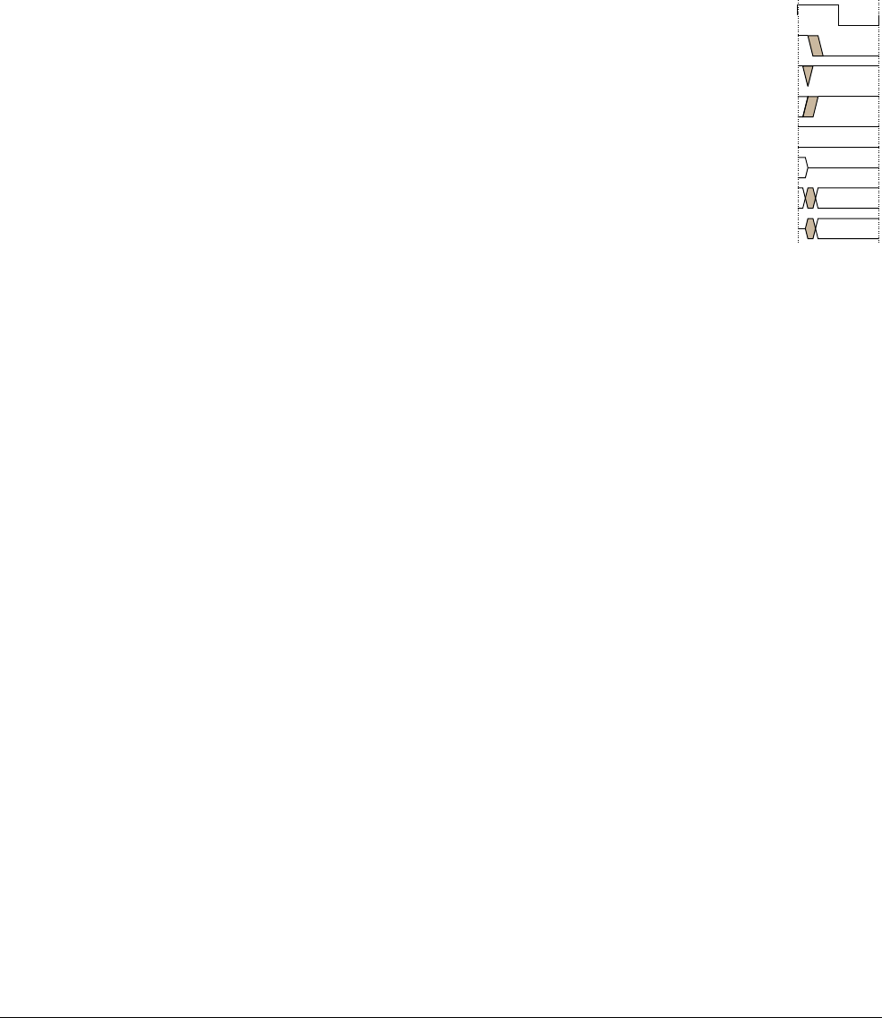
Timing diagrams
The figure named Key to timing diagram conventions explains the components used in timing
diagrams. Variations, when they occur, have clear labels. You must not assume any timing
information that is not explicit in the diagrams.
Shaded bus and signal areas are UNDEFINED, so the bus or signal can assume any value within
the shaded area at that time. The actual level is unimportant and does not affect normal
operation.
Key to timing diagram conventions
Timing diagrams sometimes show single-bit signals as HIGH and LOW at the same time and
they look similar to the bus change shown in Key to timing diagram conventions. If a timing
diagram shows a single-bit signal in this way then its value does not affect the accompanying
description.
Signals
The signal conventions are:
Signal level The level of an asserted signal depends on whether the signal is
active-HIGH or active-LOW. Asserted means:
• HIGH for active-HIGH signals.
• LOW for active-LOW signals.
Lower-case n At the start or end of a signal name denotes an active-LOW signal.
Clock
HIGH to LOW
Transient
HIGH/LOW to HIGH
Bus stable
Bus to high impedance
Bus change
High impedance to stable bus

Preface
ARM DDI 0489D Copyright © 2014, 2015 ARM. All rights reserved. x
ID082615 Non-Confidential
Additional reading
This section lists publications by ARM and by third parties.
See Infocenter,
http://infocenter.arm.com
, for access to ARM documentation.
See on ARM,
www.arm.com/cmsis
, for embedded software development resources including the
Cortex Microcontroller Software Interface Standard (CMSIS).
ARM publications
This book contains information that is specific to this product. See the following documents for
other relevant information:
•ARM®v7-M Architecture Reference Manual (ARM DDI 0403).
•ARM® CoreLink™ Level 2 Cache Controller L2C-310 Technical Reference Manual
(ARM DDI 0246).
•ARM® CoreSight™ ETM-M7 Technical Reference Manual (ARM DDI 0494).
•ARM® AMBA® AXI and ACE Protocol Specification (ARM IHI 0022).
•ARM® AMBA® 3 AHB-Lite Protocol (v1.0) (ARM IHI 0033).
•ARM® AMBA® 3 ATB Protocol Specification (ARM IHI 0032).
•ARM® AMBA® 3 APB Protocol Specification (ARM IHI 0024).
•ARM® CoreSight™ SoC-400 Technical Reference Manual (ARM DDI 0480).
•ARM® CoreSight™ Architecture Specification (v2.0) (ARM IHI 0029).
•ARM® Debug Interface v5 Architecture Specification (ARM IHI 0031).
•ARM® Embedded Trace Macrocell Architecture Specification ETMv4 (ARM IHI 0064).
The following confidential books are only available to licensees:
•ARM® Cortex®-M7 Processor Integration and Implementation Manual (ARM DII 0239).
Other publications
This section lists relevant documents published by third parties:
•Test Access Port and Boundary-Scan Architecture, IEEE Standard 1149.1-2001 (JTAG).
•IEEE Standard for Binary Floating-Point Arithmetic, IEEE Standard 754-2008.

Preface
ARM DDI 0489D Copyright © 2014, 2015 ARM. All rights reserved. xi
ID082615 Non-Confidential
Feedback
ARM welcomes feedback on this product and its documentation.
Feedback on this product
If you have any comments or suggestions about this product, contact your supplier and give:
• The product name.
• The product revision or version.
• An explanation with as much information as you can provide. Include symptoms and
diagnostic procedures if appropriate.
Feedback on content
If you have comments on content then send an e-mail to
errata@arm.com
. Give:
• The title.
• The number, ARM DDI 0489D.
• The page numbers to which your comments apply.
• A concise explanation of your comments.
ARM also welcomes general suggestions for additions and improvements.
Note
ARM tests the PDF only in Adobe Acrobat and Acrobat Reader, and cannot guarantee the
quality of the represented document when used with any other PDF reader.

ARM DDI 0489D Copyright © 2014, 2015 ARM. All rights reserved. 1-1
ID082615 Non-Confidential
Chapter 1
Introduction
This chapter introduces the processor. It contains the following sections:
•About the Cortex-M7 processor on page 1-2.
•Component blocks on page 1-6.
•Interfaces on page 1-11.
•Supported standards on page 1-13.
•Design process on page 1-14.
•Documentation on page 1-15.
•Product revisions on page 1-16.
Introduction
ARM DDI 0489D Copyright © 2014, 2015 ARM. All rights reserved. 1-2
ID082615 Non-Confidential
1.1 About the Cortex-M7 processor
The Cortex-M7 processor is a highly efficient high-performance, embedded processor that
features low interrupt latency, low-cost debug, and has backwards compatibility with existing
Cortex-M profile processors. The processor has an in-order super-scalar pipeline that means
many instructions can be dual-issued, including load/load and load/store instruction pairs
because of multiple memory interfaces.
Memory interfaces that the processor supports include:
•Tightly-Coupled Memory (TCM) interfaces.
• Harvard instruction and data caches and AXI master (AXIM) interface.
• Dedicated low-latency AHB-Lite peripheral (AHBP) interface.
•AHB-Lite slave (AHBS) interface that provides DMA access to TCMs.
The processor has an optional Memory Protection Unit (MPU) that you can configure to protect
regions of memory. Error Correcting Code (ECC) functionality for error detection and
correction, is included in the data and instruction caches when implemented. The TCM
interfaces support the implementation of external ECC to provide improved reliability and to
address safety-related applications.
The Cortex-M7 processor includes optional floating-point arithmetic functionality, with support
for single and double-precision arithmetic. See Chapter 8 Floating Point Unit.
The processor is intended for high-performance, deeply embedded applications that require fast
interrupt response features.
Figure 1-1 shows the processor in a typical system.
Figure 1-1 Example Cortex-M7 system
1.1.1 Features
The main features of the Cortex-M7 processor include:
• An in-order issue, super-scalar pipeline with dynamic branch prediction.
• DSP extensions.
• The ARMv7-M Thumb® instruction set, defined in the ARM®v7-M Architecture Reference
Manual.
• Banked Stack Pointer (SP).
• Hardware integer divide instructions,
SDIV
and
UDIV
.
• Handler and Thread modes.
DMAC
Cortex-M7 processor
AHB matrix AHB bridge
GPIO External
memory
Fast
SRAM
Low latency
peripherals
AHBS
AXIMAHBPDTCMITCM
Fast
Flash

Introduction
ARM DDI 0489D Copyright © 2014, 2015 ARM. All rights reserved. 1-3
ID082615 Non-Confidential
• Thumb and Debug states.
• Automatic processor state saving and restoration for low-latency Interrupt Service
Routine (ISR) entry and exit.
• Support for ARMv7-M big-endian byte-invariant or little-endian accesses.
• Support for ARMv7-M unaligned accesses.
• Low-latency interrupt processing achieved by:
—A Nested Vectored Interrupt Controller (NVIC) closely integrated with the
processor.
— Supporting exception-continuable instructions, such as
LDM
,
LDMDB
,
STM
,
STMDB
,
PUSH
,
POP
and
VLDM
,
VSTM
,
VPUSH
,
VPOP
if the processor has the Floating Point Unit (FPU).
• A low-cost debug solution with the optional ability to:
— Implement breakpoints.
— Implement watchpoints, tracing, and system profiling.
— Support
printf()
style debugging through an Instrumentation Trace Macrocell
(ITM).
— Optional Trace Port Interface Unit (TPIU).
— Optional Debug Access Port (DAP).
• Support for an optional Embedded Trace Macrocell (ETM). See the ARM® CoreSight™
ETM-M7 Technical Reference Manual for more information.
• A memory system, that includes an optional MPU and Harvard data and instruction cache
with ECC.
• An optional Floating Point Unit (FPU).
• Low-power features including architectural clock gating, sleep mode and Wake-up
Interrupt Controller (WIC).
• Optional AXI to AHB bridge for legacy memory system support.
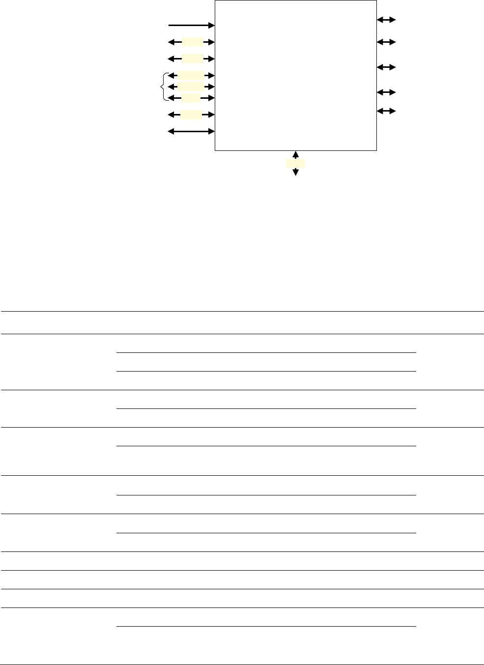
1.1.2 Interfaces
The Cortex-M7 processor has a number of external interfaces.
Figure 1-2 on page 1-4 shows the external interfaces of the Cortex-M7 processor.
Introduction
ARM DDI 0489D Copyright © 2014, 2015 ARM. All rights reserved. 1-4
ID082615 Non-Confidential
Figure 1-2 Cortex-M7 processor interfaces
1.1.3 Configuration options
The Cortex-M7 processor has configurable options that you can configure during the
implementation and integration stages to match your functional requirements.
Table 1-1 shows the configurable options at build time of the processor.
Cortex-M7 Processor
AHBD
DMA
Memory
Peripherals
MBIST
AHBP
D0TCM
D1TCM
ITCM
AHBS
Interrupts
External PPB
ATB Data
ATB Instruction
AXIM
Debug
ATB Instrumentation
Cross Trigger Interface
Table 1-1 Implementation options
Feature Options Done at
Floating-point No floating-point. Implementation
Single-precision floating-point only.
Single-precision and double-precision floating-point.
Instruction TCM No instruction TCM. Integration
4KB-16MB (powers of 2).
Data TCM No data TCM. Integration
4KB-16MB (powers of 2). The Data TCM is split equally into two TCMs,
D0TCM, and D1TCM.
Instruction cache No instruction cache unit (ICU)a.Implementation
Instruction cache unit is included.
Data cache Area optimized AXIM interface, no data cache unit (DCU)b.Implementation
Performance optimized AXIM interface, data cache unit is included.
Instruction cache size 4KB, 8KB, 16KB, 32KB, 64KB. Integration
Data cache size 4KB, 8KB, 16KB, 32KB, 64KB. Integration
AHB peripheral size 64MB, 128MB, 256MB, 512MB. Integration
ECC support on caches No ECC on instruction cache or data cache. Implementation
ECC on all implemented caches.

Introduction
ARM DDI 0489D Copyright © 2014, 2015 ARM. All rights reserved. 1-5
ID082615 Non-Confidential
Protected memory regions 0 region, 8 regions, 16 regions. Implementation
Interrupts 1-240 interrupts. Implementation
Number bits of interrupt
priority
Between three and eight bits of interrupt priority, between 8 and 256 levels of
priority.
Implementation
Debug watchpoints and
breakpoints
Reduced set. Two data watchpoints comparators and four breakpoint comparators. Implementation
Full set. Four data watchpoints comparators and eight breakpoint comparators.
ITM and Data Watchpoint
and Trace (DWT) trace
functionality
No ITM or DWT trace. Implementation
Complete ITM and DWT trace.
ETM No ETM support. Implementation
ETM instruction trace only.
ETM instruction and data trace.
Dual-redundant processor No dual-redundant processor. Implementation
Dual-redundant processor included.
Reset All Registers Only required registers that must be initialized are reset in the RTL. Implementation
All registers are reset in the RTL excluding those in the ETM, if included.
All registers are reset in the RTL including those in the ETM, if included.
Cross Trigger Interface
(CTI)
No Cross Trigger Interface. Implementation
Cross Trigger Interface included.
Wake-up Interrupt Controller
(WIC)
No Wake-up Interrupt controller. Implementation
Wake-up Interrupt controller included.
a. The ICU includes an instruction cache controller.
b. The DCU includes a data cache controller.
Table 1-1 Implementation options (continued)
Feature Options Done at
Introduction
ARM DDI 0489D Copyright © 2014, 2015 ARM. All rights reserved. 1-6
ID082615 Non-Confidential
1.2 Component blocks
The Cortex-M7 processor has fixed and optional component blocks. Optional components are:
•Wake-up Interrupt Controller (WIC).
•ITM.
•FPU.
•MPU.
• Instruction cache unit.
• Data cache unit.
•Cross Trigger Interface (CTI).
•ETM.
All other components are fixed.
Table 1-1 on page 1-4 shows the configurable options at implementation time of the processor.
Figure 1-3 shows the optional and fixed components of the Cortex-M7 processor.
Figure 1-3 Cortex-M7 functional diagram
Cortex-M7 Processor
‡ ITM
Cortex-M7
Processor
ROM table
DMA
Memory
Peripherals
NVIC
‡ ETM
MBIST
AHBP
DWT
‡ FPU
LSU
PFU
DPU
‡ WIC
Interrupts
External
PPB
ATB Data
FPB
‡ MPU
ATB
Instruction
Debugger
Cortex-M7
PPB ROM
table
ATB
Instrumentation
STB
AHBD
Memory
system
TCU
‡ Optional
D0TCM
D1TCM
ITCM
AHBS
‡ DCU and
D-cache
RAM
BIU
‡ ICU and
I-cache RAM
AXIM
‡ CTI Cross
Trigger
Interface
MIU

Introduction
ARM DDI 0489D Copyright © 2014, 2015 ARM. All rights reserved. 1-7
ID082615 Non-Confidential
The Cortex-M7 processor contains the following component blocks:
•Data Processing Unit.
•Prefetch Unit.
•Load Store Unit.
•Floating Point Unit on page 1-8.
•Nested Vectored Interrupt Controller on page 1-8.
•Wake-up Interrupt Controller on page 1-8.
•Memory System on page 1-9.
•Memory Protection Unit on page 1-9.
•Cortex-M7 Processor and PPB ROM tables on page 1-9.
•Cross Trigger Interface Unit on page 1-9.
•ETM on page 1-9.
•Debug and trace components on page 1-9.
1.2.1 Data Processing Unit
The Data Processing Unit (DPU) provides:
• Parallelized integer register file with six read ports and four write ports for large-scale
dual-issue.
• Extensive forwarding logic to minimise interlocks.
• Two ALUs, with one ALU capable of executing SIMD operations.
• Single MAC pipeline capable of 32x32-bit + 64-bit → 64-bit with two cycle result latency
and one MAC per cycle throughput.
• Single divider unit with support for operand-dependent early termination.
1.2.2 Prefetch Unit
The Prefetch Unit (PFU) provides:
• 64-bit instruction fetch bandwidth.
• 4x64-bit pre-fetch queue to decouple instruction pre-fetch from DPU pipeline operation.
•A Branch Target Address Cache (BTAC) for single-cycle turn-around of branch predictor
state and target address.
• A static branch predictor when no BTAC is specified.
• Forwarding of flags for early resolution of direct branches in the decoder and first
execution stages of the processor pipeline.
1.2.3 Load Store Unit
The Load Store Unit (LSU) provides:
• Dual 32-bit load channels to TCM, data cache, and AXI master (AXIM) interface for
64-bit load bandwidth and dual 32-bit load capability.
• Single 32-bit load channel to the AHB interface.
• Single 64-bit store channel.

Introduction
ARM DDI 0489D Copyright © 2014, 2015 ARM. All rights reserved. 1-8
ID082615 Non-Confidential
• Store buffering to increase store throughput and minimize RAM contention with data and
instruction reads.
• Separate store buffering for TCM, AHBP and AXIM for Quality of Service (QoS) and
interface-specific optimizations.
1.2.4 Floating Point Unit
The optional Floating Point Unit (FPU) provides:
• Lazy floating-point context save. Automated stacking of floating-point state is delayed
until the ISR attempts to execute a floating-point instruction. This reduces the latency to
enter the ISR and removes floating-point context save for ISRs that do not use
floating-point.
• Instructions for single-precision (C programming language
float
type) data-processing
operations.
• Optional instructions for double-precision (C
double
type) data-processing operations.
• Combined Multiply and Accumulate instructions for increased precision (Fused MAC).
• Hardware support for conversion, addition, subtraction, multiplication with optional
accumulate, division, and square-root.
• Hardware support for denormals and all IEEE Standard 754-2008 rounding modes.
• 32 32-bit single-precision registers or 16 64-bit double-precision registers.
See Chapter 8 Floating Point Unit for more information.
1.2.5 Nested Vectored Interrupt Controller
The NVIC is closely integrated with the core to achieve low-latency interrupt processing.
Features include:
• External interrupts, configurable from 1 to 240. This is configured at implementation.
• Configurable levels of interrupt priority from 8 to 256. Configured at implementation.
• Dynamic reprioritization of interrupts.
• Priority grouping. This enables selection of preempting interrupt levels and non
preempting interrupt levels.
• Support for tail-chaining and late arrival of interrupts. This enables back-to-back interrupt
processing without the overhead of state saving and restoration between interrupts.
See Chapter 7 Nested Vectored Interrupt Controller for more information.
1.2.6 Wake-up Interrupt Controller
The optional WIC provides ultra-low power sleep mode support.
See Low power modes on page 7-3 for more information.

Introduction
ARM DDI 0489D Copyright © 2014, 2015 ARM. All rights reserved. 1-9
ID082615 Non-Confidential
1.2.7 Memory System
The optional memory system includes:
•A Bus Interface Unit (BIU) with a configurable AMBA 4 AXI interface that can support
a high-performance L2 memory system.
• An extended AHB-Lite interface to support low-latency system peripherals.
•A TCM Control Unit (TCU) with TCM interfaces that can support external ECC logic and
an AHB slave (AHBS) interface for system access to TCMs.
• Instruction cache and data cache units, with optional Error Correction Code (ECC).
•A Memory Built-in Self Test (MBIST) interface provided by the MBIST interface unit
(MIU). The memory system supports online MBIST, where the RAM arrays can be
accessed by the MBIST interface while the processor is running. MBIST is also supported
during production test.
See Chapter 5 Memory System for more information.
1.2.8 Store Buffer
The Store Buffer (STB) holds store operations when they have left the load/store pipeline and
have been committed by the DPU. From the STB, a store can request access to the cache RAM
in the DCU, request the BIU to initiate linefills, or request the BIU to write the data out on the
AXIM interface.
The STB can merge several store transactions into a single transaction if they are to the same
64-bit aligned address.
1.2.9 Memory Protection Unit
The optional MPU has configurable attributes for memory protection. It includes up to 16
memory regions and Sub Region Disable (SRD), enabling efficient use of memory regions. It
also has the ability to enable a background region that implements the default memory map
attributes. See Chapter 6 Memory Protection Unit for more information.
1.2.10 Cortex-M7 Processor and PPB ROM tables
The two ROM tables enable a debugger to identify and connect to CoreSight debug
components. See Chapter 9 Debug for more information.
1.2.11 Cross Trigger Interface Unit
The optional CTI enables the debug logic and ETM to interact with each other and with other
CoreSight components. See Chapter 10 Cross Trigger Interface.
1.2.12 ETM
The optional ETM provides instruction-only or instruction and data trace capabilities when
configured. See the ARM® CoreSight™ ETM-M7 Technical Reference Manual for more
information.
1.2.13 Debug and trace components
• Configurable Breakpoint unit (FPB) for implementing breakpoints.

Introduction
ARM DDI 0489D Copyright © 2014, 2015 ARM. All rights reserved. 1-10
ID082615 Non-Confidential
• Configurable Data Watchpoint and Trace (DWT) unit for implementing watchpoints, data
tracing, and system profiling.
• Optional ITM for support of
printf()
style debugging, using instrumentation trace.
• Interfaces suitable for:
— Passing on-chip data to a Trace Port Analyzer (TPA), including Single Wire Output
(SWO) mode.
— Debugger access to all memory and registers in the system, including access to
memory-mapped devices, access to internal core registers when the core is halted,
and access to debug control registers even when reset is asserted.

Introduction
ARM DDI 0489D Copyright © 2014, 2015 ARM. All rights reserved. 1-11
ID082615 Non-Confidential
1.3 Interfaces
The processor contains the following external interfaces:
•AHBP interface.
•AHBS interface.
•AHBD interface.
•External Private Peripheral Bus.
•ATB interfaces.
•TCM interface.
•Cross Trigger interface on page 1-12.
•MBIST interface on page 1-12.
•AXIM interface on page 1-12.
1.3.1 AHBP interface
The AHB-Lite peripheral (AHBP) interface provides access suitable for low latency system
peripherals. It provides support for unaligned memory accesses, write buffer for buffering of
write data, and exclusive access transfers for multiprocessor systems. See AHB peripheral
interface on page 5-22 for more information.
1.3.2 AHBS interface
The AHB-Lite slave (AHBS) interface enables system access to TCMs. See AHB slave interface
on page 5-30 for more information.
1.3.3 AHBD interface
The AHB-Lite Debug (AHBD) interface provides debug access to the Cortex-M7 processor and
the complete memory map. See About the AHBD interface on page 9-7 for more information.
1.3.4 External Private Peripheral Bus
The APB External PPB (EPPB) enables access to CoreSight-compatible debug and trace
components, in the system connected to the processor.
1.3.5 ATB interfaces
The ATB interfaces output trace information used for debugging. The ATB interface is
compatible with the CoreSight architecture. See the ARM® CoreSight™ Architecture
Specification (v2.0) for more information.
1.3.6 TCM interface
The processor can have up to two TCM memory instances, Instruction TCM (ITCM) and Data
TCM (DTCM), each with a double word data width. Access to ITCM is through the ITCM
64-bit wide interface. Access to DTCM is through the D1TCM 32-bit wide interface and the
32-bit wide D0TCM interface. The DTCM accesses are split so that lower words always access
D0TCM and upper words always access D1TCM. The size of both TCM instances is
configurable, 4KB-16MB in powers of 2. See TCM interfaces on page 5-33 for more
information.

Introduction
ARM DDI 0489D Copyright © 2014, 2015 ARM. All rights reserved. 1-12
ID082615 Non-Confidential
1.3.7 Cross Trigger interface
The processor includes an optional Cross Trigger Interface Unit which includes an interface
suitable for connection to external CoreSight components using a Cross Trigger Matrix. See
Chapter 10 Cross Trigger Interface for more information.
1.3.8 MBIST interface
The MBIST interface is used for testing the RAMs during production test. The Cortex-M7
processor also allows the RAMs to be tested using the MBIST interface during normal
execution. This is known as online MBIST.
Contact your implementation team for more information about the MBIST interface and online
MBIST.
1.3.9 AXIM interface
The AXI master (AXIM) interface provides high-performance access to an external memory
system. The AXIM interface supports use of the ARM CoreLink L2C-310 Level 2 Cache
Controller. L2C-310 Exclusive cache configuration is not supported. See AXIM interface on
page 5-6 for more information.

Introduction
ARM DDI 0489D Copyright © 2014, 2015 ARM. All rights reserved. 1-13
ID082615 Non-Confidential
1.4 Supported standards
The processor complies with, or implements, the specifications described in:
•ARM architecture.
•Bus architecture.
•Debug.
•Embedded Trace Macrocell.
•Floating Point Unit.
This book complements architecture reference manuals, architecture specifications, protocol
specifications, and relevant external standards. It does not duplicate information from these
sources.
1.4.1 ARM architecture
The Cortex-M7 processor implements the ARMv7E-M architecture profile. See the ARM®v7-M
Architecture Reference Manual.
The Cortex-M7 processor FPB implements the Flash Patch Breakpoint version 2 architecture
revision.
1.4.2 Bus architecture
The processor provides an:
• External interface that is a variant of the AMBA 3 AHB-Lite protocol.
• External interface that complies with the AMBA 4 AXI.
The processor also implements an interface for CoreSight and other debug components using
the AMBA 3 APB protocol and AMBA 3 ATB Protocol.
For more information, see:
•The ARM® AMBA® AXI and ACE Protocol Specification.
•The ARM® AMBA® 3 AHB-Lite Protocol (v1.0).
•The ARM® AMBA® 3 APB Protocol Specification.
•The ARM® AMBA® 3 ATB Protocol Specification.
1.4.3 Debug
The debug features of the processor implement the ARM debug interface architecture. See the
ARM® Debug Interface v5 Architecture Specification.
1.4.4 Embedded Trace Macrocell
When implemented, the trace features of the processor implement the ARM Embedded Trace
Macrocell (ETM)v4 architecture. See the ARM® Embedded Trace Macrocell Architecture
Specification ETMv4.
1.4.5 Floating Point Unit
Depending on your implementation, a Cortex-M7 processor with FPU can have single-precision
only or single and double-precision floating-point data processing as defined by the FPv5
architecture, that is part of the ARMv7E-M architecture. It provides floating-point computation
functionality that is compliant with the ANSI/IEEE Std 754-2008, IEEE Standard for Binary
Floating-Point Arithmetic.

Introduction
ARM DDI 0489D Copyright © 2014, 2015 ARM. All rights reserved. 1-14
ID082615 Non-Confidential
1.5 Design process
The Cortex-M7 processor is delivered as synthesizable RTL that must go through the
implementation, integration, and programming processes before you can use it in a product.
The following definitions describe each top-level process in the design flow:
Implementation
The implementer configures and synthesizes the RTL.
Integration
The integrator connects the implemented design into a SoC. This includes
connecting it to a memory system and peripherals.
Programming
The system programmer develops the software required to configure and
initialize the processor, and tests the required application software.
Each stage in the process can be performed by a different party. Implementation and integration
choices affect the behavior and features of the processor.
For MCUs, often a single design team integrates the processor before synthesizing the complete
design. Alternatively, the team can synthesize the processor on its own or partially integrated,
to produce a macrocell that is then integrated, possibly by a separate team.
The operation of the final device depends on:
Build configuration
The implementer chooses the options that affect how the RTL source files are
pre-processed. These options usually include or exclude logic that affects one or
more of the area, maximum frequency, and features of the resulting macrocell.
Configuration inputs
The integrator configures some features of the processor by tying inputs to
specific values. These configurations affect the start-up behavior before any
software configuration is made. They can also limit the options available to the
software.
Software configuration
The programer configures the processor by programming particular values into
registers. This affects the behavior of the processor.
Note
This manual refers to implementation-defined features that are applicable to build configuration
options. Reference to a feature that is included means that the appropriate build and pin
configuration options are selected. Reference to an enabled feature means one that has also been
configured by software.

Introduction
ARM DDI 0489D Copyright © 2014, 2015 ARM. All rights reserved. 1-15
ID082615 Non-Confidential
1.6 Documentation
The Cortex-M7 processor documentation can help you complete the top-level processes of
implementation, integration, and programming required to use the product correctly.
The Cortex-M7 processor documentation comprises a Technical Reference Manual, an
Integration and Implementation Manual, and User Guide Reference Material.
Technical Reference Manual
The Technical Reference Manual (TRM) describes the functionality and the
effects of functional options on the behavior of the Cortex-M7 processor. It is
required at all stages of the design flow. Some behavior described in the TRM
might not be relevant because of the way that the Cortex-M7 processor is
implemented and integrated. If you are programming the Cortex-M7 processor
then contact the implementer to determine:
• The build configuration of the implementation.
• What integration, if any, was performed before implementing the processor.
Integration and Implementation Manual
The Integration and Implementation Manual (IIM) describes:
• The available build configuration options and related issues in selecting
them.
• How to configure the Register Transfer Level (RTL) with the build
configuration options.
• How to integrate the processor into a SoC. This includes a description of
the integration kit and describes the pins that the integrator must tie off to
configure the macrocell for the required integration.
• How to implement the processor into your design. This includes
floorplanning guidelines, Memory Built-in Self Test (MBIST) and Design
for Test (DFT) information, and how to perform netlist dynamic
verification on the processor.
• The processes to sign off the integration and implementation of the design.
The ARM product deliverables include reference scripts and information about
using them to implement your design.
Reference methodology documentation from your EDA tools vendor
complements the IIM.
The IIM is a confidential book that is only available to licensees.
User Guide Reference Material
This document provides reference material that ARM partners can configure and
include in a User Guide for an ARM Cortex-M7 processor. Typically:
• Each chapter in this reference material might correspond to a section in the
User Guide.
• Each top-level section in this reference material might correspond to a
chapter in the User Guide.
However, you can organize this material in any way, subject to the conditions of
the licence agreement under which ARM supplied the material.
See Additional reading on page x for more information about the books associated with the
Cortex-M7 processor.

Introduction
ARM DDI 0489D Copyright © 2014, 2015 ARM. All rights reserved. 1-16
ID082615 Non-Confidential
1.7 Product revisions
This section describes the differences in functionality between product revisions:
r0p0 First release.
r0p1 The following changes have been made in this release:
• Updated CPUID reset value,
0x410FC271
.
• Various engineering errata fixes.
r0p2 The following changes have been made in this release:
• Updated CPUID reset value,
0x410FC272
.
• Various engineering errata fixes.
r1p0 The following changes have been made in this release:
• Updated CPUID reset value,
0x411FC270
.
• Added CTLPPBLOCK[3:0] to allow locking of registers ITCMCR,
DTCMCR, AHBPCR, VTOR to prevent unwanted updates.
• Added ACTLR bit functions to allow low-capability AXI systems to
disable AXI reads to DEV/SO memory and disable exclusive reads/writes
to shared memory not initiated until all outstanding reads/stores on AXI are
complete.
• Added MBISTIMPERR[2] output to MBIST interface to provide an error
when attempting to access unimplemented memory.
• Improved handling of simultaneous AHBS and software activity relating to
the same TCM.
r1p1 The following changes have been made in this release:
• Updated CPUID reset value,
0x411FC271
.

ARM DDI 0489D Copyright © 2014, 2015 ARM. All rights reserved. 2-1
ID082615 Non-Confidential
Chapter 2
Programmers Model
This chapter describes the programmers model. It contains the following sections:
•About the programmers model on page 2-2.
•Modes of operation and execution on page 2-3.
•Instruction set summary on page 2-4.
•System address map on page 2-5.
•Exclusive monitor on page 2-7.
•Processor core registers on page 2-8.
•Exceptions on page 2-9.

Programmers Model
ARM DDI 0489D Copyright © 2014, 2015 ARM. All rights reserved. 2-2
ID082615 Non-Confidential
2.1 About the programmers model
This chapter gives an overview of the Cortex-M7 processor programmers model that describes
the implementation-defined options. In addition:
•Chapter 3 summarizes the system control features of the programmers model.
•Chapter 6 summarizes the MPU features of the programmers model.
•Chapter 7 summarizes the NVIC features of the programmers model.
•Chapter 8 summarizes the FPU features of the programmers model.
•Chapter 9 summarizes the Debug features of the programmers model.
•Chapter 10 summarizes the CTI features of the programmers model.
•Chapter 11 summarizes the DWT features of the programmers model.
•Chapter 12 summarizes the ITM features of the programmers model.

Programmers Model
ARM DDI 0489D Copyright © 2014, 2015 ARM. All rights reserved. 2-3
ID082615 Non-Confidential
2.2 Modes of operation and execution
This section briefly describes the modes of operation and execution of the Cortex-M7 processor.
See the ARM®v7-M Architecture Reference Manual for more information.
2.2.1 Operating modes
The processor supports two modes of operation, Thread mode and Handler mode:
• The processor enters Thread mode on reset, or as a result of an exception return.
Privileged and Unprivileged code can run in Thread mode.
• The processor enters Handler mode as a result of an exception. All code is privileged in
Handler mode.
2.2.2 Operating states
The processor can operate in one of two operating states:
• Thumb state. This is normal execution running 16-bit and 32-bit halfword-aligned Thumb
instructions.
• Debug state. This is the state when the processor is in halting debug.
2.2.3 Privileged access and unprivileged User access
Code can execute as privileged or unprivileged. Unprivileged execution limits or excludes
access to some resources. Privileged execution has access to all resources. Handler mode is
always privileged. Thread mode can be privileged or unprivileged.

Programmers Model
ARM DDI 0489D Copyright © 2014, 2015 ARM. All rights reserved. 2-4
ID082615 Non-Confidential
2.3 Instruction set summary
The processor implements the ARMv7-M instruction set and features provided by the
ARMv7E-M architecture profile. For more information about the ARMv7-M instructions, see
the ARM®v7-M Architecture Reference Manual.
2.3.1 Binary compatibility with other Cortex processors
The processor is binary compatible with the instruction sets and features implemented in other
Cortex-M profile processors. You cannot move software from the Cortex-M7 processor to:
• The Cortex-M3 processor if it contains floating-point operations or instructions that are
part of the DSP extension, such as SADD16.
• The Cortex-M4 processor if it contains double-precision floating-point operations.
• The Cortex-M0 or Cortex-M0+ processors because these are implementations of the
ARMv6-M Architecture.
Code designed for the Cortex-M3 and Cortex-M4 processors is compatible with the Cortex-M7
processor as long as it does not rely on bit-banding.
To ensure a smooth transition when migrating software to the Cortex-M7 processor, ARM
recommends that code designed to operate on the Cortex-M0, M0+, M3, and M4 processors
obey the following rules and that you configure the Configuration and Control Register (CCR)
appropriately:
• Use word transfers only to access registers in the NVIC and System Control Space (SCS).
• Treat all unused SCS registers and register fields on the processor as Do-Not-Modify.
• Configure the following fields in the CCR:
— STKALIGN bit to 1.
— UNALIGN_TRP bit to 1.
— Leave all other bits in the CCR register at their original value.
Programmers Model
ARM DDI 0489D Copyright © 2014, 2015 ARM. All rights reserved. 2-5
ID082615 Non-Confidential
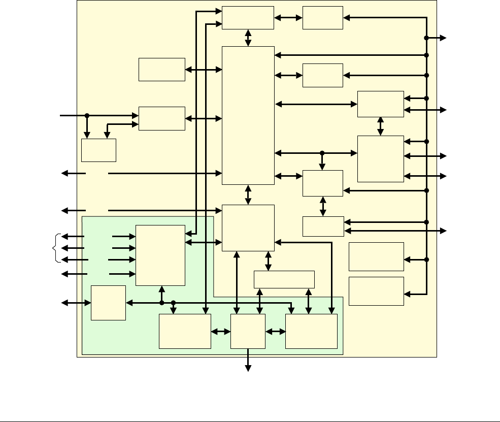
2.4 System address map
The processor contains an internal bus matrix that arbitrates the processor and external AHBD
memory accesses to both the external memory system and to the internal SCS and debug
components.
Priority is always given to the processor to ensure that any debug accesses are as non-intrusive
as possible.
Figure 2-1 shows the system address map.
Figure 2-1 System address map
Table 2-1 shows the processor interfaces that are addressed by the different memory map
regions.
System
External device
External RAM
Peripheral
SRAM
Code
0xFFFFFFFF
Private peripheral bus - External
0xE0100000
0xE0040000
0xA0000000
0x60000000
0x40000000
0x20000000
0x00000000
Private peripheral bus - Internal
1.0GB
1.0GB
0.5GB
0.5GB
0.5GB
0xE0000000
0xE0043000
0xE00FE000
CTI
0xE00FFFFF
Private Peripheral Bus
Reserved (TPIU)
0xE00FF000
0xE0041000
0xE0040000
ETM
Processor ROM table
PPB ROM table
0xE0042000
Table 2-1 Memory regions
Memory Map Region
Code Instruction fetches and data accesses are performed over the ITCM or AXIM interface.
SRAM Instruction fetches and data accesses are performed over the DTCM or AXIM interface.
Peripheral Data accesses are performed over the AHBP or AXIM interface.
Instruction fetches are performed over the AXIM interface.
External RAM Instruction fetches and data accesses are performed over the AXIM interface.

Programmers Model
ARM DDI 0489D Copyright © 2014, 2015 ARM. All rights reserved. 2-6
ID082615 Non-Confidential
See the ARM®v7-M Architecture Reference Manual for more information about the memory
model.
2.4.1 Private peripheral bus
The internal PPB interface provides access to:
•The Instrumentation Trace Macrocell (ITM).
•The Data Watchpoint and Trace (DWT).
•The Breakpoint unit (FPB).
• The SCS, including the MPU, the instruction and data cache, and the Nested Vectored
Interrupt Controller (NVIC).
• The Processor and PPB ROM tables.
The external PPB interface provides access to:
•The Embedded Trace Macrocell (ETM).
•The Cross Trigger Interface (CTI).
• CoreSight debug and trace components in the external system.
2.4.2 Unaligned accesses that cross regions
The Cortex-M7 processor supports ARMv7 unaligned accesses, and performs all accesses as
single, unaligned accesses. They are converted into two or more aligned accesses internally and
are performed on the external interfaces of the processor.
Note
All Cortex-M7 processor external accesses are aligned.
Unaligned support is only available for load/store singles (
LDR
,
LDRH, STR, STRH
). Load/store
double already supports word aligned accesses, but does not permit other unaligned accesses,
and generates a fault if this is attempted.
Unaligned accesses that cross memory map boundaries are architecturally UNPREDICTABLE. The
processor behavior is boundary dependent. Unaligned accesses are not supported to PPB space,
and so there are no boundary crossing cases for PPB accesses.
External Device Instruction fetches and data accesses are performed over the AXIM interface.
Private Peripheral Bus Data accesses to registers associated with peripherals outside the processor are performed on the
External Private Peripheral Bus (EPPB) interface. See Private peripheral bus.
This memory region is Execute Never (XN), and so instruction fetches are prohibited. An MPU,
if present, cannot change this.
System System segment for vendor system peripherals. Data accesses are performed over the AHBP
interface. This memory region is XN, and so instruction fetches are prohibited. An MPU, if
present, cannot change this.
Table 2-1 Memory regions (continued)
Memory Map Region

Programmers Model
ARM DDI 0489D Copyright © 2014, 2015 ARM. All rights reserved. 2-7
ID082615 Non-Confidential
2.5 Exclusive monitor
The Cortex-M7 processor implements a local exclusive monitor. For more information about
semaphores and the local exclusive monitor see the ARM®v7-M Architecture Reference Manual.
The local monitor within the processor is constructed so that it does not hold any physical
address. Instead it treats any access as matching the address of the previous
LDREX
instruction.
This means that the implemented Exclusives Reservation Granule (ERG) is the entire memory
address range.

Programmers Model
ARM DDI 0489D Copyright © 2014, 2015 ARM. All rights reserved. 2-8
ID082615 Non-Confidential
2.6 Processor core registers
The processor has the following 32-bit registers:
• 13 general-purpose registers, R0-R12.
•Stack Pointer (SP), R13 alias of banked registers, SP_process and SP_main.
•Link Register (LR), R14.
•Program Counter (PC), R15.
• Special-purpose Program Status Registers (xPSR).
For more information about the processor register set, see the ARM®v7-M Architecture
Reference Manual.

Programmers Model
ARM DDI 0489D Copyright © 2014, 2015 ARM. All rights reserved. 2-9
ID082615 Non-Confidential
2.7 Exceptions
The processor and the NVIC prioritize and handle all exceptions. When handling exceptions:
• All exceptions are handled in Handler mode.
• Processor state is automatically stored to the stack on an exception, and automatically
restored from the stack at the end of the Interrupt Service Routine (ISR).
• The vector is fetched in parallel to the state saving, enabling efficient interrupt entry.
The processor supports tail-chaining that enables back-to-back interrupts without the overhead
of state saving and restoration.
You configure the number of interrupts, and levels of interrupt priority, during implementation.
Software can choose only to enable a subset of the configured number of interrupts, and can
choose how many levels of the configured priorities to use.
Note
The EPSR.T bit supports the ARM architecture interworking model, however, as ARMv7-M
only supports execution of Thumb instructions, it must always be maintained with the value 1.
This means that all exception vectors must have bit[0] set. If bit[0] of the associated vector table
entry is set to 0 on exception entry, execution of the first instruction causes an INVSTATE
UsageFault. If this happens on a reset, this escalates to a HardFault, because UsageFault is
disabled on reset.
2.7.1 Exception handling
External read faults from either the TCM interfaces, the AXIM interface, or the AHB interfaces
generate a synchronous exception in the processor. External write faults generate an
asynchronous exception in the processor.
The processor implements advanced exception and interrupt handling, as described in the
ARM®v7-M Architecture Reference Manual.
The processor exception model has the following implementation-defined behavior in addition
to the architecturally-defined behavior:
• Exceptions on stacking from HardFault to NMI lockup at NMI priority.
• Exceptions on unstacking from NMI to HardFault lockup at HardFault priority.
To minimize interrupt latency, the processor can abandon the majority of multicycle instructions
that are executing when an interrupt is recognized. The only exception is a load from Device or
Strongly-ordered memory, or a shared store exclusive operation that starts on the AXI interface.
All normal memory transactions are abandoned when an interrupt is recognized.
The processor restarts any abandoned operation on return from the interrupt. The processor also
implements the Interruptible-continuable bits allowing load and store multiples to be
interruptible and continuable. In these cases the processor resumes execution of these
instructions after the last completed transfer instead of from the start. For more information on
the Interruptible-continuable bits and key limitations on when they apply, see the ARM®v7-M
Architecture Reference Manual.
Specifically, on the Cortex-M7 processor, these instructions always restart instead of continue:
• The instruction faults.
• The instruction is inside an If-Then (IT) block.
• The instruction is a load multiple, has the base register in the list and has loaded the base
register.
• The instruction is a load multiple and is subject to an ECC error.

ARM DDI 0489D Copyright © 2014, 2015 ARM. All rights reserved. 3-1
ID082615 Non-Confidential
Chapter 3
System Control
This chapter describes the registers that program the processor. It contains the following
sections:
•About system control on page 3-2.
•Register summary on page 3-3.
•Register descriptions on page 3-6.

System Control
ARM DDI 0489D Copyright © 2014, 2015 ARM. All rights reserved. 3-2
ID082615 Non-Confidential
3.1 About system control
This chapter describes the registers that control the operation of the processor. This includes
registers in the:
• System Control Space.
• Access Control Space.
• Identification Space.
• Cache Maintenance Space.

System Control
ARM DDI 0489D Copyright © 2014, 2015 ARM. All rights reserved. 3-3
ID082615 Non-Confidential
3.2 Register summary
Table 3-1 shows the system control registers. Registers not described in this chapter are
described in the ARM®v7-M Architecture Reference Manual.
Table 3-1 System control registers
Address Name Type Reset Description
0xE000E008
ACTLR RW
0x00000000
Auxiliary Control Register on page 3-6
0xE000E00C
- - - Reserved
0xE000E010
SYST_CSR RW
0x00000000
SysTick Control and Status Register
0xE000E014
SYST_RVR RW Unknown SysTick Reload Value Register
0xE000E018
SYST_CVR RW Unknown SysTick Current Value Register
0xE000E01C
SYST_CALIB RO -aSysTick Calibration Value Register
0xE000ED00
CPUID RO
0x411FC271
CPUID Base Register on page 3-8
0xE000ED04
ICSR RW or RO
0x00000000
Interrupt Control and State Register
0xE000ED08
VTOR RW -bVector Table Offset Register
0xE000ED0C
AIRCR RW
0xFA050000
cApplication Interrupt and Reset Control Register
0xE000ED10
SCR RW
0x00000000
System Control Register
0xE000ED14
CCR RWd
0x00040200
Configuration and Control Register
0xE000ED18
SHPR1 RW
0x00000000
System Handler Priority Register 1
0xE000ED1C
SHPR2 RW
0x00000000
System Handler Priority Register 2
0xE000ED20
SHPR3 RW
0x00000000
System Handler Priority Register 3
0xE000ED24
SHCSR RW
0x00000000
System Handler Control and State Register
0xE000ED28
CFSR RW
0x00000000
Configurable Fault Status Registerse
0xE000ED2C
HFSR RW
0x00000000
HardFault Status Register
0xE000ED30
DFSR RW
0x00000000
Debug Fault Status Register
0xE000ED34
MMFAR RW Unknown MemManage Fault Address Registerf
0xE000ED38
BFAR RW Unknown BusFault Address Registerf
0xE000ED40
ID_PFR0 RO
0x00000030
Processor Feature Register 0
0xE000ED44
ID_PFR1 RO
0x00000200
Processor Feature Register 1
0xE000ED48
ID_DFR0 RO
0x00100000
Debug Feature Register 0g
0xE000ED4C
ID_AFR0 RO
0x00000000
Auxiliary Feature Register 0
0xE000ED50
ID_MMFR0 RO
0x00100030
hMemory Model Feature Register 0
0xE000ED54
ID_MMFR1 RO
0x00000000
Memory Model Feature Register 1
0xE000ED58
ID_MMFR2 RO
0x01000000
Memory Model Feature Register 2
0xE000ED5C
ID_MMFR3 RO
0x00000000
Memory Model Feature Register 3

System Control
ARM DDI 0489D Copyright © 2014, 2015 ARM. All rights reserved. 3-4
ID082615 Non-Confidential
0xE000ED60
ID_ISAR0 RO
0x01101110
Instruction Set Attributes Register 0
0xE000ED64
ID_ISAR1 RO
0x02112000
Instruction Set Attributes Register 1
0xE000ED68
ID_ISAR2 RO
0x20232231
Instruction Set Attributes Register 2
0xE000ED6C
ID_ISAR3 RO
0x01111131
Instruction Set Attributes Register 3
0xE000ED70
ID_ISAR4 RO
0x01310132
Instruction Set Attributes Register 4
0xE000ED78
CLIDR RO -iCache Level ID Register on page 3-9
0xE000ED7C
CTR RO
0x8303C003
Cache Type Register
0xE000ED80
CCSIDR RO -jCache Size ID Register on page 3-10
0xE000ED84
CSSELR RW UNPREDICTABLE Cache Size Selection Register on page 3-12
0xE000ED88
CPACR RW - Coprocessor Access Control Register
0xE000EF00
STIR WO
0x00000000
Software Triggered Interrupt Register
0xE000EF50
ICIALLU WO Unknown Instruction cache invalidate all to Point of Unification
(PoU)
0xE000EF54
- - - Reserved
0xE000EF58
ICIMVAU WO Unknown Instruction cache invalidate by address to PoU
0xE000EF5C
DCIMVAC WO Unknown Data cache invalidate by address to Point of Coherency
(PoC)
0xE000EF60
DCISW WO Unknown Data cache invalidate by set/way
0xE000EF64
DCCMVAU WO Unknown Data cache by address to PoU
0xE000EF68
DCCMVAC WO Unknown Data cache clean by address to PoC
0xE000EF6C
DCCSW WO Unknown Data cache clean by set/way
0xE000EF70
DCCIMVAC WO Unknown Data cache clean and invalidate by address to PoC
0xE000EF74
DCCISW WO Unknown Data cache clean and invalidate by set/way
0xE000EF78
BPIALL RAZ/WI Unknown Not implemented
0xE000EF7C
- - - Reserved
0xE000EF80
- - - Reserved
0xE000EF90
CM7_ITCMCR RW Unknown Instruction and Data Tightly-Coupled Memory Control
Registers on page 3-13
0xE000EF94
CM7_DTCMCR RW Unknown
0xE000EF98
CM7_AHBPCR RW Unknown AHBP Control Register on page 3-14
0xE000EF9C
CM7_CACR RW Unknown L1 Cache Control Register on page 3-15
0xE000EFA0
CM7_AHBSCR RW Unknown AHB Slave Control Register on page 3-20
0xE000EFA4
- - - Reserved
0xE000EFA8
CM7_ABFSR RW Unknown Auxiliary Bus Fault Status Register on page 3-16
Table 3-1 System control registers (continued)
Address Name Type Reset Description

System Control
ARM DDI 0489D Copyright © 2014, 2015 ARM. All rights reserved. 3-5
ID082615 Non-Confidential
Table 3-2 shows how signal CFGSTCALIB[25:0] is indicated in register SYST_CALIB.
0xE000EFB0
IEBR0kRW - Instruction Error bank Register 0-1 on page 3-17
0xE000EFB4
IEBR1kRW -
0xE000EFB8
DEBR0kRW - Data Error bank Register 0-1 on page 3-18
0xE000EFBC
DEBR1kRW -
0xE000EFD0
PID4 -
0x00000004
See the Component and Peripheral ID register formats in
the ARM®v7-M Architecture Reference Manual.
0xE000EFD4
PID5 -
0x00000000
0xE000EFD8
PID6 -
0x00000000
0xE000EFDC
PID7 -
0x00000000
0xE000EFE0
PID0 -
-
l
0xE000EFE4
PID1 -
0x000000B0
0xE000EFE8
PID2 -
0x0000000B
0xE000EFEC
PID3 -
0x00000000
0xE000EFF0
CID0 -
0x0000000D
0xE000EFF4
CID1 -
0x000000E0
0xE000EFF8
CID2 -
0x00000005
0xE000EFFC
CID3 -
0x000000B1
a. SYST_CALIB indicates the value of signal CFGSTCALIB[25:0]. See Table 3-2.
b. VTOR[31:7] indicates the value of signal INITVTOR[31:7]. VTOR[6:0] are RAZ.
c. AIRCR[15] indicates the value of signal CFGBIGEND.
d. The processor implements bit[9] of CCR, STKALIGN, as RO and has a value of 1.
e. The 32-bit CFSR comprises the status registers for the faults that have configurable priority. Software can access the combined CFSR,
or use byte or halfword accesses to access the individual registers, MemManage Status Register (MMFSR), BusFault Status Register
(BFSR), and UsageFault Status Register (UFSR). See the ARM®v7-M Architecture Reference Manual for more information.
f. BFAR and MFAR are the same physical register. Because of this, the BFARVALID and MFARVALID bits are mutually exclusive.
g. ID_DFR0 reads as 0 if no debug support is implemented.
h. The reset value depends on the values of signals CFGITCMSZ and CFGDTCMSZ.
i. The reset value depends on whether L1 cache is implemented.
j. Reset value depends on which caches are implemented and their sizes.
k. Only present if ECC is present, otherwise RAZ/WI.
l. This value is
0x00000000
for implementations without FPU or
0x0000000C
for implementations with FPU.
Table 3-1 System control registers (continued)
Address Name Type Reset Description
Table 3-2 SYST_CALIB inputs
Bits Name Input
[31] NOREF CFGSTCALIB[25].
[30] SKEW CFGSTCALIB[24].
[29:24] - None. RAZ.
[23:0] TENMS CFGSTCALIB[23:0].
System Control
ARM DDI 0489D Copyright © 2014, 2015 ARM. All rights reserved. 3-6
ID082615 Non-Confidential
3.3 Register descriptions
This section describes the following system control registers whose implementation is specific
to this processor:
•Auxiliary Control Register.
•CPUID Base Register on page 3-8.
•Cache Level ID Register on page 3-9.
•Cache Size ID Register on page 3-10.
•Cache Size Selection Register on page 3-12.
•Instruction and Data Tightly-Coupled Memory Control Registers on page 3-13.
•AHBP Control Register on page 3-14.
•L1 Cache Control Register on page 3-15.
•Auxiliary Bus Fault Status Register on page 3-16.
•Instruction Error bank Register 0-1 on page 3-17.
•Data Error bank Register 0-1 on page 3-18.
•AHB Slave Control Register on page 3-20.
3.3.1 Auxiliary Control Register
The ACTLR characteristics are:
Purpose Provides implementation defined configuration and control options for the
processor.
Usage Constraints There are no usage constraints.
Configurations Available in all configurations.
Attributes See the register summary in Table 3-1 on page 3-3.
Figure 3-1 shows the ACTLR bit assignments.
Figure 3-1 ACTLR bit assignments
DISISSCH1 DISDI Reserved
31 3210
DISFOLD
Reserved
10 911
FPEXCODIS
1213
DISRAMODE
DISITMATBFLUSH
DISBTACREAD
14
DISBTACALLOC
15
DISCRITAXIRUR
16
2021
25
DISDYNADD
2627
2829
DISCRITAXIRUW
DISFPUISSOPT
Reserved

System Control
ARM DDI 0489D Copyright © 2014, 2015 ARM. All rights reserved. 3-7
ID082615 Non-Confidential
Table 3-3 shows the ACTLR bit assignments.
Table 3-3 ACTLR bit assignments
Bits Name Function
[31:29] - Reserved.
[28] DISFPUISSOPT 0 Normal operation.
[27] DISCRITAXIRUW Disable critical AXI read-under-write:
0 Normal operation. This is backwards compatible with r0.
1 AXI reads to DEV/SO memory. Exclusive reads to shared memory are not
initiated on the AXIM AR channel until all outstanding stores on AXI are
complete.
[26] DISDYNADD Disables dynamic allocation of ADD and SUB instructions:
0 Normal operation. Some ADD and SUB instructions are resolved in EX1.
1 All ADD and SUB instructions are resolved in EX2.
[25:21] DISISSCH1 0 Normal operation.
1 Instruction type might not be issued in channel 1.
[25] VFP.
[24] Integer MAC and MUL.
[23] Loads to PC.
[22] Indirect branches, but not loads to PC.
[21] Direct branches.
[20:16] DISDI 0 Normal operation.
1 Nothing can be dual-issued when this instruction type is in channel 0.
[20] VFP.
[19] Integer MAC and MUL.
[18] Loads to PC.
[17] Indirect branches, but not loads to PC.
[16] Direct branches.
[15] DISCRITAXIRUR Disables critical AXI Read-Under-Read.
0 Normal operation.
1 An AXI read to Strongly-ordered or Device memory, or an
LDREX
to shared
memory, is not put on AXI if there are any outstanding reads on AXI.
Transactions on AXI cannot be interrupted. This bit might reduce the time
that these transactions are in progress and might improve worst case
interrupt latency. Performance is decreased when this bit is set.
[14] DISBTACALLOC 0 Normal operation.
1 No new entries are allocated in Branch Target Address Cache (BTAC), but
existing entries can be updated.
[13] DISBTACREAD 0 Normal operation.
1 BTAC is not used and only static branch prediction can occur.
[12] DISITMATBFLUSH Disables ITM and DWT ATB flush:
1 ITM and DWT ATB flush disabled. AFVALID is ignored and AFREADY
is held HIGH.
Note
This bit is always 1 and therefore RO/WI.
System Control
ARM DDI 0489D Copyright © 2014, 2015 ARM. All rights reserved. 3-8
ID082615 Non-Confidential
3.3.2 CPUID Base Register
The CPUID characteristics are:
Purpose Specifies:
• The ID number of the processor core.
• The version number of the processor core.
• The implementation details of the processor core.
Usage Constraints There are no usage constraints.
Configurations Available in all configurations.
Attributes See the register summary in Table 3-1 on page 3-3.
Figure 3-2 shows the CPUID bit assignments.
Figure 3-2 CPUID bit assignments
Table 3-4 shows the CPUID bit assignments.
[11] DISRAMODE Disables dynamic read allocate mode for Write-Back Write-Allocate memory regions:
0 Normal operation.
1 Dynamic disabled.
[10] FPEXCODIS Disables FPU exception outputs.
0 Normal operation.
1 FPU exception outputs are disabled.
[9:3] - Reserved.
[2] DISFOLD 0 Normal operation.
[1:0] - Reserved.
Table 3-3 ACTLR bit assignments (continued)
Bits Name Function
31 16 15 4 3 0
IMPLEMENTER REVISIONPARTNO
24 23 20 19
VARIANT 1111
ARCHITECTURE
Table 3-4 CPUID bit assignments
Bits Name Function
[31:24] IMPLEMENTER Indicates implementer:
0x41
ARM.
[23:20] VARIANT Indicates processor revision:
0x0
Revision 0.
0x1
Revision 1.
System Control
ARM DDI 0489D Copyright © 2014, 2015 ARM. All rights reserved. 3-9
ID082615 Non-Confidential
Note
See Product revisions on page 1-16 for the different Cortex-M7 procesor revisions and the
combinations of the VARIANT and REVISION bit fields used.
3.3.3 Cache Level ID Register
The CLIDR Register characteristics are:
Purpose • Indicates the cache levels that are implemented. Architecturally,
there can be a different number of cache levels on the instruction and
data side.
• Captures the point-of-coherency.
• Captures the point-of-unification.
Usage constraints The CLIDR is:
• A read-only register.
• Accessible in Privileged mode only.
Configurations Available in all processor configurations.
Attributes See the register summary in Table 3-5 on page 3-10.
Figure 3-3 shows the CLIDR bit assignments.
Figure 3-3 CLIDR bit assignments
[19:16] ARCHITECTURE Reads as
0xF
.
[15:4] PARTNO Indicates part number:
0xC27
Cortex-M7.
[3:0] REVISION Indicates patch release:
0x0
Patch 0.
0x1
Patch 1.
0x2
Patch 2.
Table 3-4 CPUID bit assignments (continued)
Bits Name Function
Reserved -
Reserved
31 30 29 27 26 24 23 3 2 0
LoUU LoC
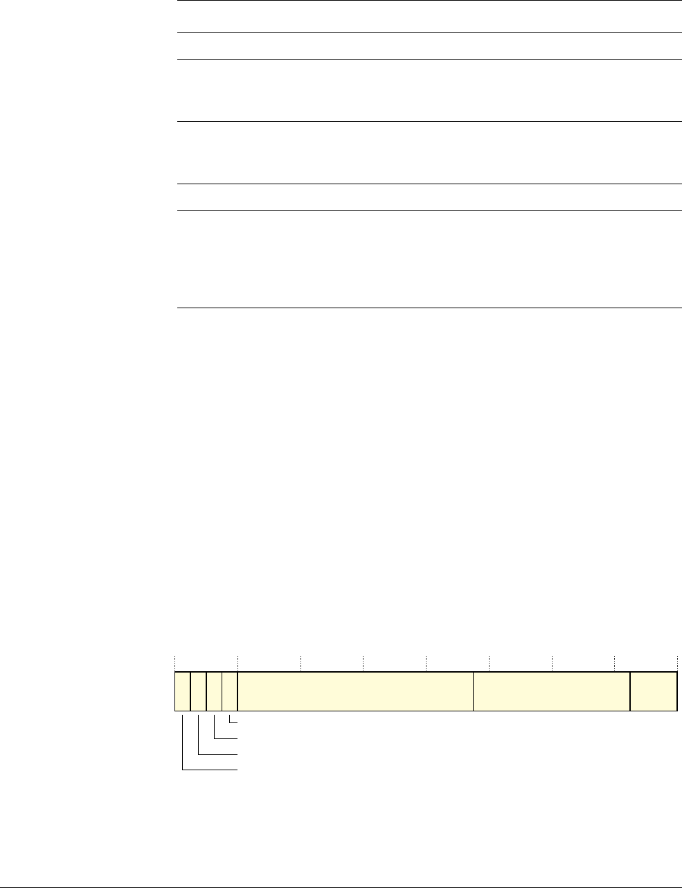
System Control
ARM DDI 0489D Copyright © 2014, 2015 ARM. All rights reserved. 3-10
ID082615 Non-Confidential
Table 3-5 shows the CLIDR bit assignments.
3.3.4 Cache Size ID Register
The CCSIDR characteristics are:
Purpose Provides information about the size and behavior of the instruction or data
cache selected by the CSSELR. Architecturally, there can be up to eight
levels of cache, containing instruction, data, or unified caches. This
processor contains L1 instruction and data caches only.
Usage constraints The CCSIDR is:
• A read-only register.
• Accessible in Privileged mode only.
Configurations Available in all processor configurations.
If no instruction or data cache is configured, the corresponding CCSIDR
is RAZ.
Attributes See the register summary in Table 3-6 on page 3-11.
Figure 3-4 shows the CCSIDR bit assignments.
Figure 3-4 CCSIDR bit assignments
Table 3-5 CLIDR bit assignments
Bits Name Function
[31:30] - Reserved.
[29:27] LoUU Level of Unification Uniprocessor:
0b001
Level 2, if either cache is implemented.
0b000
Level 1, if neither instruction nor data cache is implemented.
[26:24] LoC Level of Coherency:
0b001
Level 2, if either cache is implemented.
0b000
Level 1, if neither instruction nor data cache is implemented.
[23:3] - Reserved.
[2:0] - Level 1 cache type:
0b001
Instruction cache is implemented.
0b010
Data cache is implemented.
0b011
Instruction and data cache are implemented.
0b000
No instruction or data cache are implemented.
AssociativityNumSets LineSize
31 32 0
30 29 28
RA
WA
WB
121327
WT

System Control
ARM DDI 0489D Copyright © 2014, 2015 ARM. All rights reserved. 3-11
ID082615 Non-Confidential
Table 3-6 shows the CCSIDR bit assignments.
The LineSize field is encoded as 2 less than log(2) of the number of words in the cache line. For
example, a value of
0x0
indicates there are four words in a cache line, that is the minimum size
for the cache. A value of
0x1
indicates there are eight words in a cache line.
Table 3-7 shows the individual bit field and complete register encodings for the CCSIDR. Use
this to determine the cache size for the L1 data or instruction cache selected by the Cache Size
Selection Register (CSSELR). See Cache Size Selection Register on page 3-12.
Table 3-6 CCSIDR bit assignments
Bits Name Functiona
a. See Table 3-7 for valid bit field encodings.
[31] WT Indicates support available for Write-Through:
1 Write-Through support available.
[30] WB Indicates support available for Write-Back:
1 Write-Back support available.
[29] RA Indicates support available for read allocation:
1 Read allocation support available.
[28] WA Indicates support available for write allocation:
1 Write allocation support
available.
[27:13] NumSets Indicates the number of sets as:
(number of sets) - 1.
Cache-size dependent.
[12:3] Associativity Indicates the number of ways as:
(number of ways) - 1.
0x1
Represents two instruction
caches.
0x3
Represents four data caches.
[2:0] LineSize Indicates the number of words in each cache line.
0x1
Represents 32 bytes.
Table 3-7 CCSIDR encodings
CSSELR Cache Size
Complete
register
encoding
Register bit field encoding
WT WB RA WA NumSets Associativity LineSize
0x0
Data cache 4KB
0xF003E019
1111
0x001F 0x3 0x1
8KB
0xF007E019 0x003F
16KB
0xF00FE019 0x007F
32KB
0xF01FE019 0x00FF
64KB
0xF03FE019 0x01FF
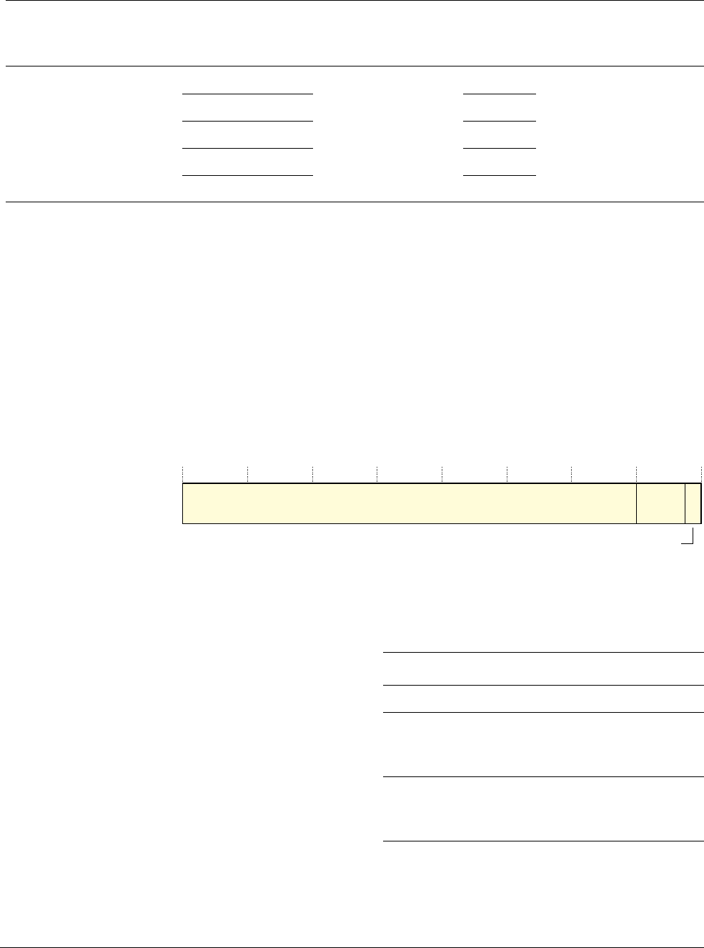
System Control
ARM DDI 0489D Copyright © 2014, 2015 ARM. All rights reserved. 3-12
ID082615 Non-Confidential
3.3.5 Cache Size Selection Register
The CSSELR characteristics are:
Purpose Holds the value that the processor uses to select the CSSELR to use.
Usage constraints The CSSELR is:
• A read/write register.
• Accessible in Privileged mode only.
Configurations Available in all processor configurations.
Attributes See the register summary in Table 3-8.
Figure 3-5 shows the CSSELR bit assignments.
Figure 3-5 CSSELR bit assignments
Table 3-8 shows the CSSELR bit assignments.
0x1
Instruction cache 4KB
0xF007E009
1111
0x003F 0x1 0x1
8KB
0xF00FE009 0x007F
16KB
0xF01FE009 0x00FF
32KB
0xF03FE009 0x01FF
64KB
0xF07FE009 0x03FF
Table 3-7 CCSIDR encodings (continued)
CSSELR Cache Size
Complete
register
encoding
Register bit field encoding
WT WB RA WA NumSets Associativity LineSize
Reserved Level
43 10
InD
31
Table 3-8 CSSELR bit assignments
Bits Name Function
[31:4] - Reserved.
[3:1] Level Identifies which cache level to select.
0b000
Level 1 cache.
This field is RAZ/WI.
[0] InD Selects either instruction or data cache.
0 Data cache.
1 Instruction cache.
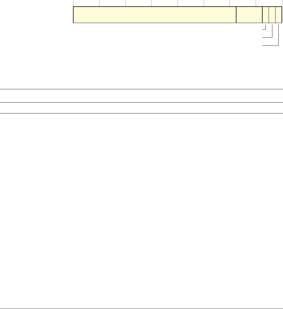
System Control
ARM DDI 0489D Copyright © 2014, 2015 ARM. All rights reserved. 3-13
ID082615 Non-Confidential
3.3.6 Instruction and Data Tightly-Coupled Memory Control Registers
The CM7_ITCMCR and CM7_DTCMCR characteristics are:
Purpose Controls whether an access is mapped to TCM or AXIM interface.
Usage Constraints Accessible in privileged mode only.
Configurations Available in all configurations.
Attributes See the register summary in Table 3-1 on page 3-3.
Figure 3-6 shows the CM7_ITCMCR and CM7_DTCMCR bit assignments.
Figure 3-6 CM7_ITCMCR and CM7_DTCMCR bit assignments
Table 3-9 shows the CM7_ITCMCR and CM7_DTCMCR bit assignments.
31 76 3210
Reserved SZ
RETEN
RMW
EN
Table 3-9 CM7_ITCMCR and CM7_DTCMCR bit assignments
Bits Name Type Function
[31:7] - - Reserved.
[6:3] SZ RO TCM size. Indicates the size of the relevant TCM:
0b0000
No TCM implemented.
0b0011
4KB.
0b0100
8KB.
0b0101
16KB.
0b0110
32KB.
0b0111
64KB.
0b1000
128KB.
0b1001
256KB.
0b1010
512KB.
0b1011
1MB.
0b1100
2MB.
0b1101
4MB.
0b1110
8MB.
0b1111
16MB.
All other encodings are reserved. The reset value is derived from the CFGITCMSZ and CFGDTCMSZ
pins.
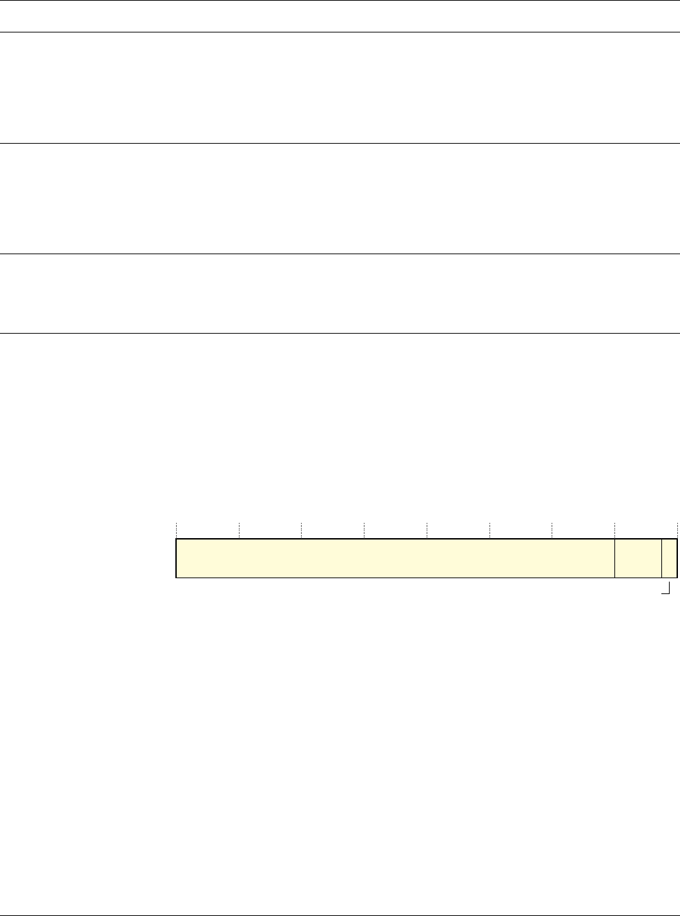
System Control
ARM DDI 0489D Copyright © 2014, 2015 ARM. All rights reserved. 3-14
ID082615 Non-Confidential
3.3.7 AHBP Control Register
The CM7_AHBPCR characteristics are:
Purpose Controls accesses to AHBP or AXIM interface.
Usage Constraints Accessible in privileged mode only.
Configurations Available in all configurations.
Attributes See the register summary in Table 3-1 on page 3-3.
Figure 3-7 CM7_AHBPCR bit assignments
[2] RETEN RW Retry phase enable. When enabled the processor guarantees to honor the retry output on the
corresponding TCM interface, re-executing the instruction that performed the TCM access.
0 Retry phase disabled.
1 Retry phase enabled.
The reset value is derived from the INITRETRYEN pin. The retry functionality can be used together
with external logic to support error detection and correction in the TCM.
[1] RMW RW Read-Modify-Write (RMW) enable. Indicates that all writes to TCM, that are not the full width of the
TCM RAM, use a RMW sequence:
0 RMW disabled.
1 RMW enabled.
The reset value is derived from the INITRMWEN pin. The RMW functionality can be used together
with external logic to support error detection and correction in the TCM.
[0] EN RW TCM enable. When a TCM is disabled all accesses are made to the AXIM interface.
0 TCM disabled.
1 TCM enabled.
The reset value is derived from the INITTCMEN pin.
Table 3-9 CM7_ITCMCR and CM7_DTCMCR bit assignments (continued)
Bits Name Type Function
Reserved
31 310
SZ
EN
4
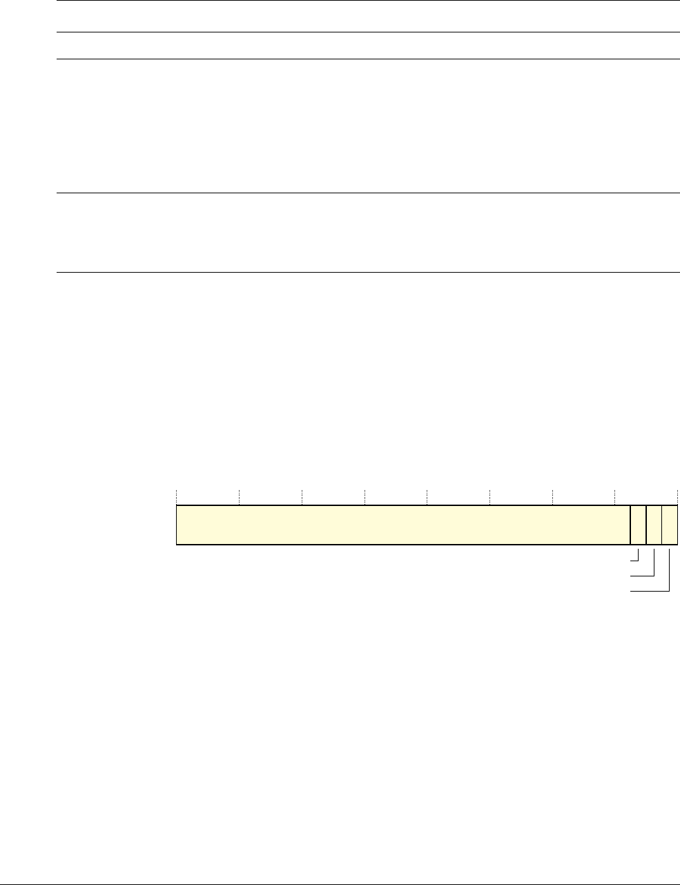
System Control
ARM DDI 0489D Copyright © 2014, 2015 ARM. All rights reserved. 3-15
ID082615 Non-Confidential
Table 3-10 shows the CM7_AHBPCR bit assignments.
3.3.8 L1 Cache Control Register
The CM7_CACR characteristics are:
Purpose Controls the L1 ECC and the L1 cache coherency usage model.
Usage Constraints Accessible in privileged mode only.
Configurations Available in all configurations.
Attributes See the register summary in Table 3-1 on page 3-3.
Figure 3-8 shows the CM7_CACR bit assignments.
Figure 3-8 CM7_CACR bit assignments
Table 3-10 CM7_AHBPCR bit assignments
Bits Name Type Function
[31:4] - - Reserved.
[3:1] SZ RO AHBP size:
0b000
0MB. AHBP disabled.
0b001
64MB.
0b010
128MB.
0b011
256MB.
0b100
512MB.
Other encodings are reserved. Reset values comes from the CFGAHBPSZ pins.
[0] EN RW AHBP enable:
0 AHBP disabled. When disabled all accesses are made to the AXIM interface.
1 AHBP enabled.
The reset value is derived from the INITAHBPEN pins.
31 3210
Reserved
FORCEWT
ECCDIS
SIWT

System Control
ARM DDI 0489D Copyright © 2014, 2015 ARM. All rights reserved. 3-16
ID082615 Non-Confidential
Table 3-11 shows the CM7_CACR bit assignments.
3.3.9 Auxiliary Bus Fault Status Register
The CM7_ABFSR characteristics are:
Purpose Stores information on the source of asynchronous bus faults.
In the bus-fault handler, software reads the BFSR and if an asynchronous
fault is observed, the CM7_ABFSR is read to determine which interfaces
are affected. The CM7_ABFSR must be cleared by writing any value to it.
For more information about the BFSR, see the ARMv7-M Architecture
Reference Manual.
Usage Constraints Accessible in privileged mode only. It is reset by nSYSRESET and is
cleared to
0x0
on writes of any value. The value in this register is only
defined when BFSR.IMPRECISERR is
0x1
.
Table 3-11 CM7_CACR bit assignments
Bits Name Type Function
[31:3] - - Reserved, RAZ/WI.
[2] FORCEWT RW Enables Force Write-Through in the data cache:
0 Disables Force Write-Through.
1 Enables Force Write-Through. All Cacheable
memory regions are treated as Write-Through.
This bit is RAZ/WI if the data cache is excluded. If the data cache is
included the reset value of FORCEWT is 0.
[1] ECCDIS RW Enables ECC in the instruction and data cache:
0 Enables ECC in the instruction and data cache. This
is RAO/WI if both data cache and instruction cache
are excluded or if ECC is excluded.
1 Disables ECC in the instruction and data cache. This
is RAZ/WI if data cache is not configured.
[0] SIWT RW Shared cacheable-is-WT for data cache. Enables limited cache
coherency usage:
0 Normal Cacheable Shared locations are treated as
being Non-cacheable. Programmed inner
cacheability attributes are ignored. This is the
default mode of operation for Shared memory. The
data cache is transparent to software for these
locations and therefore no software maintenance is
required to maintain coherency.
1 Normal Cacheable shared locations are treated as
Write-Through. Programmed inner cacheability
attributes are ignored. All writes are globally visible.
Other memory agent updates are not visible to
Cortex-M7 processor software without suitable
cache maintenance.
Useful for heterogeneous MP-systems where, for
example, the Cortex-M7 processor is integrated on
the Accelerator Coherency Port (ACP) interface on
an MP-capable processor.
This bit is RAZ/WI when data cache is not configured.

System Control
ARM DDI 0489D Copyright © 2014, 2015 ARM. All rights reserved. 3-17
ID082615 Non-Confidential
Configurations Available in all configurations.
Attributes See the register summary in Table 3-1 on page 3-3.
Figure 3-9 shows the CM7_ABFSR bit assignments.
Figure 3-9 CM7_ABFSR bit assignments
Table 3-12 shows the CM7_ABFSR bit assignments.
3.3.10 Instruction Error bank Register 0-1
The IEBR0-1 characteristics are:
Purpose Stores information about the error detected in the instruction cache during
a cache lookup.
Usage Constraints Accessible in privileged mode only.
Configurations Available if the ECC configurable option is implemented.
Attributes See the register summary in Table 3-1 on page 3-3.
Figure 3-10 on page 3-18 shows the IEBR0-1 bit assignments.
Reserved
EPPB
AXIM
AHBP
DTCM
ITCM
Reserved
31 10 9 8 7 4 3 2 1 0
AXIMTYPE
5
Table 3-12 CM7_ABFSR bit assignments
Bits Name Function
[31:10] - Reserved.
[9:8] AXIMTYPE Indicates the type of fault on the AXIM interface:
0b00
OKAY.
0b01
EXOKAY.
0b10
SLVERR.
0b11
DECERR.
Only valid when AXIM is 1.
[7:5] - Reserved.
[4] EPPB Asynchronous fault on EPPB interface.
[3] AXIM Asynchronous fault on AXIM interface.
[2] AHBP Asynchronous fault on AHBP interface.
[1] DTCM Asynchronous fault on DTCM interface.
[0] ITCM Asynchronous fault on ITCM interface

System Control
ARM DDI 0489D Copyright © 2014, 2015 ARM. All rights reserved. 3-18
ID082615 Non-Confidential
Figure 3-10 IEBR0-1 bit assignments
Table 3-13 shows the IEBR0-1 bit assignments.
3.3.11 Data Error bank Register 0-1
The DEBR0-1 characteristics are:
Purpose Stores information about the error detected in the data cache during a
cache lookup.
Usage Constraints Accessible in privileged mode only.
Configurations Available if the ECC configurable option is implemented.
Attributes See the register summary in Table 3-1 on page 3-3.
Figure 3-11 on page 3-19 shows the DEBR0-1 bit assignments.
RAM location
Type of error
RAM bank
Reserved
31 21030 29 18 17 16 15
Locked
Valid
User-defined
Table 3-13 IEBR0-1 bit assignments
Bits Name Type Description
[31:30] - RW User-defined. Error detection logic sets this field to
0b00
on a new allocation and on powerup
reset.
[29:18] - RW Reserved
[17] Type of error RW Indicates the error type:
0 Correctable error.
1 Non-correctable errora.
[16] RAM bank RW Indicates which RAM bank to use:
0 Tag RAM.
1 Data RAM.
[15:2] RAM location RW Indicates the location in instruction cache RAM:
[14] Way.
[13:4] Index.
[3:2] Line doubleword offset.
[1] Locked RW Indicates whether the location is locked or not locked:
0 Location is not locked and available for hardware to allocate.
1 Location is locked by software. Hardware is not allowed to allocate to this entry.
Reset by powerup reset to 0.
[0] Valid RW Indicates whether the entry is valid or not:
0 Entry is invalid.
1 Entry is valid.
Reset by powerup reset to 0.
a. Non-correctable errors are recorded when errors are found in multiple bits of the data read from the RAM. These errors result in data loss
or data corruption and therefore are non-recoverable.
System Control
ARM DDI 0489D Copyright © 2014, 2015 ARM. All rights reserved. 3-19
ID082615 Non-Confidential
Figure 3-11 DEBR0-1
Table 3-14 shows the DEBR0-1 bit assignments.
RAM location
Type of error
RAM bank
Reserved
31 21030 29 18 17 16 15
Locked
Valid
User-defined
Table 3-14 DEBR0-1 bit assignments
Bits Name Type Description
[31:30] - RW User-defined. Error detection logic sets this field to
0b00
on a new allocation and on powerup
reset.
[29:18] - RW Reserved.
[17] Type of error RW Indicates the error type:
0 Correctable error.
1 Non-correctable errora.
[16] RAM bank RW Indicates which RAM bank to use:
0 Tag RAM.
1 Data RAM.
[15:2] RAM location RW Indicates the data cache RAM location:
[15:14] Way.
[13:5] Index.
[4:2] Line word offset.
[1] Locked RW Indicates whether the location is locked or not locked:
0 Location is not locked and available for hardware to allocate.
1 Location is locked by software. Hardware is not allowed to allocate to this entry.
Reset by powerup reset to 0.
[0] Valid RW Indicates whether the entry is valid or not:
0 Entry is invalid.
1 Entry is valid.
Reset by powerup reset to 0.
a. Non-correctable errors are recorded when errors are found in multiple bits of the data read from the RAM. These errors result in data loss
or data corruption and therefore are non-recoverable.
System Control
ARM DDI 0489D Copyright © 2014, 2015 ARM. All rights reserved. 3-20
ID082615 Non-Confidential
3.3.12 AHB Slave Control Register
The CM7_AHBSCR characteristics are:
Purpose Controls the priority between software and AHB slave access to TCMs.
See AHBS interface arbitration on page 5-31.
Usage Constraints Accessible in privileged mode only.
Configurations Available in all configurations.
Attributes See the register summary in Table 3-1 on page 3-3.
Figure 3-12 shows the CM7_AHBSCR bit assignments.
Figure 3-12 CM7_AHBSCR bit assignments
Reserved CTL
31 210
TPRI
15 11
INITCOUNT
1016

System Control
ARM DDI 0489D Copyright © 2014, 2015 ARM. All rights reserved. 3-21
ID082615 Non-Confidential
Table 3-15 shows the CM7_AHBSCR bit assignments.
Table 3-15 CM7_AHBSCR bit assignments
Bits Name Type Function
[31:16] - - Reserved.
[15:11] INITCOUNT RW Fairness counter initialization value. Use to demote access priority of the requestor selected by
the CM7_AHBSCR.CTL field. The reset value is
0b01
.
Note
• For round-robin mode set INITCOUNT to
0b01
and CM7_AHBSCR.CTL to
0b00
or
0b01
.
• INITCOUNT must not be set to
0b00
because the demoted requestor then always takes
priority when contention occurs, and might cause livelock.
• INITCOUNT is not used when CM7_AHBSCR.CTL is
0b11
.
[10:2] TPRI RW Threshold execution priority for AHBS traffic demotion.
0b0xxxxxxx
Priority is TPRI[7:0]. This is the same as the NVIC register encodings.
0b11111111
Priority of -1. This is the priority of the HardFault exception.
0b11111110
Priority of -2. This is the priority of the NMI exception.
[1:0] CTL RW AHBS prioritization control:
0b00
AHBS access priority demoted. This is the reset value.
0b01
Software access priority demoted.
0b10
AHBS access priority demoted by initializing the fairness counter to the
CM7_AHBSCR.INITCOUNT value when the software execution priority is
higher than or equal to the threshold level programed in
CM7_AHBSCR.TPRI. When the software execution priority is below this
value, the fairness counter is initialized with 1 (round-robin).
Note
• The threshold level encoding matches the NVIC encoding and uses
arithmetically larger numbers to represent lower priority.
• The current execution priority of the processor is defined architecturally
and includes the effect of the PRIMASK, BASEPRI, and FAULTMASK
special-purpose registers.
0b11
AHBSPRI signal has control of access priority.

ARM DDI 0489D Copyright © 2014, 2015 ARM. All rights reserved. 4-1
ID082615 Non-Confidential
Chapter 4
Initialization
This chapter describes how to initialize the processor and which registers to access to enable
functionality before using the processor features. It contains the following section:
•About Initialization on page 4-2.

Initialization
ARM DDI 0489D Copyright © 2014, 2015 ARM. All rights reserved. 4-2
ID082615 Non-Confidential
4.1 About Initialization
Before you run the application, you might want to:
• Program particular values into various registers, for example, stack pointers.
• Enable various processor features, for example, error correction.
• Program particular values into memory, for example, the Tightly Coupled Memories
(TCMs).
Other initialization requirements are described in:
•Initializing the MPU.
•Initializing the FPU.
•Initializing and enabling the L1 cache on page 4-3.
•Disabling cache error checking and correction on page 4-4.
•Enabling the TCM on page 4-4.
•Preloading TCM on page 4-5.
•Enabling the TCM retry and read-modify-write on page 4-5.
•Enabling the AHBP interface on page 4-6
Some of the requirements for initialization are optional depending on the features implemented
in the Cortex-M7 processor.
Note
The Branch predictor is always enabled in the processor, therefore CCR.BP is RAO/WI. See
ARM®v7-M Architecture Reference Manual for more information on the Configuration and
Control register.
4.1.1 Initializing the MPU
If the processor has been implemented with a Memory Protection Unit (MPU), before you can
use it you must enable the MPU in the MPU_CTRL register. See the ARM®v7-M Architecture
Reference Manual for more information.
When setting up the MPU, and if the MPU has previously been programmed, disable unused
regions to prevent any previous region settings from affecting the new MPU setup.
4.1.2 Initializing the FPU
If the processor has been implemented with a Floating Point Unit (FPU) you must enable it
before floating point instructions can be executed. The following code is an example of how to
enable the feature.
CPACR EQU 0xE000ED88
LDR r0, =CPACR
LDR r1, [R0] ; Read CPACR
ORR r1, R1, #(0xF << 20) ; Set bits 20-23 to enable CP10 and CP11 coprocessors
STR r1, [R0] ; Write back the modified value to the CPACR
DSB
ISB
See the ARM®v7-M Architecture Reference Manual for more information.

Initialization
ARM DDI 0489D Copyright © 2014, 2015 ARM. All rights reserved. 4-3
ID082615 Non-Confidential
Note
Floating point logic is only available with the Cortex-M7 processor with FPU.
4.1.3 Initializing and enabling the L1 cache
If the processor has been implemented with L1 data or instruction caches, they must be
invalidated before they are enabled in software, otherwise UNPREDICTABLE behavior can occur.
Invalidate the entire data cache
Software can use the following code example to invalidate the entire data cache,
if it has been included in the processor. The operation is carried out by iterating
over each line of the cache and using the DCISW register in the Private
Peripheral Bus (PPB) memory region to invalidate the line. The number of cache
ways and sets is determined by reading the CCSIDR register.
CCSIDR EQU 0xE000ED80 ; Cache size ID register address
CSSELR EQU 0xE000ED84 ; Cache size selection register address
DCISW EQU 0xE000EF60 ; Cache maintenance op address: data cache clean and invalidate by set/way
; CSSELR selects the cache visible in CCSIDR
MOV r0, #0x0 ; 0 = select “level 1 data cache”
LDR r11, =CSSELR ;
STR r0, [r11] ;
DSB ; Ensure write to CSSELR before proceeding
LDR r11, =CCSIDR ; From CCSIDR
LDR r2, [r11] ; Read data cache size information
AND r1, r2, #0x7 ; r1 = cache line size
ADD r7, r1, #0x4 ; r7 = number of words in a cache line
UBFX r4, r2, #3, #10 ; r4 = number of “ways”-1 of data cache
UBFX r2, r2, #13, #15 ; r2 = number of “set”-1 of data cache
CLZ r6, r4 ; calculate bit offset for “way” in DCISW
LDR r11, =DCISW ; invalidate cache by set/way
inv_loop1 ; For each “set”
MOV r1, r4 ; r1 = number of “ways”-1
LSLS r8, r2, r7 ; shift “set” value to bit 5 of r8
inv_loop2 ; For each “way”
LSLS r3, r1, r6 ; shift “way” value to bit 30 in r6
ORRS r3, r3, r8 ; merge “way” and “set” value for DCISW
STR r3, [r11] ; invalidate D-cache line
SUBS r1, r1, #0x1 ; decrement “way”
BGE inv_loop2 ; End for each “way”
SUBS r2, r2, #0x1 ; Decrement “set”
BGE inv_loop1 ; End for each “set”
DSB ; Data sync barrier after invalidate cache
ISB ; Instruction sync barrier after invalidate cache

Initialization
ARM DDI 0489D Copyright © 2014, 2015 ARM. All rights reserved. 4-4
ID082615 Non-Confidential
Invalidate instruction cache
You can use the following code example to invalidate the entire instruction cache,
if it has been included in the processor. The operation is carried out by writing to
the ICIALLU register in the PPB memory region.
ICIALLU EQU 0xE000EF50
MOV r0, #0x0
LDR r11, =ICIALLU
STR r0, [r11]
DSB
ISB
Enabling data and instruction caches
You can use the following code example to enable the data and instruction cache
after they have been initialized. The operation is carried out by modifying the
CCR.IC and CCR.DC fields in the PPB memory region.
CCR EQU 0xE000ED14
LDR r11, =CCR
LDR r0, [r11]
ORR r0, r0, #0x1:SHL:16 ; Set CCR.DC field
ORR r0, r0, #0x1:SHL:17 ; Set CCR.IC field
STR r0, [r11]
DSB
ISB
4.1.4 Disabling cache error checking and correction
If cache error checking and correction is included in the processor it is enabled by default from
reset. The following code example can be used to disable the feature. The operation is carried
out by modifying the CM7_CACR.ECCEN bit the PPB memory region.
CM7_CACR EQU 0xE000EF9C
LDR r11, =CM7_CACR
LDR r0, [r11]
BFC r0, #0x1, #0x1 ; Clear CM7_CACR.ECCEN
STR r0, [r11]
DSB
ISB
Care must be taken when software changes the error checking fields in the CM7_CACR. If the
fields are changed when the caches contain data, ECC information in the caches might not be
correct for the new setting, resulting in unexpected errors and data loss. Therefore the fields in
the CM7_CACR must only be changed when both caches are turned off and the entire cache
must be invalidated after the change.
4.1.5 Enabling the TCM
The TCM interfaces can be enabled at reset in the system by an external signal on the processor.
If they are disabled at reset then the following code example can be used to enable both the
instruction and data TCM interfaces in software:
CM7_ITCMCR EQU 0xE000EF90
CM7_DTCMCR EQU 0xE000EF94

Initialization
ARM DDI 0489D Copyright © 2014, 2015 ARM. All rights reserved. 4-5
ID082615 Non-Confidential
LDR r11, =CM7_ITCMCR
LDR r0, [r11]
ORR r0, r0, #0x1 ; Set CM7_ITCMCR.EN field
STR r0, [r11]
LDR r11, =CM7_DTCMCR
LDR r0, [r11]
ORR r0, r0, #0x1 ; Set CM7_DTCMCR.EN field
STR r0, [r11]
DSB
ISB
4.1.6 Preloading TCM
Methods to preload TCMs include:
Memory copy with running boot code
Where boot code includes a memory copy routine that reads data from a
ROM, and writes it into the appropriate TCM, you must enable the TCM
to do this. This bootcode must be run from an address outside the TCM
region.
DMA into TCM The System includes a DMA device that reads data from a ROM, and
writes it to the TCMs through the AHB slave interface. This method can
be used to preload the TCM so they can be used by the processor from
reset.
Using the TCM from reset
If the TCM interface is configured to enable the TCM at reset and the reset
vector address is inside the TCM memory region then the processor boots
from TCM. The system must ensure that the bootcode software is present
in the appropriate memory region before execution starts. This can be
accomplished by either initializing the memory before reset or by
transferring the data after reset using the AHB slave interface and
asserting the CPUWAIT input signal. Asserting this signal stops the
processor fetching or executing instructions after reset. When the
CPUWAIT signal is deasserted the processor starts fetching instructions
from the reset vector address in the normal way.
Note
When CPUWAIT has been deasserted to start the processor fetching,
CPUWAIT must not be asserted again except when the processor is under
processor reset or Power-on reset; that is nSYSRESET or nPORESET
asserted. The processor does not halt if the CPUWAIT is asserted while
the processor is running.
4.1.7 Enabling the TCM retry and read-modify-write
If the TCM connected to the processor supports error detection and correction then the TCM
interface must be configured to support the retry and read-modify-write features. These can be
enabled at reset in the system by external signals on the processor. If they are disabled at reset
then the following code example can be used to enable them in software:
CM7_ITCMCR EQU 0xE000EF90
CM7_DTCMCR EQU 0xE000EF94

Initialization
ARM DDI 0489D Copyright © 2014, 2015 ARM. All rights reserved. 4-6
ID082615 Non-Confidential
LDR r11, =CM7_ITCMCR
LDR r0, [r11]
ORR r0, r0, #0x1:SHL:1 ; Set CM7_ITCMCR.RMW field
ORR r0, r0, #0x1:SHL:2 ; Set CM7_ITCMCR.RETEN field
STR r0, [r11]
LDR r11, =CM7_DTCMCR
LDR r0, [r11]
ORR r0, r0, #0x1:SHL:1 ; Set CM7_DTCMCR.RMW field
ORR r0, r0, #0x1:SHL:2 ; Set CM7_DTCMCR.RETEN field
STR r0, [r11]
DSB
ISB
4.1.8 Enabling the AHBP interface
The AHBP interface can be enabled at reset in the system by an external signal on the processor.
If it is disabled at reset then the following code example can be used to enable the AHBP
interface from software:
CM7_AHBPCR EQU 0xE000EF98
LDR r11, =CM7_AHBPCR
LDR r0, [r11]
ORR r0, r0, #0x1 ; Set CM7_AHBPCR.EN field
STR r0, [r11]
DSB
ISB

ARM DDI 0489D Copyright © 2014, 2015 ARM. All rights reserved. 5-1
ID082615 Non-Confidential
Chapter 5
Memory System
This chapter describes the Cortex-M7 processor memory system. It contains the following
sections:
•About the memory system on page 5-2.
•Fault handling on page 5-3.
•Memory types and memory system behavior on page 5-5.
•AXIM interface on page 5-6.
•AHB peripheral interface on page 5-22.
•AHB slave interface on page 5-30.
•TCM interfaces on page 5-33.
•L1 caches on page 5-37.

Memory System
ARM DDI 0489D Copyright © 2014, 2015 ARM. All rights reserved. 5-2
ID082615 Non-Confidential
5.1 About the memory system
This section provides an overview of the Cortex-M7 processor memory system.
The Cortex-M7 processor memory system can be configured during implementation and
integration. It consists of:
• Separate optional instruction and data caches.
• Multiple optional Tightly-Coupled Memory (TCM) areas.
•An AHB Slave (AHBS) interface.
• An optional Memory Protection Unit (MPU). See Chapter 6 Memory Protection Unit.
• MBIST interface.
The cache architecture is Harvard, that is, only instructions can be fetched from the instruction
cache, and only data can be read from and written to the data cache.
In parallel with each of the caches are two areas of dedicated RAM accessible to both the
instruction and data sides. These are regions of TCM.
Instruction TCM (ITCM) uses the ITCM interface and the Data TCM (DTCM) uses two
interfaces, D0TCM and D1TCM. Cortex-M7 functional diagram on page 1-6 shows this.
The ITCM interface is 64-bits wide. The DTCM is divided into two 32-bit wide interfaces,
D0TCM and D1TCM. The upper 32-bits of data is on the D1TCM interface and the lower
32-bits of the data is on the D0TCM interface.
Memory accesses to the ITCM, required for fetching instructions and for data transfer
instructions, are performed if the address is in an enabled TCM region. Remaining instruction
accesses and remaining data accesses that are not in a peripheral interface region are looked up
in the appropriate L1 cache if they are cacheable. Accesses that are not serviced by the memory
system are passed through the AXI master (AXIM) interface or the AHBP interface to the
external memory system connected to the processor.
Both instruction and data cache RAM can be configured at implementation time to have Error
Correcting Code (ECC) to protect the data stored in the memory from errors. Each TCM
interface can support external logic to the processor to report to the processor that an error has
occurred.
The processor includes support for direct access to the TCM through the AHBS interface. The
interface provides high bandwidth for DMA traffic to the memory and can be used when the
remainder of the processor is in low-power standby mode, with the internal clock disabled.
The optional MPU handles both the instruction and data memory accesses. The MPU is
responsible for protection checking, address access permissions, and memory attributes for all
accesses. Some of these attributes can be passed through the AXIM interface or AHBP interface
to the external memory system.
The memory system includes a monitor for exclusive accesses. Exclusive load and store
instructions, for example
LDREX
and
STREX
, can be used with the appropriate memory monitoring
to provide inter-process or inter-processor synchronization and semaphores. See the ARM®v7-M
Architecture Reference Manual for more information.
The processor is designed for use in chip designs that use the AMBA 4 AXI and AMBA 3
AHB-Lite protocols.

Memory System
ARM DDI 0489D Copyright © 2014, 2015 ARM. All rights reserved. 5-3
ID082615 Non-Confidential
5.2 Fault handling
Faults can occur on instruction fetches for the following reasons:
• MPU MemManage.
• External AXI slave error (SLVERR).
• External AXI decode error (DECERR).
• TCM external error.
• Breakpoints, and vector capture events.
Faults can occur on data accesses for the following reasons:
• MPU MemManage.
• Alignment UsageFault.
• External AXI slave error (SLVERR).
• External AXI decode error (DECERR).
• External AHB error from the AHBP port.
• TCM external error.
• Watchpoints.
Fault handling is described in:
•Faults.
•Usage models on page 5-4.
5.2.1 Faults
The classes of fault that can occur are:
•MPU faults.
•External faults.
•Debug events on page 5-4.
•Synchronous and asynchronous faults on page 5-4.
MPU faults
The MPU can generate a fault for various reasons. MPU faults are always synchronous, and take
priority over external faults. If an MPU fault occurs on an access that is not in the TCM, the AXI
or AHB transactions for that access are not performed.
External faults
A memory access or instruction fetch performed through the AXIM interface can generate two
different types of error response, a slave error (SLVERR) or decode error (DECERR). These
are known as external AXI errors, because they are generated by the AXI system outside the
processor.
A memory access performed through the AHBP interface can generate a single error response.
The processor manages this in the same way as a response of SLVERR from the AXI interface.
A memory or instruction fetch access performed on the TCM interface can generate a single
error response. The processor manages this in the same way as a response of SLVERR from the
AXI interface.
Synchronous faults are generated for instruction fetches and data loads. All stores generate
asynchronous faults.

Memory System
ARM DDI 0489D Copyright © 2014, 2015 ARM. All rights reserved. 5-4
ID082615 Non-Confidential
Note
An AXI slave device in the system that cannot handle exclusive transactions returns OKAY in
response to an exclusive read. This is also treated as an external error, and the processor behaves
as if the response was SLVERR.
Debug events
The debug logic in the processor can be configured to generate breakpoints or vector capture
events on instruction fetches, and watchpoints on data accesses. If the processor is
software-configured for monitor-mode debugging, a fault is taken when one of these events
occurs, or when a
BKPT
instruction is executed. For more information, see Chapter 9 Debug.
Synchronous and asynchronous faults
See External faults on page 5-3 for more information about the differences between
synchronous and asynchronous faults.
5.2.2 Usage models
This section describes some methods for handling errors in a system. Exactly how you program
the processor to handle faults depends on the configuration of your processor and system, and
what you are trying to achieve.
If a fault exception is taken, the fault handler reads the information in the link register, Program
Status Register (PSR) in the stack, and fault status registers to determine the type of fault. Some
types of fault are fatal to the system, and others can be fixed, and program execution resumed.
For example, an MPU background MemManage might indicate a stack overflow, and be
rectified by allocating more stack and reprogramming the MPU to reflect this. Alternatively, an
asynchronous external fault might indicate that a software error meant that a store instruction
occurred to an unmapped memory address. Such a fault is fatal to the system or process because
no information is recorded about the address the error occurred on, or the instruction that caused
the fault.
Table 5-1 shows the types of fault that are typically fatal because either the location of the error
is not recorded or the error is unrecoverable. Some faults that are marked as not fatal might turn
out to be fatal in some systems when the cause of the error has been determined. For example,
an MPU background MemManage fault might indicate a stack overflow, that can be rectified,
or it might indicate that, because of a bug, the software has accessed a nonexistent memory
location, that can be fatal. These cases can be distinguished by determining the location where
the error occurred.
Table 5-1 Types of faults
Type of fault Conditions Source Synchronous Fatal
MPU Access not permitted by MPUaMPU Yes No
Synchronous external Load using external memory interface AXIM, AHBP Yes No
Asynchronous external Store to Normal or Device memory using external memory
interface
AXIM, AHBP No Yes
a. See the ARM®v7-M Architecture Reference Manual for more information.

Memory System
ARM DDI 0489D Copyright © 2014, 2015 ARM. All rights reserved. 5-5
ID082615 Non-Confidential
5.3 Memory types and memory system behavior
The behavior of the memory system depends on the type attribute of the memory that is being
accessed:
• By default, only Normal, Non-shareable memory regions can be cached in the RAMs.
Caching only takes place if the appropriate cache is enabled and the memory type is
cacheable. Shared cacheable memory regions can be cached if CACR.SIWT is set to 1.
• The store buffer can merge any stores to Normal memory if they are not from a store
exclusive instruction accessing a memory region marked as Shared. See Store buffer on
page 5-38 for more information.
• Only non-cached Shared exclusive transactions are marked as exclusive on the external
interface. Load and store exclusive instructions to Shared cacheable memory regions do
not result in any accesses marked as exclusive on the external interface if CACR.SIWT is
set to 1.
• Only Normal memory is considered restartable, that is, a multi-word transfer can be
abandoned part way through because of an interrupt, to be restarted after the interrupt has
been handled. See Exception handling on page 2-9 for more information about interrupt
behavior.
• For exclusive accesses to Non-shared memory only the internal exclusive monitor is
updated and checked. Exclusive accesses to Shared memory are checked using the
internal monitor and also, if necessary, using an external monitor using the external
memory interface AXIM or AHBP.
Table 5-2 summarizes the processor memory types and associated behavior.
Table 5-2 Memory types and associated behavior
Memory type Can be cached Merging Restartable Exclusives
handled
Normal Shared NoaYes Yes Internal and external
Non-shared Yes Yes Yes Internal only
Device Shared No No No Internal and external
Non-shared No No No Internal only
Strongly-ordered Shared No No No Internal and external
a. Unless CACR.SIWT is set to 1.

Memory System
ARM DDI 0489D Copyright © 2014, 2015 ARM. All rights reserved. 5-6
ID082615 Non-Confidential
5.4 AXIM interface
This section describes the AXIM interface. The AXIM interface is a single 64-bit wide interface
that connects to a external memory system. It is used for:
• Instruction fetches.
• Data cache linefills and evictions.
• Non-cacheable Normal-type memory data accesses.
• Device and Strongly-ordered type data accesses, normally to peripherals.
The AXIM interface conforms to the AXI4 standard as described in the ARM® AMBA® AXI and
ACE Protocol Specification. Within the AXI standard, the AXIM interface uses a number of
extension signals to indicate inner memory attributes and the request source. See AXI extensions
on page 5-10.
The AXIM interface can run at the same frequency as the processor or at a lower synchronous
frequency.
Note
References in this section to an AXI slave refer to the AXI slave in the external system that is
connected to the processor AXIM interface.
The following sections describe the attributes of the AXIM interface, and provide information
about the types of burst generated:
•AXI attributes and transactions.
•Identifiers for AXIM interface accesses on page 5-9.
•AXI extensions on page 5-10.
•Memory system implications for AXI accesses on page 5-10.
5.4.1 AXI attributes and transactions
Table 5-3 shows the AXI attributes and transactions for the AXIM interface when the processor
is configured with the L1 data cache. This is for use in a native AXI system with high memory
bandwidth and supports multiple outstanding transactions, also known as a high performance
AXIM interface.
Table 5-3 High performance AXIM attributes and transactions
Attribute Value Description
Write issuing capability 39 Consisting of:
• 15 writes to Strongly-ordered or Device memory.
• 24 writes to Normal memory, that can be evictions, write bursts or single writes. A
maximum of 17 of these can be to cacheable memory and a maximum of 10 to
Non-cacheable or shareable memory.
Read issuing capability 7 Consisting of:
• 2 data linefills.
• 4 Non-cacheable data reads.
• 1 instruction fetch or instruction linefill.

Memory System
ARM DDI 0489D Copyright © 2014, 2015 ARM. All rights reserved. 5-7
ID082615 Non-Confidential
Only a subset of all possible AXI transactions can be generated. These are:
• For Normal, cacheable memory:
— WRAP4 64-bit reads, for load and Write-Back Write-Allocate store linefills and
instruction linefills.
— INCR4 64-bit writes, for evictions.
— INCR N (N:1-4) 64-bit for write transfers, for coalesced individual Write-Through
or Write-Back, no Write-Allocate stores.
— INCR N (N:1-4) 64-bit for read transfers, for loads when the data cache is disabled,
or for instruction fetches when the instruction cache is disabled.
• For Normal, Non-cacheable memory:
— INCR N (N:1-4) 64-bit for read transfers, for individual loads and load multiplies.
— INCR N (N:1-4) 64-bit for write transfers, for coalesced individual stores and store
multiples.
— INCR N (N:1-4) 64-bit for read transfers, for instruction fetches.
— INCR 1 8-bit, 16-bit, and 32-bit exclusive reads and writes, for shared exclusives.
• For Strongly-ordered or Device memory:
— INCR 1 8-bit, 16-bit and 32-bit reads and writes, for individual load and stores.
— INCR 1 32-bit for read transfers, load multiples.
— INCR N (N:1-2) 32-bit for write transfers, for store multiples.
— INCR 1 8-bit, 16-bit and 32-bit exclusive reads and writes, for shared exclusives.
• No FIXED bursts are used.
• Write bursts to Normal memory can use the following optimizations:
— Entire beats with no strobes set.
— Non-contiguous strobes per beat.
These are allowed on AXI but have implications for bridging to AHB.
For more information on IDs used for different transactions, see Identifiers for AXIM interface
accesses on page 5-9.
Write ID capability 4 Consisting of:
• 1 reserved for Strongly-ordered or Device memory.
• 1 reserved for Normal, cacheable and Non-shareable memory.
• 1 reserved for Normal, Non-cacheable or Shareable memory.
• 1 reserved for cache line evictions (Normal, cacheable, Write-Back memory).
Read ID capability 4 -
Combined issuing capability 40 Consisting of:
• 39 outstanding writes.
• 1 instruction fetcha.
a. The maximum issuing capability of the memory system is limited to one outstanding instruction read because all data reads are hazarded in
the BIU when the maximum number of write transactions have been issued.
Table 5-3 High performance AXIM attributes and transactions (continued)
Attribute Value Description

Memory System
ARM DDI 0489D Copyright © 2014, 2015 ARM. All rights reserved. 5-8
ID082615 Non-Confidential
Table 5-4 shows the AXI attributes and transactions for when the processor is not configured to
include the L1 data cache. That is, if you want to use it in a low-cost AXI system, or bridged to
AHB, that has a low-bandwidth memory system, like on an off-chip memory system.
Only a subset of all possible AXI transactions is generated. These are:
• For Normal memory:
— WRAP4 64-bit read transfers, for instruction linefills where instruction cache is
included.
— INCR N (N:1-4) 64-bit for read transfers, for individual loads and load multiplies.
— INCR N (N:1-4) 64-bit for write transfers, for coalesced individual stores and store
multiples.
— INCR N (N:1-4) 64-bit for read transfers, for Non-cacheable instruction fetches or
all instruction fetches with no instruction cache.
— INCR 1 8-bit, 16-bit and 32-bit exclusive reads and writes, for shared exclusives.
• For Strongly-ordered or Device memory:
— INCR N (N:1-2) 32-bit for read transfers, for individual loads and load multiples.
— INCR N (N:1-2) 32-bit for write transfers, for individual stores and store multiples.
— INCR 1 8-bit, 16-bit and 32-bit exclusive reads and writes, for shared exclusives.
• No FIXED bursts are used.
• Write bursts to Normal memory can use the following optimizations:
— Entire beats with no strobes set.
— Non-contiguous strobes per beat.
These are allowed on AXIM interface but have implications for bridging to AHB.
For more information on IDs used for different transactions, see Identifiers for AXIM
interface accesses on page 5-9.
Table 5-4 Area optimized AXIM attributes and transactions
Attribute Value Description
Write issuing capability 25 Consisting of:
• 15 writes to Strongly-ordered or Device memory.
• 10 writes to Normal memory.
Read issuing capability 5 Consisting of:
• 4 data read.
• 1 instruction fetch or instruction linefill.
Write ID capability 2 Consisting of:
• 1 reserved for Strongly-ordered or Device memory.
• 1 reserved for Normal memory.
Read ID capability 2 -
Combined issuing capability 26 Consisting of:
• 25 outstanding writes.
• 1 instruction fetcha.
a. The maximum issuing capability of the memory system is limited to one outstanding instruction read
because all data reads are hazarded in the BIU when the maximum number of write transactions have
been issued.

Memory System
ARM DDI 0489D Copyright © 2014, 2015 ARM. All rights reserved. 5-9
ID082615 Non-Confidential
5.4.2 Identifiers for AXIM interface accesses
The following ID values are for read and write channels, and Write-Allocate memory accesses
on the AXIM interface:
• Read channels, ARID[2:0], RID[2:0]:
0b000
Normal Non-cacheable, Device, and Strongly-ordered reads.
0b011
,
0b010
Data cache line-fills.
0b100
Instruction fetches.
• Write channels, AWID[1:0], WID[1:0], BID[1:0]:
0b00
Normal, Non-cacheable writes, All shared exclusive writes, for
example from
STREX
.
0b01
Normal cacheable writes to Write-Through and Write-Back, Non
Write-Allocate memory.
0b10
Device and Strongly-ordered writes.
0b11
Evictions to Normal cacheable Write-Back memory.
WID is not a required signal for AMBA 4 AXI. It is included for compatibility with AMBA 3
AXI systems.
5.4.3 AXI privilege information
AXI provides information about the privilege level of an access on the ARPROT and
AW P R O T signals. However, when accesses might be cached or merged together, the resulting
transaction can have both privileged and user data combined. If this happens, the Cortex-M7
processor marks the transaction as privileged, even if it was initiated by a user process.
Table 5-5 shows Cortex-M7 mode and APROT values.
5.4.4 Write response
The AXIM interface requires that the slave does not return a write response until it has received
the write address.
Table 5-5 Cortex-M7 mode and APROT values
Processor mode Type of access Value of APROT
- Cacheable read access Always marked as Privileged
User Non-cacheable read access User except for
LDM
,
LDRD
and
POP
when the L1 data cache is
implemented
Privileged Privileged
User Device or Strongly-ordered
read access
User
Privileged Privileged
- Cacheable write access Always marked as Privileged
User Device or Strongly-ordered
write access
User
Privileged Privileged
User Normal non-cacheable write
access
Privileged, except for
STREXB
,
STREXH
, and
STREX
Privileged Privileged

Memory System
ARM DDI 0489D Copyright © 2014, 2015 ARM. All rights reserved. 5-10
ID082615 Non-Confidential
Note
This write response requirement is mandatory for systems using the AMBA 4 AXI protocol. It
is also required if the Cortex-M7 processor is used with an external memory system using the
AMBA 3 AXI protocol.
5.4.5 AXI extensions
The AXIM interface uses the ARCACHE and AWCACHE AXI signals and the ARSHARE,
AW S H A R E , ARINNER, and AW I N N E R extension signals to indicate the memory attributes
of the transfer, as returned by the MPU:
•ARCACHE and AWCACHE of the master interface are generated from the memory
type and outer region attributes.
•ARINNER and AWINNER are generated from the memory type and inner region
attributes.
•ARSHARE and AW S H A R E are asserted for transactions to shared memory regions.
In additional to these attribute extension signals the AXIM interface includes the following
signals:
AWMASTER and ARMASTER
Indicates the source of the memory request. When set to:
0 The request has been generated by software running on the
processor.
1 The request has been generated by a debug request on the AHB
Debug (AHBD) interface.
AWSPARSE The AW S PA R S E is part of the write address channel signal group and
indicates the burst uses sparse byte write-strobes, that is some of the beats
of the write burst do not contain data. You can use this signal to optimize
systems that bridge the AMBA 4 AXI protocol to AHB protocol.
See the ARM® AMBA® AXI and ACE Protocol Specification for valid encodings for all the
AxCACHE and AxINNER signals.
5.4.6 Memory system implications for AXI accesses
The attributes of the memory being accessed can affect an AXI access. The memory system can
cache any Normal memory address that is marked as either:
• Cacheable, Write-Back, Read-Allocate, Write-Allocate, Non-shareable.
• Cacheable, Write-Back, Read-Allocate only, Non-shareable.
• Cacheable, Write-Through, Read-Allocate only, Non-shareable.
However, Device and Strongly-ordered memory is always Non-cacheable. Also, any unaligned
access to Device or Strongly-ordered memory generates alignment UsageFault and therefore
does not cause any AXI transfer. This means that the access examples given in this chapter never
show unaligned accesses to Device or Strongly-ordered memory.
Note
Memory regions marked as Non-Cacheable Normal must not be used to access read-sensitive
peripherals in a system. This is because read transactions to these regions from the processor
can be repeated multiple times if the originating load instruction is interrupted.

Memory System
ARM DDI 0489D Copyright © 2014, 2015 ARM. All rights reserved. 5-11
ID082615 Non-Confidential
5.4.7 AXIM interface transfers
The processor conforms to the ARM® AMBA® AXI and ACE Protocol Specification, but it does
not generate all the AXI transaction types that the specification permits. This section describes
the types of AXI transaction that the AXIM interface does not generate.
If you are designing an AXI slave to work only with the Cortex-M7 processor, and there are no
other AXI masters in your system, you can take advantage of these restrictions and the interface
attributes, described in Table 5-3 on page 5-6, to simplify the slave.
This section also contains tables that show some examples of the types of AXI burst that the
processor generates. However, because a particular type of transaction is not shown here does
not mean that the processor does not generate such a transaction.
Note
An AXI slave device connected to the AXIM interface must be capable of handling every kind
of transaction permitted by the ARM® AMBA® AXI and ACE Protocol Specification, except
where there is an explicit statement in this chapter that such a transaction is not generated. You
must not infer any additional restrictions from the example tables given.
Load and store instructions to Non-cacheable memory might not result in an AXI transfer
because the data might either be retrieved from, or merged into the internal store data buffers.
The exceptions to this are loads or stores to Strongly-ordered or Device memory. These always
result in AXI transfers. See Strongly-ordered and Device transactions on page 5-12.
Restrictions on AXI transfers on page 5-12 describes restrictions on the type of transfers that the
AXIM interface generates. If the processor is powered up, the buffered write response and read
data channel ready signals, BREADY and RREADY, are always asserted. They are deasserted
when the processor enters Dormant or Shutdown mode. You must not make any other
assumptions about the AXI handshaking signals, except that they conform to the ARM® AMBA®
AXI and ACE Protocol Specification.
The following sections give examples of transfers generated by the AXIM interface:
•Restrictions on AXI transfers on page 5-12.
•Strongly-ordered and Device transactions on page 5-12.
•Linefills on page 5-17.
•Cache line write-back (eviction) on page 5-17.
•Non-cacheable reads on page 5-17.
•Non-cacheable, Write-Back no Write-Allocate or Write-Through writes on page 5-17.
•AXI transaction splitting on page 5-18.
•Normal write merging on page 5-19.

Memory System
ARM DDI 0489D Copyright © 2014, 2015 ARM. All rights reserved. 5-12
ID082615 Non-Confidential
Restrictions on AXI transfers
The AXIM interface applies the following restrictions to the AXI transactions it generates:
• A burst never transfers more than 32 bytes.
• The burst length is never more than four transfers.
• The maximum length of a Strongly-ordered or Device write burst is two transfers.
Strongly-ordered or Device reads are always one transfer.
• No transaction ever crosses a 32-byte boundary in memory. See AXI transaction splitting
on page 5-18.
• FIXED bursts are never used.
• The write address channel always issues INCR type bursts, and never WRAP or FIXED.
• WRAP type read bursts, see Linefills on page 5-17:
— Are used only for linefills (reads) of cacheable Normal memory.
— Always have a size of 64 bits, and a length of four transfers.
— Always have a start address that is 64-bit aligned.
• If the transfer size is 8 bits or 16 bits then the burst length is always one transfer.
• The transfer size is never greater than 64 bits, because it is a 64-bit AXI bus.
• Instruction fetches, identified by ARPROT[2], are always a 64 bit transfer size, and never
locked or exclusive.
• Transactions to Device and Strongly-ordered memory are always to addresses that are
aligned for the transfer size. See Strongly-ordered and Device transactions.
• Exclusive accesses are always to addresses that are aligned for the transfer size.
• Only exclusive accesses to shared memory result in exclusive accesses on the AXIM,
identified by ARLOCK and AW L O C K . Exclusive accesses to non-shared memory are
marked as non-exclusive accesses on the bus.
Strongly-ordered and Device transactions
A load or store instruction to or from Strongly-ordered or Device memory always generates AXI
transactions of the same size as implied by the instruction. All accesses using
LDM
,
STM
,
LDRD
, or
STRD
instructions to Strongly-ordered or Device memory occur as 32-bit transfers.
LDRB
Table 5-6 shows the values of ARADDR, ARBURST, ARSIZE, and ARLEN for a
LDRB
from
bytes 0-7 in Strongly-ordered or Device memory.
Table 5-6 LDRB from Strongly-ordered or Device
Address[2:0] ARADDR ARBURST ARSIZE ARLEN
0x0
(byte 0)
0x00
Incr 8-bit 1 data transfer
0x1
(byte 1)
0x01
Incr 8-bit 1 data transfer
0x2
(byte 2)
0x02
Incr 8-bit 1 data transfer
0x3
(byte 3)
0x03
Incr 8-bit 1 data transfer

Memory System
ARM DDI 0489D Copyright © 2014, 2015 ARM. All rights reserved. 5-13
ID082615 Non-Confidential
LDRH
Table 5-7 shows the values of ARADDR, ARBURST, ARSIZE, and ARLEN for a
LDRH
from
halfwords 0-3 in Strongly-ordered or Device memory.
Note
A load of a halfword from Strongly-ordered or Device memory addresses
0x1
,
0x3
,
0x5
, or
0x7
generates an alignment UsageFault.
LDR or LDM that transfers one register
Table 5-8 shows the values of ARADDR, ARBURST, ARSIZE, and ARLEN for a
LDR
or an
LDM
that transfers one register (an
LDM
1) in Strongly-ordered or Device memory.
Note
A load of a word from Strongly-ordered or Device memory addresses
0x1
,
0x2
,
0x3
,
0x5
,
0x6
, or
0x7
generates an alignment UsageFault.
0x4
(byte 4)
0x04
Incr 8-bit 1 data transfer
0x5
(byte 5)
0x05
Incr 8-bit 1 data transfer
0x6
(byte 6)
0x06
Incr 8-bit 1 data transfer
0x7
(byte 7)
0x07
Incr 8-bit 1 data transfer
Table 5-7 LDRH from Strongly-ordered or Device memory
Address[2:0] ARADDR ARBURST ARSIZE ARLEN
0x0
(halfword 0)
0x00
Incr 16-bit 1 data transfer
0x2
(halfword 1)
0x02
Incr 16-bit 1 data transfer
0x4
(halfword 2)
0x04
Incr 16-bit 1 data transfer
0x6
(halfword 3)
0x06
Incr 16-bit 1 data transfer
Table 5-8 LDR or LDM1 from Strongly-ordered or Device memory
Address[2:0] ARADDR ARBURST ARSIZE ARLEN
0x0
(word 0)
0x00
Incr 32-bit 1 data transfer
0x4
(word 1)
0x04
Incr 32-bit 1 data transfer
Table 5-6 LDRB from Strongly-ordered or Device (continued)
Address[2:0] ARADDR ARBURST ARSIZE ARLEN

Memory System
ARM DDI 0489D Copyright © 2014, 2015 ARM. All rights reserved. 5-14
ID082615 Non-Confidential
LDM that transfers two registers
Table 5-9 shows the values of ARADDR, ARBURST, ARSIZE, and ARLEN for a
LDM
that
transfers two registers (an
LDM
2) in Strongly-ordered or Device memory.
Note
A load-multiple from address
0x1
,
0x2
,
0x3
,
0x5
,
0x6
,
0x7
,
0x9
,
0xA
,
0xB
,
0xD
,
0xE
, or
0xF
generates
an alignment UsageFault.
STRB
Table 5-10 shows the values of AWADDR, AW B U R S T , AW S I Z E , AWLEN, and WSTRB for
an
STRB
to Strongly-ordered or Device memory over the AXIM interface.
Table 5-9 LDM2, Strongly-ordered or Device memory
Address[3:0] ARADDR ARBURST ARSIZE ARLEN
0x0
(word 0)
0x00
Incr 32-bit 1 data transfer
0x04
Incr 32-bit 1 data transfer
0x4
(word 1)
0x04
Incr 32-bit 1 data transfer
0x08
Incr 32-bit 1 data transfer
0x8
(word 2)
0x08
Incr 32-bit 1 data transfer
0x0C
Incr 32-bit 1 data transfer
0xC
(word 3)
0x0C
Incr 32-bit 1 data transfer
0x10
Incr 32-bit 1 data transfer
Table 5-10 STRB to Strongly-ordered or Device memory
Address[2:0] AWADDR AWBURST AWSIZE AWLEN WSTRB
0x0
(byte 0)
0x00
Incr 8-bit 1 data transfer
0b00000001
0x1
(byte 1)
0x01
Incr 8-bit 1 data transfer
0b00000010
0x2
(byte 2)
0x02
Incr 8-bit 1 data transfer
0b00000100
0x3
(byte 3)
0x03
Incr 8-bit 1 data transfer
0b00001000
0x4
(byte 4)
0x04
Incr 8-bit 1 data transfer
0b00010000
0x5
(byte 5)
0x05
Incr 8-bit 1 data transfer
0b00100000
0x6
(byte 6)
0x06
Incr 8-bit 1 data transfer
0b01000000
0x7
(byte 7)
0x07
Incr 8-bit 1 data transfer
0b10000000

Memory System
ARM DDI 0489D Copyright © 2014, 2015 ARM. All rights reserved. 5-15
ID082615 Non-Confidential
STRH
Table 5-11 shows the values of AWADDR, AW BU R S T , AW S I Z E , AWLEN, and WSTRB for
an
STRH
over the AXIM interface to Strongly-ordered or Device memory.
Note
A store of a halfword to Strongly-ordered or Device memory addresses
0x1
,
0x3
,
0x5
, or
0x7
generates an alignment UsageFault.
STR or STM of one register
Table 5-12 shows the values of AWADDR, AW B U R S T , AW S I Z E , AWLEN, and WSTRB for
an
STR
or an
STM
that transfers one register (an
STM
1) over the AXIM interface to Strongly-ordered
or Device memory.
Note
A store of a word to Strongly-ordered or Device memory addresses
0x1
,
0x2
,
0x3
,
0x5
,
0x6
, or
0x7
generates an alignment UsageFault.
STM of five registers
Table 5-13 shows the values of AWADDR, AW B U R S T , AW S I Z E , AWLEN, and first
WSTRB for an
STM
that writes five registers (an
STM
5) over the AXIM interface to
Strongly-ordered or Device memory.
Table 5-11 STRH to Strongly-ordered or Device memory
Address[2:0] AWADDR AWBURST AWSIZE AWLEN WSTRB
0x0
(halfword 0)
0x00
Incr 16-bit 1 data transfer
0b00000011
0x2
(halfword 1)
0x02
Incr 16-bit 1 data transfer
0b00001100
0x4
(halfword 2)
0x04
Incr 16-bit 1 data transfer
0b00110000
0x6
(halfword 3)
0x06
Incr 16-bit 1 data transfer
0b11000000
Table 5-12 STR or STM1 to Strongly-ordered or Device memory
Address[2:0] AWADDR AWBURST AWSIZE AWLEN WSTRB
0x0
(word 0)
0x00
Incr 32-bit 1 data transfer
0b00001111
0x4
(word 1)
0x04
Incr 32-bit 1 data transfer
0b11110000
Table 5-13 STM5 to Strongly-ordered or Device memory to word 0 or 1
Address[4:0] AWADDR AWBURST AWSIZE AWLEN First WSTRB
0x00
(word 0)
0x00
Incr 32-bit 2 data transfer
0b00001111
0x08
Incr 32-bit 2 data transfers
0b00001111
0x10
Incr 32-bit 1 data transfer
0b00001111

Memory System
ARM DDI 0489D Copyright © 2014, 2015 ARM. All rights reserved. 5-16
ID082615 Non-Confidential
Note
A store-multiple to address
0x1
,
0x2
,
0x3
,
0x5
,
0x6
, or
0x7
generates an alignment UsageFault.
0x04
(word 1)
0x04
Incr 32-bit 1 data transfer
0b11110000
0x08
Incr 32-bit 2 data transfers
0b00001111
0x10
Incr 32-bit 2 data transfers
0b00001111
Table 5-13 STM5 to Strongly-ordered or Device memory to word 0 or 1 (continued)
Address[4:0] AWADDR AWBURST AWSIZE AWLEN First WSTRB

Memory System
ARM DDI 0489D Copyright © 2014, 2015 ARM. All rights reserved. 5-17
ID082615 Non-Confidential
Linefills
Loads and instruction fetches from Normal, cacheable memory that do not hit in the cache
generate a cache linefill when the appropriate cache is enabled. Table 5-14 shows the values of
ARADDR, ARBURST, ARSIZE, and ARLEN for cache linefills.
Cache line write-back (eviction)
When a valid and dirty cache line is evicted from the data cache, a write-back of the data must
occur. Table 5-15 shows the values of AWADDR, AWBURST, AW S I Z E , and AWLEN for
cache line write-backs, over the AXIM interface.
Non-cacheable reads
Load instructions accessing Non-cacheable Normal memory generate AXI bursts that are not
necessarily the same size or length as the instruction implies. In addition, if the data to be read
is contained in the store buffer, the instruction might not generate an AXI read transaction at all.
Non-cacheable, Write-Back no Write-Allocate or Write-Through writes
Store instructions to Non-cacheable, Write-Back no Write-Allocate Cacheable and
Write-Through Cacheable memory generate AXI bursts that are not necessarily the same size
or length as the instruction implies. The AXIM interface asserts byte-lane-strobes,
WSTRB[7:0], to ensure that only the bytes that were written by the instruction are updated.
The tables in this section give examples of the types of AXI transaction that might result from
various store instructions, accessing various addresses in Normal memory. They are provided
as examples only, and are not an exhaustive description of the AXI transactions. Depending on
the state of the processor, and the timing of the accesses, the actual bursts generated might have
a different size and length to the examples shown, even for the same instruction.
In addition, write operations to Normal memory can be merged to create more complex AXI
transactions. See Normal write merging on page 5-19 for examples.
Table 5-14 Linefill behavior on the AXI interface
Address[4:0]a
a. These are the bottom five bits of the address of the access that cause the
linefill, that is, the address of the critical word.
ARADDR ARBURST ARSIZE ARLEN
0x00
-
0x07 0x00
Wrap 64-bit 4 data transfers
0x08
-
0x0F 0x08
Wrap 64-bit 4 data transfers
0x10
-
0x17 0x10
Wrap 64-bit 4 data transfers
0x18
-
0x1F 0x18
Wrap 64-bit 4 data transfers
Table 5-15 Cache line write-back
AWADDR[4:0] AWBURST AWSIZE AWLEN
0x00
Incr 64-bit 4 data transfers

Memory System
ARM DDI 0489D Copyright © 2014, 2015 ARM. All rights reserved. 5-18
ID082615 Non-Confidential
Table 5-16 shows possible values of AWADDR, AW B U R S T , AW S I Z E , AWLEN, and
WSTRB for an
STRH
to Normal memory.
Table 5-17 shows possible values of AWADDR, AW B U R S T , AW S I Z E , AWLEN, and
WSTRB for an
STR
that transfers one register to Normal memory through the AXIM interface.
AXI transaction splitting
The processor splits AXI bursts when it accesses addresses across a cache line boundary, that
is, a 32-byte boundary. An instruction that accesses memory across one or two 32-byte
boundaries generates two or three AXI bursts respectively. The following examples show this
behavior. They are provided as examples only, and are not an exhaustive description of the AXI
transactions. Depending on the state of the processor, and the timing of the accesses, the actual
bursts generated might have a different size and length to the examples shown, even for the same
instruction.
Table 5-16 STRH to Cacheable write-through or Non-cacheable Normal memory
Address[2:0] AWADDR AWBURST AWSIZE AWLEN WSTRB
0x0
(byte 0)
0x00
Incr 64-bit 1 data transfer
0b00000011
0x1
(byte 1)
0x00
Incr 64-bit 1 data transfer
0b00000110
0x2
(byte 2)
0x00
Incr 64-bit 1 data transfer
0b00001100
0x3
(byte 3)
0x00
Incr 64-bit 1 data transfer
0b00011000
0x4
(byte 4)
0x00
Incr 64-bit 1 data transfer
0b00110000
0x5
(byte 5)
0x00
Incr 64-bit 1 data transfer
0b01100000
0x6
(byte 6)
0x00
Incr 64-bit 1 data transfer
0b11000000
0x7
(byte 7)
0x00
Incr 64-bit 1 data transfer
0b10000000
0x08
Incr 64-bit 1 data transfer
0b00000001
Table 5-17 STR to Cacheable write-through or Non-cacheable Normal memory
Address[2:0] AWADDR AWBURST AWSIZE AWLEN WSTRB
0x0
(byte 0) (word 0)
0x00
Incr 64-bit 1 data transfer
0b00001111
0x1
(byte 1)
0x00
Incr 64-bit 1 data transfer
0b00011110
0x2
(byte 2)
0x00
Incr 64-bit 1 data transfer
0b00111100
0x3
(byte 3)
0x00
Incr 64-bit 1 data transfer
0b01111000
0x4
(byte 4) (word 1)
0x00
Incr 64-bit 1 data transfer
0b11110000
0x5
(byte 5)
0x00
0x08
Incr
Incr
64-bit
64-bit
1 data transfer
1 data transfer
0b11100000
0b00000001
0x6
(byte 6)
0x00
0x08
Incr
Incr
64-bit
64-bit
1 data transfer
1 data transfer
0b11000000
0b00000011
0x7
(byte 5)
0x00
0x08
Incr
Incr
64-bit
64-bit
1 data transfer
1 data transfer
0b10000000
0b00000111

Memory System
ARM DDI 0489D Copyright © 2014, 2015 ARM. All rights reserved. 5-19
ID082615 Non-Confidential
For example,
LDMIA R10, {R0-R5}
loads six words from Non-cacheable, Normal memory. The
number of AXI transactions generated by this instruction depends on the base address, R10:
• If all six words are in the same cache line, there is a single AXI transaction. For example,
for
LDMIA R10, {R0-R5}
with
R10 = 0x1008
, the interface might generate a burst of three,
64-bit read transfers, as shown in Table 5-18.
• If the data comes from two cache lines, then there are two AXI transactions. For example,
for
LDMIA R10, {R0-R5}
with
R10 = 0x1010
, the interface might generate one burst of two
64-bit reads, and one burst of a single 64-bit read, as shown in Table 5-19.
Table 5-20 shows possible values of ARADDR, ARBURST, ARSIZE, and ARLEN for an
LDR
to Non-cacheable Normal memory that crosses a cache line boundary.
Table 5-21 shows possible values of AWADDR, AW B U R S T , AW S I Z E , AWLEN, and
WSTRB for an
STRH
to Non-cacheable Normal memory that crosses a cache line boundary.
Normal write merging
A store instruction to Non-cacheable, Write-Back no Write-Allocate Cacheable, or
Write-Through Cacheable Normal memory might not result in an AXI transfer because of the
merging of store data in the internal buffers.
Table 5-18 AXI transaction splitting, all six words in same cache line
ARADDR ARBURST ARSIZE ARLEN
0x1008
Incr 64-bit 3 data transfers
Table 5-19 AXI transaction splitting, data in two cache lines
ARADDR ARBURST ARSIZE ARLEN
0x1010
Incr 64-bit 2 data transfers
0x1020
Incr 64-bit 1 data transfer
Table 5-20 Non-cacheable LDR or LDM1 crossing a cache line boundary
Address[4:0] ARADDR ARBURST ARSIZE ARLEN
0x1D
(byte 29)
0x1D
Incr 32-bit 1 data transfer
0x20
Incr 32-bit 1 data transfer
0x1E
(byte 30)
0x1E
Incr 32-bit 1 data transfer
0x20
Incr 32-bit 1 data transfer
0x1F
(byte 31)
0x1F
Incr 32-bit 1 data transfer
0x20
Incr 32-bit 1 data transfer
Table 5-21 Non-cacheable STRH crossing a cache line boundary
Address[4:0] AWADDR AWBURST AWSIZE AWLEN WSTRB
0x1F
(byte 31)
0x18
Incr 64-bit 1 data transfer
0b10000000
0x20
Incr 64-bit 1 data transfer
0b00000001

Memory System
ARM DDI 0489D Copyright © 2014, 2015 ARM. All rights reserved. 5-20
ID082615 Non-Confidential
The store buffer can detect when it contains more than one write request to the same cache line
for Write-Through Cacheable or Non-cacheable Normal memory. This means it can combine
the data from more than one instruction into a single write burst to improve the efficiency of the
AXI interface. If the AXIM receives several write requests that do not form a single contiguous
burst it can choose to output a single burst, with the WSTRB signal low for the bytes that do
not have any data.
For write accesses to Normal memory, the store can perform writes out of order, if there are no
address dependencies. It can do this to best use its ability to merge accesses.
The instruction sequence in Example 5-1 shows the merging of writes.
Example 5-1 Write merging
MOV r0, #0x4000
STRH r1, [r0, #0x18]; Store a halfword at 0x4018
STR r2, [r0, #0xC] ; Store a word at 0x400C
STMIA r0, {r4-r7} ; Store four words at 0x4000
STRB r3, [r0, #0x1D]; Store a byte at 0x401D
Table 5-22 shows the values of AWADDR, AW B U R S T , AW S I Z E , AWLEN, and WSTRB
generated if the memory at address
0x4000
is marked as Strongly-ordered or Device type
memory.
In Example 5-1, each store instruction produces an AXI burst of the same size as the data written
by the instruction.
Table 5-23 shows a possible resulting transaction if the same memory is marked as
Non-cacheable Normal, or Write-Through Cacheable.
Table 5-22 AXI transactions for Strongly-ordered or Device type memory
AWADDR AWBURST AWSIZE AWLEN WSTRB
0x4018
Incr 16-bit 1 data transfer
0b00000011
0x400C
Incr 32-bit 1 data transfer
0b11110000
0x4000
Incr 32-bit 2 data transfers
0b00001111
0b11110000
0x4008
Incr 32-bit 2 data transfers
0b00001111
0b11110000
0x401D
Incr 8-bit 1 data transfer
0b00100000
Table 5-23 AXI transactions for Non-cacheable Normal or Write-Through Cacheable
memory
AWADDR AWBURST AWSIZE AWLEN WSTRB
0x4000
Incr 64-bit 4 data transfers
0b11111111
0b11111111
0b00000000
0b00100011

Memory System
ARM DDI 0489D Copyright © 2014, 2015 ARM. All rights reserved. 5-21
ID082615 Non-Confidential
In this example:
• The store buffer has merged the
STRB
and
STRH
writes into one buffer entry, and therefore
a single AXI transfer, the fourth in the burst.
• The writes, that occupy three buffer entries, have been merged into a single AXI burst of
four transfers.
• The write generated by the
STR
instruction has not occurred, because it was overwritten by
the
STM
instruction.
• The write transfers have occurred out of order with respect to the original program order.
The transactions shown in Table 5-23 on page 5-20 show this behavior. They are provided as
examples only, and are not an exhaustive description of the AXI transactions. Depending on the
state of the processor, and the timing of the accesses, the actual bursts generated might have a
different size and length to the examples shown, even for the same instruction.
If the same memory is marked as Write-Back Cacheable, and the addresses are allocated into a
cache line, no AXI write transactions occur until the cache line is evicted and performs a
write-back transaction. See Cache line write-back (eviction) on page 5-17.

Memory System
ARM DDI 0489D Copyright © 2014, 2015 ARM. All rights reserved. 5-22
ID082615 Non-Confidential
5.5 AHB peripheral interface
This section describes the attributes of the AHB-Lite Peripheral (AHBP) interface, and provides
information about the types of burst generated.
The AHBP interface is a single 32-bit wide interface that connects to an external memory
system. It is used only for data access. Instruction fetches are never performed on the interface.
5.5.1 AHBP interface transfers
The AHBP interface conforms to the AHB-Lite specification, but it does not generate all the
AHB transaction types that the specification permits. This section describes the types of AHB
transaction that the AHBP interface does not generate. If you are designing an AHB slave to
work only with the Cortex-M7 processor AHBP interface, you can take advantage of these
restrictions and the interface attributes described in the following sections to simplify the slave.
This section also contains tables that show some of the types of AHB transaction that the
processor generates. However, because a particular type of transaction is not shown here does
not mean that the processor does not generate such a transaction.
Note
An AHB slave device connected to the AHBP interface must be capable of handling every kind
of transaction permitted by the AHB specification, except where there is an explicit statement
in this chapter that such a transaction is not generated. You must not infer any additional
restrictions from the example tables given.
Restrictions on AHBP interface transfers describes restrictions on the type of transfers that the
AHBP interface generates.
The following sections give examples of transfers generated by the AHBP interface:
•Restrictions on AHBP interface transfers.
•Strongly-ordered and Device transactions on page 5-23.
•Normal reads on page 5-26.
•Normal writes on page 5-27.
Restrictions on AHBP interface transfers
The AHBP interface applies the following restrictions to the AHB transactions it generates:
• The interface only uses one transfer and all bursts are single, that is HBURSTP[2:0] is
always SINGLE.
• No transaction ever crosses a 4-byte boundary in memory.
• The transfer type, that is, HTRANSP[2:0] is never BUSY or SEQUENTIAL.
• The transfer size is never greater than 32 bits because it is a 32-bit AHB bus.
• All transactions are data accesses, that is HPROTP[0] is always 1.
• Transactions to Device and Strongly-ordered memory are always to addresses that are
aligned for the transfer size.
• Exclusive accesses are always to addresses that are aligned for the transfer size.

Memory System
ARM DDI 0489D Copyright © 2014, 2015 ARM. All rights reserved. 5-23
ID082615 Non-Confidential
Strongly-ordered and Device transactions
A load or store instruction, to or from Strongly-ordered or Device memory, always generates
AHB transactions of the size implied by the instruction. All accesses using
LDM
,
STM
,
LDRD
, or
STRD
instructions to Strongly-ordered or Device memory occur as single 32-bit transfers.
LDRB
Table 5-24 shows the values of HADDRP[1:0], HBURSTP, and HSIZEP for an
LDRB
from
bytes 0-3 in Strongly-ordered or Device memory.
LDRH
Table 5-25 shows the values of HADDRP[1:0], HBURSTP, and HSIZEP for an
LDRH
from
halfwords 0-1 in Strongly-ordered or Device memory.
Note
A load of a halfword from Strongly-ordered or Device memory addresses
0x1
or
0x3
generates
an alignment UsageFault.
LDR or LDM of one register
Table 5-26 shows the values of HADDRP[1:0], HBURSTP, and HSIZEP for an
LDR
or an
LDM
that transfers one register, an
LDM
1, in Strongly-ordered or Device memory.
Note
A load of a word from Strongly-ordered or Device memory addresses
0x1
,
0x02
,
0x3
,
0x5
,
0x06
,
or
0x7
generates an alignment UsageFault.
Table 5-24 LDRB transfers
Address[1:0] HADDRP[1:0] HBURSTP HSIZEP
0x0
(byte 0)
0x00
Single 8-bit
0x1
(byte 1)
0x01
Single 8-bit
0x2
(byte 2)
0x02
Single 8-bit
0x3
(byte 3)
0x03
Single 8-bit
Table 5-25 LDRH transfers
Address[1:0] HADDRP[1:0] HBURSTP HSIZEP
0x0
(halfword 0)
0x00
Single 16-bit
0x2
(halfword 1)
0x02
Single 16-bit
Table 5-26 LDR or LDM of one register
Address[1:0] HADDRP[1:0] HBURSTP HSIZEP
0x0
(word 0)
0x00
Single 32-bit

Memory System
ARM DDI 0489D Copyright © 2014, 2015 ARM. All rights reserved. 5-24
ID082615 Non-Confidential
LDM that transfers five registers
Table 5-27 shows the values of HADDRP[1:0], HBURSTP, and HSIZEP for an
LDM
that
transfers five registers, an
LDM5
, in Strongly-ordered or Device memory.
Note
A load of a word from Strongly-ordered or Device memory addresses
0x1
,
0x2
, or
0x3
generates
an alignment UsageFault.
STRB
Table 5-28 shows the values of HADDRP[1:0], HBURSTP, and HSIZEP for an
STRB
from
bytes 0-3 in Strongly-ordered or Device memory.
Table 5-27 LDM that transfers five registers
Address[1:0] HADDRP[1:0] HBURSTP HSIZEP
0x0
(word 0)
0x00
Single 32-bit
0x04
Single 32-bit
0x08
Single 32-bit
0x0C
Single 32-bit
0x10
Single 32-bit
0x4
(word 1)
0x04
Single 32-bit
0x08
Single 32-bit
0x0C
Single 32-bit
0x10
Single 32-bit
0x14
Single 32-bit
Table 5-28 STRB transfers
Address[1:0] HADDRP[1:0] HBURSTP HSIZEP
0x0
(byte 0)
0x00
Single 8-bit
0x1
(byte 1)
0x01
Single 8-bit
0x2
(byte 2)
0x02
Single 8-bit
0x3
(byte 3)
0x03
Single 8-bit

Memory System
ARM DDI 0489D Copyright © 2014, 2015 ARM. All rights reserved. 5-25
ID082615 Non-Confidential
STRH
Table 5-29 shows the values of HADDRP[1:0], HBURSTP, and HSIZEP for an
STRH
from
halfwords 0-1 in Strongly-ordered or Device memory.
Note
A store of a halfword to Strongly-ordered or Device memory addresses
0x1
or
0x3
generates an
alignment UsageFault.
STR of one register
Table 5-30 shows the values of HADDRP[1:0], HBURSTP, and HSIZEP for an
STR
that
transfers one register in Strongly-ordered or Device memory.
Note
A store of a word to Strongly-ordered or Device memory addresses
0x1
,
0x2
, or
0x3
generates
an alignment UsageFault.
STM of five registers
Table 5-31 shows the values of HADDRP[1:0], HBURSTP, and HSIZEP for an
STM
that
transfers five registers, an
STM5
, over the AHBP interface to Strongly-ordered or Device
memory.
Table 5-29 STRH transfers
Address[1:0] HADDRP[1:0] HBURSTP HSIZEP
0x0
(halfword 0)
0x00
Single 16-bit
0x2
(halfword 1)
0x02
Single 16-bit
Table 5-30 STR of one register
Address[1:0] HADDRP[1:0] HBURSTP HSIZEP
0x0
(word 0)
0x00
Single 32-bit
Table 5-31 STM of five registers
Address[1:0] HADDRP[1:0] HBURSTP HSIZEP
0x0
(word 0)
0x00
Single 32-bit
0x04
Single 32-bit
0x08
Single 32-bit
0x0C
Single 32-bit
0x10
Single 32-bit

Memory System
ARM DDI 0489D Copyright © 2014, 2015 ARM. All rights reserved. 5-26
ID082615 Non-Confidential
Note
A store of a word from Strongly-ordered or Device memory addresses
0x1
,
0x2
,
0x3
,
0x5
,
0x6
, or
0x7
generates an alignment UsageFault.
Normal reads
Load instructions accessing Normal memory generate AHBP interface transactions that might
not be the same size or length as the instruction implies. The tables in this section give examples
of AHBP transactions that might result from various load instructions, accessing various
addresses in Normal memory. They are examples only, and are not an exhaustive description of
the AHBP transactions.
LDRH
Table 5-32 shows possible values of HADDRP[2:0], HBURSTP, and HSIZEP for an
LDRH
from bytes 0 to 3 in Normal memory.
0x4
(word 1)
0x04
Single 32-bit
0x08
Single 32-bit
0x0C
Single 32-bit
0x10
Single 32-bit
0x14
Single 32-bit
Table 5-32 LDRH transfers in Normal memory
Address[1:0] HADDRP[2:0] HBURSTP HSIZEP
0x0
(byte 0)
0x00
Single 16-bit
0x1
(byte 1)
0x00
Single 32-bit
0x2
(byte 2)
0x02
Single 16-bit
0x3
(byte 3)a
a. AHBP interface transactions do not cross a double word
boundary.
0x00
Single 32-bit
0x04
Single 32-bit
Table 5-31 STM of five registers (continued)
Address[1:0] HADDRP[1:0] HBURSTP HSIZEP

Memory System
ARM DDI 0489D Copyright © 2014, 2015 ARM. All rights reserved. 5-27
ID082615 Non-Confidential
LDR
Table 5-33 shows possible values of HADDRP[2:0], HBURSTP, and HSIZEP for an
LDR
from
Normal memory.
Normal writes
Store instructions accessing Normal memory generate AHBP interface transactions that might
not be the same size or length as the instruction implies. The tables in this section give examples
of AHBP transactions that might result from various store instructions, accessing various
addresses in Normal memory. They are examples only, and are not an exhaustive description of
the AHBP transactions.
STRH
Table 5-34 shows possible values of HADDRP[1:0], HBURSTP, and HSIZEP for an
STRH
from bytes 0 to 3 in Normal memory.
Table 5-33 LDR transfers in Normal memory
Address[1:0] HADDRP[2:0] HBURSTP HSIZEP
0x0
(byte 0)
0x0
Single 32-bit
0x1
(byte 1)
0x0
Single 32-bit
0x4
Single 32-bit
0x2
(byte 2)
0x0
Single 32-bit
0x4
Single 32-bit
0x3
(byte 3)
0x0
Single 32-bit
0x4
Single 32-bit
Table 5-34 STRH transfers in Normal memory
Address[1:0] HADDRP[1:0] HBURSTP HSIZEP
0x0
(byte 0)
0x00
Single 16-bit
0x1
(byte 1)
0x01
Single 8-bit
0x02
Single 8-bit
0x2
(byte 2)
0x02
Single 16-bit
0x3
(byte 3)
0x03
Single 8-bit
0x04
Single 8-bit

Memory System
ARM DDI 0489D Copyright © 2014, 2015 ARM. All rights reserved. 5-28
ID082615 Non-Confidential
STR or STM of one register
Table 5-35 shows possible values of HADDRP[1:0], HBURSTP, and HSIZEP for an
STR
to
Normal memory.
5.5.2 AHBP semaphores
The peripheral interfaces use the internal exclusive monitor of the memory system to manage
load, store and clear exclusive instructions to non-shared memory. The internal monitor checks
exclusive accesses to shared memory and also, if necessary, any external monitor using the AHB
memory interface. You can use these instructions to construct semaphores and ensure
synchronization between different processes or processors. See the ARM®v7-M Architecture
Reference Manual for more information about how these instructions work.
Only exclusive instructions to shared memory result in exclusive accesses on the AHBP.
Exclusive accesses to non-shared memory are marked as non-exclusive accesses on the bus.
The AHBP extension signals EXREQP and EXRESPP signal exclusive request and response
for shared exclusive transactions on AHBP.
AHBP exclusive accesses
This section describes the EXREQP and EXRESPP signals and the transaction properties for
AHBP exclusive accesses:
•EXREQP is an address phase signal and is only asserted when HTRANSP indicates a
valid transaction.
•EXRESPP is a data phase signal and is only sampled on a data phase when HREADYP
is 1.
The processor only asserts the EXREQP signal when:
• A load exclusive is performed to a Shared memory region on the AHBP.
• A store exclusive is performed to a Shared memory region on the AHBP and the internal
exclusive access monitor passes. When the internal exclusive access monitor fails, no
store is performed on the AHBP.
Table 5-35 STR transfers in Normal memory
Address[1:0] HADDRP[1:0] HBURSTP HSIZEP
0x0
(byte 0, word 0)
0x00
Single 32-bit
0x1
(byte 1)
0x01
Single 8-bit
0x02
Single 16-bit
0x04
Single 8-bit
0x2
(byte 2)
0x02
Single 16-bit
0x04
Single 16-bit
0x3
(byte 3)
0x03
Single 8-bit
0x04
Single 16-bit
0x06
Single 8-bit

Memory System
ARM DDI 0489D Copyright © 2014, 2015 ARM. All rights reserved. 5-29
ID082615 Non-Confidential
Table 5-36 shows the transaction properties the system must use for EXRESPP.
Software must avoid performing exclusive accesses to shared regions of memory if no global
exclusive monitor is implemented that covers the region in question. The processor treats such
accesses as an error condition and automatically takes a BusFault exception if a load is
performed with EXREQP set to 1 and receives EXRESPP set to 1. The processor ignores
EXRESPP for accesses that:
• Are performed with EXREQP set to 0. ARM recommends that the system drives
EXRESPP to 0 in these cases.
• Return an error response on HRESPP.
The Cortex-M7 processor uses EXREQP and EXRESPP differently from the Cortex-M3
processor and the Cortex-M4 processor, therefore you might have to update both system
hardware and software when moving to a system using the Cortex-M7 processor.
Table 5-36 Transaction properties
Transaction properties
Required EXRESPP
EXREQP Load/Store
0 Load/Store -
1 Load 0 if a system monitor is implemented that covers the access address
1 otherwise
1 Store 1 if a system monitor is implemented that covers the access address and the exclusive check fails
0 otherwise

Memory System
ARM DDI 0489D Copyright © 2014, 2015 ARM. All rights reserved. 5-30
ID082615 Non-Confidential
5.6 AHB slave interface
The 32-bit AHB slave (AHBS) interface provides system access to the ITCM, D1TCM, and
D0TCM. It includes arbitration logic to support simultaneous system and processor TCM access
requests. The AHBS implements the AMBA 3 AHB-Lite protocol.
Writes are buffered in the processor Store Queue (SQ). The SQ also buffers software writes to
the TCM and it performs all stores in-order. Reads can be performed to the TCM out-of-order
with respect to buffered writes.
If there is a data dependency between a read and a software or AHBS buffered write, hazarding
logic stalls the read and attempts to drain the SQ until there are no longer any dependencies.
Writes continue to be performed in-order. Hazarding is performed at byte granularity.
All AHBS accesses are treated as being the same endianness as memory. No data swizzling is
performed for reads or writes.
The AHBS interface can be used when the processor is in sleep state.
5.6.1 Memory map
The memory map presented on the AHBS:
• Is consistent with the memory map presented to software running on the processor.
Note
The TCM enable bits, defined in the ITCMCR and DTCMCR, do not affect AHBS
accesses and instead only affect software visibility of the TCMs, see Instruction and Data
Tightly-Coupled Memory Control Registers on page 3-13. AHBS accesses are handled
independently of these bits.
• Has the additional restriction that only the TCM address range can be accessed. Any other
addresses fail.
Table 5-37 shows the AHBS memory map. Accesses to locations outside the address ranges
shown return an error response on the AHBS interface.
5.6.2 Restrictions on AHBS transactions
Loopback of transactions from the AXIM or AHBP interface onto the AHBS is not supported
because it might cause deadlock.
Table 5-37 AHBS memory map
Start
address End address HADDRS[2] TCM accessed TCM index
0x00000000 0x00000000
+
<ITCM size>
-ITCM HADDRS[n:3]a
0x20000000 0x20000000
+
<DTCM size>
0D0TCM HADDRS[n:3]a
0x20000000 0x20000000
+
<DTCM size>
1D1TCM HADDRS[n:3]a
a. The value of n depends on the configured TCM size, see TCM configuration on page 5-34.

Memory System
ARM DDI 0489D Copyright © 2014, 2015 ARM. All rights reserved. 5-31
ID082615 Non-Confidential
Note
Loopback arrangements are unlikely to be required. The processor has higher bandwidth to
TCM than the AHBS interface. This means that software can directly transfer data to and from
TCM faster than through the AHBS interface.
This restriction does not preclude arrangements where there is an indirect relationship between
a master interface access and an AHBS access. For example, if a write from the AHBP interface
requests an external agent to perform transactions on the AHBS interface. In this case do not
introduce dependency in the system between the control access that initiates the transaction and
the transaction itself.
AHBS interface transactions are not capable of performing MPU lookups. No distinction is
made internally between unprivileged and privileged AHBS interface accesses as indicated on
HPROTS. The system is entirely responsible for providing TCM protection functionality for
AHBS interface accesses as required.
A TCM error mechanism must be used by the external TCM interface logic to indicate back to
the AHBS interface that the access was aborted. In this case, the external TCM interface logic
also mask writes and obfuscate read data. For more information on the TCM interface protocol,
see TCM interface protocol on page 5-34.
The AHBS interface reads that are aborted on the TCM interface return the read data supplied
with an error response on HRESPS. The AHBS interface writes are buffered and always return
an OK response speculatively. If a write is subsequently aborted on the TCM interface, the
AHBS raises an asynchronous abort to the system using the WA B O R T S signal.
The AHBS does not support exclusive or locked accesses and AHBS interface stores do not
affect the state of the internal exclusive access monitor. This makes it unsuitable for systems
requiring concurrency controls between the AHBS interface and software.
For more information on the TCM data sharing models supported between software and AHBS
interface, see System access to TCM on page 5-35.
5.6.3 AHBS interface arbitration
There are two relevant points of arbitration in the processor:
• Accepting writes into the SQ from software and the AHBS interface.
• Performing TCM reads from software and the AHBS interface.
The processor supports five software-configurable arbitration modes:
• Round-robin only.
• Reduced AHBS interface bandwidth using the fairness counter.
• Reduced software bandwidth using the fairness counter.
• Round-robin but AHBS interface bandwidth is reduced using the fairness counter when
execution priority is set above a defined threshold.
• Round-robin with AHBS interface bandwidth controlled by an input signal.

Memory System
ARM DDI 0489D Copyright © 2014, 2015 ARM. All rights reserved. 5-32
ID082615 Non-Confidential
When active, the round-robin AHBS arbitration scheme has the following characteristics:
• Any requestor, that is, software or AHBS interface, is granted access when there is no
contention. This scheme guarantees:
— Optimal throughput for each requestor when contention is rare. In this case, the
resource usage is not evenly balanced between requestors and one requestor is more
active than the other. When contention is frequent however, the scheme used tends
towards even resource allocation between the requestors.
— Optimal average throughput across all requestors when contention is common.
The fairness counter determines which requestor gets access, where there is contention. This
counter is decremented for each access where contention occurs, and is initialized to the
CM7_AHBSCR.INITCOUNT field value when it reaches 0. See AHB Slave Control Register
on page 3-20 for more information about how to use CM7_AHBSCR.INITCOUNT.
Some limited software configurability is provided to moderate AHBS interface bandwidth by
demoting its priority to a significantly lower level without shutting it out completely. This is
achieved by increasing the initialization value of the fairness counter that forces arbitration of
an AHBS interface access. It is also possible to invert the priority scheme to allow AHBS
interface accesses to take priority over software accesses using the fairness counter.
Typically this AHBS interface bandwidth moderation feature is expected to be used for
real-time critical code that runs in a high priority ISR. To allow individual ISRs to demote
AHBS interface traffic, a threshold execution priority (TPRI) mode is provided to enable the
processor hardware to automatically do this. See AHB Slave Control Register on page 3-20 for
more information about how to use TPRI.
Note
The processor could stop executing code if the counter initialization value is 0 and the AHBS
interface fully occupies the bandwidth of a TCM or the SQ.
The system can control the AHBS interface access priority directly using the AHBSPRI input
signal on the processor. See AHB Slave Control Register on page 3-20.
Note
• Improper programming might directly degrade overall system performance.
• For the AHBS interface to accept AHBS transactions all resets must be de-asserted.
• Changes to CM7_AHBSCR might not occur immediately because the processor must
completed existing AHBS interface traffic.
• CM7_AHBSCR settings can be overruled and only be considered as a hint to the
processor.

Memory System
ARM DDI 0489D Copyright © 2014, 2015 ARM. All rights reserved. 5-33
ID082615 Non-Confidential
5.7 TCM interfaces
The memory system includes support for the connection of local Tightly Coupled Memory
called ITCM and DTCM. The ITCM has one 64-bit memory interface and the DTCM has two
32-bit memory interfaces, D0TCM and D1TCM, selected on bit[2] of the request address. Each
TCM interface is a physical connection on the processor that is suitable for connection to SRAM
with minimal glue logic. These ports are optimized for low-latency memory.
The TCM interfaces are designed to be connected to RAM, or RAM-like memory, that is,
Normal-type memory in the ARM architecture. The processor can issue speculative read
accesses on these interfaces. Therefore, read accesses through the TCM interfaces can be
repeated, and can access uninitialized or nonexistent memory locations. This means that the
TCM interfaces are generally not suitable for read-sensitive devices such as FIFOs. If an access
is speculative, the processor ignores any error or retry signaled for the access, see TCM interface
protocol on page 5-34.
The TCM interfaces also have a wait signal to support slow memories, see TCM interface
protocol on page 5-34.
The Prefetch Unit (PFU) can fetch instructions from any of the TCM interfaces. The Load Store
Unit (LSU) and the AHBS interface can each read and write data using any of the TCM
interfaces. Best performance is achieved if code is placed in ITCM and data in DTCM.
However, there is no functional restriction in which TCM, code and data is placed.
Each TCM interface has a fixed base address, see System address map on page 2-5.
This section describes:
•TCM attributes and permissions.
•TCM configuration on page 5-34.
•TCM arbitration on page 5-34.
•TCM interface protocol on page 5-34.
•TCM read modify write on page 5-35.
5.7.1 TCM attributes and permissions
Accesses to the TCMs from the LSU and PFU are checked against the MPU for access
permission. Memory access attributes and permissions are not exported on this interface. Any
unaligned access to Device or Strongly Ordered memory generates an alignment UsageFault.
Reads that generate an MPU fault or alignment UsageFault are still sent to the TCM interface,
but the data is not used and the associated load instruction does not update any processor
registers, ensuring protection is maintained. Writes that generate an MPU fault or alignment
UsageFault are never broadcast on the TCM interface.
TCMs always behave as Non-cacheable Non-shared Normal memory, irrespective of the
memory type attributes defined in the MPU for a memory region containing addresses held in
the TCM. Access permissions associated with an MPU region in the TCM address space are
treated in the same way as addresses outside the TCM address space. For more information
about memory attributes, types, and permissions, see the ARM®v7-M Architecture Reference
Manual.
Note
For code portability to other ARM processors or systems, ARM recommends that TCM regions
are always defined as Normal, Non-shared memory in the MPU. This is consistent with the
default ARMv7E-M memory map attributes that apply when the MPU is either disabled or not
implemented.

Memory System
ARM DDI 0489D Copyright © 2014, 2015 ARM. All rights reserved. 5-34
ID082615 Non-Confidential
5.7.2 TCM configuration
The base address of each TCM is fixed:
•ITCM at
0x00000000
.
•DTCM at
0x20000000
.
The ITCM and DTCM occupy the lower parts of the code and data regions of the memory map
respectively, see System address map on page 2-5.
The size of each TCM is configured during integration from 4KB to 16MB in powers of two. If
a TCM is not present in a system, its size is 0KB.
The DTCM has two interfaces, D0TCM and D1TCM. This means the size of the RAM attached
to each interface is half the total size of the DTCM.
The size of the TCMs is visible to software in the TCM Control Registers, see Instruction and
Data Tightly-Coupled Memory Control Registers on page 3-13. Memory accesses to addresses
above the implemented TCM address ranges in the code and data regions of the memory map
are sent to the AXIM interface.
The ITCM and DTCM can be enabled or disabled by software using the ITCMCR.EN and
DTCMCR.EN bits. See Instruction and Data Tightly-Coupled Memory Control Registers on
page 3-13. Input configuration signals determine the values of these bits out of reset.
5.7.3 TCM arbitration
The TCU contains arbitration logic to arbitrate between TCM access requests for the LSU, PFU,
AHBS and SQ. In most cases, the LSU has the highest priority, followed by the PFU, AHBs,
and the SQ having the lowest priority.
When a higher-priority requestor is accessing a TCM, an access from a lower-priority device
stalls.
In some circumstances the SQ can have the highest priority temporarily, for example, when a
RAW hazard occurs because of a load from the same address as a store in the SQ. This ensures
that the hazard is cleared as quickly as possible allowing the load to proceed. The AHBS
interface might have the highest priority because of AHBS priority boosting, see AHBS
interface arbitration on page 5-31. If the SQ and AHBS are priority boosted at the same time,
the SQ then has the highest priority.
5.7.4 TCM interface protocol
Each TCM interface operates independently of each other, and each might perform either a read
or a write access in a particular clock cycle. In addition to the address and data signals, the TCM
interfaces also provide information about the source of an access and whether it is privileged or
not. Therefore, it is possible to determine whether an access results from an instruction fetch
from the PFU, a data access from the LSU, an SQ access, an MBIST interface access, or a DMA
transfer from the AHBS interface.
During read accesses, an external TCM memory controller can indicate that the processor must
wait one or more clock cycles before capturing the read data from the interface. The controller
can also indicate that an error occurred during a read or a write access and that the processor
must take a bus fault. The controller might, for example, use this error to indicate a privilege
violation by decoding the address, privilege indication, or access source information. For more
information about TCM errors, see Faults on page 5-3.

Memory System
ARM DDI 0489D Copyright © 2014, 2015 ARM. All rights reserved. 5-35
ID082615 Non-Confidential
If the TCM memory controller supports ECC error detection and correction it can indicate to the
processor that an access must be retried to return the corrected data. The TCM retry
functionality in the processor must be enabled to support external TCM error correction by
setting the ITCMCR.RETEN or DTCMCR.RETEN bits to 1. See Instruction and Data
Tightly-Coupled Memory Control Registers on page 3-13.
5.7.5 TCM read modify write
Read modify write can be enabled on the TCM interfaces by setting the ITCMCR.RMW or
DTCMCR.RMW bits to 1, see Instruction and Data Tightly-Coupled Memory Control Registers
on page 3-13. When enabled, the processor uses the read modify write sequence for writes that
have a data size that are less than the width of the interface. This feature is intended to be used
in systems that implement ECC in TCM.
5.7.6 Booting from TCM
The following support is available for booting volatile TCM memory that must be initialized at
reset:
• The TCMs can be enabled from reset independently of software, using configuration input
signals.
• When the CPUWAIT signal is asserted HIGH from reset, it prevents the processor
initiating its normal hardware bootup routine. This allows the TCMs to be loaded by
system hardware before the processor performs any TCM accesses. When TCM loading
is complete the signal is deasserted to allow the processor to boot up.
• The processor AHBS port functions while CPUWAIT is asserted and services
transactions to load the TCMs initiated by system hardware. This avoids requiring
external hardware on the TCM interface for boot-time initialization.
5.7.7 Integration with Flash memory
When executing 32-bit instructions, the processor execution bandwidth can be as high as 64 bits
per cycle. For 16-bit instructions, it can be as high as 32 bits per cycle. The overall bandwidth
is very application specific, however, for general-purpose products, assume 64 bits per cycle is
required. The I-side memory system must sustain this bandwidth for maximum performance.
ARM recommends that if Flash is integrated on the ITCM interface, you use a system cache or
Flash accelerator to satisfy these fetch bandwidth requirements.
Alternatively, Flash can be integrated on the AXIM and the processor can be configured to
include the I-cache.
5.7.8 System access to TCM
The AHBS interface provides system access to the TCMs even when the processor is running.
Arbitration between software and AHBS accesses to the TCMs is supported without requiring
external TCM interface logic.
There is no hardware support for concurrency control between software and AHBS access to
the TCMs. In particular, software exclusive accesses to the TCMs is only subject to the internal
exclusive monitor that does not take AHBS accesses into account. This implies that the system
must not perform AHBS accesses to any regions of TCM memory that are used with software
exclusive accesses.

Memory System
ARM DDI 0489D Copyright © 2014, 2015 ARM. All rights reserved. 5-36
ID082615 Non-Confidential
However, it is possible to share data coherently between software running on the processor and
the system using the AHBS interface and with the following processor hardware guarantees:
• Writes to the TCMs by software or AHBS are never repeated.
Note
Store multiple instructions and unaligned single stores can be repeated on exception return
and are therefore exempt from this guarantee and unsuitable for software synchronization.
The processor guarantees that no single-copy-atomic access is repeated. For more
information on atomicity, see the ARM®v7-M Architecture Reference Manual.
• Writes to a TCM by both software and AHBS have a single point of serialization, the
TCM Store Queue. This means that when a write is observable by one master, it is
guaranteed observable by the other.
• When a write on the AHBS interface is accepted, its data phase completes with an OK
response, the processor assumes responsibility for the coherent observation of that data
item. A read initiated by either master after the AHBS write completes, returns the
updated data.
Note
TCMs are implicitly Normal memory, and therefore write buffering is permitted. A
completed AHBS write does not imply that the write was performed on the TCM
interface, but instead that it successfully entered the Store Queue. Therefore, if all writes
are required to have been committed to memory first, the system must avoid resetting the
processor until the Store Queue has drained.
The standard message passing model for data sharing can be used. The ARM architecture
requires this model to work where coherency is supported, and is therefore portable to other
ARM processors.
Table 5-38 shows the standard message passing software protocol.
Note
• Interrupt-based synchronization on the processor is possible when the AHBS interface is
used to transfer system-generated data. In this model, an interrupt is generated when the
AHBS completes the last data transfer. The first instruction in the ISR is guaranteed to
observe any data items stored before, or on this transfer. In this case, the completion of the
last AHBS access indicates global observability, instead of having to perform a software
read of the location and waiting until it updates.
• This scheme is not guaranteed to be supported on other ARM processors and you must
use it with care when you require code portability.
Table 5-38 Standard message passing software protocol
Data generator Data consumer
STR <data> LDR <valid>
DMB LOOP until <valid> set
STR <valid> LDR <data>

Memory System
ARM DDI 0489D Copyright © 2014, 2015 ARM. All rights reserved. 5-37
ID082615 Non-Confidential
5.8 L1 caches
This section describes the behavior of the optional L1 caches in the Cortex-M7 processor
memory system.
The memory system is configured during implementation and can include instruction and data
caches of varying sizes. You can configure whether each cache controller is included and, if it
is, configure the size of each cache independently. The cached instructions or data are fetched
from external memory using the AXIM interface. The cache controllers use RAMs that are
integrated into the Cortex-M7 processor during implementation.
Any access that is not for a TCM or the AHBP interface is handled by the appropriate cache
controller. If the access is to Non-shared cacheable memory, and the cache is enabled, a lookup
is performed in the cache and, if found in the cache, that is, a cache hit, the data is fetched from
or written into the cache. When the cache is not enabled and for Non-cacheable or Shared
memory the accesses are performed using the AXIM interface.
Both caches allocate a memory location to a cache line on a cache miss because of a read, that
is, all cacheable locations are Read-Allocate. In addition, the data cache can allocate on a write
access if the memory location is marked as Write-Allocate. When a cache line is allocated, the
appropriate memory is fetched into a linefill buffer by the AXIM interface before being written
to the cache. The linefill buffers always fetch the requested data first, return it, and fetch the rest
of the cache line. This enables the data read without waiting for the linefill to complete and is
known as critical word first and non-blocking behavior. If subsequent instructions require data
from the same cache line, this can also be returned when it has been fetched without waiting for
the linefill to complete, that is, the caches also support streaming. If an error is reported to the
AXIM interface for a linefill, the linefill does not update the cache RAMs.
A synchronous fault is generated if the faulting data is used by a non-speculative read in the
processor. An asynchronous fault is generated by a line-fill when an external fault occurs if write
data from an address configured as Write-Back has been merged into the line from the store
buffer. See Store buffer on page 5-38.
The data cache is four-way set-associative, the instruction cache is two-way set-associative.
Both caches use a line-length of 32-bytes. If all the cache lines in a set are valid, to allocate a
different address to the cache, the cache controller must evict a line from the cache.
Writes accesses that hit in the data cache are written into the cache RAMs. If the memory
location is marked as Write-Through, the write is also performed on the AXIM interface, so that
the data stored in the RAM remains coherent with the external memory system. If the memory
is Write-Back, the cache line is marked as dirty, and the write is only performed on the AXIM
interface when the line is evicted. When a dirty cache line is evicted, the data is passed to the
write buffer in the AXIM interface to be written to the external memory system.
The cache controllers also manage the cache maintenance operations described in Cache
maintenance operations on page 5-39.
Each cache can also be configured with ECC. If ECC is implemented and enabled, then the tags
associated with each line, and data read from the cache are checked whenever a lookup is
performed in the cache and, if possible, the data is corrected before being used in the processor.
A full description of ECC error checking and correction is beyond the scope of this document.
Contact ARM if you require more information.
For more information on the general rules about memory attributes and behavior, see the
ARM®v7-M Architecture Reference Manual.

Memory System
ARM DDI 0489D Copyright © 2014, 2015 ARM. All rights reserved. 5-38
ID082615 Non-Confidential
5.8.1 Dynamic read allocate mode
When a memory region is marked as Write-Back Write-Allocate, it normally allocates a cache
line on either a read miss or a write miss. However, there are some situations where allocating
on writes is undesirable, such as executing the C standard library
memset()
function to clear a
large block of memory to a known value. Writing large blocks of data like this can pollute the
cache with unnecessary data. It can also waste power and performance if a linefill must be
performed only to discard the linefill data because the entire line was subsequently written by
the
memset()
.
To prevent this, the Cortex-M7 Bus Interface Unit (BIU) includes logic to detect when a full
cache line has been written by the core before the linefill has completed. If this situation is
detected on three consecutive linefills, it switches into dynamic read allocate mode. When in
dynamic read allocate mode, loads behave as normal and can still cause linefills, and writes still
lookup in the cache but, if they miss, they write out to external memory rather than starting a
linefill.
The BIU continues in dynamic read allocate mode until it detects either a cacheable write burst
to external memory that is not a full cache line, or there is a load to the same line as is currently
being written to external memory.
Dynamic read allocate mode can be disabled by setting the ACTLR.DISRAMODE to 1. See
Auxiliary Control Register on page 3-6.
5.8.2 Store buffer
The memory system includes a store buffer to hold data before it is written to the cache RAMs
or passed to the AXIM interface. The store buffer has four entries. Each entry can contain up to
64 bits of data and a 32-bit address. All write requests from the data-side that are not to a TCM
or the AHBP interface are stored in the store buffer.
Store buffer merging
The store buffer has merging capabilities. If a previous write access has updated an entry, other
write accesses on the same line can merge into this entry. Merging is only possible for stores to
Normal memory.
Merging is possible between several entries that can be linked together if the data inside the
different entries belong to the same cache line.
No merging occurs for writes to Strongly-ordered or Device memory. The processor
automatically drains the store buffer as necessary before performing Strongly-ordered or Device
reads.
Store buffer behavior
The store buffer directs write requests to the following blocks:
• Cache controller for cacheable write hits:
The store buffer sends a cache lookup to check that the cache hits in the specified line, and
if so, the store buffer merges its data into the cache when the entry is drained.
• AXIM interface:
— For Non-cacheable, Write-Through Cacheable, Write-Back no Write-Allocate
Cacheable stores that miss in the data cache, a write access is performed on the
AXIM interface.

Memory System
ARM DDI 0489D Copyright © 2014, 2015 ARM. All rights reserved. 5-39
ID082615 Non-Confidential
— For Write-Back, Write-Allocate stores that miss in the data cache, a linefill is started
using either of the two linefill buffers. When the linefill data is returned from the
external memory system, the data in the store buffer is merged into the linefill buffer
and subsequently written into the cache.
Store buffer draining
A store buffer entry is drained if:
• All bytes in the entry have been written. This might result from merging.
• The entry can be merged into a linefill buffer.
• The entry contains a store to Device or Strongly-ordered memory.
• The entry is Non-cacheable or Write-Through and has been waiting for merge data for too
long.
The store buffer is completely drained when:
• An explicit drain request is done for:
— Cache maintenance operations.
—A
DMB
or
DSB
instruction.
— An exclusive store to Shared memory.
• The store buffer is full or likely to become full.
The store buffer is drained of all stores to Strongly-ordered or Device memory before a load is
performed from Strongly-ordered or Device memory.
5.8.3 Cache maintenance operations
All cache maintenance operations are executed by writing to registers in the memory-mapped
System Control Space (SCS) region of the internal PPB memory space. The operations
supported for the data cache are:
• Invalidate by address.
• Invalidate by Set/Way combination.
• Clean by address.
• Clean by Set/Way combination.
• Clean and Invalidate by address.
• Clean and Invalidate by Set/Way combination.
The operations supported for the instruction cache are:
• Invalidate all.
• Invalidate by address.
For more information see ARM®v7-M Architecture Reference Manual.
5.8.4 Cache interaction with memory system
After you enable or disable the instruction cache, you must issue an
ISB
instruction to flush the
pipeline. This ensures that all subsequent instruction fetches see the effect of enabling or
disabling the instruction cache.
After reset, you must invalidate each cache before enabling it.
When disabling the data cache, you must clean the entire cache to ensure that any dirty data is
flushed to external memory.

Memory System
ARM DDI 0489D Copyright © 2014, 2015 ARM. All rights reserved. 5-40
ID082615 Non-Confidential
Before enabling the data cache, you must invalidate the entire data cache because external
memory might have changed from when the cache was disabled.
Before enabling the instruction cache, you must invalidate the entire instruction cache if
external memory might have changed since the cache was disabled.
See Chapter 4 Initialization for example code suitable for initializing and enabling the
instruction and data caches.

ARM DDI 0489D Copyright © 2014, 2015 ARM. All rights reserved. 6-1
ID082615 Non-Confidential
Chapter 6
Memory Protection Unit
This chapter describes the Memory Protection Unit (MPU). It contains the following sections:
•About the MPU on page 6-2.
•MPU functional description on page 6-3.
•MPU programmers model on page 6-4.

Memory Protection Unit
ARM DDI 0489D Copyright © 2014, 2015 ARM. All rights reserved. 6-2
ID082615 Non-Confidential
6.1 About the MPU
The MPU is an optional component for memory protection. The processor supports the standard
ARMv7 Protected Memory System Architecture model. The MPU provides full support for:
• Eight or sixteen protection regions.
• Overlapping protection regions, with ascending region priority:
15 Highest priority, when 16 regions are implemented.
7 Highest priority, when 8 regions are implemented.
0 Lowest priority.
• Access permissions.
• Exporting memory attributes to the system.
MPU mismatches and permission violations invoke the programmable-priority MemManage
fault handler. See the ARM®v7-M Architecture Reference Manual for more information.
You can use the MPU to:
• Enforce privilege rules.
• Separate processes.
• Enforce access rules.

Memory Protection Unit
ARM DDI 0489D Copyright © 2014, 2015 ARM. All rights reserved. 6-3
ID082615 Non-Confidential
6.2 MPU functional description
The access permission bits, TEX, C, B, AP, and XN, of the Region Attributes and Size Register,
MPU_RASR, control access to the corresponding memory region. If an access is made to an
area of memory without the required permissions, a MemManage fault is raised. For more
information, see the ARM®v7-M Architecture Reference Manual.

Memory Protection Unit
ARM DDI 0489D Copyright © 2014, 2015 ARM. All rights reserved. 6-4
ID082615 Non-Confidential
6.3 MPU programmers model
Table 6-1 shows the MPU registers. These registers are described in the ARM®v7-M
Architecture Reference Manual.
Note
The MPU registers support aligned word accesses only. Byte and halfword accesses are
UNPREDICTABLE.
Table 6-1 MPU registers
Address Name Type Reset Description
0xE000ED90
MPU_TYPE RO
0x00000800
a
a. The reset value depends on the number of regions implemented:
0x00000000
0 regions.
0x00000800
8 regions.
0x00001000
16 regions.
MPU Type Register
0xE000ED94
MPU_CTRL RW
0x00000000
MPU Control Register
0xE000ED98
MPU_RNR RW Unknown MPU Region Number Register
0xE000ED9C
MPU_RBAR RW Unknown MPU Region Base Address Register
0xE000EDA0
MPU_RASR RW Unknown MPU Region Attribute and Size Register
0xE000EDA4
MPU_RBAR_A1 RW Unknown MPU alias registers
0xE000EDA8
MPU_RASR_A1 RW Unknown
0xE000EDAC
MPU_RBAR_A2 RW Unknown
0xE000EDB0
MPU_RASR_A2 RW Unknown
0xE000EDB4
MPU_RBAR_A3 RW Unknown
0xE000EDB8
MPU_RASR_A3 RW Unknown

ARM DDI 0489D Copyright © 2014, 2015 ARM. All rights reserved. 7-1
ID082615 Non-Confidential
Chapter 7
Nested Vectored Interrupt Controller
This chapter describes the Nested Vectored Interrupt Controller (NVIC). It contains the
following sections:
•About the NVIC on page 7-2.
•NVIC functional description on page 7-3.
•NVIC programmers model on page 7-4.

Nested Vectored Interrupt Controller
ARM DDI 0489D Copyright © 2014, 2015 ARM. All rights reserved. 7-2
ID082615 Non-Confidential
7.1 About the NVIC
The NVIC provides configurable interrupt handling abilities to the processor. It:
• Facilitates low-latency exception and interrupt handling.
• Controls power management.

Nested Vectored Interrupt Controller
ARM DDI 0489D Copyright © 2014, 2015 ARM. All rights reserved. 7-3
ID082615 Non-Confidential
7.2 NVIC functional description
The NVIC supports up to 240 interrupts each with up to 256 levels of priority. You can change
the priority of an interrupt dynamically. The NVIC and the processor core interface are closely
coupled, to enable low-latency interrupt processing and efficient processing of late arriving
interrupts. The NVIC maintains knowledge of the stacked, or nested, interrupts to enable
tail-chaining of interrupts.
You can only fully access the NVIC from privileged mode, but you can cause interrupts to enter
a pending state in user mode if you enable the Configuration and Control Register. Any other
user mode access causes a bus fault.
You can access all NVIC registers using only word accesses. For more information on NVIC
registers accessibility and their usage constraints, see the ARM®v7-M Architecture Reference
Manual.
Processor exception handling is described in Exceptions on page 2-9.
7.2.1 Low power modes
Your implementation can include a Wake-up Interrupt Controller (WIC). This enables the
processor and NVIC to be put into a very low-power sleep mode leaving the WIC to identify
and prioritize interrupts. When the WIC is used, you must enable SLEEPDEEP in the System
Control Register.
The processor fully implements the Wait For Interrupt (
WFI
), Wait For Event (
WFE
), and the Send
Event (
SEV
) instructions. In addition, the processor also supports the use of SLEEPONEXIT, that
causes the processor core to enter sleep mode when it returns from an exception handler to
Thread mode. See the ARM®v7-M Architecture Reference Manual for more information.
7.2.2 Level versus pulse interrupts
The processor supports both level and pulse interrupts. A level interrupt is held asserted until it
is cleared by the ISR accessing the device. A pulse interrupt is a variant of an edge model. You
must ensure that the pulse is sampled on the rising edge of the processor clock, FCLK, instead
of being asynchronous.
For level interrupts, if the signal is not deasserted before the return from the interrupt routine,
the interrupt again enters the pending state and re-activates. This is particularly useful for FIFO
and buffer-based devices because it ensures that they drain either by a single ISR or by repeated
invocations, with no extra work. This means that the device holds the signal in assert until the
device is empty.
A pulse interrupt can be reasserted during the ISR so that the interrupt can be in the pending
state and active at the same time. If another pulse arrives while the interrupt is still pending, the
interrupt remains pending and the ISR runs only once.
Pulse interrupts are mostly used for external signals and for rate or repeat signals.
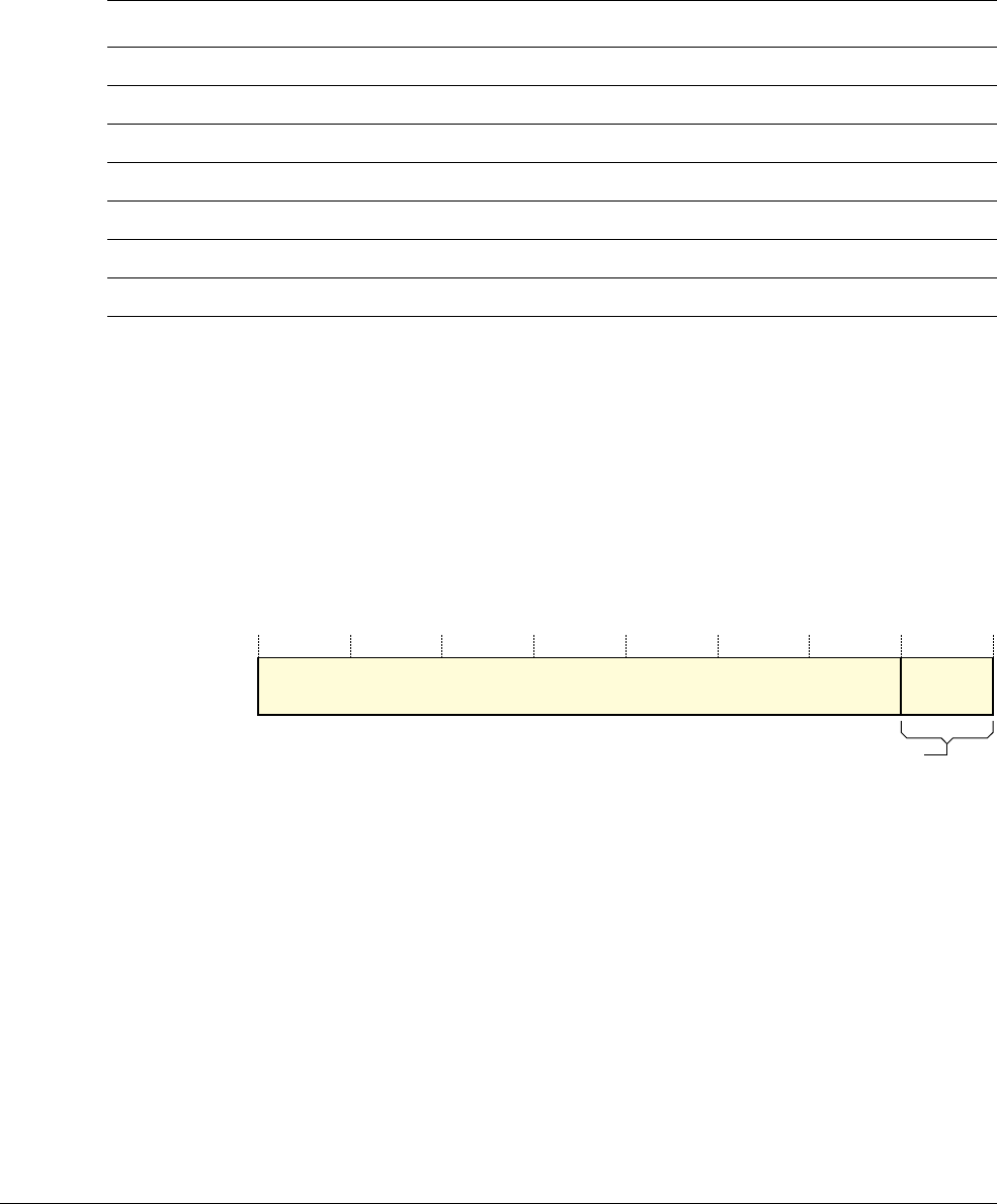
Nested Vectored Interrupt Controller
ARM DDI 0489D Copyright © 2014, 2015 ARM. All rights reserved. 7-4
ID082615 Non-Confidential
7.3 NVIC programmers model
This section describes the NVIC registers whose implementation is specific to this processor.
Other registers are described in the ARM®v7-M Architecture Reference Manual. Table 7-1
shows the NVIC registers.
7.3.1 Interrupt Controller Type Register
The ICTR characteristics are:
Purpose Shows the number of interrupt lines that the NVIC supports.
Usage Constraints There are no usage constraints.
Configurations Available in all configurations.
Attributes See the register summary in Table 7-1.
Figure 7-1 shows the ICTR bit assignments.
Figure 7-1 ICTR bit assignments
Table 7-1 NVIC registers
Address Name Type Reset Description
0xE000E004
ICTR RO - Interrupt Controller Type Register
0xE000E100-0xE000E11C
NVIC_ISER0-NVIC_ISER7 RW
0x00000000
Interrupt Set-Enable Registers
0xE000E180-0xE000E19C
NVIC_ICER0-NVIC_ICER7 RW
0x00000000
Interrupt Clear-Enable Registers
0xE000E200-0xE000E21C
NVIC_ISPR0-NVIC_ISPR7 RW
0x00000000
Interrupt Set-Pending Registers
0xE000E280-0xE000E29C
NVIC_ICPR0-NVIC_ICPR7 RW
0x00000000
Interrupt Clear-Pending Registers
0xE000E300-0xE000E31C
NVIC_IABR0-NVIC_IABR7 RO
0x00000000
Interrupt Active Bit Register
0xE000E400
-
0xE000E4EC
NVIC_IPR0-NVIC_IPR59 RW
0x00000000
Interrupt Priority Register
Reserved
31 43 0
INTLINESNUM

Nested Vectored Interrupt Controller
ARM DDI 0489D Copyright © 2014, 2015 ARM. All rights reserved. 7-5
ID082615 Non-Confidential
Table 7-2 shows the ICTR bit assignments.
Table 7-2 ICTR bit assignments
Bits Name Function
[31:4] - Reserved.
[3:0] INTLINESNUM Total number of interrupt lines in groups of 32:
0b0000
0-32.
0b0001
33-64.
0b0010
65-96.
0b0011
97-128.
0b0100
129-160.
0b0101
161-192.
0b0110
193-224.
0b0111
225-256a.
a. The processor supports a maximum of 240 external interrupts.

ARM DDI 0489D Copyright © 2014, 2015 ARM. All rights reserved. 8-1
ID082615 Non-Confidential
Chapter 8
Floating Point Unit
This chapter describes the Floating Point Unit (FPU). It contains the following sections:
•About the FPU on page 8-2.
•FPU functional description on page 8-3.
•FPU programmers model on page 8-5.

Floating Point Unit
ARM DDI 0489D Copyright © 2014, 2015 ARM. All rights reserved. 8-2
ID082615 Non-Confidential
8.1 About the FPU
The Cortex-M7 processor with FPU is an implementation of the single-precision and
double-precision variant of the ARMv7-M Architecture with Floating-Point Extension (FPv5).
The FPv5 extensions features are:
• Addition of double-precision operand support for existing data processing instructions in
FPv4-SP-D16-M.
• Some new instructions for both double and single-precision operands.
• 16 double-precision registers. This is the same as for FPv4 and there are no additional
registers.
• Software-enable control for single-precision and double-precision support using CPACR.
• Double-precision and single-precision support, when both are implemented, cannot be
enabled independently of one another.
• Identical load/store instruction support to FPv4 extensions that already includes support
for 64-bit data types.
Table 8-1 shows the ISA supported for the different configurations of the Cortex-M7 processor.
It provides floating-point computation functionality that is compliant with the ANSI/IEEE Std
754-2008, IEEE Standard for Binary Floating-Point Arithmetic, referred to as the IEEE 754
standard.
Table 8-1 Cortex-M7 ISA Support
Configuration ISA supported
Processor with no floating-point v7E-M
Processor with single-precision floating-point v7E-M + FPv5-SP-D16-M
Processor with single-precision and double-precision floating-point v7E-M + FPv5-DP-D16-M

Floating Point Unit
ARM DDI 0489D Copyright © 2014, 2015 ARM. All rights reserved. 8-3
ID082615 Non-Confidential
8.2 FPU functional description
This section describes the operations and that the FPU supports and what exceptions the FPU
generates.
The FPU fully supports single-precision and double-precision add, subtract, multiply, divide,
multiply and accumulate, and square root operations. It also provides conversions between
fixed-point and floating-point data formats, and floating-point constant instructions.
The FPU provides an extension register file containing 32 single-precision registers. These can
be viewed as:
• Sixteen 64-bit doubleword registers,
D0-D15
.
• Thirty-two 32-bit single-word registers,
S0-S31
.
• A combination of registers from these views.
For more information about the FPU, see the ARM®v7-M Architecture Reference Manual.
This section contains the following:
•Modes of operation.
•Compliance with the IEEE 754 standard on page 8-4.
•Exceptions on page 8-4.
The modes of operation are controlled using the Floating-Point Status and Control Register,
FPSCR. For more information about the FPSCR see the ARMv7-M Architecture Reference
Manual.
8.2.1 Modes of operation
The FPU provides three modes of operation to accommodate a variety of applications:
•Full-compliance mode.
•Flush-to-zero mode.
•Default NaN mode.
Full-compliance mode
In full-compliance mode, the FPU processes all operations according to the IEEE 754 standard
in hardware.
Flush-to-zero mode
Setting the FPSCR.FZ bit enables flush-to-zero mode. In this mode, the FPU treats all
subnormal input operands of arithmetic operations as zeros in the operation. Exceptions that
result from a zero operand are signaled appropriately.
VABS
,
VNEG
, and
VMOV
are not considered
arithmetic operations and are not affected by flush-to-zero mode. A result that is tiny, as
described in the IEEE 754 standard, where the destination precision is smaller in magnitude than
the minimum normal value before rounding, is replaced with a zero. The FPSCR.IDC bit
indicates when an input flush occurs. The FPSCR.UFC bit indicates when a result flush occurs.
Default NaN mode
Setting the FPSCR.DN bit enables default NaN mode. In this mode, the result of any arithmetic
data processing operation that involves an input NaN, or that generates a NaN result, returns the
default NaN. Propagation of the fraction bits is maintained only by
VABS
,
VNEG
, and
VMOV
operations. All other arithmetic operations ignore any information in the fraction bits of an input
NaN.

Floating Point Unit
ARM DDI 0489D Copyright © 2014, 2015 ARM. All rights reserved. 8-4
ID082615 Non-Confidential
8.2.2 Compliance with the IEEE 754 standard
When Default NaN (DN) and Flush-to-Zero (FZ) modes are disabled, FPv5 functionality is
compliant with the IEEE 754 standard in hardware. No support code is required to achieve this
compliance.
See the ARM®v7-M Architecture Reference Manual for information about FP architecture
compliance with the IEEE 754 standard.
8.2.3 Exceptions
The FPU sets the cumulative exception status flag in the FPSCR register as required for each
instruction, in accordance with the FPv5 architecture. The FPU does not support exception
traps. The processor also has six output pins, FPIXC, FPUFC, FPOFC, FPDZC, FPIDC, and
FPIOC, that each reflect the status of one of the cumulative exception flags.
The processor can reduce the exception latency by using lazy stacking. This means that the
processor reserves space on the stack for the FP state, but does not save that state information
to the stack until it is required to do so. See the ARM®v7-M Architecture Reference Manual for
more information.

Floating Point Unit
ARM DDI 0489D Copyright © 2014, 2015 ARM. All rights reserved. 8-5
ID082615 Non-Confidential
8.3 FPU programmers model
Table 8-2 shows the floating-point system registers in the Cortex-M7 processor with FPU, when
implemented. These registers are described in the ARM®v7-M Architecture Reference Manual.
Table 8-2 Floating-point system registers
Address Name Type Reset Description
0xE000EF34
FPCCR RW
0xC0000000
Context Control Register
0xE000EF38
FPCAR RW - Context Address Register
0xE000EF3C
FPDSCR RW
0x00000000
Default Status Control Register
0xE000EF40
MVFR0 RO
0x10110021
a
a. Single-precision only FPU.
Media and VFP Feature Register 0
0x10110221
b
b. Single-precision and double-precision FPU.
0xE000EF44
MVFR1 RO
0x11000011
aMedia and VFP Feature Register 1
0x12000011
b
0xE000EF48
MVFR2 RO
0x00000040
Media and VFP Feature Register 2

ARM DDI 0489D Copyright © 2014, 2015 ARM. All rights reserved. 9-1
ID082615 Non-Confidential
Chapter 9
Debug
This chapter describes how to debug and test software running on the processor. It contains the
following sections:
•About debug on page 9-2.
•About the AHBD interface on page 9-7.
•About the FPB on page 9-8.
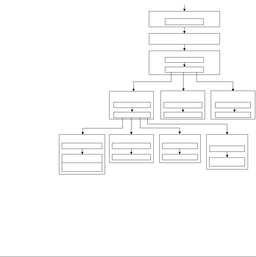
Debug
ARM DDI 0489D Copyright © 2014, 2015 ARM. All rights reserved. 9-2
ID082615 Non-Confidential
9.1 About debug
Cortex-M7 debug functionality includes processor halt, single-step, processor core register
access, Vector Catch, unlimited software breakpoints, and full system memory access. See the
ARM®v7-M Architecture Reference Manual for more information. The processor also includes
support for hardware breakpoints and watchpoints configured during implementation:
• A breakpoint unit supporting four to eight instruction comparators.
• A watchpoint unit supporting two or four watchpoints.
For processors that implement debug, ARM recommends that a debugger identify and connect
to the debug components using the CoreSight debug infrastructure.
Figure 9-1 shows the recommended flow that a debugger can follow to discover the components
in the CoreSight debug infrastructure. In this case a debugger reads the peripheral and
component ID registers for each CoreSight component in the CoreSight system.
Figure 9-1 CoreSight discovery
To identify the Cortex-M7 processor within the CoreSight system, ARM recommends that a
debugger perform the following actions:
1. Locate and identify the Cortex-M7 Processor ROM table using its CoreSight
identification. See Table 9-2 on page 9-4 for more information.
CoreSight debug port
Cortex-M7 PPB ROM
table
CoreSight ID
Pointers
CoreSight access port
Base pointer
System control space
CoreSight ID
Cortex-M7 CPUID
Debug control
Data watchpoint unit
CoreSight ID
Watchpoint control
‡ Optional component
Redirection from the
‡ System ROM table, if implemented
Breakpoint unit
CoreSight ID
Breakpoint control
Cortex-M7 Processor ROM table
CoreSight ID
Pointers
‡ ETM
CoreSight ID
‡ CTI
CoreSight ID
‡ Instrumentation
trace macrocell unit
CoreSight ID
ETM control CTI control
Instrumentation
trace control

Debug
ARM DDI 0489D Copyright © 2014, 2015 ARM. All rights reserved. 9-3
ID082615 Non-Confidential
2. Follow the pointer in the Cortex-M7 Processor ROM table to the Cortex-M7 PPB ROM
table. From the PPB ROM table pointers the following components can be identified:
a. System Control Space (SCS).
b. Breakpoint unit (FPB).
c. Data Watchpoint and Trace unit (DWT).
d. Instrumentation Trace Macrocell unit (IMT).
See Table 9-4 on page 9-5 for more information.
When a debugger identifies the SCS from its CoreSight identification, it can identify the
processor and its revision number from the CPUID register in the SCS at address
0xE000ED00
.
A debugger cannot rely on the Cortex-M7 Processor ROM table being the first ROM table
encountered. One or more system ROM tables are required between the access port and the
processor ROM table if other CoreSight components are in the system. If a system ROM table
is present, this can include a unique identifier for the implementation.
9.1.1 Cortex-M7 Processor ROM table identification and entries
Table 9-1 shows the processor ROM table identification registers and values for debugger
detection. This permits debuggers to identify the processor.
These values for the Peripheral ID registers identify this as the Cortex-M7 Processor ROM
table. The Component ID registers identify this as a CoreSight ROM table.
Note
The Cortex-M7 Processor ROM table only supports word-size transactions.
Table 9-1 Cortex-M7 Processor ROM table identification values
Address Register Value Description
0xE00FEFD0
Peripheral ID4
0x00000004
Component and Peripheral ID register formats in the
ARM®v7-M Architecture Reference Manual
0xE00FEFD4
Peripheral ID5
0x00000000
0xE00FEFD8
Peripheral ID6
0x00000000
0xE00FEFDC
Peripheral ID7
0x00000000
0xE00FEFE0
Peripheral ID0
0x000000C8
0xE00FEFE4
Peripheral ID1
0x000000B4
0xE00FEFE8
Peripheral ID2
0x0000000B
0xE00FEFEC
Peripheral ID3
0x00000000
0xE00FEFF0
Component ID0
0x0000000D
0xE00FEFF4
Component ID1
0x00000010
0xE00FEFF8
Component ID2
0x00000005
0xE00FEFFC
Component ID3
0x000000B1

Debug
ARM DDI 0489D Copyright © 2014, 2015 ARM. All rights reserved. 9-4
ID082615 Non-Confidential
Table 9-2 shows the CoreSight components that the Cortex-M7 Processor ROM table points to.
The Cortex-M7 Processor ROM table entries point to the debug components of the processor.
The offset for each entry is the offset of that component from the ROM table base address,
0xE00FE000
.
See the ARM® CoreSight™ Architecture Specification (v2.0) for more information about the
ROM table ID and component registers, and access types.
9.1.2 Cortex-M7 PPB ROM table identification and entries
Table 9-3 shows the Cortex-M7 PPB ROM table identification registers and values for debugger
detection. This permits debuggers to identify the CoreSight components on the PPB in the
processor and their debug capabilities.
Table 9-2 Cortex-M7 Processor ROM table components
Address Component Value Description
0xE00FE000
Cortex-M7 PPB ROM Table
0x00001003
See Cortex-M7 PPB ROM table identification and entries
0xE00FE004
ETM
0xFFF43003
aSee the ARM® CoreSight™ ETM-M7 Technical Reference Manual
0xE00FE008
CTI
0xFFF44003
bSee Chapter 10 Cross Trigger Interface
0xE00FE00C
Reserved
0x1FF02002
See the ARM® CoreSight™ Architecture Specification (v2.0)
0xE00FE010
End marker
0x00000000
0xE00FEFCC
SYSTEM ACCESS
0x00000001
a. Reads as
0xFFF43002
if the ETM is not implemented.
b. Reads as
0xFFF44002
if the CTI is not implemented.
Table 9-3 Cortex-M7 PPB ROM table identification values
Address Register Value Description
0xE00FFFD0
Peripheral ID4
0x00000004
Component and Peripheral ID register formats in the
ARM®v7-M Architecture Reference Manual
0xE00FFFD4
Peripheral ID5
0x00000000
0xE00FFFD8
Peripheral ID6
0x00000000
0xE00FFFDC
Peripheral ID7
0x00000000
0xE00FFFE0
Peripheral ID0
0x000000C7
0xE00FFFE4
Peripheral ID1
0x000000B4
0xE00FFFE8
Peripheral ID2
0x0000000B
0xE00FFFEC
Peripheral ID3
0x00000000
0xE00FFFF0
Component ID0
0x0000000D
0xE00FFFF4
Component ID1
0x00000010
0xE00FFFF8
Component ID2
0x00000005
0xE00FFFFC
Component ID3
0x000000B1

Debug
ARM DDI 0489D Copyright © 2014, 2015 ARM. All rights reserved. 9-5
ID082615 Non-Confidential
These values for the Peripheral ID registers identify this as the Cortex-M7 PPB ROM table. The
Component ID registers identify this as a CoreSight ROM table.
Note
The Cortex-M7 PPB ROM table only supports word size transactions.
Table 9-4 shows the CoreSight components that the Cortex-M7 PPB ROM table points to. The
values depend on the implemented debug configuration.
The Cortex-M7 PPB ROM table entries point to the debug components of the processor. The
offset for each entry is the offset of that component from the ROM table base address,
0xE00FF000
.
See the ARM®v7-M Architecture Reference Manual and the ARM® CoreSight™ Architecture
Specification (v2.0) for more information about the ROM table ID and component registers, and
their addresses and access types.
9.1.3 System Control Space
The processor provides debug through registers in the SCS. See:
•Debug register summary on page 9-6.
•System address map on page 2-5.
Table 9-4 Cortex-M7 PPB ROM table components
Address Component Value Description
0xE00FF000
SCS
0xFFF0F003
See System Control Space.
0xE00FF004
DWT
0xFFF02003
See Table 11-1 on page 11-4.
0xE00FF008
FPB
0xFFF03003
See Table 9-7 on page 9-8.
0xE00FF00C
ITM
0xFFF01003
a
a. Reads as
0xFFF01002
if the ITM is not implemented.
See Table 12-1 on page 12-4.
0xE00FF010
Reserved (TPIU)
0xFFF41002
Not present, TPIU not implemented inside
Cortex-M7.
0xE00FF014
Reserved (ETM)
0xFFF42002
Not present, ETM is referenced by the
Cortex-M7 Processor ROM table. See
Cortex-M7 Processor ROM table identification
and entries on page 9-3.
0xE00FF018
End marker
0x00000000
See DAP accessible ROM table in the ARM®v7-M
Architecture Reference Manual.
0xE00FFFCC
SYSTEM ACCESS
0x00000001

Debug
ARM DDI 0489D Copyright © 2014, 2015 ARM. All rights reserved. 9-6
ID082615 Non-Confidential
SCS CoreSight identification
Table 9-5 shows the SCS CoreSight identification registers and values for debugger detection.
Final debugger identification of the Cortex-M7 processor is through the CPUID register in the
SCS. See CPUID Base Register on page 3-8.
See the ARM®v7-M Architecture Reference Manual and the ARM® CoreSight™ Architecture
Specification (v2.0) for more information about the ROM table ID and component registers, and
their addresses and access types.
9.1.4 Debug register summary
Table 9-6 shows the debug registers. Each of these registers is 32 bits wide and is described in
the ARM®v7-M Architecture Reference Manual.
Table 9-5 SCS identification values
Address Register Value Description
0xE000EFD0
Peripheral ID4
0x00000004
Component and Peripheral ID register formats in
the ARM®v7-M Architecture Reference Manual
0xE000EFD4
Peripheral ID5
0x00000000
0xE000EFD8
Peripheral ID6
0x00000000
0xE000EFDC
Peripheral ID7
0x00000000
0xE000EFE0
Peripheral ID0
0x0000000C
a
a.
0x0000000C
SCS identification value for implementations without FPU.
0xE000EFE4
Peripheral ID1
0x000000B0
0xE000EFE8
Peripheral ID2
0x0000000B
0xE000EFEC
Peripheral ID3
0x00000000
0xE000EFF0
Component ID0
0x0000000D
0xE000EFF4
Component ID1
0x000000E0
0xE000EFF8
Component ID2
0x00000005
0xE000EFFC
Component ID3
0x000000B1
Table 9-6 Debug registers
Address Name Type Reset Description
0xE000ED30
DFSR RW
0x00000000
a
a. Power-on reset only.
Debug Fault Status Register
0xE000EDF0
DHCSR RW
0x00000000
Debug Halting Control and Status Register
0xE000EDF4
DCRSR WO - Debug Core Register Selector Register
0xE000EDF8
DCRDR RW - Debug Core Register Data Register
0xE000EDFC
DEMCR RW
0x00000000
Debug Exception and Monitor Control Register

Debug
ARM DDI 0489D Copyright © 2014, 2015 ARM. All rights reserved. 9-7
ID082615 Non-Confidential
9.2 About the AHBD interface
The 32-bit AHB debug (AHBD) interface implements the AMBA 3 AHB-Lite protocol.
It can be used with a CoreSight AHB-AP to provide debugger access to:
• All processor control and debug resources.
• A view of memory that is consistent with that observed by load/store instructions acting
on the processor.
AHBD interface accesses are only in little-endian format. The processor ensures data is
presented in the correct big- or little-endian format to the system. This is transparent to the
debugger.
Note
• The instruction cache is not accessible to a debugger. Therefore debugger accesses to
cacheable, executable regions of memory might not be coherent with the instructions
visible to the instruction side of the processor.
• The data cache must be enabled by setting the CCR.DC to 1 to read and write data to the
cache. If CCR.DC is set to 0, all debug requests to memory regions outside the TCM and
peripheral address space, access only the external memory on AXIM even if the debug
request is marked as cacheable on the AHBD interface.

Debug
ARM DDI 0489D Copyright © 2014, 2015 ARM. All rights reserved. 9-8
ID082615 Non-Confidential
9.3 About the FPB
The FPB implements hardware breakpoints.
The FPB can be configured during implementation to provide either four or eight instruction
comparators. You can configure each comparator individually to return a
BKPT
instruction to the
processor on a match, to provide hardware breakpoint capability.
The FPB does not support Flash patching. The FP_REMAP register is not implemented and is
RAZ/WI.
9.3.1 FPB functional description
The FPB contains both a global enable and individual enables for each of the comparators
implemented. If the comparison for an entry matches, the address is remapped to a
BKPT
instruction if that feature is enabled.
If the FPB supports only four breakpoints then only comparators 0-3 are used, and comparators
4-7 are implemented as RAZ/WI.
9.3.2 FPB programmers model
Table 9-7 shows the FPB registers. Depending on the implementation of your processor, some
of these registers might not be present. Any register that is configured as not present reads as
zero.
Table 9-7 FPB register summary
Address Name Type Reset Description
0xE0002000
FP_CTRL RW
0x10000040
a
0x10000080
b
FlashPatch Control Register
0xE0002004
FP_REMAP RAZ/WI - Not implemented
0xE0002008
FP_COMP0 RW
0b00000000
cFlashPatch Comparator Register0
0xE000200C
FP_COMP1 RW
0b00000000
FlashPatch Comparator Register1
0xE0002010
FP_COMP2 RW
0b00000000
FlashPatch Comparator Register2
0xE0002014
FP_COMP3 RW
0b00000000
FlashPatch Comparator Register3
0xE0002018
FP_COMP4 RW
0b00000000
FlashPatch Comparator Register4
0xE000201C
FP_COMP5 RW
0b00000000
FlashPatch Comparator Register5
0xE0002020
FP_COMP6 RW
0b00000000
FlashPatch Comparator Register6
0xE0002024
FP_COMP7 RW
0b00000000
FlashPatch Comparator Register7
0xE0000FB0
FP_LAR WO - FlashPatch Lock Access Register
0xE0000FB4
FP_LSR RO Unknown FlashPatch Lock Status Register

Debug
ARM DDI 0489D Copyright © 2014, 2015 ARM. All rights reserved. 9-9
ID082615 Non-Confidential
All FPB registers are described in the ARM®v7-M Architecture Reference Manual.
0xE0002FD0
PID4 RO
0x00000004
Peripheral identification registers
0xE0002FD4
PID5 RO
0x00000000
0xE0002FD8
PID6 RO
0x00000000
0xE0002FDC
PID7 RO
0x00000000
0xE0002FE0
PID0 RO
0x0000000E
0xE0002FE4
PID1 RO
0x000000B0
0xE0002FE8
PID2 RO
0x0000000B
0xE0002FEC
PID3 RO
0x00000000
0xE0002FF0
CID0 RO
0x0000000D
Component identification registers
0xE0002FF4
CID1 RO
0x000000E0
0xE0002FF8
CID2 RO
0x00000005
0xE0002FFC
CID3 RO
0x000000B1
a. If four instruction comparators are implemented.
b. If eight instruction comparators are implemented.
c. For FP_COMP0 to FP_COMP7, bit 0 is reset to 0. Other bits in these registers are not reset.
Table 9-7 FPB register summary (continued)
Address Name Type Reset Description

ARM DDI 0489D Copyright © 2014, 2015 ARM. All rights reserved. 10-1
ID082615 Non-Confidential
Chapter 10
Cross Trigger Interface
This chapter describes the Cortex-M7 Cross Trigger Interface (CTI). It contains the following
sections:
•About the CTI on page 10-2.
•Cortex-M7 CTI functional description on page 10-3.
•CTI programmers model on page 10-5.

Cross Trigger Interface
ARM DDI 0489D Copyright © 2014, 2015 ARM. All rights reserved. 10-2
ID082615 Non-Confidential
10.1 About the CTI
If implemented, the CTI enables the debug logic and ETM to interact with each other and with
other CoreSight components. This is called cross triggering. For example, you can configure the
CTI to generate an interrupt when the ETM trigger event occurs.
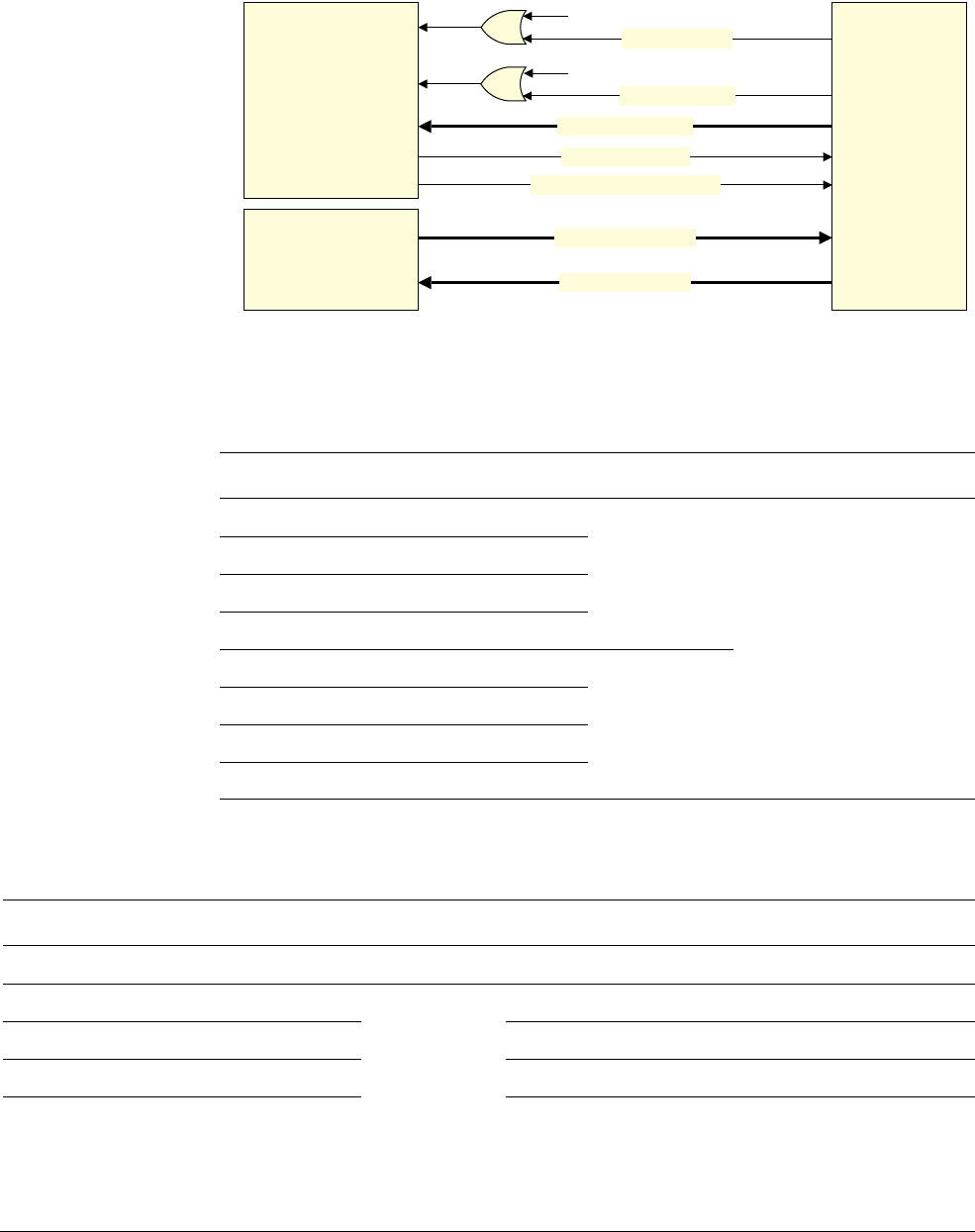
Cross Trigger Interface
ARM DDI 0489D Copyright © 2014, 2015 ARM. All rights reserved. 10-3
ID082615 Non-Confidential
10.2 Cortex-M7 CTI functional description
The Cortex-M7 CTI is connected to a number of trigger inputs and trigger outputs. Figure 10-1
shows the debug system components and the available trigger inputs and trigger outputs.
Figure 10-1 Debug system components
Table 10-1 shows how the CTI trigger inputs are connected to the Cortex-M7 processor.
Table 10-2 shows how the CTI trigger outputs are connected to the processor and ETM.
Processor
ETM
CTI
Processor halted
ETM event inputs
Interrupt requests
ETM event outputs
DWT comparator outputs
Restart request
Debug request
External debug request
External restart request
Table 10-1 Trigger signals to the CTI
Signal Description Connection Acknowledge, handshake
CTITRIGIN[7] ETM Event Output 3 ETM to CTI Pulsed
CTITRIGIN[6] ETM Event Output 2
CTITRIGIN[5] ETM Event Output 1
CTITRIGIN[4] ETM Event Output 0
CTITRIGIN[3] DWT Comparator Output 2 Processor to CTI
CTITRIGIN[2] DWT Comparator Output 1
CTITRIGIN[1] DWT Comparator Output 0
CTITRIGIN[0] Processor Halted
Table 10-2 Trigger signals from the CTI
Signal Description Connection Acknowledge, handshake
CTITRIGOUT[7] Processor Restart CTI to Processor Processor Restarted
CTITRIGOUT[6] ETM Event Input 3 CTI to ETM Pulsed
CTITRIGOUT[5] ETM Event Input 2 Pulsed
CTITRIGOUT[4] ETM Event Input 1 Pulsed
CTITRIGOUT[3] ETM Event Input 0 Pulsed

Cross Trigger Interface
ARM DDI 0489D Copyright © 2014, 2015 ARM. All rights reserved. 10-4
ID082615 Non-Confidential
Note
• After the processor is halted using CTI Trigger Output 0, the Processor Debug Request
signal remains asserted. The debugger must write to CTIINTACK to clear the halting
request before restarting the processor.
• After asserting an interrupt using the CTI Trigger Output 1 or 2, the Interrupt Service
Routine (ISR) must clear the interrupt request by writing to the CTI Interrupt
Acknowledge, CTIINTACK.
CTITRIGOUT[2] Interrupt request 1 CTI to system Acknowledged by writing to the CTIINTACK register in ISR
CTITRIGOUT[1] Interrupt request 0
CTITRIGOUT[0] Processor debug request CTI to processor Acknowledged by the debugger writing to the CTIINTACK
register
Table 10-2 Trigger signals from the CTI (continued)
Signal Description Connection Acknowledge, handshake

Cross Trigger Interface
ARM DDI 0489D Copyright © 2014, 2015 ARM. All rights reserved. 10-5
ID082615 Non-Confidential
10.3 CTI programmers model
Table 10-3 shows the CTI programmable registers. See the ARM® CoreSight™ SoC-400
Technical Reference Manual for register descriptions.
Table 10-3 CTI register summary
Address
offset Register name Type Reset
value Description
0x000
CTICONTROL RW
0x00000000
CTI Control Register
0x010
CTIINTACK WO
0x00000000
CTI Interrupt Acknowledge Register
0x014
CTIAPPSET RW
0x00000000
CTI Application Trigger Set Register
0x018
CTIAPPCLEAR RW
0x00000000
CTI Application Trigger Clear Register
0x01C
CTIAPPPULSE WO
0x00000000
CTI Application Pulse Register
0x020
-
0x03C
CTIINEN[7:0] RW
0x00000000
CTI Trigger to Channel Enable Registers
0x0A0
-
0x0BC
CTIOUTEN[7:0] RW
0x00000000
CTI Channel to Trigger Enable Registers
0x130
CTITRIGINSTATUS RO
0x00000000
CTI Trigger In Status Register
0x134
CTITRIGOUTSTATUS RO
0x00000000
CTI Trigger Out Status Register
0x138
CTICHINSTATUS RO
0x00000000
CTI Channel In Status Register
0x140
CTIGATE RW
0x00000000
Enable CTI Channel Gate register
0x144
ASICCTL RW
0x00000000
External Multiplexer Control register
0xEDC
ITCHINACK WO
0x00000000
Integration Test Channel Input
Acknowledge register
0xEE0
ITTRIGINACK WO
0x00000000
Integration Test Trigger Input Acknowledge
register
0xEE4
ITCHOUT WO
0x00000000
Integration Test Channel Output register
0xEE8
ITTRIGOUT WO
0x00000000
Integration Test Trigger Output register
0xEEC
ITCHOUTACK WO
0x00000000
Integration Test Channel Output
Acknowledge register
0xEF0
ITTRIGOUTACK RO
0x00000000
Integration Test Trigger Output
Acknowledge register
0xEF4
ITCHIN RO
0x00000000
Integration Test Channel Input register
0xEF8
ITTRIGIN RO
0x00000000
Integration Test Trigger Input register
0xF00
ITCTRL RW
0x00000000
Integration Mode Control register
0xFA0
CLAIMSET RW
0x0000000F
Claim Tag Set register
0xFA4
CLAIMCLR RW
0x00000000
Claim Tag Clear register
0xFB0
LAR WO
0x00000000
Lock Access Register
0xFB4
LSR RO
0x00000003
Lock Status Register
0xFB8
AUTHSTATUS RO
0x00000005
Authentication Status register
0xFC8
DEVID RO
0x00040800
Device Configuration register

Cross Trigger Interface
ARM DDI 0489D Copyright © 2014, 2015 ARM. All rights reserved. 10-6
ID082615 Non-Confidential
0xFCC
DEVTYPE RO
0x00000014
Device Type Identifier register
0xFD0
PIDR4 RO
0x00000004
Peripheral ID4 Register
0xFD4
- - - Reserved
0xFD8
- - - Reserved
0xFDC
- - - Reserved
0xFE0
PIDR0 RO
0x00000006
Peripheral ID0 Register
0xFE4
PIDR1 RO
0x000000B9
Peripheral ID1 Register
0xFE8
PIDR2 RO
0x0000004B
Peripheral ID2 Register
0xFEC
PIDR3 RO
0x00000000
Peripheral ID3 Register
0xFF0
CIDR0 RO
0x0000000D
Component ID0 Register
0xFF4
CIDR1 RO
0x00000090
Component ID1 Register
0xFF8
CIDR2 RO
0x00000005
Component ID2 Register
0xFFC
CIDR3 RO
0x000000B1
Component ID3 Register
Table 10-3 CTI register summary (continued)
Address
offset Register name Type Reset
value Description

ARM DDI 0489D Copyright © 2014, 2015 ARM. All rights reserved. 11-1
ID082615 Non-Confidential
Chapter 11
Data Watchpoint and Trace Unit
This chapter describes the Data Watchpoint and Trace (DWT) unit. It contains the following
sections:
•About the DWT on page 11-2.
•DWT functional description on page 11-3.
•DWT programmers model on page 11-4.

Data Watchpoint and Trace Unit
ARM DDI 0489D Copyright © 2014, 2015 ARM. All rights reserved. 11-2
ID082615 Non-Confidential
11.1 About the DWT
The DWT is a debug unit that provides watchpoints and system profiling for the processor. Data
tracing is also available if the processor has been implemented with DWT and ITM trace. See
Chapter 12 Instrumentation Trace Macrocell Unit for details about the ITM.

Data Watchpoint and Trace Unit
ARM DDI 0489D Copyright © 2014, 2015 ARM. All rights reserved. 11-3
ID082615 Non-Confidential
11.2 DWT functional description
A full DWT contains four comparators that you can configure as:
• A hardware watchpoint.
• An ETM trigger.
• A PC sampler event trigger.
• A data address sampler event trigger.
The first comparator, DWT_COMP0, can also compare against the clock cycle counter,
CYCCNT. You can also use the second comparator, DWT_COMP1, as a data comparator.
A reduced DWT contains two comparators that you can use as a watchpoint or as a trigger. The
comparators support data matching.
The DWT if present contains counters for:
• Clock cycles, CYCCNT.
• Folded instructions.
•Load Store Unit (LSU) operations.
• Sleep cycles.
• CPI, that is all instruction cycles except for the first cycle.
• Interrupt overhead.
Note
An event is generated each time a counter overflows.
You can configure the DWT to generate PC samples at defined intervals, and to generate
interrupt event information.
The DWT provides periodic requests for protocol synchronization to the ITM.

Data Watchpoint and Trace Unit
ARM DDI 0489D Copyright © 2014, 2015 ARM. All rights reserved. 11-4
ID082615 Non-Confidential
11.3 DWT programmers model
Table 11-1 shows the DWT registers. Depending on the implementation of your processor, some
of these registers might not be present. Any register that is configured as not present reads as
zero.
Table 11-1 DWT register summary
Address Name Type Reset Description
0xE0001000
DWT_CTRL RW See aControl Register
0xE0001004
DWT_CYCCNT RW
0x00000000
Cycle Count Register
0xE0001008
DWT_CPICNT RW - CPI Count Register
0xE000100C
DWT_EXCCNT RW
-
Exception Overhead Count Register
0xE0001010
DWT_SLEEPCNT RW
-
Sleep Count Register
0xE0001014
DWT_LSUCNT RW
-
LSU Count Register
0xE0001018
DWT_FOLDCNT RW
-
Folded-instruction Count Register
0xE000101C
DWT_PCSR RO - Program Counter Sample Register
0xE0001020
DWT_COMP0 RW - Comparator Register 0
0xE0001024
DWT_MASK0 RW - Mask Register 0
0xE0001028
DWT_FUNCTION0 RW
0x00000000
Function Register 0
0xE0001030
DWT_COMP1 RW - Comparator Register 1
0xE0001034
DWT_MASK1 RW - Mask Register1
0xE0001038
DWT_FUNCTION1 RW
0x00000000
bFunction Register 1
0xE0001040
DWT_COMP2 RW - Comparator Register 2
0xE0001044
DWT_MASK2 RW - Mask Register 2
0xE0001048
DWT_FUNCTION2 RW
0x00000000
Function Register 2
0xE0001050
DWT_COMP3 RW - Comparator Register 3
0xE0001054
DWT_MASK3 RW - Mask Register 3
0xE0001058
DWT_FUNCTION3 RW
0x00000000
Function Register 3
0xE0000FB0
DWT_LAR WO - Lock Access Register
0xE0000FB4
DWT_LSR RO Unknown Lock Status Register

Data Watchpoint and Trace Unit
ARM DDI 0489D Copyright © 2014, 2015 ARM. All rights reserved. 11-5
ID082615 Non-Confidential
DWT registers are described in the ARM®v7-M Architecture Reference Manual.
Note
• Cycle matching functionality is only available in comparator 0.
• Data matching functionality is only available in comparator 1.
• Data value is only sampled for accesses that do not produce an MPU or bus fault. The PC
is sampled irrespective of any faults. The PC is only sampled for the first address of a
burst.
• The FUNCTION field in the DWT_FUNCTION1 register is overridden for comparators
given by DATAVADDR0 and DATAVADDR1 if DATAVMATCH is also set in
DWT_FUNCTION1. The comparators given by DATAVADDR0 and DATAVADDR1 can
then only perform address comparator matches for comparator 1 data matches.
• ARM does not recommend PC match for watchpoints because watchpoints are
asynchronous to the event that causes them. It mainly guards and triggers the ETM.
0xE0001FD0
PID4 RO
0x00000004
Peripheral identification registers
0xE0001FD4
PID5 RO
0x00000000
0xE0001FD8
PID6 RO
0x00000000
0xE0001FDC
PID7 RO
0x00000000
0xE0001FE0
PID0 RO
0x00000002
0xE0001FE4
PID1 RO
0x000000B0
0xE0001FE8
PID2 RO
0x0000000B
0xE0001FEC
PID3 RO
0x00000000
0xE0001FF0
CID0 RO
0x0000000D
Component identification registers
0xE0001FF4
CID1 RO
0x000000E0
0xE0001FF8
CID2 RO
0x00000005
0xE0001FFC
CID3 RO
0x000000B1
a. Possible reset values are:
0x40000000
for full DWT, with trace.
0x48000000
for full DWT, without trace.
0x20000000
for reduced DWT, with trace.
0x28000000
for reduced DWT, without trace.
b. If the processor is configured for minimal debug, the DWT_FUNCTION1[9] is always RAZ.
If the processor is configured for full debug, the DWT_FUNCTION1[9] is always RA0.
All other bits in the DWT_FUNCTION1 register are reset to zero.
Table 11-1 DWT register summary (continued)
Address Name Type Reset Description

ARM DDI 0489D Copyright © 2014, 2015 ARM. All rights reserved. 12-1
ID082615 Non-Confidential
Chapter 12
Instrumentation Trace Macrocell Unit
This chapter describes the Instrumentation Trace Macrocell (ITM) unit. It contains the
following sections:
•About the ITM on page 12-2.
•ITM functional description on page 12-3.
•ITM programmers model on page 12-4.

Instrumentation Trace Macrocell Unit
ARM DDI 0489D Copyright © 2014, 2015 ARM. All rights reserved. 12-2
ID082615 Non-Confidential
12.1 About the ITM
The ITM is a an optional application-driven trace source that supports
printf()
style debugging
to trace operating system and application events, and generates diagnostic system information.

Instrumentation Trace Macrocell Unit
ARM DDI 0489D Copyright © 2014, 2015 ARM. All rights reserved. 12-3
ID082615 Non-Confidential
12.2 ITM functional description
The ITM generates trace information as packets. There are four sources that can generate
packets. If multiple sources generate packets at the same time, the ITM arbitrates the order that
packets are output. The four sources in decreasing order of priority are:
Software trace Software can write directly to ITM stimulus registers to generate packets.
Hardware trace The DWT generates these packets, and the ITM outputs them.
Time stamping Timestamps are generated relative to packets. The ITM contains a 21-bit
counter to generate the timestamp. The processor clock output clocks the
counter.
Global system timestamping
Timestamps can optionally be generated using a system-wide 64-bit count
value. The same count value is used for inserting timestamps in the ETM
trace stream, permitting coarse-grain correlation.

Instrumentation Trace Macrocell Unit
ARM DDI 0489D Copyright © 2014, 2015 ARM. All rights reserved. 12-4
ID082615 Non-Confidential
12.3 ITM programmers model
Table 12-1 shows the ITM registers whose implementation is specific to this processor. Other
registers are described in the ARM®v7-M Architecture Reference Manual.
Depending on the implementation of your processor, the ITM registers might not be present.
Any register that is configured as not present reads as zero.
Note
• You must enable TRCENA of the Debug Exception and Monitor Control Register before
you program or use the ITM.
• If the ITM stream requires synchronization packets, you must configure the
synchronization packet rate in the DWT.
Table 12-1 ITM register summary
Address Name Type Reset Description
0xE0000000
-
0xE000007C
ITM_STIM0- ITM_STIM31 RW - Stimulus Port Registers 0-31
0xE0000E00
ITM_TER RW
0x00000000
Trace Enable Register
0xE0000E40
ITM_TPR RW
0x00000000
ITM Trace Privilege Register on page 12-5
0xE0000E80
ITM_TCR RW
0x00000000
Trace Control Register
0xE0000EF0
ITM_ITATRDY RO Unknown Integration Mode: Read ATB Ready
0xE0000EF8
ITM_ITATVAL WO - Integration Mode: Write ATB Valid
0xE0000F00
ITM_TCTRL RW
0x00000000
Integration Mode Control Register
0xE0000FB0
ITM_LAR WO - Lock Access Register
0xE0000FB4
ITM_LSR RO Unknown Lock Status Register
0xE0000FD0
PID4 RO
0x00000004
Peripheral identification registers
0xE0000FD4
PID5 RO
0x00000000
0xE0000FD8
PID6 RO
0x00000000
0xE0000FDC
PID7 RO
0x00000000
0xE0000FE0
PID0 RO
0x00000001
0xE0000FE4
PID1 RO
0x000000B0
0xE0000FE8
PID2 RO
0x0000000B
0xE0000FEC
PID3 RO
0x00000000
0xE0000FF0
CID0 RO
0x0000000D
Component identification registers
0xE0000FF4
CID1 RO
0x000000E0
0xE0000FF8
CID2 RO
0x00000005
0xE0000FFC
CID3 RO
0x000000B1
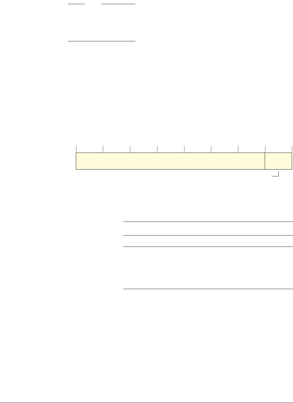
Instrumentation Trace Macrocell Unit
ARM DDI 0489D Copyright © 2014, 2015 ARM. All rights reserved. 12-5
ID082615 Non-Confidential
Note
ITM registers are fully accessible in privileged mode. In user mode, all registers can be read,
but only the Stimulus Registers and Trace Enable Registers can be written, and only when the
corresponding Trace Privilege Register bit is set. Invalid user mode writes to the ITM registers
are discarded.
12.3.1 ITM Trace Privilege Register
The ITM_TPR characteristics are:
Purpose Enables an operating system to control the stimulus ports that are
accessible by user code.
Usage constraints You can only write to this register in privileged mode.
Configurations This register is available if the ITM is configured in your implementation.
Attributes See Table 12-1 on page 12-4.
Figure 12-1 shows the ITM_TPR bit assignments.
Figure 12-1 ITM_TPR bit assignments
Table 12-2 shows the ITM_TPR bit assignments.
Reserved
31 43 0
PRIVMASK
Table 12-2 ITM_TPR bit assignments
Bits Name Function
[31:4] - Reserved.
[3:0] PRIVMASK Bit mask to enable tracing on ITM stimulus ports:
Bit[0] Stimulus ports [7:0].
Bit[1] Stimulus ports [15:8].
Bit[2] Stimulus ports [23:16].
Bit[3] Stimulus ports [31:24].

ARM DDI 0489D Copyright © 2014, 2015 ARM. All rights reserved. 13-1
ID082615 Non-Confidential
Chapter 13
Fault detection and handling
This chapter describes the fault detection and handling features of the Cortex-M7 processor. It
contains the following sections:
•About fault detection and handling on page 13-2.
•Cache RAM protection on page 13-3.
•Logic protection on page 13-6.

Fault detection and handling
ARM DDI 0489D Copyright © 2014, 2015 ARM. All rights reserved. 13-2
ID082615 Non-Confidential
13.1 About fault detection and handling
The Cortex-M7 processor fault detection and handling features:
• Report any detected error to the system.
• Correct any detected and correctable error.
When the system-on-chip reports a failure, the logging and status must provide all the required
information to identify the source of the failure. The intention is to detect and correct the errors
as much as possible, and identify them to the system.
For Error Correcting Code (ECC) on RAM, all errors explicitly seen must be reported, so that
the error propagation is minimized.
13.1.1 RAM and logic protection
The processor protects memories and logic in two different ways.
• The RAMs are protected with ECC.
• The logic of the individual processors is protected by duplication with diagnostic
compare. This is known as redundant logic in a lock-step implementation.
These are independent, and can be used separately.
The processor uses Single Error Correction and Double Error Detection (SEC-DED) ECCs to
detect and correct errors in the RAMs. A finite number of hard, that is, permanent errors can be
detected and corrected with continued normal operation using dedicated error registers.
13.1.2 Analysis of errors
A monitor external to the processor is responsible for analyzing the notified error and marking
the corrupted entries as reusable if it has been proven to be a soft error. This analysis can be
performed by reading and writing the RAM directly through the processor MBIST interface.

Fault detection and handling
ARM DDI 0489D Copyright © 2014, 2015 ARM. All rights reserved. 13-3
ID082615 Non-Confidential
13.2 Cache RAM protection
The following sections describe RAM protection:
•Protection method.
•RAM protection summary on page 13-4.
•ECC codes on page 13-4.
•RAM configuration on page 13-5.
•Performance impact on page 13-5.
13.2.1 Protection method
The following sections describe how RAM errors are managed:
•Detecting errors.
•Recovering from errors.
•Handling permanent errors.
•Error bank register behavior on page 13-4.
Detecting errors
The Cortex-M7 processor uses ECC to detect errors in the cache RAMs.
Recovering from errors
The Cortex-M7 processor can recover from a RAM error detected in the cache by using clean
and invalidate and retry. When an error is detected, as shown in Table 13-1 on page 13-4, the
corresponding index/way is cleaned and invalidated. When the clean and invalidate operation
completed, the requester retries its access. The ECC can also be used to correct single-bit errors
in the RAM.
Instruction cache
In the instruction cache, lines are always clean so that invalidating the line is
sufficient. The retried access then fetches the correct value from external
memory.
Data cache
In the data cache, the cache line can be dirty. The correction of the RAM contents
is done as part of the clean and invalidate operation for caches. This takes place
in the write buffer and the corrected data is written back to external memory. The
retried access then reads the correct value from external memory. If the data
cannot be corrected then the error is non-recoverable.
Handling permanent errors
Permanent errors are handled as follows:
General behavior
If hard, or permanent, errors occur on the RAMs, the clean, invalidate and retry
scheme might cause a deadlock, and the access is continuously replayed. To
prevent this, error bank registers are provided to mask the faulty locations as
unusable and invalid. There are two banks for each side of the memory system.
When an error is detected, the location is pushed in the bank, masking the
corresponding valid bit of the location when reading and when allocating a new

Fault detection and handling
ARM DDI 0489D Copyright © 2014, 2015 ARM. All rights reserved. 13-4
ID082615 Non-Confidential
line. The line is therefore no longer used unless the entry is reset. Because of
implementation details, there is a short period of time when the line is still seen
by the system, but is removed from the allocation pool.
The depth of the error bank determines how many errors can be supported by the
system. When this limit is reached, the system might livelock. The processor
provides information to the system indicating the number of corrupted locations
to monitor the error bank status before it becomes full. This is a condition that can
cause a potential deadlock. This information is reported on several pins signaling
the use of the error bank, that is, showing if the error bank is empty or at least one
error has been encountered.
Error bank register behavior
Both the instruction and data side use the same algorithm to select the bank to update:
• If there is a non-valid, unlocked bank then it is always allocated in preference to a valid
bank.
• If both banks are valid, or both banks are non-valid, and both are not locked then a
round-robin counter updated on each allocation selects the bank to fill.
• If there is one locked bank then the other bank is always allocated, whether or not it is
already valid.
• If both banks are locked then no allocation takes place.
13.2.2 RAM protection summary
Table 13-1 shows how the different types of RAM are protected.
13.2.3 ECC codes
When implemented, the instruction and data caches have:
• Separate 32-bit ECC codes with seven check bits, one for:
— Instruction cache tag RAM, that is RAM index, tag value, outer attributes and valid
bit.
— Data cache data RAM.
Table 13-1 RAM protection summary
RAM type Protection Recoverable error Non-recoverable error Hard error support
Data tag RAM SEC-DED ECC Error seen as single bit
errors
Error seen as a multiple bit
error
Up to two hard errors
Data cache data RAM SEC-DED ECC Error seen as single bit
errors
Error seen as a multiple bit
error on dirty lines
Instruction tag RAM SEC-DED ECC Any error, single or
double, on the tag or
valid bit stored in the
RAM
Nonea
Instruction cache data RAM SEC-DED ECC Any error on the data
stored in the RAM
Nonea
a. The instruction cache is never dirty so cache RAM errors are always recoverable by invalidating the cache and retrying the instruction.

Fault detection and handling
ARM DDI 0489D Copyright © 2014, 2015 ARM. All rights reserved. 13-5
ID082615 Non-Confidential
— Data cache data tag RAM, that is the RAM index, tag value, outer attributes, valid
bit and dirty bit.
• A 64-bit ECC code with eight check bits for the instruction cache data RAM.
13.2.4 RAM configuration
Table 13-2 shows the RAM configuration with or without ECC when the processor is
implemented with 4KB instruction and data cache.
13.2.5 Performance impact
In an error-free system, the major performance impact is the cost of the read-modify-write
scheme for non-full stores in the data side. If a store buffer slot does not contain at least a full
32-bit word, it must read the word to be able to compute the check bits. This can occur because
software only writes to an area of memory with byte or halfword store instructions. The data can
then be written in the RAM. This additional read can have a negative impact on performance
because it prevents the slot from being used for another write.
The buffering and outstanding capabilities of the memory system mask part of the additional
read, and it is negligible for most codes. However, ARM recommends that you use as few
cacheable
STRB
and
STRH
instructions as possible to reduce the performance impact.
Note
There might be a frequency impact because XOR trees are added on the data returned from the
RAMs.
Table 13-2 RAM configuration with or without ECC
RAM Storage for a RAM
set without ECC
Storage for a RAM
set with ECC
Data tag RAM 4x26 bits 4x(26+7) bits
Data data RAM 8x32 bits 8x(32+7) bits
Instruction tag RAM 4x22 bits 4x(22+7) bits
Instruction data RAM 4x64 bits 4x(64+8) bits

Fault detection and handling
ARM DDI 0489D Copyright © 2014, 2015 ARM. All rights reserved. 13-6
ID082615 Non-Confidential
13.3 Logic protection
The processor logic can be protected by a duplicate, redundant, processor, that is the exact copy
of the first processor. Both processors share the same RAMs protected with ECC and the same
input pins. The second processor is delayed by two clock cycles so that this redundant system
can detect glitches in the inputs.
The outputs of the two processors are compared on each cycle to detect any error. The outputs
of the first processor are delayed so they can be synchronized with the second processor. This
mechanism relies on the fact that any error occurring in the processor is eventually visible on
the outputs of the processor, or is inherently a safe failure.
On detection of an error in one processor, both processors are reset before executing a code
sequence, to put them in the same initial state. They can then restart execution from a previously
taken snapshot.
The processor provides a template of the logic required for the comparison of the two
processors.

ARM DDI 0489D Copyright © 2014, 2015 ARM. All rights reserved. A-1
ID082615 Non-Confidential
Appendix A
Revisions
This appendix describes the technical changes between released issues of this book.
Table A-1 Issue A
Change Location Affects
First release - -
Table A-2 Differences between issue A and issue B
Change Location Affects
ARM®v7-M Architecture Reference Manual, issue E.b,
defines Flash Patch Breakpoint version 2
ARM architecture on page 1-13 r0p2
onwards
Prefix CM7_ added to register names ITCMCR,
DTCMCR, CACR, AHBSCR, ABFSR and AHBPCR
- r0p2
Cortex-M7 processor features clarified Features on page 1-2 All revisions
Implementation options table updated Table 1-1 on page 1-4 All revisions
Data Process Unit changed to Data Processing Unit Data Processing Unit on page 1-7 All revisions
Single MAC pipeline description clarified Data Processing Unit on page 1-7 All revisions
Prefetch Unit features clarified Prefetch Unit on page 1-7 All revisions
ETM block description clarified Cross Trigger Interface Unit on page 1-9 All revisions
TCM interface description clarified TCM interface on page 1-11 All revisions

Revisions
ARM DDI 0489D Copyright © 2014, 2015 ARM. All rights reserved. A-2
ID082615 Non-Confidential
MBIST interface description clarified MBIST interface on page 1-12 All revisions
Binary compatibility with other Cortex processors
section updated
Binary compatibility with other Cortex processors on
page 2-4
All revisions
Exclusive monitor description clarified Exclusive monitor on page 2-7 All revisions
Private peripheral bus section updated Private peripheral bus on page 2-6 All revisions
Exception handling section updated Exception handling on page 2-9 All revisions
System control registers table updated Table 3-1 on page 3-3 r0p2
Added ACTLR field descriptions for new system
dependent optimization modes
Auxiliary Control Register on page 3-6 r0p2
CPUID.REVISION function updated Table 3-4 on page 3-8 r0p2
CLIDR bit assignments table updated Table 3-5 on page 3-10 r0p2
CCSIDR bit assignments figure clarified CCSIDR bit assignments on page 3-10 All revisions
CCSIDR.Associativity function updated Table 3-6 on page 3-11 r0p2
AHBP Control Register clarified AHBP Control Register on page 3-14 All revisions
CACR[1] name and function updated Table 3-11 on page 3-16 r0p2
CACR[0] function updated Table 3-11 on page 3-16 All revisions
Changed RAZ to RAO in Note About Initialization on page 4-2 All revisions
Note clarified Preloading TCM on page 4-5 All revisions
Changed AHBP peripheral interface to AHBP
interface
About the memory system on page 5-2 All revisions
Changed AHBP peripheral port to AHBP port Fault handling on page 5-3 All revisions
Write ID capability description clarified Table 5-3 on page 5-6 All revisions
ARADDR value for address
0x1D
updated Table 5-20 on page 5-19 All revisions
TCM attributes and permissions section updated TCM attributes and permissions on page 5-33 r0p1 and
r0p2
Store buffer behavior clarified Store buffer on page 5-38 All revisions
Low power modes section updated Low power modes on page 7-3 All revisions
Processor ROM table identification values addresses
updated
Table 9-1 on page 9-3 All revisions
Processor ROM table components table updated Table 9-2 on page 9-4 All revisions
FPB register summary table updated Table 9-7 on page 9-8 All revisions
DWT register summary table updated Table 11-1 on page 11-4 All revisions
Error bank register behavior section added Protection method on page 13-3 All revisions
Table A-2 Differences between issue A and issue B (continued)
Change Location Affects

Revisions
ARM DDI 0489D Copyright © 2014, 2015 ARM. All rights reserved. A-3
ID082615 Non-Confidential
Table A-3 Differences between issue B and issue C
Change Location Affects
Bullet list updated About the Cortex-M7 processor on page 1-2 r1p0
Features updated Features on page 1-2 r1p0
Memory system section updated Memory System on page 1-9 r1p0
Store Buffer section added Store Buffer on page 1-9 All revisions
CPUID reset value updated Table 3-1 on page 3-3 r1p0
ACTLR bit functions updated Table 3-3 on page 3-7 All revisions
CPUID.VARIANT and CPUID.REVISION
functions updated
Table 3-4 on page 3-8 r1p0
CSSELR bit assignments table updated Table 3-8 on page 3-12 All revisions
AHB slave interface section updated AHB slave interface on page 5-30 r1p0
Memory map section added Memory map on page 5-30 r1p0
Restrictions on AHBS transactions section updated Restrictions on AHBS transactions on page 5-30 r1p0
AHBS interface arbitration section updated AHBS interface arbitration on page 5-31 r1p0
TCM interfaces section updated TCM interfaces on page 5-33 r1p0
Note added TCM attributes and permissions on page 5-33 r1p0
TCM configuration section updated TCM configuration on page 5-34 r1p0
TCM arbitration section updated TCM arbitration on page 5-34 r1p0
TCM interface protocol section updated TCM interface protocol on page 5-34 r1p0
TCM read modify write section added TCM read modify write on page 5-35 r1p0
Booting from TCM section added Booting from TCM on page 5-35 r1p0
Integration with Flash memory section added Integration with Flash memory on page 5-35 r1p0
System access to TCM section added System access to TCM on page 5-35 r1p0
Table A-4 Differences between issue C and issue D
Change Location Affects
Updated note about the ARM architecture interworking model Exceptions on page 2-9 All revisions
CPUID.VARIANT and CPUID.REVISION functions updated Table 3-1 on page 3-3 r1p1
Added a note to the CPUID register description CPUID Base Register on page 3-8 All revisions
Invalidate the entire data cache description updated Initializing and enabling the L1 cache on page 4-3 All revisions
