ARM Architecture Reference Manual ARMv7 A And R Edition ARM.arm
DDI0406C_C_arm_architecture_reference_manual
arm_architecture_reference_manual
DDI0406C_C_arm_architecture_reference_manual
01_armv7_architecture_reference_manual
01_armv7_architecture_reference_manual
User Manual:
Open the PDF directly: View PDF ![]() .
.
Page Count: 2736 [warning: Documents this large are best viewed by clicking the View PDF Link!]
- ARM Architecture Reference Manual ARMv7-A and ARMv7-R edition
- Contents
- Preface
- Part A: Application Level Architecture
- A1: Introduction to the ARM Architecture
- A2: Application Level Programmers’ Model
- A2.1 About the Application level programmers’ model
- A2.2 ARM core data types and arithmetic
- A2.3 ARM core registers
- A2.4 The Application Program Status Register (APSR)
- A2.5 Execution state registers
- A2.6 Advanced SIMD and Floating-point Extensions
- A2.7 Floating-point data types and arithmetic
- A2.7.1 ARM standard floating-point input and output values
- A2.7.2 Advanced SIMD and Floating-point single-precision format
- A2.7.3 Floating-point double-precision format
- A2.7.4 Advanced SIMD and Floating-point half-precision formats
- A2.7.5 Flush-to-zero
- A2.7.6 NaN handling and the Default NaN
- A2.7.7 Floating-point exceptions
- A2.7.8 Pseudocode details of floating-point operations
- Generation of specific floating-point values
- Floating-point negation and absolute value
- Floating-point value unpacking
- Floating-point exception and NaN handling
- Floating-point rounding
- Selection of ARM standard floating-point arithmetic
- Floating-point comparisons
- Floating-point maximum and minimum
- Floating-point addition and subtraction
- Floating-point multiplication and division
- Floating-point fused multiply-add
- Floating-point reciprocal estimate and step
- Floating-point square root
- Floating-point reciprocal square root estimate and step
- Floating-point conversions
- A2.8 Polynomial arithmetic over {0, 1}
- A2.9 Coprocessor support
- A2.10 Thumb Execution Environment
- A2.11 Jazelle direct bytecode execution support
- A2.12 Exceptions, debug events and checks
- A3: Application Level Memory Model
- A3.1 Address space
- A3.2 Alignment support
- A3.3 Endian support
- A3.4 Synchronization and semaphores
- A3.4.1 Exclusive access instructions and Non-shareable memory regions
- A3.4.2 Exclusive access instructions and Shareable memory regions
- A3.4.3 Tagging and the size of the tagged memory block
- A3.4.4 Context switch support
- A3.4.5 Load-Exclusive and Store-Exclusive usage restrictions
- A3.4.6 Semaphores
- A3.4.7 Synchronization primitives and the memory order model
- A3.4.8 Use of WFE and SEV instructions by spin-locks
- A3.5 Memory types and attributes and the memory order model
- A3.6 Access rights
- A3.7 Virtual and physical addressing
- A3.8 Memory access order
- A3.9 Caches and memory hierarchy
- A4: The Instruction Sets
- A4.1 About the instruction sets
- A4.2 Unified Assembler Language
- A4.3 Branch instructions
- A4.4 Data-processing instructions
- A4.4.1 Standard data-processing instructions
- A4.4.2 Shift instructions
- A4.4.3 Multiply instructions
- A4.4.4 Saturating instructions
- A4.4.5 Saturating addition and subtraction instructions
- A4.4.6 Packing and unpacking instructions
- A4.4.7 Parallel addition and subtraction instructions
- A4.4.8 Divide instructions
- A4.4.9 Miscellaneous data-processing instructions
- A4.5 Status register access instructions
- A4.6 Load/store instructions
- A4.7 Load/store multiple instructions
- A4.8 Miscellaneous instructions
- A4.9 Exception-generating and exception-handling instructions
- A4.10 Coprocessor instructions
- A4.11 Advanced SIMD and Floating-point load/store instructions
- A4.12 Advanced SIMD and Floating-point register transfer instructions
- A4.13 Advanced SIMD data-processing instructions
- A4.13.1 Advanced SIMD parallel addition and subtraction
- A4.13.2 Bitwise Advanced SIMD data-processing instructions
- A4.13.3 Advanced SIMD comparison instructions
- A4.13.4 Advanced SIMD shift instructions
- A4.13.5 Advanced SIMD multiply instructions
- A4.13.6 Miscellaneous Advanced SIMD data-processing instructions
- A4.14 Floating-point data-processing instructions
- A5: ARM Instruction Set Encoding
- A5.1 ARM instruction set encoding
- A5.2 Data-processing and miscellaneous instructions
- A5.2.1 Data-processing (register)
- A5.2.2 Data-processing (register-shifted register)
- A5.2.3 Data-processing (immediate)
- A5.2.4 Modified immediate constants in ARM instructions
- A5.2.5 Multiply and multiply accumulate
- A5.2.6 Saturating addition and subtraction
- A5.2.7 Halfword multiply and multiply accumulate
- A5.2.8 Extra load/store instructions
- A5.2.9 Extra load/store instructions, unprivileged
- A5.2.10 Synchronization primitives
- A5.2.11 MSR (immediate), and hints
- A5.2.12 Miscellaneous instructions
- A5.3 Load/store word and unsigned byte
- A5.4 Media instructions
- A5.5 Branch, branch with link, and block data transfer
- A5.6 Coprocessor instructions, and Supervisor Call
- A5.7 Unconditional instructions
- A6: Thumb Instruction Set Encoding
- A6.1 Thumb instruction set encoding
- A6.2 16-bit Thumb instruction encoding
- A6.3 32-bit Thumb instruction encoding
- A6.3.1 Data-processing (modified immediate)
- A6.3.2 Modified immediate constants in Thumb instructions
- A6.3.3 Data-processing (plain binary immediate)
- A6.3.4 Branches and miscellaneous control
- A6.3.5 Load/store multiple
- A6.3.6 Load/store dual, load/store exclusive, table branch
- A6.3.7 Load word
- A6.3.8 Load halfword, memory hints
- A6.3.9 Load byte, memory hints
- A6.3.10 Store single data item
- A6.3.11 Data-processing (shifted register)
- A6.3.12 Data-processing (register)
- A6.3.13 Parallel addition and subtraction, signed
- A6.3.14 Parallel addition and subtraction, unsigned
- A6.3.15 Miscellaneous operations
- A6.3.16 Multiply, multiply accumulate, and absolute difference
- A6.3.17 Long multiply, long multiply accumulate, and divide
- A6.3.18 Coprocessor, Advanced SIMD, and Floating-point instructions
- A7: Advanced SIMD and Floating-point Instruction Encoding
- A7.1 Overview
- A7.2 Advanced SIMD and Floating-point instruction syntax
- A7.3 Register encoding
- A7.4 Advanced SIMD data-processing instructions
- A7.5 Floating-point data-processing instructions
- A7.6 Extension register load/store instructions
- A7.7 Advanced SIMD element or structure load/store instructions
- A7.8 8, 16, and 32-bit transfer between ARM core and extension registers
- A7.9 64-bit transfers between ARM core and extension registers
- A8: Instruction Descriptions
- A8.1 Format of instruction descriptions
- A8.2 Standard assembler syntax fields
- A8.3 Conditional execution
- A8.4 Shifts applied to a register
- A8.5 Memory accesses
- A8.6 Encoding of lists of ARM core registers
- A8.7 Additional pseudocode support for instruction descriptions
- A8.8 Alphabetical list of instructions
- A8.8.1 ADC (immediate)
- A8.8.2 ADC (register)
- A8.8.3 ADC (register-shifted register)
- A8.8.4 ADD (immediate, Thumb)
- A8.8.5 ADD (immediate, ARM)
- A8.8.6 ADD (register, Thumb)
- A8.8.7 ADD (register, ARM)
- A8.8.8 ADD (register-shifted register)
- A8.8.9 ADD (SP plus immediate)
- A8.8.10 ADD (SP plus register, Thumb)
- A8.8.11 ADD (SP plus register, ARM)
- A8.8.12 ADR
- A8.8.13 AND (immediate)
- A8.8.14 AND (register)
- A8.8.15 AND (register-shifted register)
- A8.8.16 ASR (immediate)
- A8.8.17 ASR (register)
- A8.8.18 B
- A8.8.19 BFC
- A8.8.20 BFI
- A8.8.21 BIC (immediate)
- A8.8.22 BIC (register)
- A8.8.23 BIC (register-shifted register)
- A8.8.24 BKPT
- A8.8.25 BL, BLX (immediate)
- A8.8.26 BLX (register)
- A8.8.27 BX
- A8.8.28 BXJ
- A8.8.29 CBNZ, CBZ
- A8.8.30 CDP, CDP2
- A8.8.31 CHKA
- A8.8.32 CLREX
- A8.8.33 CLZ
- A8.8.34 CMN (immediate)
- A8.8.35 CMN (register)
- A8.8.36 CMN (register-shifted register)
- A8.8.37 CMP (immediate)
- A8.8.38 CMP (register)
- A8.8.39 CMP (register-shifted register)
- A8.8.40 CPS
- A8.8.41 CPY
- A8.8.42 DBG
- A8.8.43 DMB
- A8.8.44 DSB
- A8.8.45 ENTERX
- A8.8.46 EOR (immediate)
- A8.8.47 EOR (register)
- A8.8.48 EOR (register-shifted register)
- A8.8.49 ERET
- A8.8.50 F*, former Floating-point instruction mnemonics
- A8.8.51 HB, HBL, HBLP, HBP
- A8.8.52 HVC
- A8.8.53 ISB
- A8.8.54 IT
- A8.8.55 LDC, LDC2 (immediate)
- A8.8.56 LDC, LDC2 (literal)
- A8.8.57 LDM/LDMIA/LDMFD (Thumb)
- A8.8.58 LDM/LDMIA/LDMFD (ARM)
- A8.8.59 LDMDA/LDMFA
- A8.8.60 LDMDB/LDMEA
- A8.8.61 LDMIB/LDMED
- A8.8.62 LDR (immediate, Thumb)
- A8.8.63 LDR (immediate, ARM)
- A8.8.64 LDR (literal)
- A8.8.65 LDR (register, Thumb)
- A8.8.66 LDR (register, ARM)
- A8.8.67 LDRB (immediate, Thumb)
- A8.8.68 LDRB (immediate, ARM)
- A8.8.69 LDRB (literal)
- A8.8.70 LDRB (register)
- A8.8.71 LDRBT
- A8.8.72 LDRD (immediate)
- A8.8.73 LDRD (literal)
- A8.8.74 LDRD (register)
- A8.8.75 LDREX
- A8.8.76 LDREXB
- A8.8.77 LDREXD
- A8.8.78 LDREXH
- A8.8.79 LDRH (immediate, Thumb)
- A8.8.80 LDRH (immediate, ARM)
- A8.8.81 LDRH (literal)
- A8.8.82 LDRH (register)
- A8.8.83 LDRHT
- A8.8.84 LDRSB (immediate)
- A8.8.85 LDRSB (literal)
- A8.8.86 LDRSB (register)
- A8.8.87 LDRSBT
- A8.8.88 LDRSH (immediate)
- A8.8.89 LDRSH (literal)
- A8.8.90 LDRSH (register)
- A8.8.91 LDRSHT
- A8.8.92 LDRT
- A8.8.93 LEAVEX
- A8.8.94 LSL (immediate)
- A8.8.95 LSL (register)
- A8.8.96 LSR (immediate)
- A8.8.97 LSR (register)
- A8.8.98 MCR, MCR2
- A8.8.99 MCRR, MCRR2
- A8.8.100 MLA
- A8.8.101 MLS
- A8.8.102 MOV (immediate)
- A8.8.103 MOV (register, Thumb)
- A8.8.104 MOV (register, ARM)
- A8.8.105 MOV (shifted register)
- A8.8.106 MOVT
- A8.8.107 MRC, MRC2
- A8.8.108 MRRC, MRRC2
- A8.8.109 MRS
- A8.8.110 MRS (Banked register)
- A8.8.111 MSR (immediate)
- A8.8.112 MSR (register)
- A8.8.113 MSR (Banked register)
- A8.8.114 MUL
- A8.8.115 MVN (immediate)
- A8.8.116 MVN (register)
- A8.8.117 MVN (register-shifted register)
- A8.8.118 NEG
- A8.8.119 NOP
- A8.8.120 ORN (immediate)
- A8.8.121 ORN (register)
- A8.8.122 ORR (immediate)
- A8.8.123 ORR (register)
- A8.8.124 ORR (register-shifted register)
- A8.8.125 PKH
- A8.8.126 PLD, PLDW (immediate)
- A8.8.127 PLD (literal)
- A8.8.128 PLD, PLDW (register)
- A8.8.129 PLI (immediate, literal)
- A8.8.130 PLI (register)
- A8.8.131 POP (Thumb)
- A8.8.132 POP (ARM)
- A8.8.133 PUSH
- A8.8.134 QADD
- A8.8.135 QADD16
- A8.8.136 QADD8
- A8.8.137 QASX
- A8.8.138 QDADD
- A8.8.139 QDSUB
- A8.8.140 QSAX
- A8.8.141 QSUB
- A8.8.142 QSUB16
- A8.8.143 QSUB8
- A8.8.144 RBIT
- A8.8.145 REV
- A8.8.146 REV16
- A8.8.147 REVSH
- A8.8.148 RFE
- A8.8.149 ROR (immediate)
- A8.8.150 ROR (register)
- A8.8.151 RRX
- A8.8.152 RSB (immediate)
- A8.8.153 RSB (register)
- A8.8.154 RSB (register-shifted register)
- A8.8.155 RSC (immediate)
- A8.8.156 RSC (register)
- A8.8.157 RSC (register-shifted register)
- A8.8.158 SADD16
- A8.8.159 SADD8
- A8.8.160 SASX
- A8.8.161 SBC (immediate)
- A8.8.162 SBC (register)
- A8.8.163 SBC (register-shifted register)
- A8.8.164 SBFX
- A8.8.165 SDIV
- A8.8.166 SEL
- A8.8.167 SETEND
- A8.8.168 SEV
- A8.8.169 SHADD16
- A8.8.170 SHADD8
- A8.8.171 SHASX
- A8.8.172 SHSAX
- A8.8.173 SHSUB16
- A8.8.174 SHSUB8
- A8.8.175 SMC (previously SMI)
- A8.8.176 SMLABB, SMLABT, SMLATB, SMLATT
- A8.8.177 SMLAD
- A8.8.178 SMLAL
- A8.8.179 SMLALBB, SMLALBT, SMLALTB, SMLALTT
- A8.8.180 SMLALD
- A8.8.181 SMLAWB, SMLAWT
- A8.8.182 SMLSD
- A8.8.183 SMLSLD
- A8.8.184 SMMLA
- A8.8.185 SMMLS
- A8.8.186 SMMUL
- A8.8.187 SMUAD
- A8.8.188 SMULBB, SMULBT, SMULTB, SMULTT
- A8.8.189 SMULL
- A8.8.190 SMULWB, SMULWT
- A8.8.191 SMUSD
- A8.8.192 SRS
- A8.8.193 SSAT
- A8.8.194 SSAT16
- A8.8.195 SSAX
- A8.8.196 SSUB16
- A8.8.197 SSUB8
- A8.8.198 STC, STC2
- A8.8.199 STM (STMIA, STMEA)
- A8.8.200 STMDA (STMED)
- A8.8.201 STMDB (STMFD)
- A8.8.202 STMIB (STMFA)
- A8.8.203 STR (immediate, Thumb)
- A8.8.204 STR (immediate, ARM)
- A8.8.205 STR (register)
- A8.8.206 STRB (immediate, Thumb)
- A8.8.207 STRB (immediate, ARM)
- A8.8.208 STRB (register)
- A8.8.209 STRBT
- A8.8.210 STRD (immediate)
- A8.8.211 STRD (register)
- A8.8.212 STREX
- A8.8.213 STREXB
- A8.8.214 STREXD
- A8.8.215 STREXH
- A8.8.216 STRH (immediate, Thumb)
- A8.8.217 STRH (immediate, ARM)
- A8.8.218 STRH (register)
- A8.8.219 STRHT
- A8.8.220 STRT
- A8.8.221 SUB (immediate, Thumb)
- A8.8.222 SUB (immediate, ARM)
- A8.8.223 SUB (register)
- A8.8.224 SUB (register-shifted register)
- A8.8.225 SUB (SP minus immediate)
- A8.8.226 SUB (SP minus register)
- A8.8.227 SUBS PC, LR and related instructions
- A8.8.228 SVC (previously SWI)
- A8.8.229 SWP, SWPB
- A8.8.230 SXTAB
- A8.8.231 SXTAB16
- A8.8.232 SXTAH
- A8.8.233 SXTB
- A8.8.234 SXTB16
- A8.8.235 SXTH
- A8.8.236 TBB, TBH
- A8.8.237 TEQ (immediate)
- A8.8.238 TEQ (register)
- A8.8.239 TEQ (register-shifted register)
- A8.8.240 TST (immediate)
- A8.8.241 TST (register)
- A8.8.242 TST (register-shifted register)
- A8.8.243 UADD16
- A8.8.244 UADD8
- A8.8.245 UASX
- A8.8.246 UBFX
- A8.8.247 UDF
- A8.8.248 UDIV
- A8.8.249 UHADD16
- A8.8.250 UHADD8
- A8.8.251 UHASX
- A8.8.252 UHSAX
- A8.8.253 UHSUB16
- A8.8.254 UHSUB8
- A8.8.255 UMAAL
- A8.8.256 UMLAL
- A8.8.257 UMULL
- A8.8.258 UQADD16
- A8.8.259 UQADD8
- A8.8.260 UQASX
- A8.8.261 UQSAX
- A8.8.262 UQSUB16
- A8.8.263 UQSUB8
- A8.8.264 USAD8
- A8.8.265 USADA8
- A8.8.266 USAT
- A8.8.267 USAT16
- A8.8.268 USAX
- A8.8.269 USUB16
- A8.8.270 USUB8
- A8.8.271 UXTAB
- A8.8.272 UXTAB16
- A8.8.273 UXTAH
- A8.8.274 UXTB
- A8.8.275 UXTB16
- A8.8.276 UXTH
- A8.8.277 VABA, VABAL
- A8.8.278 VABD, VABDL (integer)
- A8.8.279 VABD (floating-point)
- A8.8.280 VABS
- A8.8.281 VACGE, VACGT, VACLE, VACLT
- A8.8.282 VADD (integer)
- A8.8.283 VADD (floating-point)
- A8.8.284 VADDHN
- A8.8.285 VADDL, VADDW
- A8.8.286 VAND (immediate)
- A8.8.287 VAND (register)
- A8.8.288 VBIC (immediate)
- A8.8.289 VBIC (register)
- A8.8.290 VBIF, VBIT, VBSL
- A8.8.291 VCEQ (register)
- A8.8.292 VCEQ (immediate #0)
- A8.8.293 VCGE (register)
- A8.8.294 VCGE (immediate #0)
- A8.8.295 VCGT (register)
- A8.8.296 VCGT (immediate #0)
- A8.8.297 VCLE (register)
- A8.8.298 VCLE (immediate #0)
- A8.8.299 VCLS
- A8.8.300 VCLT (register)
- A8.8.301 VCLT (immediate #0)
- A8.8.302 VCLZ
- A8.8.303 VCMP, VCMPE
- A8.8.304 VCNT
- A8.8.305 VCVT (between floating-point and integer, Advanced SIMD)
- A8.8.306 VCVT, VCVTR (between floating-point and integer, Floating-point)
- A8.8.307 VCVT (between floating-point and fixed-point, Advanced SIMD)
- A8.8.308 VCVT (between floating-point and fixed-point, Floating-point)
- A8.8.309 VCVT (between double-precision and single-precision)
- A8.8.310 VCVT (between half-precision and single-precision, Advanced SIMD)
- A8.8.311 VCVTB, VCVTT
- A8.8.312 VDIV
- A8.8.313 VDUP (scalar)
- A8.8.314 VDUP (ARM core register)
- A8.8.315 VEOR
- A8.8.316 VEXT
- A8.8.317 VFMA, VFMS
- A8.8.318 VFNMA, VFNMS
- A8.8.319 VHADD, VHSUB
- A8.8.320 VLD1 (multiple single elements)
- A8.8.321 VLD1 (single element to one lane)
- A8.8.322 VLD1 (single element to all lanes)
- A8.8.323 VLD2 (multiple 2-element structures)
- A8.8.324 VLD2 (single 2-element structure to one lane)
- A8.8.325 VLD2 (single 2-element structure to all lanes)
- A8.8.326 VLD3 (multiple 3-element structures)
- A8.8.327 VLD3 (single 3-element structure to one lane)
- A8.8.328 VLD3 (single 3-element structure to all lanes)
- A8.8.329 VLD4 (multiple 4-element structures)
- A8.8.330 VLD4 (single 4-element structure to one lane)
- A8.8.331 VLD4 (single 4-element structure to all lanes)
- A8.8.332 VLDM
- A8.8.333 VLDR
- A8.8.334 VMAX, VMIN (integer)
- A8.8.335 VMAX, VMIN (floating-point)
- A8.8.336 VMLA, VMLAL, VMLS, VMLSL (integer)
- A8.8.337 VMLA, VMLS (floating-point)
- A8.8.338 VMLA, VMLAL, VMLS, VMLSL (by scalar)
- A8.8.339 VMOV (immediate)
- A8.8.340 VMOV (register)
- A8.8.341 VMOV (ARM core register to scalar)
- A8.8.342 VMOV (scalar to ARM core register)
- A8.8.343 VMOV (between ARM core register and single-precision register)
- A8.8.344 VMOV (between two ARM core registers and two single-precision registers)
- A8.8.345 VMOV (between two ARM core registers and a doubleword extension register)
- A8.8.346 VMOVL
- A8.8.347 VMOVN
- A8.8.348 VMRS
- A8.8.349 VMSR
- A8.8.350 VMUL, VMULL (integer and polynomial)
- A8.8.351 VMUL (floating-point)
- A8.8.352 VMUL, VMULL (by scalar)
- A8.8.353 VMVN (immediate)
- A8.8.354 VMVN (register)
- A8.8.355 VNEG
- A8.8.356 VNMLA, VNMLS, VNMUL
- A8.8.357 VORN (immediate)
- A8.8.358 VORN (register)
- A8.8.359 VORR (immediate)
- A8.8.360 VORR (register)
- A8.8.361 VPADAL
- A8.8.362 VPADD (integer)
- A8.8.363 VPADD (floating-point)
- A8.8.364 VPADDL
- A8.8.365 VPMAX, VPMIN (integer)
- A8.8.366 VPMAX, VPMIN (floating-point)
- A8.8.367 VPOP
- A8.8.368 VPUSH
- A8.8.369 VQABS
- A8.8.370 VQADD
- A8.8.371 VQDMLAL, VQDMLSL
- A8.8.372 VQDMULH
- A8.8.373 VQDMULL
- A8.8.374 VQMOVN, VQMOVUN
- A8.8.375 VQNEG
- A8.8.376 VQRDMULH
- A8.8.377 VQRSHL
- A8.8.378 VQRSHRN, VQRSHRUN
- A8.8.379 VQSHL (register)
- A8.8.380 VQSHL, VQSHLU (immediate)
- A8.8.381 VQSHRN, VQSHRUN
- A8.8.382 VQSUB
- A8.8.383 VRADDHN
- A8.8.384 VRECPE
- A8.8.385 VRECPS
- A8.8.386 VREV16, VREV32, VREV64
- A8.8.387 VRHADD
- A8.8.388 VRSHL
- A8.8.389 VRSHR
- A8.8.390 VRSHRN
- A8.8.391 VRSQRTE
- A8.8.392 VRSQRTS
- A8.8.393 VRSRA
- A8.8.394 VRSUBHN
- A8.8.395 VSHL (immediate)
- A8.8.396 VSHL (register)
- A8.8.397 VSHLL
- A8.8.398 VSHR
- A8.8.399 VSHRN
- A8.8.400 VSLI
- A8.8.401 VSQRT
- A8.8.402 VSRA
- A8.8.403 VSRI
- A8.8.404 VST1 (multiple single elements)
- A8.8.405 VST1 (single element from one lane)
- A8.8.406 VST2 (multiple 2-element structures)
- A8.8.407 VST2 (single 2-element structure from one lane)
- A8.8.408 VST3 (multiple 3-element structures)
- A8.8.409 VST3 (single 3-element structure from one lane)
- A8.8.410 VST4 (multiple 4-element structures)
- A8.8.411 VST4 (single 4-element structure from one lane)
- A8.8.412 VSTM
- A8.8.413 VSTR
- A8.8.414 VSUB (integer)
- A8.8.415 VSUB (floating-point)
- A8.8.416 VSUBHN
- A8.8.417 VSUBL, VSUBW
- A8.8.418 VSWP
- A8.8.419 VTBL, VTBX
- A8.8.420 VTRN
- A8.8.421 VTST
- A8.8.422 VUZP
- A8.8.423 VZIP
- A8.8.424 WFE
- A8.8.425 WFI
- A8.8.426 YIELD
- A9: The ThumbEE Instruction Set
- A9.1 About the ThumbEE instruction set
- A9.2 ThumbEE instruction set encoding
- A9.3 Additional instructions in Thumb and ThumbEE instruction sets
- A9.4 ThumbEE instructions with modified behavior
- A9.5 Additional ThumbEE instructions
- Part B: System Level Architecture
- B1: System Level Programmers’ Model
- B1.1 About the System level programmers’ model
- B1.2 System level concepts and terminology
- B1.3 ARM processor modes and ARM core registers
- B1.4 Instruction set states
- B1.5 The Security Extensions
- B1.6 The Large Physical Address Extension
- B1.7 The Virtualization Extensions
- B1.8 Exception handling
- B1.8.1 Exception vectors and the exception base address
- B1.8.2 Exception priority order
- B1.8.3 Overview of exception entry
- B1.8.4 Processor mode for taking exceptions
- B1.8.5 Processor state on exception entry
- B1.8.6 Asynchronous exception masking
- B1.8.7 Summaries of asynchronous exception behavior
- B1.8.8 Routing general exceptions to Hyp mode
- B1.8.9 Routing Debug exceptions to Hyp mode
- B1.8.10 Exception return
- B1.8.11 Virtual exceptions in the Virtualization Extensions
- B1.8.12 Low interrupt latency configuration
- B1.8.13 Wait For Event and Send Event
- B1.8.14 Wait For Interrupt
- B1.9 Exception descriptions
- B1.9.1 Reset
- B1.9.2 Undefined Instruction exception
- B1.9.3 Hyp Trap exception
- B1.9.4 Supervisor Call (SVC) exception
- B1.9.5 Secure Monitor Call (SMC) exception
- B1.9.6 Hypervisor Call (HVC) exception
- B1.9.7 Prefetch Abort exception
- B1.9.8 Data Abort exception
- B1.9.9 Virtual Abort exception
- B1.9.10 IRQ exception
- B1.9.11 Virtual IRQ exception
- B1.9.12 FIQ exception
- B1.9.13 Virtual FIQ exception
- B1.9.14 Additional pseudocode functions for exception handling
- B1.10 Coprocessors and system control
- B1.11 Advanced SIMD and floating-point support
- B1.12 Thumb Execution Environment
- B1.13 Jazelle direct bytecode execution
- B1.14 Traps to the hypervisor
- B1.14.1 General information about traps to the hypervisor
- B1.14.2 Trapping ID mechanisms
- B1.14.3 Trapping accesses to lockdown, DMA, and TCM operations
- B1.14.4 Trapping accesses to cache maintenance operations
- B1.14.5 Trapping accesses to TLB maintenance operations
- B1.14.6 Trapping accesses to the Auxiliary Control Register
- B1.14.7 Trapping accesses to the Performance Monitors Extension
- B1.14.8 Trapping use of the SMC instruction
- B1.14.9 Trapping use of the WFI and WFE instructions
- B1.14.10 Trapping accesses to Jazelle functionality
- B1.14.11 Trapping accesses to the ThumbEE configuration registers
- B1.14.12 Trapping accesses to coprocessors
- B1.14.13 Trapping writes to virtual memory control registers
- B1.14.14 Generic trapping of accesses to CP15 system control registers
- B1.14.15 Trapping CP14 accesses to debug registers
- B1.14.16 Trapping CP14 accesses to trace registers
- B1.14.17 Summary of trap controls
- B2: Common Memory System Architecture Features
- B2.1 About the memory system architecture
- B2.2 Caches and branch predictors
- B2.2.1 Cache identification
- B2.2.2 Cache behavior
- B2.2.3 Cache enabling and disabling
- B2.2.4 Branch predictors
- B2.2.5 Multiprocessor considerations for cache and similar maintenance operations
- B2.2.6 About ARMv7 cache and branch predictor maintenance functionality
- B2.2.7 Cache and branch predictor maintenance operations
- B2.2.8 The interaction of cache lockdown with cache maintenance operations
- B2.2.9 Ordering of cache and branch predictor maintenance operations
- B2.2.10 System level caches
- B2.3 IMPLEMENTATION DEFINED memory system features
- B2.4 Pseudocode details of general memory system operations
- B2.4.1 Memory data type definitions
- B2.4.2 Basic memory accesses
- B2.4.3 Interfaces to memory system specific pseudocode
- B2.4.4 Aligned memory accesses
- B2.4.5 Unaligned memory accesses
- B2.4.6 Reverse endianness
- B2.4.7 Exclusive monitors operations
- B2.4.8 Access permission checking
- B2.4.9 Default memory access decode
- B2.4.10 Data Abort exception
- B3: Virtual Memory System Architecture (VMSA)
- B3.1 About the VMSA
- B3.2 The effects of disabling MMUs on VMSA behavior
- B3.3 Translation tables
- B3.4 Secure and Non-secure address spaces
- B3.5 Short-descriptor translation table format
- B3.5.1 Short-descriptor translation table format descriptors
- B3.5.2 Memory attributes in the Short-descriptor translation table format descriptors
- B3.5.3 Control of Secure or Non-secure memory access, Short-descriptor format
- B3.5.4 Selecting between TTBR0 and TTBR1, Short-descriptor translation table format
- B3.5.5 Translation table walks, when using the Short-descriptor translation table format
- B3.6 Long-descriptor translation table format
- B3.6.1 Long-descriptor translation table format descriptors
- B3.6.2 Memory attributes in the Long-descriptor translation table format descriptors
- B3.6.3 Control of Secure or Non-secure memory access, Long-descriptor format
- B3.6.4 Selecting between TTBR0 and TTBR1, Long-descriptor translation table format
- B3.6.5 Long-descriptor translation table format address lookup levels
- B3.6.6 Translation table walks, when using the Long-descriptor translation table format
- B3.7 Memory access control
- B3.8 Memory region attributes
- B3.8.1 Overview of memory region attributes for stage 1 translations
- B3.8.2 Short-descriptor format memory region attributes, without TEX remap
- B3.8.3 Short-descriptor format memory region attributes, with TEX remap
- B3.8.4 Long-descriptor format memory region attributes
- B3.8.5 PL2 control of Non-secure memory region attributes
- B3.9 Translation Lookaside Buffers (TLBs)
- B3.10 TLB maintenance requirements
- B3.10.1 General TLB maintenance requirements
- B3.10.2 Maintenance requirements on changing system control register values
- B3.10.3 Atomicity of register changes on changing virtual machine
- B3.10.4 Synchronization of changes of ASID and TTBR
- B3.10.5 Multiprocessor effects on TLB maintenance operations
- B3.10.6 The scope of TLB maintenance operations
- B3.11 Caches in a VMSA implementation
- B3.12 VMSA memory aborts
- B3.13 Exception reporting in a VMSA implementation
- B3.13.1 About exception reporting
- B3.13.2 Reporting exceptions taken to PL1 modes
- B3.13.3 Fault reporting in PL1 modes
- B3.13.4 Summary of register updates on faults taken to PL1 modes
- B3.13.5 Reporting exceptions taken to the Non-secure PL2 mode
- B3.13.6 Use of the HSR
- B3.13.7 Summary of register updates on exceptions taken to the PL2 mode
- B3.14 Virtual Address to Physical Address translation operations
- B3.15 About the system control registers for VMSA
- B3.15.1 About system control register accesses
- B3.15.2 General behavior of system control registers
- B3.15.3 Classification of system control registers
- B3.15.4 Effect of the LPAE and Virtualization Extensions on the system control registers
- B3.15.5 Synchronization of changes to system control registers
- B3.15.6 Meaning of fixed bit values in register bit assignment diagrams
- B3.16 Organization of the CP14 registers in a VMSA implementation
- B3.17 Organization of the CP15 registers in a VMSA implementation
- B3.17.1 CP15 register summary by coprocessor register number
- VMSA CP15 c0 register summary, identification registers
- VMSA CP15 c1 register summary, system control registers
- VMSA CP15 c2 and c3 register summary, Memory protection and control registers
- CP15 c4, Not used
- VMSA CP15 c5 and c6 register summary, Memory system fault registers
- VMSA CP15 c7 register summary, Cache maintenance, address translation, and other functions
- VMSA CP15 c8 register summary, TLB maintenance operations
- VMSA CP15 c9 register summary, reserved for cache and TCM control and performance monitors
- VMSA CP15 c10 register summary, memory remapping and TLB control registers
- VMSA CP15 c11 register summary, reserved for TCM DMA registers
- VMSA CP15 c12 register summary, Security Extensions registers
- VMSA CP15 c13 register summary, Process, context and thread ID registers
- VMSA CP15 c14, reserved for Generic Timer Extension
- VMSA CP15 c15 register summary, IMPLEMENTATION DEFINED registers
- B3.17.2 Full list of VMSA CP15 registers, by coprocessor register number
- B3.17.3 Views of the CP15 registers
- B3.17.1 CP15 register summary by coprocessor register number
- B3.18 Functional grouping of VMSAv7 system control registers
- B3.18.1 Identification registers, functional group
- B3.18.2 Virtual memory control registers, functional group
- B3.18.3 PL1 Fault handling registers, functional group
- B3.18.4 Other system control registers, functional group
- B3.18.5 Lockdown, DMA, and TCM features, functional group, VMSA
- B3.18.6 Cache maintenance operations, functional group, VMSA
- B3.18.7 TLB maintenance operations, functional group
- B3.18.8 Address translation operations, functional group
- B3.18.9 Miscellaneous operations, functional group
- B3.18.10 Performance Monitors, functional group
- B3.18.11 Security Extensions registers, functional group
- B3.18.12 Virtualization Extensions registers, functional group
- B3.18.13 Generic Timer Extension registers
- B3.18.14 IMPLEMENTATION DEFINED registers, functional group
- B3.19 Pseudocode details of VMSA memory system operations
- B4: System Control Registers in a VMSA implementation
- B4.1 VMSA System control registers descriptions, in register order
- B4.1.1 ACTLR, IMPLEMENTATION DEFINED Auxiliary Control Register, VMSA
- B4.1.2 ADFSR and AIFSR, Auxiliary Data and Instruction Fault Status Registers, VMSA
- B4.1.3 AIDR, IMPLEMENTATION DEFINED Auxiliary ID Register, VMSA
- B4.1.4 AIFSR, Auxiliary Instruction Fault Status Register, VMSA
- B4.1.5 AMAIR0 and AMAIR1, Auxiliary Memory Attribute Indirection Registers 0 and 1, VMSA
- B4.1.6 ATS12NSOPR, Address Translate Stages 1 and 2 Non-secure PL1 Read, VMSA only
- B4.1.7 ATS12NSOPW, Address Translate Stages 1 and 2 Non-secure PL1 Write, VMSA only
- B4.1.8 ATS12NSOUR, Address Translate Stages 1 and 2 Non-secure Unprivileged Read, VMSA only
- B4.1.9 ATS12NSOUW, Address Translate Stages 1 and 2 Non-secure Unprivileged Write, VMSA only
- B4.1.10 ATS1CPR, Address Translate Stage 1 Current state PL1 Read, VMSA only
- B4.1.11 ATS1CPW, Address Translate Stage 1 Current state PL1 Write, VMSA only
- B4.1.12 ATS1CUR, Address Translate Stage 1 Current state Unprivileged Read, VMSA only
- B4.1.13 ATS1CUW, Address Translate Stage 1 Current state Unprivileged Write, VMSA only
- B4.1.14 ATS1HR, Address Translate Stage 1 Hyp mode Read, VMSA only
- B4.1.15 ATS1HW, Address Translate Stage 1 Hyp mode Write, VMSA only
- B4.1.16 BPIALL, Branch Predictor Invalidate All, VMSA
- B4.1.17 BPIALLIS, Branch Predictor Invalidate All, Inner Shareable, VMSA
- B4.1.18 BPIMVA, Branch Predictor Invalidate by MVA, VMSA
- B4.1.19 CCSIDR, Cache Size ID Registers, VMSA
- B4.1.20 CLIDR, Cache Level ID Register, VMSA
- B4.1.21 CNTFRQ, Counter Frequency register, VMSA
- B4.1.22 CNTHCTL, Timer PL2 Control register, Virtualization Extensions
- B4.1.23 CNTHP_CTL, PL2 Physical Timer Control register, Virtualization Extension
- B4.1.24 CNTHP_CVAL, PL2 Physical Timer CompareValue register, Virtualization Extensions
- B4.1.25 CNTHP_TVAL, PL2 Physical TimerValue register, Virtualization Extensions
- B4.1.26 CNTKCTL, Timer PL1 Control register, VMSA
- B4.1.27 CNTP_CTL, PL1 Physical Timer Control register, VMSA
- B4.1.28 CNTP_CVAL, PL1 Physical Timer CompareValue register, VMSA
- B4.1.29 CNTP_TVAL, PL1 Physical TimerValue register, VMSA
- B4.1.30 CNTPCT, Physical Count register, VMSA
- B4.1.31 CNTV_CTL, Virtual Timer Control register, VMSA
- B4.1.32 CNTV_CVAL, Virtual Timer CompareValue register, VMSA
- B4.1.33 CNTV_TVAL, Virtual TimerValue register, VMSA
- B4.1.34 CNTVCT, Virtual Count register, VMSA
- B4.1.35 CNTVOFF, Virtual Offset register, VMSA
- B4.1.36 CONTEXTIDR, Context ID Register, VMSA
- B4.1.37 CP15DMB, CP15 Data Memory Barrier operation, VMSA
- B4.1.38 CP15DSB, CP15 Data Synchronization Barrier operation, VMSA
- B4.1.39 CP15ISB, CP15 Instruction Synchronization Barrier operation, VMSA
- B4.1.40 CPACR, Coprocessor Access Control Register, VMSA
- B4.1.41 CSSELR, Cache Size Selection Register, VMSA
- B4.1.42 CTR, Cache Type Register, VMSA
- B4.1.43 DACR, Domain Access Control Register, VMSA
- B4.1.44 DCCIMVAC, Data Cache Clean and Invalidate by MVA to PoC, VMSA
- B4.1.45 DCCISW, Data Cache Clean and Invalidate by Set/Way, VMSA
- B4.1.46 DCCMVAC, Data Cache Clean by MVA to PoC, VMSA
- B4.1.47 DCCMVAU, Data Cache Clean by MVA to PoU, VMSA
- B4.1.48 DCCSW, Data Cache Clean by Set/Way, VMSA
- B4.1.49 DCIMVAC, Data Cache Invalidate by MVA to PoC, VMSA
- B4.1.50 DCISW, Data Cache Invalidate by Set/Way, VMSA
- B4.1.51 DFAR, Data Fault Address Register, VMSA
- B4.1.52 DFSR, Data Fault Status Register, VMSA
- B4.1.53 DTLBIALL, Data TLB Invalidate All, VMSA only
- B4.1.54 DTLBIASID, Data TLB Invalidate by ASID, VMSA only
- B4.1.55 DTLBIMVA, Data TLB Invalidate by MVA, VMSA only
- B4.1.56 FCSEIDR, FCSE Process ID Register, VMSA
- B4.1.57 FPEXC, Floating-Point Exception Control register, VMSA
- B4.1.58 FPSCR, Floating-point Status and Control Register, VMSA
- B4.1.59 FPSID, Floating-point System ID Register, VMSA
- B4.1.60 HACR, Hyp Auxiliary Configuration Register, Virtualization Extensions
- B4.1.61 HACTLR, Hyp Auxiliary Control Register, Virtualization Extensions
- B4.1.62 HADFSR and HAIFSR, Hyp Auxiliary Fault Syndrome Registers, Virtualization Extensions
- B4.1.63 HAMAIR0 and HAMAIR1, Hyp Auxiliary Memory Attribute Indirection Registers 0 and 1
- B4.1.64 HCPTR, Hyp Coprocessor Trap Register, Virtualization Extensions
- B4.1.65 HCR, Hyp Configuration Register, Virtualization Extensions
- B4.1.66 HDCR, Hyp Debug Configuration Register, Virtualization Extensions
- B4.1.67 HDFAR, Hyp Data Fault Address Register, Virtualization Extensions
- B4.1.68 HIFAR, Hyp Instruction Fault Address Register, Virtualization Extensions
- B4.1.69 HMAIRn, Hyp Memory Attribute Indirection Registers 0 and 1, Virtualization Extensions
- B4.1.70 HPFAR, Hyp IPA Fault Address Register, Virtualization Extensions
- B4.1.71 HSCTLR, Hyp System Control Register, Virtualization Extensions
- B4.1.72 HSR, Hyp Syndrome Register, Virtualization Extensions
- B4.1.73 HSTR, Hyp System Trap Register, Virtualization Extensions
- B4.1.74 HTCR, Hyp Translation Control Register, Virtualization Extensions
- B4.1.75 HTPIDR, Hyp Software Thread ID Register, Virtualization Extensions
- B4.1.76 HTTBR, Hyp Translation Table Base Register, Virtualization Extensions
- B4.1.77 HVBAR, Hyp Vector Base Address Register, Virtualization Extensions
- B4.1.78 ICIALLU, Instruction Cache Invalidate All to PoU, VMSA
- B4.1.79 ICIALLUIS, Instruction Cache Invalidate All to PoU, Inner Shareable, VMSA
- B4.1.80 ICIMVAU, Instruction Cache Invalidate by MVA to PoU, VMSA
- B4.1.81 ID_AFR0, Auxiliary Feature Register 0, VMSA
- B4.1.82 ID_DFR0, Debug Feature Register 0, VMSA
- B4.1.83 ID_ISAR0, Instruction Set Attribute Register 0, VMSA
- B4.1.84 ID_ISAR1, Instruction Set Attribute Register 1, VMSA
- B4.1.85 ID_ISAR2, Instruction Set Attribute Register 2, VMSA
- B4.1.86 ID_ISAR3, Instruction Set Attribute Register 3, VMSA
- B4.1.87 ID_ISAR4, Instruction Set Attribute Register 4, VMSA
- B4.1.88 ID_ISAR5, Instruction Set Attribute Register 5, VMSA
- B4.1.89 ID_MMFR0, Memory Model Feature Register 0, VMSA
- B4.1.90 ID_MMFR1, Memory Model Feature Register 1, VMSA
- B4.1.91 ID_MMFR2, Memory Model Feature Register 2, VMSA
- B4.1.92 ID_MMFR3, Memory Model Feature Register 3, VMSA
- B4.1.93 ID_PFR0, Processor Feature Register 0, VMSA
- B4.1.94 ID_PFR1, Processor Feature Register 1, VMSA
- B4.1.95 IFAR, Instruction Fault Address Register, VMSA
- B4.1.96 IFSR, Instruction Fault Status Register, VMSA
- B4.1.97 ISR, Interrupt Status Register, Security Extensions
- B4.1.98 ITLBIALL, Instruction TLB Invalidate All, VMSA only
- B4.1.99 ITLBIASID, Instruction TLB Invalidate by ASID, VMSA only
- B4.1.100 ITLBIMVA, Instruction TLB Invalidate by MVA, VMSA only
- B4.1.101 JIDR, Jazelle ID Register, VMSA
- B4.1.102 JMCR, Jazelle Main Configuration Register, VMSA
- B4.1.103 JOSCR, Jazelle OS Control Register, VMSA
- B4.1.104 MAIR0 and MAIR1, Memory Attribute Indirection Registers 0 and 1, VMSA
- B4.1.105 MIDR, Main ID Register, VMSA
- B4.1.106 MPIDR, Multiprocessor Affinity Register, VMSA
- B4.1.107 MVBAR, Monitor Vector Base Address Register, Security Extensions
- B4.1.108 MVFR0, Media and VFP Feature Register 0, VMSA
- B4.1.109 MVFR1, Media and VFP Feature Register 1, VMSA
- B4.1.110 NMRR, Normal Memory Remap Register, VMSA
- B4.1.111 NSACR, Non-Secure Access Control Register, Security Extensions
- B4.1.112 PAR, Physical Address Register, VMSA
- B4.1.113 PMCCNTR, Performance Monitors Cycle Count Register, VMSA
- B4.1.114 PMCEID0 and PMCEID1, Performance Monitors Common Event ID registers, VMSA
- B4.1.115 PMCNTENCLR, Performance Monitors Count Enable Clear register, VMSA
- B4.1.116 PMCNTENSET, Performance Monitors Count Enable Set register, VMSA
- B4.1.117 PMCR, Performance Monitors Control Register, VMSA
- B4.1.118 PMINTENCLR, Performance Monitors Interrupt Enable Clear register, VMSA
- B4.1.119 PMINTENSET, Performance Monitors Interrupt Enable Set register, VMSA
- B4.1.120 PMOVSR, Performance Monitors Overflow Flag Status Register, VMSA
- B4.1.121 PMOVSSET, Performance Monitors Overflow Flag Status Set register, Virtualization Extensions
- B4.1.122 PMSELR, Performance Monitors Event Counter Selection Register, VMSA
- B4.1.123 PMSWINC, Performance Monitors Software Increment register, VMSA
- B4.1.124 PMUSERENR, Performance Monitors User Enable Register, VMSA
- B4.1.125 PMXEVCNTR, Performance Monitors Event Count Register, VMSA
- B4.1.126 PMXEVTYPER, Performance Monitors Event Type Select Register, VMSA
- B4.1.127 PRRR, Primary Region Remap Register, VMSA
- B4.1.128 REVIDR, Revision ID Register, VMSA
- B4.1.129 SCR, Secure Configuration Register, Security Extensions
- B4.1.130 SCTLR, System Control Register, VMSA
- B4.1.131 SDER, Secure Debug Enable Register, Security Extensions
- B4.1.132 TCMTR, TCM Type Register, VMSA
- B4.1.133 TEECR, ThumbEE Configuration Register, VMSA
- B4.1.134 TEEHBR, ThumbEE Handler Base Register, VMSA
- B4.1.135 TLBIALL, TLB Invalidate All, VMSA only
- B4.1.136 TLBIALLH, TLB Invalidate All, Hyp mode, Virtualization Extensions
- B4.1.137 TLBIALLHIS, TLB Invalidate All, Hyp mode, Inner Shareable, Virtualization Extensions
- B4.1.138 TLBIALLIS, TLB Invalidate All, Inner Shareable, VMSA only
- B4.1.139 TLBIALLNSNH, TLB Invalidate all Non-secure Non-Hyp, Virtualization Extensions
- B4.1.140 TLBIALLNSNHIS, TLB Invalidate all Non-secure Non-Hyp IS, Virtualization Extensions
- B4.1.141 TLBIASID, TLB Invalidate by ASID, VMSA only
- B4.1.142 TLBIASIDIS, TLB Invalidate by ASID, Inner Shareable, VMSA only
- B4.1.143 TLBIMVA, TLB Invalidate by MVA, VMSA only
- B4.1.144 TLBIMVAA, TLB Invalidate by MVA, all ASIDs, VMSA only
- B4.1.145 TLBIMVAAIS, TLB Invalidate by MVA, all ASIDs, Inner Shareable, VMSA only
- B4.1.146 TLBIMVAH, TLB Invalidate by MVA, Hyp mode, Virtualization Extensions
- B4.1.147 TLBIMVAHIS, TLB Invalidate by MVA, Hyp mode, Inner Shareable, Virtualization Extensions
- B4.1.148 TLBIMVAIS, TLB Invalidate by MVA, Inner Shareable, VMSA only
- B4.1.149 TLBTR, TLB Type Register, VMSA
- B4.1.150 TPIDRPRW, PL1 only Thread ID Register, VMSA
- B4.1.151 TPIDRURO, User Read-Only Thread ID Register, VMSA
- B4.1.152 TPIDRURW, User Read/Write Thread ID Register, VMSA
- B4.1.153 TTBCR, Translation Table Base Control Register, VMSA
- B4.1.154 TTBR0, Translation Table Base Register 0, VMSA
- B4.1.155 TTBR1, Translation Table Base Register 1, VMSA
- B4.1.156 VBAR, Vector Base Address Register, Security Extensions
- B4.1.157 VMPIDR, Virtualization Multiprocessor ID Register, Virtualization Extensions
- B4.1.158 VPIDR, Virtualization Processor ID Register, Virtualization Extensions
- B4.1.159 VTCR, Virtualization Translation Control Register, Virtualization Extensions
- B4.1.160 VTTBR, Virtualization Translation Table Base Register, Virtualization Extensions
- B4.2 VMSA system control operations described by function
- B4.2.1 Cache and branch predictor maintenance operations, VMSA
- B4.2.2 TLB maintenance operations, not in Hyp mode
- B4.2.3 Hyp mode TLB maintenance operations, Virtualization Extensions
- B4.2.4 Performing address translation operations
- B4.2.5 Data and instruction barrier operations, VMSA
- B4.2.6 Cache and TCM lockdown registers, VMSA
- B4.2.7 IMPLEMENTATION DEFINED TLB control operations, VMSA
- B4.2.8 DMA support, VMSA
- B4.1 VMSA System control registers descriptions, in register order
- B5: Protected Memory System Architecture (PMSA)
- B5.1 About the PMSA
- B5.2 Memory access control
- B5.3 Memory region attributes
- B5.4 PMSA memory aborts
- B5.5 Exception reporting in a PMSA implementation
- B5.6 About the system control registers for PMSA
- B5.7 Organization of the CP14 registers in a PMSA implementation
- B5.8 Organization of the CP15 registers in a PMSA implementation
- B5.8.1 PMSA CP15 register summary by coprocessor register number
- PMSA CP15 c0 register summary, identification registers
- PMSA CP15 c1 register summary, system control registers
- PMSA CP15 c2 and c3 register summary, not used on a PMSA implementation
- PMSA CP15 c4 register summary, not used
- PMSA CP15 c5 and c6 register summary, memory system fault registers
- PMSA CP15 c7 register summary, cache maintenance and other functions
- PMSA CP15 c8 register summary, not used on a PMSA implementation
- PMSA CP15 c9 register summary, reserved for cache and TCM lockdown registers and performance monitors
- PMSA CP15 c10 register summary, not used on a PMSA implementation
- PMSA CP15 c11 register summary, reserved for TCM DMA registers
- PMSA CP15 c12 register summary, not used on a PMSA implementation
- PMSA CP15 c13 register summary, context and thread ID registers
- PMSA CP15 c14, reserved for Generic Timer Extension
- PMSA CP15 c15 register summary, IMPLEMENTATION DEFINED registers
- B5.8.2 Full list of PMSA CP15 registers, by coprocessor register number
- B5.8.3 Views of the CP15 registers
- B5.8.1 PMSA CP15 register summary by coprocessor register number
- B5.9 Functional grouping of PMSAv7 system control registers
- B5.9.1 Identification registers, functional group
- B5.9.2 MMU control registers, functional group
- B5.9.3 PL1 Fault handling registers, functional group
- B5.9.4 Other system control registers, functional group
- B5.9.5 Lockdown and DMA features, functional group
- B5.9.6 Cache maintenance operations, functional group
- B5.9.7 Miscellaneous operations, functional group
- B5.9.8 Performance Monitors, functional group
- B5.9.9 Generic Timer Extension registers
- B5.9.10 IMPLEMENTATION DEFINED registers, functional group
- B5.10 Pseudocode details of PMSA memory system operations
- B6: System Control Registers in a PMSA implementation
- B6.1 PMSA System control registers descriptions, in register order
- B6.1.1 ACTLR, IMPLEMENTATION DEFINED Auxiliary Control Register, PMSA
- B6.1.2 AIDR, IMPLEMENTATION DEFINED Auxiliary ID Register, PMSA
- B6.1.3 ADFSR and AIFSR, Auxiliary Data and Instruction Fault Status Registers, PMSA
- B6.1.4 BPIALL, Branch Predictor Invalidate All, PMSA
- B6.1.5 BPIALLIS, Branch Predictor Invalidate All, Inner Shareable, PMSA
- B6.1.6 BPIMVA, Branch Predictor Invalidate by MVA, PMSA
- B6.1.7 CCSIDR, Cache Size ID Registers, PMSA
- B6.1.8 CLIDR, Cache Level ID Register, PMSA
- B6.1.9 CNTFRQ, Counter Frequency register, PMSA
- B6.1.10 CNTKCTL, Timer PL1 Control register, PMSA
- B6.1.11 CNTP_CTL, PL1 Physical Timer Control register, PMSA
- B6.1.12 CNTP_CVAL, PL1 Physical Timer CompareValue register, PMSA
- B6.1.13 CNTP_TVAL, PL1 Physical TimerValue register, PMSA
- B6.1.14 CNTPCT, Physical Count register, PMSA
- B6.1.15 CNTV_CTL, Virtual Timer Control register, PMSA
- B6.1.16 CNTV_CVAL, Virtual Timer CompareValue register, PMSA
- B6.1.17 CNTV_TVAL, Virtual TimerValue register, PMSA
- B6.1.18 CNTVCT, Virtual Count register, PMSA
- B6.1.19 CONTEXTIDR, Context ID Register, PMSA
- B6.1.20 CP15DMB, CP15 Data Memory Barrier operation, PMSA
- B6.1.21 CP15DSB, CP15 Data Synchronization Barrier operation, PMSA
- B6.1.22 CP15ISB, CP15 Instruction Synchronization Barrier operation, PMSA
- B6.1.23 CPACR, Coprocessor Access Control Register, PMSA
- B6.1.24 CSSELR, Cache Size Selection Register, PMSA
- B6.1.25 CTR, Cache Type Register, PMSA
- B6.1.26 DCCIMVAC, Data Cache Clean and Invalidate by MVA to PoC, PMSA
- B6.1.27 DCCISW, Data Cache Clean and Invalidate by Set/Way, PMSA only
- B6.1.28 DCCMVAC, Data Cache Clean by MVA to PoC, PMSA
- B6.1.29 DCCMVAU, Data Cache Clean by MVA to PoU, PMSA
- B6.1.30 DCCSW, Data Cache Clean by Set/Way, PMSA
- B6.1.31 DCIMVAC, Data Cache Invalidate by MVA to PoC, PMSA
- B6.1.32 DCISW, Data Cache Invalidate by Set/Way, PMSA
- B6.1.33 DFAR, Data Fault Address Register, PMSA
- B6.1.34 DFSR, Data Fault Status Register, PMSA
- B6.1.35 DRACR, Data Region Access Control Register, PMSA
- B6.1.36 DRBAR, Data Region Base Address Register, PMSA
- B6.1.37 DRSR, Data Region Size and Enable Register, PMSA
- B6.1.38 FPEXC, Floating-Point Exception Control register, PMSA
- B6.1.39 FPSCR, Floating-point Status and Control Register, PMSA
- B6.1.40 FPSID, Floating-point System ID Register, PMSA
- B6.1.41 ICIALLU, Instruction Cache Invalidate All to PoU, PMSA
- B6.1.42 ICIALLUIS, Instruction Cache Invalidate All to PoU, Inner Shareable, PMSA
- B6.1.43 ICIMVAU, Instruction Cache Invalidate by MVA to PoU, PMSA
- B6.1.44 ID_AFR0, Auxiliary Feature Register 0, PMSA
- B6.1.45 ID_DFR0, Debug Feature Register 0, PMSA
- B6.1.46 ID_ISAR0, Instruction Set Attribute Register 0, PMSA
- B6.1.47 ID_ISAR1, Instruction Set Attribute Register 1, PMSA
- B6.1.48 ID_ISAR2, Instruction Set Attribute Register 2, PMSA
- B6.1.49 ID_ISAR3, Instruction Set Attribute Register 3, PMSA
- B6.1.50 ID_ISAR4, Instruction Set Attribute Register 4, PMSA
- B6.1.51 ID_ISAR5, Instruction Set Attribute Register 5, PMSA
- B6.1.52 ID_MMFR0, Memory Model Feature Register 0, PMSA
- B6.1.53 ID_MMFR1, Memory Model Feature Register 1, PMSA
- B6.1.54 ID_MMFR2, Memory Model Feature Register 2, PMSA
- B6.1.55 ID_MMFR3, Memory Model Feature Register 3, PMSA
- B6.1.56 ID_PFR0, Processor Feature Register 0, PMSA
- B6.1.57 ID_PFR1, Processor Feature Register 1, PMSA
- B6.1.58 IFAR, Instruction Fault Address Register, PMSA
- B6.1.59 IFSR, Instruction Fault Status Register, PMSA
- B6.1.60 IRACR, Instruction Region Access Control Register, PMSA
- B6.1.61 IRBAR, Instruction Region Base Address Register, PMSA
- B6.1.62 IRSR, Instruction Region Size and Enable Register, PMSA
- B6.1.63 JIDR, Jazelle ID Register, PMSA
- B6.1.64 JMCR, Jazelle Main Configuration Register, PMSA
- B6.1.65 JOSCR, Jazelle OS Control Register, PMSA
- B6.1.66 MIDR, Main ID Register, PMSA
- B6.1.67 MPIDR, Multiprocessor Affinity Register, PMSA
- B6.1.68 MPUIR, MPU Type Register, PMSA
- B6.1.69 MVFR0, Media and VFP Feature Register 0, PMSA
- B6.1.70 MVFR1, Media and VFP Feature Register 1, PMSA
- B6.1.71 PMCCNTR, Performance Monitors Cycle Count Register, PMSA
- B6.1.72 PMCEID0 and PMCEID1, Performance Monitors Common Event ID registers, PMSA
- B6.1.73 PMCNTENCLR, Performance Monitors Count Enable Clear register, PMSA
- B6.1.74 PMCNTENSET, Performance Monitors Count Enable Set register, PMSA
- B6.1.75 PMCR, Performance Monitors Control Register, PMSA
- B6.1.76 PMINTENCLR, Performance Monitors Interrupt Enable Clear register, PMSA
- B6.1.77 PMINTENSET, Performance Monitors Interrupt Enable Set register, PMSA
- B6.1.78 PMOVSR, Performance Monitors Overflow Flag Status Register, PMSA
- B6.1.79 PMSELR, Performance Monitors Event Counter Selection Register, PMSA
- B6.1.80 PMSWINC, Performance Monitors Software Increment register, PMSA
- B6.1.81 PMUSERENR, Performance Monitors User Enable Register, PMSA
- B6.1.82 PMXEVCNTR, Performance Monitors Event Count Register, PMSA
- B6.1.83 PMXEVTYPER, Performance Monitors Event Type Select Register, PMSA
- B6.1.84 REVIDR, Revision ID Register, PMSA
- B6.1.85 RGNR, MPU Region Number Register, PMSA
- B6.1.86 SCTLR, System Control Register, PMSA
- B6.1.87 TCMTR, TCM Type Register, PMSA
- B6.1.88 TEECR, ThumbEE Configuration Register, PMSA
- B6.1.89 TEEHBR, ThumbEE Handler Base Register, PMSA
- B6.1.90 TPIDRPRW, PL1 only Thread ID Register, PMSA
- B6.1.91 TPIDRURO, User Read-Only Thread ID Register, PMSA
- B6.1.92 TPIDRURW, User Read/Write Thread ID Register, PMSA
- B6.2 PMSA system control operations described by function
- B6.1 PMSA System control registers descriptions, in register order
- B7: The CPUID Identification Scheme
- B8: The Generic Timer
- B9: System Instructions
- B9.1 General restrictions on system instructions
- B9.2 Encoding and use of Banked register transfer instructions
- B9.3 Alphabetical list of instructions
- B9.3.1 CPS (Thumb)
- B9.3.2 CPS (ARM)
- B9.3.3 ERET
- B9.3.4 HVC
- B9.3.5 LDM (exception return)
- B9.3.6 LDM (User registers)
- B9.3.7 LDRBT, LDRHT, LDRSBT, LDRSHT, and LDRT
- B9.3.8 MRS
- B9.3.9 MRS (Banked register)
- B9.3.10 MSR (Banked register)
- B9.3.11 MSR (immediate)
- B9.3.12 MSR (register)
- B9.3.13 RFE
- B9.3.14 SMC (previously SMI)
- B9.3.15 SRS (Thumb)
- B9.3.16 SRS (ARM)
- B9.3.17 STM (User registers)
- B9.3.18 STRBT, STRHT, and STRT
- B9.3.19 SUBS PC, LR (Thumb)
- B9.3.20 SUBS PC, LR and related instructions (ARM)
- B9.3.21 VMRS
- B9.3.22 VMSR
- Part C: Debug Architecture
- C1: Introduction to the ARM Debug Architecture
- C2: Invasive Debug Authentication
- C3: Debug Events
- C3.1 About debug events
- C3.2 BKPT instruction debug events
- C3.3 Breakpoint debug events
- C3.3.1 Generation of Breakpoint debug events
- C3.3.2 Breakpoint types defined by the DBGBCR
- C3.3.3 Conditions for debug event generation defined by the DBGBCR
- C3.3.4 Byte address selection and masking defined by the DBGBCR
- C3.3.5 Instruction address comparisons for debug event generation
- Condition for breakpoint generation on address match, with byte address selection
- Condition for breakpoint generation on address mismatch, with byte address selection
- Byte address selection behavior on instruction address match or mismatch
- Breakpoint address range masking behavior
- Instruction address comparisons in different instruction set states
- Instruction address comparison programming examples
- Use of instruction address mismatch breakpoints for single-stepping
- C3.3.6 Context matching comparisons for debug event generation
- C3.3.7 Linked comparisons for debug event generation
- C3.3.8 Summary of breakpoint generation options
- C3.4 Watchpoint debug events
- C3.5 Vector catch debug events
- C3.6 Halting debug events
- C3.7 Generation of debug events
- C3.8 Debug event prioritization
- C3.9 Pseudocode details of Software debug events
- C4: Debug Exceptions
- C5: Debug State
- C5.1 About Debug state
- C5.2 Entering Debug state
- C5.3 Executing instructions in Debug state
- C5.4 Behavior of non-invasive debug in Debug state
- C5.5 Exceptions in Debug state
- C5.6 Memory system behavior in Debug state
- C5.7 Exiting Debug state
- C6: Debug Register Interfaces
- C6.1 About the debug register interfaces
- C6.2 Synchronization of debug register updates
- C6.3 Access permissions
- C6.4 The CP14 debug register interface
- C6.5 The memory-mapped and recommended external debug interfaces
- C6.6 Summary of the v7 Debug register interfaces
- C6.7 Summary of the v7.1 Debug register interfaces
- C7: Debug Reset and Powerdown Support
- C8: The Debug Communications Channel and Instruction Transfer Register
- C9: Non-invasive Debug Authentication
- C10: Sample-based Profiling
- C11: The Debug Registers
- C11.1 About the debug registers
- C11.2 Debug register summary
- C11.3 Debug identification registers
- C11.4 Control and status registers
- C11.5 Instruction and data transfer registers
- C11.6 Software debug event registers
- C11.7 Sample-based profiling registers
- C11.8 OS Save and Restore registers
- C11.9 Memory system control registers
- C11.10 Management registers
- C11.11 Register descriptions, in register order
- C11.11.1 DBGAUTHSTATUS, Authentication Status register
- C11.11.2 DBGBCR, Breakpoint Control Registers
- C11.11.3 DBGBVR, Breakpoint Value Registers
- C11.11.4 DBGBXVR, Breakpoint Extended Value Registers
- C11.11.5 DBGCID0, Debug Component ID Register 0
- C11.11.6 DBGCID1, Debug Component ID Register 1
- C11.11.7 DBGCID2, Debug Component ID Register 2
- C11.11.8 DBGCID3, Debug Component ID Register 3
- C11.11.9 DBGCIDSR, Context ID Sampling Register
- C11.11.10 DBGCLAIMCLR, Claim Tag Clear register
- C11.11.11 DBGCLAIMSET, Claim Tag Set register
- C11.11.12 DBGDEVID, Debug Device ID register
- C11.11.13 DBGDEVID1, Debug Device ID register 1
- C11.11.14 DBGDEVTYPE, Device Type Register
- C11.11.15 DBGDIDR, Debug ID Register
- C11.11.16 DBGDRAR, Debug ROM Address Register
- C11.11.17 DBGDRCR, Debug Run Control Register
- C11.11.18 DBGDSAR, Debug Self Address Offset Register
- C11.11.19 DBGDSCCR, Debug State Cache Control Register
- C11.11.20 DBGDSCR, Debug Status and Control Register
- C11.11.21 DBGDSMCR, Debug State MMU Control Register
- C11.11.22 DBGDTRRX, Host to Target Data Transfer register
- C11.11.23 DBGDTRTX, Target to Host Data Transfer register
- C11.11.24 DBGEACR, External Auxiliary Control Register
- C11.11.25 DBGECR, Event Catch Register
- C11.11.26 DBGITCTRL, Integration Mode Control register
- C11.11.27 DBGITR, Instruction Transfer Register
- C11.11.28 DBGLAR, Lock Access Register
- C11.11.29 DBGLSR, Lock Status Register
- C11.11.30 DBGOSDLR, OS Double Lock Register
- C11.11.31 DBGOSLAR, OS Lock Access Register
- C11.11.32 DBGOSLSR, OS Lock Status Register
- C11.11.33 DBGOSSRR, OS Save and Restore Register
- C11.11.34 DBGPCSR, Program Counter Sampling Register
- C11.11.35 DBGPID0, Debug Peripheral ID Register 0
- C11.11.36 DBGPID1, Debug Peripheral ID Register 1
- C11.11.37 DBGPID2, Debug Peripheral ID Register 2
- C11.11.38 DBGPID3, Debug Peripheral ID Register 3
- C11.11.39 DBGPID4, Debug Peripheral ID Register 4
- C11.11.40 DBGPRCR, Device Powerdown and Reset Control Register
- C11.11.41 DBGPRSR, Device Powerdown and Reset Status Register
- C11.11.42 DBGVCR, Vector Catch Register
- C11.11.43 DBGVIDSR, Virtualization ID Sampling Register
- C11.11.44 DBGWCR, Watchpoint Control Registers
- C11.11.45 DBGWFAR, Watchpoint Fault Address Register
- C11.11.46 DBGWVR, Watchpoint Value Registers
- C12: The Performance Monitors Extension
- C12.1 About the Performance Monitors
- C12.1.1 About the Performance Monitors v2
- C12.1.2 Identification of the Performance Monitors Extension version
- C12.1.3 PMU versions, and status in the ARM architecture
- C12.1.4 Interaction with trace
- C12.1.5 Interaction with power saving operations
- C12.1.6 Interaction with Save and Restore operations
- C12.1.7 Effects of non-invasive debug authentication on the Performance Monitors
- C12.2 Accuracy of the Performance Monitors
- C12.3 Behavior on overflow
- C12.4 Effect of the Security Extensions and Virtualization Extensions
- C12.5 Event filtering, PMUv2
- C12.6 Counter enables
- C12.7 Counter access
- C12.8 Event numbers and mnemonics
- C12.9 Performance Monitors registers
- C12.1 About the Performance Monitors
- Part D: Appendixes
- D1: Recommended External Debug Interface
- D2: Recommended Memory-mapped and External Debug Interfaces for the Performance Monitors
- D2.1 About the memory-mapped views of the Performance Monitors registers
- D2.2 PMU register descriptions for memory-mapped register views
- D2.2.1 PMAUTHSTATUS, Performance Monitors Authentication Status register
- D2.2.2 PMCFGR, Performance Monitors Configuration Register
- D2.2.3 PMCID0, Performance Monitors Component ID register 0
- D2.2.4 PMCID1, Performance Monitors Component ID register 1
- D2.2.5 PMCID2, Performance Monitors Component ID register 2
- D2.2.6 PMCID3, Performance Monitors Component ID register 3
- D2.2.7 PMDEVTYPE, Performance Monitors Device Type register
- D2.2.8 PMLAR, Performance Monitors Lock Access Register
- D2.2.9 PMLSR, Performance Monitors Lock Status Register
- D2.2.10 PMPID0, Performance Monitors Peripheral ID register 0
- D2.2.11 PMPID1, Performance Monitors Peripheral ID register 1
- D2.2.12 PMPID2, Performance Monitors Peripheral ID register 2
- D2.2.13 PMPID3, Performance Monitors Peripheral ID register 3
- D2.2.14 PMPID4, Performance Monitors Peripheral ID register 4
- D3: Recommendations for Performance Monitors Event Numbers for IMPLEMENTATION DEFINED Events
- D4: Example OS Save and Restore Sequences for External Debug Over Powerdown
- D5: System Level Implementation of the Generic Timer
- D5.1 About the Generic Timer specification
- D5.2 Memory-mapped counter module
- D5.3 Counter module control and status register summary
- D5.4 About the memory-mapped view of the counter and timer
- D5.5 The CNTBaseN and CNTPL0BaseN frames
- D5.6 The CNTCTLBase frame
- D5.7 System level Generic Timer register descriptions, in register order
- D5.7.1 CNTACRn, Counter Access Control Register
- D5.7.2 CNTCR, Counter Control Register
- D5.7.3 CNTCV, Counter Count Value register
- D5.7.4 CNTFRQ, Counter Frequency register, system level
- D5.7.5 CNTNSAR, Counter Non-Secure Access Register
- D5.7.6 CNTP_CTL, PL1 Physical Timer Control register, system level
- D5.7.7 CNTP_CVAL, PL1 Physical Timer CompareValue register, system level
- D5.7.8 CNTP_TVAL, PL1 Physical TimerValue register, system level
- D5.7.9 CNTPCT, Physical Count register, system level
- D5.7.10 CNTPL0ACR, Counter PL0 Access Control Register
- D5.7.11 CNTSR, Counter Status Register
- D5.7.12 CNTTIDR, Counter Timer ID Register
- D5.7.13 CNTV_CTL, Virtual Timer Control register, system level
- D5.7.14 CNTV_CVAL, Virtual Timer CompareValue register, system level
- D5.7.15 CNTV_TVAL, Virtual TimerValue register, system level
- D5.7.16 CNTVCT, Virtual Count register, system level
- D5.7.17 CNTVOFFn, Virtual Offset register, system level
- D5.7.18 CounterIDn, Counter ID registers 0-11
- D5.8 Providing a complete set of counter and timer features
- D5.9 Gray-count scheme for timer distribution scheme
- D6: Common VFP Subarchitecture Specification
- D6.1 Scope of this appendix
- D6.2 Introduction to the Common VFP subarchitecture
- D6.3 Exception processing
- D6.4 Support code requirements
- D6.5 Context switching
- D6.6 Subarchitecture additions to the Floating-point Extension system registers
- D6.7 Earlier versions of the Common VFP subarchitecture
- D7: Barrier Litmus Tests
- D7.1 Introduction
- D7.2 Simple ordering and barrier cases
- D7.2.1 Simple weakly consistent ordering example
- D7.2.2 Message passing
- D7.2.3 Address dependency with object construction
- D7.2.4 Causal consistency issues with multiple observers
- D7.2.5 Multiple observers of writes to multiple locations
- D7.2.6 Posting a store before polling for acknowledgement
- D7.2.7 WFE and WFI and barriers
- D7.3 Exclusive accesses and barriers
- D7.4 Using a mailbox to send an interrupt
- D7.5 Cache and TLB maintenance operations and barriers
- D8: Legacy Instruction Mnemonics
- D9: Deprecated and Obsolete Features
- D9.1 Deprecated features
- D9.1.1 Use of SWP and SWPB semaphore instructions
- D9.1.2 Use of VFP vector mode
- D9.1.3 Use of VFP FLDMX and FSTMX instructions
- D9.1.4 Use of the Fast Context Switch Extension
- D9.1.5 Direct manipulation of the Endianness bit
- D9.1.6 Ordering of instructions that change the CPSR interrupt masks
- D9.1.7 Shareability of Device memory regions
- D9.1.8 Unaligned exception returns
- D9.1.9 Deprecations relating to using the AP[2:0] scheme for defining MMU access permissions
- D9.1.10 Use of the Domain field in the DFSR
- D9.1.11 Use of the CP15 memory barrier operations
- D9.1.12 Deprecations that affect use of the SCTLR
- D9.1.13 Interrupts or asynchronous aborts in a sequence of memory transactions
- D9.1.14 Use of Instruction TLB and Data TLB operations
- D9.1.15 Use of old mnemonics for operations to invalidate entries in a unified TLB
- D9.1.16 Use of ATS12NSO** and ATS1H* operations from Secure modes at PL1
- D9.1.17 Use of old mnemonics for address translation operations
- D9.1.18 Use of the NSACR.RFR bit
- D9.1.19 Conditional execution of Advanced SIMD instructions
- D9.1.20 Use of ThumbEE instructions
- D9.1.21 Deprecations that apply to Debug operation
- Debug Status and Control Register deprecations
- Watchpoint Fault Address Register deprecations
- Escalation of privilege level on CP14 and CP15 accesses in Debug state
- Use of Secure User halting debug
- Reading the Debug Program Counter Sampling Register as register 33
- Escalation of privilege level by Debug state writes to the CPSR
- Use of the CP14 interface to access certain registers and register bits
- Use of CP14 accesses to the DCC when the OS Lock is not set
- Use of a single breakpoint to set breakpoints on more than one instruction
- Use of breakpoint address masks
- Use of a byte address select in DBGWCR that is not continuous
- Use of Vector catch debug events with Monitor debug-mode
- D9.2 Obsolete features
- D9.3 Use of the SP as a general-purpose register
- D9.4 Explicit use of the PC in ARM instructions
- D9.5 Deprecated Thumb instructions
- D9.1 Deprecated features
- D10: Fast Context Switch Extension (FCSE)
- D11: VFP Vector Operation Support
- D12: ARMv6 Differences
- D12.1 Introduction to ARMv6
- D12.2 Application level register support
- D12.3 Application level memory support
- D12.4 Instruction set support
- D12.5 System level register support
- D12.6 System level memory model
- D12.7 System Control coprocessor, CP15, support
- D12.7.1 Organization of CP15 registers for an ARMv6 VMSA implementation
- D12.7.2 Organization of CP15 registers for an ARMv6 PMSA implementation
- D12.7.3 CP15 c0, ID support
- D12.7.4 CP15 c1, System control support
- D12.7.5 CP15 c1, VMSA Security Extensions support
- D12.7.6 CP15 c2 and c3, VMSA memory protection and control registers
- D12.7.7 CP15 c5 and c6, VMSA memory system support
- D12.7.8 CP15 c5 and c6, PMSA memory system support
- D12.7.9 CP15 c6, Watchpoint Fault Address Register, DBGWFAR
- D12.7.10 CP15 c7, Cache and branch predictor operations
- D12.7.11 CP15 c7, Miscellaneous functions
- D12.7.12 CP15 c7, VMSA virtual to physical address translation support
- D12.7.13 CP15 c8, VMSA TLB support
- D12.7.14 CP15 c9, Cache lockdown support
- D12.7.15 CP15 c9, TCM support
- D12.7.16 CP15 c9, VMSA support for the Security Extensions
- D12.7.17 CP15 c10, VMSA memory remapping support
- D12.7.18 CP15 c10, VMSA TLB lockdown support
- D12.7.19 CP15 c11, DMA support
- D12.7.20 CP15 c12, VMSA support for the Security Extensions
- D12.7.21 CP15 c13, Context ID support
- D12.7.22 CP15 c15, IMPLEMENTATION DEFINED
- D13: v6 Debug and v6.1 Debug Differences
- D13.1 About v6 Debug and v6.1 Debug
- D13.2 Invasive debug authentication, v6 Debug and v6.1 Debug
- D13.3 Debug events, v6 Debug and v6.1 Debug
- D13.4 Debug exceptions, v6 Debug and v6.1 Debug
- D13.5 Debug state, v6 Debug and v6.1 Debug
- D13.6 Debug register interfaces, v6 Debug and v6.1 Debug
- D13.7 Reset and powerdown support
- D13.8 The Debug Communications Channel and Instruction Transfer Register
- D13.9 Non-invasive debug authentication, v6 Debug and v6.1 Debug
- D13.10 Sample-based profiling, v6 Debug and v6.1 Debug
- D13.11 The debug registers, v6 Debug and v6.1 Debug
- D13.11.1 Debug register summary, v6 Debug and v6.1 Debug
- D13.11.2 DBGDIDR, Debug ID Register
- D13.11.3 DBGDSCR, Debug Status and Control Register, ARMv6
- D13.11.4 DBGDTRRX, Host to Target Data Transfer Register
- D13.11.5 DBGDTRTX, Target to Host Data Transfer Register
- D13.11.6 DBGWFAR, Watchpoint Fault Address Register
- D13.11.7 DBGVCR, Vector Catch Register
- D13.11.8 DBGDSCCR, Debug State Cache Control Register
- D13.11.9 DBGDSMCR, Debug State MMU Control Register
- D13.11.10 DBGBCR, Breakpoint Control Registers
- D13.11.11 DBGWCR, Watchpoint Control Registers
- D13.12 Performance monitors, v6 Debug and v6.1 Debug
- D14: Secure User Halting Debug
- D14.1 About Secure User halting debug
- D14.2 Invasive debug authentication in an implementation that supports SUHD
- D14.3 Effects of SUHD on Debug state
- D15: ARMv4 and ARMv5 Differences
- D15.1 Introduction to ARMv4 and ARMv5
- D15.2 Application level register support
- D15.3 Application level memory support
- D15.4 Instruction set support
- D15.5 System level register support
- D15.6 System level memory model
- D15.7 System Control coprocessor, CP15 support
- D15.7.1 Organization of CP15 registers in an ARMv4 or ARMv5 VMSA implementation
- D15.7.2 Organization of CP15 registers in an ARMv4 or ARMv5 PMSA implementation
- D15.7.3 CP15 c0, ID support
- D15.7.4 CP15 c1, System control register support
- D15.7.5 CP15 c2 and c3, VMSA memory protection and control registers
- D15.7.6 CP15 c5 and c6, VMSA memory system support
- D15.7.7 CP15 c2, c3, c5, and c6, PMSA support
- CP15 c2, Memory Region Cacheability Registers, DCR and ICR, ARMv4 and ARMv5
- CP15 c3, Memory Region Bufferability Register, DBR, ARMv4 and ARMv5
- CP15 c5, Memory Region Access Permissions Registers, DAPR and IAPR, ARMv4 and ARMv5
- CP15 c5, Memory Region Extended Access Permissions Registers, DEAPR and IEAPR, ARMv4 and ARMv5
- CP15 c6, Memory Region Registers, DMRR0-DMRR7 and IMRR0-IMRR7, ARMv4 and ARMv5
- D15.7.8 CP15 c7, Cache and branch predictor operations
- D15.7.9 CP15 c7, Miscellaneous functions
- D15.7.10 CP15 c8, VMSA TLB support
- D15.7.11 CP15 c9, cache lockdown support
- D15.7.12 CP15 c9, TCM support
- D15.7.13 CP15 c10, TLB lockdown support, VMSA
- D15.7.14 CP15 c13, VMSA FCSE support
- D15.7.15 CP15 c15, IMPLEMENTATION DEFINED
- D16: Pseudocode Definition
- D16.1 About the ARMv7 pseudocode
- D16.2 Pseudocode for instruction descriptions
- D16.3 Data types
- D16.4 Expressions
- D16.5 Operators and built-in functions
- D16.5.1 Operations on generic types
- D16.5.2 Operations on Booleans
- D16.5.3 Bitstring manipulation
- Bitstring length and most significant bit
- Bitstring concatenation and replication
- Bitstring extraction
- Logical operations on bitstrings
- Bitstring count
- Testing a bitstring for being all zero or all ones
- Lowest and highest set bits of a bitstring
- Zero-extension and sign-extension of bitstrings
- Converting bitstrings to integers
- D16.5.4 Arithmetic
- D16.6 Statements and program structure
- D16.7 Miscellaneous helper procedures and functions
- D16.7.1 ArchVersion()
- D16.7.2 DebugException()
- D16.7.3 EndOfInstruction()
- D16.7.4 GenerateCoprocessorException()
- D16.7.5 GenerateIntegerZeroDivide()
- D16.7.6 HaveLPAE()
- D16.7.7 HaveMPExt()
- D16.7.8 HaveVirtExt()
- D16.7.9 Hint_Debug()
- D16.7.10 Hint_PreloadData()
- D16.7.11 Hint_PreloadDataForWrite()
- D16.7.12 Hint_PreloadInstr()
- D16.7.13 Hint_Yield()
- D16.7.14 InstrIsPL0Undefined()
- D16.7.15 IntegerZeroDivideTrappingEnabled()
- D16.7.16 IsExternalAbort()
- D16.7.17 IsAlignmentFault()
- D16.7.18 IsAsyncAbort()
- D16.7.19 IsNotAllocatedVFP()
- D16.7.20 JazelleAcceptsExecution()
- D16.7.21 LSInstructionSyndrome()
- D16.7.22 MemorySystemArchitecture()
- D16.7.23 ProcessorID()
- D16.7.24 RemapRegsHaveResetValues()
- D16.7.25 SecondStageAbort()
- D16.7.26 SwitchToJazelleExecution()
- D16.7.27 ThisInstr()
- D16.7.28 ThisInstrLength()
- D16.7.29 TLBLookupCameFromCacheMaintenance()
- D16.7.30 UnalignedSupport()
- D17: Pseudocode Index
- D18: Registers Index
- Glossary

Copyright © 1996-1998, 2000, 2004-2012, 2014 ARM. All rights reserved.
ARM DDI 0406C.c (ID051414)
ARM® Architecture Reference Manual
ARMv7-A and ARMv7-R edition

ii Copyright © 1996-1998, 2000, 2004-2012, 2014 ARM. All rights reserved. ARM DDI 0406C.c
Non-Confidential ID051414
ARM Architecture Reference Manual
ARMv7-A and ARMv7-R edition
Copyright © 1996-1998, 2000, 2004-2012, 2014 ARM. All rights reserved.
Release Information
The following changes have been made to this document.
Note that issue C.a, the first publication of issue C of this manual, was originally identified as issue C.
From ARMv7, the ARM® architecture defines different architectural profiles and this edition of this manual describes only the A
and R profiles. For details of the documentation of the ARMv7-M profile see Additional reading on page xxiii. Before ARMv7
there was only a single ARM Architecture Reference Manual, with document number DDI 0100. The first issue of this was in
February 1996, and the final issue, issue I, was in July 2005. For more information see Additional reading on page xxiii.
Proprietary Notice
This ARM Architecture Reference Manual is protected by copyright and the practice or implementation of the information herein
may be protected by one or more patents or pending applications. No part of this ARM Architecture Reference Manual may be
reproduced in any form by any means without the express prior written permission of ARM. No license, express or implied, by
estoppel or otherwise to any intellectual property rights is granted by this ARM Architecture Reference Manual.
Your access to the information in this ARM Architecture Reference Manual is conditional upon your acceptance that you will not
use or permit others to use the information for the purposes of determining whether implementations of the ARM architecture
infringe any third party patents.
This ARM Architecture Reference Manual is provided “as is”. ARM makes no representations or warranties, either express or
implied, included but not limited to, warranties of merchantability, fitness for a particular purpose, or non-infringement, that the
content of this ARM Architecture Reference Manual is suitable for any particular purpose or that any practice or implementation
of the contents of the ARM Architecture Reference Manual will not infringe any third party patents, copyrights, trade secrets, or
other rights.
This ARM Architecture Reference Manual may include technical inaccuracies or typographical errors.
To the extent not prohibited by law, in no event will ARM be liable for any damages, including without limitation any direct loss,
lost revenue, lost profits or data, special, indirect, consequential, incidental or punitive damages, however caused and regardless
of the theory of liability, arising out of or related to any furnishing, practicing, modifying or any use of this ARM Architecture
Reference Manual, even if ARM has been advised of the possibility of such damages.
Words and logos marked with ® or TM are registered trademarks or trademarks of ARM Limited, except as otherwise stated below
in this proprietary notice. Other brands and names mentioned herein may be the trademarks of their respective owners.
Copyright © 1996-1998, 2000, 2004-2012, 2014 ARM Limited
110 Fulbourn Road, Cambridge, England CB1 9NJ
This document consists solely of commercial items. You shall be responsible for ensuring that any use, duplication or disclosure
of this document complies fully with any relevant export laws and regulations to assure that this document or any portion thereof
is not exported, directly or indirectly, in violation of such export laws.
This document is Non-Confidential but any disclosure by you is subject to you providing notice to and the acceptance by
the recipient of, the conditions set out above.
In this document, where the term ARM is used to refer to the company it means “ARM or any of its subsidiaries as appropriate”.
Change History
Date Issue Confidentiality Change
05 April 2007 A Non-Confidential New edition for ARMv7-A and ARMv7-R architecture profiles.
Document number changed from ARM DDI 0100 to ARM DDI 0406 and contents restructured.
29 April 2008 B Non-Confidential Addition of the VFP Half-precision and Multiprocessing Extensions, and many clarifications and enhancements.
23 November 2011 C (C.a) Non-Confidential Addition of the Virtualization Extensions, Large Physical Address Extension, Generic Timer Extension, and other
additions. Many other clarifications and enhancements.
24 July 2012 C.b Non-Confidential Errata release for issue C.a.
20 May 2014 C.c Non-Confidential Second errata release for issue C.a.

ARM DDI 0406C.c Copyright © 1996-1998, 2000, 2004-2012, 2014 ARM. All rights reserved. iii
ID051414 Non-Confidential
Note
The term ARM can refer to versions of the ARM architecture, for example ARMv6 refers to version 6 of the ARM architecture.
The context makes it clear when the term is used in this way.

iv Copyright © 1996-1998, 2000, 2004-2012, 2014 ARM. All rights reserved. ARM DDI 0406C.c
Non-Confidential ID051414

ARM DDI 0406C.c Copyright © 1996-1998, 2000, 2004-2012, 2014 ARM. All rights reserved. v
ID051414 Non-Confidential
Contents
ARM Architecture Reference Manual ARMv7-A and
ARMv7-R edition
Preface
About this manual ..................................................................................................... xiv
Using this manual ...................................................................................................... xvi
Conventions .............................................................................................................. xxi
Additional reading ................................................................................................... xxiii
Feedback ................................................................................................................ xxiv
Part A Application Level Architecture
Chapter A1 Introduction to the ARM Architecture
A1.1 About the ARM architecture ................................................................................ A1-28
A1.2 The instruction sets ............................................................................................. A1-29
A1.3 Architecture versions, profiles, and variants ........................................................ A1-30
A1.4 Architecture extensions ....................................................................................... A1-32
A1.5 The ARM memory model .................................................................................... A1-35
Chapter A2 Application Level Programmers’ Model
A2.1 About the Application level programmers’ model ................................................ A2-38
A2.2 ARM core data types and arithmetic ................................................................... A2-40
A2.3 ARM core registers ............................................................................................. A2-45
A2.4 The Application Program Status Register (APSR) .............................................. A2-49
A2.5 Execution state registers ..................................................................................... A2-50
A2.6 Advanced SIMD and Floating-point Extensions .................................................. A2-54
A2.7 Floating-point data types and arithmetic ............................................................. A2-63
A2.8 Polynomial arithmetic over {0, 1} ......................................................................... A2-93
A2.9 Coprocessor support ........................................................................................... A2-94

vi Copyright © 1996-1998, 2000, 2004-2012, 2014 ARM. All rights reserved. ARM DDI 0406C.c
Non-Confidential ID051414
A2.10 Thumb Execution Environment ........................................................................... A2-95
A2.11 Jazelle direct bytecode execution support .......................................................... A2-97
A2.12 Exceptions, debug events and checks .............................................................. A2-102
Chapter A3 Application Level Memory Model
A3.1 Address space .................................................................................................. A3-106
A3.2 Alignment support ............................................................................................. A3-108
A3.3 Endian support .................................................................................................. A3-110
A3.4 Synchronization and semaphores ..................................................................... A3-114
A3.5 Memory types and attributes and the memory order model .............................. A3-126
A3.6 Access rights ..................................................................................................... A3-142
A3.7 Virtual and physical addressing ........................................................................ A3-145
A3.8 Memory access order ........................................................................................ A3-146
A3.9 Caches and memory hierarchy ......................................................................... A3-156
Chapter A4 The Instruction Sets
A4.1 About the instruction sets .................................................................................. A4-160
A4.2 Unified Assembler Language ............................................................................ A4-162
A4.3 Branch instructions ............................................................................................ A4-164
A4.4 Data-processing instructions ............................................................................. A4-165
A4.5 Status register access instructions .................................................................... A4-174
A4.6 Load/store instructions ...................................................................................... A4-175
A4.7 Load/store multiple instructions ......................................................................... A4-177
A4.8 Miscellaneous instructions ................................................................................ A4-178
A4.9 Exception-generating and exception-handling instructions ............................... A4-179
A4.10 Coprocessor instructions ................................................................................... A4-180
A4.11 Advanced SIMD and Floating-point load/store instructions ............................... A4-181
A4.12 Advanced SIMD and Floating-point register transfer instructions ..................... A4-183
A4.13 Advanced SIMD data-processing instructions ................................................... A4-184
A4.14 Floating-point data-processing instructions ....................................................... A4-191
Chapter A5 ARM Instruction Set Encoding
A5.1 ARM instruction set encoding ........................................................................... A5-194
A5.2 Data-processing and miscellaneous instructions .............................................. A5-196
A5.3 Load/store word and unsigned byte .................................................................. A5-208
A5.4 Media instructions ............................................................................................. A5-209
A5.5 Branch, branch with link, and block data transfer .............................................. A5-214
A5.6 Coprocessor instructions, and Supervisor Call ................................................. A5-215
A5.7 Unconditional instructions ................................................................................. A5-216
Chapter A6 Thumb Instruction Set Encoding
A6.1 Thumb instruction set encoding ........................................................................ A6-220
A6.2 16-bit Thumb instruction encoding .................................................................... A6-223
A6.3 32-bit Thumb instruction encoding .................................................................... A6-230
Chapter A7 Advanced SIMD and Floating-point Instruction Encoding
A7.1 Overview ........................................................................................................... A7-254
A7.2 Advanced SIMD and Floating-point instruction syntax ...................................... A7-255
A7.3 Register encoding ............................................................................................. A7-259
A7.4 Advanced SIMD data-processing instructions ................................................... A7-261
A7.5 Floating-point data-processing instructions ....................................................... A7-272
A7.6 Extension register load/store instructions .......................................................... A7-274
A7.7 Advanced SIMD element or structure load/store instructions ........................... A7-275
A7.8 8, 16, and 32-bit transfer between ARM core and extension registers ............. A7-278
A7.9 64-bit transfers between ARM core and extension registers ............................. A7-279
Chapter A8 Instruction Descriptions
A8.1 Format of instruction descriptions ..................................................................... A8-282

ARM DDI 0406C.c Copyright © 1996-1998, 2000, 2004-2012, 2014 ARM. All rights reserved. vii
ID051414 Non-Confidential
A8.2 Standard assembler syntax fields ..................................................................... A8-287
A8.3 Conditional execution ........................................................................................ A8-288
A8.4 Shifts applied to a register ................................................................................. A8-291
A8.5 Memory accesses ............................................................................................. A8-294
A8.6 Encoding of lists of ARM core registers ............................................................ A8-295
A8.7 Additional pseudocode support for instruction descriptions .............................. A8-296
A8.8 Alphabetical list of instructions .......................................................................... A8-300
Chapter A9 The ThumbEE Instruction Set
A9.1 About the ThumbEE instruction set ................................................................. A9-1112
A9.2 ThumbEE instruction set encoding ................................................................. A9-1115
A9.3 Additional instructions in Thumb and ThumbEE instruction sets .................... A9-1116
A9.4 ThumbEE instructions with modified behavior ................................................ A9-1117
A9.5 Additional ThumbEE instructions .................................................................... A9-1123
Part B System Level Architecture
Chapter B1 System Level Programmers’ Model
B1.1 About the System level programmers’ model .................................................. B1-1134
B1.2 System level concepts and terminology .......................................................... B1-1135
B1.3 ARM processor modes and ARM core registers ............................................. B1-1139
B1.4 Instruction set states ....................................................................................... B1-1155
B1.5 The Security Extensions ................................................................................. B1-1156
B1.6 The Large Physical Address Extension ........................................................... B1-1160
B1.7 The Virtualization Extensions .......................................................................... B1-1162
B1.8 Exception handling .......................................................................................... B1-1165
B1.9 Exception descriptions .................................................................................... B1-1205
B1.10 Coprocessors and system control ................................................................... B1-1226
B1.11 Advanced SIMD and floating-point support ..................................................... B1-1229
B1.12 Thumb Execution Environment ....................................................................... B1-1240
B1.13 Jazelle direct bytecode execution ................................................................... B1-1241
B1.14 Traps to the hypervisor ................................................................................... B1-1248
Chapter B2 Common Memory System Architecture Features
B2.1 About the memory system architecture ........................................................... B2-1264
B2.2 Caches and branch predictors ........................................................................ B2-1266
B2.3 IMPLEMENTATION DEFINED memory system features ............................... B2-1292
B2.4 Pseudocode details of general memory system operations ............................ B2-1293
Chapter B3 Virtual Memory System Architecture (VMSA)
B3.1 About the VMSA .............................................................................................. B3-1308
B3.2 The effects of disabling MMUs on VMSA behavior ......................................... B3-1314
B3.3 Translation tables ............................................................................................ B3-1318
B3.4 Secure and Non-secure address spaces ........................................................ B3-1323
B3.5 Short-descriptor translation table format ......................................................... B3-1324
B3.6 Long-descriptor translation table format .......................................................... B3-1338
B3.7 Memory access control ................................................................................... B3-1356
B3.8 Memory region attributes ................................................................................ B3-1366
B3.9 Translation Lookaside Buffers (TLBs) ............................................................. B3-1378
B3.10 TLB maintenance requirements ...................................................................... B3-1381
B3.11 Caches in a VMSA implementation ................................................................. B3-1392
B3.12 VMSA memory aborts ..................................................................................... B3-1395
B3.13 Exception reporting in a VMSA implementation .............................................. B3-1409
B3.14 Virtual Address to Physical Address translation operations ............................ B3-1438
B3.15 About the system control registers for VMSA .................................................. B3-1444
B3.16 Organization of the CP14 registers in a VMSA implementation ...................... B3-1468
B3.17 Organization of the CP15 registers in a VMSA implementation ...................... B3-1469

viii Copyright © 1996-1998, 2000, 2004-2012, 2014 ARM. All rights reserved. ARM DDI 0406C.c
Non-Confidential ID051414
B3.18 Functional grouping of VMSAv7 system control registers ............................... B3-1491
B3.19 Pseudocode details of VMSA memory system operations .............................. B3-1503
Chapter B4 System Control Registers in a VMSA implementation
B4.1 VMSA System control registers descriptions, in register order ....................... B4-1522
B4.2 VMSA system control operations described by function ................................. B4-1743
Chapter B5 Protected Memory System Architecture (PMSA)
B5.1 About the PMSA .............................................................................................. B5-1756
B5.2 Memory access control ................................................................................... B5-1761
B5.3 Memory region attributes ................................................................................ B5-1762
B5.4 PMSA memory aborts ..................................................................................... B5-1765
B5.5 Exception reporting in a PMSA implementation .............................................. B5-1769
B5.6 About the system control registers for PMSA .................................................. B5-1774
B5.7 Organization of the CP14 registers in a PMSA implementation ...................... B5-1786
B5.8 Organization of the CP15 registers in a PMSA implementation ...................... B5-1787
B5.9 Functional grouping of PMSAv7 system control registers ............................... B5-1799
B5.10 Pseudocode details of PMSA memory system operations .............................. B5-1806
Chapter B6 System Control Registers in a PMSA implementation
B6.1 PMSA System control registers descriptions, in register order ....................... B6-1810
B6.2 PMSA system control operations described by function ................................. B6-1943
Chapter B7 The CPUID Identification Scheme
B7.1 Introduction to the CPUID scheme .................................................................. B7-1950
B7.2 The CPUID registers ....................................................................................... B7-1951
B7.3 Advanced SIMD and Floating-point Extension feature identification registers B7-1957
Chapter B8 The Generic Timer
B8.1 About the Generic Timer ................................................................................. B8-1960
B8.2 Generic Timer registers summary ................................................................... B8-1969
Chapter B9 System Instructions
B9.1 General restrictions on system instructions ..................................................... B9-1972
B9.2 Encoding and use of Banked register transfer instructions ............................. B9-1973
B9.3 Alphabetical list of instructions ........................................................................ B9-1978
Part C Debug Architecture
Chapter C1 Introduction to the ARM Debug Architecture
C1.1 Scope of part C of this manual ........................................................................ C1-2022
C1.2 About the ARM Debug architecture ................................................................ C1-2023
C1.3 Security Extensions and debug ....................................................................... C1-2027
C1.4 Register interfaces .......................................................................................... C1-2028
Chapter C2 Invasive Debug Authentication
C2.1 About invasive debug authentication .............................................................. C2-2030
C2.2 Invasive debug with no Security Extensions ................................................... C2-2031
C2.3 Invasive debug with the Security Extensions .................................................. C2-2033
C2.4 Invasive debug authentication security considerations ................................... C2-2035
Chapter C3 Debug Events
C3.1 About debug events ........................................................................................ C3-2038
C3.2 BKPT instruction debug events ....................................................................... C3-2040
C3.3 Breakpoint debug events ................................................................................ C3-2041
C3.4 Watchpoint debug events ................................................................................ C3-2059

ARM DDI 0406C.c Copyright © 1996-1998, 2000, 2004-2012, 2014 ARM. All rights reserved. ix
ID051414 Non-Confidential
C3.5 Vector catch debug events .............................................................................. C3-2067
C3.6 Halting debug events ...................................................................................... C3-2075
C3.7 Generation of debug events ............................................................................ C3-2076
C3.8 Debug event prioritization ............................................................................... C3-2078
C3.9 Pseudocode details of Software debug events ............................................... C3-2080
Chapter C4 Debug Exceptions
C4.1 About debug exceptions .................................................................................. C4-2090
C4.2 Avoiding debug exceptions that might cause UNPREDICTABLE behavior .... C4-2092
Chapter C5 Debug State
C5.1 About Debug state .......................................................................................... C5-2094
C5.2 Entering Debug state ...................................................................................... C5-2095
C5.3 Executing instructions in Debug state ............................................................. C5-2098
C5.4 Behavior of non-invasive debug in Debug state .............................................. C5-2106
C5.5 Exceptions in Debug state .............................................................................. C5-2107
C5.6 Memory system behavior in Debug state ........................................................ C5-2111
C5.7 Exiting Debug state ......................................................................................... C5-2112
Chapter C6 Debug Register Interfaces
C6.1 About the debug register interfaces ................................................................ C6-2116
C6.2 Synchronization of debug register updates ..................................................... C6-2117
C6.3 Access permissions ........................................................................................ C6-2119
C6.4 The CP14 debug register interface ................................................................. C6-2123
C6.5 The memory-mapped and recommended external debug interfaces .............. C6-2128
C6.6 Summary of the v7 Debug register interfaces ................................................. C6-2130
C6.7 Summary of the v7.1 Debug register interfaces .............................................. C6-2139
Chapter C7 Debug Reset and Powerdown Support
C7.1 Debug guidelines for systems with energy management capability ................ C7-2150
C7.2 Power domains and debug ............................................................................. C7-2151
C7.3 The OS Save and Restore mechanism ........................................................... C7-2154
C7.4 Reset and debug ............................................................................................. C7-2162
Chapter C8 The Debug Communications Channel and Instruction Transfer Register
C8.1 About the DCC and DBGITR .......................................................................... C8-2166
C8.2 Operation of the DCC and Instruction Transfer Register ................................ C8-2169
C8.3 Behavior of accesses to the DCC registers and DBGITR ............................... C8-2173
C8.4 Synchronization of accesses to the DCC and the DBGITR ............................ C8-2178
Chapter C9 Non-invasive Debug Authentication
C9.1 About non-invasive debug authentication ....................................................... C9-2184
C9.2 Non-invasive debug authentication ................................................................. C9-2185
C9.3 Effects of non-invasive debug authentication .................................................. C9-2187
Chapter C10 Sample-based Profiling
C10.1 Sample-based profiling ................................................................................. C10-2190
Chapter C11 The Debug Registers
C11.1 About the debug registers ............................................................................. C11-2194
C11.2 Debug register summary ............................................................................... C11-2195
C11.3 Debug identification registers ........................................................................ C11-2198
C11.4 Control and status registers .......................................................................... C11-2199
C11.5 Instruction and data transfer registers ........................................................... C11-2200
C11.6 Software debug event registers .................................................................... C11-2201
C11.7 Sample-based profiling registers ................................................................... C11-2202
C11.8 OS Save and Restore registers .................................................................... C11-2203

xCopyright © 1996-1998, 2000, 2004-2012, 2014 ARM. All rights reserved. ARM DDI 0406C.c
Non-Confidential ID051414
C11.9 Memory system control registers .................................................................. C11-2204
C11.10 Management registers .................................................................................. C11-2205
C11.11 Register descriptions, in register order .......................................................... C11-2211
Chapter C12 The Performance Monitors Extension
C12.1 About the Performance Monitors .................................................................. C12-2302
C12.2 Accuracy of the Performance Monitors ......................................................... C12-2306
C12.3 Behavior on overflow ..................................................................................... C12-2307
C12.4 Effect of the Security Extensions and Virtualization Extensions ................... C12-2309
C12.5 Event filtering, PMUv2 ................................................................................... C12-2311
C12.6 Counter enables ............................................................................................ C12-2313
C12.7 Counter access ............................................................................................. C12-2314
C12.8 Event numbers and mnemonics .................................................................... C12-2315
C12.9 Performance Monitors registers .................................................................... C12-2328
Part D Appendixes
Appendix A Recommended External Debug Interface
D1.1 About the recommended external debug interface ......................................... D1-2338
D1.2 Authentication signals ..................................................................................... D1-2340
D1.3 Run-control and cross-triggering signals ......................................................... D1-2342
D1.4 Recommended debug slave port .................................................................... D1-2346
D1.5 Other debug signals ........................................................................................ D1-2348
Appendix B Recommended Memory-mapped and External Debug Interfaces for the
Performance Monitors
D2.1 About the memory-mapped views of the Performance Monitors registers ...... D2-2354
D2.2 PMU register descriptions for memory-mapped register views ....................... D2-2363
Appendix C Recommendations for Performance Monitors Event Numbers for
IMPLEMENTATION DEFINED Events
D3.1 ARM recommendations for IMPLEMENTATION DEFINED event numbers ... D3-2378
Appendix D Example OS Save and Restore Sequences for External Debug Over
Powerdown
D4.1 Example OS Save and Restore sequences for v7 Debug .............................. D4-2390
D4.2 Example OS Save and Restore sequences for v7.1 Debug ........................... D4-2394
Appendix E System Level Implementation of the Generic Timer
D5.1 About the Generic Timer specification ............................................................ D5-2398
D5.2 Memory-mapped counter module ................................................................... D5-2399
D5.3 Counter module control and status register summary ..................................... D5-2402
D5.4 About the memory-mapped view of the counter and timer .............................. D5-2404
D5.5 The CNTBaseN and CNTPL0BaseN frames .................................................. D5-2405
D5.6 The CNTCTLBase frame ................................................................................. D5-2407
D5.7 System level Generic Timer register descriptions, in register order ................ D5-2408
D5.8 Providing a complete set of counter and timer features .................................. D5-2425
D5.9 Gray-count scheme for timer distribution scheme ........................................... D5-2427
Appendix F Common VFP Subarchitecture Specification
D6.1 Scope of this appendix .................................................................................... D6-2431
D6.2 Introduction to the Common VFP subarchitecture .......................................... D6-2432
D6.3 Exception processing ...................................................................................... D6-2434
D6.4 Support code requirements ............................................................................. D6-2438
D6.5 Context switching ............................................................................................ D6-2440
D6.6 Subarchitecture additions to the Floating-point Extension system registers ... D6-2441

ARM DDI 0406C.c Copyright © 1996-1998, 2000, 2004-2012, 2014 ARM. All rights reserved. xi
ID051414 Non-Confidential
D6.7 Earlier versions of the Common VFP subarchitecture .................................... D6-2448
Appendix G Barrier Litmus Tests
D7.1 Introduction ..................................................................................................... D7-2450
D7.2 Simple ordering and barrier cases .................................................................. D7-2453
D7.3 Exclusive accesses and barriers ..................................................................... D7-2460
D7.4 Using a mailbox to send an interrupt ............................................................... D7-2462
D7.5 Cache and TLB maintenance operations and barriers .................................... D7-2463
Appendix H Legacy Instruction Mnemonics
D8.1 Thumb instruction mnemonics ........................................................................ D8-2470
D8.2 Other UAL mnemonic changes ....................................................................... D8-2471
D8.3 Pre-UAL pseudo-instruction NOP ................................................................... D8-2474
Appendix I Deprecated and Obsolete Features
D9.1 Deprecated features ........................................................................................ D9-2476
D9.2 Obsolete features ............................................................................................ D9-2485
D9.3 Use of the SP as a general-purpose register .................................................. D9-2486
D9.4 Explicit use of the PC in ARM instructions ...................................................... D9-2487
D9.5 Deprecated Thumb instructions ...................................................................... D9-2488
Appendix J Fast Context Switch Extension (FCSE)
D10.1 About the FCSE ............................................................................................ D10-2490
D10.2 Modified virtual addresses ............................................................................ D10-2491
D10.3 Debug and trace ............................................................................................ D10-2493
Appendix K VFP Vector Operation Support
D11.1 About VFP vector mode ................................................................................ D11-2496
D11.2 Vector length and stride control .................................................................... D11-2497
D11.3 VFP register banks ........................................................................................ D11-2498
D11.4 VFP instruction type selection ....................................................................... D11-2499
Appendix L ARMv6 Differences
D12.1 Introduction to ARMv6 ................................................................................... D12-2502
D12.2 Application level register support .................................................................. D12-2503
D12.3 Application level memory support ................................................................. D12-2506
D12.4 Instruction set support ................................................................................... D12-2510
D12.5 System level register support ........................................................................ D12-2515
D12.6 System level memory model ......................................................................... D12-2518
D12.7 System Control coprocessor, CP15, support ................................................ D12-2525
Appendix M v6 Debug and v6.1 Debug Differences
D13.1 About v6 Debug and v6.1 Debug .................................................................. D13-2550
D13.2 Invasive debug authentication, v6 Debug and v6.1 Debug ........................... D13-2551
D13.3 Debug events, v6 Debug and v6.1 Debug .................................................... D13-2552
D13.4 Debug exceptions, v6 Debug and v6.1 Debug .............................................. D13-2556
D13.5 Debug state, v6 Debug and v6.1 Debug ....................................................... D13-2557
D13.6 Debug register interfaces, v6 Debug and v6.1 Debug .................................. D13-2561
D13.7 Reset and powerdown support ..................................................................... D13-2564
D13.8 The Debug Communications Channel and Instruction Transfer Register ..... D13-2565
D13.9 Non-invasive debug authentication, v6 Debug and v6.1 Debug ................... D13-2566
D13.10 Sample-based profiling, v6 Debug and v6.1 Debug ...................................... D13-2568
D13.11 The debug registers, v6 Debug and v6.1 Debug .......................................... D13-2569
D13.12 Performance monitors, v6 Debug and v6.1 Debug ....................................... D13-2580
Appendix N Secure User Halting Debug
D14.1 About Secure User halting debug ................................................................. D14-2582

xii Copyright © 1996-1998, 2000, 2004-2012, 2014 ARM. All rights reserved. ARM DDI 0406C.c
Non-Confidential ID051414
D14.2 Invasive debug authentication in an implementation that supports SUHD .... D14-2583
D14.3 Effects of SUHD on Debug state ................................................................... D14-2584
Appendix O ARMv4 and ARMv5 Differences
D15.1 Introduction to ARMv4 and ARMv5 ............................................................... D15-2590
D15.2 Application level register support .................................................................. D15-2591
D15.3 Application level memory support ................................................................. D15-2592
D15.4 Instruction set support ................................................................................... D15-2597
D15.5 System level register support ........................................................................ D15-2603
D15.6 System level memory model ......................................................................... D15-2606
D15.7 System Control coprocessor, CP15 support ................................................. D15-2614
Appendix P Pseudocode Definition
D16.1 About the ARMv7 pseudocode ..................................................................... D16-2644
D16.2 Pseudocode for instruction descriptions ........................................................ D16-2645
D16.3 Data types ..................................................................................................... D16-2647
D16.4 Expressions ................................................................................................... D16-2651
D16.5 Operators and built-in functions .................................................................... D16-2653
D16.6 Statements and program structure ................................................................ D16-2658
D16.7 Miscellaneous helper procedures and functions ........................................... D16-2662
Appendix Q Pseudocode Index
D17.1 Pseudocode operators and keywords ........................................................... D17-2668
D17.2 Pseudocode functions and procedures ......................................................... D17-2671
Appendix R Registers Index
D18.1 Alphabetic index of ARMv7 registers, by register name ................................ D18-2688
D18.2 Full registers index ........................................................................................ D18-2699
Glossary

ARM DDI 0406C.c Copyright © 1996-1998, 2000, 2004-2012, 2014 ARM. All rights reserved. xiii
ID051414 Non-Confidential
Preface
This preface introduces the ARM® Architecture Reference Manual, ARM®v7-A and ARM®v7-R edition. It contains
the following sections:
•About this manual on page xiv
•Using this manual on page xvi
•Conventions on page xxi
•Additional reading on page xxiii
•Feedback on page xxiv.

Preface
About this manual
xiv Copyright © 1996-1998, 2000, 2004-2012, 2014 ARM. All rights reserved. ARM DDI 0406C.c
Non-Confidential ID051414
About this manual
This manual describes the A and R profiles of the ARM® architecture v7, ARMv7. It includes descriptions of:
• The processor instruction sets:
— the original ARM® instruction set
— the high code density Thumb® instruction set
— the ThumbEE instruction set, that includes specific support for Just-In-Time (JIT) or Ahead-Of-Time
(AOT) compilation.
• The modes and states that determine how a processor operates, including the current execution privilege and
security.
• The exception model.
• The memory model, that defines memory ordering and memory management:
— the ARMv7-A architecture profile defines a Virtual Memory System Architecture (VMSA)
— the ARMv7-R architecture profile defines a Protected Memory System Architecture (PMSA).
• The programmers’ model, and its use of a coprocessor interface to access system control registers that control
most processor and memory system features.
• The OPTIONAL Floating-point (VFP) Extension, that provides high-performance floating-point instructions
that support:
— single-precision and double-precision operations
— conversions between double-precision, single-precision, and half-precision floating-point values.
• The OPTIONAL Advanced SIMD Extension, that provides high-performance integer and single-precision
floating-point vector operations.
• The OPTIONAL Security Extensions, that facilitate the development of secure applications.
• The OPTIONAL Virtualization Extensions, that support the virtualization of Non-secure operation.
• The Debug architecture, that provides software access to debug features in the processor.
Note
ARMv7 introduces the architecture profiles. A separate Architecture Reference Manual describes the third profile,
the Microcontroller profile, ARMv7-M. For more information see Architecture versions, profiles, and variants on
page A1-30.
This manual gives the assembler syntax for the instructions it describes, meaning it can specify instructions in
textual form. However, this manual is not a tutorial for ARM assembler language, nor does it describe ARM
assembler language, except at a very basic level. To make effective use of ARM assembler language, read the
documentation supplied with the assembler being used.
This manual is organized into parts:
Part A Describes the application level view of the architecture. It describes the application level view of
the programmers’ model and the memory model. It also describes the precise effects of each
instruction in User mode, the normal operating mode, including any restrictions on its use. This
information is of primary importance to authors and users of compilers, assemblers, and other
programs that generate ARM machine code. Software execution in User mode is at the PL0
privilege level, also described as unprivileged.
Note
User mode is the only mode where software execution is unprivileged.

Preface
About this manual
ARM DDI 0406C.c Copyright © 1996-1998, 2000, 2004-2012, 2014 ARM. All rights reserved. xv
ID051414 Non-Confidential
Part B Describes the system level view of the architecture. It gives details of system registers, most of
which are not accessible from PL0, and the system level view of the memory model. It also gives
full details of the effects of instructions executed with some level of privilege, where these are
different from their effects in unprivileged execution.
Part C Describes the Debug architecture. This is an extension to the ARM architecture that provides
configuration, breakpoint and watchpoint support, and a Debug Communications Channel (DCC)
to a debug host.
Appendixes Provide additional information that is not part of the ARMv7 architectural requirements, including
descriptions of:
• features that are recommended but not required
• differences in previous versions of the architecture.

Preface
Using this manual
xvi Copyright © 1996-1998, 2000, 2004-2012, 2014 ARM. All rights reserved. ARM DDI 0406C.c
Non-Confidential ID051414
Using this manual
The information in this manual is organized into parts, as described in this section.
Part A, Application Level Architecture
Part A describes the application level view of the architecture. It contains the following chapters:
Chapter A1 Introduction to the ARM Architecture
Gives an overview of the ARM architecture, and the ARM and Thumb instruction sets.
Chapter A2 Application Level Programmers’ Model
Describes the application level view of the ARM programmers’ model, including the application
level view of the Advanced SIMD and Floating-point Extensions. It describes the types of values
that ARM instructions operate on, the ARM core registers that contain those values, and the
Application Program Status Register.
Chapter A3 Application Level Memory Model
Describes the application level view of the memory model, including the ARM memory types and
attributes, and memory access control.
Chapter A4 The Instruction Sets
Describes the range of instructions available in the ARM, Thumb, Advanced SIMD, and VFP
instruction sets. It also contains some details of instruction operation that are common to several
instructions.
Chapter A5 ARM Instruction Set Encoding
Describes the encoding of the ARM instruction set.
Chapter A6 Thumb Instruction Set Encoding
Describes the encoding of the Thumb instruction set.
Chapter A7 Advanced SIMD and Floating-point Instruction Encoding
Describes the encoding of the Advanced SIMD and Floating-point Extension (VFP) instruction sets.
Chapter A8 Instruction Descriptions
Gives a full description of every instruction available in the Thumb, ARM, Advanced SIMD, and
Floating-point Extension instruction sets, with the exception of information only relevant to
execution with some level of privilege.
Chapter A9 The ThumbEE Instruction Set
Gives a full description of the Thumb Execution Environment variant of the Thumb instruction set.
This means it describes the ThumbEE instruction set.

Preface
Using this manual
ARM DDI 0406C.c Copyright © 1996-1998, 2000, 2004-2012, 2014 ARM. All rights reserved. xvii
ID051414 Non-Confidential
Part B, System Level Architecture
Part B describes the system level view of the architecture. It contains the following chapters:
Chapter B1 System Level Programmers’ Model
Describes the system level view of the programmers’ model.
Chapter B2 Common Memory System Architecture Features
Describes the system level view of the memory model features that are common to all memory
systems.
Chapter B3 Virtual Memory System Architecture (VMSA)
Describes the system level view of the Virtual Memory System Architecture (VMSA) that is part of
all ARMv7-A implementations. This chapter includes a description of the organization and general
properties of the system control registers in a VMSA implementation.
Chapter B4 System Control Registers in a VMSA implementation
Describes all of the system control registers in VMSA implementation, including the registers that
are part of the OPTIONAL extensions to a VMSA implementation. The registers are described in
alphabetical order.
Chapter B5 Protected Memory System Architecture (PMSA)
Describes the system level view of the Protected Memory System Architecture (PMSA) that is part
of all ARMv7-R implementations. This chapter includes a description of the organization and
general properties of the system control registers in a PMSA implementation.
Chapter B6 System Control Registers in a PMSA implementation
Describes all of the system control registers in PMSA implementation, including the registers that
are part of the OPTIONAL extensions to a PMSA implementation. The registers are described in
alphabetical order.
Chapter B7 The CPUID Identification Scheme
Describes the CPUID scheme. This provides registers that identify the architecture version and
many features of the processor implementation. This chapter also describes the registers that
identify the implemented Advanced SIMD and VFP features, if any.
Chapter B8 The Generic Timer
Describes the OPTIONAL Generic Timer architecture extension.
Chapter B9 System Instructions
Provides detailed reference information about system instructions, and more information about
instructions that behave differently when executed with some level of privilege.
Part C, Debug Architecture
Part C describes the Debug architecture. It contains the following chapters:
Chapter C1 Introduction to the ARM Debug Architecture
Introduces the Debug architecture, defining the scope of this part of the manual.
Chapter C2 Invasive Debug Authentication
Describes the authentication of invasive debug.
Chapter C3 Debug Events
Describes the debug events.

Preface
Using this manual
xviii Copyright © 1996-1998, 2000, 2004-2012, 2014 ARM. All rights reserved. ARM DDI 0406C.c
Non-Confidential ID051414
Chapter C4 Debug Exceptions
Describes the debug exceptions that handle debug events when the processor is configured for
Monitor debug-mode.
Chapter C5 Debug State
Describes Debug state that is entered if a debug event occurs when the processor is configured for
Halting debug-mode.
Chapter C6 Debug Register Interfaces
Describes the permitted debug register interfaces and the options for their implementation.
Chapter C7 Debug Reset and Powerdown Support
Describes the reset and powerdown support in the Debug architecture, including support for debug
over powerdown.
Chapter C8 The Debug Communications Channel and Instruction Transfer Register
Describes the Debug Communication Channel (DCC) and Instruction Transfer Register (ITR), and
how an external debugger uses these features to communicate with the debug logic.
Chapter C9 Non-invasive Debug Authentication
Describes the authentication of non-invasive debug.
Chapter C10 Sample-based Profiling
Describes sample-based profiling, that provides sampling of the program counter.
Chapter C11 The Debug Registers
Describes the debug registers.
Chapter C12 The Performance Monitors Extension
Describes the OPTIONAL Performance Monitors Extension.
Part D, Appendixes
This manual contains the following appendixes:
Appendix D1 Recommended External Debug Interface
Describes the recommended external interface to the ARM debug architecture.
Note
This description is not part of the ARM architecture specification. It is included here as
supplementary information, for the convenience of developers and users who might require this
information.
Appendix D2 Recommended Memory-mapped and External Debug Interfaces for the Performance Monitors
Describes the recommended external interfaces to the Performance Monitors Extension.
Note
This description is not part of the ARM architecture specification. It is included here as
supplementary information, for the convenience of developers and users who might require this
information.

Preface
Using this manual
ARM DDI 0406C.c Copyright © 1996-1998, 2000, 2004-2012, 2014 ARM. All rights reserved. xix
ID051414 Non-Confidential
Appendix D3 Recommendations for Performance Monitors Event Numbers for IMPLEMENTATION
DEFINED Events
Gives the ARM recommendations for the use of the event numbers in the IMPLEMENTATION
DEFINED event number space.
Note
This description is not part of the ARM architecture specification. It is included here as
supplementary information, for the convenience of developers and users who might require this
information.
Appendix D4 Example OS Save and Restore Sequences for External Debug Over Powerdown
Gives software examples that perform the OS Save and Restore sequences, for v7 Debug and v7.1
Debug implementations.
Note
Chapter C7 Debug Reset and Powerdown Support describes the OS Save and Restore mechanism,
for both v7 Debug and v7.1 Debug.
Appendix D5 System Level Implementation of the Generic Timer
Contains the ARM Generic Timer architecture specification for the memory-mapped interface to
the Generic Timer.
Note
This description is not part of the ARM architecture specification. It is included here as
supplementary information, for the convenience of developers and users who might require this
information.
Appendix D6 Common VFP Subarchitecture Specification
Defines version 2 of the Common VFP Subarchitecture.
Note
This specification is not part of the ARM architecture specification. This sub-architectural
information is included here as supplementary information, for the convenience of developers and
users who might require this information.
Appendix D7 Barrier Litmus Tests
Gives examples of the use of the barrier instructions provided by the ARMv7 architecture.
Note
These examples are not part of the ARM architecture specification. They are included here as
supplementary information, for the convenience of developers and users who might require this
information.
Appendix D8 Legacy Instruction Mnemonics
Describes the legacy mnemonics and their Unified Assembler Language equivalents.
Appendix D9 Deprecated and Obsolete Features
Lists the deprecated architectural features, with references to their descriptions in parts A to C of
the manual.
Appendix D10 Fast Context Switch Extension (FCSE)
Describes the Fast Context Switch Extension (FCSE). See the appendix for information about the
status of this in different versions of the ARM architecture.

Preface
Using this manual
xx Copyright © 1996-1998, 2000, 2004-2012, 2014 ARM. All rights reserved. ARM DDI 0406C.c
Non-Confidential ID051414
Appendix D11 VFP Vector Operation Support
Describes the VFP vector operations. ARM deprecates the use of these operations.
Appendix D12 ARMv6 Differences
Describes how the ARMv6 architecture differs from the description given in parts A and B of this
manual.
Appendix D13 v6 Debug and v6.1 Debug Differences
Describes how the two debug architectures for ARMv6 differ from the description given in part C
of this manual.
Appendix D14 Secure User Halting Debug
Describes the Secure User halting debug (SUHD) feature.
Appendix D15 ARMv4 and ARMv5 Differences
Describes how the ARMv4 and ARMv5 architectures differ from the description given in parts A
and B of this manual.
Appendix D16 Pseudocode Definition
The formal definition of the pseudocode used in this manual.
Appendix D17 Pseudocode Index
Gives indexes to definitions of pseudocode operators, keywords, functions, and procedures.
Appendix D18 Registers Index
Gives indexes to register descriptions in the manual.

Preface
Conventions
ARM DDI 0406C.c Copyright © 1996-1998, 2000, 2004-2012, 2014 ARM. All rights reserved. xxi
ID051414 Non-Confidential
Conventions
The following sections describe conventions that this book can use:
•Typographic conventions
•Signals
•Numbers on page xxii
•Pseudocode descriptions on page xxii
•Assembler syntax descriptions on page xxii.
Typographic conventions
The typographic conventions are:
italic Introduces special terminology, and denotes citations.
bold Denotes signal names, and is used for terms in descriptive lists, where appropriate.
monospace
Used for assembler syntax descriptions, pseudocode, and source code examples.
Also used in the main text for instruction mnemonics and for references to other items appearing in
assembler syntax descriptions, pseudocode, and source code examples.
SMALL CAPITALS
Used in body text for a few terms that have specific technical meanings, and are defined in the
Glossary.
Colored text Indicates a link. This can be:
• a URL, for example
http://infocenter.arm.com
• a cross-reference, that includes the page number of the referenced information if it is not on
the current page, for example, Pseudocode descriptions on page xxii
• a link, to a chapter or appendix, or to a glossary entry, or to the section of the document that
defines the colored term, for example Simple sequential execution or SCTLR.
Note
Many links are to a register or instruction definition. Remember that:
• many system control registers are defined both in Chapter B4 System Control Registers in a
VMSA implementation and in Chapter B6 System Control Registers in a PMSA
implementation
• many instructions are defined in multiple forms, and in some cases the ARM encodings of an
instruction are defined separately to the Thumb encodings.
Ensure that any linked definition you refer to is appropriate to your context.
Signals
In general this specification does not define processor signals, but it does include some signal examples and
recommendations. The signal conventions are:
Signal level The level of an asserted signal depends on whether the signal is active-HIGH or
active-LOW. Asserted means:
• HIGH for active-HIGH signals
• LOW for active-LOW signals.
Lower-case n At the start or end of a signal name denotes an active-LOW signal.

Preface
Conventions
xxii Copyright © 1996-1998, 2000, 2004-2012, 2014 ARM. All rights reserved. ARM DDI 0406C.c
Non-Confidential ID051414
Numbers
Numbers are normally written in decimal. Binary numbers are preceded by
0b
, and hexadecimal numbers by
0x
. In
both cases, the prefix and the associated value are written in a
monospace
font, for example
0xFFFF0000
.
Pseudocode descriptions
This manual uses a form of pseudocode to provide precise descriptions of the specified functionality. This
pseudocode is written in a
monospace
font, and is described in Appendix D16 Pseudocode Definition.
Assembler syntax descriptions
This manual contains numerous syntax descriptions for assembler instructions and for components of assembler
instructions. These are shown in a
monospace
font, and use the conventions described in Assembler syntax on
page A8-283.

Preface
Additional reading
ARM DDI 0406C.c Copyright © 1996-1998, 2000, 2004-2012, 2014 ARM. All rights reserved. xxiii
ID051414 Non-Confidential
Additional reading
This section lists relevant publications from ARM and third parties.
See the Infocenter
http://infocenter.arm.com
, for access to ARM documentation.
ARM publications
•ARM® Debug Interface v5 Architecture Specification (ARM IHI 0031).
•ARM®v7-M Architecture Reference Manual (ARM DDI 0403).
•ARM CoreSight™ Architecture Specification (ARM IHI 0029).
•ARM® Architecture Reference Manual (ARM DDI 0100I).
Note
— Issue I of the ARM Architecture Reference Manual (DDI 0100I) was issued in July 2005 and describes
the first version of the ARMv6 architecture, and all previous architecture versions.
— Addison-Wesley Professional publish ARM Architecture Reference Manual, Second Edition
(December 27, 2000). The contents of this are identical to issue E of the ARM Architecture Reference
Manual (DDI 0100E). It describes ARMv5TE and earlier versions of the ARM architecture, and is
superseded by DDI 0100I.
•ARM Embedded Trace Macrocell Architecture Specification (ARM IHI 0014).
•ARM CoreSight™ Program Flow Trace Architecture Specification (ARM IHI 0035).
•ARM® Generic Interrupt Controller Architecture Specification (ARM IHI 0048).
Other publications
The following books are referred to in this manual, or provide more information:
• IEEE Std 1596.5-1993, IEEE Standard for Shared-Data Formats Optimized for Scalable Coherent Interface
(SCI) Processors, ISBN 1-55937-354-7.
• IEEE Std 1149.1-2001, IEEE Standard Test Access Port and Boundary Scan Architecture (JTAG).
• ANSI/IEEE Std 754-2008, and ANSI/IEEE Std 754-1985, IEEE Standard for Binary Floating-Point
Arithmetic. See also Floating-point standards, and terminology on page A2-55.
• JEDEC Solid State Technology Association, Standard Manufacturer’s Identification Code, JEP106.
•Tim Lindholm and Frank Yellin, The Java Virtual Machine Specification, Second Edition, Addison Wesley,
ISBN: 0-201-43294-3.
•Kourosh Gharachorloo, Memory Consistency Models for Shared Memory-Multiprocessors, 1995, Stanford
University Technical Report CSL-TR-95-685.

Preface
Feedback
xxiv Copyright © 1996-1998, 2000, 2004-2012, 2014 ARM. All rights reserved. ARM DDI 0406C.c
Non-Confidential ID051414
Feedback
ARM welcomes feedback on its documentation.
Feedback on this manual
If you have comments on the content of this manual, send e-mail to
errata@arm.com
. Give:
• the title
• the number, ARM DDI 0406C.c
• the page numbers to which your comments apply
• a concise explanation of your comments.
ARM also welcomes general suggestions for additions and improvements.
Part A
Application Level Architecture

ARM DDI 0406C.c Copyright © 1996-1998, 2000, 2004-2012, 2014 ARM. All rights reserved. A1-27
ID051414 Non-Confidential
Chapter A1
Introduction to the ARM Architecture
This chapter introduces the ARM architecture and contains the following sections:
•About the ARM architecture on page A1-28
•The instruction sets on page A1-29
•Architecture versions, profiles, and variants on page A1-30
•Architecture extensions on page A1-32
•The ARM memory model on page A1-35.

A1 Introduction to the ARM Architecture
A1.1 About the ARM architecture
A1-28 Copyright © 1996-1998, 2000, 2004-2012, 2014 ARM. All rights reserved. ARM DDI 0406C.c
Non-Confidential ID051414
A1.1 About the ARM architecture
The ARM architecture supports implementations across a wide range of performance points. The architectural
simplicity of ARM processors leads to very small implementations, and small implementations mean devices can
have very low power consumption. Implementation size, performance, and very low power consumption are key
attributes of the ARM architecture.
The ARM architecture is a Reduced Instruction Set Computer (RISC) architecture, as it incorporates these RISC
architecture features:
• a large uniform register file
•a load/store architecture, where data-processing operations only operate on register contents, not directly on
memory contents
• simple addressing modes, with all load/store addresses being determined from register contents and
instruction fields only.
In addition, the ARM architecture provides:
• instructions that combine a shift with an arithmetic or logical operation
• auto-increment and auto-decrement addressing modes to optimize program loops
• Load and Store Multiple instructions to maximize data throughput
• conditional execution of many instructions to maximize execution throughput.
These enhancements to a basic RISC architecture mean ARM processors achieve a good balance of high
performance, small program size, low power consumption, and small silicon area.
This Architecture Reference Manual defines a set of behaviors to which an implementation must conform, and a set
of rules for software to use the implementation. It does not describe how to build an implementation.
Except where the architecture specifies differently, the programmer-visible behavior of an implementation must be
the same as a simple sequential execution of the program. This programmer-visible behavior does not include the
execution time of the program.
The ARM architecture includes definitions of:
• An associated debug architecture, see Debug architecture versions on page A1-31 and Part C of this manual.
• Associated trace architectures, that define trace macrocells that implementers can implement with the
associated processor. For more information see the ARM Embedded Trace Macrocell Architecture
Specification and the ARM CoreSight™ Program Flow Trace Architecture Specification.

A1 Introduction to the ARM Architecture
A1.2 The instruction sets
ARM DDI 0406C.c Copyright © 1996-1998, 2000, 2004-2012, 2014 ARM. All rights reserved. A1-29
ID051414 Non-Confidential
A1.2 The instruction sets
The ARM instruction set is a set of 32-bit instructions providing comprehensive data-processing and control
functions.
The Thumb instruction set was developed as a 16-bit instruction set with a subset of the functionality of the ARM
instruction set. It provides significantly improved code density, at a cost of some reduction in performance. A
processor executing Thumb instructions can change to executing ARM instructions for performance critical
segments, in particular for handling interrupts.
ARMv6T2 introduced Thumb-2 technology. This technology extends the original Thumb instruction set with many
32-bit instructions. The range of 32-bit Thumb instructions included in ARMv6T2 permits Thumb code to achieve
performance similar to ARM code, with code density better than that of earlier Thumb code.
From ARMv6T2, the ARM and Thumb instruction sets provide almost identical functionality. For more
information, see Chapter A4 The Instruction Sets.
A1.2.1 Execution environment support
Two additional instruction sets support execution environments:
• The architecture can provide hardware acceleration of Java bytecodes. For more information, see:
—Jazelle direct bytecode execution support on page A2-97, for application level information
—Jazelle direct bytecode execution on page B1-1241, for system level information.
The Virtualization Extensions do not support hardware acceleration of Java bytecodes. That is, they support
only a trivial implementation of the Jazelle® extension.
• The ThumbEE instruction set is a variant of the Thumb instruction set that minimizes the code size overhead
of a Just-In-Time (JIT) or Ahead-Of-Time (AOT) compiler. JIT and AOT compilers convert execution
environment source code to a native executable. For more information, see:
—Thumb Execution Environment on page A2-95, for application level information
—Thumb Execution Environment on page B1-1240, for system level information.
From the publication of issue C.a of this manual, ARM deprecates any use of the ThumbEE instruction set.

A1 Introduction to the ARM Architecture
A1.3 Architecture versions, profiles, and variants
A1-30 Copyright © 1996-1998, 2000, 2004-2012, 2014 ARM. All rights reserved. ARM DDI 0406C.c
Non-Confidential ID051414
A1.3 Architecture versions, profiles, and variants
The ARM architecture has evolved significantly since its introduction, and ARM continues to develop it. Seven
major versions of the architecture have been defined to date, denoted by the version numbers 1 to 7. Of these, the
first three versions are now obsolete.
ARMv7 provides three profiles:
ARMv7-A Application profile, described in this manual:
• Implements a traditional ARM architecture with multiple modes.
• Supports a Virtual Memory System Architecture (VMSA) based on a Memory Management
Unit (MMU). An ARMv7-A implementation can be called a VMSAv7 implementation.
• Supports the ARM and Thumb instruction sets.
ARMv7-R Real-time profile, described in this manual:
• Implements a traditional ARM architecture with multiple modes.
• Supports a Protected Memory System Architecture (PMSA) based on a Memory Protection
Unit (MPU). An ARMv7-R implementation can be called a PMSAv7 implementation.
• Supports the ARM and Thumb instruction sets.
ARMv7-M Microcontroller profile, described in the ARMv7-M Architecture Reference Manual:
• Implements a programmers' model designed for low-latency interrupt processing, with
hardware stacking of registers and support for writing interrupt handlers in high-level
languages.
• Implements a variant of the ARMv7 PMSA.
• Supports a variant of the Thumb instruction set.
Note
Parts A, B, and C of this Architecture Reference Manual describe the ARMv7-A and ARMv7-R profiles:
• Appendixes describe how the ARMv4-ARMv6 architecture versions differ from ARMv7.
• Separate Architecture Reference Manuals define the M-profile architectures, see Additional reading on
page xxiii.
Architecture versions can be qualified with variant letters to specify additional instructions and other functionality
that are included as an architecture extension.
Some extensions are described separately instead of using a variant letter. For details of these extensions see
Architecture extensions on page A1-32.
The valid variants of ARMv4, ARMv5, and ARMv6 are as follows:
ARMv4 The earliest architecture variant covered by this manual. It includes only the ARM instruction set.
ARMv4T Adds the Thumb instruction set.
ARMv5T Improves interworking of ARM and Thumb instructions. Adds Count Leading Zeros (
CLZ
) and
software Breakpoint (
BKPT
) instructions.
ARMv5TE Enhances arithmetic support for digital signal processing (DSP) algorithms. Adds Preload Data
(
PLD
), Load Register Dual (
LDRD
), Store Register Dual (
STRD
), and 64-bit coprocessor register transfer
(
MCRR
,
MRRC
) instructions.
ARMv5TEJ Adds the
BXJ
instruction and other support for the Jazelle® architecture extension.
ARMv6 Adds many new instructions to the ARM instruction set. Formalizes and revises the memory model
and the Debug architecture.

A1 Introduction to the ARM Architecture
A1.3 Architecture versions, profiles, and variants
ARM DDI 0406C.c Copyright © 1996-1998, 2000, 2004-2012, 2014 ARM. All rights reserved. A1-31
ID051414 Non-Confidential
ARMv6K Adds instructions to support multiprocessing to the ARM instruction set, and some extra memory
model features.
ARMv6T2 Introduces Thumb-2 technology, that supports a major development of the Thumb instruction set to
provide a similar level of functionality to the ARM instruction set.
Note
Where appropriate, the terms ARMv6KZ or ARMv6Z describe the ARMv6K architecture with the ARMv6
Security Extensions, that were an OPTIONAL addition to the VMSAv6 architecture.
For detailed information about how earlier versions of the ARM architecture differ from ARMv7, see
Appendix D12 ARMv6 Differences and Appendix D15 ARMv4 and ARMv5 Differences.
The following architecture variants are now obsolete:
ARMv1, ARMv2, ARMv2a, ARMv3, ARMv3G, ARMv3M, ARMv4xM, ARMv4TxM, ARMv5, ARMv5xM,
ARMv5TxM, and ARMv5TExP.
Contact ARM if you require details of obsolete variants.
Each instruction description in this manual specifies the architecture versions that include the instruction.
A1.3.1 Debug architecture versions
Before ARMv6, the debug implementation for an ARM processor was IMPLEMENTATION DEFINED. ARMv6 defined
the first debug architecture.
The debug architecture versions are:
v6 Debug Introduced with the original ARMv6 architecture definition.
v6.1 Debug Introduced to ARMv6K with the OPTIONAL Security Extensions, described in Architecture
extensions on page A1-33. A VMSAv6 implementation that includes the Security Extensions must
implement v6.1 Debug.
v7 Debug First defined in issue A of this manual, and required by any ARMv7-R implementation
An ARMv7-A implementation that does not include the Virtualization Extensions must implement
either v7 Debug or v7.1 Debug.
For more information about the Virtualization Extensions, see Architecture extensions on
page A1-33.
v7.1 Debug First defined in issue C.a of this manual, and required by any ARMv7-A implementation that
includes the Virtualization Extensions.
For more information, see:
•Chapter C1 Introduction to the ARM Debug Architecture, for v7 Debug and v7.1 Debug
•About v6 Debug and v6.1 Debug on page D13-2550, for v6 Debug and v6.1 Debug.
Note
In this manual:
• debug usually refers to invasive debug, that permits modification of the state of the processor
• trace usually refers to non-invasive debug, that does not permit modification of the state of the processor.
For more information see About the ARM Debug architecture on page C1-2023.

A1 Introduction to the ARM Architecture
A1.4 Architecture extensions
A1-32 Copyright © 1996-1998, 2000, 2004-2012, 2014 ARM. All rights reserved. ARM DDI 0406C.c
Non-Confidential ID051414
A1.4 Architecture extensions
Instruction set architecture extensions summarizes the extensions that mainly affect the Instruction Set Architecture
(ISA), either extending the instructions implemented in the ARM and Thumb instruction sets, or implementing an
additional instruction set.
Architecture extensions on page A1-33 describes other extensions to the architecture.
A1.4.1 Instruction set architecture extensions
This manual describes the following extensions to the ISA:
Jazelle Is the Java bytecode execution extension that extended ARMv5TE to ARMv5TEJ. From
ARMv6, the architecture requires at least the trivial Jazelle implementation, but a Jazelle
implementation is still often described as a Jazelle extension.
The Virtualization Extensions require that the Jazelle implementation is the trivial Jazelle
implementation.
ThumbEE Is an extension that provides the ThumbEE instruction set, a variant of the Thumb
instruction set that is designed as a target for dynamically generated code. In the original
release of the ARMv7 architecture, the ThumbEE extension was:
• A required extension to the ARMv7-A profile.
• An optional extension to the ARMv7-R profile.
From publication of issue C.a of this manual, ARM deprecates any use of ThumbEE
instructions. However, ARMv7-A implementations must continue to include ThumbEE
support, for backwards compatibility.
Floating-point Is a floating-point coprocessor extension to the instruction set architectures. For historic
reasons, the Floating-point Extension is also called the VFP Extension. There have been the
following versions of the Floating-point (VFP) Extension:
VFPv1 Obsolete. Details are available on request from ARM.
VFPv2 An optional extension to:
• the ARM instruction set in the ARMv5TE, ARMv5TEJ, ARMv6, and
ARMv6K architectures
• the ARM and Thumb instruction sets in the ARMv6T2 architecture.
VFPv3 An OPTIONAL extension to the ARM, Thumb, and ThumbEE instruction sets in
the ARMv7-A and ARMv7-R profiles.
VFPv3 can be implemented with either thirty-two or sixteen doubleword
registers, as described in Advanced SIMD and Floating-point Extension
registers on page A2-56. Where necessary, the terms VFPv3-D32 and
VFPv3-D16distinguish between these two implementation options. Where the
term VFPv3 is used it covers both options.
VFPv3U is a variant of VFPv3 that supports the trapping of floating-point
exceptions to support code, see VFPv3U and VFPv4U on page A2-62.
VFPv3 with Half-precision Extension
VFPv3 and VFPv3U can be extended by the OPTIONAL Half-precision
Extension, that provides conversion functions in both directions between
half-precision floating-point and single-precision floating-point.
VFPv4 An OPTIONAL extension to the ARM, Thumb, and ThumbEE instruction sets in
the ARMv7-A and ARMv7-R profiles.
VFPv4U is a variant of VFPv4 that supports the trapping of floating-point
exceptions to support code, see VFPv3U and VFPv4U on page A2-62.

A1 Introduction to the ARM Architecture
A1.4 Architecture extensions
ARM DDI 0406C.c Copyright © 1996-1998, 2000, 2004-2012, 2014 ARM. All rights reserved. A1-33
ID051414 Non-Confidential
VFPv4 and VFPv4U add both the Half-precision Extension and the fused
multiply-add instructions to the features of VFPv3. VFPv4 can be implemented
with either thirty-two or sixteen doubleword registers, see Advanced SIMD and
Floating-point Extension registers on page A2-56. Where necessary, these
implementation options are distinguished using the terms:
• VFPv4-D32, or VFPv4U-D32, for a thirty-two register implementation
• VFPv4-D16, or VFPv4U-D16, for a sixteen register implementation.
Where the term VFPv4 is used it covers both options.
If an implementation includes both the Floating-point and Advanced SIMD Extensions:
• It must implement the corresponding versions of the extensions:
— if the implementation includes VFPv3 it must include Advanced SIMDv1
— if the implementation includes VFPv3 with the Half-precision Extension it
must include Advanced SIMDv1 with the half-precision extensions
— if the implementation includes VFPv4 it must include Advanced SIMDv2.
• The two extensions use the same register bank. This means VFP must be
implemented as VFPv3-D32, or as VFPv4-D32.
• Some instructions apply to both extensions.
Advanced SIMD Is an instruction set extension that provides Single Instruction Multiple Data (SIMD)
integer and single-precision floating-point vector operations on doubleword and quadword
registers. There have been the following versions of Advanced SIMD:
Advanced SIMDv1
It is an OPTIONAL extension to the ARMv7-A and ARMv7-R profiles.
Advanced SIMDv1 with Half-precision Extension
Advanced SIMDv1 can be extended by the OPTIONAL Half-precision Extension,
that provides conversion functions in both directions between half-precision
floating-point and single-precision floating-point.
Advanced SIMDv2
It is an OPTIONAL extension to the ARMv7-A and ARMv7-R profiles.
Advanced SIMDv2 adds both the Half-precision Extension and the fused
multiply-add instructions to the features of Advanced SIMDv1.
See the description of the Floating-point Extension for more information about
implementations that include both the Floating-point Extension and the Advanced SIMD
Extension.
A1.4.2 Architecture extensions
This manual also describes the following extensions to the ARMv7 architecture:
Security Extensions
Are an OPTIONAL set of extensions to VMSAv6 implementations of the ARMv6K architecture, and
to the ARMv7-A architecture profile, that provide a set of security features that facilitate the
development of secure applications.
Multiprocessing Extensions
Are an OPTIONAL set of extensions to the ARMv7-A and ARMv7-R profiles, that provides a set of
features that enhance multiprocessing functionality.
Large Physical Address Extension
Is an OPTIONAL extension to VMSAv7 that provides an address translation system supporting
physical addresses of up to 40 bits at a fine grain of translation.
The Large Physical Address Extension requires implementation of the Multiprocessing Extensions.

A1 Introduction to the ARM Architecture
A1.4 Architecture extensions
A1-34 Copyright © 1996-1998, 2000, 2004-2012, 2014 ARM. All rights reserved. ARM DDI 0406C.c
Non-Confidential ID051414
Virtualization Extensions
Are an OPTIONAL set of extensions to VMSAv7 that provides hardware support for virtualizing the
Non-secure state of a VMSAv7 implementation. This supports system use of a virtual machine
monitor, also called a hypervisor, to switch Guest operating systems.
The Virtualization Extensions require implementation of:
• the Security Extensions
• the Large Physical Address Extension
• the v7.1 Debug architecture, see Scope of part C of this manual on page C1-2022.
If an implementation that includes the Virtualization Extensions also implements:
• The Performance Monitors Extension, then it must implement version 2 of that extension,
PMUv2, see About the Performance Monitors on page C12-2302.
• A trace macrocell, that trace macrocell must support the Virtualization Extensions. In
particular, if the trace macrocell is:
—an Embedded Trace Macrocell (ETM), the macrocell must implement ETMv3.5 or
later, see the Embedded Trace Macrocell Architecture Specification
—a Program Trace Macrocell (PTM), the macrocell must implement PFTv1.1 or later,
see the CoreSight Program Flow Trace Architecture Specification.
In some tables in this manual, an ARMv7-A implementation that includes the Virtualization
Extensions is described as ARMv7VE, or as v7VE.
Generic Timer Extension
Is an OPTIONAL extension to any ARMv7-A or ARMv7-R, that provides a system timer, and a
low-latency register interface to it.
This extension is introduced with the Large Physical Address Extension and Virtualization
Extensions, but can be implemented with any earlier version of the ARMv7 architecture. The
Generic Timer Extension does not require the implementation of any of the extensions described in
this subsection.
For more information see Chapter B8 The Generic Timer.
Performance Monitors Extension
The ARMv7 architecture:
• reserves CP15 register space for IMPLEMENTATION DEFINED performance monitors
• defines a recommended performance monitors implementation.
From issue C.a of this manual, this recommended implementation is called the Performance
Monitors Extension.
The Performance Monitors Extension does not require the implementation of any of the extensions
described in this subsection.
If an ARMv7 implementation that includes v7.1 Debug also includes the Performance Monitors
Extension, it must implement PMUv2.
For more information see Chapter C12 The Performance Monitors Extension.
Note
The Fast Context Switch Extension (FCSE) is an older ARM extension, described in Appendix D10:
• ARM deprecates any use of this extension. This means in ARMv7 implementations before the introduction
of the Multiprocessing Extensions, the FCSE is OPTIONAL and deprecated.
• The Multiprocessing Extensions obsolete the FCSE. This means that any processor that includes the
Multiprocessing Extensions cannot include the FCSE. This includes all processors that implement the Large
Physical Address Extension.

A1 Introduction to the ARM Architecture
A1.5 The ARM memory model
ARM DDI 0406C.c Copyright © 1996-1998, 2000, 2004-2012, 2014 ARM. All rights reserved. A1-35
ID051414 Non-Confidential
A1.5 The ARM memory model
The ARM instruction sets address a single, flat address space of 232 8-bit bytes. This address space is also regarded
as 230 32-bit words or 231 16-bit halfwords.
The architecture provides facilities for:
• generating an exception on an unaligned memory access
• restricting access by applications to specified areas of memory
• translating virtual addresses provided by executing instructions into physical addresses
• altering the interpretation of word and halfword data between big-endian and little-endian
• controlling the order of accesses to memory
• controlling caches
• synchronizing access to shared memory by multiple processors.
For more information, see:
•Chapter A3 Application Level Memory Model
•Chapter B2 Common Memory System Architecture Features
•Chapter B3 Virtual Memory System Architecture (VMSA)
•Chapter B5 Protected Memory System Architecture (PMSA).

A1 Introduction to the ARM Architecture
A1.5 The ARM memory model
A1-36 Copyright © 1996-1998, 2000, 2004-2012, 2014 ARM. All rights reserved. ARM DDI 0406C.c
Non-Confidential ID051414

ARM DDI 0406C.c Copyright © 1996-1998, 2000, 2004-2012, 2014 ARM. All rights reserved. A2-37
ID051414 Non-Confidential
Chapter A2
Application Level Programmers’ Model
This chapter gives an application level view of the ARM programmers’ model. It contains the following sections:
•About the Application level programmers’ model on page A2-38
•ARM core data types and arithmetic on page A2-40
•ARM core registers on page A2-45
•The Application Program Status Register (APSR) on page A2-49
•Execution state registers on page A2-50
•Advanced SIMD and Floating-point Extensions on page A2-54
•Floating-point data types and arithmetic on page A2-63
•Polynomial arithmetic over {0, 1} on page A2-93
•Coprocessor support on page A2-94
•Thumb Execution Environment on page A2-95
•Jazelle direct bytecode execution support on page A2-97
•Exceptions, debug events and checks on page A2-102.
Note
In this chapter, system register names usually link to the description of the register in Chapter B4 System Control
Registers in a VMSA implementation, for example FPSCR. If the register is included in a PMSA implementation,
then it is also described in Chapter B6 System Control Registers in a PMSA implementation.

A2 Application Level Programmers’ Model
A2.1 About the Application level programmers’ model
A2-38 Copyright © 1996-1998, 2000, 2004-2012, 2014 ARM. All rights reserved. ARM DDI 0406C.c
Non-Confidential ID051414
A2.1 About the Application level programmers’ model
This chapter contains the programmers’ model information required for application development.
The information in this chapter is distinct from the system information required to service and support application
execution under an operating system, or higher level of system software. However, some knowledge of that system
information is needed to put the Application level programmers' model into context.
Depending on the implemented architecture extensions, the architecture supports multiple levels of execution
privilege, that number upwards from PL0, where PL0 is the lowest privilege level and is often described as
unprivileged. The Application level programmers’ model is the programmers’ model for software executing at PL0.
For more information see Processor privilege levels, execution privilege, and access privilege on page A3-142.
System software determines the privilege level at which application software runs. When an operating system
supports execution at both PL1 and PL0, an application usually runs unprivileged. This:
• permits the operating system to allocate system resources to an application in a unique or shared manner
• provides a degree of protection from other processes and tasks, and so helps protect the operating system
from malfunctioning applications.
This chapter indicates where some system level understanding is helpful, and if appropriate it gives a reference to
the system level description in Chapter B1 System Level Programmers’ Model, or elsewhere.
The Security Extensions extend the architecture to provide hardware security features that support the development
of secure applications, by providing two Security states. The Virtualization Extensions further extend the
architecture to provide virtualization of operation in Non-secure state. However, application level software is
generally unaware of these extensions. For more information, see The Security Extensions on page B1-1156 and The
Virtualization Extensions on page B1-1162.
Note
• When an implementation includes the Security Extensions, application and operating system software
normally executes in Non-secure state.
• The virtualization features accessible only at PL2 are implemented only in Non-secure state. Secure state has
only two privilege levels, PL0 and PL1.
• Older documentation, describing implementations or architecture versions that support only two privilege
levels, often refers to execution at PL1 as privileged execution.
• In this manual, the following terms have special meanings, defined in the Glossary:
—IMPLEMENTATION DEFINED, see IMPLEMENTATION DEFINED.
—OPTIONAL, see OPTIONAL.
—SUBARCHITECTURE DEFINED, see SUBARCHITECTURE DEFINED.
—UNDEFINED, see UNDEFINED.
—UNKNOWN, see UNKNOWN.
—UNPREDICTABLE, see UNPREDICTABLE.

A2 Application Level Programmers’ Model
A2.1 About the Application level programmers’ model
ARM DDI 0406C.c Copyright © 1996-1998, 2000, 2004-2012, 2014 ARM. All rights reserved. A2-39
ID051414 Non-Confidential
A2.1.1 Instruction sets, arithmetic operations, and register files
The ARM and Thumb instruction sets both provide a wide range of integer arithmetic and logical operations, that
operate on register file of sixteen 32-bit registers, the ARM core registers. As described in ARM core registers on
page A2-45, these registers include the special registers SP, LR, and PC. ARM core data types and arithmetic on
page A2-40 gives more information about these operations.
In addition, if an implementation includes:
• the Floating-point (VFP) Extension, the ARM and Thumb instruction sets include floating-point instructions
• the Advanced SIMD Extension, the ARM and Thumb instruction sets include vector instructions.
Floating-point and vector instructions operate on an independent register file, described in Advanced SIMD and
Floating-point Extension registers on page A2-56. In an implementation that includes both of these extensions, they
share a common register file. The following sections give more information about these extensions and the
instructions they provide:
•Advanced SIMD and Floating-point Extensions on page A2-54
•Floating-point data types and arithmetic on page A2-63
•Polynomial arithmetic over {0, 1} on page A2-93.

A2 Application Level Programmers’ Model
A2.2 ARM core data types and arithmetic
A2-40 Copyright © 1996-1998, 2000, 2004-2012, 2014 ARM. All rights reserved. ARM DDI 0406C.c
Non-Confidential ID051414
A2.2 ARM core data types and arithmetic
All ARMv7-A and ARMv7-R processors support the following data types in memory:
Byte 8 bits
Halfword 16 bits
Word 32 bits
Doubleword 64 bits.
Processor registers are 32 bits in size. The instruction set contains instructions supporting the following data types
held in registers:
• 32-bit pointers
• unsigned or signed 32-bit integers
• unsigned 16-bit or 8-bit integers, held in zero-extended form
• signed 16-bit or 8-bit integers, held in sign-extended form
• two 16-bit integers packed into a register
• four 8-bit integers packed into a register
• unsigned or signed 64-bit integers held in two registers.
Load and store operations can transfer bytes, halfwords, or words to and from memory. Loads of bytes or halfwords
zero-extend or sign-extend the data as it is loaded, as specified in the appropriate load instruction.
The instruction sets include load and store operations that transfer two or more words to and from memory. Software
can load and store doublewords using these instructions.
Note
For information about the atomicity of memory accesses see Atomicity in the ARM architecture on page A3-128.
When any of the data types is described as unsigned, the N-bit data value represents a non-negative integer in the
range 0 to 2N-1, using normal binary format.
When any of these types is described as signed, the N-bit data value represents an integer in the range -2N-1 to
+2N-1-1, using two's complement format.
The instructions that operate on packed halfwords or bytes include some multiply instructions that use just one of
two halfwords, and SIMD instructions that perform parallel addition or subtraction on all of the halfwords or bytes.
Direct instruction support for 64-bit integers is limited, and most 64-bit operations require sequences of two or more
instructions to synthesize them.

A2 Application Level Programmers’ Model
A2.2 ARM core data types and arithmetic
ARM DDI 0406C.c Copyright © 1996-1998, 2000, 2004-2012, 2014 ARM. All rights reserved. A2-41
ID051414 Non-Confidential
A2.2.1 Integer arithmetic
The instruction set provides a wide variety of operations on the values in registers, including bitwise logical
operations, shifts, additions, subtractions, multiplications, and many others. The pseudocode described in
Appendix D16 Pseudocode Definition defines these operations, usually in one of three ways:
• By direct use of the pseudocode operators and built-in functions defined in Operators and built-in functions
on page D16-2653.
• By use of pseudocode helper functions defined in the main text. These can be located using the table in
Appendix D17 Pseudocode Index.
• By a sequence of the form:
1. Use of the
SInt()
,
UInt()
, and
Int()
built-in functions defined in Converting bitstrings to integers on
page D16-2655 to convert the bitstring contents of the instruction operands to the unbounded integers
that they represent as two's complement or unsigned integers.
2. Use of mathematical operators, built-in functions and helper functions on those unbounded integers to
calculate other such integers.
3. Use of either the bitstring extraction operator defined in Bitstring extraction on page D16-2654 or of
the saturation helper functions described in Pseudocode details of saturation on page A2-44 to convert
an unbounded integer result into a bitstring result that can be written to a register.
Shift and rotate operations
The following types of shift and rotate operations are used in instructions:
Logical Shift Left
(
LSL
) moves each bit of a bitstring left by a specified number of bits. Zeros are shifted in at the right
end of the bitstring. Bits that are shifted off the left end of the bitstring are discarded, except that the
last such bit can be produced as a carry output.
Logical Shift Right
(
LSR
) moves each bit of a bitstring right by a specified number of bits. Zeros are shifted in at the left
end of the bitstring. Bits that are shifted off the right end of the bitstring are discarded, except that
the last such bit can be produced as a carry output.
Arithmetic Shift Right
(
ASR
) moves each bit of a bitstring right by a specified number of bits. Copies of the leftmost bit are
shifted in at the left end of the bitstring. Bits that are shifted off the right end of the bitstring are
discarded, except that the last such bit can be produced as a carry output.
Rotate Right (
ROR
) moves each bit of a bitstring right by a specified number of bits. Each bit that is shifted off the
right end of the bitstring is re-introduced at the left end. The last bit shifted off the right end of the
bitstring can be produced as a carry output.
Rotate Right with Extend
(
RRX
) moves each bit of a bitstring right by one bit. A carry input is shifted in at the left end of the
bitstring. The bit shifted off the right end of the bitstring can be produced as a carry output.
Pseudocode details of shift and rotate operations
These shift and rotate operations are supported in pseudocode by the following functions:
// LSL_C()
// =======
(bits(N), bit) LSL_C(bits(N) x, integer shift)
assert shift > 0;
extended_x = x : Zeros(shift);
result = extended_x<N-1:0>;
carry_out = extended_x<N>;

A2 Application Level Programmers’ Model
A2.2 ARM core data types and arithmetic
A2-42 Copyright © 1996-1998, 2000, 2004-2012, 2014 ARM. All rights reserved. ARM DDI 0406C.c
Non-Confidential ID051414
return (result, carry_out);
// LSL()
// =====
bits(N) LSL(bits(N) x, integer shift)
assert shift >= 0;
if shift == 0 then
result = x;
else
(result, -) = LSL_C(x, shift);
return result;
// LSR_C()
// =======
(bits(N), bit) LSR_C(bits(N) x, integer shift)
assert shift > 0;
extended_x = ZeroExtend(x, shift+N);
result = extended_x<shift+N-1:shift>;
carry_out = extended_x<shift-1>;
return (result, carry_out);
// LSR()
// =====
bits(N) LSR(bits(N) x, integer shift)
assert shift >= 0;
if shift == 0 then
result = x;
else
(result, -) = LSR_C(x, shift);
return result;
// ASR_C()
// =======
(bits(N), bit) ASR_C(bits(N) x, integer shift)
assert shift > 0;
extended_x = SignExtend(x, shift+N);
result = extended_x<shift+N-1:shift>;
carry_out = extended_x<shift-1>;
return (result, carry_out);
// ASR()
// =====
bits(N) ASR(bits(N) x, integer shift)
assert shift >= 0;
if shift == 0 then
result = x;
else
(result, -) = ASR_C(x, shift);
return result;
// ROR_C()
// =======
(bits(N), bit) ROR_C(bits(N) x, integer shift)
assert shift != 0;
m = shift MOD N;
result = LSR(x,m) OR LSL(x,N-m);
carry_out = result<N-1>;
return (result, carry_out);

A2 Application Level Programmers’ Model
A2.2 ARM core data types and arithmetic
ARM DDI 0406C.c Copyright © 1996-1998, 2000, 2004-2012, 2014 ARM. All rights reserved. A2-43
ID051414 Non-Confidential
// ROR()
// =====
bits(N) ROR(bits(N) x, integer shift)
if shift == 0 then
result = x;
else
(result, -) = ROR_C(x, shift);
return result;
// RRX_C()
// =======
(bits(N), bit) RRX_C(bits(N) x, bit carry_in)
result = carry_in : x<N-1:1>;
carry_out = x<0>;
return (result, carry_out);
// RRX()
// =====
bits(N) RRX(bits(N) x, bit carry_in)
(result, -) = RRX_C(x, carry_in);
return result;
Pseudocode details of addition and subtraction
In pseudocode, addition and subtraction can be performed on any combination of unbounded integers and bitstrings,
provided that if they are performed on two bitstrings, the bitstrings must be identical in length. The result is another
unbounded integer if both operands are unbounded integers, and a bitstring of the same length as the bitstring
operand(s) otherwise. For the precise definition of these operations, see Addition and subtraction on
page D16-2656.
The main addition and subtraction instructions can produce status information about both unsigned carry and signed
overflow conditions. When necessary, multi-word additions and subtractions are synthesized from this status
information. In pseudocode the
AddWithCarry()
function provides an addition with a carry input and carry and
overflow outputs:
// AddWithCarry()
// ==============
(bits(N), bit, bit) AddWithCarry(bits(N) x, bits(N) y, bit carry_in)
unsigned_sum = UInt(x) + UInt(y) + UInt(carry_in);
signed_sum = SInt(x) + SInt(y) + UInt(carry_in);
result = unsigned_sum<N-1:0>; // same value as signed_sum<N-1:0>
carry_out = if UInt(result) == unsigned_sum then '0' else '1';
overflow = if SInt(result) == signed_sum then '0' else '1';
return (result, carry_out, overflow);
An important property of the
AddWithCarry()
function is that if:
(result, carry_out, overflow) = AddWithCarry(x, NOT(y), carry_in)
then:
•if
carry_in == '1'
, then
result == x-y
with:
—
overflow == '1'
if signed overflow occurred during the subtraction
—
carry_out == '1'
if unsigned borrow did not occur during the subtraction, that is, if
x >= y
•if
carry_in == '0'
, then
result == x-y-1
with:
—
overflow == '1'
if signed overflow occurred during the subtraction
—
carry_out == '1'
if unsigned borrow did not occur during the subtraction, that is, if
x > y
.
Together, these mean that the
carry_in
and
carry_out
bits in
AddWithCarry()
calls can act as NOT borrow flags for
subtractions as well as carry flags for additions.

A2 Application Level Programmers’ Model
A2.2 ARM core data types and arithmetic
A2-44 Copyright © 1996-1998, 2000, 2004-2012, 2014 ARM. All rights reserved. ARM DDI 0406C.c
Non-Confidential ID051414
Pseudocode details of saturation
Some instructions perform saturating arithmetic, that is, if the result of the arithmetic overflows the destination
signed or unsigned N-bit integer range, the result produced is the largest or smallest value in that range, rather than
wrapping around modulo 2N. This is supported in pseudocode by:
• the
SignedSatQ()
and
UnsignedSatQ()
functions when an operation requires, in addition to the saturated result,
a Boolean argument that indicates whether saturation occurred
• the
SignedSat()
and
UnsignedSat()
functions when only the saturated result is required.
// SignedSatQ()
// ============
(bits(N), boolean) SignedSatQ(integer i, integer N)
if i > 2^(N-1) - 1 then
result = 2^(N-1) - 1; saturated = TRUE;
elsif i < -(2^(N-1)) then
result = -(2^(N-1)); saturated = TRUE;
else
result = i; saturated = FALSE;
return (result<N-1:0>, saturated);
// UnsignedSatQ()
// ==============
(bits(N), boolean) UnsignedSatQ(integer i, integer N)
if i > 2^N - 1 then
result = 2^N - 1; saturated = TRUE;
elsif i < 0 then
result = 0; saturated = TRUE;
else
result = i; saturated = FALSE;
return (result<N-1:0>, saturated);
// SignedSat()
// ===========
bits(N) SignedSat(integer i, integer N)
(result, -) = SignedSatQ(i, N);
return result;
// UnsignedSat()
// =============
bits(N) UnsignedSat(integer i, integer N)
(result, -) = UnsignedSatQ(i, N);
return result;
SatQ(i, N, unsigned)
returns either
UnsignedSatQ(i, N)
or
SignedSatQ(i, N)
depending on the value of its third
argument, and
Sat(i, N, unsigned)
returns either
UnsignedSat(i, N)
or
SignedSat(i, N)
depending on the value of
its third argument:
// SatQ()
// ======
(bits(N), boolean) SatQ(integer i, integer N, boolean unsigned)
(result, sat) = if unsigned then UnsignedSatQ(i, N) else SignedSatQ(i, N);
return (result, sat);
// Sat()
// =====
bits(N) Sat(integer i, integer N, boolean unsigned)
result = if unsigned then UnsignedSat(i, N) else SignedSat(i, N);
return result;

A2 Application Level Programmers’ Model
A2.3 ARM core registers
ARM DDI 0406C.c Copyright © 1996-1998, 2000, 2004-2012, 2014 ARM. All rights reserved. A2-45
ID051414 Non-Confidential
A2.3 ARM core registers
In the application level view, an ARM processor has:
• thirteen general-purpose 32-bit registers, R0 to R12
• three 32-bit registers with special uses, SP, LR, and PC, that can be described as R13 to R15.
The special registers are:
SP, the stack pointer
The processor uses SP as a pointer to the active stack.
In the Thumb instruction set, most instructions cannot access SP. The only instructions that can
access SP are those designed to use SP as a stack pointer.
The ARM instruction set provides more general access to the SP, and it can be used as a
general-purpose register. However, ARM deprecates the use of SP for any purpose other than as a
stack pointer.
Note
Using SP for any purpose other than as a stack pointer is likely to break the requirements of
operating systems, debuggers, and other software systems, causing them to malfunction.
Software can refer to SP as R13.
LR, the link register
The link register is a special register that can hold return link information. Some cases described in
this manual require this use of the LR. When software does not require the LR for linking, it can use
it for other purposes. It can refer to LR as R14.
PC, the program counter
• When executing an ARM instruction, PC reads as the address of the current instruction
plus 8.
• When executing a Thumb instruction, PC reads as the address of the current instruction
plus 4.
• Writing an address to PC causes a branch to that address.
Most Thumb instructions cannot access PC.
The ARM instruction set provides more general access to the PC, and many ARM instructions can
use the PC as a general-purpose register. However, ARM deprecates the use of PC for any purpose
other than as the program counter. See Writing to the PC on page A2-46 for more information.
Software can refer to PC as R15.
See ARM core registers on page B1-1143 for the system level view of these registers.
Note
In general, ARM strongly recommends using the names SP, LR and PC instead of R13, R14 and R15. However,
sometimes it is simpler to use the R13-R15 names when referring to a group of registers. For example, it is simpler
to refer to Registers R8 to R15, rather than to Registers R8 to R12, the SP, LR and PC. These two descriptions of the
group of registers have exactly the same meaning.

A2 Application Level Programmers’ Model
A2.3 ARM core registers
A2-46 Copyright © 1996-1998, 2000, 2004-2012, 2014 ARM. All rights reserved. ARM DDI 0406C.c
Non-Confidential ID051414
A2.3.1 Writing to the PC
In ARMv7, many data-processing instructions can write to the PC. Writes to the PC are handled as follows:
• In Thumb state, the following 16-bit Thumb instruction encodings branch to the value written to the PC:
— encoding T2 of ADD (register, Thumb) on page A8-310
— encoding T1 of MOV (register, Thumb) on page A8-486.
The value written to the PC is forced to be halfword-aligned by ignoring its least significant bit, treating that
bit as being 0.
• The
B
,
BL
,
CBNZ
,
CBZ
,
CHKA
,
HB
,
HBL
,
HBLP
,
HBP
,
TBB
, and
TBH
instructions remain in the same instruction set state
and branch to the value written to the PC.
The definition of each of these instructions ensures that the value written to the PC is correctly aligned for
the current instruction set state.
• The
BLX
(immediate) instruction switches between ARM and Thumb states and branches to the value written
to the PC. Its definition ensures that the value written to the PC is correctly aligned for the new instruction
set state.
• The following instructions write a value to the PC, treating that value as an interworking address to branch
to, with low-order bits that determine the new instruction set state:
—
BLX
(register),
BX
, and
BXJ
—
LDR
instructions with
<Rt>
equal to the PC
—
POP
and all forms of
LDM
except
LDM
(exception return), when the register list includes the PC
— in ARM state only,
ADC
,
ADD
,
ADR
,
AND
,
ASR
(immediate),
BIC
,
EOR
,
LSL
(immediate),
LSR
(immediate),
MOV
,
MVN
,
ORR
,
ROR
(immediate),
RRX
,
RSB
,
RSC
,
SBC
, and
SUB
instructions with
<Rd>
equal to the PC and without
flag-setting specified.
For details of how an interworking address specifies the new instruction set state and instruction address, see
Pseudocode details of operations on ARM core registers on page A2-47.
Note
— The register-shifted register instructions, that are available only in the ARM instruction set and are
summarized inData-processing (register-shifted register) on page A5-198, cannot write to the PC.
— The
LDR
,
POP
, and
LDM
instructions first have interworking branch behavior in ARMv5T.
— The instructions listed as having interworking branch behavior in ARM state only first have this
behavior in ARMv7.
In the cases where later versions of the architecture introduce interworking branch behavior, the behavior in
earlier architecture versions is a branch that remains in the same instruction set state. For more information,
see:
—Interworking on page D12-2503, for ARMv6
—Interworking on page D15-2591, for ARMv5 and ARMv4.
• Some instructions are treated as exception return instructions, and write both the PC and the CPSR. For more
information, including which instructions are exception return instructions, see Exception return on
page B1-1194.
• Some instructions cause an exception, and the exception handler address is written to the PC as part of the
exception entry. Similarly, in ThumbEE state, an instruction that fails its null check causes the address of the
null check handler to be written to the PC, see Null checking on page A9-1113.

A2 Application Level Programmers’ Model
A2.3 ARM core registers
ARM DDI 0406C.c Copyright © 1996-1998, 2000, 2004-2012, 2014 ARM. All rights reserved. A2-47
ID051414 Non-Confidential
A2.3.2 Pseudocode details of operations on ARM core registers
In pseudocode, the uses of the
R[]
function are:
• reading or writing R0-R12, SP, and LR, using n == 0-12, 13, and 14 respectively
• reading the PC, using n == 15.
This function has prototypes:
bits(32) R[integer n]
assert n >= 0 && n <= 15;
R[integer n] = bits(32) value
assert n >= 0 && n <= 14;
Pseudocode details of ARM core register operations on page B1-1144 explains the full operation of this function.
Descriptions of ARM store instructions that store the PC value use the
PCStoreValue()
pseudocode function to
specify the PC value stored by the instruction:
// PCStoreValue()
// ==============
bits(32) PCStoreValue()
// This function returns the PC value. On architecture versions before ARMv7, it
// is permitted to instead return PC+4, provided it does so consistently. It is
// used only to describe ARM instructions, so it returns the address of the current
// instruction plus 8 (normally) or 12 (when the alternative is permitted).
return PC;
Writing an address to the PC causes either a simple branch to that address or an interworking branch that also selects
the instruction set to execute after the branch. A simple branch is performed by the
BranchWritePC()
function:
// BranchWritePC()
// ===============
BranchWritePC(bits(32) address)
if CurrentInstrSet() == InstrSet_ARM then
if ArchVersion() < 6 && address<1:0> != '00' then UNPREDICTABLE;
BranchTo(address<31:2>:'00');
elsif CurrentInstrSet() == InstrSet_Jazelle then
if JazelleAcceptsExecution() then
BranchTo(address<31:0>);
else
newaddress = address;
newaddress<1:0> = bits(2) UNKNOWN;
BranchTo(newaddress);
else
BranchTo(address<31:1>:'0');
An interworking branch is performed by the
BXWritePC()
function:
// BXWritePC()
// ===========
BXWritePC(bits(32) address)
if CurrentInstrSet() == InstrSet_ThumbEE then
if address<0> == '1' then
BranchTo(address<31:1>:'0'); // Remaining in ThumbEE state
else
UNPREDICTABLE;
else
if address<0> == '1' then
SelectInstrSet(InstrSet_Thumb);
BranchTo(address<31:1>:'0');
elsif address<1> == '0' then
SelectInstrSet(InstrSet_ARM);
BranchTo(address);
else // address<1:0> == '10'

A2 Application Level Programmers’ Model
A2.3 ARM core registers
A2-48 Copyright © 1996-1998, 2000, 2004-2012, 2014 ARM. All rights reserved. ARM DDI 0406C.c
Non-Confidential ID051414
UNPREDICTABLE;
The
LoadWritePC()
and
ALUWritePC()
functions are used for two cases where the behavior was systematically
modified between architecture versions:
// LoadWritePC()
// =============
LoadWritePC(bits(32) address)
if ArchVersion() >= 5 then
BXWritePC(address);
else
BranchWritePC(address);
// ALUWritePC()
// ============
ALUWritePC(bits(32) address)
if ArchVersion() >= 7 && CurrentInstrSet() == InstrSet_ARM then
BXWritePC(address);
else
BranchWritePC(address);
Note
The behavior of the PC writes performed by the
ALUWritePC()
function is different in Debug state, where there are
more UNPREDICTABLE cases. The pseudocode in this section only handles the non-debug cases. For more
information, see Behavior of Data-processing instructions that access the PC in Debug state on page C5-2102.

A2 Application Level Programmers’ Model
A2.4 The Application Program Status Register (APSR)
ARM DDI 0406C.c Copyright © 1996-1998, 2000, 2004-2012, 2014 ARM. All rights reserved. A2-49
ID051414 Non-Confidential
A2.4 The Application Program Status Register (APSR)
Program status is reported in the 32-bit Application Program Status Register (APSR). The APSR bit assignments
are:
The APSR bit categories are:
• Reserved bits, that are allocated to system features, or are available for future expansion. Unprivileged
execution ignores writes to fields that are accessible only at PL1 or higher. However, application level
software that writes to the APSR must treat reserved bits as Do-Not-Modify (DNM) bits. For more
information about the reserved bits, see Format of the CPSR and SPSRs on page B1-1148.
Although bits[15:0] are UNKNOWN on reads, it is permitted that, on a read of APSR:
— Bit[9] returns the value of CPSR.E.
— Bits[8:6] return the value of CPSR.{A,I, F}, the mask bits.
This is an exception to the general rule that an UNKNOWN field must not return information that cannot be
obtained, at the current Privilege level, by an architected mechanism.
ARM recommends that these bits do not return the CPSR bit values on a read of the APSR.
• Bits that can be set by many instructions:
— The Condition flags:
N, bit[31] Negative condition flag. Set to bit[31] of the result of the instruction. If the result is
regarded as a two's complement signed integer, then the processor sets N to 1 if the result
is negative, and sets N to 0 if it is positive or zero.
Z, bit[30] Zero condition flag. Set to 1 if the result of the instruction is zero, and to 0 otherwise. A
result of zero often indicates an equal result from a comparison.
C, bit[29] Carry condition flag. Set to 1 if the instruction results in a carry condition, for example an
unsigned overflow on an addition.
V, bit[28] Overflow condition flag. Set to 1 if the instruction results in an overflow condition, for
example a signed overflow on an addition.
— The Overflow or saturation flag:
Q, bit[27] Set to 1 to indicate overflow or saturation occurred in some instructions, normally related
to digital signal processing (DSP). For more information, see Pseudocode details of
saturation on page A2-44.
— The Greater than or Equal flags:
GE[3:0], bits[19:16]
The instructions described in Parallel addition and subtraction instructions on
page A4-171 update these flags to indicate the results from individual bytes or halfwords
of the operation. These flags can control a later
SEL
instruction. For more information, see
SEL on page A8-602.
• Bits[26:24] are RAZ/SBZP. Therefore, software can use
MSR
instructions that write the top byte of the APSR
without using a read, modify, write sequence. If it does this, it must write zeros to bits[26:24].
Instructions can test the N, Z, C, and V condition flags, combining these with the condition code for the instruction
to determine whether the instruction must be executed. In this way, execution of the instruction is conditional on the
result of a previous operation. For more information about conditional execution see Conditional execution on
page A4-161 and Conditional execution on page A8-288.
In ARMv7-A and ARMv7-R, the APSR is the same register as the CPSR, but the APSR must be used only to access
the N, Z, C, V, Q, and GE[3:0] bits. For more information, see Program Status Registers (PSRs) on page B1-1147.
Reserved, UNKNOWN/SBZPN
31 30 29 28 27 26 24 23 20 19 16 15 0
ZCVQ Reserved,
UNK/SBZP GE[3:0]
RAZ/
SBZP

A2 Application Level Programmers’ Model
A2.5 Execution state registers
A2-50 Copyright © 1996-1998, 2000, 2004-2012, 2014 ARM. All rights reserved. ARM DDI 0406C.c
Non-Confidential ID051414
A2.5 Execution state registers
The execution state registers modify the execution of instructions. They control:
• Whether instructions are interpreted as Thumb instructions, ARM instructions, ThumbEE instructions, or
Java bytecodes. For more information, see Instruction set state register, ISETSTATE.
• In Thumb state and ThumbEE state only, the condition codes that apply to the next one to four instructions.
For more information, see IT block state register, ITSTATE on page A2-51.
• Whether data is interpreted as big-endian or little-endian. For more information, see Endianness mapping
register, ENDIANSTATE on page A2-53.
In ARMv7-A and ARMv7-R, the execution state registers are part of the Current Program Status Register. For more
information, see Program Status Registers (PSRs) on page B1-1147.
There is no direct access to the execution state registers from application level instructions, but they can be changed
by side-effects of application level instructions.
A2.5.1 Instruction set state register, ISETSTATE
The instruction set state register, ISETSTATE, format is:
The J bit and the T bit determine the current instruction set state for the processor. Table A2-1 shows the encoding
of these bits.
ARM state The processor executes the ARM instruction set described in Chapter A5 ARM Instruction
Set Encoding.
Thumb state The processor executes the Thumb instruction set as described in Chapter A6 Thumb
Instruction Set Encoding.
Jazelle state The processor executes Java bytecodes as part of a Java Virtual Machine (JVM). For more
information, see:
•Jazelle direct bytecode execution support on page A2-97, for application level
information
•Jazelle direct bytecode execution on page B1-1241, for system level information.
ThumbEE state The processor executes a variation of the Thumb instruction set specifically targeted for use
with dynamic compilation techniques associated with an execution environment. This can
be Java or other execution environments. This feature is required in ARMv7-A, and optional
in ARMv7-R. For more information, see:
•Thumb Execution Environment on page A2-95, for application level information
•Thumb Execution Environment on page B1-1240, for system level information.
Table A2-1 J and T bit encoding in ISETSTATE
J T Instruction set state
00ARM
0 1 Thumb
10Jazelle
1 1 ThumbEE
JT
10

A2 Application Level Programmers’ Model
A2.5 Execution state registers
ARM DDI 0406C.c Copyright © 1996-1998, 2000, 2004-2012, 2014 ARM. All rights reserved. A2-51
ID051414 Non-Confidential
Pseudocode details of ISETSTATE operations
The following pseudocode functions return the current instruction set and select a new instruction set:
enumeration InstrSet {InstrSet_ARM, InstrSet_Thumb, InstrSet_Jazelle, InstrSet_ThumbEE};
// CurrentInstrSet()
// =================
InstrSet CurrentInstrSet()
case ISETSTATE of
when '00' result = InstrSet_ARM;
when '01' result = InstrSet_Thumb;
when '10' result = InstrSet_Jazelle;
when '11' result = InstrSet_ThumbEE;
return result;
// SelectInstrSet()
// ================
SelectInstrSet(InstrSet iset)
case iset of
when InstrSet_ARM
if CurrentInstrSet() == InstrSet_ThumbEE then
UNPREDICTABLE;
else
ISETSTATE = '00';
when InstrSet_Thumb
ISETSTATE = '01';
when InstrSet_Jazelle
ISETSTATE = '10';
when InstrSet_ThumbEE
ISETSTATE = '11';
return;
A2.5.2 IT block state register, ITSTATE
The IT block state register, ITSTATE, format is:
This field holds the If-Then execution state bits for the Thumb
IT
instruction, that applies to the IT block of one to
four instructions that immediately follow the
IT
instruction. See IT on page A8-390 for a description of the
IT
instruction and the associated IT block.
ITSTATE divides into two subfields:
IT[7:5] Holds the base condition for the current IT block. The base condition is the top 3 bits of the
condition code specified by the
<firstcond>
field of the
IT
instruction.
This subfield is
0b000
when no IT block is active.
IT[4:0] Encodes:
• The size of the IT block. This is the number of instructions that are to be conditionally
executed. The size of the block is implied by the position of the least significant 1 in this field,
as shown in Table A2-2 on page A2-52.
• The value of the least significant bit of the condition code for each instruction in the block.
Note
Changing the value of the least significant bit of a condition code from 0 to 1 has the effect
of inverting the condition code.
IT[7:0]
07

A2 Application Level Programmers’ Model
A2.5 Execution state registers
A2-52 Copyright © 1996-1998, 2000, 2004-2012, 2014 ARM. All rights reserved. ARM DDI 0406C.c
Non-Confidential ID051414
This subfield is
0b00000
when no IT block is active.
When an IT instruction is executed, these bits are set according to the
<firstcond>
condition code in the instruction,
and the Then and Else (T and E) parameters in the instruction. For more information, see IT on page A8-390.
When permitted, an instruction in an IT block is conditional, see Conditional instructions on page A4-162 and
Conditional execution on page A8-288. The condition code used is the current value of IT[7:4]. When an instruction
in an IT block completes its execution normally,
ITSTATE
advances to the next line of Table A2-2. A few instructions,
for example
BKPT
, cannot be conditional and therefore are always executed, ignoring the current ITSTATE.
For details of what happens if an instruction in an IT block:
• Takes an exception see Overview of exception entry on page B1-1171.
• In ThumbEE state, causes a branch to a check handler, see IT block and check handlers on page A9-1114.
An instruction that might complete its normal execution by branching is only permitted in an IT block as the last
instruction in the block. This means that normal execution of the instruction always results in
ITSTATE
advancing to
normal execution.
On a branch or an exception return, if ITSTATE is set to a value that is not consistent with the instruction stream
being branched to or returned to, then instruction execution is UNPREDICTABLE.
ITSTATE
affects instruction execution only in Thumb and ThumbEE states. In ARM and Jazelle states,
ITSTATE
must
be
'00000000'
, otherwise the behavior is UNPREDICTABLE.
Pseudocode details of ITSTATE operations
ITSTATE
advances after normal execution of an IT block instruction. This is described by the
ITAdvance()
pseudocode
function:
// ITAdvance()
// ===========
ITAdvance()
if ITSTATE<2:0> == '000' then
ITSTATE.IT = '00000000';
else
ITSTATE.IT<4:0> = LSL(ITSTATE.IT<4:0>, 1);
The following functions test whether the current instruction is in an IT block, and whether it is the last instruction
of an IT block:
// InITBlock()
// ===========
boolean InITBlock()
return (ITSTATE.IT<3:0> != '0000');
Table A2-2 Effect of IT execution state bits
IT bits a
a. Combinations of the IT bits not shown in this table are reserved.
Note
[7:5] [4] [3] [2] [1] [0]
cond_base P1 P2 P3 P4 1 Entry point for 4-instruction IT block
cond_base P1 P2 P3 1 0 Entry point for 3-instruction IT block
cond_base P1 P2 1 0 0 Entry point for 2-instruction IT block
cond_base P1 1 0 0 0 Entry point for 1-instruction IT block
000 0 0 0 0 0 Normal execution, not in an IT block

A2 Application Level Programmers’ Model
A2.5 Execution state registers
ARM DDI 0406C.c Copyright © 1996-1998, 2000, 2004-2012, 2014 ARM. All rights reserved. A2-53
ID051414 Non-Confidential
// LastInITBlock()
// ===============
boolean LastInITBlock()
return (ITSTATE.IT<3:0> == '1000');
A2.5.3 Endianness mapping register, ENDIANSTATE
ARMv7-A and ARMv7-R support configuration between little-endian and big-endian interpretations of data
memory, as shown in Table A2-3. The endianness is controlled by ENDIANSTATE.
The ARM and Thumb instruction sets both include an instruction to manipulate ENDIANSTATE:
SETEND BE
Sets ENDIANSTATE to 1, for big-endian operation.
SETEND LE
Sets ENDIANSTATE to 0, for little-endian operation.
The
SETEND
instruction is unconditional. For more information, see SETEND on page A8-604.
Pseudocode details of ENDIANSTATE operations
The
BigEndian()
pseudocode function tests whether big-endian memory accesses are currently selected.
// BigEndian()
// ===========
boolean BigEndian()
return (ENDIANSTATE == '1');
Table A2-3 ENDIANSTATE encoding of endianness
ENDIANSTATE Endian mapping
0 Little-endian
1 Big-endian

A2 Application Level Programmers’ Model
A2.6 Advanced SIMD and Floating-point Extensions
A2-54 Copyright © 1996-1998, 2000, 2004-2012, 2014 ARM. All rights reserved. ARM DDI 0406C.c
Non-Confidential ID051414
A2.6 Advanced SIMD and Floating-point Extensions
Advanced SIMD and Floating-point (VFP) are two OPTIONAL extensions to ARMv7.
The Advanced SIMD Extension performs packed Single Instruction Multiple Data (SIMD) operations, either
integer or single-precision floating-point. The Floating-point Extension performs single-precision or
double-precision floating-point operations.
Both extensions permit floating-point exceptions, such as overflow or division by zero, to be handled without
trapping. When handled in this way, a floating-point exception causes a cumulative status register bit to be set to 1
and a default result to be produced by the operation.
The ARMv7 Floating-point Extension implementation can be VFPv3 or VFPv4, see Architecture extensions on
page A1-32. ARMv7 also defines variants of VFPv3 and VFPv4, VFPv3U and VFPv4U, that support the trapping
of floating-point exceptions, see VFPv3U and VFPv4U on page A2-62. VFPv2 also supports the trapping of
floating-point exceptions.
The Advanced SIMD implementation can be Advanced SIMDv1 or Advanced SIMDv2.
If an implementation includes both the Advanced SIMD and the Floating-point Extensions then the versions of the
two extensions must align, as described in Instruction set architecture extensions on page A1-32.
For more information about floating-point exceptions see Floating-point exceptions on page A2-70.
Each version of these extensions can be implemented at a number of levels. Table A2-4 shows the permitted
combinations of implementations of the two extensions.
The Half-precision Extension provides conversion functions in both directions between half-precision
floating-point and single-precision floating-point. This extension:
• Can be implemented with any Advanced SIMDv1 or VFPv3 implementation that supports single-precision
floating-point, and the Half-precision extension applies to both VFP and Advanced SIMD if they are both
implemented.
• Is included in any Advanced SIMDv2 or VFPv4 implementation that supports single-precision
floating-point.
For system level information about the Advanced SIMD and Floating-point Extensions see Advanced SIMD and
floating-point support on page B1-1229.
Table A2-4 Permitted combinations of Advanced SIMD and Floating-point Extensions
Advanced SIMD Floating-point (VFP)
Not implemented Not implemented
Integer only Not implemented
Integer and single-precision floating-point Single-precision floating-point onlya
a. Must be able to load and store double-precision data using the bottom 16 double-precision registers, D0-D15.
Integer and single-precision floating-point Single-precision and double-precision floating-point
Not implemented Single-precision floating-point onlya
Not implemented Single-precision and double-precision floating-point

A2 Application Level Programmers’ Model
A2.6 Advanced SIMD and Floating-point Extensions
ARM DDI 0406C.c Copyright © 1996-1998, 2000, 2004-2012, 2014 ARM. All rights reserved. A2-55
ID051414 Non-Confidential
Note
Before ARMv7, the Floating-point Extension was called the Vector Floating-point Architecture, and was used for
vector operations. For details of these deprecated operations see Appendix D11 VFP Vector Operation Support. In
ARMv7:
• ARM recommends that the Advanced SIMD Extension is used for single-precision vector floating-point
operations.
• An implementation that requires support for vector operations must implement the Advanced SIMD
Extension.
A2.6.1 Floating-point standards, and terminology
The ARM floating-point implementation includes support for all the required features of ANSI/IEEE Std 754-2008,
IEEE Standard for Binary Floating-Point Arithmetic, referred to as IEEE 754-2008. However, the original
implementation was based on the 1985 version of this standard, referred to as IEEE 754-1985, In this manual:
• Floating-point terminology generally uses the IEEE 754-1985 terms. This section summarizes how
IEEE 754-2008 changes these terms.
• References to IEEE 754 that do not include the issue year apply to either issue of the standard.
Table A2-5 shows how the terminology in this manual differs from that used in IEEE 754-2008.
The fused multiply add operations are first defined in IEEE 754-2008, and are introduced in VFPv4 and
Advanced SIMDv2. The following sections describe the instructions that perform these operations:
•VFMA, VFMS on page A8-892
•VFNMA, VFNMS on page A8-894.
All other ARMv7 floating-point operations are defined in both issues of IEEE 754.
Note
ARMv7 does not support the IEEE 754-2008 roundTiesToAway rounding mode. However, IEEE 754-compliance
does not require support for this mode.
Table A2-5 Floating-point terminology
This manual, based on IEEE 754-1985a
a. Except that normalized number is used in preference to normal number, because of
the other specific uses of normal in this manual.
IEEE 754-2008
Normalized Normal
Denormal, or denormalized Subnormal
Round towards Minus Infinity roundTowardsNegative
Round towards Plus Infinity roundTowardsPositive
Round towards Zero roundTowardZero
Round to Nearest roundTiesToEven
Rounding mode Rounding-direction attribute

A2 Application Level Programmers’ Model
A2.6 Advanced SIMD and Floating-point Extensions
A2-56 Copyright © 1996-1998, 2000, 2004-2012, 2014 ARM. All rights reserved. ARM DDI 0406C.c
Non-Confidential ID051414
A2.6.2 Advanced SIMD and Floating-point Extension registers
From VFPv3, the Advanced SIMD and Floating-point (VFP) Extensions use the same register set. This is distinct
from the ARM core register set. These registers are generally referred to as the extension registers.
The extension register set consists of either thirty-two or sixteen doubleword registers, as follows:
• If VFPv2 is implemented, it consists of sixteen doubleword registers.
• If VFPv3 is implemented, it consists of either thirty-two or sixteen doubleword registers. Where necessary,
these two implementation options are distinguished using the terms:
— VFPv3-D32, for an implementation with thirty-two doubleword registers
— VFPv3-D16, for an implementation with sixteen doubleword registers.
• If VFPv4 is implemented, it consists of either thirty-two or sixteen doubleword registers. Where necessary,
these two implementation options are distinguished using the terms:
— VFPv4-D32, for an implementation with thirty-two doubleword registers
— VFPv4-D16, for an implementation with sixteen doubleword registers.
• If Advanced SIMD is implemented, it consists of thirty-two doubleword registers.
• If Advanced SIMD and Floating-point are both implemented, Floating-point must be implemented as
VFPv3-D32 or VFPv4-D32.
The Advanced SIMD and Floating-point views of the extension register set are not identical. The following sections
describe these different views.
Figure A2-1 on page A2-57 shows the views of the extension register set, and the way the word, doubleword, and
quadword registers overlap.
Advanced SIMD views of the extension register set
Advanced SIMD can view this register set as:
• Sixteen 128-bit quadword registers,
Q0-Q15
.
• Thirty-two 64-bit doubleword registers,
D0-D31
. This view is also available in VFPv3-D32 and VFPv4-D32.
These views can be used simultaneously. For example, a program might hold 64-bit vectors in
D0
and
D1
and a
128-bit vector in
Q1
.
Floating-point views of the extension register set
In VFPv4-D32 or VFPv3-D32, the extension register set consists of thirty-two doubleword registers, that VFP can
view as:
• Thirty-two 64-bit doubleword registers,
D0-D31
. This view is also available in Advanced SIMD.
• Thirty-two 32-bit single word registers,
S0-S31
. Only half of the set is accessible in this view.
In VFPv4-D16, VFPv3-D16, and VFPv2, the extension register set consists of sixteen doubleword registers, that
VFP can view as:
• Sixteen 64-bit doubleword registers,
D0-D15
.
• Thirty-two 32-bit single word registers,
S0-S31
.
In each case, the two views can be used simultaneously.

A2 Application Level Programmers’ Model
A2.6 Advanced SIMD and Floating-point Extensions
ARM DDI 0406C.c Copyright © 1996-1998, 2000, 2004-2012, 2014 ARM. All rights reserved. A2-57
ID051414 Non-Confidential
Advanced SIMD and Floating-point register mapping
Figure A2-1 shows the different views of Advanced SIMD and Floating-point register banks, and the relationship
between them.
Figure A2-1 Advanced SIMD and Floating-point Extensions register set
The mapping between the registers is as follows:
•
S<2n>
maps to the least significant half of
D<n>
•
S<2n+1>
maps to the most significant half of
D<n>
•
D<2n>
maps to the least significant half of
Q<n>
•
D<2n+1>
maps to the most significant half of
Q<n>
.
For example, software can access the least significant half of the elements of a vector in
Q6
by referring to
D12
, and
the most significant half of the elements by referring to
D13
.
Pseudocode details of Advanced SIMD and Floating-point Extension registers
The pseudocode function
VFPSmallRegisterBank()
returns FALSE if all of the 32 registers
D0
-
D31
can be accessed,
and TRUE if only the 16 registers
D0
-
D15
can be accessed:
boolean VFPSmallRegisterBank()
In more detail,
VFPSmallRegisterBank()
:
• returns TRUE for a VFPv2, VFPv3-D16, or VFPv4-D16 implementation
• for a VFPv3-D32 or VFPv4-D32 implementation:
— returns FALSE if CPACR.D32DIS is set to 0
— returns TRUE if CPACR.D32DIS and CPACR.ASEDIS are both set to 1
— results in UNPREDICTABLE behavior if CPACR.D32DIS is set to 1 and CPACR.ASEDIS is set to 0.
VFPv2,
VFPv3-D16, or
VFPv4-D16
S0
S1
S2
S3
S4
S5
S6
S7
S28
S29
S30
S31
VFP only
D0
D1
D2
D3
D14
D15
VFPv3-D32,
VFPv4-D32, or
Advanced SIMD
D0
D1
D2
D3
D14
D15
D30
D31
D17
D16
Advanced SIMD
only
Q0
Q1
Q7
Q8
Q15
D0-D31 Q0-Q15D0-D15S0-S31

A2 Application Level Programmers’ Model
A2.6 Advanced SIMD and Floating-point Extensions
A2-58 Copyright © 1996-1998, 2000, 2004-2012, 2014 ARM. All rights reserved. ARM DDI 0406C.c
Non-Confidential ID051414
For details of the CPACR, see either:
•CPACR, Coprocessor Access Control Register, VMSA on page B4-1551
•CPACR, Coprocessor Access Control Register, PMSA on page B6-1831.
The following functions provide the
S0
-
S31
,
D0
-
D31
, and
Q0
-
Q15
views of the registers:
// The 64-bit extension register bank for Advanced SIMD and VFP.
array bits(64) _D[0..31];
// Clone the 64-bit Advanced SIMD and VFP extension register bank for use as input to
// instruction pseudocode, to avoid read-after-write for Advanced SIMD and VFP operations.
array bits(64) _Dclone[0..31];
// S[] - non-assignment form
// =========================
bits(32) S[integer n]
assert n >= 0 && n <= 31;
if (n MOD 2) == 0 then
result = D[n DIV 2]<31:0>;
else
result = D[n DIV 2]<63:32>;
return result;
// S[] - assignment form
// =====================
S[integer n] = bits(32) value
assert n >= 0 && n <= 31;
if (n MOD 2) == 0 then
D[n DIV 2]<31:0> = value;
else
D[n DIV 2]<63:32> = value;
return;
// D[] - non-assignment form
// =========================
bits(64) D[integer n]
assert n >= 0 && n <= 31;
if n >= 16 && VFPSmallRegisterBank() then UNDEFINED;
return _D[n];
// D[] - assignment form
// =====================
D[integer n] = bits(64) value
assert n >= 0 && n <= 31;
if n >= 16 && VFPSmallRegisterBank() then UNDEFINED;
_D[n] = value;
return;
// Q[] - non-assignment form
// =========================
bits(128) Q[integer n]
assert n >= 0 && n <= 15;
return D[2*n+1]:D[2*n];

A2 Application Level Programmers’ Model
A2.6 Advanced SIMD and Floating-point Extensions
ARM DDI 0406C.c Copyright © 1996-1998, 2000, 2004-2012, 2014 ARM. All rights reserved. A2-59
ID051414 Non-Confidential
// Q[] - assignment form
// =====================
Q[integer n] = bits(128) value
assert n >= 0 && n <= 15;
D[2*n] = value<63:0>;
D[2*n+1] = value<127:64>;
return;
The
Din[]
function returns a Doubleword register from the
_Dclone[]
copy of the Advanced SIMD and
Floating-point register bank, and the
Qin[]
function returns a Quadword register from that register bank.
Note
The
CheckAdvancedSIMDEnabled()
function copies the
_D[]
register bank to
_Dclone[]
, see Pseudocode details of
enabling the Advanced SIMD and Floating-point Extensions on page B1-1235.
// Din[] - non-assignment form
// ===========================
bits(64) Din[integer n]
assert n >= 0 && n <= 31;
if n >= 16 && VFPSmallRegisterBank() then UNDEFINED;
return _Dclone[n];
// Qin[] - non-assignment form
// ===========================
bits(128) Qin[integer n]
assert n >= 0 && n <= 15;
return Din[2*n+1]:Din[2*n];
A2.6.3 Data types supported by the Advanced SIMD Extension
In an implementation that includes the Advanced SIMD Extension, the Advanced SIMD instructions can operate
on integer and floating-point data, and the extension defines a set of data types to represent the different data
formats. Table A2-6 shows the available formats. Each instruction description specifies the data types that the
instruction supports.
Polynomial arithmetic over {0, 1} on page A2-93 describes the polynomial data type.
The
.F16
data type is the half-precision data type selected by the FPSCR.AHP bit. It is supported only if an
implementation includes the Half-precision extension.
The
.F32
data type is the ARM standard single-precision floating-point data type, see Advanced SIMD and
Floating-point single-precision format on page A2-64.
Table A2-6 Advanced SIMD data types
Data type specifier Meaning
.<size>
Any element of
<size>
bits
.F<size>
Floating-point number of
<size>
bits
.I<size>
Signed or unsigned integer of
<size>
bits
.P<size>
Polynomial over {0, 1} of degree less than
<size>
.S<size>
Signed integer of
<size>
bits
.U<size>
Unsigned integer of
<size>
bits

A2 Application Level Programmers’ Model
A2.6 Advanced SIMD and Floating-point Extensions
A2-60 Copyright © 1996-1998, 2000, 2004-2012, 2014 ARM. All rights reserved. ARM DDI 0406C.c
Non-Confidential ID051414
The instruction definitions use a data type specifier to define the data types appropriate to the operation. Figure A2-2
shows the hierarchy of Advanced SIMD data types.
Figure A2-2 Advanced SIMD data type hierarchy
For example, a multiply instruction must distinguish between integer and floating-point data types.
An integer multiply instruction that generates a double-width (long) result must specify the input data types as
signed or unsigned. However, some integer multiply instructions use modulo arithmetic, and therefore do not have
to distinguish between signed and unsigned inputs.
A2.6.4 Advanced SIMD vectors
In an implementation that includes the Advanced SIMD Extension, a register can hold one or more packed elements,
all of the same size and type. The combination of a register and a data type describes a vector of elements. The vector
is considered to be an array of elements of the data type specified in the instruction. The number of elements in the
vector is implied by the size of the data elements and the size of the register.
Vector indices are in the range 0 to (number of elements – 1). An index of 0 refers to the least significant end of the
vector. Figure A2-3 on page A2-61 shows examples of Advanced SIMD vectors:
† Output format only. See VMULL instruction description.
‡ Supported only if the implementation includes the Half-precision Extension.
.64
.32
.16
.8
.I8
.S64
.U64
.I64
.F32
-
-
-
.S8
.U8
.P8
-
.I16 .S16
.U16
.P16 †
.F16 ‡
.I32 .S32
.U32

A2 Application Level Programmers’ Model
A2.6 Advanced SIMD and Floating-point Extensions
ARM DDI 0406C.c Copyright © 1996-1998, 2000, 2004-2012, 2014 ARM. All rights reserved. A2-61
ID051414 Non-Confidential
Figure A2-3 Examples of Advanced SIMD vectors
Pseudocode details of Advanced SIMD vectors
The pseudocode function
Elem[]
accesses the element of a specified index and size in a vector:
// Elem[] - non-assignment form
// ============================
bits(size) Elem[bits(N) vector, integer e, integer size]
assert e >= 0 && (e+1)*size <= N;
return vector<(e+1)*size-1:e*size>;
// Elem[] - assignment form
// ========================
Elem[bits(N) vector, integer e, integer size] = bits(size) value
assert e >= 0 && (e+1)*size <= N;
vector<(e+1)*size-1:e*size> = value;
return;
A2.6.5 Advanced SIMD and Floating-point system registers
The Advanced SIMD and Floating-point (VFP) Extensions have a shared register space for system registers. Only
one register in this space is accessible at the Application level, see either:
•FPSCR, Floating-point Status and Control Register, VMSA on page B4-1570
•FPSCR, Floating-point Status and Control Register, PMSA on page B6-1847.
Note
In this chapter, short links to the FPSCR are to the description in Chapter B4 System Control Registers in a VMSA
implementation. The FPSCR description in Chapter B6 System Control Registers in a PMSA implementation is
identical to this description.
Writes to the FPSCR can have side-effects on various aspects of processor operation. All of these side-effects are
synchronous to the FPSCR write. This means they are guaranteed not to be visible to earlier instructions in the
execution stream, and they are guaranteed to be visible to later instructions in the execution stream.
See Advanced SIMD and Floating-point Extension system registers on page B1-1236 for the system level view of
the registers.
127 0
Qn
.F32 .F32 .F32 .F32
[3] [2] [1] [0]
.S16 .S16 .S16 .S16 .S16 .S16 .S16 .S16
[7] [6] [5] [4] [3] [2] [1] [0]
063
Dn
.S32 .S32
[1] [0]
.U16 .U16 .U16 .U16
[3] [2] [1] [0]
128-bit vector of single-precision
(32-bit) floating-point numbers
128-bit vector of 16-bit signed integers
64-bit vector of 32-bit signed integers
64-bit vector of 16-bit unsigned integers
64 6396 95 32 31 16 1548 4780 79112 111
32 31 16 1548 47

A2 Application Level Programmers’ Model
A2.6 Advanced SIMD and Floating-point Extensions
A2-62 Copyright © 1996-1998, 2000, 2004-2012, 2014 ARM. All rights reserved. ARM DDI 0406C.c
Non-Confidential ID051414
A2.6.6 VFPv3U and VFPv4U
The VFPv3 and VFPv4 versions of the Floating-point Extension do not support the exception trap enable bits in the
FPSCR. With these versions of the Floating-point Extension, all floating-point exceptions are untrapped.
The VFPv3U variant of the VFPv3 extension, and the VFPv4U variant of the VFPv4 extension, implement
exception trap enable bits in the FPSCR, and provide exception handling as described in Floating-point support
code on page B1-1237. There is a separate trap enable bit for each of the six floating-point exceptions described in
Floating-point exceptions on page A2-70. Except for support for this trapping mechanism:
• the VFPv3U architecture is identical to VFPv3
• the VFPv4U architecture is identical to VFPv4.
Trapped exception handling never causes the corresponding cumulative exception bit of the FPSCR to be set to 1.
If this behavior is desired, the trap handler routine must use a read, modify, write sequence on the FPSCR to set the
cumulative exception bit.
Both VFPv3U and VFPv4U can be implemented with either thirty-two or sixteen doubleword registers. That is:
• VFPv3U can be implemented as VFPv3U-D32, or as VFPv3U-D16
• VFPv4U can be implemented as VFPv4U-D32, or as VFPv4U-D16.
VFPv3U-D16 and VFPv4U-D16 are backwards compatible with VFPv2.

A2 Application Level Programmers’ Model
A2.7 Floating-point data types and arithmetic
ARM DDI 0406C.c Copyright © 1996-1998, 2000, 2004-2012, 2014 ARM. All rights reserved. A2-63
ID051414 Non-Confidential
A2.7 Floating-point data types and arithmetic
The Floating-point (VFP) Extension supports single-precision (32-bit) and double-precision (64-bit) floating-point
data types and arithmetic as defined by the IEEE 754 floating-point standard. It also supports the half-precision
(16-bit) floating-point data type for data storage only, by supporting conversions between single-precision and
half-precision data types.
ARM standard floating-point arithmetic means IEEE 754 floating-point arithmetic with the following restrictions:
• denormalized numbers are flushed to zero, see Flush-to-zero on page A2-68
• only default NaNs are supported, see NaN handling and the Default NaN on page A2-69
• the Round to Nearest rounding mode selected, by setting FPSCR.RMode to
0b00
• untrapped exception handling selected for all floating-point exceptions, by setting FPSCR[15, 12:8] to
0b000000
.
In ARMv7 implementations, trapped floating-point exception handling is supported in the VFPv3U and VFPv4U
variants of the Floating-point Extension, see VFPv3U and VFPv4U on page A2-62. In implementations of previous
architecture versions, it is supported in VFPv2.
The Advanced SIMD Extension supports only single-precision ARM standard floating-point arithmetic.
Note
Implementations of the Floating-point Extension require support code to be installed in the system if trapped
floating-point exception handling is required. See Floating-point support code on page B1-1237.
Some implementations might also require support code to support other aspects of their floating-point arithmetic.
However, with the ARMv7 architecture, ARM deprecates using support code in this way.
It is IMPLEMENTATION DEFINED which aspects of Floating-point Extension floating-point arithmetic are supported
in a system without support code installed.
Aspects of floating-point arithmetic that are implemented in support code are likely to run much more slowly than
those that are executed in hardware.
ARM recommends that:
• To maximize the chance of getting high floating-point performance, software developers use ARM standard
floating-point arithmetic.
• Software developers check whether their systems have support code installed, and if not, observe the
IMPLEMENTATION DEFINED restrictions on what operations their Floating-point Extension implementation
can handle without support code.
• Floating-point Extension implementation developers implement at least ARM standard floating-point
arithmetic in hardware, so that it can be executed without any need for support code.
The following sections give more information about ARM floating-point data types and arithmetic:
•ARM standard floating-point input and output values on page A2-64.
•Advanced SIMD and Floating-point single-precision format on page A2-64.
•Floating-point double-precision format on page A2-65.
•Advanced SIMD and Floating-point half-precision formats on page A2-66.
•Flush-to-zero on page A2-68.
•NaN handling and the Default NaN on page A2-69.
•Floating-point exceptions on page A2-70.
•Pseudocode details of floating-point operations on page A2-73.

A2 Application Level Programmers’ Model
A2.7 Floating-point data types and arithmetic
A2-64 Copyright © 1996-1998, 2000, 2004-2012, 2014 ARM. All rights reserved. ARM DDI 0406C.c
Non-Confidential ID051414
A2.7.1 ARM standard floating-point input and output values
ARM standard floating-point arithmetic supports the following input formats defined by the IEEE 754
floating-point standard:
• Zeros.
• Normalized numbers.
• Denormalized numbers are flushed to 0 before floating-point operations, see Flush-to-zero on page A2-68.
•NaNs.
• Infinities.
ARM standard floating-point arithmetic supports the Round to Nearest rounding mode defined by the IEEE 754
standard.
ARM standard floating-point arithmetic supports the following output result formats defined by the IEEE 754
standard:
• Zeros.
• Normalized numbers.
• Results that are less than the minimum normalized number are flushed to zero, see Flush-to-zero on
page A2-68.
• NaNs produced in floating-point operations are always the default NaN, see NaN handling and the Default
NaN on page A2-69.
• Infinities.
A2.7.2 Advanced SIMD and Floating-point single-precision format
The single-precision floating-point format used by the Advanced SIMD and Floating-point Extensions is as defined
by the IEEE 754 standard.
This description includes ARM-specific details that are left open by the standard. It is only intended as an
introduction to the formats and to the values they can contain. For full details, especially of the handling of infinities,
NaNs and signed zeros, see the IEEE 754 standard.
A single-precision value is a 32-bit word with the format:
The interpretation of the format depends on the value of the exponent field, bits[30:23]:
0 < exponent <
0xFF
The value is a normalized number and is equal to:
(–1)S×2
(exponent – 127) × (1.fraction)
The minimum positive normalized number is 2–126, or approximately 1.175 × 10–38.
The maximum positive normalized number is (2 – 2–23)×2
127, or approximately 3.403 × 1038.
exponent == 0
The value is either a zero or a denormalized number, depending on the fraction bits:
fraction == 0
The value is a zero. There are two distinct zeros:
+0 When S==0.
–0 When S==1.
fractionS
31 30 23 22 0
exponent
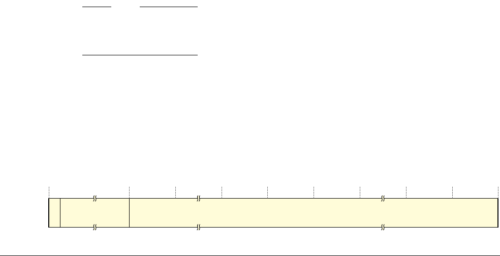
A2 Application Level Programmers’ Model
A2.7 Floating-point data types and arithmetic
ARM DDI 0406C.c Copyright © 1996-1998, 2000, 2004-2012, 2014 ARM. All rights reserved. A2-65
ID051414 Non-Confidential
These usually behave identically. In particular, the result is equal if +0 and –0 are
compared as floating-point numbers. However, they yield different results in some
circumstances. For example, the sign of the infinity produced as the result of dividing
by zero depends on the sign of the zero. The two zeros can be distinguished from each
other by performing an integer comparison of the two words.
fraction != 0
The value is a denormalized number and is equal to:
(–1)S × 2–126 × (0.fraction)
The minimum positive denormalized number is 2–149, or approximately 1.401 × 10–45.
Denormalized numbers are always flushed to zero in the Advanced SIMD Extension. They are
optionally flushed to zero in the Floating-point Extension. For details see Flush-to-zero on
page A2-68.
exponent ==
0xFF
The value is either an infinity or a Not a Number (NaN), depending on the fraction bits:
fraction == 0
The value is an infinity. There are two distinct infinities:
+infinity When S==0. This represents all positive numbers that are too big to be
represented accurately as a normalized number.
-infinity When S==1. This represents all negative numbers with an absolute value
that is too big to be represented accurately as a normalized number.
fraction != 0
The value is a NaN, and is either a quiet NaN or a signaling NaN.
In the Floating-point Extension, the two types of NaN are distinguished on the basis of
their most significant fraction bit, bit[22]:
bit[22] == 0
The NaN is a signaling NaN. The sign bit can take any value, and the
remaining fraction bits can take any value except all zeros.
bit[22] == 1
The NaN is a quiet NaN. The sign bit and remaining fraction bits can take
any value.
For details of the default NaN see NaN handling and the Default NaN on page A2-69.
Note
NaNs with different sign or fraction bits are distinct NaNs, but this does not mean software can use floating-point
comparison instructions to distinguish them. This is because the IEEE 754 standard specifies that a NaN compares
as unordered with everything, including itself.
A2.7.3 Floating-point double-precision format
The double-precision floating-point format used by the Floating-point Extension is as defined by the IEEE 754
standard.
This description includes Floating-point Extension-specific details that are left open by the standard. It is only
intended as an introduction to the formats and to the values they can contain. For full details, especially of the
handling of infinities, NaNs and signed zeros, see the IEEE 754 standard.
A double-precision value is a 64-bit doubleword, with the format:
S
63 62 52 51 32 31 0
exponent fraction

A2 Application Level Programmers’ Model
A2.7 Floating-point data types and arithmetic
A2-66 Copyright © 1996-1998, 2000, 2004-2012, 2014 ARM. All rights reserved. ARM DDI 0406C.c
Non-Confidential ID051414
Double-precision values represent numbers, infinities and NaNs in a similar way to single-precision values, with
the interpretation of the format depending on the value of the exponent:
0 < exponent <
0x7FF
The value is a normalized number and is equal to:
(–1)S × 2(exponent–1023) × (1.fraction)
The minimum positive normalized number is 2–1022, or approximately 2.225 × 10–308.
The maximum positive normalized number is (2 – 2–52) × 21023, or approximately 1.798 × 10308.
exponent == 0
The value is either a zero or a denormalized number, depending on the fraction bits:
fraction == 0
The value is a zero. There are two distinct zeros that behave analogously to the two
single-precision zeros:
+0 when S==0
–0 when S==1.
fraction != 0
The value is a denormalized number and is equal to:
(-1)S × 2–1022 × (0.fraction)
The minimum positive denormalized number is 2–1074, or approximately 4.941 × 10–324.
Optionally, denormalized numbers are flushed to zero in the Floating-point Extension. For details
see Flush-to-zero on page A2-68.
exponent ==
0x7FF
The value is either an infinity or a NaN, depending on the fraction bits:
fraction == 0
the value is an infinity. As for single-precision, there are two infinities:
+infinity When S==0.
-infinity When S==1.
fraction != 0
The value is a NaN, and is either a quiet NaN or a signaling NaN.
In the Floating-point Extension, the two types of NaN are distinguished on the basis of
their most significant fraction bit, bit[51] of the most significant word:
bit[51] == 0
The NaN is a signaling NaN. The sign bit can take any value, and the
remaining fraction bits can take any value except all zeros.
bit[51] == 1
The NaN is a quiet NaN. The sign bit and the remaining fraction bits can
take any value.
For details of the default NaN see NaN handling and the Default NaN on page A2-69.
Note
NaNs with different sign or fraction bits are distinct NaNs, but this does not mean software can use floating-point
comparison instructions to distinguish them. This is because the IEEE 754 standard specifies that a NaN compares
as unordered with everything, including itself.
A2.7.4 Advanced SIMD and Floating-point half-precision formats
The Half-precision Extension to the Advanced SIMD and Floating-point Extensions uses two half-precision
floating-point formats:
• IEEE half-precision, as described in the IEEE 754-2008 standard

A2 Application Level Programmers’ Model
A2.7 Floating-point data types and arithmetic
ARM DDI 0406C.c Copyright © 1996-1998, 2000, 2004-2012, 2014 ARM. All rights reserved. A2-67
ID051414 Non-Confidential
• Alternative half-precision.
The description of IEEE half-precision includes ARM-specific details that are left open by the standard, and is only
an introduction to the formats and to the values they can contain. For more information, especially on the handling
of infinities, NaNs and signed zeros, see the IEEE 754 standard.
For both half-precision floating-point formats, the layout of the 16-bit number is the same. The format is:
The interpretation of the format depends on the value of the exponent field, bits[14:10] and on which half-precision
format is being used.
0 < exponent <
0x1F
The value is a normalized number and is equal to:
(–1)S×2
(exponent-15) × (1.fraction)
The minimum positive normalized number is 2–14, or approximately 6.104 × 10⁻⁵.
The maximum positive normalized number is (2 – 2–10)×2
15, or 65504.
Larger normalized numbers can be expressed using the alternative format when the
exponent ==
0x1F
.
exponent == 0
The value is either a zero or a denormalized number, depending on the fraction bits:
fraction == 0
The value is a zero. There are two distinct zeros:
+0 when S==0
–0 when S==1.
fraction != 0
The value is a denormalized number and is equal to:
(–1)S × 2–14 × (0.fraction)
The minimum positive denormalized number is 2–24, or approximately 5.960 × 10⁻⁸.
exponent ==
0x1F
The value depends on which half-precision format is being used:
IEEE half-precision
The value is either an infinity or a Not a Number (NaN), depending on the fraction bits:
fraction == 0
The value is an infinity. There are two distinct infinities:
+infinity When S==0. This represents all positive numbers that are too
big to be represented accurately as a normalized number.
-infinity When S==1. This represents all negative numbers with an
absolute value that is too big to be represented accurately as a
normalized number.
fraction != 0
The value is a NaN, and is either a quiet NaN or a signaling NaN. The two
types of NaN are distinguished by their most significant fraction bit, bit[9]:
bit[9] == 0 The NaN is a signaling NaN. The sign bit can take any value,
and the remaining fraction bits can take any value except all
zeros.
bit[9] == 1 The NaN is a quiet NaN. The sign bit and remaining fraction
bits can take any value.
15 14 10 9 0
Sexponent fraction

A2 Application Level Programmers’ Model
A2.7 Floating-point data types and arithmetic
A2-68 Copyright © 1996-1998, 2000, 2004-2012, 2014 ARM. All rights reserved. ARM DDI 0406C.c
Non-Confidential ID051414
Alternative half-precision
The value is a normalized number and is equal to:
-1S × 216 × (1.fraction)
The maximum positive normalized number is (2-2-10) × 216 or 131008.
A2.7.5 Flush-to-zero
The performance of floating-point implementations can be significantly reduced when performing calculations
involving denormalized numbers and Underflow exceptions. In particular this occurs for implementations that only
handle normalized numbers and zeros in hardware, and invoke support code to handle any other types of value. For
an algorithm where a significant number of the operands and intermediate results are denormalized numbers, this
can result in a considerable loss of performance.
In many of these algorithms, this performance can be recovered, without significantly affecting the accuracy of the
final result, by replacing the denormalized operands and intermediate results with zeros. To permit this optimization,
Floating-point Extension implementations have a special processing mode called Flush-to-zero mode. Advanced
SIMD implementations always use Flush-to-zero mode.
Behavior in Flush-to-zero mode differs from normal IEEE 754 arithmetic in the following ways:
• All inputs to floating-point operations that are double-precision denormalized numbers or single-precision
denormalized numbers are treated as though they were zero. This causes an Input Denormal exception, but
does not cause an Inexact exception. The Input Denormal exception occurs only in Flush-to-zero mode.
Note
Combinations of exceptions on page A2-71 defines the floating-point operations.
The FPSCR contains a cumulative exception bit FPSCR.IDC and trap enable bit FPSCR.IDE corresponding
to the Input Denormal exception.
The occurrence of all exceptions except Input Denormal is determined using the input values after
flush-to-zero processing has occurred.
• The result of a floating-point operation is flushed to zero if the result of the operation before rounding
satisfies the condition:
0 <
Abs(result)
< MinNorm, where:
—MinNorm is2
-126 for single-precision
—MinNorm is2
-1022 for double-precision.
This causes the FPSCR.UFC bit to be set to 1, and prevents any Inexact exception from occurring for the
operation.
Underflow exceptions occur only when a result is flushed to zero.
In a VFPv2, VFPv3U, or VFPv4U implementation Underflow exceptions that occur in Flush-to-zero mode
are always treated as untrapped, even when the Underflow trap enable bit, FPSCR.UFE, is set to 1.
• An Inexact exception does not occur if the result is flushed to zero, even though the final result of zero is not
equivalent to the value that would be produced if the operation were performed with unbounded precision
and exponent range.
When an input or a result is flushed to zero the value of the sign bit of the zero is determined as follows:
• In VFPv4, VFPv4U, VFPv3, or VFPv3U, it is preserved. That is, the sign bit of the zero matches the sign bit
of the input or result that is being flushed to zero.
• In VFPv2, it is IMPLEMENTATION DEFINED whether it is preserved or always positive. The same choice must
be made for all cases of flushing an input or result to zero.
Flush-to-zero mode has no effect on half-precision numbers that are inputs to floating-point operations, or results
from floating-point operations.

A2 Application Level Programmers’ Model
A2.7 Floating-point data types and arithmetic
ARM DDI 0406C.c Copyright © 1996-1998, 2000, 2004-2012, 2014 ARM. All rights reserved. A2-69
ID051414 Non-Confidential
Note
Flush-to-zero mode is incompatible with the IEEE 754 standard, and must not be used when IEEE 754 compatibility
is a requirement. Flush-to-zero mode must be used with care. Although it can improve performance on some
algorithms, there are significant limitations on its use. These are application dependent:
• On many algorithms, it has no noticeable effect, because the algorithm does not normally use denormalized
numbers.
• On other algorithms, it can cause exceptions to occur or seriously reduce the accuracy of the results of the
algorithm.
A2.7.6 NaN handling and the Default NaN
The IEEE 754 standard specifies that:
• an operation that produces an Invalid Operation floating-point exception generates a quiet NaN as its result
if that exception is untrapped
• an operation involving a quiet NaN operand, but not a signaling NaN operand, returns an input NaN as its
result.
The Floating-point Extension behavior when Default NaN mode is disabled adheres to this, with the following
additions:
• If an untrapped Invalid Operation floating-point exception is produced, the quiet NaN result is derived from:
— the first signaling NaN operand, if the exception was produced because at least one of the operands is
a signaling NaN
— otherwise, the default NaN
• If an untrapped Invalid Operation floating-point exception is not produced, but at least one of the operands
is a quiet NaN, the result is derived from the first quiet NaN operand.
Depending on the operation, the exact value of a derived quiet NaN result may differ in both sign and number of
fraction bits from its source.For a quiet NaN result derived from signaling NaN operand, the most-significant
fraction bit is set to 1.
Note
• In these descriptions, first operand relates to the left-to-right ordering of the arguments to the pseudocode
function that describes the operation.
• The IEEE 754 standard specifies that the sign bit of a NaN has no significance.
The Floating-point Extension behavior when Default NaN mode is enabled, and the Advanced SIMD behavior in
all circumstances, is that the Default NaN is the result of all floating-point operations that either:
• generate untrapped Invalid Operation floating-point exceptions
• have one or more quiet NaN inputs, but no signaling NaN inputs.
Table A2-7 on page A2-70 shows the format of the default NaN for ARM floating-point processors.
Default NaN mode is selected for the Floating-point Extension by setting the FPSCR.DN bit to 1.
Other aspects of the functionality of the Invalid Operation exception are not affected by Default NaN mode. These
are that:
• If untrapped, it causes the FPSCR.IOC bit be set to 1.
• If trapped, it causes a user trap handler to be invoked. This is only possible in VFPv2, VFPv3U, and VFPv4U.

A2 Application Level Programmers’ Model
A2.7 Floating-point data types and arithmetic
A2-70 Copyright © 1996-1998, 2000, 2004-2012, 2014 ARM. All rights reserved. ARM DDI 0406C.c
Non-Confidential ID051414
A2.7.7 Floating-point exceptions
The Advanced SIMD and Floating-point Extensions record the following floating-point exceptions in the FPSCR
cumulative bits:
FPSCR.IOC Invalid Operation. The bit is set to 1 if the result of an operation has no mathematical value or cannot
be represented. Cases include, for example:
• (infinity) × 0
• (+infinity) + (–infinity).
These tests are made after flush-to-zero processing. For example, if flush-to-zero mode is selected,
multiplying a denormalized number and an infinity is treated as (0 × infinity), and causes an Invalid
Operation floating-point exception.
IOC is also set on any floating-point operation with one or more signaling NaNs as operands, except
for negation and absolute value, as described in Floating-point negation and absolute value on
page A2-75.
FPSCR.DZC Division by Zero. The bit is set to 1 if a divide operation has a zero divisor and a dividend that is
not zero, an infinity or a NaN. These tests are made after flush-to-zero processing, so if flush-to-zero
processing is selected, a denormalized dividend is treated as zero and prevents Division by Zero
from occurring, and a denormalized divisor is treated as zero and causes Division by Zero to occur
if the dividend is a normalized number.
For the reciprocal and reciprocal square root estimate functions the dividend is assumed to be +1.0.
This means that a zero or denormalized operand to these functions sets the DZC bit.
FPSCR.OFC Overflow. The bit is set to 1 if the absolute value of the result of an operation, produced after
rounding, is greater than the maximum positive normalized number for the destination precision.
FPSCR.UFC Underflow. The bit is set to 1 if the absolute value of the result of an operation, produced before
rounding, is less than the minimum positive normalized number for the destination precision, and
the rounded result is inexact.
The criteria for the Underflow exception to occur are different in Flush-to-zero mode. For details,
see Flush-to-zero on page A2-68.
FPSCR.IXC Inexact. The bit is set to 1 if the result of an operation is not equivalent to the value that would be
produced if the operation were performed with unbounded precision and exponent range.
The criteria for the Inexact exception to occur are different in Flush-to-zero mode. For details, see
Flush-to-zero on page A2-68.
FPSCR.IDC Input Denormal. The bit is set to 1 if a denormalized input operand is replaced in the computation
by a zero, as described in Flush-to-zero on page A2-68.
With the Advanced SIMD Extension and the VFPv3 or VFPv4 versions of the Floating-point Extension these are
non-trapping exceptions and the data-processing instructions do not generate any trapped exceptions.
Table A2-7 Default NaN encoding
Half-precision, IEEE Format Single-precision Double-precision
Sign bit 0 0a0a
Exponent
0x1F 0xFF 0x7FF
Fraction Bit[9] == 1, bits[8:0] == 0 bit[22] == 1, bits[21:0] == 0 bit[51] == 1, bits[50:0] == 0
a. In VFPv2, the sign bit of the Default NaN is UNKNOWN.

A2 Application Level Programmers’ Model
A2.7 Floating-point data types and arithmetic
ARM DDI 0406C.c Copyright © 1996-1998, 2000, 2004-2012, 2014 ARM. All rights reserved. A2-71
ID051414 Non-Confidential
With the VFPv2, VFPv3U, and VFPv4U versions of the Floating-point Extension:
• These exceptions can be trapped, by setting trap enable bits in the FPSCR, see VFPv3U and VFPv4U on
page A2-62. The way in which trapped floating-point exceptions are delivered to user software is
IMPLEMENTATION DEFINED. However, ARM recommends use of the VFP subarchitecture defined in
Appendix D6 Common VFP Subarchitecture Specification.
• The definition of the Underflow exception is different in the trapped and cummulative exception cases. In the
trapped case, meaning for VFPv2, VFPv3U, or VFPv4U, the definition is:
— the trapped Underflow exception occurs if the absolute value of the result of an operation, produced
before rounding, is less than the minimum positive normalized number for the destination precision,
regardless of whether the rounded result is inexact.
• As with cumulative exceptions, higher priority trapped exceptions can prevent lower priority exceptions from
occurring, as described in Combinations of exceptions.
Table A2-8 shows the results of untrapped floating-point exceptions:
In Table A2-8:
MaxNorm The maximum normalized number of the destination precision.
RM Round towards Minus Infinity mode, as defined in the IEEE 754 standard.
RN Round to Nearest mode, as defined in the IEEE 754 standard.
RP Round towards Plus Infinity mode, as defined in the IEEE 754 standard.
RZ Round towards Zero mode, as defined in the IEEE 754 standard.
• For Invalid Operation exceptions, for details of which quiet NaN is produced as the default result see NaN
handling and the Default NaN on page A2-69.
• For Division by Zero exceptions, the sign bit of the default result is determined normally for a division. This
means it is the exclusive OR of the sign bits of the two operands.
• For Overflow exceptions, the sign bit of the default result is determined normally for the overflowing
operation.
Combinations of exceptions
The following pseudocode functions perform floating-point operations:
FixedToFP()
FPAdd()
FPCompare()
FPCompareEQ()
FPCompareGE()
FPCompareGT()
FPDiv()
Table A2-8 Results of untrapped floating-point exceptions
Exception type Default result for positive sign Default result for negative sign
IOC, Invalid Operation Quiet NaN Quiet NaN
DZC, Division by Zero +infinity -infinity
OFC, Overflow RN, RP:
RM, RZ:
+infinity
+MaxNorm
RN, RM:
RP, RZ:
-infinity
-MaxNorm
UFC, Underflow Normal rounded result Normal rounded result
IXC, Inexact Normal rounded result Normal rounded result
IDC, Input Denormal Normal rounded result Normal rounded result

A2 Application Level Programmers’ Model
A2.7 Floating-point data types and arithmetic
A2-72 Copyright © 1996-1998, 2000, 2004-2012, 2014 ARM. All rights reserved. ARM DDI 0406C.c
Non-Confidential ID051414
FPDoubleToSingle()
FPHalfToSingle()
FPMax()
FPMin()
FPMul()
FPMulAdd()
FPRecipEstimate()
FPRecipStep()
FPRSqrtEstimate()
FPRSqrtStep()
FPSingleToDouble()
FPSingleToHalf()
FPSqrt()
FPSub()
FPToFixed()
All of these operations can generate floating-point exceptions.
Note
FPAbs()
and
FPNeg()
are not classified as floating-point operations because:
• they cannot generate floating-point exceptions
• the floating-point operation behavior described in the following sections does not apply to them:
—Flush-to-zero on page A2-68
—NaN handling and the Default NaN on page A2-69.
More than one exception can occur on the same operation. The only combinations of exceptions that can occur are:
• Overflow with Inexact
• Underflow with Inexact
• Input Denormal with other exceptions.
When none of the exceptions caused by an operation are trapped, any exception that occurs causes the associated
cumulative bit in the FPSCR to be set.
When one or more exceptions caused by an operation are trapped, the behavior of the instruction depends on the
priority of the exceptions. The Inexact exception is treated as lowest priority, and Input Denormal as highest priority:
• If the higher priority exception is trapped, its trap handler is called. It is IMPLEMENTATION DEFINED whether
the parameters to the trap handler include information about the lower priority exception. Apart from this,
the lower priority exception is ignored in this case.
• If the higher priority exception is untrapped, its cumulative bit is set to 1 and its default result is evaluated.
Then the lower priority exception is handled normally, using this default result.
Some floating-point instructions specify more than one floating-point operation, as indicated by the pseudocode
descriptions of the instruction. In such cases, an exception on one operation is treated as higher priority than an
exception on another operation if the occurrence of the second exception depends on the result of the first operation.
Otherwise, it is UNPREDICTABLE which exception is treated as higher priority.
For example, a
VMLA.F32
instruction specifies a floating-point multiplication followed by a floating-point addition.
The addition can generate Overflow, Underflow and Inexact exceptions, all of which depend on both operands to
the addition and so are treated as lower priority than any exception on the multiplication. The same applies to Invalid
Operation exceptions on the addition caused by adding opposite-signed infinities. The addition can also generate an
Input Denormal exception, caused by the addend being a denormalized number while in Flush-to-zero mode. It is
UNPREDICTABLE which of an Input Denormal exception on the addition and an exception on the multiplication is
treated as higher priority, because the occurrence of the Input Denormal exception does not depend on the result of
the multiplication. The same applies to an Invalid Operation exception on the addition caused by the addend being
a signaling NaN.

A2 Application Level Programmers’ Model
A2.7 Floating-point data types and arithmetic
ARM DDI 0406C.c Copyright © 1996-1998, 2000, 2004-2012, 2014 ARM. All rights reserved. A2-73
ID051414 Non-Confidential
Note
• The
VFMA
instruction performs a vector addition and a vector multiplication as a single operation. The
VFMS
instruction performs a vector subtraction and a vector multiplication as a single operation.
• Like other details of Floating-point instruction execution, these rules about exception handling apply to the
overall results produced by an instruction when the system uses a combination of hardware and support code
to implement it. See Floating-point support code on page B1-1237 for more information.
These principles also apply to the multiple floating-point operations generated by Floating-point instructions
in the deprecated VFP vector mode of operation. For details of this mode of operation see Appendix D11 VFP
Vector Operation Support.
A2.7.8 Pseudocode details of floating-point operations
The following subsections contain pseudocode definitions of the floating-point functionality supported by the
ARMv7 architecture:
•Generation of specific floating-point values
•Floating-point negation and absolute value on page A2-75
•Floating-point value unpacking on page A2-75
•Floating-point exception and NaN handling on page A2-76
•Floating-point rounding on page A2-78
•Selection of ARM standard floating-point arithmetic on page A2-80
•Floating-point comparisons on page A2-80
•Floating-point maximum and minimum on page A2-81
•Floating-point addition and subtraction on page A2-82
•Floating-point multiplication and division on page A2-83
•Floating-point fused multiply-add on page A2-84
•Floating-point reciprocal estimate and step on page A2-85
•Floating-point square root on page A2-87
•Floating-point reciprocal square root estimate and step on page A2-87
•Floating-point conversions on page A2-90.
Generation of specific floating-point values
The following pseudocode functions generate specific floating-point values. The
sign
argument of
FPInfinity()
,
FPMaxNormal()
, and
FPZero()
is
'0'
for the positive version and
'1'
for the negative version.
// FPZero()
// ========
bits(N) FPZero(bit sign, integer N)
assert N IN {16,32,64};
if N == 16 then
E = 5;
elsif N == 32 then
E = 8;
else E = 11;
F = N - E - 1;
exp = Zeros(E);
frac = Zeros(F);
return sign:exp:frac;
// FPTwo()
// =======
bits(N) FPTwo(integer N)
assert N IN {32,64};
if N == 16 then

A2 Application Level Programmers’ Model
A2.7 Floating-point data types and arithmetic
A2-74 Copyright © 1996-1998, 2000, 2004-2012, 2014 ARM. All rights reserved. ARM DDI 0406C.c
Non-Confidential ID051414
E = 5;
elsif N == 32 then
E = 8;
else E = 11;
F = N - E - 1;
sign = '0';
exp = '1':Zeros(E-1);
frac = Zeros(F);
return sign:exp:frac;
// FPThree()
// =========
bits(N) FPThree(integer N)
assert N IN {32,64};
if N == 16 then
E = 5;
elsif N == 32 then
E = 8;
else E = 11;
F = N - E - 1;
sign = '0';
exp = '1':Zeros(E-1);
frac = '1':Zeros(F-1);
return sign:exp:frac;
// FPMaxNormal()
// =============
bits(N) FPMaxNormal(bit sign, integer N)
assert N IN {16,32,64};
if N == 16 then
E = 5;
elsif N == 32 then
E = 8;
else E = 11;
F = N - E - 1;
exp = Ones(E-1):'0';
frac = Ones(F);
return sign:exp:frac;
// FPInfinity()
// ============
bits(N) FPInfinity(bit sign, integer N)
assert N IN {16,32,64};
if N == 16 then
E = 5;
elsif N == 32 then
E = 8;
else E = 11;
F = N - E - 1;
exp = Ones(E);
frac = Zeros(F);
return sign:exp:frac;
// FPDefaultNaN()
// ==============
bits(N) FPDefaultNaN(integer N)
assert N IN {16,32,64};
if N == 16 then
E = 5;
elsif N == 32 then

A2 Application Level Programmers’ Model
A2.7 Floating-point data types and arithmetic
ARM DDI 0406C.c Copyright © 1996-1998, 2000, 2004-2012, 2014 ARM. All rights reserved. A2-75
ID051414 Non-Confidential
E = 8;
else E = 11;
F = N - E - 1;
sign = '0';
exp = Ones(E);
frac = '1':Zeros(F-1);
return sign:exp:frac;
Note
This definition of
FPDefaultNaN()
applies to VFPv4, VFPv4U, VFPv3, and VFPv3U implementations. For VFPv2,
the sign bit of the result is a single-bit UNKNOWN value, instead of 0.
Floating-point negation and absolute value
The floating-point negation and absolute value operations only affect the sign bit. They do not treat NaN operands
specially, nor denormalized number operands when flush-to-zero is selected.
// FPNeg()
// =======
bits(N) FPNeg(bits(N) operand)
assert N IN {32,64};
return NOT(operand<N-1>) : operand<N-2:0>;
// FPAbs()
// =======
bits(N) FPAbs(bits(N) operand)
assert N IN {32,64};
return '0' : operand<N-2:0>;
Floating-point value unpacking
The
FPUnpack()
function determines the type and numerical value of a floating-point number. It also does
flush-to-zero processing on input operands.
enumeration FPType {FPType_Nonzero, FPType_Zero, FPType_Infinity, FPType_QNaN, FPType_SNaN};
// FPUnpack()
// ==========
//
// Unpack a floating-point number into its type, sign bit and the real number
// that it represents. The real number result has the correct sign for numbers
// and infinities, is very large in magnitude for infinities, and is 0.0 for
// NaNs. (These values are chosen to simplify the description of comparisons
// and conversions.)
//
// The 'fpscr_val' argument supplies FPSCR control bits. Status information is
// updated directly in the FPSCR where appropriate.
(FPType, bit, real) FPUnpack(bits(N) fpval, bits(32) fpscr_val)
assert N IN {16,32,64};
if N == 16 then
sign = fpval<15>;
exp16 = fpval<14:10>;
frac16 = fpval<9:0>;
if IsZero(exp16) then
// Produce zero if value is zero
if IsZero(frac16) then
type = FPType_Zero; value = 0.0;
else
type = FPType_Nonzero; value = 2.0^-14 * (UInt(frac16) * 2.0^-10);

A2 Application Level Programmers’ Model
A2.7 Floating-point data types and arithmetic
A2-76 Copyright © 1996-1998, 2000, 2004-2012, 2014 ARM. All rights reserved. ARM DDI 0406C.c
Non-Confidential ID051414
elsif IsOnes(exp16) && fpscr_val<26> == '0' then // Infinity or NaN in IEEE format
if IsZero(frac16) then
type = FPType_Infinity; value = 2.0^1000000;
else
type = if frac16<9> == '1' then FPType_QNaN else FPType_SNaN;
value = 0.0;
else
type = FPType_Nonzero; value = 2.0^(UInt(exp16)-15) * (1.0 + UInt(frac16) * 2.0^-10);
elsif N == 32 then
sign = fpval<31>;
exp32 = fpval<30:23>;
frac32 = fpval<22:0>;
if IsZero(exp32) then
// Produce zero if value is zero or flush-to-zero is selected.
if IsZero(frac32) || fpscr_val<24> == '1' then
type = FPType_Zero; value = 0.0;
if !IsZero(frac32) then // Denormalized input flushed to zero
FPProcessException(FPExc_InputDenorm, fpscr_val);
else
type = FPType_Nonzero; value = 2.0^-126 * (UInt(frac32) * 2.0^-23);
elsif IsOnes(exp32) then
if IsZero(frac32) then
type = FPType_Infinity; value = 2.0^1000000;
else
type = if frac32<22> == '1' then FPType_QNaN else FPType_SNaN;
value = 0.0;
else
type = FPType_Nonzero; value = 2.0^(UInt(exp32)-127) * (1.0 + UInt(frac32) * 2.0^-23);
else // N == 64
sign = fpval<63>;
exp64 = fpval<62:52>;
frac64 = fpval<51:0>;
if IsZero(exp64) then
// Produce zero if value is zero or flush-to-zero is selected.
if IsZero(frac64) || fpscr_val<24> == '1' then
type = FPType_Zero; value = 0.0;
if !IsZero(frac64) then // Denormalized input flushed to zero
FPProcessException(FPExc_InputDenorm, fpscr_val);
else
type = FPType_Nonzero; value = 2.0^-1022 * (UInt(frac64) * 2.0^-52);
elsif IsOnes(exp64) then
if IsZero(frac64) then
type = FPType_Infinity; value = 2.0^1000000;
else
type = if frac64<51> == '1' then FPType_QNaN else FPType_SNaN;
value = 0.0;
else
type = FPType_Nonzero; value = 2.0^(UInt(exp64)-1023) * (1.0 + UInt(frac64) * 2.0^-52);
if sign == '1' then value = -value;
return (type, sign, value);
Floating-point exception and NaN handling
The
FPProcessException()
procedure checks whether a floating-point exception is trapped, and handles it
accordingly:
enumeration FPExc {FPExc_InvalidOp, FPExc_DivideByZero, FPExc_Overflow,
FPExc_Underflow, FPExc_Inexact, FPExc_InputDenorm};
// FPProcessException()
// ====================
//

A2 Application Level Programmers’ Model
A2.7 Floating-point data types and arithmetic
ARM DDI 0406C.c Copyright © 1996-1998, 2000, 2004-2012, 2014 ARM. All rights reserved. A2-77
ID051414 Non-Confidential
// The 'fpscr_val' argument supplies FPSCR control bits. Status information is
// updated directly in the FPSCR where appropriate.
FPProcessException(FPExc exception, bits(32) fpscr_val)
// Get appropriate FPSCR bit numbers
case exception of
when FPExc_InvalidOp enable = 8; cumul = 0;
when FPExc_DivideByZero enable = 9; cumul = 1;
when FPExc_Overflow enable = 10; cumul = 2;
when FPExc_Underflow enable = 11; cumul = 3;
when FPExc_Inexact enable = 12; cumul = 4;
when FPExc_InputDenorm enable = 15; cumul = 7;
if fpscr_val<enable> == '1' then
IMPLEMENTATION_DEFINED floating-point trap handling;
else
FPSCR<cumul> = '1';
return;
The
FPProcessNaN()
function processes a NaN operand, producing the correct result value and generating an Invalid
Operation exception if necessary:
// FPProcessNaN()
// ==============
//
// The 'fpscr_val' argument supplies FPSCR control bits. Status information is
// updated directly in the FPSCR where appropriate.
bits(N) FPProcessNaN(FPType type, bits(N) operand, bits(32) fpscr_val)
assert N IN {32,64};
topfrac = if N == 32 then 22 else 51;
result = operand;
if type == FPType_SNaN then
result<topfrac> = '1';
FPProcessException(FPExc_InvalidOp, fpscr_val);
if fpscr_val<25> == '1' then // DefaultNaN requested
result = FPDefaultNaN(N);
return result;
The
FPProcessNaNs()
function performs the standard NaN processing for a two-operand operation:
// FPProcessNaNs()
// ===============
//
// The boolean part of the return value says whether a NaN has been found and
// processed. The bits(N) part is only relevant if it has and supplies the
// result of the operation.
//
// The 'fpscr_val' argument supplies FPSCR control bits. Status information is
// updated directly in the FPSCR where appropriate.
(boolean, bits(N)) FPProcessNaNs(FPType type1, FPType type2,
bits(N) op1, bits(N) op2,
bits(32) fpscr_val)
assert N IN {32,64};
if type1 == FPType_SNaN then
done = TRUE; result = FPProcessNaN(type1, op1, fpscr_val);
elsif type2 == FPType_SNaN then
done = TRUE; result = FPProcessNaN(type2, op2, fpscr_val);
elsif type1 == FPType_QNaN then
done = TRUE; result = FPProcessNaN(type1, op1, fpscr_val);
elsif type2 == FPType_QNaN then
done = TRUE; result = FPProcessNaN(type2, op2, fpscr_val);
else
done = FALSE; result = Zeros(N); // 'Don't care' result
return (done, result);
The
FPProcessNaNs3()
function performs the standard NaN processing for a three-operand operation:
// FPProcessNaNs3()

A2 Application Level Programmers’ Model
A2.7 Floating-point data types and arithmetic
A2-78 Copyright © 1996-1998, 2000, 2004-2012, 2014 ARM. All rights reserved. ARM DDI 0406C.c
Non-Confidential ID051414
// ===============
//
// The boolean part of the return value says whether a NaN has been found and
// processed. The bits(N) part is only relevant if it has and supplies the
// result of the operation.
//
// The 'fpscr_val' argument supplies FPSCR control bits. Status information is
// updated directly in the FPSCR where appropriate.
(boolean, bits(N)) FPProcessNaNs3(FPType type1, FPType type2, FPType type3,
bits(N) op1, bits(N) op2, bits(N) op3,
bits(32) fpscr_val)
assert N IN {32,64};
if type1 == FPType_SNaN then
done = TRUE; result = FPProcessNaN(type1, op1, fpscr_val);
elsif type2 == FPType_SNaN then
done = TRUE; result = FPProcessNaN(type2, op2, fpscr_val);
elsif type3 == FPType_SNaN then
done = TRUE; result = FPProcessNaN(type3, op3, fpscr_val);
elsif type1 == FPType_QNaN then
done = TRUE; result = FPProcessNaN(type1, op1, fpscr_val);
elsif type2 == FPType_QNaN then
done = TRUE; result = FPProcessNaN(type2, op2, fpscr_val);
elsif type3 == FPType_QNaN then
done = TRUE; result = FPProcessNaN(type3, op3, fpscr_val);
else
done = FALSE; result = Zeros(N); // 'Don't care' result
return (done, result);
Floating-point rounding
The
FPRound()
function rounds and encodes a supplied floating-point value to a specified destination format. This
includes processing Overflow, Underflow and Inexact floating-point exceptions and performing flush-to-zero
processing on the resulting value.
// FPRound()
// =========
//
// The 'fpscr_val' argument supplies FPSCR control bits. Status information is
// updated directly in the FPSCR where appropriate.
bits(N) FPRound(real value, integer N, bits(32) fpscr_val)
assert N IN {16,32,64};
assert value != 0.0;
// Obtain format parameters - minimum exponent, numbers of exponent and fraction bits.
if N == 16 then
E = 5;
elsif N == 32 then
E = 8;
else E = 11;
minimum_exp = 2 - 2^(E-1);
F = N - E - 1;
// Split value into sign, unrounded mantissa and exponent.
if value < 0.0 then
sign = '1'; mantissa = -value;
else
sign = '0'; mantissa = value;
exponent = 0;
while mantissa < 1.0 do
mantissa = mantissa * 2.0; exponent = exponent - 1;
while mantissa >= 2.0 do
mantissa = mantissa / 2.0; exponent = exponent + 1;
// Deal with flush-to-zero.

A2 Application Level Programmers’ Model
A2.7 Floating-point data types and arithmetic
ARM DDI 0406C.c Copyright © 1996-1998, 2000, 2004-2012, 2014 ARM. All rights reserved. A2-79
ID051414 Non-Confidential
if fpscr_val<24> == '1' && N != 16 && exponent < minimum_exp then
result = FPZero(sign, N);
FPSCR.UFC = '1'; // Flush-to-zero never generates a trapped exception
else
// Start creating the exponent value for the result. Start by biasing the actual exponent
// so that the minimum exponent becomes 1, lower values 0 (indicating possible underflow).
biased_exp = Max(exponent - minimum_exp + 1, 0);
if biased_exp == 0 then mantissa = mantissa / 2^(minimum_exp - exponent);
// Get the unrounded mantissa as an integer, and the "units in last place" rounding error.
int_mant = RoundDown(mantissa * 2^F); // < 2^F if biased_exp == 0, >= 2^F if not
error = mantissa * 2^F - int_mant;
// Underflow occurs if exponent is too small before rounding, and result is inexact or
// the Underflow exception is trapped.
if biased_exp == 0 && (error != 0.0 || fpscr_val<11> == '1') then
FPProcessException(FPExc_Underflow, fpscr_val);
// Round result according to rounding mode.
case fpscr_val<23:22> of
when '00' // Round to Nearest (rounding to even if exactly halfway)
round_up = (error > 0.5 || (error == 0.5 && int_mant<0> == '1'));
overflow_to_inf = TRUE;
when '01' // Round towards Plus Infinity
round_up = (error != 0.0 && sign == '0');
overflow_to_inf = (sign == '0');
when '10' // Round towards Minus Infinity
round_up = (error != 0.0 && sign == '1');
overflow_to_inf = (sign == '1');
when '11' // Round towards Zero
round_up = FALSE;
overflow_to_inf = FALSE;
if round_up then
int_mant = int_mant + 1;
if int_mant == 2^F then // Rounded up from denormalized to normalized
biased_exp = 1;
if int_mant == 2^(F+1) then // Rounded up to next exponent
biased_exp = biased_exp + 1;
int_mant = int_mant DIV 2;
// Deal with overflow and generate result.
if N != 16 || fpscr_val<26> == '0' then // Single, double or IEEE half precision
if biased_exp >= 2^E - 1 then
result = if overflow_to_inf then FPInfinity(sign, N) else FPMaxNormal(sign, N);
FPProcessException(FPExc_Overflow, fpscr_val);
error = 1.0; // Ensure that an Inexact exception occurs
else
result = sign:biased_exp<E-1:0>:int_mant<F-1:0>;
else // Alternative half precision (with N==16)
if biased_exp >= 2^E then
result = sign : Ones(15);
FPProcessException(FPExc_InvalidOp, fpscr_val);
error = 0.0; // Ensure that an Inexact exception does not occur
else
result = sign:biased_exp<E-1:0>:int_mant<F-1:0>;
// Deal with Inexact exception.
if error != 0.0 then
FPProcessException(FPExc_Inexact, fpscr_val);
return result;

A2 Application Level Programmers’ Model
A2.7 Floating-point data types and arithmetic
A2-80 Copyright © 1996-1998, 2000, 2004-2012, 2014 ARM. All rights reserved. ARM DDI 0406C.c
Non-Confidential ID051414
Selection of ARM standard floating-point arithmetic
The
StandardFPSCRValue()
function returns the FPSCR value that selects ARM standard floating-point arithmetic.
Most of the arithmetic functions have a Boolean
fpscr_controlled
argument that is
TRUE
for Floating-point
operations and
FALSE
for Advanced SIMD operations, and that selects between using the real FPSCR value and this
value.
// StandardFPSCRValue()
// ====================
bits(32) StandardFPSCRValue()
return '00000' : FPSCR<26> : '11000000000000000000000000';
Floating-point comparisons
The
FPCompare()
function compares two floating-point numbers, producing a {N, Z, C, V} condition flags result as
shown in Table A2-9:
This result defines the operation of the
VCMP
instruction in the Floating-point Extension. The
VCMP
instruction writes
these flag values in the FPSCR. After using a
VMRS
instruction to transfer them to the APSR, they can control
conditional execution as shown in Table A8-1 on page A8-288.
// FPCompare()
// ===========
(bit, bit, bit, bit) FPCompare(bits(N) op1, bits(N) op2, boolean quiet_nan_exc,
boolean fpscr_controlled)
assert N IN {32,64};
fpscr_val = if fpscr_controlled then FPSCR else StandardFPSCRValue();
(type1,sign1,value1) = FPUnpack(op1, fpscr_val);
(type2,sign2,value2) = FPUnpack(op2, fpscr_val);
if type1==FPType_SNaN || type1==FPType_QNaN || type2==FPType_SNaN || type2==FPType_QNaN then
result = ('0','0','1','1');
if type1==FPType_SNaN || type2==FPType_SNaN || quiet_nan_exc then
FPProcessException(FPExc_InvalidOp, fpscr_val);
else
// All non-NaN cases can be evaluated on the values produced by FPUnpack()
if value1 == value2 then
result = ('0','1','1','0');
elsif value1 < value2 then
result = ('1','0','0','0');
else // value1 > value2
result = ('0','0','1','0');
return result;
The
FPCompareEQ()
,
FPCompareGE()
and
FPCompareGT()
functions describe the operation of Advanced SIMD
instructions that perform floating-point comparisons.
// FPCompareEQ()
// =============
boolean FPCompareEQ(bits(32) op1, bits(32) op2, boolean fpscr_controlled)
fpscr_val = if fpscr_controlled then FPSCR else StandardFPSCRValue();
Table A2-9 Effect of a Floating-point comparison on the condition flags
Comparison result N Z C V
Equal 0 1 1 0
Less than 1 0 0 0
Greater than 0 0 1 0
Unordered 0 0 1 1

A2 Application Level Programmers’ Model
A2.7 Floating-point data types and arithmetic
ARM DDI 0406C.c Copyright © 1996-1998, 2000, 2004-2012, 2014 ARM. All rights reserved. A2-81
ID051414 Non-Confidential
(type1,sign1,value1) = FPUnpack(op1, fpscr_val);
(type2,sign2,value2) = FPUnpack(op2, fpscr_val);
if type1==FPType_SNaN || type1==FPType_QNaN || type2==FPType_SNaN || type2==FPType_QNaN then
result = FALSE;
if type1==FPType_SNaN || type2==FPType_SNaN then
FPProcessException(FPExc_InvalidOp, fpscr_val);
else
// All non-NaN cases can be evaluated on the values produced by FPUnpack()
result = (value1 == value2);
return result;
// FPCompareGE()
// =============
boolean FPCompareGE(bits(32) op1, bits(32) op2, boolean fpscr_controlled)
fpscr_val = if fpscr_controlled then FPSCR else StandardFPSCRValue();
(type1,sign1,value1) = FPUnpack(op1, fpscr_val);
(type2,sign2,value2) = FPUnpack(op2, fpscr_val);
if type1==FPType_SNaN || type1==FPType_QNaN || type2==FPType_SNaN || type2==FPType_QNaN then
result = FALSE;
FPProcessException(FPExc_InvalidOp, fpscr_val);
else
// All non-NaN cases can be evaluated on the values produced by FPUnpack()
result = (value1 >= value2);
return result;
// FPCompareGT()
// =============
boolean FPCompareGT(bits(32) op1, bits(32) op2, boolean fpscr_controlled)
fpscr_val = if fpscr_controlled then FPSCR else StandardFPSCRValue();
(type1,sign1,value1) = FPUnpack(op1, fpscr_val);
(type2,sign2,value2) = FPUnpack(op2, fpscr_val);
if type1==FPType_SNaN || type1==FPType_QNaN || type2==FPType_SNaN || type2==FPType_QNaN then
result = FALSE;
FPProcessException(FPExc_InvalidOp, fpscr_val);
else
// All non-NaN cases can be evaluated on the values produced by FPUnpack()
result = (value1 > value2);
return result;
Floating-point maximum and minimum
// FPMax()
// =======
bits(N) FPMax(bits(N) op1, bits(N) op2, boolean fpscr_controlled)
assert N IN {32,64};
fpscr_val = if fpscr_controlled then FPSCR else StandardFPSCRValue();
(type1,sign1,value1) = FPUnpack(op1, fpscr_val);
(type2,sign2,value2) = FPUnpack(op2, fpscr_val);
(done,result) = FPProcessNaNs(type1, type2, op1, op2, fpscr_val);
if !done then
if value1 > value2 then
(type,sign,value) = (type1,sign1,value1);
else
(type,sign,value) = (type2,sign2,value2);
if type == FPType_Infinity then
result = FPInfinity(sign, N);
elsif type == FPType_Zero then
sign = sign1 AND sign2; // Use most positive sign
result = FPZero(sign, N);
else
result = FPRound(value, N, fpscr_val);
return result;
// FPMin()

A2 Application Level Programmers’ Model
A2.7 Floating-point data types and arithmetic
A2-82 Copyright © 1996-1998, 2000, 2004-2012, 2014 ARM. All rights reserved. ARM DDI 0406C.c
Non-Confidential ID051414
// =======
bits(N) FPMin(bits(N) op1, bits(N) op2, boolean fpscr_controlled)
assert N IN {32,64};
fpscr_val = if fpscr_controlled then FPSCR else StandardFPSCRValue();
(type1,sign1,value1) = FPUnpack(op1, fpscr_val);
(type2,sign2,value2) = FPUnpack(op2, fpscr_val);
(done,result) = FPProcessNaNs(type1, type2, op1, op2, fpscr_val);
if !done then
if value1 < value2 then
(type,sign,value) = (type1,sign1,value1);
else
(type,sign,value) = (type2,sign2,value2);
if type == FPType_Infinity then
result = FPInfinity(sign, N);
elsif type == FPType_Zero then
sign = sign1 OR sign2; // Use most negative sign
result = FPZero(sign, N);
else
result = FPRound(value, N, fpscr_val);
return result;
Floating-point addition and subtraction
// FPAdd()
// =======
bits(N) FPAdd(bits(N) op1, bits(N) op2, boolean fpscr_controlled)
assert N IN {32,64};
fpscr_val = if fpscr_controlled then FPSCR else StandardFPSCRValue();
(type1,sign1,value1) = FPUnpack(op1, fpscr_val);
(type2,sign2,value2) = FPUnpack(op2, fpscr_val);
(done,result) = FPProcessNaNs(type1, type2, op1, op2, fpscr_val);
if !done then
inf1 = (type1 == FPType_Infinity); inf2 = (type2 == FPType_Infinity);
zero1 = (type1 == FPType_Zero); zero2 = (type2 == FPType_Zero);
if inf1 && inf2 && sign1 == NOT(sign2) then
result = FPDefaultNaN(N);
FPProcessException(FPExc_InvalidOp, fpscr_val);
elsif (inf1 && sign1 == '0') || (inf2 && sign2 == '0') then
result = FPInfinity('0', N);
elsif (inf1 && sign1 == '1') || (inf2 && sign2 == '1') then
result = FPInfinity('1', N);
elsif zero1 && zero2 && sign1 == sign2 then
result = FPZero(sign1, N);
else
result_value = value1 + value2;
if result_value == 0.0 then // Sign of exact zero result depends on rounding mode
result_sign = if fpscr_val<23:22> == '10' then '1' else '0';
result = FPZero(result_sign, N);
else
result = FPRound(result_value, N, fpscr_val);
return result;
// FPSub()
// =======
bits(N) FPSub(bits(N) op1, bits(N) op2, boolean fpscr_controlled)
assert N IN {32,64};
fpscr_val = if fpscr_controlled then FPSCR else StandardFPSCRValue();
(type1,sign1,value1) = FPUnpack(op1, fpscr_val);
(type2,sign2,value2) = FPUnpack(op2, fpscr_val);
(done,result) = FPProcessNaNs(type1, type2, op1, op2, fpscr_val);
if !done then
inf1 = (type1 == FPType_Infinity); inf2 = (type2 == FPType_Infinity);
zero1 = (type1 == FPType_Zero); zero2 = (type2 == FPType_Zero);
if inf1 && inf2 && sign1 == sign2 then

A2 Application Level Programmers’ Model
A2.7 Floating-point data types and arithmetic
ARM DDI 0406C.c Copyright © 1996-1998, 2000, 2004-2012, 2014 ARM. All rights reserved. A2-83
ID051414 Non-Confidential
result = FPDefaultNaN(N);
FPProcessException(FPExc_InvalidOp, fpscr_val);
elsif (inf1 && sign1 == '0') || (inf2 && sign2 == '1') then
result = FPInfinity('0', N);
elsif (inf1 && sign1 == '1') || (inf2 && sign2 == '0') then
result = FPInfinity('1', N);
elsif zero1 && zero2 && sign1 == NOT(sign2) then
result = FPZero(sign1, N);
else
result_value = value1 - value2;
if result_value == 0.0 then // Sign of exact zero result depends on rounding mode
result_sign = if fpscr_val<23:22> == '10' then '1' else '0';
result = FPZero(result_sign, N);
else
result = FPRound(result_value, N, fpscr_val);
return result;
Floating-point multiplication and division
// FPMul()
// =======
bits(N) FPMul(bits(N) op1, bits(N) op2, boolean fpscr_controlled)
assert N IN {32,64};
fpscr_val = if fpscr_controlled then FPSCR else StandardFPSCRValue();
(type1,sign1,value1) = FPUnpack(op1, fpscr_val);
(type2,sign2,value2) = FPUnpack(op2, fpscr_val);
(done,result) = FPProcessNaNs(type1, type2, op1, op2, fpscr_val);
if !done then
inf1 = (type1 == FPType_Infinity); inf2 = (type2 == FPType_Infinity);
zero1 = (type1 == FPType_Zero); zero2 = (type2 == FPType_Zero);
if (inf1 && zero2) || (zero1 && inf2) then
result = FPDefaultNaN(N);
FPProcessException(FPExc_InvalidOp, fpscr_val);
elsif inf1 || inf2 then
result_sign = if sign1 == sign2 then '0' else '1';
result = FPInfinity(result_sign, N);
elsif zero1 || zero2 then
result_sign = if sign1 == sign2 then '0' else '1';
result = FPZero(result_sign, N);
else
result = FPRound(value1*value2, N, fpscr_val);
return result;
// FPDiv()
// =======
bits(N) FPDiv(bits(N) op1, bits(N) op2, boolean fpscr_controlled)
assert N IN {32,64};
fpscr_val = if fpscr_controlled then FPSCR else StandardFPSCRValue();
(type1,sign1,value1) = FPUnpack(op1, fpscr_val);
(type2,sign2,value2) = FPUnpack(op2, fpscr_val);
(done,result) = FPProcessNaNs(type1, type2, op1, op2, fpscr_val);
if !done then
inf1 = (type1 == FPType_Infinity); inf2 = (type2 == FPType_Infinity);
zero1 = (type1 == FPType_Zero); zero2 = (type2 == FPType_Zero);
if (inf1 && inf2) || (zero1 && zero2) then
result = FPDefaultNaN(N);
FPProcessException(FPExc_InvalidOp, fpscr_val);
elsif inf1 || zero2 then
result_sign = if sign1 == sign2 then '0' else '1';
result = FPInfinity(result_sign, N);
if !inf1 then FPProcessException(FPExc_DivideByZero, fpscr_val);
elsif zero1 || inf2 then
result_sign = if sign1 == sign2 then '0' else '1';
result = FPZero(result_sign, N);
else

A2 Application Level Programmers’ Model
A2.7 Floating-point data types and arithmetic
A2-84 Copyright © 1996-1998, 2000, 2004-2012, 2014 ARM. All rights reserved. ARM DDI 0406C.c
Non-Confidential ID051414
result = FPRound(value1/value2, N, fpscr_val);
return result;
Floating-point fused multiply-add
// FPMulAdd()
// ==========
//
// Calculates addend + op1*op2 with a single rounding.
bits(N) FPMulAdd(bits(N) addend, bits(N) op1, bits(N) op2,
boolean fpscr_controlled)
assert N IN {32,64};
fpscr_val = if fpscr_controlled then FPSCR else StandardFPSCRValue();
(typeA,signA,valueA) = FPUnpack(addend, fpscr_val);
(type1,sign1,value1) = FPUnpack(op1, fpscr_val);
(type2,sign2,value2) = FPUnpack(op2, fpscr_val);
inf1 = (type1 == FPType_Infinity); zero1 = (type1 == FPType_Zero);
inf2 = (type2 == FPType_Infinity); zero2 = (type2 == FPType_Zero);
(done,result) = FPProcessNaNs3(typeA, type1, type2, addend, op1, op2, fpscr_val);
if typeA == FPType_QNaN && ((inf1 && zero2) || (zero1 && inf2)) then
result = FPDefaultNaN(N);
FPProcessException(FPExc_InvalidOp, fpscr_val);
if !done then
infA = (typeA == FPType_Infinity); zeroA = (typeA == FPType_Zero);
// Determine sign and type product will have if it does not cause an Invalid
// Operation.
signP = if sign1 == sign2 then '0' else '1';
infP = inf1 || inf2;
zeroP = zero1 || zero2;
// Non SNaN-generated Invalid Operation cases are multiplies of zero by infinity and
// additions of opposite-signed infinities.
if (inf1 && zero2) || (zero1 && inf2) || (infA && infP && signA == NOT(signP)) then
result = FPDefaultNaN(N);
FPProcessException(FPExc_InvalidOp, fpscr_val);
// Other cases involving infinities produce an infinity of the same sign.
elsif (infA && signA == '0') || (infP && signP == '0') then
result = FPInfinity('0', N);
elsif (infA && signA == '1') || (infP && signP == '1') then
result = FPInfinity('1', N);
// Cases where the result is exactly zero and its sign is not determined by the
// rounding mode are additions of same-signed zeros.
elsif zeroA && zeroP && signA == signP then
result = FPZero(signA, N);
// Otherwise calculate numerical result and round it.
else
result_value = valueA + (value1 * value2);
if result_value == 0.0 then // Sign of exact zero result depends on rounding mode
result_sign = if fpscr_val<23:22> == '10' then '1' else '0';
result = FPZero(result_sign, N);
else
result = FPRound(result_value, N, fpscr_val);
return result;

A2 Application Level Programmers’ Model
A2.7 Floating-point data types and arithmetic
ARM DDI 0406C.c Copyright © 1996-1998, 2000, 2004-2012, 2014 ARM. All rights reserved. A2-85
ID051414 Non-Confidential
Floating-point reciprocal estimate and step
The Advanced SIMD Extension includes instructions that support Newton-Raphson calculation of the reciprocal of
a number.
The
VRECPE
instruction produces the initial estimate of the reciprocal. It uses the following pseudocode functions:
// FPRecipEstimate()
// =================
bits(32) FPRecipEstimate(bits(32) operand)
(type,sign,value) = FPUnpack(operand, StandardFPSCRValue());
if type == FPType_SNaN || type == FPType_QNaN then
result = FPProcessNaN(type, operand, StandardFPSCRValue());
elsif type == FPType_Infinity then
result = FPZero(sign, 32);
elsif type == FPType_Zero then
result = FPInfinity(sign, 32);
FPProcessException(FPExc_DivideByZero, StandardFPSCRValue());
elsif Abs(value) >= 2^126 then // Result underflows to zero of correct sign
result = FPZero(sign, 32);
FPProcessException(FPExc_Underflow, StandardFPSCRValue());
else
// Operand must be normalized, since denormalized numbers are flushed to zero. Scale to a
// double-precision value in the range 0.5 <= x < 1.0, and calculate result exponent.
// Scaled value is positive, with:
// exponent = 1022 = double-precision representation of 2^(-1)
// fraction = original fraction extended with zeros.
scaled = '0 01111111110' : operand<22:0> : Zeros(29);
result_exp = 253 - UInt(operand<30:23>); // In range 253-252 = 1 to 253-1 = 252
// Call C function to get reciprocal estimate of scaled value.
estimate = recip_estimate(scaled);
// Result is double-precision and a multiple of 1/256 in the range 1 to 511/256. Convert
// to scaled single-precision result with the original sign bit, the copied high-order
// fraction bits, and the exponent calculated above.
result = sign : result_exp<7:0> : estimate<51:29>;
return result;
// UnsignedRecipEstimate()
// =======================
bits(32) UnsignedRecipEstimate(bits(32) operand)
if operand<31> == '0' then // Operands <= 0x7FFFFFFF produce 0xFFFFFFFF
result = Ones(32);
else
// Generate double-precision value = operand * 2^(-32). This has zero sign bit, with:
// exponent = 1022 = double-precision representation of 2^(-1)
// fraction taken from operand, excluding its most significant bit.
dp_operand = '0 01111111110' : operand<30:0> : Zeros(21);
// Call C function to get reciprocal estimate of scaled value.
estimate = recip_estimate(dp_operand);
// Result is double-precision and a multiple of 1/256 in the range 1 to 511/256.
// Multiply by 2^31 and convert to an unsigned integer - this just involves
// concatenating the implicit units bit with the top 31 fraction bits.
result = '1' : estimate<51:21>;
return result;
where
recip_estimate()
is defined by the following C function:

A2 Application Level Programmers’ Model
A2.7 Floating-point data types and arithmetic
A2-86 Copyright © 1996-1998, 2000, 2004-2012, 2014 ARM. All rights reserved. ARM DDI 0406C.c
Non-Confidential ID051414
double recip_estimate(double a)
{
int q, s;
double r;
q = (int)(a * 512.0); /* a in units of 1/512 rounded down */
r = 1.0 / (((double)q + 0.5) / 512.0); /* reciprocal r */
s = (int)(256.0 * r + 0.5); /* r in units of 1/256 rounded to nearest */
return (double)s / 256.0;
}
Table A2-10 shows the results where input values are out of range.
The Newton-Raphson iteration:
x
n+1
= x
n
(2-dx
n
)
converges to (
1/d
) if
x
0 is the result of
VRECPE
applied to
d
.
The VRECPS instruction performs a (2 - op1×op2) calculation and can be used with a multiplication to perform a
step of this iteration. The functionality of this instruction is defined by the following pseudocode function:
// FPRecipStep()
// =============
bits(32) FPRecipStep(bits(32) op1, bits(32) op2)
(type1,sign1,value1) = FPUnpack(op1, StandardFPSCRValue());
(type2,sign2,value2) = FPUnpack(op2, StandardFPSCRValue());
(done,result) = FPProcessNaNs(type1, type2, op1, op2, StandardFPSCRValue());
if !done then
inf1 = (type1 == FPType_Infinity); inf2 = (type2 == FPType_Infinity);
zero1 = (type1 == FPType_Zero); zero2 = (type2 == FPType_Zero);
if (inf1 && zero2) || (zero1 && inf2) then
product = FPZero('0', 32);
else
product = FPMul(op1, op2, FALSE);
result = FPSub(FPTwo(32), product, FALSE);
return result;
Table A2-11 shows the results where input values are out of range.
Table A2-10 VRECPE results for out of range inputs
Number type Input Vm[i] Result Vd[i]
Integer <=
0x7FFFFFFF 0xFFFFFFFF
Floating-point NaN Default NaN
Floating-point ±0 or denormalized number ±infinity a
a. FPSCR.DZC is set to 1
Floating-point ±infinity ±0
Floating-point Absolute value >= 2126 ±0
Table A2-11 VRECPS results for out of range inputs
Input Vn[i] Input Vm[i] Result Vd[i]
Any NaN - Default NaN

A2 Application Level Programmers’ Model
A2.7 Floating-point data types and arithmetic
ARM DDI 0406C.c Copyright © 1996-1998, 2000, 2004-2012, 2014 ARM. All rights reserved. A2-87
ID051414 Non-Confidential
Floating-point square root
// FPSqrt()
// ========
bits(N) FPSqrt(bits(N) operand)
assert N IN {32,64};
(type,sign,value) = FPUnpack(operand, FPSCR);
if type == FPType_SNaN || type == FPType_QNaN then
result = FPProcessNaN(type, operand, FPSCR);
elsif type == FPType_Zero then
result = FPZero(sign, N);
elsif type == FPType_Infinity && sign == '0' then
result = FPInfinity(sign, N);
elsif sign == '1' then
result = FPDefaultNaN(N);
FPProcessException(FPExc_InvalidOp, FPSCR);
else
result = FPRound(Sqrt(value), N, FPSCR);
return result;
Floating-point reciprocal square root estimate and step
The Advanced SIMD Extension includes instructions that support Newton-Raphson calculation of the reciprocal of
the square root of a number.
The
VRSQRTE
instruction produces the initial estimate of the reciprocal of the square root. It uses the following
pseudocode functions:
// FPRSqrtEstimate()
// =================
bits(32) FPRSqrtEstimate(bits(32) operand)
(type,sign,value) = FPUnpack(operand, StandardFPSCRValue());
if type == FPType_SNaN || type == FPType_QNaN then
result = FPProcessNaN(type, operand, StandardFPSCRValue());
elsif type == FPType_Zero then
result = FPInfinity(sign, 32);
FPProcessException(FPExc_DivideByZero, StandardFPSCRValue());
elsif sign == '1' then
result = FPDefaultNaN(32);
FPProcessException(FPExc_InvalidOp, StandardFPSCRValue());
elsif type == FPType_Infinity then
result = FPZero('0', 32);
else
// Operand must be normalized, since denormalized numbers are flushed to zero. Scale to a
// double-precision value in the range 0.25 <= x < 1.0, with the evenness or oddness of
// the exponent unchanged, and calculate result exponent.
// Scaled value has positive sign bit, with:
// exponent = 1022 or 1021 = double-precision representation of 2^(-1) or 2^(-2)
// fraction = original fraction extended with zeros.
if operand<23> == '0' then
scaled = '0 01111111110' : operand<22:0> : Zeros(29);
else
scaled = '0 01111111101' : operand<22:0> : Zeros(29);
- Any NaN Default NaN
±0.0 or denormalized number ±infinity 2.0
±infinity ±0.0 or denormalized number 2.0
Table A2-11 VRECPS results for out of range inputs (continued)
Input Vn[i] Input Vm[i] Result Vd[i]

A2 Application Level Programmers’ Model
A2.7 Floating-point data types and arithmetic
A2-88 Copyright © 1996-1998, 2000, 2004-2012, 2014 ARM. All rights reserved. ARM DDI 0406C.c
Non-Confidential ID051414
result_exp = (380 - UInt(operand<30:23>)) DIV 2;
// Call C function to get reciprocal estimate of scaled value.
estimate = recip_sqrt_estimate(scaled);
// Result is double-precision and a multiple of 1/256 in the range 1 to 511/256. Convert
// to scaled single-precision result with positive sign bit and high-order fraction bits,
// and exponent calculated above.
result = '0' : result_exp<7:0> : estimate<51:29>;
return result;
// UnsignedRSqrtEstimate()
// =======================
bits(32) UnsignedRSqrtEstimate(bits(32) operand)
if operand<31:30> == '00' then // Operands <= 0x3FFFFFFF produce 0xFFFFFFFF
result = Ones(32);
else
// Generate double-precision value = operand * 2^(-32). This has zero sign bit, with:
// exponent = 1022 or 1021 = double-precision representation of 2^(-1) or 2^(-2)
// fraction taken from operand, excluding its most significant one or two bits.
if operand<31> == '1' then
dp_operand = '0 01111111110' : operand<30:0> : Zeros(21);
else // operand<31:30> == '01'
dp_operand = '0 01111111101' : operand<29:0> : Zeros(22);
// Call C function to get reciprocal estimate of scaled value.
estimate = recip_sqrt_estimate(dp_operand);
// Result is double-precision and a multiple of 1/256 in the range 1 to 511/256.
// Multiply by 2^31 and convert to an unsigned integer - this just involves
// concatenating the implicit units bit with the top 31 fraction bits.
result = '1' : estimate<51:21>;
return result;
where
recip_sqrt_estimate()
is defined by the following C function:
double recip_sqrt_estimate(double a)
{
int q0, q1, s;
double r;
if (a < 0.5) /* range 0.25 <= a < 0.5 */
{
q0 = (int)(a * 512.0); /* a in units of 1/512 rounded down */
r = 1.0 / sqrt(((double)q0 + 0.5) / 512.0); /* reciprocal root r */
}
else /* range 0.5 <= a < 1.0 */
{
q1 = (int)(a * 256.0); /* a in units of 1/256 rounded down */
r = 1.0 / sqrt(((double)q1 + 0.5) / 256.0); /* reciprocal root r */
}
s = (int)(256.0 * r + 0.5); /* r in units of 1/256 rounded to nearest */
return (double)s / 256.0;
}

A2 Application Level Programmers’ Model
A2.7 Floating-point data types and arithmetic
ARM DDI 0406C.c Copyright © 1996-1998, 2000, 2004-2012, 2014 ARM. All rights reserved. A2-89
ID051414 Non-Confidential
Table A2-12 shows the results where input values are out of range.
The Newton-Raphson iteration:
x
n+1
= x
n
(3-dx
n2
)/2
converges to (
1/
√
d
) if
x
0 is the result of
VRSQRTE
applied to
d
.
The
VRSQRTS
instruction performs a (3 – op1×op2)/2 calculation and can be used with two multiplications to perform
a step of this iteration. The
FPRSqrtStep()
pseudocode function defines the functionality of this instruction:
// FPRSqrtStep()
// =============
bits(32) FPRSqrtStep(bits(32) op1, bits(32) op2)
(type1,sign1,value1) = FPUnpack(op1, StandardFPSCRValue());
(type2,sign2,value2) = FPUnpack(op2, StandardFPSCRValue());
(done,result) = FPProcessNaNs(type1, type2, op1, op2, StandardFPSCRValue());
if !done then
inf1 = (type1 == FPType_Infinity); inf2 = (type2 == FPType_Infinity);
zero1 = (type1 == FPType_Zero); zero2 = (type2 == FPType_Zero);
if (inf1 && zero2) || (zero1 && inf2) then
product = FPZero('0', 32);
else
product = FPMul(op1, op2, FALSE);
result = FPHalvedSub(FPThree(32), product, FALSE);
return result;
Table A2-13 shows the results where input values are out of range.
FPRSqrtStep()
calls the
FPHalvedSub()
pseudocode function:
// FPHalvedSub()
// =============
bits(N) FPHalvedSub(bits(N) op1, bits(N) op2, boolean fpscr_controlled)
assert N IN {32,64};
Table A2-12 VRSQRTE results for out of range inputs
Number type Input Vm[i] Result Vd[i]
Integer <=
0x3FFFFFFF 0xFFFFFFFF
Floating-point NaN, –(normalized number), –infinity Default NaN
Floating-point –0 or –(denormalized number) – infinity a
a. FPSCR.DZC is set to 1.
Floating-point +0 or +(denormalized number) +infinity a
Floating-point +infinity +0
Table A2-13 VRSQRTS results for out of range inputs
Input Vn[i] Input Vm[i] Result Vd[i]
Any NaN - Default NaN
- Any NaN Default NaN
±0.0 or denormalized number ±infinity 1.5
±infinity ±0.0 or denormalized number 1.5

A2 Application Level Programmers’ Model
A2.7 Floating-point data types and arithmetic
A2-90 Copyright © 1996-1998, 2000, 2004-2012, 2014 ARM. All rights reserved. ARM DDI 0406C.c
Non-Confidential ID051414
fpscr_val = if fpscr_controlled then FPSCR else StandardFPSCRValue();
(type1,sign1,value1) = FPUnpack(op1, fpscr_val);
(type2,sign2,value2) = FPUnpack(op2, fpscr_val);
(done,result) = FPProcessNaNs(type1, type2, op1, op2, fpscr_val);
if !done then
inf1 = (type1 == FPType_Infinity); inf2 = (type2 == FPType_Infinity);
zero1 = (type1 == FPType_Zero); zero2 = (type2 == FPType_Zero);
if inf1 && inf2 && sign1 == sign2 then
result = FPDefaultNaN(N);
FPProcessException(FPExc_InvalidOp, fpscr_val);
elsif (inf1 && sign1 == '0') || (inf2 && sign2 == '1') then
result = FPInfinity('0', N);
elsif (inf1 && sign1 == '1') || (inf2 && sign2 == '0') then
result = FPInfinity('1', N);
elsif zero1 && zero2 && sign1 == NOT(sign2) then
result = FPZero(sign1, N);
else
result_value = (value1 - value2) / 2.0;
if result_value == 0.0 then // Sign of exact zero result depends on rounding mode
result_sign = if fpscr_val<23:22> == '10' then '1' else '0';
result = FPZero(result_sign, N);
else
result = FPRound(result_value, N, fpscr_val);
return result;
Floating-point conversions
The following functions perform conversions between half-precision and single-precision floating-point numbers.
// FPHalfToSingle()
// ================
bits(32) FPHalfToSingle(bits(16) operand, boolean fpscr_controlled)
fpscr_val = if fpscr_controlled then FPSCR else StandardFPSCRValue();
(type,sign,value) = FPUnpack(operand, fpscr_val);
if type == FPType_SNaN || type == FPType_QNaN then
if fpscr_val<25> == '1' then // DN bit set
result = FPDefaultNaN(32);
else
result = sign : '11111111 1' : operand<8:0> : Zeros(13);
if type == FPType_SNaN then
FPProcessException(FPExc_InvalidOp, fpscr_val);
elsif type == FPType_Infinity then
result = FPInfinity(sign, 32);
elsif type == FPType_Zero then
result = FPZero(sign, 32);
else
result = FPRound(value, 32, fpscr_val); // Rounding will be exact
return result;
// FPSingleToHalf()
// ================
bits(16) FPSingleToHalf(bits(32) operand, boolean fpscr_controlled)
fpscr_val = if fpscr_controlled then FPSCR else StandardFPSCRValue();
(type,sign,value) = FPUnpack(operand, fpscr_val);
if type == FPType_SNaN || type == FPType_QNaN then
if fpscr_val<26> == '1' then // AH bit set
result = FPZero(sign, 16);
elsif fpscr_val<25> == '1' then // DN bit set
result = FPDefaultNaN(16);
else
result = sign : '11111 1' : operand<21:13>;
if type == FPType_SNaN || fpscr_val<26> == '1' then
FPProcessException(FPExc_InvalidOp, fpscr_val);
elsif type == FPType_Infinity then
if fpscr_val<26> == '1' then // AH bit set

A2 Application Level Programmers’ Model
A2.7 Floating-point data types and arithmetic
ARM DDI 0406C.c Copyright © 1996-1998, 2000, 2004-2012, 2014 ARM. All rights reserved. A2-91
ID051414 Non-Confidential
result = sign : Ones(15);
FPProcessException(FPExc_InvalidOp, fpscr_val);
else
result = FPInfinity(sign, 16);
elsif type == FPType_Zero then
result = FPZero(sign, 16);
else
result = FPRound(value, 16, fpscr_val);
return result;
The following functions perform conversions between single-precision and double-precision floating-point
numbers.
// FPSingleToDouble()
// ==================
bits(64) FPSingleToDouble(bits(32) operand, boolean fpscr_controlled)
fpscr_val = if fpscr_controlled then FPSCR else StandardFPSCRValue();
(type,sign,value) = FPUnpack(operand, fpscr_val);
if type == FPType_SNaN || type == FPType_QNaN then
if fpscr_val<25> == '1' then // DN bit set
result = FPDefaultNaN(64);
else
result = sign : '11111111111 1' : operand<21:0> : Zeros(29);
if type == FPType_SNaN then
FPProcessException(FPExc_InvalidOp, fpscr_val);
elsif type == FPType_Infinity then
result = FPInfinity(sign, 64);
elsif type == FPType_Zero then
result = FPZero(sign, 64);
else
result = FPRound(value, 64, fpscr_val); // Rounding will be exact
return result;
// FPDoubleToSingle()
// ==================
bits(32) FPDoubleToSingle(bits(64) operand, boolean fpscr_controlled)
fpscr_val = if fpscr_controlled then FPSCR else StandardFPSCRValue();
(type,sign,value) = FPUnpack(operand, fpscr_val);
if type == FPType_SNaN || type == FPType_QNaN then
if fpscr_val<25> == '1' then // DN bit set
result = FPDefaultNaN(32);
else
result = sign : '11111111 1' : operand<50:29>;
if type == FPType_SNaN then
FPProcessException(FPExc_InvalidOp, fpscr_val);
elsif type == FPType_Infinity then
result = FPInfinity(sign, 32);
elsif type == FPType_Zero then
result = FPZero(sign, 32);
else
result = FPRound(value, 32, fpscr_val);
return result;
The following functions perform conversions between floating-point numbers and integers or fixed-point numbers:
// FPToFixed()
// ===========
bits(M) FPToFixed(bits(N) operand, integer M, integer fraction_bits, boolean unsigned,
boolean round_towards_zero, boolean fpscr_controlled)
assert N IN {32,64};
fpscr_val = if fpscr_controlled then FPSCR else StandardFPSCRValue();
if round_towards_zero then fpscr_val<23:22> = '11';
(type,sign,value) = FPUnpack(operand, fpscr_val);

A2 Application Level Programmers’ Model
A2.7 Floating-point data types and arithmetic
A2-92 Copyright © 1996-1998, 2000, 2004-2012, 2014 ARM. All rights reserved. ARM DDI 0406C.c
Non-Confidential ID051414
// For NaNs and infinities, FPUnpack() has produced a value that will round to the
// required result of the conversion. Also, the value produced for infinities will
// cause the conversion to overflow and signal an Invalid Operation floating-point
// exception as required. NaNs must also generate such a floating-point exception.
if type == FPType_SNaN || type == FPType_QNaN then
FPProcessException(FPExc_InvalidOp, fpscr_val);
// Scale value by specified number of fraction bits, then start rounding to an integer
// and determine the rounding error.
value = value * 2^fraction_bits;
int_result = RoundDown(value);
error = value - int_result;
// Apply the specified rounding mode.
case fpscr_val<23:22> of
when '00' // Round to Nearest (rounding to even if exactly halfway)
round_up = (error > 0.5 || (error == 0.5 && int_result<0> == '1'));
when '01' // Round towards Plus Infinity
round_up = (error != 0.0);
when '10' // Round towards Minus Infinity
round_up = FALSE;
when '11' // Round towards Zero
round_up = (error != 0.0 && int_result < 0);
if round_up then int_result = int_result + 1;
// Bitstring result is the integer result saturated to the destination size, with
// saturation indicating overflow of the conversion (signaled as an Invalid
// Operation floating-point exception).
(result, overflow) = SatQ(int_result, M, unsigned);
if overflow then
FPProcessException(FPExc_InvalidOp, fpscr_val);
elsif error != 0.0 then
FPProcessException(FPExc_Inexact, fpscr_val);
return result;
// FixedToFP()
// ===========
bits(N) FixedToFP(bits(M) operand, integer N, integer fraction_bits, boolean unsigned,
boolean round_to_nearest, boolean fpscr_controlled)
assert N IN {32,64};
fpscr_val = if fpscr_controlled then FPSCR else StandardFPSCRValue();
if round_to_nearest then fpscr_val<23:22> = '00';
int_operand = if unsigned then UInt(operand) else SInt(operand);
real_operand = int_operand / 2^fraction_bits;
if real_operand == 0.0 then
result = FPZero('0', N);
else
result = FPRound(real_operand, N, fpscr_val);
return result;

A2 Application Level Programmers’ Model
A2.8 Polynomial arithmetic over {0, 1}
ARM DDI 0406C.c Copyright © 1996-1998, 2000, 2004-2012, 2014 ARM. All rights reserved. A2-93
ID051414 Non-Confidential
A2.8 Polynomial arithmetic over {0, 1}
Some Advanced SIMD instructions can operate on polynomials over {0, 1}, see Data types supported by the
Advanced SIMD Extension on page A2-59. The polynomial data type represents a polynomial in x of the form
bn–1xn–1 + … + b1x + b0 where bk is bit[k] of the value.
The coefficients 0 and 1 are manipulated using the rules of Boolean arithmetic:
• 0 + 0 = 1 + 1 = 0
• 0 + 1 = 1 + 0 = 1
• 0 × 0 = 0 × 1 = 1 × 0 = 0
• 1 × 1 = 1.
That is:
• adding two polynomials over {0, 1} is the same as a bitwise exclusive OR
• multiplying two polynomials over {0, 1} is the same as integer multiplication except that partial products are
exclusive-ORed instead of being added.
Note
The instructions that can perform polynomials arithmetic over {0, 1} are
VMUL
and
VMULL
, see VMUL, VMULL
(integer and polynomial) on page A8-958.
A2.8.1 Pseudocode details of polynomial multiplication
In pseudocode, polynomial addition is described by the EOR operation on bitstrings.
Polynomial multiplication is described by the
PolynomialMult()
function:
// PolynomialMult()
// ================
bits(M+N) PolynomialMult(bits(M) op1, bits(N) op2)
result = Zeros(M+N);
extended_op2 = Zeros(M) : op2;
for i=0 to M-1
if op1<i> == '1' then
result = result EOR LSL(extended_op2, i);
return result;

A2 Application Level Programmers’ Model
A2.9 Coprocessor support
A2-94 Copyright © 1996-1998, 2000, 2004-2012, 2014 ARM. All rights reserved. ARM DDI 0406C.c
Non-Confidential ID051414
A2.9 Coprocessor support
The ARM architecture supports coprocessors, to extend the functionality of an ARM processor. The coprocessor
instructions summarized in Coprocessor instructions on page A4-180 provide access to sixteen coprocessors,
described as CP0 to CP15. The following coprocessors are reserved by ARM for specific purposes:
• Coprocessor 15 (CP15) provides system control functionality. This includes architecture and feature
identification, as well as control, status information and configuration support.
For a VMSA implementation, the following sections give a general description of CP15:
—About the system control registers for VMSA on page B3-1444
—Organization of the CP15 registers in a VMSA implementation on page B3-1469
—Functional grouping of VMSAv7 system control registers on page B3-1491.
For a PMSA implementation, the following sections give a general description of CP15:
—About the system control registers for PMSA on page B5-1774
—Organization of the CP15 registers in a PMSA implementation on page B5-1787
—Functional grouping of PMSAv7 system control registers on page B5-1799.
CP15 also provides performance monitor registers, see Chapter C12 The Performance Monitors Extension.
• Coprocessor 14 (CP14) supports:
— debug, see Chapter C6 Debug Register Interfaces
— the Thumb Execution Environment, see Thumb Execution Environment on page A2-95
— direct Java bytecode execution, see Jazelle direct bytecode execution support on page A2-97.
• Coprocessors 10 and 11 (CP10 and CP11) together support floating-point and vector operations, and the
control and configuration of the Floating-point and Advanced SIMD architecture extensions.
• Coprocessors 8, 9, 12, and 13 are reserved for future use by ARM. Any coprocessor access instruction
attempting to access one of these coprocessors is UNDEFINED.
Note
In an implementation that includes either or both of the Advanced SIMD Extension and the Floating-point (VFP)
Extension, to permit execution of any floating-point or Advanced SIMD instructions, software must enable access
to both CP10 and CP11, see Enabling Advanced SIMD and floating-point support on page B1-1229.
The following sections give information more information about permitted accesses to coprocessors CP14 and
CP15:
•UNPREDICTABLE and UNDEFINED behavior for CP14 and CP15 accesses on page B3-1446, for a VMSA
implementation
•UNPREDICTABLE and UNDEFINED behavior for CP14 and CP15 accesses on page B5-1776, for a PMSA
implementation.
Most CP14 and CP15 functions cannot be accessed by software executing at PL0. This manual clearly identifies
those functions that can be accessed at PL0.
Software executing at PL1 can enable the unprivileged execution of all load, store, branch and data operation
instructions associated with floating-point, Advanced SIMD and execution environment support.
Coprocessors 0 to 7 can provide vendor-specific features.

A2 Application Level Programmers’ Model
A2.10 Thumb Execution Environment
ARM DDI 0406C.c Copyright © 1996-1998, 2000, 2004-2012, 2014 ARM. All rights reserved. A2-95
ID051414 Non-Confidential
A2.10 Thumb Execution Environment
Thumb Execution Environment (ThumbEE) is a variant of the Thumb instruction set designed as a target for
dynamically generated code. This is code that is compiled on the device, from a portable bytecode or other
intermediate or native representation, either shortly before or during execution. ThumbEE provides support for
Just-In-Time (JIT), Dynamic Adaptive Compilation (DAC), and Ahead-Of-Time (AOT) compilers, but cannot
interwork freely with the ARM and Thumb instruction sets.
From the publication of issue C.a of this manual, ARM deprecates any use of the ThumbEE instruction set.
ThumbEE is particularly suited to languages that feature managed pointers and array types. The processor executes
ThumbEE instructions when it is in the ThumbEE instruction set state. For information about instruction set states
see Instruction set state register, ISETSTATE on page A2-50.
ThumbEE is both the name of the instruction set and the name of the extension that provides support for that
instruction set. The ThumbEE Extension is:
• required in implementations of the ARMv7-A profile
• optional in implementations of the ARMv7-R profile.
See Thumb Execution Environment on page B1-1240 for system level information about ThumbEE.
A2.10.1 ThumbEE instructions
In ThumbEE state, the processor executes almost the same instruction set as in Thumb state. However some
instructions behave differently, some are removed, and some ThumbEE instructions are added.
The key differences are:
• additional instructions to change instruction set in both Thumb state and ThumbEE state
• new ThumbEE instructions to branch to handlers
• null pointer checking on load/store instructions executed in ThumbEE state
• an additional instruction in ThumbEE state to check array bounds
• some other modifications to load, store, and control flow instructions.
For more information about the ThumbEE instructions see Chapter A9 The ThumbEE Instruction Set.
A2.10.2 ThumbEE configuration
ThumbEE introduces two new CP14 registers, that Table A2-14 shows. These are 32-bit registers:
ThumbEE is an unprivileged, user-level facility, and there are no special provisions for using it securely. For more
information, see ThumbEE and the Security Extensions and Virtualization Extensions on page B1-1240.
Table A2-14 ThumbEE register summary
Name, VMSAaName, PMSAaCRn opc1 CRm opc2 Width Type Description
TEECR TEECR c0 6 c0 0 32-bit RW ThumbEE Configuration Register
TEEHBR TEEHBR c1 6 c0 0 32-bit RW ThumbEE Handler Base Register
a. VMSA and PMSA definitions of the register fields are identical. These columns link to the descriptions in Chapter B4 and in Chapter B6.

A2 Application Level Programmers’ Model
A2.10 Thumb Execution Environment
A2-96 Copyright © 1996-1998, 2000, 2004-2012, 2014 ARM. All rights reserved. ARM DDI 0406C.c
Non-Confidential ID051414
Use of HandlerBase
ThumbEE handlers are entered by reference to a HandlerBase address, defined by the TEEHBR. In addition to the
handlers for IndexCheck and NullCheck, there are 256 handlers, Handler_00 to Handler_FF, at 32-byte offsets from
HandlerBase. Table A2-15 shows the arrangement of handlers relative to the value of HandlerBase:
The IndexCheck occurs when a
CHKA
instruction detects an index out of range. For more information, see CHKA on
page A9-1124.
The NullCheck occurs when any memory access instruction is executed with a value of 0 in the base register. For
more information, see Null checking on page A9-1113.
Note
Checks are similar to conditional branches, with the added property that they clear the IT bits when taken.
The other handlers are called using explicit handler call instructions:
•
HB
and
HBL
can call any handler, that is, can call Handler_00-Handler_FF
•
HBLP
and
HBP
can call only Handler_00-Handler_31.
For more information see the following instruction descriptions:
•HB, HBL on page A9-1125
•HBLP on page A9-1126
•HBP on page A9-1127.
Table A2-15 Access to ThumbEE handlers
Offset from HandlerBase Name Value stored
-
0x0008
IndexCheck Branch to IndexCheck handler
-
0x0004
NullCheck Branch to NullCheck handler
0x0000
Handler_00 Implementation of Handler_00
0x0020
Handler_01 Implementation of Handler_01
………
0x1FC0
Handler_FE Implementation of Handler_FE
0x1FE0
Handler_FF Implementation of Handler_FF

A2 Application Level Programmers’ Model
A2.11 Jazelle direct bytecode execution support
ARM DDI 0406C.c Copyright © 1996-1998, 2000, 2004-2012, 2014 ARM. All rights reserved. A2-97
ID051414 Non-Confidential
A2.11 Jazelle direct bytecode execution support
From ARMv5TEJ, the architecture requires every system to include an implementation of the Jazelle extension. The
Jazelle extension provides architectural support for hardware acceleration of bytecode execution by a Java Virtual
Machine (JVM).
In the simplest implementations of the Jazelle extension, the processor does not accelerate the execution of any
bytecodes, and the JVM uses software routines to execute all bytecodes. Such an implementation is called a trivial
implementation of the Jazelle extension, and has minimal additional cost compared with not implementing the
Jazelle extension at all. An implementation that provides hardware acceleration of bytecode execution is a
non-trivial Jazelle implementation.
The Virtualization Extensions require that the Jazelle implementation is the trivial Jazelle implementation.
These requirements for the Jazelle extension mean a JVM can be written to both:
• function correctly on all processors that include a Jazelle extension implementation
• automatically take advantage of the accelerated bytecode execution provided by a processor that includes a
non-trivial implementation.
A non-trivial implementation of the Jazelle extension implements a subset of the bytecodes in hardware, choosing
bytecodes that:
• can have simple hardware implementations
• account for a large percentage of bytecode execution time.
The required features of a non-trivial implementation are:
• provision of the Jazelle state
• a new instruction,
BXJ
, to enter Jazelle state
• system support that enables an operating system to regulate the use of the Jazelle extension hardware
• system support that enables a JVM to configure the Jazelle extension hardware to its specific needs.
The required features of a trivial implementation are:
• Normally, the Jazelle instruction set state is never entered. In some implementations, an incorrect exception
return can cause entry to the Jazelle instruction set state. If this happens, the next instruction executed is
treated as UNDEFINED. For more information, see Unimplemented instruction sets on page B1-1155.
• The
BXJ
instruction behaves as a
BX
instruction.
• Configuration support that maintains the interface to the Jazelle extension is permanently disabled.
For more information about trivial implementations see Trivial implementation of the Jazelle extension on
page B1-1245.
A JVM that has been written to take advantage automatically of hardware-accelerated bytecode execution is called
an Enabled JVM (EJVM).
A2.11.1 Subarchitectures
A processor implementation that includes the Jazelle extension expects the ARM core register values and other
resources of the ARM processor to conform to an interface standard defined by the Jazelle implementation when
Jazelle state is entered and exited. For example, a specific ARM core register might be reserved for use as the pointer
to the current bytecode.
For an EJVM, and any associated debug support, to function correctly, it must be written to comply with the
interface standard defined by the acceleration hardware at Jazelle state execution entry and exit points.
An implementation of the Jazelle extension might define other configuration registers in addition to the
architecturally defined ones.

A2 Application Level Programmers’ Model
A2.11 Jazelle direct bytecode execution support
A2-98 Copyright © 1996-1998, 2000, 2004-2012, 2014 ARM. All rights reserved. ARM DDI 0406C.c
Non-Confidential ID051414
The interface standard and any additional configuration registers used for communication with the Jazelle extension
are known collectively as the subarchitecture of the implementation. They are not described in this manual. Only
EJVM implementations and debug or similar software can depend on the subarchitecture. All other software must
rely only on the architectural definition of the Jazelle extension given in this manual. A particular subarchitecture
is identified by reading the JIDR.
A2.11.2 Jazelle state
While the processor is in Jazelle state, it executes bytecode programs. A bytecode program is defined as an
executable object that comprises one or more
class
files, or is derived from and functionally equivalent to one or
more
class
files. See The Java Virtual Machine Specification for the definition of
class
files.
While the processor is in Jazelle state, the PC identifies the next JVM bytecode to be executed. A JVM bytecode is
a bytecode defined in The Java Virtual Machine Specification, or a functionally equivalent transformed version of
a bytecode defined in that specification.
For the Jazelle extension, the functionality of Native methods, as described in The Java Virtual Machine
Specification, must be specified using only instructions from the ARM, Thumb, and ThumbEE instruction sets.
An implementation of the Jazelle extension must not be documented or promoted as performing any task while it is
in Jazelle state other than the acceleration of bytecode programs in accordance with this section and the descriptions
in The Java Virtual Machine Specification.
A2.11.3 Jazelle state entry instruction,
BXJ
ARMv7 includes an ARM instruction similar to
BX
. The
BXJ
instruction has a single register operand that specifies
a target instruction set state, ARM state or Thumb state, and branch target address for use if entry to Jazelle state is
not available. For more information, see BXJ on page A8-354.
Correct entry into Jazelle state involves the EJVM executing the
BXJ
instruction at a time when both:
• the Jazelle extension Control and Configuration registers are initialized correctly, see Application level
configuration and control of the Jazelle extension on page A2-99
• application level registers and any additional configuration registers are initialized as required by the
subarchitecture of the implementation.
Executing
BXJ
with Jazelle extension enabled
Executing a
BXJ
instruction when the JMCR.JE bit is 1 causes the Jazelle hardware to do one of the following:
• enter Jazelle state and start executing bytecodes directly from a SUBARCHITECTURE DEFINED address
• branch to a SUBARCHITECTURE DEFINED handler.
Which of these occurs is SUBARCHITECTURE DEFINED.
The Jazelle subarchitecture can use Application level registers, but not System level registers, to transfer
information between the Jazelle extension and the EJVM. There are SUBARCHITECTURE DEFINED restrictions on
what Application level registers must contain when a BXJ instruction is executed, and Application level registers
have SUBARCHITECTURE DEFINED values when Jazelle state execution ends and ARM or Thumb state execution
resumes.
Jazelle subarchitectures and implementations must not use any unallocated bits in Application level registers such
as the CPSR or FPSCR. All such bits are reserved for future expansion of the ARM architecture.
Executing
BXJ
with Jazelle extension disabled
If a
BXJ
instruction is executed when the JMCR.JE bit is 0, it is executed identically to a
BX
instruction with the same
register operand.

A2 Application Level Programmers’ Model
A2.11 Jazelle direct bytecode execution support
ARM DDI 0406C.c Copyright © 1996-1998, 2000, 2004-2012, 2014 ARM. All rights reserved. A2-99
ID051414 Non-Confidential
This means that
BXJ
instructions can be executed freely when the JMCR.JE bit is 0. In particular, if an EJVM
determines that it is executing on a processor whose Jazelle extension implementation is trivial or uses an
incompatible subarchitecture, it can set JE to 0 and execute correctly. In this case it executes without the benefit of
any Jazelle hardware acceleration that might be present.
A2.11.4 Application level configuration and control of the Jazelle extension
The Jazelle extension registers are implemented as CP14 registers. Table A2-16 summarizes the
architecturally-defined Jazelle registers. Additional SUBARCHITECTURE DEFINED configuration registers might be
provided.
An EJVM can read the JIDR to determine the architecture and subarchitecture under which it is running, and:
• the JMCR gives application level control of Jazelle operation
• the JOSCR gives OS level control of Jazelle operation
The following rules apply to all Jazelle extension control and configuration registers, including any
SUBARCHITECTURE DEFINED registers:
• Registers are accessed by CP14
MRC
and
MCR
instructions with
<opc1>
set to 7.
• The values contained in configuration registers are changed only by the execution of
MCR
instructions. In
particular, they are never changed by Jazelle state execution of bytecodes.
• The access policy for each architecturally-defined register is fully defined in the register description. The
access policy of other configuration registers is SUBARCHITECTURE DEFINED.
When execution is unprivileged,
MRC
and
MCR
accesses that are restricted to execution at PL1 or higher are
UNDEFINED.
For more information see Access to Jazelle registers on page A2-100.
• In an implementation that includes the Security Extensions, the registers are Common registers, meaning
they are common to the Secure and Non-secure security states. For more information, see Classification of
system control registers on page B3-1451.
• When a configuration register is readable, reading the register:
— returns the last value written to it
— has no side-effects.
When a configuration register is not readable, attempting to read it returns an UNKNOWN value.
• When a configuration register can be written, the effect of writing to it must be idempotent. That is, the
overall effect of writing the same value more than once must not differ from the effect of writing it once.
Changes to these CP14 registers have the same synchronization requirements as changes to the CP15 registers.
These are described in:
•Synchronization of changes to system control registers on page B3-1461 for a VMSA implementation
•Synchronization of changes to system control registers on page B5-1779 for a PMSA implementation.
For more information, see Jazelle state configuration and control on page B1-1243.
Table A2-16 Jazelle architecturally-defined registers summary
Name, VMSAaName, PMSAaCRn opc1 CRm opc2 Width Type bDescription
JIDR JIDR c0 7 c0 0 32-bit RO Jazelle ID Register
JOSCR JOSCR c1 7 c0 0 32-bit RW Jazelle OS Control Register
JMCR JMCR c2 7 c0 0 32-bit RW Jazelle Main Configuration Register
a. VMSA and PMSA definitions of the register fields are identical. These columns link to the descriptions in Chapter B4 and Chapter B6.
b. Type, for a non-trivial Jazelle implementation. Trivial implementation of the Jazelle extension on page B1-1245 describes the register
requirements for a trivial Jazelle implementation.

A2 Application Level Programmers’ Model
A2.11 Jazelle direct bytecode execution support
A2-100 Copyright © 1996-1998, 2000, 2004-2012, 2014 ARM. All rights reserved. ARM DDI 0406C.c
Non-Confidential ID051414
A2.11.5 Access to Jazelle registers
For a non-trivial Jazelle implementation, Table A2-17 shows the access permissions for the Jazelle registers, and
how unprivileged access to the registers depends on the value of the JOSCR.
Trivial implementation of the Jazelle extension on page B1-1245 describes the required behavior of Jazelle register
accesses for a trivial Jazelle implementation.
A2.11.6 EJVM operation
The following subsections summarize how an EJVM must operate, to meet the requirements of the architecture:
•Initialization
•Bytecode execution
•Jazelle exception conditions on page A2-101
•Other considerations on page A2-101.
Initialization
During initialization, the EJVM must first check which subarchitecture is present, by checking the Implementer and
Subarchitecture codes in the value read from the JIDR.
If the EJVM is incompatible with the subarchitecture, it must do one of the following:
• write to the JMCR with JE set to 0
• if unaccelerated bytecode execution is unacceptable, generate an error.
If the EJVM is compatible with the subarchitecture, it must write its required configuration to the JMCR and any
SUBARCHITECTURE DEFINED configuration registers.
Bytecode execution
The EJVM must contain a handler for each bytecode.
The EJVM initiates bytecode execution by executing a
BXJ
instruction with:
• the register operand specifying the target address of the bytecode handler for the first bytecode of the program
• the Application level registers set up in accordance with the SUBARCHITECTURE DEFINED interface standard.
The bytecode handler:
• performs the data-processing operations required by the bytecode indicated
Table A2-17 Access to Jazelle registers in a non-trivial Jazelle implementation
Jazelle register Unprivileged access Access at PL1
VMSA PMSA JOSCR.CD is 0 JOSCR.CD is 1
JOSCR JOSCR Read and write access
UNDEFINED
Read and write access
UNDEFINED
Read and write access permitted
JIDR JIDR Read access permitted Read access UNDEFINED Read access permitted
Write access UNDEFINED Write access UNDEFINED Write access UNPREDICTABLE
JMCR JMCR Read access UNDEFINED Read and write access
UNDEFINED Read and write access permitted
Write access permitted
SUBARCHITECTURE DEFINED
configuration registers
Read access UNDEFINED Read and write access
UNDEFINED
Read access SUBARCHITECTURE DEFINED
Write access permitted Write access permitted

A2 Application Level Programmers’ Model
A2.11 Jazelle direct bytecode execution support
ARM DDI 0406C.c Copyright © 1996-1998, 2000, 2004-2012, 2014 ARM. All rights reserved. A2-101
ID051414 Non-Confidential
• determines the address of the next bytecode to be executed
• determines the address of the handler for that bytecode
• performs a
BXJ
to that handler address with the registers again set up to the SUBARCHITECTURE DEFINED
interface standard.
Jazelle exception conditions
During bytecode execution, the EJVM might encounter SUBARCHITECTURE DEFINED Jazelle exception conditions
that must be resolved by a software handler. For example, in the case of a configuration invalid handler, the handler
rewrites the desired configuration to the JMCR and to any SUBARCHITECTURE DEFINED configuration registers.
On entry to a Jazelle exception condition handler the contents of the Application level registers are
SUBARCHITECTURE DEFINED. This interface to the Jazelle exception condition handler might differ from the
interface standard for the bytecode handler, in order to supply information about the Jazelle exception condition.
The Jazelle exception condition handler:
• resolves the Jazelle exception condition
• determines the address of the next bytecode to be executed
• determines the address of the handler for that bytecode
• performs a
BXJ
to that handler address with the registers again set up to the SUBARCHITECTURE DEFINED
interface standard.
Other considerations
To ensure application execution and correct interaction with an operating system, an EJVM must only perform
operations that are permitted in unprivileged operation. In particular, for register accesses they must only:
• read the JIDR,
• write to the JMCR, and other configuration registers.
An EJVM must not attempt to access the JOSCR.

A2 Application Level Programmers’ Model
A2.12 Exceptions, debug events and checks
A2-102 Copyright © 1996-1998, 2000, 2004-2012, 2014 ARM. All rights reserved. ARM DDI 0406C.c
Non-Confidential ID051414
A2.12 Exceptions, debug events and checks
ARMv7 uses the following terms to describe various types of exceptional condition:
Exceptions In the ARM architecture, an exception causes entry into a processor mode that executes software at
PL1 or PL2, and execution of a software handler for the exception.
Note
The terms floating-point exception and Jazelle exception condition do not use this meaning of
exception. These terms are described later in this list.
Exceptions include:
• reset
• interrupts
• memory system aborts
• undefined instructions
• supervisor calls (SVCs), Secure Monitor calls (SMCs), and hypervisor calls (HVCs).
Most details of exception handling are not visible to application level software, and are described in
Exception handling on page B1-1165. Aspects that are visible to application level software are:
• The
SVC
instruction causes a Supervisor Call exception. This provides a mechanism for
unprivileged software to make a call to the operating system, or other system component that
is accessible only at PL1.
• In an implementation that includes the Security Extensions, the
SMC
instruction causes a
Secure Monitor Call exception, but only if software execution is at PL1 or higher.
Unprivileged software can only cause a Secure Monitor Call exception by methods defined
by the operating system, or by another component of the software system that executes at PL1
or higher.
• In an implementation that includes the Virtualization Extensions, the
HVC
instruction causes a
Hypervisor Call exception, but only if software execution is at PL1 or higher. Unprivileged
software can only cause a Hypervisor Call exception by methods defined by the hypervisor,
or by another component of the software system that executes at PL1 or higher.
• The
WFI
instruction provides a hint that nothing needs to be done until the processor takes an
interrupt or similar exception, see Wait For Interrupt on page B1-1203. This permits the
processor to enter a low-power state until that happens.
• The
WFE
instruction provides a hint that nothing needs to be done until either an
SEV
instruction
generates an event, or the processor takes an interrupt or similar exception, see Wait For
Event and Send Event on page B1-1200. This permits the processor to enter a low-power state
until one of these happens.
Floating-point exceptions
These relate to exceptional conditions encountered during floating-point arithmetic, such as division
by zero or overflow. For more information see:
•Floating-point exceptions on page A2-70
•FPSCR, Floating-point Status and Control Register, VMSA on page B4-1570, or FPSCR,
Floating-point Status and Control Register, PMSA on page B6-1847
• ANSI/IEEE Std. 754, IEEE Standard for Binary Floating-Point Arithmetic.
Jazelle exception conditions
These are conditions that cause Jazelle hardware acceleration to exit into a software handler, as
described in Jazelle exception conditions on page A2-101.

A2 Application Level Programmers’ Model
A2.12 Exceptions, debug events and checks
ARM DDI 0406C.c Copyright © 1996-1998, 2000, 2004-2012, 2014 ARM. All rights reserved. A2-103
ID051414 Non-Confidential
Debug events These are conditions that cause a debug system to take action. Most aspects of debug events are not
visible to application level software, and are described in Chapter C3 Debug Events. Aspects that
are visible to application level software include:
• The
BKPT
instruction causes a BKPT instruction debug event to occur, see BKPT instruction
debug events on page C3-2040.
• The
DBG
instruction provides a hint to the debug system.
Checks These are provided in the ThumbEE Extension. A check causes an unconditional branch to a
specific handler entry point. The base address of the ThumbEE check handlers is held in the
TEEHBR.

A2 Application Level Programmers’ Model
A2.12 Exceptions, debug events and checks
A2-104 Copyright © 1996-1998, 2000, 2004-2012, 2014 ARM. All rights reserved. ARM DDI 0406C.c
Non-Confidential ID051414

ARM DDI 0406C.c Copyright © 1996-1998, 2000, 2004-2012, 2014 ARM. All rights reserved. A3-105
ID051414 Non-Confidential
Chapter A3
Application Level Memory Model
This chapter gives an application level view of the memory model. It contains the following sections:
•Address space on page A3-106
•Alignment support on page A3-108
•Endian support on page A3-110
•Synchronization and semaphores on page A3-114
•Memory types and attributes and the memory order model on page A3-126
•Access rights on page A3-142
•Virtual and physical addressing on page A3-145
•Memory access order on page A3-146
•Caches and memory hierarchy on page A3-156.
Note
In this chapter, system register names usually link to the description of the register in Chapter B4 System Control
Registers in a VMSA implementation, for example SCTLR. If the register is included in a PMSA implementation,
then it is also described in Chapter B6 System Control Registers in a PMSA implementation.

A3 Application Level Memory Model
A3.1 Address space
A3-106 Copyright © 1996-1998, 2000, 2004-2012, 2014 ARM. All rights reserved. ARM DDI 0406C.c
Non-Confidential ID051414
A3.1 Address space
The ARM architecture Application level memory model uses a single, flat address space of 232 8-bit bytes, covering
4GBytes. Byte addresses are treated as unsigned numbers, running from 0 to 232 - 1. The address space is also
regarded as:
•2
30 32-bit words:
— the address of each word is word-aligned, meaning that the address is divisible by 4 and the least
significant bits of the address are
0b00
— the word at word-aligned address A consists of the four bytes with addresses A, A+1, A+2 and A+3.
•2
31 16-bit halfwords:
— the address of each halfword is halfword-aligned, meaning that the address is divisible by 2 and the
least significant bit of the address is 0
— the halfword at halfword-aligned address A consists of the two bytes with addresses A and A+1.
In some situations the ARM architecture supports accesses to halfwords and words that are not aligned to the
appropriate access size, see Alignment support on page A3-108.
Normally, address calculations are performed using ordinary integer instructions. This means that the address wraps
around if the calculation overflows or underflows the address space. Another way of describing this is that any
address calculation is reduced modulo 232.
A3.1.1 Address space overflow or underflow
Address space overflow occurs when the memory address increments beyond the top byte of the address space at
0xFFFFFFFF
. When this happens, the address wraps round, so that, for example, incrementing
0xFFFFFFFF
by 2 gives
a result of
0x00000001
.
Address space underflow occurs when the memory address decrements below the first byte of the address space at
0x00000000
. When this happens, the address wraps round, so that, for example, decrementing
0x00000002
by 4 gives
a result of
0xFFFFFFFE
.
When a processor performs normal sequential execution of instructions, after each instruction it finds the address
of the next instruction by calculating:
(address_of_current_instruction) + (size_of_executed_instruction)
This calculation can result in address space overflow.
Note
The size of the executed instruction depends on the current instruction set, and can depend on the instruction
executed.
Any multi-byte memory access that depends on address space overflow or underflow is UNPREDICTABLE. This
applies to both data and instruction accesses.
The following rules define the accesses that are UNPREDICTABLE:
1. If the processor executes an instruction for which the instruction address, size, and alignment mean it contains
the bytes
0xFFFFFFFF
and
0x00000000
, the result is UNPREDICTABLE.
Examples of this UNPREDICTABLE behavior include:
• relying on sequential execution of the instruction at
0x00000000
after any of:
— executing a 4-byte instruction at
0xFFFFFFFC
— executing a 2-byte instruction at
0xFFFFFFFE
— executing a 1-byte instruction at
0xFFFFFFFF
.

A3 Application Level Memory Model
A3.1 Address space
ARM DDI 0406C.c Copyright © 1996-1998, 2000, 2004-2012, 2014 ARM. All rights reserved. A3-107
ID051414 Non-Confidential
• attempting to execute an instruction that spans the top of memory, for example:
— a 4-byte instruction at
0xFFFFFFFE
— a 2-byte instruction at
0xFFFFFFFF
.
2. If the processor executes a load or store instruction for which the computed address, total access size, and
alignment mean it accesses the bytes
0xFFFFFFFF
and
0x00000000
, the result is UNPREDICTABLE.
Examples of this UNPREDICTABLE behavior include:
• attempting to perform an unaligned load or store operation that spans the top of memory, for example:
— a word load or store from or to address
0xFFFFFFFD
— a halfword load or store from or to address
0xFFFFFFFF
• attempting to perform a multiple load or store operation that spans the top of memory, for example:
— a two-word load or store from or to addresses
0xFFFFFFFC
and
0x00000000
— an Advanced SIMD multiple-element load or store that includes bytes
0xFFFFFFFF
and
0x00000000
.
This UNPREDICTABLE behavior only applies to instructions that are executed, including those that fail their condition
code check. Most ARM implementations fetch instructions ahead of the currently-executing instruction. If this
prefetching overflows the top of the address space, it does not cause UNPREDICTABLE behavior unless the prefetched
instruction with an overflowed address is executed.
Note
In some cases, instructions that operate on multiple words can decrement the memory address by 4 after each word
access. If this calculation underflows the address space, the result is UNPREDICTABLE.

A3 Application Level Memory Model
A3.2 Alignment support
A3-108 Copyright © 1996-1998, 2000, 2004-2012, 2014 ARM. All rights reserved. ARM DDI 0406C.c
Non-Confidential ID051414
A3.2 Alignment support
Instructions in the ARM architecture are aligned as follows:
• ARM instructions are word-aligned
• Thumb and ThumbEE instructions are halfword-aligned
• Java bytecodes are byte-aligned.
In the ARMv7 architecture, some load and store instructions support unaligned data accesses, as described in
Unaligned data access.
For more information about the alignment support in previous versions of the ARM architecture, see Alignment on
page D12-2506.
A3.2.1 Unaligned data access
An ARMv7 implementation must support unaligned data accesses to Normal memory by some load and store
instructions, as Table A3-1 shows. Software can set the SCTLR.A bit to control whether a misaligned access to
Normal memory by one of these instructions causes an Alignment fault Data Abort exception.
Table A3-1 Alignment requirements of load/store instructions
Instructions Alignment
check
Result if check fails when:
SCTLR.A is 0 SCTLR.A is 1
LDRB
,
LDREXB
,
LDRBT
,
LDRSB
,
LDRSBT
,
STRB
,
STREXB
,
STRBT
,
SWPB
,
TBB
None - -
LDRH
,
LDRHT
,
LDRSH
,
LDRSHT
,
STRH
,
STRHT
,
TBH
Halfword Unaligned access Alignment fault
LDREXH
,
STREXH
Halfword Alignment fault Alignment fault
LDR
,
LDRT
,
STR
,
STRT
PUSH
, encodings T3 and A2 only
POP
, encodings T3 and A2 only
Word Unaligned access Alignment fault
LDREX
,
STREX
Word Alignment fault Alignment fault
LDREXD
,
STREXD
Doubleword Alignment fault Alignment fault
All forms of
LDM
and
STM
,
LDRD
,
RFE
,
SRS
,
STRD
,
SWP
PUSH
, except for encodings T3 and A2
POP
, except for encodings T3 and A2
Word Alignment fault Alignment fault
LDC
,
LDC2
,
STC
,
STC2
Word Alignment fault Alignment fault
VLDM
,
VLDR
,
VPOP
,
VPUSH
,
VSTM
,
VSTR
Word Alignment fault Alignment fault
VLD1
,
VLD2
,
VLD3
,
VLD4
,
VST1
,
VST2
,
VST3
,
VST4
, all with standard alignmentaElement size Unaligned access Alignment fault
VLD1
,
VLD2
,
VLD3
,
VLD4
,
VST1
,
VST2
,
VST3
,
VST4
, all with
:<align>
specifieda, b As specified
by
:<align>
Alignment fault Alignment fault
a. These element and structure load/store instructions are only in the Advanced SIMD Extension to the ARMv7 ARM and Thumb instruction
sets. ARMv7 does not support the pre-ARMv6 alignment model, so software cannot use that model with these instructions.
b. Previous versions of this document used @<align> to specify alignment. Both forms are supported, see Advanced SIMD addressing mode
on page A7-277 for more information.

A3 Application Level Memory Model
A3.2 Alignment support
ARM DDI 0406C.c Copyright © 1996-1998, 2000, 2004-2012, 2014 ARM. All rights reserved. A3-109
ID051414 Non-Confidential
Note
In an implementation that includes the Virtualization Extensions, an unaligned access to Device or Strongly-ordered
memory always causes an Alignment fault Data Abort exception. For implementations that do not include the
Virtualization Extensions, see Cases where unaligned accesses are UNPREDICTABLE.
A3.2.2 Cases where unaligned accesses are UNPREDICTABLE
The following cases cause the resulting unaligned accesses to be UNPREDICTABLE, and overrule any permitted load
or store behavior shown in Table A3-1 on page A3-108:
• Any load instruction that is not faulted by the alignment restrictions shown in Table A3-1 on page A3-108
and that loads the PC has UNPREDICTABLE behavior if the address it loads from is not word-aligned.
• In an implementation that does not include the Virtualization Extensions, any unaligned access that is not
faulted by the alignment restrictions shown in Table A3-1 on page A3-108 and that accesses memory with
the Strongly-ordered or Device memory attribute has UNPREDICTABLE behavior.
Note
— In an implementation that includes the Virtualization Extensions, such an unaligned access to Device
or Strongly-ordered memory generates an Alignment fault, see Alignment faults on page B3-1402.
—Memory types and attributes and the memory order model on page A3-126 describes the
Strongly-ordered and Device memory attributes.
A3.2.3 Unaligned data access restrictions in ARMv7 and ARMv6
ARMv7 and ARMv6 have the following restrictions on unaligned data accesses:
• Accesses are not guaranteed to be single-copy atomic except at the byte access level, see Atomicity in the
ARM architecture on page A3-128. An access can be synthesized out of a series of aligned operations in a
shared memory system without guaranteeing locked transaction cycles.
• Unaligned accesses typically take a number of additional cycles to complete compared to a naturally aligned
transfer. The real-time implications must be analyzed carefully and key data structures might need to have
their alignment adjusted for optimum performance.
• An operation that performs an unaligned access can abort on any memory access that it makes, and can abort
on more than one access. This means that an unaligned access that occurs across a page boundary can
generate an abort on either side of the boundary, or on both sides of the boundary.
Shared memory schemes must not rely on seeing single-copy atomic updates of unaligned data of loads and stores
for data items larger than byte wide. For more information, see Atomicity in the ARM architecture on page A3-128.
Unaligned access operations must not be used for accessing memory-mapped registers in a Device or
Strongly-ordered memory region.

A3 Application Level Memory Model
A3.3 Endian support
A3-110 Copyright © 1996-1998, 2000, 2004-2012, 2014 ARM. All rights reserved. ARM DDI 0406C.c
Non-Confidential ID051414
A3.3 Endian support
The rules in Address space on page A3-106 require that for a word-aligned address A:
• the doubleword at address A comprises the bytes at addresses A, A+1, A+2, A+3, A+4, A+5, A+6, and A+7
• the word:
— at address A comprises the bytes at addresses A, A+1, A+2 and A+3
— at address A+4 comprises the bytes at addresses A+4, A+5, A+6 and A+7
• the halfword:
— at address A comprises the bytes at addresses A and A+1
— at address A+2 comprises the bytes at addresses A+2 and A+3
— at address A+4 comprises the bytes at addresses A+4 and A+5
— at address A+6 comprises the bytes at addresses A+6 and A+7
• this means that:
— the doubleword at address A comprises the words at addresses A and A+4
— the word at address A comprises the halfwords at addresses A and A+2
— the word at address A+4 comprises the halfwords at addresses A+4 and A+6.
However, this does not specify completely the mappings between words, halfwords, and bytes.
A memory system uses one of the two following mapping schemes. This choice is called the endianness of the
memory system.
In a little-endian memory system:
• the byte, halfword, or word at an address is the least significant byte, halfword, or word in the doubleword at
that address
• the byte or halfword at an address is the least significant byte or halfword in the word at that address
• the byte at an address is the least significant byte in the halfword at that address.
In a big-endian memory system:
• the byte, halfword, or word at an address is the most significant byte, halfword or word in the doubleword at
that address
• the byte or halfword at an address is the most significant byte or halfword in the word at that address
• the byte at an address is the most significant byte in the halfword at that address.
For an address A, Figure A3-1 on page A3-111 shows, for big-endian and little-endian memory systems, the
relationship between:
• the doubleword at address A
• the words at addresses A and A+4
• the halfwords at addresses A, A+2, A+4, and A+6
• the bytes at addresses A, A+1, A+2, A+3, A+4, A+5, A+6, and A+7.
A3 Application Level Memory Model
A3.3 Endian support
ARM DDI 0406C.c Copyright © 1996-1998, 2000, 2004-2012, 2014 ARM. All rights reserved. A3-111
ID051414 Non-Confidential
Figure A3-1 Endianness relationships
The big-endian and little-endian mapping schemes determine the order in which the bytes of a doubleword, word
or halfword are interpreted. For example, a load of a word from address
0x1000
always results in an access to the
bytes at memory locations
0x1000
,
0x1001
,
0x1002
, and
0x1003
. The endianness mapping scheme determines the
significance of these four bytes.
A3.3.1 Instruction endianness
In ARMv7-A, the mapping of instruction memory is always little-endian. In ARMv7-R, instruction endianness can
be controlled at the system level, see Instruction endianness static configuration, ARMv7-R only on page A3-112.
Note
For information about data memory endianness control, see Endianness mapping register, ENDIANSTATE on
page A2-53.
Before ARMv7, the ARM architecture included legacy support for an alternative big-endian memory model,
described as BE-32 and controlled by SCTLR.B bit, bit[7] of the register, see Endian configuration and control on
page D12-2518. ARMv7 does not support BE-32 operation, and bit SCTLR[7] is RAZ/SBZP.
Where legacy object code for ARM processors contains instructions with a big-endian byte order, the removal of
support for BE-32 operation requires the instructions in the object files to have their bytes reversed for the code to
be executed on an ARMv7 processor. This means that:
• each Thumb instruction, whether a 32-bit Thumb instruction or a 16-bit Thumb instruction, must have the
byte order of each halfword of instruction reversed
• each ARM instruction must have the byte order of each word of instruction reversed.
For most situations, this can be handled in the link stage of a tool-flow, provided the object files include sufficient
information to permit this to happen. In practice, this is the situation for all applications with the ARMv7-A profile.
For applications of the ARMv7-R profile, there are some legacy code situations where the arrangement of the bytes
in the object files cannot be adjusted by the linker. For these object files to be used by an ARMv7-R processor the
byte order of the instructions must be reversed by the processor at runtime. Therefore, the ARMv7-R profile permits
configuration of the instruction endianness.
In this figure, Byte, A+1 is an abbreviation for Byte at address A+1
MSByte MSByte-1 MSByte-2 MSByte-3 LSByte+3 LSByte+2 LSByte+1 LSByte
Byte, A+7 Byte, AByte, A+1Byte, A+2Byte, A+3Byte, A+4Byte, A+5Byte, A+6
Halfword at address AHalfword at address A+2Halfword at address A+4Halfword at address A+6
Word at address AWord at address A+4
Doubleword at address A
Little-endian memory system
Byte, A Byte, A+1 Byte, A+2 Byte, A+3 Byte, A+4 Byte, A+5 Byte, A+6 Byte, A+7
Halfword at address A Halfword at address A+2 Halfword at address A+4 Halfword at address A+6
Word at address A Word at address A+4
Doubleword at address A
MSByte MSByte-1 MSByte-2 MSByte-3 LSByte+3 LSByte+2 LSByte+1 LSByte
Big-endian memory system

A3 Application Level Memory Model
A3.3 Endian support
A3-112 Copyright © 1996-1998, 2000, 2004-2012, 2014 ARM. All rights reserved. ARM DDI 0406C.c
Non-Confidential ID051414
Instruction endianness static configuration, ARMv7-R only
To provide support for legacy big-endian object code, the ARMv7-R profile supports optional byte order reversal
hardware as a static option from reset. The ARMv7-R profile includes a read-only bit in the CP15 Control Register,
SCTLR.IE, bit[31], that indicates the instruction endianness configuration.
A3.3.2 Element size and endianness
The effect of the endianness mapping on data transfers depends on the size of the data element or elements
transferred by the load/store instructions. Table A3-2 lists the element sizes of all the load/store instructions, for all
instruction sets.
A3.3.3 Instructions to reverse bytes in an ARM core register
An application or device driver might have to interface to memory-mapped peripheral registers or shared memory
structures that are not the same endianness as the internal data structures. Similarly, the endianness of the operating
system might not match that of the peripheral registers or shared memory. In these cases, the processor requires an
efficient method to transform explicitly the endianness of the data.
In ARMv7, in the ARM and Thumb instruction sets, the following instructions provide this functionality:
REV
Reverse word (four bytes) register, for transforming big-endian and little-endian 32-bit
representations, see REV on page A8-562.
REVSH
Reverse halfword and sign-extend, for transforming signed 16-bit representations, see REVSH on
page A8-566.
REV16
Reverse packed halfwords in a register for transforming big-endian and little-endian 16-bit
representations, see REV16 on page A8-564.
A3.3.4 Endianness in Advanced SIMD
Advanced SIMD element load/store instructions transfer vectors of elements between memory and the Advanced
SIMD register bank. An instruction specifies both the length of the transfer and the size of the data elements being
transferred. This information is used by the processor to load and store data correctly in both big-endian and
little-endian systems.
Consider, for example, the instruction:
VLD1.16 {D0}, [R1]
Table A3-2 Element size of load/store instructions
Instructions Element size
LDRB
,
LDREXB
,
LDRBT
,
LDRSB
,
LDRSBT
,
STRB
,
STREXB
,
STRBT
,
SWPB
,
TBB
Byte
LDRH
,
LDREXH
,
LDRHT
,
LDRSH
,
LDRSHT
,
STRH
,
STREXH
,
STRHT
,
TBH
Halfword
LDR
,
LDRT
,
LDREX
,
STR
,
STRT
,
STREX
Word
LDRD
,
LDREXD
,
STRD
,
STREXD
Word
All forms of
LDM
,
PUSH
,
POP
,
RFE
,
SRS
, all forms of
STM
,
SWP
Word
LDC
,
LDC2
,
STC
,
STC2
Word
Forms of
VLDM
,
VLDR
,
VPOP
,
VPUSH
,
VSTM
,
VSTR
that transfer 32-bit Si registers Word
Forms of
VLDM
,
VLDR
,
VPOP
,
VPUSH
,
VSTM
,
VSTR
that transfer 64-bit Di registers Doubleword
VLD1
,
VLD2
,
VLD3
,
VLD4
,
VST1
,
VST2
,
VST3
,
VST4
Element size of the Advanced SIMD access
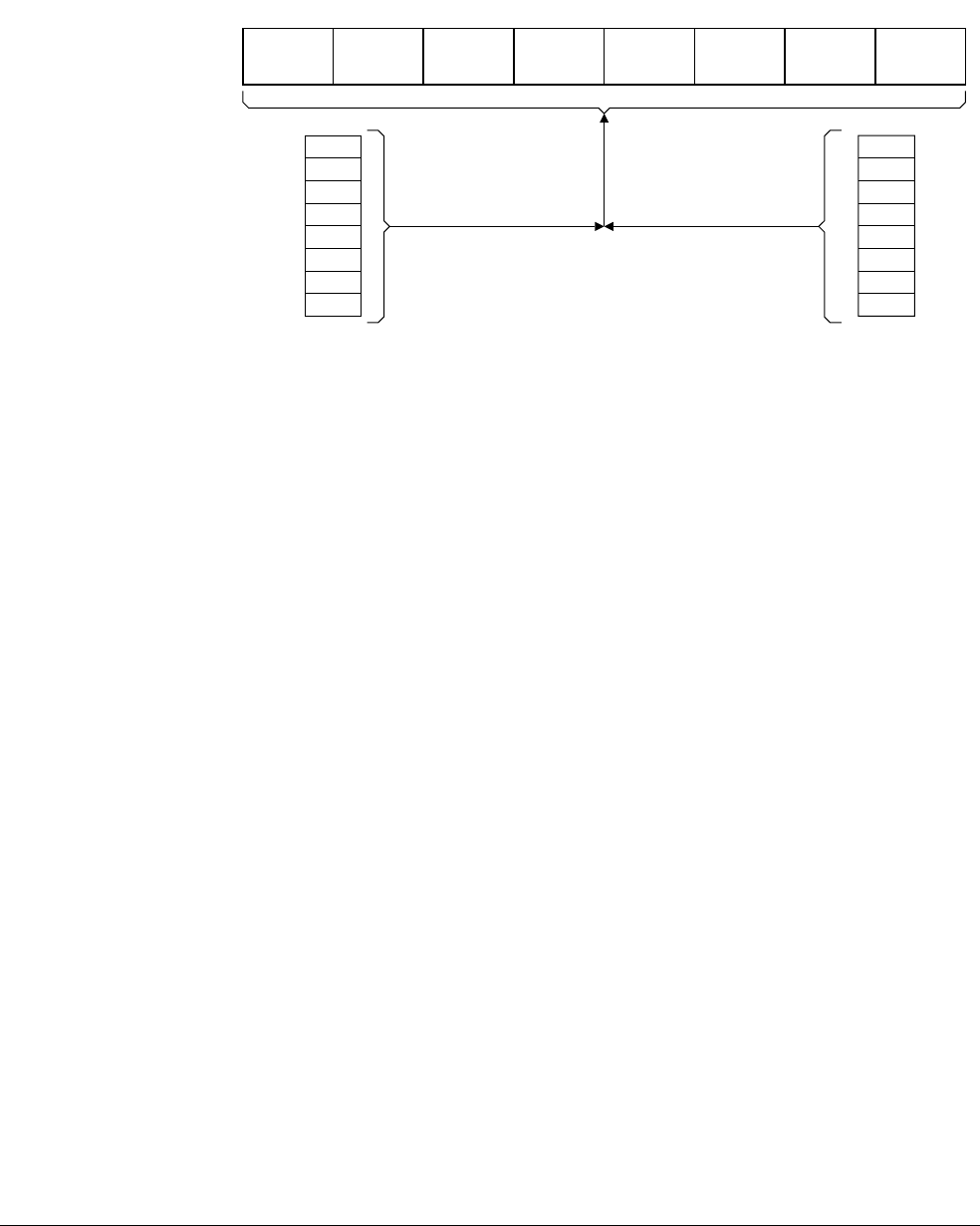
A3 Application Level Memory Model
A3.3 Endian support
ARM DDI 0406C.c Copyright © 1996-1998, 2000, 2004-2012, 2014 ARM. All rights reserved. A3-113
ID051414 Non-Confidential
This loads a 64-bit register with four 16-bit values. The four elements appear in the register in array order, with the
lowest indexed element fetched from the lowest address. The order of bytes in the elements depends on the
endianness configuration, as shown in Figure A3-2. Therefore, the order of the elements in the registers is the same
regardless of the endianness configuration.
Figure A3-2 Advanced SIMD byte order example
For information about the alignment of Advanced SIMD instructions see Unaligned data access on page A3-108.
D[15:8] D[7:0] C[15:8] C[7:0] B[15:8] B[7:0] A[15:8] A[7:0]
64-bit register containing four 16-bit elements
0
1
2
3
4
5
6 D[7:0]
C[15:8]
C[7:0]
B[15:8]
B[7:0]
A[15:8]
A[7:0] 0
1
2
3
4
5
6
D[7:0]
D[15:8]
C[7:0]
C[15:8]
B[7:0]
B[15:8]
A[7:0]
A[15:8]
Memory system with
little-endian addressing (LE)
Memory system with
big-endian addressing (BE)
VLD1.16 {D0}, [R1] VLD1.16 {D0}, [R1]
77 D[15:8]

A3 Application Level Memory Model
A3.4 Synchronization and semaphores
A3-114 Copyright © 1996-1998, 2000, 2004-2012, 2014 ARM. All rights reserved. ARM DDI 0406C.c
Non-Confidential ID051414
A3.4 Synchronization and semaphores
In architecture versions before ARMv6, support for the synchronization of shared memory depends on the
SWP
and
SWPB
instructions. These are read-locked-write operations that swap register contents with memory, and are
described in SWP, SWPB on page A8-722. These instructions support basic busy/free semaphore mechanisms, but
do not support mechanisms that require calculation to be performed on the semaphore between the read and write
phases.
From ARMv6, ARM deprecates any use of
SWP
or
SWPB
, and the ARMv7 Virtualization Extensions make these
instructions OPTIONAL and deprecated.
Note
• ARM strongly recommends that all software uses the synchronization primitives described in this section,
rather than
SWP
or
SWPB
.
• If an implementation does not support the
SWP
and
SWPB
instructions, the ID_ISAR0.Swap_instrs and
ID_ISAR4.SWP_frac fields are zero, see About the Instruction Set Attribute registers on page B7-1952.
ARMv6 introduced a new mechanism to support more comprehensive non-blocking synchronization of shared
memory, using synchronization primitives that scale for multiprocessor system designs. ARMv7 extends support for
this mechanism, and provides the following synchronization primitives in the ARM and Thumb instruction sets:
• Load-Exclusives:
—
LDREX
, see LDREX on page A8-432
—
LDREXB
, see LDREXB on page A8-434
—
LDREXD
, see LDREXD on page A8-436
—
LDREXH
, see LDREXH on page A8-438
• Store-Exclusives:
—
STREX
, see STREX on page A8-690
—
STREXB
, see STREXB on page A8-692
—
STREXD
, see STREXD on page A8-694
—
STREXH
, see STREXH on page A8-696
• Clear-Exclusive,
CLREX
, see CLREX on page A8-360.
Note
This section describes the operation of a Load-Exclusive/Store-Exclusive pair of synchronization primitives using,
as examples, the
LDREX
and
STREX
instructions. The same description applies to any other pair of synchronization
primitives:
•
LDREXB
used with
STREXB
•
LDREXD
used with
STREXD
•
LDREXH
used with
STREXH
.
Software must use a Load-Exclusive instruction only with the corresponding Store-Exclusive instruction.
The model for the use of a Load-Exclusive/Store-Exclusive instruction pair, accessing a non-aborting memory
address x is:
• The Load-Exclusive instruction reads a value from memory address x.
• The corresponding Store-Exclusive instruction succeeds in writing back to memory address x only if no other
observer, process, or thread has performed a more recent store to address x. The Store-Exclusive operation
returns a status bit that indicates whether the memory write succeeded.
A Load-Exclusive instruction tags a small block of memory for exclusive access. The size of the tagged block is
IMPLEMENTATION DEFINED, see Tagging and the size of the tagged memory block on page A3-121. A
Store-Exclusive instruction to the same address clears the tag.

A3 Application Level Memory Model
A3.4 Synchronization and semaphores
ARM DDI 0406C.c Copyright © 1996-1998, 2000, 2004-2012, 2014 ARM. All rights reserved. A3-115
ID051414 Non-Confidential
Note
In this section, the term processor includes any observer that can generate a Load-Exclusive or a Store-Exclusive.
A3.4.1 Exclusive access instructions and Non-shareable memory regions
For memory regions that do not have the Shareable attribute, the exclusive access instructions rely on a local
monitor that tags any address from which the processor executes a Load-Exclusive. Any non-aborted attempt by the
same processor to use a Store-Exclusive to modify any address is guaranteed to clear the tag.
A Load-Exclusive performs a load from memory, and:
• the executing processor tags the physical memory address for exclusive access
• the local monitor of the executing processor transitions to the Exclusive Access state.
A Store-Exclusive performs a conditional store to memory, that depends on the state of the local monitor:
If the local monitor is in the Exclusive Access state
• If the address of the Store-Exclusive is the same as the address that has been tagged in the
monitor by an earlier Load-Exclusive, then the store occurs, otherwise it is IMPLEMENTATION
DEFINED whether the store occurs.
• A status value is returned to a register:
— if the store took place the status value is 0
— otherwise, the status value is 1.
• The local monitor of the executing processor transitions to the Open Access state.
If the local monitor is in the Open Access state
• no store takes place
• a status value of 1 is returned to a register.
• the local monitor remains in the Open Access state.
The Store-Exclusive instruction defines the register to which the status value is returned.
When a processor writes using any instruction other than a Store-Exclusive it is IMPLEMENTATION DEFINED whether
the write affects the state of the local monitor.
If the local monitor is in the Exclusive Access state and the processor performs a Store-Exclusive to any address
other than the last one from which it performed a Load-Exclusive, it is IMPLEMENTATION DEFINED whether the store
updates memory, but in all cases the local monitor is reset to the Open Access state. This mechanism:
• is used on a context switch, see Context switch support on page A3-122
• must be treated as a software programming error in all other cases.
Note
It is IMPLEMENTATION DEFINED whether a store to a tagged physical address causes a tag in the local monitor to be
cleared if that store is by an observer other than the one that caused the physical address to be tagged.
Figure A3-3 on page A3-116 shows the state machine for the local monitor. Table A3-3 on page A3-116 shows the
effect of each of the operations shown in the figure.

A3 Application Level Memory Model
A3.4 Synchronization and semaphores
A3-116 Copyright © 1996-1998, 2000, 2004-2012, 2014 ARM. All rights reserved. ARM DDI 0406C.c
Non-Confidential ID051414
Figure A3-3 Local monitor state machine diagram
For more information about tagging see Tagging and the size of the tagged memory block on page A3-121.
Note
For the local monitor state machine, as shown in Figure A3-3:
• The IMPLEMENTATION DEFINED options for the local monitor are consistent with the local monitor being
constructed so that it does not hold any physical address, but instead treats any access as matching the address
of the previous
LoadExcl
.
• A local monitor implementation can be unaware of Load-Exclusive and Store-Exclusive operations from
other processors.
• The architecture does not require a load instruction by another processor, that is not a Load-Exclusive
instruction, to have any effect on the local monitor.
• It is IMPLEMENTATION DEFINED whether the transition from Exclusive Access to Open Access state occurs
when the
Store
or
StoreExcl
is from another observer.
Table A3-3 shows the effect of the operations shown in Figure A3-3.
Open
Access
Exclusive
Access
LoadExcl(x) LoadExcl(x)
CLREX
StoreExcl(x)
Store(x)
CLREX
Store(!Tagged_address)*
Store(!Tagged_address)*
Store(Tagged_address)*
Operations marked * are possible alternative IMPLEMENTATION DEFINED options.
In the diagram: LoadExcl represents any Load-Exclusive instruction
StoreExcl represents any Store-Exclusive instruction
Store represents any other store instruction.
Any LoadExcl operation updates the tagged address to the most significant bits of the address x used for the operation.
StoreExcl(Tagged_address)
StoreExcl(!Tagged_address)
Store(Tagged_address)*
Table A3-3 Effect of Exclusive instructions and write operations on the local monitor
Initial state OperationaEffect Final state
Open Access
CLREX
No effect Open Access
StoreExcl(x)
Does not update memory, returns status 1 Open Access
LoadExcl(x)
Loads value from memory, tags address x Exclusive Access
Store(x)
Updates memory, no effect on monitor Open Access
Exclusive Access
CLREX
Clears tagged address Open Access
StoreExcl(t)
Updates memory, returns status 0 Open Access
StoreExcl(!t)
Updates memory, returns status 0b
Open Access
Does not update memory, returns status 1b
LoadExcl(x)
Loads value from memory, changes tag to address x Exclusive Access

A3 Application Level Memory Model
A3.4 Synchronization and semaphores
ARM DDI 0406C.c Copyright © 1996-1998, 2000, 2004-2012, 2014 ARM. All rights reserved. A3-117
ID051414 Non-Confidential
Note
Normal memory that is Inner Non-cacheable, Outer Non-cacheable is inherently coherent between different
processors, and it is IMPLEMENTATION DEFINED whether such memory, if it does not have the Shareable attribute, is
treated as Non-shareable or as Shareable.
Changes to the local monitor state resulting from speculative execution
The architecture permits a local monitor to transition to the Open Access state as a result of speculation, or from
some other cause. This is in addition to the transitions to Open Access state caused by the architectural execution
of an operation shown in Table A3-3 on page A3-116.
An implementation must ensure that:
• the local monitor cannot be seen to transition to the Exclusive Access state except as a result of the
architectural execution of one of the operations shown in Table A3-3 on page A3-116
• any transition of the local monitor to the Open Access state not caused by the architectural execution of an
operation shown in Table A3-3 on page A3-116 must not indefinitely delay forward progress of execution.
A3.4.2 Exclusive access instructions and Shareable memory regions
For memory regions that have the Shareable attribute, exclusive access instructions rely on:
•A local monitor for each processor in the system, that tags any address from which the processor executes a
Load-Exclusive. The local monitor operates as described in Exclusive access instructions and Non-shareable
memory regions on page A3-115, except that for Shareable memory any Store-Exclusive is then subject to
checking by the global monitor if it is described in that section as doing at least one of:
— updating memory
— returning a status value of 0.
The local monitor can ignore accesses from other processors in the system.
•A global monitor that tags a physical address as exclusive access for a particular processor. This tag is used
later to determine whether a Store-Exclusive to that address that has not been failed by the local monitor can
occur. Any successful write to the tagged address by any other observer in the shareability domain of the
memory location is guaranteed to clear the tag. For each processor in the system, the global monitor:
— can hold at least one tagged address
— maintains a state machine for each tagged address it can hold.
Exclusive Access
Store(!t)
Updates memory Exclusive Accessb
Open Accessb
Store(t)
Updates memory Exclusive Accessb
Open Accessb
a. In the table:
LoadExcl
represents any Load-Exclusive instruction
StoreExcl
represents any Store-Exclusive instruction
Store
represents any store operation other than a Store-Exclusive operation.
t is the tagged address, bits[31:a] of the address of the last Load-Exclusive instruction. For more information, see
Tagging and the size of the tagged memory block on page A3-121.
b. IMPLEMENTATION DEFINED alternative actions.
Table A3-3 Effect of Exclusive instructions and write operations on the local monitor (continued)
Initial state OperationaEffect Final state

A3 Application Level Memory Model
A3.4 Synchronization and semaphores
A3-118 Copyright © 1996-1998, 2000, 2004-2012, 2014 ARM. All rights reserved. ARM DDI 0406C.c
Non-Confidential ID051414
Note
For each processor, the architecture only requires global monitor support for a single tagged address. Any
situation that might benefit from the use of multiple tagged addresses on a single processor is
UNPREDICTABLE, see Load-Exclusive and Store-Exclusive usage restrictions on page A3-122.
In addition, in an implementation that includes the Large Physical Address Extension, when the implementation is
using the Short-descriptor translation table format, it is IMPLEMENTATION DEFINED whether Load-Exclusive and
Store-Exclusive accesses to Non-shareable regions with the Normal, Inner Non-cacheable, Outer Non-cacheable
attribute use the global monitor in addition to the local monitor.
Note
The global monitor can either reside in a processor block or exist as a secondary monitor at the memory
interfaces.The IMPLEMENTATION DEFINED aspects of the monitors mean that the global monitor and local monitor
can be combined into a single unit, provided that unit performs the global monitor and local monitor functions
defined in this manual.
For Shareable regions of memory, in some implementations and for some memory types, the properties of the global
monitor can be met only by functionality outside the processor. Some system implementations might not implement
this functionality for all regions of memory. In particular, this can apply to:
• any type of memory in the system implementation that does not support hardware cache coherency
• Non-cacheable memory, or memory treated as Non-cacheable, in an implementation that does support
hardware cache coherency.
In such a system, it is defined by the system:
• whether the global monitor is implemented
• if the global monitor is implemented, which address ranges or memory types it monitors.
The behavior of Load Exclusive and Store Exclusive instructions when accessing a memory address not monitored
by the global monitor is UNPREDICTABLE.
Note
An implementation can combine the functionality of the global and local monitors into a single unit.
Operation of the global monitor
A Load-Exclusive from Shareable memory performs a load from memory, and causes the physical address of the
access to be tagged as exclusive access for the requesting processor. This access also causes the exclusive access
tag to be removed from any other physical address that has been tagged by the requesting processor.
The global monitor only supports a single outstanding exclusive access to Shareable memory per processor. A
Load-Exclusive by one processor has no effect on the global monitor state for any other processor.
Store-Exclusive performs a conditional store to memory:
• The store is guaranteed to succeed only if the physical address accessed is tagged as exclusive access for the
requesting processor and both the local monitor and the global monitor state machines for the requesting
processor are in the Exclusive Access state. In this case:
— a status value of 0 is returned to a register to acknowledge the successful store
— the final state of the global monitor state machine for the requesting processor is IMPLEMENTATION
DEFINED
— if the address accessed is tagged for exclusive access in the global monitor state machine for any other
processor then that state machine transitions to Open Access state.

A3 Application Level Memory Model
A3.4 Synchronization and semaphores
ARM DDI 0406C.c Copyright © 1996-1998, 2000, 2004-2012, 2014 ARM. All rights reserved. A3-119
ID051414 Non-Confidential
• If no address is tagged as exclusive access for the requesting processor, the store does not succeed:
— a status value of 1 is returned to a register to indicate that the store failed
— the global monitor is not affected and remains in Open Access state for the requesting processor.
• If a different physical address is tagged as exclusive access for the requesting processor, it is
IMPLEMENTATION DEFINED whether the store succeeds or not:
— if the store succeeds a status value of 0 is returned to a register, otherwise a value of 1 is returned
— if the global monitor state machine for the processor was in the Exclusive Access state before the
Store-Exclusive it is IMPLEMENTATION DEFINED whether that state machine transitions to the Open
Access state.
The Store-Exclusive instruction defines the register to which the status value is returned.
In a shared memory system, the global monitor implements a separate state machine for each processor in the
system. The state machine for accesses to Shareable memory by processor (n) can respond to all the Shareable
memory accesses visible to it. This means it responds to:
• accesses generated by the associated processor (n)
• accesses generated by the other observers in the shareability domain of the memory location (!n).
In a shared memory system, the global monitor implements a separate state machine for each observer that can
generate a Load-Exclusive or a Store-Exclusive in the system.
Figure A3-4 shows the state machine for processor(n) in a global monitor. Table A3-4 on page A3-120 shows the
effect of each of the operations shown in the figure.
Figure A3-4 Global monitor state machine diagram for processor(n) in a multiprocessor system
For more information about tagging see Tagging and the size of the tagged memory block on page A3-121.
Any LoadExcl operation updates the tagged address to the most significant bits of the address x used for the operation.
Open
Access
Exclusive
Access
LoadExcl(x,n) LoadExcl(x,n)
CLREX(n)
StoreExcl(x,n)
CLREX(n)*
StoreExcl(Tagged_address,!n)‡
Store(Tagged_address,!n)
StoreExcl(Tagged_address,n)*
Store(!Tagged_address,n)
Operations marked * are possible alternative
IMPLEMENTATION
DEFINED
options.
In the diagram: LoadExcl represents any Load-Exclusive instruction
StoreExcl represents any Store-Exclusive instruction
Store represents any other store instruction.
LoadExcl(x,!n)
StoreExcl(x,!n)
Store(x,n)
StoreExcl(!Tagged_address,n)*
Store(Tagged_address,n)*
StoreExcl(Tagged_address,!n)‡
StoreExcl(Tagged_address,n)*
StoreExcl(!Tagged_address,n)*
Store(Tagged_address,n)*
CLREX(n)*
StoreExcl(!Tagged_address,!n)
Store(!Tagged_address,!n)
CLREX(!n)
‡StoreExcl(Tagged_Address,!n) clears the monitor only if the StoreExcl updates memory
Store(x,!n)
CLREX(!n)

A3 Application Level Memory Model
A3.4 Synchronization and semaphores
A3-120 Copyright © 1996-1998, 2000, 2004-2012, 2014 ARM. All rights reserved. ARM DDI 0406C.c
Non-Confidential ID051414
Note
For the global monitor state machine, as shown in Figure A3-4 on page A3-119:
• The architecture does not require a load instruction by another processor, that is not a Load-Exclusive
instruction, to have any effect on the global monitor.
• Whether a Store-Exclusive successfully updates memory or not depends on whether the address accessed
matches the tagged Shareable memory address for the processor issuing the Store-Exclusive instruction. For
this reason, Figure A3-4 on page A3-119 and Table A3-4 only show how the (!n) entries cause state
transitions of the state machine for processor(n).
• An Load-Exclusive can only update the tagged Shareable memory address for the processor issuing the
Load-Exclusive instruction.
• The effect of the
CLREX
instruction on the global monitor is IMPLEMENTATION DEFINED.
• It is IMPLEMENTATION DEFINED:
— whether a modification to a non-shareable memory location can cause a global monitor to transition
from Exclusive Access to Open Access state
— whether a Load-Exclusive to a non-shareable memory location can cause a global monitor to transition
from Open Access to Exclusive Access state.
Table A3-4 shows the effect of the operations shown in Figure A3-4 on page A3-119.
Table A3-4 Effect of load/store operations on global monitor for processor(n)
Initial state OperationaEffect Final state
Exclusive
Access
LoadExcl(x, n)
Loads value from memory, tags address x Exclusive Access
CLREX(n)
None. Effect on the final state is IMPLEMENTATION DEFINED.Exclusive Accessd
Open Accessd
CLREX(!n)
None Exclusive Access
StoreExcl(t, !n)
Updates memory, returns status 0bOpen Access
Does not update memory, returns status 1bExclusive Access
StoreExcl(t, n)
Updates memory, returns status 0cOpen Access
Exclusive Access
StoreExcl(!t, n)
Updates memory, returns status 0dOpen Access
Exclusive Access
Does not update memory, returns status 1dOpen Access
Exclusive Access
StoreExcl(!t, !n)
Depends on state machine and tag address for processor issuing
STREX
Exclusive Access
Store(t, n)
Updates memory Exclusive Accessd
Open Accessd
Store(t, !n)
Updates memory Open Access
Store(!t, n)
,
Store(!t, !n)
Updates memory, no effect on monitor Exclusive Access

A3 Application Level Memory Model
A3.4 Synchronization and semaphores
ARM DDI 0406C.c Copyright © 1996-1998, 2000, 2004-2012, 2014 ARM. All rights reserved. A3-121
ID051414 Non-Confidential
A3.4.3 Tagging and the size of the tagged memory block
As stated in the footnotes to Table A3-3 on page A3-116 and Table A3-4 on page A3-120, when a Load-Exclusive
instruction is executed, the resulting tag address ignores the least significant bits of the memory address.
Tagged_address = Memory_address[31:a]
The value of
a
in this assignment is IMPLEMENTATION DEFINED, between a minimum value of 3 and a maximum
value of 11. For example, in an implementation where a is 4, a successful
LDREX
of address
0x000341B4
gives a tag
value of bits[31:4] of the address, giving
0x000341B
. This means that the four words of memory from
0x000341B0
to
0x000341BF
are tagged for exclusive access.
The size of the tagged memory block is called the Exclusives Reservation Granule. The Exclusives Reservation
Granule is IMPLEMENTATION DEFINED in the range 2-512 words:
• 2 words in an implementation where a is 3
• 512 words in an implementation where a is 11.
In some implementations the CTR identifies the Exclusives Reservation Granule, see either:
•CTR, Cache Type Register, VMSA on page B4-1556
•CTR, Cache Type Register, PMSA on page B6-1835.
Open Access
CLREX(n)
,
CLREX(!n)
None Open Access
StoreExcl(x, n)
Does not update memory, returns status 1 Open Access
LoadExcl(x, !n)
Loads value from memory, no effect on tag address for processor(n) Open Access
StoreExcl(x, !n)
Depends on state machine and tag address for processor issuing
STREX
bOpen Access
Store(x, n)
,
Store(x, !n)
Updates memory, no effect on monitor Open Access
LoadExcl(x, n)
Loads value from memory, tags address x Exclusive Access
a. In the table:
LoadExcl
represents any Load-Exclusive instruction
StoreExcl
represents any Store-Exclusive instruction
Store
represents any store operation other than a Store-Exclusive operation.
t is the tagged address for processor(n), bits[31:a] of the address of the last Load-Exclusive instruction issued by processor(n), see Tagging
and the size of the tagged memory block.
b. The result of a
STREX(x, !n)
or a
STREX(t, !n)
operation depends on the state machine and tagged address for the processor issuing the
STREX
instruction. This table shows how each possible outcome affects the state machine for processor(n).
c. After a successful
STREX
to the tagged address, the state of the state machine is IMPLEMENTATION DEFINED. However, this state has no effect
on the subsequent operation of the global monitor.
d. Effect is IMPLEMENTATION DEFINED. The table shows all permitted implementations.
Table A3-4 Effect of load/store operations on global monitor for processor(n) (continued)
Initial state OperationaEffect Final state

A3 Application Level Memory Model
A3.4 Synchronization and semaphores
A3-122 Copyright © 1996-1998, 2000, 2004-2012, 2014 ARM. All rights reserved. ARM DDI 0406C.c
Non-Confidential ID051414
A3.4.4 Context switch support
After a context switch, software must ensure that the local monitor is in the Open Access state. This requires it to
either:
• execute a
CLREX
instruction
• execute a dummy
STREX
to a memory address allocated for this purpose.
Note
• Using a dummy
STREX
for this purpose is backwards-compatible with the ARMv6 implementation of the
exclusive operations. The
CLREX
instruction is introduced in ARMv6K.
• Context switching is not an application level operation. However, this information is included here to
complete the description of the exclusive operations.
The
STREX
or
CLREX
instruction that follows a context switch might cause a subsequent Store-Exclusive to fail,
requiring a Load-Exclusive … Store-Exclusive sequence to be repeated. To minimize the possibility of this
happening, ARM recommends that the Store-Exclusive instruction is kept as close as possible to the associated
Load-Exclusive instruction, see Load-Exclusive and Store-Exclusive usage restrictions.
A3.4.5 Load-Exclusive and Store-Exclusive usage restrictions
The Load-Exclusive and Store-Exclusive instructions are intended to work together, as a pair, for example a
LDREX
/
STREX
pair or a
LDREXB
/
STREXB
pair. To support different implementations of these functions, software must
follow the notes and restrictions given here.
These notes describe use of an
LDREX
/
STREX
pair, but apply equally to any other Load-Exclusive/Store-Exclusive pair:
• The exclusives support a single outstanding exclusive access for each processor thread that is executed. The
architecture makes use of this by not requiring an address or size check as part of the
IsExclusiveLocal()
function. If the target virtual address of an
STREX
is different from the virtual address of the preceding
LDREX
in the same thread of execution, behavior can be UNPREDICTABLE. As a result, an
LDREX
/
STREX
pair can only
be relied upon to eventually succeed if they are executed with the same virtual address. Where a context
switch or exception might change the thread of execution, a
CLREX
instruction or a dummy
STREX
instruction
must be executed to avoid unwanted effects, as described in Context switch support. Using an
STREX
in this
way is the only occasion where software can program an
STREX
with a different address from the previously
executed
LDREX
.
•If two
STREX
instructions are executed without an intervening
LDREX
the second
STREX
returns a status value
of 1. This means that:
— ARM recommends that, in a given thread of execution, every
STREX
has a preceding
LDREX
associated
with it
— it is not necessary for every
LDREX
to have a subsequent
STREX
.
• An implementation of the Load-Exclusive and Store-Exclusive instructions can require that, in any thread of
execution, the transaction size of a Store-Exclusive is the same as the transaction size of the preceding
Load-Exclusive executed in that thread. If the transaction size of a Store-Exclusive is different from the
preceding Load-Exclusive in the same thread of execution, behavior can be UNPREDICTABLE. As a result,
software can rely on an
LDREX
/
STREX
pair to eventually succeed only if they have the same size. Where a
context switch or exception might change the thread of execution, the software must execute a
CLREX
instruction, or a dummy
STREX
instruction, to avoid unwanted effects, as described in Context switch support.
Using an
STREX
in this way is the only occasion where software can use a Store-Exclusive instruction with a
different transaction size from the previously executed Load-Exclusive instruction.
• An implementation might clear an exclusive monitor between the
LDREX
and the
STREX
, without any
application-related cause. For example, this might happen because of cache evictions. Software written for
such an implementation must, in any single thread of execution, avoid having any explicit memory accesses,
System control register updates, or cache maintenance operations between the
LDREX
instruction and the
associated
STREX
instruction.

A3 Application Level Memory Model
A3.4 Synchronization and semaphores
ARM DDI 0406C.c Copyright © 1996-1998, 2000, 2004-2012, 2014 ARM. All rights reserved. A3-123
ID051414 Non-Confidential
• In some implementations, an access to Strongly-ordered or Device memory might clear the exclusive
monitor. Therefore, software must not place a load or a store to Strongly-ordered or Device memory between
an
LDREX
and an
STREX
in a single thread of execution.
• Implementations can benefit from keeping the
LDREX
and
STREX
operations close together in a single thread of
execution. This minimizes the likelihood of the exclusive monitor state being cleared between the
LDREX
instruction and the
STREX
instruction. Therefore, for best performance, ARM strongly recommends a limit of
128 bytes between
LDREX
and
STREX
instructions in a single thread of execution.
• The architecture sets an upper limit of 2048 bytes on the size of a region that can be marked as exclusive.
Software can read the implemented size of the Exclusives reservation granule from the CTR.ERG field, see:
—CTR, Cache Type Register, VMSA on page B4-1556 for a VMSA implementation.
—CTR, Cache Type Register, PMSA on page B6-1835 for a PMSA implementation.
In a heavily contended system, having multiple objects that are in the same exclusive reservation granule
accessed by exclusive accesses can lead to starvation of a process accessing that granule. Therefore, in such
systems, ARM recommends that objects that are accessed by exclusive accesses are separated by the size of
the Exclusive Reservation Granule.
• It is IMPLEMENTATION DEFINED whether
LDREX
and
STREX
operations can be performed to a memory region
with the Device or Strongly-ordered memory attribute. Unless the implementation documentation explicitly
states that
LDREX
and
STREX
operations to a memory region with the Device or Strongly-ordered attribute are
permitted, the effect of such operations is UNPREDICTABLE.
• After taking a Data Abort exception, the state of the exclusive monitors is UNKNOWN. Therefore ARM
strongly recommends that the abort handling software performs a
CLREX
instruction, or a dummy
STREX
instruction, to clear the monitor state.
• For the memory location being accessed by a
LoadExcl/StoreExcl
pair, if the memory attributes for the
LoadExcl
instruction differ from the memory attributes for the
StoreExcl
instruction, behavior is
UNPREDICTABLE.
This can occur either:
— Because the translation of the accessed address changes between the
LoadExcl
and the
StoreExcl
.
— As a result of using different virtual addresses, with different attributes, that point to the same physical
address. This case is covered by another bullet point in this list.
If the memory attributes for the memory being accessed by an
LDREX
/
STREX
pair are changed between the
LDREX
and the
STREX
, behavior is UNPREDICTABLE.
• The effect of a data or unified cache invalidate, cache clean, or cache clean and invalidate instruction on a
local or global exclusive monitor that is in the Exclusive Access state is UNPREDICTABLE. Execution of the
instruction might clear the monitor, or it might leave it in the Exclusive Access state. For address-based
maintenance instructions this also applies to the monitors of other processors in the same shareability domain
as the processor executing the cache maintenance instruction, as determined by the shareability domain of
the address being maintained.
Note
ARM strongly recommends that implementations ensure that the use of such maintenance operations by a
processor in the Non-secure state cannot cause a denial of service on a processor in the Secure state.

A3 Application Level Memory Model
A3.4 Synchronization and semaphores
A3-124 Copyright © 1996-1998, 2000, 2004-2012, 2014 ARM. All rights reserved. ARM DDI 0406C.c
Non-Confidential ID051414
• If the mapping of the virtual to physical address is changed between the
LDREX
instruction and the
STREX
instruction, and the change is performed using a break-before-make sequence as described in General TLB
maintenance requirements on page B3-1381, if the
STREX
is performed after another write to the same
physical address as the
STREX
, and that other write was performed after the old translation was properly
invalidated and that invalidation was properly synchronized, then the
STREX
will not pass its monitor check.
Note
ARM expects that, in many implementations, either:
— The TLB invalidation will clear either the local or global monitor.
— The physical address will be checked between the
LDREX
and
STREX
.
Note
In the event of repeatedly-contending load-exclusive/store-exclusive sequences from multiple processors, an
implementation must ensure that forward progress is made by at least one processor.
A3.4.6 Semaphores
The Swap (
SWP
) and Swap Byte (
SWPB
) instructions must be used with care to ensure that expected behavior is
observed. Two examples are as follows:
1. A system with multiple bus masters that uses Swap instructions to implement semaphores that control
interactions between different bus masters.
In this case, the semaphores must be placed in an uncached region of memory, where any buffering of writes
occurs at a point common to all bus masters using the mechanism. The Swap instruction then causes a locked
read-write bus transaction.
2. A system with multiple threads running on a uniprocessor that uses Swap instructions to implement
semaphores that control interaction of the threads.
In this case, the semaphores can be placed in a cached region of memory, and a locked read-write bus
transaction might or might not occur. The Swap and Swap Byte instructions are likely to have better
performance on such a system than they do on a system with multiple bus masters, such as that described in
example 1.
Note
From ARMv6, ARM deprecates use of the Swap and Swap Byte instructions, and strongly recommends that all new
software uses the Load-Exclusive and Store-Exclusive synchronization primitives described in Synchronization and
semaphores on page A3-114, for example
LDREX
and
STREX
.
A3.4.7 Synchronization primitives and the memory order model
The synchronization primitives follow the memory order model of the memory type accessed by the instructions.
For this reason:
• Portable software for claiming a spin-lock must include a Data Memory Barrier (DMB) operation, performed
by a
DMB
instruction, between claiming the spin-lock and making any access that makes use of the spin-lock.
• Portable software for releasing a spin-lock must include a
DMB
instruction before writing to clear the spin-lock.
This requirement applies to software using:
• the Load-Exclusive/Store-Exclusive instruction pairs, for example
LDREX
/
STREX
• the deprecated synchronization primitives,
SWP
/
SWPB
.

A3 Application Level Memory Model
A3.4 Synchronization and semaphores
ARM DDI 0406C.c Copyright © 1996-1998, 2000, 2004-2012, 2014 ARM. All rights reserved. A3-125
ID051414 Non-Confidential
A3.4.8 Use of WFE and SEV instructions by spin-locks
ARMv7 and ARMv6K provide Wait For Event and Send Event instructions,
WFE
and
SEV
, that can assist with
reducing power consumption and bus contention caused by processors repeatedly attempting to obtain a spin-lock.
These instructions can be used at the application level, but a complete understanding of what they do depends on
system level understanding of exceptions. They are described in Wait For Event and Send Event on page B1-1200.

A3 Application Level Memory Model
A3.5 Memory types and attributes and the memory order model
A3-126 Copyright © 1996-1998, 2000, 2004-2012, 2014 ARM. All rights reserved. ARM DDI 0406C.c
Non-Confidential ID051414
A3.5 Memory types and attributes and the memory order model
ARMv6 defined a set of memory attributes with the characteristics required to support the memory and devices in
the system memory map. In ARMv7 this set of attributes is extended by the addition of the Outer Shareable attribute
for Normal memory and, in an implementation that does not include the Large Physical Address Extension, for
Device memory.
Note
Whether an ARMv7 implementation distinguishes between Inner Shareable and Outer Shareable memory is
IMPLEMENTATION DEFINED.
The ordering of accesses for regions of memory, referred to as the memory order model, is defined by the memory
attributes. This model is described in the following sections:
•Memory types
•Summary of ARMv7 memory attributes on page A3-127
•Atomicity in the ARM architecture on page A3-128
•Concurrent modification and execution of instructions on page A3-130
•Normal memory on page A3-132
•Device and Strongly-ordered memory on page A3-136
•Memory access restrictions on page A3-138
•The effect of the Security Extensions on page A3-141.
A3.5.1 Memory types
For each memory region, the most significant memory attribute specifies the memory type. There are three mutually
exclusive memory types:
• Normal
•Device
• Strongly-ordered.
Normal and Device memory regions have additional attributes.
Usually, memory used for programs and for data storage is suitable for access using the Normal memory attribute.
Examples of memory technologies for which the Normal memory attribute is appropriate are:
• programmed Flash ROM
Note
During programming, Flash memory can be ordered more strictly than Normal memory.
•ROM
•SRAM
• DRAM and DDR memory.
System peripherals (I/O) generally conform to different access rules. Examples of I/O accesses are:
• FIFOs where consecutive accesses:
— add queued values on write accesses
— remove queued values on read accesses.
• interrupt controller registers where an access can be used as an interrupt acknowledge, changing the state of
the controller itself
• memory controller configuration registers that are used for setting up the timing and correctness of areas of
Normal memory
• memory-mapped peripherals, where accessing a memory location can cause side-effects in the system.

A3 Application Level Memory Model
A3.5 Memory types and attributes and the memory order model
ARM DDI 0406C.c Copyright © 1996-1998, 2000, 2004-2012, 2014 ARM. All rights reserved. A3-127
ID051414 Non-Confidential
In ARMv7, the Strongly-ordered or Device memory attribute provides suitable access control for such peripherals.
To ensure correct system behavior, the access rules for Device and Strongly-ordered memory are more restrictive
than those for Normal memory, so that:
• Neither read nor write accesses can be performed speculatively.
Note
However, translation table walks can be made speculatively to memory marked as Device or
Strongly-ordered, see Device and Strongly-ordered memory on page A3-136.
• Read and write accesses cannot be repeated, for example, on return from an exception.
• The number, order and sizes of the accesses are maintained.
For more information, see Device and Strongly-ordered memory on page A3-136.
A3.5.2 Summary of ARMv7 memory attributes
Table A3-5 summarizes the memory attributes. For more information about these attributes see:
•Normal memory on page A3-132 and Shareable attribute for Device memory regions on page A3-137, for
the shareability attribute
•Write-Through Cacheable, Write-Back Cacheable and Non-cacheable Normal memory on page A3-134, for
cacheability and cache allocation hint attributes.
Note
The cacheability and cache allocation hint attributes apply only to Normal memory. Device and Strongly-ordered
memory regions are Non-cacheable.
In this table:
Shareability Applies only to Normal memory, and to Device memory in an implementation that does not include
the Large Physical Address Extension. In an implementation that includes the Large Physical
Address Extension, Device memory is always Outer Shareable,
When it is possible to assign a shareability attribute to Device memory, ARM deprecates assigning
any attribute other than Shareable or Outer Shareable, see Shareable attribute for Device memory
regions on page A3-137
Whether an ARMv7 implementation distinguishes between Inner Shareable and Outer Shareable
memory is IMPLEMENTATION DEFINED.
Cacheability Applies only to Normal memory, and can be defined independently for Inner and Outer cache
regions. Some cacheability attributes can be complemented by a cache allocation hint. This is an
indication to the memory system of whether allocating a value to a cache is likely to improve
performance. For more information see Cacheability and cache allocation hint attributes on
page B2-1264.
An implementation might not make any distinction between memory regions with attributes that
differ only in their cache allocation hint.
Table A3-5 Memory attribute summary
Memory type Implementation includes LPAEa?Shareability Cacheability
Strongly- ordered - - -

A3 Application Level Memory Model
A3.5 Memory types and attributes and the memory order model
A3-128 Copyright © 1996-1998, 2000, 2004-2012, 2014 ARM. All rights reserved. ARM DDI 0406C.c
Non-Confidential ID051414
Memory model and memory ordering on page D15-2595 compares these attributes with the memory attributes in
architecture versions before ARMv6.
A3.5.3 Atomicity in the ARM architecture
Atomicity is a feature of memory accesses, described as atomic accesses. The ARM architecture description refers
to two types of atomicity, defined in:
•Single-copy atomicity
•Multi-copy atomicity on page A3-130.
Single-copy atomicity
A read or write operation is single-copy atomic only if it meets the following conditions:
• For a single-copy atomic store, if the store overlaps another single-copy atomic store, then all of the writes
from one of the stores are inserted into the Coherence order of each overlapping byte before any of the writes
of the other store are inserted into the Coherence order of the overlapping bytes.
• If a single-copy atomic load overlaps a single-copy atomic store and for any of the overlapping bytes the load
returns the data written by the write inserted into the Coherence order of that byte by the single-copy atomic
store then the load must return data from a point in the Coherence order no earlier than the writes inserted
into the Coherence order by the single-copy atomic store of all of the overlapping bytes.
In ARMv7, the single-copy atomic processor accesses are:
• All byte accesses.
• All halfword accesses to halfword-aligned locations.
• All word accesses to word-aligned locations.
• Memory accesses caused by a
LDREXD
/
STREXD
to a doubleword-aligned location for which the
STREXD
succeeds
cause single-copy atomic updates of the doubleword being accessed.
Note
The way to atomically load two 32-bit quantities is to perform a
LDREXD
/
STREXD
sequence, reading and writing
the same value, for which the
STREXD
succeeds, and use the read values.
LDM
,
LDC
,
LDC2
,
LDRD
,
STM
,
STC
,
STC2
,
STRD
,
PUSH
,
POP
,
RFE
,
SRS
,
VLDM
,
VLDR
,
VSTM
, and
VSTR
instructions are executed as a
sequence of word-aligned word accesses. Each 32-bit word access is guaranteed to be single-copy atomic. The
architecture does not require subsequences of two or more word accesses from the sequence to be single-copy
atomic.
Device Yes Outer Shareable -
No Outer Shareable
Inner Shareable
Non-shareable
Normal - Outer Shareable One of:
• Non-cacheable
• Write-Through Cacheable
• Write-Back Cacheable.
Inner Shareable
Non-shareable
a. LPAE means the Large Physical Address Extension.
Table A3-5 Memory attribute summary (continued)
Memory type Implementation includes LPAEa?Shareability Cacheability

A3 Application Level Memory Model
A3.5 Memory types and attributes and the memory order model
ARM DDI 0406C.c Copyright © 1996-1998, 2000, 2004-2012, 2014 ARM. All rights reserved. A3-129
ID051414 Non-Confidential
In an implementation that includes the Large Physical Address Extension,
LDRD
and
STRD
accesses to 64-bit aligned
locations are 64-bit single-copy atomic as seen by translation table walks and accesses to translation tables.
Note
The Large Physical Address Extension adds this requirement to avoid the need for complex measures to avoid
atomicity issues when changing translation table entries, without creating a requirement that all locations in the
memory system are 64-bit single-copy atomic. This addition means:
• The system designer must ensure that all writable memory locations that might be used to hold translations,
such as bulk SDRAM, can be accessed with 64-bit single-copy atomicity.
• Software must ensure that translation tables are not held in memory locations that cannot meet this atomicity
requirement, such as peripherals that are typically accessed using a narrow bus.
This requirement places no burden on read-only memory locations for which reads have no side effects, since it is
impossible to detect the size of memory accesses to such locations.
Advanced SIMD element and structure loads and stores are executed as a sequence of accesses of the element or
structure size. The architecture requires the element accesses to be single-copy atomic if and only if both:
• the element size is 32 bits, or smaller
• the elements are naturally aligned.
Accesses to 64-bit elements or structures that are at least word-aligned are executed as a sequence of 32-bit accesses,
each of which is single-copy atomic.The architecture does not require subsequences of two or more 32-bit accesses
from the sequence to be single-copy atomic.
When an access is not single-copy atomic by the rules described in this section, it is executed as a sequence of one
or more accesses that aggregate to size of the access. Each of the accesses in this sequence is single-copy atomic, at
least at the byte level.
Note
In this section, the terms before the write operation and after the write operation mean before or after the write
operation has had its effect on the coherence order of the bytes of the memory location accessed by the write
operation.
If, according to these rules, an instruction is executed as a sequence of accesses, some exceptions can be taken
during that sequence. Such an exception causes execution of the instruction to be abandoned. These exceptions are:
• Synchronous Data Abort exceptions.
• The following, if low interrupt latency configuration is selected and the accesses are to Normal memory:
— IRQ interrupts
— FIQ interrupts
— asynchronous aborts.
For more information about this configuration, see Low interrupt latency configuration on page B1-1198.
If such an instruction is abandoned as a result of an asynchronous exception, then:
• For a load:
— Any register being loaded other than one used in the generation of the address by the instruction, might
contain an UNKNOWN value.
— Registers used in the generation of the address are restored to their initial value.
• For a store, any data location being stored to can contain an UNKNOWN value.
If such an instruction is abandoned as a result of a Synchronous Data Abort exception, then see Data Abort
exception on page B1-1215.

A3 Application Level Memory Model
A3.5 Memory types and attributes and the memory order model
A3-130 Copyright © 1996-1998, 2000, 2004-2012, 2014 ARM. All rights reserved. ARM DDI 0406C.c
Non-Confidential ID051414
If any of these exceptions are returned from using their preferred return address, the instruction that generated the
sequence of accesses is re-executed and so any access that had been performed before the exception was taken is
repeated.
Note
The exception behavior for these multiple access instructions means they are not suitable for use for writes to
memory for the purpose of software synchronization.
For implicit accesses:
• Cache linefills and evictions have no effect on the single-copy atomicity of explicit transactions or instruction
fetches.
• Instruction fetches are single-copy atomic:
— at 32-bit granularity in ARM state
— at 16-bit granularity in Thumb and ThumbEE states
— at 8-bit granularity in Jazelle state.
Concurrent modification and execution of instructions describes additional constraints on the behavior of
instruction fetches.
• Translation table walks are performed using accesses that are single-copy atomic:
— at 32-bit granularity when using Short-descriptor format translation tables
— at 64-bit granularity when using Long-descriptor format translation tables.
Multi-copy atomicity
In a multiprocessing system, writes to a memory location are multi-copy atomic if the following conditions are both
true:
• All writes to the same location are serialized, meaning they are observed in the same order by all observers,
although some observers might not observe all of the writes.
• A read of a location does not return the value of a write until all observers observe that write.
Writes to Normal memory are not multi-copy atomic.
All writes to Device and Strongly-ordered memory that are single-copy atomic are also multi-copy atomic.
Note
All coherent write accesses to the same location are serialized, regardless of whether or not they are multi-copy
atomic. For Normal memory, write accesses can be repeated up to the point that another write to the same address
is observed, and serialization does not prohibit the merging of writes.
A3.5.4 Concurrent modification and execution of instructions
The ARMv7 architecture limits the set of instructions that can be executed by one thread of execution as they are
being modified by another thread of execution without requiring explicit synchronization.
Except for the instructions identified in this section, the effect of the concurrent modification and execution of an
instruction is UNPREDICTABLE.
For the following instructions only, the architecture guarantees that, after modification of the instruction, behavior
is consistent with execution of either:
• The instruction originally fetched.
• A fetch of the new instruction. That is, a fetch of the instruction that results from the modification.

A3 Application Level Memory Model
A3.5 Memory types and attributes and the memory order model
ARM DDI 0406C.c Copyright © 1996-1998, 2000, 2004-2012, 2014 ARM. All rights reserved. A3-131
ID051414 Non-Confidential
The instructions to which this guarantee applies are:
In the Thumb instruction set
The 16-bit encodings of the
B
,
NOP
,
BKPT
, and
SVC
instructions.
In addition:
• The most-significant halfword of a
BL
instruction can be concurrently modified to the most
significant halfword of another
BL
instruction.
The most-significant halfword of a
BLX
instruction can be concurrently modified to the most
significant halfword of another
BLX
instruction.
These cases mean that the most significant bits of the immediate value can be modified.
• The most-significant halfword of a
BL
or
BLX
instruction can be concurrently modified to a
16-bit
B
,
BKPT
, or
SVC
instruction.
• The least-significant halfword of a
BL
instruction can be concurrently modified to the least
significant halfword of another
BL
instruction.
The least-significant halfword of a
BLX
instruction can be concurrently modified to the least
significant halfword of another
BLX
instruction.
These cases mean that the least significant bits of the immediate value can be modified.
• The least-significant halfword of a 32-bit
B
immediate instruction:
— with a condition field can be concurrently modified to the least significant halfword of
another 32-bit
B
immediate instruction with a condition field
— without a condition field can be concurrently modified to the least significant halfword
of another 32-bit
B
immediate instruction without a condition field.
These cases mean that the least significant bits of the immediate value can be modified.
• A 16-bit
B
,
BKPT
, or
SVC
instruction can be concurrently modified to the most-significant
halfword of a
BL
instruction.
Note
In the Thumb instruction set:
• the only encodings of
BKPT
and
SVC
are 16-bit
• the only encoding of
BL
is 32-bit.
In the ARM instruction set
The
B
,
BL
,
NOP
,
BKPT
,
SVC
,
HVC
, and
SMC
instructions.
For all other instructions, to avoid UNPREDICTABLE behavior, instruction modifications must be explicitly
synchronized before they are executed. The required synchronization is as follows:
1. To ensure that the modified instructions are observable, the thread of execution that is modifying the
instructions must issue the following sequence of instructions and operations:
DCCMVAU [instruction location] ; Clean data cache by MVA to point of unification
DSB ; Ensure visibility of the data cleaned from the cache
ICIMVAU [instruction location] ; Invalidate instruction cache by MVA to PoU
BPIMVAU [instruction location] ; Invalidate branch predictor by MVA to PoU
DSB ; Ensure completion of the invalidations
2. Once the modified instructions are observable, the thread of execution that is executing the modified
instructions must issue the following instructions or operations to ensure execution of the modified
instructions:
ISB ; Synchronize fetched instruction stream
Note
Issue C.a of this manual first describes this behavior, but the description applies to all ARMv7 implementations.

A3 Application Level Memory Model
A3.5 Memory types and attributes and the memory order model
A3-132 Copyright © 1996-1998, 2000, 2004-2012, 2014 ARM. All rights reserved. ARM DDI 0406C.c
Non-Confidential ID051414
In addition, for both instruction sets, if one thread of execution changes a conditional branch instruction to another
conditional branch instruction, and the change affects both the condition field and the branch target, execution of
the changed instruction by another thread of execution before the change is synchronized can lead to either:
• the old condition being associated with the new target address
• the new condition being associated with the old target address.
These possibilities apply regardless of whether the condition, either before or after the change to the branch
instruction, is the always condition.
A3.5.5 Normal memory
Accesses to normal memory region are idempotent, meaning that they exhibit the following properties:
• read accesses can be repeated with no side-effects
• repeated read accesses return the last value written to the resource being read
• read accesses can fetch additional memory locations with no side-effects
• write accesses can be repeated with no side-effects in the following cases:
— if the contents of the location accessed are unchanged between the repeated writes
— as the result of an exception, as described in this section
• unaligned accesses can be supported
• accesses can be merged before accessing the target memory system.
Normal memory can be read/write or read-only, and a Normal memory region is defined as being either Shareable
or Non-shareable. For Shareable Normal memory, whether a VMSA implementation distinguishes between Inner
Shareable and Outer Shareable is IMPLEMENTATION DEFINED. A PMSA implementation makes no distinction
between Inner Shareable and Outer Shareable regions.
The Normal memory type attribute applies to most memory used in a system.
Accesses to Normal memory have a weakly consistent model of memory ordering. See a standard text describing
memory ordering issues for a description of weakly consistent memory models, for example chapter 2 of Memory
Consistency Models for Shared Memory-Multiprocessors. In general, for Normal memory, barrier operations are
required where the order of memory accesses observed by other observers must be controlled. This requirement
applies regardless of the cacheability and shareability attributes of the Normal memory region.
The ordering requirements of accesses described in Ordering requirements for memory accesses on page A3-149
apply to all explicit accesses.
An instruction that generates a sequence of accesses as described in Atomicity in the ARM architecture on
page A3-128 might be abandoned as a result of an exception being taken during the sequence of accesses. On return
from the exception the instruction is restarted, and therefore one or more of the memory locations might be accessed
multiple times. This can result in repeated write accesses to a location that has been changed between the write
accesses.
The architecture permits speculative accesses to memory locations marked as Normal if the access permissions and
domain permit an access to the locations.
A Normal memory region has shareability attributes that define the data coherency properties of the region. These
attributes do not affect the coherency requirements of:
• Instruction fetches, see Instruction coherency issues on page A3-158.
• Translation table walks for VMSA implementations of:
— ARMv7-A without the Multiprocessing extensions
— versions of the architecture before ARMv7.
For more information, see TLB maintenance operations and the memory order model on page B3-1383.
Non-shareable Normal memory
For a Normal memory region, the Non-shareable attribute identifies Normal memory that is likely to be accessed
only by a single processor.

A3 Application Level Memory Model
A3.5 Memory types and attributes and the memory order model
ARM DDI 0406C.c Copyright © 1996-1998, 2000, 2004-2012, 2014 ARM. All rights reserved. A3-133
ID051414 Non-Confidential
A region of Normal memory with the Non-shareable attribute does not have any requirement to make data accesses
by different observers coherent, unless the memory is Non-cacheable. If other observers share the memory system,
software must use cache maintenance operations if the presence of caches might lead to coherency issues when
communicating between the observers. This cache maintenance requirement is in addition to the barrier operations
that are required to ensure memory ordering.
For Non-shareable Normal memory, it is IMPLEMENTATION DEFINED whether the Load-Exclusive and
Store-Exclusive synchronization primitives take account of the possibility of accesses by more than one observer.
Shareable, Inner Shareable, and Outer Shareable Normal memory
For Normal memory, the Shareable and Outer Shareable memory attributes describe Normal memory that is
expected to be accessed by multiple processors or other system masters:
• In a VMSA implementation, Normal memory that has the Shareable attribute but not the Outer Shareable
attribute assigned is described as having the Inner Shareable attribute.
• In a PMSA implementation, no distinction is made between Inner Shareable and Outer Shareable Normal
memory.
A region of Normal memory with the Shareable attribute is one for which data accesses to memory by different
observers within the same shareability domain are coherent.
The Outer Shareable attribute is introduced in ARMv7, and can be applied only to a Normal memory region in a
VMSA implementation that has the Shareable attribute assigned. It creates three levels of shareability for a Normal
memory region:
Non-shareable A Normal memory region that does not have the Shareable attribute assigned.
Inner Shareable A Normal memory region that has the Shareable attribute assigned, but not the Outer
Shareable attribute.
Outer Shareable A Normal memory region that has both the Shareable and the Outer Shareable attributes
assigned.
These attributes can define sets of observers for which the shareability attributes make the data or unified caches
transparent for data accesses. The sets of observers that are affected by the shareability attributes are described as
shareability domains. The details of the use of these attributes are system-specific. Example A3-1 shows how they
might be used:
Example A3-1 Use of shareability attributes
In a VMSA implementation, a particular subsystem with two clusters of processors has the requirement that:
• in each cluster, the data or unified caches of the processors in the cluster are transparent for all data accesses
with the Inner Shareable attribute
• however, between the two clusters, the caches:
— are not transparent for data accesses that have only the Inner Shareable attribute
— are transparent for data accesses that have the Outer Shareable attribute.
In this system, each cluster is in a different shareability domain for the Inner Shareable attribute, but all components
of the subsystem are in the same shareability domain for the Outer Shareable attribute.
A system might implement two such subsystems. If the data or unified caches of one subsystem are not transparent
to the accesses from the other subsystem, this system has two Outer Shareable shareability domains.
However, for a Normal memory region that is Non-cacheable, as described in Write-Through Cacheable,
Write-Back Cacheable and Non-cacheable Normal memory on page A3-134, the only significance of the
Shareability attribute is the behavior of Load-Exclusive and Store-Exclusive instructions. For more information
about this behavior see Synchronization and semaphores on page A3-114.

A3 Application Level Memory Model
A3.5 Memory types and attributes and the memory order model
A3-134 Copyright © 1996-1998, 2000, 2004-2012, 2014 ARM. All rights reserved. ARM DDI 0406C.c
Non-Confidential ID051414
Having two levels of shareability attribute means system designers can reduce the performance and power overhead
for shared memory regions that do not need to be part of the Outer Shareable shareability domain.
In a VMSA implementation, for Shareable Normal memory, whether there is a distinction between Inner Shareable
and Outer Shareable is IMPLEMENTATION DEFINED.
For Shareable Normal memory, the Load-Exclusive and Store-Exclusive synchronization primitives take account
of the possibility of accesses by more than one observer in the same Shareability domain.
Note
• System designers can use the Shareable concept to specify the locations in Normal memory that must have
coherency requirements. However, to facilitate porting of software, software developers must not assume that
specifying a memory region as Non-shareable permits software to make assumptions about the incoherency
of memory locations between different processors in a shared memory system. Such assumptions are not
portable between different multiprocessing implementations that make use of the Shareable concept. Any
multiprocessing implementation might implement caches that, inherently, are shared between different
processing elements.
• This architecture is written with an expectation that all processors using the same operating system or
hypervisor are in the same Inner Shareable shareability domain.
Write-Through Cacheable, Write-Back Cacheable and Non-cacheable Normal memory
In addition to being Outer Shareable, Inner Shareable or Non-shareable, each region of Normal memory is assigned
a cacheability attribute that is one of:
• Write-Through Cacheable
• Write-Back Cacheable
• Non-cacheable.
Also, for cacheable Normal memory regions:
• a region might be assigned a cache allocation hint
• in an ARMv7-A implementation that includes the Large Physical Address Extension, it is IMPLEMENTATION
DEFINED whether the Write-Through Cacheable and Write-Back Cacheable attributes can have an additional
attribute of Transient or Non-transient, see Transient cacheability attribute, Large Physical Address
Extension on page A3-135.
A memory location can be marked as having different cacheability attributes, for example when using aliases in a
virtual to physical address mapping:
• if the attributes differ only in the cache allocation hint this does not affect the behavior of accesses to that
location
• for other cases see Mismatched memory attributes on page A3-139.
The cacheability attributes provide a mechanism of coherency control with observers that lie outside the shareability
domain of a region of memory. In some cases, the use of Write-Through Cacheable or Non-cacheable regions of
memory might provide a better mechanism for controlling coherency than the use of hardware coherency
mechanisms or the use of cache maintenance routines. To this end, the architecture requires the following properties
for Non-cacheable or Write-Through Cacheable memory:
• a completed write to a memory location that is Non-cacheable or Write-Through Cacheable for a level of
cache made by an observer accessing the memory system inside the level of cache is visible to all observers
accessing the memory system outside the level of cache without the need of explicit cache maintenance
• a completed write to a memory location that is Non-cacheable for a level of cache made by an observer
accessing the memory system outside the level of cache is visible to all observers accessing the memory
system inside the level of cache without the need of explicit cache maintenance.

A3 Application Level Memory Model
A3.5 Memory types and attributes and the memory order model
ARM DDI 0406C.c Copyright © 1996-1998, 2000, 2004-2012, 2014 ARM. All rights reserved. A3-135
ID051414 Non-Confidential
Note
Implementations can use the cache allocation hints to indicate a probable performance benefit of caching. For
example, a programmer might know that a piece of memory is not going to be accessed again and would be better
treated as Non-cacheable. The distinction between memory regions with attributes that differ only in the cache
allocation hints exists only as a hint for performance.
The ARM architecture provides independent cacheability attributes for Normal memory for two conceptual levels
of cache, the inner and the outer cache. The relationship between these conceptual levels of cache and the
implemented physical levels of cache is IMPLEMENTATION DEFINED, and can differ from the boundaries between the
Inner and Outer Shareability domains. However:
• inner refers to the innermost caches, and always includes the lowest level of cache
• no cache controlled by the Inner cacheability attributes can lie outside a cache controlled by the Outer
cacheability attributes
• an implementation might not have any outer cache.
Example A3-2, Example A3-3, and Example A3-4 describe the possible ways of implementing a system with three
levels of cache, level 1 (L1) to level 3 (L3).
Note
• L1 cache is the level closest to the processor, see Memory hierarchy on page A3-156.
• When managing coherency, system designs must consider both the inner and outer cacheability attributes, as
well as the shareability attributes. This is because hardware might have to manage the coherency of caches
at one conceptual level, even when another conceptual level has the Non-cacheable attribute.
Example A3-2 Implementation with two inner and one outer cache levels
Implement the three levels of cache in the system, L1 to L3, with:
• the Inner cacheability attribute applied to L1 and L2 cache
• the Outer cacheability attribute applied to L3 cache.
Example A3-3 Implementation with three inner and no outer cache levels
Implement the three levels of cache in the system, L1 to L3, with the Inner cacheability attribute applied to L1, L2,
and L3 cache. Do not use the Outer cacheability attribute.
Example A3-4 Implementation with one inner and two outer cache levels
Implement the three levels of cache in the system, L1 to L3, with:
• the Inner cacheability attribute applied to L1 cache
• the Outer cacheability attribute applied to L2 and L3 cache.
Transient cacheability attribute, Large Physical Address Extension
For an ARMv7-A implementation that includes the Large Physical Address Extension, it is IMPLEMENTATION
DEFINED whether a Transient attribute is supported for cacheable Normal memory regions. If an implementation
supports this attribute, the set of possible cacheability attributes for a Normal memory region becomes:
• Write-Through Cacheable, Non-transient

A3 Application Level Memory Model
A3.5 Memory types and attributes and the memory order model
A3-136 Copyright © 1996-1998, 2000, 2004-2012, 2014 ARM. All rights reserved. ARM DDI 0406C.c
Non-Confidential ID051414
• Write-Back Cacheable, Non-transient
• Write-Through Cacheable, Transient
• Write-Back Cacheable, Transient
• Non-cacheable.
The cacheability attribute can be defined independently for the inner and outer levels of caching.
The transient attribute indicates that the benefit of caching is for a relatively short period, and that therefore it might
be better to restrict allocation, to avoid possibly casting-out other, less transient, entries.
Note
The architecture does not specify what is meant by a relatively short period.
The description of the MAIRn registers includes the assignment of the Transient attribute in an implementation that
supports this option.
A3.5.6 Device and Strongly-ordered memory
The Device and Strongly-ordered memory type attributes define memory locations where an access to the location
can cause side-effects, or where the value returned for a load can vary depending on the number of loads performed.
In ARMv7, Device and Strongly-ordered memory differ only in their shareability options, as this section describes.
Note
See Ordering of instructions that change the CPSR interrupt masks on page D12-2508 for additional requirements
that apply to accesses to Strongly-ordered memory in ARMv6.
Examples of memory regions normally marked as being Device or Strongly-ordered memory are Memory-mapped
peripherals and I/O locations.
For explicit accesses from the processor to memory marked as Device or Strongly-ordered:
• all accesses occur at their program size
• the number of accesses is the number specified by the program.
An implementation must not perform more accesses to a Device or Strongly-ordered memory location than are
specified by a simple sequential execution of the program, except as a result of an exception. This section describes
this permitted effect of an exception.
The architecture does not permit speculative data accesses to memory marked as Device or Strongly-ordered.
However, it does not prohibit speculative translation table walks to Device or Strongly-ordered memory.
Note
• For an implementation that includes the Virtualization Extensions, for accesses from an application running
in Non-secure state, a speculative translation table walk to Device or Strongly-ordered memory might result
from the second stage of address translation defined by a hypervisor. For more information, see Overlaying
the memory type attribute on page B3-1376.
• For information about restrictions on speculative instruction fetching see:
—Execute-never restrictions on instruction fetching on page B3-1359 for a VMSA implementation
—The XN (Execute-never) attribute and instruction fetching on page B5-1761 for a PMSA
implementation.
The architecture permits an Advanced SIMD element or structure load instruction to access bytes in Device or
Strongly-ordered memory that are not explicitly accessed by the instruction, provided the bytes accessed are in a
16-byte window, aligned to 16-bytes, that contains at least one byte that is explicitly accessed by the instruction.
Address locations marked as Device or Strongly-ordered are never held in a cache.

A3 Application Level Memory Model
A3.5 Memory types and attributes and the memory order model
ARM DDI 0406C.c Copyright © 1996-1998, 2000, 2004-2012, 2014 ARM. All rights reserved. A3-137
ID051414 Non-Confidential
Address locations marked as Strongly-ordered, and on an implementation that includes the Large Physical Address
Extension, address locations marked as Device, are always treated as Shareable. For more information about the
effect of the Large Physical Address Extension on the shareability of these locations see Device and
Strongly-ordered memory shareability, Large Physical Address Extension on page A3-138.
On an implementation that does not include the Large Physical Address Extension, the shareability of an address
location marked as Device is configurable, as described in Shareable attribute for Device memory regions.
All explicit accesses to Device or Strongly-ordered memory must comply with the ordering requirements of
accesses described in Ordering requirements for memory accesses on page A3-149. On an implementation that does
not include the Large Physical Address Extension, the requirements for Device memory depend on the shareability
of the Device memory locations.
An instruction that generates a sequence of accesses as described in Atomicity in the ARM architecture on
page A3-128 might be abandoned as a result of an exception being taken during the sequence of accesses. On return
from the exception the instruction is restarted, and therefore one or more of the memory locations might be accessed
multiple times. This can result in repeated write accesses to a location that has been changed between the write
accesses.
Note
Software must not use an instruction that generates a sequence of accesses to access Device or Strongly-ordered
memory if the instruction might generate a synchronous Data Abort exception on any access other than the first one.
The only architecturally-required difference between Device and Strongly-ordered memory is that:
• a write to Strongly-ordered memory can complete only when it reaches the peripheral or memory component
accessed by the write
• a write to Device memory is permitted to complete before it reaches the peripheral or memory component
accessed by the write.
Note
In addition, as described in Shareable attribute for Device memory regions, in an implementation that does not
include the Large Physical Address Extension, Device memory has Shareability attributes, the interpretation of
which is IMPLEMENTATION DEFINED, and might mean a Device memory region is not shareable.
The architecture does not permit unaligned accesses to Strongly-ordered or Device memory. Memory access
restrictions on page A3-138 summarizes the behavior of such accesses.
Shareable attribute for Device memory regions
In an implementation that does not include the Large Physical Address Extension, Device memory regions can be
given the Shareable attribute. When a Device memory region is give the Shareable attribute it can also be given the
Outer Shareable attribute. This means that a region of Device memory can be described as one of:
• Outer Shareable Device memory
• Inner Shareable Device memory
• Non-shareable Device memory.
Some implementations make no distinction between Outer Shareable Device memory and Inner Shareable Device
memory, and refer to both memory types as Shareable Device memory.
Some implementations make no distinction between Shareable Device memory and Non-shareable Device memory,
and refer to both memory types as Shareable Device memory.
For Device memory regions, the significance of shareability is IMPLEMENTATION DEFINED. However, an example
of a system supporting Shareable and Non-shareable Device memory is an implementation that supports both:
• a local bus for its private peripherals
• system peripherals implemented on the main shared system bus.

A3 Application Level Memory Model
A3.5 Memory types and attributes and the memory order model
A3-138 Copyright © 1996-1998, 2000, 2004-2012, 2014 ARM. All rights reserved. ARM DDI 0406C.c
Non-Confidential ID051414
Such a system might have more predictable access times for local peripherals such as watchdog timers or interrupt
controllers. In particular, a specific address in a Non-shareable Device memory region might access a different
physical peripheral for each processor.
ARM deprecates the marking of Device memory with a shareability attribute other than Outer Shareable or
Shareable. This means ARM strongly recommends that Device memory is never assigned a shareability attribute of
Non-shareable or Inner Shareable.
Device and Strongly-ordered memory shareability, Large Physical Address Extension
In an implementation that includes the Large Physical Address Extension, the Long-descriptor translation table
format does not distinguish between Shareable and Non-shareable Device memory.
In an implementation that includes the Large Physical Address Extension and is using the Short-descriptor
translation table format:
• An address-based cache maintenance operation for an addresses in a region with the Strongly-ordered or
Device memory type applies to all processors in the same Outer Shareable domain, regardless of any
shareability attributes applied to the region.
• Device memory transactions to a single peripheral must not be reordered, regardless of any shareability
attributes that are applied to the corresponding Device memory region.
Any single peripheral has an IMPLEMENTATION DEFINED size of not less than 1KB.
A3.5.7 Memory access restrictions
The following restrictions apply to memory accesses:
• For accesses to any two bytes, p and q, that are generated by the same instruction:
— The bytes p and q must have the same memory type and shareability attributes, otherwise the results
are UNPREDICTABLE. For example, an
LDC
,
LDM
,
LDRD
,
STC
,
STM
,
STRD
, or unaligned load or store that spans
a boundary between Normal and Device memory is UNPREDICTABLE.
— Except for possible differences in the cache allocation hints, ARM deprecates having different
cacheability attributes for the bytes p and q.
•Unaligned data access on page A3-108 identifies the instructions that can make an unaligned memory
access, and the required configuration setting. If such an access is to Device or Strongly-ordered memory
then:
— if the implementation does not include the Virtualization Extensions, the effect is UNPREDICTABLE
— if the implementation includes the Virtualization Extensions, the access generates an Alignment fault.
• The accesses of an instruction that causes multiple accesses to Device or Strongly-ordered memory must not
cross a 4KB address boundary, otherwise the effect is UNPREDICTABLE. For this reason, it is important that
an access to a volatile memory device is not made using a single instruction that crosses a 4KB address
boundary.
Note
This situation is UNPREDICTABLE even if the cause of the accesses is an unaligned access to Device or
Strongly-ordered memory in an implementation that includes the Virtualization Extensions.
ARM expects this restriction to impose constraints on the placing of volatile memory devices in the memory
map of a system, rather than expecting a compiler to be aware of the alignment of memory accesses.
• For any instruction that generates accesses to Device or Strongly-ordered memory, implementations must not
change the sequence of accesses specified by the pseudocode of the instruction. This includes not changing:
— how many accesses there are
— the time order of the accesses at any particular memory-mapped peripheral
— the data size and other properties of each access.

A3 Application Level Memory Model
A3.5 Memory types and attributes and the memory order model
ARM DDI 0406C.c Copyright © 1996-1998, 2000, 2004-2012, 2014 ARM. All rights reserved. A3-139
ID051414 Non-Confidential
In addition, processor implementations expect any attached memory system to be able to identify the memory
type of accesses, and to obey similar restrictions with regard to the number, time order, data sizes and other
properties of the accesses.
Exceptions to this rule are:
— An implementation of a processor can break this rule, provided that the original number, time order,
and other details of the accesses can be reconstructed from the information it supplies to the memory
system. In addition, the implementation must place a requirement on attached memory systems to do
this reconstruction when the accesses are to Device or Strongly-ordered memory.
For example, an implementation with a 64-bit bus might pair the word loads generated by an
LDM
into
64-bit accesses. This is because the instruction semantics ensure that the 64-bit access is always a word
load from the lower address followed by a word load from the higher address. However the
implementation must permit the memory systems to unpack the two word loads when the access is to
Device or Strongly-ordered memory.
— An Advanced SIMD element or structure load instruction can access bytes in Device or
Strongly-ordered memory that are not explicitly accessed by the instruction, provided the bytes
accessed are within a 16-byte window, aligned to 16-bytes, that contains at least one byte that is
explicitly accessed by the instruction.
— There is no requirement for the memory system to be able to identify the size of the elements accessed
by an Advanced SIMD element or structure load/store instruction.
• In a PMSA implementation, and in a VMSA implementation when any associated MMU is enabled, any
multi-access instruction that loads or stores the PC must access only Normal memory. If the instruction
accesses Device or Strongly-ordered memory the result is UNPREDICTABLE.
• Any instruction fetch must access only Normal memory. If it accesses Device or Strongly-ordered memory,
the result is UNPREDICTABLE.
• If a single physical memory location has more than one set of attributes assigned to it, ARM strongly
recommends that software ensures that the sets of attributes are identical. For more information see
Mismatched memory attributes.
An example of where multiple sets of attributes might be assigned to the same physical memory location is
the use of aliases in a virtual to physical address mapping.
Mismatched memory attributes
A physical memory location is accessed with mismatched attributes if all accesses to the location do not use a
common definition of all of the following attributes of that location:
• memory type, Strongly-ordered, Device, or Normal
• shareability
• cacheability, for both the inner and outer levels of cache, but excluding any cache allocation hints.
The following rules apply when a physical memory location is accessed with mismatched attributes:
1. When a memory location is accessed with mismatched attributes the only software visible effects are one or
more of the following:
• Uniprocessor semantics for reads and writes to that memory location might be lost. This means:
— a read of the memory location by a thread of execution might not return the value most recently
written to that memory location by that thread of execution
— multiple writes to the memory location by a thread of execution, that use different memory
attributes, might not be ordered in program order.
• There might be a loss of coherency when multiple threads of execution attempt to access a memory
location.
• There might be a loss of properties derived from the memory type, see rule 2.
• If multiple threads of execution attempt to use Load-Exclusive or Store-Exclusive instructions to
access a location with different memory attributes, the exclusive monitor state becomes UNKNOWN.

A3 Application Level Memory Model
A3.5 Memory types and attributes and the memory order model
A3-140 Copyright © 1996-1998, 2000, 2004-2012, 2014 ARM. All rights reserved. ARM DDI 0406C.c
Non-Confidential ID051414
2. The loss of properties associated with mismatched memory type attributes refers only to the following
properties of Strongly-ordered or Device memory, that are additional to the properties of Normal memory:
• prohibition of speculative accesses
• preservation of the size of accesses
• preservation of the order of accesses
• the guarantee that the write acknowledgement comes from the endpoint of the access.
If the only memory type mismatch is between Strongly-ordered and Device memory, then the only property
that can be lost is:
• the guarantee that the write acknowledgement comes from the endpoint of the access.
3. If all aliases of a memory location that permit write access to the location assign the same shareability and
cacheability attributes to that location, and all these aliases use a definition of the shareability attribute that
includes all the threads of execution that can access the location, then any thread of execution that reads the
memory location using these shareability and cacheability attributes accesses it coherently, to the extent
required by that common definition of the memory attributes.
4. The possible loss of properties caused by mismatched attributes for a memory location are defined more
precisely if all of the mismatched attributes define the memory location as one of:
• Strongly-ordered memory
• Device memory
• Normal Inner Non-cacheable, Outer Non-cacheable memory.
In these cases, the only possible software-visible effects of the mismatched attributes are one or more of:
• possible loss of properties derived from the memory type when multiple threads of execution attempt
to access the memory location.
• possible re-ordering of memory transactions to the memory location that use different memory
attributes, potentially leading to a loss of coherency or uniprocessor semantics. Any possible loss of
coherency or uniprocessor semantics can be avoided by inserting
DMB
barrier instructions between
accesses to the same memory location that might use different attributes.
5. If the mismatched attributes for a memory location all assign the same shareability attribute to the location,
any loss of coherency within a shareability domain can be avoided. To do so, software must use the
techniques that are required for the software management of the coherency of cacheable locations between
threads of execution in different shareability domains. This means:
• If any thread of execution might have written to the location with the write-back attribute, before
writing to the location not using the write-back attribute, a thread of execution must invalidate, or
clean, the location from the caches. This avoids the possibility of overwriting the location with stale
data.
• After writing to the location with the write-back attribute, a thread of execution must clean the location
from the caches, to make the write visible to external memory.
• Before reading the location with a cacheable attribute, a thread of execution must invalidate the
location from the caches, to ensure that any value held in the caches reflects the last value made visible
in external memory.
In all cases:
• location refers to any byte within the current coherency granule
• a clean and invalidate operation can be used instead of a clean operation, or instead of an invalidate
operation
• to ensure coherency, all cache maintenance and memory transactions must be completed, or ordered
by the use of barrier operations.
Note
With software management of coherency, race conditions can cause loss of data. A race condition occurs
when different threads of execution write simultaneously to bytes that are in the same location, and the
(invalidate or clean), write, clean sequence of one thread overlaps the equivalent sequence of another thread.

A3 Application Level Memory Model
A3.5 Memory types and attributes and the memory order model
ARM DDI 0406C.c Copyright © 1996-1998, 2000, 2004-2012, 2014 ARM. All rights reserved. A3-141
ID051414 Non-Confidential
6. If the mismatched attributes for a location mean that multiple cacheable accesses to the location might be
made with different shareability attributes, then coherency is guaranteed only if each thread of execution that
accesses the location with a cacheable attribute performs a clean and invalidate of the location.
Note
The Note in rule 5, about possible race conditions, also applies to this rule.
ARM strongly recommends that software does not use mismatched attributes for aliases of the same location. An
implementation might not optimize the performance of a system that uses mismatched aliases.
A3.5.8 The effect of the Security Extensions
The Security Extensions can be included as part of an ARMv7-A implementation, with a VMSA. They provide two
distinct 4GByte virtual memory spaces:
• a Secure virtual memory space
• a Non-secure virtual memory space.
The Secure virtual memory space is accessed by memory accesses in the Secure state, and the Non-secure virtual
memory space is accessed by memory accesses in the Non-secure state.
By providing different virtual memory spaces, the Security Extensions permit memory accesses made from the
Non-secure state to be distinguished from those made from the Secure state.

A3 Application Level Memory Model
A3.6 Access rights
A3-142 Copyright © 1996-1998, 2000, 2004-2012, 2014 ARM. All rights reserved. ARM DDI 0406C.c
Non-Confidential ID051414
A3.6 Access rights
ARMv7 defines additional memory region attributes, that define access permissions that can:
• Restrict data accesses, based on the privilege level of the access. See Privilege level access controls for data
accesses on page A3-143.
• Restrict instruction fetches, based on the privilege level of the process or thread making the fetch. See
Privilege level access controls for instruction accesses on page A3-143.
• On a system that implements the Security Extensions, restrict accesses so that only memory accesses with
the Secure memory attribute are permitted. See Memory region security status on page A3-144.
These attributes are defined:
• In a VMSA implementation, in the MMU, see Memory access control on page B3-1356, Memory region
attributes on page B3-1366, and The effects of disabling MMUs on VMSA behavior on page B3-1314.
• In a PMSA implementation, in the MPU, see Memory access control on page B5-1761 and Memory region
attributes on page B5-1762.
A3.6.1 Processor privilege levels, execution privilege, and access privilege
As introduced in About the Application level programmers’ model on page A2-38, within a security state, the
ARMv7 architecture defines different levels of execution privilege:
• in Secure state, the privilege levels are PL1 and PL0
• in Non-secure state, the privilege levels are PL2, PL1, and PL0.
PL0 indicates unprivileged execution in the current security state.
The current processor mode determines the execution privilege level, and therefore the execution privilege level can
be described as the processor privilege level.
Every memory access has an access privilege, that is either unprivileged or privileged.
The characteristics of the privilege levels are:
PL0 The privilege level of application software, that executes in User mode. Therefore, software
executed in User mode is described as unprivileged software. This software cannot access some
features of the architecture. In particular, it cannot change many of the configuration settings.
Software executing at PL0 makes only unprivileged memory accesses.
PL1 Software execution in all modes other than User mode and Hyp mode is at PL1. Normally, operating
system software executes at PL1. Software executing at PL1 can access all features of the
architecture, and can change the configuration settings for those features, except for some features
added by the Virtualization Extensions that are only accessible at PL2.
Note
In many implementation models, system software is unaware of the PL2 level of privilege, and of
whether the implementation includes the Virtualization Extensions.
The PL1 modes refers to all the modes other than User mode and Hyp mode.
Software executing at PL1 makes privileged memory accesses by default, but can also make
unprivileged accesses.
PL2 Software executing in Hyp mode executes at PL2.
Software executing at PL2 can perform all of the operations accessible at PL1, and can access some
additional functionality.
Hyp mode is normally used by a hypervisor, that controls, and can switch between, Guest OSs, that
execute at PL1.

A3 Application Level Memory Model
A3.6 Access rights
ARM DDI 0406C.c Copyright © 1996-1998, 2000, 2004-2012, 2014 ARM. All rights reserved. A3-143
ID051414 Non-Confidential
Hyp mode is implemented only as part of the Virtualization Extensions, and only in Non-secure
state. This means that:
• implementations that do not include the Virtualization Extensions have only two privilege
levels, PL0 and PL1
• execution in Secure state has only two privilege levels, PL0 and PL1.
In an implementation that includes the Security Extensions, the execution privilege levels are defined independently
in each security state, and there is no relationship between the Secure and Non-secure privilege levels.
Note
The fact that Non-secure Hyp mode executes at PL2 does not indicate that it is more privileged than the Secure PL1
modes. Secure PL1 modes can change the configuration and control settings for Non-secure operation in all modes,
but Non-secure modes can never change the configuration and control settings for Secure operation.
Memory access permissions can be assigned:
• at PL1, for accesses made at PL1 and at PL0
• in Non-secure state, at PL2, independently for:
— Non-secure accesses made at PL2
— Non-secure accesses made at PL1, and at PL0.
A3.6.2 Privilege level access controls for data accesses
The memory access permissions assigned at PL1 can define that a memory region is:
• Not accessible to any accesses.
• Accessible only to accesses at PL1.
• Accessible to accesses at any level of privilege.
In Non-secure state, separate memory access permissions can be assigned at PL2 for:
• Accesses made at PL1 and PL0.
• Accesses made at PL2.
The access privilege level is defined separately for explicit read and explicit write accesses. However, a system that
specifies the memory attributes is not required to support all combinations of memory attributes for read and write
accesses.
A privileged memory access is an access made during execution at PL1 or higher, as a result of a load or store
operation other than
LDRT
,
STRT
,
LDRBT
,
STRBT
,
LDRHT
,
STRHT
,
LDRSHT
, or
LDRSBT
.
An unprivileged memory access is an access made as a result of load or store operation performed in one of these
cases:
• When the processor is at PL0.
• When the processor is at PL1, and the access is made as a result of a
LDRT
,
STRT
,
LDRBT
,
STRBT
,
LDRHT
,
STRHT
,
LDRSHT
, or
LDRSBT
instruction.
A Data Abort exception is generated if the processor attempts a data access that the access rights do not permit. For
example, a Data Abort exception is generated if the processor is at PL0 and attempts to access a memory region that
is marked as only accessible to privileged memory accesses.
A3.6.3 Privilege level access controls for instruction accesses
Memory attributes access permissions assigned at PL1 can define that a memory region is:
• Not accessible for execution.
• Not accessible for execution at PL1 Only implementations that include the Large Physical Address Extension
support this attribute.

A3 Application Level Memory Model
A3.6 Access rights
A3-144 Copyright © 1996-1998, 2000, 2004-2012, 2014 ARM. All rights reserved. ARM DDI 0406C.c
Non-Confidential ID051414
• Accessible for execution only at PL1.
• Accessible for execution at any level of privilege.
In Non-secure state, in an implementation that includes the Virtualization Extensions, separate memory access
permissions can be assigned at PL2 for:
• Accesses made at PL1 and PL0.
• Accesses made at PL2.
To define the instruction access rights to a memory region, the memory attributes describe, separately, for the
region:
• Its read access rights. These are equivalent to the read access rights described in Privilege level access
controls for data accesses on page A3-143.
• Whether software can be executed from the region. This is indicated by whether or not an Execute-never
(XN) attribute is assigned to the region.
• For an implementation that includes the Large Physical Address Extension, whether software can be
executed at PL1 from the region. This is indicated by whether or not a Privileged execute-never (PXN)
attribute is assigned to the region.
This means there is a linkage between the memory attributes that define the accessibility of a region to data accesses,
and those that define whether instructions can be executed from the region. For example, a region that is accessible
for execution only at PL1 or higher:
• Has the memory attribute indicating that it is accessible only to read accesses at PL1 or higher.
• Does not have the Execute-never attribute
• If the implementation includes the Large Physical Address Extension, does not have the Privileged
execute-never attribute.
Any attempt to execute an instruction from a memory location with an applicable execute-never attribute generates
a memory fault.
A3.6.4 Memory region security status
If an implementation includes the Security Extensions, an additional memory attribute determines whether the
memory region is Secure or Non-secure. Such an implementation checks this attribute, to ensure that a region of
memory that the system designates as Secure is not accessed by memory accesses with the Non-secure memory
attribute. For more information, see Memory region attributes on page B3-1366.

A3 Application Level Memory Model
A3.7 Virtual and physical addressing
ARM DDI 0406C.c Copyright © 1996-1998, 2000, 2004-2012, 2014 ARM. All rights reserved. A3-145
ID051414 Non-Confidential
A3.7 Virtual and physical addressing
ARMv7 provides three alternative architectural profiles, ARMv7-A, ARMv7-R and ARMv7-M. Each of the
profiles specifies a different memory system. This manual describes two of these profiles:
ARMv7-A profile
The ARMv7-A memory system incorporates a Memory Management Unit (MMU), controlled by
CP15 registers. The memory system supports virtual addressing, with the MMU performing virtual
to physical address translation, in hardware, as part of program execution.
An ARMv7-A processor that implements the Virtualization Extensions provides two stages of
address translation for processes running at the Application level:
• The operating system defines the mappings from virtual addresses to intermediate physical
addresses (IPAs). When it does this, it believes it is mapping virtual addresses to physical
addresses.
• The hypervisor defines the mappings from IPAs to physical addresses. These translations are
invisible to the operating system.
For more information see About address translation on page B3-1311.
ARMv7-R profile
The ARMv7-R memory system incorporates a Memory Protection Unit (MPU), controlled by CP15
registers. The MPU does not support virtual addressing.
At the Application level, the difference between the ARMv7-A and ARMv7-R memory systems is transparent.
Regardless of which profile is implemented, an application accesses the memory map described in Address space
on page A3-106, and the implemented memory system makes the features described in this chapter available to the
application.
For a system level description of the ARMv7-A and ARMv7-R memory models see:
•Chapter B2 Common Memory System Architecture Features
•Chapter B3 Virtual Memory System Architecture (VMSA)
•Chapter B5 Protected Memory System Architecture (PMSA).
Note
This manual does not describe the ARMv7-M profile. For details of this profile see the ARMv7-M Architecture
Reference Manual.

A3 Application Level Memory Model
A3.8 Memory access order
A3-146 Copyright © 1996-1998, 2000, 2004-2012, 2014 ARM. All rights reserved. ARM DDI 0406C.c
Non-Confidential ID051414
A3.8 Memory access order
ARMv7 provides a set of three memory types, Normal, Device, and Strongly-ordered, with well-defined memory
access properties.
The ARMv7 application level view of the memory attributes is described in:
•Memory types and attributes and the memory order model on page A3-126
•Access rights on page A3-142.
When considering memory access ordering, an important feature of the ARMv7 memory model is the Shareable
memory attribute, that indicates whether a region of memory appears coherent for data accesses made by multiple
observers.
The key issues with the memory order model depend on the target audience:
• For software programmers, considering the model at the Application level, the key factor is that for accesses
to Normal memory barriers are required in some situations where the order of accesses observed by other
observers must be controlled.
• For silicon implementers, considering the model at the system level, the Strongly-ordered and Device
memory attributes place certain restrictions on the system designer in terms of what can be built and when to
indicate completion of an access.
Note
Implementations remain free to choose the mechanisms required to implement the functionality of the
memory model.
More information about the memory order model is given in the following subsections:
•Reads and writes
•Ordering requirements for memory accesses on page A3-149
•Memory barriers on page A3-151.
Additional attributes and behaviors relate to the memory system architecture. These features are defined in the
system level section of this manual:
• Virtual memory systems based on an MMU, described in Chapter B3 Virtual Memory System Architecture
(VMSA).
• Protected memory systems based on an MPU, described in Chapter B5 Protected Memory System
Architecture (PMSA).
• Caches, described in Caches and branch predictors on page B2-1266.
Note
In these system level descriptions, some attributes are described in relation to an MMU. In general, these
descriptions can also be applied to an MPU based system.
A3.8.1 Reads and writes
Each memory access is either a read or a write. Explicit memory accesses are the memory accesses required by the
function of an instruction. The following can cause memory accesses that are not explicit:
• instruction fetches
• cache loads and write-backs
• translation table walks.
Except where otherwise stated, the memory ordering requirements only apply to explicit memory accesses.

A3 Application Level Memory Model
A3.8 Memory access order
ARM DDI 0406C.c Copyright © 1996-1998, 2000, 2004-2012, 2014 ARM. All rights reserved. A3-147
ID051414 Non-Confidential
Reads
Reads are defined as memory operations that have the semantics of a load.
The memory accesses of the following instructions are reads:
•
LDR
,
LDRB
,
LDRH
,
LDRSB
, and
LDRSH
.
•
LDRT
,
LDRBT
,
LDRHT
,
LDRSBT
, and
LDRSHT
.
•
LDREX
,
LDREXB
,
LDREXD
, and
LDREXH
.
•
LDM
,
LDRD
,
POP
, and
RFE
.
•
LDC
,
LDC2
,
VLDM
,
VLDR
,
VLD1
,
VLD2
,
VLD3
,
VLD4
, and
VPOP
.
• The return of status values by
STREX
,
STREXB
,
STREXD
, and
STREXH
.
•
SWP
and
SWPB
. These instructions are available only in the ARM instruction set.
•
TBB
and
TBH
. These instructions are available only in the Thumb instruction set.
Hardware-accelerated opcode execution by the Jazelle extension can cause a number of reads to occur, according
to the state of the operand stack and the implementation of the Jazelle hardware acceleration.
Writes
Writes are defined as memory operations that have the semantics of a store.
The memory accesses of the following instructions are Writes:
•
STR
,
STRB
, and
STRH
.
•
STRT
,
STRBT
, and
STRHT
.
•
STREX
,
STREXB
,
STREXD
, and
STREXH
.
•
STM
,
STRD
,
PUSH
, and
SRS
.
•
STC
,
STC2
,
VPUSH
,
VSTM
,
VSTR
,
VST1
,
VST2
,
VST3
, and
VST4
.
•
SWP
and
SWPB
. These instructions are available only in the ARM instruction set.
Hardware-accelerated opcode execution by the Jazelle extension can cause a number of writes to occur, according
to the state of the operand stack and the implementation of the Jazelle hardware acceleration.
Synchronization primitives
Synchronization primitives must ensure correct operation of system semaphores in the memory order model. The
synchronization primitive instructions are defined as those instructions that are executed to ensure memory
synchronization. They are the following instructions:
•
LDREX
,
STREX
,
LDREXB
,
STREXB
,
LDREXD
,
STREXD
,
LDREXH
,
STREXH
.
•
SWP
,
SWPB
. From ARMv6, ARM deprecates the use of these instructions.
Observability and completion
An observer is an agent in the system that can access memory. For a processor, the following mechanisms must be
treated as independent observers:
• the mechanism that performs reads or writes to memory
• a mechanism that causes an instruction cache to be filled from memory or that fetches instructions to be
executed directly from memory
• a mechanism that performs translation table walks.
The set of observers that can observe a memory access is defined by the system.
In the definitions in this subsection, subsequent means whichever of the following is appropriate to the context:
• after the point in time where the location is observed by that observer
• after the point in time where the location is globally observed.

A3 Application Level Memory Model
A3.8 Memory access order
A3-148 Copyright © 1996-1998, 2000, 2004-2012, 2014 ARM. All rights reserved. ARM DDI 0406C.c
Non-Confidential ID051414
For all memory:
• a write to a location in memory is said to be observed by an observer when:
— a subsequent read of the location by the same observer will return the value written by the observed
write, or written by a write to that location by any observer that is sequenced in the Coherence order
of the location after the observed write
— a subsequent write of the location by the same observer will be sequenced in the Coherence order of
the location after the observed write
• a write to a location in memory is said to be globally observed for a shareability domain when:
— a subsequent read of the location by any observer in that shareability domain will return the value
written by the globally observed write, or written by a write to that location by any observer that is
sequenced in the Coherence order of the location after the globally observed write
— a subsequent write of the location by any observer in that shareability domain will be sequenced in the
Coherence order of the location after the globally observed write
• a read of a location in memory is said to be observed by an observer when a subsequent write to the location
by the same observer will have no effect on the value returned by the read
• a read of a location in memory is said to be globally observed for a shareability domain when a subsequent
write to the location by any observer in that shareability domain will have no effect on the value returned by
the read.
Additionally, for Strongly-ordered memory:
• A read or write of a memory-mapped location in a peripheral that exhibits side-effects is said to be observed,
and globally observed, only when the read or write:
— meets the general conditions listed
— can begin to affect the state of the memory-mapped peripheral
— can trigger all associated side-effects, whether they affect other peripheral devices, processors, or
memory.
Note
This definition is consistent with the memory access having reached the peripheral.
For all memory, the completion rules are defined as:
• A read or write is complete for a shareability domain when all of the following are true:
— the read or write is globally observed for that shareability domain
— any translation table walks associated with the read or write are complete for that shareability domain.
• A translation table walk is complete for a shareability domain when the memory accesses associated with the
translation table walk are globally observed for that shareability domain, and the TLB is updated.
• A cache, branch predictor, or TLB maintenance operation is complete for a shareability domain when the
effects of the operation are globally observed for that shareability domain, and any translation table walks
that arise from the operation are complete for that shareability domain.
The completion of any cache, branch predictor or TLB maintenance operation includes its completion on all
processors that are affected by both the operation and the DSB operation that is required to guarantee
visibility of the maintenance operation.
Completion of side-effects of accesses to Strongly-ordered and Device memory
The completion of a memory access to Strongly-ordered or Device memory is not guaranteed to be sufficient to
determine that the side-effects of the memory access are visible to all observers. The mechanism that ensures the
visibility of side-effects of a memory access is IMPLEMENTATION DEFINED.

A3 Application Level Memory Model
A3.8 Memory access order
ARM DDI 0406C.c Copyright © 1996-1998, 2000, 2004-2012, 2014 ARM. All rights reserved. A3-149
ID051414 Non-Confidential
A3.8.2 Ordering requirements for memory accesses
ARMv7 and ARMv6 define access restrictions in the permitted ordering of memory accesses. These restrictions
depend on the memory attributes of the accesses involved.
Two terms used in describing the memory access ordering requirements are:
Address dependency
An address dependency exists when the value returned by a read access is used for the computation
of the virtual address of a subsequent read or write access. An address dependency exists even if the
value read by the first read access does not change the virtual address of the second read or write
access. This might be the case if the value returned is masked off before it is used, or if it has no
effect on the predicted address value for the second access.
Control dependency
A control dependency exists when the data value returned by a read access determines the condition
flags, and the values of the flags are used in the condition code checking that determines the address
of a subsequent read access. This address determination might be through conditional execution, or
through the evaluation of a branch.
Figure A3-5 shows the memory ordering between two explicit accesses A1 and A2, where A1 occurs before A2 in
program order. In the figure, an access refers to a read or a write access to the specified memory type. For example,
Normal access refers to a read or write access to Normal memory. The symbols used in the figure are as follows:
< Accesses must arrive at any particular memory-mapped peripheral or block of memory in program
order, that is, A1 must arrive before A2. There are no ordering restrictions about when accesses
arrive at different peripherals or blocks of memory, provided that accesses follow the general
ordering rules given in this section.
- Accesses can arrive at any memory-mapped peripheral or block of memory in any order, provided
that the accesses follow the general ordering rules given in this section.
The size of a memory mapped peripheral, or a block of memory, is IMPLEMENTATION DEFINED, but is not smaller
than 1KByte.
Note
This implies that the maximum memory-mapped peripheral size for which the architecture guarantees order for all
implementations is 1KB.
Figure A3-5 Memory ordering restrictions
There are no ordering requirements for implicit accesses to any type of memory.
The following additional restrictions apply to the ordering of all memory accesses:
• For all accesses from a single observer, the requirements of uniprocessor semantics must be maintained, for
example:
— respecting dependencies between instructions in a single processor
— coherency.
Normal access
Strongly-ordered access
Normal access Strongly-ordered access ‡Device access ‡
A1 A2
-
-
-
-
<
<
-
<
<
Device access
‡ The ordering requirements for Device and Strongly-ordered accesses are identical.

A3 Application Level Memory Model
A3.8 Memory access order
A3-150 Copyright © 1996-1998, 2000, 2004-2012, 2014 ARM. All rights reserved. ARM DDI 0406C.c
Non-Confidential ID051414
• If there is an address dependency then the two memory accesses are observed in program order by any
observer in the common shareability domain of the two accesses.
This ordering restriction does not apply if there is only a control dependency between the two read accesses.
If there is both an address dependency and a control dependency between two read accesses the ordering
requirements of the address dependency apply.
• If the value returned by a read access is used as data written by a subsequent write access, then the two
memory accesses are observed in program order by any observer in the common shareability domain of the
two accesses.
• It is impossible for an observer in the shareability domain of a memory location to observe an access by a
store instruction that has not been architecturally executed.
• It is impossible for an observer in the shareability domain of a memory location to observe two reads to the
same memory location performed by the same observer in an order that would not occur in a sequential
execution of a program.
• For an implementation that does not include the Multiprocessing Extensions, it is IMPLEMENTATION DEFINED
whether all writes complete in a finite period of time, or whether some writes require the execution of a
DSB
instruction to guarantee their completion.
• For an implementation that includes the Multiprocessing Extensions, all writes complete in a finite period of
time.
Note
This applies for all writes, including repeated writes to the same location.
Program order for instruction execution
The program order of instruction execution is the order of the instructions in a simple sequential execution of the
program.
Explicit memory accesses in an execution can be either:
Strictly Ordered
Denoted by <. Must occur strictly in order.
Ordered Denoted by <=. Can occur either in order or simultaneously.
Load/store multiple instructions, such as
LDM
,
LDRD
,
STM
, and
STRD
, generate multiple word accesses, each of which is
a separate access for the purpose of determining ordering.
The rules for determining program order for two accesses A1 and A2 are:
If A1 and A2 are generated by two different instructions:
• A1 < A2 if the instruction that generates A1 occurs before the instruction that generates A2 in program order
• A2 < A1 if the instruction that generates A2 occurs before the instruction that generates A1 in program order.
If A1 and A2 are generated by the same instruction:
• If A1 and A2 are the load and store generated by a
SWP
or
SWPB
instruction:
— A1 < A2 if A1 is the load and A2 is the store
— A2 < A1 if A2 is the load and A1 is the store.

A3 Application Level Memory Model
A3.8 Memory access order
ARM DDI 0406C.c Copyright © 1996-1998, 2000, 2004-2012, 2014 ARM. All rights reserved. A3-151
ID051414 Non-Confidential
• In these descriptions:
—an LDM-class instruction is any form of
LDM
,
LDMDA
,
LDMDB
, or
LDMIB
, or a
POP
instruction that operates
on more than one register
—an LDC-class instruction is an
LDC
,
VLDM
,
VLDR
, or
VPOP
instruction
—an STM-class instruction is any form of
STM
,
STMDA
,
STMDB
, or
STMIB
, or a
PUSH
instruction that operates
on more than one register
—an STC-class instruction is an
STC
,
VSTM
,
VSTR
, or
VPUSH
instruction.
If A1 and A2 are two word loads generated by an LDC-class or LDM-class instruction, or two word stores
generated by an STC-class or STM-class instruction, excluding LDM-class and STM-class instructions with
a register list that includes the PC:
— A1 <= A2 if the address of A1 is less than the address of A2
— A2 <= A1 if the address of A2 is less than the address of A1.
If A1 and A2 are two word loads generated by an LDM-class instruction with a register list that includes the
PC or two word stores generated by an STM-class instruction with a register list that includes the PC, the
program order of the memory accesses is not defined.
• If A1 and A2 are two word loads generated by an
LDRD
instruction or two word stores generated by an
STRD
instruction, the program order of the memory accesses is not defined.
• If A1 and A2 are load or store accesses generated by Advanced SIMD element or structure load/store
instructions, the program order of the memory accesses is not defined.
• For any instruction or operation not explicitly mentioned in this section, if the single-copy atomicity rules
described in Single-copy atomicity on page A3-128 mean the operation becomes a sequence of accesses, then
the time-ordering of those accesses is not defined.
A3.8.3 Memory barriers
Memory barrier is the general term applied to an instruction, or sequence of instructions, that forces synchronization
events by a processor with respect to retiring load/store instructions. The ARM architecture defines a number of
memory barriers that provide a range of functionality, including:
• ordering of load/store instructions
• completion of load/store instructions
• context synchronization.
ARMv7 and ARMv6 require three explicit memory barriers to support the memory order model described in this
chapter. In ARMv7 the memory barriers are provided as instructions that are available in the ARM and Thumb
instruction sets, and in ARMv6 the memory barriers are performed by CP15 register writes. The three memory
barriers are:
• Data Memory Barrier, see Data Memory Barrier (DMB) on page A3-152
• Data Synchronization Barrier, see Data Synchronization Barrier (DSB) on page A3-153
• Instruction Synchronization Barrier, see Instruction Synchronization Barrier (ISB) on page A3-153.
Note
Depending on the required synchronization, a program might use memory barriers on their own, or it might use them
in conjunction with cache and memory management maintenance operations that are only available when software
execution is at PL1 or higher.
The DMB and DSB memory barriers affect reads and writes to the memory system generated by load/store
instructions and data or unified cache maintenance operations being executed by the processor. Instruction fetches
or accesses caused by a hardware translation table access are not explicit accesses.

A3 Application Level Memory Model
A3.8 Memory access order
A3-152 Copyright © 1996-1998, 2000, 2004-2012, 2014 ARM. All rights reserved. ARM DDI 0406C.c
Non-Confidential ID051414
Data Memory Barrier (DMB)
The
DMB
instruction is a data memory barrier. The processor that executes the
DMB
instruction is referred to as the
executing processor, Pe. The
DMB
instruction takes the required shareability domain and required access types as
arguments, see Shareability and access limitations on the data barrier operations on page A3-153. If the required
shareability is Full system then the operation applies to all observers within the system.
A DMB creates two groups of memory accesses, Group A and Group B:
Group A Contains:
• All explicit memory accesses of the required access types from observers in the same
required shareability domain as Pe that are observed by Pe before the
DMB
instruction. These
accesses include any accesses of the required access types performed by Pe.
• All loads of required access types from an observer Px in the same required shareability
domain as Pe that have been observed by any given different observer, Py, in the same
required shareability domain as Pe before Py has performed a memory access that is a
member of Group A.
Group B Contains:
• All explicit memory accesses of the required access types by Pe that occur in program order
after the
DMB
instruction.
• All explicit memory accesses of the required access types by any given observer Px in the
same required shareability domain as Pe that can only occur after a load by Px has returned
the result of a store that is a member of Group B.
Any observer with the same required shareability domain as Pe observes all members of Group A before it observes
any member of Group B to the extent that those group members are required to be observed, as determined by the
shareability and cacheability of the memory locations accessed by the group members.
Where members of Group A and members of Group B access the same memory-mapped peripheral of arbitrary
system-defined size, then members of Group A that are accessing Strongly-ordered, Device, or Normal
Non-cacheable memory arrive at that peripheral before members of Group B that are accessing Strongly-ordered,
Device, or Normal Non-cacheable memory. If the memory accesses are not to a peripheral, then there are no
restrictions from this paragraph.
Note
• Where the members of Group A and Group B that must be ordered are from the same processor, a
DMB NSH
is
sufficient for this guarantee.
• A memory access might be in neither Group A nor Group B. The DMB does not affect the order of
observation of such a memory access.
• The second part of the definition of Group A is recursive. Ultimately, membership of Group A derives from
the observation by Py of a load before Py performs an access that is a member of Group A as a result of the
first part of the definition of Group A.
• The second part of the definition of Group B is recursive. Ultimately, membership of Group B derives from
the observation by any observer of an access by Pe that is a member of Group B as a result of the first part of
the definition of Group B.
DMB
only affects memory accesses and data and unified cache maintenance operations, see Cache and branch
predictor maintenance operations on page B2-1278. It has no effect on the ordering of any other instructions
executing on the processor.
For details of the
DMB
instruction in the Thumb and ARM instruction sets see DMB on page A8-378.

A3 Application Level Memory Model
A3.8 Memory access order
ARM DDI 0406C.c Copyright © 1996-1998, 2000, 2004-2012, 2014 ARM. All rights reserved. A3-153
ID051414 Non-Confidential
Data Synchronization Barrier (DSB)
The
DSB
instruction is a special memory barrier, that synchronizes the execution stream with memory accesses. The
DSB
instruction takes the required shareability domain and required access types as arguments, see Shareability and
access limitations on the data barrier operations. If the required shareability is Full system then the operation
applies to all observers within the system.
A
DSB
behaves as a
DMB
with the same arguments, and also has the additional properties defined here.
A
DSB
completes when:
• all explicit memory accesses that are observed by Pe before the
DSB
is executed, are of the required access
types, and are from observers in the same required shareability domain as Pe, are complete for the set of
observers in the required shareability domain.
• if the required accesses types of the
DSB
is reads and writes, all cache and branch predictor maintenance
operations issued by Pe before the
DSB
are complete for the required shareability domain.
• if the required accesses types of the
DSB
is reads and writes, all TLB maintenance operations issued by Pe
before the
DSB
are complete for the required shareability domain.
In addition, no instruction that appears in program order after the
DSB
instruction can execute until the
DSB
completes.
For details of the
DSB
instruction in the Thumb and ARM instruction sets see DSB on page A8-380.
Note
Historically, this operation was referred to as Drain Write Buffer or Data Write Barrier (DWB). From ARMv6, these
names and the use of DWB were deprecated in favor of the new Data Synchronization Barrier name and DSB
abbreviation. DSB better reflects the functionality provided from ARMv6, because DSB is architecturally defined
to include all cache, TLB and branch prediction maintenance operations as well as explicit memory operations.
Instruction Synchronization Barrier (ISB)
An
ISB
instruction flushes the pipeline in the processor, so that all instructions that come after the
ISB
instruction in
program order are fetched from cache or memory only after the
ISB
instruction has completed. Using an
ISB
ensures
that the effects of context-changing operations executed before the
ISB
are visible to the instructions fetched after
the
ISB
instruction. Examples of context-changing operations that require the insertion of an
ISB
instruction to ensure
the effects of the operation are visible to instructions fetched after the
ISB
instruction are:
• completed cache, TLB, and branch predictor maintenance operations
• changes to system control registers.
Any context-changing operations appearing in program order after the
ISB
instruction only take effect after the
ISB
has been executed.
For more information about the
ISB
instruction in the Thumb and ARM instruction sets, see ISB on page A8-389.
Shareability and access limitations on the data barrier operations
The
DMB
and
DSB
instructions can each take an optional limitation argument that specifies:
• the shareability domain over which the instruction must operate, as one of:
— full system
— Outer Shareable
— Inner Shareable
— Non-shareable
• the accesses for which the instruction operates, as one of:
— read and write accesses
— write accesses only.

A3 Application Level Memory Model
A3.8 Memory access order
A3-154 Copyright © 1996-1998, 2000, 2004-2012, 2014 ARM. All rights reserved. ARM DDI 0406C.c
Non-Confidential ID051414
By default, each instruction operates for read and write accesses, over the full system, and whether an
implementation supports any other options is IMPLEMENTATION DEFINED. See the instruction descriptions for more
information about these arguments.
Note
ISB
also supports an optional limitation argument, but supports only one value for that argument, that corresponds
to full system operation.
In an implementation that includes the Virtualization Extensions, and supports shareability limitations on the data
barrier operations, the HCR.BSU field can upgrade the required shareability of the operation for an instruction that
is executed in a Non-secure PL1 or PL0 mode. Table A3-6 shows the encoding of this field:
For an instruction executed in a Non-secure PL1 or PL0 mode, Table A3-7 shows how HCR.BSU upgrades the
shareability specified by the argument of the
DMB
or
DSB
instruction:
Pseudocode details of memory barriers
The following types define the required shareability domains and required access types used as arguments for
DMB
and
DSB
instructions:
enumeration MBReqDomain {MBReqDomain_FullSystem,
MBReqDomain_OuterShareable,
MBReqDomain_InnerShareable,
MBReqDomain_Nonshareable};
enumeration MBReqTypes {MBReqTypes_All, MBReqTypes_Writes};
Table A3-6 HCR.BSU encoding
HCR.BSU Minimum shareability of instruction
00 No effect, shareability is as specified by the instruction
01 Inner Shareable
10 Outer Shareable
11 Full system
Table A3-7 Upgrading the shareability of data barrier operations
Shareability from
DMB
or
DSB
argument HCR.BSU Resultant shareability
Full system Any Full system
Outer Shareable
00
,
01
, or
10
Outer Shareable
11
, Full system Full system
Inner Shareable
00
or
01
Inner Shareable
10
, Outer Shareable Outer Shareable
11
, Full system Full system
Non-shareable
00
, No effect Non-shareable
01
, Inner Shareable Inner Shareable
10
, Outer Shareable Outer Shareable
11
, Full system Full system

A3 Application Level Memory Model
A3.8 Memory access order
ARM DDI 0406C.c Copyright © 1996-1998, 2000, 2004-2012, 2014 ARM. All rights reserved. A3-155
ID051414 Non-Confidential
The following procedures perform the memory barriers:
DataMemoryBarrier(MBReqDomain domain, MBReqTypes types)
DataSynchronizationBarrier(MBReqDomain domain, MBReqTypes types)
InstructionSynchronizationBarrier()

A3 Application Level Memory Model
A3.9 Caches and memory hierarchy
A3-156 Copyright © 1996-1998, 2000, 2004-2012, 2014 ARM. All rights reserved. ARM DDI 0406C.c
Non-Confidential ID051414
A3.9 Caches and memory hierarchy
The implementation of a memory system depends heavily on the microarchitecture and therefore the details of the
system are IMPLEMENTATION DEFINED. ARMv7 defines the application level interface to the memory system, and
supports a hierarchical memory system with multiple levels of cache. This section provides an application level
view of this system. It contains the subsections:
•Introduction to caches
•Memory hierarchy
•Implication of caches for the application programmer on page A3-157
•Preloading caches on page A3-158.
A3.9.1 Introduction to caches
A cache is a block of high-speed memory that contains a number of entries, each consisting of:
• main memory address information, commonly called a tag
• the associated data.
Caches increase the average speed of a memory access. Cache operation takes account of two principles of locality:
Spatial locality
An access to one location is likely to be followed by accesses to adjacent locations. Examples of this
principle are:
• sequential instruction execution
• accessing a data structure.
Temporal locality
An access to an area of memory is likely to be repeated in a short time period. An example of this
principle is the execution of a software loop.
To minimize the quantity of control information stored, the spatial locality property groups several locations
together under the same tag. This logical block is commonly called a cache line. When data is loaded into a cache,
access times for subsequent loads and stores are reduced, resulting in overall performance benefits. An access to
information already in a cache is called a cache hit, and other accesses are called cache misses.
Normally, caches are self-managing, with the updates occurring automatically. Whenever the processor wants to
access a cacheable location, the cache is checked. If the access is a cache hit, the access occurs in the cache,
otherwise a location is allocated and the cache line loaded from memory. Different cache topologies and access
policies are possible, however, they must comply with the memory coherency model of the underlying architecture.
Caches introduce a number of potential problems, mainly because of:
• memory accesses occurring at times other than when the programmer would otherwise expect them
• there being multiple physical locations where a data item can be held.
A3.9.2 Memory hierarchy
Memory close to a processor has very low latency, but is limited in size and expensive to implement. Further from
the processor it is easier to implement larger blocks of memory but these have increased latency. To optimize overall
performance, an ARMv7 memory system can include multiple levels of cache in a hierarchical memory system.
Figure A3-6 on page A3-157 shows such a system, in an ARMv7-A implementation of a VMSA, supporting virtual
addressing.
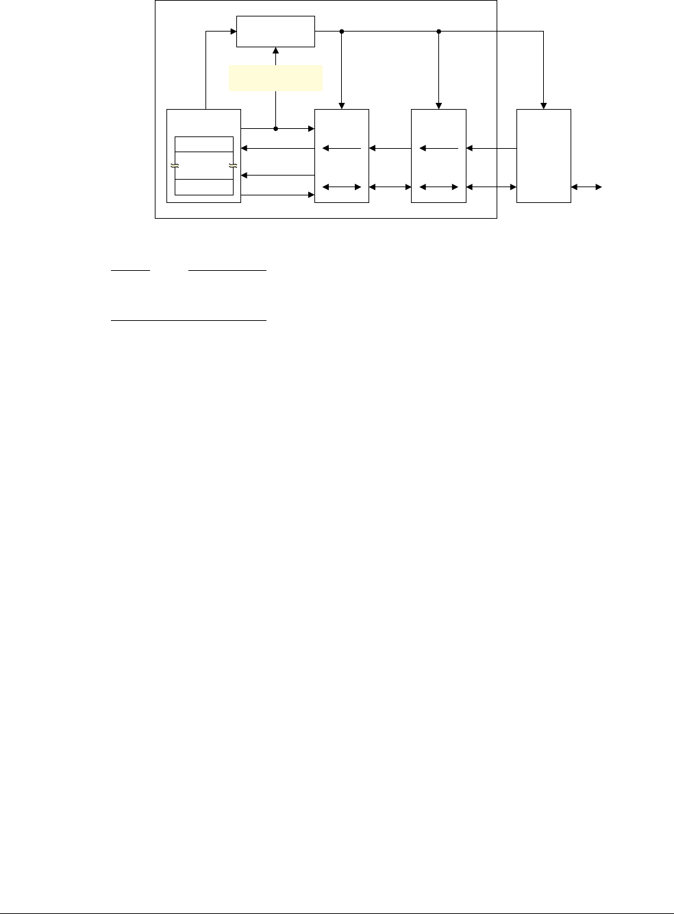
A3 Application Level Memory Model
A3.9 Caches and memory hierarchy
ARM DDI 0406C.c Copyright © 1996-1998, 2000, 2004-2012, 2014 ARM. All rights reserved. A3-157
ID051414 Non-Confidential
Figure A3-6 Multiple levels of cache in a memory hierarchy
Note
In this manual, in a hierarchical memory system, Level 1 refers to the level closest to the processor, as shown in
Figure A3-6.
A3.9.3 Implication of caches for the application programmer
In normal operation, the caches are largely invisible to the application programmer. However they can become
visible when there is a breakdown in the coherency of the caches. Such a breakdown can occur:
• when memory locations are updated by other agents in the system
• when memory updates made from the application software must be made visible to other agents in the
system.
For example:
• In a system with a DMA controller that reads memory locations that are held in the data cache of a processor,
a breakdown of coherency occurs when the processor has written new data in the data cache, but the DMA
controller reads the old data held in memory.
• In a Harvard architecture of caches, where there are separate instruction and data caches, a breakdown of
coherency occurs when new instruction data has been written into the data cache, but the instruction cache
still contains the old instruction data.
Data coherency issues
Software can ensure the data coherency of caches in the following ways:
• By not using the caches in situations where coherency issues can arise. This can be achieved by:
— using Non-cacheable or, in some cases, Write-Through Cacheable memory
— not enabling caches in the system.
• By using cache maintenance operations to manage the coherency issues in software, see About ARMv7 cache
and branch predictor maintenance functionality on page B2-1274. Many of these operations are only
available to system software.
• By using hardware coherency mechanisms to ensure the coherency of data accesses to memory for cacheable
locations by observers within the different shareability domains, see Non-shareable Normal memory on
page A3-132 and Shareable, Inner Shareable, and Outer Shareable Normal memory on page A3-133.
Processor
R15
R0
Instruction
fetch
Load
Store
Level 1
Cache
Level 2
Cache
Level 3
DRAM
SRAM
Flash
ROM Level 4
for example,
CF card, disk
Address
translation
CP15 configuration
and control
Virtual
address Physical address

A3 Application Level Memory Model
A3.9 Caches and memory hierarchy
A3-158 Copyright © 1996-1998, 2000, 2004-2012, 2014 ARM. All rights reserved. ARM DDI 0406C.c
Non-Confidential ID051414
The performance of these hardware coherency mechanisms is highly implementation-specific. In some
implementations the mechanism suppresses the ability to cache shareable locations. In other
implementations, cache coherency hardware can hold data in caches while managing coherency between
observers within the shareability domains.
Instruction coherency issues
How far ahead of the current point of execution instructions are fetched from is IMPLEMENTATION DEFINED. Such
prefetching can be either a fixed or a dynamically varying number of instructions, and can follow any or all possible
future execution paths. For all types of memory:
• the processor might have fetched the instructions from memory at any time since the last context
synchronization operation on that processor
• any instructions fetched in this way might be executed multiple times, if this is required by the execution of
the program, without being refetched from memory
Note
See Context synchronization operation for the definition of this term.
In addition, the ARM architecture does not require the hardware to ensure coherency between instruction caches
and memory, even for regions of memory with Shareable attributes. This means that for cacheable regions of
memory, an instruction cache can hold instructions that were fetched from memory before the context
synchronization operation.
If software requires coherency between instruction execution and memory, it must manage this coherency using the
ISB and DSB memory barriers and cache maintenance operations, see Ordering of cache and branch predictor
maintenance operations on page B2-1289. Many of these operations are only available to system software.
A3.9.4 Preloading caches
The ARM architecture provides memory system hints
PLD
(Preload Data),
PLDW
(Preload Data with intent to write),
and
PLI
(Preload Instruction) to permit software to communicate the expected use of memory locations to the
hardware. The memory system can respond by taking actions that are expected to speed up the memory accesses if
and when they do occur. The effect of these memory system hints is IMPLEMENTATION DEFINED. Typically,
implementations use this information to bring the data or instruction locations into caches that have faster access
times than normal memory.
The Preload instructions are hints, and so implementations can treat them as NOPs without affecting the functional
behavior of the device. The instructions do not generate synchronous Data Abort exceptions, but the memory system
operations might, under exceptional circumstances, generate asynchronous aborts. For more information, see Data
Abort exception on page B1-1215.
For more information about the operation of these instructions see Behavior of Preload Data (PLD, PLDW) and
Preload Instruction (PLI) with caches on page B2-1269.
Hardware implementations can provide other implementation-specific mechanisms to fetch memory locations in
the cache. These must comply with the general cache behavior described in Cache behavior on page B2-1267.

ARM DDI 0406C.c Copyright © 1996-1998, 2000, 2004-2012, 2014 ARM. All rights reserved. A4-159
ID051414 Non-Confidential
Chapter A4
The Instruction Sets
This chapter describes the ARM and Thumb instruction sets. It contains the following sections:
•About the instruction sets on page A4-160
•Unified Assembler Language on page A4-162
•Branch instructions on page A4-164
•Data-processing instructions on page A4-165
•Status register access instructions on page A4-174
•Load/store instructions on page A4-175
•Load/store multiple instructions on page A4-177
•Miscellaneous instructions on page A4-178
•Exception-generating and exception-handling instructions on page A4-179
•Coprocessor instructions on page A4-180
•Advanced SIMD and Floating-point load/store instructions on page A4-181
•Advanced SIMD and Floating-point register transfer instructions on page A4-183
•Advanced SIMD data-processing instructions on page A4-184
•Floating-point data-processing instructions on page A4-191.

A4 The Instruction Sets
A4.1 About the instruction sets
A4-160 Copyright © 1996-1998, 2000, 2004-2012, 2014 ARM. All rights reserved. ARM DDI 0406C.c
Non-Confidential ID051414
A4.1 About the instruction sets
ARMv7 contains two main instruction sets, the ARM and Thumb instruction sets. Much of the functionality
available is identical in the two instruction sets. This chapter describes the functionality available in the instruction
sets, and the Unified Assembler Language (UAL) that can be assembled to either instruction set.
The two instruction sets differ in how instructions are encoded:
• Thumb instructions are either 16-bit or 32-bit, and are aligned on a two-byte boundary. 16-bit and 32-bit
instructions can be intermixed freely. Many common operations are most efficiently executed using 16-bit
instructions. However:
— Most 16-bit instructions can only access the first eight of the ARM core registers, R0-R7. These are
called the low registers. A small number of 16-bit instructions can also access the high registers,
R8-R15.
— Many operations that would require two or more 16-bit instructions can be more efficiently executed
with a single 32-bit instruction.
— All 32-bit instructions can access all of the ARM core registers, R0-R15.
• ARM instructions are always 32-bit, and are aligned on a four-byte boundary.
The ARM and Thumb instruction sets can interwork freely, that is, different procedures can be compiled or
assembled to different instruction sets, and still be able to call each other efficiently.
ThumbEE is a variant of the Thumb instruction set that is designed as a target for dynamically generated code.
However, it cannot interwork freely with the ARM and Thumb instruction sets.
In an implementation that includes a non-trivial Jazelle extension, the processor can execute some Java bytecodes
in hardware. For more information see Jazelle direct bytecode execution support on page A2-97. The processor
executes Java bytecodes when it is in Jazelle state. However, this execution is outside the scope of this manual.
See:
•Chapter A5 ARM Instruction Set Encoding for encoding details of the ARM instruction set
•Chapter A6 Thumb Instruction Set Encoding for encoding details of the Thumb instruction set
•Chapter A8 Instruction Descriptions for detailed descriptions of the instructions
•Chapter A9 The ThumbEE Instruction Set for encoding details of the ThumbEE instruction set.
A4.1.1 Changing between Thumb state and ARM state
A processor in ARM state executes ARM instructions, and a processor in Thumb state executes Thumb instructions.
A processor in Thumb state can enter ARM state by executing any of the following instructions:
BX
,
BLX
, or an
LDR
or
LDM
that loads the PC.
A processor in ARM state can enter Thumb state by executing any of the same instructions.
In ARMv7, a processor in ARM state can also enter Thumb state by executing an
ADC
,
ADD
,
AND
,
ASR
,
BIC
,
EOR
,
LSL
,
LSR
,
MOV
,
MVN
,
ORR
,
ROR
,
RRX
,
RSB
,
RSC
,
SBC
, or
SUB
instruction that has the PC as destination register and does not set the
condition flags.
Note
This permits calls and returns between ARM code written for ARMv4 processors and Thumb code running on
ARMv7 processors to function correctly. ARM recommends that new software uses
BX
or
BLX
instructions instead.
In particular, ARM recommends that software uses
BX LR
to return from a procedure, not
MOV PC, LR
.
The target instruction set is either encoded directly in the instruction (for the immediate offset version of
BLX
), or is
held as bit[0] of an interworking address. For details, see the description of the
BXWritePC()
function in Pseudocode
details of operations on ARM core registers on page A2-47.
Exception entries and returns can also change between ARM and Thumb states. For details see Exception handling
on page B1-1165.

A4 The Instruction Sets
A4.1 About the instruction sets
ARM DDI 0406C.c Copyright © 1996-1998, 2000, 2004-2012, 2014 ARM. All rights reserved. A4-161
ID051414 Non-Confidential
A4.1.2 Conditional execution
In the ARM and Thumb instruction sets, most instructions can be conditionally executed.
In the ARM instruction set, conditional execution means that an instruction only has its normal effect on the
programmers’ model operation, memory and coprocessors if the N, Z, C and V condition flags in the APSR satisfy
a condition specified by the
cond
field in the instruction encoding. If the flags do not satisfy this condition, the
instruction acts as a NOP, that is, execution advances to the next instruction as normal, including any relevant checks
for exceptions being taken, but has no other effect.
In the Thumb instruction set, different mechanisms control conditional execution:
• For the following Thumb encodings, conditional execution is controlled in a similar way to the ARM
instructions:
— A 16-bit conditional branch instruction encoding, with a branch range of –256 to +254 bytes. Before
ARMv6T2, this was the only mechanism for conditional execution in Thumb code.
— A 32-bit conditional branch instruction encoding, with a branch range of approximately ±1MB.
For more information about these encodings see B on page A8-334.
• The
CBZ
and
CBNZ
instructions, Compare and Branch on Zero and Compare and Branch on Nonzero, are 16-bit
conditional instructions with a branch range of +4 to +130 bytes. For details see CBNZ, CBZ on page A8-356.
• The 16-bit If-Then instruction makes up to four following instructions conditional, and can make most other
Thumb instructions conditional. For details see IT on page A8-390. The instructions that are made
conditional by an
IT
instruction are called its IT block. For any IT block, either:
— all instructions have the same condition
— some instructions have one condition, and the other instructions have the inverse condition.
ARM deprecates the conditional execution of any instruction encoding provided by the Advanced SIMD Extension
that is not also provided by the Floating-point (VFP) Extension, and strongly recommends that any such instruction
that can be conditionally executed is specified with the
<c>
field omitted or set to
AL
. For more information, see
Conditional execution on page A8-288.
For more information about conditional execution see Conditional execution on page A8-288.
A4.1.3 Writing to the PC
Writing to the PC on page A2-46 gives an overview of instructions that write to the PC, including the required
behavior of these writes. This information is also given in the appropriate sections of this chapter.
A4.1.4 Permanently UNDEFINED encodings
All versions of the ARM architecture define some encodings as permanently UNDEFINED. That is, permanently
UNDEFINED encodings are defined in the ARM instruction set encodings, and in the 16-bit and 32-bit Thumb
encodings. From issue C.a of this manual, ARM defines an assembler mnemonic for the unconditional forms of
these instructions, see UDF on page A8-758.

A4 The Instruction Sets
A4.2 Unified Assembler Language
A4-162 Copyright © 1996-1998, 2000, 2004-2012, 2014 ARM. All rights reserved. ARM DDI 0406C.c
Non-Confidential ID051414
A4.2 Unified Assembler Language
This document uses the ARM Unified Assembler Language (UAL). This assembly language syntax provides a
canonical form for all ARM and Thumb instructions.
UAL describes the syntax for the mnemonic and the operands of each instruction. In addition, it assumes that
instructions and data items can be given labels. It does not specify the syntax to be used for labels, nor what
assembler directives and options are available. See your assembler documentation for these details.
Most earlier ARM assembly language mnemonics are still supported as synonyms, as described in the instruction
details.
Note
Most earlier Thumb assembly language mnemonics are not supported. For more information, see Appendix D8
Legacy Instruction Mnemonics.
UAL includes instruction selection rules that specify which instruction encoding is selected when more than one
can provide the required functionality. For example, both 16-bit and 32-bit encodings exist for an
ADD R0, R1, R2
instruction. The most common instruction selection rule is that when both a 16-bit encoding and a 32-bit encoding
are available, the 16-bit encoding is selected, to optimize code density.
Syntax options exist to override the normal instruction selection rules and ensure that a particular encoding is
selected. These are useful when disassembling code, to ensure that subsequent assembly produces the original code,
and in some other situations.
A4.2.1 Conditional instructions
For maximum portability of UAL assembly language between the ARM and Thumb instruction sets, ARM
recommends that:
•
IT
instructions are written before conditional instructions in the correct way for the Thumb instruction set.
• When assembling to the ARM instruction set, assemblers check that any
IT
instructions are correct, but do
not generate any code for them.
Although other Thumb instructions are unconditional, all instructions that are made conditional by an
IT
instruction
must be written with a condition. These conditions must match the conditions imposed by the
IT
instruction. For
example, an
ITTEE EQ
instruction imposes the
EQ
condition on the first two following instructions, and the
NE
condition on the next two. Those four instructions must be written with
EQ
,
EQ
,
NE
and
NE
conditions respectively.
Some instructions cannot be made conditional by an
IT
instruction. Some instructions can be conditional if they are
the last instruction in the IT block, but not otherwise.
The branch instruction encodings that include a condition code field cannot be made conditional by an
IT
instruction. If the assembler syntax indicates a conditional branch that correctly matches a preceding
IT
instruction,
it is assembled using a branch instruction encoding that does not include a condition code field.
A4.2.2 Use of labels in UAL instruction syntax
The UAL syntax for some instructions includes the label of an instruction or a literal data item that is at a fixed offset
from the instruction being specified. The assembler must:
1. Calculate the
PC
or
Align(PC, 4)
value of the instruction. The
PC
value of an instruction is its address plus 4
for a Thumb instruction, or plus 8 for an ARM instruction. The
Align(PC, 4)
value of an instruction is its
PC
value ANDed with
0xFFFFFFFC
to force it to be word-aligned. There is no difference between the
PC
and
Align(PC, 4)
values for an ARM instruction, but there can be for a Thumb instruction.
2. Calculate the offset from the
PC
or
Align(PC, 4)
value of the instruction to the address of the labelled
instruction or literal data item.
3. Assemble a PC-relative encoding of the instruction, that is, one that reads its
PC
or
Align(PC, 4)
value and
adds the calculated offset to form the required address.

A4 The Instruction Sets
A4.2 Unified Assembler Language
ARM DDI 0406C.c Copyright © 1996-1998, 2000, 2004-2012, 2014 ARM. All rights reserved. A4-163
ID051414 Non-Confidential
Note
For instructions that can encode a subtraction operation, if the instruction cannot encode the calculated offset
but can encode minus the calculated offset, the instruction encoding specifies a subtraction of minus the
calculated offset.
The syntax of the following instructions includes a label:
•
B
,
BL
, and
BLX
(immediate). The assembler syntax for these instructions always specifies the label of the
instruction that they branch to. Their encodings specify a sign-extended immediate offset that is added to the
PC
value of the instruction to form the target address of the branch.
•
CBNZ
and
CBZ
. The assembler syntax for these instructions always specifies the label of the instruction that they
branch to. Their encodings specify a zero-extended immediate offset that is added to the
PC
value of the
instruction to form the target address of the branch. They do not support backward branches.
•
LDC
,
LDC2
,
LDR
,
LDRB
,
LDRD
,
LDRH
,
LDRSB
,
LDRSH
,
PLD
,
PLDW
,
PLI
, and
VLDR
. The normal assembler syntax of these
load instructions can specify the label of a literal data item that is to be loaded. The encodings of these
instructions specify a zero-extended immediate offset that is either added to or subtracted from the
Align(PC, 4)
value of the instruction to form the address of the data item. A few such encodings perform a
fixed addition or a fixed subtraction and must only be used when that operation is required, but most contain
a bit that specifies whether the offset is to be added or subtracted.
When the assembler calculates an offset of 0 for the normal syntax of these instructions, it must assemble an
encoding that adds 0 to the
Align(PC, 4)
value of the instruction. Encodings that subtract 0 from the
Align(PC,
4)
value cannot be specified by the normal syntax.
There is an alternative syntax for these instructions that specifies the addition or subtraction and the
immediate offset explicitly. In this syntax, the label is replaced by
[PC, #+/-<imm>]
, where:
+/-
Is
+
or omitted to specify that the immediate offset is to be added to the
Align(PC, 4)
value, or
-
if it is to be subtracted.
<imm>
Is the immediate offset.
This alternative syntax makes it possible to assemble the encodings that subtract 0 from the
Align(PC, 4)
value, and to disassemble them to a syntax that can be re-assembled correctly.
•
ADR
. The normal assembler syntax for this instruction can specify the label of an instruction or literal data item
whose address is to be calculated. Its encoding specifies a zero-extended immediate offset that is either added
to or subtracted from the
Align(PC, 4)
value of the instruction to form the address of the data item, and some
opcode bits that determine whether it is an addition or subtraction.
When the assembler calculates an offset of 0 for the normal syntax of this instruction, it must assemble the
encoding that adds 0 to the
Align(PC, 4)
value of the instruction. The encoding that subtracts 0 from the
Align(PC, 4)
value cannot be specified by the normal syntax.
There is an alternative syntax for this instruction that specifies the addition or subtraction and the immediate
value explicitly, by writing them as additions
ADD <Rd>, PC, #<imm>
or subtractions
SUB <Rd>, PC, #<imm>
.
This alternative syntax makes it possible to assemble the encoding that subtracts 0 from the
Align(PC, 4)
value, and to disassemble it to a syntax that can be re-assembled correctly.
Note
ARM recommends that where possible, software avoids using:
• The alternative syntax for the
ADR
,
LDC
,
LDC2
,
LDR
,
LDRB
,
LDRD
,
LDRH
,
LDRSB
,
LDRSH
,
PLD
,
PLI
,
PLDW
, and
VLDR
instructions.
• The encodings of these instructions that subtract 0 from the
Align(PC, 4)
value.

A4 The Instruction Sets
A4.3 Branch instructions
A4-164 Copyright © 1996-1998, 2000, 2004-2012, 2014 ARM. All rights reserved. ARM DDI 0406C.c
Non-Confidential ID051414
A4.3 Branch instructions
Table A4-1 summarizes the branch instructions in the ARM and Thumb instruction sets. In addition to providing
for changes in the flow of execution, some branch instructions can change instruction set.
Branches to loaded and calculated addresses can be performed by
LDR
,
LDM
and data-processing instructions. For
details see Load/store instructions on page A4-175, Load/store multiple instructions on page A4-177, Standard
data-processing instructions on page A4-165, and Shift instructions on page A4-167.
In addition to the branch instructions shown in Table A4-1:
• In the ARM instruction set, a data-processing instruction that targets the PC behaves as a branch instruction.
For more information, see Data-processing instructions on page A4-165.
• In the ARM and Thumb instruction sets, a load instruction that targets the PC behaves as a branch instruction.
For more information, see Load/store instructions on page A4-175.
Table A4-1 Branch instructions
Instruction See Range, Thumb Range, ARM
Branch to target address B on page A8-334 ±16MB ±32MB
Compare and Branch on Nonzero,
Compare and Branch on Zero
CBNZ, CBZ on page A8-356 0-126 bytes a
Call a subroutine
Call a subroutine, change instruction setb
BL, BLX (immediate) on
page A8-348
±16MB
±16MB
±32MB
±32MB
Call a subroutine, optionally change instruction set BLX (register) on page A8-350 Any Any
Branch to target address, change instruction set BX on page A8-352 Any Any
Change to Jazelle state BXJ on page A8-354 --
Table Branch (byte offsets)
Table Branch (halfword offsets)
TBB, TBH on page A8-736 0-510 bytes
0-131070 bytes
a
a. These instructions do not exist in the ARM instruction set.
b. The range is determined by the instruction set of the
BLX
instruction, not of the instruction it branches to.

A4 The Instruction Sets
A4.4 Data-processing instructions
ARM DDI 0406C.c Copyright © 1996-1998, 2000, 2004-2012, 2014 ARM. All rights reserved. A4-165
ID051414 Non-Confidential
A4.4 Data-processing instructions
Core data-processing instructions belong to one of the following groups:
•Standard data-processing instructions.
These instructions perform basic data-processing operations, and share a common format with some
variations.
•Shift instructions on page A4-167.
•Multiply instructions on page A4-167.
•Saturating instructions on page A4-169.
•Saturating addition and subtraction instructions on page A4-169.
•Packing and unpacking instructions on page A4-170.
•Parallel addition and subtraction instructions on page A4-171.
•Divide instructions on page A4-172.
•Miscellaneous data-processing instructions on page A4-173.
For extension data-processing instructions, see Advanced SIMD data-processing instructions on page A4-184 and
Floating-point data-processing instructions on page A4-191.
A4.4.1 Standard data-processing instructions
These instructions generally have a destination register Rd, a first operand register Rn, and a second operand. The
second operand can be another register Rm, or an immediate constant.
If the second operand is an immediate constant, it can be:
• Encoded directly in the instruction.
•A modified immediate constant that uses 12 bits of the instruction to encode a range of constants. Thumb and
ARM instructions have slightly different ranges of modified immediate constants. For more information, see
Modified immediate constants in Thumb instructions on page A6-232 and Modified immediate constants in
ARM instructions on page A5-200.
If the second operand is another register, it can optionally be shifted in any of the following ways:
LSL
Logical Shift Left by 1-31 bits.
LSR
Logical Shift Right by 1-32 bits.
ASR
Arithmetic Shift Right by 1-32 bits.
ROR
Rotate Right by 1-31 bits.
RRX
Rotate Right with Extend. For details see Shift and rotate operations on page A2-41.
In Thumb code, the amount to shift by is always a constant encoded in the instruction. In ARM code, the amount to
shift by is either a constant encoded in the instruction, or the value of a register, Rs.
For instructions other than
CMN
,
CMP
,
TEQ
, and
TST
, the result of the data-processing operation is placed in the
destination register. In the ARM instruction set, the destination register can be the PC, causing the result to be treated
as a branch address. In the Thumb instruction set, this is only permitted for some 16-bit forms of the
ADD
and
MOV
instructions.
These instructions can optionally set the condition flags, according to the result of the operation. If they do not set
the flags, existing flag settings from a previous instruction are preserved.
Table A4-2 on page A4-166 summarizes the main data-processing instructions in the Thumb and ARM instruction
sets. Generally, each of these instructions is described in three sections in Chapter A8 Instruction Descriptions, one
section for each of the following:
•
INSTRUCTION
(immediate) where the second operand is a modified immediate constant.
•
INSTRUCTION
(register) where the second operand is a register, or a register shifted by a constant.
•
INSTRUCTION
(register-shifted register) where the second operand is a register shifted by a value obtained from
another register. These are only available in the ARM instruction set.

A4 The Instruction Sets
A4.4 Data-processing instructions
A4-166 Copyright © 1996-1998, 2000, 2004-2012, 2014 ARM. All rights reserved. ARM DDI 0406C.c
Non-Confidential ID051414
Table A4-2 Standard data-processing instructions
Instruction Mnemonic Notes
Add with Carry
ADC
-
Add
ADD
Thumb instruction set permits use of a modified immediate constant or a
zero-extended 12-bit immediate constant.
Form PC-relative Address
ADR
First operand is the PC. Second operand is an immediate constant. Thumb instruction
set uses a zero-extended 12-bit immediate constant. Operation is an addition or a
subtraction.
Bitwise AND
AND
-
Bitwise Bit Clear
BIC
-
Compare Negative
CMN
Sets flags. Like
ADD
but with no destination register.
Compare
CMP
Sets flags. Like
SUB
but with no destination register.
Bitwise Exclusive OR
EOR
-
Copy operand to destination
MOV
Has only one operand, with the same options as the second operand in most of these
instructions. If the operand is a shifted register, the instruction is an
LSL
,
LSR
,
ASR
, or
ROR
instruction instead. For details see Shift instructions on page A4-167.
The ARM and Thumb instruction sets permit use of a modified immediate constant
or a zero-extended 16-bit immediate constant.
Bitwise NOT
MVN
Has only one operand, with the same options as the second operand in most of these
instructions.
Bitwise OR NOT
ORN
Not available in the ARM instruction set.
Bitwise OR
ORR
-
Reverse Subtract
RSB
Subtracts first operand from second operand. This permits subtraction from constants
and shifted registers.
Reverse Subtract with Carry
RSC
Not available in the Thumb instruction set.
Subtract with Carry
SBC
-
Subtract
SUB
Thumb instruction set permits use of a modified immediate constant or a
zero-extended 12-bit immediate constant.
Test Equivalence
TEQ
Sets flags. Like
EOR
but with no destination register.
Test
TST
Sets flags. Like
AND
but with no destination register.

A4 The Instruction Sets
A4.4 Data-processing instructions
ARM DDI 0406C.c Copyright © 1996-1998, 2000, 2004-2012, 2014 ARM. All rights reserved. A4-167
ID051414 Non-Confidential
A4.4.2 Shift instructions
Table A4-3 lists the shift instructions in the ARM and Thumb instruction sets.
In the ARM instruction set only, the destination register of these instructions can be the PC, causing the result to be
treated as an address to branch to.
A4.4.3 Multiply instructions
These instructions can operate on signed or unsigned quantities. In some types of operation, the results are same
whether the operands are signed or unsigned.
•Table A4-4 summarizes the multiply instructions where there is no distinction between signed and unsigned
quantities.
The least significant 32 bits of the result are used. More significant bits are discarded.
•Table A4-5 on page A4-168 summarizes the signed multiply instructions.
•Table A4-6 on page A4-168 summarizes the unsigned multiply instructions.
Table A4-3 Shift instructions
Instruction See
Arithmetic Shift Right ASR (immediate) on page A8-330
Arithmetic Shift Right ASR (register) on page A8-332
Logical Shift Left LSL (immediate) on page A8-468
Logical Shift Left LSL (register) on page A8-470
Logical Shift Right LSR (immediate) on page A8-472
Logical Shift Right LSR (register) on page A8-474
Rotate Right ROR (immediate) on page A8-568
Rotate Right ROR (register) on page A8-570
Rotate Right with Extend RRX on page A8-572
Table A4-4 General multiply instructions
Instruction See Operation (number of bits)
Multiply Accumulate MLA on page A8-480 32 = 32 + 32 × 32
Multiply and Subtract MLS on page A8-482 32 = 32 – 32 × 32
Multiply MUL on page A8-502 32 = 32 × 32

A4 The Instruction Sets
A4.4 Data-processing instructions
A4-168 Copyright © 1996-1998, 2000, 2004-2012, 2014 ARM. All rights reserved. ARM DDI 0406C.c
Non-Confidential ID051414
Table A4-5 Signed multiply instructions
Instruction See Operation (number of bits)
Signed Multiply Accumulate (halfwords) SMLABB, SMLABT, SMLATB, SMLATT
on page A8-620
32 = 32 + 16 × 16
Signed Multiply Accumulate Dual SMLAD on page A8-622 32 = 32 + 16 × 16 + 16 × 16
Signed Multiply Accumulate Long SMLAL on page A8-624 64 = 64 + 32 × 32
Signed Multiply Accumulate Long (halfwords) SMLALBB, SMLALBT, SMLALTB,
SMLALTT on page A8-626
64 = 64 + 16 × 16
Signed Multiply Accumulate Long Dual SMLALD on page A8-628 64 = 64 + 16 × 16 + 16 × 16
Signed Multiply Accumulate (word by halfword) SMLAWB, SMLAWT on page A8-630 32 = 32 + 32 × 16 a
Signed Multiply Subtract Dual SMLSD on page A8-632 32 = 32 + 16 × 16 – 16 × 16
Signed Multiply Subtract Long Dual SMLSLD on page A8-634 64 = 64 + 16 × 16 – 16 × 16
Signed Most Significant Word Multiply Accumulate SMMLA on page A8-636 32 = 32 + 32 × 32 b
Signed Most Significant Word Multiply Subtract SMMLS on page A8-638 32 = 32 – 32 × 32 b
Signed Most Significant Word Multiply SMMUL on page A8-640 32 = 32 × 32 b
Signed Dual Multiply Add SMUAD on page A8-642 32 = 16 × 16 + 16 × 16
Signed Multiply (halfwords) SMULBB, SMULBT, SMULTB, SMULTT
on page A8-644
32 = 16 × 16
Signed Multiply Long SMULL on page A8-646 64 = 32 × 32
Signed Multiply (word by halfword) SMULWB, SMULWT on page A8-648 32 = 32 × 16 a
Signed Dual Multiply Subtract SMUSD on page A8-650 32 = 16 × 16 – 16 × 16
a. The most significant 32 bits of the 48-bit product are used. Less significant bits are discarded.
b. The most significant 32 bits of the 64-bit product are used. Less significant bits are discarded.
Table A4-6 Unsigned multiply instructions
Instruction See Operation (number of bits)
Unsigned Multiply Accumulate Accumulate Long UMAAL on page A8-774 64 = 32 + 32 + 32 × 32
Unsigned Multiply Accumulate Long UMLAL on page A8-776 64 = 64 + 32 × 32
Unsigned Multiply Long UMULL on page A8-778 64 = 32 × 32

A4 The Instruction Sets
A4.4 Data-processing instructions
ARM DDI 0406C.c Copyright © 1996-1998, 2000, 2004-2012, 2014 ARM. All rights reserved. A4-169
ID051414 Non-Confidential
A4.4.4 Saturating instructions
Table A4-7 lists the saturating instructions in the ARM and Thumb instruction sets. For more information, see
Pseudocode details of saturation on page A2-44.
A4.4.5 Saturating addition and subtraction instructions
Table A4-8 lists the saturating addition and subtraction instructions in the ARM and Thumb instruction sets. For
more information, see Pseudocode details of saturation on page A2-44.
Table A4-7 Saturating instructions
Instruction See Operation
Signed Saturate SSAT on page A8-652 Saturates optionally shifted 32-bit value to selected range
Signed Saturate 16 SSAT16 on page A8-654 Saturates two 16-bit values to selected range
Unsigned Saturate USAT on page A8-796 Saturates optionally shifted 32-bit value to selected range
Unsigned Saturate 16 USAT16 on page A8-798 Saturates two 16-bit values to selected range
Table A4-8 Saturating addition and subtraction instructions
Instruction See Operation
Saturating Add QADD on page A8-540 Add, saturating result to the 32-bit signed integer range
Saturating Subtract QSUB on page A8-554 Subtract, saturating result to the 32-bit signed integer range
Saturating Double and Add QDADD on page A8-548 Doubles one value and adds a second value, saturating the doubling and
the addition to the 32-bit signed integer range
Saturating Double and
Subtract
QDSUB on page A8-550 Doubles one value and subtracts the result from a second value, saturating
the doubling and the subtraction to the 32-bit signed integer range

A4 The Instruction Sets
A4.4 Data-processing instructions
A4-170 Copyright © 1996-1998, 2000, 2004-2012, 2014 ARM. All rights reserved. ARM DDI 0406C.c
Non-Confidential ID051414
A4.4.6 Packing and unpacking instructions
Table A4-9 lists the packing and unpacking instructions in the ARM and Thumb instruction sets. These are all
available from ARMv6T2 in the Thumb instruction set, and from ARMv6 onwards in the ARM instruction set.
Table A4-9 Packing and unpacking instructions
Instruction See Operation
Pack Halfword PKH on page A8-522 Combine halfwords
Signed Extend and Add Byte SXTAB on page A8-724 Extend 8 bits to 32 and add
Signed Extend and Add Byte 16 SXTAB16 on page A8-726 Dual extend 8 bits to 16 and add
Signed Extend and Add Halfword SXTAH on page A8-728 Extend 16 bits to 32 and add
Signed Extend Byte SXTB on page A8-730 Extend 8 bits to 32
Signed Extend Byte 16 SXTB16 on page A8-732 Dual extend 8 bits to 16
Signed Extend Halfword SXTH on page A8-734 Extend 16 bits to 32
Unsigned Extend and Add Byte UXTAB on page A8-806 Extend 8 bits to 32 and add
Unsigned Extend and Add Byte 16 UXTAB16 on page A8-808 Dual extend 8 bits to 16 and add
Unsigned Extend and Add Halfword UXTAH on page A8-810 Extend 16 bits to 32 and add
Unsigned Extend Byte UXTB on page A8-812 Extend 8 bits to 32
Unsigned Extend Byte 16 UXTB16 on page A8-814 Dual extend 8 bits to 16
Unsigned Extend Halfword UXTH on page A8-816 Extend 16 bits to 32

A4 The Instruction Sets
A4.4 Data-processing instructions
ARM DDI 0406C.c Copyright © 1996-1998, 2000, 2004-2012, 2014 ARM. All rights reserved. A4-171
ID051414 Non-Confidential
A4.4.7 Parallel addition and subtraction instructions
These instructions perform additions and subtractions on the values of two registers and write the result to a
destination register, treating the register values as sets of two halfwords or four bytes. That is, they perform SIMD
additions or subtractions on the registers. They are available in ARMv6 and above.
These instructions consist of a prefix followed by a main instruction mnemonic. The prefixes are as follows:
S
Signed arithmetic modulo 28 or 216.
Q
Signed saturating arithmetic.
SH
Signed arithmetic, halving the results.
U
Unsigned arithmetic modulo 28 or 216.
UQ
Unsigned saturating arithmetic.
UH
Unsigned arithmetic, halving the results.
The main instruction mnemonics are as follows:
ADD16
Adds the top halfwords of two operands to form the top halfword of the result, and the bottom
halfwords of the same two operands to form the bottom halfword of the result.
ASX
Exchanges halfwords of the second operand, and then adds top halfwords and subtracts bottom
halfwords.
SAX
Exchanges halfwords of the second operand, and then subtracts top halfwords and adds bottom
halfwords.
SUB16
Subtracts each halfword of the second operand from the corresponding halfword of the first operand
to form the corresponding halfword of the result.
ADD8
Adds each byte of the second operand to the corresponding byte of the first operand to form the
corresponding byte of the result.
SUB8
Subtracts each byte of the second operand from the corresponding byte of the first operand to form
the corresponding byte of the result.
The instruction set permits all 36 combinations of prefix and main instruction operand, as Table A4-10 shows.
See also Advanced SIMD parallel addition and subtraction on page A4-185.
Table A4-10 Parallel addition and subtraction instructions
Main instruction Signed Saturating Signed
halving Unsigned Unsigned
saturating Unsigned
halving
ADD16
, add, two halfwords
SADD16 QADD16 SHADD16 UADD16 UQADD16 UHADD16
ASX
, add and subtract with exchange
SASX QASX SHASX UASX UQASX UHASX
SAX
, subtract and add with exchange
SSAX QSAX SHSAX USAX UQSAX UHSAX
SUB16
, subtract, two halfwords
SSUB16 QSUB16 SHSUB16 USUB16 UQSUB16 UHSUB16
ADD8
, add, four bytes
SADD8 QADD8 SHADD8 UADD8 UQADD8 UHADD8
SUB8
, subtract, four bytes
SSUB8 QSUB8 SHSUB8 USUB8 UQSUB8 UHSUB8

A4 The Instruction Sets
A4.4 Data-processing instructions
A4-172 Copyright © 1996-1998, 2000, 2004-2012, 2014 ARM. All rights reserved. ARM DDI 0406C.c
Non-Confidential ID051414
A4.4.8 Divide instructions
The ARMv7-R profile introduces support for signed and unsigned integer divide instructions, implemented in
hardware, in the Thumb instruction set. For more information see ARMv7 implementation requirements and options
for the divide instructions.
For descriptions of the instructions see:
•SDIV on page A8-600
•UDIV on page A8-760.
Note
• The Virtualization Extensions introduce the requirement for an ARMv7-A implementation to include
SDIV
and
UDIV
.
• The ARMv7-M profile also includes the
SDIV
and
UDIV
instructions.
In the ARMv7-R profile, the SCTLR.DZ bit enables divide by zero fault detection:
SCTLR.DZ == 0 Divide-by-zero returns a zero result.
SCTLR.DZ == 1
SDIV
and
UDIV
generate an Undefined Instruction exception on a divide-by-zero.
The SCTLR.DZ bit is cleared to zero on reset.
In an ARMv7-A profile implementation that supports the
SDIV
and
UDIV
instructions, divide-by-zero always returns
a zero result.
ARMv7 implementation requirements and options for the divide instructions
Any implementation of the ARMv7-R profile must include the
SDIV
and
UDIV
instructions in the Thumb instruction
set.
Any implementation of the Virtualization Extensions must include the
SDIV
and
UDIV
instructions in the Thumb and
ARM instruction sets.
In the ARMv7-R profile, the implementation of
SDIV
and
UDIV
in the ARM instruction set is OPTIONAL.
In an ARMv7-A implementation that does not include the Virtualization Extensions, the implementation of
SDIV
and
UDIV
in both instruction sets is OPTIONAL, but the architecture permits an ARMv7-A implementation to not
implement
SDIV
and
UDIV
.
Note
Previous issues of this document have stated that a VMSAv7 implementation might implement
SDIV
and
UDIV
in the
Thumb instruction set but not in the ARM instruction set. ARM strongly recommends against this implementation
option.
The ID_ISAR0.Divide_instrs field indicates the level of support for these instructions, see ID_ISAR0, Instruction
Set Attribute Register 0, VMSA on page B4-1608 or ID_ISAR0, Instruction Set Attribute Register 0, PMSA on
page B6-1856:
• a field value of
0b0001
indicates they are implemented in the Thumb instruction set
• a field value of
0b0010
indicates they are implemented in both the Thumb and ARM instruction sets.

A4 The Instruction Sets
A4.4 Data-processing instructions
ARM DDI 0406C.c Copyright © 1996-1998, 2000, 2004-2012, 2014 ARM. All rights reserved. A4-173
ID051414 Non-Confidential
A4.4.9 Miscellaneous data-processing instructions
Table A4-11 lists the miscellaneous data-processing instructions in the ARM and Thumb instruction sets.
Immediate values in these instructions are simple binary numbers.
Table A4-11 Miscellaneous data-processing instructions
Instruction See Notes
Bit Field Clear BFC on page A8-336 -
Bit Field Insert BFI on page A8-338 -
Count Leading Zeros CLZ on page A8-362 -
Move Top MOVT on page A8-491 Moves 16-bit immediate value to top
halfword. Bottom halfword unchanged.
Reverse Bits RBIT on page A8-560 -
Byte-Reverse Word REV on page A8-562 -
Byte-Reverse Packed Halfword REV16 on page A8-564 -
Byte-Reverse Signed Halfword REVSH on page A8-566 -
Signed Bit Field Extract SBFX on page A8-598 -
Select Bytes using GE flags SEL on page A8-602 -
Unsigned Bit Field Extract UBFX on page A8-756 -
Unsigned Sum of Absolute Differences USAD8 on page A8-792 -
Unsigned Sum of Absolute Differences and Accumulate USADA8 on page A8-794 -

A4 The Instruction Sets
A4.5 Status register access instructions
A4-174 Copyright © 1996-1998, 2000, 2004-2012, 2014 ARM. All rights reserved. ARM DDI 0406C.c
Non-Confidential ID051414
A4.5 Status register access instructions
The
MRS
and
MSR
instructions move the contents of the Application Program Status Register (APSR) to or from an
ARM core register, see:
•MRS on page A8-496
•MSR (immediate) on page A8-498
•MSR (register) on page A8-500.
The Application Program Status Register (APSR) on page A2-49 described the APSR.
The condition flags in the APSR are normally set by executing data-processing instructions, and normally control
the execution of conditional instructions. However, software can set the condition flags explicitly using the
MSR
instruction, and can read the current state of the condition flags explicitly using the
MRS
instruction.
At system level, software can also:
• use these instructions to access the SPSR of the current mode
•use the
CPS
instruction to change the CPSR.M field and the CPSR.{A, I, F} interrupt mask bits.
For details of the system level use of status register access instructions
CPS
,
MRS
, and
MSR
, see:
•CPS (Thumb) on page B9-1978
•CPS (ARM) on page B9-1980
•MRS on page B9-1990
•MSR (immediate) on page B9-1996
•MSR (register) on page B9-1998.
A4.5.1 Banked register access instructions
In a processor that implements the Virtualization Extensions, in all modes except User mode, the
MRS
(Banked
register) and
MSR
(Banked register) instructions move the contents of a Banked ARM core register, the SPSR, or the
ELR_hyp, to or from an ARM core register. For instruction descriptions see:
•MRS (Banked register) on page B9-1992
•MSR (Banked register) on page B9-1994.
Note
These are system level instructions.

A4 The Instruction Sets
A4.6 Load/store instructions
ARM DDI 0406C.c Copyright © 1996-1998, 2000, 2004-2012, 2014 ARM. All rights reserved. A4-175
ID051414 Non-Confidential
A4.6 Load/store instructions
Table A4-12 summarizes the ARM core register load/store instructions in the ARM and Thumb instruction sets. See
also:
•Load/store multiple instructions on page A4-177
•Advanced SIMD and Floating-point load/store instructions on page A4-181.
Load/store instructions have several options for addressing memory. For more information, see Addressing modes
on page A4-176.
A4.6.1 Loads to the PC
The
LDR
instruction can load a value into the PC. The value loaded is treated as an interworking address, as described
by the
LoadWritePC()
pseudocode function in Pseudocode details of operations on ARM core registers on
page A2-47.
A4.6.2 Halfword and byte loads and stores
Halfword and byte stores store the least significant halfword or byte from the register, to 16 or 8 bits of memory
respectively. There is no distinction between signed and unsigned stores.
Halfword and byte loads load 16 or 8 bits from memory into the least significant halfword or byte of a register.
Unsigned loads zero-extend the loaded value to 32 bits, and signed loads sign-extend the value to 32 bits.
A4.6.3 Load unprivileged and Store unprivileged
When executing at PL0, a Load unprivileged or Store unprivileged instruction operates in exactly the same way as
the corresponding ordinary load or store instruction. For example, an
LDRT
instruction executes in exactly the same
way as the equivalent
LDR
instruction. When executed at PL1, Load unprivileged and Store unprivileged instructions
behave as they would if they were executed at PL0. For example, an
LDRT
instruction executes in exactly the way
that the equivalent
LDR
instruction would execute at PL0. In particular, the instructions make unprivileged memory
accesses.
The Load unprivileged and Store unprivileged instructions are UNPREDICTABLE if executed at PL2.
For more information, see Privilege level access controls for data accesses on page A3-143.
Table A4-12 Load/store instructions
Data type Load Store Load
unprivileged Store
unprivileged Load-
Exclusive Store-
Exclusive
32-bit word
LDR STR LDRT STRT LDREX STREX
16-bit halfword -
STRH
-
STRHT
-
STREXH
16-bit unsigned halfword
LDRH
-
LDRHT - LDREXH
-
16-bit signed halfword
LDRSH
-
LDRSHT
---
8-bit byte -
STRB
-
STRBT
-
STREXB
8-bit unsigned byte
LDRB - LDRBT
-
LDREXB
-
8-bit signed byte
LDRSB
-
LDRSBT
---
Two 32-bit words
LDRD STRD
-- --
64-bit doubleword - - - -
LDREXD STREXD

A4 The Instruction Sets
A4.6 Load/store instructions
A4-176 Copyright © 1996-1998, 2000, 2004-2012, 2014 ARM. All rights reserved. ARM DDI 0406C.c
Non-Confidential ID051414
A4.6.4 Exclusive loads and stores
Exclusive loads and stores provide shared memory synchronization. For more information, see Synchronization and
semaphores on page A3-114.
A4.6.5 Addressing modes
The address for a load or store is formed from two parts: a value from a base register, and an offset.
The base register can be any one of the ARM core registers R0-R12, SP, or LR.
For loads, the base register can be the PC. This permits PC-relative addressing for position-independent code.
Instructions marked (literal) in their title in Chapter A8 Instruction Descriptions are PC-relative loads.
The offset takes one of three formats:
Immediate The offset is an unsigned number that can be added to or subtracted from the base register
value. Immediate offset addressing is useful for accessing data elements that are a fixed
distance from the start of the data object, such as structure fields, stack offsets and
input/output registers.
Register The offset is a value from an ARM core register. This register cannot be the PC. The value
can be added to, or subtracted from, the base register value. Register offsets are useful for
accessing arrays or blocks of data.
Scaled register The offset is an ARM core register, other than the PC, shifted by an immediate value, then
added to or subtracted from the base register. This means an array index can be scaled by
the size of each array element.
The offset and base register can be used in three different ways to form the memory address. The addressing modes
are described as follows:
Offset The offset is added to or subtracted from the base register to form the memory address.
Pre-indexed The offset is added to or subtracted from the base register to form the memory address. The
base register is then updated with this new address, to permit automatic indexing through an
array or memory block.
Post-indexed The value of the base register alone is used as the memory address. The offset is then added
to or subtracted from the base register. The result is stored back in the base register, to permit
automatic indexing through an array or memory block.
Note
Not every variant is available for every instruction, and the range of permitted immediate values and the options for
scaled registers vary from instruction to instruction. See Chapter A8 Instruction Descriptions for full details for
each instruction.

A4 The Instruction Sets
A4.7 Load/store multiple instructions
ARM DDI 0406C.c Copyright © 1996-1998, 2000, 2004-2012, 2014 ARM. All rights reserved. A4-177
ID051414 Non-Confidential
A4.7 Load/store multiple instructions
Load Multiple instructions load a subset, or possibly all, of the ARM core registers from memory.
Store Multiple instructions store a subset, or possibly all, of the ARM core registers to memory.
The memory locations are consecutive word-aligned words. The addresses used are obtained from a base register,
and can be either above or below the value in the base register. The base register can optionally be updated by the
total size of the data transferred.
Table A4-13 summarizes the load/store multiple instructions in the ARM and Thumb instruction sets.
When executing at PL1, variants of the
LDM
and
STM
instructions load and store User mode registers. Another
system level variant of the
LDM
instruction performs an exception return. For details of these variants, see Chapter B9
System Instructions.
A4.7.1 Loads to the PC
The
LDM
,
LDMDA
,
LDMDB
,
LDMIB
, and
POP
instructions can load a value into the PC. The value loaded is treated as an
interworking address, as described by the
LoadWritePC()
pseudocode function in Pseudocode details of operations
on ARM core registers on page A2-47.
Table A4-13 Load/store multiple instructions
Instruction See
Load Multiple, Increment After or Full Descending LDM/LDMIA/LDMFD (Thumb) on page A8-396
LDM/LDMIA/LDMFD (ARM) on page A8-398
Load Multiple, Decrement After or Full Ascending aLDMDA/LDMFA on page A8-400
Load Multiple, Decrement Before or Empty Ascending LDMDB/LDMEA on page A8-402
Load Multiple, Increment Before or Empty Descending aLDMIB/LDMED on page A8-404
Pop multiple registers off the stack bPOP (Thumb) on page A8-534
POP (ARM) on page A8-536
Push multiple registers onto the stack cPUSH on page A8-538
Store Multiple, Increment After or Empty Ascending STM (STMIA, STMEA) on page A8-664
Store Multiple, Decrement After or Empty Descending aSTMDA (STMED) on page A8-666
Store Multiple, Decrement Before or Full Descending STMDB (STMFD) on page A8-668
Store Multiple, Increment Before or Full Ascending aSTMIB (STMFA) on page A8-670
a. Not available in the Thumb instruction set.
b. This instruction is equivalent to an
LDM
instruction with the SP as base register, and base register updating.
c. This instruction is equivalent to an
STMDB
instruction with the SP as base register, and base register updating.

A4 The Instruction Sets
A4.8 Miscellaneous instructions
A4-178 Copyright © 1996-1998, 2000, 2004-2012, 2014 ARM. All rights reserved. ARM DDI 0406C.c
Non-Confidential ID051414
A4.8 Miscellaneous instructions
Table A4-14 summarizes the miscellaneous instructions in the ARM and Thumb instruction sets.
A4.8.1 The Yield instruction
In a Symmetric Multi-Threading (SMT) design, a thread can use the
YIELD
instruction to give a hint to the processor
that it is running on. The
YIELD
hint indicates that whatever the thread is currently doing is of low importance, and
so could yield. For example, the thread might be sitting in a spin-lock. A similar use might be in modifying the
arbitration priority of the snoop bus in a multiprocessor (MP) system. Defining such an instruction permits binary
compatibility between SMT and SMP systems.
ARMv7 defines a
YIELD
instruction as a specific NOP (No Operation) hint instruction.
The
YIELD
instruction has no effect in a single-threaded system, but developers of such systems can use the
instruction to flag its intended use on migration to a multiprocessor or multithreading system. Operating systems
can use
YIELD
in places where a yield hint is wanted, knowing that it will be treated as a
NOP
if there is no
implementation benefit.
Table A4-14 Miscellaneous instructions
Instruction See
Clear-Exclusive CLREX on page A8-360
Debug Hint DBG on page A8-377
Data Memory Barrier DMB on page A8-378
Data Synchronization Barrier DSB on page A8-380
Instruction Synchronization Barrier ISB on page A8-389
If-Then IT on page A8-390
No Operation NOP on page A8-510
Preload Data PLD, PLDW (immediate) on page A8-524
PLD (literal) on page A8-526
PLD, PLDW (register) on page A8-528
Preload Instruction PLI (immediate, literal) on page A8-530
PLI (register) on page A8-532
Set Endianness SETEND on page A8-604
Send Event SEV on page A8-606
Swap, Swap Byte. Deprecated. a
a. Use Load/Store-Exclusive instructions instead, see Load/store instructions on page A4-175.
SWP, SWPB on page A8-722
Wait For Event WFE on page A8-1104
Wait For Interrupt WFI on page A8-1106
Yield YIELD on page A8-1108

A4 The Instruction Sets
A4.9 Exception-generating and exception-handling instructions
ARM DDI 0406C.c Copyright © 1996-1998, 2000, 2004-2012, 2014 ARM. All rights reserved. A4-179
ID051414 Non-Confidential
A4.9 Exception-generating and exception-handling instructions
The following instructions are intended specifically to cause a synchronous processor exception to occur:
• The
SVC
instruction generates a Supervisor Call exception. For more information, see Supervisor Call (SVC)
exception on page B1-1210.
• The Breakpoint instruction
BKPT
provides software breakpoints. For more information, see About debug
events on page C3-2038.
• In a processor that implements the Security Extensions, when executing at PL1 or higher, the
SMC
instruction
generates a Secure Monitor Call exception. For more information, see Secure Monitor Call (SMC) exception
on page B1-1211.
• In a processor that implements the Virtualization Extensions, in software executing in a Non-secure PL1
mode, the
HVC
instruction generates a Hypervisor Call exception. For more information, see Hypervisor Call
(HVC) exception on page B1-1212.
For an exception taken to a PL1 mode:
• The system level variants of the
SUBS
and
LDM
instructions perform a return from an exception.
Note
The variants of
SUBS
include
MOVS
. See the references to
SUBS PC, LR
in Table A4-15 for more information.
• From ARMv6, the
SRS
instruction can be used near the start of the handler, to store return information. The
RFE
instruction can then perform a return from the exception using the stored return information.
In a processor that implements the Virtualization Extensions, the
ERET
instruction performs a return from an
exception taken to Hyp mode.
For more information, see Exception return on page B1-1194.
Table A4-15 summarizes the instructions, in the ARM and Thumb instruction sets, for generating or handling an
exception. Except for
BKPT
and
SVC
, these are system level instructions.
Table A4-15 Exception-generating and exception-handling instructions
Instruction See
Supervisor Call SVC (previously SWI) on page A8-720
Breakpoint BKPT on page A8-346
Secure Monitor Call SMC (previously SMI) on page B9-2002
Return From Exception RFE on page B9-2000
Subtract (exception return) SUBS PC, LR (Thumb) on page B9-2010
SUBS PC, LR and related instructions (ARM) on page B9-2012
Hypervisor Call HVC on page B9-1984
Exception Return ERET on page B9-1982
Load Multiple (exception return) LDM (exception return) on page B9-1986
Store Return State SRS (Thumb) on page B9-2004
SRS (ARM) on page B9-2006

A4 The Instruction Sets
A4.10 Coprocessor instructions
A4-180 Copyright © 1996-1998, 2000, 2004-2012, 2014 ARM. All rights reserved. ARM DDI 0406C.c
Non-Confidential ID051414
A4.10 Coprocessor instructions
There are three types of instruction for communicating with coprocessors. These permit the processor to:
• Initiate a coprocessor data-processing operation. For details see CDP, CDP2 on page A8-358.
• Transfer ARM core registers to and from coprocessor registers. For details, see:
—MCR, MCR2 on page A8-476
—MCRR, MCRR2 on page A8-478
—MRC, MRC2 on page A8-492
—MRRC, MRRC2 on page A8-494.
• Load or store the values of coprocessor registers. For details, see:
—LDC, LDC2 (immediate) on page A8-392
—LDC, LDC2 (literal) on page A8-394
—STC, STC2 on page A8-662.
The instruction set distinguishes up to 16 coprocessors with a 4-bit field in each coprocessor instruction, so each
coprocessor is assigned a particular number.
Note
One coprocessor can use more than one of the 16 numbers if a large coprocessor instruction set is required.
Coprocessors 10 and 11 are used, together, for Floating-point Extension and some Advanced SIMD Extension
functionality. There are different instructions for accessing these coprocessors, of similar types to the instructions
for the other coprocessors, that is, to:
• Initiate a coprocessor data-processing operation. For details see Floating-point data-processing instructions
on page A4-191.
• Transfer ARM core registers to and from coprocessor registers. For details, see Advanced SIMD and
Floating-point register transfer instructions on page A4-183.
• Load or store the values of coprocessor registers. For details, see Advanced SIMD and Floating-point
load/store instructions on page A4-181.
Coprocessors execute the same instruction stream as the processor, ignoring non-coprocessor instructions and
coprocessor instructions for other coprocessors. Coprocessor instructions that cannot be executed by any
coprocessor hardware cause an Undefined Instruction exception.
Coprocessors 8, 9, 12, and 13 are reserved for future use by ARM. Any coprocessor access instruction attempting
to access one of these coprocessors is UNDEFINED.
For more information about specific coprocessors see Coprocessor support on page A2-94.

A4 The Instruction Sets
A4.11 Advanced SIMD and Floating-point load/store instructions
ARM DDI 0406C.c Copyright © 1996-1998, 2000, 2004-2012, 2014 ARM. All rights reserved. A4-181
ID051414 Non-Confidential
A4.11 Advanced SIMD and Floating-point load/store instructions
Table A4-16 summarizes the extension register load/store instructions in the Advanced SIMD and Floating-point
(VFP) instruction sets.
Advanced SIMD also provides instructions for loading and storing multiple elements, or structures of elements, see
Element and structure load/store instructions.
A4.11.1 Element and structure load/store instructions
Table A4-17 shows the element and structure load/store instructions available in the Advanced SIMD instruction
set. Loading and storing structures of more than one element automatically de-interleaves or interleaves the
elements, see Figure A4-1 on page A4-182 for an example of de-interleaving. Interleaving is the inverse process.
Table A4-16 Extension register load/store instructions
Instruction See Operation
Vector Load Multiple VLDM on page A8-922 Load 1-16 consecutive 64-bit registers, Advanced SIMD and Floating-point
Load 1-16 consecutive 32-bit registers, Floating-point only
Vector Load Register VLDR on page A8-924 Load one 64-bit register, Advanced SIMD and Floating-point
Load one 32-bit register, Floating-point only
Vector Store Multiple VSTM on page A8-1080 Store 1-16 consecutive 64-bit registers, Advanced SIMD and Floating-point
Store 1-16 consecutive 32-bit registers, Floating-point only
Vector Store Register VSTR on page A8-1082 Store one 64-bit register, Advanced SIMD and Floating-point
Store one 32-bit register, Floating-point only
Table A4-17 Element and structure load/store instructions
Instruction See
Load single element
Multiple elements VLD1 (multiple single elements) on page A8-898
To one lane VLD1 (single element to one lane) on page A8-900
To all lanes VLD1 (single element to all lanes) on page A8-902
Load 2-element structure
Multiple structures VLD2 (multiple 2-element structures) on page A8-904
To one lane VLD2 (single 2-element structure to one lane) on page A8-906
To all lanes VLD2 (single 2-element structure to all lanes) on page A8-908
Load 3-element structure
Multiple structures VLD3 (multiple 3-element structures) on page A8-910
To one lane VLD3 (single 3-element structure to one lane) on page A8-912
To all lanes VLD3 (single 3-element structure to all lanes) on page A8-914
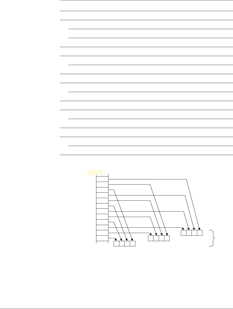
A4 The Instruction Sets
A4.11 Advanced SIMD and Floating-point load/store instructions
A4-182 Copyright © 1996-1998, 2000, 2004-2012, 2014 ARM. All rights reserved. ARM DDI 0406C.c
Non-Confidential ID051414
Figure A4-1 shows the de-interleaving of a
VLD3.16
(multiple 3-element structures) instruction:
Figure A4-1 De-interleaving an array of 3-element structures
Figure A4-1 shows the
VLD3.16
instruction operating to three 64-bit registers that comprise four 16-bit elements:
• Different instructions in this group would produce similar figures, but operate on different numbers of
registers. For example,
VLD4
and
VST4
instructions operate on four registers.
• Different element sizes would produce similar figures but with 8-bit or 32-bit elements.
• These instructions operate only on doubleword (64-bit) registers.
Load 4-element structure
Multiple structures VLD4 (multiple 4-element structures) on page A8-916
To one lane VLD4 (single 4-element structure to one lane) on page A8-918
To all lanes VLD4 (single 4-element structure to all lanes) on page A8-920
Store single element
Multiple elements VST1 (multiple single elements) on page A8-1064
From one lane VST1 (single element from one lane) on page A8-1066
Store 2-element structure
Multiple structures VST2 (multiple 2-element structures) on page A8-1068
From one lane VST2 (single 2-element structure from one lane) on page A8-1070
Store 3-element structure
Multiple structures VST3 (multiple 3-element structures) on page A8-1072
From one lane VST3 (single 3-element structure from one lane) on page A8-1074
Store 4-element structure
Multiple structures VST4 (multiple 4-element structures) on page A8-1076
From one lane VST4 (single 4-element structure from one lane) on page A8-1078
Table A4-17 Element and structure load/store instructions (continued)
Instruction See
A[0].x
A[0].y
A[0].z
A[1].x
A[1].y
A[1].z
A[2].x
A[2].y
A[2].z
A[3].x
A[3].y
A[3].z
Memory
Z3Z2Z1Z0D2
Y3Y1D1
X3X2X1D0
Y2Y0
X0
Registers
A is a packed array of
3-element structures.
Each element is a 16-bit
halfword.

A4 The Instruction Sets
A4.12 Advanced SIMD and Floating-point register transfer instructions
ARM DDI 0406C.c Copyright © 1996-1998, 2000, 2004-2012, 2014 ARM. All rights reserved. A4-183
ID051414 Non-Confidential
A4.12 Advanced SIMD and Floating-point register transfer instructions
Table A4-18 summarizes the extension register transfer instructions in the Advanced SIMD and Floating-point
(VFP) instruction sets. These instructions transfer data from ARM core registers to extension registers, or from
extension registers to ARM core registers.
Advanced SIMD vectors, and single-precision and double-precision Floating-point registers, are all views of the
same extension register set. For details see Advanced SIMD and Floating-point Extension registers on page A2-56.
Table A4-18 Extension register transfer instructions
Instruction See
Copy element from ARM core register to every element of Advanced SIMD vector VDUP (ARM core register) on page A8-886
Copy byte, halfword, or word from ARM core register to extension register VMOV (ARM core register to scalar) on
page A8-940
Copy byte, halfword, or word from extension register to ARM core register VMOV (scalar to ARM core register) on
page A8-942
Copy from single-precision Floating-point register to ARM core register, or from
ARM core register to single-precision Floating-point register
VMOV (between ARM core register and
single-precision register) on page A8-944
Copy two words from ARM core registers to consecutive single-precision
Floating-point registers, or from consecutive single-precision Floating-point
registers to ARM core registers
VMOV (between two ARM core registers and
two single-precision registers) on page A8-946
Copy two words from ARM core registers to doubleword extension register, or from
doubleword extension register to ARM core registers
VMOV (between two ARM core registers and a
doubleword extension register) on page A8-948
Copy from Advanced SIMD and Floating-point Extension System Register to ARM
core register
VMRS on page A8-954
VMRS on page B9-2014 (system level view)
Copy from ARM core register to Advanced SIMD and Floating-point Extension
System Register
VMSR on page A8-956
VMSR on page B9-2016 (system level view)
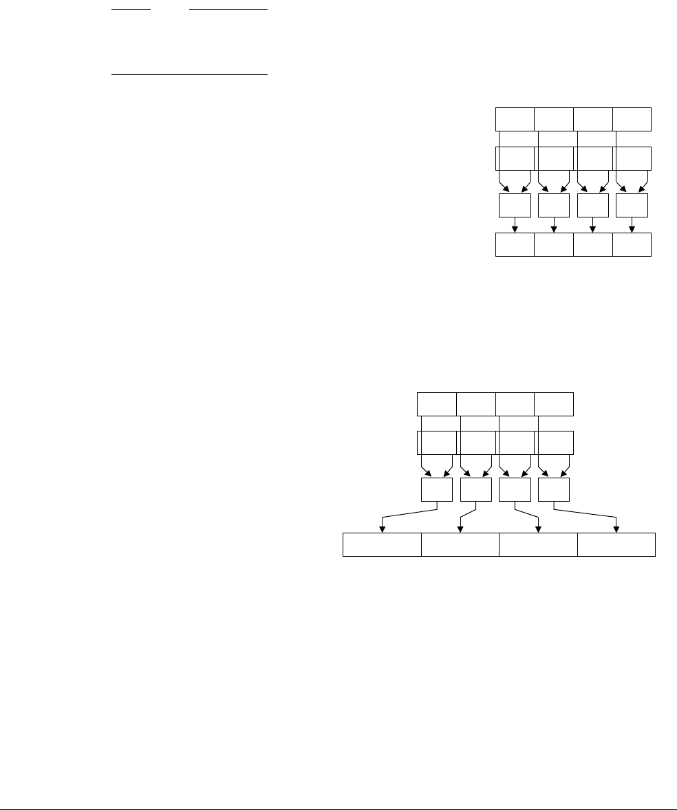
A4 The Instruction Sets
A4.13 Advanced SIMD data-processing instructions
A4-184 Copyright © 1996-1998, 2000, 2004-2012, 2014 ARM. All rights reserved. ARM DDI 0406C.c
Non-Confidential ID051414
A4.13 Advanced SIMD data-processing instructions
Advanced SIMD data-processing instructions process registers containing vectors of elements of the same type
packed together, enabling the same operation to be performed on multiple items in parallel.
Instructions operate on vectors held in 64-bit or 128-bit registers. Figure A4-2 shows an operation on two 64-bit
operand vectors, generating a 64-bit vector result.
Note
Figure A4-2 and other similar figures show 64-bit vectors that consist of four 16-bit elements, and 128-bit vectors
that consist of four 32-bit elements. Other element sizes produce similar figures, but with one, two, eight, or sixteen
operations performed in parallel instead of four.
Figure A4-2 Advanced SIMD instruction operating on 64-bit registers
Many Advanced SIMD instructions have variants that produce vectors of elements double the size of the inputs. In
this case, the number of elements in the result vector is the same as the number of elements in the operand vectors,
but each element, and the whole vector, is double the size.
Figure A4-3 shows an example of an Advanced SIMD instruction operating on 64-bit registers, and generating a
128-bit result.
Figure A4-3 Advanced SIMD instruction producing wider result
There are also Advanced SIMD instructions that have variants that produce vectors containing elements half the
size of the inputs. Figure A4-4 on page A4-185 shows an example of an Advanced SIMD instruction operating on
one 128-bit register, and generating a 64-bit result.
Op Op Op Op
Dd
Dm
Dn
Op Op Op Op
Qd
Dm
Dn

A4 The Instruction Sets
A4.13 Advanced SIMD data-processing instructions
ARM DDI 0406C.c Copyright © 1996-1998, 2000, 2004-2012, 2014 ARM. All rights reserved. A4-185
ID051414 Non-Confidential
Figure A4-4 Advanced SIMD instruction producing narrower result
Some Advanced SIMD instructions do not conform to these standard patterns. Their operation patterns are
described in the individual instruction descriptions.
Advanced SIMD instructions that perform floating-point arithmetic use the ARM standard floating-point arithmetic
defined in Floating-point data types and arithmetic on page A2-63.
A4.13.1 Advanced SIMD parallel addition and subtraction
Table A4-19 shows the Advanced SIMD parallel add and subtract instructions.
Op Op Op Op
Qn
Dd
Table A4-19 Advanced SIMD parallel add and subtract instructions
Instruction See
Vector Add VADD (integer) on page A8-828
VADD (floating-point) on page A8-830
Vector Add and Narrow, returning High Half VADDHN on page A8-832
Vector Add Long, Vector Add Wide VADDL, VADDW on page A8-834
Vector Halving Add, Vector Halving Subtract VHADD, VHSUB on page A8-896
Vector Pairwise Add and Accumulate Long VPADAL on page A8-978
Vector Pairwise Add VPADD (integer) on page A8-980
VPADD (floating-point) on page A8-982
Vector Pairwise Add Long VPADDL on page A8-984
Vector Rounding Add and Narrow, returning High Half VRADDHN on page A8-1022
Vector Rounding Halving Add VRHADD on page A8-1030
Vector Rounding Subtract and Narrow, returning High Half VRSUBHN on page A8-1044
Vector Saturating Add VQADD on page A8-996
Vector Saturating Subtract VQSUB on page A8-1020
Vector Subtract VSUB (integer) on page A8-1084
VSUB (floating-point) on page A8-1086
Vector Subtract and Narrow, returning High Half VSUBHN on page A8-1088
Vector Subtract Long, Vector Subtract Wide VSUBL, VSUBW on page A8-1090

A4 The Instruction Sets
A4.13 Advanced SIMD data-processing instructions
A4-186 Copyright © 1996-1998, 2000, 2004-2012, 2014 ARM. All rights reserved. ARM DDI 0406C.c
Non-Confidential ID051414
A4.13.2 Bitwise Advanced SIMD data-processing instructions
Table A4-20 shows bitwise Advanced SIMD data-processing instructions. These operate on the doubleword
(64-bit) or quadword (128-bit) extension registers, and there is no division into vector elements.
A4.13.3 Advanced SIMD comparison instructions
Table A4-21 shows Advanced SIMD comparison instructions.
Table A4-20 Bitwise Advanced SIMD data-processing instructions
Instruction See
Vector Bitwise AND VAND (register) on page A8-836
Vector Bitwise Bit Clear (AND complement) VBIC (immediate) on page A8-838
VBIC (register) on page A8-840
Vector Bitwise Exclusive OR VEOR on page A8-888
Vector Bitwise Insert if False VBIF, VBIT, VBSL on page A8-842
Vector Bitwise Insert if True
Vector Bitwise Move VMOV (immediate) on page A8-936
VMOV (register) on page A8-938
Vector Bitwise NOT VMVN (immediate) on page A8-964
VMVN (register) on page A8-966
Vector Bitwise OR VORR (immediate) on page A8-974
VORR (register) on page A8-976
Vector Bitwise OR NOT VORN (register) on page A8-972
Vector Bitwise Select VBIF, VBIT, VBSL on page A8-842
Table A4-21 Advanced SIMD comparison instructions
Instruction See
Vector Absolute Compare VACGE, VACGT, VACLE, VACLT on page A8-826
Vector Compare Equal VCEQ (register) on page A8-844
Vector Compare Equal to Zero VCEQ (immediate #0) on page A8-846
Vector Compare Greater Than or Equal VCGE (register) on page A8-848
Vector Compare Greater Than or Equal to Zero VCGE (immediate #0) on page A8-850
Vector Compare Greater Than VCGT (register) on page A8-852
Vector Compare Greater Than Zero VCGT (immediate #0) on page A8-854
Vector Compare Less Than or Equal to Zero VCLE (immediate #0) on page A8-856
Vector Compare Less Than Zero VCLT (immediate #0) on page A8-860
Vector Test Bits VTST on page A8-1098

A4 The Instruction Sets
A4.13 Advanced SIMD data-processing instructions
ARM DDI 0406C.c Copyright © 1996-1998, 2000, 2004-2012, 2014 ARM. All rights reserved. A4-187
ID051414 Non-Confidential
A4.13.4 Advanced SIMD shift instructions
Table A4-22 lists the shift instructions in the Advanced SIMD instruction set.
Table A4-22 Advanced SIMD shift instructions
Instruction See
Vector Saturating Rounding Shift Left VQRSHL on page A8-1010
Vector Saturating Rounding Shift Right and Narrow VQRSHRN, VQRSHRUN on page A8-1012
Vector Saturating Shift Left VQSHL (register) on page A8-1014
VQSHL, VQSHLU (immediate) on page A8-1016
Vector Saturating Shift Right and Narrow VQSHRN, VQSHRUN on page A8-1018
Vector Rounding Shift Left VRSHL on page A8-1032
Vector Rounding Shift Right VRSHR on page A8-1034
Vector Rounding Shift Right and Accumulate VRSRA on page A8-1042
Vector Rounding Shift Right and Narrow VRSHRN on page A8-1036
Vector Shift Left VSHL (immediate) on page A8-1046
VSHL (register) on page A8-1048
Vector Shift Left Long VSHLL on page A8-1050
Vector Shift Right VSHR on page A8-1052
Vector Shift Right and Narrow VSHRN on page A8-1054
Vector Shift Left and Insert VSLI on page A8-1056
Vector Shift Right and Accumulate VSRA on page A8-1060
Vector Shift Right and Insert VSRI on page A8-1062

A4 The Instruction Sets
A4.13 Advanced SIMD data-processing instructions
A4-188 Copyright © 1996-1998, 2000, 2004-2012, 2014 ARM. All rights reserved. ARM DDI 0406C.c
Non-Confidential ID051414
A4.13.5 Advanced SIMD multiply instructions
Table A4-23 summarizes the Advanced SIMD multiply instructions.
Advanced SIMD multiply instructions can operate on vectors of:
• 8-bit, 16-bit, or 32-bit unsigned integers.
• 8-bit, 16-bit, or 32-bit signed integers.
• 8-bit polynomials over {0, 1}.
VMUL
and
VMULL
are the only instructions that operate on polynomials.
VMULL
produces a 16-bit polynomial over {0, 1}.
• Single-precision (32-bit) floating-point numbers.
They can also act on one vector and one scalar.
Long instructions have doubleword (64-bit) operands, and produce quadword (128-bit) results. Other Advanced
SIMD multiply instructions can have either doubleword or quadword operands, and produce results of the same
size.
Floating-point multiply instructions can operate on:
• single-precision (32-bit) floating-point numbers
• double-precision (64-bit) floating-point numbers.
Some Floating-point Extension implementations do not support double-precision numbers.
Table A4-23 Advanced SIMD multiply instructions
Instruction See
Vector Multiply Accumulate
VMLA, VMLAL, VMLS, VMLSL (integer) on page A8-930
VMLA, VMLS (floating-point) on page A8-932
VMLA, VMLAL, VMLS, VMLSL (by scalar) on page A8-934
Vector Multiply Accumulate Long
Vector Multiply Subtract
Vector Multiply Subtract Long
Vector Multiply VMUL, VMULL (integer and polynomial) on page A8-958
VMUL (floating-point) on page A8-960
VMUL, VMULL (by scalar) on page A8-962
Vector Multiply Long
Vector Fused Multiply Accumulate VFMA, VFMS on page A8-892
Vector Fused Multiply Subtract
Vector Saturating Doubling Multiply Accumulate Long VQDMLAL, VQDMLSL on page A8-998
Vector Saturating Doubling Multiply Subtract Long
Vector Saturating Doubling Multiply Returning High Half VQDMULH on page A8-1000
Vector Saturating Rounding Doubling Multiply Returning High Half VQRDMULH on page A8-1008
Vector Saturating Doubling Multiply Long VQDMULL on page A8-1002

A4 The Instruction Sets
A4.13 Advanced SIMD data-processing instructions
ARM DDI 0406C.c Copyright © 1996-1998, 2000, 2004-2012, 2014 ARM. All rights reserved. A4-189
ID051414 Non-Confidential
A4.13.6 Miscellaneous Advanced SIMD data-processing instructions
Table A4-24 shows miscellaneous Advanced SIMD data-processing instructions.
Table A4-24 Miscellaneous Advanced SIMD data-processing instructions
Instruction See
Vector Absolute Difference and Accumulate VABA, VABAL on page A8-818
Vector Absolute Difference VABD, VABDL (integer) on page A8-820
VABD (floating-point) on page A8-822
Vector Absolute VABS on page A8-824
Vector Convert between floating-point and fixed
point
VCVT (between floating-point and fixed-point, Advanced SIMD) on
page A8-872
Vector Convert between floating-point and integer VCVT (between floating-point and integer, Advanced SIMD) on page A8-868
Vector Convert between half-precision and
single-precision
VCVT (between half-precision and single-precision, Advanced SIMD) on
page A8-878
Vector Count Leading Sign Bits VCLS on page A8-858
Vector Count Leading Zeros VCLZ on page A8-862
Vector Count Set Bits VCNT on page A8-866
Vector Duplicate scalar VDUP (scalar) on page A8-884
Vector Extract VEXT on page A8-890
Vector Move and Narrow VMOVN on page A8-952
Vector Move Long VMOVL on page A8-950
Vector Maximum, Minimum VMAX, VMIN (integer) on page A8-926
VMAX, VMIN (floating-point) on page A8-928
Vector Negate VNEG on page A8-968
Vector Pairwise Maximum, Minimum VPMAX, VPMIN (integer) on page A8-986
VPMAX, VPMIN (floating-point) on page A8-988
Vector Reciprocal Estimate VRECPE on page A8-1024
Vector Reciprocal Step VRECPS on page A8-1026
Vector Reciprocal Square Root Estimate VRSQRTE on page A8-1038
Vector Reciprocal Square Root Step VRSQRTS on page A8-1040
Vector Reverse VREV16, VREV32, VREV64 on page A8-1028
Vector Saturating Absolute VQABS on page A8-994
Vector Saturating Move and Narrow VQMOVN, VQMOVUN on page A8-1004
Vector Saturating Negate VQNEG on page A8-1006
Vector Swap VSWP on page A8-1092
Vector Table Lookup VTBL, VTBX on page A8-1094

A4 The Instruction Sets
A4.13 Advanced SIMD data-processing instructions
A4-190 Copyright © 1996-1998, 2000, 2004-2012, 2014 ARM. All rights reserved. ARM DDI 0406C.c
Non-Confidential ID051414
Vector Transpose VTRN on page A8-1096
Vector Unzip VUZP on page A8-1100
Vector Zip VZIP on page A8-1102
Table A4-24 Miscellaneous Advanced SIMD data-processing instructions (continued)
Instruction See

A4 The Instruction Sets
A4.14 Floating-point data-processing instructions
ARM DDI 0406C.c Copyright © 1996-1998, 2000, 2004-2012, 2014 ARM. All rights reserved. A4-191
ID051414 Non-Confidential
A4.14 Floating-point data-processing instructions
Table A4-25 summarizes the data-processing instructions in the Floating-point (VFP) instruction set.
For details of the floating-point arithmetic used by Floating-point instructions, see Floating-point data types and
arithmetic on page A2-63.
Table A4-25 Floating-point data-processing instructions
Instruction See
Absolute value VABS on page A8-824
Add VADD (floating-point) on page A8-830
Compare, optionally with exceptions enabled VCMP, VCMPE on page A8-864
Convert between floating-point and integer VCVT, VCVTR (between floating-point and integer, Floating-point) on
page A8-870
Convert between floating-point and fixed-point VCVT (between floating-point and fixed-point, Floating-point) on
page A8-874
Convert between double-precision and single-precision VCVT (between double-precision and single-precision) on page A8-876
Convert between half-precision and single-precision VCVTB, VCVTT on page A8-880
Divide VDIV on page A8-882
Multiply Accumulate VMLA, VMLS (floating-point) on page A8-932
Multiply Subtract
Fused Multiply Accumulate VFMA, VFMS on page A8-892
Fused Multiply Subtract
Move immediate value to extension register VMOV (immediate) on page A8-936
Copy from one extension register to another VMOV (register) on page A8-938
Multiply VMUL (floating-point) on page A8-960
Negate, by inverting the sign bit VNEG on page A8-968
Multiply Accumulate and Negate VNMLA, VNMLS, VNMUL on page A8-970
Multiply Subtract and Negate
Multiply and Negate
Fused Negate Multiply Accumulate VFNMA, VFNMS on page A8-894
Fused Negate Multiply Subtract
Square Root VSQRT on page A8-1058
Subtract VSUB (floating-point) on page A8-1086

A4 The Instruction Sets
A4.14 Floating-point data-processing instructions
A4-192 Copyright © 1996-1998, 2000, 2004-2012, 2014 ARM. All rights reserved. ARM DDI 0406C.c
Non-Confidential ID051414

ARM DDI 0406C.c Copyright © 1996-1998, 2000, 2004-2012, 2014 ARM. All rights reserved. A5-193
ID051414 Non-Confidential
Chapter A5
ARM Instruction Set Encoding
This chapter describes the encoding of the ARM instruction set. It contains the following sections:
•ARM instruction set encoding on page A5-194
•Data-processing and miscellaneous instructions on page A5-196
•Load/store word and unsigned byte on page A5-208
•Media instructions on page A5-209
•Branch, branch with link, and block data transfer on page A5-214
•Coprocessor instructions, and Supervisor Call on page A5-215
•Unconditional instructions on page A5-216.
Note
• Architecture variant information in this chapter describes the architecture variant or extension in which the
instruction encoding was introduced into the ARM instruction set. All means that the instruction encoding
was introduced in ARMv4 or earlier, and so is in all variants of the ARM instruction set covered by this
manual.
• In the decode tables in this chapter, an entry of - for a field value means the value of the field does not affect
the decoding.

A5 ARM Instruction Set Encoding
A5.1 ARM instruction set encoding
A5-194 Copyright © 1996-1998, 2000, 2004-2012, 2014 ARM. All rights reserved. ARM DDI 0406C.c
Non-Confidential ID051414
A5.1 ARM instruction set encoding
The ARM instruction stream is a sequence of word-aligned words. Each ARM instruction is a single 32-bit word in
that stream. The encoding of an ARM instruction is:
Table A5-1 shows the major subdivisions of the ARM instruction set, determined by bits[31:25, 4].
Most ARM instructions can be conditional, with a condition determined by bits[31:28] of the instruction, the
cond
field. For more information see The condition code field. This applies to all instructions except those with the cond
field equal to
0b1111
.
A5.1.1 The condition code field
Every conditional instruction contains a 4-bit condition code field, the
cond
field, in bits 31 to 28:
This field contains one of the values
0b0000
-
0b1110
, as shown in Table A8-1 on page A8-288. Most instruction
mnemonics can be extended with the letters defined in the mnemonic extension column of this table.
If the always (
AL
) condition is specified, the instruction is executed irrespective of the value of the condition flags.
The absence of a condition code on an instruction mnemonic implies the
AL
condition code.
op1 op
31 30 29 28 27 26 25 24 23 22 21 20 19 18 17 16 15 14 13 12 11 10 9 8 7 6 5 4 3 2 1 0
cond
Table A5-1 ARM instruction encoding
cond op1 op Instruction classes
not 1111 00x - Data-processing and miscellaneous instructions on page A5-196.
010 - Load/store word and unsigned byte on page A5-208.
011 0 Load/store word and unsigned byte on page A5-208.
1Media instructions on page A5-209.
10x - Branch, branch with link, and block data transfer on page A5-214.
11x - Coprocessor instructions, and Supervisor Call on page A5-215.
Includes Floating-point instructions and Advanced SIMD data transfers, see Chapter A7 Advanced SIMD
and Floating-point Instruction Encoding.
1111 - - If the cond field is
0b1111
, the instruction can only be executed unconditionally, see Unconditional
instructions on page A5-216.
Includes Advanced SIMD instructions, see Chapter A7 Advanced SIMD and Floating-point
Instruction Encoding.
31 30 29 28 27 26 25 24 23 22 21 20 19 18 17 16 15 14 13 12 11 10 9 8 7 6 5 4 3 2 1 0
cond

A5 ARM Instruction Set Encoding
A5.1 ARM instruction set encoding
ARM DDI 0406C.c Copyright © 1996-1998, 2000, 2004-2012, 2014 ARM. All rights reserved. A5-195
ID051414 Non-Confidential
A5.1.2 UNDEFINED and UNPREDICTABLE instruction set space
An attempt to execute an unallocated instruction results in either:
• Unpredictable behavior. The instruction is described as UNPREDICTABLE.
• An Undefined Instruction exception. The instruction is described as UNDEFINED.
An instruction is UNDEFINED if it is declared as UNDEFINED in an instruction description, or in this chapter.
An instruction is UNPREDICTABLE if:
• it is declared as UNPREDICTABLE in an instruction description or in this chapter
• the pseudocode for that encoding does not indicate that a different special case applies, and a bit marked (0)
or (1) in the encoding diagram of an instruction is not 0 or 1 respectively.
For more information about UNDEFINED and UNPREDICTABLE instruction behavior, see Undefined Instruction
exception on page B1-1206.
Unless otherwise specified:
• ARM instructions introduced in an architecture variant are UNDEFINED in earlier architecture variants.
• ARM instructions introduced in one or more architecture extensions are UNDEFINED in an implementation
that does not include any of those extensions.
A5.1.3 The PC and the use of
0b1111
as a register specifier
In ARM instructions, the use of
0b1111
as a register specifier specifies the PC.
Many instructions are UNPREDICTABLE if they use
0b1111
as a register specifier. This is specified by pseudocode in
the instruction description.
Note
In ARMv7, ARM deprecates use of the PC as the base register in any store instruction.
A5.1.4 The SP and the use of
0b1101
as a register specifier
In ARM instructions, the use of
0b1101
as a register specifier specifies the SP.
ARM deprecates using SP for any purpose other than as a stack pointer.

A5 ARM Instruction Set Encoding
A5.2 Data-processing and miscellaneous instructions
A5-196 Copyright © 1996-1998, 2000, 2004-2012, 2014 ARM. All rights reserved. ARM DDI 0406C.c
Non-Confidential ID051414
A5.2 Data-processing and miscellaneous instructions
The encoding of ARM data-processing instructions, and some miscellaneous, instructions is:
Table A5-2 shows the allocation of encodings in this space.
Table A5-2 Data-processing and miscellaneous instructions
op op1 op2 Instruction or instruction class Variant
0 not 10xx0 xxx0 Data-processing (register) on page A5-197 -
0xx1 Data-processing (register-shifted register) on page A5-198 -
10xx0 0xxx Miscellaneous instructions on page A5-207 -
1xx0 Halfword multiply and multiply accumulate on page A5-203 -
0xxxx 1001 Multiply and multiply accumulate on page A5-202 -
1xxxx 1001 Synchronization primitives on page A5-205 -
not 0xx1x 1011 Extra load/store instructions on page A5-203 -
11x1 Extra load/store instructions on page A5-203 -
0xx10 11x1 Extra load/store instructions on page A5-203 -
0xx1x 1011 Extra load/store instructions, unprivileged on page A5-204 -
0xx11 11x1 Extra load/store instructions, unprivileged on page A5-204 -
1 not 10xx0 - Data-processing (immediate) on page A5-199 -
10000 - 16-bit immediate load, MOV (immediate) on page A8-484 v6T2
10100 - High halfword 16-bit immediate load, MOVT on page A8-491 v6T2
10x10 - MSR (immediate), and hints on page A5-206 -
0 0 op op1 op2
31 30 29 28 27 26 25 24 23 22 21 20 19 18 17 16 15 14 13 12 11 10 9 8 7 6 5 4 3 2 1 0
cond

A5 ARM Instruction Set Encoding
A5.2 Data-processing and miscellaneous instructions
ARM DDI 0406C.c Copyright © 1996-1998, 2000, 2004-2012, 2014 ARM. All rights reserved. A5-197
ID051414 Non-Confidential
A5.2.1 Data-processing (register)
The encoding of ARM data-processing (register) instructions is:
Table A5-3 shows the allocation of encodings in this space. These encodings are in all architecture variants.
Table A5-3 Data-processing (register) instructions
op op2 imm5 Instruction See
0000x - - Bitwise AND AND (register) on page A8-326
0001x - - Bitwise Exclusive OR EOR (register) on page A8-384
0010x - - Subtract SUB (register) on page A8-712
0011x - - Reverse Subtract RSB (register) on page A8-576
0100x - - Add ADD (register, ARM) on page A8-312
0101x - - Add with Carry ADC (register) on page A8-302
0110x - - Subtract with Carry SBC (register) on page A8-594
0111x - - Reverse Subtract with Carry RSC (register) on page A8-582
10xx0 - - See Data-processing and miscellaneous instructions on page A5-196
10001 - - Test TST (register) on page A8-746
10011 - - Test Equivalence TEQ (register) on page A8-740
10101 - - Compare CMP (register) on page A8-372
10111 - - Compare Negative CMN (register) on page A8-366
1100x - - Bitwise OR ORR (register) on page A8-518
1101x 00 00000 Move MOV (register, ARM) on page A8-488
not 00000 Logical Shift Left LSL (immediate) on page A8-468
01 - Logical Shift Right LSR (immediate) on page A8-472
10 - Arithmetic Shift Right ASR (immediate) on page A8-330
11 00000 Rotate Right with Extend RRX on page A8-572
not 00000 Rotate Right ROR (immediate) on page A8-568
1110x - - Bitwise Bit Clear BIC (register) on page A8-342
1111x - - Bitwise NOT MVN (register) on page A8-506
0 0 0 op imm5 op2 0
31 30 29 28 27 26 25 24 23 22 21 20 19 18 17 16 15 14 13 12 11 10 9 8 7 6 5 4 3 2 1 0
cond

A5 ARM Instruction Set Encoding
A5.2 Data-processing and miscellaneous instructions
A5-198 Copyright © 1996-1998, 2000, 2004-2012, 2014 ARM. All rights reserved. ARM DDI 0406C.c
Non-Confidential ID051414
A5.2.2 Data-processing (register-shifted register)
The encoding of ARM data-processing (register-shifted register) instructions is:
Table A5-4 shows the allocation of encodings in this space. These encodings are in all architecture variants.
Table A5-4 Data-processing (register-shifted register) instructions
op1 op2 Instruction See
0000x - Bitwise AND AND (register-shifted register) on page A8-328
0001x - Bitwise Exclusive OR EOR (register-shifted register) on page A8-386
0010x - Subtract SUB (register-shifted register) on page A8-714
0011x - Reverse Subtract RSB (register-shifted register) on page A8-578
0100x - Add ADD (register-shifted register) on page A8-314
0101x - Add with Carry ADC (register-shifted register) on page A8-304
0110x - Subtract with Carry SBC (register-shifted register) on page A8-596
0111x - Reverse Subtract with Carry RSC (register-shifted register) on page A8-584
10xx0 - See Data-processing and miscellaneous instructions on page A5-196
10001 - Test TST (register-shifted register) on page A8-748
10011 - Test Equivalence TEQ (register-shifted register) on page A8-742
10101 - Compare CMP (register-shifted register) on page A8-374
10111 - Compare Negative CMN (register-shifted register) on page A8-368
1100x - Bitwise OR ORR (register-shifted register) on page A8-520
1101x 00 Logical Shift Left LSL (register) on page A8-470
01 Logical Shift Right LSR (register) on page A8-474
10 Arithmetic Shift Right ASR (register) on page A8-332
11 Rotate Right ROR (register) on page A8-570
1110x - Bitwise Bit Clear BIC (register-shifted register) on page A8-344
1111x - Bitwise NOT MVN (register-shifted register) on page A8-508
0 0 0 op1 0 op2 1
31 30 29 28 27 26 25 24 23 22 21 20 19 18 17 16 15 14 13 12 11 10 9 8 7 6 5 4 3 2 1 0
cond

A5 ARM Instruction Set Encoding
A5.2 Data-processing and miscellaneous instructions
ARM DDI 0406C.c Copyright © 1996-1998, 2000, 2004-2012, 2014 ARM. All rights reserved. A5-199
ID051414 Non-Confidential
A5.2.3 Data-processing (immediate)
The encoding of ARM data-processing (immediate) instructions is:
Table A5-5 shows the allocation of encodings in this space. These encodings are in all architecture variants.
These instructions all have modified immediate constants, rather than a simple 12-bit binary number. This provides
a more useful range of values. For details see Modified immediate constants in ARM instructions on page A5-200.
Table A5-5 Data-processing (immediate) instructions
op Rn Instruction See
0000x - Bitwise AND AND (immediate) on page A8-324
0001x - Bitwise Exclusive OR EOR (immediate) on page A8-382
0010x not 1111 Subtract SUB (immediate, ARM) on page A8-710
1111 Form PC-relative address ADR on page A8-322
0011x - Reverse Subtract RSB (immediate) on page A8-574
0100x not 1111 Add ADD (immediate, ARM) on page A8-308
1111 Form PC-relative address ADR on page A8-322
0101x - Add with Carry ADC (immediate) on page A8-300
0110x - Subtract with Carry SBC (immediate) on page A8-592
0111x - Reverse Subtract with Carry RSC (immediate) on page A8-580
10xx0 - See Data-processing and miscellaneous instructions on page A5-196
10001 - Test TST (immediate) on page A8-744
10011 - Test Equivalence TEQ (immediate) on page A8-738
10101 - Compare CMP (immediate) on page A8-370
10111 - Compare Negative CMN (immediate) on page A8-364
1100x - Bitwise OR ORR (immediate) on page A8-516
1101x - Move MOV (immediate) on page A8-484
1110x - Bitwise Bit Clear BIC (immediate) on page A8-340
1111x - Bitwise NOT MVN (immediate) on page A8-504
0 0 1 op Rn
31 30 29 28 27 26 25 24 23 22 21 20 19 18 17 16 15 14 13 12 11 10 9 8 7 6 5 4 3 2 1 0
cond

A5 ARM Instruction Set Encoding
A5.2 Data-processing and miscellaneous instructions
A5-200 Copyright © 1996-1998, 2000, 2004-2012, 2014 ARM. All rights reserved. ARM DDI 0406C.c
Non-Confidential ID051414
A5.2.4 Modified immediate constants in ARM instructions
The encoding of a modified immediate constant in an ARM instruction is:
Table A5-6 shows the range of modified immediate constants available in ARM data-processing instructions, and
their encoding in the a, b, c, d, e, f, g, and h bits and the rotation field in the instruction.
Note
The range of values available in ARM modified immediate constants is slightly different from the range of values
available in 32-bit Thumb instructions. See Modified immediate constants in Thumb instructions on page A6-232.
Carry out
A logical instruction with the rotation field set to
0b0000
does not affect APSR.C. Otherwise, a logical flag-setting
instruction sets APSR.C to the value of bit[31] of the modified immediate constant.
Constants with multiple encodings
Some constant values have multiple possible encodings. In this case, a UAL assembler must select the encoding
with the lowest unsigned value of the rotation field. This is the encoding that appears first in Table A5-6. For
example, the constant
#3
must be encoded with (rotation, abcdefgh) == (
0b0000
,
0b00000011
), not (
0b0001
,
0b00001100
), (
0b0010
,
0b00110000
), or (
0b0011
,
0b11000000
).
Table A5-6 Encoding of modified immediates in ARM processing instructions
rotation <const> a
a. This table shows the immediate constant value in binary form, to relate
abcdefgh
to the encoding diagram.
In assembly syntax, the immediate value is specified in the usual way (a decimal number by default).
0000
00000000 00000000 00000000 abcdefgh
0001
gh000000 00000000 00000000 00abcdef
0010
efgh0000 00000000 00000000 0000abcd
0011
cdefgh00 00000000 00000000 000000ab
0100
abcdefgh 00000000 00000000 00000000
.
.
.
.
.
.
8-bit values shifted to other even-numbered positions
1001
00000000 00abcdef gh000000 00000000
.
.
.
.
.
.
8-bit values shifted to other even-numbered positions
1110
00000000 00000000 0000abcd efgh0000
1111
00000000 00000000 000000ab cdefgh00
rotation a b c d e f g h
31 30 29 28 27 26 25 24 23 22 21 20 19 18 17 16 15 14 13 12 11 10 9 8 7 6 5 4 3 2 1 0

A5 ARM Instruction Set Encoding
A5.2 Data-processing and miscellaneous instructions
ARM DDI 0406C.c Copyright © 1996-1998, 2000, 2004-2012, 2014 ARM. All rights reserved. A5-201
ID051414 Non-Confidential
In particular, this means that all constants in the range 0-255 are encoded with rotation ==
0b0000
, and permitted
constants outside that range are encoded with rotation !=
0b0000
. A flag-setting logical instruction with a modified
immediate constant therefore leaves APSR.C unchanged if the constant is in the range 0-255 and sets it to the most
significant bit of the constant otherwise. This matches the behavior of Thumb modified immediate constants for all
constants that are permitted in both the ARM and Thumb instruction sets.
An alternative syntax is available for a modified immediate constant that permits the programmer to specify the
encoding directly. In this syntax,
#<const>
is instead written as
#<byte>, #<rot>
, where:
<byte>
is the numeric value of abcdefgh, in the range 0-255
<rot>
is twice the numeric value of rotation, an even number in the range 0-30.
This syntax permits all ARM data-processing instructions with modified immediate constants to be disassembled
to assembler syntax that assembles to the original instruction.
This syntax also makes it possible to write variants of some flag-setting logical instructions that have different
effects on APSR.C to those obtained with the normal
#<const>
syntax. For example,
ANDS R1, R2, #12, #2
has the
same behavior as
ANDS R1, R2, #3
except that it sets APSR.C to 0 instead of leaving it unchanged. Such variants of
flag-setting logical instructions do not have equivalents in the Thumb instruction set, and ARM deprecates their use.
Operation of modified immediate constants, ARM instructions
// ARMExpandImm()
// ==============
bits(32) ARMExpandImm(bits(12) imm12)
// APSR.C argument to following function call does not affect the imm32 result.
(imm32, -) = ARMExpandImm_C(imm12, APSR.C);
return imm32;
// ARMExpandImm_C()
// ================
(bits(32), bit) ARMExpandImm_C(bits(12) imm12, bit carry_in)
unrotated_value = ZeroExtend(imm12<7:0>, 32);
(imm32, carry_out) = Shift_C(unrotated_value, SRType_ROR, 2*UInt(imm12<11:8>), carry_in);
return (imm32, carry_out);

A5 ARM Instruction Set Encoding
A5.2 Data-processing and miscellaneous instructions
A5-202 Copyright © 1996-1998, 2000, 2004-2012, 2014 ARM. All rights reserved. ARM DDI 0406C.c
Non-Confidential ID051414
A5.2.5 Multiply and multiply accumulate
The encoding of ARM multiply and multiply accumulate instructions is:
Table A5-7 shows the allocation of encodings in this space.
A5.2.6 Saturating addition and subtraction
The encoding of ARM saturating addition and subtraction instructions is:
Table A5-8 shows the allocation of encodings in this space. These encodings are all available in ARMv5TE and
above, and are UNDEFINED in earlier variants of the architecture.
Table A5-7 Multiply and multiply accumulate instructions
op Instruction See Variant
000x Multiply MUL on page A8-502 All
001x Multiply Accumulate MLA on page A8-480 All
0100 Unsigned Multiply Accumulate Accumulate Long UMAAL on page A8-774 v6
0101 UNDEFINED --
0110 Multiply and Subtract MLS on page A8-482 v6T2
0111 UNDEFINED --
100x Unsigned Multiply Long UMULL on page A8-778 All
101x Unsigned Multiply Accumulate Long UMLAL on page A8-776 All
110x Signed Multiply Long SMULL on page A8-646 All
111x Signed Multiply Accumulate Long SMLAL on page A8-624 All
0 0 0 0 op 1 0 0 1
31 30 29 28 27 26 25 24 23 22 21 20 19 18 17 16 15 14 13 12 11 10 9 8 7 6 5 4 3 2 1 0
cond
Table A5-8 Saturating addition and subtraction instructions
op Instruction See
00 Saturating Add QADD on page A8-540
01 Saturating Subtract QSUB on page A8-554
10 Saturating Double and Add QDADD on page A8-548
11 Saturating Double and Subtract QDSUB on page A8-550
0 0 0 1 0 op 0 0 1 0 1
31 30 29 28 27 26 25 24 23 22 21 20 19 18 17 16 15 14 13 12 11 10 9 8 7 6 5 4 3 2 1 0
cond
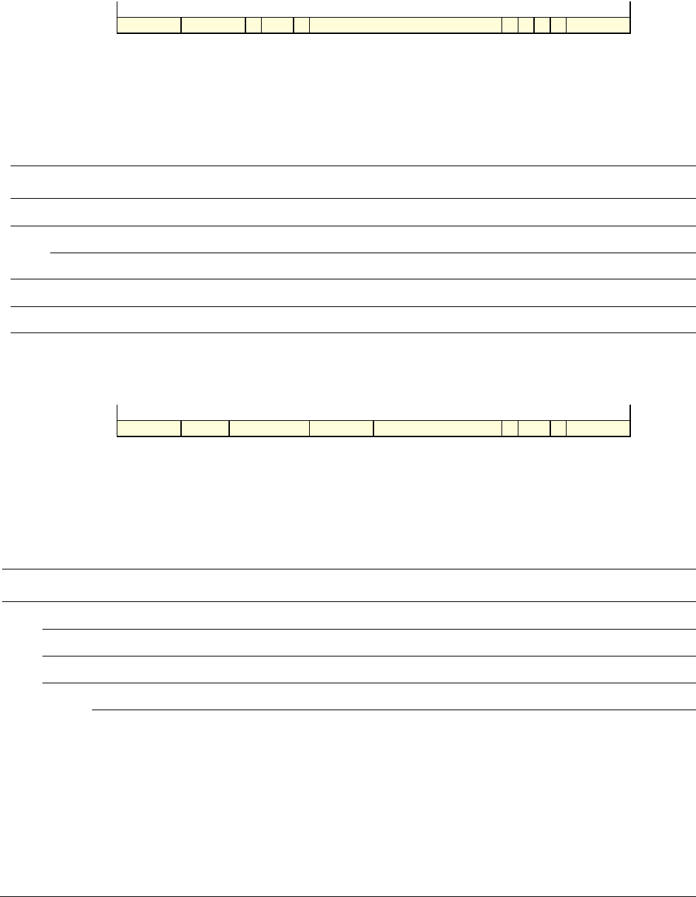
A5 ARM Instruction Set Encoding
A5.2 Data-processing and miscellaneous instructions
ARM DDI 0406C.c Copyright © 1996-1998, 2000, 2004-2012, 2014 ARM. All rights reserved. A5-203
ID051414 Non-Confidential
A5.2.7 Halfword multiply and multiply accumulate
The encoding of ARM halfword multiply and multiply accumulate instructions is:
Table A5-9 shows the allocation of encodings in this space.
These encodings are signed multiply (
SMUL
) and signed multiply accumulate (
SMLA
) instructions, operating on 16-bit
values, or mixed 16-bit and 32-bit values. The results and accumulators are 32-bit or 64-bit.
These encodings are all available in ARMv5TE and above, and are UNDEFINED in earlier variants of the architecture.
A5.2.8 Extra load/store instructions
The encoding of extra ARM load/store instructions is:
If (op2 ==
0b00
), then see Data-processing and miscellaneous instructions on page A5-196.
If ((op1 ==
0b0xx10
) && (op2 ==
0b01
)) or ((op1 ==
0b0xx11
) && (op2 !=
0b00
)) then see Extra load/store
instructions, unprivileged on page A5-204.
Otherwise, Table A5-10 shows the allocation of encodings in this space.
0 0 0 1 0 op1 0 1 op 0
31 30 29 28 27 26 25 24 23 22 21 20 19 18 17 16 15 14 13 12 11 10 9 8 7 6 5 4 3 2 1 0
cond
Table A5-9 Halfword multiply and multiply accumulate instructions
op1 op Instruction See
00 - Signed 16-bit multiply, 32-bit accumulate SMLABB, SMLABT, SMLATB, SMLATT on page A8-620
01 0 Signed 16-bit × 32-bit multiply, 32-bit accumulate SMLAWB, SMLAWT on page A8-630
1 Signed 16-bit × 32-bit multiply, 32-bit result SMULWB, SMULWT on page A8-648
10 - Signed 16-bit multiply, 64-bit accumulate SMLALBB, SMLALBT, SMLALTB, SMLALTT on page A8-626
11 - Signed 16-bit multiply, 32-bit result SMULBB, SMULBT, SMULTB, SMULTT on page A8-644
0 0 0 op1 Rn 1 op2 1
31 30 29 28 27 26 25 24 23 22 21 20 19 18 17 16 15 14 13 12 11 10 9 8 7 6 5 4 3 2 1 0
cond
Table A5-10 Extra load/store instructions
op2 op1 Rn Instruction See Variant
01 xx0x0 - Store Halfword STRH (register) on page A8-702 All
xx0x1 - Load Halfword LDRH (register) on page A8-446 All
xx1x0 - Store Halfword STRH (immediate, ARM) on page A8-700 All
xx1x1 not 1111 Load Halfword LDRH (immediate, ARM) on page A8-442 All
1111 Load Halfword LDRH (literal) on page A8-444 All
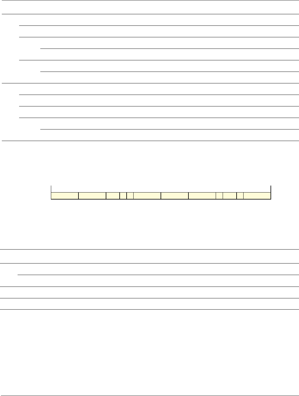
A5 ARM Instruction Set Encoding
A5.2 Data-processing and miscellaneous instructions
A5-204 Copyright © 1996-1998, 2000, 2004-2012, 2014 ARM. All rights reserved. ARM DDI 0406C.c
Non-Confidential ID051414
A5.2.9 Extra load/store instructions, unprivileged
The encoding of unprivileged extra ARM load/store instructions is:
If op2 ==
0b00
then see Data-processing and miscellaneous instructions on page A5-196.
If (op ==
0b0
&& op2 ==
0b1x
) then see Extra load/store instructions on page A5-203.
Otherwise, Table A5-11 shows the allocation of encodings in this space.
10 xx0x0 - Load Dual LDRD (register) on page A8-430 v5TE
xx0x1 - Load Signed Byte LDRSB (register) on page A8-454 All
xx1x0 not 1111 Load Dual LDRD (immediate) on page A8-426 v5TE
1111 Load Dual LDRD (literal) on page A8-428 v5TE
xx1x1 not 1111 Load Signed Byte LDRSB (immediate) on page A8-450 All
1111 Load Signed Byte LDRSB (literal) on page A8-452 All
11 xx0x0 - Store Dual STRD (register) on page A8-688 All
xx0x1 - Load Signed Halfword LDRSH (register) on page A8-462 All
xx1x0 - Store Dual STRD (immediate) on page A8-686 All
xx1x1 not 1111 Load Signed Halfword LDRSH (immediate) on page A8-458 All
1111 Load Signed Halfword LDRSH (literal) on page A8-460 All
Table A5-10 Extra load/store instructions (continued)
op2 op1 Rn Instruction See Variant
0 0 0 0 1 op 1 op2 1
31 30 29 28 27 26 25 24 23 22 21 20 19 18 17 16 15 14 13 12 11 10 9 8 7 6 5 4 3 2 1 0
cond
Table A5-11 Extra load/store instructions, unprivileged
op2 op Instruction See Variant
01 0 Store Halfword Unprivileged STRHT on page A8-704 v6T2
1 Load Halfword Unprivileged LDRHT on page A8-448 v6T2
10 1 Load Signed Byte Unprivileged LDRSBT on page A8-456 v6T2
11 1 Load Signed Halfword Unprivileged LDRSHT on page A8-464 v6T2

A5 ARM Instruction Set Encoding
A5.2 Data-processing and miscellaneous instructions
ARM DDI 0406C.c Copyright © 1996-1998, 2000, 2004-2012, 2014 ARM. All rights reserved. A5-205
ID051414 Non-Confidential
A5.2.10 Synchronization primitives
The encoding of ARM synchronization primitive instructions is:
Table A5-12 shows the allocation of encodings in this space.
Other encodings in this space are UNDEFINED.
Table A5-12 Synchronization primitives
op Instruction See Variant
0x00 Swap Word, Swap Byte SWP, SWPB on page A8-722 a
a. ARM deprecates the use of these instructions.
All
1000 Store Register Exclusive STREX on page A8-690 v6
1001 Load Register Exclusive LDREX on page A8-432 v6
1010 Store Register Exclusive Doubleword STREXD on page A8-694 v6K
1011 Load Register Exclusive Doubleword LDREXD on page A8-436 v6K
1100 Store Register Exclusive Byte STREXB on page A8-692 v6K
1101 Load Register Exclusive Byte LDREXB on page A8-434 v6K
1110 Store Register Exclusive Halfword STREXH on page A8-696 v6K
1111 Load Register Exclusive Halfword LDREXH on page A8-438 v6K
0 0 0 1 op 1 0 0 1
31 30 29 28 27 26 25 24 23 22 21 20 19 18 17 16 15 14 13 12 11 10 9 8 7 6 5 4 3 2 1 0
cond

A5 ARM Instruction Set Encoding
A5.2 Data-processing and miscellaneous instructions
A5-206 Copyright © 1996-1998, 2000, 2004-2012, 2014 ARM. All rights reserved. ARM DDI 0406C.c
Non-Confidential ID051414
A5.2.11 MSR (immediate), and hints
The encoding of ARM
MSR
(immediate) and hint instructions is:
Table A5-13 shows the allocation of encodings in this space. Encodings with
op
set to 0,
op1
set to
0b0000
, and a
value of
op2
that is not shown in the table, are unallocated hints and behave as if
op2
is set to
0b00000000
. These
unallocated hint encodings are reserved and software must not use them.
0 0 1 1 0 op 1 0 op1 op2
31 30 29 28 27 26 25 24 23 22 21 20 19 18 17 16 15 14 13 12 11 10 9 8 7 6 5 4 3 2 1 0
cond
Table A5-13 MSR (immediate), and hints
op op1 op2 Instruction See Variant
0 0000 00000000 No Operation hint NOP on page A8-510 v6K, v6T2
00000001 Yield hint YIELD on page A8-1108 v6K
00000010 Wait For Event hint WFE on page A8-1104 v6K
00000011 Wait For Interrupt hint WFI on page A8-1106 v6K
00000100 Send Event hint SEV on page A8-606 v6K
1111xxxx Debug hint DBG on page A8-377 v7
0100
1x00
- Move to Special register, Application level MSR (immediate) on page A8-498 All
xx01
xx1x
- Move to Special register, System level MSR (immediate) on page B9-1996 All
1 - - Move to Special register, System level MSR (immediate) on page B9-1996 All

A5 ARM Instruction Set Encoding
A5.2 Data-processing and miscellaneous instructions
ARM DDI 0406C.c Copyright © 1996-1998, 2000, 2004-2012, 2014 ARM. All rights reserved. A5-207
ID051414 Non-Confidential
A5.2.12 Miscellaneous instructions
The encoding of some miscellaneous ARM instructions is:
Table A5-14 shows the allocation of encodings in this space. Other encodings in this space are UNDEFINED.
0 0 0 1 0 op 0 op1 B 0 op2
31 30 29 28 27 26 25 24 23 22 21 20 19 18 17 16 15 14 13 12 11 10 9 8 7 6 5 4 3 2 1 0
cond
Table A5-14 Miscellaneous instructions
op2 B op op1 Instruction or instruction class See Variant
000 1 x0 xxxx Move from Banked or Special register MRS (Banked register) on page B9-1992 v7VE
x1 xxxx Move to Banked or Special register MSR (Banked register) on page B9-1994 v7VE
0 x0 xxxx Move from Special register MRS on page A8-496
MRS on page B9-1990
All
01 xx00 Move to Special register, Application level MSR (register) on page A8-500 All
xx01
xx1x
Move to Special register, System level MSR (register) on page B9-1998 All
11 - Move to Special register, System level MSR (register) on page B9-1998 All
001 - 01 - Branch and Exchange BX on page A8-352 v4T
11 - Count Leading Zeros CLZ on page A8-362 v5T
010 - 01 - Branch and Exchange Jazelle BXJ on page A8-354 v5TEJ
011 - 01 - Branch with Link and Exchange BLX (register) on page A8-350 v5T
101 - - - Saturating addition and subtraction Saturating addition and subtraction on
page A5-202
-
110 - 11 - Exception Return ERET on page B9-1982 v7VE
111 - 01 - Breakpoint BKPT on page A8-346 v5T
10 - Hypervisor Call HVC on page B9-1984 v7VE
11 - Secure Monitor Call SMC (previously SMI) on page B9-2002 Security
Extensions

A5 ARM Instruction Set Encoding
A5.3 Load/store word and unsigned byte
A5-208 Copyright © 1996-1998, 2000, 2004-2012, 2014 ARM. All rights reserved. ARM DDI 0406C.c
Non-Confidential ID051414
A5.3 Load/store word and unsigned byte
The encoding of ARM load/store word and unsigned byte instructions is:
These instructions have either A == 0 or B == 0. For instructions with A == 1 and B == 1, see Media instructions
on page A5-209.
Otherwise, Table A5-15 shows the allocation of encodings in this space. These encodings are in all architecture
variants.
0 1 A op1 Rn B
31 30 29 28 27 26 25 24 23 22 21 20 19 18 17 16 15 14 13 12 11 10 9 8 7 6 5 4 3 2 1 0
cond
Table A5-15 Single data transfer instructions
A op1 B Rn Instruction See
0 xx0x0 not 0x010 - - Store Register STR (immediate, ARM) on page A8-674
1 xx0x0 not 0x010 0 - Store Register STR (register) on page A8-676
0 0x010 - - Store Register Unprivileged STRT on page A8-706
1 0x010 0 -
0 xx0x1 not 0x011 - not 1111 Load Register (immediate) LDR (immediate, ARM) on page A8-408
1111 Load Register (literal) LDR (literal) on page A8-410
1 xx0x1 not 0x011 0 - Load Register LDR (register, ARM) on page A8-414
0 0x011 - - Load Register Unprivileged LDRT on page A8-466
1 0x011 0 -
0 xx1x0 not 0x110 - - Store Register Byte (immediate) STRB (immediate, ARM) on page A8-680
1 xx1x0 not 0x110 0 - Store Register Byte (register) STRB (register) on page A8-682
0 0x110 - - Store Register Byte Unprivileged STRBT on page A8-684
1 0x110 0 -
0 xx1x1 not 0x111 - not 1111 Load Register Byte (immediate) LDRB (immediate, ARM) on page A8-418
1111 Load Register Byte (literal) LDRB (literal) on page A8-420
1 xx1x1 not 0x111 0 - Load Register Byte (register) LDRB (register) on page A8-422
0 0x111 - - Load Register Byte Unprivileged LDRBT on page A8-424
1 0x111 0 -

A5 ARM Instruction Set Encoding
A5.4 Media instructions
ARM DDI 0406C.c Copyright © 1996-1998, 2000, 2004-2012, 2014 ARM. All rights reserved. A5-209
ID051414 Non-Confidential
A5.4 Media instructions
The encoding of ARM media instructions is:
Table A5-16 shows the allocation of encodings in this space.
Other encodings in this space are UNDEFINED.
0 1 1 op1 Rd op2 1 Rn
31 30 29 28 27 26 25 24 23 22 21 20 19 18 17 16 15 14 13 12 11 10 9 8 7 6 5 4 3 2 1 0
cond
Table A5-16 Media instructions
op1 op2 Rd Rn cond Instructions See Variant
000xx - - - - - Parallel addition and subtraction, signed on
page A5-210
001xx - - - - - Parallel addition and subtraction, unsigned on
page A5-211
01xxx - - - - - Packing, unpacking, saturation, and reversal
on page A5-212
10xxx - - - - - Signed multiply, signed and unsigned divide on
page A5-213
11000 000 1111 - - Unsigned Sum of Absolute Differences USAD8 on page A8-792 v6
000 not
1111
- - Unsigned Sum of Absolute Differences
and Accumulate
USADA8 on page A8-794 v6
1101x x10 - - - Signed Bit Field Extract SBFX on page A8-598 v6T2
1110x x00 - 1111 - Bit Field Clear BFC on page A8-336 v6T2
not
1111
- Bit Field Insert BFI on page A8-338 v6T2
1111x x10 - - - Unsigned Bit Field Extract UBFX on page A8-756 v6T2
11111 111 - - 1110 Permanently UNDEFINED UDF on page A8-758 Alla
not
1110 -aAll
a. Issue C.a of this manual first defines an assembler mnemonic for this encoding. This mnemonic applies only to the unconditional encoding,
with cond set to
0b1110
.

A5 ARM Instruction Set Encoding
A5.4 Media instructions
A5-210 Copyright © 1996-1998, 2000, 2004-2012, 2014 ARM. All rights reserved. ARM DDI 0406C.c
Non-Confidential ID051414
A5.4.1 Parallel addition and subtraction, signed
The encoding of ARM signed parallel addition and subtraction instructions is:
Table A5-17 shows the allocation of encodings in this space. These encodings are all available in ARMv6 and
above, and are UNDEFINED in earlier variants of the architecture.
Other encodings in this space are UNDEFINED.
Table A5-17 Signed parallel addition and subtraction instructions
op1 op2 Instruction See
01 000 Add 16-bit SADD16 on page A8-586
001 Add and Subtract with Exchange, 16-bit SASX on page A8-590
010 Subtract and Add with Exchange, 16-bit SSAX on page A8-656
011 Subtract 16-bit SSUB16 on page A8-658
100 Add 8-bit SADD8 on page A8-588
111 Subtract 8-bit SSUB8 on page A8-660
Saturating instructions
10 000 Saturating Add 16-bit QADD16 on page A8-542
001 Saturating Add and Subtract with Exchange, 16-bit QASX on page A8-546
010 Saturating Subtract and Add with Exchange, 16-bit QSAX on page A8-552
011 Saturating Subtract 16-bit QSUB16 on page A8-556
100 Saturating Add 8-bit QADD8 on page A8-544
111 Saturating Subtract 8-bit QSUB8 on page A8-558
Halving instructions
11 000 Halving Add 16-bit SHADD16 on page A8-608
001 Halving Add and Subtract with Exchange, 16-bit SHASX on page A8-612
010 Halving Subtract and Add with Exchange, 16-bit SHSAX on page A8-614
011 Halving Subtract 16-bit SHSUB16 on page A8-616
100 Halving Add 8-bit SHADD8 on page A8-610
111 Halving Subtract 8-bit SHSUB8 on page A8-618
0 1 1 0 0 0 op1 op2 1
31 30 29 28 27 26 25 24 23 22 21 20 19 18 17 16 15 14 13 12 11 10 9 8 7 6 5 4 3 2 1 0
cond

A5 ARM Instruction Set Encoding
A5.4 Media instructions
ARM DDI 0406C.c Copyright © 1996-1998, 2000, 2004-2012, 2014 ARM. All rights reserved. A5-211
ID051414 Non-Confidential
A5.4.2 Parallel addition and subtraction, unsigned
The encoding of ARM unsigned parallel addition and subtraction instructions is:
Table A5-18 shows the allocation of encodings in this space. These encodings are all available in ARMv6 and
above, and are UNDEFINED in earlier variants of the architecture.
Other encodings in this space are UNDEFINED.
Table A5-18 Unsigned parallel addition and subtractions instructions
op1 op2 Instruction See
01 000 Add 16-bit UADD16 on page A8-750
001 Add and Subtract with Exchange, 16-bit UASX on page A8-754
010 Subtract and Add with Exchange, 16-bit USAX on page A8-800
011 Subtract 16-bit USUB16 on page A8-802
100 Add 8-bit UADD8 on page A8-752
111 Subtract 8-bit USUB8 on page A8-804
Saturating instructions
10 000 Saturating Add 16-bit UQADD16 on page A8-780
001 Saturating Add and Subtract with Exchange, 16-bit UQASX on page A8-784
010 Saturating Subtract and Add with Exchange, 16-bit UQSAX on page A8-786
011 Saturating Subtract 16-bit UQSUB16 on page A8-788
100 Saturating Add 8-bit UQADD8 on page A8-782
111 Saturating Subtract 8-bit UQSUB8 on page A8-790
Halving instructions
11 000 Halving Add 16-bit UHADD16 on page A8-762
001 Halving Add and Subtract with Exchange, 16-bit UHASX on page A8-766
010 Halving Subtract and Add with Exchange, 16-bit UHSAX on page A8-768
011 Halving Subtract 16-bit UHSUB16 on page A8-770
100 Halving Add 8-bit UHADD8 on page A8-764
111 Halving Subtract 8-bit UHSUB8 on page A8-772
0 1 1 0 0 1 op1 op2 1
31 30 29 28 27 26 25 24 23 22 21 20 19 18 17 16 15 14 13 12 11 10 9 8 7 6 5 4 3 2 1 0
cond

A5 ARM Instruction Set Encoding
A5.4 Media instructions
A5-212 Copyright © 1996-1998, 2000, 2004-2012, 2014 ARM. All rights reserved. ARM DDI 0406C.c
Non-Confidential ID051414
A5.4.3 Packing, unpacking, saturation, and reversal
The encoding of ARM packing, unpacking, saturation, and reversal instructions is:
Table A5-19 shows the allocation of encodings in this space.
Other encodings in this space are UNDEFINED.
Table A5-19 Packing, unpacking, saturation, and reversal instructions
op1 op2 A Instructions See Variant
000 xx0 - Pack Halfword PKH on page A8-522 v6
011 not 1111 Signed Extend and Add Byte 16-bit SXTAB16 on page A8-726 v6
1111 Signed Extend Byte 16-bit SXTB16 on page A8-732 v6
101 - Select Bytes SEL on page A8-602 v6
01x xx0 - Signed Saturate SSAT on page A8-652 v6
010 001 - Signed Saturate, two 16-bit SSAT16 on page A8-654 v6
011 not 1111 Signed Extend and Add Byte SXTAB on page A8-724 v6
1111 Signed Extend Byte SXTB on page A8-730 v6
011 001 - Byte-Reverse Word REV on page A8-562 v6
011 not 1111 Signed Extend and Add Halfword SXTAH on page A8-728 v6
1111 Signed Extend Halfword SXTH on page A8-734 v6
101 - Byte-Reverse Packed Halfword REV16 on page A8-564 v6
100 011 not 1111 Unsigned Extend and Add Byte 16-bit UXTAB16 on page A8-808 v6
1111 Unsigned Extend Byte 16-bit UXTB16 on page A8-814 v6
11x xx0 - Unsigned Saturate USAT on page A8-796 v6
110 001 - Unsigned Saturate, two 16-bit USAT16 on page A8-798 v6
011 not 1111 Unsigned Extend and Add Byte UXTAB on page A8-806 v6
1111 Unsigned Extend Byte UXTB on page A8-812 v6
111 001 - Reverse Bits RBIT on page A8-560 v6T2
011 not 1111 Unsigned Extend and Add Halfword UXTAH on page A8-810 v6
1111 Unsigned Extend Halfword UXTH on page A8-816 v6
101 - Byte-Reverse Signed Halfword REVSH on page A8-566 v6
0 1 1 0 1 op1 A op2 1
31 30 29 28 27 26 25 24 23 22 21 20 19 18 17 16 15 14 13 12 11 10 9 8 7 6 5 4 3 2 1 0
cond

A5 ARM Instruction Set Encoding
A5.4 Media instructions
ARM DDI 0406C.c Copyright © 1996-1998, 2000, 2004-2012, 2014 ARM. All rights reserved. A5-213
ID051414 Non-Confidential
A5.4.4 Signed multiply, signed and unsigned divide
The encoding of ARM signed multiply and divide instructions is:
Table A5-20 shows the allocation of encodings in this space.
Other encodings in this space are UNDEFINED.
0 1 1 1 0 op1 A op2 1
31 30 29 28 27 26 25 24 23 22 21 20 19 18 17 16 15 14 13 12 11 10 9 8 7 6 5 4 3 2 1 0
cond
Table A5-20 Signed multiply instructions
op1 op2 A Instruction See Variant
000 00x not 1111 Signed Multiply Accumulate Dual SMLAD on page A8-622 v6
1111 Signed Dual Multiply Add SMUAD on page A8-642 v6
01x not 1111 Signed Multiply Subtract Dual SMLSD on page A8-632 v6
1111 Signed Dual Multiply Subtract SMUSD on page A8-650 v6
001 000 - Signed Divide SDIV on page A8-600 v7a
011 000 - Unsigned Divide UDIV on page A8-760 v7a
100 00x - Signed Multiply Accumulate Long Dual SMLALD on page A8-628 v6
01x - Signed Multiply Subtract Long Dual SMLSLD on page A8-634 v6
101 00x not 1111 Signed Most Significant Word Multiply Accumulate SMMLA on page A8-636 v6
1111 Signed Most Significant Word Multiply SMMUL on page A8-640 v6
11x - Signed Most Significant Word Multiply Subtract SMMLS on page A8-638 v6
a. Optional in some ARMv7 implementations, see ARMv7 implementation requirements and options for the divide instructions on
page A4-172.

A5 ARM Instruction Set Encoding
A5.5 Branch, branch with link, and block data transfer
A5-214 Copyright © 1996-1998, 2000, 2004-2012, 2014 ARM. All rights reserved. ARM DDI 0406C.c
Non-Confidential ID051414
A5.5 Branch, branch with link, and block data transfer
The encoding of ARM branch, branch with link, and block data transfer instructions is:
Table A5-21 shows the allocation of encodings in this space. These encodings are in all architecture variants.
1 0 op Rn R
31 30 29 28 27 26 25 24 23 22 21 20 19 18 17 16 15 14 13 12 11 10 9 8 7 6 5 4 3 2 1 0
cond
Table A5-21 Branch, branch with link, and block data transfer instructions
op R Rn Instructions See
0000x0 - - Store Multiple Decrement After STMDA (STMED) on page A8-666
0000x1 - - Load Multiple Decrement After LDMDA/LDMFA on page A8-400
0010x0 - - Store Multiple Increment After STM (STMIA, STMEA) on page A8-664
001001 - - Load Multiple Increment After LDM/LDMIA/LDMFD (ARM) on page A8-398
001011 - not 1101 Load Multiple Increment After LDM/LDMIA/LDMFD (ARM) on page A8-398
1101 Pop multiple registers POP (ARM) on page A8-536
010000 - - Store Multiple Decrement Before STMDB (STMFD) on page A8-668
010010 - not 1101 Store Multiple Decrement Before STMDB (STMFD) on page A8-668
- 1101 Push multiple registers PUSH on page A8-538
0100x1 - - Load Multiple Decrement Before LDMDB/LDMEA on page A8-402
0110x0 - - Store Multiple Increment Before STMIB (STMFA) on page A8-670
0110x1 - - Load Multiple Increment Before LDMIB/LDMED on page A8-404
0xx1x0 - - Store Multiple (user registers) STM (User registers) on page B9-2008
0xx1x1 0 - Load Multiple (user registers) LDM (User registers) on page B9-1988
1 - Load Multiple (exception return) LDM (exception return) on page B9-1986
10xxxx - - Branch B on page A8-334
11xxxx - - Branch with Link BL, BLX (immediate) on page A8-348

A5 ARM Instruction Set Encoding
A5.6 Coprocessor instructions, and Supervisor Call
ARM DDI 0406C.c Copyright © 1996-1998, 2000, 2004-2012, 2014 ARM. All rights reserved. A5-215
ID051414 Non-Confidential
A5.6 Coprocessor instructions, and Supervisor Call
The encoding of ARM coprocessor instructions and the Supervisor Call instruction is:
Table A5-22 shows the allocation of encodings in this space:
For more information about specific coprocessors see Coprocessor support on page A2-94.
1 1 op1 Rn coproc op
31 30 29 28 27 26 25 24 23 22 21 20 19 18 17 16 15 14 13 12 11 10 9 8 7 6 5 4 3 2 1 0
cond
Table A5-22 Coprocessor instructions, and Supervisor Call
coproc op1 op Rn Instructions See Variant
- 00000x - - UNDEFINED --
11xxxx - - Supervisor Call SVC (previously SWI) on page A8-720 All
not
101x
0xxxx0
not 000x00
- - Store Coprocessor STC, STC2 on page A8-662 All
0xxxx1
not 000x01
- not 1111 Load Coprocessor (immediate) LDC, LDC2 (immediate) on page A8-392 All
1111 Load Coprocessor (literal) LDC, LDC2 (literal) on page A8-394 All
000100 - - Move to Coprocessor from two
ARM core registers
MCRR, MCRR2 on page A8-478 v5TE
000101 - - Move to two ARM core
registers from Coprocessor
MRRC, MRRC2 on page A8-494 v5TE
10xxxx 0 - Coprocessor data operations CDP, CDP2 on page A8-358 All
10xxx0 1 - Move to Coprocessor from
ARM core register
MCR, MCR2 on page A8-476 All
10xxx1 1 - Move to ARM core register
from Coprocessor
MRC, MRC2 on page A8-492 All
101x 0xxxxx
not 000x0x
- - Advanced SIMD,
Floating-point
Extension register load/store instructions on
page A7-274
00010x - - Advanced SIMD,
Floating-point
64-bit transfers between ARM core and extension
registers on page A7-279
10xxxx 0 - Floating-point data processing Floating-point data-processing instructions on
page A7-272
10xxxx 1 - Advanced SIMD,
Floating-point
8, 16, and 32-bit transfer between ARM core and
extension registers on page A7-278

A5 ARM Instruction Set Encoding
A5.7 Unconditional instructions
A5-216 Copyright © 1996-1998, 2000, 2004-2012, 2014 ARM. All rights reserved. ARM DDI 0406C.c
Non-Confidential ID051414
A5.7 Unconditional instructions
The encoding of ARM unconditional instructions is:
Table A5-23 shows the allocation of encodings in this space.
Other encodings in this space are UNDEFINED in ARMv5 and above.
All encodings in this space are UNPREDICTABLE in ARMv4 and ARMv4T.
1 1 1 op1 Rn op
31 30 29 28 27 26 25 24 23 22 21 20 19 18 17 16 15 14 13 12 11 10 9 8 7 6 5 4 3 2 1 0
1
Table A5-23 Unconditional instructions
op1 op Rn Instruction See Variant
0xxxxxxx - - - Memory hints, Advanced SIMD instructions, and
miscellaneous instructions on page A5-217
100xx1x0 - - Store Return State SRS (ARM) on page B9-2006 v6
100xx0x1 - - Return From Exception RFE on page B9-2000 v6
101xxxxx - - Branch with Link and Exchange BL, BLX (immediate) on page A8-348 v5
110xxxx0
not 11000x00
- - Store Coprocessor STC, STC2 on page A8-662 v5
110xxxx1
not 11000x01
- not 1111 Load Coprocessor (immediate) LDC, LDC2 (immediate) on page A8-392 v5
1111 Load Coprocessor (literal) LDC, LDC2 (literal) on page A8-394 v5
11000100 - - Move to Coprocessor from two ARM
core registers
MCRR, MCRR2 on page A8-478 v6
11000101 - - Move to two ARM core registers
from Coprocessor
MRRC, MRRC2 on page A8-494 v6
1110xxxx 0 - Coprocessor data operations CDP, CDP2 on page A8-358 v5
1110xxx0 1 - Move to Coprocessor from ARM
core register
MCR, MCR2 on page A8-476 v5
1110xxx1 1 - Move to ARM core register from
Coprocessor
MRC, MRC2 on page A8-492 v5

A5 ARM Instruction Set Encoding
A5.7 Unconditional instructions
ARM DDI 0406C.c Copyright © 1996-1998, 2000, 2004-2012, 2014 ARM. All rights reserved. A5-217
ID051414 Non-Confidential
A5.7.1 Memory hints, Advanced SIMD instructions, and miscellaneous instructions
The encoding of ARM memory hint and Advanced SIMD instructions, and some miscellaneous instruction is:
Table A5-24 shows the allocation of encodings in this space.
Other encodings in this space are UNDEFINED in ARMv5 and above. All these encodings are UNPREDICTABLE in
ARMv4 and ARMv4T.
1 1 1 0 op1 Rn op2
31 30 29 28 27 26 25 24 23 22 21 20 19 18 17 16 15 14 13 12 11 10 9 8 7 6 5 4 3 2 1 0
1
Table A5-24 Hints, and Advanced SIMD instructions
op1 op2 Rn Instruction See Variant
0010000 xx0x xxx0 Change Processor State CPS (ARM) on page B9-1980 v6
0010000 0000 xxx1 Set Endianness SETEND on page A8-604 v6
0010010 0111 - UNPREDICTABLE - v5T
01xxxxx - - See Advanced SIMD data-processing instructions on page A7-261 v7
100xxx0 - - See Advanced SIMD element or structure load/store instructions on page A7-275 v7
100x001 - - Unallocated memory hint (treat as NOP) MP Exta
100x101 - - Preload Instruction PLI (immediate, literal) on page A8-530 v7
100xx11 - - UNPREDICTABLE --
101x001 - not 1111 Preload Data with intent to Write PLD, PLDW (immediate) on page A8-524 MP Exta
1111 UNPREDICTABLE --
101x101 - not 1111 Preload Data PLD, PLDW (immediate) on page A8-524 v5TE
1111 Preload Data PLD (literal) on page A8-526 v5TE
1010011 - - UNPREDICTABLE --
1010111 0000 - UNPREDICTABLE --
0001 - Clear-Exclusive CLREX on page A8-360 v6K
001x - UNPREDICTABLE --
0100 - Data Synchronization Barrier DSB on page A8-380 v6T2
0101 - Data Memory Barrier DMB on page A8-378 v7
0110 - Instruction Synchronization Barrier ISB on page A8-389 v6T2
0111 - UNPREDICTABLE --
1xxx - UNPREDICTABLE --
1011x11 - - UNPREDICTABLE -
110x001 xxx0 - Unallocated memory hint (treat as NOP) MP Exta
110x101 xxx0 - Preload Instruction PLI (register) on page A8-532 v7
111x001 xxx0 - Preload Data with intent to Write PLD, PLDW (register) on page A8-528 MP Exta

A5 ARM Instruction Set Encoding
A5.7 Unconditional instructions
A5-218 Copyright © 1996-1998, 2000, 2004-2012, 2014 ARM. All rights reserved. ARM DDI 0406C.c
Non-Confidential ID051414
111x101 xxx0 - Preload Data PLD, PLDW (register) on page A8-528 v5TE
11xxx11 xxx0 - UNPREDICTABLE --
1111111 1111 Permanently UNDEFINEDb-v5
a. Multiprocessing Extensions.
b. See Table A5-16 on page A5-209 for the full range of encodings in this permanently UNDEFINED group.
Table A5-24 Hints, and Advanced SIMD instructions (continued)
op1 op2 Rn Instruction See Variant

ARM DDI 0406C.c Copyright © 1996-1998, 2000, 2004-2012, 2014 ARM. All rights reserved. A6-219
ID051414 Non-Confidential
Chapter A6
Thumb Instruction Set Encoding
This chapter introduces the Thumb instruction set and describes how it uses the ARM programmers’ model. It
contains the following sections:
•Thumb instruction set encoding on page A6-220
•16-bit Thumb instruction encoding on page A6-223
•32-bit Thumb instruction encoding on page A6-230.
For details of the differences between the Thumb and ThumbEE instruction sets see Chapter A9 The ThumbEE
Instruction Set.
Note
• Architecture variant information in this chapter describes the architecture variant or extension in which the
instruction encoding was introduced into the Thumb instruction set.
• In the decode tables in this chapter, an entry of - for a field value means the value of the field does not affect
the decoding.

A6 Thumb Instruction Set Encoding
A6.1 Thumb instruction set encoding
A6-220 Copyright © 1996-1998, 2000, 2004-2012, 2014 ARM. All rights reserved. ARM DDI 0406C.c
Non-Confidential ID051414
A6.1 Thumb instruction set encoding
The Thumb instruction stream is a sequence of halfword-aligned halfwords. Each Thumb instruction is either a
single 16-bit halfword in that stream, or a 32-bit instruction consisting of two consecutive halfwords in that stream.
If the value of bits[15:11] of the halfword being decoded is one of the following, the halfword is the first halfword
of a 32-bit instruction:
•
0b11101
•
0b11110
•
0b11111
.
Otherwise, the halfword is a 16-bit instruction.
For details of the encoding of 16-bit Thumb instructions see 16-bit Thumb instruction encoding on page A6-223.
For details of the encoding of 32-bit Thumb instructions see 32-bit Thumb instruction encoding on page A6-230.
A6.1.1 UNDEFINED and UNPREDICTABLE instruction set space
An attempt to execute an unallocated instruction results in either:
• Unpredictable behavior. The instruction is described as UNPREDICTABLE.
• An Undefined Instruction exception. The instruction is described as UNDEFINED.
An instruction is UNDEFINED if it is declared as UNDEFINED in an instruction description, or in this chapter.
An instruction is UNPREDICTABLE if:
• a bit marked (0) in the encoding diagram of an instruction is not 0, and the pseudocode for that encoding does
not indicate that a different special case applies when that bit is not 0
• a bit marked (1) in the encoding diagram of an instruction is not 1, and the pseudocode for that encoding does
not indicate that a different special case applies when that bit is not 1
• it is declared as UNPREDICTABLE in an instruction description or in this chapter.
For more information about UNDEFINED and UNPREDICTABLE instruction behavior, see Undefined Instruction
exception on page B1-1206.
Unless otherwise specified:
• Thumb instructions introduced in an architecture variant are either UNPREDICTABLE or UNDEFINED in earlier
architecture variants.
• A Thumb instruction that is provided by one or more of the architecture extensions is either UNPREDICTABLE
or UNDEFINED in an implementation that does not include any of those extensions.
In both cases, the instruction is UNPREDICTABLE if it is a 32-bit instruction in an architecture variant before
ARMv6T2, and UNDEFINED otherwise.
A6.1.2 Use of the PC, and use of
0b1111
as a register specifier
The use of
0b1111
as a register specifier is not normally permitted in Thumb instructions. When a value of
0b1111
is
permitted, a variety of meanings is possible. For register reads, these meanings include:
• Read the PC value, that is, the address of the current instruction + 4. The base register of the table branch
instructions
TBB
and
TBH
can be the PC. This means branch tables can be placed in memory immediately after
the instruction.
• Read the word-aligned PC value, that is, the address of the current instruction + 4, with bits[1:0] forced to
zero. The base register of
LDC
,
LDR
,
LDRB
,
LDRD
(pre-indexed, no writeback),
LDRH
,
LDRSB
, and
LDRSH
instructions
can be the word-aligned PC. This provides PC-relative data addressing. In addition, some encodings of the
ADD
and
SUB
instructions permit their source registers to be
0b1111
for the same purpose.

A6 Thumb Instruction Set Encoding
A6.1 Thumb instruction set encoding
ARM DDI 0406C.c Copyright © 1996-1998, 2000, 2004-2012, 2014 ARM. All rights reserved. A6-221
ID051414 Non-Confidential
• Read zero. This is done in some cases when one instruction is a special case of another, more general
instruction, but with one operand zero. In these cases, the instructions are listed on separate pages, with a
special case in the pseudocode for the more general instruction cross-referencing the other page.
For register writes, these meanings include:
• The PC can be specified as the destination register of an
LDR
instruction. This is done by encoding Rt as
0b1111
. The loaded value is treated as an address, and the effect of execution is a branch to that address. Bit[0]
of the loaded value selects whether to execute ARM or Thumb instructions after the branch.
• Some other instructions write the PC in similar ways. An instruction can specify that the PC is written:
— implicitly, for example, branch instructions
— explicitly by a register specifier of
0b1111
, for example 16-bit
MOV
(register) instructions
— explicitly by using a register mask, for example
LDM
instructions.
The address to branch to can be:
— a loaded value, for example,
RFE
— a register value, for example,
BX
— the result of a calculation, for example,
TBB
or
TBH
.
The method of choosing the instruction set used after the branch can be:
— similar to the
LDR
case, for example,
LDM
or
BX
— a fixed instruction set other than the one currently being used, for example, the immediate form of
BLX
— unchanged, for example, branch instructions or 16-bit
MOV
(register) instructions
— set from the {J, T} bits of the SPSR, for
RFE
and
SUBS PC, LR, #imm8
.
• Discard the result of a calculation. This is done in some cases when one instruction is a special case of
another, more general instruction, but with the result discarded. In these cases, the instructions are listed on
separate pages, with a special case in the pseudocode for the more general instruction cross-referencing the
other page.
• If the destination register specifier of an
LDRB
,
LDRH
,
LDRSB
, or
LDRSH
instruction is
0b1111
, the instruction is a
memory hint instead of a load operation.
• If the destination register specifier of an
MRC
instruction is 0b1111, bits[31:28] of the value transferred from
the coprocessor are written to the N, Z, C, and V condition flags in the APSR, and bits[27:0] are discarded.
A6.1.3 Use of the SP, and use of
0b1101
as a register specifier
R13 is defined in the Thumb instruction set so that its use is primarily as a stack pointer, and R13 is normally
identified as SP in Thumb instructions. In 32-bit Thumb instructions, if software uses R13 as a general-purpose
register beyond the architecturally defined constraints described in this section, the results are UNPREDICTABLE.
The restrictions applicable to R13 are described in:
•R13[1:0] definition
•32-bit Thumb instruction support for R13 on page A6-222.
See also 16-bit Thumb instruction support for R13 on page A6-222.
R13[1:0] definition
Bits[1:0] of R13 are SBZP. Writing a nonzero value to bits[1:0] causes UNPREDICTABLE behavior.

A6 Thumb Instruction Set Encoding
A6.1 Thumb instruction set encoding
A6-222 Copyright © 1996-1998, 2000, 2004-2012, 2014 ARM. All rights reserved. ARM DDI 0406C.c
Non-Confidential ID051414
32-bit Thumb instruction support for R13
R13 instruction support is restricted to the following:
• R13 as the source or destination register of a
MOV
instruction. Only register to register transfers without shifts
are supported, with no flag-setting:
MOV SP, <Rm>
MOV <Rn>, SP
• Using the following instructions to adjust R13 up or down by a multiple of 4:
ADD{W} SP, SP, #<imm>
SUB{W} SP, SP, #<imm>
ADD SP, SP, <Rm>
ADD SP, SP, <Rm>, LSL #<n> ; For <n> = 1, 2, 3
SUB SP, SP, <Rm>
SUB SP, SP, <Rm>, LSL #<n> ; For <n> = 1, 2, 3
• R13 as a base register
<Rn>
of any load/store instruction. This supports SP-based addressing for load, store,
or memory hint instructions, with positive or negative offsets, with and without writeback.
• R13 as the first operand
<Rn>
in any
ADD{S}
,
CMN
,
CMP
, or
SUB{S}
instruction. The add and subtract instructions
support SP-based address generation, with the address going into an ARM core register, R0-R12 or R14.
CMN
and
CMP
are useful for stack checking in some circumstances.
• R13 as the transferred register
<Rt>
in any
LDR
or
STR
instruction.
16-bit Thumb instruction support for R13
For 16-bit data-processing instructions that affect high registers, R13 can only be used as described in 32-bit Thumb
instruction support for R13. ARM deprecates any other use. This affects the high register forms of
CMP
and
ADD
,
where ARM deprecates the use of R13 as
<Rm>
.

A6 Thumb Instruction Set Encoding
A6.2 16-bit Thumb instruction encoding
ARM DDI 0406C.c Copyright © 1996-1998, 2000, 2004-2012, 2014 ARM. All rights reserved. A6-223
ID051414 Non-Confidential
A6.2 16-bit Thumb instruction encoding
The encoding of a 16-bit Thumb instruction is:
Table A6-1 shows the allocation of 16-bit instruction encodings.
Table A6-1 16-bit Thumb instruction encoding
Opcode Instruction or instruction class Variant
00xxxx Shift (immediate), add, subtract, move, and compare on page A6-224 -
010000 Data-processing on page A6-225 -
010001 Special data instructions and branch and exchange on page A6-226 -
01001x Load from Literal Pool, see LDR (literal) on page A8-410 v4T
0101xx
011xxx
100xxx
Load/store single data item on page A6-227 -
10100x Generate PC-relative address, see ADR on page A8-322 v4T
10101x Generate SP-relative address, see ADD (SP plus immediate) on page A8-316 v4T
1011xx Miscellaneous 16-bit instructions on page A6-228 -
11000x Store multiple registers, see STM (STMIA, STMEA) on page A8-664 a
a. In ThumbEE, 16-bit load/store multiple instructions are not available. This encoding is used for special
ThumbEE instructions. For details see Chapter A9 The ThumbEE Instruction Set.
v4T
11001x Load multiple registers, see LDM/LDMIA/LDMFD (Thumb) on page A8-396 av4T
1101xx Conditional branch, and Supervisor Call on page A6-229 -
11100x Unconditional Branch, see B on page A8-334 v4T
Opcode
15 14 13 12 11 10 9 8 7 6 5 4 3 2 1 0

A6 Thumb Instruction Set Encoding
A6.2 16-bit Thumb instruction encoding
A6-224 Copyright © 1996-1998, 2000, 2004-2012, 2014 ARM. All rights reserved. ARM DDI 0406C.c
Non-Confidential ID051414
A6.2.1 Shift (immediate), add, subtract, move, and compare
The encoding of 16-bit Thumb shift (immediate), add, subtract, move, and compare instructions is:
Table A6-2 shows the allocation of encodings in this space.
All these instructions are available since the Thumb instruction set was introduced in ARMv4T.
Table A6-2 16-bit Thumb shift (immediate), add, subtract, move, and compare instructions
Opcode Instruction See
000xx Logical Shift Lefta
a. When
Opcode
is
0b00000
, and bits[8:6] are
0b000
, this is an encoding for
MOV
, see
MOV (register, Thumb) on page A8-486.
LSL (immediate) on page A8-468
001xx Logical Shift Right LSR (immediate) on page A8-472
010xx Arithmetic Shift Right ASR (immediate) on page A8-330
01100 Add register ADD (register, Thumb) on page A8-310
01101 Subtract register SUB (register) on page A8-712
01110 Add 3-bit immediate ADD (immediate, Thumb) on page A8-306
01111 Subtract 3-bit immediate SUB (immediate, Thumb) on page A8-708
100xx Move MOV (immediate) on page A8-484
101xx Compare CMP (immediate) on page A8-370
110xx Add 8-bit immediate ADD (immediate, Thumb) on page A8-306
111xx Subtract 8-bit immediate SUB (immediate, Thumb) on page A8-708
0 0 Opcode
15 14 13 12 11 10 9 8 7 6 5 4 3 2 1 0

A6 Thumb Instruction Set Encoding
A6.2 16-bit Thumb instruction encoding
ARM DDI 0406C.c Copyright © 1996-1998, 2000, 2004-2012, 2014 ARM. All rights reserved. A6-225
ID051414 Non-Confidential
A6.2.2 Data-processing
The encoding of 16-bit Thumb data-processing instructions is:
Table A6-3 shows the allocation of encodings in this space.
All these instructions are available since the Thumb instruction set was introduced in ARMv4T.
Table A6-3 16-bit Thumb data-processing instructions
Opcode Instruction See
0000 Bitwise AND AND (register) on page A8-326
0001 Bitwise Exclusive OR EOR (register) on page A8-384
0010 Logical Shift Left LSL (register) on page A8-470
0011 Logical Shift Right LSR (register) on page A8-474
0100 Arithmetic Shift Right ASR (register) on page A8-332
0101 Add with Carry ADC (register) on page A8-302
0110 Subtract with Carry SBC (register) on page A8-594
0111 Rotate Right ROR (register) on page A8-570
1000 Test TST (register) on page A8-746
1001 Reverse Subtract from 0 RSB (immediate) on page A8-574
1010 Compare CMP (register) on page A8-372
1011 Compare Negative CMN (register) on page A8-366
1100 Bitwise OR ORR (register) on page A8-518
1101 Multiply MUL on page A8-502
1110 Bitwise Bit Clear BIC (register) on page A8-342
1111 Bitwise NOT MVN (register) on page A8-506
0 1 0 0 0 0 Opcode
15 14 13 12 11 10 9 8 7 6 5 4 3 2 1 0

A6 Thumb Instruction Set Encoding
A6.2 16-bit Thumb instruction encoding
A6-226 Copyright © 1996-1998, 2000, 2004-2012, 2014 ARM. All rights reserved. ARM DDI 0406C.c
Non-Confidential ID051414
A6.2.3 Special data instructions and branch and exchange
The encoding of 16-bit Thumb special data instructions and branch and exchange instructions is:
Table A6-4 shows the allocation of encodings in this space.
Table A6-4 16-bit Thumb special data instructions and branch and exchange
Opcode Instruction See Variant
0000 Add Low Registers ADD (register, Thumb) on page A8-310 v6T2 a
a. UNPREDICTABLE in earlier variants.
0001
001x
Add High Registers ADD (register, Thumb) on page A8-310 v4T
01xx Compare High Registers CMP (register) on page A8-372 v4T
1000 Move Low Registers MOV (register, Thumb) on page A8-486 v6 a
1001
101x
Move High Registers MOV (register, Thumb) on page A8-486 v4T
110x Branch and Exchange BX on page A8-352 v4T
111x Branch with Link and Exchange BLX (register) on page A8-350 v5T a
0 1 0 0 0 1 Opcode
15 14 13 12 11 10 9 8 7 6 5 4 3 2 1 0

A6 Thumb Instruction Set Encoding
A6.2 16-bit Thumb instruction encoding
ARM DDI 0406C.c Copyright © 1996-1998, 2000, 2004-2012, 2014 ARM. All rights reserved. A6-227
ID051414 Non-Confidential
A6.2.4 Load/store single data item
The encoding of 16-bit Thumb instructions that load or store a single data item is:
These instructions have one of the following values of opA:
•
0b0101
•
0b011x
•
0b100x
.
Table A6-5 shows the allocation of encodings in this space.
All these instructions are available since the Thumb instruction set was introduced in ARMv4T.
Table A6-5 16-bit Thumb Load/store single data item instructions
opA opB Instruction See
0101 000 Store Register STR (register) on page A8-676
001 Store Register Halfword STRH (register) on page A8-702
010 Store Register Byte STRB (register) on page A8-682
011 Load Register Signed Byte LDRSB (register) on page A8-454
100 Load Register LDR (register, Thumb) on page A8-412
101 Load Register Halfword LDRH (register) on page A8-446
110 Load Register Byte LDRB (register) on page A8-422
111 Load Register Signed Halfword LDRSH (register) on page A8-462
0110 0xx Store Register STR (immediate, Thumb) on page A8-672
1xx Load Register LDR (immediate, Thumb) on page A8-406
0111 0xx Store Register Byte STRB (immediate, Thumb) on page A8-678
1xx Load Register Byte LDRB (immediate, Thumb) on page A8-416
1000 0xx Store Register Halfword STRH (immediate, Thumb) on page A8-698
1xx Load Register Halfword LDRH (immediate, Thumb) on page A8-440
1001 0xx Store Register SP relative STR (immediate, Thumb) on page A8-672
1xx Load Register SP relative LDR (immediate, Thumb) on page A8-406
opA opB
15 14 13 12 11 10 9 8 7 6 5 4 3 2 1 0

A6 Thumb Instruction Set Encoding
A6.2 16-bit Thumb instruction encoding
A6-228 Copyright © 1996-1998, 2000, 2004-2012, 2014 ARM. All rights reserved. ARM DDI 0406C.c
Non-Confidential ID051414
A6.2.5 Miscellaneous 16-bit instructions
The encoding of 16-bit Thumb miscellaneous instructions is:
Table A6-6 shows the allocation of encodings in this space. Other encodings in this space are UNDEFINED.
Table A6-6 Miscellaneous 16-bit instructions
Opcode Instruction See Variant
00000xx Add Immediate to SP ADD (SP plus immediate) on page A8-316 v4T
00001xx Subtract Immediate from SP SUB (SP minus immediate) on page A8-716 v4T
0001xxx Compare and Branch on Zero CBNZ, CBZ on page A8-356 v6T2
001000x Signed Extend Halfword SXTH on page A8-734 v6
001001x Signed Extend Byte SXTB on page A8-730 v6
001010x Unsigned Extend Halfword UXTH on page A8-816 v6
001011x Unsigned Extend Byte UXTB on page A8-812 v6
0011xxx Compare and Branch on Zero CBNZ, CBZ on page A8-356 v6T2
010xxxx Push Multiple Registers PUSH on page A8-538 v4T
0110010 Set Endianness SETEND on page A8-604 v6
0110011 Change Processor State CPS (Thumb) on page B9-1978 v6
1001xxx Compare and Branch on Nonzero CBNZ, CBZ on page A8-356 v6T2
101000x Byte-Reverse Word REV on page A8-562 v6
101001x Byte-Reverse Packed Halfword REV16 on page A8-564 v6
101011x Byte-Reverse Signed Halfword REVSH on page A8-566 v6
1011xxx Compare and Branch on Nonzero CBNZ, CBZ on page A8-356 v6T2
110xxxx Pop Multiple Registers POP (Thumb) on page A8-534 v4T
1110xxx Breakpoint BKPT on page A8-346 v5
1111xxx If-Then, and hints If-Then, and hints on page A6-229 -
1 0 1 1 Opcode
15 14 13 12 11 10 9 8 7 6 5 4 3 2 1 0
A6 Thumb Instruction Set Encoding
A6.2 16-bit Thumb instruction encoding
ARM DDI 0406C.c Copyright © 1996-1998, 2000, 2004-2012, 2014 ARM. All rights reserved. A6-229
ID051414 Non-Confidential
If-Then, and hints
The encoding of 16-bit Thumb If-Then and hint instructions is:
Table A6-7 shows the allocation of encodings in this space.
Other encodings in this space are unallocated hints. They execute as NOPs, but software must not use them.
A6.2.6 Conditional branch, and Supervisor Call
The encoding of 16-bit Thumb conditional branch and Supervisor Call instructions is:
Table A6-8 shows the allocation of encodings in this space.
All these instructions are available since the Thumb instruction set was introduced in ARMv4T.
Table A6-7 16-bit If-Then and hint instructions
opA opB Instruction See Variant
- not 0000 If-Then IT on page A8-390 v6T2
0000 0000 No Operation hint NOP on page A8-510 v6T2
0001 0000 Yield hint YIELD on page A8-1108 v7
0010 0000 Wait For Event hint WFE on page A8-1104 v7
0011 0000 Wait For Interrupt hint WFI on page A8-1106 v7
0100 0000 Send Event hint SEV on page A8-606 v7
1 0 1 1 1 1 1 1 opA opB
15 14 13 12 11 10 9 8 7 6 5 4 3 2 1 0
Table A6-8 Conditional branch and Supervisor Call instructions
Opcode Instruction See
not 111x Conditional branch B on page A8-334
1110 Permanently UNDEFINED UDF on page A8-758a
a. Issue C.a of this manual first defines an assembler mnemonic for this encoding.
1111 Supervisor Call SVC (previously SWI) on page A8-720
1 1 0 1 Opcode
15 14 13 12 11 10 9 8 7 6 5 4 3 2 1 0

A6 Thumb Instruction Set Encoding
A6.3 32-bit Thumb instruction encoding
A6-230 Copyright © 1996-1998, 2000, 2004-2012, 2014 ARM. All rights reserved. ARM DDI 0406C.c
Non-Confidential ID051414
A6.3 32-bit Thumb instruction encoding
The encoding of a 32-bit Thumb instruction is:
If op1 ==
0b00
, a 16-bit instruction is encoded, see 16-bit Thumb instruction encoding on page A6-223.
Otherwise, Table A6-9 shows the allocation of encodings in this space.
Table A6-9 32-bit Thumb instruction encoding
op1 op2 op Instruction class, see
01 00xx0xx - Load/store multiple on page A6-237
00xx1xx - Load/store dual, load/store exclusive, table branch on page A6-238
01xxxxx - Data-processing (shifted register) on page A6-243
1xxxxxx - Coprocessor, Advanced SIMD, and Floating-point instructions on page A6-251
10 x0xxxxx 0 Data-processing (modified immediate) on page A6-231
x1xxxxx 0 Data-processing (plain binary immediate) on page A6-234
-1Branches and miscellaneous control on page A6-235
11 000xxx0 - Store single data item on page A6-242
00xx001 - Load byte, memory hints on page A6-241
00xx011 - Load halfword, memory hints on page A6-240
00xx101 - Load word on page A6-239
00xx111 - UNDEFINED
001xxx0 - Advanced SIMD element or structure load/store instructions on page A7-275
010xxxx - Data-processing (register) on page A6-245
0110xxx - Multiply, multiply accumulate, and absolute difference on page A6-249
0111xxx - Long multiply, long multiply accumulate, and divide on page A6-250
1xxxxxx - Coprocessor, Advanced SIMD, and Floating-point instructions on page A6-251
1 1 op1 op2 op
15 14 13 12 11 10 9 8 7 6 5 4 3 2 1 0
1
1514131211109876543210

A6 Thumb Instruction Set Encoding
A6.3 32-bit Thumb instruction encoding
ARM DDI 0406C.c Copyright © 1996-1998, 2000, 2004-2012, 2014 ARM. All rights reserved. A6-231
ID051414 Non-Confidential
A6.3.1 Data-processing (modified immediate)
The encoding of the 32-bit Thumb data-processing (modified immediate) instructions is:
Table A6-10 shows the allocation of encodings in this space. Other encodings in this space are UNDEFINED.
These encodings are all available in ARMv6T2 and above.
These instructions all have modified immediate constants, rather than a simple 12-bit binary number. This provides
a more useful range of values. For details see Modified immediate constants in Thumb instructions on page A6-232.
Table A6-10 32-bit modified immediate data-processing instructions
op Rn Rd:S Instruction See
0000 - not 11111 Bitwise AND AND (immediate) on page A8-324
11111 Test TST (immediate) on page A8-744
0001 - - Bitwise Bit Clear BIC (immediate) on page A8-340
0010 not 1111 - Bitwise OR ORR (immediate) on page A8-516
1111 - Move MOV (immediate) on page A8-484
0011 not 1111 - Bitwise OR NOT ORN (immediate) on page A8-512
1111 - Bitwise NOT MVN (immediate) on page A8-504
0100 - not 11111 Bitwise Exclusive OR EOR (immediate) on page A8-382
11111 Test Equivalence TEQ (immediate) on page A8-738
1000 - not 11111 Add ADD (immediate, Thumb) on page A8-306
11111 Compare Negative CMN (immediate) on page A8-364
1010 - - Add with Carry ADC (immediate) on page A8-300
1011 - - Subtract with Carry SBC (immediate) on page A8-592
1101 - not 11111 Subtract SUB (immediate, Thumb) on page A8-708
11111 Compare CMP (immediate) on page A8-370
1110 - - Reverse Subtract RSB (immediate) on page A8-574
1 1 1 0 0 op S Rn 0 Rd
15 14 13 12 11 10 9 8 7 6 5 4 3 2 1 0
1
1514131211109876543210

A6 Thumb Instruction Set Encoding
A6.3 32-bit Thumb instruction encoding
A6-232 Copyright © 1996-1998, 2000, 2004-2012, 2014 ARM. All rights reserved. ARM DDI 0406C.c
Non-Confidential ID051414
A6.3.2 Modified immediate constants in Thumb instructions
The encoding of a modified immediate constant in a 32-bit Thumb instruction is:
Table A6-11 shows the range of modified immediate constants available in Thumb data-processing instructions, and
their encoding in the a, b, c, d, e, f, g, h, and i bits, and the imm3 field, in the instruction.
Note
As the footnotes to Table A6-11 show, the range of values available in Thumb modified immediate constants is
slightly different from the range of values available in ARM instructions. See Modified immediate constants in ARM
instructions on page A5-200 for the ARM values.
Carry out
A logical instruction with i:imm3:a == '00xxx' does not affect the Carry flag. Otherwise, a logical flag-setting
instruction sets the Carry flag to the value of bit[31] of the modified immediate constant.
Table A6-11 Encoding of modified immediates in Thumb data-processing instructions
i:imm3:a <const> a
a. This table shows the immediate constant value in binary form, to relate
abcdefgh
to the encoding diagram.
In assembly syntax, the immediate value is specified in the usual way (a decimal number by default).
0000x
00000000 00000000 00000000 abcdefgh
0001x
00000000 abcdefgh 00000000 abcdefgh
b
b. Not available in ARM instructions. UNPREDICTABLE if abcdefgh == 00000000.
0010x
abcdefgh 00000000 abcdefgh 00000000
b
0011x
abcdefgh abcdefgh abcdefgh abcdefgh
b
01000
1bcdefgh 00000000 00000000 00000000
01001
01bcdefg h0000000 00000000 00000000
c
01010
001bcdef gh000000 00000000 00000000
01011
0001bcde fgh00000 00000000 00000000
c
.
.
.
.
.
.
8-bit values shifted to other positions
11101
00000000 00000000 000001bc defgh000
c
11110
00000000 00000000 0000001b cdefgh00
11111
00000000 00000000 00000001 bcdefgh0
c
c. Not available in ARM instructions if
h
== 1.
i imm3 a b c d e f g h
15 14 13 12 11 10 9 8 7 6 5 4 3 2 1 0
1514131211109876543210

A6 Thumb Instruction Set Encoding
A6.3 32-bit Thumb instruction encoding
ARM DDI 0406C.c Copyright © 1996-1998, 2000, 2004-2012, 2014 ARM. All rights reserved. A6-233
ID051414 Non-Confidential
Operation of modified immediate constants, Thumb instructions
// ThumbExpandImm()
// ================
bits(32) ThumbExpandImm(bits(12) imm12)
// APSR.C argument to following function call does not affect the imm32 result.
(imm32, -) = ThumbExpandImm_C(imm12, APSR.C);
return imm32;
// ThumbExpandImm_C()
// ==================
(bits(32), bit) ThumbExpandImm_C(bits(12) imm12, bit carry_in)
if imm12<11:10> == '00' then
case imm12<9:8> of
when '00'
imm32 = ZeroExtend(imm12<7:0>, 32);
when '01'
if imm12<7:0> == '00000000' then UNPREDICTABLE;
imm32 = '00000000' : imm12<7:0> : '00000000' : imm12<7:0>;
when '10'
if imm12<7:0> == '00000000' then UNPREDICTABLE;
imm32 = imm12<7:0> : '00000000' : imm12<7:0> : '00000000';
when '11'
if imm12<7:0> == '00000000' then UNPREDICTABLE;
imm32 = imm12<7:0> : imm12<7:0> : imm12<7:0> : imm12<7:0>;
carry_out = carry_in;
else
unrotated_value = ZeroExtend('1':imm12<6:0>, 32);
(imm32, carry_out) = ROR_C(unrotated_value, UInt(imm12<11:7>));
return (imm32, carry_out);

A6 Thumb Instruction Set Encoding
A6.3 32-bit Thumb instruction encoding
A6-234 Copyright © 1996-1998, 2000, 2004-2012, 2014 ARM. All rights reserved. ARM DDI 0406C.c
Non-Confidential ID051414
A6.3.3 Data-processing (plain binary immediate)
The encoding of the 32-bit Thumb data-processing (plain binary immediate) instructions is:
Table A6-12 shows the allocation of encodings in this space. Other encodings in this space are UNDEFINED.
These encodings are all available in ARMv6T2 and above.
Table A6-12 32-bit unmodified immediate data-processing instructions
op Rn Instruction See
00000 not 1111 Add Wide (12-bit) ADD (immediate, Thumb) on page A8-306
1111 Form PC-relative Address ADR on page A8-322
00100 - Move Wide (16-bit) MOV (immediate) on page A8-484
01010 not 1111 Subtract Wide (12-bit) SUB (immediate, Thumb) on page A8-708
1111 Form PC-relative Address ADR on page A8-322
01100 - Move Top (16-bit) MOVT on page A8-491
10000
10010 a
a. In the second halfword of the instruction, bits[14:12, 7:6] !=
0b00000
.
- Signed Saturate SSAT on page A8-652
10010 b
b. In the second halfword of the instruction, bits[14:12, 7:6] ==
0b00000
.
- Signed Saturate, two 16-bit SSAT16 on page A8-654
10100 - Signed Bit Field Extract SBFX on page A8-598
10110 not 1111 Bit Field Insert BFI on page A8-338
1111 Bit Field Clear BFC on page A8-336
11000
11010 a
- Unsigned Saturate USAT on page A8-796
11010 b- Unsigned Saturate, two 16-bit USAT16 on page A8-798
11100 - Unsigned Bit Field Extract UBFX on page A8-756
1 1 1 0 1 op Rn 0
15 14 13 12 11 10 9 8 7 6 5 4 3 2 1 0
1
1514131211109876543210

A6 Thumb Instruction Set Encoding
A6.3 32-bit Thumb instruction encoding
ARM DDI 0406C.c Copyright © 1996-1998, 2000, 2004-2012, 2014 ARM. All rights reserved. A6-235
ID051414 Non-Confidential
A6.3.4 Branches and miscellaneous control
The encoding of the 32-bit Thumb branch instructions and miscellaneous control instructions is:
Table A6-13 shows the allocation of encodings in this space. Other encodings in this space are UNDEFINED.
1 1 1 0 op 1 op1 op2 imm8
15 14 13 12 11 10 9 8 7 6 5 4 3 2 1 0
1
1514131211109876543210
Table A6-13 Branches and miscellaneous control instructions
op1 imm8 op op2 Instruction See Variant
0x0 - not
x111xxx
- Conditional branch B on page A8-334 v6T2
xx1xxxxx 011100x - Move to Banked or Special register MSR (Banked register) on
page B9-1994
v7VE
xx0xxxxx 0111000 xx00 Move to Special register, Application
level
MSR (register) on page A8-500 All
xx01
xx1x
Move to Special register,
System level
MSR (register) on page B9-1998 All
0111001 - Move to Special register,
System level
MSR (register) on page B9-1998 All
- 0111010 - - Change Processor State, and hints on page A6-236
- 0111011 - - Miscellaneous control instructions on page A6-237
- 0111100 - Branch and Exchange Jazelle BXJ on page A8-354 v6T2
00000000 0111101 - Exception Return ERET on page B9-1982 v6T2a
not
00000000
0111101 - Exception Return SUBS PC, LR (Thumb) on
page B9-2010
v6T2
xx1xxxxx 011111x - Move from Banked or Special
register
MRS (Banked register) on
page B9-1992
v7VE
xx0xxxxx 0111110 - Move from Special register,
Application level
MRS on page A8-496 v6T2
0111111 - Move from Special register, System
level
MRS on page B9-1990 v6T2
000 - 1111110 - Hypervisor Call HVC on page B9-1984 v7VE
1111111 - Secure Monitor Call SMC (previously SMI) on
page B9-2002
Security
Extensions
0x1 - - - Branch B on page A8-334 v6T2
010 - 1111111 - Permanently UNDEFINED UDF on page A8-758 Allb
A6 Thumb Instruction Set Encoding
A6.3 32-bit Thumb instruction encoding
A6-236 Copyright © 1996-1998, 2000, 2004-2012, 2014 ARM. All rights reserved. ARM DDI 0406C.c
Non-Confidential ID051414
Change Processor State, and hints
The encoding of 32-bit Thumb Change Processor State and hint instructions is:
Table A6-14 shows the allocation of encodings in this space. Encodings with
op1
set to
0b000
and a value of
op2
that
is not shown in the table are unallocated hints, and behave as if
op2
is set to
0b00000000
. These unallocated hint
encodings are reserved and software must not use them.
1x0 - - - Branch with Link and Exchange BL, BLX (immediate) on
page A8-348 v5T c
1x1 - - - Branch with Link BL, BLX (immediate) on
page A8-348
v4T
a. v7VE, that is, ARMv7 with the Virtualization Extensions, first defines
ERET
as an assembler mnemonic for this encoding. From ARMv6T2
this is an encoding for SUBS PC, LR (Thumb) on page B9-2010 with an imm8 value of zero. The Virtualization Extensions do not change
the behavior of the encoded instruction when it is executed at PL1.
b. Issue C.a of this manual first defines an assembler mnemonic for this encoding.
c. UNDEFINED in ARMv4T.
Table A6-13 Branches and miscellaneous control instructions (continued)
op1 imm8 op op2 Instruction See Variant
Table A6-14 Change Processor State, and hint instructions
op1 op2 Instruction See Variant
not 000 - Change Processor State CPS (Thumb) on page B9-1978 v6T2
000 00000000 No Operation hint NOP on page A8-510 v6T2
00000001 Yield hint YIELD on page A8-1108 v7
00000010 Wait For Event hint WFE on page A8-1104 v7
00000011 Wait For Interrupt hint WFI on page A8-1106 v7
00000100 Send Event hint SEV on page A8-606 v7
1111xxxx Debug hint DBG on page A8-377 v7
1 1 1 0 0 1 1 1 0 1 0 1 0 0 op1 op2
15 14 13 12 11 10 9 8 7 6 5 4 3 2 1 0
1
1514131211109876543210
A6 Thumb Instruction Set Encoding
A6.3 32-bit Thumb instruction encoding
ARM DDI 0406C.c Copyright © 1996-1998, 2000, 2004-2012, 2014 ARM. All rights reserved. A6-237
ID051414 Non-Confidential
Miscellaneous control instructions
The encoding of some 32-bit Thumb miscellaneous control instructions is:
Table A6-15 shows the allocation of encodings in this space. Other encodings in this space are UNDEFINED in
ARMv7. They are UNPREDICTABLE in ARMv6T2.
A6.3.5 Load/store multiple
The encoding of 32-bit Thumb load/store multiple instructions is:
Table A6-16 shows the allocation of encodings in this space.
These encodings are all available in ARMv6T2 and above.
Table A6-15 Miscellaneous control instructions
op Instruction See Variant
0000 Exit ThumbEE state a
a. This instruction is a NOP in Thumb state.
ENTERX, LEAVEX on page A9-1116 ThumbEE
0001 Enter ThumbEE state ENTERX, LEAVEX on page A9-1116 ThumbEE
0010 Clear-Exclusive CLREX on page A8-360 v7
0100 Data Synchronization Barrier DSB on page A8-380 v7
0101 Data Memory Barrier DMB on page A8-378 v7
0110 Instruction Synchronization Barrier ISB on page A8-389 v7
1 1 1 0 0 1 1 1 0 1 1 1 0 0 op
15 14 13 12 11 10 9 8 7 6 5 4 3 2 1 0
1
1514131211109876543210
1 1 0 1 0 0 op 0 W L Rn
15 14 13 12 11 10 9 8 7 6 5 4 3 2 1 0
1
1514131211109876543210
Table A6-16 Load/store multiple instructions
op L W:Rn Instruction See
00 0 - Store Return State SRS (Thumb) on page B9-2004
1 - Return From Exception RFE on page B9-2000
01 0 - Store Multiple (Increment After, Empty Ascending) STM (STMIA, STMEA) on page A8-664
1 not 11101 Load Multiple (Increment After, Full Descending) LDM/LDMIA/LDMFD (Thumb) on page A8-396
11101 Pop Multiple Registers from the stack POP (Thumb) on page A8-534
10 0 not 11101 Store Multiple (Decrement Before, Full Descending) STMDB (STMFD) on page A8-668
11101 Push Multiple Registers to the stack. PUSH on page A8-538
1 - Load Multiple (Decrement Before, Empty Ascending) LDMDB/LDMEA on page A8-402
11 0 - Store Return State SRS (Thumb) on page B9-2004
1 - Return From Exception RFE on page B9-2000

A6 Thumb Instruction Set Encoding
A6.3 32-bit Thumb instruction encoding
A6-238 Copyright © 1996-1998, 2000, 2004-2012, 2014 ARM. All rights reserved. ARM DDI 0406C.c
Non-Confidential ID051414
A6.3.6 Load/store dual, load/store exclusive, table branch
The encoding of 32-bit Thumb load/store dual, load/store exclusive and table branch instructions is:
Table A6-17 shows the allocation of encodings in this space. Other encodings in this space are UNDEFINED.
1 1 0 1 0 0 op1 1 op2 Rn op3
15 14 13 12 11 10 9 8 7 6 5 4 3 2 1 0
1
1514131211109876543210
Table A6-17 Load/store double or exclusive, table branch
op1 op2 op3 Rn Instruction See Variant
00 00 - - Store Register Exclusive STREX on page A8-690 v6T2
01 - - Load Register Exclusive LDREX on page A8-432 v6T2
0x 10 - - Store Register Dual STRD (immediate) on page A8-686 v6T2
1x x0 - -
0x 11 - not 1111 Load Register Dual (immediate) LDRD (immediate) on page A8-426 v6T2
1x x1 - not 1111
0x 11 - 1111 Load Register Dual (literal) LDRD (literal) on page A8-428 v6T2
1x x1 - 1111
01 00 0100 - Store Register Exclusive Byte STREXB on page A8-692 v7
0101 - Store Register Exclusive Halfword STREXH on page A8-696 v7
0111 - Store Register Exclusive Doubleword STREXD on page A8-694 v7
01 0000 - Table Branch Byte TBB, TBH on page A8-736 v6T2
0001 - Table Branch Halfword TBB, TBH on page A8-736 v6T2
0100 - Load Register Exclusive Byte LDREXB on page A8-434 v7
0101 - Load Register Exclusive Halfword LDREXH on page A8-438 v7
0111 - Load Register Exclusive Doubleword LDREXD on page A8-436 v7

A6 Thumb Instruction Set Encoding
A6.3 32-bit Thumb instruction encoding
ARM DDI 0406C.c Copyright © 1996-1998, 2000, 2004-2012, 2014 ARM. All rights reserved. A6-239
ID051414 Non-Confidential
A6.3.7 Load word
The encoding of 32-bit Thumb load word instructions is:
Table A6-18 shows the allocation of encodings in this space. Other encodings in this space are UNDEFINED.
These encodings are all available in ARMv6T2 and above.
Table A6-18 Load word
op1 op2 Rn Instruction See
00 000000 not 1111 Load Register LDR (register, Thumb) on page A8-412
00 1xx1xx not 1111 Load Register LDR (immediate, Thumb) on page A8-406
1100xx not 1111
01 - not 1111
00 1110xx not 1111 Load Register Unprivileged LDRT on page A8-466
0x - 1111 Load Register LDR (literal) on page A8-410
1 1 1 1 0 0 op1 1 0 1 Rn op2
15 14 13 12 11 10 9 8 7 6 5 4 3 2 1 0
1
1514131211109876543210

A6 Thumb Instruction Set Encoding
A6.3 32-bit Thumb instruction encoding
A6-240 Copyright © 1996-1998, 2000, 2004-2012, 2014 ARM. All rights reserved. ARM DDI 0406C.c
Non-Confidential ID051414
A6.3.8 Load halfword, memory hints
The encoding of 32-bit Thumb load halfword instructions and some memory hint instructions is:
Table A6-19 shows the allocation of encodings in this space. Other encodings in this space are UNDEFINED.
Except where otherwise noted, these encodings are available in ARMv6T2 and above.
1 1 1 1 0 0 op1 0 1 1 Rn Rt op2
15 14 13 12 11 10 9 8 7 6 5 4 3 2 1 0
1
1514131211109876543210
Table A6-19 Load halfword, preload
op1 op2 Rn Rt Instruction See
0x - 1111 not 1111 Load Register Halfword LDRH (literal) on page A8-444
1111 Preload Data PLD (literal) on page A8-526
00 1xx1xx not 1111 - Load Register Halfword LDRH (immediate, Thumb) on
page A8-440
1100xx not 1111 not 1111
01 - not 1111 not 1111
00 000000 not 1111 not 1111 Load Register Halfword LDRH (register) on page A8-446
1110xx not 1111 - Load Register Halfword Unprivileged LDRHT on page A8-448
000000 not 1111 1111 Preload Data with intent to WriteaPLD, PLDW (register) on page A8-528
1100xx not 1111 1111 Preload Data with intent to WriteaPLD, PLDW (immediate) on
page A8-524
01 - not 1111 1111
10 1xx1xx not 1111 - Load Register Signed Halfword LDRSH (immediate) on page A8-458
1100xx not 1111 not 1111
11 - not 1111 not 1111
1x - 1111 not 1111 Load Register Signed Halfword LDRSH (literal) on page A8-460
10 000000 not 1111 not 1111 Load Register Signed Halfword LDRSH (register) on page A8-462
1110xx not 1111 - Load Register Signed Halfword Unprivileged LDRSHT on page A8-464
10 000000 not 1111 1111 Unallocated memory hint (treat as NOP) -
1100xx not 1111 1111
1x - 1111 1111
11 - not 1111 1111 Unallocated memory hint (treat as NOP) -
a. Available in ARMv7 with the Multiprocessing Extensions. In an ARMv7 implementation that does not include the Multiprocessing
Extensions, and in ARMv6T2, these are unallocated memory hints, that are treated as NOPs.

A6 Thumb Instruction Set Encoding
A6.3 32-bit Thumb instruction encoding
ARM DDI 0406C.c Copyright © 1996-1998, 2000, 2004-2012, 2014 ARM. All rights reserved. A6-241
ID051414 Non-Confidential
A6.3.9 Load byte, memory hints
The encoding of 32-bit Thumb load byte instructions and some memory hint instructions is:
Table A6-20 shows the allocation of encodings in this space. Other encodings in this space are UNDEFINED.
These encodings are all available in ARMv6T2 and above.
1 1 1 1 0 0 op1 0 0 1 Rn Rt op2
15 14 13 12 11 10 9 8 7 6 5 4 3 2 1 0
1
1514131211109876543210
Table A6-20 Load byte, memory hints
op1 op2 Rn Rt Instruction See
00 000000 not 1111 not 1111 Load Register Byte LDRB (register) on page A8-422
1111 Preload Data PLD, PLDW (register) on page A8-528
0x - 1111 not 1111 Load Register Byte LDRB (literal) on page A8-420
1111 Preload Data PLD (literal) on page A8-526
00 1xx1xx not 1111 - Load Register Byte LDRB (immediate, Thumb) on page A8-416
1100xx not 1111 not 1111 Load Register Byte
1111 Preload Data PLD, PLDW (immediate) on page A8-524
1110xx not 1111 - Load Register Byte Unprivileged LDRBT on page A8-424
01 - not 1111 not 1111 Load Register Byte LDRB (immediate, Thumb) on page A8-416
1111 Preload Data PLD, PLDW (immediate) on page A8-524
10 000000 not 1111 not 1111 Load Register Signed Byte LDRSB (register) on page A8-454
1111 Preload Instruction PLI (register) on page A8-532
1x - 1111 not 1111 Load Register Signed Byte LDRSB (literal) on page A8-452
1111 Preload Instruction PLI (immediate, literal) on page A8-530
10 1xx1xx not 1111 - Load Register Signed Byte LDRSB (immediate) on page A8-450
1100xx not 1111 not 1111 Load Register Signed Byte LDRSB (immediate) on page A8-450
1111 Preload Instruction PLI (immediate, literal) on page A8-530
1110xx not 1111 - Load Register Signed Byte Unprivileged LDRSBT on page A8-456
11 - not 1111 not 1111 Load Register Signed Byte LDRSB (immediate) on page A8-450
1111 Preload Instruction PLI (immediate, literal) on page A8-530

A6 Thumb Instruction Set Encoding
A6.3 32-bit Thumb instruction encoding
A6-242 Copyright © 1996-1998, 2000, 2004-2012, 2014 ARM. All rights reserved. ARM DDI 0406C.c
Non-Confidential ID051414
A6.3.10 Store single data item
The encoding of 32-bit Thumb store single data item instructions is:
Table A6-21 show the allocation of encodings in this space. Other encodings in this space are UNDEFINED.
These encodings are all available in ARMv6T2 and above.
Table A6-21 Store single data item
op1 op2 Instruction See
000 1xx1xx Store Register Byte STRB (immediate, Thumb) on page A8-678
1100xx
100 -
000 000000 Store Register Byte STRB (register) on page A8-682
1110xx Store Register Byte Unprivileged STRBT on page A8-684
001 1xx1xx Store Register Halfword STRH (immediate, Thumb) on page A8-698
1100xx
101 -
001 000000 Store Register Halfword STRH (register) on page A8-702
1110xx Store Register Halfword Unprivileged STRHT on page A8-704
010 1xx1xx Store Register STR (immediate, Thumb) on page A8-672
1100xx
110 -
010 000000 Store Register STR (register) on page A8-676
1110xx Store Register Unprivileged STRT on page A8-706
1 1 1 1 0 0 0 op1 0 op2
15 14 13 12 11 10 9 8 7 6 5 4 3 2 1 0
1
1514131211109876543210

A6 Thumb Instruction Set Encoding
A6.3 32-bit Thumb instruction encoding
ARM DDI 0406C.c Copyright © 1996-1998, 2000, 2004-2012, 2014 ARM. All rights reserved. A6-243
ID051414 Non-Confidential
A6.3.11 Data-processing (shifted register)
The encoding of 32-bit Thumb data-processing (shifted register) instructions is:
Table A6-22 shows the allocation of encodings in this space. Other encodings in this space are UNDEFINED.
These encodings are all available in ARMv6T2 and above.
Table A6-22 Data-processing (shifted register)
op Rn Rd:S Instruction See
0000 - not 11111 Bitwise AND AND (register) on page A8-326
11111 Test TST (register) on page A8-746
0001 - - Bitwise Bit Clear BIC (register) on page A8-342
0010 not 1111 - Bitwise OR ORR (register) on page A8-518
1111 - - Move register and immediate shifts on page A6-244
0011 not 1111 - Bitwise OR NOT ORN (register) on page A8-514
1111 - Bitwise NOT MVN (register) on page A8-506
0100 - not 11111 Bitwise Exclusive OR EOR (register) on page A8-384
11111 Test Equivalence TEQ (register) on page A8-740
0110 - - Pack Halfword PKH on page A8-522
1000 - not 11111 Add ADD (register, Thumb) on page A8-310
11111 Compare Negative CMN (register) on page A8-366
1010 - - Add with Carry ADC (register) on page A8-302
1011 - - Subtract with Carry SBC (register) on page A8-594
1101 - not 11111 Subtract SUB (register) on page A8-712
11111 Compare CMP (register) on page A8-372
1110 - - Reverse Subtract RSB (register) on page A8-576
1 1 0 1 0 1 op S Rn Rd
15 14 13 12 11 10 9 8 7 6 5 4 3 2 1 0
1
1514131211109876543210

A6 Thumb Instruction Set Encoding
A6.3 32-bit Thumb instruction encoding
A6-244 Copyright © 1996-1998, 2000, 2004-2012, 2014 ARM. All rights reserved. ARM DDI 0406C.c
Non-Confidential ID051414
Move register and immediate shifts
The encoding of the 32-bit Thumb move register and immediate shift instructions is:
Table A6-23 shows the allocation of encodings in this space.
These encodings are all available in ARMv6T2 and above.
Table A6-23 Move register and immediate shifts
type imm3:imm2 Instruction See
00 00000 Move MOV (register, Thumb) on page A8-486
not 00000 Logical Shift Left LSL (immediate) on page A8-468
01 - Logical Shift Right LSR (immediate) on page A8-472
10 - Arithmetic Shift Right ASR (immediate) on page A8-330
11 00000 Rotate Right with Extend RRX on page A8-572
not 00000 Rotate Right ROR (immediate) on page A8-568
1 1 0 1 0 1 0 0 1 0 1 1 1 1 imm3 imm2 type
15 14 13 12 11 10 9 8 7 6 5 4 3 2 1 0
1
1514131211109876543210

A6 Thumb Instruction Set Encoding
A6.3 32-bit Thumb instruction encoding
ARM DDI 0406C.c Copyright © 1996-1998, 2000, 2004-2012, 2014 ARM. All rights reserved. A6-245
ID051414 Non-Confidential
A6.3.12 Data-processing (register)
The encoding of 32-bit Thumb data-processing (register) instructions is:
If, in the second halfword of the instruction, bits[15:12] !=
0b1111
, the instruction is UNDEFINED.
Table A6-24 shows the allocation of encodings in this space. Other encodings in this space are UNDEFINED.
These encodings are all available in ARMv6T2 and above.
1 1 1 1 0 1 0 op1 Rn 1 1 1 1 op2
15 14 13 12 11 10 9 8 7 6 5 4 3 2 1 0
1
1514131211109876543210
Table A6-24 Data-processing (register)
op1 op2 Rn Instruction See
000x 0000 - Logical Shift Left LSL (register) on page A8-470
001x 0000 - Logical Shift Right LSR (register) on page A8-474
010x 0000 - Arithmetic Shift Right ASR (register) on page A8-332
011x 0000 - Rotate Right ROR (register) on page A8-570
0000 1xxx not 1111 Signed Extend and Add Halfword SXTAH on page A8-728
1111 Signed Extend Halfword SXTH on page A8-734
0001 1xxx not 1111 Unsigned Extend and Add Halfword UXTAH on page A8-810
1111 Unsigned Extend Halfword UXTH on page A8-816
0010 1xxx not 1111 Signed Extend and Add Byte 16-bit SXTAB16 on page A8-726
1111 Signed Extend Byte 16-bit SXTB16 on page A8-732
0011 1xxx not 1111 Unsigned Extend and Add Byte 16-bit UXTAB16 on page A8-808
1111 Unsigned Extend Byte 16-bit UXTB16 on page A8-814
0100 1xxx not 1111 Signed Extend and Add Byte SXTAB on page A8-724
1111 Signed Extend Byte SXTB on page A8-730
0101 1xxx not 1111 Unsigned Extend and Add Byte UXTAB on page A8-806
1111 Unsigned Extend Byte UXTB on page A8-812
1xxx 00xx - - Parallel addition and subtraction, signed on page A6-246
1xxx 01xx - - Parallel addition and subtraction, unsigned on page A6-247
10xx 10xx - - Miscellaneous operations on page A6-248

A6 Thumb Instruction Set Encoding
A6.3 32-bit Thumb instruction encoding
A6-246 Copyright © 1996-1998, 2000, 2004-2012, 2014 ARM. All rights reserved. ARM DDI 0406C.c
Non-Confidential ID051414
A6.3.13 Parallel addition and subtraction, signed
The encoding of 32-bit Thumb signed parallel addition and subtraction instructions is:
If, in the second halfword of the instruction, bits[15:12] !=
0b1111
, the instruction is UNDEFINED.
Table A6-25 shows the allocation of encodings in this space. Other encodings in this space are UNDEFINED. These
encodings are all available in ARMv6T2 and above.
Table A6-25 Signed parallel addition and subtraction instructions
op1 op2 Instruction See
001 00 Add 16-bit SADD16 on page A8-586
010 00 Add and Subtract with Exchange, 16-bit SASX on page A8-590
110 00 Subtract and Add with Exchange, 16-bit SSAX on page A8-656
101 00 Subtract 16-bit SSUB16 on page A8-658
000 00 Add 8-bit SADD8 on page A8-588
100 00 Subtract 8-bit SSUB8 on page A8-660
Saturating instructions
001 01 Saturating Add 16-bit QADD16 on page A8-542
010 01 Saturating Add and Subtract with Exchange, 16-bit QASX on page A8-546
110 01 Saturating Subtract and Add with Exchange, 16-bit QSAX on page A8-552
101 01 Saturating Subtract 16-bit QSUB16 on page A8-556
000 01 Saturating Add 8-bit QADD8 on page A8-544
100 01 Saturating Subtract 8-bit QSUB8 on page A8-558
Halving instructions
001 10 Halving Add 16-bit SHADD16 on page A8-608
010 10 Halving Add and Subtract with Exchange, 16-bit SHASX on page A8-612
110 10 Halving Subtract and Add with Exchange, 16-bit SHSAX on page A8-614
101 10 Halving Subtract 16-bit SHSUB16 on page A8-616
000 10 Halving Add 8-bit SHADD8 on page A8-610
100 10 Halving Subtract 8-bit SHSUB8 on page A8-618
1 1 1 1 0 1 0 1 op1 1 1 1 1 0 0 op2
15 14 13 12 11 10 9 8 7 6 5 4 3 2 1 0
1
1514131211109876543210

A6 Thumb Instruction Set Encoding
A6.3 32-bit Thumb instruction encoding
ARM DDI 0406C.c Copyright © 1996-1998, 2000, 2004-2012, 2014 ARM. All rights reserved. A6-247
ID051414 Non-Confidential
A6.3.14 Parallel addition and subtraction, unsigned
The encoding of 32-bit Thumb unsigned parallel addition and subtraction instructions is:
If, in the second halfword of the instruction, bits[15:12] !=
0b1111
, the instruction is UNDEFINED.
Table A6-26 shows the allocation of encodings in this space. Other encodings in this space are UNDEFINED. These
encodings are all available in ARMv6T2 and above.
Table A6-26 Unsigned parallel addition and subtraction instructions
op1 op2 Instruction See
001 00 Add 16-bit UADD16 on page A8-750
010 00 Add and Subtract with Exchange, 16-bit UASX on page A8-754
110 00 Subtract and Add with Exchange, 16-bit USAX on page A8-800
101 00 Subtract 16-bit USUB16 on page A8-802
000 00 Add 8-bit UADD8 on page A8-752
100 00 Subtract 8-bit USUB8 on page A8-804
Saturating instructions
001 01 Saturating Add 16-bit UQADD16 on page A8-780
010 01 Saturating Add and Subtract with Exchange, 16-bit UQASX on page A8-784
110 01 Saturating Subtract and Add with Exchange, 16-bit UQSAX on page A8-786
101 01 Saturating Subtract 16-bit UQSUB16 on page A8-788
000 01 Saturating Add 8-bit UQADD8 on page A8-782
100 01 Saturating Subtract 8-bit UQSUB8 on page A8-790
Halving instructions
001 10 Halving Add 16-bit UHADD16 on page A8-762
010 10 Halving Add and Subtract with Exchange, 16-bit UHASX on page A8-766
110 10 Halving Subtract and Add with Exchange, 16-bit UHSAX on page A8-768
101 10 Halving Subtract 16-bit UHSUB16 on page A8-770
000 10 Halving Add 8-bit UHADD8 on page A8-764
100 10 Halving Subtract 8-bit UHSUB8 on page A8-772
1 1 1 1 0 1 0 1 op1 1 1 1 1 0 1 op2
15 14 13 12 11 10 9 8 7 6 5 4 3 2 1 0
1
1514131211109876543210

A6 Thumb Instruction Set Encoding
A6.3 32-bit Thumb instruction encoding
A6-248 Copyright © 1996-1998, 2000, 2004-2012, 2014 ARM. All rights reserved. ARM DDI 0406C.c
Non-Confidential ID051414
A6.3.15 Miscellaneous operations
The encoding of some 32-bit Thumb miscellaneous instructions is:
If, in the second halfword of the instruction, bits[15:12] !=
0b1111
, the instruction is UNDEFINED.
Table A6-27 shows the allocation of encodings in this space. Other encodings in this space are UNDEFINED. These
encodings are all available in ARMv6T2 and above.
Table A6-27 Miscellaneous operations
op1 op2 Instruction See
00 00 Saturating Add QADD on page A8-540
01 Saturating Double and Add QDADD on page A8-548
10 Saturating Subtract QSUB on page A8-554
11 Saturating Double and Subtract QDSUB on page A8-550
01 00 Byte-Reverse Word REV on page A8-562
01 Byte-Reverse Packed Halfword REV16 on page A8-564
10 Reverse Bits RBIT on page A8-560
11 Byte-Reverse Signed Halfword REVSH on page A8-566
10 00 Select Bytes SEL on page A8-602
11 00 Count Leading Zeros CLZ on page A8-362
1 1 1 1 0 1 0 1 0 op1 1 1 1 1 1 0 op2
15 14 13 12 11 10 9 8 7 6 5 4 3 2 1 0
1
1514131211109876543210

A6 Thumb Instruction Set Encoding
A6.3 32-bit Thumb instruction encoding
ARM DDI 0406C.c Copyright © 1996-1998, 2000, 2004-2012, 2014 ARM. All rights reserved. A6-249
ID051414 Non-Confidential
A6.3.16 Multiply, multiply accumulate, and absolute difference
The encoding of 32-bit Thumb multiply, multiply accumulate, and absolute difference instructions is:
If, in the second halfword of the instruction, bits[7:6] !=
0b00
, the instruction is UNDEFINED.
Table A6-28 shows the allocation of encodings in this space. Other encodings in this space are UNDEFINED. These
encodings are all available in ARMv6T2 and above.
1 1 1 1 0 1 1 0 op1 Ra 0 0 op2
15 14 13 12 11 10 9 8 7 6 5 4 3 2 1 0
1
1514131211109876543210
Table A6-28 Multiply, multiply accumulate, and absolute difference operations
op1 op2 Ra Instruction See
000 00 not 1111 Multiply Accumulate MLA on page A8-480
1111 Multiply MUL on page A8-502
01 - Multiply and Subtract MLS on page A8-482
001 - not 1111 Signed Multiply Accumulate (Halfwords) SMLABB, SMLABT, SMLATB, SMLATT on
page A8-620
1111 Signed Multiply (Halfwords) SMULBB, SMULBT, SMULTB, SMULTT on
page A8-644
010 0x not 1111 Signed Multiply Accumulate Dual SMLAD on page A8-622
1111 Signed Dual Multiply Add SMUAD on page A8-642
011 0x not 1111 Signed Multiply Accumulate (Word by halfword) SMLAWB, SMLAWT on page A8-630
1111 Signed Multiply (Word by halfword) SMULWB, SMULWT on page A8-648
100 0x not 1111 Signed Multiply Subtract Dual SMLSD on page A8-632
1111 Signed Dual Multiply Subtract SMUSD on page A8-650
101 0x not 1111 Signed Most Significant Word Multiply Accumulate SMMLA on page A8-636
1111 Signed Most Significant Word Multiply SMMUL on page A8-640
110 0x - Signed Most Significant Word Multiply Subtract SMMLS on page A8-638
111 00 not 1111 Unsigned Sum of Absolute Differences, Accumulate USADA8 on page A8-794
1111 Unsigned Sum of Absolute Differences USAD8 on page A8-792

A6 Thumb Instruction Set Encoding
A6.3 32-bit Thumb instruction encoding
A6-250 Copyright © 1996-1998, 2000, 2004-2012, 2014 ARM. All rights reserved. ARM DDI 0406C.c
Non-Confidential ID051414
A6.3.17 Long multiply, long multiply accumulate, and divide
The encoding of 32-bit Thumb long multiply, long multiply accumulate, and divide instructions is:
Table A6-29 shows the allocation of encodings in this space. Other encodings in this space are UNDEFINED.
1 1 1 1 0 1 1 1 op1 op2
15 14 13 12 11 10 9 8 7 6 5 4 3 2 1 0
1
1514131211109876543210
Table A6-29 Multiply, multiply accumulate, and absolute difference operations
op1 op2 Instruction See Variant
000 0000 Signed Multiply Long SMULL on page A8-646 v6T2
001 1111 Signed Divide SDIV on page A8-600 v7-Ra
010 0000 Unsigned Multiply Long UMULL on page A8-778 v6T2
011 1111 Unsigned Divide UDIV on page A8-760 v7-Ra
100 0000 Signed Multiply Accumulate Long SMLAL on page A8-624 v6T2
10xx Signed Multiply Accumulate Long (Halfwords) SMLALBB, SMLALBT, SMLALTB, SMLALTT on
page A8-626
v6T2
110x Signed Multiply Accumulate Long Dual SMLALD on page A8-628 v6T2
101 110x Signed Multiply Subtract Long Dual SMLSLD on page A8-634 v6T2
110 0000 Unsigned Multiply Accumulate Long UMLAL on page A8-776 v6T2
0110 Unsigned Multiply Accumulate Accumulate Long UMAAL on page A8-774 v6T2
a. Optional in some ARMv7 implementations, see ARMv7 implementation requirements and options for the divide instructions on
page A4-172.

A6 Thumb Instruction Set Encoding
A6.3 32-bit Thumb instruction encoding
ARM DDI 0406C.c Copyright © 1996-1998, 2000, 2004-2012, 2014 ARM. All rights reserved. A6-251
ID051414 Non-Confidential
A6.3.18 Coprocessor, Advanced SIMD, and Floating-point instructions
The encoding of 32-bit Thumb coprocessor instructions is:
Table A6-30 shows the allocation of encodings in this space. These encodings are all available in ARMv6T2 and
above:
For more information about specific coprocessors see Coprocessor support on page A2-94.
1 1 1 1 op1 Rn coproc op
15 14 13 12 11 10 9 8 7 6 5 4 3 2 1 0
1
1514131211109876543210
Table A6-30 Coprocessor, Advanced SIMD, and Floating-point instructions
coproc op1 op Rn Instructions See
- 00000x - - UNDEFINED -
11xxxx - - Advanced SIMD Advanced SIMD data-processing instructions on
page A7-261
not 101x 0xxxx0
not 000x0x
- - Store Coprocessor STC, STC2 on page A8-662
0xxxx1
not 000x0x
- not 1111 Load Coprocessor (immediate) LDC, LDC2 (immediate) on page A8-392
1111 Load Coprocessor (literal) LDC, LDC2 (literal) on page A8-394
000100 - - Move to Coprocessor from two
ARM core registers
MCRR, MCRR2 on page A8-478
000101 - - Move to two ARM core
registers from Coprocessor
MRRC, MRRC2 on page A8-494
10xxxx 0 - Coprocessor data operations CDP, CDP2 on page A8-358
10xxx0 1 - Move to Coprocessor from
ARM core register
MCR, MCR2 on page A8-476
10xxx1 1 - Move to ARM core register
from Coprocessor
MRC, MRC2 on page A8-492
101x 0xxxxx
not 000x0x
- - Advanced SIMD,
Floating-point
Extension register load/store instructions on
page A7-274
00010x - - Advanced SIMD,
Floating-point
64-bit transfers between ARM core and extension
registers on page A7-279
10xxxx 0 - Floating-point data processing Floating-point data-processing instructions on
page A7-272
10xxxx 1 - Advanced SIMD,
Floating-point
8, 16, and 32-bit transfer between ARM core and
extension registers on page A7-278

A6 Thumb Instruction Set Encoding
A6.3 32-bit Thumb instruction encoding
A6-252 Copyright © 1996-1998, 2000, 2004-2012, 2014 ARM. All rights reserved. ARM DDI 0406C.c
Non-Confidential ID051414

ARM DDI 0406C.c Copyright © 1996-1998, 2000, 2004-2012, 2014 ARM. All rights reserved. A7-253
ID051414 Non-Confidential
Chapter A7
Advanced SIMD and Floating-point
Instruction Encoding
This chapter gives an overview of the Advanced SIMD and Floating-point (VFP) instruction sets. It contains the
following sections:
•Overview on page A7-254
•Advanced SIMD and Floating-point instruction syntax on page A7-255
•Register encoding on page A7-259
•Advanced SIMD data-processing instructions on page A7-261
•Floating-point data-processing instructions on page A7-272
•Extension register load/store instructions on page A7-274
•Advanced SIMD element or structure load/store instructions on page A7-275
•8, 16, and 32-bit transfer between ARM core and extension registers on page A7-278
•64-bit transfers between ARM core and extension registers on page A7-279.
Note
• The Advanced SIMD architecture extension, its associated implementations, and supporting software, are
commonly referred to as NEON™ technology.
• In the decode tables in this chapter, an entry of - for a field value means the value of the field does not affect
the decoding.

A7 Advanced SIMD and Floating-point Instruction Encoding
A7.1 Overview
A7-254 Copyright © 1996-1998, 2000, 2004-2012, 2014 ARM. All rights reserved. ARM DDI 0406C.c
Non-Confidential ID051414
A7.1 Overview
All Advanced SIMD and Floating-point instructions are available in both ARM state and Thumb state.
A7.1.1 Advanced SIMD
The following sections describe the classes of instruction in the Advanced SIMD Extension:
•Advanced SIMD data-processing instructions on page A7-261
•Advanced SIMD element or structure load/store instructions on page A7-275
•Extension register load/store instructions on page A7-274
•8, 16, and 32-bit transfer between ARM core and extension registers on page A7-278
•64-bit transfers between ARM core and extension registers on page A7-279.
A7.1.2 Floating-point
The following sections describe the classes of instruction in the Floating-point Extension:
•Extension register load/store instructions on page A7-274
•8, 16, and 32-bit transfer between ARM core and extension registers on page A7-278
•64-bit transfers between ARM core and extension registers on page A7-279
•Floating-point data-processing instructions on page A7-272.

A7 Advanced SIMD and Floating-point Instruction Encoding
A7.2 Advanced SIMD and Floating-point instruction syntax
ARM DDI 0406C.c Copyright © 1996-1998, 2000, 2004-2012, 2014 ARM. All rights reserved. A7-255
ID051414 Non-Confidential
A7.2 Advanced SIMD and Floating-point instruction syntax
Advanced SIMD and Floating-point (VFP) instructions use the general conventions of the ARM instruction set.
Advanced SIMD and Floating-point data-processing instructions use the following general format:
V{<modifier>}<operation>{<shape>}{<c>}{<q>}{.<dt>} {<dest>,} <src1>, <src2>
All Advanced SIMD and Floating-point instructions begin with a
V
. This distinguishes Advanced SIMD vector and
Floating-point instructions from ARM scalar instructions.
The main operation is specified in the
<operation>
field. It is usually a three letter mnemonic the same as or similar
to the corresponding scalar integer instruction.
The
<c>
and
<q>
fields are standard assembler syntax fields. For details see Standard assembler syntax fields on
page A8-287.
A7.2.1 Advanced SIMD instruction modifiers
The
<modifier>
field provides additional variants of some instructions. Table A7-1 provides definitions of the
modifiers. Modifiers are not available for every instruction.
A7.2.2 Advanced SIMD operand shapes
The
<shape>
field provides additional variants of some instructions. Table A7-2 provides definitions of the shapes.
Operand shapes are not available for every instruction.
Note
• Some assemblers support a Q shape specifier, that requires all operands to be Q registers. An example of
using this specifier is
VADDQ.S32 q0, q1, q2
. This is not standard UAL, and ARM recommends that
programmers do not use a Q shape specifier.
• A disassembler must not generate any shape specifier not shown in Table A7-2.
Table A7-1 Advanced SIMD instruction modifiers
<modifier> Meaning
Q The operation uses saturating arithmetic.
R The operation performs rounding.
D The operation doubles the result (before accumulation, if any).
H The operation halves the result.
Table A7-2 Advanced SIMD operand shapes
<shape> Meaning Typical register shape
(none) The operands and result are all the same width. Dd, Dn, Dm Qd, Qn, Qm
L Long operation - result is twice the width of both operands Qd, Dn, Dm
N Narrow operation - result is half the width of both operands Dd, Qn, Qm
W Wide operation - result and first operand are twice the width of the second operand Qd, Qn, Dm

A7 Advanced SIMD and Floating-point Instruction Encoding
A7.2 Advanced SIMD and Floating-point instruction syntax
A7-256 Copyright © 1996-1998, 2000, 2004-2012, 2014 ARM. All rights reserved. ARM DDI 0406C.c
Non-Confidential ID051414
A7.2.3 Data type specifiers
The
<dt>
field normally contains one data type specifier. Unless the assembler syntax description for the instruction
indicates otherwise, this indicates the data type contained in:
• the second operand, if any
• the operand, if there is no second operand
• the result, if there are no operand registers.
The data types of the other operand and result are implied by the
<dt>
field combined with the instruction shape. For
information about data type formats see Data types supported by the Advanced SIMD Extension on page A2-59.
In the instruction syntax descriptions in Chapter A8 Instruction Descriptions, the
<dt>
field is usually specified as
a single field. However, where more convenient, it is sometimes specified as a concatenation of two fields,
<type><size>
.
Syntax flexibility
There is some flexibility in the data type specifier syntax:
• Software can specify three data types, specifying the result and both operand data types. For example:
VSUBW.I16.I16.S8 Q3, Q5, D0
instead of
VSUBW.S8 Q3, Q5, D0
• Software can specify two data types, specifying the data types of the two operands. The data type of the result
is implied by the instruction shape. For example:
VSUBW.I16.S8 Q3, Q5, D0
instead of
VSUBW.S8 Q3, Q5, D0
• Software can specify two data types, specifying the data types of the single operand and the result. For
example:
VMOVN.I16.I32 D0, Q1
instead of
VMOVN.I32 D0, Q1
• Where an instruction requires a less specific data type, software can instead specify a more specific type, as
shown in Table A7-3.
• Where an instruction does not require a data type, software can provide one.
• The
F32
data type can be abbreviated to
F
.
• The
F64
data type can be abbreviated to
D
.
In all cases, if software provides additional information, the additional information must match the instruction
shape. Disassembly does not regenerate this additional information.
Table A7-3 Data type specification flexibility
Specified data type Permitted more specific data types
None Any
.I<size>
-
.S<size> .U<size>
--
.8 .I8 .S8 .U8 .P8
-
.16 .I16 .S16 .U16 .P16 .F16
.32 .I32 .S32 .U32
-
.F32
or
.F
.64 .I64 .S64 .U64
-
.F64
or
.D

A7 Advanced SIMD and Floating-point Instruction Encoding
A7.2 Advanced SIMD and Floating-point instruction syntax
ARM DDI 0406C.c Copyright © 1996-1998, 2000, 2004-2012, 2014 ARM. All rights reserved. A7-257
ID051414 Non-Confidential
A7.2.4 Register specifiers
The
<dest>
,
<src1>
, and
<src2>
fields contain register specifiers, or in some cases scalar specifiers or register lists.
Table A7-4 shows the register and scalar specifier formats that appear in the instruction descriptions.
If
<dest>
is omitted, it is the same as
<src1>
.
Table A7-4 Advanced SIMD and Floating-point register specifier formats
<specifier> Usual meaning a
a. In some instructions the roles of registers are different.
Used in
<Qd>
A quadword destination register for the result vector. Advanced SIMD
<Qn>
A quadword source register for the first operand vector. Advanced SIMD
<Qm>
A quadword source register for the second operand vector. Advanced SIMD
<Dd>
A doubleword destination register for the result vector. Both
<Dn>
A doubleword source register for the first operand vector. Both
<Dm>
A doubleword source register for the second operand vector. Both
<Sd>
A singleword destination register for the result vector. Floating-point
<Sn>
A singleword source register for the first operand vector. Floating-point
<Sm>
A singleword source register for the second operand vector. Floating-point
<Dd[x]>
A destination scalar for the result. Element x of vector
<Dd>
. Advanced SIMD
<Dn[x]>
A source scalar for the first operand. Element x of vector
<Dn>
.Bothb
b. In the Floating-point Extension,
<Dn[x]>
is used only in
VMOV
(scalar to ARM core register), see VMOV
(scalar to ARM core register) on page A8-942.
<Dm[x]>
A source scalar for the second operand. Element x of vector
<Dm>
. Advanced SIMD
<Rt>
An ARM core register, used for a source or destination address. Both
<Rt2>
An ARM core register, used for a source or destination address. Both
<Rn>
An ARM core register, used as a load or store base address. Both
<Rm>
An ARM core register, used as a post-indexed address source. Both

A7 Advanced SIMD and Floating-point Instruction Encoding
A7.2 Advanced SIMD and Floating-point instruction syntax
A7-258 Copyright © 1996-1998, 2000, 2004-2012, 2014 ARM. All rights reserved. ARM DDI 0406C.c
Non-Confidential ID051414
A7.2.5 Register lists
A register list is a list of register specifiers separated by commas and enclosed in brackets { and }. There are
restrictions on what registers can appear in a register list. These restrictions are described in the individual
instruction descriptions. Table A7-5 shows some register list formats, with examples of actual register lists
corresponding to those formats.
Note
Register lists must not wrap around the end of the register bank.
Syntax flexibility
There is some flexibility in the register list syntax:
• Where a register list contains consecutive registers, they can be specified as a range, instead of listing every
register, for example
{D0-D3}
instead of
{D0, D1, D2, D3}
.
• Where a register list contains an even number of consecutive doubleword registers starting with an even
numbered register, it can be written as a list of quadword registers instead, for example
{Q1, Q2}
instead of
{D2-D5}
.
• Where a register list contains only one register, the enclosing braces can be omitted, for example
VLD1.8 D0, [R0]
instead of
VLD1.8 {D0}, [R0]
.
Table A7-5 Example register lists
Format Example Alternative
{<Dd>} {D3} D3
{<Dd>, <Dd+1>, <Dd+2>} {D3, D4, D5} {D3-D5}
{<Dd[x]>, <Dd+2[x]} {D0[3], D2[3]}
-
{<Dd[]>} {D7[]} D7[]

A7 Advanced SIMD and Floating-point Instruction Encoding
A7.3 Register encoding
ARM DDI 0406C.c Copyright © 1996-1998, 2000, 2004-2012, 2014 ARM. All rights reserved. A7-259
ID051414 Non-Confidential
A7.3 Register encoding
An Advanced SIMD register is either:
•quadword, meaning it is 128 bits wide
•doubleword, meaning it is 64 bits wide.
Some instructions have options for either doubleword or quadword registers. This is normally encoded in Q, bit[6],
as Q = 0 for doubleword operations, or Q = 1 for quadword operations.
A Floating-point register is either:
• double-precision, meaning it is 64 bits wide
• single-precision, meaning it is 32 bits wide.
This is encoded in the
sz
field, bit[8], as sz = 1 for double-precision operations, or sz = 0 for single-precision
operations.
The Thumb instruction encoding of Advanced SIMD or Floating-point registers is:
The ARM instruction encoding of Advanced SIMD or Floating-point registers is:
Some instructions use only one or two registers, and use the unused register fields as additional opcode bits.
Table A7-6 shows the encodings for the registers.
D Vn Vd sz N Q M Vm
15 14 13 12 11 10 9 8 7 6 5 4 3 2 1 0
1514131211109876543210
D Vn Vd sz N Q M Vm
31 30 29 28 27 26 25 24 23 22 21 20 19 18 17 16 15 14 13 12 11 10 9 8 7 6 5 4 3 2 1 0
Table A7-6 Encoding of register numbers
Register
mnemonic Usual usage Register number
encoded inaNotesaUsed in
<Qd>
Destination (quadword) D, Vd (bits[22, 15:13]) bit[12] == 0bAdvanced SIMD
<Qn>
First operand (quadword) N, Vn (bits[7, 19:17]) bit[16] == 0bAdvanced SIMD
<Qm>
Second operand (quadword) M, Vm (bits[5, 3:1]) bit[0] == 0bAdvanced SIMD
<Dd>
Destination (doubleword) D, Vd (bits[22, 15:12]) - Both
<Dn>
First operand (doubleword) N, Vn (bits[7, 19:16]) - Both
<Dm>
Second operand (doubleword) M, Vm (bits[5, 3:0]) - Both
<Sd>
Destination (single-precision) Vd, D (bits[15:12, 22]) - Floating-point
<Sn>
First operand (single-precision) Vn, N (bits[19:16, 7]) - Floating-point
<Sm>
Second operand (single-precision) Vm, M (bits[3:0, 5]) - Floating-point
a. Bit numbers given for the ARM instruction encoding. See the figures in this section for the equivalent bits in the Thumb
encoding.
b. If this bit is 1, the instruction is UNDEFINED.

A7 Advanced SIMD and Floating-point Instruction Encoding
A7.3 Register encoding
A7-260 Copyright © 1996-1998, 2000, 2004-2012, 2014 ARM. All rights reserved. ARM DDI 0406C.c
Non-Confidential ID051414
A7.3.1 Advanced SIMD scalars
Advanced SIMD scalars can be 8-bit, 16-bit, 32-bit, or 64-bit. Instructions other than multiply instructions can
access any element in the register set. The instruction syntax refers to the scalars using an index into a doubleword
vector. The descriptions of the individual instructions contain details of the encodings.
Table A7-7 shows the form of encoding for scalars used in multiply instructions. These instructions cannot access
scalars in some registers. The descriptions of the individual instructions contain cross references to this section
where appropriate.
32-bit Advanced SIMD scalars, when used as single-precision floating-point numbers, are equivalent to
Floating-point single-precision registers. That is,
Dm[x]
in a 32-bit context (0 <=
m
<= 15, 0 <=
x
<=1) is equivalent
to
S[2m + x]
.
Table A7-7 Encoding of scalars in multiply instructions
Scalar
mnemonic Usual usage Scalar
size Register
specifier Index
specifier Accessible
registers
<Dm[x]>
Second operand 16-bit Vm[2:0] M, Vm[3] D0-D7
32-bit Vm[3:0] M D0-D15

A7 Advanced SIMD and Floating-point Instruction Encoding
A7.4 Advanced SIMD data-processing instructions
ARM DDI 0406C.c Copyright © 1996-1998, 2000, 2004-2012, 2014 ARM. All rights reserved. A7-261
ID051414 Non-Confidential
A7.4 Advanced SIMD data-processing instructions
The Thumb encoding of Advanced SIMD data processing instructions is:
The ARM encoding of Advanced SIMD data processing instructions is:
Table A7-8 shows the encoding for Advanced SIMD data-processing instructions. Other encodings in this space are
UNDEFINED.
In these instructions, the U bit is in a different location in ARM and Thumb instructions. This is bit[12] of the first
halfword in the Thumb encoding, and bit[24] in the ARM encoding. Other variable bits are in identical locations in
the two encodings, after adjusting for the fact that the ARM encoding is held in memory as a single word and the
Thumb encoding is held as two consecutive halfwords.
The ARM instructions can only be executed unconditionally. The Thumb instructions can be executed conditionally
by using the
IT
instruction. For details see IT on page A8-390.
Table A7-8 Data-processing instructions
UA B C See
- 0xxxx - - Three registers of the same length on page A7-262
1x000 - 0xx1 One register and a modified immediate value on page A7-269
1x001 - 0xx1 Two registers and a shift amount on page A7-266
1x01x - 0xx1
1x1xx - 0xx1
1xxxx - 1xx1
1x0xx - x0x0 Three registers of different lengths on page A7-264
1x10x - x0x0
1x0xx - x1x0 Two registers and a scalar on page A7-265
1x10x - x1x0
0 1x11x - xxx0 Vector Extract, VEXT on page A8-890
1 1x11x 0xxx xxx0 Two registers, miscellaneous on page A7-267
10xx xxx0 Vector Table Lookup, VTBL, VTBX on page A8-1094
1100 0xx0 Vector Duplicate, VDUP (scalar) on page A8-884
1 1 U 1 1 1 1 A B C
15 14 13 12 11 10 9 8 7 6 5 4 3 2 1 0
1
1514131211109876543210
1 1 1 0 0 1 U A B C
31 30 29 28 27 26 25 24 23 22 21 20 19 18 17 16 15 14 13 12 11 10 9 8 7 6 5 4 3 2 1 0
1

A7 Advanced SIMD and Floating-point Instruction Encoding
A7.4 Advanced SIMD data-processing instructions
A7-262 Copyright © 1996-1998, 2000, 2004-2012, 2014 ARM. All rights reserved. ARM DDI 0406C.c
Non-Confidential ID051414
A7.4.1 Three registers of the same length
The Thumb encoding of these instructions is:
The ARM encoding of these instructions is:
Table A7-9 shows the allocation of encodings in this space. Other encodings in this space are UNDEFINED.
1 1 U 1 1 1 1 0 C A B
15 14 13 12 11 10 9 8 7 6 5 4 3 2 1 0
1
1514131211109876543210
1 1 1 0 0 1 U 0 C A B
31 30 29 28 27 26 25 24 23 22 21 20 19 18 17 16 15 14 13 12 11 10 9 8 7 6 5 4 3 2 1 0
1
Table A7-9 Three registers of the same length
A B U C Instruction See Varianta
0000 0 - - Vector Halving Add VHADD, VHSUB on page A8-896 ASIMD
1 - - Vector Saturating Add VQADD on page A8-996 ASIMD
0001 0 - - Vector Rounding Halving Add VRHADD on page A8-1030 ASIMD
1 0 00 Vector Bitwise AND VAND (register) on page A8-836 ASIMD
01 Vector Bitwise Bit Clear, AND complement VBIC (register) on page A8-840 ASIMD
10 Vector Bitwise OR, if source registers differ VORR (register) on page A8-976 ASIMD
Vector Move, if source registers identical VMOV (register) on page A8-938 ASIMD
11 Vector Bitwise OR NOT VORN (register) on page A8-972 ASIMD
0001 1 1 00 Vector Bitwise Exclusive OR VEOR on page A8-888 ASIMD
01 Vector Bitwise Select VBIF, VBIT, VBSL on page A8-842 ASIMD
10 Vector Bitwise Insert if True VBIF, VBIT, VBSL on page A8-842 ASIMD
11 Vector Bitwise Insert if False VBIF, VBIT, VBSL on page A8-842 ASIMD
0010 0 - - Vector Halving Subtract VHADD, VHSUB on page A8-896 ASIMD
1 - - Vector Saturating Subtract VQSUB on page A8-1020 ASIMD
0011 0 - - Vector Compare Greater Than VCGT (register) on page A8-852 ASIMD
1 - - Vector Compare Greater Than or Equal VCGE (register) on page A8-848 ASIMD
0100 0 - - Vector Shift Left VSHL (register) on page A8-1048 ASIMD
1 - - Vector Saturating Shift Left VQSHL (register) on page A8-1014 ASIMD
0101 0 - - Vector Rounding Shift Left VRSHL on page A8-1032 ASIMD
1 - - Vector Saturating Rounding Shift Left VQRSHL on page A8-1010 ASIMD
0110 - - - Vector Maximum or Minimum VMAX, VMIN (integer) on page A8-926 ASIMD
0111 0 - - Vector Absolute Difference VABD, VABDL (integer) on page A8-820 ASIMD
1 - - Vector Absolute Difference and Accumulate VABA, VABAL on page A8-818 ASIMD

A7 Advanced SIMD and Floating-point Instruction Encoding
A7.4 Advanced SIMD data-processing instructions
ARM DDI 0406C.c Copyright © 1996-1998, 2000, 2004-2012, 2014 ARM. All rights reserved. A7-263
ID051414 Non-Confidential
1000 0 0 - Vector Add VADD (integer) on page A8-828 ASIMD
1 - Vector Subtract VSUB (integer) on page A8-1084 ASIMD
1 0 - Vector Test Bits VTST on page A8-1098 ASIMD
1 - Vector Compare Equal VCEQ (register) on page A8-844 ASIMD
1001 0 - - Vector Multiply Accumulate or Subtract VMLA, VMLAL, VMLS, VMLSL (integer)
on page A8-930
ASIMD
1 - - Vector Multiply VMUL, VMULL (integer and polynomial)
on page A8-958
ASIMD
1010 - - - Vector Pairwise Maximum or Minimum VPMAX, VPMIN (integer) on
page A8-986
ASIMD
1011 0 0 - Vector Saturating Doubling Multiply Returning
High Half
VQDMULH on page A8-1000 ASIMD
1 - Vector Saturating Rounding Doubling Multiply
Returning High Half
VQRDMULH on page A8-1008 ASIMD
1 0 - Vector Pairwise Add VPADD (integer) on page A8-980 ASIMD
1100 1 0 - Vector Fused Multiply Accumulate or Subtract VFMA, VFMS on page A8-892 ASIMDv2
1101 0 0 0x Vector Add VADD (floating-point) on page A8-830 ASIMD
1x Vector Subtract VSUB (floating-point) on page A8-1086 ASIMD
1 0x Vector Pairwise Add VPADD (floating-point) on page A8-982 ASIMD
1x Vector Absolute Difference VABD (floating-point) on page A8-822 ASIMD
1 0 - Vector Multiply Accumulate or Subtract VMLA, VMLS (floating-point) on
page A8-932
ASIMD
1 0x Vector Multiply VMUL (floating-point) on page A8-960 ASIMD
1110 0 0 0x Vector Compare Equal VCEQ (register) on page A8-844 ASIMD
1 0x Vector Compare Greater Than or Equal VCGE (register) on page A8-848 ASIMD
1x Vector Compare Greater Than VCGT (register) on page A8-852 ASIMD
1 1 - Vector Absolute Compare Greater or Less Than
(or Equal)
VACGE, VACGT, VACLE, VACLT on
page A8-826
ASIMD
1111 0 0 - Vector Maximum or Minimum VMAX, VMIN (floating-point) on
page A8-928
ASIMD
1- Vector Pairwise Maximum or Minimum VPMAX, VPMIN (floating-point) on
page A8-988
ASIMD
1 0 0x Vector Reciprocal Step VRECPS on page A8-1026 ASIMD
0 1x Vector Reciprocal Square Root Step VRSQRTS on page A8-1040 ASIMD
a. In this column, ASIMD indicates Advanced SIMD, and ASIMDv2 indicates Advanced SIMDv2.
Table A7-9 Three registers of the same length (continued)
A B U C Instruction See Varianta
A7 Advanced SIMD and Floating-point Instruction Encoding
A7.4 Advanced SIMD data-processing instructions
A7-264 Copyright © 1996-1998, 2000, 2004-2012, 2014 ARM. All rights reserved. ARM DDI 0406C.c
Non-Confidential ID051414
A7.4.2 Three registers of different lengths
The Thumb encoding of these instructions is:
The ARM encoding of these instructions is:
If B ==
0b11
, see Advanced SIMD data-processing instructions on page A7-261.
Otherwise, Table A7-10 shows the allocation of encodings in this space. Other encodings in this space are
UNDEFINED.
1 1 U 1 1 1 1 1 B A 0 0
15 14 13 12 11 10 9 8 7 6 5 4 3 2 1 0
1
1514131211109876543210
1 1 1 0 0 1 U 1 B A 0 0
31 30 29 28 27 26 25 24 23 22 21 20 19 18 17 16 15 14 13 12 11 10 9 8 7 6 5 4 3 2 1 0
1
Table A7-10 Data-processing instructions with three registers of different lengths
A U Instruction See
000x - Vector Add Long or Wide VADDL, VADDW on page A8-834
001x - Vector Subtract Long or Wide VSUBL, VSUBW on page A8-1090
0100 0 Vector Add and Narrow, returning High Half VADDHN on page A8-832
1 Vector Rounding Add and Narrow, returning High Half VRADDHN on page A8-1022
0101 - Vector Absolute Difference and Accumulate VABA, VABAL on page A8-818
0110 0 Vector Subtract and Narrow, returning High Half VSUBHN on page A8-1088
1 Vector Rounding Subtract and Narrow, returning High Half VRSUBHN on page A8-1044
0111 - Vector Absolute Difference VABD, VABDL (integer) on page A8-820
10x0 - Vector Multiply Accumulate or Subtract VMLA, VMLAL, VMLS, VMLSL (integer) on page A8-930
10x1 0 Vector Saturating Doubling Multiply Accumulate or
Subtract Long
VQDMLAL, VQDMLSL on page A8-998
1100 - Vector Multiply
(integer) VMUL, VMULL (integer and polynomial) on page A8-958
1101 0 Vector Saturating Doubling Multiply Long VQDMULL on page A8-1002
1110 - Vector Multiply (polynomial) VMUL, VMULL (integer and polynomial) on page A8-958
A7 Advanced SIMD and Floating-point Instruction Encoding
A7.4 Advanced SIMD data-processing instructions
ARM DDI 0406C.c Copyright © 1996-1998, 2000, 2004-2012, 2014 ARM. All rights reserved. A7-265
ID051414 Non-Confidential
A7.4.3 Two registers and a scalar
The Thumb encoding of these instructions is:
The ARM encoding of these instructions is:
If B ==
0b11
, see Advanced SIMD data-processing instructions on page A7-261.
Otherwise, Table A7-11 shows the allocation of encodings in this space. Other encodings in this space are
UNDEFINED.
1 1 U 1 1 1 1 1 B A 1 0
15 14 13 12 11 10 9 8 7 6 5 4 3 2 1 0
1
1514131211109876543210
1 1 1 0 0 1 U 1 B A 1 0
31 30 29 28 27 26 25 24 23 22 21 20 19 18 17 16 15 14 13 12 11 10 9 8 7 6 5 4 3 2 1 0
1
Table A7-11 Data-processing instructions with two registers and a scalar
A U Instruction See
0x0x - Vector Multiply Accumulate or Subtract VMLA, VMLAL, VMLS, VMLSL (by scalar) on page A8-934
0x10 - Vector Multiply Accumulate or Subtract Long VMLA, VMLAL, VMLS, VMLSL (by scalar) on page A8-934
0x11 0 Vector Saturating Doubling Multiply Accumulate or
Subtract Long
VQDMLAL, VQDMLSL on page A8-998
100x - Vector Multiply VMUL, VMULL (by scalar) on page A8-962
1010 - Vector Multiply Long VMUL, VMULL (by scalar) on page A8-962
1011 0 Vector Saturating Doubling Multiply Long VQDMULL on page A8-1002
1100 - Vector Saturating Doubling Multiply returning High
Half
VQDMULH on page A8-1000
1101 - Vector Saturating Rounding Doubling Multiply
returning High Half
VQRDMULH on page A8-1008

A7 Advanced SIMD and Floating-point Instruction Encoding
A7.4 Advanced SIMD data-processing instructions
A7-266 Copyright © 1996-1998, 2000, 2004-2012, 2014 ARM. All rights reserved. ARM DDI 0406C.c
Non-Confidential ID051414
A7.4.4 Two registers and a shift amount
The Thumb encoding of these instructions is:
The ARM encoding of these instructions is:
If [L, imm3] ==
0b0000
, see One register and a modified immediate value on page A7-269.
Otherwise, Table A7-12 shows the allocation of encodings in this space. Other encodings in this space are
UNDEFINED.
1 1 U 1 1 1 1 1 imm3 A L B 1
15 14 13 12 11 10 9 8 7 6 5 4 3 2 1 0
1
1514131211109876543210
1 1 1 0 0 1 U 1 imm3 A L B 1
31 30 29 28 27 26 25 24 23 22 21 20 19 18 17 16 15 14 13 12 11 10 9 8 7 6 5 4 3 2 1 0
1
Table A7-12 Data-processing instructions with two registers and a shift amount
A U B L Instruction See
0000 - - - Vector Shift Right VSHR on page A8-1052
0001 - - - Vector Shift Right and Accumulate VSRA on page A8-1060
0010 - - - Vector Rounding Shift Right VRSHR on page A8-1034
0011 - - - Vector Rounding Shift Right and Accumulate VRSRA on page A8-1042
0100 1 - - Vector Shift Right and Insert VSRI on page A8-1062
0101 0 - - Vector Shift Left VSHL (immediate) on page A8-1046
1 - - Vector Shift Left and Insert VSLI on page A8-1056
011x - - - Vector Saturating Shift Left VQSHL, VQSHLU (immediate) on page A8-1016
1000 0 0 0 Vector Shift Right Narrow VSHRN on page A8-1054
1 0 Vector Rounding Shift Right Narrow VRSHRN on page A8-1036
1 0 0 Vector Saturating Shift Right, Unsigned Narrow VQSHRN, VQSHRUN on page A8-1018
1 0 Vector Saturating Shift Right, Rounded Unsigned
Narrow
VQRSHRN, VQRSHRUN on page A8-1012
1001 - 0 0 Vector Saturating Shift Right, Narrow VQSHRN, VQSHRUN on page A8-1018
1 0 Vector Saturating Shift Right, Rounded Narrow VQRSHRN, VQRSHRUN on page A8-1012
1010 - 0 0 Vector Shift Left Long VSHLL on page A8-1050
Vector Move Long VMOVL on page A8-950
111x - - 0 Vector Convert VCVT (between floating-point and fixed-point,
Advanced SIMD) on page A8-872

A7 Advanced SIMD and Floating-point Instruction Encoding
A7.4 Advanced SIMD data-processing instructions
ARM DDI 0406C.c Copyright © 1996-1998, 2000, 2004-2012, 2014 ARM. All rights reserved. A7-267
ID051414 Non-Confidential
A7.4.5 Two registers, miscellaneous
The Thumb encoding of these instructions is:
The ARM encoding of these instructions is:
The allocation of encodings in this space is shown in Table A7-13. Other encodings in this space are UNDEFINED.
1 1 1 1 1 1 1 1 1 1 A 0 B 0
15 14 13 12 11 10 9 8 7 6 5 4 3 2 1 0
1
1514131211109876543210
1 1 1 0 0 1 1 1 1 1 A 0 B 0
31 30 29 28 27 26 25 24 23 22 21 20 19 18 17 16 15 14 13 12 11 10 9 8 7 6 5 4 3 2 1 0
1
Table A7-13 Instructions with two registers, miscellaneous
A B Instruction See
00 0000x Vector Reverse in doublewords VREV16, VREV32, VREV64 on page A8-1028
0001x Vector Reverse in words VREV16, VREV32, VREV64 on page A8-1028
0010x Vector Reverse in halfwords VREV16, VREV32, VREV64 on page A8-1028
010xx Vector Pairwise Add Long VPADDL on page A8-984
1000x Vector Count Leading Sign Bits VCLS on page A8-858
1001x Vector Count Leading Zeros VCLZ on page A8-862
1010x Vector Count VCNT on page A8-866
1011x Vector Bitwise NOT VMVN (register) on page A8-966
110xx Vector Pairwise Add and Accumulate Long VPADAL on page A8-978
00 1110x Vector Saturating Absolute VQABS on page A8-994
1111x Vector Saturating Negate VQNEG on page A8-1006
01 x000x Vector Compare Greater Than Zero VCGT (immediate #0) on page A8-854
x001x Vector Compare Greater Than or Equal to Zero VCGE (immediate #0) on page A8-850
x010x Vector Compare Equal to zero VCEQ (immediate #0) on page A8-846
x011x Vector Compare Less Than or Equal to Zero VCLE (immediate #0) on page A8-856
x100x Vector Compare Less Than Zero VCLT (immediate #0) on page A8-860
x110x Vector Absolute VABS on page A8-824
x111x Vector Negate VNEG on page A8-968

A7 Advanced SIMD and Floating-point Instruction Encoding
A7.4 Advanced SIMD data-processing instructions
A7-268 Copyright © 1996-1998, 2000, 2004-2012, 2014 ARM. All rights reserved. ARM DDI 0406C.c
Non-Confidential ID051414
10 0000x Vector Swap VSWP on page A8-1092
0001x Vector Transpose VTRN on page A8-1096
0010x Vector Unzip VUZP on page A8-1100
0011x Vector Zip VZIP on page A8-1102
01000 Vector Move and Narrow VMOVN on page A8-952
01001 Vector Saturating Move and Unsigned Narrow VQMOVN, VQMOVUN on page A8-1004
0101x Vector Saturating Move and Narrow VQMOVN, VQMOVUN on page A8-1004
01100 Vector Shift Left Long (maximum shift) VSHLL on page A8-1050
11x00 Vector Convert VCVT (between half-precision and single-precision, Advanced
SIMD) on page A8-878
11 10x0x Vector Reciprocal Estimate VRECPE on page A8-1024
10x1x Vector Reciprocal Square Root Estimate VRSQRTE on page A8-1038
11xxx Vector Convert VCVT (between floating-point and integer, Advanced SIMD) on
page A8-868
Table A7-13 Instructions with two registers, miscellaneous (continued)
A B Instruction See

A7 Advanced SIMD and Floating-point Instruction Encoding
A7.4 Advanced SIMD data-processing instructions
ARM DDI 0406C.c Copyright © 1996-1998, 2000, 2004-2012, 2014 ARM. All rights reserved. A7-269
ID051414 Non-Confidential
A7.4.6 One register and a modified immediate value
The Thumb encoding of these instructions is:
The ARM encoding of these instructions is:
Table A7-14 shows the allocation of encodings in this space.
Table A7-15 shows the modified immediate constants available with these instructions, and how they are encoded.
Table A7-14 Data-processing instructions with one register and a modified immediate value
op cmode Instruction See
0 0xx0 Vector Move VMOV (immediate) on page A8-936
0xx1 Vector Bitwise OR VORR (immediate) on page A8-974
10x0 Vector Move VMOV (immediate) on page A8-936
10x1 Vector Bitwise OR VORR (immediate) on page A8-974
11xx Vector Move VMOV (immediate) on page A8-936
1 0xx0 Vector Bitwise NOT VMVN (immediate) on page A8-964
0xx1 Vector Bit Clear VBIC (immediate) on page A8-838
10x0 Vector Bitwise NOT VMVN (immediate) on page A8-964
10x1 Vector Bit Clear VBIC (immediate) on page A8-838
110x Vector Bitwise NOT VMVN (immediate) on page A8-964
1110 Vector Move VMOV (immediate) on page A8-936
1111 UNDEFINED -
1 1 a 1 1 1 1 1 0 0 0 b c d cmode 0 op 1 e f g h
15 14 13 12 11 10 9 8 7 6 5 4 3 2 1 0
1
1514131211109876543210
1 1 1 0 0 1 a 1 0 0 0 b c d cmode 0 op 1 e f g h
31 30 29 28 27 26 25 24 23 22 21 20 19 18 17 16 15 14 13 12 11 10 9 8 7 6 5 4 3 2 1 0
1
Table A7-15 Modified immediate values for Advanced SIMD instructions
op cmode Constanta<dt>bNotes
- 000x
00000000 00000000 00000000 abcdefgh 00000000 00000000 00000000 abcdefgh I32
c
001x
00000000 00000000 abcdefgh 00000000 00000000 00000000 abcdefgh 00000000 I32
c, d
010x
00000000 abcdefgh 00000000 00000000 00000000 abcdefgh 00000000 00000000 I32
c, d
011x
abcdefgh 00000000 00000000 00000000 abcdefgh 00000000 00000000 00000000 I32
c, d
100x
00000000 abcdefgh 00000000 abcdefgh 00000000 abcdefgh 00000000 abcdefgh I16
c
101x
abcdefgh 00000000 abcdefgh 00000000 abcdefgh 00000000 abcdefgh 00000000 I16
c, d
1100
00000000 00000000 abcdefgh 11111111 00000000 00000000 abcdefgh 11111111 I32
d, e
1101
00000000 abcdefgh 11111111 11111111 00000000 abcdefgh 11111111 11111111 I32
d, e

A7 Advanced SIMD and Floating-point Instruction Encoding
A7.4 Advanced SIMD data-processing instructions
A7-270 Copyright © 1996-1998, 2000, 2004-2012, 2014 ARM. All rights reserved. ARM DDI 0406C.c
Non-Confidential ID051414
01110
abcdefgh abcdefgh abcdefgh abcdefgh abcdefgh abcdefgh abcdefgh abcdefgh I8
f
1111
aBbbbbbc defgh000 00000000 00000000 aBbbbbbc defgh000 00000000 00000000 F32
f, g
11110
aaaaaaaa bbbbbbbb cccccccc dddddddd eeeeeeee ffffffff gggggggg hhhhhhhh I64
f
1111 UNDEFINED --
a. In this table, the immediate value is shown in binary form, to relate abcdefgh to the encoding diagram. In assembler
syntax, the constant is specified by a data type and a value of that type. That value is specified in the normal way (a
decimal number by default) and is replicated enough times to fill the 64-bit immediate. For example, a data type of
I32
and a value of 10 specify the 64-bit constant
0x0000000A0000000A
.
b. This specifies the data type used when the instruction is disassembled. On assembly, the data type must be matched in
the table if possible. Other data types are permitted as pseudo-instructions when a program is assembled, provided the
64-bit constant specified by the data type and value is available for the instruction. If a constant is available in more than
one way, the first entry in this table that can produce it is used. For example,
VMOV.I64 D0, #0x8000000080000000
does
not specify a 64-bit constant that is available from the I64 line of the table, but does specify one that is available from
the fourth I32 line or the F32 line. It is assembled to the first of these, and therefore is disassembled as
VMOV.I32 D0,
#0x80000000
.
c. This constant is available for the
VBIC
,
VMOV
,
VMVN
, and
VORR
instructions.
d. UNPREDICTABLE if
abcdefgh
== 00000000.
e. This constant is available for the
VMOV
and
VMVN
instructions only.
f. This constant is available for the
VMOV
instruction only.
g. In this entry,
B
=NOT(
b
). The bit pattern represents the floating-point number (–1)S × 2exp × mantissa, where
S=
UInt(a)
, exp =
UInt(NOT(b):c:d)-3
and mantissa =
(16+UInt(e:f:g:h))/16
.
Table A7-15 Modified immediate values for Advanced SIMD instructions (continued)
op cmode Constanta<dt>bNotes

A7 Advanced SIMD and Floating-point Instruction Encoding
A7.4 Advanced SIMD data-processing instructions
ARM DDI 0406C.c Copyright © 1996-1998, 2000, 2004-2012, 2014 ARM. All rights reserved. A7-271
ID051414 Non-Confidential
Advanced SIMD expand immediate pseudocode
// AdvSIMDExpandImm()
// ==================
bits(64) AdvSIMDExpandImm(bit op, bits(4) cmode, bits(8) imm8)
case cmode<3:1> of
when '000'
testimm8 = FALSE; imm64 = Replicate(Zeros(24):imm8, 2);
when '001'
testimm8 = TRUE; imm64 = Replicate(Zeros(16):imm8:Zeros(8), 2);
when '010'
testimm8 = TRUE; imm64 = Replicate(Zeros(8):imm8:Zeros(16), 2);
when '011'
testimm8 = TRUE; imm64 = Replicate(imm8:Zeros(24), 2);
when '100'
testimm8 = FALSE; imm64 = Replicate(Zeros(8):imm8, 4);
when '101'
testimm8 = TRUE; imm64 = Replicate(imm8:Zeros(8), 4);
when '110'
testimm8 = TRUE;
if cmode<0> == '0' then
imm64 = Replicate(Zeros(16):imm8:Ones(8), 2);
else
imm64 = Replicate(Zeros(8):imm8:Ones(16), 2);
when '111'
testimm8 = FALSE;
if cmode<0> == '0' && op == '0' then
imm64 = Replicate(imm8, 8);
if cmode<0> == '0' && op == '1' then
imm8a = Replicate(imm8<7>, 8); imm8b = Replicate(imm8<6>, 8);
imm8c = Replicate(imm8<5>, 8); imm8d = Replicate(imm8<4>, 8);
imm8e = Replicate(imm8<3>, 8); imm8f = Replicate(imm8<2>, 8);
imm8g = Replicate(imm8<1>, 8); imm8h = Replicate(imm8<0>, 8);
imm64 = imm8a:imm8b:imm8c:imm8d:imm8e:imm8f:imm8g:imm8h;
if cmode<0> == '1' && op == '0' then
imm32 = imm8<7>:NOT(imm8<6>):Replicate(imm8<6>,5):imm8<5:0>:Zeros(19);
imm64 = Replicate(imm32, 2);
if cmode<0> == '1' && op == '1' then
UNDEFINED;
if testimm8 && imm8 == '00000000' then
UNPREDICTABLE;
return imm64;
A7 Advanced SIMD and Floating-point Instruction Encoding
A7.5 Floating-point data-processing instructions
A7-272 Copyright © 1996-1998, 2000, 2004-2012, 2014 ARM. All rights reserved. ARM DDI 0406C.c
Non-Confidential ID051414
A7.5 Floating-point data-processing instructions
The Thumb encoding of Floating-point (VFP) data processing instructions is:
The ARM encoding of Floating-point (VFP) data processing instructions is:
If
T
== 1 in the Thumb encoding or
cond
==
0b1111
in the ARM encoding, the instruction is UNDEFINED.
Otherwise:
•Table A7-16 shows the encodings for three-register Floating-point data-processing instructions. Other
encodings in this space are UNDEFINED.
•Table A7-17 applies only if Table A7-16 indicates that it does. It shows the encodings for Floating-point
data-processing instructions with two registers or a register and an immediate. Other encodings in this space
are UNDEFINED.
•Table A7-18 on page A7-273 shows the immediate constants available in the
VMOV
(immediate) instruction.
These instructions are
CDP
instructions for coprocessors 10 and 11.
1 1 T 1 1 1 0 opc1 opc2 1 0 1 opc3 0 opc4
15 14 13 12 11 10 9 8 7 6 5 4 3 2 1 0
1
1514131211109876543210
1 1 1 0 opc1 opc2 1 0 1 opc3 0 opc4
31 30 29 28 27 26 25 24 23 22 21 20 19 18 17 16 15 14 13 12 11 10 9 8 7 6 5 4 3 2 1 0
cond
Table A7-16 Three-register Floating-point data-processing instructions
opc1 opc3 Instruction See Variant
0x00 - Vector Multiply Accumulate or Subtract VMLA, VMLS (floating-point) on page A8-932 VFPv2
0x01 - Vector Negate Multiply Accumulate or Subtract VNMLA, VNMLS, VNMUL on page A8-970 VFPv2
0x10 x1
x0 Vector Multiply VMUL (floating-point) on page A8-960 VFPv2
0x11 x0 Vector Add VADD (floating-point) on page A8-830 VFPv2
x1 Vector Subtract VSUB (floating-point) on page A8-1086 VFPv2
1x00 x0 Vector Divide VDIV on page A8-882
1x01 - Vector Fused Negate Multiply Accumulate or
Subtract
VFNMA, VFNMS on page A8-894 VFPv4
1x10 - Vector Fused Multiply Accumulate or Subtract VFMA, VFMS on page A8-892 VFPv4
1x11 - Other Floating-point data-processing instructions Table A7-17 -
Table A7-17 Other Floating-point data-processing instructions
opc2 opc3 Instruction See Variant
-x0Vector Move VMOV (immediate) on page A8-936 VFPv3
0000 01 Vector Move VMOV (register) on page A8-938 VFPv2
11 Vector Absolute VABS on page A8-824 VFPv2
0001 01 Vector Negate VNEG on page A8-968 VFPv2
11 Vector Square Root VSQRT on page A8-1058 VFPv2

A7 Advanced SIMD and Floating-point Instruction Encoding
A7.5 Floating-point data-processing instructions
ARM DDI 0406C.c Copyright © 1996-1998, 2000, 2004-2012, 2014 ARM. All rights reserved. A7-273
ID051414 Non-Confidential
A7.5.1 Operation of modified immediate constants, Floating-point
The
VFPExpandImm()
pseudocode function describes the operation of an immediate constant in a floating-point
instruction.
// VFPExpandImm()
// ==============
bits(N) VFPExpandImm(bits(8) imm8, integer N)
assert N IN {32,64};
if N == 32 then
E = 8;
else
E = 11;
F = N - E - 1;
sign = imm8<7>;
exp = NOT(imm8<6>):Replicate(imm8<6>,E-3):imm8<5:4>;
frac = imm8<3:0>:Zeros(F-4);
return sign:exp:frac;
001x x1 Vector Convert VCVTB, VCVTT on page A8-880 VFPv3HPa
010x x1 Vector Compare VCMP, VCMPE on page A8-864 VFPv2
0111 11 Vector Convert VCVT (between double-precision and single-precision) on page A8-876 VFPv2
1000 x1 Vector Convert VCVT, VCVTR (between floating-point and integer, Floating-point) on
page A8-870
VFPv2
101x x1 Vector Convert VCVT (between floating-point and fixed-point, Floating-point) on
page A8-874
VFPv3
110x x1 Vector Convert VCVT, VCVTR (between floating-point and integer, Floating-point) on
page A8-870
VFPv2
111x x1 Vector Convert VCVT (between floating-point and fixed-point, Floating-point) on
page A8-874
VFPv3
a. VFPv3 Half-precision Extension.
Table A7-17 Other Floating-point data-processing instructions (continued)
opc2 opc3 Instruction See Variant
Table A7-18 Floating-point modified immediate constants
Data type opc2 opc4 Constant a
F32
abcd efgh
aBbbbbbc defgh000 00000000 00000000
F64
abcd efgh
aBbbbbbb bbcdefgh 00000000 00000000 00000000 00000000 00000000 00000000
a. In this column,
B
=NOT(
b
). The bit pattern represents the floating-point number (–1)S × 2exp × mantissa, where
S=
UInt(a)
, exp =
UInt(NOT(b):c:d)-3
and mantissa =
(16+UInt(e:f:g:h))/16
.
A7 Advanced SIMD and Floating-point Instruction Encoding
A7.6 Extension register load/store instructions
A7-274 Copyright © 1996-1998, 2000, 2004-2012, 2014 ARM. All rights reserved. ARM DDI 0406C.c
Non-Confidential ID051414
A7.6 Extension register load/store instructions
The Thumb encoding of Advanced SIMD and Floating-point (VFP) Extension register load and store instructions is:
The ARM encoding of Advanced SIMD and Floating-point (VFP) Extension register load and store instructions is:
If
T
== 1 in the Thumb encoding or
cond
==
0b1111
in the ARM encoding, the instruction is UNDEFINED.
Otherwise, the allocation of encodings in this space is shown in Table A7-19. Other encodings in this space are
UNDEFINED.
These instructions are
LDC
and
STC
instructions for coprocessors 10 and 11.
1 1 T 1 1 0 Opcode Rn 1 0 1
15 14 13 12 11 10 9 8 7 6 5 4 3 2 1 0
1
1514131211109876543210
1 1 0 Opcode Rn 1 0 1
31 30 29 28 27 26 25 24 23 22 21 20 19 18 17 16 15 14 13 12 11 10 9 8 7 6 5 4 3 2 1 0
cond
Table A7-19 Extension register load/store instructions
Opcode Rn Instruction See
0010x - - 64-bit transfers between ARM core and extension
registers on page A7-279
01x00 - Vector Store Multiple (Increment After, no writeback) VSTM on page A8-1080
01x10 - Vector Store Multiple (Increment After, writeback) VSTM on page A8-1080
1xx00 - Vector Store Register VSTR on page A8-1082
10x10 not 1101 Vector Store Multiple (Decrement Before, writeback) VSTM on page A8-1080
1101 Vector Push Registers VPUSH on page A8-992
01x01 - Vector Load Multiple (Increment After, no writeback) VLDM on page A8-922
01x11 not 1101 Vector Load Multiple (Increment After, writeback) VLDM on page A8-922
1101 Vector Pop Registers VPOP on page A8-990
1xx01 - Vector Load Register VLDR on page A8-924
10x11 - Vector Load Multiple (Decrement Before, writeback) VLDM on page A8-922

A7 Advanced SIMD and Floating-point Instruction Encoding
A7.7 Advanced SIMD element or structure load/store instructions
ARM DDI 0406C.c Copyright © 1996-1998, 2000, 2004-2012, 2014 ARM. All rights reserved. A7-275
ID051414 Non-Confidential
A7.7 Advanced SIMD element or structure load/store instructions
The Thumb encoding of Advanced SIMD element load and store instructions is:
The ARM encoding of Advanced SIMD element load and store instructions is:
The allocation of encodings in this space is shown in:
•Table A7-20 if L == 0. These are the encodings for store instructions.
•Table A7-21 on page A7-276 if L == 1. These are the encodings for load instructions.
Other encodings in this space are UNDEFINED.
The variable bits are in identical locations in the two encodings, after adjusting for the fact that the ARM encoding
is held in memory as a single word and the Thumb encoding is held as two consecutive halfwords.
The ARM instructions can only be executed unconditionally. The Thumb instructions can be executed conditionally
by using the
IT
instruction. For details see IT on page A8-390.
Table A7-20 Element and structure store instructions (L == 0)
A B Instruction See
0 0010
011x
1010
Vector Store VST1 (multiple single elements) on page A8-1064
0011
100x
Vector Store VST2 (multiple 2-element structures) on page A8-1068
010x Vector Store VST3 (multiple 3-element structures) on page A8-1072
000x Vector Store VST4 (multiple 4-element structures) on page A8-1076
1 0x00
1000
Vector Store VST1 (single element from one lane) on page A8-1066
0x01
1001
Vector Store VST2 (single 2-element structure from one lane) on page A8-1070
0x10
1010
Vector Store VST3 (single 3-element structure from one lane) on page A8-1074
0x11
1011
Vector Store VST4 (single 4-element structure from one lane) on page A8-1078
1 1 1 1 0 0 1 A L 0 B
15 14 13 12 11 10 9 8 7 6 5 4 3 2 1 0
1
1514131211109876543210
1 1 1 0 1 0 0 A L 0 B
31 30 29 28 27 26 25 24 23 22 21 20 19 18 17 16 15 14 13 12 11 10 9 8 7 6 5 4 3 2 1 0
1

A7 Advanced SIMD and Floating-point Instruction Encoding
A7.7 Advanced SIMD element or structure load/store instructions
A7-276 Copyright © 1996-1998, 2000, 2004-2012, 2014 ARM. All rights reserved. ARM DDI 0406C.c
Non-Confidential ID051414
Table A7-21 Element and structure load instructions (L == 1)
A B Instruction See
0 0010
011x
1010
Vector Load VLD1 (multiple single elements) on page A8-898
0011
100x
Vector Load VLD2 (multiple 2-element structures) on page A8-904
010x Vector Load VLD3 (multiple 3-element structures) on page A8-910
000x Vector Load VLD4 (multiple 4-element structures) on page A8-916
1 0x00
1000
Vector Load VLD1 (single element to one lane) on page A8-900
1100 Vector Load VLD1 (single element to all lanes) on page A8-902
0x01
1001
Vector Load VLD2 (single 2-element structure to one lane) on page A8-906
1101 Vector Load VLD2 (single 2-element structure to all lanes) on page A8-908
0x10
1010
Vector Load VLD3 (single 3-element structure to one lane) on page A8-912
1110 Vector Load VLD3 (single 3-element structure to all lanes) on page A8-914
0x11
1011
Vector Load VLD4 (single 4-element structure to one lane) on page A8-918
1111 Vector Load VLD4 (single 4-element structure to all lanes) on page A8-920

A7 Advanced SIMD and Floating-point Instruction Encoding
A7.7 Advanced SIMD element or structure load/store instructions
ARM DDI 0406C.c Copyright © 1996-1998, 2000, 2004-2012, 2014 ARM. All rights reserved. A7-277
ID051414 Non-Confidential
A7.7.1 Advanced SIMD addressing mode
All the element and structure load/store instructions use this addressing mode. There is a choice of three formats:
[<Rn>{:<align>}]
The address is contained in ARM core register Rn.
Rn is not updated by this instruction.
Encoded as Rm =
0b1111
.
If Rn is encoded as
0b1111
, the instruction is UNPREDICTABLE.
[<Rn>{:<align>}]!
The address is contained in ARM core register Rn.
Rn is updated by this instruction:
Rn = Rn + transfer_size
Encoded as Rm =
0b1101
.
transfer_size
is the number of bytes transferred by the instruction. This means that, after
the instruction is executed, Rn points to the address in memory immediately following the
last address loaded from or stored to.
If Rn is encoded as
0b1111
, the instruction is UNPREDICTABLE.
This addressing mode can also be written as:
[<Rn>{:align}], #<transfer_size>
However, disassembly produces the
[<Rn>{:align}]!
form.
[<Rn>{:<align>}], <Rm>
The address is contained in ARM core register
<Rn>
.
Rn is updated by this instruction:
Rn = Rn + Rm
Encoded as Rm = Rm. Rm must not be encoded as
0b1111
or
0b1101
, the PC or the SP.
If Rn is encoded as
0b1111
, the instruction is UNPREDICTABLE.
In all cases,
<align>
specifies an alignment. Details are given in the individual instruction descriptions.
Previous versions of the document used the
@
character for alignment. So, for example, the first format in this section
was shown as
[<Rn>{@<align>}]
. Both
@
and
:
are supported. However, to ensure portability of code to assemblers
that treat
@
as a comment character,
:
is preferred.
A7 Advanced SIMD and Floating-point Instruction Encoding
A7.8 8, 16, and 32-bit transfer between ARM core and extension registers
A7-278 Copyright © 1996-1998, 2000, 2004-2012, 2014 ARM. All rights reserved. ARM DDI 0406C.c
Non-Confidential ID051414
A7.8 8, 16, and 32-bit transfer between ARM core and extension registers
The Thumb encoding of Advanced SIMD and Floating-point 8-bit, 16-bit, and 32-bit register data transfer
instructions is:
The ARM encoding of Advanced SIMD and Floating-point 8-bit, 16-bit, and 32-bit register data transfer
instructions is:
If
T
== 1 in the Thumb encoding or
cond
==
0b1111
in the ARM encoding, the instruction is UNDEFINED.
Otherwise, the allocation of encodings in this space is shown in Table A7-22. Other encodings in this space are
UNDEFINED.
These instructions are
MRC
and
MCR
instructions for coprocessors 10 and 11.
1 1 T 1 1 1 0 A L 1 0 1 C B 1
15 14 13 12 11 10 9 8 7 6 5 4 3 2 1 0
1
1514131211109876543210
1 1 1 0 A L 1 0 1 C B 1
31 30 29 28 27 26 25 24 23 22 21 20 19 18 17 16 15 14 13 12 11 10 9 8 7 6 5 4 3 2 1 0
cond
Table A7-22 8-bit, 16-bit and 32-bit data transfer instructions
L C A B Instruction See
0 0 000 - Vector Move VMOV (between ARM core register and single-precision register) on
page A8-944
111 - Move to Floating-point Special
register from ARM core register
VMSR on page A8-956
VMSR on page B9-2016, System level view
0 1 0xx - Vector Move VMOV (ARM core register to scalar) on page A8-940
1xx 0x Vector Duplicate VDUP (ARM core register) on page A8-886
1 0 000 - Vector Move VMOV (between ARM core register and single-precision register) on
page A8-944
111 - Move to ARM core register from
Floating-point Special register
VMRS on page A8-954
VMRS on page B9-2014, System level view
1 xxx - Vector Move VMOV (scalar to ARM core register) on page A8-942

A7 Advanced SIMD and Floating-point Instruction Encoding
A7.9 64-bit transfers between ARM core and extension registers
ARM DDI 0406C.c Copyright © 1996-1998, 2000, 2004-2012, 2014 ARM. All rights reserved. A7-279
ID051414 Non-Confidential
A7.9 64-bit transfers between ARM core and extension registers
The Thumb encoding of Advanced SIMD and Floating-point 64-bit register data transfer instructions is:
The ARM encoding of Advanced SIMD and Floating-point 64-bit register data transfer instructions is:
If
T
== 1 in the Thumb encoding or
cond
==
0b1111
in the ARM encoding, the instruction is UNDEFINED.
Otherwise, the allocation of encodings in this space is shown in Table A7-23. Other encodings in this space are
UNDEFINED.
These instructions are
MRRC
and
MCRR
instructions for coprocessors 10 and 11.
Table A7-23 64-bit data transfer instructions
C op Instruction
0 00x1 VMOV (between two ARM core registers and two single-precision registers) on page A8-946
1 00x1 VMOV (between two ARM core registers and a doubleword extension register) on page A8-948
1 1 T 1 1 0 0 0 1 0 1 0 1 C op
15 14 13 12 11 10 9 8 7 6 5 4 3 2 1 0
1
1514131211109876543210
1 1 0 0 0 1 0 1 0 1 C op
31 30 29 28 27 26 25 24 23 22 21 20 19 18 17 16 15 14 13 12 11 10 9 8 7 6 5 4 3 2 1 0
cond

A7 Advanced SIMD and Floating-point Instruction Encoding
A7.9 64-bit transfers between ARM core and extension registers
A7-280 Copyright © 1996-1998, 2000, 2004-2012, 2014 ARM. All rights reserved. ARM DDI 0406C.c
Non-Confidential ID051414

ARM DDI 0406C.c Copyright © 1996-1998, 2000, 2004-2012, 2014 ARM. All rights reserved. A8-281
ID051414 Non-Confidential
Chapter A8
Instruction Descriptions
This chapter describes each instruction. It contains the following sections:
•Format of instruction descriptions on page A8-282
•Standard assembler syntax fields on page A8-287
•Conditional execution on page A8-288
•Shifts applied to a register on page A8-291
•Memory accesses on page A8-294
•Encoding of lists of ARM core registers on page A8-295
•Additional pseudocode support for instruction descriptions on page A8-296
•Alphabetical list of instructions on page A8-300.
Note
The Floating-point Extension was previously described as the VFP Extension, and:
• Different versions of this extension, and the instructions they introduce, are identified using the abbreviation
VFP, for example VFPv3.
• The deprecated vector features of the Floating-point Extension are identified as VFP vectors.

A8 Instruction Descriptions
A8.1 Format of instruction descriptions
A8-282 Copyright © 1996-1998, 2000, 2004-2012, 2014 ARM. All rights reserved. ARM DDI 0406C.c
Non-Confidential ID051414
A8.1 Format of instruction descriptions
The instruction descriptions in Alphabetical list of instructions on page A8-300 normally use the following format:
• instruction section title
• introduction to the instruction
• instruction encoding(s) with architecture information
• assembler syntax
• pseudocode describing how the instruction operates
• exception information
• notes (where applicable).
Each of these items is described in more detail in the following subsections.
A few instruction descriptions describe alternative mnemonics for other instructions and use an abbreviated and
modified version of this format.
A8.1.1 Instruction section title
The instruction section title gives the base mnemonic for the instructions described in the section. When one
mnemonic has multiple forms described in separate instruction sections, this is followed by a short description of
the form in parentheses. The most common use of this is to distinguish between forms of an instruction in which
one of the operands is an immediate value and forms in which it is a register.
Another use of parenthesized text is to indicate the former mnemonic in some cases where a mnemonic has been
replaced entirely by another mnemonic in the new assembler syntax.
A8.1.2 Introduction to the instruction
The instruction section title is followed by text that briefly describes the main features of the instruction. This
description is not necessarily complete and is not definitive. If there is any conflict between it and the more detailed
information that follows, the latter takes priority.
A8.1.3 Instruction encodings
This is a list of one or more instruction encodings. Each instruction encoding is labelled as:
• T1, T2, T3 … for the first, second, third and any additional Thumb encodings
• A1, A2, A3 … for the first, second, third and any additional ARM encodings
• E1, E2, E3 … for the first, second, third and any additional ThumbEE encodings that are not also Thumb
encodings.
Where Thumb and ARM encodings are very closely related, the two encodings are described together, for example
as encoding T1/A1.
Each instruction encoding description consists of:
• Information about which architecture variants include the particular encoding of the instruction. This is
presented in one of two ways:
— For instruction encodings that are in the main instruction set architecture, as a list of the architecture
variants that include the encoding. See Architecture versions, profiles, and variants on page A1-30 for
a summary of these variants.
— For instruction encodings that are in the architecture extensions, as a list of the architecture extensions
that include the encoding. See Architecture extensions on page A1-32 for a summary of the
architecture extensions and the architecture variants that they can extend.
In architecture variant lists:
— ARMv7 means ARMv7-A and ARMv7-R profiles. The architecture variant information in this manual
does not cover the ARMv7-M profile.

A8 Instruction Descriptions
A8.1 Format of instruction descriptions
ARM DDI 0406C.c Copyright © 1996-1998, 2000, 2004-2012, 2014 ARM. All rights reserved. A8-283
ID051414 Non-Confidential
— * is used as a wildcard. For example, ARMv5T* means ARMv5T, ARMv5TE, and ARMv5TEJ.
• An assembly syntax that ensures that the assembler selects the encoding in preference to any other encoding.
In some cases, multiple syntaxes are given. The correct one to use is sometimes indicated by annotations to
the syntax, such as Inside IT block and Outside IT block. In other cases, the correct one to use can be
determined by looking at the assembler syntax description and using it to determine which syntax
corresponds to the instruction being disassembled.
There is usually more than one syntax that ensures re-assembly to any particular encoding, and the exact set
of syntaxes that do so usually depends on the register numbers, immediate constants and other operands to
the instruction. For example, when assembling to the Thumb instruction set, the syntax
AND R0, R0, R8
ensures selection of a 32-bit encoding but
AND R0, R0, R1
selects a 16-bit encoding.
The assembly syntax documented for the encoding is chosen to be the simplest one that ensures selection of
that encoding for all operand combinations supported by that encoding. This often means that it includes
elements that are only necessary for a small subset of operand combinations. For example, the assembler
syntax documented for the 32-bit Thumb
AND
(register) encoding includes the
.W
qualifier to ensure that the
32-bit encoding is selected even for the small proportion of operand combinations for which the 16-bit
encoding is also available.
The assembly syntax given for an encoding is therefore a suitable one for a disassembler to disassemble that
encoding to. However, disassemblers might wish to use simpler syntaxes when they are suitable for the
operand combination, in order to produce more readable disassembled code.
• An encoding diagram, or a Thumb encoding diagram followed by an ARM encoding diagram when they are
being described together. This is half-width for 16-bit Thumb encodings and full-width for 32-bit Thumb and
ARM encodings. The 32-bit ARM encoding diagrams number the bits from 31 to 0, while the 32-bit Thumb
encoding diagrams number the bits from 15 to 0 for each halfword, to distinguish them from ARM encodings
and to act as a reminder that a 32-bit Thumb instruction consists of two consecutive halfwords rather than a
word.
In particular, if instructions are stored using the standard little-endian instruction endianness, the encoding
diagram for an ARM instruction at address A shows the bytes at addresses A+3, A+2, A+1, A from left to
right, but the encoding diagram for a 32-bit Thumb instruction shows them in the order A+1, A for the first
halfword, followed by A+3, A+2 for the second halfword.
• Encoding-specific pseudocode. This is pseudocode that translates the encoding-specific instruction fields
into inputs to the encoding-independent pseudocode in the later Operation subsection, and that picks out any
special cases in the encoding. For a detailed description of the pseudocode used and of the relationship
between the encoding diagram, the encoding-specific pseudocode and the encoding-independent
pseudocode, see Appendix D16 Pseudocode Definition.
A8.1.4 Assembler syntax
The Assembly syntax subsection describes the standard UAL syntax for the instruction.
Each syntax description consists of the following elements:
• One or more syntax prototype lines written in a
typewriter
font, using the conventions described in
Assembler syntax prototype line conventions on page A8-284. Each prototype line documents the mnemonic
and (where appropriate) operand parts of a full line of assembler code. When there is more than one such line,
each prototype line is annotated to indicate required results of the encoding-specific pseudocode.
For each instruction encoding belonging to a target instruction set, an assembler can use this information to
determine whether it can use that encoding to encode the instruction requested by the UAL source. If multiple
encodings can encode the instruction then:
— If both a 16-bit encoding and a 32-bit encoding can encode the instruction, the architecture prefers the
16-bit encoding. This means the assembler must use the 16-bit encoding rather than the 32-bit
encoding.
Software can use the
.W
and
.N
qualifiers to specify the required encoding width, see Standard
assembler syntax fields on page A8-287.
— If multiple encodings of the same length can encode the instruction, the Assembler syntax subsection
says which encoding is preferred, and how software can, instead, select the other encodings.

A8 Instruction Descriptions
A8.1 Format of instruction descriptions
A8-284 Copyright © 1996-1998, 2000, 2004-2012, 2014 ARM. All rights reserved. ARM DDI 0406C.c
Non-Confidential ID051414
Each encoding also documents UAL syntax that selects it in preference to any other encoding.
If no encodings of the target instruction set can encode the instruction requested by the UAL source, normally
the assembler generates an error saying that the instruction is not available in that instruction set.
Note
Often, an instruction is available in one instruction set but not in another. The Assembler syntax subsection
identifies many of these cases. For example, the ARM instructions with bits<31:28> ==
0b1111
described in
Unconditional instructions on page A5-216 cannot have a condition code, but the equivalent Thumb
instructions often can, and this usually appears in the Assembler syntax subsection as a statement that the
ARM instruction cannot be conditional.
However, some such cases are too complex to describe in the available space, so the definitive test of whether
an instruction is available in a given instruction set is whether there is an available encoding for it in that
instruction set.
• The line where: followed by descriptions of all of the variable or optional fields of the prototype syntax line.
Some syntax fields are standardized across all or most instructions. Standard assembler syntax fields on
page A8-287 describes these fields.
By default, syntax fields that specify registers, such as
<Rd>
,
<Rn>
, or
<Rt>
, can be any of R0-R12 or LR in
Thumb instructions, and any of R0-R12, SP or LR in ARM instructions. These require that the
encoding-specific pseudocode set the corresponding integer variable (such as
d
,
n
, or
t
) to the corresponding
register number, using 0-12 for R0-R12, 13 for SP, or 14 for LR:
— Normally, software can do this by setting the corresponding field in the instruction, typically named
Rd, Rn, Rt, to the binary encoding of that number.
— In the case of 16-bit Thumb encodings, the field is normally of length 3, and so the encoding is only
available when the assembler syntax specifies one of R0-R7. Such encodings often use a register field
name like Rdn. This indicates that the encoding is only available if
<Rd>
and
<Rn>
specify the same
register, and that the register number of that register is encoded in the field if they do.
The description of a syntax field that specifies a register sometimes extends or restricts the permitted range
of registers or documents other differences from the default rules for such fields. Examples of extensions are
permitting the use of the SP in a Thumb instruction, or permitting the use of the PC, identified using register
number 15.
• Where appropriate, text that briefly describes changes from the pre-UAL ARM assembler syntax. Where
present, this usually consists of an alternative pre-UAL form of the assembler mnemonic. The pre-UAL
ARM assembler syntax does not conflict with UAL. ARM recommends that it is supported, as an optional
extension to UAL, so that pre-UAL ARM assembler source files can be assembled.
Note
The pre-UAL Thumb assembler syntax is incompatible with UAL and is not documented in the instruction sections.
For details see Appendix D8 Legacy Instruction Mnemonics.
Assembler syntax prototype line conventions
The following conventions are used in assembler syntax prototype lines and their subfields:
< >
Any item bracketed by
<
and
>
is a short description of a type of value to be supplied by the user in
that position. A longer description of the item is normally supplied by subsequent text. Such items
often correspond to a similarly named field in an encoding diagram for an instruction. When the
correspondence only requires the binary encoding of an integer value or register number to be
substituted into the instruction encoding, it is not described explicitly. For example, if the assembler
syntax for an ARM instruction contains an item
<Rn>
and the instruction encoding diagram contains
a 4-bit field named Rn, the number of the register specified in the assembler syntax is encoded in
binary in the instruction field.

A8 Instruction Descriptions
A8.1 Format of instruction descriptions
ARM DDI 0406C.c Copyright © 1996-1998, 2000, 2004-2012, 2014 ARM. All rights reserved. A8-285
ID051414 Non-Confidential
If the correspondence between the assembler syntax item and the instruction encoding is more
complex than simple binary encoding of an integer or register number, the item description indicates
how it is encoded. This is often done by specifying a required output from the encoding-specific
pseudocode, such as
add = TRUE
. The assembler must only use encodings that produce that output.
{}
Any item bracketed by
{
and
}
is optional. A description of the item and of how its presence or
absence is encoded in the instruction is normally supplied by subsequent text.
Many instructions have an optional destination register. Unless otherwise stated, if such a
destination register is omitted, it is the same as the immediately following source register in the
instruction syntax.
#
In the assembler syntax, numeric constants are normally preceded by a
#
. Some UAL instruction
syntax descriptions explicitly show this
#
as optional. Any UAL assembler:
• must treat the
#
as optional where an instruction syntax description shows it as optional
• can treat the
#
either as mandatory or as optional where an instruction syntax description does
not show it as optional.
Note
ARM recommends that UAL assemblers treat all uses of
#
shown in this manual as optional.
spaces Single spaces are used for clarity, to separate items. When a space is obligatory in the assembler
syntax, two or more consecutive spaces are used.
+/-
This indicates an optional
+
or
-
sign. If neither is coded,
+
is assumed.
All other characters must be encoded precisely as they appear in the assembler syntax. Apart from
{
and
}
, the
special characters described above do not appear in the basic forms of assembler instructions documented in this
manual. The
{
and
}
characters need to be encoded in a few places as part of a variable item. When this happens,
the long description of the variable item indicates how they must be used.
A8.1.5 Pseudocode describing how the instruction operates
The Operation subsection contains encoding-independent pseudocode that describes the main operation of the
instruction. For a detailed description of the pseudocode used and of the relationship between the encoding diagram,
the encoding-specific pseudocode and the encoding-independent pseudocode, see Appendix D16 Pseudocode
Definition.

A8 Instruction Descriptions
A8.1 Format of instruction descriptions
A8-286 Copyright © 1996-1998, 2000, 2004-2012, 2014 ARM. All rights reserved. ARM DDI 0406C.c
Non-Confidential ID051414
A8.1.6 Exception information
The Exceptions subsection contains a list of the exceptional conditions that can be caused by execution of the
instruction.
Processor exceptions are listed as follows:
• Resets and interrupts (both IRQs and FIQs) are not listed. They can occur before or after the execution of any
instruction, and in some cases during the execution of an instruction, but they are not in general caused by
the instruction concerned.
• Prefetch Abort exceptions are normally caused by a memory abort when an instruction is fetched, followed
by an attempt to execute that instruction. This can happen for any instruction, but is caused by the aborted
attempt to fetch the instruction rather than by the instruction itself, and so is not listed. A special case is the
BKPT
instruction, that is defined as causing a Prefetch Abort exception in some circumstances.
• Data Abort exceptions are listed for all instructions that perform data memory accesses.
• Undefined Instruction exceptions are listed when they are part of the effects of a defined instruction. For
example, all coprocessor instructions are defined to produce the Undefined Instruction exception if not
accepted by their coprocessor. Undefined Instruction exceptions caused by the execution of an undefined
instruction are not listed, even when the undefined instruction is a special case of one or more of the
encodings of the instruction. Such special cases are instead indicated in the encoding-specific pseudocode for
the encoding.
• Supervisor Call and Secure Monitor Call exceptions are listed for the
SVC
and
SMC
instructions respectively.
Supervisor Call exceptions and the
SVC
instruction were previously called Software Interrupt exceptions and
the
SWI
instruction. Secure Monitor Call exceptions and the
SMC
instruction were previously called Secure
Monitor interrupts and the
SMI
instruction.
Floating-point exceptions are listed for instructions that can produce them. Floating-point exceptions on
page A2-70 describes these exceptions. They do not normally result in processor exceptions.
A8.1.7 Notes
Where appropriate, other notes about the instruction appear under additional subheadings.
Note
Information that was documented in notes in previous versions of the ARM Architecture Reference Manual and its
supplements has often been moved elsewhere. For example, operand restrictions on the values of fields in an
instruction encoding are now normally documented in the encoding-specific pseudocode for that encoding.

A8 Instruction Descriptions
A8.2 Standard assembler syntax fields
ARM DDI 0406C.c Copyright © 1996-1998, 2000, 2004-2012, 2014 ARM. All rights reserved. A8-287
ID051414 Non-Confidential
A8.2 Standard assembler syntax fields
The following assembler syntax fields are standard across all or most instructions:
<c>
Is an optional field. It specifies the condition under which the instruction is executed. See
Conditional execution on page A8-288 for the range of available conditions and their encoding. If
<c>
is omitted, it defaults to always (
AL
).
<q>
Specifies optional assembler qualifiers on the instruction. The following qualifiers are defined:
.N
Meaning narrow, specifies that the assembler must select a 16-bit encoding for the
instruction. If this is not possible, an assembler error is produced.
.W
Meaning wide, specifies that the assembler must select a 32-bit encoding for the
instruction. If this is not possible, an assembler error is produced.
If neither
.W
nor
.N
is specified, the assembler can select either 16-bit or 32-bit encodings. If both
are available, it must select a 16-bit encoding. In a few cases, more than one encoding of the same
length can be available for an instruction. The rules for selecting between such encodings are
instruction-specific and are part of the instruction description.
Note
When assembling to the ARM instruction set, the
.N
qualifier produces an assembler error and
the
.W
qualifier has no effect.

A8 Instruction Descriptions
A8.3 Conditional execution
A8-288 Copyright © 1996-1998, 2000, 2004-2012, 2014 ARM. All rights reserved. ARM DDI 0406C.c
Non-Confidential ID051414
A8.3 Conditional execution
Most ARM instructions, and most Thumb instructions from ARMv6T2 onwards, can be executed conditionally,
based on the values of the APSR condition flags. Before ARMv6T2, the only conditional Thumb instruction was
the 16-bit conditional branch instruction. Table A8-1 lists the available conditions.
In Thumb instructions, the condition, if it is not
AL
, is normally encoded in a preceding
IT
instruction. For more
information see Conditional instructions on page A4-162 and IT on page A8-390. Some conditional branch
instructions do not require a preceding
IT
instruction, because they include a condition code in their encoding.
In ARM instructions, bits[31:28] of the instruction contain the condition code, or contain
0b1111
for some ARM
instructions that can only be executed unconditionally.
ARM deprecates the conditional execution of any instruction encoding provided by the Advanced SIMD Extension
that is not also provided by the Floating-point (VFP) extension, and strongly recommends that:
• For ARM instructions, any such Advanced SIMD instruction that can be conditionally executed is executed
with the
<c>
field omitted or set to
AL
.
Note
This applies only to
VDUP
, see VDUP (ARM core register) on page A8-886. The other instructions do not
permit conditional execution in ARM state.
Table A8-1 Condition codes
cond Mnemonic
extension Meaning (integer) Meaning (floating-point) a
a. Unordered means at least one NaN operand.
Condition flags
0000
EQ
Equal Equal Z == 1
0001
NE
Not equal Not equal, or unordered Z == 0
0010
CS
b
b.
HS
(unsigned higher or same) is a synonym for
CS
.
Carry set Greater than, equal, or unordered C == 1
0011
CC
c
c.
LO
(unsigned lower) is a synonym for
CC
.
Carry clear Less than C == 0
0100
MI
Minus, negative Less than N == 1
0101
PL
Plus, positive or zero Greater than, equal, or unordered N == 0
0110
VS
Overflow Unordered V == 1
0111
VC
No overflow Not unordered V == 0
1000
HI
Unsigned higher Greater than, or unordered C == 1 and Z == 0
1001
LS
Unsigned lower or same Less than or equal C == 0 or Z == 1
1010
GE
Signed greater than or equal Greater than or equal N == V
1011
LT
Signed less than Less than, or unordered N != V
1100
GT
Signed greater than Greater than Z == 0 and N == V
1101
LE
Signed less than or equal Less than, equal, or unordered Z == 1 or N != V
1110 None (
AL
) d
d.
AL
is an optional mnemonic extension for always, except in
IT
instructions. For details see IT on page A8-390.
Always (unconditional) Always (unconditional) Any

A8 Instruction Descriptions
A8.3 Conditional execution
ARM DDI 0406C.c Copyright © 1996-1998, 2000, 2004-2012, 2014 ARM. All rights reserved. A8-289
ID051414 Non-Confidential
• For Thumb instructions, such Advanced SIMD instructions are never included in an IT block. This means
they must be specified with the
<c>
field omitted or set to
AL
.
This deprecation does not apply to Advanced SIMD instruction encodings that are also available as Floating-point
instruction encodings. That is, it does not apply to the Advanced SIMD encodings of the instructions described in
the following sections:
•VLDM on page A8-922.
•VLDR on page A8-924.
•VMOV (ARM core register to scalar) on page A8-940.
•VMOV (between two ARM core registers and a doubleword extension register) on page A8-948.
•VMRS on page A8-954.
•VMSR on page A8-956.
•VPOP on page A8-990.
•VPUSH on page A8-992.
•VSTM on page A8-1080.
•VSTR on page A8-1082.
See also Conditional execution of undefined instructions on page B1-1209.
A8.3.1 Pseudocode details of conditional execution
The
CurrentCond()
pseudocode function has prototype:
bits(4) CurrentCond()
This function returns a 4-bit condition specifier as follows:
• For ARM instructions, it returns bits[31:28] of the instruction.
• For the T1 and T3 encodings of the Branch instruction (see B on page A8-334), it returns the 4-bit
cond
field
of the encoding.
• For all other Thumb and ThumbEE instructions:
—if
ITSTATE.IT<3:0> != '0000'
it returns
ITSTATE.IT<7:4>
—if
ITSTATE.IT<7:0> == '00000000'
it returns
'1110'
— otherwise, execution of the instruction is UNPREDICTABLE.
For more information, see IT block state register, ITSTATE on page A2-51.
The
ConditionPassed()
function uses this condition specifier and the APSR condition flags to determine whether
the instruction must be executed:
// ConditionPassed()
// =================
boolean ConditionPassed()
cond = CurrentCond();
// Evaluate base condition.
case cond<3:1> of
when ‘000’ result = (APSR.Z == ‘1’); // EQ or NE
when ‘001’ result = (APSR.C == ‘1’); // CS or CC
when ‘010’ result = (APSR.N == ‘1’); // MI or PL
when ‘011’ result = (APSR.V == ‘1’); // VS or VC
when ‘100’ result = (APSR.C == ‘1’) && (APSR.Z == ‘0’); // HI or LS
when ‘101’ result = (APSR.N == APSR.V); // GE or LT
when ‘110’ result = (APSR.N == APSR.V) && (APSR.Z == ‘0’); // GT or LE
when ‘111’ result = TRUE; // AL
// Condition flag values in the set ‘111x’ indicate the instruction is always executed.
// Otherwise, invert condition if necessary.
if cond<0> == ‘1’ && cond != ‘1111’ then
result = !result;

A8 Instruction Descriptions
A8.3 Conditional execution
A8-290 Copyright © 1996-1998, 2000, 2004-2012, 2014 ARM. All rights reserved. ARM DDI 0406C.c
Non-Confidential ID051414
return result;
Undefined Instruction exception on page B1-1206 describes the handling of conditional instructions that are
UNDEFINED or UNPREDICTABLE. The pseudocode in the manual, as a sequential description of the instructions, has
limitations in this respect. For more information, see Limitations of the instruction pseudocode on page D16-2646.

A8 Instruction Descriptions
A8.4 Shifts applied to a register
ARM DDI 0406C.c Copyright © 1996-1998, 2000, 2004-2012, 2014 ARM. All rights reserved. A8-291
ID051414 Non-Confidential
A8.4 Shifts applied to a register
ARM register offset load/store word and unsigned byte instructions can apply a wide range of different constant
shifts to the offset register. Both Thumb and ARM data-processing instructions can apply the same range of different
constant shifts to the second operand register. For details see Constant shifts.
ARM data-processing instructions can apply a register-controlled shift to the second operand register.
A8.4.1 Constant shifts
These are the same in Thumb and ARM instructions, except that the input bits come from different positions.
<shift>
is an optional shift to be applied to
<Rm>
. It can be any one of:
(omitted) No shift.
LSL #<n>
Logical shift left
<n>
bits. 1 <=
<n>
<= 31.
LSR #<n>
Logical shift right
<n>
bits. 1 <=
<n>
<= 32.
ASR #<n>
Arithmetic shift right
<n>
bits. 1 <=
<n>
<= 32.
ROR #<n>
Rotate right
<n>
bits. 1 <=
<n>
<= 31.
RRX
Rotate right one bit, with extend. Bit[0] is written to
shifter_carry_out
, bits[31:1] are shifted right
one bit, and the Carry flag is shifted into bit[31].
Note
Assemblers can permit the use of some or all of
ASR #0
,
LSL #0
,
LSR #0
, and
ROR #0
to specify that no shift is to be
performed. This is not standard UAL, and the encoding selected for Thumb instructions might vary between UAL
assemblers if it is used. To ensure disassembled code assembles to the original instructions, disassemblers must omit
the shift specifier when the instruction specifies no shift.
Similarly, assemblers can permit the use of
#0
in the immediate forms of
ASR
,
LSL
,
LSR
, and
ROR
instructions to specify
that no shift is to be performed, that is, that a
MOV
(register) instruction is wanted. Again, this is not standard UAL,
and the encoding selected for Thumb instructions might vary between UAL assemblers if it is used. To ensure
disassembled code assembles to the original instructions, disassemblers must use the
MOV
(register) syntax when the
instruction specifies no shift.
Encoding
The assembler encodes
<shift>
into two type bits and five immediate bits, as follows:
(omitted) type =
0b00
, immediate = 0.
LSL #<n>
type =
0b00
, immediate =
<n>
.
LSR #<n>
type =
0b01
.
If
<n>
< 32, immediate =
<n>
.
If
<n>
== 32, immediate = 0.
ASR #<n>
type =
0b10
.
If
<n>
< 32, immediate =
<n>
.
If
<n>
== 32, immediate = 0.
ROR #<n>
type =
0b11
, immediate =
<n>
.
RRX
type =
0b11
, immediate = 0.

A8 Instruction Descriptions
A8.4 Shifts applied to a register
A8-292 Copyright © 1996-1998, 2000, 2004-2012, 2014 ARM. All rights reserved. ARM DDI 0406C.c
Non-Confidential ID051414
A8.4.2 Register controlled shifts
These are only available in ARM instructions.
<type>
is the type of shift to apply to the value read from
<Rm>
. It must be one of:
ASR
Arithmetic shift right, encoded as type =
0b10
.
LSL
Logical shift left, encoded as type =
0b00
.
LSR
Logical shift right, encoded as type =
0b01
.
ROR
Rotate right, encoded as type =
0b11
.
The bottom byte of
<Rs>
contains the shift amount.
A8.4.3 Pseudocode details of instruction-specified shifts and rotates
enumeration SRType {SRType_LSL, SRType_LSR, SRType_ASR, SRType_ROR, SRType_RRX};
// DecodeImmShift()
// ================
(SRType, integer) DecodeImmShift(bits(2) type, bits(5) imm5)
case type of
when ‘00’
shift_t = SRType_LSL; shift_n = UInt(imm5);
when ‘01’
shift_t = SRType_LSR; shift_n = if imm5 == ‘00000’ then 32 else UInt(imm5);
when ‘10’
shift_t = SRType_ASR; shift_n = if imm5 == ‘00000’ then 32 else UInt(imm5);
when ‘11’
if imm5 == ‘00000’ then
shift_t = SRType_RRX; shift_n = 1;
else
shift_t = SRType_ROR; shift_n = UInt(imm5);
return (shift_t, shift_n);
// DecodeRegShift()
// ================
SRType DecodeRegShift(bits(2) type)
case type of
when ‘00’ shift_t = SRType_LSL;
when ‘01’ shift_t = SRType_LSR;
when ‘10’ shift_t = SRType_ASR;
when ‘11’ shift_t = SRType_ROR;
return shift_t;
// Shift()
// =======
bits(N) Shift(bits(N) value, SRType type, integer amount, bit carry_in)
(result, -) = Shift_C(value, type, amount, carry_in);
return result;
// Shift_C()
// =========
(bits(N), bit) Shift_C(bits(N) value, SRType type, integer amount, bit carry_in)
assert !(type == SRType_RRX && amount != 1);
if amount == 0 then
(result, carry_out) = (value, carry_in);
else
case type of
when SRType_LSL
(result, carry_out) = LSL_C(value, amount);

A8 Instruction Descriptions
A8.4 Shifts applied to a register
ARM DDI 0406C.c Copyright © 1996-1998, 2000, 2004-2012, 2014 ARM. All rights reserved. A8-293
ID051414 Non-Confidential
when SRType_LSR
(result, carry_out) = LSR_C(value, amount);
when SRType_ASR
(result, carry_out) = ASR_C(value, amount);
when SRType_ROR
(result, carry_out) = ROR_C(value, amount);
when SRType_RRX
(result, carry_out) = RRX_C(value, carry_in);
return (result, carry_out);

A8 Instruction Descriptions
A8.5 Memory accesses
A8-294 Copyright © 1996-1998, 2000, 2004-2012, 2014 ARM. All rights reserved. ARM DDI 0406C.c
Non-Confidential ID051414
A8.5 Memory accesses
Commonly, the following addressing modes are permitted for memory access instructions:
Offset addressing
The offset value is applied to an address obtained from the base register. The result is used as the
address for the memory access. The value of the base register is unchanged.
The assembly language syntax for this mode is:
[<Rn>, <offset>]
Pre-indexed addressing
The offset value is applied to an address obtained from the base register. The result is used as the
address for the memory access, and written back into the base register.
The assembly language syntax for this mode is:
[<Rn>, <offset>]!
Post-indexed addressing
The address obtained from the base register is used, unchanged, as the address for the memory
access. The offset value is applied to the address, and written back into the base register
The assembly language syntax for this mode is:
[<Rn>], <offset>
In each case,
<Rn>
is the base register.
<offset>
can be:
• an immediate constant, such as
<imm8>
or
<imm12>
• an index register,
<Rm>
• a shifted index register, such as
<Rm>, LSL #<shift>
.
For information about unaligned access, endianness, and exclusive access, see:
•Alignment support on page A3-108
•Endian support on page A3-110
•Synchronization and semaphores on page A3-114.

A8 Instruction Descriptions
A8.6 Encoding of lists of ARM core registers
ARM DDI 0406C.c Copyright © 1996-1998, 2000, 2004-2012, 2014 ARM. All rights reserved. A8-295
ID051414 Non-Confidential
A8.6 Encoding of lists of ARM core registers
A number of instructions operate on lists of ARM core registers. For these instructions, the assembler syntax
includes a
<registers>
field, that provides a list of the registers to be operated on, with list entries separated by
commas.
The registers list is encoded in the instruction encoding. Most often, this is done using an 8-bit, 13-bit, or 16-bit
register_list
field. This section gives more information about these and other possible register list encodings.
In a
register_list
field, each bit corresponds to a single register, and if the
<registers>
field of the assembler
instruction includes Rt then
register_list<t>
is set to 1, otherwise it is set to 0.
The full rules for the encoding of lists of ARM core registers are:
• Except for the cases listed here, 16-bit Thumb encodings use an 8-bit register list, and can access only
registers R0-R7.
The exceptions to this rule are:
— The T1 encoding of
POP
uses an 8-bit register list, and an additional bit,
P
, that corresponds to the PC.
This means it can access any of R0-R7 and the PC.
— The T1 encoding of
PUSH
uses an 8-bit register list, and an additional bit,
M
, that corresponds to the LR.
This means it can access any of R0-R7 and the LR.
• 32-bit Thumb encodings of load operations use a 13-bit register list, and two additional bits,
M
, corresponding
to the LR, and
P
, corresponding to the PC. This means these instructions can access any of R0-R12 and the
LR and PC.
• 32-bit Thumb encodings of store operations use a 13-bit register list, and one additional bit,
M
, corresponding
to the LR. This means these instructions can access any of R0-R12 and the LR.
• Except for the case listed here, ARM encodings use a 16-bit register list. This means these instructions can
access any of R0-R12 and the SP, LR, and PC.
The exception to this rule is:
— The system instructions
LDM
(exception return) and
LDM
(User registers) use a 15-bit register list. This
means these instructions can access any of R0-R12 and the SP and LR.
• The T3 and A2 encodings of
POP
, and the T3 and A2 encodings of
PUSH
, access a single register from the set
of registers {R0-R12, LR, PC} and encode the register number in the
Rt
field.
Note
POP
is a load operation, and
PUSH
is a store operation.
In every case, the encoding-specific pseudocode converts the register list into a 32-bit variable,
registers
, with a
bit corresponding to each of the registers R0-R12, SP, LR, and PC.
Note
Some Floating-point and Advanced SIMD instructions operate on lists of Advanced SIMD and Floating-point
extension registers. The assembler syntax of these instructions includes a
<list>
field that specifies the registers to
be operated on, and the description of the instruction in Alphabetical list of instructions on page A8-300 defines the
use and encoding of this field.

A8 Instruction Descriptions
A8.7 Additional pseudocode support for instruction descriptions
A8-296 Copyright © 1996-1998, 2000, 2004-2012, 2014 ARM. All rights reserved. ARM DDI 0406C.c
Non-Confidential ID051414
A8.7 Additional pseudocode support for instruction descriptions
Earlier sections of this chapter include pseudocode that describes features of the execution of ARM and Thumb
instructions, see:
•Pseudocode details of conditional execution on page A8-289
•Pseudocode details of instruction-specified shifts and rotates on page A8-292
The following subsection gives additional pseudocode support functions for some of the instructions described in
Alphabetical list of instructions on page A8-300:
A8.7.1 Pseudocode details of coprocessor operations
The
Coproc_Accepted()
pseudocode function determines whether a coprocessor instruction is accepted for
execution.
// Coproc_Accepted()
// =================
// Determines whether the coprocessor instruction is accepted.
boolean Coproc_Accepted(integer cp_num, bits(32) instr)
// Not called for CP10 and CP11 coprocessors
assert !(cp_num IN {10,11});
if !(cp_num IN {14,15}) then
// Check against NSACR/CPACR/HCPTR
if HaveSecurityExt() then
// Check Non-Secure Access Control Register for permission to use cp_num.
if !IsSecure() && NSACR<cp_num> == ‘0’ then UNDEFINED;
// Check Coprocessor Access Control Register for permission to use cp_num.
if !HaveVirtExt() || !CurrentModeIsHyp() then
case CPACR<2*cp_num+1:2*cp_num> of
when ‘00’ UNDEFINED;
when ‘01’ if !CurrentModeIsNotUser() then UNDEFINED;
// else CPACR permits access
when ‘10’ UNPREDICTABLE;
when ‘11’ // CPACR permits access
if HaveSecurityExt() && HaveVirtExt() && !IsSecure() && HCPTR<cp_num> == ‘1’ then
HSRString = Zeros(25);
HSRString<5> = ‘0’;
HSRString<3:0> = cp_num<3:0>;
WriteHSR(‘000111’, HSRString);
if !CurrentModeIsHyp() then
TakeHypTrapException();
else
UNDEFINED;
return CPxInstrDecode(instr);
elsif cp_num == 14 then
// CP14 space
// Unpack the basic classes based on Opc1
if instr<27:24> == ‘1110’ && instr<4> == ‘1’ && instr<31:28> != ‘1111’ then
// MCR/MRC
opc1 = UInt(instr<23:21>);
two_reg = FALSE;
if instr<15:12> == ‘1111’ &&
!(instr<23:16> == ‘00010000’ && instr<7:0> == ‘00010001’) then
// every case using APSR except the DBGBSCRint
UNPREDICTABLE;
elsif instr<27:20> == ‘11000101’ && instr<31:28> != ‘1111’ then
// MRRC
opc1 = UInt(instr<7:4>);
if opc1 != 0 then UNDEFINED;

A8 Instruction Descriptions
A8.7 Additional pseudocode support for instruction descriptions
ARM DDI 0406C.c Copyright © 1996-1998, 2000, 2004-2012, 2014 ARM. All rights reserved. A8-297
ID051414 Non-Confidential
two_reg = TRUE;
elsif instr<27:25> == ‘110’ && instr<31:28> != ‘1111’ && instr<22> == ‘0’ then
// LDC/STC
opc1 = 0; // only use of LDC/STC is for Debug
if UInt(instr<15:12>) != 5 then UNDEFINED;
else
UNDEFINED;
case opc1 of
// Does not consider possible traps of Debug and Trace registers from
// Non-secure modes to Hyp mode here.
when 0 return CP14DebugInstrDecode(instr);
when 1 return CP14TraceInstrDecode(instr);
when 6
// ThumbEE registers - fully decoded here
if two_reg then UNDEFINED;
if instr<7:5> != ‘000’ || instr<3:1> != ‘000’ ||
instr<15:12> == ‘1111’ then
UNPREDICTABLE;
else
if instr<0> == ‘0’ then
if !CurrentModeIsNotUser() then UNDEFINED;
if instr<1> == ‘1’ then
if !CurrentModeIsNotUser() && TEECR.XED == ‘1’ then UNDEFINED;
if HaveSecurityExt() && HaveVirtExt() && !IsSecure() &&
!CurrentModeIsHyp() && HSTR.TTEE == ‘1’ then
HSRString = Zeros(25);
HSRString<19:17> = instr<7:5>;
HSRString<16:14> = instr<23:21>;
HSRString<13:10> = instr<19:16>;
HSRString<8:5> = instr<15:12>;
HSRString<4:1> = instr<3:0>;
HSRString<0> = instr<20>;
WriteHSR(‘000101’, HSRString);
TakeHypTrapException();
return TRUE;
when 7 return CP14JazelleInstrDecode(instr);
otherwise
UNDEFINED;
elsif cp_num == 15 then
// Only MCR/MCRR/MRRC/MRC are supported in CP15
if instr<27:24> == ‘1110’ && instr<4> == ‘1’ && instr<31:28> != ‘1111’ then
// MCR/MRC
CrNnum = UInt(instr<19:16>);
two_reg = FALSE;
if instr<15:12> == ‘1111’ then UNPREDICTABLE;
// don’t support use of the PC
elsif instr<27:21> == ‘1100010’ && instr<31:28> != ‘1111’ then
// MCRR/MRRC
CrNnum = UInt(instr<3:0>);
two_reg = TRUE;
else
UNDEFINED;
if CrNnum == 4 then UNPREDICTABLE;
// Check for coarse-grained Hyp traps
// Check against HSTR for PL1 accesses
if HaveSecurityExt() && HaveVirtExt() && !IsSecure() && !CurrentModeIsHyp() &&
CrNnum != 14 && HSTR<CrNnum> == ‘1’ then
if !CurrentModeIsNotUser() && InstrIsPL0Undefined(instr) then
IMPLEMENTATION_CHOICE to be UNDEFINED;
HSRString = Zeros(25);
if two_reg then

A8 Instruction Descriptions
A8.7 Additional pseudocode support for instruction descriptions
A8-298 Copyright © 1996-1998, 2000, 2004-2012, 2014 ARM. All rights reserved. ARM DDI 0406C.c
Non-Confidential ID051414
HSRString<19:16> = instr<7:4>;
HSRString<13:10> = instr<19:16>;
HSRString<8:5> = instr<15:12>;
HSRString<4:1> = instr<3:0>;
HSRString<0> = instr<20>;
WriteHSR(‘000100’, HSRString);
else
HSRString<19:17> = instr<7:5>;
HSRString<16:14> = instr<23:21>;
HSRString<13:10> = instr<19:16>;
HSRString<8:5> = instr<15:12>;
HSRString<4:1> = instr<3:0>;
HSRString<0> = instr<20>;
WriteHSR(‘000011’, HSRString);
TakeHypTrapException();
// Check for TIDCP as a coarse-grain check for PL1 accesses
if HaveSecurityExt() && HaveVirtExt() && !IsSecure() && !CurrentModeIsHyp() &&
HCR.TIDCP == ‘1’ && !two_reg then
CrMnum = UInt(instr<3:0>);
if (CrNnum == 9 && CrMnum IN {0,1,2,5,6,7,8}) ||
(CrNnum == 10 && CrMnum IN {0,1,4,8}) ||
(CrNnum == 11 && CrMnum IN {0,1,2,3,4,5,6,7,8,15}) then
if !CurrentModeIsNotUser() && InstrIsPL0Undefined(instr) then
IMPLEMENTATION_CHOICE to be UNDEFINED;
HSRString = Zeros(25);
HSRString<19:17> = instr<7:5>;
HSRString<16:14> = instr<23:21>;
HSRString<13:10> = instr<19:16>;
HSRString<8:5> = instr<15:12>;
HSRString<4:1> = instr<3:0>;
HSRString<0> = instr<20>;
WriteHSR(‘000011’, HSRString);
TakeHypTrapException();
return CP15InstrDecode(instr);
The
Coproc_DoneLoading()
pseudocode function determines, for an
LDC
instruction, whether enough words have been
loaded:
boolean Coproc_DoneLoading(integer cp_num, bits(32) instr)
The
Coproc_DoneStoring()
function determines for an
STC
instruction whether enough words have been stored:
boolean Coproc_DoneStoring(integer cp_num, bits(32) instr)
The
Coproc_GetOneWord()
function obtains the word for an
MRC
instruction from the coprocessor:
bits(32) Coproc_GetOneWord(integer cp_num, bits(32) instr)
The
Coproc_GetTwoWords()
function obtains the two words for an
MRRC
instruction from the coprocessor:
(bits(32), bits(32)) Coproc_GetTwoWords(integer cp_num, bits(32) instr)
Note
The relative significance of the two words returned is IMPLEMENTATION DEFINED, but all uses within this manual
present the two words in the order (most significant, least significant).
The
Coproc_GetWordToStore()
function obtains the next word to store for an
STC
instruction from the coprocessor:
bits(32) Coproc_GetWordToStore(integer cp_num, bits(32) instr)
The
Coproc_InternalOperation()
procedure instructs a coprocessor to perform the internal operation requested by a
CDP
instruction:
Coproc_InternalOperation(integer cp_num, bits(32) instr)
The
Coproc_SendLoadedWord()
procedure sends a loaded word for an
LDC
instruction to the coprocessor:

A8 Instruction Descriptions
A8.7 Additional pseudocode support for instruction descriptions
ARM DDI 0406C.c Copyright © 1996-1998, 2000, 2004-2012, 2014 ARM. All rights reserved. A8-299
ID051414 Non-Confidential
Coproc_SendLoadedWord(bits(32) word, integer cp_num, bits(32) instr)
The
Coproc_SendOneWord()
procedure sends the word for an
MCR
instruction to the coprocessor:
Coproc_SendOneWord(bits(32) word, integer cp_num, bits(32) instr)
The
Coproc_SendTwoWords()
procedure sends the two words for an
MCRR
instruction to the coprocessor:
Coproc_SendTwoWords(bits(32) word2, bits(32) word1, integer cp_num, bits(32) instr)
Note
The relative significance of
word2
and
word1
is IMPLEMENTATION DEFINED, but all uses within this manual treat
word2
as more significant than
word1
.
The
CPxInstrDecode()
pseudocode function decodes an accepted access to a coprocessor other than CP10, CP11,
CP14, or CP15:
boolean CPxInstrDecode(bits(32) instr)
The
CP14DebugInstrDecode()
pseudocode function decodes an accepted access to a CP14 debug register:
boolean CP14DebugInstrDecode(bits(32) instr)
The
CP14JazelleInstrDecode()
pseudocode function decodes an accepted access to a CP14 Jazelle register:
boolean CP14JazelleInstrDecode(bits(32) instr)
The
CP14TraceInstrDecode()
pseudocode function decodes an accepted access to a CP14 Trace register:
boolean CP14TraceInstrDecode(bits(32) instr)
The
CP15InstrDecode()
pseudocode function decodes an accepted access to a CP15 register:
boolean CP15InstrDecode(bits(32) instr)
A8.7.2 Calling the supervisor
The
CallSupervisor()
pseudocode function generates a Supervisor Call exception, after setting up the HSR if the
exception must be taken to Hyp mode. Valid execution of the
SVC
instruction calls this function.
// CallSupervisor()
// ================
//
// Calls the Supervisor, with appropriate trapping etc
CallSupervisor(bits(16) immediate)
if CurrentModeIsHyp() ||
(HaveVirtExt() && !IsSecure() && !CurrentModeIsNotUser() && HCR.TGE == ‘1’) then
// will be taken to Hyp mode so must set HSR
HSRString = Zeros(25);
HSRString<15:0> = if CurrentCond() == ‘1110’ then immediate else bits(16) UNKNOWN;
WriteHSR(‘010001’, HSRString);
// This will go to Hyp mode if necessary
TakeSVCException();
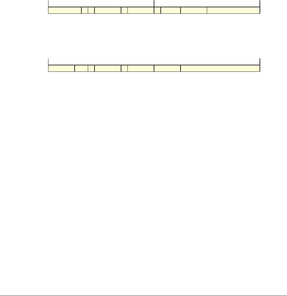
A8 Instruction Descriptions
A8.8 Alphabetical list of instructions
A8-300 Copyright © 1996-1998, 2000, 2004-2012, 2014 ARM. All rights reserved. ARM DDI 0406C.c
Non-Confidential ID051414
A8.8 Alphabetical list of instructions
This section lists every instruction. For details of the format used see Format of instruction descriptions on
page A8-282.
This section is formatted so that a full description of an instruction uses a double page.
A8.8.1 ADC (immediate)
Add with Carry (immediate) adds an immediate value and the Carry flag value to a register value, and writes the
result to the destination register. It can optionally update the condition flags based on the result.
d = UInt(Rd); n = UInt(Rn); setflags = (S == ‘1’); imm32 = ThumbExpandImm(i:imm3:imm8);
if d IN {13,15} || n IN {13,15} then UNPREDICTABLE;
For the case when
cond
is
0b1111
, see Unconditional instructions on page A5-216.
if Rd == ‘1111’ && S == ‘1’ then SEE SUBS PC, LR and related instructions;
d = UInt(Rd); n = UInt(Rn); setflags = (S == ‘1’); imm32 = ARMExpandImm(imm12);
Encoding T1 ARMv6T2, ARMv7
ADC{S}<c> <Rd>, <Rn>, #<const>
Encoding A1 ARMv4*, ARMv5T*, ARMv6*, ARMv7
ADC{S}<c> <Rd>, <Rn>, #<const>
1 1 1 0 i 0 1 0 1 0 S Rn 0 imm3 Rd imm8
15 14 13 12 11 10 9 8 7 6 5 4 3 2 1 0
1
1514131211109876543210
0 0 1 0 1 0 1 S Rn Rd imm12
31 30 29 28 27 26 25 24 23 22 21 20 19 18 17 16 15 14 13 12 11 10 9 8 7 6 5 4 3 2 1 0
cond

A8 Instruction Descriptions
A8.8 Alphabetical list of instructions
ARM DDI 0406C.c Copyright © 1996-1998, 2000, 2004-2012, 2014 ARM. All rights reserved. A8-301
ID051414 Non-Confidential
Assembler syntax
ADC{S}{<c>}{<q>} {<Rd>,} <Rn>, #<const>
where:
S
If
S
is present, the instruction updates the flags. Otherwise, the flags are not updated.
<c>, <q>
See Standard assembler syntax fields on page A8-287.
<Rd>
The destination register. If
S
is specified and <Rd> is the PC, see SUBS PC, LR (Thumb) on
page B9-2010 or SUBS PC, LR and related instructions (ARM) on page B9-2012.
In ARM instructions, if
S
is not specified and <Rd> is the PC, the instruction is a branch to the
address calculated by the operation. This is an interworking branch, see Pseudocode details of
operations on ARM core registers on page A2-47. ARM deprecates this use of PC.
Note
Before ARMv7, this was a simple branch.
<Rn>
The first operand register. The PC can be used in ARM instructions. ARM deprecates this use of PC.
<const>
The immediate value to be added to the value obtained from
<Rn>
. See Modified immediate constants
in Thumb instructions on page A6-232 or Modified immediate constants in ARM instructions on
page A5-200 for the range of values.
The pre-UAL syntax
ADC<c>S
is equivalent to
ADCS<c>
.
Operation
if ConditionPassed() then
EncodingSpecificOperations();
(result, carry, overflow) = AddWithCarry(R[n], imm32, APSR.C);
if d == 15 then // Can only occur for ARM encoding
ALUWritePC(result); // setflags is always FALSE here
else
R[d] = result;
if setflags then
APSR.N = result<31>;
APSR.Z = IsZeroBit(result);
APSR.C = carry;
APSR.V = overflow;
Exceptions
None.

A8 Instruction Descriptions
A8.8 Alphabetical list of instructions
A8-302 Copyright © 1996-1998, 2000, 2004-2012, 2014 ARM. All rights reserved. ARM DDI 0406C.c
Non-Confidential ID051414
A8.8.2 ADC (register)
Add with Carry (register) adds a register value, the Carry flag value, and an optionally-shifted register value, and
writes the result to the destination register. It can optionally update the condition flags based on the result.
d = UInt(Rdn); n = UInt(Rdn); m = UInt(Rm); setflags = !InITBlock();
(shift_t, shift_n) = (SRType_LSL, 0);
d = UInt(Rd); n = UInt(Rn); m = UInt(Rm); setflags = (S == ‘1’);
(shift_t, shift_n) = DecodeImmShift(type, imm3:imm2);
if d IN {13,15} || n IN {13,15} || m IN {13,15} then UNPREDICTABLE;
For the case when
cond
is
0b1111
, see Unconditional instructions on page A5-216.
if Rd == ‘1111’ && S == ‘1’ then SEE SUBS PC, LR and related instructions;
d = UInt(Rd); n = UInt(Rn); m = UInt(Rm); setflags = (S == ‘1’);
(shift_t, shift_n) = DecodeImmShift(type, imm5);
Encoding T1 ARMv4T, ARMv5T*, ARMv6*, ARMv7
ADCS <Rdn>, <Rm>
Outside IT block.
ADC<c> <Rdn>, <Rm>
Inside IT block.
Encoding T2 ARMv6T2, ARMv7
ADC{S}<c>.W <Rd>, <Rn>, <Rm>{, <shift>}
Encoding A1 ARMv4*, ARMv5T*, ARMv6*, ARMv7
ADC{S}<c> <Rd>, <Rn>, <Rm>{, <shift>}
0 1 0 0 0 0 0 1 0 1 Rm Rdn
15 14 13 12 11 10 9 8 7 6 5 4 3 2 1 0
1 1 0 1 0 1 1 0 1 0 S Rn (0) imm3 Rd imm2 type Rm
15 14 13 12 11 10 9 8 7 6 5 4 3 2 1 0
1
1514131211109876543210
0 0 0 0 1 0 1 S Rn Rd imm5 type 0 Rm
31 30 29 28 27 26 25 24 23 22 21 20 19 18 17 16 15 14 13 12 11 10 9 8 7 6 5 4 3 2 1 0
cond

A8 Instruction Descriptions
A8.8 Alphabetical list of instructions
ARM DDI 0406C.c Copyright © 1996-1998, 2000, 2004-2012, 2014 ARM. All rights reserved. A8-303
ID051414 Non-Confidential
Assembler syntax
ADC{S}{<c>}{<q>} {<Rd>,} <Rn>, <Rm> {, <shift>}
where:
S
If
S
is present, the instruction updates the flags. Otherwise, the flags are not updated.
<c>, <q>
See Standard assembler syntax fields on page A8-287.
<Rd>
The destination register. If
S
is specified and
<Rd>
is the PC, see SUBS PC, LR (Thumb) on
page B9-2010 or SUBS PC, LR and related instructions (ARM) on page B9-2012.
In ARM instructions, if
S
is not specified and
<Rd>
is the PC, the instruction is a branch to the address
calculated by the operation. This is an interworking branch, see Pseudocode details of operations
on ARM core registers on page A2-47. ARM deprecates this use of the PC.
Note
Before ARMv7, this was a simple branch.
<Rn>
The first operand register. The PC can be used in ARM instructions. ARM deprecates this use of the
PC.
<Rm>
The optionally shifted second operand register. The PC can be used in ARM instructions. ARM
deprecates this use of the PC.
<shift>
The shift to apply to the value read from
<Rm>
. If present, encoding T1 is not permitted. If absent, no
shift is applied and any encoding is permitted. Shifts applied to a register on page A8-291 describes
the shifts and how they are encoded.
In Thumb assembly:
• outside an IT block, if
ADCS <Rd>, <Rn>, <Rd>
has
<Rd>
and
<Rn>
both in the range R0-R7, it is assembled using
encoding T1 as though
ADCS <Rd>, <Rn>
had been written.
• inside an IT block, if
ADC<c> <Rd>, <Rn>, <Rd>
has
<Rd>
and
<Rn>
both in the range R0-R7, it is assembled
using encoding T1 as though
ADC<c> <Rd>, <Rn>
had been written.
To prevent either of these happening, use the .W qualifier.
The pre-UAL syntax
ADC<c>S
is equivalent to
ADCS<c>
.
Operation
if ConditionPassed() then
EncodingSpecificOperations();
shifted = Shift(R[m], shift_t, shift_n, APSR.C);
(result, carry, overflow) = AddWithCarry(R[n], shifted, APSR.C);
if d == 15 then // Can only occur for ARM encoding
ALUWritePC(result); // setflags is always FALSE here
else
R[d] = result;
if setflags then
APSR.N = result<31>;
APSR.Z = IsZeroBit(result);
APSR.C = carry;
APSR.V = overflow;
Exceptions
None.

A8 Instruction Descriptions
A8.8 Alphabetical list of instructions
A8-304 Copyright © 1996-1998, 2000, 2004-2012, 2014 ARM. All rights reserved. ARM DDI 0406C.c
Non-Confidential ID051414
A8.8.3 ADC (register-shifted register)
Add with Carry (register-shifted register) adds a register value, the Carry flag value, and a register-shifted register
value. It writes the result to the destination register, and can optionally update the condition flags based on the result.
For the case when
cond
is
0b1111
, see Unconditional instructions on page A5-216.
d = UInt(Rd); n = UInt(Rn); m = UInt(Rm); s = UInt(Rs);
setflags = (S == ‘1’); shift_t = DecodeRegShift(type);
if d == 15 || n == 15 || m == 15 || s == 15 then UNPREDICTABLE;
Encoding A1 ARMv4*, ARMv5T*, ARMv6*, ARMv7
ADC{S}<c> <Rd>, <Rn>, <Rm>, <type> <Rs>
0 0 0 0 1 0 1 S Rn Rd Rs 0 type 1 Rm
31 30 29 28 27 26 25 24 23 22 21 20 19 18 17 16 15 14 13 12 11 10 9 8 7 6 5 4 3 2 1 0
cond

A8 Instruction Descriptions
A8.8 Alphabetical list of instructions
ARM DDI 0406C.c Copyright © 1996-1998, 2000, 2004-2012, 2014 ARM. All rights reserved. A8-305
ID051414 Non-Confidential
Assembler syntax
ADC{S}{<c>}{<q>} {<Rd>,} <Rn>, <Rm>, <type> <Rs>
where:
S
If
S
is present, the instruction updates the flags. Otherwise, the flags are not updated.
<c>, <q>
See Standard assembler syntax fields on page A8-287.
<Rd>
The destination register.
<Rn>
The first operand register.
<Rm>
The register that is shifted and used as the second operand.
<type>
The type of shift to apply to the value read from
<Rm>
. It must be one of:
ASR
Arithmetic shift right, encoded as type =
0b10
.
LSL
Logical shift left, encoded as type =
0b00
.
LSR
Logical shift right, encoded as type =
0b01
.
ROR
Rotate right, encoded as type =
0b11
.
<Rs>
The register whose bottom byte contains the amount to shift by.
The pre-UAL syntax
ADC<c>S
is equivalent to
ADCS<c>
.
Operation
if ConditionPassed() then
EncodingSpecificOperations();
shift_n = UInt(R[s]<7:0>);
shifted = Shift(R[m], shift_t, shift_n, APSR.C);
(result, carry, overflow) = AddWithCarry(R[n], shifted, APSR.C);
R[d] = result;
if setflags then
APSR.N = result<31>;
APSR.Z = IsZeroBit(result);
APSR.C = carry;
APSR.V = overflow;
Exceptions
None.
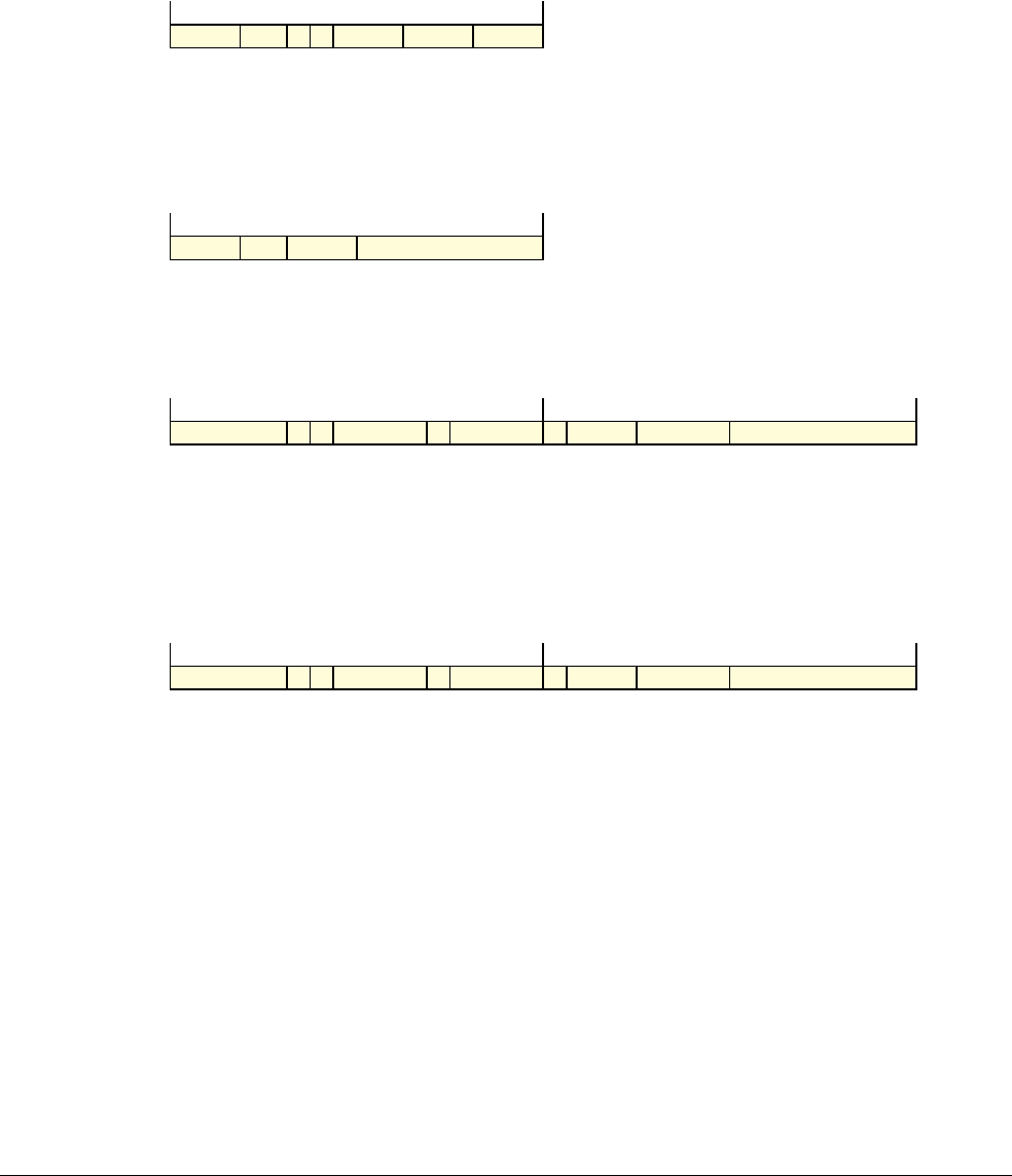
A8 Instruction Descriptions
A8.8 Alphabetical list of instructions
A8-306 Copyright © 1996-1998, 2000, 2004-2012, 2014 ARM. All rights reserved. ARM DDI 0406C.c
Non-Confidential ID051414
A8.8.4 ADD (immediate, Thumb)
This instruction adds an immediate value to a register value, and writes the result to the destination register. It can
optionally update the condition flags based on the result.
d = UInt(Rd); n = UInt(Rn); setflags = !InITBlock(); imm32 = ZeroExtend(imm3, 32);
d = UInt(Rdn); n = UInt(Rdn); setflags = !InITBlock(); imm32 = ZeroExtend(imm8, 32);
if Rd == ‘1111’ && S == ‘1’ then SEE CMN (immediate);
if Rn == ‘1101’ then SEE ADD (SP plus immediate);
d = UInt(Rd); n = UInt(Rn); setflags = (S == ‘1’); imm32 = ThumbExpandImm(i:imm3:imm8);
if d == 13 || (d == 15 && S == ‘0’) || n == 15 then UNPREDICTABLE;
if Rn == ‘1111’ then SEE ADR;
if Rn == ‘1101’ then SEE ADD (SP plus immediate);
d = UInt(Rd); n = UInt(Rn); setflags = FALSE; imm32 = ZeroExtend(i:imm3:imm8, 32);
if d IN {13,15} then UNPREDICTABLE;
Encoding T1 ARMv4T, ARMv5T*, ARMv6*, ARMv7
ADDS <Rd>, <Rn>, #<imm3>
Outside IT block.
ADD<c> <Rd>, <Rn>, #<imm3>
Inside IT block.
Encoding T2 ARMv4T, ARMv5T*, ARMv6*, ARMv7
ADDS <Rdn>, #<imm8>
Outside IT block.
ADD<c> <Rdn>, #<imm8>
Inside IT block.
Encoding T3 ARMv6T2, ARMv7
ADD{S}<c>.W <Rd>, <Rn>, #<const>
Encoding T4 ARMv6T2, ARMv7
ADDW<c> <Rd>, <Rn>, #<imm12>
0 0 0 1 1 1 0 imm3 Rn Rd
15 14 13 12 11 10 9 8 7 6 5 4 3 2 1 0
0 0 1 1 0 Rdn imm8
15 14 13 12 11 10 9 8 7 6 5 4 3 2 1 0
1 1 1 0 i 0 1 0 0 0 S Rn 0 imm3 Rd imm8
15 14 13 12 11 10 9 8 7 6 5 4 3 2 1 0
1
1514131211109876543210
1 1 1 0 i 1 0 0 0 0 0 Rn 0 imm3 Rd imm8
15 14 13 12 11 10 9 8 7 6 5 4 3 2 1 0
1
1514131211109876543210

A8 Instruction Descriptions
A8.8 Alphabetical list of instructions
ARM DDI 0406C.c Copyright © 1996-1998, 2000, 2004-2012, 2014 ARM. All rights reserved. A8-307
ID051414 Non-Confidential
Assembler syntax
where:
S
If
S
is present, the instruction updates the flags. Otherwise, the flags are not updated.
<c>, <q>
See Standard assembler syntax fields on page A8-287.
<Rd>
The destination register.
<Rn>
The first operand register. If
<Rn>
is SP, see ADD (SP plus immediate) on page A8-316. If
<Rn>
is
PC, see ADR on page A8-322.
<const>
The immediate value to be added to the value obtained from
<Rn>
. The range of values is 0-7 for
encoding T1, 0-255 for encoding T2 and 0-4095 for encoding T4. See Modified immediate constants
in Thumb instructions on page A6-232 for the range of values for encoding T3.
When multiple encodings of the same length are available for an instruction, encoding T3 is preferred to encoding
T4 (if encoding T4 is required, use the
ADDW
syntax). Encoding T1 is preferred to encoding T2 if
<Rd>
is specified
and encoding T2 is preferred to encoding T1 if
<Rd>
is omitted.
The pre-UAL syntax
ADD<c>S
is equivalent to
ADDS<c>
.
Operation
if ConditionPassed() then
EncodingSpecificOperations();
(result, carry, overflow) = AddWithCarry(R[n], imm32, ‘0’);
R[d] = result;
if setflags then
APSR.N = result<31>;
APSR.Z = IsZeroBit(result);
APSR.C = carry;
APSR.V = overflow;
Exceptions
None.
ADD{S}{<c>}{<q>} {<Rd>,} <Rn>, #<const>
All encodings permitted
ADDW{<c>}{<q>} {<Rd>,} <Rn>, #<const>
Only encoding T4 permitted

A8 Instruction Descriptions
A8.8 Alphabetical list of instructions
A8-308 Copyright © 1996-1998, 2000, 2004-2012, 2014 ARM. All rights reserved. ARM DDI 0406C.c
Non-Confidential ID051414
A8.8.5 ADD (immediate, ARM)
This instruction adds an immediate value to a register value, and writes the result to the destination register. It can
optionally update the condition flags based on the result.
For the case when
cond
is
0b1111
, see Unconditional instructions on page A5-216.
if Rn == ‘1111’ && S == ‘0’ then SEE ADR;
if Rn == ‘1101’ then SEE ADD (SP plus immediate);
if Rd == ‘1111’ && S == ‘1’ then SEE SUBS PC, LR and related instructions;
d = UInt(Rd); n = UInt(Rn); setflags = (S == ‘1’); imm32 = ARMExpandImm(imm12);
Encoding A1 ARMv4*, ARMv5T*, ARMv6*, ARMv7
ADD{S}<c> <Rd>, <Rn>, #<const>
0 0 1 0 1 0 0 S Rn Rd imm12
31 30 29 28 27 26 25 24 23 22 21 20 19 18 17 16 15 14 13 12 11 10 9 8 7 6 5 4 3 2 1 0
cond

A8 Instruction Descriptions
A8.8 Alphabetical list of instructions
ARM DDI 0406C.c Copyright © 1996-1998, 2000, 2004-2012, 2014 ARM. All rights reserved. A8-309
ID051414 Non-Confidential
Assembler syntax
where:
S
If
S
is present, the instruction updates the flags. Otherwise, the flags are not updated.
<c>, <q>
See Standard assembler syntax fields on page A8-287.
<Rd>
The destination register. If
S
is specified and
<Rd>
is the PC, see SUBS PC, LR and related
instructions (ARM) on page B9-2012.
If
S
is not specified and
<Rd>
is the PC, the instruction is a branch to the address calculated by the
operation. This is an interworking branch, see Pseudocode details of operations on ARM core
registers on page A2-47.
Note
Before ARMv7, this was a simple branch.
<Rn>
The first operand register. If the SP is specified for
<Rn>
, see ADD (SP plus immediate) on
page A8-316. If the PC is specified for
<Rn>
, see ADR on page A8-322.
<const>
The immediate value to be added to the value obtained from
<Rn>
. See Modified immediate constants
in ARM instructions on page A5-200 for the range of values.
The pre-UAL syntax
ADD<c>S
is equivalent to
ADDS<c>
.
Operation
if ConditionPassed() then
EncodingSpecificOperations();
(result, carry, overflow) = AddWithCarry(R[n], imm32, ‘0’);
if d == 15 then
ALUWritePC(result); // setflags is always FALSE here
else
R[d] = result;
if setflags then
APSR.N = result<31>;
APSR.Z = IsZeroBit(result);
APSR.C = carry;
APSR.V = overflow;
Exceptions
None.
ADD{S}{<c>}{<q>} {<Rd>,} <Rn>, #<const>
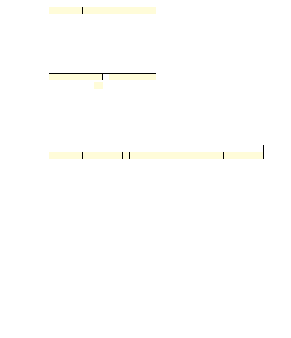
A8 Instruction Descriptions
A8.8 Alphabetical list of instructions
A8-310 Copyright © 1996-1998, 2000, 2004-2012, 2014 ARM. All rights reserved. ARM DDI 0406C.c
Non-Confidential ID051414
A8.8.6 ADD (register, Thumb)
This instruction adds a register value and an optionally-shifted register value, and writes the result to the destination
register. It can optionally update the condition flags based on the result.
d = UInt(Rd); n = UInt(Rn); m = UInt(Rm); setflags = !InITBlock();
(shift_t, shift_n) = (SRType_LSL, 0);
if (DN:Rdn) == ‘1101’ || Rm == ‘1101’ then SEE ADD (SP plus register);
d = UInt(DN:Rdn); n = d; m = UInt(Rm); setflags = FALSE; (shift_t, shift_n) = (SRType_LSL, 0);
if n == 15 && m == 15 then UNPREDICTABLE;
if d == 15 && InITBlock() && !LastInITBlock() then UNPREDICTABLE;
if Rd == ‘1111’ && S == ‘1’ then SEE CMN (register);
if Rn == ‘1101’ then SEE ADD (SP plus register);
d = UInt(Rd); n = UInt(Rn); m = UInt(Rm); setflags = (S == ‘1’);
(shift_t, shift_n) = DecodeImmShift(type, imm3:imm2);
if d == 13 || (d == 15 && S == ‘0’) || n == 15 || m IN {13,15} then UNPREDICTABLE;
Encoding T1 ARMv4T, ARMv5T*, ARMv6*, ARMv7
ADDS <Rd>, <Rn>, <Rm>
Outside IT block.
ADD<c> <Rd>, <Rn>, <Rm>
Inside IT block.
Encoding T2 ARMv6T2, ARMv7 if
<Rdn>
and
<Rm>
are both from R0-R7
ARMv4T, ARMv5T*, ARMv6*, ARMv7 otherwise
ADD<c> <Rdn>, <Rm>
If
<Rdn>
is the PC, must be outside or last in IT block.
Encoding T3 ARMv6T2, ARMv7
ADD{S}<c>.W <Rd>, <Rn>, <Rm>{, <shift>}
0 0 0 1 1 0 0 Rm Rn Rd
15 14 13 12 11 10 9 8 7 6 5 4 3 2 1 0
0 1 0 0 0 1 0 0
DN
Rm Rdn
15 14 13 12 11 10 9 8 7 6 5 4 3 2 1 0
1 1 0 1 0 1 1 0 0 0 S Rn (0) imm3 Rd imm2 type Rm
15 14 13 12 11 10 9 8 7 6 5 4 3 2 1 0
1
1514131211109876543210

A8 Instruction Descriptions
A8.8 Alphabetical list of instructions
ARM DDI 0406C.c Copyright © 1996-1998, 2000, 2004-2012, 2014 ARM. All rights reserved. A8-311
ID051414 Non-Confidential
Assembler syntax
ADD{S}{<c>}{<q>} {<Rd>,} <Rn>, <Rm> {, <shift>}
where:
S
If
S
is present, the instruction updates the flags. Otherwise, the flags are not updated.
<c>, <q>
See Standard assembler syntax fields on page A8-287.
<Rd>
The destination register. If
S
is specified and
<Rd>
is the PC, see CMN (register) on page A8-366. If
omitted,
<Rd>
is the same as
<Rn>
and encoding T2 is preferred to encoding T1 inside an IT block. If
<Rd>
is present, encoding T1 is preferred to encoding T2.
If
<Rd>
is the PC and
S
is not specified, encoding T2 is used and the instruction is a branch to the
address calculated by the operation. This is a simple branch, see Pseudocode details of operations
on ARM core registers on page A2-47.
<Rn>
The first operand register. The PC can be used in encoding T2. If
<Rn>
is SP, see ADD (SP plus
register, Thumb) on page A8-318.
<Rm>
The register that is optionally shifted and used as the second operand. The PC can be used in
encoding T2
<shift>
The shift to apply to the value read from
<Rm>
. If present, only encoding T3 is permitted. If omitted,
no shift is applied and any encoding is permitted. Shifts applied to a register on page A8-291
describes the shifts and how they are encoded.
Inside an IT block, if
ADD<c> <Rd>, <Rn>, <Rd>
cannot be assembled using encoding T1, it is assembled using
encoding T2 as though
ADD<c> <Rd>, <Rn>
had been written. To prevent this happening, use the
.W
qualifier.
The pre-UAL syntax
ADD<c>S
is equivalent to
ADDS<c>
.
Operation
if ConditionPassed() then
EncodingSpecificOperations();
shifted = Shift(R[m], shift_t, shift_n, APSR.C);
(result, carry, overflow) = AddWithCarry(R[n], shifted, ‘0’);
if d == 15 then
ALUWritePC(result); // setflags is always FALSE here
else
R[d] = result;
if setflags then
APSR.N = result<31>;
APSR.Z = IsZeroBit(result);
APSR.C = carry;
APSR.V = overflow;
Exceptions
None.

A8 Instruction Descriptions
A8.8 Alphabetical list of instructions
A8-312 Copyright © 1996-1998, 2000, 2004-2012, 2014 ARM. All rights reserved. ARM DDI 0406C.c
Non-Confidential ID051414
A8.8.7 ADD (register, ARM)
This instruction adds a register value and an optionally-shifted register value, and writes the result to the destination
register. It can optionally update the condition flags based on the result.
For the case when
cond
is
0b1111
, see Unconditional instructions on page A5-216.
if Rd == ‘1111’ && S == ‘1’ then SEE SUBS PC, LR and related instructions;
if Rn == ‘1101’ then SEE ADD (SP plus register);
d = UInt(Rd); n = UInt(Rn); m = UInt(Rm); setflags = (S == ‘1’);
(shift_t, shift_n) = DecodeImmShift(type, imm5);
Encoding A1 ARMv4*, ARMv5T*, ARMv6*, ARMv7
ADD{S}<c> <Rd>, <Rn>, <Rm>{, <shift>}
cond 0 0 0 0 1 0 0 S Rn Rd imm5 type 0 Rm
31 30 29 28 27 26 25 24 23 22 21 20 19 18 17 16 15 14 13 12 11 10 9 8 7 6 5 4 3 2 1 0

A8 Instruction Descriptions
A8.8 Alphabetical list of instructions
ARM DDI 0406C.c Copyright © 1996-1998, 2000, 2004-2012, 2014 ARM. All rights reserved. A8-313
ID051414 Non-Confidential
Assembler syntax
ADD{S}{<c>}{<q>} {<Rd>,} <Rn>, <Rm> {, <shift>}
where:
S
If
S
is present, the instruction updates the flags. Otherwise, the flags are not updated.
<c>, <q>
See Standard assembler syntax fields on page A8-287.
<Rd>
The destination register. If
S
is specified and
<Rd>
is the PC, see SUBS PC, LR and related
instructions (ARM) on page B9-2012. If omitted,
<Rd>
is the same as
<Rn>
.
If
<Rd>
is the PC and
S
is not specified, the instruction is a branch to the address calculated by the
operation. This is an interworking branch, see Pseudocode details of operations on ARM core
registers on page A2-47.
Note
Before ARMv7, this was a simple branch.
<Rn>
The first operand register. The PC can be used. If
<Rn>
is SP, see ADD (SP plus register, Thumb) on
page A8-318.
<Rm>
The register that is optionally shifted and used as the second operand. The PC can be used.
<shift>
The shift to apply to the value read from
<Rm>
. If present, only encoding T3 or A1 is permitted. If
omitted, no shift is applied and any encoding is permitted. Shifts applied to a register on
page A8-291 describes the shifts and how they are encoded.
The pre-UAL syntax
ADD<c>S
is equivalent to
ADDS<c>
.
Operation
if ConditionPassed() then
EncodingSpecificOperations();
shifted = Shift(R[m], shift_t, shift_n, APSR.C);
(result, carry, overflow) = AddWithCarry(R[n], shifted, ‘0’);
if d == 15 then
ALUWritePC(result); // setflags is always FALSE here
else
R[d] = result;
if setflags then
APSR.N = result<31>;
APSR.Z = IsZeroBit(result);
APSR.C = carry;
APSR.V = overflow;
Exceptions
None.

A8 Instruction Descriptions
A8.8 Alphabetical list of instructions
A8-314 Copyright © 1996-1998, 2000, 2004-2012, 2014 ARM. All rights reserved. ARM DDI 0406C.c
Non-Confidential ID051414
A8.8.8 ADD (register-shifted register)
Add (register-shifted register) adds a register value and a register-shifted register value. It writes the result to the
destination register, and can optionally update the condition flags based on the result.
For the case when
cond
is
0b1111
, see Unconditional instructions on page A5-216.
d = UInt(Rd); n = UInt(Rn); m = UInt(Rm); s = UInt(Rs);
setflags = (S == ‘1’); shift_t = DecodeRegShift(type);
if d == 15 || n == 15 || m == 15 || s == 15 then UNPREDICTABLE;
Encoding A1 ARMv4*, ARMv5T*, ARMv6*, ARMv7
ADD{S}<c> <Rd>, <Rn>, <Rm>, <type> <Rs>
cond 0 0 0 0 1 0 0 S Rn Rd Rs 0 type 1 Rm
31 30 29 28 27 26 25 24 23 22 21 20 19 18 17 16 15 14 13 12 11 10 9 8 7 6 5 4 3 2 1 0

A8 Instruction Descriptions
A8.8 Alphabetical list of instructions
ARM DDI 0406C.c Copyright © 1996-1998, 2000, 2004-2012, 2014 ARM. All rights reserved. A8-315
ID051414 Non-Confidential
Assembler syntax
ADD{S}{<c>}{<q>} {<Rd>,} <Rn>, <Rm>, <type> <Rs>
where:
S
If
S
is present, the instruction updates the flags. Otherwise, the flags are not updated.
<c>, <q>
See Standard assembler syntax fields on page A8-287.
<Rd>
The destination register.
<Rn>
The first operand register.
<Rm>
The register that is shifted and used as the second operand.
<type>
The type of shift to apply to the value read from
<Rm>
. It must be one of:
ASR
Arithmetic shift right, encoded as type =
0b10
.
LSL
Logical shift left, encoded as type =
0b00
.
LSR
Logical shift right, encoded as type =
0b01
.
ROR
Rotate right, encoded as type =
0b11
.
<Rs>
The register whose bottom byte contains the amount to shift by.
The pre-UAL syntax
ADD<c>S
is equivalent to
ADDS<c>
.
Operation
if ConditionPassed() then
EncodingSpecificOperations();
shift_n = UInt(R[s]<7:0>);
shifted = Shift(R[m], shift_t, shift_n, APSR.C);
(result, carry, overflow) = AddWithCarry(R[n], shifted, ‘0’);
R[d] = result;
if setflags then
APSR.N = result<31>;
APSR.Z = IsZeroBit(result);
APSR.C = carry;
APSR.V = overflow;
Exceptions
None.
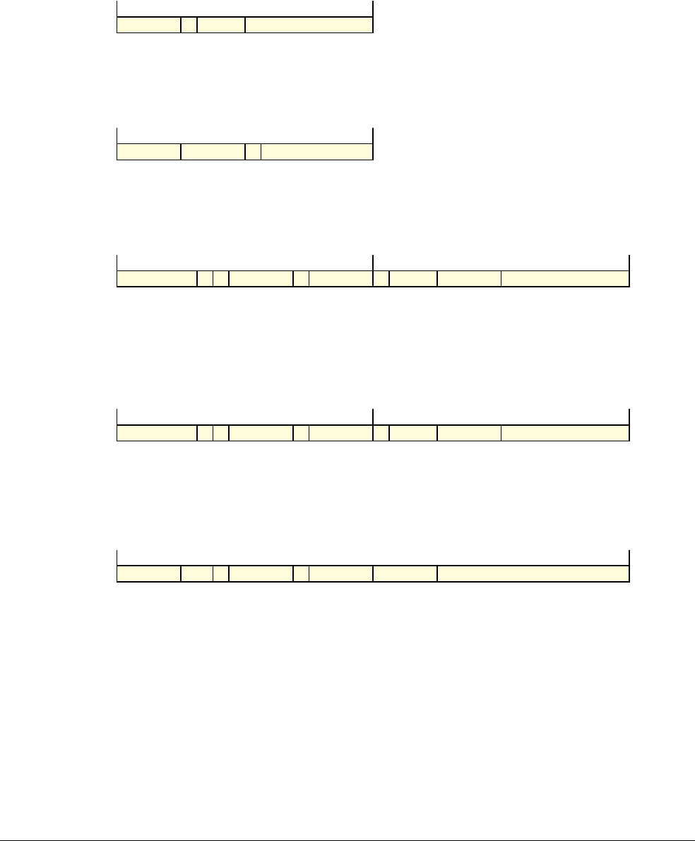
A8 Instruction Descriptions
A8.8 Alphabetical list of instructions
A8-316 Copyright © 1996-1998, 2000, 2004-2012, 2014 ARM. All rights reserved. ARM DDI 0406C.c
Non-Confidential ID051414
A8.8.9 ADD (SP plus immediate)
This instruction adds an immediate value to the SP value, and writes the result to the destination register.
d = UInt(Rd); setflags = FALSE; imm32 = ZeroExtend(imm8:’00’, 32);
d = 13; setflags = FALSE; imm32 = ZeroExtend(imm7:’00’, 32);
if Rd == ‘1111’ && S == ‘1’ then SEE CMN (immediate);
d = UInt(Rd); setflags = (S == ‘1’); imm32 = ThumbExpandImm(i:imm3:imm8);
if d == 15 && S == ‘0’ then UNPREDICTABLE;
d = UInt(Rd); setflags = FALSE; imm32 = ZeroExtend(i:imm3:imm8, 32);
if d == 15 then UNPREDICTABLE;
For the case when
cond
is
0b1111
, see Unconditional instructions on page A5-216.
if Rd == ‘1111’ && S == ‘1’ then SEE SUBS PC, LR and related instructions;
d = UInt(Rd); setflags = (S == ‘1’); imm32 = ARMExpandImm(imm12);
Encoding T1 ARMv4T, ARMv5T*, ARMv6*, ARMv7
ADD<c> <Rd>, SP, #<imm>
Encoding T2 ARMv4T, ARMv5T*, ARMv6*, ARMv7
ADD<c> SP, SP, #<imm>
Encoding T3 ARMv6T2, ARMv7
ADD{S}<c>.W <Rd>, SP, #<const>
Encoding T4 ARMv6T2, ARMv7
ADDW<c> <Rd>, SP, #<imm12>
Encoding A1 ARMv4*, ARMv5T*, ARMv6*, ARMv7
ADD{S}<c> <Rd>, SP, #<const>
1 0 1 0 1 Rd imm8
15 14 13 12 11 10 9 8 7 6 5 4 3 2 1 0
1 0 1 1 0 0 0 0 0 imm7
15 14 13 12 11 10 9 8 7 6 5 4 3 2 1 0
1 1 1 0 i 0 1 0 0 0 S 1 1 0 1 0 imm3 Rd imm8
15 14 13 12 11 10 9 8 7 6 5 4 3 2 1 0
1
1514131211109876543210
1 1 1 0 i 1 0 0 0 0 0 1 1 0 1 0 imm3 Rd imm8
15 14 13 12 11 10 9 8 7 6 5 4 3 2 1 0
1
1514131211109876543210
cond 0 0 1 0 1 0 0 S 1 1 0 1 Rd imm12
31 30 29 28 27 26 25 24 23 22 21 20 19 18 17 16 15 14 13 12 11 10 9 8 7 6 5 4 3 2 1 0

A8 Instruction Descriptions
A8.8 Alphabetical list of instructions
ARM DDI 0406C.c Copyright © 1996-1998, 2000, 2004-2012, 2014 ARM. All rights reserved. A8-317
ID051414 Non-Confidential
Assembler syntax
where:
S
If
S
is present, the instruction updates the flags. Otherwise, the flags are not updated.
<c>, <q>
See Standard assembler syntax fields on page A8-287.
<Rd>
The destination register. If
S
is specified and
<Rd>
is the PC, see SUBS PC, LR (Thumb) on
page B9-2010 or SUBS PC, LR and related instructions (ARM) on page B9-2012. If omitted,
<Rd>
is SP.
In ARM instructions, if
S
is not specified and
<Rd>
is the PC, the instruction is a branch to the address
calculated by the operation. This is an interworking branch, see Pseudocode details of operations
on ARM core registers on page A2-47.
Note
Before ARMv7, this was a simple branch.
<const>
The immediate value to be added to the value obtained from SP. Values are multiples of 4 in the
range 0-1020 for encoding T1, multiples of 4 in the range 0-508 for encoding T2 and any value in
the range 0-4095 for encoding T4. See Modified immediate constants in Thumb instructions on
page A6-232 or Modified immediate constants in ARM instructions on page A5-200 for the range
of values for encodings T3 and A1.
When both 32-bit encodings are available for an instruction, encoding T3 is preferred to encoding
T4.
Note
If encoding T4 is required, use the
ADDW
syntax.
The pre-UAL syntax
ADD<c>S
is equivalent to
ADDS<c>
.
Operation
if ConditionPassed() then
EncodingSpecificOperations();
(result, carry, overflow) = AddWithCarry(SP, imm32, ‘0’);
if d == 15 then // Can only occur for ARM encoding
ALUWritePC(result); // setflags is always FALSE here
else
R[d] = result;
if setflags then
APSR.N = result<31>;
APSR.Z = IsZeroBit(result);
APSR.C = carry;
APSR.V = overflow;
Exceptions
None.
ADD{S}{<c>}{<q>} {<Rd>,} SP, #<const>
All encodings permitted
ADDW{<c>}{<q>} {<Rd>,} SP, #<const>
Only encoding T4 is permitted
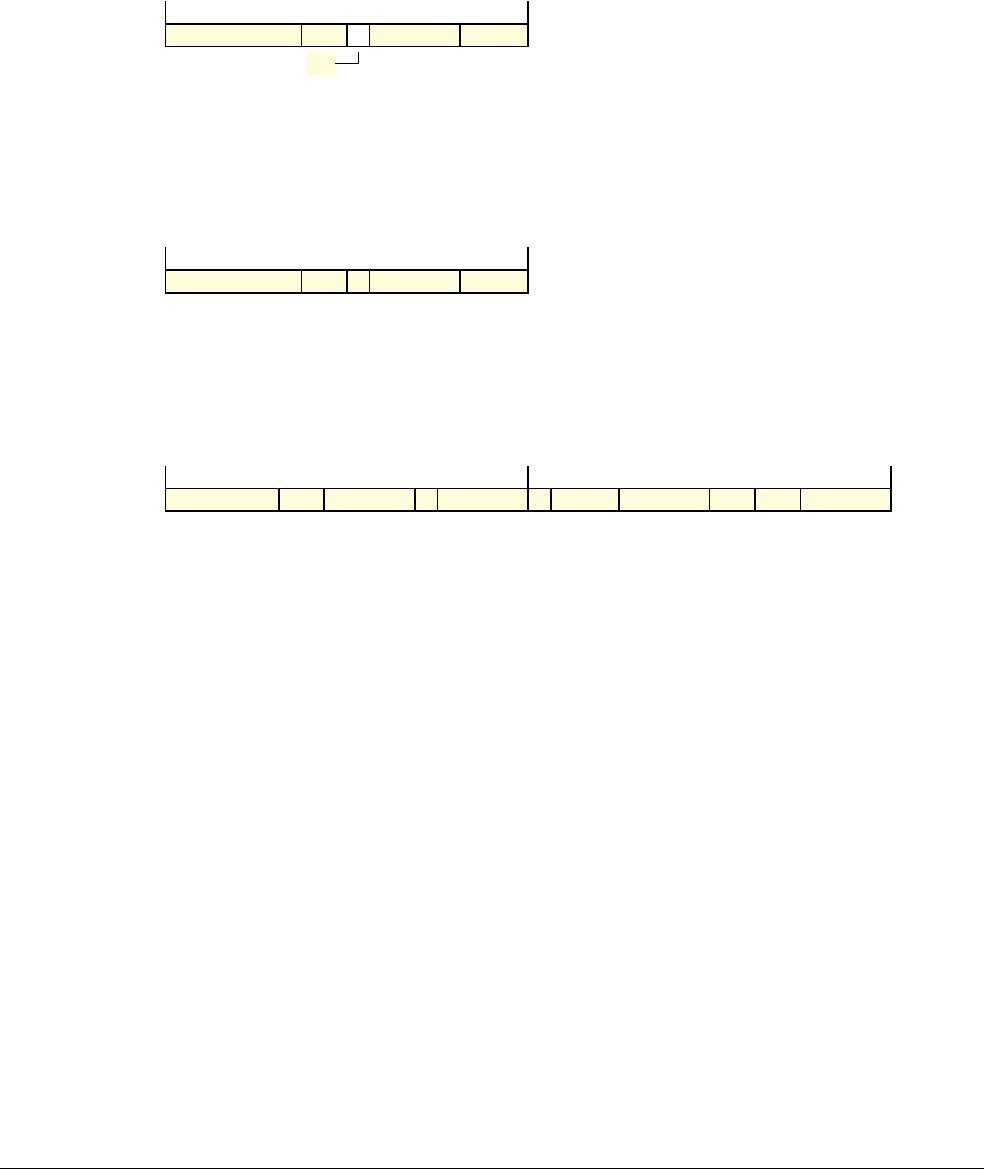
A8 Instruction Descriptions
A8.8 Alphabetical list of instructions
A8-318 Copyright © 1996-1998, 2000, 2004-2012, 2014 ARM. All rights reserved. ARM DDI 0406C.c
Non-Confidential ID051414
A8.8.10 ADD (SP plus register, Thumb)
This instruction adds an optionally-shifted register value to the SP value, and writes the result to the destination
register.
d = UInt(DM:Rdm); m = UInt(DM:Rdm); setflags = FALSE;
if d == 15 && InITBlock() && !LastInITBlock() then UNPREDICTABLE;
(shift_t, shift_n) = (SRType_LSL, 0);
if Rm == ‘1101’ then SEE encoding T1;
d = 13; m = UInt(Rm); setflags = FALSE;
(shift_t, shift_n) = (SRType_LSL, 0);
if Rd == ‘1111’ && S == ‘1’ then SEE CMN (register);
d = UInt(Rd); m = UInt(Rm); setflags = (S == ‘1’);
(shift_t, shift_n) = DecodeImmShift(type, imm3:imm2);
if d == 13 && (shift_t != SRType_LSL || shift_n > 3) then UNPREDICTABLE;
if (d == 15 && S == ‘0’) || m IN {13,15} then UNPREDICTABLE;
Encoding T1 ARMv4T, ARMv5T*, ARMv6*, ARMv7
ADD<c> <Rdm>, SP, <Rdm>
Encoding T2 ARMv4T, ARMv5T*, ARMv6*, ARMv7
ADD<c> SP, <Rm>
Encoding T3 ARMv6T2, ARMv7
ADD{S}<c>.W <Rd>, SP, <Rm>{, <shift>}
0 1 0 0 0 1 0 0
DM
1 1 0 1 Rdm
1514131211109876543210
0 1 0 0 0 1 0 0 1 Rm 1 0 1
15 14 13 12 11 10 9 8 7 6 5 4 3 2 1 0
1 1 0 1 0 1 1 0 0 0 S 1 1 0 1 (0) imm3 Rd imm2 type Rm
15 14 13 12 11 10 9 8 7 6 5 4 3 2 1 0
1
1514131211109876543210

A8 Instruction Descriptions
A8.8 Alphabetical list of instructions
ARM DDI 0406C.c Copyright © 1996-1998, 2000, 2004-2012, 2014 ARM. All rights reserved. A8-319
ID051414 Non-Confidential
Assembler syntax
ADD{S}{<c>}{<q>} {<Rd>,} SP, <Rm>{, <shift>}
where:
S
If
S
is present, the instruction updates the flags. Otherwise, the flags are not updated.
<c>, <q>
See Standard assembler syntax fields on page A8-287.
<Rd>
The destination register. If
S
is specified and
<Rd>
is the PC, see CMN (register) on page A8-366.
This register can be SP. If omitted,
<Rd>
is SP. This register can be the PC, but if it is, encoding T3
is not permitted. ARM deprecates using the PC.
If
<Rd>
is the PC and
S
is not specified, encoding T1 is used and the instruction is a branch to the
address calculated by the operation. This is a simple branch, see Pseudocode details of operations
on ARM core registers on page A2-47.
<Rm>
The register that is optionally shifted and used as the second operand. This register can be the PC,
but if it is, encoding T3 is not permitted. ARM deprecates using the PC. This register can be the SP,
but:
• ARM deprecates using the SP
• only encoding T1 is available and so the instruction can only be
ADD SP, SP, SP
.
<shift>
The shift to apply to the value read from
<Rm>
. If omitted, no shift is applied and any encoding is
permitted. If present, only encoding T3 is permitted. Shifts applied to a register on page A8-291
describes the shifts and how they are encoded.
If
<Rd>
is SP or omitted,
<shift>
is only permitted to be omitted,
LSL #1
,
LSL #2
, or
LSL #3
.
The pre-UAL syntax
ADD<c>S
is equivalent to
ADDS<c>
.
Operation
if ConditionPassed() then
EncodingSpecificOperations();
shifted = Shift(R[m], shift_t, shift_n, APSR.C);
(result, carry, overflow) = AddWithCarry(SP, shifted, ‘0’);
if d == 15 then
ALUWritePC(result); // setflags is always FALSE here
else
R[d] = result;
if setflags then
APSR.N = result<31>;
APSR.Z = IsZeroBit(result);
APSR.C = carry;
APSR.V = overflow;
Exceptions
None.

A8 Instruction Descriptions
A8.8 Alphabetical list of instructions
A8-320 Copyright © 1996-1998, 2000, 2004-2012, 2014 ARM. All rights reserved. ARM DDI 0406C.c
Non-Confidential ID051414
A8.8.11 ADD (SP plus register, ARM)
This instruction adds an optionally-shifted register value to the SP value, and writes the result to the destination
register.
For the case when
cond
is
0b1111
, see Unconditional instructions on page A5-216.
if Rd == ‘1111’ && S == ‘1’ then SEE SUBS PC, LR and related instructions;
d = UInt(Rd); m = UInt(Rm); setflags = (S == ‘1’);
(shift_t, shift_n) = DecodeImmShift(type, imm5);
Encoding A1 ARMv4*, ARMv5T*, ARMv6*, ARMv7
ADD{S}<c> <Rd>, SP, <Rm>{, <shift>}
cond 0 0 0 0 1 0 0 S 1 1 0 1 Rd imm5 type 0 Rm
31 30 29 28 27 26 25 24 23 22 21 20 19 18 17 16 15 14 13 12 11 10 9 8 7 6 5 4 3 2 1 0

A8 Instruction Descriptions
A8.8 Alphabetical list of instructions
ARM DDI 0406C.c Copyright © 1996-1998, 2000, 2004-2012, 2014 ARM. All rights reserved. A8-321
ID051414 Non-Confidential
Assembler syntax
ADD{S}{<c>}{<q>} {<Rd>,} SP, <Rm>{, <shift>}
where:
S
If
S
is present, the instruction updates the flags. Otherwise, the flags are not updated.
<c>, <q>
See Standard assembler syntax fields on page A8-287.
<Rd>
The destination register. If
S
is specified and
<Rd>
is the PC, see SUBS PC, LR and related
instructions (ARM) on page B9-2012. This register can be SP. If omitted,
<Rd>
is SP. This register
can be the PC, but ARM deprecates using the PC.
If
S
is not specified and
<Rd>
is the PC, the instruction is a branch to the address calculated by the
operation. This is an interworking branch, see Pseudocode details of operations on ARM core
registers on page A2-47. ARM deprecates this use of the PC.
Note
Before ARMv7, this was a simple branch.
<Rm>
The register that is optionally shifted and used as the second operand. This register can be the PC,
but ARM deprecates using the PC. This register can be the SP, but ARM deprecates using the SP.
<shift>
The shift to apply to the value read from
<Rm>
. If omitted, no shift is applied and any encoding is
permitted. Shifts applied to a register on page A8-291 describes the shifts and how they are
encoded.
The pre-UAL syntax
ADD<c>S
is equivalent to
ADDS<c>
.
Operation
if ConditionPassed() then
EncodingSpecificOperations();
shifted = Shift(R[m], shift_t, shift_n, APSR.C);
(result, carry, overflow) = AddWithCarry(SP, shifted, ‘0’);
if d == 15 then
ALUWritePC(result); // setflags is always FALSE here
else
R[d] = result;
if setflags then
APSR.N = result<31>;
APSR.Z = IsZeroBit(result);
APSR.C = carry;
APSR.V = overflow;
Exceptions
None.

A8 Instruction Descriptions
A8.8 Alphabetical list of instructions
A8-322 Copyright © 1996-1998, 2000, 2004-2012, 2014 ARM. All rights reserved. ARM DDI 0406C.c
Non-Confidential ID051414
A8.8.12 ADR
This instruction adds an immediate value to the PC value to form a PC-relative address, and writes the result to the
destination register.
d = UInt(Rd); imm32 = ZeroExtend(imm8:’00’, 32); add = TRUE;
d = UInt(Rd); imm32 = ZeroExtend(i:imm3:imm8, 32); add = FALSE;
if d IN {13,15} then UNPREDICTABLE;
d = UInt(Rd); imm32 = ZeroExtend(i:imm3:imm8, 32); add = TRUE;
if d IN {13,15} then UNPREDICTABLE;
For the case when
cond
is
0b1111
, see Unconditional instructions on page A5-216.
d = UInt(Rd); imm32 = ARMExpandImm(imm12); add = TRUE;
For the case when
cond
is
0b1111
, see Unconditional instructions on page A5-216.
d = UInt(Rd); imm32 = ARMExpandImm(imm12); add = FALSE;
Encoding T1 ARMv4T, ARMv5T*, ARMv6*, ARMv7
ADR<c> <Rd>, <label>
Encoding T2 ARMv6T2, ARMv7
ADR<c>.W <Rd>, <label> <label>
before current instruction
SUB <Rd>, PC, #0
Special case for subtraction of zero
Encoding T3 ARMv6T2, ARMv7
ADR<c>.W <Rd>, <label> <label>
after current instruction
Encoding A1 ARMv4*, ARMv5T*, ARMv6*, ARMv7
ADR<c> <Rd>, <label> <label>
after current instruction
Encoding A2 ARMv4*, ARMv5T*, ARMv6*, ARMv7
ADR<c> <Rd>, <label> <label>
before current instruction
SUB <Rd>, PC, #0
Special case for subtraction of zero
1 0 1 0 0 Rd imm8
15 14 13 12 11 10 9 8 7 6 5 4 3 2 1 0
1 1 1 0 i 1 0 1 0 1 0 1 1 1 1 0 imm3 Rd imm8
15 14 13 12 11 10 9 8 7 6 5 4 3 2 1 0
1
1514131211109876543210
1 1 1 0 i 1 0 0 0 0 0 1 1 1 1 0 imm3 Rd imm8
15 14 13 12 11 10 9 8 7 6 5 4 3 2 1 0
1
1514131211109876543210
cond 0 0 1 0 1 0 0 0 1 1 1 1 Rd imm12
31 30 29 28 27 26 25 24 23 22 21 20 19 18 17 16 15 14 13 12 11 10 9 8 7 6 5 4 3 2 1 0
cond 0 0 1 0 0 1 0 0 1 1 1 1 Rd imm12
31 30 29 28 27 26 25 24 23 22 21 20 19 18 17 16 15 14 13 12 11 10 9 8 7 6 5 4 3 2 1 0

A8 Instruction Descriptions
A8.8 Alphabetical list of instructions
ARM DDI 0406C.c Copyright © 1996-1998, 2000, 2004-2012, 2014 ARM. All rights reserved. A8-323
ID051414 Non-Confidential
Assembler syntax
where:
<c>, <q>
See Standard assembler syntax fields on page A8-287.
<Rd>
The destination register. In ARM instructions, if
<Rd>
is the PC, the instruction is a branch to the
address calculated by the operation. This is an interworking branch, see Pseudocode details of
operations on ARM core registers on page A2-47.
Note
Before ARMv7, this was a simple branch.
<label>
The label of an instruction or literal data item whose address is to be loaded into
<Rd>
. The assembler
calculates the required value of the offset from the
Align(PC, 4)
value of the
ADR
instruction to this
label.
If the offset is zero or positive, encodings T1, T3, and A1 are permitted, with
imm32
equal to the
offset.
If the offset is negative, encodings T2 and A2 are permitted, with
imm32
equal to the size of the offset.
That is, the use of encoding T2 or A2 indicates that the required offset is minus the value of
imm32
.
Permitted values of the size of the offset are:
Encoding T1 Multiples of 4 in the range 0 to 1020.
Encodings T2, T3 Any value in the range 0 to 4095.
Encodings A1, A2 Any of the constants described in Modified immediate constants in ARM
instructions on page A5-200.
The alternative syntax permits the addition or subtraction of the offset and the immediate offset to be specified
separately, including permitting a subtraction of 0 that cannot be specified using the normal syntax. For more
information, see Use of labels in UAL instruction syntax on page A4-162.
Operation
if ConditionPassed() then
EncodingSpecificOperations();
result = if add then (Align(PC,4) + imm32) else (Align(PC,4) - imm32);
if d == 15 then // Can only occur for ARM encodings
ALUWritePC(result);
else
R[d] = result;
Exceptions
None.
ADR{<c>}{<q>} <Rd>, <label>
Normal syntax
ADD{<c>}{<q>} <Rd>, PC, #<const>
Alternative for encodings T1, T3, A1
SUB{<c>}{<q>} <Rd>, PC, #<const>
Alternative for encoding T2, A2

A8 Instruction Descriptions
A8.8 Alphabetical list of instructions
A8-324 Copyright © 1996-1998, 2000, 2004-2012, 2014 ARM. All rights reserved. ARM DDI 0406C.c
Non-Confidential ID051414
A8.8.13 AND (immediate)
This instruction performs a bitwise AND of a register value and an immediate value, and writes the result to the
destination register.
if Rd == ‘1111’ && S == ‘1’ then SEE TST (immediate);
d = UInt(Rd); n = UInt(Rn); setflags = (S == ‘1’);
(imm32, carry) = ThumbExpandImm_C(i:imm3:imm8, APSR.C);
if d == 13 || (d == 15 && S == ‘0’) || n IN {13,15} then UNPREDICTABLE;
For the case when
cond
is
0b1111
, see Unconditional instructions on page A5-216.
if Rd == ‘1111’ && S == ‘1’ then SEE SUBS PC, LR and related instructions;
d = UInt(Rd); n = UInt(Rn); setflags = (S == ‘1’);
(imm32, carry) = ARMExpandImm_C(imm12, APSR.C);
Encoding T1 ARMv6T2, ARMv7
AND{S}<c> <Rd>, <Rn>, #<const>
Encoding A1 ARMv4*, ARMv5T*, ARMv6*, ARMv7
AND{S}<c> <Rd>, <Rn>, #<const>
1 1 1 0 i 0 0 0 0 0 S Rn 0 imm3 Rd imm8
15 14 13 12 11 10 9 8 7 6 5 4 3 2 1 0
1
1514131211109876543210
cond 0 0 1 0 0 0 0 S Rn Rd imm12
31 30 29 28 27 26 25 24 23 22 21 20 19 18 17 16 15 14 13 12 11 10 9 8 7 6 5 4 3 2 1 0

A8 Instruction Descriptions
A8.8 Alphabetical list of instructions
ARM DDI 0406C.c Copyright © 1996-1998, 2000, 2004-2012, 2014 ARM. All rights reserved. A8-325
ID051414 Non-Confidential
Assembler syntax
AND{S}{<c>}{<q>} {<Rd>,} <Rn>, #<const>
where:
S
If
S
is present, the instruction updates the flags. Otherwise, the flags are not updated.
<c>, <q>
See Standard assembler syntax fields on page A8-287.
<Rd>
The destination register. If
S
is specified and
<Rd>
is the PC, see SUBS PC, LR (Thumb) on
page B9-2010 or SUBS PC, LR and related instructions (ARM) on page B9-2012.
In ARM instructions, if
S
is not specified and
<Rd>
is the PC, the instruction is a branch to the address
calculated by the operation. This is an interworking branch, see Pseudocode details of operations
on ARM core registers on page A2-47. ARM deprecates this use of the PC.
Note
Before ARMv7, this was a simple branch.
<Rn>
The first operand register. The PC can be used in ARM instructions. ARM deprecates this use of the
PC.
<const>
The immediate value to be ANDed with the value obtained from
<Rn>
. See Modified immediate
constants in Thumb instructions on page A6-232 or Modified immediate constants in ARM
instructions on page A5-200 for the range of values.
The pre-UAL syntax
AND<c>S
is equivalent to
ANDS<c>
.
Operation
if ConditionPassed() then
EncodingSpecificOperations();
result = R[n] AND imm32;
if d == 15 then // Can only occur for ARM encoding
ALUWritePC(result); // setflags is always FALSE here
else
R[d] = result;
if setflags then
APSR.N = result<31>;
APSR.Z = IsZeroBit(result);
APSR.C = carry;
// APSR.V unchanged
Exceptions
None.

A8 Instruction Descriptions
A8.8 Alphabetical list of instructions
A8-326 Copyright © 1996-1998, 2000, 2004-2012, 2014 ARM. All rights reserved. ARM DDI 0406C.c
Non-Confidential ID051414
A8.8.14 AND (register)
This instruction performs a bitwise AND of a register value and an optionally-shifted register value, and writes the
result to the destination register. It can optionally update the condition flags based on the result.
d = UInt(Rdn); n = UInt(Rdn); m = UInt(Rm); setflags = !InITBlock();
(shift_t, shift_n) = (SRType_LSL, 0);
if Rd == ‘1111’ && S == ‘1’ then SEE TST (register);
d = UInt(Rd); n = UInt(Rn); m = UInt(Rm); setflags = (S == ‘1’);
(shift_t, shift_n) = DecodeImmShift(type, imm3:imm2);
if d == 13 || (d == 15 && S == ‘0’) || n IN {13,15} || m IN {13,15} then UNPREDICTABLE;
For the case when
cond
is
0b1111
, see Unconditional instructions on page A5-216.
if Rd == ‘1111’ && S == ‘1’ then SEE SUBS PC, LR and related instructions;
d = UInt(Rd); n = UInt(Rn); m = UInt(Rm); setflags = (S == ‘1’);
(shift_t, shift_n) = DecodeImmShift(type, imm5);
Encoding T1 ARMv4T, ARMv5T*, ARMv6*, ARMv7
ANDS <Rdn>, <Rm>
Outside IT block.
AND<c> <Rdn>, <Rm>
Inside IT block.
Encoding T2 ARMv6T2, ARMv7
AND{S}<c>.W <Rd>, <Rn>, <Rm>{, <shift>}
Encoding A1 ARMv4*, ARMv5T*, ARMv6*, ARMv7
AND{S}<c> <Rd>, <Rn>, <Rm>{, <shift>}
0 1 0 0 0 0 0 0 0 0 Rm Rdn
15 14 13 12 11 10 9 8 7 6 5 4 3 2 1 0
1 1 0 1 0 1 0 0 0 0 S Rn (0) imm3 Rd imm2 type Rm
15 14 13 12 11 10 9 8 7 6 5 4 3 2 1 0
1
1514131211109876543210
cond 0 0 0 0 0 0 0 S Rn Rd imm5 type 0 Rm
31 30 29 28 27 26 25 24 23 22 21 20 19 18 17 16 15 14 13 12 11 10 9 8 7 6 5 4 3 2 1 0

A8 Instruction Descriptions
A8.8 Alphabetical list of instructions
ARM DDI 0406C.c Copyright © 1996-1998, 2000, 2004-2012, 2014 ARM. All rights reserved. A8-327
ID051414 Non-Confidential
Assembler syntax
AND{S}{<c>}{<q>} {<Rd>,} <Rn>, <Rm> {, <shift>}
where:
S
If
S
is present, the instruction updates the flags. Otherwise, the flags are not updated.
<c>, <q>
See Standard assembler syntax fields on page A8-287.
<Rd>
The destination register. If
S
is specified and
<Rd>
is the PC, see SUBS PC, LR (Thumb) on
page B9-2010 or SUBS PC, LR and related instructions (ARM) on page B9-2012.
In ARM instructions, if
S
is not specified and
<Rd>
is the PC, the instruction is a branch to the address
calculated by the operation. This is an interworking branch, see Pseudocode details of operations
on ARM core registers on page A2-47. ARM deprecates this use of the PC.
Note
Before ARMv7, this was a simple branch.
<Rn>
The first operand register. The PC can be used in ARM instructions. ARM deprecates this use of the
PC.
<Rm>
The register that is optionally shifted and used as the second operand. The PC can be used in ARM
instructions. ARM deprecates this use of the PC.
<shift>
The shift to apply to the value read from
<Rm>
. If present, encoding T1 is not permitted. If absent, no
shift is applied and all encodings are permitted. Shifts applied to a register on page A8-291
describes the shifts and how they are encoded.
In Thumb assembly:
• outside an IT block, if
ANDS <Rd>, <Rn>, <Rd>
has
<Rd>
and
<Rn>
both in the range R0-R7, it is assembled using
encoding T1 as though
ANDS <Rd>, <Rn>
had been written
• inside an IT block, if
AND<c> <Rd>, <Rn>, <Rd>
has
<Rd>
and
<Rn>
both in the range R0-R7, it is assembled
using encoding T1 as though
AND<c> <Rd>, <Rn>
had been written.
To prevent either of these happening, use the .W qualifier.
The pre-UAL syntax
AND<c>S
is equivalent to
ANDS<c>
.
Operation
if ConditionPassed() then
EncodingSpecificOperations();
(shifted, carry) = Shift_C(R[m], shift_t, shift_n, APSR.C);
result = R[n] AND shifted;
if d == 15 then // Can only occur for ARM encoding
ALUWritePC(result); // setflags is always FALSE here
else
R[d] = result;
if setflags then
APSR.N = result<31>;
APSR.Z = IsZeroBit(result);
APSR.C = carry;
// APSR.V unchanged
Exceptions
None.

A8 Instruction Descriptions
A8.8 Alphabetical list of instructions
A8-328 Copyright © 1996-1998, 2000, 2004-2012, 2014 ARM. All rights reserved. ARM DDI 0406C.c
Non-Confidential ID051414
A8.8.15 AND (register-shifted register)
This instruction performs a bitwise AND of a register value and a register-shifted register value. It writes the result
to the destination register, and can optionally update the condition flags based on the result.
For the case when
cond
is
0b1111
, see Unconditional instructions on page A5-216.
d = UInt(Rd); n = UInt(Rn); m = UInt(Rm); s = UInt(Rs);
setflags = (S == ‘1’); shift_t = DecodeRegShift(type);
if d == 15 || n == 15 || m == 15 || s == 15 then UNPREDICTABLE;
Encoding A1 ARMv4*, ARMv5T*, ARMv6*, ARMv7
AND{S}<c> <Rd>, <Rn>, <Rm>, <type> <Rs>
cond 0 0 0 0 0 0 0 S Rn Rd Rs 0 type 1 Rm
31 30 29 28 27 26 25 24 23 22 21 20 19 18 17 16 15 14 13 12 11 10 9 8 7 6 5 4 3 2 1 0

A8 Instruction Descriptions
A8.8 Alphabetical list of instructions
ARM DDI 0406C.c Copyright © 1996-1998, 2000, 2004-2012, 2014 ARM. All rights reserved. A8-329
ID051414 Non-Confidential
Assembler syntax
AND{S}{<c>}{<q>} {<Rd>,} <Rn>, <Rm>, <type> <Rs>
where:
S
If
S
is present, the instruction updates the flags. Otherwise, the flags are not updated.
<c>, <q>
See Standard assembler syntax fields on page A8-287.
<Rd>
The destination register.
<Rn>
The first operand register.
<Rm>
The register that is shifted and used as the second operand.
<type>
The type of shift to apply to the value read from
<Rm>
. It must be one of:
ASR
Arithmetic shift right, encoded as type =
0b10
.
LSL
Logical shift left, encoded as type =
0b00
.
LSR
Logical shift right, encoded as type =
0b01
.
ROR
Rotate right, encoded as type =
0b11
.
<Rs>
The register whose bottom byte contains the amount to shift by.
The pre-UAL syntax
AND<c>S
is equivalent to
ANDS<c>
.
Operation
if ConditionPassed() then
EncodingSpecificOperations();
shift_n = UInt(R[s]<7:0>);
(shifted, carry) = Shift_C(R[m], shift_t, shift_n, APSR.C);
result = R[n] AND shifted;
R[d] = result;
if setflags then
APSR.N = result<31>;
APSR.Z = IsZeroBit(result);
APSR.C = carry;
// APSR.V unchanged
Exceptions
None.

A8 Instruction Descriptions
A8.8 Alphabetical list of instructions
A8-330 Copyright © 1996-1998, 2000, 2004-2012, 2014 ARM. All rights reserved. ARM DDI 0406C.c
Non-Confidential ID051414
A8.8.16 ASR (immediate)
Arithmetic Shift Right (immediate) shifts a register value right by an immediate number of bits, shifting in copies
of its sign bit, and writes the result to the destination register. It can optionally update the condition flags based on
the result.
d = UInt(Rd); m = UInt(Rm); setflags = !InITBlock();
(-, shift_n) = DecodeImmShift(‘10’, imm5);
d = UInt(Rd); m = UInt(Rm); setflags = (S == ‘1’);
(-, shift_n) = DecodeImmShift(‘10’, imm3:imm2);
if d IN {13,15} || m IN {13,15} then UNPREDICTABLE;
For the case when
cond
is
0b1111
, see Unconditional instructions on page A5-216.
if Rd == ‘1111’ && S == ‘1’ then SEE SUBS PC, LR and related instructions;
d = UInt(Rd); m = UInt(Rm); setflags = (S == ‘1’);
(-, shift_n) = DecodeImmShift(‘10’, imm5);
Encoding T1 ARMv4T, ARMv5T*, ARMv6*, ARMv7
ASRS <Rd>, <Rm>, #<imm>
Outside IT block.
ASR<c> <Rd>, <Rm>, #<imm>
Inside IT block.
Encoding T2 ARMv6T2, ARMv7
ASR{S}<c>.W <Rd>, <Rm>, #<imm>
Encoding A1 ARMv4*, ARMv5T*, ARMv6*, ARMv7
ASR{S}<c> <Rd>, <Rm>, #<imm>
0 0 0 1 0 imm5 Rm Rd
15 14 13 12 11 10 9 8 7 6 5 4 3 2 1 0
1 1 0 1 0 1 0 0 1 0 S 1 1 1 1 (0) imm3 Rd imm2 1 0 Rm
15 14 13 12 11 10 9 8 7 6 5 4 3 2 1 0
1
1514131211109876543210
cond 0 0 0 1 1 0 1 S (0) (0) (0) (0) Rd imm5 1 0 0 Rm
31 30 29 28 27 26 25 24 23 22 21 20 19 18 17 16 15 14 13 12 11 10 9 8 7 6 5 4 3 2 1 0

A8 Instruction Descriptions
A8.8 Alphabetical list of instructions
ARM DDI 0406C.c Copyright © 1996-1998, 2000, 2004-2012, 2014 ARM. All rights reserved. A8-331
ID051414 Non-Confidential
Assembler syntax
ASR{S}{<c>}{<q>} {<Rd>,} <Rm>, #<imm>
where:
S
If
S
is present, the instruction updates the flags. Otherwise, the flags are not updated.
<c>, <q>
See Standard assembler syntax fields on page A8-287.
<Rd>
The destination register.
In ARM instructions, if
S
is not specified and
<Rd>
is the PC, the instruction is a branch to the address
calculated by the operation. This is an interworking branch, see Pseudocode details of operations
on ARM core registers on page A2-47. ARM deprecates this use of the PC.
Note
Before ARMv7, this was a simple branch.
<Rm>
The first operand register. The PC can be used in ARM instructions. ARM deprecates this use of the
PC.
<imm>
The shift amount, in the range 1 to 32. See Shifts applied to a register on page A8-291.
Operation
if ConditionPassed() then
EncodingSpecificOperations();
(result, carry) = Shift_C(R[m], SRType_ASR, shift_n, APSR.C);
if d == 15 then // Can only occur for ARM encoding
ALUWritePC(result); // setflags is always FALSE here
else
R[d] = result;
if setflags then
APSR.N = result<31>;
APSR.Z = IsZeroBit(result);
APSR.C = carry;
// APSR.V unchanged
Exceptions
None.

A8 Instruction Descriptions
A8.8 Alphabetical list of instructions
A8-332 Copyright © 1996-1998, 2000, 2004-2012, 2014 ARM. All rights reserved. ARM DDI 0406C.c
Non-Confidential ID051414
A8.8.17 ASR (register)
Arithmetic Shift Right (register) shifts a register value right by a variable number of bits, shifting in copies of its
sign bit, and writes the result to the destination register. The variable number of bits is read from the bottom byte of
a register. It can optionally update the condition flags based on the result.
d = UInt(Rdn); n = UInt(Rdn); m = UInt(Rm); setflags = !InITBlock();
d = UInt(Rd); n = UInt(Rn); m = UInt(Rm); setflags = (S == ‘1’);
if d IN {13,15} || n IN {13,15} || m IN {13,15} then UNPREDICTABLE;
For the case when
cond
is
0b1111
, see Unconditional instructions on page A5-216.
d = UInt(Rd); n = UInt(Rn); m = UInt(Rm); setflags = (S == ‘1’);
if d == 15 || n == 15 || m == 15 then UNPREDICTABLE;
Encoding T1 ARMv4T, ARMv5T*, ARMv6*, ARMv7
ASRS <Rdn>, <Rm>
Outside IT block.
ASR<c> <Rdn>, <Rm>
Inside IT block.
Encoding T2 ARMv6T2, ARMv7
ASR{S}<c>.W <Rd>, <Rn>, <Rm>
Encoding A1 ARMv4*, ARMv5T*, ARMv6*, ARMv7
ASR{S}<c> <Rd>, <Rn>, <Rm>
0 1 0 0 0 0 0 1 0 0 Rm Rdn
15 14 13 12 11 10 9 8 7 6 5 4 3 2 1 0
1 1 1 1 0 1 0 0 1 0 S Rn 1 1 1 1 Rd 0 0 0 0 Rm
15 14 13 12 11 10 9 8 7 6 5 4 3 2 1 0
1
1514131211109876543210
cond 0 0 0 1 1 0 1 S (0) (0) (0) (0) Rd Rm 0 1 0 1 Rn
31 30 29 28 27 26 25 24 23 22 21 20 19 18 17 16 15 14 13 12 11 10 9 8 7 6 5 4 3 2 1 0

A8 Instruction Descriptions
A8.8 Alphabetical list of instructions
ARM DDI 0406C.c Copyright © 1996-1998, 2000, 2004-2012, 2014 ARM. All rights reserved. A8-333
ID051414 Non-Confidential
Assembler syntax
ASR{S}{<c>}{<q>} {<Rd>,} <Rn>, <Rm>
where:
S
If
S
is present, the instruction updates the flags. Otherwise, the flags are not updated.
<c>, <q>
See Standard assembler syntax fields on page A8-287.
<Rd>
The destination register.
<Rn>
The first operand register.
<Rm>
The register whose bottom byte contains the amount to shift by.
Operation
if ConditionPassed() then
EncodingSpecificOperations();
shift_n = UInt(R[m]<7:0>);
(result, carry) = Shift_C(R[n], SRType_ASR, shift_n, APSR.C);
R[d] = result;
if setflags then
APSR.N = result<31>;
APSR.Z = IsZeroBit(result);
APSR.C = carry;
// APSR.V unchanged
Exceptions
None.
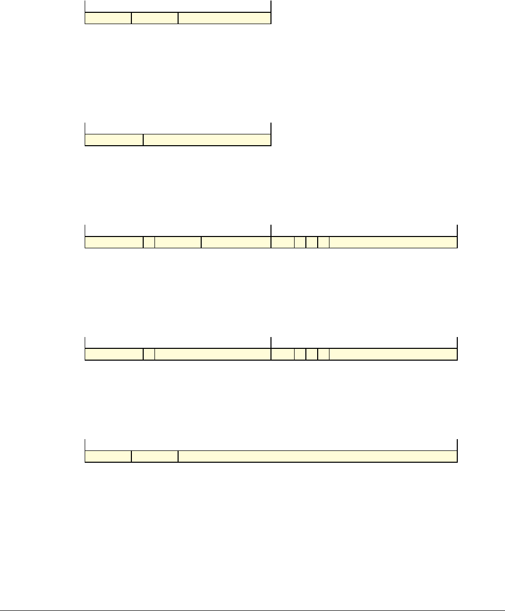
A8 Instruction Descriptions
A8.8 Alphabetical list of instructions
A8-334 Copyright © 1996-1998, 2000, 2004-2012, 2014 ARM. All rights reserved. ARM DDI 0406C.c
Non-Confidential ID051414
A8.8.18 B
Branch causes a branch to a target address.
if cond == ‘1110’ then SEE UDF;
if cond == ‘1111’ then SEE SVC;
imm32 = SignExtend(imm8:’0’, 32);
if InITBlock() then UNPREDICTABLE;
imm32 = SignExtend(imm11:’0’, 32);
if InITBlock() && !LastInITBlock() then UNPREDICTABLE;
if cond<3:1> == ‘111’ then SEE “Related encodings”;
imm32 = SignExtend(S:J2:J1:imm6:imm11:’0’, 32);
if InITBlock() then UNPREDICTABLE;
I1 = NOT(J1 EOR S); I2 = NOT(J2 EOR S); imm32 = SignExtend(S:I1:I2:imm10:imm11:’0’, 32);
if InITBlock() && !LastInITBlock() then UNPREDICTABLE;
For the case when
cond
is
0b1111
, see Unconditional instructions on page A5-216.
imm32 = SignExtend(imm24:’00’, 32);
Encoding T1 ARMv4T, ARMv5T*, ARMv6*, ARMv7
B<c> <label>
Not permitted in IT block.
Encoding T2 ARMv4T, ARMv5T*, ARMv6*, ARMv7
B<c> <label>
Outside or last in IT block
Encoding T3 ARMv6T2, ARMv7
B<c>.W <label>
Not permitted in IT block.
Encoding T4 ARMv6T2, ARMv7
B<c>.W <label>
Outside or last in IT block
Encoding A1 ARMv4*, ARMv5T*, ARMv6*, ARMv7
B<c> <label>
Related encodings See Branches and miscellaneous control on page A6-235.
1 1 0 1 cond imm8
15 14 13 12 11 10 9 8 7 6 5 4 3 2 1 0
1 1 1 0 0 imm11
15 14 13 12 11 10 9 8 7 6 5 4 3 2 1 0
1 1 1 0 S cond imm6 1 0 J1 0 J2 imm11
15 14 13 12 11 10 9 8 7 6 5 4 3 2 1 0
1
1514131211109876543210
1 1 1 0 S imm10 1 0 J1 1 J2 imm11
15 14 13 12 11 10 9 8 7 6 5 4 3 2 1 0
1
1514131211109876543210
cond 1 0 1 0 imm24
31 30 29 28 27 26 25 24 23 22 21 20 19 18 17 16 15 14 13 12 11 10 9 8 7 6 5 4 3 2 1 0

A8 Instruction Descriptions
A8.8 Alphabetical list of instructions
ARM DDI 0406C.c Copyright © 1996-1998, 2000, 2004-2012, 2014 ARM. All rights reserved. A8-335
ID051414 Non-Confidential
Assembler syntax
B{<c>}{<q>} <label>
where:
<c>, <q>
See Standard assembler syntax fields on page A8-287.
Note
Encodings T1 and T3 are conditional in their own right, and do not require an
IT
instruction to make
them conditional.
For encodings T1 and T3,
<c>
must not be
AL
or omitted. The 4-bit encoding of the condition is
placed in the instruction and not in a preceding
IT
instruction, and the instruction must not be in an
IT block. As a result, encodings T1 and T2 are never both available to the assembler, nor are
encodings T3 and T4.
<label>
The label of the instruction that is to be branched to. The assembler calculates the required value of
the offset from the PC value of the
B
instruction to this label, then selects an encoding that sets
imm32
to that offset.
Permitted offsets are:
Encoding T1 Even numbers in the range –256 to 254
Encoding T2 Even numbers in the range –2048 to 2046
Encoding T3 Even numbers in the range –1048576 to 1048574
Encoding T4 Even numbers in the range –16777216 to 16777214
Encoding A1 Multiples of 4 in the range –33554432 to 33554428.
Operation
if ConditionPassed() then
EncodingSpecificOperations();
BranchWritePC(PC + imm32);
Exceptions
None.

A8 Instruction Descriptions
A8.8 Alphabetical list of instructions
A8-336 Copyright © 1996-1998, 2000, 2004-2012, 2014 ARM. All rights reserved. ARM DDI 0406C.c
Non-Confidential ID051414
A8.8.19 BFC
Bit Field Clear clears any number of adjacent bits at any position in a register, without affecting the other bits in the
register.
d = UInt(Rd); msbit = UInt(msb); lsbit = UInt(imm3:imm2);
if d IN {13,15} then UNPREDICTABLE;
For the case when
cond
is
0b1111
, see Unconditional instructions on page A5-216.
d = UInt(Rd); msbit = UInt(msb); lsbit = UInt(lsb);
if d == 15 then UNPREDICTABLE;
Encoding T1 ARMv6T2, ARMv7
BFC<c> <Rd>, #<lsb>, #<width>
Encoding A1 ARMv6T2, ARMv7
BFC<c> <Rd>, #<lsb>, #<width>
1 1 1 0 (0) 1 1 0 1 1 0 1 1 1 1 0 imm3 Rd imm2 (0) msb
15 14 13 12 11 10 9 8 7 6 5 4 3 2 1 0
1
1514131211109876543210
cond 0 1 1 1 1 1 0 msb Rd lsb 0 0 1 1 1 1 1
31 30 29 28 27 26 25 24 23 22 21 20 19 18 17 16 15 14 13 12 11 10 9 8 7 6 5 4 3 2 1 0

A8 Instruction Descriptions
A8.8 Alphabetical list of instructions
ARM DDI 0406C.c Copyright © 1996-1998, 2000, 2004-2012, 2014 ARM. All rights reserved. A8-337
ID051414 Non-Confidential
Assembler syntax
BFC{<c>}{<q>} <Rd>, #<lsb>, #<width>
where:
<c>, <q>
See Standard assembler syntax fields on page A8-287.
<Rd>
The destination register.
<lsb>
The least significant bit that is to be cleared, in the range 0 to 31. This determines the required value
of
lsbit
.
<width>
The number of bits to be cleared, in the range 1 to 32-
<lsb>
. The required value of
msbit
is
<lsb>+<width>-1
.
Operation
if ConditionPassed() then
EncodingSpecificOperations();
if msbit >= lsbit then
R[d]<msbit:lsbit> = Replicate(‘0’, msbit-lsbit+1);
// Other bits of R[d] are unchanged
else
UNPREDICTABLE;
Exceptions
None.

A8 Instruction Descriptions
A8.8 Alphabetical list of instructions
A8-338 Copyright © 1996-1998, 2000, 2004-2012, 2014 ARM. All rights reserved. ARM DDI 0406C.c
Non-Confidential ID051414
A8.8.20 BFI
Bit Field Insert copies any number of low order bits from a register into the same number of adjacent bits at any
position in the destination register.
if Rn == ‘1111’ then SEE BFC;
d = UInt(Rd); n = UInt(Rn); msbit = UInt(msb); lsbit = UInt(imm3:imm2);
if d IN {13,15} || n == 13 then UNPREDICTABLE;
For the case when
cond
is
0b1111
, see Unconditional instructions on page A5-216.
if Rn == ‘1111’ then SEE BFC;
d = UInt(Rd); n = UInt(Rn); msbit = UInt(msb); lsbit = UInt(lsb);
if d == 15 then UNPREDICTABLE;
Encoding T1 ARMv6T2, ARMv7
BFI<c> <Rd>, <Rn>, #<lsb>, #<width>
Encoding A1 ARMv6T2, ARMv7
BFI<c> <Rd>, <Rn>, #<lsb>, #<width>
1 1 1 0 (0) 1 1 0 1 1 0 Rn 0 imm3 Rd imm2 (0) msb
15 14 13 12 11 10 9 8 7 6 5 4 3 2 1 0
1
1514131211109876543210
cond 0 1 1 1 1 1 0 msb Rd lsb 0 0 1 Rn
31 30 29 28 27 26 25 24 23 22 21 20 19 18 17 16 15 14 13 12 11 10 9 8 7 6 5 4 3 2 1 0

A8 Instruction Descriptions
A8.8 Alphabetical list of instructions
ARM DDI 0406C.c Copyright © 1996-1998, 2000, 2004-2012, 2014 ARM. All rights reserved. A8-339
ID051414 Non-Confidential
Assembler syntax
BFI{<c>}{<q>} <Rd>, <Rn>, #<lsb>, #<width>
where:
<c>, <q>
See Standard assembler syntax fields on page A8-287.
<Rd>
The destination register.
<Rn>
The source register.
<lsb>
The least significant destination bit, in the range 0 to 31. This determines the required value of
lsbit
.
<width>
The number of bits to be copied, in the range 1 to 32-
<lsb>
. The required value of
msbit
is
<lsb>+<width>-1
.
Operation
if ConditionPassed() then
EncodingSpecificOperations();
if msbit >= lsbit then
R[d]<msbit:lsbit> = R[n]<(msbit-lsbit):0>;
// Other bits of R[d] are unchanged
else
UNPREDICTABLE;
Exceptions
None.

A8 Instruction Descriptions
A8.8 Alphabetical list of instructions
A8-340 Copyright © 1996-1998, 2000, 2004-2012, 2014 ARM. All rights reserved. ARM DDI 0406C.c
Non-Confidential ID051414
A8.8.21 BIC (immediate)
Bitwise Bit Clear (immediate) performs a bitwise AND of a register value and the complement of an immediate
value, and writes the result to the destination register. It can optionally update the condition flags based on the result.
d = UInt(Rd); n = UInt(Rn); setflags = (S == ‘1’);
(imm32, carry) = ThumbExpandImm_C(i:imm3:imm8, APSR.C);
if d IN {13,15} || n IN {13,15} then UNPREDICTABLE;
For the case when
cond
is
0b1111
, see Unconditional instructions on page A5-216.
if Rd == ‘1111’ && S == ‘1’ then SEE SUBS PC, LR and related instructions;
d = UInt(Rd); n = UInt(Rn); setflags = (S == ‘1’);
(imm32, carry) = ARMExpandImm_C(imm12, APSR.C);
Encoding T1 ARMv6T2, ARMv7
BIC{S}<c> <Rd>, <Rn>, #<const>
Encoding A1 ARMv4*, ARMv5T*, ARMv6*, ARMv7
BIC{S}<c> <Rd>, <Rn>, #<const>
1 1 1 0 i 0 0 0 0 1 S Rn 0 imm3 Rd imm8
15 14 13 12 11 10 9 8 7 6 5 4 3 2 1 0
1
1514131211109876543210
cond 0 0 1 1 1 1 0 S Rn Rd imm12
31 30 29 28 27 26 25 24 23 22 21 20 19 18 17 16 15 14 13 12 11 10 9 8 7 6 5 4 3 2 1 0

A8 Instruction Descriptions
A8.8 Alphabetical list of instructions
ARM DDI 0406C.c Copyright © 1996-1998, 2000, 2004-2012, 2014 ARM. All rights reserved. A8-341
ID051414 Non-Confidential
Assembler syntax
BIC{S}{<c>}{<q>} {<Rd>,} <Rn>, #<const>
where:
S
If
S
is present, the instruction updates the flags. Otherwise, the flags are not updated.
<c>, <q>
See Standard assembler syntax fields on page A8-287.
<Rd>
The destination register. If
S
is specified and
<Rd>
is the PC, see SUBS PC, LR (Thumb) on
page B9-2010 or SUBS PC, LR and related instructions (ARM) on page B9-2012.
In ARM instructions, if
S
is not specified and
<Rd>
is the PC, the instruction is a branch to the address
calculated by the operation. This is an interworking branch, see Pseudocode details of operations
on ARM core registers on page A2-47. ARM deprecates this use of the PC.
Note
Before ARMv7, this was a simple branch.
<Rn>
The register that contains the operand. The PC can be used in ARM instructions. ARM deprecates
this use of the PC.
<const>
The immediate value to be bitwise inverted and ANDed with the value obtained from
<Rn>
. See
Modified immediate constants in Thumb instructions on page A6-232 or Modified immediate
constants in ARM instructions on page A5-200 for the range of values.
The pre-UAL syntax
BIC<c>S
is equivalent to
BICS<c>
.
Operation
if ConditionPassed() then
EncodingSpecificOperations();
result = R[n] AND NOT(imm32);
if d == 15 then // Can only occur for ARM encoding
ALUWritePC(result); // setflags is always FALSE here
else
R[d] = result;
if setflags then
APSR.N = result<31>;
APSR.Z = IsZeroBit(result);
APSR.C = carry;
// APSR.V unchanged
Exceptions
None.
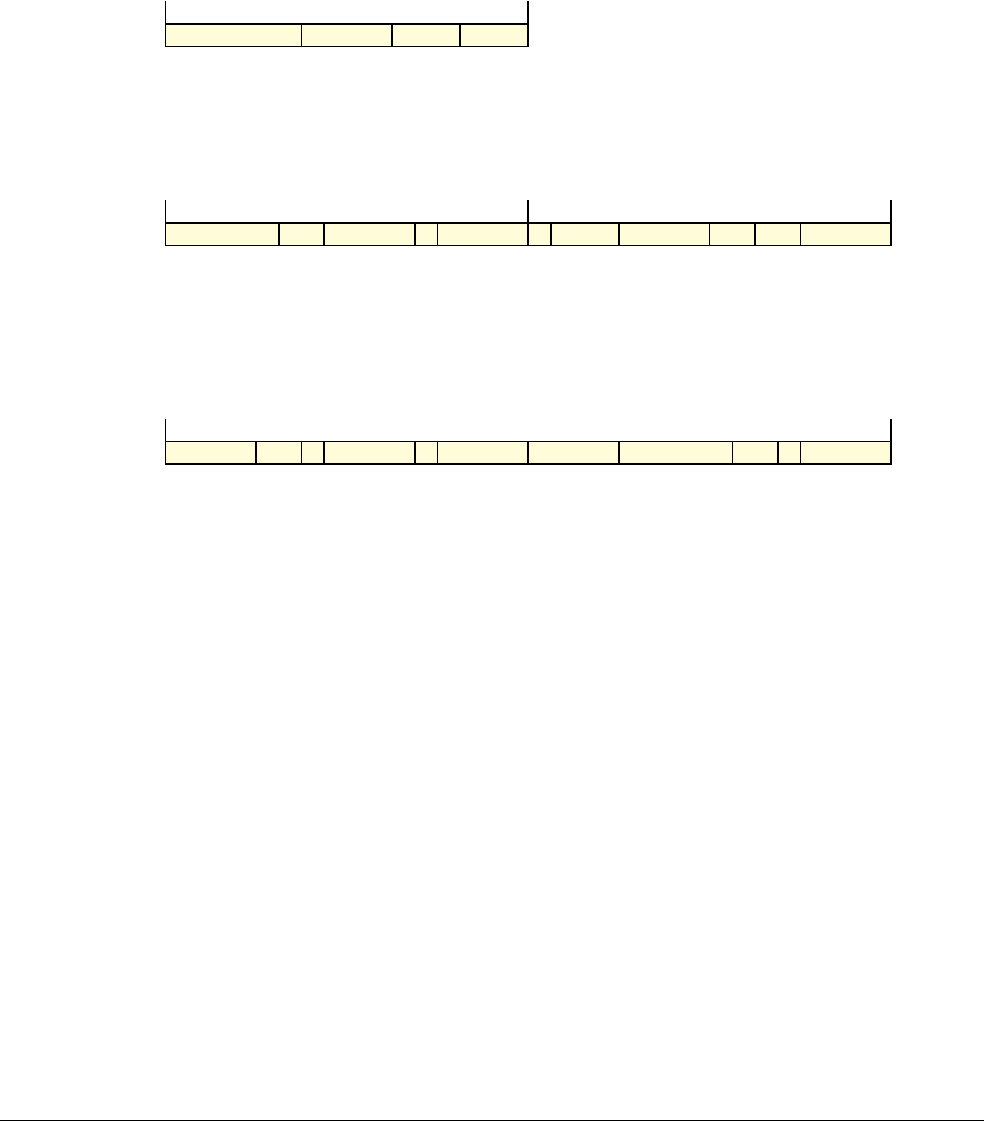
A8 Instruction Descriptions
A8.8 Alphabetical list of instructions
A8-342 Copyright © 1996-1998, 2000, 2004-2012, 2014 ARM. All rights reserved. ARM DDI 0406C.c
Non-Confidential ID051414
A8.8.22 BIC (register)
Bitwise Bit Clear (register) performs a bitwise AND of a register value and the complement of an optionally-shifted
register value, and writes the result to the destination register. It can optionally update the condition flags based on
the result.
d = UInt(Rdn); n = UInt(Rdn); m = UInt(Rm); setflags = !InITBlock();
(shift_t, shift_n) = (SRType_LSL, 0);
d = UInt(Rd); n = UInt(Rn); m = UInt(Rm); setflags = (S == ‘1’);
(shift_t, shift_n) = DecodeImmShift(type, imm3:imm2);
if d IN {13,15} || n IN {13,15} || m IN {13,15} then UNPREDICTABLE;
For the case when
cond
is
0b1111
, see Unconditional instructions on page A5-216.
if Rd == ‘1111’ && S == ‘1’ then SEE SUBS PC, LR and related instructions;
d = UInt(Rd); n = UInt(Rn); m = UInt(Rm); setflags = (S == ‘1’);
(shift_t, shift_n) = DecodeImmShift(type, imm5);
Encoding T1 ARMv4T, ARMv5T*, ARMv6*, ARMv7
BICS <Rdn>, <Rm>
Outside IT block.
BIC<c> <Rdn>, <Rm>
Inside IT block.
Encoding T2 ARMv6T2, ARMv7
BIC{S}<c>.W <Rd>, <Rn>, <Rm>{, <shift>}
Encoding A1 ARMv4*, ARMv5T*, ARMv6*, ARMv7
BIC{S}<c> <Rd>, <Rn>, <Rm>{, <shift>}
0 1 0 0 0 0 1 1 1 0 Rm Rdn
15 14 13 12 11 10 9 8 7 6 5 4 3 2 1 0
1 1 0 1 0 1 0 0 0 1 S Rn (0) imm3 Rd imm2 type Rm
15 14 13 12 11 10 9 8 7 6 5 4 3 2 1 0
1
1514131211109876543210
cond 0 0 0 1 1 1 0 S Rn Rd imm5 type 0 Rm
31 30 29 28 27 26 25 24 23 22 21 20 19 18 17 16 15 14 13 12 11 10 9 8 7 6 5 4 3 2 1 0

A8 Instruction Descriptions
A8.8 Alphabetical list of instructions
ARM DDI 0406C.c Copyright © 1996-1998, 2000, 2004-2012, 2014 ARM. All rights reserved. A8-343
ID051414 Non-Confidential
Assembler syntax
BIC{S}{<c>}{<q>} {<Rd>,} <Rn>, <Rm> {, <shift>}
where:
S
If
S
is present, the instruction updates the flags. Otherwise, the flags are not updated.
<c>, <q>
See Standard assembler syntax fields on page A8-287.
<Rd>
The destination register. If
S
is specified and
<Rd>
is the PC, see SUBS PC, LR (Thumb) on
page B9-2010 or SUBS PC, LR and related instructions (ARM) on page B9-2012.
In ARM instructions, if
S
is not specified and
<Rd>
is the PC, the instruction is a branch to the address
calculated by the operation. This is an interworking branch, see Pseudocode details of operations
on ARM core registers on page A2-47. ARM deprecates this use of the PC.
Note
Before ARMv7, this was a simple branch.
<Rn>
The first operand register. The PC can be used in ARM instructions. ARM deprecates this use of the
PC.
<Rm>
The register that is optionally shifted and used as the second operand. The PC can be used in ARM
instructions. ARM deprecates this use of the PC.
<shift>
The shift to apply to the value read from
<Rm>
. If present, encoding T1 is not permitted. If absent, no
shift is applied and all encodings are permitted. Shifts applied to a register on page A8-291
describes the shifts and how they are encoded.
The pre-UAL syntax
BIC<c>S
is equivalent to
BICS<c>
.
Operation
if ConditionPassed() then
EncodingSpecificOperations();
(shifted, carry) = Shift_C(R[m], shift_t, shift_n, APSR.C);
result = R[n] AND NOT(shifted);
if d == 15 then // Can only occur for ARM encoding
ALUWritePC(result); // setflags is always FALSE here
else
R[d] = result;
if setflags then
APSR.N = result<31>;
APSR.Z = IsZeroBit(result);
APSR.C = carry;
// APSR.V unchanged
Exceptions
None.

A8 Instruction Descriptions
A8.8 Alphabetical list of instructions
A8-344 Copyright © 1996-1998, 2000, 2004-2012, 2014 ARM. All rights reserved. ARM DDI 0406C.c
Non-Confidential ID051414
A8.8.23 BIC (register-shifted register)
Bitwise Bit Clear (register-shifted register) performs a bitwise AND of a register value and the complement of a
register-shifted register value. It writes the result to the destination register, and can optionally update the condition
flags based on the result.
For the case when
cond
is
0b1111
, see Unconditional instructions on page A5-216.
d = UInt(Rd); n = UInt(Rn); m = UInt(Rm); s = UInt(Rs);
setflags = (S == ‘1’); shift_t = DecodeRegShift(type);
if d == 15 || n == 15 || m == 15 || s == 15 then UNPREDICTABLE;
Encoding A1 ARMv4*, ARMv5T*, ARMv6*, ARMv7
BIC{S}<c> <Rd>, <Rn>, <Rm>, <type> <Rs>
cond 0 0 0 1 1 1 0 S Rn Rd Rs 0 type 1 Rm
31 30 29 28 27 26 25 24 23 22 21 20 19 18 17 16 15 14 13 12 11 10 9 8 7 6 5 4 3 2 1 0

A8 Instruction Descriptions
A8.8 Alphabetical list of instructions
ARM DDI 0406C.c Copyright © 1996-1998, 2000, 2004-2012, 2014 ARM. All rights reserved. A8-345
ID051414 Non-Confidential
Assembler syntax
BIC{S}{<c>}{<q>} {<Rd>,} <Rn>, <Rm>, <type> <Rs>
where:
S
If
S
is present, the instruction updates the flags. Otherwise, the flags are not updated.
<c>, <q>
See Standard assembler syntax fields on page A8-287.
<Rd>
The destination register.
<Rn>
The first operand register.
<Rm>
The register that is shifted and used as the second operand.
<type>
The type of shift to apply to the value read from
<Rm>
. It must be one of:
ASR
Arithmetic shift right, encoded as type =
0b10
.
LSL
Logical shift left, encoded as type =
0b00
.
LSR
Logical shift right, encoded as type =
0b01
.
ROR
Rotate right, encoded as type =
0b11
.
<Rs>
The register whose bottom byte contains the amount to shift by.
The pre-UAL syntax
BIC<c>S
is equivalent to
BICS<c>
.
Operation
if ConditionPassed() then
EncodingSpecificOperations();
shift_n = UInt(R[s]<7:0>);
(shifted, carry) = Shift_C(R[m], shift_t, shift_n, APSR.C);
result = R[n] AND NOT(shifted);
R[d] = result;
if setflags then
APSR.N = result<31>;
APSR.Z = IsZeroBit(result);
APSR.C = carry;
// APSR.V unchanged
Exceptions
None.

A8 Instruction Descriptions
A8.8 Alphabetical list of instructions
A8-346 Copyright © 1996-1998, 2000, 2004-2012, 2014 ARM. All rights reserved. ARM DDI 0406C.c
Non-Confidential ID051414
A8.8.24 BKPT
Breakpoint causes a software breakpoint to occur.
Breakpoint is always unconditional, even when inside an IT block.
imm32 = ZeroExtend(imm8, 32);
// imm32 is for assembly/disassembly only and is ignored by hardware.
imm32 = ZeroExtend(imm12:imm4, 32);
// imm32 is for assembly/disassembly only and is ignored by hardware.
if cond != ‘1110’ then UNPREDICTABLE; // BKPT must be encoded with AL condition
Encoding T1 ARMv5T*, ARMv6*, ARMv7
BKPT #<imm8>
Encoding A1 ARMv5T*, ARMv6*, ARMv7
BKPT #<imm16>
1 0 1 1 1 1 1 0 imm8
15 14 13 12 11 10 9 8 7 6 5 4 3 2 1 0
cond 0 0 0 1 0 0 1 0 imm12 0 1 1 1 imm4
31 30 29 28 27 26 25 24 23 22 21 20 19 18 17 16 15 14 13 12 11 10 9 8 7 6 5 4 3 2 1 0

A8 Instruction Descriptions
A8.8 Alphabetical list of instructions
ARM DDI 0406C.c Copyright © 1996-1998, 2000, 2004-2012, 2014 ARM. All rights reserved. A8-347
ID051414 Non-Confidential
Assembler syntax
BKPT{<q>} {#}<imm>
where:
<q>
See Standard assembler syntax fields on page A8-287. A
BKPT
instruction must be unconditional.
<imm>
Specifies a value that is stored in the instruction, in the range 0-255 for a Thumb instruction or
0-65535 for an ARM instruction. This value is ignored by the processor, but can be used by a
debugger to store more information about the breakpoint.
Operation
EncodingSpecificOperations();
BKPTInstrDebugEvent();
Exceptions
Prefetch Abort.

A8 Instruction Descriptions
A8.8 Alphabetical list of instructions
A8-348 Copyright © 1996-1998, 2000, 2004-2012, 2014 ARM. All rights reserved. ARM DDI 0406C.c
Non-Confidential ID051414
A8.8.25 BL, BLX (immediate)
Branch with Link calls a subroutine at a PC-relative address.
Branch with Link and Exchange Instruction Sets (immediate) calls a subroutine at a PC-relative address, and
changes instruction set from ARM to Thumb, or from Thumb to ARM.
I1 = NOT(J1 EOR S); I2 = NOT(J2 EOR S); imm32 = SignExtend(S:I1:I2:imm10:imm11:’0’, 32);
targetInstrSet = CurrentInstrSet();
if InITBlock() && !LastInITBlock() then UNPREDICTABLE;
if CurrentInstrSet() == InstrSet_ThumbEE || H == ‘1’ then UNDEFINED;
I1 = NOT(J1 EOR S); I2 = NOT(J2 EOR S); imm32 = SignExtend(S:I1:I2:imm10H:imm10L:’00’, 32);
targetInstrSet = InstrSet_ARM;
if InITBlock() && !LastInITBlock() then UNPREDICTABLE;
For the case when
cond
is
0b1111
, see the A2 encoding.
imm32 = SignExtend(imm24:’00’, 32); targetInstrSet = InstrSet_ARM;
imm32 = SignExtend(imm24:H:’0’, 32); targetInstrSet = InstrSet_Thumb;
Encoding T1 ARMv4T, ARMv5T*, ARMv6*, ARMv7 if J1 == J2 == 1
ARMv6T2, ARMv7 otherwise
BL<c> <label>
Outside or last in IT block
Encoding T2 ARMv5T*, ARMv6*, ARMv7 if J1 == J2 == 1
ARMv6T2, ARMv7 otherwise
BLX<c> <label>
Outside or last in IT block
Encoding A1 ARMv4*, ARMv5T*, ARMv6*, ARMv7
BL<c> <label>
Encoding A2 ARMv5T*, ARMv6*, ARMv7
BLX <label>
1 1 1 0 S imm10 1 1 J1 1 J2 imm11
15 14 13 12 11 10 9 8 7 6 5 4 3 2 1 0
1
1514131211109876543210
1 1 1 0 S imm10H 1 1 J1 0 J2 imm10L H
15 14 13 12 11 10 9 8 7 6 5 4 3 2 1 0
1
1514131211109876543210
cond 1 0 1 1 imm24
31 30 29 28 27 26 25 24 23 22 21 20 19 18 17 16 15 14 13 12 11 10 9 8 7 6 5 4 3 2 1 0
1 1 1 1 0 1 H imm24
31 30 29 28 27 26 25 24 23 22 21 20 19 18 17 16 15 14 13 12 11 10 9 8 7 6 5 4 3 2 1 0
1

A8 Instruction Descriptions
A8.8 Alphabetical list of instructions
ARM DDI 0406C.c Copyright © 1996-1998, 2000, 2004-2012, 2014 ARM. All rights reserved. A8-349
ID051414 Non-Confidential
Assembler syntax
BL{X}{<c>}{<q>} <label>
where:
<c>, <q>
See Standard assembler syntax fields on page A8-287. An ARM
BLX
(immediate) instruction must
be unconditional.
X
If present, specifies a change of instruction set (from ARM to Thumb or from Thumb to ARM). If
X is omitted, the processor remains in the same state. For ThumbEE instructions, specifying X is
not permitted.
<label>
The label of the instruction that is to be branched to.
BL
uses encoding T1 or A1. The assembler calculates the required value of the offset from the PC
value of the
BL
instruction to this label, then selects an encoding with
imm32
set to that offset.
BLX
uses encoding T2 or A2. The assembler calculates the required value of the offset from the
Align(PC, 4)
value of the
BLX
instruction to this label, then selects an encoding with
imm32
set to that
offset.
Permitted offsets are:
Encoding T1 Even numbers in the range –16777216 to 16777214.
Encoding T2 Multiples of 4 in the range –16777216 to 16777212.
Encoding A1 Multiples of 4 in the range –33554432 to 33554428.
Encoding A2 Even numbers in the range –33554432 to 33554430.
Operation
if ConditionPassed() then
EncodingSpecificOperations();
if CurrentInstrSet() == InstrSet_ARM then
LR = PC - 4;
else
LR = PC<31:1> : ‘1’;
if targetInstrSet == InstrSet_ARM then
targetAddress = Align(PC,4) + imm32;
else
targetAddress = PC + imm32;
SelectInstrSet(targetInstrSet);
BranchWritePC(targetAddress);
Exceptions
None.
Branch range before ARMv6T2
Before ARMv6T2, J1 and J2 in encodings T1 and T2 were both 1, resulting in a smaller branch range. The
instructions could be executed as two separate 16-bit instructions, as described in BL and BLX (immediate)
instructions, before ARMv6T2 on page D12-2504.

A8 Instruction Descriptions
A8.8 Alphabetical list of instructions
A8-350 Copyright © 1996-1998, 2000, 2004-2012, 2014 ARM. All rights reserved. ARM DDI 0406C.c
Non-Confidential ID051414
A8.8.26 BLX (register)
Branch with Link and Exchange (register) calls a subroutine at an address and instruction set specified by a register.
m = UInt(Rm);
if m == 15 then UNPREDICTABLE;
if InITBlock() && !LastInITBlock() then UNPREDICTABLE;
For the case when
cond
is
0b1111
, see Unconditional instructions on page A5-216.
m = UInt(Rm);
if m == 15 then UNPREDICTABLE;
Encoding T1 ARMv5T*, ARMv6*, ARMv7
BLX<c> <Rm>
Outside or last in IT block
Encoding A1 ARMv5T*, ARMv6*, ARMv7
BLX<c> <Rm>
0 1 0 0 0 1 1 1 1 Rm (0) (0) (0)
15 14 13 12 11 10 9 8 7 6 5 4 3 2 1 0
cond 0 0 0 1 0 0 1 0 (1) (1) (1) (1) (1) (1) (1) (1) (1) (1) (1) (1) 0 0 1 1 Rm
31 30 29 28 27 26 25 24 23 22 21 20 19 18 17 16 15 14 13 12 11 10 9 8 7 6 5 4 3 2 1 0

A8 Instruction Descriptions
A8.8 Alphabetical list of instructions
ARM DDI 0406C.c Copyright © 1996-1998, 2000, 2004-2012, 2014 ARM. All rights reserved. A8-351
ID051414 Non-Confidential
Assembler syntax
BLX{<c>}{<q>} <Rm>
where:
<c>, <q>
See Standard assembler syntax fields on page A8-287.
<Rm>
The register that contains the branch target address and instruction set selection bit. This register can
be the SP in both ARM and Thumb instructions, but ARM deprecates this use of the SP.
Operation
if ConditionPassed() then
EncodingSpecificOperations();
target = R[m];
if CurrentInstrSet() == InstrSet_ARM then
next_instr_addr = PC - 4;
LR = next_instr_addr;
else
next_instr_addr = PC - 2;
LR = next_instr_addr<31:1> : ‘1’;
BXWritePC(target);
Exceptions
None.
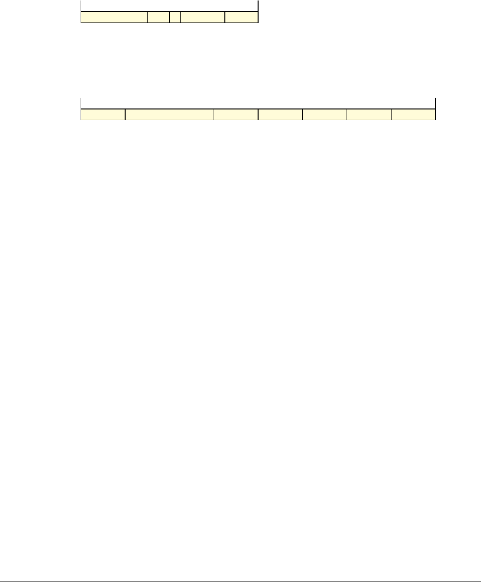
A8 Instruction Descriptions
A8.8 Alphabetical list of instructions
A8-352 Copyright © 1996-1998, 2000, 2004-2012, 2014 ARM. All rights reserved. ARM DDI 0406C.c
Non-Confidential ID051414
A8.8.27 BX
Branch and Exchange causes a branch to an address and instruction set specified by a register.
m = UInt(Rm);
if InITBlock() && !LastInITBlock() then UNPREDICTABLE;
For the case when
cond
is
0b1111
, see Unconditional instructions on page A5-216.
m = UInt(Rm);
Encoding T1 ARMv4T, ARMv5T*, ARMv6*, ARMv7
BX<c> <Rm>
Outside or last in IT block
Encoding A1 ARMv4T, ARMv5T*, ARMv6*, ARMv7
BX<c> <Rm>
0 1 0 0 0 1 1 1 0 Rm (0) (0) (0)
15 14 13 12 11 10 9 8 7 6 5 4 3 2 1 0
cond 0 0 0 1 0 0 1 0 (1) (1) (1) (1) (1) (1) (1) (1) (1) (1) (1) (1) 0 0 0 1 Rm
31 30 29 28 27 26 25 24 23 22 21 20 19 18 17 16 15 14 13 12 11 10 9 8 7 6 5 4 3 2 1 0

A8 Instruction Descriptions
A8.8 Alphabetical list of instructions
ARM DDI 0406C.c Copyright © 1996-1998, 2000, 2004-2012, 2014 ARM. All rights reserved. A8-353
ID051414 Non-Confidential
Assembler syntax
BX{<c>}{<q>} <Rm>
where:
<c>, <q>
See Standard assembler syntax fields on page A8-287.
<Rm>
The register that contains the branch target address and instruction set selection bit. The PC can be
used. This register can be the SP in both ARM and Thumb instructions, but ARM deprecates this
use of the SP.
Note
If
<Rm>
is the PC in a Thumb instruction at a non word-aligned address, it results in UNPREDICTABLE
behavior because the address passed to the
BXWritePC()
pseudocode function has bits<1:0> = '10'.
Operation
if ConditionPassed() then
EncodingSpecificOperations();
BXWritePC(R[m]);
Exceptions
None.
A8 Instruction Descriptions
A8.8 Alphabetical list of instructions
A8-354 Copyright © 1996-1998, 2000, 2004-2012, 2014 ARM. All rights reserved. ARM DDI 0406C.c
Non-Confidential ID051414
A8.8.28 BXJ
Branch and Exchange Jazelle attempts to change to Jazelle state. If the attempt fails, it branches to an address and
instruction set specified by a register as though it were a
BX
instruction.
In an implementation that includes the Virtualization Extensions, if HSTR.TJDBX is set to 1, execution of a
BXJ
instruction in a Non-secure mode other than Hyp mode generates a Hyp Trap exception. For more information see
Trapping accesses to Jazelle functionality on page B1-1256.
m = UInt(Rm);
if m IN {13,15} then UNPREDICTABLE;
if InITBlock() && !LastInITBlock() then UNPREDICTABLE;
For the case when
cond
is
0b1111
, see Unconditional instructions on page A5-216.
m = UInt(Rm);
if m == 15 then UNPREDICTABLE;
Encoding T1 ARMv6T2, ARMv7
BXJ<c> <Rm>
Outside or last in IT block
Encoding A1 ARMv5TEJ, ARMv6*, ARMv7
BXJ<c> <Rm>
1 1 1 0 0 1 1 1 1 0 0 Rm 1 0 (0) 0 (1) (1) (1) (1) (0) (0) (0) (0) (0) (0) (0) (0)
15 14 13 12 11 10 9 8 7 6 5 4 3 2 1 0
1
1514131211109876543210
cond 0 0 0 1 0 0 1 0 (1) (1) (1) (1) (1) (1) (1) (1) (1) (1) (1) (1) 0 0 1 0 Rm
31 30 29 28 27 26 25 24 23 22 21 20 19 18 17 16 15 14 13 12 11 10 9 8 7 6 5 4 3 2 1 0

A8 Instruction Descriptions
A8.8 Alphabetical list of instructions
ARM DDI 0406C.c Copyright © 1996-1998, 2000, 2004-2012, 2014 ARM. All rights reserved. A8-355
ID051414 Non-Confidential
Assembler syntax
BXJ{<c>}{<q>} <Rm>
where:
<c>, <q>
See Standard assembler syntax fields on page A8-287.
<Rm>
The register that specifies the branch target address and instruction set selection bit to be used if the
attempt to switch to Jazelle state fails.
Operation
if ConditionPassed() then
EncodingSpecificOperations();
if HaveVirtExt() && !IsSecure() && !CurrentModeIsHyp() && HSTR.TJDBX == ‘1’ then
HSRString = Zeros(25);
HSRString<3:0> = m;
WriteHSR(‘001010’, HSRString);
TakeHypTrapException();
elsif JMCR.JE == ‘0’ || CurrentInstrSet() == InstrSet_ThumbEE then
BXWritePC(R[m]);
else
if JazelleAcceptsExecution() then
SwitchToJazelleExecution();
else
SUBARCHITECTURE_DEFINED handler call;
Exceptions
Hyp Trap.

A8 Instruction Descriptions
A8.8 Alphabetical list of instructions
A8-356 Copyright © 1996-1998, 2000, 2004-2012, 2014 ARM. All rights reserved. ARM DDI 0406C.c
Non-Confidential ID051414
A8.8.29 CBNZ, CBZ
Compare and Branch on Nonzero and Compare and Branch on Zero compare the value in a register with zero, and
conditionally branch forward a constant value. They do not affect the condition flags.
n = UInt(Rn); imm32 = ZeroExtend(i:imm5:’0’, 32); nonzero = (op == ‘1’);
if InITBlock() then UNPREDICTABLE;
Encoding T1 ARMv6T2, ARMv7
CB{N}Z <Rn>, <label>
Not permitted in IT block.
1 0 1 1 op 0 i 1 imm5 Rn
15 14 13 12 11 10 9 8 7 6 5 4 3 2 1 0

A8 Instruction Descriptions
A8.8 Alphabetical list of instructions
ARM DDI 0406C.c Copyright © 1996-1998, 2000, 2004-2012, 2014 ARM. All rights reserved. A8-357
ID051414 Non-Confidential
Assembler syntax
CB{N}Z{<q>} <Rn>, <label>
where:
N
If specified, causes the branch to occur when the contents of
<Rn>
are nonzero (encoded as op = 1).
If omitted, causes the branch to occur when the contents of
<Rn>
are zero (encoded as op = 0).
<q>
See Standard assembler syntax fields on page A8-287. A
CBZ
or
CBNZ
instruction must be
unconditional.
<Rn>
The operand register.
<label>
The label of the instruction that is to be branched to. The assembler calculates the required value of
the offset from the PC value of the
CBZ
or
CBNZ
instruction to this label, then selects an encoding that
sets
imm32
to that offset. Permitted offsets are even numbers in the range 0 to 126.
Operation
EncodingSpecificOperations();
if nonzero != IsZero(R[n]) then
BranchWritePC(PC + imm32);
Exceptions
None.
A8 Instruction Descriptions
A8.8 Alphabetical list of instructions
A8-358 Copyright © 1996-1998, 2000, 2004-2012, 2014 ARM. All rights reserved. ARM DDI 0406C.c
Non-Confidential ID051414
A8.8.30 CDP, CDP2
Coprocessor Data Processing tells a coprocessor to perform an operation that is independent of ARM core registers
and memory. If no coprocessor can execute the instruction, an Undefined Instruction exception is generated.
This is a generic coprocessor instruction. Some of the fields have no functionality defined by the architecture and
are free for use by the coprocessor instruction set designer. These are the
opc1
,
opc2
,
CRd
,
CRn
, and
CRm
fields.
However, coprocessors CP8-CP15 are reserved for use by ARM, and this manual defines the valid
CDP
and
CDP2
instructions when
coproc
is in the range
p8
-
p15
. For more information see Coprocessor support on page A2-94 and
General behavior of system control registers on page B5-1776.
For the case when
cond
is
0b1111
, see the T2 and A2 encoding.
if coproc IN “101x” then SEE “Floating-point instructions”;
cp = UInt(coproc);
if coproc IN “101x” then UNDEFINED;
cp = UInt(coproc);
Encoding T1/A1 ARMv6T2, ARMv7 for encoding T1
ARMv4*, ARMv5T*, ARMv6*, ARMv7 for encoding A1
CDP<c> <coproc>, <opc1>, <CRd>, <CRn>, <CRm>, <opc2>
Encoding T2/A2 ARMv6T2, ARMv7 for encoding T2
ARMv5T*, ARMv6*, ARMv7 for encoding A2
CDP2<c> <coproc>, <opc1>, <CRd>, <CRn>, <CRm>, <opc2>
Floating-point instructions See Floating-point data-processing instructions on page A7-272.
1 1 0 1 1 1 0 opc1 CRn CRd coproc opc2 0 CRm
15 14 13 12 11 10 9 8 7 6 5 4 3 2 1 0
1
1514131211109876543210
cond 1 1 1 0 opc1 CRn CRd coproc opc2 0 CRm
31 30 29 28 27 26 25 24 23 22 21 20 19 18 17 16 15 14 13 12 11 10 9 8 7 6 5 4 3 2 1 0
1 1 1 1 1 1 0 opc1 CRn CRd coproc opc2 0 CRm
15 14 13 12 11 10 9 8 7 6 5 4 3 2 1 0
1
1514131211109876543210
1 1 1 1 1 1 0 opc1 CRn CRd coproc opc2 0 CRm
31 30 29 28 27 26 25 24 23 22 21 20 19 18 17 16 15 14 13 12 11 10 9 8 7 6 5 4 3 2 1 0
1

A8 Instruction Descriptions
A8.8 Alphabetical list of instructions
ARM DDI 0406C.c Copyright © 1996-1998, 2000, 2004-2012, 2014 ARM. All rights reserved. A8-359
ID051414 Non-Confidential
Assembler syntax
CDP{2}{<c>}{<q>} <coproc>, {#}<opc1>, <CRd>, <CRn>, <CRm> {, {#}<opc2>}
where:
2
If specified, selects encoding T2/A2. If omitted, selects encoding T1/A1.
<c>, <q>
See Standard assembler syntax fields on page A8-287. An ARM
CDP2
instruction must be
unconditional.
<coproc>
The name of the coprocessor, and causes the corresponding coprocessor number to be placed in the
cp_num field of the instruction. The generic coprocessor names are p0-p15.
<opc1>
Is a coprocessor-specific opcode, in the range 0 to 15.
<CRd>
The destination coprocessor register for the instruction.
<CRn>
The coprocessor register that contains the first operand.
<CRm>
The coprocessor register that contains the second operand.
<opc2>
Is a coprocessor-specific opcode in the range 0 to 7. If it is omitted,
<opc2>
is 0.
Operation
if ConditionPassed() then
EncodingSpecificOperations();
if !Coproc_Accepted(cp, ThisInstr()) then
GenerateCoprocessorException();
else
Coproc_InternalOperation(cp, ThisInstr());
Exceptions
Undefined Instruction.
Uses of these instructions by specific coprocessors might generate other exceptions.
A8 Instruction Descriptions
A8.8 Alphabetical list of instructions
A8-360 Copyright © 1996-1998, 2000, 2004-2012, 2014 ARM. All rights reserved. ARM DDI 0406C.c
Non-Confidential ID051414
A8.8.31 CHKA
CHKA
is a ThumbEE instruction, see CHKA on page A9-1124.
A8.8.32 CLREX
Clear-Exclusive clears the local record of the executing processor that an address has had a request for an exclusive
access.
// No additional decoding required
// No additional decoding required
Encoding T1 ARMv7
CLREX<c>
Encoding A1 ARMv6K, ARMv7
CLREX
1 1 1 0 0 1 1 1 0 1 1 (1) (1) (1) (1) 1 0 (0) 0 (1) (1) (1) (1) 0 0 1 0 (1) (1) (1) (1)
15 14 13 12 11 10 9 8 7 6 5 4 3 2 1 0
1
1514131211109876543210
(1)1 1 1 0 1 0 1 0 1 1 1 (1) (1) (1) (1) (1) (1) (1) (0) (0) (0) (0) 0 0 0 1 (1) (1) (1) (1)
31 30 29 28 27 26 25 24 23 22 21 20 19 18 17 16 15 14 13 12 11 10 9 8 7 6 5 4 3 2 1 0
1

A8 Instruction Descriptions
A8.8 Alphabetical list of instructions
ARM DDI 0406C.c Copyright © 1996-1998, 2000, 2004-2012, 2014 ARM. All rights reserved. A8-361
ID051414 Non-Confidential
Assembler syntax
CLREX{<c>}{<q>}
where:
<c>, <q>
See Standard assembler syntax fields on page A8-287. An ARM
CLREX
instruction must be
unconditional.
Operation
if ConditionPassed() then
EncodingSpecificOperations();
ClearExclusiveLocal(ProcessorID());
Exceptions
None.
A8 Instruction Descriptions
A8.8 Alphabetical list of instructions
A8-362 Copyright © 1996-1998, 2000, 2004-2012, 2014 ARM. All rights reserved. ARM DDI 0406C.c
Non-Confidential ID051414
A8.8.33 CLZ
Count Leading Zeros returns the number of binary zero bits before the first binary one bit in a value.
if !Consistent(Rm) then UNPREDICTABLE;
d = UInt(Rd); m = UInt(Rm);
if d IN {13,15} || m IN {13,15} then UNPREDICTABLE;
For the case when
cond
is
0b1111
, see Unconditional instructions on page A5-216.
d = UInt(Rd); m = UInt(Rm);
if d == 15 || m == 15 then UNPREDICTABLE;
Encoding T1 ARMv6T2, ARMv7
CLZ<c> <Rd>, <Rm>
Encoding A1 ARMv5T*, ARMv6*, ARMv7
CLZ<c> <Rd>, <Rm>
1 1 1 1 0 1 0 1 0 1 1 Rm 1 1 1 1 Rd 1 0 0 0 Rm
15 14 13 12 11 10 9 8 7 6 5 4 3 2 1 0
1
1514131211109876543210
cond 0 0 0 1 0 1 1 0 (1) (1) (1) (1) Rd (1) (1) (1) (1) 0 0 0 1 Rm
31 30 29 28 27 26 25 24 23 22 21 20 19 18 17 16 15 14 13 12 11 10 9 8 7 6 5 4 3 2 1 0

A8 Instruction Descriptions
A8.8 Alphabetical list of instructions
ARM DDI 0406C.c Copyright © 1996-1998, 2000, 2004-2012, 2014 ARM. All rights reserved. A8-363
ID051414 Non-Confidential
Assembler syntax
CLZ{<c>}{<q>} <Rd>, <Rm>
where:
<c>, <q>
See Standard assembler syntax fields on page A8-287.
<Rd>
The destination register.
<Rm>
The register that contains the operand. Its number must be encoded twice in encoding T1.
Operation
if ConditionPassed() then
EncodingSpecificOperations();
result = CountLeadingZeroBits(R[m]);
R[d] = result<31:0>;
Exceptions
None.

A8 Instruction Descriptions
A8.8 Alphabetical list of instructions
A8-364 Copyright © 1996-1998, 2000, 2004-2012, 2014 ARM. All rights reserved. ARM DDI 0406C.c
Non-Confidential ID051414
A8.8.34 CMN (immediate)
Compare Negative (immediate) adds a register value and an immediate value. It updates the condition flags based
on the result, and discards the result.
n = UInt(Rn); imm32 = ThumbExpandImm(i:imm3:imm8);
if n == 15 then UNPREDICTABLE;
For the case when
cond
is
0b1111
, see Unconditional instructions on page A5-216.
n = UInt(Rn); imm32 = ARMExpandImm(imm12);
Encoding T1 ARMv6T2, ARMv7
CMN<c> <Rn>, #<const>
Encoding A1 ARMv4*, ARMv5T*, ARMv6*, ARMv7
CMN<c> <Rn>, #<const>
1 1 1 0 i 0 1 0 0 0 1 Rn 0 imm3 1 1 1 1 imm8
15 14 13 12 11 10 9 8 7 6 5 4 3 2 1 0
1
1514131211109876543210
cond 0 0 1 1 0 1 1 1 Rn (0) (0) (0) (0) imm12
31 30 29 28 27 26 25 24 23 22 21 20 19 18 17 16 15 14 13 12 11 10 9 8 7 6 5 4 3 2 1 0

A8 Instruction Descriptions
A8.8 Alphabetical list of instructions
ARM DDI 0406C.c Copyright © 1996-1998, 2000, 2004-2012, 2014 ARM. All rights reserved. A8-365
ID051414 Non-Confidential
Assembler syntax
CMN{<c>}{<q>} <Rn>, #<const>
where:
<c>, <q>
See Standard assembler syntax fields on page A8-287.
<Rn>
The register that contains the operand. SP can be used in Thumb and ARM instructions. The PC can
be used in ARM instructions, but ARM deprecates this use of the PC.
<const>
The immediate value to be added to the value obtained from
<Rn>
. See Modified immediate constants
in Thumb instructions on page A6-232 or Modified immediate constants in ARM instructions on
page A5-200 for the range of values.
Operation
if ConditionPassed() then
EncodingSpecificOperations();
(result, carry, overflow) = AddWithCarry(R[n], imm32, ‘0’);
APSR.N = result<31>;
APSR.Z = IsZeroBit(result);
APSR.C = carry;
APSR.V = overflow;
Exceptions
None.

A8 Instruction Descriptions
A8.8 Alphabetical list of instructions
A8-366 Copyright © 1996-1998, 2000, 2004-2012, 2014 ARM. All rights reserved. ARM DDI 0406C.c
Non-Confidential ID051414
A8.8.35 CMN (register)
Compare Negative (register) adds a register value and an optionally-shifted register value. It updates the condition
flags based on the result, and discards the result.
n = UInt(Rn); m = UInt(Rm);
(shift_t, shift_n) = (SRType_LSL, 0);
n = UInt(Rn); m = UInt(Rm);
(shift_t, shift_n) = DecodeImmShift(type, imm3:imm2);
if n == 15 || m IN {13,15} then UNPREDICTABLE;
For the case when
cond
is
0b1111
, see Unconditional instructions on page A5-216.
n = UInt(Rn); m = UInt(Rm);
(shift_t, shift_n) = DecodeImmShift(type, imm5);
Encoding T1 ARMv4T, ARMv5T*, ARMv6*, ARMv7
CMN<c> <Rn>, <Rm>
Encoding T2 ARMv6T2, ARMv7
CMN<c>.W <Rn>, <Rm>{, <shift>}
Encoding A1 ARMv4*, ARMv5T*, ARMv6*, ARMv7
CMN<c> <Rn>, <Rm>{, <shift>}
0 1 0 0 0 0 1 0 1 1 Rm Rn
15 14 13 12 11 10 9 8 7 6 5 4 3 2 1 0
1 1 0 1 0 1 1 0 0 0 1 Rn (0) imm3 1 1 1 1 imm2 type Rm
15 14 13 12 11 10 9 8 7 6 5 4 3 2 1 0
1
1514131211109876543210
cond 0 0 0 1 0 1 1 1 Rn (0) (0) (0) (0) imm5 type 0 Rm
31 30 29 28 27 26 25 24 23 22 21 20 19 18 17 16 15 14 13 12 11 10 9 8 7 6 5 4 3 2 1 0

A8 Instruction Descriptions
A8.8 Alphabetical list of instructions
ARM DDI 0406C.c Copyright © 1996-1998, 2000, 2004-2012, 2014 ARM. All rights reserved. A8-367
ID051414 Non-Confidential
Assembler syntax
CMN{<c>}{<q>} <Rn>, <Rm> {, <shift>}
where:
<c>, <q>
See Standard assembler syntax fields on page A8-287.
<Rn>
The first operand register. SP can be used in Thumb instructions (encoding T2) and in ARM
instructions. The PC can be used in ARM instructions, but ARM deprecates this use of the PC.
<Rm>
The register that is optionally shifted and used as the second operand. The PC can be used in ARM
instructions, but ARM deprecates this use of the PC.
<shift>
The shift to apply to the value read from
<Rm>
. If present, encoding T1 is not permitted. If absent, no
shift is applied and all encodings are permitted. Shifts applied to a register on page A8-291
describes the shifts and how they are encoded.
Operation
if ConditionPassed() then
EncodingSpecificOperations();
shifted = Shift(R[m], shift_t, shift_n, APSR.C);
(result, carry, overflow) = AddWithCarry(R[n], shifted, ‘0’);
APSR.N = result<31>;
APSR.Z = IsZeroBit(result);
APSR.C = carry;
APSR.V = overflow;
Exceptions
None.

A8 Instruction Descriptions
A8.8 Alphabetical list of instructions
A8-368 Copyright © 1996-1998, 2000, 2004-2012, 2014 ARM. All rights reserved. ARM DDI 0406C.c
Non-Confidential ID051414
A8.8.36 CMN (register-shifted register)
Compare Negative (register-shifted register) adds a register value and a register-shifted register value. It updates the
condition flags based on the result, and discards the result.
For the case when
cond
is
0b1111
, see Unconditional instructions on page A5-216.
n = UInt(Rn); m = UInt(Rm); s = UInt(Rs);
shift_t = DecodeRegShift(type);
if n == 15 || m == 15 || s == 15 then UNPREDICTABLE;
Encoding A1 ARMv4*, ARMv5T*, ARMv6*, ARMv7
CMN<c> <Rn>, <Rm>, <type> <Rs>
cond 0 0 0 1 0 1 1 1 Rn (0) (0) (0) (0) Rs 0 type 1 Rm
31 30 29 28 27 26 25 24 23 22 21 20 19 18 17 16 15 14 13 12 11 10 9 8 7 6 5 4 3 2 1 0

A8 Instruction Descriptions
A8.8 Alphabetical list of instructions
ARM DDI 0406C.c Copyright © 1996-1998, 2000, 2004-2012, 2014 ARM. All rights reserved. A8-369
ID051414 Non-Confidential
Assembler syntax
CMN{<c>}{<q>} <Rn>, <Rm>, <type> <Rs>
where:
<c>, <q>
See Standard assembler syntax fields on page A8-287.
<Rn>
The first operand register.
<Rm>
The register that is shifted and used as the second operand.
<type>
The type of shift to apply to the value read from
<Rm>
. It must be one of:
ASR
Arithmetic shift right, encoded as type =
0b10
.
LSL
Logical shift left, encoded as type =
0b00
.
LSR
Logical shift right, encoded as type =
0b01
.
ROR
Rotate right, encoded as type =
0b11
.
<Rs>
The register whose bottom byte contains the amount to shift by.
Operation
if ConditionPassed() then
EncodingSpecificOperations();
shift_n = UInt(R[s]<7:0>);
shifted = Shift(R[m], shift_t, shift_n, APSR.C);
(result, carry, overflow) = AddWithCarry(R[n], shifted, ‘0’);
APSR.N = result<31>;
APSR.Z = IsZeroBit(result);
APSR.C = carry;
APSR.V = overflow;
Exceptions
None.

A8 Instruction Descriptions
A8.8 Alphabetical list of instructions
A8-370 Copyright © 1996-1998, 2000, 2004-2012, 2014 ARM. All rights reserved. ARM DDI 0406C.c
Non-Confidential ID051414
A8.8.37 CMP (immediate)
Compare (immediate) subtracts an immediate value from a register value. It updates the condition flags based on
the result, and discards the result.
n = UInt(Rn); imm32 = ZeroExtend(imm8, 32);
n = UInt(Rn); imm32 = ThumbExpandImm(i:imm3:imm8);
if n == 15 then UNPREDICTABLE;
For the case when
cond
is
0b1111
, see Unconditional instructions on page A5-216.
n = UInt(Rn); imm32 = ARMExpandImm(imm12);
Encoding T1 ARMv4T, ARMv5T*, ARMv6*, ARMv7
CMP<c> <Rn>, #<imm8>
Encoding T2 ARMv6T2, ARMv7
CMP<c>.W <Rn>, #<const>
Encoding A1 ARMv4*, ARMv5T*, ARMv6*, ARMv7
CMP<c> <Rn>, #<const>
0 0 1 0 1 Rn imm8
15 14 13 12 11 10 9 8 7 6 5 4 3 2 1 0
1 1 1 0 i 0 1 1 0 1 1 Rn 0 imm3 1 1 1 1 imm8
15 14 13 12 11 10 9 8 7 6 5 4 3 2 1 0
1
1514131211109876543210
cond 0 0 1 1 0 1 0 1 Rn (0) (0) (0) (0) imm12
31 30 29 28 27 26 25 24 23 22 21 20 19 18 17 16 15 14 13 12 11 10 9 8 7 6 5 4 3 2 1 0

A8 Instruction Descriptions
A8.8 Alphabetical list of instructions
ARM DDI 0406C.c Copyright © 1996-1998, 2000, 2004-2012, 2014 ARM. All rights reserved. A8-371
ID051414 Non-Confidential
Assembler syntax
CMP{<c>}{<q>} <Rn>, #<const>
where:
<c>, <q>
See Standard assembler syntax fields on page A8-287.
<Rn>
The first operand register. SP can be used in Thumb instructions (encoding T2) and in ARM
instructions. The PC can be used in ARM instructions, but ARM deprecates this use of the PC.
<const>
The immediate value to be compared with the value obtained from
<Rn>
. The range of values is
0-255 for encoding T1. See Modified immediate constants in Thumb instructions on page A6-232
or Modified immediate constants in ARM instructions on page A5-200 for the range of values for
encoding T2 and A1.
Operation
if ConditionPassed() then
EncodingSpecificOperations();
(result, carry, overflow) = AddWithCarry(R[n], NOT(imm32), ‘1’);
APSR.N = result<31>;
APSR.Z = IsZeroBit(result);
APSR.C = carry;
APSR.V = overflow;
Exceptions
None.
A8 Instruction Descriptions
A8.8 Alphabetical list of instructions
A8-372 Copyright © 1996-1998, 2000, 2004-2012, 2014 ARM. All rights reserved. ARM DDI 0406C.c
Non-Confidential ID051414
A8.8.38 CMP (register)
Compare (register) subtracts an optionally-shifted register value from a register value. It updates the condition flags
based on the result, and discards the result.
n = UInt(Rn); m = UInt(Rm);
(shift_t, shift_n) = (SRType_LSL, 0);
n = UInt(N:Rn); m = UInt(Rm);
(shift_t, shift_n) = (SRType_LSL, 0);
if n < 8 && m < 8 then UNPREDICTABLE;
if n == 15 || m == 15 then UNPREDICTABLE;
n = UInt(Rn); m = UInt(Rm);
(shift_t, shift_n) = DecodeImmShift(type, imm3:imm2);
if n == 15 || m IN {13,15} then UNPREDICTABLE;
For the case when
cond
is
0b1111
, see Unconditional instructions on page A5-216.
n = UInt(Rn); m = UInt(Rm);
(shift_t, shift_n) = DecodeImmShift(type, imm5);
Encoding T1 ARMv4T, ARMv5T*, ARMv6*, ARMv7
CMP<c> <Rn>, <Rm> <Rn>
and
<Rm>
both from R0-R7
Encoding T2 ARMv4T, ARMv5T*, ARMv6*, ARMv7
CMP<c> <Rn>, <Rm> <Rn>
and
<Rm>
not both from R0-R7
Encoding T3 ARMv6T2, ARMv7
CMP<c>.W <Rn>, <Rm> {, <shift>}
Encoding A1 ARMv4*, ARMv5T*, ARMv6*, ARMv7
CMP<c> <Rn>, <Rm>{, <shift>}
0 1 0 0 0 0 1 0 1 0 Rm Rn
15 14 13 12 11 10 9 8 7 6 5 4 3 2 1 0
0 1 0 0 0 1 0 1 N Rm Rn
15 14 13 12 11 10 9 8 7 6 5 4 3 2 1 0
1 1 0 1 0 1 1 1 0 1 1 Rn (0) imm3 1 1 1 1 imm2 type Rm
15 14 13 12 11 10 9 8 7 6 5 4 3 2 1 0
1
1514131211109876543210
cond 0 0 0 1 0 1 0 1 Rn (0) (0) (0) (0) imm5 type 0 Rm
31 30 29 28 27 26 25 24 23 22 21 20 19 18 17 16 15 14 13 12 11 10 9 8 7 6 5 4 3 2 1 0

A8 Instruction Descriptions
A8.8 Alphabetical list of instructions
ARM DDI 0406C.c Copyright © 1996-1998, 2000, 2004-2012, 2014 ARM. All rights reserved. A8-373
ID051414 Non-Confidential
Assembler syntax
CMP{<c>}{<q>} <Rn>, <Rm> {, <shift>}
where:
<c>, <q>
See Standard assembler syntax fields on page A8-287.
<Rn>
The first operand register. The SP can be used. The PC can be used in ARM instructions, but ARM
deprecates this use of the PC.
<Rm>
The register that is optionally shifted and used as the second operand. The PC can be used in ARM
instructions, but ARM deprecates this use of the PC. The SP can be used in both ARM and Thumb
instructions, but:
• ARM deprecates the use of SP
• when assembling for the Thumb instruction set, only encoding T2 is available.
<shift>
The shift to apply to the value read from
<Rm>
. If present, encodings T1 and T2 are not permitted. If
absent, no shift is applied and all encodings are permitted. Shifts applied to a register on
page A8-291 describes the shifts and how they are encoded.
Operation
if ConditionPassed() then
EncodingSpecificOperations();
shifted = Shift(R[m], shift_t, shift_n, APSR.C);
(result, carry, overflow) = AddWithCarry(R[n], NOT(shifted), ‘1’);
APSR.N = result<31>;
APSR.Z = IsZeroBit(result);
APSR.C = carry;
APSR.V = overflow;
Exceptions
None.

A8 Instruction Descriptions
A8.8 Alphabetical list of instructions
A8-374 Copyright © 1996-1998, 2000, 2004-2012, 2014 ARM. All rights reserved. ARM DDI 0406C.c
Non-Confidential ID051414
A8.8.39 CMP (register-shifted register)
Compare (register-shifted register) subtracts a register-shifted register value from a register value. It updates the
condition flags based on the result, and discards the result.
For the case when
cond
is
0b1111
, see Unconditional instructions on page A5-216.
n = UInt(Rn); m = UInt(Rm); s = UInt(Rs);
shift_t = DecodeRegShift(type);
if n == 15 || m == 15 || s == 15 then UNPREDICTABLE;
Encoding A1 ARMv4*, ARMv5T*, ARMv6*, ARMv7
CMP<c> <Rn>, <Rm>, <type> <Rs>
cond 0 0 0 1 0 1 0 1 Rn (0) (0) (0) (0) Rs 0 type 1 Rm
31 30 29 28 27 26 25 24 23 22 21 20 19 18 17 16 15 14 13 12 11 10 9 8 7 6 5 4 3 2 1 0

A8 Instruction Descriptions
A8.8 Alphabetical list of instructions
ARM DDI 0406C.c Copyright © 1996-1998, 2000, 2004-2012, 2014 ARM. All rights reserved. A8-375
ID051414 Non-Confidential
Assembler syntax
CMP{<c>}{<q>} <Rn>, <Rm>, <type> <Rs>
where:
<c>, <q>
See Standard assembler syntax fields on page A8-287.
<Rn>
The first operand register.
<Rm>
The register that is shifted and used as the second operand.
<type>
The type of shift to apply to the value read from
<Rm>
. It must be one of:
ASR
Arithmetic shift right, encoded as type =
0b10
.
LSL
Logical shift left, encoded as type =
0b00
.
LSR
Logical shift right, encoded as type =
0b01
.
ROR
Rotate right, encoded as type =
0b11
.
<Rs>
The register whose bottom byte contains the amount to shift by.
Operation
if ConditionPassed() then
EncodingSpecificOperations();
shift_n = UInt(R[s]<7:0>);
shifted = Shift(R[m], shift_t, shift_n, APSR.C);
(result, carry, overflow) = AddWithCarry(R[n], NOT(shifted), ‘1’);
APSR.N = result<31>;
APSR.Z = IsZeroBit(result);
APSR.C = carry;
APSR.V = overflow;
Exceptions
None.

A8 Instruction Descriptions
A8.8 Alphabetical list of instructions
A8-376 Copyright © 1996-1998, 2000, 2004-2012, 2014 ARM. All rights reserved. ARM DDI 0406C.c
Non-Confidential ID051414
A8.8.40 CPS
Change Processor State is a system instruction, see CPS (Thumb) on page B9-1978 and CPS (ARM) on
page B9-1980.
A8.8.41 CPY
Copy is a pre-UAL synonym for
MOV
(register).
Assembler syntax
CPY <Rd>, <Rn>
This is equivalent to:
MOV <Rd>, <Rn>
Exceptions
None.
A8 Instruction Descriptions
A8.8 Alphabetical list of instructions
ARM DDI 0406C.c Copyright © 1996-1998, 2000, 2004-2012, 2014 ARM. All rights reserved. A8-377
ID051414 Non-Confidential
A8.8.42 DBG
Debug Hint provides a hint to debug and related systems. See their documentation for what use (if any) they make
of this instruction.
// Any decoding of ‘option’ is specified by the debug system
For the case when
cond
is
0b1111
, see Unconditional instructions on page A5-216.
// Any decoding of ‘option’ is specified by the debug system
Assembler syntax
DBG{<c>}{<q>} #<option>
where:
<c>, <q>
See Standard assembler syntax fields on page A8-287.
<option>
Provides extra information about the hint, and is in the range 0 to 15.
Operation
if ConditionPassed() then
EncodingSpecificOperations();
Hint_Debug(option);
Exceptions
None.
Encoding T1 ARMv7 (executes as NOP in ARMv6T2)
DBG<c> #<option>
Encoding A1 ARMv7 (executes as NOP in ARMv6Kand ARMv6T2)
DBG<c> #<option>
1 1 1 0 0 1 1 1 0 1 0 (1) (1) (1) (1) 1 0 (0) 0 (0) 0 0 0 1 1 1 1 option
15 14 13 12 11 10 9 8 7 6 5 4 3 2 1 0
1
1514131211109876543210
cond 0 0 1 1 0 0 1 0 0 0 0 0 (1) (1) (1) (1) (0) (0) (0) (0) 1 1 1 1 option
31 30 29 28 27 26 25 24 23 22 21 20 19 18 17 16 15 14 13 12 11 10 9 8 7 6 5 4 3 2 1 0
A8 Instruction Descriptions
A8.8 Alphabetical list of instructions
A8-378 Copyright © 1996-1998, 2000, 2004-2012, 2014 ARM. All rights reserved. ARM DDI 0406C.c
Non-Confidential ID051414
A8.8.43 DMB
Data Memory Barrier is a memory barrier that ensures the ordering of observations of memory accesses, see Data
Memory Barrier (DMB) on page A3-152.
// No additional decoding required
// No additional decoding required
Assembler syntax
DMB{<c>}{<q>} {<option>}
where:
<c>, <q>
See Standard assembler syntax fields on page A8-287. An ARM
DMB
instruction must be
unconditional.
<option>
Specifies an optional limitation on the DMB operation. Values are:
SY
Full system is the required shareability domain, reads and writes are the required access
types. Can be omitted.
This option is referred to as the full system DMB. Encoded as option =
0b1111
.
ST
Full system is the required shareability domain, writes are the required access type.
SYST
is a synonym for
ST
. Encoded as option =
0b1110
.
ISH
Inner Shareable is the required shareability domain, reads and writes are the required
access types. Encoded as option =
0b1011
.
ISHST
Inner Shareable is the required shareability domain, writes are the required access type.
Encoded as option =
0b1010
.
NSH
Non-shareable is the required shareability domain, reads and writes are the required
access types. Encoded as option =
0b0111
.
NSHST
Non-shareable is the required shareability domain, writes are the required access type.
Encoded as option =
0b0110
.
OSH
Outer Shareable is the required shareability domain, reads and writes are the required
access types. Encoded as option =
0b0011
.
OSHST
Outer Shareable is the required shareability domain, writes are the required access type.
Encoded as option =
0b0010
.
All other encodings of option are reserved. It is IMPLEMENTATION DEFINED whether options other
than
SY
are implemented. All unsupported and reserved options must execute as a full system DMB
operation, but software must not rely on this behavior.
Encoding T1 ARMv7
DMB<c> <option>
Encoding A1 ARMv7
DMB <option>
1 1 1 0 0 1 1 1 0 1 1 (1) (1) (1) (1) 1 0 (0) 0 (1) (1) (1) (1) 0 1 0 1 option
15 14 13 12 11 10 9 8 7 6 5 4 3 2 1 0
1
1514131211109876543210
1 1 1 0 1 0 1 0 1 1 1 (1) (1) (1) (1) (1) (1) (1) (1) (0) (0) (0) (0) 0 1 0 1 option
31 30 29 28 27 26 25 24 23 22 21 20 19 18 17 16 15 14 13 12 11 10 9 8 7 6 5 4 3 2 1 0
1

A8 Instruction Descriptions
A8.8 Alphabetical list of instructions
ARM DDI 0406C.c Copyright © 1996-1998, 2000, 2004-2012, 2014 ARM. All rights reserved. A8-379
ID051414 Non-Confidential
Note
The instruction supports the following alternative
<option>
values, but ARM recommends that
software does not use these alternative values:
•
SH
as an alias for
ISH
•
SHST
as an alias for
ISHST
•
UN
as an alias for
NSH
•
UNST
is an alias for
NSHST
.
Operation
if ConditionPassed() then
EncodingSpecificOperations();
case option of
when ‘0010’ domain = MBReqDomain_OuterShareable; types = MBReqTypes_Writes;
when ‘0011’ domain = MBReqDomain_OuterShareable; types = MBReqTypes_All;
when ‘0110’ domain = MBReqDomain_Nonshareable; types = MBReqTypes_Writes;
when ‘0111’ domain = MBReqDomain_Nonshareable; types = MBReqTypes_All;
when ‘1010’ domain = MBReqDomain_InnerShareable; types = MBReqTypes_Writes;
when ‘1011’ domain = MBReqDomain_InnerShareable; types = MBReqTypes_All;
when ‘1110’ domain = MBReqDomain_FullSystem; types = MBReqTypes_Writes;
otherwise domain = MBReqDomain_FullSystem; types = MBReqTypes_All;
if HaveVirtExt() && !IsSecure() && !CurrentModeIsHyp() then
if HCR.BSU == ‘11’ then
domain = MBReqDomain_FullSystem;
if HCR.BSU == ‘10’ && domain != MBReqDomain_FullSystem then
domain = MBReqDomain_OuterShareable;
if HCR.BSU == ‘01’ && domain == MBReqDomain_Nonshareable then
domain = MBReqDomain_InnerShareable;
DataMemoryBarrier(domain, types);
Exceptions
None.

A8 Instruction Descriptions
A8.8 Alphabetical list of instructions
A8-380 Copyright © 1996-1998, 2000, 2004-2012, 2014 ARM. All rights reserved. ARM DDI 0406C.c
Non-Confidential ID051414
A8.8.44 DSB
Data Synchronization Barrier is a memory barrier that ensures the completion of memory accesses, see Data
Synchronization Barrier (DSB) on page A3-153.
// No additional decoding required
// No additional decoding required
Assembler syntax
DSB{<c>}{<q>} {<option>}
where:
<c>, <q>
See Standard assembler syntax fields on page A8-287. An ARM
DSB
instruction must be
unconditional.
<option>
Specifies an optional limitation on the DSB operation. Values are:
SY
Full system is the required shareability domain, reads and writes are the required access
types. Can be omitted.
This option is referred to as the full system DSB. Encoded as option =
0b1111
.
ST
Full system is the required shareability domain, writes are the required access type.
SYST
is a synonym for
ST
. Encoded as option =
0b1110
.
ISH
Inner Shareable is the required shareability domain, reads and writes are the required
access types. Encoded as option =
0b1011
.
ISHST
Inner Shareable is the required shareability domain, writes are the required access type.
Encoded as option =
0b1010
.
NSH
Non-shareable is the required shareability domain, reads and writes are the required
access types. Encoded as option =
0b0111
.
NSHST
Non-shareable is the required shareability domain, writes are the required access type.
Encoded as option =
0b0110
.
OSH
Outer Shareable is the required shareability domain, reads and writes are the required
access types. Encoded as option =
0b0011
.
OSHST
Outer Shareable is the required shareability domain, writes are the required access type.
Encoded as option =
0b0010
.
All other encodings of option are reserved. It is IMPLEMENTATION DEFINED whether options other
than
SY
are implemented. All unsupported and reserved options must execute as a full system DSB
operation, but software must not rely on this behavior.
Encoding T1 ARMv7
DSB<c> <option>
Encoding A1 ARMv7
DSB <option>
1 1 1 0 0 1 1 1 0 1 1 (1) (1) (1) (1) 1 0 (0) 0 (1) (1) (1) (1) 0 1 0 0 option
15 14 13 12 11 10 9 8 7 6 5 4 3 2 1 0
1
1514131211109876543210
1 1 1 0 1 0 1 0 1 1 1 (1) (1) (1) (1) (1) (1) (1) (1) (0) (0) (0) (0) 0 1 0 0 option
31 30 29 28 27 26 25 24 23 22 21 20 19 18 17 16 15 14 13 12 11 10 9 8 7 6 5 4 3 2 1 0
1

A8 Instruction Descriptions
A8.8 Alphabetical list of instructions
ARM DDI 0406C.c Copyright © 1996-1998, 2000, 2004-2012, 2014 ARM. All rights reserved. A8-381
ID051414 Non-Confidential
Note
The instruction supports the following alternative
<option>
values, but ARM recommends that
software does not use these alternative values:
•
SH
as an alias for
ISH
•
SHST
as an alias for
ISHST
•
UN
as an alias for
NSH
•
UNST
is an alias for
NSHST
.
Operation
if ConditionPassed() then
EncodingSpecificOperations();
case option of
when ‘0010’ domain = MBReqDomain_OuterShareable; types = MBReqTypes_Writes;
when ‘0011’ domain = MBReqDomain_OuterShareable; types = MBReqTypes_All;
when ‘0110’ domain = MBReqDomain_Nonshareable; types = MBReqTypes_Writes;
when ‘0111’ domain = MBReqDomain_Nonshareable; types = MBReqTypes_All;
when ‘1010’ domain = MBReqDomain_InnerShareable; types = MBReqTypes_Writes;
when ‘1011’ domain = MBReqDomain_InnerShareable; types = MBReqTypes_All;
when ‘1110’ domain = MBReqDomain_FullSystem; types = MBReqTypes_Writes;
otherwise domain = MBReqDomain_FullSystem; types = MBReqTypes_All;
if HaveVirtExt() && !IsSecure() && !CurrentModeIsHyp() then
if HCR.BSU == ‘11’ then
domain = MBReqDomain_FullSystem;
if HCR.BSU == ‘10’ && domain != MBReqDomain_FullSystem then
domain = MBReqDomain_OuterShareable;
if HCR.BSU == ‘01’ && domain == MBReqDomain_Nonshareable then
domain = MBReqDomain_InnerShareable;
DataSynchronizationBarrier(domain, types);
Exceptions
None.
A8 Instruction Descriptions
A8.8 Alphabetical list of instructions
A8-382 Copyright © 1996-1998, 2000, 2004-2012, 2014 ARM. All rights reserved. ARM DDI 0406C.c
Non-Confidential ID051414
A8.8.45 ENTERX
ENTERX
causes a change from Thumb state to ThumbEE state, or has no effect in ThumbEE state. For details see
ENTERX, LEAVEX on page A9-1116.
A8.8.46 EOR (immediate)
Bitwise Exclusive OR (immediate) performs a bitwise Exclusive OR of a register value and an immediate value,
and writes the result to the destination register. It can optionally update the condition flags based on the result.
if Rd == ‘1111’ && S == ‘1’ then SEE TEQ (immediate);
d = UInt(Rd); n = UInt(Rn); setflags = (S == ‘1’);
(imm32, carry) = ThumbExpandImm_C(i:imm3:imm8, APSR.C);
if d == 13 || (d == 15 && S == ‘0’) || n IN {13,15} then UNPREDICTABLE;
For the case when
cond
is
0b1111
, see Unconditional instructions on page A5-216.
if Rd == ‘1111’ && S == ‘1’ then SEE SUBS PC, LR and related instructions;
d = UInt(Rd); n = UInt(Rn); setflags = (S == ‘1’);
(imm32, carry) = ARMExpandImm_C(imm12, APSR.C);
Encoding T1 ARMv6T2, ARMv7
EOR{S}<c> <Rd>, <Rn>, #<const>
Encoding A1 ARMv4*, ARMv5T*, ARMv6*, ARMv7
EOR{S}<c> <Rd>, <Rn>, #<const>
1 1 1 0 i 0 0 1 0 0 S Rn 0 imm3 Rd imm8
15 14 13 12 11 10 9 8 7 6 5 4 3 2 1 0
1
1514131211109876543210
cond 0 0 1 0 0 0 1 S Rn Rd imm12
31 30 29 28 27 26 25 24 23 22 21 20 19 18 17 16 15 14 13 12 11 10 9 8 7 6 5 4 3 2 1 0

A8 Instruction Descriptions
A8.8 Alphabetical list of instructions
ARM DDI 0406C.c Copyright © 1996-1998, 2000, 2004-2012, 2014 ARM. All rights reserved. A8-383
ID051414 Non-Confidential
Assembler syntax
EOR{S}{<c>}{<q>} {<Rd>,} <Rn>, #<const>
where:
S
If
S
is present, the instruction updates the flags. Otherwise, the flags are not updated.
<c>, <q>
See Standard assembler syntax fields on page A8-287.
<Rd>
The destination register. If
S
is specified and
<Rd>
is the PC, see SUBS PC, LR (Thumb) on
page B9-2010 or SUBS PC, LR and related instructions (ARM) on page B9-2012.
In ARM instructions, if
S
is not specified and
<Rd>
is the PC, the instruction is a branch to the address
calculated by the operation. This is an interworking branch, see Pseudocode details of operations
on ARM core registers on page A2-47. ARM deprecates this use of the PC.
Note
Before ARMv7, this was a simple branch.
<Rn>
The register that contains the operand. The PC can be used in ARM instructions, but ARM
deprecates this use of the PC.
<const>
The immediate value to be exclusive ORed with the value obtained from
<Rn>
. See Modified
immediate constants in Thumb instructions on page A6-232 or Modified immediate constants in
ARM instructions on page A5-200 for the range of values.
The pre-UAL syntax
EOR<c>S
is equivalent to
EORS<c>
.
Operation
if ConditionPassed() then
EncodingSpecificOperations();
result = R[n] EOR imm32;
if d == 15 then // Can only occur for ARM encoding
ALUWritePC(result); // setflags is always FALSE here
else
R[d] = result;
if setflags then
APSR.N = result<31>;
APSR.Z = IsZeroBit(result);
APSR.C = carry;
// APSR.V unchanged
Exceptions
None.
A8 Instruction Descriptions
A8.8 Alphabetical list of instructions
A8-384 Copyright © 1996-1998, 2000, 2004-2012, 2014 ARM. All rights reserved. ARM DDI 0406C.c
Non-Confidential ID051414
A8.8.47 EOR (register)
Bitwise Exclusive OR (register) performs a bitwise Exclusive OR of a register value and an optionally-shifted
register value, and writes the result to the destination register. It can optionally update the condition flags based on
the result.
d = UInt(Rdn); n = UInt(Rdn); m = UInt(Rm); setflags = !InITBlock();
(shift_t, shift_n) = (SRType_LSL, 0);
if Rd == ‘1111’ && S == ‘1’ then SEE TEQ (register);
d = UInt(Rd); n = UInt(Rn); m = UInt(Rm); setflags = (S == ‘1’);
(shift_t, shift_n) = DecodeImmShift(type, imm3:imm2);
if d == 13 || (d == 15 && S == ‘0’) || n IN {13,15} || m IN {13,15} then UNPREDICTABLE;
For the case when
cond
is
0b1111
, see Unconditional instructions on page A5-216.
if Rd == ‘1111’ && S == ‘1’ then SEE SUBS PC, LR and related instructions;
d = UInt(Rd); n = UInt(Rn); m = UInt(Rm); setflags = (S == ‘1’);
(shift_t, shift_n) = DecodeImmShift(type, imm5);
Encoding T1 ARMv4T, ARMv5T*, ARMv6*, ARMv7
EORS <Rdn>, <Rm>
Outside IT block.
EOR<c> <Rdn>, <Rm>
Inside IT block.
Encoding T2 ARMv6T2, ARMv7
EOR{S}<c>.W <Rd>, <Rn>, <Rm>{, <shift>}
Encoding A1 ARMv4*, ARMv5T*, ARMv6*, ARMv7
EOR{S}<c> <Rd>, <Rn>, <Rm>{, <shift>}
0 1 0 0 0 0 0 0 0 1 Rm Rdn
15 14 13 12 11 10 9 8 7 6 5 4 3 2 1 0
1 1 0 1 0 1 0 1 0 0 S Rn (0) imm3 Rd imm2 type Rm
15 14 13 12 11 10 9 8 7 6 5 4 3 2 1 0
1
1514131211109876543210
cond 0 0 0 0 0 0 1 S Rn Rd imm5 type 0 Rm
31 30 29 28 27 26 25 24 23 22 21 20 19 18 17 16 15 14 13 12 11 10 9 8 7 6 5 4 3 2 1 0

A8 Instruction Descriptions
A8.8 Alphabetical list of instructions
ARM DDI 0406C.c Copyright © 1996-1998, 2000, 2004-2012, 2014 ARM. All rights reserved. A8-385
ID051414 Non-Confidential
Assembler syntax
EOR{S}{<c>}{<q>} {<Rd>,} <Rn>, <Rm> {, <shift>}
where:
S
If
S
is present, the instruction updates the flags. Otherwise, the flags are not updated.
<c>, <q>
See Standard assembler syntax fields on page A8-287.
<Rd>
The destination register. If
S
is specified and
<Rd>
is the PC, see SUBS PC, LR (Thumb) on
page B9-2010 or SUBS PC, LR and related instructions (ARM) on page B9-2012.
In ARM instructions, if
S
is not specified and
<Rd>
is the PC, the instruction is a branch to the address
calculated by the operation. This is an interworking branch, see Pseudocode details of operations
on ARM core registers on page A2-47. ARM deprecates this use of the PC.
Note
Before ARMv7, this was a simple branch.
<Rn>
The first operand register. The PC can be used in ARM instructions, but ARM deprecates this use
of the PC.
<Rm>
The register that is optionally shifted and used as the second operand. The PC can be used in ARM
instructions, but ARM deprecates this use of the PC.
<shift>
The shift to apply to the value read from
<Rm>
. If present, encoding T1 is not permitted. If absent, no
shift is applied and all encodings are permitted.Shifts applied to a register on page A8-291 describes
the shifts and how they are encoded.
In Thumb assembly:
• outside an IT block, if
EORS <Rd>, <Rn>, <Rd>
has
<Rd>
and
<Rn>
both in the range R0-R7, it is assembled using
encoding T1 as though
EORS <Rd>, <Rn>
had been written
• inside an IT block, if
EOR<c> <Rd>, <Rn>, <Rd>
has
<Rd>
and
<Rn>
both in the range R0-R7, it is assembled
using encoding T1 as though
EOR<c> <Rd>, <Rn>
had been written.
To prevent either of these happening, use the .W qualifier.
The pre-UAL syntax
EOR<c>S
is equivalent to
EORS<c>
.
Operation
if ConditionPassed() then
EncodingSpecificOperations();
(shifted, carry) = Shift_C(R[m], shift_t, shift_n, APSR.C);
result = R[n] EOR shifted;
if d == 15 then // Can only occur for ARM encoding
ALUWritePC(result); // setflags is always FALSE here
else
R[d] = result;
if setflags then
APSR.N = result<31>;
APSR.Z = IsZeroBit(result);
APSR.C = carry;
// APSR.V unchanged
Exceptions
None.

A8 Instruction Descriptions
A8.8 Alphabetical list of instructions
A8-386 Copyright © 1996-1998, 2000, 2004-2012, 2014 ARM. All rights reserved. ARM DDI 0406C.c
Non-Confidential ID051414
A8.8.48 EOR (register-shifted register)
Bitwise Exclusive OR (register-shifted register) performs a bitwise Exclusive OR of a register value and a
register-shifted register value. It writes the result to the destination register, and can optionally update the condition
flags based on the result.
For the case when
cond
is
0b1111
, see Unconditional instructions on page A5-216.
d = UInt(Rd); n = UInt(Rn); m = UInt(Rm); s = UInt(Rs);
setflags = (S == ‘1’); shift_t = DecodeRegShift(type);
if d == 15 || n == 15 || m == 15 || s == 15 then UNPREDICTABLE;
Encoding A1 ARMv4*, ARMv5T*, ARMv6*, ARMv7
EOR{S}<c> <Rd>, <Rn>, <Rm>, <type> <Rs>
cond 0 0 0 0 0 0 1 S Rn Rd Rs 0 type 1 Rm
31 30 29 28 27 26 25 24 23 22 21 20 19 18 17 16 15 14 13 12 11 10 9 8 7 6 5 4 3 2 1 0

A8 Instruction Descriptions
A8.8 Alphabetical list of instructions
ARM DDI 0406C.c Copyright © 1996-1998, 2000, 2004-2012, 2014 ARM. All rights reserved. A8-387
ID051414 Non-Confidential
Assembler syntax
EOR{S}{<c>}{<q>} {<Rd>,} <Rn>, <Rm>, <type> <Rs>
where:
S
If
S
is present, the instruction updates the flags. Otherwise, the flags are not updated.
<c>, <q>
See Standard assembler syntax fields on page A8-287.
<Rd>
The destination register.
<Rn>
The first operand register.
<Rm>
The register that is shifted and used as the second operand.
<type>
The type of shift to apply to the value read from
<Rm>
. It must be one of:
ASR
Arithmetic shift right, encoded as type =
0b10
.
LSL
Logical shift left, encoded as type =
0b00
.
LSR
Logical shift right, encoded as type =
0b01
.
ROR
Rotate right, encoded as type =
0b11
.
<Rs>
The register whose bottom byte contains the amount to shift by.
The pre-UAL syntax
EOR<c>S
is equivalent to
EORS<c>
.
Operation
if ConditionPassed() then
EncodingSpecificOperations();
shift_n = UInt(R[s]<7:0>);
(shifted, carry) = Shift_C(R[m], shift_t, shift_n, APSR.C);
result = R[n] EOR shifted;
R[d] = result;
if setflags then
APSR.N = result<31>;
APSR.Z = IsZeroBit(result);
APSR.C = carry;
// APSR.V unchanged
Exceptions
None.

A8 Instruction Descriptions
A8.8 Alphabetical list of instructions
A8-388 Copyright © 1996-1998, 2000, 2004-2012, 2014 ARM. All rights reserved. ARM DDI 0406C.c
Non-Confidential ID051414
A8.8.49 ERET
Exception Return is a system instruction, see ERET on page B9-1982.
A8.8.50 F*, former Floating-point instruction mnemonics
Before the introduction of UAL, the Floating-point (VFP) instructions had mnemonics starting with
F
. In UAL, most
of these mnemonics are renamed to start with
V
. Other UAL mnemonic changes on page D8-2471 lists all of the
Floating-point instruction mnemonic changes. UAL does not define new mnemonics for the
FLDMX
and
FSTMX
instructions, see FLDMX, FSTMX.
FLDMX, FSTMX
Encodings T1/A1 of the
VLDM
,
VPOP
,
VPUSH
, and
VSTM
instructions contain an imm8 field that is set to twice the number
of doubleword registers to be transferred. ARM deprecates use of these encodings with an odd value in imm8, and
there is no UAL syntax for them.
The pre-UAL mnemonics
FLDMX
and
FSTMX
result in the same instructions as
FLDMD
(
VLDM.64
or
VPOP.64
) and
FSTMD
(
VSTM.64
or
VPUSH.64
) respectively, except that imm8 is equal to twice the number of doubleword registers plus one:
• from ARMv6, ARM deprecates use of
FLDMX
and
FSTMX
, except for disassembly purposes, and for reassembly
of disassembled code
•if an
FLDMX
or
FSTMX
instruction accesses any register in the range D16-D32, the instruction is UNPREDICTABLE.
A8.8.51 HB, HBL, HBLP, HBP
These are ThumbEE instructions, see HB, HBL on page A9-1125, HBLP on page A9-1126, and HBP on
page A9-1127.
A8.8.52 HVC
Hypervisor Call is a system instruction, see HVC on page B9-1984.
A8 Instruction Descriptions
A8.8 Alphabetical list of instructions
ARM DDI 0406C.c Copyright © 1996-1998, 2000, 2004-2012, 2014 ARM. All rights reserved. A8-389
ID051414 Non-Confidential
A8.8.53 ISB
Instruction Synchronization Barrier flushes the pipeline in the processor, so that all instructions following the
ISB
are fetched from cache or memory, after the instruction has been completed. It ensures that the effects of context
changing operations executed before the
ISB
instruction are visible to the instructions fetched after the
ISB
. Context
changing operations include changing the Address Space Identifier (ASID), TLB maintenance operations, branch
predictor maintenance operations, and all changes to the CP15 registers. In addition, any branches that appear in
program order after the
ISB
instruction are written into the branch prediction logic with the context that is visible
after the
ISB
instruction. This is needed to ensure correct execution of the instruction stream.
// No additional decoding required
// No additional decoding required
Assembler syntax
ISB{<c>}{<q>} {<option>}
where:
<c>, <q>
See Standard assembler syntax fields on page A8-287. An ARM
ISB
instruction must be
unconditional.
<option>
Specifies an optional limitation on the ISB operation. Values are:
SY
Full system ISB operation, encoded as option =
0b1111
. Can be omitted.
All other encodings of option are reserved. The corresponding instructions execute as full system
ISB operations, but must not be relied upon by software.
Operation
if ConditionPassed() then
EncodingSpecificOperations();
InstructionSynchronizationBarrier();
Exceptions
None.
Encoding T1 ARMv7
ISB<c> <option>
Encoding A1 ARMv7
ISB <option>
1 1 1 0 0 1 1 1 0 1 1 (1) (1) (1) (1) 1 0 (0) 0 (1) (1) (1) (1) 0 1 1 0 option
15 14 13 12 11 10 9 8 7 6 5 4 3 2 1 0
1
1514131211109876543210
1 1 1 0 1 0 1 0 1 1 1 (1) (1) (1) (1) (1) (1) (1) (1) (0) (0) (0) (0) 0 1 1 0 option
31 30 29 28 27 26 25 24 23 22 21 20 19 18 17 16 15 14 13 12 11 10 9 8 7 6 5 4 3 2 1 0
1

A8 Instruction Descriptions
A8.8 Alphabetical list of instructions
A8-390 Copyright © 1996-1998, 2000, 2004-2012, 2014 ARM. All rights reserved. ARM DDI 0406C.c
Non-Confidential ID051414
A8.8.54 IT
If-Then makes up to four following instructions (the IT block) conditional. The conditions for the instructions in the
IT block are the same as, or the inverse of, the condition the
IT
instruction specifies for the first instruction in the
block.
The
IT
instruction itself does not affect the condition flags, but the execution of the instructions in the IT block can
change the condition flags.
16-bit instructions in the IT block, other than
CMP
,
CMN
and
TST
, do not set the condition flags. An
IT
instruction with
the
AL
condition can be used to get this changed behavior without conditional execution.
The architecture permits exception return to an instruction in the IT block only if the restoration of the CPSR
restores ITSTATE to a state consistent with the conditions specified by the
IT
instruction. Any other exception return
to an instruction in an IT block is UNPREDICTABLE. Any branch to a target instruction in an IT block is not permitted,
and if such a branch is made it is UNPREDICTABLE what condition is used when executing that target instruction and
any subsequent instruction in the IT block.
See also Conditional instructions on page A4-162 and Conditional execution on page A8-288.
if mask == ‘0000’ then SEE “Related encodings”;
if firstcond == ‘1111’ || (firstcond == ‘1110’ && BitCount(mask) != 1) then UNPREDICTABLE;
if InITBlock() then UNPREDICTABLE;
Assembler syntax
IT{<x>{<y>{<z>}}}{<q>} <firstcond>
where:
<x>
The condition for the second instruction in the IT block.
<y>
The condition for the third instruction in the IT block.
<z>
The condition for the fourth instruction in the IT block.
<q>
See Standard assembler syntax fields on page A8-287. An
IT
instruction must be unconditional.
<firstcond>
The condition for the first instruction in the IT block. See Table A8-1 on page A8-288 for the range
of conditions available, and the encodings.
Each of
<x>
,
<y>
, and
<z>
can be either:
T
Then. The condition for the instruction is
<firstcond>
.
E
Else. The condition for the instruction is the inverse of
<firstcond>
. The condition code is the same
as
<firstcond>
, except that the least significant bit is inverted.
E
must not be specified if
<firstcond>
is
AL
.
Table A8-2 on page A8-391 shows how the values of
<x>
,
<y>
, and
<z>
determine the value of the
mask
field.
Encoding T1 ARMv6T2, ARMv7
IT{<x>{<y>{<z>}}} <firstcond>
Not permitted in IT block
Related encodings See If-Then, and hints on page A6-229.
1 0 1 1 1 1 1 1 firstcond mask
15 14 13 12 11 10 9 8 7 6 5 4 3 2 1 0

A8 Instruction Descriptions
A8.8 Alphabetical list of instructions
ARM DDI 0406C.c Copyright © 1996-1998, 2000, 2004-2012, 2014 ARM. All rights reserved. A8-391
ID051414 Non-Confidential
The conditions specified in an
IT
instruction must match those specified in the syntax of the instructions in its IT
block. When assembling to ARM code, assemblers check
IT
instruction syntax for validity but do not generate
assembled instructions for them. See Conditional instructions on page A4-162.
Operation
EncodingSpecificOperations();
ITSTATE.IT<7:0> = firstcond:mask;
Exceptions
None.
Table A8-2 Determination of mask field
<x> <y> <z> mask[3] mask[2] mask[1] mask[0]
Omitted Omitted Omitted 1 0 0 0
T
Omitted Omitted firstcond[0] 1 0 0
E
Omitted Omitted NOT firstcond[0] 1 0 0
TT
Omitted firstcond[0] firstcond[0] 1 0
ET
Omitted NOT firstcond[0] firstcond[0] 1 0
TE
Omitted firstcond[0] NOT firstcond[0] 1 0
EE
Omitted NOT firstcond[0] NOT firstcond[0] 1 0
TTT
firstcond[0] firstcond[0] firstcond[0] 1
ETT
NOT firstcond[0] firstcond[0] firstcond[0] 1
TET
firstcond[0] NOT firstcond[0] firstcond[0] 1
EET
NOT firstcond[0] NOT firstcond[0] firstcond[0] 1
TTE
firstcond[0] firstcond[0] NOT firstcond[0] 1
ETE
NOT firstcond[0] firstcond[0] NOT firstcond[0] 1
TEE
firstcond[0] NOT firstcond[0] NOT firstcond[0] 1
EEE
NOT firstcond[0] NOT firstcond[0] NOT firstcond[0] 1
A8 Instruction Descriptions
A8.8 Alphabetical list of instructions
A8-392 Copyright © 1996-1998, 2000, 2004-2012, 2014 ARM. All rights reserved. ARM DDI 0406C.c
Non-Confidential ID051414
A8.8.55 LDC, LDC2 (immediate)
Load Coprocessor loads memory data from a sequence of consecutive memory addresses to a coprocessor. If no
coprocessor can execute the instruction, an Undefined Instruction exception is generated.
This is a generic coprocessor instruction. Some of the fields have no functionality defined by the architecture and
are free for use by the coprocessor instruction set designer. These are the
D
bit, the
CRd
field, and in the Unindexed
addressing mode only, the
imm8
field. However, coprocessors CP8-CP15 are reserved for use by ARM, and this
manual defines the valid
LDC
and
LDC2
instructions when
coproc
is in the range
p8
-
p15
. For more information see
Coprocessor support on page A2-94.
In an implementation that includes the Virtualization Extensions, the permitted
LDC
access to a system control
register can be trapped to Hyp mode, meaning that an attempt to execute an
LDC
instruction in a Non-secure mode
other than Hyp mode, that would be permitted in the absence of the Hyp trap controls, generates a Hyp Trap
exception. For more information, see Trapping general CP14 accesses to debug registers on page B1-1261.
For more information about these instructions, see General behavior of system control registers on page B3-1446
or General behavior of system control registers on page B5-1776.
Note
For simplicity, the
LDC
pseudocode does not show this possible trap to Hyp mode.
For the case when
cond
is
0b1111
, see Unconditional instructions on page A5-216.
if Rn == ‘1111’ then SEE LDC (literal);
if P == ‘0’ && U == ‘0’ && D == ‘0’ && W == ‘0’ then UNDEFINED;
if P == ‘0’ && U == ‘0’ && D == ‘1’ && W == ‘0’ then SEE MRRC, MRRC2;
if coproc IN “101x” then SEE “Advanced SIMD and Floating-point”;
n = UInt(Rn); cp = UInt(coproc);
imm32 = ZeroExtend(imm8:’00’, 32); index = (P == ‘1’); add = (U == ‘1’); wback = (W == ‘1’);
if Rn == ‘1111’ then SEE LDC (literal);
if P == ‘0’ && U == ‘0’ && D == ‘0’ && W == ‘0’ then UNDEFINED;
if P == ‘0’ && U == ‘0’ && D == ‘1’ && W == ‘0’ then SEE MRRC, MRRC2;
if coproc IN “101x” then UNDEFINED;
n = UInt(Rn); cp = UInt(coproc);
imm32 = ZeroExtend(imm8:’00’, 32); index = (P == ‘1’); add = (U == ‘1’); wback = (W == ‘1’);
Encoding T1/A1 ARMv6T2, ARMv7 for encoding T1
ARMv4*, ARMv5T*, ARMv6*, ARMv7 for encoding A1
LDC{L}<c> <coproc>, <CRd>, [<Rn>, #+/-<imm>]{!}
LDC{L}<c> <coproc>, <CRd>, [<Rn>], #+/-<imm>
LDC{L}<c> <coproc>, <CRd>, [<Rn>], <option>
Encoding T2/A2 ARMv6T2, ARMv7 for encoding T2
ARMv5T*, ARMv6*, ARMv7 for encoding A2
LDC2{L}<c> <coproc>, <CRd>, [<Rn>, #+/-<imm>]{!}
LDC2{L}<c> <coproc>, <CRd>, [<Rn>], #+/-<imm>
LDC2{L}<c> <coproc>, <CRd>, [<Rn>], <option>
1 1 0 1 1 0 P U D W 1 Rn CRd coproc imm8
15 14 13 12 11 10 9 8 7 6 5 4 3 2 1 0
1
1514131211109876543210
cond 1 1 0 P U D W 1 Rn CRd coproc imm8
31 30 29 28 27 26 25 24 23 22 21 20 19 18 17 16 15 14 13 12 11 10 9 8 7 6 5 4 3 2 1 0
1 1 1 1 1 0 P U D W 1 Rn CRd coproc imm8
15 14 13 12 11 10 9 8 7 6 5 4 3 2 1 0
1
1514131211109876543210
1 1 1 1 1 0 P U D W 1 Rn CRd coproc imm8
31 30 29 28 27 26 25 24 23 22 21 20 19 18 17 16 15 14 13 12 11 10 9 8 7 6 5 4 3 2 1 0
1

A8 Instruction Descriptions
A8.8 Alphabetical list of instructions
ARM DDI 0406C.c Copyright © 1996-1998, 2000, 2004-2012, 2014 ARM. All rights reserved. A8-393
ID051414 Non-Confidential
Assembler syntax
where:
2
If specified, selects encoding T2/A2. If omitted, selects encoding T1/A1.
L
If specified, selects the D == 1 form of the encoding. If omitted, selects the D == 0 form.
<c>, <q>
See Standard assembler syntax fields on page A8-287. An ARM
LDC2
instruction must be
unconditional.
<coproc>
The name of the coprocessor. The generic coprocessor names are p0-p15.
<CRd>
The coprocessor destination register.
<Rn>
The base register. The SP can be used. For PC use see LDC, LDC2 (literal) on page A8-394.
+/-
Is + or omitted if the immediate offset is to be added to the base register value (
add == TRUE
, encoded
as U ==1), or – if it is to be subtracted (
add == FALSE
, encoded as U==0).
#0
and
#-0
generate
different instructions.
<imm>
The immediate offset used for forming the address. Values are multiples of 4 in the range 0-1020.
For the offset addressing syntax,
<imm>
can be omitted, meaning an offset of +0.
<option>
A coprocessor option. An integer in the range 0-255 enclosed in { }. Encoded in imm8.
The pre-UAL syntax
LDC<c>L
is equivalent to
LDCL<c>
.
Operation
if ConditionPassed() then
EncodingSpecificOperations();
if !Coproc_Accepted(cp, ThisInstr()) then
GenerateCoprocessorException();
else
NullCheckIfThumbEE(n);
offset_addr = if add then (R[n] + imm32) else (R[n] - imm32);
address = if index then offset_addr else R[n];
repeat
Coproc_SendLoadedWord(MemA[address,4], cp, ThisInstr());
address = address + 4;
until Coproc_DoneLoading(cp, ThisInstr());
if wback then R[n] = offset_addr;
Exceptions
Undefined Instruction, Data Abort, Hyp Trap.
Uses of these instructions by specific coprocessors might generate other exceptions.
Advanced SIMD and Floating-point See Extension register load/store instructions on page A7-274
LDC{2}{L}{<c>}{<q>} <coproc>, <CRd>, [<Rn>{, #+/-<imm>}]
Offset. P = 1, W = 0.
LDC{2}{L}{<c>}{<q>} <coproc>, <CRd>, [<Rn>, #+/-<imm>]!
Pre-indexed. P = 1, W = 1.
LDC{2}{L}{<c>}{<q>} <coproc>, <CRd>, [<Rn>], #+/-<imm>
Post-indexed. P = 0, W = 1.
LDC{2}{L}{<c>}{<q>} <coproc>, <CRd>, [<Rn>], <option>
Unindexed. P = 0, W = 0, U = 1.
A8 Instruction Descriptions
A8.8 Alphabetical list of instructions
A8-394 Copyright © 1996-1998, 2000, 2004-2012, 2014 ARM. All rights reserved. ARM DDI 0406C.c
Non-Confidential ID051414
A8.8.56 LDC, LDC2 (literal)
Load Coprocessor loads memory data from a sequence of consecutive memory addresses to a coprocessor. If no
coprocessor can execute the instruction, an Undefined Instruction exception is generated.
This is a generic coprocessor instruction. Some of the fields have no functionality defined by the architecture and
are free for use by the coprocessor instruction set designer. These are the
D
bit, the
CRd
field, and in the Unindexed
addressing mode only, the
imm8
field. However, coprocessors CP8-CP15 are reserved for use by ARM, and this
manual defines the valid
LDC
and
LDC2
instructions when
coproc
is in the range
p8
-
p15
. For more information see
Coprocessor support on page A2-94 and General behavior of system control registers on page B5-1776.
In an implementation that includes the Virtualization Extensions, the permitted
LDC
access to a system control
register can be trapped to Hyp mode, meaning that an attempt to execute an
LDC
instruction in a Non-secure mode
other than Hyp mode, that would be permitted in the absence of the Hyp trap controls, generates a Hyp Trap
exception. For more information, see Trapping general CP14 accesses to debug registers on page B1-1261.
Note
For simplicity, the
LDC
pseudocode does not show this possible trap to Hyp mode.
For the case when
cond
is
0b1111
, see the T2/A2 encoding.
if P == ‘0’ && U == ‘0’ && D == ‘0’ && W == ‘0’ then UNDEFINED;
if P == ‘0’ && U == ‘0’ && D == ‘1’ && W == ‘0’ then SEE MRRC, MRRC2;
if coproc IN “101x” then SEE “Advanced SIMD and Floating-point”;
index = (P == ‘1’); add = (U == ‘1’); cp = UInt(coproc); imm32 = ZeroExtend(imm8:’00’, 32);
if W == ‘1’ || (P == ‘0’ && CurrentInstrSet() != InstrSet_ARM) then UNPREDICTABLE;
if P == ‘0’ && U == ‘0’ && D == ‘0’ && W == ‘0’ then UNDEFINED;
if P == ‘0’ && U == ‘0’ && D == ‘1’ && W == ‘0’ then SEE MRRC, MRRC2;
if coproc IN “101x” then UNDEFINED;
index = (P == ‘1’); add = (U == ‘1’); cp = UInt(coproc); imm32 = ZeroExtend(imm8:’00’, 32);
if W == ‘1’ || (P == ‘0’ && CurrentInstrSet() != InstrSet_ARM) then UNPREDICTABLE;
Encoding T1/A1 ARMv6T2, ARMv7 for encoding T1
ARMv4*, ARMv5T*, ARMv6*, ARMv7 for encoding A1
LDC{L}<c> <coproc>, <CRd>, <label>
LDC{L}<c> <coproc>, <CRd>, [PC, #-0]
Special case
LDC{L}<c> <coproc>, <CRd>, [PC], <option>
Encoding T2/A2 ARMv6T2, ARMv7 for encoding T2
ARMv5T*, ARMv6*, ARMv7 for encoding A2
LDC2{L}<c> <coproc>, <CRd>, <label>
LDC2{L}<c> <coproc>, <CRd>, [PC, #-0]
Special case
LDC2{L}<c> <coproc>, <CRd>, [PC], <option>
Advanced SIMD and Floating-point See Extension register load/store instructions on page A7-274
1 1 0 1 1 0 P U D W 1 1 1 1 1 CRd coproc imm8
15 14 13 12 11 10 9 8 7 6 5 4 3 2 1 0
1
1514131211109876543210
cond 1 1 0 P U D W 1 1 1 1 1 CRd coproc imm8
31 30 29 28 27 26 25 24 23 22 21 20 19 18 17 16 15 14 13 12 11 10 9 8 7 6 5 4 3 2 1 0
1 1 1 1 1 0 P U D W 1 1 1 1 1 CRd coproc imm8
15 14 13 12 11 10 9 8 7 6 5 4 3 2 1 0
1
1514131211109876543210
1 1 1 1 1 0 P U D W 1 1 1 1 1 CRd coproc imm8
31 30 29 28 27 26 25 24 23 22 21 20 19 18 17 16 15 14 13 12 11 10 9 8 7 6 5 4 3 2 1 0
1

A8 Instruction Descriptions
A8.8 Alphabetical list of instructions
ARM DDI 0406C.c Copyright © 1996-1998, 2000, 2004-2012, 2014 ARM. All rights reserved. A8-395
ID051414 Non-Confidential
Assembler syntax
where:
2
If specified, selects encoding T2/A2. If omitted, selects encoding T1/A1.
L
If specified, selects the D == 1 form of the encoding. If omitted, selects the D == 0 form.
<c>, <q>
See Standard assembler syntax fields on page A8-287. An ARM
LDC2
instruction must be
unconditional.
<coproc>
The name of the coprocessor. The generic coprocessor names are p0-p15.
<CRd>
The coprocessor destination register.
<label>
The label of the literal data item that is to be loaded into
<Rt>
. The assembler calculates the required
value of the offset from the
Align(PC, 4)
value of the instruction to this label. Permitted values of
the offset are multiples of 4 in the range -1020 to 1020.
If the offset is zero or positive,
imm32
is equal to the offset and
add == TRUE
(encoded as U == 1).
If the offset is negative,
imm32
is equal to minus the offset and
add == FALSE (encoded as U == 0)
.
The alternative syntax permits the addition or subtraction of the offset and the immediate offset to be specified
separately, including permitting a subtraction of 0 that cannot be specified using the normal syntax. For more
information, see Use of labels in UAL instruction syntax on page A4-162.
The unindexed form is permitted for the ARM instruction set only. In it,
<option>
is a coprocessor option, written
as an integer 0-255 enclosed in { } and encoded in
imm8
.
The pre-UAL syntax
LDC<c>L
is equivalent to
LDCL<c>
.
Operation
if ConditionPassed() then
EncodingSpecificOperations();
if !Coproc_Accepted(cp, ThisInstr()) then
GenerateCoprocessorException();
else
NullCheckIfThumbEE(15);
offset_addr = if add then (Align(PC,4) + imm32) else (Align(PC,4) - imm32);
address = if index then offset_addr else Align(PC,4);
repeat
Coproc_SendLoadedWord(MemA[address,4], cp, ThisInstr());
address = address + 4;
until Coproc_DoneLoading(cp, ThisInstr());
Exceptions
Undefined Instruction, Data Abort, Hyp Trap.
Uses of these instructions by specific coprocessors might generate other exceptions.
LDC{2}{L}{<c>}{<q>} <coproc>, <CRd>, <label>
Normal form with P = 1, W = 0
LDC{2}{L}{<c>}{<q>} <coproc>, <CRd>, [PC, #+/-<imm>]
Alternative form with P = 1, W = 0
LDC{2}{L}{<c>}{<q>} <coproc>, <CRd>, [PC], <option>
Unindexed form with P = 0, U = 1, W = 0,
encoding A1/A2 only
A8 Instruction Descriptions
A8.8 Alphabetical list of instructions
A8-396 Copyright © 1996-1998, 2000, 2004-2012, 2014 ARM. All rights reserved. ARM DDI 0406C.c
Non-Confidential ID051414
A8.8.57 LDM/LDMIA/LDMFD (Thumb)
Load Multiple Increment After (Load Multiple Full Descending) loads multiple registers from consecutive memory
locations using an address from a base register. The consecutive memory locations start at this address, and the
address just above the highest of those locations can optionally be written back to the base register. The registers
loaded can include the PC, causing a branch to a loaded address. Related system instructions are LDM (User
registers) on page B9-1988 and LDM (exception return) on page B9-1986.
if CurrentInstrSet() == InstrSet_ThumbEE then SEE “ThumbEE instructions”;
n = UInt(Rn); registers = ‘00000000’:register_list; wback = (registers<n> == ‘0’);
if BitCount(registers) < 1 then UNPREDICTABLE;
if W == ‘1’ && Rn == ‘1101’ then SEE POP (Thumb);
n = UInt(Rn); registers = P:M:’0’:register_list; wback = (W == ‘1’);
if n == 15 || BitCount(registers) < 2 || (P == ‘1’ && M == ‘1’) then UNPREDICTABLE;
if registers<15> == ‘1’ && InITBlock() && !LastInITBlock() then UNPREDICTABLE;
if wback && registers<n> == ‘1’ then UNPREDICTABLE;
Encoding T1 ARMv4T, ARMv5T*, ARMv6*, ARMv7 (not in ThumbEE)
LDM<c> <Rn>!, <registers> <Rn>
not included in
<registers>
LDM<c> <Rn>, <registers> <Rn>
included in
<registers>
Encoding T2 ARMv6T2, ARMv7
LDM<c>.W <Rn>{!}, <registers>
ThumbEE instructions See 16-bit ThumbEE instructions on page A9-1115.
1 1 0 0 1 Rn register_list
15 14 13 12 11 10 9 8 7 6 5 4 3 2 1 0
1 1 0 1 0 0 0 1 0 W 1 Rn P M (0) register_list
15 14 13 12 11 10 9 8 7 6 5 4 3 2 1 0
1
1514131211109876543210

A8 Instruction Descriptions
A8.8 Alphabetical list of instructions
ARM DDI 0406C.c Copyright © 1996-1998, 2000, 2004-2012, 2014 ARM. All rights reserved. A8-397
ID051414 Non-Confidential
Assembler syntax
LDM{<c>}{<q>} <Rn>{!}, <registers>
where:
<c>, <q>
See Standard assembler syntax fields on page A8-287.
<Rn>
The base register. SP can be used. If it is the SP and ! is specified, the instruction is treated as
described in POP (Thumb) on page A8-534.
!
Causes the instruction to write a modified value back to
<Rn>
. Encoded as W = 1. If
!
is omitted, the
instruction does not change
<Rn>
in this way. Encoded as W = 0.
<registers>
Is a list of one or more registers to be loaded, separated by commas and surrounded by
{
and
}
. The
lowest-numbered register is loaded from the lowest memory address, through to the
highest-numbered register from the highest memory address. See also Encoding of lists of ARM core
registers on page A8-295.
Encoding T2 does not support a list containing only one register. If an
LDMIA
instruction with just
one register
<Rt>
in the list is assembled to Thumb and encoding T1 is not available, it is assembled
to the equivalent
LDR{<c>}{<q>} <Rt>, [<Rn>]{, #4}
instruction.
The SP cannot be in the list.
The PC can be in the list. If it is, the instruction branches to the address loaded to the PC. In
ARMv5T and above, this is an interworking branch, see Pseudocode details of operations on ARM
core registers on page A2-47. If the PC is in the list:
• the LR must not be in the list
• the instruction must be either outside any IT block, or the last instruction in an IT block.
If
!
is specified,
<registers>
cannot include the base register.
LDMIA
and
LDMFD
are pseudo-instructions for
LDM
.
LDMFD
refers to its use for popping data from Full Descending stacks.
The pre-UAL syntaxes
LDM<c>IA
and
LDM<c>FD
are equivalent to
LDM<c>
.
Operation
if ConditionPassed() then
EncodingSpecificOperations(); NullCheckIfThumbEE(n);
address = R[n];
for i = 0 to 14
if registers<i> == ‘1’ then
R[i] = MemA[address,4]; address = address + 4;
if registers<15> == ‘1’ then
LoadWritePC(MemA[address,4]);
if wback && registers<n> == ‘0’ then R[n] = R[n] + 4*BitCount(registers);
if wback && registers<n> == ‘1’ then R[n] = bits(32) UNKNOWN;
Exceptions
Data Abort.

A8 Instruction Descriptions
A8.8 Alphabetical list of instructions
A8-398 Copyright © 1996-1998, 2000, 2004-2012, 2014 ARM. All rights reserved. ARM DDI 0406C.c
Non-Confidential ID051414
A8.8.58 LDM/LDMIA/LDMFD (ARM)
Load Multiple Increment After (Load Multiple Full Descending) loads multiple registers from consecutive memory
locations using an address from a base register. The consecutive memory locations start at this address, and the
address just above the highest of those locations can optionally be written back to the base register. The registers
loaded can include the PC, causing a branch to a loaded address. Related system instructions are LDM (User
registers) on page B9-1988 and LDM (exception return) on page B9-1986.
For the case when
cond
is
0b1111
, see Unconditional instructions on page A5-216.
if W == ‘1’ && Rn == ‘1101’ && BitCount(register_list) > 1 then SEE POP (ARM);
n = UInt(Rn); registers = register_list; wback = (W == ‘1’);
if n == 15 || BitCount(registers) < 1 then UNPREDICTABLE;
if wback && registers<n> == ‘1’ && ArchVersion() >= 7 then UNPREDICTABLE;
Encoding A1 ARMv4*, ARMv5T*, ARMv6*, ARMv7
LDM<c> <Rn>{!}, <registers>
1 0 0 0 1 0 W 1 Rn register_list
31 30 29 28 27 26 25 24 23 22 21 20 19 18 17 16 15 14 13 12 11 10 9 8 7 6 5 4 3 2 1 0
cond

A8 Instruction Descriptions
A8.8 Alphabetical list of instructions
ARM DDI 0406C.c Copyright © 1996-1998, 2000, 2004-2012, 2014 ARM. All rights reserved. A8-399
ID051414 Non-Confidential
Assembler syntax
LDM{<c>}{<q>} <Rn>{!}, <registers>
where:
<c>, <q>
See Standard assembler syntax fields on page A8-287.
<Rn>
The base register. SP can be used. If the SP is used, ! is specified, and there is more than one register
in the
<registers>
list, the instruction is treated as described in POP (ARM) on page A8-536.
!
Causes the instruction to write a modified value back to
<Rn>
. Encoded as W = 1. If
!
is omitted, the
instruction does not change
<Rn>
in this way. Encoded as W = 0.
<registers>
Is a list of one or more registers to be loaded, separated by commas and surrounded by
{
and
}
. The
lowest-numbered register is loaded from the lowest memory address, through to the
highest-numbered register from the highest memory address. See also Encoding of lists of ARM core
registers on page A8-295.
The SP can be in the list. However, ARM deprecates using these instructions with SP in the list.
The PC can be in the list. If it is, the instruction branches to the address loaded to the PC. In
ARMv5T and above, this is an interworking branch, see Pseudocode details of operations on ARM
core registers on page A2-47.
ARM deprecates using these instructions with both the LR and the PC in the list.
Instructions with the base register in the list and ! specified are only available before ARMv7, and
ARM deprecates the use of such instructions. The value of the base register after such an instruction
is UNKNOWN.
LDMIA
and
LDMFD
are pseudo-instructions for
LDM
.
LDMFD
refers to its use for popping data from Full Descending stacks.
The pre-UAL syntaxes
LDM<c>IA
and
LDM<c>FD
are equivalent to
LDM<c>
.
Operation
if ConditionPassed() then
EncodingSpecificOperations(); NullCheckIfThumbEE(n);
address = R[n];
for i = 0 to 14
if registers<i> == ‘1’ then
R[i] = MemA[address,4]; address = address + 4;
if registers<15> == ‘1’ then
LoadWritePC(MemA[address,4]);
if wback && registers<n> == ‘0’ then R[n] = R[n] + 4*BitCount(registers);
if wback && registers<n> == ‘1’ then R[n] = bits(32) UNKNOWN;
Exceptions
Data Abort.

A8 Instruction Descriptions
A8.8 Alphabetical list of instructions
A8-400 Copyright © 1996-1998, 2000, 2004-2012, 2014 ARM. All rights reserved. ARM DDI 0406C.c
Non-Confidential ID051414
A8.8.59 LDMDA/LDMFA
Load Multiple Decrement After (Load Multiple Full Ascending) loads multiple registers from consecutive memory
locations using an address from a base register. The consecutive memory locations end at this address, and the
address just below the lowest of those locations can optionally be written back to the base register. The registers
loaded can include the PC, causing a branch to a loaded address.
Related system instructions are LDM (User registers) on page B9-1988 and LDM (exception return) on
page B9-1986.
For the case when
cond
is
0b1111
, see Unconditional instructions on page A5-216.
n = UInt(Rn); registers = register_list; wback = (W == ‘1’);
if n == 15 || BitCount(registers) < 1 then UNPREDICTABLE;
if wback && registers<n> == ‘1’ && ArchVersion() >= 7 then UNPREDICTABLE;
Encoding A1 ARMv4*, ARMv5T*, ARMv6*, ARMv7
LDMDA<c> <Rn>{!}, <registers>
cond 1 0 0 0 0 0 W 1 Rn register_list
31 30 29 28 27 26 25 24 23 22 21 20 19 18 17 16 15 14 13 12 11 10 9 8 7 6 5 4 3 2 1 0

A8 Instruction Descriptions
A8.8 Alphabetical list of instructions
ARM DDI 0406C.c Copyright © 1996-1998, 2000, 2004-2012, 2014 ARM. All rights reserved. A8-401
ID051414 Non-Confidential
Assembler syntax
LDMDA{<c>}{<q>} <Rn>{!}, <registers>
where:
<c>, <q>
See Standard assembler syntax fields on page A8-287.
<Rn>
The base register. SP can be used.
!
Causes the instruction to write a modified value back to
<Rn>
. Encoded as W = 1.
If
!
is omitted, the instruction does not change
<Rn>
in this way. Encoded as W = 0.
<registers>
Is a list of one or more registers to be loaded, separated by commas and surrounded by
{
and
}
. The
lowest-numbered register is loaded from the lowest memory address, through to the
highest-numbered register from the highest memory address. See also Encoding of lists of ARM core
registers on page A8-295.
The SP can be in the list. However, instructions that include the SP in the list are deprecated.
The PC can be in the list. If it is, the instruction branches to the address (data) loaded to the PC. In
ARMv5T and above, this branch is an interworking branch, see Pseudocode details of operations
on ARM core registers on page A2-47.
ARM deprecates including both LR and PC in the list.
Instructions with the base register in the list and ! specified are only available before ARMv7, and
ARM deprecates the use of such instructions. The value of the base register after such an instruction
is UNKNOWN.
LDMFA
is a pseudo-instruction for
LDMDA
, referring to its use for popping data from Full Ascending stacks.
The pre-UAL syntaxes
LDM<c>DA
and
LDM<c>FA
are equivalent to
LDMDA<c>
.
Operation
if ConditionPassed() then
EncodingSpecificOperations();
address = R[n] - 4*BitCount(registers) + 4;
for i = 0 to 14
if registers<i> == ‘1’ then
R[i] = MemA[address,4]; address = address + 4;
if registers<15> == ‘1’ then
LoadWritePC(MemA[address,4]);
if wback && registers<n> == ‘0’ then R[n] = R[n] - 4*BitCount(registers);
if wback && registers<n> == ‘1’ then R[n] = bits(32) UNKNOWN;
Exceptions
Data Abort.

A8 Instruction Descriptions
A8.8 Alphabetical list of instructions
A8-402 Copyright © 1996-1998, 2000, 2004-2012, 2014 ARM. All rights reserved. ARM DDI 0406C.c
Non-Confidential ID051414
A8.8.60 LDMDB/LDMEA
Load Multiple Decrement Before (Load Multiple Empty Ascending) loads multiple registers from consecutive
memory locations using an address from a base register. The consecutive memory locations end just below this
address, and the address of the lowest of those locations can optionally be written back to the base register. The
registers loaded can include the PC, causing a branch to a loaded address.
Related system instructions are LDM (User registers) on page B9-1988 and LDM (exception return) on
page B9-1986.
n = UInt(Rn); registers = P:M:’0’:register_list; wback = (W == ‘1’);
if n == 15 || BitCount(registers) < 2 || (P == ‘1’ && M == ‘1’) then UNPREDICTABLE;
if registers<15> == ‘1’ && InITBlock() && !LastInITBlock() then UNPREDICTABLE;
if wback && registers<n> == ‘1’ then UNPREDICTABLE;
For the case when
cond
is
0b1111
, see Unconditional instructions on page A5-216.
n = UInt(Rn); registers = register_list; wback = (W == ‘1’);
if n == 15 || BitCount(registers) < 1 then UNPREDICTABLE;
if wback && registers<n> == ‘1’ && ArchVersion() >= 7 then UNPREDICTABLE;
Encoding T1 ARMv6T2, ARMv7
LDMDB<c> <Rn>{!}, <registers>
Encoding A1 ARMv4*, ARMv5T*, ARMv6*, ARMv7
LDMDB<c> <Rn>{!}, <registers>
1 1 0 1 0 0 1 0 0 W 1 Rn P M (0) register_list
15 14 13 12 11 10 9 8 7 6 5 4 3 2 1 0
1
1514131211109876543210
cond 1 0 0 1 0 0 W 1 Rn register_list
31 30 29 28 27 26 25 24 23 22 21 20 19 18 17 16 15 14 13 12 11 10 9 8 7 6 5 4 3 2 1 0

A8 Instruction Descriptions
A8.8 Alphabetical list of instructions
ARM DDI 0406C.c Copyright © 1996-1998, 2000, 2004-2012, 2014 ARM. All rights reserved. A8-403
ID051414 Non-Confidential
Assembler syntax
LDMDB{<c>}{<q>} <Rn>{!}, <registers>
where:
<c>, <q>
See Standard assembler syntax fields on page A8-287.
<Rn>
The base register. The SP can be used.
!
Causes the instruction to write a modified value back to
<Rn>
. Encoded as W = 1.
If
!
is omitted, the instruction does not change
<Rn>
in this way. Encoded as W = 0.
<registers>
Is a list of one or more registers to be loaded, separated by commas and surrounded by
{
and
}
. The
lowest-numbered register is loaded from the lowest memory address, through to the
highest-numbered register from the highest memory address. See also Encoding of lists of ARM core
registers on page A8-295.
Encoding T1 does not support a list containing only one register. If an
LDMDB
instruction with just
one register
<Rt>
in the list is assembled to Thumb, it is assembled to the equivalent
LDR{<c>}{<q>}
<Rt>, [<Rn>, #-4]{!}
instruction.
The SP can be in the list in ARM instructions, but not in Thumb instructions. However, ARM
instructions that include the SP in the list are deprecated.
The PC can be in the list. If it is, the instruction branches to the address loaded to the PC. In
ARMv5T and above, this is an interworking branch, see Pseudocode details of operations on ARM
core registers on page A2-47. In Thumb instructions, if the PC is in the list:
• the LR must not be in the list
• the instruction must be either outside any IT block, or the last instruction in an IT block.
For the ARM instruction set, ARM deprecates including both LR and PC in the list.
Instructions with the base register in the list and ! specified are only available in the ARM
instruction set before ARMv7, and ARM deprecates the use of such instructions. The value of the
base register after such an instruction is UNKNOWN.
LDMEA
is a pseudo-instruction for
LDMDB
, referring to its use for popping data from Empty Ascending stacks.
The pre-UAL syntaxes
LDM<c>DB
and
LDM<c>EA
are equivalent to
LDMDB<c>
.
Operation
if ConditionPassed() then
EncodingSpecificOperations(); NullCheckIfThumbEE(n);
address = R[n] - 4*BitCount(registers);
for i = 0 to 14
if registers<i> == ‘1’ then
R[i] = MemA[address,4]; address = address + 4;
if registers<15> == ‘1’ then
LoadWritePC(MemA[address,4]);
if wback && registers<n> == ‘0’ then R[n] = R[n] - 4*BitCount(registers);
if wback && registers<n> == ‘1’ then R[n] = bits(32) UNKNOWN;
Exceptions
Data Abort.

A8 Instruction Descriptions
A8.8 Alphabetical list of instructions
A8-404 Copyright © 1996-1998, 2000, 2004-2012, 2014 ARM. All rights reserved. ARM DDI 0406C.c
Non-Confidential ID051414
A8.8.61 LDMIB/LDMED
Load Multiple Increment Before (Load Multiple Empty Descending) loads multiple registers from consecutive
memory locations using an address from a base register. The consecutive memory locations start just above this
address, and the address of the last of those locations can optionally be written back to the base register. The registers
loaded can include the PC, causing a branch to a loaded address.
Related system instructions are LDM (User registers) on page B9-1988 and LDM (exception return) on
page B9-1986.
For the case when
cond
is
0b1111
, see Unconditional instructions on page A5-216.
n = UInt(Rn); registers = register_list; wback = (W == ‘1’);
if n == 15 || BitCount(registers) < 1 then UNPREDICTABLE;
if wback && registers<n> == ‘1’ && ArchVersion() >= 7 then UNPREDICTABLE;
Encoding A1 ARMv4*, ARMv5T*, ARMv6*, ARMv7
LDMIB<c> <Rn>{!}, <registers>
cond 1 0 0 1 1 0 W 1 Rn register_list
31 30 29 28 27 26 25 24 23 22 21 20 19 18 17 16 15 14 13 12 11 10 9 8 7 6 5 4 3 2 1 0

A8 Instruction Descriptions
A8.8 Alphabetical list of instructions
ARM DDI 0406C.c Copyright © 1996-1998, 2000, 2004-2012, 2014 ARM. All rights reserved. A8-405
ID051414 Non-Confidential
Assembler syntax
LDMIB{<c>}{<q>} <Rn>{!}, <registers>
where:
<c>, <q>
See Standard assembler syntax fields on page A8-287.
<Rn>
The base register. The SP can be used.
!
Causes the instruction to write a modified value back to
<Rn>
. Encoded as W = 1.
If
!
is omitted, the instruction does not change
<Rn>
in this way. Encoded as W = 0.
<registers>
Is a list of one or more registers to be loaded, separated by commas and surrounded by
{
and
}
. The
lowest-numbered register is loaded from the lowest memory address, through to the
highest-numbered register from the highest memory address. See also Encoding of lists of ARM core
registers on page A8-295.
The SP can be in the list. However, instructions that include the SP in the list are deprecated.
The PC can be in the list. If it is, the instruction branches to the address (data) loaded to the PC. In
ARMv5T and above, this branch is an interworking branch, see Pseudocode details of operations
on ARM core registers on page A2-47.
ARM deprecates including both LR and PC in the list.
Instructions with the base register in the list and ! specified are only available before ARMv7, and
ARM deprecates the use of such instructions. The value of the base register after such an instruction
is UNKNOWN.
LDMED
is a pseudo-instruction for
LDMIB
, referring to its use for popping data from Empty Descending stacks.
The pre-UAL syntaxes
LDM<c>IB
and
LDM<c>ED
are equivalent to
LDMIB<c>
.
Operation
if ConditionPassed() then
EncodingSpecificOperations();
address = R[n] + 4;
for i = 0 to 14
if registers<i> == ‘1’ then
R[i] = MemA[address,4]; address = address + 4;
if registers<15> == ‘1’ then
LoadWritePC(MemA[address,4]);
if wback && registers<n> == ‘0’ then R[n] = R[n] + 4*BitCount(registers);
if wback && registers<n> == ‘1’ then R[n] = bits(32) UNKNOWN;
Exceptions
Data Abort.
A8 Instruction Descriptions
A8.8 Alphabetical list of instructions
A8-406 Copyright © 1996-1998, 2000, 2004-2012, 2014 ARM. All rights reserved. ARM DDI 0406C.c
Non-Confidential ID051414
A8.8.62 LDR (immediate, Thumb)
Load Register (immediate) calculates an address from a base register value and an immediate offset, loads a word
from memory, and writes it to a register. It can use offset, post-indexed, or pre-indexed addressing. For information
about memory accesses see Memory accesses on page A8-294.
t = UInt(Rt); n = UInt(Rn); imm32 = ZeroExtend(imm5:’00’, 32);
index = TRUE; add = TRUE; wback = FALSE;
t = UInt(Rt); n = 13; imm32 = ZeroExtend(imm8:’00’, 32);
index = TRUE; add = TRUE; wback = FALSE;
if Rn == ‘1111’ then SEE LDR (literal);
t = UInt(Rt); n = UInt(Rn); imm32 = ZeroExtend(imm12, 32); index = TRUE; add = TRUE;
wback = FALSE; if t == 15 && InITBlock() && !LastInITBlock() then UNPREDICTABLE;
if Rn == ‘1111’ then SEE LDR (literal);
if P == ‘1’ && U == ‘1’ && W == ‘0’ then SEE LDRT;
if Rn == ‘1101’ && P == ‘0’ && U == ‘1’ && W == ‘1’ && imm8 == ‘00000100’ then SEE POP;
if P == ‘0’ && W == ‘0’ then UNDEFINED;
t = UInt(Rt); n = UInt(Rn);
imm32 = ZeroExtend(imm8, 32); index = (P == ‘1’); add = (U == ‘1’); wback = (W == ‘1’);
if (wback && n == t) || (t == 15 && InITBlock() && !LastInITBlock()) then UNPREDICTABLE;
Encoding T1 ARMv4T, ARMv5T*, ARMv6*, ARMv7
LDR<c> <Rt>, [<Rn>{, #<imm>}]
Encoding T2 ARMv4T, ARMv5T*, ARMv6*, ARMv7
LDR<c> <Rt>, [SP{, #<imm>}]
Encoding T3 ARMv6T2, ARMv7
LDR<c>.W <Rt>, [<Rn>{, #<imm12>}]
Encoding T4 ARMv6T2, ARMv7
LDR<c> <Rt>, [<Rn>, #-<imm8>]
LDR<c> <Rt>, [<Rn>], #+/-<imm8>
LDR<c> <Rt>, [<Rn>, #+/-<imm8>]!
0 1 1 0 1 imm5 Rn Rt
15 14 13 12 11 10 9 8 7 6 5 4 3 2 1 0
1 0 0 1 1 Rt imm8
15 14 13 12 11 10 9 8 7 6 5 4 3 2 1 0
1 1 1 1 0 0 0 1 1 0 1 Rn Rt imm12
15 14 13 12 11 10 9 8 7 6 5 4 3 2 1 0
1
1514131211109876543210
1 1 1 1 0 0 0 0 1 0 1 Rn Rt 1 P U W imm8
15 14 13 12 11 10 9 8 7 6 5 4 3 2 1 0
1
1514131211109876543210

A8 Instruction Descriptions
A8.8 Alphabetical list of instructions
ARM DDI 0406C.c Copyright © 1996-1998, 2000, 2004-2012, 2014 ARM. All rights reserved. A8-407
ID051414 Non-Confidential
Assembler syntax
where:
<c>, <q>
See Standard assembler syntax fields on page A8-287.
<Rt>
The destination register. The SP can be used. The PC can be used, provided the instruction is either
outside an IT block or the last instruction of an IT block. If the PC is used, the instruction branches
to the address (data) loaded to the PC. In ARMv5T and above, this branch is an interworking branch,
see Pseudocode details of operations on ARM core registers on page A2-47.
<Rn>
The base register. The SP can be used. For PC use see LDR (literal) on page A8-410.
+/- +
or omitted The immediate offset is to be added to the base register value (
add == TRUE
,
encoded as U == 1 in encoding T4).
–
The immediate offset is to be subtracted from the base register value.
Encoding T4 must be used, with
add == FALSE
, encoded as U == 0.
#0
and
#-0
generate different instructions.
<imm>
The immediate offset used for forming the address. For the offset addressing syntax,
<imm>
can be
omitted, meaning an offset of 0. Values are:
Encoding T1 Multiples of 4 in the range 0-124.
Encoding T2 Multiples of 4 in the range 0-1020.
Encoding T3 Any value in the range 0-4095.
Encoding T4 Any value in the range 0-255.
Operation
if ConditionPassed() then
EncodingSpecificOperations(); NullCheckIfThumbEE(n);
offset_addr = if add then (R[n] + imm32) else (R[n] - imm32);
address = if index then offset_addr else R[n];
data = MemU[address,4];
if wback then R[n] = offset_addr;
if t == 15 then
if address<1:0> == ‘00’ then LoadWritePC(data); else UNPREDICTABLE;
elsif UnalignedSupport() || address<1:0> == ‘00’ then
R[t] = data;
else R[t] = bits(32) UNKNOWN; // Can only apply before ARMv7
Exceptions
Data Abort.
ThumbEE instruction
ThumbEE has additional
LDR
(immediate) encodings, see LDR (immediate) on page A9-1128.
LDR{<c>}{<q>} <Rt>, [<Rn> {, #+/-<imm>}]
Offset:
index==TRUE
,
wback==FALSE
LDR{<c>}{<q>} <Rt>, [<Rn>, #+/-<imm>]!
Pre-indexed:
index==TRUE
,
wback==TRUE
LDR{<c>}{<q>} <Rt>, [<Rn>], #+/-<imm>
Post-indexed:
index==FALSE
,
wback==TRUE

A8 Instruction Descriptions
A8.8 Alphabetical list of instructions
A8-408 Copyright © 1996-1998, 2000, 2004-2012, 2014 ARM. All rights reserved. ARM DDI 0406C.c
Non-Confidential ID051414
A8.8.63 LDR (immediate, ARM)
Load Register (immediate) calculates an address from a base register value and an immediate offset, loads a word
from memory, and writes it to a register. It can use offset, post-indexed, or pre-indexed addressing. For information
about memory accesses see Memory accesses on page A8-294.
For the case when
cond
is
0b1111
, see Unconditional instructions on page A5-216.
if Rn == ‘1111’ then SEE LDR (literal);
if P == ‘0’ && W == ‘1’ then SEE LDRT;
if Rn == ‘1101’ && P == ‘0’ && U == ‘1’ && W == ‘0’ && imm12 == ‘000000000100’ then SEE POP;
t = UInt(Rt); n = UInt(Rn); imm32 = ZeroExtend(imm12, 32);
index = (P == ‘1’); add = (U == ‘1’); wback = (P == ‘0’) || (W == ‘1’);
if wback && n == t then UNPREDICTABLE;
Encoding A1 ARMv4*, ARMv5T*, ARMv6*, ARMv7
LDR<c> <Rt>, [<Rn>{, #+/-<imm12>}]
LDR<c> <Rt>, [<Rn>], #+/-<imm12>
LDR<c> <Rt>, [<Rn>, #+/-<imm12>]!
0 1 0 P U 0 W 1 Rn Rt imm12
31 30 29 28 27 26 25 24 23 22 21 20 19 18 17 16 15 14 13 12 11 10 9 8 7 6 5 4 3 2 1 0
cond

A8 Instruction Descriptions
A8.8 Alphabetical list of instructions
ARM DDI 0406C.c Copyright © 1996-1998, 2000, 2004-2012, 2014 ARM. All rights reserved. A8-409
ID051414 Non-Confidential
Assembler syntax
where:
<c>, <q>
See Standard assembler syntax fields on page A8-287.
<Rt>
The destination register. The SP or the PC can be used. If the PC is used, the instruction branches
to the address (data) loaded to the PC. In ARMv5T and above, this branch is an interworking branch,
see Pseudocode details of operations on ARM core registers on page A2-47.
<Rn>
The base register. The SP can be used. For PC use see LDR (literal) on page A8-410.
+/-
Is + or omitted if the immediate offset is to be added to the base register value (
add == TRUE
, encoded
as U ==1), or – if it is to be subtracted (
add == FALSE
, encoded as U ==0).
#0
and
#-0
generate
different instructions.
<imm>
The immediate offset used for forming the address. For the offset addressing syntax,
<imm>
can be
omitted, meaning an offset of 0. Any value in the range 0-4095 is permitted.
Operation
if ConditionPassed() then
EncodingSpecificOperations();
offset_addr = if add then (R[n] + imm32) else (R[n] - imm32);
address = if index then offset_addr else R[n];
data = MemU[address,4];
if wback then R[n] = offset_addr;
if t == 15 then
if address<1:0> == ‘00’ then LoadWritePC(data); else UNPREDICTABLE;
elsif UnalignedSupport() || address<1:0> == ‘00’ then
R[t] = data;
else // Can only apply before ARMv7
R[t] = ROR(data, 8*UInt(address<1:0>));
Exceptions
Data Abort.
LDR{<c>}{<q>} <Rt>, [<Rn> {, #+/-<imm>}]
Offset:
index==TRUE
,
wback==FALSE
LDR{<c>}{<q>} <Rt>, [<Rn>, #+/-<imm>]!
Pre-indexed:
index==TRUE
,
wback==TRUE
LDR{<c>}{<q>} <Rt>, [<Rn>], #+/-<imm>
Post-indexed:
index==FALSE
,
wback==TRUE
A8 Instruction Descriptions
A8.8 Alphabetical list of instructions
A8-410 Copyright © 1996-1998, 2000, 2004-2012, 2014 ARM. All rights reserved. ARM DDI 0406C.c
Non-Confidential ID051414
A8.8.64 LDR (literal)
Load Register (literal) calculates an address from the PC value and an immediate offset, loads a word from memory,
and writes it to a register. For information about memory accesses see Memory accesses on page A8-294.
t = UInt(Rt); imm32 = ZeroExtend(imm8:’00’, 32); add = TRUE;
t = UInt(Rt); imm32 = ZeroExtend(imm12, 32); add = (U == ‘1’);
if t == 15 && InITBlock() && !LastInITBlock() then UNPREDICTABLE;
For the case when
cond
is
0b1111
, see Unconditional instructions on page A5-216.
if P == ‘0’ && W == ‘1’ then SEE LDRT;
if P == W then UNPREDICTABLE;
t = UInt(Rt); imm32 = ZeroExtend(imm12, 32); add = (U == ‘1’);
Encoding T1 ARMv4T, ARMv5T*, ARMv6*, ARMv7
LDR<c> <Rt>, <label>
Encoding T2 ARMv6T2, ARMv7
LDR<c>.W <Rt>, <label>
LDR<c>.W <Rt>, [PC, #-0]
Special case
Encoding A1 ARMv4*, ARMv5T*, ARMv6*, ARMv7
LDR<c> <Rt>, <label>
LDR<c> <Rt>, [PC, #-0]
Special case
0 1 0 0 1 Rt imm8
15 14 13 12 11 10 9 8 7 6 5 4 3 2 1 0
1 1 1 1 0 0 0 U 1 0 1 1 1 1 1 Rt imm12
15 14 13 12 11 10 9 8 7 6 5 4 3 2 1 0
1
1514131211109876543210
cond 0 1 0 P U 0 W 1 1 1 1 1 Rt imm12
31 30 29 28 27 26 25 24 23 22 21 20 19 18 17 16 15 14 13 12 11 10 9 8 7 6 5 4 3 2 1 0

A8 Instruction Descriptions
A8.8 Alphabetical list of instructions
ARM DDI 0406C.c Copyright © 1996-1998, 2000, 2004-2012, 2014 ARM. All rights reserved. A8-411
ID051414 Non-Confidential
Assembler syntax
where:
<c>, <q>
See Standard assembler syntax fields on page A8-287.
<Rt>
The destination register. The SP can be used. The PC can be used, provided the instruction is either
outside an IT block or the last instruction of an IT block. If the PC is used, the instruction branches
to the address (data) loaded to the PC. In ARMv5T and above, this branch is an interworking branch,
see Pseudocode details of operations on ARM core registers on page A2-47.
<label>
The label of the literal data item that is to be loaded into
<Rt>
. The assembler calculates the required
value of the offset from the
Align(PC, 4)
value of the instruction to this label. Permitted values of
the offset are:
Encoding T1 Multiples of four in the range 0 to 1020.
Encoding T2 or A1 Any value in the range -4095 to 4095.
If the offset is zero or positive,
imm32
is equal to the offset and
add == TRUE
, encoded as U == 1 in
encoding T2.
If the offset is negative,
imm32
is equal to minus the offset and
add == FALSE
, encoded as U == 0.
Negative offset is not available in encoding T1.
Note
In examples in this manual, the syntax
=<value>
is used for the label of a memory word whose
contents are constant and equal to
<value>
. The actual syntax for such a label is
assembler-dependent.
The alternative syntax permits the addition or subtraction of the offset and the immediate offset to be specified
separately, including permitting a subtraction of 0 that cannot be specified using the normal syntax. For more
information, see Use of labels in UAL instruction syntax on page A4-162.
Operation
if ConditionPassed() then
EncodingSpecificOperations(); NullCheckIfThumbEE(15);
base = Align(PC,4);
address = if add then (base + imm32) else (base - imm32);
data = MemU[address,4];
if t == 15 then
if address<1:0> == ‘00’ then LoadWritePC(data); else UNPREDICTABLE;
elsif UnalignedSupport() || address<1:0> == ‘00’ then
R[t] = data;
else // Can only apply before ARMv7
if CurrentInstrSet() == InstrSet_ARM then
R[t] = ROR(data, 8*UInt(address<1:0>));
else
R[t] = bits(32) UNKNOWN;
Exceptions
Data Abort.
LDR{<c>}{<q>} <Rt>, <label>
Normal form
LDR{<c>}{<q>} <Rt>, [PC, #+/-<imm>]
Alternative form
A8 Instruction Descriptions
A8.8 Alphabetical list of instructions
A8-412 Copyright © 1996-1998, 2000, 2004-2012, 2014 ARM. All rights reserved. ARM DDI 0406C.c
Non-Confidential ID051414
A8.8.65 LDR (register, Thumb)
Load Register (register) calculates an address from a base register value and an offset register value, loads a word
from memory, and writes it to a register. The offset register value can optionally be shifted. For information about
memory accesses, see Memory accesses on page A8-294.
The Thumb form of
LDR
(register) does not support register writeback.
if CurrentInstrSet() == InstrSet_ThumbEE then SEE “Modified operation in ThumbEE”;
t = UInt(Rt); n = UInt(Rn); m = UInt(Rm);
(shift_t, shift_n) = (SRType_LSL, 0);
if Rn == ‘1111’ then SEE LDR (literal);
t = UInt(Rt); n = UInt(Rn); m = UInt(Rm);
(shift_t, shift_n) = (SRType_LSL, UInt(imm2));
if m IN {13,15} then UNPREDICTABLE;
if t == 15 && InITBlock() && !LastInITBlock() then UNPREDICTABLE;
Encoding T1 ARMv4T, ARMv5T*, ARMv6*, ARMv7
LDR<c> <Rt>, [<Rn>, <Rm>]
Encoding T2 ARMv6T2, ARMv7
LDR<c>.W <Rt>, [<Rn>, <Rm>{, LSL #<imm2>}]
Modified operation in ThumbEE See LDR (register) on page A9-1118
0 1 0 1 1 0 0 Rm Rn Rt
15 14 13 12 11 10 9 8 7 6 5 4 3 2 1 0
1 1 1 1 0 0 0 0 1 0 1 Rn Rt 0 0 0 0 0 0 imm2 Rm
15 14 13 12 11 10 9 8 7 6 5 4 3 2 1 0
1
1514131211109876543210

A8 Instruction Descriptions
A8.8 Alphabetical list of instructions
ARM DDI 0406C.c Copyright © 1996-1998, 2000, 2004-2012, 2014 ARM. All rights reserved. A8-413
ID051414 Non-Confidential
Assembler syntax
where:
<c>, <q>
See Standard assembler syntax fields on page A8-287.
<Rt>
The destination register. The SP can be used. The PC can be used, provided the instruction is either
outside an IT block or the last instruction of an IT block. If the PC is used, the instruction branches
to the address (data) loaded to the PC. In ARMv5T and above, this branch is an interworking branch,
see Pseudocode details of operations on ARM core registers on page A2-47.
<Rn>
The base register. The SP can be used. In the Thumb instruction set, the PC cannot be used with this
form of the
LDR
instruction.
+
In Thumb instructions, the optionally shifted value of
<Rm>
is added to the base register value.
Thumb instructions cannot subtract
<Rm>
from the base register value.
<Rm>
The offset that is optionally shifted and applied to the value of
<Rn>
to form the address.
<shift>
The shift to apply to the value read from
<Rm>
. If present, encoding T1 is not permitted. If absent, no
shift is applied and all encodings are permitted. For encoding T2,
<shift>
can only be omitted,
encoded as imm2 =
0b00
, or
LSL #<imm>
with
<imm>
= 1, 2, or 3, and
<imm>
encoded in imm2.
Operation
if ConditionPassed() then
EncodingSpecificOperations(); NullCheckIfThumbEE(n);
offset = Shift(R[m], shift_t, shift_n, APSR.C);
offset_addr = (R[n] + offset);
address = offset_addr;
data = MemU[address,4];
if t == 15 then
if address<1:0> == ‘00’ then
LoadWritePC(data);
else
UNPREDICTABLE;
elsif UnalignedSupport() || address<1:0> == ‘00’ then
R[t] = data;
else // Can only apply before ARMv7
R[t] = bits(32) UNKNOWN;
Exceptions
Data Abort.
LDR{<c>}{<q>} <Rt>, [<Rn>, {+}<Rm>{, <shift>}]
Offset addressing

A8 Instruction Descriptions
A8.8 Alphabetical list of instructions
A8-414 Copyright © 1996-1998, 2000, 2004-2012, 2014 ARM. All rights reserved. ARM DDI 0406C.c
Non-Confidential ID051414
A8.8.66 LDR (register, ARM)
Load Register (register) calculates an address from a base register value and an offset register value, loads a word
from memory, and writes it to a register. The offset register value can optionally be shifted. For information about
memory accesses, see Memory accesses on page A8-294.
For the case when
cond
is
0b1111
, see Unconditional instructions on page A5-216.
if P == ‘0’ && W == ‘1’ then SEE LDRT;
t = UInt(Rt); n = UInt(Rn); m = UInt(Rm);
index = (P == ‘1’); add = (U == ‘1’); wback = (P == ‘0’) || (W == ‘1’);
(shift_t, shift_n) = DecodeImmShift(type, imm5);
if m == 15 then UNPREDICTABLE;
if wback && (n == 15 || n == t) then UNPREDICTABLE;
if ArchVersion() < 6 && wback && m == n then UNPREDICTABLE;
Encoding A1 ARMv4*, ARMv5T*, ARMv6*, ARMv7
LDR<c> <Rt>, [<Rn>,+/-<Rm>{, <shift>}]{!}
LDR<c> <Rt>, [<Rn>],+/-<Rm>{, <shift>}
cond 0 1 1 P U 0 W 1 Rn Rt imm5 type 0 Rm
31 30 29 28 27 26 25 24 23 22 21 20 19 18 17 16 15 14 13 12 11 10 9 8 7 6 5 4 3 2 1 0

A8 Instruction Descriptions
A8.8 Alphabetical list of instructions
ARM DDI 0406C.c Copyright © 1996-1998, 2000, 2004-2012, 2014 ARM. All rights reserved. A8-415
ID051414 Non-Confidential
Assembler syntax
where:
<c>, <q>
See Standard assembler syntax fields on page A8-287.
<Rt>
The destination register. The SP can be used. The PC can be used. If the PC is used, the instruction
branches to the address (data) loaded to the PC. In ARMv5T and above, this branch is an
interworking branch, see Pseudocode details of operations on ARM core registers on page A2-47.
<Rn>
The base register. The SP can be used. The PC can be used for offset addressing only.
+/-
If + or omitted, the optionally shifted value of
<Rm>
is added to the base register value (
add == TRUE
encoded as U == 1).
If –, the optionally shifted value of
<Rm>
is subtracted from the base register value (
add==FALSE
encoded as U == 0).
<Rm>
The offset that is optionally shifted and applied to the value of
<Rn>
to form the address.
<shift>
The shift to apply to the value read from
<Rm>
. If absent, no shift is applied. Otherwise, see Shifts
applied to a register on page A8-291.
Operation
if ConditionPassed() then
EncodingSpecificOperations();
offset = Shift(R[m], shift_t, shift_n, APSR.C);
offset_addr = if add then (R[n] + offset) else (R[n] - offset);
address = if index then offset_addr else R[n];
data = MemU[address,4];
if wback then R[n] = offset_addr;
if t == 15 then
if address<1:0> == ‘00’ then
LoadWritePC(data);
else
UNPREDICTABLE;
elsif UnalignedSupport() || address<1:0> == ‘00’ then
R[t] = data;
else // Can only apply before ARMv7
R[t] = ROR(data, 8*UInt(address<1:0>));
Exceptions
Data Abort.
LDR{<c>}{<q>} <Rt>, [<Rn>, {+/-}<Rm>{, <shift>}]
Offset:
index==TRUE
,
wback==FALSE
LDR{<c>}{<q>} <Rt>, [<Rn>, {+/-}<Rm>{, <shift>}]!
Pre-indexed:
index==TRUE
,
wback==TRUE
LDR{<c>}{<q>} <Rt>, [<Rn>], {+/-}<Rm>{, <shift>}
Post-indexed:
index==FALSE
,
wback==TRUE
A8 Instruction Descriptions
A8.8 Alphabetical list of instructions
A8-416 Copyright © 1996-1998, 2000, 2004-2012, 2014 ARM. All rights reserved. ARM DDI 0406C.c
Non-Confidential ID051414
A8.8.67 LDRB (immediate, Thumb)
Load Register Byte (immediate) calculates an address from a base register value and an immediate offset, loads a
byte from memory, zero-extends it to form a 32-bit word, and writes it to a register. It can use offset, post-indexed,
or pre-indexed addressing. For information about memory accesses see Memory accesses on page A8-294.
t = UInt(Rt); n = UInt(Rn); imm32 = ZeroExtend(imm5, 32);
index = TRUE; add = TRUE; wback = FALSE;
if Rt == ‘1111’ then SEE PLD;
if Rn == ‘1111’ then SEE LDRB (literal);
t = UInt(Rt); n = UInt(Rn); imm32 = ZeroExtend(imm12, 32);
index = TRUE; add = TRUE; wback = FALSE;
if t == 13 then UNPREDICTABLE;
if Rt == ‘1111’ && P == ‘1’ && U == ‘0’ && W == ‘0’ then SEE PLD, PLDW (immediate);
if Rn == ‘1111’ then SEE LDRB (literal);
if P == ‘1’ && U == ‘1’ && W == ‘0’ then SEE LDRBT;
if P == ‘0’ && W == ‘0’ then UNDEFINED;
t = UInt(Rt); n = UInt(Rn); imm32 = ZeroExtend(imm8, 32);
index = (P == ‘1’); add = (U == ‘1’); wback = (W == ‘1’);
if t == 13 || (t == 15 && W == ‘1’) || (wback && n == t) then UNPREDICTABLE;
Encoding T1 ARMv4T, ARMv5T*, ARMv6*, ARMv7
LDRB<c> <Rt>, [<Rn>{, #<imm5>}]
Encoding T2 ARMv6T2, ARMv7
LDRB<c>.W <Rt>, [<Rn>{, #<imm12>}]
Encoding T3 ARMv6T2, ARMv7
LDRB<c> <Rt>, [<Rn>, #-<imm8>]
LDRB<c> <Rt>, [<Rn>], #+/-<imm8>
LDRB<c> <Rt>, [<Rn>, #+/-<imm8>]!
0 1 1 1 1 imm5 Rn Rt
15 14 13 12 11 10 9 8 7 6 5 4 3 2 1 0
1 1 1 1 0 0 0 1 0 0 1 Rn Rt imm12
15 14 13 12 11 10 9 8 7 6 5 4 3 2 1 0
1
1514131211109876543210
1 1 1 1 0 0 0 0 0 0 1 Rn Rt 1 P U W imm8
15 14 13 12 11 10 9 8 7 6 5 4 3 2 1 0
1
1514131211109876543210

A8 Instruction Descriptions
A8.8 Alphabetical list of instructions
ARM DDI 0406C.c Copyright © 1996-1998, 2000, 2004-2012, 2014 ARM. All rights reserved. A8-417
ID051414 Non-Confidential
Assembler syntax
where:
<c>, <q>
See Standard assembler syntax fields on page A8-287.
<Rt>
The destination register.
<Rn>
The base register. The SP can be used. For PC use see LDRB (literal) on page A8-420.
+/-
Is + or omitted if the immediate offset is to be added to the base register value (
add == TRUE
, encoded
as U == 1), or – if it is to be subtracted (
add == FALSE
, encoded as U == 0).
#0
and
#-0
generate
different instructions.
<imm>
The immediate offset used for forming the address. For the offset addressing syntax,
<imm>
can be
omitted, meaning an offset of 0. Values are:
Encoding T1 any value in the range 0-31
Encoding T2 any value in the range 0-4095
Encoding T3 any value in the range 0-255.
The pre-UAL syntax
LDR<c>B
is equivalent to
LDRB<c>
.
Operation
if ConditionPassed() then
EncodingSpecificOperations(); NullCheckIfThumbEE(n);
offset_addr = if add then (R[n] + imm32) else (R[n] - imm32);
address = if index then offset_addr else R[n];
R[t] = ZeroExtend(MemU[address,1], 32);
if wback then R[n] = offset_addr;
Exceptions
Data Abort.
LDRB{<c>}{<q>} <Rt>, [<Rn> {, #+/-<imm>}]
Offset:
index==TRUE
,
wback==FALSE
LDRB{<c>}{<q>} <Rt>, [<Rn>, #+/-<imm>]!
Pre-indexed:
index==TRUE
,
wback==TRUE
LDRB{<c>}{<q>} <Rt>, [<Rn>], #+/-<imm>
Post-indexed:
index==FALSE
,
wback==TRUE

A8 Instruction Descriptions
A8.8 Alphabetical list of instructions
A8-418 Copyright © 1996-1998, 2000, 2004-2012, 2014 ARM. All rights reserved. ARM DDI 0406C.c
Non-Confidential ID051414
A8.8.68 LDRB (immediate, ARM)
Load Register Byte (immediate) calculates an address from a base register value and an immediate offset, loads a
byte from memory, zero-extends it to form a 32-bit word, and writes it to a register. It can use offset, post-indexed,
or pre-indexed addressing. For information about memory accesses see Memory accesses on page A8-294.
For the case when
cond
is
0b1111
, see Unconditional instructions on page A5-216.
if Rn == ‘1111’ then SEE LDRB (literal);
if P == ‘0’ && W == ‘1’ then SEE LDRBT;
t = UInt(Rt); n = UInt(Rn); imm32 = ZeroExtend(imm12, 32);
index = (P == ‘1’); add = (U == ‘1’); wback = (P == ‘0’) || (W == ‘1’);
if t == 15 || (wback && n == t) then UNPREDICTABLE;
Encoding A1 ARMv4*, ARMv5T*, ARMv6*, ARMv7
LDRB<c> <Rt>, [<Rn>{, #+/-<imm12>}]
LDRB<c> <Rt>, [<Rn>], #+/-<imm12>
LDRB<c> <Rt>, [<Rn>, #+/-<imm12>]!
0 1 0 P U 1 W 1 Rn Rt imm12
31 30 29 28 27 26 25 24 23 22 21 20 19 18 17 16 15 14 13 12 11 10 9 8 7 6 5 4 3 2 1 0
cond

A8 Instruction Descriptions
A8.8 Alphabetical list of instructions
ARM DDI 0406C.c Copyright © 1996-1998, 2000, 2004-2012, 2014 ARM. All rights reserved. A8-419
ID051414 Non-Confidential
Assembler syntax
where:
<c>, <q>
See Standard assembler syntax fields on page A8-287.
<Rt>
The destination register.
<Rn>
The base register. The SP can be used. For PC use see LDRB (literal) on page A8-420.
+/-
Is + or omitted if the immediate offset is to be added to the base register value (
add == TRUE
, encoded
as U == 1), or – if it is to be subtracted (
add == FALSE
, encoded as U == 0).
#0
and
#-0
generate
different instructions.
<imm>
The immediate offset used for forming the address. For the offset addressing syntax,
<imm>
can be
omitted, meaning an offset of 0. Any value in the range 0-4095 is permitted.
The pre-UAL syntax
LDR<c>B
is equivalent to
LDRB<c>
.
Operation
if ConditionPassed() then
EncodingSpecificOperations();
offset_addr = if add then (R[n] + imm32) else (R[n] - imm32);
address = if index then offset_addr else R[n];
R[t] = ZeroExtend(MemU[address,1], 32);
if wback then R[n] = offset_addr;
Exceptions
Data Abort.
LDRB{<c>}{<q>} <Rt>, [<Rn> {, #+/-<imm>}]
Offset:
index==TRUE
,
wback==FALSE
LDRB{<c>}{<q>} <Rt>, [<Rn>, #+/-<imm>]!
Pre-indexed:
index==TRUE
,
wback==TRUE
LDRB{<c>}{<q>} <Rt>, [<Rn>], #+/-<imm>
Post-indexed:
index==FALSE
,
wback==TRUE
A8 Instruction Descriptions
A8.8 Alphabetical list of instructions
A8-420 Copyright © 1996-1998, 2000, 2004-2012, 2014 ARM. All rights reserved. ARM DDI 0406C.c
Non-Confidential ID051414
A8.8.69 LDRB (literal)
Load Register Byte (literal) calculates an address from the PC value and an immediate offset, loads a byte from
memory, zero-extends it to form a 32-bit word, and writes it to a register. For information about memory accesses
see Memory accesses on page A8-294.
if Rt == ‘1111’ then SEE PLD;
t = UInt(Rt); imm32 = ZeroExtend(imm12, 32); add = (U == ‘1’);
if t == 13 then UNPREDICTABLE;
For the case when
cond
is
0b1111
, see Unconditional instructions on page A5-216.
if P == ‘0’ && W == ‘1’ then SEE LDRBT;
if P == W then UNPREDICTABLE;
t = UInt(Rt); imm32 = ZeroExtend(imm12, 32); add = (U == ‘1’);
if t == 15 then UNPREDICTABLE;
Encoding T1 ARMv6T2, ARMv7
LDRB<c> <Rt>, <label>
LDRB<c> <Rt>, [PC, #-0]
Special case
Encoding A1 ARMv4*, ARMv5T*, ARMv6*, ARMv7
LDRB<c> <Rt>, <label>
LDRB<c> <Rt>, [PC, #-0]
Special case
1 1 1 1 0 0 0 U 0 0 1 1 1 1 1 Rt imm12
15 14 13 12 11 10 9 8 7 6 5 4 3 2 1 0
1
1514131211109876543210
cond 0 1 0 P U 1 W 1 1 1 1 1 Rt imm12
31 30 29 28 27 26 25 24 23 22 21 20 19 18 17 16 15 14 13 12 11 10 9 8 7 6 5 4 3 2 1 0

A8 Instruction Descriptions
A8.8 Alphabetical list of instructions
ARM DDI 0406C.c Copyright © 1996-1998, 2000, 2004-2012, 2014 ARM. All rights reserved. A8-421
ID051414 Non-Confidential
Assembler syntax
where:
<c>, <q>
See Standard assembler syntax fields on page A8-287.
<Rt>
The destination register.
<label>
The label of the literal data item that is to be loaded into
<Rt>
. The assembler calculates the required
value of the offset from the
Align(PC, 4)
value of the instruction to this label. Permitted values of
the offset are -4095 to 4095.
If the offset is zero or positive,
imm32
is equal to the offset and
add == TRUE
, encoded as U == 1.
If the offset is negative,
imm32
is equal to minus the offset and
add == FALSE
, encoded as U == 0.
The alternative syntax permits the addition or subtraction of the offset and the immediate offset to be specified
separately, including permitting a subtraction of 0 that cannot be specified using the normal syntax. For more
information, see Use of labels in UAL instruction syntax on page A4-162.
The pre-UAL syntax
LDR<c>B
is equivalent to
LDRB<c>
.
Operation
if ConditionPassed() then
EncodingSpecificOperations(); NullCheckIfThumbEE(15);
base = Align(PC,4);
address = if add then (base + imm32) else (base - imm32);
R[t] = ZeroExtend(MemU[address,1], 32);
Exceptions
Data Abort.
LDRB{<c>}{<q>} <Rt>, <label>
Normal form
LDRB{<c>}{<q>} <Rt>, [PC, #+/-<imm>]
Alternative form
A8 Instruction Descriptions
A8.8 Alphabetical list of instructions
A8-422 Copyright © 1996-1998, 2000, 2004-2012, 2014 ARM. All rights reserved. ARM DDI 0406C.c
Non-Confidential ID051414
A8.8.70 LDRB (register)
Load Register Byte (register) calculates an address from a base register value and an offset register value, loads a
byte from memory, zero-extends it to form a 32-bit word, and writes it to a register. The offset register value can
optionally be shifted. For information about memory accesses see Memory accesses on page A8-294.
t = UInt(Rt); n = UInt(Rn); m = UInt(Rm);
index = TRUE; add = TRUE; wback = FALSE;
(shift_t, shift_n) = (SRType_LSL, 0);
if Rt == ‘1111’ then SEE PLD;
if Rn == ‘1111’ then SEE LDRB (literal);
t = UInt(Rt); n = UInt(Rn); m = UInt(Rm);
index = TRUE; add = TRUE; wback = FALSE;
(shift_t, shift_n) = (SRType_LSL, UInt(imm2));
if t == 13 || m IN {13,15} then UNPREDICTABLE;
For the case when
cond
is
0b1111
, see Unconditional instructions on page A5-216.
if P == ‘0’ && W == ‘1’ then SEE LDRBT;
t = UInt(Rt); n = UInt(Rn); m = UInt(Rm);
index = (P == ‘1’); add = (U == ‘1’); wback = (P == ‘0’) || (W == ‘1’);
(shift_t, shift_n) = DecodeImmShift(type, imm5);
if t == 15 || m == 15 then UNPREDICTABLE;
if wback && (n == 15 || n == t) then UNPREDICTABLE;
if ArchVersion() < 6 && wback && m == n then UNPREDICTABLE;
Encoding T1 ARMv4T, ARMv5T*, ARMv6*, ARMv7
LDRB<c> <Rt>, [<Rn>, <Rm>]
Encoding T2 ARMv6T2, ARMv7
LDRB<c>.W <Rt>, [<Rn>, <Rm>{, LSL #<imm2>}]
Encoding A1 ARMv4*, ARMv5T*, ARMv6*, ARMv7
LDRB<c> <Rt>, [<Rn>,+/-<Rm>{, <shift>}]{!}
LDRB<c> <Rt>, [<Rn>],+/-<Rm>{, <shift>}
0 1 0 1 1 1 0 Rm Rn Rt
15 14 13 12 11 10 9 8 7 6 5 4 3 2 1 0
1 1 1 1 0 0 0 0 0 0 1 Rn Rt 0 0 0 0 0 0 imm2 Rm
15 14 13 12 11 10 9 8 7 6 5 4 3 2 1 0
1
1514131211109876543210
cond 0 1 1 P U 1 W 1 Rn Rt imm5 type 0 Rm
31 30 29 28 27 26 25 24 23 22 21 20 19 18 17 16 15 14 13 12 11 10 9 8 7 6 5 4 3 2 1 0

A8 Instruction Descriptions
A8.8 Alphabetical list of instructions
ARM DDI 0406C.c Copyright © 1996-1998, 2000, 2004-2012, 2014 ARM. All rights reserved. A8-423
ID051414 Non-Confidential
Assembler syntax
where:
<c>, <q>
See Standard assembler syntax fields on page A8-287.
<Rt>
The destination register.
<Rn>
The base register. The SP can be used. In the ARM instruction set the PC can be used, for the offset
addressing form of the instruction only. In the Thumb instruction set, the PC cannot be used with
any of these forms of the
LDRB
instruction.
+/-
Is + or omitted if the optionally shifted value of
<Rm>
is to be added to the base register value
(
add == TRUE
, encoded as U == 1 in encoding A1), or – if it is to be subtracted (permitted in ARM
instructions only,
add == FALSE, encoded as U == 0
).
<Rm>
Contains the offset that is optionally shifted and applied to the value of
<Rn>
to form the address.
<shift>
The shift to apply to the value read from
<Rm>
. If present, encoding T1 is not permitted. If absent, no
shift is applied and all encodings are permitted. For encoding T2,
<shift>
can only be omitted,
encoded as imm2 =
0b00
, or
LSL #<imm>
with
<imm>
= 1, 2, or 3, and
<imm>
encoded in imm2. For
encoding A1, see Shifts applied to a register on page A8-291.
The pre-UAL syntax
LDR<c>B
is equivalent to
LDRB<c>
.
Operation
if ConditionPassed() then
EncodingSpecificOperations(); NullCheckIfThumbEE(n);
offset = Shift(R[m], shift_t, shift_n, APSR.C);
offset_addr = if add then (R[n] + offset) else (R[n] - offset);
address = if index then offset_addr else R[n];
R[t] = ZeroExtend(MemU[address,1],32);
if wback then R[n] = offset_addr;
Exceptions
Data Abort.
LDRB{<c>}{<q>} <Rt>, [<Rn>, +/-<Rm>{, <shift>}]
Offset:
index==TRUE
,
wback==FALSE
LDRB{<c>}{<q>} <Rt>, [<Rn>, +/-<Rm>{, <shift>}]!
Pre-indexed:
index==TRUE
,
wback==TRUE
LDRB{<c>}{<q>} <Rt>, [<Rn>], +/-<Rm>{, <shift>}
Post-indexed:
index==FALSE
,
wback==TRUE

A8 Instruction Descriptions
A8.8 Alphabetical list of instructions
A8-424 Copyright © 1996-1998, 2000, 2004-2012, 2014 ARM. All rights reserved. ARM DDI 0406C.c
Non-Confidential ID051414
A8.8.71 LDRBT
Load Register Byte Unprivileged loads a byte from memory, zero-extends it to form a 32-bit word, and writes it to
a register. For information about memory accesses see Memory accesses on page A8-294.
The memory access is restricted as if the processor were running in User mode. This makes no difference if the
processor is actually running in User mode.
LDRBT
is UNPREDICTABLE in Hyp mode.
The Thumb instruction uses an offset addressing mode, that calculates the address used for the memory access from
a base register value and an immediate offset, and leaves the base register unchanged.
The ARM instruction uses a post-indexed addressing mode, that uses a base register value as the address for the
memory access, and calculates a new address from a base register value and an offset and writes it back to the base
register. The offset can be an immediate value or an optionally-shifted register value.
if Rn == ‘1111’ then SEE LDRB (literal);
t = UInt(Rt); n = UInt(Rn); postindex = FALSE; add = TRUE;
register_form = FALSE; imm32 = ZeroExtend(imm8, 32);
if t IN {13,15} then UNPREDICTABLE;
For the case when
cond
is
0b1111
, see Unconditional instructions on page A5-216.
t = UInt(Rt); n = UInt(Rn); postindex = TRUE; add = (U == ‘1’);
register_form = FALSE; imm32 = ZeroExtend(imm12, 32);
if t == 15 || n == 15 || n == t then UNPREDICTABLE;
For the case when
cond
is
0b1111
, see Unconditional instructions on page A5-216.
t = UInt(Rt); n = UInt(Rn); m = UInt(Rm); postindex = TRUE; add = (U == ‘1’);
register_form = TRUE; (shift_t, shift_n) = DecodeImmShift(type, imm5);
if t == 15 || n == 15 || n == t || m == 15 then UNPREDICTABLE;
if ArchVersion() < 6 && m == n then UNPREDICTABLE;
Encoding T1 ARMv6T2, ARMv7
LDRBT<c> <Rt>, [<Rn>, #<imm8>]
Encoding A1 ARMv4*, ARMv5T*, ARMv6*, ARMv7
LDRBT<c> <Rt>, [<Rn>], #+/-<imm12>
Encoding A2 ARMv4*, ARMv5T*, ARMv6*, ARMv7
LDRBT<c> <Rt>, [<Rn>],+/-<Rm>{, <shift>}
1 1 1 1 0 0 0 0 0 0 1 Rn Rt 1 1 1 0 imm8
15 14 13 12 11 10 9 8 7 6 5 4 3 2 1 0
1
1514131211109876543210
cond 0 1 0 0 U 1 1 1 Rn Rt imm12
31 30 29 28 27 26 25 24 23 22 21 20 19 18 17 16 15 14 13 12 11 10 9 8 7 6 5 4 3 2 1 0
cond 0 1 1 0 U 1 1 1 Rn Rt imm5 type 0 Rm
31 30 29 28 27 26 25 24 23 22 21 20 19 18 17 16 15 14 13 12 11 10 9 8 7 6 5 4 3 2 1 0

A8 Instruction Descriptions
A8.8 Alphabetical list of instructions
ARM DDI 0406C.c Copyright © 1996-1998, 2000, 2004-2012, 2014 ARM. All rights reserved. A8-425
ID051414 Non-Confidential
Assembler syntax
where:
<c>, <q>
See Standard assembler syntax fields on page A8-287.
<Rt>
The destination register.
<Rn>
The base register. The SP can be used.
+/-
Is + or omitted if
<imm>
or the optionally shifted value of
<Rm>
is to be added to the base register value
(
add == TRUE
, encoded as U == 1 in encodings A1 and A2), or – if it is to be subtracted (permitted
in ARM instructions only,
add == FALSE
, encoded as U == 0).
<imm>
The immediate offset applied to the value of
<Rn>
. Values are 0-255 for encoding T1, and 0-4095 for
encoding A1.
<imm>
can be omitted, meaning an offset of 0.
<Rm>
Contains the offset that is optionally shifted and applied to the value of
<Rn>
to form the address.
<shift>
The shift to apply to the value read from
<Rm>
. If omitted, no shift is applied. Shifts applied to a
register on page A8-291 describes the shifts and how they are encoded.
The pre-UAL syntax
LDR<c>BT
is equivalent to
LDRBT<c>
.
Operation
if ConditionPassed() then
if CurrentModeIsHyp() then UNPREDICTABLE; // Hyp mode
EncodingSpecificOperations(); NullCheckIfThumbEE(n);
offset = if register_form then Shift(R[m], shift_t, shift_n, APSR.C) else imm32;
offset_addr = if add then (R[n] + offset) else (R[n] - offset);
address = if postindex then R[n] else offset_addr;
R[t] = ZeroExtend(MemU_unpriv[address,1],32);
if postindex then R[n] = offset_addr;
Exceptions
Data Abort.
LDRBT{<c>}{<q>} <Rt>, [<Rn> {, #<imm>}]
Offset: Thumb only
LDRBT{<c>}{<q>} <Rt>, [<Rn>] {, #+/-<imm>}
Post-indexed: ARM only
LDRBT{<c>}{<q>} <Rt>, [<Rn>], +/-<Rm> {, <shift>}
Post-indexed: ARM only
A8 Instruction Descriptions
A8.8 Alphabetical list of instructions
A8-426 Copyright © 1996-1998, 2000, 2004-2012, 2014 ARM. All rights reserved. ARM DDI 0406C.c
Non-Confidential ID051414
A8.8.72 LDRD (immediate)
Load Register Dual (immediate) calculates an address from a base register value and an immediate offset, loads two
words from memory, and writes them to two registers. It can use offset, post-indexed, or pre-indexed addressing.
For information about memory accesses see Memory accesses on page A8-294.
if P == ‘0’ && W == ‘0’ then SEE “Related encodings”;
if Rn == ‘1111’ then SEE LDRD (literal);
t = UInt(Rt); t2 = UInt(Rt2); n = UInt(Rn); imm32 = ZeroExtend(imm8:’00’, 32);
index = (P == ‘1’); add = (U == ‘1’); wback = (W == ‘1’);
if wback && (n == t || n == t2) then UNPREDICTABLE;
if t IN {13,15} || t2 IN {13,15} || t == t2 then UNPREDICTABLE;
For the case when
cond
is
0b1111
, see Unconditional instructions on page A5-216.
if Rn == ‘1111’ then SEE LDRD (literal);
if Rt<0> == ‘1’ then UNPREDICTABLE;
t = UInt(Rt); t2 = t+1; n = UInt(Rn); imm32 = ZeroExtend(imm4H:imm4L, 32);
index = (P == ‘1’); add = (U == ‘1’); wback = (P == ‘0’) || (W == ‘1’);
if P == ‘0’ && W == ‘1’ then UNPREDICTABLE;
if wback && (n == t || n == t2) then UNPREDICTABLE;
if t2 == 15 then UNPREDICTABLE;
Encoding T1 ARMv6T2, ARMv7
LDRD<c> <Rt>, <Rt2>, [<Rn>{, #+/-<imm>}]
LDRD<c> <Rt>, <Rt2>, [<Rn>], #+/-<imm>
LDRD<c> <Rt>, <Rt2>, [<Rn>, #+/-<imm>]!
Encoding A1 ARMv5TE*, ARMv6*, ARMv7
LDRD<c> <Rt>, <Rt2>, [<Rn>{, #+/-<imm8>}]
LDRD<c> <Rt>, <Rt2>, [<Rn>], #+/-<imm8>
LDRD<c> <Rt>, <Rt2>, [<Rn>, #+/-<imm8>]!
Related encodings See Load/store dual, load/store exclusive, table branch on page A6-238.
1 1 0 1 0 0 P U 1 W 1 Rn Rt Rt2 imm8
15 14 13 12 11 10 9 8 7 6 5 4 3 2 1 0
1
1514131211109876543210
cond 0 0 0 P U 1 W 0 Rn Rt imm4H 1 1 0 1 imm4L
31 30 29 28 27 26 25 24 23 22 21 20 19 18 17 16 15 14 13 12 11 10 9 8 7 6 5 4 3 2 1 0

A8 Instruction Descriptions
A8.8 Alphabetical list of instructions
ARM DDI 0406C.c Copyright © 1996-1998, 2000, 2004-2012, 2014 ARM. All rights reserved. A8-427
ID051414 Non-Confidential
Assembler syntax
where:
<c>, <q>
See Standard assembler syntax fields on page A8-287.
<Rt>
The first destination register. For an ARM instruction,
<Rt>
must be even-numbered and not R14.
<Rt2>
The second destination register. For an ARM instruction,
<Rt2>
must be
<R(t+1)>
.
<Rn>
The base register. The SP can be used. For PC use see LDRD (literal) on page A8-428.
+/-
Is + or omitted if the immediate offset is to be added to the base register value (
add == TRUE
, encoded
as U == 1), or – if it is to be subtracted (
add == FALSE
, encoded as U == 0).
#0
and
#-0
generate
different instructions.
<imm>
The immediate offset used for forming the address. For the offset addressing syntax,
<imm>
can be
omitted, meaning an offset of 0. Values are:
Encoding T1 Multiples of 4 in the range 0-1020.
Encoding A1 Any value in the range 0-255.
The pre-UAL syntax
LDR<c>D
is equivalent to
LDRD<c>
.
Operation
if ConditionPassed() then
EncodingSpecificOperations(); NullCheckIfThumbEE(n);
offset_addr = if add then (R[n] + imm32) else (R[n] - imm32);
address = if index then offset_addr else R[n];
if HaveLPAE() && address<2:0> == ‘000’ then
data = MemA[address,8];
if BigEndian() then
R[t] = data<63:32>;
R[t2] = data<31:0>;
else
R[t] = data<31:0>;
R[t2] = data<63:32>;
else
R[t] = MemA[address,4];
R[t2] = MemA[address+4,4];
if wback then R[n] = offset_addr;
Exceptions
Data Abort.
LDRD{<c>}{<q>} <Rt>, <Rt2>, [<Rn> {, #+/-<imm>}]
Offset:
index==TRUE
,
wback==FALSE
LDRD{<c>}{<q>} <Rt>, <Rt2>, [<Rn>, #+/-<imm>]!
Pre-indexed:
index==TRUE
,
wback==TRUE
LDRD{<c>}{<q>} <Rt>, <Rt2>, [<Rn>], #+/-<imm>
Post-indexed:
index==FALSE
,
wback==TRUE
A8 Instruction Descriptions
A8.8 Alphabetical list of instructions
A8-428 Copyright © 1996-1998, 2000, 2004-2012, 2014 ARM. All rights reserved. ARM DDI 0406C.c
Non-Confidential ID051414
A8.8.73 LDRD (literal)
Load Register Dual (literal) calculates an address from the PC value and an immediate offset, loads two words from
memory, and writes them to two registers. For information about memory accesses see Memory accesses on
page A8-294.
if P == ‘0’ && W == ‘0’ then SEE “Related encodings”;
t = UInt(Rt); t2 = UInt(Rt2);
imm32 = ZeroExtend(imm8:’00’, 32); add = (U == ‘1’);
if t IN {13,15} || t2 IN {13,15} || t == t2 then UNPREDICTABLE;
if W == ‘1’ then UNPREDICTABLE;
For the case when
cond
is
0b1111
, see Unconditional instructions on page A5-216.
if Rt<0> == ‘1’ then UNPREDICTABLE;
t = UInt(Rt); t2 = t+1; imm32 = ZeroExtend(imm4H:imm4L, 32); add = (U == ‘1’);
if t2 == 15 then UNPREDICTABLE;
Encoding T1 ARMv6T2, ARMv7
LDRD<c> <Rt>, <Rt2>, <label>
LDRD<c> <Rt>, <Rt2>, [PC, #-0]
Special case
Encoding A1 ARMv5TE*, ARMv6*, ARMv7
LDRD<c> <Rt>, <Rt2>, <label>
LDRD<c> <Rt>, <Rt2>, [PC, #-0]
Special case
Related encodings See Load/store dual, load/store exclusive, table branch on page A6-238.
1 1 0 1 0 0 P U 1 W 1 1 1 1 1 Rt Rt2 imm8
15 14 13 12 11 10 9 8 7 6 5 4 3 2 1 0
1
1514131211109876543210
cond 0 0 0 (1) U 1 (0) 0 1 1 1 1 Rt imm4H 1 1 0 1 imm4L
31 30 29 28 27 26 25 24 23 22 21 20 19 18 17 16 15 14 13 12 11 10 9 8 7 6 5 4 3 2 1 0

A8 Instruction Descriptions
A8.8 Alphabetical list of instructions
ARM DDI 0406C.c Copyright © 1996-1998, 2000, 2004-2012, 2014 ARM. All rights reserved. A8-429
ID051414 Non-Confidential
Assembler syntax
where:
<c>, <q>
See Standard assembler syntax fields on page A8-287.
<Rt>
The first destination register. For an ARM instruction,
<Rt>
must be even-numbered and not R14.
<Rt2>
The second destination register. For an ARM instruction,
<Rt2>
must be
<R(t+1)>
.
<label>
The label of the literal data item that is to be loaded into
<Rt>
. The assembler calculates the required
value of the offset from the
Align(PC, 4)
value of the instruction to this label. Permitted values of
the offset are:
Encoding T1 Multiples of 4 in the range -1020 to 1020.
Encoding A1 Any value in the range -255 to 255.
If the offset is zero or positive,
imm32
is equal to the offset and
add == TRUE
, encoded as U == 1.
If the offset is negative,
imm32
is equal to minus the offset and
add == FALSE
, encoded as U == 0.
The alternative syntax permits the addition or subtraction of the offset and the immediate offset to be specified
separately, including permitting a subtraction of 0 that cannot be specified using the normal syntax. For more
information, see Use of labels in UAL instruction syntax on page A4-162.
The pre-UAL syntax
LDR<c>D
is equivalent to
LDRD<c>
.
Operation
if ConditionPassed() then
EncodingSpecificOperations(); NullCheckIfThumbEE(15);
address = if add then (Align(PC,4) + imm32) else (Align(PC,4) - imm32);
if HaveLPAE() && address<2:0> == ‘000’ then
data = MemA[address,8];
if BigEndian() then
R[t] = data<63:32>;
R[t2] = data<31:0>;
else
R[t] = data<31:0>;
R[t2] = data<63:32>;
else
R[t] = MemA[address,4];
R[t2] = MemA[address+4,4];
Exceptions
Data Abort.
LDRD{<c>}{<q>} <Rt>, <Rt2>, <label>
Normal form
LDRD{<c>}{<q>} <Rt>, <Rt2>, [PC, #+/-<imm>]
Alternative form

A8 Instruction Descriptions
A8.8 Alphabetical list of instructions
A8-430 Copyright © 1996-1998, 2000, 2004-2012, 2014 ARM. All rights reserved. ARM DDI 0406C.c
Non-Confidential ID051414
A8.8.74 LDRD (register)
Load Register Dual (register) calculates an address from a base register value and a register offset, loads two words
from memory, and writes them to two registers. It can use offset, post-indexed, or pre-indexed addressing. For
information about memory accesses see Memory accesses on page A8-294.
For the case when
cond
is
0b1111
, see Unconditional instructions on page A5-216.
if Rt<0> == ‘1’ then UNPREDICTABLE;
t = UInt(Rt); t2 = t+1; n = UInt(Rn); m = UInt(Rm);
index = (P == ‘1’); add = (U == ‘1’); wback = (P == ‘0’) || (W == ‘1’);
if P == ‘0’ && W == ‘1’ then UNPREDICTABLE;
if t2 == 15 || m == 15 || m == t || m == t2 then UNPREDICTABLE;
if wback && (n == 15 || n == t || n == t2) then UNPREDICTABLE;
if ArchVersion() < 6 && wback && m == n then UNPREDICTABLE;
Encoding A1 ARMv5TE*, ARMv6*, ARMv7
LDRD<c> <Rt>, <Rt2>, [<Rn>,+/-<Rm>]{!}
LDRD<c> <Rt>, <Rt2>, [<Rn>],+/-<Rm>
cond 0 0 0 P U 0 W 0 Rn Rt (0) (0) (0) (0) 1 1 0 1 Rm
31 30 29 28 27 26 25 24 23 22 21 20 19 18 17 16 15 14 13 12 11 10 9 8 7 6 5 4 3 2 1 0

A8 Instruction Descriptions
A8.8 Alphabetical list of instructions
ARM DDI 0406C.c Copyright © 1996-1998, 2000, 2004-2012, 2014 ARM. All rights reserved. A8-431
ID051414 Non-Confidential
Assembler syntax
where:
<c>, <q>
See Standard assembler syntax fields on page A8-287.
<Rt>
The first destination register. This register must be even-numbered and not R14.
<Rt2>
The second destination register. This register must be
<R(t+1)>
.
<Rn>
The base register. The SP can be used. The PC can be used, for offset addressing only.
+/-
Is + or omitted if the value of
<Rm>
is to be added to the base register value (
add == TRUE
, encoded as
U == 1), or – if it is to be subtracted (
add == FALSE
, encoded as U == 0).
<Rm>
Contains the offset that is applied to the value of
<Rn>
to form the address.
The pre-UAL syntax
LDR<c>D
is equivalent to
LDRD<c>
.
Operation
if ConditionPassed() then
EncodingSpecificOperations();
offset_addr = if add then (R[n] + R[m]) else (R[n] - R[m]);
address = if index then offset_addr else R[n];
if HaveLPAE() && address<2:0> == ‘000’ then
data = MemA[address,8];
if BigEndian() then
R[t] = data<63:32>;
R[t2] = data<31:0>;
else
R[t] = data<31:0>;
R[t2] = data<63:32>;
else
R[t] = MemA[address,4];
R[t2] = MemA[address+4,4];
if wback then R[n] = offset_addr;
Exceptions
Data Abort.
LDRD{<c>}{<q>} <Rt>, <Rt2>, [<Rn>, +/-<Rm>]
Offset:
index==TRUE
,
wback==FALSE
LDRD{<c>}{<q>} <Rt>, <Rt2>, [<Rn>, +/-<Rm>]!
Pre-indexed:
index==TRUE
,
wback==TRUE
LDRD{<c>}{<q>} <Rt>, <Rt2>, [<Rn>], +/-<Rm>
Post-indexed:
index==FALSE
,
wback==TRUE
A8 Instruction Descriptions
A8.8 Alphabetical list of instructions
A8-432 Copyright © 1996-1998, 2000, 2004-2012, 2014 ARM. All rights reserved. ARM DDI 0406C.c
Non-Confidential ID051414
A8.8.75 LDREX
Load Register Exclusive calculates an address from a base register value and an immediate offset, loads a word from
memory, writes it to a register and:
• if the address has the Shared Memory attribute, marks the physical address as exclusive access for the
executing processor in a global monitor
• causes the executing processor to indicate an active exclusive access in the local monitor.
For more information about support for shared memory see Synchronization and semaphores on page A3-114. For
information about memory accesses see Memory accesses on page A8-294.
t = UInt(Rt); n = UInt(Rn); imm32 = ZeroExtend(imm8:’00’, 32);
if t IN {13,15} || n == 15 then UNPREDICTABLE;
For the case when
cond
is
0b1111
, see Unconditional instructions on page A5-216.
t = UInt(Rt); n = UInt(Rn); imm32 = Zeros(32); // Zero offset
if t == 15 || n == 15 then UNPREDICTABLE;
Encoding T1 ARMv6T2, ARMv7
LDREX<c> <Rt>, [<Rn>{, #<imm>}]
Encoding A1 ARMv6*, ARMv7
LDREX<c> <Rt>, [<Rn>]
1 1 0 1 0 0 0 0 1 0 1 Rn Rt (1) (1) (1) (1) imm8
15 14 13 12 11 10 9 8 7 6 5 4 3 2 1 0
1
1514131211109876543210
cond 0 0 0 1 1 0 0 1 Rn Rt (1) (1) (1) (1) 1 0 0 1 (1) (1) (1) (1)
31 30 29 28 27 26 25 24 23 22 21 20 19 18 17 16 15 14 13 12 11 10 9 8 7 6 5 4 3 2 1 0

A8 Instruction Descriptions
A8.8 Alphabetical list of instructions
ARM DDI 0406C.c Copyright © 1996-1998, 2000, 2004-2012, 2014 ARM. All rights reserved. A8-433
ID051414 Non-Confidential
Assembler syntax
LDREX{<c>}{<q>} <Rt>, [<Rn> {, #<imm>}]
where:
<c>, <q>
See Standard assembler syntax fields on page A8-287.
<Rt>
The destination register.
<Rn>
The base register. The SP can be used.
<imm>
The immediate offset added to the value of
<Rn>
to form the address.
<imm>
can be omitted, meaning
an offset of 0. Values are:
Encoding T1 multiples of 4 in the range 0-1020
Encoding A1 omitted or 0.
Operation
if ConditionPassed() then
EncodingSpecificOperations(); NullCheckIfThumbEE(n);
address = R[n] + imm32;
SetExclusiveMonitors(address,4);
R[t] = MemA[address,4];
Exceptions
Data Abort.

A8 Instruction Descriptions
A8.8 Alphabetical list of instructions
A8-434 Copyright © 1996-1998, 2000, 2004-2012, 2014 ARM. All rights reserved. ARM DDI 0406C.c
Non-Confidential ID051414
A8.8.76 LDREXB
Load Register Exclusive Byte derives an address from a base register value, loads a byte from memory, zero-extends
it to form a 32-bit word, writes it to a register and:
• if the address has the Shared Memory attribute, marks the physical address as exclusive access for the
executing processor in a global monitor
• causes the executing processor to indicate an active exclusive access in the local monitor.
For more information about support for shared memory see Synchronization and semaphores on page A3-114. For
information about memory accesses see Memory accesses on page A8-294.
t = UInt(Rt); n = UInt(Rn);
if t IN {13,15} || n == 15 then UNPREDICTABLE;
For the case when
cond
is
0b1111
, see Unconditional instructions on page A5-216.
t = UInt(Rt); n = UInt(Rn);
if t == 15 || n == 15 then UNPREDICTABLE;
Encoding T1 ARMv7
LDREXB<c> <Rt>, [<Rn>]
Encoding A1 ARMv6K, ARMv7
LDREXB<c> <Rt>, [<Rn>]
1 1 0 1 0 0 0 1 1 0 1 Rn Rt (1) (1) (1) (1) 0 1 0 0 (1) (1) (1) (1)
15 14 13 12 11 10 9 8 7 6 5 4 3 2 1 0
1
1514131211109876543210
cond 0 0 0 1 1 1 0 1 Rn Rt (1) (1) (1) (1) 1 0 0 1 (1) (1) (1) (1)
31 30 29 28 27 26 25 24 23 22 21 20 19 18 17 16 15 14 13 12 11 10 9 8 7 6 5 4 3 2 1 0

A8 Instruction Descriptions
A8.8 Alphabetical list of instructions
ARM DDI 0406C.c Copyright © 1996-1998, 2000, 2004-2012, 2014 ARM. All rights reserved. A8-435
ID051414 Non-Confidential
Assembler syntax
LDREXB{<c>}{<q>} <Rt>, [<Rn>]
where:
<c>, <q>
See Standard assembler syntax fields on page A8-287.
<Rt>
The destination register.
<Rn>
The base register. The SP can be used.
Operation
if ConditionPassed() then
EncodingSpecificOperations(); NullCheckIfThumbEE(n);
address = R[n];
SetExclusiveMonitors(address,1);
R[t] = ZeroExtend(MemA[address,1], 32);
Exceptions
Data Abort.

A8 Instruction Descriptions
A8.8 Alphabetical list of instructions
A8-436 Copyright © 1996-1998, 2000, 2004-2012, 2014 ARM. All rights reserved. ARM DDI 0406C.c
Non-Confidential ID051414
A8.8.77 LDREXD
Load Register Exclusive Doubleword derives an address from a base register value, loads a 64-bit doubleword from
memory, writes it to two registers and:
• if the address has the Shared Memory attribute, marks the physical address as exclusive access for the
executing processor in a global monitor
• causes the executing processor to indicate an active exclusive access in the local monitor.
For more information about support for shared memory see Synchronization and semaphores on page A3-114. For
information about memory accesses see Memory accesses on page A8-294.
t = UInt(Rt); t2 = UInt(Rt2); n = UInt(Rn);
if t IN {13,15} || t2 IN {13,15} || t == t2 || n == 15 then UNPREDICTABLE;
For the case when
cond
is
0b1111
, see Unconditional instructions on page A5-216.
t = UInt(Rt); t2 = t+1; n = UInt(Rn);
if Rt<0> == ‘1’ || Rt == ‘1110’ || n == 15 then UNPREDICTABLE;
Encoding T1 ARMv7
LDREXD<c> <Rt>, <Rt2>, [<Rn>]
Encoding A1 ARMv6K, ARMv7
LDREXD<c> <Rt>, <Rt2>, [<Rn>]
1 1 0 1 0 0 0 1 1 0 1 Rn Rt Rt2 0 1 1 1 (1) (1) (1) (1)
15 14 13 12 11 10 9 8 7 6 5 4 3 2 1 0
1
1514131211109876543210
cond 0 0 0 1 1 0 1 1 Rn Rt (1) (1) (1) (1) 1 0 0 1 (1) (1) (1) (1)
31 30 29 28 27 26 25 24 23 22 21 20 19 18 17 16 15 14 13 12 11 10 9 8 7 6 5 4 3 2 1 0

A8 Instruction Descriptions
A8.8 Alphabetical list of instructions
ARM DDI 0406C.c Copyright © 1996-1998, 2000, 2004-2012, 2014 ARM. All rights reserved. A8-437
ID051414 Non-Confidential
Assembler syntax
LDREXD{<c>}{<q>} <Rt>, <Rt2>, [<Rn>]
where:
<c>, <q>
See Standard assembler syntax fields on page A8-287.
<Rt>
The first destination register. For an ARM instruction,
<Rt>
must be even-numbered and not R14.
<Rt2>
The second destination register. For an ARM instruction,
<Rt2>
must be
<R(t+1)>
.
<Rn>
The base register. The SP can be used.
Operation
if ConditionPassed() then
EncodingSpecificOperations(); NullCheckIfThumbEE(n);
address = R[n];
// LDREXD requires doubleword-aligned address
if address<2:0> != ‘000’ then AlignmentFault(address, FALSE)
SetExclusiveMonitors(address,8);
// See the description of Single-copy atomicity for details of whether
// the two loads are 64-bit single-copy atomic.
R[t] = MemA[address,4];
R[t2] = MemA[address+4,4];
Exceptions
Data Abort.

A8 Instruction Descriptions
A8.8 Alphabetical list of instructions
A8-438 Copyright © 1996-1998, 2000, 2004-2012, 2014 ARM. All rights reserved. ARM DDI 0406C.c
Non-Confidential ID051414
A8.8.78 LDREXH
Load Register Exclusive Halfword derives an address from a base register value, loads a halfword from memory,
zero-extends it to form a 32-bit word, writes it to a register and:
• if the address has the Shared Memory attribute, marks the physical address as exclusive access for the
executing processor in a global monitor
• causes the executing processor to indicate an active exclusive access in the local monitor.
For more information about support for shared memory see Synchronization and semaphores on page A3-114. For
information about memory accesses see Memory accesses on page A8-294.
t = UInt(Rt); n = UInt(Rn);
if t IN {13,15} || n == 15 then UNPREDICTABLE;
For the case when
cond
is
0b1111
, see Unconditional instructions on page A5-216.
t = UInt(Rt); n = UInt(Rn);
if t == 15 || n == 15 then UNPREDICTABLE;
Encoding T1 ARMv7
LDREXH<c> <Rt>, [<Rn>]
Encoding A1 ARMv6K, ARMv7
LDREXH<c> <Rt>, [<Rn>]
1 1 0 1 0 0 0 1 1 0 1 Rn Rt (1) (1) (1) (1) 0 1 0 1 (1) (1) (1) (1)
15 14 13 12 11 10 9 8 7 6 5 4 3 2 1 0
1
1514131211109876543210
cond 0 0 0 1 1 1 1 1 Rn Rt (1) (1) (1) (1) 1 0 0 1 (1) (1) (1) (1)
31 30 29 28 27 26 25 24 23 22 21 20 19 18 17 16 15 14 13 12 11 10 9 8 7 6 5 4 3 2 1 0

A8 Instruction Descriptions
A8.8 Alphabetical list of instructions
ARM DDI 0406C.c Copyright © 1996-1998, 2000, 2004-2012, 2014 ARM. All rights reserved. A8-439
ID051414 Non-Confidential
Assembler syntax
LDREXH{<c>}{<q>} <Rt>, [<Rn>]
where:
<c>, <q>
See Standard assembler syntax fields on page A8-287.
<Rt>
The destination register.
<Rn>
The base register. The SP can be used.
Operation
if ConditionPassed() then
EncodingSpecificOperations(); NullCheckIfThumbEE(n);
address = R[n];
SetExclusiveMonitors(address,2);
R[t] = ZeroExtend(MemA[address,2], 32);
Exceptions
Data Abort.

A8 Instruction Descriptions
A8.8 Alphabetical list of instructions
A8-440 Copyright © 1996-1998, 2000, 2004-2012, 2014 ARM. All rights reserved. ARM DDI 0406C.c
Non-Confidential ID051414
A8.8.79 LDRH (immediate, Thumb)
Load Register Halfword (immediate) calculates an address from a base register value and an immediate offset, loads
a halfword from memory, zero-extends it to form a 32-bit word, and writes it to a register. It can use offset,
post-indexed, or pre-indexed addressing. For information about memory accesses see Memory accesses on
page A8-294.
t = UInt(Rt); n = UInt(Rn); imm32 = ZeroExtend(imm5:’0’, 32);
index = TRUE; add = TRUE; wback = FALSE;
if Rt == ‘1111’ then SEE PLD (immediate);
if Rn == ‘1111’ then SEE LDRH (literal);
t = UInt(Rt); n = UInt(Rn); imm32 = ZeroExtend(imm12, 32);
index = TRUE; add = TRUE; wback = FALSE;
if t == 13 then UNPREDICTABLE;
if Rn == ‘1111’ then SEE LDRH (literal);
if Rt == ‘1111’ && P == ‘1’ && U == ‘0’ && W == ‘0’ then SEE PLD, PLDW (immediate);
if P == ‘1’ && U == ‘1’ && W == ‘0’ then SEE LDRHT;
if P == ‘0’ && W == ‘0’ then UNDEFINED;
t = UInt(Rt); n = UInt(Rn); imm32 = ZeroExtend(imm8, 32);
index = (P == ‘1’); add = (U == ‘1’); wback = (W == ‘1’);
if t == 13 || (t == 15 && W == ‘1’) || (wback && n == t) then UNPREDICTABLE;
Encoding T1 ARMv4T, ARMv5T*, ARMv6*, ARMv7
LDRH<c> <Rt>, [<Rn>{, #<imm>}]
Encoding T2 ARMv6T2, ARMv7
LDRH<c>.W <Rt>, [<Rn>{, #<imm12>}]
Encoding T3 ARMv6T2, ARMv7
LDRH<c> <Rt>, [<Rn>, #-<imm8>]
LDRH<c> <Rt>, [<Rn>], #+/-<imm8>
LDRH<c> <Rt>, [<Rn>, #+/-<imm8>]!
1 0 0 0 1 imm5 Rn Rt
15 14 13 12 11 10 9 8 7 6 5 4 3 2 1 0
1 1 1 1 0 0 0 1 0 1 1 Rn Rt imm12
15 14 13 12 11 10 9 8 7 6 5 4 3 2 1 0
1
1514131211109876543210
1 1 1 1 0 0 0 0 0 1 1 Rn Rt 1 P U W imm8
15 14 13 12 11 10 9 8 7 6 5 4 3 2 1 0
1
1514131211109876543210

A8 Instruction Descriptions
A8.8 Alphabetical list of instructions
ARM DDI 0406C.c Copyright © 1996-1998, 2000, 2004-2012, 2014 ARM. All rights reserved. A8-441
ID051414 Non-Confidential
Assembler syntax
where:
<c>, <q>
See Standard assembler syntax fields on page A8-287.
<Rt>
The destination register.
<Rn>
The base register. The SP can be used. For PC use see LDRH (literal) on page A8-444.
+/-
Is + or omitted to indicate that the immediate offset is added to the base register value (
add == TRUE
),
or – to indicate that the offset is to be subtracted (
add == FALSE
). Different instructions are generated
for
#0
and
#-0
.
<imm>
The immediate offset used for forming the address. For the offset addressing syntax,
<imm>
can be
omitted, meaning an offset of 0. Values are:
Encoding T1 multiples of 2 in the range 0-62
Encoding T2 any value in the range 0-4095
Encoding T3 any value in the range 0-255.
The pre-UAL syntax
LDR<c>H
is equivalent to
LDRH<c>
.
Operation
if ConditionPassed() then
EncodingSpecificOperations(); NullCheckIfThumbEE(n);
offset_addr = if add then (R[n] + imm32) else (R[n] - imm32);
address = if index then offset_addr else R[n];
data = MemU[address,2];
if wback then R[n] = offset_addr;
if UnalignedSupport() || address<0> == ‘0’ then
R[t] = ZeroExtend(data, 32);
else // Can only apply before ARMv7
R[t] = bits(32) UNKNOWN;
Exceptions
Data Abort.
LDRH{<c>}{<q>} <Rt>, [<Rn> {, #+/-<imm>}]
Offset:
index==TRUE
,
wback==FALSE
LDRH{<c>}{<q>} <Rt>, [<Rn>, #+/-<imm>]!
Pre-indexed:
index==TRUE
,
wback==TRUE
LDRH{<c>}{<q>} <Rt>, [<Rn>], #+/-<imm>
Post-indexed:
index==FALSE
,
wback==TRUE

A8 Instruction Descriptions
A8.8 Alphabetical list of instructions
A8-442 Copyright © 1996-1998, 2000, 2004-2012, 2014 ARM. All rights reserved. ARM DDI 0406C.c
Non-Confidential ID051414
A8.8.80 LDRH (immediate, ARM)
Load Register Halfword (immediate) calculates an address from a base register value and an immediate offset, loads
a halfword from memory, zero-extends it to form a 32-bit word, and writes it to a register. It can use offset,
post-indexed, or pre-indexed addressing. For information about memory accesses see Memory accesses on
page A8-294.
For the case when
cond
is
0b1111
, see Unconditional instructions on page A5-216.
if Rn == ‘1111’ then SEE LDRH (literal);
if P == ‘0’ && W == ‘1’ then SEE LDRHT;
t = UInt(Rt); n = UInt(Rn); imm32 = ZeroExtend(imm4H:imm4L, 32);
index = (P == ‘1’); add = (U == ‘1’); wback = (P == ‘0’) || (W == ‘1’);
if t == 15 || (wback && n == t) then UNPREDICTABLE;
Encoding A1 ARMv4*, ARMv5T*, ARMv6*, ARMv7
LDRH<c> <Rt>, [<Rn>{, #+/-<imm8>}]
LDRH<c> <Rt>, [<Rn>], #+/-<imm8>
LDRH<c> <Rt>, [<Rn>, #+/-<imm8>]!
0 0 0 P U 1 W 1 Rn Rt imm4H 1 0 1 1 imm4L
31 30 29 28 27 26 25 24 23 22 21 20 19 18 17 16 15 14 13 12 11 10 9 8 7 6 5 4 3 2 1 0
cond

A8 Instruction Descriptions
A8.8 Alphabetical list of instructions
ARM DDI 0406C.c Copyright © 1996-1998, 2000, 2004-2012, 2014 ARM. All rights reserved. A8-443
ID051414 Non-Confidential
Assembler syntax
where:
<c>, <q>
See Standard assembler syntax fields on page A8-287.
<Rt>
The destination register.
<Rn>
The base register. The SP can be used. For PC use see LDRH (literal) on page A8-444.
+/-
Is + or omitted to indicate that the immediate offset is added to the base register value (
add == TRUE
),
or – to indicate that the offset is to be subtracted (
add == FALSE
). Different instructions are generated
for
#0
and
#-0
.
<imm>
The immediate offset used for forming the address. For the offset addressing syntax,
<imm>
can be
omitted, meaning an offset of 0. Any value in the range 0-255 is permitted.
The pre-UAL syntax
LDR<c>H
is equivalent to
LDRH<c>
.
Operation
if ConditionPassed() then
EncodingSpecificOperations();
offset_addr = if add then (R[n] + imm32) else (R[n] - imm32);
address = if index then offset_addr else R[n];
data = MemU[address,2];
if wback then R[n] = offset_addr;
if UnalignedSupport() || address<0> == ‘0’ then
R[t] = ZeroExtend(data, 32);
else // Can only apply before ARMv7
R[t] = bits(32) UNKNOWN;
Exceptions
Data Abort.
LDRH{<c>}{<q>} <Rt>, [<Rn> {, #+/-<imm>}]
Offset:
index==TRUE
,
wback==FALSE
LDRH{<c>}{<q>} <Rt>, [<Rn>, #+/-<imm>]!
Pre-indexed:
index==TRUE
,
wback==TRUE
LDRH{<c>}{<q>} <Rt>, [<Rn>], #+/-<imm>
Post-indexed:
index==FALSE
,
wback==TRUE

A8 Instruction Descriptions
A8.8 Alphabetical list of instructions
A8-444 Copyright © 1996-1998, 2000, 2004-2012, 2014 ARM. All rights reserved. ARM DDI 0406C.c
Non-Confidential ID051414
A8.8.81 LDRH (literal)
Load Register Halfword (literal) calculates an address from the PC value and an immediate offset, loads a halfword
from memory, zero-extends it to form a 32-bit word, and writes it to a register. For information about memory
accesses see Memory accesses on page A8-294.
if Rt == ‘1111’ then SEE PLD (literal);
t = UInt(Rt); imm32 = ZeroExtend(imm12, 32); add = (U == ‘1’);
if t == 13 then UNPREDICTABLE;
For the case when
cond
is
0b1111
, see Unconditional instructions on page A5-216.
if P == ‘0’ && W == ‘1’ then SEE LDHRT;
if P == W then UNPREDICTABLE;
t = UInt(Rt); imm32 = ZeroExtend(imm4H:imm4L, 32); add = (U == ‘1’);
if t == 15 then UNPREDICTABLE;
Encoding T1 ARMv6T2, ARMv7
LDRH<c> <Rt>, <label>
LDRH<c> <Rt>, [PC, #-0]
Special case
Encoding A1 ARMv4*, ARMv5T*, ARMv6*, ARMv7
LDRH<c> <Rt>, <label>
LDRH<c> <Rt>, [PC, #-0]
Special case
1 1 1 1 0 0 0 U 0 1 1 1 1 1 1 Rt imm12
15 14 13 12 11 10 9 8 7 6 5 4 3 2 1 0
1
1514131211109876543210
cond 0 0 0 U 1 1 1 1 1 1 Rt imm4H 1 0 1 1 imm4L
31 30 29 28 27 26 25 24 23 22 21 20 19 18 17 16 15 14 13 12 11 10 9 8 7 6 5 4 3 2 1 0
P W

A8 Instruction Descriptions
A8.8 Alphabetical list of instructions
ARM DDI 0406C.c Copyright © 1996-1998, 2000, 2004-2012, 2014 ARM. All rights reserved. A8-445
ID051414 Non-Confidential
Assembler syntax
where:
<c>, <q>
See Standard assembler syntax fields on page A8-287.
<Rt>
The destination register.
<label>
The label of the literal data item that is to be loaded into
<Rt>
. The assembler calculates the required
value of the offset from the
Align(PC, 4)
value of the instruction to this label. Permitted values of
the offset are:
Encoding T1 any value in the range -4095 to 4095
Encoding A1 any value in the range -255 to 255.
If the offset is zero or positive,
imm32
is equal to the offset and
add == TRUE
.
If the offset is negative,
imm32
is equal to minus the offset and
add == FALSE
.
The alternative syntax permits the addition or subtraction of the offset and the immediate offset to be specified
separately, including permitting a subtraction of 0 that cannot be specified using the normal syntax. For more
information, see Use of labels in UAL instruction syntax on page A4-162.
The pre-UAL syntax
LDR<c>H
is equivalent to
LDRH<c>
.
Operation
if ConditionPassed() then
EncodingSpecificOperations(); NullCheckIfThumbEE(15);
base = Align(PC,4);
address = if add then (base + imm32) else (base - imm32);
data = MemU[address,2];
if UnalignedSupport() || address<0> == ‘0’ then
R[t] = ZeroExtend(data, 32);
else // Can only apply before ARMv7
R[t] = bits(32) UNKNOWN;
Exceptions
Data Abort.
LDRH{<c>}{<q>} <Rt>, <label>
Normal form
LDRH{<c>}{<q>} <Rt>, [PC, #+/-<imm>]
Alternative form

A8 Instruction Descriptions
A8.8 Alphabetical list of instructions
A8-446 Copyright © 1996-1998, 2000, 2004-2012, 2014 ARM. All rights reserved. ARM DDI 0406C.c
Non-Confidential ID051414
A8.8.82 LDRH (register)
Load Register Halfword (register) calculates an address from a base register value and an offset register value, loads
a halfword from memory, zero-extends it to form a 32-bit word, and writes it to a register. The offset register value
can be shifted left by 0, 1, 2, or 3 bits. For information about memory accesses see Memory accesses on
page A8-294.
if CurrentInstrSet() == InstrSet_ThumbEE then SEE “Modified operation in ThumbEE”;
t = UInt(Rt); n = UInt(Rn); m = UInt(Rm);
index = TRUE; add = TRUE; wback = FALSE;
(shift_t, shift_n) = (SRType_LSL, 0);
if Rn == ‘1111’ then SEE LDRH (literal);
if Rt == ‘1111’ then SEE PLDW (register);
t = UInt(Rt); n = UInt(Rn); m = UInt(Rm);
index = TRUE; add = TRUE; wback = FALSE;
(shift_t, shift_n) = (SRType_LSL, UInt(imm2));
if t == 13 || m IN {13,15} then UNPREDICTABLE;
For the case when
cond
is
0b1111
, see Unconditional instructions on page A5-216.
if P == ‘0’ && W == ‘1’ then SEE LDRHT;
t = UInt(Rt); n = UInt(Rn); m = UInt(Rm);
index = (P == ‘1’); add = (U == ‘1’); wback = (P == ‘0’) || (W == ‘1’);
(shift_t, shift_n) = (SRType_LSL, 0);
if t == 15 || m == 15 then UNPREDICTABLE;
if wback && (n == 15 || n == t) then UNPREDICTABLE;
if ArchVersion() < 6 && wback && m == n then UNPREDICTABLE;
Encoding T1 ARMv4T, ARMv5T*, ARMv6*, ARMv7
LDRH<c> <Rt>, [<Rn>, <Rm>]
Encoding T2 ARMv6T2, ARMv7
LDRH<c>.W <Rt>, [<Rn>, <Rm>{, LSL #<imm2>}]
Encoding A1 ARMv4*, ARMv5T*, ARMv6*, ARMv7
LDRH<c> <Rt>, [<Rn>,+/-<Rm>]{!}
LDRH<c> <Rt>, [<Rn>],+/-<Rm>
Modified operation in ThumbEE See LDRH (register) on page A9-1119
0 1 0 1 1 0 1 Rm Rn Rt
15 14 13 12 11 10 9 8 7 6 5 4 3 2 1 0
1 1 1 1 0 0 0 0 0 1 1 Rn Rt 0 0 0 0 0 0 imm2 Rm
15 14 13 12 11 10 9 8 7 6 5 4 3 2 1 0
1
1514131211109876543210
cond 0 0 0 P U 0 W 1 Rn Rt (0) (0) (0) (0) 1 0 1 1 Rm
31 30 29 28 27 26 25 24 23 22 21 20 19 18 17 16 15 14 13 12 11 10 9 8 7 6 5 4 3 2 1 0

A8 Instruction Descriptions
A8.8 Alphabetical list of instructions
ARM DDI 0406C.c Copyright © 1996-1998, 2000, 2004-2012, 2014 ARM. All rights reserved. A8-447
ID051414 Non-Confidential
Assembler syntax
where:
<c>, <q>
See Standard assembler syntax fields on page A8-287.
<Rt>
The destination register.
<Rn>
The base register. The SP can be used. In the ARM instruction set the PC can be used, for offset
addressing forms of the instruction only. In the Thumb instruction set, the PC cannot be used for any
of these forms of the
LDRH
instruction.
+/-
Is + or omitted if the optionally shifted value of
<Rm>
is to be added to the base register value
(
add == TRUE
), or – if it is to be subtracted (permitted in ARM instructions only,
add==FALSE
).
<Rm>
Contains the offset that is optionally left shifted and added to the value of
<Rn>
to form the address.
<imm>
If present, the size of the left shift to apply to the value from
<Rm>
, in the range 1-3. Only encoding
T2 is permitted, and
<imm>
is encoded in imm2.
If absent, no shift is specified and all encodings are permitted. In encoding T2, imm2 is encoded as
0b00
.
The pre-UAL syntax
LDR<c>H
is equivalent to
LDRH<c>
.
Operation
if ConditionPassed() then
EncodingSpecificOperations(); NullCheckIfThumbEE(n);
offset = Shift(R[m], shift_t, shift_n, APSR.C);
offset_addr = if add then (R[n] + offset) else (R[n] - offset);
address = if index then offset_addr else R[n];
data = MemU[address,2];
if wback then R[n] = offset_addr;
if UnalignedSupport() || address<0> == ‘0’ then
R[t] = ZeroExtend(data, 32);
else // Can only apply before ARMv7
R[t] = bits(32) UNKNOWN;
Exceptions
Data Abort.
LDRH{<c>}{<q>} <Rt>, [<Rn>, <Rm>{, LSL #<imm>}]
Offset:
index==TRUE
,
wback==FALSE
LDRH{<c>}{<q>} <Rt>, [<Rn>, +/-<Rm>]
Offset:
index==TRUE
,
wback==FALSE
LDRH{<c>}{<q>} <Rt>, [<Rn>, +/-<Rm>]!
Pre-indexed:
index==TRUE
,
wback==TRUE
LDRH{<c>}{<q>} <Rt>, [<Rn>], +/-<Rm>
Post-indexed:
index==FALSE
,
wback==TRUE

A8 Instruction Descriptions
A8.8 Alphabetical list of instructions
A8-448 Copyright © 1996-1998, 2000, 2004-2012, 2014 ARM. All rights reserved. ARM DDI 0406C.c
Non-Confidential ID051414
A8.8.83 LDRHT
Load Register Halfword Unprivileged loads a halfword from memory, zero-extends it to form a 32-bit word, and
writes it to a register. For information about memory accesses see Memory accesses on page A8-294.
The memory access is restricted as if the processor were running in User mode. This makes no difference if the
processor is actually running in User mode.
LDRHT
is UNPREDICTABLE in Hyp mode.
The Thumb instruction uses an offset addressing mode, that calculates the address used for the memory access from
a base register value and an immediate offset, and leaves the base register unchanged.
The ARM instruction uses a post-indexed addressing mode, that uses a base register value as the address for the
memory access, and calculates a new address from a base register value and an offset and writes it back to the base
register. The offset can be an immediate value or a register value.
if Rn == ‘1111’ then SEE LDRH (literal);
t = UInt(Rt); n = UInt(Rn); postindex = FALSE; add = TRUE;
register_form = FALSE; imm32 = ZeroExtend(imm8, 32);
if t IN {13,15} then UNPREDICTABLE;
For the case when
cond
is
0b1111
, see Unconditional instructions on page A5-216.
t = UInt(Rt); n = UInt(Rn); postindex = TRUE; add = (U == ‘1’);
register_form = FALSE; imm32 = ZeroExtend(imm4H:imm4L, 32);
if t == 15 || n == 15 || n == t then UNPREDICTABLE;
For the case when
cond
is
0b1111
, see Unconditional instructions on page A5-216.
t = UInt(Rt); n = UInt(Rn); m = UInt(Rm); postindex = TRUE; add = (U == ‘1’);
register_form = TRUE;
if t == 15 || n == 15 || n == t || m == 15 then UNPREDICTABLE;
Encoding T1 ARMv6T2, ARMv7
LDRHT<c> <Rt>, [<Rn>, #<imm8>]
Encoding A1 ARMv6T2, ARMv7
LDRHT<c> <Rt>, [<Rn>] {, #+/-<imm8>}
Encoding A2 ARMv6T2, ARMv7
LDRHT<c> <Rt>, [<Rn>], +/-<Rm>
1 1 1 1 0 0 0 0 0 1 1 Rn Rt 1 1 1 0 imm8
15 14 13 12 11 10 9 8 7 6 5 4 3 2 1 0
1
1514131211109876543210
cond 0 0 0 0 U 1 1 1 Rn Rt imm4H 1 0 1 1 imm4L
31 30 29 28 27 26 25 24 23 22 21 20 19 18 17 16 15 14 13 12 11 10 9 8 7 6 5 4 3 2 1 0
cond 0 0 0 0 U 0 1 1 Rn Rt (0) (0) (0) (0) 1 0 1 1 Rm
31 30 29 28 27 26 25 24 23 22 21 20 19 18 17 16 15 14 13 12 11 10 9 8 7 6 5 4 3 2 1 0

A8 Instruction Descriptions
A8.8 Alphabetical list of instructions
ARM DDI 0406C.c Copyright © 1996-1998, 2000, 2004-2012, 2014 ARM. All rights reserved. A8-449
ID051414 Non-Confidential
Assembler syntax
where:
<c>, <q>
See Standard assembler syntax fields on page A8-287.
<Rt>
The destination register.
<Rn>
The base register. The SP can be used.
+/-
Is + or omitted if
<imm>
or the optionally shifted value of
<Rm>
is to be added to the base register
value.Encoded as
add = TRUE
.
Is – if
<imm>
or the optionally shifted value of
<Rm>
is to be subtracted from the base register value.
This is permitted in ARM instructions only, and is encoded as
add = FALSE
.
<imm>
The immediate offset applied to the value of
<Rn>
. Any value in the range 0-255 is permitted.
<imm>
can be omitted, meaning an offset of 0.
<Rm>
Contains the offset that is applied to the value of
<Rn>
to form the address.
Operation
if ConditionPassed() then
if CurrentModeIsHyp() then UNPREDICTABLE; // Hyp mode
EncodingSpecificOperations(); NullCheckIfThumbEE(n);
offset = if register_form then R[m] else imm32;
offset_addr = if add then (R[n] + offset) else (R[n] - offset);
address = if postindex then R[n] else offset_addr;
data = MemU_unpriv[address,2];
if postindex then R[n] = offset_addr;
if UnalignedSupport() || address<0> == ‘0’ then
R[t] = ZeroExtend(data, 32);
else // Can only apply before ARMv7
R[t] = bits(32) UNKNOWN;
Exceptions
Data Abort.
LDRHT{<c>}{<q>} <Rt>, [<Rn> {, #<imm>}]
Offset: Thumb only
LDRHT{<c>}{<q>} <Rt>, [<Rn>] {, #+/-<imm>}
Post-indexed: ARM only
LDRHT{<c>}{<q>} <Rt>, [<Rn>], +/-<Rm>
Post-indexed: ARM only
A8 Instruction Descriptions
A8.8 Alphabetical list of instructions
A8-450 Copyright © 1996-1998, 2000, 2004-2012, 2014 ARM. All rights reserved. ARM DDI 0406C.c
Non-Confidential ID051414
A8.8.84 LDRSB (immediate)
Load Register Signed Byte (immediate) calculates an address from a base register value and an immediate offset,
loads a byte from memory, sign-extends it to form a 32-bit word, and writes it to a register. It can use offset,
post-indexed, or pre-indexed addressing. For information about memory accesses see Memory accesses on
page A8-294.
if Rt == ‘1111’ then SEE PLI;
if Rn == ‘1111’ then SEE LDRSB (literal);
t = UInt(Rt); n = UInt(Rn); imm32 = ZeroExtend(imm12, 32);
index = TRUE; add = TRUE; wback = FALSE;
if t == 13 then UNPREDICTABLE;
if Rt == ‘1111’ && P == ‘1’ && U == ‘0’ && W == ‘0’ then SEE PLI;
if Rn == ‘1111’ then SEE LDRSB (literal);
if P == ‘1’ && U == ‘1’ && W == ‘0’ then SEE LDRSBT;
if P == ‘0’ && W == ‘0’ then UNDEFINED;
t = UInt(Rt); n = UInt(Rn); imm32 = ZeroExtend(imm8, 32);
index = (P == ‘1’); add = (U == ‘1’); wback = (W == ‘1’);
if t == 13 || (t == 15 && W == ‘1’) || (wback && n == t) then UNPREDICTABLE;
For the case when
cond
is
0b1111
, see Unconditional instructions on page A5-216.
if Rn == ‘1111’ then SEE LDRSB (literal);
if P == ‘0’ && W == ‘1’ then SEE LDRSBT;
t = UInt(Rt); n = UInt(Rn); imm32 = ZeroExtend(imm4H:imm4L, 32);
index = (P == ‘1’); add = (U == ‘1’); wback = (P == ‘0’) || (W == ‘1’);
if t == 15 || (wback && n == t) then UNPREDICTABLE;
Encoding T1 ARMv6T2, ARMv7
LDRSB<c> <Rt>, [<Rn>, #<imm12>]
Encoding T2 ARMv6T2, ARMv7
LDRSB<c> <Rt>, [<Rn>, #-<imm8>]
LDRSB<c> <Rt>, [<Rn>], #+/-<imm8>
LDRSB<c> <Rt>, [<Rn>, #+/-<imm8>]!
Encoding A1 ARMv4*, ARMv5T*, ARMv6*, ARMv7
LDRSB<c> <Rt>, [<Rn>{, #+/-<imm8>}]
LDRSB<c> <Rt>, [<Rn>], #+/-<imm8>
LDRSB<c> <Rt>, [<Rn>, #+/-<imm8>]!
1 1 1 1 0 0 1 1 0 0 1 Rn Rt imm12
15 14 13 12 11 10 9 8 7 6 5 4 3 2 1 0
1
1514131211109876543210
1 1 1 1 0 0 1 0 0 0 1 Rn Rt 1 P U W imm8
15 14 13 12 11 10 9 8 7 6 5 4 3 2 1 0
1
1514131211109876543210
0 0 0 P U 1 W 1 Rn Rt imm4H 1 1 0 1 imm4L
31 30 29 28 27 26 25 24 23 22 21 20 19 18 17 16 15 14 13 12 11 10 9 8 7 6 5 4 3 2 1 0
cond

A8 Instruction Descriptions
A8.8 Alphabetical list of instructions
ARM DDI 0406C.c Copyright © 1996-1998, 2000, 2004-2012, 2014 ARM. All rights reserved. A8-451
ID051414 Non-Confidential
Assembler syntax
where:
<c>, <q>
See Standard assembler syntax fields on page A8-287.
<Rt>
The destination register.
<Rn>
The base register. The SP can be used. For PC use see LDRSB (literal) on page A8-452.
+/-
Is + or omitted to indicate that the immediate offset is added to the base register value (
add == TRUE
),
or – to indicate that the offset is to be subtracted (
add == FALSE
). Different instructions are generated
for
#0
and
#-0
.
<imm>
The immediate offset used for forming the address. For the offset addressing syntax,
<imm>
can be
omitted, meaning an offset of 0. Values are:
Encoding T1 any value in the range 0-4095
Encoding T2 or A1 any value in the range0-255.
The pre-UAL syntax
LDR<c>SB
is equivalent to
LDRSB<c>
.
Operation
if ConditionPassed() then
EncodingSpecificOperations(); NullCheckIfThumbEE(n);
offset_addr = if add then (R[n] + imm32) else (R[n] - imm32);
address = if index then offset_addr else R[n];
R[t] = SignExtend(MemU[address,1], 32);
if wback then R[n] = offset_addr;
Exceptions
Data Abort.
LDRSB{<c>}{<q>} <Rt>, [<Rn> {, #+/-<imm>}]
Offset:
index==TRUE
,
wback==FALSE
LDRSB{<c>}{<q>} <Rt>, [<Rn>, #+/-<imm>]!
Pre-indexed:
index==TRUE
,
wback==TRUE
LDRSB{<c>}{<q>} <Rt>, [<Rn>], #+/-<imm>
Post-indexed:
index==FALSE
,
wback==TRUE
A8 Instruction Descriptions
A8.8 Alphabetical list of instructions
A8-452 Copyright © 1996-1998, 2000, 2004-2012, 2014 ARM. All rights reserved. ARM DDI 0406C.c
Non-Confidential ID051414
A8.8.85 LDRSB (literal)
Load Register Signed Byte (literal) calculates an address from the PC value and an immediate offset, loads a byte
from memory, sign-extends it to form a 32-bit word, and writes it to a register. For information about memory
accesses see Memory accesses on page A8-294.
if Rt == ‘1111’ then SEE PLI;
t = UInt(Rt); imm32 = ZeroExtend(imm12, 32); add = (U == ‘1’);
if t == 13 then UNPREDICTABLE;
For the case when
cond
is
0b1111
, see Unconditional instructions on page A5-216.
if P == ‘0’ && W == ‘1’ then SEE LDRSBT;
if P == W then UNPREDICTABLE;
t = UInt(Rt); imm32 = ZeroExtend(imm4H:imm4L, 32); add = (U == ‘1’);
if t == 15 then UNPREDICTABLE;
Encoding T1 ARMv6T2, ARMv7
LDRSB<c> <Rt>, <label>
LDRSB<c> <Rt>, [PC, #-0]
Special case
Encoding A1 ARMv4*, ARMv5T*, ARMv6*, ARMv7
LDRSB<c> <Rt>, <label>
LDRSB<c> <Rt>, [PC, #-0]
Special case
1 1 1 1 0 0 1 U 0 0 1 1 1 1 1 Rt imm12
15 14 13 12 11 10 9 8 7 6 5 4 3 2 1 0
1
1514131211109876543210
cond 0 0 0 P U 1 W 1 1 1 1 1 Rt imm4H 1 1 0 1 imm4L
31 30 29 28 27 26 25 24 23 22 21 20 19 18 17 16 15 14 13 12 11 10 9 8 7 6 5 4 3 2 1 0

A8 Instruction Descriptions
A8.8 Alphabetical list of instructions
ARM DDI 0406C.c Copyright © 1996-1998, 2000, 2004-2012, 2014 ARM. All rights reserved. A8-453
ID051414 Non-Confidential
Assembler syntax
where:
<c>, <q>
See Standard assembler syntax fields on page A8-287.
<Rt>
The destination register.
<label>
The label of the literal data item that is to be loaded into
<Rt>
. The assembler calculates the required
value of the offset from the
Align(PC, 4)
value of the instruction to this label. Permitted values of
the offset are:
Encoding T1 any value in the range -4095 to 4095
Encoding A1 any value in the range -255 to 255.
If the offset is zero or positive,
imm32
is equal to the offset and
add == TRUE
.
If the offset is negative,
imm32
is equal to minus the offset and
add == FALSE
.
The alternative syntax permits the addition or subtraction of the offset and the immediate offset to be specified
separately, including permitting a subtraction of 0 that cannot be specified using the normal syntax. For more
information, see Use of labels in UAL instruction syntax on page A4-162.
The pre-UAL syntax
LDR<c>SB
is equivalent to
LDRSB<c>
.
Operation
if ConditionPassed() then
EncodingSpecificOperations(); NullCheckIfThumbEE(15);
base = Align(PC,4);
address = if add then (base + imm32) else (base - imm32);
R[t] = SignExtend(MemU[address,1], 32);
Exceptions
Data Abort.
LDRSB{<c>}{<q>} <Rt>, <label>
Normal form
LDRSB{<c>}{<q>} <Rt>, [PC, #+/-<imm>]
Alternative form
A8 Instruction Descriptions
A8.8 Alphabetical list of instructions
A8-454 Copyright © 1996-1998, 2000, 2004-2012, 2014 ARM. All rights reserved. ARM DDI 0406C.c
Non-Confidential ID051414
A8.8.86 LDRSB (register)
Load Register Signed Byte (register) calculates an address from a base register value and an offset register value,
loads a byte from memory, sign-extends it to form a 32-bit word, and writes it to a register. The offset register value
can be shifted left by 0, 1, 2, or 3 bits. For information about memory accesses see Memory accesses on
page A8-294.
t = UInt(Rt); n = UInt(Rn); m = UInt(Rm);
index = TRUE; add = TRUE; wback = FALSE;
(shift_t, shift_n) = (SRType_LSL, 0);
if Rt == ‘1111’ then SEE PLI;
if Rn == ‘1111’ then SEE LDRSB (literal);
t = UInt(Rt); n = UInt(Rn); m = UInt(Rm);
index = TRUE; add = TRUE; wback = FALSE;
(shift_t, shift_n) = (SRType_LSL, UInt(imm2));
if t == 13 || m IN {13,15} then UNPREDICTABLE;
For the case when
cond
is
0b1111
, see Unconditional instructions on page A5-216.
if P == ‘0’ && W == ‘1’ then SEE LDRSBT;
t = UInt(Rt); n = UInt(Rn); m = UInt(Rm);
index = (P == ‘1’); add = (U == ‘1’); wback = (P == ‘0’) || (W == ‘1’);
(shift_t, shift_n) = (SRType_LSL, 0);
if t == 15 || m == 15 then UNPREDICTABLE;
if wback && (n == 15 || n == t) then UNPREDICTABLE;
if ArchVersion() < 6 && wback && m == n then UNPREDICTABLE;
Encoding T1 ARMv4T, ARMv5T*, ARMv6*, ARMv7
LDRSB<c> <Rt>, [<Rn>, <Rm>]
Encoding T2 ARMv6T2, ARMv7
LDRSB<c>.W <Rt>, [<Rn>, <Rm>{, LSL #<imm2>}]
Encoding A1 ARMv4*, ARMv5T*, ARMv6*, ARMv7
LDRSB<c> <Rt>, [<Rn>,+/-<Rm>]{!}
LDRSB<c> <Rt>, [<Rn>],+/-<Rm>
0 1 0 1 0 1 1 Rm Rn Rt
15 14 13 12 11 10 9 8 7 6 5 4 3 2 1 0
1 1 1 1 0 0 1 0 0 0 1 Rn Rt 0 0 0 0 0 0 imm2 Rm
15 14 13 12 11 10 9 8 7 6 5 4 3 2 1 0
1
1514131211109876543210
cond 0 0 0 P U 0 W 1 Rn Rt (0) (0) (0) (0) 1 1 0 1 Rm
31 30 29 28 27 26 25 24 23 22 21 20 19 18 17 16 15 14 13 12 11 10 9 8 7 6 5 4 3 2 1 0

A8 Instruction Descriptions
A8.8 Alphabetical list of instructions
ARM DDI 0406C.c Copyright © 1996-1998, 2000, 2004-2012, 2014 ARM. All rights reserved. A8-455
ID051414 Non-Confidential
Assembler syntax
where:
<c>, <q>
See Standard assembler syntax fields on page A8-287.
<Rt>
The destination register.
<Rn>
The base register. The SP can be used. In the ARM instruction set the PC can be used, for the offset
addressing forms of the instruction only. In the Thumb instruction set, the PC cannot be used for any
of these forms of the
LDRSB
instruction.
+/-
Is + or omitted if the optionally shifted value of
<Rm>
is to be added to the base register value
(
add == TRUE
), or – if it is to be subtracted (permitted in ARM instructions only,
add == FALSE
).
<Rm>
Contains the offset that is optionally left shifted and added to the value of
<Rn>
to form the address.
<imm>
If present, the size of the left shift to apply to the value from
<Rm>
, in the range 1-3. Only encoding
T2 is permitted, and
<imm>
is encoded in imm2.
If absent, no shift is specified and all encodings are permitted. In encoding T2, imm2 is encoded as
0b00
.
The pre-UAL syntax
LDR<c>SB
is equivalent to
LDRSB<c>
.
Operation
if ConditionPassed() then
EncodingSpecificOperations(); NullCheckIfThumbEE(n);
offset = Shift(R[m], shift_t, shift_n, APSR.C);
offset_addr = if add then (R[n] + offset) else (R[n] - offset);
address = if index then offset_addr else R[n];
R[t] = SignExtend(MemU[address,1], 32);
if wback then R[n] = offset_addr;
Exceptions
Data Abort.
LDRSB{<c>}{<q>} <Rt>, [<Rn>, <Rm>{, LSL #<imm>}]
Offset:
index==TRUE
,
wback==FALSE
LDRSB{<c>}{<q>} <Rt>, [<Rn>, +/-<Rm>]
Offset:
index==TRUE
,
wback==FALSE
LDRSB{<c>}{<q>} <Rt>, [<Rn>, +/-<Rm>]!
Pre-indexed:
index==TRUE
,
wback==TRUE
LDRSB{<c>}{<q>} <Rt>, [<Rn>], +/-<Rm>
Post-indexed:
index==FALSE
,
wback==TRUE

A8 Instruction Descriptions
A8.8 Alphabetical list of instructions
A8-456 Copyright © 1996-1998, 2000, 2004-2012, 2014 ARM. All rights reserved. ARM DDI 0406C.c
Non-Confidential ID051414
A8.8.87 LDRSBT
Load Register Signed Byte Unprivileged loads a byte from memory, sign-extends it to form a 32-bit word, and
writes it to a register. For information about memory accesses see Memory accesses on page A8-294.
The memory access is restricted as if the processor were running in User mode. This makes no difference if the
processor is actually running in User mode.
LDRSBT
is UNPREDICTABLE in Hyp mode.
The Thumb instruction uses an offset addressing mode, that calculates the address used for the memory access from
a base register value and an immediate offset, and leaves the base register unchanged.
The ARM instruction uses a post-indexed addressing mode, that uses a base register value as the address for the
memory access, and calculates a new address from a base register value and an offset and writes it back to the base
register. The offset can be an immediate value or a register value.
if Rn == ‘1111’ then SEE LDRSB (literal);
t = UInt(Rt); n = UInt(Rn); postindex = FALSE; add = TRUE;
register_form = FALSE; imm32 = ZeroExtend(imm8, 32);
if t IN {13,15} then UNPREDICTABLE;
For the case when
cond
is
0b1111
, see Unconditional instructions on page A5-216.
t = UInt(Rt); n = UInt(Rn); postindex = TRUE; add = (U == ‘1’);
register_form = FALSE; imm32 = ZeroExtend(imm4H:imm4L, 32);
if t == 15 || n == 15 || n == t then UNPREDICTABLE;
For the case when cond is 0b1111, see Unconditional instructions on page A5-216.
t = UInt(Rt); n = UInt(Rn); m = UInt(Rm); postindex = TRUE; add = (U == ‘1’);
register_form = TRUE;
if t == 15 || n == 15 || n == t || m == 15 then UNPREDICTABLE;
Encoding T1 ARMv6T2, ARMv7
LDRSBT<c> <Rt>, [<Rn>, #<imm8>]
Encoding A1 ARMv6T2, ARMv7
LDRSBT<c> <Rt>, [<Rn>] {, #+/-<imm8>}
Encoding A2 ARMv6T2, ARMv7
LDRSBT<c> <Rt>, [<Rn>], +/-<Rm>
1 1 1 1 0 0 1 0 0 0 1 Rn Rt 1 1 1 0 imm8
15 14 13 12 11 10 9 8 7 6 5 4 3 2 1 0
1
1514131211109876543210
cond 0 0 0 0 U 1 1 1 Rn Rt imm4H 1 1 0 1 imm4L
31 30 29 28 27 26 25 24 23 22 21 20 19 18 17 16 15 14 13 12 11 10 9 8 7 6 5 4 3 2 1 0
cond 0 0 0 0 U 0 1 1 Rn Rt (0) (0) (0) (0) 1 1 0 1 Rm
31 30 29 28 27 26 25 24 23 22 21 20 19 18 17 16 15 14 13 12 11 10 9 8 7 6 5 4 3 2 1 0

A8 Instruction Descriptions
A8.8 Alphabetical list of instructions
ARM DDI 0406C.c Copyright © 1996-1998, 2000, 2004-2012, 2014 ARM. All rights reserved. A8-457
ID051414 Non-Confidential
Assembler syntax
where:
<c>, <q>
See Standard assembler syntax fields on page A8-287.
<Rt>
The destination register.
<Rn>
The base register. The SP can be used.
+/-
Is + or omitted if
<imm>
or the optionally shifted value of
<Rm>
is to be added to the base register value
(
add == TRUE
), or – if it is to be subtracted (permitted in ARM instructions only,
add == FALSE
).
<imm>
The immediate offset applied to the value of
<Rn>
. Any value in the range 0-255 is permitted.
<imm>
can be omitted, meaning an offset of 0.
<Rm>
Contains the offset that is applied to the value of
<Rn>
to form the address.
Operation
if ConditionPassed() then
if CurrentModeIsHyp() then UNPREDICTABLE; // Hyp mode
EncodingSpecificOperations(); NullCheckIfThumbEE(n);
offset = if register_form then R[m] else imm32;
offset_addr = if add then (R[n] + offset) else (R[n] - offset);
address = if postindex then R[n] else offset_addr;
R[t] = SignExtend(MemU_unpriv[address,1], 32);
if postindex then R[n] = offset_addr;
Exceptions
Data Abort.
LDRSBT{<c>}{<q>} <Rt>, [<Rn> {, #<imm>}]
Offset: Thumb only
LDRSBT{<c>}{<q>} <Rt>, [<Rn>] {, #+/-<imm>}
Post-indexed: ARM only
LDRSBT{<c>}{<q>} <Rt>, [<Rn>], +/-<Rm>
Post-indexed: ARM only

A8 Instruction Descriptions
A8.8 Alphabetical list of instructions
A8-458 Copyright © 1996-1998, 2000, 2004-2012, 2014 ARM. All rights reserved. ARM DDI 0406C.c
Non-Confidential ID051414
A8.8.88 LDRSH (immediate)
Load Register Signed Halfword (immediate) calculates an address from a base register value and an immediate
offset, loads a halfword from memory, sign-extends it to form a 32-bit word, and writes it to a register. It can use
offset, post-indexed, or pre-indexed addressing. For information about memory accesses see Memory accesses on
page A8-294.
if Rn == ‘1111’ then SEE LDRSH (literal);
if Rt == ‘1111’ then SEE “Related instructions”;
t = UInt(Rt); n = UInt(Rn); imm32 = ZeroExtend(imm12, 32);
index = TRUE; add = TRUE; wback = FALSE;
if t == 13 then UNPREDICTABLE;
if Rn == ‘1111’ then SEE LDRSH (literal);
if Rt == ‘1111’ && P == ‘1’ && U == ‘0’ && W == ‘0’ then SEE “Related instructions”;
if P == ‘1’ && U == ‘1’ && W == ‘0’ then SEE LDRSHT;
if P == ‘0’ && W == ‘0’ then UNDEFINED;
t = UInt(Rt); n = UInt(Rn); imm32 = ZeroExtend(imm8, 32);
index = (P == ‘1’); add = (U == ‘1’); wback = (W == ‘1’);
if t == 13 || (t == 15 && W == ‘1’) || (wback && n == t) then UNPREDICTABLE;
For the case when
cond
is
0b1111
, see Unconditional instructions on page A5-216.
if Rn == ‘1111’ then SEE LDRSH (literal);
if P == ‘0’ && W == ‘1’ then SEE LDRSHT;
t = UInt(Rt); n = UInt(Rn); imm32 = ZeroExtend(imm4H:imm4L, 32);
index = (P == ‘1’); add = (U == ‘1’); wback = (P == ‘0’) || (W == ‘1’);
if t == 15 || (wback && n == t) then UNPREDICTABLE;
Encoding T1 ARMv6T2, ARMv7
LDRSH<c> <Rt>, [<Rn>, #<imm12>]
Encoding T2 ARMv6T2, ARMv7
LDRSH<c> <Rt>, [<Rn>, #-<imm8>]
LDRSH<c> <Rt>, [<Rn>], #+/-<imm8>
LDRSH<c> <Rt>, [<Rn>, #+/-<imm8>]!
Encoding A1 ARMv4*, ARMv5T*, ARMv6*, ARMv7
LDRSH<c> <Rt>, [<Rn>{, #+/-<imm8>}]
LDRSH<c> <Rt>, [<Rn>], #+/-<imm8>
LDRSH<c> <Rt>, [<Rn>, #+/-<imm8>]!
Related instructions See Load halfword, memory hints on page A6-240
1 1 1 1 0 0 1 1 0 1 1 Rn Rt imm12
15 14 13 12 11 10 9 8 7 6 5 4 3 2 1 0
1
1514131211109876543210
1 1 1 1 0 0 1 0 0 1 1 Rn Rt 1 P U W imm8
15 14 13 12 11 10 9 8 7 6 5 4 3 2 1 0
1
1514131211109876543210
0 0 0 P U 1 W 1 Rn Rt imm4H 1 1 1 1 imm4L
31 30 29 28 27 26 25 24 23 22 21 20 19 18 17 16 15 14 13 12 11 10 9 8 7 6 5 4 3 2 1 0
cond

A8 Instruction Descriptions
A8.8 Alphabetical list of instructions
ARM DDI 0406C.c Copyright © 1996-1998, 2000, 2004-2012, 2014 ARM. All rights reserved. A8-459
ID051414 Non-Confidential
Assembler syntax
where:
<c>, <q>
See Standard assembler syntax fields on page A8-287.
<Rt>
The destination register.
<Rn>
The base register. The SP can be used. For PC use see LDRSH (literal) on page A8-460.
+/-
Is + or omitted to indicate that the immediate offset is added to the base register value (
add == TRUE
),
or – to indicate that the offset is to be subtracted (
add == FALSE
). Different instructions are generated
for
#0
and
#-0
.
<imm>
The immediate offset used for forming the address, Values are 0-4095 for encoding T1, and 0-255
for encoding T2 or A1. For the offset syntax,
<imm>
can be omitted, meaning an offset of 0.
The pre-UAL syntax
LDR<c>SH
is equivalent to
LDRSH<c>
.
Operation
if ConditionPassed() then
EncodingSpecificOperations(); NullCheckIfThumbEE(n);
offset_addr = if add then (R[n] + imm32) else (R[n] - imm32);
address = if index then offset_addr else R[n];
data = MemU[address,2];
if wback then R[n] = offset_addr;
if UnalignedSupport() || address<0> == ‘0’ then
R[t] = SignExtend(data, 32);
else // Can only apply before ARMv7
R[t] = bits(32) UNKNOWN;
Exceptions
Data Abort.
LDRSH{<c>}{<q>} <Rt>, [<Rn> {, #+/-<imm>}]
Offset:
index==TRUE
,
wback==FALSE
LDRSH{<c>}{<q>} <Rt>, [<Rn>, #+/-<imm>]!
Pre-indexed:
index==TRUE
,
wback==TRUE
LDRSH{<c>}{<q>} <Rt>, [<Rn>], #+/-<imm>
Post-indexed:
index==FALSE
,
wback==TRUE

A8 Instruction Descriptions
A8.8 Alphabetical list of instructions
A8-460 Copyright © 1996-1998, 2000, 2004-2012, 2014 ARM. All rights reserved. ARM DDI 0406C.c
Non-Confidential ID051414
A8.8.89 LDRSH (literal)
Load Register Signed Halfword (literal) calculates an address from the PC value and an immediate offset, loads a
halfword from memory, sign-extends it to form a 32-bit word, and writes it to a register. For information about
memory accesses see Memory accesses on page A8-294.
if Rt == ‘1111’ then SEE “Related instructions”;
t = UInt(Rt); imm32 = ZeroExtend(imm12, 32); add = (U == ‘1’);
if t == 13 then UNPREDICTABLE;
For the case when
cond
is
0b1111
, see Unconditional instructions on page A5-216.
if P == ‘0’ && W == ‘1’ then SEE LDRSHT;
if P == W then UNPREDICTABLE;
t = UInt(Rt); imm32 = ZeroExtend(imm4H:imm4L, 32); add = (U == ‘1’);
if t == 15 then UNPREDICTABLE;
Encoding T1 ARMv6T2, ARMv7
LDRSH<c> <Rt>, <label>
LDRSH<c> <Rt>, [PC, #-0]
Special case
Encoding A1 ARMv4*, ARMv5T*, ARMv6*, ARMv7
LDRSH<c> <Rt>, <label>
LDRSH<c> <Rt>, [PC, #-0]
Special case
Related instructions See Load halfword, memory hints on page A6-240
1 1 1 1 0 0 1 U 0 1 1 1 1 1 1 Rt imm12
15 14 13 12 11 10 9 8 7 6 5 4 3 2 1 0
1
1514131211109876543210
cond 0 0 0 P U 1 W 1 1 1 1 1 Rt imm4H 1 1 1 1 imm4L
31 30 29 28 27 26 25 24 23 22 21 20 19 18 17 16 15 14 13 12 11 10 9 8 7 6 5 4 3 2 1 0

A8 Instruction Descriptions
A8.8 Alphabetical list of instructions
ARM DDI 0406C.c Copyright © 1996-1998, 2000, 2004-2012, 2014 ARM. All rights reserved. A8-461
ID051414 Non-Confidential
Assembler syntax
where:
<c>, <q>
See Standard assembler syntax fields on page A8-287.
<Rt>
The destination register.
<label>
The label of the literal data item that is to be loaded into
<Rt>
. The assembler calculates the required
value of the offset from the
Align(PC, 4)
value of the instruction to this label. Permitted values of
the offset are:
Encoding T1 any value in the range -4095 to 4095
Encoding A1 any value in the range -255 to 255.
If the offset is zero or positive,
imm32
is equal to the offset and
add == TRUE
.
If the offset is negative,
imm32
is equal to minus the offset and
add == FALSE
.
The alternative syntax permits the addition or subtraction of the offset and the immediate offset to be specified
separately, including permitting a subtraction of 0 that cannot be specified using the normal syntax. For more
information, see Use of labels in UAL instruction syntax on page A4-162.
The pre-UAL syntax
LDR<c>SH
is equivalent to
LDRSH<c>
.
Operation
if ConditionPassed() then
EncodingSpecificOperations(); NullCheckIfThumbEE(15);
base = Align(PC,4);
address = if add then (base + imm32) else (base - imm32);
data = MemU[address,2];
if UnalignedSupport() || address<0> == ‘0’ then
R[t] = SignExtend(data, 32);
else // Can only apply before ARMv7
R[t] = bits(32) UNKNOWN;
Exceptions
Data Abort.
LDRSH{<c>}{<q>} <Rt>, <label>
Normal form
LDRSH{<c>}{<q>} <Rt>, [PC, #+/-<imm>]
Alternative form
A8 Instruction Descriptions
A8.8 Alphabetical list of instructions
A8-462 Copyright © 1996-1998, 2000, 2004-2012, 2014 ARM. All rights reserved. ARM DDI 0406C.c
Non-Confidential ID051414
A8.8.90 LDRSH (register)
Load Register Signed Halfword (register) calculates an address from a base register value and an offset register
value, loads a halfword from memory, sign-extends it to form a 32-bit word, and writes it to a register. The offset
register value can be shifted left by 0, 1, 2, or 3 bits. For information about memory accesses see Memory accesses
on page A8-294.
if CurrentInstrSet() == InstrSet_ThumbEE then SEE “Modified operation in ThumbEE”;
t = UInt(Rt); n = UInt(Rn); m = UInt(Rm);
index = TRUE; add = TRUE; wback = FALSE;
(shift_t, shift_n) = (SRType_LSL, 0);
if Rn == ‘1111’ then SEE LDRSH (literal);
if Rt == ‘1111’ then SEE “Related instructions”;
t = UInt(Rt); n = UInt(Rn); m = UInt(Rm);
index = TRUE; add = TRUE; wback = FALSE;
(shift_t, shift_n) = (SRType_LSL, UInt(imm2));
if t == 13 || m IN {13,15} then UNPREDICTABLE;
For the case when
cond
is
0b1111
, see Unconditional instructions on page A5-216.
if P == ‘0’ && W == ‘1’ then SEE LDRSHT;
t = UInt(Rt); n = UInt(Rn); m = UInt(Rm);
index = (P == ‘1’); add = (U == ‘1’); wback = (P == ‘0’) || (W == ‘1’);
(shift_t, shift_n) = (SRType_LSL, 0);
if t == 15 || m == 15 then UNPREDICTABLE;
if wback && (n == 15 || n == t) then UNPREDICTABLE;
if ArchVersion() < 6 && wback && m == n then UNPREDICTABLE;
Encoding T1 ARMv4T, ARMv5T*, ARMv6*, ARMv7
LDRSH<c> <Rt>, [<Rn>, <Rm>]
Encoding T2 ARMv6T2, ARMv7
LDRSH<c>.W <Rt>, [<Rn>, <Rm>{, LSL #<imm2>}]
Encoding A1 ARMv4*, ARMv5T*, ARMv6*, ARMv7
LDRSH<c> <Rt>, [<Rn>,+/-<Rm>]{!}
LDRSH<c> <Rt>, [<Rn>],+/-<Rm>
Related instructions See Load halfword, memory hints on page A6-240
Modified operation in ThumbEE See LDRSH (register) on page A9-1120
0 1 0 1 1 1 1 Rm Rn Rt
15 14 13 12 11 10 9 8 7 6 5 4 3 2 1 0
1 1 1 1 0 0 1 0 0 1 1 Rn Rt 0 0 0 0 0 0 imm2 Rm
15 14 13 12 11 10 9 8 7 6 5 4 3 2 1 0
1
1514131211109876543210
cond 0 0 0 P U 0 W 1 Rn Rt (0) (0) (0) (0) 1 1 1 1 Rm
31 30 29 28 27 26 25 24 23 22 21 20 19 18 17 16 15 14 13 12 11 10 9 8 7 6 5 4 3 2 1 0

A8 Instruction Descriptions
A8.8 Alphabetical list of instructions
ARM DDI 0406C.c Copyright © 1996-1998, 2000, 2004-2012, 2014 ARM. All rights reserved. A8-463
ID051414 Non-Confidential
Assembler syntax
where:
<c>, <q>
See Standard assembler syntax fields on page A8-287.
<Rt>
The destination register.
<Rn>
The base register. The SP can be used. In the ARM instruction set the PC can be used, for the offset
addressing forms of the instruction only. In the Thumb instruction set, the PC cannot be used for any
of these forms of the
LDRSH
instruction.
+/-
Is + or omitted if the optionally shifted value of
<Rm>
is to be added to the base register value
(
add == TRUE
), or – if it is to be subtracted (permitted in ARM instructions only,
add == FALSE
).
<Rm>
Contains the offset that is optionally left shifted and added to the value of
<Rn>
to form the address.
<imm>
If present, the size of the left shift to apply to the value from
<Rm>
, in the range 1-3. Only encoding
T2 is permitted, and
<imm>
is encoded in imm2.
If absent, no shift is specified and all encodings are permitted. In encoding T2, imm2 is encoded as
0b00
.
The pre-UAL syntax
LDR<c>SH
is equivalent to
LDRSH<c>
.
Operation
if ConditionPassed() then
EncodingSpecificOperations(); NullCheckIfThumbEE(n);
offset = Shift(R[m], shift_t, shift_n, APSR.C);
offset_addr = if add then (R[n] + offset) else (R[n] - offset);
address = if index then offset_addr else R[n];
data = MemU[address,2];
if wback then R[n] = offset_addr;
if UnalignedSupport() || address<0> == ‘0’ then
R[t] = SignExtend(data, 32);
else // Can only apply before ARMv7
R[t] = bits(32) UNKNOWN;
Exceptions
Data Abort.
LDRSH{<c>}{<q>} <Rt>, [<Rn>, <Rm>{, LSL #<imm>}]
Offset:
index==TRUE
,
wback==FALSE
LDRSH{<c>}{<q>} <Rt>, [<Rn>, +/-<Rm>]
Offset:
index==TRUE
,
wback==FALSE
LDRSH{<c>}{<q>} <Rt>, [<Rn>, +/-<Rm>]!
Pre-indexed:
index==TRUE
,
wback==TRUE
LDRSH{<c>}{<q>} <Rt>, [<Rn>], +/-<Rm>
Post-indexed:
index==FALSE
,
wback==TRUE

A8 Instruction Descriptions
A8.8 Alphabetical list of instructions
A8-464 Copyright © 1996-1998, 2000, 2004-2012, 2014 ARM. All rights reserved. ARM DDI 0406C.c
Non-Confidential ID051414
A8.8.91 LDRSHT
Load Register Signed Halfword Unprivileged loads a halfword from memory, sign-extends it to form a 32-bit word,
and writes it to a register. For information about memory accesses see Memory accesses on page A8-294.
The memory access is restricted as if the processor were running in User mode. This makes no difference if the
processor is actually running in User mode.
LDRSHT
is UNPREDICTABLE in Hyp mode.
The Thumb instruction uses an offset addressing mode, that calculates the address used for the memory access from
a base register value and an immediate offset, and leaves the base register unchanged.
The ARM instruction uses a post-indexed addressing mode, that uses a base register value as the address for the
memory access, and calculates a new address from a base register value and an offset and writes it back to the base
register. The offset can be an immediate value or a register value.
if Rn == ‘1111’ then SEE LDRSH (literal);
t = UInt(Rt); n = UInt(Rn); postindex = FALSE; add = TRUE;
register_form = FALSE; imm32 = ZeroExtend(imm8, 32);
if t IN {13,15} then UNPREDICTABLE;
For the case when
cond
is
0b1111
, see Unconditional instructions on page A5-216.
t = UInt(Rt); n = UInt(Rn); postindex = TRUE; add = (U == ‘1’);
register_form = FALSE; imm32 = ZeroExtend(imm4H:imm4L, 32);
if t == 15 || n == 15 || n == t then UNPREDICTABLE;
For the case when cond is 0b1111, see Unconditional instructions on page A5-216.
t = UInt(Rt); n = UInt(Rn); m = UInt(Rm); postindex = TRUE; add = (U == ‘1’);
register_form = TRUE;
if t == 15 || n == 15 || n == t || m == 15 then UNPREDICTABLE;
Encoding T1 ARMv6T2, ARMv7
LDRSHT<c> <Rt>, [<Rn>, #<imm8>]
Encoding A1 ARMv6T2, ARMv7
LDRSHT<c> <Rt>, [<Rn>] {, #+/-<imm8>}
Encoding A2 ARMv6T2, ARMv7
LDRSHT<c> <Rt>, [<Rn>], +/-<Rm>
1 1 1 1 0 0 1 0 0 1 1 Rn Rt 1 1 1 0 imm8
15 14 13 12 11 10 9 8 7 6 5 4 3 2 1 0
1
1514131211109876543210
cond 0 0 0 0 U 1 1 1 Rn Rt imm4H 1 1 1 1 imm4L
31 30 29 28 27 26 25 24 23 22 21 20 19 18 17 16 15 14 13 12 11 10 9 8 7 6 5 4 3 2 1 0
cond 0 0 0 0 U 0 1 1 Rn Rt (0) (0) (0) (0) 1 1 1 1 Rm
31 30 29 28 27 26 25 24 23 22 21 20 19 18 17 16 15 14 13 12 11 10 9 8 7 6 5 4 3 2 1 0

A8 Instruction Descriptions
A8.8 Alphabetical list of instructions
ARM DDI 0406C.c Copyright © 1996-1998, 2000, 2004-2012, 2014 ARM. All rights reserved. A8-465
ID051414 Non-Confidential
Assembler syntax
where:
<c>, <q>
See Standard assembler syntax fields on page A8-287.
<Rt>
The destination register.
<Rn>
The base register. The SP can be used.
+/-
Is + or omitted if
<imm>
or the optionally shifted value of
<Rm>
is to be added to the base register value
(
add == TRUE
), or – if it is to be subtracted (permitted in ARM instructions only,
add == FALSE
).
<imm>
The immediate offset applied to the value of
<Rn>
. Any value in the range 0-255 is permitted.
<imm>
can be omitted, meaning an offset of 0.
<Rm>
Contains the offset that is applied to the value of
<Rn>
to form the address.
Operation
if ConditionPassed() then
if CurrentModeIsHyp() then UNPREDICTABLE; // Hyp mode
EncodingSpecificOperations(); NullCheckIfThumbEE(n);
offset = if register_form then R[m] else imm32;
offset_addr = if add then (R[n] + offset) else (R[n] - offset);
address = if postindex then R[n] else offset_addr;
data = MemU_unpriv[address,2];
if postindex then R[n] = offset_addr;
if UnalignedSupport() || address<0> == ‘0’ then
R[t] = SignExtend(data, 32);
else // Can only apply before ARMv7
R[t] = bits(32) UNKNOWN;
Exceptions
Data Abort.
LDRSHT{<c>}{<q>} <Rt>, [<Rn> {, #<imm>}]
Offset: Thumb only
LDRSHT{<c>}{<q>} <Rt>, [<Rn>] {, #+/-<imm>}
Post-indexed: ARM only
LDRSHT{<c>}{<q>} <Rt>, [<Rn>], +/-<Rm>
Post-indexed: ARM only

A8 Instruction Descriptions
A8.8 Alphabetical list of instructions
A8-466 Copyright © 1996-1998, 2000, 2004-2012, 2014 ARM. All rights reserved. ARM DDI 0406C.c
Non-Confidential ID051414
A8.8.92 LDRT
Load Register Unprivileged loads a word from memory, and writes it to a register. For information about memory
accesses see Memory accesses on page A8-294.
The memory access is restricted as if the processor were running in User mode. This makes no difference if the
processor is actually running in User mode.
LDRT
is UNPREDICTABLE in Hyp mode.
The Thumb instruction uses an offset addressing mode, that calculates the address used for the memory access from
a base register value and an immediate offset, and leaves the base register unchanged.
The ARM instruction uses a post-indexed addressing mode, that uses a base register value as the address for the
memory access, and calculates a new address from a base register value and an offset and writes it back to the base
register. The offset can be an immediate value or an optionally-shifted register value.
if Rn == ‘1111’ then SEE LDR (literal);
t = UInt(Rt); n = UInt(Rn); postindex = FALSE; add = TRUE;
register_form = FALSE; imm32 = ZeroExtend(imm8, 32);
if t IN {13,15} then UNPREDICTABLE;
For the case when
cond
is
0b1111
, see Unconditional instructions on page A5-216.
t = UInt(Rt); n = UInt(Rn); postindex = TRUE; add = (U == ‘1’);
register_form = FALSE; imm32 = ZeroExtend(imm12, 32);
if t == 15 || n == 15 || n == t then UNPREDICTABLE;
For the case when
cond
is
0b1111
, see Unconditional instructions on page A5-216.
t = UInt(Rt); n = UInt(Rn); m = UInt(Rm); postindex = TRUE; add = (U == ‘1’);
register_form = TRUE; (shift_t, shift_n) = DecodeImmShift(type, imm5);
if t == 15 || n == 15 || n == t || m == 15 then UNPREDICTABLE;
if ArchVersion() < 6 && m == n then UNPREDICTABLE;
Encoding T1 ARMv6T2, ARMv7
LDRT<c> <Rt>, [<Rn>, #<imm8>]
Encoding A1 ARMv4*, ARMv5T*, ARMv6*, ARMv7
LDRT<c> <Rt>, [<Rn>] {, #+/-<imm12>}
Encoding A2 ARMv4*, ARMv5T*, ARMv6*, ARMv7
LDRT<c> <Rt>, [<Rn>],+/-<Rm>{, <shift>}
1 1 1 1 0 0 0 0 1 0 1 Rn Rt 1 1 1 0 imm8
15 14 13 12 11 10 9 8 7 6 5 4 3 2 1 0
1
1514131211109876543210
cond 0 1 0 0 U 0 1 1 Rn Rt imm12
31 30 29 28 27 26 25 24 23 22 21 20 19 18 17 16 15 14 13 12 11 10 9 8 7 6 5 4 3 2 1 0
cond 0 1 1 0 U 0 1 1 Rn Rt imm5 type 0 Rm
31 30 29 28 27 26 25 24 23 22 21 20 19 18 17 16 15 14 13 12 11 10 9 8 7 6 5 4 3 2 1 0

A8 Instruction Descriptions
A8.8 Alphabetical list of instructions
ARM DDI 0406C.c Copyright © 1996-1998, 2000, 2004-2012, 2014 ARM. All rights reserved. A8-467
ID051414 Non-Confidential
Assembler syntax
where:
<c>, <q>
See Standard assembler syntax fields on page A8-287.
<Rt>
The destination register.
<Rn>
The base register. The SP can be used.
+/-
Is + or omitted if
<imm>
or the optionally shifted value of
<Rm>
is to be added to the base register value
(
add == TRUE
), or – if it is to be subtracted (permitted in ARM instructions only,
add == FALSE
).
<imm>
The immediate offset applied to the value of
<Rn>
. Values are 0-255 for encoding T1, and 0-4095 for
encoding A1.
<imm>
can be omitted, meaning an offset of 0.
<Rm>
Contains the offset that is optionally shifted and applied to the value of
<Rn>
to form the address.
<shift>
The shift to apply to the value read from
<Rm>
. If omitted, no shift is applied. Shifts applied to a
register on page A8-291 describes the shifts and how they are encoded.
The pre-UAL syntax
LDR<c>T
is equivalent to
LDRT<c>
.
Operation
if ConditionPassed() then
if CurrentModeIsHyp() then UNPREDICTABLE; // Hyp mode
EncodingSpecificOperations(); NullCheckIfThumbEE(n);
offset = if register_form then Shift(R[m], shift_t, shift_n, APSR.C) else imm32;
offset_addr = if add then (R[n] + offset) else (R[n] - offset);
address = if postindex then R[n] else offset_addr;
data = MemU_unpriv[address,4];
if postindex then R[n] = offset_addr;
if UnalignedSupport() || address<1:0> == ‘00’ then
R[t] = data;
else // Can only apply before ARMv7
if CurrentInstrSet() == InstrSet_ARM then
R[t] = ROR(data, 8*UInt(address<1:0>));
else
R[t] = bits(32) UNKNOWN;
Exceptions
Data Abort.
LDRT{<c>}{<q>} <Rt>, [<Rn> {, #<imm>}]
Offset: Thumb only
LDRT{<c>}{<q>} <Rt>, [<Rn>] {, #+/-<imm>}
Post-indexed: ARM only
LDRT{<c>}{<q>} <Rt>, [<Rn>], +/-<Rm> {, <shift>}
Post-indexed: ARM only
A8 Instruction Descriptions
A8.8 Alphabetical list of instructions
A8-468 Copyright © 1996-1998, 2000, 2004-2012, 2014 ARM. All rights reserved. ARM DDI 0406C.c
Non-Confidential ID051414
A8.8.93 LEAVEX
LEAVEX
causes a change from ThumbEE to Thumb state, or has no effect in Thumb state. For details see ENTERX,
LEAVEX on page A9-1116.
A8.8.94 LSL (immediate)
Logical Shift Left (immediate) shifts a register value left by an immediate number of bits, shifting in zeros, and
writes the result to the destination register. It can optionally update the condition flags based on the result.
if imm5 == ‘00000’ then SEE MOV (register);
d = UInt(Rd); m = UInt(Rm); setflags = !InITBlock();
(-, shift_n) = DecodeImmShift(‘00’, imm5);
if (imm3:imm2) == ‘00000’ then SEE MOV (register);
d = UInt(Rd); m = UInt(Rm); setflags = (S == ‘1’);
(-, shift_n) = DecodeImmShift(‘00’, imm3:imm2);
if d IN {13,15} || m IN {13,15} then UNPREDICTABLE;
For the case when
cond
is
0b1111
, see Unconditional instructions on page A5-216.
if Rd == ‘1111’ && S == ‘1’ then SEE SUBS PC, LR and related instructions;
if imm5 == ‘00000’ then SEE MOV (register);
d = UInt(Rd); m = UInt(Rm); setflags = (S == ‘1’);
(-, shift_n) = DecodeImmShift(‘00’, imm5);
Encoding T1 ARMv4T, ARMv5T*, ARMv6*, ARMv7
LSLS <Rd>, <Rm>, #<imm5>
Outside IT block.
LSL<c> <Rd>, <Rm>, #<imm5>
Inside IT block.
Encoding T2 ARMv6T2, ARMv7
LSL{S}<c>.W <Rd>, <Rm>, #<imm5>
Encoding A1 ARMv4*, ARMv5T*, ARMv6*, ARMv7
LSL{S}<c> <Rd>, <Rm>, #<imm5>
0 0 0 0 0 imm5 Rm Rd
15 14 13 12 11 10 9 8 7 6 5 4 3 2 1 0
1 1 0 1 0 1 0 0 1 0 S 1 1 1 1 (0) imm3 Rd imm2 0 0 Rm
15 14 13 12 11 10 9 8 7 6 5 4 3 2 1 0
1
1514131211109876543210
cond 0 0 0 1 1 0 1 S (0) (0) (0) (0) Rd imm5 0 0 0 Rm
31 30 29 28 27 26 25 24 23 22 21 20 19 18 17 16 15 14 13 12 11 10 9 8 7 6 5 4 3 2 1 0

A8 Instruction Descriptions
A8.8 Alphabetical list of instructions
ARM DDI 0406C.c Copyright © 1996-1998, 2000, 2004-2012, 2014 ARM. All rights reserved. A8-469
ID051414 Non-Confidential
Assembler syntax
LSL{S}{<c>}{<q>} {<Rd>,} <Rm>, #<imm5>
where:
S
If
S
is present, the instruction updates the flags. Otherwise, the flags are not updated.
<c>, <q>
See Standard assembler syntax fields on page A8-287.
<Rd>
The destination register.
In ARM instructions, if
S
is not specified and
<Rd>
is the PC, the instruction is a branch to the address
calculated by the operation. This is an interworking branch, see Pseudocode details of operations
on ARM core registers on page A2-47. ARM deprecates this use of the PC.
Note
Before ARMv7, this was a simple branch.
<Rm>
The first operand register. The PC can be used in ARM instructions, but ARM deprecates this use
of the PC.
<imm5>
The shift amount, in the range 1 to 31. See Shifts applied to a register on page A8-291.
Operation
if ConditionPassed() then
EncodingSpecificOperations();
(result, carry) = Shift_C(R[m], SRType_LSL, shift_n, APSR.C);
if d == 15 then // Can only occur for ARM encoding
ALUWritePC(result); // setflags is always FALSE here
else
R[d] = result;
if setflags then
APSR.N = result<31>;
APSR.Z = IsZeroBit(result);
APSR.C = carry;
// APSR.V unchanged
Exceptions
None.

A8 Instruction Descriptions
A8.8 Alphabetical list of instructions
A8-470 Copyright © 1996-1998, 2000, 2004-2012, 2014 ARM. All rights reserved. ARM DDI 0406C.c
Non-Confidential ID051414
A8.8.95 LSL (register)
Logical Shift Left (register) shifts a register value left by a variable number of bits, shifting in zeros, and writes the
result to the destination register. The variable number of bits is read from the bottom byte of a register. It can
optionally update the condition flags based on the result.
d = UInt(Rdn); n = UInt(Rdn); m = UInt(Rm); setflags = !InITBlock();
d = UInt(Rd); n = UInt(Rn); m = UInt(Rm); setflags = (S == ‘1’);
if d IN {13,15} || n IN {13,15} || m IN {13,15} then UNPREDICTABLE;
For the case when
cond
is
0b1111
, see Unconditional instructions on page A5-216.
d = UInt(Rd); n = UInt(Rn); m = UInt(Rm); setflags = (S == ‘1’);
if d == 15 || n == 15 || m == 15 then UNPREDICTABLE;
Encoding T1 ARMv4T, ARMv5T*, ARMv6*, ARMv7
LSLS <Rdn>, <Rm>
Outside IT block.
LSL<c> <Rdn>, <Rm>
Inside IT block.
Encoding T2 ARMv6T2, ARMv7
LSL{S}<c>.W <Rd>, <Rn>, <Rm>
Encoding A1 ARMv4*, ARMv5T*, ARMv6*, ARMv7
LSL{S}<c> <Rd>, <Rn>, <Rm>
0 1 0 0 0 0 0 0 1 0 Rm Rdn
15 14 13 12 11 10 9 8 7 6 5 4 3 2 1 0
1 1 1 1 0 1 0 0 0 0 S Rn 1 1 1 1 Rd 0 0 0 0 Rm
15 14 13 12 11 10 9 8 7 6 5 4 3 2 1 0
1
1514131211109876543210
cond 0 0 0 1 1 0 1 S (0) (0) (0) (0) Rd Rm 0 0 0 1 Rn
31 30 29 28 27 26 25 24 23 22 21 20 19 18 17 16 15 14 13 12 11 10 9 8 7 6 5 4 3 2 1 0

A8 Instruction Descriptions
A8.8 Alphabetical list of instructions
ARM DDI 0406C.c Copyright © 1996-1998, 2000, 2004-2012, 2014 ARM. All rights reserved. A8-471
ID051414 Non-Confidential
Assembler syntax
LSL{S}{<c>}{<q>} {<Rd>,} <Rn>, <Rm>
where:
S
If
S
is present, the instruction updates the flags. Otherwise, the flags are not updated.
<c>, <q>
See Standard assembler syntax fields on page A8-287.
<Rd>
The destination register.
<Rn>
The first operand register.
<Rm>
The register whose bottom byte contains the amount to shift by.
Operation
if ConditionPassed() then
EncodingSpecificOperations();
shift_n = UInt(R[m]<7:0>);
(result, carry) = Shift_C(R[n], SRType_LSL, shift_n, APSR.C);
R[d] = result;
if setflags then
APSR.N = result<31>;
APSR.Z = IsZeroBit(result);
APSR.C = carry;
// APSR.V unchanged
Exceptions
None.
A8 Instruction Descriptions
A8.8 Alphabetical list of instructions
A8-472 Copyright © 1996-1998, 2000, 2004-2012, 2014 ARM. All rights reserved. ARM DDI 0406C.c
Non-Confidential ID051414
A8.8.96 LSR (immediate)
Logical Shift Right (immediate) shifts a register value right by an immediate number of bits, shifting in zeros, and
writes the result to the destination register. It can optionally update the condition flags based on the result.
d = UInt(Rd); m = UInt(Rm); setflags = !InITBlock();
(-, shift_n) = DecodeImmShift(‘01’, imm5);
d = UInt(Rd); m = UInt(Rm); setflags = (S == ‘1’);
(-, shift_n) = DecodeImmShift(‘01’, imm3:imm2);
if d IN {13,15} || m IN {13,15} then UNPREDICTABLE;
For the case when
cond
is
0b1111
, see Unconditional instructions on page A5-216.
if Rd == ‘1111’ && S == ‘1’ then SEE SUBS PC, LR and related instructions;
d = UInt(Rd); m = UInt(Rm); setflags = (S == ‘1’);
(-, shift_n) = DecodeImmShift(‘01’, imm5);
Encoding T1 ARMv4T, ARMv5T*, ARMv6*, ARMv7
LSRS <Rd>, <Rm>, #<imm>
Outside IT block.
LSR<c> <Rd>, <Rm>, #<imm>
Inside IT block.
Encoding T2 ARMv6T2, ARMv7
LSR{S}<c>.W <Rd>, <Rm>, #<imm>
Encoding A1 ARMv4*, ARMv5T*, ARMv6*, ARMv7
LSR{S}<c> <Rd>, <Rm>, #<imm>
0 0 0 0 1 imm5 Rm Rd
15 14 13 12 11 10 9 8 7 6 5 4 3 2 1 0
1 1 0 1 0 1 0 0 1 0 S 1 1 1 1 (0) imm3 Rd imm2 0 1 Rm
15 14 13 12 11 10 9 8 7 6 5 4 3 2 1 0
1
1514131211109876543210
cond 0 0 0 1 1 0 1 S (0) (0) (0) (0) Rd imm5 0 1 0 Rm
31 30 29 28 27 26 25 24 23 22 21 20 19 18 17 16 15 14 13 12 11 10 9 8 7 6 5 4 3 2 1 0

A8 Instruction Descriptions
A8.8 Alphabetical list of instructions
ARM DDI 0406C.c Copyright © 1996-1998, 2000, 2004-2012, 2014 ARM. All rights reserved. A8-473
ID051414 Non-Confidential
Assembler syntax
LSR{S}{<c>}{<q>} {<Rd>,} <Rm>, #<imm>
where:
S
If
S
is present, the instruction updates the flags. Otherwise, the flags are not updated.
<c>, <q>
See Standard assembler syntax fields on page A8-287.
<Rd>
The destination register.
In ARM instructions, if
S
is not specified and
<Rd>
is the PC, the instruction is a branch to the address
calculated by the operation. This is an interworking branch, see Pseudocode details of operations
on ARM core registers on page A2-47. ARM deprecates this use of the PC.
Note
Before ARMv7, this was a simple branch.
<Rm>
The first operand register. The PC can be used in ARM instructions, but ARM deprecates this use
of the PC.
<imm>
The shift amount, in the range 1 to 32. See Shifts applied to a register on page A8-291.
Operation
if ConditionPassed() then
EncodingSpecificOperations();
(result, carry) = Shift_C(R[m], SRType_LSR, shift_n, APSR.C);
if d == 15 then // Can only occur for ARM encoding
ALUWritePC(result); // setflags is always FALSE here
else
R[d] = result;
if setflags then
APSR.N = result<31>;
APSR.Z = IsZeroBit(result);
APSR.C = carry;
// APSR.V unchanged
Exceptions
None.

A8 Instruction Descriptions
A8.8 Alphabetical list of instructions
A8-474 Copyright © 1996-1998, 2000, 2004-2012, 2014 ARM. All rights reserved. ARM DDI 0406C.c
Non-Confidential ID051414
A8.8.97 LSR (register)
Logical Shift Right (register) shifts a register value right by a variable number of bits, shifting in zeros, and writes
the result to the destination register. The variable number of bits is read from the bottom byte of a register. It can
optionally update the condition flags based on the result.
d = UInt(Rdn); n = UInt(Rdn); m = UInt(Rm); setflags = !InITBlock();
d = UInt(Rd); n = UInt(Rn); m = UInt(Rm); setflags = (S == ‘1’);
if d IN {13,15} || n IN {13,15} || m IN {13,15} then UNPREDICTABLE;
For the case when
cond
is
0b1111
, see Unconditional instructions on page A5-216.
d = UInt(Rd); n = UInt(Rn); m = UInt(Rm); setflags = (S == ‘1’);
if d == 15 || n == 15 || m == 15 then UNPREDICTABLE;
Encoding T1 ARMv4T, ARMv5T*, ARMv6*, ARMv7
LSRS <Rdn>, <Rm>
Outside IT block.
LSR<c> <Rdn>, <Rm>
Inside IT block.
Encoding T2 ARMv6T2, ARMv7
LSR{S}<c>.W <Rd>, <Rn>, <Rm>
Encoding A1 ARMv4*, ARMv5T*, ARMv6*, ARMv7
LSR{S}<c> <Rd>, <Rn>, <Rm>
0 1 0 0 0 0 0 0 1 1 Rm Rdn
15 14 13 12 11 10 9 8 7 6 5 4 3 2 1 0
1 1 1 1 0 1 0 0 0 1 S Rn 1 1 1 1 Rd 0 0 0 0 Rm
15 14 13 12 11 10 9 8 7 6 5 4 3 2 1 0
1
1514131211109876543210
(0)cond 0 0 0 1 1 0 1 S (0) (0) (0) Rd Rm 0 0 1 1 Rn
31 30 29 28 27 26 25 24 23 22 21 20 19 18 17 16 15 14 13 12 11 10 9 8 7 6 5 4 3 2 1 0

A8 Instruction Descriptions
A8.8 Alphabetical list of instructions
ARM DDI 0406C.c Copyright © 1996-1998, 2000, 2004-2012, 2014 ARM. All rights reserved. A8-475
ID051414 Non-Confidential
Assembler syntax
LSR{S}{<c>}{<q>} {<Rd>,} <Rn>, <Rm>
where:
S
If
S
is present, the instruction updates the flags. Otherwise, the flags are not updated.
<c>, <q>
See Standard assembler syntax fields on page A8-287.
<Rd>
The destination register.
<Rn>
The first operand register.
<Rm>
The register whose bottom byte contains the amount to shift by.
Operation
if ConditionPassed() then
EncodingSpecificOperations();
shift_n = UInt(R[m]<7:0>);
(result, carry) = Shift_C(R[n], SRType_LSR, shift_n, APSR.C);
R[d] = result;
if setflags then
APSR.N = result<31>;
APSR.Z = IsZeroBit(result);
APSR.C = carry;
// APSR.V unchanged
Exceptions
None.
A8 Instruction Descriptions
A8.8 Alphabetical list of instructions
A8-476 Copyright © 1996-1998, 2000, 2004-2012, 2014 ARM. All rights reserved. ARM DDI 0406C.c
Non-Confidential ID051414
A8.8.98 MCR, MCR2
Move to Coprocessor from ARM core register passes the value of an ARM core register to a coprocessor. If no
coprocessor can execute the instruction, an Undefined Instruction exception is generated.
This is a generic coprocessor instruction. Some of the fields have no functionality defined by the architecture and
are free for use by the coprocessor instruction set designer. These are the
opc1
,
opc2
,
CRn
, and
CRm
fields. However,
coprocessors CP8-CP15 are reserved for use by ARM, and this manual defines the valid
MCR
and
MCR2
instructions
when
coproc
is in the range
p8
-
p15
. For more information see Coprocessor support on page A2-94 and General
behavior of system control registers on page B5-1776.
In an implementation that includes the Virtualization Extensions,
MCR
accesses to system control registers can be
trapped to Hyp mode, meaning that an attempt to execute an
MCR
instruction in a Non-secure mode other than Hyp
mode, that would be permitted in the absence of the Hyp trap controls, generates a Hyp Trap exception. For more
information, see Traps to the hypervisor on page B1-1248.
Note
Because of the range of possible traps to Hyp mode, the
MCR
pseudocode does not show these possible traps.
For the case when
cond
is
0b1111
, see T2/A2 encoding.
if coproc IN “101x” then SEE “Advanced SIMD and Floating-point”;
t = UInt(Rt); cp = UInt(coproc);
if t == 15 || (t == 13 && (CurrentInstrSet() != InstrSet_ARM)) then UNPREDICTABLE;
if coproc IN “101x” then UNDEFINED;
t = UInt(Rt); cp = UInt(coproc);
if t == 15 || (t == 13 && (CurrentInstrSet() != InstrSet_ARM)) then UNPREDICTABLE;
Encoding T1/A1 ARMv6T2, ARMv7 for encoding T1
ARMv4*, ARMv5T*, ARMv6*, ARMv7 for encoding A1
MCR<c> <coproc>, <opc1>, <Rt>, <CRn>, <CRm>{, <opc2>}
Encoding T2/A2 ARMv6T2, ARMv7 for encoding T2
ARMv5T*, ARMv6*, ARMv7 for encoding A2
MCR2<c> <coproc>, <opc1>, <Rt>, <CRn>, <CRm>{, <opc2>}
Advanced SIMD and
Floating-point See 8, 16, and 32-bit transfer between ARM core and extension registers on
page A7-278
1 1 0 1 1 1 0 opc1 0 CRn Rt coproc opc2 1 CRm
15 14 13 12 11 10 9 8 7 6 5 4 3 2 1 0
1
1514131211109876543210
1 1 1 0 opc1 0 CRn Rt coproc opc2 1 CRmcond
31 30 29 28 27 26 25 24 23 22 21 20 19 18 17 16 15 14 13 12 11 10 9 8 7 6 5 4 3 2 1 0
1 1 1 1 1 1 0 opc1 0 CRn Rt coproc opc2 1 CRm
15 14 13 12 11 10 9 8 7 6 5 4 3 2 1 0
1
1514131211109876543210
1 1 1 1 1 1 1 0 opc1 0 CRn Rt coproc opc2 1 CRm
31 30 29 28 27 26 25 24 23 22 21 20 19 18 17 16 15 14 13 12 11 10 9 8 7 6 5 4 3 2 1 0

A8 Instruction Descriptions
A8.8 Alphabetical list of instructions
ARM DDI 0406C.c Copyright © 1996-1998, 2000, 2004-2012, 2014 ARM. All rights reserved. A8-477
ID051414 Non-Confidential
Assembler syntax
MCR{2}{<c>}{<q>} <coproc>, {#}<opc1>, <Rt>, <CRn>, <CRm>{, {#}<opc2>}
where:
2
If specified, selects encoding T2/A2. If omitted, selects encoding T1/A1.
<c>, <q>
See Standard assembler syntax fields on page A8-287. An ARM
MCR2
instruction must be
unconditional.
<coproc>
The name of the coprocessor. The generic coprocessor names are p0-p15.
<opc1>
Is a coprocessor-specific opcode in the range 0 to 7.
<Rt>
Is the ARM core register whose value is transferred to the coprocessor.
<CRn>
Is the destination coprocessor register.
<CRm>
Is an additional destination coprocessor register.
<opc2>
Is a coprocessor-specific opcode in the range 0-7. If omitted,
<opc2>
is assumed to be 0.
Operation
if ConditionPassed() then
EncodingSpecificOperations();
if !Coproc_Accepted(cp, ThisInstr()) then
GenerateCoprocessorException();
else
Coproc_SendOneWord(R[t], cp, ThisInstr());
Exceptions
Undefined Instruction, Hyp Trap.
Uses of these instructions by specific coprocessors might generate other exceptions.
A8 Instruction Descriptions
A8.8 Alphabetical list of instructions
A8-478 Copyright © 1996-1998, 2000, 2004-2012, 2014 ARM. All rights reserved. ARM DDI 0406C.c
Non-Confidential ID051414
A8.8.99 MCRR, MCRR2
Move to Coprocessor from two ARM core registers passes the values of two ARM core registers to a coprocessor.
If no coprocessor can execute the instruction, an Undefined Instruction exception is generated.
This is a generic coprocessor instruction. Some of the fields have no functionality defined by the architecture and
are free for use by the coprocessor instruction set designer. These are the
opc1
and
CRm
fields. However, coprocessors
CP8-CP15 are reserved for use by ARM, and this manual defines the valid
MCRR
and
MCRR2
instructions when
coproc
is in the range
p8
-
p15
. For more information see Coprocessor support on page A2-94 and General behavior of
system control registers on page B5-1776.
In an implementation that includes the Virtualization Extensions,
MCRR
accesses to system control registers can be
trapped to Hyp mode, meaning that an attempt to execute an
MCRR
instruction in a Non-secure mode other than Hyp
mode, that would be permitted in the absence of the Hyp trap controls, generates a Hyp Trap exception. For more
information, see Traps to the hypervisor on page B1-1248.
Note
Because of the range of possible traps to Hyp mode, the
MCRR
pseudocode does not show these possible traps.
For the case when
cond
is
0b1111
, see T2/A2 encoding.
if coproc IN “101x” then SEE “Advanced SIMD and Floating-point”;
t = UInt(Rt); t2 = UInt(Rt2); cp = UInt(coproc);
if t == 15 || t2 == 15 then UNPREDICTABLE;
if (t == 13 || t2 == 13) && (CurrentInstrSet() != InstrSet_ARM) then UNPREDICTABLE;
if coproc IN “101x” then UNDEFINED;
t = UInt(Rt); t2 = UInt(Rt2); cp = UInt(coproc);
if t == 15 || t2 == 15 then UNPREDICTABLE;
if (t == 13 || t2 == 13) && (CurrentInstrSet() != InstrSet_ARM) then UNPREDICTABLE;
Encoding T1/A1 ARMv6T2, ARMv7 for encoding T1
ARMv5TE*, ARMv6*, ARMv7 for encoding A1
MCRR<c> <coproc>, <opc1>, <Rt>, <Rt2>, <CRm>
Encoding T2/A2 ARMv6T2, ARMv7 for encoding T2
ARMv6*, ARMv7 for encoding A2
MCRR2<c> <coproc>, <opc1>, <Rt>, <Rt2>, <CRm>
Advanced SIMD and
Floating-point See 64-bit transfers between ARM core and extension registers on page A7-279
1 1 0 1 1 0 0 0 1 0 0 Rt2 Rt coproc opc1 CRm
15 14 13 12 11 10 9 8 7 6 5 4 3 2 1 0
1
1514131211109876543210
1 1 0 0 0 1 0 0 Rt2 Rt coproc opc1 CRmcond
31 30 29 28 27 26 25 24 23 22 21 20 19 18 17 16 15 14 13 12 11 10 9 8 7 6 5 4 3 2 1 0
1 1 1 1 1 0 0 0 1 0 0 Rt2 Rt coproc opc1 CRm
15 14 13 12 11 10 9 8 7 6 5 4 3 2 1 0
1
1514131211109876543210
1 1 1 1 1 1 0 0 0 1 0 0 Rt2 Rt coproc opc1 CRm
31 30 29 28 27 26 25 24 23 22 21 20 19 18 17 16 15 14 13 12 11 10 9 8 7 6 5 4 3 2 1 0

A8 Instruction Descriptions
A8.8 Alphabetical list of instructions
ARM DDI 0406C.c Copyright © 1996-1998, 2000, 2004-2012, 2014 ARM. All rights reserved. A8-479
ID051414 Non-Confidential
Assembler syntax
MCRR{2}{<c>}{<q>} <coproc>, {#}<opc1>, <Rt>, <Rt2>, <CRm>
where:
2
If specified, selects encoding T2/A2. If omitted, selects encoding T1/A1.
<c>, <q>
See Standard assembler syntax fields on page A8-287. An ARM
MCRR2
instruction must be
unconditional.
<coproc>
The name of the coprocessor.
The generic coprocessor names are p0-p15.
<opc1>
Is a coprocessor-specific opcode in the range 0 to 15.
<Rt>
Is the first ARM core register whose value is transferred to the coprocessor.
<Rt2>
Is the second ARM core register whose value is transferred to the coprocessor.
<CRm>
Is the destination coprocessor register.
Note
For the architected uses of the MCRR instructions, as described in this manual, Rt2 transfers bits[63:32] of the
selected coprocessor register, and Rt transfers bits[31:0]. For IMPLEMENTATION DEFINED uses of the instructions the
relative significance of Rt2 and Rt is IMPLEMENTATION DEFINED.
Operation
if ConditionPassed() then
EncodingSpecificOperations();
if !Coproc_Accepted(cp, ThisInstr()) then
GenerateCoprocessorException();
else
Coproc_SendTwoWords(R[t2], R[t], cp, ThisInstr());
Exceptions
Undefined Instruction, Hyp Trap.
Uses of these instructions by specific coprocessors might generate other exceptions.
A8 Instruction Descriptions
A8.8 Alphabetical list of instructions
A8-480 Copyright © 1996-1998, 2000, 2004-2012, 2014 ARM. All rights reserved. ARM DDI 0406C.c
Non-Confidential ID051414
A8.8.100 MLA
Multiply Accumulate multiplies two register values, and adds a third register value. The least significant 32 bits of
the result are written to the destination register. These 32 bits do not depend on whether the source register values
are considered to be signed values or unsigned values.
In an ARM instruction, the condition flags can optionally be updated based on the result. Use of this option
adversely affects performance on many processor implementations.
if Ra == ‘1111’ then SEE MUL;
d = UInt(Rd); n = UInt(Rn); m = UInt(Rm); a = UInt(Ra); setflags = FALSE;
if d IN {13,15} || n IN {13,15} || m IN {13,15} || a == 13 then UNPREDICTABLE;
For the case when
cond
is
0b1111
, see Unconditional instructions on page A5-216.
d = UInt(Rd); n = UInt(Rn); m = UInt(Rm); a = UInt(Ra); setflags = (S == ‘1’);
if d == 15 || n == 15 || m == 15 || a == 15 then UNPREDICTABLE;
if ArchVersion() < 6 && d == n then UNPREDICTABLE;
Encoding T1 ARMv6T2, ARMv7
MLA<c> <Rd>, <Rn>, <Rm>, <Ra>
Encoding A1 ARMv4*, ARMv5T*, ARMv6*, ARMv7
MLA{S}<c> <Rd>, <Rn>, <Rm>, <Ra>
1 1 1 1 0 1 1 0 0 0 0 Rn Ra Rd 0 0 0 0 Rm
15 14 13 12 11 10 9 8 7 6 5 4 3 2 1 0
1
1514131211109876543210
cond 0 0 0 0 0 0 1 S Rd Ra Rm 1 0 0 1 Rn
31 30 29 28 27 26 25 24 23 22 21 20 19 18 17 16 15 14 13 12 11 10 9 8 7 6 5 4 3 2 1 0

A8 Instruction Descriptions
A8.8 Alphabetical list of instructions
ARM DDI 0406C.c Copyright © 1996-1998, 2000, 2004-2012, 2014 ARM. All rights reserved. A8-481
ID051414 Non-Confidential
Assembler syntax
MLA{S}{<c>}{<q>} <Rd>, <Rn>, <Rm>, <Ra>
where:
S
If
S
is present, the instruction updates the flags. Otherwise, the flags are not updated.
S
can be specified only for the ARM instruction set.
<c>, <q>
See Standard assembler syntax fields on page A8-287.
<Rd>
The destination register.
<Rn>
The first operand register.
<Rm>
The second operand register.
<Ra>
The register containing the accumulate value.
The pre-UAL syntax
MLA<c>S
is equivalent to
MLAS<c>
.
Operation
if ConditionPassed() then
EncodingSpecificOperations();
operand1 = SInt(R[n]); // operand1 = UInt(R[n]) produces the same final results
operand2 = SInt(R[m]); // operand2 = UInt(R[m]) produces the same final results
addend = SInt(R[a]); // addend = UInt(R[a]) produces the same final results
result = operand1 * operand2 + addend;
R[d] = result<31:0>;
if setflags then
APSR.N = result<31>;
APSR.Z = IsZeroBit(result<31:0>);
if ArchVersion() == 4 then
APSR.C = bit UNKNOWN;
// else APSR.C unchanged
// APSR.V always unchanged
Exceptions
None.
A8 Instruction Descriptions
A8.8 Alphabetical list of instructions
A8-482 Copyright © 1996-1998, 2000, 2004-2012, 2014 ARM. All rights reserved. ARM DDI 0406C.c
Non-Confidential ID051414
A8.8.101 MLS
Multiply and Subtract multiplies two register values, and subtracts the product from a third register value. The least
significant 32 bits of the result are written to the destination register. These 32 bits do not depend on whether the
source register values are considered to be signed values or unsigned values.
d = UInt(Rd); n = UInt(Rn); m = UInt(Rm); a = UInt(Ra);
if d IN {13,15} || n IN {13,15} || m IN {13,15} || a IN {13,15} then UNPREDICTABLE;
For the case when
cond
is
0b1111
, see Unconditional instructions on page A5-216.
d = UInt(Rd); n = UInt(Rn); m = UInt(Rm); a = UInt(Ra);
if d == 15 || n == 15 || m == 15 || a == 15 then UNPREDICTABLE;
Encoding T1 ARMv6T2, ARMv7
MLS<c> <Rd>, <Rn>, <Rm>, <Ra>
Encoding A1 ARMv6T2, ARMv7
MLS<c> <Rd>, <Rn>, <Rm>, <Ra>
1 1 1 1 0 1 1 0 0 0 0 Rn Ra Rd 0 0 0 1 Rm
15 14 13 12 11 10 9 8 7 6 5 4 3 2 1 0
1
1514131211109876543210
cond 0 0 0 0 0 1 1 0 Rd Ra Rm 1 0 0 1 Rn
31 30 29 28 27 26 25 24 23 22 21 20 19 18 17 16 15 14 13 12 11 10 9 8 7 6 5 4 3 2 1 0

A8 Instruction Descriptions
A8.8 Alphabetical list of instructions
ARM DDI 0406C.c Copyright © 1996-1998, 2000, 2004-2012, 2014 ARM. All rights reserved. A8-483
ID051414 Non-Confidential
Assembler syntax
MLS{<c>}{<q>} <Rd>, <Rn>, <Rm>, <Ra>
where:
<c>, <q>
See Standard assembler syntax fields on page A8-287.
<Rd>
The destination register.
<Rn>
The first operand register.
<Rm>
The second operand register.
<Ra>
The register containing the accumulate value.
Operation
if ConditionPassed() then
EncodingSpecificOperations();
operand1 = SInt(R[n]); // operand1 = UInt(R[n]) produces the same final results
operand2 = SInt(R[m]); // operand2 = UInt(R[m]) produces the same final results
addend = SInt(R[a]); // addend = UInt(R[a]) produces the same final results
result = addend - operand1 * operand2;
R[d] = result<31:0>;
Exceptions
None.
A8 Instruction Descriptions
A8.8 Alphabetical list of instructions
A8-484 Copyright © 1996-1998, 2000, 2004-2012, 2014 ARM. All rights reserved. ARM DDI 0406C.c
Non-Confidential ID051414
A8.8.102 MOV (immediate)
Move (immediate) writes an immediate value to the destination register. It can optionally update the condition flags
based on the value.
d = UInt(Rd); setflags = !InITBlock(); imm32 = ZeroExtend(imm8, 32); carry = APSR.C;
d = UInt(Rd); setflags = (S == ‘1’); (imm32, carry) = ThumbExpandImm_C(i:imm3:imm8, APSR.C);
if d IN {13,15} then UNPREDICTABLE;
d = UInt(Rd); setflags = FALSE; imm32 = ZeroExtend(imm4:i:imm3:imm8, 32);
if d IN {13,15} then UNPREDICTABLE;
For the case when cond is 0b1111, see Unconditional instructions on page A5-216.
if Rd == ‘1111’ && S == ‘1’ then SEE SUBS PC, LR and related instructions;
d = UInt(Rd); setflags = (S == ‘1’); (imm32, carry) = ARMExpandImm_C(imm12, APSR.C);
For the case when
cond
is
0b1111
, see Unconditional instructions on page A5-216.
d = UInt(Rd); setflags = FALSE; imm32 = ZeroExtend(imm4:imm12, 32);
if d == 15 then UNPREDICTABLE;
Encoding T1 ARMv4T, ARMv5T*, ARMv6*, ARMv7
MOVS <Rd>, #<imm8>
Outside IT block.
MOV<c> <Rd>, #<imm8>
Inside IT block.
Encoding T2 ARMv6T2, ARMv7
MOV{S}<c>.W <Rd>, #<const>
Encoding T3 ARMv6T2, ARMv7
MOVW<c> <Rd>, #<imm16>
Encoding A1 ARMv4*, ARMv5T*, ARMv6*, ARMv7
MOV{S}<c> <Rd>, #<const>
Encoding A2 ARMv6T2, ARMv7
MOVW<c> <Rd>, #<imm16>
0 0 1 0 0 Rd imm8
15 14 13 12 11 10 9 8 7 6 5 4 3 2 1 0
1 1 1 0 i 0 0 0 1 0 S 1 1 1 1 0 imm3 Rd imm8
15 14 13 12 11 10 9 8 7 6 5 4 3 2 1 0
1
1514131211109876543210
1 1 1 0 i 1 0 0 1 0 0 imm4 0 imm3 Rd imm8
15 14 13 12 11 10 9 8 7 6 5 4 3 2 1 0
1
1514131211109876543210
cond 0 0 1 1 1 0 1 S (0) (0) (0) (0) Rd imm12
31 30 29 28 27 26 25 24 23 22 21 20 19 18 17 16 15 14 13 12 11 10 9 8 7 6 5 4 3 2 1 0
cond 0 0 1 1 0 0 0 0 imm4 Rd imm12
31 30 29 28 27 26 25 24 23 22 21 20 19 18 17 16 15 14 13 12 11 10 9 8 7 6 5 4 3 2 1 0

A8 Instruction Descriptions
A8.8 Alphabetical list of instructions
ARM DDI 0406C.c Copyright © 1996-1998, 2000, 2004-2012, 2014 ARM. All rights reserved. A8-485
ID051414 Non-Confidential
Assembler syntax
where:
S
If
S
is present, the instruction updates the flags. Otherwise, the flags are not updated.
<c>, <q>
See Standard assembler syntax fields on page A8-287.
<Rd>
The destination register. If
S
is specified and
<Rd>
is the PC, see SUBS PC, LR (Thumb) on
page B9-2010 or SUBS PC, LR and related instructions (ARM) on page B9-2012.
In ARM instructions, if
S
is not specified and
<Rd>
is the PC, encoding A2 is not permitted, and for
encoding A1 the instruction is a branch to the address calculated by the operation. This is an
interworking branch, see Pseudocode details of operations on ARM core registers on page A2-47.
ARM deprecates this use of the PC.
Note
Before ARMv7, this was a simple branch.
<const>
The immediate value to be placed in
<Rd>
. The range of values is 0-255 for encoding T1 and 0-65535
for encoding T3 or A2. See Modified immediate constants in Thumb instructions on page A6-232
or Modified immediate constants in ARM instructions on page A5-200 for the range of values for
encoding T2 or A1.
When both 32-bit encodings are available for an instruction, encoding T2 or A1 is preferred to
encoding T3 or A2 (if encoding T3 or A2 is required, use the
MOVW
syntax).
The pre-UAL syntax
MOV<c>S
is equivalent to
MOVS<c>
.
Operation
if ConditionPassed() then
EncodingSpecificOperations();
result = imm32;
if d == 15 then // Can only occur for encoding A1
ALUWritePC(result); // setflags is always FALSE here
else
R[d] = result;
if setflags then
APSR.N = result<31>;
APSR.Z = IsZeroBit(result);
APSR.C = carry;
// APSR.V unchanged
Exceptions
None.
MOV{S}{<c>}{<q>} <Rd>, #<const>
All encodings permitted
MOVW{<c>}{<q>} <Rd>, #<const>
Only encoding T3 or A2 permitted
A8 Instruction Descriptions
A8.8 Alphabetical list of instructions
A8-486 Copyright © 1996-1998, 2000, 2004-2012, 2014 ARM. All rights reserved. ARM DDI 0406C.c
Non-Confidential ID051414
A8.8.103 MOV (register, Thumb)
Move (register) copies a value from a register to the destination register. It can optionally update the condition flags
based on the value.
d = UInt(D:Rd); m = UInt(Rm); setflags = FALSE;
if d == 15 && InITBlock() && !LastInITBlock() then UNPREDICTABLE;
d = UInt(Rd); m = UInt(Rm); setflags = TRUE;
if InITBlock() then UNPREDICTABLE;
d = UInt(Rd); m = UInt(Rm); setflags = (S == ‘1’);
if setflags && (d IN {13,15} || m IN {13,15}) then UNPREDICTABLE;
if !setflags && (d == 15 || m == 15 || (d == 13 && m == 13)) then UNPREDICTABLE;
Encoding T1 ARMv6*, ARMv7 if
<Rd>
and
<Rm>
both from R0-R7
ARMv4T, ARMv5T*, ARMv6*, ARMv7 otherwise
MOV<c> <Rd>, <Rm>
If
<Rd>
is the PC, must be outside or last in IT block.
Encoding T2 ARMv4T, ARMv5T*, ARMv6*, ARMv7
MOVS <Rd>, <Rm>
Not permitted in IT block
Encoding T3 ARMv6T2, ARMv7
MOV{S}<c>.W <Rd>, <Rm>
0 1 0 0 0 1 1 0 D Rm Rd
15 14 13 12 11 10 9 8 7 6 5 4 3 2 1 0
0 0 0 0 0 0 0 0 0 0 Rm Rd
15 14 13 12 11 10 9 8 7 6 5 4 3 2 1 0
1 1 0 1 0 1 0 0 1 0 S 1 1 1 1 (0) 0 0 0 Rd 0 0 0 0 Rm
15 14 13 12 11 10 9 8 7 6 5 4 3 2 1 0
1
1514131211109876543210

A8 Instruction Descriptions
A8.8 Alphabetical list of instructions
ARM DDI 0406C.c Copyright © 1996-1998, 2000, 2004-2012, 2014 ARM. All rights reserved. A8-487
ID051414 Non-Confidential
Assembler syntax
MOV{S}{<c>}{<q>} <Rd>, <Rm>
where:
S
If
S
is present, the instruction updates the flags. Otherwise, the flags are not updated.
<c>, <q>
See Standard assembler syntax fields on page A8-287.
<Rd>
The destination register. This register can be the SP or PC.
S
must not be specified if
<Rd>
is the SP.
If
<Rd>
is the PC and
S
is not specified:
• The instruction causes a branch to the address moved to the PC. This is a simple branch, see
Pseudocode details of operations on ARM core registers on page A2-47.
• The instruction must either be outside an IT block or the last instruction of an IT block.
<Rm>
The source register. This register can be the SP or PC.
S
must not be specified if
<Rm>
is the SP or PC.
Encoding T3 is not permitted if:
•
<Rd>
or
<Rm>
is the PC
• both
<Rd>
and
<Rm>
are the SP.
Note
• ARM deprecates the use of the following
MOV
(register) instructions:
— ones in which
<Rd>
is the SP or PC and
<Rm>
is also the SP or PC
— ones in which
S
is specified and
<Rm>
is the SP, or
<Rm>
is the PC.
•See also Changing between Thumb state and ARM state on page A4-160 about the use of the
MOV PC, LR
instruction.
The pre-UAL syntax
MOV<c>S
is equivalent to
MOVS<c>
.
Operation
if ConditionPassed() then
EncodingSpecificOperations();
result = R[m];
if d == 15 then
ALUWritePC(result); // setflags is always FALSE here
else
R[d] = result;
if setflags then
APSR.N = result<31>;
APSR.Z = IsZeroBit(result);
// APSR.C unchanged
// APSR.V unchanged
Exceptions
None.

A8 Instruction Descriptions
A8.8 Alphabetical list of instructions
A8-488 Copyright © 1996-1998, 2000, 2004-2012, 2014 ARM. All rights reserved. ARM DDI 0406C.c
Non-Confidential ID051414
A8.8.104 MOV (register, ARM)
Move (register) copies a value from a register to the destination register. It can optionally update the condition flags
based on the value.
For the case when
cond
is
0b1111
, see Unconditional instructions on page A5-216.
if Rd == ‘1111’ && S == ‘1’ then SEE SUBS PC, LR and related instructions;
d = UInt(Rd); m = UInt(Rm); setflags = (S == ‘1’);
Encoding A1 ARMv4*, ARMv5T*, ARMv6*, ARMv7
MOV{S}<c> <Rd>, <Rm>
cond 0 0 0 1 1 0 1 S (0) (0) (0) (0) Rd 0 0 0 0 0 0 0 0 Rm
31 30 29 28 27 26 25 24 23 22 21 20 19 18 17 16 15 14 13 12 11 10 9 8 7 6 5 4 3 2 1 0

A8 Instruction Descriptions
A8.8 Alphabetical list of instructions
ARM DDI 0406C.c Copyright © 1996-1998, 2000, 2004-2012, 2014 ARM. All rights reserved. A8-489
ID051414 Non-Confidential
Assembler syntax
MOV{S}{<c>}{<q>} <Rd>, <Rm>
where:
S
If
S
is present, the instruction updates the flags. Otherwise, the flags are not updated.
<c>, <q>
See Standard assembler syntax fields on page A8-287.
<Rd>
The destination register. If
S
is specified and
<Rd>
is the PC, see SUBS PC, LR and related
instructions (ARM) on page B9-2012. This register can be the SP or PC.
If
<Rd>
is the PC and
S
is not specified, the instruction causes a branch to the address moved to the
PC. This is an interworking branch, see Pseudocode details of operations on ARM core registers on
page A2-47.
Note
Before ARMv7, this was a simple branch.
<Rm>
The source register. This register can be the SP or PC.
Note
• ARM deprecates the use of the following
MOV
(register) instructions:
— ones in which
<Rd>
is the SP or PC and
<Rm>
is also the SP or PC
— ones in which
S
is specified and
<Rd>
is the SP,
<Rm>
is the SP, or
<Rm>
is the PC.
•See also Changing between Thumb state and ARM state on page A4-160 about the use of the
MOV PC, LR
instruction.
The pre-UAL syntax
MOV<c>S
is equivalent to
MOVS<c>
.
Operation
if ConditionPassed() then
EncodingSpecificOperations();
result = R[m];
if d == 15 then
ALUWritePC(result); // setflags is always FALSE here
else
R[d] = result;
if setflags then
APSR.N = result<31>;
APSR.Z = IsZeroBit(result);
// APSR.C unchanged
// APSR.V unchanged
Exceptions
None.

A8 Instruction Descriptions
A8.8 Alphabetical list of instructions
A8-490 Copyright © 1996-1998, 2000, 2004-2012, 2014 ARM. All rights reserved. ARM DDI 0406C.c
Non-Confidential ID051414
A8.8.105 MOV (shifted register)
For the special case of
MOVS
where
<Rd>
is the PC, see SUBS PC, LR (Thumb) on page B9-2010 and SUBS PC, LR
and related instructions (ARM) on page B9-2012. Otherwise,
MOV
(shifted register) is a pseudo-instruction for
ASR
,
LSL
,
LSR
,
ROR
, and
RRX
. For more information see the following sections:
•ASR (immediate) on page A8-330
•ASR (register) on page A8-332
•LSL (immediate) on page A8-468
•LSL (register) on page A8-470
•LSR (immediate) on page A8-472
•LSR (register) on page A8-474
•ROR (immediate) on page A8-568
•ROR (register) on page A8-570
•RRX on page A8-572.
Assembler syntax
Table A8-3 shows the equivalences between
MOV
(shifted register) and other instructions.
Disassembly produces the canonical form of the instruction.
Exceptions
None.
Table A8-3 MOV (shifted register) equivalences
MOV instruction Canonical form
MOV{S} <Rd>, <Rm>, ASR #<n> ASR{S} <Rd>, <Rm>, #<n>
MOV{S} <Rd>, <Rm>, LSL #<n> LSL{S} <Rd>, <Rm>, #<n>
MOV{S} <Rd>, <Rm>, LSR #<n> LSR{S} <Rd>, <Rm>, #<n>
MOV{S} <Rd>, <Rm>, ROR #<n> ROR{S} <Rd>, <Rm>, #<n>
MOV{S} <Rd>, <Rm>, ASR <Rs> ASR{S} <Rd>, <Rm>, <Rs>
MOV{S} <Rd>, <Rm>, LSL <Rs> LSL{S} <Rd>, <Rm>, <Rs>
MOV{S} <Rd>, <Rm>, LSR <Rs> LSR{S} <Rd>, <Rm>, <Rs>
MOV{S} <Rd>, <Rm>, ROR <Rs> ROR{S} <Rd>, <Rm>, <Rs>
MOV{S} <Rd>, <Rm>, RRX RRX{S} <Rd>, <Rm>
A8 Instruction Descriptions
A8.8 Alphabetical list of instructions
ARM DDI 0406C.c Copyright © 1996-1998, 2000, 2004-2012, 2014 ARM. All rights reserved. A8-491
ID051414 Non-Confidential
A8.8.106 MOVT
Move Top writes an immediate value to the top halfword of the destination register. It does not affect the contents
of the bottom halfword.
d = UInt(Rd); imm16 = imm4:i:imm3:imm8;
if d IN {13,15} then UNPREDICTABLE;
For the case when
cond
is
0b1111
, see Unconditional instructions on page A5-216.
d = UInt(Rd); imm16 = imm4:imm12;
if d == 15 then UNPREDICTABLE;
Assembler syntax
MOVT{<c>}{<q>} <Rd>, #<imm16>
where:
<c>, <q>
See Standard assembler syntax fields on page A8-287.
<Rd>
The destination register.
<imm16>
The immediate value to be written to
<Rd>
. It must be in the range 0-65535.
Operation
if ConditionPassed() then
EncodingSpecificOperations();
R[d]<31:16> = imm16;
// R[d]<15:0> unchanged
Exceptions
None.
Encoding T1 ARMv6T2, ARMv7
MOVT<c> <Rd>, #<imm16>
Encoding A1 ARMv6T2, ARMv7
MOVT<c> <Rd>, #<imm16>
1 1 1 0 i 1 0 1 1 0 0 imm4 0 imm3 Rd imm8
15 14 13 12 11 10 9 8 7 6 5 4 3 2 1 0
1
1514131211109876543210
cond 0 0 1 1 0 1 0 0 imm4 Rd imm12
31 30 29 28 27 26 25 24 23 22 21 20 19 18 17 16 15 14 13 12 11 10 9 8 7 6 5 4 3 2 1 0
A8 Instruction Descriptions
A8.8 Alphabetical list of instructions
A8-492 Copyright © 1996-1998, 2000, 2004-2012, 2014 ARM. All rights reserved. ARM DDI 0406C.c
Non-Confidential ID051414
A8.8.107 MRC, MRC2
Move to ARM core register from Coprocessor causes a coprocessor to transfer a value to an ARM core register or
to the condition flags. If no coprocessor can execute the instruction, an Undefined Instruction exception is
generated.
This is a generic coprocessor instruction. Some of the fields have no functionality defined by the architecture and
are free for use by the coprocessor instruction set designer. These are the
opc1
,
opc2
,
CRn
, and
CRm
fields. However,
coprocessors CP8-CP15 are reserved for use by ARM, and this manual defines the valid
MRC
and
MRC2
instructions
when
coproc
is in the range
p8
-
p15
. For more information see Coprocessor support on page A2-94 and General
behavior of system control registers on page B5-1776.
In an implementation that includes the Virtualization Extensions,
MRC
accesses to system control registers can be
trapped to Hyp mode, meaning that an attempt to execute an
MRC
instruction in a Non-secure mode other than Hyp
mode, that would be permitted in the absence of the Hyp trap controls, generates a Hyp Trap exception. For more
information, see Traps to the hypervisor on page B1-1248.
Note
Because of the range of possible traps to Hyp mode, the
MRC
pseudocode does not show these possible traps.
For the case when
cond
is
0b1111
, see the T2/A2 encoding.
if coproc IN “101x” then SEE “Advanced SIMD and Floating-point”;
t = UInt(Rt); cp = UInt(coproc);
if t == 13 && (CurrentInstrSet() != InstrSet_ARM) then UNPREDICTABLE;
if coproc IN “101x” then UNDEFINED;
t = UInt(Rt); cp = UInt(coproc);
if t == 13 && (CurrentInstrSet() != InstrSet_ARM) then UNPREDICTABLE;
Encoding T1/A1 ARMv6T2, ARMv7 for encoding T1
ARMv4*, ARMv5T*, ARMv6*, ARMv7 for encoding A1
MRC<c> <coproc>, <opc1>, <Rt>, <CRn>, <CRm>{, <opc2>}
Encoding T2/A2 ARMv6T2, ARMv7 for encoding T2
ARMv5T*, ARMv6*, ARMv7 for encoding A2
MRC2<c> <coproc>, <opc1>, <Rt>, <CRn>, <CRm>{, <opc2>}
Advanced SIMD and
Floating-point See 8, 16, and 32-bit transfer between ARM core and extension registers on
page A7-278
1 1 0 1 1 1 0 opc1 1 CRn Rt coproc opc2 1 CRm
15 14 13 12 11 10 9 8 7 6 5 4 3 2 1 0
1
1514131211109876543210
cond 1 1 1 0 opc1 1 CRn Rt coproc opc2 1 CRm
31 30 29 28 27 26 25 24 23 22 21 20 19 18 17 16 15 14 13 12 11 10 9 8 7 6 5 4 3 2 1 0
1 1 1 1 1 1 0 opc1 1 CRn Rt coproc opc2 1 CRm
15 14 13 12 11 10 9 8 7 6 5 4 3 2 1 0
1
1514131211109876543210
1 1 1 1 1 1 0 opc1 1 CRn Rt coproc opc2 1 CRm
31 30 29 28 27 26 25 24 23 22 21 20 19 18 17 16 15 14 13 12 11 10 9 8 7 6 5 4 3 2 1 0
1

A8 Instruction Descriptions
A8.8 Alphabetical list of instructions
ARM DDI 0406C.c Copyright © 1996-1998, 2000, 2004-2012, 2014 ARM. All rights reserved. A8-493
ID051414 Non-Confidential
Assembler syntax
MRC{2}{<c>}{<q>} <coproc>, {#}<opc1>, <Rt>, <CRn>, <CRm>{, {#}<opc2>}
where:
2
If specified, selects encoding T2/A2. If omitted, selects encoding T1/A1.
<c>, <q>
See Standard assembler syntax fields on page A8-287. An ARM
MRC2
instruction must be
unconditional.
<coproc>
The name of the coprocessor. The generic coprocessor names are p0-p15.
<opc1>
Is a coprocessor-specific opcode in the range 0 to 7.
<Rt>
Is the destination ARM core register. This register can be R0-R14 or, in some cases, APSR_nzcv.
The APSR_nzcv form writes bits[31:28] of the transferred value to the N, Z, C, and V condition
flags and is specified by setting the Rt field of the encoding to
0b1111
. Some coprocessors do not
support that form of the instruction. For permitted uses with CP14 and CP15, see:
•Additional rules for MCR and MRC accesses to CP14 and CP15 registers on page B3-1448
for a VMSA implementation.
•Additional rules for MCR and MRC accesses to CP14 and CP15 registers on page B5-1777
for a PMSA implementation.
In pre-UAL assembler syntax, PC was written instead of APSR_nzcv to select this form.
<CRn>
Is the coprocessor register that contains the first operand.
<CRm>
Is an additional source or destination coprocessor register.
<opc2>
Is a coprocessor-specific opcode in the range 0 to 7. If omitted,
<opc2>
is assumed to be 0.
Operation
if ConditionPassed() then
EncodingSpecificOperations();
if !Coproc_Accepted(cp, ThisInstr()) then
GenerateCoprocessorException();
else
value = Coproc_GetOneWord(cp, ThisInstr());
if t != 15 then
R[t] = value;
else
// Note: not all coprocessors support assignment to the APSR
APSR.N = value<31>;
APSR.Z = value<30>;
APSR.C = value<29>;
APSR.V = value<28>;
// value<27:0> are not used.
Exceptions
Undefined Instruction, Hyp Trap.
Uses of these instructions by specific coprocessors might generate other exceptions.
A8 Instruction Descriptions
A8.8 Alphabetical list of instructions
A8-494 Copyright © 1996-1998, 2000, 2004-2012, 2014 ARM. All rights reserved. ARM DDI 0406C.c
Non-Confidential ID051414
A8.8.108 MRRC, MRRC2
Move to two ARM core registers from Coprocessor causes a coprocessor to transfer values to two ARM core
registers. If no coprocessor can execute the instruction, an Undefined Instruction exception is generated.
This is a generic coprocessor instruction. Some of the fields have no functionality defined by the architecture and
are free for use by the coprocessor instruction set designer. These are the
opc1
and
CRm
fields. However, coprocessors
CP8-CP15 are reserved for use by ARM, and this manual defines the valid
MRRC
and
MRRC2
instructions when
coproc
is in the range
p8
-
p15
. For more information see Coprocessor support on page A2-94 and General behavior of
system control registers on page B5-1776.
In an implementation that includes the Virtualization Extensions,
MRRC
accesses to system control registers can be
trapped to Hyp mode, meaning that an attempt to execute an
MRRC
instruction in a Non-secure mode other than Hyp
mode, that would be permitted in the absence of the Hyp trap controls, generates a Hyp Trap exception. For more
information, see Traps to the hypervisor on page B1-1248.
Note
Because of the range of possible traps to Hyp mode, the
MRRC
pseudocode does not show these possible traps.
For the case when
cond
is
0b1111
.see the T2/A2 encoding.
if coproc IN “101x” then SEE “Advanced SIMD and Floating-point”;
t = UInt(Rt); t2 = UInt(Rt2); cp = UInt(coproc);
if t == 15 || t2 == 15 || t == t2 then UNPREDICTABLE;
if (t == 13 || t2 == 13) && (CurrentInstrSet() != InstrSet_ARM) then UNPREDICTABLE;
if coproc IN “101x” then UNDEFINED;
t = UInt(Rt); t2 = UInt(Rt2); cp = UInt(coproc);
if t == 15 || t2 == 15 || t == t2 then UNPREDICTABLE;
if (t == 13 || t2 == 13) && (CurrentInstrSet() != InstrSet_ARM) then UNPREDICTABLE;
Encoding T1/A1 ARMv6T2, ARMv7 for encoding T1
ARMv5TE*, ARMv6*, ARMv7 for encoding A1
MRRC<c> <coproc>, <opc>, <Rt>, <Rt2>, <CRm>
Encoding T2/A2 ARMv6T2, ARMv7 for encoding T2
ARMv6*, ARMv7 for encoding A2
MRRC2<c> <coproc>, <opc>, <Rt>, <Rt2>, <CRm>
Advanced SIMD and
Floating-point See 64-bit transfers between ARM core and extension registers on page A7-279
1 1 0 1 1 0 0 0 1 0 1 Rt2 Rt coproc opc1 CRm
15 14 13 12 11 10 9 8 7 6 5 4 3 2 1 0
1
1514131211109876543210
cond 1 1 0 0 0 1 0 1 Rt2 Rt coproc opc1 CRm
31 30 29 28 27 26 25 24 23 22 21 20 19 18 17 16 15 14 13 12 11 10 9 8 7 6 5 4 3 2 1 0
1 1 1 1 1 0 0 0 1 0 1 Rt2 Rt coproc opc1 CRm
15 14 13 12 11 10 9 8 7 6 5 4 3 2 1 0
1
1514131211109876543210
1 1 1 1 1 0 0 0 1 0 1 Rt2 Rt coproc opc1 CRm
31 30 29 28 27 26 25 24 23 22 21 20 19 18 17 16 15 14 13 12 11 10 9 8 7 6 5 4 3 2 1 0
1

A8 Instruction Descriptions
A8.8 Alphabetical list of instructions
ARM DDI 0406C.c Copyright © 1996-1998, 2000, 2004-2012, 2014 ARM. All rights reserved. A8-495
ID051414 Non-Confidential
Assembler syntax
MRRC{2}{<c>}{<q>} <coproc>, {#}<opc1>, <Rt>, <Rt2>, <CRm>
where:
2
If specified, selects encoding T2/A2. If omitted, selects encoding T1/A1.
<c>, <q>
See Standard assembler syntax fields on page A8-287. An ARM
MRRC2
instruction must be
unconditional.
<coproc>
The name of the coprocessor. The generic coprocessor names are p0-p15.
<opc1>
Is a coprocessor-specific opcode in the range 0 to 15.
<Rt>
Is the first destination ARM core register.
<Rt2>
Is the second destination ARM core register.
<CRm>
Is the coprocessor register that supplies the data to be transferred.
Note
For the architected uses of the MRRC instructions, as described in this manual, Rt2 transfers bits[63:32] of the
selected coprocessor register, and Rt transfers bits[31:0]. For IMPLEMENTATION DEFINED uses of the instructions the
relative significance of Rt2 and Rt is IMPLEMENTATION DEFINED.
Operation
if ConditionPassed() then
EncodingSpecificOperations();
if !Coproc_Accepted(cp, ThisInstr()) then
GenerateCoprocessorException();
else
(R[t2], R[t]) = Coproc_GetTwoWords(cp, ThisInstr());
Exceptions
Undefined Instruction, Hyp Trap.
Uses of these instructions by specific coprocessors might generate other exceptions.
A8 Instruction Descriptions
A8.8 Alphabetical list of instructions
A8-496 Copyright © 1996-1998, 2000, 2004-2012, 2014 ARM. All rights reserved. ARM DDI 0406C.c
Non-Confidential ID051414
A8.8.109 MRS
Move to Register from Special register moves the value from the APSR into an ARM core register.
For details of system level use of this instruction, see MRS on page B9-1990.
d = UInt(Rd);
if d IN {13,15} then UNPREDICTABLE;
For the case when
cond
is
0b1111
, see Unconditional instructions on page A5-216.
d = UInt(Rd);
if d == 15 then UNPREDICTABLE;
Encoding T1 ARMv6T2, ARMv7
MRS<c> <Rd>, <spec_reg>
Encoding A1 ARMv4*, ARMv5T*, ARMv6*, ARMv7
MRS<c> <Rd>, <spec_reg>
1 1 1 0 0 1 1 1 1 1 0 (1) (1) (1) (1) 1 0 (0) 0 Rd (0) (0) 0 (0) (0) (0) (0) (0)
15 14 13 12 11 10 9 8 7 6 5 4 3 2 1 0
1
1514131211109876543210
cond 0 0 0 1 0 0 0 0 (1) (1) (1) (1) Rd (0) (0) 0 (0) 0 0 0 0 (0) (0) (0) (0)
31 30 29 28 27 26 25 24 23 22 21 20 19 18 17 16 15 14 13 12 11 10 9 8 7 6 5 4 3 2 1 0

A8 Instruction Descriptions
A8.8 Alphabetical list of instructions
ARM DDI 0406C.c Copyright © 1996-1998, 2000, 2004-2012, 2014 ARM. All rights reserved. A8-497
ID051414 Non-Confidential
Assembler syntax
MRS{<c>}{<q>} <Rd>, <spec_reg>
where:
<c>, <q>
See Standard assembler syntax fields on page A8-287.
<Rd>
The destination register.
<spec_reg>
Is one of:
•
APSR
•
CPSR
.
When the
MRS
instruction is executed in User mode,
CPSR
is treated as a synonym of
APSR
.
ARM recommends that application level software uses the
APSR
form. For more information, see The
Application Program Status Register (APSR) on page A2-49.
Operation
if ConditionPassed() then
EncodingSpecificOperations();
R[d] = APSR;
Exceptions
None.
A8 Instruction Descriptions
A8.8 Alphabetical list of instructions
A8-498 Copyright © 1996-1998, 2000, 2004-2012, 2014 ARM. All rights reserved. ARM DDI 0406C.c
Non-Confidential ID051414
A8.8.110 MRS (Banked register)
Move to Register from Banked or Special register is a system instruction, see MRS (Banked register) on
page B9-1992.
A8.8.111 MSR (immediate)
Move immediate value to Special register moves selected bits of an immediate value to the corresponding bits in
the APSR.
For details of system level use of this instruction, see MSR (immediate) on page B9-1996.
For the case when
cond
is
0b1111
, see Unconditional instructions on page A5-216.
if mask == ‘00’ then SEE “Related encodings”;
imm32 = ARMExpandImm(imm12); write_nzcvq = (mask<1> == ‘1’); write_g = (mask<0> == ‘1’);
Encoding A1 ARMv4*, ARMv5T*, ARMv6*, ARMv7
MSR<c> <spec_reg>, #<const>
Related encodings See MSR (immediate), and hints on page A5-206.
cond 0 0 1 1 0 0 1 0 mask 0 0 (1) (1) (1) (1) imm12
31 30 29 28 27 26 25 24 23 22 21 20 19 18 17 16 15 14 13 12 11 10 9 8 7 6 5 4 3 2 1 0

A8 Instruction Descriptions
A8.8 Alphabetical list of instructions
ARM DDI 0406C.c Copyright © 1996-1998, 2000, 2004-2012, 2014 ARM. All rights reserved. A8-499
ID051414 Non-Confidential
Assembler syntax
MSR{<c>}{<q>} <spec_reg>, #<imm>
where:
<c>, <q>
See Standard assembler syntax fields on page A8-287.
<spec_reg>
Is one of:
•
APSR_<bits>
•
CPSR_<fields>
.
ARM recommends that application level software uses the
APSR
forms. For more
information, see The Application Program Status Register (APSR) on page A2-49.
<imm>
Is the immediate value to be transferred to
<spec_reg>
. See Modified immediate constants in
ARM instructions on page A5-200 for the range of values.
<bits>
Is one of
nzcvq
,
g
, or
nzcvqg
.
In the A and R profiles:
•
APSR_nzcvq
is the same as
CPSR_f
•
APSR_g
is the same as
CPSR_s
•
APSR_nzcvqg
is the same as
CPSR_fs
.
<fields>
Is a sequence of one or more of the following:
s
,
f
.
Operation
if ConditionPassed() then
EncodingSpecificOperations();
if write_nzcvq then
APSR.N = imm32<31>;
APSR.Z = imm32<30>;
APSR.C = imm32<29>;
APSR.V = imm32<28>;
APSR.Q = imm32<27>;
if write_g then
APSR.GE = imm32<19:16>;
Exceptions
None.
Usage
For details of the APSR see The Application Program Status Register (APSR) on page A2-49. Because of the
Do-Not-Modify nature of its reserved bits, the immediate form of
MSR
is normally only useful at the Application
level for writing to
APSR_nzcvq
(
CPSR_f
).
For the A and R profiles, MSR (immediate) on page B9-1996 describes additional functionality that is available
using the reserved bits. This includes some deprecated functionality that is also available to unprivileged software
and therefore can be used at the Application level.
A8 Instruction Descriptions
A8.8 Alphabetical list of instructions
A8-500 Copyright © 1996-1998, 2000, 2004-2012, 2014 ARM. All rights reserved. ARM DDI 0406C.c
Non-Confidential ID051414
A8.8.112 MSR (register)
Move to Special register from ARM core register moves selected bits of an ARM core register to the APSR.
For details of system level use of this instruction, see MSR (register) on page B9-1998.
n = UInt(Rn); write_nzcvq = (mask<1> == ‘1’); write_g = (mask<0> == ‘1’);
if mask == ‘00’ then UNPREDICTABLE;
if n IN {13,15} then UNPREDICTABLE;
For the case when
cond
is
0b1111
, see Unconditional instructions on page A5-216.
n = UInt(Rn); write_nzcvq = (mask<1> == ‘1’); write_g = (mask<0> == ‘1’);
if mask == ‘00’ then UNPREDICTABLE;
if n == 15 then UNPREDICTABLE;
Encoding T1 ARMv6T2, ARMv7
MSR<c> <spec_reg>, <Rn>
Encoding A1 ARMv4*, ARMv5T*, ARMv6*, ARMv7
MSR<c> <spec_reg>, <Rn>
0 01 1 1 0 0 1 1 1 0 0 0 Rn 1 0 (0) 0 mask (0) (0) 0 (0) (0) (0) (0) (0)
15 14 13 12 11 10 9 8 7 6 5 4 3 2 1 0
1
1514131211109876543210
0 0cond 0 0 0 1 0 0 1 0 mask (1) (1) (1) (1) (0) (0) 0 (0) 0 0 0 0 Rn
31 30 29 28 27 26 25 24 23 22 21 20 19 18 17 16 15 14 13 12 11 10 9 8 7 6 5 4 3 2 1 0

A8 Instruction Descriptions
A8.8 Alphabetical list of instructions
ARM DDI 0406C.c Copyright © 1996-1998, 2000, 2004-2012, 2014 ARM. All rights reserved. A8-501
ID051414 Non-Confidential
Assembler syntax
MSR{<c>}{<q>} <spec_reg>, <Rn>
where:
<c>, <q>
See Standard assembler syntax fields on page A8-287.
<spec_reg>
Is one of:
•
APSR_<bits>
•
CPSR_<fields>
.
ARM recommends that application level software uses the
APSR
form. For more information, see The
Application Program Status Register (APSR) on page A2-49.
<Rn>
Is the ARM core register to be transferred to
<spec_reg>
.
<bits>
Is one of
nzcvq
,
g
, or
nzcvqg
.
In the A and R profiles:
•
APSR_nzcvq
is the same as
CPSR_f
•
APSR_g
is the same as
CPSR_s
•
APSR_nzcvqg
is the same as
CPSR_fs
.
<fields>
Is a sequence of one or more of the following:
s
,
f
.
Operation
if ConditionPassed() then
EncodingSpecificOperations();
if write_nzcvq then
APSR.N = R[n]<31>;
APSR.Z = R[n]<30>;
APSR.C = R[n]<29>;
APSR.V = R[n]<28>;
APSR.Q = R[n]<27>;
if write_g then
APSR.GE = R[n]<19:16>;
Exceptions
None.
Usage
For details of the APSR see The Application Program Status Register (APSR) on page A2-49. Because of the
Do-Not-Modify nature of its reserved bits, a read-modify-write sequence is normally needed when the
MSR
instruction is being used at Application level and its destination is not
APSR_nzcvq
(
CPSR_f
).
For the A and R profiles, MSR (register) on page B9-1998 describes additional functionality that is available using
the reserved bits. This includes some deprecated functionality that is also available to unprivileged software and
therefore can be used at the Application level.
A8 Instruction Descriptions
A8.8 Alphabetical list of instructions
A8-502 Copyright © 1996-1998, 2000, 2004-2012, 2014 ARM. All rights reserved. ARM DDI 0406C.c
Non-Confidential ID051414
A8.8.113 MSR (Banked register)
Move to Banked or Special register from ARM core register is a system instruction, see MSR (Banked register) on
page B9-1994.
A8.8.114 MUL
Multiply multiplies two register values. The least significant 32 bits of the result are written to the destination
register. These 32 bits do not depend on whether the source register values are considered to be signed values or
unsigned values.
Optionally, it can update the condition flags based on the result. In the Thumb instruction set, this option is limited
to only a few forms of the instruction. Use of this option adversely affects performance on many processor
implementations.
d = UInt(Rdm); n = UInt(Rn); m = UInt(Rdm); setflags = !InITBlock();
if ArchVersion() < 6 && d == n then UNPREDICTABLE;
d = UInt(Rd); n = UInt(Rn); m = UInt(Rm); setflags = FALSE;
if d IN {13,15} || n IN {13,15} || m IN {13,15} then UNPREDICTABLE;
For the case when
cond
is
0b1111
, see Unconditional instructions on page A5-216.
d = UInt(Rd); n = UInt(Rn); m = UInt(Rm); setflags = (S == ‘1’);
if d == 15 || n == 15 || m == 15 then UNPREDICTABLE;
if ArchVersion() < 6 && d == n then UNPREDICTABLE;
Encoding T1 ARMv4T, ARMv5T*, ARMv6*, ARMv7
MULS <Rdm>, <Rn>, <Rdm>
Outside IT block.
MUL<c> <Rdm>, <Rn>, <Rdm>
Inside IT block.
Encoding T2 ARMv6T2, ARMv7
MUL<c> <Rd>, <Rn>, <Rm>
Encoding A1 ARMv4*, ARMv5T*, ARMv6*, ARMv7
MUL{S}<c> <Rd>, <Rn>, <Rm>
0 1 0 0 0 0 1 1 0 1 Rn Rdm
15 14 13 12 11 10 9 8 7 6 5 4 3 2 1 0
1 1 1 1 0 1 1 0 0 0 0 Rn 1 1 1 1 Rd 0 0 0 0 Rm
15 14 13 12 11 10 9 8 7 6 5 4 3 2 1 0
1
1514131211109876543210
cond 0 0 0 0 0 0 0 S Rd (0) (0) (0) (0) Rm 1 0 0 1 Rn
31 30 29 28 27 26 25 24 23 22 21 20 19 18 17 16 15 14 13 12 11 10 9 8 7 6 5 4 3 2 1 0

A8 Instruction Descriptions
A8.8 Alphabetical list of instructions
ARM DDI 0406C.c Copyright © 1996-1998, 2000, 2004-2012, 2014 ARM. All rights reserved. A8-503
ID051414 Non-Confidential
Assembler syntax
MUL{S}{<c>}{<q>} <Rd>, <Rn>{, <Rm>}
where:
S
If
S
is present, the instruction updates the flags. Otherwise, the flags are not updated.
In the Thumb instruction set,
S
can be specified only if both
<Rn>
and
<Rm>
are R0-R7 and the
instruction is outside an IT block.
<c>, <q>
See Standard assembler syntax fields on page A8-287.
<Rd>
The destination register.
<Rn>
The first operand register.
<Rm>
The second operand register. If omitted,
<Rd>
is used.
Note
Issues A and B of this document showed the
MUL
syntax as
MUL{S}{<c>}{<q>} {<Rd>, }<Rn>, <Rm>
. The
<Rm>
register
is now made optional because omitting
<Rd>
can generate UNPREDICTABLE instructions in some cases. Some
assembler versions might not support this revised specification.
The pre-UAL syntax
MUL<c>S
is equivalent to
MULS<c>
.
Operation
if ConditionPassed() then
EncodingSpecificOperations();
operand1 = SInt(R[n]); // operand1 = UInt(R[n]) produces the same final results
operand2 = SInt(R[m]); // operand2 = UInt(R[m]) produces the same final results
result = operand1 * operand2;
R[d] = result<31:0>;
if setflags then
APSR.N = result<31>;
APSR.Z = IsZeroBit(result<31:0>);
if ArchVersion() == 4 then
APSR.C = bit UNKNOWN;
// else APSR.C unchanged
// APSR.V always unchanged
Exceptions
None.
A8 Instruction Descriptions
A8.8 Alphabetical list of instructions
A8-504 Copyright © 1996-1998, 2000, 2004-2012, 2014 ARM. All rights reserved. ARM DDI 0406C.c
Non-Confidential ID051414
A8.8.115 MVN (immediate)
Bitwise NOT (immediate) writes the bitwise inverse of an immediate value to the destination register. It can
optionally update the condition flags based on the value.
d = UInt(Rd); setflags = (S == ‘1’);
(imm32, carry) = ThumbExpandImm_C(i:imm3:imm8, APSR.C);
if d IN {13,15} then UNPREDICTABLE;
For the case when
cond
is
0b1111
, see Unconditional instructions on page A5-216.
if Rd == ‘1111’ && S == ‘1’ then SEE SUBS PC, LR and related instructions;
d = UInt(Rd); setflags = (S == ‘1’);
(imm32, carry) = ARMExpandImm_C(imm12, APSR.C);
Encoding T1 ARMv6T2, ARMv7
MVN{S}<c> <Rd>, #<const>
Encoding A1 ARMv4*, ARMv5T*, ARMv6*, ARMv7
MVN{S}<c> <Rd>, #<const>
1 1 1 0 i 0 0 0 1 1 S 1 1 1 1 0 imm3 Rd imm8
15 14 13 12 11 10 9 8 7 6 5 4 3 2 1 0
1
1514131211109876543210
cond 0 0 1 1 1 1 1 S (0) (0) (0) (0) Rd imm12
31 30 29 28 27 26 25 24 23 22 21 20 19 18 17 16 15 14 13 12 11 10 9 8 7 6 5 4 3 2 1 0

A8 Instruction Descriptions
A8.8 Alphabetical list of instructions
ARM DDI 0406C.c Copyright © 1996-1998, 2000, 2004-2012, 2014 ARM. All rights reserved. A8-505
ID051414 Non-Confidential
Assembler syntax
MVN{S}{<c>}{<q>} <Rd>, #<const>
where:
S
If
S
is present, the instruction updates the flags. Otherwise, the flags are not updated.
<c>, <q>
See Standard assembler syntax fields on page A8-287.
<Rd>
The destination register. If
S
is specified and
<Rd>
is the PC, see SUBS PC, LR (Thumb) on
page B9-2010 or SUBS PC, LR and related instructions (ARM) on page B9-2012.
In ARM instructions, if
S
is not specified and
<Rd>
is the PC, the instruction is a branch to the address
calculated by the operation. This is an interworking branch, see Pseudocode details of operations
on ARM core registers on page A2-47. ARM deprecates this use of the PC.
Note
Before ARMv7, this was a simple branch.
<const>
The immediate value to be bitwise inverted. See Modified immediate constants in Thumb
instructions on page A6-232 or Modified immediate constants in ARM instructions on page A5-200
for the range of values.
The pre-UAL syntax
MVN<c>S
is equivalent to
MVNS<c>
.
Operation
if ConditionPassed() then
EncodingSpecificOperations();
result = NOT(imm32);
if d == 15 then // Can only occur for ARM encoding
ALUWritePC(result); // setflags is always FALSE here
else
R[d] = result;
if setflags then
APSR.N = result<31>;
APSR.Z = IsZeroBit(result);
APSR.C = carry;
// APSR.V unchanged
Exceptions
None.

A8 Instruction Descriptions
A8.8 Alphabetical list of instructions
A8-506 Copyright © 1996-1998, 2000, 2004-2012, 2014 ARM. All rights reserved. ARM DDI 0406C.c
Non-Confidential ID051414
A8.8.116 MVN (register)
Bitwise NOT (register) writes the bitwise inverse of a register value to the destination register. It can optionally
update the condition flags based on the result.
d = UInt(Rd); m = UInt(Rm); setflags = !InITBlock();
(shift_t, shift_n) = (SRType_LSL, 0);
d = UInt(Rd); m = UInt(Rm); setflags = (S == ‘1’);
(shift_t, shift_n) = DecodeImmShift(type, imm3:imm2);
if d IN {13,15} || m IN {13,15} then UNPREDICTABLE;
For the case when
cond
is
0b1111
, see Unconditional instructions on page A5-216.
if Rd == ‘1111’ && S == ‘1’ then SEE SUBS PC, LR and related instructions;
d = UInt(Rd); m = UInt(Rm); setflags = (S == ‘1’);
(shift_t, shift_n) = DecodeImmShift(type, imm5);
Encoding T1 ARMv4T, ARMv5T*, ARMv6*, ARMv7
MVNS <Rd>, <Rm>
Outside IT block.
MVN<c> <Rd>, <Rm>
Inside IT block.
Encoding T2 ARMv6T2, ARMv7
MVN{S}<c>.W <Rd>, <Rm>{, <shift>}
Encoding A1 ARMv4*, ARMv5T*, ARMv6*, ARMv7
MVN{S}<c> <Rd>, <Rm>{, <shift>}
0 1 0 0 0 0 1 1 1 1 Rm Rd
15 14 13 12 11 10 9 8 7 6 5 4 3 2 1 0
1 1 0 1 0 1 0 0 1 1 S 1 1 1 1 (0) imm3 Rd imm2 type Rm
15 14 13 12 11 10 9 8 7 6 5 4 3 2 1 0
1
1514131211109876543210
cond 0 0 0 1 1 1 1 S (0) (0) (0) (0) Rd imm5 type 0 Rm
31 30 29 28 27 26 25 24 23 22 21 20 19 18 17 16 15 14 13 12 11 10 9 8 7 6 5 4 3 2 1 0

A8 Instruction Descriptions
A8.8 Alphabetical list of instructions
ARM DDI 0406C.c Copyright © 1996-1998, 2000, 2004-2012, 2014 ARM. All rights reserved. A8-507
ID051414 Non-Confidential
Assembler syntax
MVN{S}{<c>}{<q>} <Rd>, <Rm> {, <shift>}
where:
S
If
S
is present, the instruction updates the flags. Otherwise, the flags are not updated.
<c>, <q>
See Standard assembler syntax fields on page A8-287.
<Rd>
The destination register. If
S
is specified and
<Rd>
is the PC, see SUBS PC, LR (Thumb) on
page B9-2010 or SUBS PC, LR and related instructions (ARM) on page B9-2012.
In ARM instructions, if
S
is not specified and
<Rd>
is the PC, the instruction is a branch to the address
calculated by the operation. This is an interworking branch, see Pseudocode details of operations
on ARM core registers on page A2-47. ARM deprecates this use of the PC.
Note
Before ARMv7, this was a simple branch.
<Rm>
The register that is optionally shifted and used as the source register. The PC can be used in ARM
instructions, but ARM deprecates this use of the PC.
<shift>
The shift to apply to the value read from
<Rm>
. If present, encoding T1 is not permitted. If absent, no
shift is applied and all encodings are permitted. Shifts applied to a register on page A8-291
describes the shifts and how they are encoded.
The pre-UAL syntax
MVN<c>S
is equivalent to
MVNS<c>
.
Operation
if ConditionPassed() then
EncodingSpecificOperations();
(shifted, carry) = Shift_C(R[m], shift_t, shift_n, APSR.C);
result = NOT(shifted);
if d == 15 then // Can only occur for ARM encoding
ALUWritePC(result); // setflags is always FALSE here
else
R[d] = result;
if setflags then
APSR.N = result<31>;
APSR.Z = IsZeroBit(result);
APSR.C = carry;
// APSR.V unchanged
Exceptions
None.

A8 Instruction Descriptions
A8.8 Alphabetical list of instructions
A8-508 Copyright © 1996-1998, 2000, 2004-2012, 2014 ARM. All rights reserved. ARM DDI 0406C.c
Non-Confidential ID051414
A8.8.117 MVN (register-shifted register)
Bitwise NOT (register-shifted register) writes the bitwise inverse of a register-shifted register value to the
destination register. It can optionally update the condition flags based on the result.
For the case when
cond
is
0b1111
, see Unconditional instructions on page A5-216.
d = UInt(Rd); m = UInt(Rm); s = UInt(Rs);
setflags = (S == ‘1’); shift_t = DecodeRegShift(type);
if d == 15 || m == 15 || s == 15 then UNPREDICTABLE;
Encoding A1 ARMv4*, ARMv5T*, ARMv6*, ARMv7
MVN{S}<c> <Rd>, <Rm>, <type> <Rs>
cond 0 0 0 1 1 1 1 S (0) (0) (0) (0) Rd Rs 0 type 1 Rm
31 30 29 28 27 26 25 24 23 22 21 20 19 18 17 16 15 14 13 12 11 10 9 8 7 6 5 4 3 2 1 0

A8 Instruction Descriptions
A8.8 Alphabetical list of instructions
ARM DDI 0406C.c Copyright © 1996-1998, 2000, 2004-2012, 2014 ARM. All rights reserved. A8-509
ID051414 Non-Confidential
Assembler syntax
MVN{S}{<c>}{<q>} <Rd>, <Rm>, <type> <Rs>
where:
S
If
S
is present, the instruction updates the flags. Otherwise, the flags are not updated.
<c>, <q>
See Standard assembler syntax fields on page A8-287.
<Rd>
The destination register.
<Rm>
The register that is shifted and used as the operand.
<type>
The type of shift to apply to the value read from
<Rm>
. It must be one of:
ASR
Arithmetic shift right, encoded as type =
0b10
.
LSL
Logical shift left, encoded as type =
0b00
.
LSR
Logical shift right, encoded as type =
0b01
.
ROR
Rotate right, encoded as type =
0b11
.
<Rs>
The register whose bottom byte contains the amount to shift by.
The pre-UAL syntax
MVN<c>S
is equivalent to
MVNS<c>
.
Operation
if ConditionPassed() then
EncodingSpecificOperations();
shift_n = UInt(R[s]<7:0>);
(shifted, carry) = Shift_C(R[m], shift_t, shift_n, APSR.C);
result = NOT(shifted);
R[d] = result;
if setflags then
APSR.N = result<31>;
APSR.Z = IsZeroBit(result);
APSR.C = carry;
// APSR.V unchanged
Exceptions
None.
A8 Instruction Descriptions
A8.8 Alphabetical list of instructions
A8-510 Copyright © 1996-1998, 2000, 2004-2012, 2014 ARM. All rights reserved. ARM DDI 0406C.c
Non-Confidential ID051414
A8.8.118 NEG
Negate is a pre-UAL synonym for
RSB
(immediate) with an immediate value of 0. For details see RSB (immediate)
on page A8-574.
Assembler syntax
NEG{<c>}{<q>} <Rd>, <Rm>
This is equivalent to:
RSBS{<c>}{<q>} <Rd>, <Rm>, #0
Exceptions
None.
A8.8.119 NOP
No Operation does nothing. This instruction can be used for instruction alignment purposes.
See Pre-UAL pseudo-instruction NOP on page D8-2474 for details of
NOP
before the introduction of UAL and the
ARMv6K and ARMv6T2 architecture variants.
Note
The timing effects of including a
NOP
instruction in a program are not guaranteed. It can increase execution time,
leave it unchanged, or even reduce it. Therefore,
NOP
instructions are not suitable for timing loops.
// No additional decoding required
// No additional decoding required
For the case when
cond
is
0b1111
, see Unconditional instructions on page A5-216.
// No additional decoding required
Encoding T1 ARMv6T2, ARMv7
NOP<c>
Encoding T2 ARMv6T2, ARMv7
NOP<c>.W
Encoding A1 ARMv6K, ARMv6T2, ARMv7
NOP<c>
1 0 1 1 1 1 1 1 0 0 0 0 0 0 0 0
15 14 13 12 11 10 9 8 7 6 5 4 3 2 1 0
1 1 1 0 0 1 1 1 0 1 0 (1) (1) (1) (1) 1 0 (0) 0 (0) 0 0 0 0 0 0 0 0 0 0 0
15 14 13 12 11 10 9 8 7 6 5 4 3 2 1 0
1
1514131211109876543210
cond 0 0 1 1 0 0 1 0 0 0 0 0 (1) (1) (1) (1) (0) (0) (0) (0) 0 0 0 0 0 0 0 0
31 30 29 28 27 26 25 24 23 22 21 20 19 18 17 16 15 14 13 12 11 10 9 8 7 6 5 4 3 2 1 0

A8 Instruction Descriptions
A8.8 Alphabetical list of instructions
ARM DDI 0406C.c Copyright © 1996-1998, 2000, 2004-2012, 2014 ARM. All rights reserved. A8-511
ID051414 Non-Confidential
Assembler syntax
NOP{<c>}{<q>}
where:
{<c>}{<q>}
See Standard assembler syntax fields on page A8-287.
Operation
if ConditionPassed() then
EncodingSpecificOperations();
// Do nothing
Exceptions
None.

A8 Instruction Descriptions
A8.8 Alphabetical list of instructions
A8-512 Copyright © 1996-1998, 2000, 2004-2012, 2014 ARM. All rights reserved. ARM DDI 0406C.c
Non-Confidential ID051414
A8.8.120 ORN (immediate)
Bitwise OR NOT (immediate) performs a bitwise (inclusive) OR of a register value and the complement of an
immediate value, and writes the result to the destination register. It can optionally update the condition flags based
on the result.
if Rn == ‘1111’ then SEE MVN (immediate);
d = UInt(Rd); n = UInt(Rn); setflags = (S == ‘1’);
(imm32, carry) = ThumbExpandImm_C(i:imm3:imm8, APSR.C);
if d IN {13,15} || n == 13 then UNPREDICTABLE;
Encoding T1 ARMv6T2, ARMv7
ORN{S}<c> <Rd>, <Rn>, #<const>
1 1 1 0 i 0 0 0 1 1 S Rn 0 imm3 Rd imm8
15 14 13 12 11 10 9 8 7 6 5 4 3 2 1 0
1
1514131211109876543210

A8 Instruction Descriptions
A8.8 Alphabetical list of instructions
ARM DDI 0406C.c Copyright © 1996-1998, 2000, 2004-2012, 2014 ARM. All rights reserved. A8-513
ID051414 Non-Confidential
Assembler syntax
ORN{S}{<c>}{<q>} {<Rd>,} <Rn>, #<const>
where:
S
If
S
is present, the instruction updates the flags. Otherwise, the flags are not updated.
<c>, <q>
See Standard assembler syntax fields on page A8-287.
<Rd>
The destination register.
<Rn>
The register that contains the operand.
<const>
The immediate value to be bitwise inverted and ORed with the value obtained from
<Rn>
. See
Modified immediate constants in Thumb instructions on page A6-232 for the range of values.
Operation
if ConditionPassed() then
EncodingSpecificOperations();
result = R[n] OR NOT(imm32);
R[d] = result;
if setflags then
APSR.N = result<31>;
APSR.Z = IsZeroBit(result);
APSR.C = carry;
// APSR.V unchanged
Exceptions
None.

A8 Instruction Descriptions
A8.8 Alphabetical list of instructions
A8-514 Copyright © 1996-1998, 2000, 2004-2012, 2014 ARM. All rights reserved. ARM DDI 0406C.c
Non-Confidential ID051414
A8.8.121 ORN (register)
Bitwise OR NOT (register) performs a bitwise (inclusive) OR of a register value and the complement of an
optionally-shifted register value, and writes the result to the destination register. It can optionally update the
condition flags based on the result.
if Rn == ‘1111’ then SEE MVN (register);
d = UInt(Rd); n = UInt(Rn); m = UInt(Rm); setflags = (S == ‘1’);
(shift_t, shift_n) = DecodeImmShift(type, imm3:imm2);
if d IN {13,15} || n == 13 || m IN {13,15} then UNPREDICTABLE;
Encoding T1 ARMv6T2, ARMv7
ORN{S}<c> <Rd>, <Rn>, <Rm>{, <shift>}
1 1 0 1 0 1 0 0 1 1 S Rn (0) imm3 Rd imm2 type Rm
15 14 13 12 11 10 9 8 7 6 5 4 3 2 1 0
1
1514131211109876543210

A8 Instruction Descriptions
A8.8 Alphabetical list of instructions
ARM DDI 0406C.c Copyright © 1996-1998, 2000, 2004-2012, 2014 ARM. All rights reserved. A8-515
ID051414 Non-Confidential
Assembler syntax
ORN{S}{<c>}{<q>} {<Rd>,} <Rn>, <Rm> {, <shift>}
where:
S
If
S
is present, the instruction updates the flags. Otherwise, the flags are not updated.
<c>, <q>
See Standard assembler syntax fields on page A8-287.
<Rd>
The destination register.
<Rn>
The first operand register.
<Rm>
The register that is optionally shifted and used as the second operand.
<shift>
The shift to apply to the value read from
<Rm>
. If omitted, no shift is applied. Shifts applied to a
register on page A8-291 describes the shifts and how they are encoded.
Operation
if ConditionPassed() then
EncodingSpecificOperations();
(shifted, carry) = Shift_C(R[m], shift_t, shift_n, APSR.C);
result = R[n] OR NOT(shifted);
R[d] = result;
if setflags then
APSR.N = result<31>;
APSR.Z = IsZeroBit(result);
APSR.C = carry;
// APSR.V unchanged
Exceptions
None.
A8 Instruction Descriptions
A8.8 Alphabetical list of instructions
A8-516 Copyright © 1996-1998, 2000, 2004-2012, 2014 ARM. All rights reserved. ARM DDI 0406C.c
Non-Confidential ID051414
A8.8.122 ORR (immediate)
Bitwise OR (immediate) performs a bitwise (inclusive) OR of a register value and an immediate value, and writes
the result to the destination register. It can optionally update the condition flags based on the result.
if Rn == ‘1111’ then SEE MOV (immediate);
d = UInt(Rd); n = UInt(Rn); setflags = (S == ‘1’);
(imm32, carry) = ThumbExpandImm_C(i:imm3:imm8, APSR.C);
if d IN {13,15} || n == 13 then UNPREDICTABLE;
For the case when
cond
is
0b1111
, see Unconditional instructions on page A5-216.
if Rd == ‘1111’ && S == ‘1’ then SEE SUBS PC, LR and related instructions;
d = UInt(Rd); n = UInt(Rn); setflags = (S == ‘1’);
(imm32, carry) = ARMExpandImm_C(imm12, APSR.C);
Encoding T1 ARMv6T2, ARMv7
ORR{S}<c> <Rd>, <Rn>, #<const>
Encoding A1 ARMv4*, ARMv5T*, ARMv6*, ARMv7
ORR{S}<c> <Rd>, <Rn>, #<const>
1 1 1 0 i 0 0 0 1 0 S Rn 0 imm3 Rd imm8
15 14 13 12 11 10 9 8 7 6 5 4 3 2 1 0
1
1514131211109876543210
cond 0 0 1 1 1 0 0 S Rn Rd imm12
31 30 29 28 27 26 25 24 23 22 21 20 19 18 17 16 15 14 13 12 11 10 9 8 7 6 5 4 3 2 1 0

A8 Instruction Descriptions
A8.8 Alphabetical list of instructions
ARM DDI 0406C.c Copyright © 1996-1998, 2000, 2004-2012, 2014 ARM. All rights reserved. A8-517
ID051414 Non-Confidential
Assembler syntax
ORR{S}{<c>}{<q>} {<Rd>,} <Rn>, #<const>
where:
S
If
S
is present, the instruction updates the flags. Otherwise, the flags are not updated.
<c>, <q>
See Standard assembler syntax fields on page A8-287.
<Rd>
The destination register. If
S
is specified and
<Rd>
is the PC, see SUBS PC, LR (Thumb) on
page B9-2010 or SUBS PC, LR and related instructions (ARM) on page B9-2012.
In ARM instructions, if
S
is not specified and
<Rd>
is the PC, the instruction is a branch to the address
calculated by the operation. This is an interworking branch, see Pseudocode details of operations
on ARM core registers on page A2-47. ARM deprecates this use of the PC.
Note
Before ARMv7, this was a simple branch.
<Rn>
The register that contains the operand. The PC can be used in ARM instructions, but ARM
deprecates this use of the PC.
<const>
The immediate value to be bitwise ORed with the value obtained from
<Rn>
. See Modified
immediate constants in Thumb instructions on page A6-232 or Modified immediate constants in
ARM instructions on page A5-200 for the range of values.
The pre-UAL syntax
ORR<c>S
is equivalent to
ORRS<c>
.
Operation
if ConditionPassed() then
EncodingSpecificOperations();
result = R[n] OR imm32;
if d == 15 then // Can only occur for ARM encoding
ALUWritePC(result); // setflags is always FALSE here
else
R[d] = result;
if setflags then
APSR.N = result<31>;
APSR.Z = IsZeroBit(result);
APSR.C = carry;
// APSR.V unchanged
Exceptions
None.

A8 Instruction Descriptions
A8.8 Alphabetical list of instructions
A8-518 Copyright © 1996-1998, 2000, 2004-2012, 2014 ARM. All rights reserved. ARM DDI 0406C.c
Non-Confidential ID051414
A8.8.123 ORR (register)
Bitwise OR (register) performs a bitwise (inclusive) OR of a register value and an optionally-shifted register value,
and writes the result to the destination register. It can optionally update the condition flags based on the result.
d = UInt(Rdn); n = UInt(Rdn); m = UInt(Rm); setflags = !InITBlock();
(shift_t, shift_n) = (SRType_LSL, 0);
if Rn == ‘1111’ then SEE “Related encodings”;
d = UInt(Rd); n = UInt(Rn); m = UInt(Rm); setflags = (S == ‘1’);
(shift_t, shift_n) = DecodeImmShift(type, imm3:imm2);
if d IN {13,15} || n == 13 || m IN {13,15} then UNPREDICTABLE;
For the case when
cond
is
0b1111
, see Unconditional instructions on page A5-216.
if Rd == ‘1111’ && S == ‘1’ then SEE SUBS PC, LR and related instructions;
d = UInt(Rd); n = UInt(Rn); m = UInt(Rm); setflags = (S == ‘1’);
(shift_t, shift_n) = DecodeImmShift(type, imm5);
Encoding T1 ARMv4T, ARMv5T*, ARMv6*, ARMv7
ORRS <Rdn>, <Rm>
Outside IT block.
ORR<c> <Rdn>, <Rm>
Inside IT block.
Encoding T2 ARMv6T2, ARMv7
ORR{S}<c>.W <Rd>, <Rn>, <Rm>{, <shift>}
Encoding A1 ARMv4*, ARMv5T*, ARMv6*, ARMv7
ORR{S}<c> <Rd>, <Rn>, <Rm>{, <shift>}
Related encodings See Move register and immediate shifts on page A6-244.
0 1 0 0 0 0 1 1 0 0 Rm Rdn
15 14 13 12 11 10 9 8 7 6 5 4 3 2 1 0
1 1 0 1 0 1 0 0 1 0 S Rn (0) imm3 Rd imm2 type Rm
15 14 13 12 11 10 9 8 7 6 5 4 3 2 1 0
1
1514131211109876543210
cond 0 0 0 1 1 0 0 S Rn Rd imm5 type 0 Rm
31 30 29 28 27 26 25 24 23 22 21 20 19 18 17 16 15 14 13 12 11 10 9 8 7 6 5 4 3 2 1 0

A8 Instruction Descriptions
A8.8 Alphabetical list of instructions
ARM DDI 0406C.c Copyright © 1996-1998, 2000, 2004-2012, 2014 ARM. All rights reserved. A8-519
ID051414 Non-Confidential
Assembler syntax
ORR{S}{<c>}{<q>} {<Rd>,} <Rn>, <Rm> {, <shift>}
where:
S
If
S
is present, the instruction updates the flags. Otherwise, the flags are not updated.
<c>, <q>
See Standard assembler syntax fields on page A8-287.
<Rd>
The destination register. If
S
is specified and
<Rd>
is the PC, see SUBS PC, LR (Thumb) on
page B9-2010 or SUBS PC, LR and related instructions (ARM) on page B9-2012.
In ARM instructions, if
S
is not specified and
<Rd>
is the PC, the instruction is a branch to the address
calculated by the operation. This is an interworking branch, see Pseudocode details of operations
on ARM core registers on page A2-47. ARM deprecates this use of the PC.
Note
Before ARMv7, this was a simple branch.
<Rn>
The first operand register. The PC can be used in ARM instructions, but ARM deprecates this use
of the PC.
<Rm>
The register that is optionally shifted and used as the second operand. The PC can be used in ARM
instructions, but ARM deprecates this use of the PC.
<shift>
The shift to apply to the value read from
<Rm>
. If present, encoding T1 is not permitted. If absent, no
shift is applied and all encodings are permitted. Shifts applied to a register on page A8-291
describes the shifts and how they are encoded.
In Thumb assembly:
• outside an IT block, if
ORRS <Rd>, <Rn>, <Rd>
is written with
<Rd>
and
<Rn>
both in the range R0-R7, it is
assembled using encoding T1 as though
ORRS <Rd>, <Rn>
had been written
• inside an IT block, if
ORR<c> <Rd>, <Rn>, <Rd>
is written with
<Rd>
and
<Rn>
both in the range R0-R7, it is
assembled using encoding T1 as though
ORR<c> <Rd>, <Rn>
had been written.
To prevent either of these happening, use the .W qualifier.
The pre-UAL syntax
ORR<c>S
is equivalent to
ORRS<c>
.
Operation
if ConditionPassed() then
EncodingSpecificOperations();
(shifted, carry) = Shift_C(R[m], shift_t, shift_n, APSR.C);
result = R[n] OR shifted;
if d == 15 then // Can only occur for ARM encoding
ALUWritePC(result); // setflags is always FALSE here
else
R[d] = result;
if setflags then
APSR.N = result<31>;
APSR.Z = IsZeroBit(result);
APSR.C = carry;
// APSR.V unchanged
Exceptions
None.

A8 Instruction Descriptions
A8.8 Alphabetical list of instructions
A8-520 Copyright © 1996-1998, 2000, 2004-2012, 2014 ARM. All rights reserved. ARM DDI 0406C.c
Non-Confidential ID051414
A8.8.124 ORR (register-shifted register)
Bitwise OR (register-shifted register) performs a bitwise (inclusive) OR of a register value and a register-shifted
register value, and writes the result to the destination register. It can optionally update the condition flags based on
the result.
For the case when
cond
is
0b1111
, see Unconditional instructions on page A5-216.
d = UInt(Rd); n = UInt(Rn); m = UInt(Rm); s = UInt(Rs);
setflags = (S == ‘1’); shift_t = DecodeRegShift(type);
if d == 15 || n == 15 || m == 15 || s == 15 then UNPREDICTABLE;
Encoding A1 ARMv4*, ARMv5T*, ARMv6*, ARMv7
ORR{S}<c> <Rd>, <Rn>, <Rm>, <type> <Rs>
cond 0 0 0 1 1 0 0 S Rn Rd Rs 0 type 1 Rm
31 30 29 28 27 26 25 24 23 22 21 20 19 18 17 16 15 14 13 12 11 10 9 8 7 6 5 4 3 2 1 0

A8 Instruction Descriptions
A8.8 Alphabetical list of instructions
ARM DDI 0406C.c Copyright © 1996-1998, 2000, 2004-2012, 2014 ARM. All rights reserved. A8-521
ID051414 Non-Confidential
Assembler syntax
ORR{S}{<c>}{<q>} {<Rd>,} <Rn>, <Rm>, <type> <Rs>
where:
S
If
S
is present, the instruction updates the flags. Otherwise, the flags are not updated.
<c>, <q>
See Standard assembler syntax fields on page A8-287.
<Rd>
The destination register.
<Rn>
The first operand register.
<Rm>
The register that is shifted and used as the second operand.
<type>
The type of shift to apply to the value read from
<Rm>
. It must be one of:
ASR
Arithmetic shift right, encoded as type =
0b10
.
LSL
Logical shift left, encoded as type =
0b00
.
LSR
Logical shift right, encoded as type =
0b01
.
ROR
Rotate right, encoded as type =
0b11
.
<Rs>
The register whose bottom byte contains the amount to shift by.
The pre-UAL syntax
ORR<c>S
is equivalent to
ORRS<c>
.
Operation
if ConditionPassed() then
EncodingSpecificOperations();
shift_n = UInt(R[s]<7:0>);
(shifted, carry) = Shift_C(R[m], shift_t, shift_n, APSR.C);
result = R[n] OR shifted;
R[d] = result;
if setflags then
APSR.N = result<31>;
APSR.Z = IsZeroBit(result);
APSR.C = carry;
// APSR.V unchanged
Exceptions
None.
A8 Instruction Descriptions
A8.8 Alphabetical list of instructions
A8-522 Copyright © 1996-1998, 2000, 2004-2012, 2014 ARM. All rights reserved. ARM DDI 0406C.c
Non-Confidential ID051414
A8.8.125 PKH
Pack Halfword combines one halfword of its first operand with the other halfword of its shifted second operand.
if S == ‘1’ || T == ‘1’ then UNDEFINED;
d = UInt(Rd); n = UInt(Rn); m = UInt(Rm); tbform = (tb == ‘1’);
(shift_t, shift_n) = DecodeImmShift(tb:’0’, imm3:imm2);
if d IN {13,15} || n IN {13,15} || m IN {13,15} then UNPREDICTABLE;
For the case when
cond
is
0b1111
, see Unconditional instructions on page A5-216.
d = UInt(Rd); n = UInt(Rn); m = UInt(Rm); tbform = (tb == ‘1’);
(shift_t, shift_n) = DecodeImmShift(tb:’0’, imm5);
if d == 15 || n == 15 || m == 15 then UNPREDICTABLE;
Encoding T1 ARMv6T2, ARMv7
PKHBT<c> <Rd>, <Rn>, <Rm>{, LSL #<imm>}
PKHTB<c> <Rd>, <Rn>, <Rm>{, ASR #<imm>}
Encoding A1 ARMv6*, ARMv7
PKHBT<c> <Rd>, <Rn>, <Rm>{, LSL #<imm>}
PKHTB<c> <Rd>, <Rn>, <Rm>{, ASR #<imm>}
1 1 0 1 0 1 0 1 1 0 S Rn (0) imm3 Rd imm2 tb T Rm
15 14 13 12 11 10 9 8 7 6 5 4 3 2 1 0
1
1514131211109876543210
0 1 1 0 1 0 0 0 Rn Rd imm5 tb 0 1 Rm
31 30 29 28 27 26 25 24 23 22 21 20 19 18 17 16 15 14 13 12 11 10 9 8 7 6 5 4 3 2 1 0
cond

A8 Instruction Descriptions
A8.8 Alphabetical list of instructions
ARM DDI 0406C.c Copyright © 1996-1998, 2000, 2004-2012, 2014 ARM. All rights reserved. A8-523
ID051414 Non-Confidential
Assembler syntax
where:
<c>, <q>
See Standard assembler syntax fields on page A8-287.
<Rd>
The destination register.
<Rn>
The first operand register.
<Rm>
The register that is optionally shifted and used as the second operand.
<imm>
The shift to apply to the value read from
<Rm>
, encoded in imm3:imm2 for encoding T1 and imm5
for encoding A1.
For
PKHBT
, it is one of:
omitted No shift, encoded as
0b00000
.
1-31 Left shift by specified number of bits, encoded as a binary number.
For
PKHTB
, it is one of:
omitted Instruction is a pseudo-instruction and is assembled as though
PKHBT{<c>}{<q>} <Rd>,
<Rm>, <Rn>
had been written.
1-32 Arithmetic right shift by specified number of bits. A shift by 32 bits is encoded as
0b00000
. Other shift amounts are encoded as binary numbers.
Note
An assembler can permit
<imm>
= 0 to mean the same thing as omitting the shift, but this is not
standard UAL and must not be used for disassembly.
Operation
if ConditionPassed() then
EncodingSpecificOperations();
operand2 = Shift(R[m], shift_t, shift_n, APSR.C); // APSR.C ignored
R[d]<15:0> = if tbform then operand2<15:0> else R[n]<15:0>;
R[d]<31:16> = if tbform then R[n]<31:16> else operand2<31:16>;
Exceptions
None.
PKHBT{<c>}{<q>} {<Rd>,} <Rn>, <Rm> {, LSL #<imm>} tbform
== FALSE
PKHTB{<c>}{<q>} {<Rd>,} <Rn>, <Rm> {, ASR #<imm>} tbform
== TRUE
A8 Instruction Descriptions
A8.8 Alphabetical list of instructions
A8-524 Copyright © 1996-1998, 2000, 2004-2012, 2014 ARM. All rights reserved. ARM DDI 0406C.c
Non-Confidential ID051414
A8.8.126 PLD, PLDW (immediate)
Preload Data signals the memory system that data memory accesses from a specified address are likely in the near
future. The memory system can respond by taking actions that are expected to speed up the memory accesses when
they do occur, such as pre-loading the cache line containing the specified address into the data cache.
On an architecture variant that includes both the
PLD
and
PLDW
instructions, the
PLD
instruction signals that the likely
memory access is a read, and the
PLDW
instruction signals that it is a write.
The effect of a
PLD
or
PLDW
instruction is IMPLEMENTATION DEFINED. For more information, see Preloading caches
on page A3-158 and Behavior of Preload Data (PLD, PLDW) and Preload Instruction (PLI) with caches on
page B2-1269.
if Rn == ‘1111’ then SEE PLD (literal);
n = UInt(Rn); imm32 = ZeroExtend(imm12, 32); add = TRUE; is_pldw = (W == ‘1’);
if Rn == ‘1111’ then SEE PLD (literal);
n = UInt(Rn); imm32 = ZeroExtend(imm8, 32); add = FALSE; is_pldw = (W == ‘1’);
if Rn == ‘1111’ then SEE PLD (literal);
n = UInt(Rn); imm32 = ZeroExtend(imm12, 32); add = (U == ‘1’); is_pldw = (R == ‘0’);
Encoding T1 ARMv6T2, ARMv7 for PLD
ARMv7 with MP Extensions for PLDW
PLD{W}<c> [<Rn>, #<imm12>]
Encoding T2 ARMv6T2, ARMv7 for PLD
ARMv7 with MP Extensions for PLDW
PLD{W}<c> [<Rn>, #-<imm8>]
Encoding A1 ARMv5TE*, ARMv6*, ARMv7 for PLD
ARMv7 with MP Extensions for PLDW
PLD{W} [<Rn>, #+/-<imm12>]
1 1 1 1 0 0 0 1 0 W 1 Rn 1 1 1 1 imm12
15 14 13 12 11 10 9 8 7 6 5 4 3 2 1 0
1
1514131211109876543210
1 1 1 1 0 0 0 0 0 W 1 Rn 1 1 1 1 1 1 0 0 imm8
15 14 13 12 11 10 9 8 7 6 5 4 3 2 1 0
1
1514131211109876543210
1 1 1 0 1 0 1 U R 0 1 Rn (1) (1) (1) (1) imm12
31 30 29 28 27 26 25 24 23 22 21 20 19 18 17 16 15 14 13 12 11 10 9 8 7 6 5 4 3 2 1 0
1

A8 Instruction Descriptions
A8.8 Alphabetical list of instructions
ARM DDI 0406C.c Copyright © 1996-1998, 2000, 2004-2012, 2014 ARM. All rights reserved. A8-525
ID051414 Non-Confidential
Assembler syntax
where:
W
If specified, selects PLDW, encoded as W = 1 in Thumb encodings and R = 0 in ARM encodings.
If omitted, selects PLD, encoded as W = 0 in Thumb encodings and R = 1 in ARM encodings.
<c>, <q>
See Standard assembler syntax fields on page A8-287. An ARM
PLD
or
PLDW
instruction must be
unconditional.
<Rn>
The base register. The SP can be used. For PC use in the
PLD
instruction, see PLD (literal) on
page A8-526.
+/-
Is + or omitted to indicate that the immediate offset is added to the base register value (
add == TRUE
),
or – to indicate that the offset is to be subtracted (
add == FALSE
). Different instructions are generated
for
#0
and
#-0
.
<imm>
The immediate offset used for forming the address. This offset can be omitted, meaning an offset of
0. Values are:
Encoding T1, A1 any value in the range 0-4095
Encoding T2 any value in the range 0-255.
Operation
if ConditionPassed() then
EncodingSpecificOperations();
address = if add then (R[n] + imm32) else (R[n] - imm32);
if is_pldw then
Hint_PreloadDataForWrite(address);
else
Hint_PreloadData(address);
Exceptions
None.
PLD{W}{<c>}{<q>} [<Rn> {, #+/-<imm>}]
A8 Instruction Descriptions
A8.8 Alphabetical list of instructions
A8-526 Copyright © 1996-1998, 2000, 2004-2012, 2014 ARM. All rights reserved. ARM DDI 0406C.c
Non-Confidential ID051414
A8.8.127 PLD (literal)
Preload Data signals the memory system that data memory accesses from a specified address are likely in the near
future. The memory system can respond by taking actions that are expected to speed up the memory accesses when
they do occur, such as pre-loading the cache line containing the specified address into the data cache.
The effect of a
PLD
instruction is IMPLEMENTATION DEFINED. For more information, see Preloading caches on
page A3-158 and Behavior of Preload Data (PLD, PLDW) and Preload Instruction (PLI) with caches on
page B2-1269.
imm32 = ZeroExtend(imm12, 32); add = (U == ‘1’);
imm32 = ZeroExtend(imm12, 32); add = (U == ‘1’);
Encoding T1 ARMv6T2, ARMv7
PLD<c> <label>
PLD<c> [PC, #-0]
Special case
Encoding A1 ARMv5TE*, ARMv6*, ARMv7
PLD <label>
PLD [PC, #-0]
Special case
1 1 1 1 0 0 0 U 0 (0) 1 1 1 1 1 1 1 1 1 imm12
15 14 13 12 11 10 9 8 7 6 5 4 3 2 1 0
1
1514131211109876543210
1 1 1 0 1 0 1 U (1) 0 1 1 1 1 1 (1) (1) (1) (1) imm12
31 30 29 28 27 26 25 24 23 22 21 20 19 18 17 16 15 14 13 12 11 10 9 8 7 6 5 4 3 2 1 0
1

A8 Instruction Descriptions
A8.8 Alphabetical list of instructions
ARM DDI 0406C.c Copyright © 1996-1998, 2000, 2004-2012, 2014 ARM. All rights reserved. A8-527
ID051414 Non-Confidential
Assembler syntax
where:
<c>, <q>
See Standard assembler syntax fields on page A8-287. An ARM
PLD
instruction must be
unconditional.
<label>
The label of the literal data item that is likely to be accessed in the near future. The assembler
calculates the required value of the offset from the
Align(PC, 4)
value of the instruction to this label.
The offset must be in the range –4095 to 4095.
If the offset is zero or positive,
imm32
is equal to the offset and
add == TRUE
.
If the offset is negative,
imm32
is equal to minus the offset and
add == FALSE
.
+/-
Is + or omitted to indicate that the immediate offset is added to the
Align(PC, 4)
value (
add == TRUE
),
or – to indicate that the offset is to be subtracted (
add == FALSE
). Different instructions are generated
for
#0
and
#-0
.
<imm>
The immediate offset used for forming the address. Values are in the range 0-4095.
The alternative syntax permits the addition or subtraction of the offset and the immediate offset to be specified
separately, including permitting a subtraction of 0 that cannot be specified using the normal syntax. For more
information, see Use of labels in UAL instruction syntax on page A4-162.
Operation
if ConditionPassed() then
EncodingSpecificOperations();
address = if add then (Align(PC,4) + imm32) else (Align(PC,4) - imm32);
Hint_PreloadData(address);
Exceptions
None.
PLD{<c>}{<q>} <label>
Normal form
PLD{<c>}{<q>} [PC, #+/-<imm>]
Alternative form
A8 Instruction Descriptions
A8.8 Alphabetical list of instructions
A8-528 Copyright © 1996-1998, 2000, 2004-2012, 2014 ARM. All rights reserved. ARM DDI 0406C.c
Non-Confidential ID051414
A8.8.128 PLD, PLDW (register)
Preload Data signals the memory system that data memory accesses from a specified address are likely in the near
future. The memory system can respond by taking actions that are expected to speed up the memory accesses when
they do occur, such as pre-loading the cache line containing the specified address into the data cache.
On an architecture variant that includes both the
PLD
and
PLDW
instructions, the
PLD
instruction signals that the likely
memory access is a read, and the
PLDW
instruction signals that it is a write.
The effect of a
PLD
or
PLDW
instruction is IMPLEMENTATION DEFINED. For more information, see Preloading caches
on page A3-158 and Behavior of Preload Data (PLD, PLDW) and Preload Instruction (PLI) with caches on
page B2-1269.
if Rn == ‘1111’ then SEE PLD (literal);
n = UInt(Rn); m = UInt(Rm); add = TRUE; is_pldw = (W == ‘1’);
(shift_t, shift_n) = (SRType_LSL, UInt(imm2));
if m IN {13,15} then UNPREDICTABLE;
n = UInt(Rn); m = UInt(Rm); add = (U == ‘1’); is_pldw = (R == ‘0’);
(shift_t, shift_n) = DecodeImmShift(type, imm5);
if m == 15 || (n == 15 && is_pldw) then UNPREDICTABLE;
Encoding T1 ARMv6T2, ARMv7 for PLD
ARMv7 with MP Extensions for PLDW
PLD{W}<c> [<Rn>, <Rm>{, LSL #<imm2>}]
Encoding A1 ARMv5TE*, ARMv6*, ARMv7 for PLD
ARMv7 with MP Extensions for PLDW
PLD{W} [<Rn>,+/-<Rm>{, <shift>}]
1 1 1 1 0 0 0 0 0 W 1 Rn 1 1 1 1 0 0 0 0 0 0 imm2 Rm
15 14 13 12 11 10 9 8 7 6 5 4 3 2 1 0
1
1514131211109876543210
1 1 1 0 1 1 1 U R 0 1 Rn (1) (1) (1) (1) imm5 type 0 Rm
31 30 29 28 27 26 25 24 23 22 21 20 19 18 17 16 15 14 13 12 11 10 9 8 7 6 5 4 3 2 1 0
1

A8 Instruction Descriptions
A8.8 Alphabetical list of instructions
ARM DDI 0406C.c Copyright © 1996-1998, 2000, 2004-2012, 2014 ARM. All rights reserved. A8-529
ID051414 Non-Confidential
Assembler syntax
PLD{W}{<c>}{<q>} [<Rn>, +/-<Rm> {, <shift>}]
where:
W
If specified, selects PLDW, encoded as W = 1 in Thumb encodings and R = 0 in ARM encodings.
If omitted, selects PLD, encoded as W = 0 in Thumb encodings and R = 1 in ARM encodings.
<c>, <q>
See Standard assembler syntax fields on page A8-287. An ARM
PLD
or
PLDW
instruction must be
unconditional.
<Rn>
Is the base register. The SP can be used. The PC can be used in ARM
PLD
instructions, but not in
Thumb
PLD
instructions or in any
PLDW
instructions.
+/-
Is + or omitted if the optionally shifted value of
<Rm>
is to be added to the base register value
(
add == TRUE
), or – if it is to be subtracted (permitted in ARM instructions only,
add == FALSE
).
<Rm>
Contains the offset that is optionally shifted and applied to the value of
<Rn>
to form the address.
<shift>
The shift to apply to the value read from
<Rm>
. If absent, no shift is applied. For encoding T1,
<shift>
can only be omitted, encoded as imm2 =
0b00
, or
LSL #<imm>
with
<imm>
= 1, 2, or 3, with
<imm>
encoded in imm2. For encoding A1, see Shifts applied to a register on page A8-291.
Operation
if ConditionPassed() then
EncodingSpecificOperations();
offset = Shift(R[m], shift_t, shift_n, APSR.C);
address = if add then (R[n] + offset) else (R[n] - offset);
if is_pldw then
Hint_PreloadDataForWrite(address);
else
Hint_PreloadData(address);
Exceptions
None.
A8 Instruction Descriptions
A8.8 Alphabetical list of instructions
A8-530 Copyright © 1996-1998, 2000, 2004-2012, 2014 ARM. All rights reserved. ARM DDI 0406C.c
Non-Confidential ID051414
A8.8.129 PLI (immediate, literal)
Preload Instruction signals the memory system that instruction memory accesses from a specified address are likely
in the near future. The memory system can respond by taking actions that are expected to speed up the memory
accesses when they do occur, such as pre-loading the cache line containing the specified address into the instruction
cache.
The effect of a
PLI
instruction is IMPLEMENTATION DEFINED. For more information, see Preloading caches on
page A3-158 and Behavior of Preload Data (PLD, PLDW) and Preload Instruction (PLI) with caches on
page B2-1269.
if Rn == ‘1111’ then SEE encoding T3;
n = UInt(Rn); imm32 = ZeroExtend(imm12, 32); add = TRUE;
if Rn == ‘1111’ then SEE encoding T3;
n = UInt(Rn); imm32 = ZeroExtend(imm8, 32); add = FALSE;
n = 15; imm32 = ZeroExtend(imm12, 32); add = (U == ‘1’);
n = UInt(Rn); imm32 = ZeroExtend(imm12, 32); add = (U == ‘1’);
Encoding T1 ARMv7
PLI<c> [<Rn>, #<imm12>]
Encoding T2 ARMv7
PLI<c> [<Rn>, #-<imm8>]
Encoding T3 ARMv7
PLI<c> <label>
PLI<c> [PC, #-0]
Special case
Encoding A1 ARMv7
PLI [<Rn>, #+/-<imm12>]
PLI <label>
PLI [PC, #-0]
Special case
1 1 1 1 0 0 1 1 0 0 1 Rn 1 1 1 1 imm12
15 14 13 12 11 10 9 8 7 6 5 4 3 2 1 0
1
1514131211109876543210
1 1 1 1 0 0 1 0 0 0 1 Rn 1 1 1 1 1 1 0 0 imm8
15 14 13 12 11 10 9 8 7 6 5 4 3 2 1 0
1
1514131211109876543210
1 1 1 1 0 0 1 U 0 0 1 1 1 1 1 1 1 1 1 imm12
15 14 13 12 11 10 9 8 7 6 5 4 3 2 1 0
1
1514131211109876543210
1 1 1 0 1 0 0 U 1 0 1 Rn (1) (1) (1) (1) imm12
31 30 29 28 27 26 25 24 23 22 21 20 19 18 17 16 15 14 13 12 11 10 9 8 7 6 5 4 3 2 1 0
1

A8 Instruction Descriptions
A8.8 Alphabetical list of instructions
ARM DDI 0406C.c Copyright © 1996-1998, 2000, 2004-2012, 2014 ARM. All rights reserved. A8-531
ID051414 Non-Confidential
Assembler syntax
where:
<c>, <q>
See Standard assembler syntax fields on page A8-287. An ARM
PLI
instruction must be
unconditional.
<Rn>
Is the base register. The SP can be used.
+/-
Is + or omitted to indicate that the immediate offset is added to the base register value (
add == TRUE
),
or – to indicate that the offset is to be subtracted (
add == FALSE
). Different instructions are generated
for
#0
and
#-0
.
<imm>
The immediate offset used for forming the address. For the immediate form of the syntax,
<imm>
can
be omitted, in which case the
#0
form of the instruction is assembled. Values are:
Encoding T1, T3, A1 any value in the range 0 to 4095
Encoding T2 any value in the range 0 to 255.
<label>
The label of the instruction that is likely to be accessed in the near future. The assembler calculates
the required value of the offset from the
Align(PC, 4)
value of the instruction to this label. The offset
must be in the range –4095 to 4095.
If the offset is zero or positive,
imm32
is equal to the offset and
add == TRUE
.
If the offset is negative,
imm32
is equal to minus the offset and
add == FALSE
.
For the literal forms of the instruction, encoding T3 is used, or Rn is encoded as
0b1111
in encoding A1, to indicate
that the PC is the base register.
The alternative literal syntax permits the addition or subtraction of the offset and the immediate offset to be specified
separately, including permitting a subtraction of 0 that cannot be specified using the normal syntax. For more
information, see Use of labels in UAL instruction syntax on page A4-162.
Operation
if ConditionPassed() then
EncodingSpecificOperations();
base = if n == 15 then Align(PC,4) else R[n];
address = if add then (base + imm32) else (base - imm32);
Hint_PreloadInstr(address);
Exceptions
None.
PLI{<c>}{<q>} [<Rn> {, #+/-<imm>}]
Immediate form
PLI{<c>}{<q>} <label>
Normal literal form
PLI{<c>}{<q>} [PC, #+/-<imm>]
Alternative literal form
A8 Instruction Descriptions
A8.8 Alphabetical list of instructions
A8-532 Copyright © 1996-1998, 2000, 2004-2012, 2014 ARM. All rights reserved. ARM DDI 0406C.c
Non-Confidential ID051414
A8.8.130 PLI (register)
Preload Instruction signals the memory system that instruction memory accesses from a specified address are likely
in the near future. The memory system can respond by taking actions that are expected to speed up the memory
accesses when they do occur, such as pre-loading the cache line containing the specified address into the instruction
cache. For more information, see Behavior of Preload Data (PLD, PLDW) and Preload Instruction (PLI) with
caches on page B2-1269.
The effect of a
PLI
instruction is IMPLEMENTATION DEFINED. For more information, see Preloading caches on
page A3-158 and Behavior of Preload Data (PLD, PLDW) and Preload Instruction (PLI) with caches on
page B2-1269.
if Rn == ‘1111’ then SEE PLI (immediate, literal);
n = UInt(Rn); m = UInt(Rm); add = TRUE;
(shift_t, shift_n) = (SRType_LSL, UInt(imm2));
if m IN {13,15} then UNPREDICTABLE;
n = UInt(Rn); m = UInt(Rm); add = (U == ‘1’);
(shift_t, shift_n) = DecodeImmShift(type, imm5);
if m == 15 then UNPREDICTABLE;
Encoding T1 ARMv7
PLI<c> [<Rn>, <Rm>{, LSL #<imm2>}]
Encoding A1 ARMv7
PLI [<Rn>,+/-<Rm>{, <shift>}]
1 1 1 1 0 0 1 0 0 0 1 Rn 1 1 1 1 0 0 0 0 0 0 imm2 Rm
15 14 13 12 11 10 9 8 7 6 5 4 3 2 1 0
1
1514131211109876543210
1 1 1 0 1 1 0 U 1 0 1 Rn (1) (1) (1) (1) imm5 type 0 Rm
31 30 29 28 27 26 25 24 23 22 21 20 19 18 17 16 15 14 13 12 11 10 9 8 7 6 5 4 3 2 1 0
1

A8 Instruction Descriptions
A8.8 Alphabetical list of instructions
ARM DDI 0406C.c Copyright © 1996-1998, 2000, 2004-2012, 2014 ARM. All rights reserved. A8-533
ID051414 Non-Confidential
Assembler syntax
PLI{<c>}{<q>} [<Rn>, +/-<Rm> {, <shift>}]
where:
<c>, <q>
See Standard assembler syntax fields on page A8-287. An ARM
PLI
instruction must be
unconditional.
<Rn>
Is the base register. The SP can be used.
+/-
Is + or omitted if the optionally shifted value of
<Rm>
is to be added to the base register value
(
add == TRUE
), or – if it is to be subtracted (permitted in ARM instructions only,
add == FALSE
).
<Rm>
Contains the offset that is optionally shifted and applied to the value of
<Rn>
to form the address.
<shift>
The shift to apply to the value read from
<Rm>
. If absent, no shift is applied. For encoding T1,
<shift>
can only be omitted, encoded as imm2 =
0b00
, or
LSL #<imm>
with
<imm>
= 1, 2, or 3, with
<imm>
encoded in imm2. For encoding A1, see Shifts applied to a register on page A8-291.
Operation
if ConditionPassed() then
EncodingSpecificOperations();
offset = Shift(R[m], shift_t, shift_n, APSR.C);
address = if add then (R[n] + offset) else (R[n] - offset);
Hint_PreloadInstr(address);
Exceptions
None.
A8 Instruction Descriptions
A8.8 Alphabetical list of instructions
A8-534 Copyright © 1996-1998, 2000, 2004-2012, 2014 ARM. All rights reserved. ARM DDI 0406C.c
Non-Confidential ID051414
A8.8.131 POP (Thumb)
Pop Multiple Registers loads multiple registers from the stack, loading from consecutive memory locations starting
at the address in SP, and updates SP to point just above the loaded data.
registers = P:’0000000’:register_list; UnalignedAllowed = FALSE;
if BitCount(registers) < 1 then UNPREDICTABLE;
if registers<15> == ‘1’ && InITBlock() && !LastInITBlock() then UNPREDICTABLE;
registers = P:M:’0’:register_list; UnalignedAllowed = FALSE;
if BitCount(registers) < 2 || (P == ‘1’ && M == ‘1’) then UNPREDICTABLE;
if registers<15> == ‘1’ && InITBlock() && !LastInITBlock() then UNPREDICTABLE;
t = UInt(Rt); registers = Zeros(16); registers<t> = ‘1’; UnalignedAllowed = TRUE;
if t == 13 || (t == 15 && InITBlock() && !LastInITBlock()) then UNPREDICTABLE;
Encoding T1 ARMv4T, ARMv5T*, ARMv6*, ARMv7
POP<c> <registers>
Encoding T2 ARMv6T2, ARMv7
POP<c>.W <registers> <registers>
contains more than one register
Encoding T3 ARMv6T2, ARMv7
POP<c>.W <registers> <registers>
contains one register,
<Rt>
1 0 1 1 1 1 0 P register_list
15 14 13 12 11 10 9 8 7 6 5 4 3 2 1 0
1 1 0 1 0 0 0 1 0 1 1 1 1 0 1 P M (0) register_list
15 14 13 12 11 10 9 8 7 6 5 4 3 2 1 0
1
1514131211109876543210
1 1 1 1 0 0 0 0 1 0 1 1 1 0 1 Rt 1 0 1 1 0 0 0 0 0 1 0 0
15 14 13 12 11 10 9 8 7 6 5 4 3 2 1 0
1
1514131211109876543210

A8 Instruction Descriptions
A8.8 Alphabetical list of instructions
ARM DDI 0406C.c Copyright © 1996-1998, 2000, 2004-2012, 2014 ARM. All rights reserved. A8-535
ID051414 Non-Confidential
Assembler syntax
where:
<c>, <q>
See Standard assembler syntax fields on page A8-287.
<registers>
Is a list of one or more registers to be loaded, separated by commas and surrounded by
{
and
}
. The
lowest-numbered register is loaded from the lowest memory address, through to the
highest-numbered register from the highest memory address. See also Encoding of lists of ARM core
registers on page A8-295.
If the list contains more than one register, the instruction is assembled to encoding T1 or T2. If the
list contains exactly one register, the instruction is assembled to encoding T1 or T3.
The PC can be in the list. If it is, the instruction branches to the address loaded to the PC. In
ARMv5T and above, this is an interworking branch, see Pseudocode details of operations on ARM
core registers on page A2-47. If the PC is in the list:
• the LR must not be in the list
• the instruction must be either outside any IT block, or the last instruction in an IT block.
Operation
if ConditionPassed() then
EncodingSpecificOperations(); NullCheckIfThumbEE(13);
address = SP;
for i = 0 to 14
if registers<i> == ‘1’ then
R[i] = if UnalignedAllowed then MemU[address,4] else MemA[address,4];
address = address + 4;
if registers<15> == ‘1’ then
if UnalignedAllowed then
if address<1:0> == ‘00’ then
LoadWritePC(MemU[address,4]);
else
UNPREDICTABLE;
else
LoadWritePC(MemA[address,4]);
if registers<13> == ‘0’ then SP = SP + 4*BitCount(registers);
if registers<13> == ‘1’ then SP = bits(32) UNKNOWN;
Exceptions
Data Abort.
POP{<c>}{<q>} <registers>
Standard syntax
LDM{<c>}{<q>} SP!, <registers>
Equivalent
LDM
syntax
A8 Instruction Descriptions
A8.8 Alphabetical list of instructions
A8-536 Copyright © 1996-1998, 2000, 2004-2012, 2014 ARM. All rights reserved. ARM DDI 0406C.c
Non-Confidential ID051414
A8.8.132 POP (ARM)
Pop Multiple Registers loads multiple registers from the stack, loading from consecutive memory locations starting
at the address in SP, and updates SP to point just above the loaded data.
For the case when
cond
is
0b1111
, see Unconditional instructions on page A5-216.
if BitCount(register_list) < 2 then SEE LDM / LDMIA / LDMFD;
registers = register_list; UnalignedAllowed = FALSE;
if registers<13> == ‘1’ && ArchVersion() >= 7 then UNPREDICTABLE;
For the case when
cond
is
0b1111
, see Unconditional instructions on page A5-216.
t = UInt(Rt); registers = Zeros(16); registers<t> = ‘1’; UnalignedAllowed = TRUE;
if t == 13 then UNPREDICTABLE;
Encoding A1 ARMv4*, ARMv5T*, ARMv6*, ARMv7
POP<c> <registers> <registers>
contains more than one register
Encoding A2 ARMv4*, ARMv5T*, ARMv6*, ARMv7
POP<c> <registers> <registers>
contains one register,
<Rt>
cond 1 0 0 0 1 0 1 1 1 1 0 1 register_list
31 30 29 28 27 26 25 24 23 22 21 20 19 18 17 16 15 14 13 12 11 10 9 8 7 6 5 4 3 2 1 0
cond 0 1 0 0 1 0 0 1 1 1 0 1 Rt 0 0 0 0 0 0 0 0 0 1 0 0
31 30 29 28 27 26 25 24 23 22 21 20 19 18 17 16 15 14 13 12 11 10 9 8 7 6 5 4 3 2 1 0

A8 Instruction Descriptions
A8.8 Alphabetical list of instructions
ARM DDI 0406C.c Copyright © 1996-1998, 2000, 2004-2012, 2014 ARM. All rights reserved. A8-537
ID051414 Non-Confidential
Assembler syntax
where:
<c>, <q>
See Standard assembler syntax fields on page A8-287.
<registers>
Is a list of one or more registers to be loaded, separated by commas and surrounded by
{
and
}
. The
lowest-numbered register is loaded from the lowest memory address, through to the
highest-numbered register from the highest memory address. See also Encoding of lists of ARM core
registers on page A8-295.
If the list contains more than one register, the instruction is assembled to encoding A1. If the list
contains exactly one register, the instruction is assembled to encoding A2.
The SP can only be in the list before ARMv7. ARM deprecates any use of ARM instructions that
include the SP, and the value of the SP after such an instruction is UNKNOWN.
The PC can be in the list. If it is, the instruction branches to the address loaded to the PC. In
ARMv5T and above, this is an interworking branch, see Pseudocode details of operations on ARM
core registers on page A2-47.
ARM deprecates the use of this instruction with both the LR and the PC in the list.
Operation
if ConditionPassed() then
EncodingSpecificOperations(); NullCheckIfThumbEE(13);
address = SP;
for i = 0 to 14
if registers<i> == ‘1’ then
R[i] = if UnalignedAllowed then MemU[address,4] else MemA[address,4];
address = address + 4;
if registers<15> == ‘1’ then
if UnalignedAllowed then
if address<1:0> == ‘00’ then
LoadWritePC(MemU[address,4]);
else
UNPREDICTABLE;
else
LoadWritePC(MemA[address,4]);
if registers<13> == ‘0’ then SP = SP + 4*BitCount(registers);
if registers<13> == ‘1’ then SP = bits(32) UNKNOWN;
Exceptions
Data Abort.
POP{<c>}{<q>} <registers>
Standard syntax
LDM{<c>}{<q>} SP!, <registers>
Equivalent
LDM
syntax
A8 Instruction Descriptions
A8.8 Alphabetical list of instructions
A8-538 Copyright © 1996-1998, 2000, 2004-2012, 2014 ARM. All rights reserved. ARM DDI 0406C.c
Non-Confidential ID051414
A8.8.133 PUSH
Push Multiple Registers stores multiple registers to the stack, storing to consecutive memory locations ending just
below the address in SP, and updates SP to point to the start of the stored data.
registers = ‘0’:M:’000000’:register_list; UnalignedAllowed = FALSE;
if BitCount(registers) < 1 then UNPREDICTABLE;
registers = ‘0’:M:’0’:register_list; UnalignedAllowed = FALSE;
if BitCount(registers) < 2 then UNPREDICTABLE;
t = UInt(Rt); registers = Zeros(16); registers<t> = ‘1’; UnalignedAllowed = TRUE;
if t IN {13,15} then UNPREDICTABLE;
For the case when
cond
is
0b1111
, see Unconditional instructions on page A5-216.
if BitCount(register_list) < 2 then SEE STMDB / STMFD;
registers = register_list; UnalignedAllowed = FALSE;
For the case when
cond
is
0b1111
, see Unconditional instructions on page A5-216.
t = UInt(Rt); registers = Zeros(16); registers<t> = ‘1’; UnalignedAllowed = TRUE;
if t == 13 then UNPREDICTABLE;
Encoding T1 ARMv4T, ARMv5T*, ARMv6*, ARMv7
PUSH<c> <registers>
Encoding T2 ARMv6T2, ARMv7
PUSH<c>.W <registers> <registers>
contains more than one register
Encoding T3 ARMv6T2, ARMv7
PUSH<c>.W <registers> <registers>
contains one register,
<Rt>
Encoding A1 ARMv4*, ARMv5T*, ARMv6*, ARMv7
PUSH<c> <registers> <registers>
contains more than one register
Encoding A2 ARMv4*, ARMv5T*, ARMv6*, ARMv7
PUSH<c> <registers> <registers>
contains one register,
<Rt>
1 0 1 1 0 1 0 M register_list
15 14 13 12 11 10 9 8 7 6 5 4 3 2 1 0
1 1 0 1 0 0 1 0 0 1 0 1 1 0 1 (0) M (0) register_list
15 14 13 12 11 10 9 8 7 6 5 4 3 2 1 0
1
1514131211109876543210
1 1 1 1 0 0 0 0 1 0 0 1 1 0 1 Rt 1 1 0 1 0 0 0 0 0 1 0 0
15 14 13 12 11 10 9 8 7 6 5 4 3 2 1 0
1
1514131211109876543210
cond 1 0 0 1 0 0 1 0 1 1 0 1 register_list
31 30 29 28 27 26 25 24 23 22 21 20 19 18 17 16 15 14 13 12 11 10 9 8 7 6 5 4 3 2 1 0
cond 0 1 0 1 0 0 1 0 1 1 0 1 Rt 0 0 0 0 0 0 0 0 0 1 0 0
31 30 29 28 27 26 25 24 23 22 21 20 19 18 17 16 15 14 13 12 11 10 9 8 7 6 5 4 3 2 1 0

A8 Instruction Descriptions
A8.8 Alphabetical list of instructions
ARM DDI 0406C.c Copyright © 1996-1998, 2000, 2004-2012, 2014 ARM. All rights reserved. A8-539
ID051414 Non-Confidential
Assembler syntax
where:
<c>, <q>
See Standard assembler syntax fields on page A8-287.
<registers>
Is a list of one or more registers to be stored, separated by commas and surrounded by
{
and
}
. The
lowest-numbered register is stored to the lowest memory address, through to the highest-numbered
register to the highest memory address. See also Encoding of lists of ARM core registers on
page A8-295.
If the list contains more than one register, the instruction is assembled to encoding T1, T2, or A1. If
the list contains exactly one register, the instruction is assembled to encoding T1, T3, or A2.
The SP and PC can be in the list in ARM instructions, but not in Thumb instructions. However:
• ARM deprecates the use of ARM instructions that include the PC in the list
• if the SP is in the list, and it is not the lowest-numbered register in the list, the instruction
stores an UNKNOWN value for the SP.
Operation
if ConditionPassed() then
EncodingSpecificOperations(); NullCheckIfThumbEE(13);
address = SP - 4*BitCount(registers);
for i = 0 to 14
if registers<i> == ‘1’ then
if i == 13 && i != LowestSetBit(registers) then // Only possible for encoding A1
MemA[address,4] = bits(32) UNKNOWN;
else
if UnalignedAllowed then
MemU[address,4] = R[i];
else
MemA[address,4] = R[i];
address = address + 4;
if registers<15> == ‘1’ then // Only possible for encoding A1 or A2
if UnalignedAllowed then
MemU[address,4] = PCStoreValue();
else
MemA[address,4] = PCStoreValue();
SP = SP - 4*BitCount(registers);
Exceptions
Data Abort.
PUSH{<c>}{<q>} <registers>
Standard syntax
STMDB{<c>}{<q>} SP!, <registers>
Equivalent
STM
syntax

A8 Instruction Descriptions
A8.8 Alphabetical list of instructions
A8-540 Copyright © 1996-1998, 2000, 2004-2012, 2014 ARM. All rights reserved. ARM DDI 0406C.c
Non-Confidential ID051414
A8.8.134 QADD
Saturating Add adds two register values, saturates the result to the 32-bit signed integer range –231 to (231 – 1), and
writes the result to the destination register. If saturation occurs, it sets the Q flag in the APSR.
d = UInt(Rd); n = UInt(Rn); m = UInt(Rm);
if d IN {13,15} || n IN {13,15} || m IN {13,15} then UNPREDICTABLE;
For the case when
cond
is
0b1111
, see Unconditional instructions on page A5-216.
d = UInt(Rd); n = UInt(Rn); m = UInt(Rm);
if d == 15 || n == 15 || m == 15 then UNPREDICTABLE;
Encoding T1 ARMv6T2, ARMv7
QADD<c> <Rd>, <Rm>, <Rn>
Encoding A1 ARMv5TE*, ARMv6*, ARMv7
QADD<c> <Rd>, <Rm>, <Rn>
1 1 1 1 0 1 0 1 0 0 0 Rn 1 1 1 1 Rd 1 0 0 0 Rm
15 14 13 12 11 10 9 8 7 6 5 4 3 2 1 0
1
1514131211109876543210
cond 0 0 0 1 0 0 0 0 Rn Rd (0) (0) (0) (0) 0 1 0 1 Rm
31 30 29 28 27 26 25 24 23 22 21 20 19 18 17 16 15 14 13 12 11 10 9 8 7 6 5 4 3 2 1 0

A8 Instruction Descriptions
A8.8 Alphabetical list of instructions
ARM DDI 0406C.c Copyright © 1996-1998, 2000, 2004-2012, 2014 ARM. All rights reserved. A8-541
ID051414 Non-Confidential
Assembler syntax
QADD{<c>}{<q>} {<Rd>,} <Rm>, <Rn>
where:
<c>, <q>
See Standard assembler syntax fields on page A8-287.
<Rd>
The destination register.
<Rm>
The first operand register.
<Rn>
The second operand register.
Operation
if ConditionPassed() then
EncodingSpecificOperations();
(R[d], sat) = SignedSatQ(SInt(R[m]) + SInt(R[n]), 32);
if sat then
APSR.Q = ‘1’;
Exceptions
None.

A8 Instruction Descriptions
A8.8 Alphabetical list of instructions
A8-542 Copyright © 1996-1998, 2000, 2004-2012, 2014 ARM. All rights reserved. ARM DDI 0406C.c
Non-Confidential ID051414
A8.8.135 QADD16
Saturating Add 16 performs two 16-bit integer additions, saturates the results to the 16-bit signed integer range
–215 ≤x≤215 – 1, and writes the results to the destination register.
d = UInt(Rd); n = UInt(Rn); m = UInt(Rm);
if d IN {13,15} || n IN {13,15} || m IN {13,15} then UNPREDICTABLE;
For the case when
cond
is
0b1111
, see Unconditional instructions on page A5-216.
d = UInt(Rd); n = UInt(Rn); m = UInt(Rm);
if d == 15 || n == 15 || m == 15 then UNPREDICTABLE;
Encoding T1 ARMv6T2, ARMv7
QADD16<c> <Rd>, <Rn>, <Rm>
Encoding A1 ARMv6*, ARMv7
QADD16<c> <Rd>, <Rn>, <Rm>
1 1 1 1 0 1 0 1 0 0 1 Rn 1 1 1 1 Rd 0 0 0 1 Rm
15 14 13 12 11 10 9 8 7 6 5 4 3 2 1 0
1
1514131211109876543210
cond
31 30 29 28 27 26 25 24 23 22 21 20 19 18 17 16 15 14 13 12 11 10 9 8 7 6 5 4 3 2 1 0
0 1 1 0 0 0 1 0 Rn Rd (1) (1) (1) (1) 0 0 0 1 Rm

A8 Instruction Descriptions
A8.8 Alphabetical list of instructions
ARM DDI 0406C.c Copyright © 1996-1998, 2000, 2004-2012, 2014 ARM. All rights reserved. A8-543
ID051414 Non-Confidential
Assembler syntax
QADD16{<c>}{<q>} {<Rd>,} <Rn>, <Rm>
where:
<c>, <q>
See Standard assembler syntax fields on page A8-287.
<Rd>
The destination register.
<Rn>
The first operand register.
<Rm>
The second operand register.
Operation
if ConditionPassed() then
EncodingSpecificOperations();
sum1 = SInt(R[n]<15:0>) + SInt(R[m]<15:0>);
sum2 = SInt(R[n]<31:16>) + SInt(R[m]<31:16>);
R[d]<15:0> = SignedSat(sum1, 16);
R[d]<31:16> = SignedSat(sum2, 16);
Exceptions
None.

A8 Instruction Descriptions
A8.8 Alphabetical list of instructions
A8-544 Copyright © 1996-1998, 2000, 2004-2012, 2014 ARM. All rights reserved. ARM DDI 0406C.c
Non-Confidential ID051414
A8.8.136 QADD8
Saturating Add 8 performs four 8-bit integer additions, saturates the results to the 8-bit signed integer range
–27≤x≤27– 1, and writes the results to the destination register.
d = UInt(Rd); n = UInt(Rn); m = UInt(Rm);
if d IN {13,15} || n IN {13,15} || m IN {13,15} then UNPREDICTABLE;
For the case when
cond
is
0b1111
, see Unconditional instructions on page A5-216.
d = UInt(Rd); n = UInt(Rn); m = UInt(Rm);
if d == 15 || n == 15 || m == 15 then UNPREDICTABLE;
Encoding T1 ARMv6T2, ARMv7
QADD8<c> <Rd>, <Rn>, <Rm>
Encoding A1 ARMv6*, ARMv7
QADD8<c> <Rd>, <Rn>, <Rm>
1 1 1 1 0 1 0 1 0 0 0 Rn 1 1 1 1 Rd 0 0 0 1 Rm
15 14 13 12 11 10 9 8 7 6 5 4 3 2 1 0
1
1514131211109876543210
cond
31 30 29 28 27 26 25 24 23 22 21 20 19 18 17 16 15 14 13 12 11 10 9 8 7 6 5 4 3 2 1 0
0 1 1 0 0 0 1 0 Rn Rd (1) (1) (1) (1) 1 0 0 1 Rm

A8 Instruction Descriptions
A8.8 Alphabetical list of instructions
ARM DDI 0406C.c Copyright © 1996-1998, 2000, 2004-2012, 2014 ARM. All rights reserved. A8-545
ID051414 Non-Confidential
Assembler syntax
QADD8{<c>}{<q>} {<Rd>,} <Rn>, <Rm>
where:
<c>, <q>
See Standard assembler syntax fields on page A8-287.
<Rd>
The destination register.
<Rn>
The first operand register.
<Rm>
The second operand register.
Operation
if ConditionPassed() then
EncodingSpecificOperations();
sum1 = SInt(R[n]<7:0>) + SInt(R[m]<7:0>);
sum2 = SInt(R[n]<15:8>) + SInt(R[m]<15:8>);
sum3 = SInt(R[n]<23:16>) + SInt(R[m]<23:16>);
sum4 = SInt(R[n]<31:24>) + SInt(R[m]<31:24>);
R[d]<7:0> = SignedSat(sum1, 8);
R[d]<15:8> = SignedSat(sum2, 8);
R[d]<23:16> = SignedSat(sum3, 8);
R[d]<31:24> = SignedSat(sum4, 8);
Exceptions
None.

A8 Instruction Descriptions
A8.8 Alphabetical list of instructions
A8-546 Copyright © 1996-1998, 2000, 2004-2012, 2014 ARM. All rights reserved. ARM DDI 0406C.c
Non-Confidential ID051414
A8.8.137 QASX
Saturating Add and Subtract with Exchange exchanges the two halfwords of the second operand, performs one
16-bit integer addition and one 16-bit subtraction, saturates the results to the 16-bit signed integer range
–215 ≤x≤215 – 1, and writes the results to the destination register.
d = UInt(Rd); n = UInt(Rn); m = UInt(Rm);
if d IN {13,15} || n IN {13,15} || m IN {13,15} then UNPREDICTABLE;
For the case when
cond
is
0b1111
, see Unconditional instructions on page A5-216.
d = UInt(Rd); n = UInt(Rn); m = UInt(Rm);
if d == 15 || n == 15 || m == 15 then UNPREDICTABLE;
Encoding T1 ARMv6T2, ARMv7
QASX<c> <Rd>, <Rn>, <Rm>
Encoding A1 ARMv6*, ARMv7
QASX<c> <Rd>, <Rn>, <Rm>
1 1 1 1 0 1 0 1 0 1 0 Rn 1 1 1 1 Rd 0 0 0 1 Rm
15 14 13 12 11 10 9 8 7 6 5 4 3 2 1 0
1
1514131211109876543210
cond 0 1 1 0 0 0 1 0 Rn Rd (1) (1) (1) (1) 0 0 1 1 Rm
31 30 29 28 27 26 25 24 23 22 21 20 19 18 17 16 15 14 13 12 11 10 9 8 7 6 5 4 3 2 1 0

A8 Instruction Descriptions
A8.8 Alphabetical list of instructions
ARM DDI 0406C.c Copyright © 1996-1998, 2000, 2004-2012, 2014 ARM. All rights reserved. A8-547
ID051414 Non-Confidential
Assembler syntax
QASX{<c>}{<q>} {<Rd>,} <Rn>, <Rm>
where:
<c>, <q>
See Standard assembler syntax fields on page A8-287.
<Rd>
The destination register.
<Rn>
The first operand register.
<Rm>
The second operand register.
The pre-UAL syntax
QADDSUBX<c>
is equivalent to
QASX<c>
.
Operation
if ConditionPassed() then
EncodingSpecificOperations();
diff = SInt(R[n]<15:0>) - SInt(R[m]<31:16>);
sum = SInt(R[n]<31:16>) + SInt(R[m]<15:0>);
R[d]<15:0> = SignedSat(diff, 16);
R[d]<31:16> = SignedSat(sum, 16);
Exceptions
None.

A8 Instruction Descriptions
A8.8 Alphabetical list of instructions
A8-548 Copyright © 1996-1998, 2000, 2004-2012, 2014 ARM. All rights reserved. ARM DDI 0406C.c
Non-Confidential ID051414
A8.8.138 QDADD
Saturating Double and Add adds a doubled register value to another register value, and writes the result to the
destination register. Both the doubling and the addition have their results saturated to the 32-bit signed integer range
–231 ≤x≤231 – 1. If saturation occurs in either operation, it sets the Q flag in the APSR.
d = UInt(Rd); n = UInt(Rn); m = UInt(Rm);
if d IN {13,15} || n IN {13,15} || m IN {13,15} then UNPREDICTABLE;
For the case when
cond
is
0b1111
, see Unconditional instructions on page A5-216.
d = UInt(Rd); n = UInt(Rn); m = UInt(Rm);
if d == 15 || n == 15 || m == 15 then UNPREDICTABLE;
Encoding T1 ARMv6T2, ARMv7
QDADD<c> <Rd>, <Rm>, <Rn>
Encoding A1 ARMv5TE*, ARMv6*, ARMv7
QDADD<c> <Rd>, <Rm>, <Rn>
1 1 1 1 0 1 0 1 0 0 0 Rn 1 1 1 1 Rd 1 0 0 1 Rm
15 14 13 12 11 10 9 8 7 6 5 4 3 2 1 0
1
1514131211109876543210
cond
31 30 29 28 27 26 25 24 23 22 21 20 19 18 17 16 15 14 13 12 11 10 9 8 7 6 5 4 3 2 1 0
0 0 0 1 0 1 0 0 Rn Rd (0) (0) (0) (0) 0 1 0 1 Rm

A8 Instruction Descriptions
A8.8 Alphabetical list of instructions
ARM DDI 0406C.c Copyright © 1996-1998, 2000, 2004-2012, 2014 ARM. All rights reserved. A8-549
ID051414 Non-Confidential
Assembler syntax
QDADD{<c>}{<q>} {<Rd>,} <Rm>, <Rn>
where:
<c>, <q>
See Standard assembler syntax fields on page A8-287.
<Rd>
The destination register.
<Rm>
The first operand register.
<Rn>
The second operand register.
Operation
if ConditionPassed() then
EncodingSpecificOperations();
(doubled, sat1) = SignedSatQ(2 * SInt(R[n]), 32);
(R[d], sat2) = SignedSatQ(SInt(R[m]) + SInt(doubled), 32);
if sat1 || sat2 then
APSR.Q = ‘1’;
Exceptions
None.

A8 Instruction Descriptions
A8.8 Alphabetical list of instructions
A8-550 Copyright © 1996-1998, 2000, 2004-2012, 2014 ARM. All rights reserved. ARM DDI 0406C.c
Non-Confidential ID051414
A8.8.139 QDSUB
Saturating Double and Subtract subtracts a doubled register value from another register value, and writes the result
to the destination register. Both the doubling and the subtraction have their results saturated to the 32-bit signed
integer range –231 ≤x≤231 – 1. If saturation occurs in either operation, it sets the Q flag in the APSR.
d = UInt(Rd); n = UInt(Rn); m = UInt(Rm);
if d IN {13,15} || n IN {13,15} || m IN {13,15} then UNPREDICTABLE;
For the case when
cond
is
0b1111
, see Unconditional instructions on page A5-216.
d = UInt(Rd); n = UInt(Rn); m = UInt(Rm);
if d == 15 || n == 15 || m == 15 then UNPREDICTABLE;
Encoding T1 ARMv6T2, ARMv7
QDSUB<c> <Rd>, <Rm>, <Rn>
Encoding A1 ARMv5TE*, ARMv6*, ARMv7
QDSUB<c> <Rd>, <Rm>, <Rn>
1 1 1 1 0 1 0 1 0 0 0 Rn 1 1 1 1 Rd 1 0 1 1 Rm
15 14 13 12 11 10 9 8 7 6 5 4 3 2 1 0
1
1514131211109876543210
cond 0 0 0 1 0 1 1 0 Rn Rd (0) (0) (0) (0) 0 1 0 1 Rm
31 30 29 28 27 26 25 24 23 22 21 20 19 18 17 16 15 14 13 12 11 10 9 8 7 6 5 4 3 2 1 0

A8 Instruction Descriptions
A8.8 Alphabetical list of instructions
ARM DDI 0406C.c Copyright © 1996-1998, 2000, 2004-2012, 2014 ARM. All rights reserved. A8-551
ID051414 Non-Confidential
Assembler syntax
QDSUB{<c>}{<q>} {<Rd>,} <Rm>, <Rn>
where:
<c>, <q>
See Standard assembler syntax fields on page A8-287.
<Rd>
The destination register.
<Rm>
The first operand register.
<Rn>
The second operand register.
Operation
if ConditionPassed() then
EncodingSpecificOperations();
(doubled, sat1) = SignedSatQ(2 * SInt(R[n]), 32);
(R[d], sat2) = SignedSatQ(SInt(R[m]) - SInt(doubled), 32);
if sat1 || sat2 then
APSR.Q = ‘1’;
Exceptions
None.

A8 Instruction Descriptions
A8.8 Alphabetical list of instructions
A8-552 Copyright © 1996-1998, 2000, 2004-2012, 2014 ARM. All rights reserved. ARM DDI 0406C.c
Non-Confidential ID051414
A8.8.140 QSAX
Saturating Subtract and Add with Exchange exchanges the two halfwords of the second operand, performs one
16-bit integer subtraction and one 16-bit addition, saturates the results to the 16-bit signed integer range
–215 ≤x≤215 – 1, and writes the results to the destination register.
d = UInt(Rd); n = UInt(Rn); m = UInt(Rm);
if d IN {13,15} || n IN {13,15} || m IN {13,15} then UNPREDICTABLE;
For the case when
cond
is
0b1111
, see Unconditional instructions on page A5-216.
d = UInt(Rd); n = UInt(Rn); m = UInt(Rm);
if d == 15 || n == 15 || m == 15 then UNPREDICTABLE;
Encoding T1 ARMv6T2, ARMv7
QSAX<c> <Rd>, <Rn>, <Rm>
Encoding A1 ARMv6*, ARMv7
QSAX<c> <Rd>, <Rn>, <Rm>
1 1 1 1 0 1 0 1 1 1 0 Rn 1 1 1 1 Rd 0 0 0 1 Rm
15 14 13 12 11 10 9 8 7 6 5 4 3 2 1 0
1
1514131211109876543210
cond 0 1 1 0 0 0 1 0 Rn Rd (1) (1) (1) (1) 0 1 0 1 Rm
31 30 29 28 27 26 25 24 23 22 21 20 19 18 17 16 15 14 13 12 11 10 9 8 7 6 5 4 3 2 1 0

A8 Instruction Descriptions
A8.8 Alphabetical list of instructions
ARM DDI 0406C.c Copyright © 1996-1998, 2000, 2004-2012, 2014 ARM. All rights reserved. A8-553
ID051414 Non-Confidential
Assembler syntax
QSAX{<c>}{<q>} {<Rd>,} <Rn>, <Rm>
where:
<c>, <q>
See Standard assembler syntax fields on page A8-287.
<Rd>
The destination register.
<Rn>
The first operand register.
<Rm>
The second operand register.
The pre-UAL syntax
QSUBADDX<c>
is equivalent to
QSAX<c>
.
Operation
if ConditionPassed() then
EncodingSpecificOperations();
sum = SInt(R[n]<15:0>) + SInt(R[m]<31:16>);
diff = SInt(R[n]<31:16>) - SInt(R[m]<15:0>);
R[d]<15:0> = SignedSat(sum, 16);
R[d]<31:16> = SignedSat(diff, 16);
Exceptions
None.
A8 Instruction Descriptions
A8.8 Alphabetical list of instructions
A8-554 Copyright © 1996-1998, 2000, 2004-2012, 2014 ARM. All rights reserved. ARM DDI 0406C.c
Non-Confidential ID051414
A8.8.141 QSUB
Saturating Subtract subtracts one register value from another register value, saturates the result to the 32-bit signed
integer range –231 ≤x≤231 – 1, and writes the result to the destination register. If saturation occurs, it sets the Q
flag in the APSR.
d = UInt(Rd); n = UInt(Rn); m = UInt(Rm);
if d IN {13,15} || n IN {13,15} || m IN {13,15} then UNPREDICTABLE;
For the case when
cond
is
0b1111
, see Unconditional instructions on page A5-216.
d = UInt(Rd); n = UInt(Rn); m = UInt(Rm);
if d == 15 || n == 15 || m == 15 then UNPREDICTABLE;
Encoding T1 ARMv6T2, ARMv7
QSUB<c> <Rd>, <Rm>, <Rn>
Encoding A1 ARMv5TE*, ARMv6*, ARMv7
QSUB<c> <Rd>, <Rm>, <Rn>
1 1 1 1 0 1 0 1 0 0 0 Rn 1 1 1 1 Rd 1 0 1 0 Rm
15 14 13 12 11 10 9 8 7 6 5 4 3 2 1 0
1
1514131211109876543210
cond 0 0 0 1 0 0 1 0 Rn Rd (0) (0) (0) (0) 0 1 0 1 Rm
31 30 29 28 27 26 25 24 23 22 21 20 19 18 17 16 15 14 13 12 11 10 9 8 7 6 5 4 3 2 1 0

A8 Instruction Descriptions
A8.8 Alphabetical list of instructions
ARM DDI 0406C.c Copyright © 1996-1998, 2000, 2004-2012, 2014 ARM. All rights reserved. A8-555
ID051414 Non-Confidential
Assembler syntax
QSUB{<c>}{<q>} {<Rd>,} <Rm>, <Rn>
where:
<c>, <q>
See Standard assembler syntax fields on page A8-287.
<Rd>
The destination register.
<Rm>
The first operand register.
<Rn>
The second operand register.
Operation
if ConditionPassed() then
EncodingSpecificOperations();
(R[d], sat) = SignedSatQ(SInt(R[m]) - SInt(R[n]), 32);
if sat then
APSR.Q = ‘1’;
Exceptions
None.

A8 Instruction Descriptions
A8.8 Alphabetical list of instructions
A8-556 Copyright © 1996-1998, 2000, 2004-2012, 2014 ARM. All rights reserved. ARM DDI 0406C.c
Non-Confidential ID051414
A8.8.142 QSUB16
Saturating Subtract 16 performs two 16-bit integer subtractions, saturates the results to the 16-bit signed integer
range –215 ≤x≤215 – 1, and writes the results to the destination register.
d = UInt(Rd); n = UInt(Rn); m = UInt(Rm);
if d IN {13,15} || n IN {13,15} || m IN {13,15} then UNPREDICTABLE;
For the case when
cond
is
0b1111
, see Unconditional instructions on page A5-216.
d = UInt(Rd); n = UInt(Rn); m = UInt(Rm);
if d == 15 || n == 15 || m == 15 then UNPREDICTABLE;
Encoding T1 ARMv6T2, ARMv7
QSUB16<c> <Rd>, <Rn>, <Rm>
Encoding A1 ARMv6*, ARMv7
QSUB16<c> <Rd>, <Rn>, <Rm>
1 1 1 1 0 1 0 1 1 0 1 Rn 1 1 1 1 Rd 0 0 0 1 Rm
15 14 13 12 11 10 9 8 7 6 5 4 3 2 1 0
1
1514131211109876543210
cond 0 1 1 0 0 0 1 0 Rn Rd (1) (1) (1) (1) 0 1 1 1 Rm
31 30 29 28 27 26 25 24 23 22 21 20 19 18 17 16 15 14 13 12 11 10 9 8 7 6 5 4 3 2 1 0

A8 Instruction Descriptions
A8.8 Alphabetical list of instructions
ARM DDI 0406C.c Copyright © 1996-1998, 2000, 2004-2012, 2014 ARM. All rights reserved. A8-557
ID051414 Non-Confidential
Assembler syntax
QSUB16{<c>}{<q>} {<Rd>,} <Rn>, <Rm>
where:
<c>, <q>
See Standard assembler syntax fields on page A8-287.
<Rd>
The destination register.
<Rn>
The first operand register.
<Rm>
The second operand register.
Operation
if ConditionPassed() then
EncodingSpecificOperations();
diff1 = SInt(R[n]<15:0>) - SInt(R[m]<15:0>);
diff2 = SInt(R[n]<31:16>) - SInt(R[m]<31:16>);
R[d]<15:0> = SignedSat(diff1, 16);
R[d]<31:16> = SignedSat(diff2, 16);
Exceptions
None.

A8 Instruction Descriptions
A8.8 Alphabetical list of instructions
A8-558 Copyright © 1996-1998, 2000, 2004-2012, 2014 ARM. All rights reserved. ARM DDI 0406C.c
Non-Confidential ID051414
A8.8.143 QSUB8
Saturating Subtract 8 performs four 8-bit integer subtractions, saturates the results to the 8-bit signed integer range
–27≤x≤27– 1, and writes the results to the destination register.
d = UInt(Rd); n = UInt(Rn); m = UInt(Rm);
if d IN {13,15} || n IN {13,15} || m IN {13,15} then UNPREDICTABLE;
For the case when
cond
is
0b1111
, see Unconditional instructions on page A5-216.
d = UInt(Rd); n = UInt(Rn); m = UInt(Rm);
if d == 15 || n == 15 || m == 15 then UNPREDICTABLE;
Encoding T1 ARMv6T2, ARMv7
QSUB8<c> <Rd>, <Rn>, <Rm>
Encoding A1 ARMv6*, ARMv7
QSUB8<c> <Rd>, <Rn>, <Rm>
1 1 1 1 0 1 0 1 1 0 0 Rn 1 1 1 1 Rd 0 0 0 1 Rm
15 14 13 12 11 10 9 8 7 6 5 4 3 2 1 0
1
1514131211109876543210
cond 0 1 1 0 0 0 1 0 Rn Rd (1) (1) (1) (1) 1 1 1 1 Rm
31 30 29 28 27 26 25 24 23 22 21 20 19 18 17 16 15 14 13 12 11 10 9 8 7 6 5 4 3 2 1 0

A8 Instruction Descriptions
A8.8 Alphabetical list of instructions
ARM DDI 0406C.c Copyright © 1996-1998, 2000, 2004-2012, 2014 ARM. All rights reserved. A8-559
ID051414 Non-Confidential
Assembler syntax
QSUB8{<c>}{<q>} {<Rd>,} <Rn>, <Rm>
where:
<c>, <q>
See Standard assembler syntax fields on page A8-287.
<Rd>
The destination register.
<Rn>
The first operand register.
<Rm>
The second operand register.
Operation
if ConditionPassed() then
EncodingSpecificOperations();
diff1 = SInt(R[n]<7:0>) - SInt(R[m]<7:0>);
diff2 = SInt(R[n]<15:8>) - SInt(R[m]<15:8>);
diff3 = SInt(R[n]<23:16>) - SInt(R[m]<23:16>);
diff4 = SInt(R[n]<31:24>) - SInt(R[m]<31:24>);
R[d]<7:0> = SignedSat(diff1, 8);
R[d]<15:8> = SignedSat(diff2, 8);
R[d]<23:16> = SignedSat(diff3, 8);
R[d]<31:24> = SignedSat(diff4, 8);
Exceptions
None.

A8 Instruction Descriptions
A8.8 Alphabetical list of instructions
A8-560 Copyright © 1996-1998, 2000, 2004-2012, 2014 ARM. All rights reserved. ARM DDI 0406C.c
Non-Confidential ID051414
A8.8.144 RBIT
Reverse Bits reverses the bit order in a 32-bit register.
if !Consistent(Rm) then UNPREDICTABLE;
d = UInt(Rd); m = UInt(Rm);
if d IN {13,15} || m IN {13,15} then UNPREDICTABLE;
For the case when
cond
is
0b1111
, see Unconditional instructions on page A5-216.
d = UInt(Rd); m = UInt(Rm);
if d == 15 || m == 15 then UNPREDICTABLE;
Encoding T1 ARMv6T2, ARMv7
RBIT<c> <Rd>, <Rm>
Encoding A1 ARMv6T2, ARMv7
RBIT<c> <Rd>, <Rm>
1 1 1 1 0 1 0 1 0 0 1 Rm 1 1 1 1 Rd 1 0 1 0 Rm
15 14 13 12 11 10 9 8 7 6 5 4 3 2 1 0
1
1514131211109876543210
cond 0 1 1 0 1 1 1 1 (1) (1) (1) (1) Rd (1) (1) (1) (1) 0 0 1 1 Rm
31 30 29 28 27 26 25 24 23 22 21 20 19 18 17 16 15 14 13 12 11 10 9 8 7 6 5 4 3 2 1 0

A8 Instruction Descriptions
A8.8 Alphabetical list of instructions
ARM DDI 0406C.c Copyright © 1996-1998, 2000, 2004-2012, 2014 ARM. All rights reserved. A8-561
ID051414 Non-Confidential
Assembler syntax
RBIT{<c>}{<q>} <Rd>, <Rm>
where:
<c>, <q>
See Standard assembler syntax fields on page A8-287.
<Rd>
The destination register.
<Rm>
The register that contains the operand. In encoding T1, its number must be encoded twice.
Operation
if ConditionPassed() then
EncodingSpecificOperations();
bits(32) result;
for i = 0 to 31
result<31-i> = R[m]<i>;
R[d] = result;
Exceptions
None.

A8 Instruction Descriptions
A8.8 Alphabetical list of instructions
A8-562 Copyright © 1996-1998, 2000, 2004-2012, 2014 ARM. All rights reserved. ARM DDI 0406C.c
Non-Confidential ID051414
A8.8.145 REV
Byte-Reverse Word reverses the byte order in a 32-bit register.
d = UInt(Rd); m = UInt(Rm);
if !Consistent(Rm) then UNPREDICTABLE;
d = UInt(Rd); m = UInt(Rm);
if d IN {13,15} || m IN {13,15} then UNPREDICTABLE;
For the case when
cond
is
0b1111
, see Unconditional instructions on page A5-216.
d = UInt(Rd); m = UInt(Rm);
if d == 15 || m == 15 then UNPREDICTABLE;
Encoding T1 ARMv6*, ARMv7
REV<c> <Rd>, <Rm>
Encoding T2 ARMv6T2, ARMv7
REV<c>.W <Rd>, <Rm>
Encoding A1 ARMv6*, ARMv7
REV<c> <Rd>, <Rm>
1 0 1 1 1 0 1 0 0 0 Rm Rd
15 14 13 12 11 10 9 8 7 6 5 4 3 2 1 0
1 1 1 1 0 1 0 1 0 0 1 Rm 1 1 1 1 Rd 1 0 0 0 Rm
15 14 13 12 11 10 9 8 7 6 5 4 3 2 1 0
1
1514131211109876543210
cond 0 1 1 0 1 0 1 1 (1) (1) (1) (1) Rd (1) (1) (1) (1) 0 0 1 1 Rm
31 30 29 28 27 26 25 24 23 22 21 20 19 18 17 16 15 14 13 12 11 10 9 8 7 6 5 4 3 2 1 0

A8 Instruction Descriptions
A8.8 Alphabetical list of instructions
ARM DDI 0406C.c Copyright © 1996-1998, 2000, 2004-2012, 2014 ARM. All rights reserved. A8-563
ID051414 Non-Confidential
Assembler syntax
REV{<c>}{<q>} <Rd>, <Rm>
where:
<c>, <q>
See Standard assembler syntax fields on page A8-287.
<Rd>
The destination register.
<Rm>
The register that contains the operand. Its number must be encoded twice in encoding T2.
Operation
if ConditionPassed() then
EncodingSpecificOperations();
bits(32) result;
result<31:24> = R[m]<7:0>;
result<23:16> = R[m]<15:8>;
result<15:8> = R[m]<23:16>;
result<7:0> = R[m]<31:24>;
R[d] = result;
Exceptions
None.
A8 Instruction Descriptions
A8.8 Alphabetical list of instructions
A8-564 Copyright © 1996-1998, 2000, 2004-2012, 2014 ARM. All rights reserved. ARM DDI 0406C.c
Non-Confidential ID051414
A8.8.146 REV16
Byte-Reverse Packed Halfword reverses the byte order in each16-bit halfword of a 32-bit register.
d = UInt(Rd); m = UInt(Rm);
if !Consistent(Rm) then UNPREDICTABLE;
d = UInt(Rd); m = UInt(Rm);
if d IN {13,15} || m IN {13,15} then UNPREDICTABLE;
For the case when
cond
is
0b1111
, see Unconditional instructions on page A5-216.
d = UInt(Rd); m = UInt(Rm);
if d == 15 || m == 15 then UNPREDICTABLE;
Encoding T1 ARMv6*, ARMv7
REV16<c> <Rd>, <Rm>
Encoding T2 ARMv6T2, ARMv7
REV16<c>.W <Rd>, <Rm>
Encoding A1 ARMv6*, ARMv7
REV16<c> <Rd>, <Rm>
1 0 1 1 1 0 1 0 0 1 Rm Rd
15 14 13 12 11 10 9 8 7 6 5 4 3 2 1 0
1 1 1 1 0 1 0 1 0 0 1 Rm 1 1 1 1 Rd 1 0 0 1 Rm
15 14 13 12 11 10 9 8 7 6 5 4 3 2 1 0
1
1514131211109876543210
cond 0 1 1 0 1 0 1 1 (1) (1) (1) (1) Rd (1) (1) (1) (1) 1 0 1 1 Rm
31 30 29 28 27 26 25 24 23 22 21 20 19 18 17 16 15 14 13 12 11 10 9 8 7 6 5 4 3 2 1 0

A8 Instruction Descriptions
A8.8 Alphabetical list of instructions
ARM DDI 0406C.c Copyright © 1996-1998, 2000, 2004-2012, 2014 ARM. All rights reserved. A8-565
ID051414 Non-Confidential
Assembler syntax
REV16{<c>}{<q>} <Rd>, <Rm>
where:
<c>, <q>
See Standard assembler syntax fields on page A8-287.
<Rd>
The destination register.
<Rm>
The register that contains the operand. Its number must be encoded twice in encoding T2.
Operation
if ConditionPassed() then
EncodingSpecificOperations();
bits(32) result;
result<31:24> = R[m]<23:16>;
result<23:16> = R[m]<31:24>;
result<15:8> = R[m]<7:0>;
result<7:0> = R[m]<15:8>;
R[d] = result;
Exceptions
None.
A8 Instruction Descriptions
A8.8 Alphabetical list of instructions
A8-566 Copyright © 1996-1998, 2000, 2004-2012, 2014 ARM. All rights reserved. ARM DDI 0406C.c
Non-Confidential ID051414
A8.8.147 REVSH
Byte-Reverse Signed Halfword reverses the byte order in the lower 16-bit halfword of a 32-bit register, and
sign-extends the result to 32 bits.
d = UInt(Rd); m = UInt(Rm);
if !Consistent(Rm) then UNPREDICTABLE;
d = UInt(Rd); m = UInt(Rm);
if d IN {13,15} || m IN {13,15} then UNPREDICTABLE;
For the case when
cond
is
0b1111
, see Unconditional instructions on page A5-216.
d = UInt(Rd); m = UInt(Rm);
if d == 15 || m == 15 then UNPREDICTABLE;
Encoding T1 ARMv6*, ARMv7
REVSH<c> <Rd>, <Rm>
Encoding T2 ARMv6T2, ARMv7
REVSH<c>.W <Rd>, <Rm>
Encoding A1 ARMv6*, ARMv7
REVSH<c> <Rd>, <Rm>
1 0 1 1 1 0 1 0 1 1 Rm Rd
15 14 13 12 11 10 9 8 7 6 5 4 3 2 1 0
1 1 1 1 0 1 0 1 0 0 1 Rm 1 1 1 1 Rd 1 0 1 1 Rm
15 14 13 12 11 10 9 8 7 6 5 4 3 2 1 0
1
1514131211109876543210
cond 0 1 1 0 1 1 1 1 (1) (1) (1) (1) Rd (1) (1) (1) (1) 1 0 1 1 Rm
31 30 29 28 27 26 25 24 23 22 21 20 19 18 17 16 15 14 13 12 11 10 9 8 7 6 5 4 3 2 1 0

A8 Instruction Descriptions
A8.8 Alphabetical list of instructions
ARM DDI 0406C.c Copyright © 1996-1998, 2000, 2004-2012, 2014 ARM. All rights reserved. A8-567
ID051414 Non-Confidential
Assembler syntax
REVSH{<c>}{<q>} <Rd>, <Rm>
where:
<c>, <q>
See Standard assembler syntax fields on page A8-287.
<Rd>
The destination register.
<Rm>
The register that contains the operand. Its number must be encoded twice in encoding T2.
Operation
if ConditionPassed() then
EncodingSpecificOperations();
bits(32) result;
result<31:8> = SignExtend(R[m]<7:0>, 24);
result<7:0> = R[m]<15:8>;
R[d] = result;
Exceptions
None.

A8 Instruction Descriptions
A8.8 Alphabetical list of instructions
A8-568 Copyright © 1996-1998, 2000, 2004-2012, 2014 ARM. All rights reserved. ARM DDI 0406C.c
Non-Confidential ID051414
A8.8.148 RFE
Return From Exception is a system instruction. For details see RFE on page B9-2000.
A8.8.149 ROR (immediate)
Rotate Right (immediate) provides the value of the contents of a register rotated by a constant value. The bits that
are rotated off the right end are inserted into the vacated bit positions on the left. It can optionally update the
condition flags based on the result.
if (imm3:imm2) == ‘00000’ then SEE RRX;
d = UInt(Rd); m = UInt(Rm); setflags = (S == ‘1’);
(-, shift_n) = DecodeImmShift(‘11’, imm3:imm2);
if d IN {13,15} || m IN {13,15} then UNPREDICTABLE;
For the case when
cond
is
0b1111
, see Unconditional instructions on page A5-216.
if Rd == ‘1111’ && S == ‘1’ then SEE SUBS PC, LR and related instructions;
if imm5 == ‘00000’ then SEE RRX;
d = UInt(Rd); m = UInt(Rm); setflags = (S == ‘1’);
(-, shift_n) = DecodeImmShift(‘11’, imm5);
Encoding T1 ARMv6T2, ARMv7
ROR{S}<c> <Rd>, <Rm>, #<imm>
Encoding A1 ARMv4*, ARMv5T*, ARMv6*, ARMv7
ROR{S}<c> <Rd>, <Rm>, #<imm>
1 1 0 1 0 1 0 0 1 0 S 1 1 1 1 (0) imm3 Rd imm2 1 1 Rm
15 14 13 12 11 10 9 8 7 6 5 4 3 2 1 0
1
1514131211109876543210
cond 0 0 0 1 1 0 1 S (0) (0) (0) (0) Rd imm5 1 1 0 Rm
31 30 29 28 27 26 25 24 23 22 21 20 19 18 17 16 15 14 13 12 11 10 9 8 7 6 5 4 3 2 1 0

A8 Instruction Descriptions
A8.8 Alphabetical list of instructions
ARM DDI 0406C.c Copyright © 1996-1998, 2000, 2004-2012, 2014 ARM. All rights reserved. A8-569
ID051414 Non-Confidential
Assembler syntax
ROR{S}{<c>}{<q>} {<Rd>,} <Rm>, #<imm>
where:
S
If
S
is present, the instruction updates the flags. Otherwise, the flags are not updated.
<c>, <q>
See Standard assembler syntax fields on page A8-287.
<Rd>
The destination register.
In ARM instructions, if
S
is not specified and
<Rd>
is the PC, the instruction is a branch to the address
calculated by the operation. This is an interworking branch, see Pseudocode details of operations
on ARM core registers on page A2-47. ARM deprecates this use of the PC.
Note
Before ARMv7, this was a simple branch.
<Rm>
The first operand register. The PC can be used in ARM instructions, but ARM deprecates this use
of the PC.
<imm>
The shift amount, in the range 1 to 31. See Shifts applied to a register on page A8-291.
Operation
if ConditionPassed() then
EncodingSpecificOperations();
(result, carry) = Shift_C(R[m], SRType_ROR, shift_n, APSR.C);
if d == 15 then // Can only occur for ARM encoding
ALUWritePC(result); // setflags is always FALSE here
else
R[d] = result;
if setflags then
APSR.N = result<31>;
APSR.Z = IsZeroBit(result);
APSR.C = carry;
// APSR.V unchanged
Exceptions
None.
A8 Instruction Descriptions
A8.8 Alphabetical list of instructions
A8-570 Copyright © 1996-1998, 2000, 2004-2012, 2014 ARM. All rights reserved. ARM DDI 0406C.c
Non-Confidential ID051414
A8.8.150 ROR (register)
Rotate Right (register) provides the value of the contents of a register rotated by a variable number of bits. The bits
that are rotated off the right end are inserted into the vacated bit positions on the left. The variable number of bits is
read from the bottom byte of a register. It can optionally update the condition flags based on the result.
d = UInt(Rdn); n = UInt(Rdn); m = UInt(Rm); setflags = !InITBlock();
d = UInt(Rd); n = UInt(Rn); m = UInt(Rm); setflags = (S == ‘1’);
if d IN {13,15} || n IN {13,15} || m IN {13,15} then UNPREDICTABLE;
For the case when
cond
is
0b1111
, see Unconditional instructions on page A5-216.
d = UInt(Rd); n = UInt(Rn); m = UInt(Rm); setflags = (S == ‘1’);
if d == 15 || n == 15 || m == 15 then UNPREDICTABLE;
Encoding T1 ARMv4T, ARMv5T*, ARMv6*, ARMv7
RORS <Rdn>, <Rm>
Outside IT block.
ROR<c> <Rdn>, <Rm>
Inside IT block.
Encoding T2 ARMv6T2, ARMv7
ROR{S}<c>.W <Rd>, <Rn>, <Rm>
Encoding A1 ARMv4*, ARMv5T*, ARMv6*, ARMv7
ROR{S}<c> <Rd>, <Rn>, <Rm>
0 1 0 0 0 0 0 1 1 1 Rm Rdn
15 14 13 12 11 10 9 8 7 6 5 4 3 2 1 0
1 1 1 1 0 1 0 0 1 1 S Rn 1 1 1 1 Rd 0 0 0 0 Rm
15 14 13 12 11 10 9 8 7 6 5 4 3 2 1 0
1
1514131211109876543210
cond 0 0 0 1 1 0 1 S (0) (0) (0) (0) Rd Rm 0 1 1 1 Rn
31 30 29 28 27 26 25 24 23 22 21 20 19 18 17 16 15 14 13 12 11 10 9 8 7 6 5 4 3 2 1 0

A8 Instruction Descriptions
A8.8 Alphabetical list of instructions
ARM DDI 0406C.c Copyright © 1996-1998, 2000, 2004-2012, 2014 ARM. All rights reserved. A8-571
ID051414 Non-Confidential
Assembler syntax
ROR{S}{<c>}{<q>} {<Rd>,} <Rn>, <Rm>
where:
S
If
S
is present, the instruction updates the flags. Otherwise, the flags are not updated.
<c>, <q>
See Standard assembler syntax fields on page A8-287.
<Rd>
The destination register.
<Rn>
The first operand register.
<Rm>
The register whose bottom byte contains the amount to rotate by.
Operation
if ConditionPassed() then
EncodingSpecificOperations();
shift_n = UInt(R[m]<7:0>);
(result, carry) = Shift_C(R[n], SRType_ROR, shift_n, APSR.C);
R[d] = result;
if setflags then
APSR.N = result<31>;
APSR.Z = IsZeroBit(result);
APSR.C = carry;
// APSR.V unchanged
Exceptions
None.

A8 Instruction Descriptions
A8.8 Alphabetical list of instructions
A8-572 Copyright © 1996-1998, 2000, 2004-2012, 2014 ARM. All rights reserved. ARM DDI 0406C.c
Non-Confidential ID051414
A8.8.151 RRX
Rotate Right with Extend provides the value of the contents of a register shifted right by one place, with the Carry
flag shifted into bit[31].
RRX
can optionally update the condition flags based on the result. In that case, bit[0] is shifted into the Carry flag.
d = UInt(Rd); m = UInt(Rm); setflags = (S == ‘1’);
if d IN {13,15} || m IN {13,15} then UNPREDICTABLE;
For the case when
cond
is
0b1111
, see Unconditional instructions on page A5-216.
if Rd == ‘1111’ && S == ‘1’ then SEE SUBS PC, LR and related instructions;
d = UInt(Rd); m = UInt(Rm); setflags = (S == ‘1’);
Encoding T1 ARMv6T2, ARMv7
RRX{S}<c> <Rd>, <Rm>
Encoding A1 ARMv4*, ARMv5T*, ARMv6*, ARMv7
RRX{S}<c> <Rd>, <Rm>
1 1 0 1 0 1 0 0 1 0 S 1 1 1 1 (0) 0 0 0 Rd 0 0 1 1 Rm
15 14 13 12 11 10 9 8 7 6 5 4 3 2 1 0
1
1514131211109876543210
cond 0 0 0 1 1 0 1 S (0) (0) (0) (0) Rd 0 0 0 0 0 1 1 0 Rm
31 30 29 28 27 26 25 24 23 22 21 20 19 18 17 16 15 14 13 12 11 10 9 8 7 6 5 4 3 2 1 0

A8 Instruction Descriptions
A8.8 Alphabetical list of instructions
ARM DDI 0406C.c Copyright © 1996-1998, 2000, 2004-2012, 2014 ARM. All rights reserved. A8-573
ID051414 Non-Confidential
Assembler syntax
RRX{S}{<c>}{<q>} {<Rd>,} <Rm>
where:
S
If
S
is present, the instruction updates the flags. Otherwise, the flags are not updated.
<c>, <q>
See Standard assembler syntax fields on page A8-287.
<Rd>
The destination register.
In ARM instructions, if
S
is not specified and
<Rd>
is the PC, the instruction is a branch to the address
calculated by the operation. This is an interworking branch, see Pseudocode details of operations
on ARM core registers on page A2-47. ARM deprecates this use of the PC.
Note
Before ARMv7, this was a simple branch.
<Rm>
The register that contains the operand. The PC can be used in ARM instructions, but ARM
deprecates this use of the PC.
Operation
if ConditionPassed() then
EncodingSpecificOperations();
(result, carry) = Shift_C(R[m], SRType_RRX, 1, APSR.C);
if d == 15 then // Can only occur for ARM encoding
ALUWritePC(result); // setflags is always FALSE here
else
R[d] = result;
if setflags then
APSR.N = result<31>;
APSR.Z = IsZeroBit(result);
APSR.C = carry;
// APSR.V unchanged
Exceptions
None.
A8 Instruction Descriptions
A8.8 Alphabetical list of instructions
A8-574 Copyright © 1996-1998, 2000, 2004-2012, 2014 ARM. All rights reserved. ARM DDI 0406C.c
Non-Confidential ID051414
A8.8.152 RSB (immediate)
Reverse Subtract (immediate) subtracts a register value from an immediate value, and writes the result to the
destination register. It can optionally update the condition flags based on the result.
d = UInt(Rd); n = UInt(Rn); setflags = !InITBlock(); imm32 = Zeros(32); // immediate = #0
d = UInt(Rd); n = UInt(Rn); setflags = (S == ‘1’); imm32 = ThumbExpandImm(i:imm3:imm8);
if d IN {13,15} || n IN {13,15} then UNPREDICTABLE;
For the case when
cond
is
0b1111
, see Unconditional instructions on page A5-216.
if Rd == ‘1111’ && S == ‘1’ then SEE SUBS PC, LR and related instructions;
d = UInt(Rd); n = UInt(Rn); setflags = (S == ‘1’); imm32 = ARMExpandImm(imm12);
Encoding T1 ARMv4T, ARMv5T*, ARMv6*, ARMv7
RSBS <Rd>, <Rn>, #0
Outside IT block.
RSB<c> <Rd>, <Rn>, #0
Inside IT block.
Encoding T2 ARMv6T2, ARMv7
RSB{S}<c>.W <Rd>, <Rn>, #<const>
Encoding A1 ARMv4*, ARMv5T*, ARMv6*, ARMv7
RSB{S}<c> <Rd>, <Rn>, #<const>
0 1 0 0 0 0 1 0 0 1 Rn Rd
15 14 13 12 11 10 9 8 7 6 5 4 3 2 1 0
1 1 1 0 i 0 1 1 1 0 S Rn 0 imm3 Rd imm8
15 14 13 12 11 10 9 8 7 6 5 4 3 2 1 0
1
1514131211109876543210
cond 0 0 1 0 0 1 1 S Rn Rd imm12
31 30 29 28 27 26 25 24 23 22 21 20 19 18 17 16 15 14 13 12 11 10 9 8 7 6 5 4 3 2 1 0

A8 Instruction Descriptions
A8.8 Alphabetical list of instructions
ARM DDI 0406C.c Copyright © 1996-1998, 2000, 2004-2012, 2014 ARM. All rights reserved. A8-575
ID051414 Non-Confidential
Assembler syntax
RSB{S}{<c>}{<q>} {<Rd>,} <Rn>, #<const>
where:
S
If
S
is present, the instruction updates the flags. Otherwise, the flags are not updated.
<c>, <q>
See Standard assembler syntax fields on page A8-287.
<Rd>
The destination register. If
S
is specified and
<Rd>
is the PC, see SUBS PC, LR (Thumb) on
page B9-2010 or SUBS PC, LR and related instructions (ARM) on page B9-2012.
In ARM instructions, if
S
is not specified and
<Rd>
is the PC, the instruction is a branch to the address
calculated by the operation. This is an interworking branch, see Pseudocode details of operations
on ARM core registers on page A2-47. ARM deprecates this use of the PC.
Note
Before ARMv7, this was a simple branch.
<Rn>
The first operand register. The PC can be used in ARM instructions, but ARM deprecates this use
of the PC.
<const>
The immediate value to be added to the value obtained from
<Rn>
. The only permitted value for
encoding T1 is 0. See Modified immediate constants in Thumb instructions on page A6-232 or
Modified immediate constants in ARM instructions on page A5-200 for the range of values for
encoding T2 or A1.
The pre-UAL syntax
RSB<c>S
is equivalent to
RSBS<c>
.
Operation
if ConditionPassed() then
EncodingSpecificOperations();
(result, carry, overflow) = AddWithCarry(NOT(R[n]), imm32, ‘1’);
if d == 15 then // Can only occur for ARM encoding
ALUWritePC(result); // setflags is always FALSE here
else
R[d] = result;
if setflags then
APSR.N = result<31>;
APSR.Z = IsZeroBit(result);
APSR.C = carry;
APSR.V = overflow;
Exceptions
None.

A8 Instruction Descriptions
A8.8 Alphabetical list of instructions
A8-576 Copyright © 1996-1998, 2000, 2004-2012, 2014 ARM. All rights reserved. ARM DDI 0406C.c
Non-Confidential ID051414
A8.8.153 RSB (register)
Reverse Subtract (register) subtracts a register value from an optionally-shifted register value, and writes the result
to the destination register. It can optionally update the condition flags based on the result.
d = UInt(Rd); n = UInt(Rn); m = UInt(Rm); setflags = (S == ‘1’);
(shift_t, shift_n) = DecodeImmShift(type, imm3:imm2);
if d IN {13,15} || n IN {13,15} || m IN {13,15} then UNPREDICTABLE;
For the case when
cond
is
0b1111
, see Unconditional instructions on page A5-216.
if Rd == ‘1111’ && S == ‘1’ then SEE SUBS PC, LR and related instructions;
d = UInt(Rd); n = UInt(Rn); m = UInt(Rm); setflags = (S == ‘1’);
(shift_t, shift_n) = DecodeImmShift(type, imm5);
Encoding T1 ARMv6T2, ARMv7
RSB{S}<c> <Rd>, <Rn>, <Rm>{, <shift>}
Encoding A1 ARMv4*, ARMv5T*, ARMv6*, ARMv7
RSB{S}<c> <Rd>, <Rn>, <Rm>{, <shift>}
1 1 0 1 0 1 1 1 1 0 S Rn (0) imm3 Rd imm2 type Rm
15 14 13 12 11 10 9 8 7 6 5 4 3 2 1 0
1
1514131211109876543210
cond 0 0 0 0 0 1 1 S Rn Rd imm5 type 0 Rm
31 30 29 28 27 26 25 24 23 22 21 20 19 18 17 16 15 14 13 12 11 10 9 8 7 6 5 4 3 2 1 0

A8 Instruction Descriptions
A8.8 Alphabetical list of instructions
ARM DDI 0406C.c Copyright © 1996-1998, 2000, 2004-2012, 2014 ARM. All rights reserved. A8-577
ID051414 Non-Confidential
Assembler syntax
RSB{S}{<c>}{<q>} {<Rd>,} <Rn>, <Rm> {, <shift>}
where:
S
If
S
is present, the instruction updates the flags. Otherwise, the flags are not updated.
<c>, <q>
See Standard assembler syntax fields on page A8-287.
<Rd>
The destination register. If
S
is specified and
<Rd>
is the PC, see SUBS PC, LR (Thumb) on
page B9-2010 or SUBS PC, LR and related instructions (ARM) on page B9-2012.
In ARM instructions, if
S
is not specified and
<Rd>
is the PC, the instruction is a branch to the address
calculated by the operation. This is an interworking branch, see Pseudocode details of operations
on ARM core registers on page A2-47. ARM deprecates this use of the PC.
Note
Before ARMv7, this was a simple branch.
<Rn>
The first operand register. The PC can be used in ARM instructions, but ARM deprecates this use
of the PC.
<Rm>
The register that is optionally shifted and used as the second operand. The PC can be used in ARM
instructions, but ARM deprecates this use of the PC.
<shift>
The shift to apply to the value read from
<Rm>
. If omitted, no shift is applied. Shifts applied to a
register on page A8-291 describes the shifts and how they are encoded.
The pre-UAL syntax
RSB<c>S
is equivalent to
RSBS<c>
.
Operation
if ConditionPassed() then
EncodingSpecificOperations();
shifted = Shift(R[m], shift_t, shift_n, APSR.C);
(result, carry, overflow) = AddWithCarry(NOT(R[n]), shifted, ‘1’);
if d == 15 then // Can only occur for ARM encoding
ALUWritePC(result); // setflags is always FALSE here
else
R[d] = result;
if setflags then
APSR.N = result<31>;
APSR.Z = IsZeroBit(result);
APSR.C = carry;
APSR.V = overflow;
Exceptions
None.

A8 Instruction Descriptions
A8.8 Alphabetical list of instructions
A8-578 Copyright © 1996-1998, 2000, 2004-2012, 2014 ARM. All rights reserved. ARM DDI 0406C.c
Non-Confidential ID051414
A8.8.154 RSB (register-shifted register)
Reverse Subtract (register-shifted register) subtracts a register value from a register-shifted register value, and
writes the result to the destination register. It can optionally update the condition flags based on the result.
For the case when
cond
is
0b1111
, see Unconditional instructions on page A5-216.
d = UInt(Rd); n = UInt(Rn); m = UInt(Rm); s = UInt(Rs);
setflags = (S == ‘1’); shift_t = DecodeRegShift(type);
if d == 15 || n == 15 || m == 15 || s == 15 then UNPREDICTABLE;
Encoding A1 ARMv4*, ARMv5T*, ARMv6*, ARMv7
RSB{S}<c> <Rd>, <Rn>, <Rm>, <type> <Rs>
cond 0 0 0 0 0 1 1 S Rn Rd Rs 0 type 1 Rm
31 30 29 28 27 26 25 24 23 22 21 20 19 18 17 16 15 14 13 12 11 10 9 8 7 6 5 4 3 2 1 0

A8 Instruction Descriptions
A8.8 Alphabetical list of instructions
ARM DDI 0406C.c Copyright © 1996-1998, 2000, 2004-2012, 2014 ARM. All rights reserved. A8-579
ID051414 Non-Confidential
Assembler syntax
RSB{S}{<c>}{<q>} {<Rd>,} <Rn>, <Rm>, <type> <Rs>
where:
S
If
S
is present, the instruction updates the flags. Otherwise, the flags are not updated.
<c>, <q>
See Standard assembler syntax fields on page A8-287.
<Rd>
The destination register.
<Rn>
The first operand register.
<Rm>
The register that is shifted and used as the second operand.
<type>
The type of shift to apply to the value read from
<Rm>
. It must be one of:
ASR
Arithmetic shift right, encoded as type =
0b10
.
LSL
Logical shift left, encoded as type =
0b00
.
LSR
Logical shift right, encoded as type =
0b01
.
ROR
Rotate right, encoded as type =
0b11
.
<Rs>
The register whose bottom byte contains the amount to shift by.
The pre-UAL syntax
RSB<c>S
is equivalent to
RSBS<c>
.
Operation
if ConditionPassed() then
EncodingSpecificOperations();
shift_n = UInt(R[s]<7:0>);
shifted = Shift(R[m], shift_t, shift_n, APSR.C);
(result, carry, overflow) = AddWithCarry(NOT(R[n]), shifted, ‘1’);
R[d] = result;
if setflags then
APSR.N = result<31>;
APSR.Z = IsZeroBit(result);
APSR.C = carry;
APSR.V = overflow;
Exceptions
None.

A8 Instruction Descriptions
A8.8 Alphabetical list of instructions
A8-580 Copyright © 1996-1998, 2000, 2004-2012, 2014 ARM. All rights reserved. ARM DDI 0406C.c
Non-Confidential ID051414
A8.8.155 RSC (immediate)
Reverse Subtract with Carry (immediate) subtracts a register value and the value of NOT (Carry flag) from an
immediate value, and writes the result to the destination register. It can optionally update the condition flags based
on the result.
For the case when
cond
is
0b1111
, see Unconditional instructions on page A5-216.
if Rd == ‘1111’ && S == ‘1’ then SEE SUBS PC, LR and related instructions;
d = UInt(Rd); n = UInt(Rn); setflags = (S == ‘1’); imm32 = ARMExpandImm(imm12);
Encoding A1 ARMv4*, ARMv5T*, ARMv6*, ARMv7
RSC{S}<c> <Rd>, <Rn>, #<const>
cond 0 0 1 0 1 1 1 S Rn Rd imm12
31 30 29 28 27 26 25 24 23 22 21 20 19 18 17 16 15 14 13 12 11 10 9 8 7 6 5 4 3 2 1 0

A8 Instruction Descriptions
A8.8 Alphabetical list of instructions
ARM DDI 0406C.c Copyright © 1996-1998, 2000, 2004-2012, 2014 ARM. All rights reserved. A8-581
ID051414 Non-Confidential
Assembler syntax
RSC{S}{<c>}{<q>} {<Rd>,} <Rn>, #<const>
where:
S
If
S
is present, the instruction updates the flags. Otherwise, the flags are not updated.
<c>, <q>
See Standard assembler syntax fields on page A8-287.
<Rd>
The destination register. If
S
is specified and
<Rd>
is the PC, see SUBS PC, LR and related
instructions (ARM) on page B9-2012.
<Rn>
The first operand register. The PC can be used, but ARM deprecates this use of the PC.
<const>
The immediate value that the value obtained from
<Rn>
is to be subtracted from. See Modified
immediate constants in ARM instructions on page A5-200 for the range of values.
The pre-UAL syntax
RSC<c>S
is equivalent to
RSCS<c>
.
Operation
if ConditionPassed() then
EncodingSpecificOperations();
(result, carry, overflow) = AddWithCarry(NOT(R[n]), imm32, APSR.C);
if d == 15 then
ALUWritePC(result); // setflags is always FALSE here
else
R[d] = result;
if setflags then
APSR.N = result<31>;
APSR.Z = IsZeroBit(result);
APSR.C = carry;
APSR.V = overflow;
Exceptions
None.

A8 Instruction Descriptions
A8.8 Alphabetical list of instructions
A8-582 Copyright © 1996-1998, 2000, 2004-2012, 2014 ARM. All rights reserved. ARM DDI 0406C.c
Non-Confidential ID051414
A8.8.156 RSC (register)
Reverse Subtract with Carry (register) subtracts a register value and the value of NOT (Carry flag) from an
optionally-shifted register value, and writes the result to the destination register. It can optionally update the
condition flags based on the result.
For the case when
cond
is
0b1111
, see Unconditional instructions on page A5-216.
if Rd == ‘1111’ && S == ‘1’ then SEE SUBS PC, LR and related instructions;
d = UInt(Rd); n = UInt(Rn); m = UInt(Rm); setflags = (S == ‘1’);
(shift_t, shift_n) = DecodeImmShift(type, imm5);
Encoding A1 ARMv4*, ARMv5T*, ARMv6*, ARMv7
RSC{S}<c> <Rd>, <Rn>, <Rm>{, <shift>}
cond 0 0 0 0 1 1 1 S Rn Rd imm5 type 0 Rm
31 30 29 28 27 26 25 24 23 22 21 20 19 18 17 16 15 14 13 12 11 10 9 8 7 6 5 4 3 2 1 0

A8 Instruction Descriptions
A8.8 Alphabetical list of instructions
ARM DDI 0406C.c Copyright © 1996-1998, 2000, 2004-2012, 2014 ARM. All rights reserved. A8-583
ID051414 Non-Confidential
Assembler syntax
RSC{S}{<c>}{<q>} {<Rd>,} <Rn>, <Rm> {, <shift>}
where:
S
If
S
is present, the instruction updates the flags. Otherwise, the flags are not updated.
<c>, <q>
See Standard assembler syntax fields on page A8-287.
<Rd>
The destination register. If
S
is specified and
<Rd>
is the PC, see SUBS PC, LR and related
instructions (ARM) on page B9-2012.
In ARM instructions, if
S
is not specified and
<Rd>
is the PC, the instruction is a branch to the address
calculated by the operation. This is an interworking branch, see Pseudocode details of operations
on ARM core registers on page A2-47. ARM deprecates this use of the PC.
Note
Before ARMv7, this was a simple branch.
<Rn>
The first operand register. The PC can be used, but ARM deprecates this use of the PC.
<Rm>
The register that is optionally shifted and used as the second operand. The PC can be used, but ARM
deprecates this use of the PC.
<shift>
The shift to apply to the value read from
<Rm>
. If omitted, no shift is applied. Shifts applied to a
register on page A8-291 describes the shifts and how they are encoded.
The pre-UAL syntax
RSC<c>S
is equivalent to
RSCS<c>
.
Operation
if ConditionPassed() then
EncodingSpecificOperations();
shifted = Shift(R[m], shift_t, shift_n, APSR.C);
(result, carry, overflow) = AddWithCarry(NOT(R[n]), shifted, APSR.C);
if d == 15 then
ALUWritePC(result); // setflags is always FALSE here
else
R[d] = result;
if setflags then
APSR.N = result<31>;
APSR.Z = IsZeroBit(result);
APSR.C = carry;
APSR.V = overflow;
Exceptions
None.

A8 Instruction Descriptions
A8.8 Alphabetical list of instructions
A8-584 Copyright © 1996-1998, 2000, 2004-2012, 2014 ARM. All rights reserved. ARM DDI 0406C.c
Non-Confidential ID051414
A8.8.157 RSC (register-shifted register)
Reverse Subtract (register-shifted register) subtracts a register value and the value of NOT (Carry flag) from a
register-shifted register value, and writes the result to the destination register. It can optionally update the condition
flags based on the result.
For the case when
cond
is
0b1111
, see Unconditional instructions on page A5-216.
d = UInt(Rd); n = UInt(Rn); m = UInt(Rm); s = UInt(Rs);
setflags = (S == ‘1’); shift_t = DecodeRegShift(type);
if d == 15 || n == 15 || m == 15 || s == 15 then UNPREDICTABLE;
Encoding A1 ARMv4*, ARMv5T*, ARMv6*, ARMv7
RSC{S}<c> <Rd>, <Rn>, <Rm>, <type> <Rs>
cond 0 0 0 0 1 1 1 S Rn Rd Rs 0 type 1 Rm
31 30 29 28 27 26 25 24 23 22 21 20 19 18 17 16 15 14 13 12 11 10 9 8 7 6 5 4 3 2 1 0

A8 Instruction Descriptions
A8.8 Alphabetical list of instructions
ARM DDI 0406C.c Copyright © 1996-1998, 2000, 2004-2012, 2014 ARM. All rights reserved. A8-585
ID051414 Non-Confidential
Assembler syntax
RSC{S}{<c>}{<q>} {<Rd>,} <Rn>, <Rm>, <type> <Rs>
where:
S
If
S
is present, the instruction updates the flags. Otherwise, the flags are not updated.
<c>, <q>
See Standard assembler syntax fields on page A8-287.
<Rd>
The destination register.
<Rn>
The first operand register.
<Rm>
The register that is shifted and used as the second operand.
<type>
The type of shift to apply to the value read from
<Rm>
. It must be one of:
ASR
Arithmetic shift right, encoded as type =
0b10
.
LSL
Logical shift left, encoded as type =
0b00
.
LSR
Logical shift right, encoded as type =
0b01
.
ROR
Rotate right, encoded as type =
0b11
.
<Rs>
The register whose bottom byte contains the amount to shift by.
The pre-UAL syntax
RSC<c>S
is equivalent to
RSCS<c>
.
Operation
if ConditionPassed() then
EncodingSpecificOperations();
shift_n = UInt(R[s]<7:0>);
shifted = Shift(R[m], shift_t, shift_n, APSR.C);
(result, carry, overflow) = AddWithCarry(NOT(R[n]), shifted, APSR.C);
R[d] = result;
if setflags then
APSR.N = result<31>;
APSR.Z = IsZeroBit(result);
APSR.C = carry;
APSR.V = overflow;
Exceptions
None.

A8 Instruction Descriptions
A8.8 Alphabetical list of instructions
A8-586 Copyright © 1996-1998, 2000, 2004-2012, 2014 ARM. All rights reserved. ARM DDI 0406C.c
Non-Confidential ID051414
A8.8.158 SADD16
Signed Add 16 performs two 16-bit signed integer additions, and writes the results to the destination register. It sets
the APSR.GE bits according to the results of the additions.
d = UInt(Rd); n = UInt(Rn); m = UInt(Rm);
if d IN {13,15} || n IN {13,15} || m IN {13,15} then UNPREDICTABLE;
For the case when
cond
is
0b1111
, see Unconditional instructions on page A5-216.
d = UInt(Rd); n = UInt(Rn); m = UInt(Rm);
if d == 15 || n == 15 || m == 15 then UNPREDICTABLE;
Encoding T1 ARMv6T2, ARMv7
SADD16<c> <Rd>, <Rn>, <Rm>
Encoding A1 ARMv6*, ARMv7
SADD16<c> <Rd>, <Rn>, <Rm>
1 1 1 1 0 1 0 1 0 0 1 Rn 1 1 1 1 Rd 0 0 0 0 Rm
15 14 13 12 11 10 9 8 7 6 5 4 3 2 1 0
1
1514131211109876543210
cond 0 1 1 0 0 0 0 1 Rn Rd (1) (1) (1) (1) 0 0 0 1 Rm
31 30 29 28 27 26 25 24 23 22 21 20 19 18 17 16 15 14 13 12 11 10 9 8 7 6 5 4 3 2 1 0

A8 Instruction Descriptions
A8.8 Alphabetical list of instructions
ARM DDI 0406C.c Copyright © 1996-1998, 2000, 2004-2012, 2014 ARM. All rights reserved. A8-587
ID051414 Non-Confidential
Assembler syntax
SADD16{<c>}{<q>} {<Rd>,} <Rn>, <Rm>
where:
<c>, <q>
See Standard assembler syntax fields on page A8-287.
<Rd>
The destination register.
<Rn>
The first operand register.
<Rm>
The second operand register.
Operation
if ConditionPassed() then
EncodingSpecificOperations();
sum1 = SInt(R[n]<15:0>) + SInt(R[m]<15:0>);
sum2 = SInt(R[n]<31:16>) + SInt(R[m]<31:16>);
R[d]<15:0> = sum1<15:0>;
R[d]<31:16> = sum2<15:0>;
APSR.GE<1:0> = if sum1 >= 0 then ‘11’ else ‘00’;
APSR.GE<3:2> = if sum2 >= 0 then ‘11’ else ‘00’;
Exceptions
None.

A8 Instruction Descriptions
A8.8 Alphabetical list of instructions
A8-588 Copyright © 1996-1998, 2000, 2004-2012, 2014 ARM. All rights reserved. ARM DDI 0406C.c
Non-Confidential ID051414
A8.8.159 SADD8
Signed Add 8 performs four 8-bit signed integer additions, and writes the results to the destination register. It sets
the APSR.GE bits according to the results of the additions.
d = UInt(Rd); n = UInt(Rn); m = UInt(Rm);
if d IN {13,15} || n IN {13,15} || m IN {13,15} then UNPREDICTABLE;
For the case when
cond
is
0b1111
, see Unconditional instructions on page A5-216.
d = UInt(Rd); n = UInt(Rn); m = UInt(Rm);
if d == 15 || n == 15 || m == 15 then UNPREDICTABLE;
Encoding T1 ARMv6T2, ARMv7
SADD8<c> <Rd>, <Rn>, <Rm>
Encoding A1 ARMv6*, ARMv7
SADD8<c> <Rd>, <Rn>, <Rm>
1 1 1 1 0 1 0 1 0 0 0 Rn 1 1 1 1 Rd 0 0 0 0 Rm
15 14 13 12 11 10 9 8 7 6 5 4 3 2 1 0
1
1514131211109876543210
cond 0 1 1 0 0 0 0 1 Rn Rd (1) (1) (1) (1) 1 0 0 1 Rm
31 30 29 28 27 26 25 24 23 22 21 20 19 18 17 16 15 14 13 12 11 10 9 8 7 6 5 4 3 2 1 0

A8 Instruction Descriptions
A8.8 Alphabetical list of instructions
ARM DDI 0406C.c Copyright © 1996-1998, 2000, 2004-2012, 2014 ARM. All rights reserved. A8-589
ID051414 Non-Confidential
Assembler syntax
SADD8{<c>}{<q>} {<Rd>,} <Rn>, <Rm>
where:
<c>, <q>
See Standard assembler syntax fields on page A8-287.
<Rd>
The destination register.
<Rn>
The first operand register.
<Rm>
The second operand register.
Operation
if ConditionPassed() then
EncodingSpecificOperations();
sum1 = SInt(R[n]<7:0>) + SInt(R[m]<7:0>);
sum2 = SInt(R[n]<15:8>) + SInt(R[m]<15:8>);
sum3 = SInt(R[n]<23:16>) + SInt(R[m]<23:16>);
sum4 = SInt(R[n]<31:24>) + SInt(R[m]<31:24>);
R[d]<7:0> = sum1<7:0>;
R[d]<15:8> = sum2<7:0>;
R[d]<23:16> = sum3<7:0>;
R[d]<31:24> = sum4<7:0>;
APSR.GE<0> = if sum1 >= 0 then ‘1’ else ‘0’;
APSR.GE<1> = if sum2 >= 0 then ‘1’ else ‘0’;
APSR.GE<2> = if sum3 >= 0 then ‘1’ else ‘0’;
APSR.GE<3> = if sum4 >= 0 then ‘1’ else ‘0’;
Exceptions
None.

A8 Instruction Descriptions
A8.8 Alphabetical list of instructions
A8-590 Copyright © 1996-1998, 2000, 2004-2012, 2014 ARM. All rights reserved. ARM DDI 0406C.c
Non-Confidential ID051414
A8.8.160 SASX
Signed Add and Subtract with Exchange exchanges the two halfwords of the second operand, performs one 16-bit
integer addition and one 16-bit subtraction, and writes the results to the destination register. It sets the APSR.GE
bits according to the results.
d = UInt(Rd); n = UInt(Rn); m = UInt(Rm);
if d IN {13,15} || n IN {13,15} || m IN {13,15} then UNPREDICTABLE;
For the case when
cond
is
0b1111
, see Unconditional instructions on page A5-216.
d = UInt(Rd); n = UInt(Rn); m = UInt(Rm);
if d == 15 || n == 15 || m == 15 then UNPREDICTABLE;
Encoding T1 ARMv6T2, ARMv7
SASX<c> <Rd>, <Rn>, <Rm>
Encoding A1 ARMv6*, ARMv7
SASX<c> <Rd>, <Rn>, <Rm>
1 1 1 1 0 1 0 1 0 1 0 Rn 1 1 1 1 Rd 0 0 0 0 Rm
15 14 13 12 11 10 9 8 7 6 5 4 3 2 1 0
1
1514131211109876543210
cond 0 1 1 0 0 0 0 1 Rn Rd (1) (1) (1) (1) 0 0 1 1 Rm
31 30 29 28 27 26 25 24 23 22 21 20 19 18 17 16 15 14 13 12 11 10 9 8 7 6 5 4 3 2 1 0

A8 Instruction Descriptions
A8.8 Alphabetical list of instructions
ARM DDI 0406C.c Copyright © 1996-1998, 2000, 2004-2012, 2014 ARM. All rights reserved. A8-591
ID051414 Non-Confidential
Assembler syntax
SASX{<c>}{<q>} {<Rd>,} <Rn>, <Rm>
where:
<c>, <q>
See Standard assembler syntax fields on page A8-287.
<Rd>
The destination register.
<Rn>
The first operand register.
<Rm>
The second operand register.
The pre-UAL syntax
SADDSUBX<c>
is equivalent to
SASX<c>
.
Operation
if ConditionPassed() then
EncodingSpecificOperations();
diff = SInt(R[n]<15:0>) - SInt(R[m]<31:16>);
sum = SInt(R[n]<31:16>) + SInt(R[m]<15:0>);
R[d]<15:0> = diff<15:0>;
R[d]<31:16> = sum<15:0>;
APSR.GE<1:0> = if diff >= 0 then ‘11’ else ‘00’;
APSR.GE<3:2> = if sum >= 0 then ‘11’ else ‘00’;
Exceptions
None.
A8 Instruction Descriptions
A8.8 Alphabetical list of instructions
A8-592 Copyright © 1996-1998, 2000, 2004-2012, 2014 ARM. All rights reserved. ARM DDI 0406C.c
Non-Confidential ID051414
A8.8.161 SBC (immediate)
Subtract with Carry (immediate) subtracts an immediate value and the value of NOT (Carry flag) from a register
value, and writes the result to the destination register. It can optionally update the condition flags based on the result.
d = UInt(Rd); n = UInt(Rn); setflags = (S == ‘1’); imm32 = ThumbExpandImm(i:imm3:imm8);
if d IN {13,15} || n IN {13,15} then UNPREDICTABLE;
For the case when
cond
is
0b1111
, see Unconditional instructions on page A5-216.
if Rd == ‘1111’ && S == ‘1’ then SEE SUBS PC, LR and related instructions;
d = UInt(Rd); n = UInt(Rn); setflags = (S == ‘1’); imm32 = ARMExpandImm(imm12);
Encoding T1 ARMv6T2, ARMv7
SBC{S}<c> <Rd>, <Rn>, #<const>
Encoding A1 ARMv4*, ARMv5T*, ARMv6*, ARMv7
SBC{S}<c> <Rd>, <Rn>, #<const>
1 1 1 0 i 0 1 0 1 1 S Rn 0 imm3 Rd imm8
15 14 13 12 11 10 9 8 7 6 5 4 3 2 1 0
1
1514131211109876543210
cond 0 0 1 0 1 1 0 S Rn Rd imm12
31 30 29 28 27 26 25 24 23 22 21 20 19 18 17 16 15 14 13 12 11 10 9 8 7 6 5 4 3 2 1 0

A8 Instruction Descriptions
A8.8 Alphabetical list of instructions
ARM DDI 0406C.c Copyright © 1996-1998, 2000, 2004-2012, 2014 ARM. All rights reserved. A8-593
ID051414 Non-Confidential
Assembler syntax
SBC{S}{<c>}{<q>} {<Rd>,} <Rn>, #<const>
where:
S
If
S
is present, the instruction updates the flags. Otherwise, the flags are not updated.
<c>, <q>
See Standard assembler syntax fields on page A8-287.
<Rd>
The destination register. If
S
is specified and
<Rd>
is the PC, see SUBS PC, LR (Thumb) on
page B9-2010 or SUBS PC, LR and related instructions (ARM) on page B9-2012.
In ARM instructions, if
S
is not specified and
<Rd>
is the PC, the instruction is a branch to the address
calculated by the operation. This is an interworking branch, see Pseudocode details of operations
on ARM core registers on page A2-47. ARM deprecates this use of the PC.
Note
Before ARMv7, this was a simple branch.
<Rn>
The first operand register. The PC can be used in ARM instructions, but ARM deprecates this use
of the PC.
<const>
The immediate value to be subtracted from the value obtained from
<Rn>
. See Modified immediate
constants in Thumb instructions on page A6-232 or Modified immediate constants in ARM
instructions on page A5-200 for the range of values.
The pre-UAL syntax
SBC<c>S
is equivalent to
SBCS<c>
.
Operation
if ConditionPassed() then
EncodingSpecificOperations();
(result, carry, overflow) = AddWithCarry(R[n], NOT(imm32), APSR.C);
if d == 15 then // Can only occur for ARM encoding
ALUWritePC(result); // setflags is always FALSE here
else
R[d] = result;
if setflags then
APSR.N = result<31>;
APSR.Z = IsZeroBit(result);
APSR.C = carry;
APSR.V = overflow;
Exceptions
None.

A8 Instruction Descriptions
A8.8 Alphabetical list of instructions
A8-594 Copyright © 1996-1998, 2000, 2004-2012, 2014 ARM. All rights reserved. ARM DDI 0406C.c
Non-Confidential ID051414
A8.8.162 SBC (register)
Subtract with Carry (register) subtracts an optionally-shifted register value and the value of NOT (Carry flag) from
a register value, and writes the result to the destination register. It can optionally update the condition flags based
on the result.
d = UInt(Rdn); n = UInt(Rdn); m = UInt(Rm); setflags = !InITBlock();
(shift_t, shift_n) = (SRType_LSL, 0);
d = UInt(Rd); n = UInt(Rn); m = UInt(Rm); setflags = (S == ‘1’);
(shift_t, shift_n) = DecodeImmShift(type, imm3:imm2);
if d IN {13,15} || n IN {13,15} || m IN {13,15} then UNPREDICTABLE;
For the case when
cond
is
0b1111
, see Unconditional instructions on page A5-216.
if Rd == ‘1111’ && S == ‘1’ then SEE SUBS PC, LR and related instructions;
d = UInt(Rd); n = UInt(Rn); m = UInt(Rm); setflags = (S == ‘1’);
(shift_t, shift_n) = DecodeImmShift(type, imm5);
Encoding T1 ARMv4T, ARMv5T*, ARMv6*, ARMv7
SBCS <Rdn>, <Rm>
Outside IT block.
SBC<c> <Rdn>, <Rm>
Inside IT block.
Encoding T2 ARMv6T2, ARMv7
SBC{S}<c>.W <Rd>, <Rn>, <Rm>{, <shift>}
Encoding A1 ARMv4*, ARMv5T*, ARMv6*, ARMv7
SBC{S}<c> <Rd>, <Rn>, <Rm>{, <shift>}
0 1 0 0 0 0 0 1 1 0 Rm Rdn
15 14 13 12 11 10 9 8 7 6 5 4 3 2 1 0
1 1 0 1 0 1 1 0 1 1 S Rn (0) imm3 Rd imm2 type Rm
15 14 13 12 11 10 9 8 7 6 5 4 3 2 1 0
1
1514131211109876543210
cond 0 0 0 0 1 1 0 S Rn Rd imm5 type 0 Rm
31 30 29 28 27 26 25 24 23 22 21 20 19 18 17 16 15 14 13 12 11 10 9 8 7 6 5 4 3 2 1 0

A8 Instruction Descriptions
A8.8 Alphabetical list of instructions
ARM DDI 0406C.c Copyright © 1996-1998, 2000, 2004-2012, 2014 ARM. All rights reserved. A8-595
ID051414 Non-Confidential
Assembler syntax
SBC{S}{<c>}{<q>} {<Rd>,} <Rn>, <Rm> {, <shift>}
where:
S
If
S
is present, the instruction updates the flags. Otherwise, the flags are not updated.
<c>, <q>
See Standard assembler syntax fields on page A8-287.
<Rd>
The destination register. If
S
is specified and
<Rd>
is the PC, see SUBS PC, LR (Thumb) on
page B9-2010 or SUBS PC, LR and related instructions (ARM) on page B9-2012.
In ARM instructions, if
S
is not specified and
<Rd>
is the PC, the instruction is a branch to the address
calculated by the operation. This is an interworking branch, see Pseudocode details of operations
on ARM core registers on page A2-47. ARM deprecates this use of the PC.
Note
Before ARMv7, this was a simple branch.
<Rn>
The first operand register. The PC can be used in ARM instructions, but ARM deprecates this use
of the PC.
<Rm>
The register that is optionally shifted and used as the second operand. The PC can be used in ARM
instructions, but ARM deprecates this use of the PC.
<shift>
The shift to apply to the value read from
<Rm>
. If present, encoding T1 is not permitted. If absent, no
shift is applied and all encodings are permitted. Shifts applied to a register on page A8-291
describes the shifts and how they are encoded.
The pre-UAL syntax
SBC<c>S
is equivalent to
SBCS<c>
.
Operation
if ConditionPassed() then
EncodingSpecificOperations();
shifted = Shift(R[m], shift_t, shift_n, APSR.C);
(result, carry, overflow) = AddWithCarry(R[n], NOT(shifted), APSR.C);
if d == 15 then // Can only occur for ARM encoding
ALUWritePC(result); // setflags is always FALSE here
else
R[d] = result;
if setflags then
APSR.N = result<31>;
APSR.Z = IsZeroBit(result);
APSR.C = carry;
APSR.V = overflow;
Exceptions
None.

A8 Instruction Descriptions
A8.8 Alphabetical list of instructions
A8-596 Copyright © 1996-1998, 2000, 2004-2012, 2014 ARM. All rights reserved. ARM DDI 0406C.c
Non-Confidential ID051414
A8.8.163 SBC (register-shifted register)
Subtract with Carry (register-shifted register) subtracts a register-shifted register value and the value of NOT (Carry
flag) from a register value, and writes the result to the destination register. It can optionally update the condition
flags based on the result.
For the case when
cond
is
0b1111
, see Unconditional instructions on page A5-216.
d = UInt(Rd); n = UInt(Rn); m = UInt(Rm); s = UInt(Rs);
setflags = (S == ‘1’); shift_t = DecodeRegShift(type);
if d == 15 || n == 15 || m == 15 || s == 15 then UNPREDICTABLE;
Encoding A1 ARMv4*, ARMv5T*, ARMv6*, ARMv7
SBC{S}<c> <Rd>, <Rn>, <Rm>, <type> <Rs>
cond 0 0 0 0 1 1 0 S Rn Rd Rs 0 type 1 Rm
31 30 29 28 27 26 25 24 23 22 21 20 19 18 17 16 15 14 13 12 11 10 9 8 7 6 5 4 3 2 1 0

A8 Instruction Descriptions
A8.8 Alphabetical list of instructions
ARM DDI 0406C.c Copyright © 1996-1998, 2000, 2004-2012, 2014 ARM. All rights reserved. A8-597
ID051414 Non-Confidential
Assembler syntax
SBC{S}{<c>}{<q>} {<Rd>,} <Rn>, <Rm>, <type> <Rs>
where:
S
If
S
is present, the instruction updates the flags. Otherwise, the flags are not updated.
<c>, <q>
See Standard assembler syntax fields on page A8-287.
<Rd>
The destination register.
<Rn>
The first operand register.
<Rm>
The register that is shifted and used as the second operand.
<type>
The type of shift to apply to the value read from
<Rm>
. It must be one of:
ASR
Arithmetic shift right, encoded as type =
0b10
.
LSL
Logical shift left, encoded as type =
0b00
.
LSR
Logical shift right, encoded as type =
0b01
.
ROR
Rotate right, encoded as type =
0b11
.
<Rs>
The register whose bottom byte contains the amount to shift by.
The pre-UAL syntax
SBC<c>S
is equivalent to
SBCS<c>
.
Operation
if ConditionPassed() then
EncodingSpecificOperations();
shift_n = UInt(R[s]<7:0>);
shifted = Shift(R[m], shift_t, shift_n, APSR.C);
(result, carry, overflow) = AddWithCarry(R[n], NOT(shifted), APSR.C);
R[d] = result;
if setflags then
APSR.N = result<31>;
APSR.Z = IsZeroBit(result);
APSR.C = carry;
APSR.V = overflow;
Exceptions
None.

A8 Instruction Descriptions
A8.8 Alphabetical list of instructions
A8-598 Copyright © 1996-1998, 2000, 2004-2012, 2014 ARM. All rights reserved. ARM DDI 0406C.c
Non-Confidential ID051414
A8.8.164 SBFX
Signed Bit Field Extract extracts any number of adjacent bits at any position from a register, sign-extends them to
32 bits, and writes the result to the destination register.
d = UInt(Rd); n = UInt(Rn);
lsbit = UInt(imm3:imm2); widthminus1 = UInt(widthm1);
if d IN {13,15} || n IN {13,15} then UNPREDICTABLE;
For the case when
cond
is
0b1111
, see Unconditional instructions on page A5-216.
d = UInt(Rd); n = UInt(Rn);
lsbit = UInt(lsb); widthminus1 = UInt(widthm1);
if d == 15 || n == 15 then UNPREDICTABLE;
Encoding T1 ARMv6T2, ARMv7
SBFX<c> <Rd>, <Rn>, #<lsb>, #<width>
Encoding A1 ARMv6T2, ARMv7
SBFX<c> <Rd>, <Rn>, #<lsb>, #<width>
1 1 1 0 (0) 1 1 0 1 0 0 Rn 0 imm3 Rd imm2 (0) widthm1
15 14 13 12 11 10 9 8 7 6 5 4 3 2 1 0
1
1514131211109876543210
cond 0 1 1 1 1 0 1 widthm1 Rd lsb 1 0 1 Rn
31 30 29 28 27 26 25 24 23 22 21 20 19 18 17 16 15 14 13 12 11 10 9 8 7 6 5 4 3 2 1 0

A8 Instruction Descriptions
A8.8 Alphabetical list of instructions
ARM DDI 0406C.c Copyright © 1996-1998, 2000, 2004-2012, 2014 ARM. All rights reserved. A8-599
ID051414 Non-Confidential
Assembler syntax
SBFX{<c>}{<q>} <Rd>, <Rn>, #<lsb>, #<width>
where:
<c>, <q>
See Standard assembler syntax fields on page A8-287.
<Rd>
The destination register.
<Rn>
The first operand register.
<lsb>
is the bit number of the least significant bit in the field, in the range 0-31. This determines the
required value of
lsbit
.
<width>
is the width of the field, in the range 1 to 32-
<lsb>
. The required value of
widthminus1
is
<width>-1
.
Operation
if ConditionPassed() then
EncodingSpecificOperations();
msbit = lsbit + widthminus1;
if msbit <= 31 then
R[d] = SignExtend(R[n]<msbit:lsbit>, 32);
else
UNPREDICTABLE;
Exceptions
None.

A8 Instruction Descriptions
A8.8 Alphabetical list of instructions
A8-600 Copyright © 1996-1998, 2000, 2004-2012, 2014 ARM. All rights reserved. ARM DDI 0406C.c
Non-Confidential ID051414
A8.8.165 SDIV
Signed Divide divides a 32-bit signed integer register value by a 32-bit signed integer register value, and writes the
result to the destination register. The condition flags are not affected.
See ARMv7 implementation requirements and options for the divide instructions on page A4-172 for more
information about this instruction.
d = UInt(Rd); n = UInt(Rn); m = UInt(Rm);
if d IN {13,15} || n IN {13,15} || m IN {13,15} then UNPREDICTABLE;
For the case when
cond
is
0b1111
, see Unconditional instructions on page A5-216.
d = UInt(Rd); n = UInt(Rn); m = UInt(Rm);
if d == 15 || n == 15 || m == 15 then UNPREDICTABLE;
Encoding T1 ARMv7-R, ARMv7VE, otherwise OPTIONAL in ARMv7-A
SDIV<c> <Rd>, <Rn>, <Rm>
Encoding A1 ARMv7VE, otherwise OPTIONAL in ARMv7-A and ARMv7-R
SDIV<c> <Rd>, <Rn>, <Rm>
01 1 1 1 0 1 1 1 0 1 Rn (1) (1) (1) (1) Rd 1 1 1 1 Rm
15 14 13 12 11 10 9 8 7 6 5 4 3 2 1 0
1
1514131211109876543210
0 1 1 1 0 0 0 1 Rd (1) (1) (1) (1) Rm 0 0 0 1 Rn
31 30 29 28 27 26 25 24 23 22 21 20 19 18 17 16 15 14 13 12 11 10 9 8 7 6 5 4 3 2 1 0
cond

A8 Instruction Descriptions
A8.8 Alphabetical list of instructions
ARM DDI 0406C.c Copyright © 1996-1998, 2000, 2004-2012, 2014 ARM. All rights reserved. A8-601
ID051414 Non-Confidential
Assembler syntax
SDIV{<c>}{<q>} {<Rd>,} <Rn>, <Rm>
where:
<c>, <q>
See Standard assembler syntax fields on page A8-287.
<Rd>
The destination register.
<Rn>
The register that contains the dividend.
<Rm>
The register that contains the divisor.
Operation
if ConditionPassed() then
EncodingSpecificOperations();
if SInt(R[m]) == 0 then
if IntegerZeroDivideTrappingEnabled() then
GenerateIntegerZeroDivide();
else
result = 0;
else
result = RoundTowardsZero(SInt(R[n]) / SInt(R[m]));
R[d] = result<31:0>;
Exceptions
In ARMv7-R profile, Undefined Instruction, see Divide instructions on page A4-172.
In ARMv7-A profile, none.
Overflow
If the signed integer division
0x80000000 / 0xFFFFFFFF
is performed, the pseudocode produces the intermediate
integer result +231, that overflows the 32-bit signed integer range. No indication of this overflow case is produced,
and the 32-bit result written to
R[d]
must be the bottom 32 bits of the binary representation of +231. So the result of
the division is
0x80000000
.

A8 Instruction Descriptions
A8.8 Alphabetical list of instructions
A8-602 Copyright © 1996-1998, 2000, 2004-2012, 2014 ARM. All rights reserved. ARM DDI 0406C.c
Non-Confidential ID051414
A8.8.166 SEL
Select Bytes selects each byte of its result from either its first operand or its second operand, according to the values
of the GE flags.
d = UInt(Rd); n = UInt(Rn); m = UInt(Rm);
if d IN {13,15} || n IN {13,15} || m IN {13,15} then UNPREDICTABLE;
For the case when
cond
is
0b1111
, see Unconditional instructions on page A5-216.
d = UInt(Rd); n = UInt(Rn); m = UInt(Rm);
if d == 15 || n == 15 || m == 15 then UNPREDICTABLE;
Encoding T1 ARMv6T2, ARMv7
SEL<c> <Rd>, <Rn>, <Rm>
Encoding A1 ARMv6*, ARMv7
SEL<c> <Rd>, <Rn>, <Rm>
1 1 1 1 0 1 0 1 0 1 0 Rn 1 1 1 1 Rd 1 0 0 0 Rm
15 14 13 12 11 10 9 8 7 6 5 4 3 2 1 0
1
1514131211109876543210
cond 0 1 1 0 1 0 0 0 Rn Rd (1) (1) (1) (1) 1 0 1 1 Rm
31 30 29 28 27 26 25 24 23 22 21 20 19 18 17 16 15 14 13 12 11 10 9 8 7 6 5 4 3 2 1 0

A8 Instruction Descriptions
A8.8 Alphabetical list of instructions
ARM DDI 0406C.c Copyright © 1996-1998, 2000, 2004-2012, 2014 ARM. All rights reserved. A8-603
ID051414 Non-Confidential
Assembler syntax
SEL{<c>}{<q>} {<Rd>,} <Rn>, <Rm>
where:
<c>, <q>
See Standard assembler syntax fields on page A8-287.
<Rd>
The destination register.
<Rn>
The first operand register.
<Rm>
The second operand register.
Operation
if ConditionPassed() then
EncodingSpecificOperations();
R[d]<7:0> = if APSR.GE<0> == ‘1’ then R[n]<7:0> else R[m]<7:0>;
R[d]<15:8> = if APSR.GE<1> == ‘1’ then R[n]<15:8> else R[m]<15:8>;
R[d]<23:16> = if APSR.GE<2> == ‘1’ then R[n]<23:16> else R[m]<23:16>;
R[d]<31:24> = if APSR.GE<3> == ‘1’ then R[n]<31:24> else R[m]<31:24>;
Exceptions
None.

A8 Instruction Descriptions
A8.8 Alphabetical list of instructions
A8-604 Copyright © 1996-1998, 2000, 2004-2012, 2014 ARM. All rights reserved. ARM DDI 0406C.c
Non-Confidential ID051414
A8.8.167 SETEND
Set Endianness writes a new value to ENDIANSTATE.
set_bigend = (E == ‘1’);
if InITBlock() then UNPREDICTABLE;
set_bigend = (E == ‘1’);
Encoding T1 ARMv6*, ARMv7
SETEND <endian_specifier>
Not permitted in IT block
Encoding A1 ARMv6*, ARMv7
SETEND <endian_specifier>
Cannot be conditional
1 0 1 1 0 1 1 0 0 1 0 (1) E (0) (0) (0)
15 14 13 12 11 10 9 8 7 6 5 4 3 2 1 0
1 1 1 0 0 0 1 0 0 0 0 (0) (0) (0) 1 (0) (0) (0) (0) (0) (0) E (0) 0 0 0 0 (0) (0) (0) (0)
31 30 29 28 27 26 25 24 23 22 21 20 19 18 17 16 15 14 13 12 11 10 9 8 7 6 5 4 3 2 1 0
1

A8 Instruction Descriptions
A8.8 Alphabetical list of instructions
ARM DDI 0406C.c Copyright © 1996-1998, 2000, 2004-2012, 2014 ARM. All rights reserved. A8-605
ID051414 Non-Confidential
Assembler syntax
SETEND{<q>} <endian_specifier>
where:
<q>
See Standard assembler syntax fields on page A8-287. A
SETEND
instruction must be unconditional.
<endian_specifier>
Is one of:
BE
Sets the E bit in the instruction. This sets ENDIANSTATE.
LE
Clears the E bit in the instruction. This clears ENDIANSTATE.
Operation
EncodingSpecificOperations();
ENDIANSTATE = if set_bigend then ‘1’ else ‘0’;
Exceptions
None.
A8 Instruction Descriptions
A8.8 Alphabetical list of instructions
A8-606 Copyright © 1996-1998, 2000, 2004-2012, 2014 ARM. All rights reserved. ARM DDI 0406C.c
Non-Confidential ID051414
A8.8.168 SEV
Send Event is a hint instruction. It causes an event to be signaled to all processors in the multiprocessor system. For
more information, see Wait For Event and Send Event on page B1-1200.
// No additional decoding required
// No additional decoding required
For the case when
cond
is
0b1111
, see Unconditional instructions on page A5-216.
// No additional decoding required
Encoding T1 ARMv7 (executes as NOP in ARMv6T2)
SEV<c>
Encoding T2 ARMv7 (executes as NOP in ARMv6T2)
SEV<c>.W
Encoding A1 ARMv6K, ARMv7 (executes as NOP in ARMv6T2)
SEV<c>
1 0 1 1 1 1 1 1 0 1 0 0 0 0 0 0
15 14 13 12 11 10 9 8 7 6 5 4 3 2 1 0
1 1 1 0 0 1 1 1 0 1 0 (1) (1) (1) (1) 1 0 (0) 0 (0) 0 0 0 0 0 0 0 0 1 0 0
15 14 13 12 11 10 9 8 7 6 5 4 3 2 1 0
1
1514131211109876543210
cond 0 0 1 1 0 0 1 0 0 0 0 0 (1) (1) (1) (1) (0) (0) (0) (0) 0 0 0 0 0 1 0 0
31 30 29 28 27 26 25 24 23 22 21 20 19 18 17 16 15 14 13 12 11 10 9 8 7 6 5 4 3 2 1 0

A8 Instruction Descriptions
A8.8 Alphabetical list of instructions
ARM DDI 0406C.c Copyright © 1996-1998, 2000, 2004-2012, 2014 ARM. All rights reserved. A8-607
ID051414 Non-Confidential
Assembler syntax
SEV{<c>}{<q>}
where:
<c>, <q>
See Standard assembler syntax fields on page A8-287.
Operation
if ConditionPassed() then
EncodingSpecificOperations();
SendEvent();
Exceptions
None.

A8 Instruction Descriptions
A8.8 Alphabetical list of instructions
A8-608 Copyright © 1996-1998, 2000, 2004-2012, 2014 ARM. All rights reserved. ARM DDI 0406C.c
Non-Confidential ID051414
A8.8.169 SHADD16
Signed Halving Add 16 performs two signed 16-bit integer additions, halves the results, and writes the results to the
destination register.
d = UInt(Rd); n = UInt(Rn); m = UInt(Rm);
if d IN {13,15} || n IN {13,15} || m IN {13,15} then UNPREDICTABLE;
For the case when
cond
is
0b1111
, see Unconditional instructions on page A5-216.
d = UInt(Rd); n = UInt(Rn); m = UInt(Rm);
if d == 15 || n == 15 || m == 15 then UNPREDICTABLE;
Encoding T1 ARMv6T2, ARMv7
SHADD16<c> <Rd>, <Rn>, <Rm>
Encoding A1 ARMv6*, ARMv7
SHADD16<c> <Rd>, <Rn>, <Rm>
1 1 1 1 0 1 0 1 0 0 1 Rn 1 1 1 1 Rd 0 0 1 0 Rm
15 14 13 12 11 10 9 8 7 6 5 4 3 2 1 0
1
1514131211109876543210
cond 0 1 1 0 0 0 1 1 Rn Rd (1) (1) (1) (1) 0 0 0 1 Rm
31 30 29 28 27 26 25 24 23 22 21 20 19 18 17 16 15 14 13 12 11 10 9 8 7 6 5 4 3 2 1 0

A8 Instruction Descriptions
A8.8 Alphabetical list of instructions
ARM DDI 0406C.c Copyright © 1996-1998, 2000, 2004-2012, 2014 ARM. All rights reserved. A8-609
ID051414 Non-Confidential
Assembler syntax
SHADD16{<c>}{<q>} {<Rd>,} <Rn>, <Rm>
where:
<c>, <q>
See Standard assembler syntax fields on page A8-287.
<Rd>
The destination register.
<Rn>
The first operand register.
<Rm>
The second operand register.
Operation
if ConditionPassed() then
EncodingSpecificOperations();
sum1 = SInt(R[n]<15:0>) + SInt(R[m]<15:0>);
sum2 = SInt(R[n]<31:16>) + SInt(R[m]<31:16>);
R[d]<15:0> = sum1<16:1>;
R[d]<31:16> = sum2<16:1>;
Exceptions
None.

A8 Instruction Descriptions
A8.8 Alphabetical list of instructions
A8-610 Copyright © 1996-1998, 2000, 2004-2012, 2014 ARM. All rights reserved. ARM DDI 0406C.c
Non-Confidential ID051414
A8.8.170 SHADD8
Signed Halving Add 8 performs four signed 8-bit integer additions, halves the results, and writes the results to the
destination register.
d = UInt(Rd); n = UInt(Rn); m = UInt(Rm);
if d IN {13,15} || n IN {13,15} || m IN {13,15} then UNPREDICTABLE;
For the case when
cond
is
0b1111
, see Unconditional instructions on page A5-216.
d = UInt(Rd); n = UInt(Rn); m = UInt(Rm);
if d == 15 || n == 15 || m == 15 then UNPREDICTABLE;
Encoding T1 ARMv6T2, ARMv7
SHADD8<c> <Rd>, <Rn>, <Rm>
Encoding A1 ARMv6*, ARMv7
SHADD8<c> <Rd>, <Rn>, <Rm>
1 1 1 1 0 1 0 1 0 0 0 Rn 1 1 1 1 Rd 0 0 1 0 Rm
15 14 13 12 11 10 9 8 7 6 5 4 3 2 1 0
1
1514131211109876543210
cond 0 1 1 0 0 0 1 1 Rn Rd (1) (1) (1) (1) 1 0 0 1 Rm
31 30 29 28 27 26 25 24 23 22 21 20 19 18 17 16 15 14 13 12 11 10 9 8 7 6 5 4 3 2 1 0

A8 Instruction Descriptions
A8.8 Alphabetical list of instructions
ARM DDI 0406C.c Copyright © 1996-1998, 2000, 2004-2012, 2014 ARM. All rights reserved. A8-611
ID051414 Non-Confidential
Assembler syntax
SHADD8{<c>}{<q>} {<Rd>,} <Rn>, <Rm>
where:
<c>, <q>
See Standard assembler syntax fields on page A8-287.
<Rd>
The destination register.
<Rn>
The first operand register.
<Rm>
The second operand register.
Operation
if ConditionPassed() then
EncodingSpecificOperations();
sum1 = SInt(R[n]<7:0>) + SInt(R[m]<7:0>);
sum2 = SInt(R[n]<15:8>) + SInt(R[m]<15:8>);
sum3 = SInt(R[n]<23:16>) + SInt(R[m]<23:16>);
sum4 = SInt(R[n]<31:24>) + SInt(R[m]<31:24>);
R[d]<7:0> = sum1<8:1>;
R[d]<15:8> = sum2<8:1>;
R[d]<23:16> = sum3<8:1>;
R[d]<31:24> = sum4<8:1>;
Exceptions
None.

A8 Instruction Descriptions
A8.8 Alphabetical list of instructions
A8-612 Copyright © 1996-1998, 2000, 2004-2012, 2014 ARM. All rights reserved. ARM DDI 0406C.c
Non-Confidential ID051414
A8.8.171 SHASX
Signed Halving Add and Subtract with Exchange exchanges the two halfwords of the second operand, performs one
signed 16-bit integer addition and one signed 16-bit subtraction, halves the results, and writes the results to the
destination register.
d = UInt(Rd); n = UInt(Rn); m = UInt(Rm);
if d IN {13,15} || n IN {13,15} || m IN {13,15} then UNPREDICTABLE;
For the case when
cond
is
0b1111
, see Unconditional instructions on page A5-216.
d = UInt(Rd); n = UInt(Rn); m = UInt(Rm);
if d == 15 || n == 15 || m == 15 then UNPREDICTABLE;
Encoding T1 ARMv6T2, ARMv7
SHASX<c> <Rd>, <Rn>, <Rm>
Encoding A1 ARMv6*, ARMv7
SHASX<c> <Rd>, <Rn>, <Rm>
1 1 1 1 0 1 0 1 0 1 0 Rn 1 1 1 1 Rd 0 0 1 0 Rm
15 14 13 12 11 10 9 8 7 6 5 4 3 2 1 0
1
1514131211109876543210
0cond 0 1 1 0 0 1 1 Rn Rd (1) (1) (1) (1) 0 0 1 1 Rm
31 30 29 28 27 26 25 24 23 22 21 20 19 18 17 16 15 14 13 12 11 10 9 8 7 6 5 4 3 2 1 0

A8 Instruction Descriptions
A8.8 Alphabetical list of instructions
ARM DDI 0406C.c Copyright © 1996-1998, 2000, 2004-2012, 2014 ARM. All rights reserved. A8-613
ID051414 Non-Confidential
Assembler syntax
SHASX{<c>}{<q>} {<Rd>,} <Rn>, <Rm>
where:
<c>, <q>
See Standard assembler syntax fields on page A8-287.
<Rd>
The destination register.
<Rn>
The first operand register.
<Rm>
The second operand register.
The pre-UAL syntax
SHADDSUBX<c>
is equivalent to
SHASX<c>
.
Operation
if ConditionPassed() then
EncodingSpecificOperations();
diff = SInt(R[n]<15:0>) - SInt(R[m]<31:16>);
sum = SInt(R[n]<31:16>) + SInt(R[m]<15:0>);
R[d]<15:0> = diff<16:1>;
R[d]<31:16> = sum<16:1>;
Exceptions
None.
A8 Instruction Descriptions
A8.8 Alphabetical list of instructions
A8-614 Copyright © 1996-1998, 2000, 2004-2012, 2014 ARM. All rights reserved. ARM DDI 0406C.c
Non-Confidential ID051414
A8.8.172 SHSAX
Signed Halving Subtract and Add with Exchange exchanges the two halfwords of the second operand, performs one
signed 16-bit integer subtraction and one signed 16-bit addition, halves the results, and writes the results to the
destination register.
d = UInt(Rd); n = UInt(Rn); m = UInt(Rm);
if d IN {13,15} || n IN {13,15} || m IN {13,15} then UNPREDICTABLE;
For the case when
cond
is
0b1111
, see Unconditional instructions on page A5-216.
d = UInt(Rd); n = UInt(Rn); m = UInt(Rm);
if d == 15 || n == 15 || m == 15 then UNPREDICTABLE;
Encoding T1 ARMv6T2, ARMv7
SHSAX<c> <Rd>, <Rn>, <Rm>
Encoding A1 ARMv6*, ARMv7
SHSAX<c> <Rd>, <Rn>, <Rm>
1 1 1 1 0 1 0 1 1 1 0 Rn 1 1 1 1 Rd 0 0 1 0 Rm
15 14 13 12 11 10 9 8 7 6 5 4 3 2 1 0
1
1514131211109876543210
cond 0 1 1 0 0 0 1 1 Rn Rd (1) (1) (1) (1) 0 1 0 1 Rm
31 30 29 28 27 26 25 24 23 22 21 20 19 18 17 16 15 14 13 12 11 10 9 8 7 6 5 4 3 2 1 0

A8 Instruction Descriptions
A8.8 Alphabetical list of instructions
ARM DDI 0406C.c Copyright © 1996-1998, 2000, 2004-2012, 2014 ARM. All rights reserved. A8-615
ID051414 Non-Confidential
Assembler syntax
SHSAX{<c>}{<q>} {<Rd>,} <Rn>, <Rm>
where:
<c>, <q>
See Standard assembler syntax fields on page A8-287.
<Rd>
The destination register.
<Rn>
The first operand register.
<Rm>
The second operand register.
The pre-UAL syntax
SHSUBADDX<c>
is equivalent to
SHSAX<c>
.
Operation
if ConditionPassed() then
EncodingSpecificOperations();
sum = SInt(R[n]<15:0>) + SInt(R[m]<31:16>);
diff = SInt(R[n]<31:16>) - SInt(R[m]<15:0>);
R[d]<15:0> = sum<16:1>;
R[d]<31:16> = diff<16:1>;
Exceptions
None.

A8 Instruction Descriptions
A8.8 Alphabetical list of instructions
A8-616 Copyright © 1996-1998, 2000, 2004-2012, 2014 ARM. All rights reserved. ARM DDI 0406C.c
Non-Confidential ID051414
A8.8.173 SHSUB16
Signed Halving Subtract 16 performs two signed 16-bit integer subtractions, halves the results, and writes the results
to the destination register.
d = UInt(Rd); n = UInt(Rn); m = UInt(Rm);
if d IN {13,15} || n IN {13,15} || m IN {13,15} then UNPREDICTABLE;
For the case when
cond
is
0b1111
, see Unconditional instructions on page A5-216.
d = UInt(Rd); n = UInt(Rn); m = UInt(Rm);
if d == 15 || n == 15 || m == 15 then UNPREDICTABLE;
Encoding T1 ARMv6T2, ARMv7
SHSUB16<c> <Rd>, <Rn>, <Rm>
Encoding A1 ARMv6*, ARMv7
SHSUB16<c> <Rd>, <Rn>, <Rm>
1 1 1 1 0 1 0 1 1 0 1 Rn 1 1 1 1 Rd 0 0 1 0 Rm
15 14 13 12 11 10 9 8 7 6 5 4 3 2 1 0
1
1514131211109876543210
cond 0 1 1 0 0 0 1 1 Rn Rd (1) (1) (1) (1) 0 1 1 1 Rm
31 30 29 28 27 26 25 24 23 22 21 20 19 18 17 16 15 14 13 12 11 10 9 8 7 6 5 4 3 2 1 0

A8 Instruction Descriptions
A8.8 Alphabetical list of instructions
ARM DDI 0406C.c Copyright © 1996-1998, 2000, 2004-2012, 2014 ARM. All rights reserved. A8-617
ID051414 Non-Confidential
Assembler syntax
SHSUB16{<c>}{<q>} {<Rd>,} <Rn>, <Rm>
where:
<c>, <q>
See Standard assembler syntax fields on page A8-287.
<Rd>
The destination register.
<Rn>
The first operand register.
<Rm>
The second operand register.
Operation
if ConditionPassed() then
EncodingSpecificOperations();
diff1 = SInt(R[n]<15:0>) - SInt(R[m]<15:0>);
diff2 = SInt(R[n]<31:16>) - SInt(R[m]<31:16>);
R[d]<15:0> = diff1<16:1>;
R[d]<31:16> = diff2<16:1>;
Exceptions
None.
A8 Instruction Descriptions
A8.8 Alphabetical list of instructions
A8-618 Copyright © 1996-1998, 2000, 2004-2012, 2014 ARM. All rights reserved. ARM DDI 0406C.c
Non-Confidential ID051414
A8.8.174 SHSUB8
Signed Halving Subtract 8 performs four signed 8-bit integer subtractions, halves the results, and writes the results
to the destination register.
d = UInt(Rd); n = UInt(Rn); m = UInt(Rm);
if d IN {13,15} || n IN {13,15} || m IN {13,15} then UNPREDICTABLE;
For the case when
cond
is
0b1111
, see Unconditional instructions on page A5-216.
d = UInt(Rd); n = UInt(Rn); m = UInt(Rm);
if d == 15 || n == 15 || m == 15 then UNPREDICTABLE;
Encoding T1 ARMv6T2, ARMv7
SHSUB8<c> <Rd>, <Rn>, <Rm>
Encoding A1 ARMv6*, ARMv7
SHSUB8<c> <Rd>, <Rn>, <Rm>
1 1 1 1 0 1 0 1 1 0 0 Rn 1 1 1 1 Rd 0 0 1 0 Rm
15 14 13 12 11 10 9 8 7 6 5 4 3 2 1 0
1
1514131211109876543210
cond 0 1 1 0 0 0 1 1 Rn Rd (1) (1) (1) (1) 1 1 1 1 Rm
31 30 29 28 27 26 25 24 23 22 21 20 19 18 17 16 15 14 13 12 11 10 9 8 7 6 5 4 3 2 1 0

A8 Instruction Descriptions
A8.8 Alphabetical list of instructions
ARM DDI 0406C.c Copyright © 1996-1998, 2000, 2004-2012, 2014 ARM. All rights reserved. A8-619
ID051414 Non-Confidential
Assembler syntax
SHSUB8{<c>}{<q>} {<Rd>,} <Rn>, <Rm>
where:
<c>, <q>
See Standard assembler syntax fields on page A8-287.
<Rd>
The destination register.
<Rn>
The first operand register.
<Rm>
The second operand register.
Operation
if ConditionPassed() then
EncodingSpecificOperations();
diff1 = SInt(R[n]<7:0>) - SInt(R[m]<7:0>);
diff2 = SInt(R[n]<15:8>) - SInt(R[m]<15:8>);
diff3 = SInt(R[n]<23:16>) - SInt(R[m]<23:16>);
diff4 = SInt(R[n]<31:24>) - SInt(R[m]<31:24>);
R[d]<7:0> = diff1<8:1>;
R[d]<15:8> = diff2<8:1>;
R[d]<23:16> = diff3<8:1>;
R[d]<31:24> = diff4<8:1>;
Exceptions
None.
A8 Instruction Descriptions
A8.8 Alphabetical list of instructions
A8-620 Copyright © 1996-1998, 2000, 2004-2012, 2014 ARM. All rights reserved. ARM DDI 0406C.c
Non-Confidential ID051414
A8.8.175 SMC (previously SMI)
Secure Monitor Call is a system instruction. For details see SMC (previously SMI) on page B9-2002.
A8.8.176 SMLABB, SMLABT, SMLATB, SMLATT
Signed Multiply Accumulate (halfwords) performs a signed multiply accumulate operation. The multiply acts on
two signed 16-bit quantities, taken from either the bottom or the top half of their respective source registers. The
other halves of these source registers are ignored. The 32-bit product is added to a 32-bit accumulate value and the
result is written to the destination register.
If overflow occurs during the addition of the accumulate value, the instruction sets the Q flag in the APSR. It is not
possible for overflow to occur during the multiplication.
if Ra == ‘1111’ then SEE SMULBB, SMULBT, SMULTB, SMULTT;
d = UInt(Rd); n = UInt(Rn); m = UInt(Rm); a = UInt(Ra);
n_high = (N == ‘1’); m_high = (M == ‘1’);
if d IN {13,15} || n IN {13,15} || m IN {13,15} || a == 13 then UNPREDICTABLE;
For the case when
cond
is
0b1111
, see Unconditional instructions on page A5-216.
d = UInt(Rd); n = UInt(Rn); m = UInt(Rm); a = UInt(Ra);
n_high = (N == ‘1’); m_high = (M == ‘1’);
if d == 15 || n == 15 || m == 15 || a == 15 then UNPREDICTABLE;
Encoding T1 ARMv6T2, ARMv7
SMLA<x><y><c> <Rd>, <Rn>, <Rm>, <Ra>
Encoding A1 ARMv5TE*, ARMv6*, ARMv7
SMLA<x><y><c> <Rd>, <Rn>, <Rm>, <Ra>
1 1 1 1 0 1 1 0 0 0 1 Rn Ra Rd 0 0 N M Rm
15 14 13 12 11 10 9 8 7 6 5 4 3 2 1 0
1
1514131211109876543210
cond 0 0 0 1 0 0 0 0 Rd Ra Rm 1 M N 0 Rn
31 30 29 28 27 26 25 24 23 22 21 20 19 18 17 16 15 14 13 12 11 10 9 8 7 6 5 4 3 2 1 0

A8 Instruction Descriptions
A8.8 Alphabetical list of instructions
ARM DDI 0406C.c Copyright © 1996-1998, 2000, 2004-2012, 2014 ARM. All rights reserved. A8-621
ID051414 Non-Confidential
Assembler syntax
SMLA<x><y>{<c>}{<q>} <Rd>, <Rn>, <Rm>, <Ra>
where:
<x>
Specifies which half of the source register
<Rn>
is used as the first multiply operand. If
<x>
is
B
, then
the bottom half (bits[15:0]) of
<Rn>
is used. If
<x>
is
T
, then the top half (bits[31:16]) of
<Rn>
is used.
<y>
Specifies which half of the source register
<Rm>
is used as the second multiply operand. If
<y>
is
B
,
then the bottom half (bits[15:0]) of
<Rm>
is used. If
<y>
is
T
, then the top half (bits[31:16]) of
<Rm>
is
used.
<c>, <q>
See Standard assembler syntax fields on page A8-287.
<Rd>
The destination register.
<Rn>
The source register whose bottom or top half (selected by
<x>
) is the first multiply operand.
<Rm>
The source register whose bottom or top half (selected by
<y>
) is the second multiply operand.
<Ra>
The register that contains the accumulate value.
Operation
if ConditionPassed() then
EncodingSpecificOperations();
operand1 = if n_high then R[n]<31:16> else R[n]<15:0>;
operand2 = if m_high then R[m]<31:16> else R[m]<15:0>;
result = SInt(operand1) * SInt(operand2) + SInt(R[a]);
R[d] = result<31:0>;
if result != SInt(result<31:0>) then // Signed overflow
APSR.Q = ‘1’;
Exceptions
None.

A8 Instruction Descriptions
A8.8 Alphabetical list of instructions
A8-622 Copyright © 1996-1998, 2000, 2004-2012, 2014 ARM. All rights reserved. ARM DDI 0406C.c
Non-Confidential ID051414
A8.8.177 SMLAD
Signed Multiply Accumulate Dual performs two signed 16 × 16-bit multiplications. It adds the products to a 32-bit
accumulate operand.
Optionally, the instruction can exchange the halfwords of the second operand before performing the arithmetic. This
produces top × bottom and bottom × top multiplication.
This instruction sets the Q flag if the accumulate operation overflows. Overflow cannot occur during the
multiplications.
if Ra == ‘1111’ then SEE SMUAD;
d = UInt(Rd); n = UInt(Rn); m = UInt(Rm); a = UInt(Ra);
m_swap = (M == ‘1’);
if d IN {13,15} || n IN {13,15} || m IN {13,15} || a == 13 then UNPREDICTABLE;
For the case when
cond
is
0b1111
, see Unconditional instructions on page A5-216.
if Ra == ‘1111’ then SEE SMUAD;
d = UInt(Rd); n = UInt(Rn); m = UInt(Rm); a = UInt(Ra);
m_swap = (M == ‘1’);
if d == 15 || n == 15 || m == 15 then UNPREDICTABLE;
Encoding T1 ARMv6T2, ARMv7
SMLAD{X}<c> <Rd>, <Rn>, <Rm>, <Ra>
Encoding A1 ARMv6*, ARMv7
SMLAD{X}<c> <Rd>, <Rn>, <Rm>, <Ra>
1 1 1 1 0 1 1 0 0 1 0 Rn Ra Rd 0 0 0 M Rm
15 14 13 12 11 10 9 8 7 6 5 4 3 2 1 0
1
1514131211109876543210
cond 0 1 1 1 0 0 0 0 Rd Ra Rm 0 0 M 1 Rn
31 30 29 28 27 26 25 24 23 22 21 20 19 18 17 16 15 14 13 12 11 10 9 8 7 6 5 4 3 2 1 0

A8 Instruction Descriptions
A8.8 Alphabetical list of instructions
ARM DDI 0406C.c Copyright © 1996-1998, 2000, 2004-2012, 2014 ARM. All rights reserved. A8-623
ID051414 Non-Confidential
Assembler syntax
SMLAD{X}{<c>}{<q>} <Rd>, <Rn>, <Rm>, <Ra>
where:
X
If X is present (encoded as M = 1), the multiplications are bottom × top and top × bottom.
If the X is omitted (encoded as M = 0), the multiplications are bottom × bottom and top × top.
<c>, <q>
See Standard assembler syntax fields on page A8-287.
<Rd>
The destination register.
<Rn>
The first operand register.
<Rm>
The second operand register.
<Ra>
The register that contains the accumulate value.
Operation
if ConditionPassed() then
EncodingSpecificOperations();
operand2 = if m_swap then ROR(R[m],16) else R[m];
product1 = SInt(R[n]<15:0>) * SInt(operand2<15:0>);
product2 = SInt(R[n]<31:16>) * SInt(operand2<31:16>);
result = product1 + product2 + SInt(R[a]);
R[d] = result<31:0>;
if result != SInt(result<31:0>) then // Signed overflow
APSR.Q = ‘1’;
Exceptions
None.

A8 Instruction Descriptions
A8.8 Alphabetical list of instructions
A8-624 Copyright © 1996-1998, 2000, 2004-2012, 2014 ARM. All rights reserved. ARM DDI 0406C.c
Non-Confidential ID051414
A8.8.178 SMLAL
Signed Multiply Accumulate Long multiplies two signed 32-bit values to produce a 64-bit value, and accumulates
this with a 64-bit value.
In ARM instructions, the condition flags can optionally be updated based on the result. Use of this option adversely
affects performance on many processor implementations.
dLo = UInt(RdLo); dHi = UInt(RdHi); n = UInt(Rn); m = UInt(Rm); setflags = FALSE;
if dLo IN {13,15} || dHi IN {13,15} || n IN {13,15} || m IN {13,15} then UNPREDICTABLE;
if dHi == dLo then UNPREDICTABLE;
For the case when
cond
is
0b1111
, see Unconditional instructions on page A5-216.
dLo = UInt(RdLo); dHi = UInt(RdHi); n = UInt(Rn); m = UInt(Rm); setflags = (S == ‘1’);
if dLo == 15 || dHi == 15 || n == 15 || m == 15 then UNPREDICTABLE;
if dHi == dLo then UNPREDICTABLE;
if ArchVersion() < 6 && (dHi == n || dLo == n) then UNPREDICTABLE;
Encoding T1 ARMv6T2, ARMv7
SMLAL<c> <RdLo>, <RdHi>, <Rn>, <Rm>
Encoding A1 ARMv4*, ARMv5T*, ARMv6*, ARMv7
SMLAL{S}<c> <RdLo>, <RdHi>, <Rn>, <Rm>
1 1 1 1 0 1 1 1 1 0 0 Rn RdLo RdHi 0 0 0 0 Rm
15 14 13 12 11 10 9 8 7 6 5 4 3 2 1 0
1
1514131211109876543210
cond 0 0 0 0 1 1 1 S RdHi RdLo Rm 1 0 0 1 Rn
31 30 29 28 27 26 25 24 23 22 21 20 19 18 17 16 15 14 13 12 11 10 9 8 7 6 5 4 3 2 1 0

A8 Instruction Descriptions
A8.8 Alphabetical list of instructions
ARM DDI 0406C.c Copyright © 1996-1998, 2000, 2004-2012, 2014 ARM. All rights reserved. A8-625
ID051414 Non-Confidential
Assembler syntax
SMLAL{S}{<c>}{<q>} <RdLo>, <RdHi>, <Rn>, <Rm>
where:
S
If
S
is present, the instruction updates the flags. Otherwise, the flags are not updated.
S
can be specified only for the ARM instruction set.
<c>, <q>
See Standard assembler syntax fields on page A8-287.
<RdLo>
Supplies the lower 32 bits of the accumulate value, and is the destination register for the lower 32
bits of the result.
<RdHi>
Supplies the upper 32 bits of the accumulate value, and is the destination register for the upper 32
bits of the result.
<Rn>
The first operand register.
<Rm>
The second operand register.
The pre-UAL syntax
SMLAL<c>S
is equivalent to
SMLALS<c>
.
Operation
if ConditionPassed() then
EncodingSpecificOperations();
result = SInt(R[n]) * SInt(R[m]) + SInt(R[dHi]:R[dLo]);
R[dHi] = result<63:32>;
R[dLo] = result<31:0>;
if setflags then
APSR.N = result<63>;
APSR.Z = IsZeroBit(result<63:0>);
if ArchVersion() == 4 then
APSR.C = bit UNKNOWN;
APSR.V = bit UNKNOWN;
// else APSR.C, APSR.V unchanged
Exceptions
None.
A8 Instruction Descriptions
A8.8 Alphabetical list of instructions
A8-626 Copyright © 1996-1998, 2000, 2004-2012, 2014 ARM. All rights reserved. ARM DDI 0406C.c
Non-Confidential ID051414
A8.8.179 SMLALBB, SMLALBT, SMLALTB, SMLALTT
Signed Multiply Accumulate Long (halfwords) multiplies two signed 16-bit values to produce a 32-bit value, and
accumulates this with a 64-bit value. The multiply acts on two signed 16-bit quantities, taken from either the bottom
or the top half of their respective source registers. The other halves of these source registers are ignored. The 32-bit
product is sign-extended and accumulated with a 64-bit accumulate value.
Overflow is possible during this instruction, but only as a result of the 64-bit addition. This overflow is not detected
if it occurs. Instead, the result wraps around modulo 264.
dLo = UInt(RdLo); dHi = UInt(RdHi); n = UInt(Rn); m = UInt(Rm);
n_high = (N == ‘1’); m_high = (M == ‘1’);
if dLo IN {13,15} || dHi IN {13,15} || n IN {13,15} || m IN {13,15} then UNPREDICTABLE;
if dHi == dLo then UNPREDICTABLE;
For the case when
cond
is
0b1111
, see Unconditional instructions on page A5-216.
dLo = UInt(RdLo); dHi = UInt(RdHi); n = UInt(Rn); m = UInt(Rm);
n_high = (N == ‘1’); m_high = (M == ‘1’);
if dLo == 15 || dHi == 15 || n == 15 || m == 15 then UNPREDICTABLE;
if dHi == dLo then UNPREDICTABLE;
Encoding T1 ARMv6T2, ARMv7
SMLAL<x><y><c> <RdLo>, <RdHi>, <Rn>, <Rm>
Encoding A1 ARMv5TE*, ARMv6*, ARMv7
SMLAL<x><y><c> <RdLo>, <RdHi>, <Rn>, <Rm>
1 1 1 1 0 1 1 1 1 0 0 Rn RdLo RdHi 1 0 N M Rm
15 14 13 12 11 10 9 8 7 6 5 4 3 2 1 0
1
1514131211109876543210
cond 0 0 0 1 0 1 0 0 RdHi RdLo Rm 1 M N 0 Rn
31 30 29 28 27 26 25 24 23 22 21 20 19 18 17 16 15 14 13 12 11 10 9 8 7 6 5 4 3 2 1 0

A8 Instruction Descriptions
A8.8 Alphabetical list of instructions
ARM DDI 0406C.c Copyright © 1996-1998, 2000, 2004-2012, 2014 ARM. All rights reserved. A8-627
ID051414 Non-Confidential
Assembler syntax
SMLAL<x><y>{<c>}{<q>} <RdLo>, <RdHi>, <Rn>, <Rm>
where:
<x>
Specifies which half of the source register
<Rn>
is used as the first multiply operand. If
<x>
is
B
, then
the bottom half (bits[15:0]) of
<Rn>
is used. If
<x>
is
T
, then the top half (bits[31:16]) of
<Rn>
is used.
<y>
Specifies which half of the source register
<Rm>
is used as the second multiply operand. If
<y>
is
B
,
then the bottom half (bits[15:0]) of
<Rm>
is used. If
<y>
is
T
, then the top half (bits[31:16]) of
<Rm>
is
used.
<c>, <q>
See Standard assembler syntax fields on page A8-287.
<RdLo>
Supplies the lower 32 bits of the accumulate value, and is the destination register for the lower 32
bits of the result.
<RdHi>
Supplies the upper 32 bits of the accumulate value, and is the destination register for the upper 32
bits of the result.
<Rn>
The source register whose bottom or top half (selected by
<x>
) is the first multiply operand.
<Rm>
The source register whose bottom or top half (selected by
<y>
) is the second multiply operand.
Operation
if ConditionPassed() then
EncodingSpecificOperations();
operand1 = if n_high then R[n]<31:16> else R[n]<15:0>;
operand2 = if m_high then R[m]<31:16> else R[m]<15:0>;
result = SInt(operand1) * SInt(operand2) + SInt(R[dHi]:R[dLo]);
R[dHi] = result<63:32>;
R[dLo] = result<31:0>;
Exceptions
None.

A8 Instruction Descriptions
A8.8 Alphabetical list of instructions
A8-628 Copyright © 1996-1998, 2000, 2004-2012, 2014 ARM. All rights reserved. ARM DDI 0406C.c
Non-Confidential ID051414
A8.8.180 SMLALD
Signed Multiply Accumulate Long Dual performs two signed 16 × 16-bit multiplications. It adds the products to a
64-bit accumulate operand.
Optionally, the instruction can exchange the halfwords of the second operand before performing the arithmetic. This
produces top × bottom and bottom × top multiplication.
Overflow is possible during this instruction, but only as a result of the 64-bit addition. This overflow is not detected
if it occurs. Instead, the result wraps around modulo 264.
dLo = UInt(RdLo); dHi = UInt(RdHi); n = UInt(Rn); m = UInt(Rm); m_swap = (M == ‘1’);
if dLo IN {13,15} || dHi IN {13,15} || n IN {13,15} || m IN {13,15} then UNPREDICTABLE;
if dHi == dLo then UNPREDICTABLE;
For the case when
cond
is
0b1111
, see Unconditional instructions on page A5-216.
dLo = UInt(RdLo); dHi = UInt(RdHi); n = UInt(Rn); m = UInt(Rm); m_swap = (M == ‘1’);
if dLo == 15 || dHi == 15 || n == 15 || m == 15 then UNPREDICTABLE;
if dHi == dLo then UNPREDICTABLE;
Encoding T1 ARMv6T2, ARMv7
SMLALD{X}<c> <RdLo>, <RdHi>, <Rn>, <Rm>
Encoding A1 ARMv6*, ARMv7
SMLALD{X}<c> <RdLo>, <RdHi>, <Rn>, <Rm>
1 1 1 1 0 1 1 1 1 0 0 Rn RdLo RdHi 1 1 0 M Rm
15 14 13 12 11 10 9 8 7 6 5 4 3 2 1 0
1
1514131211109876543210
cond 0 1 1 1 0 1 0 0 RdHi RdLo Rm 0 0 M 1 Rn
31 30 29 28 27 26 25 24 23 22 21 20 19 18 17 16 15 14 13 12 11 10 9 8 7 6 5 4 3 2 1 0

A8 Instruction Descriptions
A8.8 Alphabetical list of instructions
ARM DDI 0406C.c Copyright © 1996-1998, 2000, 2004-2012, 2014 ARM. All rights reserved. A8-629
ID051414 Non-Confidential
Assembler syntax
SMLALD{X}{<c>}{<q>} <RdLo>, <RdHi>, <Rn>, <Rm>
where:
X
If X is present, the multiplications are bottom × top and top × bottom.
If the X is omitted, the multiplications are bottom × bottom and top × top.
<c>, <q>
See Standard assembler syntax fields on page A8-287.
<RdLo>
Supplies the lower 32 bits of the accumulate value, and is the destination register for the lower 32
bits of the result.
<RdHi>
Supplies the upper 32 bits of the accumulate value, and is the destination register for the upper 32
bits of the result.
<Rn>
The first operand register.
<Rm>
The second operand register.
Operation
if ConditionPassed() then
EncodingSpecificOperations();
operand2 = if m_swap then ROR(R[m],16) else R[m];
product1 = SInt(R[n]<15:0>) * SInt(operand2<15:0>);
product2 = SInt(R[n]<31:16>) * SInt(operand2<31:16>);
result = product1 + product2 + SInt(R[dHi]:R[dLo]);
R[dHi] = result<63:32>;
R[dLo] = result<31:0>;
Exceptions
None.
A8 Instruction Descriptions
A8.8 Alphabetical list of instructions
A8-630 Copyright © 1996-1998, 2000, 2004-2012, 2014 ARM. All rights reserved. ARM DDI 0406C.c
Non-Confidential ID051414
A8.8.181 SMLAWB, SMLAWT
Signed Multiply Accumulate (word by halfword) performs a signed multiply accumulate operation. The multiply
acts on a signed 32-bit quantity and a signed 16-bit quantity. The signed 16-bit quantity is taken from either the
bottom or the top half of its source register. The other half of the second source register is ignored. The top 32 bits
of the 48-bit product are added to a 32-bit accumulate value and the result is written to the destination register. The
bottom 16 bits of the 48-bit product are ignored.
If overflow occurs during the addition of the accumulate value, the instruction sets the Q flag in the APSR. No
overflow can occur during the multiplication.
if Ra == ‘1111’ then SEE SMULWB, SMULWT;
d = UInt(Rd); n = UInt(Rn); m = UInt(Rm); a = UInt(Ra); m_high = (M == ‘1’);
if d IN {13,15} || n IN {13,15} || m IN {13,15} || a == 13 then UNPREDICTABLE;
For the case when
cond
is
0b1111
, see Unconditional instructions on page A5-216.
d = UInt(Rd); n = UInt(Rn); m = UInt(Rm); a = UInt(Ra); m_high = (M == ‘1’);
if d == 15 || n == 15 || m == 15 || a == 15 then UNPREDICTABLE;
Encoding T1 ARMv6T2, ARMv7
SMLAW<y><c> <Rd>, <Rn>, <Rm>, <Ra>
Encoding A1 ARMv5TE*, ARMv6*, ARMv7
SMLAW<y><c> <Rd>, <Rn>, <Rm>, <Ra>
1 1 1 1 0 1 1 0 0 1 1 Rn Ra Rd 0 0 0 M Rm
15 14 13 12 11 10 9 8 7 6 5 4 3 2 1 0
1
1514131211109876543210
cond 0 0 0 1 0 0 1 0 Rd Ra Rm 1 M 0 0 Rn
31 30 29 28 27 26 25 24 23 22 21 20 19 18 17 16 15 14 13 12 11 10 9 8 7 6 5 4 3 2 1 0

A8 Instruction Descriptions
A8.8 Alphabetical list of instructions
ARM DDI 0406C.c Copyright © 1996-1998, 2000, 2004-2012, 2014 ARM. All rights reserved. A8-631
ID051414 Non-Confidential
Assembler syntax
SMLAW<y>{<c>}{<q>} <Rd>, <Rn>, <Rm>, <Ra>
where:
<y>
Specifies which half of the source register
<Rm>
is used as the second multiply operand. If
<y>
is
B
,
then the bottom half (bits[15:0]) of
<Rm>
is used. If
<y>
is
T
, then the top half (bits[31:16]) of
<Rm>
is
used.
<c>, <q>
See Standard assembler syntax fields on page A8-287.
<Rd>
The destination register.
<Rn>
The first operand register.
<Rm>
The source register whose bottom or top half (selected by
<y>
) is the second multiply operand.
<Ra>
The register that contains the accumulate value.
Operation
if ConditionPassed() then
EncodingSpecificOperations();
operand2 = if m_high then R[m]<31:16> else R[m]<15:0>;
result = SInt(R[n]) * SInt(operand2) + (SInt(R[a]) << 16);
R[d] = result<47:16>;
if (result >> 16) != SInt(R[d]) then // Signed overflow
APSR.Q = ‘1’;
Exceptions
None.
A8 Instruction Descriptions
A8.8 Alphabetical list of instructions
A8-632 Copyright © 1996-1998, 2000, 2004-2012, 2014 ARM. All rights reserved. ARM DDI 0406C.c
Non-Confidential ID051414
A8.8.182 SMLSD
Signed Multiply Subtract Dual performs two signed 16 × 16-bit multiplications. It adds the difference of the
products to a 32-bit accumulate operand.
Optionally, the instruction can exchange the halfwords of the second operand before performing the arithmetic. This
produces top × bottom and bottom × top multiplication.
This instruction sets the Q flag if the accumulate operation overflows. Overflow cannot occur during the
multiplications or subtraction.
if Ra == ‘1111’ then SEE SMUSD;
d = UInt(Rd); n = UInt(Rn); m = UInt(Rm); a = UInt(Ra); m_swap = (M == ‘1’);
if d IN {13,15} || n IN {13,15} || m IN {13,15} || a == 13 then UNPREDICTABLE;
For the case when
cond
is
0b1111
, see Unconditional instructions on page A5-216.
if Ra == ‘1111’ then SEE SMUSD;
d = UInt(Rd); n = UInt(Rn); m = UInt(Rm); a = UInt(Ra); m_swap = (M == ‘1’);
if d == 15 || n == 15 || m == 15 then UNPREDICTABLE;
Encoding T1 ARMv6T2, ARMv7
SMLSD{X}<c> <Rd>, <Rn>, <Rm>, <Ra>
Encoding A1 ARMv6*, ARMv7
SMLSD{X}<c> <Rd>, <Rn>, <Rm>, <Ra>
1 1 1 1 0 1 1 0 1 0 0 Rn Ra Rd 0 0 0 M Rm
15 14 13 12 11 10 9 8 7 6 5 4 3 2 1 0
1
1514131211109876543210
cond 0 1 1 1 0 0 0 0 Rd Ra Rm 0 1 M 1 Rn
31 30 29 28 27 26 25 24 23 22 21 20 19 18 17 16 15 14 13 12 11 10 9 8 7 6 5 4 3 2 1 0

A8 Instruction Descriptions
A8.8 Alphabetical list of instructions
ARM DDI 0406C.c Copyright © 1996-1998, 2000, 2004-2012, 2014 ARM. All rights reserved. A8-633
ID051414 Non-Confidential
Assembler syntax
SMLSD{X}{<c>}{<q>} <Rd>, <Rn>, <Rm>, <Ra>
where:
X
If X is present, the multiplications are bottom × top and top × bottom.
If the X is omitted, the multiplications are bottom × bottom and top × top.
<c>, <q>
See Standard assembler syntax fields on page A8-287.
<Rd>
The destination register.
<Rn>
The first operand register.
<Rm>
The second operand register.
<Ra>
The register that contains the accumulate value.
Operation
if ConditionPassed() then
EncodingSpecificOperations();
operand2 = if m_swap then ROR(R[m],16) else R[m];
product1 = SInt(R[n]<15:0>) * SInt(operand2<15:0>);
product2 = SInt(R[n]<31:16>) * SInt(operand2<31:16>);
result = product1 - product2 + SInt(R[a]);
R[d] = result<31:0>;
if result != SInt(result<31:0>) then // Signed overflow
APSR.Q = ‘1’;
Exceptions
None.
A8 Instruction Descriptions
A8.8 Alphabetical list of instructions
A8-634 Copyright © 1996-1998, 2000, 2004-2012, 2014 ARM. All rights reserved. ARM DDI 0406C.c
Non-Confidential ID051414
A8.8.183 SMLSLD
Signed Multiply Subtract Long Dual performs two signed 16 × 16-bit multiplications. It adds the difference of the
products to a 64-bit accumulate operand.
Optionally, the instruction can exchange the halfwords of the second operand before performing the arithmetic. This
produces top × bottom and bottom × top multiplication.
Overflow is possible during this instruction, but only as a result of the 64-bit addition. This overflow is not detected
if it occurs. Instead, the result wraps around modulo 264.
dLo = UInt(RdLo); dHi = UInt(RdHi); n = UInt(Rn); m = UInt(Rm); m_swap = (M == ‘1’);
if dLo IN {13,15} || dHi IN {13,15} || n IN {13,15} || m IN {13,15} then UNPREDICTABLE;
if dHi == dLo then UNPREDICTABLE;
For the case when
cond
is
0b1111
, see Unconditional instructions on page A5-216.
dLo = UInt(RdLo); dHi = UInt(RdHi); n = UInt(Rn); m = UInt(Rm); m_swap = (M == ‘1’);
if dLo == 15 || dHi == 15 || n == 15 || m == 15 then UNPREDICTABLE;
if dHi == dLo then UNPREDICTABLE;
Encoding T1 ARMv6T2, ARMv7
SMLSLD{X}<c> <RdLo>, <RdHi>, <Rn>, <Rm>
Encoding A1 ARMv6*, ARMv7
SMLSLD{X}<c> <RdLo>, <RdHi>, <Rn>, <Rm>
1 1 1 1 0 1 1 1 1 0 1 Rn RdLo RdHi 1 1 0 M Rm
15 14 13 12 11 10 9 8 7 6 5 4 3 2 1 0
1
1514131211109876543210
cond 0 1 1 1 0 1 0 0 RdHi RdLo Rm 0 1 M 1 Rn
31 30 29 28 27 26 25 24 23 22 21 20 19 18 17 16 15 14 13 12 11 10 9 8 7 6 5 4 3 2 1 0

A8 Instruction Descriptions
A8.8 Alphabetical list of instructions
ARM DDI 0406C.c Copyright © 1996-1998, 2000, 2004-2012, 2014 ARM. All rights reserved. A8-635
ID051414 Non-Confidential
Assembler syntax
SMLSLD{X}{<c>}{<q>} <RdLo>, <RdHi>, <Rn>, <Rm>
where:
X
If X is present, the multiplications are bottom × top and top × bottom.
If the X is omitted, the multiplications are bottom × bottom and top × top.
<c>, <q>
See Standard assembler syntax fields on page A8-287.
<RdLo>
Supplies the lower 32 bits of the accumulate value, and is the destination register for the lower 32
bits of the result.
<RdHi>
Supplies the upper 32 bits of the accumulate value, and is the destination register for the upper 32
bits of the result.
<Rn>
The first operand register.
<Rm>
The second operand register.
Operation
if ConditionPassed() then
EncodingSpecificOperations();
operand2 = if m_swap then ROR(R[m],16) else R[m];
product1 = SInt(R[n]<15:0>) * SInt(operand2<15:0>);
product2 = SInt(R[n]<31:16>) * SInt(operand2<31:16>);
result = product1 - product2 + SInt(R[dHi]:R[dLo]);
R[dHi] = result<63:32>;
R[dLo] = result<31:0>;
Exceptions
None.

A8 Instruction Descriptions
A8.8 Alphabetical list of instructions
A8-636 Copyright © 1996-1998, 2000, 2004-2012, 2014 ARM. All rights reserved. ARM DDI 0406C.c
Non-Confidential ID051414
A8.8.184 SMMLA
Signed Most Significant Word Multiply Accumulate multiplies two signed 32-bit values, extracts the most
significant 32 bits of the result, and adds an accumulate value.
Optionally, the instruction can specify that the result is rounded instead of being truncated. In this case, the constant
0x80000000
is added to the product before the high word is extracted.
if Ra == ‘1111’ then SEE SMMUL;
d = UInt(Rd); n = UInt(Rn); m = UInt(Rm); a = UInt(Ra); round = (R == ‘1’);
if d IN {13,15} || n IN {13,15} || m IN {13,15} || a == 13 then UNPREDICTABLE;
For the case when
cond
is
0b1111
, see Unconditional instructions on page A5-216.
if Ra == ‘1111’ then SEE SMMUL;
d = UInt(Rd); n = UInt(Rn); m = UInt(Rm); a = UInt(Ra); round = (R == ‘1’);
if d == 15 || n == 15 || m == 15 then UNPREDICTABLE;
Encoding T1 ARMv6T2, ARMv7
SMMLA{R}<c> <Rd>, <Rn>, <Rm>, <Ra>
Encoding A1 ARMv6*, ARMv7
SMMLA{R}<c> <Rd>, <Rn>, <Rm>, <Ra>
1 1 1 1 0 1 1 0 1 0 1 Rn Ra Rd 0 0 0 R Rm
15 14 13 12 11 10 9 8 7 6 5 4 3 2 1 0
1
1514131211109876543210
cond 0 1 1 1 0 1 0 1 Rd Ra Rm 0 0 R 1 Rn
31 30 29 28 27 26 25 24 23 22 21 20 19 18 17 16 15 14 13 12 11 10 9 8 7 6 5 4 3 2 1 0

A8 Instruction Descriptions
A8.8 Alphabetical list of instructions
ARM DDI 0406C.c Copyright © 1996-1998, 2000, 2004-2012, 2014 ARM. All rights reserved. A8-637
ID051414 Non-Confidential
Assembler syntax
SMMLA{R}{<c>}{<q>} <Rd>, <Rn>, <Rm>, <Ra>
where:
R
If R is present, the multiplication is rounded.
If the R is omitted, the multiplication is truncated.
<c>, <q>
See Standard assembler syntax fields on page A8-287.
<Rd>
The destination register.
<Rn>
The register that contains the first multiply operand.
<Rm>
The register that contains the second multiply operand.
<Ra>
The register that contains the accumulate value.
Operation
if ConditionPassed() then
EncodingSpecificOperations();
result = (SInt(R[a]) << 32) + SInt(R[n]) * SInt(R[m]);
if round then result = result + 0x80000000;
R[d] = result<63:32>;
Exceptions
None.

A8 Instruction Descriptions
A8.8 Alphabetical list of instructions
A8-638 Copyright © 1996-1998, 2000, 2004-2012, 2014 ARM. All rights reserved. ARM DDI 0406C.c
Non-Confidential ID051414
A8.8.185 SMMLS
Signed Most Significant Word Multiply Subtract multiplies two signed 32-bit values, subtracts the result from a
32-bit accumulate value that is shifted left by 32 bits, and extracts the most significant 32 bits of the result of that
subtraction.
Optionally, the instruction can specify that the result of the instruction is rounded instead of being truncated. In this
case, the constant
0x80000000
is added to the result of the subtraction before the high word is extracted.
d = UInt(Rd); n = UInt(Rn); m = UInt(Rm); a = UInt(Ra); round = (R == ‘1’);
if d IN {13,15} || n IN {13,15} || m IN {13,15} || a IN {13,15} then UNPREDICTABLE;
For the case when
cond
is
0b1111
, see Unconditional instructions on page A5-216.
d = UInt(Rd); n = UInt(Rn); m = UInt(Rm); a = UInt(Ra); round = (R == ‘1’);
if d == 15 || n == 15 || m == 15 || a == 15 then UNPREDICTABLE;
Encoding T1 ARMv6T2, ARMv7
SMMLS{R}<c> <Rd>, <Rn>, <Rm>, <Ra>
Encoding A1 ARMv6*, ARMv7
SMMLS{R}<c> <Rd>, <Rn>, <Rm>, <Ra>
1 1 1 1 0 1 1 0 1 1 0 Rn Ra Rd 0 0 0 R Rm
15 14 13 12 11 10 9 8 7 6 5 4 3 2 1 0
1
1514131211109876543210
cond 0 1 1 1 0 1 0 1 Rd Ra Rm 1 1 R 1 Rn
31 30 29 28 27 26 25 24 23 22 21 20 19 18 17 16 15 14 13 12 11 10 9 8 7 6 5 4 3 2 1 0

A8 Instruction Descriptions
A8.8 Alphabetical list of instructions
ARM DDI 0406C.c Copyright © 1996-1998, 2000, 2004-2012, 2014 ARM. All rights reserved. A8-639
ID051414 Non-Confidential
Assembler syntax
SMMLS{R}{<c>}{<q>} <Rd>, <Rn>, <Rm>, <Ra>
where:
R
If R is present, the multiplication is rounded.
If the R is omitted, the multiplication is truncated.
<c>, <q>
See Standard assembler syntax fields on page A8-287.
<Rd>
The destination register.
<Rn>
The register that contains the first multiply operand.
<Rm>
The register that contains the second multiply operand.
<Ra>
The register that contains the accumulate value.
Operation
if ConditionPassed() then
EncodingSpecificOperations();
result = (SInt(R[a]) << 32) - SInt(R[n]) * SInt(R[m]);
if round then result = result + 0x80000000;
R[d] = result<63:32>;
Exceptions
None.
A8 Instruction Descriptions
A8.8 Alphabetical list of instructions
A8-640 Copyright © 1996-1998, 2000, 2004-2012, 2014 ARM. All rights reserved. ARM DDI 0406C.c
Non-Confidential ID051414
A8.8.186 SMMUL
Signed Most Significant Word Multiply multiplies two signed 32-bit values, extracts the most significant 32 bits of
the result, and writes those bits to the destination register.
Optionally, the instruction can specify that the result is rounded instead of being truncated. In this case, the constant
0x80000000
is added to the product before the high word is extracted.
d = UInt(Rd); n = UInt(Rn); m = UInt(Rm); round = (R == ‘1’);
if d IN {13,15} || n IN {13,15} || m IN {13,15} then UNPREDICTABLE;
For the case when
cond
is
0b1111
, see Unconditional instructions on page A5-216.
d = UInt(Rd); n = UInt(Rn); m = UInt(Rm); round = (R == ‘1’);
if d == 15 || n == 15 || m == 15 then UNPREDICTABLE;
Encoding T1 ARMv6T2, ARMv7
SMMUL{R}<c> <Rd>, <Rn>, <Rm>
Encoding A1 ARMv6*, ARMv7
SMMUL{R}<c> <Rd>, <Rn>, <Rm>
1 1 1 1 0 1 1 0 1 0 1 Rn 1 1 1 1 Rd 0 0 0 R Rm
15 14 13 12 11 10 9 8 7 6 5 4 3 2 1 0
1
1514131211109876543210
cond 0 1 1 1 0 1 0 1 Rd 1 1 1 1 Rm 0 0 R 1 Rn
31 30 29 28 27 26 25 24 23 22 21 20 19 18 17 16 15 14 13 12 11 10 9 8 7 6 5 4 3 2 1 0

A8 Instruction Descriptions
A8.8 Alphabetical list of instructions
ARM DDI 0406C.c Copyright © 1996-1998, 2000, 2004-2012, 2014 ARM. All rights reserved. A8-641
ID051414 Non-Confidential
Assembler syntax
SMMUL{R}{<c>}{<q>} {<Rd>,} <Rn>, <Rm>
where:
R
If R is present, the multiplication is rounded.
If the R is omitted, the multiplication is truncated.
<c>, <q>
See Standard assembler syntax fields on page A8-287.
<Rd>
The destination register.
<Rn>
The first operand register.
<Rm>
The second operand register.
Operation
if ConditionPassed() then
EncodingSpecificOperations();
result = SInt(R[n]) * SInt(R[m]);
if round then result = result + 0x80000000;
R[d] = result<63:32>;
Exceptions
None.

A8 Instruction Descriptions
A8.8 Alphabetical list of instructions
A8-642 Copyright © 1996-1998, 2000, 2004-2012, 2014 ARM. All rights reserved. ARM DDI 0406C.c
Non-Confidential ID051414
A8.8.187 SMUAD
Signed Dual Multiply Add performs two signed 16 × 16-bit multiplications. It adds the products together, and writes
the result to the destination register.
Optionally, the instruction can exchange the halfwords of the second operand before performing the arithmetic. This
produces top × bottom and bottom × top multiplication.
This instruction sets the Q flag if the addition overflows. The multiplications cannot overflow.
d = UInt(Rd); n = UInt(Rn); m = UInt(Rm); m_swap = (M == ‘1’);
if d IN {13,15} || n IN {13,15} || m IN {13,15} then UNPREDICTABLE;
For the case when
cond
is
0b1111
, see Unconditional instructions on page A5-216.
d = UInt(Rd); n = UInt(Rn); m = UInt(Rm); m_swap = (M == ‘1’);
if d == 15 || n == 15 || m == 15 then UNPREDICTABLE;
Encoding T1 ARMv6T2, ARMv7
SMUAD{X}<c> <Rd>, <Rn>, <Rm>
Encoding A1 ARMv6*, ARMv7
SMUAD{X}<c> <Rd>, <Rn>, <Rm>
1 1 1 1 0 1 1 0 0 1 0 Rn 1 1 1 1 Rd 0 0 0 M Rm
15 14 13 12 11 10 9 8 7 6 5 4 3 2 1 0
1
1514131211109876543210
cond 0 1 1 1 0 0 0 0 Rd 1 1 1 1 Rm 0 0 M 1 Rn
31 30 29 28 27 26 25 24 23 22 21 20 19 18 17 16 15 14 13 12 11 10 9 8 7 6 5 4 3 2 1 0

A8 Instruction Descriptions
A8.8 Alphabetical list of instructions
ARM DDI 0406C.c Copyright © 1996-1998, 2000, 2004-2012, 2014 ARM. All rights reserved. A8-643
ID051414 Non-Confidential
Assembler syntax
SMUAD{X}{<c>}{<q>} {<Rd>,} <Rn>, <Rm>
where:
X
If X is present, the multiplications are bottom × top and top × bottom.
If the X is omitted, the multiplications are bottom × bottom and top × top.
<c>, <q>
See Standard assembler syntax fields on page A8-287.
<Rd>
The destination register.
<Rn>
The first operand register.
<Rm>
The second operand register.
Operation
if ConditionPassed() then
EncodingSpecificOperations();
operand2 = if m_swap then ROR(R[m],16) else R[m];
product1 = SInt(R[n]<15:0>) * SInt(operand2<15:0>);
product2 = SInt(R[n]<31:16>) * SInt(operand2<31:16>);
result = product1 + product2;
R[d] = result<31:0>;
if result != SInt(result<31:0>) then // Signed overflow
APSR.Q = ‘1’;
Exceptions
None.
A8 Instruction Descriptions
A8.8 Alphabetical list of instructions
A8-644 Copyright © 1996-1998, 2000, 2004-2012, 2014 ARM. All rights reserved. ARM DDI 0406C.c
Non-Confidential ID051414
A8.8.188 SMULBB, SMULBT, SMULTB, SMULTT
Signed Multiply (halfwords) multiplies two signed 16-bit quantities, taken from either the bottom or the top half of
their respective source registers. The other halves of these source registers are ignored. The 32-bit product is written
to the destination register. No overflow is possible during this instruction.
d = UInt(Rd); n = UInt(Rn); m = UInt(Rm);
n_high = (N == ‘1’); m_high = (M == ‘1’);
if d IN {13,15} || n IN {13,15} || m IN {13,15} then UNPREDICTABLE;
For the case when
cond
is
0b1111
, see Unconditional instructions on page A5-216.
d = UInt(Rd); n = UInt(Rn); m = UInt(Rm);
n_high = (N == ‘1’); m_high = (M == ‘1’);
if d == 15 || n == 15 || m == 15 then UNPREDICTABLE;
Encoding T1 ARMv6T2, ARMv7
SMUL<x><y><c> <Rd>, <Rn>, <Rm>
Encoding A1 ARMv5TE*, ARMv6*, ARMv7
SMUL<x><y><c> <Rd>, <Rn>, <Rm>
1 1 1 1 0 1 1 0 0 0 1 Rn 1 1 1 1 Rd 0 0 N M Rm
15 14 13 12 11 10 9 8 7 6 5 4 3 2 1 0
1
1514131211109876543210
(0) (0) (0) (0)cond 0 0 0 1 0 1 1 0 Rd Rm 1 M N 0 Rn
31 30 29 28 27 26 25 24 23 22 21 20 19 18 17 16 15 14 13 12 11 10 9 8 7 6 5 4 3 2 1 0

A8 Instruction Descriptions
A8.8 Alphabetical list of instructions
ARM DDI 0406C.c Copyright © 1996-1998, 2000, 2004-2012, 2014 ARM. All rights reserved. A8-645
ID051414 Non-Confidential
Assembler syntax
SMUL<x><y>{<c>}{<q>} {<Rd>,} <Rn>, <Rm>
where:
<x>
Specifies which half of the source register
<Rn>
is used as the first multiply operand. If
<x>
is
B
, then
the bottom half (bits[15:0]) of
<Rn>
is used. If
<x>
is
T
, then the top half (bits[31:16]) of
<Rn>
is used.
<y>
Specifies which half of the source register
<Rm>
is used as the second multiply operand. If
<y>
is
B
,
then the bottom half (bits[15:0]) of
<Rm>
is used. If
<y>
is
T
, then the top half (bits[31:16]) of
<Rm>
is
used.
<c>, <q>
See Standard assembler syntax fields on page A8-287.
<Rd>
The destination register.
<Rn>
The source register whose bottom or top half (selected by
<x>
) is the first multiply operand.
<Rm>
The source register whose bottom or top half (selected by
<y>
) is the second multiply operand.
Operation
if ConditionPassed() then
EncodingSpecificOperations();
operand1 = if n_high then R[n]<31:16> else R[n]<15:0>;
operand2 = if m_high then R[m]<31:16> else R[m]<15:0>;
result = SInt(operand1) * SInt(operand2);
R[d] = result<31:0>;
// Signed overflow cannot occur
Exceptions
None.

A8 Instruction Descriptions
A8.8 Alphabetical list of instructions
A8-646 Copyright © 1996-1998, 2000, 2004-2012, 2014 ARM. All rights reserved. ARM DDI 0406C.c
Non-Confidential ID051414
A8.8.189 SMULL
Signed Multiply Long multiplies two 32-bit signed values to produce a 64-bit result.
In ARM instructions, the condition flags can optionally be updated based on the result. Use of this option adversely
affects performance on many processor implementations.
dLo = UInt(RdLo); dHi = UInt(RdHi); n = UInt(Rn); m = UInt(Rm); setflags = FALSE;
if dLo IN {13,15} || dHi IN {13,15} || n IN {13,15} || m IN {13,15} then UNPREDICTABLE;
if dHi == dLo then UNPREDICTABLE;
For the case when
cond
is
0b1111
, see Unconditional instructions on page A5-216.
dLo = UInt(RdLo); dHi = UInt(RdHi); n = UInt(Rn); m = UInt(Rm); setflags = (S == ‘1’);
if dLo == 15 || dHi == 15 || n == 15 || m == 15 then UNPREDICTABLE;
if dHi == dLo then UNPREDICTABLE;
if ArchVersion() < 6 && (dHi == n || dLo == n) then UNPREDICTABLE;
Encoding T1 ARMv6T2, ARMv7
SMULL<c> <RdLo>, <RdHi>, <Rn>, <Rm>
Encoding A1 ARMv4*, ARMv5T*, ARMv6*, ARMv7
SMULL{S}<c> <RdLo>, <RdHi>, <Rn>, <Rm>
1 1 1 1 0 1 1 1 0 0 0 Rn RdLo RdHi 0 0 0 0 Rm
15 14 13 12 11 10 9 8 7 6 5 4 3 2 1 0
1
1514131211109876543210
cond 0 0 0 0 1 1 0 S RdHi RdLo Rm 1 0 0 1 Rn
31 30 29 28 27 26 25 24 23 22 21 20 19 18 17 16 15 14 13 12 11 10 9 8 7 6 5 4 3 2 1 0

A8 Instruction Descriptions
A8.8 Alphabetical list of instructions
ARM DDI 0406C.c Copyright © 1996-1998, 2000, 2004-2012, 2014 ARM. All rights reserved. A8-647
ID051414 Non-Confidential
Assembler syntax
SMULL{S}{<c>}{<q>} <RdLo>, <RdHi>, <Rn>, <Rm>
where:
S
If
S
is present, the instruction updates the flags. Otherwise, the flags are not updated.
S
can be specified only for the ARM instruction set.
<c>, <q>
See Standard assembler syntax fields on page A8-287.
<RdLo>
Stores the lower 32 bits of the result.
<RdHi>
Stores the upper 32 bits of the result.
<Rn>
The first operand register.
<Rm>
The second operand register.
The pre-UAL syntax
SMULL<c>S
is equivalent to
SMULLS<c>
.
Operation
if ConditionPassed() then
EncodingSpecificOperations();
result = SInt(R[n]) * SInt(R[m]);
R[dHi] = result<63:32>;
R[dLo] = result<31:0>;
if setflags then
APSR.N = result<63>;
APSR.Z = IsZeroBit(result<63:0>);
if ArchVersion() == 4 then
APSR.C = bit UNKNOWN;
APSR.V = bit UNKNOWN;
// else APSR.C, APSR.V unchanged
Exceptions
None.

A8 Instruction Descriptions
A8.8 Alphabetical list of instructions
A8-648 Copyright © 1996-1998, 2000, 2004-2012, 2014 ARM. All rights reserved. ARM DDI 0406C.c
Non-Confidential ID051414
A8.8.190 SMULWB, SMULWT
Signed Multiply (word by halfword) multiplies a signed 32-bit quantity and a signed 16-bit quantity. The signed
16-bit quantity is taken from either the bottom or the top half of its source register. The other half of the second
source register is ignored. The top 32 bits of the 48-bit product are written to the destination register. The bottom
16 bits of the 48-bit product are ignored. No overflow is possible during this instruction.
d = UInt(Rd); n = UInt(Rn); m = UInt(Rm); m_high = (M == ‘1’);
if d IN {13,15} || n IN {13,15} || m IN {13,15} then UNPREDICTABLE;
For the case when
cond
is
0b1111
, see Unconditional instructions on page A5-216.
d = UInt(Rd); n = UInt(Rn); m = UInt(Rm); m_high = (M == ‘1’);
if d == 15 || n == 15 || m == 15 then UNPREDICTABLE;
Encoding T1 ARMv6T2, ARMv7
SMULW<y><c> <Rd>, <Rn>, <Rm>
Encoding A1 ARMv5TE*, ARMv6*, ARMv7
SMULW<y><c> <Rd>, <Rn>, <Rm>
1 1 1 1 0 1 1 0 0 1 1 Rn 1 1 1 1 Rd 0 0 0 M Rm
15 14 13 12 11 10 9 8 7 6 5 4 3 2 1 0
1
1514131211109876543210
(0) (0) (0)cond 0 0 0 1 0 0 1 0 Rd (0) Rm 1 M 1 0 Rn
31 30 29 28 27 26 25 24 23 22 21 20 19 18 17 16 15 14 13 12 11 10 9 8 7 6 5 4 3 2 1 0

A8 Instruction Descriptions
A8.8 Alphabetical list of instructions
ARM DDI 0406C.c Copyright © 1996-1998, 2000, 2004-2012, 2014 ARM. All rights reserved. A8-649
ID051414 Non-Confidential
Assembler syntax
SMULW<y>{<c>}{<q>} {<Rd>,} <Rn>, <Rm>
where:
<y>
Specifies which half of the source register
<Rm>
is used as the second multiply operand. If
<y>
is
B
,
then the bottom half (bits[15:0]) of
<Rm>
is used. If
<y>
is
T
, then the top half (bits[31:16]) of
<Rm>
is
used.
<c>, <q>
See Standard assembler syntax fields on page A8-287.
<Rd>
The destination register.
<Rn>
The first operand register.
<Rm>
The source register whose bottom or top half (selected by
<y>
) is the second multiply operand.
Operation
if ConditionPassed() then
EncodingSpecificOperations();
operand2 = if m_high then R[m]<31:16> else R[m]<15:0>;
product = SInt(R[n]) * SInt(operand2);
R[d] = product<47:16>;
// Signed overflow cannot occur
Exceptions
None.
A8 Instruction Descriptions
A8.8 Alphabetical list of instructions
A8-650 Copyright © 1996-1998, 2000, 2004-2012, 2014 ARM. All rights reserved. ARM DDI 0406C.c
Non-Confidential ID051414
A8.8.191 SMUSD
Signed Multiply Subtract Dual performs two signed 16 × 16-bit multiplications. It subtracts one of the products from
the other, and writes the result to the destination register.
Optionally, the instruction can exchange the halfwords of the second operand before performing the arithmetic. This
produces top × bottom and bottom × top multiplication.
Overflow cannot occur.
d = UInt(Rd); n = UInt(Rn); m = UInt(Rm); m_swap = (M == ‘1’);
if d IN {13,15} || n IN {13,15} || m IN {13,15} then UNPREDICTABLE;
For the case when
cond
is
0b1111
, see Unconditional instructions on page A5-216.
d = UInt(Rd); n = UInt(Rn); m = UInt(Rm); m_swap = (M == ‘1’);
if d == 15 || n == 15 || m == 15 then UNPREDICTABLE;
Encoding T1 ARMv6T2, ARMv7
SMUSD{X}<c> <Rd>, <Rn>, <Rm>
Encoding A1 ARMv6*, ARMv7
SMUSD{X}<c> <Rd>, <Rn>, <Rm>
1 1 1 1 0 1 1 0 1 0 0 Rn 1 1 1 1 Rd 0 0 0 M Rm
15 14 13 12 11 10 9 8 7 6 5 4 3 2 1 0
1
1514131211109876543210
cond 0 1 1 1 0 0 0 0 Rd 1 1 1 1 Rm 0 1 M 1 Rn
31 30 29 28 27 26 25 24 23 22 21 20 19 18 17 16 15 14 13 12 11 10 9 8 7 6 5 4 3 2 1 0

A8 Instruction Descriptions
A8.8 Alphabetical list of instructions
ARM DDI 0406C.c Copyright © 1996-1998, 2000, 2004-2012, 2014 ARM. All rights reserved. A8-651
ID051414 Non-Confidential
Assembler syntax
SMUSD{X}{<c>}{<q>} {<Rd>,} <Rn>, <Rm>
where:
X
If X is present, the multiplications are bottom × top and top × bottom.
If the X is omitted, the multiplications are bottom × bottom and top × top.
<c>, <q>
See Standard assembler syntax fields on page A8-287.
<Rd>
The destination register.
<Rn>
The first operand register.
<Rm>
The second operand register.
Operation
if ConditionPassed() then
EncodingSpecificOperations();
operand2 = if m_swap then ROR(R[m],16) else R[m];
product1 = SInt(R[n]<15:0>) * SInt(operand2<15:0>);
product2 = SInt(R[n]<31:16>) * SInt(operand2<31:16>);
result = product1 - product2;
R[d] = result<31:0>;
// Signed overflow cannot occur
Exceptions
None.
A8 Instruction Descriptions
A8.8 Alphabetical list of instructions
A8-652 Copyright © 1996-1998, 2000, 2004-2012, 2014 ARM. All rights reserved. ARM DDI 0406C.c
Non-Confidential ID051414
A8.8.192 SRS
Store Return State is a system instruction. For details see SRS (Thumb) on page B9-2004 and SRS (ARM) on
page B9-2006.
A8.8.193 SSAT
Signed Saturate saturates an optionally-shifted signed value to a selectable signed range.
The Q flag is set if the operation saturates.
if sh == ‘1’ && (imm3:imm2) == ‘00000’ then SEE SSAT16;
d = UInt(Rd); n = UInt(Rn); saturate_to = UInt(sat_imm)+1;
(shift_t, shift_n) = DecodeImmShift(sh:’0’, imm3:imm2);
if d IN {13,15} || n IN {13,15} then UNPREDICTABLE;
For the case when
cond
is
0b1111
, see Unconditional instructions on page A5-216.
d = UInt(Rd); n = UInt(Rn); saturate_to = UInt(sat_imm)+1;
(shift_t, shift_n) = DecodeImmShift(sh:’0’, imm5);
if d == 15 || n == 15 then UNPREDICTABLE;
Encoding T1 ARMv6T2, ARMv7
SSAT<c> <Rd>, #<imm>, <Rn>{, <shift>}
Encoding A1 ARMv6*, ARMv7
SSAT<c> <Rd>, #<imm>, <Rn>{, <shift>}
1 1 1 0 (0) 1 1 0 0 sh 0 Rn 0 imm3 Rd imm2 (0) sat_imm
15 14 13 12 11 10 9 8 7 6 5 4 3 2 1 0
1
1514131211109876543210
cond 0 1 1 0 1 0 1 sat_imm Rd imm5 sh 0 1 Rn
31 30 29 28 27 26 25 24 23 22 21 20 19 18 17 16 15 14 13 12 11 10 9 8 7 6 5 4 3 2 1 0

A8 Instruction Descriptions
A8.8 Alphabetical list of instructions
ARM DDI 0406C.c Copyright © 1996-1998, 2000, 2004-2012, 2014 ARM. All rights reserved. A8-653
ID051414 Non-Confidential
Assembler syntax
SSAT{<c>}{<q>} <Rd>, #<imm>, <Rn> {, <shift>}
where:
<c>, <q>
See Standard assembler syntax fields on page A8-287.
<Rd>
The destination register.
<imm>
The bit position for saturation, in the range 1 to 32. The
sat_imm
field of the instruction encodes this
bit position, by taking the value (
<imm>
-1).
<Rn>
The register that contains the value to be saturated.
<shift>
The optional shift, encoded in the
sh
bit and the
immsh
field, where
immsh
is:
•
imm3:imm2
for encoding T1
•
imm5
for encoding A1.
<shift>
must be one of:
omitted No shift. Encoded as
sh
= 0,
immsh
=
0b00000
.
LSL #<n>
Left shift by
<n>
bits, with
<n>
in the range 1-31.
Encoded as
sh
= 0,
immsh
=
<n>
.
ASR #<n>
Arithmetic right shift by
<n>
bits, with
<n>
in the range 1-31.
Encoded as
sh
= 1,
immsh
=
<n>
.
ASR #32
Arithmetic right shift by 32 bits, permitted only for encoding A1.
Encoded as
sh
= 1,
immsh
=
0b00000
.
Note
An assembler can permit
ASR #0
or
LSL #0
to mean the same thing as omitting the shift, but this is
not standard UAL and must not be used for disassembly.
Operation
if ConditionPassed() then
EncodingSpecificOperations();
operand = Shift(R[n], shift_t, shift_n, APSR.C); // APSR.C ignored
(result, sat) = SignedSatQ(SInt(operand), saturate_to);
R[d] = SignExtend(result, 32);
if sat then
APSR.Q = ‘1’;
Exceptions
None.

A8 Instruction Descriptions
A8.8 Alphabetical list of instructions
A8-654 Copyright © 1996-1998, 2000, 2004-2012, 2014 ARM. All rights reserved. ARM DDI 0406C.c
Non-Confidential ID051414
A8.8.194 SSAT16
Signed Saturate 16 saturates two signed 16-bit values to a selected signed range.
The Q flag is set if the operation saturates.
d = UInt(Rd); n = UInt(Rn); saturate_to = UInt(sat_imm)+1;
if d IN {13,15} || n IN {13,15} then UNPREDICTABLE;
For the case when
cond
is
0b1111
, see Unconditional instructions on page A5-216.
d = UInt(Rd); n = UInt(Rn); saturate_to = UInt(sat_imm)+1;
if d == 15 || n == 15 then UNPREDICTABLE;
Encoding T1 ARMv6T2, ARMv7
SSAT16<c> <Rd>, #<imm>, <Rn>
Encoding A1 ARMv6*, ARMv7
SSAT16<c> <Rd>, #<imm>, <Rn>
1 1 1 0 (0) 1 1 0 0 1 0 Rn 0 0 0 0 Rd 0 0 (0) (0) sat_imm
15 14 13 12 11 10 9 8 7 6 5 4 3 2 1 0
1
1514131211109876543210
cond 0 1 1 0 1 0 1 0 sat_imm Rd (1) (1) (1) (1) 0 0 1 1 Rn
31 30 29 28 27 26 25 24 23 22 21 20 19 18 17 16 15 14 13 12 11 10 9 8 7 6 5 4 3 2 1 0

A8 Instruction Descriptions
A8.8 Alphabetical list of instructions
ARM DDI 0406C.c Copyright © 1996-1998, 2000, 2004-2012, 2014 ARM. All rights reserved. A8-655
ID051414 Non-Confidential
Assembler syntax
SSAT16{<c>}{<q>} <Rd>, #<imm>, <Rn>
where:
<c>, <q>
See Standard assembler syntax fields on page A8-287.
<Rd>
The destination register.
<imm>
The bit position for saturation, in the range 1 to 16. The
sat_imm
field of the instruction encodes this
bit position, by taking the value (
<imm>
-1).
<Rn>
The register that contains the values to be saturated.
Operation
if ConditionPassed() then
EncodingSpecificOperations();
(result1, sat1) = SignedSatQ(SInt(R[n]<15:0>), saturate_to);
(result2, sat2) = SignedSatQ(SInt(R[n]<31:16>), saturate_to);
R[d]<15:0> = SignExtend(result1, 16);
R[d]<31:16> = SignExtend(result2, 16);
if sat1 || sat2 then
APSR.Q = ‘1’;
Exceptions
None.

A8 Instruction Descriptions
A8.8 Alphabetical list of instructions
A8-656 Copyright © 1996-1998, 2000, 2004-2012, 2014 ARM. All rights reserved. ARM DDI 0406C.c
Non-Confidential ID051414
A8.8.195 SSAX
Signed Subtract and Add with Exchange exchanges the two halfwords of the second operand, performs one 16-bit
integer subtraction and one 16-bit addition, and writes the results to the destination register. It sets the APSR.GE
bits according to the results.
d = UInt(Rd); n = UInt(Rn); m = UInt(Rm);
if d IN {13,15} || n IN {13,15} || m IN {13,15} then UNPREDICTABLE;
For the case when
cond
is
0b1111
, see Unconditional instructions on page A5-216.
d = UInt(Rd); n = UInt(Rn); m = UInt(Rm);
if d == 15 || n == 15 || m == 15 then UNPREDICTABLE;
Encoding T1 ARMv6T2, ARMv7
SSAX<c> <Rd>, <Rn>, <Rm>
Encoding A1 ARMv6*, ARMv7
SSAX<c> <Rd>, <Rn>, <Rm>
01 1 1 1 1 0 1 1 1 0 Rn 1 1 1 1 Rd 0 0 0 0 Rm
15 14 13 12 11 10 9 8 7 6 5 4 3 2 1 0
1
1514131211109876543210
cond 0 1 1 0 0 0 0 1 Rn Rd (1) (1) (1) (1) 0 1 0 1 Rm
31 30 29 28 27 26 25 24 23 22 21 20 19 18 17 16 15 14 13 12 11 10 9 8 7 6 5 4 3 2 1 0

A8 Instruction Descriptions
A8.8 Alphabetical list of instructions
ARM DDI 0406C.c Copyright © 1996-1998, 2000, 2004-2012, 2014 ARM. All rights reserved. A8-657
ID051414 Non-Confidential
Assembler syntax
SSAX{<c>}{<q>} {<Rd>,} <Rn>, <Rm>
where:
<c>, <q>
See Standard assembler syntax fields on page A8-287.
<Rd>
The destination register.
<Rn>
The first operand register.
<Rm>
The second operand register.
The pre-UAL syntax
SSUBADDX<c>
is equivalent to
SSAX<c>
.
Operation
if ConditionPassed() then
EncodingSpecificOperations();
sum = SInt(R[n]<15:0>) + SInt(R[m]<31:16>);
diff = SInt(R[n]<31:16>) - SInt(R[m]<15:0>);
R[d]<15:0> = sum<15:0>;
R[d]<31:16> = diff<15:0>;
APSR.GE<1:0> = if sum >= 0 then ‘11’ else ‘00’;
APSR.GE<3:2> = if diff >= 0 then ‘11’ else ‘00’;
Exceptions
None.

A8 Instruction Descriptions
A8.8 Alphabetical list of instructions
A8-658 Copyright © 1996-1998, 2000, 2004-2012, 2014 ARM. All rights reserved. ARM DDI 0406C.c
Non-Confidential ID051414
A8.8.196 SSUB16
Signed Subtract 16 performs two 16-bit signed integer subtractions, and writes the results to the destination register.
It sets the APSR.GE bits according to the results of the subtractions.
d = UInt(Rd); n = UInt(Rn); m = UInt(Rm);
if d IN {13,15} || n IN {13,15} || m IN {13,15} then UNPREDICTABLE;
For the case when
cond
is
0b1111
, see Unconditional instructions on page A5-216.
d = UInt(Rd); n = UInt(Rn); m = UInt(Rm);
if d == 15 || n == 15 || m == 15 then UNPREDICTABLE;
Encoding T1 ARMv6T2, ARMv7
SSUB16<c> <Rd>, <Rn>, <Rm>
Encoding A1 ARMv6*, ARMv7
SSUB16<c> <Rd>, <Rn>, <Rm>
1 1 1 1 0 1 0 1 1 0 1 Rn 1 1 1 1 Rd 0 0 0 0 Rm
15 14 13 12 11 10 9 8 7 6 5 4 3 2 1 0
1
1514131211109876543210
cond 0 1 1 0 0 0 0 1 Rn Rd (1) (1) (1) (1) 0 1 1 1 Rm
31 30 29 28 27 26 25 24 23 22 21 20 19 18 17 16 15 14 13 12 11 10 9 8 7 6 5 4 3 2 1 0

A8 Instruction Descriptions
A8.8 Alphabetical list of instructions
ARM DDI 0406C.c Copyright © 1996-1998, 2000, 2004-2012, 2014 ARM. All rights reserved. A8-659
ID051414 Non-Confidential
Assembler syntax
SSUB16{<c>}{<q>} {<Rd>,} <Rn>, <Rm>
where:
<c>, <q>
See Standard assembler syntax fields on page A8-287.
<Rd>
The destination register.
<Rn>
The first operand register.
<Rm>
The second operand register.
Operation
if ConditionPassed() then
EncodingSpecificOperations();
diff1 = SInt(R[n]<15:0>) - SInt(R[m]<15:0>);
diff2 = SInt(R[n]<31:16>) - SInt(R[m]<31:16>);
R[d]<15:0> = diff1<15:0>;
R[d]<31:16> = diff2<15:0>;
APSR.GE<1:0> = if diff1 >= 0 then ‘11’ else ‘00’;
APSR.GE<3:2> = if diff2 >= 0 then ‘11’ else ‘00’;
Exceptions
None.

A8 Instruction Descriptions
A8.8 Alphabetical list of instructions
A8-660 Copyright © 1996-1998, 2000, 2004-2012, 2014 ARM. All rights reserved. ARM DDI 0406C.c
Non-Confidential ID051414
A8.8.197 SSUB8
Signed Subtract 8 performs four 8-bit signed integer subtractions, and writes the results to the destination register.
It sets the APSR.GE bits according to the results of the subtractions.
d = UInt(Rd); n = UInt(Rn); m = UInt(Rm);
if d IN {13,15} || n IN {13,15} || m IN {13,15} then UNPREDICTABLE;
For the case when
cond
is
0b1111
, see Unconditional instructions on page A5-216.
d = UInt(Rd); n = UInt(Rn); m = UInt(Rm);
if d == 15 || n == 15 || m == 15 then UNPREDICTABLE;
Encoding T1 ARMv6T2, ARMv7
SSUB8<c> <Rd>, <Rn>, <Rm>
Encoding A1 ARMv6*, ARMv7
SSUB8<c> <Rd>, <Rn>, <Rm>
1 1 1 1 0 1 0 1 1 0 0 Rn 1 1 1 1 Rd 0 0 0 0 Rm
15 14 13 12 11 10 9 8 7 6 5 4 3 2 1 0
1
1514131211109876543210
cond 0 1 1 0 0 0 0 1 Rn Rd (1) (1) (1) (1) 1 1 1 1 Rm
31 30 29 28 27 26 25 24 23 22 21 20 19 18 17 16 15 14 13 12 11 10 9 8 7 6 5 4 3 2 1 0

A8 Instruction Descriptions
A8.8 Alphabetical list of instructions
ARM DDI 0406C.c Copyright © 1996-1998, 2000, 2004-2012, 2014 ARM. All rights reserved. A8-661
ID051414 Non-Confidential
Assembler syntax
SSUB8{<c>}{<q>} {<Rd>,} <Rn>, <Rm>
where:
<c>, <q>
See Standard assembler syntax fields on page A8-287.
<Rd>
The destination register.
<Rn>
The first operand register.
<Rm>
The second operand register.
Operation
if ConditionPassed() then
EncodingSpecificOperations();
diff1 = SInt(R[n]<7:0>) - SInt(R[m]<7:0>);
diff2 = SInt(R[n]<15:8>) - SInt(R[m]<15:8>);
diff3 = SInt(R[n]<23:16>) - SInt(R[m]<23:16>);
diff4 = SInt(R[n]<31:24>) - SInt(R[m]<31:24>);
R[d]<7:0> = diff1<7:0>;
R[d]<15:8> = diff2<7:0>;
R[d]<23:16> = diff3<7:0>;
R[d]<31:24> = diff4<7:0>;
APSR.GE<0> = if diff1 >= 0 then ‘1’ else ‘0’;
APSR.GE<1> = if diff2 >= 0 then ‘1’ else ‘0’;
APSR.GE<2> = if diff3 >= 0 then ‘1’ else ‘0’;
APSR.GE<3> = if diff4 >= 0 then ‘1’ else ‘0’;
Exceptions
None.
A8 Instruction Descriptions
A8.8 Alphabetical list of instructions
A8-662 Copyright © 1996-1998, 2000, 2004-2012, 2014 ARM. All rights reserved. ARM DDI 0406C.c
Non-Confidential ID051414
A8.8.198 STC, STC2
Store Coprocessor stores data from a coprocessor to a sequence of consecutive memory addresses. If no coprocessor
can execute the instruction, an Undefined Instruction exception is generated.
This is a generic coprocessor instruction. Some of the fields have no functionality defined by the architecture and
are free for use by the coprocessor instruction set designer. These are the
D
bit, the
CRd
field, and in the Unindexed
addressing mode only, the
imm8
field. However, coprocessors CP8-CP15 are reserved for use by ARM, and this
manual defines the valid
STC
and
STC2
instructions when
coproc
is in the range
p8
-
p15
. For more information see
Coprocessor support on page A2-94 and General behavior of system control registers on page B5-1776.
In an implementation that includes the Virtualization Extensions, the permitted
STC
access to a system control
register can be trapped to Hyp mode, meaning that an attempt to execute an
STC
instruction in a Non-secure mode
other than Hyp mode, that would be permitted in the absence of the Hyp trap controls, generates a Hyp Trap
exception. For more information, see Trapping general CP14 accesses to debug registers on page B1-1261.
Note
For simplicity, the
STC
pseudocode does not show this possible trap to Hyp mode.
For the case when
cond
is
0b1111
, see the T2/A2 encoding.
if P == ‘0’ && U == ‘0’ && D == ‘0’ && W == ‘0’ then UNDEFINED;
if P == ‘0’ && U == ‘0’ && D == ‘1’ && W == ‘0’ then SEE MCRR, MCRR2;
if coproc IN “101x” then SEE “Advanced SIMD and Floating-point”;
n = UInt(Rn); cp = UInt(coproc);
imm32 = ZeroExtend(imm8:’00’, 32); index = (P == ‘1’); add = (U == ‘1’); wback = (W == ‘1’);
if n == 15 && (wback || CurrentInstrSet() != InstrSet_ARM) then UNPREDICTABLE;
if P == ‘0’ && U == ‘0’ && D == ‘0’ && W == ‘0’ then UNDEFINED;
if P == ‘0’ && U == ‘0’ && D == ‘1’ && W == ‘0’ then SEE MCRR, MCRR2;
if coproc IN “101x” then UNDEFINED;
n = UInt(Rn); cp = UInt(coproc);
imm32 = ZeroExtend(imm8:’00’, 32); index = (P == ‘1’); add = (U == ‘1’); wback = (W == ‘1’);
if n == 15 && (wback || CurrentInstrSet() != InstrSet_ARM) then UNPREDICTABLE;
Encoding T1/A1 ARMv6T2, ARMv7 for encoding T1
ARMv4*, ARMv5T*, ARMv6*, ARMv7 for encoding A1
STC{L}<c> <coproc>, <CRd>, [<Rn>, #+/-<imm>]{!}
STC{L}<c> <coproc>, <CRd>, [<Rn>], #+/-<imm>
STC{L}<c> <coproc>, <CRd>, [<Rn>], <option>
Encoding T2/A2 ARMv6T2, ARMv7 for encoding T2
ARMv5T*, ARMv6*, ARMv7 for encoding A2
STC2{L}<c> <coproc>, <CRd>, [<Rn>, #+/-<imm>]{!}
STC2{L}<c> <coproc>, <CRd>, [<Rn>], #+/-<imm>
STC2{L}<c> <coproc>, <CRd>, [<Rn>], <option>
1 1 0 1 1 0 P U D W 0 Rn CRd coproc imm8
15 14 13 12 11 10 9 8 7 6 5 4 3 2 1 0
1
1514131211109876543210
cond 1 1 0 P U D W 0 Rn CRd coproc imm8
31 30 29 28 27 26 25 24 23 22 21 20 19 18 17 16 15 14 13 12 11 10 9 8 7 6 5 4 3 2 1 0
1 1 1 1 1 0 P U D W 0 Rn CRd coproc imm8
15 14 13 12 11 10 9 8 7 6 5 4 3 2 1 0
1
1514131211109876543210
1 1 1 1 1 0 P U D W 0 Rn CRd coproc imm8
31 30 29 28 27 26 25 24 23 22 21 20 19 18 17 16 15 14 13 12 11 10 9 8 7 6 5 4 3 2 1 0
1

A8 Instruction Descriptions
A8.8 Alphabetical list of instructions
ARM DDI 0406C.c Copyright © 1996-1998, 2000, 2004-2012, 2014 ARM. All rights reserved. A8-663
ID051414 Non-Confidential
Assembler syntax
where:
2
If specified, selects encoding T2/A2. If omitted, selects encoding T1/A1.
L
If specified, selects the D == 1 form of the encoding. If omitted, selects the D == 0 form.
<c>, <q>
See Standard assembler syntax fields on page A8-287. An ARM
STC2
instruction must be
unconditional.
<coproc>
The name of the coprocessor. The generic coprocessor names are p0-p15.
<CRd>
The coprocessor source register.
<Rn>
The base register. The SP can be used. In the ARM instruction set, for offset and unindexed
addressing only, the PC can be used. However, ARM deprecates use of the PC.
+/-
Is + or omitted if the immediate offset is to be added to the base register value (
add == TRUE
), or – if
it is to be subtracted (
add == FALSE
).
#0
and
#-0
generate different instructions.
<imm>
The immediate offset used for forming the address. Values are multiples of 4 in the range 0-1020.
For the offset addressing syntax,
<imm>
can be omitted, meaning an offset of +0.
<option>
A coprocessor option. An integer in the range 0-255 enclosed in { }. Encoded in imm8.
The pre-UAL syntax
STC<c>L
is equivalent to
STCL<c>
.
Operation
if ConditionPassed() then
EncodingSpecificOperations();
if !Coproc_Accepted(cp, ThisInstr()) then
GenerateCoprocessorException();
else
NullCheckIfThumbEE(n);
offset_addr = if add then (R[n] + imm32) else (R[n] - imm32);
address = if index then offset_addr else R[n];
repeat
MemA[address,4] = Coproc_GetWordToStore(cp, ThisInstr());
address = address + 4;
until Coproc_DoneStoring(cp, ThisInstr());
if wback then R[n] = offset_addr;
Exceptions
Undefined Instruction, Data Abort, Hyp Trap.
Uses of these instructions by specific coprocessors might generate other exceptions.
Advanced SIMD and Floating-point See Extension register load/store instructions on page A7-274
STC{2}{L}{<c>}{<q>} <coproc>, <CRd>, [<Rn>{, #+/-<imm>}]
Offset. P = 1, W = 0.
STC{2}{L}{<c>}{<q>} <coproc>, <CRd>, [<Rn>, #+/-<imm>]!
Pre-indexed. P = 1, W = 1.
STC{2}{L}{<c>}{<q>} <coproc>, <CRd>, [<Rn>], #+/-<imm>
Post-indexed. P = 0, W = 1.
STC{2}{L}{<c>}{<q>} <coproc>, <CRd>, [<Rn>], <option>
Unindexed. P = 0, W = 0, U = 1.
A8 Instruction Descriptions
A8.8 Alphabetical list of instructions
A8-664 Copyright © 1996-1998, 2000, 2004-2012, 2014 ARM. All rights reserved. ARM DDI 0406C.c
Non-Confidential ID051414
A8.8.199 STM (STMIA, STMEA)
Store Multiple Increment After (Store Multiple Empty Ascending) stores multiple registers to consecutive memory
locations using an address from a base register. The consecutive memory locations start at this address, and the
address just above the last of those locations can optionally be written back to the base register.
For details of related system instructions see STM (User registers) on page B9-2008.
if CurrentInstrSet() == InstrSet_ThumbEE then SEE “ThumbEE instructions”;
n = UInt(Rn); registers = ‘00000000’:register_list; wback = TRUE;
if BitCount(registers) < 1 then UNPREDICTABLE;
n = UInt(Rn); registers = ‘0’:M:’0’:register_list; wback = (W == ‘1’);
if n == 15 || BitCount(registers) < 2 then UNPREDICTABLE;
if wback && registers<n> == ‘1’ then UNPREDICTABLE;
For the case when
cond
is
0b1111
, see Unconditional instructions on page A5-216.
n = UInt(Rn); registers = register_list; wback = (W == ‘1’);
if n == 15 || BitCount(registers) < 1 then UNPREDICTABLE;
Encoding T1 ARMv4T, ARMv5T*, ARMv6*, ARMv7 (not in ThumbEE)
STM<c> <Rn>!, <registers>
Encoding T2 ARMv6T2, ARMv7
STM<c>.W <Rn>{!}, <registers>
Encoding A1 ARMv4*, ARMv5T*, ARMv6*, ARMv7
STM<c> <Rn>{!}, <registers>
ThumbEE instructions See 16-bit ThumbEE instructions on page A9-1115.
1 1 0 0 0 Rn register_list
15 14 13 12 11 10 9 8 7 6 5 4 3 2 1 0
1 1 0 1 0 0 0 1 0 W 0 Rn (0) M (0) register_list
15 14 13 12 11 10 9 8 7 6 5 4 3 2 1 0
1
1514131211109876543210
cond 1 0 0 0 1 0 W 0 Rn register_list
31 30 29 28 27 26 25 24 23 22 21 20 19 18 17 16 15 14 13 12 11 10 9 8 7 6 5 4 3 2 1 0

A8 Instruction Descriptions
A8.8 Alphabetical list of instructions
ARM DDI 0406C.c Copyright © 1996-1998, 2000, 2004-2012, 2014 ARM. All rights reserved. A8-665
ID051414 Non-Confidential
Assembler syntax
STM{<c>}{<q>} <Rn>{!}, <registers>
where:
<c>, <q>
See Standard assembler syntax fields on page A8-287.
<Rn>
The base register. The SP can be used.
!
Causes the instruction to write a modified value back to
<Rn>
. Encoded as W = 1.
If
!
is omitted, the instruction does not change
<Rn>
in this way. Encoded as W = 0.
<registers>
Is a list of one or more registers to be stored, separated by commas and surrounded by
{
and
}
. The
lowest-numbered register is stored to the lowest memory address, through to the highest-numbered
register to the highest memory address. See also Encoding of lists of ARM core registers on
page A8-295.
Encoding T2 does not support a list containing only one register. If an
STM
instruction with just one
register
<Rt>
in the list is assembled to Thumb and encoding T1 is not available, it is assembled to
the equivalent
STR{<c>}{<q>} <Rt>, [<Rn>]{, #4}
instruction.
The SP and PC can be in the list in ARM instructions, but not in Thumb instructions. However,
ARM deprecates the use of ARM instructions that include the SP or the PC in the list.
ARM deprecates the use of instructions with the base register in the list and ! specified. If the base
register is not the lowest-numbered register in the list, such an instruction stores an UNKNOWN value
for the base register.
An instruction with the base register in the list and ! specified cannot use encoding T2.
STMEA
and
STMIA
are pseudo-instructions for
STM
.
STMEA
refers to its use for pushing data onto Empty Ascending
stacks.
The pre-UAL syntaxes
STM<c>IA
and
STM<c>EA
are equivalent to
STM<c>
.
Operation
if ConditionPassed() then
EncodingSpecificOperations(); NullCheckIfThumbEE(n);
address = R[n];
for i = 0 to 14
if registers<i> == ‘1’ then
if i == n && wback && i != LowestSetBit(registers) then
MemA[address,4] = bits(32) UNKNOWN; // Only possible for encodings T1 and A1
else
MemA[address,4] = R[i];
address = address + 4;
if registers<15> == ‘1’ then // Only possible for encoding A1
MemA[address,4] = PCStoreValue();
if wback then R[n] = R[n] + 4*BitCount(registers);
Exceptions
Data Abort.

A8 Instruction Descriptions
A8.8 Alphabetical list of instructions
A8-666 Copyright © 1996-1998, 2000, 2004-2012, 2014 ARM. All rights reserved. ARM DDI 0406C.c
Non-Confidential ID051414
A8.8.200 STMDA (STMED)
Store Multiple Decrement After (Store Multiple Empty Descending) stores multiple registers to consecutive
memory locations using an address from a base register. The consecutive memory locations end at this address, and
the address just below the lowest of those locations can optionally be written back to the base register.
For details of related system instructions see STM (User registers) on page B9-2008.
For the case when
cond
is
0b1111
, see Unconditional instructions on page A5-216.
n = UInt(Rn); registers = register_list; wback = (W == ‘1’);
if n == 15 || BitCount(registers) < 1 then UNPREDICTABLE;
Encoding A1 ARMv4*, ARMv5T*, ARMv6*, ARMv7
STMDA<c> <Rn>{!}, <registers>
cond 1 0 0 0 0 0 W 0 Rn register_list
31 30 29 28 27 26 25 24 23 22 21 20 19 18 17 16 15 14 13 12 11 10 9 8 7 6 5 4 3 2 1 0

A8 Instruction Descriptions
A8.8 Alphabetical list of instructions
ARM DDI 0406C.c Copyright © 1996-1998, 2000, 2004-2012, 2014 ARM. All rights reserved. A8-667
ID051414 Non-Confidential
Assembler syntax
STMDA{<c>}{<q>} <Rn>{!}, <registers>
where:
<c>, <q>
See Standard assembler syntax fields on page A8-287.
<Rn>
The base register. The SP can be used.
!
Causes the instruction to write a modified value back to
<Rn>
. Encoded as W = 1.
If
!
is omitted, the instruction does not change
<Rn>
in this way. Encoded as W = 0.
<registers>
Is a list of one or more registers to be stored, separated by commas and surrounded by
{
and
}
. The
lowest-numbered register is stored to the lowest memory address, through to the highest-numbered
register to the highest memory address. See also Encoding of lists of ARM core registers on
page A8-295.
The SP and PC can be in the list. However, ARM deprecates the use of instructions that include the
SP or the PC in the list.
ARM deprecates the use of instructions with the base register in the list and ! specified. If the base
register is not the lowest-numbered register in the list, such an instruction stores an UNKNOWN value
for the base register.
STMED
is s pseudo-instruction for
STMDA
, referring to its use for pushing data onto Empty Descending stacks.
The pre-UAL syntaxes
STM<c>DA
and
STM<c>ED
are equivalent to
STMDA<c>
.
Operation
if ConditionPassed() then
EncodingSpecificOperations();
address = R[n] - 4*BitCount(registers) + 4;
for i = 0 to 14
if registers<i> == ‘1’ then
if i == n && wback && i != LowestSetBit(registers) then
MemA[address,4] = bits(32) UNKNOWN;
else
MemA[address,4] = R[i];
address = address + 4;
if registers<15> == ‘1’ then
MemA[address,4] = PCStoreValue();
if wback then R[n] = R[n] - 4*BitCount(registers);
Exceptions
Data Abort.
A8 Instruction Descriptions
A8.8 Alphabetical list of instructions
A8-668 Copyright © 1996-1998, 2000, 2004-2012, 2014 ARM. All rights reserved. ARM DDI 0406C.c
Non-Confidential ID051414
A8.8.201 STMDB (STMFD)
Store Multiple Decrement Before (Store Multiple Full Descending) stores multiple registers to consecutive memory
locations using an address from a base register. The consecutive memory locations end just below this address, and
the address of the first of those locations can optionally be written back to the base register.
For details of related system instructions see STM (User registers) on page B9-2008.
if W == ‘1’ && Rn == ‘1101’ then SEE PUSH;
n = UInt(Rn); registers = ‘0’:M:’0’:register_list; wback = (W == ‘1’);
if n == 15 || BitCount(registers) < 2 then UNPREDICTABLE;
if wback && registers<n> == ‘1’ then UNPREDICTABLE;
For the case when
cond
is
0b1111
, see Unconditional instructions on page A5-216.
if W == ‘1’ && Rn == ‘1101’ && BitCount(register_list) >= 2 then SEE PUSH;
n = UInt(Rn); registers = register_list; wback = (W == ‘1’);
if n == 15 || BitCount(registers) < 1 then UNPREDICTABLE;
Encoding T1 ARMv6T2, ARMv7
STMDB<c> <Rn>{!}, <registers>
Encoding A1 ARMv4*, ARMv5T*, ARMv6*, ARMv7
STMDB<c> <Rn>{!}, <registers>
1 1 0 1 0 0 1 0 0 W 0 Rn (0) M (0) register_list
15 14 13 12 11 10 9 8 7 6 5 4 3 2 1 0
1
1514131211109876543210
cond 1 0 0 1 0 0 W 0 Rn register_list
31 30 29 28 27 26 25 24 23 22 21 20 19 18 17 16 15 14 13 12 11 10 9 8 7 6 5 4 3 2 1 0

A8 Instruction Descriptions
A8.8 Alphabetical list of instructions
ARM DDI 0406C.c Copyright © 1996-1998, 2000, 2004-2012, 2014 ARM. All rights reserved. A8-669
ID051414 Non-Confidential
Assembler syntax
STMDB{<c>}{<q>} <Rn>{!}, <registers>
where:
<c>, <q>
See Standard assembler syntax fields on page A8-287.
<Rn>
The base register. The SP can be used. If the SP is used, and ! is specified:
• for encoding T1, it is treated as described in PUSH on page A8-538
• for encoding A1, if there is more than one register in the
<registers>
list, it is treated as
described in PUSH on page A8-538.
!
Causes the instruction to write a modified value back to
<Rn>
. Encoded as W = 1.
If
!
is omitted, the instruction does not change
<Rn>
in this way. Encoded as W = 0.
<registers>
Is a list of one or more registers to be stored, separated by commas and surrounded by
{
and
}
. The
lowest-numbered register is stored to the lowest memory address, through to the highest-numbered
register to the highest memory address. See also Encoding of lists of ARM core registers on
page A8-295.
Encoding T1 does not support a list containing only one register. If an
STMDB
instruction with just
one register
<Rt>
in the list is assembled to Thumb, it is assembled to the equivalent
STR{<c>}{<q>}
<Rt>, [<Rn>, #-4]{!}
instruction.
The SP and PC can be in the list in ARM instructions, but not in Thumb instructions. However,
ARM deprecates the use of ARM instructions that include the SP or the PC in the list.
Instructions with the base register in the list and ! specified are only available in the ARM
instruction set, and ARM deprecates the use of such instructions. If the base register is not the
lowest-numbered register in the list, such an instruction stores an UNKNOWN value for the base
register.
STMFD
is a pseudo-instruction for
STMDB
, referring to its use for pushing data onto Full Descending stacks.
The pre-UAL syntaxes
STM<c>DB
and
STM<c>FD
are equivalent to
STMDB<c>
.
Operation
if ConditionPassed() then
EncodingSpecificOperations(); NullCheckIfThumbEE(n);
address = R[n] - 4*BitCount(registers);
for i = 0 to 14
if registers<i> == ‘1’ then
if i == n && wback && i != LowestSetBit(registers) then
MemA[address,4] = bits(32) UNKNOWN; // Only possible for encoding A1
else
MemA[address,4] = R[i];
address = address + 4;
if registers<15> == ‘1’ then // Only possible for encoding A1
MemA[address,4] = PCStoreValue();
if wback then R[n] = R[n] - 4*BitCount(registers);
Exceptions
Data Abort.

A8 Instruction Descriptions
A8.8 Alphabetical list of instructions
A8-670 Copyright © 1996-1998, 2000, 2004-2012, 2014 ARM. All rights reserved. ARM DDI 0406C.c
Non-Confidential ID051414
A8.8.202 STMIB (STMFA)
Store Multiple Increment Before (Store Multiple Full Ascending) stores multiple registers to consecutive memory
locations using an address from a base register. The consecutive memory locations start just above this address, and
the address of the last of those locations can optionally be written back to the base register.
For details of related system instructions see STM (User registers) on page B9-2008.
For the case when
cond
is
0b1111
, see Unconditional instructions on page A5-216.
n = UInt(Rn); registers = register_list; wback = (W == ‘1’);
if n == 15 || BitCount(registers) < 1 then UNPREDICTABLE;
Encoding A1 ARMv4*, ARMv5T*, ARMv6*, ARMv7
STMIB<c> <Rn>{!}, <registers>
cond 1 0 0 1 1 0 W 0 Rn register_list
31 30 29 28 27 26 25 24 23 22 21 20 19 18 17 16 15 14 13 12 11 10 9 8 7 6 5 4 3 2 1 0

A8 Instruction Descriptions
A8.8 Alphabetical list of instructions
ARM DDI 0406C.c Copyright © 1996-1998, 2000, 2004-2012, 2014 ARM. All rights reserved. A8-671
ID051414 Non-Confidential
Assembler syntax
STMIB{<c>}{<q>} <Rn>{!}, <registers>
where:
<c>, <q>
See Standard assembler syntax fields on page A8-287.
<Rn>
The base register. The SP can be used.
!
Causes the instruction to write a modified value back to
<Rn>
. Encoded as W = 1.
If
!
is omitted, the instruction does not change
<Rn>
in this way. Encoded as W = 0.
<registers>
Is a list of one or more registers to be stored, separated by commas and surrounded by
{
and
}
. The
lowest-numbered register is stored to the lowest memory address, through to the highest-numbered
register to the highest memory address. See also Encoding of lists of ARM core registers on
page A8-295.
The SP and PC can be in the list. However, ARM deprecates the use of instructions that include the
SP or the PC in the list.
ARM deprecates the use of instructions with the base register in the list and ! specified. If the base
register is not the lowest-numbered register in the list, such an instruction stores an UNKNOWN value
for the base register.
STMFA
is a pseudo-instruction for
STMIB
, referring to its use for pushing data onto Full Ascending stacks.
The pre-UAL syntax
STM<c>IB
and
STM<c>FA
are equivalent to
STMIB<c>
.
Operation
if ConditionPassed() then
EncodingSpecificOperations();
address = R[n] + 4;
for i = 0 to 14
if registers<i> == ‘1’ then
if i == n && wback && i != LowestSetBit(registers) then
MemA[address,4] = bits(32) UNKNOWN;
else
MemA[address,4] = R[i];
address = address + 4;
if registers<15> == ‘1’ then
MemA[address,4] = PCStoreValue();
if wback then R[n] = R[n] + 4*BitCount(registers);
Exceptions
Data Abort.
A8 Instruction Descriptions
A8.8 Alphabetical list of instructions
A8-672 Copyright © 1996-1998, 2000, 2004-2012, 2014 ARM. All rights reserved. ARM DDI 0406C.c
Non-Confidential ID051414
A8.8.203 STR (immediate, Thumb)
Store Register (immediate) calculates an address from a base register value and an immediate offset, and stores a
word from a register to memory. It can use offset, post-indexed, or pre-indexed addressing. For information about
memory accesses see Memory accesses on page A8-294.
t = UInt(Rt); n = UInt(Rn); imm32 = ZeroExtend(imm5:’00’, 32);
index = TRUE; add = TRUE; wback = FALSE;
t = UInt(Rt); n = 13; imm32 = ZeroExtend(imm8:’00’, 32);
index = TRUE; add = TRUE; wback = FALSE;
if Rn == ‘1111’ then UNDEFINED;
t = UInt(Rt); n = UInt(Rn); imm32 = ZeroExtend(imm12, 32);
index = TRUE; add = TRUE; wback = FALSE;
if t == 15 then UNPREDICTABLE;
if P == ‘1’ && U == ‘1’ && W == ‘0’ then SEE STRT;
if Rn == ‘1101’ && P == ‘1’ && U == ‘0’ && W == ‘1’ && imm8 == ‘00000100’ then SEE PUSH;
if Rn == ‘1111’ || (P == ‘0’ && W == ‘0’) then UNDEFINED;
t = UInt(Rt); n = UInt(Rn); imm32 = ZeroExtend(imm8, 32);
index = (P == ‘1’); add = (U == ‘1’); wback = (W == ‘1’);
if t == 15 || (wback && n == t) then UNPREDICTABLE;
Encoding T1 ARMv4T, ARMv5T*, ARMv6*, ARMv7
STR<c> <Rt>, [<Rn>{, #<imm>}]
Encoding T2 ARMv4T, ARMv5T*, ARMv6*, ARMv7
STR<c> <Rt>, [SP, #<imm>]
Encoding T3 ARMv6T2, ARMv7
STR<c>.W <Rt>, [<Rn>, #<imm12>]
Encoding T4 ARMv6T2, ARMv7
STR<c> <Rt>, [<Rn>, #-<imm8>]
STR<c> <Rt>, [<Rn>], #+/-<imm8>
STR<c> <Rt>, [<Rn>, #+/-<imm8>]!
0 1 1 0 0 imm5 Rn Rt
15 14 13 12 11 10 9 8 7 6 5 4 3 2 1 0
1 0 0 1 0 Rt imm8
15 14 13 12 11 10 9 8 7 6 5 4 3 2 1 0
1 1 1 1 0 0 0 1 1 0 0 Rn Rt imm12
15 14 13 12 11 10 9 8 7 6 5 4 3 2 1 0
1
1514131211109876543210
1 1 1 1 0 0 0 0 1 0 0 Rn Rt 1 P U W imm8
15 14 13 12 11 10 9 8 7 6 5 4 3 2 1 0
1
1514131211109876543210

A8 Instruction Descriptions
A8.8 Alphabetical list of instructions
ARM DDI 0406C.c Copyright © 1996-1998, 2000, 2004-2012, 2014 ARM. All rights reserved. A8-673
ID051414 Non-Confidential
Assembler syntax
where:
<c>, <q>
See Standard assembler syntax fields on page A8-287.
<Rt>
The source register. The SP can be used.
<Rn>
The base register. The SP can be used.
+/-
Is + or omitted if the immediate offset is to be added to the base register value (
add == TRUE
), or – if
it is to be subtracted (
add == FALSE
).
#0
and
#-0
generate different instructions.
<imm>
The immediate offset used for forming the address. Values are:
Encoding T1 multiples of 4 in the range 0-124
Encoding T2 multiples of 4 in the range 0-1020
Encoding T3 any value in the range 0-4095
Encoding T4 any value in the range 0-255.
For the offset addressing syntax,
<imm>
can be omitted, meaning an offset of 0.
Operation
if ConditionPassed() then
EncodingSpecificOperations(); NullCheckIfThumbEE(n);
offset_addr = if add then (R[n] + imm32) else (R[n] - imm32);
address = if index then offset_addr else R[n];
if UnalignedSupport() || address<1:0> == ‘00’ then
MemU[address,4] = R[t];
else // Can only occur before ARMv7
MemU[address,4] = bits(32) UNKNOWN;
if wback then R[n] = offset_addr;
Exceptions
Data Abort.
ThumbEE instruction
ThumbEE has an additional
STR
(immediate) encoding. For details see STR (immediate) on page A9-1130.
STR{<c>}{<q>} <Rt>, [<Rn> {, #+/-<imm>}]
Offset:
index==TRUE
,
wback==FALSE
STR{<c>}{<q>} <Rt>, [<Rn>, #+/-<imm>]!
Pre-indexed:
index==TRUE
,
wback==TRUE
STR{<c>}{<q>} <Rt>, [<Rn>], #+/-<imm>
Post-indexed:
index==FALSE
,
wback==TRUE

A8 Instruction Descriptions
A8.8 Alphabetical list of instructions
A8-674 Copyright © 1996-1998, 2000, 2004-2012, 2014 ARM. All rights reserved. ARM DDI 0406C.c
Non-Confidential ID051414
A8.8.204 STR (immediate, ARM)
Store Register (immediate) calculates an address from a base register value and an immediate offset, and stores a
word from a register to memory. It can use offset, post-indexed, or pre-indexed addressing. For information about
memory accesses see Memory accesses on page A8-294.
For the case when
cond
is
0b1111
, see Unconditional instructions on page A5-216.
if P == ‘0’ && W == ‘1’ then SEE STRT;
if Rn == ‘1101’ && P == ‘1’ && U == ‘0’ && W == ‘1’ && imm12 == ‘000000000100’ then SEE PUSH;
t = UInt(Rt); n = UInt(Rn); imm32 = ZeroExtend(imm12, 32);
index = (P == ‘1’); add = (U == ‘1’); wback = (P == ‘0’) || (W == ‘1’);
if wback && (n == 15 || n == t) then UNPREDICTABLE;
Encoding A1 ARMv4*, ARMv5T*, ARMv6*, ARMv7
STR<c> <Rt>, [<Rn>{, #+/-<imm12>}]
STR<c> <Rt>, [<Rn>], #+/-<imm12>
STR<c> <Rt>, [<Rn>, #+/-<imm12>]!
cond 0 1 0 P U 0 W 0 Rn Rt imm12
31 30 29 28 27 26 25 24 23 22 21 20 19 18 17 16 15 14 13 12 11 10 9 8 7 6 5 4 3 2 1 0

A8 Instruction Descriptions
A8.8 Alphabetical list of instructions
ARM DDI 0406C.c Copyright © 1996-1998, 2000, 2004-2012, 2014 ARM. All rights reserved. A8-675
ID051414 Non-Confidential
Assembler syntax
where:
<c>, <q>
See Standard assembler syntax fields on page A8-287.
<Rt>
The source register. The SP or the PC can be used. However, ARM deprecates use of the PC.
<Rn>
The base register. The SP can be used. For offset addressing only, the PC can be used. However,
ARM deprecates use of the PC.
+/-
Is + or omitted if the immediate offset is to be added to the base register value (
add == TRUE
), or – if
it is to be subtracted (
add == FALSE
).
#0
and
#-0
generate different instructions.
<imm>
The immediate offset used for forming the address. Any value in the range 0-4095 is permitted. For
the offset addressing syntax,
<imm>
can be omitted, meaning an offset of 0.
Operation
if ConditionPassed() then
EncodingSpecificOperations();
offset_addr = if add then (R[n] + imm32) else (R[n] - imm32);
address = if index then offset_addr else R[n];
MemU[address,4] = if t == 15 then PCStoreValue() else R[t];
if wback then R[n] = offset_addr;
Exceptions
Data Abort.
STR{<c>}{<q>} <Rt>, [<Rn> {, #+/-<imm>}]
Offset:
index==TRUE
,
wback==FALSE
STR{<c>}{<q>} <Rt>, [<Rn>, #+/-<imm>]!
Pre-indexed:
index==TRUE
,
wback==TRUE
STR{<c>}{<q>} <Rt>, [<Rn>], #+/-<imm>
Post-indexed:
index==FALSE
,
wback==TRUE
A8 Instruction Descriptions
A8.8 Alphabetical list of instructions
A8-676 Copyright © 1996-1998, 2000, 2004-2012, 2014 ARM. All rights reserved. ARM DDI 0406C.c
Non-Confidential ID051414
A8.8.205 STR (register)
Store Register (register) calculates an address from a base register value and an offset register value, stores a word
from a register to memory. The offset register value can optionally be shifted. For information about memory
accesses see Memory accesses on page A8-294.
if CurrentInstrSet() == InstrSet_ThumbEE then SEE “Modified operation in ThumbEE”;
t = UInt(Rt); n = UInt(Rn); m = UInt(Rm);
index = TRUE; add = TRUE; wback = FALSE;
(shift_t, shift_n) = (SRType_LSL, 0);
if Rn == ‘1111’ then UNDEFINED;
t = UInt(Rt); n = UInt(Rn); m = UInt(Rm);
index = TRUE; add = TRUE; wback = FALSE;
(shift_t, shift_n) = (SRType_LSL, UInt(imm2));
if t == 15 || m IN {13,15} then UNPREDICTABLE;
For the case when
cond
is
0b1111
, see Unconditional instructions on page A5-216.
if P == ‘0’ && W == ‘1’ then SEE STRT;
t = UInt(Rt); n = UInt(Rn); m = UInt(Rm);
index = (P == ‘1’); add = (U == ‘1’); wback = (P == ‘0’) || (W == ‘1’);
(shift_t, shift_n) = DecodeImmShift(type, imm5);
if m == 15 then UNPREDICTABLE;
if wback && (n == 15 || n == t) then UNPREDICTABLE;
if ArchVersion() < 6 && wback && m == n then UNPREDICTABLE;
Encoding T1 ARMv4T, ARMv5T*, ARMv6*, ARMv7
STR<c> <Rt>, [<Rn>, <Rm>]
Encoding T2 ARMv6T2, ARMv7
STR<c>.W <Rt>, [<Rn>, <Rm>{, LSL #<imm2>}]
Encoding A1 ARMv4*, ARMv5T*, ARMv6*, ARMv7
STR<c> <Rt>, [<Rn>,+/-<Rm>{, <shift>}]{!}
STR<c> <Rt>, [<Rn>],+/-<Rm>{, <shift>}
Modified operation in ThumbEE See STR (register) on page A9-1121
0 1 0 1 0 0 0 Rm Rn Rt
15 14 13 12 11 10 9 8 7 6 5 4 3 2 1 0
0 00 0 01 1 1 1 0 0 0 0 1 0 0 Rn Rt 0 imm2 Rm
15 14 13 12 11 10 9 8 7 6 5 4 3 2 1 0
1
1514131211109876543210
cond 0 1 1 P U 0 W 0 Rn Rt imm5 type 0 Rm
31 30 29 28 27 26 25 24 23 22 21 20 19 18 17 16 15 14 13 12 11 10 9 8 7 6 5 4 3 2 1 0

A8 Instruction Descriptions
A8.8 Alphabetical list of instructions
ARM DDI 0406C.c Copyright © 1996-1998, 2000, 2004-2012, 2014 ARM. All rights reserved. A8-677
ID051414 Non-Confidential
Assembler syntax
where:
<c>, <q>
See Standard assembler syntax fields on page A8-287.
<Rt>
The source register. The SP can be used. In the ARM instruction set, the PC can be used. However,
ARM deprecates use of the PC.
<Rn>
The base register. The SP can be used. In the ARM instruction set, for offset addressing only, the
PC can be used. However, ARM deprecates use of the PC.
+/-
Is + or omitted if the optionally shifted value of
<Rm>
is to be added to the base register value
(
add == TRUE
), or – if it is to be subtracted (permitted in ARM instructions only,
add == FALSE
).
<Rm>
Contains the offset that is optionally shifted and added to the value of
<Rn>
to form the address.
<shift>
The shift to apply to the value read from
<Rm>
. If present, encoding T1 is not permitted. If absent, no
shift is applied and all encodings are permitted. For encoding T2,
<shift>
can only be omitted,
encoded as imm2 =
0b00
, or
LSL #<imm>
with
<imm>
= 1, 2, or 3, and
<imm>
encoded in imm2. For
encoding A1, see Shifts applied to a register on page A8-291.
Operation
if ConditionPassed() then
EncodingSpecificOperations(); NullCheckIfThumbEE(n);
offset = Shift(R[m], shift_t, shift_n, APSR.C);
offset_addr = if add then (R[n] + offset) else (R[n] - offset);
address = if index then offset_addr else R[n];
if t == 15 then // Only possible for encoding A1
data = PCStoreValue();
else
data = R[t];
if UnalignedSupport() || address<1:0> == ‘00’ || CurrentInstrSet() == InstrSet_ARM then
MemU[address,4] = data;
else // Can only occur before ARMv7
MemU[address,4] = bits(32) UNKNOWN;
if wback then R[n] = offset_addr;
Exceptions
Data Abort.
STR{<c>}{<q>} <Rt>, [<Rn>, <Rm>{, <shift>}]
Offset:
index==TRUE
,
wback==FALSE
STR{<c>}{<q>} <Rt>, [<Rn>, <Rm>{, <shift>}]!
Pre-indexed:
index==TRUE
,
wback==TRUE
STR{<c>}{<q>} <Rt>, [<Rn>], <Rm>{, <shift>}
Post-indexed:
index==FALSE
,
wback==TRUE
A8 Instruction Descriptions
A8.8 Alphabetical list of instructions
A8-678 Copyright © 1996-1998, 2000, 2004-2012, 2014 ARM. All rights reserved. ARM DDI 0406C.c
Non-Confidential ID051414
A8.8.206 STRB (immediate, Thumb)
Store Register Byte (immediate) calculates an address from a base register value and an immediate offset, and stores
a byte from a register to memory. It can use offset, post-indexed, or pre-indexed addressing. For information about
memory accesses see Memory accesses on page A8-294.
t = UInt(Rt); n = UInt(Rn); imm32 = ZeroExtend(imm5, 32);
index = TRUE; add = TRUE; wback = FALSE;
if Rn == ‘1111’ then UNDEFINED;
t = UInt(Rt); n = UInt(Rn); imm32 = ZeroExtend(imm12, 32);
index = TRUE; add = TRUE; wback = FALSE;
if t IN {13,15} then UNPREDICTABLE;
if P == ‘1’ && U == ‘1’ && W == ‘0’ then SEE STRBT;
if Rn == ‘1111’ || (P == ‘0’ && W == ‘0’) then UNDEFINED;
t = UInt(Rt); n = UInt(Rn); imm32 = ZeroExtend(imm8, 32);
index = (P == ‘1’); add = (U == ‘1’); wback = (W == ‘1’);
if t IN {13,15} || (wback && n == t) then UNPREDICTABLE;
Encoding T1 ARMv4T, ARMv5T*, ARMv6*, ARMv7
STRB<c> <Rt>, [<Rn>, #<imm5>]
Encoding T2 ARMv6T2, ARMv7
STRB<c>.W <Rt>, [<Rn>, #<imm12>]
Encoding T3 ARMv6T2, ARMv7
STRB<c> <Rt>, [<Rn>, #-<imm8>]
STRB<c> <Rt>, [<Rn>], #+/-<imm8>
STRB<c> <Rt>, [<Rn>, #+/-<imm8>]!
0 1 1 1 0 imm5 Rn Rt
15 14 13 12 11 10 9 8 7 6 5 4 3 2 1 0
1 1 1 1 0 0 0 1 0 0 0 Rn Rt imm12
15 14 13 12 11 10 9 8 7 6 5 4 3 2 1 0
1
1514131211109876543210
1 1 1 1 0 0 0 0 0 0 0 Rn Rt 1 P U W imm8
15 14 13 12 11 10 9 8 7 6 5 4 3 2 1 0
1
1514131211109876543210

A8 Instruction Descriptions
A8.8 Alphabetical list of instructions
ARM DDI 0406C.c Copyright © 1996-1998, 2000, 2004-2012, 2014 ARM. All rights reserved. A8-679
ID051414 Non-Confidential
Assembler syntax
where:
<c>, <q>
See Standard assembler syntax fields on page A8-287.
<Rt>
The source register.
<Rn>
The base register. The SP can be used.
+/-
Is + or omitted if the immediate offset is to be added to the base register value (
add == TRUE
), or – if
it is to be subtracted (
add == FALSE
).
#0
and
#-0
generate different instructions.
<imm>
The immediate offset used for forming the address. Values are:
Encoding T1 any value in the range 0-31
Encoding T2 any value in the range 0-4095
Encoding T3 any value in the range 0-255.
For the offset addressing syntax,
<imm>
can be omitted, meaning an offset of 0.
The pre-UAL syntax
STR<c>B
is equivalent to
STRB<c>
.
Operation
if ConditionPassed() then
EncodingSpecificOperations(); NullCheckIfThumbEE(n);
offset_addr = if add then (R[n] + imm32) else (R[n] - imm32);
address = if index then offset_addr else R[n];
MemU[address,1] = R[t]<7:0>;
if wback then R[n] = offset_addr;
Exceptions
Data Abort.
STRB{<c>}{<q>} <Rt>, [<Rn> {, #+/-<imm>}]
Offset:
index==TRUE
,
wback==FALSE
STRB{<c>}{<q>} <Rt>, [<Rn>, #+/-<imm>]!
Pre-indexed:
index==TRUE
,
wback==TRUE
STRB{<c>}{<q>} <Rt>, [<Rn>], #+/-<imm>
Post-indexed:
index==FALSE
,
wback==TRUE

A8 Instruction Descriptions
A8.8 Alphabetical list of instructions
A8-680 Copyright © 1996-1998, 2000, 2004-2012, 2014 ARM. All rights reserved. ARM DDI 0406C.c
Non-Confidential ID051414
A8.8.207 STRB (immediate, ARM)
Store Register Byte (immediate) calculates an address from a base register value and an immediate offset, and stores
a byte from a register to memory. It can use offset, post-indexed, or pre-indexed addressing. For information about
memory accesses see Memory accesses on page A8-294.
For the case when
cond
is
0b1111
, see Unconditional instructions on page A5-216.
if P == ‘0’ && W == ‘1’ then SEE STRBT;
t = UInt(Rt); n = UInt(Rn); imm32 = ZeroExtend(imm12, 32);
index = (P == ‘1’); add = (U == ‘1’); wback = (P == ‘0’) || (W == ‘1’);
if t == 15 then UNPREDICTABLE;
if wback && (n == 15 || n == t) then UNPREDICTABLE;
Encoding A1 ARMv4*, ARMv5T*, ARMv6*, ARMv7
STRB<c> <Rt>, [<Rn>{, #+/-<imm12>}]
STRB<c> <Rt>, [<Rn>], #+/-<imm12>
STRB<c> <Rt>, [<Rn>, #+/-<imm12>]!
cond 0 1 0 P U 1 W 0 Rn Rt imm12
31 30 29 28 27 26 25 24 23 22 21 20 19 18 17 16 15 14 13 12 11 10 9 8 7 6 5 4 3 2 1 0

A8 Instruction Descriptions
A8.8 Alphabetical list of instructions
ARM DDI 0406C.c Copyright © 1996-1998, 2000, 2004-2012, 2014 ARM. All rights reserved. A8-681
ID051414 Non-Confidential
Assembler syntax
where:
<c>, <q>
See Standard assembler syntax fields on page A8-287.
<Rt>
The source register.
<Rn>
The base register. The SP can be used. For offset addressing only, the PC can be used. However,
ARM deprecates use of the PC.
+/-
Is + or omitted if the immediate offset is to be added to the base register value (
add == TRUE
), or – if
it is to be subtracted (
add == FALSE
).
#0
and
#-0
generate different instructions.
<imm>
The immediate offset used for forming the address. Values are 0-4095. For the offset addressing
syntax,
<imm>
can be omitted, meaning an offset of 0.
The pre-UAL syntax
STR<c>B
is equivalent to
STRB<c>
.
Operation
if ConditionPassed() then
EncodingSpecificOperations();
offset_addr = if add then (R[n] + imm32) else (R[n] - imm32);
address = if index then offset_addr else R[n];
MemU[address,1] = R[t]<7:0>;
if wback then R[n] = offset_addr;
Exceptions
Data Abort.
STRB{<c>}{<q>} <Rt>, [<Rn> {, #+/-<imm>}]
Offset:
index==TRUE
,
wback==FALSE
STRB{<c>}{<q>} <Rt>, [<Rn>, #+/-<imm>]!
Pre-indexed:
index==TRUE
,
wback==TRUE
STRB{<c>}{<q>} <Rt>, [<Rn>], #+/-<imm>
Post-indexed:
index==FALSE
,
wback==TRUE
A8 Instruction Descriptions
A8.8 Alphabetical list of instructions
A8-682 Copyright © 1996-1998, 2000, 2004-2012, 2014 ARM. All rights reserved. ARM DDI 0406C.c
Non-Confidential ID051414
A8.8.208 STRB (register)
Store Register Byte (register) calculates an address from a base register value and an offset register value, and stores
a byte from a register to memory. The offset register value can optionally be shifted. For information about memory
accesses see Memory accesses on page A8-294.
t = UInt(Rt); n = UInt(Rn); m = UInt(Rm);
index = TRUE; add = TRUE; wback = FALSE;
(shift_t, shift_n) = (SRType_LSL, 0);
if Rn == ‘1111’ then UNDEFINED;
t = UInt(Rt); n = UInt(Rn); m = UInt(Rm);
index = TRUE; add = TRUE; wback = FALSE;
(shift_t, shift_n) = (SRType_LSL, UInt(imm2));
if t IN {13,15} || m IN {13,15} then UNPREDICTABLE;
For the case when
cond
is
0b1111
, see Unconditional instructions on page A5-216.
if P == ‘0’ && W == ‘1’ then SEE STRBT;
t = UInt(Rt); n = UInt(Rn); m = UInt(Rm);
index = (P == ‘1’); add = (U == ‘1’); wback = (P == ‘0’) || (W == ‘1’);
(shift_t, shift_n) = DecodeImmShift(type, imm5);
if t == 15 || m == 15 then UNPREDICTABLE;
if wback && (n == 15 || n == t) then UNPREDICTABLE;
if ArchVersion() < 6 && wback && m == n then UNPREDICTABLE;
Encoding T1 ARMv4T, ARMv5T*, ARMv6*, ARMv7
STRB<c> <Rt>, [<Rn>, <Rm>]
Encoding T2 ARMv6T2, ARMv7
STRB<c>.W <Rt>, [<Rn>, <Rm>{, LSL #<imm2>}]
Encoding A1 ARMv4*, ARMv5T*, ARMv6*, ARMv7
STRB<c> <Rt>, [<Rn>,+/-<Rm>{, <shift>}]{!}
STRB<c> <Rt>, [<Rn>],+/-<Rm>{, <shift>}
0 1 0 1 0 1 0 Rm Rn Rt
15 14 13 12 11 10 9 8 7 6 5 4 3 2 1 0
1 1 1 1 0 0 0 0 0 0 0 Rn Rt 0 0 0 0 0 0 imm2 Rm
15 14 13 12 11 10 9 8 7 6 5 4 3 2 1 0
1
1514131211109876543210
cond 0 1 1 P U 1 W 0 Rn Rt imm5 type 0 Rm
31 30 29 28 27 26 25 24 23 22 21 20 19 18 17 16 15 14 13 12 11 10 9 8 7 6 5 4 3 2 1 0

A8 Instruction Descriptions
A8.8 Alphabetical list of instructions
ARM DDI 0406C.c Copyright © 1996-1998, 2000, 2004-2012, 2014 ARM. All rights reserved. A8-683
ID051414 Non-Confidential
Assembler syntax
where:
<c>, <q>
See Standard assembler syntax fields on page A8-287.
<Rt>
The source register.
<Rn>
The base register. The SP can be used. In the ARM instruction set, for offset addressing only, the
PC can be used. However, ARM deprecates use of the PC.
+/-
Is + or omitted if the optionally shifted value of
<Rm>
is to be added to the base register value
(
add == TRUE
), or – if it is to be subtracted (permitted in ARM instructions only,
add == FALSE
).
<Rm>
Contains the offset that is optionally shifted and added to the value of
<Rn>
to form the address.
<shift>
The shift to apply to the value read from
<Rm>
. If present, encoding T1 is not permitted. If absent, no
shift is applied and all encodings are permitted. For encoding T2,
<shift>
can only be omitted,
encoded as imm2 =
0b00
, or
LSL #<imm>
with
<imm>
= 1, 2, or 3, and
<imm>
encoded in imm2. For
encoding A1, see Shifts applied to a register on page A8-291.
The pre-UAL syntax
STR<c>B
is equivalent to
STRB<c>
.
Operation
if ConditionPassed() then
EncodingSpecificOperations(); NullCheckIfThumbEE(n);
offset = Shift(R[m], shift_t, shift_n, APSR.C);
offset_addr = if add then (R[n] + offset) else (R[n] - offset);
address = if index then offset_addr else R[n];
MemU[address,1] = R[t]<7:0>;
if wback then R[n] = offset_addr;
Exceptions
Data Abort.
STRB{<c>}{<q>} <Rt>, [<Rn>, <Rm>{, <shift>}]
Offset:
index==TRUE
,
wback==FALSE
STRB{<c>}{<q>} <Rt>, [<Rn>, <Rm>{, <shift>}]!
Pre-indexed:
index==TRUE
,
wback==TRUE
STRB{<c>}{<q>} <Rt>, [<Rn>], <Rm>{, <shift>}
Post-indexed:
index==FALSE
,
wback==TRUE

A8 Instruction Descriptions
A8.8 Alphabetical list of instructions
A8-684 Copyright © 1996-1998, 2000, 2004-2012, 2014 ARM. All rights reserved. ARM DDI 0406C.c
Non-Confidential ID051414
A8.8.209 STRBT
Store Register Byte Unprivileged stores a byte from a register to memory. For information about memory accesses
see Memory accesses on page A8-294.
The memory access is restricted as if the processor were running in User mode. This makes no difference if the
processor is actually running in User mode.
STRBT
is UNPREDICTABLE in Hyp mode.
The Thumb instruction uses an offset addressing mode, that calculates the address used for the memory access from
a base register value and an immediate offset, and leaves the base register unchanged.
The ARM instruction uses a post-indexed addressing mode, that uses a base register value as the address for the
memory access, and calculates a new address from a base register value and an offset and writes it back to the base
register. The offset can be an immediate value or an optionally-shifted register value.
if Rn == ‘1111’ then UNDEFINED;
t = UInt(Rt); n = UInt(Rn); postindex = FALSE; add = TRUE;
register_form = FALSE; imm32 = ZeroExtend(imm8, 32);
if t IN {13,15} then UNPREDICTABLE;
For the case when
cond
is
0b1111
, see Unconditional instructions on page A5-216.
t = UInt(Rt); n = UInt(Rn); postindex = TRUE; add = (U == ‘1’);
register_form = FALSE; imm32 = ZeroExtend(imm12, 32);
if t == 15 || n == 15 || n == t then UNPREDICTABLE;
For the case when
cond
is
0b1111
, see Unconditional instructions on page A5-216.
t = UInt(Rt); n = UInt(Rn); m = UInt(Rm); postindex = TRUE; add = (U == ‘1’);
register_form = TRUE; (shift_t, shift_n) = DecodeImmShift(type, imm5);
if t == 15 || n == 15 || n == t || m == 15 then UNPREDICTABLE;
if ArchVersion() < 6 && m == n then UNPREDICTABLE;
Encoding T1 ARMv6T2, ARMv7
STRBT<c> <Rt>, [<Rn>, #<imm8>]
Encoding A1 ARMv4*, ARMv5T*, ARMv6*, ARMv7
STRBT<c> <Rt>, [<Rn>], #+/-<imm12>
Encoding A2 ARMv4*, ARMv5T*, ARMv6*, ARMv7
STRBT<c> <Rt>, [<Rn>],+/-<Rm>{, <shift>}
1 1 1 1 0 0 0 0 0 0 0 Rn Rt 1 1 1 0 imm8
15 14 13 12 11 10 9 8 7 6 5 4 3 2 1 0
1
1514131211109876543210
cond 0 1 0 0 U 1 1 0 Rn Rt imm12
31 30 29 28 27 26 25 24 23 22 21 20 19 18 17 16 15 14 13 12 11 10 9 8 7 6 5 4 3 2 1 0
cond 0 1 1 0 U 1 1 0 Rn Rt imm5 type 0 Rm
31 30 29 28 27 26 25 24 23 22 21 20 19 18 17 16 15 14 13 12 11 10 9 8 7 6 5 4 3 2 1 0

A8 Instruction Descriptions
A8.8 Alphabetical list of instructions
ARM DDI 0406C.c Copyright © 1996-1998, 2000, 2004-2012, 2014 ARM. All rights reserved. A8-685
ID051414 Non-Confidential
Assembler syntax
where:
<c>, <q>
See Standard assembler syntax fields on page A8-287.
<Rt>
The source register.
<Rn>
The base register. The SP can be used.
+/-
Is + or omitted if
<imm>
or the optionally shifted value of
<Rm>
is to be added to the base register value
(
add == TRUE
), or – if it is to be subtracted (permitted in ARM instructions only,
add == FALSE
).
<imm>
The immediate offset applied to the value of
<Rn>
. Values are 0-255 for encoding T1, and 0-4095 for
encoding A1.
<imm>
can be omitted, meaning an offset of 0.
<Rm>
Contains the offset that is optionally shifted and added to the value of
<Rn>
to form the address.
<shift>
The shift to apply to the value read from
<Rm>
. If omitted, no shift is applied. Shifts applied to a
register on page A8-291 describes the shifts and how they are encoded.
The pre-UAL syntax
STR<c>BT
is equivalent to
STRBT<c>
.
Operation
if ConditionPassed() then
if CurrentModeIsHyp() then UNPREDICTABLE; // Hyp mode
EncodingSpecificOperations(); NullCheckIfThumbEE(n);
offset = if register_form then Shift(R[m], shift_t, shift_n, APSR.C) else imm32;
offset_addr = if add then (R[n] + offset) else (R[n] - offset);
address = if postindex then R[n] else offset_addr;
MemU_unpriv[address,1] = R[t]<7:0>;
if postindex then R[n] = offset_addr;
Exceptions
Data Abort.
STRBT{<c>}{<q>} <Rt>, [<Rn> {, #<imm>}]
Offset: Thumb only
STRBT{<c>}{<q>} <Rt>, [<Rn>] {, #<imm>}
Post-indexed: ARM only
STRBT{<c>}{<q>} <Rt>, [<Rn>], +/-<Rm> {, <shift>}
Post-indexed: ARM only
A8 Instruction Descriptions
A8.8 Alphabetical list of instructions
A8-686 Copyright © 1996-1998, 2000, 2004-2012, 2014 ARM. All rights reserved. ARM DDI 0406C.c
Non-Confidential ID051414
A8.8.210 STRD (immediate)
Store Register Dual (immediate) calculates an address from a base register value and an immediate offset, and stores
two words from two registers to memory. It can use offset, post-indexed, or pre-indexed addressing. For information
about memory accesses see Memory accesses on page A8-294.
if P == ‘0’ && W == ‘0’ then SEE “Related encodings”;
t = UInt(Rt); t2 = UInt(Rt2); n = UInt(Rn); imm32 = ZeroExtend(imm8:’00’, 32);
index = (P == ‘1’); add = (U == ‘1’); wback = (W == ‘1’);
if wback && (n == t || n == t2) then UNPREDICTABLE;
if n == 15 || t IN {13,15} || t2 IN {13,15} then UNPREDICTABLE;
For the case when
cond
is
0b1111
, see Unconditional instructions on page A5-216.
if Rt<0> == ‘1’ then UNPREDICTABLE;
t = UInt(Rt); t2 = t+1; n = UInt(Rn); imm32 = ZeroExtend(imm4H:imm4L, 32);
index = (P == ‘1’); add = (U == ‘1’); wback = (P == ‘0’) || (W == ‘1’);
if P == ‘0’ && W == ‘1’ then UNPREDICTABLE;
if wback && (n == 15 || n == t || n == t2) then UNPREDICTABLE;
if t2 == 15 then UNPREDICTABLE;
Encoding T1 ARMv6T2, ARMv7
STRD<c> <Rt>, <Rt2>, [<Rn>{, #+/-<imm>}]
STRD<c> <Rt>, <Rt2>, [<Rn>], #+/-<imm>
STRD<c> <Rt>, <Rt2>, [<Rn>, #+/-<imm>]!
Encoding A1 ARMv5TE*, ARMv6*, ARMv7
STRD<c> <Rt>, <Rt2>, [<Rn>{, #+/-<imm8>}]
STRD<c> <Rt>, <Rt2>, [<Rn>], #+/-<imm8>
STRD<c> <Rt>, <Rt2>, [<Rn>, #+/-<imm8>]!
Related encodings See Load/store dual, load/store exclusive, table branch on page A6-238.
1 1 0 1 0 0 P U 1 W 0 Rn Rt Rt2 imm8
15 14 13 12 11 10 9 8 7 6 5 4 3 2 1 0
1
1514131211109876543210
cond 0 0 0 P U 1 W 0 Rn Rt imm4H 1 1 1 1 imm4L
31 30 29 28 27 26 25 24 23 22 21 20 19 18 17 16 15 14 13 12 11 10 9 8 7 6 5 4 3 2 1 0

A8 Instruction Descriptions
A8.8 Alphabetical list of instructions
ARM DDI 0406C.c Copyright © 1996-1998, 2000, 2004-2012, 2014 ARM. All rights reserved. A8-687
ID051414 Non-Confidential
Assembler syntax
where:
<c>, <q>
See Standard assembler syntax fields on page A8-287.
<Rt>
The first source register. For an ARM instruction,
<Rt>
must be even-numbered and not R14.
<Rt2>
The second source register. For an ARM instruction,
<Rt2>
must be
<R(t+1)>
.
<Rn>
The base register. The SP can be used. In the ARM instruction set, for offset addressing only, the
PC can be used. However, ARM deprecates use of the PC.
+/-
Is + or omitted if the immediate offset is to be added to the base register value (
add == TRUE
), or – if
it is to be subtracted (
add == FALSE
).
#0
and
#-0
generate different instructions.
<imm>
The immediate offset used for forming the address. Values are multiples of 4 in the range 0-1020
for encoding T1, and any value in the range 0-255 for encoding A1. For the offset addressing syntax,
<imm>
can be omitted, meaning an offset of 0.
The pre-UAL syntax
STR<c>D
is equivalent to
STRD<c>
.
Operation
if ConditionPassed() then
EncodingSpecificOperations(); NullCheckIfThumbEE(n);
offset_addr = if add then (R[n] + imm32) else (R[n] - imm32);
address = if index then offset_addr else R[n];
if HaveLPAE() && address<2:0> == ‘000’ then
bits(64) data;
if BigEndian() then
data<63:32> = R[t];
data<31:0> = R[t2];
else
data<31:0> = R[t];
data<63:32> = R[t2];
MemA[address,8] = data;
else
MemA[address,4] = R[t];
MemA[address+4,4] = R[t2];
if wback then R[n] = offset_addr;
Exceptions
Data Abort.
STRD{<c>}{<q>} <Rt>, <Rt2>, [<Rn> {, #+/-<imm>}]
Offset:
index==TRUE
,
wback==FALSE
STRD{<c>}{<q>} <Rt>, <Rt2>, [<Rn>, #+/-<imm>]!
Pre-indexed:
index==TRUE
,
wback==TRUE
STRD{<c>}{<q>} <Rt>, <Rt2>, [<Rn>], #+/-<imm>
Post-indexed:
index==FALSE
,
wback==TRUE

A8 Instruction Descriptions
A8.8 Alphabetical list of instructions
A8-688 Copyright © 1996-1998, 2000, 2004-2012, 2014 ARM. All rights reserved. ARM DDI 0406C.c
Non-Confidential ID051414
A8.8.211 STRD (register)
Store Register Dual (register) calculates an address from a base register value and a register offset, and stores two
words from two registers to memory. It can use offset, post-indexed, or pre-indexed addressing. For information
about memory accesses see Memory accesses on page A8-294.
For the case when
cond
is
0b1111
, see Unconditional instructions on page A5-216.
if Rt<0> == ‘1’ then UNPREDICTABLE;
t = UInt(Rt); t2 = t+1; n = UInt(Rn); m = UInt(Rm);
index = (P == ‘1’); add = (U == ‘1’); wback = (P == ‘0’) || (W == ‘1’);
if P == ‘0’ && W == ‘1’ then UNPREDICTABLE;
if t2 == 15 || m == 15 then UNPREDICTABLE;
if wback && (n == 15 || n == t || n == t2) then UNPREDICTABLE;
if ArchVersion() < 6 && wback && m == n then UNPREDICTABLE;
Encoding A1 ARMv5TE*, ARMv6*, ARMv7
STRD<c> <Rt>, <Rt2>, [<Rn>,+/-<Rm>]{!}
STRD<c> <Rt>, <Rt2>, [<Rn>],+/-<Rm>
cond 0 0 0 P U 0 W 0 Rn Rt (0) (0) (0) (0) 1 1 1 1 Rm
31 30 29 28 27 26 25 24 23 22 21 20 19 18 17 16 15 14 13 12 11 10 9 8 7 6 5 4 3 2 1 0

A8 Instruction Descriptions
A8.8 Alphabetical list of instructions
ARM DDI 0406C.c Copyright © 1996-1998, 2000, 2004-2012, 2014 ARM. All rights reserved. A8-689
ID051414 Non-Confidential
Assembler syntax
where:
<c>, <q>
See Standard assembler syntax fields on page A8-287.
<Rt>
The first source register. This register must be even-numbered and not R14.
<Rt2>
The second source register. This register must be
<R(t+1)>
.
<Rn>
The base register. The SP can be used. For offset addressing only, the PC can be used. However,
ARM deprecates use of the PC.
+/-
Is + or omitted if the immediate offset is to be added to the base register value (
add == TRUE
), or – if
it is to be subtracted (
add == FALSE
).
<Rm>
Contains the offset that is added to the value of
<Rn>
to form the address.
The pre-UAL syntax
STR<c>D
is equivalent to
STRD<c>
.
Operation
if ConditionPassed() then
EncodingSpecificOperations();
offset_addr = if add then (R[n] + R[m]) else (R[n] - R[m]);
address = if index then offset_addr else R[n];
if HaveLPAE() && address<2:0> == ‘000’ then
bits(64) data;
if BigEndian() then
data<63:32> = R[t];
data<31:0> = R[t2];
else
data<31:0> = R[t];
data<63:32> = R[t2];
MemA[address,8] = data;
else
MemA[address,4] = R[t];
MemA[address+4,4] = R[t2];
if wback then R[n] = offset_addr;
Exceptions
Data Abort.
STRD{<c>}{<q>} <Rt>, <Rt2>, [<Rn>, +/-<Rm>]
Offset:
index==TRUE
,
wback==FALSE
STRD{<c>}{<q>} <Rt>, <Rt2>, [<Rn>, +/-<Rm>]!
Pre-indexed:
index==TRUE
,
wback==TRUE
STRD{<c>}{<q>} <Rt>, <Rt2>, [<Rn>], +/-<Rm>
Post-indexed:
index==FALSE
,
wback==TRUE
A8 Instruction Descriptions
A8.8 Alphabetical list of instructions
A8-690 Copyright © 1996-1998, 2000, 2004-2012, 2014 ARM. All rights reserved. ARM DDI 0406C.c
Non-Confidential ID051414
A8.8.212 STREX
Store Register Exclusive calculates an address from a base register value and an immediate offset, stores a word
from a register to memory if the executing processor has exclusive access to the memory addressed, and returns a
status word that indicates whether this store was performed.
For more information about support for shared memory see Synchronization and semaphores on page A3-114. For
information about memory accesses see Memory accesses on page A8-294.
d = UInt(Rd); t = UInt(Rt); n = UInt(Rn); imm32 = ZeroExtend(imm8:’00’, 32);
if d IN {13,15} || t IN {13,15} || n == 15 then UNPREDICTABLE;
if d == n || d == t then UNPREDICTABLE;
For the case when
cond
is
0b1111
, see Unconditional instructions on page A5-216.
d = UInt(Rd); t = UInt(Rt); n = UInt(Rn); imm32 = Zeros(32); // Zero offset
if d == 15 || t == 15 || n == 15 then UNPREDICTABLE;
if d == n || d == t then UNPREDICTABLE;
Encoding T1 ARMv6T2, ARMv7
STREX<c> <Rd>, <Rt>, [<Rn>{, #<imm>}]
Encoding A1 ARMv6*, ARMv7
STREX<c> <Rd>, <Rt>, [<Rn>]
1 1 0 1 0 0 0 0 1 0 0 Rn Rt Rd imm8
15 14 13 12 11 10 9 8 7 6 5 4 3 2 1 0
1
1514131211109876543210
cond 0 0 0 1 1 0 0 0 Rn Rd (1) (1) (1) (1) 1 0 0 1 Rt
31 30 29 28 27 26 25 24 23 22 21 20 19 18 17 16 15 14 13 12 11 10 9 8 7 6 5 4 3 2 1 0

A8 Instruction Descriptions
A8.8 Alphabetical list of instructions
ARM DDI 0406C.c Copyright © 1996-1998, 2000, 2004-2012, 2014 ARM. All rights reserved. A8-691
ID051414 Non-Confidential
Assembler syntax
STREX{<c>}{<q>} <Rd>, <Rt>, [<Rn> {, #<imm>}]
where:
<c>, <q>
See Standard assembler syntax fields on page A8-287.
<Rd>
The destination register for the returned status value. The value returned is:
0
if the operation updates memory
1
if the operation fails to update memory.
<Rt>
The source register.
<Rn>
The base register. The SP can be used.
<imm>
The immediate offset added to the value of
<Rn>
to form the address. Values are multiples of 4 in the
range 0-1020 for encoding T1, and 0 for encoding A1.
<imm>
can be omitted, meaning an offset of 0.
Operation
if ConditionPassed() then
EncodingSpecificOperations(); NullCheckIfThumbEE(n);
address = R[n] + imm32;
if ExclusiveMonitorsPass(address,4) then
MemA[address,4] = R[t];
R[d] = ZeroExtend(‘0’, 32);
else
R[d] = ZeroExtend(‘1’, 32);
Exceptions
Data Abort.
Aborts and alignment
If a synchronous Data Abort exception is generated by the execution of this instruction:
• memory is not updated
•
<Rd>
is not updated.
In ARMv7, a non word-aligned memory address causes an Alignment fault Data Abort exception to be generated,
subject to the following rules:
•If
ExclusiveMonitorsPass()
returns
TRUE
, the exception is generated.
• Otherwise, it is IMPLEMENTATION DEFINED whether the exception is generated.
If
ExclusiveMonitorsPass()
returns
FALSE
and the memory address, if accessed, would generate a synchronous Data
Abort exception, it is IMPLEMENTATION DEFINED whether the exception is generated.
Note
In ARMv6:
•If SCTLR.A and SCTLR.U are both 0, a non word-aligned memory address causes UNPREDICTABLE
behavior.
• Otherwise, the ARMv7 behavior applies.
A8 Instruction Descriptions
A8.8 Alphabetical list of instructions
A8-692 Copyright © 1996-1998, 2000, 2004-2012, 2014 ARM. All rights reserved. ARM DDI 0406C.c
Non-Confidential ID051414
A8.8.213 STREXB
Store Register Exclusive Byte derives an address from a base register value, stores a byte from a register to memory
if the executing processor has exclusive access to the memory addressed, and returns a status word that indicates
whether this store was performed.
For more information about support for shared memory see Synchronization and semaphores on page A3-114. For
information about memory accesses see Memory accesses on page A8-294.
d = UInt(Rd); t = UInt(Rt); n = UInt(Rn);
if d IN {13,15} || t IN {13,15} || n == 15 then UNPREDICTABLE;
if d == n || d == t then UNPREDICTABLE;
For the case when
cond
is
0b1111
, see Unconditional instructions on page A5-216.
d = UInt(Rd); t = UInt(Rt); n = UInt(Rn);
if d == 15 || t == 15 || n == 15 then UNPREDICTABLE;
if d == n || d == t then UNPREDICTABLE;
Encoding T1 ARMv7
STREXB<c> <Rd>, <Rt>, [<Rn>]
Encoding A1 ARMv6K, ARMv7
STREXB<c> <Rd>, <Rt>, [<Rn>]
1 1 0 1 0 0 0 1 1 0 0 Rn Rt (1) (1) (1) (1) 0 1 0 0 Rd
15 14 13 12 11 10 9 8 7 6 5 4 3 2 1 0
1
1514131211109876543210
cond 0 0 0 1 1 1 0 0 Rn Rd (1) (1) (1) (1) 1 0 0 1 Rt
31 30 29 28 27 26 25 24 23 22 21 20 19 18 17 16 15 14 13 12 11 10 9 8 7 6 5 4 3 2 1 0

A8 Instruction Descriptions
A8.8 Alphabetical list of instructions
ARM DDI 0406C.c Copyright © 1996-1998, 2000, 2004-2012, 2014 ARM. All rights reserved. A8-693
ID051414 Non-Confidential
Assembler syntax
STREXB{<c>}{<q>} <Rd>, <Rt>, [<Rn>]
where:
<c>, <q>
See Standard assembler syntax fields on page A8-287.
<Rd>
The destination register for the returned status value. The value returned is:
0
if the operation updates memory
1
if the operation fails to update memory.
<Rt>
The source register.
<Rn>
The base register. The SP can be used.
Operation
if ConditionPassed() then
EncodingSpecificOperations(); NullCheckIfThumbEE(n);
address = R[n];
if ExclusiveMonitorsPass(address,1) then
MemA[address,1] = R[t]<7:0>;
R[d] = ZeroExtend(‘0’, 32);
else
R[d] = ZeroExtend(‘1’, 32);
Exceptions
Data Abort.
Aborts
If a synchronous Data Abort exception is generated by the execution of this instruction:
• memory is not updated
•
<Rd>
is not updated.
If
ExclusiveMonitorsPass()
returns
FALSE
and the memory address, if accessed, would generate a synchronous Data
Abort exception, it is IMPLEMENTATION DEFINED whether the exception is generated.

A8 Instruction Descriptions
A8.8 Alphabetical list of instructions
A8-694 Copyright © 1996-1998, 2000, 2004-2012, 2014 ARM. All rights reserved. ARM DDI 0406C.c
Non-Confidential ID051414
A8.8.214 STREXD
Store Register Exclusive Doubleword derives an address from a base register value, stores a 64-bit doubleword from
two registers to memory if the executing processor has exclusive access to the memory addressed, and returns a
status word that indicates whether this store was performed.
For more information about support for shared memory see Synchronization and semaphores on page A3-114. For
information about memory accesses see Memory accesses on page A8-294.
d = UInt(Rd); t = UInt(Rt); t2 = UInt(Rt2); n = UInt(Rn);
if d IN {13,15} || t IN {13,15} || t2 IN {13,15} || n == 15 then UNPREDICTABLE;
if d == n || d == t || d == t2 then UNPREDICTABLE;
For the case when
cond
is
0b1111
, see Unconditional instructions on page A5-216.
d = UInt(Rd); t = UInt(Rt); t2 = t+1; n = UInt(Rn);
if d == 15 || Rt<0> == ‘1’ || Rt == ‘1110’ || n == 15 then UNPREDICTABLE;
if d == n || d == t || d == t2 then UNPREDICTABLE;
Encoding T1 ARMv7
STREXD<c> <Rd>, <Rt>, <Rt2>, [<Rn>]
Encoding A1 ARMv6K, ARMv7
STREXD<c> <Rd>, <Rt>, <Rt2>, [<Rn>]
1 1 0 1 0 0 0 1 1 0 0 Rn Rt Rt2 0 1 1 1 Rd
15 14 13 12 11 10 9 8 7 6 5 4 3 2 1 0
1
1514131211109876543210
cond 0 0 0 1 1 0 1 0 Rn Rd (1) (1) (1) (1) 1 0 0 1 Rt
31 30 29 28 27 26 25 24 23 22 21 20 19 18 17 16 15 14 13 12 11 10 9 8 7 6 5 4 3 2 1 0

A8 Instruction Descriptions
A8.8 Alphabetical list of instructions
ARM DDI 0406C.c Copyright © 1996-1998, 2000, 2004-2012, 2014 ARM. All rights reserved. A8-695
ID051414 Non-Confidential
Assembler syntax
STREXD{<c>}{<q>} <Rd>, <Rt>, <Rt2>, [<Rn>]
where:
<c>, <q>
See Standard assembler syntax fields on page A8-287.
<Rd>
The destination register for the returned status value. The value returned is:
0
if the operation updates memory
1
if the operation fails to update memory.
<Rd>
must not be the same as
<Rn>
,
<Rt>
, or
<Rt2>
.
<Rt>
The first source register. For an ARM instruction,
<Rt>
must be even-numbered and not R14.
<Rt2>
The second source register. For an ARM instruction,
<Rt2>
must be
<R(t+1)>
.
<Rn>
The base register. The SP can be used.
Operation
if ConditionPassed() then
EncodingSpecificOperations(); NullCheckIfThumbEE(n);
address = R[n];
// For the alignment requirements see “Aborts and alignment”
// Create doubleword to store such that R[t] will be stored at address and R[t2] at address+4.
value = if BigEndian() then R[t]:R[t2] else R[t2]:R[t];
if ExclusiveMonitorsPass(address,8) then
MemA[address,8] = value;
R[d] = ZeroExtend(‘0’, 32);
else
R[d] = ZeroExtend(‘1’, 32);
Exceptions
Data Abort.
Aborts and alignment
If a synchronous Data Abort exception is generated by the execution of this instruction:
• memory is not updated
•
<Rd>
is not updated.
In ARMv7, a non doubleword-aligned memory address causes an Alignment fault Data Abort exception to be
generated, subject to the following rules:
•If
ExclusiveMonitorsPass()
returns
TRUE
, the exception is generated.
• Otherwise, it is IMPLEMENTATION DEFINED whether the exception is generated.
If
ExclusiveMonitorsPass()
returns
FALSE
and the memory address, if accessed, would generate a synchronous Data
Abort exception, it is IMPLEMENTATION DEFINED whether the exception is generated.
Note
In ARMv6K:
•If SCTLR.A and SCTLR.U are both 0, a non doubleword-aligned memory address causes UNPREDICTABLE
behavior.
• Otherwise, the ARMv7 behavior applies.

A8 Instruction Descriptions
A8.8 Alphabetical list of instructions
A8-696 Copyright © 1996-1998, 2000, 2004-2012, 2014 ARM. All rights reserved. ARM DDI 0406C.c
Non-Confidential ID051414
A8.8.215 STREXH
Store Register Exclusive Halfword derives an address from a base register value, stores a halfword from a register
to memory if the executing processor has exclusive access to the memory addressed, and returns a status word that
indicates whether this store was performed.
For more information about support for shared memory see Synchronization and semaphores on page A3-114. For
information about memory accesses see Memory accesses on page A8-294.
d = UInt(Rd); t = UInt(Rt); n = UInt(Rn);
if d IN {13,15} || t IN {13,15} || n == 15 then UNPREDICTABLE;
if d == n || d == t then UNPREDICTABLE;
For the case when
cond
is
0b1111
, see Unconditional instructions on page A5-216.
d = UInt(Rd); t = UInt(Rt); n = UInt(Rn);
if d == 15 || t == 15 || n == 15 then UNPREDICTABLE;
if d == n || d == t then UNPREDICTABLE;
Encoding T1 ARMv7
STREXH<c> <Rd>, <Rt>, [<Rn>]
Encoding A1 ARMv6K, ARMv7
STREXH<c> <Rd>, <Rt>, [<Rn>]
1 1 0 1 0 0 0 1 1 0 0 Rn Rt (1) (1) (1) (1) 0 1 0 1 Rd
15 14 13 12 11 10 9 8 7 6 5 4 3 2 1 0
1
1514131211109876543210
cond 0 0 0 1 1 1 1 0 Rn Rd (1) (1) (1) (1) 1 0 0 1 Rt
31 30 29 28 27 26 25 24 23 22 21 20 19 18 17 16 15 14 13 12 11 10 9 8 7 6 5 4 3 2 1 0

A8 Instruction Descriptions
A8.8 Alphabetical list of instructions
ARM DDI 0406C.c Copyright © 1996-1998, 2000, 2004-2012, 2014 ARM. All rights reserved. A8-697
ID051414 Non-Confidential
Assembler syntax
STREXH{<c>}{<q>} <Rd>, <Rt>, [<Rn>]
where:
<c>, <q>
See Standard assembler syntax fields on page A8-287.
<Rd>
The destination register for the returned status value. The value returned is:
0
if the operation updates memory
1
if the operation fails to update memory.
<Rt>
The source register.
<Rn>
The base register. The SP can be used.
Operation
if ConditionPassed() then
EncodingSpecificOperations(); NullCheckIfThumbEE(n);
address = R[n];
if ExclusiveMonitorsPass(address,2) then
MemA[address,2] = R[t]<15:0>;
R[d] = ZeroExtend(‘0’, 32);
else
R[d] = ZeroExtend(‘1’, 32);
Exceptions
Data Abort.
Aborts and alignment
If a synchronous Data Abort exception is generated by the execution of this instruction:
• memory is not updated
•
<Rd>
is not updated.
In ARMv7, a non halfword-aligned memory address causes an Alignment fault Data Abort exception to be
generated, subject to the following rules:
•If
ExclusiveMonitorsPass()
returns
TRUE
, the exception is generated.
• Otherwise, it is IMPLEMENTATION DEFINED whether the exception is generated.
If
ExclusiveMonitorsPass()
returns
FALSE
and the memory address, if accessed, would generate a synchronous Data
Abort exception, it is IMPLEMENTATION DEFINED whether the exception is generated.
Note
In ARMv6K:
•If SCTLR.A and SCTLR.U are both 0, a non halfword-aligned memory address causes UNPREDICTABLE
behavior.
• Otherwise, the ARMv7 behavior applies.
A8 Instruction Descriptions
A8.8 Alphabetical list of instructions
A8-698 Copyright © 1996-1998, 2000, 2004-2012, 2014 ARM. All rights reserved. ARM DDI 0406C.c
Non-Confidential ID051414
A8.8.216 STRH (immediate, Thumb)
Store Register Halfword (immediate) calculates an address from a base register value and an immediate offset, and
stores a halfword from a register to memory. It can use offset, post-indexed, or pre-indexed addressing. For
information about memory accesses see Memory accesses on page A8-294.
t = UInt(Rt); n = UInt(Rn); imm32 = ZeroExtend(imm5:’0’, 32);
index = TRUE; add = TRUE; wback = FALSE;
if Rn == ‘1111’ then UNDEFINED;
t = UInt(Rt); n = UInt(Rn); imm32 = ZeroExtend(imm12, 32);
index = TRUE; add = TRUE; wback = FALSE;
if t IN {13,15} then UNPREDICTABLE;
if P == ‘1’ && U == ‘1’ && W == ‘0’ then SEE STRHT;
if Rn == ‘1111’ || (P == ‘0’ && W == ‘0’) then UNDEFINED;
t = UInt(Rt); n = UInt(Rn); imm32 = ZeroExtend(imm8, 32);
index = (P == ‘1’); add = (U == ‘1’); wback = (W == ‘1’);
if t IN {13,15} || (wback && n == t) then UNPREDICTABLE;
Encoding T1 ARMv4T, ARMv5T*, ARMv6*, ARMv7
STRH<c> <Rt>, [<Rn>{, #<imm>}]
Encoding T2 ARMv6T2, ARMv7
STRH<c>.W <Rt>, [<Rn>{, #<imm12>}]
Encoding T3 ARMv6T2, ARMv7
STRH<c> <Rt>, [<Rn>, #-<imm8>]
STRH<c> <Rt>, [<Rn>], #+/-<imm8>
STRH<c> <Rt>, [<Rn>, #+/-<imm8>]!
1 0 0 0 0 imm5 Rn Rt
15 14 13 12 11 10 9 8 7 6 5 4 3 2 1 0
1 1 1 1 0 0 0 1 0 1 0 Rn Rt imm12
15 14 13 12 11 10 9 8 7 6 5 4 3 2 1 0
1
1514131211109876543210
1 1 1 1 0 0 0 0 0 1 0 Rn Rt 1 P U W imm8
15 14 13 12 11 10 9 8 7 6 5 4 3 2 1 0
1
1514131211109876543210

A8 Instruction Descriptions
A8.8 Alphabetical list of instructions
ARM DDI 0406C.c Copyright © 1996-1998, 2000, 2004-2012, 2014 ARM. All rights reserved. A8-699
ID051414 Non-Confidential
Assembler syntax
where:
<c>, <q>
See Standard assembler syntax fields on page A8-287.
<Rt>
The source register.
<Rn>
The base register. The SP can be used.
+/-
Is + or omitted if the immediate offset is to be added to the base register value (
add == TRUE
), or – if
it is to be subtracted (
add == FALSE
).
#0
and
#-0
generate different instructions.
<imm>
The immediate offset used for forming the address. Values are:
Encoding T1 multiples of 2 in the range 0-62
Encoding T2 any value in the range 0-4095
Encoding T3 any value in the range 0-255.
For the offset addressing syntax,
<imm>
can be omitted, meaning an offset of 0.
The pre-UAL syntax
STR<c>H
is equivalent to
STRH<c>
.
Operation
if ConditionPassed() then
EncodingSpecificOperations(); NullCheckIfThumbEE(n);
offset_addr = if add then (R[n] + imm32) else (R[n] - imm32);
address = if index then offset_addr else R[n];
if UnalignedSupport() || address<0> == ‘0’ then
MemU[address,2] = R[t]<15:0>;
else // Can only occur before ARMv7
MemU[address,2] = bits(16) UNKNOWN;
if wback then R[n] = offset_addr;
Exceptions
Data Abort.
STRH{<c>}{<q>} <Rt>, [<Rn> {, #+/-<imm>}]
Offset:
index==TRUE
,
wback==FALSE
STRH{<c>}{<q>} <Rt>, [<Rn>, #+/-<imm>]!
Pre-indexed:
index==TRUE
,
wback==TRUE
STRH{<c>}{<q>} <Rt>, [<Rn>], #+/-<imm>
Post-indexed:
index==FALSE
,
wback==TRUE

A8 Instruction Descriptions
A8.8 Alphabetical list of instructions
A8-700 Copyright © 1996-1998, 2000, 2004-2012, 2014 ARM. All rights reserved. ARM DDI 0406C.c
Non-Confidential ID051414
A8.8.217 STRH (immediate, ARM)
Store Register Halfword (immediate) calculates an address from a base register value and an immediate offset, and
stores a halfword from a register to memory. It can use offset, post-indexed, or pre-indexed addressing. For
information about memory accesses see Memory accesses on page A8-294.
For the case when
cond
is
0b1111
, see Unconditional instructions on page A5-216.
if P == ‘0’ && W == ‘1’ then SEE STRHT;
t = UInt(Rt); n = UInt(Rn); imm32 = ZeroExtend(imm4H:imm4L, 32);
index = (P == ‘1’); add = (U == ‘1’); wback = (P == ‘0’) || (W == ‘1’);
if t == 15 then UNPREDICTABLE;
if wback && (n == 15 || n == t) then UNPREDICTABLE;
Encoding A1 ARMv4*, ARMv5T*, ARMv6*, ARMv7
STRH<c> <Rt>, [<Rn>{, #+/-<imm8>}]
STRH<c> <Rt>, [<Rn>], #+/-<imm8>
STRH<c> <Rt>, [<Rn>, #+/-<imm8>]!
cond 0 0 0 P U 1 W 0 Rn Rt imm4H 1 0 1 1 imm4L
31 30 29 28 27 26 25 24 23 22 21 20 19 18 17 16 15 14 13 12 11 10 9 8 7 6 5 4 3 2 1 0

A8 Instruction Descriptions
A8.8 Alphabetical list of instructions
ARM DDI 0406C.c Copyright © 1996-1998, 2000, 2004-2012, 2014 ARM. All rights reserved. A8-701
ID051414 Non-Confidential
Assembler syntax
where:
<c>, <q>
See Standard assembler syntax fields on page A8-287.
<Rt>
The source register.
<Rn>
The base register. The SP can be used. For offset addressing only, the PC can be used. However,
ARM deprecates use of the PC.
+/-
Is + or omitted if the immediate offset is to be added to the base register value (
add == TRUE
), or – if
it is to be subtracted (
add == FALSE
).
#0
and
#-0
generate different instructions.
<imm>
The immediate offset used for forming the address. Values are 0-255. For the offset addressing
syntax,
<imm>
can be omitted, meaning an offset of 0.
The pre-UAL syntax
STR<c>H
is equivalent to
STRH<c>
.
Operation
if ConditionPassed() then
EncodingSpecificOperations();
offset_addr = if add then (R[n] + imm32) else (R[n] - imm32);
address = if index then offset_addr else R[n];
if UnalignedSupport() || address<0> == ‘0’ then
MemU[address,2] = R[t]<15:0>;
else // Can only occur before ARMv7
MemU[address,2] = bits(16) UNKNOWN;
if wback then R[n] = offset_addr;
Exceptions
Data Abort.
STRH{<c>}{<q>} <Rt>, [<Rn> {, #+/-<imm>}]
Offset:
index==TRUE
,
wback==FALSE
STRH{<c>}{<q>} <Rt>, [<Rn>, #+/-<imm>]!
Pre-indexed:
index==TRUE
,
wback==TRUE
STRH{<c>}{<q>} <Rt>, [<Rn>], #+/-<imm>
Post-indexed:
index==FALSE
,
wback==TRUE
A8 Instruction Descriptions
A8.8 Alphabetical list of instructions
A8-702 Copyright © 1996-1998, 2000, 2004-2012, 2014 ARM. All rights reserved. ARM DDI 0406C.c
Non-Confidential ID051414
A8.8.218 STRH (register)
Store Register Halfword (register) calculates an address from a base register value and an offset register value, and
stores a halfword from a register to memory. The offset register value can be shifted left by 0, 1, 2, or 3 bits. For
information about memory accesses see Memory accesses on page A8-294.
if CurrentInstrSet() == InstrSet_ThumbEE then SEE “Modified operation in ThumbEE”;
t = UInt(Rt); n = UInt(Rn); m = UInt(Rm);
index = TRUE; add = TRUE; wback = FALSE;
(shift_t, shift_n) = (SRType_LSL, 0);
if Rn == ‘1111’ then UNDEFINED;
t = UInt(Rt); n = UInt(Rn); m = UInt(Rm);
index = TRUE; add = TRUE; wback = FALSE;
(shift_t, shift_n) = (SRType_LSL, UInt(imm2));
if t IN {13,15} || m IN {13,15} then UNPREDICTABLE;
For the case when
cond
is
0b1111
, see Unconditional instructions on page A5-216.
if P == ‘0’ && W == ‘1’ then SEE STRHT;
t = UInt(Rt); n = UInt(Rn); m = UInt(Rm);
index = (P == ‘1’); add = (U == ‘1’); wback = (P == ‘0’) || (W == ‘1’);
(shift_t, shift_n) = (SRType_LSL, 0);
if t == 15 || m == 15 then UNPREDICTABLE;
if wback && (n == 15 || n == t) then UNPREDICTABLE;
if ArchVersion() < 6 && wback && m == n then UNPREDICTABLE;
Encoding T1 ARMv4T, ARMv5T*, ARMv6*, ARMv7
STRH<c> <Rt>, [<Rn>, <Rm>]
Encoding T2 ARMv6T2, ARMv7
STRH<c>.W <Rt>, [<Rn>, <Rm>{, LSL #<imm2>}]
Encoding A1 ARMv4*, ARMv5T*, ARMv6*, ARMv7
STRH<c> <Rt>, [<Rn>,+/-<Rm>]{!}
STRH<c> <Rt>, [<Rn>],+/-<Rm>
Modified operation in ThumbEE See STRH (register) on page A9-1122
0 1 0 1 0 0 1 Rm Rn Rt
15 14 13 12 11 10 9 8 7 6 5 4 3 2 1 0
1 1 1 1 0 0 0 0 0 1 0 Rn Rt 0 0 0 0 0 0 imm2 Rm
15 14 13 12 11 10 9 8 7 6 5 4 3 2 1 0
1
1514131211109876543210
cond 0 0 0 P U 0 W 0 Rn Rt (0) (0) (0) (0) 1 0 1 1 Rm
31 30 29 28 27 26 25 24 23 22 21 20 19 18 17 16 15 14 13 12 11 10 9 8 7 6 5 4 3 2 1 0

A8 Instruction Descriptions
A8.8 Alphabetical list of instructions
ARM DDI 0406C.c Copyright © 1996-1998, 2000, 2004-2012, 2014 ARM. All rights reserved. A8-703
ID051414 Non-Confidential
Assembler syntax
where:
<c>, <q>
See Standard assembler syntax fields on page A8-287.
<Rt>
The source register.
<Rn>
The base register. The SP can be used. In the ARM instruction set, for offset addressing only, the
PC can be used. However, ARM deprecates use of the PC.
+/-
Is + or omitted if the optionally shifted value of
<Rm>
is to be added to the base register value
(
add == TRUE
), or – if it is to be subtracted (permitted in ARM instructions only,
add == FALSE
).
<Rm>
Contains the offset that is optionally left shifted and added to the value of
<Rn>
to form the address.
<imm>
If present, the size of the left shift to apply to the value from
<Rm>
, in the range 1-3. Only encoding
T2 is permitted, and
<imm>
is encoded in imm2.
If absent, no shift is specified and all encodings are permitted. In encoding T2, imm2 is encoded as
0b00
.
The pre-UAL syntax
STR<c>H
is equivalent to
STRH<c>
.
Operation
if ConditionPassed() then
EncodingSpecificOperations(); NullCheckIfThumbEE(n);
offset = Shift(R[m], shift_t, shift_n, APSR.C);
offset_addr = if add then (R[n] + offset) else (R[n] - offset);
address = if index then offset_addr else R[n];
if UnalignedSupport() || address<0> == ‘0’ then
MemU[address,2] = R[t]<15:0>;
else // Can only occur before ARMv7
MemU[address,2] = bits(16) UNKNOWN;
if wback then R[n] = offset_addr;
Exceptions
Data Abort.
STRH{<c>}{<q>} <Rt>, [<Rn>, +/-<Rm>{, LSL #<imm>}]
Offset:
index==TRUE
,
wback==FALSE
STRH{<c>}{<q>} <Rt>, [<Rn>, +/-<Rm>]!
Pre-indexed:
index==TRUE
,
wback==TRUE
STRH{<c>}{<q>} <Rt>, [<Rn>], +/-<Rm>
Post-indexed:
index==FALSE
,
wback==TRUE
A8 Instruction Descriptions
A8.8 Alphabetical list of instructions
A8-704 Copyright © 1996-1998, 2000, 2004-2012, 2014 ARM. All rights reserved. ARM DDI 0406C.c
Non-Confidential ID051414
A8.8.219 STRHT
Store Register Halfword Unprivileged stores a halfword from a register to memory. For information about memory
accesses see Memory accesses on page A8-294.
The memory access is restricted as if the processor were running in User mode. This makes no difference if the
processor is actually running in User mode.
STRHT
is UNPREDICTABLE in Hyp mode.
The Thumb instruction uses an offset addressing mode, that calculates the address used for the memory access from
a base register value and an immediate offset, and leaves the base register unchanged.
The ARM instruction uses a post-indexed addressing mode, that uses a base register value as the address for the
memory access, and calculates a new address from a base register value and an offset and writes it back to the base
register. The offset can be an immediate value or a register value.
if Rn == ‘1111’ then UNDEFINED;
t = UInt(Rt); n = UInt(Rn); postindex = FALSE; add = TRUE;
register_form = FALSE; imm32 = ZeroExtend(imm8, 32);
if t IN {13,15} then UNPREDICTABLE;
For the case when
cond
is
0b1111
, see Unconditional instructions on page A5-216.
t = UInt(Rt); n = UInt(Rn); postindex = TRUE; add = (U == ‘1’);
register_form = FALSE; imm32 = ZeroExtend(imm4H:imm4L, 32);
if t == 15 || n == 15 || n == t then UNPREDICTABLE;
For the case when
cond
is
0b1111
, see Unconditional instructions on page A5-216.
t = UInt(Rt); n = UInt(Rn); m = UInt(Rm); postindex = TRUE; add = (U == ‘1’);
register_form = TRUE;
if t == 15 || n == 15 || n == t || m == 15 then UNPREDICTABLE;
Encoding T1 ARMv6T2, ARMv7
STRHT<c> <Rt>, [<Rn>, #<imm8>]
Encoding A1 ARMv6T2, ARMv7
STRHT<c> <Rt>, [<Rn>] {, #+/-<imm8>}
Encoding A2 ARMv6T2, ARMv7
STRHT<c> <Rt>, [<Rn>], +/-<Rm>
1 1 1 1 0 0 0 0 0 1 0 Rn Rt 1 1 1 0 imm8
15 14 13 12 11 10 9 8 7 6 5 4 3 2 1 0
1
1514131211109876543210
cond 0 0 0 0 U 1 1 0 Rn Rt imm4H 1 0 1 1 imm4L
31 30 29 28 27 26 25 24 23 22 21 20 19 18 17 16 15 14 13 12 11 10 9 8 7 6 5 4 3 2 1 0
(0) (0) (0) (0)cond 0 0 0 0 U 0 1 0 Rn Rt 1 0 1 1 Rm
31 30 29 28 27 26 25 24 23 22 21 20 19 18 17 16 15 14 13 12 11 10 9 8 7 6 5 4 3 2 1 0

A8 Instruction Descriptions
A8.8 Alphabetical list of instructions
ARM DDI 0406C.c Copyright © 1996-1998, 2000, 2004-2012, 2014 ARM. All rights reserved. A8-705
ID051414 Non-Confidential
Assembler syntax
where:
<c>, <q>
See Standard assembler syntax fields on page A8-287.
<Rt>
The source register.
<Rn>
The base register. The SP can be used.
+/-
Is + or omitted if
<imm>
or the optionally shifted value of
<Rm>
is to be added to the base register value
(
add == TRUE
), or – if it is to be subtracted (permitted in ARM instructions only,
add == FALSE
).
<imm>
The immediate offset applied to the value of
<Rn>
. Any value in the range 0-255 is permitted.
<imm>
can be omitted, meaning an offset of 0.
<Rm>
Contains the offset that is applied to the value of
<Rn>
to form the address.
Operation
if ConditionPassed() then
if CurrentModeIsHyp() then UNPREDICTABLE; // Hyp mode
EncodingSpecificOperations(); NullCheckIfThumbEE(n);
offset = if register_form then R[m] else imm32;
offset_addr = if add then (R[n] + offset) else (R[n] - offset);
address = if postindex then R[n] else offset_addr;
if UnalignedSupport() || address<0> == ‘0’ then
MemU_unpriv[address,2] = R[t]<15:0>;
else // Can only occur before ARMv7
MemU_unpriv[address,2] = bits(16) UNKNOWN;
if postindex then R[n] = offset_addr;
Exceptions
Data Abort.
STRHT{<c>}{<q>} <Rt>, [<Rn> {, #<imm>}]
Offset: Thumb only
STRHT{<c>}{<q>} <Rt>, [<Rn>] {, #+/-<imm>}
Post-indexed: ARM only
STRHT{<c>}{<q>} <Rt>, [<Rn>], +/-<Rm>
Post-indexed: ARM only
A8 Instruction Descriptions
A8.8 Alphabetical list of instructions
A8-706 Copyright © 1996-1998, 2000, 2004-2012, 2014 ARM. All rights reserved. ARM DDI 0406C.c
Non-Confidential ID051414
A8.8.220 STRT
Store Register Unprivileged stores a word from a register to memory. For information about memory accesses see
Memory accesses on page A8-294.
The memory access is restricted as if the processor were running in User mode. This makes no difference if the
processor is actually running in User mode.
STRT
is UNPREDICTABLE in Hyp mode.
The Thumb instruction uses an offset addressing mode, that calculates the address used for the memory access from
a base register value and an immediate offset, and leaves the base register unchanged.
The ARM instruction uses a post-indexed addressing mode, that uses a base register value as the address for the
memory access, and calculates a new address from a base register value and an offset and writes it back to the base
register. The offset can be an immediate value or an optionally-shifted register value.
if Rn == ‘1111’ then UNDEFINED;
t = UInt(Rt); n = UInt(Rn); postindex = FALSE; add = TRUE;
register_form = FALSE; imm32 = ZeroExtend(imm8, 32);
if t IN {13,15} then UNPREDICTABLE;
For the case when
cond
is
0b1111
, see Unconditional instructions on page A5-216.
t = UInt(Rt); n = UInt(Rn); postindex = TRUE; add = (U == ‘1’);
register_form = FALSE; imm32 = ZeroExtend(imm12, 32);
if n == 15 || n == t then UNPREDICTABLE;
For the case when
cond
is
0b1111
, see Unconditional instructions on page A5-216.
t = UInt(Rt); n = UInt(Rn); m = UInt(Rm); postindex = TRUE; add = (U == ‘1’);
register_form = TRUE; (shift_t, shift_n) = DecodeImmShift(type, imm5);
if n == 15 || n == t || m == 15 then UNPREDICTABLE;
if ArchVersion() < 6 && m == n then UNPREDICTABLE;
Encoding T1 ARMv6T2, ARMv7
STRT<c> <Rt>, [<Rn>, #<imm8>]
Encoding A1 ARMv4*, ARMv5T*, ARMv6*, ARMv7
STRT<c> <Rt>, [<Rn>] {, +/-<imm12>}
Encoding A2 ARMv4*, ARMv5T*, ARMv6*, ARMv7
STRT<c> <Rt>, [<Rn>],+/-<Rm>{, <shift>}
1 1 1 1 0 0 0 0 1 0 0 Rn Rt 1 1 1 0 imm8
15 14 13 12 11 10 9 8 7 6 5 4 3 2 1 0
1
1514131211109876543210
cond 0 1 0 0 U 0 1 0 Rn Rt imm12
31 30 29 28 27 26 25 24 23 22 21 20 19 18 17 16 15 14 13 12 11 10 9 8 7 6 5 4 3 2 1 0
cond 0 1 1 0 U 0 1 0 Rn Rt imm5 type 0 Rm
31 30 29 28 27 26 25 24 23 22 21 20 19 18 17 16 15 14 13 12 11 10 9 8 7 6 5 4 3 2 1 0

A8 Instruction Descriptions
A8.8 Alphabetical list of instructions
ARM DDI 0406C.c Copyright © 1996-1998, 2000, 2004-2012, 2014 ARM. All rights reserved. A8-707
ID051414 Non-Confidential
Assembler syntax
where:
<c>, <q>
See Standard assembler syntax fields on page A8-287.
<Rt>
The source register. In the ARM instruction set, the PC can be used. However, ARM deprecates use
of the PC.
<Rn>
The base register. The SP can be used.
+/-
Is + or omitted if
<imm>
or the optionally shifted value of
<Rm>
is to be added to the base register value
(
add == TRUE
), or – if it is to be subtracted (permitted in ARM instructions only,
add == FALSE
).
<imm>
The immediate offset applied to the value of
<Rn>
. Values are 0-255 for encoding T1, and 0-4095 for
encoding A1.
<imm>
can be omitted, meaning an offset of 0.
<Rm>
Contains the offset that is optionally shifted and added to the value of
<Rn>
to form the address.
<shift>
The shift to apply to the value read from
<Rm>
. If omitted, no shift is applied. Shifts applied to a
register on page A8-291 describes the shifts and how they are encoded.
The pre-UAL syntax
STR<c>T
is equivalent to
STRT<c>
.
Operation
if ConditionPassed() then
if CurrentModeIsHyp() then UNPREDICTABLE; // Hyp mode
EncodingSpecificOperations(); NullCheckIfThumbEE(n);
offset = if register_form then Shift(R[m], shift_t, shift_n, APSR.C) else imm32;
offset_addr = if add then (R[n] + offset) else (R[n] - offset);
address = if postindex then R[n] else offset_addr;
if t == 15 then // Only possible for encodings A1 and A2
data = PCStoreValue();
else
data = R[t];
if UnalignedSupport() || address<1:0> == ‘00’ || CurrentInstrSet() == InstrSet_ARM then
MemU_unpriv[address,4] = data;
else // Can only occur before ARMv7
MemU_unpriv[address,4] = bits(32) UNKNOWN;
if postindex then R[n] = offset_addr;
Exceptions
Data Abort.
STRT{<c>}{<q>} <Rt>, [<Rn> {, #<imm>}]
Offset: Thumb only
STRT{<c>}{<q>} <Rt>, [<Rn>] {, #+/-<imm>}
Post-indexed: ARM only
STRT{<c>}{<q>} <Rt>, [<Rn>], +/-<Rm> {, <shift>}
Post-indexed: ARM only

A8 Instruction Descriptions
A8.8 Alphabetical list of instructions
A8-708 Copyright © 1996-1998, 2000, 2004-2012, 2014 ARM. All rights reserved. ARM DDI 0406C.c
Non-Confidential ID051414
A8.8.221 SUB (immediate, Thumb)
This instruction subtracts an immediate value from a register value, and writes the result to the destination register.
It can optionally update the condition flags based on the result.
d = UInt(Rd); n = UInt(Rn); setflags = !InITBlock(); imm32 = ZeroExtend(imm3, 32);
d = UInt(Rdn); n = UInt(Rdn); setflags = !InITBlock(); imm32 = ZeroExtend(imm8, 32);
if Rd == ‘1111’ && S == ‘1’ then SEE CMP (immediate);
if Rn == ‘1101’ then SEE SUB (SP minus immediate);
d = UInt(Rd); n = UInt(Rn); setflags = (S == ‘1’); imm32 = ThumbExpandImm(i:imm3:imm8);
if d == 13 || (d == 15 && S == ‘0’) || n == 15 then UNPREDICTABLE;
if Rn == ‘1111’ then SEE ADR;
if Rn == ‘1101’ then SEE SUB (SP minus immediate);
d = UInt(Rd); n = UInt(Rn); setflags = FALSE; imm32 = ZeroExtend(i:imm3:imm8, 32);
if d IN {13,15} then UNPREDICTABLE;
Encoding T1 ARMv4T, ARMv5T*, ARMv6*, ARMv7
SUBS <Rd>, <Rn>, #<imm3>
Outside IT block.
SUB<c> <Rd>, <Rn>, #<imm3>
Inside IT block.
Encoding T2 ARMv4T, ARMv5T*, ARMv6*, ARMv7
SUBS <Rdn>, #<imm8>
Outside IT block.
SUB<c> <Rdn>, #<imm8>
Inside IT block.
Encoding T3 ARMv6T2, ARMv7
SUB{S}<c>.W <Rd>, <Rn>, #<const>
Encoding T4 ARMv6T2, ARMv7
SUBW<c> <Rd>, <Rn>, #<imm12>
0 0 0 1 1 1 1 imm3 Rn Rd
15 14 13 12 11 10 9 8 7 6 5 4 3 2 1 0
0 0 1 1 1 Rdn imm8
15 14 13 12 11 10 9 8 7 6 5 4 3 2 1 0
1 1 1 0 i 0 1 1 0 1 S Rn 0 imm3 Rd imm8
15 14 13 12 11 10 9 8 7 6 5 4 3 2 1 0
1
1514131211109876543210
1 1 1 0 i 1 0 1 0 1 0 Rn 0 imm3 Rd imm8
15 14 13 12 11 10 9 8 7 6 5 4 3 2 1 0
1
1514131211109876543210

A8 Instruction Descriptions
A8.8 Alphabetical list of instructions
ARM DDI 0406C.c Copyright © 1996-1998, 2000, 2004-2012, 2014 ARM. All rights reserved. A8-709
ID051414 Non-Confidential
Assembler syntax
where:
S
If
S
is present, the instruction updates the flags. Otherwise, the flags are not updated.
<c>, <q>
See Standard assembler syntax fields on page A8-287.
<Rd>
The destination register. If
S
is specified and
<Rd>
is the PC, see SUBS PC, LR (Thumb) on
page B9-2010.
<Rn>
The first operand register. If the SP is specified for
<Rn>
, see SUB (SP minus immediate) on
page A8-716. If the PC is specified for
<Rn>
, see ADR on page A8-322.
<const>
The immediate value to be subtracted from the value obtained from
<Rn>
. The range of values is 0-7
for encoding T1, 0-255 for encoding T2 and 0-4095 for encoding T4. See Modified immediate
constants in Thumb instructions on page A6-232 for the range of values for encoding T3.
When multiple encodings of the same length are available for an instruction, encoding T3 is
preferred to encoding T4. If encoding T4 is required, use the
SUBW
syntax. Encoding T1 is preferred
to encoding T2 if
<Rd>
is specified and encoding T2 is preferred to encoding T1 if
<Rd>
is omitted.
The pre-UAL syntax
SUB<c>S
is equivalent to
SUBS<c>
.
Operation
if ConditionPassed() then
EncodingSpecificOperations();
(result, carry, overflow) = AddWithCarry(R[n], NOT(imm32), ‘1’);
R[d] = result;
if setflags then
APSR.N = result<31>;
APSR.Z = IsZeroBit(result);
APSR.C = carry;
APSR.V = overflow;
Exceptions
None.
SUB{S}{<c>}{<q>} {<Rd>,} <Rn>, #<const>
All encodings permitted
SUBW{<c>}{<q>} {<Rd>,} <Rn>, #<const>
Only encoding T4 permitted

A8 Instruction Descriptions
A8.8 Alphabetical list of instructions
A8-710 Copyright © 1996-1998, 2000, 2004-2012, 2014 ARM. All rights reserved. ARM DDI 0406C.c
Non-Confidential ID051414
A8.8.222 SUB (immediate, ARM)
This instruction subtracts an immediate value from a register value, and writes the result to the destination register.
It can optionally update the condition flags based on the result.
For the case when
cond
is
0b1111
, see Unconditional instructions on page A5-216.
if Rn == ‘1111’ && S == ‘0’ then SEE ADR;
if Rn == ‘1101’ then SEE SUB (SP minus immediate);
if Rd == ‘1111’ && S == ‘1’ then SEE SUBS PC, LR and related instructions;
d = UInt(Rd); n = UInt(Rn); setflags = (S == ‘1’); imm32 = ARMExpandImm(imm12);
Encoding A1 ARMv4*, ARMv5T*, ARMv6*, ARMv7
SUB{S}<c> <Rd>, <Rn>, #<const>
cond 0 0 1 0 0 1 0 S Rn Rd imm12
31 30 29 28 27 26 25 24 23 22 21 20 19 18 17 16 15 14 13 12 11 10 9 8 7 6 5 4 3 2 1 0

A8 Instruction Descriptions
A8.8 Alphabetical list of instructions
ARM DDI 0406C.c Copyright © 1996-1998, 2000, 2004-2012, 2014 ARM. All rights reserved. A8-711
ID051414 Non-Confidential
Assembler syntax
where:
S
If
S
is present, the instruction updates the flags. Otherwise, the flags are not updated.
<c>, <q>
See Standard assembler syntax fields on page A8-287.
<Rd>
The destination register. If
S
is specified and
<Rd>
is the PC, see SUBS PC, LR and related
instructions (ARM) on page B9-2012.
If
S
is not specified and
<Rd>
is the PC, the instruction is a branch to the address calculated by the
operation. This is an interworking branch, see Pseudocode details of operations on ARM core
registers on page A2-47.
Note
Before ARMv7, this was a simple branch.
<Rn>
The first operand register. If the SP is specified for
<Rn>
, see SUB (SP minus immediate) on
page A8-716. If the PC is specified for
<Rn>
, see ADR on page A8-322.
<const>
The immediate value to be subtracted from the value obtained from
<Rn>
. See Modified immediate
constants in ARM instructions on page A5-200 for the range of values.
The pre-UAL syntax
SUB<c>S
is equivalent to
SUBS<c>
.
Operation
if ConditionPassed() then
EncodingSpecificOperations();
(result, carry, overflow) = AddWithCarry(R[n], NOT(imm32), ‘1’);
if d == 15 then
ALUWritePC(result); // setflags is always FALSE here
else
R[d] = result;
if setflags then
APSR.N = result<31>;
APSR.Z = IsZeroBit(result);
APSR.C = carry;
APSR.V = overflow;
Exceptions
None.
SUB{S}{<c>}{<q>} {<Rd>,} <Rn>, #<const>
A8 Instruction Descriptions
A8.8 Alphabetical list of instructions
A8-712 Copyright © 1996-1998, 2000, 2004-2012, 2014 ARM. All rights reserved. ARM DDI 0406C.c
Non-Confidential ID051414
A8.8.223 SUB (register)
This instruction subtracts an optionally-shifted register value from a register value, and writes the result to the
destination register. It can optionally update the condition flags based on the result.
d = UInt(Rd); n = UInt(Rn); m = UInt(Rm); setflags = !InITBlock();
(shift_t, shift_n) = (SRType_LSL, 0);
if Rd == ‘1111’ && S == ‘1’ then SEE CMP (register);
if Rn == ‘1101’ then SEE SUB (SP minus register);
d = UInt(Rd); n = UInt(Rn); m = UInt(Rm); setflags = (S == ‘1’);
(shift_t, shift_n) = DecodeImmShift(type, imm3:imm2);
if d == 13 || (d == 15 && S == ‘0’) || n == 15 || m IN {13,15} then UNPREDICTABLE;
For the case when
cond
is
0b1111
, see Unconditional instructions on page A5-216.
if Rd == ‘1111’ && S == ‘1’ then SEE SUBS PC, LR and related instructions;
if Rn == ‘1101’ then SEE SUB (SP minus register);
d = UInt(Rd); n = UInt(Rn); m = UInt(Rm); setflags = (S == ‘1’);
(shift_t, shift_n) = DecodeImmShift(type, imm5);
Encoding T1 ARMv4T, ARMv5T*, ARMv6*, ARMv7
SUBS <Rd>, <Rn>, <Rm>
Outside IT block.
SUB<c> <Rd>, <Rn>, <Rm>
Inside IT block.
Encoding T2 ARMv6T2, ARMv7
SUB{S}<c>.W <Rd>, <Rn>, <Rm>{, <shift>}
Encoding A1 ARMv4*, ARMv5T*, ARMv6*, ARMv7
SUB{S}<c> <Rd>, <Rn>, <Rm>{, <shift>}
0 0 0 1 1 0 1 Rm Rn Rd
15 14 13 12 11 10 9 8 7 6 5 4 3 2 1 0
1 1 0 1 0 1 1 1 0 1 S Rn (0) imm3 Rd imm2 type Rm
15 14 13 12 11 10 9 8 7 6 5 4 3 2 1 0
1
1514131211109876543210
cond 0 0 0 0 0 1 0 S Rn Rd imm5 type 0 Rm
31 30 29 28 27 26 25 24 23 22 21 20 19 18 17 16 15 14 13 12 11 10 9 8 7 6 5 4 3 2 1 0

A8 Instruction Descriptions
A8.8 Alphabetical list of instructions
ARM DDI 0406C.c Copyright © 1996-1998, 2000, 2004-2012, 2014 ARM. All rights reserved. A8-713
ID051414 Non-Confidential
Assembler syntax
SUB{S}{<c>}{<q>} {<Rd>,} <Rn>, <Rm> {, <shift>}
where:
S
If
S
is present, the instruction updates the flags. Otherwise, the flags are not updated.
<c>, <q>
See Standard assembler syntax fields on page A8-287.
<Rd>
The destination register. If
S
is specified and
<Rd>
is the PC, see SUBS PC, LR (Thumb) on
page B9-2010 or SUBS PC, LR and related instructions (ARM) on page B9-2012.
In ARM instructions, if
S
is not specified and
<Rd>
is the PC, the instruction is a branch to the address
calculated by the operation. This is an interworking branch, see Pseudocode details of operations
on ARM core registers on page A2-47.
Note
Before ARMv7, this was a simple branch.
<Rn>
The first operand register. The PC can be used in ARM instructions, but ARM deprecates this use
of the PC. If the SP is specified for
<Rn>
, see SUB (SP minus register) on page A8-718.
<Rm>
The register that is optionally shifted and used as the second operand. The PC can be used in ARM
instructions, but ARM deprecates this use of the PC.
<shift>
The shift to apply to the value read from
<Rm>
. If present, encoding T1 is not permitted. If absent, no
shift is applied and all encodings are permitted. Shifts applied to a register on page A8-291
describes the shifts and how they are encoded.
The pre-UAL syntax
SUB<c>S
is equivalent to
SUBS<c>
.
Operation
if ConditionPassed() then
EncodingSpecificOperations();
shifted = Shift(R[m], shift_t, shift_n, APSR.C);
(result, carry, overflow) = AddWithCarry(R[n], NOT(shifted), ‘1’);
if d == 15 then // Can only occur for ARM encoding
ALUWritePC(result); // setflags is always FALSE here
else
R[d] = result;
if setflags then
APSR.N = result<31>;
APSR.Z = IsZeroBit(result);
APSR.C = carry;
APSR.V = overflow;
Exceptions
None.

A8 Instruction Descriptions
A8.8 Alphabetical list of instructions
A8-714 Copyright © 1996-1998, 2000, 2004-2012, 2014 ARM. All rights reserved. ARM DDI 0406C.c
Non-Confidential ID051414
A8.8.224 SUB (register-shifted register)
This instruction subtracts a register-shifted register value from a register value, and writes the result to the
destination register. It can optionally update the condition flags based on the result.
For the case when
cond
is
0b1111
, see Unconditional instructions on page A5-216.
d = UInt(Rd); n = UInt(Rn); m = UInt(Rm); s = UInt(Rs);
setflags = (S == ‘1’); shift_t = DecodeRegShift(type);
if d == 15 || n == 15 || m == 15 || s == 15 then UNPREDICTABLE;
Encoding A1 ARMv4*, ARMv5T*, ARMv6*, ARMv7
SUB{S}<c> <Rd>, <Rn>, <Rm>, <type> <Rs>
cond 0 0 0 0 0 1 0 S Rn Rd Rs 0 type 1 Rm
31 30 29 28 27 26 25 24 23 22 21 20 19 18 17 16 15 14 13 12 11 10 9 8 7 6 5 4 3 2 1 0

A8 Instruction Descriptions
A8.8 Alphabetical list of instructions
ARM DDI 0406C.c Copyright © 1996-1998, 2000, 2004-2012, 2014 ARM. All rights reserved. A8-715
ID051414 Non-Confidential
Assembler syntax
SUB{S}{<c>}{<q>} {<Rd>,} <Rn>, <Rm>, <type> <Rs>
where:
S
If
S
is present, the instruction updates the flags. Otherwise, the flags are not updated.
<c>, <q>
See Standard assembler syntax fields on page A8-287.
<Rd>
The destination register.
<Rn>
The first operand register.
<Rm>
The register that is shifted and used as the second operand.
<type>
The type of shift to apply to the value read from
<Rm>
. It must be one of:
ASR
Arithmetic shift right, encoded as type =
0b10
.
LSL
Logical shift left, encoded as type =
0b00
.
LSR
Logical shift right, encoded as type =
0b01
.
ROR
Rotate right, encoded as type =
0b11
.
<Rs>
The register whose bottom byte contains the amount to shift by.
The pre-UAL syntax
SUB<c>S
is equivalent to
SUBS<c>
.
Operation
if ConditionPassed() then
EncodingSpecificOperations();
shift_n = UInt(R[s]<7:0>);
shifted = Shift(R[m], shift_t, shift_n, APSR.C);
(result, carry, overflow) = AddWithCarry(R[n], NOT(shifted), ‘1’);
R[d] = result;
if setflags then
APSR.N = result<31>;
APSR.Z = IsZeroBit(result);
APSR.C = carry;
APSR.V = overflow;
Exceptions
None.
A8 Instruction Descriptions
A8.8 Alphabetical list of instructions
A8-716 Copyright © 1996-1998, 2000, 2004-2012, 2014 ARM. All rights reserved. ARM DDI 0406C.c
Non-Confidential ID051414
A8.8.225 SUB (SP minus immediate)
This instruction subtracts an immediate value from the SP value, and writes the result to the destination register.
d = 13; setflags = FALSE; imm32 = ZeroExtend(imm7:’00’, 32);
if Rd == ‘1111’ && S == ‘1’ then SEE CMP (immediate);
d = UInt(Rd); setflags = (S == ‘1’); imm32 = ThumbExpandImm(i:imm3:imm8);
if d == 15 && S == ‘0’ then UNPREDICTABLE;
d = UInt(Rd); setflags = FALSE; imm32 = ZeroExtend(i:imm3:imm8, 32);
if d == 15 then UNPREDICTABLE;
For the case when
cond
is
0b1111
, see Unconditional instructions on page A5-216.
if Rd == ‘1111’ && S == ‘1’ then SEE SUBS PC, LR and related instructions;
d = UInt(Rd); setflags = (S == ‘1’); imm32 = ARMExpandImm(imm12);
Encoding T1 ARMv4T, ARMv5T*, ARMv6*, ARMv7
SUB<c> SP, SP, #<imm>
Encoding T2 ARMv6T2, ARMv7
SUB{S}<c>.W <Rd>, SP, #<const>
Encoding T3 ARMv6T2, ARMv7
SUBW<c> <Rd>, SP, #<imm12>
Encoding A1 ARMv4*, ARMv5T*, ARMv6*, ARMv7
SUB{S}<c> <Rd>, SP, #<const>
1 0 1 1 0 0 0 0 1 imm7
15 14 13 12 11 10 9 8 7 6 5 4 3 2 1 0
1 1 1 0 i 0 1 1 0 1 S 1 1 0 1 0 imm3 Rd imm8
15 14 13 12 11 10 9 8 7 6 5 4 3 2 1 0
1
1514131211109876543210
1 1 1 0 i 1 0 1 0 1 0 1 1 0 1 0 imm3 Rd imm8
15 14 13 12 11 10 9 8 7 6 5 4 3 2 1 0
1
1514131211109876543210
1 1 0 1cond 0 0 1 0 0 1 0 S Rd imm12
31 30 29 28 27 26 25 24 23 22 21 20 19 18 17 16 15 14 13 12 11 10 9 8 7 6 5 4 3 2 1 0

A8 Instruction Descriptions
A8.8 Alphabetical list of instructions
ARM DDI 0406C.c Copyright © 1996-1998, 2000, 2004-2012, 2014 ARM. All rights reserved. A8-717
ID051414 Non-Confidential
Assembler syntax
where:
S
If
S
is present, the instruction updates the flags. Otherwise, the flags are not updated.
<c>, <q>
See Standard assembler syntax fields on page A8-287.
<Rd>
The destination register. If
S
is specified and
<Rd>
is the PC, see SUBS PC, LR (Thumb) on
page B9-2010 or SUBS PC, LR and related instructions (ARM) on page B9-2012. If omitted,
<Rd>
is SP.
In ARM instructions, if
S
is not specified and
<Rd>
is the PC, the instruction is a branch to the address
calculated by the operation. This is an interworking branch, see Pseudocode details of operations
on ARM core registers on page A2-47.
Note
Before ARMv7, this was a simple branch.
<const>
The immediate value to be subtracted from the value obtained from SP. Values are multiples of 4 in
the range 0-508 for encoding T1 and any value in the range 0-4095 for encoding T3. See Modified
immediate constants in Thumb instructions on page A6-232 or Modified immediate constants in
ARM instructions on page A5-200 for the range of values for encodings T2 and A1.
When both 32-bit encodings are available for an instruction, encoding T2 is preferred to encoding
T3 (if encoding T3 is required, use the
SUBW
syntax).
The pre-UAL syntax
SUB<c>S
is equivalent to
SUBS<c>
.
Operation
if ConditionPassed() then
EncodingSpecificOperations();
(result, carry, overflow) = AddWithCarry(SP, NOT(imm32), ‘1’);
if d == 15 then // Can only occur for ARM encoding
ALUWritePC(result); // setflags is always FALSE here
else
R[d] = result;
if setflags then
APSR.N = result<31>;
APSR.Z = IsZeroBit(result);
APSR.C = carry;
APSR.V = overflow;
Exceptions
None.
SUB{S}{<c>}{<q>} {<Rd>,} SP, #<const>
All encodings permitted
SUBW{<c>}{<q>} {<Rd>,} SP, #<const>
Only encoding T3 permitted
A8 Instruction Descriptions
A8.8 Alphabetical list of instructions
A8-718 Copyright © 1996-1998, 2000, 2004-2012, 2014 ARM. All rights reserved. ARM DDI 0406C.c
Non-Confidential ID051414
A8.8.226 SUB (SP minus register)
This instruction subtracts an optionally-shifted register value from the SP value, and writes the result to the
destination register.
if Rd == ‘1111’ && S == ‘1’ then SEE CMP (register);
d = UInt(Rd); m = UInt(Rm); setflags = (S == ‘1’);
(shift_t, shift_n) = DecodeImmShift(type, imm3:imm2);
if d == 13 && (shift_t != SRType_LSL || shift_n > 3) then UNPREDICTABLE;
if (d == 15 && S == ‘0’) || m IN {13,15} then UNPREDICTABLE;
For the case when
cond
is
0b1111
, see Unconditional instructions on page A5-216.
if Rd == ‘1111’ && S == ‘1’ then SEE SUBS PC, LR and related instructions;
d = UInt(Rd); m = UInt(Rm); setflags = (S == ‘1’);
(shift_t, shift_n) = DecodeImmShift(type, imm5);
Encoding T1 ARMv6T2, ARMv7
SUB{S}<c> <Rd>, SP, <Rm>{, <shift>}
Encoding A1 ARMv4*, ARMv5T*, ARMv6*, ARMv7
SUB{S}<c> <Rd>, SP, <Rm>{, <shift>}
1 1 0 1 0 1 1 1 0 1 S 1 1 0 1 (0) imm3 Rd imm2 type Rm
15 14 13 12 11 10 9 8 7 6 5 4 3 2 1 0
1
1514131211109876543210
cond 0 0 0 0 0 1 0 S 1 1 0 1 Rd imm5 type 0 Rm
31 30 29 28 27 26 25 24 23 22 21 20 19 18 17 16 15 14 13 12 11 10 9 8 7 6 5 4 3 2 1 0

A8 Instruction Descriptions
A8.8 Alphabetical list of instructions
ARM DDI 0406C.c Copyright © 1996-1998, 2000, 2004-2012, 2014 ARM. All rights reserved. A8-719
ID051414 Non-Confidential
Assembler syntax
SUB{S}{<c>}{<q>} {<Rd>,} SP, <Rm> {, <shift>}
where:
S
If
S
is present, the instruction updates the flags. Otherwise, the flags are not updated.
<c><q>
See Standard assembler syntax fields on page A8-287.
<Rd>
The destination register. If
S
is specified and
<Rd>
is the PC, see SUBS PC, LR (Thumb) on
page B9-2010 or SUBS PC, LR and related instructions (ARM) on page B9-2012. If omitted,
<Rd>
is SP.
In ARM instructions, if
S
is not specified and
<Rd>
is the PC, the instruction is a branch to the address
calculated by the operation. This is an interworking branch, see Pseudocode details of operations
on ARM core registers on page A2-47.
Note
Before ARMv7, this was a simple branch.
<Rm>
The register that is optionally shifted and used as the second operand. The PC can be used in ARM
instructions, but ARM deprecates this use of the PC.
<shift>
The shift to apply to the value read from
<Rm>
. If omitted, no shift is applied. Shifts applied to a
register on page A8-291 describes the shifts and how they are encoded.
In the Thumb instruction set, if
<Rd>
is SP or omitted,
<shift>
is only permitted to be omitted,
LSL #1
,
LSL #2
, or
LSL #3
.
The pre-UAL syntax
SUB<c>S
is equivalent to
SUBS<c>
.
Operation
if ConditionPassed() then
EncodingSpecificOperations();
shifted = Shift(R[m], shift_t, shift_n, APSR.C);
(result, carry, overflow) = AddWithCarry(SP, NOT(shifted), ‘1’);
if d == 15 then // Can only occur for ARM encoding
ALUWritePC(result); // setflags is always FALSE here
else
R[d] = result;
if setflags then
APSR.N = result<31>;
APSR.Z = IsZeroBit(result);
APSR.C = carry;
APSR.V = overflow;
Exceptions
None.
A8 Instruction Descriptions
A8.8 Alphabetical list of instructions
A8-720 Copyright © 1996-1998, 2000, 2004-2012, 2014 ARM. All rights reserved. ARM DDI 0406C.c
Non-Confidential ID051414
A8.8.227 SUBS PC, LR and related instructions
These instructions are for system level use only. See SUBS PC, LR (Thumb) on page B9-2010 and SUBS PC, LR
and related instructions (ARM) on page B9-2012.
A8.8.228 SVC (previously SWI)
Supervisor Call, previously called Software Interrupt, causes a Supervisor Call exception. For more information,
see Supervisor Call (SVC) exception on page B1-1210.
Software can use this instruction as a call to an operating system to provide a service.
In the following cases, the Supervisor Call exception generated by the
SVC
instruction is taken to Hyp mode:
•If the
SVC
is executed in Hyp mode.
•If HCR.TGE is set to 1, and the
SVC
is executed in Non-secure User mode. For more information, see
Supervisor Call exception, when HCR.TGE is set to 1 on page B1-1192
In these cases, the HSR identifies that the exception entry was caused by a Supervisor Call exception, EC value
0x11
,
see Use of the HSR on page B3-1424. The immediate field in the HSR:
•if the
SVC
is unconditional:
— for the Thumb instruction, is the zero-extended value of the
imm8
field
— for the ARM instruction, is the least-significant 16 bits the
imm24
field
•if the
SVC
is conditional, is UNKNOWN.
imm32 = ZeroExtend(imm8, 32);
// imm32 is for assembly/disassembly. SVC handlers in some
// systems interpret imm8 in software, for example to determine the required service.
For the case when
cond
is
0b1111
, see Unconditional instructions on page A5-216.
imm32 = ZeroExtend(imm24, 32);
// imm32 is for assembly/disassembly. SVC handlers in some
// systems interpret imm24 in software, for example to determine the required service.
Encoding T1 ARMv4T, ARMv5T*, ARMv6*, ARMv7
SVC<c> #<imm8>
Encoding A1 ARMv4*, ARMv5T*, ARMv6*, ARMv7
SVC<c> #<imm24>
1 1 0 1 1 1 1 1 imm8
15 14 13 12 11 10 9 8 7 6 5 4 3 2 1 0
cond 1 1 1 1 imm24
31 30 29 28 27 26 25 24 23 22 21 20 19 18 17 16 15 14 13 12 11 10 9 8 7 6 5 4 3 2 1 0

A8 Instruction Descriptions
A8.8 Alphabetical list of instructions
ARM DDI 0406C.c Copyright © 1996-1998, 2000, 2004-2012, 2014 ARM. All rights reserved. A8-721
ID051414 Non-Confidential
Assembler syntax
SVC{<c>}{<q>} {#}<imm>
where:
<c>, <q>
See Standard assembler syntax fields on page A8-287.
<imm>
Specifies an immediate constant, 8-bit in Thumb instructions, or 24-bit in ARM instructions.
The pre-UAL syntax
SWI<c>
is equivalent to
SVC<c>
.
Operation
if ConditionPassed() then
EncodingSpecificOperations();
CallSupervisor(imm32<15:0>);
Exceptions
Supervisor Call.

A8 Instruction Descriptions
A8.8 Alphabetical list of instructions
A8-722 Copyright © 1996-1998, 2000, 2004-2012, 2014 ARM. All rights reserved. ARM DDI 0406C.c
Non-Confidential ID051414
A8.8.229 SWP, SWPB
SWP
(Swap) swaps a word between registers and memory.
SWP
loads a word from the memory address given by the
value of register
<Rn>
. The value of register
<Rt2>
is then stored to the memory address given by the value of
<Rn>
,
and the original loaded value is written to register
<Rt>
. If the same register is specified for
<Rt>
and
<Rt2>
, this
instruction swaps the value of the register and the value at the memory address.
SWPB
(Swap Byte) swaps a byte between registers and memory.
SWPB
loads a byte from the memory address given by
the value of register
<Rn>
. The value of the least significant byte of register
<Rt2>
is stored to the memory address
given by
<Rn>
, the original loaded value is zero-extended to a 32-bit word, and the word is written to register
<Rt>
.
If the same register is specified for
<Rt>
and
<Rt2>
, this instruction swaps the value of the least significant byte of
the register and the byte value at the memory address, and clears the most significant three bytes of the register.
For both instructions, the memory system ensures that no other memory access can occur to the memory location
between the load access and the store access.
Note
• The
SWP
and
SWPB
instructions rely on the properties of the system beyond the processor to ensure that no
stores from other observers can occur between the load access and the store access, and this might not be
implemented for all regions of memory on some system implementations. In all cases,
SWP
and
SWPB
do ensure
that no stores from the processor that executed the
SWP
or
SWPB
instruction can occur between the load access
and the store access of the
SWP
or
SWPB
.
• ARM deprecates the use of
SWP
and
SWPB
, and strongly recommends that new software uses:
—
LDREX
/
STREX
in preference to
SWP
—
LDREXB
/
STREXB
in preference to
SWPB
.
• If the translation table entries that relate to a memory location accessed by the
SWP
or
SWPB
instruction change,
or are seen to change by the executing processor as a result of TLB eviction, this might mean that the
translation table attributes, permissions or addresses for the load are different to those for the store. In this
case, the architecture makes no guarantee that no memory access occur to these memory locations between
the load and store.
The Virtualization Extensions make the
SWP
and
SWPB
instructions OPTIONAL and deprecated:
• If an implementation does not include the
SWP
and
SWPB
instructions, the ID_ISAR0.Swap_instrs and
ID_ISAR4.SWP_frac fields are zero, see About the Instruction Set Attribute registers on page B7-1952.
• In an implementation that includes
SWP
and
SWPB
, both instructions are UNDEFINED in Hyp mode.
For the case when
cond
is
0b1111
, see Unconditional instructions on page A5-216.
t = UInt(Rt); t2 = UInt(Rt2); n = UInt(Rn); size = if B == ‘1’ then 1 else 4;
if t == 15 || t2 == 15 || n == 15 || n == t || n == t2 then UNPREDICTABLE;
Encoding A1 ARMv4*, ARMv5T*, deprecated in ARMv6* and ARMv7, OPTIONAL in ARMv7VE
SWP{B}<c> <Rt>, <Rt2>, [<Rn>]
cond 0 0 0 1 0 B 0 0 Rn Rt (0) (0) (0) (0) 1 0 0 1 Rt2
31 30 29 28 27 26 25 24 23 22 21 20 19 18 17 16 15 14 13 12 11 10 9 8 7 6 5 4 3 2 1 0

A8 Instruction Descriptions
A8.8 Alphabetical list of instructions
ARM DDI 0406C.c Copyright © 1996-1998, 2000, 2004-2012, 2014 ARM. All rights reserved. A8-723
ID051414 Non-Confidential
Assembler syntax
SWP{B}{<c>}{<q>} <Rt>, <Rt2>, [<Rn>]
where:
B
If
B
is present, the instruction operates on a byte. Otherwise, it operates on a word.
<c>, <q>
See Standard assembler syntax fields on page A8-287.
<Rt>
The destination register.
<Rt2>
Contains the value that is stored to memory.
<Rn>
Contains the memory address to load from.
The pre-UAL syntax
SWP<c>B
is equivalent to
SWPB<c>
.
Operation
if ConditionPassed() then
EncodingSpecificOperations();
if CurrentModeIsHyp() then UNDEFINED;
// The MemA[] accesses in the next two statements are locked together, that is, the memory
// system must ensure that no other access to the same location can occur between them.
data = ZeroExtend(MemA[R[n], size],32);
MemA[R[n], size] = R[t2]<8*size-1:0>;
if size == 1 then // SWPB
R[t] = data;
else // SWP
// Rotation in the following will always be by zero in ARMv7, due to alignment checks,
// but can be nonzero in legacy configurations.
R[t] = ROR(data, 8*UInt(R[n]<1:0>));
Exceptions
Data Abort.

A8 Instruction Descriptions
A8.8 Alphabetical list of instructions
A8-724 Copyright © 1996-1998, 2000, 2004-2012, 2014 ARM. All rights reserved. ARM DDI 0406C.c
Non-Confidential ID051414
A8.8.230 SXTAB
Signed Extend and Add Byte extracts an 8-bit value from a register, sign-extends it to 32 bits, adds the result to the
value in another register, and writes the final result to the destination register. The instruction can specify a rotation
by 0, 8, 16, or 24 bits before extracting the 8-bit value.
if Rn == ‘1111’ then SEE SXTB;
d = UInt(Rd); n = UInt(Rn); m = UInt(Rm); rotation = UInt(rotate:’000’);
if d IN {13,15} || n == 13 || m IN {13,15} then UNPREDICTABLE;
For the case when
cond
is
0b1111
, see Unconditional instructions on page A5-216.
if Rn == ‘1111’ then SEE SXTB;
d = UInt(Rd); n = UInt(Rn); m = UInt(Rm); rotation = UInt(rotate:’000’);
if d == 15 || m == 15 then UNPREDICTABLE;
Encoding T1 ARMv6T2, ARMv7
SXTAB<c> <Rd>, <Rn>, <Rm>{, <rotation>}
Encoding A1 ARMv6*, ARMv7
SXTAB<c> <Rd>, <Rn>, <Rm>{, <rotation>}
1 1 1 1 0 1 0 0 1 0 0 Rn 1 1 1 1 Rd 1 (0) rotate Rm
15 14 13 12 11 10 9 8 7 6 5 4 3 2 1 0
1
1514131211109876543210
cond 0 1 1 0 1 0 1 0 Rn Rd rotate (0) (0) 0 1 1 1 Rm
31 30 29 28 27 26 25 24 23 22 21 20 19 18 17 16 15 14 13 12 11 10 9 8 7 6 5 4 3 2 1 0

A8 Instruction Descriptions
A8.8 Alphabetical list of instructions
ARM DDI 0406C.c Copyright © 1996-1998, 2000, 2004-2012, 2014 ARM. All rights reserved. A8-725
ID051414 Non-Confidential
Assembler syntax
SXTAB{<c>}{<q>} {<Rd>,} <Rn>, <Rm> {, <rotation>}
where:
<c>, <q>
See Standard assembler syntax fields on page A8-287.
<Rd>
The destination register.
<Rn>
The first operand register.
<Rm>
The second operand register.
<rotation>
This can be any one of:
omitted encoded as rotate =
0b00
ROR #8
encoded as rotate =
0b01
ROR #16
encoded as rotate =
0b10
ROR #24
encoded as rotate =
0b11
.
Note
An assembler can permit
ROR #0
to mean the same thing as omitting the rotation, possibly with
restrictions on the permitted encodings, but this is not standard UAL and must not be used for
disassembly.
Operation
if ConditionPassed() then
EncodingSpecificOperations();
rotated = ROR(R[m], rotation);
R[d] = R[n] + SignExtend(rotated<7:0>, 32);
Exceptions
None.

A8 Instruction Descriptions
A8.8 Alphabetical list of instructions
A8-726 Copyright © 1996-1998, 2000, 2004-2012, 2014 ARM. All rights reserved. ARM DDI 0406C.c
Non-Confidential ID051414
A8.8.231 SXTAB16
Signed Extend and Add Byte 16 extracts two 8-bit values from a register, sign-extends them to 16 bits each, adds
the results to two 16-bit values from another register, and writes the final results to the destination register. The
instruction can specify a rotation by 0, 8, 16, or 24 bits before extracting the 8-bit values.
if Rn == ‘1111’ then SEE SXTB16;
d = UInt(Rd); n = UInt(Rn); m = UInt(Rm); rotation = UInt(rotate:’000’);
if d IN {13,15} || n == 13 || m IN {13,15} then UNPREDICTABLE;
For the case when
cond
is
0b1111
, see Unconditional instructions on page A5-216.
if Rn == ‘1111’ then SEE SXTB16;
d = UInt(Rd); n = UInt(Rn); m = UInt(Rm); rotation = UInt(rotate:’000’);
if d == 15 || m == 15 then UNPREDICTABLE;
Encoding T1 ARMv6T2, ARMv7
SXTAB16<c> <Rd>, <Rn>, <Rm>{, <rotation>}
Encoding A1 ARMv6*, ARMv7
SXTAB16<c> <Rd>, <Rn>, <Rm>{, <rotation>}
1 1 1 1 0 1 0 0 0 1 0 Rn 1 1 1 1 Rd 1 (0) rotate Rm
15 14 13 12 11 10 9 8 7 6 5 4 3 2 1 0
1
1514131211109876543210
cond 0 1 1 0 1 0 0 0 Rn Rd rotate (0) (0) 0 1 1 1 Rm
31 30 29 28 27 26 25 24 23 22 21 20 19 18 17 16 15 14 13 12 11 10 9 8 7 6 5 4 3 2 1 0

A8 Instruction Descriptions
A8.8 Alphabetical list of instructions
ARM DDI 0406C.c Copyright © 1996-1998, 2000, 2004-2012, 2014 ARM. All rights reserved. A8-727
ID051414 Non-Confidential
Assembler syntax
SXTAB16{<c>}{<q>} {<Rd>,} <Rn>, <Rm> {, <rotation>}
where:
<c>, <q>
See Standard assembler syntax fields on page A8-287.
<Rd>
The destination register.
<Rn>
The first operand register.
<Rm>
The second operand register.
<rotation>
This can be any one of:
omitted encoded as rotate =
0b00
ROR #8
encoded as rotate =
0b01
ROR #16
encoded as rotate =
0b10
ROR #24
encoded as rotate =
0b11
.
Note
An assembler can permit
ROR #0
to mean the same thing as omitting the rotation, possibly with
restrictions on the permitted encodings, but this is not standard UAL and must not be used for
disassembly.
Operation
if ConditionPassed() then
EncodingSpecificOperations();
rotated = ROR(R[m], rotation);
R[d]<15:0> = R[n]<15:0> + SignExtend(rotated<7:0>, 16);
R[d]<31:16> = R[n]<31:16> + SignExtend(rotated<23:16>, 16);
Exceptions
None.

A8 Instruction Descriptions
A8.8 Alphabetical list of instructions
A8-728 Copyright © 1996-1998, 2000, 2004-2012, 2014 ARM. All rights reserved. ARM DDI 0406C.c
Non-Confidential ID051414
A8.8.232 SXTAH
Signed Extend and Add Halfword extracts a 16-bit value from a register, sign-extends it to 32 bits, adds the result
to a value from another register, and writes the final result to the destination register. The instruction can specify a
rotation by 0, 8, 16, or 24 bits before extracting the 16-bit value.
if Rn == ‘1111’ then SEE SXTH;
d = UInt(Rd); n = UInt(Rn); m = UInt(Rm); rotation = UInt(rotate:’000’);
if d IN {13,15} || n == 13 || m IN {13,15} then UNPREDICTABLE;
For the case when
cond
is
0b1111
, see Unconditional instructions on page A5-216.
if Rn == ‘1111’ then SEE SXTH;
d = UInt(Rd); n = UInt(Rn); m = UInt(Rm); rotation = UInt(rotate:’000’);
if d == 15 || m == 15 then UNPREDICTABLE;
Encoding T1 ARMv6T2, ARMv7
SXTAH<c> <Rd>, <Rn>, <Rm>{, <rotation>}
Encoding A1 ARMv6*, ARMv7
SXTAH<c> <Rd>, <Rn>, <Rm>{, <rotation>}
1 1 1 1 0 1 0 0 0 0 0 Rn 1 1 1 1 Rd 1 (0) rotate Rm
15 14 13 12 11 10 9 8 7 6 5 4 3 2 1 0
1
1514131211109876543210
cond 0 1 1 0 1 0 1 1 Rn Rd rotate (0) (0) 0 1 1 1 Rm
31 30 29 28 27 26 25 24 23 22 21 20 19 18 17 16 15 14 13 12 11 10 9 8 7 6 5 4 3 2 1 0

A8 Instruction Descriptions
A8.8 Alphabetical list of instructions
ARM DDI 0406C.c Copyright © 1996-1998, 2000, 2004-2012, 2014 ARM. All rights reserved. A8-729
ID051414 Non-Confidential
Assembler syntax
SXTAH{<c>}{<q>} {<Rd>,} <Rn>, <Rm> {, <rotation>}
where:
<c>, <q>
See Standard assembler syntax fields on page A8-287.
<Rd>
The destination register.
<Rn>
The first operand register.
<Rm>
The second operand register.
<rotation>
This can be any one of:
omitted encoded as rotate =
0b00
ROR #8
encoded as rotate =
0b01
ROR #16
encoded as rotate =
0b10
ROR #24
encoded as rotate =
0b11
.
Note
An assembler can permit
ROR #0
to mean the same thing as omitting the rotation, possibly with
restrictions on the permitted encodings, but this is not standard UAL and must not be used for
disassembly.
Operation
if ConditionPassed() then
EncodingSpecificOperations();
rotated = ROR(R[m], rotation);
R[d] = R[n] + SignExtend(rotated<15:0>, 32);
Exceptions
None.

A8 Instruction Descriptions
A8.8 Alphabetical list of instructions
A8-730 Copyright © 1996-1998, 2000, 2004-2012, 2014 ARM. All rights reserved. ARM DDI 0406C.c
Non-Confidential ID051414
A8.8.233 SXTB
Signed Extend Byte extracts an 8-bit value from a register, sign-extends it to 32 bits, and writes the result to the
destination register. The instruction can specify a rotation by 0, 8, 16, or 24 bits before extracting the 8-bit value.
d = UInt(Rd); m = UInt(Rm); rotation = 0;
d = UInt(Rd); m = UInt(Rm); rotation = UInt(rotate:’000’);
if d IN {13,15} || m IN {13,15} then UNPREDICTABLE;
For the case when
cond
is
0b1111
, see Unconditional instructions on page A5-216.
d = UInt(Rd); m = UInt(Rm); rotation = UInt(rotate:’000’);
if d == 15 || m == 15 then UNPREDICTABLE;
Encoding T1 ARMv6*, ARMv7
SXTB<c> <Rd>, <Rm>
Encoding T2 ARMv6T2, ARMv7
SXTB<c>.W <Rd>, <Rm>{, <rotation>}
Encoding A1 ARMv6*, ARMv7
SXTB<c> <Rd>, <Rm>{, <rotation>}
1 0 1 1 0 0 1 0 0 1 Rm Rd
15 14 13 12 11 10 9 8 7 6 5 4 3 2 1 0
1 1 1 1 0 1 0 0 1 0 0 1 1 1 1 1 1 1 1 Rd 1 (0) rotate Rm
15 14 13 12 11 10 9 8 7 6 5 4 3 2 1 0
1
1514131211109876543210
cond 0 1 1 0 1 0 1 0 1 1 1 1 Rd rotate (0) (0) 0 1 1 1 Rm
31 30 29 28 27 26 25 24 23 22 21 20 19 18 17 16 15 14 13 12 11 10 9 8 7 6 5 4 3 2 1 0

A8 Instruction Descriptions
A8.8 Alphabetical list of instructions
ARM DDI 0406C.c Copyright © 1996-1998, 2000, 2004-2012, 2014 ARM. All rights reserved. A8-731
ID051414 Non-Confidential
Assembler syntax
SXTB{<c>}{<q>} {<Rd>,} <Rm> {, <rotation>}
where:
<c>, <q>
See Standard assembler syntax fields on page A8-287.
<Rd>
The destination register.
<Rm>
The register that contains the operand.
<rotation>
This can be any one of:
omitted any encoding, encoded as rotate =
0b00
in encoding T2 or A1
ROR #8
encoding T2 or A1, encoded as rotate =
0b01
ROR #16
encoding T2 or A1, encoded as rotate =
0b10
ROR #24
encoding T2 or A1, encoded as rotate =
0b11
.
Note
An assembler can permit
ROR #0
to mean the same thing as omitting the rotation, possibly with
restrictions on the permitted encodings, but this is not standard UAL and must not be used for
disassembly.
Operation
if ConditionPassed() then
EncodingSpecificOperations();
rotated = ROR(R[m], rotation);
R[d] = SignExtend(rotated<7:0>, 32);
Exceptions
None.

A8 Instruction Descriptions
A8.8 Alphabetical list of instructions
A8-732 Copyright © 1996-1998, 2000, 2004-2012, 2014 ARM. All rights reserved. ARM DDI 0406C.c
Non-Confidential ID051414
A8.8.234 SXTB16
Signed Extend Byte 16 extracts two 8-bit values from a register, sign-extends them to 16 bits each, and writes the
results to the destination register. The instruction can specify a rotation by 0, 8, 16, or 24 bits before extracting the
8-bit values.
d = UInt(Rd); m = UInt(Rm); rotation = UInt(rotate:’000’);
if d IN {13,15} || m IN {13,15} then UNPREDICTABLE;
For the case when
cond
is
0b1111
, see Unconditional instructions on page A5-216.
d = UInt(Rd); m = UInt(Rm); rotation = UInt(rotate:’000’);
if d == 15 || m == 15 then UNPREDICTABLE;
Encoding T1 ARMv6T2, ARMv7
SXTB16<c> <Rd>, <Rm>{, <rotation>}
Encoding A1 ARMv6*, ARMv7
SXTB16<c> <Rd>, <Rm>{, <rotation>}
1 1 1 1 0 1 0 0 0 1 0 1 1 1 1 1 1 1 1 Rd 1 (0) rotate Rm
15 14 13 12 11 10 9 8 7 6 5 4 3 2 1 0
1
1514131211109876543210
cond 0 1 1 0 1 0 0 0 1 1 1 1 Rd rotate (0) (0) 0 1 1 1 Rm
31 30 29 28 27 26 25 24 23 22 21 20 19 18 17 16 15 14 13 12 11 10 9 8 7 6 5 4 3 2 1 0

A8 Instruction Descriptions
A8.8 Alphabetical list of instructions
ARM DDI 0406C.c Copyright © 1996-1998, 2000, 2004-2012, 2014 ARM. All rights reserved. A8-733
ID051414 Non-Confidential
Assembler syntax
SXTB16{<c>}{<q>} {<Rd>,} <Rm> {, <rotation>}
where:
<c>, <q>
See Standard assembler syntax fields on page A8-287.
<Rd>
The destination register.
<Rm>
The register that contains the operand.
<rotation>
This can be any one of:
omitted encoded as rotate =
0b00
ROR #8
encoded as rotate =
0b01
ROR #16
encoded as rotate =
0b10
ROR #24
encoded as rotate =
0b11
.
Note
An assembler can permit
ROR #0
to mean the same thing as omitting the rotation, possibly with
restrictions on the permitted encodings, but this is not standard UAL and must not be used for
disassembly.
Operation
if ConditionPassed() then
EncodingSpecificOperations();
rotated = ROR(R[m], rotation);
R[d]<15:0> = SignExtend(rotated<7:0>, 16);
R[d]<31:16> = SignExtend(rotated<23:16>, 16);
Exceptions
None.

A8 Instruction Descriptions
A8.8 Alphabetical list of instructions
A8-734 Copyright © 1996-1998, 2000, 2004-2012, 2014 ARM. All rights reserved. ARM DDI 0406C.c
Non-Confidential ID051414
A8.8.235 SXTH
Signed Extend Halfword extracts a 16-bit value from a register, sign-extends it to 32 bits, and writes the result to
the destination register. The instruction can specify a rotation by 0, 8, 16, or 24 bits before extracting the 16-bit
value.
d = UInt(Rd); m = UInt(Rm); rotation = 0;
d = UInt(Rd); m = UInt(Rm); rotation = UInt(rotate:’000’);
if d IN {13,15} || m IN {13,15} then UNPREDICTABLE;
For the case when
cond
is
0b1111
, see Unconditional instructions on page A5-216.
d = UInt(Rd); m = UInt(Rm); rotation = UInt(rotate:’000’);
if d == 15 || m == 15 then UNPREDICTABLE;
Encoding T1 ARMv6*, ARMv7
SXTH<c> <Rd>, <Rm>
Encoding T2 ARMv6T2, ARMv7
SXTH<c>.W <Rd>, <Rm>{, <rotation>}
Encoding A1 ARMv6*, ARMv7
SXTH<c> <Rd>, <Rm>{, <rotation>}
1 0 1 1 0 0 1 0 0 0 Rm Rd
15 14 13 12 11 10 9 8 7 6 5 4 3 2 1 0
1 1 1 1 0 1 0 0 0 0 0 1 1 1 1 1 1 1 1 Rd 1 (0) rotate Rm
15 14 13 12 11 10 9 8 7 6 5 4 3 2 1 0
1
1514131211109876543210
cond 0 1 1 0 1 0 1 1 1 1 1 1 Rd rotate (0) (0) 0 1 1 1 Rm
31 30 29 28 27 26 25 24 23 22 21 20 19 18 17 16 15 14 13 12 11 10 9 8 7 6 5 4 3 2 1 0

A8 Instruction Descriptions
A8.8 Alphabetical list of instructions
ARM DDI 0406C.c Copyright © 1996-1998, 2000, 2004-2012, 2014 ARM. All rights reserved. A8-735
ID051414 Non-Confidential
Assembler syntax
SXTH{<c>}{<q>} {<Rd>,} <Rm> {, <rotation>}
where:
<c>, <q>
See Standard assembler syntax fields on page A8-287.
<Rd>
The destination register.
<Rm>
The register that contains the operand.
<rotation>
This can be any one of:
omitted any encoding, encoded as rotate =
0b00
in encoding T2 or A1
ROR #8
encoding T2 or A1, encoded as rotate =
0b01
ROR #16
encoding T2 or A1, encoded as rotate =
0b10
ROR #24
encoding T2 or A1, encoded as rotate =
0b11
.
Note
An assembler can permit
ROR #0
to mean the same thing as omitting the rotation, possibly with
restrictions on the permitted encodings, but this is not standard UAL and must not be used for
disassembly.
Operation
if ConditionPassed() then
EncodingSpecificOperations();
rotated = ROR(R[m], rotation);
R[d] = SignExtend(rotated<15:0>, 32);
Exceptions
None.

A8 Instruction Descriptions
A8.8 Alphabetical list of instructions
A8-736 Copyright © 1996-1998, 2000, 2004-2012, 2014 ARM. All rights reserved. ARM DDI 0406C.c
Non-Confidential ID051414
A8.8.236 TBB, TBH
Table Branch Byte causes a PC-relative forward branch using a table of single byte offsets. A base register provides
a pointer to the table, and a second register supplies an index into the table. The branch length is twice the value of
the byte returned from the table.
Table Branch Halfword causes a PC-relative forward branch using a table of single halfword offsets. A base register
provides a pointer to the table, and a second register supplies an index into the table. The branch length is twice the
value of the halfword returned from the table.
n = UInt(Rn); m = UInt(Rm); is_tbh = (H == ‘1’);
if n == 13 || m IN {13,15} then UNPREDICTABLE;
if InITBlock() && !LastInITBlock() then UNPREDICTABLE;
Encoding T1 ARMv6T2, ARMv7
TBB<c> [<Rn>, <Rm>]
Outside or last in IT block
TBH<c> [<Rn>, <Rm>, LSL #1]
Outside or last in IT block
1 1 0 1 0 0 0 1 1 0 1 Rn (1) (1) (1) (1) (0) (0) (0) (0) 0 0 0 H Rm
15 14 13 12 11 10 9 8 7 6 5 4 3 2 1 0
1
1514131211109876543210

A8 Instruction Descriptions
A8.8 Alphabetical list of instructions
ARM DDI 0406C.c Copyright © 1996-1998, 2000, 2004-2012, 2014 ARM. All rights reserved. A8-737
ID051414 Non-Confidential
Assembler syntax
TBB{<c>}{<q>} [<Rn>, <Rm>]
TBH{<c>}{<q>} [<Rn>, <Rm>, LSL #1]
where:
<c>, <q>
See Standard assembler syntax fields on page A8-287.
<Rn>
The base register. This contains the address of the table of branch lengths. The PC can be used. If it
is, the table immediately follows this instruction.
<Rm>
The index register.
For
TBB
, this contains an integer pointing to a single byte in the table. The offset in the table is the
value of the index.
For
TBH
, this contains an integer pointing to a halfword in the table. The offset in the table is twice
the value of the index.
Operation
if ConditionPassed() then
EncodingSpecificOperations(); NullCheckIfThumbEE(n);
if is_tbh then
halfwords = UInt(MemU[R[n]+LSL(R[m],1), 2]);
else
halfwords = UInt(MemU[R[n]+R[m], 1]);
BranchWritePC(PC + 2*halfwords);
Exceptions
Data Abort.

A8 Instruction Descriptions
A8.8 Alphabetical list of instructions
A8-738 Copyright © 1996-1998, 2000, 2004-2012, 2014 ARM. All rights reserved. ARM DDI 0406C.c
Non-Confidential ID051414
A8.8.237 TEQ (immediate)
Test Equivalence (immediate) performs a bitwise exclusive OR operation on a register value and an immediate
value. It updates the condition flags based on the result, and discards the result.
n = UInt(Rn);
(imm32, carry) = ThumbExpandImm_C(i:imm3:imm8, APSR.C);
if n IN {13,15} then UNPREDICTABLE;
For the case when
cond
is
0b1111
, see Unconditional instructions on page A5-216.
n = UInt(Rn);
(imm32, carry) = ARMExpandImm_C(imm12, APSR.C);
Encoding T1 ARMv6T2, ARMv7
TEQ<c> <Rn>, #<const>
Encoding A1 ARMv4*, ARMv5T*, ARMv6*, ARMv7
TEQ<c> <Rn>, #<const>
1 1 1 0 i 0 0 1 0 0 1 Rn 0 imm3 1 1 1 1 imm8
15 14 13 12 11 10 9 8 7 6 5 4 3 2 1 0
1
1514131211109876543210
cond 0 0 1 1 0 0 1 1 Rn (0) (0) (0) (0) imm12
31 30 29 28 27 26 25 24 23 22 21 20 19 18 17 16 15 14 13 12 11 10 9 8 7 6 5 4 3 2 1 0

A8 Instruction Descriptions
A8.8 Alphabetical list of instructions
ARM DDI 0406C.c Copyright © 1996-1998, 2000, 2004-2012, 2014 ARM. All rights reserved. A8-739
ID051414 Non-Confidential
Assembler syntax
TEQ{<c>}{<q>} <Rn>, #<const>
where:
<c>, <q>
See Standard assembler syntax fields on page A8-287.
<Rn>
The operand register. The PC can be used in ARM instructions, but ARM deprecates this use of the
PC.
<const>
The immediate value to be tested against the value obtained from
<Rn>
. See Modified immediate
constants in Thumb instructions on page A6-232 or Modified immediate constants in ARM
instructions on page A5-200 for the range of values.
Operation
if ConditionPassed() then
EncodingSpecificOperations();
result = R[n] EOR imm32;
APSR.N = result<31>;
APSR.Z = IsZeroBit(result);
APSR.C = carry;
// APSR.V unchanged
Exceptions
None.
A8 Instruction Descriptions
A8.8 Alphabetical list of instructions
A8-740 Copyright © 1996-1998, 2000, 2004-2012, 2014 ARM. All rights reserved. ARM DDI 0406C.c
Non-Confidential ID051414
A8.8.238 TEQ (register)
Test Equivalence (register) performs a bitwise exclusive OR operation on a register value and an optionally-shifted
register value. It updates the condition flags based on the result, and discards the result.
n = UInt(Rn); m = UInt(Rm);
(shift_t, shift_n) = DecodeImmShift(type, imm3:imm2);
if n IN {13,15} || m IN {13,15} then UNPREDICTABLE;
For the case when
cond
is
0b1111
, see Unconditional instructions on page A5-216.
n = UInt(Rn); m = UInt(Rm);
(shift_t, shift_n) = DecodeImmShift(type, imm5);
Encoding T1 ARMv6T2, ARMv7
TEQ<c> <Rn>, <Rm>{, <shift>}
Encoding A1 ARMv4*, ARMv5T*, ARMv6*, ARMv7
TEQ<c> <Rn>, <Rm>{, <shift>}
1 1 0 1 0 1 0 1 0 0 1 Rn (0) imm3 1 1 1 1 imm2 type Rm
15 14 13 12 11 10 9 8 7 6 5 4 3 2 1 0
1
1514131211109876543210
cond 0 0 0 1 0 0 1 1 Rn (0) (0) (0) (0) imm5 type 0 Rm
31 30 29 28 27 26 25 24 23 22 21 20 19 18 17 16 15 14 13 12 11 10 9 8 7 6 5 4 3 2 1 0

A8 Instruction Descriptions
A8.8 Alphabetical list of instructions
ARM DDI 0406C.c Copyright © 1996-1998, 2000, 2004-2012, 2014 ARM. All rights reserved. A8-741
ID051414 Non-Confidential
Assembler syntax
TEQ{<c>}{<q>} <Rn>, <Rm> {, <shift>}
where:
<c>, <q>
See Standard assembler syntax fields on page A8-287.
<Rn>
The first operand register. The PC can be used in ARM instructions, but ARM deprecates this use
of the PC.
<Rm>
The register that is optionally shifted and used as the second operand. The PC can be used in ARM
instructions, but ARM deprecates this use of the PC.
<shift>
The shift to apply to the value read from
<Rm>
. If omitted, no shift is applied. Shifts applied to a
register on page A8-291 describes the shifts and how they are encoded.
Operation
if ConditionPassed() then
EncodingSpecificOperations();
(shifted, carry) = Shift_C(R[m], shift_t, shift_n, APSR.C);
result = R[n] EOR shifted;
APSR.N = result<31>;
APSR.Z = IsZeroBit(result);
APSR.C = carry;
// APSR.V unchanged
Exceptions
None.

A8 Instruction Descriptions
A8.8 Alphabetical list of instructions
A8-742 Copyright © 1996-1998, 2000, 2004-2012, 2014 ARM. All rights reserved. ARM DDI 0406C.c
Non-Confidential ID051414
A8.8.239 TEQ (register-shifted register)
Test Equivalence (register-shifted register) performs a bitwise exclusive OR operation on a register value and a
register-shifted register value. It updates the condition flags based on the result, and discards the result.
For the case when
cond
is
0b1111
, see Unconditional instructions on page A5-216.
n = UInt(Rn); m = UInt(Rm); s = UInt(Rs);
shift_t = DecodeRegShift(type);
if n == 15 || m == 15 || s == 15 then UNPREDICTABLE;
Encoding A1 ARMv4*, ARMv5T*, ARMv6*, ARMv7
TEQ<c> <Rn>, <Rm>, <type> <Rs>
cond 0 0 0 1 0 0 1 1 Rn (0) (0) (0) (0) Rs 0 type 1 Rm
31 30 29 28 27 26 25 24 23 22 21 20 19 18 17 16 15 14 13 12 11 10 9 8 7 6 5 4 3 2 1 0

A8 Instruction Descriptions
A8.8 Alphabetical list of instructions
ARM DDI 0406C.c Copyright © 1996-1998, 2000, 2004-2012, 2014 ARM. All rights reserved. A8-743
ID051414 Non-Confidential
Assembler syntax
TEQ{<c>}{<q>} <Rn>, <Rm>, <type> <Rs>
where:
<c>, <q>
See Standard assembler syntax fields on page A8-287.
<Rn>
The first operand register.
<Rm>
The register that is shifted and used as the second operand.
<type>
The type of shift to apply to the value read from
<Rm>
. It must be one of:
ASR
Arithmetic shift right, encoded as type =
0b10
.
LSL
Logical shift left, encoded as type =
0b00
.
LSR
Logical shift right, encoded as type =
0b01
.
ROR
Rotate right, encoded as type =
0b11
.
<Rs>
The register whose bottom byte contains the amount to shift by.
Operation
if ConditionPassed() then
EncodingSpecificOperations();
shift_n = UInt(R[s]<7:0>);
(shifted, carry) = Shift_C(R[m], shift_t, shift_n, APSR.C);
result = R[n] EOR shifted;
APSR.N = result<31>;
APSR.Z = IsZeroBit(result);
APSR.C = carry;
// APSR.V unchanged
Exceptions
None.

A8 Instruction Descriptions
A8.8 Alphabetical list of instructions
A8-744 Copyright © 1996-1998, 2000, 2004-2012, 2014 ARM. All rights reserved. ARM DDI 0406C.c
Non-Confidential ID051414
A8.8.240 TST (immediate)
Test (immediate) performs a bitwise AND operation on a register value and an immediate value. It updates the
condition flags based on the result, and discards the result.
n = UInt(Rn);
(imm32, carry) = ThumbExpandImm_C(i:imm3:imm8, APSR.C);
if n IN {13,15} then UNPREDICTABLE;
For the case when
cond
is
0b1111
, see Unconditional instructions on page A5-216.
n = UInt(Rn);
(imm32, carry) = ARMExpandImm_C(imm12, APSR.C);
Encoding T1 ARMv6T2, ARMv7
TST<c> <Rn>, #<const>
Encoding A1 ARMv4*, ARMv5T*, ARMv6*, ARMv7
TST<c> <Rn>, #<const>
1 1 1 0 i 0 0 0 0 0 1 Rn 0 imm3 1 1 1 1 imm8
15 14 13 12 11 10 9 8 7 6 5 4 3 2 1 0
1
1514131211109876543210
cond 0 0 1 1 0 0 0 1 Rn (0) (0) (0) (0) imm12
31 30 29 28 27 26 25 24 23 22 21 20 19 18 17 16 15 14 13 12 11 10 9 8 7 6 5 4 3 2 1 0

A8 Instruction Descriptions
A8.8 Alphabetical list of instructions
ARM DDI 0406C.c Copyright © 1996-1998, 2000, 2004-2012, 2014 ARM. All rights reserved. A8-745
ID051414 Non-Confidential
Assembler syntax
TST{<c>}{<q>} <Rn>, #<const>
where:
<c>, <q>
See Standard assembler syntax fields on page A8-287.
<Rn>
The operand register. The PC can be used in ARM instructions, but ARM deprecates this use of the
PC.
<const>
The immediate value to be tested against the value obtained from
<Rn>
. See Modified immediate
constants in Thumb instructions on page A6-232 or Modified immediate constants in ARM
instructions on page A5-200 for the range of values.
Operation
if ConditionPassed() then
EncodingSpecificOperations();
result = R[n] AND imm32;
APSR.N = result<31>;
APSR.Z = IsZeroBit(result);
APSR.C = carry;
// APSR.V unchanged
Exceptions
None.
A8 Instruction Descriptions
A8.8 Alphabetical list of instructions
A8-746 Copyright © 1996-1998, 2000, 2004-2012, 2014 ARM. All rights reserved. ARM DDI 0406C.c
Non-Confidential ID051414
A8.8.241 TST (register)
Test (register) performs a bitwise AND operation on a register value and an optionally-shifted register value. It
updates the condition flags based on the result, and discards the result.
n = UInt(Rn); m = UInt(Rm);
(shift_t, shift_n) = (SRType_LSL, 0);
n = UInt(Rn); m = UInt(Rm);
(shift_t, shift_n) = DecodeImmShift(type, imm3:imm2);
if n IN {13,15} || m IN {13,15} then UNPREDICTABLE;
For the case when
cond
is
0b1111
, see Unconditional instructions on page A5-216.
n = UInt(Rn); m = UInt(Rm);
(shift_t, shift_n) = DecodeImmShift(type, imm5);
Encoding T1 ARMv4T, ARMv5T*, ARMv6*, ARMv7
TST<c> <Rn>, <Rm>
Encoding T2 ARMv6T2, ARMv7
TST<c>.W <Rn>, <Rm>{, <shift>}
Encoding A1 ARMv4*, ARMv5T*, ARMv6*, ARMv7
TST<c> <Rn>, <Rm>{, <shift>}
0 1 0 0 0 0 1 0 0 0 Rm Rn
15 14 13 12 11 10 9 8 7 6 5 4 3 2 1 0
1 1 0 1 0 1 0 0 0 0 1 Rn (0) imm3 1 1 1 1 imm2 type Rm
15 14 13 12 11 10 9 8 7 6 5 4 3 2 1 0
1
1514131211109876543210
cond 0 0 0 1 0 0 0 1 Rn (0) (0) (0) (0) imm5 type 0 Rm
31 30 29 28 27 26 25 24 23 22 21 20 19 18 17 16 15 14 13 12 11 10 9 8 7 6 5 4 3 2 1 0

A8 Instruction Descriptions
A8.8 Alphabetical list of instructions
ARM DDI 0406C.c Copyright © 1996-1998, 2000, 2004-2012, 2014 ARM. All rights reserved. A8-747
ID051414 Non-Confidential
Assembler syntax
TST{<c>}{<q>} <Rn>, <Rm> {, <shift>}
where:
<c>, <q>
See Standard assembler syntax fields on page A8-287.
<Rn>
The first operand register. The PC can be used in ARM instructions, but ARM deprecates this use
of the PC.
<Rm>
The register that is optionally shifted and used as the second operand. The PC can be used in ARM
instructions, but ARM deprecates this use of the PC.
<shift>
The shift to apply to the value read from
<Rm>
. If present, encoding T1 is not permitted. If absent, no
shift is applied and all encodings are permitted. Shifts applied to a register on page A8-291
describes the shifts and how they are encoded.
Operation
if ConditionPassed() then
EncodingSpecificOperations();
(shifted, carry) = Shift_C(R[m], shift_t, shift_n, APSR.C);
result = R[n] AND shifted;
APSR.N = result<31>;
APSR.Z = IsZeroBit(result);
APSR.C = carry;
// APSR.V unchanged
Exceptions
None.

A8 Instruction Descriptions
A8.8 Alphabetical list of instructions
A8-748 Copyright © 1996-1998, 2000, 2004-2012, 2014 ARM. All rights reserved. ARM DDI 0406C.c
Non-Confidential ID051414
A8.8.242 TST (register-shifted register)
Test (register-shifted register) performs a bitwise AND operation on a register value and a register-shifted register
value. It updates the condition flags based on the result, and discards the result.
For the case when
cond
is
0b1111
, see Unconditional instructions on page A5-216.
n = UInt(Rn); m = UInt(Rm); s = UInt(Rs);
shift_t = DecodeRegShift(type);
if n == 15 || m == 15 || s == 15 then UNPREDICTABLE;
Encoding A1 ARMv4*, ARMv5T*, ARMv6*, ARMv7
TST<c> <Rn>, <Rm>, <type> <Rs>
cond 0 0 0 1 0 0 0 1 Rn (0) (0) (0) (0) Rs 0 type 1 Rm
31 30 29 28 27 26 25 24 23 22 21 20 19 18 17 16 15 14 13 12 11 10 9 8 7 6 5 4 3 2 1 0

A8 Instruction Descriptions
A8.8 Alphabetical list of instructions
ARM DDI 0406C.c Copyright © 1996-1998, 2000, 2004-2012, 2014 ARM. All rights reserved. A8-749
ID051414 Non-Confidential
Assembler syntax
TST{<c>}{<q>} <Rn>, <Rm>, <type> <Rs>
where:
<c>, <q>
See Standard assembler syntax fields on page A8-287.
<Rn>
The first operand register.
<Rm>
The register that is shifted and used as the second operand.
<type>
The type of shift to apply to the value read from
<Rm>
. It must be one of:
ASR
Arithmetic shift right, encoded as type =
0b10
.
LSL
Logical shift left, encoded as type =
0b00
.
LSR
Logical shift right, encoded as type =
0b01
.
ROR
Rotate right, encoded as type =
0b11
.
<Rs>
The register whose bottom byte contains the amount to shift by.
Operation
if ConditionPassed() then
EncodingSpecificOperations();
shift_n = UInt(R[s]<7:0>);
(shifted, carry) = Shift_C(R[m], shift_t, shift_n, APSR.C);
result = R[n] AND shifted;
APSR.N = result<31>;
APSR.Z = IsZeroBit(result);
APSR.C = carry;
// APSR.V unchanged
Exceptions
None.

A8 Instruction Descriptions
A8.8 Alphabetical list of instructions
A8-750 Copyright © 1996-1998, 2000, 2004-2012, 2014 ARM. All rights reserved. ARM DDI 0406C.c
Non-Confidential ID051414
A8.8.243 UADD16
Unsigned Add 16 performs two 16-bit unsigned integer additions, and writes the results to the destination register.
It sets the APSR.GE bits according to the results of the additions.
d = UInt(Rd); n = UInt(Rn); m = UInt(Rm);
if d IN {13,15} || n IN {13,15} || m IN {13,15} then UNPREDICTABLE;
For the case when
cond
is
0b1111
, see Unconditional instructions on page A5-216.
d = UInt(Rd); n = UInt(Rn); m = UInt(Rm);
if d == 15 || n == 15 || m == 15 then UNPREDICTABLE;
Encoding T1 ARMv6T2, ARMv7
UADD16<c> <Rd>, <Rn>, <Rm>
Encoding A1 ARMv6*, ARMv7
UADD16<c> <Rd>, <Rn>, <Rm>
1 1 1 1 0 1 0 1 0 0 1 Rn 1 1 1 1 Rd 0 1 0 0 Rm
15 14 13 12 11 10 9 8 7 6 5 4 3 2 1 0
1
1514131211109876543210
cond 0 1 1 0 0 1 0 1 Rn Rd (1) (1) (1) (1) 0 0 0 1 Rm
31 30 29 28 27 26 25 24 23 22 21 20 19 18 17 16 15 14 13 12 11 10 9 8 7 6 5 4 3 2 1 0

A8 Instruction Descriptions
A8.8 Alphabetical list of instructions
ARM DDI 0406C.c Copyright © 1996-1998, 2000, 2004-2012, 2014 ARM. All rights reserved. A8-751
ID051414 Non-Confidential
Assembler syntax
UADD16{<c>}{<q>} {<Rd>,} <Rn>, <Rm>
where:
<c>, <q>
See Standard assembler syntax fields on page A8-287.
<Rd>
The destination register.
<Rn>
The first operand register.
<Rm>
The second operand register.
Operation
if ConditionPassed() then
EncodingSpecificOperations();
sum1 = UInt(R[n]<15:0>) + UInt(R[m]<15:0>);
sum2 = UInt(R[n]<31:16>) + UInt(R[m]<31:16>);
R[d]<15:0> = sum1<15:0>;
R[d]<31:16> = sum2<15:0>;
APSR.GE<1:0> = if sum1 >= 0x10000 then ‘11’ else ‘00’;
APSR.GE<3:2> = if sum2 >= 0x10000 then ‘11’ else ‘00’;
Exceptions
None.

A8 Instruction Descriptions
A8.8 Alphabetical list of instructions
A8-752 Copyright © 1996-1998, 2000, 2004-2012, 2014 ARM. All rights reserved. ARM DDI 0406C.c
Non-Confidential ID051414
A8.8.244 UADD8
Unsigned Add 8 performs four unsigned 8-bit integer additions, and writes the results to the destination register. It
sets the APSR.GE bits according to the results of the additions.
d = UInt(Rd); n = UInt(Rn); m = UInt(Rm);
if d IN {13,15} || n IN {13,15} || m IN {13,15} then UNPREDICTABLE;
For the case when
cond
is
0b1111
, see Unconditional instructions on page A5-216.
d = UInt(Rd); n = UInt(Rn); m = UInt(Rm);
if d == 15 || n == 15 || m == 15 then UNPREDICTABLE;
Encoding T1 ARMv6T2, ARMv7
UADD8<c> <Rd>, <Rn>, <Rm>
Encoding A1 ARMv6*, ARMv7
UADD8<c> <Rd>, <Rn>, <Rm>
1 1 1 1 0 1 0 1 0 0 0 Rn 1 1 1 1 Rd 0 1 0 0 Rm
15 14 13 12 11 10 9 8 7 6 5 4 3 2 1 0
1
1514131211109876543210
cond 0 1 1 0 0 1 0 1 Rn Rd (1) (1) (1) (1) 1 0 0 1 Rm
31 30 29 28 27 26 25 24 23 22 21 20 19 18 17 16 15 14 13 12 11 10 9 8 7 6 5 4 3 2 1 0

A8 Instruction Descriptions
A8.8 Alphabetical list of instructions
ARM DDI 0406C.c Copyright © 1996-1998, 2000, 2004-2012, 2014 ARM. All rights reserved. A8-753
ID051414 Non-Confidential
Assembler syntax
UADD8{<c>}{<q>} {<Rd>,} <Rn>, <Rm>
where:
<c>, <q>
See Standard assembler syntax fields on page A8-287.
<Rd>
The destination register.
<Rn>
The first operand register.
<Rm>
The second operand register.
Operation
if ConditionPassed() then
EncodingSpecificOperations();
sum1 = UInt(R[n]<7:0>) + UInt(R[m]<7:0>);
sum2 = UInt(R[n]<15:8>) + UInt(R[m]<15:8>);
sum3 = UInt(R[n]<23:16>) + UInt(R[m]<23:16>);
sum4 = UInt(R[n]<31:24>) + UInt(R[m]<31:24>);
R[d]<7:0> = sum1<7:0>;
R[d]<15:8> = sum2<7:0>;
R[d]<23:16> = sum3<7:0>;
R[d]<31:24> = sum4<7:0>;
APSR.GE<0> = if sum1 >= 0x100 then ‘1’ else ‘0’;
APSR.GE<1> = if sum2 >= 0x100 then ‘1’ else ‘0’;
APSR.GE<2> = if sum3 >= 0x100 then ‘1’ else ‘0’;
APSR.GE<3> = if sum4 >= 0x100 then ‘1’ else ‘0’;
Exceptions
None.

A8 Instruction Descriptions
A8.8 Alphabetical list of instructions
A8-754 Copyright © 1996-1998, 2000, 2004-2012, 2014 ARM. All rights reserved. ARM DDI 0406C.c
Non-Confidential ID051414
A8.8.245 UASX
Unsigned Add and Subtract with Exchange exchanges the two halfwords of the second operand, performs one
unsigned 16-bit integer addition and one unsigned 16-bit subtraction, and writes the results to the destination
register. It sets the APSR.GE bits according to the results.
d = UInt(Rd); n = UInt(Rn); m = UInt(Rm);
if d IN {13,15} || n IN {13,15} || m IN {13,15} then UNPREDICTABLE;
For the case when
cond
is
0b1111
, see Unconditional instructions on page A5-216.
d = UInt(Rd); n = UInt(Rn); m = UInt(Rm);
if d == 15 || n == 15 || m == 15 then UNPREDICTABLE;
Encoding T1 ARMv6T2, ARMv7
UASX<c> <Rd>, <Rn>, <Rm>
Encoding A1 ARMv6*, ARMv7
UASX<c> <Rd>, <Rn>, <Rm>
1 1 1 1 0 1 0 1 0 1 0 Rn 1 1 1 1 Rd 0 1 0 0 Rm
15 14 13 12 11 10 9 8 7 6 5 4 3 2 1 0
1
1514131211109876543210
cond 0 1 1 0 0 1 0 1 Rn Rd (1) (1) (1) (1) 0 0 1 1 Rm
31 30 29 28 27 26 25 24 23 22 21 20 19 18 17 16 15 14 13 12 11 10 9 8 7 6 5 4 3 2 1 0

A8 Instruction Descriptions
A8.8 Alphabetical list of instructions
ARM DDI 0406C.c Copyright © 1996-1998, 2000, 2004-2012, 2014 ARM. All rights reserved. A8-755
ID051414 Non-Confidential
Assembler syntax
UASX{<c>}{<q>} {<Rd>,} <Rn>, <Rm>
where:
<c>, <q>
See Standard assembler syntax fields on page A8-287.
<Rd>
The destination register.
<Rn>
The first operand register.
<Rm>
The second operand register.
The pre-UAL syntax
UADDSUBX<c>
is equivalent to
UASX<c>
.
Operation
if ConditionPassed() then
EncodingSpecificOperations();
diff = UInt(R[n]<15:0>) - UInt(R[m]<31:16>);
sum = UInt(R[n]<31:16>) + UInt(R[m]<15:0>);
R[d]<15:0> = diff<15:0>;
R[d]<31:16> = sum<15:0>;
APSR.GE<1:0> = if diff >= 0 then ‘11’ else ‘00’;
APSR.GE<3:2> = if sum >= 0x10000 then ‘11’ else ‘00’;
Exceptions
None.

A8 Instruction Descriptions
A8.8 Alphabetical list of instructions
A8-756 Copyright © 1996-1998, 2000, 2004-2012, 2014 ARM. All rights reserved. ARM DDI 0406C.c
Non-Confidential ID051414
A8.8.246 UBFX
Unsigned Bit Field Extract extracts any number of adjacent bits at any position from a register, zero-extends them
to 32 bits, and writes the result to the destination register.
d = UInt(Rd); n = UInt(Rn);
lsbit = UInt(imm3:imm2); widthminus1 = UInt(widthm1);
if d IN {13,15} || n IN {13,15} then UNPREDICTABLE;
For the case when
cond
is
0b1111
, see Unconditional instructions on page A5-216.
d = UInt(Rd); n = UInt(Rn);
lsbit = UInt(lsb); widthminus1 = UInt(widthm1);
if d == 15 || n == 15 then UNPREDICTABLE;
Encoding T1 ARMv6T2, ARMv7
UBFX<c> <Rd>, <Rn>, #<lsb>, #<width>
Encoding A1 ARMv6T2, ARMv7
UBFX<c> <Rd>, <Rn>, #<lsb>, #<width>
1 1 1 0 (0) 1 1 1 1 0 0 Rn 0 imm3 Rd imm2 (0) widthm1
15 14 13 12 11 10 9 8 7 6 5 4 3 2 1 0
1
1514131211109876543210
cond 0 1 1 1 1 1 1 widthm1 Rd lsb 1 0 1 Rn
31 30 29 28 27 26 25 24 23 22 21 20 19 18 17 16 15 14 13 12 11 10 9 8 7 6 5 4 3 2 1 0

A8 Instruction Descriptions
A8.8 Alphabetical list of instructions
ARM DDI 0406C.c Copyright © 1996-1998, 2000, 2004-2012, 2014 ARM. All rights reserved. A8-757
ID051414 Non-Confidential
Assembler syntax
UBFX{<c>}{<q>} <Rd>, <Rn>, #<lsb>, #<width>
where:
<c>, <q>
See Standard assembler syntax fields on page A8-287.
<Rd>
The destination register.
<Rn>
The first operand register.
<lsb>
is the bit number of the least significant bit in the field, in the range 0-31. This determines the
required value of
lsbit
.
<width>
is the width of the field, in the range 1 to 32-
<lsb>
. The required value of
widthminus1
is
<width>-1
.
Operation
if ConditionPassed() then
EncodingSpecificOperations();
msbit = lsbit + widthminus1;
if msbit <= 31 then
R[d] = ZeroExtend(R[n]<msbit:lsbit>, 32);
else
UNPREDICTABLE;
Exceptions
None.
A8 Instruction Descriptions
A8.8 Alphabetical list of instructions
A8-758 Copyright © 1996-1998, 2000, 2004-2012, 2014 ARM. All rights reserved. ARM DDI 0406C.c
Non-Confidential ID051414
A8.8.247 UDF
Permanently Undefined generates an Undefined Instruction exception.
The encodings for
UDF
used in this section are defined as permanently UNDEFINED in the versions of the architecture
specified in this section. Issue C.a of this manual first defines an assembler mnemonic for these encodings.
However:
• with the Thumb instruction set, ARM deprecates using the
UDF
instruction in an IT block
• in the ARM instruction set,
UDF
is not conditional.
imm32 = ZeroExtend(imm8, 32);
// imm32 is for assembly and disassembly only, and is ignored by hardware.
imm32 = ZeroExtend(imm4:imm12, 32);
// imm32 is for assembly and disassembly only, and is ignored by hardware.
imm32 = ZeroExtend(imm12:imm4, 32);
// imm32 is for assembly and disassembly only, and is ignored by hardware.
Encoding T1 ARMv4T, ARMv5T*, ARMv6, ARMv7
UDF<c> #<imm8>
Encoding T2 ARMv6T2, ARMv7
UDF<c>.W #<imm16>
Encoding A1 ARMv4T, ARMv5T*, ARMv6, ARMv7
UDF<c> #<imm16>
1 1 0 1 1 1 1 0 imm8
15 14 13 12 11 10 9 8 7 6 5 4 3 2 1 0
1 1 1 0 1 1 1 1 1 1 1 imm4 1 0 1 0 imm12
15 14 13 12 11 10 9 8 7 6 5 4 3 2 1 0
1
1514131211109876543210
01 1 1 0 1 1 1 1 1 1 1 imm12 1 1 1 1 imm4
31 30 29 28 27 26 25 24 23 22 21 20 19 18 17 16 15 14 13 12 11 10 9 8 7 6 5 4 3 2 1 0

A8 Instruction Descriptions
A8.8 Alphabetical list of instructions
ARM DDI 0406C.c Copyright © 1996-1998, 2000, 2004-2012, 2014 ARM. All rights reserved. A8-759
ID051414 Non-Confidential
Assembler syntax
UDF{<c>}{<q>} {#}<imm>
where:
<c>, <q>
See Standard assembler syntax fields on page A8-287.
In the ARM instruction set,
<c>
must be
AL
or omitted.
In the Thumb instruction set, ARM deprecates using any
<c>
value other than
AL
.
<imm>
Specifies an immediate constant, that is 8-bit in encoding T1, and 16-bit in encodings T2 and A1.
The processor ignores the value of this constant.
Operation
if ConditionPassed() then
EncodingSpecificOperations();
UNDEFINED;
Exceptions
Undefined Instruction.

A8 Instruction Descriptions
A8.8 Alphabetical list of instructions
A8-760 Copyright © 1996-1998, 2000, 2004-2012, 2014 ARM. All rights reserved. ARM DDI 0406C.c
Non-Confidential ID051414
A8.8.248 UDIV
Unsigned Divide divides a 32-bit unsigned integer register value by a 32-bit unsigned integer register value, and
writes the result to the destination register. The condition flags are not affected.
See ARMv7 implementation requirements and options for the divide instructions on page A4-172 for more
information about this instruction.
d = UInt(Rd); n = UInt(Rn); m = UInt(Rm);
if d IN {13,15} || n IN {13,15} || m IN {13,15} then UNPREDICTABLE;
For the case when
cond
is
0b1111
, see Unconditional instructions on page A5-216.
d = UInt(Rd); n = UInt(Rn); m = UInt(Rm);
if d == 15 || n == 15 || m == 15 then UNPREDICTABLE;
Encoding T1 ARMv7-R, ARMv7VE, otherwise OPTIONAL in ARMv7-A
UDIV<c> <Rd>, <Rn>, <Rm>
Encoding A1 ARMv7VE, otherwise OPTIONAL in ARMv7-A and ARMv7-R
UDIV<c> <Rd>, <Rn>, <Rm>
1 1 1 1 0 1 1 1 0 1 1 Rn (1) (1) (1) (1) Rd 1 1 1 1 Rm
15 14 13 12 11 10 9 8 7 6 5 4 3 2 1 0
1
1514131211109876543210
0 1 1 1 0 0 1 1 Rd (1) (1) (1) (1) Rm 0 0 0 1 Rn
31 30 29 28 27 26 25 24 23 22 21 20 19 18 17 16 15 14 13 12 11 10 9 8 7 6 5 4 3 2 1 0
cond

A8 Instruction Descriptions
A8.8 Alphabetical list of instructions
ARM DDI 0406C.c Copyright © 1996-1998, 2000, 2004-2012, 2014 ARM. All rights reserved. A8-761
ID051414 Non-Confidential
Assembler syntax
UDIV{<c>}{<q>} {<Rd>,} <Rn>, <Rm>
where:
<c>, <q>
See Standard assembler syntax fields on page A8-287.
<Rd>
The destination register.
<Rn>
The register that contains the dividend.
<Rm>
The register that contains the divisor.
Operation
if ConditionPassed() then
EncodingSpecificOperations();
if UInt(R[m]) == 0 then
if IntegerZeroDivideTrappingEnabled() then
GenerateIntegerZeroDivide();
else
result = 0;
else
result = RoundTowardsZero(UInt(R[n]) / UInt(R[m]));
R[d] = result<31:0>;
Exceptions
In ARMv7-R profile, Undefined Instruction, see Divide instructions on page A4-172.
In ARMv7-A profile, none.

A8 Instruction Descriptions
A8.8 Alphabetical list of instructions
A8-762 Copyright © 1996-1998, 2000, 2004-2012, 2014 ARM. All rights reserved. ARM DDI 0406C.c
Non-Confidential ID051414
A8.8.249 UHADD16
Unsigned Halving Add 16 performs two unsigned 16-bit integer additions, halves the results, and writes the results
to the destination register.
d = UInt(Rd); n = UInt(Rn); m = UInt(Rm);
if d IN {13,15} || n IN {13,15} || m IN {13,15} then UNPREDICTABLE;
For the case when
cond
is
0b1111
, see Unconditional instructions on page A5-216.
d = UInt(Rd); n = UInt(Rn); m = UInt(Rm);
if d == 15 || n == 15 || m == 15 then UNPREDICTABLE;
Encoding T1 ARMv6T2, ARMv7
UHADD16<c> <Rd>, <Rn>, <Rm>
Encoding A1 ARMv6*, ARMv7
UHADD16<c> <Rd>, <Rn>, <Rm>
1 1 1 1 0 1 0 1 0 0 1 Rn 1 1 1 1 Rd 0 1 1 0 Rm
15 14 13 12 11 10 9 8 7 6 5 4 3 2 1 0
1
1514131211109876543210
cond 0 1 1 0 0 1 1 1 Rn Rd (1) (1) (1) (1) 0 0 0 1 Rm
31 30 29 28 27 26 25 24 23 22 21 20 19 18 17 16 15 14 13 12 11 10 9 8 7 6 5 4 3 2 1 0

A8 Instruction Descriptions
A8.8 Alphabetical list of instructions
ARM DDI 0406C.c Copyright © 1996-1998, 2000, 2004-2012, 2014 ARM. All rights reserved. A8-763
ID051414 Non-Confidential
Assembler syntax
UHADD16{<c>}{<q>} {<Rd>,} <Rn>, <Rm>
where:
<c>, <q>
See Standard assembler syntax fields on page A8-287.
<Rd>
The destination register.
<Rn>
The first operand register.
<Rm>
The second operand register.
Operation
if ConditionPassed() then
EncodingSpecificOperations();
sum1 = UInt(R[n]<15:0>) + UInt(R[m]<15:0>);
sum2 = UInt(R[n]<31:16>) + UInt(R[m]<31:16>);
R[d]<15:0> = sum1<16:1>;
R[d]<31:16> = sum2<16:1>;
Exceptions
None.

A8 Instruction Descriptions
A8.8 Alphabetical list of instructions
A8-764 Copyright © 1996-1998, 2000, 2004-2012, 2014 ARM. All rights reserved. ARM DDI 0406C.c
Non-Confidential ID051414
A8.8.250 UHADD8
Unsigned Halving Add 8 performs four unsigned 8-bit integer additions, halves the results, and writes the results to
the destination register.
d = UInt(Rd); n = UInt(Rn); m = UInt(Rm);
if d IN {13,15} || n IN {13,15} || m IN {13,15} then UNPREDICTABLE;
For the case when
cond
is
0b1111
, see Unconditional instructions on page A5-216.
d = UInt(Rd); n = UInt(Rn); m = UInt(Rm);
if d == 15 || n == 15 || m == 15 then UNPREDICTABLE;
Encoding T1 ARMv6T2, ARMv7
UHADD8<c> <Rd>, <Rn>, <Rm>
Encoding A1 ARMv6*, ARMv7
UHADD8<c> <Rd>, <Rn>, <Rm>
1 1 1 1 0 1 0 1 0 0 0 Rn 1 1 1 1 Rd 0 1 1 0 Rm
15 14 13 12 11 10 9 8 7 6 5 4 3 2 1 0
1
1514131211109876543210
cond 0 1 1 0 0 1 1 1 Rn Rd (1) (1) (1) (1) 1 0 0 1 Rm
31 30 29 28 27 26 25 24 23 22 21 20 19 18 17 16 15 14 13 12 11 10 9 8 7 6 5 4 3 2 1 0

A8 Instruction Descriptions
A8.8 Alphabetical list of instructions
ARM DDI 0406C.c Copyright © 1996-1998, 2000, 2004-2012, 2014 ARM. All rights reserved. A8-765
ID051414 Non-Confidential
Assembler syntax
UHADD8{<c>}{<q>} {<Rd>,} <Rn>, <Rm>
where:
<c>, <q>
See Standard assembler syntax fields on page A8-287.
<Rd>
The destination register.
<Rn>
The first operand register.
<Rm>
The second operand register.
Operation
if ConditionPassed() then
EncodingSpecificOperations();
sum1 = UInt(R[n]<7:0>) + UInt(R[m]<7:0>);
sum2 = UInt(R[n]<15:8>) + UInt(R[m]<15:8>);
sum3 = UInt(R[n]<23:16>) + UInt(R[m]<23:16>);
sum4 = UInt(R[n]<31:24>) + UInt(R[m]<31:24>);
R[d]<7:0> = sum1<8:1>;
R[d]<15:8> = sum2<8:1>;
R[d]<23:16> = sum3<8:1>;
R[d]<31:24> = sum4<8:1>;
Exceptions
None.

A8 Instruction Descriptions
A8.8 Alphabetical list of instructions
A8-766 Copyright © 1996-1998, 2000, 2004-2012, 2014 ARM. All rights reserved. ARM DDI 0406C.c
Non-Confidential ID051414
A8.8.251 UHASX
Unsigned Halving Add and Subtract with Exchange exchanges the two halfwords of the second operand, performs
one unsigned 16-bit integer addition and one unsigned 16-bit subtraction, halves the results, and writes the results
to the destination register.
d = UInt(Rd); n = UInt(Rn); m = UInt(Rm);
if d IN {13,15} || n IN {13,15} || m IN {13,15} then UNPREDICTABLE;
For the case when
cond
is
0b1111
, see Unconditional instructions on page A5-216.
d = UInt(Rd); n = UInt(Rn); m = UInt(Rm);
if d == 15 || n == 15 || m == 15 then UNPREDICTABLE;
Encoding T1 ARMv6T2, ARMv7
UHASX<c> <Rd>, <Rn>, <Rm>
Encoding A1 ARMv6*, ARMv7
UHASX<c> <Rd>, <Rn>, <Rm>
1 1 1 1 0 1 0 1 0 1 0 Rn 1 1 1 1 Rd 0 1 1 0 Rm
15 14 13 12 11 10 9 8 7 6 5 4 3 2 1 0
1
1514131211109876543210
cond 0 1 1 0 0 1 1 1 Rn Rd (1) (1) (1) (1) 0 0 1 1 Rm
31 30 29 28 27 26 25 24 23 22 21 20 19 18 17 16 15 14 13 12 11 10 9 8 7 6 5 4 3 2 1 0

A8 Instruction Descriptions
A8.8 Alphabetical list of instructions
ARM DDI 0406C.c Copyright © 1996-1998, 2000, 2004-2012, 2014 ARM. All rights reserved. A8-767
ID051414 Non-Confidential
Assembler syntax
UHASX{<c>}{<q>} {<Rd>,} <Rn>, <Rm>
where:
<c>, <q>
See Standard assembler syntax fields on page A8-287.
<Rd>
The destination register.
<Rn>
The first operand register.
<Rm>
The second operand register.
The pre-UAL syntax
UHADDSUBX<c>
is equivalent to
UHASX<c>
.
Operation
if ConditionPassed() then
EncodingSpecificOperations();
diff = UInt(R[n]<15:0>) - UInt(R[m]<31:16>);
sum = UInt(R[n]<31:16>) + UInt(R[m]<15:0>);
R[d]<15:0> = diff<16:1>;
R[d]<31:16> = sum<16:1>;
Exceptions
None.

A8 Instruction Descriptions
A8.8 Alphabetical list of instructions
A8-768 Copyright © 1996-1998, 2000, 2004-2012, 2014 ARM. All rights reserved. ARM DDI 0406C.c
Non-Confidential ID051414
A8.8.252 UHSAX
Unsigned Halving Subtract and Add with Exchange exchanges the two halfwords of the second operand, performs
one unsigned 16-bit integer subtraction and one unsigned 16-bit addition, halves the results, and writes the results
to the destination register.
d = UInt(Rd); n = UInt(Rn); m = UInt(Rm);
if d IN {13,15} || n IN {13,15} || m IN {13,15} then UNPREDICTABLE;
For the case when
cond
is
0b1111
, see Unconditional instructions on page A5-216.
d = UInt(Rd); n = UInt(Rn); m = UInt(Rm);
if d == 15 || n == 15 || m == 15 then UNPREDICTABLE;
Encoding T1 ARMv6T2, ARMv7
UHSAX<c> <Rd>, <Rn>, <Rm>
Encoding A1 ARMv6*, ARMv7
UHSAX<c> <Rd>, <Rn>, <Rm>
1 1 1 1 0 1 0 1 1 1 0 Rn 1 1 1 1 Rd 0 1 1 0 Rm
15 14 13 12 11 10 9 8 7 6 5 4 3 2 1 0
1
1514131211109876543210
cond 0 1 1 0 0 1 1 1 Rn Rd (1) (1) (1) (1) 0 1 0 1 Rm
31 30 29 28 27 26 25 24 23 22 21 20 19 18 17 16 15 14 13 12 11 10 9 8 7 6 5 4 3 2 1 0

A8 Instruction Descriptions
A8.8 Alphabetical list of instructions
ARM DDI 0406C.c Copyright © 1996-1998, 2000, 2004-2012, 2014 ARM. All rights reserved. A8-769
ID051414 Non-Confidential
Assembler syntax
UHSAX{<c>}{<q>} {<Rd>,} <Rn>, <Rm>
where:
<c>, <q>
See Standard assembler syntax fields on page A8-287.
<Rd>
The destination register.
<Rn>
The first operand register.
<Rm>
The second operand register.
The pre-UAL syntax
UHSUBADDX<c>
is equivalent to
UHSAX<c>
.
Operation
if ConditionPassed() then
EncodingSpecificOperations();
sum = UInt(R[n]<15:0>) + UInt(R[m]<31:16>);
diff = UInt(R[n]<31:16>) - UInt(R[m]<15:0>);
R[d]<15:0> = sum<16:1>;
R[d]<31:16> = diff<16:1>;
Exceptions
None.

A8 Instruction Descriptions
A8.8 Alphabetical list of instructions
A8-770 Copyright © 1996-1998, 2000, 2004-2012, 2014 ARM. All rights reserved. ARM DDI 0406C.c
Non-Confidential ID051414
A8.8.253 UHSUB16
Unsigned Halving Subtract 16 performs two unsigned 16-bit integer subtractions, halves the results, and writes the
results to the destination register.
d = UInt(Rd); n = UInt(Rn); m = UInt(Rm);
if d IN {13,15} || n IN {13,15} || m IN {13,15} then UNPREDICTABLE;
For the case when
cond
is
0b1111
, see Unconditional instructions on page A5-216.
d = UInt(Rd); n = UInt(Rn); m = UInt(Rm);
if d == 15 || n == 15 || m == 15 then UNPREDICTABLE;
Encoding T1 ARMv6T2, ARMv7
UHSUB16<c> <Rd>, <Rn>, <Rm>
Encoding A1 ARMv6*, ARMv7
UHSUB16<c> <Rd>, <Rn>, <Rm>
1 1 1 1 0 1 0 1 1 0 1 Rn 1 1 1 1 Rd 0 1 1 0 Rm
15 14 13 12 11 10 9 8 7 6 5 4 3 2 1 0
1
1514131211109876543210
0 1 1 1cond 0 1 1 0 0 1 1 1 Rn Rd (1) (1) (1) (1) Rm
31 30 29 28 27 26 25 24 23 22 21 20 19 18 17 16 15 14 13 12 11 10 9 8 7 6 5 4 3 2 1 0

A8 Instruction Descriptions
A8.8 Alphabetical list of instructions
ARM DDI 0406C.c Copyright © 1996-1998, 2000, 2004-2012, 2014 ARM. All rights reserved. A8-771
ID051414 Non-Confidential
Assembler syntax
UHSUB16{<c>}{<q>} {<Rd>,} <Rn>, <Rm>
where:
<c>, <q>
See Standard assembler syntax fields on page A8-287.
<Rd>
The destination register.
<Rn>
The first operand register.
<Rm>
The second operand register.
Operation
if ConditionPassed() then
EncodingSpecificOperations();
diff1 = UInt(R[n]<15:0>) - UInt(R[m]<15:0>);
diff2 = UInt(R[n]<31:16>) - UInt(R[m]<31:16>);
R[d]<15:0> = diff1<16:1>;
R[d]<31:16> = diff2<16:1>;
Exceptions
None.

A8 Instruction Descriptions
A8.8 Alphabetical list of instructions
A8-772 Copyright © 1996-1998, 2000, 2004-2012, 2014 ARM. All rights reserved. ARM DDI 0406C.c
Non-Confidential ID051414
A8.8.254 UHSUB8
Unsigned Halving Subtract 8 performs four unsigned 8-bit integer subtractions, halves the results, and writes the
results to the destination register.
d = UInt(Rd); n = UInt(Rn); m = UInt(Rm);
if d IN {13,15} || n IN {13,15} || m IN {13,15} then UNPREDICTABLE;
For the case when
cond
is
0b1111
, see Unconditional instructions on page A5-216.
d = UInt(Rd); n = UInt(Rn); m = UInt(Rm);
if d == 15 || n == 15 || m == 15 then UNPREDICTABLE;
Encoding T1 ARMv6T2, ARMv7
UHSUB8<c> <Rd>, <Rn>, <Rm>
Encoding A1 ARMv6*, ARMv7
UHSUB8<c> <Rd>, <Rn>, <Rm>
1 1 1 1 0 1 0 1 1 0 0 Rn 1 1 1 1 Rd 0 1 1 0 Rm
15 14 13 12 11 10 9 8 7 6 5 4 3 2 1 0
1
1514131211109876543210
cond 0 1 1 0 0 1 1 1 Rn Rd (1) (1) (1) (1) 1 1 1 1 Rm
31 30 29 28 27 26 25 24 23 22 21 20 19 18 17 16 15 14 13 12 11 10 9 8 7 6 5 4 3 2 1 0

A8 Instruction Descriptions
A8.8 Alphabetical list of instructions
ARM DDI 0406C.c Copyright © 1996-1998, 2000, 2004-2012, 2014 ARM. All rights reserved. A8-773
ID051414 Non-Confidential
Assembler syntax
UHSUB8{<c>}{<q>} {<Rd>,} <Rn>, <Rm>
where:
<c>, <q>
See Standard assembler syntax fields on page A8-287.
<Rd>
The destination register.
<Rn>
The first operand register.
<Rm>
The second operand register.
Operation
if ConditionPassed() then
EncodingSpecificOperations();
diff1 = UInt(R[n]<7:0>) - UInt(R[m]<7:0>);
diff2 = UInt(R[n]<15:8>) - UInt(R[m]<15:8>);
diff3 = UInt(R[n]<23:16>) - UInt(R[m]<23:16>);
diff4 = UInt(R[n]<31:24>) - UInt(R[m]<31:24>);
R[d]<7:0> = diff1<8:1>;
R[d]<15:8> = diff2<8:1>;
R[d]<23:16> = diff3<8:1>;
R[d]<31:24> = diff4<8:1>;
Exceptions
None.
A8 Instruction Descriptions
A8.8 Alphabetical list of instructions
A8-774 Copyright © 1996-1998, 2000, 2004-2012, 2014 ARM. All rights reserved. ARM DDI 0406C.c
Non-Confidential ID051414
A8.8.255 UMAAL
Unsigned Multiply Accumulate Accumulate Long multiplies two unsigned 32-bit values to produce a 64-bit value,
adds two unsigned 32-bit values, and writes the 64-bit result to two registers.
dLo = UInt(RdLo); dHi = UInt(RdHi); n = UInt(Rn); m = UInt(Rm);
if dLo IN {13,15} || dHi IN {13,15} || n IN {13,15} || m IN {13,15} then UNPREDICTABLE;
if dHi == dLo then UNPREDICTABLE;
For the case when
cond
is
0b1111
, see Unconditional instructions on page A5-216.
dLo = UInt(RdLo); dHi = UInt(RdHi); n = UInt(Rn); m = UInt(Rm);
if dLo == 15 || dHi == 15 || n == 15 || m == 15 then UNPREDICTABLE;
if dHi == dLo then UNPREDICTABLE;
Encoding T1 ARMv6T2, ARMv7
UMAAL<c> <RdLo>, <RdHi>, <Rn>, <Rm>
Encoding A1 ARMv6*, ARMv7
UMAAL<c> <RdLo>, <RdHi>, <Rn>, <Rm>
1 1 1 1 0 1 1 1 1 1 0 Rn RdLo RdHi 0 1 1 0 Rm
15 14 13 12 11 10 9 8 7 6 5 4 3 2 1 0
1
1514131211109876543210
cond 0 0 0 0 0 1 0 0 RdHi RdLo Rm 1 0 0 1 Rn
31 30 29 28 27 26 25 24 23 22 21 20 19 18 17 16 15 14 13 12 11 10 9 8 7 6 5 4 3 2 1 0

A8 Instruction Descriptions
A8.8 Alphabetical list of instructions
ARM DDI 0406C.c Copyright © 1996-1998, 2000, 2004-2012, 2014 ARM. All rights reserved. A8-775
ID051414 Non-Confidential
Assembler syntax
UMAAL{<c>}{<q>} <RdLo>, <RdHi>, <Rn>, <Rm>
where:
<c>, <q>
See Standard assembler syntax fields on page A8-287.
<RdLo>
Supplies one of the 32-bit values to be added, and is the destination register for the lower 32 bits of
the result.
<RdHi>
Supplies the other of the 32-bit values to be added, and is the destination register for the upper
32 bits of the result.
<Rn>
The register that contains the first multiply operand.
<Rm>
The register that contains the second multiply operand.
Operation
if ConditionPassed() then
EncodingSpecificOperations();
result = UInt(R[n]) * UInt(R[m]) + UInt(R[dHi]) + UInt(R[dLo]);
R[dHi] = result<63:32>;
R[dLo] = result<31:0>;
Exceptions
None.
A8 Instruction Descriptions
A8.8 Alphabetical list of instructions
A8-776 Copyright © 1996-1998, 2000, 2004-2012, 2014 ARM. All rights reserved. ARM DDI 0406C.c
Non-Confidential ID051414
A8.8.256 UMLAL
Unsigned Multiply Accumulate Long multiplies two unsigned 32-bit values to produce a 64-bit value, and
accumulates this with a 64-bit value.
In ARM instructions, the condition flags can optionally be updated based on the result. Use of this option adversely
affects performance on many processor implementations.
dLo = UInt(RdLo); dHi = UInt(RdHi); n = UInt(Rn); m = UInt(Rm); setflags = FALSE;
if dLo IN {13,15} || dHi IN {13,15} || n IN {13,15} || m IN {13,15} then UNPREDICTABLE;
if dHi == dLo then UNPREDICTABLE;
For the case when
cond
is
0b1111
, see Unconditional instructions on page A5-216.
dLo = UInt(RdLo); dHi = UInt(RdHi); n = UInt(Rn); m = UInt(Rm); setflags = (S == ‘1’);
if dLo == 15 || dHi == 15 || n == 15 || m == 15 then UNPREDICTABLE;
if dHi == dLo then UNPREDICTABLE;
if ArchVersion() < 6 && (dHi == n || dLo == n) then UNPREDICTABLE;
Encoding T1 ARMv6T2, ARMv7
UMLAL<c> <RdLo>, <RdHi>, <Rn>, <Rm>
Encoding A1 ARMv4*, ARMv5T*, ARMv6*, ARMv7
UMLAL{S}<c> <RdLo>, <RdHi>, <Rn>, <Rm>
1 1 1 1 0 1 1 1 1 1 0 Rn RdLo RdHi 0 0 0 0 Rm
15 14 13 12 11 10 9 8 7 6 5 4 3 2 1 0
1
1514131211109876543210
cond 0 0 0 0 1 0 1 S RdHi RdLo Rm 1 0 0 1 Rn
31 30 29 28 27 26 25 24 23 22 21 20 19 18 17 16 15 14 13 12 11 10 9 8 7 6 5 4 3 2 1 0

A8 Instruction Descriptions
A8.8 Alphabetical list of instructions
ARM DDI 0406C.c Copyright © 1996-1998, 2000, 2004-2012, 2014 ARM. All rights reserved. A8-777
ID051414 Non-Confidential
Assembler syntax
UMLAL{S}{<c>}{<q>} <RdLo>, <RdHi>, <Rn>, <Rm>
where:
S
If
S
is present, the instruction updates the flags. Otherwise, the flags are not updated.
S
can be specified only for the ARM instruction set.
<c>, <q>
See Standard assembler syntax fields on page A8-287.
<RdLo>
Supplies the lower 32 bits of the accumulate value, and is the destination register for the lower 32
bits of the result.
<RdHi>
Supplies the upper 32 bits of the accumulate value, and is the destination register for the upper 32
bits of the result.
<Rn>
The first operand register.
<Rm>
The second operand register.
The pre-UAL syntax
UMLAL<c>S
is equivalent to
UMLALS<c>
.
Operation
if ConditionPassed() then
EncodingSpecificOperations();
result = UInt(R[n]) * UInt(R[m]) + UInt(R[dHi]:R[dLo]);
R[dHi] = result<63:32>;
R[dLo] = result<31:0>;
if setflags then
APSR.N = result<63>;
APSR.Z = IsZeroBit(result<63:0>);
if ArchVersion() == 4 then
APSR.C = bit UNKNOWN;
APSR.V = bit UNKNOWN;
// else APSR.C, APSR.V unchanged
Exceptions
None.

A8 Instruction Descriptions
A8.8 Alphabetical list of instructions
A8-778 Copyright © 1996-1998, 2000, 2004-2012, 2014 ARM. All rights reserved. ARM DDI 0406C.c
Non-Confidential ID051414
A8.8.257 UMULL
Unsigned Multiply Long multiplies two 32-bit unsigned values to produce a 64-bit result.
In ARM instructions, the condition flags can optionally be updated based on the result. Use of this option adversely
affects performance on many processor implementations.
dLo = UInt(RdLo); dHi = UInt(RdHi); n = UInt(Rn); m = UInt(Rm); setflags = FALSE;
if dLo IN {13,15} || dHi IN {13,15} || n IN {13,15} || m IN {13,15} then UNPREDICTABLE;
if dHi == dLo then UNPREDICTABLE;
For the case when
cond
is
0b1111
, see Unconditional instructions on page A5-216.
dLo = UInt(RdLo); dHi = UInt(RdHi); n = UInt(Rn); m = UInt(Rm); setflags = (S == ‘1’);
if dLo == 15 || dHi == 15 || n == 15 || m == 15 then UNPREDICTABLE;
if dHi == dLo then UNPREDICTABLE;
if ArchVersion() < 6 && (dHi == n || dLo == n) then UNPREDICTABLE;
Encoding T1 ARMv6T2, ARMv7
UMULL<c> <RdLo>, <RdHi>, <Rn>, <Rm>
Encoding A1 ARMv4*, ARMv5T*, ARMv6*, ARMv7
UMULL{S}<c> <RdLo>, <RdHi>, <Rn>, <Rm>
1 1 1 1 0 1 1 1 0 1 0 Rn RdLo RdHi 0 0 0 0 Rm
15 14 13 12 11 10 9 8 7 6 5 4 3 2 1 0
1
1514131211109876543210
cond 0 0 0 0 1 0 0 S RdHi RdLo Rm 1 0 0 1 Rn
31 30 29 28 27 26 25 24 23 22 21 20 19 18 17 16 15 14 13 12 11 10 9 8 7 6 5 4 3 2 1 0

A8 Instruction Descriptions
A8.8 Alphabetical list of instructions
ARM DDI 0406C.c Copyright © 1996-1998, 2000, 2004-2012, 2014 ARM. All rights reserved. A8-779
ID051414 Non-Confidential
Assembler syntax
UMULL{S}{<c>}{<q>} <RdLo>, <RdHi>, <Rn>, <Rm>
where:
S
If
S
is present, the instruction updates the flags. Otherwise, the flags are not updated.
S
can be specified only for the ARM instruction set.
<c>, <q>
See Standard assembler syntax fields on page A8-287.
<RdLo>
Stores the lower 32 bits of the result.
<RdHi>
Stores the upper 32 bits of the result.
<Rn>
The first operand register.
<Rm>
The second operand register.
The pre-UAL syntax
UMULL<c>S
is equivalent to
UMULLS<c>
.
Operation
if ConditionPassed() then
EncodingSpecificOperations();
result = UInt(R[n]) * UInt(R[m]);
R[dHi] = result<63:32>;
R[dLo] = result<31:0>;
if setflags then
APSR.N = result<63>;
APSR.Z = IsZeroBit(result<63:0>);
if ArchVersion() == 4 then
APSR.C = bit UNKNOWN;
APSR.V = bit UNKNOWN;
// else APSR.C, APSR.V unchanged
Exceptions
None.

A8 Instruction Descriptions
A8.8 Alphabetical list of instructions
A8-780 Copyright © 1996-1998, 2000, 2004-2012, 2014 ARM. All rights reserved. ARM DDI 0406C.c
Non-Confidential ID051414
A8.8.258 UQADD16
Unsigned Saturating Add 16 performs two unsigned 16-bit integer additions, saturates the results to the 16-bit
unsigned integer range 0 ≤x≤216 – 1, and writes the results to the destination register.
d = UInt(Rd); n = UInt(Rn); m = UInt(Rm);
if d IN {13,15} || n IN {13,15} || m IN {13,15} then UNPREDICTABLE;
For the case when
cond
is
0b1111
, see Unconditional instructions on page A5-216.
d = UInt(Rd); n = UInt(Rn); m = UInt(Rm);
if d == 15 || n == 15 || m == 15 then UNPREDICTABLE;
Encoding T1 ARMv6T2, ARMv7
UQADD16<c> <Rd>, <Rn>, <Rm>
Encoding A1 ARMv6*, ARMv7
UQADD16<c> <Rd>, <Rn>, <Rm>
1 1 1 1 0 1 0 1 0 0 1 Rn 1 1 1 1 Rd 0 1 0 1 Rm
15 14 13 12 11 10 9 8 7 6 5 4 3 2 1 0
1
1514131211109876543210
cond 0 1 1 0 0 1 1 0 Rn Rd (1) (1) (1) (1) 0 0 0 1 Rm
31 30 29 28 27 26 25 24 23 22 21 20 19 18 17 16 15 14 13 12 11 10 9 8 7 6 5 4 3 2 1 0

A8 Instruction Descriptions
A8.8 Alphabetical list of instructions
ARM DDI 0406C.c Copyright © 1996-1998, 2000, 2004-2012, 2014 ARM. All rights reserved. A8-781
ID051414 Non-Confidential
Assembler syntax
UQADD16{<c>}{<q>} {<Rd>,} <Rn>, <Rm>
where:
<c>, <q>
See Standard assembler syntax fields on page A8-287.
<Rd>
The destination register.
<Rn>
The first operand register.
<Rm>
The second operand register.
Operation
if ConditionPassed() then
EncodingSpecificOperations();
sum1 = UInt(R[n]<15:0>) + UInt(R[m]<15:0>);
sum2 = UInt(R[n]<31:16>) + UInt(R[m]<31:16>);
R[d]<15:0> = UnsignedSat(sum1, 16);
R[d]<31:16> = UnsignedSat(sum2, 16);
Exceptions
None.

A8 Instruction Descriptions
A8.8 Alphabetical list of instructions
A8-782 Copyright © 1996-1998, 2000, 2004-2012, 2014 ARM. All rights reserved. ARM DDI 0406C.c
Non-Confidential ID051414
A8.8.259 UQADD8
Unsigned Saturating Add 8 performs four unsigned 8-bit integer additions, saturates the results to the 8-bit unsigned
integer range 0 ≤x≤28– 1, and writes the results to the destination register.
d = UInt(Rd); n = UInt(Rn); m = UInt(Rm);
if d IN {13,15} || n IN {13,15} || m IN {13,15} then UNPREDICTABLE;
For the case when
cond
is
0b1111
, see Unconditional instructions on page A5-216.
d = UInt(Rd); n = UInt(Rn); m = UInt(Rm);
if d == 15 || n == 15 || m == 15 then UNPREDICTABLE;
Encoding T1 ARMv6T2, ARMv7
UQADD8<c> <Rd>, <Rn>, <Rm>
Encoding A1 ARMv6*, ARMv7
UQADD8<c> <Rd>, <Rn>, <Rm>
1 1 1 1 0 1 0 1 0 0 0 Rn 1 1 1 1 Rd 0 1 0 1 Rm
15 14 13 12 11 10 9 8 7 6 5 4 3 2 1 0
1
1514131211109876543210
cond 0 1 1 0 0 1 1 0 Rn Rd (1) (1) (1) (1) 1 0 0 1 Rm
31 30 29 28 27 26 25 24 23 22 21 20 19 18 17 16 15 14 13 12 11 10 9 8 7 6 5 4 3 2 1 0

A8 Instruction Descriptions
A8.8 Alphabetical list of instructions
ARM DDI 0406C.c Copyright © 1996-1998, 2000, 2004-2012, 2014 ARM. All rights reserved. A8-783
ID051414 Non-Confidential
Assembler syntax
UQADD8{<c>}{<q>} {<Rd>,} <Rn>, <Rm>
where:
<c>, <q>
See Standard assembler syntax fields on page A8-287.
<Rd>
The destination register.
<Rn>
The first operand register.
<Rm>
The second operand register.
Operation
if ConditionPassed() then
EncodingSpecificOperations();
sum1 = UInt(R[n]<7:0>) + UInt(R[m]<7:0>);
sum2 = UInt(R[n]<15:8>) + UInt(R[m]<15:8>);
sum3 = UInt(R[n]<23:16>) + UInt(R[m]<23:16>);
sum4 = UInt(R[n]<31:24>) + UInt(R[m]<31:24>);
R[d]<7:0> = UnsignedSat(sum1, 8);
R[d]<15:8> = UnsignedSat(sum2, 8);
R[d]<23:16> = UnsignedSat(sum3, 8);
R[d]<31:24> = UnsignedSat(sum4, 8);
Exceptions
None.

A8 Instruction Descriptions
A8.8 Alphabetical list of instructions
A8-784 Copyright © 1996-1998, 2000, 2004-2012, 2014 ARM. All rights reserved. ARM DDI 0406C.c
Non-Confidential ID051414
A8.8.260 UQASX
Unsigned Saturating Add and Subtract with Exchange exchanges the two halfwords of the second operand,
performs one unsigned 16-bit integer addition and one unsigned 16-bit subtraction, saturates the results to the 16-bit
unsigned integer range 0 ≤x≤216 – 1, and writes the results to the destination register.
d = UInt(Rd); n = UInt(Rn); m = UInt(Rm);
if d IN {13,15} || n IN {13,15} || m IN {13,15} then UNPREDICTABLE;
For the case when
cond
is
0b1111
, see Unconditional instructions on page A5-216.
d = UInt(Rd); n = UInt(Rn); m = UInt(Rm);
if d == 15 || n == 15 || m == 15 then UNPREDICTABLE;
Encoding T1 ARMv6T2, ARMv7
UQASX<c> <Rd>, <Rn>, <Rm>
Encoding A1 ARMv6*, ARMv7
UQASX<c> <Rd>, <Rn>, <Rm>
1 1 1 1 0 1 0 1 0 1 0 Rn 1 1 1 1 Rd 0 1 0 1 Rm
15 14 13 12 11 10 9 8 7 6 5 4 3 2 1 0
1
1514131211109876543210
cond 0 1 1 0 0 1 1 0 Rn Rd (1) (1) (1) (1) 0 0 1 1 Rm
31 30 29 28 27 26 25 24 23 22 21 20 19 18 17 16 15 14 13 12 11 10 9 8 7 6 5 4 3 2 1 0

A8 Instruction Descriptions
A8.8 Alphabetical list of instructions
ARM DDI 0406C.c Copyright © 1996-1998, 2000, 2004-2012, 2014 ARM. All rights reserved. A8-785
ID051414 Non-Confidential
Assembler syntax
UQASX{<c>}{<q>} {<Rd>,} <Rn>, <Rm>
where:
<c>, <q>
See Standard assembler syntax fields on page A8-287.
<Rd>
The destination register.
<Rn>
The first operand register.
<Rm>
The second operand register.
The pre-UAL syntax
UQADDSUBX<c>
is equivalent to
UQASX<c>
.
Operation
if ConditionPassed() then
EncodingSpecificOperations();
diff = UInt(R[n]<15:0>) - UInt(R[m]<31:16>);
sum = UInt(R[n]<31:16>) + UInt(R[m]<15:0>);
R[d]<15:0> = UnsignedSat(diff, 16);
R[d]<31:16> = UnsignedSat(sum, 16);
Exceptions
None.

A8 Instruction Descriptions
A8.8 Alphabetical list of instructions
A8-786 Copyright © 1996-1998, 2000, 2004-2012, 2014 ARM. All rights reserved. ARM DDI 0406C.c
Non-Confidential ID051414
A8.8.261 UQSAX
Unsigned Saturating Subtract and Add with Exchange exchanges the two halfwords of the second operand,
performs one unsigned 16-bit integer subtraction and one unsigned 16-bit addition, saturates the results to the 16-bit
unsigned integer range 0 ≤x≤216 – 1, and writes the results to the destination register.
d = UInt(Rd); n = UInt(Rn); m = UInt(Rm);
if d IN {13,15} || n IN {13,15} || m IN {13,15} then UNPREDICTABLE;
For the case when
cond
is
0b1111
, see Unconditional instructions on page A5-216.
d = UInt(Rd); n = UInt(Rn); m = UInt(Rm);
if d == 15 || n == 15 || m == 15 then UNPREDICTABLE;
Encoding T1 ARMv6T2, ARMv7
UQSAX<c> <Rd>, <Rn>, <Rm>
Encoding A1 ARMv6*, ARMv7
UQSAX<c> <Rd>, <Rn>, <Rm>
1 1 1 1 0 1 0 1 1 1 0 Rn 1 1 1 1 Rd 0 1 0 1 Rm
15 14 13 12 11 10 9 8 7 6 5 4 3 2 1 0
1
1514131211109876543210
cond 0 1 1 0 0 1 1 0 Rn Rd (1) (1) (1) (1) 0 1 0 1 Rm
31 30 29 28 27 26 25 24 23 22 21 20 19 18 17 16 15 14 13 12 11 10 9 8 7 6 5 4 3 2 1 0

A8 Instruction Descriptions
A8.8 Alphabetical list of instructions
ARM DDI 0406C.c Copyright © 1996-1998, 2000, 2004-2012, 2014 ARM. All rights reserved. A8-787
ID051414 Non-Confidential
Assembler syntax
UQSAX{<c>}{<q>} {<Rd>,} <Rn>, <Rm>
where:
<c>, <q>
See Standard assembler syntax fields on page A8-287.
<Rd>
The destination register.
<Rn>
The first operand register.
<Rm>
The second operand register.
The pre-UAL syntax
UQSUBADDX<c>
is equivalent to
UQSAX<c>
.
Operation
if ConditionPassed() then
EncodingSpecificOperations();
sum = UInt(R[n]<15:0>) + UInt(R[m]<31:16>);
diff = UInt(R[n]<31:16>) - UInt(R[m]<15:0>);
R[d]<15:0> = UnsignedSat(sum, 16);
R[d]<31:16> = UnsignedSat(diff, 16);
Exceptions
None.

A8 Instruction Descriptions
A8.8 Alphabetical list of instructions
A8-788 Copyright © 1996-1998, 2000, 2004-2012, 2014 ARM. All rights reserved. ARM DDI 0406C.c
Non-Confidential ID051414
A8.8.262 UQSUB16
Unsigned Saturating Subtract 16 performs two unsigned 16-bit integer subtractions, saturates the results to the
16-bit unsigned integer range 0 ≤x≤216 – 1, and writes the results to the destination register.
d = UInt(Rd); n = UInt(Rn); m = UInt(Rm);
if d IN {13,15} || n IN {13,15} || m IN {13,15} then UNPREDICTABLE;
For the case when
cond
is
0b1111
, see Unconditional instructions on page A5-216.
d = UInt(Rd); n = UInt(Rn); m = UInt(Rm);
if d == 15 || n == 15 || m == 15 then UNPREDICTABLE;
Encoding T1 ARMv6T2, ARMv7
UQSUB16<c> <Rd>, <Rn>, <Rm>
Encoding A1 ARMv6*, ARMv7
UQSUB16<c> <Rd>, <Rn>, <Rm>
1 1 1 1 0 1 0 1 1 0 1 Rn 1 1 1 1 Rd 0 1 0 1 Rm
15 14 13 12 11 10 9 8 7 6 5 4 3 2 1 0
1
1514131211109876543210
cond 0 1 1 0 0 1 1 0 Rn Rd (1) (1) (1) (1) 0 1 1 1 Rm
31 30 29 28 27 26 25 24 23 22 21 20 19 18 17 16 15 14 13 12 11 10 9 8 7 6 5 4 3 2 1 0

A8 Instruction Descriptions
A8.8 Alphabetical list of instructions
ARM DDI 0406C.c Copyright © 1996-1998, 2000, 2004-2012, 2014 ARM. All rights reserved. A8-789
ID051414 Non-Confidential
Assembler syntax
UQSUB16{<c>}{<q>} {<Rd>,} <Rn>, <Rm>
where:
<c>, <q>
See Standard assembler syntax fields on page A8-287.
<Rd>
The destination register.
<Rn>
The first operand register.
<Rm>
The second operand register.
Operation
if ConditionPassed() then
EncodingSpecificOperations();
diff1 = UInt(R[n]<15:0>) - UInt(R[m]<15:0>);
diff2 = UInt(R[n]<31:16>) - UInt(R[m]<31:16>);
R[d]<15:0> = UnsignedSat(diff1, 16);
R[d]<31:16> = UnsignedSat(diff2, 16);
Exceptions
None.

A8 Instruction Descriptions
A8.8 Alphabetical list of instructions
A8-790 Copyright © 1996-1998, 2000, 2004-2012, 2014 ARM. All rights reserved. ARM DDI 0406C.c
Non-Confidential ID051414
A8.8.263 UQSUB8
Unsigned Saturating Subtract 8 performs four unsigned 8-bit integer subtractions, saturates the results to the 8-bit
unsigned integer range 0 ≤x≤28– 1, and writes the results to the destination register.
d = UInt(Rd); n = UInt(Rn); m = UInt(Rm);
if d IN {13,15} || n IN {13,15} || m IN {13,15} then UNPREDICTABLE;
For the case when
cond
is
0b1111
, see Unconditional instructions on page A5-216.
d = UInt(Rd); n = UInt(Rn); m = UInt(Rm);
if d == 15 || n == 15 || m == 15 then UNPREDICTABLE;
Encoding T1 ARMv6T2, ARMv7
UQSUB8<c> <Rd>, <Rn>, <Rm>
Encoding A1 ARMv6*, ARMv7
UQSUB8<c> <Rd>, <Rn>, <Rm>
1 1 1 1 0 1 0 1 1 0 0 Rn 1 1 1 1 Rd 0 1 0 1 Rm
15 14 13 12 11 10 9 8 7 6 5 4 3 2 1 0
1
1514131211109876543210
cond 0 1 1 0 0 1 1 0 Rn Rd (1) (1) (1) (1) 1 1 1 1 Rm
31 30 29 28 27 26 25 24 23 22 21 20 19 18 17 16 15 14 13 12 11 10 9 8 7 6 5 4 3 2 1 0

A8 Instruction Descriptions
A8.8 Alphabetical list of instructions
ARM DDI 0406C.c Copyright © 1996-1998, 2000, 2004-2012, 2014 ARM. All rights reserved. A8-791
ID051414 Non-Confidential
Assembler syntax
UQSUB8{<c>}{<q>} {<Rd>,} <Rn>, <Rm>
where:
<c>, <q>
See Standard assembler syntax fields on page A8-287.
<Rd>
The destination register.
<Rn>
The first operand register.
<Rm>
The second operand register.
Operation
if ConditionPassed() then
EncodingSpecificOperations();
diff1 = UInt(R[n]<7:0>) - UInt(R[m]<7:0>);
diff2 = UInt(R[n]<15:8>) - UInt(R[m]<15:8>);
diff3 = UInt(R[n]<23:16>) - UInt(R[m]<23:16>);
diff4 = UInt(R[n]<31:24>) - UInt(R[m]<31:24>);
R[d]<7:0> = UnsignedSat(diff1, 8);
R[d]<15:8> = UnsignedSat(diff2, 8);
R[d]<23:16> = UnsignedSat(diff3, 8);
R[d]<31:24> = UnsignedSat(diff4, 8);
Exceptions
None.

A8 Instruction Descriptions
A8.8 Alphabetical list of instructions
A8-792 Copyright © 1996-1998, 2000, 2004-2012, 2014 ARM. All rights reserved. ARM DDI 0406C.c
Non-Confidential ID051414
A8.8.264 USAD8
Unsigned Sum of Absolute Differences performs four unsigned 8-bit subtractions, and adds the absolute values of
the differences together.
d = UInt(Rd); n = UInt(Rn); m = UInt(Rm);
if d IN {13,15} || n IN {13,15} || m IN {13,15} then UNPREDICTABLE;
For the case when
cond
is
0b1111
, see Unconditional instructions on page A5-216.
d = UInt(Rd); n = UInt(Rn); m = UInt(Rm);
if d == 15 || n == 15 || m == 15 then UNPREDICTABLE;
Encoding T1 ARMv6T2, ARMv7
USAD8<c> <Rd>, <Rn>, <Rm>
Encoding A1 ARMv6*, ARMv7
USAD8<c> <Rd>, <Rn>, <Rm>
1 1 1 1 0 1 1 0 1 1 1 Rn 1 1 1 1 Rd 0 0 0 0 Rm
15 14 13 12 11 10 9 8 7 6 5 4 3 2 1 0
1
1514131211109876543210
cond 0 1 1 1 1 0 0 0 Rd 1 1 1 1 Rm 0 0 0 1 Rn
31 30 29 28 27 26 25 24 23 22 21 20 19 18 17 16 15 14 13 12 11 10 9 8 7 6 5 4 3 2 1 0

A8 Instruction Descriptions
A8.8 Alphabetical list of instructions
ARM DDI 0406C.c Copyright © 1996-1998, 2000, 2004-2012, 2014 ARM. All rights reserved. A8-793
ID051414 Non-Confidential
Assembler syntax
USAD8{<c>}{<q>} {<Rd>,} <Rn>, <Rm>
where:
<c>, <q>
See Standard assembler syntax fields on page A8-287.
<Rd>
The destination register.
<Rn>
The first operand register.
<Rm>
The second operand register.
Operation
if ConditionPassed() then
EncodingSpecificOperations();
absdiff1 = Abs(UInt(R[n]<7:0>) - UInt(R[m]<7:0>));
absdiff2 = Abs(UInt(R[n]<15:8>) - UInt(R[m]<15:8>));
absdiff3 = Abs(UInt(R[n]<23:16>) - UInt(R[m]<23:16>));
absdiff4 = Abs(UInt(R[n]<31:24>) - UInt(R[m]<31:24>));
result = absdiff1 + absdiff2 + absdiff3 + absdiff4;
R[d] = result<31:0>;
Exceptions
None.

A8 Instruction Descriptions
A8.8 Alphabetical list of instructions
A8-794 Copyright © 1996-1998, 2000, 2004-2012, 2014 ARM. All rights reserved. ARM DDI 0406C.c
Non-Confidential ID051414
A8.8.265 USADA8
Unsigned Sum of Absolute Differences and Accumulate performs four unsigned 8-bit subtractions, and adds the
absolute values of the differences to a 32-bit accumulate operand.
if Ra == ‘1111’ then SEE USAD8;
d = UInt(Rd); n = UInt(Rn); m = UInt(Rm); a = UInt(Ra);
if d IN {13,15} || n IN {13,15} || m IN {13,15} || a == 13 then UNPREDICTABLE;
For the case when
cond
is
0b1111
, see Unconditional instructions on page A5-216.
if Ra == ‘1111’ then SEE USAD8;
d = UInt(Rd); n = UInt(Rn); m = UInt(Rm); a = UInt(Ra);
if d == 15 || n == 15 || m == 15 then UNPREDICTABLE;
Encoding T1 ARMv6T2, ARMv7
USADA8<c> <Rd>, <Rn>, <Rm>, <Ra>
Encoding A1 ARMv6*, ARMv7
USADA8<c> <Rd>, <Rn>, <Rm>, <Ra>
1 1 1 1 0 1 1 0 1 1 1 Rn Ra Rd 0 0 0 0 Rm
15 14 13 12 11 10 9 8 7 6 5 4 3 2 1 0
1
1514131211109876543210
cond 0 1 1 1 1 0 0 0 Rd Ra Rm 0 0 0 1 Rn
31 30 29 28 27 26 25 24 23 22 21 20 19 18 17 16 15 14 13 12 11 10 9 8 7 6 5 4 3 2 1 0

A8 Instruction Descriptions
A8.8 Alphabetical list of instructions
ARM DDI 0406C.c Copyright © 1996-1998, 2000, 2004-2012, 2014 ARM. All rights reserved. A8-795
ID051414 Non-Confidential
Assembler syntax
USADA8{<c>}{<q>} <Rd>, <Rn>, <Rm>, <Ra>
where:
<c>, <q>
See Standard assembler syntax fields on page A8-287.
<Rd>
The destination register.
<Rn>
The first operand register.
<Rm>
The second operand register.
<Ra>
The register that contains the accumulation value.
Operation
if ConditionPassed() then
EncodingSpecificOperations();
absdiff1 = Abs(UInt(R[n]<7:0>) - UInt(R[m]<7:0>));
absdiff2 = Abs(UInt(R[n]<15:8>) - UInt(R[m]<15:8>));
absdiff3 = Abs(UInt(R[n]<23:16>) - UInt(R[m]<23:16>));
absdiff4 = Abs(UInt(R[n]<31:24>) - UInt(R[m]<31:24>));
result = UInt(R[a]) + absdiff1 + absdiff2 + absdiff3 + absdiff4;
R[d] = result<31:0>;
Exceptions
None.
A8 Instruction Descriptions
A8.8 Alphabetical list of instructions
A8-796 Copyright © 1996-1998, 2000, 2004-2012, 2014 ARM. All rights reserved. ARM DDI 0406C.c
Non-Confidential ID051414
A8.8.266 USAT
Unsigned Saturate saturates an optionally-shifted signed value to a selected unsigned range.
The Q flag is set if the operation saturates.
if sh == ‘1’ && (imm3:imm2) == ‘00000’ then SEE USAT16;
d = UInt(Rd); n = UInt(Rn); saturate_to = UInt(sat_imm);
(shift_t, shift_n) = DecodeImmShift(sh:’0’, imm3:imm2);
if d IN {13,15} || n IN {13,15} then UNPREDICTABLE;
For the case when
cond
is
0b1111
, see Unconditional instructions on page A5-216.
d = UInt(Rd); n = UInt(Rn); saturate_to = UInt(sat_imm);
(shift_t, shift_n) = DecodeImmShift(sh:’0’, imm5);
if d == 15 || n == 15 then UNPREDICTABLE;
Encoding T1 ARMv6T2, ARMv7
USAT<c> <Rd>, #<imm5>, <Rn>{, <shift>}
Encoding A1 ARMv6*, ARMv7
USAT<c> <Rd>, #<imm5>, <Rn>{, <shift>}
1 1 1 0 (0) 1 1 1 0 sh 0 Rn 0 imm3 Rd imm2 (0) sat_imm
15 14 13 12 11 10 9 8 7 6 5 4 3 2 1 0
1
1514131211109876543210
cond 0 1 1 0 1 1 1 sat_imm Rd imm5 sh 0 1 Rn
31 30 29 28 27 26 25 24 23 22 21 20 19 18 17 16 15 14 13 12 11 10 9 8 7 6 5 4 3 2 1 0

A8 Instruction Descriptions
A8.8 Alphabetical list of instructions
ARM DDI 0406C.c Copyright © 1996-1998, 2000, 2004-2012, 2014 ARM. All rights reserved. A8-797
ID051414 Non-Confidential
Assembler syntax
USAT{<c>}{<q>} <Rd>, #<imm>, <Rn> {, <shift>}
where:
<c>, <q>
See Standard assembler syntax fields on page A8-287.
<Rd>
The destination register.
<imm>
The bit position for saturation, in the range 0 to 31. This is encoded directly in the
sat_imm
field of
the instruction, meaning
sat_imm
takes the value of
<imm>
.
<Rn>
The register that contains the value to be saturated.
<shift>
The optional shift, encoded in the sh bit and the
immsh
field, where
immsh
is:
•
imm3:imm2
for encoding T1
•
imm5
for encoding A1.
<shift>
must be one of:
omitted No shift. Encoded as
sh
= 0,
immsh
=
0b00000
.
LSL #<n>
Left shift by
<n>
bits, with
<n>
in the range 1-31.
Encoded as
sh
= 0,
immsh
=
<n>
.
ASR #<n>
Arithmetic right shift by
<n>
bits, with
<n>
in the range 1-31.
Encoded as
sh
= 1,
immsh
=
<n>
.
ASR #32
Arithmetic right shift by 32 bits, permitted only for encoding A1.
Encoded as
sh
= 1,
immsh
=
0b00000
.
Note
An assembler can permit
ASR #0
or
LSL #0
to mean the same thing as omitting the shift, but this is
not standard UAL and must not be used for disassembly.
Operation
if ConditionPassed() then
EncodingSpecificOperations();
operand = Shift(R[n], shift_t, shift_n, APSR.C); // APSR.C ignored
(result, sat) = UnsignedSatQ(SInt(operand), saturate_to);
R[d] = ZeroExtend(result, 32);
if sat then
APSR.Q = ‘1’;
Exceptions
None.

A8 Instruction Descriptions
A8.8 Alphabetical list of instructions
A8-798 Copyright © 1996-1998, 2000, 2004-2012, 2014 ARM. All rights reserved. ARM DDI 0406C.c
Non-Confidential ID051414
A8.8.267 USAT16
Unsigned Saturate 16 saturates two signed 16-bit values to a selected unsigned range.
The Q flag is set if the operation saturates.
d = UInt(Rd); n = UInt(Rn); saturate_to = UInt(sat_imm);
if d IN {13,15} || n IN {13,15} then UNPREDICTABLE;
For the case when
cond
is
0b1111
, see Unconditional instructions on page A5-216.
d = UInt(Rd); n = UInt(Rn); saturate_to = UInt(sat_imm);
if d == 15 || n == 15 then UNPREDICTABLE;
Encoding T1 ARMv6T2, ARMv7
USAT16<c> <Rd>, #<imm4>, <Rn>
Encoding A1 ARMv6*, ARMv7
USAT16<c> <Rd>, #<imm4>, <Rn>
1 1 1 0 (0) 1 1 1 0 1 0 Rn 0 0 0 0 Rd 0 0 (0) (0) sat_imm
15 14 13 12 11 10 9 8 7 6 5 4 3 2 1 0
1
1514131211109876543210
cond 0 1 1 0 1 1 1 0 sat_imm Rd (1) (1) (1) (1) 0 0 1 1 Rn
31 30 29 28 27 26 25 24 23 22 21 20 19 18 17 16 15 14 13 12 11 10 9 8 7 6 5 4 3 2 1 0

A8 Instruction Descriptions
A8.8 Alphabetical list of instructions
ARM DDI 0406C.c Copyright © 1996-1998, 2000, 2004-2012, 2014 ARM. All rights reserved. A8-799
ID051414 Non-Confidential
Assembler syntax
USAT16{<c>}{<q>} <Rd>, #<imm>, <Rn>
where:
<c>, <q>
See Standard assembler syntax fields on page A8-287.
<Rd>
The destination register.
<imm>
The bit position for saturation, in the range 0 to 15. This is encoded directly in the
sat_imm
field of
the instruction, meaning
sat_imm
takes the value of
<imm>
.
<Rn>
The register that contains the values to be saturated.
Operation
if ConditionPassed() then
EncodingSpecificOperations();
(result1, sat1) = UnsignedSatQ(SInt(R[n]<15:0>), saturate_to);
(result2, sat2) = UnsignedSatQ(SInt(R[n]<31:16>), saturate_to);
R[d]<15:0> = ZeroExtend(result1, 16);
R[d]<31:16> = ZeroExtend(result2, 16);
if sat1 || sat2 then
APSR.Q = ‘1’;
Exceptions
None.

A8 Instruction Descriptions
A8.8 Alphabetical list of instructions
A8-800 Copyright © 1996-1998, 2000, 2004-2012, 2014 ARM. All rights reserved. ARM DDI 0406C.c
Non-Confidential ID051414
A8.8.268 USAX
Unsigned Subtract and Add with Exchange exchanges the two halfwords of the second operand, performs one
unsigned 16-bit integer subtraction and one unsigned 16-bit addition, and writes the results to the destination
register. It sets the APSR.GE bits according to the results.
d = UInt(Rd); n = UInt(Rn); m = UInt(Rm);
if d IN {13,15} || n IN {13,15} || m IN {13,15} then UNPREDICTABLE;
For the case when
cond
is
0b1111
, see Unconditional instructions on page A5-216.
d = UInt(Rd); n = UInt(Rn); m = UInt(Rm);
if d == 15 || n == 15 || m == 15 then UNPREDICTABLE;
Encoding T1 ARMv6T2, ARMv7
USAX<c> <Rd>, <Rn>, <Rm>
Encoding A1 ARMv6*, ARMv7
USAX<c> <Rd>, <Rn>, <Rm>
1 1 1 1 0 1 0 1 1 1 0 Rn 1 1 1 1 Rd 0 1 0 0 Rm
15 14 13 12 11 10 9 8 7 6 5 4 3 2 1 0
1
1514131211109876543210
cond 0 1 1 0 0 1 0 1 Rn Rd (1) (1) (1) (1) 0 1 0 1 Rm
31 30 29 28 27 26 25 24 23 22 21 20 19 18 17 16 15 14 13 12 11 10 9 8 7 6 5 4 3 2 1 0

A8 Instruction Descriptions
A8.8 Alphabetical list of instructions
ARM DDI 0406C.c Copyright © 1996-1998, 2000, 2004-2012, 2014 ARM. All rights reserved. A8-801
ID051414 Non-Confidential
Assembler syntax
USAX{<c>}{<q>} {<Rd>,} <Rn>, <Rm>
where:
<c>, <q>
See Standard assembler syntax fields on page A8-287.
<Rd>
The destination register.
<Rn>
The first operand register.
<Rm>
The second operand register.
The pre-UAL syntax
USUBADDX<c>
is equivalent to
USAX<c>
.
Operation
if ConditionPassed() then
EncodingSpecificOperations();
sum = UInt(R[n]<15:0>) + UInt(R[m]<31:16>);
diff = UInt(R[n]<31:16>) - UInt(R[m]<15:0>);
R[d]<15:0> = sum<15:0>;
R[d]<31:16> = diff<15:0>;
APSR.GE<1:0> = if sum >= 0x10000 then ‘11’ else ‘00’;
APSR.GE<3:2> = if diff >= 0 then ‘11’ else ‘00’;
Exceptions
None.

A8 Instruction Descriptions
A8.8 Alphabetical list of instructions
A8-802 Copyright © 1996-1998, 2000, 2004-2012, 2014 ARM. All rights reserved. ARM DDI 0406C.c
Non-Confidential ID051414
A8.8.269 USUB16
Unsigned Subtract 16 performs two 16-bit unsigned integer subtractions, and writes the results to the destination
register. It sets the APSR.GE bits according to the results of the subtractions.
d = UInt(Rd); n = UInt(Rn); m = UInt(Rm);
if d IN {13,15} || n IN {13,15} || m IN {13,15} then UNPREDICTABLE;
For the case when
cond
is
0b1111
, see Unconditional instructions on page A5-216.
d = UInt(Rd); n = UInt(Rn); m = UInt(Rm);
if d == 15 || n == 15 || m == 15 then UNPREDICTABLE;
Encoding T1 ARMv6T2, ARMv7
USUB16<c> <Rd>, <Rn>, <Rm>
Encoding A1 ARMv6*, ARMv7
USUB16<c> <Rd>, <Rn>, <Rm>
1 1 1 1 0 1 0 1 1 0 1 Rn 1 1 1 1 Rd 0 1 0 0 Rm
15 14 13 12 11 10 9 8 7 6 5 4 3 2 1 0
1
1514131211109876543210
cond 0 1 1 0 0 1 0 1 Rn Rd (1) (1) (1) (1) 0 1 1 1 Rm
31 30 29 28 27 26 25 24 23 22 21 20 19 18 17 16 15 14 13 12 11 10 9 8 7 6 5 4 3 2 1 0

A8 Instruction Descriptions
A8.8 Alphabetical list of instructions
ARM DDI 0406C.c Copyright © 1996-1998, 2000, 2004-2012, 2014 ARM. All rights reserved. A8-803
ID051414 Non-Confidential
Assembler syntax
USUB16{<c>}{<q>} {<Rd>,} <Rn>, <Rm>
where:
<c>, <q>
See Standard assembler syntax fields on page A8-287.
<Rd>
The destination register.
<Rn>
The first operand register.
<Rm>
The second operand register.
Operation
if ConditionPassed() then
EncodingSpecificOperations();
diff1 = UInt(R[n]<15:0>) - UInt(R[m]<15:0>);
diff2 = UInt(R[n]<31:16>) - UInt(R[m]<31:16>);
R[d]<15:0> = diff1<15:0>;
R[d]<31:16> = diff2<15:0>;
APSR.GE<1:0> = if diff1 >= 0 then ‘11’ else ‘00’;
APSR.GE<3:2> = if diff2 >= 0 then ‘11’ else ‘00’;
Exceptions
None.

A8 Instruction Descriptions
A8.8 Alphabetical list of instructions
A8-804 Copyright © 1996-1998, 2000, 2004-2012, 2014 ARM. All rights reserved. ARM DDI 0406C.c
Non-Confidential ID051414
A8.8.270 USUB8
Unsigned Subtract 8 performs four 8-bit unsigned integer subtractions, and writes the results to the destination
register. It sets the APSR.GE bits according to the results of the subtractions.
d = UInt(Rd); n = UInt(Rn); m = UInt(Rm);
if d IN {13,15} || n IN {13,15} || m IN {13,15} then UNPREDICTABLE;
For the case when
cond
is
0b1111
, see Unconditional instructions on page A5-216.
d = UInt(Rd); n = UInt(Rn); m = UInt(Rm);
if d == 15 || n == 15 || m == 15 then UNPREDICTABLE;
Encoding T1 ARMv6T2, ARMv7
USUB8<c> <Rd>, <Rn>, <Rm>
Encoding A1 ARMv6*, ARMv7
USUB8<c> <Rd>, <Rn>, <Rm>
1 1 1 1 0 1 0 1 1 0 0 Rn 1 1 1 1 Rd 0 1 0 0 Rm
15 14 13 12 11 10 9 8 7 6 5 4 3 2 1 0
1
1514131211109876543210
cond 0 1 1 0 0 1 0 1 Rn Rd (1) (1) (1) (1) 1 1 1 1 Rm
31 30 29 28 27 26 25 24 23 22 21 20 19 18 17 16 15 14 13 12 11 10 9 8 7 6 5 4 3 2 1 0

A8 Instruction Descriptions
A8.8 Alphabetical list of instructions
ARM DDI 0406C.c Copyright © 1996-1998, 2000, 2004-2012, 2014 ARM. All rights reserved. A8-805
ID051414 Non-Confidential
Assembler syntax
USUB8{<c>}{<q>} {<Rd>,} <Rn>, <Rm>
where:
<c>, <q>
See Standard assembler syntax fields on page A8-287.
<Rd>
The destination register.
<Rn>
The first operand register.
<Rm>
The second operand register.
Operation
if ConditionPassed() then
EncodingSpecificOperations();
diff1 = UInt(R[n]<7:0>) - UInt(R[m]<7:0>);
diff2 = UInt(R[n]<15:8>) - UInt(R[m]<15:8>);
diff3 = UInt(R[n]<23:16>) - UInt(R[m]<23:16>);
diff4 = UInt(R[n]<31:24>) - UInt(R[m]<31:24>);
R[d]<7:0> = diff1<7:0>;
R[d]<15:8> = diff2<7:0>;
R[d]<23:16> = diff3<7:0>;
R[d]<31:24> = diff4<7:0>;
APSR.GE<0> = if diff1 >= 0 then ‘1’ else ‘0’;
APSR.GE<1> = if diff2 >= 0 then ‘1’ else ‘0’;
APSR.GE<2> = if diff3 >= 0 then ‘1’ else ‘0’;
APSR.GE<3> = if diff4 >= 0 then ‘1’ else ‘0’;
Exceptions
None.

A8 Instruction Descriptions
A8.8 Alphabetical list of instructions
A8-806 Copyright © 1996-1998, 2000, 2004-2012, 2014 ARM. All rights reserved. ARM DDI 0406C.c
Non-Confidential ID051414
A8.8.271 UXTAB
Unsigned Extend and Add Byte extracts an 8-bit value from a register, zero-extends it to 32 bits, adds the result to
the value in another register, and writes the final result to the destination register. The instruction can specify a
rotation by 0, 8, 16, or 24 bits before extracting the 8-bit value.
if Rn == ‘1111’ then SEE UXTB;
d = UInt(Rd); n = UInt(Rn); m = UInt(Rm); rotation = UInt(rotate:’000’);
if d IN {13,15} || n == 13 || m IN {13,15} then UNPREDICTABLE;
For the case when
cond
is
0b1111
, see Unconditional instructions on page A5-216.
if Rn == ‘1111’ then SEE UXTB;
d = UInt(Rd); n = UInt(Rn); m = UInt(Rm); rotation = UInt(rotate:’000’);
if d == 15 || m == 15 then UNPREDICTABLE;
Encoding T1 ARMv6T2, ARMv7
UXTAB<c> <Rd>, <Rn>, <Rm>{, <rotation>}
Encoding A1 ARMv6*, ARMv7
UXTAB<c> <Rd>, <Rn>, <Rm>{, <rotation>}
1 1 1 1 0 1 0 0 1 0 1 Rn 1 1 1 1 Rd 1 (0) rotate Rm
15 14 13 12 11 10 9 8 7 6 5 4 3 2 1 0
1
1514131211109876543210
cond 0 1 1 0 1 1 1 0 Rn Rd rotate (0) (0) 0 1 1 1 Rm
31 30 29 28 27 26 25 24 23 22 21 20 19 18 17 16 15 14 13 12 11 10 9 8 7 6 5 4 3 2 1 0

A8 Instruction Descriptions
A8.8 Alphabetical list of instructions
ARM DDI 0406C.c Copyright © 1996-1998, 2000, 2004-2012, 2014 ARM. All rights reserved. A8-807
ID051414 Non-Confidential
Assembler syntax
UXTAB{<c>}{<q>} {<Rd>,} <Rn>, <Rm> {, <rotation>}
where:
<c>, <q>
See Standard assembler syntax fields on page A8-287.
<Rd>
The destination register.
<Rn>
The first operand register.
<Rm>
The second operand register.
<rotation>
This can be any one of:
omitted encoded as rotate =
0b00
ROR #8
encoded as rotate =
0b01
ROR #16
encoded as rotate =
0b10
ROR #24
encoded as rotate =
0b11
.
Note
An assembler can permit
ROR #0
to mean the same thing as omitting the rotation, possibly with
restrictions on the permitted encodings, but this is not standard UAL and must not be used for
disassembly.
Operation
if ConditionPassed() then
EncodingSpecificOperations();
rotated = ROR(R[m], rotation);
R[d] = R[n] + ZeroExtend(rotated<7:0>, 32);
Exceptions
None.
A8 Instruction Descriptions
A8.8 Alphabetical list of instructions
A8-808 Copyright © 1996-1998, 2000, 2004-2012, 2014 ARM. All rights reserved. ARM DDI 0406C.c
Non-Confidential ID051414
A8.8.272 UXTAB16
Unsigned Extend and Add Byte 16 extracts two 8-bit values from a register, zero-extends them to 16 bits each, adds
the results to two 16-bit values from another register, and writes the final results to the destination register. The
instruction can specify a rotation by 0, 8, 16, or 24 bits before extracting the 8-bit values.
if Rn == ‘1111’ then SEE UXTB16;
d = UInt(Rd); n = UInt(Rn); m = UInt(Rm); rotation = UInt(rotate:’000’);
if d IN {13,15} || n == 13 || m IN {13,15} then UNPREDICTABLE;
For the case when
cond
is
0b1111
, see Unconditional instructions on page A5-216.
if Rn == ‘1111’ then SEE UXTB16;
d = UInt(Rd); n = UInt(Rn); m = UInt(Rm); rotation = UInt(rotate:’000’);
if d == 15 || m == 15 then UNPREDICTABLE;
Encoding T1 ARMv6T2, ARMv7
UXTAB16<c> <Rd>, <Rn>, <Rm>{, <rotation>}
Encoding A1 ARMv6*, ARMv7
UXTAB16<c> <Rd>, <Rn>, <Rm>{, <rotation>}
1 1 1 1 0 1 0 0 0 1 1 Rn 1 1 1 1 Rd 1 (0) rotate Rm
15 14 13 12 11 10 9 8 7 6 5 4 3 2 1 0
1
1514131211109876543210
cond 0 1 1 0 1 1 0 0 Rn Rd rotate (0) (0) 0 1 1 1 Rm
31 30 29 28 27 26 25 24 23 22 21 20 19 18 17 16 15 14 13 12 11 10 9 8 7 6 5 4 3 2 1 0

A8 Instruction Descriptions
A8.8 Alphabetical list of instructions
ARM DDI 0406C.c Copyright © 1996-1998, 2000, 2004-2012, 2014 ARM. All rights reserved. A8-809
ID051414 Non-Confidential
Assembler syntax
UXTAB16{<c>}{<q>} {<Rd>,} <Rn>, <Rm> {, <rotation>}
where:
<c>, <q>
See Standard assembler syntax fields on page A8-287.
<Rd>
The destination register.
<Rn>
The first operand register.
<Rm>
The second operand register.
<rotation>
This can be any one of:
omitted encoded as rotate =
0b00
ROR #8
encoded as rotate =
0b01
ROR #16
encoded as rotate =
0b10
ROR #24
encoded as rotate =
0b11
.
Note
An assembler can permit
ROR #0
to mean the same thing as omitting the rotation, possibly with
restrictions on the permitted encodings, but this is not standard UAL and must not be used for
disassembly.
Operation
if ConditionPassed() then
EncodingSpecificOperations();
rotated = ROR(R[m], rotation);
R[d]<15:0> = R[n]<15:0> + ZeroExtend(rotated<7:0>, 16);
R[d]<31:16> = R[n]<31:16> + ZeroExtend(rotated<23:16>, 16);
Exceptions
None.

A8 Instruction Descriptions
A8.8 Alphabetical list of instructions
A8-810 Copyright © 1996-1998, 2000, 2004-2012, 2014 ARM. All rights reserved. ARM DDI 0406C.c
Non-Confidential ID051414
A8.8.273 UXTAH
Unsigned Extend and Add Halfword extracts a 16-bit value from a register, zero-extends it to 32 bits, adds the result
to a value from another register, and writes the final result to the destination register. The instruction can specify a
rotation by 0, 8, 16, or 24 bits before extracting the 16-bit value.
if Rn == ‘1111’ then SEE UXTH;
d = UInt(Rd); n = UInt(Rn); m = UInt(Rm); rotation = UInt(rotate:’000’);
if d IN {13,15} || n == 13 || m IN {13,15} then UNPREDICTABLE;
For the case when
cond
is
0b1111
, see Unconditional instructions on page A5-216.
if Rn == ‘1111’ then SEE UXTH;
d = UInt(Rd); n = UInt(Rn); m = UInt(Rm); rotation = UInt(rotate:’000’);
if d == 15 || m == 15 then UNPREDICTABLE;
Encoding T1 ARMv6T2, ARMv7
UXTAH<c> <Rd>, <Rn>, <Rm>{, <rotation>}
Encoding A1 ARMv6*, ARMv7
UXTAH<c> <Rd>, <Rn>, <Rm>{, <rotation>}
1 1 1 1 0 1 0 0 0 0 1 Rn 1 1 1 1 Rd 1 (0) rotate Rm
15 14 13 12 11 10 9 8 7 6 5 4 3 2 1 0
1
1514131211109876543210
cond 0 1 1 0 1 1 1 1 Rn Rd rotate (0) (0) 0 1 1 1 Rm
31 30 29 28 27 26 25 24 23 22 21 20 19 18 17 16 15 14 13 12 11 10 9 8 7 6 5 4 3 2 1 0

A8 Instruction Descriptions
A8.8 Alphabetical list of instructions
ARM DDI 0406C.c Copyright © 1996-1998, 2000, 2004-2012, 2014 ARM. All rights reserved. A8-811
ID051414 Non-Confidential
Assembler syntax
UXTAH{<c>}{<q>} {<Rd>,} <Rn>, <Rm> {, <rotation>}
where:
<c>, <q>
See Standard assembler syntax fields on page A8-287.
<Rd>
The destination register.
<Rn>
The first operand register.
<Rm>
The second operand register.
<rotation>
This can be any one of:
omitted encoded as rotate =
0b00
ROR #8
encoded as rotate =
0b01
ROR #16
encoded as rotate =
0b10
ROR #24
encoded as rotate =
0b11
.
Note
An assembler can permit
ROR #0
to mean the same thing as omitting the rotation, possibly with
restrictions on the permitted encodings, but this is not standard UAL and must not be used for
disassembly.
Operation
if ConditionPassed() then
EncodingSpecificOperations();
rotated = ROR(R[m], rotation);
R[d] = R[n] + ZeroExtend(rotated<15:0>, 32);
Exceptions
None.
A8 Instruction Descriptions
A8.8 Alphabetical list of instructions
A8-812 Copyright © 1996-1998, 2000, 2004-2012, 2014 ARM. All rights reserved. ARM DDI 0406C.c
Non-Confidential ID051414
A8.8.274 UXTB
Unsigned Extend Byte extracts an 8-bit value from a register, zero-extends it to 32 bits, and writes the result to the
destination register. The instruction can specify a rotation by 0, 8, 16, or 24 bits before extracting the 8-bit value.
d = UInt(Rd); m = UInt(Rm); rotation = 0;
d = UInt(Rd); m = UInt(Rm); rotation = UInt(rotate:’000’);
if d IN {13,15} || m IN {13,15} then UNPREDICTABLE;
For the case when
cond
is
0b1111
, see Unconditional instructions on page A5-216.
d = UInt(Rd); m = UInt(Rm); rotation = UInt(rotate:’000’);
if d == 15 || m == 15 then UNPREDICTABLE;
Encoding T1 ARMv6*, ARMv7
UXTB<c> <Rd>, <Rm>
Encoding T2 ARMv6T2, ARMv7
UXTB<c>.W <Rd>, <Rm>{, <rotation>}
Encoding A1 ARMv6*, ARMv7
UXTB<c> <Rd>, <Rm>{, <rotation>}
RdRm1 0 1 1 0 0 1 0 1 1
15 14 13 12 11 10 9 8 7 6 5 4 3 2 1 0
RmRd1 1 1 1 0 1 0 0 1 0 1 1 1 1 1 1 1 1 1 1 (0)
15 14 13 12 11 10 9 8 7 6 5 4 3 2 1 0
1
1514131211109876543210
rotate
cond Rd rotate (0) (0) Rm0 1 1 0 1 1 1 0 1 1 1 1 0 1 1 1
31 30 29 28 27 26 25 24 23 22 21 20 19 18 17 16 15 14 13 12 11 10 9 8 7 6 5 4 3 2 1 0

A8 Instruction Descriptions
A8.8 Alphabetical list of instructions
ARM DDI 0406C.c Copyright © 1996-1998, 2000, 2004-2012, 2014 ARM. All rights reserved. A8-813
ID051414 Non-Confidential
Assembler syntax
UXTB{<c>}{<q>} {<Rd>,} <Rm> {, <rotation>}
where:
<c>, <q>
See Standard assembler syntax fields on page A8-287.
<Rd>
The destination register.
<Rm>
The second operand register.
<rotation>
This can be any one of:
omitted any encoding, encoded as rotate =
0b00
in encoding T2 or A1
ROR #8
encoding T2 or A1, encoded as rotate =
0b01
ROR #16
encoding T2 or A1, encoded as rotate =
0b10
ROR #24
encoding T2 or A1, encoded as rotate =
0b11
.
Note
An assembler can permit
ROR #0
to mean the same thing as omitting the rotation, possibly with
restrictions on the permitted encodings, but this is not standard UAL and must not be used for
disassembly.
The pre-UAL syntax
UEXT8<c>
is equivalent to
UXTB<c>
.
Operation
if ConditionPassed() then
EncodingSpecificOperations();
rotated = ROR(R[m], rotation);
R[d] = ZeroExtend(rotated<7:0>, 32);
Exceptions
None.
A8 Instruction Descriptions
A8.8 Alphabetical list of instructions
A8-814 Copyright © 1996-1998, 2000, 2004-2012, 2014 ARM. All rights reserved. ARM DDI 0406C.c
Non-Confidential ID051414
A8.8.275 UXTB16
Unsigned Extend Byte 16 extracts two 8-bit values from a register, zero-extends them to 16 bits each, and writes
the results to the destination register. The instruction can specify a rotation by 0, 8, 16, or 24 bits before extracting
the 8-bit values.
d = UInt(Rd); m = UInt(Rm); rotation = UInt(rotate:’000’);
if d IN {13,15} || m IN {13,15} then UNPREDICTABLE;
For the case when
cond
is
0b1111
, see Unconditional instructions on page A5-216.
d = UInt(Rd); m = UInt(Rm); rotation = UInt(rotate:’000’);
if d == 15 || m == 15 then UNPREDICTABLE;
Encoding T1 ARMv6T2, ARMv7
UXTB16<c> <Rd>, <Rm>{, <rotation>}
Encoding A1 ARMv6*, ARMv7
UXTB16<c> <Rd>, <Rm>{, <rotation>}
Rd rotate Rm1 1 1 1 0 1 0 0 0 1 1 1 1 1 1 1 1 1 1 1 (0)
15 14 13 12 11 10 9 8 7 6 5 4 3 2 1 0
1
1514131211109876543210
rotate RmRdcond 0 1 1 0 1 1 0 0 1 1 1 1 (0) (0) 0 1 1 1
31 30 29 28 27 26 25 24 23 22 21 20 19 18 17 16 15 14 13 12 11 10 9 8 7 6 5 4 3 2 1 0

A8 Instruction Descriptions
A8.8 Alphabetical list of instructions
ARM DDI 0406C.c Copyright © 1996-1998, 2000, 2004-2012, 2014 ARM. All rights reserved. A8-815
ID051414 Non-Confidential
Assembler syntax
UXTB16{<c>}{<q>} {<Rd>,} <Rm> {, <rotation>}
where:
<c>, <q>
See Standard assembler syntax fields on page A8-287.
<Rd>
The destination register.
<Rm>
The second operand register.
<rotation>
This can be any one of:
omitted encoded as rotate =
0b00
ROR #8
encoded as rotate =
0b01
ROR #16
encoded as rotate =
0b10
ROR #24
encoded as rotate =
0b11
.
Note
An assembler can permit
ROR #0
to mean the same thing as omitting the rotation, possibly with
restrictions on the permitted encodings, but this is not standard UAL and must not be used for
disassembly.
Operation
if ConditionPassed() then
EncodingSpecificOperations();
rotated = ROR(R[m], rotation);
R[d]<15:0> = ZeroExtend(rotated<7:0>, 16);
R[d]<31:16> = ZeroExtend(rotated<23:16>, 16);
Exceptions
None.

A8 Instruction Descriptions
A8.8 Alphabetical list of instructions
A8-816 Copyright © 1996-1998, 2000, 2004-2012, 2014 ARM. All rights reserved. ARM DDI 0406C.c
Non-Confidential ID051414
A8.8.276 UXTH
Unsigned Extend Halfword extracts a 16-bit value from a register, zero-extends it to 32 bits, and writes the result to
the destination register. The instruction can specify a rotation by 0, 8, 16, or 24 bits before extracting the 16-bit
value.
d = UInt(Rd); m = UInt(Rm); rotation = 0;
d = UInt(Rd); m = UInt(Rm); rotation = UInt(rotate:’000’);
if d IN {13,15} || m IN {13,15} then UNPREDICTABLE;
For the case when
cond
is
0b1111
, see Unconditional instructions on page A5-216.
d = UInt(Rd); m = UInt(Rm); rotation = UInt(rotate:’000’);
if d == 15 || m == 15 then UNPREDICTABLE;
Encoding T1 ARMv6*, ARMv7
UXTH<c> <Rd>, <Rm>
Encoding T2 ARMv6T2, ARMv7
UXTH<c>.W <Rd>, <Rm>{, <rotation>}
Encoding A1 ARMv6*, ARMv7
UXTH<c> <Rd>, <Rm>{, <rotation>}
Rm Rd1 0 1 1 0 0 1 0 1 0
15 14 13 12 11 10 9 8 7 6 5 4 3 2 1 0
Rd rotate Rm1 1 1 1 0 1 0 0 0 0 1 1 1 1 1 1 1 1 1 1 (0)
15 14 13 12 11 10 9 8 7 6 5 4 3 2 1 0
1
1514131211109876543210
rotateRd Rmcond 0 1 1 0 1 1 1 1 1 1 1 1 (0) (0) 0 1 1 1
31 30 29 28 27 26 25 24 23 22 21 20 19 18 17 16 15 14 13 12 11 10 9 8 7 6 5 4 3 2 1 0

A8 Instruction Descriptions
A8.8 Alphabetical list of instructions
ARM DDI 0406C.c Copyright © 1996-1998, 2000, 2004-2012, 2014 ARM. All rights reserved. A8-817
ID051414 Non-Confidential
Assembler syntax
UXTH{<c>}{<q>} {<Rd>,} <Rm> {, <rotation>}
where:
<c>, <q>
See Standard assembler syntax fields on page A8-287.
<Rd>
The destination register.
<Rm>
The second operand register.
<rotation>
This can be any one of:
omitted any encoding, encoded as
rotate
=
0b00
in encoding T2 or A1
ROR #8
encoding T2 or A1, encoded as
rotate
=
0b01
ROR #16
encoding T2 or A1, encoded as
rotate
=
0b10
ROR #24
encoding T2 or A1, encoded as
rotate
=
0b11
.
Note
An assembler can permit
ROR #0
to mean the same thing as omitting the rotation, possibly with
restrictions on the permitted encodings, but this is not standard UAL and must not be used for
disassembly.
The pre-UAL syntax
UEXT16<c>
is equivalent to
UXTH<c>
.
Operation
if ConditionPassed() then
EncodingSpecificOperations();
rotated = ROR(R[m], rotation);
R[d] = ZeroExtend(rotated<15:0>, 32);
Exceptions
None.
A8 Instruction Descriptions
A8.8 Alphabetical list of instructions
A8-818 Copyright © 1996-1998, 2000, 2004-2012, 2014 ARM. All rights reserved. ARM DDI 0406C.c
Non-Confidential ID051414
A8.8.277 VABA, VABAL
Vector Absolute Difference and Accumulate {Long} subtracts the elements of one vector from the corresponding
elements of another vector, and accumulates the absolute values of the results into the elements of the destination
vector.
Operand and result elements are either all integers of the same length, or optionally the results can be double the
length of the operands.
Depending on settings in the CPACR, NSACR, and HCPTR registers, and the security state and mode in which the
instruction is executed, an attempt to execute the instruction might be UNDEFINED, or trapped to Hyp mode.
Summary of access controls for Advanced SIMD functionality on page B1-1233 summarizes these controls.
ARM deprecates the conditional execution of any Advanced SIMD instruction that is not also available as a VFP
instruction, see Conditional execution on page A8-288.
if size == ‘11’ then UNDEFINED;
if Q == ‘1’ && (Vd<0> == ‘1’ || Vn<0> == ‘1’ || Vm<0> == ‘1’) then UNDEFINED;
unsigned = (U == ‘1’); long_destination = FALSE;
esize = 8 << UInt(size); elements = 64 DIV esize;
d = UInt(D:Vd); n = UInt(N:Vn); m = UInt(M:Vm); regs = if Q == ‘0’ then 1 else 2;
if size == ‘11’ then SEE “Related encodings”;
if Vd<0> == ‘1’ then UNDEFINED;
unsigned = (U == ‘1’); long_destination = TRUE;
esize = 8 << UInt(size); elements = 64 DIV esize;
d = UInt(D:Vd); n = UInt(N:Vn); m = UInt(M:Vm); regs = 1;
Encoding T1/A1 Advanced SIMD
VABA<c>.<dt> <Qd>, <Qn>, <Qm>
VABA<c>.<dt> <Dd>, <Dn>, <Dm>
Encoding T2/A2 Advanced SIMD
VABAL<c>.<dt> <Qd>, <Dn>, <Dm>
Related encodings See Advanced SIMD data-processing instructions on page A7-261.
1 1 U 1 1 1 1 0 D size Vn Vd 0 1 1 1 N Q M 1 Vm
15 14 13 12 11 10 9 8 7 6 5 4 3 2 1 0
1
1514131211109876543210
1 1 1 0 0 1 U 0 D size Vn Vd 0 1 1 1 N Q M 1 Vm
31 30 29 28 27 26 25 24 23 22 21 20 19 18 17 16 15 14 13 12 11 10 9 8 7 6 5 4 3 2 1 0
1
1 1 U 1 1 1 1 1 D size Vn Vd 0 1 0 1 N 0 M 0 Vm
15 14 13 12 11 10 9 8 7 6 5 4 3 2 1 0
1
1514131211109876543210
1 1 1 0 0 1 U 1 D size Vn Vd 0 1 0 1 N 0 M 0 Vm
31 30 29 28 27 26 25 24 23 22 21 20 19 18 17 16 15 14 13 12 11 10 9 8 7 6 5 4 3 2 1 0
1

A8 Instruction Descriptions
A8.8 Alphabetical list of instructions
ARM DDI 0406C.c Copyright © 1996-1998, 2000, 2004-2012, 2014 ARM. All rights reserved. A8-819
ID051414 Non-Confidential
Assembler syntax
where:
<c>, <q>
See Standard assembler syntax fields on page A8-287. An ARM
VABA
or
VABAL
instruction
must be unconditional. ARM strongly recommends that a Thumb
VABA
or
VABAL
instruction
is unconditional, see Conditional execution on page A8-288.
<dt>
The data type for the elements of the operands. It must be one of:
S8
encoded as size =
0b00
, U = 0.
S16
encoded as size =
0b01
, U = 0.
S32
encoded as size =
0b10
, U = 0.
U8
encoded as size =
0b00
, U = 1.
U16
encoded as size =
0b01
, U = 1.
U32
encoded as size =
0b10
, U = 1.
<Qd>, <Qn>, <Qm>
The destination vector and the operand vectors, for a quadword operation.
<Dd>, <Dn>, <Dm>
The destination vector and the operand vectors, for a doubleword operation.
<Qd>, <Dn>, <Dm>
The destination vector and the operand vectors, for a long operation.
Operation
if ConditionPassed() then
EncodingSpecificOperations(); CheckAdvSIMDEnabled();
for r = 0 to regs-1
for e = 0 to elements-1
op1 = Elem[Din[n+r],e,esize];
op2 = Elem[Din[m+r],e,esize];
absdiff = Abs(Int(op1,unsigned) - Int(op2,unsigned));
if long_destination then
Elem[Q[d>>1],e,2*esize] = Elem[Qin[d>>1],e,2*esize] + absdiff;
else
Elem[D[d+r],e,esize] = Elem[Din[d+r],e,esize] + absdiff;
Exceptions
Undefined Instruction, Hyp Trap.
VABA{<c>}{<q>}.<dt> <Qd>, <Qn>, <Qm>
Encoding T1/A1, Q = 1
VABA{<c>}{<q>}.<dt> <Dd>, <Dn>, <Dm>
Encoding T1/A1, Q = 0
VABAL{<c>}{<q>}.<dt> <Qd>, <Dn>, <Dm>
Encoding T2/A2
A8 Instruction Descriptions
A8.8 Alphabetical list of instructions
A8-820 Copyright © 1996-1998, 2000, 2004-2012, 2014 ARM. All rights reserved. ARM DDI 0406C.c
Non-Confidential ID051414
A8.8.278 VABD, VABDL (integer)
Vector Absolute Difference {Long} (integer) subtracts the elements of one vector from the corresponding elements
of another vector, and places the absolute values of the results in the elements of the destination vector.
Operand and result elements are either all integers of the same length, or optionally the results can be double the
length of the operands.
Depending on settings in the CPACR, NSACR, and HCPTR registers, and the security state and mode in which the
instruction is executed, an attempt to execute the instruction might be UNDEFINED, or trapped to Hyp mode.
Summary of access controls for Advanced SIMD functionality on page B1-1233 summarizes these controls.
ARM deprecates the conditional execution of any Advanced SIMD instruction that is not also available as a VFP
instruction, see Conditional execution on page A8-288.
if size == ‘11’ then UNDEFINED;
if Q == ‘1’ && (Vd<0> == ‘1’ || Vn<0> == ‘1’ || Vm<0> == ‘1’) then UNDEFINED;
unsigned = (U == ‘1’); long_destination = FALSE;
esize = 8 << UInt(size); elements = 64 DIV esize;
d = UInt(D:Vd); n = UInt(N:Vn); m = UInt(M:Vm); regs = if Q == ‘0’ then 1 else 2;
if size == ‘11’ then SEE “Related encodings”;
if Vd<0> == ‘1’ then UNDEFINED;
unsigned = (U == ‘1’); long_destination = TRUE;
esize = 8 << UInt(size); elements = 64 DIV esize;
d = UInt(D:Vd); n = UInt(N:Vn); m = UInt(M:Vm); regs = 1;
Encoding T1/A1 Advanced SIMD
VABD<c>.<dt> <Qd>, <Qn>, <Qm>
VABD<c>.<dt> <Dd>, <Dn>, <Dm>
Encoding T2/A2 Advanced SIMD
VABDL<c>.<dt> <Qd>, <Dn>, <Dm>
Related encodings See Advanced SIMD data-processing instructions on page A7-261.
1 1 U 1 1 1 1 0 D size Vn Vd 0 1 1 1 N Q M 0 Vm
15 14 13 12 11 10 9 8 7 6 5 4 3 2 1 0
1
1514131211109876543210
1 1 1 0 0 1 U 0 D size Vn Vd 0 1 1 1 N Q M 0 Vm
31 30 29 28 27 26 25 24 23 22 21 20 19 18 17 16 15 14 13 12 11 10 9 8 7 6 5 4 3 2 1 0
1
1 1 U 1 1 1 1 1 D size Vn Vd 0 1 1 1 N 0 M 0 Vm
15 14 13 12 11 10 9 8 7 6 5 4 3 2 1 0
1
1514131211109876543210
1 1 1 0 0 1 U 1 D size Vn Vd 0 1 1 1 N 0 M 0 Vm
31 30 29 28 27 26 25 24 23 22 21 20 19 18 17 16 15 14 13 12 11 10 9 8 7 6 5 4 3 2 1 0
1

A8 Instruction Descriptions
A8.8 Alphabetical list of instructions
ARM DDI 0406C.c Copyright © 1996-1998, 2000, 2004-2012, 2014 ARM. All rights reserved. A8-821
ID051414 Non-Confidential
Assembler syntax
where:
<c>, <q>
See Standard assembler syntax fields on page A8-287. An ARM
VABD
or
VABDL
instruction
must be unconditional. ARM strongly recommends that a Thumb
VABD
or
VABDL
instruction
is unconditional, see Conditional execution on page A8-288.
<dt>
The data type for the elements of the operands. It must be one of:
S8
encoded as size =
0b00
, U = 0.
S16
encoded as size =
0b01
, U = 0.
S32
encoded as size =
0b10
, U = 0.
U8
encoded as size =
0b00
, U = 1.
U16
encoded as size =
0b01
, U = 1.
U32
encoded as size =
0b10
, U = 1.
<Qd>, <Qn>, <Qm>
The destination vector and the operand vectors, for a quadword operation.
<Dd>, <Dn>, <Dm>
The destination vector and the operand vectors, for a doubleword operation.
<Qd>, <Dn>, <Dm>
The destination vector and the operand vectors, for a long operation.
Operation
if ConditionPassed() then
EncodingSpecificOperations(); CheckAdvSIMDEnabled();
for r = 0 to regs-1
for e = 0 to elements-1
op1 = Elem[Din[n+r],e,esize];
op2 = Elem[Din[m+r],e,esize];
absdiff = Abs(Int(op1,unsigned) - Int(op2,unsigned));
if long_destination then
Elem[Q[d>>1],e,2*esize] = absdiff<2*esize-1:0>;
else
Elem[D[d+r],e,esize] = absdiff<esize-1:0>;
Exceptions
Undefined Instruction, Hyp Trap.
VABD{<c>}{<q>}.<dt> {<Qd>, }<Qn>, <Qm>
Encoding T1/A1, Q = 1
VABD{<c>}{<q>}.<dt> {<Dd>, }<Dn>, <Dm>
Encoding T1/A1, Q = 0
VABDL{<c>}{<q>}.<dt> <Qd>, <Dn>, <Dm>
Encoding T2/A2

A8 Instruction Descriptions
A8.8 Alphabetical list of instructions
A8-822 Copyright © 1996-1998, 2000, 2004-2012, 2014 ARM. All rights reserved. ARM DDI 0406C.c
Non-Confidential ID051414
A8.8.279 VABD (floating-point)
Vector Absolute Difference (floating-point) subtracts the elements of one vector from the corresponding elements
of another vector, and places the absolute values of the results in the elements of the destination vector.
Operand and result elements are all single-precision floating-point numbers.
Depending on settings in the CPACR, NSACR, and HCPTR registers, and the security state and mode in which the
instruction is executed, an attempt to execute the instruction might be UNDEFINED, or trapped to Hyp mode.
Summary of access controls for Advanced SIMD functionality on page B1-1233 summarizes these controls.
ARM deprecates the conditional execution of any Advanced SIMD instruction that is not also available as a VFP
instruction, see Conditional execution on page A8-288.
if Q == ‘1’ && (Vd<0> == ‘1’ || Vn<0> == ‘1’ || Vm<0> == ‘1’) then UNDEFINED;
if sz == ‘1’ then UNDEFINED;
esize = 32; elements = 2;
d = UInt(D:Vd); n = UInt(N:Vn); m = UInt(M:Vm); regs = if Q == ‘0’ then 1 else 2;
Encoding T1/A1 Advanced SIMD (UNDEFINED in integer-only variant)
VABD<c>.F32 <Qd>, <Qn>, <Qm>
VABD<c>.F32 <Dd>, <Dn>, <Dm>
1 1 1 1 1 1 1 0 D 1 sz Vn Vd 1 1 0 1 N Q M 0 Vm
15 14 13 12 11 10 9 8 7 6 5 4 3 2 1 0
1
1514131211109876543210
1 1 1 0 0 1 1 0 D 1 sz Vn Vd 1 1 0 1 N Q M 0 Vm
31 30 29 28 27 26 25 24 23 22 21 20 19 18 17 16 15 14 13 12 11 10 9 8 7 6 5 4 3 2 1 0
1

A8 Instruction Descriptions
A8.8 Alphabetical list of instructions
ARM DDI 0406C.c Copyright © 1996-1998, 2000, 2004-2012, 2014 ARM. All rights reserved. A8-823
ID051414 Non-Confidential
Assembler syntax
where:
<c>, <q>
See Standard assembler syntax fields on page A8-287. An ARM
VABD
instruction must be
unconditional. ARM strongly recommends that a Thumb
VABD
instruction is unconditional,
see Conditional execution on page A8-288.
<Qd>, <Qn>, <Qm>
The destination vector and the operand vectors, for a quadword operation.
<Dd>, <Dn>, <Dm>
The destination vector and the operand vectors, for a doubleword operation.
Operation
if ConditionPassed() then
EncodingSpecificOperations(); CheckAdvSIMDEnabled();
for r = 0 to regs-1
for e = 0 to elements-1
op1 = Elem[D[n+r],e,esize]; op2 = Elem[D[m+r],e,esize];
Elem[D[d+r],e,esize] = FPAbs(FPSub(op1,op2,FALSE));
Exceptions
Undefined Instruction, Hyp Trap.
Floating-point exceptions
Input Denormal, Invalid Operation, Overflow, Underflow, Inexact.
VABD{<c>}{<q>}.F32 {<Qd>, }<Qn>, <Qm>
Encoded as Q = 1, sz = 0
VABD{<c>}{<q>}.F32 {<Dd>, }<Dn>, <Dm>
Encoded as Q = 0, sz = 0

A8 Instruction Descriptions
A8.8 Alphabetical list of instructions
A8-824 Copyright © 1996-1998, 2000, 2004-2012, 2014 ARM. All rights reserved. ARM DDI 0406C.c
Non-Confidential ID051414
A8.8.280 VABS
Vector Absolute takes the absolute value of each element in a vector, and places the results in a second vector. The
floating-point version only clears the sign bit.
Depending on settings in the CPACR, NSACR, HCPTR, and FPEXC registers, and the security state and mode in
which the instruction is executed, an attempt to execute the instruction might be UNDEFINED, or trapped to Hyp
mode. Summary of general controls of CP10 and CP11 functionality on page B1-1231 and Summary of access
controls for Advanced SIMD functionality on page B1-1233 summarize these controls.
ARM deprecates the conditional execution of any Advanced SIMD instruction that is not also available as a VFP
instruction, see Conditional execution on page A8-288.
if size == ‘11’ || (F == ‘1’ && size != ‘10’) then UNDEFINED;
if Q == ‘1’ && (Vd<0> == ‘1’ || Vm<0> == ‘1’) then UNDEFINED;
advsimd = TRUE; floating_point = (F == ‘1’);
esize = 8 << UInt(size); elements = 64 DIV esize;
d = UInt(D:Vd); m = UInt(M:Vm); regs = if Q == ‘0’ then 1 else 2;
For the case when
cond
is
0b1111
, see Unconditional instructions on page A5-216.
if FPSCR.Len != ‘000’ || FPSCR.Stride != ‘00’ then SEE “VFP vectors”;
advsimd = FALSE; dp_operation = (sz == ‘1’);
d = if dp_operation then UInt(D:Vd) else UInt(Vd:D);
m = if dp_operation then UInt(M:Vm) else UInt(Vm:M);
Encoding T1/A1 Advanced SIMD (F = 1 UNDEFINED in integer-only variants)
VABS<c>.<dt> <Qd>, <Qm>
VABS<c>.<dt> <Dd>, <Dm>
Encoding T2/A2 VFPv2, VFPv3, VFPv4 (sz = 1 UNDEFINED in single-precision only variants)
VABS<c>.F64 <Dd>, <Dm>
VABS<c>.F32 <Sd>, <Sm>
VFP vectors Encoding T2/A2 can operate on VFP vectors under control of the FPSCR.{Len, Stride}
fields. For details see Appendix D11 VFP Vector Operation Support.
1 1 1 1 1 1 1 1 D 1 1 size 0 1 Vd 0 F 1 1 0 Q M 0 Vm
15 14 13 12 11 10 9 8 7 6 5 4 3 2 1 0
1
1514131211109876543210
1 1 1 0 0 1 1 1 D 1 1 size 0 1 Vd 0 F 1 1 0 Q M 0 Vm
31 30 29 28 27 26 25 24 23 22 21 20 19 18 17 16 15 14 13 12 11 10 9 8 7 6 5 4 3 2 1 0
1
1 1 0 1 1 1 0 1 D 1 1 0 0 0 0 Vd 1 0 1 sz 1 1 M 0 Vm
15 14 13 12 11 10 9 8 7 6 5 4 3 2 1 0
1
1514131211109876543210
1 1 1 0 1 D 1 1 0 0 0 0 Vd 1 0 1 sz 1 1 M 0 Vm
31 30 29 28 27 26 25 24 23 22 21 20 19 18 17 16 15 14 13 12 11 10 9 8 7 6 5 4 3 2 1 0
cond

A8 Instruction Descriptions
A8.8 Alphabetical list of instructions
ARM DDI 0406C.c Copyright © 1996-1998, 2000, 2004-2012, 2014 ARM. All rights reserved. A8-825
ID051414 Non-Confidential
Assembler syntax
where:
<c>, <q>
See Standard assembler syntax fields on page A8-287. An ARM Advanced SIMD
VABS
instruction
must be unconditional. ARM strongly recommends that a Thumb Advanced SIMD
VABS
instruction
is unconditional, see Conditional execution on page A8-288.
<dt>
The data type for the elements of the vectors. It must be one of:
S8
Encoded as
size
=
0b00
,
F
=0.
S16
Encoded as
size
=
0b01
,
F
=0.
S32
Encoded as
size
=
0b10
,
F
=0.
F32
Encoded as
size
=
0b10
,
F
=1.
<Qd>, <Qm>
The destination vector and the operand vector, for a quadword operation.
<Dd>, <Dm>
The destination vector and the operand vector, for a doubleword operation.
<Sd>, <Sm>
The destination vector and the operand vector, for a singleword operation.
Operation
if ConditionPassed() then
EncodingSpecificOperations(); CheckAdvSIMDOrVFPEnabled(TRUE, advsimd);
if advsimd then // Advanced SIMD instruction
for r = 0 to regs-1
for e = 0 to elements-1
if floating_point then
Elem[D[d+r],e,esize] = FPAbs(Elem[D[m+r],e,esize]);
else
result = Abs(SInt(Elem[D[m+r],e,esize]));
Elem[D[d+r],e,esize] = result<esize-1:0>;
else // VFP instruction
if dp_operation then
D[d] = FPAbs(D[m]);
else
S[d] = FPAbs(S[m]);
Exceptions
Undefined Instruction, Hyp Trap.
VABS{<c>}{<q>}.<dt> <Qd>, <Qm>
Encoding T1/A1
VABS{<c>}{<q>}.<dt> <Dd>, <Dm>
Encoding T1/A1
VABS{<c>}{<q>}.F32 <Sd>, <Sm>
Floating-point only, encoding T2/A2, encoded as
sz
=0
VABS{<c>}{<q>}.F64 <Dd>, <Dm>
Encoding T2/A2, encoded as
sz
=1

A8 Instruction Descriptions
A8.8 Alphabetical list of instructions
A8-826 Copyright © 1996-1998, 2000, 2004-2012, 2014 ARM. All rights reserved. ARM DDI 0406C.c
Non-Confidential ID051414
A8.8.281 VACGE, VACGT, VACLE, VACLT
VACGE
(Vector Absolute Compare Greater Than or Equal) and
VACGT
(Vector Absolute Compare Greater Than) take
the absolute value of each element in a vector, and compare it with the absolute value of the corresponding element
of a second vector. If the condition is true, the corresponding element in the destination vector is set to all ones.
Otherwise, it is set to all zeros.
VACLE
(Vector Absolute Compare Less Than or Equal) is a pseudo-instruction, equivalent to a
VACGE
instruction with
the operands reversed. Disassembly produces the
VACGE
instruction.
VACLT
(Vector Absolute Compare Less Than) is a pseudo-instruction, equivalent to a
VACGT
instruction with the
operands reversed. Disassembly produces the
VACGT
instruction.
The operands and result can be quadword or doubleword vectors. They must all be the same size.
The operand vector elements must be 32-bit floating-point numbers.
The result vector elements are 32-bit fields.
Depending on settings in the CPACR, NSACR, and HCPTR registers, and the security state and mode in which the
instruction is executed, an attempt to execute the instruction might be UNDEFINED, or trapped to Hyp mode.
Summary of access controls for Advanced SIMD functionality on page B1-1233 summarizes these controls.
ARM deprecates the conditional execution of any Advanced SIMD instruction that is not also available as a VFP
instruction, see Conditional execution on page A8-288.
if Q == ‘1’ && (Vd<0> == ‘1’ || Vn<0> == ‘1’ || Vm<0> == ‘1’) then UNDEFINED;
if sz == ‘1’ then UNDEFINED;
or_equal = (op == ‘0’); esize = 32; elements = 2;
d = UInt(D:Vd); n = UInt(N:Vn); m = UInt(M:Vm); regs = if Q == ‘0’ then 1 else 2;
Encoding T1/A1 Advanced SIMD (UNDEFINED in integer-only variant)
V<op><c>.F32 <Qd>, <Qn>, <Qm>
V<op><c>.F32 <Dd>, <Dn>, <Dm>
1 1 1 1 1 1 1 0 D op sz Vn Vd 1 1 1 0 N Q M 1 Vm
15 14 13 12 11 10 9 8 7 6 5 4 3 2 1 0
1
1514131211109876543210
1 1 1 0 0 1 1 0 D op sz Vn Vd 1 1 1 0 N Q M 1 Vm
31 30 29 28 27 26 25 24 23 22 21 20 19 18 17 16 15 14 13 12 11 10 9 8 7 6 5 4 3 2 1 0
1

A8 Instruction Descriptions
A8.8 Alphabetical list of instructions
ARM DDI 0406C.c Copyright © 1996-1998, 2000, 2004-2012, 2014 ARM. All rights reserved. A8-827
ID051414 Non-Confidential
Assembler syntax
where:
<op>
The operation. It must be one of:
ACGE
Absolute Compare Greater than or Equal, encoded as op = 0.
ACGT
Absolute Compare Greater Than, encoded as op = 1.
<c>, <q>
See Standard assembler syntax fields on page A8-287. An ARM
VACGE
,
VACGT
,
VACLE
, or
VACLT
instruction must be unconditional.ARM strongly recommends that a Thumb
VACGE
,
VACGT
,
VACLE
, or
VACLT
instruction is unconditional, see Conditional execution on
page A8-288.
<Qd>, <Qn>, <Qm>
The destination vector and the operand vectors, for a quadword operation.
<Dd>, <Dn>, <Dm>
The destination vector and the operand vectors, for a doubleword operation.
Operation
if ConditionPassed() then
EncodingSpecificOperations(); CheckAdvSIMDEnabled();
for r = 0 to regs-1
for e = 0 to elements-1
op1 = FPAbs(Elem[D[n+r],e,esize]); op2 = FPAbs(Elem[D[m+r],e,esize]);
if or_equal then
test_passed = FPCompareGE(op1, op2, FALSE);
else
test_passed = FPCompareGT(op1, op2, FALSE);
Elem[D[d+r],e,esize] = if test_passed then Ones(esize) else Zeros(esize);
Exceptions
Undefined Instruction, Hyp Trap.
Floating-point exceptions
Input Denormal, Invalid Operation.
V<op>{<c>}{<q>}.F32 {<Qd>,} <Qn>, <Qm>
Encoded as Q = 1
V<op>{<c>}{<q>}.F32 {<Dd>,} <Dn>, <Dm>
Encoded as Q = 0

A8 Instruction Descriptions
A8.8 Alphabetical list of instructions
A8-828 Copyright © 1996-1998, 2000, 2004-2012, 2014 ARM. All rights reserved. ARM DDI 0406C.c
Non-Confidential ID051414
A8.8.282 VADD (integer)
Vector Add adds corresponding elements in two vectors, and places the results in the destination vector.
Depending on settings in the CPACR, NSACR, and HCPTR registers, and the security state and mode in which the
instruction is executed, an attempt to execute the instruction might be UNDEFINED, or trapped to Hyp mode.
Summary of access controls for Advanced SIMD functionality on page B1-1233 summarizes these controls.
ARM deprecates the conditional execution of any Advanced SIMD instruction encoding that is not also available
as a VFP instruction encoding, see Conditional execution on page A8-288.
if Q == ‘1’ && (Vd<0> == ‘1’ || Vn<0> == ‘1’ || Vm<0> == ‘1’) then UNDEFINED;
esize = 8 << UInt(size); elements = 64 DIV esize;
d = UInt(D:Vd); n = UInt(N:Vn); m = UInt(M:Vm); regs = if Q == ‘0’ then 1 else 2;
Encoding T1/A1 Advanced SIMD
VADD<c>.<dt> <Qd>, <Qn>, <Qm>
VADD<c>.<dt> <Dd>, <Dn>, <Dm>
1 1 0 1 1 1 1 0 D size Vn Vd 1 0 0 0 N Q M 0 Vm
15 14 13 12 11 10 9 8 7 6 5 4 3 2 1 0
1
1514131211109876543210
1 1 1 0 0 1 0 0 D size Vn Vd 1 0 0 0 N Q M 0 Vm
31 30 29 28 27 26 25 24 23 22 21 20 19 18 17 16 15 14 13 12 11 10 9 8 7 6 5 4 3 2 1 0
1

A8 Instruction Descriptions
A8.8 Alphabetical list of instructions
ARM DDI 0406C.c Copyright © 1996-1998, 2000, 2004-2012, 2014 ARM. All rights reserved. A8-829
ID051414 Non-Confidential
Assembler syntax
where:
<c>, <q>
See Standard assembler syntax fields on page A8-287. An ARM Advanced SIMD
VADD
instruction must be unconditional. ARM strongly recommends that a Thumb Advanced
SIMD
VADD
instruction is unconditional, see Conditional execution on page A8-288.
<dt>
The data type for the elements of the vectors. It must be one of:
I8
size =
0b00
.
I16
size =
0b01
.
I32
size =
0b10
.
I64
size =
0b11
.
<Qd>, <Qn>, <Qm>
The destination vector and the operand vectors, for a quadword operation.
<Dd>, <Dn>, <Dm>
The destination vector and the operand vectors, for a doubleword operation.
Operation
if ConditionPassed() then
EncodingSpecificOperations(); CheckAdvSIMDEnabled();
for r = 0 to regs-1
for e = 0 to elements-1
Elem[D[d+r],e,esize] = Elem[D[n+r],e,esize] + Elem[D[m+r],e,esize];
Exceptions
Undefined Instruction, Hyp Trap.
VADD{<c>}{<q>}.<dt> {<Qd>,} <Qn>, <Qm>
VADD{<c>}{<q>}.<dt> {<Dd>,} <Dn>, <Dm>
A8 Instruction Descriptions
A8.8 Alphabetical list of instructions
A8-830 Copyright © 1996-1998, 2000, 2004-2012, 2014 ARM. All rights reserved. ARM DDI 0406C.c
Non-Confidential ID051414
A8.8.283 VADD (floating-point)
Vector Add adds corresponding elements in two vectors, and places the results in the destination vector.
Depending on settings in the CPACR, NSACR, HCPTR, and FPEXC registers, and the security state and mode in
which the instruction is executed, an attempt to execute the instruction might be UNDEFINED, or trapped to Hyp
mode. Summary of general controls of CP10 and CP11 functionality on page B1-1231 and Summary of access
controls for Advanced SIMD functionality on page B1-1233 summarize these controls.
ARM deprecates the conditional execution of any Advanced SIMD instruction encoding that is not also available
as a VFP instruction encoding, see Conditional execution on page A8-288.
if Q == ‘1’ && (Vd<0> == ‘1’ || Vn<0> == ‘1’ || Vm<0> == ‘1’) then UNDEFINED;
if sz == ‘1’ then UNDEFINED;
advsimd = TRUE; esize = 32; elements = 2;
d = UInt(D:Vd); n = UInt(N:Vn); m = UInt(M:Vm); regs = if Q == ‘0’ then 1 else 2;
For the case when
cond
is
0b1111
, see Unconditional instructions on page A5-216.
if FPSCR.Len != ‘000’ || FPSCR.Stride != ‘00’ then SEE “VFP vectors”;
advsimd = FALSE; dp_operation = (sz == ‘1’);
d = if dp_operation then UInt(D:Vd) else UInt(Vd:D);
n = if dp_operation then UInt(N:Vn) else UInt(Vn:N);
m = if dp_operation then UInt(M:Vm) else UInt(Vm:M);
Encoding T1/A1 Advanced SIMD (UNDEFINED in integer-only variant)
VADD<c>.F32 <Qd>, <Qn>, <Qm>
VADD<c>.F32 <Dd>, <Dn>, <Dm>
Encoding T2/A2 VFPv2, VFPv3, VFPv4 (sz = 1 UNDEFINED in single-precision only variants)
VADD<c>.F64 <Dd>, <Dn>, <Dm>
VADD<c>.F32 <Sd>, <Sn>, <Sm>
VFP vectors Encoding T2/A2 can operate on VFP vectors under control of the FPSCR.{Len, Stride}
fields. For details see Appendix D11 VFP Vector Operation Support.
1 1 0 1 1 1 1 0 D 0 sz Vn Vd 1 1 0 1 N Q M 0 Vm
15 14 13 12 11 10 9 8 7 6 5 4 3 2 1 0
1
1514131211109876543210
1 1 0 11 1 1 0 0 1 0 0 D 0 sz Vn Vd N Q M 0 Vm
31 30 29 28 27 26 25 24 23 22 21 20 19 18 17 16 15 14 13 12 11 10 9 8 7 6 5 4 3 2 1 0
1
1 1 0 1 1 1 0 0 D 1 1 Vn Vd 1 0 1 sz N 0 M 0 Vm
15 14 13 12 11 10 9 8 7 6 5 4 3 2 1 0
1
1514131211109876543210
11 1 1 0 0 D 1 Vn Vd 1 0 1 sz N 0 M 0 Vm
31 30 29 28 27 26 25 24 23 22 21 20 19 18 17 16 15 14 13 12 11 10 9 8 7 6 5 4 3 2 1 0
cond

A8 Instruction Descriptions
A8.8 Alphabetical list of instructions
ARM DDI 0406C.c Copyright © 1996-1998, 2000, 2004-2012, 2014 ARM. All rights reserved. A8-831
ID051414 Non-Confidential
Assembler syntax
where:
<c>, <q>
See Standard assembler syntax fields on page A8-287. An ARM Advanced SIMD
VADD
instruction must be unconditional. ARM strongly recommends that a Thumb Advanced
SIMD
VADD
instruction is unconditional, see Conditional execution on page A8-288
<Qd>, <Qn>, <Qm>
The destination vector and the operand vectors, for a quadword operation.
<Dd>, <Dn>, <Dm>
The destination vector and the operand vectors, for a doubleword operation.
<Sd>, <Sn>, <Sm>
The destination vector and the operand vectors, for a singleword operation.
Operation
if ConditionPassed() then
EncodingSpecificOperations(); CheckAdvSIMDOrVFPEnabled(TRUE, advsimd);
if advsimd then // Advanced SIMD instruction
for r = 0 to regs-1
for e = 0 to elements-1
Elem[D[d+r],e,esize] = FPAdd(Elem[D[n+r],e,esize], Elem[D[m+r],e,esize], FALSE);
else // VFP instruction
if dp_operation then
D[d] = FPAdd(D[n], D[m], TRUE);
else
S[d] = FPAdd(S[n], S[m], TRUE);
Exceptions
Undefined Instruction, Hyp Trap.
Floating-point exceptions
Input Denormal, Invalid Operation, Overflow, Underflow, Inexact.
VADD{<c>}{<q>}.F32 {<Qd>,} <Qn>, <Qm>
Encoding T1/A1, encoded as
Q
= 1,
sz
=0
VADD{<c>}{<q>}.F32 {<Dd>,} <Dn>, <Dm>
Encoding T1/A1, encoded as
Q
= 0,
sz
=0
VADD{<c>}{<q>}.F32 {<Sd>,} <Sn>, <Sm>
Encoding T2/A2, encoded as
sz
=0
VADD{<c>}{<q>}.F64 {<Dd>,} <Dn>, <Dm>
Encoding T2/A2, encoded as
sz
=1

A8 Instruction Descriptions
A8.8 Alphabetical list of instructions
A8-832 Copyright © 1996-1998, 2000, 2004-2012, 2014 ARM. All rights reserved. ARM DDI 0406C.c
Non-Confidential ID051414
A8.8.284 VADDHN
Vector Add and Narrow, returning High Half adds corresponding elements in two quadword vectors, and places the
most significant half of each result in a doubleword vector. The results are truncated. (For rounded results, see
VRADDHN on page A8-1022).
The operand elements can be 16-bit, 32-bit, or 64-bit integers. There is no distinction between signed and unsigned
integers.
Depending on settings in the CPACR, NSACR, and HCPTR registers, and the security state and mode in which the
instruction is executed, an attempt to execute the instruction might be UNDEFINED, or trapped to Hyp mode.
Summary of access controls for Advanced SIMD functionality on page B1-1233 summarizes these controls.
ARM deprecates the conditional execution of any Advanced SIMD instruction encoding that is not also available
as a VFP instruction encoding, see Conditional execution on page A8-288.
if size == ‘11’ then SEE “Related encodings”;
if Vn<0> == ‘1’ || Vm<0> == ‘1’ then UNDEFINED;
esize = 8 << UInt(size); elements = 64 DIV esize;
d = UInt(D:Vd); n = UInt(N:Vn); m = UInt(M:Vm);
Encoding T1/A1 Advanced SIMD
VADDHN<c>.<dt> <Dd>, <Qn>, <Qm>
Related encodings See Advanced SIMD data-processing instructions on page A7-261.
1 1 0 1 1 1 1 1 D size Vn Vd 0 1 0 0 N 0 M 0 Vm
15 14 13 12 11 10 9 8 7 6 5 4 3 2 1 0
1
1514131211109876543210
0 011 1 1 0 0 1 0 1 D size Vn Vd 0 N 0 M 0 Vm
31 30 29 28 27 26 25 24 23 22 21 20 19 18 17 16 15 14 13 12 11 10 9 8 7 6 5 4 3 2 1 0
1

A8 Instruction Descriptions
A8.8 Alphabetical list of instructions
ARM DDI 0406C.c Copyright © 1996-1998, 2000, 2004-2012, 2014 ARM. All rights reserved. A8-833
ID051414 Non-Confidential
Assembler syntax
where:
<c>, <q>
See Standard assembler syntax fields on page A8-287. An ARM
VADDHN
instruction must be
unconditional.ARM strongly recommends that a Thumb
VADDHN
instruction is unconditional,
see Conditional execution on page A8-288.
<dt>
The data type for the elements of the operands. It must be one of:
I16
size =
0b00
.
I32
size =
0b01
.
I64
size =
0b10
.
<Dd>, <Qn>, <Qm>
The destination vector, the first operand vector, and the second operand vector.
Operation
if ConditionPassed() then
EncodingSpecificOperations(); CheckAdvSIMDEnabled();
for e = 0 to elements-1
result = Elem[Qin[n>>1],e,2*esize] + Elem[Qin[m>>1],e,2*esize];
Elem[D[d],e,esize] = result<2*esize-1:esize>;
Exceptions
Undefined Instruction, Hyp Trap.
VADDHN{<c>}{<q>}.<dt> <Dd>, <Qn>, <Qm>
A8 Instruction Descriptions
A8.8 Alphabetical list of instructions
A8-834 Copyright © 1996-1998, 2000, 2004-2012, 2014 ARM. All rights reserved. ARM DDI 0406C.c
Non-Confidential ID051414
A8.8.285 VADDL, VADDW
VADDL
(Vector Add Long) adds corresponding elements in two doubleword vectors, and places the results in a
quadword vector. Before adding, it sign-extends or zero-extends the elements of both operands.
VADDW
(Vector Add Wide) adds corresponding elements in one quadword and one doubleword vector, and places the
results in a quadword vector. Before adding, it sign-extends or zero-extends the elements of the doubleword
operand.
Depending on settings in the CPACR, NSACR, and HCPTR registers, and the security state and mode in which the
instruction is executed, an attempt to execute the instruction might be UNDEFINED, or trapped to Hyp mode.
Summary of access controls for Advanced SIMD functionality on page B1-1233 summarizes these controls.
ARM deprecates the conditional execution of any Advanced SIMD instruction encoding that is not also available
as a VFP instruction encoding, see Conditional execution on page A8-288.
if size == ‘11’ then SEE “Related encodings”;
if Vd<0> == ‘1’ || (op == ‘1’ && Vn<0> == ‘1’) then UNDEFINED;
unsigned = (U == ‘1’);
esize = 8 << UInt(size); elements = 64 DIV esize; is_vaddw = (op == ‘1’);
d = UInt(D:Vd); n = UInt(N:Vn); m = UInt(M:Vm);
Encoding T1/A1 Advanced SIMD
VADDL<c>.<dt> <Qd>, <Dn>, <Dm>
VADDW<c>.<dt> <Qd>, <Qn>, <Dm>
Related encodings See Advanced SIMD data-processing instructions on page A7-261.
Vn1 1 U 1 1 1 1 1 D size Vd 0 0 0 op N 0 M 0 Vm
15 14 13 12 11 10 9 8 7 6 5 4 3 2 1 0
1
1514131211109876543210
N0 01 1 1 0 0 1 U 1 D size Vn Vd 0 op 0 M 0 Vm
31 30 29 28 27 26 25 24 23 22 21 20 19 18 17 16 15 14 13 12 11 10 9 8 7 6 5 4 3 2 1 0
1

A8 Instruction Descriptions
A8.8 Alphabetical list of instructions
ARM DDI 0406C.c Copyright © 1996-1998, 2000, 2004-2012, 2014 ARM. All rights reserved. A8-835
ID051414 Non-Confidential
Assembler syntax
where:
<c>, <q>
See Standard assembler syntax fields on page A8-287. An ARM
VADDL
or
VADDW
instruction must be
unconditional. ARM strongly recommends that a Thumb
VADDL
or
VADDW
instruction is unconditional,
see Conditional execution on page A8-288.
<dt>
The data type for the elements of the second operand vector. It must be one of:
S8
encoded as size =
0b00
, U = 0.
S16
encoded as size =
0b01
, U = 0.
S32
encoded as size =
0b10
, U = 0.
U8
encoded as size =
0b00
, U = 1.
U16
encoded as size =
0b01
, U = 1.
U32
encoded as size =
0b10
, U = 1.
<Qd>
The destination register. If this register is omitted in a
VADDW
instruction, it is the same register as
<Qn>
.
<Qn>, <Dm>
The first and second operand registers for a
VADDW
instruction.
<Dn>, <Dm>
The first and second operand registers for a
VADDL
instruction.
Operation
if ConditionPassed() then
EncodingSpecificOperations(); CheckAdvSIMDEnabled();
for e = 0 to elements-1
if is_vaddw then
op1 = Int(Elem[Qin[n>>1],e,2*esize], unsigned);
else
op1 = Int(Elem[Din[n],e,esize], unsigned);
result = op1 + Int(Elem[Din[m],e,esize],unsigned);
Elem[Q[d>>1],e,2*esize] = result<2*esize-1:0>;
Exceptions
Undefined Instruction, Hyp Trap.
VADDL{<c>}{<q>}.<dt> <Qd>, <Dn>, <Dm>
Encoded as op = 0
VADDW{<c>}{<q>}.<dt> {<Qd>,} <Qn>, <Dm>
Encoded as op = 1

A8 Instruction Descriptions
A8.8 Alphabetical list of instructions
A8-836 Copyright © 1996-1998, 2000, 2004-2012, 2014 ARM. All rights reserved. ARM DDI 0406C.c
Non-Confidential ID051414
A8.8.286 VAND (immediate)
This is a pseudo-instruction, equivalent to a
VBIC
(immediate) instruction with the immediate value bitwise inverted.
For details see VBIC (immediate) on page A8-838.
A8.8.287 VAND (register)
This instruction performs a bitwise AND operation between two registers, and places the result in the destination
register.
Depending on settings in the CPACR, NSACR, and HCPTR registers, and the security state and mode in which the
instruction is executed, an attempt to execute the instruction might be UNDEFINED, or trapped to Hyp mode.
Summary of access controls for Advanced SIMD functionality on page B1-1233 summarizes these controls.
ARM deprecates the conditional execution of any Advanced SIMD instruction encoding that is not also available
as a VFP instruction encoding, see Conditional execution on page A8-288.
if Q == ‘1’ && (Vd<0> == ‘1’ || Vn<0> == ‘1’ || Vm<0> == ‘1’) then UNDEFINED;
d = UInt(D:Vd); n = UInt(N:Vn); m = UInt(M:Vm); regs = if Q == ‘0’ then 1 else 2;
Encoding T1/A1 Advanced SIMD
VAND<c> <Qd>, <Qn>, <Qm>
VAND<c> <Dd>, <Dn>, <Dm>
1 1 0 1 1 1 1 0 D 0 0 Vn Vd 0 0 0 1 N Q M 1 Vm
15 14 13 12 11 10 9 8 7 6 5 4 3 2 1 0
1
1514131211109876543210
0 101 1 1 0 0 1 0 0 D 0 0 Vn Vd 0 N Q M 1 Vm
31 30 29 28 27 26 25 24 23 22 21 20 19 18 17 16 15 14 13 12 11 10 9 8 7 6 5 4 3 2 1 0
1

A8 Instruction Descriptions
A8.8 Alphabetical list of instructions
ARM DDI 0406C.c Copyright © 1996-1998, 2000, 2004-2012, 2014 ARM. All rights reserved. A8-837
ID051414 Non-Confidential
Assembler syntax
where:
<c>, <q>
See Standard assembler syntax fields on page A8-287. An ARM
VAND
instruction must be
unconditional. ARM strongly recommends that a Thumb
VAND
instruction is unconditional,
see Conditional execution on page A8-288.
<dt>
An optional data type. It is ignored by assemblers, and does not affect the encoding.
<Qd>, <Qn>, <Qm>
The destination vector and the operand vectors, for a quadword operation.
<Dd>, <Dn>, <Dm>
The destination vector and the operand vectors, for a doubleword operation.
Operation
if ConditionPassed() then
EncodingSpecificOperations(); CheckAdvSIMDEnabled();
for r = 0 to regs-1
D[d+r] = D[n+r] AND D[m+r];
Exceptions
Undefined Instruction, Hyp Trap.
VAND{<c>}{<q>}{.<dt>} {<Qd>,} <Qn>, <Qm>
Encoded as Q = 1
VAND{<c>}{<q>}{.<dt>} {<Dd>,} <Dn>, <Dm>
Encoded as Q = 0

A8 Instruction Descriptions
A8.8 Alphabetical list of instructions
A8-838 Copyright © 1996-1998, 2000, 2004-2012, 2014 ARM. All rights reserved. ARM DDI 0406C.c
Non-Confidential ID051414
A8.8.288 VBIC (immediate)
Vector Bitwise Bit Clear (immediate) performs a bitwise AND between a register value and the complement of an
immediate value, and returns the result into the destination vector. For the range of constants available, see One
register and a modified immediate value on page A7-269.
Depending on settings in the CPACR, NSACR, and HCPTR registers, and the security state and mode in which the
instruction is executed, an attempt to execute the instruction might be UNDEFINED, or trapped to Hyp mode.
Summary of access controls for Advanced SIMD functionality on page B1-1233 summarizes these controls.
ARM deprecates the conditional execution of any Advanced SIMD instruction encoding that is not also available
as a VFP instruction encoding, see Conditional execution on page A8-288.
if cmode<0> == ‘0’ || cmode<3:2> == ‘11’ then SEE “Related encodings”;
if Q == ‘1’ && Vd<0> == ‘1’ then UNDEFINED;
imm64 = AdvSIMDExpandImm(‘1’, cmode, i:imm3:imm4);
d = UInt(D:Vd); regs = if Q == ‘0’ then 1 else 2;
Encoding T1/A1 Advanced SIMD
VBIC<c>.<dt> <Qd>, #<imm>
VBIC<c>.<dt> <Dd>, #<imm>
Related encodings See One register and a modified immediate value on page A7-269.
1 1 i 1 1 1 1 1 D 0 0 0 imm3 Vd cmode 0 Q 1 1 imm4
15 14 13 12 11 10 9 8 7 6 5 4 3 2 1 0
1
1514131211109876543210
1 1 1 0 0 1 i 1 D 0 0 0 imm3 Vd cmode 0 Q 1 1 imm4
31 30 29 28 27 26 25 24 23 22 21 20 19 18 17 16 15 14 13 12 11 10 9 8 7 6 5 4 3 2 1 0
1

A8 Instruction Descriptions
A8.8 Alphabetical list of instructions
ARM DDI 0406C.c Copyright © 1996-1998, 2000, 2004-2012, 2014 ARM. All rights reserved. A8-839
ID051414 Non-Confidential
Assembler syntax
where:
<c>, <q>
See Standard assembler syntax fields on page A8-287. An ARM
VBIC
instruction must be
unconditional. ARM strongly recommends that a Thumb
VBIC
instruction is unconditional, see
Conditional execution on page A8-288.
<dt>
The data type used for
<imm>
. It can be either
I16
or
I32
.
I8
,
I64
, and
F32
are also permitted, but the resulting syntax is a pseudo-instruction.
<Qd>
The destination vector for a quadword operation.
<Dd>
The destination vector for a doubleword operation.
<imm>
A constant of the type specified by
<dt>
. This constant is replicated enough times to fill the
destination register. For example,
VBIC.I32 D0, #10
ANDs the complement of
0x0000000A0000000A
with D0, and puts the result into D0.
For details of the range of constants available and the encoding of
<dt>
and
<imm>
, see One register and a modified
immediate value on page A7-269.
Operation
if ConditionPassed() then
EncodingSpecificOperations(); CheckAdvSIMDEnabled();
for r = 0 to regs-1
D[d+r] = D[d+r] AND NOT(imm64);
Exceptions
Undefined Instruction, Hyp Trap.
Pseudo-instructions
VAND
can be used with a range of constants that are the bitwise inverse of the available constants for
VBIC
. This is
assembled as the equivalent
VBIC
instruction. Disassembly produces the
VBIC
form.
One register and a modified immediate value on page A7-269 describes pseudo-instructions with a combination of
<dt>
and
<imm>
that is not supported by hardware, but that generates the same destination register value as a different
combination that is supported by hardware.
VBIC{<c>}{<q>}.<dt> {<Qd>,} <Qd>, #<imm>
Encoded as Q = 1
VBIC{<c>}{<q>}.<dt> {<Dd>,} <Dd>, #<imm>>
Encoded as Q = 0

A8 Instruction Descriptions
A8.8 Alphabetical list of instructions
A8-840 Copyright © 1996-1998, 2000, 2004-2012, 2014 ARM. All rights reserved. ARM DDI 0406C.c
Non-Confidential ID051414
A8.8.289 VBIC (register)
Vector Bitwise Bit Clear (register) performs a bitwise AND between a register value and the complement of a
register value, and places the result in the destination register.
Depending on settings in the CPACR, NSACR, and HCPTR registers, and the security state and mode in which the
instruction is executed, an attempt to execute the instruction might be UNDEFINED, or trapped to Hyp mode.
Summary of access controls for Advanced SIMD functionality on page B1-1233 summarizes these controls.
ARM deprecates the conditional execution of any Advanced SIMD instruction encoding that is not also available
as a VFP instruction encoding, see Conditional execution on page A8-288.
if Q == ‘1’ && (Vd<0> == ‘1’ || Vn<0> == ‘1’ || Vm<0> == ‘1’) then UNDEFINED;
d = UInt(D:Vd); n = UInt(N:Vn); m = UInt(M:Vm); regs = if Q == ‘0’ then 1 else 2;
Encoding T1/A1 Advanced SIMD
VBIC<c> <Qd>, <Qn>, <Qm>
VBIC<c> <Dd>, <Dn>, <Dm>
1 1 0 1 1 1 1 0 D 0 1 Vn Vd 0 0 0 1 N Q M 1 Vm
15 14 13 12 11 10 9 8 7 6 5 4 3 2 1 0
1
1514131211109876543210
1 1 1 0 0 1 0 0 D 0 1 Vn Vd 0 0 0 1 N Q M 1 Vm
31 30 29 28 27 26 25 24 23 22 21 20 19 18 17 16 15 14 13 12 11 10 9 8 7 6 5 4 3 2 1 0
1

A8 Instruction Descriptions
A8.8 Alphabetical list of instructions
ARM DDI 0406C.c Copyright © 1996-1998, 2000, 2004-2012, 2014 ARM. All rights reserved. A8-841
ID051414 Non-Confidential
Assembler syntax
where:
<c>, <q>
See Standard assembler syntax fields on page A8-287. An ARM
VBIC
instruction must be
unconditional. ARM strongly recommends that a Thumb
VBIC
instruction is unconditional,
see Conditional execution on page A8-288.
<dt>
An optional data type. It is ignored by assemblers, and does not affect the encoding.
<Qd>, <Qn>, <Qm>
The destination vector and the operand vectors, for a quadword operation.
<Dd>, <Dn>, <Dm>
The destination vector and the operand vectors, for a doubleword operation.
Operation
if ConditionPassed() then
EncodingSpecificOperations(); CheckAdvSIMDEnabled();
for r = 0 to regs-1
D[d+r] = D[n+r] AND NOT(D[m+r]);
Exceptions
Undefined Instruction, Hyp Trap.
VBIC{<c>}{<q>}{.<dt>} {<Qd>,} <Qn>, <Qm>
Encoded as Q = 1
VBIC{<c>}{<q>}{.<dt>} {<Dd>,} <Dn>, <Dm>
Encoded as Q = 0

A8 Instruction Descriptions
A8.8 Alphabetical list of instructions
A8-842 Copyright © 1996-1998, 2000, 2004-2012, 2014 ARM. All rights reserved. ARM DDI 0406C.c
Non-Confidential ID051414
A8.8.290 VBIF, VBIT, VBSL
VBIF
(Vector Bitwise Insert if False),
VBIT
(Vector Bitwise Insert if True), and
VBSL
(Vector Bitwise Select) perform
bitwise selection under the control of a mask, and place the results in the destination register. The registers can be
either quadword or doubleword, and must all be the same size.
Depending on settings in the CPACR, NSACR, and HCPTR registers, and the security state and mode in which the
instruction is executed, an attempt to execute the instruction might be UNDEFINED, or trapped to Hyp mode.
Summary of access controls for Advanced SIMD functionality on page B1-1233 summarizes these controls.
ARM deprecates the conditional execution of any Advanced SIMD instruction encoding that is not also available
as a VFP instruction encoding, see Conditional execution on page A8-288.
if Q == ‘1’ && (Vd<0> == ‘1’ || Vn<0> == ‘1’ || Vm<0> == ‘1’) then UNDEFINED;
if op == ‘00’ then SEE VEOR;
if op == ‘01’ then operation = VBitOps_VBSL;
if op == ‘10’ then operation = VBitOps_VBIT;
if op == ‘11’ then operation = VBitOps_VBIF;
d = UInt(D:Vd); n = UInt(N:Vn); m = UInt(M:Vm); regs = if Q == ‘0’ then 1 else 2;
Encoding T1/A1 Advanced SIMD
V<op><c> <Qd>, <Qn>, <Qm>
V<op><c> <Dd>, <Dn>, <Dm>
1 1 1 1 1 1 1 0 D op Vn Vd 0 0 0 1 N Q M 1 Vm
15 14 13 12 11 10 9 8 7 6 5 4 3 2 1 0
1
1514131211109876543210
1 1 1 0 0 1 1 0 D op Vn Vd 0 0 0 1 N Q M 1 Vm
31 30 29 28 27 26 25 24 23 22 21 20 19 18 17 16 15 14 13 12 11 10 9 8 7 6 5 4 3 2 1 0
1

A8 Instruction Descriptions
A8.8 Alphabetical list of instructions
ARM DDI 0406C.c Copyright © 1996-1998, 2000, 2004-2012, 2014 ARM. All rights reserved. A8-843
ID051414 Non-Confidential
Assembler syntax
where:
<op>
The operation. It must be one of:
BIF
Bitwise Insert if False, encoded as op =
0b11
. Inserts each bit from Vn into Vd
if the corresponding bit of Vm is 0, otherwise leaves the Vd bit unchanged.
BIT
Bitwise Insert if True, encoded as op =
0b10
. Inserts each bit from Vn into Vd if
the corresponding bit of Vm is 1, otherwise leaves the Vd bit unchanged.
BSL
Bitwise Select, encoded as op =
0b01
. Selects each bit from Vn into Vd if the
corresponding bit of Vd is 1, otherwise selects the bit from Vm.
<c>, <q>
See Standard assembler syntax fields on page A8-287. An ARM
VBIF
,
VBIT
, or
VBSL
instruction must be unconditional. ARM strongly recommends that a Thumb
VBIF
,
VBIT
, or
VBSL
instruction is unconditional, see Conditional execution on page A8-288.
<dt>
An optional data type. It is ignored by assemblers, and does not affect the encoding.
<Qd>, <Qn>, <Qm>
The destination vector and the operand vectors, for a quadword operation.
<Dd>, <Dn>, <Dm>
The destination vector and the operand vectors, for a doubleword operation.
Operation
enumeration VBitOps {VBitOps_VBIF, VBitOps_VBIT, VBitOps_VBSL};
if ConditionPassed() then
EncodingSpecificOperations(); CheckAdvSIMDEnabled();
for r = 0 to regs-1
case operation of
when VBitOps_VBIF D[d+r] = (D[d+r] AND D[m+r]) OR (D[n+r] AND NOT(D[m+r]));
when VBitOps_VBIT D[d+r] = (D[n+r] AND D[m+r]) OR (D[d+r] AND NOT(D[m+r]));
when VBitOps_VBSL D[d+r] = (D[n+r] AND D[d+r]) OR (D[m+r] AND NOT(D[d+r]));
Exceptions
Undefined Instruction, Hyp Trap.
V<op>{<c>}{<q>}{.<dt>} {<Qd>,} <Qn>, <Qm>
Encoded as Q = 1
V<op>{<c>}{<q>}{.<dt>} {<Dd>,} <Dn>, <Dm>
Encoded as Q = 0
A8 Instruction Descriptions
A8.8 Alphabetical list of instructions
A8-844 Copyright © 1996-1998, 2000, 2004-2012, 2014 ARM. All rights reserved. ARM DDI 0406C.c
Non-Confidential ID051414
A8.8.291 VCEQ (register)
VCEQ
(Vector Compare Equal) takes each element in a vector, and compares it with the corresponding element of a
second vector. If they are equal, the corresponding element in the destination vector is set to all ones. Otherwise, it
is set to all zeros.
The operand vector elements can be any one of:
• 8-bit, 16-bit, or 32-bit integers. There is no distinction between signed and unsigned integers.
• 32-bit floating-point numbers.
The result vector elements are fields the same size as the operand vector elements.
Depending on settings in the CPACR, NSACR, and HCPTR registers, and the security state and mode in which the
instruction is executed, an attempt to execute the instruction might be UNDEFINED, or trapped to Hyp mode.
Summary of access controls for Advanced SIMD functionality on page B1-1233 summarizes these controls.
ARM deprecates the conditional execution of any Advanced SIMD instruction encoding that is not also available
as a VFP instruction encoding, see Conditional execution on page A8-288.
if Q == ‘1’ && (Vd<0> == ‘1’ || Vn<0> == ‘1’ || Vm<0> == ‘1’) then UNDEFINED;
if size == ‘11’ then UNDEFINED;
int_operation = TRUE; esize = 8 << UInt(size); elements = 64 DIV esize;
d = UInt(D:Vd); n = UInt(N:Vn); m = UInt(M:Vm); regs = if Q == ‘0’ then 1 else 2;
if Q == ‘1’ && (Vd<0> == ‘1’ || Vn<0> == ‘1’ || Vm<0> == ‘1’) then UNDEFINED;
if sz == ‘1’ then UNDEFINED;
int_operation = FALSE; esize = 32; elements = 2;
d = UInt(D:Vd); n = UInt(N:Vn); m = UInt(M:Vm); regs = if Q == ‘0’ then 1 else 2;
Encoding T1/A1 Advanced SIMD
VCEQ<c>.<dt> <Qd>, <Qn>, <Qm> <dt>
an integer type
VCEQ<c>.<dt> <Dd>, <Dn>, <Dm> <dt>
an integer type
Encoding T2/A2 Advanced SIMD (UNDEFINED in integer-only variant)
VCEQ<c>.F32 <Qd>, <Qn>, <Qm>
VCEQ<c>.F32 <Dd>, <Dn>, <Dm>
1 1 1 1 1 1 1 0 D size Vn Vd 1 0 0 0 N Q M 1 Vm
15 14 13 12 11 10 9 8 7 6 5 4 3 2 1 0
1
1514131211109876543210
1 1 1 0 0 1 1 0 D size Vn Vd 1 0 0 0 N Q M 1 Vm
31 30 29 28 27 26 25 24 23 22 21 20 19 18 17 16 15 14 13 12 11 10 9 8 7 6 5 4 3 2 1 0
1
1 1 0 1 1 1 1 0 D 0 sz Vn Vd 1 1 1 0 N Q M 0 Vm
15 14 13 12 11 10 9 8 7 6 5 4 3 2 1 0
1
1514131211109876543210
1 1 1 0 0 1 0 0 D 0 sz Vn Vd 1 1 1 0 N Q M 0 Vm
31 30 29 28 27 26 25 24 23 22 21 20 19 18 17 16 15 14 13 12 11 10 9 8 7 6 5 4 3 2 1 0
1

A8 Instruction Descriptions
A8.8 Alphabetical list of instructions
ARM DDI 0406C.c Copyright © 1996-1998, 2000, 2004-2012, 2014 ARM. All rights reserved. A8-845
ID051414 Non-Confidential
Assembler syntax
where:
<c>, <q>
See Standard assembler syntax fields on page A8-287. An ARM
VCEQ
instruction must be
unconditional. ARM strongly recommends that a Thumb
VCEQ
instruction is unconditional,
see Conditional execution on page A8-288.
<dt>
The data types for the elements of the operands. It must be one of:
I8
encoding T1/A1, size =
0b00
.
I16
encoding T1/A1, size =
0b01
.
I32
encoding T1/A1, size =
0b10
.
F32
encoding T2/A2, sz = 0.
<Qd>, <Qn>, <Qm>
The destination vector and the operand vectors, for a quadword operation.
<Dd>, <Dn>, <Dm>
The destination vector and the operand vectors, for a doubleword operation.
Operation
if ConditionPassed() then
EncodingSpecificOperations(); CheckAdvSIMDEnabled();
for r = 0 to regs-1
for e = 0 to elements-1
op1 = Elem[D[n+r],e,esize]; op2 = Elem[D[m+r],e,esize];
if int_operation then
test_passed = (op1 == op2);
else
test_passed = FPCompareEQ(op1, op2, FALSE);
Elem[D[d+r],e,esize] = if test_passed then Ones(esize) else Zeros(esize);
Exceptions
Undefined Instruction, Hyp Trap.
Floating-point exceptions
Input Denormal, Invalid Operation.
VCEQ{<c>}{<q>}.<dt> {<Qd>,} <Qn>, <Qm>
Encoded as Q = 1
VCEQ{<c>}{<q>}.<dt> {<Dd>,} <Dn>, <Dm>
Encoded as Q = 0

A8 Instruction Descriptions
A8.8 Alphabetical list of instructions
A8-846 Copyright © 1996-1998, 2000, 2004-2012, 2014 ARM. All rights reserved. ARM DDI 0406C.c
Non-Confidential ID051414
A8.8.292 VCEQ (immediate #0)
VCEQ #0
(Vector Compare Equal to zero) takes each element in a vector, and compares it with zero. If it is equal to
zero, the corresponding element in the destination vector is set to all ones. Otherwise, it is set to all zeros.
The operand vector elements can be any one of:
• 8-bit, 16-bit, or 32-bit integers. There is no distinction between signed and unsigned integers.
• 32-bit floating-point numbers.
The result vector elements are fields the same size as the operand vector elements.
Depending on settings in the CPACR, NSACR, and HCPTR registers, and the security state and mode in which the
instruction is executed, an attempt to execute the instruction might be UNDEFINED, or trapped to Hyp mode.
Summary of access controls for Advanced SIMD functionality on page B1-1233 summarizes these controls.
ARM deprecates the conditional execution of any Advanced SIMD instruction encoding that is not also available
as a VFP instruction encoding, see Conditional execution on page A8-288.
if size == ‘11’ || (F == ‘1’ && size != ‘10’) then UNDEFINED;
if Q == ‘1’ && (Vd<0> == ‘1’ || Vm<0> == ‘1’) then UNDEFINED;
floating_point = (F == ‘1’);
esize = 8 << UInt(size); elements = 64 DIV esize;
d = UInt(D:Vd); m = UInt(M:Vm); regs = if Q == ‘0’ then 1 else 2;
Encoding T1/A1 Advanced SIMD (F = 1 UNDEFINED in integer-only variants)
VCEQ<c>.<dt> <Qd>, <Qm>, #0
VCEQ<c>.<dt> <Dd>, <Dm>, #0
1 1 1 1 1 1 1 1 D 1 1 size 0 1 Vd 0 F 0 1 0 Q M 0 Vm
15 14 13 12 11 10 9 8 7 6 5 4 3 2 1 0
1
1514131211109876543210
1 1 1 0 0 1 1 1 D 1 1 size 0 1 Vd 0 F 0 1 0 Q M 0 Vm
31 30 29 28 27 26 25 24 23 22 21 20 19 18 17 16 15 14 13 12 11 10 9 8 7 6 5 4 3 2 1 0
1

A8 Instruction Descriptions
A8.8 Alphabetical list of instructions
ARM DDI 0406C.c Copyright © 1996-1998, 2000, 2004-2012, 2014 ARM. All rights reserved. A8-847
ID051414 Non-Confidential
Assembler syntax
where:
<c>, <q>
See Standard assembler syntax fields on page A8-287. An ARM
VCEQ
instruction must be
unconditional. ARM strongly recommends that a Thumb
VCEQ
instruction is unconditional, see
Conditional execution on page A8-288.
<dt>
The data types for the elements of the operands. It must be one of:
I8
encoded as size =
0b00
, F = 0.
I16
encoded as size =
0b01
, F = 0.
I32
encoded as size =
0b10
, F = 0.
F32
encoded as size =
0b10
, F = 1.
<Qd>, <Qm>
The destination vector and the operand vector, for a quadword operation.
<Dd>, <Dm>
The destination vector and the operand vector, for a doubleword operation.
Operation
if ConditionPassed() then
EncodingSpecificOperations(); CheckAdvSIMDEnabled();
for r = 0 to regs-1
for e = 0 to elements-1
if floating_point then
test_passed = FPCompareEQ(Elem[D[m+r],e,esize], FPZero(‘0’,esize), FALSE);
else
test_passed = (Elem[D[m+r],e,esize] == Zeros(esize));
Elem[D[d+r],e,esize] = if test_passed then Ones(esize) else Zeros(esize);
Exceptions
Undefined Instruction, Hyp Trap.
Floating-point exceptions
Input Denormal, Invalid Operation.
VCEQ{<c>}{<q>}.<dt> {<Qd>,} <Qm>, #0
Encoded as Q = 1
VCEQ{<c>}{<q>}.<dt> {<Dd>,} <Dm>, #0
Encoded as Q = 0

A8 Instruction Descriptions
A8.8 Alphabetical list of instructions
A8-848 Copyright © 1996-1998, 2000, 2004-2012, 2014 ARM. All rights reserved. ARM DDI 0406C.c
Non-Confidential ID051414
A8.8.293 VCGE (register)
VCGE
(Vector Compare Greater Than or Equal) takes each element in a vector, and compares it with the
corresponding element of a second vector. If the first is greater than or equal to the second, the corresponding
element in the destination vector is set to all ones. Otherwise, it is set to all zeros.
The operand vector elements can be any one of:
• 8-bit, 16-bit, or 32-bit signed integers
• 8-bit, 16-bit, or 32-bit unsigned integers
• 32-bit floating-point numbers.
The result vector elements are fields the same size as the operand vector elements.
Depending on settings in the CPACR, NSACR, and HCPTR registers, and the security state and mode in which the
instruction is executed, an attempt to execute the instruction might be UNDEFINED, or trapped to Hyp mode.
Summary of access controls for Advanced SIMD functionality on page B1-1233 summarizes these controls.
ARM deprecates the conditional execution of any Advanced SIMD instruction encoding that is not also available
as a VFP instruction encoding, see Conditional execution on page A8-288.
if Q == ‘1’ && (Vd<0> == ‘1’ || Vn<0> == ‘1’ || Vm<0> == ‘1’) then UNDEFINED;
if size == ‘11’ then UNDEFINED;
type = if U == ‘1’ then VCGEtype_unsigned else VCGEtype_signed;
esize = 8 << UInt(size); elements = 64 DIV esize;
d = UInt(D:Vd); n = UInt(N:Vn); m = UInt(M:Vm); regs = if Q == ‘0’ then 1 else 2;
if Q == ‘1’ && (Vd<0> == ‘1’ || Vn<0> == ‘1’ || Vm<0> == ‘1’) then UNDEFINED;
if sz == ‘1’ then UNDEFINED;
type = VCGEtype_fp; esize = 32; elements = 2;
d = UInt(D:Vd); n = UInt(N:Vn); m = UInt(M:Vm); regs = if Q == ‘0’ then 1 else 2;
Encoding T1/A1 Advanced SIMD
VCGE<c>.<dt> <Qd>, <Qn>, <Qm> <dt>
an integer type
VCGE<c>.<dt> <Dd>, <Dn>, <Dm> <dt>
an integer type
Encoding T2/A2 Advanced SIMD (UNDEFINED in integer-only variant)
VCGE<c>.F32 <Qd>, <Qn>, <Qm>
VCGE<c>.F32 <Dd>, <Dn>, <Dm>
Vn 0 1 11 1 U 1 1 1 1 0 D size Vd 0 N Q M 1 Vm
15 14 13 12 11 10 9 8 7 6 5 4 3 2 1 0
1
1514131211109876543210
0 11 1 1 0 0 1 U 0 D size Vn Vd 0 1 N Q M 1 Vm
31 30 29 28 27 26 25 24 23 22 21 20 19 18 17 16 15 14 13 12 11 10 9 8 7 6 5 4 3 2 1 0
1
Vn1 1 1 1 1 1 1 0 D 0 sz Vd 1 1 1 0 N Q M 0 Vm
15 14 13 12 11 10 9 8 7 6 5 4 3 2 1 0
1
1514131211109876543210
1 1 1 0 0 1 1 0 D 0 sz Vn Vd 1 1 1 0 N Q M 0 Vm
31 30 29 28 27 26 25 24 23 22 21 20 19 18 17 16 15 14 13 12 11 10 9 8 7 6 5 4 3 2 1 0
1

A8 Instruction Descriptions
A8.8 Alphabetical list of instructions
ARM DDI 0406C.c Copyright © 1996-1998, 2000, 2004-2012, 2014 ARM. All rights reserved. A8-849
ID051414 Non-Confidential
Assembler syntax
where:
<c>, <q>
See Standard assembler syntax fields on page A8-287. An ARM
VCGE
instruction must be
unconditional. ARM strongly recommends that a Thumb
VCGE
instruction is unconditional,
see Conditional execution on page A8-288.
<dt>
The data types for the elements of the operands. It must be one of:
S8
encoding T1/A1, encoded as size =
0b00
, U = 0.
S16
encoding T1/A1, encoded as size =
0b01
, U = 0.
S32
encoding T1/A1, encoded as size =
0b10
, U = 0.
U8
encoding T1/A1, encoded as size =
0b00
, U = 1.
U16
encoding T1/A1, encoded as size =
0b01
, U = 1.
U32
encoding T1/A1, encoded as size =
0b10
, U = 1.
F32
encoding T2/A2, encoded as sz = 0.
<Qd>, <Qn>, <Qm>
The destination vector and the operand vectors, for a quadword operation.
<Dd>, <Dn>, <Dm>
The destination vector and the operand vectors, for a doubleword operation.
Operation
enumeration VCGEtype {VCGEtype_signed, VCGEtype_unsigned, VCGEtype_fp};
if ConditionPassed() then
EncodingSpecificOperations(); CheckAdvSIMDEnabled();
for r = 0 to regs-1
for e = 0 to elements-1
op1 = Elem[D[n+r],e,esize]; op2 = Elem[D[m+r],e,esize];
case type of
when VCGEtype_signed test_passed = (SInt(op1) >= SInt(op2));
when VCGEtype_unsigned test_passed = (UInt(op1) >= UInt(op2));
when VCGEtype_fp test_passed = FPCompareGE(op1, op2, FALSE);
Elem[D[d+r],e,esize] = if test_passed then Ones(esize) else Zeros(esize);
Exceptions
Undefined Instruction, Hyp Trap.
Floating-point exceptions
Input Denormal, Invalid Operation.
VCGE{<c>}{<q>}.<dt> {<Qd>,} <Qn>, <Qm>
Encoded as Q = 1
VCGE{<c>}{<q>}.<dt> {<Dd>,} <Dn>, <Dm>
Encoded as Q = 0

A8 Instruction Descriptions
A8.8 Alphabetical list of instructions
A8-850 Copyright © 1996-1998, 2000, 2004-2012, 2014 ARM. All rights reserved. ARM DDI 0406C.c
Non-Confidential ID051414
A8.8.294 VCGE (immediate #0)
VCGE #0
(Vector Compare Greater Than or Equal to Zero) take each element in a vector, and compares it with zero.
If it is greater than or equal to zero, the corresponding element in the destination vector is set to all ones. Otherwise,
it is set to all zeros.
The operand vector elements can be any one of:
• 8-bit, 16-bit, or 32-bit signed integers
• 32-bit floating-point numbers.
The result vector elements are fields the same size as the operand vector elements.
Depending on settings in the CPACR, NSACR, and HCPTR registers, and the security state and mode in which the
instruction is executed, an attempt to execute the instruction might be UNDEFINED, or trapped to Hyp mode.
Summary of access controls for Advanced SIMD functionality on page B1-1233 summarizes these controls.
ARM deprecates the conditional execution of any Advanced SIMD instruction encoding that is not also available
as a VFP instruction encoding, see Conditional execution on page A8-288.
if size == ‘11’ || (F == ‘1’ && size != ‘10’) then UNDEFINED;
if Q == ‘1’ && (Vd<0> == ‘1’ || Vm<0> == ‘1’) then UNDEFINED;
floating_point = (F == ‘1’);
esize = 8 << UInt(size); elements = 64 DIV esize;
d = UInt(D:Vd); m = UInt(M:Vm); regs = if Q == ‘0’ then 1 else 2;
Encoding T1/A1 Advanced SIMD (F = 1 UNDEFINED in integer-only variants)
VCGE<c>.<dt> <Qd>, <Qm>, #0
VCGE<c>.<dt> <Dd>, <Dm>, #0
11 1 1 1 1 1 1 1 D 1 size 0 1 Vd 0 F 0 0 1 Q M 0 Vm
15 14 13 12 11 10 9 8 7 6 5 4 3 2 1 0
1
1514131211109876543210
1 1 1 0 0 1 1 1 D 1 1 size 0 1 Vd 0 F 0 0 1 Q M 0 Vm
31 30 29 28 27 26 25 24 23 22 21 20 19 18 17 16 15 14 13 12 11 10 9 8 7 6 5 4 3 2 1 0
1

A8 Instruction Descriptions
A8.8 Alphabetical list of instructions
ARM DDI 0406C.c Copyright © 1996-1998, 2000, 2004-2012, 2014 ARM. All rights reserved. A8-851
ID051414 Non-Confidential
Assembler syntax
where:
<c>, <q>
See Standard assembler syntax fields on page A8-287. An ARM
VCGE
instruction must be
unconditional. ARM strongly recommends that a Thumb
VCGE
instruction is unconditional, see
Conditional execution on page A8-288.
<dt>
The data types for the elements of the operands. It must be one of:
S8
encoded as size =
0b00
, F = 0.
S16
encoded as size =
0b01
, F = 0.
S32
encoded as size =
0b10
, F = 0.
F32
encoded as size =
0b10
, F = 1.
<Qd>, <Qm>
The destination vector and the operand vector, for a quadword operation.
<Dd>, <Dm>
The destination vector and the operand vector, for a doubleword operation.
Operation
if ConditionPassed() then
EncodingSpecificOperations(); CheckAdvSIMDEnabled();
for r = 0 to regs-1
for e = 0 to elements-1
if floating_point then
test_passed = FPCompareGE(Elem[D[m+r],e,esize], FPZero(‘0’,esize), FALSE);
else
test_passed = (SInt(Elem[D[m+r],e,esize]) >= 0);
Elem[D[d+r],e,esize] = if test_passed then Ones(esize) else Zeros(esize);
Exceptions
Undefined Instruction, Hyp Trap.
Floating-point exceptions
Input Denormal, Invalid Operation.
VCGE{<c>}{<q>}.<dt> {<Qd>,} <Qm>, #0
Encoded as Q = 1
VCGE{<c>}{<q>}.<dt> {<Dd>,} <Dm>, #0
Encoded as Q = 0
A8 Instruction Descriptions
A8.8 Alphabetical list of instructions
A8-852 Copyright © 1996-1998, 2000, 2004-2012, 2014 ARM. All rights reserved. ARM DDI 0406C.c
Non-Confidential ID051414
A8.8.295 VCGT (register)
VCGT
(Vector Compare Greater Than) takes each element in a vector, and compares it with the corresponding element
of a second vector. If the first is greater than the second, the corresponding element in the destination vector is set
to all ones. Otherwise, it is set to all zeros.
The operand vector elements can be any one of:
• 8-bit, 16-bit, or 32-bit signed integers
• 8-bit, 16-bit, or 32-bit unsigned integers
• 32-bit floating-point numbers.
The result vector elements are fields the same size as the operand vector elements.
Depending on settings in the CPACR, NSACR, and HCPTR registers, and the security state and mode in which the
instruction is executed, an attempt to execute the instruction might be UNDEFINED, or trapped to Hyp mode.
Summary of access controls for Advanced SIMD functionality on page B1-1233 summarizes these controls.
ARM deprecates the conditional execution of any Advanced SIMD instruction encoding that is not also available
as a VFP instruction encoding, see Conditional execution on page A8-288.
if Q == ‘1’ && (Vd<0> == ‘1’ || Vn<0> == ‘1’ || Vm<0> == ‘1’) then UNDEFINED;
if size == ‘11’ then UNDEFINED;
type = if U == ‘1’ then VCGTtype_unsigned else VCGTtype_signed;
esize = 8 << UInt(size); elements = 64 DIV esize;
d = UInt(D:Vd); n = UInt(N:Vn); m = UInt(M:Vm); regs = if Q == ‘0’ then 1 else 2;
if Q == ‘1’ && (Vd<0> == ‘1’ || Vn<0> == ‘1’ || Vm<0> == ‘1’) then UNDEFINED;
if sz == ‘1’ then UNDEFINED;
type = VCGTtype_fp; esize = 32; elements = 2;
d = UInt(D:Vd); n = UInt(N:Vn); m = UInt(M:Vm); regs = if Q == ‘0’ then 1 else 2;
Encoding T1/A1 Advanced SIMD
VCGT<c>.<dt> <Qd>, <Qn>, <Qm> <dt>
an integer type
VCGT<c>.<dt> <Dd>, <Dn>, <Dm> <dt>
an integer type
Encoding T2/A2 Advanced SIMD (UNDEFINED in integer-only variant)
VCGT<c>.F32 <Qd>, <Qn>, <Qm>
VCGT<c>.F32 <Dd>, <Dn>, <Dm>
1 1 U 1 1 1 1 0 D size Vn Vd 0 0 1 1 N Q M 0 Vm
15 14 13 12 11 10 9 8 7 6 5 4 3 2 1 0
1
1514131211109876543210
1 1 1 0 0 1 U 0 D size Vn Vd 0 0 1 1 N Q M 0 Vm
31 30 29 28 27 26 25 24 23 22 21 20 19 18 17 16 15 14 13 12 11 10 9 8 7 6 5 4 3 2 1 0
1
1 1 1 1 1 1 1 0 D 1 sz Vn Vd 1 1 1 0 N Q M 0 Vm
15 14 13 12 11 10 9 8 7 6 5 4 3 2 1 0
1
1514131211109876543210
1 1 1 0 0 1 1 0 D 1 sz Vn Vd 1 1 1 0 N Q M 0 Vm
31 30 29 28 27 26 25 24 23 22 21 20 19 18 17 16 15 14 13 12 11 10 9 8 7 6 5 4 3 2 1 0
1

A8 Instruction Descriptions
A8.8 Alphabetical list of instructions
ARM DDI 0406C.c Copyright © 1996-1998, 2000, 2004-2012, 2014 ARM. All rights reserved. A8-853
ID051414 Non-Confidential
Assembler syntax
where:
<c>, <q>
See Standard assembler syntax fields on page A8-287. An ARM
VCGT
instruction must be
unconditional. ARM strongly recommends that a Thumb
VCGT
instruction is unconditional,
see Conditional execution on page A8-288.
<dt>
The data types for the elements of the operands. It must be one of:
S8
encoding T1/A1, encoded as size =
0b00
, U = 0.
S16
encoding T1/A1, encoded as size =
0b01
, U = 0.
S32
encoding T1/A1, encoded as size =
0b10
, U = 0.
U8
encoding T1/A1, encoded as size =
0b00
, U = 1.
U16
encoding T1/A1, encoded as size =
0b01
, U = 1.
U32
encoding T1/A1, encoded as size =
0b10
, U = 1.
F32
encoding T2/A2, encoded as sz = 0.
<Qd>, <Qn>, <Qm>
The destination vector and the operand vectors, for a quadword operation.
<Dd>, <Dn>, <Dm>
The destination vector and the operand vectors, for a doubleword operation.
Operation
enumeration VCGTtype {VCGTtype_signed, VCGTtype_unsigned, VCGTtype_fp};
if ConditionPassed() then
EncodingSpecificOperations(); CheckAdvSIMDEnabled();
for r = 0 to regs-1
for e = 0 to elements-1
op1 = Elem[D[n+r],e,esize]; op2 = Elem[D[m+r],e,esize];
case type of
when VCGTtype_signed test_passed = (SInt(op1) > SInt(op2));
when VCGTtype_unsigned test_passed = (UInt(op1) > UInt(op2));
when VCGTtype_fp test_passed = FPCompareGT(op1, op2, FALSE);
Elem[D[d+r],e,esize] = if test_passed then Ones(esize) else Zeros(esize);
Exceptions
Undefined Instruction, Hyp Trap.
Floating-point exceptions
Input Denormal, Invalid Operation.
VCGT{<c>}{<q>}.<dt> {<Qd>,} <Qn>, <Qm>
Encoded as Q = 1
VCGT{<c>}{<q>}.<dt> {<Dd>,} <Dn>, <Dm>
Encoded as Q = 0

A8 Instruction Descriptions
A8.8 Alphabetical list of instructions
A8-854 Copyright © 1996-1998, 2000, 2004-2012, 2014 ARM. All rights reserved. ARM DDI 0406C.c
Non-Confidential ID051414
A8.8.296 VCGT (immediate #0)
VCGT #0
(Vector Compare Greater Than Zero) take each element in a vector, and compares it with zero. If it is greater
than zero, the corresponding element in the destination vector is set to all ones. Otherwise, it is set to all zeros.
The operand vector elements can be any one of:
• 8-bit, 16-bit, or 32-bit signed integers
• 32-bit floating-point numbers.
The result vector elements are fields the same size as the operand vector elements.
Depending on settings in the CPACR, NSACR, and HCPTR registers, and the security state and mode in which the
instruction is executed, an attempt to execute the instruction might be UNDEFINED, or trapped to Hyp mode.
Summary of access controls for Advanced SIMD functionality on page B1-1233 summarizes these controls.
ARM deprecates the conditional execution of any Advanced SIMD instruction encoding that is not also available
as a VFP instruction encoding, see Conditional execution on page A8-288.
if size == ‘11’ || (F == ‘1’ && size != ‘10’) then UNDEFINED;
if Q == ‘1’ && (Vd<0> == ‘1’ || Vm<0> == ‘1’) then UNDEFINED;
floating_point = (F == ‘1’);
esize = 8 << UInt(size); elements = 64 DIV esize;
d = UInt(D:Vd); m = UInt(M:Vm); regs = if Q == ‘0’ then 1 else 2;
Encoding T1/A1 Advanced SIMD (F = 1 UNDEFINED in integer-only variants)
VCGT<c>.<dt> <Qd>, <Qm>, #0
VCGT<c>.<dt> <Dd>, <Dm>, #0
1 1 1 1 1 1 1 1 D 1 1 size 0 1 Vd 0 F 0 0 0 Q M 0 Vm
15 14 13 12 11 10 9 8 7 6 5 4 3 2 1 0
1
1514131211109876543210
1 1 1 0 0 1 1 1 D 1 1 size 0 1 Vd 0 F 0 0 0 Q M 0 Vm
31 30 29 28 27 26 25 24 23 22 21 20 19 18 17 16 15 14 13 12 11 10 9 8 7 6 5 4 3 2 1 0
1

A8 Instruction Descriptions
A8.8 Alphabetical list of instructions
ARM DDI 0406C.c Copyright © 1996-1998, 2000, 2004-2012, 2014 ARM. All rights reserved. A8-855
ID051414 Non-Confidential
Assembler syntax
where:
<c>, <q>
See Standard assembler syntax fields on page A8-287. An ARM
VCGT
instruction must be
unconditional. ARM strongly recommends that a Thumb
VCGT
instruction is unconditional, see
Conditional execution on page A8-288.
<dt>
The data types for the elements of the operands. It must be one of:
S8
encoded as size =
0b00
, F = 0.
S16
encoded as size =
0b01
, F = 0.
S32
encoded as size =
0b10
, F = 0.
F32
encoded as size =
0b10
, F = 1.
<Qd>, <Qm>
The destination vector and the operand vector, for a quadword operation.
<Dd>, <Dm>
The destination vector and the operand vector, for a doubleword operation.
Operation
if ConditionPassed() then
EncodingSpecificOperations(); CheckAdvSIMDEnabled();
for r = 0 to regs-1
for e = 0 to elements-1
if floating_point then
test_passed = FPCompareGT(Elem[D[m+r],e,esize], FPZero(‘0’,esize), FALSE);
else
test_passed = (SInt(Elem[D[m+r],e,esize]) > 0);
Elem[D[d+r],e,esize] = if test_passed then Ones(esize) else Zeros(esize);
Exceptions
Undefined Instruction, Hyp Trap.
Floating-point exceptions
Input Denormal, Invalid Operation.
VCGT{<c>}{<q>}.<dt> {<Qd>,} <Qm>, #0
Encoded as Q = 1
VCGT{<c>}{<q>}.<dt> {<Dd>,} <Dm>, #0
Encoded as Q = 0

A8 Instruction Descriptions
A8.8 Alphabetical list of instructions
A8-856 Copyright © 1996-1998, 2000, 2004-2012, 2014 ARM. All rights reserved. ARM DDI 0406C.c
Non-Confidential ID051414
A8.8.297 VCLE (register)
VCLE
is a pseudo-instruction, equivalent to a
VCGE
instruction with the operands reversed. For details see VCGE
(register) on page A8-848.
A8.8.298 VCLE (immediate #0)
VCLE #0
(Vector Compare Less Than or Equal to Zero) take each element in a vector, and compares it with zero. If
it is less than or equal to zero, the corresponding element in the destination vector is set to all ones. Otherwise, it is
set to all zeros.
The operand vector elements can be any one of:
• 8-bit, 16-bit, or 32-bit signed integers
• 32-bit floating-point numbers.
The result vector elements are fields the same size as the operand vector elements.
Depending on settings in the CPACR, NSACR, and HCPTR registers, and the security state and mode in which the
instruction is executed, an attempt to execute the instruction might be UNDEFINED, or trapped to Hyp mode.
Summary of access controls for Advanced SIMD functionality on page B1-1233 summarizes these controls.
ARM deprecates the conditional execution of any Advanced SIMD instruction encoding that is not also available
as a VFP instruction encoding, see Conditional execution on page A8-288.
if size == ‘11’ || (F == ‘1’ && size != ‘10’) then UNDEFINED;
if Q == ‘1’ && (Vd<0> == ‘1’ || Vm<0> == ‘1’) then UNDEFINED;
floating_point = (F == ‘1’);
esize = 8 << UInt(size); elements = 64 DIV esize;
d = UInt(D:Vd); m = UInt(M:Vm); regs = if Q == ‘0’ then 1 else 2;
Encoding T1/A1 Advanced SIMD (F = 1 UNDEFINED in integer-only variants)
VCLE<c>.<dt> <Qd>, <Qm>, #0
VCLE<c>.<dt> <Dd>, <Dm>, #0
1 1 1 1 1 1 1 1 D 1 1 size 0 1 Vd 0 F 0 1 1 Q M 0 Vm
15 14 13 12 11 10 9 8 7 6 5 4 3 2 1 0
1
1514131211109876543210
1 1 1 0 0 1 1 1 D 1 1 size 0 1 Vd 0 F 0 1 1 Q M 0 Vm
31 30 29 28 27 26 25 24 23 22 21 20 19 18 17 16 15 14 13 12 11 10 9 8 7 6 5 4 3 2 1 0
1

A8 Instruction Descriptions
A8.8 Alphabetical list of instructions
ARM DDI 0406C.c Copyright © 1996-1998, 2000, 2004-2012, 2014 ARM. All rights reserved. A8-857
ID051414 Non-Confidential
Assembler syntax
where:
<c>, <q>
See Standard assembler syntax fields on page A8-287. An ARM
VCLE
instruction must be
unconditional. ARM strongly recommends that a Thumb
VCLE
instruction is unconditional,
see Conditional execution on page A8-288.
<dt>
The data types for the elements of the operands. It must be one of:
S8
encoded as size =
0b00
, F = 0.
S16
encoded as size =
0b01
, F = 0.
S32
encoded as size =
0b10
, F = 0.
F32
encoded as size =
0b10
, F = 1.
<Qd>, <Qm>
The destination vector and the operand vector, for a quadword operation.
<Dd>, <Dm>
The destination vector and the operand vector, for a doubleword operation.
Operation
if ConditionPassed() then
EncodingSpecificOperations(); CheckAdvSIMDEnabled();
for r = 0 to regs-1
for e = 0 to elements-1
if floating_point then
test_passed = FPCompareGE(FPZero(‘0’,esize), Elem[D[m+r],e,esize], FALSE);
else
test_passed = (SInt(Elem[D[m+r],e,esize]) <= 0);
Elem[D[d+r],e,esize] = if test_passed then Ones(esize) else Zeros(esize);
Exceptions
Undefined Instruction, Hyp Trap.
Floating-point exceptions
Input Denormal, Invalid Operation.
VCLE{<c>}{<q>}.<dt> {<Qd>,} <Qm>, #0
Encoded as Q = 1
VCLE{<c>}{<q>}.<dt> {<Dd>,} <Dm>, #0
Encoded as Q = 0

A8 Instruction Descriptions
A8.8 Alphabetical list of instructions
A8-858 Copyright © 1996-1998, 2000, 2004-2012, 2014 ARM. All rights reserved. ARM DDI 0406C.c
Non-Confidential ID051414
A8.8.299 VCLS
Vector Count Leading Sign Bits counts the number of consecutive bits following the topmost bit, that are the same
as the topmost bit, in each element in a vector, and places the results in a second vector. The count does not include
the topmost bit itself.
The operand vector elements can be any one of 8-bit, 16-bit, or 32-bit signed integers.
The result vector elements are the same data type as the operand vector elements.
Depending on settings in the CPACR, NSACR, and HCPTR registers, and the security state and mode in which the
instruction is executed, an attempt to execute the instruction might be UNDEFINED, or trapped to Hyp mode.
Summary of access controls for Advanced SIMD functionality on page B1-1233 summarizes these controls.
ARM deprecates the conditional execution of any Advanced SIMD instruction encoding that is not also available
as a VFP instruction encoding, see Conditional execution on page A8-288.
if size == ‘11’ then UNDEFINED;
if Q == ‘1’ && (Vd<0> == ‘1’ || Vm<0> == ‘1’) then UNDEFINED;
esize = 8 << UInt(size); elements = 64 DIV esize;
d = UInt(D:Vd); m = UInt(M:Vm); regs = if Q == ‘0’ then 1 else 2;
Encoding T1/A1 Advanced SIMD
VCLS<c>.<dt> <Qd>, <Qm>
VCLS<c>.<dt> <Dd>, <Dm>
1 1 1 1 1 1 1 1 D 1 1 size 0 0 Vd 0 1 0 0 0 Q M 0 Vm
15 14 13 12 11 10 9 8 7 6 5 4 3 2 1 0
1
1514131211109876543210
1 1 1 0 0 1 1 1 D 1 1 size 0 0 Vd 0 1 0 0 0 Q M 0 Vm
31 30 29 28 27 26 25 24 23 22 21 20 19 18 17 16 15 14 13 12 11 10 9 8 7 6 5 4 3 2 1 0
1

A8 Instruction Descriptions
A8.8 Alphabetical list of instructions
ARM DDI 0406C.c Copyright © 1996-1998, 2000, 2004-2012, 2014 ARM. All rights reserved. A8-859
ID051414 Non-Confidential
Assembler syntax
where:
<c>, <q>
See Standard assembler syntax fields on page A8-287. An ARM
VCLS
instruction must be
unconditional. ARM strongly recommends that a Thumb
VCLS
instruction is unconditional, see
Conditional execution on page A8-288.
<dt>
The data size for the elements of the operands. It must be one of:
S8
encoded as size =
0b00
.
S16
encoded as size =
0b01
.
S32
encoded as size =
0b10
.
<Qd>, <Qm>
The destination vector and the operand vector, for a quadword operation.
<Dd>, <Dm>
The destination vector and the operand vector, for a doubleword operation.
Operation
if ConditionPassed() then
EncodingSpecificOperations(); CheckAdvSIMDEnabled();
for r = 0 to regs-1
for e = 0 to elements-1
Elem[D[d+r],e,esize] = CountLeadingSignBits(Elem[D[m+r],e,esize])<esize-1:0>;
Exceptions
Undefined Instruction, Hyp Trap.
VCLS{<c>}{<q>}.<dt> <Qd>, <Qm>
Encoded as Q = 1
VCLS{<c>}{<q>}.<dt> <Dd>, <Dm>
Encoded as Q = 0

A8 Instruction Descriptions
A8.8 Alphabetical list of instructions
A8-860 Copyright © 1996-1998, 2000, 2004-2012, 2014 ARM. All rights reserved. ARM DDI 0406C.c
Non-Confidential ID051414
A8.8.300 VCLT (register)
VCLT
is a pseudo-instruction, equivalent to a
VCGT
instruction with the operands reversed. For details see VCGT
(register) on page A8-852.
A8.8.301 VCLT (immediate #0)
VCLT #0
(Vector Compare Less Than Zero) take each element in a vector, and compares it with zero. If it is less than
zero, the corresponding element in the destination vector is set to all ones. Otherwise, it is set to all zeros.
The operand vector elements can be any one of:
• 8-bit, 16-bit, or 32-bit signed integers
• 32-bit floating-point numbers.
The result vector elements are fields the same size as the operand vector elements.
Depending on settings in the CPACR, NSACR, and HCPTR registers, and the security state and mode in which the
instruction is executed, an attempt to execute the instruction might be UNDEFINED, or trapped to Hyp mode.
Summary of access controls for Advanced SIMD functionality on page B1-1233 summarizes these controls.
ARM deprecates the conditional execution of any Advanced SIMD instruction encoding that is not also available
as a VFP instruction encoding, see Conditional execution on page A8-288.
if size == ‘11’ || (F == ‘1’ && size != ‘10’) then UNDEFINED;
if Q == ‘1’ && (Vd<0> == ‘1’ || Vm<0> == ‘1’) then UNDEFINED;
floating_point = (F == ‘1’);
esize = 8 << UInt(size); elements = 64 DIV esize;
d = UInt(D:Vd); m = UInt(M:Vm); regs = if Q == ‘0’ then 1 else 2;
Encoding T1/A1 Advanced SIMD (F = 1 UNDEFINED in integer-only variants)
VCLT<c>.<dt> <Qd>, <Qm>, #0
VCLT<c>.<dt> <Dd>, <Dm>, #0
1 1 1 1 1 1 1 1 D 1 1 size 0 1 Vd 0 F 1 0 0 Q M 0 Vm
15 14 13 12 11 10 9 8 7 6 5 4 3 2 1 0
1
1514131211109876543210
01 1 1 0 0 1 1 1 D 1 1 size 0 1 Vd 0 F 1 0 Q M 0 Vm
31 30 29 28 27 26 25 24 23 22 21 20 19 18 17 16 15 14 13 12 11 10 9 8 7 6 5 4 3 2 1 0
1

A8 Instruction Descriptions
A8.8 Alphabetical list of instructions
ARM DDI 0406C.c Copyright © 1996-1998, 2000, 2004-2012, 2014 ARM. All rights reserved. A8-861
ID051414 Non-Confidential
Assembler syntax
where:
<c>, <q>
See Standard assembler syntax fields on page A8-287. An ARM
VCLT
instruction must be
unconditional. ARM strongly recommends that a Thumb
VCLT
instruction is unconditional,
see Conditional execution on page A8-288.
<dt>
The data types for the elements of the operands. It must be one of:
S8
encoded as size =
0b00
, F = 0.
S16
encoded as size =
0b01
, F = 0.
S32
encoded as size =
0b10
, F = 0.
F32
encoded as size =
0b10
, F = 1.
<Qd>, <Qm>
The destination vector and the operand vector, for a quadword operation.
<Dd>, <Dm>
The destination vector and the operand vector, for a doubleword operation.
Operation
if ConditionPassed() then
EncodingSpecificOperations(); CheckAdvSIMDEnabled();
for r = 0 to regs-1
for e = 0 to elements-1
if floating_point then
test_passed = FPCompareGT(FPZero(‘0’,esize), Elem[D[m+r],e,esize], FALSE);
else
test_passed = (SInt(Elem[D[m+r],e,esize]) < 0);
Elem[D[d+r],e,esize] = if test_passed then Ones(esize) else Zeros(esize);
Exceptions
Undefined Instruction, Hyp Trap.
Floating-point exceptions
Input Denormal, Invalid Operation.
VCLT{<c>}{<q>}.<dt> {<Qd>,} <Qm>, #0
Encoded as Q = 1
VCLT{<c>}{<q>}.<dt> {<Dd>,} <Dm>, #0
Encoded as Q = 0

A8 Instruction Descriptions
A8.8 Alphabetical list of instructions
A8-862 Copyright © 1996-1998, 2000, 2004-2012, 2014 ARM. All rights reserved. ARM DDI 0406C.c
Non-Confidential ID051414
A8.8.302 VCLZ
Vector Count Leading Zeros counts the number of consecutive zeros, starting from the most significant bit, in each
element in a vector, and places the results in a second vector.
The operand vector elements can be any one of 8-bit, 16-bit, or 32-bit integers. There is no distinction between
signed and unsigned integers.
The result vector elements are the same data type as the operand vector elements.
Depending on settings in the CPACR, NSACR, and HCPTR registers, and the security state and mode in which the
instruction is executed, an attempt to execute the instruction might be UNDEFINED, or trapped to Hyp mode.
Summary of access controls for Advanced SIMD functionality on page B1-1233 summarizes these controls.
ARM deprecates the conditional execution of any Advanced SIMD instruction encoding that is not also available
as a VFP instruction encoding, see Conditional execution on page A8-288.
if size == ‘11’ then UNDEFINED;
if Q == ‘1’ && (Vd<0> == ‘1’ || Vm<0> == ‘1’) then UNDEFINED;
esize = 8 << UInt(size); elements = 64 DIV esize;
d = UInt(D:Vd); m = UInt(M:Vm); regs = if Q == ‘0’ then 1 else 2;
Encoding T1/A1 Advanced SIMD
VCLZ<c>.<dt> <Qd>, <Qm>
VCLZ<c>.<dt> <Dd>, <Dm>
1 1 1 1 1 1 1 1 D 1 1 size 0 0 Vd 0 1 0 0 1 Q M 0 Vm
15 14 13 12 11 10 9 8 7 6 5 4 3 2 1 0
1
1514131211109876543210
1 1 1 0 0 1 1 1 D 1 1 size 0 0 Vd 0 1 0 0 1 Q M 0 Vm
31 30 29 28 27 26 25 24 23 22 21 20 19 18 17 16 15 14 13 12 11 10 9 8 7 6 5 4 3 2 1 0
1

A8 Instruction Descriptions
A8.8 Alphabetical list of instructions
ARM DDI 0406C.c Copyright © 1996-1998, 2000, 2004-2012, 2014 ARM. All rights reserved. A8-863
ID051414 Non-Confidential
Assembler syntax
where:
<c>, <q>
See Standard assembler syntax fields on page A8-287. An ARM
VCLZ
instruction must be
unconditional. ARM strongly recommends that a Thumb
VCLZ
instruction is unconditional, see
Conditional execution on page A8-288.
<dt>
The data size for the elements of the operands. It must be one of:
I8
encoded as size =
0b00
.
I16
encoded as size =
0b01
.
I32
encoded as size =
0b10
.
<Qd>, <Qm>
The destination vector and the operand vector, for a quadword operation.
<Dd>, <Dm>
The destination vector and the operand vector, for a doubleword operation.
Operation
if ConditionPassed() then
EncodingSpecificOperations(); CheckAdvSIMDEnabled();
for r = 0 to regs-1
for e = 0 to elements-1
Elem[D[d+r],e,esize] = CountLeadingZeroBits(Elem[D[m+r],e,esize])<esize-1:0>;
Exceptions
Undefined Instruction, Hyp Trap.
VCLZ{<c>}{<q>}.<dt> <Qd>, <Qm>
Encoded as Q = 1
VCLZ{<c>}{<q>}.<dt> <Dd>, <Dm>
Encoded as Q = 0
A8 Instruction Descriptions
A8.8 Alphabetical list of instructions
A8-864 Copyright © 1996-1998, 2000, 2004-2012, 2014 ARM. All rights reserved. ARM DDI 0406C.c
Non-Confidential ID051414
A8.8.303 VCMP, VCMPE
This instruction compares two floating-point registers, or one floating-point register and zero. It writes the result to
the FPSCR flags. These are normally transferred to the ARM flags by a subsequent
VMRS
instruction.
It can optionally raise an Invalid Operation exception if either operand is any type of NaN. It always raises an Invalid
Operation exception if either operand is a signaling NaN.
Depending on settings in the CPACR, NSACR, and HCPTR registers, and the security state and mode in which the
instruction is executed, an attempt to execute the instruction might be UNDEFINED, or trapped to Hyp mode.
Summary of general controls of CP10 and CP11 functionality on page B1-1231 summarizes these controls.
For the case when
cond
is
0b1111
, see Unconditional instructions on page A5-216.
dp_operation = (sz == ‘1’); quiet_nan_exc = (E == ‘1’); with_zero = FALSE;
d = if dp_operation then UInt(D:Vd) else UInt(Vd:D);
m = if dp_operation then UInt(M:Vm) else UInt(Vm:M);
For the case when
cond
is
0b1111
, see Unconditional instructions on page A5-216.
dp_operation = (sz == ‘1’); quiet_nan_exc = (E == ‘1’); with_zero = TRUE;
d = if dp_operation then UInt(D:Vd) else UInt(Vd:D);
Encoding T1/A1 VFPv2, VFPv3, VFPv4 (sz = 1 UNDEFINED in single-precision only variants)
VCMP{E}<c>.F64 <Dd>, <Dm>
VCMP{E}<c>.F32 <Sd>, <Sm>
Encoding T2/A2 VFPv2, VFPv3, VFPv4 (sz = 1 UNDEFINED in single-precision only variants)
VCMP{E}<c>.F64 <Dd>, #0.0
VCMP{E}<c>.F32 <Sd>, #0.0
1 1 0 1 1 1 0 1 D 1 1 0 1 0 0 Vd 1 0 1 sz E 1 M 0 Vm
15 14 13 12 11 10 9 8 7 6 5 4 3 2 1 0
1
1514131211109876543210
1 1 1 0 1 D 1 1 0 1 0 0 Vd 1 0 1 sz E 1 M 0 Vm
31 30 29 28 27 26 25 24 23 22 21 20 19 18 17 16 15 14 13 12 11 10 9 8 7 6 5 4 3 2 1 0
cond
1 1 0 1 1 1 0 1 D 1 1 0 1 0 1 Vd 1 0 1 sz E 1 (0) 0 (0) (0) (0) (0)
15 14 13 12 11 10 9 8 7 6 5 4 3 2 1 0
1
1514131211109876543210
1 1 1 0 1 D 1 1 0 1 0 1 Vd 1 0 1 sz E 1 (0) 0 (0) (0) (0) (0)
31 30 29 28 27 26 25 24 23 22 21 20 19 18 17 16 15 14 13 12 11 10 9 8 7 6 5 4 3 2 1 0
cond

A8 Instruction Descriptions
A8.8 Alphabetical list of instructions
ARM DDI 0406C.c Copyright © 1996-1998, 2000, 2004-2012, 2014 ARM. All rights reserved. A8-865
ID051414 Non-Confidential
Assembler syntax
where:
E
If present, any NaN operand causes an Invalid Operation exception. Encoded as E = 1.
Otherwise, only a signaling NaN causes the exception. Encoded as E = 0.
<c>, <q>
See Standard assembler syntax fields on page A8-287.
<Dd>, <Dm>
The operand vectors, for a doubleword operation.
<Sd>, <Sm>
The operand vectors, for a singleword operation.
Operation
if ConditionPassed() then
EncodingSpecificOperations(); CheckVFPEnabled(TRUE);
if dp_operation then
op64 = if with_zero then FPZero(‘0’,64) else D[m];
(FPSCR.N, FPSCR.Z, FPSCR.C, FPSCR.V) = FPCompare(D[d], op64, quiet_nan_exc, TRUE);
else
op32 = if with_zero then FPZero(‘0’,32) else S[m];
(FPSCR.N, FPSCR.Z, FPSCR.C, FPSCR.V) = FPCompare(S[d], op32, quiet_nan_exc, TRUE);
Exceptions
Undefined Instruction, Hyp Trap.
Floating-point exceptions
Invalid Operation, Input Denormal.
NaNs
The IEEE 754 standard specifies that the result of a comparison is precisely one of
<, ==
,
>
or unordered. If either
or both of the operands are NaNs, they are unordered, and all three of (Operand1 < Operand2),
(Operand1 == Operand2) and (Operand1 > Operand2) are false. This results in the FPSCR flags being set as N=0,
Z=0, C=1 and V=1.
VCMPE
raises an Invalid Operation exception if either operand is any type of NaN, and is suitable for testing for
<
,
<=
,
>
,
>=
, and other predicates that raise an exception when the operands are unordered.
VCMP{E}{<c>}{<q>}.F64 <Dd>, <Dm>
Encoding T1/A1, encoded as sz = 1
VCMP{E}{<c>}{<q>}.F32 <Sd>, <Sm>
Encoding T1/A1, encoded as sz = 0
VCMP{E}{<c>}{<q>}.F64 <Dd>, #0.0
Encoding T2/A2, encoded as sz = 1
VCMP{E}{<c>}{<q>}.F32 <Sd>, #0.0
Encoding T2/A2, encoded as sz = 0

A8 Instruction Descriptions
A8.8 Alphabetical list of instructions
A8-866 Copyright © 1996-1998, 2000, 2004-2012, 2014 ARM. All rights reserved. ARM DDI 0406C.c
Non-Confidential ID051414
A8.8.304 VCNT
This instruction counts the number of bits that are one in each element in a vector, and places the results in a second
vector.
The operand vector elements must be 8-bit fields.
The result vector elements are 8-bit integers.
Depending on settings in the CPACR, NSACR, and HCPTR registers, and the security state and mode in which the
instruction is executed, an attempt to execute the instruction might be UNDEFINED, or trapped to Hyp mode.
Summary of access controls for Advanced SIMD functionality on page B1-1233 summarizes these controls.
ARM deprecates the conditional execution of any Advanced SIMD instruction encoding that is not also available
as a VFP instruction encoding, see Conditional execution on page A8-288.
if size != ‘00’ then UNDEFINED;
if Q == ‘1’ && (Vd<0> == ‘1’ || Vm<0> == ‘1’) then UNDEFINED;
esize = 8; elements = 8;
d = UInt(D:Vd); m = UInt(M:Vm); regs = if Q == ‘0’ then 1 else 2;
Encoding T1/A1 Advanced SIMD
VCNT<c>.8 <Qd>, <Qm>
VCNT<c>.8 <Dd>, <Dm>
1 1 1 1 1 1 1 1 D 1 1 size 0 0 Vd 0 1 0 1 0 Q M 0 Vm
15 14 13 12 11 10 9 8 7 6 5 4 3 2 1 0
1
1514131211109876543210
1 1 1 0 0 1 1 1 D 1 1 size 0 0 Vd 0 1 0 1 0 Q M 0 Vm
31 30 29 28 27 26 25 24 23 22 21 20 19 18 17 16 15 14 13 12 11 10 9 8 7 6 5 4 3 2 1 0
1

A8 Instruction Descriptions
A8.8 Alphabetical list of instructions
ARM DDI 0406C.c Copyright © 1996-1998, 2000, 2004-2012, 2014 ARM. All rights reserved. A8-867
ID051414 Non-Confidential
Assembler syntax
where:
<c>, <q>
See Standard assembler syntax fields on page A8-287. An ARM
VCNT
instruction must be
unconditional. ARM strongly recommends that a Thumb
VCNT
instruction is unconditional,
see Conditional execution on page A8-288.
<Qd>, <Qm>
The destination vector and the operand vector, for a quadword operation.
<Dd>, <Dm>
The destination vector and the operand vector, for a doubleword operation.
Operation
if ConditionPassed() then
EncodingSpecificOperations(); CheckAdvSIMDEnabled();
for r = 0 to regs-1
for e = 0 to elements-1
Elem[D[d+r],e,esize] = BitCount(Elem[D[m+r],e,esize])<esize-1:0>;
Exceptions
Undefined Instruction, Hyp Trap.
VCNT{<c>}{<q>}.8 <Qd>, <Qm>
Encoded as Q = 1
VCNT{<c>}{<q>}.8 <Dd>, <Dm>
Encoded as Q = 0

A8 Instruction Descriptions
A8.8 Alphabetical list of instructions
A8-868 Copyright © 1996-1998, 2000, 2004-2012, 2014 ARM. All rights reserved. ARM DDI 0406C.c
Non-Confidential ID051414
A8.8.305 VCVT (between floating-point and integer, Advanced SIMD)
This instruction converts each element in a vector from floating-point to integer, or from integer to floating-point,
and places the results in a second vector.
The vector elements must be 32-bit floating-point numbers, or 32-bit integers. Signed and unsigned integers are
distinct.
The floating-point to integer operation uses the Round towards Zero rounding mode. The integer to floating-point
operation uses the Round to Nearest rounding mode.
Depending on settings in the CPACR, NSACR, and HCPTR registers, and the security state and mode in which the
instruction is executed, an attempt to execute the instruction might be UNDEFINED, or trapped to Hyp mode.
Summary of access controls for Advanced SIMD functionality on page B1-1233 summarizes these controls.
ARM deprecates the conditional execution of any Advanced SIMD instruction encoding that is not also available
as a VFP instruction encoding, see Conditional execution on page A8-288.
if Q == ‘1’ && (Vd<0> == ‘1’ || Vm<0> == ‘1’) then UNDEFINED;
if size != ‘10’ then UNDEFINED;
to_integer = (op<1> == ‘1’); unsigned = (op<0> == ‘1’); esize = 32; elements = 2;
if to_integer then
round_zero = TRUE; // Variable name indicates purpose of FPToFixed() argument
else
round_nearest = TRUE; // Variable name indicates purpose of FixedToFP() argument
d = UInt(D:Vd); m = UInt(M:Vm); regs = if Q == ‘0’ then 1 else 2;
Encoding T1/A1 Advanced SIMD (UNDEFINED in integer-only variant)
VCVT<c>.<Td>.<Tm> <Qd>, <Qm>
VCVT<c>.<Td>.<Tm> <Dd>, <Dm>
1 1 1 1 1 1 1 1 D 1 1 size 1 1 Vd 0 1 1 op Q M 0 Vm
15 14 13 12 11 10 9 8 7 6 5 4 3 2 1 0
1
1514131211109876543210
1 1 1 0 0 1 1 1 D 1 1 size 1 1 Vd 0 1 1 op Q M 0 Vm
31 30 29 28 27 26 25 24 23 22 21 20 19 18 17 16 15 14 13 12 11 10 9 8 7 6 5 4 3 2 1 0
1

A8 Instruction Descriptions
A8.8 Alphabetical list of instructions
ARM DDI 0406C.c Copyright © 1996-1998, 2000, 2004-2012, 2014 ARM. All rights reserved. A8-869
ID051414 Non-Confidential
Assembler syntax
where:
<c>, <q>
See Standard assembler syntax fields on page A8-287. An ARM Advanced SIMD
VCVT
instruction
must be unconditional. ARM strongly recommends that a Thumb Advanced SIMD
VCVT
instruction
is unconditional, see Conditional execution on page A8-288.
.<Td>.<Tm>
The data types for the elements of the vectors. They must be one of:
.S32.F32
encoded as op =
0b10
, size =
0b10
.
.U32.F32
encoded as op =
0b11
, size =
0b10
.
.F32.S32
encoded as op =
0b00
, size =
0b10
.
.F32.U32
encoded as op =
0b01
, size =
0b10
.
<Qd>, <Qm>
The destination vector and the operand vector, for a quadword operation.
<Dd>, <Dm>
The destination vector and the operand vector, for a doubleword operation.
Operation
if ConditionPassed() then
EncodingSpecificOperations(); CheckAdvSIMDEnabled();
for r = 0 to regs-1
for e = 0 to elements-1
op = Elem[D[m+r],e,esize];
if to_integer then
result = FPToFixed(op, esize, 0, unsigned, round_zero, FALSE);
else
result = FixedToFP(op, esize, 0, unsigned, round_nearest, FALSE);
Elem[D[d+r],e,esize] = result;
Exceptions
Undefined Instruction, Hyp Trap.
Floating-point exceptions
Input Denormal, Invalid Operation, Inexact.
VCVT{<c>}{<q>}.<Td>.<Tm> <Qd>, <Qm>
Encoded as Q = 1
VCVT{<c>}{<q>}.<Td>.<Tm> <Dd>, <Dm>
Encoded as Q = 0
A8 Instruction Descriptions
A8.8 Alphabetical list of instructions
A8-870 Copyright © 1996-1998, 2000, 2004-2012, 2014 ARM. All rights reserved. ARM DDI 0406C.c
Non-Confidential ID051414
A8.8.306 VCVT, VCVTR (between floating-point and integer, Floating-point)
These instructions convert a value in a register from floating-point to a 32-bit integer, or from a 32-bit integer to
floating-point, and place the result in a second register.
The floating-point to integer operation normally uses the Round towards Zero rounding mode, but can optionally
use the rounding mode specified by the FPSCR. The integer to floating-point operation uses the rounding mode
specified by the FPSCR.
VCVT (between floating-point and fixed-point, Floating-point) on page A8-874 describes conversions between
floating-point and 16-bit integers.
Depending on settings in the CPACR, NSACR, HCPTR, and FPEXC registers, and the security state and mode in
which the instruction is executed, an attempt to execute the instruction might be UNDEFINED, or trapped to Hyp
mode. Summary of general controls of CP10 and CP11 functionality on page B1-1231 summarizes these controls.
For the case when
cond
is
0b1111
, see Unconditional instructions on page A5-216.
if opc2 != ‘000’ && !(opc2 IN “10x”) then SEE “Related encodings”;
to_integer = (opc2<2> == ‘1’); dp_operation = (sz == 1);
if to_integer then
unsigned = (opc2<0> == ‘0’); round_zero = (op == ‘1’);
d = UInt(Vd:D); m = if dp_operation then UInt(M:Vm) else UInt(Vm:M);
else
unsigned = (op == ‘0’); round_nearest = FALSE; // FALSE selects FPSCR rounding
m = UInt(Vm:M); d = if dp_operation then UInt(D:Vd) else UInt(Vd:D);
Encoding T1/A1 VFPv2, VFPv3, VFPv4 (sz = 1 UNDEFINED in single-precision only variants)
VCVT{R}<c>.S32.F64 <Sd>, <Dm>
VCVT{R}<c>.S32.F32 <Sd>, <Sm>
VCVT{R}<c>.U32.F64 <Sd>, <Dm>
VCVT{R}<c>.U32.F32 <Sd>, <Sm>
VCVT<c>.F64.<Tm> <Dd>, <Sm>
VCVT<c>.F32.<Tm> <Sd>, <Sm>
Related encodings See Floating-point data-processing instructions on page A7-272.
1 1 0 1 1 1 0 1 D 1 1 1 opc2 Vd 1 0 1 sz op 1 M 0 Vm
15 14 13 12 11 10 9 8 7 6 5 4 3 2 1 0
1
1514131211109876543210
cond 1 1 1 0 1 D 1 1 1 opc2 Vd 1 0 1 sz op 1 M 0 Vm
31 30 29 28 27 26 25 24 23 22 21 20 19 18 17 16 15 14 13 12 11 10 9 8 7 6 5 4 3 2 1 0

A8 Instruction Descriptions
A8.8 Alphabetical list of instructions
ARM DDI 0406C.c Copyright © 1996-1998, 2000, 2004-2012, 2014 ARM. All rights reserved. A8-871
ID051414 Non-Confidential
Assembler syntax
where:
R
If
R
is specified, the operation uses the rounding mode specified by the FPSCR. Encoded as op = 0.
If
R
is omitted. the operation uses the Round towards Zero rounding mode. For syntaxes in which
R
is optional, op is encoded as 1 if
R
is omitted.
<c>, <q>
See Standard assembler syntax fields on page A8-287.
<Tm>
The data type for the operand. It must be one of:
S32
encoded as op = 1
U32
encoded as op = 0.
<Sd>, <Dm>
The destination register and the operand register, for a double-precision operand.
<Dd>, <Sm>
The destination register and the operand register, for a double-precision result.
<Sd>, <Sm>
The destination register and the operand register, for a single-precision operand or result.
Operation
if ConditionPassed() then
EncodingSpecificOperations(); CheckVFPEnabled(TRUE);
if to_integer then
if dp_operation then
S[d] = FPToFixed(D[m], 32, 0, unsigned, round_zero, TRUE);
else
S[d] = FPToFixed(S[m], 32, 0, unsigned, round_zero, TRUE);
else
if dp_operation then
D[d] = FixedToFP(S[m], 64, 0, unsigned, round_nearest, TRUE);
else
S[d] = FixedToFP(S[m], 32, 0, unsigned, round_nearest, TRUE);
Exceptions
Undefined Instruction, Hyp Trap.
Floating-point exceptions
Input Denormal, Invalid Operation, Inexact.
VCVT{R}{<c>}{<q>}.S32.F64 <Sd>, <Dm>
Encoded as opc2 =
0b101
, sz = 1
VCVT{R}{<c>}{<q>}.S32.F32 <Sd>, <Sm>
Encoded as opc2 =
0b101
, sz = 0
VCVT{R}{<c>}{<q>}.U32.F64 <Sd>, <Dm>
Encoded as opc2 =
0b100
, sz = 1
VCVT{R}{<c>}{<q>}.U32.F32 <Sd>, <Sm>
Encoded as opc2 =
0b100
, sz = 0
VCVT{<c>}{<q>}.F64.<Tm> <Dd>, <Sm>
Encoded as opc2 =
0b000
, sz = 1
VCVT{<c>}{<q>}.F32.<Tm> <Sd>, <Sm>
Encoded as opc2 =
0b000
, sz = 0

A8 Instruction Descriptions
A8.8 Alphabetical list of instructions
A8-872 Copyright © 1996-1998, 2000, 2004-2012, 2014 ARM. All rights reserved. ARM DDI 0406C.c
Non-Confidential ID051414
A8.8.307 VCVT (between floating-point and fixed-point, Advanced SIMD)
This instruction converts each element in a vector from floating-point to fixed-point, or from fixed-point to
floating-point, and places the results in a second vector.
The vector elements must be 32-bit floating-point numbers, or 32-bit integers. Signed and unsigned integers are
distinct.
The floating-point to fixed-point operation uses the Round towards Zero rounding mode. The fixed-point to
floating-point operation uses the Round to Nearest rounding mode.
Depending on settings in the CPACR, NSACR, and HCPTR registers, and the security state and mode in which the
instruction is executed, an attempt to execute the instruction might be UNDEFINED, or trapped to Hyp mode.
Summary of access controls for Advanced SIMD functionality on page B1-1233 summarizes these controls.
ARM deprecates the conditional execution of any Advanced SIMD instruction encoding that is not also available
as a VFP instruction encoding, see Conditional execution on page A8-288.
if imm6 IN “000xxx” then SEE “Related encodings”;
if imm6 IN “0xxxxx” then UNDEFINED;
if Q == ‘1’ && (Vd<0> == ‘1’ || Vm<0> == ‘1’) then UNDEFINED;
to_fixed = (op == ‘1’); unsigned = (U == ‘1’);
if to_fixed then
round_zero = TRUE; // Variable name indicates purpose of FPToFixed() argument
else
round_nearest = TRUE; // Variable name indicates purpose of FixedToFP() argument
esize = 32; frac_bits = 64 - UInt(imm6); elements = 2;
d = UInt(D:Vd); m = UInt(M:Vm); regs = if Q == ‘0’ then 1 else 2;
Encoding T1/A1 Advanced SIMD (UNDEFINED in integer-only variant)
VCVT<c>.<Td>.<Tm> <Qd>, <Qm>, #<fbits>
VCVT<c>.<Td>.<Tm> <Dd>, <Dm>, #<fbits>
Related encodings See One register and a modified immediate value on page A7-269.
1 1 U 1 1 1 1 1 D imm6 Vd 1 1 1 op 0 Q M 1 Vm
15 14 13 12 11 10 9 8 7 6 5 4 3 2 1 0
1
1514131211109876543210
1 1 1 0 0 1 U 1 D imm6 Vd 1 1 1 op 0 Q M 1 Vm
31 30 29 28 27 26 25 24 23 22 21 20 19 18 17 16 15 14 13 12 11 10 9 8 7 6 5 4 3 2 1 0
1

A8 Instruction Descriptions
A8.8 Alphabetical list of instructions
ARM DDI 0406C.c Copyright © 1996-1998, 2000, 2004-2012, 2014 ARM. All rights reserved. A8-873
ID051414 Non-Confidential
Assembler syntax
where:
<c>, <q>
See Standard assembler syntax fields on page A8-287. An ARM Advanced SIMD
VCVT
instruction
must be unconditional. ARM strongly recommends that a Thumb Advanced SIMD
VCVT
instruction
is unconditional, see Conditional execution on page A8-288.
.<Td>.<Tm>
The data types for the elements of the vectors. They must be one of:
.S32.F32
encoded as op = 1, U = 0
.U32.F32
encoded as op = 1, U = 1
.F32.S32
encoded as op = 0, U = 0
.F32.U32
encoded as op = 0, U = 1.
<Qd>, <Qm>
The destination vector and the operand vector, for a quadword operation.
<Dd>, <Dm>
The destination vector and the operand vector, for a doubleword operation.
<fbits>
The number of fraction bits in the fixed point number, in the range 1 to 32:
• (64 -
<fbits>
) is encoded in imm6.
An assembler can permit an
<fbits>
value of 0. This is encoded as floating-point to integer or integer
to floating-point instruction, see VCVT (between floating-point and integer, Advanced SIMD) on
page A8-868.
Operation
if ConditionPassed() then
EncodingSpecificOperations(); CheckAdvSIMDEnabled();
for r = 0 to regs-1
for e = 0 to elements-1
op = Elem[D[m+r],e,esize];
if to_fixed then
result = FPToFixed(op, esize, frac_bits, unsigned, round_zero, FALSE);
else
result = FixedToFP(op, esize, frac_bits, unsigned, round_nearest, FALSE);
Elem[D[d+r],e,esize] = result;
Exceptions
Undefined Instruction, Hyp Trap.
Floating-point exceptions
Input Denormal, Invalid Operation, Inexact.
VCVT{<c>}{<q>}.<Td>.<Tm> <Qd>, <Qm>, #<fbits>
Encoded as Q = 1
VCVT{<c>}{<q>}.<Td>.<Tm> <Dd>, <Dm>, #<fbits>
Encoded as Q = 0

A8 Instruction Descriptions
A8.8 Alphabetical list of instructions
A8-874 Copyright © 1996-1998, 2000, 2004-2012, 2014 ARM. All rights reserved. ARM DDI 0406C.c
Non-Confidential ID051414
A8.8.308 VCVT (between floating-point and fixed-point, Floating-point)
This instruction converts a value in a register from floating-point to fixed-point, or from fixed-point to
floating-point. Software can specify the fixed-point value as either signed or unsigned.
The floating-point value can be single-precision or double-precision.
The fixed-point value can be 16-bit or 32-bit. Conversions from fixed-point values take their operand from the
low-order bits of the source register and ignore any remaining bits. Signed conversions to fixed-point values
sign-extend the result value to the destination register width. Unsigned conversions to fixed-point values
zero-extend the result value to the destination register width.
The floating-point to fixed-point operation uses the Round towards Zero rounding mode. The fixed-point to
floating-point operation uses the Round to Nearest rounding mode.
Depending on settings in the CPACR, NSACR, HCPTR, and FPEXC registers, and the security state and mode in
which the instruction is executed, an attempt to execute the instruction might be UNDEFINED, or trapped to Hyp
mode. Summary of general controls of CP10 and CP11 functionality on page B1-1231 summarizes these controls.
For the case when
cond
is
0b1111
, see Unconditional instructions on page A5-216.
to_fixed = (op == ‘1’); dp_operation = (sf == ‘1’); unsigned = (U == ‘1’);
size = if sx == ‘0’ then 16 else 32;
frac_bits = size - UInt(imm4:i);
if to_fixed then
round_zero = TRUE;
else
round_nearest = TRUE;
d = if dp_operation then UInt(D:Vd) else UInt(Vd:D);
if frac_bits < 0 then UNPREDICTABLE;
Encoding T1/A1 VFPv3, VFPv4 (sf = 1 UNDEFINED in single-precision only variants)
VCVT<c>.<Td>.F64 <Dd>, <Dd>, #<fbits>
VCVT<c>.<Td>.F32 <Sd>, <Sd>, #<fbits>
VCVT<c>.F64.<Td> <Dd>, <Dd>, #<fbits>
VCVT<c>.F32.<Td> <Sd>, <Sd>, #<fbits>
1 1 0 1 1 1 0 1 D 1 1 1 op 1 U Vd 1 0 1 sf sx 1 i 0 imm4
15 14 13 12 11 10 9 8 7 6 5 4 3 2 1 0
1
1514131211109876543210
1 1 1 0 1 D 1 1 1 op 1 U Vd 1 0 1 sf sx 1 i 0 imm4
31 30 29 28 27 26 25 24 23 22 21 20 19 18 17 16 15 14 13 12 11 10 9 8 7 6 5 4 3 2 1 0
cond

A8 Instruction Descriptions
A8.8 Alphabetical list of instructions
ARM DDI 0406C.c Copyright © 1996-1998, 2000, 2004-2012, 2014 ARM. All rights reserved. A8-875
ID051414 Non-Confidential
Assembler syntax
where:
<c>, <q>
See Standard assembler syntax fields on page A8-287.
<Td>
The data type for the fixed-point number. It must be one of:
S16
encoded as U = 0, sx = 0
U16
encoded as U = 1, sx = 0
S32
encoded as U = 0, sx = 1
U32
encoded as U = 1, sx = 1.
<Dd>
The destination and operand register, for a double-precision operand.
<Sd>
The destination and operand register, for a single-precision operand.
<fbits>
The number of fraction bits in the fixed-point number:
• If
<Td>
is
S16
or
U16
,
<fbits>
must be in the range 0-16. (16 -
<fbits>
) is encoded in
[imm4, i]
•I f
<Td>
is
S32
or
U32
,
<fbits>
must be in the range 1-32. (32 -
<fbits>
) is encoded in
[imm4, i]
.
Operation
if ConditionPassed() then
EncodingSpecificOperations(); CheckVFPEnabled(TRUE);
if to_fixed then
if dp_operation then
result = FPToFixed(D[d], size, frac_bits, unsigned, round_zero, TRUE);
D[d] = if unsigned then ZeroExtend(result, 64) else SignExtend(result, 64);
else
result = FPToFixed(S[d], size, frac_bits, unsigned, round_zero, TRUE);
S[d] = if unsigned then ZeroExtend(result, 32) else SignExtend(result, 32);
else
if dp_operation then
D[d] = FixedToFP(D[d]<size-1:0>, 64, frac_bits, unsigned, round_nearest, TRUE);
else
S[d] = FixedToFP(S[d]<size-1:0>, 32, frac_bits, unsigned, round_nearest, TRUE);
Exceptions
Undefined Instruction, Hyp Trap.
Floating-point exceptions
Input Denormal, Invalid Operation, Inexact.
VCVT{<c>}{<q>}.<Td>.F64 <Dd>, <Dd>, #<fbits>
Encoded as op = 1, sf = 1
VCVT{<c>}{<q>}.<Td>.F32 <Sd>, <Sd>, #<fbits>
Encoded as op = 1, sf = 0
VCVT{<c>}{<q>}.F64.<Td> <Dd>, <Dd>, #<fbits>
Encoded as op = 0, sf = 1
VCVT{<c>}{<q>}.F32.<Td> <Sd>, <Sd>, #<fbits>
Encoded as op = 0, sf = 0
A8 Instruction Descriptions
A8.8 Alphabetical list of instructions
A8-876 Copyright © 1996-1998, 2000, 2004-2012, 2014 ARM. All rights reserved. ARM DDI 0406C.c
Non-Confidential ID051414
A8.8.309 VCVT (between double-precision and single-precision)
This instruction does one of the following:
• converts the value in a double-precision register to single-precision and writes the result to a single-precision
register
• converts the value in a single-precision register to double-precision and writes the result to a double-precision
register.
Depending on settings in the CPACR, NSACR, HCPTR, and FPEXC registers, and the security state and mode in
which the instruction is executed, an attempt to execute the instruction might be UNDEFINED, or trapped to Hyp
mode. Summary of general controls of CP10 and CP11 functionality on page B1-1231 summarizes these controls.
For the case when
cond
is
0b1111
, see Unconditional instructions on page A5-216.
double_to_single = (sz == ‘1’);
d = if double_to_single then UInt(Vd:D) else UInt(D:Vd);
m = if double_to_single then UInt(M:Vm) else UInt(Vm:M);
Encoding T1/A1 VFPv2, VFPv3, VFPv4 (UNDEFINED in single-precision only variants)
VCVT<c>.F64.F32 <Dd>, <Sm>
VCVT<c>.F32.F64 <Sd>, <Dm>
1 1 0 1 1 1 0 1 D 1 1 0 1 1 1 Vd 1 0 1 sz 1 1 M 0 Vm
15 14 13 12 11 10 9 8 7 6 5 4 3 2 1 0
1
1514131211109876543210
1 1 1 0 1 D 1 1 0 1 1 1 Vd 1 0 1 sz 1 1 M 0 Vm
31 30 29 28 27 26 25 24 23 22 21 20 19 18 17 16 15 14 13 12 11 10 9 8 7 6 5 4 3 2 1 0
cond

A8 Instruction Descriptions
A8.8 Alphabetical list of instructions
ARM DDI 0406C.c Copyright © 1996-1998, 2000, 2004-2012, 2014 ARM. All rights reserved. A8-877
ID051414 Non-Confidential
Assembler syntax
where:
<c>, <q>
See Standard assembler syntax fields on page A8-287.
<Dd>, <Sm>
The destination register and the operand register, for a single-precision operand.
<Sd>, <Dm>
The destination register and the operand register, for a double-precision operand.
Operation
if ConditionPassed() then
EncodingSpecificOperations(); CheckVFPEnabled(TRUE);
if double_to_single then
S[d] = FPDoubleToSingle(D[m], TRUE);
else
D[d] = FPSingleToDouble(S[m], TRUE);
Exceptions
Undefined Instruction, Hyp Trap.
Floating-point exceptions
Invalid Operation, Input Denormal, Overflow, Underflow, Inexact.
VCVT{<c>}{<q>}.F64.F32 <Dd>, <Sm>
Encoded as sz = 0
VCVT{<c>}{<q>}.F32.F64 <Sd>, <Dm>
Encoded as sz = 1

A8 Instruction Descriptions
A8.8 Alphabetical list of instructions
A8-878 Copyright © 1996-1998, 2000, 2004-2012, 2014 ARM. All rights reserved. ARM DDI 0406C.c
Non-Confidential ID051414
A8.8.310 VCVT (between half-precision and single-precision, Advanced SIMD)
This instruction converts each element in a vector from single-precision to half-precision floating-point or from
half-precision to single-precision, and places the results in a second vector.
The vector elements must be 32-bit floating-point numbers, or 16-bit floating-point numbers.
Depending on settings in the CPACR, NSACR, and HCPTR registers, and the security state and mode in which the
instruction is executed, an attempt to execute the instruction might be UNDEFINED, or trapped to Hyp mode.
Summary of access controls for Advanced SIMD functionality on page B1-1233 summarizes these controls.
ARM deprecates the conditional execution of any Advanced SIMD instruction encoding that is not also available
as a VFP instruction encoding, see Conditional execution on page A8-288.
half_to_single = (op == ‘1’);
if size != ‘01’ then UNDEFINED;
if half_to_single && Vd<0> == ‘1’ then UNDEFINED;
if !half_to_single && Vm<0> == ‘1’ then UNDEFINED;
esize = 16; elements = 4;
m = UInt(M:Vm); d = UInt(D:Vd);
Encoding T1/A1 Advanced SIMD with Half-precision Extension (UNDEFINED in integer-only variant)
VCVT<c>.F32.F16 <Qd>, <Dm>
VCVT<c>.F16.F32 <Dd>, <Qm>
1 1 1 1 1 1 1 1 D 1 1 size 1 0 Vd 0 1 1 op 0 0 M 0 Vm
15 14 13 12 11 10 9 8 7 6 5 4 3 2 1 0
1
1514131211109876543210
1 1 1 0 0 1 1 1 D 1 1 size 1 0 Vd 0 1 1 op 0 0 M 0 Vm
31 30 29 28 27 26 25 24 23 22 21 20 19 18 17 16 15 14 13 12 11 10 9 8 7 6 5 4 3 2 1 0
1

A8 Instruction Descriptions
A8.8 Alphabetical list of instructions
ARM DDI 0406C.c Copyright © 1996-1998, 2000, 2004-2012, 2014 ARM. All rights reserved. A8-879
ID051414 Non-Confidential
Assembler syntax
where:
<c>, <q>
See Standard assembler syntax fields on page A8-287. An ARM
VCVT
instruction must be
unconditional. ARM strongly recommends that a Thumb
VCVT
instruction is unconditional, see
Conditional execution on page A8-288.
<Qd>, <Dm>
The destination vector and the operand vector for a half-precision to single-precision operation.
<Dd>, <Qm>
The destination vector and the operand vectors for a single-precision to half-precision operation.
Operation
if ConditionPassed() then
EncodingSpecificOperations(); CheckAdvSIMDEnabled();
for e = 0 to elements-1
if half_to_single then
Elem[Q[d>>1],e,2*esize] = FPHalfToSingle(Elem[Din[m],e,esize], FALSE);
else
Elem[D[d],e,esize] = FPSingleToHalf(Elem[Qin[m>>1],e,2*esize], FALSE);
Exceptions
Undefined Instruction, Hyp Trap.
Floating-point exceptions
Invalid Operation, Input Denormal, Overflow, Underflow, Inexact.
VCVT{<c>}{<q>}.F32.F16 <Qd>, <Dm>
Encoded as op = 1
VCVT{<c>}{<q>}.F16.F32 <Dd>, <Qm>
Encoded as op = 0

A8 Instruction Descriptions
A8.8 Alphabetical list of instructions
A8-880 Copyright © 1996-1998, 2000, 2004-2012, 2014 ARM. All rights reserved. ARM DDI 0406C.c
Non-Confidential ID051414
A8.8.311 VCVTB, VCVTT
Vector Convert Bottom and Vector Convert Top do one of the following:
• convert the half-precision value in the top or bottom half of a single-precision register to single-precision and
write the result to a single-precision register
• convert the value in a single-precision register to half-precision and write the result into the top or bottom
half of a single-precision register, preserving the other half of the target register.
Depending on settings in the CPACR, NSACR, HCPTR, and FPEXC registers, and the security state and mode in
which the instruction is executed, an attempt to execute the instruction might be UNDEFINED, or trapped to Hyp
mode. Summary of general controls of CP10 and CP11 functionality on page B1-1231 summarizes these controls.
For the case when
cond
is
0b1111
, see Unconditional instructions on page A5-216.
half_to_single = (op == ‘0’);
lowbit = if T == ‘1’ then 16 else 0;
m = UInt(Vm:M); d = UInt(Vd:D);
Encoding T1/A1 VFPv3 Half-precision Extension, VFPv4
VCVT<y><c>.F32.F16 <Sd>, <Sm>
VCVT<y><c>.F16.F32 <Sd>, <Sm>
1 1 0 1 1 1 0 1 D 1 1 0 0 1 op Vd 1 0 1 (0) T 1 M 0 Vm
15 14 13 12 11 10 9 8 7 6 5 4 3 2 1 0
1
1514131211109876543210
1 1 1 0 1 D 1 1 0 0 1 op Vd 1 0 1 (0) T 1 M 0 Vm
31 30 29 28 27 26 25 24 23 22 21 20 19 18 17 16 15 14 13 12 11 10 9 8 7 6 5 4 3 2 1 0
cond

A8 Instruction Descriptions
A8.8 Alphabetical list of instructions
ARM DDI 0406C.c Copyright © 1996-1998, 2000, 2004-2012, 2014 ARM. All rights reserved. A8-881
ID051414 Non-Confidential
Assembler syntax
where:
<y>
Specifies which half of the operand register
<Sm>
or destination register
<Sd>
is used for the operand
or destination. One of:
B
Encoded as T = 0.
Instruction uses the bottom half of the register, bits[15:0].
T
Encoded as T = 1.
Instruction uses the top half of the register, bits[31:16].
<c>, <q>
See Standard assembler syntax fields on page A8-287.
<Sd>
The destination register.
<Sm>
The operand register.
Operation
if ConditionPassed() then
EncodingSpecificOperations(); CheckVFPEnabled(TRUE);
if half_to_single then
S[d] = FPHalfToSingle(S[m]<lowbit+15:lowbit>, TRUE);
else
S[d]<lowbit+15:lowbit> = FPSingleToHalf(S[m], TRUE);
Exceptions
Undefined Instruction, Hyp Trap.
Floating-point exceptions
Invalid Operation, Input Denormal, Overflow, Underflow, Inexact.
VCVT<y>{<c>}{<q>}.F32.F16 <Sd>, <Sm>
Encoded as op = 0
VCVT<y>{<c>}{<q>}.F16.F32 <Sd>, <Sm>
Encoded as op = 1

A8 Instruction Descriptions
A8.8 Alphabetical list of instructions
A8-882 Copyright © 1996-1998, 2000, 2004-2012, 2014 ARM. All rights reserved. ARM DDI 0406C.c
Non-Confidential ID051414
A8.8.312 VDIV
This instruction divides one floating-point value by another floating-point value and writes the result to a third
floating-point register.
Depending on settings in the CPACR, NSACR, HCPTR, and FPEXC registers, and the security state and mode in
which the instruction is executed, an attempt to execute the instruction might be UNDEFINED, or trapped to Hyp
mode. Summary of general controls of CP10 and CP11 functionality on page B1-1231 summarizes these controls.
For the case when
cond
is
0b1111
, see Unconditional instructions on page A5-216.
if FPSCR.Len != ‘000’ || FPSCR.Stride != ‘00’ then SEE “VFP vectors”;
dp_operation = (sz == ‘1’);
d = if dp_operation then UInt(D:Vd) else UInt(Vd:D);
n = if dp_operation then UInt(N:Vn) else UInt(Vn:N);
m = if dp_operation then UInt(M:Vm) else UInt(Vm:M);
Encoding T1/A1 VFPv2, VFPv3, VFPv4 (sz = 1 UNDEFINED in single-precision only variants)
VDIV<c>.F64 <Dd>, <Dn>, <Dm>
VDIV<c>.F32 <Sd>, <Sn>, <Sm>
VFP vectors This instruction can operate on VFP vectors under control of the FPSCR.{Len, Stride} fields.
For details see Appendix D11 VFP Vector Operation Support.
1 1 0 1 1 1 0 1 D 0 0 Vn Vd 1 0 1 sz N 0 M 0 Vm
15 14 13 12 11 10 9 8 7 6 5 4 3 2 1 0
1
1514131211109876543210
1 1 1 0 1 D 0 0 Vn Vd 1 0 1 sz N 0 M 0 Vm
31 30 29 28 27 26 25 24 23 22 21 20 19 18 17 16 15 14 13 12 11 10 9 8 7 6 5 4 3 2 1 0
cond

A8 Instruction Descriptions
A8.8 Alphabetical list of instructions
ARM DDI 0406C.c Copyright © 1996-1998, 2000, 2004-2012, 2014 ARM. All rights reserved. A8-883
ID051414 Non-Confidential
Assembler syntax
where:
<c>, <q>
See Standard assembler syntax fields on page A8-287.
<Dd>, <Dn>, <Dm>
The destination register and the operand registers, for a double-precision operation.
<Sd>, <Sn>, <Sm>
The destination register and the operand registers, for a single-precision operation.
Operation
if ConditionPassed() then
EncodingSpecificOperations(); CheckVFPEnabled(TRUE);
if dp_operation then
D[d] = FPDiv(D[n], D[m], TRUE);
else
S[d] = FPDiv(S[n], S[m], TRUE);
Exceptions
Undefined Instruction, Hyp Trap.
Floating-point exceptions
Invalid Operation, Division by Zero, Overflow, Underflow, Inexact, Input Denormal.
VDIV{<c>}{<q>}.F64 {<Dd>,} <Dn>, <Dm>
Encoded as sz = 1
VDIV{<c>}{<q>}.F32 {<Sd>,} <Sn>, <Sm>
Encoded as sz = 0

A8 Instruction Descriptions
A8.8 Alphabetical list of instructions
A8-884 Copyright © 1996-1998, 2000, 2004-2012, 2014 ARM. All rights reserved. ARM DDI 0406C.c
Non-Confidential ID051414
A8.8.313 VDUP (scalar)
Vector Duplicate duplicates a scalar into every element of the destination vector.
The scalar, and the destination vector elements, can be any one of 8-bit, 16-bit, or 32-bit fields. There is no
distinction between data types.
For more information about scalars see Advanced SIMD scalars on page A7-260.
Depending on settings in the CPACR, NSACR, and HCPTR registers, and the security state and mode in which the
instruction is executed, an attempt to execute the instruction might be UNDEFINED, or trapped to Hyp mode.
Summary of access controls for Advanced SIMD functionality on page B1-1233 summarizes these controls.
ARM deprecates the conditional execution of any Advanced SIMD instruction encoding that is not also available
as a VFP instruction encoding, see Conditional execution on page A8-288.
if imm4 IN “x000” then UNDEFINED;
if Q == ‘1’ && Vd<0> == ‘1’ then UNDEFINED;
case imm4 of
when “xxx1” esize = 8; elements = 8; index = UInt(imm4<3:1>);
when “xx10” esize = 16; elements = 4; index = UInt(imm4<3:2>);
when “x100” esize = 32; elements = 2; index = UInt(imm4<3>);
d = UInt(D:Vd); m = UInt(M:Vm); regs = if Q == ‘0’ then 1 else 2;
Encoding T1/A1 Advanced SIMD
VDUP<c>.<size> <Qd>, <Dm[x]>
VDUP<c>.<size> <Dd>, <Dm[x]>
1 1 1 1 1 1 1 1 D 1 1 imm4 Vd 1 1 0 0 0 Q M 0 Vm
15 14 13 12 11 10 9 8 7 6 5 4 3 2 1 0
1
1514131211109876543210
1 1 1 0 0 1 1 1 D 1 1 imm4 Vd 1 1 0 0 0 Q M 0 Vm
31 30 29 28 27 26 25 24 23 22 21 20 19 18 17 16 15 14 13 12 11 10 9 8 7 6 5 4 3 2 1 0
1

A8 Instruction Descriptions
A8.8 Alphabetical list of instructions
ARM DDI 0406C.c Copyright © 1996-1998, 2000, 2004-2012, 2014 ARM. All rights reserved. A8-885
ID051414 Non-Confidential
Assembler syntax
where:
<c>, <q>
See Standard assembler syntax fields on page A8-287. An ARM
VDUP
instruction must be
unconditional. ARM strongly recommends that a Thumb
VDUP
instruction is unconditional, see
Conditional execution on page A8-288.
<size>
The data size. It must be one of:
8
Encoded as imm4<0> = '1'. imm4<3:1> encodes the index
[x]
of the scalar.
16
Encoded as imm4<1:0> = '10'. imm4<3:2> encodes the index
[x]
of the scalar.
32
Encoded as imm4<2:0> = '100'. imm4<3> encodes the index
[x]
of the scalar.
<Qd>
The destination vector for a quadword operation.
<Dd>
The destination vector for a doubleword operation.
<Dm[x]>
The scalar. For details of how
[x]
is encoded, see the description of
<size>
.
Operation
if ConditionPassed() then
EncodingSpecificOperations(); CheckAdvSIMDEnabled();
scalar = Elem[D[m],index,esize];
for r = 0 to regs-1
for e = 0 to elements-1
Elem[D[d+r],e,esize] = scalar;
Exceptions
Undefined Instruction, Hyp Trap.
VDUP{<c>}{<q>}.<size> <Qd>, <Dm[x]>
Encoded as Q = 1
VDUP{<c>}{<q>}.<size> <Dd>, <Dm[x]>
Encoded as Q = 0

A8 Instruction Descriptions
A8.8 Alphabetical list of instructions
A8-886 Copyright © 1996-1998, 2000, 2004-2012, 2014 ARM. All rights reserved. ARM DDI 0406C.c
Non-Confidential ID051414
A8.8.314 VDUP (ARM core register)
This instruction duplicates an element from an ARM core register into every element of the destination vector.
The destination vector elements can be 8-bit, 16-bit, or 32-bit fields. The source element is the least significant 8,
16, or 32 bits of the ARM core register. There is no distinction between data types.
Depending on settings in the CPACR, NSACR, and HCPTR registers, and the security state and mode in which the
instruction is executed, an attempt to execute the instruction might be UNDEFINED, or trapped to Hyp mode.
Summary of access controls for Advanced SIMD functionality on page B1-1233 summarizes these controls.
ARM deprecates the conditional execution of any Advanced SIMD instruction encoding that is not also available
as a VFP instruction encoding, see Conditional execution on page A8-288.
For the case when
cond
is
0b1111
, see Unconditional instructions on page A5-216.
if Q == ‘1’ && Vd<0> == ‘1’ then UNDEFINED;
d = UInt(D:Vd); t = UInt(Rt); regs = if Q == ‘0’ then 1 else 2;
case B:E of
when ‘00’ esize = 32; elements = 2;
when ‘01’ esize = 16; elements = 4;
when ‘10’ esize = 8; elements = 8;
when ‘11’ UNDEFINED;
if t == 15 || (CurrentInstrSet() != InstrSet_ARM && t == 13) then UNPREDICTABLE;
Encoding T1/A1 Advanced SIMD
VDUP<c>.<size> <Qd>, <Rt>
VDUP<c>.<size> <Dd>, <Rt>
1 1 0 1 1 1 0 1 B Q 0 Vd Rt 1 0 1 1 D 0 E 1 (0) (0) (0) (0)
15 14 13 12 11 10 9 8 7 6 5 4 3 2 1 0
1
1514131211109876543210
1 1 1 0 1 B Q 0 Vd Rt 1 0 1 1 D 0 E 1 (0) (0) (0) (0)
31 30 29 28 27 26 25 24 23 22 21 20 19 18 17 16 15 14 13 12 11 10 9 8 7 6 5 4 3 2 1 0
cond

A8 Instruction Descriptions
A8.8 Alphabetical list of instructions
ARM DDI 0406C.c Copyright © 1996-1998, 2000, 2004-2012, 2014 ARM. All rights reserved. A8-887
ID051414 Non-Confidential
Assembler syntax
where:
<c>, <q>
See Standard assembler syntax fields on page A8-287. ARM strongly recommends that any
VDUP
instruction is unconditional, see Conditional execution on page A8-288.
<size>
The data size for the elements of the destination vector. It must be one of:
8
encoded as [b, e] =
0b10
.
16
encoded as [b, e] =
0b01
.
32
encoded as [b, e] =
0b00
.
<Qd>
The destination vector for a quadword operation.
<Dd>
The destination vector for a doubleword operation.
<Rt>
The ARM source register.
Operation
if ConditionPassed() then
EncodingSpecificOperations(); CheckAdvSIMDEnabled();
scalar = R[t]<esize-1:0>;
for r = 0 to regs-1
for e = 0 to elements-1
Elem[D[d+r],e,esize] = scalar;
Exceptions
Undefined Instruction, Hyp Trap.
VDUP{<c>}{<q>}.<size> <Qd>, <Rt>
Encoded as Q = 1
VDUP{<c>}{<q>}.<size> <Dd>, <Rt>
Encoded as Q = 0

A8 Instruction Descriptions
A8.8 Alphabetical list of instructions
A8-888 Copyright © 1996-1998, 2000, 2004-2012, 2014 ARM. All rights reserved. ARM DDI 0406C.c
Non-Confidential ID051414
A8.8.315 VEOR
Vector Bitwise Exclusive OR performs a bitwise Exclusive OR operation between two registers, and places the
result in the destination register. The operand and result registers can be quadword or doubleword. They must all be
the same size.
Depending on settings in the CPACR, NSACR, and HCPTR registers, and the security state and mode in which the
instruction is executed, an attempt to execute the instruction might be UNDEFINED, or trapped to Hyp mode.
Summary of access controls for Advanced SIMD functionality on page B1-1233 summarizes these controls.
ARM deprecates the conditional execution of any Advanced SIMD instruction encoding that is not also available
as a VFP instruction encoding, see Conditional execution on page A8-288.
if Q == ‘1’ && (Vd<0> == ‘1’ || Vn<0> == ‘1’ || Vm<0> == ‘1’) then UNDEFINED;
d = UInt(D:Vd); n = UInt(N:Vn); m = UInt(M:Vm); regs = if Q == ‘0’ then 1 else 2;
Encoding T1/A1 Advanced SIMD
VEOR<c> <Qd>, <Qn>, <Qm>
VEOR<c> <Dd>, <Dn>, <Dm>
1 1 1 1 1 1 1 0 D 0 0 Vn Vd 0 0 0 1 N Q M 1 Vm
15 14 13 12 11 10 9 8 7 6 5 4 3 2 1 0
1
1514131211109876543210
1 1 1 0 0 1 1 0 D 0 0 Vn Vd 0 0 0 1 N Q M 1 Vm
31 30 29 28 27 26 25 24 23 22 21 20 19 18 17 16 15 14 13 12 11 10 9 8 7 6 5 4 3 2 1 0
1

A8 Instruction Descriptions
A8.8 Alphabetical list of instructions
ARM DDI 0406C.c Copyright © 1996-1998, 2000, 2004-2012, 2014 ARM. All rights reserved. A8-889
ID051414 Non-Confidential
Assembler syntax
where:
<c>, <q>
See Standard assembler syntax fields on page A8-287. An ARM
VEOR
instruction must be
unconditional. ARM strongly recommends that a Thumb
VEOR
instruction is unconditional,
see Conditional execution on page A8-288.
<dt>
An optional data type. It is ignored by assemblers, and does not affect the encoding.
<Qd>, <Qn>, <Qm>
The destination vector and the operand vectors, for a quadword operation.
<Dd>, <Dn>, <Dm>
The destination vector and the operand vectors, for a doubleword operation.
Operation
if ConditionPassed() then
EncodingSpecificOperations(); CheckAdvSIMDEnabled();
for r = 0 to regs-1
D[d+r] = D[n+r] EOR D[m+r];
Exceptions
Undefined Instruction, Hyp Trap.
VEOR{<c>}{<q>}{.<dt>} {<Qd>,} <Qn>, <Qm>
Encoded as Q = 1
VEOR{<c>}{<q>}{.<dt>} {<Dd>,} <Dn>, <Dm>
Encoded as Q = 0
A8 Instruction Descriptions
A8.8 Alphabetical list of instructions
A8-890 Copyright © 1996-1998, 2000, 2004-2012, 2014 ARM. All rights reserved. ARM DDI 0406C.c
Non-Confidential ID051414
A8.8.316 VEXT
Vector Extract extracts elements from the bottom end of the second operand vector and the top end of the first,
concatenates them and places the result in the destination vector. See Figure A8-1 for an example.
The elements of the vectors are treated as being 8-bit fields. There is no distinction between data types.
Figure A8-1 VEXT doubleword operation for imm = 3
Depending on settings in the CPACR, NSACR, and HCPTR registers, and the security state and mode in which the
instruction is executed, an attempt to execute the instruction might be UNDEFINED, or trapped to Hyp mode.
Summary of access controls for Advanced SIMD functionality on page B1-1233 summarizes these controls.
ARM deprecates the conditional execution of any Advanced SIMD instruction encoding that is not also available
as a VFP instruction encoding, see Conditional execution on page A8-288.
if Q == ‘1’ && (Vd<0> == ‘1’ || Vn<0> == ‘1’ || Vm<0> == ‘1’) then UNDEFINED;
if Q == ‘0’ && imm4<3> == ‘1’ then UNDEFINED;
quadword_operation = (Q == ‘1’); position = 8 * UInt(imm4);
d = UInt(D:Vd); n = UInt(N:Vn); m = UInt(M:Vm);
7654321076543210
Vm Vn
Vd
Encoding T1/A1 Advanced SIMD
VEXT<c>.8 <Qd>, <Qn>, <Qm>, #<imm>
VEXT<c>.8 <Dd>, <Dn>, <Dm>, #<imm>
1 1 0 1 1 1 1 1 D 1 1 Vn Vd imm4 N Q M 0 Vm
15 14 13 12 11 10 9 8 7 6 5 4 3 2 1 0
1
1514131211109876543210
1 1 1 0 0 1 0 1 D 1 1 Vn Vd imm4 N Q M 0 Vm
31 30 29 28 27 26 25 24 23 22 21 20 19 18 17 16 15 14 13 12 11 10 9 8 7 6 5 4 3 2 1 0
1

A8 Instruction Descriptions
A8.8 Alphabetical list of instructions
ARM DDI 0406C.c Copyright © 1996-1998, 2000, 2004-2012, 2014 ARM. All rights reserved. A8-891
ID051414 Non-Confidential
Assembler syntax
where:
<c>, <q>
See Standard assembler syntax fields on page A8-287. An ARM
VEXT
instruction must be
unconditional. ARM strongly recommends that a Thumb
VEXT
instruction is unconditional,
see Conditional execution on page A8-288.
<size>
Size of the operation. The value can be:
• 8, 16, or 32 for doubleword operations
• 8, 16, 32, or 64 for quadword operations.
If the value is 16, 32, or 64, the syntax is a pseudo-instruction for a
VEXT
instruction
specifying the equivalent number of bytes. The following examples show how an assembler
treats values greater than 8:
VEXT.16 D0, D1, #x
is treated as
VEXT.8 D0, D1, #(x*2)
VEXT.32 D0, D1, #x
is treated as
VEXT.8 D0, D1, #(x*4)
VEXT.64 Q0, Q1, #x
is treated as
VEXT.8 Q0, Q1, #(x*8)
.
<Qd>, <Qn>, <Qm>
The destination vector and the operand vectors, for a quadword operation.
<Dd>, <Dn>, <Dm>
The destination vector and the operand vectors, for a doubleword operation.
<imm>
The location of the extracted result in the concatenation of the operands, as a number of
bytes from the least significant end, in the range 0-7 for a doubleword operation or 0-15 for
a quadword operation.
Operation
if ConditionPassed() then
EncodingSpecificOperations(); CheckAdvSIMDEnabled();
if quadword_operation then
Q[d>>1] = (Q[m>>1]:Q[n>>1])<position+127:position>;
else
D[d] = (D[m]:D[n])<position+63:position>;
Exceptions
Undefined Instruction, Hyp Trap.
VEXT{<c>}{<q>}.<size> {<Qd>,} <Qn>, <Qm>, #<imm>
Encoded as Q = 1
VEXT{<c>}{<q>}.<size> {<Dd>,} <Dn>, <Dm>, #<imm>
Encoded as Q = 0
A8 Instruction Descriptions
A8.8 Alphabetical list of instructions
A8-892 Copyright © 1996-1998, 2000, 2004-2012, 2014 ARM. All rights reserved. ARM DDI 0406C.c
Non-Confidential ID051414
A8.8.317 VFMA, VFMS
Vector Fused Multiply Accumulate multiplies corresponding elements of two vectors, and accumulates the results
into the elements of the destination vector. The instruction does not round the result of the multiply before the
accumulation.
Vector Fused Multiply Subtract negates the elements of one vector and multiplies them with the corresponding
elements of another vector, adds the products to the corresponding elements of the destination vector, and places the
results in the destination vector. The instruction does not round the result of the multiply before the addition.
Depending on settings in the CPACR, NSACR, HCPTR, and FPEXC registers, and the security state and mode in
which the instruction is executed, an attempt to execute the instruction might be UNDEFINED, or trapped to Hyp
mode. Summary of general controls of CP10 and CP11 functionality on page B1-1231 and Summary of access
controls for Advanced SIMD functionality on page B1-1233 summarize these controls.
ARM deprecates the conditional execution of any Advanced SIMD instruction encoding that is not also available
as a VFP instruction encoding, see Conditional execution on page A8-288.
if Q == ‘1’ && (Vd<0> == ‘1’ || Vn<0> == ‘1’ || Vm<0> == ‘1’) then UNDEFINED;
if sz == ‘1’ then UNDEFINED;
advsimd = TRUE; op1_neg = (op == ‘1’); esize = 32; elements = 2;
d = UInt(D:Vd); n = UInt(N:Vn); m = UInt(M:Vm);
regs = if Q == ‘0’ then 1 else 2;
For the case when
cond
is
0b1111
, see Unconditional instructions on page A5-216.
if FPSCR.Len != ‘000’ || FPSCR.Stride != ‘00’ then UNPREDICTABLE;
advsimd = FALSE; dp_operation = (sz == ‘1’); op1_neg = (op == ‘1’);
d = if dp_operation then UInt(D:Vd) else UInt(Vd:D);
n = if dp_operation then UInt(N:Vn) else UInt(Vn:N);
m = if dp_operation then UInt(M:Vm) else UInt(Vm:M);
Encoding T1/A1 Advanced SIMDv2 (UNDEFINED in integer-only variant)
VFM<y><c>.F32 <Qd>, <Qn>, <Qm>
VFM<y><c>.F32 <Dd>, <Dn>, <Dm>
Encoding T2/A2 VFPv4 (sz = 1 UNDEFINED in single-precision only variants)
VFM<y><c>.F64 <Dd>, <Dn>, <Dm>
VFM<y><c>.F32 <Sd>, <Sn>, <Sm>
1 1 0 1 1 1 1 0 D op sz Vn Vd 1 1 0 0 N Q M 1 Vm
15 14 13 12 11 10 9 8 7 6 5 4 3 2 1 0
1
1514131211109876543210
1 1 1 0 0 1 0 0 D op sz Vn Vd 1 1 0 0 N Q M 1 Vm
31 30 29 28 27 26 25 24 23 22 21 20 19 18 17 16 15 14 13 12 11 10 9 8 7 6 5 4 3 2 1 0
1
1 1 0 1 1 1 0 1 D 1 0 Vn Vd 1 0 1 sz N op M 0 Vm
15 14 13 12 11 10 9 8 7 6 5 4 3 2 1 0
1
1514131211109876543210
1 1 1 0 1 D 1 0 Vn Vd 1 0 1 sz N op M 0 Vm
31 30 29 28 27 26 25 24 23 22 21 20 19 18 17 16 15 14 13 12 11 10 9 8 7 6 5 4 3 2 1 0
cond

A8 Instruction Descriptions
A8.8 Alphabetical list of instructions
ARM DDI 0406C.c Copyright © 1996-1998, 2000, 2004-2012, 2014 ARM. All rights reserved. A8-893
ID051414 Non-Confidential
Assembler syntax
where:
<y>
One of:
A
Specifies
VFMA
, encoded as op = 0.
S
Specifies
VFMS
, encoded as op = 1.
<c>, <q>
See Standard assembler syntax fields on page A8-287. An ARM Advanced SIMD
VFMA
or
VMFS
instruction must be unconditional. ARM strongly recommends that a Thumb Advanced
SIMD
VFMA
or
VMFS
instruction is unconditional, see Conditional execution on page A8-288.
<Qd>, <Qn>, <Qm>
The destination vector and the operand vectors, for a quadword operation.
<Dd>, <Dn>, <Dm>
The destination vector and the operand vectors, for a doubleword operation.
<Sd>, <Sn>, <Sm>
The destination vector and the operand vectors, for a singleword operation.
Operation
if ConditionPassed() then
EncodingSpecificOperations(); CheckAdvSIMDOrVFPEnabled(TRUE, advsimd);
if advsimd then // Advanced SIMD instruction
for r = 0 to regs-1
for e = 0 to elements-1
op1 = Elem[D[n+r],e,esize];
if op1_neg then op1 = FPNeg(op1);
Elem[D[d+r],e,esize] = FPMulAdd(Elem[D[d+r],e,esize],
op1, Elem[D[m+r],e,esize], FALSE);
else // VFP instruction
if dp_operation then
op64 = if op1_neg then FPNeg(D[n]) else D[n];
D[d] = FPMulAdd(D[d], op64, D[m], TRUE);
else
op32 = if op1_neg then FPNeg(S[n]) else S[n];
S[d] = FPMulAdd(S[d], op32, S[m], TRUE);
Exceptions
Undefined Instruction, Hyp Trap.
Floating-point exceptions
Input Denormal, Invalid Operation, Overflow, Underflow, Inexact.
The operation (QNaN + (0 × infinity)) causes an Invalid Operation floating-point exception.
VFM<y><c><q>.F32 <Qd>, <Qn>, <Qm>
Encoding T1/A1, encoded as Q = 1, sz = 0
VFM<y><c><q>.F32 <Dd>, <Dn>, <Dm>
Encoding T1/A1, encoded as Q = 0, sz = 0
VFM<y><c><q>.F64 <Dd>, <Dn>, <Dm>
Encoding T2/A2, encoded as sz = 1
VFM<y><c><q>.F32 <Sd>, <Sn>, <Sm>
Encoding T2/A2, encoded as sz = 0
A8 Instruction Descriptions
A8.8 Alphabetical list of instructions
A8-894 Copyright © 1996-1998, 2000, 2004-2012, 2014 ARM. All rights reserved. ARM DDI 0406C.c
Non-Confidential ID051414
A8.8.318 VFNMA, VFNMS
Vector Fused Negate Multiply Accumulate negates one floating-point register value and multiplies it by another
floating-point register value, adds the negation of the floating-point value in the destination register to the product,
and writes the result back to the destination register. The instruction does not round the result of the multiply before
the addition.
Vector Fused Negate Multiply Subtract multiplies together two floating-point register values, adds the negation of
the floating-point value in the destination register to the product, and writes the result back to the destination
register. The instruction does not round the result of the multiply before the addition.
Depending on settings in the CPACR, NSACR, HCPTR, and FPEXC registers, and the security state and mode in
which the instruction is executed, an attempt to execute the instruction might be UNDEFINED, or trapped to Hyp
mode. Summary of general controls of CP10 and CP11 functionality on page B1-1231 summarizes these controls.
For the case when
cond
is
0b1111
, see Unconditional instructions on page A5-216.
if FPSCR.Len != ‘000’ || FPSCR.Stride != ‘00’ then UNPREDICTABLE;
op1_neg = (op == ‘1’);
dp_operation = (sz == ‘1’);
d = if dp_operation then UInt(D:Vd) else UInt(Vd:D);
n = if dp_operation then UInt(N:Vn) else UInt(Vn:N);
m = if dp_operation then UInt(M:Vm) else UInt(Vm:M);
Encoding T1/A1 VFPv4 (sz = 1 UNDEFINED in single-precision only variants)
VFNM<y><c>.F64 <Dd>, <Dn>, <Dm>
VFNM<y><c>.F32 <Sd>, <Sn>, <Sm>
1 1 0 1 1 1 0 1 D 0 1 Vn Vd 1 0 1 sz N op M 0 Vm
15 14 13 12 11 10 9 8 7 6 5 4 3 2 1 0
1
1514131211109876543210
1 1 1 0 1 D 0 1 Vn Vd 1 0 1 sz N op M 0 Vm
31 30 29 28 27 26 25 24 23 22 21 20 19 18 17 16 15 14 13 12 11 10 9 8 7 6 5 4 3 2 1 0
cond

A8 Instruction Descriptions
A8.8 Alphabetical list of instructions
ARM DDI 0406C.c Copyright © 1996-1998, 2000, 2004-2012, 2014 ARM. All rights reserved. A8-895
ID051414 Non-Confidential
Assembler syntax
where:
<y>
One of:
A
Specifies
VFNMA
, encoded as op = 1.
S
Specifies
VFNMS
, encoded as op = 0.
<c>, <q>
See Standard assembler syntax fields on page A8-287.
<Dd>, <Dn>, <Dm>
The destination vector and the operand vectors, for a doubleword operation.
<Sd>, <Sn>, <Sm>
The destination vector and the operand vectors, for a singleword operation.
Operation
if ConditionPassed() then
EncodingSpecificOperations(); CheckVFPEnabled(TRUE);
if dp_operation then
op64 = if op1_neg then FPNeg(D[n]) else D[n];
D[d] = FPMulAdd(FPNeg(D[d]), op64, D[m], TRUE);
else
op32 = if op1_neg then FPNeg(S[n]) else S[n];
S[d] = FPMulAdd(FPNeg(S[d]), op32, S[m], TRUE);
Exceptions
Undefined Instruction, Hyp Trap.
Floating-point exceptions
Input Denormal, Invalid Operation, Overflow, Underflow, Inexact.
The operation (QNaN + (0 × infinity)) causes an Invalid Operation floating-point exception.
VFNM<y><c><q>.F64 <Dd>, <Dn>, <Dm>
Encoding T1/A1, encoded as sz = 1
VFNM<y><c><q>.F32 <Sd>, <Sn>, <Sm>
Encoding T1/A1, encoded as sz = 0

A8 Instruction Descriptions
A8.8 Alphabetical list of instructions
A8-896 Copyright © 1996-1998, 2000, 2004-2012, 2014 ARM. All rights reserved. ARM DDI 0406C.c
Non-Confidential ID051414
A8.8.319 VHADD, VHSUB
Vector Halving Add adds corresponding elements in two vectors of integers, shifts each result right one bit, and
places the final results in the destination vector. The results of the halving operations are truncated (for rounded
results see VRHADD on page A8-1030).
Vector Halving Subtract subtracts the elements of the second operand from the corresponding elements of the first
operand, shifts each result right one bit, and places the final results in the destination vector. The results of the
halving operations are truncated (there is no rounding version).
The operand and result elements are all the same type, and can be any one of:
• 8-bit, 16-bit, or 32-bit signed integers
• 8-bit, 16-bit, or 32-bit unsigned integers.
Depending on settings in the CPACR, NSACR, and HCPTR registers, and the security state and mode in which the
instruction is executed, an attempt to execute the instruction might be UNDEFINED, or trapped to Hyp mode.
Summary of access controls for Advanced SIMD functionality on page B1-1233 summarizes these controls.
ARM deprecates the conditional execution of any Advanced SIMD instruction encoding that is not also available
as a VFP instruction encoding, see Conditional execution on page A8-288.
if Q == ‘1’ && (Vd<0> == ‘1’ || Vn<0> == ‘1’ || Vm<0> == ‘1’) then UNDEFINED;
if size == ‘11’ then UNDEFINED;
add = (op == ‘0’); unsigned = (U == ‘1’);
esize = 8 << UInt(size); elements = 64 DIV esize;
d = UInt(D:Vd); n = UInt(N:Vn); m = UInt(M:Vm); regs = if Q == ‘0’ then 1 else 2;
Encoding T1/A1 Advanced SIMD
VH<op><c> <Qd>, <Qn>, <Qm>
VH<op><c> <Dd>, <Dn>, <Dm>
1 1 U 1 1 1 1 0 D size Vn Vd 0 0 op 0 N Q M 0 Vm
15 14 13 12 11 10 9 8 7 6 5 4 3 2 1 0
1
1514131211109876543210
1 1 1 0 0 1 U 0 D size Vn Vd 0 0 op 0 N Q M 0 Vm
31 30 29 28 27 26 25 24 23 22 21 20 19 18 17 16 15 14 13 12 11 10 9 8 7 6 5 4 3 2 1 0
1

A8 Instruction Descriptions
A8.8 Alphabetical list of instructions
ARM DDI 0406C.c Copyright © 1996-1998, 2000, 2004-2012, 2014 ARM. All rights reserved. A8-897
ID051414 Non-Confidential
Assembler syntax
where:
<op>
The operation, It must be one of:
ADD
encoded as op = 0.
SUB
encoded as op = 1.
<c>, <q>
See Standard assembler syntax fields on page A8-287. An ARM
VHADD
or
VHSUB
instruction
must be unconditional. ARM strongly recommends that a Thumb
VHADD
or
VHSUB
instruction
is unconditional, see Conditional execution on page A8-288.
<dt>
The data type for the elements of the vectors. It must be one of:
S8
encoded as size =
0b00
, U = 0.
S16
encoded as size =
0b01
, U = 0.
S32
encoded as size =
0b10
, U = 0.
U8
encoded as size =
0b00
, U = 1.
U16
encoded as size =
0b01
, U = 1.
U32
encoded as size =
0b10
, U = 1.
<Qd>, <Qn>, <Qm>
The destination vector and the operand vectors, for a quadword operation.
<Dd>, <Dn>, <Dm>
The destination vector and the operand vectors, for a doubleword operation.
Operation
if ConditionPassed() then
EncodingSpecificOperations(); CheckAdvSIMDEnabled();
for r = 0 to regs-1
for e = 0 to elements-1
op1 = Int(Elem[D[n+r],e,esize], unsigned);
op2 = Int(Elem[D[m+r],e,esize], unsigned);
result = if add then op1+op2 else op1-op2;
Elem[D[d+r],e,esize] = result<esize:1>;
Exceptions
Undefined Instruction, Hyp Trap.
VH<op>{<c>}{<q>}.<dt> {<Qd>,} <Qn>, <Qm>
Encoded as Q = 1
VH<op>{<c>}{<q>}.<dt> {<Dd>,} <Dn>, <Dm>
Encoded as Q = 0

A8 Instruction Descriptions
A8.8 Alphabetical list of instructions
A8-898 Copyright © 1996-1998, 2000, 2004-2012, 2014 ARM. All rights reserved. ARM DDI 0406C.c
Non-Confidential ID051414
A8.8.320 VLD1 (multiple single elements)
This instruction loads elements from memory into one, two, three, or four registers, without de-interleaving. Every
element of each register is loaded. For details of the addressing mode see Advanced SIMD addressing mode on
page A7-277.
Depending on settings in the CPACR, NSACR, and HCPTR registers, and the security state and mode in which the
instruction is executed, an attempt to execute the instruction might be UNDEFINED, or trapped to Hyp mode.
Summary of access controls for Advanced SIMD functionality on page B1-1233 summarizes these controls.
ARM deprecates the conditional execution of any Advanced SIMD instruction encoding that is not also available
as a VFP instruction encoding, see Conditional execution on page A8-288.
case type of
when ‘0111’
regs = 1; if align<1> == ‘1’ then UNDEFINED;
when ‘1010’
regs = 2; if align == ‘11’ then UNDEFINED;
when ‘0110’
regs = 3; if align<1> == ‘1’ then UNDEFINED;
when ‘0010’
regs = 4;
otherwise
SEE “Related encodings”;
alignment = if align == ‘00’ then 1 else 4 << UInt(align);
ebytes = 1 << UInt(size); esize = 8 * ebytes; elements = 8 DIV ebytes;
d = UInt(D:Vd); n = UInt(Rn); m = UInt(Rm);
wback = (m != 15); register_index = (m != 15 && m != 13);
if n == 15 || d+regs > 32 then UNPREDICTABLE;
Assembler syntax
where:
<c>, <q>
See Standard assembler syntax fields on page A8-287. An ARM
VLD1
instruction must be
unconditional. ARM strongly recommends that a Thumb
VLD1
instruction is unconditional, see
Conditional execution on page A8-288.
<size>
The data size. It must be one of:
8
encoded as size =
0b00
.
16
encoded as size =
0b01
.
32
encoded as size =
0b10
.
64
encoded as size =
0b11
.
Encoding T1/A1 Advanced SIMD
VLD1<c>.<size> <list>, [<Rn>{:<align>}]{!}
VLD1<c>.<size> <list>, [<Rn>{:<align>}], <Rm>
Related encodings See Advanced SIMD element or structure load/store instructions on page A7-275.
VLD1{<c>}{<q>}.<size> <list>, [<Rn>{:<align>}]
Encoded as Rm =
0b1111
VLD1{<c>}{<q>}.<size> <list>, [<Rn>{:<align>}]!
Encoded as Rm =
0b1101
VLD1{<c>}{<q>}.<size> <list>, [<Rn>{:<align>}], <Rm>
Rm cannot be
0b11x1
1 1 1 1 0 0 1 0 D 1 0 Rn Vd type size align Rm
15 14 13 12 11 10 9 8 7 6 5 4 3 2 1 0
1
1514131211109876543210
1 1 1 0 1 0 0 0 D 1 0 Rn Vd type size align Rm
31 30 29 28 27 26 25 24 23 22 21 20 19 18 17 16 15 14 13 12 11 10 9 8 7 6 5 4 3 2 1 0
1

A8 Instruction Descriptions
A8.8 Alphabetical list of instructions
ARM DDI 0406C.c Copyright © 1996-1998, 2000, 2004-2012, 2014 ARM. All rights reserved. A8-899
ID051414 Non-Confidential
<list>
The list of registers to load. It must be one of:
{<Dd>}
encoded as D:Vd =
<Dd>
, type =
0b0111
.
{<Dd>, <Dd+1>}
encoded as D:Vd =
<Dd>
, type =
0b1010
.
{<Dd>, <Dd+1>, <Dd+2>}
encoded as D:Vd =
<Dd>
, type =
0b0110
.
{<Dd>, <Dd+1>, <Dd+2>, <Dd+3>}
encoded as D:Vd =
<Dd>
, type =
0b0010
.
<Rn>
Contains the base address for the access.
<align>
The alignment. It can be one of:
64
8-byte alignment, encoded as align =
0b01
.
128
16-byte alignment, available only if
<list>
contains two or four registers, encoded as
align =
0b10
.
256
32-byte alignment, available only if
<list>
contains four registers, encoded as
align =
0b11
.
omitted Standard alignment, see Unaligned data access on page A3-108. Encoded as
align =
0b00
.
: is the preferred separator before the
<align>
value, but the alignment can be specified as
@<align>
,
see Advanced SIMD addressing mode on page A7-277.
!
If present, specifies writeback.
<Rm>
Contains an address offset applied after the access.
For more information about
<Rn>
,
!
, and
<Rm>
, see Advanced SIMD addressing mode on page A7-277.
Operation
if ConditionPassed() then
EncodingSpecificOperations(); CheckAdvSIMDEnabled(); NullCheckIfThumbEE(n);
address = R[n]; if (address MOD alignment) != 0 then AlignmentFault(address, FALSE);
for r = 0 to regs-1
for e = 0 to elements-1
if ebytes != 8 then
data<esize-1:0> = MemU[address,ebytes];
else
if SCTLR.A == ‘1’ && address != Align(address, 8) then AlignmentFault(address, FALSE);
data<31:0> = if BigEndian() then MemU[address+4,4] else MemU[address,4];
data<63:32> = if BigEndian() then MemU[address,4] else MemU[address+4,4];
Elem[D[d+r],e, esize] = data<esize-1:0>;
address = address + ebytes;
if wback then R[n] = R[n] + (if register_index then R[m] else 8*regs);
Exceptions
Undefined Instruction, Hyp Trap, Data Abort.

A8 Instruction Descriptions
A8.8 Alphabetical list of instructions
A8-900 Copyright © 1996-1998, 2000, 2004-2012, 2014 ARM. All rights reserved. ARM DDI 0406C.c
Non-Confidential ID051414
A8.8.321 VLD1 (single element to one lane)
This instruction loads one element from memory into one element of a register. Elements of the register that are not
loaded are unchanged. For details of the addressing mode see Advanced SIMD addressing mode on page A7-277.
Depending on settings in the CPACR, NSACR, and HCPTR registers, and the security state and mode in which the
instruction is executed, an attempt to execute the instruction might be UNDEFINED, or trapped to Hyp mode.
Summary of access controls for Advanced SIMD functionality on page B1-1233 summarizes these controls.
ARM deprecates the conditional execution of any Advanced SIMD instruction encoding that is not also available
as a VFP instruction encoding, see Conditional execution on page A8-288.
if size == ‘11’ then SEE VLD1 (single element to all lanes);
case size of
when ‘00’
if index_align<0> != ‘0’ then UNDEFINED;
ebytes = 1; esize = 8; index = UInt(index_align<3:1>); alignment = 1;
when ‘01’
if index_align<1> != ‘0’ then UNDEFINED;
ebytes = 2; esize = 16; index = UInt(index_align<3:2>);
alignment = if index_align<0> == ‘0’ then 1 else 2;
when ‘10’
if index_align<2> != ‘0’ then UNDEFINED;
if index_align<1:0> != ‘00’ && index_align<1:0> != ‘11’ then UNDEFINED;
ebytes = 4; esize = 32; index = UInt(index_align<3>);
alignment = if index_align<1:0> == ‘00’ then 1 else 4;
d = UInt(D:Vd); n = UInt(Rn); m = UInt(Rm);
wback = (m != 15); register_index = (m != 15 && m != 13);
if n == 15 then UNPREDICTABLE;
Encoding T1/A1 Advanced SIMD
VLD1<c>.<size> <list>, [<Rn>{:<align>}]{!}
VLD1<c>.<size> <list>, [<Rn>{:<align>}], <Rm>
1 1 1 1 0 0 1 1 D 1 0 Rn Vd size 0 0 index_align Rm
15 14 13 12 11 10 9 8 7 6 5 4 3 2 1 0
1
1514131211109876543210
1 1 1 0 1 0 0 1 D 1 0 Rn Vd size 0 0 index_align Rm
31 30 29 28 27 26 25 24 23 22 21 20 19 18 17 16 15 14 13 12 11 10 9 8 7 6 5 4 3 2 1 0
1

A8 Instruction Descriptions
A8.8 Alphabetical list of instructions
ARM DDI 0406C.c Copyright © 1996-1998, 2000, 2004-2012, 2014 ARM. All rights reserved. A8-901
ID051414 Non-Confidential
Assembler syntax
where:
<c>, <q>
See Standard assembler syntax fields on page A8-287. An ARM
VLD1
instruction must be
unconditional. ARM strongly recommends that a Thumb
VLD1
instruction is unconditional, see
Conditional execution on page A8-288.
<size>
The data size. It must be one of:
8
encoded as size =
0b00
.
16
encoded as size =
0b01
.
32
encoded as size =
0b10
.
<list>
The register containing the element to load. It must be
{<Dd[x]>}
. The register
<Dd>
is encoded in
D:Vd
.
<Rn>
Contains the base address for the access.
<align>
The alignment. It can be one of:
16
2-byte alignment, available only if
<size>
is 16
32
4-byte alignment, available only if
<size>
is 32
omitted Standard alignment, see Unaligned data access on page A3-108.
: is the preferred separator before the
<align>
value, but the alignment can be specified as
@<align>
,
see Advanced SIMD addressing mode on page A7-277.
!
If present, specifies writeback.
<Rm>
Contains an address offset applied after the access.
For more information about
<Rn>
,
!
, and
<Rm>
, see Advanced SIMD addressing mode on page A7-277.
Table A8-4 shows the encoding of index and alignment for the different
<size>
values.
Operation
if ConditionPassed() then
EncodingSpecificOperations(); CheckAdvSIMDEnabled(); NullCheckIfThumbEE(n);
address = R[n]; if (address MOD alignment) != 0 then AlignmentFault(address, FALSE);
Elem[D[d], index, esize] = MemU[address, ebytes];
if wback then R[n] = R[n] + (if register_index then R[m] else ebytes);
Exceptions
Undefined Instruction, Hyp Trap, Data Abort.
VLD1{<c>}{<q>}.<size> <list>, [<Rn>{:<align>}]
Encoded as Rm =
0b1111
VLD1{<c>}{<q>}.<size> <list>, [<Rn>{:<align>}]!
Encoded as Rm =
0b1101
VLD1{<c>}{<q>}.<size> <list>, [<Rn>{:<align>}], <Rm>
Rm cannot be
0b11x1
Table A8-4 Encoding of index and alignment
<size>
== 8
<size>
== 16
<size>
== 32
Index
index_align[3:1]
=x
index_align[3:2]
=x
index_align[3]
=x
<align>
omitted
index_align[0]
=0
index_align[1:0]
=
'00' index_align[2:0]
=
'000'
<align>
== 16 -
index_align[1:0]
=
'01'
-
<align>
== 32 - -
index_align[2:0]
=
'011'

A8 Instruction Descriptions
A8.8 Alphabetical list of instructions
A8-902 Copyright © 1996-1998, 2000, 2004-2012, 2014 ARM. All rights reserved. ARM DDI 0406C.c
Non-Confidential ID051414
A8.8.322 VLD1 (single element to all lanes)
This instruction loads one element from memory into every element of one or two vectors. For details of the
addressing mode see Advanced SIMD addressing mode on page A7-277.
Depending on settings in the CPACR, NSACR, and HCPTR registers, and the security state and mode in which the
instruction is executed, an attempt to execute the instruction might be UNDEFINED, or trapped to Hyp mode.
Summary of access controls for Advanced SIMD functionality on page B1-1233 summarizes these controls.
ARM deprecates the conditional execution of any Advanced SIMD instruction encoding that is not also available
as a VFP instruction encoding, see Conditional execution on page A8-288.
if size == ‘11’ || (size == ‘00’ && a == ‘1’) then UNDEFINED;
ebytes = 1 << UInt(size); elements = 8 DIV ebytes; regs = if T == ‘0’ then 1 else 2;
alignment = if a == ‘0’ then 1 else ebytes;
d = UInt(D:Vd); n = UInt(Rn); m = UInt(Rm);
wback = (m != 15); register_index = (m != 15 && m != 13);
if n == 15 || d+regs > 32 then UNPREDICTABLE;
Encoding T1/A1 Advanced SIMD
VLD1<c>.<size> <list>, [<Rn>{:<align>}]{!}
VLD1<c>.<size> <list>, [<Rn>{:<align>}], <Rm>
1 1 1 1 1 0 0 1 1 D 1 0 Rn Vd 1 1 0 0 size T a Rm
15 14 13 12 11 10 9 8 7 6 5 4 3 2 1 0
1514131211109876543210
1 1 1 0 1 0 0 1 D 1 0 Rn Vd 1 1 0 0 size T a Rm
31 30 29 28 27 26 25 24 23 22 21 20 19 18 17 16 15 14 13 12 11 10 9 8 7 6 5 4 3 2 1 0
1

A8 Instruction Descriptions
A8.8 Alphabetical list of instructions
ARM DDI 0406C.c Copyright © 1996-1998, 2000, 2004-2012, 2014 ARM. All rights reserved. A8-903
ID051414 Non-Confidential
Assembler syntax
where:
<c>, <q>
See Standard assembler syntax fields on page A8-287. An ARM
VLD1
instruction must be
unconditional. ARM strongly recommends that a Thumb
VLD1
instruction is unconditional, see
Conditional execution on page A8-288.
<size>
The data size. It must be one of:
8
encoded as size =
0b00
.
16
encoded as size =
0b01
.
32
encoded as size =
0b10
.
<list>
The list of registers to load. It must be one of:
{<Dd[]>}
encoded as D:Vd =
<Dd>
, T = 0.
{<Dd[]>, <Dd+1[]>}
encoded as D:Vd =
<Dd>
, T = 1.
<Rn>
Contains the base address for the access.
<align>
The alignment. It can be one of:
16
2-byte alignment, available only if
<size>
is 16, encoded as a = 1.
32
4-byte alignment, available only if
<size>
is 32, encoded as a = 1.
omitted Standard alignment, see Unaligned data access on page A3-108. Encoded as a = 0.
: is the preferred separator before the
<align>
value, but the alignment can be specified as
@<align>
,
see Advanced SIMD addressing mode on page A7-277.
!
If present, specifies writeback.
<Rm>
Contains an address offset applied after the access.
For more information about
<Rn>
,
!
, and
<Rm>
, see Advanced SIMD addressing mode on page A7-277.
Operation
if ConditionPassed() then
EncodingSpecificOperations(); CheckAdvSIMDEnabled(); NullCheckIfThumbEE(n);
address = R[n]; if (address MOD alignment) != 0 then AlignmentFault(address, FALSE);
replicated_element = Replicate(MemU[address,ebytes], elements);
if wback then R[n] = R[n] + (if register_index then R[m] else ebytes);
for r = 0 to regs-1
D[d+r] = replicated_element;
Exceptions
Undefined Instruction, Hyp Trap, Data Abort.
VLD1{<c>}{<q>}.<size> <list>, [<Rn>{:<align>}]
Encoded as Rm =
0b1111
VLD1{<c>}{<q>}.<size> <list>, [<Rn>{:<align>}]!
Encoded as Rm =
0b1101
VLD1{<c>}{<q>}.<size> <list>, [<Rn>{:<align>}], <Rm>
Rm cannot be
0b11x1

A8 Instruction Descriptions
A8.8 Alphabetical list of instructions
A8-904 Copyright © 1996-1998, 2000, 2004-2012, 2014 ARM. All rights reserved. ARM DDI 0406C.c
Non-Confidential ID051414
A8.8.323 VLD2 (multiple 2-element structures)
This instruction loads multiple 2-element structures from memory into two or four registers, with de-interleaving.
For more information, see Element and structure load/store instructions on page A4-181. Every element of each
register is loaded. For details of the addressing mode see Advanced SIMD addressing mode on page A7-277.
Depending on settings in the CPACR, NSACR, and HCPTR registers, and the security state and mode in which the
instruction is executed, an attempt to execute the instruction might be UNDEFINED, or trapped to Hyp mode.
Summary of access controls for Advanced SIMD functionality on page B1-1233 summarizes these controls.
ARM deprecates the conditional execution of any Advanced SIMD instruction encoding that is not also available
as a VFP instruction encoding, see Conditional execution on page A8-288.
if size == ‘11’ then UNDEFINED;
case type of
when ‘1000’
regs = 1; inc = 1; if align == ‘11’ then UNDEFINED;
when ‘1001’
regs = 1; inc = 2; if align == ‘11’ then UNDEFINED;
when ‘0011’
regs = 2; inc = 2;
otherwise
SEE “Related encodings”;
alignment = if align == ‘00’ then 1 else 4 << UInt(align);
ebytes = 1 << UInt(size); esize = 8 * ebytes; elements = 8 DIV ebytes;
d = UInt(D:Vd); d2 = d + inc; n = UInt(Rn); m = UInt(Rm);
wback = (m != 15); register_index = (m != 15 && m != 13);
if n == 15 || d2+regs > 32 then UNPREDICTABLE;
Encoding T1/A1 Advanced SIMD
VLD2<c>.<size> <list>, [<Rn>{:<align>}]{!}
VLD2<c>.<size> <list>, [<Rn>{:<align>}], <Rm>
Related encodings See Advanced SIMD element or structure load/store instructions on page A7-275.
1 1 1 1 0 0 1 0 D 1 0 Rn Vd type size align Rm
15 14 13 12 11 10 9 8 7 6 5 4 3 2 1 0
1
1514131211109876543210
1 1 1 0 1 0 0 0 D 1 0 Rn Vd type size align Rm
31 30 29 28 27 26 25 24 23 22 21 20 19 18 17 16 15 14 13 12 11 10 9 8 7 6 5 4 3 2 1 0
1

A8 Instruction Descriptions
A8.8 Alphabetical list of instructions
ARM DDI 0406C.c Copyright © 1996-1998, 2000, 2004-2012, 2014 ARM. All rights reserved. A8-905
ID051414 Non-Confidential
Assembler syntax
where:
<c>, <q>
See Standard assembler syntax fields on page A8-287. An ARM
VLD2
instruction must be
unconditional. ARM strongly recommends that a Thumb
VLD2
instruction is unconditional, see
Conditional execution on page A8-288.
<size>
The data size. It must be one of:
8
encoded as size =
0b00
.
16
encoded as size =
0b01
.
32
encoded as size =
0b10
.
<list>
The list of registers to load. It must be one of:
{<Dd>, <Dd+1>}
Single-spaced registers, encoded as D:Vd =
<Dd>
, type =
0b1000
.
{<Dd>, <Dd+2>}
Double-spaced registers, encoded as D:Vd =
<Dd>
, type =
0b1001
.
{<Dd>, <Dd+1>, <Dd+2>, <Dd+3>}
Single-spaced registers, encoded as D:Vd =
<Dd>
, type =
0b0011
.
<Rn>
Contains the base address for the access.
<align>
The alignment. It can be one of:
64
8-byte alignment, encoded as align =
0b01
.
128
16-byte alignment, encoded as align =
0b10
.
256
32-byte alignment, available only if
<list>
contains four registers. Encoded as align
=
0b11
.
omitted Standard alignment, see Unaligned data access on page A3-108. Encoded as
align =
0b00
.
: is the preferred separator before the
<align>
value, but the alignment can be specified as
@<align>
,
see Advanced SIMD addressing mode on page A7-277.
!
If present, specifies writeback.
<Rm>
Contains an address offset applied after the access.
For more information about
<Rn>
,
!
, and
<Rm>
, see Advanced SIMD addressing mode on page A7-277.
Operation
if ConditionPassed() then
EncodingSpecificOperations(); CheckAdvSIMDEnabled(); NullCheckIfThumbEE(n);
address = R[n]; if (address MOD alignment) != 0 then AlignmentFault(address, FALSE);
for r = 0 to regs-1
for e = 0 to elements-1
Elem[D[d+r], e, esize] = MemU[address, ebytes];
Elem[D[d2+r], e, esize] = MemU[address+ebytes, ebytes];
address = address + 2*ebytes;
if wback then R[n] = R[n] + (if register_index then R[m] else 16*regs);
Exceptions
Undefined Instruction, Hyp Trap, Data Abort.
VLD2{<c>}{<q>}.<size> <list>, [<Rn>{:<align>}]
Encoded as Rm =
0b1111
VLD2{<c>}{<q>}.<size> <list>, [<Rn>{:<align>}]!
Encoded as Rm =
0b1101
VLD2{<c>}{<q>}.<size> <list>, [<Rn>{:<align>}], <Rm>
Rm cannot be
0b11x1

A8 Instruction Descriptions
A8.8 Alphabetical list of instructions
A8-906 Copyright © 1996-1998, 2000, 2004-2012, 2014 ARM. All rights reserved. ARM DDI 0406C.c
Non-Confidential ID051414
A8.8.324 VLD2 (single 2-element structure to one lane)
This instruction loads one 2-element structure from memory into corresponding elements of two registers. Elements
of the registers that are not loaded are unchanged. For details of the addressing mode see Advanced SIMD
addressing mode on page A7-277.
Depending on settings in the CPACR, NSACR, and HCPTR registers, and the security state and mode in which the
instruction is executed, an attempt to execute the instruction might be UNDEFINED, or trapped to Hyp mode.
Summary of access controls for Advanced SIMD functionality on page B1-1233 summarizes these controls.
ARM deprecates the conditional execution of any Advanced SIMD instruction encoding that is not also available
as a VFP instruction encoding, see Conditional execution on page A8-288.
if size == ‘11’ then SEE VLD2 (single 2-element structure to all lanes);
case size of
when ‘00’
ebytes = 1; esize = 8; index = UInt(index_align<3:1>); inc = 1;
alignment = if index_align<0> == ‘0’ then 1 else 2;
when ‘01’
ebytes = 2; esize = 16; index = UInt(index_align<3:2>);
inc = if index_align<1> == ‘0’ then 1 else 2;
alignment = if index_align<0> == ‘0’ then 1 else 4;
when ‘10’
if index_align<1> != ‘0’ then UNDEFINED;
ebytes = 4; esize = 32; index = UInt(index_align<3>);
inc = if index_align<2> == ‘0’ then 1 else 2;
alignment = if index_align<0> == ‘0’ then 1 else 8;
d = UInt(D:Vd); d2 = d + inc; n = UInt(Rn); m = UInt(Rm);
wback = (m != 15); register_index = (m != 15 && m != 13);
if n == 15 || d2 > 31 then UNPREDICTABLE;
Assembler syntax
where:
<c>, <q>
See Standard assembler syntax fields on page A8-287. An ARM
VLD2
instruction must be
unconditional. ARM strongly recommends that a Thumb
VLD2
instruction is unconditional, see
Conditional execution on page A8-288.
<size>
The data size. It must be one of:
8
encoded as size =
0b00
.
16
encoded as size =
0b01
.
32
encoded as size =
0b10
.
Encoding T1/A1 Advanced SIMD
VLD2<c>.<size> <list>, [<Rn>{:<align>}]{!}
VLD2<c>.<size> <list>, [<Rn>{:<align>}], <Rm>
VLD2{<c>}{<q>}.<size> <list>, [<Rn>{:<align>}]
Encoded as Rm =
0b1111
VLD2{<c>}{<q>}.<size> <list>, [<Rn>{:<align>}]!
Encoded as Rm =
0b1101
VLD2{<c>}{<q>}.<size> <list>, [<Rn>{:<align>}], <Rm>
Rm cannot be
0b11x1
1 1 1 1 0 0 1 1 D 1 0 Rn Vd size 0 1 index_align Rm
15 14 13 12 11 10 9 8 7 6 5 4 3 2 1 0
1
1514131211109876543210
1 1 1 0 1 0 0 1 D 1 0 Rn Vd size 0 1 index_align Rm
31 30 29 28 27 26 25 24 23 22 21 20 19 18 17 16 15 14 13 12 11 10 9 8 7 6 5 4 3 2 1 0
1

A8 Instruction Descriptions
A8.8 Alphabetical list of instructions
ARM DDI 0406C.c Copyright © 1996-1998, 2000, 2004-2012, 2014 ARM. All rights reserved. A8-907
ID051414 Non-Confidential
<list>
The registers containing the structure. Encoded with D:Vd =
<Dd>
. It must be one of:
{<Dd[x]>, <Dd+1[x]>}
Single-spaced registers, see Table A8-5.
{<Dd[x]>, <Dd+2[x]>}
Double-spaced registers, see Table A8-5.
This is not available if
<size>
== 8.
<Rn>
Contains the base address for the access.
<align>
The alignment. It can be one of:
16
2-byte alignment, available only if
<size>
is 8
32
4-byte alignment, available only if
<size>
is 16
64
8-byte alignment, available only if
<size>
is 32
omitted Standard alignment, see Unaligned data access on page A3-108.
: is the preferred separator before the
<align>
value, but the alignment can be specified as
@<align>
,
see Advanced SIMD addressing mode on page A7-277.
!
If present, specifies writeback.
<Rm>
Contains an address offset applied after the access.
For more information about
<Rn>
,
!
, and
<Rm>
see Advanced SIMD addressing mode on page A7-277.
Operation
if ConditionPassed() then
EncodingSpecificOperations(); CheckAdvSIMDEnabled(); NullCheckIfThumbEE(n);
address = R[n]; if (address MOD alignment) != 0 then AlignmentFault(address, FALSE);
Elem[D[d], index, esize] = MemU[address, ebytes];
Elem[D[d2], index, esize] = MemU[address+ebytes, ebytes];
if wback then R[n] = R[n] + (if register_index then R[m] else 2*ebytes);
Exceptions
Undefined Instruction, Hyp Trap, Data Abort.
Table A8-5 Encoding of index, alignment, and register spacing
<size>
== 8
<size>
== 16
<size>
== 32
Index
index_align[3:1]
=x
index_align[3:2]
=x
index_align[3]
=x
Single-spacing -
index_align[1]
=0
index_align[2]
=0
Double-spacing -
index_align[1]
=1
index_align[2]
=1
<align>
omitted
index_align[0]
=0
index_align[0]
=0
index_align[1:0]
=
'00'
<align>
== 16
index_align[0]
=1 - -
<align>
== 32 -
index_align[0]
=1 -
<align>
== 64 - -
index_align[1:0]
=
'01'

A8 Instruction Descriptions
A8.8 Alphabetical list of instructions
A8-908 Copyright © 1996-1998, 2000, 2004-2012, 2014 ARM. All rights reserved. ARM DDI 0406C.c
Non-Confidential ID051414
A8.8.325 VLD2 (single 2-element structure to all lanes)
This instruction loads one 2-element structure from memory into all lanes of two registers. For details of the
addressing mode see Advanced SIMD addressing mode on page A7-277.
Depending on settings in the CPACR, NSACR, and HCPTR registers, and the security state and mode in which the
instruction is executed, an attempt to execute the instruction might be UNDEFINED, or trapped to Hyp mode.
Summary of access controls for Advanced SIMD functionality on page B1-1233 summarizes these controls.
ARM deprecates the conditional execution of any Advanced SIMD instruction encoding that is not also available
as a VFP instruction encoding, see Conditional execution on page A8-288.
if size == ‘11’ then UNDEFINED;
ebytes = 1 << UInt(size); elements = 8 DIV ebytes;
alignment = if a == ‘0’ then 1 else 2*ebytes;
inc = if T == ‘0’ then 1 else 2;
d = UInt(D:Vd); d2 = d + inc; n = UInt(Rn); m = UInt(Rm);
wback = (m != 15); register_index = (m != 15 && m != 13);
if n == 15 || d2 > 31 then UNPREDICTABLE;
Encoding T1/A1 Advanced SIMD
VLD2<c>.<size> <list>, [<Rn>{:<align>}]{!}
VLD2<c>.<size> <list>, [<Rn>{:<align>}], <Rm>
1 1 1 1 0 0 1 1 D 1 0 Rn Vd 1 1 0 1 size T a Rm
15 14 13 12 11 10 9 8 7 6 5 4 3 2 1 0
1
1514131211109876543210
1 1 1 0 1 0 0 1 D 1 0 Rn Vd 1 1 0 1 size T a Rm
31 30 29 28 27 26 25 24 23 22 21 20 19 18 17 16 15 14 13 12 11 10 9 8 7 6 5 4 3 2 1 0
1

A8 Instruction Descriptions
A8.8 Alphabetical list of instructions
ARM DDI 0406C.c Copyright © 1996-1998, 2000, 2004-2012, 2014 ARM. All rights reserved. A8-909
ID051414 Non-Confidential
Assembler syntax
where:
<c>, <q>
See Standard assembler syntax fields on page A8-287. An ARM
VLD2
instruction must be
unconditional. ARM strongly recommends that a Thumb
VLD2
instruction is unconditional, see
Conditional execution on page A8-288.
<size>
The data size. It must be one of:
8
encoded as size =
0b00
.
16
encoded as size =
0b01
.
32
encoded as size =
0b10
.
<list>
The registers containing the structure. It must be one of:
{<Dd[]>, <Dd+1[]>}
Single-spaced registers, encoded as D:Vd =
<Dd>
, T = 0.
{<Dd[]>, <Dd+2[]>}
Double-spaced registers, encoded as D:Vd =
<Dd>
, T = 1.
<Rn>
Contains the base address for the access.
<align>
The alignment. It can be one of:
16
2-byte alignment, available only if
<size>
is 8, encoded as a = 1.
32
4-byte alignment, available only if
<size>
is 16, encoded as a = 1.
64
8-byte alignment, available only if
<size>
is 32, encoded as a = 1.
omitted Standard alignment, see Unaligned data access on page A3-108. Encoded as a = 0.
: is the preferred separator before the
<align>
value, but the alignment can be specified as
@<align>
,
see Advanced SIMD addressing mode on page A7-277.
!
If present, specifies writeback.
<Rm>
Contains an address offset applied after the access.
For more information about
<Rn>
,
!
, and
<Rm>
, see Advanced SIMD addressing mode on page A7-277.
Operation
if ConditionPassed() then
EncodingSpecificOperations(); CheckAdvSIMDEnabled(); NullCheckIfThumbEE(n);
address = R[n]; if (address MOD alignment) != 0 then AlignmentFault(address, FALSE);
D[d] = Replicate(MemU[address, ebytes], elements);
D[d2] = Replicate(MemU[address+ebytes, ebytes], elements);
if wback then R[n] = R[n] + (if register_index then R[m] else 2*ebytes);
Exceptions
Undefined Instruction, Hyp Trap, Data Abort.
VLD2{<c>}{<q>}.<size> <list>, [<Rn>{:<align>}]
Encoded as Rm =
0b1111
VLD2{<c>}{<q>}.<size> <list>, [<Rn>{:<align>}]!
Encoded as Rm =
0b1101
VLD2{<c>}{<q>}.<size> <list>, [<Rn>{:<align>}], <Rm>
Rm cannot be
0b11x1

A8 Instruction Descriptions
A8.8 Alphabetical list of instructions
A8-910 Copyright © 1996-1998, 2000, 2004-2012, 2014 ARM. All rights reserved. ARM DDI 0406C.c
Non-Confidential ID051414
A8.8.326 VLD3 (multiple 3-element structures)
This instruction loads multiple 3-element structures from memory into three registers, with de-interleaving. For
more information, see Element and structure load/store instructions on page A4-181. Every element of each register
is loaded. For details of the addressing mode see Advanced SIMD addressing mode on page A7-277.
Depending on settings in the CPACR, NSACR, and HCPTR registers, and the security state and mode in which the
instruction is executed, an attempt to execute the instruction might be UNDEFINED, or trapped to Hyp mode.
Summary of access controls for Advanced SIMD functionality on page B1-1233 summarizes these controls.
ARM deprecates the conditional execution of any Advanced SIMD instruction encoding that is not also available
as a VFP instruction encoding, see Conditional execution on page A8-288.
if size == ‘11’ || align<1> == ‘1’ then UNDEFINED;
case type of
when ‘0100’
inc = 1;
when ‘0101’
inc = 2;
otherwise
SEE “Related encodings”;
alignment = if align<0> == ‘0’ then 1 else 8;
ebytes = 1 << UInt(size); esize = 8 * ebytes; elements = 8 DIV ebytes;
d = UInt(D:Vd); d2 = d + inc; d3 = d2 + inc; n = UInt(Rn); m = UInt(Rm);
wback = (m != 15); register_index = (m != 15 && m != 13);
if n == 15 || d3 > 31 then UNPREDICTABLE;
Encoding T1/A1 Advanced SIMD
VLD3<c>.<size> <list>, [<Rn>{:<align>}]{!}
VLD3<c>.<size> <list>, [<Rn>{:<align>}], <Rm>
Related encodings See Advanced SIMD element or structure load/store instructions on page A7-275.
1 1 1 1 0 0 1 0 D 1 0 Rn Vd type size align Rm
15 14 13 12 11 10 9 8 7 6 5 4 3 2 1 0
1
1514131211109876543210
1 1 1 0 1 0 0 0 D 1 0 Rn Vd type size align Rm
31 30 29 28 27 26 25 24 23 22 21 20 19 18 17 16 15 14 13 12 11 10 9 8 7 6 5 4 3 2 1 0
1

A8 Instruction Descriptions
A8.8 Alphabetical list of instructions
ARM DDI 0406C.c Copyright © 1996-1998, 2000, 2004-2012, 2014 ARM. All rights reserved. A8-911
ID051414 Non-Confidential
Assembler syntax
where:
<c>, <q>
See Standard assembler syntax fields on page A8-287. An ARM
VLD3
instruction must be
unconditional. ARM strongly recommends that a Thumb
VLD3
instruction is unconditional, see
Conditional execution on page A8-288.
<size>
The data size. It must be one of:
8
encoded as size =
0b00
.
16
encoded as size =
0b01
.
32
encoded as size =
0b10
.
<list>
The list of registers to load. It must be one of:
{<Dd>, <Dd+1>, <Dd+2>}
Single-spaced registers, encoded as D:Vd =
<Dd>
, type =
0b0100
.
{<Dd>, <Dd+2>, <Dd+4>}
Double-spaced registers, encoded as D:Vd =
<Dd>
, type =
0b0101
.
<Rn>
Contains the base address for the access.
<align>
The alignment. It can be:
64
8-byte alignment, encoded as align =
0b01
.
omitted Standard alignment, see Unaligned data access on page A3-108. Encoded as
align =
0b00
.
: is the preferred separator before the
<align>
value, but the alignment can be specified as
@<align>
,
see Advanced SIMD addressing mode on page A7-277.
!
If present, specifies writeback.
<Rm>
Contains an address offset applied after the access.
For more information about
<Rn>
,
!
, and
<Rm>
, see Advanced SIMD addressing mode on page A7-277.
Operation
if ConditionPassed() then
EncodingSpecificOperations(); CheckAdvSIMDEnabled(); NullCheckIfThumbEE(n);
address = R[n]; if (address MOD alignment) != 0 then AlignmentFault(address, FALSE);
for e = 0 to elements-1
Elem[D[d], e, esize] = MemU[address, ebytes];
Elem[D[d2], e, esize] = MemU[address+ebytes, ebytes];
Elem[D[d3], e, esize] = MemU[address+2*ebytes, ebytes];
address = address + 3*ebytes;
if wback then R[n] = R[n] + (if register_index then R[m] else 24);
Exceptions
Undefined Instruction, Hyp Trap, Data Abort.
VLD3{<c>}{<q>}.<size> <list>, [<Rn>{:<align>}]
Encoded as Rm =
0b1111
VLD3{<c>}{<q>}.<size> <list>, [<Rn>{:<align>}]!
Encoded as Rm =
0b1101
VLD3{<c>}{<q>}.<size> <list>, [<Rn>{:<align>}], <Rm>
Rm cannot be
0b11x1

A8 Instruction Descriptions
A8.8 Alphabetical list of instructions
A8-912 Copyright © 1996-1998, 2000, 2004-2012, 2014 ARM. All rights reserved. ARM DDI 0406C.c
Non-Confidential ID051414
A8.8.327 VLD3 (single 3-element structure to one lane)
This instruction loads one 3-element structure from memory into corresponding elements of three registers.
Elements of the registers that are not loaded are unchanged. For details of the addressing mode see Advanced SIMD
addressing mode on page A7-277.
Depending on settings in the CPACR, NSACR, and HCPTR registers, and the security state and mode in which the
instruction is executed, an attempt to execute the instruction might be UNDEFINED, or trapped to Hyp mode.
Summary of access controls for Advanced SIMD functionality on page B1-1233 summarizes these controls.
ARM deprecates the conditional execution of any Advanced SIMD instruction encoding that is not also available
as a VFP instruction encoding, see Conditional execution on page A8-288.
if size == ‘11’ then SEE VLD3 (single 3-element structure to all lanes);
case size of
when ‘00’
if index_align<0> != ‘0’ then UNDEFINED;
ebytes = 1; esize = 8; index = UInt(index_align<3:1>); inc = 1;
when ‘01’
if index_align<0> != ‘0’ then UNDEFINED;
ebytes = 2; esize = 16; index = UInt(index_align<3:2>);
inc = if index_align<1> == ‘0’ then 1 else 2;
when ‘10’
if index_align<1:0> != ‘00’ then UNDEFINED;
ebytes = 4; esize = 32; index = UInt(index_align<3>);
inc = if index_align<2> == ‘0’ then 1 else 2;
d = UInt(D:Vd); d2 = d + inc; d3 = d2 + inc; n = UInt(Rn); m = UInt(Rm);
wback = (m != 15); register_index = (m != 15 && m != 13);
if n == 15 || d3 > 31 then UNPREDICTABLE;
Encoding T1/A1 Advanced SIMD
VLD3<c>.<size> <list>, [<Rn>]{!}
VLD3<c>.<size> <list>, [<Rn>], <Rm>
1 1 1 1 0 0 1 1 D 1 0 Rn Vd size 1 0 index_align Rm
15 14 13 12 11 10 9 8 7 6 5 4 3 2 1 0
1
1514131211109876543210
1 1 1 0 1 0 0 1 D 1 0 Rn Vd size 1 0 index_align Rm
31 30 29 28 27 26 25 24 23 22 21 20 19 18 17 16 15 14 13 12 11 10 9 8 7 6 5 4 3 2 1 0
1

A8 Instruction Descriptions
A8.8 Alphabetical list of instructions
ARM DDI 0406C.c Copyright © 1996-1998, 2000, 2004-2012, 2014 ARM. All rights reserved. A8-913
ID051414 Non-Confidential
Assembler syntax
where:
<c>, <q>
See Standard assembler syntax fields on page A8-287. An ARM
VLD3
instruction must be
unconditional. ARM strongly recommends that a Thumb
VLD3
instruction is unconditional, see
Conditional execution on page A8-288.
<size>
The data size. It must be one of:
8
encoded as size =
0b00
.
16
encoded as size =
0b01
.
32
encoded as size =
0b10
.
<list>
The registers containing the structure. Encoded with D:Vd =
<Dd>
. It must be one of:
{<Dd[x]>, <Dd+1[x]>, <Dd+2[x]>}
Single-spaced registers, see Table A8-6.
{<Dd[x]>, <Dd+2[x]>, <Dd+4[x]>}
Double-spaced registers, see Table A8-6.
This is not available if
<size>
== 8.
<Rn>
Contains the base address for the access.
!
If present, specifies writeback.
<Rm>
Contains an address offset applied after the access.
For more information about
<Rn>
,
!
, and
<Rm>
, see Advanced SIMD addressing mode on page A7-277.
Alignment
Standard alignment rules apply, see Unaligned data access on page A3-108.
Operation
if ConditionPassed() then
EncodingSpecificOperations(); CheckAdvSIMDEnabled(); NullCheckIfThumbEE(n);
address = R[n];
Elem[D[d], index, esize] = MemU[address, ebytes];
Elem[D[d2], index, esize] = MemU[address+ebytes, ebytes];
Elem[D[d3], index, esize] = MemU[address+2*ebytes, ebytes];
if wback then R[n] = R[n] + (if register_index then R[m] else 3*ebytes);
Exceptions
Undefined Instruction, Hyp Trap, Data Abort.
VLD3{<c>}{<q>}.<size> <list>, [<Rn>]
Encoded as Rm =
0b1111
VLD3{<c>}{<q>}.<size> <list>, [<Rn>]!
Encoded as Rm =
0b1101
VLD3{<c>}{<q>}.<size> <list>, [<Rn>], <Rm>
Rm cannot be
0b11x1
Table A8-6 Encoding of index and register spacing
<size>
== 8
<size>
== 16
<size>
== 32
Index
index_align[3:1]
=x
index_align[3:2]
=x
index_align[3]
=x
Single-spacing
index_align[0]
= 0
index_align[1:0]
=
'00' index_align[2:0]
=
'000'
Double-spacing -
index_align[1:0]
=
'10' index_align[2:0]
=
'100'

A8 Instruction Descriptions
A8.8 Alphabetical list of instructions
A8-914 Copyright © 1996-1998, 2000, 2004-2012, 2014 ARM. All rights reserved. ARM DDI 0406C.c
Non-Confidential ID051414
A8.8.328 VLD3 (single 3-element structure to all lanes)
This instruction loads one 3-element structure from memory into all lanes of three registers. For details of the
addressing mode see Advanced SIMD addressing mode on page A7-277.
Depending on settings in the CPACR, NSACR, and HCPTR registers, and the security state and mode in which the
instruction is executed, an attempt to execute the instruction might be UNDEFINED, or trapped to Hyp mode.
Summary of access controls for Advanced SIMD functionality on page B1-1233 summarizes these controls.
ARM deprecates the conditional execution of any Advanced SIMD instruction encoding that is not also available
as a VFP instruction encoding, see Conditional execution on page A8-288.
if size == ‘11’ || a == ‘1’ then UNDEFINED;
ebytes = 1 << UInt(size); elements = 8 DIV ebytes;
inc = if T == ‘0’ then 1 else 2;
d = UInt(D:Vd); d2 = d + inc; d3 = d2 + inc; n = UInt(Rn); m = UInt(Rm);
wback = (m != 15); register_index = (m != 15 && m != 13);
if n == 15 || d3 > 31 then UNPREDICTABLE;
Encoding T1/A1 Advanced SIMD
VLD3<c>.<size> <list>, [<Rn>]{!}
VLD3<c>.<size> <list>, [<Rn>], <Rm>
1 01 1 1 1 0 0 1 1 D 1 0 Rn Vd 1 1 size T a Rm
15 14 13 12 11 10 9 8 7 6 5 4 3 2 1 0
1
1514131211109876543210
1 1 1 0 1 0 0 1 D 1 0 Rn Vd 1 1 1 0 size T a Rm
31 30 29 28 27 26 25 24 23 22 21 20 19 18 17 16 15 14 13 12 11 10 9 8 7 6 5 4 3 2 1 0
1

A8 Instruction Descriptions
A8.8 Alphabetical list of instructions
ARM DDI 0406C.c Copyright © 1996-1998, 2000, 2004-2012, 2014 ARM. All rights reserved. A8-915
ID051414 Non-Confidential
Assembler syntax
where:
<c>, <q>
See Standard assembler syntax fields on page A8-287. An ARM
VLD3
instruction must be
unconditional. ARM strongly recommends that a Thumb
VLD3
instruction is unconditional, see
Conditional execution on page A8-288.
<size>
The data size. It must be one of:
8
encoded as size =
0b00
.
16
encoded as size =
0b01
.
32
encoded as size =
0b10
.
<list>
The registers containing the structures. It must be one of:
{<Dd[]>, <Dd+1[]>, <Dd+2[]>}
Single-spaced registers, encoded as D:Vd =
<Dd>
, T = 0.
{<Dd[]>, <Dd+2[]>, <Dd+4[]>}
Double-spaced registers, encoded as D:Vd =
<Dd>
, T = 1.
<Rn>
Contains the base address for the access.
!
If present, specifies writeback.
<Rm>
Contains an address offset applied after the access.
For more information about
<Rn>
,
!
, and
<Rm>
, see Advanced SIMD addressing mode on page A7-277.
Alignment
Standard alignment rules apply, see Unaligned data access on page A3-108.
The a bit must be encoded as 0.
Operation
if ConditionPassed() then
EncodingSpecificOperations(); CheckAdvSIMDEnabled(); NullCheckIfThumbEE(n);
address = R[n];
D[d] = Replicate(MemU[address, ebytes], elelments);
D[d2] = Replicate(MemU[address+ebytes, ebytes], elements);
D[d3] = Replicate(MemU[address+2*ebytes, ebytes], elements);
if wback then R[n] = R[n] + (if register_index then R[m] else 3*ebytes);
Exceptions
Undefined Instruction, Hyp Trap, Data Abort.
VLD3{<c>}{<q>}.<size> <list>, [<Rn>]
Encoded as Rm =
0b1111
VLD3{<c>}{<q>}.<size> <list>, [<Rn>]!
Encoded as Rm =
0b1101
VLD3{<c>}{<q>}.<size> <list>, [<Rn>], <Rm>
Rm cannot be
0b11x1

A8 Instruction Descriptions
A8.8 Alphabetical list of instructions
A8-916 Copyright © 1996-1998, 2000, 2004-2012, 2014 ARM. All rights reserved. ARM DDI 0406C.c
Non-Confidential ID051414
A8.8.329 VLD4 (multiple 4-element structures)
This instruction loads multiple 4-element structures from memory into four registers, with de-interleaving. For more
information, see Element and structure load/store instructions on page A4-181. Every element of each register is
loaded. For details of the addressing mode see Advanced SIMD addressing mode on page A7-277.
Depending on settings in the CPACR, NSACR, and HCPTR registers, and the security state and mode in which the
instruction is executed, an attempt to execute the instruction might be UNDEFINED, or trapped to Hyp mode.
Summary of access controls for Advanced SIMD functionality on page B1-1233 summarizes these controls.
ARM deprecates the conditional execution of any Advanced SIMD instruction encoding that is not also available
as a VFP instruction encoding, see Conditional execution on page A8-288.
if size == ‘11’ then UNDEFINED;
case type of
when ‘0000’
inc = 1;
when ‘0001’
inc = 2;
otherwise
SEE “Related encodings”;
alignment = if align == ‘00’ then 1 else 4 << UInt(align);
ebytes = 1 << UInt(size); esize = 8 * ebytes; elements = 8 DIV ebytes;
d = UInt(D:Vd); d2 = d + inc; d3 = d2 + inc; d4 = d3 + inc; n = UInt(Rn); m = UInt(Rm);
wback = (m != 15); register_index = (m != 15 && m != 13);
if n == 15 || d4 > 31 then UNPREDICTABLE;
Encoding T1/A1 Advanced SIMD
VLD4<c>.<size> <list>, [<Rn>{:<align>}]{!}
VLD4<c>.<size> <list>, [<Rn>{:<align>}], <Rm>
Related encodings See Advanced SIMD element or structure load/store instructions on page A7-275.
1 1 1 1 0 0 1 0 D 1 0 Rn Vd type size align Rm
15 14 13 12 11 10 9 8 7 6 5 4 3 2 1 0
1
1514131211109876543210
1 1 1 0 1 0 0 0 D 1 0 Rn Vd type size align Rm
31 30 29 28 27 26 25 24 23 22 21 20 19 18 17 16 15 14 13 12 11 10 9 8 7 6 5 4 3 2 1 0
1

A8 Instruction Descriptions
A8.8 Alphabetical list of instructions
ARM DDI 0406C.c Copyright © 1996-1998, 2000, 2004-2012, 2014 ARM. All rights reserved. A8-917
ID051414 Non-Confidential
Assembler syntax
where:
<c>, <q>
See Standard assembler syntax fields on page A8-287. An ARM
VLD4
instruction must be
unconditional. ARM strongly recommends that a Thumb
VLD4
instruction is unconditional, see
Conditional execution on page A8-288.
<size>
The data size. It must be one of:
8
encoded as size =
0b00
.
16
encoded as size =
0b01
.
32
encoded as size =
0b10
.
<list>
The list of registers to load. It must be one of:
{<Dd>, <Dd+1>, <Dd+2>, <Dd+3>}
Single-spaced registers, encoded as D:Vd =
<Dd>
, type =
0b0000
.
{<Dd>, <Dd+2>, <Dd+4>, <Dd+6>}
Double-spaced registers, encoded as D:Vd =
<Dd>
, type =
0b0001
.
<Rn>
Contains the base address for the access.
<align>
The alignment. It can be one of:
64
8-byte alignment, encoded as align =
0b01
.
128
16-byte alignment, encoded as align =
0b10
.
256
32-byte alignment, encoded as align =
0b11
.
omitted Standard alignment, see Unaligned data access on page A3-108. Encoded as
align =
0b00
.
: is the preferred separator before the
<align>
value, but the alignment can be specified as
@<align>
,
see Advanced SIMD addressing mode on page A7-277.
!
If present, specifies writeback.
<Rm>
Contains an address offset applied after the access.
For more information about
<Rn>
,
!
, and
<Rm>
, see Advanced SIMD addressing mode on page A7-277.
Operation
if ConditionPassed() then
EncodingSpecificOperations(); CheckAdvSIMDEnabled(); NullCheckIfThumbEE(n);
address = R[n]; if (address MOD alignment) != 0 then AlignmentFault(address, FALSE);
for e = 0 to elements-1
Elem[D[d], e, esize] = MemU[address, ebytes];
Elem[D[d2], e, esize] = MemU[address+ebytes, ebytes];
Elem[D[d3], e, esize] = MemU[address+2*ebytes, ebytes];
Elem[D[d4], e, esize] = MemU[address+3*ebytes, ebytes];
address = address + 4*ebytes;
if wback then R[n] = R[n] + (if register_index then R[m] else 32);
Exceptions
Undefined Instruction, Hyp Trap, Data Abort.
VLD4{<c>}{<q>}.<size> <list>, [<Rn>{:<align>}]
Encoded as Rm =
0b1111
VLD4{<c>}{<q>}.<size> <list>, [<Rn>{:<align>}]!
Encoded as Rm =
0b1101
VLD4{<c>}{<q>}.<size> <list>, [<Rn>{:<align>}], <Rm>
Rm cannot be
0b11x1

A8 Instruction Descriptions
A8.8 Alphabetical list of instructions
A8-918 Copyright © 1996-1998, 2000, 2004-2012, 2014 ARM. All rights reserved. ARM DDI 0406C.c
Non-Confidential ID051414
A8.8.330 VLD4 (single 4-element structure to one lane)
This instruction loads one 4-element structure from memory into corresponding elements of four registers. Elements
of the registers that are not loaded are unchanged. For details of the addressing mode see Advanced SIMD
addressing mode on page A7-277.
Depending on settings in the CPACR, NSACR, and HCPTR registers, and the security state and mode in which the
instruction is executed, an attempt to execute the instruction might be UNDEFINED, or trapped to Hyp mode.
Summary of access controls for Advanced SIMD functionality on page B1-1233 summarizes these controls.
ARM deprecates the conditional execution of any Advanced SIMD instruction encoding that is not also available
as a VFP instruction encoding, see Conditional execution on page A8-288.
if size == ‘11’ then SEE VLD4 (single 4-element structure to all lanes);
case size of
when ‘00’
ebytes = 1; esize = 8; index = UInt(index_align<3:1>); inc = 1;
alignment = if index_align<0> == ‘0’ then 1 else 4;
when ‘01’
ebytes = 2; esize = 16; index = UInt(index_align<3:2>);
inc = if index_align<1> == ‘0’ then 1 else 2;
alignment = if index_align<0> == ‘0’ then 1 else 8;
when ‘10’
if index_align<1:0> == ‘11’ then UNDEFINED;
ebytes = 4; esize = 32; index = UInt(index_align<3>);
inc = if index_align<2> == ‘0’ then 1 else 2;
alignment = if index_align<1:0> == ‘00’ then 1 else 4 << UInt(index_align<1:0>);
d = UInt(D:Vd); d2 = d + inc; d3 = d2 + inc; d4 = d3 + inc; n = UInt(Rn); m = UInt(Rm);
wback = (m != 15); register_index = (m != 15 && m != 13);
if n == 15 || d4 > 31 then UNPREDICTABLE;
Assembler syntax
where:
<c>, <q>
See Standard assembler syntax fields on page A8-287. An ARM
VLD4
instruction must be
unconditional. ARM strongly recommends that a Thumb
VLD4
instruction is unconditional, see
Conditional execution on page A8-288.
<size>
The data size. It must be one of:
8
encoded as size =
0b00
.
16
encoded as size =
0b01
.
32
encoded as size =
0b10
.
Encoding T1/A1 Advanced SIMD
VLD4<c>.<size> <list>, [<Rn>{:<align>}]{!}
VLD4<c>.<size> <list>, [<Rn>{:<align>}], <Rm>
VLD4{<c>}{<q>}.<size> <list>, [<Rn>{:<align>}]
Encoded as Rm =
0b1111
VLD4{<c>}{<q>}.<size> <list>, [<Rn>{:<align>}]!
Encoded as Rm =
0b1101
VLD4{<c>}{<q>}.<size> <list>, [<Rn>{:<align>}], <Rm>
Rm cannot be
0b11x1
1 1 1 1 0 0 1 1 D 1 0 Rn Vd size 1 1 index_align Rm
15 14 13 12 11 10 9 8 7 6 5 4 3 2 1 0
1
1514131211109876543210
1 1 1 0 1 0 0 1 D 1 0 Rn Vd size 1 1 index_align Rm
31 30 29 28 27 26 25 24 23 22 21 20 19 18 17 16 15 14 13 12 11 10 9 8 7 6 5 4 3 2 1 0
1

A8 Instruction Descriptions
A8.8 Alphabetical list of instructions
ARM DDI 0406C.c Copyright © 1996-1998, 2000, 2004-2012, 2014 ARM. All rights reserved. A8-919
ID051414 Non-Confidential
<list>
The registers containing the structure. Encoded with D:Vd =
<Dd>
. It must be one of:
{<Dd[x]>, <Dd+1[x]>, <Dd+2[x]>, <Dd+3[x]>}
Single-spaced registers, see Table A8-7.
{<Dd[x]>, <Dd+2[x]>, <Dd+4[x]>, <Dd+6[x]>}
Double-spaced registers, see Table A8-7.
Not available if
<size>
== 8.
<Rn>
The base address for the access.
<align>
The alignment. It can be:
32
4-byte alignment, available only if
<size>
is 8.
64
8-byte alignment, available only if
<size>
is 16 or 32.
128
16-byte alignment, available only if
<size>
is 32.
omitted Standard alignment, see Unaligned data access on page A3-108.
: is the preferred separator before the
<align>
value, but the alignment can be specified as
@<align>
,
see Advanced SIMD addressing mode on page A7-277.
!
If present, specifies writeback.
<Rm>
Contains an address offset applied after the access.
For more information about
<Rn>
,
!
, and
<Rm>
see Advanced SIMD addressing mode on page A7-277.
Operation
if ConditionPassed() then
EncodingSpecificOperations(); CheckAdvSIMDEnabled(); NullCheckIfThumbEE(n);
address = R[n]; if (address MOD alignment) != 0 then AlignmentFault(address, FALSE);
Elem[D[d], index, esize] = MemU[address, ebytes];
Elem[D[d2], index, esize] = MemU[address+ebytes, ebytes];
Elem[D[d3], index, esize] = MemU[address+2*ebytes, ebytes];
Elem[D[d4], index, esize] = MemU[address+3*ebytes, ebytes];
if wback then R[n] = R[n] + (if register_index then R[m] else 4*ebytes);
Exceptions
Undefined Instruction, Hyp Trap, Data Abort.
Table A8-7 Encoding of index, alignment, and register spacing
<size>
== 8
<size>
== 16
<size>
== 32
Index
index_align[3:1]
=x
index_align[3:2]
=x
index_align[3]
=x
Single-spacing -
index_align[1]
=0
index_align[2]
=0
Double-spacing -
index_align[1]
=1
index_align[2]
=1
<align>
omitted
index_align[0]
=0
index_align[0]
=0
index_align[1:0]
=
'00'
<align>
== 32
index_align[0]
=1 - -
<align>
== 64 -
index_align[0]
=1
index_align[1:0]
=
'01'
<align>
== 128 - -
index_align[1:0]
=
'10'

A8 Instruction Descriptions
A8.8 Alphabetical list of instructions
A8-920 Copyright © 1996-1998, 2000, 2004-2012, 2014 ARM. All rights reserved. ARM DDI 0406C.c
Non-Confidential ID051414
A8.8.331 VLD4 (single 4-element structure to all lanes)
This instruction loads one 4-element structure from memory into all lanes of four registers. For details of the
addressing mode see Advanced SIMD addressing mode on page A7-277.
Depending on settings in the CPACR, NSACR, and HCPTR registers, and the security state and mode in which the
instruction is executed, an attempt to execute the instruction might be UNDEFINED, or trapped to Hyp mode.
Summary of access controls for Advanced SIMD functionality on page B1-1233 summarizes these controls.
ARM deprecates the conditional execution of any Advanced SIMD instruction encoding that is not also available
as a VFP instruction encoding, see Conditional execution on page A8-288.
if size == ‘11’ && a == ‘0’ then UNDEFINED;
if size == ‘11’ then
ebytes = 4; elements = 2; alignment = 16;
else
ebytes = 1 << UInt(size); elements = 8 DIV ebytes;
if size == ‘10’ then
alignment = if a == ‘0’ then 1 else 8;
else
alignment = if a == ‘0’ then 1 else 4*ebytes;
inc = if T == ‘0’ then 1 else 2;
d = UInt(D:Vd); d2 = d + inc; d3 = d2 + inc; d4 = d3 + inc; n = UInt(Rn); m = UInt(Rm);
wback = (m != 15); register_index = (m != 15 && m != 13);
if n == 15 || d4 > 31 then UNPREDICTABLE;
Encoding T1/A1 Advanced SIMD
VLD4<c>.<size> <list>, [<Rn>{ :<align>}]{!}
VLD4<c>.<size> <list>, [<Rn>{ :<align>}], <Rm>
1 1 1 1 0 0 1 1 D 1 0 Rn Vd 1 1 1 1 size T a Rm
15 14 13 12 11 10 9 8 7 6 5 4 3 2 1 0
1
1514131211109876543210
1 1 1 0 1 0 0 1 D 1 0 Rn Vd 1 1 1 1 size T a Rm
31 30 29 28 27 26 25 24 23 22 21 20 19 18 17 16 15 14 13 12 11 10 9 8 7 6 5 4 3 2 1 0
1

A8 Instruction Descriptions
A8.8 Alphabetical list of instructions
ARM DDI 0406C.c Copyright © 1996-1998, 2000, 2004-2012, 2014 ARM. All rights reserved. A8-921
ID051414 Non-Confidential
Assembler syntax
where:
<c>, <q>
See Standard assembler syntax fields on page A8-287. An ARM
VLD4
instruction must be
unconditional. ARM strongly recommends that a Thumb
VLD4
instruction is unconditional, see
Conditional execution on page A8-288.
<size>
The data size. It must be one of:
8
encoded as size =
0b00
.
16
encoded as size =
0b01
.
32
encoded as size =
0b10
, or
0b11
for 16-byte alignment.
<list>
The registers containing the structures. It must be one of:
{<Dd[]>, <Dd+1[]>, <Dd+2[]>, <Dd+3[]>}
Single-spaced registers, encoded as D:Vd =
<Dd>
, T = 0
{<Dd[]>, <Dd+2[]>, <Dd+4[]>, <Dd+6[]>}
Double-spaced registers, encoded as D:Vd =
<Dd>
, T = 1.
<Rn>
The base address for the access.
<align>
The alignment. It can be one of:
32
4-byte alignment, available only if
<size>
is 8, encoded as a = 1.
64
8-byte alignment, available only if
<size>
is 16 or 32, encoded as a = 1.
128
16-byte alignment, available only if
<size>
is 32, encoded as a = 1, size =
0b11
.
omitted Standard alignment, see Unaligned data access on page A3-108. Encoded as a = 0.
: is the preferred separator before the
<align>
value, but the alignment can be specified as
@<align>
,
see Advanced SIMD addressing mode on page A7-277.
!
If present, specifies writeback.
<Rm>
Contains an address offset applied after the access.
For more information about
<Rn>
,
!
, and
<Rm>
, see Advanced SIMD addressing mode on page A7-277.
Operation
if ConditionPassed() then
EncodingSpecificOperations(); CheckAdvSIMDEnabled(); NullCheckIfThumbEE(n);
address = R[n]; if (address MOD alignment) != 0 then AlignmentFault(address, FALSE);
D[d] = Replicate(MemU[address, ebytes], elements);
D[d2] = Replicate(MemU[address+ebytes, ebytes], elements);
D[d3] = Replicate(MemU[address+2*ebytes, ebytes], elements);
D[d4] = Replicate(MemU[address+3*ebytes, ebytes], elements);
if wback then R[n] = R[n] + (if register_index then R[m] else 4*ebytes);
Exceptions
Undefined Instruction, Hyp Trap, Data Abort.
VLD4{<c>}{<q>}.<size> <list>, [<Rn>{ :<align>}]
Encoded as Rm =
0b1111
VLD4{<c>}{<q>}.<size> <list>, [<Rn>{ :<align>}]!
Encoded as Rm =
0b1101
VLD4{<c>}{<q>}.<size> <list>, [<Rn>{ :<align>}], <Rm>
Rm cannot be
0b11x1
A8 Instruction Descriptions
A8.8 Alphabetical list of instructions
A8-922 Copyright © 1996-1998, 2000, 2004-2012, 2014 ARM. All rights reserved. ARM DDI 0406C.c
Non-Confidential ID051414
A8.8.332 VLDM
Vector Load Multiple loads multiple extension registers from consecutive memory locations using an address from
an ARM core register.
Depending on settings in the CPACR, NSACR, HCPTR, and FPEXC registers, and the security state and mode in
which the instruction is executed, an attempt to execute the instruction might be UNDEFINED, or trapped to Hyp
mode. Summary of general controls of CP10 and CP11 functionality on page B1-1231 summarizes these controls.
For the case when
cond
is
0b1111
, see Unconditional instructions on page A5-216.
if P == ‘0’ && U == ‘0’ && W == ‘0’ then SEE “Related encodings”;
if P == ‘0’ && U == ‘1’ && W == ‘1’ && Rn == ‘1101’ then SEE VPOP;
if P == ‘1’ && W == ‘0’ then SEE VLDR;
if P == U && W == ‘1’ then UNDEFINED;
// Remaining combinations are PUW = 010 (IA without !), 011 (IA with !), 101 (DB with !)
single_regs = FALSE; add = (U == ‘1’); wback = (W == ‘1’);
d = UInt(D:Vd); n = UInt(Rn); imm32 = ZeroExtend(imm8:’00’, 32);
regs = UInt(imm8) DIV 2; // If UInt(imm8) is odd, see “FLDMX”.
if n == 15 && (wback || CurrentInstrSet() != InstrSet_ARM) then UNPREDICTABLE;
if regs == 0 || regs > 16 || (d+regs) > 32 then UNPREDICTABLE;
if VFPSmallRegisterBank() && (d+regs) > 16 then UNPREDICTABLE;
For the case when
cond
is
0b1111
, see Unconditional instructions on page A5-216.
if P == ‘0’ && U == ‘0’ && W == ‘0’ then SEE “Related encodings”;
if P == ‘0’ && U == ‘1’ && W == ‘1’ && Rn == ‘1101’ then SEE VPOP;
if P == ‘1’ && W == ‘0’ then SEE VLDR;
if P == U && W == ‘1’ then UNDEFINED;
// Remaining combinations are PUW = 010 (IA without !), 011 (IA with !), 101 (DB with !)
single_regs = TRUE; add = (U == ‘1’); wback = (W == ‘1’); d = UInt(Vd:D); n = UInt(Rn);
imm32 = ZeroExtend(imm8:’00’, 32); regs = UInt(imm8);
if n == 15 && (wback || CurrentInstrSet() != InstrSet_ARM) then UNPREDICTABLE;
if regs == 0 || (d+regs) > 32 then UNPREDICTABLE;
Encoding T1/A1 VFPv2, VFPv3, VFPv4, Advanced SIMD
VLDM{mode}<c> <Rn>{!}, <list> <list>
is consecutive 64-bit registers
Encoding T2/A2 VFPv2, VFPv3, VFPv4
VLDM{mode}<c> <Rn>{!}, <list> <list>
is consecutive 32-bit registers
Related encodings See 64-bit transfers between ARM core and extension registers on page A7-279.
FLDMX Encoding T1/A1 behaves as described by the pseudocode if imm8 is odd. However,
there is no UAL syntax for such encodings and ARM deprecates their use. For more
information, see FLDMX, FSTMX on page A8-388.
1 1 0 1 1 0 P U D W 1 Rn Vd 1 0 1 1 imm8
15 14 13 12 11 10 9 8 7 6 5 4 3 2 1 0
1
1514131211109876543210
1 1 0 P U D W 1 Rn Vd 1 0 1 1 imm8
31 30 29 28 27 26 25 24 23 22 21 20 19 18 17 16 15 14 13 12 11 10 9 8 7 6 5 4 3 2 1 0
cond
1 1 0 1 1 0 P U D W 1 Rn Vd 1 0 1 0 imm8
15 14 13 12 11 10 9 8 7 6 5 4 3 2 1 0
1
1514131211109876543210
11 0 P U D W 1 Rn Vd 1 0 1 0 imm8
31 30 29 28 27 26 25 24 23 22 21 20 19 18 17 16 15 14 13 12 11 10 9 8 7 6 5 4 3 2 1 0
cond

A8 Instruction Descriptions
A8.8 Alphabetical list of instructions
ARM DDI 0406C.c Copyright © 1996-1998, 2000, 2004-2012, 2014 ARM. All rights reserved. A8-923
ID051414 Non-Confidential
Assembler syntax
VLDM{<mode>}{<c>}{<q>}{.<size>} <Rn>{!}, <list>
where:
<mode>
The addressing mode:
IA
Increment After. The consecutive addresses start at the address specified in
<Rn>
. This
is the default and can be omitted. Encoded as P = 0, U = 1.
DB
Decrement Before. The consecutive addresses end just before the address specified in
<Rn>
. Encoded as P = 1, U = 0.
<c>, <q>
See Standard assembler syntax fields on page A8-287.
<size>
An optional data size specifier. If present, it must be equal to the size in bits, 32 or 64, of the registers
in
<list>
.
<Rn>
The base register. The SP can be used. In the ARM instruction set, if
!
is not specified the PC can
be used, but ARM deprecates this use of the PC.
!
Causes the instruction to write a modified value back to
<Rn>
. This is required if
<mode>
==
DB
, and
is optional if
<mode>
==
IA
. Encoded as W = 1.
If
!
is omitted, the instruction does not change
<Rn>
in this way. Encoded as W = 0.
<list>
The extension registers to be loaded, as a list of consecutively numbered doubleword (encoding
T1/A1) or singleword (encoding T2/A2) registers, separated by commas and surrounded by
brackets. It is encoded in the instruction by setting D and Vd to specify the first register in the list,
and imm8 to twice the number of registers in the list (encoding T1/A1) or the number of registers
in the list (encoding T2/A2).
<list>
must contain at least one register. If it contains doubleword
registers it must not contain more than 16 registers.
Operation
if ConditionPassed() then
EncodingSpecificOperations(); CheckVFPEnabled(TRUE); NullCheckIfThumbEE(n);
address = if add then R[n] else R[n]-imm32;
for r = 0 to regs-1
if single_regs then
S[d+r] = MemA[address,4]; address = address+4;
else
word1 = MemA[address,4]; word2 = MemA[address+4,4]; address = address+8;
// Combine the word-aligned words in the correct order for current endianness.
D[d+r] = if BigEndian() then word1:word2 else word2:word1;
if wback then R[n] = if add then R[n]+imm32 else R[n]-imm32;
Exceptions
Undefined Instruction, Hyp Trap, Data Abort.
A8 Instruction Descriptions
A8.8 Alphabetical list of instructions
A8-924 Copyright © 1996-1998, 2000, 2004-2012, 2014 ARM. All rights reserved. ARM DDI 0406C.c
Non-Confidential ID051414
A8.8.333 VLDR
This instruction loads a single extension register from memory, using an address from an ARM core register, with
an optional offset.
Depending on settings in the CPACR, NSACR, HCPTR, and FPEXC registers, and the security state and mode in
which the instruction is executed, an attempt to execute the instruction might be UNDEFINED, or trapped to Hyp
mode. Summary of general controls of CP10 and CP11 functionality on page B1-1231 and Summary of access
controls for Advanced SIMD functionality on page B1-1233 summarize these controls.
For the case when
cond
is
0b1111
, see Unconditional instructions on page A5-216.
single_reg = FALSE; add = (U == ‘1’); imm32 = ZeroExtend(imm8:’00’, 32);
d = UInt(D:Vd); n = UInt(Rn);
For the case when
cond
is
0b1111
, see Unconditional instructions on page A5-216.
single_reg = TRUE; add = (U == ‘1’); imm32 = ZeroExtend(imm8:’00’, 32);
d = UInt(Vd:D); n = UInt(Rn);
Encoding T1/A1 VFPv2, VFPv3, VFPv4, Advanced SIMD
VLDR<c> <Dd>, [<Rn>{, #+/-<imm>}]
VLDR<c> <Dd>, <label>
VLDR<c> <Dd>, [PC, #-0]
Special case
Encoding T2/A2 VFPv2, VFPv3, VFPv4
VLDR<c> <Sd>, [<Rn>{, #+/-<imm>}]
VLDR<c> <Sd>, <label>
VLDR<c> <Sd>, [PC, #-0]
Special case
1 1 0 1 1 0 1 U D 0 1 Rn Vd 1 0 1 1 imm8
15 14 13 12 11 10 9 8 7 6 5 4 3 2 1 0
1
1514131211109876543210
1 1 0 1 U D 0 1 Rn Vd 1 0 1 1 imm8
31 30 29 28 27 26 25 24 23 22 21 20 19 18 17 16 15 14 13 12 11 10 9 8 7 6 5 4 3 2 1 0
cond
1 1 0 1 1 0 1 U D 0 1 Rn Vd 1 0 1 0 imm8
15 14 13 12 11 10 9 8 7 6 5 4 3 2 1 0
1
1514131211109876543210
cond 1 1 0 1 U D 0 1 Rn Vd 1 0 1 0 imm8
31 30 29 28 27 26 25 24 23 22 21 20 19 18 17 16 15 14 13 12 11 10 9 8 7 6 5 4 3 2 1 0

A8 Instruction Descriptions
A8.8 Alphabetical list of instructions
ARM DDI 0406C.c Copyright © 1996-1998, 2000, 2004-2012, 2014 ARM. All rights reserved. A8-925
ID051414 Non-Confidential
Assembler syntax
where:
<c>, <q>
See Standard assembler syntax fields on page A8-287.
.32, .64
Optional data size specifiers.
<Dd>
The destination register for a doubleword load.
<Sd>
The destination register for a singleword load.
<Rn>
The base register. The SP can be used.
+/-
Is + or omitted if the immediate offset is to be added to the base register value (
add == TRUE
), or – if
it is to be subtracted (
add == FALSE
).
#0
and
#-0
generate different instructions.
<imm>
The immediate offset used for forming the address. For the immediate forms of the syntax,
<imm>
can be omitted, in which case the #0 form of the instruction is assembled. Permitted values are
multiples of 4 in the range 0 to 1020.
<label>
The label of the literal data item to be loaded. The assembler calculates the required value of the
offset from the
Align(PC, 4)
value of the instruction to this label. Permitted values are multiples of
4 in the range -1020 to 1020.
If the offset is zero or positive,
imm32
is equal to the offset and
add == TRUE
.
If the offset is negative,
imm32
is equal to minus the offset and
add == FALSE
.
For the literal forms of the instruction, the base register is encoded as
0b1111
to indicate that the PC is the base
register.
The alternative syntax permits the addition or subtraction of the offset and the immediate offset to be specified
separately, including permitting a subtraction of 0 that cannot be specified using the normal syntax. For more
information, see Use of labels in UAL instruction syntax on page A4-162.
Operation
if ConditionPassed() then
EncodingSpecificOperations(); CheckVFPEnabled(TRUE); NullCheckIfThumbEE(n);
base = if n == 15 then Align(PC,4) else R[n];
address = if add then (base + imm32) else (base - imm32);
if single_reg then
S[d] = MemA[address,4];
else
word1 = MemA[address,4]; word2 = MemA[address+4,4];
// Combine the word-aligned words in the correct order for current endianness.
D[d] = if BigEndian() then word1:word2 else word2:word1;
Exceptions
Undefined Instruction, Hyp Trap, Data Abort.
VLDR{<c>}{<q>}{.64} <Dd>, [<Rn> {, #+/-<imm>}]
Encoding T1/A1, immediate form
VLDR{<c>}{<q>}{.64} <Dd>, <label>
Encoding T1/A1, normal literal form
VLDR{<c>}{<q>}{.64} <Dd>, [PC, #+/-<imm>]
Encoding T1/A1, alternative literal form
VLDR{<c>}{<q>}{.32} <Sd>, [<Rn> {, #+/-<imm>}]
Encoding T2/A2, immediate form
VLDR{<c>}{<q>}{.32} <Sd>, <label>
Encoding T2/A2, normal literal form
VLDR{<c>}{<q>}{.32} <Sd>, [PC, #+/-<imm>]
Encoding T2/A2, alternative literal form

A8 Instruction Descriptions
A8.8 Alphabetical list of instructions
A8-926 Copyright © 1996-1998, 2000, 2004-2012, 2014 ARM. All rights reserved. ARM DDI 0406C.c
Non-Confidential ID051414
A8.8.334 VMAX, VMIN (integer)
Vector Maximum compares corresponding elements in two vectors, and copies the larger of each pair into the
corresponding element in the destination vector.
Vector Minimum compares corresponding elements in two vectors, and copies the smaller of each pair into the
corresponding element in the destination vector.
The operand vector elements can be any one of:
• 8-bit, 16-bit, or 32-bit signed integers
• 8-bit, 16-bit, or 32-bit unsigned integers.
The result vector elements are the same size as the operand vector elements.
Depending on settings in the CPACR, NSACR, and HCPTR registers, and the security state and mode in which the
instruction is executed, an attempt to execute the instruction might be UNDEFINED, or trapped to Hyp mode.
Summary of access controls for Advanced SIMD functionality on page B1-1233 summarizes these controls.
ARM deprecates the conditional execution of any Advanced SIMD instruction encoding that is not also available
as a VFP instruction encoding, see Conditional execution on page A8-288.
if Q == ‘1’ && (Vd<0> == ‘1’ || Vn<0> == ‘1’ || Vm<0> == ‘1’) then UNDEFINED;
if size == ‘11’ then UNDEFINED;
maximum = (op == ‘0’); unsigned = (U == ‘1’);
esize = 8 << UInt(size); elements = 64 DIV esize;
d = UInt(D:Vd); n = UInt(N:Vn); m = UInt(M:Vm); regs = if Q == ‘0’ then 1 else 2;
Encoding T1/A1 Advanced SIMD
V<op><c>.<dt> <Qd>, <Qn>, <Qm>
V<op><c>.<dt> <Dd>, <Dn>, <Dm>
1 1 U 1 1 1 1 0 D size Vn Vd 0 1 1 0 N Q M op Vm
15 14 13 12 11 10 9 8 7 6 5 4 3 2 1 0
1
1514131211109876543210
1 1 1 0 0 1 U 0 D size Vn Vd 0 1 1 0 N Q M op Vm
31 30 29 28 27 26 25 24 23 22 21 20 19 18 17 16 15 14 13 12 11 10 9 8 7 6 5 4 3 2 1 0
1

A8 Instruction Descriptions
A8.8 Alphabetical list of instructions
ARM DDI 0406C.c Copyright © 1996-1998, 2000, 2004-2012, 2014 ARM. All rights reserved. A8-927
ID051414 Non-Confidential
Assembler syntax
where:
<op>
The operation. It must be one of:
MAX
encoded as op = 0.
MIN
encoded as op = 1.
<c>, <q>
See Standard assembler syntax fields on page A8-287. An ARM
VMAX
or
VMIN
instruction
must be unconditional. ARM strongly recommends that a Thumb
VMAX
or
VMIN
instruction is
unconditional, see Conditional execution on page A8-288.
<dt>
The data types for the elements of the vectors. It must be one of:
S8
encoded as size =
0b00
, U = 0.
S16
encoded as size =
0b01
, U = 0.
S32
encoded as size =
0b10
, U = 0.
U8
encoded as size =
0b00
, U = 1.
U16
encoded as size =
0b01
, U = 1.
U32
encoded as size =
0b10
, U = 1.
<Qd>, <Qn>, <Qm>
The destination vector and the operand vectors, for a quadword operation.
<Dd>, <Dn>, <Dm>
The destination vector and the operand vectors, for a doubleword operation.
Operation
if ConditionPassed() then
EncodingSpecificOperations(); CheckAdvSIMDEnabled();
for r = 0 to regs-1
for e = 0 to elements-1
op1 = Int(Elem[D[n+r],e,esize], unsigned);
op2 = Int(Elem[D[m+r],e,esize], unsigned);
result = if maximum then Max(op1,op2) else Min(op1,op2);
Elem[D[d+r],e,esize] = result<esize-1:0>;
Exceptions
Undefined Instruction, Hyp Trap.
V<op>{<c>}{<q>}.<dt> {<Qd>,} <Qn>, <Qm>
Encoded as Q = 1
V<op>{<c>}{<q>}.<dt> {<Dd>,} <Dn>, <Dm>
Encoded as Q = 0

A8 Instruction Descriptions
A8.8 Alphabetical list of instructions
A8-928 Copyright © 1996-1998, 2000, 2004-2012, 2014 ARM. All rights reserved. ARM DDI 0406C.c
Non-Confidential ID051414
A8.8.335 VMAX, VMIN (floating-point)
Vector Maximum compares corresponding elements in two vectors, and copies the larger of each pair into the
corresponding element in the destination vector.
Vector Minimum compares corresponding elements in two vectors, and copies the smaller of each pair into the
corresponding element in the destination vector.
The operand vector elements are 32-bit floating-point numbers.
Depending on settings in the CPACR, NSACR, and HCPTR registers, and the security state and mode in which the
instruction is executed, an attempt to execute the instruction might be UNDEFINED, or trapped to Hyp mode.
Summary of access controls for Advanced SIMD functionality on page B1-1233 summarizes these controls.
ARM deprecates the conditional execution of any Advanced SIMD instruction encoding that is not also available
as a VFP instruction encoding, see Conditional execution on page A8-288.
if Q == ‘1’ && (Vd<0> == ‘1’ || Vn<0> == ‘1’ || Vm<0> == ‘1’) then UNDEFINED;
if sz == ‘1’ then UNDEFINED;
maximum = (op == ‘0’); esize = 32; elements = 2;
d = UInt(D:Vd); n = UInt(N:Vn); m = UInt(M:Vm); regs = if Q == ‘0’ then 1 else 2;
Encoding T1/A1 Advanced SIMD (UNDEFINED in integer-only variant)
V<op><c>.F32 <Qd>, <Qn>, <Qm>
V<op><c>.F32 <Dd>, <Dn>, <Dm>
1 1 0 1 1 1 1 0 D op sz Vn Vd 1 1 1 1 N Q M 0 Vm
15 14 13 12 11 10 9 8 7 6 5 4 3 2 1 0
1
1514131211109876543210
1 1 1 0 0 1 0 0 D op sz Vn Vd 1 1 1 1 N Q M 0 Vm
31 30 29 28 27 26 25 24 23 22 21 20 19 18 17 16 15 14 13 12 11 10 9 8 7 6 5 4 3 2 1 0
1

A8 Instruction Descriptions
A8.8 Alphabetical list of instructions
ARM DDI 0406C.c Copyright © 1996-1998, 2000, 2004-2012, 2014 ARM. All rights reserved. A8-929
ID051414 Non-Confidential
Assembler syntax
where:
<op>
The operation. It must be one of:
MAX
Encoded as op = 0.
MIN
Encoded as op = 1.
<c>, <q>
See Standard assembler syntax fields on page A8-287. An ARM
VMAX
or
VMIN
instruction
must be unconditional. ARM strongly recommends that a Thumb
VMAX
or
VMIN
instruction is
unconditional, see Conditional execution on page A8-288.
<Qd>, <Qn>, <Qm>
The destination vector and the operand vectors, for a quadword operation.
<Dd>, <Dn>, <Dm>
The destination vector and the operand vectors, for a doubleword operation.
Operation
if ConditionPassed() then
EncodingSpecificOperations(); CheckAdvSIMDEnabled();
for r = 0 to regs-1
for e = 0 to elements-1
op1 = Elem[D[n+r],e,esize]; op2 = Elem[D[m+r],e,esize];
Elem[D[d+r],e,esize] = if maximum then FPMax(op1,op2,FALSE) else FPMin(op1,op2,FALSE);
Exceptions
Undefined Instruction, Hyp Trap.
Floating-point exceptions
Invalid Operation, Input Denormal.
Floating-point maximum and minimum
• max(+0.0, –0.0) = +0.0
• min(+0.0, –0.0) = –0.0
• If any input is a NaN, the corresponding result element is the default NaN.
V<op>{<c>}{<q>}.F32 {<Qd>,} <Qn>, <Qm>
Encoded as Q = 1
V<op>{<c>}{<q>}.F32 {<Dd>,} <Dn>, <Dm>
Encoded as Q = 0
A8 Instruction Descriptions
A8.8 Alphabetical list of instructions
A8-930 Copyright © 1996-1998, 2000, 2004-2012, 2014 ARM. All rights reserved. ARM DDI 0406C.c
Non-Confidential ID051414
A8.8.336 VMLA, VMLAL, VMLS, VMLSL (integer)
Vector Multiply Accumulate and Vector Multiply Subtract multiply corresponding elements in two vectors, and
either add the products to, or subtract them from, the corresponding elements of the destination vector. Vector
Multiply Accumulate Long and Vector Multiply Subtract Long do the same thing, but with destination vector
elements that are twice as long as the elements that are multiplied.
Depending on settings in the CPACR, NSACR, and HCPTR registers, and the security state and mode in which the
instruction is executed, an attempt to execute the instruction might be UNDEFINED, or trapped to Hyp mode.
Summary of access controls for Advanced SIMD functionality on page B1-1233 summarizes these controls.
ARM deprecates the conditional execution of any Advanced SIMD instruction encoding that is not also available
as a VFP instruction encoding, see Conditional execution on page A8-288.
if size == ‘11’ then UNDEFINED;
if Q == ‘1’ && (Vd<0> == ‘1’ || Vn<0> == ‘1’ || Vm<0> == ‘1’) then UNDEFINED;
add = (op == ‘0’); long_destination = FALSE;
unsigned = FALSE; // “Don’t care” value: TRUE produces same functionality
esize = 8 << UInt(size); elements = 64 DIV esize;
d = UInt(D:Vd); n = UInt(N:Vn); m = UInt(M:Vm); regs = if Q == ‘0’ then 1 else 2;
if size == ‘11’ then SEE “Related encodings”;
if Vd<0> == ‘1’ then UNDEFINED;
add = (op == ‘0’); long_destination = TRUE; unsigned = (U == ‘1’);
esize = 8 << UInt(size); elements = 64 DIV esize;
d = UInt(D:Vd); n = UInt(N:Vn); m = UInt(M:Vm); regs = 1;
Encoding T1/A1 Advanced SIMD
V<op><c>.<dt> <Qd>, <Qn>, <Qm>
V<op><c>.<dt> <Dd>, <Dn>, <Dm>
Encoding T2/A2 Advanced SIMD
V<op>L<c>.<dt> <Qd>, <Dn>, <Dm>
Related encodings See Advanced SIMD data-processing instructions on page A7-261.
0 01 1 op 1 1 1 1 0 D size Vn Vd 1 1 N Q M 0 Vm
15 14 13 12 11 10 9 8 7 6 5 4 3 2 1 0
1
1514131211109876543210
1 1 1 0 0 1 op 0 D size Vn Vd 1 0 0 1 N Q M 0 Vm
31 30 29 28 27 26 25 24 23 22 21 20 19 18 17 16 15 14 13 12 11 10 9 8 7 6 5 4 3 2 1 0
1
1 1 U 1 1 1 1 1 D size Vn Vd 1 0 op 0 N 0 M 0 Vm
15 14 13 12 11 10 9 8 7 6 5 4 3 2 1 0
1
1514131211109876543210
1 1 1 0 0 1 U 1 D size Vn Vd 1 0 op 0 N 0 M 0 Vm
31 30 29 28 27 26 25 24 23 22 21 20 19 18 17 16 15 14 13 12 11 10 9 8 7 6 5 4 3 2 1 0
1

A8 Instruction Descriptions
A8.8 Alphabetical list of instructions
ARM DDI 0406C.c Copyright © 1996-1998, 2000, 2004-2012, 2014 ARM. All rights reserved. A8-931
ID051414 Non-Confidential
Assembler syntax
where:
<op>
The operation. It must be one of:
MLA
Vector Multiply Accumulate. Encoded as op = 0.
MLS
Vector Multiply Subtract. Encoded as op = 1.
<c>, <q>
See Standard assembler syntax fields on page A8-287. An ARM Advanced SIMD
VMLA
,
VMLAL
,
VMLS
, or
VMLSL
instruction must be unconditional. ARM strongly recommends that a
Thumb Advanced SIMD
VMLA
,
VMLAL
,
VMLS
, or
VMLSL
instruction is unconditional, see
Conditional execution on page A8-288.
<type>
The data type for the elements of the operands. It must be one of:
S
Optional in encoding T1/A1. Encoded as U = 0 in encoding T2/A2.
U
Optional in encoding T1/A1. Encoded as U = 1 in encoding T2/A2.
I
Available only in encoding T1/A1.
<size>
The data size for the elements of the operands. It must be one of:
8
Encoded as size =
0b00
.
16
Encoded as size =
0b01
.
32
Encoded as size =
0b10
.
<Qd>, <Qn>, <Qm>
The destination vector and the operand vectors, for a quadword operation.
<Dd>, <Dn>, <Dm>
The destination vector and the operand vectors, for a doubleword operation.
<Qd>, <Dn>, <Dm>
The destination vector and the operand vectors, for a long operation.
Operation
if ConditionPassed() then
EncodingSpecificOperations(); CheckAdvSIMDEnabled();
for r = 0 to regs-1
for e = 0 to elements-1
product = Int(Elem[Din[n+r],e,esize],unsigned) * Int(Elem[Din[m+r],e,esize],unsigned);
addend = if add then product else -product;
if long_destination then
Elem[Q[d>>1],e,2*esize] = Elem[Qin[d>>1],e,2*esize] + addend;
else
Elem[D[d+r],e,esize] = Elem[Din[d+r],e,esize] + addend;
Exceptions
Undefined Instruction, Hyp Trap.
V<op>{<c>}{<q>}.<type><size> <Qd>, <Qn>, <Qm>
Encoding T1/A1, encoded as Q = 1
V<op>{<c>}{<q>}.<type><size> <Dd>, <Dn>, <Dm>
Encoding T1/A1, encoded as Q = 0
V<op>L{<c>}{<q>}.<type><size> <Qd>, <Dn>, <Dm>
Encoding T2/A2
A8 Instruction Descriptions
A8.8 Alphabetical list of instructions
A8-932 Copyright © 1996-1998, 2000, 2004-2012, 2014 ARM. All rights reserved. ARM DDI 0406C.c
Non-Confidential ID051414
A8.8.337 VMLA, VMLS (floating-point)
Vector Multiply Accumulate multiplies corresponding elements in two vectors, and accumulates the results into the
elements of the destination vector.
Vector Multiply Subtract multiplies corresponding elements in two vectors, subtracts the products from
corresponding elements of the destination vector, and places the results in the destination vector.
Note
ARM recommends that software does not use the
VMLS
instruction in the Round towards Plus Infinity and Round
towards Minus Infinity rounding modes, because the rounding of the product and of the sum can change the result
of the instruction in opposite directions, defeating the purpose of these rounding modes.
Depending on settings in the CPACR, NSACR, HCPTR, and FPEXC registers, and the security state and mode in
which the instruction is executed, an attempt to execute the instruction might be UNDEFINED, or trapped to Hyp
mode. Summary of general controls of CP10 and CP11 functionality on page B1-1231 and Summary of access
controls for Advanced SIMD functionality on page B1-1233 summarize these controls.
ARM deprecates the conditional execution of any Advanced SIMD instruction encoding that is not also available
as a VFP instruction encoding, see Conditional execution on page A8-288.
if Q == ‘1’ && (Vd<0> == ‘1’ || Vn<0> == ‘1’ || Vm<0> == ‘1’) then UNDEFINED;
if sz == ‘1’ then UNDEFINED;
advsimd = TRUE; add = (op == ‘0’); esize = 32; elements = 2;
d = UInt(D:Vd); n = UInt(N:Vn); m = UInt(M:Vm); regs = if Q == ‘0’ then 1 else 2;
For the case when
cond
is
0b1111
, see Unconditional instructions on page A5-216.
if FPSCR.Len != ‘000’ || FPSCR.Stride != ‘00’ then SEE “VFP vectors”;
advsimd = FALSE; dp_operation = (sz == ‘1’); add = (op == ‘0’);
d = if dp_operation then UInt(D:Vd) else UInt(Vd:D);
n = if dp_operation then UInt(N:Vn) else UInt(Vn:N);
m = if dp_operation then UInt(M:Vm) else UInt(Vm:M);
Encoding T1/A1 Advanced SIMD (UNDEFINED in integer-only variant)
V<op><c>.F32 <Qd>, <Qn>, <Qm>
V<op><c>.F32 <Dd>, <Dn>, <Dm>
Encoding T2/A2 VFPv2, VFPv3, VFPv4 (sz = 1 UNDEFINED in single-precision only variants)
V<op><c>.F64 <Dd>, <Dn>, <Dm>
V<op><c>.F32 <Sd>, <Sn>, <Sm>
VFP vectors Encoding T2/A2 can operate on VFP vectors under control of the FPSCR.{Len, Stride} fields.
For details see Appendix D11 VFP Vector Operation Support.
1 1 0 1 1 1 1 0 D op sz Vn Vd 1 1 0 1 N Q M 1 Vm
15 14 13 12 11 10 9 8 7 6 5 4 3 2 1 0
1
1514131211109876543210
1 1 1 0 0 1 0 0 D op sz Vn Vd 1 1 0 1 N Q M 1 Vm
31 30 29 28 27 26 25 24 23 22 21 20 19 18 17 16 15 14 13 12 11 10 9 8 7 6 5 4 3 2 1 0
1
1 1 0 1 1 1 0 0 D 0 0 Vn Vd 1 0 1 sz N op M 0 Vm
15 14 13 12 11 10 9 8 7 6 5 4 3 2 1 0
1
1514131211109876543210
1 1 1 0 0 D 0 0 Vn Vd 1 0 1 sz N op M 0 Vm
31 30 29 28 27 26 25 24 23 22 21 20 19 18 17 16 15 14 13 12 11 10 9 8 7 6 5 4 3 2 1 0
cond

A8 Instruction Descriptions
A8.8 Alphabetical list of instructions
ARM DDI 0406C.c Copyright © 1996-1998, 2000, 2004-2012, 2014 ARM. All rights reserved. A8-933
ID051414 Non-Confidential
Assembler syntax
where:
<op>
The operation. It must be one of:
MLA
Vector Multiply Accumulate. Encoded as op = 0.
MLS
Vector Multiply Subtract. Encoded as op = 1.
<c>, <q>
See Standard assembler syntax fields on page A8-287. An ARM Advanced SIMD
VMLA
or
VMLS
instruction must be unconditional. ARM strongly recommends that a Thumb Advanced
SIMD
VMLA
or
VMLS
instruction is unconditional, see Conditional execution on page A8-288.
<Qd>, <Qn>, <Qm>
The destination vector and the operand vectors, for a quadword operation.
<Dd>, <Dn>, <Dm>
The destination vector and the operand vectors, for a doubleword operation.
<Sd>, <Sn>, <Sm>
The destination vector and the operand vectors, for a singleword operation.
Operation
if ConditionPassed() then
EncodingSpecificOperations(); CheckAdvSIMDOrVFPEnabled(TRUE, advsimd);
if advsimd then // Advanced SIMD instruction
for r = 0 to regs-1
for e = 0 to elements-1
product = FPMul(Elem[D[n+r],e,esize], Elem[D[m+r],e,esize], FALSE);
addend = if add then product else FPNeg(product);
Elem[D[d+r],e,esize] = FPAdd(Elem[D[d+r],e,esize], addend, FALSE);
else // VFP instruction
if dp_operation then
addend64 = if add then FPMul(D[n], D[m], TRUE) else FPNeg(FPMul(D[n], D[m], TRUE));
D[d] = FPAdd(D[d], addend64, TRUE);
else
addend32 = if add then FPMul(S[n], S[m], TRUE) else FPNeg(FPMul(S[n], S[m], TRUE));
S[d] = FPAdd(S[d], addend32, TRUE);
Exceptions
Undefined Instruction, Hyp Trap.
Floating-point exceptions
Input Denormal, Invalid Operation, Overflow, Underflow, Inexact.
V<op>{<c>}{<q>}.F32 <Qd>, <Qn>, <Qm>
Encoding T1/A1, encoded as Q = 1, sz = 0
V<op>{<c>}{<q>}.F32 <Dd>, <Dn>, <Dm>
Encoding T1/A1, encoded as Q = 0, sz = 0
V<op>{<c>}{<q>}.F64 <Dd>, <Dn>, <Dm>
Encoding T2/A2, encoded as sz = 1
V<op>{<c>}{<q>}.F32 <Sd>, <Sn>, <Sm>
Encoding T2/A2, encoded as sz = 0
A8 Instruction Descriptions
A8.8 Alphabetical list of instructions
A8-934 Copyright © 1996-1998, 2000, 2004-2012, 2014 ARM. All rights reserved. ARM DDI 0406C.c
Non-Confidential ID051414
A8.8.338 VMLA, VMLAL, VMLS, VMLSL (by scalar)
Vector Multiply Accumulate and Vector Multiply Subtract multiply elements of a vector by a scalar, and either add
the products to, or subtract them from, corresponding elements of the destination vector. Vector Multiply
Accumulate Long and Vector Multiply Subtract Long do the same thing, but with destination vector elements that
are twice as long as the elements that are multiplied.
For more information about scalars see Advanced SIMD scalars on page A7-260.
Depending on settings in the CPACR, NSACR, and HCPTR registers, and the security state and mode in which the
instruction is executed, an attempt to execute the instruction might be UNDEFINED, or trapped to Hyp mode.
Summary of access controls for Advanced SIMD functionality on page B1-1233 summarizes these controls.
ARM deprecates the conditional execution of any Advanced SIMD instruction encoding that is not also available
as a VFP instruction encoding, see Conditional execution on page A8-288.
if size == ‘11’ then SEE “Related encodings”;
if size == ‘00’ || (F == ‘1’ && size == ‘01’) then UNDEFINED;
if Q == ‘1’ && (Vd<0> == ‘1’ || Vn<0> == ‘1’) then UNDEFINED;
unsigned = FALSE; // “Don’t care” value: TRUE produces same functionality
add = (op == ‘0’); floating_point = (F == ‘1’); long_destination = FALSE;
d = UInt(D:Vd); n = UInt(N:Vn); regs = if Q == ‘0’ then 1 else 2;
if size == ‘01’ then esize = 16; elements = 4; m = UInt(Vm<2:0>); index = UInt(M:Vm<3>);
if size == ‘10’ then esize = 32; elements = 2; m = UInt(Vm); index = UInt(M);
if size == ‘11’ then SEE “Related encodings”;
if size == ‘00’ || Vd<0> == ‘1’ then UNDEFINED;
unsigned = (U == ‘1’); add = (op == ‘0’); floating_point = FALSE; long_destination = TRUE;
d = UInt(D:Vd); n = UInt(N:Vn); regs = 1;
if size == ‘01’ then esize = 16; elements = 4; m = UInt(Vm<2:0>); index = UInt(M:Vm<3>);
if size == ‘10’ then esize = 32; elements = 2; m = UInt(Vm); index = UInt(M);
Encoding T1/A1 Advanced SIMD (F = 1 UNDEFINED in integer-only variants)
V<op><c>.<dt> <Qd>, <Qn>, <Dm[x]>
V<op><c>.<dt> <Dd>, <Dn>, <Dm[x]>
Encoding T2/A2 Advanced SIMD
V<op>L<c>.<dt> <Qd>, <Dn>, <Dm[x]>
Related encodings See Advanced SIMD data-processing instructions on page A7-261.
1 1 Q 1 1 1 1 1 D size Vn Vd 0 op 0 F N 1 M 0 Vm
15 14 13 12 11 10 9 8 7 6 5 4 3 2 1 0
1
1514131211109876543210
1 1 1 0 0 1 Q 1 D size Vn Vd 0 op 0 F N 1 M 0 Vm
31 30 29 28 27 26 25 24 23 22 21 20 19 18 17 16 15 14 13 12 11 10 9 8 7 6 5 4 3 2 1 0
1
1 1 U 1 1 1 1 1 D size Vn Vd 0 op 1 0 N 1 M 0 Vm
15 14 13 12 11 10 9 8 7 6 5 4 3 2 1 0
1
1514131211109876543210
1 1 1 0 0 1 U 1 D size Vn Vd 0 op 1 0 N 1 M 0 Vm
31 30 29 28 27 26 25 24 23 22 21 20 19 18 17 16 15 14 13 12 11 10 9 8 7 6 5 4 3 2 1 0
1

A8 Instruction Descriptions
A8.8 Alphabetical list of instructions
ARM DDI 0406C.c Copyright © 1996-1998, 2000, 2004-2012, 2014 ARM. All rights reserved. A8-935
ID051414 Non-Confidential
Assembler syntax
where:
<op>
The operation. It must be one of:
MLA
Vector Multiply Accumulate. Encoded as op = 0.
MLS
Vector Multiply Subtract. Encoded as op = 1.
<c>, <q>
See Standard assembler syntax fields on page A8-287. An ARM Advanced SIMD
VMLA
,
VMLAL
,
VMLS
,
or
VMLSL
instruction must be unconditional. ARM strongly recommends that a Thumb Advanced
SIMD
VMLA
,
VMLAL
,
VMLS
, or
VMLSL
instruction is unconditional, see Conditional execution on
page A8-288.
<type>
The data type for the elements of the operands. It must be one of:
S
Encoding T2/A2, encoded as U = 0.
U
Encoding T2/A2, encoded as U = 1.
I
Encoding T1/A1, encoded as F = 0.
F
Encoding T1/A1, encoded as F = 1.
<size>
must be 32.
<size>
The operand element data size. It can be:
16
Encoded as size = 01.
32
Encoded as size = 10.
<Qd>, <Qn>
The accumulate vector, and the operand vector, for a quadword operation.
<Dd>, <Dn>
The accumulate vector, and the operand vector, for a doubleword operation.
<Qd>, <Dn>
The accumulate vector, and the operand vector, for a long operation.
<Dm[x]>
The scalar.
Dm
is restricted to D0-D7 if
<size>
is 16, or D0-D15 otherwise.
Operation
if ConditionPassed() then
EncodingSpecificOperations(); CheckAdvSIMDEnabled();
op2 = Elem[Din[m],index,esize]; op2val = Int(op2, unsigned);
for r = 0 to regs-1
for e = 0 to elements-1
op1 = Elem[Din[n+r],e,esize]; op1val = Int(op1, unsigned);
if floating_point then
fp_addend = if add then FPMul(op1,op2,FALSE) else FPNeg(FPMul(op1,op2,FALSE));
Elem[D[d+r],e,esize] = FPAdd(Elem[Din[d+r],e,esize], fp_addend, FALSE);
else
addend = if add then op1val*op2val else -op1val*op2val;
if long_destination then
Elem[Q[d>>1],e,2*esize] = Elem[Qin[d>>1],e,2*esize] + addend;
else
Elem[D[d+r],e,esize] = Elem[Din[d+r],e,esize] + addend;
Exceptions
Undefined Instruction, Hyp Trap.
Floating-point exceptions
Input Denormal, Invalid Operation, Overflow, Underflow, Inexact.
V<op>{<c>}{<q>}.<type><size> <Qd>, <Qn>, <Dm[x]>
Encoding T1/A1, encoded as Q = 1
V<op>{<c>}{<q>}.<type><size> <Dd>, <Dn>, <Dm[x]>
Encoding T1/A1, encoded as Q = 0
V<op>L{<c>}{<q>}.<type><size> <Qd>, <Dn>, <Dm[x]>
Encoding T2/A2
A8 Instruction Descriptions
A8.8 Alphabetical list of instructions
A8-936 Copyright © 1996-1998, 2000, 2004-2012, 2014 ARM. All rights reserved. ARM DDI 0406C.c
Non-Confidential ID051414
A8.8.339 VMOV (immediate)
This instruction places an immediate constant into every element of the destination register.
Depending on settings in the CPACR, NSACR, HCPTR, and FPEXC registers, and the security state and mode in
which the instruction is executed, an attempt to execute the instruction might be UNDEFINED, or trapped to Hyp
mode. Summary of general controls of CP10 and CP11 functionality on page B1-1231 and Summary of access
controls for Advanced SIMD functionality on page B1-1233 summarize these controls.
ARM deprecates the conditional execution of any Advanced SIMD instruction encoding that is not also available
as a VFP instruction encoding, see Conditional execution on page A8-288.
if op == ‘0’ && cmode<0> == ‘1’ && cmode<3:2> != ‘11’ then SEE VORR (immediate);
if op == ‘1’ && cmode != ‘1110’ then SEE “Related encodings”;
if Q == ‘1’ && Vd<0> == ‘1’ then UNDEFINED;
single_register = FALSE; advsimd = TRUE; imm64 = AdvSIMDExpandImm(op, cmode, i:imm3:imm4);
d = UInt(D:Vd); regs = if Q == ‘0’ then 1 else 2;
For the case when
cond
is
0b1111
, see Unconditional instructions on page A5-216.
if FPSCR.Len != ‘000’ || FPSCR.Stride != ‘00’ then SEE “VFP vectors”;
single_register = (sz == ‘0’); advsimd = FALSE;
if single_register then
d = UInt(Vd:D); imm32 = VFPExpandImm(imm4H:imm4L, 32);
else
d = UInt(D:Vd); imm64 = VFPExpandImm(imm4H:imm4L, 64); regs = 1;
Encoding T1/A1 Advanced SIMD
VMOV<c>.<dt> <Qd>, #<imm>
VMOV<c>.<dt> <Dd>, #<imm>
Encoding T2/A2 VFPv3, VFPv4 (sz = 1 UNDEFINED in single-precision only variants)
VMOV<c>.F64 <Dd>, #<imm>
VMOV<c>.F32 <Sd>, #<imm>
Related encodings See One register and a modified immediate value on page A7-269.
VFP vectors Encoding T2/A2 can operate on VFP vectors under control of the FPSCR.{Len, Stride}
fields. For details see Appendix D11 VFP Vector Operation Support.
1 1 i 1 1 1 1 1 D 0 0 0 imm3 Vd cmode 0 Q op 1 imm4
15 14 13 12 11 10 9 8 7 6 5 4 3 2 1 0
1
1514131211109876543210
1 1 1 0 0 1 i 1 D 0 0 0 imm3 Vd cmode 0 Q op 1 imm4
31 30 29 28 27 26 25 24 23 22 21 20 19 18 17 16 15 14 13 12 11 10 9 8 7 6 5 4 3 2 1 0
1
1 1 0 1 1 1 0 1 D 1 1 imm4H Vd 1 0 1 sz (0) 0 (0) 0 imm4L
15 14 13 12 11 10 9 8 7 6 5 4 3 2 1 0
1
1514131211109876543210
1 1 1 0 1 D 1 1 imm4H Vd 1 0 1 sz (0) 0 (0) 0 imm4L
31 30 29 28 27 26 25 24 23 22 21 20 19 18 17 16 15 14 13 12 11 10 9 8 7 6 5 4 3 2 1 0
cond

A8 Instruction Descriptions
A8.8 Alphabetical list of instructions
ARM DDI 0406C.c Copyright © 1996-1998, 2000, 2004-2012, 2014 ARM. All rights reserved. A8-937
ID051414 Non-Confidential
Assembler syntax
where:
<c>, <q>
See Standard assembler syntax fields on page A8-287. An ARM Advanced SIMD
VMOV
(immediate)
instruction must be unconditional. ARM strongly recommends that a Thumb Advanced SIMD
VMOV
(immediate) instruction is unconditional, see Conditional execution on page A8-288.
<dt>
The data type. It must be one of
I8
,
I16
,
I32
,
I64
, or
F32
.
<Qd>
The destination register for a quadword operation.
<Dd>
The destination register for a doubleword operation.
<Sd>
The destination register for a singleword operation.
<imm>
A constant of the type specified by
<dt>
. This constant is replicated enough times to fill the
destination register. For example,
VMOV.I32 D0, #10
writes
0x0000000A0000000A
to D0.
For the range of constants available, and the encoding of
<dt>
and
<imm>
, see:
•One register and a modified immediate value on page A7-269 for encoding T1/A1
•Floating-point data-processing instructions on page A7-272 for encoding T2/A2.
Operation
if ConditionPassed() then
EncodingSpecificOperations(); CheckAdvSIMDOrVFPEnabled(TRUE, advsimd);
if single_register then
S[d] = imm32;
else
for r = 0 to regs-1
D[d+r] = imm64;
Exceptions
Undefined Instruction, Hyp Trap.
Pseudo-instructions
One register and a modified immediate value on page A7-269 describes pseudo-instructions with a combination of
<dt>
and
<imm>
that is not supported by hardware, but that generates the same destination register value as a different
combination that is supported by hardware.
VMOV{<c>}{<q>}.<dt> <Qd>, #<imm>
Encoding T1/A1, encoded as Q = 1
VMOV{<c>}{<q>}.<dt> <Dd>, #<imm>
Encoding T1/A1, encoded as Q = 0
VMOV{<c>}{<q>}.F64 <Dd>, #<imm>
Encoding T2/A2, encoded as sz = 1
VMOV{<c>}{<q>}.F32 <Sd>, #<imm>
Encoding T2/A2, encoded as sz = 0
A8 Instruction Descriptions
A8.8 Alphabetical list of instructions
A8-938 Copyright © 1996-1998, 2000, 2004-2012, 2014 ARM. All rights reserved. ARM DDI 0406C.c
Non-Confidential ID051414
A8.8.340 VMOV (register)
This instruction copies the contents of one register to another.
Depending on settings in the CPACR, NSACR, HCPTR, and FPEXC registers, and the security state and mode in
which the instruction is executed, an attempt to execute the instruction might be UNDEFINED, or trapped to Hyp
mode. Summary of general controls of CP10 and CP11 functionality on page B1-1231 and Summary of access
controls for Advanced SIMD functionality on page B1-1233 summarize these controls.
ARM deprecates the conditional execution of any Advanced SIMD instruction encoding that is not also available
as a VFP instruction encoding, see Conditional execution on page A8-288.
if !Consistent(M) || !Consistent(Vm) then SEE VORR (register);
if Q == ‘1’ && (Vd<0> == ‘1’ || Vm<0> == ‘1’) then UNDEFINED;
single_register = FALSE; advsimd = TRUE;
d = UInt(D:Vd); m = UInt(M:Vm); regs = if Q == ‘0’ then 1 else 2;
For the case when
cond
is
0b1111
, see Unconditional instructions on page A5-216.
if FPSCR.Len != ‘000’ || FPSCR.Stride != ‘00’ then SEE “VFP vectors”;
single_register = (sz == ‘0’); advsimd = FALSE;
if single_register then
d = UInt(Vd:D); m = UInt(Vm:M);
else
d = UInt(D:Vd); m = UInt(M:Vm); regs = 1;
Encoding T1/A1 Advanced SIMD
VMOV<c> <Qd>, <Qm>
VMOV<c> <Dd>, <Dm>
Encoding T2/A2 VFPv2, VFPv3, VFPv4 (sz = 1 UNDEFINED in single-precision only variants)
VMOV<c>.F64 <Dd>, <Dm>
VMOV<c>.F32 <Sd>, <Sm>
VFP vectors Encoding T2/A2 can operate on VFP vectors under control of the FPSCR.{Len, Stride} fields.
For details see Appendix D11 VFP Vector Operation Support.
1 1 0 1 1 1 1 0 D 1 0 Vm Vd 0 0 0 1 M Q M 1 Vm
15 14 13 12 11 10 9 8 7 6 5 4 3 2 1 0
1
1514131211109876543210
1 1 1 0 0 1 0 0 D 1 0 Vm Vd 0 0 0 1 M Q M 1 Vm
31 30 29 28 27 26 25 24 23 22 21 20 19 18 17 16 15 14 13 12 11 10 9 8 7 6 5 4 3 2 1 0
1
1 1 0 1 1 1 0 1 D 1 1 0 0 0 0 Vd 1 0 1 sz 0 1 M 0 Vm
15 14 13 12 11 10 9 8 7 6 5 4 3 2 1 0
1
1514131211109876543210
1 1 1 0 1 D 1 1 0 0 0 0 Vd 1 0 1 sz 0 1 M 0 Vm
31 30 29 28 27 26 25 24 23 22 21 20 19 18 17 16 15 14 13 12 11 10 9 8 7 6 5 4 3 2 1 0
cond

A8 Instruction Descriptions
A8.8 Alphabetical list of instructions
ARM DDI 0406C.c Copyright © 1996-1998, 2000, 2004-2012, 2014 ARM. All rights reserved. A8-939
ID051414 Non-Confidential
Assembler syntax
where:
<c>, <q>
See Standard assembler syntax fields on page A8-287. An ARM Advanced SIMD
VMOV
(register) instruction must be unconditional. ARM strongly recommends that a Thumb
Advanced SIMD
VMOV
(register) instruction is unconditional, see Conditional execution on
page A8-288.
<dt>
An optional data type.
<dt>
must not be
F64
, but it is otherwise ignored.
<Qd>, <Qm>
The destination register and the source register, for a quadword operation.
<Dd>, <Dm>
The destination register and the source register, for a doubleword operation.
<Sd>, <Sm>
The destination register and the source register, for a singleword operation.
Operation
if ConditionPassed() then
EncodingSpecificOperations(); CheckAdvSIMDOrVFPEnabled(TRUE, advsimd);
if single_register then
S[d] = S[m];
else
for r = 0 to regs-1
D[d+r] = D[m+r];
Exceptions
Undefined Instruction, Hyp Trap.
VMOV{<c>}{<q>}{.<dt>} <Qd>, <Qm>
Encoding T1/A1, encoded as Q = 1
VMOV{<c>}{<q>}{.<dt>} <Dd>, <Dm>
Encoding T1/A1, encoded as Q = 0
VMOV{<c>}{<q>}.F64 <Dd>, <Dm>
Encoding T2/A2, encoded as sz = 1
VMOV{<c>}{<q>}.F32 <Sd>, <Sm>
Encoding T2/A2, encoded as sz = 0
A8 Instruction Descriptions
A8.8 Alphabetical list of instructions
A8-940 Copyright © 1996-1998, 2000, 2004-2012, 2014 ARM. All rights reserved. ARM DDI 0406C.c
Non-Confidential ID051414
A8.8.341 VMOV (ARM core register to scalar)
This instruction copies a byte, halfword, or word from an ARM core register into an Advanced SIMD scalar.
On a Floating-point-only system, this instruction transfers one word to the upper or lower half of a double-precision
floating-point register from an ARM core register. This is an identical operation to the Advanced SIMD single word
transfer.
For more information about scalars see Advanced SIMD scalars on page A7-260.
Depending on settings in the CPACR, NSACR, HCPTR, and FPEXC registers, and the security state and mode in
which the instruction is executed, an attempt to execute the instruction might be UNDEFINED, or trapped to Hyp
mode. Summary of general controls of CP10 and CP11 functionality on page B1-1231 and Summary of access
controls for Advanced SIMD functionality on page B1-1233 summarize these controls.
For the case when
cond
is
0b1111
, see Unconditional instructions on page A5-216.
case opc1:opc2 of
when “1xxx” advsimd = TRUE; esize = 8; index = UInt(opc1<0>:opc2);
when “0xx1” advsimd = TRUE; esize = 16; index = UInt(opc1<0>:opc2<1>);
when “0x00” advsimd = FALSE; esize = 32; index = UInt(opc1<0>);
when “0x10” UNDEFINED;
d = UInt(D:Vd); t = UInt(Rt);
if t == 15 || (CurrentInstrSet() != InstrSet_ARM && t == 13) then UNPREDICTABLE;
Encoding T1/A1 Word version (
opc1:opc2 == '0x00'
): VFPv2, VFPv3, VFPv4, Advanced SIMD
Advanced SIMD otherwise
VMOV<c>.<size> <Dd[x]>, <Rt>
1 1 0 1 1 1 0 0 opc1 0 Vd Rt 1 0 1 1 D opc2 1 (0) (0) (0) (0)
15 14 13 12 11 10 9 8 7 6 5 4 3 2 1 0
1
1514131211109876543210
1 1 1 0 0 opc1 0 Vd Rt 1 0 1 1 D opc2 1 (0) (0) (0) (0)
31 30 29 28 27 26 25 24 23 22 21 20 19 18 17 16 15 14 13 12 11 10 9 8 7 6 5 4 3 2 1 0
cond

A8 Instruction Descriptions
A8.8 Alphabetical list of instructions
ARM DDI 0406C.c Copyright © 1996-1998, 2000, 2004-2012, 2014 ARM. All rights reserved. A8-941
ID051414 Non-Confidential
Assembler syntax
where:
<c>, <q>
See Standard assembler syntax fields on page A8-287.
<size>
The data size. It must be one of:
8
Encoded as
opc1<1>
=1.
[x]
is encoded in
opc1<0>
,
opc2
.
16
Encoded as
opc1<1>
= 0,
opc2<0>
=1.
[x]
is encoded in
opc1<0>
,
opc2<1>
.
32
Encoded as
opc1<1>
= 0,
opc2
=
0b00
.
[x]
is encoded in
opc1<0>
.
omitted Equivalent to
32.
<Dd[x]>
The scalar. The register
<Dd>
is encoded in D:Vd. For details of how
[x]
is encoded, see the
description of
<size>
.
<Rt>
The source ARM core register.
Operation
if ConditionPassed() then
EncodingSpecificOperations(); CheckAdvSIMDOrVFPEnabled(TRUE, advsimd);
Elem[D[d],index,esize] = R[t]<esize-1:0>;
Exceptions
Undefined Instruction, Hyp Trap.
VMOV{<c>}{<q>}{.<size>} <Dd[x]>, <Rt>

A8 Instruction Descriptions
A8.8 Alphabetical list of instructions
A8-942 Copyright © 1996-1998, 2000, 2004-2012, 2014 ARM. All rights reserved. ARM DDI 0406C.c
Non-Confidential ID051414
A8.8.342 VMOV (scalar to ARM core register)
This instruction copies a byte, halfword, or word from an Advanced SIMD scalar to an ARM core register. Bytes
and halfwords can be either zero-extended or sign-extended.
On a Floating-point-only system, this instruction transfers one word from the upper or lower half of a
double-precision floating-point register to an ARM core register. This is an identical operation to the Advanced
SIMD single word transfer.
For more information about scalars see Advanced SIMD scalars on page A7-260.
Depending on settings in the CPACR, NSACR, HCPTR, and FPEXC registers, and the security state and mode in
which the instruction is executed, an attempt to execute the instruction might be UNDEFINED, or trapped to Hyp
mode. Summary of general controls of CP10 and CP11 functionality on page B1-1231 and Summary of access
controls for Advanced SIMD functionality on page B1-1233 summarize these controls.
For the case when
cond
is
0b1111
, see Unconditional instructions on page A5-216.
case U:opc1:opc2 of
when “x1xxx” advsimd = TRUE; esize = 8; index = UInt(opc1<0>:opc2);
when “x0xx1” advsimd = TRUE; esize = 16; index = UInt(opc1<0>:opc2<1>);
when “00x00” advsimd = FALSE; esize = 32; index = UInt(opc1<0>);
when “10x00” UNDEFINED;
when “x0x10” UNDEFINED;
t = UInt(Rt); n = UInt(N:Vn); unsigned = (U == ‘1’);
if t == 15 || (CurrentInstrSet() != InstrSet_ARM && t == 13) then UNPREDICTABLE;
Encoding T1/A1 Word version (
U:opc1:opc2 == '00x00'
): VFPv2, VFPv3, VFPv4, Advanced SIMD
Advanced SIMD otherwise
VMOV<c>.<dt> <Rt>, <Dn[x]>
1 1 0 1 1 1 0 U opc1 1 Vn Rt 1 0 1 1 N opc2 1 (0) (0) (0) (0)
15 14 13 12 11 10 9 8 7 6 5 4 3 2 1 0
1
1514131211109876543210
1 1 1 0 U opc1 1 Vn Rt 1 0 1 1 N opc2 1 (0) (0) (0) (0)
31 30 29 28 27 26 25 24 23 22 21 20 19 18 17 16 15 14 13 12 11 10 9 8 7 6 5 4 3 2 1 0
cond

A8 Instruction Descriptions
A8.8 Alphabetical list of instructions
ARM DDI 0406C.c Copyright © 1996-1998, 2000, 2004-2012, 2014 ARM. All rights reserved. A8-943
ID051414 Non-Confidential
Assembler syntax
where:
<c>, <q>
See Standard assembler syntax fields on page A8-287.
<dt>
The data type. It must be one of:
S8
Encoded as U = 0,
opc1<1>
= 1.
[x]
is encoded in
opc1<0>
,
opc2
.
S16
Encoded as U = 0,
opc1<1>
= 0,
opc2<0>
= 1.
[x]
is encoded in
opc1<0>
,
opc2<1>
.
U8
Encoded as U = 1,
opc1<1>
= 1.
[x]
is encoded in
opc1<0>
,
opc2
.
U16
Encoded as U = 1,
opc1<1>
= 0,
opc2<0>
= 1.
[x]
is encoded in
opc1<0>
,
opc2<1>
.
32
Encoded as U = 0,
opc1<1>
= 0,
opc2
=
0b00
.
[x]
is encoded in
opc1<0>
.
omitted Equivalent to
32
.
<Dn[x]>
The scalar. For details of how
[x]
is encoded see the description of
<dt>
.
<Rt>
The destination ARM core register.
Operation
if ConditionPassed() then
EncodingSpecificOperations(); CheckAdvSIMDOrVFPEnabled(TRUE, advsimd);
if unsigned then
R[t] = ZeroExtend(Elem[D[n],index,esize], 32);
else
R[t] = SignExtend(Elem[D[n],index,esize], 32);
Exceptions
Undefined Instruction, Hyp Trap.
VMOV{<c>}{<q>}{.<dt>} <Rt>, <Dn[x]>

A8 Instruction Descriptions
A8.8 Alphabetical list of instructions
A8-944 Copyright © 1996-1998, 2000, 2004-2012, 2014 ARM. All rights reserved. ARM DDI 0406C.c
Non-Confidential ID051414
A8.8.343 VMOV (between ARM core register and single-precision register)
This instruction transfers the contents of a single-precision Floating-point register to an ARM core register, or the
contents of an ARM core register to a single-precision Floating-point register.
Depending on settings in the CPACR, NSACR, HCPTR, and FPEXC registers, and the security state and mode in
which the instruction is executed, an attempt to execute the instruction might be UNDEFINED, or trapped to Hyp
mode. Summary of general controls of CP10 and CP11 functionality on page B1-1231 summarizes these controls.
For the case when
cond
is
0b1111
, see Unconditional instructions on page A5-216.
to_arm_register = (op == ‘1’); t = UInt(Rt); n = UInt(Vn:N);
if t == 15 || (CurrentInstrSet() != InstrSet_ARM && t == 13) then UNPREDICTABLE;
Encoding T1/A1 VFPv2, VFPv3, VFPv4
VMOV<c> <Sn>, <Rt>
VMOV<c> <Rt>, <Sn>
1 1 0 1 1 1 0 0 0 0 op Vn Rt 1 0 1 0 N (0) (0) 1 (0) (0) (0) (0)
15 14 13 12 11 10 9 8 7 6 5 4 3 2 1 0
1
1514131211109876543210
1 1 1 0 0 0 0 op Vn Rt 1 0 1 0 N (0) (0) 1 (0) (0) (0) (0)
31 30 29 28 27 26 25 24 23 22 21 20 19 18 17 16 15 14 13 12 11 10 9 8 7 6 5 4 3 2 1 0
cond

A8 Instruction Descriptions
A8.8 Alphabetical list of instructions
ARM DDI 0406C.c Copyright © 1996-1998, 2000, 2004-2012, 2014 ARM. All rights reserved. A8-945
ID051414 Non-Confidential
Assembler syntax
where:
<c>, <q>
See Standard assembler syntax fields on page A8-287.
<Sn>
The single-precision VFP register.
<Rt>
The ARM core register.
Operation
if ConditionPassed() then
EncodingSpecificOperations(); CheckVFPEnabled(TRUE);
if to_arm_register then
R[t] = S[n];
else
S[n] = R[t];
Exceptions
Undefined Instruction, Hyp Trap.
VMOV{<c>}{<q>} <Sn>, <Rt>
Encoded as op = 0
VMOV{<c>}{<q>} <Rt>, <Sn>
Encoded as op = 1

A8 Instruction Descriptions
A8.8 Alphabetical list of instructions
A8-946 Copyright © 1996-1998, 2000, 2004-2012, 2014 ARM. All rights reserved. ARM DDI 0406C.c
Non-Confidential ID051414
A8.8.344 VMOV (between two ARM core registers and two single-precision registers)
This instruction transfers the contents of two consecutively numbered single-precision Floating-point registers to
two ARM core registers, or the contents of two ARM core registers to a pair of single-precision Floating-point
registers. The ARM core registers do not have to be contiguous.
Depending on settings in the CPACR, NSACR, HCPTR, and FPEXC registers, and the security state and mode in
which the instruction is executed, an attempt to execute the instruction might be UNDEFINED, or trapped to Hyp
mode. Summary of general controls of CP10 and CP11 functionality on page B1-1231 summarizes these controls.
For the case when
cond
is
0b1111
, see Unconditional instructions on page A5-216.
to_arm_registers = (op == ‘1’); t = UInt(Rt); t2 = UInt(Rt2); m = UInt(Vm:M);
if t == 15 || t2 == 15 || m == 31 then UNPREDICTABLE;
if CurrentInstrSet() != InstrSet_ARM && (t == 13 || t2 == 13) then UNPREDICTABLE;
if to_arm_registers && t == t2 then UNPREDICTABLE;
Encoding T1/A1 VFPv2, VFPv3, VFPv4
VMOV<c> <Sm>, <Sm1>, <Rt>, <Rt2>
VMOV<c> <Rt>, <Rt2>, <Sm>, <Sm1>
1 1 0 1 1 0 0 0 1 0 op Rt2 Rt 1 0 1 0 0 0 M 1 Vm
15 14 13 12 11 10 9 8 7 6 5 4 3 2 1 0
1
1514131211109876543210
1 1 0 0 0 1 0 op Rt2 Rt 1 0 1 0 0 0 M 1 Vm
31 30 29 28 27 26 25 24 23 22 21 20 19 18 17 16 15 14 13 12 11 10 9 8 7 6 5 4 3 2 1 0
cond

A8 Instruction Descriptions
A8.8 Alphabetical list of instructions
ARM DDI 0406C.c Copyright © 1996-1998, 2000, 2004-2012, 2014 ARM. All rights reserved. A8-947
ID051414 Non-Confidential
Assembler syntax
where:
<c>, <q>
See Standard assembler syntax fields on page A8-287.
<Sm>
The first single-precision Floating-point register.
<Sm1>
The second single-precision Floating-point register. This is the next single-precision Floating-point
register after
<Sm>
.
<Rt>
The ARM core register that
<Sm>
is transferred to or from.
<Rt2>
The ARM core register that
<Sm1>
is transferred to or from.
Operation
if ConditionPassed() then
EncodingSpecificOperations(); CheckVFPEnabled(TRUE);
if to_arm_registers then
R[t] = S[m];
R[t2] = S[m+1];
else
S[m] = R[t];
S[m+1] = R[t2];
Exceptions
Undefined Instruction, Hyp Trap.
VMOV{<c>}{<q>} <Sm>, <Sm1>, <Rt>, <Rt2>
Encoded as op = 0
VMOV{<c>}{<q>} <Rt>, <Rt2>, <Sm>, <Sm1>
Encoded as op = 1

A8 Instruction Descriptions
A8.8 Alphabetical list of instructions
A8-948 Copyright © 1996-1998, 2000, 2004-2012, 2014 ARM. All rights reserved. ARM DDI 0406C.c
Non-Confidential ID051414
A8.8.345 VMOV (between two ARM core registers and a doubleword extension register)
This instruction copies two words from two ARM core registers into a doubleword extension register, or from a
doubleword extension register to two ARM core registers.
Depending on settings in the CPACR, NSACR, HCPTR, and FPEXC registers, and the security state and mode in
which the instruction is executed, an attempt to execute the instruction might be UNDEFINED, or trapped to Hyp
mode. Summary of general controls of CP10 and CP11 functionality on page B1-1231 and Summary of access
controls for Advanced SIMD functionality on page B1-1233 summarize these controls.
For the case when
cond
is
0b1111
, see Unconditional instructions on page A5-216.
to_arm_registers = (op == ‘1’); t = UInt(Rt); t2 = UInt(Rt2); m = UInt(M:Vm);
if t == 15 || t2 == 15 then UNPREDICTABLE;
if CurrentInstrSet() != InstrSet_ARM && (t == 13 || t2 == 13) then UNPREDICTABLE;
if to_arm_registers && t == t2 then UNPREDICTABLE;
Encoding T1/A1 VFPv2, VFPv3, VFPv4, Advanced SIMD
VMOV<c> <Dm>, <Rt>, <Rt2>
VMOV<c> <Rt>, <Rt2>, <Dm>
1 1 0 1 1 0 0 0 1 0 op Rt2 Rt 1 0 1 1 0 0 M 1 Vm
15 14 13 12 11 10 9 8 7 6 5 4 3 2 1 0
1
1514131211109876543210
1 1 0 0 0 1 0 op Rt2 Rt 1 0 1 1 0 0 M 1 Vm
31 30 29 28 27 26 25 24 23 22 21 20 19 18 17 16 15 14 13 12 11 10 9 8 7 6 5 4 3 2 1 0
cond

A8 Instruction Descriptions
A8.8 Alphabetical list of instructions
ARM DDI 0406C.c Copyright © 1996-1998, 2000, 2004-2012, 2014 ARM. All rights reserved. A8-949
ID051414 Non-Confidential
Assembler syntax
where:
<c>, <q>
See Standard assembler syntax fields on page A8-287.
<Dm>
The doubleword extension register.
<Rt>, <Rt2>
The two ARM core registers.
Operation
if ConditionPassed() then
EncodingSpecificOperations(); CheckVFPEnabled(TRUE);
if to_arm_registers then
R[t] = D[m]<31:0>;
R[t2] = D[m]<63:32>;
else
D[m]<31:0> = R[t];
D[m]<63:32> = R[t2];
Exceptions
Undefined Instruction, Hyp Trap.
VMOV{<c>}{<q>} <Dm>, <Rt>, <Rt2>
Encoded as op = 0
VMOV{<c>}{<q>} <Rt>, <Rt2>, <Dm>
Encoded as op = 1

A8 Instruction Descriptions
A8.8 Alphabetical list of instructions
A8-950 Copyright © 1996-1998, 2000, 2004-2012, 2014 ARM. All rights reserved. ARM DDI 0406C.c
Non-Confidential ID051414
A8.8.346 VMOVL
Vector Move Long takes each element in a doubleword vector, sign or zero-extends them to twice their original
length, and places the results in a quadword vector.
Depending on settings in the CPACR, NSACR, and HCPTR registers, and the security state and mode in which the
instruction is executed, an attempt to execute the instruction might be UNDEFINED, or trapped to Hyp mode.
Summary of access controls for Advanced SIMD functionality on page B1-1233 summarizes these controls.
ARM deprecates the conditional execution of any Advanced SIMD instruction encoding that is not also available
as a VFP instruction encoding, see Conditional execution on page A8-288.
if imm3 == ‘000’ then SEE “Related encodings”;
if imm3 != ‘001’ && imm3 != ‘010’ && imm3 != ‘100’ then SEE VSHLL;
if Vd<0> == ‘1’ then UNDEFINED;
esize = 8 * UInt(imm3);
unsigned = (U == ‘1’); elements = 64 DIV esize;
d = UInt(D:Vd); m = UInt(M:Vm);
Encoding T1/A1 Advanced SIMD
VMOVL<c>.<dt> <Qd>, <Dm>
Related encodings See One register and a modified immediate value on page A7-269.
1 1 U 1 1 1 1 1 D imm3 0 0 0 Vd 1 0 1 0 0 0 M 1 Vm
15 14 13 12 11 10 9 8 7 6 5 4 3 2 1 0
1
1514131211109876543210
01 1 1 0 0 1 U 1 D imm3 0 0 0 Vd 1 1 0 0 0 M 1 Vm
31 30 29 28 27 26 25 24 23 22 21 20 19 18 17 16 15 14 13 12 11 10 9 8 7 6 5 4 3 2 1 0
1

A8 Instruction Descriptions
A8.8 Alphabetical list of instructions
ARM DDI 0406C.c Copyright © 1996-1998, 2000, 2004-2012, 2014 ARM. All rights reserved. A8-951
ID051414 Non-Confidential
Assembler syntax
where:
<c>, <q>
See Standard assembler syntax fields on page A8-287. An ARM
VMOVL
instruction must be
unconditional. ARM strongly recommends that a Thumb
VMOVL
instruction is unconditional, see
Conditional execution on page A8-288.
<dt>
The data type for the elements of the operand. It must be one of:
S8
Encoded as U = 0, imm3 =
0b001
.
S16
Encoded as U = 0, imm3 =
0b010
.
S32
Encoded as U = 0, imm3 =
0b100
.
U8
Encoded as U = 1, imm3 =
0b001
.
U16
Encoded as U = 1, imm3 =
0b010
.
U32
Encoded as U = 1, imm3 =
0b100
.
<Qd>, <Dm>
The destination vector and the operand vector.
Operation
if ConditionPassed() then
EncodingSpecificOperations(); CheckAdvSIMDEnabled();
for e = 0 to elements-1
result = Int(Elem[Din[m],e,esize], unsigned);
Elem[Q[d>>1],e,2*esize] = result<2*esize-1:0>;
Exceptions
Undefined Instruction, Hyp Trap.
VMOVL{<c>}{<q>}.dt> <Qd>, <Dm>

A8 Instruction Descriptions
A8.8 Alphabetical list of instructions
A8-952 Copyright © 1996-1998, 2000, 2004-2012, 2014 ARM. All rights reserved. ARM DDI 0406C.c
Non-Confidential ID051414
A8.8.347 VMOVN
Vector Move and Narrow copies the least significant half of each element of a quadword vector into the
corresponding elements of a doubleword vector.
The operand vector elements can be any one of 16-bit, 32-bit, or 64-bit integers. There is no distinction between
signed and unsigned integers.
Depending on settings in the CPACR, NSACR, and HCPTR registers, and the security state and mode in which the
instruction is executed, an attempt to execute the instruction might be UNDEFINED, or trapped to Hyp mode.
Summary of access controls for Advanced SIMD functionality on page B1-1233 summarizes these controls.
ARM deprecates the conditional execution of any Advanced SIMD instruction encoding that is not also available
as a VFP instruction encoding, see Conditional execution on page A8-288.
if size == ‘11’ then UNDEFINED;
if Vm<0> == ‘1’ then UNDEFINED;
esize = 8 << UInt(size); elements = 64 DIV esize;
d = UInt(D:Vd); m = UInt(M:Vm);
Encoding T1/A1 Advanced SIMD
VMOVN<c>.<dt> <Dd>, <Qm>
1 1 1 1 1 1 1 1 D 1 1 size 1 0 Vd 0 0 1 0 0 0 M 0 Vm
15 14 13 12 11 10 9 8 7 6 5 4 3 2 1 0
1
1514131211109876543210
1 1 1 0 0 1 1 1 D 1 1 size 1 0 Vd 0 0 1 0 0 0 M 0 Vm
31 30 29 28 27 26 25 24 23 22 21 20 19 18 17 16 15 14 13 12 11 10 9 8 7 6 5 4 3 2 1 0
1

A8 Instruction Descriptions
A8.8 Alphabetical list of instructions
ARM DDI 0406C.c Copyright © 1996-1998, 2000, 2004-2012, 2014 ARM. All rights reserved. A8-953
ID051414 Non-Confidential
Assembler syntax
where:
<c>, <q>
See Standard assembler syntax fields on page A8-287. An ARM
VMOVN
instruction must be
unconditional. ARM strongly recommends that a Thumb
VMOVN
instruction is unconditional, see
Conditional execution on page A8-288.
<dt>
The data type for the elements of the operand. It must be one of:
I16
Encoded as size =
0b00
.
I32
Encoded as size =
0b01
.
I64
Encoded as size =
0b10
.
<Dd>, <Qm>
The destination vector and the operand vector.
Operation
if ConditionPassed() then
EncodingSpecificOperations(); CheckAdvSIMDEnabled();
for e = 0 to elements-1
Elem[D[d],e,esize] = Elem[Qin[m>>1],e,2*esize]<esize-1:0>;
Exceptions
Undefined Instruction, Hyp Trap.
VMOVN{<c>}{<q>}.<dt> <Dd>, <Qm>
A8 Instruction Descriptions
A8.8 Alphabetical list of instructions
A8-954 Copyright © 1996-1998, 2000, 2004-2012, 2014 ARM. All rights reserved. ARM DDI 0406C.c
Non-Confidential ID051414
A8.8.348 VMRS
Move to ARM core register from Advanced SIMD and Floating-point Extension System Register moves the value
of the FPSCR to an ARM core register.
For details of system level use of this instruction, see VMRS on page B9-2014.
Depending on settings in the CPACR, NSACR, HCPTR, and FPEXC registers, and the security state and mode in
which the instruction is executed, an attempt to execute the instruction might be UNDEFINED, or trapped to Hyp
mode. Summary of general controls of CP10 and CP11 functionality on page B1-1231 and Summary of access
controls for Advanced SIMD functionality on page B1-1233 summarize these controls.
For the case when
cond
is
0b1111
, see Unconditional instructions on page A5-216.
t = UInt(Rt);
if t == 13 && CurrentInstrSet() != InstrSet_ARM then UNPREDICTABLE;
Encoding T1/A1 VFPv2, VFPv3, VFPv4, Advanced SIMD
VMRS<c> <Rt>, FPSCR
0 0 0 11 1 0 1 1 1 0 1 1 1 1 Rt 1 0 1 0 (0) (0) (0) 1 (0) (0) (0) (0)
15 14 13 12 11 10 9 8 7 6 5 4 3 2 1 0
1
1514131211109876543210
0 0 0 11 1 1 0 1 1 1 1 Rt 1 0 1 0 (0) (0) (0) 1 (0) (0) (0) (0)
31 30 29 28 27 26 25 24 23 22 21 20 19 18 17 16 15 14 13 12 11 10 9 8 7 6 5 4 3 2 1 0
cond

A8 Instruction Descriptions
A8.8 Alphabetical list of instructions
ARM DDI 0406C.c Copyright © 1996-1998, 2000, 2004-2012, 2014 ARM. All rights reserved. A8-955
ID051414 Non-Confidential
Assembler syntax
VMRS{<c>}{<q>} <Rt>, FPSCR
where:
<c>, <q>
See Standard assembler syntax fields on page A8-287.
<Rt>
The destination ARM core register. This register can be R0-R14 or APSR_nzcv. APSR_nzcv is
encoded as Rt =
0b1111
, and the instruction transfers the FPSCR.{N, Z, C, V} condition flags to the
APSR.{N, Z, C, V} condition flags.
The pre-UAL instruction
FMSTAT
is equivalent to
VMRS APSR_nzcv, FPSCR
.
Operation
if ConditionPassed() then
EncodingSpecificOperations(); CheckVFPEnabled(TRUE);
SerializeVFP(); VFPExcBarrier();
if t != 15 then
R[t] = FPSCR;
else
APSR.N = FPSCR.N;
APSR.Z = FPSCR.Z;
APSR.C = FPSCR.C;
APSR.V = FPSCR.V;
Exceptions
Undefined Instruction, Hyp Trap.

A8 Instruction Descriptions
A8.8 Alphabetical list of instructions
A8-956 Copyright © 1996-1998, 2000, 2004-2012, 2014 ARM. All rights reserved. ARM DDI 0406C.c
Non-Confidential ID051414
A8.8.349 VMSR
Move to Advanced SIMD and Floating-point Extension System Register from ARM core register moves the value
of an ARM core register to the FPSCR.
For details of system level use of this instruction, see VMSR on page B9-2016.
Depending on settings in the CPACR, NSACR, HCPTR, and FPEXC registers, and the security state and mode in
which the instruction is executed, an attempt to execute the instruction might be UNDEFINED, or trapped to Hyp
mode. Summary of general controls of CP10 and CP11 functionality on page B1-1231 and Summary of access
controls for Advanced SIMD functionality on page B1-1233 summarize these controls.
For the case when
cond
is
0b1111
, see Unconditional instructions on page A5-216.
t = UInt(Rt);
if t == 15 || (t == 13 && CurrentInstrSet() != InstrSet_ARM) then UNPREDICTABLE;
Encoding T1/A1 VFPv2, VFPv3, VFPv4, Advanced SIMD
VMSR<c> FPSCR, <Rt>
0 0 0 11 1 0 1 1 1 0 1 1 1 0 Rt 1 0 1 0 (0) (0) (0) 1 (0) (0) (0) (0)
15 14 13 12 11 10 9 8 7 6 5 4 3 2 1 0
1
1514131211109876543210
0 0 0 11 1 1 0 1 1 1 0 Rt 1 0 1 0 (0) (0) (0) 1 (0) (0) (0) (0)
31 30 29 28 27 26 25 24 23 22 21 20 19 18 17 16 15 14 13 12 11 10 9 8 7 6 5 4 3 2 1 0
cond

A8 Instruction Descriptions
A8.8 Alphabetical list of instructions
ARM DDI 0406C.c Copyright © 1996-1998, 2000, 2004-2012, 2014 ARM. All rights reserved. A8-957
ID051414 Non-Confidential
Assembler syntax
VMSR{<c>}{<q>} FPSCR, <Rt>
where:
<c>, <q>
See Standard assembler syntax fields on page A8-287.
<Rt>
The ARM core register to be transferred to the FPSCR.
Operation
if ConditionPassed() then
EncodingSpecificOperations(); CheckVFPEnabled(TRUE);
SerializeVFP(); VFPExcBarrier();
FPSCR = R[t];
Exceptions
Undefined Instruction, Hyp Trap.
A8 Instruction Descriptions
A8.8 Alphabetical list of instructions
A8-958 Copyright © 1996-1998, 2000, 2004-2012, 2014 ARM. All rights reserved. ARM DDI 0406C.c
Non-Confidential ID051414
A8.8.350 VMUL, VMULL (integer and polynomial)
Vector Multiply multiplies corresponding elements in two vectors. Vector Multiply Long does the same thing, but
with destination vector elements that are twice as long as the elements that are multiplied.
For information about multiplying polynomials see Polynomial arithmetic over {0, 1} on page A2-93.
Depending on settings in the CPACR, NSACR, and HCPTR registers, and the security state and mode in which the
instruction is executed, an attempt to execute the instruction might be UNDEFINED, or trapped to Hyp mode.
Summary of access controls for Advanced SIMD functionality on page B1-1233 summarizes these controls.
ARM deprecates the conditional execution of any Advanced SIMD instruction encoding that is not also available
as a VFP instruction encoding, see Conditional execution on page A8-288.
if size == ‘11’ || (op == ‘1’ && size != ‘00’) then UNDEFINED;
if Q == ‘1’ && (Vd<0> == ‘1’ || Vn<0> == ‘1’ || Vm<0> == ‘1’) then UNDEFINED;
polynomial = (op == ‘1’); long_destination = FALSE;
unsigned = FALSE; // “Don’t care” value: TRUE produces same functionality
esize = 8 << UInt(size); elements = 64 DIV esize;
d = UInt(D:Vd); n = UInt(N:Vn); m = UInt(M:Vm); regs = if Q == ‘0’ then 1 else 2;
if size == ‘11’ then SEE “Related encodings”;
if op == ‘1’ && (U != ‘0’ || size != ‘00’) then UNDEFINED;
if Vd<0> == ‘1’ then UNDEFINED;
polynomial = (op == ‘1’); long_destination = TRUE; unsigned = (U == ‘1’);
esize = 8 << UInt(size); elements = 64 DIV esize;
d = UInt(D:Vd); n = UInt(N:Vn); m = UInt(M:Vm); regs = 1;
Encoding T1/A1 Advanced SIMD
VMUL<c>.<dt> <Qd>, <Qn>, <Qm>
VMUL<c>.<dt> <Dd>, <Dn>, <Dm>
Encoding T2/A2 Advanced SIMD
VMULL<c>.<dt> <Qd>, <Dn>, <Dm>
Related encodings See Advanced SIMD data-processing instructions on page A7-261.
1 1 op 1 1 1 1 0 D size Vn Vd 1 0 0 1 N Q M 1 Vm
15 14 13 12 11 10 9 8 7 6 5 4 3 2 1 0
1
1514131211109876543210
1 1 1 0 0 1 op 0 D size Vn Vd 1 0 0 1 N Q M 1 Vm
31 30 29 28 27 26 25 24 23 22 21 20 19 18 17 16 15 14 13 12 11 10 9 8 7 6 5 4 3 2 1 0
1
1 1 U 1 1 1 1 1 D size Vn Vd 1 1 op 0 N 0 M 0 Vm
15 14 13 12 11 10 9 8 7 6 5 4 3 2 1 0
1
1514131211109876543210
1 1 1 0 0 1 U 1 D size Vn Vd 1 1 op 0 N 0 M 0 Vm
31 30 29 28 27 26 25 24 23 22 21 20 19 18 17 16 15 14 13 12 11 10 9 8 7 6 5 4 3 2 1 0
1

A8 Instruction Descriptions
A8.8 Alphabetical list of instructions
ARM DDI 0406C.c Copyright © 1996-1998, 2000, 2004-2012, 2014 ARM. All rights reserved. A8-959
ID051414 Non-Confidential
Assembler syntax
where:
<c>, <q>
See Standard assembler syntax fields on page A8-287. An ARM Advanced SIMD
VMUL
or
VMULL
instruction must be unconditional. ARM strongly recommends that a Thumb
Advanced SIMD
VMUL
or
VMULL
instruction is unconditional, see Conditional execution on
page A8-288.
<type>
The data type for the elements of the operands. It must be one of:
S
Encoded as op = 0 in both encodings, with U = 0 in encoding T2/A2.
U
Encoded as op = 0 in both encodings, with U = 1 in encoding T2/A2.
I
Encoding T1/A1 only, encoded as op = 0.
P
Encoded as op = 1 in both encodings, with U= 0 in encoding T2/A2.
When
<type>
is
P
,
<size>
must be
8
.
<size>
The data size for the elements of the operands. It must be one of:
8
Encoded as size =
0b00
.
16
Encoded as size =
0b01
.
32
Encoded as size =
0b10
.
<Qd>, <Qn>, <Qm>
The destination vector and the operand vectors, for a quadword operation.
<Dd>, <Dn>, <Dm>
The destination vector and the operand vectors, for a doubleword operation.
<Qd>, <Dn>, <Dm>
The destination vector and the operand vectors, for a long operation.
Operation
if ConditionPassed() then
EncodingSpecificOperations(); CheckAdvSIMDEnabled();
for r = 0 to regs-1
for e = 0 to elements-1
op1 = Elem[Din[n+r],e,esize]; op1val = Int(op1, unsigned);
op2 = Elem[Din[m+r],e,esize]; op2val = Int(op2, unsigned);
if polynomial then
product = PolynomialMult(op1,op2);
else
product = (op1val*op2val)<2*esize-1:0>;
if long_destination then
Elem[Q[d>>1],e,2*esize] = product;
else
Elem[D[d+r],e,esize] = product<esize-1:0>;
Exceptions
Undefined Instruction, Hyp Trap.
VMUL{<c>}{<q>}.<type><size> {<Qd>,} <Qn>, <Qm>
Encoding T1/A1, encoded as Q = 1
VMUL{<c>}{<q>}.<type><size> {<Dd>,} <Dn>, <Dm>
Encoding T1/A1, encoded as Q = 0
VMULL{<c>}{<q>}.<type><size> <Qd>, <Dn>, <Dm>
Encoding T2/A2

A8 Instruction Descriptions
A8.8 Alphabetical list of instructions
A8-960 Copyright © 1996-1998, 2000, 2004-2012, 2014 ARM. All rights reserved. ARM DDI 0406C.c
Non-Confidential ID051414
A8.8.351 VMUL (floating-point)
Vector Multiply multiplies corresponding elements in two vectors, and places the results in the destination vector.
Depending on settings in the CPACR, NSACR, HCPTR, and FPEXC registers, and the security state and mode in
which the instruction is executed, an attempt to execute the instruction might be UNDEFINED, or trapped to Hyp
mode. Summary of general controls of CP10 and CP11 functionality on page B1-1231 and Summary of access
controls for Advanced SIMD functionality on page B1-1233 summarize these controls.
ARM deprecates the conditional execution of any Advanced SIMD instruction encoding that is not also available
as a VFP instruction encoding, see Conditional execution on page A8-288.
if Q == ‘1’ && (Vd<0> == ‘1’ || Vn<0> == ‘1’ || Vm<0> == ‘1’) then UNDEFINED;
if sz == ‘1’ then UNDEFINED;
advsimd = TRUE; esize = 32; elements = 2;
d = UInt(D:Vd); n = UInt(N:Vn); m = UInt(M:Vm); regs = if Q == ‘0’ then 1 else 2;
For the case when
cond
is
0b1111
, see Unconditional instructions on page A5-216.
if FPSCR.Len != ‘000’ || FPSCR.Stride != ‘00’ then SEE “VFP vectors”;
advsimd = FALSE; dp_operation = (sz == ‘1’);
d = if dp_operation then UInt(D:Vd) else UInt(Vd:D);
n = if dp_operation then UInt(N:Vn) else UInt(Vn:N);
m = if dp_operation then UInt(M:Vm) else UInt(Vm:M);
Encoding T1/A1 Advanced SIMD (UNDEFINED in integer-only variant)
VMUL<c>.F32 <Qd>, <Qn>, <Qm>
VMUL<c>.F32 <Dd>, <Dn>, <Dm>
Encoding T2/A2 VFPv2, VFPv3, VFPv4 (sz = 1 UNDEFINED in single-precision only variants)
VMUL<c>.F64 <Dd>, <Dn>, <Dm>
VMUL<c>.F32 <Sd>, <Sn>, <Sm>
VFP vectors Encoding T2/A2 can operate on VFP vectors under control of the FPSCR.{Len, Stride} fields.
For details see Appendix D11 VFP Vector Operation Support.
1 1 1 1 1 1 1 0 D 0 sz Vn Vd 1 1 0 1 N Q M 1 Vm
15 14 13 12 11 10 9 8 7 6 5 4 3 2 1 0
1
1514131211109876543210
1 1 1 0 0 1 1 0 D 0 sz Vn Vd 1 1 0 1 N Q M 1 Vm
31 30 29 28 27 26 25 24 23 22 21 20 19 18 17 16 15 14 13 12 11 10 9 8 7 6 5 4 3 2 1 0
1
1 1 0 1 1 1 0 0 D 1 0 Vn Vd 1 0 1 sz N 0 M 0 Vm
15 14 13 12 11 10 9 8 7 6 5 4 3 2 1 0
1
1514131211109876543210
1 1 1 0 0 D 1 0 Vn Vd 1 0 1 sz N 0 M 0 Vm
31 30 29 28 27 26 25 24 23 22 21 20 19 18 17 16 15 14 13 12 11 10 9 8 7 6 5 4 3 2 1 0
cond

A8 Instruction Descriptions
A8.8 Alphabetical list of instructions
ARM DDI 0406C.c Copyright © 1996-1998, 2000, 2004-2012, 2014 ARM. All rights reserved. A8-961
ID051414 Non-Confidential
Assembler syntax
where:
<c>, <q>
See Standard assembler syntax fields on page A8-287. An ARM Advanced SIMD
VMUL
instruction must be unconditional. ARM strongly recommends that a Thumb Advanced
SIMD
VMUL
instruction is unconditional, see Conditional execution on page A8-288.
<Qd>, <Qn>, <Qm>
The destination vector and the operand vectors, for a quadword operation.
<Dd>, <Dn>, <Dm>
The destination vector and the operand vectors, for a doubleword operation.
<Sd>, <Sn>, <Sm>
The destination vector and the operand vectors, for a singleword operation.
Operation
if ConditionPassed() then
EncodingSpecificOperations(); CheckAdvSIMDOrVFPEnabled(TRUE, advsimd);
if advsimd then // Advanced SIMD instruction
for r = 0 to regs-1
for e = 0 to elements-1
Elem[D[d+r],e,esize] = FPMul(Elem[D[n+r],e,esize], Elem[D[m+r],e,esize], FALSE);
else // VFP instruction
if dp_operation then
D[d] = FPMul(D[n], D[m], TRUE);
else
S[d] = FPMul(S[n], S[m], TRUE);
Exceptions
Undefined Instruction, Hyp Trap.
Floating-point exceptions
Input Denormal, Invalid Operation, Overflow, Underflow, Inexact.
VMUL{<c>}{<q>}.F32 {<Qd>,} <Qn>, <Qm>
Encoding T1/A1, encoded as Q = 1, sz = 0
VMUL{<c>}{<q>}.F32 {<Dd>,} <Dn>, <Dm>
Encoding T1/A1, encoded as Q = 0, sz = 0
VMUL{<c>}{<q>}.F64 {<Dd>,} <Dn>, <Dm>
Encoding T2/A2, encoded as sz = 1
VMUL{<c>}{<q>}.F32 {<Sd>,} <Sn>, <Sm>
Encoding T2/A2, encoded as sz = 0

A8 Instruction Descriptions
A8.8 Alphabetical list of instructions
A8-962 Copyright © 1996-1998, 2000, 2004-2012, 2014 ARM. All rights reserved. ARM DDI 0406C.c
Non-Confidential ID051414
A8.8.352 VMUL, VMULL (by scalar)
Vector Multiply multiplies each element in a vector by a scalar, and places the results in a second vector. Vector
Multiply Long does the same thing, but with destination vector elements that are twice as long as the elements that
are multiplied.
For more information about scalars see Advanced SIMD scalars on page A7-260.
Depending on settings in the CPACR, NSACR, and HCPTR registers, and the security state and mode in which the
instruction is executed, an attempt to execute the instruction might be UNDEFINED, or trapped to Hyp mode.
Summary of access controls for Advanced SIMD functionality on page B1-1233 summarizes these controls.
ARM deprecates the conditional execution of any Advanced SIMD instruction encoding that is not also available
as a VFP instruction encoding, see Conditional execution on page A8-288.
if size == ‘11’ then SEE “Related encodings”;
if size == ‘00’ || (F == ‘1’ && size == ‘01’) then UNDEFINED;
if Q == ‘1’ && (Vd<0> == ‘1’ || Vn<0> == ‘1’) then UNDEFINED;
unsigned = FALSE; // “Don’t care” value: TRUE produces same functionality
floating_point = (F == ‘1’); long_destination = FALSE;
d = UInt(D:Vd); n = UInt(N:Vn); regs = if Q == ‘0’ then 1 else 2;
if size == ‘01’ then esize = 16; elements = 4; m = UInt(Vm<2:0>); index = UInt(M:Vm<3>);
if size == ‘10’ then esize = 32; elements = 2; m = UInt(Vm); index = UInt(M);
if size == ‘11’ then SEE “Related encodings”;
if size == ‘00’ || Vd<0> == ‘1’ then UNDEFINED;
unsigned = (U == ‘1’); long_destination = TRUE; floating_point = FALSE;
d = UInt(D:Vd); n = UInt(N:Vn); regs = 1;
if size == ‘01’ then esize = 16; elements = 4; m = UInt(Vm<2:0>); index = UInt(M:Vm<3>);
if size == ‘10’ then esize = 32; elements = 2; m = UInt(Vm); index = UInt(M);
Encoding T1/A1 Advanced SIMD (F = 1 UNDEFINED in integer-only variants)
VMUL<c>.<dt> <Qd>, <Qn>, <Dm[x]>
VMUL<c>.<dt> <Dd>, <Dn>, <Dm[x]>
Encoding T2/A2 Advanced SIMD
VMULL<c>.<dt> <Qd>, <Dn>, <Dm[x]>
Related encodings See Advanced SIMD data-processing instructions on page A7-261.
1 1 Q 1 1 1 1 1 D size Vn Vd 1 0 0 F N 1 M 0 Vm
15 14 13 12 11 10 9 8 7 6 5 4 3 2 1 0
1
1514131211109876543210
1 1 1 0 0 1 Q 1 D size Vn Vd 1 0 0 F N 1 M 0 Vm
31 30 29 28 27 26 25 24 23 22 21 20 19 18 17 16 15 14 13 12 11 10 9 8 7 6 5 4 3 2 1 0
1
1 1 U 1 1 1 1 1 D size Vn Vd 1 0 1 0 N 1 M 0 Vm
15 14 13 12 11 10 9 8 7 6 5 4 3 2 1 0
1
1514131211109876543210
1 1 1 0 0 1 U 1 D size Vn Vd 1 0 1 0 N 1 M 0 Vm
31 30 29 28 27 26 25 24 23 22 21 20 19 18 17 16 15 14 13 12 11 10 9 8 7 6 5 4 3 2 1 0
1

A8 Instruction Descriptions
A8.8 Alphabetical list of instructions
ARM DDI 0406C.c Copyright © 1996-1998, 2000, 2004-2012, 2014 ARM. All rights reserved. A8-963
ID051414 Non-Confidential
Assembler syntax
where:
<c>, <q>
See Standard assembler syntax fields on page A8-287. An ARM Advanced SIMD
VMUL
or
VMULL
instruction must be unconditional. ARM strongly recommends that a Thumb Advanced SIMD
VMUL
or
VMULL
instruction is unconditional, see Conditional execution on page A8-288.
<dt>
The data type for the scalar, and the elements of the operand vector. It must be one of:
I16
Encoding T1/A1, encoded as size =
0b01
, F = 0.
I32
Encoding T1/A1, encoded as size =
0b10
, F = 0.
F32
Encoding T1/A1, encoded as size =
0b10
, F = 1.
S16
Encoding T2/A2, encoded as size =
0b01
, U = 0.
S32
Encoding T2/A2, encoded as size =
0b10
, U = 0.
U16
Encoding T2/A2, encoded as size =
0b01
, U = 1.
U32
Encoding T2/A2, encoded as size =
0b10
, U = 1.
<Qd>, <Qn>
The destination vector, and the operand vector, for a quadword operation.
<Dd>, <Dn>
The destination vector, and the operand vector, for a doubleword operation.
<Qd>, <Dn>
The destination vector, and the operand vector, for a long operation.
<Dm[x]>
The scalar.
Dm
is restricted to D0-D7 if
<dt>
is
I16
,
S16
, or
U16
, or D0-D15 otherwise.
Operation
if ConditionPassed() then
EncodingSpecificOperations(); CheckAdvSIMDEnabled();
op2 = Elem[Din[m],index,esize]; op2val = Int(op2, unsigned);
for r = 0 to regs-1
for e = 0 to elements-1
op1 = Elem[Din[n+r],e,esize]; op1val = Int(op1, unsigned);
if floating_point then
Elem[D[d+r],e,esize] = FPMul(op1, op2, FALSE);
else
if long_destination then
Elem[Q[d>>1],e,2*esize] = (op1val*op2val)<2*esize-1:0>;
else
Elem[D[d+r],e,esize] = (op1val*op2val)<esize-1:0>;
Exceptions
Undefined Instruction, Hyp Trap.
Floating-point exceptions
Input Denormal, Invalid Operation, Overflow, Underflow, Inexact.
VMUL{<c>}{<q>}.<dt> {<Qd>,} <Qn>, <Dm[x]>
Encoding T1/A1, encoded as Q = 1
VMUL{<c>}{<q>}.<dt> {<Dd>,} <Dn>, <Dm[x]>
Encoding T1/A1, encoded as Q = 0
VMULL{<c>}{<q>}.<dt> <Qd>, <Dn>, <Dm[x]>
Encoding T2/A2

A8 Instruction Descriptions
A8.8 Alphabetical list of instructions
A8-964 Copyright © 1996-1998, 2000, 2004-2012, 2014 ARM. All rights reserved. ARM DDI 0406C.c
Non-Confidential ID051414
A8.8.353 VMVN (immediate)
Vector Bitwise NOT (immediate) places the bitwise inverse of an immediate integer constant into every element of
the destination register. For the range of constants available, see One register and a modified immediate value on
page A7-269.
Depending on settings in the CPACR, NSACR, and HCPTR registers, and the security state and mode in which the
instruction is executed, an attempt to execute the instruction might be UNDEFINED, or trapped to Hyp mode.
Summary of access controls for Advanced SIMD functionality on page B1-1233 summarizes these controls.
ARM deprecates the conditional execution of any Advanced SIMD instruction encoding that is not also available
as a VFP instruction encoding, see Conditional execution on page A8-288.
if (cmode<0> == ‘1’ && cmode<3:2> != ‘11’) || cmode<3:1> == ‘111’ then SEE “Related encodings”;
if Q == ‘1’ && Vd<0> == ‘1’ then UNDEFINED;
imm64 = AdvSIMDExpandImm(‘1’, cmode, i:imm3:imm4);
d = UInt(D:Vd); regs = if Q == ‘0’ then 1 else 2;
Encoding T1/A1 Advanced SIMD
VMVN<c>.<dt> <Qd>, #<imm>
VMVN<c>.<dt> <Dd>, #<imm>
Related encodings See One register and a modified immediate value on page A7-269.
1 1 i 1 1 1 1 1 D 0 0 0 imm3 Vd cmode 0 Q 1 1 imm4
15 14 13 12 11 10 9 8 7 6 5 4 3 2 1 0
1
1514131211109876543210
imm3 Vd cmode imm41 1 1 0 0 1 i 1 D 0 0 0 0 Q 1 1
31 30 29 28 27 26 25 24 23 22 21 20 19 18 17 16 15 14 13 12 11 10 9 8 7 6 5 4 3 2 1 0
1

A8 Instruction Descriptions
A8.8 Alphabetical list of instructions
ARM DDI 0406C.c Copyright © 1996-1998, 2000, 2004-2012, 2014 ARM. All rights reserved. A8-965
ID051414 Non-Confidential
Assembler syntax
where:
<c>, <q>
See Standard assembler syntax fields on page A8-287. An ARM
VMVN
instruction must be
unconditional. ARM strongly recommends that a Thumb
VMVN
instruction is unconditional, see
Conditional execution on page A8-288.
<dt>
The data type. It must be either
I16
or
I32
.
<Qd>
The destination register for a quadword operation.
<Dd>
The destination register for a doubleword operation.
<imm>
A constant of the specified type.
See One register and a modified immediate value on page A7-269 for the range of constants available, and the
encoding of
<dt>
and
<imm>
.
Operation
if ConditionPassed() then
EncodingSpecificOperations(); CheckAdvSIMDEnabled();
for r = 0 to regs-1
D[d+r] = NOT(imm64);
Exceptions
Undefined Instruction, Hyp Trap.
Pseudo-instructions
One register and a modified immediate value on page A7-269 describes pseudo-instructions with a combination of
<dt>
and
<imm>
that is not supported by hardware, but that generates the same destination register value as a different
combination that is supported by hardware.
VMVN{<c>}{<q>}.dt> <Qd>, #<imm>
Encoding T1/A1, encoded as Q = 1
VMVN{<c>}{<q>}.dt> <Dd>, #<imm>
Encoding T1/A1, encoded as Q = 0

A8 Instruction Descriptions
A8.8 Alphabetical list of instructions
A8-966 Copyright © 1996-1998, 2000, 2004-2012, 2014 ARM. All rights reserved. ARM DDI 0406C.c
Non-Confidential ID051414
A8.8.354 VMVN (register)
Vector Bitwise NOT (register) takes a value from a register, inverts the value of each bit, and places the result in the
destination register. The registers can be either doubleword or quadword.
Depending on settings in the CPACR, NSACR, and HCPTR registers, and the security state and mode in which the
instruction is executed, an attempt to execute the instruction might be UNDEFINED, or trapped to Hyp mode.
Summary of access controls for Advanced SIMD functionality on page B1-1233 summarizes these controls.
ARM deprecates the conditional execution of any Advanced SIMD instruction encoding that is not also available
as a VFP instruction encoding, see Conditional execution on page A8-288.
if size != ‘00’ then UNDEFINED;
if Q == ‘1’ && (Vd<0> == ‘1’ || Vm<0> == ‘1’) then UNDEFINED;
d = UInt(D:Vd); m = UInt(M:Vm); regs = if Q == ‘0’ then 1 else 2;
Encoding T1/A1 Advanced SIMD
VMVN<c> <Qd>, <Qm>
VMVN<c> <Dd>, <Dm>
1 1 1 1 1 1 1 1 D 1 1 size 0 0 Vd 0 1 0 1 1 Q M 0 Vm
15 14 13 12 11 10 9 8 7 6 5 4 3 2 1 0
1
1514131211109876543210
1 1 1 0 0 1 1 1 D 1 1 size 0 0 Vd 0 1 0 1 1 Q M 0 Vm
31 30 29 28 27 26 25 24 23 22 21 20 19 18 17 16 15 14 13 12 11 10 9 8 7 6 5 4 3 2 1 0
1

A8 Instruction Descriptions
A8.8 Alphabetical list of instructions
ARM DDI 0406C.c Copyright © 1996-1998, 2000, 2004-2012, 2014 ARM. All rights reserved. A8-967
ID051414 Non-Confidential
Assembler syntax
where:
<c>, <q>
See Standard assembler syntax fields on page A8-287. An ARM
VMVN
instruction must be
unconditional. ARM strongly recommends that a Thumb
VMVN
instruction is unconditional, see
Conditional execution on page A8-288.
<dt>
An optional data type. It is ignored by assemblers, and does not affect the encoding.
<Qd>, <Qm>
The destination vector and the operand vector, for a quadword operation.
<Dd>, <Dm>
The destination vector and the operand vector, for a doubleword operation.
Operation
if ConditionPassed() then
EncodingSpecificOperations(); CheckAdvSIMDEnabled();
for r = 0 to regs-1
D[d+r] = NOT(D[m+r]);
Exceptions
Undefined Instruction, Hyp Trap.
VMVN{<c>}{<q>}{.<dt>} <Qd>, <Qm>
VMVN{<c>}{<q>}{.<dt>} <Dd>, <Dm>
A8 Instruction Descriptions
A8.8 Alphabetical list of instructions
A8-968 Copyright © 1996-1998, 2000, 2004-2012, 2014 ARM. All rights reserved. ARM DDI 0406C.c
Non-Confidential ID051414
A8.8.355 VNEG
Vector Negate negates each element in a vector, and places the results in a second vector. The floating-point version
only inverts the sign bit.
Depending on settings in the CPACR, NSACR, HCPTR, and FPEXC registers, and the security state and mode in
which the instruction is executed, an attempt to execute the instruction might be UNDEFINED, or trapped to Hyp
mode. Summary of general controls of CP10 and CP11 functionality on page B1-1231 and Summary of access
controls for Advanced SIMD functionality on page B1-1233 summarize these controls.
ARM deprecates the conditional execution of any Advanced SIMD instruction encoding that is not also available
as a VFP instruction encoding, see Conditional execution on page A8-288.
if size == ‘11’ || (F == ‘1’ && size != ‘10’) then UNDEFINED;
if Q == ‘1’ && (Vd<0> == ‘1’ || Vm<0> == ‘1’) then UNDEFINED;
advsimd = TRUE; floating_point = (F == ‘1’);
esize = 8 << UInt(size); elements = 64 DIV esize;
d = UInt(D:Vd); m = UInt(M:Vm); regs = if Q == ‘0’ then 1 else 2;
For the case when
cond
is
0b1111
, see Unconditional instructions on page A5-216.
if FPSCR.Len != ‘000’ || FPSCR.Stride != ‘00’ then SEE “VFP vectors”;
advsimd = FALSE; dp_operation = (sz == ‘1’);
d = if dp_operation then UInt(D:Vd) else UInt(Vd:D);
m = if dp_operation then UInt(M:Vm) else UInt(Vm:M);
Encoding T1/A1 Advanced SIMD (F = 1 UNDEFINED in integer-only variants)
VNEG<c>.<dt> <Qd>, <Qm>
VNEG<c>.<dt> <Dd>, <Dm>
Encoding T2/A2 VFPv2, VFPv3, VFPv4 (sz = 1 UNDEFINED in single-precision only variants)
VNEG<c>.F64 <Dd>, <Dm>
VNEG<c>.F32 <Sd>, <Sm>
VFP vectors Encoding T2/A2 can operate on VFP vectors under control of the FPSCR.{Len, Stride} fields.
For details see Appendix D11 VFP Vector Operation Support.
1 1 1 1 1 1 1 1 D 1 1 size 0 1 Vd 0 F 1 1 1 Q M 0 Vm
15 14 13 12 11 10 9 8 7 6 5 4 3 2 1 0
1
1514131211109876543210
1 1 1 0 0 1 1 1 D 1 1 size 0 1 Vd 0 F 1 1 1 Q M 0 Vm
31 30 29 28 27 26 25 24 23 22 21 20 19 18 17 16 15 14 13 12 11 10 9 8 7 6 5 4 3 2 1 0
1
01 1 0 1 1 1 0 1 D 1 1 0 0 1 Vd 1 0 1 sz 0 1 M 0 Vm
15 14 13 12 11 10 9 8 7 6 5 4 3 2 1 0
1
1514131211109876543210
01 1 1 0 1 D 1 1 0 0 1 Vd 1 0 1 sz 0 1 M 0 Vm
31 30 29 28 27 26 25 24 23 22 21 20 19 18 17 16 15 14 13 12 11 10 9 8 7 6 5 4 3 2 1 0
cond

A8 Instruction Descriptions
A8.8 Alphabetical list of instructions
ARM DDI 0406C.c Copyright © 1996-1998, 2000, 2004-2012, 2014 ARM. All rights reserved. A8-969
ID051414 Non-Confidential
Assembler syntax
where:
<c>, <q>
See Standard assembler syntax fields on page A8-287. An ARM Advanced SIMD
VNEG
instruction
must be unconditional. ARM strongly recommends that a Thumb Advanced SIMD
VNEG
instruction
is unconditional, see Conditional execution on page A8-288.
<dt>
The data type for the elements of the vectors. It must be one of:
S8
Encoded as
size
=
0b00
,
F
=0.
S16
Encoded as
size
=
0b01
,
F
=0.
S32
Encoded as
size
=
0b10
,
F
=0.
F32
Encoded as
size
=
0b10
,
F
=1.
<Qd>, <Qm>
The destination vector and the operand vector, for a quadword operation.
<Dd>, <Dm>
The destination vector and the operand vector, for a doubleword operation.
<Sd>, <Sm>
The destination vector and the operand vector, for a singleword operation.
Operation
if ConditionPassed() then
EncodingSpecificOperations(); CheckAdvSIMDOrVFPEnabled(TRUE, advsimd);
if advsimd then // Advanced SIMD instruction
for r = 0 to regs-1
for e = 0 to elements-1
if floating_point then
Elem[D[d+r],e,esize] = FPNeg(Elem[D[m+r],e,esize]);
else
result = -SInt(Elem[D[m+r],e,esize]);
Elem[D[d+r],e,esize] = result<esize-1:0>;
else // VFP instruction
if dp_operation then
D[d] = FPNeg(D[m]);
else
S[d] = FPNeg(S[m]);
Exceptions
Undefined Instruction, Hyp Trap.
VNEG{<c>}{<q>}.<dt> <Qd>, <Qm>
Encoding T1/A1
VNEG{<c>}{<q>}.<dt> <Dd>, <Dm>
Encoding T1/A1
VNEG{<c>}{<q>}.F32 <Sd>, <Sm>
Floating-point only, encoding T2/A2, encoded as
sz
=0
VNEG{<c>}{<q>}.F64 <Dd>, <Dm>
Encoding T2/A2, encoded as
sz
=1
A8 Instruction Descriptions
A8.8 Alphabetical list of instructions
A8-970 Copyright © 1996-1998, 2000, 2004-2012, 2014 ARM. All rights reserved. ARM DDI 0406C.c
Non-Confidential ID051414
A8.8.356 VNMLA, VNMLS, VNMUL
VNMLA
multiplies together two floating-point register values, adds the negation of the floating-point value in the
destination register to the negation of the product, and writes the result back to the destination register.
VNMLS
multiplies together two floating-point register values, adds the negation of the floating-point value in the
destination register to the product, and writes the result back to the destination register.
VNMUL
multiplies together two floating-point register values, and writes the negation of the result to the destination
register.
Note
ARM recommends that software does not use the
VNMLA
instruction in the Round towards Plus Infinity and Round
towards Minus Infinity rounding modes, because the rounding of the product and of the sum can change the result
of the instruction in opposite directions, defeating the purpose of these rounding modes.
Depending on settings in the CPACR, NSACR, HCPTR, and FPEXC registers, and the security state and mode in
which the instruction is executed, an attempt to execute the instruction might be UNDEFINED, or trapped to Hyp
mode. Summary of general controls of CP10 and CP11 functionality on page B1-1231 summarizes these controls.
For the case when
cond
is
0b1111
, see Unconditional instructions on page A5-216.
if FPSCR.Len != ‘000’ || FPSCR.Stride != ‘00’ then SEE “VFP vectors”;
type = if op == ‘1’ then VFPNegMul_VNMLA else VFPNegMul_VNMLS;
dp_operation = (sz == ‘1’);
d = if dp_operation then UInt(D:Vd) else UInt(Vd:D);
n = if dp_operation then UInt(N:Vn) else UInt(Vn:N);
m = if dp_operation then UInt(M:Vm) else UInt(Vm:M);
For the case when
cond
is
0b1111
, see Unconditional instructions on page A5-216.
if FPSCR.Len != ‘000’ || FPSCR.Stride != ‘00’ then SEE “VFP vectors”;
type = VFPNegMul_VNMUL;
dp_operation = (sz == ‘1’);
d = if dp_operation then UInt(D:Vd) else UInt(Vd:D);
n = if dp_operation then UInt(N:Vn) else UInt(Vn:N);
m = if dp_operation then UInt(M:Vm) else UInt(Vm:M);
Encoding T1/A1 VFPv2, VFPv3, VFPv4 (sz = 1 UNDEFINED in single-precision only variants)
VNMLA<c>.F64 <Dd>, <Dn>, <Dm>
VNMLA<c>.F32 <Sd>, <Sn>, <Sm>
VNMLS<c>.F64 <Dd>, <Dn>, <Dm>
VNMLS<c>.F32 <Sd>, <Sn>, <Sm>
Encoding T2/A2 VFPv2, VFPv3, VFPv4 (sz = 1 UNDEFINED in single-precision only variants)
VNMUL<c>.F64 <Dd>, <Dn>, <Dm>
VNMUL<c>.F32 <Sd>, <Sn>, <Sm>
1 1 0 1 1 1 0 0 D 0 1 Vn Vd 1 0 1 sz N op M 0 Vm
15 14 13 12 11 10 9 8 7 6 5 4 3 2 1 0
1
1514131211109876543210
1 1 1 0 0 D 0 1 Vn Vd 1 0 1 sz N op M 0 Vm
31 30 29 28 27 26 25 24 23 22 21 20 19 18 17 16 15 14 13 12 11 10 9 8 7 6 5 4 3 2 1 0
cond
1 1 0 1 1 1 0 0 D 1 0 Vn Vd 1 0 1 sz N 1 M 0 Vm
15 14 13 12 11 10 9 8 7 6 5 4 3 2 1 0
1
1514131211109876543210
1 1 1 0 0 D 1 0 Vn Vd 1 0 1 sz N 1 M 0 Vm
31 30 29 28 27 26 25 24 23 22 21 20 19 18 17 16 15 14 13 12 11 10 9 8 7 6 5 4 3 2 1 0
cond

A8 Instruction Descriptions
A8.8 Alphabetical list of instructions
ARM DDI 0406C.c Copyright © 1996-1998, 2000, 2004-2012, 2014 ARM. All rights reserved. A8-971
ID051414 Non-Confidential
Assembler syntax
where:
<op>
The operation. It must be one of:
MLA
Vector Negate Multiply Accumulate. Encoded as op = 0.
MLS
Vector Negate Multiply Subtract. Encoded as op = 1.
<c>, <q>
See Standard assembler syntax fields on page A8-287.
<Dd>, <Dn>, <Dm>
The destination register and the operand registers, for a double-precision operation.
<Sd>, <Sn>, <Sm>
The destination register and the operand registers, for a single-precision operation.
Operation
enumeration VFPNegMul {VFPNegMul_VNMLA, VFPNegMul_VNMLS, VFPNegMul_VNMUL};
if ConditionPassed() then
EncodingSpecificOperations(); CheckVFPEnabled(TRUE);
if dp_operation then
product64 = FPMul(D[n], D[m], TRUE);
case type of
when VFPNegMul_VNMLA D[d] = FPAdd(FPNeg(D[d]), FPNeg(product64), TRUE);
when VFPNegMul_VNMLS D[d] = FPAdd(FPNeg(D[d]), product64, TRUE);
when VFPNegMul_VNMUL D[d] = FPNeg(product64);
else
product32 = FPMul(S[n], S[m], TRUE);
case type of
when VFPNegMul_VNMLA S[d] = FPAdd(FPNeg(S[d]), FPNeg(product32), TRUE);
when VFPNegMul_VNMLS S[d] = FPAdd(FPNeg(S[d]), product32, TRUE);
when VFPNegMul_VNMUL S[d] = FPNeg(product32);
Exceptions
Undefined Instruction, Hyp Trap.
Floating-point exceptions
Invalid Operation, Overflow, Underflow, Inexact, Input Denormal.
VFP vectors These instructions can operate on VFP vectors under control of the FPSCR.{Len, Stride} fields.
For details see Appendix D11 VFP Vector Operation Support.
VN<op>{<c>}{<q>}.F64 <Dd>, <Dn>, <Dm>
Encoding T1/A1, encoded as sz = 1
VN<op>{<c>}{<q>}.F32 <Sd>, <Sn>, <Sm>
Encoding T1/A1, encoded as sz = 0
VNMUL{<c>}{<q>}.F64 {<Dd>,} <Dn>, <Dm>
Encoding T2/A2, encoded as sz = 1
VNMUL{<c>}{<q>}.F32 {<Sd>,} <Sn>, <Sm>
Encoding T2/A2, encoded as sz = 0

A8 Instruction Descriptions
A8.8 Alphabetical list of instructions
A8-972 Copyright © 1996-1998, 2000, 2004-2012, 2014 ARM. All rights reserved. ARM DDI 0406C.c
Non-Confidential ID051414
A8.8.357 VORN (immediate)
VORN
(immediate) is a pseudo-instruction, equivalent to a
VORR
(immediate) instruction with the immediate value
bitwise inverted. For details see VORR (immediate) on page A8-974.
A8.8.358 VORN (register)
This instruction performs a bitwise OR NOT operation between two registers, and places the result in the destination
register. The operand and result registers can be quadword or doubleword. They must all be the same size.
Depending on settings in the CPACR, NSACR, and HCPTR registers, and the security state and mode in which the
instruction is executed, an attempt to execute the instruction might be UNDEFINED, or trapped to Hyp mode.
Summary of access controls for Advanced SIMD functionality on page B1-1233 summarizes these controls.
ARM deprecates the conditional execution of any Advanced SIMD instruction encoding that is not also available
as a VFP instruction encoding, see Conditional execution on page A8-288.
if Q == ‘1’ && (Vd<0> == ‘1’ || Vn<0> == ‘1’ || Vm<0> == ‘1’) then UNDEFINED;
d = UInt(D:Vd); n = UInt(N:Vn); m = UInt(M:Vm); regs = if Q == ‘0’ then 1 else 2;
Encoding T1/A1 Advanced SIMD
VORN<c> <Qd>, <Qn>, <Qm>
VORN<c> <Dd>, <Dn>, <Dm>
1 1 0 1 1 1 1 0 D 1 1 Vn Vd 0 0 0 1 N Q M 1 Vm
15 14 13 12 11 10 9 8 7 6 5 4 3 2 1 0
1
1514131211109876543210
1 1 1 0 0 1 0 0 D 1 1 Vn Vd 0 0 0 1 N Q M 1 Vm
31 30 29 28 27 26 25 24 23 22 21 20 19 18 17 16 15 14 13 12 11 10 9 8 7 6 5 4 3 2 1 0
1

A8 Instruction Descriptions
A8.8 Alphabetical list of instructions
ARM DDI 0406C.c Copyright © 1996-1998, 2000, 2004-2012, 2014 ARM. All rights reserved. A8-973
ID051414 Non-Confidential
Assembler syntax
where:
<c>, <q>
See Standard assembler syntax fields on page A8-287. An ARM
VORN
instruction must be
unconditional. ARM strongly recommends that a Thumb
VORN
instruction is unconditional,
see Conditional execution on page A8-288.
<dt>
An optional data type. It is ignored by assemblers, and does not affect the encoding.
<Qd>, <Qn>, <Qm>
The destination vector and the operand vectors, for a quadword operation.
<Dd>, <Dn>, <Dm>
The destination vector and the operand vectors, for a doubleword operation.
Operation
if ConditionPassed() then
EncodingSpecificOperations(); CheckAdvSIMDEnabled();
for r = 0 to regs-1
D[d+r] = D[n+r] OR NOT(D[m+r]);
Exceptions
Undefined Instruction, Hyp Trap.
VORN{<c>}{<q>}{.<dt>} {<Qd>,} <Qn>, <Qm>
Encoded as Q = 1
VORN{<c>}{<q>}{.<dt>} {<Dd>,} <Dn>, <Dm>
Encoded as Q = 0

A8 Instruction Descriptions
A8.8 Alphabetical list of instructions
A8-974 Copyright © 1996-1998, 2000, 2004-2012, 2014 ARM. All rights reserved. ARM DDI 0406C.c
Non-Confidential ID051414
A8.8.359 VORR (immediate)
This instruction takes the contents of the destination vector, performs a bitwise OR with an immediate constant, and
returns the result into the destination vector. For the range of constants available, see One register and a modified
immediate value on page A7-269.
Depending on settings in the CPACR, NSACR, and HCPTR registers, and the security state and mode in which the
instruction is executed, an attempt to execute the instruction might be UNDEFINED, or trapped to Hyp mode.
Summary of access controls for Advanced SIMD functionality on page B1-1233 summarizes these controls.
ARM deprecates the conditional execution of any Advanced SIMD instruction encoding that is not also available
as a VFP instruction encoding, see Conditional execution on page A8-288.
if cmode<0> == ‘0’ || cmode<3:2> == ‘11’ then SEE VMOV (immediate);
if Q == ‘1’ && Vd<0> == ‘1’ then UNDEFINED;
imm64 = AdvSIMDExpandImm(‘0’, cmode, i:imm3:imm4);
d = UInt(D:Vd); regs = if Q == ‘0’ then 1 else 2;
Encoding T1/A1 Advanced SIMD
VORR<c>.<dt> <Qd>, #<imm>
VORR<c>.<dt> <Dd>, #<imm>
01 1 i 1 1 1 1 1 D 0 0 imm3 Vd cmode 0 Q 0 1 imm4
15 14 13 12 11 10 9 8 7 6 5 4 3 2 1 0
1
1514131211109876543210
01 1 1 0 0 1 i 1 D 0 0 imm3 Vd cmode 0 Q 0 1 imm4
31 30 29 28 27 26 25 24 23 22 21 20 19 18 17 16 15 14 13 12 11 10 9 8 7 6 5 4 3 2 1 0
1

A8 Instruction Descriptions
A8.8 Alphabetical list of instructions
ARM DDI 0406C.c Copyright © 1996-1998, 2000, 2004-2012, 2014 ARM. All rights reserved. A8-975
ID051414 Non-Confidential
Assembler syntax
where:
<c>, <q>
See Standard assembler syntax fields on page A8-287. An ARM
VORR
instruction must be
unconditional. ARM strongly recommends that a Thumb
VORR
instruction is unconditional, see
Conditional execution on page A8-288.
<dt>
The data type used for
<imm>
. It can be either
I16
or
I32
.
I8
,
I64
, and
F32
are also permitted, but the resulting syntax is a pseudo-instruction.
<Qd>
The destination vector for a quadword operation.
<Dd>
The destination vector for a doubleword operation.
<imm>
A constant of the type specified by
<dt>
. This constant is replicated enough times to fill the
destination register. For example,
VORR.I32 D0, #10
ORs
0x0000000A0000000A
into D0.
For details of the range of constants available, and the encoding of
<dt>
and
<imm>
, see One register and a modified
immediate value on page A7-269.
Operation
if ConditionPassed() then
EncodingSpecificOperations(); CheckAdvSIMDEnabled();
for r = 0 to regs-1
D[d+r] = D[d+r] OR imm64;
Exceptions
Undefined Instruction, Hyp Trap.
Pseudo-instructions
VORN
can be used, with a range of constants that are the bitwise inverse of the available constants for
VORR
. This is
assembled as the equivalent
VORR
instruction. Disassembly produces the
VORR
form.
One register and a modified immediate value on page A7-269 describes pseudo-instructions with a combination of
<dt>
and
<imm>
that is not supported by hardware, but that generates the same destination register value as a different
combination that is supported by hardware.
VORR{<c>}{<q>}.<dt> {<Qd>,} <Qd>, #<imm>
Encoded as Q = 1
VORR{<c>}{<q>}.<dt> {<Dd>,} <Dd>, #<imm>>
Encoded as Q = 0

A8 Instruction Descriptions
A8.8 Alphabetical list of instructions
A8-976 Copyright © 1996-1998, 2000, 2004-2012, 2014 ARM. All rights reserved. ARM DDI 0406C.c
Non-Confidential ID051414
A8.8.360 VORR (register)
This instruction performs a bitwise OR operation between two registers, and places the result in the destination
register. The operand and result registers can be quadword or doubleword. They must all be the same size.
Depending on settings in the CPACR, NSACR, and HCPTR registers, and the security state and mode in which the
instruction is executed, an attempt to execute the instruction might be UNDEFINED, or trapped to Hyp mode.
Summary of access controls for Advanced SIMD functionality on page B1-1233 summarizes these controls.
ARM deprecates the conditional execution of any Advanced SIMD instruction encoding that is not also available
as a VFP instruction encoding, see Conditional execution on page A8-288.
if N == M && Vn == Vm then SEE VMOV (register);
if Q == ‘1’ && (Vd<0> == ‘1’ || Vn<0> == ‘1’ || Vm<0> == ‘1’) then UNDEFINED;
d = UInt(D:Vd); n = UInt(N:Vn); m = UInt(M:Vm); regs = if Q == ‘0’ then 1 else 2;
Encoding T1/A1 Advanced SIMD
VORR<c> <Qd>, <Qn>, <Qm>
VORR<c> <Dd>, <Dn>, <Dm>
0 0 11 1 0 1 1 1 1 0 D 1 0 Vn Vd 0 N Q M 1 Vm
15 14 13 12 11 10 9 8 7 6 5 4 3 2 1 0
1
1514131211109876543210
0 0 11 1 1 0 0 1 0 0 D 1 0 Vn Vd 0 N Q M 1 Vm
31 30 29 28 27 26 25 24 23 22 21 20 19 18 17 16 15 14 13 12 11 10 9 8 7 6 5 4 3 2 1 0
1

A8 Instruction Descriptions
A8.8 Alphabetical list of instructions
ARM DDI 0406C.c Copyright © 1996-1998, 2000, 2004-2012, 2014 ARM. All rights reserved. A8-977
ID051414 Non-Confidential
Assembler syntax
where:
<c>, <q>
See Standard assembler syntax fields on page A8-287. An ARM
VORR
instruction must be
unconditional. ARM strongly recommends that a Thumb
VORR
instruction is unconditional,
see Conditional execution on page A8-288.
<dt>
An optional data type. It is ignored by assemblers, and does not affect the encoding.
<Qd>, <Qn>, <Qm>
The destination vector and the operand vectors, for a quadword operation.
<Dd>, <Dn>, <Dm>
The destination vector and the operand vectors, for a doubleword operation.
Operation
if ConditionPassed() then
EncodingSpecificOperations(); CheckAdvSIMDEnabled();
for r = 0 to regs-1
D[d+r] = D[n+r] OR D[m+r];
Exceptions
Undefined Instruction, Hyp Trap.
VORR{<c>}{<q>}{.<dt>} {<Qd>,} <Qn>, <Qm>
Encoded as Q = 1
VORR{<c>}{<q>}{.<dt>} {<Dd>,} <Dn>, <Dm>
Encoded as Q = 0
A8 Instruction Descriptions
A8.8 Alphabetical list of instructions
A8-978 Copyright © 1996-1998, 2000, 2004-2012, 2014 ARM. All rights reserved. ARM DDI 0406C.c
Non-Confidential ID051414
A8.8.361 VPADAL
Vector Pairwise Add and Accumulate Long adds adjacent pairs of elements of a vector, and accumulates the results
into the elements of the destination vector.
The vectors can be doubleword or quadword. The operand elements can be 8-bit, 16-bit, or 32-bit integers. The
result elements are twice the length of the operand elements.
Figure A8-2 shows an example of the operation of
VPADAL
.
Figure A8-2 VPADAL doubleword operation for data type
S16
Depending on settings in the CPACR, NSACR, and HCPTR registers, and the security state and mode in which the
instruction is executed, an attempt to execute the instruction might be UNDEFINED, or trapped to Hyp mode.
Summary of access controls for Advanced SIMD functionality on page B1-1233 summarizes these controls.
ARM deprecates the conditional execution of any Advanced SIMD instruction encoding that is not also available
as a VFP instruction encoding, see Conditional execution on page A8-288.
if size == ‘11’ then UNDEFINED;
if Q == ‘1’ && (Vd<0> == ‘1’ || Vm<0> == ‘1’) then UNDEFINED;
unsigned = (op == ‘1’);
esize = 8 << UInt(size); elements = 64 DIV esize;
d = UInt(D:Vd); m = UInt(M:Vm); regs = if Q == ‘0’ then 1 else 2;
Dm
Dd
+ +
Encoding T1/A1 Advanced SIMD
VPADAL<c>.<dt> <Qd>, <Qm>
VPADAL<c>.<dt> <Dd>, <Dm>
0size 1 1 01 1 1 1 1 1 1 1 D 1 1 0 Vd 0 op Q M 0 Vm
15 14 13 12 11 10 9 8 7 6 5 4 3 2 1 0
1
1514131211109876543210
00 1 1 01 1 1 0 0 1 1 1 D 1 1 size Vd 0 op Q M 0 Vm
31 30 29 28 27 26 25 24 23 22 21 20 19 18 17 16 15 14 13 12 11 10 9 8 7 6 5 4 3 2 1 0
1

A8 Instruction Descriptions
A8.8 Alphabetical list of instructions
ARM DDI 0406C.c Copyright © 1996-1998, 2000, 2004-2012, 2014 ARM. All rights reserved. A8-979
ID051414 Non-Confidential
Assembler syntax
where:
<c>, <q>
See Standard assembler syntax fields on page A8-287. An ARM
VPADAL
instruction must be
unconditional. ARM strongly recommends that a Thumb
VPADAL
instruction is unconditional, see
Conditional execution on page A8-288.
<dt>
The data type for the elements of the vectors. It must be one of:
S8
Encoded as size =
0b00
, op = 0.
S16
Encoded as size =
0b01
, op = 0.
S32
Encoded as size =
0b10
, op = 0.
U8
Encoded as size =
0b00
, op = 1.
U16
Encoded as size =
0b01
, op = 1.
U32
Encoded as size =
0b10
, op = 1.
<Qd>, <Qm>
The destination vector and the operand vector, for a quadword operation.
<Dd>, <Dm>
The destination vector and the operand vector, for a doubleword operation.
Operation
if ConditionPassed() then
EncodingSpecificOperations(); CheckAdvSIMDEnabled();
h = elements DIV 2;
for r = 0 to regs-1
for e = 0 to h-1
op1 = Elem[D[m+r],2*e,esize]; op2 = Elem[D[m+r],2*e+1,esize];
result = Int(op1, unsigned) + Int(op2, unsigned);
Elem[D[d+r],e,2*esize] = Elem[D[d+r],e,2*esize] + result;
Exceptions
Undefined Instruction, Hyp Trap.
VPADAL{<c>}{<q>}.<dt> <Qd>, <Qm>
Encoded as Q = 1
VPADAL{<c>}{<q>}.<dt> <Dd>, <Dm>
Encoded as Q = 0
A8 Instruction Descriptions
A8.8 Alphabetical list of instructions
A8-980 Copyright © 1996-1998, 2000, 2004-2012, 2014 ARM. All rights reserved. ARM DDI 0406C.c
Non-Confidential ID051414
A8.8.362 VPADD (integer)
Vector Pairwise Add (integer) adds adjacent pairs of elements of two vectors, and places the results in the destination
vector.
The operands and result are doubleword vectors.
The operand and result elements must all be the same type, and can be 8-bit, 16-bit, or 32-bit integers. There is no
distinction between signed and unsigned integers.
Figure A8-3 shows an example of the operation of
VPADD
.
Figure A8-3 VPADD operation for data type
I16
Depending on settings in the CPACR, NSACR, and HCPTR registers, and the security state and mode in which the
instruction is executed, an attempt to execute the instruction might be UNDEFINED, or trapped to Hyp mode.
Summary of access controls for Advanced SIMD functionality on page B1-1233 summarizes these controls.
ARM deprecates the conditional execution of any Advanced SIMD instruction encoding that is not also available
as a VFP instruction encoding, see Conditional execution on page A8-288.
if size == ‘11’ || Q == ‘1’ then UNDEFINED;
esize = 8 << UInt(size); elements = 64 DIV esize;
d = UInt(D:Vd); n = UInt(N:Vn); m = UInt(M:Vm);
Dm
Dd
+ +
Dn
+ +
Encoding T1/A1 Advanced SIMD
VPADD<c>.<dt> <Dd>, <Dn>, <Dm>
1 1 0 1 1 1 1 0 D size Vn Vd 1 0 1 1 N Q M 1 Vm
15 14 13 12 11 10 9 8 7 6 5 4 3 2 1 0
1
1514131211109876543210
1 1 1 0 0 1 0 0 D size Vn Vd 1 0 1 1 N Q M 1 Vm
31 30 29 28 27 26 25 24 23 22 21 20 19 18 17 16 15 14 13 12 11 10 9 8 7 6 5 4 3 2 1 0
1

A8 Instruction Descriptions
A8.8 Alphabetical list of instructions
ARM DDI 0406C.c Copyright © 1996-1998, 2000, 2004-2012, 2014 ARM. All rights reserved. A8-981
ID051414 Non-Confidential
Assembler syntax
where:
<c>, <q>
See Standard assembler syntax fields on page A8-287. An ARM
VPADD
instruction must be
unconditional. ARM strongly recommends that a Thumb
VPADD
instruction is unconditional,
see Conditional execution on page A8-288.
<dt>
The data type for the elements of the vectors. It must be one of:
I8
Encoding T1/A1, encoded as size =
0b00
.
I16
Encoding T1/A1, encoded as size =
0b01
.
I32
Encoding T1/A1, encoded as size =
0b10
.
<Dd>, <Dn>, <Dm>
The destination vector, the first operand vector, and the second operand vector.
Operation
if ConditionPassed() then
EncodingSpecificOperations(); CheckAdvSIMDEnabled();
bits(64) dest;
h = elements DIV 2;
for e = 0 to h-1
Elem[dest,e,esize] = Elem[D[n],2*e,esize] + Elem[D[n],2*e+1,esize];
Elem[dest,e+h,esize] = Elem[D[m],2*e,esize] + Elem[D[m],2*e+1,esize];
D[d] = dest;
Exceptions
Undefined Instruction, Hyp Trap.
VPADD{<c>}{<q>}.<dt> {<Dd>,} <Dn>, <Dm>
Encoded as Q = 0

A8 Instruction Descriptions
A8.8 Alphabetical list of instructions
A8-982 Copyright © 1996-1998, 2000, 2004-2012, 2014 ARM. All rights reserved. ARM DDI 0406C.c
Non-Confidential ID051414
A8.8.363 VPADD (floating-point)
Vector Pairwise Add (floating-point) adds adjacent pairs of elements of two vectors, and places the results in the
destination vector.
The operands and result are doubleword vectors.
The operand and result elements are 32-bit floating-point numbers.
Figure A8-3 on page A8-980 shows an example of the operation of
VPADD
.
Depending on settings in the CPACR, NSACR, and HCPTR registers, and the security state and mode in which the
instruction is executed, an attempt to execute the instruction might be UNDEFINED, or trapped to Hyp mode.
Summary of access controls for Advanced SIMD functionality on page B1-1233 summarizes these controls.
ARM deprecates the conditional execution of any Advanced SIMD instruction encoding that is not also available
as a VFP instruction encoding, see Conditional execution on page A8-288.
if sz == ‘1’ || Q == ‘1’ then UNDEFINED;
esize = 32; elements = 2;
d = UInt(D:Vd); n = UInt(N:Vn); m = UInt(M:Vm);
Encoding T1/A1 Advanced SIMD (UNDEFINED in integer-only variant)
VPADD<c>.F32 <Dd>, <Dn>, <Dm>
1 0 11 1 1 1 1 1 1 0 D 0 sz Vn Vd 1 N Q M 0 Vm
15 14 13 12 11 10 9 8 7 6 5 4 3 2 1 0
1
1514131211109876543210
1 1 1 0 0 1 1 0 D 0 sz Vn Vd 1 1 0 1 N Q M 0 Vm
31 30 29 28 27 26 25 24 23 22 21 20 19 18 17 16 15 14 13 12 11 10 9 8 7 6 5 4 3 2 1 0
1

A8 Instruction Descriptions
A8.8 Alphabetical list of instructions
ARM DDI 0406C.c Copyright © 1996-1998, 2000, 2004-2012, 2014 ARM. All rights reserved. A8-983
ID051414 Non-Confidential
Assembler syntax
where:
<c>, <q>
See Standard assembler syntax fields on page A8-287. An ARM
VPADD
instruction must be
unconditional. ARM strongly recommends that a Thumb
VPADD
instruction is unconditional,
see Conditional execution on page A8-288.
<Dd>, <Dn>, <Dm>
The destination vector, the first operand vector, and the second operand vector.
Operation
if ConditionPassed() then
EncodingSpecificOperations(); CheckAdvSIMDEnabled();
bits(64) dest;
h = elements DIV 2;
for e = 0 to h-1
Elem[dest,e,esize] = FPAdd(Elem[D[n],2*e,esize], Elem[D[n],2*e+1,esize], FALSE);
Elem[dest,e+h,esize] = FPAdd(Elem[D[m],2*e,esize], Elem[D[m],2*e+1,esize], FALSE);
D[d] = dest;
Exceptions
Undefined Instruction, Hyp Trap.
Floating-point exceptions
Input Denormal, Invalid Operation, Overflow, Underflow, Inexact.
VPADD{<c>}{<q>}.F32 {<Dd>,} <Dn>, <Dm>
Encoded as Q = 0, sz = 0
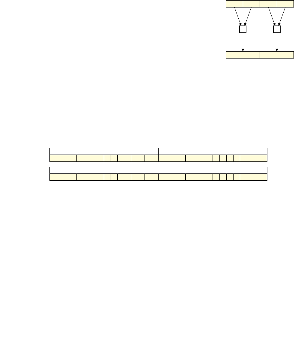
A8 Instruction Descriptions
A8.8 Alphabetical list of instructions
A8-984 Copyright © 1996-1998, 2000, 2004-2012, 2014 ARM. All rights reserved. ARM DDI 0406C.c
Non-Confidential ID051414
A8.8.364 VPADDL
Vector Pairwise Add Long adds adjacent pairs of elements of two vectors, and places the results in the destination
vector.
The vectors can be doubleword or quadword. The operand elements can be 8-bit, 16-bit, or 32-bit integers. The
result elements are twice the length of the operand elements.
Figure A8-4 shows an example of the operation of
VPADDL
.
Figure A8-4 VPADDL doubleword operation for data type
S16
Depending on settings in the CPACR, NSACR, and HCPTR registers, and the security state and mode in which the
instruction is executed, an attempt to execute the instruction might be UNDEFINED, or trapped to Hyp mode.
Summary of access controls for Advanced SIMD functionality on page B1-1233 summarizes these controls.
ARM deprecates the conditional execution of any Advanced SIMD instruction encoding that is not also available
as a VFP instruction encoding, see Conditional execution on page A8-288.
if size == ‘11’ then UNDEFINED;
if Q == ‘1’ && (Vd<0> == ‘1’ || Vm<0> == ‘1’) then UNDEFINED;
unsigned = (op == ‘1’);
esize = 8 << UInt(size); elements = 64 DIV esize;
d = UInt(D:Vd); m = UInt(M:Vm); regs = if Q == ‘0’ then 1 else 2;
Dm
Dd
+ +
Encoding T1/A1 Advanced SIMD
VPADDL<c>.<dt> <Qd>, <Qm>
VPADDL<c>.<dt> <Dd>, <Dm>
1 1 1 1 1 1 1 1 D 1 1 size 0 0 Vd 0 0 1 0 op Q M 0 Vm
15 14 13 12 11 10 9 8 7 6 5 4 3 2 1 0
1
1514131211109876543210
1 1 1 0 0 1 1 1 D 1 1 size 0 0 Vd 0 0 1 0 op Q M 0 Vm
31 30 29 28 27 26 25 24 23 22 21 20 19 18 17 16 15 14 13 12 11 10 9 8 7 6 5 4 3 2 1 0
1

A8 Instruction Descriptions
A8.8 Alphabetical list of instructions
ARM DDI 0406C.c Copyright © 1996-1998, 2000, 2004-2012, 2014 ARM. All rights reserved. A8-985
ID051414 Non-Confidential
Assembler syntax
where:
<c>, <q>
See Standard assembler syntax fields on page A8-287. An ARM
VPADDL
instruction must be
unconditional. ARM strongly recommends that a Thumb
VPADDL
instruction is unconditional, see
Conditional execution on page A8-288.
<dt>
The data type for the elements of the vectors. It must be one of:
S8
Encoded as size =
0b00
, op = 0.
S16
Encoded as size =
0b01
, op = 0.
S32
Encoded as size =
0b10
, op = 0.
U8
Encoded as size =
0b00
, op = 1.
U16
Encoded as size =
0b01
, op = 1.
U32
Encoded as size =
0b10
, op = 1.
<Qd>, <Qm>
The destination vector and the operand vector, for a quadword operation.
<Dd>, <Dm>
The destination vector and the operand vector, for a doubleword operation.
Operation
if ConditionPassed() then
EncodingSpecificOperations(); CheckAdvSIMDEnabled();
h = elements DIV 2;
for r = 0 to regs-1
for e = 0 to h-1
op1 = Elem[D[m+r],2*e,esize]; op2 = Elem[D[m+r],2*e+1,esize];
result = Int(op1, unsigned) + Int(op2, unsigned);
Elem[D[d+r],e,2*esize] = result<2*esize-1:0>;
Exceptions
Undefined Instruction, Hyp Trap.
VPADDL{<c>}{<q>}.<dt> <Qd>, <Qm>
Encoded as Q = 1
VPADDL{<c>}{<q>}.<dt> <Dd>, <Dm>
Encoded as Q = 0
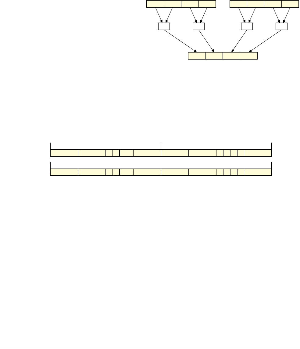
A8 Instruction Descriptions
A8.8 Alphabetical list of instructions
A8-986 Copyright © 1996-1998, 2000, 2004-2012, 2014 ARM. All rights reserved. ARM DDI 0406C.c
Non-Confidential ID051414
A8.8.365 VPMAX, VPMIN (integer)
Vector Pairwise Maximum compares adjacent pairs of elements in two doubleword vectors, and copies the larger
of each pair into the corresponding element in the destination doubleword vector.
Vector Pairwise Minimum compares adjacent pairs of elements in two doubleword vectors, and copies the smaller
of each pair into the corresponding element in the destination doubleword vector.
Figure A8-5 shows an example of the operation of
VPMAX
.
Figure A8-5 VPMAX operation for data type
S16
or
U16
Depending on settings in the CPACR, NSACR, and HCPTR registers, and the security state and mode in which the
instruction is executed, an attempt to execute the instruction might be UNDEFINED, or trapped to Hyp mode.
Summary of access controls for Advanced SIMD functionality on page B1-1233 summarizes these controls.
ARM deprecates the conditional execution of any Advanced SIMD instruction encoding that is not also available
as a VFP instruction encoding, see Conditional execution on page A8-288.
if size == ‘11’ || Q == ‘1’ then UNDEFINED;
maximum = (op == ‘0’); unsigned = (U == ‘1’);
esize = 8 << UInt(size); elements = 64 DIV esize;
d = UInt(D:Vd); n = UInt(N:Vn); m = UInt(M:Vm);
Dm
Dd
max max
Dn
max max
Encoding T1/A1 Advanced SIMD
VP<op><c>.<dt> <Dd>, <Dn>, <Dm>
1 1 U 1 1 1 1 0 D size Vn Vd 1 0 1 0 N Q M op Vm
15 14 13 12 11 10 9 8 7 6 5 4 3 2 1 0
1
1514131211109876543210
1 1 1 0 0 1 U 0 D size Vn Vd 1 0 1 0 N Q M op Vm
31 30 29 28 27 26 25 24 23 22 21 20 19 18 17 16 15 14 13 12 11 10 9 8 7 6 5 4 3 2 1 0
1

A8 Instruction Descriptions
A8.8 Alphabetical list of instructions
ARM DDI 0406C.c Copyright © 1996-1998, 2000, 2004-2012, 2014 ARM. All rights reserved. A8-987
ID051414 Non-Confidential
Assembler syntax
where:
<op>
The operation. It must be one of:
MAX
Encoded as op = 0.
MIN
Encoded as op = 1.
<c>, <q>
See Standard assembler syntax fields on page A8-287. An ARM
VPMAX
or
VPMIN
instruction
must be unconditional. ARM strongly recommends that a Thumb
VPMAX
or
VPMIN
instruction
is unconditional, see Conditional execution on page A8-288.
<dt>
The data type for the elements of the vectors. It must be one of:
S8
Encoding T1/A1, encoded as size =
0b00
, U = 0.
S16
Encoding T1/A1, encoded as size =
0b01
, U = 0.
S32
Encoding T1/A1, encoded as size =
0b10
, U = 0.
U8
Encoding T1/A1, encoded as size =
0b00
, U = 1.
U16
Encoding T1/A1, encoded as size =
0b01
, U = 1.
U32
Encoding T1/A1, encoded as size =
0b10
, U = 1.
<Dd>, <Dn>, <Dm>
The destination vector and the operand vectors.
Operation
if ConditionPassed() then
EncodingSpecificOperations(); CheckAdvSIMDEnabled();
bits(64) dest;
h = elements DIV 2;
for e = 0 to h-1
op1 = Int(Elem[D[n],2*e,esize], unsigned);
op2 = Int(Elem[D[n],2*e+1,esize], unsigned);
result = if maximum then Max(op1,op2) else Min(op1,op2);
Elem[dest,e,esize] = result<esize-1:0>;
op1 = Int(Elem[D[m],2*e,esize], unsigned);
op2 = Int(Elem[D[m],2*e+1,esize], unsigned);
result = if maximum then Max(op1,op2) else Min(op1,op2);
Elem[dest,e+h,esize] = result<esize-1:0>;
D[d] = dest;
Exceptions
Undefined Instruction, Hyp Trap.
VP<op>{<c>}{<q>}.<dt> {<Dd>,} <Dn>, <Dm>
Encoded as Q = 0

A8 Instruction Descriptions
A8.8 Alphabetical list of instructions
A8-988 Copyright © 1996-1998, 2000, 2004-2012, 2014 ARM. All rights reserved. ARM DDI 0406C.c
Non-Confidential ID051414
A8.8.366 VPMAX, VPMIN (floating-point)
Vector Pairwise Maximum compares adjacent pairs of elements in two doubleword vectors, and copies the larger
of each pair into the corresponding element in the destination doubleword vector.
Vector Pairwise Minimum compares adjacent pairs of elements in two doubleword vectors, and copies the smaller
of each pair into the corresponding element in the destination doubleword vector.
Figure A8-5 on page A8-986 shows an example of the operation of
VPMAX
.
Depending on settings in the CPACR, NSACR, and HCPTR registers, and the security state and mode in which the
instruction is executed, an attempt to execute the instruction might be UNDEFINED, or trapped to Hyp mode.
Summary of access controls for Advanced SIMD functionality on page B1-1233 summarizes these controls.
ARM deprecates the conditional execution of any Advanced SIMD instruction encoding that is not also available
as a VFP instruction encoding, see Conditional execution on page A8-288.
if sz == ‘1’ || Q == ‘1’ then UNDEFINED;
maximum = (op == ‘0’); esize = 32; elements = 2;
d = UInt(D:Vd); n = UInt(N:Vn); m = UInt(M:Vm);
Encoding T1/A1 Advanced SIMD (UNDEFINED in integer-only variant)
VP<op><c>.F32 <Dd>, <Dn>, <Dm>
1 1 1 1 1 1 1 0 D op sz Vn Vd 1 1 1 1 N Q M 0 Vm
15 14 13 12 11 10 9 8 7 6 5 4 3 2 1 0
1
1514131211109876543210
1 1 1 0 0 1 1 0 D op sz Vn Vd 1 1 1 1 N Q M 0 Vm
31 30 29 28 27 26 25 24 23 22 21 20 19 18 17 16 15 14 13 12 11 10 9 8 7 6 5 4 3 2 1 0
1

A8 Instruction Descriptions
A8.8 Alphabetical list of instructions
ARM DDI 0406C.c Copyright © 1996-1998, 2000, 2004-2012, 2014 ARM. All rights reserved. A8-989
ID051414 Non-Confidential
Assembler syntax
where:
<op>
The operation. It must be one of:
MAX
Encoded as op = 0.
MIN
Encoded as op = 1.
<c>, <q>
See Standard assembler syntax fields on page A8-287. An ARM
VPMAX
or
VPMIN
instruction
must be unconditional. ARM strongly recommends that a Thumb
VPMAX
or
VPMIN
instruction
is unconditional, see Conditional execution on page A8-288.
<Dd>, <Dn>, <Dm>
The destination vector and the operand vectors.
Operation
if ConditionPassed() then
EncodingSpecificOperations(); CheckAdvSIMDEnabled();
bits(64) dest;
h = elements DIV 2;
for e = 0 to h-1
op1 = Elem[D[n],2*e,esize]; op2 = Elem[D[n],2*e+1,esize];
Elem[dest,e,esize] = if maximum then FPMax(op1,op2,FALSE) else FPMin(op1,op2,FALSE);
op1 = Elem[D[m],2*e,esize]; op2 = Elem[D[m],2*e+1,esize];
Elem[dest,e+h,esize] = if maximum then FPMax(op1,op2,FALSE) else FPMin(op1,op2,FALSE);
D[d] = dest;
Exceptions
Undefined Instruction, Hyp Trap.
Floating-point exceptions
Invalid Operation, Input Denormal.
VP<op>{<c>}{<q>}.F32 {<Dd>,} <Dn>, <Dm>
Encoded as Q = 0, sz = 0

A8 Instruction Descriptions
A8.8 Alphabetical list of instructions
A8-990 Copyright © 1996-1998, 2000, 2004-2012, 2014 ARM. All rights reserved. ARM DDI 0406C.c
Non-Confidential ID051414
A8.8.367 VPOP
Vector Pop loads multiple consecutive extension registers from the stack.
Depending on settings in the CPACR, NSACR, HCPTR, and FPEXC registers, and the security state and mode in
which the instruction is executed, an attempt to execute the instruction might be UNDEFINED, or trapped to Hyp
mode. Summary of general controls of CP10 and CP11 functionality on page B1-1231 and Summary of access
controls for Advanced SIMD functionality on page B1-1233 summarize these controls.
For the case when
cond
is
0b1111
, see Unconditional instructions on page A5-216.
single_regs = FALSE; d = UInt(D:Vd); imm32 = ZeroExtend(imm8:’00’, 32);
regs = UInt(imm8) DIV 2; // If UInt(imm8) is odd, see “FLDMX”.
if regs == 0 || regs > 16 || (d+regs) > 32 then UNPREDICTABLE;
if VFPSmallRegisterBank() && (d+regs) > 16 then UNPREDICTABLE;
For the case when
cond
is
0b1111
, see Unconditional instructions on page A5-216.
single_regs = TRUE; d = UInt(Vd:D); imm32 = ZeroExtend(imm8:’00’, 32);
regs = UInt(imm8);
if regs == 0 || (d+regs) > 32 then UNPREDICTABLE;
Encoding T1/A1 VFPv2, VFPv3, VFPv4, Advanced SIMD
VPOP <list> <list>
is consecutive 64-bit registers
Encoding T2/A2 VFPv2, VFPv3, VFPv4
VPOP <list> <list>
is consecutive 32-bit registers
FLDMX Encoding T1/A1 behaves as described by the pseudocode if imm8 is odd. However,
there is no UAL syntax for such encodings and ARM deprecates their use. For more
information, see FLDMX, FSTMX on page A8-388.
1 1 0 1 1 0 0 1 D 1 1 1 1 0 1 Vd 1 0 1 1 imm8
15 14 13 12 11 10 9 8 7 6 5 4 3 2 1 0
1
1514131211109876543210
1 1 0 0 1 D 1 1 1 1 0 1 Vd 1 0 1 1 imm8
31 30 29 28 27 26 25 24 23 22 21 20 19 18 17 16 15 14 13 12 11 10 9 8 7 6 5 4 3 2 1 0
cond
1 1 0 1 1 0 0 1 D 1 1 1 1 0 1 Vd 1 0 1 0 imm8
15 14 13 12 11 10 9 8 7 6 5 4 3 2 1 0
1
1514131211109876543210
1 1 0 0 1 D 1 1 1 1 0 1 Vd 1 0 1 0 imm8
31 30 29 28 27 26 25 24 23 22 21 20 19 18 17 16 15 14 13 12 11 10 9 8 7 6 5 4 3 2 1 0
cond

A8 Instruction Descriptions
A8.8 Alphabetical list of instructions
ARM DDI 0406C.c Copyright © 1996-1998, 2000, 2004-2012, 2014 ARM. All rights reserved. A8-991
ID051414 Non-Confidential
Assembler syntax
VPOP{<c>}{<q>}{.<size>} <list>
where:
<c>, <q>
See Standard assembler syntax fields on page A8-287.
<size>
An optional data size specifier. If present, it must be equal to the size in bits, 32 or 64, of the registers
in
<list>
.
<list>
The extension registers to be loaded, as a list of consecutively numbered doubleword (encoding
T1/A1) or singleword (encoding T2/A2) registers, separated by commas and surrounded by
brackets. It is encoded in the instruction by setting D and Vd to specify the first register in the list,
and imm8 to twice the number of registers in the list (encoding T1/A1) or the number of registers
in the list (encoding T2/A2).
<list>
must contain at least one register, and not more than sixteen.
Operation
if ConditionPassed() then
EncodingSpecificOperations(); CheckVFPEnabled(TRUE); NullCheckIfThumbEE(13);
address = SP;
SP = SP + imm32;
if single_regs then
for r = 0 to regs-1
S[d+r] = MemA[address,4]; address = address+4;
else
for r = 0 to regs-1
word1 = MemA[address,4]; word2 = MemA[address+4,4]; address = address+8;
// Combine the word-aligned words in the correct order for current endianness.
D[d+r] = if BigEndian() then word1:word2 else word2:word1;
Exceptions
Undefined Instruction, Hyp Trap, Data Abort.
A8 Instruction Descriptions
A8.8 Alphabetical list of instructions
A8-992 Copyright © 1996-1998, 2000, 2004-2012, 2014 ARM. All rights reserved. ARM DDI 0406C.c
Non-Confidential ID051414
A8.8.368 VPUSH
Vector Push stores multiple consecutive extension registers to the stack.
Depending on settings in the CPACR, NSACR, HCPTR, and FPEXC registers, and the security state and mode in
which the instruction is executed, an attempt to execute the instruction might be UNDEFINED, or trapped to Hyp
mode. Summary of general controls of CP10 and CP11 functionality on page B1-1231 and Summary of access
controls for Advanced SIMD functionality on page B1-1233 summarize these controls.
For the case when
cond
is
0b1111
, see Unconditional instructions on page A5-216.
single_regs = FALSE; d = UInt(D:Vd); imm32 = ZeroExtend(imm8:’00’, 32);
regs = UInt(imm8) DIV 2; // If UInt(imm8) is odd, see “FSTMX”.
if regs == 0 || regs > 16 || (d+regs) > 32 then UNPREDICTABLE;
if VFPSmallRegisterBank() && (d+regs) > 16 then UNPREDICTABLE;
For the case when
cond
is
0b1111
, see Unconditional instructions on page A5-216.
single_regs = TRUE; d = UInt(Vd:D);
imm32 = ZeroExtend(imm8:’00’, 32); regs = UInt(imm8);
if regs == 0 || (d+regs) > 32 then UNPREDICTABLE;
Encoding T1/A1 VFPv2, VFPv3, VFPv4, Advanced SIMD
VPUSH<c> <list> <list>
is consecutive 64-bit registers
Encoding T2/A2 VFPv2, VFPv3, VFPv4
VPUSH<c> <list> <list>
is consecutive 32-bit registers
FSTMX Encoding T1/A1 behaves as described by the pseudocode if imm8 is odd. However,
there is no UAL syntax for such encodings and ARM deprecates their use. For more
information, see FLDMX, FSTMX on page A8-388.
1 1 0 1 1 0 1 0 D 1 0 1 1 0 1 Vd 1 0 1 1 imm8
15 14 13 12 11 10 9 8 7 6 5 4 3 2 1 0
1
1514131211109876543210
1 1 0 1 0 D 1 0 1 1 0 1 Vd 1 0 1 1 imm8
31 30 29 28 27 26 25 24 23 22 21 20 19 18 17 16 15 14 13 12 11 10 9 8 7 6 5 4 3 2 1 0
cond
1 1 0 1 1 0 1 0 D 1 0 1 1 0 1 Vd 1 0 1 0 imm8
15 14 13 12 11 10 9 8 7 6 5 4 3 2 1 0
1
1514131211109876543210
1 1 0 1 0 D 1 0 1 1 0 1 Vd 1 0 1 0 imm8
31 30 29 28 27 26 25 24 23 22 21 20 19 18 17 16 15 14 13 12 11 10 9 8 7 6 5 4 3 2 1 0
cond

A8 Instruction Descriptions
A8.8 Alphabetical list of instructions
ARM DDI 0406C.c Copyright © 1996-1998, 2000, 2004-2012, 2014 ARM. All rights reserved. A8-993
ID051414 Non-Confidential
Assembler syntax
VPUSH{<c>}{<q>}{.<size>} <list>
where:
<c>, <q>
See Standard assembler syntax fields on page A8-287.
<size>
An optional data size specifier. If present, it must be equal to the size in bits, 32 or 64, of the registers
in
<list>
.
<list>
The extension registers to be stored, as a list of consecutively numbered doubleword (encoding
T1/A1) or singleword (encoding T2/A2) registers, separated by commas and surrounded by
brackets. It is encoded in the instruction by setting D and Vd to specify the first register in the list,
and imm8 to twice the number of registers in the list (encoding T1/A1), or the number of registers
in the list (encoding T2/A2).
<list>
must contain at least one register, and not more than sixteen.
Operation
if ConditionPassed() then
EncodingSpecificOperations(); CheckVFPEnabled(TRUE); NullCheckIfThumbEE(13);
address = SP - imm32;
SP = SP - imm32;
if single_regs then
for r = 0 to regs-1
MemA[address,4] = S[d+r]; address = address+4;
else
for r = 0 to regs-1
// Store as two word-aligned words in the correct order for current endianness.
MemA[address,4] = if BigEndian() then D[d+r]<63:32> else D[d+r]<31:0>;
MemA[address+4,4] = if BigEndian() then D[d+r]<31:0> else D[d+r]<63:32>;
address = address+8;
Exceptions
Undefined Instruction, Hyp Trap, Data Abort.

A8 Instruction Descriptions
A8.8 Alphabetical list of instructions
A8-994 Copyright © 1996-1998, 2000, 2004-2012, 2014 ARM. All rights reserved. ARM DDI 0406C.c
Non-Confidential ID051414
A8.8.369 VQABS
Vector Saturating Absolute takes the absolute value of each element in a vector, and places the results in the
destination vector.
If any of the results overflow, they are saturated. The cumulative saturation bit, FPSCR.QC, is set if saturation
occurs. For details see Pseudocode details of saturation on page A2-44.
Depending on settings in the CPACR, NSACR, and HCPTR registers, and the security state and mode in which the
instruction is executed, an attempt to execute the instruction might be UNDEFINED, or trapped to Hyp mode.
Summary of access controls for Advanced SIMD functionality on page B1-1233 summarizes these controls.
ARM deprecates the conditional execution of any Advanced SIMD instruction encoding that is not also available
as a VFP instruction encoding, see Conditional execution on page A8-288.
if size == ‘11’ then UNDEFINED;
if Q == ‘1’ && (Vd<0> == ‘1’ || Vm<0> == ‘1’) then UNDEFINED;
esize = 8 << UInt(size); elements = 64 DIV esize;
d = UInt(D:Vd); m = UInt(M:Vm); regs = if Q == ‘0’ then 1 else 2;
Encoding T1/A1 Advanced SIMD
VQABS<c>.<dt> <Qd>, <Qm>
VQABS<c>.<dt> <Dd>, <Dm>
1 1 1 1 1 1 1 1 D 1 1 size 0 0 Vd 0 1 1 1 0 Q M 0 Vm
15 14 13 12 11 10 9 8 7 6 5 4 3 2 1 0
1
1514131211109876543210
1 1 1 0 0 1 1 1 D 1 1 size 0 0 Vd 0 1 1 1 0 Q M 0 Vm
31 30 29 28 27 26 25 24 23 22 21 20 19 18 17 16 15 14 13 12 11 10 9 8 7 6 5 4 3 2 1 0
1

A8 Instruction Descriptions
A8.8 Alphabetical list of instructions
ARM DDI 0406C.c Copyright © 1996-1998, 2000, 2004-2012, 2014 ARM. All rights reserved. A8-995
ID051414 Non-Confidential
Assembler syntax
where:
<c>, <q>
See Standard assembler syntax fields on page A8-287. An ARM
VQABS
instruction must be
unconditional. ARM strongly recommends that a Thumb
VQABS
instruction is unconditional, see
Conditional execution on page A8-288.
<dt>
The data type for the elements of the vectors. It must be one of:
S8
Encoded as size =
0b00
.
S16
Encoded as size =
0b01
.
S32
Encoded as size =
0b10
.
<Qd>, <Qm>
The destination vector and the operand vector, for a quadword operation.
<Dd>, <Dm>
The destination vector and the operand vector, for a doubleword operation.
Operation
if ConditionPassed() then
EncodingSpecificOperations(); CheckAdvSIMDEnabled();
for r = 0 to regs-1
for e = 0 to elements-1
result = Abs(SInt(Elem[D[m+r],e,esize]));
(Elem[D[d+r],e,esize], sat) = SignedSatQ(result, esize);
if sat then FPSCR.QC = ‘1’;
Exceptions
Undefined Instruction, Hyp Trap.
VQABS{<c>}{<q>}.<dt> <Qd>, <Qm>
Encoded as Q = 1
VQABS{<c>}{<q>}.<dt> <Dd>, <Dm>
Encoded as Q = 0
A8 Instruction Descriptions
A8.8 Alphabetical list of instructions
A8-996 Copyright © 1996-1998, 2000, 2004-2012, 2014 ARM. All rights reserved. ARM DDI 0406C.c
Non-Confidential ID051414
A8.8.370 VQADD
Vector Saturating Add adds the values of corresponding elements of two vectors, and places the results in the
destination vector.
If any of the results overflow, they are saturated. The cumulative saturation bit, FPSCR.QC, is set if saturation
occurs. For details see Pseudocode details of saturation on page A2-44.
Depending on settings in the CPACR, NSACR, and HCPTR registers, and the security state and mode in which the
instruction is executed, an attempt to execute the instruction might be UNDEFINED, or trapped to Hyp mode.
Summary of access controls for Advanced SIMD functionality on page B1-1233 summarizes these controls.
ARM deprecates the conditional execution of any Advanced SIMD instruction encoding that is not also available
as a VFP instruction encoding, see Conditional execution on page A8-288.
if Q == ‘1’ && (Vd<0> == ‘1’ || Vn<0> == ‘1’ || Vm<0> == ‘1’) then UNDEFINED;
unsigned = (U == ‘1’);
esize = 8 << UInt(size); elements = 64 DIV esize;
d = UInt(D:Vd); n = UInt(N:Vn); m = UInt(M:Vm); regs = if Q == ‘0’ then 1 else 2;
Encoding T1/A1 Advanced SIMD
VQADD<c>.<dt> <Qd>, <Qn>, <Qm>
VQADD<c>.<dt> <Dd>, <Dn>, <Dm>
1 1 U 1 1 1 1 0 D size Vn Vd 0 0 0 0 N Q M 1 Vm
15 14 13 12 11 10 9 8 7 6 5 4 3 2 1 0
1
1514131211109876543210
1 1 1 0 0 1 U 0 D size Vn Vd 0 0 0 0 N Q M 1 Vm
31 30 29 28 27 26 25 24 23 22 21 20 19 18 17 16 15 14 13 12 11 10 9 8 7 6 5 4 3 2 1 0
1

A8 Instruction Descriptions
A8.8 Alphabetical list of instructions
ARM DDI 0406C.c Copyright © 1996-1998, 2000, 2004-2012, 2014 ARM. All rights reserved. A8-997
ID051414 Non-Confidential
Assembler syntax
where:
<c>, <q>
See Standard assembler syntax fields on page A8-287. An ARM
VQADD
instruction must be
unconditional. ARM strongly recommends that a Thumb
VQADD
instruction is unconditional,
see Conditional execution on page A8-288.
<type>
The data type for the elements of the vectors. It must be one of:
S
Signed, encoded as U = 0.
U
Unsigned, encoded as U = 1.
<size>
The data size for the elements of the vectors. It must be one of:
8
Encoded as size =
0b00
.
16
Encoded as size =
0b01
.
32
Encoded as size =
0b10
.
64
Encoded as size =
0b11
.
<Qd>, <Qn>, <Qm>
The destination vector and the operand vectors, for a quadword operation.
<Dd>, <Dn>, <Dm>
The destination vector and the operand vectors, for a doubleword operation.
Operation
if ConditionPassed() then
EncodingSpecificOperations(); CheckAdvSIMDEnabled();
for r = 0 to regs-1
for e = 0 to elements-1
sum = Int(Elem[D[n+r],e,esize], unsigned) + Int(Elem[D[m+r],e,esize], unsigned);
(Elem[D[d+r],e,esize], sat) = SatQ(sum, esize, unsigned);
if sat then FPSCR.QC = ‘1’;
Exceptions
Undefined Instruction, Hyp Trap.
VQADD{<c>}{<q>}.<type><size> {<Qd>,} <Qn>, <Qm>
Encoded as Q = 1
VQADD{<c>}{<q>}.<type><size> {<Dd>,} <Dn>, <Dm>
Encoded as Q = 0
A8 Instruction Descriptions
A8.8 Alphabetical list of instructions
A8-998 Copyright © 1996-1998, 2000, 2004-2012, 2014 ARM. All rights reserved. ARM DDI 0406C.c
Non-Confidential ID051414
A8.8.371 VQDMLAL, VQDMLSL
Vector Saturating Doubling Multiply Accumulate Long multiplies corresponding elements in two doubleword
vectors, doubles the products, and accumulates the results into the elements of a quadword vector.
Vector Saturating Doubling Multiply Subtract Long multiplies corresponding elements in two doubleword vectors,
subtracts double the products from corresponding elements of a quadword vector, and places the results in the same
quadword vector.
In both instructions, the second operand can be a scalar instead of a vector. For more information about scalars see
Advanced SIMD scalars on page A7-260.
If any of the results overflow, they are saturated. The cumulative saturation bit, FPSCR.QC, is set if saturation
occurs. For details see Pseudocode details of saturation on page A2-44.
Depending on settings in the CPACR, NSACR, and HCPTR registers, and the security state and mode in which the
instruction is executed, an attempt to execute the instruction might be UNDEFINED, or trapped to Hyp mode.
Summary of access controls for Advanced SIMD functionality on page B1-1233 summarizes these controls.
ARM deprecates the conditional execution of any Advanced SIMD instruction encoding that is not also available
as a VFP instruction encoding, see Conditional execution on page A8-288.
if size == ‘11’ then SEE “Related encodings”;
if size == ‘00’ || Vd<0> == ‘1’ then UNDEFINED;
add = (op == ‘0’);
scalar_form = FALSE; d = UInt(D:Vd); n = UInt(N:Vn); m = UInt(M:Vm);
esize = 8 << UInt(size); elements = 64 DIV esize;
if size == ‘11’ then SEE “Related encodings”;
if size == ‘00’ || Vd<0> == ‘1’ then UNDEFINED;
add = (op == ‘0’);
scalar_form = TRUE; d = UInt(D:Vd); n = UInt(N:Vn);
if size == ‘01’ then esize = 16; elements = 4; m = UInt(Vm<2:0>); index = UInt(M:Vm<3>);
if size == ‘10’ then esize = 32; elements = 2; m = UInt(Vm); index = UInt(M);
Encoding T1/A1 Advanced SIMD
VQD<op><c>.<dt> <Qd>, <Dn>, <Dm>
Encoding T2/A2 Advanced SIMD
VQD<op><c>.<dt> <Qd>, <Dn>, <Dm[x]>
Related encodings See Advanced SIMD data-processing instructions on page A7-261.
1 1 0 1 1 1 1 1 D size Vn Vd 1 0 op 1 N 0 M 0 Vm
15 14 13 12 11 10 9 8 7 6 5 4 3 2 1 0
1
1514131211109876543210
1 1 1 0 0 1 0 1 D size Vn Vd 1 0 op 1 N 0 M 0 Vm
31 30 29 28 27 26 25 24 23 22 21 20 19 18 17 16 15 14 13 12 11 10 9 8 7 6 5 4 3 2 1 0
1
1 1 0 1 1 1 1 1 D size Vn Vd 0 op 1 1 N 1 M 0 Vm
15 14 13 12 11 10 9 8 7 6 5 4 3 2 1 0
1
1514131211109876543210
1 1 1 0 0 1 0 1 D size Vn Vd 0 op 1 1 N 1 M 0 Vm
31 30 29 28 27 26 25 24 23 22 21 20 19 18 17 16 15 14 13 12 11 10 9 8 7 6 5 4 3 2 1 0
1

A8 Instruction Descriptions
A8.8 Alphabetical list of instructions
ARM DDI 0406C.c Copyright © 1996-1998, 2000, 2004-2012, 2014 ARM. All rights reserved. A8-999
ID051414 Non-Confidential
Assembler syntax
where:
<op>
The operation. It must be one of:
MLAL
Encoded as op = 0.
MLSL
Encoded as op = 1.
<c>, <q>
See Standard assembler syntax fields on page A8-287. An ARM
VQDMLAL
or
VQDMLSL
instruction must
be unconditional. ARM strongly recommends that a Thumb
VQDMLAL
or
VQDMLSL
instruction is
unconditional, see Conditional execution on page A8-288.
<dt>
The data type for the elements of the operands. It must be one of:
S16
Encoded as size =
0b01
.
S32
Encoded as size =
0b10
.
<Qd>, <Dn>
The destination vector and the first operand vector.
<Dm>
The second operand vector, for an all vector operation.
<Dm[x]>
The scalar for a scalar operation. If
<dt>
is
S16
,
Dm
is restricted to D0-D7. If
<dt>
is
S32
,
Dm
is restricted
to D0-D15.
Operation
if ConditionPassed() then
EncodingSpecificOperations(); CheckAdvSIMDEnabled();
if scalar_form then op2 = SInt(Elem[Din[m],index,esize]);
for e = 0 to elements-1
if !scalar_form then op2 = SInt(Elem[Din[m],e,esize]);
op1 = SInt(Elem[Din[n],e,esize]);
// The following only saturates if both op1 and op2 equal -(2^(esize-1))
(product, sat1) = SignedSatQ(2*op1*op2, 2*esize);
if add then
result = SInt(Elem[Qin[d>>1],e,2*esize]) + SInt(product);
else
result = SInt(Elem[Qin[d>>1],e,2*esize]) - SInt(product);
(Elem[Q[d>>1],e,2*esize], sat2) = SignedSatQ(result, 2*esize);
if sat1 || sat2 then FPSCR.QC = ‘1’;
Exceptions
Undefined Instruction, Hyp Trap.
VQD<op>{<c>}{<q>}.<dt> <Qd>, <Dn>, <Dm>
VQD<op>{<c>}{<q>}.<dt> <Qd>, <Dn>, <Dm[x]>

A8 Instruction Descriptions
A8.8 Alphabetical list of instructions
A8-1000 Copyright © 1996-1998, 2000, 2004-2012, 2014 ARM. All rights reserved. ARM DDI 0406C.c
Non-Confidential ID051414
A8.8.372 VQDMULH
Vector Saturating Doubling Multiply Returning High Half multiplies corresponding elements in two vectors,
doubles the results, and places the most significant half of the final results in the destination vector. The results are
truncated (for rounded results see VQRDMULH on page A8-1008).
The second operand can be a scalar instead of a vector. For more information about scalars see Advanced SIMD
scalars on page A7-260.
If any of the results overflow, they are saturated. The cumulative saturation bit, FPSCR.QC, is set if saturation
occurs. For details see Pseudocode details of saturation on page A2-44.
Depending on settings in the CPACR, NSACR, and HCPTR registers, and the security state and mode in which the
instruction is executed, an attempt to execute the instruction might be UNDEFINED, or trapped to Hyp mode.
Summary of access controls for Advanced SIMD functionality on page B1-1233 summarizes these controls.
ARM deprecates the conditional execution of any Advanced SIMD instruction encoding that is not also available
as a VFP instruction encoding, see Conditional execution on page A8-288.
if Q == ‘1’ && (Vd<0> == ‘1’ || Vn<0> == ‘1’ || Vm<0> == ‘1’) then UNDEFINED;
if size == ‘00’ || size == ‘11’ then UNDEFINED;
scalar_form = FALSE; esize = 8 << UInt(size); elements = 64 DIV esize;
d = UInt(D:Vd); n = UInt(N:Vn); m = UInt(M:Vm); regs = if Q == ‘0’ then 1 else 2;
if size == ‘11’ then SEE “Related encodings”;
if size == ‘00’ then UNDEFINED;
if Q == ‘1’ && (Vd<0> == ‘1’ || Vn<0> == ‘1’) then UNDEFINED;
scalar_form = TRUE; d = UInt(D:Vd); n = UInt(N:Vn); regs = if Q == ‘0’ then 1 else 2;
if size == ‘01’ then esize = 16; elements = 4; m = UInt(Vm<2:0>); index = UInt(M:Vm<3>);
if size == ‘10’ then esize = 32; elements = 2; m = UInt(Vm); index = UInt(M);
Encoding T1/A1 Advanced SIMD
VQDMULH<c>.<dt> <Qd>, <Qn>, <Qm>
VQDMULH<c>.<dt> <Dd>, <Dn>, <Dm>
Encoding T2/A2 Advanced SIMD
VQDMULH<c>.<dt> <Qd>, <Qn>, <Dm[x]>
VQDMULH<c>.<dt> <Dd>, <Dn>, <Dm[x]>
Related encodings See Advanced SIMD data-processing instructions on page A7-261.
1 1 0 1 1 1 1 0 D size Vn Vd 1 0 1 1 N Q M 0 Vm
15 14 13 12 11 10 9 8 7 6 5 4 3 2 1 0
1
1514131211109876543210
1 1 1 0 0 1 0 0 D size Vn Vd 1 0 1 1 N Q M 0 Vm
31 30 29 28 27 26 25 24 23 22 21 20 19 18 17 16 15 14 13 12 11 10 9 8 7 6 5 4 3 2 1 0
1
1 1 Q 1 1 1 1 1 D size Vn Vd 1 1 0 0 N 1 M 0 Vm
15 14 13 12 11 10 9 8 7 6 5 4 3 2 1 0
1
1514131211109876543210
1 1 1 0 0 1 Q 1 D size Vn Vd 1 1 0 0 N 1 M 0 Vm
31 30 29 28 27 26 25 24 23 22 21 20 19 18 17 16 15 14 13 12 11 10 9 8 7 6 5 4 3 2 1 0
1

A8 Instruction Descriptions
A8.8 Alphabetical list of instructions
ARM DDI 0406C.c Copyright © 1996-1998, 2000, 2004-2012, 2014 ARM. All rights reserved. A8-1001
ID051414 Non-Confidential
Assembler syntax
where:
<c>, <q>
See Standard assembler syntax fields on page A8-287. An ARM
VQDMULH
instruction must
be unconditional. ARM strongly recommends that a Thumb
VQDMULH
instruction is
unconditional, see Conditional execution on page A8-288.
<dt>
The data type for the elements of the operands. It must be one of:
S16
Encoded as size =
0b01
.
S32
Encoded as size =
0b10
.
<Qd>, <Qn>
The destination vector and the first operand vector, for a quadword operation.
<Dd>, <Dn>
The destination vector and the first operand vector, for a doubleword operation.
<Qm>
The second operand vector, for a quadword all vector operation.
<Dm>
The second operand vector, for a doubleword all vector operation.
<Dm[x]>
The scalar for either a quadword or a doubleword scalar operation. If
<dt>
is
S16
,
Dm
is
restricted to D0-D7. If
<dt>
is
S32
,
Dm
is restricted to D0-D15.
Operation
if ConditionPassed() then
EncodingSpecificOperations(); CheckAdvSIMDEnabled();
if scalar_form then op2 = SInt(Elem[D[m],index,esize]);
for r = 0 to regs-1
for e = 0 to elements-1
if !scalar_form then op2 = SInt(Elem[D[m+r],e,esize]);
op1 = SInt(Elem[D[n+r],e,esize]);
// The following only saturates if both op1 and op2 equal -(2^(esize-1))
(result, sat) = SignedSatQ((2*op1*op2) >> esize, esize);
Elem[D[d+r],e,esize] = result;
if sat then FPSCR.QC = ‘1’;
Exceptions
Undefined Instruction, Hyp Trap.
VQDMULH{<c>}{<q>}.<dt> {<Qd>,} <Qn>, <Qm>
Encoding T1/A1, encoded as Q = 1
VQDMULH{<c>}{<q>}.<dt> {<Dd>,} <Dn>, <Dm>
Encoding T1/A1, encoded as Q = 0
VQDMULH{<c>}{<q>}.<dt> {<Qd>,} <Qn>, <Dm[x]>
Encoding T2/A2, encoded as Q = 1
VQDMULH{<c>}{<q>}.<dt> {<Dd>,} <Dn>, <Dm[x]>
Encoding T2/A2, encoded as Q = 0
A8 Instruction Descriptions
A8.8 Alphabetical list of instructions
A8-1002 Copyright © 1996-1998, 2000, 2004-2012, 2014 ARM. All rights reserved. ARM DDI 0406C.c
Non-Confidential ID051414
A8.8.373 VQDMULL
Vector Saturating Doubling Multiply Long multiplies corresponding elements in two doubleword vectors, doubles
the products, and places the results in a quadword vector.
The second operand can be a scalar instead of a vector. For more information about scalars see Advanced SIMD
scalars on page A7-260.
If any of the results overflow, they are saturated. The cumulative saturation bit, FPSCR.QC, is set if saturation
occurs. For details see Pseudocode details of saturation on page A2-44.
Depending on settings in the CPACR, NSACR, and HCPTR registers, and the security state and mode in which the
instruction is executed, an attempt to execute the instruction might be UNDEFINED, or trapped to Hyp mode.
Summary of access controls for Advanced SIMD functionality on page B1-1233 summarizes these controls.
ARM deprecates the conditional execution of any Advanced SIMD instruction encoding that is not also available
as a VFP instruction encoding, see Conditional execution on page A8-288.
if size == ‘11’ then SEE “Related encodings”;
if size == ‘00’ || Vd<0> == ‘1’ then UNDEFINED;
scalar_form = FALSE; d = UInt(D:Vd); n = UInt(N:Vn); m = UInt(M:Vm);
esize = 8 << UInt(size); elements = 64 DIV esize;
if size == ‘11’ then SEE “Related encodings”;
if size == ‘00’ || Vd<0> == ‘1’ then UNDEFINED;
scalar_form = TRUE; d = UInt(D:Vd); n = UInt(N:Vn);
if size == ‘01’ then esize = 16; elements = 4; m = UInt(Vm<2:0>); index = UInt(M:Vm<3>);
if size == ‘10’ then esize = 32; elements = 2; m = UInt(Vm); index = UInt(M);
Encoding T1/A1 Advanced SIMD
VQDMULL<c>.<dt> <Qd>, <Dn>, <Dm>
Encoding T2/A2 Advanced SIMD
VQDMULL<c>.<dt> <Qd>, <Dn>, <Dm[x]>
Related encodings See Advanced SIMD data-processing instructions on page A7-261.
1 1 0 1 1 1 1 1 D size Vn Vd 1 1 0 1 N 0 M 0 Vm
15 14 13 12 11 10 9 8 7 6 5 4 3 2 1 0
1
1514131211109876543210
1 1 1 0 0 1 0 1 D size Vn Vd 1 1 0 1 N 0 M 0 Vm
31 30 29 28 27 26 25 24 23 22 21 20 19 18 17 16 15 14 13 12 11 10 9 8 7 6 5 4 3 2 1 0
1
1 1 0 1 1 1 1 1 D size Vn Vd 1 0 1 1 N 1 M 0 Vm
15 14 13 12 11 10 9 8 7 6 5 4 3 2 1 0
1
1514131211109876543210
1 1 1 0 0 1 0 1 D size Vn Vd 1 0 1 1 N 1 M 0 Vm
31 30 29 28 27 26 25 24 23 22 21 20 19 18 17 16 15 14 13 12 11 10 9 8 7 6 5 4 3 2 1 0
1

A8 Instruction Descriptions
A8.8 Alphabetical list of instructions
ARM DDI 0406C.c Copyright © 1996-1998, 2000, 2004-2012, 2014 ARM. All rights reserved. A8-1003
ID051414 Non-Confidential
Assembler syntax
where:
<c>, <q>
See Standard assembler syntax fields on page A8-287. An ARM
VQDMULL
instruction must be
unconditional. ARM strongly recommends that a Thumb
VQDMULL
instruction is unconditional, see
Conditional execution on page A8-288.
<dt>
The data type for the elements of the operands. It must be one of:
S16
Encoded as size =
0b01
.
S32
Encoded as size =
0b10
.
<Qd>, <Dn>
The destination vector and the first operand vector.
<Dm>
The second operand vector, for an all vector operation.
<Dm[x]>
The scalar for a scalar operation. If
<dt>
is
S16
,
Dm
is restricted to D0-D7. If
<dt>
is
S32
,
Dm
is restricted
to D0-D15.
Operation
if ConditionPassed() then
EncodingSpecificOperations(); CheckAdvSIMDEnabled();
if scalar_form then op2 = SInt(Elem[Din[m],index,esize]);
for e = 0 to elements-1
if !scalar_form then op2 = SInt(Elem[Din[m],e,esize]);
op1 = SInt(Elem[Din[n],e,esize]);
// The following only saturates if both op1 and op2 equal -(2^(esize-1))
(product, sat) = SignedSatQ(2*op1*op2, 2*esize);
Elem[Q[d>>1],e,2*esize] = product;
if sat then FPSCR.QC = ‘1’;
Exceptions
Undefined Instruction, Hyp Trap.
VQDMULL{<c>}{<q>}.<dt> <Qd>, <Dn>, <Dm>
VQDMULL{<c>}{<q>}.<dt> <Qd>, <Dn>, <Dm[x]>

A8 Instruction Descriptions
A8.8 Alphabetical list of instructions
A8-1004 Copyright © 1996-1998, 2000, 2004-2012, 2014 ARM. All rights reserved. ARM DDI 0406C.c
Non-Confidential ID051414
A8.8.374 VQMOVN, VQMOVUN
Vector Saturating Move and Narrow copies each element of the operand vector to the corresponding element of the
destination vector.
The operand is a quadword vector. The elements can be any one of:
• 16-bit, 32-bit, or 64-bit signed integers
• 16-bit, 32-bit, or 64-bit unsigned integers.
The result is a doubleword vector. The elements are half the length of the operand vector elements. If the operand
is unsigned, the results are unsigned. If the operand is signed, the results can be signed or unsigned.
If any of the results overflow, they are saturated. The cumulative saturation bit, FPSCR.QC, is set if saturation
occurs. For details see Pseudocode details of saturation on page A2-44.
Depending on settings in the CPACR, NSACR, and HCPTR registers, and the security state and mode in which the
instruction is executed, an attempt to execute the instruction might be UNDEFINED, or trapped to Hyp mode.
Summary of access controls for Advanced SIMD functionality on page B1-1233 summarizes these controls.
ARM deprecates the conditional execution of any Advanced SIMD instruction encoding that is not also available
as a VFP instruction encoding, see Conditional execution on page A8-288.
if op == ‘00’ then SEE VMOVN;
if size == ‘11’ || Vm<0> == ‘1’ then UNDEFINED;
src_unsigned = (op == ‘11’); dest_unsigned = (op<0> == ‘1’);
esize = 8 << UInt(size); elements = 64 DIV esize;
d = UInt(D:Vd); m = UInt(M:Vm);
Encoding T1/A1 Advanced SIMD
VQMOV{U}N<c>.<type><size> <Dd>, <Qm>
1 1 1 1 1 1 1 1 D 1 1 size 1 0 Vd 0 0 1 0 op M 0 Vm
15 14 13 12 11 10 9 8 7 6 5 4 3 2 1 0
1
1514131211109876543210
1 1 1 0 0 1 1 1 D 1 1 size 1 0 Vd 0 0 1 0 op M 0 Vm
31 30 29 28 27 26 25 24 23 22 21 20 19 18 17 16 15 14 13 12 11 10 9 8 7 6 5 4 3 2 1 0
1

A8 Instruction Descriptions
A8.8 Alphabetical list of instructions
ARM DDI 0406C.c Copyright © 1996-1998, 2000, 2004-2012, 2014 ARM. All rights reserved. A8-1005
ID051414 Non-Confidential
Assembler syntax
where:
U
If present, specifies that the operation produces unsigned results, even though the operands are
signed. Encoded as op =
0b01
.
<c>, <q>
See Standard assembler syntax fields on page A8-287. An ARM
VQMOVN
or
VQMOVUN
instruction must
be unconditional. ARM strongly recommends that a Thumb
VQMOVN
or
VQMOVUN
instruction is
unconditional, see Conditional execution on page A8-288.
<type>
The data type for the elements of the operand. It must be one of:
S
Encoded as:
• op =
0b10
for
VQMOVN
.
• op =
0b01
for
VQMOVUN
.
U
Encoded as op =
0b11
. Not available for
VQMOVUN
.
<size>
The data size for the elements of the operand. It must be one of:
16
Encoded as size =
0b00
.
32
Encoded as size =
0b01
.
64
Encoded as size =
0b10
.
<Dd>, <Qm>
The destination vector and the operand vector.
Operation
if ConditionPassed() then
EncodingSpecificOperations(); CheckAdvSIMDEnabled();
for e = 0 to elements-1
operand = Int(Elem[Qin[m>>1],e,2*esize], src_unsigned);
(Elem[D[d],e,esize], sat) = SatQ(operand, esize, dest_unsigned);
if sat then FPSCR.QC = ‘1’;
Exceptions
Undefined Instruction, Hyp Trap.
VQMOV{U}N{<c>}{<q>}.<type><size> <Dd>, <Qm>

A8 Instruction Descriptions
A8.8 Alphabetical list of instructions
A8-1006 Copyright © 1996-1998, 2000, 2004-2012, 2014 ARM. All rights reserved. ARM DDI 0406C.c
Non-Confidential ID051414
A8.8.375 VQNEG
Vector Saturating Negate negates each element in a vector, and places the results in the destination vector.
If any of the results overflow, they are saturated. The cumulative saturation bit, FPSCR.QC, is set if saturation
occurs. For details see Pseudocode details of saturation on page A2-44.
Depending on settings in the CPACR, NSACR, and HCPTR registers, and the security state and mode in which the
instruction is executed, an attempt to execute the instruction might be UNDEFINED, or trapped to Hyp mode.
Summary of access controls for Advanced SIMD functionality on page B1-1233 summarizes these controls.
ARM deprecates the conditional execution of any Advanced SIMD instruction encoding that is not also available
as a VFP instruction encoding, see Conditional execution on page A8-288.
if size == ‘11’ then UNDEFINED;
if Q == ‘1’ && (Vd<0> == ‘1’ || Vm<0> == ‘1’) then UNDEFINED;
esize = 8 << UInt(size); elements = 64 DIV esize;
d = UInt(D:Vd); m = UInt(M:Vm); regs = if Q == ‘0’ then 1 else 2;
Encoding T1/A1 Advanced SIMD
VQNEG<c>.<dt> <Qd>, <Qm>
VQNEG<c>.<dt> <Dd>, <Dm>
Q1 1 1 1 1 1 1 1 D 1 1 size 0 0 Vd 0 1 1 1 1 M 0 Vm
15 14 13 12 11 10 9 8 7 6 5 4 3 2 1 0
1
1514131211109876543210
Q1 1 1 0 0 1 1 1 D 1 1 size 0 0 Vd 0 1 1 1 1 M 0 Vm
31 30 29 28 27 26 25 24 23 22 21 20 19 18 17 16 15 14 13 12 11 10 9 8 7 6 5 4 3 2 1 0
1

A8 Instruction Descriptions
A8.8 Alphabetical list of instructions
ARM DDI 0406C.c Copyright © 1996-1998, 2000, 2004-2012, 2014 ARM. All rights reserved. A8-1007
ID051414 Non-Confidential
Assembler syntax
where:
<c>, <q>
See Standard assembler syntax fields on page A8-287. An ARM
VQNEG
instruction must be
unconditional. ARM strongly recommends that a Thumb
VQNEG
instruction is unconditional, see
Conditional execution on page A8-288.
<dt>
The data type for the elements of the vectors. It must be one of:
S8
Encoded as size =
0b00
.
S16
Encoded as size =
0b01
.
S32
Encoded as size =
0b10
.
<Qd>, <Qm>
The destination vector and the operand vector, for a quadword operation.
<Dd>, <Dm>
The destination vector and the operand vector, for a doubleword operation.
Operation
if ConditionPassed() then
EncodingSpecificOperations(); CheckAdvSIMDEnabled();
for r = 0 to regs-1
for e = 0 to elements-1
result = -SInt(Elem[D[m+r],e,esize]);
(Elem[D[d+r],e,esize], sat) = SignedSatQ(result, esize);
if sat then FPSCR.QC = ‘1’;
Exceptions
Undefined Instruction, Hyp Trap.
VQNEG{<c>}{<q>}.<dt> <Qd>, <Qm>
Encoded as Q = 1
VQNEG{<c>}{<q>}.<dt> <Dd>, <Dm>
Encoded as Q = 0
A8 Instruction Descriptions
A8.8 Alphabetical list of instructions
A8-1008 Copyright © 1996-1998, 2000, 2004-2012, 2014 ARM. All rights reserved. ARM DDI 0406C.c
Non-Confidential ID051414
A8.8.376 VQRDMULH
Vector Saturating Rounding Doubling Multiply Returning High Half multiplies corresponding elements in two
vectors, doubles the results, and places the most significant half of the final results in the destination vector. The
results are rounded (for truncated results see VQDMULH on page A8-1000).
The second operand can be a scalar instead of a vector. For more information about scalars see Advanced SIMD
scalars on page A7-260.
If any of the results overflow, they are saturated. The cumulative saturation bit, FPSCR.QC, is set if saturation
occurs. For details see Pseudocode details of saturation on page A2-44.
Depending on settings in the CPACR, NSACR, and HCPTR registers, and the security state and mode in which the
instruction is executed, an attempt to execute the instruction might be UNDEFINED, or trapped to Hyp mode.
Summary of access controls for Advanced SIMD functionality on page B1-1233 summarizes these controls.
ARM deprecates the conditional execution of any Advanced SIMD instruction encoding that is not also available
as a VFP instruction encoding, see Conditional execution on page A8-288.
if Q == ‘1’ && (Vd<0> == ‘1’ || Vn<0> == ‘1’ || Vm<0> == ‘1’) then UNDEFINED;
if size == ‘00’ || size == ‘11’ then UNDEFINED;
scalar_form = FALSE; esize = 8 << UInt(size); elements = 64 DIV esize;
d = UInt(D:Vd); n = UInt(N:Vn); m = UInt(M:Vm); regs = if Q == ‘0’ then 1 else 2;
if size == ‘11’ then SEE “Related encodings”;
if size == ‘00’ then UNDEFINED;
if Q == ‘1’ && (Vd<0> == ‘1’ || Vn<0> == ‘1’) then UNDEFINED;
scalar_form = TRUE; d = UInt(D:Vd); n = UInt(N:Vn); regs = if Q == ‘0’ then 1 else 2;
if size == ‘01’ then esize = 16; elements = 4; m = UInt(Vm<2:0>); index = UInt(M:Vm<3>);
if size == ‘10’ then esize = 32; elements = 2; m = UInt(Vm); index = UInt(M);
Encoding T1/A1 Advanced SIMD
VQRDMULH<c>.<dt> <Qd>, <Qn>, <Qm>
VQRDMULH<c>.<dt> <Dd>, <Dn>, <Dm>
Encoding T2/A2 Advanced SIMD
VQRDMULH<c>.<dt> <Qd>, <Qn>, <Dm[x]>
VQRDMULH<c>.<dt> <Dd>, <Dn>, <Dm[x]>
Related encodings See Advanced SIMD data-processing instructions on page A7-261.
1 1 1 1 1 1 1 0 D size Vn Vd 1 0 1 1 N Q M 0 Vm
15 14 13 12 11 10 9 8 7 6 5 4 3 2 1 0
1
1514131211109876543210
1 1 1 0 0 1 1 0 D size Vn Vd 1 0 1 1 N Q M 0 Vm
31 30 29 28 27 26 25 24 23 22 21 20 19 18 17 16 15 14 13 12 11 10 9 8 7 6 5 4 3 2 1 0
1
1 1 Q 1 1 1 1 1 D size Vn Vd 1 1 0 1 N 1 M 0 Vm
15 14 13 12 11 10 9 8 7 6 5 4 3 2 1 0
1
1514131211109876543210
1 1 1 0 0 1 Q 1 D size Vn Vd 1 1 0 1 N 1 M 0 Vm
31 30 29 28 27 26 25 24 23 22 21 20 19 18 17 16 15 14 13 12 11 10 9 8 7 6 5 4 3 2 1 0
1

A8 Instruction Descriptions
A8.8 Alphabetical list of instructions
ARM DDI 0406C.c Copyright © 1996-1998, 2000, 2004-2012, 2014 ARM. All rights reserved. A8-1009
ID051414 Non-Confidential
Assembler syntax
where:
<c>, <q>
See Standard assembler syntax fields on page A8-287. An ARM
VQRDMULH
instruction must
be unconditional. ARM strongly recommends that a Thumb
VQRDMULH
instruction is
unconditional, see Conditional execution on page A8-288.
<dt>
The data type for the elements of the operands. It must be one of:
S16
Encoded as size =
0b01
.
S32
Encoded as size =
0b10
.
<Qd>, <Qn>
The destination vector and the first operand vector, for a quadword operation.
<Dd>, <Dn>
The destination vector and the first operand vector, for a doubleword operation.
<Qm>
The second operand vector, for a quadword all vector operation.
<Dm>
The second operand vector, for a doubleword all vector operation.
<Dm[x]>
The scalar for either a quadword or a doubleword scalar operation. If
<dt>
is
S16
,
Dm
is
restricted to D0-D7. If
<dt>
is
S32
,
Dm
is restricted to D0-D15.
Operation
if ConditionPassed() then
EncodingSpecificOperations(); CheckAdvSIMDEnabled();
round_const = 1 << (esize-1);
if scalar_form then op2 = SInt(Elem[D[m],index,esize]);
for r = 0 to regs-1
for e = 0 to elements-1
op1 = SInt(Elem[D[n+r],e,esize]);
if !scalar_form then op2 = SInt(Elem[D[m+r],e,esize]);
(result, sat) = SignedSatQ((2*op1*op2 + round_const) >> esize, esize);
Elem[D[d+r],e,esize] = result;
if sat then FPSCR.QC = ‘1’;
Exceptions
Undefined Instruction, Hyp Trap.
VQRDMULH{<c>}{<q>}.<dt> {<Qd>,} <Qn>, <Qm>
Encoding T1/A1, encoded as Q = 1
VQRDMULH{<c>}{<q>}.<dt> {<Dd>,} <Dn>, <Dm>
Encoding T1/A1, encoded as Q = 0
VQRDMULH{<c>}{<q>}.<dt> {<Qd>,} <Qn>, <Dm[x]>
Encoding T2/A2, encoded as Q = 1
VQRDMULH{<c>}{<q>}.<dt> {<Dd>,} <Dn>, <Dm[x]>
Encoding T2/A2, encoded as Q = 0

A8 Instruction Descriptions
A8.8 Alphabetical list of instructions
A8-1010 Copyright © 1996-1998, 2000, 2004-2012, 2014 ARM. All rights reserved. ARM DDI 0406C.c
Non-Confidential ID051414
A8.8.377 VQRSHL
Vector Saturating Rounding Shift Left takes each element in a vector, shifts them by a value from the least
significant byte of the corresponding element of a second vector, and places the results in the destination vector. If
the shift value is positive, the operation is a left shift. Otherwise, it is a right shift.
For truncated results see VQSHL (register) on page A8-1014.
The first operand and result elements are the same data type, and can be any one of:
• 8-bit, 16-bit, 32-bit, or 64-bit signed integers
• 8-bit, 16-bit, 32-bit, or 64-bit unsigned integers.
The second operand is a signed integer of the same size.
If any of the results overflow, they are saturated. The cumulative saturation bit, FPSCR.QC, is set if saturation
occurs. For details see Pseudocode details of saturation on page A2-44.
Depending on settings in the CPACR, NSACR, and HCPTR registers, and the security state and mode in which the
instruction is executed, an attempt to execute the instruction might be UNDEFINED, or trapped to Hyp mode.
Summary of access controls for Advanced SIMD functionality on page B1-1233 summarizes these controls.
ARM deprecates the conditional execution of any Advanced SIMD instruction encoding that is not also available
as a VFP instruction encoding, see Conditional execution on page A8-288.
if Q == ‘1’ && (Vd<0> == ‘1’ || Vm<0> == ‘1’ || Vn<0> == ‘1’) then UNDEFINED;
unsigned = (U == ‘1’);
esize = 8 << UInt(size); elements = 64 DIV esize;
d = UInt(D:Vd); m = UInt(M:Vm); n = UInt(N:Vn); regs = if Q == ‘0’ then 1 else 2;
Encoding T1/A1 Advanced SIMD
VQRSHL<c>.<type><size> <Qd>, <Qm>, <Qn>
VQRSHL<c>.<type><size> <Dd>, <Dm>, <Dn>
1 1 U 1 1 1 1 0 D size Vn Vd 0 1 0 1 N Q M 1 Vm
15 14 13 12 11 10 9 8 7 6 5 4 3 2 1 0
1
1514131211109876543210
1 1 1 0 0 1 U 0 D size Vn Vd 0 1 0 1 N Q M 1 Vm
31 30 29 28 27 26 25 24 23 22 21 20 19 18 17 16 15 14 13 12 11 10 9 8 7 6 5 4 3 2 1 0
1

A8 Instruction Descriptions
A8.8 Alphabetical list of instructions
ARM DDI 0406C.c Copyright © 1996-1998, 2000, 2004-2012, 2014 ARM. All rights reserved. A8-1011
ID051414 Non-Confidential
Assembler syntax
where:
<c>, <q>
See Standard assembler syntax fields on page A8-287. An ARM
VQRSHL
instruction must be
unconditional. ARM strongly recommends that a Thumb
VQRSHL
instruction is
unconditional, see Conditional execution on page A8-288.
<type>
The data type for the elements of the vectors. It must be one of:
S
Signed, encoded as U = 0.
U
Unsigned, encoded as U = 1.
Together with the
<size>
field, this indicates the data type and size of the first operand and
the result.
<size>
The data size for the elements of the vectors. It must be one of:
8
Encoded as size =
0b00
.
16
Encoded as size =
0b01
.
32
Encoded as size =
0b10
.
64
Encoded as size =
0b11
.
<Qd>, <Qm>, <Qn>
The destination vector and the operand vectors, for a quadword operation.
<Dd>, <Dm>, <Dn>
The destination vector and the operand vectors, for a doubleword operation.
Operation
if ConditionPassed() then
EncodingSpecificOperations(); CheckAdvSIMDEnabled();
for r = 0 to regs-1
for e = 0 to elements-1
shift = SInt(Elem[D[n+r],e,esize]<7:0>);
round_const = 1 << (-1-shift); // 0 for left shift, 2^(n-1) for right shift
operand = Int(Elem[D[m+r],e,esize], unsigned);
(result, sat) = SatQ((operand + round_const) << shift, esize, unsigned);
Elem[D[d+r],e,esize] = result;
if sat then FPSCR.QC = ‘1’;
Exceptions
Undefined Instruction, Hyp Trap.
VQRSHL{<c>}{<q>}.<type><size> {<Qd>,} <Qm>, <Qn>
Encoded as Q = 1
VQRSHL{<c>}{<q>}.<type><size> {<Dd>,} <Dm>, <Dn>
Encoded as Q = 0
A8 Instruction Descriptions
A8.8 Alphabetical list of instructions
A8-1012 Copyright © 1996-1998, 2000, 2004-2012, 2014 ARM. All rights reserved. ARM DDI 0406C.c
Non-Confidential ID051414
A8.8.378 VQRSHRN, VQRSHRUN
Vector Saturating Rounding Shift Right, Narrow takes each element in a quadword vector of integers, right shifts
them by an immediate value, and places the rounded results in a doubleword vector.
For truncated results, see VQSHRN, VQSHRUN on page A8-1018.
The operand elements must all be the same size, and can be any one of:
• 16-bit, 32-bit, or 64-bit signed integers
• 16-bit, 32-bit, or 64-bit unsigned integers.
The result elements are half the width of the operand elements. If the operand elements are signed, the results can
be either signed or unsigned. If the operand elements are unsigned, the result elements must also be unsigned.
If any of the results overflow, they are saturated. The cumulative saturation bit, FPSCR.QC, is set if saturation
occurs. For details see Pseudocode details of saturation on page A2-44.
Depending on settings in the CPACR, NSACR, and HCPTR registers, and the security state and mode in which the
instruction is executed, an attempt to execute the instruction might be UNDEFINED, or trapped to Hyp mode.
Summary of access controls for Advanced SIMD functionality on page B1-1233 summarizes these controls.
ARM deprecates the conditional execution of any Advanced SIMD instruction encoding that is not also available
as a VFP instruction encoding, see Conditional execution on page A8-288.
if imm6 IN “000xxx” then SEE “Related encodings”;
if U == ‘0’ && op == ‘0’ then SEE VRSHRN;
if Vm<0> == ‘1’ then UNDEFINED;
case imm6 of
when “001xxx” esize = 8; elements = 8; shift_amount = 16 - UInt(imm6);
when “01xxxx” esize = 16; elements = 4; shift_amount = 32 - UInt(imm6);
when “1xxxxx” esize = 32; elements = 2; shift_amount = 64 - UInt(imm6);
src_unsigned = (U == ‘1’ && op == ‘1’); dest_unsigned = (U == ‘1’);
d = UInt(D:Vd); m = UInt(M:Vm);
Encoding T1/A1 Advanced SIMD
VQRSHR{U}N<c>.<type><size> <Dd>, <Qm>, #<imm>
Related encodings See One register and a modified immediate value on page A7-269.
1 1 U 1 1 1 1 1 D imm6 Vd 1 0 0 op 0 1 M 1 Vm
15 14 13 12 11 10 9 8 7 6 5 4 3 2 1 0
1
1514131211109876543210
1 1 1 0 0 1 U 1 D imm6 Vd 1 0 0 op 0 1 M 1 Vm
31 30 29 28 27 26 25 24 23 22 21 20 19 18 17 16 15 14 13 12 11 10 9 8 7 6 5 4 3 2 1 0
1

A8 Instruction Descriptions
A8.8 Alphabetical list of instructions
ARM DDI 0406C.c Copyright © 1996-1998, 2000, 2004-2012, 2014 ARM. All rights reserved. A8-1013
ID051414 Non-Confidential
Assembler syntax
where:
U
If present, specifies that the results are unsigned, although the operands are signed.
<c>, <q>
See Standard assembler syntax fields on page A8-287. An ARM
VQRSHRN
or
VQRSHRUN
instruction
must be unconditional. ARM strongly recommends that a Thumb
VQRSHRN
or
VQRSHRUN
instruction is
unconditional, see Conditional execution on page A8-288.
<type>
The data type for the elements of the vectors. It must be one of:
S
Signed. Encoded as:
• U =0, op =1, for
VQRSHRN
.
• U =1, op =0, for
VQRSHRUN
.
U
Unsigned:
• Encoded as U = 1, op = 1, for
VQRSHRN
.
• Not available for
VQRSHRUN
.
<size>
The data size for the elements of the vectors. It must be one of:
16
Encoded as imm6<5:3> =
0b001
. (8 –
<imm>
) is encoded in imm6<2:0>.
32
Encoded as imm6<5:4> =
0b01
. (16 –
<imm>
) is encoded in imm6<3:0>.
64
Encoded as imm6<5> =
0b1
. (32 –
<imm>
) is encoded in imm6<4:0>.
<Dd>, <Qm>
The destination vector and the operand vector.
<imm>
The immediate value, in the range 1 to
<size>
/2. See the description of
<size>
for how
<imm>
is
encoded.
Operation
if ConditionPassed() then
EncodingSpecificOperations(); CheckAdvSIMDEnabled();
round_const = 1 << (shift_amount - 1);
for e = 0 to elements-1
operand = Int(Elem[Qin[m>>1],e,2*esize], src_unsigned);
(result, sat) = SatQ((operand + round_const) >> shift_amount, esize, dest_unsigned);
Elem[D[d],e,esize] = result;
if sat then FPSCR.QC = ‘1’;
Exceptions
Undefined Instruction, Hyp Trap.
Pseudo-instructions
VQRSHR{U}N{<c>}{<q>}.<type><size> <Dd>, <Qm>, #<imm>
VQRSHRN.I<size> <Dd>, <Qm>, #0
is a synonym for
VQMOVN.I<size> <Dd>, <Qm>
VQRSHRUN.I<size> <Dd>, <Qm>, #0
is a synonym for
VQMOVUN.I<size> <Dd>, <Qm>

A8 Instruction Descriptions
A8.8 Alphabetical list of instructions
A8-1014 Copyright © 1996-1998, 2000, 2004-2012, 2014 ARM. All rights reserved. ARM DDI 0406C.c
Non-Confidential ID051414
A8.8.379 VQSHL (register)
Vector Saturating Shift Left (register) takes each element in a vector, shifts them by a value from the least significant
byte of the corresponding element of a second vector, and places the results in the destination vector. If the shift
value is positive, the operation is a left shift. Otherwise, it is a right shift.
The results are truncated. For rounded results, see VQRSHL on page A8-1010.
The first operand and result elements are the same data type, and can be any one of:
• 8-bit, 16-bit, 32-bit, or 64-bit signed integers
• 8-bit, 16-bit, 32-bit, or 64-bit unsigned integers.
The second operand is a signed integer of the same size.
If any of the results overflow, they are saturated. The cumulative saturation bit, FPSCR.QC, is set if saturation
occurs. For details see Pseudocode details of saturation on page A2-44.
Depending on settings in the CPACR, NSACR, and HCPTR registers, and the security state and mode in which the
instruction is executed, an attempt to execute the instruction might be UNDEFINED, or trapped to Hyp mode.
Summary of access controls for Advanced SIMD functionality on page B1-1233 summarizes these controls.
ARM deprecates the conditional execution of any Advanced SIMD instruction encoding that is not also available
as a VFP instruction encoding, see Conditional execution on page A8-288.
if Q == ‘1’ && (Vd<0> == ‘1’ || Vm<0> == ‘1’ || Vn<0> == ‘1’) then UNDEFINED;
unsigned = (U == ‘1’);
esize = 8 << UInt(size); elements = 64 DIV esize;
d = UInt(D:Vd); m = UInt(M:Vm); n = UInt(N:Vn); regs = if Q == ‘0’ then 1 else 2;
Encoding T1/A1 Advanced SIMD
VQSHL<c>.<type><size> <Qd>, <Qm>, <Qn>
VQSHL<c>.<type><size> <Dd>, <Dm>, <Dn>
1 1 U 1 1 1 1 0 D size Vn Vd 0 1 0 0 N Q M 1 Vm
15 14 13 12 11 10 9 8 7 6 5 4 3 2 1 0
1
1514131211109876543210
1 1 1 0 0 1 U 0 D size Vn Vd 0 1 0 0 N Q M 1 Vm
31 30 29 28 27 26 25 24 23 22 21 20 19 18 17 16 15 14 13 12 11 10 9 8 7 6 5 4 3 2 1 0
1

A8 Instruction Descriptions
A8.8 Alphabetical list of instructions
ARM DDI 0406C.c Copyright © 1996-1998, 2000, 2004-2012, 2014 ARM. All rights reserved. A8-1015
ID051414 Non-Confidential
Assembler syntax
where:
<c>, <q>
See Standard assembler syntax fields on page A8-287. An ARM
VQSHL
instruction must be
unconditional. ARM strongly recommends that a Thumb
VQSHL
instruction is unconditional,
see Conditional execution on page A8-288.
<type>
The data type for the elements of the vectors. It must be one of:
S
Signed, encoded as U = 0.
U
Unsigned, encoded as U = 1.
Together with the
<size>
field, this indicates the data type and size of the first operand and
the result.
<size>
The data size for the elements of the vectors. It must be one of:
8
Encoded as size =
0b00
.
16
Encoded as size =
0b01
.
32
Encoded as size =
0b10
.
64
Encoded as size =
0b11
.
<Qd>, <Qm>, <Qn>
The destination vector and the operand vectors, for a quadword operation.
<Dd>, <Dm>, <Dn>
The destination vector and the operand vectors, for a doubleword operation.
Operation
if ConditionPassed() then
EncodingSpecificOperations(); CheckAdvSIMDEnabled();
for r = 0 to regs-1
for e = 0 to elements-1
shift = SInt(Elem[D[n+r],e,esize]<7:0>);
operand = Int(Elem[D[m+r],e,esize], unsigned);
(result,sat) = SatQ(operand << shift, esize, unsigned);
Elem[D[d+r],e,esize] = result;
if sat then FPSCR.QC = ‘1’;
Exceptions
Undefined Instruction, Hyp Trap.
VQSHL{<c>}{<q>}.<type><size> {<Qd>,} <Qm>, <Qn>
Encoded as Q = 1
VQSHL{<c>}{<q>}.<type><size> {<Dd>,} <Dm>, <Dn>
Encoded as Q = 0

A8 Instruction Descriptions
A8.8 Alphabetical list of instructions
A8-1016 Copyright © 1996-1998, 2000, 2004-2012, 2014 ARM. All rights reserved. ARM DDI 0406C.c
Non-Confidential ID051414
A8.8.380 VQSHL, VQSHLU (immediate)
Vector Saturating Shift Left (immediate) takes each element in a vector of integers, left shifts them by an immediate
value, and places the results in a second vector.
The operand elements must all be the same size, and can be any one of:
• 8-bit, 16-bit, 32-bit, or 64-bit signed integers
• 8-bit, 16-bit, 32-bit, or 64-bit unsigned integers.
The result elements are the same size as the operand elements. If the operand elements are signed, the results can
be either signed or unsigned. If the operand elements are unsigned, the result elements must also be unsigned.
If any of the results overflow, they are saturated. The cumulative saturation bit, FPSCR.QC, is set if saturation
occurs. For details see Pseudocode details of saturation on page A2-44.
Depending on settings in the CPACR, NSACR, and HCPTR registers, and the security state and mode in which the
instruction is executed, an attempt to execute the instruction might be UNDEFINED, or trapped to Hyp mode.
Summary of access controls for Advanced SIMD functionality on page B1-1233 summarizes these controls.
ARM deprecates the conditional execution of any Advanced SIMD instruction encoding that is not also available
as a VFP instruction encoding, see Conditional execution on page A8-288.
if (L:imm6) IN “0000xxx” then SEE “Related encodings”;
if U == ‘0’ && op == ‘0’ then UNDEFINED;
if Q == ‘1’ && (Vd<0> == ‘1’ || Vm<0> == ‘1’) then UNDEFINED;
case L:imm6 of
when “0001xxx” esize = 8; elements = 8; shift_amount = UInt(imm6) - 8;
when “001xxxx” esize = 16; elements = 4; shift_amount = UInt(imm6) - 16;
when “01xxxxx” esize = 32; elements = 2; shift_amount = UInt(imm6) - 32;
when “1xxxxxx” esize = 64; elements = 1; shift_amount = UInt(imm6);
src_unsigned = (U == ‘1’ && op == ‘1’); dest_unsigned = (U == ‘1’);
d = UInt(D:Vd); m = UInt(M:Vm); regs = if Q == ‘0’ then 1 else 2;
Encoding T1/A1 Advanced SIMD
VQSHL{U}<c>.<type><size> <Qd>, <Qm>, #<imm>
VQSHL{U}<c>.<type><size> <Dd>, <Dm>, #<imm>
Related encodings See One register and a modified immediate value on page A7-269.
1 1 U 1 1 1 1 1 D imm6 Vd 0 1 1 op L Q M 1 Vm
15 14 13 12 11 10 9 8 7 6 5 4 3 2 1 0
1
1514131211109876543210
1 1 1 0 0 1 U 1 D imm6 Vd 0 1 1 op L Q M 1 Vm
31 30 29 28 27 26 25 24 23 22 21 20 19 18 17 16 15 14 13 12 11 10 9 8 7 6 5 4 3 2 1 0
1

A8 Instruction Descriptions
A8.8 Alphabetical list of instructions
ARM DDI 0406C.c Copyright © 1996-1998, 2000, 2004-2012, 2014 ARM. All rights reserved. A8-1017
ID051414 Non-Confidential
Assembler syntax
where:
U
If present, specifies that the results are unsigned, although the operands are signed.
<c>, <q>
See Standard assembler syntax fields on page A8-287. An ARM
VQSHL
or
VQSHLU
instruction must be
unconditional. ARM strongly recommends that a Thumb
VQSHL
or
VQSHLU
instruction is
unconditional, see Conditional execution on page A8-288.
<type>
The data type for the elements of the vectors. It must be one of:
S
Signed. Encoded as:
• U =0, op =1, for
VQSHL
.
• U =1, op =0, for
VQSHLU
.
U
Unsigned:
• Encoded as U = 1, op = 1, for
VQSHL
.
• Not available for
VQSHLU
.
<size>
The data size for the elements of the vectors. It must be one of:
8
Encoded as L = 0, imm6<5:3> =
0b001
.
<imm>
is encoded in imm6<2:0>.
16
Encoded as L = 0, imm6<5:4> =
0b01
.
<imm>
is encoded in imm6<3:0>.
32
Encoded as L = 0, imm6<5> =
0b1
.
<imm>
is encoded in imm6<4:0>.
64
Encoded as L = 1.
<imm>
is encoded in imm6<5:0>.
<Qd>, <Qm>
The destination vector, and the operand vector, for a quadword operation.
<Dd>, <Dm>
The destination vector, and the operand vector, for a doubleword operation.
<imm>
The immediate value, in the range 0 to
<size>
-1. See the description of
<size>
for how
<imm>
is
encoded.
Operation
if ConditionPassed() then
EncodingSpecificOperations(); CheckAdvSIMDEnabled();
for r = 0 to regs-1
for e = 0 to elements-1
operand = Int(Elem[D[m+r],e,esize], src_unsigned);
(result, sat) = SatQ(operand << shift_amount, esize, dest_unsigned);
Elem[D[d+r],e,esize] = result;
if sat then FPSCR.QC = ‘1’;
Exceptions
Undefined Instruction, Hyp Trap.
VQSHL{U}{<c>}{<q>}.<type><size> {<Qd>,} <Qm>, #<imm>
Encoded as Q = 1
VQSHL{U}{<c>}{<q>}.<type><size> {<Dd>,} <Dm>, #<imm>
Encoded as Q = 0

A8 Instruction Descriptions
A8.8 Alphabetical list of instructions
A8-1018 Copyright © 1996-1998, 2000, 2004-2012, 2014 ARM. All rights reserved. ARM DDI 0406C.c
Non-Confidential ID051414
A8.8.381 VQSHRN, VQSHRUN
Vector Saturating Shift Right, Narrow takes each element in a quadword vector of integers, right shifts them by an
immediate value, and places the truncated results in a doubleword vector.
For rounded results, see VQRSHRN, VQRSHRUN on page A8-1012.
The operand elements must all be the same size, and can be any one of:
• 16-bit, 32-bit, or 64-bit signed integers
• 16-bit, 32-bit, or 64-bit unsigned integers.
The result elements are half the width of the operand elements. If the operand elements are signed, the results can
be either signed or unsigned. If the operand elements are unsigned, the result elements must also be unsigned.
If any of the results overflow, they are saturated. The cumulative saturation bit, FPSCR.QC, is set if saturation
occurs. For details see Pseudocode details of saturation on page A2-44.
Depending on settings in the CPACR, NSACR, and HCPTR registers, and the security state and mode in which the
instruction is executed, an attempt to execute the instruction might be UNDEFINED, or trapped to Hyp mode.
Summary of access controls for Advanced SIMD functionality on page B1-1233 summarizes these controls.
ARM deprecates the conditional execution of any Advanced SIMD instruction encoding that is not also available
as a VFP instruction encoding, see Conditional execution on page A8-288.
if imm6 IN “000xxx” then SEE “Related encodings”;
if U == ‘0’ && op == ‘0’ then SEE VSHRN;
if Vm<0> == ‘1’ then UNDEFINED;
case imm6 of
when “001xxx” esize = 8; elements = 8; shift_amount = 16 - UInt(imm6);
when “01xxxx” esize = 16; elements = 4; shift_amount = 32 - UInt(imm6);
when “1xxxxx” esize = 32; elements = 2; shift_amount = 64 - UInt(imm6);
src_unsigned = (U == ‘1’ && op == ‘1’); dest_unsigned = (U == ‘1’);
d = UInt(D:Vd); m = UInt(M:Vm);
Encoding T1/A1 Advanced SIMD
VQSHR{U}N<c>.<type><size> <Dd>, <Qm>, #<imm>
Related encodings See One register and a modified immediate value on page A7-269.
1 1 U 1 1 1 1 1 D imm6 Vd 1 0 0 op 0 0 M 1 Vm
15 14 13 12 11 10 9 8 7 6 5 4 3 2 1 0
1
1514131211109876543210
1 1 1 0 0 1 U 1 D imm6 Vd 1 0 0 op 0 0 M 1 Vm
31 30 29 28 27 26 25 24 23 22 21 20 19 18 17 16 15 14 13 12 11 10 9 8 7 6 5 4 3 2 1 0
1

A8 Instruction Descriptions
A8.8 Alphabetical list of instructions
ARM DDI 0406C.c Copyright © 1996-1998, 2000, 2004-2012, 2014 ARM. All rights reserved. A8-1019
ID051414 Non-Confidential
Assembler syntax
where:
U
If present, specifies that the results are unsigned, although the operands are signed.
<c>, <q>
See Standard assembler syntax fields on page A8-287. An ARM
VQSHRN
or
VQSHRUN
instruction must
be unconditional. ARM strongly recommends that a Thumb
VQSHRN
or
VQSHRUN
instruction is
unconditional, see Conditional execution on page A8-288.
<type>
The data type for the elements of the vectors. It must be one of:
S
Signed. Encoded as:
• U =0, op =1, for
VQSHRN
.
• U =1, op =0, for
VQSHRUN
.
U
Unsigned:
• Encoded as U = 1, op = 1, for
VQSHRN
.
• Not available for
VQSHRUN
.
<size>
The data size for the elements of the vectors. It must be one of:
16
Encoded as imm6<5:3> =
0b001
. (8 –
<imm>
) is encoded in imm6<2:0>.
32
Encoded as imm6<5:4> =
0b01
. (16 –
<imm>
) is encoded in imm6<3:0>.
64
Encoded as imm6<5> =
0b1
. (32 –
<imm>
) is encoded in imm6<4:0>.
<Dd>, <Qm>
The destination vector, and the operand vector.
<imm>
The immediate value, in the range 1 to
<size>
/2. See the description of
<size>
for how
<imm>
is
encoded.
Operation
if ConditionPassed() then
EncodingSpecificOperations(); CheckAdvSIMDEnabled();
for e = 0 to elements-1
operand = Int(Elem[Qin[m>>1],e,2*esize], src_unsigned);
(result, sat) = SatQ(operand >> shift_amount, esize, dest_unsigned);
Elem[D[d],e,esize] = result;
if sat then FPSCR.QC = ‘1’;
Exceptions
Undefined Instruction, Hyp Trap.
Pseudo-instructions
VQSHR{U}N{<c>}{<q>}.<type><size> <Dd>, <Qm>, #<imm>
VQSHRN.I<size> <Dd>, <Qm>, #0
is a synonym for
VQMOVN.I<size> <Dd>, <Qm>
VQSHRUN.I<size> <Dd>, <Qm>, #0
is a synonym for
VQMOVUN.I<size> <Dd>, <Qm>

A8 Instruction Descriptions
A8.8 Alphabetical list of instructions
A8-1020 Copyright © 1996-1998, 2000, 2004-2012, 2014 ARM. All rights reserved. ARM DDI 0406C.c
Non-Confidential ID051414
A8.8.382 VQSUB
Vector Saturating Subtract subtracts the elements of the second operand vector from the corresponding elements of
the first operand vector, and places the results in the destination vector. Signed and unsigned operations are distinct.
The operand and result elements must all be the same type, and can be any one of:
• 8-bit, 16-bit, 32-bit, or 64-bit signed integers
• 8-bit, 16-bit, 32-bit, or 64-bit unsigned integers.
If any of the results overflow, they are saturated. The cumulative saturation bit, FPSCR.QC, is set if saturation
occurs. For details see Pseudocode details of saturation on page A2-44.
Depending on settings in the CPACR, NSACR, and HCPTR registers, and the security state and mode in which the
instruction is executed, an attempt to execute the instruction might be UNDEFINED, or trapped to Hyp mode.
Summary of access controls for Advanced SIMD functionality on page B1-1233 summarizes these controls.
ARM deprecates the conditional execution of any Advanced SIMD instruction encoding that is not also available
as a VFP instruction encoding, see Conditional execution on page A8-288.
if Q == ‘1’ && (Vd<0> == ‘1’ || Vn<0> == ‘1’ || Vm<0> == ‘1’) then UNDEFINED;
unsigned = (U == ‘1’);
esize = 8 << UInt(size); elements = 64 DIV esize;
d = UInt(D:Vd); n = UInt(N:Vn); m = UInt(M:Vm); regs = if Q == ‘0’ then 1 else 2;
Encoding T1/A1 Advanced SIMD
VQSUB<c>.<type><size> <Qd>, <Qn>, <Qm>
VQSUB<c>.<type><size> <Dd>, <Dn>, <Dm>
1 1 U 1 1 1 1 0 D size Vn Vd 0 0 1 0 N Q M 1 Vm
15 14 13 12 11 10 9 8 7 6 5 4 3 2 1 0
1
1514131211109876543210
1 1 1 0 0 1 U 0 D size Vn Vd 0 0 1 0 N Q M 1 Vm
31 30 29 28 27 26 25 24 23 22 21 20 19 18 17 16 15 14 13 12 11 10 9 8 7 6 5 4 3 2 1 0
1

A8 Instruction Descriptions
A8.8 Alphabetical list of instructions
ARM DDI 0406C.c Copyright © 1996-1998, 2000, 2004-2012, 2014 ARM. All rights reserved. A8-1021
ID051414 Non-Confidential
Assembler syntax
where:
<c>, <q>
See Standard assembler syntax fields on page A8-287. An ARM
VQSUB
instruction must be
unconditional. ARM strongly recommends that a Thumb
VQSUB
instruction is unconditional,
see Conditional execution on page A8-288.
<type>
The data type for the elements of the vectors. It must be one of:
S
Signed, encoded as U = 0.
U
Unsigned, encoded as U = 1.
<size>
The data size for the elements of the vectors. It must be one of:
8
Encoded as size =
0b00
.
16
Encoded as size =
0b01
.
32
Encoded as size =
0b10
.
64
Encoded as size =
0b11
.
<Qd>, <Qn>, <Qm>
The destination vector and the operand vectors, for a quadword operation.
<Dd>, <Dn>, <Dm>
The destination vector and the operand vectors, for a doubleword operation.
Operation
if ConditionPassed() then
EncodingSpecificOperations(); CheckAdvSIMDEnabled();
for r = 0 to regs-1
for e = 0 to elements-1
diff = Int(Elem[D[n+r],e,esize], unsigned) - Int(Elem[D[m+r],e,esize], unsigned);
(Elem[D[d+r],e,esize], sat) = SatQ(diff, esize, unsigned);
if sat then FPSCR.QC = ‘1’;
Exceptions
Undefined Instruction, Hyp Trap.
VQSUB{<c>}{<q>}.<type><size> {<Qd>,} <Qn>, <Qm>
Encoded as Q = 1
VQSUB{<c>}{<q>}.<type><size> {<Dd>,} <Dn>, <Dm>
Encoded as Q = 0

A8 Instruction Descriptions
A8.8 Alphabetical list of instructions
A8-1022 Copyright © 1996-1998, 2000, 2004-2012, 2014 ARM. All rights reserved. ARM DDI 0406C.c
Non-Confidential ID051414
A8.8.383 VRADDHN
Vector Rounding Add and Narrow, returning High Half adds corresponding elements in two quadword vectors, and
places the most significant half of each result in a doubleword vector. The results are rounded. (For truncated results,
see VADDHN on page A8-832.)
The operand elements can be 16-bit, 32-bit, or 64-bit integers. There is no distinction between signed and unsigned
integers.
Depending on settings in the CPACR, NSACR, and HCPTR registers, and the security state and mode in which the
instruction is executed, an attempt to execute the instruction might be UNDEFINED, or trapped to Hyp mode.
Summary of access controls for Advanced SIMD functionality on page B1-1233 summarizes these controls.
ARM deprecates the conditional execution of any Advanced SIMD instruction encoding that is not also available
as a VFP instruction encoding, see Conditional execution on page A8-288.
if size == ‘11’ then SEE “Related encodings”;
if Vn<0> == ‘1’ || Vm<0> == ‘1’ then UNDEFINED;
esize = 8 << UInt(size); elements = 64 DIV esize;
d = UInt(D:Vd); n = UInt(N:Vn); m = UInt(M:Vm);
Encoding T1/A1 Advanced SIMD
VRADDHN<c>.<dt> <Dd>, <Qn>, <Qm>
Related encodings See Advanced SIMD data-processing instructions on page A7-261.
1 1 1 1 1 1 1 1 D size Vn Vd 0 1 0 0 N 0 M 0 Vm
15 14 13 12 11 10 9 8 7 6 5 4 3 2 1 0
1
1514131211109876543210
1 1 1 0 0 1 1 1 D size Vn Vd 0 1 0 0 N 0 M 0 Vm
31 30 29 28 27 26 25 24 23 22 21 20 19 18 17 16 15 14 13 12 11 10 9 8 7 6 5 4 3 2 1 0
1

A8 Instruction Descriptions
A8.8 Alphabetical list of instructions
ARM DDI 0406C.c Copyright © 1996-1998, 2000, 2004-2012, 2014 ARM. All rights reserved. A8-1023
ID051414 Non-Confidential
Assembler syntax
where:
<c>, <q>
See Standard assembler syntax fields on page A8-287. An ARM
VRADDHN
instruction must
be unconditional. ARM strongly recommends that a Thumb
VRADDHN
instruction is
unconditional, see Conditional execution on page A8-288.
<dt>
The data type for the elements of the operands. It must be one of:
I16
Encoded as size =
0b00
.
I32
Encoded as size =
0b01
.
I64
Encoded as size =
0b10
.
<Dd>, <Qn>, <Qm>
The destination vector and the operand vectors.
Operation
if ConditionPassed() then
EncodingSpecificOperations(); CheckAdvSIMDEnabled();
round_const = 1 << (esize-1);
for e = 0 to elements-1
result = Elem[Qin[n>>1],e,2*esize] + Elem[Qin[m>>1],e,2*esize] + round_const;
Elem[D[d],e,esize] = result<2*esize-1:esize>;
Exceptions
Undefined Instruction, Hyp Trap.
VRADDHN{<c>}{<q>}.<dt> <Dd>, <Qn>, <Qm>
A8 Instruction Descriptions
A8.8 Alphabetical list of instructions
A8-1024 Copyright © 1996-1998, 2000, 2004-2012, 2014 ARM. All rights reserved. ARM DDI 0406C.c
Non-Confidential ID051414
A8.8.384 VRECPE
Vector Reciprocal Estimate finds an approximate reciprocal of each element in the operand vector, and places the
results in the destination vector.
The operand and result elements are the same type, and can be 32-bit floating-point numbers, or 32-bit unsigned
integers.
For details of the operation performed by this instruction see Floating-point reciprocal estimate and step on
page A2-85.
Depending on settings in the CPACR, NSACR, and HCPTR registers, and the security state and mode in which the
instruction is executed, an attempt to execute the instruction might be UNDEFINED, or trapped to Hyp mode.
Summary of access controls for Advanced SIMD functionality on page B1-1233 summarizes these controls.
ARM deprecates the conditional execution of any Advanced SIMD instruction encoding that is not also available
as a VFP instruction encoding, see Conditional execution on page A8-288.
if Q == ‘1’ && (Vd<0> == ‘1’ || Vm<0> == ‘1’) then UNDEFINED;
if size != ‘10’ then UNDEFINED;
floating_point = (F == ‘1’); esize = 32; elements = 2;
d = UInt(D:Vd); m = UInt(M:Vm); regs = if Q == ‘0’ then 1 else 2;
Encoding T1/A1 Advanced SIMD (F = 1 UNDEFINED in integer-only variants)
VRECPE<c>.<dt> <Qd>, <Qm>
VRECPE<c>.<dt> <Dd>, <Dm>
Q1 1 1 1 1 1 1 1 D 1 1 size 1 1 Vd 0 1 0 F 0 M 0 Vm
15 14 13 12 11 10 9 8 7 6 5 4 3 2 1 0
1
1514131211109876543210
Q
01 1 1 0 0 1 1 1 D 1 1 size 1 1 Vd 0 1 0 F M 0 Vm
31 30 29 28 27 26 25 24 23 22 21 20 19 18 17 16 15 14 13 12 11 10 9 8 7 6 5 4 3 2 1 0
1

A8 Instruction Descriptions
A8.8 Alphabetical list of instructions
ARM DDI 0406C.c Copyright © 1996-1998, 2000, 2004-2012, 2014 ARM. All rights reserved. A8-1025
ID051414 Non-Confidential
Assembler syntax
where:
<c>, <q>
See Standard assembler syntax fields on page A8-287. An ARM
VRECPE
instruction must be
unconditional. ARM strongly recommends that a Thumb
VRECPE
instruction is unconditional, see
Conditional execution on page A8-288.
<dt>
The data types for the elements of the vectors. It must be one of:
U32
Encoded as F = 0, size =
0b10
.
F32
Encoded as F = 1, size =
0b10
.
<Qd>, <Qm>
The destination vector and the operand vector, for a quadword operation.
<Dd>, <Dm>
The destination vector and the operand vector, for a doubleword operation.
Operation
if ConditionPassed() then
EncodingSpecificOperations(); CheckAdvSIMDEnabled();
for r = 0 to regs-1
for e = 0 to elements-1
if floating_point then
Elem[D[d+r],e,esize] = FPRecipEstimate(Elem[D[m+r],e,esize]);
else
Elem[D[d+r],e,esize] = UnsignedRecipEstimate(Elem[D[m+r],e,esize]);
Exceptions
Undefined Instruction, Hyp Trap.
Floating-point exceptions
Input Denormal, Invalid Operation, Underflow, Division by Zero.
Newton-Raphson iteration
For details of the operation performed and how it can be used in a Newton-Raphson iteration to calculate the
reciprocal of a number, see Floating-point reciprocal estimate and step on page A2-85.
VRECPE{<c>}{<q>}.<dt> <Qd>, <Qm>
Encoded as Q = 1
VRECPE{<c>}{<q>}.<dt> <Dd>, <Dm>
Encoded as Q = 0

A8 Instruction Descriptions
A8.8 Alphabetical list of instructions
A8-1026 Copyright © 1996-1998, 2000, 2004-2012, 2014 ARM. All rights reserved. ARM DDI 0406C.c
Non-Confidential ID051414
A8.8.385 VRECPS
Vector Reciprocal Step multiplies the elements of one vector by the corresponding elements of another vector,
subtracts each of the products from 2.0, and places the results into the elements of the destination vector.
The operand and result elements are 32-bit floating-point numbers.
For details of the operation performed by this instruction see Floating-point reciprocal estimate and step on
page A2-85.
Depending on settings in the CPACR, NSACR, and HCPTR registers, and the security state and mode in which the
instruction is executed, an attempt to execute the instruction might be UNDEFINED, or trapped to Hyp mode.
Summary of access controls for Advanced SIMD functionality on page B1-1233 summarizes these controls.
ARM deprecates the conditional execution of any Advanced SIMD instruction encoding that is not also available
as a VFP instruction encoding, see Conditional execution on page A8-288.
if Q == ‘1’ && (Vd<0> == ‘1’ || Vn<0> == ‘1’ || Vm<0> == ‘1’) then UNDEFINED;
if sz == ‘1’ then UNDEFINED;
esize = 32; elements = 2;
d = UInt(D:Vd); n = UInt(N:Vn); m = UInt(M:Vm); regs = if Q == ‘0’ then 1 else 2;
Encoding T1/A1 Advanced SIMD (UNDEFINED in integer-only variant)
VRECPS<c>.F32 <Qd>, <Qn>, <Qm>
VRECPS<c>.F32 <Dd>, <Dn>, <Dm>
sz
01 1 0 1 1 1 1 0 D Vn Vd 1 1 1 1 N Q M 1 Vm
15 14 13 12 11 10 9 8 7 6 5 4 3 2 1 0
1
1514131211109876543210
sz
01 1 1 0 0 1 0 0 D Vn Vd 1 1 1 1 N Q M 1 Vm
31 30 29 28 27 26 25 24 23 22 21 20 19 18 17 16 15 14 13 12 11 10 9 8 7 6 5 4 3 2 1 0
1

A8 Instruction Descriptions
A8.8 Alphabetical list of instructions
ARM DDI 0406C.c Copyright © 1996-1998, 2000, 2004-2012, 2014 ARM. All rights reserved. A8-1027
ID051414 Non-Confidential
Assembler syntax
where:
<c>, <q>
See Standard assembler syntax fields on page A8-287. An ARM
VRECPS
instruction must be
unconditional. ARM strongly recommends that a Thumb
VRECPS
instruction is
unconditional, see Conditional execution on page A8-288.
<Qd>, <Qn>, <Qm>
The destination vector and the operand vectors for a quadword operation.
<Dd>, <Dn>, <Dm>
The destination vector and the operand vectors for a doubleword operation.
Operation
if ConditionPassed() then
EncodingSpecificOperations(); CheckAdvSIMDEnabled();
for r = 0 to regs-1
for e = 0 to elements-1
Elem[D[d+r],e,esize] = FPRecipStep(Elem[D[n+r],e,esize], Elem[D[m+r],e,esize]);
Exceptions
Undefined Instruction, Hyp Trap.
Floating-point exceptions
Input Denormal, Invalid Operation, Overflow, Underflow, Inexact.
Newton-Raphson iteration
For details of the operation performed and how it can be used in a Newton-Raphson iteration to calculate the
reciprocal of a number, see Floating-point reciprocal estimate and step on page A2-85.
VRECPS{<c>}{<q>}.F32 {<Qd>,} <Qn>, <Qm>
Encoded as Q = 1
VRECPS{<c>}{<q>}.F32 {<Dd>,} <Dn>, <Dm>
Encoded as Q = 0
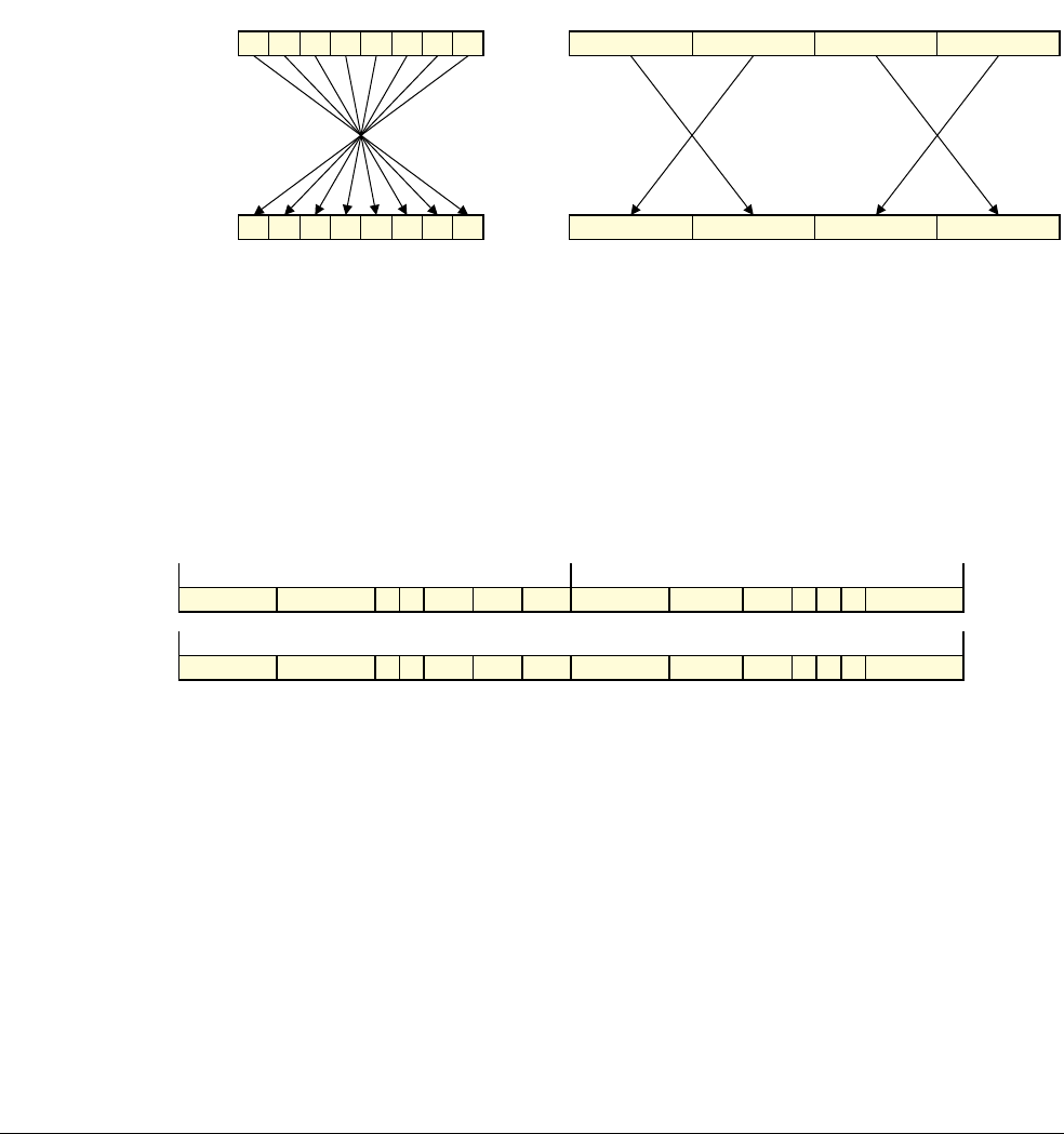
A8 Instruction Descriptions
A8.8 Alphabetical list of instructions
A8-1028 Copyright © 1996-1998, 2000, 2004-2012, 2014 ARM. All rights reserved. ARM DDI 0406C.c
Non-Confidential ID051414
A8.8.386 VREV16, VREV32, VREV64
VREV16
(Vector Reverse in halfwords) reverses the order of 8-bit elements in each halfword of the vector, and places
the result in the corresponding destination vector.
VREV32
(Vector Reverse in words) reverses the order of 8-bit or 16-bit elements in each word of the vector, and places
the result in the corresponding destination vector.
VREV64
(Vector Reverse in doublewords) reverses the order of 8-bit, 16-bit, or 32-bit elements in each doubleword
of the vector, and places the result in the corresponding destination vector.
There is no distinction between data types, other than size.
Figure A8-6 shows two examples of the operation of
VREV
.
Figure A8-6 VREV operation examples
Depending on settings in the CPACR, NSACR, and HCPTR registers, and the security state and mode in which the
instruction is executed, an attempt to execute the instruction might be UNDEFINED, or trapped to Hyp mode.
Summary of access controls for Advanced SIMD functionality on page B1-1233 summarizes these controls.
ARM deprecates the conditional execution of any Advanced SIMD instruction encoding that is not also available
as a VFP instruction encoding, see Conditional execution on page A8-288.
if UInt(op)+UInt(size) >= 3 then UNDEFINED;
if Q == ‘1’ && (Vd<0> == ‘1’ || Vm<0> == ‘1’) then UNDEFINED;
esize = 8 << UInt(size); elements = 64 DIV esize;
groupsize = (1 << (3-UInt(op)-UInt(size))); // elements per reversing group: 2, 4 or 8
reverse_mask = (groupsize-1)<esize-1:0>; // EORing mask used for index calculations
d = UInt(D:Vd); m = UInt(M:Vm); regs = if Q == ‘0’ then 1 else 2;
Dm Qm
Dd Qm
VREV64.8, doubleword VREV64.32, quadword
Encoding T1/A1 Advanced SIMD
VREV<n><c>.<size> <Qd>, <Qm>
VREV<n><c>.<size> <Dd>, <Dm>
1 1 1 1 1 1 1 1 D 1 1 size 0 0 Vd 0 0 0 op Q M 0 Vm
15 14 13 12 11 10 9 8 7 6 5 4 3 2 1 0
1
1514131211109876543210
1 1 1 0 0 1 1 1 D 1 1 size 0 0 Vd 0 0 0 op Q M 0 Vm
31 30 29 28 27 26 25 24 23 22 21 20 19 18 17 16 15 14 13 12 11 10 9 8 7 6 5 4 3 2 1 0
1

A8 Instruction Descriptions
A8.8 Alphabetical list of instructions
ARM DDI 0406C.c Copyright © 1996-1998, 2000, 2004-2012, 2014 ARM. All rights reserved. A8-1029
ID051414 Non-Confidential
Assembler syntax
where:
<n>
The size of the regions in which the vector elements are reversed. It must be one of:
16
Encoded as op =
0b10
.
32
Encoded as op =
0b01
.
64
Encoded as op =
0b00
.
<c>, <q>
See Standard assembler syntax fields on page A8-287. An ARM
VREV
instruction must be
unconditional. ARM strongly recommends that a Thumb
VREV
instruction is unconditional, see
Conditional execution on page A8-288.
<size>
The size of the vector elements. It must be one of:
8
Encoded as size =
0b00
.
16
Encoded as size =
0b01
.
32
Encoded as size =
0b10
.
<size>
must specify a smaller size than
<n>
.
<Qd>, <Qm>
The destination vector and the operand vector, for a quadword operation.
<Dd>, <Dm>
The destination vector and the operand vector, for a doubleword operation.
If op + size >= 3, the instruction is reserved.
Operation
if ConditionPassed() then
EncodingSpecificOperations(); CheckAdvSIMDEnabled();
bits(64) dest;
for r = 0 to regs-1
for e = 0 to elements-1
// Calculate destination element index by bitwise EOR on source element index:
e_bits = e<esize-1:0>; d_bits = e_bits EOR reverse_mask; d = UInt(d_bits);
Elem[dest,d,esize] = Elem[D[m+r],e,esize];
D[d+r] = dest;
Exceptions
Undefined Instruction, Hyp Trap.
VREV<n>{<c>}{<q>}.<size> <Qd>, <Qm>
Encoded as Q = 1
VREV<n>{<c>}{<q>}.<size> <Dd>, <Dm>
Encoded as Q = 0

A8 Instruction Descriptions
A8.8 Alphabetical list of instructions
A8-1030 Copyright © 1996-1998, 2000, 2004-2012, 2014 ARM. All rights reserved. ARM DDI 0406C.c
Non-Confidential ID051414
A8.8.387 VRHADD
Vector Rounding Halving Add adds corresponding elements in two vectors of integers, shifts each result right one
bit, and places the final results in the destination vector.
The operand and result elements are all the same type, and can be any one of:
• 8-bit, 16-bit, or 32-bit signed integers
• 8-bit, 16-bit, or 32-bit unsigned integers.
The results of the halving operations are rounded. For truncated results see VHADD, VHSUB on page A8-896.
Depending on settings in the CPACR, NSACR, and HCPTR registers, and the security state and mode in which the
instruction is executed, an attempt to execute the instruction might be UNDEFINED, or trapped to Hyp mode.
Summary of access controls for Advanced SIMD functionality on page B1-1233 summarizes these controls.
ARM deprecates the conditional execution of any Advanced SIMD instruction encoding that is not also available
as a VFP instruction encoding, see Conditional execution on page A8-288.
if Q == ‘1’ && (Vd<0> == ‘1’ || Vn<0> == ‘1’ || Vm<0> == ‘1’) then UNDEFINED;
if size == ‘11’ then UNDEFINED;
unsigned = (U == ‘1’);
esize = 8 << UInt(size); elements = 64 DIV esize;
d = UInt(D:Vd); n = UInt(N:Vn); m = UInt(M:Vm); regs = if Q == ‘0’ then 1 else 2;
Encoding T1/A1 Advanced SIMD
VRHADD<c> <Qd>, <Qn>, <Qm>
VRHADD<c> <Dd>, <Dn>, <Dm>
1 1 U 1 1 1 1 0 D size Vn Vd 0 0 0 1 N Q M 0 Vm
15 14 13 12 11 10 9 8 7 6 5 4 3 2 1 0
1
1514131211109876543210
1 1 1 0 0 1 U 0 D size Vn Vd 0 0 0 1 N Q M 0 Vm
31 30 29 28 27 26 25 24 23 22 21 20 19 18 17 16 15 14 13 12 11 10 9 8 7 6 5 4 3 2 1 0
1

A8 Instruction Descriptions
A8.8 Alphabetical list of instructions
ARM DDI 0406C.c Copyright © 1996-1998, 2000, 2004-2012, 2014 ARM. All rights reserved. A8-1031
ID051414 Non-Confidential
Assembler syntax
where:
<c>, <q>
See Standard assembler syntax fields on page A8-287. An ARM
VRHADD
instruction must be
unconditional. ARM strongly recommends that a Thumb
VRHADD
instruction is
unconditional, see Conditional execution on page A8-288.
<dt>
The data type for the elements of the vectors. It must be one of:
S8
Encoded as size =
0b00
, U = 0.
S16
Encoded as size =
0b01
, U = 0.
S32
Encoded as size =
0b10
, U = 0.
U8
Encoded as size =
0b00
, U = 1.
U16
Encoded as size =
0b01
, U = 1.
U32
Encoded as size =
0b10
, U = 1.
<Qd>, <Qn>, <Qm>
The destination vector and the operand vectors, for a quadword operation.
<Dd>, <Dn>, <Dm>
The destination vector and the operand vectors, for a doubleword operation.
Operation
if ConditionPassed() then
EncodingSpecificOperations(); CheckAdvSIMDEnabled();
for r = 0 to regs-1
for e = 0 to elements-1
op1 = Int(Elem[D[n+r],e,esize], unsigned);
op2 = Int(Elem[D[m+r],e,esize], unsigned);
result = op1 + op2 + 1;
Elem[D[d+r],e,esize] = result<esize:1>;
Exceptions
Undefined Instruction, Hyp Trap.
VRHADD{<c>}{<q>}.<dt> {<Qd>,} <Qn>, <Qm>
Encoded as Q = 1
VRHADD{<c>}{<q>}.<dt> {<Dd>,} <Dn>, <Dm>
Encoded as Q = 0

A8 Instruction Descriptions
A8.8 Alphabetical list of instructions
A8-1032 Copyright © 1996-1998, 2000, 2004-2012, 2014 ARM. All rights reserved. ARM DDI 0406C.c
Non-Confidential ID051414
A8.8.388 VRSHL
Vector Rounding Shift Left takes each element in a vector, shifts them by a value from the least significant byte of
the corresponding element of a second vector, and places the results in the destination vector. If the shift value is
positive, the operation is a left shift. If the shift value is negative, it is a rounding right shift. (For a truncating shift,
see VSHL (register) on page A8-1048).
The first operand and result elements are the same data type, and can be any one of:
• 8-bit, 16-bit, 32-bit, or 64-bit signed integers
• 8-bit, 16-bit, 32-bit, or 64-bit unsigned integers.
The second operand is always a signed integer of the same size.
Depending on settings in the CPACR, NSACR, and HCPTR registers, and the security state and mode in which the
instruction is executed, an attempt to execute the instruction might be UNDEFINED, or trapped to Hyp mode.
Summary of access controls for Advanced SIMD functionality on page B1-1233 summarizes these controls.
ARM deprecates the conditional execution of any Advanced SIMD instruction encoding that is not also available
as a VFP instruction encoding, see Conditional execution on page A8-288.
if Q == ‘1’ && (Vd<0> == ‘1’ || Vm<0> == ‘1’ || Vn<0> == ‘1’) then UNDEFINED;
unsigned = (U == ‘1’);
esize = 8 << UInt(size); elements = 64 DIV esize;
d = UInt(D:Vd); m = UInt(M:Vm); n = UInt(N:Vn); regs = if Q == ‘0’ then 1 else 2;
Encoding T1/A1 Advanced SIMD
VRSHL<c>.<type><size> <Qd>, <Qm>, <Qn>
VRSHL<c>.<type><size> <Dd>, <Dm>, <Dn>
1 1 U 1 1 1 1 0 D size Vn Vd 0 1 0 1 N Q M 0 Vm
15 14 13 12 11 10 9 8 7 6 5 4 3 2 1 0
1
1514131211109876543210
1 1 1 0 0 1 U 0 D size Vn Vd 0 1 0 1 N Q M 0 Vm
31 30 29 28 27 26 25 24 23 22 21 20 19 18 17 16 15 14 13 12 11 10 9 8 7 6 5 4 3 2 1 0
1

A8 Instruction Descriptions
A8.8 Alphabetical list of instructions
ARM DDI 0406C.c Copyright © 1996-1998, 2000, 2004-2012, 2014 ARM. All rights reserved. A8-1033
ID051414 Non-Confidential
Assembler syntax
where:
<c>, <q>
See Standard assembler syntax fields on page A8-287. An ARM
VRSHL
instruction must be
unconditional. ARM strongly recommends that a Thumb
VRSHL
instruction is unconditional,
see Conditional execution on page A8-288.
<type>
The data type for the elements of the vectors. It must be one of:
S
Signed, encoded as U = 0.
U
Unsigned, encoded as U = 1.
Together with the
<size>
field, this indicates the data type and size of the first operand and
the result.
<size>
The data size for the elements of the vectors. It must be one of:
8
Encoded as size =
0b00
.
16
Encoded as size =
0b01
.
32
Encoded as size =
0b10
.
64
Encoded as size =
0b11
.
<Qd>, <Qm>, <Qn>
The destination vector and the operand vectors, for a quadword operation.
<Dd>, <Dm>, <Dn>
The destination vector and the operand vectors, for a doubleword operation.
Operation
if ConditionPassed() then
EncodingSpecificOperations(); CheckAdvSIMDEnabled();
for r = 0 to regs-1
for e = 0 to elements-1
shift = SInt(Elem[D[n+r],e,esize]<7:0>);
round_const = 1 << (-shift-1); // 0 for left shift, 2^(n-1) for right shift
result = (Int(Elem[D[m+r],e,esize], unsigned) + round_const) << shift;
Elem[D[d+r],e,esize] = result<esize-1:0>;
Exceptions
Undefined Instruction, Hyp Trap.
VRSHL{<c>}{<q>}.<type><size> {<Qd>,} <Qm>, <Qn>
Encoded as Q = 1
VRSHL{<c>}{<q>}.<type><size> {<Dd>,} <Dm>, <Dn>
Encoded as Q = 0

A8 Instruction Descriptions
A8.8 Alphabetical list of instructions
A8-1034 Copyright © 1996-1998, 2000, 2004-2012, 2014 ARM. All rights reserved. ARM DDI 0406C.c
Non-Confidential ID051414
A8.8.389 VRSHR
Vector Rounding Shift Right takes each element in a vector, right shifts them by an immediate value, and places the
rounded results in the destination vector. For truncated results, see VSHR on page A8-1052.
The operand and result elements must be the same size, and can be any one of:
• 8-bit, 16-bit, 32-bit, or 64-bit signed integers.
• 8-bit, 16-bit, 32-bit, or 64-bit unsigned integers.
Depending on settings in the CPACR, NSACR, and HCPTR registers, and the security state and mode in which the
instruction is executed, an attempt to execute the instruction might be UNDEFINED, or trapped to Hyp mode.
Summary of access controls for Advanced SIMD functionality on page B1-1233 summarizes these controls.
ARM deprecates the conditional execution of any Advanced SIMD instruction encoding that is not also available
as a VFP instruction encoding, see Conditional execution on page A8-288.
if (L:imm6) IN “0000xxx” then SEE “Related encodings”;
if Q == ‘1’ && (Vd<0> == ‘1’ || Vm<0> == ‘1’) then UNDEFINED;
case L:imm6 of
when “0001xxx” esize = 8; elements = 8; shift_amount = 16 - UInt(imm6);
when “001xxxx” esize = 16; elements = 4; shift_amount = 32 - UInt(imm6);
when “01xxxxx” esize = 32; elements = 2; shift_amount = 64 - UInt(imm6);
when “1xxxxxx” esize = 64; elements = 1; shift_amount = 64 - UInt(imm6);
unsigned = (U == ‘1’); d = UInt(D:Vd); m = UInt(M:Vm); regs = if Q == ‘0’ then 1 else 2;
Encoding T1/A1 Advanced SIMD
VRSHR<c>.<type><size> <Qd>, <Qm>, #<imm>
VRSHR<c>.<type><size> <Dd>, <Dm>, #<imm>
Related encodings See One register and a modified immediate value on page A7-269.
1 1 U 1 1 1 1 1 D imm6 Vd 0 0 1 0 L Q M 1 Vm
15 14 13 12 11 10 9 8 7 6 5 4 3 2 1 0
1
1514131211109876543210
1 1 1 0 0 1 U 1 D imm6 Vd 0 0 1 0 L Q M 1 Vm
31 30 29 28 27 26 25 24 23 22 21 20 19 18 17 16 15 14 13 12 11 10 9 8 7 6 5 4 3 2 1 0
1

A8 Instruction Descriptions
A8.8 Alphabetical list of instructions
ARM DDI 0406C.c Copyright © 1996-1998, 2000, 2004-2012, 2014 ARM. All rights reserved. A8-1035
ID051414 Non-Confidential
Assembler syntax
where:
<c>, <q>
See Standard assembler syntax fields on page A8-287. An ARM
VRSHR
instruction must be
unconditional. ARM strongly recommends that a Thumb
VRSHR
instruction is unconditional, see
Conditional execution on page A8-288.
<type>
The data type for the elements of the vectors. It must be one of:
S
Signed, encoded as U = 0
U
Unsigned, encoded as U = 1.
<size>
The data size for the elements of the vectors. It must be one of:
8
Encoded as L = 0, imm6<5:3> =
0b001
. (8 –
<imm>
) is encoded in imm6<2:0>.
16
Encoded as L = 0, imm6<5:4> =
0b01
. (16 –
<imm>
) is encoded in imm6<3:0>.
32
Encoded as L = 0, imm6<5> =
0b1
. (32 –
<imm>
) is encoded in imm6<4:0>.
64
Encoded as L = 1. (64 –
<imm>
) is encoded in imm6<5:0>.
<Qd>, <Qm>
The destination vector, and the operand vector, for a quadword operation.
<Dd>, <Dm>
The destination vector, and the operand vector, for a doubleword operation.
<imm>
The immediate value, in the range 1 to
<size>
. See the description of
<size>
for how
<imm>
is
encoded.
Operation
if ConditionPassed() then
EncodingSpecificOperations(); CheckAdvSIMDEnabled();
round_const = 1 << (shift_amount - 1);
for r = 0 to regs-1
for e = 0 to elements-1
result = (Int(Elem[D[m+r],e,esize], unsigned) + round_const) >> shift_amount;
Elem[D[d+r],e,esize] = result<esize-1:0>;
Exceptions
Undefined Instruction, Hyp Trap.
Pseudo-instructions
For details see VMOV (register) on page A8-938.
VRSHR{<c>}{<q>}.<type><size> {<Qd>,} <Qm>, #<imm>
Encoded as Q = 1
VRSHR{<c>}{<q>}.<type><size> {<Dd>,} <Dm>, #<imm>
Encoded as Q = 0
VRSHR.<type><size> <Qd>, <Qm>, #0
is a synonym for
VMOV <Qd>, <Qm>
VRSHR.<type><size> <Dd>, <Dm>, #0
is a synonym for
VMOV <Dd>, <Dm>

A8 Instruction Descriptions
A8.8 Alphabetical list of instructions
A8-1036 Copyright © 1996-1998, 2000, 2004-2012, 2014 ARM. All rights reserved. ARM DDI 0406C.c
Non-Confidential ID051414
A8.8.390 VRSHRN
Vector Rounding Shift Right and Narrow takes each element in a vector, right shifts them by an immediate value,
and places the rounded results in the destination vector. For truncated results, see VSHRN on page A8-1054.
The operand elements can be 16-bit, 32-bit, or 64-bit integers. There is no distinction between signed and unsigned
integers. The destination elements are half the size of the source elements.
Depending on settings in the CPACR, NSACR, and HCPTR registers, and the security state and mode in which the
instruction is executed, an attempt to execute the instruction might be UNDEFINED, or trapped to Hyp mode.
Summary of access controls for Advanced SIMD functionality on page B1-1233 summarizes these controls.
ARM deprecates the conditional execution of any Advanced SIMD instruction encoding that is not also available
as a VFP instruction encoding, see Conditional execution on page A8-288.
if imm6 IN “000xxx” then SEE “Related encodings”;
if Vm<0> == ‘1’ then UNDEFINED;
case imm6 of
when “001xxx” esize = 8; elements = 8; shift_amount = 16 - UInt(imm6);
when “01xxxx” esize = 16; elements = 4; shift_amount = 32 - UInt(imm6);
when “1xxxxx” esize = 32; elements = 2; shift_amount = 64 - UInt(imm6);
d = UInt(D:Vd); m = UInt(M:Vm);
Encoding T1/A1 Advanced SIMD
VRSHRN<c>.I<size> <Dd>, <Qm>, #<imm>
Related encodings See One register and a modified immediate value on page A7-269.
1 1 0 1 1 1 1 1 D imm6 Vd 1 0 0 0 0 1 M 1 Vm
15 14 13 12 11 10 9 8 7 6 5 4 3 2 1 0
1
1514131211109876543210
1 1 1 0 0 1 0 1 D imm6 Vd 1 0 0 0 0 1 M 1 Vm
31 30 29 28 27 26 25 24 23 22 21 20 19 18 17 16 15 14 13 12 11 10 9 8 7 6 5 4 3 2 1 0
1

A8 Instruction Descriptions
A8.8 Alphabetical list of instructions
ARM DDI 0406C.c Copyright © 1996-1998, 2000, 2004-2012, 2014 ARM. All rights reserved. A8-1037
ID051414 Non-Confidential
Assembler syntax
where:
<c>, <q>
See Standard assembler syntax fields on page A8-287. An ARM
VRSHRN
instruction must be
unconditional. ARM strongly recommends that a Thumb
VRSHRN
instruction is unconditional, see
Conditional execution on page A8-288.
<size>
The data size for the elements of the vectors. It must be one of:
16
Encoded as imm6<5:3> =
0b001
. (8 –
<imm>
) is encoded in imm6<2:0>.
32
Encoded as imm6<5:4> =
0b01
. (16 –
<imm>
) is encoded in imm6<3:0>.
64
Encoded as imm6<5> =
0b1
. (32 –
<imm>
) is encoded in imm6<4:0>.
<Dd>, <Qm>
The destination vector, and the operand vector.
<imm>
The immediate value, in the range 1 to
<size>
/2. See the description of
<size>
for how
<imm>
is
encoded.
Operation
if ConditionPassed() then
EncodingSpecificOperations(); CheckAdvSIMDEnabled();
round_const = 1 << (shift_amount-1);
for e = 0 to elements-1
result = LSR(Elem[Qin[m>>1],e,2*esize] + round_const, shift_amount);
Elem[D[d],e,esize] = result<esize-1:0>;
Exceptions
Undefined Instruction, Hyp Trap.
Pseudo-instructions
For details see VMOVN on page A8-952.
VRSHRN{<c>}{<q>}.I<size> <Dd>, <Qm>, #<imm>
VRSHRN.I<size> <Dd>, <Qm>, #0
is a synonym for
VMOVN.I<size> <Dd>, <Qm>

A8 Instruction Descriptions
A8.8 Alphabetical list of instructions
A8-1038 Copyright © 1996-1998, 2000, 2004-2012, 2014 ARM. All rights reserved. ARM DDI 0406C.c
Non-Confidential ID051414
A8.8.391 VRSQRTE
Vector Reciprocal Square Root Estimate finds an approximate reciprocal square root of each element in a vector,
and places the results in a second vector.
The operand and result elements are the same type, and can be 32-bit floating-point numbers, or 32-bit unsigned
integers.
For details of the operation performed by this instruction see Floating-point reciprocal square root estimate and
step on page A2-87.
Depending on settings in the CPACR, NSACR, and HCPTR registers, and the security state and mode in which the
instruction is executed, an attempt to execute the instruction might be UNDEFINED, or trapped to Hyp mode.
Summary of access controls for Advanced SIMD functionality on page B1-1233 summarizes these controls.
ARM deprecates the conditional execution of any Advanced SIMD instruction encoding that is not also available
as a VFP instruction encoding, see Conditional execution on page A8-288.
if Q == ‘1’ && (Vd<0> == ‘1’ || Vm<0> == ‘1’) then UNDEFINED;
if size != ‘10’ then UNDEFINED;
floating_point = (F == ‘1’); esize = 32; elements = 2;
d = UInt(D:Vd); m = UInt(M:Vm); regs = if Q == ‘0’ then 1 else 2;
Encoding T1/A1 Advanced SIMD (F = 1 UNDEFINED in integer-only variants)
VRSQRTE<c>.<dt> <Qd>, <Qm>
VRSQRTE<c>.<dt> <Dd>, <Dm>
Q1 1 1 1 1 1 1 1 D 1 1 size 1 1 Vd 0 1 0 F 1 M 0 Vm
15 14 13 12 11 10 9 8 7 6 5 4 3 2 1 0
1
1514131211109876543210
Q
11 1 1 0 0 1 1 1 D 1 1 size 1 1 Vd 0 1 0 F M 0 Vm
31 30 29 28 27 26 25 24 23 22 21 20 19 18 17 16 15 14 13 12 11 10 9 8 7 6 5 4 3 2 1 0
1

A8 Instruction Descriptions
A8.8 Alphabetical list of instructions
ARM DDI 0406C.c Copyright © 1996-1998, 2000, 2004-2012, 2014 ARM. All rights reserved. A8-1039
ID051414 Non-Confidential
Assembler syntax
where:
<c>, <q>
See Standard assembler syntax fields on page A8-287. An ARM
VRSQRTE
instruction must be
unconditional. ARM strongly recommends that a Thumb
VRSQRTE
instruction is unconditional, see
Conditional execution on page A8-288.
<dt>
The data types for the elements of the vectors. It must be one of:
U32
Encoded as F = 0, size =
0b10
.
F32
Encoded as F = 1, size =
0b10
.
<Qd>, <Qm>
The destination vector and the operand vector, for a quadword operation.
<Dd>, <Dm>
The destination vector and the operand vector, for a doubleword operation.
Operation
if ConditionPassed() then
EncodingSpecificOperations(); CheckAdvSIMDEnabled();
for r = 0 to regs-1
for e = 0 to elements-1
if floating_point then
Elem[D[d+r],e,esize] = FPRSqrtEstimate(Elem[D[m+r],e,esize]);
else
Elem[D[d+r],e,esize] = UnsignedRSqrtEstimate(Elem[D[m+r],e,esize]);
Exceptions
Undefined Instruction, Hyp Trap.
Floating-point exceptions
Input Denormal, Invalid Operation, Division by Zero.
Newton-Raphson iteration
For details of the operation performed and how it can be used in a Newton-Raphson iteration to calculate the
reciprocal of the square root of a number, see Floating-point reciprocal square root estimate and step on
page A2-87.
VRSQRTE{<c>}{<q>}.<dt> <Qd>, <Qm>
Encoded as Q = 1
VRSQRTE{<c>}{<q>}.<dt> <Dd>, <Dm>
Encoded as Q = 0

A8 Instruction Descriptions
A8.8 Alphabetical list of instructions
A8-1040 Copyright © 1996-1998, 2000, 2004-2012, 2014 ARM. All rights reserved. ARM DDI 0406C.c
Non-Confidential ID051414
A8.8.392 VRSQRTS
Vector Reciprocal Square Root Step multiplies the elements of one vector by the corresponding elements of another
vector, subtracts each of the products from 3.0, divides these results by 2.0, and places the results into the elements
of the destination vector.
The operand and result elements are 32-bit floating-point numbers.
For details of the operation performed by this instruction see Floating-point reciprocal square root estimate and
step on page A2-87.
Depending on settings in the CPACR, NSACR, and HCPTR registers, and the security state and mode in which the
instruction is executed, an attempt to execute the instruction might be UNDEFINED, or trapped to Hyp mode.
Summary of access controls for Advanced SIMD functionality on page B1-1233 summarizes these controls.
ARM deprecates the conditional execution of any Advanced SIMD instruction encoding that is not also available
as a VFP instruction encoding, see Conditional execution on page A8-288.
if Q == ‘1’ && (Vd<0> == ‘1’ || Vn<0> == ‘1’ || Vm<0> == ‘1’) then UNDEFINED;
if sz == ‘1’ then UNDEFINED;
esize = 32; elements = 2;
d = UInt(D:Vd); n = UInt(N:Vn); m = UInt(M:Vm); regs = if Q == ‘0’ then 1 else 2;
Encoding T1/A1 Advanced SIMD (UNDEFINED in integer-only variant)
VRSQRTS<c>.F32 <Qd>, <Qn>, <Qm>
VRSQRTS<c>.F32 <Dd>, <Dn>, <Dm>
sz
11 1 0 1 1 1 1 0 D Vn Vd 1 1 1 1 N Q M 1 Vm
15 14 13 12 11 10 9 8 7 6 5 4 3 2 1 0
1
1514131211109876543210
sz
11 1 1 0 0 1 0 0 D Vn Vd 1 1 1 1 N Q M 1 Vm
31 30 29 28 27 26 25 24 23 22 21 20 19 18 17 16 15 14 13 12 11 10 9 8 7 6 5 4 3 2 1 0
1

A8 Instruction Descriptions
A8.8 Alphabetical list of instructions
ARM DDI 0406C.c Copyright © 1996-1998, 2000, 2004-2012, 2014 ARM. All rights reserved. A8-1041
ID051414 Non-Confidential
Assembler syntax
where:
<c>, <q>
See Standard assembler syntax fields on page A8-287. An ARM
VRSQRTS
instruction must
be unconditional. ARM strongly recommends that a Thumb
VRSQRTS
instruction is
unconditional, see Conditional execution on page A8-288.
<Qd>, <Qn>, <Qm>
The destination vector and the operand vectors for a quadword operation.
<Dd>, <Dn>, <Dm>
The destination vector and the operand vectors for a doubleword operation.
Operation
if ConditionPassed() then
EncodingSpecificOperations(); CheckAdvSIMDEnabled();
for r = 0 to regs-1
for e = 0 to elements-1
Elem[D[d+r],e,esize] = FPRSqrtStep(Elem[D[n+r],e,esize], Elem[D[m+r],e,esize]);
Exceptions
Undefined Instruction, Hyp Trap.
Floating-point exceptions
Input Denormal, Invalid Operation, Overflow, Underflow, Inexact.
Newton-Raphson iteration
For details of the operation performed and how it can be used in a Newton-Raphson iteration to calculate the
reciprocal of the square root of a number, see Floating-point reciprocal square root estimate and step on
page A2-87.
VRSQRTS{<c>}{<q>}.F32 {<Qd>,} <Qn>, <Qm>
Encoded as Q = 1, sz = 0
VRSQRTS{<c>}{<q>}.F32 {<Dd>,} <Dn>, <Dm>
Encoded as Q = 0, sz = 0

A8 Instruction Descriptions
A8.8 Alphabetical list of instructions
A8-1042 Copyright © 1996-1998, 2000, 2004-2012, 2014 ARM. All rights reserved. ARM DDI 0406C.c
Non-Confidential ID051414
A8.8.393 VRSRA
Vector Rounding Shift Right and Accumulate takes each element in a vector, right shifts them by an immediate
value, and accumulates the rounded results into the destination vector. (For truncated results, see VSRA on
page A8-1060.)
The operand and result elements must all be the same type, and can be any one of:
• 8-bit, 16-bit, 32-bit, or 64-bit signed integers.
• 8-bit, 16-bit, 32-bit, or 64-bit unsigned integers.
Depending on settings in the CPACR, NSACR, and HCPTR registers, and the security state and mode in which the
instruction is executed, an attempt to execute the instruction might be UNDEFINED, or trapped to Hyp mode.
Summary of access controls for Advanced SIMD functionality on page B1-1233 summarizes these controls.
ARM deprecates the conditional execution of any Advanced SIMD instruction encoding that is not also available
as a VFP instruction encoding, see Conditional execution on page A8-288.
if (L:imm6) IN “0000xxx” then SEE “Related encodings”;
if Q == ‘1’ && (Vd<0> == ‘1’ || Vm<0> == ‘1’) then UNDEFINED;
case L:imm6 of
when “0001xxx” esize = 8; elements = 8; shift_amount = 16 - UInt(imm6);
when “001xxxx” esize = 16; elements = 4; shift_amount = 32 - UInt(imm6);
when “01xxxxx” esize = 32; elements = 2; shift_amount = 64 - UInt(imm6);
when “1xxxxxx” esize = 64; elements = 1; shift_amount = 64 - UInt(imm6);
unsigned = (U == ‘1’); d = UInt(D:Vd); m = UInt(M:Vm); regs = if Q == ‘0’ then 1 else 2;
Encoding T1/A1 Advanced SIMD
VRSRA<c>.<type><size> <Qd>, <Qm>, #<imm>
VRSRA<c>.<type><size> <Dd>, <Dm>, #<imm>
Related encodings See One register and a modified immediate value on page A7-269.
1 1 U 1 1 1 1 1 D imm6 Vd 0 0 1 1 L Q M 1 Vm
15 14 13 12 11 10 9 8 7 6 5 4 3 2 1 0
1
1514131211109876543210
1 1 1 0 0 1 U 1 D imm6 Vd 0 0 1 1 L Q M 1 Vm
31 30 29 28 27 26 25 24 23 22 21 20 19 18 17 16 15 14 13 12 11 10 9 8 7 6 5 4 3 2 1 0
1

A8 Instruction Descriptions
A8.8 Alphabetical list of instructions
ARM DDI 0406C.c Copyright © 1996-1998, 2000, 2004-2012, 2014 ARM. All rights reserved. A8-1043
ID051414 Non-Confidential
Assembler syntax
where:
<c>, <q>
See Standard assembler syntax fields on page A8-287. An ARM
VRSRA
instruction must be
unconditional. ARM strongly recommends that a Thumb
VRSRA
instruction is unconditional, see
Conditional execution on page A8-288.
<type>
The data type for the elements of the vectors. It must be one of:
S
Signed, encoded as U = 0.
U
Unsigned, encoded as U = 1.
<size>
The data size for the elements of the vectors. It must be one of:
8
Encoded as L = 0, imm6<5:3> =
0b001
. (8 –
<imm>
) is encoded in imm6<2:0>.
16
Encoded as L = 0, imm6<5:4> =
0b01
. (16 –
<imm>
) is encoded in imm6<3:0>.
32
Encoded as L = 0, imm6<5> =
0b1
. (32 –
<imm>
) is encoded in imm6<4:0>.
64
Encoded as L = 1. (64 –
<imm>
) is encoded in imm6<5:0>.
<Qd>, <Qm>
The destination vector, and the operand vector, for a quadword operation.
<Dd>, <Dm>
The destination vector, and the operand vector, for a doubleword operation.
<imm>
The immediate value, in the range 1 to
<size>
. See the description of
<size>
for how
<imm>
is
encoded.
Operation
if ConditionPassed() then
EncodingSpecificOperations(); CheckAdvSIMDEnabled();
round_const = 1 << (shift_amount - 1);
for r = 0 to regs-1
for e = 0 to elements-1
result = (Int(Elem[D[m+r],e,esize], unsigned) + round_const) >> shift_amount;
Elem[D[d+r],e,esize] = Elem[D[d+r],e,esize] + result;
Exceptions
Undefined Instruction, Hyp Trap.
VRSRA{<c>}{<q>}.<type><size> {<Qd>,} <Qm>, #<imm>
Encoded as Q = 1
VRSRA{<c>}{<q>}.<type><size> {<Dd>,} <Dm>, #<imm>
Encoded as Q = 0

A8 Instruction Descriptions
A8.8 Alphabetical list of instructions
A8-1044 Copyright © 1996-1998, 2000, 2004-2012, 2014 ARM. All rights reserved. ARM DDI 0406C.c
Non-Confidential ID051414
A8.8.394 VRSUBHN
Vector Rounding Subtract and Narrow, returning High Half subtracts the elements of one quadword vector from the
corresponding elements of another quadword vector takes the most significant half of each result, and places the
final results in a doubleword vector. The results are rounded. (For truncated results, see VSUBHN on
page A8-1088.)
The operand elements can be 16-bit, 32-bit, or 64-bit integers. There is no distinction between signed and unsigned
integers.
Depending on settings in the CPACR, NSACR, and HCPTR registers, and the security state and mode in which the
instruction is executed, an attempt to execute the instruction might be UNDEFINED, or trapped to Hyp mode.
Summary of access controls for Advanced SIMD functionality on page B1-1233 summarizes these controls.
ARM deprecates the conditional execution of any Advanced SIMD instruction encoding that is not also available
as a VFP instruction encoding, see Conditional execution on page A8-288.
if size == ‘11’ then SEE “Related encodings”;
if Vn<0> == ‘1’ || Vm<0> == ‘1’ then UNDEFINED;
esize = 8 << UInt(size); elements = 64 DIV esize;
d = UInt(D:Vd); n = UInt(N:Vn); m = UInt(M:Vm);
Encoding T1/A1 Advanced SIMD
VRSUBHN<c>.<dt> <Dd>, <Qn>, <Qm>
Related encodings See Advanced SIMD data-processing instructions on page A7-261.
1 1 1 1 1 1 1 1 D size Vn Vd 0 1 1 0 N 0 M 0 Vm
15 14 13 12 11 10 9 8 7 6 5 4 3 2 1 0
1
1514131211109876543210
1 1 1 0 0 1 1 1 D size Vn Vd 0 1 1 0 N 0 M 0 Vm
31 30 29 28 27 26 25 24 23 22 21 20 19 18 17 16 15 14 13 12 11 10 9 8 7 6 5 4 3 2 1 0
1

A8 Instruction Descriptions
A8.8 Alphabetical list of instructions
ARM DDI 0406C.c Copyright © 1996-1998, 2000, 2004-2012, 2014 ARM. All rights reserved. A8-1045
ID051414 Non-Confidential
Assembler syntax
where:
<c>, <q>
See Standard assembler syntax fields on page A8-287. An ARM
VRSUBHN
instruction must
be unconditional. ARM strongly recommends that a Thumb
VRSUBHN
instruction is
unconditional, see Conditional execution on page A8-288.
<dt>
The data type for the elements of the operands. It must be one of:
I16
Encoded as size =
0b00
.
I32
Encoded as size =
0b01
.
I64
Encoded as size =
0b10
.
<Dd>, <Qn>, <Qm>
The destination vector and the operand vectors.
Operation
if ConditionPassed() then
EncodingSpecificOperations(); CheckAdvSIMDEnabled();
round_const = 1 << (esize-1);
for e = 0 to elements-1
result = Elem[Qin[n>>1],e,2*esize] - Elem[Qin[m>>1],e,2*esize] + round_const;
Elem[D[d],e,esize] = result<2*esize-1:esize>;
Exceptions
Undefined Instruction, Hyp Trap.
VRSUBHN{<c>}{<q>}.<dt> <Dd>, <Qn>, <Qm>

A8 Instruction Descriptions
A8.8 Alphabetical list of instructions
A8-1046 Copyright © 1996-1998, 2000, 2004-2012, 2014 ARM. All rights reserved. ARM DDI 0406C.c
Non-Confidential ID051414
A8.8.395 VSHL (immediate)
Vector Shift Left (immediate) takes each element in a vector of integers, left shifts them by an immediate value, and
places the results in the destination vector.
Bits shifted out of the left of each element are lost.
The elements must all be the same size, and can be 8-bit, 16-bit, 32-bit, or 64-bit integers. There is no distinction
between signed and unsigned integers.
Depending on settings in the CPACR, NSACR, and HCPTR registers, and the security state and mode in which the
instruction is executed, an attempt to execute the instruction might be UNDEFINED, or trapped to Hyp mode.
Summary of access controls for Advanced SIMD functionality on page B1-1233 summarizes these controls.
ARM deprecates the conditional execution of any Advanced SIMD instruction encoding that is not also available
as a VFP instruction encoding, see Conditional execution on page A8-288.
if L:imm6 IN “0000xxx” then SEE “Related encodings”;
if Q == ‘1’ && (Vd<0> == ‘1’ || Vm<0> == ‘1’) then UNDEFINED;
case L:imm6 of
when “0001xxx” esize = 8; elements = 8; shift_amount = UInt(imm6) - 8;
when “001xxxx” esize = 16; elements = 4; shift_amount = UInt(imm6) - 16;
when “01xxxxx” esize = 32; elements = 2; shift_amount = UInt(imm6) - 32;
when “1xxxxxx” esize = 64; elements = 1; shift_amount = UInt(imm6);
d = UInt(D:Vd); m = UInt(M:Vm); regs = if Q == ‘0’ then 1 else 2;
Encoding T1/A1 Advanced SIMD
VSHL<c>.I<size> <Qd>, <Qm>, #<imm>
VSHL<c>.I<size> <Dd>, <Dm>, #<imm>
Related encodings See One register and a modified immediate value on page A7-269.
1 1 0 1 1 1 1 1 D imm6 Vd 0 1 0 1 L Q M 1 Vm
15 14 13 12 11 10 9 8 7 6 5 4 3 2 1 0
1
1514131211109876543210
1 1 1 0 0 1 0 1 D imm6 Vd 0 1 0 1 L Q M 1 Vm
31 30 29 28 27 26 25 24 23 22 21 20 19 18 17 16 15 14 13 12 11 10 9 8 7 6 5 4 3 2 1 0
1

A8 Instruction Descriptions
A8.8 Alphabetical list of instructions
ARM DDI 0406C.c Copyright © 1996-1998, 2000, 2004-2012, 2014 ARM. All rights reserved. A8-1047
ID051414 Non-Confidential
Assembler syntax
where:
<c>, <q>
See Standard assembler syntax fields on page A8-287. An ARM
VSHL
instruction must be
unconditional. ARM strongly recommends that a Thumb
VSHL
instruction is unconditional, see
Conditional execution on page A8-288.
<size>
The data size for the elements of the vectors. It must be one of:
8
Encoded as L = 0, imm6<5:3> =
0b001
.
<imm>
is encoded in imm6<2:0>.
16
Encoded as L = 0, imm6<5:4> =
0b01
.
<imm>
is encoded in imm6<3:0>.
32
Encoded as L = 0, imm6<5> =
0b1
.
<imm>
is encoded in imm6<4:0>.
64
Encoded as L = 1.
<imm>
is encoded in imm6<5:0>.
<Qd>, <Qm>
The destination vector, and the operand vector, for a quadword operation.
<Dd>, <Dm>
The destination vector, and the operand vector, for a doubleword operation.
<imm>
The immediate value, in the range 0 to
<size>
-1. See the description of
<size>
for how
<imm>
is
encoded.
Operation
if ConditionPassed() then
EncodingSpecificOperations(); CheckAdvSIMDEnabled();
for r = 0 to regs-1
for e = 0 to elements-1
Elem[D[d+r],e,esize] = LSL(Elem[D[m+r],e,esize], shift_amount);
Exceptions
Undefined Instruction, Hyp Trap.
VSHL{<c>}{<q>}.I<size> {<Qd>,} <Qm>, #<imm>
Encoded as Q = 1
VSHL{<c>}{<q>}.I<size> {<Dd>,} <Dm>, #<imm>
Encoded as Q = 0
A8 Instruction Descriptions
A8.8 Alphabetical list of instructions
A8-1048 Copyright © 1996-1998, 2000, 2004-2012, 2014 ARM. All rights reserved. ARM DDI 0406C.c
Non-Confidential ID051414
A8.8.396 VSHL (register)
Vector Shift Left (register) takes each element in a vector, shifts them by a value from the least significant byte of
the corresponding element of a second vector, and places the results in the destination vector. If the shift value is
positive, the operation is a left shift. If the shift value is negative, it is a truncating right shift.
Note
For a rounding shift, see VRSHL on page A8-1032.
The first operand and result elements are the same data type, and can be any one of:
• 8-bit, 16-bit, 32-bit, or 64-bit signed integers
• 8-bit, 16-bit, 32-bit, or 64-bit unsigned integers.
The second operand is always a signed integer of the same size.
Depending on settings in the CPACR, NSACR, and HCPTR registers, and the security state and mode in which the
instruction is executed, an attempt to execute the instruction might be UNDEFINED, or trapped to Hyp mode.
Summary of access controls for Advanced SIMD functionality on page B1-1233 summarizes these controls.
ARM deprecates the conditional execution of any Advanced SIMD instruction encoding that is not also available
as a VFP instruction encoding, see Conditional execution on page A8-288.
if Q == ‘1’ && (Vd<0> == ‘1’ || Vm<0> == ‘1’ || Vn<0> == ‘1’) then UNDEFINED;
unsigned = (U == ‘1’);
esize = 8 << UInt(size); elements = 64 DIV esize;
d = UInt(D:Vd); m = UInt(M:Vm); n = UInt(N:Vn); regs = if Q == ‘0’ then 1 else 2;
Encoding T1/A1 Advanced SIMD
VSHL<c>.<type><size> <Qd>, <Qm>, <Qn>
VSHL<c>.<type><size> <Dd>, <Dm>, <Dn>
1 1 U 1 1 1 1 0 D size Vn Vd 0 1 0 0 N Q M 0 Vm
15 14 13 12 11 10 9 8 7 6 5 4 3 2 1 0
1
1514131211109876543210
1 1 1 0 0 1 U 0 D size Vn Vd 0 1 0 0 N Q M 0 Vm
31 30 29 28 27 26 25 24 23 22 21 20 19 18 17 16 15 14 13 12 11 10 9 8 7 6 5 4 3 2 1 0
1

A8 Instruction Descriptions
A8.8 Alphabetical list of instructions
ARM DDI 0406C.c Copyright © 1996-1998, 2000, 2004-2012, 2014 ARM. All rights reserved. A8-1049
ID051414 Non-Confidential
Assembler syntax
where:
<c>, <q>
See Standard assembler syntax fields on page A8-287. An ARM
VSHL
instruction must be
unconditional. ARM strongly recommends that a Thumb
VSHL
instruction is unconditional,
see Conditional execution on page A8-288.
<type>
The data type for the elements of the vectors. It must be one of:
S
Signed, encoded as U = 0.
U
Unsigned, encoded as U = 1.
Together with the
<size>
field, this indicates the data type and size of the first operand and
the result.
<size>
The data size for the elements of the vectors. It must be one of:
8
Encoded as size =
0b00
.
16
Encoded as size =
0b01
.
32
Encoded as size =
0b10
.
64
Encoded as size =
0b11
.
<Qd>, <Qm>, <Qn>
The destination vector and the operand vectors, for a quadword operation.
<Dd>, <Dm>, <Dn>
The destination vector and the operand vectors, for a doubleword operation.
Operation
if ConditionPassed() then
EncodingSpecificOperations(); CheckAdvSIMDEnabled();
for r = 0 to regs-1
for e = 0 to elements-1
shift = SInt(Elem[D[n+r],e,esize]<7:0>);
result = Int(Elem[D[m+r],e,esize], unsigned) << shift;
Elem[D[d+r],e,esize] = result<esize-1:0>;
Exceptions
Undefined Instruction, Hyp Trap.
VSHL{<c>}{<q>}.<type><size> {<Qd>,} <Qm>, <Qn>
Encoded as Q = 1
VSHL{<c>}{<q>}.<type><size> {<Dd>,} <Dm>, <Dn>
Encoded as Q = 0
A8 Instruction Descriptions
A8.8 Alphabetical list of instructions
A8-1050 Copyright © 1996-1998, 2000, 2004-2012, 2014 ARM. All rights reserved. ARM DDI 0406C.c
Non-Confidential ID051414
A8.8.397 VSHLL
Vector Shift Left Long takes each element in a doubleword vector, left shifts them by an immediate value, and places
the results in a quadword vector.
The operand elements can be:
• 8-bit, 16-bit, or 32-bit signed integers
• 8-bit, 16-bit, or 32-bit unsigned integers
• 8-bit, 16-bit, or 32-bit untyped integers (maximum shift only).
The result elements are twice the length of the operand elements.
Depending on settings in the CPACR, NSACR, and HCPTR registers, and the security state and mode in which the
instruction is executed, an attempt to execute the instruction might be UNDEFINED, or trapped to Hyp mode.
Summary of access controls for Advanced SIMD functionality on page B1-1233 summarizes these controls.
ARM deprecates the conditional execution of any Advanced SIMD instruction encoding that is not also available
as a VFP instruction encoding, see Conditional execution on page A8-288.
if imm6 IN “000xxx” then SEE “Related encodings”;
if Vd<0> == ‘1’ then UNDEFINED;
case imm6 of
when “001xxx” esize = 8; elements = 8; shift_amount = UInt(imm6) - 8;
when “01xxxx” esize = 16; elements = 4; shift_amount = UInt(imm6) - 16;
when “1xxxxx” esize = 32; elements = 2; shift_amount = UInt(imm6) - 32;
if shift_amount == 0 then SEE VMOVL;
unsigned = (U == ‘1’); d = UInt(D:Vd); m = UInt(M:Vm);
if size == ‘11’ || Vd<0> == ‘1’ then UNDEFINED;
esize = 8 << UInt(size); elements = 64 DIV esize; shift_amount = esize;
unsigned = FALSE; // Or TRUE without change of functionality
d = UInt(D:Vd); m = UInt(M:Vm);
Encoding T1/A1 Advanced SIMD
VSHLL<c>.<type><size> <Qd>, <Dm>, #<imm>
(0 <
<imm>
<
<size>
)
Encoding T2/A2 Advanced SIMD
VSHLL<c>.<type><size> <Qd>, <Dm>, #<imm>
(
<imm>
==
<size>
)
Related encodings See One register and a modified immediate value on page A7-269.
1 1 U 1 1 1 1 1 D imm6 Vd 1 0 1 0 0 0 M 1 Vm
15 14 13 12 11 10 9 8 7 6 5 4 3 2 1 0
1
1514131211109876543210
1 1 1 0 0 1 U 1 D imm6 Vd 1 0 1 0 0 0 M 1 Vm
31 30 29 28 27 26 25 24 23 22 21 20 19 18 17 16 15 14 13 12 11 10 9 8 7 6 5 4 3 2 1 0
1
1 1 1 1 1 1 1 1 D 1 1 size 1 0 Vd 0 0 1 1 0 0 M 0 Vm
15 14 13 12 11 10 9 8 7 6 5 4 3 2 1 0
1
1514131211109876543210
1 1 1 0 0 1 1 1 D 1 1 size 1 0 Vd 0 0 1 1 0 0 M 0 Vm
31 30 29 28 27 26 25 24 23 22 21 20 19 18 17 16 15 14 13 12 11 10 9 8 7 6 5 4 3 2 1 0
1

A8 Instruction Descriptions
A8.8 Alphabetical list of instructions
ARM DDI 0406C.c Copyright © 1996-1998, 2000, 2004-2012, 2014 ARM. All rights reserved. A8-1051
ID051414 Non-Confidential
Assembler syntax
where:
<c>, <q>
See Standard assembler syntax fields on page A8-287. An ARM
VSHLL
instruction must be
unconditional. ARM strongly recommends that a Thumb
VSHLL
instruction is unconditional, see
Conditional execution on page A8-288.
<type>
The data type for the elements of the operand. It must be one of:
S
Signed. In encoding T1/A1, encoded as U = 0.
U
Unsigned. In encoding T1/A1, encoded as U = 1.
I
Untyped integer, Available only in encoding T2/A2.
<size>
The data size for the elements of the operand. Table A8-8 shows the permitted values and their
encodings:
<Qd>, <Dm>
The destination vector and the operand vector.
<imm>
The immediate value.
<imm>
must lie in the range 1 to
<size>
, and:
•if
<size>
==
<imm>
, the encoding is T2/A2
• otherwise, the encoding is T1/A1, and:
—if
<size>
== 8,
<imm>
is encoded in imm6<2:0>
—if
<size>
== 16,
<imm>
is encoded in imm6<3:0>
—if
<size>
== 32,
<imm>
is encoded in imm6<4:0>.
Operation
if ConditionPassed() then
EncodingSpecificOperations(); CheckAdvSIMDEnabled();
for e = 0 to elements-1
result = Int(Elem[Din[m],e,esize], unsigned) << shift_amount;
Elem[Q[d>>1],e,2*esize] = result<2*esize-1:0>;
Exceptions
Undefined Instruction, Hyp Trap.
VSHLL{<c>}{<q>}.<type><size> <Qd>, <Dm>, #<imm>
Table A8-8 VSHLL <size> field encoding
<size> Encoding T1/A1 Encoding T2/A2
8
Encoded as imm6<5:3> =
0b001
Encoded as size =
0b00
16
Encoded as imm6<5:4> =
0b01
Encoded as size =
0b01
32
Encoded as imm6<5> = 1 Encoded as size =
0b10

A8 Instruction Descriptions
A8.8 Alphabetical list of instructions
A8-1052 Copyright © 1996-1998, 2000, 2004-2012, 2014 ARM. All rights reserved. ARM DDI 0406C.c
Non-Confidential ID051414
A8.8.398 VSHR
Vector Shift Right takes each element in a vector, right shifts them by an immediate value, and places the truncated
results in the destination vector. For rounded results, see VRSHR on page A8-1034.
The operand and result elements must be the same size, and can be any one of:
• 8-bit, 16-bit, 32-bit, or 64-bit signed integers.
• 8-bit, 16-bit, 32-bit, or 64-bit unsigned integers.
Depending on settings in the CPACR, NSACR, and HCPTR registers, and the security state and mode in which the
instruction is executed, an attempt to execute the instruction might be UNDEFINED, or trapped to Hyp mode.
Summary of access controls for Advanced SIMD functionality on page B1-1233 summarizes these controls.
ARM deprecates the conditional execution of any Advanced SIMD instruction encoding that is not also available
as a VFP instruction encoding, see Conditional execution on page A8-288.
if (L:imm6) IN “0000xxx” then SEE “Related encodings”;
if Q == ‘1’ && (Vd<0> == ‘1’ || Vm<0> == ‘1’) then UNDEFINED;
case L:imm6 of
when “0001xxx” esize = 8; elements = 8; shift_amount = 16 - UInt(imm6);
when “001xxxx” esize = 16; elements = 4; shift_amount = 32 - UInt(imm6);
when “01xxxxx” esize = 32; elements = 2; shift_amount = 64 - UInt(imm6);
when “1xxxxxx” esize = 64; elements = 1; shift_amount = 64 - UInt(imm6);
unsigned = (U == ‘1’); d = UInt(D:Vd); m = UInt(M:Vm); regs = if Q == ‘0’ then 1 else 2;
Encoding T1/A1 Advanced SIMD
VSHR<c>.<type><size> <Qd>, <Qm>, #<imm>
VSHR<c>.<type><size> <Dd>, <Dm>, #<imm>
Related encodings See One register and a modified immediate value on page A7-269.
1 1 U 1 1 1 1 1 D imm6 Vd 0 0 0 0 L Q M 1 Vm
15141312111098765432101514131211109876543210
1
1 1 1 0 0 1 U 1 D imm6 Vd 0 0 0 0 L Q M 1 Vm
31 30 29 28 27 26 25 24 23 22 21 20 19 18 17 16 15 14 13 12 11 10 9 8 7 6 5 4 3 2 1 0
1

A8 Instruction Descriptions
A8.8 Alphabetical list of instructions
ARM DDI 0406C.c Copyright © 1996-1998, 2000, 2004-2012, 2014 ARM. All rights reserved. A8-1053
ID051414 Non-Confidential
Assembler syntax
where:
<c>, <q>
See Standard assembler syntax fields on page A8-287. An ARM
VSHR
instruction must be
unconditional. ARM strongly recommends that a Thumb
VSHR
instruction is unconditional, see
Conditional execution on page A8-288.
<type>
The data type for the elements of the vectors. It must be one of:
S
Signed, encoded as U = 0.
U
Unsigned, encoded as U = 1.
<size>
The data size for the elements of the vectors. It must be one of:
8
Encoded as L = 0, imm6<5:3> =
0b001
. (8 –
<imm>
) is encoded in imm6<2:0>.
16
Encoded as L = 0, imm6<5:4> =
0b01
. (16 –
<imm>
) is encoded in imm6<3:0>.
32
Encoded as L = 0, imm6<5> =
0b1
. (32 –
<imm>
) is encoded in imm6<4:0>.
64
Encoded as L = 1. (64 –
<imm>
) is encoded in imm6<5:0>.
<Qd>, <Qm>
The destination vector, and the operand vector, for a quadword operation.
<Dd>, <Dm>
The destination vector, and the operand vector, for a doubleword operation.
<imm>
The immediate value, in the range 1 to
<size>
. See the description of
<size>
for how
<imm>
is
encoded.
Operation
if ConditionPassed() then
EncodingSpecificOperations(); CheckAdvSIMDEnabled();
for r = 0 to regs-1
for e = 0 to elements-1
result = Int(Elem[D[m+r],e,esize], unsigned) >> shift_amount;
Elem[D[d+r],e,esize] = result<esize-1:0>;
Exceptions
Undefined Instruction, Hyp Trap.
Pseudo-instructions
VSHR{<c>}{<q>}.<type><size> {<Qd>,} <Qm>, #<imm>
Encoded as Q = 1
VSHR{<c>}{<q>}.<type><size> {<Dd>,} <Dm>, #<imm>
Encoded as Q = 0
VSHR.<type><size> <Qd>, <Qm>, #0
is a synonym for
VMOV <Qd>, <Qm>
VSHR.<type><size> <Dd>, <Dm>, #0
is a synonym for
VMOV <Dd>, <Dm>
A8 Instruction Descriptions
A8.8 Alphabetical list of instructions
A8-1054 Copyright © 1996-1998, 2000, 2004-2012, 2014 ARM. All rights reserved. ARM DDI 0406C.c
Non-Confidential ID051414
A8.8.399 VSHRN
Vector Shift Right Narrow takes each element in a vector, right shifts them by an immediate value, and places the
truncated results in the destination vector. For rounded results, see VRSHRN on page A8-1036.
The operand elements can be 16-bit, 32-bit, or 64-bit integers. There is no distinction between signed and unsigned
integers. The destination elements are half the size of the source elements.
Depending on settings in the CPACR, NSACR, and HCPTR registers, and the security state and mode in which the
instruction is executed, an attempt to execute the instruction might be UNDEFINED, or trapped to Hyp mode.
Summary of access controls for Advanced SIMD functionality on page B1-1233 summarizes these controls.
ARM deprecates the conditional execution of any Advanced SIMD instruction encoding that is not also available
as a VFP instruction encoding, see Conditional execution on page A8-288.
if imm6 IN “000xxx” then SEE “Related encodings”;
if Vm<0> == ‘1’ then UNDEFINED;
case imm6 of
when “001xxx” esize = 8; elements = 8; shift_amount = 16 - UInt(imm6);
when “01xxxx” esize = 16; elements = 4; shift_amount = 32 - UInt(imm6);
when “1xxxxx” esize = 32; elements = 2; shift_amount = 64 - UInt(imm6);
d = UInt(D:Vd); m = UInt(M:Vm);
Encoding T1/A1 Advanced SIMD
VSHRN<c>.I<size> <Dd>, <Qm>, #<imm>
Related encodings See One register and a modified immediate value on page A7-269.
1 1 0 1 1 1 1 1 D imm6 Vd 1 0 0 0 0 0 M 1 Vm
15 14 13 12 11 10 9 8 7 6 5 4 3 2 1 0
1
1514131211109876543210
1 1 1 0 0 1 0 1 D imm6 Vd 1 0 0 0 0 0 M 1 Vm
31 30 29 28 27 26 25 24 23 22 21 20 19 18 17 16 15 14 13 12 11 10 9 8 7 6 5 4 3 2 1 0
1

A8 Instruction Descriptions
A8.8 Alphabetical list of instructions
ARM DDI 0406C.c Copyright © 1996-1998, 2000, 2004-2012, 2014 ARM. All rights reserved. A8-1055
ID051414 Non-Confidential
Assembler syntax
where:
<c>, <q>
See Standard assembler syntax fields on page A8-287. An ARM
VSHRN
instruction must be
unconditional. ARM strongly recommends that a Thumb
VSHRN
instruction is unconditional, see
Conditional execution on page A8-288.
<size>
The data size for the elements of the vectors. It must be one of:
16
Encoded as imm6<5:3> =
0b001
. (8 –
<imm>
) is encoded in imm6<2:0>.
32
Encoded as imm6<5:4> =
0b01
. (16 –
<imm>
) is encoded in imm6<3:0>.
64
Encoded as imm6<5> =
0b1
. (32 –
<imm>
) is encoded in imm6<4:0>.
<Dd>, <Qm>
The destination vector, and the operand vector.
<imm>
The immediate value, in the range 1 to
<size>
/2. See the description of
<size>
for how
<imm>
is
encoded.
Operation
if ConditionPassed() then
EncodingSpecificOperations(); CheckAdvSIMDEnabled();
for e = 0 to elements-1
result = LSR(Elem[Qin[m>>1],e,2*esize], shift_amount);
Elem[D[d],e,esize] = result<esize-1:0>;
Exceptions
Undefined Instruction, Hyp Trap.
Pseudo-instructions
For details see VMOVN on page A8-952.
VSHRN{<c>}{<q>}.I<size> <Dd>, <Qm>, #<imm>
VSHRN.I<size> <Dd>, <Qm>, #0
is a synonym for
VMOVN.I<size> <Dd>, <Qm>

A8 Instruction Descriptions
A8.8 Alphabetical list of instructions
A8-1056 Copyright © 1996-1998, 2000, 2004-2012, 2014 ARM. All rights reserved. ARM DDI 0406C.c
Non-Confidential ID051414
A8.8.400 VSLI
Vector Shift Left and Insert takes each element in the operand vector, left shifts them by an immediate value, and
inserts the results in the destination vector. Bits shifted out of the left of each element are lost.
The elements must all be the same size, and can be 8-bit, 16-bit, 32-bit, or 64-bit. There is no distinction between
data types.
Depending on settings in the CPACR, NSACR, and HCPTR registers, and the security state and mode in which the
instruction is executed, an attempt to execute the instruction might be UNDEFINED, or trapped to Hyp mode.
Summary of access controls for Advanced SIMD functionality on page B1-1233 summarizes these controls.
ARM deprecates the conditional execution of any Advanced SIMD instruction encoding that is not also available
as a VFP instruction encoding, see Conditional execution on page A8-288.
if (L:imm6) IN “0000xxx” then SEE “Related encodings”;
if Q == ‘1’ && (Vd<0> == ‘1’ || Vm<0> == ‘1’) then UNDEFINED;
case L:imm6 of
when “0001xxx” esize = 8; elements = 8; shift_amount = UInt(imm6) - 8;
when “001xxxx” esize = 16; elements = 4; shift_amount = UInt(imm6) - 16;
when “01xxxxx” esize = 32; elements = 2; shift_amount = UInt(imm6) - 32;
when “1xxxxxx” esize = 64; elements = 1; shift_amount = UInt(imm6);
d = UInt(D:Vd); m = UInt(M:Vm); regs = if Q == ‘0’ then 1 else 2;
Encoding T1/A1 Advanced SIMD
VSLI<c>.<size> <Qd>, <Qm>, #<imm>
VSLI<c>.<size> <Dd>, <Dm>, #<imm>
Related encodings See One register and a modified immediate value on page A7-269.
1 1 1 1 1 1 1 1 D imm6 Vd 0 1 0 1 L Q M 1 Vm
15 14 13 12 11 10 9 8 7 6 5 4 3 2 1 0
1
1514131211109876543210
1 1 1 0 0 1 1 1 D imm6 Vd 0 1 0 1 L Q M 1 Vm
31 30 29 28 27 26 25 24 23 22 21 20 19 18 17 16 15 14 13 12 11 10 9 8 7 6 5 4 3 2 1 0
1

A8 Instruction Descriptions
A8.8 Alphabetical list of instructions
ARM DDI 0406C.c Copyright © 1996-1998, 2000, 2004-2012, 2014 ARM. All rights reserved. A8-1057
ID051414 Non-Confidential
Assembler syntax
where:
<c>, <q>
See Standard assembler syntax fields on page A8-287. An ARM
VSLI
instruction must be
unconditional. ARM strongly recommends that a Thumb
VSLI
instruction is unconditional, see
Conditional execution on page A8-288.
<size>
The data size for the elements of the vectors. It must be one of:
8
Encoded as L = 0, imm6<5:3> =
0b001
.
<imm>
is encoded in imm6<2:0>.
16
Encoded as L = 0, imm6<5:4> =
0b01
.
<imm>
is encoded in imm6<3:0>.
32
Encoded as L = 0, imm6<5> =
0b1
.
<imm>
is encoded in imm6<4:0>.
64
Encoded as L = 1.
<imm>
is encoded in imm6<5:0>.
<Qd>, <Qm>
The destination vector, and the operand vector, for a quadword operation.
<Dd>, <Dm>
The destination vector, and the operand vector, for a doubleword operation.
<imm>
The immediate value, in the range 0 to
<size>
-1. See the description of
<size>
for how
<imm>
is
encoded.
Operation
if ConditionPassed() then
EncodingSpecificOperations(); CheckAdvSIMDEnabled();
mask = LSL(Ones(esize), shift_amount);
for r = 0 to regs-1
for e = 0 to elements-1
shifted_op = LSL(Elem[D[m+r],e,esize], shift_amount);
Elem[D[d+r],e,esize] = (Elem[D[d+r],e,esize] AND NOT(mask)) OR shifted_op;
Exceptions
Undefined Instruction, Hyp Trap.
VSLI{<c>}{<q>}.<size> {<Qd>,} <Qm>, #<imm>
Encoded as Q = 1
VSLI{<c>}{<q>}.<size> {<Dd>,} <Dm>, #<imm>
Encoded as Q = 0

A8 Instruction Descriptions
A8.8 Alphabetical list of instructions
A8-1058 Copyright © 1996-1998, 2000, 2004-2012, 2014 ARM. All rights reserved. ARM DDI 0406C.c
Non-Confidential ID051414
A8.8.401 VSQRT
This instruction calculates the square root of the value in a floating-point register and writes the result to another
floating-point register.
Depending on settings in the CPACR, NSACR, HCPTR, and FPEXC registers, and the security state and mode in
which the instruction is executed, an attempt to execute the instruction might be UNDEFINED, or trapped to Hyp
mode. Summary of general controls of CP10 and CP11 functionality on page B1-1231 summarizes these controls.
For the case when
cond
is
0b1111
, see Unconditional instructions on page A5-216.
if FPSCR.Len != ‘000’ || FPSCR.Stride != ‘00’ then SEE “VFP vectors”;
dp_operation = (sz == ‘1’);
d = if dp_operation then UInt(D:Vd) else UInt(Vd:D);
m = if dp_operation then UInt(M:Vm) else UInt(Vm:M);
Encoding T1/A1 VFPv2, VFPv3, VFPv4 (sz = 1 UNDEFINED in single-precision only variants)
VSQRT<c>.F64 <Dd>, <Dm>
VSQRT<c>.F32 <Sd>, <Sm>
VFP vectors This instruction can operate on VFP vectors under control of the FPSCR.{Len, Stride} fields.
For details see Appendix D11 VFP Vector Operation Support.
1 1 0 1 1 1 0 1 D 1 1 0 0 0 1 Vd 1 0 1 sz 1 1 M 0 Vm
15 14 13 12 11 10 9 8 7 6 5 4 3 2 1 0
1
1514131211109876543210
1 1 1 0 1 D 1 1 0 0 0 1 Vd 1 0 1 sz 1 1 M 0 Vm
31 30 29 28 27 26 25 24 23 22 21 20 19 18 17 16 15 14 13 12 11 10 9 8 7 6 5 4 3 2 1 0
cond

A8 Instruction Descriptions
A8.8 Alphabetical list of instructions
ARM DDI 0406C.c Copyright © 1996-1998, 2000, 2004-2012, 2014 ARM. All rights reserved. A8-1059
ID051414 Non-Confidential
Assembler syntax
where:
<c>, <q>
See Standard assembler syntax fields on page A8-287.
<Dd>, <Dm>
The destination vector and the operand vector, for a double-precision operation.
<Sd>, <Sm>
The destination vector and the operand vector, for a single-precision operation.
Operation
if ConditionPassed() then
EncodingSpecificOperations(); CheckVFPEnabled(TRUE);
if dp_operation then
D[d] = FPSqrt(D[m]);
else
S[d] = FPSqrt(S[m]);
Exceptions
Undefined Instruction, Hyp Trap.
Floating-point exceptions
Invalid Operation, Inexact, Input Denormal.
VSQRT{<c>}{<q>}.F64 <Dd>, <Dm>
Encoded as sz = 1
VSQRT{<c>}{<q>}.F32 <Sd>, <Sm>
Encoded as sz = 0

A8 Instruction Descriptions
A8.8 Alphabetical list of instructions
A8-1060 Copyright © 1996-1998, 2000, 2004-2012, 2014 ARM. All rights reserved. ARM DDI 0406C.c
Non-Confidential ID051414
A8.8.402 VSRA
Vector Shift Right and Accumulate takes each element in a vector, right shifts them by an immediate value, and
accumulates the truncated results into the destination vector. (For rounded results, see VRSRA on page A8-1042.)
The operand and result elements must all be the same type, and can be any one of:
• 8-bit, 16-bit, 32-bit, or 64-bit signed integers.
• 8-bit, 16-bit, 32-bit, or 64-bit unsigned integers.
Depending on settings in the CPACR, NSACR, and HCPTR registers, and the security state and mode in which the
instruction is executed, an attempt to execute the instruction might be UNDEFINED, or trapped to Hyp mode.
Summary of access controls for Advanced SIMD functionality on page B1-1233 summarizes these controls.
ARM deprecates the conditional execution of any Advanced SIMD instruction encoding that is not also available
as a VFP instruction encoding, see Conditional execution on page A8-288.
if (L:imm6) IN “0000xxx” then SEE “Related encodings”;
if Q == ‘1’ && (Vd<0> == ‘1’ || Vm<0> == ‘1’) then UNDEFINED;
case L:imm6 of
when “0001xxx” esize = 8; elements = 8; shift_amount = 16 - UInt(imm6);
when “001xxxx” esize = 16; elements = 4; shift_amount = 32 - UInt(imm6);
when “01xxxxx” esize = 32; elements = 2; shift_amount = 64 - UInt(imm6);
when “1xxxxxx” esize = 64; elements = 1; shift_amount = 64 - UInt(imm6);
unsigned = (U == ‘1’); d = UInt(D:Vd); m = UInt(M:Vm); regs = if Q == ‘0’ then 1 else 2;
Encoding T1/A1 Advanced SIMD
VSRA<c>.<type><size> <Qd>, <Qm>, #<imm>
VSRA<c>.<type><size> <Dd>, <Dm>, #<imm>
Related encodings See One register and a modified immediate value on page A7-269.
1 1 U 1 1 1 1 1 D imm6 Vd 0 0 0 1 L Q M 1 Vm
15 14 13 12 11 10 9 8 7 6 5 4 3 2 1 0
1
1514131211109876543210
1 1 1 0 0 1 U 1 D imm6 Vd 0 0 0 1 L Q M 1 Vm
31 30 29 28 27 26 25 24 23 22 21 20 19 18 17 16 15 14 13 12 11 10 9 8 7 6 5 4 3 2 1 0
1

A8 Instruction Descriptions
A8.8 Alphabetical list of instructions
ARM DDI 0406C.c Copyright © 1996-1998, 2000, 2004-2012, 2014 ARM. All rights reserved. A8-1061
ID051414 Non-Confidential
Assembler syntax
where:
<c>, <q>
See Standard assembler syntax fields on page A8-287. An ARM
VSRA
instruction must be
unconditional. ARM strongly recommends that a Thumb
VSRA
instruction is unconditional, see
Conditional execution on page A8-288.
<type>
The data type for the elements of the vectors. It must be one of:
S
Signed, encoded as U = 0.
U
Unsigned, encoded as U = 1.
<size>
The data size for the elements of the vectors. It must be one of:
8
Encoded as L = 0, imm6<5:3> =
0b001
. (8 –
<imm>
) is encoded in imm6<2:0>.
16
Encoded as L = 0, imm6<5:4> =
0b01
. (16 –
<imm>
) is encoded in imm6<3:0>.
32
Encoded as L = 0, imm6<5> =
0b1
. (32 –
<imm>
) is encoded in imm6<4:0>.
64
Encoded as L = 1. (64 –
<imm>
) is encoded in imm6<5:0>.
<Qd>, <Qm>
The destination vector, and the operand vector, for a quadword operation.
<Dd>, <Dm>
The destination vector, and the operand vector, for a doubleword operation.
<imm>
The immediate value, in the range 1 to
<size>
. See the description of
<size>
for how
<imm>
is
encoded.
Operation
if ConditionPassed() then
EncodingSpecificOperations(); CheckAdvSIMDEnabled();
for r = 0 to regs-1
for e = 0 to elements-1
result = Int(Elem[D[m+r],e,esize], unsigned) >> shift_amount;
Elem[D[d+r],e,esize] = Elem[D[d+r],e,esize] + result;
Exceptions
Undefined Instruction, Hyp Trap.
VSRA{<c>}{<q>}.<type><size> {<Qd>,} <Qm>, #<imm>
Encoded as Q = 1
VSRA{<c>}{<q>}.<type><size> {<Dd>,} <Dm>, #<imm>
Encoded as Q = 0

A8 Instruction Descriptions
A8.8 Alphabetical list of instructions
A8-1062 Copyright © 1996-1998, 2000, 2004-2012, 2014 ARM. All rights reserved. ARM DDI 0406C.c
Non-Confidential ID051414
A8.8.403 VSRI
Vector Shift Right and Insert takes each element in the operand vector, right shifts them by an immediate value, and
inserts the results in the destination vector. Bits shifted out of the right of each element are lost.
The elements must all be the same size, and can be 8-bit, 16-bit, 32-bit, or 64-bit. There is no distinction between
data types.
Depending on settings in the CPACR, NSACR, and HCPTR registers, and the security state and mode in which the
instruction is executed, an attempt to execute the instruction might be UNDEFINED, or trapped to Hyp mode.
Summary of access controls for Advanced SIMD functionality on page B1-1233 summarizes these controls.
ARM deprecates the conditional execution of any Advanced SIMD instruction encoding that is not also available
as a VFP instruction encoding, see Conditional execution on page A8-288.
if (L:imm6) IN “0000xxx” then SEE “Related encodings”;
if Q == ‘1’ && (Vd<0> == ‘1’ || Vm<0> == ‘1’) then UNDEFINED;
case L:imm6 of
when “0001xxx” esize = 8; elements = 8; shift_amount = 16 - UInt(imm6);
when “001xxxx” esize = 16; elements = 4; shift_amount = 32 - UInt(imm6);
when “01xxxxx” esize = 32; elements = 2; shift_amount = 64 - UInt(imm6);
when “1xxxxxx” esize = 64; elements = 1; shift_amount = 64 - UInt(imm6);
d = UInt(D:Vd); m = UInt(M:Vm); regs = if Q == ‘0’ then 1 else 2;
Encoding T1/A1 Advanced SIMD
VSRI<c>.<size> <Qd>, <Qm>, #<imm>
VSRI<c>.<size> <Dd>, <Dm>, #<imm>
Related encodings See One register and a modified immediate value on page A7-269.
1 1 1 1 1 1 1 1 D imm6 Vd 0 1 0 0 L Q M 1 Vm
15 14 13 12 11 10 9 8 7 6 5 4 3 2 1 0
1
1514131211109876543210
1 1 1 0 0 1 1 1 D imm6 Vd 0 1 0 0 L Q M 1 Vm
31 30 29 28 27 26 25 24 23 22 21 20 19 18 17 16 15 14 13 12 11 10 9 8 7 6 5 4 3 2 1 0
1

A8 Instruction Descriptions
A8.8 Alphabetical list of instructions
ARM DDI 0406C.c Copyright © 1996-1998, 2000, 2004-2012, 2014 ARM. All rights reserved. A8-1063
ID051414 Non-Confidential
Assembler syntax
where:
<c>, <q>
See Standard assembler syntax fields on page A8-287. An ARM
VSRI
instruction must be
unconditional. ARM strongly recommends that a Thumb
VSRI
instruction is unconditional, see
Conditional execution on page A8-288.
<size>
The data size for the elements of the vectors. It must be one of:
8
Encoded as L = 0, imm6<5:3> =
0b001
. (8 –
<imm>
) is encoded in imm6<2:0>.
16
Encoded as L = 0, imm6<5:4> =
0b01
. (16 –
<imm>
) is encoded in imm6<3:0>.
32
Encoded as L = 0, imm6<5> =
0b1
. (32 –
<imm>
) is encoded in imm6<4:0>.
64
Encoded as L = 1. (64 –
<imm>
) is encoded in imm6<5:0>.
<Qd>, <Qm>
The destination vector, and the operand vector, for a quadword operation.
<Dd>, <Dm>
The destination vector, and the operand vector, for a doubleword operation.
<imm>
The immediate value, in the range 1 to
<size>
. See the description of
<size>
for how
<imm>
is
encoded.
Operation
if ConditionPassed() then
EncodingSpecificOperations(); CheckAdvSIMDEnabled();
mask = LSR(Ones(esize), shift_amount);
for r = 0 to regs-1
for e = 0 to elements-1
shifted_op = LSR(Elem[D[m+r],e,esize], shift_amount);
Elem[D[d+r],e,esize] = (Elem[D[d+r],e,esize] AND NOT(mask)) OR shifted_op;
Exceptions
Undefined Instruction, Hyp Trap.
VSRI{<c>}{<q>}.<size> {<Qd>,} <Qm>, #<imm>
Encoded as Q = 1
VSRI{<c>}{<q>}.<size> {<Dd>,} <Dm>, #<imm>
Encoded as Q = 0

A8 Instruction Descriptions
A8.8 Alphabetical list of instructions
A8-1064 Copyright © 1996-1998, 2000, 2004-2012, 2014 ARM. All rights reserved. ARM DDI 0406C.c
Non-Confidential ID051414
A8.8.404 VST1 (multiple single elements)
Vector Store (multiple single elements) stores elements to memory from one, two, three, or four registers, without
interleaving. Every element of each register is stored. For details of the addressing mode see Advanced SIMD
addressing mode on page A7-277.
Depending on settings in the CPACR, NSACR, and HCPTR registers, and the security state and mode in which the
instruction is executed, an attempt to execute the instruction might be UNDEFINED, or trapped to Hyp mode.
Summary of access controls for Advanced SIMD functionality on page B1-1233 summarizes these controls.
ARM deprecates the conditional execution of any Advanced SIMD instruction encoding that is not also available
as a VFP instruction encoding, see Conditional execution on page A8-288.
case type of
when ‘0111’
regs = 1; if align<1> == ‘1’ then UNDEFINED;
when ‘1010’
regs = 2; if align == ‘11’ then UNDEFINED;
when ‘0110’
regs = 3; if align<1> == ‘1’ then UNDEFINED;
when ‘0010’
regs = 4;
otherwise
SEE “Related encodings”;
alignment = if align == ‘00’ then 1 else 4 << UInt(align);
ebytes = 1 << UInt(size); esize = 8 * ebytes; elements = 8 DIV ebytes;
d = UInt(D:Vd); n = UInt(Rn); m = UInt(Rm);
wback = (m != 15); register_index = (m != 15 && m != 13);
if n == 15 || d+regs > 32 then UNPREDICTABLE;
Assembler syntax
where:
<c>, <q>
See Standard assembler syntax fields on page A8-287. An ARM
VST1
instruction must be
unconditional. ARM strongly recommends that a Thumb
VST1
instruction is unconditional, see
Conditional execution on page A8-288.
<size>
The data size. It must be one of:
8
Encoded as size =
0b00
.
16
Encoded as size =
0b01
.
32
Encoded as size =
0b10
.
64
Encoded as size =
0b11
.
Encoding T1/A1 Advanced SIMD
VST1<c>.<size> <list>, [<Rn>{:<align>}]{!}
VST1<c>.<size> <list>, [<Rn>{:<align>}], <Rm>
Related encodings See Advanced SIMD element or structure load/store instructions on page A7-275.
VST1{<c>}{<q>}.<size> <list>, [<Rn>{:<align>}]
Encoded as Rm =
0b1111
VST1{<c>}{<q>}.<size> <list>, [<Rn>{:<align>}]!
Encoded as Rm =
0b1101
VST1{<c>}{<q>}.<size> <list>, [<Rn>{:<align>}], <Rm>
Rm cannot be
0b11x1
1 1 1 1 0 0 1 0 D 0 0 Rn Vd type size align Rm
15 14 13 12 11 10 9 8 7 6 5 4 3 2 1 0
1
1514131211109876543210
1 1 1 0 1 0 0 0 D 0 0 Rn Vd type size align Rm
31 30 29 28 27 26 25 24 23 22 21 20 19 18 17 16 15 14 13 12 11 10 9 8 7 6 5 4 3 2 1 0
1

A8 Instruction Descriptions
A8.8 Alphabetical list of instructions
ARM DDI 0406C.c Copyright © 1996-1998, 2000, 2004-2012, 2014 ARM. All rights reserved. A8-1065
ID051414 Non-Confidential
<list>
The list of registers to store. It must be one of:
{<Dd>}
Encoded as D:Vd =
<Dd>
, type =
0b0111
.
{<Dd>, <Dd+1>}
Encoded as D:Vd =
<Dd>
, type =
0b1010
.
{<Dd>, <Dd+1>, <Dd+2>}
Encoded as D:Vd =
<Dd>
, type =
0b0110
.
{<Dd>, <Dd+1>, <Dd+2>, <Dd+3>}
Encoded as D:Vd =
<Dd>
, type =
0b0010
.
<Rn>
Contains the base address for the access.
<align>
The alignment. It can be one of:
64
8-byte alignment, encoded as align =
0b01
.
128
16-byte alignment, available only if
<list>
contains two or four registers, encoded as
align =
0b10
.
256
32-byte alignment, available only if
<list>
contains four registers, encoded as
align =
0b11
.
omitted Standard alignment, see Unaligned data access on page A3-108. Encoded as
align =
0b00
.
: is the preferred separator before the
<align>
value, but the alignment can be specified as
@<align>
,
see Advanced SIMD addressing mode on page A7-277.
!
If present, specifies writeback.
<Rm>
Contains an address offset applied after the access.
For more information about
<Rn>
,
!
, and
<Rm>
, see Advanced SIMD addressing mode on page A7-277.
Operation
if ConditionPassed() then
EncodingSpecificOperations(); CheckAdvSIMDEnabled(); NullCheckIfThumbEE(n);
address = R[n]; if (address MOD alignment) != 0 then AlignmentFault(address, TRUE);
for r = 0 to regs-1
for e = 0 to elements - 1
if ebytes != 8 then
MemU[address, ebytes] = Elem[D[d+r], e, esize];
else
if SCTLR.A == ‘1’ && address != Align(address, 8) then AlignmentFault(address, FALSE);
data = Elem[D[d+r], e, esize];
MemU[address, 4] = if BigEndian() then data<63:32> else data<31:0>;
MemU[address+4, 4] = if BigEndian() then data<31:0> else data<63:32>;
address = address + ebytes;
if wback then R[n] = R[n] + (if register_index then R[m] else 8*regs);
Exceptions
Undefined Instruction, Hyp Trap, Data Abort.
A8 Instruction Descriptions
A8.8 Alphabetical list of instructions
A8-1066 Copyright © 1996-1998, 2000, 2004-2012, 2014 ARM. All rights reserved. ARM DDI 0406C.c
Non-Confidential ID051414
A8.8.405 VST1 (single element from one lane)
This instruction stores one element to memory from one element of a register. For details of the addressing mode
see Advanced SIMD addressing mode on page A7-277.
Depending on settings in the CPACR, NSACR, and HCPTR registers, and the security state and mode in which the
instruction is executed, an attempt to execute the instruction might be UNDEFINED, or trapped to Hyp mode.
Summary of access controls for Advanced SIMD functionality on page B1-1233 summarizes these controls.
ARM deprecates the conditional execution of any Advanced SIMD instruction encoding that is not also available
as a VFP instruction encoding, see Conditional execution on page A8-288.
if size == ‘11’ then UNDEFINED;
case size of
when ‘00’
if index_align<0> != ‘0’ then UNDEFINED;
ebytes = 1; esize = 8; index = UInt(index_align<3:1>); alignment = 1;
when ‘01’
if index_align<1> != ‘0’ then UNDEFINED;
ebytes = 2; esize = 16; index = UInt(index_align<3:2>);
alignment = if index_align<0> == ‘0’ then 1 else 2;
when ‘10’
if index_align<2> != ‘0’ then UNDEFINED;
if index_align<1:0> != ‘00’ && index_align<1:0> != ‘11’ then UNDEFINED;
ebytes = 4; esize = 32; index = UInt(index_align<3>);
alignment = if index_align<1:0> == ‘00’ then 1 else 4;
d = UInt(D:Vd); n = UInt(Rn); m = UInt(Rm);
wback = (m != 15); register_index = (m != 15 && m != 13);
if n == 15 then UNPREDICTABLE;
Encoding T1/A1 Advanced SIMD
VST1<c>.<size> <list>, [<Rn>{:<align>}]{!}
VST1<c>.<size> <list>, [<Rn>{:<align>}], <Rm>
1 1 1 1 0 0 1 1 D 0 0 Rn Vd size 0 0 index_align Rm
15 14 13 12 11 10 9 8 7 6 5 4 3 2 1 0
1
1514131211109876543210
1 1 1 0 1 0 0 1 D 0 0 Rn Vd size 0 0 index_align Rm
31 30 29 28 27 26 25 24 23 22 21 20 19 18 17 16 15 14 13 12 11 10 9 8 7 6 5 4 3 2 1 0
1

A8 Instruction Descriptions
A8.8 Alphabetical list of instructions
ARM DDI 0406C.c Copyright © 1996-1998, 2000, 2004-2012, 2014 ARM. All rights reserved. A8-1067
ID051414 Non-Confidential
Assembler syntax
where:
<c>, <q>
See Standard assembler syntax fields on page A8-287. An ARM
VST1
instruction must be
unconditional. ARM strongly recommends that a Thumb
VST1
instruction is unconditional, see
Conditional execution on page A8-288.
<size>
The data size. It must be one of:
8
Encoded as size =
0b00
.
16
Encoded as size =
0b01
.
32
Encoded as size =
0b10
.
<list>
The register containing the element to store. It must be
{<Dd[x]>}
. The register
Dd
is encoded in D:Vd
<Rn>
Contains the base address for the access.
<align>
The alignment. It can be one of:
16
2-byte alignment, available only if
<size>
is 16.
32
4-byte alignment, available only if
<size>
is 32.
omitted Standard alignment, see Unaligned data access on page A3-108.
: is the preferred separator before the
<align>
value, but the alignment can be specified as
@<align>
,
see Advanced SIMD addressing mode on page A7-277.
!
If present, specifies writeback.
<Rm>
Contains an address offset applied after the access.
For more information about
<Rn>
,
!
, and
<Rm>
, see Advanced SIMD addressing mode on page A7-277.
Table A8-9 shows the encoding of index and alignment for different
<size>
values.
Operation
if ConditionPassed() then
EncodingSpecificOperations(); CheckAdvSIMDEnabled(); NullCheckIfThumbEE(n);
address = R[n]; if (address MOD alignment) != 0 then AlignmentFault(address, TRUE);
MemU[address,ebytes] = Elem[D[d], index, esize];
if wback then R[n] = R[n] + (if register_index then R[m] else ebytes);
Exceptions
Undefined Instruction, Hyp Trap, Data Abort.
VST1{<c>}{<q>}.<size> <list>, [<Rn>{:<align>}]
Encoded as Rm =
0b1111
VST1{<c>}{<q>}.<size> <list>, [<Rn>{:<align>}]!
Encoded as Rm =
0b1101
VST1{<c>}{<q>}.<size> <list>, [<Rn>{:<align>}], <Rm>
Rm cannot be
0b11x1
Table A8-9 Encoding of index and alignment
<size>
== 8
<size>
== 16
<size>
== 32
Index
index_align[3:1]
=x
index_align[3:2]
=x
index_align[3]
=x
<align>
omitted
index_align[0]
=0
index_align[1:0]
=
'00' index_align[2:0]
=
'000'
<align>
== 16 -
index_align[1:0]
=
'01'
-
<align>
== 32 - -
index_align[2:0]
=
'011'

A8 Instruction Descriptions
A8.8 Alphabetical list of instructions
A8-1068 Copyright © 1996-1998, 2000, 2004-2012, 2014 ARM. All rights reserved. ARM DDI 0406C.c
Non-Confidential ID051414
A8.8.406 VST2 (multiple 2-element structures)
This instruction stores multiple 2-element structures from two or four registers to memory, with interleaving. For
more information, see Element and structure load/store instructions on page A4-181. Every element of each register
is saved. For details of the addressing mode see Advanced SIMD addressing mode on page A7-277.
Depending on settings in the CPACR, NSACR, and HCPTR registers, and the security state and mode in which the
instruction is executed, an attempt to execute the instruction might be UNDEFINED, or trapped to Hyp mode.
Summary of access controls for Advanced SIMD functionality on page B1-1233 summarizes these controls.
ARM deprecates the conditional execution of any Advanced SIMD instruction encoding that is not also available
as a VFP instruction encoding, see Conditional execution on page A8-288.
if size == ‘11’ then UNDEFINED;
case type of
when ‘1000’
regs = 1; inc = 1; if align == ‘11’ then UNDEFINED;
when ‘1001’
regs = 1; inc = 2; if align == ‘11’ then UNDEFINED;
when ‘0011’
regs = 2; inc = 2;
otherwise
SEE “Related encodings”;
alignment = if align == ‘00’ then 1 else 4 << UInt(align);
ebytes = 1 << UInt(size); esize = 8 * ebytes; elements = 8 DIV ebytes;
d = UInt(D:Vd); d2 = d + inc; n = UInt(Rn); m = UInt(Rm);
wback = (m != 15); register_index = (m != 15 && m != 13);
if n == 15 || d2+regs > 32 then UNPREDICTABLE;
Encoding T1/A1 Advanced SIMD
VST2<c>.<size> <list>, [<Rn>{:<align>}]{!}
VST2<c>.<size> <list>, [<Rn>{:<align>}], <Rm>
Related encodings See Advanced SIMD element or structure load/store instructions on page A7-275.
1 1 1 1 0 0 1 0 D 0 0 Rn Vd type size align Rm
15 14 13 12 11 10 9 8 7 6 5 4 3 2 1 0
1
1514131211109876543210
1 1 1 0 1 0 0 0 D 0 0 Rn Vd type size align Rm
31 30 29 28 27 26 25 24 23 22 21 20 19 18 17 16 15 14 13 12 11 10 9 8 7 6 5 4 3 2 1 0
1

A8 Instruction Descriptions
A8.8 Alphabetical list of instructions
ARM DDI 0406C.c Copyright © 1996-1998, 2000, 2004-2012, 2014 ARM. All rights reserved. A8-1069
ID051414 Non-Confidential
Assembler syntax
where:
<c>, <q>
See Standard assembler syntax fields on page A8-287. An ARM
VST2
instruction must be
unconditional. ARM strongly recommends that a Thumb
VST2
instruction is unconditional, see
Conditional execution on page A8-288.
<size>
The data size. It must be one of:
8
Encoded as size =
0b00
.
16
Encoded as size =
0b01
.
32
Encoded as size =
0b10
.
<list>
The list of registers to store. It must be one of:
{<Dd>, <Dd+1>}
Encoded as D:Vd =
<Dd>
, type =
0b1000
.
{<Dd>, <Dd+2>}
Encoded as D:Vd =
<Dd>
, type =
0b1001
.
{<Dd>, <Dd+1>, <Dd+2>, <Dd+3>}
Encoded as D:Vd =
<Dd>
, type =
0b0011
.
<Rn>
Contains the base address for the access.
<align>
The alignment. It can be one of:
64
8-byte alignment, encoded as align =
0b01
.
128
16-byte alignment, encoded as align =
0b10
.
256
32-byte alignment, available only if
<list>
contains four registers, encoded as
align =
0b11
.
omitted Standard alignment, see Unaligned data access on page A3-108. Encoded as
align =
0b00
.
: is the preferred separator before the
<align>
value, but the alignment can be specified as
@<align>
,
see Advanced SIMD addressing mode on page A7-277.
!
If present, specifies writeback.
<Rm>
Contains an address offset applied after the access.
For more information about
<Rn>
,
!
, and
<Rm>
, see Advanced SIMD addressing mode on page A7-277.
Operation
if ConditionPassed() then
EncodingSpecificOperations(); CheckAdvSIMDEnabled(); NullCheckIfThumbEE(n);
address = R[n]; if (address MOD alignment) != 0 then AlignmentFault(address, TRUE);
for r = 0 to regs-1
for e = 0 to elements-1
MemU[address, ebytes] = Elem[D[d+r], e, esize];
MemU[address+ebytes, ebytes] = Elem[D[d2+r],e, esize];
address = address + 2*ebytes;
if wback then R[n] = R[n] + (if register_index then R[m] else 16*regs);
Exceptions
Undefined Instruction, Hyp Trap, Data Abort.
VST2{<c>}{<q>}.<size> <list>, [<Rn>{:<align>}]
Encoded as Rm =
0b1111
VST2{<c>}{<q>}.<size> <list>, [<Rn>{:<align>}]!
Encoded as Rm =
0b1101
VST2{<c>}{<q>}.<size> <list>, [<Rn>{:<align>}], <Rm>
Rm cannot be
0b11x1

A8 Instruction Descriptions
A8.8 Alphabetical list of instructions
A8-1070 Copyright © 1996-1998, 2000, 2004-2012, 2014 ARM. All rights reserved. ARM DDI 0406C.c
Non-Confidential ID051414
A8.8.407 VST2 (single 2-element structure from one lane)
This instruction stores one 2-element structure to memory from corresponding elements of two registers. For details
of the addressing mode see Advanced SIMD addressing mode on page A7-277.
Depending on settings in the CPACR, NSACR, and HCPTR registers, and the security state and mode in which the
instruction is executed, an attempt to execute the instruction might be UNDEFINED, or trapped to Hyp mode.
Summary of access controls for Advanced SIMD functionality on page B1-1233 summarizes these controls.
ARM deprecates the conditional execution of any Advanced SIMD instruction encoding that is not also available
as a VFP instruction encoding, see Conditional execution on page A8-288.
if size == ‘11’ then UNDEFINED;
case size of
when ‘00’
ebytes = 1; esize = 8; index = UInt(index_align<3:1>); inc = 1;
alignment = if index_align<0> == ‘0’ then 1 else 2;
when ‘01’
ebytes = 2; esize = 16; index = UInt(index_align<3:2>);
inc = if index_align<1> == ‘0’ then 1 else 2;
alignment = if index_align<0> == ‘0’ then 1 else 4;
when ‘10’
if index_align<1> != ‘0’ then UNDEFINED;
ebytes = 4; esize = 32; index = UInt(index_align<3>);
inc = if index_align<2> == ‘0’ then 1 else 2;
alignment = if index_align<0> == ‘0’ then 1 else 8;
d = UInt(D:Vd); d2 = d + inc; n = UInt(Rn); m = UInt(Rm);
wback = (m != 15); register_index = (m != 15 && m != 13);
if n == 15 || d2 > 31 then UNPREDICTABLE;
Assembler syntax
where:
<c>, <q>
See Standard assembler syntax fields on page A8-287. An ARM
VST2
instruction must be
unconditional. ARM strongly recommends that a Thumb
VST2
instruction is unconditional, see
Conditional execution on page A8-288.
<size>
The data size. It must be one of:
8
Encoded as size =
0b00
.
16
Encoded as size =
0b01
.
32
Encoded as size =
0b10
.
<list>
The registers containing the structure. Encoded with D:Vd =
<Dd>
. It must be one of:
{<Dd[x]>, <Dd+1[x]>}
Single-spaced registers, see Table A8-10 on page A8-1071.
{<Dd[x]>, <Dd+2[x]>}
Double-spaced registers, see Table A8-10 on page A8-1071. This is not
available if
<size>
== 8.
Encoding T1/A1 Advanced SIMD
VST2<c>.<size> <list>, [<Rn>{:<align>}]{!}
VST2<c>.<size> <list>, [<Rn>{:<align>}], <Rm>
VST2{<c>}{<q>}.<size> <list>, [<Rn>{:<align>}]
Encoded as Rm =
0b1111
VST2{<c>}{<q>}.<size> <list>, [<Rn>{:<align>}]!
Encoded as Rm =
0b1101
VST2{<c>}{<q>}.<size> <list>, [<Rn>{:<align>}], <Rm>
Rm cannot be
0b11x1
1 1 1 1 0 0 1 1 D 0 0 Rn Vd size 0 1 index_align Rm
15 14 13 12 11 10 9 8 7 6 5 4 3 2 1 0
1
1514131211109876543210
1 1 1 0 1 0 0 1 D 0 0 Rn Vd size 0 1 index_align Rm
31 30 29 28 27 26 25 24 23 22 21 20 19 18 17 16 15 14 13 12 11 10 9 8 7 6 5 4 3 2 1 0
1

A8 Instruction Descriptions
A8.8 Alphabetical list of instructions
ARM DDI 0406C.c Copyright © 1996-1998, 2000, 2004-2012, 2014 ARM. All rights reserved. A8-1071
ID051414 Non-Confidential
<Rn>
Contains the base address for the access.
<align>
The alignment. It can be one of:
16
2-byte alignment, available only if
<size>
is 8
32
4-byte alignment, available only if
<size>
is 16
64
8-byte alignment, available only if
<size>
is 32
omitted Standard alignment, see Unaligned data access on page A3-108.
: is the preferred separator before the
<align>
value, but the alignment can be specified as
@<align>
,
see Advanced SIMD addressing mode on page A7-277.
!
If present, specifies writeback.
<Rm>
Contains an address offset applied after the access.
For more information about
<Rn>
,
!
, and
<Rm>
, see Advanced SIMD addressing mode on page A7-277.
Operation
if ConditionPassed() then
EncodingSpecificOperations(); CheckAdvSIMDEnabled(); NullCheckIfThumbEE(n);
address = R[n]; if (address MOD alignment) != 0 then AlignmentFault(address, TRUE);
MemU[address, ebytes] = Elem[D[d], index, esize];
MemU[address+ebytes, ebytes] = Elem[D[d2], index, esize];
if wback then R[n] = R[n] + (if register_index then R[m] else 2*ebytes);
Exceptions
Undefined Instruction, Hyp Trap, Data Abort.
Table A8-10 Encoding of index, alignment, and register spacing
<size>
== 8
<size>
== 16
<size>
== 32
Index
index_align[3:1]
=x
index_align[3:2]
=x
index_align[3]
=x
Single-spacing -
index_align[1]
=0
index_align[2]
=0
Double-spacing -
index_align[1]
=1
index_align[2]
=1
<align>
omitted
index_align[0]
=0
index_align[0]
=0
index_align[1:0]
=
'00'
<align>
== 16
index_align[0]
=1 - -
<align>
== 32 -
index_align[0]
=1 -
<align>
== 64 - -
index_align[1:0]
=
'01'

A8 Instruction Descriptions
A8.8 Alphabetical list of instructions
A8-1072 Copyright © 1996-1998, 2000, 2004-2012, 2014 ARM. All rights reserved. ARM DDI 0406C.c
Non-Confidential ID051414
A8.8.408 VST3 (multiple 3-element structures)
This instruction stores multiple 3-element structures to memory from three registers, with interleaving. For more
information, see Element and structure load/store instructions on page A4-181. Every element of each register is
saved. For details of the addressing mode see Advanced SIMD addressing mode on page A7-277.
Depending on settings in the CPACR, NSACR, and HCPTR registers, and the security state and mode in which the
instruction is executed, an attempt to execute the instruction might be UNDEFINED, or trapped to Hyp mode.
Summary of access controls for Advanced SIMD functionality on page B1-1233 summarizes these controls.
ARM deprecates the conditional execution of any Advanced SIMD instruction encoding that is not also available
as a VFP instruction encoding, see Conditional execution on page A8-288.
if size == ‘11’ || align<1> == ‘1’ then UNDEFINED;
case type of
when ‘0100’
inc = 1;
when ‘0101’
inc = 2;
otherwise
SEE “Related encodings”;
alignment = if align<0> == ‘0’ then 1 else 8;
ebytes = 1 << UInt(size); esize = 8 * ebytes; elements = 8 DIV ebytes;
d = UInt(D:Vd); d2 = d + inc; d3 = d2 + inc; n = UInt(Rn); m = UInt(Rm);
wback = (m != 15); register_index = (m != 15 && m != 13);
if n == 15 || d3 > 31 then UNPREDICTABLE;
Encoding T1/A1 Advanced SIMD
VST3<c>.<size> <list>, [<Rn>{:<align>}]{!}
VST3<c>.<size> <list>, [<Rn>{:<align>}], <Rm>
Related encodings See Advanced SIMD element or structure load/store instructions on page A7-275.
1 1 1 1 0 0 1 0 D 0 0 Rn Vd type size align Rm
15 14 13 12 11 10 9 8 7 6 5 4 3 2 1 0
1
1514131211109876543210
1 1 1 0 1 0 0 0 D 0 0 Rn Vd type size align Rm
31 30 29 28 27 26 25 24 23 22 21 20 19 18 17 16 15 14 13 12 11 10 9 8 7 6 5 4 3 2 1 0
1

A8 Instruction Descriptions
A8.8 Alphabetical list of instructions
ARM DDI 0406C.c Copyright © 1996-1998, 2000, 2004-2012, 2014 ARM. All rights reserved. A8-1073
ID051414 Non-Confidential
Assembler syntax
where:
<c>, <q>
See Standard assembler syntax fields on page A8-287. An ARM
VST3
instruction must be
unconditional. ARM strongly recommends that a Thumb
VST3
instruction is unconditional, see
Conditional execution on page A8-288.
<size>
The data size. It must be one of:
8
Encoded as size =
0b00
.
16
Encoded as size =
0b01
.
32
Encoded as size =
0b10
.
<list>
The list of registers to store. It must be one of:
{<Dd>, <Dd+1>, <Dd+2>}
Encoded as D:Vd =
<Dd>
, type =
0b0100
.
{<Dd>, <Dd+2>, <Dd+4>}
Encoded as D:Vd =
<Dd>
, type =
0b0101
.
<Rn>
Contains the base address for the access.
<align>
The alignment. It can be:
64
8-byte alignment, encoded as align =
0b01
.
omitted Standard alignment, see Unaligned data access on page A3-108. Encoded as
align =
0b00
.
: is the preferred separator before the
<align>
value, but the alignment can be specified as
@<align>
,
see Advanced SIMD addressing mode on page A7-277.
!
If present, specifies writeback.
<Rm>
Contains an address offset applied after the access.
For more information about
<Rn>
,
!
, and
<Rm>
, see Advanced SIMD addressing mode on page A7-277.
Operation
if ConditionPassed() then
EncodingSpecificOperations(); CheckAdvSIMDEnabled(); NullCheckIfThumbEE(n);
address = R[n]; if (address MOD alignment) != 0 then AlignmentFault(address, TRUE);
for e = 0 to elements-1
MemU[address, ebytes] = Elem[D[d], e, esize];
MemU[address+ebytes, ebytes] = Elem[D[d2], e, esize];
MemU[address+2*ebytes, ebytes] = Elem[D[d3], e, esize];
address = address + 3*ebytes;
if wback then R[n] = R[n] + (if register_index then R[m] else 24);
Exceptions
Undefined Instruction, Hyp Trap, Data Abort.
VST3{<c>}{<q>}.<size> <list>, [<Rn>{:<align>}]
Encoded as Rm =
0b1111
VST3{<c>}{<q>}.<size> <list>, [<Rn>{:<align>}]!
Encoded as Rm =
0b1101
VST3{<c>}{<q>}.<size> <list>, [<Rn>{:<align>}], <Rm>
Rm cannot be
0b11x1

A8 Instruction Descriptions
A8.8 Alphabetical list of instructions
A8-1074 Copyright © 1996-1998, 2000, 2004-2012, 2014 ARM. All rights reserved. ARM DDI 0406C.c
Non-Confidential ID051414
A8.8.409 VST3 (single 3-element structure from one lane)
This instruction stores one 3-element structure to memory from corresponding elements of three registers. For
details of the addressing mode see Advanced SIMD addressing mode on page A7-277.
Depending on settings in the CPACR, NSACR, and HCPTR registers, and the security state and mode in which the
instruction is executed, an attempt to execute the instruction might be UNDEFINED, or trapped to Hyp mode.
Summary of access controls for Advanced SIMD functionality on page B1-1233 summarizes these controls.
ARM deprecates the conditional execution of any Advanced SIMD instruction encoding that is not also available
as a VFP instruction encoding, see Conditional execution on page A8-288.
if size == ‘11’ then UNDEFINED;
case size of
when ‘00’
if index_align<0> != ‘0’ then UNDEFINED;
ebytes = 1; esize = 8; index = UInt(index_align<3:1>); inc = 1;
when ‘01’
if index_align<0> != ‘0’ then UNDEFINED;
ebytes = 2; esize = 16; index = UInt(index_align<3:2>);
inc = if index_align<1> == ‘0’ then 1 else 2;
when ‘10’
if index_align<1:0> != ‘00’ then UNDEFINED;
ebytes = 4; esize = 32; index = UInt(index_align<3>);
inc = if index_align<2> == ‘0’ then 1 else 2;
d = UInt(D:Vd); d2 = d + inc; d3 = d2 + inc; n = UInt(Rn); m = UInt(Rm);
wback = (m != 15); register_index = (m != 15 && m != 13);
if n == 15 || d3 > 31 then UNPREDICTABLE;
Encoding T1/A1 Advanced SIMD
VST3<c>.<size> <list>, [<Rn>]{!}
VST3<c>.<size> <list>, [<Rn>], <Rm>
1 1 1 1 0 0 1 1 D 0 0 Rn Vd size 1 0 index_align Rm
15 14 13 12 11 10 9 8 7 6 5 4 3 2 1 0
1
1514131211109876543210
1 1 1 0 1 0 0 1 D 0 0 Rn Vd size 1 0 index_align Rm
31 30 29 28 27 26 25 24 23 22 21 20 19 18 17 16 15 14 13 12 11 10 9 8 7 6 5 4 3 2 1 0
1

A8 Instruction Descriptions
A8.8 Alphabetical list of instructions
ARM DDI 0406C.c Copyright © 1996-1998, 2000, 2004-2012, 2014 ARM. All rights reserved. A8-1075
ID051414 Non-Confidential
Assembler syntax
where:
<c>, <q>
See Standard assembler syntax fields on page A8-287. An ARM
VST3
instruction must be
unconditional. ARM strongly recommends that a Thumb
VST3
instruction is unconditional, see
Conditional execution on page A8-288.
<size>
The data size. It must be one of:
8
Encoded as size =
0b00
.
16
Encoded as size =
0b01
.
32
Encoded as size =
0b10
.
<list>
The registers containing the structure. Encoded with D:Vd =
<Dd>
. It must be one of:
{<Dd[x]>, <Dd+1[x]>, <Dd+2[x]>}
Single-spaced registers, see Table A8-11.
{<Dd[x]>, <Dd+2[x]>, <Dd+4[x]>}
Double-spaced registers, see Table A8-11. This is not available if
<size>
== 8.
<Rn>
Contains the base address for the access.
!
If present, specifies writeback.
<Rm>
Contains an address offset applied after the access.
For more information about
<Rn>
,
!
, and
<Rm>
, see Advanced SIMD addressing mode on page A7-277.
Alignment
Standard alignment rules apply, see Unaligned data access on page A3-108.
Operation
if ConditionPassed() then
EncodingSpecificOperations(); CheckAdvSIMDEnabled(); NullCheckIfThumbEE(n);
address = R[n];
MemU[address, ebytes] = Elem[D[d], index, esize];
MemU[address+ebytes, ebytes] = Elem[D[d2], index, esize];
MemU[address+2*ebytes, ebytes] = Elem[D[d3], index, esize];
if wback then R[n] = R[n] + (if register_index then R[m] else 3*ebytes);
Exceptions
Undefined Instruction, Hyp Trap, Data Abort.
VST3{<c>}{<q>}.<size> <list>, [<Rn>]
Encoded as Rm =
0b1111
VST3{<c>}{<q>}.<size> <list>, [<Rn>]!
Encoded as Rm =
0b1101
VST3{<c>}{<q>}.<size> <list>, [<Rn>], <Rm>
Rm cannot be
0b11x1
Table A8-11 Encoding of index and register spacing
<size>
== 8
<size>
== 16
<size>
== 32
Index
index_align[3:1]
=x
index_align[3:2]
=x
index_align[3]
=x
Single-spacing
index_align[0]
=0
index_align[1:0]
=
'00' index_align[2:0]
=
'000'
Double-spacing -
index_align[1:0]
=
'10' index_align[2:0]
=
'100'

A8 Instruction Descriptions
A8.8 Alphabetical list of instructions
A8-1076 Copyright © 1996-1998, 2000, 2004-2012, 2014 ARM. All rights reserved. ARM DDI 0406C.c
Non-Confidential ID051414
A8.8.410 VST4 (multiple 4-element structures)
This instruction stores multiple 4-element structures to memory from four registers, with interleaving. For more
information, see Element and structure load/store instructions on page A4-181. Every element of each register is
saved. For details of the addressing mode see Advanced SIMD addressing mode on page A7-277.
Depending on settings in the CPACR, NSACR, and HCPTR registers, and the security state and mode in which the
instruction is executed, an attempt to execute the instruction might be UNDEFINED, or trapped to Hyp mode.
Summary of access controls for Advanced SIMD functionality on page B1-1233 summarizes these controls.
ARM deprecates the conditional execution of any Advanced SIMD instruction encoding that is not also available
as a VFP instruction encoding, see Conditional execution on page A8-288.
if size == ‘11’ then UNDEFINED;
case type of
when ‘0000’
inc = 1;
when ‘0001’
inc = 2;
otherwise
SEE “Related encodings”;
alignment = if align == ‘00’ then 1 else 4 << UInt(align);
ebytes = 1 << UInt(size); esize = 8 * ebytes; elements = 8 DIV ebytes;
d = UInt(D:Vd); d2 = d + inc; d3 = d2 + inc; d4 = d3 + inc; n = UInt(Rn); m = UInt(Rm);
wback = (m != 15); register_index = (m != 15 && m != 13);
if n == 15 || d4 > 31 then UNPREDICTABLE;
Encoding T1/A1 Advanced SIMD
VST4<c>.<size> <list>, [<Rn>{:<align>}]{!}
VST4<c>.<size> <list>, [<Rn>{:<align>}], <Rm>
Related encodings See Advanced SIMD element or structure load/store instructions on page A7-275.
1 1 1 1 0 0 1 0 D 0 0 Rn Vd type size align Rm
15 14 13 12 11 10 9 8 7 6 5 4 3 2 1 0
1
1514131211109876543210
1 1 1 0 1 0 0 0 D 0 0 Rn Vd type size align Rm
31 30 29 28 27 26 25 24 23 22 21 20 19 18 17 16 15 14 13 12 11 10 9 8 7 6 5 4 3 2 1 0
1

A8 Instruction Descriptions
A8.8 Alphabetical list of instructions
ARM DDI 0406C.c Copyright © 1996-1998, 2000, 2004-2012, 2014 ARM. All rights reserved. A8-1077
ID051414 Non-Confidential
Assembler syntax
where:
<c>, <q>
See Standard assembler syntax fields on page A8-287. An ARM
VST4
instruction must be
unconditional. ARM strongly recommends that a Thumb
VST4
instruction is unconditional, see
Conditional execution on page A8-288.
<size>
The data size. It must be one of:
8
Encoded as size =
0b00
.
16
Encoded as size =
0b01
.
32
Encoded as size =
0b10
.
<list>
The list of registers to store. It must be one of:
{<Dd>, <Dd+1>, <Dd+2>, <Dd+3>}
Encoded as D:Vd =
<Dd>
, type =
0b0000
.
{<Dd>, <Dd+2>, <Dd+4>, <Dd+6>}
Encoded as D:Vd =
<Dd>
, type =
0b0001
.
<Rn>
Contains the base address for the access.
<align>
The alignment. It can be one of:
64
8-byte alignment, encoded as align =
0b01
.
128
16-byte alignment, encoded as align =
0b10
.
256
32-byte alignment, encoded as align =
0b11
.
omitted Standard alignment, see Unaligned data access on page A3-108. Encoded as
align =
0b00
.
: is the preferred separator before the
<align>
value, but the alignment can be specified as
@<align>
,
see Advanced SIMD addressing mode on page A7-277.
!
If present, specifies writeback.
<Rm>
Contains an address offset applied after the access.
For more information about
<Rn>
,
!
, and
<Rm>
, see Advanced SIMD addressing mode on page A7-277.
Operation
if ConditionPassed() then
EncodingSpecificOperations(); CheckAdvSIMDEnabled(); NullCheckIfThumbEE(n);
address = R[n]; if (address MOD alignment) != 0 then AlignmentFault(address, TRUE);
for e = 0 to elements-1
MemU[address, ebytes] = Elem[D[d], e, esize];
MemU[address+ebytes, ebytes] = Elem[D[d2], e, esize];
MemU[address+2*ebytes, ebytes] = Elem[D[d3], e, esize];
MemU[address+3*ebytes, ebytes] = Elem[D[d4], e, esize];
address = address + 4*ebytes;
if wback then R[n] = R[n] + (if register_index then R[m] else 32);
Exceptions
Undefined Instruction, Hyp Trap, Data Abort.
VST4{<c>}{<q>}.<size> <list>, [<Rn>{:<align>}]
Encoded as Rm =
0b1111
VST4{<c>}{<q>}.<size> <list>, [<Rn>{:<align>}]!
Encoded as Rm =
0b1101
VST4{<c>}{<q>}.<size> <list>, [<Rn>{:<align>}], <Rm>
Rm cannot be
0b11x1

A8 Instruction Descriptions
A8.8 Alphabetical list of instructions
A8-1078 Copyright © 1996-1998, 2000, 2004-2012, 2014 ARM. All rights reserved. ARM DDI 0406C.c
Non-Confidential ID051414
A8.8.411 VST4 (single 4-element structure from one lane)
This instruction stores one 4-element structure to memory from corresponding elements of four registers. For details
of the addressing mode see Advanced SIMD addressing mode on page A7-277.
Depending on settings in the CPACR, NSACR, and HCPTR registers, and the security state and mode in which the
instruction is executed, an attempt to execute the instruction might be UNDEFINED, or trapped to Hyp mode.
Summary of access controls for Advanced SIMD functionality on page B1-1233 summarizes these controls.
ARM deprecates the conditional execution of any Advanced SIMD instruction encoding that is not also available
as a VFP instruction encoding, see Conditional execution on page A8-288.
if size == ‘11’ then UNDEFINED;
case size of
when ‘00’
ebytes = 1; esize = 8; index = UInt(index_align<3:1>); inc = 1;
alignment = if index_align<0> == ‘0’ then 1 else 4;
when ‘01’
ebytes = 2; esize = 16; index = UInt(index_align<3:2>);
inc = if index_align<1> == ‘0’ then 1 else 2;
alignment = if index_align<0> == ‘0’ then 1 else 8;
when ‘10’
if index_align<1:0> == ‘11’ then UNDEFINED;
ebytes = 4; esize = 32; index = UInt(index_align<3>);
inc = if index_align<2> == ‘0’ then 1 else 2;
alignment = if index_align<1:0> == ‘00’ then 1 else 4 << UInt(index_align<1:0>);
d = UInt(D:Vd); d2 = d + inc; d3 = d2 + inc; d4 = d3 + inc; n = UInt(Rn); m = UInt(Rm);
wback = (m != 15); register_index = (m != 15 && m != 13);
if n == 15 || d4 > 31 then UNPREDICTABLE;
Assembler syntax
where:
<c>, <q>
See Standard assembler syntax fields on page A8-287. An ARM
VST4
instruction must be
unconditional. ARM strongly recommends that a Thumb
VST4
instruction is unconditional, see
Conditional execution on page A8-288.
<size>
The data size. It must be one of:
8
Encoded as size =
0b00
.
16
Encoded as size =
0b01
.
32
Encoded as size =
0b10
.
<list>
The registers containing the structure. Encoded with D:Vd =
<Dd>
. It must be one of:
{<Dd[x]>, <Dd+1[x]>, <Dd+2[x]>, <Dd+3[x]>}
Single-spaced registers, see Table A8-12 on page A8-1079.
{<Dd[x]>, <Dd+2[x]>, <Dd+4[x]>, <Dd+6[x]>}
Double-spaced registers, see Table A8-12 on page A8-1079. This is not available if
<size>
== 8.
Encoding T1/A1 Advanced SIMD
VST4<c>.<size> <list>, [<Rn>{:<align>}]{!}
VST4<c>.<size> <list>, [<Rn>{:<align>}], <Rm>
VST4{<c>}{<q>}.<size> <list>, [<Rn>{:<align>}]
Encoded as Rm =
0b1111
VST4{<c>}{<q>}.<size> <list>, [<Rn>{:<align>}]!
Encoded as Rm =
0b1101
VST4{<c>}{<q>}.<size> <list>, [<Rn>{:<align>}], <Rm>
Rm cannot be
0b11x1
1 1 1 1 0 0 1 1 D 0 0 Rn Vd size 1 1 index_align Rm
15 14 13 12 11 10 9 8 7 6 5 4 3 2 1 0
1
1514131211109876543210
1 1 1 0 1 0 0 1 D 0 0 Rn Vd size 1 1 index_align Rm
31 30 29 28 27 26 25 24 23 22 21 20 19 18 17 16 15 14 13 12 11 10 9 8 7 6 5 4 3 2 1 0
1

A8 Instruction Descriptions
A8.8 Alphabetical list of instructions
ARM DDI 0406C.c Copyright © 1996-1998, 2000, 2004-2012, 2014 ARM. All rights reserved. A8-1079
ID051414 Non-Confidential
<Rn>
The base address for the access.
<align>
The alignment. It can be:
32
4-byte alignment, available only if
<size>
is 8.
64
8-byte alignment, available only if
<size>
is 16 or 32.
128
16-byte alignment, available only if
<size>
is 32.
omitted Standard alignment, see Unaligned data access on page A3-108.
: is the preferred separator before the
<align>
value, but the alignment can be specified as
@<align>
,
see Advanced SIMD addressing mode on page A7-277.
!
If present, specifies writeback.
<Rm>
Contains an address offset applied after the access.
For more information about
<Rn>
,
!
, and
<Rm>
, see Advanced SIMD addressing mode on page A7-277.
Operation
if ConditionPassed() then
EncodingSpecificOperations(); CheckAdvSIMDEnabled(); NullCheckIfThumbEE(n);
address = R[n]; if (address MOD alignment) != 0 then AlignmentFault(address, TRUE);
MemU[address, ebytes] = Elem[D[d], index, esize];
MemU[address+ebytes, ebytes] = Elem[D[d2], index, esize];
MemU[address+2*ebytes, ebytes] = Elem[D[d3], index, esize];
MemU[address+3*ebytes, ebytes] = Elem[D[d4], index, esize];
if wback then R[n] = R[n] + (if register_index then R[m] else 4*ebytes);
Exceptions
Undefined Instruction, Hyp Trap, Data Abort.
Table A8-12 Encoding of index, alignment, and register spacing
<size>
== 8
<size>
== 16
<size>
== 32
Index
index_align[3:1]
=x
index_align[3:2]
=x
index_align[3]
=x
Single-spacing -
index_align[1]
=0
index_align[2]
=0
Double-spacing -
index_align[1]
=1
index_align[2]
=1
<align>
omitted
index_align[0]
=0
index_align[0]
=0
index_align[1:0]
=
'00'
<align>
== 32
index_align[0]
=1 - -
<align>
== 64 -
index_align[0]
=1
index_align[1:0]
=
'01'
<align>
== 128 - -
index_align[1:0]
=
'10'
A8 Instruction Descriptions
A8.8 Alphabetical list of instructions
A8-1080 Copyright © 1996-1998, 2000, 2004-2012, 2014 ARM. All rights reserved. ARM DDI 0406C.c
Non-Confidential ID051414
A8.8.412 VSTM
Vector Store Multiple stores multiple extension registers to consecutive memory locations using an address from an
ARM core register.
Depending on settings in the CPACR, NSACR, HCPTR, and FPEXC registers, and the security state and mode in
which the instruction is executed, an attempt to execute the instruction might be UNDEFINED, or trapped to Hyp
mode. Summary of general controls of CP10 and CP11 functionality on page B1-1231 and Summary of access
controls for Advanced SIMD functionality on page B1-1233 summarize these controls.
For the case when
cond
is
0b1111
, see Unconditional instructions on page A5-216.
if P == ‘0’ && U == ‘0’ && W == ‘0’ then SEE “Related encodings”;
if P == ‘1’ && U == ‘0’ && W == ‘1’ && Rn == ‘1101’ then SEE VPUSH;
if P == ‘1’ && W == ‘0’ then SEE VSTR;
if P == U && W == ‘1’ then UNDEFINED;
// Remaining combinations are PUW = 010 (IA without !), 011 (IA with !), 101 (DB with !)
single_regs = FALSE; add = (U == ‘1’); wback = (W == ‘1’);
d = UInt(D:Vd); n = UInt(Rn); imm32 = ZeroExtend(imm8:’00’, 32);
regs = UInt(imm8) DIV 2; // If UInt(imm8) is odd, see “FSTMX”.
if n == 15 && (wback || CurrentInstrSet() != InstrSet_ARM) then UNPREDICTABLE;
if regs == 0 || regs > 16 || (d+regs) > 32 then UNPREDICTABLE;
if VFPSmallRegisterBank() && (d+regs) > 16 then UNPREDICTABLE;
For the case when
cond
is
0b1111
, see Unconditional instructions on page A5-216.
if P == ‘0’ && U == ‘0’ && W == ‘0’ then SEE “Related encodings”;
if P == ‘1’ && U == ‘0’ && W == ‘1’ && Rn == ‘1101’ then SEE VPUSH;
if P == ‘1’ && W == ‘0’ then SEE VSTR;
if P == U && W == ‘1’ then UNDEFINED;
// Remaining combinations are PUW = 010 (IA without !), 011 (IA with !), 101 (DB with !)
single_regs = TRUE; add = (U == ‘1’); wback = (W == ‘1’); d = UInt(Vd:D); n = UInt(Rn);
imm32 = ZeroExtend(imm8:’00’, 32); regs = UInt(imm8);
if n == 15 && (wback || CurrentInstrSet() != InstrSet_ARM) then UNPREDICTABLE;
if regs == 0 || (d+regs) > 32 then UNPREDICTABLE;
Encoding T1/A1 VFPv2, VFPv3, VFPv4, Advanced SIMD
VSTM{mode}<c> <Rn>{!}, <list> <list>
is consecutive 64-bit registers
Encoding T2/A2 VFPv2, VFPv3, VFPv4
VSTM{mode}<c> <Rn>{!}, <list> <list>
is consecutive 32-bit registers
Related encodings See 64-bit transfers between ARM core and extension registers on page A7-279.
FSTMX Encoding T1/A1 behaves as described by the pseudocode if imm8 is odd. However, there is
no UAL syntax for such encodings and ARM deprecates their use. For more information, see
FLDMX, FSTMX on page A8-388.
1 1 0 1 1 0 P U D W 0 Rn Vd 1 0 1 1 imm8
15 14 13 12 11 10 9 8 7 6 5 4 3 2 1 0
1
1514131211109876543210
cond 1 1 0 P U D W 0 Rn Vd 1 0 1 1 imm8
31 30 29 28 27 26 25 24 23 22 21 20 19 18 17 16 15 14 13 12 11 10 9 8 7 6 5 4 3 2 1 0
1 1 0 1 1 0 P U D W 0 Rn Vd 1 0 1 0 imm8
15 14 13 12 11 10 9 8 7 6 5 4 3 2 1 0
1
1514131211109876543210
cond 1 1 0 P U D W 0 Rn Vd 1 0 1 0 imm8
31 30 29 28 27 26 25 24 23 22 21 20 19 18 17 16 15 14 13 12 11 10 9 8 7 6 5 4 3 2 1 0

A8 Instruction Descriptions
A8.8 Alphabetical list of instructions
ARM DDI 0406C.c Copyright © 1996-1998, 2000, 2004-2012, 2014 ARM. All rights reserved. A8-1081
ID051414 Non-Confidential
Assembler syntax
VSTM{<mode>}{<c>}{<q>}{.<size>} <Rn>{!}, <list>
where:
<mode>
The addressing mode:
IA
Increment After. The consecutive addresses start at the address specified in
<Rn>
. This
is the default and can be omitted. Encoded as P = 0, U = 1.
DB
Decrement Before. The consecutive addresses end just before the address specified in
<Rn>
. Encoded as P = 1, U = 0.
<c>, <q>
See Standard assembler syntax fields on page A8-287.
<size>
An optional data size specifier. If present, it must be equal to the size in bits, 32 or 64, of the registers
in
<list>
.
<Rn>
The base register. The SP can be used. In the ARM instruction set, if
!
is not specified the PC can
be used. However, ARM deprecates use of the PC.
!
Causes the instruction to write a modified value back to
<Rn>
. Required if <mode> ==
DB
. Encoded
as W = 1.
If
!
is omitted, the instruction does not change
<Rn>
in this way. Encoded as W = 0.
<list>
The extension registers to be stored, as a list of consecutively numbered doubleword (encoding
T1/A1) or singleword (encoding T2/A2) registers, separated by commas and surrounded by
brackets. It is encoded in the instruction by setting D and Vd to specify the first register in the list,
and imm8 to twice the number of registers in the list (encoding T1/A1) or the number of registers
(encoding T2/A2).
<list>
must contain at least one register. If it contains doubleword registers it
must not contain more than 16 registers.
Operation
if ConditionPassed() then
EncodingSpecificOperations(); CheckVFPEnabled(TRUE); NullCheckIfThumbEE(n);
address = if add then R[n] else R[n]-imm32;
for r = 0 to regs-1
if single_regs then
MemA[address,4] = S[d+r]; address = address+4;
else
// Store as two word-aligned words in the correct order for current endianness.
MemA[address,4] = if BigEndian() then D[d+r]<63:32> else D[d+r]<31:0>;
MemA[address+4,4] = if BigEndian() then D[d+r]<31:0> else D[d+r]<63:32>;
address = address+8;
if wback then R[n] = if add then R[n]+imm32 else R[n]-imm32;
Exceptions
Undefined Instruction, Hyp Trap, Data Abort.
A8 Instruction Descriptions
A8.8 Alphabetical list of instructions
A8-1082 Copyright © 1996-1998, 2000, 2004-2012, 2014 ARM. All rights reserved. ARM DDI 0406C.c
Non-Confidential ID051414
A8.8.413 VSTR
This instruction stores a single extension register to memory, using an address from an ARM core register, with an
optional offset.
Depending on settings in the CPACR, NSACR, HCPTR, and FPEXC registers, and the security state and mode in
which the instruction is executed, an attempt to execute the instruction might be UNDEFINED, or trapped to Hyp
mode. Summary of general controls of CP10 and CP11 functionality on page B1-1231 and Summary of access
controls for Advanced SIMD functionality on page B1-1233 summarize these controls.
For the case when
cond
is
0b1111
, see Unconditional instructions on page A5-216.
single_reg = FALSE; add = (U == ‘1’); imm32 = ZeroExtend(imm8:’00’, 32);
d = UInt(D:Vd); n = UInt(Rn);
if n == 15 && CurrentInstrSet() != InstrSet_ARM then UNPREDICTABLE;
For the case when
cond
is
0b1111
, see Unconditional instructions on page A5-216.
single_reg = TRUE; add = (U == ‘1’); imm32 = ZeroExtend(imm8:’00’, 32);
d = UInt(Vd:D); n = UInt(Rn);
if n == 15 && CurrentInstrSet() != InstrSet_ARM then UNPREDICTABLE;
Encoding T1/A1 VFPv2, VFPv3, VFPv4, Advanced SIMD
VSTR<c> <Dd>, [<Rn>{, #+/-<imm>}]
Encoding T2/A2 VFPv2, VFPv3, VFPv4
VSTR<c> <Sd>, [<Rn>{, #+/-<imm>}]
1 1 0 1 1 0 1 U D 0 0 Rn Vd 1 0 1 1 imm8
15 14 13 12 11 10 9 8 7 6 5 4 3 2 1 0
1
1514131211109876543210
cond 1 1 0 1 U D 0 0 Rn Vd 1 0 1 1 imm8
31 30 29 28 27 26 25 24 23 22 21 20 19 18 17 16 15 14 13 12 11 10 9 8 7 6 5 4 3 2 1 0
1 1 0 1 1 0 1 U D 0 0 Rn Vd 1 0 1 0 imm8
15 14 13 12 11 10 9 8 7 6 5 4 3 2 1 0
1
1514131211109876543210
cond 1 1 0 1 U D 0 0 Rn Vd 1 0 1 0 imm8
31 30 29 28 27 26 25 24 23 22 21 20 19 18 17 16 15 14 13 12 11 10 9 8 7 6 5 4 3 2 1 0

A8 Instruction Descriptions
A8.8 Alphabetical list of instructions
ARM DDI 0406C.c Copyright © 1996-1998, 2000, 2004-2012, 2014 ARM. All rights reserved. A8-1083
ID051414 Non-Confidential
Assembler syntax
where:
<c>, <q>
See Standard assembler syntax fields on page A8-287.
.32, .64
Optional data size specifiers.
<Dd>
The source register for a doubleword store.
<Sd>
The source register for a singleword store.
<Rn>
The base register. The SP can be used. In the ARM instruction set the PC can be used. However,
ARM deprecates use of the PC.
+/-
Is + or omitted if the immediate offset is to be added to the base register value (
add == TRUE
), or – if
it is to be subtracted (
add == FALSE
).
#0
and
#-0
generate different instructions.
<imm>
The immediate offset used for forming the address. Values are multiples of 4 in the range 0-1020.
<imm>
can be omitted, meaning an offset of +0.
Operation
if ConditionPassed() then
EncodingSpecificOperations(); CheckVFPEnabled(TRUE); NullCheckIfThumbEE(n);
address = if add then (R[n] + imm32) else (R[n] - imm32);
if single_reg then
MemA[address,4] = S[d];
else
// Store as two word-aligned words in the correct order for current endianness.
MemA[address,4] = if BigEndian() then D[d]<63:32> else D[d]<31:0>;
MemA[address+4,4] = if BigEndian() then D[d]<31:0> else D[d]<63:32>;
Exceptions
Undefined Instruction, Hyp Trap, Data Abort.
VSTR{<c>}{<q>}{.64} <Dd>, [<Rn>{, #+/-<imm>}]
Encoding T1/A1
VSTR{<c>}{<q>}{.32} <Sd>, [<Rn>{, #+/-<imm>}]
Encoding T2/A2

A8 Instruction Descriptions
A8.8 Alphabetical list of instructions
A8-1084 Copyright © 1996-1998, 2000, 2004-2012, 2014 ARM. All rights reserved. ARM DDI 0406C.c
Non-Confidential ID051414
A8.8.414 VSUB (integer)
Vector Subtract subtracts the elements of one vector from the corresponding elements of another vector, and places
the results in the destination vector.
Depending on settings in the CPACR, NSACR, and HCPTR registers, and the security state and mode in which the
instruction is executed, an attempt to execute the instruction might be UNDEFINED, or trapped to Hyp mode.
Summary of access controls for Advanced SIMD functionality on page B1-1233 summarizes these controls.
ARM deprecates the conditional execution of any Advanced SIMD instruction encoding that is not also available
as a VFP instruction encoding, see Conditional execution on page A8-288.
if Q == ‘1’ && (Vd<0> == ‘1’ || Vn<0> == ‘1’ || Vm<0> == ‘1’) then UNDEFINED;
esize = 8 << UInt(size); elements = 64 DIV esize;
d = UInt(D:Vd); n = UInt(N:Vn); m = UInt(M:Vm); regs = if Q == ‘0’ then 1 else 2;
Encoding T1/A1 Advanced SIMD
VSUB<c>.<dt> <Qd>, <Qn>, <Qm>
VSUB<c>.<dt> <Dd>, <Dn>, <Dm>
1 1 1 1 1 1 1 0 D size Vn Vd 1 0 0 0 N Q M 0 Vm
15 14 13 12 11 10 9 8 7 6 5 4 3 2 1 0
1
1514131211109876543210
1 1 1 0 0 1 1 0 D size Vn Vd 1 0 0 0 N Q M 0 Vm1
31 30 29 28 27 26 25 24 23 22 21 20 19 18 17 16 15 14 13 12 11 10 9 8 7 6 5 4 3 2 1 0

A8 Instruction Descriptions
A8.8 Alphabetical list of instructions
ARM DDI 0406C.c Copyright © 1996-1998, 2000, 2004-2012, 2014 ARM. All rights reserved. A8-1085
ID051414 Non-Confidential
Assembler syntax
where:
<c>, <q>
See Standard assembler syntax fields on page A8-287. An ARM Advanced SIMD
VSUB
instruction must be unconditional. ARM strongly recommends that a Thumb Advanced
SIMD
VSUB
instruction is unconditional, see Conditional execution on page A8-288.
<dt>
The data type for the elements of the vectors. It must be one of:
I8
Encoded as size =
0b00
.
I16
Encoded as size =
0b01
.
I32
Encoded as size =
0b10
.
I64
Encoded as size =
0b11
.
<Qd>, <Qn>, <Qm>
The destination vector and the operand vectors, for a quadword operation.
<Dd>, <Dn>, <Dm>
The destination vector and the operand vectors, for a doubleword operation.
Operation
if ConditionPassed() then
EncodingSpecificOperations(); CheckAdvSIMDEnabled();
for r = 0 to regs-1
for e = 0 to elements-1
Elem[D[d+r],e,esize] = Elem[D[n+r],e,esize] - Elem[D[m+r],e,esize];
Exceptions
Undefined Instruction, Hyp Trap.
VSUB{<c>}{<q>}.<dt> {<Qd>,} <Qn>, <Qm>
VSUB{<c>}{<q>}.<dt> {<Dd>,} <Dn>, <Dm>

A8 Instruction Descriptions
A8.8 Alphabetical list of instructions
A8-1086 Copyright © 1996-1998, 2000, 2004-2012, 2014 ARM. All rights reserved. ARM DDI 0406C.c
Non-Confidential ID051414
A8.8.415 VSUB (floating-point)
Vector Subtract subtracts the elements of one vector from the corresponding elements of another vector, and places
the results in the destination vector.
Depending on settings in the CPACR, NSACR, HCPTR, and FPEXC registers, and the security state and mode in
which the instruction is executed, an attempt to execute the instruction might be UNDEFINED, or trapped to Hyp
mode. Summary of general controls of CP10 and CP11 functionality on page B1-1231 and Summary of access
controls for Advanced SIMD functionality on page B1-1233 summarize these controls.
ARM deprecates the conditional execution of any Advanced SIMD instruction encoding that is not also available
as a VFP instruction encoding, see Conditional execution on page A8-288.
if Q == ‘1’ && (Vd<0> == ‘1’ || Vn<0> == ‘1’ || Vm<0> == ‘1’) then UNDEFINED;
if sz == ‘1’ then UNDEFINED;
advsimd = TRUE; esize = 32; elements = 2;
d = UInt(D:Vd); n = UInt(N:Vn); m = UInt(M:Vm); regs = if Q == ‘0’ then 1 else 2;
For the case when
cond
is
0b1111
, see Unconditional instructions on page A5-216.
if FPSCR.Len != ‘000’ || FPSCR.Stride != ‘00’ then SEE “VFP vectors”;
advsimd = FALSE; dp_operation = (sz == ‘1’);
d = if dp_operation then UInt(D:Vd) else UInt(Vd:D);
n = if dp_operation then UInt(N:Vn) else UInt(Vn:N);
m = if dp_operation then UInt(M:Vm) else UInt(Vm:M);
Encoding T1/A1 Advanced SIMD (UNDEFINED in integer-only variant)
VSUB<c>.F32 <Qd>, <Qn>, <Qm>
VSUB<c>.F32 <Dd>, <Dn>, <Dm>
Encoding T2/A2 VFPv2, VFPv3, VFPv4 (sz = 1 UNDEFINED in single-precision only variants)
VSUB<c>.F64 <Dd>, <Dn>, <Dm>
VSUB<c>.F32 <Sd>, <Sn>, <Sm>
VFP vectors Encoding T2/A2 can operate on VFP vectors under control of the FPSCR.{Len, Stride} fields.
For details see Appendix D11 VFP Vector Operation Support.
1 1 0 1 1 1 1 0 D 1 sz Vn Vd 1 1 0 1 N Q M 0 Vm
15 14 13 12 11 10 9 8 7 6 5 4 3 2 1 0
1
1514131211109876543210
1 1 1 0 0 1 0 0 D 1 sz Vn Vd 1 1 0 1 N Q M 0 Vm1
31 30 29 28 27 26 25 24 23 22 21 20 19 18 17 16 15 14 13 12 11 10 9 8 7 6 5 4 3 2 1 0
1 1 0 1 1 1 0 0 D 1 1 Vn Vd 1 0 1 sz N 1 M 0 Vm
15 14 13 12 11 10 9 8 7 6 5 4 3 2 1 0
1
1514131211109876543210
cond 1 1 1 0 0 D 1 1 Vn Vd 1 0 1 sz N 1 M 0 Vm
31 30 29 28 27 26 25 24 23 22 21 20 19 18 17 16 15 14 13 12 11 10 9 8 7 6 5 4 3 2 1 0

A8 Instruction Descriptions
A8.8 Alphabetical list of instructions
ARM DDI 0406C.c Copyright © 1996-1998, 2000, 2004-2012, 2014 ARM. All rights reserved. A8-1087
ID051414 Non-Confidential
Assembler syntax
where:
<c>, <q>
See Standard assembler syntax fields on page A8-287. An ARM Advanced SIMD
VSUB
instruction must be unconditional. ARM strongly recommends that a Thumb Advanced
SIMD
VSUB
instruction is unconditional, see Conditional execution on page A8-288.
<Qd>, <Qn>, <Qm>
The destination vector and the operand vectors, for a quadword operation.
<Dd>, <Dn>, <Dm>
The destination vector and the operand vectors, for a doubleword operation.
<Sd>, <Sn>, <Sm>
The destination vector and the operand vectors, for a singleword operation.
Operation
if ConditionPassed() then
EncodingSpecificOperations(); CheckAdvSIMDOrVFPEnabled(TRUE, advsimd);
if advsimd then // Advanced SIMD instruction
for r = 0 to regs-1
for e = 0 to elements-1
Elem[D[d+r],e,esize] = FPSub(Elem[D[n+r],e,esize], Elem[D[m+r],e,esize], FALSE);
else // VFP instruction
if dp_operation then
D[d] = FPSub(D[n], D[m], TRUE);
else
S[d] = FPSub(S[n], S[m], TRUE);
Exceptions
Undefined Instruction, Hyp Trap.
Floating-point exceptions
Input Denormal, Invalid Operation, Overflow, Underflow, Inexact.
VSUB{<c>}{<q>}.F32 {<Qd>,} <Qn>, <Qm>
Encoding T1/A1, encoded as Q = 1, sz = 0
VSUB{<c>}{<q>}.F32 {<Dd>,} <Dn>, <Dm>
Encoding T1/A1, encoded as Q = 0, sz = 0
VSUB{<c>}{<q>}.F64 {<Dd>,} <Dn>, <Dm>
Encoding T2/A2, encoded as sz = 1
VSUB{<c>}{<q>}.F32 {<Sd>,} <Sn>, <Sm>
Encoding T2/A2, encoded as sz = 0

A8 Instruction Descriptions
A8.8 Alphabetical list of instructions
A8-1088 Copyright © 1996-1998, 2000, 2004-2012, 2014 ARM. All rights reserved. ARM DDI 0406C.c
Non-Confidential ID051414
A8.8.416 VSUBHN
Vector Subtract and Narrow, returning High Half subtracts the elements of one quadword vector from the
corresponding elements of another quadword vector, takes the most significant half of each result, and places the
final results in a doubleword vector. The results are truncated. (For rounded results, see VRSUBHN on
page A8-1044.
There is no distinction between signed and unsigned integers.
Depending on settings in the CPACR, NSACR, and HCPTR registers, and the security state and mode in which the
instruction is executed, an attempt to execute the instruction might be UNDEFINED, or trapped to Hyp mode.
Summary of access controls for Advanced SIMD functionality on page B1-1233 summarizes these controls.
ARM deprecates the conditional execution of any Advanced SIMD instruction encoding that is not also available
as a VFP instruction encoding, see Conditional execution on page A8-288.
if size == ‘11’ then SEE “Related encodings”;
if Vn<0> == ‘1’ || Vm<0> == ‘1’ then UNDEFINED;
esize = 8 << UInt(size); elements = 64 DIV esize;
d = UInt(D:Vd); n = UInt(N:Vn); m = UInt(M:Vm);
Encoding T1/A1 Advanced SIMD
VSUBHN<c>.<dt> <Dd>, <Qn>, <Qm>
Related encodings See Advanced SIMD data-processing instructions on page A7-261.
1 1 0 1 1 1 1 1 D size Vn Vd 0 1 1 0 N 0 M 0 Vm
15 14 13 12 11 10 9 8 7 6 5 4 3 2 1 0
1
1514131211109876543210
1 1 1 0 0 1 0 1 D size Vn Vd 0 1 1 0 N 0 M 0 Vm1
31 30 29 28 27 26 25 24 23 22 21 20 19 18 17 16 15 14 13 12 11 10 9 8 7 6 5 4 3 2 1 0

A8 Instruction Descriptions
A8.8 Alphabetical list of instructions
ARM DDI 0406C.c Copyright © 1996-1998, 2000, 2004-2012, 2014 ARM. All rights reserved. A8-1089
ID051414 Non-Confidential
Assembler syntax
where:
<c>, <q>
See Standard assembler syntax fields on page A8-287. An ARM
VSUBHN
instruction must be
unconditional. ARM strongly recommends that a Thumb
VSUBHN
instruction is
unconditional, see Conditional execution on page A8-288.
<dt>
The data type for the elements of the operands. It must be one of:
I16
Encoded as size =
0b00
.
I32
Encoded as size =
0b01
.
I64
Encoded as size =
0b10
.
<Dd>, <Qn>, <Qm>
The destination vector, the first operand vector, and the second operand vector.
Operation
if ConditionPassed() then
EncodingSpecificOperations(); CheckAdvSIMDEnabled();
for e = 0 to elements-1
result = Elem[Qin[n>>1],e,2*esize] - Elem[Qin[m>>1],e,2*esize];
Elem[D[d],e,esize] = result<2*esize-1:esize>;
Exceptions
Undefined Instruction, Hyp Trap.
VSUBHN{<c>}{<q>}.<dt> <Dd>, <Qn>, <Qm>
A8 Instruction Descriptions
A8.8 Alphabetical list of instructions
A8-1090 Copyright © 1996-1998, 2000, 2004-2012, 2014 ARM. All rights reserved. ARM DDI 0406C.c
Non-Confidential ID051414
A8.8.417 VSUBL, VSUBW
Vector Subtract Long subtracts the elements of one doubleword vector from the corresponding elements of another
doubleword vector, and places the results in a quadword vector. Before subtracting, it sign-extends or zero-extends
the elements of both operands.
Vector Subtract Wide subtracts the elements of a doubleword vector from the corresponding elements of a quadword
vector, and places the results in another quadword vector. Before subtracting, it sign-extends or zero-extends the
elements of the doubleword operand.
Depending on settings in the CPACR, NSACR, and HCPTR registers, and the security state and mode in which the
instruction is executed, an attempt to execute the instruction might be UNDEFINED, or trapped to Hyp mode.
Summary of access controls for Advanced SIMD functionality on page B1-1233 summarizes these controls.
ARM deprecates the conditional execution of any Advanced SIMD instruction encoding that is not also available
as a VFP instruction encoding, see Conditional execution on page A8-288.
if size == ‘11’ then SEE “Related encodings”;
if Vd<0> == ‘1’ || (op == ‘1’ && Vn<0> == ‘1’) then UNDEFINED;
unsigned = (U == ‘1’);
esize = 8 << UInt(size); elements = 64 DIV esize; is_vsubw = (op == ‘1’);
d = UInt(D:Vd); n = UInt(N:Vn); m = UInt(M:Vm);
Encoding T1/A1 Advanced SIMD
VSUBL<c>.<dt> <Qd>, <Dn>, <Dm>
VSUBW<c>.<dt> <Qd>, <Qn>, <Dm>
Related encodings See Advanced SIMD data-processing instructions on page A7-261.
1 1 U 1 1 1 1 1 D size Vn Vd 0 0 1 op N 0 M 0 Vm
15 14 13 12 11 10 9 8 7 6 5 4 3 2 1 0
1
1514131211109876543210
1 1 1 0 0 1 U 1 D size Vn Vd 0 0 1 op N 0 M 0 Vm1
31 30 29 28 27 26 25 24 23 22 21 20 19 18 17 16 15 14 13 12 11 10 9 8 7 6 5 4 3 2 1 0

A8 Instruction Descriptions
A8.8 Alphabetical list of instructions
ARM DDI 0406C.c Copyright © 1996-1998, 2000, 2004-2012, 2014 ARM. All rights reserved. A8-1091
ID051414 Non-Confidential
Assembler syntax
where:
<c>, <q>
See Standard assembler syntax fields on page A8-287. An ARM
VSUBL
or
VSUBW
instruction must be
unconditional. ARM strongly recommends that a Thumb
VSUBL
or
VSUBW
instruction is unconditional,
see Conditional execution on page A8-288.
<dt>
The data type for the elements of the second operand. It must be one of:
S8
Encoded as size =
0b00
, U = 0.
S16
Encoded as size =
0b01
, U = 0.
S32
Encoded as size =
0b10
, U = 0.
U8
Encoded as size =
0b00
, U = 1.
U16
Encoded as size =
0b01
, U = 1.
U32
Encoded as size =
0b10
, U = 1.
<Qd>
The destination register.
<Qn>, <Dm>
The first and second operand registers for a
VSUBW
instruction.
<Dn>, <Dm>
The first and second operand registers for a
VSUBL
instruction.
Operation
if ConditionPassed() then
EncodingSpecificOperations(); CheckAdvSIMDEnabled();
for e = 0 to elements-1
if is_vsubw then
op1 = Int(Elem[Qin[n>>1],e,2*esize], unsigned);
else
op1 = Int(Elem[Din[n],e,esize], unsigned);
result = op1 - Int(Elem[Din[m],e,esize], unsigned);
Elem[Q[d>>1],e,2*esize] = result<2*esize-1:0>;
Exceptions
Undefined Instruction, Hyp Trap.
VSUBL{<c>}{<q>}.<dt> <Qd>, <Dn>, <Dm>
Encoded as op = 0
VSUBW{<c>}{<q>}.<dt> {<Qd>,} <Qn>, <Dm>
Encoded as op = 1

A8 Instruction Descriptions
A8.8 Alphabetical list of instructions
A8-1092 Copyright © 1996-1998, 2000, 2004-2012, 2014 ARM. All rights reserved. ARM DDI 0406C.c
Non-Confidential ID051414
A8.8.418 VSWP
VSWP
(Vector Swap) exchanges the contents of two vectors. The vectors can be either doubleword or quadword.
There is no distinction between data types.
Depending on settings in the CPACR, NSACR, and HCPTR registers, and the security state and mode in which the
instruction is executed, an attempt to execute the instruction might be UNDEFINED, or trapped to Hyp mode.
Summary of access controls for Advanced SIMD functionality on page B1-1233 summarizes these controls.
ARM deprecates the conditional execution of any Advanced SIMD instruction encoding that is not also available
as a VFP instruction encoding, see Conditional execution on page A8-288.
if size != ‘00’ then UNDEFINED;
if Q == ‘1’ && (Vd<0> == ‘1’ || Vm<0> == ‘1’) then UNDEFINED;
d = UInt(D:Vd); m = UInt(M:Vm); regs = if Q == ‘0’ then 1 else 2;
Encoding T1/A1 Advanced SIMD
VSWP<c> <Qd>, <Qm>
VSWP<c> <Dd>, <Dm>
1 1 1 1 1 1 1 1 D 1 1 size 1 0 Vd 0 0 0 0 0 Q M 0 Vm
15 14 13 12 11 10 9 8 7 6 5 4 3 2 1 0
1
1514131211109876543210
1 1 1 0 0 1 1 1 D 1 1 size 1 0 Vd 0 0 0 0 0 Q M 0 Vm1
31 30 29 28 27 26 25 24 23 22 21 20 19 18 17 16 15 14 13 12 11 10 9 8 7 6 5 4 3 2 1 0

A8 Instruction Descriptions
A8.8 Alphabetical list of instructions
ARM DDI 0406C.c Copyright © 1996-1998, 2000, 2004-2012, 2014 ARM. All rights reserved. A8-1093
ID051414 Non-Confidential
Assembler syntax
where:
<c>, <q>
See Standard assembler syntax fields on page A8-287. An ARM
VSWP
instruction must be
unconditional. ARM strongly recommends that a Thumb
VSWP
instruction is unconditional, see
Conditional execution on page A8-288.
<dt>
An optional data type. It is ignored by assemblers, and does not affect the encoding.
<Qd>, <Qm>
The vectors for a quadword operation.
<Dd>, <Dm>
The vectors for a doubleword operation.
Operation
if ConditionPassed() then
EncodingSpecificOperations(); CheckAdvSIMDEnabled();
for r = 0 to regs-1
if d == m then
D[d+r] = bits(64) UNKNOWN;
else
D[d+r] = Din[m+r];
D[m+r] = Din[d+r];
Exceptions
Undefined Instruction, Hyp Trap.
VSWP{<c>}{<q>}{.<dt>} <Qd>, <Qm>
Encoded as Q = 1, size =
0b00
VSWP{<c>}{<q>}{.<dt>} <Dd>, <Dm>
Encoded as Q = 0, size =
0b00

A8 Instruction Descriptions
A8.8 Alphabetical list of instructions
A8-1094 Copyright © 1996-1998, 2000, 2004-2012, 2014 ARM. All rights reserved. ARM DDI 0406C.c
Non-Confidential ID051414
A8.8.419 VTBL, VTBX
Vector Table Lookup uses byte indexes in a control vector to look up byte values in a table and generate a new
vector. Indexes out of range return 0.
Vector Table Extension works in the same way, except that indexes out of range leave the destination element
unchanged.
Depending on settings in the CPACR, NSACR, and HCPTR registers, and the security state and mode in which the
instruction is executed, an attempt to execute the instruction might be UNDEFINED, or trapped to Hyp mode.
Summary of access controls for Advanced SIMD functionality on page B1-1233 summarizes these controls.
ARM deprecates the conditional execution of any Advanced SIMD instruction encoding that is not also available
as a VFP instruction encoding, see Conditional execution on page A8-288.
is_vtbl = (op == ‘0’); length = UInt(len)+1;
d = UInt(D:Vd); n = UInt(N:Vn); m = UInt(M:Vm);
if n+length > 32 then UNPREDICTABLE;
Encoding T1/A1 Advanced SIMD
V<op><c>.8 <Dd>, <list>, <Dm>
1 1 1 1 1 1 1 1 D 1 1 Vn Vd 1 0 len N op M 0 Vm
15 14 13 12 11 10 9 8 7 6 5 4 3 2 1 0
1
1514131211109876543210
1 1 1 0 0 1 1 1 D 1 1 Vn Vd 1 0 len N op M 0 Vm1
31 30 29 28 27 26 25 24 23 22 21 20 19 18 17 16 15 14 13 12 11 10 9 8 7 6 5 4 3 2 1 0

A8 Instruction Descriptions
A8.8 Alphabetical list of instructions
ARM DDI 0406C.c Copyright © 1996-1998, 2000, 2004-2012, 2014 ARM. All rights reserved. A8-1095
ID051414 Non-Confidential
Assembler syntax
where:
<op>
The operation. It must be one of:
TBL
Vector Table Lookup. Encoded as op = 0.
TBX
Vector Table Extension. Encoded as op = 1.
<c>, <q>
See Standard assembler syntax fields on page A8-287. An ARM
VTBL
or
VTBX
instruction must be
unconditional. ARM strongly recommends that a Thumb
VTBL
or
VTBX
instruction is unconditional,
see Conditional execution on page A8-288.
<Dd>
The destination vector.
<list>
The vectors containing the table. It must be one of:
{<Dn>}
encoded as len =
0b00
.
{<Dn>, <Dn+1>}
encoded as len =
0b01
.
{<Dn>, <Dn+1>, <Dn+2>}
encoded as len =
0b10
.
{<Dn>, <Dn+1>, <Dn+2>, <Dn+3>}
encoded as len =
0b11
.
<Dm>
The index vector.
Operation
if ConditionPassed() then
EncodingSpecificOperations(); CheckAdvSIMDEnabled();
// Create 256-bit = 32-byte table variable, with zeros in entries that will not be used.
table3 = if length == 4 then D[n+3] else Zeros(64);
table2 = if length >= 3 then D[n+2] else Zeros(64);
table1 = if length >= 2 then D[n+1] else Zeros(64);
table = table3 : table2 : table1 : D[n];
for i = 0 to 7
index = UInt(Elem[D[m],i,8]);
if index < 8*length then
Elem[D[d],i,8] = Elem[table,index,8];
else
if is_vtbl then
Elem[D[d],i,8] = Zeros(8);
// else Elem[D[d],i,8] unchanged
Exceptions
Undefined Instruction, Hyp Trap.
V<op>{<c>}{<q>}.8 <Dd>, <list>, <Dm>

A8 Instruction Descriptions
A8.8 Alphabetical list of instructions
A8-1096 Copyright © 1996-1998, 2000, 2004-2012, 2014 ARM. All rights reserved. ARM DDI 0406C.c
Non-Confidential ID051414
A8.8.420 VTRN
Vector Transpose treats the elements of its operand vectors as elements of 2 × 2 matrices, and transposes the
matrices.
The elements of the vectors can be 8-bit, 16-bit, or 32-bit. There is no distinction between data types.
Figure A8-7 shows the operation of doubleword
VTRN
. Quadword
VTRN
performs the same operation as doubleword
VTRN
twice, once on the upper halves of the quadword vectors, and once on the lower halves
Figure A8-7 VTRN doubleword operation
Depending on settings in the CPACR, NSACR, and HCPTR registers, and the security state and mode in which the
instruction is executed, an attempt to execute the instruction might be UNDEFINED, or trapped to Hyp mode.
Summary of access controls for Advanced SIMD functionality on page B1-1233 summarizes these controls.
ARM deprecates the conditional execution of any Advanced SIMD instruction encoding that is not also available
as a VFP instruction encoding, see Conditional execution on page A8-288.
if size == ‘11’ then UNDEFINED;
if Q == ‘1’ && (Vd<0> == ‘1’ || Vm<0> == ‘1’) then UNDEFINED;
esize = 8 << UInt(size); elements = 64 DIV esize;
d = UInt(D:Vd); m = UInt(M:Vm); regs = if Q == ‘0’ then 1 else 2;
Dd
Dm
VTRN.16
0123
Dd
Dm
VTRN.32
01
Dd
Dm
VTRN.8
01234567
Encoding T1/A1 Advanced SIMD
VTRN<c>.<size> <Qd>, <Qm>
VTRN<c>.<size> <Dd>, <Dm>
1 1 1 1 1 1 1 1 D 1 1 size 1 0 Vd 0 0 0 0 1 Q M 0 Vm
15 14 13 12 11 10 9 8 7 6 5 4 3 2 1 0
1
1514131211109876543210
1 1 1 0 0 1 1 1 D 1 1 size 1 0 Vd 0 0 0 0 1 Q M 0 Vm1
31 30 29 28 27 26 25 24 23 22 21 20 19 18 17 16 15 14 13 12 11 10 9 8 7 6 5 4 3 2 1 0

A8 Instruction Descriptions
A8.8 Alphabetical list of instructions
ARM DDI 0406C.c Copyright © 1996-1998, 2000, 2004-2012, 2014 ARM. All rights reserved. A8-1097
ID051414 Non-Confidential
Assembler syntax
where:
<c>, <q>
See Standard assembler syntax fields on page A8-287. An ARM
VTRN
instruction must be
unconditional. ARM strongly recommends that a Thumb
VTRN
instruction is unconditional, see
Conditional execution on page A8-288.
<size>
The data size for the elements of the vectors. It must be one of:
8
Encoded as size =
0b00
.
16
Encoded as size =
0b01
.
32
Encoded as size =
0b10
.
<Qd>, <Qm>
The destination vector, and the operand vector, for a quadword operation.
<Dd>, <Dm>
The destination vector, and the operand vector, for a doubleword operation.
Operation
if ConditionPassed() then
EncodingSpecificOperations(); CheckAdvSIMDEnabled();
h = elements DIV 2;
for r = 0 to regs-1
if d == m then
D[d+r] = bits(64) UNKNOWN;
else
for e = 0 to h-1
Elem[D[d+r],2*e+1,esize] = Elem[Din[m+r],2*e,esize];
Elem[D[m+r],2*e,esize] = Elem[Din[d+r],2*e+1,esize];
Exceptions
Undefined Instruction, Hyp Trap.
VTRN{<c>}{<q>}.<size> <Qd>, <Qm>
Encoded as Q = 1
VTRN{<c>}{<q>}.<size> <Dd>, <Dm>
Encoded as Q = 0

A8 Instruction Descriptions
A8.8 Alphabetical list of instructions
A8-1098 Copyright © 1996-1998, 2000, 2004-2012, 2014 ARM. All rights reserved. ARM DDI 0406C.c
Non-Confidential ID051414
A8.8.421 VTST
Vector Test Bits takes each element in a vector, and bitwise ANDs it with the corresponding element of a second
vector. If the result is not zero, the corresponding element in the destination vector is set to all ones. Otherwise, it is
set to all zeros.
The operand vector elements can be any one of:
• 8-bit, 16-bit, or 32-bit fields.
The result vector elements are fields the same size as the operand vector elements.
Depending on settings in the CPACR, NSACR, and HCPTR registers, and the security state and mode in which the
instruction is executed, an attempt to execute the instruction might be UNDEFINED, or trapped to Hyp mode.
Summary of access controls for Advanced SIMD functionality on page B1-1233 summarizes these controls.
ARM deprecates the conditional execution of any Advanced SIMD instruction encoding that is not also available
as a VFP instruction encoding, see Conditional execution on page A8-288.
if Q == ‘1’ && (Vd<0> == ‘1’ || Vn<0> == ‘1’ || Vm<0> == ‘1’) then UNDEFINED;
if size == ‘11’ then UNDEFINED;
esize = 8 << UInt(size); elements = 64 DIV esize;
d = UInt(D:Vd); n = UInt(N:Vn); m = UInt(M:Vm); regs = if Q == ‘0’ then 1 else 2;
Encoding T1/A1 Advanced SIMD
VTST<c>.<size> <Qd>, <Qn>, <Qm>
VTST<c>.<size> <Dd>, <Dn>, <Dm>
1 1 0 1 1 1 1 0 D size Vn Vd 1 0 0 0 N Q M 1 Vm
15 14 13 12 11 10 9 8 7 6 5 4 3 2 1 0
1
1514131211109876543210
1 1 1 0 0 1 0 0 D size Vn Vd 1 0 0 0 N Q M 1 Vm1
31 30 29 28 27 26 25 24 23 22 21 20 19 18 17 16 15 14 13 12 11 10 9 8 7 6 5 4 3 2 1 0

A8 Instruction Descriptions
A8.8 Alphabetical list of instructions
ARM DDI 0406C.c Copyright © 1996-1998, 2000, 2004-2012, 2014 ARM. All rights reserved. A8-1099
ID051414 Non-Confidential
Assembler syntax
where:
<c>, <q>
See Standard assembler syntax fields on page A8-287. An ARM
VTST
instruction must be
unconditional. ARM strongly recommends that a Thumb
VTST
instruction is unconditional,
see Conditional execution on page A8-288.
<size>
The data size for the elements of the operands. It must be one of:
8
Encoded as size =
0b00
.
16
Encoded as size =
0b01
.
32
Encoded as size =
0b10
.
<Qd>, <Qn>, <Qm>
The destination vector and the operand vectors, for a quadword operation.
<Dd>, <Dn>, <Dm>
The destination vector and the operand vectors, for a doubleword operation.
Operation
if ConditionPassed() then
EncodingSpecificOperations(); CheckAdvSIMDEnabled();
for r = 0 to regs-1
for e = 0 to elements-1
if !IsZero(Elem[D[n+r],e,esize] AND Elem[D[m+r],e,esize]) then
Elem[D[d+r],e,esize] = Ones(esize);
else
Elem[D[d+r],e,esize] = Zeros(esize);
Exceptions
Undefined Instruction, Hyp Trap.
VTST{<c>}{<q>}.<size> {<Qd>,} <Qn>, <Qm>
Encoded as Q = 1
VTST{<c>}{<q>}.<size> {<Dd>,} <Dn>, <Dm>
Encoded as Q = 0
A8 Instruction Descriptions
A8.8 Alphabetical list of instructions
A8-1100 Copyright © 1996-1998, 2000, 2004-2012, 2014 ARM. All rights reserved. ARM DDI 0406C.c
Non-Confidential ID051414
A8.8.422 VUZP
Vector Unzip de-interleaves the elements of two vectors. See Table A8-13 and Table A8-14 for examples of the
operation.
The elements of the vectors can be 8-bit, 16-bit, or 32-bit. There is no distinction between data types.
Depending on settings in the CPACR, NSACR, and HCPTR registers, and the security state and mode in which the
instruction is executed, an attempt to execute the instruction might be UNDEFINED, or trapped to Hyp mode.
Summary of access controls for Advanced SIMD functionality on page B1-1233 summarizes these controls.
ARM deprecates the conditional execution of any Advanced SIMD instruction encoding that is not also available
as a VFP instruction encoding, see Conditional execution on page A8-288.
if size == ‘11’ || (Q == ‘0’ && size == ‘10’) then UNDEFINED;
if Q == ‘1’ && (Vd<0> == ‘1’ || Vm<0> == ‘1’) then UNDEFINED;
quadword_operation = (Q == ‘1’); esize = 8 << UInt(size);
d = UInt(D:Vd); m = UInt(M:Vm);
Table A8-13 shows the operation of a doubleword
VUZP.8
instruction, and Table A8-14 shows the operation of a
quadword
VUZP.32
instruction, and
Encoding T1/A1 Advanced SIMD
VUZP<c>.<size> <Qd>, <Qm>
VUZP<c>.<size> <Dd>, <Dm>
Table A8-13 Operation of doubleword VUZP.8
Register state before operation Register state after operation
Dd A7A6A5A4A3A2A1A0B6B4B2B0A6A4A2A0
Dm B7B6B5B4B3B2B1B0B7B5B3B1A7A5A3A1
Table A8-14 Operation of quadword VUZP.32
Register state before operation Register state after operation
Qd A3A2A1A0B2B0A2A0
Qm B3B2B1B0B3B1A3A1
1 1 1 1 1 1 1 1 D 1 1 size 1 0 Vd 0 0 0 1 0 Q M 0 Vm
15 14 13 12 11 10 9 8 7 6 5 4 3 2 1 0
1
1514131211109876543210
1 1 1 0 0 1 1 1 D 1 1 size 1 0 Vd 0 0 0 1 0 Q M 0 Vm1
31 30 29 28 27 26 25 24 23 22 21 20 19 18 17 16 15 14 13 12 11 10 9 8 7 6 5 4 3 2 1 0

A8 Instruction Descriptions
A8.8 Alphabetical list of instructions
ARM DDI 0406C.c Copyright © 1996-1998, 2000, 2004-2012, 2014 ARM. All rights reserved. A8-1101
ID051414 Non-Confidential
Assembler syntax
where:
<c>, <q>
See Standard assembler syntax fields on page A8-287. An ARM
VUZP
instruction must be
unconditional. ARM strongly recommends that a Thumb
VUZP
instruction is unconditional, see
Conditional execution on page A8-288.
<size>
The data size for the elements of the vectors. It must be one of:
8
Encoded as size =
0b00
.
16
Encoded as size =
0b01
.
32
Encoded as size =
0b10
for a quadword operation.
Doubleword operation with
<size>
= 32 is a pseudo-instruction.
<Qd>, <Qm>
The vectors for a quadword operation.
<Dd>, <Dm>
The vectors for a doubleword operation.
Operation
if ConditionPassed() then
EncodingSpecificOperations(); CheckAdvSIMDEnabled();
if quadword_operation then
if d == m then
Q[d>>1] = bits(128) UNKNOWN; Q[m>>1] = bits(128) UNKNOWN;
else
zipped_q = Q[m>>1]:Q[d>>1];
for e = 0 to (128 DIV esize) - 1
Elem[Q[d>>1],e,esize] = Elem[zipped_q,2*e,esize];
Elem[Q[m>>1],e,esize] = Elem[zipped_q,2*e+1,esize];
else
if d == m then
D[d] = bits(64) UNKNOWN; D[m] = bits(64) UNKNOWN;
else
zipped_d = D[m]:D[d];
for e = 0 to (64 DIV esize) - 1
Elem[D[d],e,esize] = Elem[zipped_d,2*e,esize];
Elem[D[m],e,esize] = Elem[zipped_d,2*e+1,esize];
Exceptions
Undefined Instruction, Hyp Trap.
Pseudo-instruction
VUZP.32 <Dd>, <Dm>
is a synonym for
VTRN.32 <Dd>, <Dm>
. For details see VTRN on page A8-1096.
VUZP{<c>}{<q>}.<size> <Qd>, <Qm>
Encoded as Q = 1
VUZP{<c>}{<q>}.<size> <Dd>, <Dm>
Encoded as Q = 0
A8 Instruction Descriptions
A8.8 Alphabetical list of instructions
A8-1102 Copyright © 1996-1998, 2000, 2004-2012, 2014 ARM. All rights reserved. ARM DDI 0406C.c
Non-Confidential ID051414
A8.8.423 VZIP
Vector Zip interleaves the elements of two vectors. See Table A8-15 and Table A8-16 for examples of the operation.
The elements of the vectors can be 8-bit, 16-bit, or 32-bit. There is no distinction between data types.
Depending on settings in the CPACR, NSACR, and HCPTR registers, and the security state and mode in which the
instruction is executed, an attempt to execute the instruction might be UNDEFINED, or trapped to Hyp mode.
Summary of access controls for Advanced SIMD functionality on page B1-1233 summarizes these controls.
ARM deprecates the conditional execution of any Advanced SIMD instruction encoding that is not also available
as a VFP instruction encoding, see Conditional execution on page A8-288.
if size == ‘11’ || (Q == ‘0’ && size == ‘10’) then UNDEFINED;
if Q == ‘1’ && (Vd<0> == ‘1’ || Vm<0> == ‘1’) then UNDEFINED;
quadword_operation = (Q == ‘1’); esize = 8 << UInt(size);
d = UInt(D:Vd); m = UInt(M:Vm);
Table A8-15 shows the operation of a doubleword
VZIP.8
instruction, and Table A8-16 shows the operation of a
quadword
VZIP.32
instruction.
Encoding T1/A1 Advanced SIMD
VZIP<c>.<size> <Qd>, <Qm>
VZIP<c>.<size> <Dd>, <Dm>
Table A8-15 Operation of doubleword VZIP.8
Register state before operation Register state after operation
Dd A7A6A5A4A3A2A1A0B3A3B2A2B1A1B0A0
Dm B7B6B5B4B3B2B1B0B7A7B6A6B5A5B4A4
Table A8-16 Operation of quadword VZIP.32
Register state before operation Register state after operation
Qd A3A2A1A0B1A1B0A0
Qm B3B2B1B0B3A3B2A2
1 1 1 1 1 1 1 1 D 1 1 size 1 0 Vd 0 0 0 1 1 Q M 0 Vm
15 14 13 12 11 10 9 8 7 6 5 4 3 2 1 0
1
1514131211109876543210
1 1 1 0 0 1 1 1 D 1 1 size 1 0 Vd 0 0 0 1 1 Q M 0 Vm1
31 30 29 28 27 26 25 24 23 22 21 20 19 18 17 16 15 14 13 12 11 10 9 8 7 6 5 4 3 2 1 0

A8 Instruction Descriptions
A8.8 Alphabetical list of instructions
ARM DDI 0406C.c Copyright © 1996-1998, 2000, 2004-2012, 2014 ARM. All rights reserved. A8-1103
ID051414 Non-Confidential
Assembler syntax
where:
<c>, <q>
See Standard assembler syntax fields on page A8-287. An ARM
VZIP
instruction must be
unconditional. ARM strongly recommends that a Thumb
VZIP
instruction is unconditional, see
Conditional execution on page A8-288.
<size>
The data size for the elements of the vectors. It must be one of:
8
Encoded as size =
0b00
.
16
Encoded as size =
0b01
.
32
Encoded as size =
0b10
for a quadword operation.
Doubleword operation with
<size>
= 32 is a pseudo-instruction.
<Qd>, <Qm>
The vectors for a quadword operation.
<Dd>, <Dm>
The vectors for a doubleword operation.
Operation
if ConditionPassed() then
EncodingSpecificOperations(); CheckAdvSIMDEnabled();
if quadword_operation then
if d == m then
Q[d>>1] = bits(128) UNKNOWN; Q[m>>1] = bits(128) UNKNOWN;
else
bits(256) zipped_q;
for e = 0 to (128 DIV esize) - 1
Elem[zipped_q,2*e,esize] = Elem[Q[d>>1],e,esize];
Elem[zipped_q,2*e+1,esize] = Elem[Q[m>>1],e,esize];
Q[d>>1] = zipped_q<127:0>; Q[m>>1] = zipped_q<255:128>;
else
if d == m then
D[d] = bits(64) UNKNOWN; D[m] = bits(64) UNKNOWN;
else
bits(128) zipped_d;
for e = 0 to (64 DIV esize) - 1
Elem[zipped_d,2*e,esize] = Elem[D[d],e,esize];
Elem[zipped_d,2*e+1,esize] = Elem[D[m],e,esize];
D[d] = zipped_d<63:0>; D[m] = zipped_d<127:64>;
Exceptions
Undefined Instruction, Hyp Trap.
Pseudo-instructions
VZIP.32 <Dd>, <Dm>
is a synonym for
VTRN.32 <Dd>, <Dm>
. For details see VTRN on page A8-1096.
VZIP{<c>}{<q>}.<size> <Qd>, <Qm>
Encoded as Q = 1
VZIP{<c>}{<q>}.<size> <Dd>, <Dm>
Encoded as Q = 0

A8 Instruction Descriptions
A8.8 Alphabetical list of instructions
A8-1104 Copyright © 1996-1998, 2000, 2004-2012, 2014 ARM. All rights reserved. ARM DDI 0406C.c
Non-Confidential ID051414
A8.8.424 WFE
Wait For Event is a hint instruction that permits the processor to enter a low-power state until one of a number of
events occurs, including events signaled by executing the
SEV
instruction on any processor in the multiprocessor
system. For more information, see Wait For Event and Send Event on page B1-1200.
In an implementation that includes the Virtualization Extensions, if HCR.TWE is set to 1, execution of a
WFE
instruction in a Non-secure mode other than Hyp mode generates a Hyp Trap exception if, ignoring the value of the
HCR.TWE bit, conditions permit the processor to suspend execution. For more information see Trapping use of the
WFI and WFE instructions on page B1-1256.
// No additional decoding required
// No additional decoding required
For the case when
cond
is
0b1111
, see Unconditional instructions on page A5-216.
// No additional decoding required
Encoding T1 ARMv7 (executes as NOP in ARMv6T2)
WFE<c>
Encoding T2 ARMv7 (executes as NOP in ARMv6T2)
WFE<c>.W
Encoding A1 ARMv6K, ARMv7 (executes as NOP in ARMv6T2)
WFE<c>
1 0 1 1 1 1 1 1 0 0 1 0 0 0 0 0
15 14 13 12 11 10 9 8 7 6 5 4 3 2 1 0
1 1 1 0 0 1 1 1 0 1 0 (1) (1) (1) (1) 1 0 (0) 0 (0) 0 0 0 0 0 0 0 0 0 1 0
15 14 13 12 11 10 9 8 7 6 5 4 3 2 1 0
1
1514131211109876543210
cond 0 0 1 1 0 0 1 0 0 0 0 0 (1) (1) (1) (1) (0) (0) (0) (0) 0 0 0 0 0 0 1 0
31 30 29 28 27 26 25 24 23 22 21 20 19 18 17 16 15 14 13 12 11 10 9 8 7 6 5 4 3 2 1 0

A8 Instruction Descriptions
A8.8 Alphabetical list of instructions
ARM DDI 0406C.c Copyright © 1996-1998, 2000, 2004-2012, 2014 ARM. All rights reserved. A8-1105
ID051414 Non-Confidential
Assembler syntax
WFE{<c>}{<q>}
where:
<c>, <q>
See Standard assembler syntax fields on page A8-287.
Operation
if ConditionPassed() then
EncodingSpecificOperations();
if EventRegistered() then
ClearEventRegister();
else
if HaveVirtExt() && !IsSecure() && !CurrentModeIsHyp() && HCR.TWE == ‘1’ then
HSRString = Zeros(25);
HSRString<0> = ‘1’;
WriteHSR(‘000001’, HSRString);
TakeHypTrapException();
else
WaitForEvent();
Exceptions
Hyp Trap.
A8 Instruction Descriptions
A8.8 Alphabetical list of instructions
A8-1106 Copyright © 1996-1998, 2000, 2004-2012, 2014 ARM. All rights reserved. ARM DDI 0406C.c
Non-Confidential ID051414
A8.8.425 WFI
Wait For Interrupt is a hint instruction that permits the processor to enter a low-power state until one of a number
of asynchronous events occurs. For more information, see Wait For Interrupt on page B1-1203.
In an implementation that includes the Virtualization Extensions, if HCR.TWI is set to 1, execution of a
WFI
instruction in a Non-secure mode other than Hyp mode generates a Hyp Trap exception if, ignoring the value of the
HCR.TWI bit, conditions permit the processor to suspend execution. For more information see Trapping use of the
WFI and WFE instructions on page B1-1256.
// No additional decoding required
// No additional decoding required
For the case when
cond
is
0b1111
, see Unconditional instructions on page A5-216.
// No additional decoding required
Encoding T1 ARMv7 (executes as NOP in ARMv6T2)
WFI<c>
Encoding T2 ARMv7 (executes as NOP in ARMv6T2)
WFI<c>.W
Encoding A1 ARMv6K, ARMv7 (executes as NOP in ARMv6T2)
WFI<c>
1 0 1 1 1 1 1 1 0 0 1 1 0 0 0 0
15 14 13 12 11 10 9 8 7 6 5 4 3 2 1 0
1 1 1 0 0 1 1 1 0 1 0 (1) (1) (1) (1) 1 0 (0) 0 (0) 0 0 0 0 0 0 0 0 0 1 1
15 14 13 12 11 10 9 8 7 6 5 4 3 2 1 0
1
1514131211109876543210
cond 0 0 1 1 0 0 1 0 0 0 0 0 (1) (1) (1) (1) (0) (0) (0) (0) 0 0 0 0 0 0 1 1
31 30 29 28 27 26 25 24 23 22 21 20 19 18 17 16 15 14 13 12 11 10 9 8 7 6 5 4 3 2 1 0

A8 Instruction Descriptions
A8.8 Alphabetical list of instructions
ARM DDI 0406C.c Copyright © 1996-1998, 2000, 2004-2012, 2014 ARM. All rights reserved. A8-1107
ID051414 Non-Confidential
Assembler syntax
WFI{<c>}{<q>}
where:
<c>, <q>
See Standard assembler syntax fields on page A8-287.
Operation
if ConditionPassed() then
EncodingSpecificOperations();
if HaveVirtExt() && !IsSecure() && !CurrentModeIsHyp() && HCR.TWI == ‘1’ then
HSRString = Zeros(25);
HSRString<0> = ‘0’;
WriteHSR(‘000001’, HSRString);
TakeHypTrapException();
else
WaitForInterrupt();
Exceptions
Hyp Trap.

A8 Instruction Descriptions
A8.8 Alphabetical list of instructions
A8-1108 Copyright © 1996-1998, 2000, 2004-2012, 2014 ARM. All rights reserved. ARM DDI 0406C.c
Non-Confidential ID051414
A8.8.426 YIELD
YIELD
is a hint instruction. Software with a multithreading capability can use a
YIELD
instruction to indicate to the
hardware that it is performing a task, for example a spin-lock, that could be swapped out to improve overall system
performance. Hardware can use this hint to suspend and resume multiple software threads if it supports the
capability.
For more information about the recommended use of this instruction see The Yield instruction on page A4-178.
// No additional decoding required
// No additional decoding required
For the case when
cond
is
0b1111
, see Unconditional instructions on page A5-216.
// No additional decoding required
Encoding T1 ARMv7 (executes as NOP in ARMv6T2)
YIELD<c>
Encoding T2 ARMv7 (executes as NOP in ARMv6T2)
YIELD<c>.W
Encoding A1 ARMv6K, ARMv7 (executes as NOP in ARMv6T2)
YIELD<c>
1 0 1 1 1 1 1 1 0 0 0 1 0 0 0 0
15 14 13 12 11 10 9 8 7 6 5 4 3 2 1 0
1 1 1 0 0 1 1 1 0 1 0 (1) (1) (1) (1) 1 0 (0) 0 (0) 0 0 0 0 0 0 0 0 0 0 1
15 14 13 12 11 10 9 8 7 6 5 4 3 2 1 0
1
1514131211109876543210
cond 0 0 1 1 0 0 1 0 0 0 0 0 (1) (1) (1) (1) (0) (0) (0) (0) 0 0 0 0 0 0 0 1
31 30 29 28 27 26 25 24 23 22 21 20 19 18 17 16 15 14 13 12 11 10 9 8 7 6 5 4 3 2 1 0

A8 Instruction Descriptions
A8.8 Alphabetical list of instructions
ARM DDI 0406C.c Copyright © 1996-1998, 2000, 2004-2012, 2014 ARM. All rights reserved. A8-1109
ID051414 Non-Confidential
Assembler syntax
YIELD{<c>}{<q>}
where:
<c>, <q>
See Standard assembler syntax fields on page A8-287.
Operation
if ConditionPassed() then
EncodingSpecificOperations();
Hint_Yield();
Exceptions
None.

A8 Instruction Descriptions
A8.8 Alphabetical list of instructions
A8-1110 Copyright © 1996-1998, 2000, 2004-2012, 2014 ARM. All rights reserved. ARM DDI 0406C.c
Non-Confidential ID051414

ARM DDI 0406C.c Copyright © 1996-1998, 2000, 2004-2012, 2014 ARM. All rights reserved. A9-1111
ID051414 Non-Confidential
Chapter A9
The ThumbEE Instruction Set
This chapter describes the ThumbEE instruction set. It contains the following sections:
•About the ThumbEE instruction set on page A9-1112
•ThumbEE instruction set encoding on page A9-1115
•Additional instructions in Thumb and ThumbEE instruction sets on page A9-1116
•ThumbEE instructions with modified behavior on page A9-1117
•Additional ThumbEE instructions on page A9-1123.

A9 The ThumbEE Instruction Set
A9.1 About the ThumbEE instruction set
A9-1112 Copyright © 1996-1998, 2000, 2004-2012, 2014 ARM. All rights reserved. ARM DDI 0406C.c
Non-Confidential ID051414
A9.1 About the ThumbEE instruction set
In general, instructions in ThumbEE are identical to Thumb instructions, with the following exceptions:
• A small number of instructions are affected by modifications to transitions from ThumbEE state. For more
information, see ThumbEE state transitions.
• A substantial number of instructions have a null check on the base register before any other operation takes
place, but are identical (or almost identical) in all other respects. For more information, see Null checking on
page A9-1113.
• A small number of instructions are modified in additional ways. See Instructions with modifications on
page A9-1113.
• Three Thumb instructions,
BLX
(immediate), 16-bit
LDM
, and 16-bit
STM
, are removed in ThumbEE state.
The encoding corresponding to
BLX
(immediate) in Thumb is UNDEFINED in ThumbEE state.
16-bit
LDM
and
STM
are replaced by new instructions, for details see Additional ThumbEE instructions on
page A9-1123.
• Two new 32-bit instructions,
ENTERX
and
LEAVEX
, are introduced in both the Thumb instruction set and the
ThumbEE instruction set. See Additional instructions in Thumb and ThumbEE instruction sets on
page A9-1116. These instructions use previously UNDEFINED encodings.
Attempting to execute ThumbEE instructions at PL2 is UNPREDICTABLE.
From the publication of issue C.a of this manual, ARM deprecates any use of the ThumbEE instruction set.
A9.1.1 ThumbEE state transitions
Instruction set state transitions to ThumbEE state can occur implicitly as part of a return from exception, or
explicitly on execution of an
ENTERX
instruction.
Instruction set state transitions from ThumbEE state can only occur due to an exception, or due to a transition to
Thumb state using the
LEAVEX
instruction. Return from exception instructions (
RFE
and
SUBS PC, LR, #imm
) are
UNPREDICTABLE in ThumbEE state.
Any other Thumb instructions that can update the PC in ThumbEE state are UNPREDICTABLE if they attempt to
change to ARM state. Interworking of ARM and Thumb instructions is not supported in ThumbEE state. The
instructions affected are:
•
LDR
,
LDM
, and
POP
instructions that write to the PC, if bit[0] of the value loaded to the PC is 0
•
BLX
(register),
BX
, and
BXJ
, where
Rm
bit[0] == 0.
Note
SVC
,
BKPT
, and UNDEFINED instructions cause an exception to occur.
If a
BXJ <Rm>
instruction is executed in ThumbEE state, with Rm bit[0] == 1, it does not enter Jazelle state. Instead,
it behaves like the corresponding
BX <Rm>
instruction and remains in ThumbEE state.
Debug state is a special case. For the rules governing changes to CPSR state bits and Debug state, see Executing
instructions in Debug state on page C5-2098.

A9 The ThumbEE Instruction Set
A9.1 About the ThumbEE instruction set
ARM DDI 0406C.c Copyright © 1996-1998, 2000, 2004-2012, 2014 ARM. All rights reserved. A9-1113
ID051414 Non-Confidential
A9.1.2 Null checking
A null check is performed for all load/store instructions when they are executed in ThumbEE state. If the value in
the base register is zero, execution branches to the NullCheck handler at HandlerBase – 4.
For most load/store instructions, this is the only difference from normal Thumb operation. Exceptions to this rule
are described in this chapter.
Note
• The null check examines the value in the base register, not any calculated value offset from the base register.
• If the base register is the SP or the PC, a zero value in the base register results in UNPREDICTABLE behavior.
•
RFE
and
SRS
instructions do not require null checking because they have UNPREDICTABLE behavior when
executed in ThumbEE state.
The instructions affected by null checking are:
• all instructions whose mnemonic starts with
LD
,
ST
,
VLD
or
VST
•
POP
,
PUSH
,
TBB
,
TBH
,
VPOP
, and
VPUSH
.
For each of these instructions, the pseudocode shown in the Operation section uses the following function:
// NullCheckIfThumbEE()
// ====================
NullCheckIfThumbEE(integer n)
if CurrentInstrSet() == InstrSet_ThumbEE then
if n == 15 then
if IsZero(Align(PC,4)) then UNPREDICTABLE;
elsif n == 13 then
if IsZero(SP) then UNPREDICTABLE;
else
if IsZero(R[n]) then
LR = PC<31:1> : '1'; // PC holds this instruction's address plus 4
ITSTATE.IT = '00000000';
BranchWritePC(TEEHBR - 4);
EndOfInstruction();
return;
A9.1.3 Instructions with modifications
In addition to the instructions described in ThumbEE state transitions on page A9-1112 and Null checking,
Table A9-1 shows other instructions that are modified in ThumbEE state. The pseudocode, including the null check
if any, is given in ThumbEE instructions with modified behavior on page A9-1117.
Table A9-1 Modified instructions
Instructions Rbase Modification
LDR
(register) Rn Rm multiplied by 4, null check
LDRH
(register) Rn Rm multiplied by 2, null check
LDRSH
(register) Rn Rm multiplied by 2, null check
STR
(register) Rn Rm multiplied by 4, null check
STRH
(register) Rn Rm multiplied by 2, null check

A9 The ThumbEE Instruction Set
A9.1 About the ThumbEE instruction set
A9-1114 Copyright © 1996-1998, 2000, 2004-2012, 2014 ARM. All rights reserved. ARM DDI 0406C.c
Non-Confidential ID051414
A9.1.4 IT block and check handlers
CHKA
, stores, and loads can occur anywhere in an IT block, except that a load to the PC is permitted only as the last
instruction in the block. If one of these instructions results in a branch to the null pointer or array index handlers,
the IT state bits in ITSTATE are cleared. This provides unconditional execution from the start of the handler.
The original IT state bits are not preserved.

A9 The ThumbEE Instruction Set
A9.2 ThumbEE instruction set encoding
ARM DDI 0406C.c Copyright © 1996-1998, 2000, 2004-2012, 2014 ARM. All rights reserved. A9-1115
ID051414 Non-Confidential
A9.2 ThumbEE instruction set encoding
In general, instructions in the ThumbEE instruction set are encoded in exactly the same way as Thumb instructions
described in Chapter A6 Thumb Instruction Set Encoding. The differences are as follows:
• There are no 16-bit
LDM
or
STM
instructions in the ThumbEE instruction set.
• The 16-bit encodings used for
LDM
and
STM
in the Thumb instruction set are used for different 16-bit
instructions in the ThumbEE instruction set. For details, see 16-bit ThumbEE instructions.
• There are two new 32-bit instructions in both Thumb state and ThumbEE state. For details, see Additional
instructions in Thumb and ThumbEE instruction sets on page A9-1116.
A9.2.1 16-bit ThumbEE instructions
The encoding of 16-bit ThumbEE instructions is:
Table A9-2 shows the allocation of encodings in this space.
Table A9-2 16-bit ThumbEE instructions
Opcode Instruction See
0000 Handler Branch with Parameter HBP on page A9-1127
0001 UNDEFINED -
001x Handler Branch, Handler Branch with Link HB, HBL on page A9-1125
01xx Handler Branch with Link and Parameter HBLP on page A9-1126
100x Load Register from a frame LDR (immediate) on page A9-1128
1010 Check Array CHKA on page A9-1124
1011 Load Register from a literal pool LDR (immediate) on page A9-1128
110x Load Register (array operations) LDR (immediate) on page A9-1128
111x Store Register to a frame STR (immediate) on page A9-1130
1 1 0 0 Opcode
15 14 13 12 11 10 9 8 7 6 5 4 3 2 1 0

A9 The ThumbEE Instruction Set
A9.3 Additional instructions in Thumb and ThumbEE instruction sets
A9-1116 Copyright © 1996-1998, 2000, 2004-2012, 2014 ARM. All rights reserved. ARM DDI 0406C.c
Non-Confidential ID051414
A9.3 Additional instructions in Thumb and ThumbEE instruction sets
On a processor with the ThumbEE Extension, there are two additional 32-bit instructions,
ENTERX
and
LEAVEX
. These
are available in both Thumb state and ThumbEE state.
A9.3.1 ENTERX, LEAVEX
ENTERX
causes a change from Thumb state to ThumbEE state, or has no effect in ThumbEE state.
ENTERX
is UNDEFINED in Hyp mode.
LEAVEX
causes a change from ThumbEE state to Thumb state, or has no effect in Thumb state.
is_enterx = (J == '1');
if InITBlock() then UNPREDICTABLE;
Assembler syntax
where:
<q>
See Standard assembler syntax fields on page A8-287. An
ENTERX
or
LEAVEX
instruction must be
unconditional.
Operation
if is_enterx then
if CurrentModeIsHyp() then
UNDEFINED;
else
SelectInstrSet(InstrSet_ThumbEE);
else
SelectInstrSet(InstrSet_Thumb);
Exceptions
None.
Encoding T1 ThumbEE
ENTERX
Not permitted in IT block.
LEAVEX
Not permitted in IT block.
ENTERX{<q>}
Encoded as J = 1
LEAVEX{<q>}
Encoded as J = 0
1 1 1 0 0 1 1 1 0 1 1 (1) (1) (1) (1) 1 0 (0) 0 (1) (1) (1) (1) 0 0 0 J (1) (1) (1) (1)
15 14 13 12 11 10 9 8 7 6 5 4 3 2 1 0
1
1514131211109876543210

A9 The ThumbEE Instruction Set
A9.4 ThumbEE instructions with modified behavior
ARM DDI 0406C.c Copyright © 1996-1998, 2000, 2004-2012, 2014 ARM. All rights reserved. A9-1117
ID051414 Non-Confidential
A9.4 ThumbEE instructions with modified behavior
The 16-bit encodings of the following Thumb instructions have changed functionality in ThumbEE:
•LDR (register) on page A9-1118
•LDRH (register) on page A9-1119
•LDRSH (register) on page A9-1120
•STR (register) on page A9-1121
•STRH (register) on page A9-1122.
In ThumbEE state there are the following changes in the behavior of instructions:
• All load/store instructions perform null checks on their base register values, as described in Null checking on
page A9-1113. The pseudocode for these instructions in Chapter A8 Instruction Descriptions describes this
by calling the
NullCheckIfThumbEE()
pseudocode procedure.
• Instructions that attempt to enter ARM state are UNPREDICTABLE, as described in ThumbEE state transitions
on page A9-1112. The pseudocode for these instructions in Chapter A8 Instruction Descriptions describes
this by calling the
SelectInstrSet()
or
BXWritePC()
pseudocode procedure.
• The
BXJ
instruction behaves like the
BX
instruction, as described in ThumbEE state transitions on
page A9-1112. The pseudocode for the instruction, in BXJ on page A8-354, describes this directly.

A9 The ThumbEE Instruction Set
A9.4 ThumbEE instructions with modified behavior
A9-1118 Copyright © 1996-1998, 2000, 2004-2012, 2014 ARM. All rights reserved. ARM DDI 0406C.c
Non-Confidential ID051414
A9.4.1 LDR (register)
Load Register (register) calculates an address from a base register value and an offset register value, loads a word
from memory, and writes it to a register. The offset register value is shifted left by 2 bits. For information about
memory accesses see Memory accesses on page A8-294.
The similar Thumb instruction does not have a left shift.
t = UInt(Rt); n = UInt(Rn); m = UInt(Rm);
Assembler syntax
LDR{<c>}{<q>} <Rt>, [<Rn>, <Rm>, LSL #2]
where:
<c>, <q>
See Standard assembler syntax fields on page A8-287.
<Rt>
The destination register.
<Rn>
The base register.
<Rm>
Contains the offset that is shifted and applied to the value of
<Rn>
to form the address.
Operation
if ConditionPassed() then
EncodingSpecificOperations(); NullCheckIfThumbEE(n);
address = R[n] + LSL(R[m],2);
R[t] = MemU[address,4];
Exceptions and checks
Data Abort, NullCheck.
Encoding T1 ThumbEE
LDR<c> <Rt>, [<Rn>, <, <Rm>, LSL #2]
0 1 0 1 1 0 0 Rm Rn Rt
15 14 13 12 11 10 9 8 7 6 5 4 3 2 1 0

A9 The ThumbEE Instruction Set
A9.4 ThumbEE instructions with modified behavior
ARM DDI 0406C.c Copyright © 1996-1998, 2000, 2004-2012, 2014 ARM. All rights reserved. A9-1119
ID051414 Non-Confidential
A9.4.2 LDRH (register)
Load Register Halfword (register) calculates an address from a base register value and an offset register value, loads
a halfword from memory, zero-extends it to form a 32-bit word, and writes it to a register. The offset register value
is shifted left by 1 bit. For information about memory accesses see Memory accesses on page A8-294.
The similar Thumb instruction does not have a left shift.
t = UInt(Rt); n = UInt(Rn); m = UInt(Rm);
Assembler syntax
LDRH{<c>}{<q>} <Rt>, [<Rn>, <Rm>, LSL #1]
where:
<c>, <q>
See Standard assembler syntax fields on page A8-287.
<Rt>
The destination register.
<Rn>
The base register.
<Rm>
Contains the offset that is shifted and applied to the value of
<Rn>
to form the address.
Operation
if ConditionPassed() then
EncodingSpecificOperations(); NullCheckIfThumbEE(n);
address = R[n] + LSL(R[m],1);
R[t] = ZeroExtend(MemU[address,2], 32);
Exceptions and checks
Data Abort, NullCheck.
Encoding T1 ThumbEE
LDRH<c> <Rt>, [<Rn>, <, <Rm>, LSL #1]
0 1 0 1 1 0 1 Rm Rn Rt
15 14 13 12 11 10 9 8 7 6 5 4 3 2 1 0

A9 The ThumbEE Instruction Set
A9.4 ThumbEE instructions with modified behavior
A9-1120 Copyright © 1996-1998, 2000, 2004-2012, 2014 ARM. All rights reserved. ARM DDI 0406C.c
Non-Confidential ID051414
A9.4.3 LDRSH (register)
Load Register Signed Halfword (register) calculates an address from a base register value and an offset register
value, loads a halfword from memory, sign-extends it to form a 32-bit word, and writes it to a register. The offset
register value is shifted left by 1 bit. For information about memory accesses see Memory accesses on page A8-294.
The similar Thumb instruction does not have a left shift.
t = UInt(Rt); n = UInt(Rn); m = UInt(Rm);
Assembler syntax
LDRSH{<c>}{<q>} <Rt>, [<Rn>, <Rm>, LSL #1]
where:
<c>, <q>
See Standard assembler syntax fields on page A8-287.
<Rt>
The destination register.
<Rn>
The base register.
<Rm>
Contains the offset that is shifted and applied to the value of
<Rn>
to form the address.
Operation
if ConditionPassed() then
EncodingSpecificOperations(); NullCheckIfThumbEE(n);
address = R[n] + LSL(R[m],1);
R[t] = SignExtend(MemU[address,2], 32);
Exceptions and checks
Data Abort, NullCheck.
Encoding T1 ThumbEE
LDRSH<c> <Rt>, [<Rn>, <Rm>, LSL #1]
0 1 0 1 1 1 1 Rm Rn Rt
15 14 13 12 11 10 9 8 7 6 5 4 3 2 1 0

A9 The ThumbEE Instruction Set
A9.4 ThumbEE instructions with modified behavior
ARM DDI 0406C.c Copyright © 1996-1998, 2000, 2004-2012, 2014 ARM. All rights reserved. A9-1121
ID051414 Non-Confidential
A9.4.4 STR (register)
Store Register (register) calculates an address from a base register value and an offset register value, and stores a
word from a register to memory. The offset register value is shifted left by 2 bits. For information about memory
accesses see Memory accesses on page A8-294.
The similar Thumb instruction does not have a left shift.
t = UInt(Rt); n = UInt(Rn); m = UInt(Rm);
Assembler syntax
STR{<c>}{<q>} <Rt>, [<Rn>, <Rm>, LSL #2]
where:
<c>, <q>
See Standard assembler syntax fields on page A8-287.
<Rt>
The source register.
<Rn>
The base register.
<Rm>
Contains the offset that is shifted and applied to the value of
<Rn>
to form the address.
Operation
if ConditionPassed() then
EncodingSpecificOperations(); NullCheckIfThumbEE(n);
address = R[n] + LSL(R[m],2);
MemU[address,4] = R[t];
Exceptions and checks
Data Abort, NullCheck.
Encoding T1 ThumbEE
STR<c> <Rt>, [<Rn>, <Rm>, LSL #2]
0 1 0 1 0 0 0 Rm Rn Rt
15 14 13 12 11 10 9 8 7 6 5 4 3 2 1 0

A9 The ThumbEE Instruction Set
A9.4 ThumbEE instructions with modified behavior
A9-1122 Copyright © 1996-1998, 2000, 2004-2012, 2014 ARM. All rights reserved. ARM DDI 0406C.c
Non-Confidential ID051414
A9.4.5 STRH (register)
Store Register Halfword (register) calculates an address from a base register value and an offset register value, and
stores a halfword from a register to memory. The offset register value is shifted left by 1 bit. For information about
memory accesses see Memory accesses on page A8-294.
The similar Thumb instruction does not have a left shift.
t = UInt(Rt); n = UInt(Rn); m = UInt(Rm);
Assembler syntax
STRH{<c>}{<q>} <Rt>, [<Rn>, <Rm>, LSL #1]
where:
<c>, <q>
See Standard assembler syntax fields on page A8-287.
<Rt>
The source register.
<Rn>
The base register.
<Rm>
Contains the offset that is shifted and applied to the value of
<Rn>
to form the address.
Operation
if ConditionPassed() then
EncodingSpecificOperations(); NullCheckIfThumbEE(n);
address = R[n] + LSL(R[m],1);
MemU[address,2] = R[t]<15:0>;
Exceptions and checks
Data Abort, NullCheck.
Encoding T1 ThumbEE
STRH<c> <Rt>, [<Rn>, <Rm>, LSL #1]
0 1 0 1 0 0 1 Rm Rn Rt
15 14 13 12 11 10 9 8 7 6 5 4 3 2 1 0

A9 The ThumbEE Instruction Set
A9.5 Additional ThumbEE instructions
ARM DDI 0406C.c Copyright © 1996-1998, 2000, 2004-2012, 2014 ARM. All rights reserved. A9-1123
ID051414 Non-Confidential
A9.5 Additional ThumbEE instructions
The following instructions are available in ThumbEE state, but not in Thumb state:
•CHKA on page A9-1124
•HB, HBL on page A9-1125
•HBLP on page A9-1126
•HBP on page A9-1127
•LDR (immediate) on page A9-1128
•STR (immediate) on page A9-1130.
These are 16-bit instructions. They occupy the instruction encoding space that
STMIA
and
LDMIA
occupy in Thumb
state.

A9 The ThumbEE Instruction Set
A9.5 Additional ThumbEE instructions
A9-1124 Copyright © 1996-1998, 2000, 2004-2012, 2014 ARM. All rights reserved. ARM DDI 0406C.c
Non-Confidential ID051414
A9.5.1 CHKA
CHKA
(Check Array) compares the unsigned values in two registers. If the first is lower than, or the same as, the
second, it copies the PC to the LR, and causes a branch to the IndexCheck handler.
n = UInt(N:Rn); m = UInt(Rm);
if n == 15 || m IN {13,15} then UNPREDICTABLE;
Assembler syntax
CHKA{<c>}{<q>} <Rn>, <Rm>
where:
<c>, <q>
See Standard assembler syntax fields on page A8-287.
<Rn>
The first operand register. This contains the array size. Use of the SP is permitted.
<Rm>
The second operand register. This contains the array index.
Operation
if ConditionPassed() then
EncodingSpecificOperations();
if UInt(R[n]) <= UInt(R[m]) then
LR = PC<31:1> : '1'; // PC holds this instruction's address + 4
ITSTATE.IT = '00000000';
BranchWritePC(TEEHBR - 8);
Exceptions and checks
IndexCheck.
Usage
Use
CHKA
to check that an array index is in bounds.
CHKA
does not modify the APSR condition flags.
Encoding E1 ThumbEE
CHKA<c> <Rn>, <Rm>
1 1 0 0 1 0 1 0 N Rm Rn
15 14 13 12 11 10 9 8 7 6 5 4 3 2 1 0

A9 The ThumbEE Instruction Set
A9.5 Additional ThumbEE instructions
ARM DDI 0406C.c Copyright © 1996-1998, 2000, 2004-2012, 2014 ARM. All rights reserved. A9-1125
ID051414 Non-Confidential
A9.5.2 HB, HBL
Handler Branch branches to a specified handler.
Handler Branch with Link saves a return address to the LR, and then branches to a specified handler.
generate_link = (L == '1'); handler_offset = ZeroExtend(handler:'00000', 32);
if InITBlock() && !LastInITBlock() then UNPREDICTABLE;
Assembler syntax
where:
<c>, <q>
See Standard assembler syntax fields on page A8-287.
<HandlerID>
The index number of the handler to be called, in the range 0-255.
Operation
if ConditionPassed() then
EncodingSpecificOperations();
if generate_link then
next_instr_addr = PC - 2;
LR = next_instr_addr<31:1> : '1';
BranchWritePC(TEEHBR + handler_offset);
Exceptions
None.
Usage
HB{L}
makes a large number of handlers available.
Encoding E1 ThumbEE
HB{L}<c> #<HandlerID>
Outside or last in IT block
HB{<c>}{<q>} #<HandlerID>
Encoded as L = 0
HBL{<c>}{<q>} #<HandlerID>
Encoded as L = 1
1 1 0 0 0 0 1 L handler
15 14 13 12 11 10 9 8 7 6 5 4 3 2 1 0

A9 The ThumbEE Instruction Set
A9.5 Additional ThumbEE instructions
A9-1126 Copyright © 1996-1998, 2000, 2004-2012, 2014 ARM. All rights reserved. ARM DDI 0406C.c
Non-Confidential ID051414
A9.5.3 HBLP
HBLP
(Handler Branch with Link and Parameter) saves a return address to the LR, and then branches to a specified
handler. It passes a 5-bit parameter to the handler in R8.
imm32 = ZeroExtend(imm5, 32); handler_offset = ZeroExtend(handler:'00000', 32);
if InITBlock() && !LastInITBlock() then UNPREDICTABLE;
Assembler syntax
HBLP{<c>}{<q>} #<imm>, #<HandlerID>
where:
<c>, <q>
See Standard assembler syntax fields on page A8-287.
<imm>
The parameter to pass to the handler, in the range 0-31.
<HandlerID>
The index number of the handler to be called, in the range 0-31.
Operation
if ConditionPassed() then
EncodingSpecificOperations();
R[8] = imm32;
next_instr_addr = PC - 2;
LR = next_instr_addr<31:1> : '1';
BranchWritePC(TEEHBR + handler_offset);
Exceptions
None.
Encoding E1 ThumbEE
HBLP<c> #<imm>, #<HandlerID>
Outside or last in IT block
1 1 0 0 0 1 imm5 handler
15 14 13 12 11 10 9 8 7 6 5 4 3 2 1 0

A9 The ThumbEE Instruction Set
A9.5 Additional ThumbEE instructions
ARM DDI 0406C.c Copyright © 1996-1998, 2000, 2004-2012, 2014 ARM. All rights reserved. A9-1127
ID051414 Non-Confidential
A9.5.4 HBP
HBP
(Handler Branch with Parameter) causes a branch to a specified handler. It passes a 3-bit parameter to the
handler in R8.
imm32 = ZeroExtend(imm3, 32); handler_offset = ZeroExtend(handler:'00000', 32);
if InITBlock() && !LastInITBlock() then UNPREDICTABLE;
Assembler syntax
HBP{<c>}{<q>} #<imm>, #<HandlerID>
where:
<c>, <q>
See Standard assembler syntax fields on page A8-287.
<imm>
The parameter to pass to the handler, in the range 0-7.
<HandlerID>
The index number of the handler to be called, in the range 0-31.
Operation
if ConditionPassed() then
EncodingSpecificOperations();
R[8] = imm32;
BranchWritePC(TEEHBR + handler_offset);
Exceptions
None.
Encoding E1 ThumbEE
HBP<c> #<imm>, #<HandlerID>
Outside or last in IT block
1 1 0 0 0 0 0 0 imm3 handler
15 14 13 12 11 10 9 8 7 6 5 4 3 2 1 0
A9 The ThumbEE Instruction Set
A9.5 Additional ThumbEE instructions
A9-1128 Copyright © 1996-1998, 2000, 2004-2012, 2014 ARM. All rights reserved. ARM DDI 0406C.c
Non-Confidential ID051414
A9.5.5 LDR (immediate)
Load Register (immediate) provides 16-bit instructions to load words using:
• R9 as base register, with a positive offset of up to 63 words, for loading from a frame
• R10 as base register, with a positive offset of up to 31 words, for loading from a literal pool
• R0-R7 as base register, with a negative offset of up to 7 words, for array operations.
t = UInt(Rt); n = 9; imm32 = ZeroExtend(imm6:'00', 32); add = TRUE;
t = UInt(Rt); n = 10; imm32 = ZeroExtend(imm5:'00', 32); add = TRUE;
t = UInt(Rt); n = UInt(Rn); imm32 = ZeroExtend(imm3:'00', 32); add = FALSE;
Encoding E1 ThumbEE
LDR<c> <Rt>, [R9{, #<imm>}]
Encoding E2 ThumbEE
LDR<c> <Rt>, [R10{, #<imm>}]
Encoding E3 ThumbEE
LDR<c> <Rt>, [<Rn>{, #-<imm>}]
1 1 0 0 1 1 0 imm6 Rt
15 14 13 12 11 10 9 8 7 6 5 4 3 2 1 0
1 1 0 0 1 0 1 1 imm5 Rt
15 14 13 12 11 10 9 8 7 6 5 4 3 2 1 0
1 1 0 0 1 0 0 imm3 Rn Rt
15 14 13 12 11 10 9 8 7 6 5 4 3 2 1 0

A9 The ThumbEE Instruction Set
A9.5 Additional ThumbEE instructions
ARM DDI 0406C.c Copyright © 1996-1998, 2000, 2004-2012, 2014 ARM. All rights reserved. A9-1129
ID051414 Non-Confidential
Assembler syntax
LDR{<c>}{<q>} <Rt>, [<Rn>{, #<imm>}]
where:
<c>, <q>
See Standard assembler syntax fields on page A8-287.
<Rt>
The destination register.
<Rn>
The base register. This register is:
• R9 for encoding E1
• R10 for encoding E2
• any of R0-R7 for encoding E3.
<imm>
The immediate offset used for forming the address. Values are multiples of 4 in the range:
0-252
encoding E1
0-124
encoding E2
–28-0
encoding E3.
<imm>
can be omitted, meaning an offset of 0.
Operation
if ConditionPassed() then
EncodingSpecificOperations(); NullCheckIfThumbEE(n);
address = if add then (R[n] + imm32) else (R[n] - imm32);
R[t] = MemU[address,4];
Exceptions and checks
Data Abort, NullCheck.

A9 The ThumbEE Instruction Set
A9.5 Additional ThumbEE instructions
A9-1130 Copyright © 1996-1998, 2000, 2004-2012, 2014 ARM. All rights reserved. ARM DDI 0406C.c
Non-Confidential ID051414
A9.5.6 STR (immediate)
Store Register (immediate) provides a 16-bit word store instruction using R9 as base register, with a positive offset
of up to 63 words, for storing to a frame.
t = UInt(Rt); imm32 = ZeroExtend(imm6:'00', 32);
Assembler syntax
STR{<c>}{<q>} <Rt>, [R9, #<imm>]
where:
<c>, <q>
See Standard assembler syntax fields on page A8-287.
<Rt>
The source register.
<imm>
The immediate offset applied to the value of R9 to form the address. Values are multiples of 4 in the
range 0-252.
<imm>
can be omitted, meaning an offset of 0.
Operation
if ConditionPassed() then
EncodingSpecificOperations(); NullCheckIfThumbEE(9);
address = R[9] + imm32;
MemU[address,4] = R[t];
Exceptions and checks
Data Abort, NullCheck.
Encoding E1 ThumbEE
STR<c> <Rt>, [R9, #<imm>]
1 1 0 0 1 1 1 imm6 Rt
15 14 13 12 11 10 9 8 7 6 5 4 3 2 1 0
Part B
System Level Architecture

ARM DDI 0406C.c Copyright © 1996-1998, 2000, 2004-2012, 2014 ARM. All rights reserved. B1-1133
ID051414 Non-Confidential
Chapter B1
System Level Programmers’ Model
This chapter provides a system level view of the programmers’ model. It contains the following sections:
•About the System level programmers’ model on page B1-1134
•System level concepts and terminology on page B1-1135
•ARM processor modes and ARM core registers on page B1-1139
•Instruction set states on page B1-1155
•The Security Extensions on page B1-1156
•The Large Physical Address Extension on page B1-1160
•The Virtualization Extensions on page B1-1162
•Exception handling on page B1-1165
•Exception descriptions on page B1-1205
•Coprocessors and system control on page B1-1226
•Advanced SIMD and floating-point support on page B1-1229
•Thumb Execution Environment on page B1-1240
•Jazelle direct bytecode execution on page B1-1241
•Traps to the hypervisor on page B1-1248.
Note
In this chapter, system register names usually link to the description of the register in Chapter B4 System Control
Registers in a VMSA implementation, for example SCTLR. If the register is included in a PMSA implementation,
then it is also described in Chapter B6 System Control Registers in a PMSA implementation.

B1 System Level Programmers’ Model
B1.1 About the System level programmers’ model
B1-1134 Copyright © 1996-1998, 2000, 2004-2012, 2014 ARM. All rights reserved. ARM DDI 0406C.c
Non-Confidential ID051414
B1.1 About the System level programmers’ model
An application programmer has only a restricted view of the system. The System level programmers’ model
supports this application level view of the system, and includes features required for an operating system (OS) to
provide the programming environment seen by an application.
The system level programmers’ model includes all of the system features required to support operating systems and
to handle hardware events.
System level concepts and terminology on page B1-1135 gives a system level introduction to the basic concepts of
the ARM architecture, and the terminology used for describing the architecture. The rest of this chapter describes
the system level programmers’ model.
The other chapters in this part describe:
• The memory system architectures:
—Chapter B2 Common Memory System Architecture Features describes common features of the
memory system architectures
—Chapter B3 Virtual Memory System Architecture (VMSA) describes the Virtual Memory System
Architecture (VMSA) used in the ARMv7-A profile
—Chapter B5 Protected Memory System Architecture (PMSA) describes the Protected Memory System
Architecture (PMSA) used in the ARMv7-R profile.
• The CPUID mechanism, that an OS can use to determine the capabilities of the processor it is running on.
See Chapter B7 The CPUID Identification Scheme.
• The instructions that provide system level functionality, such as returning from an exception. See Chapter B9
System Instructions.

B1 System Level Programmers’ Model
B1.2 System level concepts and terminology
ARM DDI 0406C.c Copyright © 1996-1998, 2000, 2004-2012, 2014 ARM. All rights reserved. B1-1135
ID051414 Non-Confidential
B1.2 System level concepts and terminology
The following sections introduce a number of concepts that are critical to understanding the system level description
of the architecture:
•Mode, state, and privilege level
•Exceptions on page B1-1136.
The Virtualization Extensions, described in The Virtualization Extensions on page B1-1162, significantly affect
some areas of ARM terminology. For consistency, this manual applies these changes across all ARMv7
implementations.
B1.2.1 Mode, state, and privilege level
Mode, state, and privilege level are key concepts in the ARM architecture.
Mode
The ARM architecture A and R profiles provide a set of modes that support normal software execution and handle
exceptions. The current mode determines:
• the set of registers that are available to the processor
• the privilege level of the executing software.
For more information, see ARM processor modes and ARM core registers on page B1-1139.
State
In the ARM architecture, state describes the following distinct concepts:
Instruction set state
ARMv7 provides four instruction set states. The instruction set state determines the instruction set
that is being executed, and is one of ARM state, Thumb state, Jazelle state, or ThumbEE state.
Instruction set state register, ISETSTATE on page A2-50 gives more information about these states.
Execution state
The execution state consists of the instruction set state and some control bits that modify how the
instruction stream is decoded. For details, see Execution state registers on page A2-50 and Program
Status Registers (PSRs) on page B1-1147.
Security state In the ARM architecture, the number of security states depends on whether an implementation
includes the Security Extensions:
• An implementation that includes the Security Extensions provides two security states, Secure
state and Non-secure state. Each security state has its own system registers and memory
address space.
The security state is largely independent of the processor mode. The only exceptions to this
independence of security state and processor mode are:
— Monitor mode, that exists only in the Secure state, and supports transitions between
Secure and Non-secure state
— Hyp mode, part of the Virtualization Extensions, that exits only in the Non-secure
state, because the Virtualization Extensions only support virtualization of the
Non-secure state.
Some system control resources are only accessible from the Secure state.
For more information, see The Security Extensions on page B1-1156.
• An implementation that does not include the Security Extensions provides only a single
security state.

B1 System Level Programmers’ Model
B1.2 System level concepts and terminology
B1-1136 Copyright © 1996-1998, 2000, 2004-2012, 2014 ARM. All rights reserved. ARM DDI 0406C.c
Non-Confidential ID051414
In this manual:
•Secure software means software running in Secure state
•Non-secure software means software running in Non-secure state.
Debug state Debug state refers to the processor being halted for debug purposes, because a debug event has
occurred when the processor is configured to Halting debug-mode. See Invasive debug on
page C1-2023.
When the processor is not in Debug state it is described as being in Non-debug state.
Except where explicitly stated otherwise, parts A and B of this manual describe processor behavior
and instruction execution in Non-debug state. Chapter C5 Debug State describes the differences in
Debug state.
Privilege level
Privilege level is an attribute of software execution, in a particular security state, determined by the processor mode,
as follows:
Secure state In Secure state there are two privilege levels:
PL0 Software executed in User mode executes at PL0.
PL1 Software executed in any mode other than User mode executes at PL1.
Non-secure state
In Non-secure state there are two or three privilege levels:
PL0 Software executed in User mode executes at PL0.
PL1 Software executed in any mode other than User or Hyp mode executes at PL1.
PL2 In an implementation that includes the Virtualization Extensions, software executed in
Hyp mode executes at PL2.
Software execution at PL0 is sometimes described as unprivileged execution. A mode associated with a particular
privilege level, PLn, can be described as a PLn mode.
Note
• The privilege level defines the ability to access resources in the current security state, and does not imply
anything about the ability to access resources in the other security state.
• An implementation that does not include the Virtualization Extensions has no Non-secure resources that can
be accessed only from the PL2 privilege level.
For more information see Processor privilege levels, execution privilege, and access privilege on page A3-142.
B1.2.2 Exceptions
An exception is a condition that changes the normal flow of control in a program. The change of flow switches
execution to an exception handler, and the state of the system at the point where the exception occurred is presented
to the exception handler. A key component of the state presented to the handler is the return address, that indicates
the point in the instruction stream from which the exception was taken.
The ARM architecture provides a number of different exceptions as described in Exception handling on
page B1-1165. The architecture defines the mode each exception is taken to. The Security Extensions and
Virtualization Extensions add configuration settings that can determine the mode to which an exception is taken.

B1 System Level Programmers’ Model
B1.2 System level concepts and terminology
ARM DDI 0406C.c Copyright © 1996-1998, 2000, 2004-2012, 2014 ARM. All rights reserved. B1-1137
ID051414 Non-Confidential
Terminology for describing exceptions
In this manual, a number of terms have specific meanings when describing exceptions:
• An exception is generated in one of the following ways:
— Directly as a result of the execution or attempted execution of the instruction stream. For example, an
exception is generated as a result of an undefined instruction.
— Indirectly, as a result of something in the state of the system. For example, an exception is generated
as a result of an interrupt signaled by a peripheral.
• An exception is taken by a processor at the point where it causes a change to the normal flow of control in
the program.
The mode in use immediately before an exception is taken is described as the mode the exception is taken
from. The mode that is used on taking the exception is described as the mode the exception is taken to.
The mode an exception is taken to is determined by:
— the type of exception
— the mode the exception is taken from
— configuration settings in the Security Extensions and Virtualization Extensions.
The architecture defines the mode to which each exception is taken in an implementation that does not
include the Security Extensions. This is called the default mode for that exception.This default mode is
unchanged in an implementation that includes the Security Extensions, however in some circumstances
controls provided by the Security Extensions, or by the Virtualization Extensions, might mean that an
exception is not taken to the default mode for that exception, see Processor mode for taking exceptions on
page B1-1173.
• An exception is described as synchronous if both of the following apply:
— the exception is generated as a result of direct execution or attempted execution of the instruction
stream
— the return address presented to the exception handler is guaranteed to indicate the instruction that
caused the exception.
• An exception is described as asynchronous if either of the following applies:
— the exception is not generated as a result of direct execution or attempted execution of the instruction
stream
— the return address presented to the exception handler is not guaranteed to indicate the instruction that
caused the exception.
Note
For a synchronous exception, the exception is taken from the mode in which it was generated. However, for an
asynchronous exception, the processor mode might change after the exception is generated and before it is taken.
Asynchronous exceptions are classified as:
Precise asynchronous exceptions
The state presented to the exception handler is guaranteed to be consistent with the state at an
identifiable instruction boundary in the execution stream from which the exception was taken.
Imprecise asynchronous exceptions
The state presented to the exception handler is not guaranteed to be consistent with any point in the
execution stream from which the exception was taken.

B1 System Level Programmers’ Model
B1.2 System level concepts and terminology
B1-1138 Copyright © 1996-1998, 2000, 2004-2012, 2014 ARM. All rights reserved. ARM DDI 0406C.c
Non-Confidential ID051414
Exceptions, privilege, and security state
ARMv7 has the following security state and privilege requirements for exception handling:
• Exceptions must be taken to a mode with a privilege level of PL1 or higher.
• Within a particular security state:
— an exception must be taken to a mode with a privilege level greater than or equal to the privilege level
of the mode the exception is taken from
— exception return must be made to a mode with a privilege level less than or equal to the privilege level
at which the exception handler is executing.
In an implementation that does not include the Security Extensions, this requirement applies to the single
security state of the processor.
• In an implementation that includes the Security Extensions:
— An exception can be taken from any Non-secure mode, including Hyp mode, to Secure Monitor mode.
Note
In ARMv7, privilege levels are defined independently in each security state. Therefore, the rule about
privilege levels is not relevant to taking an exception from a Non-secure mode to a Secure mode.
— An exception can never be taken from a Secure mode to a Non-secure mode.
One effect of these requirements is that an exception taken from Non-secure Hyp mode must be taken to either:
• Non-secure Hyp mode
• Secure Monitor mode.

B1 System Level Programmers’ Model
B1.3 ARM processor modes and ARM core registers
ARM DDI 0406C.c Copyright © 1996-1998, 2000, 2004-2012, 2014 ARM. All rights reserved. B1-1139
ID051414 Non-Confidential
B1.3 ARM processor modes and ARM core registers
The following sections describe the ARM processor modes and the ARM core registers:
•ARM processor modes
•ARM core registers on page B1-1143
•Program Status Registers (PSRs) on page B1-1147
•ELR_hyp on page B1-1154.
B1.3.1 ARM processor modes
Table B1-1 shows the processor modes defined by the ARM architecture. In this table:
• the Processor mode column gives the name of each mode and the abbreviation used, for example, in the ARM
core register name suffixes used in ARM core registers on page B1-1143
• the Privilege level column gives the privilege level of software executing in that mode, see Privilege level on
page B1-1136
• the Encoding column gives the corresponding CPSR.M field
• the Security state column applies only to processors that implement the Security Extensions.
Mode changes can be made under software control, or can be caused by an external or internal exception.
Notes on the ARM processor modes
User mode An operating system runs applications in User mode to restrict the use of system resources. Software
executing in User mode executes at PL0. Execution in User mode is sometimes described as
unprivileged execution. Application programs normally execute in User mode, and any program
executed in User mode:
• makes only unprivileged accesses to system resources, meaning it cannot access protected
system resources
• makes only unprivileged access to memory
• cannot change mode except by causing an exception, see Exception handling on
page B1-1165.
System mode Software executing in System mode executes at PL1. System mode has the same registers available
as User mode, and is not entered by any exception.
Table B1-1 ARM processor modes
Processor mode Encoding Privilege level Implemented Security state
User usr 10000 PL0 Always Both
FIQ fiq 10001 PL1 Always Both
IRQ irq 10010 PL1 Always Both
Supervisor svc 10011 PL1 Always Both
Monitor mon 10110 PL1 With Security Extensions Secure only
Abort abt 10111 PL1 Always Both
Hyp hyp 11010 PL2 With Virtualization Extensions Non-secure only
Undefined und 11011 PL1 Always Both
System sys 11111 PL1 Always Both

B1 System Level Programmers’ Model
B1.3 ARM processor modes and ARM core registers
B1-1140 Copyright © 1996-1998, 2000, 2004-2012, 2014 ARM. All rights reserved. ARM DDI 0406C.c
Non-Confidential ID051414
Supervisor mode
Supervisor mode is the default mode to which a Supervisor Call exception is taken.
Executing a
SVC
(Supervisor Call) instruction generates an Supervisor Call exception, that is taken
to Supervisor mode.
A processor enters Supervisor mode on Reset.
Abort mode Abort mode is the default mode to which a Data Abort exception or Prefetch Abort exception is
taken.
Undefined mode
Undefined mode is the default mode to which an instruction-related exception, including any
attempt to execute an UNDEFINED instruction, is taken.
FIQ mode FIQ mode is the default mode to which an FIQ interrupt is taken.
IRQ mode IRQ mode is the default mode to which an IRQ interrupt is taken.
Hyp mode Hyp mode is the Non-secure PL2 mode, implemented as part of the Virtualization Extensions. Hyp
mode is entered on taking an exception from Non-secure state that must be taken to PL2
The Hypervisor Call exception and Hyp Trap exception are exceptions that are implemented as part
of the Virtualization Extensions, and that are always taken in Hyp mode.
Note
This means that Hypervisor Call exceptions and Hyp Trap exceptions cannot be taken from Secure
state.
In a Non-secure PL1 mode, executing a
HVC
(Hypervisor Call) instruction generates a Hypervisor
Call exception.
For more information, see Hyp mode on page B1-1141.
Monitor mode
Monitor mode is the mode to which a Secure Monitor Call exception is taken.
In a PL1 mode, executing an
SMC
(Secure Monitor Call) instruction generates a Secure Monitor Call
exception.
Monitor mode is a Secure mode, meaning it is always in the Secure state, regardless of the value of
the SCR.NS bit.
Software running in Monitor mode has access to both the Secure and Non-secure copies of system
registers. This means Monitor mode provides the normal method of changing between the Secure
and Non-secure security states.
Note
It is important to distinguish between:
Monitor mode
This is a processor mode that is only available when an implementation includes the
Security Extensions. It is used in normal operation, as a mechanism to transfer between
Secure and Non-secure state, as described in this section.
Monitor debug-mode
This is a debug mode and is available regardless of whether the implementation includes
the Security Extensions. For more information, see About the ARM Debug architecture
on page C1-2023.
Monitor mode is implemented only as part of the Security Extensions. For more information, see
The Security Extensions on page B1-1156.

B1 System Level Programmers’ Model
B1.3 ARM processor modes and ARM core registers
ARM DDI 0406C.c Copyright © 1996-1998, 2000, 2004-2012, 2014 ARM. All rights reserved. B1-1141
ID051414 Non-Confidential
Secure and Non-secure modes
In a processor that implements the Security Extensions, most mode names can be qualified as
Secure or Non-secure, to indicate whether the processor is also in Secure state or Non-secure state.
For example:
• if a processor is in Supervisor mode and Secure state, it is in Secure Supervisor mode
• if a processor is in User mode and Non-secure state, it is in Non-secure User mode.
Note
As indicated in the appropriate Mode descriptions:
• Monitor mode is a Secure mode, meaning it is always in the Secure state
• Hyp mode is a Non-secure mode, meaning it is accessible only in Non-secure state.
Figure B1-1 shows the modes, privilege levels, and security states, for an implementation that includes the Security
Extensions and the Virtualization Extensions.
Figure B1-1 Modes, privilege levels, and security states
Hyp mode
Hyp mode is a Non-secure mode, implemented only as part of the Virtualization Extensions. It provides the usual
method of controlling almost all of the functionality of the Virtualization Extensions.
Note
The alternative method of controlling this functionality is by accessing the Hyp mode controls from Secure Monitor
mode, with the SCR.NS bit set to 1.
This section summarizes how Hyp mode differs from the other modes, and references where the features of Hyp
mode are described in more detail:
• Software executing in Hyp mode executes at PL2, see Mode, state, and privilege level on page B1-1135.
• Hyp mode is accessible only in Non-secure state. When the processor is in Secure state, setting CPSR.M to
0b11010
, the encoding for Hyp mode, has no meaning. Therefore, in Secure state, the effect of attempting to
set CPSR.M to
0b11010
is UNPREDICTABLE. For more information see The Current Program Status Register
(CPSR) on page B1-1147.
Secure PL0
User mode
Non-secure PL0
User mode
Secure PL1
System mode
Supervisor mode
FIQ mode
IRQ mode
Undef mode
Abort mode
Non-secure PL1
System mode
Supervisor mode
FIQ mode
IRQ mode
Undef mode
Abort mode
Non-secure PL2
Hyp mode
Secure PL1
Monitor mode
Secure stateNon-secure state
SCR.NS set to 0,
Secure
SCR.NS set to 1,
Non-secure
SCR.NS
can be 0 or 1

B1 System Level Programmers’ Model
B1.3 ARM processor modes and ARM core registers
B1-1142 Copyright © 1996-1998, 2000, 2004-2012, 2014 ARM. All rights reserved. ARM DDI 0406C.c
Non-Confidential ID051414
• In Non-debug state, the only mechanisms for changing to Hyp mode are:
— an exception taken from a Non-secure PL1 or PL0 mode
— an exception return from Secure Monitor mode.
• In Hyp mode, the only exception return is execution of an
ERET
instruction, see ERET on page B9-1982.
• In Hyp mode, the CPACR has no effect on the execution of coprocessor, floating-point, or Advanced SIMD
instructions. The HCPTR controls execution of these instructions in Hyp mode.
• If software running in Hyp mode executes an
SVC
instruction, the Supervisor Call exception generated by the
instruction is taken to Hyp mode, see SVC (previously SWI) on page A8-720.
• The effect of an exception return with the restored CPSR specifying Hyp mode is UNPREDICTABLE if either:
—SCR.NS is set to 0
— the return is from a Non-secure PL1 mode.
• The instructions described in the following sections are UNDEFINED if executed in Hyp mode:
—SRS (Thumb) on page B9-2004
—SRS (ARM) on page B9-2006
—RFE on page B9-2000
—LDM (exception return) on page B9-1986
—LDM (User registers) on page B9-1988
—STM (User registers) on page B9-2008
—SUBS PC, LR and related instructions (ARM) on page B9-2012.
—SUBS PC, LR (Thumb) on page B9-2010, when executed with a nonzero constant.
Note
In Thumb state,
ERET
is encoded as
SUBS PC, LR, #0
, and therefore this is a valid instruction.
• The unprivileged Load unprivileged and Store unprivileged instructions
LDRT
,
LDRSHT
,
LDRHT
,
LDRBT
,
STRT
,
STRHT
, and
STRBT
, are UNPREDICTABLE if executed in Hyp mode.
From reset, the
HVC
instruction is UNDEFINED in Non-secure PL1 modes, meaning entry to Hyp mode is disabled by
default. To permit entry to Hyp mode using the Hypervisor Call exception, Secure software must enable use of the
HVC
instruction by setting the SCR.HCE bit to 1. In addition, when SCR.HCE is set to 0,
HVC
is UNPREDICTABLE in
Hyp mode.
Pseudocode details of mode operations
The
BadMode()
function tests whether a 5-bit mode number corresponds to one of the permitted modes:
// BadMode()
// =========
boolean BadMode(bits(5) mode)
case mode of
when '10000' result = FALSE; // User mode
when '10001' result = FALSE; // FIQ mode
when '10010' result = FALSE; // IRQ mode
when '10011' result = FALSE; // Supervisor mode
when '10110' result = !HaveSecurityExt(); // Monitor mode
when '10111' result = FALSE; // Abort mode
when '11010' result = !HaveVirtExt(); // Hyp mode
when '11011' result = FALSE; // Undefined mode
when '11111' result = FALSE; // System mode
otherwise result = TRUE;
return result;

B1 System Level Programmers’ Model
B1.3 ARM processor modes and ARM core registers
ARM DDI 0406C.c Copyright © 1996-1998, 2000, 2004-2012, 2014 ARM. All rights reserved. B1-1143
ID051414 Non-Confidential
The following pseudocode functions provide information about the current mode:
// CurrentModeIsNotUser()
// ======================
boolean CurrentModeIsNotUser()
if BadMode(CPSR.M) then UNPREDICTABLE;
if CPSR.M == '10000' then return FALSE; // User mode
return TRUE; // Other modes
// CurrentModeIsUserOrSystem()
// ===========================
boolean CurrentModeIsUserOrSystem()
if BadMode(CPSR.M) then UNPREDICTABLE;
if CPSR.M == '10000' then return TRUE; // User mode
if CPSR.M == '11111' then return TRUE; // System mode
return FALSE; // Other modes
// CurrentModeIsHyp()
// ==================
boolean CurrentModeIsHyp()
if BadMode(CPSR.M) then UNPREDICTABLE;
if CPSR.M == '11010' then return TRUE; // Hyp mode
return FALSE; // Other modes
B1.3.2 ARM core registers
ARM core registers on page A2-45 describes the application level view of the ARM core registers. This view
provides 16 ARM core registers, R0 to R12, the stack pointer (SP), the link register (LR), and the program counter
(PC). These registers are selected from a larger set of registers, that includes Banked copies of some registers, with
the current register selected by the execution mode. The implementation and banking of the ARM core registers
depends on whether or not the implementation includes the Security Extensions, or the Virtualization Extensions.
Figure B1-2 on page B1-1144 shows the full set of Banked ARM core registers, the Program Status Registers CPSR
and SPSR, and the ELR_hyp Special register.
Note
• The architecture uses system level register names, such as R0_usr, R8_usr, and R8_fiq, when it must identify
a specific register. The application level names refer to the registers for the current mode, and usually are
sufficient to identify a register.
• The Security Extensions and Virtualization Extensions are supported only in the ARMv7-A architecture
profile.
• The Virtualization Extensions require implementation of the Security Extensions.

B1 System Level Programmers’ Model
B1.3 ARM processor modes and ARM core registers
B1-1144 Copyright © 1996-1998, 2000, 2004-2012, 2014 ARM. All rights reserved. ARM DDI 0406C.c
Non-Confidential ID051414
Figure B1-2 ARM core registers, PSRs, and ELR_hyp, showing register banking
As described in Processor mode for taking exceptions on page B1-1173, on taking an exception the processor
changes mode, unless it is already in the mode to which it must take the exception. Each mode that the processor
might enter in this way has:
• A Banked copy of the stack pointer, for example SP_irq and SP_hyp.
• A register that holds a preferred return address for the exception. This is:
— for each PL1 mode, a Banked copy of the link register, for example LR_und and LR_mon
— for the PL2 mode, Hyp mode, the special register ELR_hyp.
• A saved copy of the CPSR, made on exception entry, for example SPSR_irq and SPSR_hyp.
In addition FIQ mode has Banked copies of the ARM core registers R8 to R12.
User mode and System mode share the same ARM core registers.
User mode, System mode, and Hyp mode share the same LR.
For more information about the application level view of the SP, LR, and PC, and the alternative descriptions of
them as R13, R14 and R15, see ARM core registers on page A2-45.
Pseudocode details of ARM core register operations
The following pseudocode gives access to the ARM core registers:
// The names of the Banked core registers.
enumeration RName {RName_0usr, RName_1usr, RName_2usr, RName_3usr, RName_4usr, RName_5usr,
RName_6usr, RName_7usr, RName_8usr, RName_8fiq, RName_9usr, RName_9fiq,
RName_10usr, RName_10fiq, RName_11usr, RName_11fiq, RName_12usr, RName_12fiq,
RName_SPusr, RName_SPfiq, RName_SPirq, RName_SPsvc,
RName_SPabt, RName_SPund, RName_SPmon, RName_SPhyp,
RName_LRusr, RName_LRfiq, RName_LRirq, RName_LRsvc,
APSR
R12
SP
LR
PC
R11
R10
R9
R8
R7
R6
R5
R4
R3
R2
R1
R0
‡ Part of the Security Extensions. Exists only in Secure state.
User System Supervisor Abort Undefined IRQ FIQ
R0_usr
R1_usr
R2_usr
R3_usr
R4_usr
R5_usr
R6_usr
R7_usr
R8_usr
R9_usr
R10_usr
R11_usr
R12_usr
SP_usr
LR_usr
PC
CPSR
SPSR_svc SPSR_abt SPSR_irq SPSR_fiq
LR_svc LR_abt LR_irq LR_fiq
SP_svc SP_abt SP_irq SP_fiq
R8_fiq
R9_fiq
R10_fiq
R11_fiq
R12_fiq
LR_und
SP_und
SPSR_und
Monitor
‡
SPSR_mon
LR_mon
SP_mon
Application
level view System level view
Hyp
†
SP_hyp
SPSR_hyp
† Part of the Virtualization Extensions. Exists only in Non-secure state.
ELR_hyp
Cells with no entry indicate that the User mode register is used.

B1 System Level Programmers’ Model
B1.3 ARM processor modes and ARM core registers
ARM DDI 0406C.c Copyright © 1996-1998, 2000, 2004-2012, 2014 ARM. All rights reserved. B1-1145
ID051414 Non-Confidential
RName_LRabt, RName_LRund, RName_LRmon,
RName_PC};
// The physical array of Banked core registers.
//
// _R[RName_PC] is defined to be the address of the current instruction. The
// offset of 4 or 8 bytes is applied to it by the register access functions.
array bits(32) _R[RName];
// RBankSelect()
// =============
RName RBankSelect(bits(5) mode, RName usr, RName fiq, RName irq,
RName svc, RName abt, RName und, RName mon, RName hyp)
if BadMode(mode) then
UNPREDICTABLE;
else
case mode of
when '10000' result = usr; // User mode
when '10001' result = fiq; // FIQ mode
when '10010' result = irq; // IRQ mode
when '10011' result = svc; // Supervisor mode
when '10110' result = mon; // Monitor mode
when '10111' result = abt; // Abort mode
when '11010' result = hyp; // Hyp mode
when '11011' result = und; // Undefined mode
when '11111' result = usr; // System mode uses User mode registers
return result;
// RfiqBankSelect()
// ================
RName RfiqBankSelect(bits(5) mode, RName usr, RName fiq)
return RBankSelect(mode, usr, fiq, usr, usr, usr, usr, usr, usr);
// LookUpRName()
// =============
RName LookUpRName(integer n, bits(5) mode)
assert n >= 0 && n <= 14;
case n of
when 0 result = RName_0usr;
when 1 result = RName_1usr;
when 2 result = RName_2usr;
when 3 result = RName_3usr;
when 4 result = RName_4usr;
when 5 result = RName_5usr;
when 6 result = RName_6usr;
when 7 result = RName_7usr;
when 8 result = RfiqBankSelect(mode, RName_8usr, RName_8fiq);
when 9 result = RfiqBankSelect(mode, RName_9usr, RName_9fiq);
when 10 result = RfiqBankSelect(mode, RName_10usr, RName_10fiq);
when 11 result = RfiqBankSelect(mode, RName_11usr, RName_11fiq);
when 12 result = RfiqBankSelect(mode, RName_12usr, RName_12fiq);
when 13 result = RBankSelect(mode, RName_SPusr, RName_SPfiq, RName_SPirq,
RName_SPsvc, RName_SPabt, RName_SPund, RName_SPmon, RName_SPhyp);
when 14 result = RBankSelect(mode, RName_LRusr, RName_LRfiq, RName_LRirq,
RName_LRsvc, RName_LRabt, RName_LRund, RName_LRmon, RName_LRusr);
return result;

B1 System Level Programmers’ Model
B1.3 ARM processor modes and ARM core registers
B1-1146 Copyright © 1996-1998, 2000, 2004-2012, 2014 ARM. All rights reserved. ARM DDI 0406C.c
Non-Confidential ID051414
// Rmode[] - non-assignment form
// =============================
bits(32) Rmode[integer n, bits(5) mode]
assert n >= 0 && n <= 14;
// In Non-secure state, check for attempted use of Monitor mode ('10110'), or of FIQ
// mode ('10001') when the Security Extensions are reserving the FIQ registers. The
// definition of UNPREDICTABLE does not permit this to be a security hole.
if !IsSecure() && mode == '10110' then UNPREDICTABLE;
if !IsSecure() && mode == '10001' && NSACR.RFR == '1' then UNPREDICTABLE;
return _R[LookUpRName(n,mode)];
// Rmode[] - assignment form
// =========================
Rmode[integer n, bits(5) mode] = bits(32) value
assert n >= 0 && n <= 14;
// In Non-secure state, check for attempted use of Monitor mode ('10110'), or of FIQ
// mode ('10001') when the Security Extensions are reserving the FIQ registers. The
// definition of UNPREDICTABLE does not permit this to be a security hole.
if !IsSecure() && mode == '10110' then UNPREDICTABLE;
if !IsSecure() && mode == '10001' && NSACR.RFR == '1' then UNPREDICTABLE;
// Writes of non word-aligned values to SP are only permitted in ARM state.
if n == 13 && value<1:0> != '00' && CurrentInstrSet() != InstrSet_ARM then UNPREDICTABLE;
_R[LookUpRName(n,mode)] = value;
return;
// R[] - non-assignment form
// =========================
bits(32) R[integer n]
assert n >= 0 && n <= 15;
if n == 15 then
offset = if CurrentInstrSet() == InstrSet_ARM then 8 else 4;
result = _R[RName_PC] + offset;
else
result = Rmode[n, CPSR.M];
return result;
// R[] - assignment form
// =====================
R[integer n] = bits(32) value
assert n >= 0 && n <= 14;
Rmode[n, CPSR.M] = value;
return;
// SP - non-assignment form
// ========================
bits(32) SP
return R[13];
// SP - assignment form
// ====================
SP = bits(32) value
R[13] = value;
// LR - non-assignment form
// ========================
bits(32) LR
return R[14];

B1 System Level Programmers’ Model
B1.3 ARM processor modes and ARM core registers
ARM DDI 0406C.c Copyright © 1996-1998, 2000, 2004-2012, 2014 ARM. All rights reserved. B1-1147
ID051414 Non-Confidential
// LR - assignment form
// ====================
LR = bits(32) value
R[14] = value;
// PC - non-assignment form
// ========================
bits(32) PC
return R[15];
// BranchTo()
// ==========
BranchTo(bits(32) address)
_R[RName_PC] = address;
return;
B1.3.3 Program Status Registers (PSRs)
The Application level programmers’ model provides the Application Program Status Register, see The Application
Program Status Register (APSR) on page A2-49. This is an application level alias for the Current Program Status
Register (CPSR). The system level view of the CPSR extends the register, adding system level information.
Every mode that an exception can be taken to has its own saved copy of the CPSR, the Saved Program Status
Register (SPSR), as shown in Figure B1-2 on page B1-1144. For example, the SPSR for Monitor mode is called
SPSR_mon.
The Current Program Status Register (CPSR)
The Current Program Status Register (CPSR) holds processor status and control information:
• the APSR, see The Application Program Status Register (APSR) on page A2-49
• the current instruction set state, see Instruction set state register, ISETSTATE on page A2-50
• the execution state bits for the Thumb If-Then instruction, see IT block state register, ITSTATE on page A2-51
• the current endianness, see Endianness mapping register, ENDIANSTATE on page A2-53
• the current processor mode
• interrupt and asynchronous abort disable bits.
The non-APSR bits of the CPSR have defined reset values. These are shown in the
TakeReset()
pseudocode
function, see Reset on page B1-1205.
Writes to the CPSR have side-effects on various aspects of processor operation. All of these side-effects, except for
those on memory accesses associated with fetching instructions, are synchronous to the CPSR write. This means
they are guaranteed:
• not to be visible to earlier instructions in the execution stream
• to be visible to later instructions in the execution stream.
The privilege level and address space of memory accesses associated with fetching instructions depend on the
current privilege level and security state. Writes to CPSR.M can change one of both of the privilege level and
security state. The effect, on memory accesses associated with fetching instructions, of a change of privilege level
or security state is:
• Synchronous to the change of privilege level or security state, if that change is caused by an exception entry
or exception return.
• Guaranteed not to be visible to any memory access caused by fetching an earlier instruction in the execution
stream.
• Guaranteed to be visible to any memory access caused by fetching any instruction after the next context
synchronization operation in the execution stream.
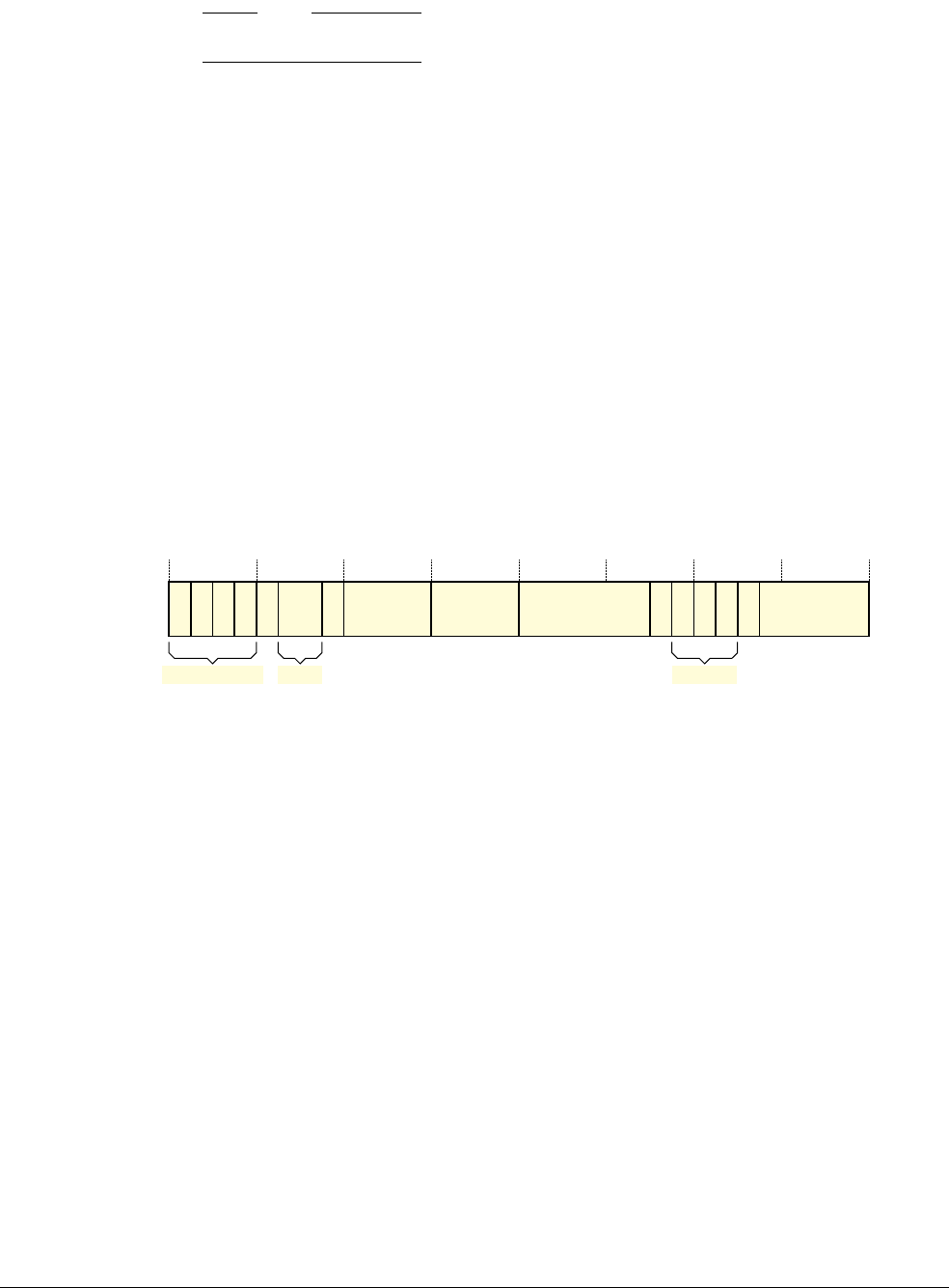
B1 System Level Programmers’ Model
B1.3 ARM processor modes and ARM core registers
B1-1148 Copyright © 1996-1998, 2000, 2004-2012, 2014 ARM. All rights reserved. ARM DDI 0406C.c
Non-Confidential ID051414
Note
See Context synchronization operation for the definition of this term.
• Might or might not affect memory accesses caused by fetching instructions between the mode change
instruction and the point where the mode change is guaranteed to be visible.
See Exception return on page B1-1194 for the definition of exception return instructions.
The Saved Program Status Registers (SPSRs)
The purpose of an SPSR is to record the pre-exception value of the CPSR. On taking an exception, the CPSR is
copied to the SPSR of the mode to which the exception is taken. Saving this value means the exception handler can:
• on exception return, restore the CPSR to the value it had immediately before the exception was taken
• examine the value that the CPSR had when the exception was taken, for example to determine the instruction
set state and privilege level in which the instruction that caused an Undefined Instruction exception was
executed.
Figure B1-2 on page B1-1144 shows the banking of the SPSRs.
The SPSRs are UNKNOWN on reset. Any operation in a Non-secure PL1 or PL0 mode makes SPSR_hyp UNKNOWN.
Format of the CPSR and SPSRs
The CPSR and SPSR bit assignments are:
Condition flags, bits[31:28]
Set on the result of instruction execution. The flags are:
N, bit[31] Negative condition flag
Z, bit[30] Zero condition flag
C, bit[29] Carry condition flag
V, bit[28] Overflow condition flag.
The condition flags can be read or written in any mode, and are described in The Application
Program Status Register (APSR) on page A2-49.
Q, bit[27] Cumulative saturation bit. This bit can be read or written in any mode, and is described in The
Application Program Status Register (APSR) on page A2-49.
IT[7:0], bits[15:10, 26:25]
If-Then execution state bits for the Thumb
IT
(If-Then) instruction. IT block state register, ITSTATE
on page A2-51 describes the encoding of these bits. CPSR.IT[7:0] are the IT[7:0] bits described
there. For more information, see IT on page A8-390.
For details of how these bits can be accessed see Accessing the execution state bits on page B1-1150.
J, bit[24] Jazelle bit, see the description of the T bit, bit[5].
Bits[23:20] Reserved. RAZ/SBZP.
N
31 30 29 28 27 26 25 24 23 20 19 16 15 10 9 8 7 6 5 4 3 2 1 0
Z C V Q J Reserved,
RAZ/SBZP GE[3:0] IT[7:2] E A I F T M[4:0]
IT[1:0]
Condition flags Mask bits

B1 System Level Programmers’ Model
B1.3 ARM processor modes and ARM core registers
ARM DDI 0406C.c Copyright © 1996-1998, 2000, 2004-2012, 2014 ARM. All rights reserved. B1-1149
ID051414 Non-Confidential
GE[3:0], bits[19:16]
Greater than or Equal flags, for the parallel addition and subtraction (SIMD) instructions described
in Parallel addition and subtraction instructions on page A4-171.
The GE[3:0] field can be read or written in any mode, and is described in The Application Program
Status Register (APSR) on page A2-49.
E, bit[9] Endianness execution state bit. Controls the load and store endianness for data accesses:
0 Little-endian operation
1 Big-endian operation.
Instruction fetches ignore this bit.
Endianness mapping register, ENDIANSTATE on page A2-53 describes the encoding of this bit.
CPSR.E is the ENDIANSTATE bit described there.
For details of how this bit can be accessed see Accessing the execution state bits on page B1-1150.
When the reset value of the SCTLR.EE bit is defined by a configuration input signal, that value also
applies to the CPSR.E bit on reset, and therefore applies to software execution from reset.
Mask bits, bits[8:6]
These bits are:
A, bit[8] Asynchronous abort mask bit.
I, bit[7] IRQ mask bit.
F, bit[6] FIQ mask bit.
The possible values of each bit are:
0 Exception not masked.
1 Exception masked.
The A bit has no effect on any Data Abort exception generated by a Watchpoint debug event, even
if that exception is asynchronous. For more information see Debug exception on Watchpoint debug
event on page C4-2091.
In an implementation that does not include the Security Extensions, setting a mask bit masks the
corresponding exception, meaning it cannot be taken. However, the Security Extensions and
Virtualization Extensions significantly alter the behavior and effect of these bits, see Effects of the
Security Extensions on the CPSR A and F bits on page B1-1151 and Asynchronous exception
masking on page B1-1184.
The mask bits can be written only at PL1 or higher. Their values can be read in any mode, but ARM
deprecates any use of their values, or attempt to change them, by software executing at PL0.
Updates to the F bit are restricted if Non-maskable FIQs (NMFIs) are supported, see Non-maskable
FIQs on page B1-1151.
T, bit[5] Thumb execution state bit. This bit and the J execution state bit, bit[24], determine the instruction
set state of the processor, ARM, Thumb, Jazelle, or ThumbEE. Instruction set state register,
ISETSTATE on page A2-50 describes the encoding of these bits. CPSR.J and CPSR.T are the same
bits as ISETSTATE.J and ISETSTATE.T respectively. For more information, see Instruction set
states on page B1-1155.
For details of how these bits can be accessed see Accessing the execution state bits on page B1-1150.

B1 System Level Programmers’ Model
B1.3 ARM processor modes and ARM core registers
B1-1150 Copyright © 1996-1998, 2000, 2004-2012, 2014 ARM. All rights reserved. ARM DDI 0406C.c
Non-Confidential ID051414
M[4:0], bits[4:0]
Mode field. This field determines the current mode of the processor. The permitted values of this
field are listed in Table B1-1 on page B1-1139. All other values of M[4:0] are reserved. The effect
of setting M[4:0] to a reserved value is UNPREDICTABLE.
Note
See the entry for UNPREDICTABLE in the Glossary for the restrictions on UNPREDICTABLE
behavior. These restrictions mean that, for any CPSR.M value that is defined as UNPREDICTABLE in
Non-secure state, the UNPREDICTABLE behavior must not cause entry to Secure state, or to any mode
that the current configuration settings mean is not accessible in Non-secure state.
For more information about the processor modes see ARM processor modes on page B1-1139.
Figure B1-2 on page B1-1144 shows the registers that can be accessed in each mode.
This field can be written only at PL1 or higher. Its value can be read in any mode, but ARM
deprecates software executing at PL0 making any use of its value, or attempting to change it.
In an implementation that includes the Security Extensions, except as a result of an exception entry
or exception return:
• Attempting to change CPSR.M to enter Monitor mode from Non-secure state is
UNPREDICTABLE.
• When NSACR.RFR is set to 1, attempting to change CPSR.M to enter FIQ mode from
Non-secure state is UNPREDICTABLE.
From the introduction of the Virtualization Extensions, ARM deprecates any use of
NSACR.RFR.
In an implementation that includes the Virtualization Extensions, except as a result of an exception
entry or exception return:
• attempting to change CPSR.M to enter Hyp mode from any mode other than Hyp mode is
UNPREDICTABLE
• attempting to change CPSR.M to enter any mode other than Hyp mode from Hyp mode is
UNPREDICTABLE.
See Exception return on page B1-1194 for more information about constraints on the CPSR.M value
on an exception return.
Accessing the execution state bits
The execution state bits are the IT[7:0], J, E, and T bits. If the current mode has an SPSR, software can read or write
these bits in the SPSR.
In the CPSR, unless the processor is in Debug state:
• The execution state bits, other than the E bit, are RAZ when read by an
MRS
instruction.
• Writes to the execution state bits, other than the E bit, by an
MSR
instruction are:
— For ARMv7 and ARMv6T2, ignored in all modes.
— For architecture variants before ARMv6T2, ignored in User mode and required to write zeros in other
modes. If a nonzero value is written at PL1, behavior is UNPREDICTABLE.
Instructions other than
MRS
and
MSR
that access the execution state bits can read and write them in any mode.
Unlike the other execution state bits in the CPSR, at PL1 or above CPSR.E can be read by an
MRS
instruction and
written by an
MSR
instruction. However, ARM deprecates:
•Using the CPSR.E value read by an
MRS
instruction.
•Using an
MSR
instruction to change the value of CPSR.E.
At PL0, a read of the CPSR by an
MSR
instruction returns an UNKNOWN value for the E bit, and a write by an
MSR
instruction has no effect on the E bit.

B1 System Level Programmers’ Model
B1.3 ARM processor modes and ARM core registers
ARM DDI 0406C.c Copyright © 1996-1998, 2000, 2004-2012, 2014 ARM. All rights reserved. B1-1151
ID051414 Non-Confidential
Note
• Software can use the
SETEND
instruction to change the current endianness.
• To determine the current endianness, software can use an
LDR
instruction to load a word of memory with a
known value that differs if the endianness is reversed. For example, using an
LDR
(literal) instruction to load
a word whose four bytes are
0x01
,
0x00
,
0x00
, and
0x00
in ascending order of memory address loads the
destination register with:
—
0x00000001
if the current endianness is little-endian
—
0x01000000
if the current endianness is big-endian.
For more information about the behavior of these bits in Debug state see Behavior of MRS and MSR instructions
that access the CPSR in Debug state on page C5-2099.
Non-maskable FIQs
Some ARMv7 implementations can be configured so that the CPSR.F bit cannot be set to 1 by an
MSR
or
CPS
instruction. This is defined as Non-maskable FIQ (NMFI) operation. In such an implementation, this configuration
is controlled by a configuration input signal, that is asserted HIGH to enable NMFI operation.
Note
There is no software control of NMFI operation.
The Virtualization Extensions do not support NMFIs. Otherwise, it is IMPLEMENTATION DEFINED whether an
ARMv7 processor supports NMFIs. In all cases, software can detect whether FIQs are maskable by reading the
SCTLR.NMFI bit:
NMFI == 0 Software can mask FIQs by setting the CPSR.F bit to 1.
NMFI == 1 Software cannot set the CPSR.F bit to 1. This means software cannot mask FIQs.
For more information see either:
•SCTLR, System Control Register, VMSA on page B4-1707
•SCTLR, System Control Register, PMSA on page B6-1932.
When the SCTLR.NMFI bit is 1:
• an instruction writing 0 to the CPSR.F bit clears it to 0, but an instruction attempting to write 1 to it leaves it
unchanged.
•CPSR.F can be set to 1 only by exception entries, as described in CPSR.{A, I, F, M} values on exception entry
on page B1-1183.
In an implementation that includes the Security Extensions, this restriction on accessing CPSR.F interacts with the
SCR.FW control, as described in Effects of the Security Extensions on the CPSR A and F bits.
Effects of the Security Extensions on the CPSR A and F bits
In an implementation that includes the Security Extensions:
• If the implementation does not include the Virtualization Extensions, when the processor is in Non-secure
state:
— the CPSR.F bit cannot be changed if the SCR.FW bit is set to 0
— the CPSR.A bit cannot be changed if the SCR.AW bit is set to 0.
• If the implementation includes the Virtualization Extensions, clearing the SCR.FW and SCR.AW bits to 0
does not affect the ability to change the CPSR.F and CPSR.A bits, but does prevent those bit from masking
exceptions in some situations.
For more information see Asynchronous exception masking on page B1-1184.

B1 System Level Programmers’ Model
B1.3 ARM processor modes and ARM core registers
B1-1152 Copyright © 1996-1998, 2000, 2004-2012, 2014 ARM. All rights reserved. ARM DDI 0406C.c
Non-Confidential ID051414
Note
For an implementation that includes the Security Extensions but not the Virtualization Extensions, when the
processor is in the Non-secure state, software executing at PL1 can change the SPSR.F and SPSR.A bits even if the
corresponding bits in the SCR are set to 0. However, when the SPSR is copied to the CPSR the CPSR.F and CPSR.A
bits are not updated if the corresponding bits in the SCR are set to 0.
For an implementation that includes the Security Extensions but not the Virtualization Extensions, Table B1-2
shows how, in Non-secure state, SCR.FW interacts with SCTLR.NMFI to control possible updates to CPSR.F bit.
The table includes the SCTLR.NMFI controls in Secure state.
Note
The SCTLR.NMFI bit is common to the Secure and Non-secure versions of the SCTLR, because it is a read-only
bit that reflects the value of a configuration input signal.
The Virtualization Extensions do not support NMFIs. In an implementation that includes the Virtualization
Extensions, SCTLR.NMFI is RAZ.
Pseudocode details of PSR operations
The following pseudocode gives access to the PSRs:
bits(32) CPSR, SPSR_fiq, SPSR_irq, SPSR_svc, SPSR_mon, SPSR_abt, SPSR_und, SPSR_hyp;
// SPSR[] - non-assignment form
// ============================
bits(32) SPSR[]
if BadMode(CPSR.M) then
UNPREDICTABLE;
else
bits(32) result;
case CPSR.M of
when '10001' result = SPSR_fiq; // FIQ mode
when '10010' result = SPSR_irq; // IRQ mode
when '10011' result = SPSR_svc; // Supervisor mode
when '10110' result = SPSR_mon; // Monitor mode
when '10111' result = SPSR_abt; // Abort mode
when '11010' result = SPSR_hyp; // Hyp mode
when '11011' result = SPSR_und; // Undefined mode
otherwise UNPREDICTABLE;
return result;
// SPSR[] - assignment form
// ========================
SPSR[] = bits(32) value
if BadMode(CPSR.M) then
Table B1-2 NMFI behavior, Security Extensions implemented without the Virtualization Extensions
Security state SCR.FW bit SCTLR.NMFI bit CPSR.F bit properties
Secure x 0 F bit can be written to 0 or 1
1 F bit can be written to 0 but not to 1
Non-secure 0 x F bit cannot be written
1 0 F bit can be written to 0 or 1
1 F bit can be written to 0 but not to 1

B1 System Level Programmers’ Model
B1.3 ARM processor modes and ARM core registers
ARM DDI 0406C.c Copyright © 1996-1998, 2000, 2004-2012, 2014 ARM. All rights reserved. B1-1153
ID051414 Non-Confidential
UNPREDICTABLE;
else
case CPSR.M of
when '10001' SPSR_fiq = value; // FIQ mode
when '10010' SPSR_irq = value; // IRQ mode
when '10011' SPSR_svc = value; // Supervisor mode
when '10110' SPSR_mon = value; // Monitor mode
when '10111' SPSR_abt = value; // Abort mode
when '11010' SPSR_hyp = value; // Hyp mode
when '11011' SPSR_und = value; // Undefined mode
otherwise UNPREDICTABLE;
return;
// CPSRWriteByInstr()
// ==================
CPSRWriteByInstr(bits(32) value, bits(4) bytemask, boolean is_excpt_return)
privileged = CurrentModeIsNotUser();
nmfi = (SCTLR.NMFI == '1');
if bytemask<3> == '1' then
CPSR<31:27> = value<31:27>; // N,Z,C,V,Q flags
if is_excpt_return then
CPSR<26:24> = value<26:24>; // IT<1:0>,J execution state bits
if bytemask<2> == '1' then
// bits <23:20> are reserved SBZP bits
CPSR<19:16> = value<19:16>; // GE<3:0> flags
if bytemask<1> == '1' then
if is_excpt_return then
CPSR<15:10> = value<15:10>; // IT<7:2> execution state bits
CPSR<9> = value<9>; // E bit is user-writable
if privileged && (IsSecure() || SCR.AW == '1' || HaveVirtExt()) then
CPSR<8> = value<8>; // A interrupt mask
if bytemask<0> == '1' then
if privileged then
CPSR<7> = value<7>; // I interrupt mask
if privileged && (!nmfi || value<6> == '0') &&
(IsSecure() || SCR.FW == '1' || HaveVirtExt()) then
CPSR<6> = value<6>; // F interrupt mask
if is_excpt_return then
CPSR<5> = value<5>; // T execution state bit
if privileged then
if BadMode(value<4:0>) then
UNPREDICTABLE;
else
// Check for attempts to enter modes only permitted in Secure state from
// Non-secure state. These are Monitor mode ('10110'), and FIQ mode ('10001')
// if the Security Extensions have reserved it. The definition of UNPREDICTABLE
// does not permit the resulting behavior to be a security hole.
if !IsSecure() && value<4:0> == '10110' then UNPREDICTABLE;
if !IsSecure() && value<4:0> == '10001' && NSACR.RFR == '1' then UNPREDICTABLE;
// There is no Hyp mode ('11010') in Secure state, so that is UNPREDICTABLE
if SCR.NS == '0' && value<4:0> == '11010' then UNPREDICTABLE;
// Cannot move into Hyp mode directly from a Non-secure PL1 mode
if !IsSecure() && CPSR.M != '11010' && value<4:0> == '11010' then
UNPREDICTABLE;
// Cannot move out of Hyp mode with this function except on an exception return
if CPSR.M == '11010' && value<4:0> != '11010' && !is_excpt_return then
UNPREDICTABLE;
CPSR.M = value<4:0>; // CPSR<4:0>, mode bits
return;

B1 System Level Programmers’ Model
B1.3 ARM processor modes and ARM core registers
B1-1154 Copyright © 1996-1998, 2000, 2004-2012, 2014 ARM. All rights reserved. ARM DDI 0406C.c
Non-Confidential ID051414
// SPSRWriteByInstr()
// ==================
SPSRWriteByInstr(bits(32) value, bits(4) bytemask)
if CurrentModeIsUserOrSystem() then UNPREDICTABLE;
if bytemask<3> == '1' then
SPSR[]<31:24> = value<31:24>; // N,Z,C,V,Q flags, IT<1:0>,J execution state bits
if bytemask<2> == '1' then
// bits <23:20> are reserved SBZP bits
SPSR[]<19:16> = value<19:16>; // GE<3:0> flags
if bytemask<1> == '1' then
SPSR[]<15:8> = value<15:8>; // IT<7:2> execution state bits, E bit, A interrupt mask
if bytemask<0> == '1' then
SPSR[]<7:5> = value<7:5>; // I,F interrupt masks, T execution state bit
if BadMode(value<4:0>) then // Mode bits
UNPREDICTABLE;
else
SPSR[]<4:0> = value<4:0>;
return;
B1.3.4 ELR_hyp
Hyp mode does not provide its own Banked copy of LR. Instead, on taking an exception to Hyp mode, the preferred
return address is stored in ELR_hyp, a 32-bit Special register implemented for this purpose.
ELR_hyp is implemented only as part of the Virtualization Extensions.
ELR_hyp can be accessed explicitly only by executing:
•an
MRS
or
MSR
instruction that targets ELR_hyp, see:
—MRS (Banked register) on page B9-1992
—MSR (Banked register) on page B9-1994.
The
ERET
instruction uses the value in ELR_hyp as the return address for the exception. For more information, see
ERET on page B9-1982.
Software execution in any Non-secure PL1 or PL0 mode makes ELR_hyp UNKNOWN.
For more information about the use of ELR_hyp see Exceptions on page B1-1136.

B1 System Level Programmers’ Model
B1.4 Instruction set states
ARM DDI 0406C.c Copyright © 1996-1998, 2000, 2004-2012, 2014 ARM. All rights reserved. B1-1155
ID051414 Non-Confidential
B1.4 Instruction set states
The instruction set states are described in Chapter A2 Application Level Programmers’ Model and application level
operations on them are described there. This section supplies more information about how they interact with system
level functionality, in the sections:
•Exceptions and instruction set state.
•Unimplemented instruction sets.
B1.4.1 Exceptions and instruction set state
If an exception is taken to a PL1 mode, the SCTLR.TE bit for the security state the exception is taken to determines
the processor instruction set state that handles the exception, and if necessary, the processor changes to this
instruction set state on exception entry.
If the exception is taken to Hyp mode, the HSCTLR.TE bit determines the processor instruction set state that
handles the exception, and if necessary, the processor changes to this instruction set state on exception entry.
On coming out of reset, the processor starts execution in Supervisor mode, in the instruction set state determined by
the reset value of SCTLR.TE.
For more information see:
• for a VMSA implementation:
—SCTLR, System Control Register, VMSA on page B4-1707
—HSCTLR, Hyp System Control Register, Virtualization Extensions on page B4-1591
• for a PMSA implementation, SCTLR, System Control Register, PMSA on page B6-1932.
For more information about exception entry see Overview of exception entry on page B1-1171.
B1.4.2 Unimplemented instruction sets
The CPSR.J and CPSR.T bits define the current instruction set state, see Instruction set state register, ISETSTATE
on page A2-50.
In the ARMv7 architecture:
• The Jazelle state:
— Before the introduction of the Virtualization Extensions, is optional. ARM does not recommend
support for Jazelle state in any ARMv7 implementation.
— Is obsoleted by the introduction of the Virtualization Extensions. An ARMv7-A implementation that
includes the Virtualization Extensions cannot support Jazelle state.
• The ThumbEE state is optional in the ARMv7-R architecture. ARM does not recommend support for
ThumbEE state in any ARMv7-R implementation.
Some system instructions permit setting CPSR.{J, T} to values that select an unimplemented instruction set state,
for example setting CPSR.J to 1 and CPSR.T to 0 on an processor that does not implement the Jazelle state. If such
values are written to CPSR.{J, T}, the implementation behaves in one of these ways:
•Sets CPSR.{J, T} to the requested values and causes the next instruction to generate an Undefined Instruction
exception, as described in Exception return to an unimplemented instruction set state on page B1-1197.
• Does not set CPSR.{J, T} to the requested values. The processor might change the value of one or both of
the bits in such a way that the new values correspond to an implemented instruction set state. If this is done
then the instruction set state changes to this new state. The detailed behavior of the attempt to change to an
unimplemented state is IMPLEMENTATION DEFINED.

B1 System Level Programmers’ Model
B1.5 The Security Extensions
B1-1156 Copyright © 1996-1998, 2000, 2004-2012, 2014 ARM. All rights reserved. ARM DDI 0406C.c
Non-Confidential ID051414
B1.5 The Security Extensions
The Security Extensions are an OPTIONAL extension to the ARMv7-A architecture profile. When implemented, the
Security Extensions integrate hardware security features into the architecture, to facilitate the development of secure
applications. Many features of the architecture are extended to integrate with the Security Extensions, and because
of this integration of the Security Extensions into the architecture, features of the Security Extensions are described
in many sections of this manual.
Note
The Security Extensions are also permitted as an extension to the ARMv6K architecture. The resulting combination
is sometimes called the ARMv6Z or ARMv6KZ architecture.
The following sections give general information about the Security Extensions:
•Security states
•Impact of the Security Extensions on the modes and exception model on page B1-1158
•Security Extensions features added by the Virtualization Extensions on page B1-1158
•Classification of system control registers on page B3-1451.
B1.5.1 Security states
The Security Extensions define two security states, Secure state and Non-secure state. All instruction execution
takes place either in Secure state or in Non-secure state:
• Each security state operates in its own virtual memory address space, with its own translation regime.
Note
Figure B3-1 on page B3-1309 shows the different translation regimes.
• Many system controls can be set independently in each of the security states.
• All of the processor modes that are available in a system that does not implement the Security Extensions are
available in each of the security states. However:
— in any implementation that includes the Security Extensions, Monitor mode is available only in Secure
state
— in an implementation that also includes the Virtualization Extensions, Hyp mode is available only in
Non-secure state.
The Security Extensions also define an additional processor mode, Monitor mode, that provides a bridge between
software running in Non-secure state and software running in Secure state, see Changing from Secure to Non-secure
state on page B1-1157.
The following features mean the two security states can provide more security than is typically provided by systems
using the split between the different levels of execution privilege:
• the memory system provides mechanisms that prevent the Non-secure state accessing regions of the physical
memory designated as Secure
• system controls that apply to the Secure state are not accessible from the Non-secure state
• entry to the Secure state from the Non-secure state is provided only by a small number of exceptions
• exit from the Secure state to the Non-secure state is provided only by a small number of mechanisms
• many operating system and hypervisor exceptions can be handled without changing security state.

B1 System Level Programmers’ Model
B1.5 The Security Extensions
ARM DDI 0406C.c Copyright © 1996-1998, 2000, 2004-2012, 2014 ARM. All rights reserved. B1-1157
ID051414 Non-Confidential
The fundamental mechanism that determines the security state is the SCR.NS bit:
• For all modes other than Monitor mode and Hyp mode, the SCR.NS bit determines the security state for
software execution.
• In an implementation that includes the Virtualization Extensions, Hyp mode is available only in Non-secure
state, meaning it is available only when the SCR.NS bit is set to 1.
• Software executing in Monitor mode executes in the Secure state regardless of the value of the SCR.NS bit.
The ARM core registers and the processor status registers are not Banked between the Secure and the Non-secure
states. ARM expects that, when switching execution between the Non-secure and Secure states, a kernel running
mostly in Monitor mode will switch the values of these registers.
The registers LR_mon and SPSR_mon are UNKNOWN when executing in Non-secure state.
Many of the system registers referred to in Coprocessors and system control on page B1-1226 are Banked between
the Secure and Non-secure security states. A Banked copy of a register applies only to execution in the appropriate
security state. A small number of system registers are not Banked but apply to both the Secure and Non-secure
security states. The registers that are not Banked relate to global system configuration options that ARM expects to
be common to the two security states.
Changing from Secure to Non-secure state
Monitor mode is provided to support switching between Secure and Non-secure states. Except in Monitor mode and
Hyp mode, the security state is controlled by the SCR.NS bit. Software executing in a Secure PL1 mode can change
the SCR, but ARM strongly recommends that software obeys the following rules for changing SCR.NS:
• To avoid security holes, software must not:
— Change from Secure to Non-secure state by using an
MSR
or
CPS
instruction to switch from Monitor
mode to some other mode while SCR.NS is 1.
—Use an
MCR
instruction that writes SCR.NS to change from Secure to Non-secure state. This means
ARM recommends that software does not alter SCR.NS in any mode except Monitor mode. ARM
deprecates changing SCR.NS in any other mode.
Note
When the value of NSACR.RFR is 1, if the processor is in Secure FIQ mode, the effect of changing SCR.NS
to 1 is UNPREDICTABLE.
• The usual mechanism for changing from Secure to Non-secure state is an exception return.To return to
Non-secure state, software executing in Monitor mode sets SCR.NS to 1 and then performs the exception
return.
Pseudocode details of Secure state operations
The
HaveSecurityExt()
function returns TRUE if the implementation includes the Security Extensions, and FALSE
otherwise.
The
IsSecure()
function returns TRUE if the processor is in Secure state, or if the implementation does not include
the Security Extensions, and FALSE otherwise.
// IsSecure()
// ==========
boolean IsSecure()
return !HaveSecurityExt() || SCR.NS == '0' || CPSR.M == '10110'; // Monitor mode

B1 System Level Programmers’ Model
B1.5 The Security Extensions
B1-1158 Copyright © 1996-1998, 2000, 2004-2012, 2014 ARM. All rights reserved. ARM DDI 0406C.c
Non-Confidential ID051414
B1.5.2 Impact of the Security Extensions on the modes and exception model
This section gives an overview of the effect of the Security Extensions on the modes and exception model:
• Monitor mode is implemented only as part of the Security Extensions. For more information, see ARM
processor modes on page B1-1139 and Security states on page B1-1156.
• The Secure Monitor Call (SMC) exception is implemented only as part of the Security Extensions. The
SMC
instruction generates this exception. For more information, see Secure Monitor Call (SMC) exception on
page B1-1211 and SMC (previously SMI) on page B9-2002.
• For exceptions taken to any PL1 mode, because the SCTLR is Banked between the Secure and Non-secure
states, the V and VE bits are defined independently for the Secure and Non-secure states. For each state:
— the SCTLR.V bit controls whether the low or the high exception vectors are used
— for the IRQ and FIQ exceptions, the SCTLR.VE bit controls whether the IRQ and FIQ vectors are
IMPLEMENTATION DEFINED.
For more information, see Exception vectors and the exception base address on page B1-1165.
• For exceptions taken to any PL1 mode, the base address for the low exception vectors is held in a register
that is Banked between the two security states, meaning this base address is defined independently for each
security state.
Another register holds the base address for exceptions taken to Monitor mode.
For more information, see Exception vectors and the exception base address on page B1-1165.
• Setting bits in the SCR to 1 causes one or more of external aborts, IRQs and FIQs to be taken to Monitor
mode and to use the Monitor exception base address, see Asynchronous exception routing controls on
page B1-1175.
• When an exception is taken from Monitor mode in Non-debug state, SCR.NS is set to zero, to ensure that the
exception is taken to Secure state. However, if an exception is taken from Monitor mode in Debug state, the
exception entry does not change the value of SCR.NS.
Note
Many uses of the Security Extensions can be simplified if the system is designed so that exceptions cannot
be taken from Monitor mode.
• Clearing bits in the SCR to 0 prevents software executing in Non-secure state from being able to mask one
or both of asynchronous aborts and FIQs. The mechanism to do this depends on whether the implementation
includes the Virtualization Extensions, see Asynchronous exception masking on page B1-1184. With either
mechanism:
— clearing the SCR.AW bit to 0 prevents Non-secure masking of asynchronous aborts that are taken to
Monitor mode
— clearing the SCR.FW bit to 0 prevents Non-secure masking of FIQs that are taken to Monitor mode.
B1.5.3 Security Extensions features added by the Virtualization Extensions
In an implementation that includes the Virtualization Extensions, the following features are added to the Security
Extensions:
• When the SCR.SIF bit is set to 1, any instruction fetched from Non-secure physical memory cannot be
executed in Secure state. For more information, see Restriction on Secure instruction fetch on page B3-1361.
•SCTLR and HSCTLR include WXN bits that, when set to 1, prevent instruction execution from writable
memory regions.
Similarly, setting SCTLR.UWXN to 1 prevents instruction execution from any memory region that
unprivileged software can write to.
For more information see Preventing execution from writable locations on page B3-1361.

B1 System Level Programmers’ Model
B1.5 The Security Extensions
ARM DDI 0406C.c Copyright © 1996-1998, 2000, 2004-2012, 2014 ARM. All rights reserved. B1-1159
ID051414 Non-Confidential
• When the SCR.SCD bit is set to 1, entry to Secure state by taking a Secure Monitor Call exception is disabled.
This means that, when SCR.SCD is set to 1:
—an
SMC
instruction executed in Non-secure state, and not trapped by the HCR.TSC mechanism
described in Trapping use of the SMC instruction on page B1-1255, is UNDEFINED
—an
SMC
instruction executed in a Secure PL1 mode is UNPREDICTABLE.
For more information, see SMC (previously SMI) on page B9-2002.

B1 System Level Programmers’ Model
B1.6 The Large Physical Address Extension
B1-1160 Copyright © 1996-1998, 2000, 2004-2012, 2014 ARM. All rights reserved. ARM DDI 0406C.c
Non-Confidential ID051414
B1.6 The Large Physical Address Extension
The Large Physical Address Extension is an OPTIONAL extension to the ARMv7-A architecture profile. Any
implementation that includes the Large Physical Address Extension must also include the Multiprocessing
Extensions.
The Large Physical Address Extension adds a new translation table format:
• the format used in an implementation that does not include the Large Physical Address Extension is now
called the Short-descriptor format, see Short-descriptor translation table format on page B3-1324
• the format added by the Large Physical Address Extension is the Long-descriptor format, see
Long-descriptor translation table format on page B3-1338.
An implementation that includes the Large Physical Address Extension must support both translation table formats.
Other effects of the Large Physical Address Extension are described throughout this manual, and include:
• Changes to the permitted attributes for Device memory regions, see Summary of ARMv7 memory attributes
on page A3-127 and Device and Strongly-ordered memory shareability, Large Physical Address Extension
on page A3-138.
Note
The ordering requirements for Device accesses are identical to those for Strongly-ordered accesses, see
Ordering requirements for memory accesses on page A3-149.
• The addition of a requirement that
LDRD
and
STRD
accesses to 64-bit aligned locations are 64-bit single-copy
atomic as seen by translation table walks and accesses to translation tables, see Single-copy atomicity on
page A3-128.
• Requiring the Short-descriptor translation table format to include the Privileged execute-never (PXN)
attribute, see Memory attributes in the Short-descriptor translation table format descriptors on
page B3-1328.
Note
— In an implementation that does not include the Large Physical Address Extension, the inclusion of the
PXN attribute in the Short-descriptor translation table format is OPTIONAL.
— The Long-descriptor translation table format always includes the PXN attribute.
• An implementation that includes the Large Physical Address Extension must implement the Multiprocessing
Extensions and therefore cannot include the FCSE, see Use of the Fast Context Switch Extension on
page D9-2477.
• The Large Physical Address Extension:
— Extends the DBGDRAR and DBGDSAR to 64 bits, to hold PAs of up to 40 bits.
— Defines new formats for the DFSR, IFSR, and TTBCR, for use with the Long-descriptor translation
table format.
— Adds bits to the DFSR and IFSR formats used with the Long-descriptor translation table format.
DFSR.CM indicates when a fault is caused by a cache maintenance or address translation operation.
DFSR.LPAE and IFSR.LPAE indicate the translation table format in use when the fault was generated.
— Extends the PAR to 64 bits, to hold PAs of up to 40 bits.
— Extends TTBR0 and TTBR1 to 64 bits, to support the Long-descriptor translation table format.
— Defines two Memory Attribute Indirection Registers, MAIR0 and MAIR1, to replace PRRR and
NMRR when using the Long-descriptor translation table format.
— Provides two IMPLEMENTATION DEFINED Auxiliary Memory Attribute Indirection Registers 0
AMAIR0 and AMAIR1.

B1 System Level Programmers’ Model
B1.6 The Large Physical Address Extension
ARM DDI 0406C.c Copyright © 1996-1998, 2000, 2004-2012, 2014 ARM. All rights reserved. B1-1161
ID051414 Non-Confidential
• The introduction of the Large Physical Address Extension changes:
— some terminology used for MMU faults, see VMSAv7 MMU fault terminology on page B3-1398
— the naming of the address translation operations, see Naming of the address translation operations,
and operation summary on page B3-1438.

B1 System Level Programmers’ Model
B1.7 The Virtualization Extensions
B1-1162 Copyright © 1996-1998, 2000, 2004-2012, 2014 ARM. All rights reserved. ARM DDI 0406C.c
Non-Confidential ID051414
B1.7 The Virtualization Extensions
The Virtualization Extensions are an OPTIONAL extension to the ARMv7-A architecture profile. Any
implementation that includes the Virtualization Extensions must include the Security Extensions, the Large Physical
Address Extension, and the Multiprocessing Extensions.
When implemented, the Virtualization Extensions provide a set of hardware features that support virtualizing the
Non-secure state of an ARM VMSAv7 implementation. The basic model of a virtualized system involves:
• a hypervisor, running in Non-secure Hyp mode, that is responsible for switching Guest operating systems
• a number of Guest operating systems, each of which runs in the Non-secure PL1 and PL0 modes
• for each Guest operating system, applications, that usually run in User mode.
Note
A Guest OS runs on a virtual machine. However, its own view is that it is running on an ARM processor. Normally,
a Guest OS is completely unaware:
• that it is running on a virtual machine
• of any other Guest OS.
Another way of describing virtualization is that:
• a Guest operating system, including all applications and tasks running under that operating system, runs on
a virtual machine
• a hypervisor switches between virtual machines.
Each virtual machine is identified by a virtual machine identifier (VMID), assigned by the hypervisor.
Many features of the architecture are extended to integrate with the Virtualization Extensions, and because of this
integration of the Virtualization Extensions into the architecture, features of the Virtualization Extensions are
described in many sections of this manual. The key features are:
• Hyp mode is implemented only in Non-secure state, to support Guest OS management. Hyp mode operates
in its own Non-secure virtual address space, that is different from the Non-secure virtual address space
accessed from Non-secure PL0 and PL1 modes.
• The Virtualization Extensions provide controls to:
— Define virtual values for a small number of identification registers. A read of the identification register
by a Guest OS or its applications returns the virtual value.
— Trap various other operations, including accesses to many other registers, and memory management
operations. A trapped operation generates an exception that is taken to Hyp mode.
These controls are configured by software executing in Hyp mode.
• With the Security Extensions, the Virtualization Extensions control the routing of interrupts and
asynchronous Data Abort exceptions to the appropriate one of:
— the current Guest OS
— a Guest OS that is not currently running
— the hypervisor
— the Secure monitor.
• When an implementation includes the Virtualization Extensions, it provides independent translation regimes
for memory accesses from:
— Secure modes, the Secure PL1&0 translation regime
— Non-secure Hyp mode, the Non-secure PL2 translation regime
— Non-secure PL1 and PL0 modes, the Non-secure PL1&0 translation regime.
Figure B3-1 on page B3-1309 shows these translation regimes.

B1 System Level Programmers’ Model
B1.7 The Virtualization Extensions
ARM DDI 0406C.c Copyright © 1996-1998, 2000, 2004-2012, 2014 ARM. All rights reserved. B1-1163
ID051414 Non-Confidential
• In the Non-secure PL1&0 translation regime, address translation occurs in two stages:
— Stage 1 maps the Virtual Address (VA) to an Intermediate Physical Address (IPA). Typically, the Guest
OS configures and controls this stage, and believes that the IPA is the Physical Address (PA)
— Stage 2 maps the IPA to the PA. Typically, the hypervisor controls this stage, and a Guest OS is
completely unaware of this translation.
For more information, see About address translation on page B3-1311.
Impact of the Virtualization Extensions on the modes and exception model gives more information about many of
these features.
B1.7.1 Impact of the Virtualization Extensions on the modes and exception model
This section summarizes the effect of the Virtualization Extensions on the modes and exception model. An
implementation that includes the Virtualization Extensions:
• Implements a new Non-secure mode, Hyp mode. Hyp mode on page B1-1141 summarizes how Hyp mode
differs from the other processor modes.
• Implements new exceptions, see:
—Hypervisor Call (HVC) exception on page B1-1212
—Hyp Trap exception on page B1-1209
—Virtual IRQ exception on page B1-1221
—Virtual FIQ exception on page B1-1223
—Virtual Abort exception on page B1-1218.
The Hypervisor Call and Hyp Trap exceptions are always taken to Hyp mode. The virtual exceptions are
taken to Non-secure IRQ, FIQ, or Abort mode, see The virtual exceptions on page B1-1164.
• Implements a new register that holds the exception vector base address for exceptions taken to Hyp mode,
the HVBAR.
• Provides controls that can be used to route IRQs, FIQs, and asynchronous aborts, to Hyp mode. This is
possible only if Secure software has not routed the exception to Monitor mode, and applies only to exceptions
taken from a Non-secure mode.
For more information see Asynchronous exception routing controls on page B1-1175.
• Provides controls that can be used to route some synchronous exceptions, taken from Non-secure modes, to
Hyp mode. For more information see Routing general exceptions to Hyp mode on page B1-1192 and Routing
Debug exceptions to Hyp mode on page B1-1194.
• Provide mechanisms to trap processor functions to Hyp mode, using the Hyp Trap exception, see Traps to
the hypervisor on page B1-1248.
When an operation is trapped to Hyp mode, the hypervisor typically either:
— emulates the required operation, so the application running in the Guest OS is unaware of the trap to
Hyp mode
— returns an error to the Guest OS.
• Implements enhanced exception reporting for exceptions taken to Hyp mode, see Reporting exceptions taken
to the Non-secure PL2 mode on page B3-1420. These exceptions are reported using the HSR, see Use of the
HSR on page B3-1424,
• Implements a new exception return instruction,
ERET
, for return from Hyp mode. For more information see
Hyp mode on page B1-1141.

B1 System Level Programmers’ Model
B1.7 The Virtualization Extensions
B1-1164 Copyright © 1996-1998, 2000, 2004-2012, 2014 ARM. All rights reserved. ARM DDI 0406C.c
Non-Confidential ID051414
The virtual exceptions
The Virtualization Extensions introduce three virtual exceptions:
• the Virtual IRQ exception, that corresponds to the physical IRQ exception
• the Virtual FIQ exception, that corresponds to the physical FIQ exception
• the Virtual Abort exception, that corresponds to a physical asynchronous External Data Abort exception.
Software executing in Hyp mode can use these to signal exceptions to the other Non-secure modes. A Non-secure
PL1 or PL0 mode cannot distinguish a virtual exception from the corresponding physical exception.
A usage model for these exceptions is that physical IRQs, FIQs and asynchronous aborts that occur when the
processor is in a Non-secure PL1 or PL0 mode are routed to Hyp mode. The exception handler, executing in Hyp
mode, determines whether the exception can be handled in Hyp mode or requires routing to a Guest OS. When an
exception requires handling by a Guest OS it is marked as pending for that Guest OS. When the hypervisor switches
to a particular Guest OS, it uses the appropriate virtual exception to signal any pending virtual exception to that
Guest OS.
For more information see Virtual exceptions in the Virtualization Extensions on page B1-1197.

B1 System Level Programmers’ Model
B1.8 Exception handling
ARM DDI 0406C.c Copyright © 1996-1998, 2000, 2004-2012, 2014 ARM. All rights reserved. B1-1165
ID051414 Non-Confidential
B1.8 Exception handling
An exception causes the processor to suspend program execution to handle an event, such as an externally generated
interrupt or an attempt to execute an undefined instruction. Exceptions can be generated by internal and external
sources.
Normally, when an exception is taken the processor state is preserved immediately, before handling the exception.
This means that, when the event has been handled, the original state can be restored and program execution resumed
from the point where the exception was taken.
More than one exception might be generated at the same time, and a new exception can be generated while the
processor is handling an exception.
The following sections describe exception handling:
•Exception vectors and the exception base address
•Exception priority order on page B1-1169
•Overview of exception entry on page B1-1171
•Processor mode for taking exceptions on page B1-1173
•Processor state on exception entry on page B1-1182
•Asynchronous exception masking on page B1-1184
•Summaries of asynchronous exception behavior on page B1-1186
•Routing general exceptions to Hyp mode on page B1-1192
•Routing Debug exceptions to Hyp mode on page B1-1194
•Exception return on page B1-1194
•Virtual exceptions in the Virtualization Extensions on page B1-1197
•Low interrupt latency configuration on page B1-1198.
•Wait For Event and Send Event on page B1-1200
•Wait For Interrupt on page B1-1203.
Exception descriptions on page B1-1205 then describes each exception.
B1.8.1 Exception vectors and the exception base address
When an exception is taken, processor execution is forced to an address that corresponds to the type of exception.
This address is called the exception vector for that exception.
A set of exception vectors comprises eight consecutive word-aligned memory addresses, starting at an exception
base address. These eight vectors form a vector table. For the IRQ and FIQ exceptions only, when the exceptions
are taken to IRQ mode and FIQ mode, software can change the exception vectors from the vector table values by
setting the SCTLR.VE bit to 1, see Vectored interrupt support on page B1-1168.
The number of possible exception base addresses, and therefore the number of vector tables, depends on the
implemented architecture profile and extensions, as follows:
Implementation that does not include the Security Extensions
This section applied to all ARMv7-R implementations.
An implementation that does not include the Security Extensions has a single vector table, the base
address of which is selected by SCTLR.V, see SCTLR, System Control Register, VMSA on
page B4-1707 or SCTLR, System Control Register, PMSA on page B6-1932:
V==0 Exception base address =
0x00000000
. This setting is referred to as normal vectors, or as
low vectors.
V==1 Exception base address =
0xFFFF0000
. This setting is referred to as high vectors, or
Hivecs.
Note
ARM deprecates using the Hivecs setting, SCTLR.V == 1, in ARMv7-R. ARM recommends that
Hivecs is used only in ARMv7-A implementations.

B1 System Level Programmers’ Model
B1.8 Exception handling
B1-1166 Copyright © 1996-1998, 2000, 2004-2012, 2014 ARM. All rights reserved. ARM DDI 0406C.c
Non-Confidential ID051414
Implementation that includes the Security Extensions
Any implementation that includes the Security Extensions has the following vector tables:
• One for exceptions taken to Secure Monitor mode. This is the Monitor vector table, and is in
the address space of the Secure PL1&0 translation regime.
• One for exceptions taken to Secure PL1 modes other than Monitor mode. This is the Secure
vector table, and is in the address space of the Secure PL1&0 translation regime.
• One for exceptions taken to Non-secure PL1 modes. This is the Non-secure vector table, and
is in the address space of the Non-secure PL1&0 translation regime.
For the Monitor vector table, MVBAR holds the exception base address.
For the Secure vector table:
• the Secure SCTLR.V bit determines the exception base address:
V==0 The Secure VBAR holds the exception base address.
V==1 Exception base address =
0xFFFF0000
, the Hivecs setting.
For the Non-secure vector table:
• the Non-secure SCTLR.V bit determines the exception base address:
V==0 The Non-secure VBAR holds the exception base address.
V==1 Exception base address =
0xFFFF0000
, the Hivecs setting.
Implementation that includes the Virtualization Extensions
An implementation that includes the Virtualization Extensions must include the Security
Extensions, and also includes an additional vector table. Therefore, it has the following vector
tables:
• One for exceptions taken to Secure Monitor mode. This is the Monitor vector table, and is in
the address space of the Secure PL1&0 translation regime.
• One for exceptions taken to Secure PL1 modes other than Monitor mode. This is the Secure
vector table, and is in the address space of the Secure PL1&0 translation regime.
• One for exceptions taken to Hyp mode, the Non-secure PL2 mode. This is the Hyp vector
table, and is in the address space of the Non-secure PL2 translation regime.
• One for exceptions taken to Non-secure PL1 modes. This is the Non-secure vector table, and
is in the address space of the Non-secure PL1&0 translation regime.
The exception base addresses of the Monitor vector table, the Secure vector table, and the
Non-secure vector table are determined in the same way as for an implementation that includes the
Security extensions but not the Virtualization extensions.
For the Hyp vector table, HVBAR holds the exception base address.
The following subsections give more information:
•The vector tables and exception offsets
•Vectored interrupt support on page B1-1168
•Pseudocode determination of the exception base address on page B1-1168.
The vector tables and exception offsets
Table B1-3 on page B1-1167 defines the vector table entries. In this table:
• The Hyp mode column defines the vector table entries for exceptions taken to Hyp mode.
• The Monitor mode column defines the vector table entries for exceptions taken to Monitor mode.
• The Secure and Non-secure columns define the Secure and Non-secure vector table entries, that are used for
exceptions taken to PL1 modes other than Monitor mode. Table B1-4 on page B1-1167 shows the mode to
which each of these exceptions is taken. Each of these modes is described as the default mode for taking the
corresponding exception.

B1 System Level Programmers’ Model
B1.8 Exception handling
ARM DDI 0406C.c Copyright © 1996-1998, 2000, 2004-2012, 2014 ARM. All rights reserved. B1-1167
ID051414 Non-Confidential
For more information about determining the mode to which an exception is taken, see Processor mode for taking
exceptions on page B1-1173.
The Virtualization Extensions provide a number of additional exceptions, some of which are not shown explicitly
in the vector tables. For more information, see Offsets of exceptions introduced by the Virtualization Extensions.
For more information about use of the vector tables see Overview of exception entry on page B1-1171.
Offsets of exceptions introduced by the Virtualization Extensions
The Virtualization Extensions introduce the following new exceptions. The processor enters the handlers for these
exceptions using the following vector table entries shown in Table B1-3:
Hypervisor Call
If taken from Hyp mode, shown explicitly in the Hyp mode vector table. Otherwise, see Use of offset
0x14 in the Hyp vector table on page B1-1168.
Hyp Trap Shown explicitly in the Hyp mode vector table.
Virtual Abort Entered through the Data Abort vector in the Non-secure vector table.
Table B1-3 The vector tables
Offset
Vector tables
HypaMonitorbSecure Non-secure
0x00
Not used Not used Reset Not used
0x04
Undefined Instruction, from Hyp mode Not used Undefined Instruction Undefined Instruction
0x08
Hypervisor Call, from Hyp mode Secure Monitor Call Supervisor Call Supervisor Call
0x0C
Prefetch Abort, from Hyp mode Prefetch Abort Prefetch Abort Prefetch Abort
0x10
Data Abort, from Hyp mode Data Abort Data Abort Data Abort
0x14
Hyp Trap, or Hyp mode entrycNot used Not used Not used
0x18
IRQ interrupt IRQ interrupt IRQ interrupt IRQ interrupt
0x1C
FIQ interrupt FIQ interrupt FIQ interrupt FIQ interrupt
a. Non-secure state only. Implemented only if the implementation includes the Virtualization Extensions.
b. Secure state only. Implemented only if the implementation includes the Security Extensions.
c. See Use of offset 0x14 in the Hyp vector table on page B1-1168.
Table B1-4 Modes for taking exceptions using the Secure or Non-secure vector table
Exception PL1 Mode taken to
Reset Supervisor
Undefined Instruction Undefined
Supervisor Call Supervisor
Prefetch Abort Abort
Data Abort Abort
IRQ interrupt IRQ
FIQ interrupt FIQ

B1 System Level Programmers’ Model
B1.8 Exception handling
B1-1168 Copyright © 1996-1998, 2000, 2004-2012, 2014 ARM. All rights reserved. ARM DDI 0406C.c
Non-Confidential ID051414
Virtual IRQ Entered through the IRQ vector in the Non-secure vector table.
Virtual FIQ Entered through the FIQ vector in the Non-secure vector table.
Note
The virtual exceptions on page B1-1164 summarizes these exceptions, and Virtual exceptions in the Virtualization
Extensions on page B1-1197 gives more information.
Use of offset
0x14
in the Hyp vector table
The vector at offset
0x14
in the Hyp vector table is used for exceptions that cause entry to Hyp mode. This means it
is:
• Always used for the Hyp Trap exception.
• Used for the following exceptions, when the exception is not taken from Hyp mode:
— Hypervisor Call
— Supervisor Call, when caused by execution of an
SVC
instruction in Non-secure User mode when
HCR.TGE is set to 1
— Undefined Instruction
— Prefetch Abort
— Data Abort.
Table B1-3 on page B1-1167 shows the offsets used for these exceptions when they are taken from Hyp
mode.
• Never used for IRQ exceptions, Virtual IRQ exceptions, FIQ exceptions, or Virtual FIQ exceptions.
For more information, see Processor mode for taking exceptions on page B1-1173.
Pseudocode determination of the exception base address
For an exception taken to a PL1 mode other than Monitor mode, the
ExcVectorBase()
function determines the
exception base address:
// ExcVectorBase()
// ===============
bits(32) ExcVectorBase()
if SCTLR.V == '1' then // Hivecs selected, base = 0xFFFF0000
return Ones(16):Zeros(16);
elsif HaveSecurityExt() then
return VBAR;
else
return Zeros(32);
Vectored interrupt support
At reset, any implemented vectored interrupt mechanism is disabled, and the IRQ and FIQ exception vectors are at
fixed offsets from the exception base address that is being used. With this configuration, an FIQ or IRQ handler
typically starts with an instruction sequence that determines the cause of the interrupt and then branches to an
appropriate routine to handle it.
If an implementation supports vectored interrupts, enabling this feature means an interrupt controller can prioritize
interrupts and provide the address of the required interrupt handler directly to the processor, for use as the interrupt
vector. For interrupts taken to PL1 modes other than Monitor mode, vectored interrupt behavior is enabled by setting
the SCTLR.VE bit to 1, see either:
•SCTLR, System Control Register, VMSA on page B4-1707
•SCTLR, System Control Register, PMSA on page B6-1932.

B1 System Level Programmers’ Model
B1.8 Exception handling
ARM DDI 0406C.c Copyright © 1996-1998, 2000, 2004-2012, 2014 ARM. All rights reserved. B1-1169
ID051414 Non-Confidential
The hardware that supports vectored interrupts is IMPLEMENTATION DEFINED, and an implementation might not
include any support for this operation.
In an implementation that includes the Security Extensions:
• The SCTLR.VE bit is Banked between Secure and Non-secure states to provide independent control of
whether vectored interrupt support is enabled.
• Interrupts can be routed to Monitor mode, by setting either or both of the SCR.IRQ and SCR.FIQ bits to 1.
When an interrupt is routed to Monitor mode it uses the vector in the vector table at the Monitor exception
base address held in MVBAR, regardless of the value of either Banked copy of the SCTLR.VE bit.
The Virtualization Extensions do not support this vectoring of the IRQ and FIQ exceptions when these exceptions
are routed to Hyp mode. When an interrupt is routed to Hyp mode, it uses the vector in the vector table at the Hyp
exception base address held in HVBAR, regardless of the value of either Banked copy of the SCTLR.VE bit.
From the introduction of the Virtualization Extensions, ARM deprecates any use of the SCTLR.VE bit.
B1.8.2 Exception priority order
An instruction is not valid if it generates a synchronous Prefetch Abort exception. Therefore, if an instruction
generates a Prefetch Abort exception, no other synchronous exception or debug event is generated on that
instruction.
A Breakpoint debug event, or an address matching form of the Vector catch debug event, is associated with the
instruction. This means the corresponding exception is taken before the instruction is executed. Therefore, when a
Breakpoint or address matching Vector catch debug event occurs, no other synchronous exception or debug event,
that might have occurred as a result of executing the instruction, can occur.
Note
• The Exception trapping form of the Vector catch debug event, introduced in v7.1 Debug, causes a debug
event as a result of trapping an exception that has been prioritized as described in this section. This means it
is outside the scope of the description in this section. For more information see Vector catch debug events on
page C3-2067.
• In v7 Debug, the only supported Vector catch debug events are address matching Vector catch debug events.
Otherwise:
• An instruction that generates an Undefined Instruction exception or a Hyp Trap exception cannot cause any
memory access, and therefore cannot cause a Data Abort exception.
• If an instruction generates both an Undefined Instruction exception and a Hyp Trap exception then, unless
this manual explicitly states otherwise, the Undefined Instruction exception has priority.
• If a system call is configured to generate an Undefined Instruction exception or a Hyp Trap exception, then
the Undefined Instruction exception or the Hyp Trap exception has priority over the system call. The system
calls are the
SVC
,
HVC
, and
SMC
instructions.
• A memory access that generates an MMU fault, an MPU fault, or a synchronous Watchpoint debug event
must not generate an external abort.
• All other synchronous exceptions are mutually exclusive and are derived from a decode of the instruction.
For more information, see:
•Debug event prioritization on page C3-2078 for information about the prioritization of debug events,
including their prioritization relative to MMU faults, MPU faults, and synchronous external aborts
•Prioritization of aborts on page B3-1407, for information about:
— the prioritization of aborts on a single memory access in a VMSA implementation
— the prioritization of exceptions generated during address translation

B1 System Level Programmers’ Model
B1.8 Exception handling
B1-1170 Copyright © 1996-1998, 2000, 2004-2012, 2014 ARM. All rights reserved. ARM DDI 0406C.c
Non-Confidential ID051414
•Prioritization of aborts on page B5-1768, for information about the prioritization of aborts on a single
memory access in a PMSA implementation.
Architectural requirements for taking asynchronous exceptions
The ARM architecture does not define when asynchronous exceptions are taken, but sets the following limits on
when they are taken:
• An asynchronous exception that is pending before one of the following context synchronizing events is taken
before the first instruction after the context synchronizing event completes its execution, provided that the
pending asynchronous event is not masked after the context synchronizing event. The context synchronizing
events are:
— Execution of an
ISB
instruction.
— Taking an exception.
— Return from an exception.
— Exit from Debug state.
The ISR identifies any pending asynchronous exceptions.
Note
If the first instruction after the context synchronizing event generates a synchronous exception, then the
architecture does not define the order in which that synchronous exception and the asynchronous exception
are taken.
• In the absence of an specific requirement to take an asynchronous exception, because of a context
synchronizing event, the only requirement of the architecture is that an unmasked asynchronous exception is
taken in finite time.
Note
The taking of an unmasked asynchronous exception in finite time must occur with all code sequences,
including with a sequence that consists of unconditional loops.
Within these limits, the prioritization of asynchronous exceptions relative to other exceptions, both synchronous and
asynchronous, is IMPLEMENTATION DEFINED.
Note
A special requirement applies to asynchronous watchpoints, see Debug event prioritization on page C3-2078.
The CPSR includes a mask bit for each type of asynchronous exception. Setting one of these bits to 1 can prevent
the corresponding asynchronous exception from being taken, see Summaries of asynchronous exception behavior
on page B1-1186.
Taking an exception sets an exception-dependent subset of these mask bits.
Note
The subset of the CPSR mask bits that is set on taking an exception can prioritize the execution of FIQ handlers over
that of IRQ and asynchronous abort handlers.

B1 System Level Programmers’ Model
B1.8 Exception handling
ARM DDI 0406C.c Copyright © 1996-1998, 2000, 2004-2012, 2014 ARM. All rights reserved. B1-1171
ID051414 Non-Confidential
B1.8.3 Overview of exception entry
On taking an exception:
1. The hardware determines the mode to which the exception must be taken, see Processor mode for taking
exceptions on page B1-1173.
2. A link value, indicating the preferred return address for the exception, is saved. This is a possible return
address for the exception handler, and depends on:
• the exception type
• whether the exception is taken to a PL1 mode or a PL2 mode
• for some exceptions taken to a PL1 mode, the instruction set state when the exception is taken.
Where the link value is saved depends on whether the exception is taken to a PL1 mode or a PL2 mode.
For more information see Link values saved on exception entry on page B1-1172.
3. The value of the CPSR is saved in the SPSR for the mode to which the exception must be taken. The value
saved in SPSR.IT[7:0] is always correct for the preferred return address.
4. In an implementation that includes the Security Exceptions:
• if the exception taken from Monitor mode, SCR.NS is cleared to 0
• otherwise, taking the exception leaves SCR.NS unchanged.
5. The CPSR is updated with new context information for the exception handler. This includes:
• Setting CPSR.M to the processor mode to which the exception is taken.
• Setting the appropriate CPSR mask bits. This can disable the corresponding exceptions, preventing
uncontrolled nesting of exception handlers.
• Setting the instruction set state to the state required for exception entry.
• Setting the endianness to the required value for exception entry.
• Clearing the CPSR.IT[7:0] bits to 0.
For more information, see Processor state on exception entry on page B1-1182.
6. The appropriate exception vector is loaded into the PC, see Exception vectors and the exception base address
on page B1-1165.
7. Execution continues from the address held in the PC.
For an exception taken to a PL1 mode, on exception entry, the exception handler can use the
SRS
instruction to store
the return state onto the stack of any mode at the same privilege level, and the CPS instruction to change mode. For
more information about the instructions, see SRS (Thumb) on page B9-2004, SRS (ARM) on page B9-2006, CPS
(Thumb) on page B9-1978, and CPS (ARM) on page B9-1980.
Later sections of this chapter describe each of the possible exceptions, and each of these descriptions includes a
pseudocode description of the processor state changes when it takes that exception. Table B1-5 gives an index to
these descriptions:
Table B1-5 Pseudocode descriptions of exception entry
Exception Description of exception entry
Reset Pseudocode description of taking the Reset exception on page B1-1206
Undefined Instruction Pseudocode description of taking the Undefined Instruction exception on page B1-1208
Supervisor Call Pseudocode description of taking the Supervisor Call exception on page B1-1211
Secure Monitor Call Pseudocode description of taking the Secure Monitor Call exception on page B1-1212
Hypervisor Call Pseudocode description of taking the Hypervisor Call exception on page B1-1213
Prefetch Abort Pseudocode description of taking the Prefetch Abort exception on page B1-1214

B1 System Level Programmers’ Model
B1.8 Exception handling
B1-1172 Copyright © 1996-1998, 2000, 2004-2012, 2014 ARM. All rights reserved. ARM DDI 0406C.c
Non-Confidential ID051414
The following sections give more information about the processor state changes, for different architecture
implementations. However, you must refer to the pseudocode for a full description of the state changes:
•Processor mode for taking exceptions on page B1-1173
•Processor state on exception entry on page B1-1182.
Link values saved on exception entry
On exception entry, a link value for use on return from the exception, is saved. This link value is based on the
preferred return address for the exception, as shown in Table B1-6:
Note
• Although Reset is described as an exception, it differs significantly from other exceptions. The architecture
has no concept of a return from a Reset and therefore it is not listed in this section.
• For each exception, the preferred return address is not affected by whether the exception is taken from a PL1
mode or from a PL0 mode.
Data Abort Pseudocode description of taking the Data Abort exception on page B1-1216
IRQ Pseudocode description of taking the IRQ exception on page B1-1220
FIQ Pseudocode description of taking the FIQ exception on page B1-1222
Hyp Trap Pseudocode description of taking the Hyp Trap exception on page B1-1210
Virtual Abort Pseudocode description of taking the Virtual Abort exception on page B1-1218
Virtual IRQ Pseudocode description of taking the Virtual IRQ exception on page B1-1221
Virtual FIQ Pseudocode description of taking the Virtual FIQ exception on page B1-1224
Table B1-5 Pseudocode descriptions of exception entry (continued)
Exception Description of exception entry
Table B1-6 Exception return addresses
Exception Preferred return address Taken to a mode at
Undefined Instruction Address of the UNDEFINED instruction PL1a, or PL2b
Supervisor Call Address of the instruction after the
SVC
instruction PL1a or PL2b
Secure Monitor Call Address of the instruction after the
SMC
instruction PL1, and only in Secure state
Hypervisor Call Address of the instruction after the
HVC
instruction PL2 onlyb
Prefetch Abort Address of aborted instruction fetch PL1a or PL2b
Data Abort Address of instruction that generated the abort PL1a or PL2b
Virtual Abort Address of next instruction to execute PL1, and only in Non-secure state
Hyp Trap Address of the trapped instruction PL2 onlyb
IRQ or FIQ Address of next instruction to execute PL1a or PL2b
Virtual IRQ or Virtual FIQ Address of next instruction to execute PL1, and only in Non-secure state
a. Secure or Non-secure.
b. PL2 is implemented only in Non-secure state. Therefore, an exception can be taken to PL2 mode only if it is taken from Non-secure state.

B1 System Level Programmers’ Model
B1.8 Exception handling
ARM DDI 0406C.c Copyright © 1996-1998, 2000, 2004-2012, 2014 ARM. All rights reserved. B1-1173
ID051414 Non-Confidential
However, the link value saved, and where it is saved, depend on whether the exception is taken to a PL1 mode, or
to a PL2 mode, as follows:
Exception taken to a PL1 mode
The link value is saved in the LR for the mode to which the exception is taken.
The saved link value is the preferred return address for the exception, plus an offset that depends on
the instruction set state when the exception was taken, as Table B1-7 shows:
Exception taken to a PL2 mode
The link value is saved in the ELR_hyp Special register.
The saved link value is the preferred return address for the exception, as shown in Table B1-6 on
page B1-1172, with no offset.
B1.8.4 Processor mode for taking exceptions
The following principles determine the mode to which an exception is taken:
• An exception cannot be taken to a PL0 mode.
• An exception is taken either:
— at the privilege level at which the processor was executing when it took the exception
— at a higher privilege level.
This means that, in Secure state, an exception is always taken to a PL1 mode.
• Configuration options and other features provided by the Security Extensions and the Virtualization
Extensions can determine the mode to which some exceptions are taken, as follows:
In an implementation that does not include the Security Extensions
An exception is always taken to the default mode for that exception.
Note
An implementation that includes the Virtualization Extensions must also include the Security
Extensions.
Table B1-7 Offsets applied to Link value for exceptions taken to PL1 modes
Exception
Offset, for processor state of:
ARM Thumba
a. Thumb or ThumbEE state.
Jazelle
Undefined Instruction +4 +2 -b
b. See Undefined Instruction exception in Jazelle state on page B1-1209.
Supervisor Call None None -c
c. Exception cannot occur in Jazelle state.
Secure Monitor Call None None -c
Prefetch Abort +4 +4 +4
Data Abort +8+8+8
Virtual Abort +8 +8 +8
IRQ or FIQ +4+4+4
Virtual IRQ or Virtual FIQ +4 +4 +4

B1 System Level Programmers’ Model
B1.8 Exception handling
B1-1174 Copyright © 1996-1998, 2000, 2004-2012, 2014 ARM. All rights reserved. ARM DDI 0406C.c
Non-Confidential ID051414
In an implementation that includes the Security Extensions
A Secure Monitor Call exception is always taken to Secure Monitor mode.
IRQ, FIQ, and External abort exceptions can be configured to be taken to Secure Monitor mode.
Any exception taken from Secure state that is not taken to Secure Monitor mode is taken to
Secure state in the default mode for that exception.
If the implementation does not include the Virtualization Extensions, any exception taken from
Non-secure state that is not taken to Secure Monitor mode is taken to Non-secure state in the
default mode for that exception.
In an implementation that includes the Virtualization Extensions
An exception taken from Non-secure state that is not taken to Secure Monitor mode is taken to
Non-secure state and:
• if the exception is taken from Hyp mode then it is taken to Hyp mode
• otherwise, the exception is either taken to Hyp mode, as described in Exceptions taken to
Hyp mode, or taken to the default mode for the exception.
Note
The Virtualization Extensions have no effect on the handling of exceptions taken from Secure
state.
Table B1-4 on page B1-1167 shows the default mode to which each exception is taken.
Asynchronous exception routing controls on page B1-1175 describes the exception routing controls provided by the
Security Extensions and the Virtualization Extensions.
For a VMSA implementation, Routing of aborts on page B3-1396 gives more information about the modes to which
memory aborts are taken.
Summary of the possible modes for taking each exception on page B1-1175 shows all modes to which each
exception might be taken, in any implementation. That is, it applies to implementations:
• that include neither the Security Extensions, nor the Virtualization Extensions
• that include the Security Extensions, but not the Virtualization Extensions
• that include both the Security Extensions and the Virtualization Extensions.
Exceptions taken to Hyp mode
In an implementation that includes the Virtualization Extensions:
• Any exception taken from Hyp mode, that is not routed to Secure Monitor Mode by the controls described
in Asynchronous exception routing controls on page B1-1175, is taken to Hyp mode.
• The following exceptions, if taken from Non-secure state, are taken to Hyp mode:
— An abort that Routing of aborts on page B3-1396 identifies as taken to Hyp mode.
— A Hyp Trap exception, see Traps to the hypervisor on page B1-1248.
— A Hypervisor Call exception. This is generated by executing a
HVC
instruction in a Non-secure mode.
— An asynchronous abort, IRQ exception or FIQ exception that is not routed to Secure Monitor mode
but is explicitly routed to Hyp mode, as described in Asynchronous exception routing controls on
page B1-1175.
— A synchronous external abort, Alignment fault, Undefined Instruction exception, or Supervisor Call
exception taken from the Non-secure PL0 mode and explicitly routed to Hyp mode, as described in
Routing general exceptions to Hyp mode on page B1-1192.
Note
A synchronous external abort can be routed to Hyp mode only if it not routed to Secure Monitor mode.
— A debug exception that is explicitly routed to Hyp mode as described in Routing Debug exceptions to
Hyp mode on page B1-1194.

B1 System Level Programmers’ Model
B1.8 Exception handling
ARM DDI 0406C.c Copyright © 1996-1998, 2000, 2004-2012, 2014 ARM. All rights reserved. B1-1175
ID051414 Non-Confidential
Note
The virtual exceptions cannot be taken to Hyp mode. They are always taken to a Non-secure PL1 mode.
Asynchronous exception routing controls
In an implementation that includes the Security Extensions, the following bits in the SCR control the routing of
asynchronous exceptions, and also the routing of synchronous external aborts:
SCR.EA When this bit is set to 1, any external abort is taken to Secure Monitor mode.
Note
• Unlike other controls described in this section, SCR.EA controls the routing of both
synchronous and asynchronous external aborts.
• The other classes of abort cannot be routed to Monitor mode. For more information about the
classification of aborts, see VMSA memory aborts on page B3-1395 or PMSA memory aborts
on page B5-1765.
SCR.FIQ When this bit is set to 1, any FIQ exception is taken to Secure Monitor mode.
SCR.IRQ When this bit is set to 1, any IRQ exception is taken to Secure Monitor mode.
Only Secure software can change the values of these bits.
In an implementation that includes the Virtualization Extensions, the following bits in the HCR route asynchronous
exceptions to Hyp mode, for exceptions that are both:
• taken from a Non-secure PL1 or PL0 mode
• not configured, by the SCR.{EA, FIQ, IRQ} controls, to be taken to Secure Monitor mode.
HCR.AMO If SCR.EA is set to 0, when this bit is set to 1, an asynchronous external abort taken from a
Non-secure PL1 or PL0 mode is taken to Hyp mode, instead of to Non-secure Abort mode.
HCR.FMO If SCR.FIQ is set to 0, when this bit is set to 1, an FIQ exception taken from a Non-secure PL1 or
PL0 mode is taken to Hyp mode, instead of to Non-secure FIQ mode.
HCR.IMO If SCR.IRQ is set to 0, when this bit is set to 1, an IRQ exceptions taken from a Non-secure PL1 or
PL0 mode is taken to Hyp mode, instead of to Non-secure IRQ mode.
Only software executing in Hyp mode, or Secure software executing in Monitor mode when SCR.NS is set to 1, can
change the values of these bits.
See also Summaries of asynchronous exception behavior on page B1-1186.
The HCR.{AMO, FMO, IMO} bits also affect the masking of asynchronous exceptions in Non-secure state, as
described in Asynchronous exception masking on page B1-1184.
The SCR.{EA, FIQ, IRQ} and HCR.{AMO, FMO, IMO} bits have no effect on the routing of Virtual Abort, Virtual
FIQ, and Virtual IRQ exceptions.
Summary of the possible modes for taking each exception
The following subsections describe the modes to which each exception can be taken:
•Determining the mode to which the Undefined Instruction exception is taken on page B1-1176
•Determining the mode to which the Supervisor Call exception is taken on page B1-1177
•The mode to which the Secure Monitor Call exception is taken on page B1-1177
•The mode to which the Hypervisor Call exception is taken on page B1-1177
•The mode to which the Hyp Trap exception is taken on page B1-1178
•Determining the mode to which the Prefetch Abort exception is taken on page B1-1178
•Determining the mode to which the Data Abort exception is taken on page B1-1179
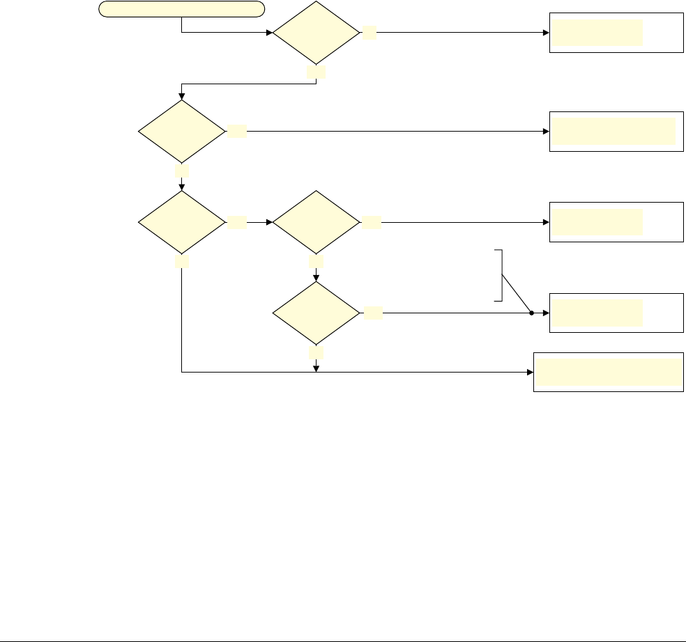
B1 System Level Programmers’ Model
B1.8 Exception handling
B1-1176 Copyright © 1996-1998, 2000, 2004-2012, 2014 ARM. All rights reserved. ARM DDI 0406C.c
Non-Confidential ID051414
•The mode to which the Virtual Abort exception is taken on page B1-1180
•Determining the mode to which the IRQ exception is taken on page B1-1180
•The mode to which the Virtual IRQ exception is taken on page B1-1180
•Determining the mode to which the FIQ exception is taken on page B1-1181
•The mode to which the Virtual FIQ exception is taken on page B1-1181.
These descriptions also show the vector offset for the exception entry for each mode.
For more information about:
• vector offsets, see Exception vectors and the exception base address on page B1-1165
• the routing of external aborts, IRQ and FIQ exceptions, and the virtual exceptions, see Asynchronous
exception routing controls on page B1-1175.
Determining the mode to which the Undefined Instruction exception is taken
Figure B1-3 shows how the implementation, state, and configuration options determine the mode to which an
Undefined Instruction exception is taken.
Figure B1-3 The mode the Undefined Instruction exception is taken to
Undefined Instruction exception
State is
Secure
?
Taken from
Hyp mode
?
Yes
No
HCR.TGE
== 1
?
Non-secure Undefined mode,
vector offset 0x04
Hyp mode,
vector offset 0x04
Hyp mode,
vector offset 0x14
Have
Security
Extensions
?
Undefined mode,
vector offset 0x04
No
Have
Virtualization
Extensions
?
YesYes
No
Yes
Secure Undefined mode,
vector offset 0x04
No
No
Yes
From User mode only. The
effect of executing in a PL1
mode with HCR.TGE set to
1 is UNPREDICTABLE.
B1 System Level Programmers’ Model
B1.8 Exception handling
ARM DDI 0406C.c Copyright © 1996-1998, 2000, 2004-2012, 2014 ARM. All rights reserved. B1-1177
ID051414 Non-Confidential
Determining the mode to which the Supervisor Call exception is taken
Figure B1-4 shows how the implementation, state, and configuration options determine the mode to which a
Supervisor Call exception is taken.
Figure B1-4 The mode the Supervisor Call exception is taken to
The mode to which the Secure Monitor Call exception is taken
The Secure Monitor Call exception is supported only as part of the Security Extensions. A Secure Monitor Call
exception is taken to Monitor mode, using vector offset
0x08
from the Monitor exception base address.
Note
An
SMC
instruction that is trapped to Hyp mode because HCR.TSC is set to 1 generates a Hyp Trap exception, see
The mode to which the Hyp Trap exception is taken on page B1-1178.
The mode to which the Hypervisor Call exception is taken
The Hypervisor Call exception is supported only as part of the Virtualization Extensions. A Hypervisor Call
exception is taken to Hyp mode, using a vector offset that depends on the mode from which the exception is taken,
as Figure B1-5 shows. This offset is from the Hyp exception base address.
Figure B1-5 The mode the Hypervisor Call exception is taken to
Supervisor Call exception
State is
Secure
?
Taken from
Hyp mode
?
Yes
No
HCR.TGE
== 1
?
Non-secure Supervisor mode,
vector offset 0x08
Hyp mode,
vector offset 0x08
Hyp mode,
vector offset 0x14
Have
Security
Extensions
?
Supervisor mode,
vector offset 0x08
No
Have
Virtualization
Extensions
?
Yes
No
Secure Supervisor mode,
vector offset 0x08
No
Yes
Yes
No
Yes
From User mode only. The
effect of executing in a PL1
mode with HCR.TGE set to
1 is
UNPREDICTABLE
.
Hypervisor Call exception
Hyp mode,
vector offset 0x14
Taken from
Hyp mode
?
Hyp mode,
vector offset 0x08
Yes
No
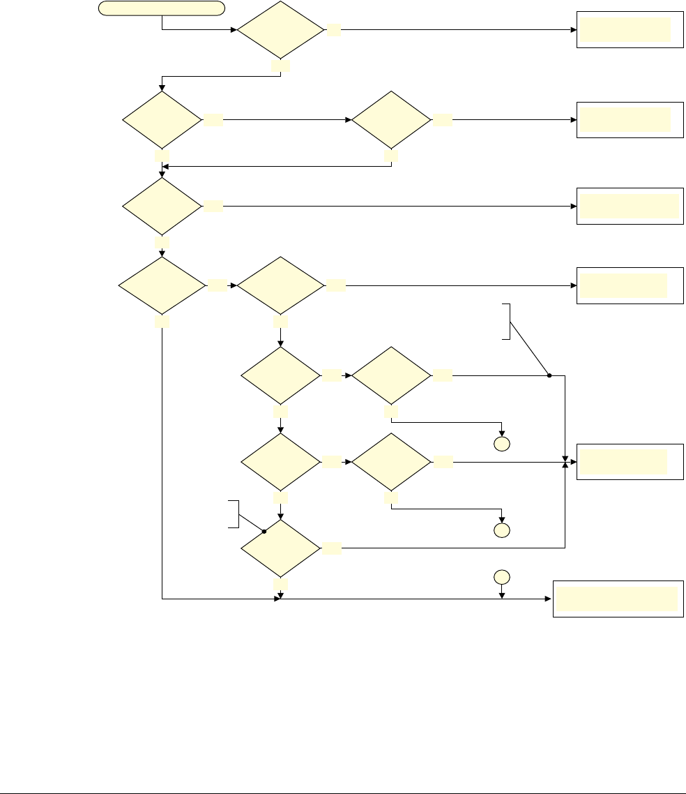
B1 System Level Programmers’ Model
B1.8 Exception handling
B1-1178 Copyright © 1996-1998, 2000, 2004-2012, 2014 ARM. All rights reserved. ARM DDI 0406C.c
Non-Confidential ID051414
The mode to which the Hyp Trap exception is taken
The Hyp Trap exception is supported only as part of the Virtualization Extensions. A Hyp Trap exception is taken
to Hyp mode, using a vector offset of
0x14
from the Hyp exception base address.
Determining the mode to which the Prefetch Abort exception is taken
Figure B1-6 shows how the implementation, state, and configuration options determine the mode to which a
Prefetch Abort exception is taken.
Figure B1-6 The mode the Prefetch Abort exception is taken to
Prefetch Abort exception
External
abort
?
Yes
Hyp mode, vector
offset 0x0C
Monitor mode,
vector offset 0x0C
SCR.EA
== 1
?
Yes
Debug
exception
?
HDCR.TDE
== 1
?
Stage 2
abort
?
On address
translation
Have
Security
Extensions
?
No Abort mode,
vector offset 0x0C
State is
Secure
?
Secure Abort mode,
vector offset 0x0C
1
Taken from
Hyp mode
?
No
Yes
Have
Virtualization
Extensions
?
Yes
No
No
Yes Hyp mode, vector
offset 0x14
Yes
Yes
Non-secure Abort mode,
vector offset 0x0C
Yes
No
1
No
Yes
No
Yes
1
No
From User mode only. The effect of
executing in a PL1 mode with
HCR.TGE set to 1 is
UNPREDICTABLE
.
HCR.TGE
== 1
?
External
abort
?
Yes
No
No
No
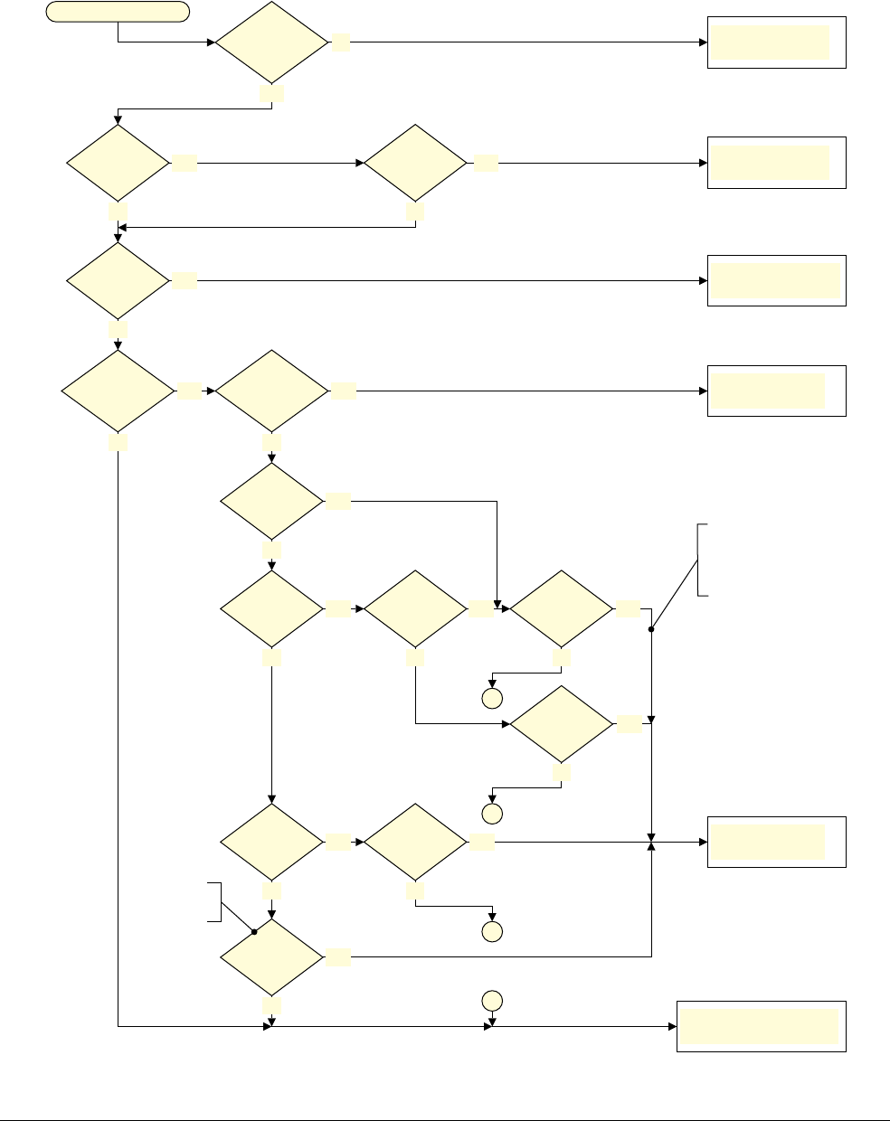
B1 System Level Programmers’ Model
B1.8 Exception handling
ARM DDI 0406C.c Copyright © 1996-1998, 2000, 2004-2012, 2014 ARM. All rights reserved. B1-1179
ID051414 Non-Confidential
Determining the mode to which the Data Abort exception is taken
Figure B1-7 shows how the implementation, state, and configuration options determine the mode to which a Data
Abort exception is taken.
Figure B1-7 The mode the Data Abort exception is taken to
Data Abort exception
External
abort
?
Yes
Hyp mode, vector
offset 0x10
Monitor mode,
vector offset 0x10
SCR.EA
== 1
?
Yes
Debug
exception
?
HDCR.TDE
== 1
?
Stage 2
abort
?
On address
translation
Have
Security
Extensions
?
No Abort mode,
vector offset 0x10
State is
Secure
?
Secure Abort mode,
vector offset 0x10
No
Taken from
Hyp mode
?
Yes
Have
Virtualization
Extensions
?
Yes
Alignment
fault
?
Yes
Yes
Non-secure Abort mode,
vector offset 0x10
Yes
Yes
No
Yes
No
No
Hyp mode, vector
offset 0x14
Yes
1
No
HCR.AMO
== 1
?
Yes
No
1
1
No
No
No
External
abort
?
HCR.TGE
== 1
?
Yes Synchronous
?
Yes Yes
From User mode only. The
effect of executing in a PL1
mode with HCR.TGE set to
1 is
UNPREDICTABLE
.
No
No
No
No
1
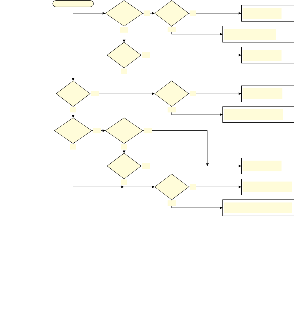
B1 System Level Programmers’ Model
B1.8 Exception handling
B1-1180 Copyright © 1996-1998, 2000, 2004-2012, 2014 ARM. All rights reserved. ARM DDI 0406C.c
Non-Confidential ID051414
The mode to which the Virtual Abort exception is taken
The Virtual Abort exception is supported only as part of the Virtualization Extensions. A Virtual Abort exception is
taken from a Non-secure PL1 or PL0 mode, and is taken to Non-secure Abort mode, using a vector offset of
0x10
from the Non-secure exception base address.
For more information about this exception see Virtual exceptions in the Virtualization Extensions on page B1-1197.
Determining the mode to which the IRQ exception is taken
Figure B1-8 shows how the implementation, state, and configuration options determine the mode to which an IRQ
exception is taken.
Figure B1-8 The mode the IRQ exception is taken to
The mode to which the Virtual IRQ exception is taken
The Virtual IRQ exception is supported only as part of the Virtualization Extensions. A Virtual IRQ exception is
taken from a Non-secure PL1 or PL0 mode, and is taken to Non-secure IRQ mode, using a vector offset of
0x18
from
the Non-secure exception base address.
For more information about this exception see Virtual exceptions in the Virtualization Extensions on page B1-1197.
Yes
State is
Secure
?
IRQ exception Have
Security
Extensions
?
No
No
IRQ mode,
vector offset 0x18
SCTLR.VE
== 1
?
Yes
IRQ mode, vector is
IMPLEMENTATION
DEFINED
SCTLR.VE
== 1
?
Secure IRQ mode,
vector offset 0x18
No
Secure IRQ mode, vector is
IMPLEMENTATION
DEFINED
No
No
SCR.IRQ
== 1
?
Monitor mode,
vector offset 0x18
Yes
Yes
Yes
Yes
Taken from
Hyp mode
?
Have
Virtualization
Extensions
?
Yes
HCR.IMO
== 1
?
No
Hyp mode,
vector offset 0x18
Yes
SCTLR.VE
== 1
?
Non-secure IRQ mode,
vector offset 0x18
No
Non-secure IRQ mode, vector is
IMPLEMENTATION
DEFINED
No
No
Yes
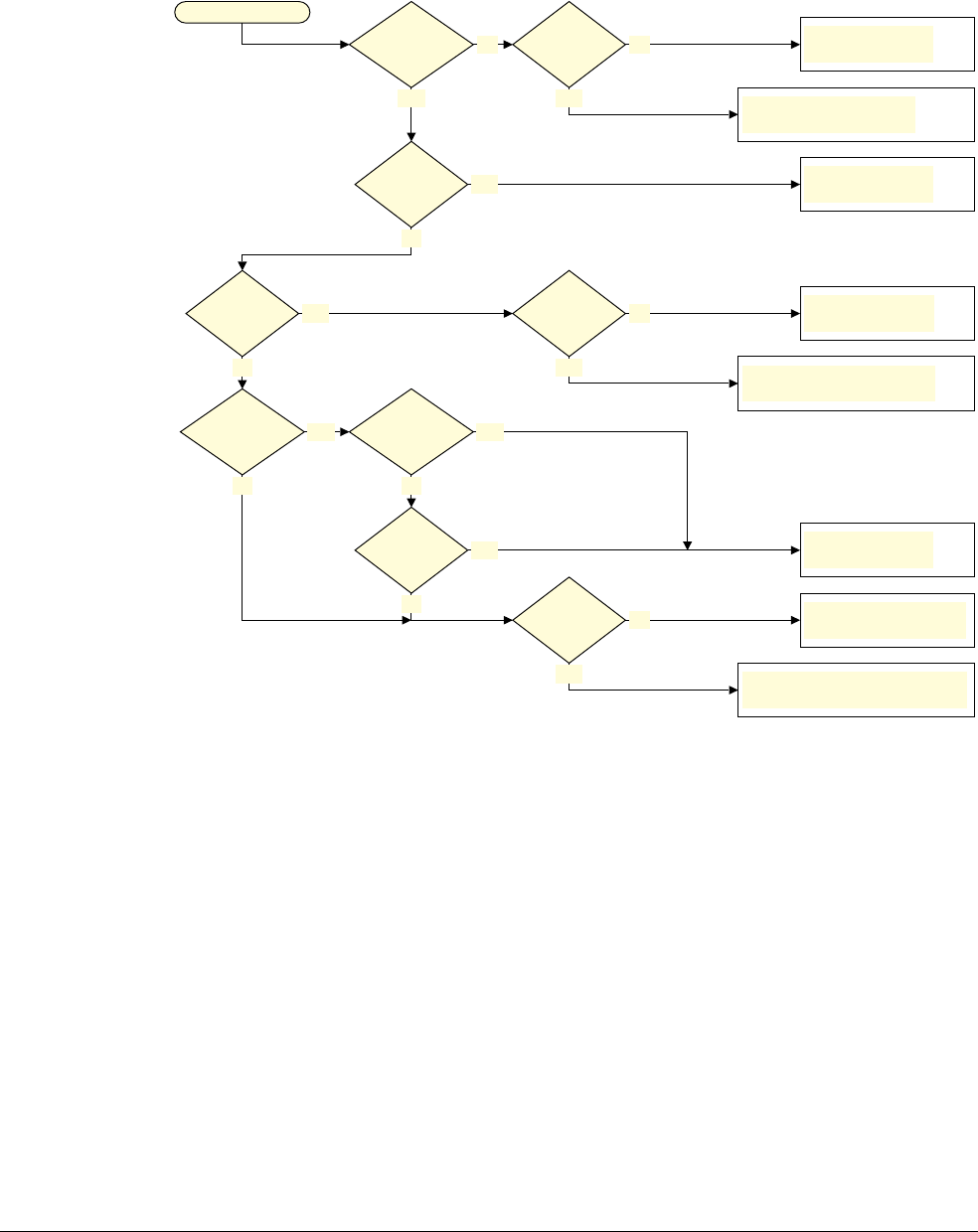
B1 System Level Programmers’ Model
B1.8 Exception handling
ARM DDI 0406C.c Copyright © 1996-1998, 2000, 2004-2012, 2014 ARM. All rights reserved. B1-1181
ID051414 Non-Confidential
Determining the mode to which the FIQ exception is taken
Figure B1-8 on page B1-1180 shows how the implementation, state, and configuration options determine the mode
to which an FIQ exception is taken.
Figure B1-9 The mode the FIQ exception is taken to
The mode to which the Virtual FIQ exception is taken
The Virtual FIQ exception is supported only as part of the Virtualization Extensions. A Virtual FIQ exception is
taken from a Non-secure PL1 or PL0 mode, and is taken to Non-secure FIQ mode, using a vector offset of
0x1C
from
the Non-secure exception base address.
For more information about this exception see Virtual exceptions in the Virtualization Extensions on page B1-1197.
Yes
State is
Secure
?
FIQ exception Have
Security
Extensions
?
No
No
FIQ mode,
vector offset 0x1C
SCTLR.VE
== 1
?
Yes
FIQ mode, vector is
IMPLEMENTATION
DEFINED
SCTLR.VE
== 1
?
Secure FIQ mode,
vector offset 0x1C
No
Secure FIQ mode, vector is
IMPLEMENTATION
DEFINED
Yes
Taken from
Hyp mode
?
Have
Virtualization
Extensions
?
Yes
No
HCR.FMO
== 1
?
Hyp mode,
vector offset 0x1C
No
Yes
SCTLR.VE
== 1
?
Non-secure FIQ mode,
vector offset 0x1C
No
Non-secure FIQ mode, vector is
IMPLEMENTATION
DEFINED
No
No
SCR.FIQ
== 1
?
Monitor mode,
vector offset 0x1C
Yes
Yes
Yes
No
Yes

B1 System Level Programmers’ Model
B1.8 Exception handling
B1-1182 Copyright © 1996-1998, 2000, 2004-2012, 2014 ARM. All rights reserved. ARM DDI 0406C.c
Non-Confidential ID051414
B1.8.5 Processor state on exception entry
The description of each exception includes a pseudocode description of entry to that exception, as Table B1-5 on
page B1-1171 shows. The following sections describe the processor state changes on entering an exception, for
different processor implementations and operating states. However, you must always see the exception entry
pseudocode for a full description of the state changes on exception entry:
•Instruction set state on exception entry
•CPSR.E bit value on exception entry
•CPSR.{A, I, F, M} values on exception entry on page B1-1183.
Instruction set state on exception entry
Exception handlers always execute in either Thumb state or ARM state, as Table B1-8 shows. On exception entry,
CPSR.{T, J} are set to the values shown, with the CPSR.T value determined by SCTLR.TE or HSCTLR.TE,
depending on the mode the exception is taken to:
When an implementation includes the Security Extensions, SCTLR is Banked for Secure and Non-secure states, and
therefore the TE bit value might be different for Secure and Non-secure states. For an exception taken to a Secure
or Non-secure PL1 mode, the SCTLR.TE bit for the security state to which the exception is taken determines the
instruction set state for the exception handler. This means the PL1 exception handlers might run in different
instruction set states, depending on the security state.
CPSR.E bit value on exception entry
The CPSR.E bit controls the load and store endianness for data handling. On exception entry, this bit is set as
Table B1-9 shows:
For more information, see the bit description in Format of the CPSR and SPSRs on page B1-1148.
Table B1-8 CPSR.J and CPSR.T bit values on exception entry
Exception mode HSCTLR.TE SCTLR.TE CPSR.J CPSR.T Exception handler state
Secure or Non-secure PL1 x 0 0 0 ARM
1 0 1 Thumb
Hyp 0 x 00ARM
1 x 0 1 Thumb
Table B1-9 CPSR.E bit value on exception entry
Exception mode HSCTLR.EE SCTLR.EE Endianness for data loads and stores CPSR.E
Secure or Non-secure PL1 x 0 Little-endian 0
1Big-endian 1
Hyp 0 x Little-endian 0
1 x Big-endian 1

B1 System Level Programmers’ Model
B1.8 Exception handling
ARM DDI 0406C.c Copyright © 1996-1998, 2000, 2004-2012, 2014 ARM. All rights reserved. B1-1183
ID051414 Non-Confidential
CPSR.{A, I, F, M} values on exception entry
On exception entry, CPSR.M is set to the value for the mode to which the exception is taken, as described in
Processor mode for taking exceptions on page B1-1173.
Table B1-10 shows the cases where CPSR.{A, I, F} bits are set to 1 on an exception entry, and how this depends on
the mode and security state to which an exception is taken. If the table entry for a particular mode and security state
does not define a value for a CPSR.{A, I, F} bit then that bit is unchanged by the exception entry. In this table:
• The Exception mode column is the mode to which the exception is taken.
• The Non-secure, no Virtualization Extensions column applies to exceptions taken to Non-secure state in an
implementation that includes the Security Extensions but not the Virtualization Extensions.
• The All others column applies to:
— implementations that do not include the Security Extensions
— exceptions taken to Secure state
— exceptions taken to Non-secure state in an implementation that includes the Virtualization Extensions.
Note
Compared to an implementation that includes only the Security Extensions, implementing the Virtualization
Extensions changes both the effects of the SCR.{AW, FW} bits and the interpretation of the CPSR.{A, F} bits.
Asynchronous exception masking on page B1-1184 summarizes the behavior for both of these implementation
options.
Table B1-10 CPSR.{A, I, F} values on exception entry
Exception mode Security state and implementation
Non-secure, no Virtualization Extensions All others
Hyp - If SCR.EA==0 then CPSR.A is set to 1
If SCR.IRQ==0 then CPSR.I is set to 1
If SCR.FIQ==0 then CPSR.F is set to 1
Monitor - CPSR.A is set to 1
CPSR.I is set to 1
CPSR.F is set to 1
FIQ If SCR.AW==1 then CPSR.A is set to 1
CPSR.I is set to 1
If SCR.FW==1 then CPSR.F is set to 1
CPSR.A is set to 1
CPSR.I is set to 1
CPSR.F is set to 1
IRQ, Abort If SCR.AW==1 then CPSR.A is set to 1
CPSR.I is set to 1
CPSR.A is set to 1
CPSR.I is set to 1
Undefined, Supervisor CPSR.I is set to 1 CPSR.I is set to 1

B1 System Level Programmers’ Model
B1.8 Exception handling
B1-1184 Copyright © 1996-1998, 2000, 2004-2012, 2014 ARM. All rights reserved. ARM DDI 0406C.c
Non-Confidential ID051414
B1.8.6 Asynchronous exception masking
The CPSR.{A, I, F} bits can mask the corresponding exceptions, as follows:
•CPSR.A can mask asynchronous aborts
•CPSR.I can mask IRQ exceptions
•CPSR.F can mask FIQ exceptions.
In an ARMv7 implementation that does not include the Security Extensions, setting one of these bits to 1 masks the
corresponding exception, meaning the exception cannot be taken.
In an implementation that includes the Security Extensions, the SCR.{AW, FW} bits provide a mechanism to
prevent use of the CPSR.{A, F} mask bits by Non-secure software. In an implementation that includes the
Virtualization Extensions:
•HCR.{AMO, FMO} modify this mechanism
•HCR.IMO can prevent the masking, by CPSR.I, of IRQs taken from Non-secure state.
This means the asynchronous exception masking mechanism is as follows:
Implementation that includes the Security Extensions but not the Virtualization Extensions
When an SCR.{AW, FW} bit is set to 0, Non-secure software cannot update the corresponding
CPSR bit. This means:
•when SCR.AW is set to 0, CPSR.A cannot be updated in Non-secure state
•when SCR.FW is set to 0, CPSR.F cannot be updated in Non-secure state.
Note
There is no control of updates to CPSR.I. CPSR.I can be updated in either security state.
The CPSR.{A, I, F} bits mask the corresponding exceptions. This means:
•when CPSR.A is set to 1, asynchronous aborts are masked
•when CPSR.I is set to 1, IRQs are masked
•when CPSR.F is set to 1, FIQs are masked.
Implementation that includes the Security Extensions and the Virtualization Extensions
When an HCR.{AMO, IMO, FMO} mask override bit is set to 1, the value of the corresponding
CPSR.{A, I, F} bit is ignored when both of the following apply:
• the exception is taken from Non-secure state
•either:
— the corresponding SCR.{EA, IRQ, FIQ} bit routes the exception to Monitor mode
— the exception is taken from a Non-secure mode other than Hyp mode.
In addition, when an SCR.{AW, FW} bit is set to 0, the value of the corresponding CPSR.{A, F}
bit is ignored when all of the following apply:
• the exception is taken from Non-secure state
• the corresponding SCR.{EA, FIQ} bit routes the exception to Monitor mode
• the corresponding HCR.{AMO, FMO} mask override bit is set to 0.
This means that the controls on each of the CPSR mask bits, and the effect of those bits, are as shown
in the following tables.

B1 System Level Programmers’ Model
B1.8 Exception handling
ARM DDI 0406C.c Copyright © 1996-1998, 2000, 2004-2012, 2014 ARM. All rights reserved. B1-1185
ID051414 Non-Confidential
Table B1-11 shows the controls of the masking of asynchronous exceptions by CPSR.A.
Table B1-12 shows the controls of the masking of FIQ exceptions by CPSR.F:
Table B1-13 shows the controls of the masking of FIQ exceptions by CPSR.F:
The values of SCR.{AW, FW} do not affect whether CPSR.{A, F} can be updated in Non-secure
state.
Mask override bits in the Virtualization Extensions on page B1-1186 gives more information about
the HCR.{AMO, IMO, FMO} bits.
Table B1-11 Control of masking by CPSR.A
Security state HCR.AMO SCR.EA SCR.AW Mode CPSR.A
Secure x x x x Masks asynchronous aborts, when set to 1
Non-secure 0 0 x x Masks asynchronous aborts, when set to 1
1 0 x Ignored
1 x Masks asynchronous aborts, when set to 1
1 x x Not Hyp Ignored
0 x Hyp Masks asynchronous aborts, when set to 1
1 x x Ignored
Table B1-12 Control of masking by CPSR.I
Security state HCR.IMO SCR.IRQ Mode CPSR.I
Secure x x x Masks IRQs, when set to 1
Non-secure 0 x x Masks IRQs, when set to 1
1 x Not Hyp Ignored
0 Hyp Masks IRQs, when set to 1
1 x Ignored
Table B1-13 Control of masking by CPSR.F
Security state HCR.FMO SCR.FIQ SCR.FW Mode CPSR.F
Secure x x x x Masks FIQs, when set to 1
Non-secure 0 0 x x Masks FIQs, when set to 1
1 0 x Ignored
1 x Masks FIQs, when set to 1
1 x x Not Hyp Ignored
0 x Hyp Masks FIQs, when set to 1
1 x x Ignored

B1 System Level Programmers’ Model
B1.8 Exception handling
B1-1186 Copyright © 1996-1998, 2000, 2004-2012, 2014 ARM. All rights reserved. ARM DDI 0406C.c
Non-Confidential ID051414
Mask override bits in the Virtualization Extensions
The Virtualization Extensions add a set of mask override bits to the HCR, that affect both:
• the masking of asynchronous exceptions taken from Non-secure state
• the enabling of the corresponding virtual exceptions.
These mask bits and their effects are:
•HCR.AMO can affect the masking of asynchronous aborts, and the enabling of Virtual Abort exceptions
•HCR.IMO can affect the masking of IRQ exceptions, and the enabling of Virtual IRQ exceptions
•HCR.FMO can affect the masking of FIQ exceptions, and the enabling of Virtual FIQ exceptions.
These bits can also affect the routing of the corresponding physical exceptions, see Asynchronous exception routing
controls on page B1-1175.
The HCR mask override bits have no effect on exceptions taken to Secure state.
If an HCR mask override bit is set to 1, when the processor is in Non-secure state and not in Hyp mode:
• If the corresponding physical exception is not routed to Monitor mode, the physical exception is taken to Hyp
mode.
• When the corresponding CPSR mask bit is set to 1 it:
— masks the corresponding virtual exception
— does not mask the corresponding physical exception.
• If the corresponding virtual exception bit in the HCR is set to 1, and the corresponding CPSR mask bit is not
set to 1, the virtual exception is signaled to the processor.
When the processor is in Hyp mode, if an HCR mask override bit is set to 1 the corresponding CPSR mask bit cannot
mask the corresponding physical exception if that exception is routed to Monitor mode.
Note
When the processor is in Hyp mode:
• physical asynchronous exceptions that are not routed to Monitor mode are taken to Hyp mode
• virtual exceptions are not signaled to the processor.
B1.8.7 Summaries of asynchronous exception behavior
In an ARMv7 implementation that does not include the Security Extensions, the asynchronous exceptions behave
as follows:
• an asynchronous abort is taken to Abort mode
• an IRQ exception is taken to IRQ mode
• an FIQ exception is taken to FIQ mode.
The Security Extensions and Virtualization Extensions introduce controls that affect:
• the routing of these exceptions, see Asynchronous exception routing controls on page B1-1175
• masking of these exceptions in Non-secure state, see Asynchronous exception masking on page B1-1184.
This section summarizes the effect of these controls, for each of the asynchronous exceptions. Because the
Virtualization Extensions change the behavior of some of the Security Extensions controls, it gives separate
summaries for implementations that include and do not include the Virtualization Extensions.

B1 System Level Programmers’ Model
B1.8 Exception handling
ARM DDI 0406C.c Copyright © 1996-1998, 2000, 2004-2012, 2014 ARM. All rights reserved. B1-1187
ID051414 Non-Confidential
Note
• In an implementation that includes the Security Extensions but does not include the Virtualization
Extensions, the following configurations permit the Non-secure state to deny service to the Secure state.
Therefore, ARM recommends that, wherever possible, these configurations are not used:
— Setting SCR.IRQ to 1. With this configuration, Non-secure PL1 software can set CPSR.I to 1, denying
the required routing of IRQs to Monitor mode.
— Setting SCR.FW to 1 when SCR.FIQ is set to 1. With this configuration, Non-secure PL1 software can
set CPSR.F to 1, denying the required routing of FIQs to Monitor mode.
The changes introduced by the Virtualization Extensions remove these possible denials of service.
• Interrupts driven by Secure peripherals are called Secure interrupts. When SCR.FW = 0 and SCR.FIQ = 1,
FIQ exceptions can be used as Secure interrupts. These enter Secure state in a deterministic way.
The following subsections summarize the behavior of asynchronous exceptions:
•Asynchronous exception behavior, Security Extensions only
•Asynchronous exception behavior, with the Virtualization Extensions on page B1-1188
Asynchronous exception behavior, Security Extensions only
The following subsections describe the behavior of each of the asynchronous exceptions, in an implementation that
includes the Security Extensions but not the Virtualization Extensions:
•Behavior of asynchronous aborts, Virtualization Extensions not implemented
•Behavior of IRQ exceptions, Virtualization Extensions not implemented on page B1-1188
•Behavior of FIQ exceptions, Virtualization Extensions not implemented on page B1-1188.
Behavior of asynchronous aborts, Virtualization Extensions not implemented
Table B1-14 shows how SCR.{AW, EA} control asynchronous abort behavior.
Note
The values of SCR.EA and CPSR.A have no effect on the behavior of asynchronous watchpoints.
Table B1-14 Behavior of asynchronous aborts, Virtualization Extensions not implemented
SCR.EA SCR.AW Effect on asynchronous abort behavior
0 0 Asynchronous aborts are taken to Abort mode.
If CPSR.A is set to 1 it masks asynchronous aborts in all states and modes.
CPSR.A can be modified in Secure PL1 modes, but cannot be modified in Non-secure PL1 modes.
0 1 Asynchronous aborts are taken to Abort mode.
If CPSR.A is set to 1 it masks asynchronous aborts in all states and modes.
CPSR.A can be modified in Secure and Non-secure PL1 modes.
1 0 Asynchronous aborts are taken to Monitor mode.
If CPSR.A is set to 1 it masks asynchronous aborts in all states and modes.
CPSR.A can be modified in Secure PL1 modes, but cannot be modified in Non-secure PL1 modes.
1 1 Asynchronous aborts are taken to Monitor mode.
If CPSR.A is set to 1 it masks asynchronous aborts in all states and modes.
CPSR.A can be modified in Secure and Non-secure PL1 modes.

B1 System Level Programmers’ Model
B1.8 Exception handling
B1-1188 Copyright © 1996-1998, 2000, 2004-2012, 2014 ARM. All rights reserved. ARM DDI 0406C.c
Non-Confidential ID051414
Behavior of IRQ exceptions, Virtualization Extensions not implemented
Table B1-15 shows how SCR.IRQ controls IRQ exception behavior.
Behavior of FIQ exceptions, Virtualization Extensions not implemented
Table B1-16 shows how SCR.{FIQ, FW} control FIQ exception behavior.
Asynchronous exception behavior, with the Virtualization Extensions
The following subsections describe the behavior of each of the asynchronous exceptions, in an implementation that
includes both the Security Extensions and the Virtualization Extensions:
•Behavior of asynchronous aborts when an implementation includes the Virtualization Extensions on
page B1-1189
•Behavior of IRQ exceptions when an implementation includes the Virtualization Extensions on page B1-1190
•Behavior of FIQ exceptions when an implementation includes the Virtualization Extensions on
page B1-1191.
These summaries include the behavior of the virtual exceptions. See Virtual exceptions in the Virtualization
Extensions on page B1-1197 for more information about these exceptions. To distinguish them from the virtual
exceptions, the asynchronous aborts defined for an ARMv7 implementation that does not include the Virtualization
Extensions are described as physical aborts. That is, they are described as physical asynchronous aborts, physical
IRQs, and physical FIQs.
Table B1-15 Behavior of IRQ exceptions, Virtualization Extensions not implemented
SCR.IRQ Effect on IRQ exception behavior
0 IRQ exceptions are taken to IRQ mode.
If CPSR.I is set to 1 it masks IRQs in all states and modes.
1 IRQ exceptions are taken to Monitor mode.
If CPSR.I is set to 1 it masks IRQs in all states and modes.
Table B1-16 Behavior of FIQ exceptions, Virtualization Extensions not implemented
SCR.FIQ SCR.FW Effect on FIQ exception behavior
0 0 FIQ exceptions are taken to FIQ mode.
If CPSR.F is set to 1 it masks FIQs in all states and modes.
CPSR.F can be modified in Secure PL1 modes, but cannot be modified in Non-secure PL1 modes.
0 1 FIQ exceptions are taken to FIQ mode.
If CPSR.F is set to 1 it masks FIQs in all states and modes.
CPSR.F can be modified in Secure and Non-secure PL1 modes.
1 0 FIQ exceptions are taken to Monitor mode.
If CPSR.F is set to 1 it masks FIQs in all states and modes.
CPSR.F can be modified in Secure PL1 modes, but cannot be modified in Non-secure PL1 modes.
1 1 FIQ exceptions are taken to Monitor mode.
If CPSR.F is set to 1 it masks FIQs in all states and modes.
CPSR.F can be modified in Secure and Non-secure PL1 modes.

B1 System Level Programmers’ Model
B1.8 Exception handling
ARM DDI 0406C.c Copyright © 1996-1998, 2000, 2004-2012, 2014 ARM. All rights reserved. B1-1189
ID051414 Non-Confidential
Note
As stated in Vectored interrupt support on page B1-1168, the Virtualization Extensions do not support the vectoring
of IRQ or FIQ exceptions that are routed to Hyp mode. Therefore, if at least one of HCR.IMO and HCR.FMO is set
to 1, the processor behaves as if the Non-secure SCTLR.VE bit is set to 0, regardless of the actual value of that bit.
Behavior of asynchronous aborts when an implementation includes the Virtualization Extensions
Table B1-17 shows how SCR.{AW, EA} and HCR.AMO control asynchronous abort behavior in an
implementation that includes the Virtualization Extensions. In such an implementation, CPSR.A can be modified in
Secure and Non-secure PL1 modes and in Hyp mode, regardless of the value of SCR.AW.
Table B1-17 Behavior of asynchronous aborts, Virtualization Extensions implemented
SCR.EA SCR.AW HCR.AMO Effect on asynchronous abort behavior
0 x 0 Physical asynchronous aborts are taken to:
• Abort mode, if taken from a PL0 or PL1 mode
• Hyp mode, if taken from Hyp mode.
HCR.VA, the Virtual asynchronous abort bit, has no effect, and Virtual asynchronous aborts
are masked.
If CPSR.A is set to 1 it masks physical asynchronous aborts in all states and modes.
0 x 1 Physical asynchronous aborts are taken to:
• Secure Abort mode if taken from a Secure mode
• Hyp mode if taken from a Non-secure mode.
If HCR.VA is set to 1 and the processor is in a Non-secure PL1 or PL0 mode, a virtual
asynchronous abort is signaled to the processor.
If CPSR.A is set to 1:
• in Secure state or in Hyp mode, physical asynchronous aborts are masked
• in a Non-secure PL1 or PL0 mode:
— virtual asynchronous aborts are masked
— physical asynchronous aborts are not masked.
1 0 0 Physical asynchronous aborts are taken to Monitor mode.
HCR.VA, the Virtual asynchronous abort bit, has no effect, and Virtual asynchronous aborts
are masked.
If CPSR.A is set to 1:
• in Secure state, physical asynchronous aborts are masked
• in Non-secure state, physical asynchronous aborts are not masked.
1 x 1 Physical asynchronous aborts are taken to Monitor mode.
If HCR.VA is set to 1 and the processor is in a Non-secure PL1 or PL0 mode, a virtual
asynchronous abort is signaled to the processor.
If CPSR.A is set to 1:
• in Secure state, physical asynchronous aborts are masked
• in Non-secure state:
— physical asynchronous aborts are not masked
— in PL1 and PL0 modes, virtual asynchronous aborts are masked.
1 1 0 Physical asynchronous aborts are taken to Monitor mode.
HCR.VA, the Virtual asynchronous abort bit, has no effect.
If CPSR.A is set to 1 it masks physical asynchronous aborts in all states and modes.

B1 System Level Programmers’ Model
B1.8 Exception handling
B1-1190 Copyright © 1996-1998, 2000, 2004-2012, 2014 ARM. All rights reserved. ARM DDI 0406C.c
Non-Confidential ID051414
Behavior of IRQ exceptions when an implementation includes the Virtualization Extensions
Table B1-18 shows how SCR.IRQ and HCR.IMO control IRQ exception behavior, in an implementation that
includes the Virtualization Extensions.
Table B1-18 Behavior of IRQ exceptions, Virtualization Extensions implemented
SCR.IRQ HCR.IMO Effect on IRQ exception behavior
0 0 Physical IRQs are taken to:
• IRQ mode, if taken from a PL0 or PL1 mode
• Hyp mode, if taken from Hyp mode.
HCR.VI, the Virtual IRQ bit, has no effect, and Virtual IRQs are masked.
If CPSR.I is set to 1 it masks IRQs in all states and modes.
0 1 Physical IRQs are taken to:
• Secure IRQ mode if taken from a Secure mode
• Hyp mode if taken from a Non-secure mode.
If HCR.VI is set to 1 and the processor is in a Non-secure PL1 or PL0 mode, a virtual IRQ is signaled to
the processor.
If CPSR.I is set to 1:
• in Secure state or in Hyp mode, physical IRQs are masked
• in a Non-secure PL1 or PL0 mode:
— virtual IRQs are masked
— physical IRQs are not masked.
1 0 Physical IRQs are taken to Monitor mode.
HCR.VI, the Virtual IRQ bit, has no effect, and Virtual IRQs are masked.
If CPSR.I is set to 1 it masks physical IRQs in all states and modes.
1 1 Physical IRQs are taken to Monitor mode.
If HCR.VI is set to 1 and the processor is in a Non-secure PL1 or PL0 mode, a virtual IRQ is signaled to
the processor.
If CPSR.I is set to 1:
• in Secure state, physical IRQs are masked
• in Non-secure state:
— physical IRQs are not masked
— in PL1 and PL0 modes, virtual IRQs are masked.

B1 System Level Programmers’ Model
B1.8 Exception handling
ARM DDI 0406C.c Copyright © 1996-1998, 2000, 2004-2012, 2014 ARM. All rights reserved. B1-1191
ID051414 Non-Confidential
Behavior of FIQ exceptions when an implementation includes the Virtualization Extensions
Table B1-19 shows how SCR.{FIQ, FW} and HCR.FMO control FIQ exception behavior, in an implementation that
includes the Virtualization Extensions. In such an implementation, CPSR.F can be modified in Secure and
Non-secure PL1 modes and in Hyp mode, regardless of the value of SCR.FW.
Table B1-19 Behavior of FIQ exceptions, Virtualization Extensions implemented
SCR.FIQ SCR.FW HCR.FMO Effect on FIQ exception behavior
0 x 0 Physical FIQs are taken to:
• FIQ mode, if taken from a PL1 or PL0 mode
• Hyp mode, if taken from Hyp mode.
HCR.VF, the Virtual FIQ bit, has no effect, and Virtual FIQs are masked.
If CPSR.F is set to 1 it masks FIQs in all states and modes.
0x1aPhysical FIQs are taken to:
• Secure FIQ mode if taken from a Secure mode
• Hyp mode if taken from a Non-secure mode.
If HCR.VF is set to 1 and the processor is in a Non-secure PL1 or PL0 mode, a virtual FIQ
is signaled to the processor.
If CPSR.F is set to 1:
• in Secure state or in Hyp mode, physical FIQs are masked
• in a Non-secure PL1 or PL0 mode:
— virtual FIQs are masked
— physical FIQs are not masked.
1 0 0 Physical FIQs are taken to Monitor mode.
HCR.VF, the Virtual FIQ bit, has no effect, and Virtual FIQs are masked.
If CPSR.F is set to 1:
• in Secure state, physical FIQs are masked
• in Non-secure state, physical FIQs are not masked.
1x1aPhysical FIQs are taken to Monitor mode.
If HCR.VF is set to 1 and the processor is in a Non-secure PL1 or PL0 mode, a virtual FIQ
is signaled to the processor.
If CPSR.F is set to 1:
• in Secure state, physical FIQs are masked
• in Non-secure state:
— physical FIQs are not masked
— in PL1 and PL0 modes, virtual FIQs are masked.
1 1 0 Physical FIQs are taken to Monitor mode.
HCR.VF, the Virtual FIQ bit, has no effect.
If CPSR.F is set to 1 it masks physical FIQs in all states and modes.
a. Only if NSACR.RFR is set to 0. If NSACR.RFR is set to 1, the processor behaves as if HCR.FMO is set to 0.

B1 System Level Programmers’ Model
B1.8 Exception handling
B1-1192 Copyright © 1996-1998, 2000, 2004-2012, 2014 ARM. All rights reserved. ARM DDI 0406C.c
Non-Confidential ID051414
B1.8.8 Routing general exceptions to Hyp mode
Note
The routing provided by setting HCR.TGE to 1 permits applications that run in User mode to run on a hypervisor,
in Hyp mode, without a Guest OS running in a Non-secure PL1 mode. Many UNPREDICTABLE definitions associated
with setting HCR.TGE to 1 are based on this usage model.
When HCR.TGE is set to 1, and the processor is in Non-secure User mode, the following exceptions are taken to
Hyp mode, instead of to the default Non-secure mode for handling the exception:
• Undefined Instruction exceptions.
• Supervisor Call exceptions.
• Synchronous External aborts.
• Any Alignment fault other than an alignment fault caused by the memory type when SCTLR.M is 1.
Note
If SCTLR.M and HCR.TGE are both 1 then behavior is UNPREDICTABLE.
The following sections give more information about the behavior when each of these exceptions is routed in this
way:
•Undefined Instruction exception, when HCR.TGE is set to 1
•Supervisor Call exception, when HCR.TGE is set to 1
•Synchronous external abort, when HCR.TGE is set to 1 on page B1-1193
•Alignment fault, when HCR.TGE is set to 1 on page B1-1193.
The effect of executing in any of the following states with HCR.TGE set to 1 is UNPREDICTABLE:
• In a Non-secure PL1 mode.
• In Non-secure User mode if either:
—SCTLR.M is set to 1.
— One or more of HDCR.{TDE, TDA, TDRA, TDOSA} is set to 0.
Undefined Instruction exception, when HCR.TGE is set to 1
When HCR.TGE is set to 1, if the processor is executing in Non-secure User mode and attempts to execute an
UNDEFINED instruction, it takes the Hyp Trap exception, instead of an Undefined Instruction exception. On taking
the Hyp Trap exception, the HSR reports an unknown reason for the exception, using the EC value
0x00
. For more
information see Use of the HSR on page B3-1424.
Supervisor Call exception, when HCR.TGE is set to 1
When HCR.TGE is set to 1, if the processor executes an
SVC
instruction in Non-secure User mode, the Supervisor
Call exception generated by the instruction is taken to Hyp mode.
The HSR reports that entry to Hyp mode was because of a Supervisor Call exception, and:
•If the
SVC
is unconditional, takes for the
imm16
value in the HSR:
— A zero-extended 8-bit immediate value for the Thumb
SVC
instruction.
Note
The only Thumb encoding for
SVC
is a 16-bit instruction encoding.
— The bottom16 bits of the immediate value for the ARM
SVC
instruction.
•If the
SVC
is conditional, the
imm16
value in the HSR is UNKNOWN.

B1 System Level Programmers’ Model
B1.8 Exception handling
ARM DDI 0406C.c Copyright © 1996-1998, 2000, 2004-2012, 2014 ARM. All rights reserved. B1-1193
ID051414 Non-Confidential
If the
SVC
is conditional, the processor takes the exception only if it passes its condition code check.
The HSR reports the exception as a Supervisor Call exception taken to Hyp mode, using the EC value
0x11
. For
more information, see Use of the HSR on page B3-1424.
Note
The effect of setting HCR.TGE to 1 is to route the Supervisor Call exception to Hyp mode, not to trap the execution
of the
SVC
instruction. This means that the preferred return address for the exception, when routed to Hyp mode in
this way, is the instruction after the
SVC
instruction.
Synchronous external abort, when HCR.TGE is set to 1
When HCR.TGE is set to 1, and SCR.EA is set to 0, if the processor is executing in Non-secure User mode and
attempts to execute an instruction that causes a synchronous external abort, it takes the Hyp Trap exception, instead
of a Data Abort or Prefetch Abort exception. On taking the Hyp Trap exception, the HSR indicates whether a Data
Abort exception or a Prefetch Abort exception caused the Hyp Trap exception entry, and presents a valid syndrome
in the HSR.
Note
When SCR.EA is set to 1, external aborts are routed to Secure Monitor mode, and this takes priority over the
HCR.TGE routing. For more information, see Asynchronous exception routing controls on page B1-1175. The
SCR.EA control described in that section applies to both synchronous and asynchronous external aborts.
If an instruction that causes this exception is conditional, the processor takes the exception only if the instruction
passes its condition code check.
The HSR reports the exception either:
• as a Prefetch Abort exception routed to Hyp mode, using the EC value
0x20
• as a Data Abort exception routed to Hyp mode, using the EC value
0x24
.
For more information about the exception reporting, see Use of the HSR on page B3-1424.
Alignment fault, when HCR.TGE is set to 1
When HCR.TGE is set to 1, if the processor is executing in Non-secure User mode, this control applies to an attempt
to execute an instruction that causes an Alignment fault because one or more of the following applies:
•SCTLR.A is set to 1
• the instruction supports only aligned accesses, and is accessing an unaligned address.
•HCR.DC is set to 0 and SCTLR.M is set to 0, so all memory accesses are Strongly-Ordered, and unaligned
accesses to strongly-ordered memory cause alignment faults.
Unaligned data access on page A3-108 summarizes the Alignment faults that are trapped.
In these cases, the attempted execution generates a Hyp Trap exception, instead of a Data Abort exception. When
the Hyp Trap exception is taken, the HSR reports that a Data Abort caused the Hyp Trap exception entry, and
presents a valid syndrome.
When the Non-secure SCTLR.M bit is set to 1, enabling the Non-secure PL1&0 stage 1 MMU, an
otherwise-permitted unaligned access to Device or Strongly-ordered memory generates an Alignment fault.
However, having HCR.TGE set to 1 when SCTLR.M is set to 1 is generally UNPREDICTABLE.
If an instruction that causes this exception is conditional, the processor takes the exception only if the instruction
passes its condition code check.
The HSR reports the exception as a Data Abort routed to Hyp mode, using the EC value
0x24
, see Use of the HSR
on page B3-1424.

B1 System Level Programmers’ Model
B1.8 Exception handling
B1-1194 Copyright © 1996-1998, 2000, 2004-2012, 2014 ARM. All rights reserved. ARM DDI 0406C.c
Non-Confidential ID051414
B1.8.9 Routing Debug exceptions to Hyp mode
When HDCR.TDE is set to 1, if the processor is executing in a Non-secure mode other than Hyp mode, any Debug
exception is routed to Hyp mode. This means it generates a Hyp Trap exception. This applies to:
• Debug exceptions associated with instruction fetch, that would otherwise generate a Prefetch Abort
exception. These are exceptions generated by the Breakpoint, BKPT instruction, and Vector catch debug
events, see Debug exception on BKPT instruction, Breakpoint, or Vector catch debug events on
page C4-2090.
• Debug exceptions associated with data accesses, that would otherwise generate a Data Abort exception.
These are exceptions generated by the Watchpoint debug event, see Debug exception on Watchpoint debug
event on page C4-2091.
When HDCR.TDE is set to 1, the HDCR.{TDRA, TDOSA, TDA} bits must all be set to 1, otherwise behavior is
UNPREDICTABLE. See also Permitted combinations of HDCR.{TDRA, TDOSA, TDA, TDE} bits on page B1-1261.
Note
• A debug event generates a debug exception only when invasive debug is enabled and Monitor debug-mode
is selected, see About debug exceptions on page C4-2090. When Halting debug-mode is selected, a debug
event causes Debug state entry and cannot be trapped to Hyp mode.
• When HDCR.TDE is set to 1, the Hyp Trap exception is generated instead of the Prefetch Abort exception
or Data Abort exception that is otherwise generated by the Debug exception.
• Debug exceptions, other than the exception on the
BKPT
instruction, are not permitted in Hyp mode.
When a Hyp Trap exception is generated because HDCR.TDE is set to 1, The HSR reports the exception either:
• as a Prefetch Abort exception routed to Hyp mode, using the EC value
0x20
• as a Data Abort exception routed to Hyp mode, using the EC value
0x24
.
For more information see Use of the HSR on page B3-1424.
B1.8.10 Exception return
In the ARM architecture, exception return requires the simultaneous restoration of the PC and CPSR to values that
are consistent with the desired state of execution on returning from the exception. Typically, exception return
involves returning to one of:
• the instruction after the instruction boundary at which an asynchronous exception was taken
• the instruction following an
SVC
,
SMC
, or
HMC
instruction, for an exception generated by one of those
instructions
• the instruction that caused the exception, after the reason for the exception has been removed
• the subsequent instruction, if the instruction that caused the exception has been emulated in the exception
handler.
The ARM architecture defines a preferred return address for each exception other than Reset, see Link values saved
on exception entry on page B1-1172. The values of the SPSR.IT[7:0] bits generated on exception entry are always
correct for this preferred return address, but might require adjustment by the exception handler if returning
elsewhere.
In some cases, to calculate the appropriate preferred return address, a subtraction must be performed on the link
value saved on taking the exception. The description of each exception includes any value that must be subtracted
from the link value, and other information about the required exception return.

B1 System Level Programmers’ Model
B1.8 Exception handling
ARM DDI 0406C.c Copyright © 1996-1998, 2000, 2004-2012, 2014 ARM. All rights reserved. B1-1195
ID051414 Non-Confidential
On an exception return, the CPSR takes either:
• the value loaded by the
RFE
instruction
• if the exception return is not performed by executing an
RFE
instruction, the value of the current SPSR at the
time of the exception return
Where the exception return is UNPREDICTABLE, the implementation can adjust the value loaded into the CPSR, to
avoid a security hole, or other undesirable behavior. For example:
• In an implementation that includes the Security Extensions, if the processor is in a Non-secure PL1 mode,
and one of the following applies:
— The restored CPSR.M value is
0b10110
, the value for Monitor mode.
—NSACR.RFR is set to 1, and the restored CPSR.M value is
0b10001
, the value for FIQ mode.
Note
When NSACR.RFR is set to 1, FIQ mode is reserved for Secure operation.
— If the implementation includes the Virtualization Extensions, and the restored CPSR.M value is
0b11010
, the value for Hyp mode.
In this case, CPSR.M takes an UNKNOWN value that does not correspond to any of:
— Hyp mode
— Monitor mode
—if NSACR.RFR is set to 1, FIQ mode.
• In an implementation that includes the Virtualization Extensions, if the processor is in the Non-secure PL2
mode and one of the following applies:
— the restored CPSR.M value is
0b10110
, the value for Monitor mode
—NSACR.RFR is set to 1 and the restored CPSR.M value is
0b10001
, the value for FIQ mode.
In this case, CPSR.M takes an UNKNOWN value that does not correspond to either:
— Monitor mode
—if NSACR.RFR is set to 1, FIQ mode.
• In an implementation that includes the Virtualization Extensions, if SCR.NS is set to 0 and the restored
CPSR.M value is
0b11010
, the value for Hyp mode.
In this case, CPSR.M takes an UNKNOWN value that does not correspond to Hyp mode.
•If the new CPSR.{J, T} bits correspond to an unsupported instruction set, including an instruction set that is
not supported in the mode of operation that applies immediately after the exception return, the CPSR.{J, T}
bits might be set to values that correspond to a supported instruction set. For more information see Exception
return to an unimplemented instruction set state on page B1-1197.
An example of where this might happen is a return to Hyp mode with CPSR.{J, T} set to {1, 1}, the values
for ThumbEE.
•If the new CPSR.IT bits correspond to a reserved value then CPSR.IT might be set to a permitted UNKNOWN
value. For more information see IT block state register, ITSTATE on page A2-51.
Exception return instructions
The instructions that an exception handler can use to return from an exception depend on whether the exception was
taken to a PL1 mode, or in a PL2 mode, see:
•Return from an exception taken to a PL1 mode on page B1-1196
•Return from an exception taken to a PL2 mode on page B1-1196.
Note
The Thumb exception return instructions are all UNPREDICTABLE if executed in ThumbEE state.

B1 System Level Programmers’ Model
B1.8 Exception handling
B1-1196 Copyright © 1996-1998, 2000, 2004-2012, 2014 ARM. All rights reserved. ARM DDI 0406C.c
Non-Confidential ID051414
Return from an exception taken to a PL1 mode
For an exception taken to a PL1 mode, the ARM architecture provides the following exception return instructions:
• Data-processing instructions with the S bit set and the PC as a destination, see SUBS PC, LR (Thumb) on
page B9-2010 and SUBS PC, LR and related instructions (ARM) on page B9-2012.
Typically:
— a return where no subtraction is required uses
SUBS
with an operand of 0, or the equivalent
MOVS
instruction
— a return requiring subtraction uses
SUBS
with a nonzero operand.
• From ARMv6, the
RFE
instruction, see RFE on page B9-2000. If a subtraction is required, typically it is
performed before saving the LR value to memory.
• In ARM state, a form of the
LDM
instruction, see LDM (exception return) on page B9-1986. If a subtraction is
required, typically it is performed before saving the LR value to memory.
Return from an exception taken to a PL2 mode
For an exception taken to a PL2 mode, the ARM architecture provides the
ERET
instruction, see ERET on
page B9-1982. An exception handler executing in a PL2 mode must return using the
ERET
instruction.
Hyp mode is the only PL2 mode. Both Hyp mode and the
ERET
instruction are implemented only as part of the
Virtualization Extensions.
Alignment of exception returns
The {J, T} bits of the value transferred to the CPSR by an exception return control the target instruction set of that
return. The behavior of the hardware for exception returns for different values of the {J, T} bits is as follows:
{J, T} == 00 The target instruction set state is ARM state. Bits[1:0] of the address transferred to the PC are
ignored by the hardware.
{J, T} == 01 The target instruction set state is Thumb state:
• bit[0] of the address transferred to the PC is ignored by the hardware
• bit[1] of the address transferred to the PC is part of the instruction address.
{J, T} == 10 The target instruction set state is Jazelle state. In a non-trivial implementation of the Jazelle
extension, bits[1:0] of the address transferred to the PC are part of the instruction address. For the
behavior in a trivial implementation of the Jazelle extension, see Exception return to an
unimplemented instruction set state on page B1-1197. For details of the trivial implementation see
Trivial implementation of the Jazelle extension on page B1-1245.
{J, T} == 11 The target instruction set state is ThumbEE state:
• bit[0] of the address transferred to the PC is ignored by the hardware
• bit[1] of the address transferred to the PC is part of the instruction address.
ARM deprecates any dependence on the requirements that the hardware ignores bits of the address. ARM
recommends that the address transferred to the PC for an exception return is correctly aligned for the target
instruction set.
After an exception entry other than Reset, the LR value has the correct alignment for the instruction set indicated
by the SPSR.{J, T} bits. This means that if exception return instructions are used with the LR and SPSR values
produced by such an exception entry, the only precaution software needs to take to ensure correct alignment is that
any subtraction is of a multiple of four if returning to ARM state, or a multiple of two if returning to Thumb state
or to ThumbEE state.

B1 System Level Programmers’ Model
B1.8 Exception handling
ARM DDI 0406C.c Copyright © 1996-1998, 2000, 2004-2012, 2014 ARM. All rights reserved. B1-1197
ID051414 Non-Confidential
Exception return to an unimplemented instruction set state
An implementation that does not support one or both of Jazelle and ThumbEE states does not normally get into an
unimplemented instruction set state, because:
• on a trivial Jazelle implementation, the
BXJ
instruction acts as a
BX
instruction
• on an implementation that does not include ThumbEE support, the
ENTERX
instruction is UNDEFINED
• normal exception entry and return preserves the instruction set state.
However, on some implementations, an exception return instruction might set CPSR.{J. T} to the values
corresponding to an unimplemented instruction set state, see Unimplemented instruction sets on page B1-1155. This
is most likely to happen because a faulty exception handler restores the wrong value to the CPSR.
If the processor attempts to execute an instruction while the CPSR.{J, T} bits indicate an unimplemented instruction
set state, an Undefined Instruction exception is taken. This happens if either:
•CPSR.J == 1 and CPSR.T == 1, and the processor does not support ThumbEE state
•CPSR.J == 1 and CPSR.T == 0, and the processor does not support Jazelle state.
The Undefined Instruction exception handler can detect the cause of this exception because on entry to the handler
the SPSR.{J, T} bits indicate the unimplemented instruction set state. If the Undefined Instruction exception handler
wants to return to a valid instruction set state it can change the values its exception return instruction writes to the
CPSR.{J, T} bits.
If an exception return writes CPSR.{J, T} values that correspond to an unimplemented instruction set state, and also
writes the address of an aborting memory location to the PC, it is IMPLEMENTATION DEFINED whether:
• the instruction fetch is attempted, and a Prefetch Abort exception is taken because the memory access aborts
• an Undefined Instruction exception is taken, without the instruction being fetched.
If an exception return writes CPSR.{J, T} values that correspond to an unimplemented instruction set, the width of
the instruction fetch is an IMPLEMENTATION DEFINED value that is 1, 2 or 4 bytes.
An implementation that supports neither of the Jazelle and ThumbEE states can implement the J bits of the PSRs as
RAZ/WI. On such an implementation, a return to an unimplemented instruction set state cannot occur.
B1.8.11 Virtual exceptions in the Virtualization Extensions
The Virtualization Extensions introduce three virtual exceptions, that correspond to the physical asynchronous
exceptions:
• Virtual Abort, that corresponds to a physical external asynchronous abort
• Virtual IRQ, that corresponds to a physical IRQ
• Virtual FIQ, that corresponds to a physical FIQ.
When the corresponding HCR.{AMO, IMO, FMO} bit is set to 1, a virtual exception is generated either:
• By setting a virtual interrupt pending, HCR.{VA, VI, VF}, to 1.
• For a Virtual IRQ or Virtual FIQ, by an IMPLEMENTATION DEFINED mechanism. This might be a signal from
an interrupt controller, for example from a Virtual GIC, as defined by the ARM Generic Interrupt Controller
Architecture Specification.
A virtual exception is taken only from a Non-secure PL1 or PL0 mode. In any other mode, if the exception is
generated it is not taken.
A virtual exception is taken to Non-secure state in the default mode for the corresponding physical exception. This
means:
• a Virtual Abort is taken to Non-secure Abort mode
• a Virtual IRQ is taken to Non-secure IRQ mode
• a Virtual FIQ is taken to Non-secure FIQ mode.

B1 System Level Programmers’ Model
B1.8 Exception handling
B1-1198 Copyright © 1996-1998, 2000, 2004-2012, 2014 ARM. All rights reserved. ARM DDI 0406C.c
Non-Confidential ID051414
Table B1-20 summarizes the HCR bits that route asynchronous exceptions to Hyp mode, and the bits that generate
the virtual exceptions.
The HCR.{AMO, IMO, FMO} bits route the corresponding physical exception to Hyp mode only if the physical
exception is not routed to Monitor mode by the SCR.{EA, IRQ, FIQ} bit. Similarly, the HCR.{VA, VI, VF} bits
generate a virtual exception only if set to 1 when the corresponding HCR.{AMO, IMO, FMO} is set to 1. For more
information, see Asynchronous exception behavior, with the Virtualization Extensions on page B1-1188.
When an HCR.{AMO, IMO, FMO} control bit is set to 1, the corresponding mask bit in the CPSR:
• does not mask the physical exception
• masks the virtual exception, if the processor is executing in a Non-secure PL1 or PL0 mode.
Taking a Virtual Abort exception clears HCR.VA to zero. Taking a Virtual IRQ exception or a Virtual FIQ exception
does not affect the value of HCR.VI or HCR.VF.
Note
This means that the exception handler for a Virtual IRQ exception or a Virtual FIQ exception must cause software
executing in Hyp mode, or in Monitor mode, to update the HCR to clear the appropriate virtual exception bit to 0.
See WFE wake-up events on page B1-1201 and Wait For Interrupt on page B1-1203 for information about how
virtual exceptions affect wake up from power-saving states.
Note
A hypervisor can use virtual exceptions to signal exceptions to the current Guest OS. The Guest OS takes a virtual
exception exactly as it would take the corresponding physical exception, and is unaware of any distinction between
virtual exceptions and the corresponding physical exceptions.
B1.8.12 Low interrupt latency configuration
Setting SCTLR.FI to 1 enables the low interrupt latency configuration of an implementation. This configuration can
reduce the interrupt latency of the processor. The mechanisms implemented to achieve low interrupt latency are
IMPLEMENTATION DEFINED. For the description of the SCTLR see either:
•SCTLR, System Control Register, VMSA on page B4-1707
•SCTLR, System Control Register, PMSA on page B6-1932.
In an implementation that includes the Virtualization Extensions, the HSCTLR.FI bit is a RO bit that indicates the
current value of SCTLR.FI.
To ensure that a change between normal and low interrupt latency configurations is synchronized correctly, the
SCTLR.FI bit must be changed only in IMPLEMENTATION DEFINED circumstances. The FI bit can be changed shortly
after reset, with interrupts disabled, and before enabling any MMU, MPU, or cache, using the following sequence:
DSB
ISB
MCR p15, 0, Rx, c1, c0, c0 ; change FI bit in the SCTLR
DSB
ISB
An implementation can define other sequences and circumstances that permit the SCTLR.FI bit to be changed.
Table B1-20 HCR bits controlling asynchronous exceptions
Exception Routing the physical exception to Hyp mode Generating the virtual exception
Asynchronous abort HCR.AMO HCR.VA
IRQ HCR.IMO HCR.VI
FIQ HCR.FMO HCR.VF

B1 System Level Programmers’ Model
B1.8 Exception handling
ARM DDI 0406C.c Copyright © 1996-1998, 2000, 2004-2012, 2014 ARM. All rights reserved. B1-1199
ID051414 Non-Confidential
Note
• Examples of methods that might be implemented to reduce interrupt latency are:
— disabling Hit-Under-Miss functionality in a processor
— the abandoning of restartable external accesses.
These choices permit the processor to react to a pending interrupt faster than would otherwise be the case.
• Reducing interrupt latency can result in reduced performance overall.
A low interrupt latency configuration might permit interrupts and asynchronous aborts to be taken during a sequence
of memory transactions generated by a single load or store instruction. For details of what these sequences are and
the consequences of taking interrupts and asynchronous aborts in this way see Single-copy atomicity on
page A3-128. If the implementation permits interrupts to be taken during an
LDM
or
STM
instruction in this way, those
instructions are described as being restartable.
ARM deprecates any software reliance on the behavior that an interrupt or asynchronous abort cannot occur in a
sequence of memory transactions generated by a single load or store instruction that accesses Normal memory.
Note
A particular case that has shown this reliance is load multiples that load the stack pointer from memory. In an
implementation where an interrupt is taken during the
LDM
, this can corrupt the stack pointer.

B1 System Level Programmers’ Model
B1.8 Exception handling
B1-1200 Copyright © 1996-1998, 2000, 2004-2012, 2014 ARM. All rights reserved. ARM DDI 0406C.c
Non-Confidential ID051414
B1.8.13 Wait For Event and Send Event
ARMv7 and ARMv6K provide a mechanism, the Wait For Event mechanism, that permits a processor in a
multiprocessor system to request entry to a low-power state, and, if the request succeeds, to remain in that state until
it receives an event generated by a Send Event operation on another processor in the system. Example B1-1
describes how a spinlock implementation might use this mechanism to save energy.
Example B1-1 Spinlock as an example of using Wait For Event and Send Event
A multiprocessor operating system requires locking mechanisms to protect data structures from being accessed
simultaneously by multiple processors. These mechanisms prevent the data structures becoming inconsistent or
corrupted if different processors try to make conflicting changes. If a lock is busy, because a data structure is being
used by one processor, it might not be practical for another processor to do anything except wait for the lock to be
released. For example, if a processor is handling an interrupt from a device it might need to add data received from
the device to a queue. If another processor is removing data from the queue, it will have locked the memory area
that holds the queue. The first processor cannot add the new data until the queue is in a consistent state and the lock
has been released. It cannot return from the interrupt handler until the data has been added to the queue, so it must
wait.
Typically, a spin-lock mechanism is used in these circumstances:
• A processor requiring access to the protected data attempts to obtain the lock using single-copy atomic
synchronization primitives such as the Load-Exclusive and Store-Exclusive operations described in
Synchronization and semaphores on page A3-114.
• If the processor obtains the lock it performs its memory operation and releases the lock.
• If the processor cannot obtain the lock, it reads the lock value repeatedly in a tight loop until the lock becomes
available. At this point it again attempts to obtain the lock.
A spin-lock mechanism is not ideal for all situations:
• in a low-power system the tight read loop is undesirable because it uses energy to no effect
• in a multi-threaded processor the execution of spin-locks by waiting threads can significantly degrade overall
performance.
Using the Wait For Event and Send Event mechanism can improve the energy efficiency of a spinlock. In this
situation, a processor that fails to obtain a lock can execute a Wait For Event instruction,
WFE
, to request entry to a
low-power state. When a processor releases a lock, it must execute a Send Event instruction,
SEV
, causing any
waiting processors to wake up. Then, these processors can attempt to gain the lock again.
The Virtualization Extensions provide a bit that traps to Hyp mode any attempt to enter a low-power state from a
Non-secure PL1 or PL0 mode. For more information see Trapping use of the WFI and WFE instructions on
page B1-1256.
The architecture does not define the exact nature of the low power state, but the execution of a
WFE
instruction must
not cause a loss of memory coherency.
Note
Although a complex operating system can contain thousands of distinct locks, the event sent by this mechanism does
not indicate which lock has been released. If the event relates to a different lock, or if another processor acquires the
lock more quickly, the processor fails to acquire the lock and can re-enter the low-power state waiting for the next
event.
The Wait For Event system relies on hardware and software working together to achieve energy saving:
• the hardware provides the mechanism to enter the Wait For Event low-power state

B1 System Level Programmers’ Model
B1.8 Exception handling
ARM DDI 0406C.c Copyright © 1996-1998, 2000, 2004-2012, 2014 ARM. All rights reserved. B1-1201
ID051414 Non-Confidential
• the operating system software is responsible for issuing:
— a Wait For Event instruction, to request entry to the low-power state, used in the example when waiting
for a spin-lock
— a Send Event instruction, required in the example when releasing a spin-lock.
The mechanism depends on the interaction of:
• WFE wake-up events, see WFE wake-up events
• the Event Register, see The Event Register
• the Send Event instruction, see The Send Event instruction on page B1-1202
• the Wait For Event instruction, see The Wait For Event instruction on page B1-1202.
WFE wake-up events
The following events are WFE wake-up events:
• the execution of an
SEV
instruction on any processor in the multiprocessor system
• a physical IRQ interrupt, unless masked by the CPSR.I bit
• a physical FIQ interrupt, unless masked by the CPSR.F bit
• a physical asynchronous abort, unless masked by the CPSR.A bit
• in Non-secure state in any mode other than Hyp mode:
— when HCR.IMO is set to 1, a virtual IRQ interrupt, unless masked by the CPSR.I bit
— when HCR.FMO is set to 1, a virtual FIQ interrupt, unless masked by the CPSR.F bit
— when HCR.AMO is set to 1, a virtual asynchronous abort, unless masked by the CPSR.A bit
• an asynchronous debug event, if invasive debug is enabled and the debug event is permitted
• an event sent by the timer event stream, see Event streams on page B8-1964
• an event sent by some IMPLEMENTATION DEFINED mechanism.
In addition to the possible masking of WFE wake-up events shown in this list, when invasive debug is enabled and
DBGDSCR[15:14] is not set to
0b00
, DBGDSCR.INTdis can mask interrupts, including masking them acting as
WFE wake-up events. For more information, see DBGDSCR, Debug Status and Control Register on
page C11-2243.
As shown in the list of wake-up events, an implementation can include IMPLEMENTATION DEFINED hardware
mechanisms to generate wake-up events.
Note
For more information about CPSR masking see Asynchronous exception masking on page B1-1184. If the
configuration of the masking controls provided by the Security Extensions, or Virtualization Extensions, mean that
a CPSR mask bit cannot mask the corresponding exception, then the physical exception is a WFE wake-up event,
regardless of the value of the CPSR mask bit.
The Event Register
The Event Register is a single bit register for each processor. When set, an event register indicates that an event has
occurred, since the register was last cleared, that might require some action by the processor. Therefore, the
processor must not suspend operation on issuing a
WFE
instruction.
The reset value of the Event Register is UNKNOWN.
The Event Register is set by:
•an
SEV
instruction
• an event sent by some IMPLEMENTATION DEFINED mechanism
• a debug event that causes entry into Debug state
• an exception return.
As shown in this list, the Event Register might be set by IMPLEMENTATION DEFINED mechanisms.

B1 System Level Programmers’ Model
B1.8 Exception handling
B1-1202 Copyright © 1996-1998, 2000, 2004-2012, 2014 ARM. All rights reserved. ARM DDI 0406C.c
Non-Confidential ID051414
The Event Register is cleared only by a Wait For Event instruction.
Software cannot read or write the value of the Event Register directly.
The Send Event instruction
The Send Event instruction,
SEV
, causes an event to be signaled to all processors in the multiprocessor system. The
mechanism that signals the event to the processors is IMPLEMENTATION DEFINED. Hardware does not guarantee the
ordering of this event with respect to the completion of memory accesses by instructions before the
SEV
instruction.
Therefore, ARM recommends that software includes a
DSB
instruction before an
SEV
instruction.
Note
A
DSB
instruction ensures that no instruction, including any
SEV
instruction, that appears in program order after the
DSB
instruction, can execute until the
DSB
instruction has completed. For more information, see Data Synchronization
Barrier (DSB) on page A3-153.
Execution of the Send Event instruction sets the Event Register.
The Send Event instruction is available at all privilege levels, see SEV on page A8-606.
An implementation can merge two or more events sent by two or more instances of SEV execution into a single
write to the event register and a single WFE wake-up event for a processor.
The Wait For Event instruction
The action of the Wait For Event instruction depends on the state of the Event Register:
• If the Event Register is set, the instruction clears the register and completes immediately. Normally, if this
happens the software makes another attempt to claim the lock.
• If the Event Register is clear the processor can suspend execution and enter a low-power state. It can remain
in that state until the processor detects a WFE wake-up event or a reset. When the processor detects a WFE
wake-up event, or earlier if the implementation chooses, the
WFE
instruction completes.
The Wait For Event instruction,
WFE
, is available at all privilege levels, see WFE on page A8-1104.
Software using the Wait For Event mechanism must tolerate spurious wake-up events, including multiple wake ups.
The Virtualization Extensions provide a bit that traps to Hyp mode any attempt to enter a low-power state from a
Non-secure PL1 or PL0 mode. For more information see Trapping use of the WFI and WFE instructions on
page B1-1256.
Pseudocode details of the Wait For Event lock mechanism
This section defines pseudocode functions that describe the operation of the Wait For Event mechanism.
The
ClearEventRegister()
pseudocode procedure clears the Event Register of the current processor.
The
EventRegistered()
pseudocode function returns TRUE if the Event Register of the current processor is set and
FALSE if it is clear:
boolean EventRegistered()
The
WaitForEvent()
pseudocode procedure optionally suspends execution until a WFE wake-up event or reset
occurs, or until some earlier time if the implementation chooses. It is IMPLEMENTATION DEFINED whether restarting
execution after the period of suspension causes a
ClearEventRegister()
to occur.
The
SendEvent()
pseudocode procedure sets the Event Register of every processor in the multiprocessor system.
The
SendEventLocal()
pseudocode procedure sets the Event Register of the processor that executes the
SendEventLocal()
procedure.

B1 System Level Programmers’ Model
B1.8 Exception handling
ARM DDI 0406C.c Copyright © 1996-1998, 2000, 2004-2012, 2014 ARM. All rights reserved. B1-1203
ID051414 Non-Confidential
B1.8.14 Wait For Interrupt
ARMv7 supports Wait For Interrupt through an instruction,
WFI
, that is provided in the ARM and Thumb instruction
sets. For more information, see WFI on page A8-1106.
Note
ARMv7 redefines the CP15 c7 encoding previously used for WFI as UNPREDICTABLE, see Retired operations on
page B3-1499 and Retired operations on page B5-1804.
When a processor issues a
WFI
instruction it can suspend execution and enter a low-power state.
The Virtualization Extensions provide a bit that traps to Hyp mode any attempt to enter a low-power state from a
Non-secure PL1 or PL0 mode. For more information see Trapping use of the WFI and WFE instructions on
page B1-1256.
The processor can remain in the WFI low-power state until it is reset, or it detects one of the following WFI wake-up
events:
• a physical IRQ interrupt, regardless of the value of the CPSR.I bit
• a physical FIQ interrupt, regardless of the value of the CPSR.F bit
• a physical asynchronous abort, regardless of the value of the CPSR.A bit
• in Non-secure state in any mode other than Hyp mode:
— when HCR.IMO is set to 1, a virtual IRQ interrupt, regardless of the value of the CPSR.I bit
— when HCR.FMO is set to 1, a virtual FIQ interrupt, regardless of the value of the CPSR.F bit
— when HCR.AMO is set to 1, a virtual asynchronous abort, regardless of the value of the CPSR.A bit
• an asynchronous debug event, when invasive debug is enabled and the debug event is permitted.
An implementation can include other IMPLEMENTATION DEFINED hardware mechanisms to generate WFI wake-up
events.
When the hardware detects a WFI wake-up event, or earlier if the implementation chooses, the
WFI
instruction
completes.
WFI wake-up events cannot be masked by the mask bits in the CPSR.
The architecture does not define the exact nature of the low power state, but the execution of a
WFI
instruction must
not cause a loss of memory coherency.
Note
• Because debug events are WFI wake-up events, ARM strongly recommends that Wait For Interrupt is used
as part of an idle loop rather than waiting for a single specific interrupt event to occur and then moving
forward. This ensures the intervention of debug while waiting does not significantly change the function of
the program being debugged.
• In some previous implementations of Wait For Interrupt, the idle loop is followed by exit functions that must
be executed before taking the interrupt. The operation of Wait For Interrupt remains consistent with this
model, and therefore differs from the operation of Wait For Event.
• Some implementations of Wait For Interrupt drain down any pending memory activity before suspending
execution. This increases the power saving, by increasing the area over which clocks can be stopped. The
ARM architecture does not require this operation, and software must not rely on Wait For Interrupt operating
in this way.

B1 System Level Programmers’ Model
B1.8 Exception handling
B1-1204 Copyright © 1996-1998, 2000, 2004-2012, 2014 ARM. All rights reserved. ARM DDI 0406C.c
Non-Confidential ID051414
Using WFI to indicate an idle state on bus interfaces
A common implementation practice is to complete any entry into powerdown routines with a
WFI
instruction.
Typically, the
WFI
instruction:
1. Forces the suspension of execution, and of all associated bus activity.
2. Suspends the execution of instructions by the processor.
The control logic required to do this tracks the activity of the bus interfaces of the processor. This means it can signal
to an external power controller that there is no ongoing bus activity.
However, the processor must continue to process memory-mapped and external debug interface accesses to debug
registers when in the WFI state. The indication of idle state to the system normally only applies to the functional
interfaces of the processor, not the debug interfaces.
On an implementation that includes v7.1 Debug, when DBGPRSR.DLK, the OS Double Lock status bit, is set to 1,
the processor must not signal this idle state to the processor unless it can guarantee, also, that the debug interface is
idle. For more information about OS Double Lock, see Permissions in relation to locks on page C6-2120.
Note
In a processor that implements separate core and debug power domains, the debug interface referred to in this
section is the interface between the core and debug power domains, since the signal to the power controller indicates
that the core power domain is idle. For more information about the power domains see Power domains and debug
on page C7-2151.
The exact nature of this interface is IMPLEMENTATION DEFINED, but the use of Wait For Interrupt as the only
architecturally-defined mechanism that completely suspends execution makes it very suitable as the preferred
powerdown entry mechanism.
Pseudocode details of Wait For Interrupt
The
WaitForInterrupt()
pseudocode procedure optionally suspends execution until a WFI wake-up event or reset
occurs, or until some earlier time if the implementation chooses.

B1 System Level Programmers’ Model
B1.9 Exception descriptions
ARM DDI 0406C.c Copyright © 1996-1998, 2000, 2004-2012, 2014 ARM. All rights reserved. B1-1205
ID051414 Non-Confidential
B1.9 Exception descriptions
Exception handling on page B1-1165 gives general information about exception handling. This section describes
each of the exceptions, in the following subsections:
•Reset
•Undefined Instruction exception on page B1-1206
•Hyp Trap exception on page B1-1209
•Supervisor Call (SVC) exception on page B1-1210
•Secure Monitor Call (SMC) exception on page B1-1211
•Hypervisor Call (HVC) exception on page B1-1212
•Prefetch Abort exception on page B1-1213
•Data Abort exception on page B1-1215
•Virtual Abort exception on page B1-1218
•IRQ exception on page B1-1219
•Virtual IRQ exception on page B1-1221
•FIQ exception on page B1-1222
•Virtual FIQ exception on page B1-1223.
Additional pseudocode functions for exception handling on page B1-1224 gives additional pseudocode that is used
in the pseudocode descriptions of a number of the exceptions.
B1.9.1 Reset
On an ARM processor, when the Reset input is asserted the processor stops execution. When Reset is deasserted,
the processor then starts executing instructions:
• in Secure state, if it implements the Security Extensions
• in Supervisor mode, with interrupts disabled.
Reset returns some processor state to architecturally-defined or IMPLEMENTATION DEFINED values, and makes other
state UNKNOWN. For more information see:
• for a VMSAv7 implementation:
—Behavior of the caches at reset on page B2-1269
—Enabling MMUs on page B3-1316
—TLB behavior at reset on page B3-1379
—Reset behavior of CP14 and CP15 registers on page B3-1450
• For a PMSAv7 implementation:
—Behavior of the caches at reset on page B2-1269
—Enabling and disabling the MPU on page B5-1758
—Reset behavior of CP14 and CP15 registers on page B5-1778.
When reset is deasserted, execution starts either:
• From the low or high reset vector address,
0x00000000
or
0xFFFF0000
, as determined by the reset value of the
SCTLR.V bit. This reset value can be determined by an IMPLEMENTATION DEFINED configuration input
signal.
•From an IMPLEMENTATION DEFINED address.
When executions starts, system behavior depends on the reset value of the CPSR, as defined by the
TakeReset()
pseudocode function that is defined later in this section. See also The Current Program Status Register (CPSR) on
page B1-1147.
The ARM architecture does not define any way of returning to a previous execution state from a reset.

B1 System Level Programmers’ Model
B1.9 Exception descriptions
B1-1206 Copyright © 1996-1998, 2000, 2004-2012, 2014 ARM. All rights reserved. ARM DDI 0406C.c
Non-Confidential ID051414
Note
• A Reset exception does not reset the value of all of the debug registers. For more information see Reset and
debug on page C7-2162.
• The ARM architecture does not distinguish between multiple levels of reset. A system can provide multiple
distinct levels of reset that reset different parts of the system. These all correspond to this single reset
exception.
Pseudocode description of taking the Reset exception
The
TakeReset()
pseudocode procedure describes how the processor takes the exception:
// TakeReset()
// ===========
TakeReset()
// Enter Supervisor mode and (if relevant) Secure state, and reset CP15. This affects
// the Banked versions and values of various registers accessed later in the code.
// Also reset other system components.
CPSR.M = '10011'; // Supervisor mode
if HaveSecurityExt() then SCR.NS = '0';
ResetControlRegisters();
if HaveAdvSIMDorVFP() then FPEXC.EN = '0'; SUBARCHITECTURE_DEFINED further resetting;
if HaveThumbEE() then TEECR.XED = '0';
if HaveJazelle() then JMCR.JE = '0'; SUBARCHITECTURE_DEFINED further resetting;
// Further CPSR changes: all interrupts disabled, IT state reset, instruction set
// and endianness according to the SCTLR values produced by the above call to
// ResetControlRegisters().
CPSR.I = '1'; CPSR.F = '1'; CPSR.A = '1';
CPSR.IT = '00000000';
CPSR.J = '0'; CPSR.T = SCTLR.TE; // TE=0: ARM, TE=1: Thumb
CPSR.E = SCTLR.EE; // EE=0: little-endian, EE=1: big-endian
// All registers, bits and fields not reset by the above pseudocode or by the
// BranchTo() call below are UNKNOWN bitstrings after reset. In particular, the
// return information registers R14_svc and SPSR_svc have UNKNOWN values, so that
// it is impossible to return from a reset in an architecturally defined way.
// Branch to Reset vector.
ResetVector[31:1] = if HasIMPDEFResetVactor() then Bits[31:1] IMPLEMENTATION DEFINED else
ExecVectorBase()[31:1];
ResetVector[0] = '0';
BranchTo(ResetVector);
The
HasIMPDEFResetVector()
pseudocode function returns TRUE if the implementation has an IMPLEMENTATION
DEFINED reset vector.
B1.9.2 Undefined Instruction exception
An Undefined Instruction exception might be caused by:
• A coprocessor instruction that is not accessible because of the settings in one or more of:
—the CPACR, see CPACR, Coprocessor Access Control Register, VMSA on page B4-1551, or CPACR,
Coprocessor Access Control Register, PMSA on page B6-1831
— in an implementation that includes the Security Extensions, the NSACR
— in an implementation that includes the Virtualization Extensions, when the processor is in Hyp mode,
the HCPTR.
• A coprocessor instruction that is not implemented.

B1 System Level Programmers’ Model
B1.9 Exception descriptions
ARM DDI 0406C.c Copyright © 1996-1998, 2000, 2004-2012, 2014 ARM. All rights reserved. B1-1207
ID051414 Non-Confidential
• A coprocessor instruction that causes an exception during execution, for example a trapped floating-point
exception on a floating-point instruction, see Floating-point exceptions on page A2-70.
• An instruction that is UNDEFINED.
• An attempt to execute an instruction in an unimplemented instruction set state, see Exception return to an
unimplemented instruction set state on page B1-1197.
• Division by zero in an
SDIV
or
UDIV
instruction, in an ARMv7-R implementation when the SCTLR.DZ bit is
set to 1.
Note
In an ARMv7-A implementation that includes the
SDIV
and
UDIV
instructions, division by zero always returns
a result of zero, see ARMv7 implementation requirements and options for the divide instructions on
page A4-172.
By default, an Undefined Instruction exception is taken to Undefined mode, but an Undefined Instruction exception
can be taken to Hyp mode, see Determining the mode to which the Undefined Instruction exception is taken on
page B1-1176.
The Undefined Instruction exception can provide:
• signaling of:
— an illegal instruction execution
— division by zero errors, in the ARMv7-R profile
• software emulation of a coprocessor in a system that does not have the physical coprocessor hardware
•lazy context switching of coprocessor registers
• general-purpose instruction set extension by software emulation.
In some coprocessor designs, an internal exceptional condition caused by one coprocessor instruction is signaled
asynchronously by refusing to respond to a later coprocessor instruction that belongs to the same coprocessor. In
these circumstances, the Undefined Instruction exception handler must take whatever action is needed to clear the
exceptional condition, and then return to the second coprocessor instruction.
Note
The only mechanism to determine the cause of an Undefined Instruction exception that is taken to Undefined mode
is analysis of the instruction indicated by the return link in the LR on exception entry. Therefore it is important that
a coprocessor only reports exceptional conditions by generating Undefined Instruction exceptions on its own
coprocessor instructions.
The preferred return address for an Undefined Instruction exception is the address of the instruction that generated
the exception. This return is performed as follows:
• If returning from Secure or Non-secure Undefined mode, the exception return uses the SPSR and LR_und
values generated by the exception entry, as follows:
—If SPSR.{J, T} are both 0, indicating that the exception occurred in ARM state, the return uses an
exception return instruction with a subtraction of 4.
—If SPSR.T is 1, indicating that the exception occurred in Thumb state or ThumbEE state, the return
uses an exception return instruction with a subtraction of 2
—If SPSR.J is 1 and SPSR.T is 0, indicating that the exception occurred in Jazelle state, then exception
return is not possible. For more information see Undefined Instruction exception in Jazelle state on
page B1-1209.
• If returning from Hyp mode, the exception return is performed by an
ERET
instruction, using the SPSR and
ELR_hyp values generated by the exception entry.
For more information, see Exception return on page B1-1194.

B1 System Level Programmers’ Model
B1.9 Exception descriptions
B1-1208 Copyright © 1996-1998, 2000, 2004-2012, 2014 ARM. All rights reserved. ARM DDI 0406C.c
Non-Confidential ID051414
Note
If handling the Undefined Instruction exception requires instruction emulation, followed by return to the next
instruction after the instruction that caused the exception, the instruction emulator must use the instruction length
to calculate the correct return address, and to calculate the updated values of the IT bits if necessary.
Pseudocode description of taking the Undefined Instruction exception
The
TakeUndefInstrException()
pseudocode procedure describes how the processor takes the exception:
// TakeUndefInstrException()
// =========================
TakeUndefInstrException()
// Determine return information. SPSR is to be the current CPSR, and LR is to be the
// current PC minus 2 for Thumb or 4 for ARM, to change the PC offsets of 4 or 8
// respectively from the address of the current instruction into the required return
// address offsets of 2 or 4 respectively.
new_lr_value = if CPSR.T == '1' then PC-2 else PC-4;
new_spsr_value = CPSR;
vect_offset = 4;
// Check whether to take exception to Hyp mode
// if in Hyp mode then stay in Hyp mode
take_to_hyp = HaveVirtExt() && HaveSecurityExt() && SCR.NS == '1' && CPSR.M == '11010';
// if HCR.TGE is set, take to Hyp mode through Hyp Trap vector
route_to_hyp = (HaveVirtExt() && HaveSecurityExt() && !IsSecure() && HCR.TGE == '1'
&& CPSR.M == '10000'); // User mode
// if HCR.TGE == '1' and in a Non-secure PL1 mode, the effect is UNPREDICTABLE
return_offset = if CPSR.T == '1' then 2 else 4;
preferred_exceptn_return = new_lr_value - return_offset;
if take_to_hyp then
// Note that whatever called TakeUndefInstrException() will have set the HSR
EnterHypMode(new_spsr_value, preferred_exceptn_return, vect_offset);
elsif route_to_hyp then
// Note that whatever called TakeUndefInstrException() will have set the HSR
EnterHypMode(new_spsr_value, preferred_exceptn_return, 20);
else
// Enter Undefined ('11011') mode, and ensure Secure state if initially in Monitor
// ('10110') mode. This affects the Banked versions of various registers accessed later
// in the code.
if CPSR.M == '10110' then SCR.NS = '0';
CPSR.M = '11011';
// Write return information to registers, and make further CPSR changes:
// IRQs disabled, IT state reset, instruction set and endianness set to
// SCTLR-configured values.
SPSR[] = new_spsr_value;
R[14] = new_lr_value;
CPSR.I = '1';
CPSR.IT = '00000000';
CPSR.J = '0'; CPSR.T = SCTLR.TE; // TE=0: ARM, TE=1: Thumb
CPSR.E = SCTLR.EE; // EE=0: little-endian, EE=1: big-endian
// Branch to Undefined Instruction vector.
BranchTo(ExcVectorBase() + vect_offset);
Additional pseudocode functions for exception handling on page B1-1224 defines the
EnterHypMode()
pseudocode
procedure.

B1 System Level Programmers’ Model
B1.9 Exception descriptions
ARM DDI 0406C.c Copyright © 1996-1998, 2000, 2004-2012, 2014 ARM. All rights reserved. B1-1209
ID051414 Non-Confidential
Undefined Instruction exception in Jazelle state
The architecture does not define any behavior that requires a processor to take an Undefined Instruction exception
when it is operating in Jazelle state. However, on some implementations the processor might take an Undefined
Instruction exception as a result of UNPREDICTABLE behavior, for example attempting instruction execution in
Jazelle state on a possible trivial implementation of the Jazelle extension, see Exception return to an unimplemented
instruction set state on page B1-1197. If the processor takes such an Undefined Instruction exception in Jazelle
state, exception entry sets the LR to an UNKNOWN value.
Conditional execution of undefined instructions
The conditional execution rules described in Conditional execution on page A8-288 apply to all instructions. This
includes undefined instructions and other instructions that would cause entry to the Undefined Instruction
exception.
If such an instruction fails its condition check, the behavior depends on the architecture profile and the potential
cause of entry to the Undefined Instruction exception, as follows:
• In the ARMv7-A profile:
— If the potential cause is the execution of the instruction itself and depends on data values used by the
instruction, the instruction executes as a
NOP
and does not cause an Undefined Instruction exception.
— If the potential cause is the execution of an earlier coprocessor instruction, or the execution of the
instruction itself without dependence on the data values used by the instruction, it is IMPLEMENTATION
DEFINED whether the instruction executes as a
NOP
or causes an Undefined Instruction exception.
An implementation must handle all such cases in the same way.
• In the ARMv7-R profile, the instruction executes as a
NOP
and does not cause an Undefined Instruction
exception.
Note
Before ARMv7, all implementations executed any instruction that failed its condition check as a
NOP
, even if it
would otherwise have caused an Undefined Instruction exception. An Undefined Instruction handler written for
these implementations might assume without checking that the undefined instruction passed its condition check.
Such an Undefined Instruction handler is likely to need rewriting, to check the condition is passed, before it
functions correctly on all ARMv7-A implementations.
Interaction of UNPREDICTABLE and UNDEFINED instruction behavior
If this manual describes an instruction as both UNPREDICTABLE and UNDEFINED then the instruction is
UNPREDICTABLE.
Note
An example of this is where both:
• an instruction, or instruction class, is made UNDEFINED by some general principle, or by a configuration field
• a particular encoding of that instruction or instruction class is specified as UNPREDICTABLE.
B1.9.3 Hyp Trap exception
The Hyp Trap exception is implemented only as part of the Virtualization Extensions.
A Hyp Trap exception is generated if the processor is running in a Non-secure mode other than Hyp mode, and
commits for execution an instruction that is trapped to Hyp mode. Instruction traps are enabled by setting bits to 1
in the HCR, HCPTR, HDCR, or HSTR. For more information see Traps to the hypervisor on page B1-1248.
A Hyp Trap exception is taken to Hyp mode.
The preferred return address for a Hyp Trap exception is the address of the trapped instruction. The exception return
is performed by an
ERET
instruction, using the SPSR and ELR_hyp values generated by the exception entry.

B1 System Level Programmers’ Model
B1.9 Exception descriptions
B1-1210 Copyright © 1996-1998, 2000, 2004-2012, 2014 ARM. All rights reserved. ARM DDI 0406C.c
Non-Confidential ID051414
Note
The SPSR and ELR_hyp values generated on exception entry can be used, without modification, for an exception
return to re-execute the trapped instruction. If the exception handler emulates the trapped instruction, and must
return to the following instruction, the emulation of the instruction must include modifying ELR_hyp, and possibly
updating SPSR_hyp.
For related information, see General information about traps to the hypervisor on page B1-1249.
Pseudocode description of taking the Hyp Trap exception
The
TakeHypTrapException()
pseudocode procedure describes how the processor takes the exception:
// TakeHypTrapException()
// ======================
TakeHypTrapException()
// A Hyp Trap exception is caused by executing an instruction that is trapped to Hyp mode as
// a result of a trap set by a bit in the HCR, HCPTR, HSTR or HDCR. By definition, it can
// only be generated in a Non-secure mode other than Hyp mode.
// Note that, when a Supervisor Call exception is taken to Hyp mode because HCR.TGE==1, this
// is not a trap of the SVC instruction. See the TakeSVCException() pseudocode for this case.
preferred_exceptn_return = if CPSR.T == '1' then PC-4 else PC-8;
new_spsr_value = CPSR;
EnterHypMode(new_spsr_value, preferred_exceptn_return, 20);
Additional pseudocode functions for exception handling on page B1-1224 defines the
EnterHypMode()
pseudocode
procedure.
B1.9.4 Supervisor Call (SVC) exception
The Supervisor Call instruction,
SVC
, requests a supervisor function, causing the processor to enter Supervisor mode.
Typically, the
SVC
instruction is executed to request an operating system function. For more information, see SVC
(previously SWI) on page A8-720.
Note
• In previous versions of the ARM architecture, the
SVC
instruction was called
SWI
, Software Interrupt.
• In an implementation that includes the Virtualization Extensions:
— When an
SVC
instruction is executed in Hyp mode, the Supervisor Call exception is taken to Hyp mode.
For more information see SVC (previously SWI) on page A8-720.
— When the HCR.TGE bit is set to 1, the Supervisor Call exception generated by execution of an
SVC
instruction in Non-secure User mode is routed to Hyp mode. For more information, see Supervisor
Call exception, when HCR.TGE is set to 1 on page B1-1192.
By default, a Supervisor Call exception is taken to Supervisor mode, but a Supervisor Call exception can be taken
to Hyp mode, see Determining the mode to which the Supervisor Call exception is taken on page B1-1177.
The preferred return address for a Supervisor Call exception is the address of the next instruction after the
SVC
instruction. This return is performed as follows:
• if returning from Secure or Non-secure Supervisor mode, the exception return uses the SPSR and LR_svc
values generated by the exception entry, in an exception return instruction without subtraction
• if returning from Hyp mode, the exception return is performed by an
ERET
instruction, using the SPSR and
ELR_hyp values generated by the exception entry.
For more information, see Exception return on page B1-1194.

B1 System Level Programmers’ Model
B1.9 Exception descriptions
ARM DDI 0406C.c Copyright © 1996-1998, 2000, 2004-2012, 2014 ARM. All rights reserved. B1-1211
ID051414 Non-Confidential
Pseudocode description of taking the Supervisor Call exception
The
TakeSVCException()
pseudocode procedure describes how the processor takes the exception:
// TakeSVCException()
// ==================
TakeSVCException()
// Determine return information. SPSR is to be the current CPSR, after changing the IT[]
// bits to give them the correct values for the following instruction, and LR is to be
// the current PC minus 2 for Thumb or 4 for ARM, to change the PC offsets of 4 or 8
// respectively from the address of the current instruction into the required address of
// the next instruction, the SVC instruction having size 2bytes for Thumb or 4 bytes for ARM.
ITAdvance();
new_lr_value = if CPSR.T == '1' then PC-2 else PC-4;
new_spsr_value = CPSR;
vect_offset = 8;
// Check whether to take exception to Hyp mode
// if in Hyp mode then stay in Hyp mode
take_to_hyp = (HaveVirtExt() && HaveSecurityExt() && SCR.NS == '1' && CPSR.M == '11010');
// if HCR.TGE is set to 1, take to Hyp mode through Hyp Trap vector
route_to_hyp = (HaveVirtExt() && HaveSecurityExt() && !IsSecure() && HCR.TGE == '1'
&& CPSR.M == '10000'); // User mode
// if HCR.TGE == '1' and in a Non-secure PL1 mode, the effect is UNPREDICTABLE
preferred_exceptn_return = new_lr_value;
if take_to_hyp then
EnterHypMode(new_spsr_value, preferred_exceptn_return, vect_offset);
elsif route_to_hyp then
EnterHypMode(new_spsr_value, preferred_exceptn_return, 20);
else
// Enter Supervisor ('10011') mode, and ensure Secure state if initially in Monitor
// ('10110') mode. This affects the Banked versions of various registers accessed later
// in the code.
if CPSR.M == '10110' then SCR.NS = '0';
CPSR.M = '10011';
// Write return information to registers, and make further CPSR changes: IRQs disabled,
// IT state reset, instruction set and endianness set to SCTLR-configured values.
SPSR[] = new_spsr_value;
R[14] = new_lr_value;
CPSR.I = '1';
CPSR.IT = '00000000';
CPSR.J = '0'; CPSR.T = SCTLR.TE; // TE=0: ARM, TE=1: Thumb
CPSR.E = SCTLR.EE; // EE=0: little-endian, EE=1: big-endian
// Branch to SVC vector.
BranchTo(ExcVectorBase() + vect_offset);
Additional pseudocode functions for exception handling on page B1-1224 defines the
EnterHypMode()
pseudocode
procedure.
B1.9.5 Secure Monitor Call (SMC) exception
The Secure Monitor Call exception is implemented only as part of the Security Extensions.
The Secure Monitor Call instruction,
SMC
, requests a Secure Monitor function, causing the processor to enter
Monitor mode. For more information, see SMC (previously SMI) on page B9-2002.
Note
• In previous versions of the ARM architecture, the
SMC
instruction was called
SMI
, Software Monitor Interrupt.

B1 System Level Programmers’ Model
B1.9 Exception descriptions
B1-1212 Copyright © 1996-1998, 2000, 2004-2012, 2014 ARM. All rights reserved. ARM DDI 0406C.c
Non-Confidential ID051414
• In an implementation that includes the Virtualization Extensions, when the HCR.TSC bit is set to 1, execution
of an
SMC
instruction in a Non-secure PL1 mode is trapped to Hyp mode, and therefore generates a Hyp Trap
Exception. For more information see Trapping use of the SMC instruction on page B1-1255.
A Secure Monitor Call exception is taken to Monitor mode.
The preferred return address for a Secure Monitor Call exception is the address of the next instruction after the
SMC
instruction. This return is performed using the SPSR and LR_mon values generated by the exception entry, using
an exception return instruction without a subtraction.
For more information, see Exception return on page B1-1194.
Note
The exception handler can return to the
SMC
instruction itself by returning using a subtraction of 4, without any
adjustment to the SPSR.IT[7:0] bits. If it does this, the return occurs, then interrupts or external aborts might occur
and be handled, then the
SMC
instruction is re-executed and another Secure Monitor Call exception occurs.
This relies on:
• the
SMC
instruction being used correctly, either outside an IT block or as the last instruction in an IT block, so
that the SPSR.IT[7:0] bits indicate unconditional execution
• the Secure Monitor Call handler not changing the result of the original conditional execution test for the
SMC
instruction.
Pseudocode description of taking the Secure Monitor Call exception
The
TakeSMCException()
pseudocode procedure describes how the processor takes the exception:
// TakeSMCException()
// ==================
TakeSMCException()
// Determine return information. SPSR is to be the current CPSR, after changing the IT[]
// bits to give them the correct values for the following instruction, and LR is to be
// the current PC minus 0 for Thumb or 4 for ARM, to change the PC offsets of 4 or 8
// respectively from the address of the current instruction into the required address of
// the next instruction (with the SMC instruction always being 4 bytes in length).
ITAdvance();
new_lr_value = if CPSR.T == '1' then PC else PC-4;
new_spsr_value = CPSR;
vect_offset = 8;
// Ensure Secure state if initially in Monitor mode.
// This affects the Banked versions of various registers accessed later in the code.
if CPSR.M == '10110' then SCR.NS = '0';
EnterMonitorMode(new_spsr_value, new_lr_value, vect_offset);
Additional pseudocode functions for exception handling on page B1-1224 defines the
EnterMonitorMode()
pseudocode procedure.
B1.9.6 Hypervisor Call (HVC) exception
The Hypervisor Call exception is implemented only as part of the Virtualization Extensions.
The Hypervisor Call instruction,
HVC
, requests a hypervisor function, causing the processor to enter Hyp mode. For
more information, see HVC on page B9-1984. The instruction generates a Hypervisor Call exception that is taken
to Hyp mode.
The preferred return address for a Hypervisor Call exception is the address of the next instruction after the
HVC
instruction. The exception return is performed by an
ERET
instruction, using the SPSR and ELR_hyp values
generated by the exception entry.

B1 System Level Programmers’ Model
B1.9 Exception descriptions
ARM DDI 0406C.c Copyright © 1996-1998, 2000, 2004-2012, 2014 ARM. All rights reserved. B1-1213
ID051414 Non-Confidential
For more information, see Exception return on page B1-1194.
Executing an
HVC
instruction transfers the immediate argument of the instruction to the HSR. The exception handler
retrieves the argument from the HSR, and therefore does not have to access the original HVC instruction. For more
information see Use of the HSR on page B3-1424.
Pseudocode description of taking the Hypervisor Call exception
The
TakeHVCException()
pseudocode procedure describes how the processor takes the exception:
// TakeHVCException()
// ==================
TakeHVCException()
// Determine return information. SPSR is to be the current CPSR, after changing the IT[]
// bits to give them the correct values for the following instruction, and LR is to be
// the current PC minus 0 for Thumb or 4 for ARM, to change the PC offsets of 4 or 8
// respectively from the address of the current instruction into the required address of
// the next instruction (with the HVC instruction always being 4 bytes in length).
ITAdvance();
preferred_exceptn_return = if CPSR.T == '1' then PC else PC-4;
new_spsr_value = CPSR;
// Enter Hyp mode. HVC pseudocode has checked that use of HVC is valid.
// Required vector offset depends on whether current mode is Hyp mode.
if CPSR.M == '11010' then
EnterHypMode(new_spsr_value, preferred_exceptn_return, 8);
else
EnterHypMode(new_spsr_value, preferred_exceptn_return, 20);
Additional pseudocode functions for exception handling on page B1-1224 defines the
EnterHypMode()
pseudocode
procedure.
B1.9.7 Prefetch Abort exception
A Prefetch Abort exception can be generated by:
• A synchronous memory abort on an instruction fetch.
Note
Asynchronous aborts on instruction fetches are reported using the Data Abort exception, see Data Abort
exception on page B1-1215.
Prefetch Abort exception entry is synchronous to the instruction whose fetch aborted.
For more information about memory aborts see:
—VMSA memory aborts on page B3-1395
—PMSA memory aborts on page B5-1765.
• A Breakpoint, Vector catch or BKPT instruction debug event, see Debug exception on BKPT instruction,
Breakpoint, or Vector catch debug events on page C4-2090.
Note
If an implementation fetches instructions speculatively, it must handle a synchronous abort on such an instruction
fetch by:
• generating a Prefetch Abort exception only if the instruction would be executed in a simple sequential
execution of the program
• ignoring the abort if the instruction would not be executed in a simple sequential execution of the program.

B1 System Level Programmers’ Model
B1.9 Exception descriptions
B1-1214 Copyright © 1996-1998, 2000, 2004-2012, 2014 ARM. All rights reserved. ARM DDI 0406C.c
Non-Confidential ID051414
By default, a Prefetch Abort exception is taken to Abort mode, but a Prefetch Abort exception can be taken to
Monitor mode, or Hyp mode. For more information, see Determining the mode to which the Prefetch Abort
exception is taken on page B1-1178.
The preferred return address for a Prefetch Abort exception is the address of the aborted instruction. This return is
performed as follows:
• If returning from a PL1 mode, using the SPSR and LR values generated by the exception entry, using an
exception return instruction with a subtraction of 4. This means using:
— SPSR_abt and LR_abt if returning from Abort mode
— SPSR_mon and LR_mon if returning from Monitor mode.
• If returning from Hyp mode, using the SPSR_hyp and ELR_hyp values generated by the exception entry,
using an
ERET
instruction.
For more information, see Exception return on page B1-1194.
Pseudocode description of taking the Prefetch Abort exception
The
TakePrefetchAbortException()
pseudocode procedure describes how the processor takes the exception:
// TakePrefetchAbortException()
// ============================
TakePrefetchAbortException()
// Determine return information. SPSR is to be the current CPSR, and LR is to be the
// current PC minus 0 for Thumb or 4 for ARM, to change the PC offsets of 4 or 8
// respectively from the address of the current instruction into the required address
// of the current instruction plus 4.
new_lr_value = if CPSR.T == '1' then PC else PC-4;
new_spsr_value = CPSR;
vect_offset = 12;
preferred_exceptn_return = new_lr_value - 4;
// Determine whether this is an external abort to be routed to Monitor mode.
route_to_monitor = HaveSecurityExt() && SCR.EA == '1' && IsExternalAbort();
// Check whether to take exception to Hyp mode
// if in Hyp mode then stay in Hyp mode
take_to_hyp = HaveVirtExt() && HaveSecurityExt() && SCR.NS == '1' && CPSR.M == '11010';
// otherwise, check whether to take to Hyp mode through Hyp Trap vector
route_to_hyp = (HaveVirtExt() && HaveSecurityExt() && !IsSecure() &&
(SecondStageAbort() ||
(DebugException() && HDCR.TDE == '1' && CPSR.M != '11010') ||
(IsExternalAbort() && !IsAsyncAbort() && HCR.TGE == '1'
&& CPSR.M == '10000'))); // User mode
// if HCR.TGE == '1' and in a Non-secure PL1 mode, the effect is UNPREDICTABLE
if route_to_monitor then
// Ensure Secure state if initially in Monitor ('10110') mode. This affects
// the Banked versions of various registers accessed later in the code.
if CPSR.M == '10110' then SCR.NS = '0';
EnterMonitorMode(new_spsr_value, new_lr_value, vect_offset);
elsif take_to_hyp then
// Note that whatever called TakePrefetchAbortException() will have set the HSR
EnterHypMode(new_spsr_value, preferred_exceptn_return, vect_offset);
elsif route_to_hyp then
// Note that whatever called TakePrefetchAbortException() will have set the HSR
EnterHypMode(new_spsr_value, preferred_exceptn_return, 20);
else
// Handle in Abort mode. Ensure Secure state if initially in Monitor mode. This
// affects the Banked versions of various registers accessed later in the code.
if HaveSecurityExt() && CPSR.M == '10110' then SCR.NS = '0';
CPSR.M = '10111'; // Abort mode
// Write return information to registers, and make further CPSR changes:

B1 System Level Programmers’ Model
B1.9 Exception descriptions
ARM DDI 0406C.c Copyright © 1996-1998, 2000, 2004-2012, 2014 ARM. All rights reserved. B1-1215
ID051414 Non-Confidential
// IRQs disabled, other interrupts disabled if appropriate, IT state reset,
// instruction set and endianness set to SCTLR-configured values.
SPSR[] = new_spsr_value;
R[14] = new_lr_value;
CPSR.I = '1';
if !HaveSecurityExt() || HaveVirtExt() || SCR.NS == '0' || SCR.AW == '1' then
CPSR.A = '1';
CPSR.IT = '00000000';
CPSR.J = '0'; CPSR.T = SCTLR.TE; // TE=0: ARM, TE=1: Thumb
CPSR.E = SCTLR.EE; // EE=0: little-endian, EE=1: big-endian
BranchTo(ExcVectorBase() + vect_offset);
Additional pseudocode functions for exception handling on page B1-1224 defines the
EnterMonitorMode()
and
EnterHypMode()
pseudocode procedures.
B1.9.8 Data Abort exception
A Data Abort exception can be generated by:
• A synchronous abort on a data read or write memory access. Exception entry is synchronous to the instruction
that generated the memory access.
• An asynchronous abort. The memory access that caused the abort can be any of:
— a data read or write access
— an instruction fetch
— in a VMSA memory system, a translation table access.
Exception entry occurs asynchronously, and is similar to an interrupt.
As described in Asynchronous exception masking on page B1-1184, asynchronous aborts can be masked.
When this happens, a generated asynchronous abort is not taken until it is not masked.
Note
There are no asynchronous internal aborts in ARMv7 and earlier architecture versions, so asynchronous
aborts are always asynchronous external aborts.
• A Watchpoint debug event, see Debug exception on Watchpoint debug event on page C4-2091.
Note
Data Abort exceptions generated by Watchpoint debug events can be either asynchronous or synchronous.
However, the CPSR.A bit has no effect on the taking of such an exception, regardless of whether it is
asynchronous.
By default, a Data Abort exception is taken to Abort mode, but a Data Abort exception can be taken to Monitor
mode, or to Hyp mode. For more information see Determining the mode to which the Data Abort exception is taken
on page B1-1179.
For more information about memory aborts see:
•VMSA memory aborts on page B3-1395
•PMSA memory aborts on page B5-1765.
The preferred return address for a Data Abort exception is the address of the instruction that generated the aborting
memory access, or the address of the instruction following the instruction boundary at which an asynchronous Data
Abort exception was taken. This return is performed as follows:
• If returning from a PL1 mode, using the SPSR and LR values generated by the exception entry, using an
exception return instruction with a subtraction of 8. This means using:
— SPSR_abt and LR_abt if returning from Abort mode
— SPSR_mon and LR_mon if returning from Monitor mode.
• If returning from Hyp mode, using the SPSR_hyp and ELR_hyp values generated by the exception entry,
using an
ERET
instruction.

B1 System Level Programmers’ Model
B1.9 Exception descriptions
B1-1216 Copyright © 1996-1998, 2000, 2004-2012, 2014 ARM. All rights reserved. ARM DDI 0406C.c
Non-Confidential ID051414
For more information, see Exception return on page B1-1194.
Pseudocode description of taking the Data Abort exception
The
TakeDataAbortException()
pseudocode procedure describes how the processor takes the exception:
// TakeDataAbortException()
// ========================
TakeDataAbortException()
// Determine return information. SPSR is to be the current CPSR, and LR is to be the
// current PC plus 4 for Thumb or 0 for ARM, to change the PC offsets of 4 or 8
// respectively from the address of the current instruction into the required address
// of the current instruction plus 8. For an asynchronous abort, the PC and CPSR are
// considered to have already moved on to their values for the instruction following
// the instruction boundary at which the exception occurred.
new_lr_value = if CPSR.T == '1' then PC+4 else PC;
new_spsr_value = CPSR;
vect_offset = 16;
preferred_exceptn_return = new_lr_value - 8;
// Determine whether this is an external abort to be routed to Monitor mode.
route_to_monitor = HaveSecurityExt() && SCR.EA == '1' && IsExternalAbort();
// Check whether to take exception to Hyp mode
// if in Hyp mode then stay in Hyp mode
take_to_hyp = HaveVirtExt() && HaveSecurityExt() && SCR.NS == '1' && CPSR.M == '11010';
// otherwise, check whether to take to Hyp mode through Hyp Trap vector
route_to_hyp = (HaveVirtExt() && HaveSecurityExt() && !IsSecure() &&
(SecondStageAbort() || (CPSR.M != '11010' &&
(IsExternalAbort() && IsAsyncAbort() && HCR.AMO == '1') ||
(DebugException() && HDCR.TDE == '1')) ||
(CPSR.M == '10000' && HCR.TGE == '1' &&
(IsAlignmentFault() || (IsExternalAbort() && !IsAsyncAbort())))));
// if HCR.TGE == '1' and in a Non-secure PL1 mode, the effect is UNPREDICTABLE
if route_to_monitor then
// Ensure Secure state if initially in Monitor mode. This affects the Banked
// versions of various registers accessed later in the code
if CPSR.M == '10110' then SCR.NS = '0';
EnterMonitorMode(new_spsr_value, new_lr_value, vect_offset);
elsif take_to_hyp then
EnterHypMode(new_spsr_value, preferred_exceptn_return, vect_offset);
elsif route_to_hyp then
EnterHypMode(new_spsr_value, preferred_exceptn_return, 20);
else
// Handle in Abort mode. Ensure Secure state if initially in Monitor mode. This
// affects the Banked versions of various registers accessed later in the code
if HaveSecurityExt() && CPSR.M == '10110' then SCR.NS = '0';
CPSR.M = '10111'; // Abort mode
// Write return information to registers, and make further CPSR changes:
// IRQs disabled, other interrupts disabled if appropriate,
// IT state reset, instruction set and endianness set to SCTLR-configured values.
SPSR[] = new_spsr_value;
R[14] = new_lr_value;
CPSR.I = '1';
if !HaveSecurityExt() || HaveVirtExt() || SCR.NS == '0' || SCR.AW == '1' then
CPSR.A = '1';
CPSR.IT = '00000000';
CPSR.J = '0'; CPSR.T = SCTLR.TE; // TE=0: ARM, TE=1: Thumb
CPSR.E = SCTLR.EE; // EE=0: little-endian, EE=1: big-endian
BranchTo(ExcVectorBase() + vect_offset);

B1 System Level Programmers’ Model
B1.9 Exception descriptions
ARM DDI 0406C.c Copyright © 1996-1998, 2000, 2004-2012, 2014 ARM. All rights reserved. B1-1217
ID051414 Non-Confidential
Additional pseudocode functions for exception handling on page B1-1224 defines the
EnterMonitorMode()
and
EnterHypMode()
pseudocode procedures.
Effects of data-aborted instructions
An instruction that accesses data memory can modify memory by storing one or more values. If the execution of
such an instruction generates a Data Abort exception, or causes Debug state entry because of a watchpoint set on
the instruction, the value of each memory location that the instruction stores to is:
• unchanged for any location for which one of the following applies:
— an MMU fault is generated
— a Watchpoint is generated
— an external abort is generated, if that external abort is taken synchronously
•UNKNOWN for any location for which no exception and no debug event is generated.
If the access to a memory location generates an external abort that is taken asynchronously, it is outside the scope
of the architecture to define the effect of the store on that memory location, because this depends on the
system-specific nature of the external abort. However, in general, ARM recommends that such locations are
unchanged.
For external aborts and Watchpoints, where in principle faulting could be identified at byte or halfword granularity,
the size of a location in this definition is the size for which a memory access is single-copy atomic.
Instructions that access data memory can modify registers in the following ways:
• By loading values into one or more of the ARM core registers. The registers loaded can include the PC.
• By specifying base register writeback, in which the base register used in the address calculation has a
modified value written to it. All instructions that support base register writeback have UNPREDICTABLE results
if base register writeback is specified with the PC as the base register. Only ARM core registers other than
the PC can be modified reliably in this way.
• By changing the value of one or more coprocessor registers either directly or indirectly, for example:
— Executing an
LDC
instruction loads a coprocessor register directly from memory.
— Executing an
STC
instruction that accesses DBGDTRRXint can have a side effect of changing
DBGDSCR.RXfull. This means the
STC
instruction changes the value of DBGDSCR indirectly.
• By modifying the CPSR.
If the execution of such an instruction generates a synchronous Data Abort exception, the following rules determine
the values left in these registers:
• On entry to the Data Abort exception handler:
— the PC value is the Data Abort vector address, see Exception vectors and the exception base address
on page B1-1165
— the LR_abt value is determined from the address of the aborted instruction.
Neither value is affected by the results of any load specified by the instruction.
• The base register is restored to its original value if either:
— the aborted instruction is a load and the list of registers to be loaded includes the base register
— the base register is being written back.
• If the instruction only loads one ARM core register, the value in that register is unchanged.
• If the instruction loads more than one ARM core register, UNKNOWN values are left in destination registers
other than the PC and the base register of the instruction.
• If the instruction affects any coprocessor registers, UNKNOWN values are left in the coprocessor registers that
are affected.
•CPSR bits that are not defined as updated on exception entry retain their current value.

B1 System Level Programmers’ Model
B1.9 Exception descriptions
B1-1218 Copyright © 1996-1998, 2000, 2004-2012, 2014 ARM. All rights reserved. ARM DDI 0406C.c
Non-Confidential ID051414
• If the instruction is a
STREX
,
STREXB
,
STREXH
, or
STREXD
,
<Rd>
is not updated.
After taking a Data Abort exception, the state of the exclusive monitors is UNKNOWN. Therefore, ARM strongly
recommends that the abort handler performs a
CLREX
instruction, or a dummy
STREX
instruction, to clear the exclusive
monitor state.
The ARM abort model
The abort model used by an ARM processor implementation is described as a Base Restored Abort Model. This
means that if a synchronous Data Abort exception is generated by executing an instruction that specifies base
register writeback, the value in the base register is unchanged.
Note
In versions of the ARM architecture before ARMv6, it is IMPLEMENTATION DEFINED whether the abort model used
is the Base Restored Abort Model or the Base Updated Abort Model. For more information, see The ARM abort
model on page D15-2604.
The abort model applies uniformly across all instructions.
B1.9.9 Virtual Abort exception
The Virtual Abort exception is implemented only as part of the Virtualization Extensions.
A Virtual Abort exception is generated if all of the following apply:
• the processor is in a Non-secure mode other than Hyp mode
•HCR.AMO is set to 1
•HCR.VA is set to 1
•CPSR.A is set to 0.
The conditions for generating a Virtual Abort exception mean the exception is always:
• taken from a Non-secure PL1 or PL0 mode
• taken to Non-secure Abort mode.
For more information see Virtual exceptions in the Virtualization Extensions on page B1-1197.
Note
Because the Virtual Abort exception is always taken to Non-secure Abort mode, on exception entry the preferred
return address is always saved to LR_abt.
The preferred return address for a Virtual Abort exception is the address of the instruction immediately after the
instruction boundary where the exception was taken. This return is performed using the SPSR and LR_abt values
generated by the exception entry, using an exception return instruction without subtraction.
Pseudocode description of taking the Virtual Abort exception
The
TakeVirtualAbortException()
pseudocode procedure describes how the processor takes the exception:
// TakeVirtualAbortException()
// ===========================
TakeVirtualAbortException()
// Determine return information. SPSR is to be the current CPSR, and LR is to be the
// current PC plus 4 for Thumb or 0 for ARM, to change the PC offsets of 4 or 8
// respectively from the address of the current instruction into the required address
// of the current instruction plus 8. For an asynchronous abort, the PC and CPSR are
// considered to have already moved on to their values for the instruction following
// the instruction boundary at which the exception occurred.
new_lr_value = if CPSR.T == '1' then PC+4 else PC;
new_spsr_value = CPSR;

B1 System Level Programmers’ Model
B1.9 Exception descriptions
ARM DDI 0406C.c Copyright © 1996-1998, 2000, 2004-2012, 2014 ARM. All rights reserved. B1-1219
ID051414 Non-Confidential
vect_offset = 16;
CPSR.M = '10111'; // Abort mode
// Write return information to registers, and make further CPSR changes:
// IRQs disabled, other interrupts disabled if appropriate,
// IT state reset, instruction set and endianness set to SCTLR-configured values.
HCR.VA = '0';
SPSR[] = new_spsr_value;
R[14] = new_lr_value;
CPSR.I = '1';
CPSR.A = '1';
CPSR.IT = '00000000';
CPSR.J = '0'; CPSR.T = SCTLR.TE; // TE=0: ARM, TE=1: Thumb
CPSR.E = SCTLR.EE; // EE=0: little-endian, EE=1: big-endian
BranchTo(ExcVectorBase() + vect_offset);
B1.9.10 IRQ exception
The IRQ exception is generated by IMPLEMENTATION DEFINED means. Typically this is by asserting an IRQ interrupt
request input to the processor.
How an IRQ exception is taken depends on SCTLR.FI:
•If SCTLR.FI == 0, IRQ exception entry is precise to an instruction boundary.
•If SCTLR.FI == 1, IRQ exception entry is precise to an instruction boundary, except that some of the effects
of the instruction that follows that boundary might have occurred. These effects are restricted to those that
can be repeated idempotently and without breaking the rules in Single-copy atomicity on page A3-128.
Examples of such effects are:
— changing the value of a register that the instruction writes to but does not read
— performing an access to Normal memory.
Note
This relaxation of the normal definition of a precise asynchronous exception permits interrupts to occur
during the execution of instructions that change register or memory values, while only requiring the
implementation to restore those register values that are needed to correctly re-execute the instruction after a
return to the preferred return address.
LDM
and
STM
are examples of such instructions.
As described in Asynchronous exception masking on page B1-1184, IRQ exceptions can be masked. When this
happens, a generated IRQ exception is not taken until it is not masked.
By default, an IRQ exception is taken to IRQ mode, but an IRQ exception can be taken to Monitor mode, or Hyp
mode. For more information, see Determining the mode to which the IRQ exception is taken on page B1-1180.
The preferred return address for an IRQ exception is the address of the instruction following the instruction
boundary at which the exception was taken. This return is performed as follows:
• If returning from a PL1 mode, using the SPSR and LR values generated by the exception entry, using an
exception return instruction with a subtraction of 4. This means using:
— SPSR_irq and LR_irq if returning from IRQ mode
— SPSR_mon and LR_mon if returning from Monitor mode.
• If returning from Hyp mode, using the SPSR_hyp and ELR_hyp values generated by the exception entry,
using an
ERET
instruction.
For more information, see Exception return on page B1-1194.

B1 System Level Programmers’ Model
B1.9 Exception descriptions
B1-1220 Copyright © 1996-1998, 2000, 2004-2012, 2014 ARM. All rights reserved. ARM DDI 0406C.c
Non-Confidential ID051414
Pseudocode description of taking the IRQ exception
The
TakePhysicalIRQException()
pseudocode procedure describes how the processor takes the exception:
// TakePhysicalIRQException()
// ==========================
TakePhysicalIRQException()
// Determine return information. SPSR is to be the current CPSR, and LR is to be the
// current PC minus 0 for Thumb or 4 for ARM, to change the PC offsets of 4 or 8
// respectively from the address of the current instruction into the required address
// of the instruction boundary at which the interrupt occurred plus 4. For this
// purpose, the PC and CPSR are considered to have already moved on to their values
// for the instruction following that boundary.
new_lr_value = if CPSR.T == '1' then PC else PC-4;
new_spsr_value = CPSR;
vect_offset = 24;
// Determine whether IRQs are routed to Monitor mode.
route_to_monitor = HaveSecurityExt() && SCR.IRQ == '1';
// Determine whether IRQs are routed to Hyp mode.
route_to_hyp = (HaveVirtExt() && HaveSecurityExt() && SCR.IRQ == '0' && HCR.IMO == '1'
&& !IsSecure()) || CPSR.M == '11010';
if route_to_monitor then
// Ensure Secure state if initially in Monitor ('10110') mode. This affects
// the Banked versions of various registers accessed later in the code.
if CPSR.M == '10110' then SCR.NS = '0';
EnterMonitorMode(new_spsr_value, new_lr_value, vect_offset);
elsif route_to_hyp then
HSR = bits(32) UNKNOWN;
preferred_exceptn_return = new_lr_value - 4;
EnterHypMode(new_spsr_value, preferred_exceptn_return, vect_offset);
else
// Handle in IRQ mode. Ensure Secure state if initially in Monitor mode. This
// affects the Banked versions of various registers accessed later in the code.
if CPSR.M == '10110' then SCR.NS = '0';
CPSR.M = '10010'; // IRQ mode
// Write return information to registers, and make further CPSR changes:
// IRQs disabled, IT state reset, instruction set and endianness set to
// SCTLR-configured values.
SPSR[] = new_spsr_value;
R[14] = new_lr_value;
CPSR.I = '1';
if !HaveSecurityExt() || HaveVirtExt() || SCR.NS == '0' || SCR.AW == '1' then
CPSR.A = '1';
CPSR.IT = '00000000';
CPSR.J = '0'; CPSR.T = SCTLR.TE; // TE=0: ARM, TE=1: Thumb
CPSR.E = SCTLR.EE; // EE=0: little-endian, EE=1: big-endian
// Branch to correct IRQ vector.
if SCTLR.VE == '1' then
IMPLEMENTATION_DEFINED branch to an IRQ vector;
else
BranchTo(ExcVectorBase() + vect_offset);
Additional pseudocode functions for exception handling on page B1-1224 defines the
EnterMonitorMode()
and
EnterHypMode()
pseudocode procedures.

B1 System Level Programmers’ Model
B1.9 Exception descriptions
ARM DDI 0406C.c Copyright © 1996-1998, 2000, 2004-2012, 2014 ARM. All rights reserved. B1-1221
ID051414 Non-Confidential
B1.9.11 Virtual IRQ exception
The Virtual IRQ exception is implemented only as part of the Virtualization Extensions.
A Virtual IRQ exception is generated if all of the following apply:
• the processor is in a Non-secure mode other than Hyp mode
•HCR.IMO is set to 1
•CPSR.I is set to 0
•either:
—HCR.VI is set to 1
— a Virtual IRQ exception is generated by an IMPLEMENTATION DEFINED mechanism.
The conditions for generating a Virtual IRQ exception mean the exception is always:
• taken from a Non-secure PL1 or PL0 mode
• taken to Non-secure IRQ mode.
For more information see Virtual exceptions in the Virtualization Extensions on page B1-1197
The preferred return address for a Virtual IRQ exception is the address of the instruction immediately after the
instruction boundary where the exception was taken. This return is performed using the SPSR and LR_irq values
generated by the exception entry, using an exception return instruction with a subtraction of 4.
Pseudocode description of taking the Virtual IRQ exception
The
TakeVirtualIRQException()
pseudocode procedure describes how the processor takes the exception:
// TakeVirtualIRQException()
// =========================
TakeVirtualIRQException()
// Determine return information. SPSR is to be the current CPSR, and LR is to be the
// current PC minus 0 for Thumb or 4 for ARM, to change the PC offsets of 4 or 8
// respectively from the address of the current instruction into the required address
// of the instruction boundary at which the interrupt occurred plus 4. For this
// purpose, the PC and CPSR are considered to have already moved on to their values
// for the instruction following that boundary.
new_lr_value = if CPSR.T == '1' then PC else PC-4;
new_spsr_value = CPSR;
vect_offset = 24;
CPSR.M = '10010'; // IRQ mode
// Write return information to registers, and make further CPSR changes:
// IRQs disabled, IT state reset, instruction set and endianness set to
// SCTLR-configured values.
SPSR[] = new_spsr_value;
R[14] = new_lr_value;
CPSR.I = '1';
CPSR.A = '1';
CPSR.IT = '00000000';
CPSR.J = '0'; CPSR.T = SCTLR.TE; // TE=0: ARM, TE=1: Thumb
CPSR.E = SCTLR.EE; // EE=0: little-endian, EE=1: big-endian
// Branch to correct IRQ vector.
if SCTLR.VE == '1' then
IMPLEMENTATION_DEFINED branch to an IRQ vector;
else
BranchTo(ExcVectorBase() + vect_offset);

B1 System Level Programmers’ Model
B1.9 Exception descriptions
B1-1222 Copyright © 1996-1998, 2000, 2004-2012, 2014 ARM. All rights reserved. ARM DDI 0406C.c
Non-Confidential ID051414
B1.9.12 FIQ exception
The FIQ exception is generated by IMPLEMENTATION DEFINED means. Typically this is by asserting an FIQ interrupt
request input to the processor.
How an FIQ exception is taken depends on SCTLR.FI:
•If SCTLR.FI == 0, FIQ exception entry is precise to an instruction boundary.
•If SCTLR.FI == 1, FIQ exception entry is precise to an instruction boundary, except that some of the effects
of the instruction that follows that boundary might have occurred. These effects are restricted to those that
can be repeated idempotently and without breaking the rules in Single-copy atomicity on page A3-128.
Examples of such effects are:
— changing the value of a register that the instruction writes but does not read
— performing an access to Normal memory.
Note
This relaxation of the normal definition of a precise asynchronous exception permits interrupts to occur
during the execution of instructions that change register or memory values, while only requiring the
implementation to restore those register values that are needed to correctly re-execute the instruction after a
return to the preferred return address.
LDM
and
STM
are examples of such instructions.
As described in Asynchronous exception masking on page B1-1184, FIQ exceptions can be masked. When this
happens, a generated FIQ exception is not taken until it is not masked.
By default, an FIQ exception is taken to FIQ mode, but an FIQ exception can be taken to Monitor mode, or to Hyp
mode. For more information, see Determining the mode to which the FIQ exception is taken on page B1-1181.
The preferred return address for an FIQ exception is the address of the instruction following the instruction
boundary at which the exception was taken. This return is performed as follows:
• If returning from a PL1 mode, using the SPSR and LR values generated by the exception entry, using an
exception return instruction with a subtraction of 4. This means using:
— SPSR_fiq and LR_fiq if returning from FIQ mode
— SPSR_mon and LR_mon if returning from Monitor mode.
• If returning from Hyp mode, using the SPSR_hyp and ELR_hyp values generated by the exception entry,
using an
ERET
instruction.
For more information, see Exception return on page B1-1194.
Pseudocode description of taking the FIQ exception
The
TakePhysicalFIQException()
pseudocode procedure describes how the processor takes the exception:
// TakePhysicalFIQException()
// ==========================
TakePhysicalFIQException()
// Determine return information. SPSR is to be the current CPSR, and LR is to be the
// current PC minus 0 for Thumb or 4 for ARM, to change the PC offsets of 4 or 8
// respectively from the address of the current instruction into the required address
// of the instruction boundary at which the interrupt occurred plus 4. For this
// purpose, the PC and CPSR are considered to have already moved on to their values
// for the instruction following that boundary.
new_lr_value = if CPSR.T == '1' then PC else PC-4;
new_spsr_value = CPSR;
vect_offset = 28;
// Determine whether FIQs are routed to Monitor mode.
route_to_monitor = HaveSecurityExt() && SCR.FIQ == '1';
// Determine whether route FIQ to Hyp mode.

B1 System Level Programmers’ Model
B1.9 Exception descriptions
ARM DDI 0406C.c Copyright © 1996-1998, 2000, 2004-2012, 2014 ARM. All rights reserved. B1-1223
ID051414 Non-Confidential
route_to_hyp = (HaveVirtExt() && HaveSecurityExt() && SCR.FIQ == '0' && HCR.FMO == '1'
&& !IsSecure()) || CPSR.M == '11010';
if route_to_monitor then
// Ensure Secure state if initially in Monitor ('10110') mode. This affects
// the Banked versions of various registers accessed later in the code.
if CPSR.M == '10110' then SCR.NS = '0';
EnterMonitorMode(new_spsr_value, new_lr_value, vect_offset);
elsif route_to_hyp then
HSR = bits(32) UNKNOWN;
preferred_exceptn_return = new_lr_value - 4;
EnterHypMode(new_spsr_value, preferred_exceptn_return, vect_offset);
else
// Handle in FIQ mode. Ensure Secure state if initially in Monitor mode. This
// affects the Banked versions of various registers accessed later in the code.
if CPSR.M == '10110' then SCR.NS = '0';
CPSR.M = '10001'; // FIQ mode
// Write return information to registers, and make further CPSR changes:
// IRQs disabled, other interrupts disabled if appropriate, IT state reset,
// instruction set and endianness set to SCTLR-configured values.
SPSR[] = new_spsr_value;
R[14] = new_lr_value;
CPSR.I = '1';
if !HaveSecurityExt() || HaveVirtExt() || SCR.NS == '0' || SCR.FW == '1' then
CPSR.F = '1';
if !HaveSecurityExt() || HaveVirtExt() || SCR.NS == '0' || SCR.AW == '1' then
CPSR.A = '1';
CPSR.IT = '00000000';
CPSR.J = '0'; CPSR.T = SCTLR.TE; // TE=0: ARM, TE=1: Thumb
CPSR.E = SCTLR.EE; // EE=0: little-endian, EE=1: big-endian
// Branch to correct FIQ vector.
if SCTLR.VE == '1' then
IMPLEMENTATION_DEFINED branch to an FIQ vector;
else
BranchTo(ExcVectorBase() + vect_offset);
Additional pseudocode functions for exception handling on page B1-1224 defines the
EnterMonitorMode()
and
EnterHypMode()
pseudocode procedures.
B1.9.13 Virtual FIQ exception
The Virtual FIQ exception is implemented only as part of the Virtualization Extensions.
A Virtual FIQ exception is generated if all of the following apply:
• the processor is in a Non-secure mode other than Hyp mode
•HCR.FMO is set to 1
•CPSR.F is set to 0
•either:
—HCR.VF is set to 1
— a Virtual FIQ exception is generated by an IMPLEMENTATION DEFINED mechanism.
The conditions for generating a Virtual FIQ exception mean the exception is always:
• taken from a Non-secure PL1 or PL0 mode
• taken to Non-secure FIQ mode.
For more information see Virtual exceptions in the Virtualization Extensions on page B1-1197.
The preferred return address for a Virtual FIQ exception is the address of the instruction immediately after the
instruction boundary where the exception was taken. This return is performed using the SPSR and LR_irq values
generated by the exception entry, using an exception return instruction with a subtraction of 4.

B1 System Level Programmers’ Model
B1.9 Exception descriptions
B1-1224 Copyright © 1996-1998, 2000, 2004-2012, 2014 ARM. All rights reserved. ARM DDI 0406C.c
Non-Confidential ID051414
Pseudocode description of taking the Virtual FIQ exception
The
TakeVirtualFIQException()
pseudocode procedure describes how the processor takes the exception:
// TakeVirtualFIQException()
// =========================
TakeVirtualFIQException()
// Determine return information. SPSR is to be the current CPSR, and LR is to be the
// current PC minus 0 for Thumb or 4 for ARM, to change the PC offsets of 4 or 8
// respectively from the address of the current instruction into the required address
// of the instruction boundary at which the interrupt occurred plus 4. For this
// purpose, the PC and CPSR are considered to have already moved on to their values
// for the instruction following that boundary.
new_lr_value = if CPSR.T == '1' then PC else PC-4;
new_spsr_value = CPSR;
vect_offset = 28;
CPSR.M = '10001'; // FIQ mode
// Write return information to registers, and make further CPSR changes:
// IRQs disabled, other interrupts disabled if appropriate, IT state reset,
// instruction set and endianness set to SCTLR-configured values.
SPSR[] = new_spsr_value;
R[14] = new_lr_value;
CPSR.I = '1';
CPSR.F = '1';
CPSR.A = '1';
CPSR.IT = '00000000';
CPSR.J = '0'; CPSR.T = SCTLR.TE; // TE=0: ARM, TE=1: Thumb
CPSR.E = SCTLR.EE; // EE=0: little-endian, EE=1: big-endian
// Branch to correct FIQ vector.
if SCTLR.VE == '1' then
IMPLEMENTATION_DEFINED branch to an FIQ vector;
else
BranchTo(ExcVectorBase() + vect_offset);
B1.9.14 Additional pseudocode functions for exception handling
The
EnterMonitorMode()
pseudocode function changes the processor mode to Monitor mode, with the required state
changes:
// EnterMonitorMode()
// ==================
EnterMonitorMode(bits(32) new_spsr_value, bits(32) new_lr_value, integer vect_offset)
CPSR.M = '10110';
SPSR[] = new_spsr_value;
R[14] = new_lr_value;
CPSR.J = '0';
CPSR.T = SCTLR.TE;
CPSR.E = SCTLR.EE;
CPSR.A = '1';
CPSR.F = '1';
CPSR.I = '1';
CPSR.IT = '00000000';
BranchTo(MVBAR + vect_offset);
The
EnterHypMode()
pseudocode function changes the processor mode to Hyp mode, with the required state changes:
// EnterHypMode()
// =============
EnterHypMode(bits(32) new_spsr_value, bits(32) preferred_exceptn_return, integer vect_offset)
CPSR.M = '11010';
SPSR[] = new_spsr_value;

B1 System Level Programmers’ Model
B1.9 Exception descriptions
ARM DDI 0406C.c Copyright © 1996-1998, 2000, 2004-2012, 2014 ARM. All rights reserved. B1-1225
ID051414 Non-Confidential
ELR_hyp = preferred_exceptn_return;
CPSR.J = '0';
CPSR.T = HSCTLR.TE;
CPSR.E = HSCTLR.EE;
if SCR.EA == '0' then CPSR.A = '1';
if SCR.FIQ == '0' then CPSR.F = '1';
if SCR.IRQ == '0' then CPSR.I = '1';
CPSR.IT = '00000000';
BranchTo(HVBAR + vect_offset);

B1 System Level Programmers’ Model
B1.10 Coprocessors and system control
B1-1226 Copyright © 1996-1998, 2000, 2004-2012, 2014 ARM. All rights reserved. ARM DDI 0406C.c
Non-Confidential ID051414
B1.10 Coprocessors and system control
The ARM architecture supports sixteen coprocessors, usually referred to as CP0 to CP15. Coprocessor support on
page A2-94 introduces these coprocessors. The architecture reserves two of these coprocessors, CP14 and CP15,
for configuration and control related to the architecture:
• CP14 is reserved for the configuration and control of:
— debug features, see The CP14 debug register interface on page C6-2123
— trace features, see the Embedded Trace Macrocell Architecture Specification and the CoreSight
Program Flow Trace Architecture Specification
— the Thumb Execution Environment, see Thumb Execution Environment on page B1-1240
— direct Java bytecode execution, see Jazelle direct bytecode execution on page B1-1241.
• CP15 is called the System Control coprocessor, and is reserved for the control and configuration of the ARM
processor system, including architecture and feature identification.
This section gives:
• an introduction to the CP14 and CP15 registers, see CP14 and CP15 system control registers
• information about access controls for coprocessors CP0 to CP13, see Access controls on CP0 to CP13 on
page B1-1227.
B1.10.1 CP14 and CP15 system control registers
The implementation of the CP15 registers depends heavily on whether the ARMv7 implementation is:
• an ARMv7-A implementation with a Virtual Memory System Architecture (VMSA)
• an ARMv7-R implementation with a Protected Memory System Architecture (PMSA).
The implementation of the CP14 registers is generally similar in ARMv7-A and ARMv7-R implementation.
However, CP14 provides both:
• The system control registers for ThumbEE and the Jazelle extension. These relate to the functionality
described in parts A and B of this manual.
• An interface to the debug and trace registers. These relate to the functionality described in part C of this
manual and in separate trace architecture specifications.
Therefore, part B of this manual provides separate register descriptions for VMSA and PMSA implementations.
Both descriptions include general information about CP14 register accesses, including accesses to the Debug
registers. In more detail:
• For a VMSA implementation:
—Chapter B3, starting at the section About the system control registers for VMSA on page B3-1444,
gives a general description of the system control registers, including the CP14 interface to the Debug
registers
—Chapter B4 System Control Registers in a VMSA implementation describes all of the non-debug
system control registers, in order of their register names.
• For a PMSA implementation:
—Chapter B5, starting at the section About the system control registers for PMSA on page B5-1774,
gives a general description of the system control registers, including the CP14 interface to the Debug
registers
—Chapter B6 System Control Registers in a PMSA implementation describes all of the non-debug
system control registers, in order of their register names.
• For all implementations:
—Chapter C6 Debug Register Interfaces gives more information about CP14 accesses to the debug
registers
—Chapter C11 The Debug Registers describes all of the debug registers, in order of their register names.

B1 System Level Programmers’ Model
B1.10 Coprocessors and system control
ARM DDI 0406C.c Copyright © 1996-1998, 2000, 2004-2012, 2014 ARM. All rights reserved. B1-1227
ID051414 Non-Confidential
Registers that are common to VMSA and PMSA implementations are described in both Chapter B4 and Chapter B6.
Some registers are implemented differently in VMSA and PMSA implementations.
Access to CP14 and CP15 registers
Most CP14 and CP15 registers are accessible only from PL1 or higher. For possible accesses from PL0:
• The register descriptions in Chapter B4 System Control Registers in a VMSA implementation and Chapter B6
System Control Registers in a PMSA implementation indicate whether a register is accessible from PL0.
Note
These chapters provide all of the CP14 and CP15 register descriptions in this manual, except for the CP14
debug registers, that are described in Chapter C11 The Debug Registers.
• The descriptions of the CP14 interface in Chapter C6 Debug Register Interfaces include the permitted
accesses to the debug registers from PL0.
• The following sections summarize the permitted accesses to CP15 registers from PL0:
— for a VMSA implementation, PL0 views of the CP15 registers on page B3-1488
— for a PMSA implementation, PL0 views of the CP15 registers on page B5-1797.
B1.10.2 Access controls on CP0 to CP13
Coprocessors CP0 to CP13 might be required for optional features of the ARMv7 implementation. In particular,
CP10 and CP11 support the floating-point instructions provided by the Floating-point and Advanced SIMD
Extensions to the architecture, see Advanced SIMD and floating-point support on page B1-1229.
Coprocessors CP0 to CP7 can provide IMPLEMENTATION DEFINED vendor-specific features.
The CPACR controls access to coprocessors CP0 to CP13 from software executing at PL1 or PL0, see either:
•CPACR, Coprocessor Access Control Register, VMSA on page B4-1551
•CPACR, Coprocessor Access Control Register, PMSA on page B6-1831.
Initially on powerup or reset, access to coprocessors CP0 to CP13 is disabled.
Note
The CPACR has no effect on accesses from Hyp mode.
If an implementation includes the Security Extensions, the NSACR determines which of the CP0 to CP13
coprocessors can be accessed from the Non-secure state.
If an implementation includes the Virtualization Extensions, the HCPTR provides additional controls on
Non-secure accesses to coprocessors CP0 to CP13. For accesses that are otherwise permitted by the CPACR and
NSACR settings, setting HCPTR bits to 1:
• traps otherwise-permitted accesses from PL1 or PL0 to Hyp mode
• makes accesses from Hyp mode UNDEFINED.
For more information, see Trapping accesses to coprocessors on page B1-1257.

B1 System Level Programmers’ Model
B1.10 Coprocessors and system control
B1-1228 Copyright © 1996-1998, 2000, 2004-2012, 2014 ARM. All rights reserved. ARM DDI 0406C.c
Non-Confidential ID051414
Note
• When an implementation includes either or both of the Floating-point and Advanced SIMD Extensions, the
access settings for CP10 and CP11 must be identical. If these settings are not identical the behavior of the
extensions is UNPREDICTABLE.
• To check which coprocessors are implemented:
1. If required, read the Coprocessor Access Control Register and save the value.
2. Write the value
0x0FFFFFFF
to the register, to write
0b11
to the access field for each of the coprocessors
CP13 to CP0.
3. Read the Coprocessor Access Control Register again and check the access field for each coprocessor:
• if the access field value is
0b00
the coprocessor is not implemented
• if the access field value is
0b11
the coprocessor is implemented.
4. If required, write the value from stage 1 back to the register to restore the original value.

B1 System Level Programmers’ Model
B1.11 Advanced SIMD and floating-point support
ARM DDI 0406C.c Copyright © 1996-1998, 2000, 2004-2012, 2014 ARM. All rights reserved. B1-1229
ID051414 Non-Confidential
B1.11 Advanced SIMD and floating-point support
Advanced SIMD and Floating-point Extensions on page A2-54 introduces:
• the Floating-point (VFP) Extension, that adds scalar floating-point instructions to the ARM and Thumb
instruction sets
• the Advanced SIMD Extension, that adds integer and floating-point vector instructions to the ARM and
Thumb instruction sets
• the Advanced SIMD and Floating-point Extension registers D0 - D31 and their alternative views as S0 - S31
and Q0 - Q15.
• the Floating-Point Status and Control Register (FPSCR).
For more information about the system registers for the Advanced SIMD and Floating-point Extensions see
Advanced SIMD and Floating-point Extension system registers on page B1-1236.
Software can interrogate the registers summarized in Advanced SIMD and Floating-point Extension feature
identification registers on page B7-1957 to discover the implemented Advanced SIMD and floating-point support.
The following subsections give more information about the Advanced SIMD and Floating-point Extensions:
•Enabling Advanced SIMD and floating-point support
•Advanced SIMD and Floating-point Extension system registers on page B1-1236
•Context switching with the Advanced SIMD and Floating-point Extensions on page B1-1237
•Floating-point support code on page B1-1237
•VFP subarchitecture support on page B1-1239.
B1.11.1 Enabling Advanced SIMD and floating-point support
If an ARMv7 implementation includes support for any Advanced SIMD or Floating-point features then software
must ensure that the required access to these features is enabled:
• Any use of Advanced SIMD or floating-point features requires access to CP10 and CP11.
• Additional controls apply to the use of Advanced SIMD features, see Additional controls on Advanced SIMD
functionality on page B1-1233.
The controls of access to CP10 and CP11 are:
•CPACR.{cp10, cp11} control access from PL1 and PL0. The permitted values of these fields are:
0b00 No access. Any access to the Advanced SIMD and Floating-point Extension features is
UNDEFINED.
0b01 Accessible at PL1 only. Any access to the Advanced SIMD and Floating-point Extension features
from PL0 is UNDEFINED.
0b11 Accessible from PL0 and PL1. The meaning of this level of access is defined by the appropriate
coprocessor.
These fields reset to
0b00
, no access.
• In an implementation that includes the Security Extensions, NSACR.{cp10, cp11} control access from
Non-secure state. The permitted values of these bits are:
0 Accessible from Secure state only. Any access to the Advanced SIMD and Floating-point
Extension features from Non-secure state is UNDEFINED.
1 Accessible from both security states, subject to any other access controls that apply. These
include:
• For all accesses from PL1 or PL0, the CPACR.{cp10, cp11} controls.
• If the implementation includes the Virtualization Extension, the HCPTR.{TCP10,
TCP11} control. This applies to accesses from PL2, PL1, and PL0.

B1 System Level Programmers’ Model
B1.11 Advanced SIMD and floating-point support
B1-1230 Copyright © 1996-1998, 2000, 2004-2012, 2014 ARM. All rights reserved. ARM DDI 0406C.c
Non-Confidential ID051414
• In an implementation that includes the Virtualization Extensions, when NSACR.{cp10, cp11} are set to 1, to
permit Non-secure accesses, HCPTR.{TCP10, TCP11} provide an additional control on those accesses. The
permitted values of these bits are:
0 Advanced SIMD and Floating-point Extension features are accessible from Non-secure state,
subject to any other access controls that apply. The CPACR.{cp10, cp11} controls:
• Apply to accesses from PL1 or PL0.
• Have no effect on accesses from PL2, Hyp mode.
1 Trap coprocessor accesses:
• Accesses from PL1 or PL0 that are permitted by other controls, including the
CPACR.{cp10, cp11} controls, generate an exception that is taken to Hyp mode.
• Any access to Advanced SIMD and Floating-point Extension features from PL2, Hyp
mode, is UNDEFINED.
When NSACR.{cp10, cp11} are set to 0, all accesses to Advanced SIMD and Floating-point Extension
features from Non-secure state are UNDEFINED.
Note
The HCPTR can also trap to Hyp mode otherwise-permitted Non-secure PL1 and PL0 accesses to Advanced
SIMD or Floating-point functionality. At reset, those traps are disabled.
In an implementation that includes at least one of the Advanced SIMD and Floating-point Extensions, access control
bits for CP10 and CP11 must be programmed with the same values, otherwise operation of the controlled Advanced
SIMD and Floating-point features is UNPREDICTABLE. This means that operation is UNPREDICTABLE:
• In any implementation, if the values of CPACR.cp10 and CPACR.cp11 are different.
• In an implementation that includes the Security Extensions, in Non-secure state, if the values of
NSACR.cp10 and NSACR.cp11 are different.
• In an implementation that includes the Virtualization Extensions, in Non-secure state, if the values of
HCPTR.TCP10 and HCPTR.TCP11 are different.
In addition, FPEXC.EN is an enable bit for most Advanced SIMD and Floating-point operations. When FPEXC.EN
is 0, all Advanced SIMD and Floating-point instructions are treated as UNDEFINED except for:
•A
VMSR
to the FPEXC or FPSID register.
•A
VMRS
from the FPEXC, FPSID, MVFR0, or MVFR1 register.
These instructions can be executed only at PL1 or higher.
Note
• Although FPSID is a read-only register, software can perform a
VMSR
to the FPSID to force Floating-point
serialization, as described in Asynchronous bounces, serialization, and Floating-point exception barriers on
page B1-1238.
• When FPEXC.EN is 0, these operations are treated as UNDEFINED:
—A
VMSR
to the FPSCR.
—A
VMRS
from the FPSCR.
• If a Floating-point implementation contains system registers additional to the FPSID, FPSCR, FPEXC,
MVFR0, and MVFR1 registers, the behavior of
VMSR
instructions to them and
VMRS
instructions from them is
SUBARCHITECTURE DEFINED.
These controls, summarized in Summary of general controls of CP10 and CP11 functionality on page B1-1231,
apply to all functionality that depends on access to CP10 and CP11. That is, they apply equally to all implemented
Advanced SIMD and floating-point functionality.
Additional controls apply to any implemented Advanced SIMD functionality, see Additional controls on Advanced
SIMD functionality on page B1-1233.

B1 System Level Programmers’ Model
B1.11 Advanced SIMD and floating-point support
ARM DDI 0406C.c Copyright © 1996-1998, 2000, 2004-2012, 2014 ARM. All rights reserved. B1-1231
ID051414 Non-Confidential
Pseudocode details of enabling the Advanced SIMD and Floating-point Extensions on page B1-1235 gives a
pseudocode description of both sets of controls.
Summary of general controls of CP10 and CP11 functionality
Table B1-21 summarizes the access controls for the implemented Advanced SIMD and floating-point functionality,
that are based on controlling access to coprocessors CP10 and CP11, and on the FPEXC.EN enable bit. The
following subsections give more information about the entries in this table:
•Information about the general controls of CP10 and CP11 functionality on page B1-1232
•PL0 access to Advanced SIMD and floating-point functionality, and traps of PL0 functionality on
page B1-1232.
In this table, and in Table B1-23 on page B1-1234, an entry of:
•UND indicates that the Advanced SIMD or floating-point access generates an Undefined Instruction
exception. For an access made from Hyp mode this exception is taken to Hyp mode, otherwise it is taken to
Secure or Non-secure Undefined mode.
• Trapped indicates that accesses generate a Hyp Trap exception, that is taken to Hyp mode.
Table B1-21 Summary of access controls for all CP10 and CP11 functionality
Controls Secure Non-secure
CPACR.cpnaNSACR.cpnHCPTR.TCPnFPEXC.EN PL1 PL0 PL2 PL1 PL0
00 0 x
b
x
UND UND UND UND UND
10 0
UND UND UNDcUND UND
1
UND UND Enabled UND UND
1x
UND UND UND UND UND
01 0 x
b
0
UNDcUND UND UND UND
1
Enabled UND UND UND UND
10 0
UNDcUND UNDcUNDcUND
1
Enabled UND Enabled Enabled UND
10
UNDcUND UND UNDdUND
1
Enabled UND UND Trapped UND
11 0 x
b
0
UNDcUND UND UND UND
1
Enabled Enabled UND UND UND
10 0
UNDcUND UNDcUNDcUND
1
Enabled Enabled Enabled Enabled Enabled
10
UNDcUND UND UNDdUND
1
Enabled Enabled UND Trapped Trapped
a. When the corresponding NSACR bit is set to 0, for Non-secure accesses the CPACR field behaves as RAZ/WI. That is, when
NSACR.cp10 is set to 0, for Non-secure accesses CPACR.cp10 ignores writes, and reads as
0b00
, regardless of its actual value.
b. When the NSACR control bits are set to 0, for Non-secure accesses the HCPTR control bits behave as RAO/WI.
c. Except for
VMSR
to the FPEXC or FPSID register, or a
VMRS
from the FPEXC, FPSID, MVFR0, or MVFR1 register.
d. Except for
VMSR
to the FPEXC or FPSID register, or a
VMRS
from the FPEXC, FPSID, MVFR0, or MVFR1 register, that are Trapped.

B1 System Level Programmers’ Model
B1.11 Advanced SIMD and floating-point support
B1-1232 Copyright © 1996-1998, 2000, 2004-2012, 2014 ARM. All rights reserved. ARM DDI 0406C.c
Non-Confidential ID051414
Note
In Table B1-21 on page B1-1231:
• the behavior of Secure accesses depends only on the CPACR and FPEXC control values
• the behavior of accesses from Hyp mode depends only on the NSACR, HCPTR, and FPEXC control values.
Information about the general controls of CP10 and CP11 functionality
In Table B1-21 on page B1-1231, the values for each of the registers shown in the Controls columns are:
CPACR The value of the CPACR.cp10 and CPACR.cp11 fields. These fields must be programmed to the
same value, otherwise behavior is UNPREDICTABLE. The table does not show the reserved value of
0b10
.
In addition, when CP10 and CP11 functionality is otherwise enabled, if CPACR.D32DIS is set to 1,
any operation that uses registers D16-D31 of the Floating-point register file is UNDEFINED.
These controls are part of any implementation that includes at least one of the Advanced SIMD
Extension and the Floating-point Extension.
NSACR The value of the NSACR.cp10 and NSACR.cp11 bits. These bits must be programmed to the same
value, otherwise behavior is UNPREDICTABLE.
These controls are implemented only as part of the Security Extensions. For the access controls for
an implementation that does not include the Security Extensions, consider only:
• the Secure PL1 and PL0 columns
• the rows for which NSACR is
0
, and HCPTR is
0
or
x
.
HCPTR The value of the HCPTR.TCP10 and HCPTR.TCP11 bits. These bits must be programmed to the
same value, otherwise behavior is UNPREDICTABLE.
These controls are implemented only as part of the Virtualization Extensions. For the access controls
for an implementation that does not include the Virtualization Extensions:
• ignore the Non-secure PL2 column
• consider only the rows for which HCPTR is
0
or
x
.
FPEXC.EN The value of FPEXC.EN. As indicated in this section, and in the table footnote, when this bit is set
to 0:
• most Advanced SIMD and floating-point functionality is disabled
• a limited number of register accesses are permitted at PL1 or higher.
When this bit is set to 1, Advanced SIMD and floating-point functionality is enabled, but subject to:
• the other access controls shown in the table
• the restrictions described in PL0 access to Advanced SIMD and floating-point functionality,
and traps of PL0 functionality.
This control is part of any implementation that includes at least one of the Advanced SIMD
Extension and the Floating-point Extension.
PL0 access to Advanced SIMD and floating-point functionality, and traps of PL0 functionality
When Table B1-21 on page B1-1231 shows that PL0 access to the Advanced SIMD and floating-point functionality
is Enabled or Trapped, this applies only to the subset of functionality that is available at PL0.
In particular:
• The only Advanced SIMD and Floating-point Extension system register that is accessible at PL0 is the
FPSCR.
• The Advanced SIMD and floating-point instructions are available at PL0.
This means that when the CPACR, NSACR, and FPEXC controls permit Non-secure PL0 access to this Advanced
SIMD and floating point functionality, HCPTR.{TCP10, TCP11} determine whether those accesses are trapped to
Hyp mode.

B1 System Level Programmers’ Model
B1.11 Advanced SIMD and floating-point support
ARM DDI 0406C.c Copyright © 1996-1998, 2000, 2004-2012, 2014 ARM. All rights reserved. B1-1233
ID051414 Non-Confidential
Execution at PL0 corresponds to the application level view of the extensions, as described in Advanced SIMD and
Floating-point Extensions on page A2-54.
Additional controls on Advanced SIMD functionality
If the general controls summarized in Summary of general controls of CP10 and CP11 functionality on
page B1-1231 permit access to CP10 and CP11 functionality, additional controls apply to any implemented
Advanced SIMD functionality. The following controls apply to all Advanced SIMD instructions, that is, to all
instruction encodings in Alphabetical list of instructions on page A8-300 that are identified as Advanced SIMD
encodings and are not also Floating-point encodings:
• when CPACR.ASEDIS is set to 1, all Advanced SIMD instructions are UNDEFINED
• in an implementation that includes the Security Extensions, when CPACR.ASEDIS is set to 0, if
NSACR.NSASEDIS is set to 1 and the processor is in Non-secure state, CPACR.ASEDIS appears as
RAO/WI and all Advanced SIMD instructions are UNDEFINED
• in an implementation that includes the Virtualization Extensions, when the CPACR and NSACR settings
permit Non-secure use of the Advanced SIMD instructions, if HCPTR.TASE is set to 1 any use of an
Advanced SIMD instruction from:
— a Non-secure PL1 or PL0 mode is trapped to Hyp mode
— Hyp mode generates an Undefined Instruction exception that is taken to Hyp mode.
Table B1-22 references the descriptions of the registers that control this functionality, and Summary of access
controls for Advanced SIMD functionality shows these controls.
Summary of access controls for Advanced SIMD functionality
Table B1-23 on page B1-1234 summarizes the additional access controls for the use of Advanced SIMD
instructions.
• In this table, entries of UND and Enabled have the meanings defined in Summary of general controls of CP10
and CP11 functionality on page B1-1231
• The entries shown in this table must be combined with the information shown in Table B1-21 on
page B1-1231 as follows:
— If at least one table shows the access as UND then the access is UNDEFINED.
— Otherwise, if at least one table shows the access as Trapped then the access generates a Hyp Trap
exception.
— Otherwise, both tables show the access as Enabled, meaning the access is permitted.
Table B1-22 Registers that control access to Advanced SIMD and floating-point functionality
Description VMSA PMSA Note
Coprocessor Access Control Register CPACR CPACR -
Floating-Point Exception Control register FPEXC FPEXC -
Non-Secure Access Control Register NSACR - Security Extensions, therefore VMSA only
Hyp Coprocessor Trap Register HCPTR - Virtualization Extensions, therefore VMSA only

B1 System Level Programmers’ Model
B1.11 Advanced SIMD and floating-point support
B1-1234 Copyright © 1996-1998, 2000, 2004-2012, 2014 ARM. All rights reserved. ARM DDI 0406C.c
Non-Confidential ID051414
When interpreting Table B1-23:
• The NSACR is implemented only as part of the Security Extensions. For an implementation that does not
include the Security Extensions, use of the Advanced SIMD instructions:
— is enabled when CPACR.ASEDIS is set to 0
— is disabled when CPACR.ASEDIS is set to 1.
• The HCPTR is implemented only as part of the Virtualization Extensions. For an implementation that does
not include the Virtualization Extensions, when the controls shown in Table B1-21 on page B1-1231 permit
Non-secure use of the CP10 and CP11 functionality, use of the Advanced SIMD instructions from
Non-secure state:
— is enabled when CPACR.ASEDIS and NSACR.NSASEDIS are both set to 0
— is disabled otherwise.
Table B1-23 Summary of additional access controls for Advanced SIMD functionality
Controls Secure Non-secure
CPACR.ASEDIS NSACR.NSASEDIS HCPTR.TASE PL1 PL0 PL2 PL1 PL0
0
a
00
Enabled Enabled Enabled Enabled Enabled
1
Enabled Enabled UND Trapped Trapped
1x
aEnabled Enabled UND UND UND
10 0
UND UND Enabled UND UND
1
UND UND UND UND UND
1x
aUND UND UND UND UND
a. When NSACR.NSASEDIS is set to 1, for Non-secure accesses:
– to CPACR, the ASEDIS bit behaves as RAO/WI
– to HCPTR, the TASE bit behaves as RAO/WI.

B1 System Level Programmers’ Model
B1.11 Advanced SIMD and floating-point support
ARM DDI 0406C.c Copyright © 1996-1998, 2000, 2004-2012, 2014 ARM. All rights reserved. B1-1235
ID051414 Non-Confidential
Pseudocode details of enabling the Advanced SIMD and Floating-point Extensions
The following pseudocode takes appropriate action if an Advanced SIMD or Floating-point instruction is used when
the extensions are not enabled:
// CheckAdvSIMDOrVFPEnabled()
// ==========================
CheckAdvSIMDOrVFPEnabled(boolean include_fpexc_check, boolean advsimd)
// In Non-secure state, Non-secure view of CPACR and HCPTR determines behavior
// Copy register values
cpacr_cp10 = CPACR.cp10;
cpacr_cp11 = CPACR.cp11;
cpacr_asedis = CPACR.ASEDIS;
if HaveVirtExt() then
hcptr_cp10 = HCPTR.TCP10;
hcptr_cp11 = HCPTR.TCP11;
hcptr_tase = HCPTR.TASE;
if HaveSecurityExt() then
// Check Non-Secure Access Control Register for permission to use CP10/11.
if NSACR.cp10 != NSACR.cp11 then UNPREDICTABLE;
if !IsSecure() then
// Modify register values to the Non-secure view
if NSACR.cp10 == '0' then
cpacr_cp10 = '00';
cpacr_cp11 = '00';
if HaveVirtExt() then
hcptr_cp10 = '1';
hcptr_cp11 = '1';
if NSACR.NSASEDIS == '1' then
cpacr_asedis = '1';
if HaveVirtExt() then
hcptr_tase = '1';
// Check Coprocessor Access Control Register for permission to use CP10/11.
if !HaveVirtExt() || !CurrentModeIsHyp() then
if cpacr_cp10 != cpacr_cp11 then UNPREDICTABLE;
case cpacr_cp10 of
when '00' UNDEFINED;
when '01' if !CurrentModeIsNotUser() then UNDEFINED;
// else CPACR permits access
when '10' UNPREDICTABLE;
when '11' // CPACR permits access
// If the Advanced SIMD extension is specified, check whether it is disabled.
if advsimd && cpacr_asedis == '1' then UNDEFINED;
// If required, check FPEXC enabled bit.
if include_fpexc_check && FPEXC.EN == '0' then UNDEFINED;
if HaveSecurityExt() && HaveVirtExt() && !IsSecure() then
if hcptr_cp10 != hcptr_cp11 then UNPREDICTABLE;
if hcptr_cp10 == '1' || (advsimd && hcptr_tase == '1') then
HSRString = Zeros(25);
if advsimd then
HSRString<5> = '1';
HSRString<3:0> = bits (4) UNKNOWN;
else
HSRString<5> = '0';
HSRString<3:0> = '1010';
WriteHSR('000111', HSRString);
if !CurrentModeIsHyp() then
TakeHypTrapException();
else
UNDEFINED;

B1 System Level Programmers’ Model
B1.11 Advanced SIMD and floating-point support
B1-1236 Copyright © 1996-1998, 2000, 2004-2012, 2014 ARM. All rights reserved. ARM DDI 0406C.c
Non-Confidential ID051414
return;
// CheckAdvSIMDEnabled()
// =====================
CheckAdvSIMDEnabled()
CheckAdvSIMDOrVFPEnabled(TRUE, TRUE);
// Return from CheckAdvSIMDOrVFPEnabled() occurs only if Advanced SIMD access is permitted
// Make temporary copy of D registers
// _Dclone[] is used as input data for instruction pseudocode
for i = 0 to 31
_Dclone[i] = _D[i];
return;
// CheckVFPEnabled()
// =================
CheckVFPEnabled(boolean include_fpexc_check)
CheckAdvSIMDOrVFPEnabled(include_fpexc_check, FALSE);
// Return from CheckAdvSIMDOrVFPEnabled() occurs only if VFP access is permitted
return;
B1.11.2 Advanced SIMD and Floating-point Extension system registers
The Advanced SIMD and Floating-point Extensions share a common set of system registers. Any ARMv7
implementation that includes either or both of these extensions must implement these registers. This section gives
general information about this set of registers, and indicates where each register is described in detail. It contains
the following subsections:
•Register map of the Advanced SIMD and Floating-point Extension system registers
•Accessing the Advanced SIMD and Floating-point Extension system registers on page B1-1237.
Register map of the Advanced SIMD and Floating-point Extension system registers
Table B1-24 shows the register map of the Advanced SIMD and Floating-point registers. Each register is 32 bits
wide. In an implementation that includes the Security Extensions, the Advanced SIMD and Floating-point registers
are common registers, see Common system control registers on page B3-1457.
Table B1-24 Advanced SIMD and Floating-point common register block
Name, VMSAaName, PMSAaSystem register Width Type Description
FPSID FPSID
0b0000
32-bit RO Floating-point System ID Register
FPSCR FPSCR
0b0001
32-bit RW Floating-point Status and Control Register
--
0b0010
-
0b0101
32-bit - All accesses are UNPREDICTABLE
MVFR1 MVFR1
0b0110
32-bit RO Media and VFP Feature Register 1
MVFR0 MVFR0
0b0111
32-bit RO Media and VFP Feature Register 0
FPEXC FPEXC
0b1000
32-bit RW Floating-Point Exception Register
--
0b1001
-
0b1111
32-bit SUBARCHITECTURE DEFINED
a. VMSA and PMSA definitions of the register fields are identical. These columns link to the descriptions in Chapter B4 and Chapter B6.

B1 System Level Programmers’ Model
B1.11 Advanced SIMD and floating-point support
ARM DDI 0406C.c Copyright © 1996-1998, 2000, 2004-2012, 2014 ARM. All rights reserved. B1-1237
ID051414 Non-Confidential
Note
Appendix D6 Common VFP Subarchitecture Specification includes examples of how a Floating-point
subarchitecture might define additional registers, in the SUBARCHITECTURE DEFINED register space using addresses
in the
0b1001
to
0b1111
range. Appendix D6 is not part of the ARMv7 architecture. It is included as an example of
how a Floating-point subarchitecture might be defined.
Accessing the Advanced SIMD and Floating-point Extension system registers
Software accesses the Advanced SIMD and Floating-point Extension system registers using the
VMRS
and
VMSR
instructions, see:
•VMRS on page B9-2014
•VMSR on page B9-2016.
For example:
VMRS <Rt>, FPSID ; Read Floating-Point System ID Register
VMRS <Rt>, MVFR1 ; Read Media and VFP Feature Register 1
VMSR FPSCR, <Rt> ; Write Floating-Point System Control Register
Software can access the Advanced SIMD and Floating-point Extension system registers only if the access controls
for the extensions permit the access, see Enabling Advanced SIMD and floating-point support on page B1-1229.
Note
All hardware ID information can be accessed only from PL1 or higher. This means:
The FPSID is accessible only from PL1 or higher.
This is a change introduced in VFPv3. In VFPv2 implementations the FPSID register can be
accessed in all modes.
The MVFR registers are accessible only from PL1 or higher.
Unprivileged software must issue a system call to determine what features are supported.
B1.11.3 Context switching with the Advanced SIMD and Floating-point Extensions
In an implementation that includes one or both of the Advanced SIMD and Floating-point Extensions, if the
Floating-point registers are used by only a subset of processes, the operating system might implement lazy context
switching of the extension registers and extension system registers.
In the simplest lazy context switch implementation, the primary context switch software disables the Advanced
SIMD and Floating-point Extensions, by disabling access to coprocessors CP10 and CP11 in the Coprocessor
Access Control Register, see Enabling Advanced SIMD and floating-point support on page B1-1229. Subsequently,
when a process or thread attempts to use an Advanced SIMD or Floating-point instruction, it triggers an Undefined
Instruction exception. The operating system responds by saving and restoring the extension registers and extension
system registers. Typically, it then re-executes the Advanced SIMD or Floating-point instruction that generated the
Undefined Instruction exception.
B1.11.4 Floating-point support code
A complete Floating-point implementation might require a software component, called the support code. For
example, if an implementation includes VFPv3U or VFPv4U, support code must handle the trapped floating-point
exceptions. The interface to the support code is called the VFP subarchitecture. ARM has defined a subarchitecture
that is suitable for use with implementations of the ARM Floating-point Extension, see Appendix D6 Common VFP
Subarchitecture Specification.

B1 System Level Programmers’ Model
B1.11 Advanced SIMD and floating-point support
B1-1238 Copyright © 1996-1998, 2000, 2004-2012, 2014 ARM. All rights reserved. ARM DDI 0406C.c
Non-Confidential ID051414
Note
The Common VFP Subarchitecture is not part of the ARMv7 architecture specification, see VFP subarchitecture
support on page B1-1239.
If the Floating-point Extension hardware does not respond to a Floating-point instruction, the support code is
entered through the ARM Undefined Instruction vector. This software entry is called a bounce.
When an implementation includes VFPv3U or VFPv4U, the bounce mechanism also supports trapped
floating-point exceptions. Trapped floating-point exceptions, called traps, are floating-point exceptions that an
implementation passes back to application software to resolve, see Floating-point exceptions on page A2-70. The
support code must catch a trapped exception and convert it into a trap handler call.
Support code can perform other tasks, as determined by the implementation. For example, it might be used for rare
conditions, such as operations that are difficult to implement in hardware, or operations that are gate-intensive in
hardware. However, in ARMv7, ARM:
• deprecates any such use of support code
• strongly recommends that all floating-point functionality, except for short vector support, is fully
implemented in hardware.
The division of labor between the hardware and software components of an implementation, and details of the
interface between the support code and hardware are SUBARCHITECTURE DEFINED.
Asynchronous bounces, serialization, and Floating-point exception barriers
Note
Asynchronous bounces were commonly used in ARMv6 implementations. For ARMv7 implementations, ARM
strongly recommends that any bounces are synchronous.
A Floating-point implementation can produce an asynchronous bounce, in which a Floating-point instruction takes
the Undefined Instruction exception because support code processing is required for an earlier Floating-point
instruction. The mechanism by which the support code determines the nature of the required processing is
SUBARCHITECTURE DEFINED. Typically, it involves:
• using the SUBARCHITECTURE DEFINED bits of the FPEXC
• using the SUBARCHITECTURE DEFINED extension system registers, see Advanced SIMD and Floating-point
Extension system registers on page B1-1236
• setting FPEXC.EX == 1, to indicate that the SUBARCHITECTURE DEFINED extension system registers must be
saved on a context switch.
An asynchronous bounce might not relate to the last Floating-point instruction executed before the one that
generated the Undefined Instruction exception. Another Floating-point instruction might have been issued and
retired before the asynchronous bounce occurs. This is possible only if this intervening instruction has no register
dependencies on the Floating-point instruction that requires support code processing. In addition. a subarchitecture
can proved SUBARCHITECTURE DEFINED mechanisms for handling an intervening Floating-point instruction that has
issued but not retired. The common VFP subarchitecture defined in Appendix D6 includes such mechanisms.
However,
VMRS
and
VMSR
instructions that access the FPSID, FPSCR, or FPEXC registers are serializing instructions.
This means that, before they perform any required register transfer, they ensure that any exceptional condition that
requires support code processing, from any preceding Floating-point instruction, has been detected and reflected in
the extension system registers. A
VMSR
instruction to the read-only FPSID register is a serializing NOP.

B1 System Level Programmers’ Model
B1.11 Advanced SIMD and floating-point support
ARM DDI 0406C.c Copyright © 1996-1998, 2000, 2004-2012, 2014 ARM. All rights reserved. B1-1239
ID051414 Non-Confidential
In addition:
•A
VMRS
or
VMSR
instruction that accesses the FPSCR acts as a Floating-point exception barrier. This means
that, before it performs the register transfer, it ensures that any outstanding exceptional conditions in
preceding Floating-point instructions have been detected and processed by the support code. If necessary, the
VMRS
or
VMSR
instruction takes an asynchronous bounce to force the processing of any outstanding exceptional
conditions.
•
VMRS
and
VMSR
instructions that access the FPSID or FPEXC do not take asynchronous bounces.
In pseudocode, Floating-point serialization and the Floating-point exception barriers are described by the
SerializeVFP()
and
VFPExcBarrier()
functions respectively.
B1.11.5 VFP subarchitecture support
In the ARMv7 specification of the Floating-point Extension, some features are identified as SUBARCHITECTURE
DEFINED. ARMv7 is compatible with the ARM Common VFP subarchitecture, that is used by several Floating-point
implementations. However, ARMv7 does not require or specifically recommend the use of the ARM Common VFP
subarchitecture.
Appendix D6 Common VFP Subarchitecture Specification is the specification of the ARM Common VFP
subarchitecture. The subarchitecture is not part of the ARMv7 architecture specification. For details of the status of
the subarchitecture specification see the Note on the cover page of Appendix D6.

B1 System Level Programmers’ Model
B1.12 Thumb Execution Environment
B1-1240 Copyright © 1996-1998, 2000, 2004-2012, 2014 ARM. All rights reserved. ARM DDI 0406C.c
Non-Confidential ID051414
B1.12 Thumb Execution Environment
Thumb Execution Environment on page A2-95 introduces the Thumb Execution Environment (ThumbEE), and
includes:
• an application level view of the execution environment
• a summary of its system control registers.
Chapter A9 The ThumbEE Instruction Set describes the ThumbEE instruction set.
This section describes the system level programmers’ model for ThumbEE.
From the publication of issue C.a of this manual, ARM deprecates any use of the ThumbEE instruction set.
The ThumbEE Configuration Register can be read at PL0, but can be written only at PL1 or higher, see TEECR,
ThumbEE Configuration Register, VMSA on page B4-1717 or TEECR, ThumbEE Configuration Register, PMSA on
page B6-1939.
Access to the ThumbEE Handler Base Register depends on the value held in the TEECR and the current privilege
level, see TEEHBR, ThumbEE Handler Base Register, VMSA on page B4-1718 or TEEHBR, ThumbEE Handler
Base Register, PMSA on page B6-1940.
The processor executes ThumbEE instructions when it is in ThumbEE state.
The processor instruction set state is indicated by the CPSR.{J T} bits, see Program Status Registers (PSRs) on
page B1-1147. CPSR.{J, T} ==
0b11
when the processor is in ThumbEE state.
During normal execution, not involving exception entries and returns:
• ThumbEE state can only be entered from Thumb state, using the
ENTERX
instruction
• exit from ThumbEE state always occurs using the
LEAVEX
instruction and returns execution to Thumb state.
For details of these instructions see ENTERX, LEAVEX on page A9-1116.
When an exception occurs in ThumbEE state, exception entry goes to either ARM state or Thumb state as usual,
depending on the value of SCTLR.TE. When the exception handler returns, the exception return instruction restores
CPSR.{J, T} as usual, causing a return to ThumbEE state.
In ThumbEE state, execution of the exception return instructions described in Exception return on page B1-1194 is
UNPREDICTABLE.
B1.12.1 ThumbEE and the Security Extensions and Virtualization Extensions
When an implementation that includes ThumbEE support also includes the Security Extensions, the ThumbEE
registers are common registers, see Common system control registers on page B3-1457.
When an implementation that includes ThumbEE support also includes the Virtualization Extensions, accesses to
the ThumbEE registers from Non-secure PL1 and PL0 modes can be trapped to Hyp mode, see Trapping accesses
to the ThumbEE configuration registers on page B1-1256.
B1.12.2 Aborts, exceptions, and checks
Aborts and exceptions are unchanged in ThumbEE. A null check takes priority over an abort or watchpoint on the
same memory access. For more information, see Null checking on page A9-1113.
The IT state bits in the CPSR are always cleared on entry to a NullCheck or IndexCheck handler. For more
information, see IT block and check handlers on page A9-1114.

B1 System Level Programmers’ Model
B1.13 Jazelle direct bytecode execution
ARM DDI 0406C.c Copyright © 1996-1998, 2000, 2004-2012, 2014 ARM. All rights reserved. B1-1241
ID051414 Non-Confidential
B1.13 Jazelle direct bytecode execution
In Jazelle state the processor executes bytecode programs, as described in Jazelle state on page A2-98. The
CPSR.{J, T} bits indicate the processor instruction set state, see Program Status Registers (PSRs) on page B1-1147.
CPSR.{J, T} ==
0b10
when the processor is in Jazelle state. Because the Virtualization Extensions require an
implementation to include only a trivial Jazelle implementation, an implementation that includes the Virtualization
Extensions cannot execute in Jazelle state.
For more information about entering and exiting Jazelle state see Jazelle state on page B1-1246.
B1.13.1 Extension of the PC to 32 bits
In a non-trivial Jazelle implementation, all 32 bits of the PC are defined. This means the PC can point to an arbitrary
bytecode instruction. In the PC, bit[0] always reads as zero when in ARM, Thumb, or ThumbEE state.
Note
The existence of bit[0] as a valid address bit in the PC is visible in ARM, Thumb, or ThumbEE states only when an
exception occurs in Jazelle state and the exception return address is odd-byte aligned.
B1.13.2 Exception handling in the Jazelle extension
Exception handling on page B1-1165 describes exception entry for an exception that occurs while the processor is
executing in Jazelle state. This section gives more information about how exceptions in Jazelle state are taken and
handled. Because an implementation that includes the Virtualization Extensions cannot include a non-trivial Jazelle
implementation, exceptions taken from Jazelle state are always taken to and handled in a PL1 mode.
IRQ and FIQ interrupts
To ensure the standard mechanism for handling interrupts works correctly, a Jazelle hardware implementation must
ensure that one of the following applies at the point where execution of a Java bytecode instruction might be
interrupted by an IRQ or FIQ:
• Execution has reached a bytecode instruction boundary. That is:
— all operations required to implement one bytecode instruction have completed
— no operation required to implement the next bytecode instruction has completed.
The LR value on entry to the interrupt handler must be (address of the next bytecode instruction) + 4.
• The sequence of operations performed from the start of execution of the current bytecode instruction, up to
the point where the interrupt occurs, is idempotent. This means that the sequence can be repeated from its
start without changing the overall result of executing the bytecode instruction.
The LR value on entry to the interrupt handler must be (address of the current bytecode instruction) + 4.
• Corrective action is taken either:
— directly by the Jazelle extension hardware
— indirectly, by calling a SUBARCHITECTURE DEFINED handler in the EJVM.
The corrective action must re-create a situation where the bytecode instruction can be re-executed from its
start.
The LR value on entry to the interrupt handler must be (address of the interrupted bytecode instruction) + 4.
In an implementation that includes the Virtualization Extensions, these options apply, also, to the point where
execution might be interrupted by a virtual IRQ or virtual FIQ:

B1 System Level Programmers’ Model
B1.13 Jazelle direct bytecode execution
B1-1242 Copyright © 1996-1998, 2000, 2004-2012, 2014 ARM. All rights reserved. ARM DDI 0406C.c
Non-Confidential ID051414
Data Abort exceptions
The standard mechanism for handling a Data Abort exception is:
• read the Fault Status and Fault Address registers
• fix the reason for the abort
• return using
SUBS PC, LR, #8
or its equivalent.
The abort handler must be able to do this without looking at the instruction that caused the abort, and without
knowing the instruction set state it was executed in.
Note
• This assumes that the intention is to return to and retry the bytecode instruction that caused the Data Abort
exception. If the intention is instead to return to the bytecode instruction after the one that caused the abort,
then the return address must be modified by the length of the bytecode instruction that caused the abort.
• For details of the exception reporting, see:
—Exception reporting in a VMSA implementation on page B3-1409, for a VMSA implementation
—Exception reporting in a PMSA implementation on page B5-1769, for a PMSA implementation.
To ensure the standard mechanism for handling Data Abort exceptions works correctly, a Jazelle hardware
implementation must ensure that one of the following applies at any point where a Java bytecode instruction can
generate a Data Abort exception:
• The sequence of operations performed from the start of execution of the bytecode instruction, up to the point
where the Data Abort exception is generated, is idempotent. This means that the sequence can be repeated
from its start without changing the overall result of executing the bytecode instruction.
• If the Data Abort exception is generated during execution of a bytecode instruction, corrective action is taken
either:
— directly by the Jazelle extension hardware
— indirectly, by calling a SUBARCHITECTURE DEFINED handler in the EJVM.
The corrective action must re-create a situation where the bytecode instruction can be re-executed from its
start.
Note
From ARMv6, the ARM architecture does not support the Base Updated Abort Model. This removes a potential
obstacle to the first of these solutions. For information about the Base Updated Abort Model in earlier versions of
the ARM architecture see The ARM abort model on page D15-2604.
Prefetch Abort exceptions
On taking a Prefetch Abort exception, the Prefetch Abort exception handler can use the value saved in LR_abt to
locate the start of the instruction that caused the abort, without knowing the instruction set state in which its
execution was attempted. The start of this instruction is always at address (LR_abt – 4).
A multi-byte bytecode instruction can cross a page boundary. In this case the Prefetch Abort exception handler
cannot use LR_abt to determine which of the two pages caused the abort. Instead, in an ARMv7 implementation,
for any exception taken to a PL1 mode, the IFAR indicates the faulting address.
Supervisor Call and Secure Monitor Call exceptions
Supervisor Call and Secure Monitor Call exceptions cannot be generated during Jazelle state execution. To generate
one of these exceptions, a Jazelle implementation must exit to a software handler that executes an
SVC
or
SMC
instruction.

B1 System Level Programmers’ Model
B1.13 Jazelle direct bytecode execution
ARM DDI 0406C.c Copyright © 1996-1998, 2000, 2004-2012, 2014 ARM. All rights reserved. B1-1243
ID051414 Non-Confidential
Undefined Instruction exceptions
The Undefined Instruction exception cannot be taken during Jazelle state execution, except that on a trivial
implementation of the Jazelle extension, the UNPREDICTABLE behavior described in Exception return to an
unimplemented instruction set state on page B1-1197 might include taking the Undefined Instruction exception.
B1.13.3 Jazelle state configuration and control
For details of the configuration and control of Jazelle state from the application level, see Application level
configuration and control of the Jazelle extension on page A2-99. That section includes a summary of the Jazelle
extension registers. For descriptions of the registers see:
• for a VMSA implementation, JIDR, JMCR, and JOSCR
• for a PMSA implementation, JIDR, JMCR, and JOSCR.
JIDR and JMCR can be accessed from PL0. JOSCR is accessible only from PL1 or higher.
Note
VMSA and PMSA implementations of the Jazelle registers are identical. The registers are described both in
Chapter B4 System Control Registers in a VMSA implementation and in Chapter B6 System Control Registers in a
PMSA implementation.
In an implementation that includes the Security Extensions, the Jazelle registers are Common registers, see Common
system control registers on page B3-1457. Each register has the same access permissions in both security states. For
more information, see the register descriptions.
Note
• Normally, an EJVM never accesses the JOSCR.
• An EJVM that runs in User mode must not attempt to access the JOSCR.
The JOSCR provides a control mechanism that is independent of the subarchitecture of the Jazelle extension. An
operating system can use this mechanism to control access to the Jazelle extension.The JOSCR.CV and JOSCR.CD
are both set to 0 on reset. This ensures that, subject to some conditions, an EJVM can operate under an OS that does
not support the Jazelle extension. The main condition required to ensure an EJVM can operate under an OS that
does not support the Jazelle extension is that the operating system never swaps between two EJVM processes that
require different settings of the Jazelle configuration registers.
Two examples of how this condition can be met in a system are:
• if there is only ever one process or thread using the EJVM
• if all of the processes or threads that use the EJVM use the same static settings of the configuration registers.
Controlling entry to Jazelle state
The normal method of entering Jazelle state is using the
BXJ
instruction, see Jazelle state entry instruction, BXJ on
page A2-98. The operation of this instruction depends on the values of both JMCR.JE and JOSCR.CV.
When the JMCR.JE bit is 0, the JOSCR has no effect on the execution of
BXJ
instructions. They always execute as
BX
instructions, and there is no attempt to enter Jazelle state.
When the JMCR.JE bit is 1, the JOSCR.CV bit controls the operation of
BXJ
instructions:
If CV == 1 The Jazelle extension hardware configuration is valid and enabled. A
BXJ
instruction causes the
processor to enter Jazelle state in SUBARCHITECTURE DEFINED circumstances, and execute bytecode
instructions as described in Executing BXJ with Jazelle extension enabled on page A2-98.

B1 System Level Programmers’ Model
B1.13 Jazelle direct bytecode execution
B1-1244 Copyright © 1996-1998, 2000, 2004-2012, 2014 ARM. All rights reserved. ARM DDI 0406C.c
Non-Confidential ID051414
If CV == 0 The Jazelle extension hardware configuration is not valid and therefore entry to Jazelle state is
disabled.
In all SUBARCHITECTURE DEFINED circumstances where, if CV had been 1 the
BXJ
instruction would
have caused the Jazelle extension hardware to enter Jazelle state, it instead:
• enters a Configuration Invalid handler
•sets CV to 1.
A Configuration Invalid handler is a sequence of instructions that:
• includes
MCR
instructions to write the configuration required by the EJVM
• ends with a
BXJ
instruction to re-attempt execution of the required bytecode instruction.
The following are SUBARCHITECTURE DEFINED:
• how the address of the Configuration Invalid handler is determined
• the entry and exit conditions of the Configuration Invalid handler.
In circumstances in which the Jazelle extension hardware would not have entered Jazelle state if CV
had been 1, it is IMPLEMENTATION DEFINED whether:
• the Configuration Invalid handler is entered
•a
SUBARCHITECTURE DEFINED handler is entered, as described in Executing BXJ with Jazelle
extension enabled on page A2-98.
In ARMv7, the JOSCVR.CV bit is set to 0 on exception entry for all implementations other than a trivial
implementation of the Jazelle extension.
The intended use of the JOSCR.CV bit is:
1. When a context switch occurs, JOSCR.CV is set to 0. This is done by the operating system or, in ARMv7, as
the result of an exception.
2. When the new process or thread performs a
BXJ
instruction to start executing bytecode instructions, the
Configuration Invalid handler is entered and JOSCR.CV is set to 1.
3. The Configuration Invalid handler:
• writes the configuration required by the EJVM to the Jazelle configuration registers
• retries the
BXJ
instruction to execute the bytecode instruction.
This ensures that the Jazelle extension configuration registers are set up correctly for the EJVM concerned before
any bytecode instructions are executed. It successfully handles cases where a context switch occurs during
execution of the Configuration Invalid handler.
In an implementation that includes the Virtualization Exceptions, accesses to the Jazelle system control registers
from Non-secure PL1 and PL0 modes can be trapped to Hyp mode, see Trapping accesses to Jazelle functionality
on page B1-1256.
Monitoring and controlling User mode access to the Jazelle extension
The system can use the JOSCR.CD bit in different ways to monitor and control User mode access to the Jazelle
extension hardware. Possible uses include:
• An OS can set JOSCR.CD to 1 and JMCR.JE to 0, to prevent all User mode access to the Jazelle extension
hardware. With these settings any use of the
BXJ
instruction has the same result as a
BX
instruction, and any
attempt to configure the hardware, including any attempt to set the JMCR.JE bit to 1, results in an Undefined
Instruction exception.

B1 System Level Programmers’ Model
B1.13 Jazelle direct bytecode execution
ARM DDI 0406C.c Copyright © 1996-1998, 2000, 2004-2012, 2014 ARM. All rights reserved. B1-1245
ID051414 Non-Confidential
• A simple mechanism for the OS to provide User mode access to the Jazelle extension hardware, while
protecting EJVMs from conflicting use of the hardware by other processes, is:
— Set the JOSCR.CD bit to 0.
— Preserve and restore the JMCR on context switches, initializing its value to 0 for new processes.
— The JOSCR.CV bit is set to 0 on each context switch, either by the operating system or, in ARMv7, as
the result of an exception. This ensures that EJVMs reconfigure the Jazelle extension hardware to
match their requirements when necessary.
The context switch mechanism is described in Controlling entry to Jazelle state on page B1-1243.
B1.13.4 EJVM operation
EJVM operation on page A2-100 described the architectural requirements for an EJVM at the Application level.
Because the EJVM is provided for use by applications, the system level description of the architecture does not
require significant additional information about the EJVM.
Initialization on page A2-100 stated that, if the EJVM is compatible with the subarchitecture, the EJVM must write
its required configuration to the JMCR and any other configuration registers. The EJVM must not omit this step on
the assumption that the JOSCR.CV bit is 0. In other words, the EJVM must not assume that JOSCR.CV is set to 0,
and that this will trigger entry to the Configuration Invalid handler before any bytecode instruction is executed by
the Jazelle extension hardware.
B1.13.5 Trivial implementation of the Jazelle extension
Jazelle direct bytecode execution support on page A2-97 introduced the possible trivial implementation of the
Jazelle extension, and summarized the application level requirements of a trivial implementation. This section gives
the system level description of a trivial implementation of the Jazelle extension.
The Virtualization Extensions require that the Jazelle implementation is the trivial Jazelle implementation.
A trivial implementation of the Jazelle extension must:
• Implement the JIDR with the implementer and subarchitecture fields set to zero. The register can be
implemented so that the whole register is RAZ.
• Implement the JMCR as RAZ/WI.
• Implement the JOSCR either:
— so that it can be read and written, but its effects are ignored
—as RAZ/WI.
This ensures that operating systems that support an EJVM execute correctly.
• Implement the
BXJ
instruction to behave identically to the
BX
instruction in all circumstances, as required by
the fact that the JMCR.JE bit is always zero. This means that, with a trivial implementation of the Jazelle
extension, Jazelle state can never be entered normally.
Note
As described in Trapping accesses to Jazelle functionality on page B1-1256, if HSTR.TJDBX is set to 1, an
otherwise-valid execution of a
BXJ
instruction is trapped to Hyp mode, but execution of a
BX
instruction is not
trapped. In this respect only,
BXJ
and
BX
behave differently.
• Treat Jazelle state as an unimplemented instruction set state, as described in Exception return to an
unimplemented instruction set state on page B1-1197.
A trivial implementation does not have to extend the PC to 32 bits, that is, it can implement PC[0] as RAZ/WI. This
is because the only way that PC[0] is visible in ARM or Thumb state is as a result of a processor exception occurring
during Jazelle state execution, and Jazelle state execution cannot occur on a trivial implementation.

B1 System Level Programmers’ Model
B1.13 Jazelle direct bytecode execution
B1-1246 Copyright © 1996-1998, 2000, 2004-2012, 2014 ARM. All rights reserved. ARM DDI 0406C.c
Non-Confidential ID051414
B1.13.6 Jazelle state
All processor state information that can be modified by Jazelle state execution is held in registers that are visible at
the application level, as described in ARM core registers on page B1-1143 and The Application Program Status
Register (APSR) on page A2-49. Configuration information can be kept either in these application level registers or
in Jazelle configuration registers that are accessible at the Application level, see Application level configuration and
control of the Jazelle extension on page A2-99. This might include configuration registers that are Jazelle
SUBARCHITECTURE DEFINED. This ensures that the processor configuration information is preserved and restored
correctly when processor exceptions and context switches occur. In this context, configuration information is
information that affects Jazelle state execution but is not modified by it.
An EJVM implementation must check whether the implemented Jazelle extension is compatible with its use of the
application level registers. If the implementation is compatible, the EJVM sets JMCR.JE to 1. If the implementation
is not compatible, the EJVM sets JMCR.JE to 0, and executes without hardware acceleration.
Jazelle state exit
The processor exits Jazelle state in IMPLEMENTATION DEFINED circumstances. Typically, this is due to attempted
execution of a bytecode instruction that the implementation cannot handle in hardware, or that generates one of the
Java exceptions described in The Java Virtual Machine Specification. On exit from Jazelle state, various processor
registers contain SUBARCHITECTURE DEFINED values, enabling the EJVM to resume software execution of the
bytecode program correctly.
The processor also exits Jazelle state if it takes an exception. In this case, the CPSR is copied to the Banked SPSR
for the mode to which the exception is taken, so the Banked SPSR contains J == 1 and T == 0. This means re-enters
Jazelle state on return from the exception, when the SPSR is copied back into the CPSR. With the restriction that
Jazelle state execution can modify only application level registers, this ensures that all registers are correctly
preserved and can be restored by the exception handlers. Configuration and control registers can be modified in the
exception handler itself as described in Jazelle state configuration and control on page B1-1243.
Specific considerations apply to the processor taking an exception from Jazelle state, see Exception handling in the
Jazelle extension on page B1-1241.
It is IMPLEMENTATION DEFINED whether Jazelle extension hardware contains state that is both:
• modified during Jazelle state execution
• held outside the application level registers during Jazelle state execution.
If such state exists, the implementation must:
• Initialize the state from one or more of the application level registers whenever Jazelle state is entered,
whether as the result of:
— the execution of a
BXJ
instruction
— the processor returning from taking an exception.
• Write the state into one or more of the application level registers whenever Jazelle state is exited, whether as
a result of the processor taking an exception, or of IMPLEMENTATION DEFINED circumstances.
• Ensure that the mechanism for writing the state into application level registers on the processor taking an
exception, and initializing the state from application level registers on returning from that exception, ensures
that the state is correctly preserved and restored over the exception.

B1 System Level Programmers’ Model
B1.13 Jazelle direct bytecode execution
ARM DDI 0406C.c Copyright © 1996-1998, 2000, 2004-2012, 2014 ARM. All rights reserved. B1-1247
ID051414 Non-Confidential
Additional Jazelle state restrictions
The Virtualization Extensions require that the Jazelle implementation is the trivial Jazelle implementation.
Therefore a processor that implements the Virtualization Extensions cannot enter Jazelle state.
Execution in Jazelle state is UNPREDICTABLE in FIQ mode.
Otherwise, the Jazelle extension hardware must obey the following restrictions:
• It must not change processor mode other than by taking one of the processor exceptions described in
Exception descriptions on page B1-1205.
• It must not access Banked copies of registers other than the ones belonging to the processor mode in which
it is entered.
• It must not do anything that is illegal for an UNPREDICTABLE instruction, see UNPREDICTABLE.
As a result of these requirements, Jazelle state can be entered from PL0 without risking a breach of OS security.

B1 System Level Programmers’ Model
B1.14 Traps to the hypervisor
B1-1248 Copyright © 1996-1998, 2000, 2004-2012, 2014 ARM. All rights reserved. ARM DDI 0406C.c
Non-Confidential ID051414
B1.14 Traps to the hypervisor
This section describes the traps the Virtualization Extensions provide, that software executing at PL2 can use to trap
Non-secure operations performed at PL1 or PL0.
In a similar way, software executing at PL2 can route a number of exceptions to be taken to Hyp mode. Therefore,
the trapping and related mechanisms provided by the Virtualization Extensions include:
• Trapping attempted execution of certain instructions to Hyp mode, so a hypervisor can emulate the
instruction. This section describes these traps.
• Routing certain synchronous exceptions to Hyp mode, see:
—Routing general exceptions to Hyp mode on page B1-1192
—Routing Debug exceptions to Hyp mode on page B1-1194.
Note
— These controls for routing synchronous exceptions to Hyp mode are similar to the controls for the traps
described in this section, and Summary of trap controls on page B1-1262 includes these trap controls.
— In addition, a hypervisor can route interrupts and asynchronous external aborts to itself. For more
information see Asynchronous exception routing controls on page B1-1175.
• Providing aliased versions of some system control registers, see Trapping ID mechanisms on page B1-1251.
Because of the wide range of usage models for virtualization, the Virtualization Extensions provide many trapping
options, support different levels of granularity of the trapping. The following sections describe these trapping
options:
•General information about traps to the hypervisor on page B1-1249
•Trapping ID mechanisms on page B1-1251
•Trapping accesses to lockdown, DMA, and TCM operations on page B1-1253
•Trapping accesses to cache maintenance operations on page B1-1254
•Trapping accesses to TLB maintenance operations on page B1-1254
•Trapping accesses to the Auxiliary Control Register on page B1-1254
•Trapping accesses to the Performance Monitors Extension on page B1-1255
•Trapping use of the SMC instruction on page B1-1255
•Trapping use of the WFI and WFE instructions on page B1-1256
•Trapping accesses to Jazelle functionality on page B1-1256
•Trapping accesses to the ThumbEE configuration registers on page B1-1256
•Trapping accesses to coprocessors on page B1-1257
•Trapping writes to virtual memory control registers on page B1-1258
•Generic trapping of accesses to CP15 system control registers on page B1-1259
•Trapping CP14 accesses to debug registers on page B1-1260
•Trapping CP14 accesses to trace registers on page B1-1261
•Summary of trap controls on page B1-1262.
Note
Many of these sections include a Note that indicates when or why a hypervisor might use the traps described in that
section. This information is not part of the architecture specification.
These sections include descriptions of trapping Debug configuration options that can generate traps when the
processor is in Non-debug state. The Virtualization Extensions do not provide any trapping in Debug state.

B1 System Level Programmers’ Model
B1.14 Traps to the hypervisor
ARM DDI 0406C.c Copyright © 1996-1998, 2000, 2004-2012, 2014 ARM. All rights reserved. B1-1249
ID051414 Non-Confidential
B1.14.1 General information about traps to the hypervisor
The Hyp Trap exception provides the standard mechanism for trapping Guest OS functions to the hypervisor. The
processor always takes a Hyp Trap exception to Hyp mode, and enters the exception handler using the vector at
offset
0x14
from the Hyp vector base address. For more information see Exception handling on page B1-1165.
When the processor enters the handler for a Hyp Trap exception, the HSR holds syndrome information for the
exception. For more information see Use of the HSR on page B3-1424.
A Hyp Trap exception can be generated only when all of the following apply:
• The processor is both:
— not in Debug state
— in a Non-secure PL1 or PL0 mode.
• The trapped instruction is not UNPREDICTABLE in the mode in which it is executed. UNPREDICTABLE
instructions can generate a Hyp Trap exception, but the architecture does not require them to do so, see
UNPREDICTABLE.
• The trapped instruction is not UNDEFINED in the mode in which it is executed, except for the following cases
in which an UNDEFINED instruction might cause a Hyp Trap exception:
— a trapped conditional UNDEFINED instruction that, if it was not trapped, would generate an Undefined
Instruction exception, see Hyp traps on instructions that fail their condition code check on
page B1-1250
— a PL0 mode access to IMPLEMENTATION DEFINED CP15 features in primary CP15 register c9-c11, see
Trapping accesses to lockdown, DMA, and TCM operations on page B1-1253
— a PL0 mode access to an IMPLEMENTATION DEFINED CP15 register for which there is a generic Hyp
trap, see Generic trapping of accesses to CP15 system control registers on page B1-1259
— when HCR.TGE is set to 1, any instruction executed in a Non-secure PL1 or PL0 mode that generates
an Undefined Instruction exception, see Undefined Instruction exception, when HCR.TGE is set to 1
on page B1-1192.
Note
• These rules mean that, for traps on system control register accesses, unless the specific trap description states
otherwise:
— If the register description in this manual describes the register as not being accessible from User mode
in Non-secure state, the Virtualization Extensions do not change this behavior. User mode accesses to
the register cannot be trapped.
— If the register description in this manual describes the register as being accessible from User mode in
Non-secure state, when accesses to the register are trapped to Hyp mode the trap applies to accesses
from both Non-secure PL1 modes and from the Non-secure PL0 mode.
• Traps to Hyp mode never apply in Secure state, regardless of the value of the SCR.NS bit.
• Although a Hyp Trap exception cannot be generated when the processor is in Hyp mode, the HCPTR restricts
coprocessor accesses in Hyp mode, as well as in the Non-secure PL1 modes. If the HCPTR settings generate
an exception when the processor is in Hyp mode, that exception is taken using the Hyp mode Undefined
Instruction vector, not the Hyp Trap vector.
• PL0 mode is a synonym for User mode.
Many instructions that can be trapped by a Hyp trap are UNDEFINED in User mode. For these instructions, enabling
a Hyp trap on the instruction has no effect on operation in Non-secure User mode. A small number of traps also
apply to operations in Non-secure User mode. This means they trap operations at PL0 and at PL1.

B1 System Level Programmers’ Model
B1.14 Traps to the hypervisor
B1-1250 Copyright © 1996-1998, 2000, 2004-2012, 2014 ARM. All rights reserved. ARM DDI 0406C.c
Non-Confidential ID051414
Hyp traps on instructions that fail their condition code check
If the processor executes an instruction that has a Hyp trap set, and that instruction fails its condition code check,
unless the specific trap description states otherwise, it is IMPLEMENTATION DEFINED which of the following occurs:
• the instruction generates a Hyp Trap exception
• the instruction executes as a
NOP
.
Note
The architecture requires that a Hyp trap on a conditional
SMC
instruction generates an exception only if the
instruction passes its condition code check, see Trapping use of the SMC instruction on page B1-1255.
This is consistent with the treatment of conditional undefined instructions, as described in Conditional execution of
undefined instructions on page B1-1209. Any implementation must be consistent in its handling of instructions that
fail their condition code check, meaning that whenever a Hyp trap it set on such an instruction it must either:
• always generate a Hyp Trap exception
• always treat the instruction as a
NOP
.
This requirement that an implementation is consistent in its handling of instructions that fail their condition code
check also means that the IMPLEMENTATION DEFINED part of the requirements of Conditional execution of undefined
instructions on page B1-1209 must be consistent with the handling of Hyp traps on instructions that fail their
condition code check, as Table B1-25 shows:
Hyp traps on instructions that are UNPREDICTABLE
For an instruction that is UNPREDICTABLE, but is in a class that has a Hyp trap, the behavior of the instruction when
the Hyp trap is enabled is UNPREDICTABLE. The architecture permits such an instruction to generate a Hyp Trap
exception, but does not require it to do so.
Note
UNPREDICTABLE behavior must not perform any function that cannot be performed at the current or lower level of
privilege using instructions that are not UNPREDICTABLE. This means that setting a Hyp trap on an instruction
changes the set of instructions that might be executed in Non-secure state at PL1 or PL0. This affects, indirectly, the
permitted behavior of UNPREDICTABLE instructions.
If no instructions are configured to generate Hyp traps, then the attempted execution of an UNPREDICTABLE
instruction in a Non-secure PL1 or PL0 mode cannot generate a Hyp Trap exception.
Hyp traps on instructions that are UNDEFINED
Except where explicitly stated in this manual, if an enabled Hyp trap is associated with an instruction that would
otherwise be UNDEFINED, attempting to execute that instruction from a Non-secure PL1 or PL0 mode generates an
Undefined Instruction exception, not a Hyp Trap exception.
Table B1-25 Consistent handling of instructions that fail their condition code check
Behavior of conditional UNDEFINED instructionaHyp trap on instruction that fails its condition code checkb
Executes as a
NOP
Executes as a
NOP
Generates an Undefined Instruction exception Generates a Hyp Trap exception
a. As defined in Conditional execution of undefined instructions on page B1-1209. In Non-secure PL1 and PL0 modes, applies only if no
Hyp trap is set for the instruction, otherwise see the behavior in the other column of the table.
b. For a trapped instruction executed in a Non-secure PL1 or PL0 mode.

B1 System Level Programmers’ Model
B1.14 Traps to the hypervisor
ARM DDI 0406C.c Copyright © 1996-1998, 2000, 2004-2012, 2014 ARM. All rights reserved. B1-1251
ID051414 Non-Confidential
Traps of register access instructions
When an attempt to execute an instruction is trapped to Hyp mode, the trap is taken before execution of the
instruction. This means that, if the trapped instruction is a register access instruction, before taking the Hyp Trap
exception:
• no register access is made
• no side-effects normally associated with the register access occur.
B1.14.2 Trapping ID mechanisms
Note
The processor ID registers that can be accessed from Non-secure state can present a virtualization hole, since system
software can use them to determine information about the physical hardware that a hypervisor might want to
conceal. However, many uses of virtualization do not require the hypervisor to disguise the identity of the physical
processor.
For a small number of frequently-accessed ID registers, the Virtualization Extensions provide read/write aliases of
the registers, accessible only from Hyp mode, or from Secure state. A read of the original ID register from a
Non-secure PL1 mode actually returns the value of the read/write alias register. This register substitution is invisible
to the software reading the register.
A reset sets VPIDR to the MIDR value, and VMPIDR to the MPIDR value.
Reads of MIDR or MPIDR from Hyp mode or from Secure state are unchanged by the Virtualization Extensions,
and access the physical registers. This also applies to accesses from Monitor mode with SCR.NS set to 1.
Note
A hypervisor often has to virtualize one or both of the MIDR and MPIDR because:
• the MIDR provides information about the implementer, the processor name, and revision information
• in a multiprocessor implementation, the MPIDR defines the processor position within a cluster.
The Virtualization Extensions divide the remaining ID registers into a number of groups, and provide a bit for each
group in the HCR, to control trapping of accesses to that group of registers. Setting one of these HCR bits to 1 means
that any attempt to read a register in that group or, for the CSSELR register, attempts to write that register if it is in
that group from a Non-secure mode other than Hyp mode generates a Hyp Trap exception, unless the register
description indicates that the attempted access is UNDEFINED. This trap has no effect on writes to these registers other
than the case of the CSSELR.
Note
Most but not all of the ID registers are RO registers, and write accesses to these registers behave as described in
Read-only and write-only register encodings on page B3-1449. Each register description identifies whether the
register is RO.
Table B1-26 ID register substitution by the Virtualization Extensions
Physical ID register RW alias register
MIDR VPIDR
MPIDR VMPIDR

B1 System Level Programmers’ Model
B1.14 Traps to the hypervisor
B1-1252 Copyright © 1996-1998, 2000, 2004-2012, 2014 ARM. All rights reserved. ARM DDI 0406C.c
Non-Confidential ID051414
Table B1-27 shows the HCR trap bits, and references the subsections that define the registers in each group. Each
group description also indicates how the trap is reported to the exception handler.
ID group 0, Primary device identification registers
Note
With MIDR and MPIDR, these registers provide the coarse-grained identification mechanisms that software is
likely to access.
The registers that are in ID group 0 for Hyp traps are the FPSID register and the JIDR.
When an exception is taken because HCR.TID0 is set to 1, the HSR reports the exception:
• using EC value
0x05
, trapped CP14 access, for a read of JIDR
• using EC value
0x08
, trapped CP10 access, for a read of FPSID.
If the HCPTR traps accesses to CP10 and CP11, then for a read of FPSID that trap has priority over the ID group 0
trap. For more information, see Trapping accesses to coprocessors on page B1-1257.
For more information about the exception reporting, see Use of the HSR on page B3-1424.
ID group 1, Implementation identification registers
Note
In ARMv7, these registers often provide coarse-grained identification mechanisms for implementation-specific
features.
The registers that are in ID group 1 for Hyp traps are the TCMTR, TLBTR, REVIDR, and AIDR.
When an exception is taken because HCR.TID1 is set to 1, the HSR reports the exception as a trapped CP15 access,
using the EC value
0x03
, see Use of the HSR on page B3-1424.
ID group 2, Cache identification registers
Note
These are the registers that describe and control the cache implementation.
The registers that are in ID group 2 for Hyp traps are the CTR, CCSIDR, CLIDR, and CSSELR.
When an exception is taken because HCR.TID2 is set to 1, the HSR reports the exception as a trapped CP15 access,
using the EC value
0x03
, see Use of the HSR on page B3-1424.
Table B1-27 ID register groups for Hyp Trap exceptions
Trap bit Register group definition
HCR.TID0 ID group 0, Primary device identification registers
HCR.TID1 ID group 1, Implementation identification registers
HCR.TID2 ID group 2, Cache identification registers
HCR.TID3 ID group 3, Detailed feature identification registers on page B1-1253

B1 System Level Programmers’ Model
B1.14 Traps to the hypervisor
ARM DDI 0406C.c Copyright © 1996-1998, 2000, 2004-2012, 2014 ARM. All rights reserved. B1-1253
ID051414 Non-Confidential
ID group 3, Detailed feature identification registers
Note
These are the CPUID registers, that provide detailed information about the features of the processor
implementation. In many implementations of virtualization the hypervisor will not trap accesses to registers in this
group. The architecture only requires this trap to apply to the registers listed in this section. There is no requirement
for the trap to apply to the registers that Chapter B7 The CPUID Identification Scheme defines as reserved.
The registers that are in ID group 3 for Hyp traps are the ID_PFR0, ID_PFR1, ID_DFR0, ID_AFR0, ID_MMFR0,
ID_MMFR1, ID_MMFR2, ID_MMFR3, ID_ISAR0, ID_ISAR1, ID_ISAR2, ID_ISAR3, ID_ISAR4, ID_ISAR5,
MVFR0, and MVFR1.
When an exception is taken because HCR.TID3 is set to 1, the HSR reports the exception:
• using EC value
0x08
, trapped CP10 access, for a read of MVFR0 or MVFR1
• using EC value
0x03
, trapped CP15 access, for a read of any other register in the group.
If the HCPTR traps accesses to CP10 and CP11, then for reads of MVFR0 and MVFR1, that trap has priority over
the ID group 3 trap. For more information, see Trapping accesses to coprocessors on page B1-1257.
For more information about the exception reporting, see Use of the HSR on page B3-1424.
B1.14.3 Trapping accesses to lockdown, DMA, and TCM operations
The lockdown, DMA, and TCM features of the ARM architecture are IMPLEMENTATION DEFINED. However, the
architecture reserves the following CP 15 register encodings for control of these features:
• CRn==c9, opc1=={0-7}, CRm=={c0-c2, c5-c8}, opc2=={0-7}, see Cache and TCM lockdown registers,
VMSA on page B4-1753
• CRn==c10, opc1=={0-7}, CRm=={c0, c1, c4, c8}, opc2=={0-7}, see VMSA CP15 c10 register summary,
memory remapping and TLB control registers on page B3-1478
• CRn==c11, opc1=={0-7}, CRm=={c0-c8, c15}, opc2=={0-7}, see VMSA CP15 c11 register summary,
reserved for TCM DMA registers on page B3-1478.
Setting HCR.TIDCP to 1 means:
• any attempt to use an
MCR
or
MRC
instruction with one of these encodings from a Non-secure PL1 mode
generates a Hyp Trap exception
• on an attempt to use an
MCR
or
MRC
instruction with one of these encodings from Non-secure PL0 mode, it is
IMPLEMENTATION DEFINED which of the following occurs:
— the processor takes the Hyp Trap exception
— the processor treats the instruction as UNDEFINED, and takes the Undefined Instruction exception to
Non-secure Undefined mode
• any lockdown fault in the memory system caused by the use of these operations in Non-secure state generates
a Data Abort exception that is taken to Hyp mode.
An implementation can include IMPLEMENTATION DEFINED registers that provide additional controls, to give
finer-grained control of the trapping of IMPLEMENTATION DEFINED features.
When an exception is taken because HCR.TIDCP is set to 1, the HSR reports the exception as a trapped CP15
access, using the EC value
0x03
, see Use of the HSR on page B3-1424.
Note
• ARM expects the trapping of Non-secure User mode access to these functions to Hyp mode to be unusual,
and used only when the hypervisor is virtualizing User mode operation. ARM strongly recommends that,
unless the hypervisor must virtualize User mode operation, a Non-secure User mode access to any of these
functions generates an Undefined Instruction exception, as it would if the implementation did not include the
Virtualization Extensions. The processor then takes this exception to Non-secure Undefined mode.

B1 System Level Programmers’ Model
B1.14 Traps to the hypervisor
B1-1254 Copyright © 1996-1998, 2000, 2004-2012, 2014 ARM. All rights reserved. ARM DDI 0406C.c
Non-Confidential ID051414
• The trapping of all attempted accesses to these registers from Non-secure PL1 modes overrides the general
behavior described in Hyp traps on instructions that are UNDEFINED on page B1-1250.
B1.14.4 Trapping accesses to cache maintenance operations
Note
Virtualizing a uniprocessor system within an MP system, permitting a virtual machine to move between different
physical processors, makes cache maintenance by set/way difficult. This is because a set/way operation might be
interrupted part way through its operation, and therefore the hypervisor must reproduce the effect of the
maintenance on both physical processors
Table B1-28 shows the HCR trap bits that trap cache maintenance operations to the hypervisor. When one of these
bits is set to 1, any attempt to access one of the corresponding CP15 c7 operations from a Non-secure PL1 mode
generates a Hyp Trap exception.
For any of these traps, when the exception is taken, the HSR reports the exception as a trapped CP15 access, using
the EC value
0x03
, see Use of the HSR on page B3-1424.
For more information about these operations, see Cache and branch predictor maintenance operations, VMSA on
page B4-1743.
B1.14.5 Trapping accesses to TLB maintenance operations
Setting HCR.TTLB to 1 means that any attempt to access one of the CP15 c8 maintenance operations from a
Non-secure PL1 mode generates a Hyp Trap exception. The trapped operations are TLBIALLIS, TLBIMVAIS,
TLBIASIDIS, TLBIMVAAIS, DTLBIALL, ITLBIALL, TLBIALL, DTLBIMVA, ITLBIMVA, TLBIMVA,
DTLBIASID, ITLBIASID, TLBIASID, TLBIMVAA.
When an exception is taken because HCR.TTLB is set to 1, the HSR reports the exception as a trapped CP15 access,
using the EC value
0x03
, see Use of the HSR on page B3-1424.
For more information about these operations, see TLB maintenance operations, not in Hyp mode on page B4-1746.
B1.14.6 Trapping accesses to the Auxiliary Control Register
Note
The ACTLR is an IMPLEMENTATION DEFINED register that might implement global control bits for the processor.
An attempt by a Guest OS to access the ACTLR is a potential virtualization problem. Trapping these accesses to the
hypervisor means the hypervisor can react, typically by emulating the required function or signaling a virtualization
error.
Setting HCR.TAC to 1 means that any attempt to access the ACTLR from Non-secure PL1 generates a Hyp Trap
exception.
When an exception is taken because HCR.TAC is set to 1, the HSR reports the exception as a trapped CP15 access,
using the EC value
0x03
, see Use of the HSR on page B3-1424.
Table B1-28 Control of Hyp traps for cache maintenance operations
Trap bit Traps Trapped operations
HCR.TSW Data cache maintenance by set/way DCISW, DCCSW, DCCISW
HCR.TPC Data cache maintenance to point of coherency DCIMVAC, DCCIMVAC, DCCMVAC
HCR.TPU Cache maintenance to point of unification ICIMVAU, ICIALLU, ICIALLUIS, DCCMVAU

B1 System Level Programmers’ Model
B1.14 Traps to the hypervisor
ARM DDI 0406C.c Copyright © 1996-1998, 2000, 2004-2012, 2014 ARM. All rights reserved. B1-1255
ID051414 Non-Confidential
B1.14.7 Trapping accesses to the Performance Monitors Extension
Note
A hypervisor might assign Performance Monitors functionality to a particular Guest OS, or might virtualize
performance monitoring. The Virtualization Extensions provide a trap bit that, when set to 1, traps all CP15 accesses
to the Performance Monitors to the Hyp Trap exception. A hypervisor might use this as part of a lazy context switch
that assigns the Performance Monitors to a particular Guest OS, or might use it as part of a virtualization approach.
A second trap bit traps accesses to the PMCR. The hypervisor can use this in emulating the Performance Monitors
identification bits.
The Performance Monitors Extension is an OPTIONAL extension to an ARMv7 implementation. The processor
accesses the Performance Monitors Extension registers through the CP15 c9 registers with opc1 == {0-7},
CRm == {c12-c15}, opc2 == {0-7}.
In an implementation that includes the Performance Monitors Extension:
• Setting HDCR.TPM to 1 traps accesses to the Performance Monitors Extension registers to Hyp mode. When
this bit is set to 1, any attempt to access these registers from a Non-secure PL1 or PL0 mode generates a Hyp
Trap exception, unless the register description in Performance Monitors registers on page C12-2328
indicates that the attempted access is UNDEFINED.
• Setting HDCR.TPMCR to 1 traps CP15 accesses to the PMCR to Hyp mode. The conditions for this trap are
identical to those for the trap controlled by HDCR.TPM.
For either of these traps, when the exception is taken, the HSR reports the exception as a trapped CP15 access, using
the EC value
0x03
, see Use of the HSR on page B3-1424.
B1.14.8 Trapping use of the
SMC
instruction
Note
Typically, a hypervisor determines whether a Guest OS can access Secure state directly. If the hypervisor does not
permit a particular Guest OS to access Secure state directly, and that Guest OS attempts to change to Secure state,
then the hypervisor must either report a virtualization error or emulate the required Secure state operation. To
support this, the HCR includes a bit that traps use of the
SMC
instruction to the Hyp Trap exception.
When HCR.TSC is set to 1, an attempt to execute an
SMC
instruction from a Non-secure PL1 mode generates a Hyp
Trap exception, regardless of the value of SCR.SCD.
Note
When HCR.TSC is set to 0, SCR.SCD controls whether
SMC
instructions can be executed from Non-secure state:
• when SCR.SCD is set to 0, the
SMC
instruction executes normally in Non-secure state
• when SCR.SCD is set to 1, the
SMC
instruction is UNDEFINED in Non-secure state.
The HCR.TSC trap mechanism traps the attempted execution of a conditional
SMC
instruction only if the instruction
passes its condition code check.
When an exception is taken because HCR.TSC is set to 1, the HSR reports the exception as a trapped
SMC
instruction,
using the EC value
0x13
, see Use of the HSR on page B3-1424.

B1 System Level Programmers’ Model
B1.14 Traps to the hypervisor
B1-1256 Copyright © 1996-1998, 2000, 2004-2012, 2014 ARM. All rights reserved. ARM DDI 0406C.c
Non-Confidential ID051414
B1.14.9 Trapping use of the WFI and WFE instructions
Note
An operating system can use the WFI mechanism to signal to the processor that it can suspend operation until it
receives an interrupt. In a virtualized system, the hypervisor might use this signal as an indication that it can switch
to another Guest OS. Therefore, the HCR includes a bit that traps attempted execution of a
WFI
instruction to the
Hyp Trap exception.
Software can use the WFE mechanism to signal to the processor that it can suspend execution during polling of a
variable, such as a spinlock. In a virtualized system, WFE might indicate an opportunity for the hypervisor to
reschedule. However, WFE generally requires a shorter wait than WFI, and therefore there might be situations
where rescheduling on WFE is not appropriate.
For this reason, the HCR includes separate bits for trapping WFI and WFE to the Hyp Trap exception.
When HCR.TWI is set to 1, and the processor is in a Non-secure mode other than Hyp mode, execution of a
WFI
instruction generates a Hyp Trap exception if, ignoring the value of the HCR.TWI bit, conditions permit the
processor to suspend execution. For more information about when a
WFI
instruction can cause the processor to
suspend execution, see Wait For Interrupt on page B1-1203.
When HCR.TWE is set to 1, and the processor is in a Non-secure mode other than Hyp mode, execution of a
WFE
instruction generates a Hyp Trap exception if, ignoring the value of the HCR.TWE bit, conditions permit the
processor to suspend execution. For more information about when a
WFE
instruction can cause the processor to
suspend execution, see Wait For Event and Send Event on page B1-1200.
For either of these traps, when the exception is taken, the HSR reports the exception as a trapped
WFI
or
WFE
instruction, using the EC value
0x01
, see Use of the HSR on page B3-1424.
B1.14.10 Trapping accesses to Jazelle functionality
Setting HSTR.TJDBX to 1 means that, when the processor is in a Non-secure mode other than Hyp mode, the
following generate a Hyp Trap exception:
• any access to the JOSCR, JMCR, or a Jazelle SUBARCHITECTURE DEFINED configuration register, that this
reference manual or the Jazelle subarchitecture description does not describe as UNDEFINED
• any attempt to execute a
BXJ
instruction.
Note
• An implementation that includes the Virtualization Extensions must include only a trivial Jazelle
implementation. These traps apply to the trivial Jazelle implementation.
• The HSTR.TJDBX trap does not trap accesses to the JIDR. See, instead, ID group 0, Primary device
identification registers on page B1-1252.
When an exception is taken because HSTR.TJDBX is set to 1, the HSR reports the exception as:
• a trapped CP14 access, using EC value
0x05
, for an access to a Jazelle register
• a trapped
BXJ
instruction, using EC value
0x0A
, for execution of a
BXJ
instruction.
For more information about the exception reporting, see Use of the HSR on page B3-1424.
B1.14.11 Trapping accesses to the ThumbEE configuration registers
Setting HSTR.TTEE to 1 means that, when the processor is in a Non-secure mode other than Hyp mode, any access
to the ThumbEE configuration registers TEECR and TEEHBR that this reference manual does not describe as
UNDEFINED, generates a Hyp Trap exception.
When an exception is taken because HSTR.TTEE is set to 1, the HSR reports the exception as a trapped CP14
access, using the EC value
0x05
, see Use of the HSR on page B3-1424.

B1 System Level Programmers’ Model
B1.14 Traps to the hypervisor
ARM DDI 0406C.c Copyright © 1996-1998, 2000, 2004-2012, 2014 ARM. All rights reserved. B1-1257
ID051414 Non-Confidential
B1.14.12 Trapping accesses to coprocessors
Note
• A hypervisor might use the coprocessor access trapping mechanism as part of an implementation of lazy
switching of Guest OSs.
• One function of the CPACR is as an ID register that identifies what coprocessor functionality is implemented.
A hypervisor can trap CPACR accesses, to emulate this ID mechanism.
The HCPTR provides bits that trap coprocessor operations, to coprocessors other than CP14 and CP15, to Hyp
mode. The traps controlled by the HCPTR apply regardless of whether the processor is in Debug state.
As described in Access controls on CP0 to CP13 on page B1-1227, the HCPTR traps are secondary to the controls
provided by the CPACR and NSACR. Only if those controls permit a Non-secure access to a coprocessor can the
HCPTR setting trap that access to Hyp mode.
If the NSACR.cpn control bit is set to 1, prohibiting Non-secure accesses to coprocessor n, then:
• Non-secure accesses to the coprocessor behave as if HCPTR.TCPn is set to1, regardless of the value of that
bit.
• Non-secure writes to the corresponding HCPTR.TCPn bit are ignored.
• Non-secure reads of HCPTR.TCPn return 1, regardless of the actual value of that bit.
In addition, for the HCPTR traps on coprocessor accesses, and on the use of Advanced SIMD functionality, if a trap
bit is set to 1, an attempt to access the trapped functionality from Hyp mode generates an Undefined Instruction
exception, that is taken to Hyp mode.
The following subsections give more information about the HCPTR traps:
•Trapping of Advanced SIMD functionality
•General trapping of coprocessor accesses on page B1-1258
•Trapping CPACR accesses on page B1-1258.
Trapping CP14 accesses to trace registers on page B1-1261 describes an additional HCPTR trap.
Trapping of Advanced SIMD functionality
When the settings in the CPACR and NSACR permit Non-secure accesses to Advanced SIMD functionality, and
HCPTR.{TCP10, TCP11} are set to 0, if HCPTR.TASE is set to 1, execution of any Advanced SIMD instruction:
• From a Non-secure mode other than Hyp mode generates a Hyp Trap exception.
Note
If the CPACR.ASEDIS is set to 1, the CPACR.ASEDIS setting takes priority. This means any execution of
an Advanced SIMD instruction by Non-secure software executing at PL1 or PL0 generates an Undefined
Instruction exception, taken to Non-secure Undefined mode, and is not trapped to Hyp mode.
• From Hyp mode generates an Undefined Instruction exception, taken to Hyp mode, with the HSR holding a
syndrome for the instruction.
Note
When HCPTR.TASE is set to 0, if the NSACR settings permit Non-secure use of the Advanced SIMD
functionality then Hyp mode can access that functionality, regardless of any settings in the CPACR.
When an exception is taken because HCPTR.TASE is set to 1, the HSR reports the exception as a HCPTR-trapped
coprocessor access, using the EC value
0x07
, see Use of the HSR on page B3-1424.

B1 System Level Programmers’ Model
B1.14 Traps to the hypervisor
B1-1258 Copyright © 1996-1998, 2000, 2004-2012, 2014 ARM. All rights reserved. ARM DDI 0406C.c
Non-Confidential ID051414
General trapping of coprocessor accesses
The HCPTR defines a set of trap bits, TCP0 to TCP13, for trapping accesses to coprocessors CP0 to CP13. Setting
HCPTR.TCPn to1 means that an access to coprocessor CPn that is otherwise permitted:
• From a Non-secure mode other than Hyp mode, generates a Hyp Trap exception.
Note
If the CPACR.cpn field does not permit the PL1 or PL0 access, then the CPACR.cpn setting takes priority.
This means the access generates an Undefined Instruction exception, taken to Non-secure Undefined mode,
and is not trapped to Hyp mode.
• From Hyp mode, generates an Undefined Instruction exception, taken to Hyp mode, with the HSR holding a
syndrome for the instruction.
Note
When HCPTR.TCPn is set to 0, if the NSACR settings permit Non-secure use of coprocessor CPn then Hyp
mode can access that coprocessor, regardless of any settings in the CPACR.
When an exception is taken because an HCPTR.TCPn bit is set to 1, the HSR reports the exception as a
HCPTR-trapped coprocessor access, using the EC value
0x07
, see Use of the HSR on page B3-1424.
Trapping CPACR accesses
When HCPTR.TCPAC is set to 1, any access to CPACR from a Non-secure PL1 mode generates a Hyp Trap
exception.
When an exception is taken because HCPTR.TCPAC is set to 1, the HSR reports the exception as a trapped CP15
access, using the EC value
0x03
, see Use of the HSR on page B3-1424.
B1.14.13 Trapping writes to virtual memory control registers
Note
The Virtualization Extensions provide a second stage of address translation, that a hypervisor can use to remap the
address map defined by a Guest OS. In addition, a hypervisor can trap attempts by the Guest OS to write to the
registers that control the Non-secure memory system. A hypervisor might use this trap as part of its virtualization
of memory management.
Setting HCR.TVM to 1 means that any attempt, to write to a Non-secure memory control register from a Non-secure
PL1 or PL0 mode, that this reference manual does not describe as UNDEFINED, generates a Hyp Trap exception. This
trap applies to accesses to the SCTLR, TTBR0, TTBR1, TTBCR, DACR, DFSR, IFSR, DFAR, IFAR, AxFSRs,
PRRR, NMRR, MAIRs, and the CONTEXTIDR.
When an exception is taken because HCR.TVM is set to 1, the HSR reports the exception:
• as a trapped
MCR
or
MRC
CP15 access, using the EC value
0x03
, if the access is to a 32-bit register
• as a trapped
MCRR
or
MRRC
CP15 access, using the EC value
0x04
, if the access is to a 64-bit register.
For more information about the exception reporting, see Use of the HSR on page B3-1424.

B1 System Level Programmers’ Model
B1.14 Traps to the hypervisor
ARM DDI 0406C.c Copyright © 1996-1998, 2000, 2004-2012, 2014 ARM. All rights reserved. B1-1259
ID051414 Non-Confidential
B1.14.14 Generic trapping of accesses to CP15 system control registers
Note
• Many of the hypervisor traps described in the section Traps to the hypervisor on page B1-1248 trap specific
CP15 system control register operations to Hyp mode. However, because of the large number of possible
usage models for virtualization, the traps on specific functions might not meet all possible requirements.
Therefore, the Virtualization Extensions also provide a set of generic traps for trapping CP15 accesses to Hyp
mode, as described in this subsection.
• ARM expects that trapping of Non-secure User mode accesses to CP15 to Hyp mode will be unusual, and
used only when the hypervisor must virtualize User mode operation. ARM recommends that, whenever
possible, Non-secure User mode accesses to CP15 behave as they would if the processor did not implement
the Virtualization Extensions, generating an Undefined Instruction exception taken to Non-secure Undefined
mode if the architecture does not support the User mode access.
The HSTR provides trap bits {T0-T3, T5-T13, T15}, for trapping accesses to each implemented primary CP15
register, {c0-c3, c5-c13, c15}. When a trap bit is set to 0, it has no effect on accesses to the CP15 registers. When a
trap bit is set to 1, the trap applies as follows:
•In
MCR
and
MRC
instructions, CRn specifies the primary CP15 register. The trap applies if the value of CRn
corresponds to the trapped primary CP15 register.
•In
MCRR
and
MRRC
instructions, CRm specifies the primary CP15 register. The trap applies if the value of CRm
corresponds to the trapped primary CP15 register.
For a trapped primary CP15 register:
• Any
MCR
,
MRC
,
MCRR
, or
MRRC
access from a Non-secure PL1 mode, generates a Hyp Trap exception.
• Any
MCR
,
MRC
,
MCRR
, or
MRRC
access from Non-secure User mode:
— generates a Hyp Trap exception if the access would not be UNDEFINED if the corresponding trap bit
was set to 0
— otherwise, generates an Undefined Instruction exception, taken to Non-secure Undefined mode.
If it is IMPLEMENTATION DEFINED whether, when the corresponding trap bit is set to 0, an access from
Non-secure User mode is UNDEFINED, then, when the corresponding trap bit is set to 1, it is IMPLEMENTATION
DEFINED whether an access from Non-secure User mode generates:
— a Hyp trap exception
— an Undefined Instruction exception, taken to Non-secure Undefined mode.
This behavior is an exception to the general trapping behavior described in Hyp traps on instructions that are
UNDEFINED on page B1-1250.
Note
• The definition of this trap means that, when HSTR.Tx is set to 1, the trap applies to accesses from Non-secure
PL1 or PL0 modes:
— using an
MCR
or
MRC
instruction with CRn set to x
— using an
MCRR
or
MRRC
instruction with CRm set to x.
• An implementation might provide additional controls, in IMPLEMENTATION DEFINED registers, to provide
finer-grained control of control of trapping of IMPLEMENTATION DEFINED features.
• HSTR bit[14] is reserved, UNK/SBZP regardless of whether the implementation includes the Generic Timer,
that has its control registers in CP15 c14. The HSTR does not provide a trap on accesses to the Generic Timer
CP15 registers.

B1 System Level Programmers’ Model
B1.14 Traps to the hypervisor
B1-1260 Copyright © 1996-1998, 2000, 2004-2012, 2014 ARM. All rights reserved. ARM DDI 0406C.c
Non-Confidential ID051414
For example, when HSTR.T7 is set to 1:
• any 32-bit CP15 access from a Non-secure PL1 mode, using an
MRC
or
MCR
instruction with CRn set to c7, is
trapped to Hyp mode
• any 64-bit CP15 access from a Non-secure PL1 mode, using an
MRRC
or
MCRR
instructions with CRm set to c7,
is trapped to Hyp mode.
When an exception is taken because an HSTR.Tn bit is set to 1, the HSR reports the exception:
• as a trapped
MCR
or
MRC
CP15 access, using the EC value
0x03
, if the access uses an
MCR
or
MRC
instruction
• as a trapped
MCRR
or
MRRC
CP15 access, using the EC value
0x04
, if the access uses an
MCRR
or
MRRC
instruction.
For more information about the exception reporting, see Use of the HSR on page B3-1424.
B1.14.15 Trapping CP14 accesses to debug registers
Bits in HDCR control the trapping of Non-secure CP14 accesses to Hyp mode. When a HDCR control bit is set to 1,
and the processor is executing in a Non-secure mode other than Hyp mode and is in Non-debug state, any access to
an associated debug register through the CP14 interface generates a Hyp Trap exception.
CP14 register accesses can have side-effects. When a CP14 register access is trapped to Hyp mode, no side-effects
occur before the exception is taken, see Traps of register access instructions on page B1-1251.
For more information about the reporting of the exceptions see Use of the HSR on page B3-1424.
The following sections summarize the HDCR control bits, the associated debug registers, and the HSR reporting of
the Hyp Trap exception:
•Trapping CP14 accesses to Debug ROM registers
•Trapping CP14 accesses to OS-related debug registers
•Trapping general CP14 accesses to debug registers on page B1-1261
•Permitted combinations of HDCR.{TDRA, TDOSA, TDA, TDE} bits on page B1-1261.
Trapping CP14 accesses to Debug ROM registers
When HDCR.TDRA is set to 1, if the processor is executing in a Non-secure mode other than Hyp mode, and is in
Non-debug state, any CP14 access to DBGDRAR or DBGDSAR generates a Hyp Trap exception.
If HDCR.TDE is set to 1, or HDCR.TDA is set to 1, HDCR.TDRA must be set to 1, otherwise behavior is
UNPREDICTABLE. For more information about HDCR.TDE, see Routing Debug exceptions to Hyp mode on
page B1-1194.
The HSR reports the exception as a trapped
MCR
or
MRC
access to CP14, using the EC value
0x05
.
Trapping CP14 accesses to OS-related debug registers
When HDCR.TDOSA is set to 1, if the processor is executing in a Non-secure mode other than Hyp mode, and is
in Non-debug state, any CP14 access to an OS-related debug register generates a Hyp Trap exception.
If HDCR.TDE is set to 1, or HDCR.TDA is set to 1, HDCR.TDOSA must be set to 1, otherwise behavior is
UNPREDICTABLE. For more information about HDCR.TDE, see Routing Debug exceptions to Hyp mode on
page B1-1194.
The OS-related debug registers are:
•DBGOSLSR, DBGOSLAR, DBGOSDLR, and DBGPRCR
• any IMPLEMENTATION DEFINED integration registers, including DBGITCTRL
• any IMPLEMENTATION DEFINED register with similar functionality, that the implementation specifies is
trapped by HDCR.TDOSA.

B1 System Level Programmers’ Model
B1.14 Traps to the hypervisor
ARM DDI 0406C.c Copyright © 1996-1998, 2000, 2004-2012, 2014 ARM. All rights reserved. B1-1261
ID051414 Non-Confidential
Depending on the instruction used for the attempted register access, the HSR reports the exception:
• for an access to a 32-bit CP14 register, as a trapped
MCR
or
MRC
access to CP14, using the EC value
0x05
• for an access to a 64-bit register, as a trapped
MRRC
access to CP14, using the EC value
0x0C
.
Trapping general CP14 accesses to debug registers
When HDCR.TDA is set to 1, if the processor is executing in a Non-secure mode other than Hyp mode, and is in
Non-debug state, any CP14 access to a Debug register generates a Hyp Trap exception, except for:
• Any access that this reference manual describes as UNPREDICTABLE or as causing an Undefined Instruction
exception. Accesses described as UNPREDICTABLE can generate a Hyp Trap exception, but the architecture
does not require them to do so, see UNPREDICTABLE.
• Any access to DBGDRAR or DBGDSAR. For more information about trapping accesses to these registers
see Trapping CP14 accesses to Debug ROM registers on page B1-1260.
• Any access to an OS-related debug register. For a list of these registers, and more information about trapping
accesses to them, see Trapping CP14 accesses to OS-related debug registers on page B1-1260.
Accesses trapped to Hyp mode by setting HDCR.TDA to 1 include
STC
accesses to DBGDTRRXint, and
LDC
accesses to DBGDTRTXint.
When HDCR.TDA is set to 1, both of HDCR.{TDRA, TDOSA} must be set to 1, otherwise behavior is
UNPREDICTABLE.
If HDCR.TDE is set to 1, HDCR.TDA must be set to 1, otherwise behavior is UNPREDICTABLE. For more
information about HDCR.TDE, see Routing Debug exceptions to Hyp mode on page B1-1194.
Depending on the instruction used for the attempted register access, the HSR reports the exception:
• as a trapped
MCR
or
MRC
access to CP14, using the EC value
0x05
• as a trapped
LDC
or
STC
access to CP14, using the EC value
0x06
.
Permitted combinations of HDCR.{TDRA, TDOSA, TDA, TDE} bits
The permitted values of the HDCR.{TDRA, TDOSA, TDA, TDE} bits are
0b0000
,
0b0100
,
0b1000
,
0b1100
,
0b1110
,
and
0b1111
. If these bits are set to any other values, behavior is UNPREDICTABLE.
B1.14.16 Trapping CP14 accesses to trace registers
When HCPTR.TTA is set to 1, any access to a CP14 Trace register through the CP14 interface, except for accesses
that the appropriate Trace Architecture Specification describes as UNPREDICTABLE or as causing an Undefined
Instruction exception:
• if made from a Non-secure PL1 or PL0 mode, generates a Hyp Trap exception
• if made from Hyp mode, generates an Undefined Instruction exception, taken to Hyp mode, with the HSR
holding a syndrome for the instruction.
Note
Accesses described as UNPREDICTABLE can generate a Hyp Trap or Undefined Instruction exception, but the
architecture does not require them to do so. See UNPREDICTABLE.
CP14 register accesses can have side-effects. When a CP14 register access is trapped to Hyp mode, or generates an
Undefined Instruction exception, because of the value of HCPTR.TTA, no side-effects occur before the exception
is taken, see Traps of register access instructions on page B1-1251.
When the processor is in Debug state, these register accesses do not generate Hyp Trap exceptions, regardless of the
value of HCPTR.TTA.
Trapping accesses to coprocessors on page B1-1257 describes other traps controlled by HCPTR.

B1 System Level Programmers’ Model
B1.14 Traps to the hypervisor
B1-1262 Copyright © 1996-1998, 2000, 2004-2012, 2014 ARM. All rights reserved. ARM DDI 0406C.c
Non-Confidential ID051414
When a Hyp Trap exception is generated because HCPTR.TTA is set to 1, the HSR reports the exception as a
trapped
MCR
or
MRC
access to CP14, using the EC value
0x05
. For more information see Use of the HSR on
page B3-1424.
B1.14.17 Summary of trap controls
Table B1-29 summarizes the hypervisor trap controls, and the associated trap bits. To provide a single summary of
all the controls that can cause entry to Hyp mode, it also includes the exception routing controls described in Routing
general exceptions to Hyp mode on page B1-1192 and Routing Debug exceptions to Hyp mode on page B1-1194.
Table B1-29 Summary of Hyp trap controls
Trap description Controlled by
Trapping ID mechanisms on page B1-1251 HCR.{TID0, TID1, TID2, TID3}
Trapping accesses to lockdown, DMA, and TCM operations on page B1-1253 HCR.TIDCP
Trapping accesses to cache maintenance operations on page B1-1254 HCR.{TSW, TPC, TPU}
Trapping accesses to TLB maintenance operations on page B1-1254 HCR.TTLB
Trapping accesses to the Auxiliary Control Register on page B1-1254 HCR.TAC
Trapping accesses to the Performance Monitors Extension on page B1-1255 HDCR.{TPM, TPMCR}
Trapping use of the SMC instruction on page B1-1255 HCR.TSC
Trapping use of the WFI and WFE instructions on page B1-1256 HCR.{TWI, TWE}
Trapping accesses to Jazelle functionality on page B1-1256 HSTR.TJDBX
Trapping accesses to the ThumbEE configuration registers on page B1-1256 HSTR.TTEE
Trapping of Advanced SIMD functionality on page B1-1257 HCPTR.TASE
General trapping of coprocessor accesses on page B1-1258 HCPTR.{TCP0-TCP13}
Trapping CPACR accesses on page B1-1258 HCPTR.TCPAC
Trapping writes to virtual memory control registers on page B1-1258 HCR.TVM
Generic trapping of accesses to CP15 system control registers on page B1-1259 HSTR.{T0-T3, T5-T13, T15}
Trapping CP14 accesses to Debug ROM registers on page B1-1260 HDCR.TDRA
Trapping CP14 accesses to OS-related debug registers on page B1-1260 HDCR.TDOSA
Trapping general CP14 accesses to debug registers on page B1-1261 HDCR.TDA
Trapping CP14 accesses to trace registers on page B1-1261 HCPTR.TTA
Routing general exceptions to Hyp mode on page B1-1192 HCR.TGE
Routing Debug exceptions to Hyp mode on page B1-1194 HDCR.TDE

ARM DDI 0406C.c Copyright © 1996-1998, 2000, 2004-2012, 2014 ARM. All rights reserved. B2-1263
ID051414 Non-Confidential
Chapter B2
Common Memory System Architecture Features
This chapter provides a system level view of the general features of the memory system. It contains the following
sections:
•About the memory system architecture on page B2-1264
•Caches and branch predictors on page B2-1266
•IMPLEMENTATION DEFINED memory system features on page B2-1292
•Pseudocode details of general memory system operations on page B2-1293.

B2 Common Memory System Architecture Features
B2.1 About the memory system architecture
B2-1264 Copyright © 1996-1998, 2000, 2004-2012, 2014 ARM. All rights reserved. ARM DDI 0406C.c
Non-Confidential ID051414
B2.1 About the memory system architecture
The ARM architecture supports different implementation choices for the memory system microarchitecture and
memory hierarchy, depending on the requirements of the system being implemented. In this respect, the memory
system architecture describes a design space in which an implementation is made. The architecture does not
prescribe a particular form for the memory systems. Key concepts are abstracted in a way that permits
implementation choices to be made while enabling the development of common software routines that do not have
to be specific to a particular microarchitectural form of the memory system. For more information about the concept
of a hierarchical memory system see Memory hierarchy on page A3-156.
B2.1.1 Form of the memory system architecture
ARMv7 supports different forms of the memory system architecture, that map onto the different architecture
profiles. Two of these are described in this manual:
• ARMv7-A, the A profile, requires the inclusion of a Virtual Memory System Architecture (VMSA), as
described in Chapter B3 Virtual Memory System Architecture (VMSA).
• ARMv7-R, the R profile, requires the inclusion of a Protected Memory System Architecture (PMSA), as
described in Chapter B5 Protected Memory System Architecture (PMSA).
Both of these memory system architectures provide mechanisms to split memory into different regions. Each region
has specific memory types and attributes. The two memory system architectures have different capabilities and
programmers’ models.
The memory system architecture model required by ARMv7-M, the M profile, is outside the scope of this manual.
It is described in the ARMv7-M Architecture Reference Manual.
B2.1.2 Memory attributes
Summary of ARMv7 memory attributes on page A3-127 summarizes the memory attributes, including how different
memory types have different attributes. Each region of memory has a set of memory attributes:
• In a VMSA implementation, the translation tables define the virtual memory regions, and the attributes for
each region.
Note
Depending on its translation regime, an access is subject to one or two stages of translation. For an access
that requires two stages of translation, the attributes from each stage of translation are combined to obtain the
final region attribute. About the VMSA on page B3-1308 defines the translation regimes.
For more information, see Translation tables on page B3-1318.
• In a PMSA implementation the attributes are part of each MPU memory region definition, see Memory region
attributes on page B5-1762.
Cacheability and cache allocation hint attributes
As described in Summary of ARMv7 memory attributes on page A3-127, the ARMv7 memory attributes include
cacheability and cache allocation hint attributes. In most implementations, these are combined into a single attribute,
that is one of:
• Non-cacheable
• Write-Through Cacheable
• Write-Back Write-Allocate Cacheable
• Write-Back no Write-Allocate Cacheable.
The exception to this is an ARMv7-A implementation that includes the Large Physical Address Extension and is
using the Long-descriptor translation table format. In this case, the translation table entry for any Cacheable region
assigns that region both a Read-Allocate and a Write-Allocate hint. Each hint is either Allocate or Do not allocate.
For more information see Long-descriptor format memory region attributes on page B3-1372.

B2 Common Memory System Architecture Features
B2.1 About the memory system architecture
ARM DDI 0406C.c Copyright © 1996-1998, 2000, 2004-2012, 2014 ARM. All rights reserved. B2-1265
ID051414 Non-Confidential
Note
A Cacheable region with both no Read-Allocate and no Write-Allocate hints is not the same as a Non-cacheable
region. A Non-cacheable region has coherency guarantees for observers outside its Shareability domains, that do
not apply for a region that is Cacheable, no Read-Allocate, no Write-Allocate.
The architecture does not require an implementation to make any use of cache allocation hints. This means an
implementation might not make any distinction between memory regions with attributes that differ only in their
cache allocation hint.
B2.1.3 Levels of cache
In ARMv7, the architecturally-defined cache control mechanism covers multiple levels of cache, as described in
Caches and branch predictors on page B2-1266. Also, it permits levels of cache beyond the scope of these cache
control mechanisms, see System level caches on page B2-1290.
Note
Before ARMv7, the architecturally-defined cache control mechanism covers only a single level of cache, and any
support for other levels of cache is IMPLEMENTATION DEFINED.

B2 Common Memory System Architecture Features
B2.2 Caches and branch predictors
B2-1266 Copyright © 1996-1998, 2000, 2004-2012, 2014 ARM. All rights reserved. ARM DDI 0406C.c
Non-Confidential ID051414
B2.2 Caches and branch predictors
The concept of caches is described in Caches and memory hierarchy on page A3-156. This section describes the
ARMv7 cache identification and control mechanisms, and the cache maintenance operations, in the following
sections:
•Cache identification
•Cache behavior on page B2-1267
•Cache enabling and disabling on page B2-1270
•Branch predictors on page B2-1272
•Multiprocessor considerations for cache and similar maintenance operations on page B2-1273
•About ARMv7 cache and branch predictor maintenance functionality on page B2-1274
•Cache and branch predictor maintenance operations on page B2-1278
•The interaction of cache lockdown with cache maintenance operations on page B2-1287
•Ordering of cache and branch predictor maintenance operations on page B2-1289
•System level caches on page B2-1290.
Note
• Branch predictors typically use a form of cache to hold branch target data. Therefore, they are included in
this section.
• The following sections describe the cache identification and control mechanisms in previous versions of the
ARM architecture:
—Cache support on page D12-2519, for ARMv6
—Cache support on page D15-2606, for the ARMv4 and ARMv5 architectures.
B2.2.1 Cache identification
The ARMv7 cache identification consists of a set of registers that describe the implemented caches that are under
the control of the processor:
• A single Cache Type Register defines:
— the minimum line length of any of the instruction caches
— the minimum line length of any of the data or unified caches
— the cache indexing and tagging policy of the Level 1 instruction cache.
For more information, see:
—CTR, Cache Type Register, VMSA on page B4-1556, for a VMSA implementation
—CTR, Cache Type Register, PMSA on page B6-1835, for a PMSA implementation.
• A single Cache Level ID Register defines:
— the type of cache implemented at a each cache level, up to the maximum of seven levels
— the Level of Coherence (LoC) for the caches
— the Level of Unification (LoU) for the caches.
For more information, see:
—CLIDR, Cache Level ID Register, VMSA on page B4-1530, for a VMSA implementation
—CLIDR, Cache Level ID Register, PMSA on page B6-1816, for a PMSA implementation.
• A single Cache Size Selection Register selects the cache level and cache type of the current Cache Size
Identification Register, see:
—CSSELR, Cache Size Selection Register, VMSA on page B4-1555, for a VMSA implementation
—CSSELR, Cache Size Selection Register, PMSA on page B6-1834, for a PMSA implementation.
• For each implemented cache, across all the levels of caching, a Cache Size Identification Register defines:
— whether the cache supports Write-Through, Write-Back, Read-Allocate and Write-Allocate
— the number of sets, associativity and line length of the cache.

B2 Common Memory System Architecture Features
B2.2 Caches and branch predictors
ARM DDI 0406C.c Copyright © 1996-1998, 2000, 2004-2012, 2014 ARM. All rights reserved. B2-1267
ID051414 Non-Confidential
For more information, see:
—CCSIDR, Cache Size ID Registers, VMSA on page B4-1528, for a VMSA implementation
—CCSIDR, Cache Size ID Registers, PMSA on page B6-1814, for a PMSA implementation.
Identifying the cache resources in ARMv7
In ARMv7 the architecture defines support for multiple levels of cache, up to a maximum of seven levels. This
complicates the process of identifying the cache resources available to an ARMv7 processor. To obtain this
information, software must:
1. Read the Cache Type Register to find the indexing and tagging policy used for the Level 1 instruction cache.
This register also provides the size of the smallest cache lines used for the instruction caches, and for the data
and unified caches. These values are used in cache maintenance operations.
2. Read the Cache Level ID Register to find what caches are implemented. The register includes seven Cache
type fields, for cache levels 1 to 7. Scanning these fields, starting from Level 1, identifies the instruction, data
or unified caches implemented at each level. This scan ends when it reaches a level at which no caches are
defined. The Cache Level ID Register also provides the Level of Unification (LoU) and the Level of
Coherence (LoC) for the cache implementation.
3. For each cache identified at stage 2:
• Write to the Cache Size Selection Register to select the required cache. A cache is identified by its
level, and whether it is:
— an instruction cache
— a data or unified cache.
• Read the Cache Size ID Register to find details of the cache.
Note
In ARMv6, only the Level 1 caches are architecturally defined, and the Cache Type Register holds details of the
caches. For more information, see Cache support on page D12-2519.
B2.2.2 Cache behavior
The following subsections summarize the behavior of caches in an ARMv7 implementation:
•General behavior of the caches
•Behavior of the caches at reset on page B2-1269
•Behavior of Preload Data (PLD, PLDW) and Preload Instruction (PLI) with caches on page B2-1269.
General behavior of the caches
When a memory location is marked with a Normal Cacheable memory attribute, determining whether a copy of the
memory location is held in a cache still depends on many aspects of the implementation. The following
non-exhaustive list of factors might be involved:
• the size, line length, and associativity of the cache
• the cache allocation algorithm
• activity by other elements of the system that can access the memory
• speculative instruction fetching algorithms
• speculative data fetching algorithms
• interrupt behaviors.
Given this range of factors, and the large variety of cache systems that might be implemented, the architecture
cannot guarantee whether:
• a memory location present in the cache remains in the cache
• a memory location not present in the cache is brought into the cache.

B2 Common Memory System Architecture Features
B2.2 Caches and branch predictors
B2-1268 Copyright © 1996-1998, 2000, 2004-2012, 2014 ARM. All rights reserved. ARM DDI 0406C.c
Non-Confidential ID051414
Instead, the following principles apply to the behavior of caches:
• The architecture has a concept of an entry locked down in the cache. How lockdown is achieved is
IMPLEMENTATION DEFINED, and lockdown might not be supported by:
— a particular implementation
— some memory attributes.
• An unlocked entry in the cache cannot be relied upon to remain in the cache. If an unlocked entry does remain
in the cache, it cannot be relied upon to remain incoherent with the rest of memory. In other words, software
must not assume that an unlocked item that remains in the cache remains dirty.
• A locked entry in the cache can be relied upon to remain in the cache. A locked entry in the cache cannot be
relied upon to remain incoherent with the rest of memory, that is, it cannot be relied on to remain dirty.
Note
For more information, see The interaction of cache lockdown with cache maintenance operations on
page B2-1287.
• If a memory location both has permissions that mean it can be accessed, either by reads or by writes, for the
translation scheme at either the current level of privilege or at a higher level of privilege, and is marked as
Cacheable for that translation regime, then there is no mechanism that can guarantee that the memory
location cannot be allocated to an enabled cache at any time.
Any application must assume that any memory location with such access permissions and cacheability
attributes can be allocated to any enabled cache at any time.
• If the cache is disabled, it is guaranteed that no new allocation of memory locations into the cache occurs.
• If the cache is enabled, it is guaranteed that no memory location that does not have a Cacheable attribute is
allocated into the cache.
• If the cache is enabled, it is guaranteed that no memory location is allocated to the cache if the access
permissions for that location are such that the location cannot be accessed by reads and cannot be accessed
by writes in both:
— the translation regime at the current level of privilege
— the translation regime at a higher level of privilege.
• For data accesses, any memory location that is marked as Normal Shareable is guaranteed to be coherent with
all masters in that shareability domain.
• Any memory location is not guaranteed to remain incoherent with the rest of memory.
• The eviction of a cache entry from a cache level can overwrite memory that has been written by another
observer only if the entry contains a memory location that has been written to by an observer in the
shareability domain of that memory location. The maximum size of the memory that can be overwritten is
called the Cache Write-back Granule. In some implementations the CTR identifies the Cache Write-back
Granule, see:
—CTR, Cache Type Register, VMSA on page B4-1556 for a VMSA implementation
—CTR, Cache Type Register, PMSA on page B6-1835 for a PMSA implementation.
• The allocation of a memory location into a cache cannot cause the most recent value of that memory location
to become invisible to an observer, if it had previously been visible to that observer.
For the purpose of these principles, a cache entry covers at least 16 bytes and no more than 2KB of contiguous
address space, aligned to its size.
In ARMv7, in the following situations it is UNPREDICTABLE whether the location is returned from cache or from
memory:
• The location is not marked as Cacheable but is contained in the cache. This situation can occur if a location
is marked as Non-cacheable after it has been allocated into the cache.
• The location is marked as Cacheable and might be contained in the cache, but the cache is disabled.

B2 Common Memory System Architecture Features
B2.2 Caches and branch predictors
ARM DDI 0406C.c Copyright © 1996-1998, 2000, 2004-2012, 2014 ARM. All rights reserved. B2-1269
ID051414 Non-Confidential
Behavior of the caches at reset
In ARMv7:
• All caches are disabled at reset.
• An implementation can require the use of a specific cache initialization routine to invalidate its storage array
before it is enabled. The exact form of any required initialization routine is IMPLEMENTATION DEFINED, and
the routine must be documented clearly as part of the documentation of the device.
•It is IMPLEMENTATION DEFINED whether an access can generate a cache hit when the cache is disabled. If an
implementation permits cache hits when the cache is disabled the cache initialization routine must:
— provide a mechanism to ensure the correct initialization of the caches
— be documented clearly as part of the documentation of the device.
In particular, if an implementation permits cache hits when the cache is disabled and the cache contents are
not invalidated at reset, the initialization routine must avoid any possibility of running from an uninitialized
cache. It is acceptable for an initialization routine to require a fixed instruction sequence to be placed in a
restricted range of memory.
• ARM recommends that whenever an invalidation routine is required, it is based on the ARMv7 cache
maintenance operations.
When it is enabled, the state of a cache is UNPREDICTABLE if the appropriate initialization routine has not been
performed.
Similar rules apply:
• to branch predictor behavior, see Behavior of the branch predictors at reset on page B2-1273
• on an ARMv7-A implementation, to TLB behavior, see TLB behavior at reset on page B3-1379.
Note
Before ARMv7, caches are invalidated by the assertion of reset, see Cache behavior at reset on page D12-2520.
Behavior of Preload Data (PLD, PLDW) and Preload Instruction (PLI) with caches
The
PLD
and
PLI
instructions provide Preload Data and Preload Instruction operations. These instructions are
implemented in the ARM and Thumb instruction sets. The Multiprocessing Extensions add the
PLDW
instruction.
These instructions are memory system hints, and the effect of each instruction is IMPLEMENTATION DEFINED, see
Preloading caches on page A3-158.
Because they are hints to the memory system, the operation of a
PLD
,
PLDW
, or
PLI
instruction does not cause a
synchronous abort to occur. However, a memory operation performed as a result of one of these memory system
hints might trigger an asynchronous event, so influencing the execution of the processor. Examples of the
asynchronous events that might be triggered are asynchronous aborts and interrupts.
Any location that can be allocated into a cache at any time as described in the General behavior of the caches on
page B2-1267 can be allocated as a result of a
PLD
,
PLDW
, or
PLI
instructions.
A memory location can be accessed as a result of a
PLD,
PLDW
, or
PLI
instruction if:
• In a VMSA implementation, the location both:
— Has permissions that mean it can be accessed, either by reads or by writes, for the translation regime
at either the current level of privilege or at a higher level of privilege.
— Is marked as Normal memory for that translation regime in which it can be accessed.
• In a PMSA implementation, both:
— The location is in a memory region with permissions, defined by the PMSA, that mean it can be
accessed, either by reads or by writes. at either the current level of privilege or at a higher level of
privilege.
— That memory region is marked as Normal memory.

B2 Common Memory System Architecture Features
B2.2 Caches and branch predictors
B2-1270 Copyright © 1996-1998, 2000, 2004-2012, 2014 ARM. All rights reserved. ARM DDI 0406C.c
Non-Confidential ID051414
A
PLI
instruction must not perform any access that cannot be performed by a speculative instruction fetch by the
processor. Therefore:
• If a location is marked as Execute Never and Device, for the VMSA translation regime or PMSA memory
region at the current level of privilege and at any higher level of privilege a
PLI
instruction cannot cause an
access to that location.
• In a VMSA implementation, if all associated MMUs are disabled, a
PLI
instruction cannot access any
memory location that cannot be accessed by instruction fetches.
Note
In ARMv6, a speculative instruction fetch is provided by the optional Prefetch instruction cache line operation in
CP15 c7, with encoding
<opc1>
== 0,
<CRm>
== c13,
<opc2>
== 1, see CP15 c7, Cache and branch predictor
operations on page D12-2533.
Cache lockdown
Cache lockdown requirements can conflict with the management of hardware coherency. For this reason, ARMv7
introduces significant changes in this area, compared to previous versions of the ARM architecture. These changes
recognize that, in many systems, cache lockdown is inappropriate.
For an ARMv7 implementation:
• There is no requirement to support cache lockdown.
• If cache lockdown is supported, the lockdown mechanism is IMPLEMENTATION DEFINED. However key
properties of the interaction of lockdown with the architecture must be described in the implementation
documentation.
• The Cache Type Register does not hold information about lockdown. This is a change from ARMv6.
However some CP15 c9 encodings are available for IMPLEMENTATION DEFINED cache lockdown features, see
IMPLEMENTATION DEFINED memory system features on page B2-1292.
Note
For details of cache lockdown in ARMv6 see CP15 c9, Cache lockdown support on page D12-2539.
B2.2.3 Cache enabling and disabling
Levels of cache on page B2-1265 indicates that:
• In ARMv7 the architecture defines the control of multiple levels of cache.
• Before ARMv7 the architecture defines the control of only one level of cache.
This means the mechanism for cache enabling and disabling caches changes in ARMv7. In ARMv6, and in earlier
versions of the architecture, SCTLR.C and SCTLR.I control enabling and disabling of caches, see:
•SCTLR, System Control Register, VMSA on page B4-1707, for a VMSA implementation
•SCTLR, System Control Register, PMSA on page B6-1932, for a PMSA implementation.
In ARMv7:
•SCTLR.C enables or disables all data and unified caches for data accesses, across all levels of cache visible
to the processor. It is IMPLEMENTATION DEFINED whether it also enables or disables the use of unified caches
for instruction accesses.
•SCTLR.I enables or disables all instruction caches, across all levels of cache visible to the processor.

B2 Common Memory System Architecture Features
B2.2 Caches and branch predictors
ARM DDI 0406C.c Copyright © 1996-1998, 2000, 2004-2012, 2014 ARM. All rights reserved. B2-1271
ID051414 Non-Confidential
• If an implementation requires finer-grained control of cache enabling it can implement control bits in the
Auxiliary Control Register for this purpose. For example, an implementation might define control bits to
enable and disable the caches at a particular level. For more information about the Auxiliary Control Register
see:
—ACTLR, IMPLEMENTATION DEFINED Auxiliary Control Register, VMSA on page B4-1522, for a
VMSA implementation
—ACTLR, IMPLEMENTATION DEFINED Auxiliary Control Register, PMSA on page B6-1810, for a
PMSA implementation.
Note
In ARMv6, the SCTLR I, C, and W bits provide separate enables for the level 1 instruction cache, if implemented,
the level 1 data or unified cache, and write buffering.
When a cache is disabled for a type of access, for a particular translation regime:
• it is IMPLEMENTATION DEFINED whether a cache hit occurs if a location that is held in the cache is accessed
by that type of access.
• any location that is not held in the cache is not brought into the cache as a result of a memory access of that
type.
Note
When interpreting this requirement for a PMSA implementation, all memory accesses belong to a single translation
regime that provides a flat mapping from input address to output address.
It is IMPLEMENTATION DEFINED whether the following bits affect the memory attributes generated by an enabled
MMU or MPU:
• for execution in Hyp mode, HSCTLR.{C, I}
• for execution in any other mode, SCTLR.{C, I}.
In an implementation where the {C, I} bits can affect the generated memory attributes:
• If the implementation is a VMSAv7 implementation that includes the Virtualization Extensions, HCR.DC is
set to 1, and SCTLR.M is set to 0, then for execution using a PL1&0 translation regime the {C, I} bits have
no effect on cacheability.
•Otherwise:
— When a C bit is set to 0, disabling the data or unified cache for the corresponding translation regime,
data accesses and translation table walks from that translation regime to any Normal memory region
behave as Non-cacheable for all levels of data or unified cache.
Note
Setting a C bit to 0 has no effect on the behavior of instruction accesses.
— When an I bit is set to 0, disabling the instruction cache for the corresponding translation regime,
instruction accesses from that translation regime to any Normal memory region behave as
Non-cacheable for all levels of instruction cache.
For implementations where the {C, I} bits can affect the generated memory attributes, this otherwise case
applies to all PMSA implementations, and to a VMSA implementation where any of the following applies:
— The implementation does not include the Virtualization Extensions.
—HCR.DC is set to 0, or SCTLR.M is set to 1.
— Execution is not using a PL1&0 translation regime.
Note
Regardless of whether the {C, I} bits affect the memory attributes, when a cache is disabled for a type of memory
access, a memory location that is not held in the cache is never brought into the cache as a result of a memory access
of that type.

B2 Common Memory System Architecture Features
B2.2 Caches and branch predictors
B2-1272 Copyright © 1996-1998, 2000, 2004-2012, 2014 ARM. All rights reserved. ARM DDI 0406C.c
Non-Confidential ID051414
If the MMU or MPU is disabled, the following sections describe the effects of SCTLR.{C, I} on the memory
attributes:
•The effects of disabling MMUs on VMSA behavior on page B3-1314 for the MMU
•Behavior when the MPU is disabled on page B5-1758 for the MPU.
B2.2.4 Branch predictors
Branch predictor hardware typically uses a form of cache to hold branch information. The ARM architecture
permits this branch predictor hardware to be visible to software, and so the branch predictor is not architecturally
invisible. This means that under some circumstances software must perform branch predictor maintenance to avoid
incorrect execution caused by out-of-date entries in the branch predictor. For example, to ensure correct operation
it might be necessary to invalidate branch predictor entries on a change to instruction memory, or a change of
instruction address mapping. For more information, see Requirements for branch predictor maintenance
operations.
An invalidate all operation on the branch predictor ensures that any location held in the branch predictor has no
functional effect on execution. An invalidate branch predictor by MVA operation operates on the address of the
branch instruction, but can affect other branch predictor entries.
Note
The architecture does not make visible the range of addresses in a branch predictor to which the invalidate operation
applies. This means the address used in the invalidate by MVA operation must be the address of the branch to be
invalidated.
If branch prediction is architecturally visible, an instruction cache invalidate all operation also invalidates all branch
predictors.
Requirements for branch predictor maintenance operations
If, for a given translation regime and a given ASID and VMID as appropriate, the instructions at any virtual address
change, then branch predictor maintenance operations must be performed to invalidate entries in the branch
predictor, to ensure that the change is visible to subsequent execution. This maintenance is required when writing
new values to instruction locations. It can also be required as a result of any of the following situations that change
the translation of a virtual address to a physical address, if, as a result of the change to the translation, the instructions
at the virtual addresses change:
• enabling or disabling the MMU
• writing new mappings to the translation tables
• any change to the TTBR0, TTBR1, or TTBCR registers, unless accompanied by a change to the ContextID,
or a change to the VMID
• changes to the VTTBR or VTCR registers, unless accompanied by a change to the VMID.
Note
Invalidation is not required if the changes to the translations are such that the instructions associated with the
non-faulting translations of a virtual address, for a given translation regime and a given ASID and VMID, as
appropriate, remain unchanged throughout the sequence of changes to the translations. Examples of translation
changes to which this applies are:
• changing a valid translation to a translation that generates a MMU fault
• changing a translation that generates a MMU fault to a valid translation.
Failure to invalidate entries might give UNPREDICTABLE results, caused by the execution of old branches. For more
information, see Ordering of cache and branch predictor maintenance operations on page B2-1289.

B2 Common Memory System Architecture Features
B2.2 Caches and branch predictors
ARM DDI 0406C.c Copyright © 1996-1998, 2000, 2004-2012, 2014 ARM. All rights reserved. B2-1273
ID051414 Non-Confidential
Note
• In ARMv7, there is no requirement to use the branch predictor maintenance operations to invalidate the
branch predictor after:
— changing the ContextID or VMID, or changing the FCSE ProcessID in an implementation that
includes the FCSE
— a cache operation that is identified as also flushing the branch predictors, see Cache and branch
predictor maintenance operations on page B2-1278.
• In ARMv6, the branch predictor must be invalidated after a change to the ContextID or FCSE ProcessID, see
CP15 c13, Context ID support on page D12-2547.
Behavior of the branch predictors at reset
In ARMv7:
• If branch predictors are not architecturally invisible the branch prediction logic is disabled at reset.
• An implementation can require the use of a specific branch predictor initialization routine to invalidate the
branch predictor storage array before it is enabled. The exact form of any required initialization routine is
IMPLEMENTATION DEFINED, but the routine must be documented clearly as part of the documentation of the
device.
• ARM recommends that whenever an invalidation routine is required, it is based on the ARMv7 branch
predictor maintenance operations.
When it is enabled, the state of the branch predictor logic is UNPREDICTABLE if the appropriate initialization routine
has not been performed.
Similar rules apply:
• to cache behavior, see Behavior of the caches at reset on page B2-1269
• on an ARMv7-A implementation, to TLB behavior, see TLB behavior at reset on page B3-1379.
B2.2.5 Multiprocessor considerations for cache and similar maintenance operations
The ARMv7 architecture defines maintenance operations for:
• caches,
• branch predictors
• on a VMSA implementation, TLBs.
For an implementation that does not include the Multiprocessing Extensions, the ARMv7 architecture defines these
operations as applying only to resources directly attached to the processor on which the operation is executed. This
means there is no requirement for maintenance operations to influence other processors with which data can be
shared. If porting an architecturally-portable multiprocessor operating system to an implementation of the ARMv7
architecture that does not include the Multiprocessing Extensions, when a maintenance operation is performed, the
operating system must use Inter-Processor Interrupts (IPIs) to inform other processors in a multiprocessor
configuration that they must perform the equivalent operation.
The ARMv7 Multiprocessing Extensions provide enhanced support for multiprocessor implementations, including
extending the maintenance operations, so that some maintenance operations affect other processors in the system.
The Multiprocessing Extensions both:
• change the effect of some existing maintenance operations
• add new maintenance operations.
The following sections include descriptions of the extensions to the maintenance operations:
•Cache and branch predictor maintenance operations on page B2-1278
•TLB maintenance requirements on page B3-1381.

B2 Common Memory System Architecture Features
B2.2 Caches and branch predictors
B2-1274 Copyright © 1996-1998, 2000, 2004-2012, 2014 ARM. All rights reserved. ARM DDI 0406C.c
Non-Confidential ID051414
When a uniprocessor implementation with no hardware support for cache coherency includes the Multiprocessing
Extensions, the Inner Shareable and Outer Shareable domains apply only to the single processor, and all instructions
defined to apply to the Inner Shareable domain behave as aliases of the local operations.
B2.2.6 About ARMv7 cache and branch predictor maintenance functionality
This chapter describes cache and branch predictor maintenance for ARMv7. For details of maintenance operations
in previous versions of the ARM architecture see:
•CP15 c7, Cache and branch predictor operations on page D12-2533 for ARMv6
•CP15 c7, Cache and branch predictor operations on page D15-2629 for the ARMv4 and ARMv5
architectures.
The following sections give general information about the ARMv7 cache and branch prediction maintenance
functionality:
•Terms used in describing the maintenance operations
•The ARMv7 abstraction of the cache hierarchy on page B2-1277.
Cache and branch predictor maintenance operations on page B2-1278 describes the maintenance operations.
Requirements for branch predictor maintenance operations on page B2-1272 describes cases that require software
to perform branch predictor maintenance.
Terms used in describing the maintenance operations
Cache maintenance operations are defined to act on particular memory locations. Operations can be defined:
• by the address of the memory location to be maintained, referred to as operating by MVA
• by a mechanism that describes the location in the hardware of the cache, referred to as operating by set/way.
In addition, for instruction caches and branch predictors, there are operations that invalidate all entries.
The following subsections define the terms used in the descriptions of the cache operations:
•Terminology for operations by MVA
•Terminology for operations by set/way on page B2-1275
•Terminology for Clean, Invalidate, and Clean and Invalidate operations on page B2-1275.
Terminology for operations by MVA
The term Modified Virtual Address (MVA) relates to the Fast Context Switch Extension (FCSE) mechanism,
described in Appendix D10 Fast Context Switch Extension (FCSE). When the FCSE is absent or disabled, the MVA
and VA have the same value. However the term MVA is used throughout this section, and elsewhere in this manual,
for cache and TLB operations. This is consistent with previous issues of the ARM Architecture Reference Manual.
Note
From ARMv6, ARM deprecates any use of the FCSE. The FCSE is OPTIONAL and deprecated in an ARMv7
implementation that does not include the Multiprocessing Extensions, and is not supported by any implementation
that includes the Multiprocessing Extensions. That is, the Multiprocessing Extensions make the FCSE obsolete.
Virtual addresses only exist in systems with a MMU. When no MMU is implemented, or all applicable MMUs are
disabled, the MVA and VA are identical to the PA.
Note
For more information about memory system behavior when MMUs are disabled, see The effects of disabling MMUs
on VMSA behavior on page B3-1314.

B2 Common Memory System Architecture Features
B2.2 Caches and branch predictors
ARM DDI 0406C.c Copyright © 1996-1998, 2000, 2004-2012, 2014 ARM. All rights reserved. B2-1275
ID051414 Non-Confidential
Terminology for operations by set/way
Cache maintenance operations by set/way refer to the particular structures in a cache. Three parameters describe the
location in a cache hierarchy that an operation works on. These parameters are:
Level The cache level of the hierarchy. The number of levels of cache is IMPLEMENTATION DEFINED, and
can be determined from the Cache Level ID Register, see:
•CLIDR, Cache Level ID Register, VMSA on page B4-1530 for a VMSA implementation
•CLIDR, Cache Level ID Register, PMSA on page B6-1816 for a PMSA implementation.
In the ARM architecture, the lower numbered levels are those closest to the processor, see Memory
hierarchy on page A3-156.
Set Each level of a cache is split up into a number of sets. Each set is a set of locations in a cache level
to which an address can be assigned. Usually, the set number is an IMPLEMENTATION DEFINED
function of an address.
In the ARM architecture, sets are numbered from 0.
Way The Associativity of a cache defines the number of locations in a set to which an address can be
assigned. The way number specifies a location in a set.
In the ARM architecture, ways are numbered from 0.
Terminology for Clean, Invalidate, and Clean and Invalidate operations
Caches introduce coherency problems in two possible directions:
1. An update to a memory location by a processor that accesses a cache might not be visible to other observers
that can access memory. This can occur because new updates are still in the cache and are not visible yet to
the other observers that do not access that cache.
2. Updates to memory locations by other observers that can access memory might not be visible to a processor
that accesses a cache. This can occur when the cache contains an old, or stale, copy of the memory location
that has been updated.
The Clean and Invalidate operations address these two issues. The definitions of these operations are:
Clean A cache clean operation ensures that updates made by an observer that controls the cache are made
visible to other observers that can access memory at the point to which the operation is performed.
Once the Clean has completed, the new memory values are guaranteed to be visible to the point to
which the operation is performed, for example to the point of unification.
The cleaning of a cache entry from a cache can overwrite memory that has been written by another
observer only if the entry contains a location that has been written to by an observer in the
shareability domain of that memory location.
Invalidate A cache invalidate operation ensures that updates made visible by observers that access memory at
the point to which the invalidate is defined are made visible to an observer that controls the cache.
This might result in the loss of updates to the locations affected by the invalidate operation that have
been written by observers that access the cache.
If the address of an entry on which the invalidate operates does not have a Normal Cacheable
attribute, or if the cache is disabled, then an invalidate operation also ensures that this address is not
present in the cache.
Note
Entries for addresses with a Normal Cacheable attribute can be allocated to an enabled cache at any
time, and so the cache invalidate operation cannot ensure that the address is not present in an
enabled cache.
Clean and Invalidate
A cache clean and invalidate operation behaves as the execution of a clean operation followed
immediately by an invalidate operation. Both operations are performed to the same location.

B2 Common Memory System Architecture Features
B2.2 Caches and branch predictors
B2-1276 Copyright © 1996-1998, 2000, 2004-2012, 2014 ARM. All rights reserved. ARM DDI 0406C.c
Non-Confidential ID051414
The points to which a cache maintenance operation can be defined differ depending on whether the operation is by
MVA or by set/way:
• For set/way operations, and for All (entire cache) operations, the point is defined to be to the next level of
caching.
• For MVA operations, two conceptual points are defined:
Point of coherency (PoC)
For a particular MVA, the PoC is the point at which all agents that can access memory are
guaranteed to see the same copy of a memory location. In many cases, this is effectively the main
system memory, although the architecture does not prohibit the implementation of caches beyond
the PoC that have no effect on the coherence between memory system agents.
Point of unification (PoU)
The PoU for a processor is the point by which the instruction and data caches and the translation
table walks of that processor are guaranteed to see the same copy of a memory location. In many
cases, the point of unification is the point in a uniprocessor memory system by which the
instruction and data caches and the translation table walks have merged.
The PoU for an Inner Shareable shareability domain is the point by which the instruction and data
caches and the translation table walks of all the processors in that Inner Shareable shareability
domain are guaranteed to see the same copy of a memory location.Defining this point permits
self-modifying software to ensure future instruction fetches are associated with the modified
version of the software by using the standard correctness policy of:
1. Clean data cache entry by address.
2. Invalidate instruction cache entry by address.
The PoU also permits a uniprocessor system that does not implement the Multiprocessing
Extensions to use the clean data cache entry operation to ensure that all writes to the translation
tables are visible to the translation table walk hardware.
The following fields in the CLIDR relate to these conceptual points:
LoC, Level of coherence
This field defines the last level of cache that must be cleaned or invalidated when cleaning or
invalidating to the point of coherency. The LoC value is a cache level, so, for example, if LoC
contains the value 3:
• A clean to the point of coherency operation requires the level 1, level 2 and level 3 caches
to be cleaned.
• Level 4 cache is the first level that does not have to be maintained.
If the LoC field value is
0x0
, this means that no levels of cache need to cleaned or invalidated
when cleaning or invalidating to the point of coherency.
If the LoC field value is a nonzero value that corresponds to a level that is not implemented, this
indicates that all implemented caches are before the point of coherency.
LoUU, Level of unification, uniprocessor
This field defines the last level of cache that must be cleaned or invalidated when cleaning or
invalidating to the point of unification for the processor. As with LoC, the LoUU value is a cache
level.
If the LoUU field value is
0x0
, this means that no levels of cache need to cleaned or invalidated
when cleaning or invalidating to the point of unification.
If the LoUU field value is a nonzero value that corresponds to a level that is not implemented,
this indicates that all implemented caches are before the point of unification.
LoUIS, Level of unification, Inner Shareable
This field is defined only as part of the Multiprocessing Extensions. If an implementation does
not include the Multiprocessing Extensions then this field is RAZ.
In an implementation that includes the Multiprocessing Extensions:
• This field defines the last level of cache that must be cleaned or invalidated when cleaning
or invalidating to the point of unification for the Inner Shareable shareability domain. As
with LoC, the LoUIS value is a cache level.

B2 Common Memory System Architecture Features
B2.2 Caches and branch predictors
ARM DDI 0406C.c Copyright © 1996-1998, 2000, 2004-2012, 2014 ARM. All rights reserved. B2-1277
ID051414 Non-Confidential
• If the LoUIS field value is
0x0
, this means that no levels of cache need to cleaned or
invalidated when cleaning or invalidating to the point of unification for the Inner
Shareable shareability domain.
• If the LoUIS field value is a nonzero value that corresponds to a level that is not
implemented, this indicates that all implemented caches are before the point of unification.
For more information, see:
—CLIDR, Cache Level ID Register, VMSA on page B4-1530 for a VMSA implementation
—CLIDR, Cache Level ID Register, PMSA on page B6-1816 for a PMSA implementation.
The ARMv7 abstraction of the cache hierarchy
The following subsections describe the ARMv7 abstraction of the cache hierarchy:
•Cache hierarchy abstraction for address-based operations
•Cache hierarchy abstraction for set/way-based operations.
Performing cache maintenance operations on page B2-1286 gives more information about the cache maintenance
operations, including an example of cache maintenance code, that can be adapted for other cache operations.
Cache hierarchy abstraction for address-based operations
The addressed-based cache operations are described as operating by MVA. Each of these operations is always
qualified as being one of:
• performed to the point of coherency
• performed to the point of unification.
See Terms used in describing the maintenance operations on page B2-1274 for definitions of point of coherency
and point of unification, and more information about possible meanings of MVA.
Summary of cache and branch predictor maintenance operations on page B2-1278 lists the address-based
maintenance operations.
The CTR holds minimum line length values for:
• the instruction caches
• the data and unified caches.
These values support efficient invalidation of a range of addresses, because this value is the most efficient address
stride to use to apply a sequence of address-based maintenance operations to a range of addresses.
For the Invalidate data or unified cache line by MVA operation, the Cache Write-back Granule field of the CTR
defines the maximum granule that a single invalidate instruction can invalidate. This meaning of the Cache
Write-back Granule is in addition to its defining the maximum size that can be written back.
For details of the CTR see:
•CTR, Cache Type Register, VMSA on page B4-1556 for a VMSA implementation
•CTR, Cache Type Register, PMSA on page B6-1835 for a PMSA implementation.
Cache hierarchy abstraction for set/way-based operations
Summary of cache and branch predictor maintenance operations on page B2-1278 lists the set/way-based
maintenance operations.The CP15 c7 encodings of these operations include a required field that specifies the cache
level for the operation:
• a clean operation cleans from the level of cache specified through to at least the next level of cache, moving
further from the processor
• an invalidate operation invalidates only at the level specified.

B2 Common Memory System Architecture Features
B2.2 Caches and branch predictors
B2-1278 Copyright © 1996-1998, 2000, 2004-2012, 2014 ARM. All rights reserved. ARM DDI 0406C.c
Non-Confidential ID051414
B2.2.7 Cache and branch predictor maintenance operations
Cache and branch predictor maintenance operations are performed using accesses to CP15 c7. The following
sections define the encodings for these operations:
•Cache and branch predictor maintenance operations, VMSA on page B4-1743, for a VMSA implementation
•Cache and branch predictor maintenance operations, PMSA on page B6-1943, for a PMSA implementation.
The following sections describe the operations:
•Summary of cache and branch predictor maintenance operations
•Requirements for cache and branch predictor maintenance operations on page B2-1280
•Scope of cache and branch predictor maintenance operations on page B2-1281
•Virtualization Extensions upgrading of maintenance operations on page B2-1286
•Performing cache maintenance operations on page B2-1286.
Summary of cache and branch predictor maintenance operations
The following subsections summarize the required cache and branch predictor maintenance operations:
•Data cache and unified cache operations
•Instruction cache operations on page B2-1279
•Branch predictor operations on page B2-1280.
Note
Other cache maintenance operations specified in ARMv6 are not supported in ARMv7. Their associated encodings
in CP15 c7 are UNPREDICTABLE.
An ARMv7 implementation can add additional IMPLEMENTATION DEFINED cache maintenance functionality using
CP15 c15 operations, if this is required.
In a VMSA implementation, some maintenance operations that take an MVA as an argument can generate an MMU
fault. The fault descriptions in MMU faults on page B3-1403 identify these cases.
General requirements for the scope of maintenance operations on page B2-1281 gives information that applies to
all of these operations. Where appropriate, the operation summaries give cross-references to subsections that give
additional information that is relevant to that operation.
Data cache and unified cache operations
Any of these operations can be applied to any data cache, or to any unified cache. The supported operations, grouped
by the argument required for the operation, are:
Operations by MVA
The data and unified cache operations by MVA are:
DCIMVAC Invalidate, to point of coherency.
DCCMVAC Clean, to point of coherency.
DCCMVAU Clean, to point of unification.
DCCIMVAC Clean and invalidate, to point of coherency.
These operations invalidate, clean, or clean and invalidate a data or unified cache line based on the
address it contains. For more information see:
•Requirements for operations by MVA on page B2-1280
• For an implementation that includes the Multiprocessing Extensions:
— For the operations to the point of coherency, Effect of the Multiprocessing Extensions
on operations to the point of coherency on page B2-1281.
— For DCCMVAU, Effect of the Multiprocessing Extensions on operations not to the
point of coherency on page B2-1282.

B2 Common Memory System Architecture Features
B2.2 Caches and branch predictors
ARM DDI 0406C.c Copyright © 1996-1998, 2000, 2004-2012, 2014 ARM. All rights reserved. B2-1279
ID051414 Non-Confidential
For a data or unified cache maintenance operation by MVA, the operation cannot generate a Data
Abort exception for a Domain fault or a Permission fault, except for the Permission fault cases
described in:
•Virtualization Extensions upgrading of maintenance operations on page B2-1286.
•Stage 2 fault on a stage 1 translation table walk, Virtualization Extensions on page B3-1402.
For more information about these faults see MMU faults on page B3-1403.
Operations by set/way
The data and unified cache operations by set/way are:
DCISW Invalidate.
DCCSW Clean.
DCCISW Clean and invalidate, to point of coherency.
These operations invalidate, clean, or clean and invalidate a data or unified cache line based on its
location in the cache hierarchy. For more information see:
•Requirements for operations by set/way on page B2-1280.
• For an implementation that includes the Multiprocessing Extensions, Effect of the
Multiprocessing Extensions on All and set/way maintenance operations on page B2-1283.
Instruction cache operations
The supported operations, grouped by the operation type, are:
Operation by MVA
ICIMVAU Invalidate, to point of unification.
This instruction invalidates an instruction cache line based on the address it contains. For more
information see:
•Requirements for operations by MVA on page B2-1280.
• For an implementation that includes the Multiprocessing Extensions, Effect of the
Multiprocessing Extensions on operations not to the point of coherency on page B2-1282.
For an instruction cache maintenance operation by MVA:
• It is IMPLEMENTATION DEFINED whether the operation can generate a Data Abort exception
for a Translation fault or an Access flag fault.
• The operation cannot generate a Data Abort exception for a Domain fault or a Permission
fault, except for the Permission fault case described in Stage 2 fault on a stage 1 translation
table walk, Virtualization Extensions on page B3-1402.
For more information about these faults see MMU faults on page B3-1403.
Operations on all entries
The instruction cache operations that operate on all entries are:
ICIALLU Invalidate all, to point of unification.
ICIALLUIS Invalidate all, to point of unification, Inner Shareable.
These instructions invalidate the entire instruction cache or caches, and, if branch predictors are
architecturally-visible, all branch predictors. ICIALLUIS operates on all processors in the Inner
Shareable domain of the processor that performs the operation.
For more information about these instructions on an implementation that includes the
Multiprocessing Extensions, see Effect of the Multiprocessing Extensions on All and set/way
maintenance operations on page B2-1283.

B2 Common Memory System Architecture Features
B2.2 Caches and branch predictors
B2-1280 Copyright © 1996-1998, 2000, 2004-2012, 2014 ARM. All rights reserved. ARM DDI 0406C.c
Non-Confidential ID051414
Branch predictor operations
The supported operations, grouped by the operation type, are:
Operation by MVA
BPIMVA Invalidate.
Invalidates the branch predictor based on a branch address. For more information see:
•Requirements for operations by MVA.
• for an implementation that includes the Multiprocessing Extensions, Effect of the
Multiprocessing Extensions on operations not to the point of coherency on page B2-1282.
For a branch predictor maintenance operation by MVA:
• It is IMPLEMENTATION DEFINED whether the operation can generate a Data Abort exception
for a Translation fault or an Access flag fault.
• The operation cannot generate a Data Abort exception for a Domain fault or a Permission
fault, except for the Permission fault case described in Stage 2 fault on a stage 1 translation
table walk, Virtualization Extensions on page B3-1402.
For more information about these faults see MMU faults on page B3-1403.
Operations on all entries
The instruction cache operations that operate on all entries are:
BPIALL Invalidate all.
BPIALLIS Invalidate all, Inner Shareable.
These instructions invalidate all branch predictors. BPIALLIS operates on all processors in the
Inner Shareable domain of the processor that performs the operation.
For more information about these instructions on an implementation that includes the
Multiprocessing Extensions, see Effect of the Multiprocessing Extensions on All and set/way
maintenance operations on page B2-1283.
Requirements for cache and branch predictor maintenance operations
The following subsections give information about the requirements for the cache and branch predictor operations
that take arguments that define their target:
•Requirements for operations by MVA
•Requirements for operations by set/way.
Requirements for operations by MVA
In the cache operations, any operation described as operating by MVA includes as part of any required MVA to PA
translation:
• for an operation performed at PL1, the current system Address Space Identifier (ASID)
• if the implementation includes the Security Extensions, the current security state
• if the implementation includes the Virtualization Extensions:
— whether the operation was performed from Hyp mode, or from a Non-secure PL1 mode
— for an operation performed from a Non-secure PL1 mode, the virtual machine identifier (VMID).
Requirements for operations by set/way
Cache maintenance operations that work by set/way use the level, set and way values to determine the location acted
on by the operation. The address in memory that corresponds to this cache location is determined by the cache.
Note
Because the allocation of a memory address to a cache location is entirely IMPLEMENTATION DEFINED, ARM expects
that most portable software will use only the set/way operations as single steps in a routine to perform maintenance
on the entire cache.

B2 Common Memory System Architecture Features
B2.2 Caches and branch predictors
ARM DDI 0406C.c Copyright © 1996-1998, 2000, 2004-2012, 2014 ARM. All rights reserved. B2-1281
ID051414 Non-Confidential
Scope of cache and branch predictor maintenance operations
The following subsections describe the general architectural requirements for the scope of cache and branch
predictor maintenance operations, and how the Multiprocessing Extensions affect the scope of different operations:
•General requirements for the scope of maintenance operations
•Effect of the Multiprocessing Extensions on operations to the point of coherency
•Effect of the Multiprocessing Extensions on operations not to the point of coherency on page B2-1282
•Effect of the Multiprocessing Extensions on All and set/way maintenance operations on page B2-1283
•Effects of the Security and Virtualization Extensions on the maintenance operations on page B2-1284
•Additional requirements of the Virtualization Extensions on page B2-1285.
General requirements for the scope of maintenance operations
The ARMv7 specification of the cache maintenance operations describes what each operation is guaranteed to do
in a system. It does not limit other behaviors that might occur, provided they are consistent with the requirements
described in Cache behavior on page B2-1267 and in Branch predictors on page B2-1272.
This means that:
• as a side-effect of a cache maintenance operation:
— any location in the cache might be cleaned
— any unlocked location in the cache might be cleaned and invalidated.
• as a side-effect of a branch predictor maintenance operation, any entry in the branch predictor might be
invalidated.
Note
ARM recommends that, for best performance, such side-effects are kept to a minimum. In particular, in an
implementation that includes the Security Extensions, ARM strongly recommends that the side-effects of operations
performed in Non-secure state do not have a significant performance impact on execution in Secure state.
In addition, on a VMSAv7 implementation:
• if the implementation includes the Security Extensions, each security state has its own physical address
space, affecting the required and permitted scope of cache maintenance operations
• the Virtualization Extensions add additional requirements for the cache maintenance operations.
Effects of the Security and Virtualization Extensions on the maintenance operations on page B2-1284 describes
these effects.
Effect of the Multiprocessing Extensions on operations to the point of coherency
The Multiprocessing Extensions add requirements for the scope of the following operations, that affect data and
unified caches to the point of coherency:
• invalidate data, or unified, cache line by MVA to the point of coherency, DCIMVAC
• clean data, or unified, cache line by MVA to the point of coherency, DCCMVAC
• clean and invalidate data, or unified, cache line by MVA to the point of coherency, DCCIMVAC.
For Normal memory that is not Inner Non-cacheable, Outer Non-cacheable, these instructions must affect the caches
of other processors in the shareability domain described by the shareability attributes of the MVA supplied with the
operation.
In the following cases, these operations must affect the caches of all processors in the Outer Shareable shareability
domain of the processor on which the operation is performed:
• For Strongly-ordered memory

B2 Common Memory System Architecture Features
B2.2 Caches and branch predictors
B2-1282 Copyright © 1996-1998, 2000, 2004-2012, 2014 ARM. All rights reserved. ARM DDI 0406C.c
Non-Confidential ID051414
• In an implementation that includes the Large Physical Address Extension, for Device memory. When using
the Short-descriptor translation table format this requirement applies regardless of any shareability attribute
applied to the region. This means that any PRRR.NOS bit that applies to the Device memory region has no
effect on the scope of the operation.
On an implementation that does not include the Large Physical Address Extension, for Device memory it is
IMPLEMENTATION DEFINED which of the following applies:
• these operations affect the caches of other processors in the Outer Shareable shareability domain
• these operations affect the caches of other processors in the shareability domain defined by the shareability
attributes of the MVA passed with the instruction.
On an implementation that includes the Large Physical Address Extension and is using the Short-descriptor
translation table format, for Normal memory that is Inner Non-cacheable, Outer Non-cacheable, it is
IMPLEMENTATION DEFINED which of the following applies:
• these operations affect the caches of other processors in the Outer Shareable shareability domain
• these operations affect the caches of other processors in the shareability domain defined by the shareability
attributes of the MVA passed with the instruction.
In all cases, for any affected processor, these operations affect all data and unified caches to the point of coherency.
For the cases where the shareability attribute of the MVA supplied with the operation determines the scope of the
operation, Table B2-1 shows how this attribute determines the minimum set of processors affected, and the point to
which the operation must be effective.
Effect of the Multiprocessing Extensions on operations not to the point of coherency
The Multiprocessing Extensions add requirements for the scope of the following operations, that operate by MVA
but not to the point of coherency:
• Clean data, or unified, cache line by MVA to the point of unification, DCCMVAU
• Invalidate instruction cache line by MVA to point of unification, ICIMVAU
• Invalidate MVA from branch predictors, BPIMVA.
On an implementation that includes the Large Physical Address Extension:
• For an MVA in a Strongly-ordered or Device memory region, these operations apply to all processors in the
Inner Shareable shareability domain.
Note
For Device memory, this requirement applies regardless of the current translation table format. When using
the Short-descriptor format, the shareability attribute of a Device memory region has no effect on the scope
of these operations. This means that any PRRR.NOS bit that applies to the Device memory region has no
effect on the scope of the operation.
Table B2-1 Processors affected by Data and Unified cache operations
Shareability Processors affected Effective to
Non-shareable The processor performing the operation Point of coherency of the entire system
Inner Shareable All processors in the same Inner Shareable shareability domain as the
processor performing the operation
Point of coherency of the entire system
Outer Shareable All processors in the same Outer Shareable shareability domain as the
processor performing the operation
Point of coherency of the entire system

B2 Common Memory System Architecture Features
B2.2 Caches and branch predictors
ARM DDI 0406C.c Copyright © 1996-1998, 2000, 2004-2012, 2014 ARM. All rights reserved. B2-1283
ID051414 Non-Confidential
• When the implementation is using the Short-descriptor translation table format, for Normal memory that is
Inner Non-cacheable, Outer Non-cacheable, it is IMPLEMENTATION DEFINED which of the following applies:
— These operations affect the caches of other processors in the Inner Shareable shareability domain.
— These operations affect the caches of other processors in the shareability domain defined by the
shareability attributes of the MVA passed with the instruction.
Otherwise, for these operations:
•Table B2-2 shows how, for an MVA in a Normal or Device memory region, the shareability attribute of the
MVA determines the minimum set of processors affected, and the point to which the operation must be
effective.
• The scope of an operation using an MVA in a Strongly-Ordered memory region is the same as that shown, in
Table B2-2, for an address with an Inner Shareable or Outer Shareable attribute.
Note
The set of processors guaranteed to be affected is never greater than the processors in the Inner Shareable
shareability domain containing the processor performing the operation.
Effect of the Multiprocessing Extensions on All and set/way maintenance operations
For an implementation that includes the Multiprocessing Extension, this section describes the
architecturally-required effect of local and Inner Shareable instructions for cache and branch predictor maintenance
operations that operate on all entries, or operate by set/way:
Local instructions
The only architectural guarantee for the following instructions is that they apply to the caches or
branch predictors of the processor that performs the operation:
• Invalidate entire instruction cache, ICIALLU
• Invalidate all branch predictors, BPIALL
• Clean and Invalidate data or unified cache line by set/way, DCCISW
• Clean data or unified cache line by set/way, DCCSW
• Invalidate data or unified cache line by set/way, DCISW.
That is, these operations have an effect only on the processor that performs the operation.
If the branch predictors are architecturally-visible, ICIALLU also performs a BPIALL operation.
These operations are functionally unchanged from the their operation in an ARMv7 implementation
that does not include the Multiprocessing Extensions.
Inner Shareable instructions
The following instructions can affect the caches or branch predictors of all processors in the same
Inner Shareable shareability domain as the processor that performs the operation:
• Invalidate all branch predictors Inner Shareable, BPIALLIS
• Invalidate entire instruction cache Inner Shareable, ICIALLUIS.
Table B2-2 Processors affected by Address-based cache maintenance operations
Shareability Processors affected Effective to
Non-shareable The processor performing the
operation
Point of unification of instruction cache fills, data cache fills and write-backs,
and translation table walks, on the processor performing the operation
Inner Shareable or
Outer Shareable
All processors in the same Inner
Shareable shareability domain
as the processor performing the
operation
To the point of unification of instruction cache fills, data cache fills and
write-backs, and translation table walks, of all processors in the same Inner
Shareable shareability domain as the processor performing the operation

B2 Common Memory System Architecture Features
B2.2 Caches and branch predictors
B2-1284 Copyright © 1996-1998, 2000, 2004-2012, 2014 ARM. All rights reserved. ARM DDI 0406C.c
Non-Confidential ID051414
If the branch predictors are architecturally-visible, ICIALLUIS also performs a BPIALLIS
operation.
These operations have an effect to the point of unification of instruction cache fills, data cache fills
and write-backs, and translation table walks, of all processors in the same Inner Shareable
shareability domain.
Effects of the Security and Virtualization Extensions on the maintenance operations
In an implementation that includes the Security Extensions, each security state has its own physical address space,
and therefore cache and branch predictor entries are associated with a physical address space. In addition, in an
implementation that includes the Virtualization Extensions, cache and branch predictor maintenance operations
performed in Non-secure state have to take account of:
• whether the operation was performed at PL1 or at PL2
• for operations by MVA, the current VMID.
Table B2-3 shows the effect of the Security and Virtualization Extensions on these maintenance operations.
Table B2-3 Effect of the Security and Virtualization Extensions on the maintenance operations
Cache operation Security
state Targeted entry
Data or unified cache operations
Invalidate, Clean, or
Clean and Invalidate by
MVA: DCIMVAC,
DCCMVAC,
DCCMVAU,
DCCIMVAC
Either All lines that hold the PA that, in the current security state, is mapped to by the
combination of all ofa:
•The specified MVA.
• The current ASID.
• In an implementation that includes the Virtualization Extensions, for an
operation performed in a Non-secure PL1 mode, the current VMIDb.
Invalidate, Clean, or
Clean and Invalidate by
set/way: DCISW,
DCCSW, DCCISW
Non- secure Line specified by set/way provided that the entry comes from the Non-secure PA
space.a
Secure Line specified by set/way regardless of the PA space that the entry has come from.
Instruction cache operations
Invalidate by MVA:
ICIMVAU
Either All lines that match the specified VA, come from the VA space of the current Security
state, and for the PL1 translation regime match the current ASID. In an
implementation that includes the Virtualization Extensions, for an instruction
executed in Non-secure state, lines are invalidated only if they also match the current
privilege level, and for the PL1 translation regime, the current VMIDb.
Invalidate All: ICIALLU,
ICIALLUIS
• Can invalidate any unlocked entry in the instruction cache.
• Are required to invalidate any entries relevant to the software component that executed it. The
Non-secure and Secure descriptions give more information.
Non- secure In an implementation that includes the Virtualization Extensions, an operation
performed at PL1 must apply to all instruction cache lines that contain entries
associated with the current virtual machine, meaning any entry with the current
VMIDb.
Otherwise, an operation must apply to all instruction cache lines that contain entries
that can be accessed from Non-secure state.
Secure Must invalidate all instruction cache lines.

B2 Common Memory System Architecture Features
B2.2 Caches and branch predictors
ARM DDI 0406C.c Copyright © 1996-1998, 2000, 2004-2012, 2014 ARM. All rights reserved. B2-1285
ID051414 Non-Confidential
For locked entries and entries that might be locked, the behavior of cache maintenance operations described in The
interaction of cache lockdown with cache maintenance operations on page B2-1287 applies. This behavior is not
affected by either the Security Extensions or the Virtualization Extensions.
With an implementation that generates aborts if entries are locked or might be locked in the cache, when the use of
lockdown aborts is enabled, these aborts can occur on any cache maintenance operation regardless of the Security
Extensions.
For more information about the cache maintenance operations see About ARMv7 cache and branch predictor
maintenance functionality on page B2-1274 and Cache and branch predictor maintenance operations, VMSA on
page B4-1743.
Additional requirements of the Virtualization Extensions
An implementation that includes the Virtualization Extensions has the following additional requirements for cache
maintenance:
• The architecture does not require cache cleaning when switching between virtual machines. Cache
invalidation by set/way must not present an opportunity for one virtual machine to corrupt state associated
with a second virtual machine. To ensure this requirement is met, Non-secure clean by set/way operations
can be upgraded to clean and invalidate by set/way.
• A data or unified clean by MVA operation performed in a Non-secure PL1 mode must not cause a change to
a data location for which the stage 2 translation properties do not permit write access.
For more information about these cases, see Virtualization Extensions upgrading of maintenance operations on
page B2-1286.
Branch predictor operations
Invalidate by MVA:
BPIMVA
Either All entries that match the specified MVA and the current ASID, and come from the
same VA space as the current Security state. In an implementation that includes the
Virtualization Extensions, for an operation performed in Non-secure state, entries are
invalidated only if they also match the current VMIDb and security level, PL1 or PL2.
Invalidate all: BPIALL,
BPIALLIS
• Can invalidate any unlocked entry in the instruction cache.
• Are required to invalidate any entries relevant to the software component that executed it. The
Non-secure and Secure descriptions give more information.
Non-secure In an implementation that includes the Virtualization Extensions, an operation
performed at PL1 must apply to all entries associated with the current virtual
machine, meaning any entry with the current VMIDb.
Otherwise, an operation must apply to all entries that can be accessed from
Non-secure state.
Secure Must invalidate all entries.
a. See also Additional requirements of the Virtualization Extensions.
b. Dependencies on the VMID apply even when HCR.VM is set to 0. However, VTTBR.VMID resets to zero, meaning there is a valid VMID
from reset.
Table B2-3 Effect of the Security and Virtualization Extensions on the maintenance operations (continued)
Cache operation Security
state Targeted entry

B2 Common Memory System Architecture Features
B2.2 Caches and branch predictors
B2-1286 Copyright © 1996-1998, 2000, 2004-2012, 2014 ARM. All rights reserved. ARM DDI 0406C.c
Non-Confidential ID051414
Virtualization Extensions upgrading of maintenance operations
In an implementation that includes the Virtualization Extensions:
• When HCR.FB is set to 1, for maintenance operations performed in a Non-secure PL1 mode:
—An ICIALLU is broadcast across the Inner Shareable domain. This means it is upgraded to
ICIALLUIS.
—A BPIALL is broadcast across the Inner Shareable domain. This means it is upgraded to BPIALLIS.
• When HCR.SWIO is set to 1, an invalidate by set/way performed in a Non-secure PL1 mode is treated as a
clean and invalidate by set/way. This means DCISW is upgraded to DCCISW.
As indicated in Additional requirements of the Virtualization Extensions on page B2-1285, a Data or unified cache
invalidation by MVA operation performed in a Non-secure PL1 mode must not cause a change to data in a location
for which the stage 2 translation permissions do not permit write access. Where such a permission violation occurs,
it is IMPLEMENTATION DEFINED whether:
• a stage 2 Permission fault is generated for the DCIMVAC operation
• the DCIMVAC operation is upgraded to DCCIMVAC.
Note
Functionally, upgrading DCIMVAC to DCCIMVAC is acceptable for any data invalidate by MVA executed in a
Non-secure PL1 mode. Therefore, the implementation documentation might not specify the exact conditions in
which this upgrade occurs. Possible approaches are to upgrade DCIMVAC to DCCIMVAC:
• for any Non-secure PL1 operation when the stage 2 MMU is enabled
• only if a stage 2 Permission fault is detected.
Performing cache maintenance operations
To ensure all cache lines in a block of address space are maintained through all levels of cache, ARM strongly
recommends that software:
• for data or unified cache maintenance, uses the CTR.DMINLINE value to determine the loop increment size
for a loop of data cache maintenance by MVA operations
• for instruction cache maintenance, uses the CTR.IMINLINE value to determine the loop increment size for
a loop of instruction cache maintenance by MVA operations.
Example code for cache maintenance operations
The code sequence given in this subsection illustrates a generic mechanism for cleaning the entire data or unified
cache to the point of coherency.
Note
In a multiprocessor implementation where multiple processors share a cache before the point of coherency, running
this sequence on multiple processors results in the operations being repeated on the shared cache.
MRC p15, 1, R0, c0, c0, 1 ; Read CLIDR into R0
ANDS R3, R0, #0x07000000
MOV R3, R3, LSR #23 ; Cache level value (naturally aligned)
BEQ Finished
MOV R10, #0
Loop1
ADD R2, R10, R10, LSR #1 ; Work out 3 x cachelevel
MOV R1, R0, LSR R2 ; bottom 3 bits are the Cache type for this level
AND R1, R1, #7 ; get those 3 bits alone
CMP R1, #2
BLT Skip ; no cache or only instruction cache at this level
MCR p15, 2, R10, c0, c0, 0 ; write CSSELR from R10
ISB ; ISB to sync the change to the CCSIDR
MRC p15, 1, R1, c0, c0, 0 ; read current CCSIDR to R1

B2 Common Memory System Architecture Features
B2.2 Caches and branch predictors
ARM DDI 0406C.c Copyright © 1996-1998, 2000, 2004-2012, 2014 ARM. All rights reserved. B2-1287
ID051414 Non-Confidential
AND R2, R1, #7 ; extract the line length field
ADD R2, R2, #4 ; add 4 for the line length offset (log2 16 bytes)
LDR R4, =0x3FF
ANDS R4, R4, R1, LSR #3 ; R4 is the max number on the way size (right aligned)
CLZ R5, R4 ; R5 is the bit position of the way size increment
MOV R9, R4 ; R9 working copy of the max way size (right aligned)
Loop2
LDR R7, =0x00007FFF
ANDS R7, R7, R1, LSR #13 ; R7 is the max number of the index size (right aligned)
Loop3
ORR R11, R10, R9, LSL R5 ; factor in the way number and cache number into R11
ORR R11, R11, R7, LSL R2 ; factor in the index number
MCR p15, 0, R11, c7, c10, 2 ; DCCSW, clean by set/way
SUBS R7, R7, #1 ; decrement the index
BGE Loop3
SUBS R9, R9, #1 ; decrement the way number
BGE Loop2
Skip
ADD R10, R10, #2 ; increment the cache number
CMP R3, R10
BGT Loop1
DSB
Finished
Similar approaches can be used for all cache maintenance operations.
Note
Cache maintenance by set/way does not happen on multiple processors, and cannot be made to happen atomically
for each address on each processor. Therefore in multiprocessor systems, the use of cache maintenance to clean, or
clean and invalidate, the entire cache for coherency management with very large buffers or with buffers with
unknown address can fail to provide the expected coherency results because of speculation by other processors. The
only way that these instructions can be used in this way is to first ensure that all processors that might cause
speculative accesses to caches that need to be maintained are not capable of generating speculative accesses. This
can be achieved by ensuring that those processors have no memory locations marked as cacheable. Such an
approach can have very large system performance effects, and ARM advises implementers to use hardware
coherency mechanisms in systems where this will be an issue.
Boundary conditions for cache maintenance operations
Cache maintenance operations operate on the caches when the caches are enabled or when they are disabled.
For the address-based cache maintenance operations, the operations operate on the caches regardless of the memory
type and cacheability attributes marked for the memory address in the VMSA translation table entries or in the
PMSA section attributes. This means that the cache operations can apply regardless of:
• Whether the address accessed:
— Is Strongly-ordered, Device or Normal memory.
— Has a Cacheable attribute, or the Non-cacheable attribute.
• Any applicable domain control of the address accessed.
• The access permissions for the address accessed, other than the effect of the stage 2 write permissions on
cache invalidation operations on a data or unified cache, as described in Virtualization Extensions upgrading
of maintenance operations on page B2-1286.
B2.2.8 The interaction of cache lockdown with cache maintenance operations
The interaction of cache lockdown and cache maintenance operations is IMPLEMENTATION DEFINED. However, an
architecturally-defined cache maintenance operation on a locked cache line must comply with the following general
rules:
• The effect of the following operations on locked cache entries is IMPLEMENTATION DEFINED:
— cache clean by set/way, DCCSW

B2 Common Memory System Architecture Features
B2.2 Caches and branch predictors
B2-1288 Copyright © 1996-1998, 2000, 2004-2012, 2014 ARM. All rights reserved. ARM DDI 0406C.c
Non-Confidential ID051414
— cache invalidate by set/way, DCISW
— cache clean and invalidate by set/way, DCCISW
— instruction cache invalidate all, ICIALLU and ICIALLUIS.
However, one of the following approaches must be adopted in all these cases:
1. If the operation specified an invalidation, a locked entry is not invalidated from the cache. If the
operation specified a clean it is IMPLEMENTATION DEFINED whether locked entries are cleaned.
2. If an entry is locked down, or could be locked down, an IMPLEMENTATION DEFINED Data Abort
exception is generated, using the fault status code defined for this purpose in CP15 c5, see either:
•Exception reporting in a VMSA implementation on page B3-1409
•Exception reporting in a PMSA implementation on page B5-1769.
This permits a usage model for cache invalidate routines to operate on a large range of addresses by
performing the required operation on the entire cache, without having to consider whether any cache entries
are locked. The operation performed is either an invalidate, or a clean and invalidate.
• The effect of the following operations is IMPLEMENTATION DEFINED:
— cache clean by MVA, DCCMVAC and DCCMVAU
— cache invalidate by MVA, DCIMVAC
— cache clean and invalidate by MVA, DCCIMVAC.
However, one of the following approaches must be adopted in all these cases:
1. If the operation specified an invalidation, a locked entry is invalidated from the cache. For the clean
and invalidate operation, the entry must be cleaned before it is invalidated.
2. If the operation specified an invalidation, a locked entry is not invalidated from the cache. If the
operation specified a clean it is IMPLEMENTATION DEFINED whether locked entries are cleaned.
3. If an entry is locked down, or could be locked down, an IMPLEMENTATION DEFINED Data Abort
exception is generated, using the fault status code defined for this purpose in CP15 c5, see either:
•Exception reporting in a VMSA implementation on page B3-1409
•Exception reporting in a PMSA implementation on page B5-1769.
In an implementation that includes the Virtualization Extensions, if HCR.TIDCP is set to 1, any such
exception taken from a Non-secure PL1 mode is routed to Hyp mode, see Trapping accesses to
lockdown, DMA, and TCM operations on page B1-1253.
Note
An implementation that uses an abort mechanisms for entries that can be locked down but are not actually locked
down must:
• document the IMPLEMENTATION DEFINED instruction sequences that perform the required operations on
entries that are not locked down
• implement one of the other permitted alternatives for the locked entries.
ARM recommends that, when possible, such IMPLEMENTATION DEFINED instruction sequences use
architecturally-defined operations. This minimizes the number of customized operations required.
In addition, an implementation that uses an abort mechanism for handling cache maintenance operations on entries
that can be locked down but are not actually locked down, must provide a mechanism that ensures that no cache
entries are locked. The reset setting of the cache must be that no cache entries are locked.
On an ARMv7-A implementation, similar rules apply to TLB lockdown, see The interaction of TLB lockdown with
TLB maintenance operations on page B3-1383.
Additional cache functions for the implementation of lockdown
An implementation can add additional cache maintenance functions for the handling of lockdown in the
IMPLEMENTATION DEFINED spaces reserved for Cache Lockdown. Examples of possible functions are:
• Operations that unlock all cache entries.

B2 Common Memory System Architecture Features
B2.2 Caches and branch predictors
ARM DDI 0406C.c Copyright © 1996-1998, 2000, 2004-2012, 2014 ARM. All rights reserved. B2-1289
ID051414 Non-Confidential
• Operations that preload into specific levels of cache. These operations might be provided for instruction
caches, data caches, or both.
An implementation can add other functions as required.
B2.2.9 Ordering of cache and branch predictor maintenance operations
The following rules describe the effect of the memory order model on the cache and branch predictor maintenance
operations:
• All cache and branch predictor maintenance operations that do not specify an address execute, relative to
each other, in program order.
All cache and branch predictor operations that specify an address:
— execute in program order relative to all cache and branch predictor operations that do not specify an
address
— execute in program order relative to all cache and branch predictor operations that specify the same
address
— can execute in any order relative to cache and branch predictor operations that specify a different
address.
• On an ARMv7-A implementation:
— where a cache or branch predictor maintenance operation appears in program order before a change to
the translation tables, the architecture guarantees that the cache or branch predictor maintenance
operation uses the translations that were visible before the change to the translation tables
— where a change of the translation tables appears in program order before a cache or branch predictor
maintenance operation, software must execute the sequence outlined in TLB maintenance operations
and the memory order model on page B3-1383 before performing the cache or branch predictor
maintenance operation, to ensure that the maintenance operation uses the new translations.
•A
DMB
instruction causes the effect of all data or unified cache maintenance operations appearing in program
order before the
DMB
to be visible to all explicit load and store operations appearing in program order after the
DMB
.
Also, a
DMB
instruction ensures that the effects of any data or unified cache maintenance operations appearing
in program order before the
DMB
are observable by any observer in the same required shareability domain
before any data or unified cache maintenance or explicit memory operations appearing in program order after
the
DMB
are observed by the same observer. Completion of the
DMB
does not guarantee the visibility of all data
to other observers. For example, all data might not be visible to a translation table walk, or to instruction
fetches.
•A
DSB
is required to guarantee the completion of all cache maintenance operations that appear in program
order before the
DSB
instruction.
• A context synchronization operation is required to guarantee the effects of any branch predictor maintenance
operation. This means a context synchronization operation causes the effect of all completed branch predictor
maintenance operations appearing in program order before the context synchronization operation to be
visible to all instructions after the context synchronization operation.
Note
See Context synchronization operation in the Glossary for the definition of this term.
This means that, if a branch instruction appears after an invalidate branch predictor operation and before any
context synchronization operation, it is UNPREDICTABLE whether the branch instruction is affected by the
invalidate. Software must avoid this ordering of instructions, because it might cause UNPREDICTABLE
behavior.
• Any data or unified cache maintenance operation by MVA must be executed in program order relative to any
explicit load or store on the same processor to an address covered by the MVA of the cache operation if that
load or store is to Normal Cacheable memory. The order of memory accesses that result from the cache

B2 Common Memory System Architecture Features
B2.2 Caches and branch predictors
B2-1290 Copyright © 1996-1998, 2000, 2004-2012, 2014 ARM. All rights reserved. ARM DDI 0406C.c
Non-Confidential ID051414
maintenance operation, relative to any other memory accesses to Normal Cacheable memory, are subject to
the memory ordering rules. For more information, see Ordering requirements for memory accesses on
page A3-149.
Any data or unified cache maintenance operation by MVA can be executed in any order relative to any
explicit load or store on the same processor to an address covered by the MVA of the cache operation if that
load or store is not to Normal Cacheable memory.
• There is no restriction on the ordering of data or unified cache maintenance operations by MVA relative to
any explicit load or store on the same processor where the address of the explicit load or store is not covered
by the MVA of the cache operation. Where the ordering must be restricted, a
DMB
instruction must be inserted
to enforce ordering.
• There is no restriction on the ordering of a data or unified cache maintenance operation by set/way relative
to any explicit load or store on the same processor. Where the ordering must be restricted, a
DMB
instruction
must be inserted to enforce ordering.
• Software must execute a context synchronization operation after the completion of an instruction cache
maintenance operation, to guarantee that the effect of the maintenance operation is visible to any instruction
fetch.
In a VMSAv7 implementation, the scope of instruction cache maintenance depends on the type of the instruction
cache. For more information see Instruction caches on page B3-1392.
Example B2-1 Cache cleaning operations for self-modifying code
The sequence of cache cleaning operations for a line of self-modifying code on a uniprocessor system is:
; Enter this code with <Rx> containing the new 32-bit instruction. Use STRH in the first
; line instead of STR for a 16-bit instruction.
STR <Rx>, [instruction location]
DCCMVAU [instruction location] ; Clean data cache by MVA to point of unification
DSB ; Ensure visibility of the data cleaned from the cache
ICIMVAU [instruction location] ; Invalidate instruction cache by MVA to PoU
BPIMVAU [instruction location] ; Invalidate branch predictor by MVA to PoU
DSB ; Ensure completion of the invalidations
ISB ; Synchronize fetched instruction stream
B2.2.10 System level caches
The system level architecture might define further aspects of the software view of caches and the memory model
that are not defined by the ARMv7 processor architecture. These aspects of the system level architecture can affect
the requirements for software management of caches and coherency. For example, a system design might introduce
additional levels of caching that cannot be managed using the CP15 maintenance operations defined by the ARMv7
architecture. Such caches are referred to as system caches and are managed through the use of memory-mapped
operations. The ARMv7 architecture does not forbid the presence of system caches that are outside the scope of the
architecture, but ARM strongly recommends that such caches are always placed after the point of coherency for all
memory locations that might be held in the cache. Placing such system caches after the point of coherency means
that coherency management does not require maintenance of these system caches.
ARM also strongly recommends:
• For the maintenance of any such system cache:
— physical, rather than virtual, addresses are used for address-based cache maintenance operations.
— any IMPLEMENTATION DEFINED system cache maintenance operations include at least the set of
functions defined by Cache and branch predictor maintenance operations on page B2-1278, with the
number of levels of system cache operated on by these cache maintenance operations being
IMPLEMENTATION DEFINED.

B2 Common Memory System Architecture Features
B2.2 Caches and branch predictors
ARM DDI 0406C.c Copyright © 1996-1998, 2000, 2004-2012, 2014 ARM. All rights reserved. B2-1291
ID051414 Non-Confidential
• Wherever possible, all caches that require maintenance to ensure coherency are included in the caches
affected by the architecturally-defined CP15 cache maintenance operations, so that the
architecturally-defined software sequences for managing the memory model and coherency are sufficient for
managing all caches in the system.

B2 Common Memory System Architecture Features
B2.3 IMPLEMENTATION DEFINED memory system features
B2-1292 Copyright © 1996-1998, 2000, 2004-2012, 2014 ARM. All rights reserved. ARM DDI 0406C.c
Non-Confidential ID051414
B2.3 IMPLEMENTATION DEFINED memory system features
ARMv7 reserves space in the SCTLR for use with IMPLEMENTATION DEFINED features of the cache, and other
IMPLEMENTATION DEFINED features of the memory system architecture.
In particular, in ARMv7 the following memory system features are IMPLEMENTATION DEFINED:
• Cache lockdown, see Cache lockdown on page B2-1270.
• In VMSAv7, TLB lockdown, see TLB lockdown on page B3-1379.
•Tightly Coupled Memory (TCM) support, including any associated DMA scheme. The TCM Type Register,
TCMTR is required in all implementations, and if no TCMs are implemented this must be indicated by the
value of this register.
Note
For details of the optional TCMs and associated DMA scheme in ARMv6 see TCM support on
page D12-2520.
B2.3.1 ARMv7 CP15 register support for IMPLEMENTATION DEFINED features
The ARMv7 CP15 registers implementation includes the following support for IMPLEMENTATION DEFINED features
of the memory system:
• The TCM Type Register, TCMTR, in CP15 c0, must be implemented. The following conditions apply to this
register:
— If no TCMs are implemented, the TCMTR indicates zero-size TCMs. For more information see
TCMTR, TCM Type Register, VMSA on page B4-1716 or TCMTR, TCM Type Register, PMSA on
page B6-1938.
— If bits[31:29] are
0b100
, the format of the rest of the register format is IMPLEMENTATION DEFINED. This
value indicates that the implementation includes TCMs that do not follow the ARMv6 usage model.
Other fields in the register might give more information about the TCMs.
• The CP15 c9 encoding space with
<CRm>
= {0-2, 5-7} is IMPLEMENTATION DEFINED for all values of
<opc2>
and
<opc1>
. This space is reserved for branch predictor, cache and TCM functionality, for example
maintenance, override behaviors and lockdown. It permits:
— ARMv6 backwards compatible schemes
— alternative schemes.
For more information, see:
—Cache and TCM lockdown registers, VMSA on page B4-1753, for a VMSA implementation
—Cache and TCM lockdown registers, PMSA on page B6-1946, for a PMSA implementation.
• In a VMSAv7 implementation, part of the CP15 c10 encoding space is IMPLEMENTATION DEFINED and
reserved for TLB functionality, see TLB lockdown on page B3-1379.
• The CP15 c11 encoding space with
<CRm>
= {0-8, 15} is IMPLEMENTATION DEFINED for all values of
<opc2>
and
<opc1>
. This space is reserved for DMA operations to and from the TCMs It permits:
— an ARMv6 backwards compatible scheme
— an alternative scheme.
For more information, see:
—VMSA CP15 c11 register summary, reserved for TCM DMA registers on page B3-1478, for a VMSA
implementation
—PMSA CP15 c11 register summary, reserved for TCM DMA registers on page B5-1792, for a PMSA
implementation.

B2 Common Memory System Architecture Features
B2.4 Pseudocode details of general memory system operations
ARM DDI 0406C.c Copyright © 1996-1998, 2000, 2004-2012, 2014 ARM. All rights reserved. B2-1293
ID051414 Non-Confidential
B2.4 Pseudocode details of general memory system operations
This section contains pseudocode describing general memory operations, in the subsections:
•Memory data type definitions.
•Basic memory accesses on page B2-1294.
•Interfaces to memory system specific pseudocode on page B2-1294.
•Aligned memory accesses on page B2-1295
•Unaligned memory accesses on page B2-1296
•Reverse endianness on page B2-1298
•Exclusive monitors operations on page B2-1298
•Access permission checking on page B2-1299
•Default memory access decode on page B2-1300
•Data Abort exception on page B2-1302.
The pseudocode in this section applies to both VMSA and PMSA implementations. Additional pseudocode for
memory operations is given in:
•Pseudocode details of VMSA memory system operations on page B3-1503
•Pseudocode details of PMSA memory system operations on page B5-1806.
B2.4.1 Memory data type definitions
The following data type definitions are used by the memory system pseudocode functions:
// Types of memory
enumeration MemType {MemType_Normal, MemType_Device, MemType_StronglyOrdered};
// Memory attributes descriptor
type MemoryAttributes is (
MemType type,
bits(2) innerattrs, // The possible encodings for each attributes field are as follows:
bits(2) outerattrs, // '00' = Non-cacheable; '10' = Write-Through
// '11' = Write-Back; '01' = RESERVED
bits(2) innerhints, // the possible encodings for the hints are as follows
bits(2) outerhints, // '00' = No-Allocate; '01' = Write-Allocate
// '10' = Read-Allocate; ;'11' = Read-Allocate and Write-Allocate
boolean innertransient,
boolean outertransient,
boolean shareable,
boolean outershareable
)
// Physical address type, with extra bits used by some VMSA features
type FullAddress is (
bits(40) physicaladdress,
bit NS // '0' = Secure, '1' = Non-secure
)
// Descriptor used to access the underlying memory array
type AddressDescriptor is (
MemoryAttributes memattrs,
FullAddress paddress
)

B2 Common Memory System Architecture Features
B2.4 Pseudocode details of general memory system operations
B2-1294 Copyright © 1996-1998, 2000, 2004-2012, 2014 ARM. All rights reserved. ARM DDI 0406C.c
Non-Confidential ID051414
// Access permissions descriptor
type Permissions is (
bits(3) ap, // Access permission bits
bit xn, // Execute-never bit
bit pxn // Privileged execute-never bit
)
B2.4.2 Basic memory accesses
The
_Mem[]
function performs single-copy atomic, aligned, little-endian memory accesses to the underlying physical
memory array of bytes:
bits(8*size) _Mem[AddressDescriptor memaddrdesc, integer size]
assert size == 1 || size == 2 || size == 4 || size == 8;
_Mem[AddressDescriptor memaddrdesc, integer size] = bits(8*size) value
assert size == 1 || size == 2 || size == 4 || size == 8;
This function addresses the array using
memaddrdesc.paddress
, that supplies:
• A 32-bit physical address.
• An 8-bit physical address extension, that is treated as additional high-order bits of the physical address. This
extension is always
0b00000000
in the PMSA.
• A single NS bit to select between Secure and Non-secure parts of the array. This bit is always 0 if the Security
Extensions are not implemented.
The actual implemented array of memory might be smaller than the 241 bytes implied. In this case, the scheme for
aliasing is IMPLEMENTATION DEFINED, or some parts of the address space might give rise to external aborts. For
more information, see:
•External aborts on page B3-1405 for a VMSA implementation
•External aborts on page B5-1767 for a PMSA implementation.
Implementations might generate synchronous or asynchronous external aborts as a result of memory accesses, for
a variety of IMPLEMENTATION DEFINED reasons. The handling and reporting of these aborts is outside the scope of
the pseudocode.
The attributes in
memaddrdesc.memattrs
are used by the memory system to determine caching and ordering behaviors
as described in Memory types and attributes and the memory order model on page A3-126.
B2.4.3 Interfaces to memory system specific pseudocode
The following functions call the VMSA-specific or PMSA-specific functions to handle Alignment faults and
perform address translation.
// AlignmentFault()
// ================
AlignmentFault(bits(32) address, boolean iswrite)
case MemorySystemArchitecture() of
when MemArch_VMSA
taketohypmode = CurrentModeIsHyp() || HCR.TGE == '1';
secondstageabort = FALSE;
AlignmentFaultV(address, iswrite, taketohypmode, secondstageabort)
when MemArch_PMSA
AlignmentFaultP(address, iswrite);
// TranslateAddress()
// ==================
AddressDescriptor TranslateAddress(bits(32) VA, boolean ispriv, boolean iswrite,
integer size, boolean wasaligned)
case MemorySystemArchitecture() of

B2 Common Memory System Architecture Features
B2.4 Pseudocode details of general memory system operations
ARM DDI 0406C.c Copyright © 1996-1998, 2000, 2004-2012, 2014 ARM. All rights reserved. B2-1295
ID051414 Non-Confidential
when MemArch_VMSA return TranslateAddressV(VA, ispriv, iswrite, size, wasaligned);
when MemArch_PMSA return TranslateAddressP(VA, ispriv, iswrite, wasaligned);
B2.4.4 Aligned memory accesses
The
MemA[]
function performs a memory access at the current privilege level, and the
MemA_unpriv[]
function
performs an access that is always unprivileged. In both cases the architecture requires the access to be aligned, and
in ARMv7 the function generates an Alignment fault if it is not.
Note
In versions of the architecture before ARMv7, if the SCTLR.A and SCTLR.U bits are both 0, an unaligned access
is forced to be aligned by replacing the low-order address bits with zeros.
// MemA[]
// ======
bits(8*size) MemA[bits(32) address, integer size]
return MemA_with_priv[address, size, CurrentModeIsNotUser(), TRUE];
MemA[bits(32) address, integer size] = bits(8*size) value
MemA_with_priv[address, size, CurrentModeIsNotUser(), TRUE] = value;
return;
// MemA_unpriv[]
// =============
bits(8*size) MemA_unpriv[bits(32) address, integer size]
return MemA_with_priv[address, size, FALSE, TRUE];
MemA_unpriv[bits(32) address, integer size] = bits(8*size) value
MemA_with_priv[address, size, FALSE, TRUE] = value;
return;
// MemA_with_priv[]
// ================
// Non-assignment form
bits(8*size) MemA_with_priv[bits(32) address, integer size, boolean privileged, boolean wasaligned]
// Sort out alignment
if address == Align(address, size) then
VA = address;
elsif ArchVersion() >= 7 || SCTLR.A == '1' || SCTLR.U == '1' then
// Unaligned access always faults in ARMv7, SCTLR.U is RAO.
AlignmentFault(address, FALSE);
else
// Legacy non alignment-checking configuration, SCTLR.{A, U} == {'0', '0'}
VA = Align(address, size);
// MMU or MPU
memaddrdesc = TranslateAddress(VA, privileged, FALSE, size, wasaligned);
// Memory array access, and sort out endianness
value = _Mem[memaddrdesc, size];
if CPSR.E == '1' then
value = BigEndianReverse(value, size);
return value;
// Assignment form
MemA_with_priv[bits(32) address, integer size, boolean privileged,
boolean wasaligned] = bits(8*size) value
// Sort out alignment
if address == Align(address, size) then

B2 Common Memory System Architecture Features
B2.4 Pseudocode details of general memory system operations
B2-1296 Copyright © 1996-1998, 2000, 2004-2012, 2014 ARM. All rights reserved. ARM DDI 0406C.c
Non-Confidential ID051414
VA = address;
elsif ArchVersion() >= 7 || SCTLR.A == '1' || SCTLR.U == '1' then
// Unaligned access always faults in ARMv7, SCTLR.U is RAO.
AlignmentFault(address, TRUE);
else
// Legacy non alignment-checking configuration, SCTLR.{A, U} == {'0', '0'}
VA = Align(address, size);
// MMU or MPU
memaddrdesc = TranslateAddress(VA, privileged, TRUE, size, wasaligned);
// Effect on exclusives
if memaddrdesc.memattrs.shareable then
ClearExclusiveByAddress(memaddrdesc.paddress, ProcessorID(), size);
// Sort out endianness, then memory array access
if CPSR.E == '1' then
value = BigEndianReverse(value, size);
_Mem[memaddrdesc,size] = value;
return;
B2.4.5 Unaligned memory accesses
The
MemU[]
function performs a memory access at the current privilege level, and the
MemU_unpriv[]
function
performs an access that is always unprivileged.
In both cases:
• For an access from Hyp mode:
—If the HSCTLR.A bit is 0, unaligned accesses are supported.
—If the HSCTLR.A bit is 1, unaligned accesses generate Alignment faults.
• For an access from any other mode:
—if the SCTLR.A bit is 0, unaligned accesses are supported
—if the SCTLR.A bit is 1, unaligned accesses produce Alignment faults.
Note
In versions of the architecture before ARMv7, if the SCTLR.A and SCTLR.U bits are both 0, an unaligned access
is forced to be aligned by replacing the low-order address bits with zeros.
// MemU[]
// ======
bits(8*size) MemU[bits(32) address, integer size]
return MemU_with_priv[address, size, CurrentModeIsNotUser()];
MemU[bits(32) address, integer size] = bits(8*size) value
MemU_with_priv[address, size, CurrentModeIsNotUser()] = value;
return;
// MemU_unpriv[]
// =============
bits(8*size) MemU_unpriv[bits(32) address, integer size]
return MemU_with_priv[address, size, FALSE];
MemU_unpriv[bits(32) address, integer size] = bits(8*size) value
MemU_with_priv[address, size, FALSE] = value;
return;
// MemU_with_priv[]
// ================
//

B2 Common Memory System Architecture Features
B2.4 Pseudocode details of general memory system operations
ARM DDI 0406C.c Copyright © 1996-1998, 2000, 2004-2012, 2014 ARM. All rights reserved. B2-1297
ID051414 Non-Confidential
// Due to single-copy atomicity constraints, the aligned accesses are distinguished from
// the unaligned accesses:
// * aligned accesses are performed at their size
// * unaligned accesses are expressed as a set of byte accesses.
// Non-assignment form
bits(8*size) MemU_with_priv[bits(32) address, integer size, boolean privileged]
bits(8*size) value;
// Legacy non alignment-checking configuration forces access to be aligned
if ArchVersion() < 7 && SCTLR.A == '0' && SCTLR.U == '0' then
address = Align(address, size);
// Do aligned access, take alignment fault, or do sequence of bytes
if address == Align(address, size) then
value = MemA_with_priv[address, size, privileged, TRUE];
elsif HaveVirtExt() && !IsSecure() && CurrentModeIsHyp() && HSCTLR.A == '1' then
// Access from Hyp mode faults if HSCTLR.A == '1'
AlignmentFault(address, FALSE);
elsif !CurrentModeIsHyp() && SCTLR.A == '1' then
// Access from mode other than Hyp faults if SCTLR.A == '1'
AlignmentFault(address, FALSE);
else
// Permitted unaligned access. For ARMv7 this is either:
// HSCTLR.A == '0', for an access from Hyp mode.
// SCTLR.A == '0', for an access from a mode other than Hyp mode.
for i = 0 to size-1
value<8*i+7:8*i> = MemA_with_priv[address+i, 1, privileged, FALSE];
if CPSR.E == '1' then
value = BigEndianReverse(value, size);
return value;
// Assignment form
MemU_with_priv[bits(32) address, integer size, boolean privileged] = bits(8*size) value
// Legacy non alignment-checking configuration forces access to be aligned
if ArchVersion() < 7 && SCTLR.A == '0' && SCTLR.U == '0' then
address = Align(address, size);
// Do aligned access, take alignment fault, or do sequence of bytes
if address == Align(address, size) then
MemA_with_priv[address, size, privileged, TRUE] = value;
elsif HaveVirtExt() && !IsSecure() && CurrentModeIsHyp() && HSCTLR.A == '1' then
// Access from Hyp mode faults if HSCTLR.A == '1'
AlignmentFault(address, TRUE);
elsif !CurrentModeIsHyp() && SCTLR.A == '1' then
// Access from mode other than Hyp faults if SCTLR.A == '1'
AlignmentFault(address, TRUE);
else
// Permitted unaligned access. For ARMv7 this is either:
// HSCTLR.A == '0', for an access from Hyp mode.
// SCTLR.A == '0', for an access from a mode other than Hyp mode.
if CPSR.E == '1' then
value = BigEndianReverse(value, size);
for i = 0 to size-1
MemA_with_priv[address+i, 1, privileged, FALSE] = value<8*i+7:8*i>;
return;

B2 Common Memory System Architecture Features
B2.4 Pseudocode details of general memory system operations
B2-1298 Copyright © 1996-1998, 2000, 2004-2012, 2014 ARM. All rights reserved. ARM DDI 0406C.c
Non-Confidential ID051414
B2.4.6 Reverse endianness
The following pseudocode describes the operation to reverse endianness:
// BigEndianReverse()
// ==================
bits(8*N) BigEndianReverse (bits(8*N) value, integer N)
assert N == 1 || N == 2 || N == 4 || N == 8;
bits(8*N) result;
case N of
when 1
result<7:0> = value<7:0>;
when 2
result<15:8> = value<7:0>;
result<7:0> = value<15:8>;
when 4
result<31:24> = value<7:0>;
result<23:16> = value<15:8>;
result<15:8> = value<23:16>;
result<7:0> = value<31:24>;
when 8
result<63:56> = value<7:0>;
result<55:48> = value<15:8>;
result<47:40> = value<23:16>;
result<39:32> = value<31:24>;
result<31:24> = value<39:32>;
result<23:16> = value<47:40>;
result<15:8> = value<55:48>;
result<7:0> = value<63:56>;
return result;
B2.4.7 Exclusive monitors operations
The
SetExclusiveMonitors()
function sets the exclusive monitors for a Load-Exclusive instruction. The
ExclusiveMonitorsPass()
function checks whether a Store-Exclusive instruction still has possession of the exclusive
monitors and therefore completes successfully.
// SetExclusiveMonitors()
// ======================
SetExclusiveMonitors(bits(32) address, integer size)
memaddrdesc = TranslateAddress(address, CurrentModeIsNotUser(), FALSE, size, TRUE);
if memaddrdesc.memattrs.shareable then
MarkExclusiveGlobal(memaddrdesc.paddress, ProcessorID(), size);
MarkExclusiveLocal(memaddrdesc.paddress, ProcessorID(), size);
// ExclusiveMonitorsPass()
// =======================
boolean ExclusiveMonitorsPass(bits(32) address, integer size)
// It is IMPLEMENTATION DEFINED whether the detection of memory aborts happens
// before or after the check on the local Exclusive Monitor. As a result a failure
// of the local monitor can occur on some implementations even if the memory
// access would give an memory abort.
if address != Align(address, size) then
AlignmentFault(address, TRUE);
else
memaddrdesc = TranslateAddress(address, CurrentModeIsNotUser(), TRUE, size, TRUE);
passed = IsExclusiveLocal(memaddrdesc.paddress, ProcessorID(), size);
if passsed then
ClearExclusiveLocal(ProcessorID());

B2 Common Memory System Architecture Features
B2.4 Pseudocode details of general memory system operations
ARM DDI 0406C.c Copyright © 1996-1998, 2000, 2004-2012, 2014 ARM. All rights reserved. B2-1299
ID051414 Non-Confidential
if memaddrdesc.memattrs.shareable then
passed = passed && IsExclusiveGlobal(memaddrdesc.paddress, ProcessorID(), size);
return passed;
The
MarkExclusiveGlobal()
procedure takes as arguments a
FullAddress
,
paddress
, the processor identifier
processorid
and the size of the transfer. The procedure records that processor
processorid
has requested exclusive
access covering at least
size
bytes from address
paddress
. The size of region marked as exclusive is
IMPLEMENTATION DEFINED, up to a limit of 2KB, and no smaller than two words, and aligned in the address space
to the size of the region. It is UNPREDICTABLE whether this causes any previous request for exclusive access to any
other address by the same processor to be cleared.
MarkExclusiveGlobal(FullAddress paddress, integer processorid, integer size)
The
MarkExclusiveLocal()
procedure takes as arguments a FullAddress
paddress
, the processor identifier
processorid
and the size of the transfer. The procedure records in a local record that processor
processorid
has
requested exclusive access to an address covering at least
size
bytes from address paddress. The size of the region
marked as exclusive is IMPLEMENTATION DEFINED, and can at its largest cover the whole of memory, but is no
smaller than two words, and is aligned in the address space to the size of the region. It is IMPLEMENTATION DEFINED
whether this procedure also performs a
MarkExclusiveGlobal()
using the same parameters.
MarkExclusiveLocal(FullAddress paddress, integer processorid, integer size)
The
IsExclusiveGlobal()
function takes as arguments a FullAddress
paddress
, the processor identifier
processorid
and the size of the transfer. The function returns TRUE if the processor
processorid
has marked in a global record
an address range as exclusive access requested that covers at least the
size
bytes from address
paddress
. It is
IMPLEMENTATION DEFINED whether it returns TRUE or FALSE if a global record has marked a different address as
exclusive access requested. If no address is marked in a global record as exclusive access,
IsExclusiveGlobal()
returns FALSE.
boolean IsExclusiveGlobal(FullAddress paddress, integer processorid, integer size)
The
IsExclusiveLocal()
function takes as arguments a FullAddress
paddress
, the processor identifier
processorid
and the size of the transfer. The function returns TRUE if the processor
processorid
has marked an address range
as exclusive access requested that covers at least the
size
bytes from address
paddress
. It is IMPLEMENTATION
DEFINED whether this function returns TRUE or FALSE if the address marked as exclusive access requested does
not cover all of the
size
bytes from address
paddress
. If no address is marked as exclusive access requested, then
this function returns FALSE. It is IMPLEMENTATION DEFINED whether this result is ANDed with the result of
IsExclusiveGlobal()
with the same parameters.
boolean IsExclusiveLocal(FullAddress paddress, integer processorid, integer size)
The
ClearExclusiveByAddress()
procedure takes as arguments a FullAddress
paddress
, the processor identifier
processorid
and the size of the transfer. The procedure clears the global records of all processors, other than
processorid
, for which an address region including any of the
size
bytes starting from
paddress
has had a request
for an exclusive access. It is IMPLEMENTATION DEFINED whether the equivalent global record of the processor
processorid
is also cleared if any of the
size
bytes starting from
paddress
has had a request for an exclusive access,
or if any other address has had a request for an exclusive access.
ClearExclusiveByAddress(FullAddress paddress, integer processorid, integer size)
The
ClearExclusiveLocal()
procedure takes as arguments the processor identifier
processorid
. The procedure clears
the local record of processor
processorid
for which an address has had a request for an exclusive access. It is
IMPLEMENTATION DEFINED whether this operation also clears the global record of processor
processorid
that an
address has had a request for an exclusive access.
ClearExclusiveLocal(integer processorid)
B2.4.8 Access permission checking
The function
CheckPermission()
is used by both the VMSA and PMSA architectures to perform access permission
checking based on attributes derived from the translation tables or region descriptors. The
domain
and
sectionnotpage
arguments are only relevant for the VMSA architecture.

B2 Common Memory System Architecture Features
B2.4 Pseudocode details of general memory system operations
B2-1300 Copyright © 1996-1998, 2000, 2004-2012, 2014 ARM. All rights reserved. ARM DDI 0406C.c
Non-Confidential ID051414
The interpretation of the access permissions is shown in:
•Access permissions on page B3-1356, for a VMSA implementation
•Access permissions on page B5-1761, for a PMSA implementation.
The following pseudocode describes the checking of the access permission:
// CheckPermission()
// =================
// Function used for permission checking at stage 1 of the translation process
// for the:
// VMSA Long-descriptor format
// VMSA Short-descriptor format
// PMSA format.
CheckPermission(Permissions perms, bits(32) mva, integer level, bits(4) domain, boolean iswrite,
boolean ispriv, boolean taketohypmode, boolean LDFSRformat)
// variable for the DataAbort function with fixed values
secondstageabort = FALSE;
ipavalid = FALSE;
s2fs1walk = FALSE;
ipa = bits(40) UNKNOWN;
if SCTLR.AFE == '1' then
perms.ap<0> = '1';
case perms.ap of
when '000' abort = TRUE;
when '001' abort = !ispriv;
when '010' abort = !ispriv && iswrite;
when '011' abort = FALSE;
when '100' UNPREDICTABLE;
when '101' abort = !ispriv || iswrite;
when '110' abort = iswrite;
when '111'
if MemorySystemArchitecture() == MemArch_VMSA then
abort = iswrite;
else
UNPREDICTABLE;
if abort then
DataAbort(mva, ipa, domain, level, iswrite, DAbort_Permission, taketohypmode,
secondstageabort, ipavalid, LDFSRformat, s2fs1walk);
return;
B2.4.9 Default memory access decode
The function
DefaultTEXDecode()
is used by both the VMSA and PMSA architectures to decode the
texcb
and
S
attributes derived from the translation tables or region descriptors.
The following sections show the interpretation of the arguments:
• For a VMSA implementation, Short-descriptor format memory region attributes, without TEX remap on
page B3-1367.
• For a PMSA implementation, C, B, and TEX[2:0] encodings on page B5-1762.
The following pseudocode describes the default memory access decoding for a PMSA implementation, and for a
VMSA implementation when TEX remap is not enabled:
// DefaultTEXDecode()
// ==================
MemoryAttributes DefaultTEXDecode(bits(5) texcb, bit S)

B2 Common Memory System Architecture Features
B2.4 Pseudocode details of general memory system operations
ARM DDI 0406C.c Copyright © 1996-1998, 2000, 2004-2012, 2014 ARM. All rights reserved. B2-1301
ID051414 Non-Confidential
MemoryAttributes memattrs;
case texcb of
when '00000' // Strongly-ordered
memattrs.type = MemType_StronglyOrdered;
memattrs.innerattrs = bits(2) UNKNOWN;
memattrs.innerhints = bits(2) UNKNOWN;
memattrs.outerattrs = bits(2) UNKNOWN;
memattrs.outerhints = bits(2) UNKNOWN;
memattrs.shareable = TRUE;
when '00001' // Shareable Device
memattrs.type = MemType_Device;
memattrs.innerattrs = bits(2) UNKNOWN;
memattrs.innerhints = bits(2) UNKNOWN;
memattrs.outerattrs = bits(2) UNKNOWN;
memattrs.outerhints = bits(2) UNKNOWN;
memattrs.shareable = TRUE;
when '00010' // Outer and Inner Write-Through, no Write-Allocate
memattrs.type = MemType_Normal;
memattrs.innerattrs = '10';
memattrs.innerhints = '10';
memattrs.outerattrs = '10';
memattrs.outerhints = '10';
memattrs.shareable = (S == '1');
when '00011' // Outer and Inner Write-Back, no Write-Allocate
memattrs.type = MemType_Normal;
memattrs.innerattrs = '11';
memattrs.innerhints = '10';
memattrs.outerattrs = '11';
memattrs.outerhints = '10';
memattrs.shareable = (S == '1');
when '00100' // Outer and Inner Non-cacheable
memattrs.type = MemType_Normal;
memattrs.innerattrs = '00';
memattrs.innerhints = '00';
memattrs.outerattrs = '00';
memattrs.outerhints = '00';
memattrs.shareable = (S == '1');
when '00110'
IMPLEMENTATION_DEFINED setting of memattrs;
when '00111' // Outer and Inner Write-Back, Write-Allocate
memattrs.type = MemType_Normal;
memattrs.innerattrs = '11';
memattrs.innerhints = '11';
memattrs.outerattrs = '11';
memattrs.outerhints = '11';
memattrs.shareable = (S == '1');
when '01000' // Non-shareable Device
memattrs.type = MemType_Device;
memattrs.innerattrs = bits(2) UNKNOWN;
memattrs.innerhints = bits(2) UNKNOWN;
memattrs.outerattrs = bits(2) UNKNOWN;
memattrs.outerhints = bits(2) UNKNOWN;
memattrs.shareable = TRUE;
when "1xxxx" // Cacheable, <3:2> = Outer attrs, <1:0> = Inner attrs
memattrs.type = MemType_Normal;
hintsattrs = ConvertAttrsHints(texcb<1:0>);
memattrs.innerattrs = hintsattrs<1:0>;
memattrs.innerhints = hintsattrs<3:2>;
hintsattrs = ConvertAttrsHints(texcb<3:2>);
memattrs.outerattrs = hintsattrs<1:0>;
memattrs.outerhints = hintsattrs<3:2>;
memattrs.shareable = (S == '1');
otherwise
UNPREDICTABLE;
memattrs.outershareable = memattrs.shareable;

B2 Common Memory System Architecture Features
B2.4 Pseudocode details of general memory system operations
B2-1302 Copyright © 1996-1998, 2000, 2004-2012, 2014 ARM. All rights reserved. ARM DDI 0406C.c
Non-Confidential ID051414
return memattrs;
B2.4.10 Data Abort exception
The
DataAbort()
function generates a Data Abort exception, and is used by both the VMSA and PMSA architectures
to set the fault-reporting registers to indicate:
• the type of the abort, including the distinction between section and page on a VMSA implementation
• on a VMSA implementation that is using the Short-descriptor translation table format, the domain, if
appropriate
• whether the access was a read or write.
For a synchronous abort it also sets the DFAR to the MVA of the abort.
For details of the fault encoding values see:
• for a VMSA implementation:
—PL1 fault reporting with the Short-descriptor translation table format on page B3-1414
—Fault reporting with the Long-descriptor translation table format on page B3-1416
• for a PMSA implementation, Fault Status Register encodings for the PMSA on page B5-1771.
An implementation might also set any IMPLEMENTATION DEFINED auxiliary fault reporting registers.
// Data Abort types.
enumeration DAbort {DAbort_AccessFlag,
DAbort_Alignment,
DAbort_Background,
DAbort_Domain,
DAbort_Permission,
DAbort_Translation,
DAbort_SyncExternal,
DAbort_SyncExternalonWalk,
DAbort_SyncParity,
DAbort_SyncParityonWalk,
DAbort_AsyncParity,
DAbort_AsyncExternal,
DAbort_SyncWatchpoint,
DAbort_AsyncWatchpoint,
DAbort_TLBConflict,
DAbort_Lockdown,
DAbort_Coproc,
DAbort_ICacheMaint};
// DataAbort()
// ===========
DataAbort(bits(32) vaddress, bits(40) ipaddress, bits(4) domain, integer level, boolean iswrite,
DAbort type, boolean taketohypmode, boolean secondstageabort, boolean ipavalid,
boolean LDFSRformat, boolean s2fs1walk)
// Data Abort handling for Memory Management generated aborts
if MemorySystemArchitecture() == MemArch_VMSA then
if !taketohypmode then
bits(14) DFSRString = Zeros(14);
if type IN {DAbort_AsyncParity,DAbort_AsyncExternal,DAbort_AsyncWatchpoint} ||
(type == DAbort_SyncWatchpoint && UInt(DBGDIDR.Version) <= 4) then
DFAR = bits(32) UNKNOWN;
else
DFAR = vaddress;
if LDFSRformat then
// new format
DFSRString<13> = if TLBLookupCameFromCacheMaintenance() then '1' else '0';
if type IN {DAbort_AsyncExternal,DAbort_SyncExternal} then
DFSRString<12> = IMPLEMENTATION_DEFINED;
else
DFSRString<12> = '0';

B2 Common Memory System Architecture Features
B2.4 Pseudocode details of general memory system operations
ARM DDI 0406C.c Copyright © 1996-1998, 2000, 2004-2012, 2014 ARM. All rights reserved. B2-1303
ID051414 Non-Confidential
if type IN {DAbort_SyncWatchpoint,DAbort_AsyncWatchpoint} then
DFSRString<11> = bit UNKNOWN;
else
DFSRString<11> = if iswrite then '1' else '0';
DFSRString<10> = bit UNKNOWN;
DFSRString<9> = '1';
DFSRString<8:6> = bits(3) UNKNOWN;
DFSRString<5:0> = EncodeLDFSR(type, level);
else
if HaveLPAE() then
DFSRString<13> = if TLBLookupCameFromCacheMaintenance() then '1' else '0';
if type IN {DAbort_AsyncExternal,DAbort_SyncExternal} then
DFSRString<12> = IMPLEMENTATION_DEFINED;
else
DFSRString<12> = '0';
if type IN {DAbort_SyncWatchpoint,DAbort_AsyncWatchpoint} then
DFSRString<11> = bit UNKNOWN;
else
DFSRString<11> = if iswrite then '1' else '0';
DFSRString<9> = '0';
DFSRString<8> = bit UNKNOWN;
domain_valid = (type == DAbort_Domain ||
(level == 2 &&
type IN {DAbort_Translation,DAbort_AccessFlag,
DAbort_SyncExternalonWalk,DAbort_SyncParityonWalk}) ||
(!HaveLPAE() && type == DAbort_Permission));
if domain_valid then
DFSRString<7:4> = domain;
else
DFSRString<7:4> = bits(4) UNKNOWN;
DFSRString<10,3:0> = EncodeSDFSR(type, level);
DFSR<13:0> = DFSRString;
else
bits(25) HSRString = Zeros(25);
bits(6) ec;
HDFAR = vaddress;
if ipavalid then
HPFAR<31:4> = ipaddress<39:12>;
if secondstageabort then
ec = '100100';
HSRString<24:16> = LSInstructionSyndrome();
else
ec = '100101';
HSRString<24> = '0'; // Instruction syndrome not valid
if type IN {DAbort_AsyncExternal,DAbort_SyncExternal} then
HSRString<9> = IMPLEMENTATION_DEFINED;
else
HSRString<9> = '0';
HSRString<8> = if TLBLookupCameFromCacheMaintenance() then '1' else '0';
HSRString<7> = if s2fs1walk then '1' else '0';
HSRString<6> = if iswrite then '1' else '0';
HSRString<5:0> = EncodeLDFSR(type, level);
WriteHSR(ec, HSRString);
else
// PMSA
bits(14) DFSRString = Zeros(14);
if type IN {DAbort_AsyncParity,DAbort_AsyncExternal,DAbort_AsyncWatchpoint} ||
(type == DAbort_SyncWatchpoint && UInt(DBGDIDR.Version) <= 4) then
DFAR = bits(32) UNKNOWN;
elseif type == DAbort_SyncParity then
DFAR = IMPLEMENTATION_DEFINED vaddress or unchanged;
else
DFAR = vaddress;
if type IN {DAbort_AsyncExternal,DAbort_SyncExternal} then
DFSRString<12> = IMPLEMENTATION_DEFINED;
else
DFSRString<12> = '0';

B2 Common Memory System Architecture Features
B2.4 Pseudocode details of general memory system operations
B2-1304 Copyright © 1996-1998, 2000, 2004-2012, 2014 ARM. All rights reserved. ARM DDI 0406C.c
Non-Confidential ID051414
if type IN {DAbort_SyncWatchpoint,DAbort_AsyncWatchpoint} then
DFSRString<11> = bit UNKNOWN;
else
DFSRString<11> = if iswrite then '1' else '0';
DFSRString<10,3:0> = EncodePMSAFSR(type);
DFSR<13:0> = DFSRString;
TakeDataAbortException();
return;
For a VMSA implementation, the
EncodeSDFSR()
pseudocode function returns the required fault code for a fault
status register that is reporting a Data Abort when using the Short-descriptor translation table format:
// EncodeSDFSR()
// =============
// Function that gives the Short-descriptor FSR code for
// different types of Data Abort
bits(5) EncodeSDFSR(DAbort type, integer level)
bits(5) result;
case type of
when DAbort_AccessFlag
if level == 1 then
result<4:0> = '00011';
else
result<4:0> = '00110';
when DAbort_Alignment
result<4:0> = '00001';
when DAbort_Permission
result<4:2> = '011';
result<0> = '1';
result<1> = level<1>;
when DAbort_Domain
result<4:2> = '010';
result<0> = '1';
result<1> = level<1>;
when DAbort_Translation
result<4:2> = '001';
result<0> = '1';
result<1> = level<1>;
when DAbort_SyncExternal
result<4:0> = '01000';
when DAbort_SyncExternalonWalk
result<4:2> = '011';
result<0> = '0';
result<1> = level<1>;
when DAbort_SyncParity
result<4:0> = '11001';
when DAbort_SyncParityonWalk
result<4:2> = '111';
result<0> = '0';
result<1> = level<1>;
when DAbort_AsyncParity
result<4:0> = '11000';
when DAbort_AsyncExternal
result<4:0> = '10110';
when DAbort_SyncWatchpoint, DAbort_AsyncWatchpoint
result<4:0> = '00010';
when DAbort_TLBConflict
result<4:0> = '10000';
when DAbort_Lockdown
result<4:0> = '10100';
when DAbort_Coproc
result<4:0> = '11010';
when DAbort_ICacheMaint

B2 Common Memory System Architecture Features
B2.4 Pseudocode details of general memory system operations
ARM DDI 0406C.c Copyright © 1996-1998, 2000, 2004-2012, 2014 ARM. All rights reserved. B2-1305
ID051414 Non-Confidential
result<4:0> = '00100';
otherwise
result<4:0> = bits(5) UNKNOWN;
return result;
For a VMSA implementation, the
EncodeLDFSR()
pseudocode function returns the required fault code for a fault
status register that is reporting a Data Abort when using the Long-descriptor translation table format:
// EncodeLDFSR()
// =============
// Function that gives the Long-descriptor FSR code for
// different types of Data Abort
bits(6) EncodeLDFSR(DAbort type, integer level)
bits(6) result;
case type of
when DAbort_AccessFlag
result<5:2> = '0010';
result<1:0> = level<1:0>;
when DAbort_Alignment
result<5:0> = '100001';
when DAbort_Permission
result<5:2> = '0011';
result<1:0> = level<1:0>;
when DAbort_Translation
result<5:2> = '0001';
result<1:0> = level<1:0>;
when DAbort_SyncExternal
result<5:0> = '010000';
when DAbort_SyncExternalonWalk
result<5:2> = '0101';
result<1:0> = level<1:0>;
when DAbort_SyncParity
result<5:0> = '011000';
when DAbort_SyncParityonWalk
result<5:2> = '0111';
result<1:0> = level<1:0>;
when DAbort_AsyncParity
result<5:0> = '011001';
when DAbort_AsyncExternal
result<5:0> = '010001';
when DAbort_SyncWatchpoint, DAbort_AsyncWatchpoint
result<5:0> = '100010';
when DAbort_TLBConflict
result<5:0> = '110000';
when DAbort_Lockdown
result<5:0> = '110100';
when DAbort_Coproc
result<5:0> = '111010';
otherwise
result<5:0> = bits(6) UNKNOWN;
return result;
For a PMSA implementation, the
EncodePMSAFSR()
pseudocode function returns the required fault code for a fault
status register that is reporting a Data Abort:
// EncodePMSAFSR()
// ===============
// Function that gives the PMSA FSR code for
// different types of Data Abort
bits(5) EncodePMSAFSR(DAbort type)
bits(5) result;

B2 Common Memory System Architecture Features
B2.4 Pseudocode details of general memory system operations
B2-1306 Copyright © 1996-1998, 2000, 2004-2012, 2014 ARM. All rights reserved. ARM DDI 0406C.c
Non-Confidential ID051414
case type of
when DAbort_Alignment
result<4:0> = '00001';
when DAbort_Permission
result<4:0> = '01101';
when DAbort_SyncExternal
result<4:0> = '01000';
when DAbort_SyncParity
result<4:0> = '11001';
when DAbort_AsyncParity
result<4:0> = '11000';
when DAbort_AsyncExternal
result<4:0> = '10110';
when DAbort_SyncWatchpoint, DAbort_AsyncWatchpoint
result<4:0> = '00010';
when DAbort_Background
result<4:0> = '00000';
when DAbort_Lockdown
result<4:0> = '10100';
when DAbort_Coproc
result<4:0> = '11010';
otherwise
result<4:0> = bits(5) UNKNOWN;
return result;

ARM DDI 0406C.c Copyright © 1996-1998, 2000, 2004-2012, 2014 ARM. All rights reserved. B3-1307
ID051414 Non-Confidential
Chapter B3
Virtual Memory System Architecture (VMSA)
This chapter provides a system level view of the Virtual Memory System Architecture (VMSA), the memory system
architecture of an ARMv7-A implementation. It contains the following sections:
•About the VMSA on page B3-1308
•The effects of disabling MMUs on VMSA behavior on page B3-1314
•Translation tables on page B3-1318
•Secure and Non-secure address spaces on page B3-1323
•Short-descriptor translation table format on page B3-1324
•Long-descriptor translation table format on page B3-1338
•Memory access control on page B3-1356
•Memory region attributes on page B3-1366
•Translation Lookaside Buffers (TLBs) on page B3-1378
•TLB maintenance requirements on page B3-1381
•Caches in a VMSA implementation on page B3-1392
•VMSA memory aborts on page B3-1395
•Exception reporting in a VMSA implementation on page B3-1409
•Virtual Address to Physical Address translation operations on page B3-1438
•About the system control registers for VMSA on page B3-1444
•Organization of the CP14 registers in a VMSA implementation on page B3-1468
•Organization of the CP15 registers in a VMSA implementation on page B3-1469
•Functional grouping of VMSAv7 system control registers on page B3-1491
•Pseudocode details of VMSA memory system operations on page B3-1503.
Note
For an ARMv7-A implementation, this chapter must be read with Chapter B2 Common Memory System
Architecture Features.

B3 Virtual Memory System Architecture (VMSA)
B3.1 About the VMSA
B3-1308 Copyright © 1996-1998, 2000, 2004-2012, 2014 ARM. All rights reserved. ARM DDI 0406C.c
Non-Confidential ID051414
B3.1 About the VMSA
Note
• This chapter describes the ARMv7 VMSA, including the Security Extensions, the Multiprocessing
Extensions, the Large Physical Address Extension (LPAE), and the Virtualization Extensions. This is referred
to as the Extended VMSAv7. This chapter also describes the differences in VMSAv7 implementations that
do not include some or all of these extensions.
• For details of the VMSA differences in previous versions of the ARM architecture see:
—VMSA support on page D12-2521 for ARMv6
—Virtual memory support on page D15-2606 for the ARMv4 and ARMv5 architectures.
In VMSAv7, a Memory Management Unit (MMU) controls address translation, access permissions, and memory
attribute determination and checking, for memory accesses made by the processor. The MMU is controlled by
system control registers, that can also disable the MMU. This chapter includes a definition the behavior of the
memory system when the MMU is disabled.
The Extended VMSAv7 provides multiple stages of memory system control, as follows:
• for operation in Secure state, a single stage of memory system control
• for operation in Non-secure state, up to two stages of memory system control:
— when executing at PL2, a single stage of memory system control
— when executing at PL1 or PL0, two stages of memory system control.
Each supported stage of memory system control is provided by an MMU, with its own independent set of controls.
Therefore, the Extended VMSAv7 provides the following MMUs:
• Secure PL1&0 stage 1 MMU
• Non-secure PL2 stage 1 MMU
• Non-secure PL1&0 stage 1 MMU
• Non-secure PL1&0 stage 2 MMU.
Note
The model of having a separate MMU for each stage of memory control is an architectural abstraction. It does not
indicate any specific hardware requirements for an Extended VMSAv7 processor implementation. The architecture
requires only that the behavior of any VMSAv7 processor matches the behavior described in this manual.
These features mean the Extended VMSAv7 can support a hierarchy of software supervision, for example an
Operating System and a hypervisor.
Each MMU uses a set of address translations and associated memory properties held in memory mapped tables
called translation tables.
If an implementation does not include the Security Extensions, it has only a single security state, with a single MMU
with controls equivalent to the Secure state MMU controls.
If an implementation does not include the Virtualization Extensions then:
• it does not support execution at PL2
• it Non-secure state, it provides only the Non-secure PL1&0 stage 1 MMU.
For an MMU, the translation tables define the following properties:
Access to the Secure or Non-secure address map
If an implementation includes the Security Extensions, the translation table entries determine
whether an access from Secure state accesses the Secure or the Non-secure address map. Any access
from Non-secure state accesses the Non-secure address map.

B3 Virtual Memory System Architecture (VMSA)
B3.1 About the VMSA
ARM DDI 0406C.c Copyright © 1996-1998, 2000, 2004-2012, 2014 ARM. All rights reserved. B3-1309
ID051414 Non-Confidential
Memory access permission control
This controls whether a program is permitted to access a memory region. For instruction and data
access, the possible settings are:
• no access
• read-only
• write-only
• read/write.
For instruction accesses, additional controls determine whether instructions can be fetched and
executed from the memory region.
If a processor attempts an access that is not permitted, a memory fault is signaled to the processor.
Memory region attributes
These describe the properties of a memory region. The top-level attribute, the Memory type, is one
of Strongly-ordered, Device, or Normal. Device and Normal memory regions can have additional
attributes, see Summary of ARMv7 memory attributes on page A3-127.
Address translation mappings
An address translation maps an input address to an output address.
A stage 1 translation takes the address of an explicit data access or instruction fetch, a virtual
address (VA), as the input address, and translates it to a different output address:
• if only one stage of translation is provided, this output address is the physical address (PA)
• if two stages of address translation are provided, the output address of the stage 1 translation
is an intermediate physical address (IPA).
Note
In the ARMv7 architecture, a software agent, such as an Operating System, that uses or defines stage
1 memory translations, might be unaware of the distinction between IPA and PA.
A stage 2 translation translates the IPA to a PA.
The possible security states and privilege levels of memory accesses define a set of translation
regimes. Figure B3-1 shows the VMSA translation regimes, and their associated translation stages
and MMUs.
Figure B3-1 VMSA translation regimes, and associated MMUs
Note
Conceptually, a translation regime that has only a stage 1 MMU is equivalent to a regime with a fixed, flat stage 2
mapping from IPA to PA.
System Control coprocessor (CP15) registers control the VMSA, including defining the location of the translation
tables, and enabling and configuring the MMUs. Also, they report any faults that occur on a memory access. For
more information, see Functional grouping of VMSAv7 system control registers on page B3-1491.
The following sections give an overview of the VMSA, and of the implementation options for VMSAv7:
•Address types used in a VMSA description on page B3-1310
•Address spaces in a VMSA implementation on page B3-1311
•About address translation on page B3-1311.
Translation regime
Secure PL1&0 VA PA, Secure or Non-secure
VANon-secure PL1&0 Non-secure PL1&0
stage 1 MMU IPA
PA, Non-secure onlyNon-secure PL2 VA
Secure PL1&0 stage 1 MMU
Non-secure PL2 stage 1 MMU
Non-secure PL1&0
stage 2 MMU PA, Non-secure only

B3 Virtual Memory System Architecture (VMSA)
B3.1 About the VMSA
B3-1310 Copyright © 1996-1998, 2000, 2004-2012, 2014 ARM. All rights reserved. ARM DDI 0406C.c
Non-Confidential ID051414
The remainder of the chapter fully describes the VMSA, including the different implementation options, as
summarized in Organization of this chapter on page B3-1313.
B3.1.1 Address types used in a VMSA description
A description of VMSAv7 refers to the following address types.
Note
These descriptions relate to a VMSAv7 description and therefore sometimes differ from the generic definitions
given in the Glossary.
Virtual Address (VA)
An address used in an instruction, as a data or instruction address, is a Virtual Address (VA).
An address held in the PC, LR, or SP, is a VA.
The VA map runs from zero to the size of the VA space. For ARMv7, the maximum VA space is
4GB, giving a maximum VA range of
0x00000000
-
0xFFFFFFFF
.
Modified Virtual Address (MVA)
On an implementation that implements and uses the FCSE, the FCSE takes a VA and transforms it
to an MVA. This is a preliminary address translation, performed before the address translation
described in this chapter.
Otherwise, MVA is a synonym for VA.
Note
Appendix D10 Fast Context Switch Extension (FCSE) describes the FCSE. From ARMv6, ARM
deprecates any use of the FCSE. The FCSE is:
•OPTIONAL and deprecated in an ARMv7 implementation that does not include the
Multiprocessing Extensions.
• Obsolete from the introduction of the Multiprocessing Extensions.
Intermediate Physical Address (IPA)
In a translation regime that provides two stages of address translation, the IPA is the address after
the stage 1 translation, and is the input address for the stage 2 translation.
In a translation regime that provides only one stage of address translation, the IPA is identical to the
PA.
In ARM VMSA implementations, only one stage of address translation is provided:
• if the implementation does not include the Virtualization Extensions
• when executing in Secure state
• when executing in Hyp mode.
Physical Address (PA)
The address of a location in the Secure or Non-secure memory map. That is, an output address from
the processor to the memory system.

B3 Virtual Memory System Architecture (VMSA)
B3.1 About the VMSA
ARM DDI 0406C.c Copyright © 1996-1998, 2000, 2004-2012, 2014 ARM. All rights reserved. B3-1311
ID051414 Non-Confidential
B3.1.2 Address spaces in a VMSA implementation
The ARMv7 architecture supports:
• A VA address space of up to 32 bits. The actual width is IMPLEMENTATION DEFINED.
• An IPA address space of up to 40 bits. The translation tables and associated system control registers define
the width of the implemented address space.
Note
The Large Physical Address Extension defines two translation table formats. The Long-descriptor format gives
access to the full 40-bit IPA or PA address space at a granularity of 4KB. The Short-descriptor format:
• Gives access to a 32-bit PA address space at 4KB granularity.
• Optionally, gives access to a 40-bit PA address space, but only at 16MB granularity.
If an implementation includes the Security Extensions, the address maps are defined independently for Secure and
Non-secure operation, providing two independent 40-bit address spaces, where:
• a VA accessed from Non-secure state can only be translated to the Non-secure address map
• a VA accessed from Secure state can be translated to either the Secure or the Non-secure address map.
B3.1.3 About address translation
Address translation is the process of mapping one address type to another, for example, mapping VAs to IPAs, or
mapping VAs to PAs. A translation table defines the mapping from one address type to another, and a Translation
table base register indicates the start of a translation table. Each implemented MMU shown in VMSA translation
regimes, and associated MMUs on page B3-1309 requires its own set of translation tables.
For PL1&0 stage 1 translations, the mapping can be split between two tables, one controlling the lower part of the
VA space, and the other controlling the upper part of the VA space. This can be used, for example, so that:
• one table defines the mapping for operating system and I/O addresses, that do not change on a context switch
• a second table defines the mapping for application-specific addresses, and therefore might require updating
on a context switch.
The VMSAv7 implementation options determine the supported MMUs, and therefore the supported address
translations:
VMSAv7 without the Security Extensions
Supports only a single PL1&0 stage 1 MMU. Operation of this MMU can be split between two sets
of translation tables, defined by TTBR0 and TTBR1, and controlled by TTBCR.
VMSAv7 with the Security Extensions but without the Virtualization Extensions
Supports only the Secure PL1&0 stage 1 MMU and the Non-secure PL1&0 stage 1 MMU.
Operation of each of these MMUs can be split between two sets of translation tables, defined by the
Secure and Non-secure copies of TTBR0 and TTBR1, and controlled by the Secure and Non-secure
copies of TTBCR.
VMSAv7 with Virtualization Extensions
The implementation supports all of the MMUs, as follows:
Secure PL1&0 stage 1 MMU
Operation of this MMU can be split between two sets of translation tables, defined by
the Secure copies of TTBR0 and TTBR1, and controlled by the Secure copy of TTBCR.
Non-secure PL2 stage 1 MMU
The HTTBR defines the translation table for this MMU, controlled by HTCR.

B3 Virtual Memory System Architecture (VMSA)
B3.1 About the VMSA
B3-1312 Copyright © 1996-1998, 2000, 2004-2012, 2014 ARM. All rights reserved. ARM DDI 0406C.c
Non-Confidential ID051414
Non-secure PL1&0 stage 1 MMU
Operation of this MMU can be split between two sets of translation tables, defined by
the Non-secure copies of TTBR0 and TTBR1 and controlled by the Non-secure copy of
TTBCR.
Non-secure PL1&0 stage 2 control
The VTTBR defines the translation table for this MMU, controlled by VTCR.
Figure B3-2 shows the possible memory translations in a VMSAv7 implementation that includes the Virtualization
Extensions, and indicates the required privilege level to define each set of translation tables:
Figure B3-2 Memory translation summary, with Virtualization Extensions
In general:
• the translation from VA to PA can require multiple stages of address translation, as Figure B3-2 shows
• a single stage of address translation takes an input address and translates it to an output address.
A full translation table lookup is called a translation table walk. It is performed automatically by hardware, and can
have a significant cost in execution time. To support fine granularity of the VA to PA mapping, a single input address
to output address translation can require multiple accesses to the translation tables, with each access giving finer
granularity. Each access is described as a level of address lookup. The final level of the lookup defines:
• the required output address
• the attributes and access permissions of the addressed memory.
Translation Lookaside Buffers (TLBs) reduce the average cost of a memory access by caching the results of
translation table walks. TLBs behave as caches of the translation table information, and the VMSA provides TLB
maintenance operations for the management of TLB contents.
Note
The ARM architecture permits TLBs to hold any translation table entry that does not directly cause a Translation
fault or an Access flag fault.
To reduce the software overhead of TLB maintenance, the VMSA distinguishes between Global pages and
Process-specific pages. The Address Space Identifier (ASID) identifies pages associated with a specific process and
provides a mechanism for changing process-specific tables without having to maintain the TLB structures.
If an implementation includes the Virtualization Extensions, the virtual machine identifier (VMID) identifies the
current virtual machine, with its own independent ASID space. The TLB entries include this VMID information,
meaning TLBs do not require explicit invalidation when changing from one virtual machine to another, if the virtual
machines have different VMIDs. For stage 2 translations, all translations are associated with the current VMID, and
there is no concept of global entries.
VA
† Configured at Non-secure PL1
§ Configured at Non-secure PL2
Translation table base address
and control registers
Non-secure TTBR0
†
, TTBR1
†
,
and TTBCR
†
IPA VTTBR
§
and VTCR
§
HTTBR
§
and HTCR
§
VA
‡ Configured at Secure PL1
Secure PL1&0 stage 1 MMU
Secure TTBR0
‡
, TTBR1
‡
, and TTBCR
‡
Non-secure PL1&0 stage 1 MMU
Non-secure PL2 stage 1 MMU
VA
PA,
Secure or Non-secure
PA,
Non-secure only
PA,
Non-secure only
Non-secure PL1&0 stage 2 MMU
Translation regime
Secure PL1&0
Non-secure PL1&0
Non-secure PL2

B3 Virtual Memory System Architecture (VMSA)
B3.1 About the VMSA
ARM DDI 0406C.c Copyright © 1996-1998, 2000, 2004-2012, 2014 ARM. All rights reserved. B3-1313
ID051414 Non-Confidential
B3.1.4 Organization of this chapter
The remainder of this chapter is organized as follows.
The first part of the chapter describes address translation and the associated memory properties held in the
translation table entries, in the following sections:
•The effects of disabling MMUs on VMSA behavior on page B3-1314
•Translation tables on page B3-1318
•Secure and Non-secure address spaces on page B3-1323
•Short-descriptor translation table format on page B3-1324
•Long-descriptor translation table format on page B3-1338
•Memory access control on page B3-1356
•Memory region attributes on page B3-1366
•Translation Lookaside Buffers (TLBs) on page B3-1378
•TLB maintenance requirements on page B3-1381.
Caches in a VMSA implementation on page B3-1392 describes VMSA-specific cache requirements.
The following sections describe aborts on VMSA memory accesses, and how these and other faults are reported in
a VMSA implementation:
•VMSA memory aborts on page B3-1395
•Exception reporting in a VMSA implementation on page B3-1409.
Virtual Address to Physical Address translation operations on page B3-1438 describes these operations, and how
they relate to address translation.
A number of sections then describe the control registers in a VMSA implementation. The following sections give
general information about the control registers, and the organization of the registers in the two coprocessors, CP14
and CP15, that provide the interface to these registers:
•About the system control registers for VMSA on page B3-1444
•Organization of the CP14 registers in a VMSA implementation on page B3-1468
•Organization of the CP15 registers in a VMSA implementation on page B3-1469
•Functional grouping of VMSAv7 system control registers on page B3-1491.
The following sections then describe each of the functional groups of CP15 registers, including a full description of
each register in the group:
•Identification registers, functional group on page B3-1492
•Virtual memory control registers, functional group on page B3-1493
•PL1 Fault handling registers, functional group on page B3-1494
•Other system control registers, functional group on page B3-1494
•Lockdown, DMA, and TCM features, functional group, VMSA on page B3-1495
•Cache maintenance operations, functional group, VMSA on page B3-1496
•TLB maintenance operations, functional group on page B3-1497
•Address translation operations, functional group on page B3-1498
•Miscellaneous operations, functional group on page B3-1499
•Performance Monitors, functional group on page B3-1500
•Security Extensions registers, functional group on page B3-1500
•Virtualization Extensions registers, functional group on page B3-1501
•IMPLEMENTATION DEFINED registers, functional group on page B3-1502.
Pseudocode details of VMSA memory system operations on page B3-1503 then describes many feature of VMSA
operation.

B3 Virtual Memory System Architecture (VMSA)
B3.2 The effects of disabling MMUs on VMSA behavior
B3-1314 Copyright © 1996-1998, 2000, 2004-2012, 2014 ARM. All rights reserved. ARM DDI 0406C.c
Non-Confidential ID051414
B3.2 The effects of disabling MMUs on VMSA behavior
About the VMSA on page B3-1308 defines the translation regimes and the associated MMUs. The VMSA includes
an enable bit for each MMU, as follows:
•SCTLR.M, in the Secure copy of the register, controls Secure PL1&0 stage 1 MMU
•SCTLR.M, in the Non-secure copy of the register, controls Non-secure PL1&0 stage 1 MMU
•HCR.VM controls Non-secure PL1&0 stage 2 MMU
•HSCTLR.M controls Non-secure PL2 stage 1 MMU.
The following sections describe the effect on VMSAv7 behavior of disabling each stage of translation:
•VMSA behavior when a stage 1 MMU is disabled
•VMSA behavior when the stage 2 MMU is disabled on page B3-1316
•Behavior of instruction fetches when all associated MMUs are disabled on page B3-1316.
Enabling MMUs on page B3-1316 gives information about enabling MMUs, in particular after a reset on an
implementation that includes the Security Extensions.
B3.2.1 VMSA behavior when a stage 1 MMU is disabled
When a stage 1 MMU is disabled, memory accesses that would otherwise be translated by that MMU are treated as
follows:
Non-secure PL1 and PL0 accesses when HCR.DC is set to 1, Virtualization Extensions
In an implementation that includes the Virtualization Extensions, for an access from a Non-secure
PL1 or PL0 mode when HCR.DC is set to 1, the stage 1 translation assigns the Normal
Non-shareable, Inner Write-Back Write-Allocate, Outer Write-Back Write-Allocate memory
attributes.
All other accesses
For all other accesses, when a stage 1 MMU is disabled, the assigned attributes depend on whether
the access is a data access or an instruction access, as follows:
Data access
The stage 1 translation assigns the Strongly-Ordered memory type.
Note
This means the access is Non-cacheable. Unexpected data cache hit behavior is
IMPLEMENTATION DEFINED.
Instruction access
The stage 1 translation assigns Normal memory attribute, with the cacheability and
shareability attributes determined by the value of:
• the Secure copy of SCTLR.I for the Secure PL1&0 translation regime
• the Non-secure copy of SCTLR.I for the Non-secure PL1&0 translation regime
•HSCTLR.I for the Non-secure PL2 translation regime.
In these cases, the meaning of the I bit is as follows:
When I is set to 0
The stage 1 translation assigns the Non-cacheable attribute. If the
implementation includes the Large Physical Address Extension, the Outer
Shareable attribute is assigned, otherwise the shareability attribute is
IMPLEMENTATION DEFINED.
When I is set to 1
The stage 1 translation assigns the Cacheable, Inner Write-Through no
Write-Allocate, Outer Write-Through no Write-Allocate attribute.

B3 Virtual Memory System Architecture (VMSA)
B3.2 The effects of disabling MMUs on VMSA behavior
ARM DDI 0406C.c Copyright © 1996-1998, 2000, 2004-2012, 2014 ARM. All rights reserved. B3-1315
ID051414 Non-Confidential
Note
• An implementation that includes the Virtualization Extensions must include the
Large Physical Address Extension, and therefore if the stage 1 MMU is disabled
and HSCTLR.I is set to 0, the Outer Shareable attribute is assigned.
• On some implementations, if the SCTLR.TRE bit is set to 0 then this behavior
can be changed by the remap settings in the memory remap registers, see VMSA
CP15 c10 register summary, memory remapping and TLB control registers on
page B3-1478. The details of TEX remap when SCTLR.TRE is set to 0 are
IMPLEMENTATION DEFINED, see SCTLR.TRE, SCTLR.M, and the effect of the
TEX remap registers on page B3-1371.
These rules apply in the following cases:
• the implementation does not include the Virtualization Extensions
• the implementation includes the Virtualization Extensions and any of the
following applies:
— the access is from Secure state
— the access is from Hyp mode
— the access is from a Non-secure PL1 or PL0 mode and HCR.DC is set to 0.
For this stage of translation, no memory access permission checks are performed, and therefore no MMU faults
relating to this stage of translation can be generated.
Note
Alignment checking is performed, and therefore Alignment faults can occur.
For every access, the output address of the stage 1 translation is equal to the input address. This is called a flat
address mapping. If the implementation supports output addresses of more than 32 bits then the output address bits
above bit[31] are zero. For example, for a VA to PA translation on an implementation that supports 40-bit PAs,
PA[39:32] is
0x00
.
If stage 1 translation is disabled for a Secure translation regime every access in Secure state using that translation
regime is made to the Secure physical address space.
If stage 1 translation is disabled for a Non-secure translation regime every access in Non-secure state using that
translation regime is made to the Non-secure physical address space.
For a Non-secure PL1 or PL0 access, if the PL1&0 stage 2 MMU is enabled, the stage 1 memory attribute
assignments and output address can be modified by the stage 2 translation.
The effect of executing in a Non-secure PL1 or PL0 mode with HCR.DC set to 1 is UNPREDICTABLE if one or more
of the following applies:
• the Non-secure SCTLR.M bit is set to 1, enabling the Non-secure PL1&0 stage 1 MMU
• the HCR.VM bit is set to 0, disabling the Non-secure PL1&0 stage 2 MMU.
The effect of HCR.DC might be held in TLB entries associated with a particular VMID. Therefore, if software
executing at PL2 changes the HCR.DC value without also changing the current VMID, it must also invalidate all
TLB entries associated with the current VMID. Otherwise, the behavior of Non-secure software executing at PL1
or PL0 is UNPREDICTABLE.
See also Behavior of instruction fetches when all associated MMUs are disabled on page B3-1316.
Effect of disabling the MMU on maintenance and address translation operations
CP15 cache maintenance operations act on the target cache whether the MMU is enabled or not, and regardless of
the values of the memory attributes. However, if the MMU is disabled, they use the flat address mapping, and all
mappings are considered global.
CP15 TLB invalidate operations act on the target TLB whether the MMU is enabled or not.

B3 Virtual Memory System Architecture (VMSA)
B3.2 The effects of disabling MMUs on VMSA behavior
B3-1316 Copyright © 1996-1998, 2000, 2004-2012, 2014 ARM. All rights reserved. ARM DDI 0406C.c
Non-Confidential ID051414
When the Non-secure PL1&0 stage 1 MMU is disabled, any ATS1C** or ATS12NSO** address translation
operation that accesses the Non-secure state translation reflects the effect of the HCR.DC bit. For more information
about these operations see Virtual Address to Physical Address translation operations on page B3-1438.
B3.2.2 VMSA behavior when the stage 2 MMU is disabled
When the stage 2 MMU is disabled:
• the IPA output from the stage 1 translation maps flat to the PA
• the memory attributes and permissions from the stage 1 translation apply to the PA.
If the stage 1 MMU and the stage 2 MMU are both disabled, see Behavior of instruction fetches when all associated
MMUs are disabled.
B3.2.3 Behavior of instruction fetches when all associated MMUs are disabled
The information in this section applies to memory accesses:
• from Secure PL1 and PL0 modes, when the Secure PL1&0 stage 1 MMU is disabled
• from the Non-secure PL2 mode, when the Non-secure PL2 stage 1 MMU is disabled
• from Non-secure PL1 and PL0 modes, when all of the following apply:
— the Non-secure PL1&0 stage 1 MMU is disabled
— the Non-secure PL1&0 stage 2 MMU is disabled
—HCR.DC is set to 0.
In these cases, a memory location might be accessed as a result of an instruction fetch if one of the following
conditions is met:
• The memory location is in the same 4KB block of memory (aligned to 4KB) as an instruction that a simple
sequential execution of the program requires to be fetched, or is in the 4KB block of memory immediately
following such a block.
• The memory location is in the same 4KB block of memory (aligned to 4KB) from which a simple sequential
execution of the program with all associated MMUs disabled has previously required an instruction to be
fetched, or is in the 4KB block immediately following such a block.
These accesses can be caused by speculative instruction fetches, regardless of whether the prefetched instruction is
committed for execution.
Note
To ensure architectural compliance, software must ensure that both of the following apply:
• instructions that will be executed when an MMU is disabled are located in 4KB blocks of the address space
that contain only memory that is tolerant to speculative accesses
• each 4KB block of the address space that immediately follows a 4KB block that holds instructions that will
be executed when an MMU is disabled also contains only memory which is tolerant to speculative accesses.
B3.2.4 Enabling MMUs
An implementation that does not include the Security Extensions has a single MMU, controlled by SCTLR.M. On
startup or reset, SCTLR.M bit resets to 0, meaning the MMU is disabled.
In an implementation that includes the Security Extensions:
• The PL1&0 stage 1 MMU enable bit, SCTLR.M, is Banked, meaning there are separate enables for operation
in Secure and Non-secure state
• On startup or reset, only the Secure copy of the SCTLR.M bit resets to 0, disabling the Secure state PL1&0
stage 1 MMU. The reset value of the Non-secure copy of SCTLR.M is UNKNOWN.

B3 Virtual Memory System Architecture (VMSA)
B3.2 The effects of disabling MMUs on VMSA behavior
ARM DDI 0406C.c Copyright © 1996-1998, 2000, 2004-2012, 2014 ARM. All rights reserved. B3-1317
ID051414 Non-Confidential
In an implementation that includes the Virtualization Extensions, on startup or reset, the HSCTLR.M bit, that
controls the Non-secure PL2 stage 1 MMU, is UNKNOWN.
Note
If the PA of the software that enables or disables an MMU differs from its VA, speculative instruction fetching can
cause complications. ARM strongly recommends that the PA and VA of any software that enables or disables an
MMU are identical if that MMU controls address translations that apply to the software currently being executed.

B3 Virtual Memory System Architecture (VMSA)
B3.3 Translation tables
B3-1318 Copyright © 1996-1998, 2000, 2004-2012, 2014 ARM. All rights reserved. ARM DDI 0406C.c
Non-Confidential ID051414
B3.3 Translation tables
VMSAv7 defines two alternative translation table formats:
Short-descriptor format
This is the original format defined in issue A of this Architecture Reference Manual, and is the only
format supported on implementations that do not include the Large Physical Address Extension. It
uses 32-bit descriptor entries in the translation tables, and provides:
• Up to two levels of address lookup.
• 32-bit input addresses.
• Output addresses of up to 40 bits.
• Support for PAs of more than 32 bits by use of supersections, with 16MB granularity.
• Support for No access, Client, and Manager domains.
• 32-bit table entries.
Long-descriptor format
The Large Physical Address Extension adds support for this format. It uses 64-bit descriptor entries
in the translation tables, and provides:
• Up to three levels of address lookup.
• Input addresses of up to 40 bits, when used for stage 2 translations.
• Output addresses of up to 40 bits.
• 4KB assignment granularity across the entire PA range.
• No support for domains, all memory regions are treated as in a Client domain.
• 64-bit table entries.
• Fixed 4KB table size, unless truncated by the size of the input address space.
Note
Translation with a 40-bit input address range requires two concatenated 4KB top-level tables,
aligned to 8KB.
The Large Physical Address Extension is an OPTIONAL extension, but an implementation that includes the
Virtualization Extensions must also include the Large Physical Address Extension.
In an implementation that includes the Large Physical Address Extension, but not the Virtualization Extensions, the
TTBCR.EAE bit indicates the current translation table format.
In an implementation that includes the Virtualization Extensions, of the possible address translations shown in
Figure B3-2 on page B3-1312:
• the translation tables for the Secure PL1&0 stage 1 translations, and for the Non-secure PL1&0 stage 1
translations, can use either translation table format, and the TTBCR.EAE bit indicates the current translation
table format
• the translation tables for the Non-secure PL2 stage 1 translations, and for the Non-secure PL1&0 stage 2
translations, must use the Long-descriptor translation table format.
Many aspects of performing a translation table walk depend on the current translation table format. Therefore, the
following sections describe the two formats, including how the MMU performs a translation table walk for each
format:
•Short-descriptor translation table format on page B3-1324
•Long-descriptor translation table format on page B3-1338.
The following subsections describe aspects of the translation tables and translation table walks that are independent
of the translation table format:
•Translation table walks on page B3-1319
•Information returned by a translation table lookup on page B3-1320
•Determining the translation table base address on page B3-1320

B3 Virtual Memory System Architecture (VMSA)
B3.3 Translation tables
ARM DDI 0406C.c Copyright © 1996-1998, 2000, 2004-2012, 2014 ARM. All rights reserved. B3-1319
ID051414 Non-Confidential
•Security Extensions control of translation table walks on page B3-1321
•Access to the Secure or Non-secure physical address map on page B3-1321.
See also TLB maintenance requirements on page B3-1381.
B3.3.1 Translation table walks
A translation table walk occurs as the result of a TLB miss, and starts with a read of the appropriate starting-level
translation table. The result of that read determines whether additional translation table reads are required, for this
stage of translation, as described in either:
•Translation table walks, when using the Short-descriptor translation table format on page B3-1331
•Translation table walks, when using the Long-descriptor translation table format on page B3-1350.
Note
When using the Short-descriptor translation table format, the starting level for a translation table walk is always a
first-level lookup. However, with the Long-descriptor translation table format, the starting-level can be either a
first-level or a second-level lookup.
For the PL1&0 stage 1 translations, SCTLR.EE determines the endianness of the translation table lookups. In an
implementation that includes the Security Extensions, SCTLR is Banked, and therefore the endianness is
determined independently for the Secure and Non-secure PL1&0 stage 1 translations.
If an implementation includes the Virtualization Extensions, HSCTLR.EE defines the endianness for the
Non-secure PL2 stage 1 and Non-secure PL1&0 stage 2 translations.
Note
Dynamically changing translation table endianness
Because any change to SCTLR.EE or HSCTLR.EE requires synchronization before it is visible to
subsequent operations, ARM strongly recommends that:
•SCTLR.EE is changed only when either:
— executing in a mode that does not use the translation tables affected by SCTLR.EE
— executing with SCTLR.M set to 0.
•HSCTLR.EE is changed only when either:
— executing in a mode that does not use the translation tables affected by HSCTLR.EE
— executing with HSCTLR.M set to 0.
The physical address of the base of the starting-level translation table is determined from the appropriate Translation
table base register (TTBR), see Determining the translation table base address on page B3-1320.
In an ARMv7 implementation that does not include the Multiprocessing Extensions, and in implementations of
architecture versions before ARMv7, it is IMPLEMENTATION DEFINED whether a hardware translation table walk can
cause a read from the L1 unified or data cache. If an implementation does not support translation table accesses from
L1 cache then software must ensure coherency between translation table walks and data updates. This involves one
of:
• storing translation tables in Normal memory that is Write-Through Cacheable for all cacheability regions to
the PoU
• storing translation tables in Inner Write-Back Cacheable Normal memory and ensuring the appropriate cache
entries are cleaned after modification
• storing translation tables in Non-cacheable memory.
For more information, see TLB maintenance operations and the memory order model on page B3-1383.

B3 Virtual Memory System Architecture (VMSA)
B3.3 Translation tables
B3-1320 Copyright © 1996-1998, 2000, 2004-2012, 2014 ARM. All rights reserved. ARM DDI 0406C.c
Non-Confidential ID051414
If an implementation includes the Multiprocessing Extensions, translation table walks must access data or unified
caches, or data and unified caches, of other agents participating in the coherency protocol, according to the
shareability attributes described in the TTBR. These shareability attributes must be consistent with the shareability
attributes for the translation tables themselves.
B3.3.2 Information returned by a translation table lookup
In a VMSA implementation, when an associated MMU is enabled, a memory access requires one or more
translation table lookups. If the required translation table descriptor is not held in a TLB, a translation table walk is
performed to obtain the descriptor. A lookup, whether from the TLB or as the result of a translation table walk,
returns both:
• an output address that corresponds to the input address for the lookup
• a set of properties that correspond to that output address.
The returned properties are classified as providing address map control, access controls, or region attributes. This
classification determines how the descriptions of the properties are grouped. The classification is based on the
following model:
Address map control
Memory accesses from Secure state can access either the Secure or the Non-secure address map, as
summarized in Access to the Secure or Non-secure physical address map on page B3-1321.
Memory accesses from Non-secure state can only access the Non-secure address map.
Access controls
Determine whether the processor, in its current state, can access the output address that corresponds
to the given input address. If not, an MMU fault is generated and there is no memory access.
Memory access control on page B3-1356 describes the properties in this group.
Attributes Are valid only for an output address that the processor, in its current state, can access. The attributes
define aspects of the required behavior of accesses to the target memory region.
Memory region attributes on page B3-1366 describes the properties in this group.
B3.3.3 Determining the translation table base address
On a TLB miss, the VMSA must perform a translation table walk, and therefore must find the base address of the
translation table to use for its lookup. A TTBR holds this address. As Figure B3-2 on page B3-1312 shows:
• For a Non-secure PL2 stage 1 translation, the HTTBR holds the required base address. The HTCR is the
control register for these translations.
• For a Non-secure PL1&0 stage 2 translation, the VTTBR holds the required base address. The VTCR is the
control register for these translations.
• For a Non-secure PL1&0 stage 1 translation, or for a Secure PL1&0 stage 1 translation, either TTBR0 or
TTBR1 holds the required base address. The TTBCR is the control register for these translations.
The Non-secure copies of TTBR0, TTBR1, and TTBCR, relate to the Non-secure PL1&0 stage 1 translation.
The Secure copies of TTBR0, TTBR1, and TTBCR, relate to the Secure PL1&0 stage 1 translation.
For Secure or Non-secure PL1&0 translation table walks:
•TTBR0 can be configured to describe the translation of VAs in the entire address map, or to describe only the
translation of VAs in the lower part of the address map
•If TTBR0 is configured to describe the translation of VAs in the lower part of the address map, TTBR1 is
configured to describe the translation of VAs in the upper part of the address map.

B3 Virtual Memory System Architecture (VMSA)
B3.3 Translation tables
ARM DDI 0406C.c Copyright © 1996-1998, 2000, 2004-2012, 2014 ARM. All rights reserved. B3-1321
ID051414 Non-Confidential
The contents of the appropriate copy of the TTBCR determine whether the address map is separated into two parts,
and where the separation occurs. The details of the separation depend on the current translation table format, see:
•Selecting between TTBR0 and TTBR1, Short-descriptor translation table format on page B3-1330
•Selecting between TTBR0 and TTBR1, Long-descriptor translation table format on page B3-1345.
Example B3-1 Example use of TTBR0 and TTBR1
An example of using the two TTBRs is:
TTBR0 Used for process-specific addresses.
Each process maintains a separate first-level translation table. On a context switch:
•TTBR0 is updated to point to the first-level translation table for the new context
•TTBCR is updated if this change changes the size of the translation table
• the CONTEXTIDR is updated.
TTBCR can be programmed so that all translations use TTBR0 in a manner compatible with
architecture versions before ARMv6.
TTBR1 Used for operating system and I/O addresses, that do not change on a context switch.
B3.3.4 Security Extensions control of translation table walks
When an implementation includes the Security Extensions, two bits in the TTBCR for the current security state
control whether a translation table walk is performed on a TLB miss. These two bits are the:
• PD0 and PD1 bits, on a processor using the Short-descriptor translation table format
• EPD0 and EPD1 bits, on a processor using the Long-descriptor translation table format.
Note
The different bit names are because the bits are in different positions in TTBCR, depending on the translation table
format.
The effect of these bits is:
{E}PDx == 0 If a TLB miss occurs based on TTBRx, a translation table walk is performed. The current security
state determines whether the memory access is Secure or Non-secure.
{E}PDx == 1 If a TLB miss occurs based on TTBRx, a First level Translation fault is returned, and no translation
table walk is performed.
B3.3.5 Access to the Secure or Non-secure physical address map
As stated in Address spaces in a VMSA implementation on page B3-1311, a processor that implements the Security
Extensions implements independent Secure and Non-secure address maps. These are defined by the translation
tables identified by the Secure TTBR0 and TTBR1. In both translation table formats:
• In the Secure translation tables, the NS bit in a descriptor indicates whether the descriptor refers to the Secure
or the Non-secure address map:
NS == 0 Access the Secure physical address space.
NS == 1 Access the Non-secure physical address space.
• In the Non-secure translation tables, the corresponding bit is SBZ. Non-secure accesses always access the
Non-secure physical address space, regardless of the value of this bit.

B3 Virtual Memory System Architecture (VMSA)
B3.3 Translation tables
B3-1322 Copyright © 1996-1998, 2000, 2004-2012, 2014 ARM. All rights reserved. ARM DDI 0406C.c
Non-Confidential ID051414
The Long-descriptor translation table format extends this control, adding an NSTable bit to the Secure translation
tables, as described in Hierarchical control of Secure or Non-secure memory accesses, Long-descriptor format on
page B3-1344. In the Non-secure translation tables, the corresponding bit is SBZ, and Non-secure accesses ignore
the value of this bit.
The following sections describe the address map controls in the two implementations:
•Control of Secure or Non-secure memory access, Short-descriptor format on page B3-1330
•Control of Secure or Non-secure memory access, Long-descriptor format on page B3-1344.
For more information, see Secure and Non-secure address spaces on page B3-1323.

B3 Virtual Memory System Architecture (VMSA)
B3.4 Secure and Non-secure address spaces
ARM DDI 0406C.c Copyright © 1996-1998, 2000, 2004-2012, 2014 ARM. All rights reserved. B3-1323
ID051414 Non-Confidential
B3.4 Secure and Non-secure address spaces
When implemented, the Security Extensions provide two physical address spaces, a Secure physical address space
and a Non-secure physical address space.
As described in Access to the Secure or Non-secure physical address map on page B3-1321, for Secure and
Non-secure PL1&0 stage 1 translations, the translation table base registers, TTBR0, TTBR1, and TTBCR are
Banked between Secure and Non-secure versions, and the security state of the processor when it performs a memory
access selects the corresponding version of the registers. This means there are independent Secure and Non-secure
versions of these translation tables, and translation table walks are made to the physical address space corresponding
to the security state of the translation tables used.
For a translation table walk caused by a memory access from Non-secure state, all memory accesses are to the
Non-secure address space.
For a translation table walk caused by a memory access from Secure state:
• In an implementation that includes the Large Physical Address Extension, when address translation is using
the Long-descriptor translation table format:
— the first lookup performed must access the Secure address space
— if a table descriptor read from the Secure address space has the NSTable bit set to 0, then the next level
of lookup is from the Secure address space
— if a table descriptor read from the Secure address space has the NSTable bit set to 1, then the next level
of lookup, and any subsequent level of lookup, is from the Non-secure address space.
For more information, see Control of Secure or Non-secure memory access, Long-descriptor format on
page B3-1344.
• Otherwise, all memory accesses are to the Secure address space.
Note
• An ARMv7 implementation that includes the Virtualization Extensions, when executing in Non-secure state,
supports additional translations:
— Non-secure PL2 stage 1 translation
— Non-secure PL1&0 stage 2 translation.
These translations can access only the Non-secure address space.
• A system implementation can alias parts of the Secure physical address space to the Non-secure physical
address space in an implementation-specific way. As with any other aliasing of physical memory, the use of
aliases in this way can require the use of cache maintenance operations to ensure that changes to memory
made using one alias of the physical memory are visible to accesses to the other alias of the physical memory.

B3 Virtual Memory System Architecture (VMSA)
B3.5 Short-descriptor translation table format
B3-1324 Copyright © 1996-1998, 2000, 2004-2012, 2014 ARM. All rights reserved. ARM DDI 0406C.c
Non-Confidential ID051414
B3.5 Short-descriptor translation table format
The Short-descriptor translation table format supports a memory map based on memory sections or pages:
Supersections Consist of 16MB blocks of memory. Support for Supersections is optional, except that an
implementation that includes the Large Physical Address Extension and supports more that 32 bits
of Physical Address must also support Supersections to provide access to the entire Physical
Address space.
Sections Consist of 1MB blocks of memory.
Large pages Consist of 64KB blocks of memory.
Small pages Consist of 4KB blocks of memory.
Supersections, Sections and Large pages map large regions of memory using only a single TLB entry.
Note
Whether a VMSAv7 implementation of the Short-descriptor format translation tables supports supersections is
IMPLEMENTATION DEFINED.
When using the Short-descriptor translation table format, two levels of translation tables are held in memory:
First-level table
Holds first-level descriptors that contain the base address and
• translation properties for a Section and Supersection
• translation properties and pointers to a second-level table for a Large page or a Small page.
Second-level tables
Hold second-level descriptors that contain the base address and translation properties for a Small
page or a Large page. With the Short-descriptor format, second-level tables can be referred to as
Page tables.
A second-level table requires 1KByte of memory.
In the translation tables, in general, a descriptor is one of:
• an invalid or fault entry
• a page table entry, that points to a next-level translation table
• a page or section entry, that defines the memory properties for the access
• a reserved format.
Bits[1:0] of the descriptor give the primary indication of the descriptor type.
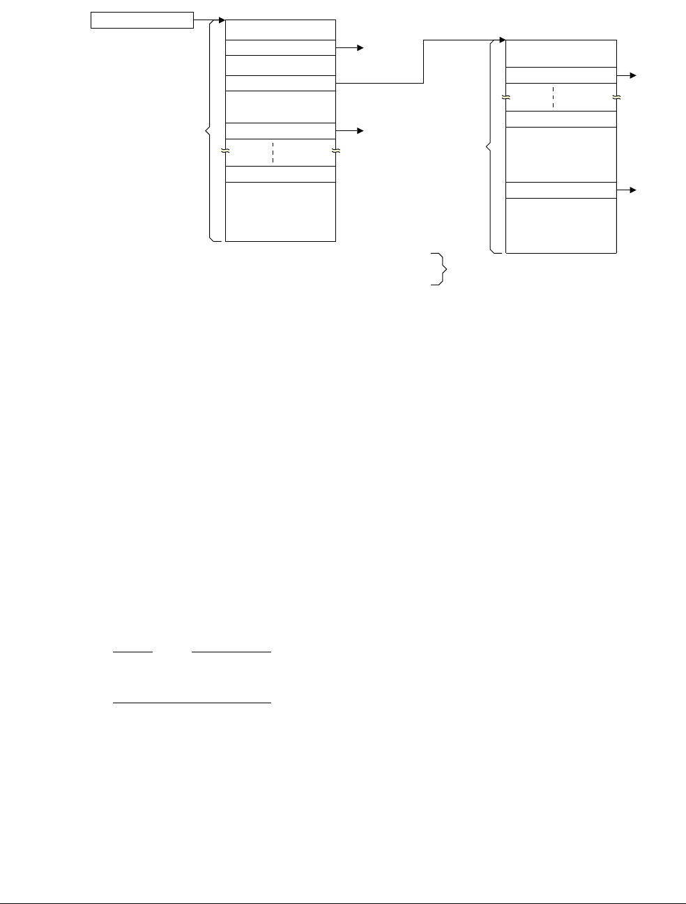
B3 Virtual Memory System Architecture (VMSA)
B3.5 Short-descriptor translation table format
ARM DDI 0406C.c Copyright © 1996-1998, 2000, 2004-2012, 2014 ARM. All rights reserved. B3-1325
ID051414 Non-Confidential
Figure B3-3 gives a general view of address translation when using the Short-descriptor translation table format.
Figure B3-3 General view of address translation using Short-descriptor format translation tables
Additional requirements for Short-descriptor format translation tables on page B3-1328 describes why, when using
the Short-descriptor format, Supersection and Large page entries must be repeated 16 times, as shown in
Figure B3-3.
Short-descriptor translation table format descriptors, Memory attributes in the Short-descriptor translation table
format descriptors on page B3-1328, and Control of Secure or Non-secure memory access, Short-descriptor format
on page B3-1330 describe the format of the descriptors in the Short-descriptor format translation tables.
The following sections then describe the use of this translation table format:
•Selecting between TTBR0 and TTBR1, Short-descriptor translation table format on page B3-1330
•Translation table walks, when using the Short-descriptor translation table format on page B3-1331.
B3.5.1 Short-descriptor translation table format descriptors
The following sections describe the formats of the entries in the Short-descriptor translation tables:
•Short-descriptor translation table first-level descriptor formats on page B3-1326
•Short-descriptor translation table second-level descriptor formats on page B3-1327.
For more information about second-level translation tables see Additional requirements for Short-descriptor format
translation tables on page B3-1328.
Note
Previous versions of the ARM Architecture Reference Manual, and some other documentation, describes the AP[2]
bit in the translation table entries as the APX bit.
Information returned by a translation table lookup on page B3-1320 describes the classification of the non-address
fields in the descriptors as address map control, access control, or attribute fields.
TTBR0 or TTBR1
First-level table
Indexed by
VA[19:12]
Section
1MB
memory
region
Page table
Supersection
16MB
memory
region
Second-level table
Indexed by
VA[31-N:20]
‡
Large page
64KB
memory
page
Small page
4KB
memory
page
‡ When using TTBR1, N is 0. When using TTBR0, 0 ≤ N < 8.
† Repeated entries required because of descriptor field overlaps.
Supersection
Repeated
16 times
†
Repeated
16 times
†
Large page
See text for more information.
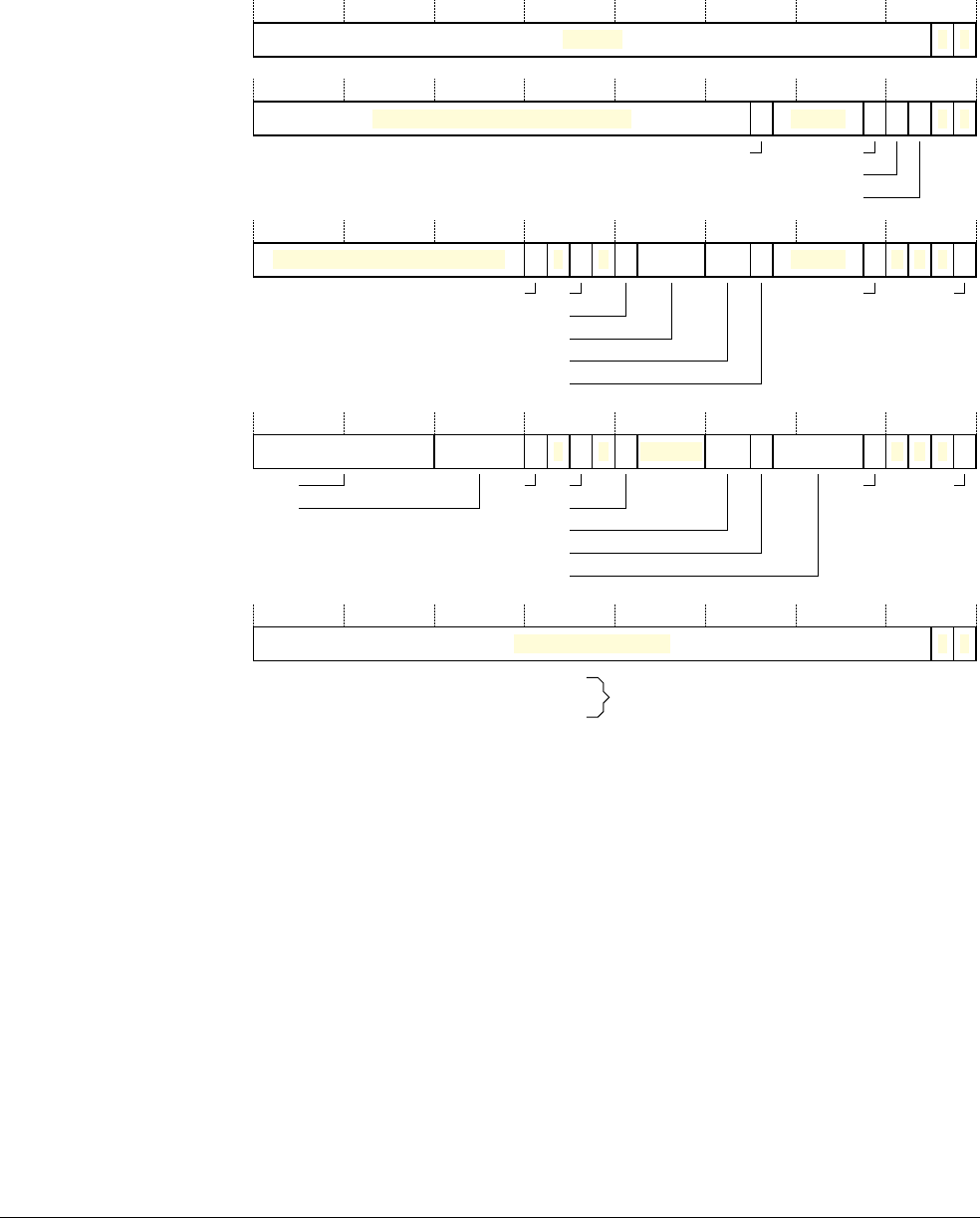
B3 Virtual Memory System Architecture (VMSA)
B3.5 Short-descriptor translation table format
B3-1326 Copyright © 1996-1998, 2000, 2004-2012, 2014 ARM. All rights reserved. ARM DDI 0406C.c
Non-Confidential ID051414
Short-descriptor translation table first-level descriptor formats
Each entry in the first-level table describes the mapping of the associated 1MB MVA range.
Figure B3-4 shows the possible first-level descriptor formats.
Figure B3-4 Short-descriptor first-level descriptor formats
Inclusion of the PXN attribute in the Short-descriptor translation table formats is:
•OPTIONAL in an implementation that does not include the Large Physical Address Extension
• required in an implementation includes the Large Physical Address Extension.
Descriptor bits[1:0] identify the descriptor type. On an implementation that supports the PXN attribute, for the
Section and Supersection entries, bit[0] also defines the PXN value. The encoding of these bits is:
0b00
, Invalid
The associated VA is unmapped, and any attempt to access it generates a Translation fault.
Software can use bits[31:2] of the descriptor for its own purposes, because the hardware ignores
these bits.
0b01
, Page table
The descriptor gives the address of a second-level translation table, that specifies the mapping of the
associated 1MByte VA range.
0 0
31 210
IGNORED
Invalid
Page table Domain 0 1
31 1098 543210
Page table base address, bits[31:10]
SBZ
NS
PXN†
0 S Domain C B 1
31 20 19 18 17 16 15 14 12 11 10 9 8 5 4 3 2 1 0
Section base address, PA[31:20]Section
NS nG
AP[2]
TEX[2:0]
AP[1:0]
XN
1 S C B 1
31 24 23 20 19 18 17 16 15 14 12 11 10 9 8 5 4 3 2 1 0
Supersection base address, PA[31:24]
Supersection
Extended base address, PA[35:32]
NS nG
AP[2]
IMPLEMENTATION DEFINED
XN
1 1
31 210
Reserved, UNK/SBZP
Reserved, when Large
Physical Address Extension
not implemented
Extended base address, PA[39:36]
TEX[2:0]
AP[1:0]
IMPLEMENTATION DEFINED
IMPLEMENTATION DEFINED
PXN‡
PXN‡
† If the implementation does not support the PXN attribute this bit is SBZ.
‡ If the implementation does not support the PXN attribute these bits must be 0.
An implementation that includes the Large Physical
Address Extension must support the PXN attribute.
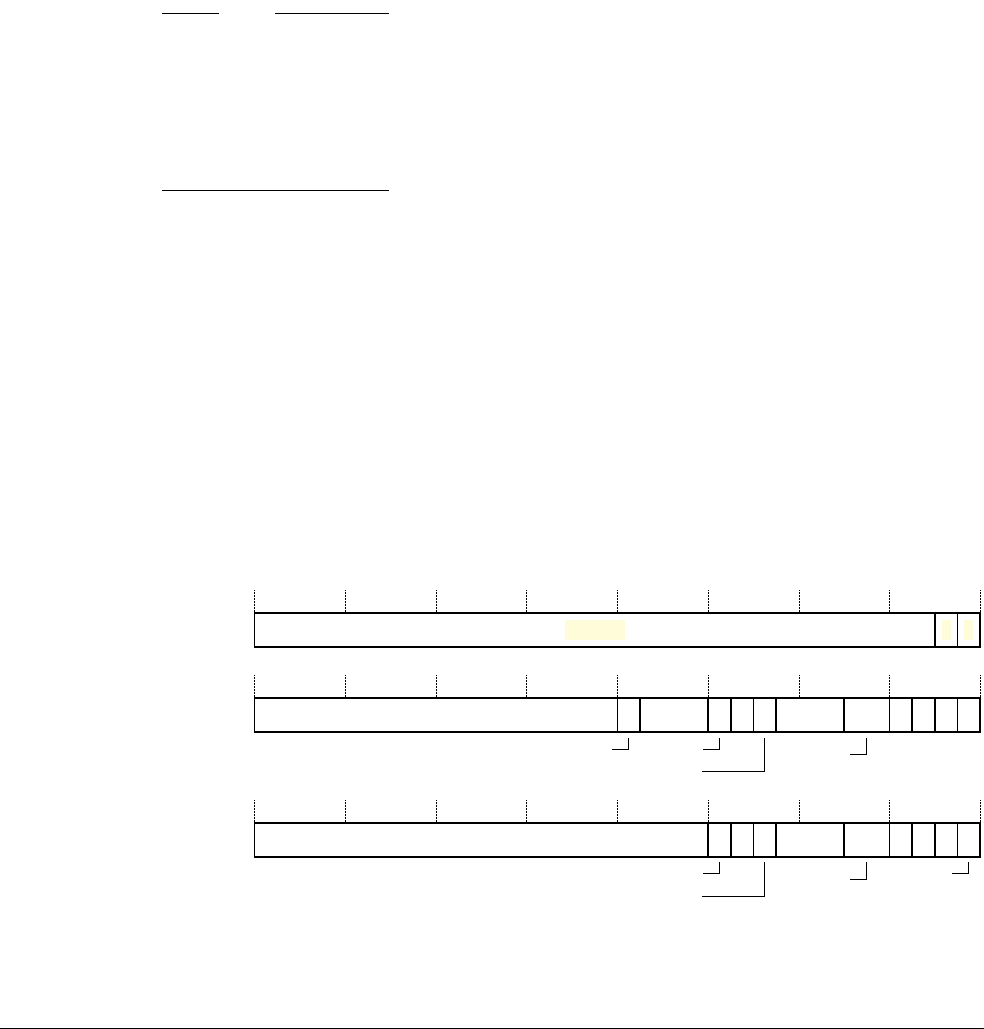
B3 Virtual Memory System Architecture (VMSA)
B3.5 Short-descriptor translation table format
ARM DDI 0406C.c Copyright © 1996-1998, 2000, 2004-2012, 2014 ARM. All rights reserved. B3-1327
ID051414 Non-Confidential
0b10
, Section or Supersection
The descriptor gives the base address of the Section or Supersection. Bit[18] determines whether
the entry describes a Section or a Supersection.
If the implementation supports the PXN attribute, this encoding also defines the PXN bit as 0.
0b11
, Section or Supersection, if the implementation supports the PXN attribute
If an implementation supports the PXN attribute, this encoding is identical to
0b10
, except that it
defines the PXN bit as 1.
0b11
, Reserved, UNK/SBZP, if the implementation does not support the PXN attribute
An attempt to access the associated VA generates a Translation fault.
On an implementation that does not support the PXN attribute, this encoding must not be used.
Note
• Issues A and B of this manual did not include the OPTIONAL support of the PXN attribute. The addition of
support for this attribute is backwards-compatible with software written to use the original VMSAv7
definition of the Short-descriptor translation table formats.
• A VMSAv7 implementation that implements the Large Physical Address Extension can use the
Short-descriptor translation table format for the Secure or Non-secure PL1&0 stage 1 translations, by setting
TTBCR.EAE to 0.
The address information in the first-level descriptors is:
Page table Bits[31:10] of the descriptor are bits[31:10] of the address of a Page table.
Section Bits[31:20] of the descriptor are bits[31:20] of the address of the Section.
Supersection Bits[31:24] of the descriptor are bits[31:24] of the address of the Supersection.
Optionally, bits[8:5, 23:20] of the descriptor are bits[39:32] of the extended Supersection address.
On an implementation that includes the Virtualization Extensions, for the Non-secure translation tables, the address
in the descriptor is the IPA of the Page table, Section, or Supersection. Otherwise, the address is the PA of the Page
table, Section, or Supersection.
For descriptions of the other fields in the descriptors, see Memory attributes in the Short-descriptor translation table
format descriptors on page B3-1328.
Short-descriptor translation table second-level descriptor formats
Figure B3-5 shows the possible formats of a second-level descriptor.
Figure B3-5 Short-descriptor second-level descriptor formats
Large page Large page base address, PA[31:16]
XN
TEX[2:0]
nG
S
AP[2]
SBZ C B 0 1
0 0
31 210
IGNORED
Invalid
16
31 15
AP[1:0]
14 12111098 6543210
Small page base address, PA[31:12]
31 12111098 6543210
S TEX[2:0] C B 1
nG
AP[2]
AP[1:0] XN
Small page

B3 Virtual Memory System Architecture (VMSA)
B3.5 Short-descriptor translation table format
B3-1328 Copyright © 1996-1998, 2000, 2004-2012, 2014 ARM. All rights reserved. ARM DDI 0406C.c
Non-Confidential ID051414
Descriptor bits[1:0] identify the descriptor type. The encoding of these bits is:
0b00
, Invalid
The associated VA is unmapped, and attempting to access it generates a Translation fault.
Software can use bits[31:2] of the descriptor for its own purposes, because the hardware ignores
these bits.
0b01
, Large page
The descriptor gives the base address and properties of the Large page.
0b1x
, Small page
The descriptor gives the base address and properties of the Small page.
In this descriptor format, bit[0] of the descriptor is the XN bit.
The address information in the second-level descriptors is:
Large page Bits[31:16] of the descriptor are bits[31:16] of the address of the Large page.
Small page Bits[31:12] of the descriptor are bits[31:12] of the address of the Small page.
On an implementation that includes the Virtualization Extensions, for the Non-secure translation tables, the address
in the descriptor is the IPA of the Page table, Section, or Supersection. Otherwise, the address is the PA of the Page
table, Section, or Supersection.
For descriptions of the other fields in the descriptors, see Memory attributes in the Short-descriptor translation table
format descriptors.
Additional requirements for Short-descriptor format translation tables
When using Supersection or Large page descriptors in the Short-descriptor translation table format, the input
address field that defines the Supersection or Large page descriptor address overlaps the table address field. In each
case, the size of the overlap is 4 bits. The following diagrams show these overlaps:
•Figure B3-8 on page B3-1334 for the first-level translation table Supersection entry
•Figure B3-10 on page B3-1336 for the second-level translation table Large page table entry.
Considering the case of using Large page table descriptors in a second-level translation table, this overlap means
that for any specific Large page, the bottom four bits of the second-level translation table entry might take any value
from
0b0000
to
0b1111
. Therefore, each of these sixteen index values must point to a separate copy of the same
descriptor.
This means that each Large page or Supersection descriptor must:
• occur first on a sixteen-word boundary
• be repeated in 16 consecutive memory locations.
B3.5.2 Memory attributes in the Short-descriptor translation table format descriptors
This section describes the descriptor fields other than the descriptor type field and the address field:
TEX[2:0], C, B
Memory region attribute bits, see Memory region attributes on page B3-1366.
These bits are not present in a Page table entry.
XN bit The Execute-never bit. Determines whether the processor can execute software from the addressed
region, see Execute-never restrictions on instruction fetching on page B3-1359.
This bit is not present in a Page table entry.

B3 Virtual Memory System Architecture (VMSA)
B3.5 Short-descriptor translation table format
ARM DDI 0406C.c Copyright © 1996-1998, 2000, 2004-2012, 2014 ARM. All rights reserved. B3-1329
ID051414 Non-Confidential
PXN bit, when supported
The Privileged execute-never bit:
• On an implementation that does not include the Large Physical Address Extension, support
for the PXN bit in the Short-descriptor translation table format is OPTIONAL.
• On an implementation that includes the Large Physical Address Extension, the
Short-descriptor translation table format must include the PXN bit.
When supported, the PXN bit determines whether the processor can execute software from the
region when executing at PL1, see Execute-never restrictions on instruction fetching on
page B3-1359.
Note
Memory accesses by software executing at PL2 always use the Long-descriptor translation table
format.
When this bit is set to 1 in the Page table descriptor, it indicates that all memory pages described in
the corresponding page table are Privileged execute-never.
NS bit Non-secure bit. If an implementation includes the Security Extensions, for memory accesses from
Secure state, this bit specifies whether the translated PA is in the Secure or Non-secure address map,
see Control of Secure or Non-secure memory access, Short-descriptor format on page B3-1330.
This bit is not present in second-level descriptors. The value of the NS bit in the first level Page table
descriptor applies to all entries in the corresponding second-level translation table.
Domain Domain field, see Domains, Short-descriptor format only on page B3-1362.
This field is not present in a Supersection entry. Memory described by Supersections is in domain 0.
This bit is not present in second-level descriptors. The value of the Domain field in the first level
Page table descriptor applies to all entries in the corresponding second-level translation table.
An IMPLEMENTATION DEFINED bit
This bit is not present in second-level descriptors.
AP[2], AP[1:0]
Access Permissions bits, see Memory access control on page B3-1356.
AP[0] can be configured as the Access flag, see The Access flag on page B3-1362.
These bits are not present in a Page table entry.
S bit The Shareable bit. Determines whether the addressed region is Shareable memory, see Memory
region attributes on page B3-1366.
This bit is not present in a Page table entry.
nG bit The not global bit. Determines how the translation is marked in the TLB, see Global and
process-specific translation table entries on page B3-1378.
This bit is not present in a Page table entry.
Bit[18], when bits[1:0] indicate a Section or Supersection descriptor
0 Descriptor is for a Section
1 Descriptor is for a Supersection.

B3 Virtual Memory System Architecture (VMSA)
B3.5 Short-descriptor translation table format
B3-1330 Copyright © 1996-1998, 2000, 2004-2012, 2014 ARM. All rights reserved. ARM DDI 0406C.c
Non-Confidential ID051414
B3.5.3 Control of Secure or Non-secure memory access, Short-descriptor format
Access to the Secure or Non-secure physical address map on page B3-1321 describes how the NS bit in the
translation table entries:
• for accesses from Secure state, determines whether the access is to Secure or Non-secure memory
• is ignored by accesses from Non-secure state.
In the Short-descriptor translation table format, the NS bit is defined only in the first-level translation tables. This
means that, in a first-level Page table descriptor, the NS bit defines the physical address space, Secure or
Non-secure, for all of the Large pages and Small pages of memory described by that table.
The NS bit of a first-level Page table descriptor has no effect on the physical address space in which that translation
table is held. As stated in Secure and Non-secure address spaces on page B3-1323, the physical address of that
translation table is in:
• the Secure address space if the translation table walk is in Secure state
• the Non-secure address space if the translation table walk is in Non-secure state.
This means the granularity of the Secure and Non-secure memory spaces is 1MB. However, in these memory
spaces, table entries can define physical memory regions with a granularity of 4KB.
B3.5.4 Selecting between TTBR0 and TTBR1, Short-descriptor translation table format
As described in Determining the translation table base address on page B3-1320, two sets of translation tables can
be defined for each of the PL1&0 stage 1 translations, and TTBR0 and TTBR1 hold the base addresses for the two
sets of tables. When using the Short-descriptor translation table format, the value of TTBCR.N indicates the number
of most significant bits of the input VA that determine whether TTBR0 or TTBR1 holds the required translation
table base address, as follows:
• If N == 0 then use TTBR0. Setting TTBCR.N to zero disables use of a second set of translation tables.
• if N > 0 then:
— if bits[31:32-N] of the input VA are all zero then use TTBR0
— otherwise use TTBR1.
Table B3-1 shows how the value of N determines the lowest address translated using TTBR1, and the size of the
first-level translation table addressed by TTBR0.
Whenever TTBCR.N is nonzero, the size of the translation table addressed by TTBR1 is 16KB.
Figure B3-6 on page B3-1331 shows how the value of TTBCR.N controls the boundary between VAs that are
translated using TTBR0, and VAs that are translated using TTBR1.
Table B3-1 Effect of TTBCR.N on address translation, Short-descriptor format
TTBCR.N First address translated with TTBR1 TTBR0 table
Size Index range
0b000
TTBR1 not used 16KB VA[31:20]
0b001 0x80000000
8KB VA[30:20]
0b010 0x40000000
4KB VA[29:20]
0b011 0x20000000
2KB VA[28:20]
0b100 0x10000000
1KB VA[27:20]
0b101 0x08000000
512 bytes VA[26:20]
0b110 0x04000000
256 bytes VA[25:20]
0b111 0x02000000
128 bytes VA[24:20]
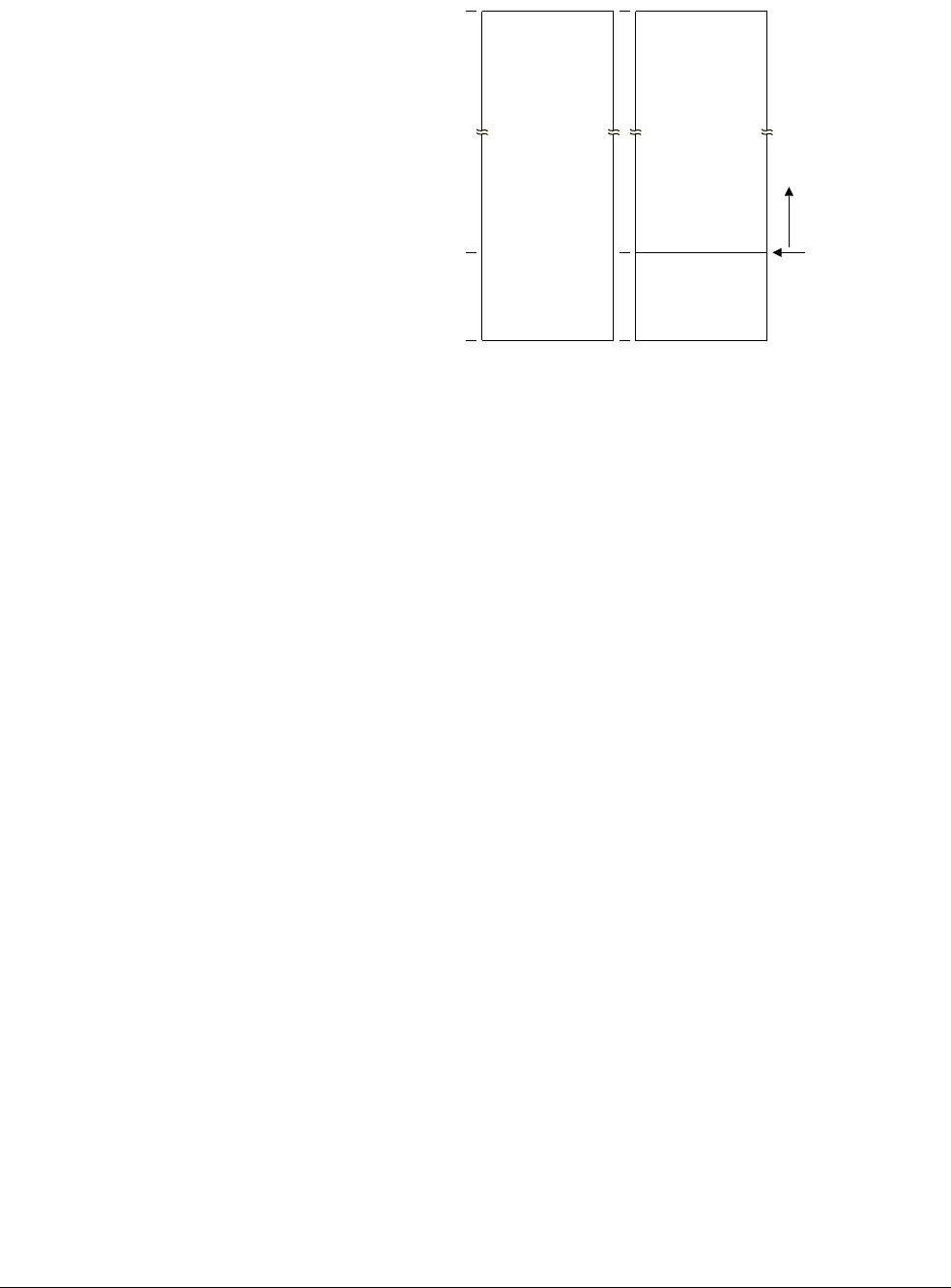
B3 Virtual Memory System Architecture (VMSA)
B3.5 Short-descriptor translation table format
ARM DDI 0406C.c Copyright © 1996-1998, 2000, 2004-2012, 2014 ARM. All rights reserved. B3-1331
ID051414 Non-Confidential
Figure B3-6 How TTBCR.N controls the boundary between the TTBRs, Short-descriptor format
In the selected TTBR. the following bits define the memory region attributes for the translation table walk:
• the RGN, S and C bits, in an implementation that does not include the Multiprocessing Extensions
• the RGN, S, and IRGN[1:0] bits, in an implementation that includes the Multiprocessing Extensions.
For more information, see TTBCR, Translation Table Base Control Register, VMSA on page B4-1724, TTBR0,
Translation Table Base Register 0, VMSA on page B4-1729 and TTBR1, Translation Table Base Register 1, VMSA
on page B4-1733.
Translation table walks, when using the Short-descriptor translation table format describes the translation.
B3.5.5 Translation table walks, when using the Short-descriptor translation table format
When using the Short-descriptor translation table format, and a memory access requires a translation table walk:
• a section-mapped access only requires a read of the first-level translation table
• a page-mapped access also requires a read of the second-level translation table.
Reading a first-level translation table describes how either TTBR1 or TTBR0 is used, with the accessed VA, to
determine the address of the first-level descriptor.
Reading a first-level translation table shows the output address as A[39:0]:
• On an implementation that includes the Virtualization Extensions, for a Non-secure PL1&0 stage 1
translation, this is the IPA of the required descriptor. A Non-secure PL1&0 stage 2 translation of this address
is performed to obtain the PA of the descriptor.
• Otherwise, this address is the PA of the required descriptor.
The full translation flow for Sections, Supersections, Small pages and Large pages on page B3-1332 then shows the
complete translation flow for each valid memory access.
Reading a first-level translation table
When performing a fetch based on TTBR0:
• the address bits taken from TTBR0 vary between bits[31:14] and bits[31:7]
• the address bits taken from the VA, that is the input address for the translation, vary between bits[31:20] and
bits[24:20].
The width of the TTBR0 and VA fields depend on the value of TTBCR.N, as Figure B3-7 on page B3-1332 shows.
0x00000000
0xFFFFFFFF
0x02000000
TTBR0 region
Boundary, when
TTBCR.N==0b111
Effect of decreasing N
TTBR1 region
TTBR0 region
TTBCR.N==0b000
Use of TTBR1 disabled
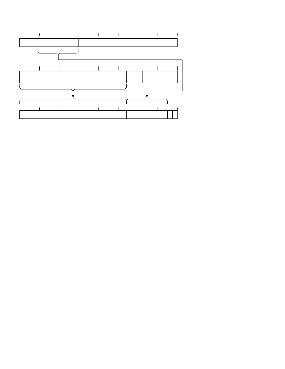
B3 Virtual Memory System Architecture (VMSA)
B3.5 Short-descriptor translation table format
B3-1332 Copyright © 1996-1998, 2000, 2004-2012, 2014 ARM. All rights reserved. ARM DDI 0406C.c
Non-Confidential ID051414
When performing a fetch based on TTBR1, Bits TTBR1[31:14] are concatenated with bits[31:20] of the VA. This
makes the fetch equivalent to that shown in Figure B3-7, with N==0.
Note
See The address and Properties fields shown in the translation flows on page B3-1333 for more information about
the Properties label used in this and other figures.
Figure B3-7 Accessing first-level translation table based on TTBR0, Short-descriptor format
Regardless of which register is used as the base for the fetch, the resulting output address selects a four-byte
translation table entry that is one of:
• A first-level descriptor for a Section or Supersection.
•A Page table descriptor that points to a second-level translation table. In this case:
— a second fetch is performed to retrieve a second-level descriptor
— the descriptor also contains some attributes for the access, see Figure B3-4 on page B3-1326.
• A faulting entry.
The full translation flow for Sections, Supersections, Small pages and Large pages
In a translation table walk, only the first lookup uses the translation table base address from the appropriate
Translation table base register. Subsequent lookups use a combination of address information from:
• the table descriptor read in the previous lookup
• the input address.
This section summarizes how each of the memory section and page options is described in the translation tables,
and has a subsection summarizing the full translation flow for each of the options.
As described in Short-descriptor translation table format descriptors on page B3-1325, the four options are:
Supersection A 16MB memory region, see Translation flow for a Supersection on page B3-1334.
Section A 1MB memory region, see Translation flow for a Section on page B3-1335.
Large page A 64KB memory region, described by the combination of:
• a first-level translation table entry that indicates a second-level Page table address
• a second-level descriptor that indicates a Large page.
See Translation flow for a Large page on page B3-1336.
TTBR0
A[31:0] of first-level descriptor
A[39:32] = 0x00
‡ This field is absent if N is 0
N is the value of TTBCR.N
Input address
Table index
31 20 19 032-N 31-N
‡
00Translation base
31 0
Table index
2 114-N 13-N
Descriptor address
For details of the Properties field, see the register description
Properties
UNK/
SBZP
Translation base
31 14-N 13-N 07 6

B3 Virtual Memory System Architecture (VMSA)
B3.5 Short-descriptor translation table format
ARM DDI 0406C.c Copyright © 1996-1998, 2000, 2004-2012, 2014 ARM. All rights reserved. B3-1333
ID051414 Non-Confidential
Small page A 4KB memory region, described by the combination of:
• a first-level translation table entry that indicates a second-level Page table address
• a second-level descriptor that indicates a Small page.
See Translation flow for a Small page on page B3-1337.
The address and Properties fields shown in the translation flows
On an implementation that includes the Virtualization Extensions, for the Non-secure translation tables:
• any descriptor address is the IPA of the required descriptor
• the final output address is the IPA of the Section, Supersection, Large page, or Small page.
In these cases, a PL1&0 stage 2 translation is performed to translate the IPA to the required PA.
Otherwise, the address is the PA of the descriptor, Section, Supersection, Large page, or Small page.
Properties indicates register or translation table fields that return information, other than address information, about
the translation or the targeted memory region. For more information see Information returned by a translation table
lookup on page B3-1320, and the description of the register or translation table descriptor.
For translations using the Short-descriptor translation table format, Short-descriptor translation table format
descriptors on page B3-1325 describes the descriptors formats.

B3 Virtual Memory System Architecture (VMSA)
B3.5 Short-descriptor translation table format
B3-1334 Copyright © 1996-1998, 2000, 2004-2012, 2014 ARM. All rights reserved. ARM DDI 0406C.c
Non-Confidential ID051414
Translation flow for a Supersection
Figure B3-8 shows the complete translation flow for a Supersection. For more information about the fields shown
in this figure see The address and Properties fields shown in the translation flows on page B3-1333.
Figure B3-8 Supersection address translation
Note
Figure B3-8 shows how, when the input address, the VA, addresses a Supersection, the top four bits of the
Supersection index bits of the address overlap the bottom four bits of the Table index bits. For more information,
see Additional requirements for Short-descriptor format translation tables on page B3-1328.
00000000
For a translation based on TTBR0, N is the value of TTBCR.N
For a translation based on TTBR1, N is 0
UNK/
SBZP
Translation base
31 14-N 13-N 0
First-level
Supersection descriptor
First-level descriptor address
Supersection index
Table index
Bits[8:5,23:20]
Supersection index
31 24 23 0
Supersection BAExtended BA
39 32
Translation Table Base Register
Input address
7 6
Properties
Output address, A[39:0]
‡ This field is absent if N is 0
BA = Base address
For details of Properties fields, see the register or descriptor description
31 210
x
Extended Supersection BA and Properties fields
Supersection BA
24 23
1
First-level lookup
00Translation base
31 0
Table index
2 114-N 13-N39 32
24 2331 20 19 032-N 31-N
‡
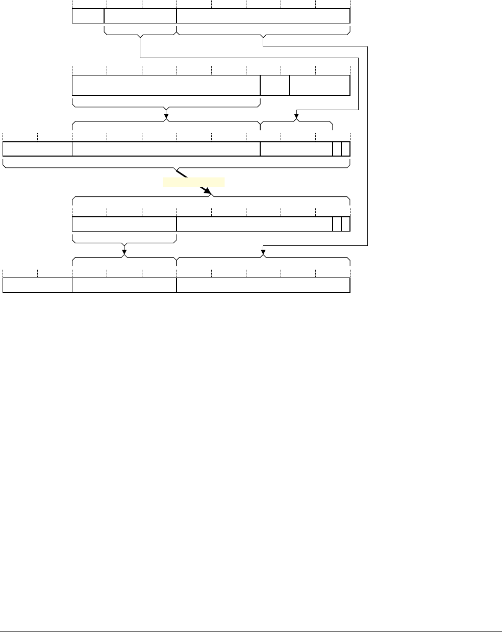
B3 Virtual Memory System Architecture (VMSA)
B3.5 Short-descriptor translation table format
ARM DDI 0406C.c Copyright © 1996-1998, 2000, 2004-2012, 2014 ARM. All rights reserved. B3-1335
ID051414 Non-Confidential
Translation flow for a Section
Figure B3-9 shows the complete translation flow for a Section. For more information about the fields shown in this
figure see The address and Properties fields shown in the translation flows on page B3-1333.
Figure B3-9 Section address translation
00000000
39 32
‡ This field is absent if N is 0
For a translation based on TTBR0, N is the value of TTBCR.N
For a translation based on TTBR1, N is 0
31 20 19 0
Section base address Section index
00Translation base
31 0
Table index
2 114-N 13-N
Table index
31 20 19 032-N 31-N
‡ Section index
For details of Properties fields, see the register or descriptor description.
00000000
39 32
Output address, A[39:0]
First-level Section descriptor
Properties
31 20 19 2 1 0
Section base address x1
First-level lookup
First-level descriptor address
Translation Table Base Register
UNK/
SBZP
Translation base
31 14-N 13-N 07 6
Properties
Input address
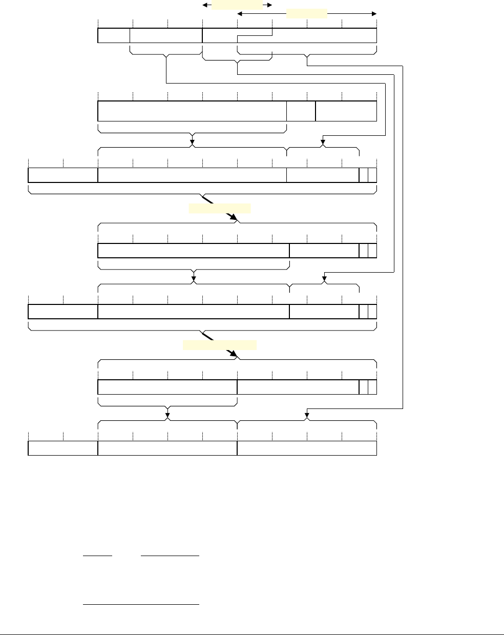
B3 Virtual Memory System Architecture (VMSA)
B3.5 Short-descriptor translation table format
B3-1336 Copyright © 1996-1998, 2000, 2004-2012, 2014 ARM. All rights reserved. ARM DDI 0406C.c
Non-Confidential ID051414
Translation flow for a Large page
Figure B3-10 shows the complete translation flow for a Large page. For more information about the fields shown
in this figure see The address and Properties fields shown in the translation flows on page B3-1333.
Figure B3-10 Large page address translation
Note
Figure B3-10 shows how, when the input address, the VA, addresses a Large page, the top four bits of the page index
bits of the address overlap the bottom four bits of the First-level table index bits. For more information, see
Additional requirements for Short-descriptor format translation tables on page B3-1328.
00000000
39 32
Page index
For a translation based on TTBR0, N is the value of TTBCR.N
For a translation based on TTBR1, N is 0
Second-level descriptor
L2 table index
Page index
31 16 15 0
Large page base address
00Page table base address
31 0
L2 table index
2 110 9
Properties
31 10 9 2 1 0
Page table base address 10
00Translation base
31 0
L1 table index
2 114-N 13-N
L1 table index
31 20 19 032-N 31-N
‡
12 1116 15
Translation Table
Base Register
L1 = First-level, L2 = Second-level
‡ This field is absent if N is 0
For details of Properties fields, see the register or descriptor description
Output address, A[39:0]
00000000
39 32
1Properties
31 16 15 2 1 0
Large page base address 0
Second-level lookup
Second-level descriptor
address
First-level descriptor
First-level lookup
First-level descriptor
address
00000000
39 32
UNK/
SBZP
Translation base
31 14-N 13-N 07 6
Properties
Input address
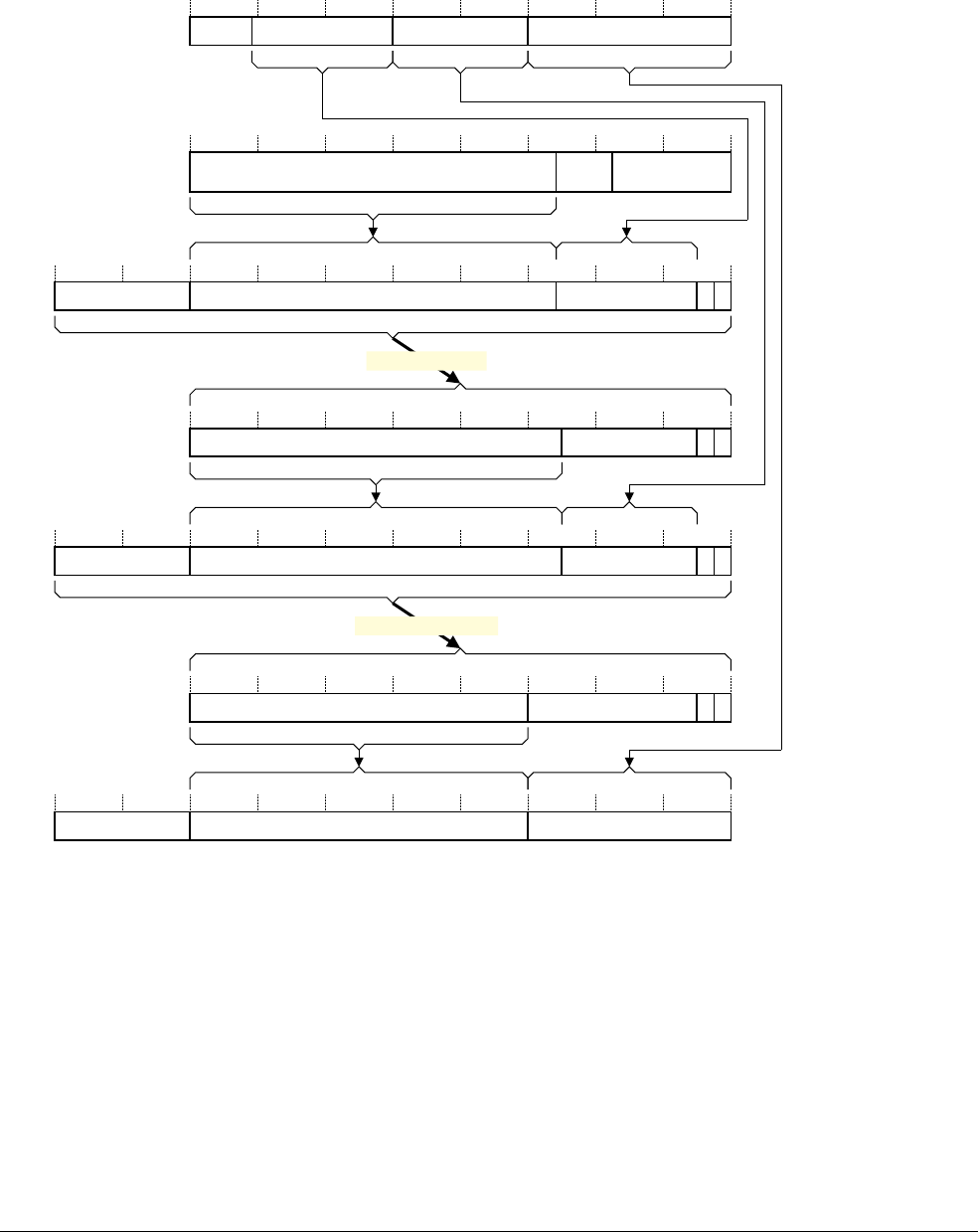
B3 Virtual Memory System Architecture (VMSA)
B3.5 Short-descriptor translation table format
ARM DDI 0406C.c Copyright © 1996-1998, 2000, 2004-2012, 2014 ARM. All rights reserved. B3-1337
ID051414 Non-Confidential
Translation flow for a Small page
Figure B3-11 shows the complete translation flow for a Small page. For more information about the fields shown
in this figure see The address and Properties fields shown in the translation flows on page B3-1333.
Figure B3-11 Small page address translation
Page index
31 12 11 0
Small page base address
00Page table base address
31 0
L2 table index
2 110 9
00Translation base
31 0
L1 table index
2 114-N 13-N
L1 table index
31 20 19 032-N 31-N
‡ Page index
12 11
L2 table index
For a translation based on TTBR0, N is the value of TTBCR.N
For a translation based on TTBR1, N is 0
L1 = First-level, L2 = Second-level
‡ This field is absent if N is 0
For details of Properties fields, see the register or descriptor description.
Output address, A[39:0]00000000
39 32
Properties
31 12 11 2 1 0
Small page base address 1 x Second-level descriptor
Second-level lookup
Second-level descriptor
address
00000000
39 32
First-level descriptorProperties
31 10 9 2 1 0
Page table base address 10
First-level lookup
First-level descriptor
address
00000000
39 32
UNK/
SBZP
Translation base
31 14-N 13-N 07 6
Properties Translation Table
Base Register
Input address
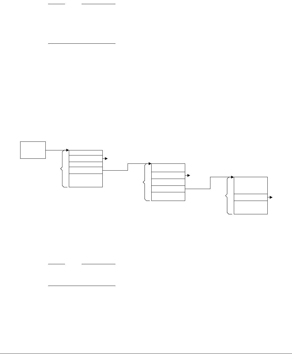
B3 Virtual Memory System Architecture (VMSA)
B3.6 Long-descriptor translation table format
B3-1338 Copyright © 1996-1998, 2000, 2004-2012, 2014 ARM. All rights reserved. ARM DDI 0406C.c
Non-Confidential ID051414
B3.6 Long-descriptor translation table format
The Long-descriptor translation table format is implemented only as part of the Large Physical Address Extension.
It supports the assignment of memory attributes to memory Pages, at a granularity of 4KB, across the complete
input address range. It also supports the assignment of memory attributes to blocks of memory, where a block can
be 2MB or 1GB.
Note
• While the current implementation is limited to three levels of address lookup, its design and naming
conventions support extension to additional levels, to support a larger input address range.
• Similarly, while the current implementation limits the output address range to 40 bits, its design supports
extension to a larger output address range.
In a VMSAv7 implementation that does not include the Virtualization Extensions, the Long-descriptor translation
table format can be used for either or both the Secure and Non-secure address translations.
In an implementation that includes the Virtualization Extensions, Figure B3-2 on page B3-1312 shows the different
address translation stages, and the Long-descriptor translation table format:
• is used for:
— the Non-secure PL2 stage 1 translation
— the Non-secure PL1&0 stage 2 translation
• can be used for the Secure and Non-secure PL1&0 stage 1 translations.
When used for a stage 1 translation, the translation tables support an input address of up to 32 bits, corresponding
to the VA address range of the processor. Figure B3-12 gives a general view of stage 1 address translation when
using the Long-descriptor translation table format.
Figure B3-12 General view of stage 1 address translation using Long-descriptor format
When used for a stage 2 translation, the translation tables support an input address range of up to 40 bits, to support
the translation from IPA to PA. If the input address for the stage 2 translation is a 32-bit address then this address is
zero-extended to 40 bits.
Note
When the Short-descriptor translation table format is used for the Non-secure stage 1 translations, this generates
32-bit IPAs. These are zero-extended to 40 bits to provide the input address for the stage 2 translation.
TTBR0,
TTBR1, or
HTTBR
First-level table
Indexed by
VA[29:21]
Block
1GB
memory
region
Table
Second-level table
Indexed by
VA[31:30]
4KB
memory
page
If a First-level table would contain only one entry, it is skipped, and the TTBR points
to the Second-level table. This happens if the VA address range is 30 bits or less.
Block
2MB
memory
region
Table
Third-level table
Page
Indexed by
VA[20:12]
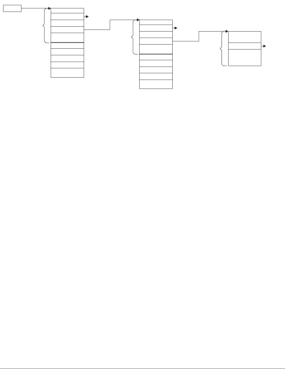
B3 Virtual Memory System Architecture (VMSA)
B3.6 Long-descriptor translation table format
ARM DDI 0406C.c Copyright © 1996-1998, 2000, 2004-2012, 2014 ARM. All rights reserved. B3-1339
ID051414 Non-Confidential
Figure B3-13 gives a general view of stage 2 address translation. Stage 2 translation always uses the
Long-descriptor translation table format.
Figure B3-13 General view of stage 2 address translation, Long-descriptor translation table format
Use of concatenated translation tables for stage 2 translations on page B3-1348 describes how using concatenated
Second-level tables means lookup can start at the Second level, as referred to in Figure B3-13.
Long-descriptor translation table format descriptors, Memory attributes in the Long-descriptor translation table
format descriptors on page B3-1342, and Control of Secure or Non-secure memory access, Long-descriptor format
on page B3-1344 describe the format of the descriptors in the Long-descriptor format translation tables.
The following sections then describe the use of this translation table format:
•Selecting between TTBR0 and TTBR1, Long-descriptor translation table format on page B3-1345
•Long-descriptor translation table format address lookup levels on page B3-1348
•Translation table walks, when using the Long-descriptor translation table format on page B3-1350.
B3.6.1 Long-descriptor translation table format descriptors
As described in Long-descriptor translation table format address lookup levels on page B3-1348, the
Long-descriptor translation table format provides up to three levels of address lookup. A translation table walk starts
either at the first level or the second level of address lookup.
In general, a descriptor is one of:
• an invalid or fault entry
• a table entry, that points to the next-level translation table
• a block entry, that defines the memory properties for the access
• a reserved format.
Bit[1] of the descriptor indicates the descriptor type, and bit[0] indicates whether the descriptor is valid.
The following sections describe the Long-descriptor translation table descriptor formats:
•Long-descriptor translation table first-level and second-level descriptor formats on page B3-1340
•Long-descriptor translation table third-level descriptor formats on page B3-1341.
Information returned by a translation table lookup on page B3-1320 describes the classification of the non-address
fields in the descriptors between address map control, access controls, and region attributes.
VTTBR
First-level tables
Block
1GB
memory
region
Table
Indexed by
IPA[38:30]
4KB
memory
page
If a First-level table would contain 16 entries or fewer, first-level lookup can be omited. If so, VTTBR
points to the start of a block of concatenated Second-level tables. See text for more information.
Third-level table
Page
Block
Table
Indexed by
IPA[20:12]
Up to two concatenated
First-level tables, so that
IPA[39] indexes the table.
Indexed by
IPA[29:21]
Second-level tables
Block
2MB
memory
region
Table
Block
Table
B3 Virtual Memory System Architecture (VMSA)
B3.6 Long-descriptor translation table format
B3-1340 Copyright © 1996-1998, 2000, 2004-2012, 2014 ARM. All rights reserved. ARM DDI 0406C.c
Non-Confidential ID051414
Long-descriptor translation table first-level and second-level descriptor formats
In the Long-descriptor translation tables, the formats of the first-level and second-level descriptors differ only in the
size of the block of memory addressed by the block descriptor. A block entry:
• in a first-level table describes the mapping of the associated 1GB input address range
• in a second-level table describes the mapping of the associated 2MB input address range.
Figure B3-14 shows the Long-descriptor first-level and second-level descriptor formats:
Figure B3-14 Long-descriptor first-level and second-level descriptor formats
Descriptor encodings, Long-descriptor first-level and second-level formats
In the Long-descriptor translation tables, the formats of the first-level and second-level descriptors differ only in the
size of the block of memory addressed by the block descriptor.
Descriptor bit[0] identifies whether the descriptor is valid, and is 1 for a valid descriptor. If a lookup returns an
invalid descriptor, the associated input address is unmapped, and any attempt to access it generates a Translation
fault.
Descriptor bit[1] identifies the descriptor type, and is encoded as:
0, Block The descriptor gives the base address of a block of memory, and the attributes for that memory
region.
1, Table The descriptor gives the address of the next level of translation table, and for a stage 1 translation,
some attributes for that translation.
The other fields in the valid descriptors are:
Block descriptor
Gives the base address and attributes of a block of memory:
• for a first-level Block descriptor, bits[39:30] are bits[39:30] of the output address that
specifies a 1GB block of memory
• for a second-level Block descriptor, bits[39:21] are bits[39:21] of the output address that
specifies a 2MB block of memory.
Bits[63:52, 11:2] provide attributes for the target memory block, see Memory attributes in the
Long-descriptor translation table format descriptors on page B3-1342. The position and contents
of these bits are identical in the second-level block descriptor and in the third-level page descriptor.
0
IGNORED
63 10
Invalid
1Upper block attributes
63 52 51 3940 nn-1 12 11 2 1 0
UNK/SBZP Output address[39:n]UNK/SBZP Lower block attributes 0
Block
For the first-level descriptor, n is 30. For the second-level descriptor, n is 21.
The first-level descriptor returns the address of the second-level table.
The second-level descriptor returns the address of the third-level table.
1
63 62 61 60 59 58 52 51 40 39 12 11 2 1 0
IGNORED UNK/SBZP Next-level table address[39:12] IGNORED 1
Table
PXNTable
XNTable
APTable
NSTable
Stage 1 only,
SBZ at stage 2
B3 Virtual Memory System Architecture (VMSA)
B3.6 Long-descriptor translation table format
ARM DDI 0406C.c Copyright © 1996-1998, 2000, 2004-2012, 2014 ARM. All rights reserved. B3-1341
ID051414 Non-Confidential
Table descriptor
Bits[39:12] are bits[39:12] of the address of the required next-level table. Bits[11:0] of the table
address are zero:
• for a first-level Table descriptor, this is the address of a second-level table
• for a second-level Table descriptor, this is the address of a third-level table.
For a stage 1 translation only, bits[63:59] provide attributes for the next-level lookup, see Memory
attributes in the Long-descriptor translation table format descriptors on page B3-1342.
If the implementation includes the Virtualization Extensions and the translation table defines the Non-secure PL1&0
stage 1 translations, then the output address in the descriptor is the IPA of the target block or table. Otherwise, it is
the PA of the target block or table.
Long-descriptor translation table third-level descriptor formats
Each entry in a third-level table describes the mapping of the associated 4KB input address range.
Figure B3-15 shows the Long-descriptor third-level descriptor formats.
Figure B3-15 Long-descriptor third-level descriptor formats
Descriptor bit[0] identifies whether the descriptor is valid, and is 1 for a valid descriptor. If a lookup returns an
invalid descriptor, the associated input address is unmapped, and any attempt to access it generates a Translation
fault.
Descriptor bit[1] identifies the descriptor type, and is encoded as:
0, Reserved, invalid
Behaves identically to encodings with bit[0] set to 0.
This encoding must not be used in third-level translation tables.
1, Page Gives the address and attributes of a 4KB page of memory.
At this level, the only valid format is the Page descriptor. The other fields in the Page descriptor are:
Page descriptor
Bits[39:12] are bits[39:12] of the output address for a page of memory.
Bits[63:52, 11:2] provide attributes for the target memory page, see Memory attributes in the
Long-descriptor translation table format descriptors on page B3-1342. The position and contents
of these bits are identical in the first-level block descriptor and in the second-level block descriptor.
If the implementation includes the Virtualization Extensions and the translation table defines the Non-secure PL1&0
stage 1 translations, then the output address in the descriptor is the IPA of the target page. Otherwise, it is the PA of
the target page.
0
IGNORED
63 10
Invalid
Reserved 1Reserved, UNK/SBZP
63 210
0
Page 1Upper page attributes
63 52 51 3940 12 11 2 1 0
UNK/SBZP Output address[39:12] Lower page attributes 1
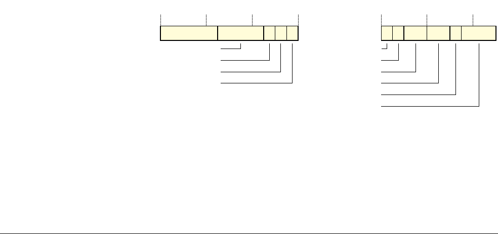
B3 Virtual Memory System Architecture (VMSA)
B3.6 Long-descriptor translation table format
B3-1342 Copyright © 1996-1998, 2000, 2004-2012, 2014 ARM. All rights reserved. ARM DDI 0406C.c
Non-Confidential ID051414
B3.6.2 Memory attributes in the Long-descriptor translation table format descriptors
The memory attributes in the Long-descriptor translation tables are based on those in the Short-descriptor
translation table format, with some extensions. Memory region attributes on page B3-1366 describes these
attributes. In the Long-descriptor translation table format:
• Table entries for stage 1 translations define attributes for the next level of lookup, see Next-level attributes in
stage 1 Long-descriptor Table descriptors
• Block and page entries define memory attributes for the target block or page of memory. Stage 1 and stage 2
translations have some differences in these attributes, see:
—Attribute fields in stage 1 Long-descriptor Block and Page descriptors
—Attribute fields in stage 2 Long-descriptor Block and Page descriptors on page B3-1343.
Next-level attributes in stage 1 Long-descriptor Table descriptors
In a Table descriptor for a stage 1 translation, bits[63:59] of the descriptor define the following attributes for the
next-level translation table access:
NSTable, bit[63] For memory accesses from Secure state, specifies the security level for subsequent levels of
lookup, see Hierarchical control of Secure or Non-secure memory accesses,
Long-descriptor format on page B3-1344.
For memory accesses from Non-secure state, this bit is ignored.
APTable, bits[62:61] Access permissions limit for subsequent levels of lookup, see Hierarchical control of access
permissions, Long-descriptor format on page B3-1357.
APTable[0] is reserved, SBZ, in the Non-secure PL2 stage 1 translation tables.
XNTable, bit[60] XN limit for subsequent levels of lookup, see Hierarchical control of instruction fetching,
Long-descriptor format on page B3-1360.
PXNTable, bit[59] PXN limit for subsequent levels of lookup, see Hierarchical control of instruction fetching,
Long-descriptor format on page B3-1360.
This bit is reserved, SBZ, in the Non-secure PL2 stage 1 translation tables.
Attribute fields in stage 1 Long-descriptor Block and Page descriptors
Block and Page descriptors split the memory attributes into an upper block and a lower block. Figure B3-16 shows
the memory attribute fields in these blocks, for a stage 1 translation:
Figure B3-16 Memory attribute fields in Long-descriptor stage 1 Block and Page descriptors
For a stage 1 descriptor, the attributes are:
XN, bit[54] The Execute-never bit. Determines whether the region is executable, see Execute-never restrictions
on instruction fetching on page B3-1359.
Upper attributes Lower attributes
IGNORED
63 59 58 55 54 53 52
IGNORED
XN
PXN
Contiguous bit
1110987654 2
nG
AF
SH[1:0]
AP[2:1]
NS
AttrIndx[2:0]
Reserved for software use
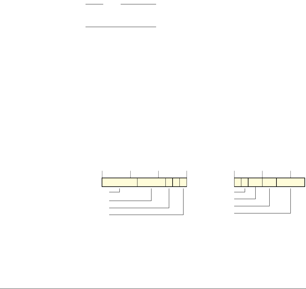
B3 Virtual Memory System Architecture (VMSA)
B3.6 Long-descriptor translation table format
ARM DDI 0406C.c Copyright © 1996-1998, 2000, 2004-2012, 2014 ARM. All rights reserved. B3-1343
ID051414 Non-Confidential
PXN, bit[53] The Privileged execute-never bit. Determines whether the region is executable at PL1, see
Execute-never restrictions on instruction fetching on page B3-1359.
This bit is reserved, SBZ, in the Non-secure PL2 stage 1 translation tables.
Contiguous bit, bit[52]
A bit indicating that 16 adjacent translation table entries point to contiguous memory regions, see
Contiguous bit on page B3-1373.
nG, bit[11] The not global bit. Determines how the translation is marked in the TLB, see Global and
process-specific translation table entries on page B3-1378.
This bit is reserved, SBZ, in the Non-secure PL2 stage 1 translation tables.
AF, bit[10] The Access flag, see The Access flag on page B3-1362.
SH, bits[9:8] Shareability field, see Memory region attributes on page B3-1366.
AP[2:1], bits[7:6]
Access Permissions bits, see Memory access control on page B3-1356.
Note
For consistency with the Short-descriptor translation table formats, the Long-descriptor format
defines AP[2:1] as the Access Permissions bits, and does not define an AP[0] bit.
AP[1] is reserved, SBO, in the Non-secure PL2 stage 1 translation tables.
NS, bit[5] Non-secure bit. For memory accesses from Secure state, specifies whether the output address is in
Secure or Non-secure memory, see Control of Secure or Non-secure memory access,
Long-descriptor format on page B3-1344.
For memory accesses from Non-secure state, this bit is ignored.
AttrIndx[2:0], bits[4:2]
Stage 1 memory attributes index field, for the indicated Memory Attribute Indirection Register, see
Long-descriptor format memory region attributes on page B3-1372.
In the upper attributes block, the architecture guarantees that hardware does not alter the fields marked as IGNORED.
For more information see Other fields in the Long-descriptor translation table format descriptors on page B3-1373.
Attribute fields in stage 2 Long-descriptor Block and Page descriptors
Block and Page descriptors split the memory attributes into an upper block and a lower block. Figure B3-17 shows
the memory attribute fields in these blocks, for a stage 2 translation:
Figure B3-17 Memory attribute fields in Long-descriptor stage 2 Block and Page descriptors
For a stage 2 descriptor, the attributes are:
XN, bit[54] The Execute-never bit. Determines whether the region is executable, see Execute-never restrictions
on instruction fetching on page B3-1359.
Lower attributes
MemAttr[3:0]
111098765 2
(0)
AF
SH[1:0]
HAP[2:1]
Upper attributes
IGNORED
63 59 58 55 54 53 52
IGNORED
(0)
XN
Contiguous bit
Reserved for software use
Reserved for System MMU

B3 Virtual Memory System Architecture (VMSA)
B3.6 Long-descriptor translation table format
B3-1344 Copyright © 1996-1998, 2000, 2004-2012, 2014 ARM. All rights reserved. ARM DDI 0406C.c
Non-Confidential ID051414
Contiguous bit, bit[52]
A bit indicating that 16 adjacent translation table entries point to contiguous memory regions, see
Contiguous bit on page B3-1373.
AF, bit[10] The Access flag, see The Access flag on page B3-1362.
SH, bits[9:8] Shareability field, see PL2 control of Non-secure memory region attributes on page B3-1374.
HAP[2:1], bits[7:6]
Stage 2 Access Permissions bits, see PL2 control of Non-secure access permissions on
page B3-1364.
Note
For consistency with the AP[2:1] field, the Long-descriptor format defines HAP[2:1] as the Stage 2
Access Permissions bits, and does not define an HAP[0] bit.
MemAttr[3:0], bits[5:2]
Stage 2 memory attributes, see PL2 control of Non-secure memory region attributes on
page B3-1374.
In the upper attributes block, the architecture guarantees that hardware does not alter the fields marked as IGNORED.
For more information see Other fields in the Long-descriptor translation table format descriptors on page B3-1373.
B3.6.3 Control of Secure or Non-secure memory access, Long-descriptor format
Access to the Secure or Non-secure physical address map on page B3-1321 describes how the NS bit in the
translation table entries:
• for accesses from Secure state, determines whether the access is to Secure or Non-secure memory
• is ignored by accesses from Non-secure state.
In the Long-descriptor format:
• the NS bit relates only to the memory block or page at the output address defined by the descriptor
• the descriptors also include an NSTable bit, see Hierarchical control of Secure or Non-secure memory
accesses, Long-descriptor format.
The NS and NSTable bits are valid only for memory accesses from Secure state. Memory accesses from Non-secure
state ignore the values of these bits.
Hierarchical control of Secure or Non-secure memory accesses, Long-descriptor
format
For Long-descriptor format table descriptors for stage 1 translations, the descriptor includes an NSTable bit, that
indicates whether the table identified in the descriptor is in Secure or Non-secure memory. For accesses from Secure
state, the meaning of the NSTable bit is:
NSTable == 0 The defined table address is in the Secure physical address space. In the descriptors in that
translation table, NS bits and NSTable bits have their defined meanings.
NSTable == 1 The defined table address is in the Non-secure physical address space. Because this table is fetched
from the Non-secure address space, the NS and NSTable bits in the descriptors in this table must be
ignored. This means that, for this table:
• The value of the NS bit in any block or page descriptor is ignored. The block or page address
is refers to Non-secure memory.
• The value of the NSTable bit in any table descriptor is ignored, and the table address refers
to Non-secure memory. When this table is accessed, the NS bit in any block or page
descriptor is ignored, and all descriptors in the table refer to Non-secure memory.

B3 Virtual Memory System Architecture (VMSA)
B3.6 Long-descriptor translation table format
ARM DDI 0406C.c Copyright © 1996-1998, 2000, 2004-2012, 2014 ARM. All rights reserved. B3-1345
ID051414 Non-Confidential
In addition, an entry fetched in Secure state is treated as non-global if either:
• NSTable is set to 1
• the fetch ignores the values of NS and NSTable, because of a higher-level fetch with NSTable set to 1.
That is, these entries must be treated as if nG==1, regardless of the value of the nG bit. For more information about
the nG bit, see Global and process-specific translation table entries on page B3-1378.
Note
• When using the Long-descriptor format, table descriptors are defined only for the first level and second level
of lookup.
• Stage 2 translations are performed only for operations in Non-secure state, that can access only the
Non-secure address space. Therefore, the stage 2 descriptors do not include NS or NSTable bits.
B3.6.4 Selecting between TTBR0 and TTBR1, Long-descriptor translation table format
As described in Determining the translation table base address on page B3-1320, two sets of translation tables can
be defined for each of the PL1&0 stage 1 translations, and TTBR0 and TTBR1 hold the base addresses for the two
sets of tables. The Long-descriptor translation table format provides more flexibility in defining the boundary
between using TTBR0 and using TTBR1. When a PL1&0 stage 1 MMU is enabled, TTBR0 is always used. If
TTBR1 is also used then:
•TTBR1 is used for the top part of the input address range
•TTBR0 is used for the bottom part of the input address range.
The TTBCR.T0SZ and TTBCR.T1SZ size fields control the use of TTBR0 and TTBR1, as Table B3-2 shows.
For stage 1 translations, the input address is always a VA, and the maximum possible VA is (232-1).
When address translation is using the Long-descriptor translation table format:
•Figure B3-18 on page B3-1346 shows how, when TTBCR.T1SZ is zero, the value of TTBCR.T0SZ controls
the boundary between VAs that are translated using TTBR0, and VAs that are translated using TTBR1.
Table B3-2 Use of TTBR0 and TTBR1, Long-descriptor format
TTBCR Input address range using:
T0SZ T1SZ TTBR0 TTBR1
0b000 0b000
All addresses Not used
Ma
a. M, N must be greater than 0.The maximum possible value for each of T0SZ and T1SZ is 7.
0b000
Zero to (2(32-M)-1) 232-M to maximum input address
0b000
NaZero to (232-2(32-N)-1) 232-2(32-N) to maximum input address
MaNaZero to (2(32-M)-1) 232-2(32-N) to maximum input address
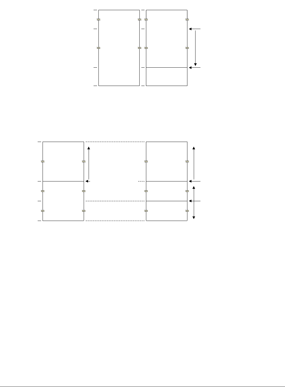
B3 Virtual Memory System Architecture (VMSA)
B3.6 Long-descriptor translation table format
B3-1346 Copyright © 1996-1998, 2000, 2004-2012, 2014 ARM. All rights reserved. ARM DDI 0406C.c
Non-Confidential ID051414
Figure B3-18 Control of TTBR boundary, when TTBCR.T1SZ is zero
•Figure B3-19 shows how, when TTBCR.T1SZ is nonzero, the values of TTBCR.T0SZ and TTBCR.T1SZ
control the boundaries between VAs that are translated using TTBR0, and VAs that are translated using
TTBR1.
Figure B3-19 Control of TTBR boundaries, when TTBCR.T1SZ is nonzero
When T0SZ and T1SZ are both nonzero:
— If both fields are set to
0b001
, the boundary between the two regions is
0x80000000
. This is identical to
having T0SZ set to
0b000
and T1SZ set to
0b001
.
— Otherwise, the TTBR0 and TTBR1 regions are non-contiguous. In this case, any attempt to access an
address that is in that gap between the TTBR0 and TTBR1 regions generates a Translation fault.
When using the Long-descriptor translation table format:
• The TTBCR contains fields that define memory region attributes for the translation table walk, for each
TTBR. These are the SH0, ORGN0, IRGN0, SH1, ORGN1, and IRGN1 bits.
• Each TTBR contains an ASID field, and the TTBCR.A1 field selects which ASID to use.
For this translation table format, Long-descriptor translation table format address lookup levels on page B3-1348
summarizes the lookup levels, and Translation table walks, when using the Long-descriptor translation table format
on page B3-1350 describes the possible translations.
0x00000000
0xFFFFFFFF
0x02000000
TTBR0 region Effect of increasing TTBCR.T0SZ
TTBCR.T0SZ==0b000
Use of TTBR1 disabled
TTBR0 region
TTBR1 region
Boundary, when TTBCR.T0SZ==0b111
0x80000000 Boundary, when TTBCR.T0SZ==0b001
TTBCR.T1SZ==0b000
0x00000000
0xFFFFFFFF
TTBR0 region
Effect of increasing TTBCR.T1SZ
TTBR1 region
TTBCR.T0SZ==0b000
0x80000000 Boundary,
TTBCR.T1SZ==0b001
0x40000000
TTBR1 region
TTBR0 region
Boundary, when TTBCR.T0SZ==0b010
Effect of increasing TTBCR.T0SZ
Accesses
generate a
Translation fault
Effect of
increasing
TTBCR.T1SZ
Boundary, when TTBCR.T1SZ==0b001
TTBCR.T0SZ>0b000
Effect of decreasing TTBCR.T0SZ

B3 Virtual Memory System Architecture (VMSA)
B3.6 Long-descriptor translation table format
ARM DDI 0406C.c Copyright © 1996-1998, 2000, 2004-2012, 2014 ARM. All rights reserved. B3-1347
ID051414 Non-Confidential
Possible translation table registers programming errors
In all the descriptions in this subsection, the size of the input address supported for a PL1&0 stage 1 translation
refers to the size specified by a TTBCR.TxSZ field.
Note
For a PL1&0 stage 1 translation, the input address range can be split so that the lower addresses are translated by
TTBR0 and the higher addresses are translated by TTBR1. In this case, each of input address sizes specified by
TTBCR.{T0SZ, T1SZ} is smaller than the total address size supported by the stage of translation.
The following are possible errors in the programming of TTBR0, TTBR1, and TTBCR. For the translation of a
particular address at a particular stage of translation, either:
• The block size being used to translate the address is larger than the size of the input address supported at a
stage of translation used in performing the required translation. This can occur only for the stage 1 translation
of the PL1&0 translation regime, and only when either TTBCR.T0SZ or TTBCR.T1SZ is zero, meaning
there is no gap between the address range translated by TTBR0 and the range translated by TTBR1. In this
case, this programming error occurs if a block translated from the region that has TxSZ set to zero straddles
the boundary between the two address ranges. Example B3-2 shows an example of this mis-programming.
• The address range translated by a set of blocks marked as contiguous, by use of the contiguous bit, is larger
than the size of the input address supported at a stage of translation used in performing the required
translation.
Example B3-2 Translation table programming error
If TTBCR.T0SZ is programmed to 0 and TTBCR.T1SZ is programmed to 7, this means:
•TTBR0 translates addresses in the range
0x00000000
-
0xFDFFFFFF
.
•TTBR1 translates addresses in the range
0xFE000000
-
0xFFFFFFFF
.
The translation table indicated by TTBR0 might be programmed with a block entry for a 1GB region starting at
0xC0000000
. This covers the address range
0xC0000000
-
0xFFFFFFFF
, that overlaps the TTBR1 address range. This
means this block size is larger than the input address size supported for translations using TTBR0, and therefore this
is a programming error.
To understand why this must be a programming error, consider a memory access to address
0xFFFF0000
. According
to the TTBCR.{T0SZ, T1SZ} values, this must be translated using TTBR1. However, the access matches a TLB
entry for the translation, using TTBR0, of the block at
0xC0000000
. Hardware is not required to detect that the access
to
0xFFFF0000
is being translated incorrectly.
In these cases, an implementation might use one of the following approaches:
• Treat such a block, that might be a block within a contiguous set of blocks, as causing a Translation fault,
even though the block is valid, and the address accessed within that block is within the size of the input
address supported at a stage of translation.
• Treat such a block, that might be a block within a contiguous set of blocks, as not causing a Translation fault,
even though the address accessed within that block is outside the size of the input address supported at a stage
of translation, provided that both of the following apply:
— The block is valid.
— At least one address within the block, or contiguous set of blocks, is within the size of the input address
supported at a stage of translation.

B3 Virtual Memory System Architecture (VMSA)
B3.6 Long-descriptor translation table format
B3-1348 Copyright © 1996-1998, 2000, 2004-2012, 2014 ARM. All rights reserved. ARM DDI 0406C.c
Non-Confidential ID051414
B3.6.5 Long-descriptor translation table format address lookup levels
As stated at the start of this section, because the Long-descriptor translation table format is used for the PL1&0
stage 2 translations, the format must support input addresses of up to 40 bits.
Table B3-3 summarizes the properties of the three levels of address lookup when using this format.
For first-level and second-level tables, reducing the input address range reduces the number of addresses in the table
and therefore reduces the table size.The appropriate Translation Table Control Register specifies the input address
range.
Stage 1 translations require an input address range of up to 32 bits, corresponding to VA[31:0]. For these
translations:
• for a memory access from a mode other than Hyp mode, the Secure or Non-secure TTBR0 or TTBR1 holds
the translation table base address, and the Secure or Non-secure TTBCR is the control register
• for a memory access from Hyp mode, HTTBR holds the translation table base address, and HTCR is the
control register.
Note
For translations controlled by TTBR0 and TTBR1, if neither Translation Table Base Register has an input address
range larger than 1GB, then translation starts at the second level. Together, TTBR0 and TTBR1 can still cover the
32-bit VA input address range.
Stage 2 translations require an input address range of up to 40 bits, corresponding to IPA[39:0], and the supported
input address size is configurable in the range 25-40 bits. Table B3-3 indicates a requirement for the translation
mechanism to support a 39-bit input address range, Address[38:0]. Use of concatenated translation tables for stage
2 translations describes how a 40-bit IPA address range is supported. For stage 2 translations:
•VTTBR holds the translation table base address, and VTCR is the control register.
• if a supplied input address is larger than the configured input address size, a Translation fault is generated.
Use of concatenated translation tables for stage 2 translations
If a stage 2 translation requires 16 entries or fewer in its top-level translation table, it can instead:
• require the corresponding number of concatenated translation tables at the next translation level, aligned to
the size of the block of concatenated translation tables
• start the translation at that next translation level.
Note
Stage 2 translations always use the Long-descriptor translation table format.
Table B3-3 Properties of the three levels of address lookup with Long-descriptor translation tables
Level
Input address Output addressa
Number of entries
Size Address rangebSize Address range
First Up to 512GB Up to Address[38:0] 1GB Address[39:30] Up to 512
Second Up to 1GB Up to Address[29:0] 2MB Address[39:21] Up to 512
Third 2MB Address[20:0] 4KB Address[39:12] 512
a. Output address when an entry addresses a block of memory or a memory page. If an entry addresses the next level of
address lookup it specifies Address[39:12] for the next-level translation table.
b. Input address range for the translation table. See Use of concatenated first-level translation tables on page B3-1349 for
details of support for a 40-bit input address range.

B3 Virtual Memory System Architecture (VMSA)
B3.6 Long-descriptor translation table format
ARM DDI 0406C.c Copyright © 1996-1998, 2000, 2004-2012, 2014 ARM. All rights reserved. B3-1349
ID051414 Non-Confidential
Use of this translation scheme is:
• Required when the stage 2 translation supports a 40-bit input address range, see Use of concatenated
first-level translation tables
• Supported for a stage 2 translation with an input address range of 31-34 bits, see Use of concatenated
second-level translation tables.
Note
This translation scheme:
• avoids the overhead of an additional level of translation
• requires the software that is defining the translation to:
— define the concatenated translation tables with the required overall alignment
— program VTTBR to hold the address of the first of the concatenated translation tables
— program VTCR to indicate the required input address range and first lookup level.
Use of concatenated first-level translation tables
The Long-descriptor format translation tables provide 9 bits of address resolution at each level of lookup. However,
a 40-bit input address range with a translation granularity of 4KB requires a total of 28 bits of address resolution.
Therefore, a stage 2 translation that supports a 40-bit input address range requires two concatenated first-level
translation tables, together aligned to 8KB, where:
• the table at the address with PA[12:0]==
0b0000000000000
defines the translations for input addresses with
bit[39]==0
• the table at the address with PA[12:0]==
0b1000000000000
defines the translations for input addresses with
bit[39]==1
• the 8KB alignment requirement means that both table have the same value for PA[39:13].
Use of concatenated second-level translation tables
A stage 2 translation with an input address range of 31-34 bits can start the translation either:
• with a first-level lookup, accessing a first-level translation table with 2-16 entries
• with a second-level lookup, accessing a set of concatenated second-level translation tables.
Table B3-4 shows these options, for each of the input address ranges that can use this scheme.
Note
Because these are stage 2 translations, the input address range is an IPA range.
Table B3-4 Possible uses of concatenated translation tables for second-level lookup
Input address range Lookup starts at first level Lookup starts at second level
IPA range Size Required first-level entries Number of concatenated tables Required alignmenta
IPA[30:0] 231 bytes 2 2 8KB
IPA[31:0] 232 bytes 4 4 16KB
IPA[32:0] 233 bytes 8 8 32KB
IPA[33:0] 234 bytes 16 16 64KB
a. Required alignment of the set of concatenated second-level tables.

B3 Virtual Memory System Architecture (VMSA)
B3.6 Long-descriptor translation table format
B3-1350 Copyright © 1996-1998, 2000, 2004-2012, 2014 ARM. All rights reserved. ARM DDI 0406C.c
Non-Confidential ID051414
See also Determining the required first lookup level for stage 2 translations on page B3-1352.
B3.6.6 Translation table walks, when using the Long-descriptor translation table format
Figure B3-2 on page B3-1312 shows the possible address translations in an Large Physical Address Extension
implementation. These are:
Stage 1 translations
For all stage 1 translations:
• the input address range is up to 32 bits, as determined by either:
—TTBCR.T0SZ or TTBCR.T1SZ, for a PL1&0 stage 1 translation
—HTCR.T0SZ, for a PL2 stage 1 translation
• the output address range is 40 bits.
The stage 1 translations are:
Non-secure PL1&0 stage 1 translation
The stage 1 translation for memory accesses from Non-secure modes other than Hyp
mode. In an implementation that includes the Virtualization Extensions, this translates
a VA to an IPA, otherwise it translates a VA to a PA. For this translation:
• Non-secure TTBR0 or TTBR1 holds the translation table base address
• Non-secure TTBCR determines which TTBR is used.
Non-secure PL2 stage 1 translation
The stage 1 translation for memory accesses from Hyp mode. Supported only if the
implementation includes the Virtualization Extensions, and translates a VA to a PA. For
this translation, HTTBR holds the translation table base address.
Secure PL1&0 stage 1 translation
The stage 1 translation for memory accesses from Secure modes, translates a VA to a
PA. For this translation:
• Secure TTBR0 or TTBR1 holds the translation table base address
• Secure TTBCR determines which TTBR is used.
Stage 2 translation
Non-secure PL1&0 stage 2 translation
The stage 2 translation for memory accesses from Non-secure modes other than Hyp
mode. Supported only if the implementation includes the Virtualization Extensions, and
translates an IPA to a PA. For this translation:
• the input address range is 40 bits, as determined by VTCR.T0SZ
• the output address range depends on the implemented memory system, and is up
to 40 bits
•VTTBR holds the translation table base address
•VTCR specifies the required input address range, and whether the first lookup is
at the first level or at the second level.
The Long-descriptor translation table format provides up to three levels of address lookup, as described in
Long-descriptor translation table format address lookup levels on page B3-1348, and the first lookup, in which the
MMU reads the translation table base address, is at either the first level or the second level. The following
determines the level of the first lookup:
• For a stage 1 translation, the required input address range. For more information see Determining the required
first lookup level for stage 1 translations on page B3-1352.
• For a stage 2 translation, the level specified by the VTCR.SL0 field. For more information see Determining
the required first lookup level for stage 2 translations on page B3-1352.
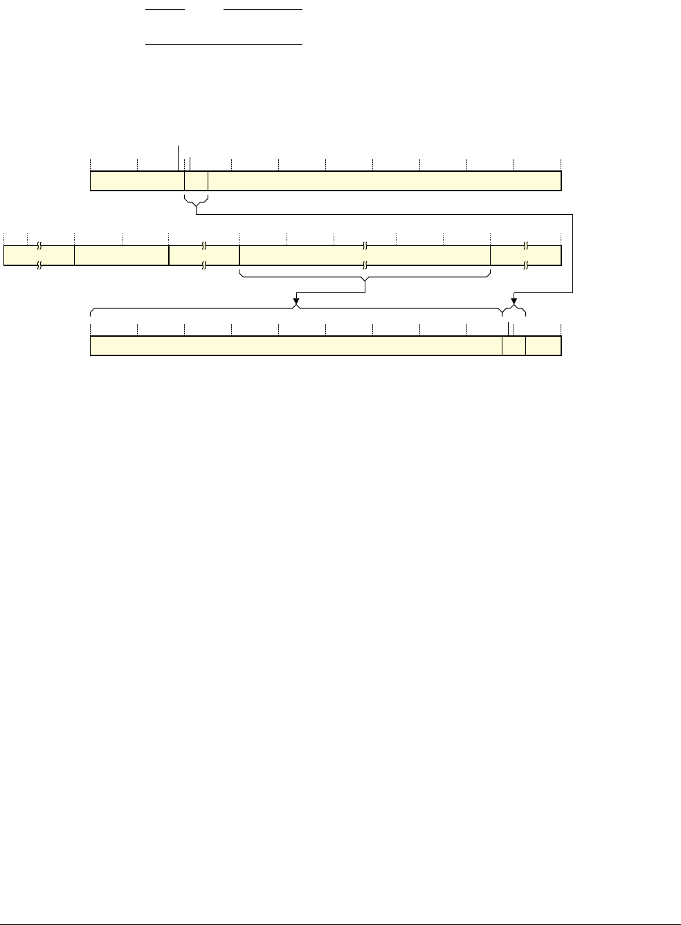
B3 Virtual Memory System Architecture (VMSA)
B3.6 Long-descriptor translation table format
ARM DDI 0406C.c Copyright © 1996-1998, 2000, 2004-2012, 2014 ARM. All rights reserved. B3-1351
ID051414 Non-Confidential
Note
For a stage 2 translation, the size of the required input address range constrains the VTCR.SL0 value.
Figure B3-20 shows how the descriptor address for the first lookup for a translation using the Long-descriptor
translation table format is determined from the input address and the translation table base register value. This figure
shows the lookup for a translation that starts with a first-level lookup, that translates bits[39:30] of the input address,
zero extended if necessary.
Figure B3-20 Long-descriptor first lookup, starting at first level
For a translation that starts with a first-level lookup, as shown in Figure B3-20:
For a stage 1 translation
n is in the range 4-5 and:
• for a memory access from Hyp mode:
—HTTBR is the translation table base register
—n=5-HTCR.T0SZ
• for other accesses:
— the Secure or Non-secure copy of TTBR0 or TTBR1 is the translation table base
register
—n=5-TTBCR.TxSZ, where x is 0 when using TTBR0, and 1 when using TTBR1.
For a stage 2 translation
n is in the range 4-13 and:
•VTTBR is the translation table base register
•n=5-VTCR.T0SZ.
For a translation that starts with a second-level lookup, the descriptor address is obtained in the same way, except
that bits[(n+17):21] of the input address provide bits[(n-1):3] of the descriptor address, where:
For a stage 1 translation
n is in the range 7-12. As Determining the required first lookup level for stage 1 translations on
page B3-1352 shows, for a stage 1 translation to start with a second-level lookup, the corresponding
T0SZ or T1SZ field must be 2 or more. This means:
• for a memory access from Hyp mode, n=14-HTCR.T0SZ
• for other memory accesses, n=14-TTBCR.TxSZ, where x is 0 when using TTBR0, and 1
when using TTBR1.
Input address‡
39
n+27
n+26
30 29 0
39 n
n-1
32 0
000Descriptor address
†
See text for more information about the translation table base register used, and the value of n.
† For a Non-secure PL1&0 stage 1 translation, the IPA of the descriptor. Otherwise, the PA of the descriptor.
‡ This field is absent if n is 13.
UNK/SBZP
40 39
Translation table base address[39:n]UNK/SBZP
63 56 55 48 47 nn-1 0
Register-defined UNK/SBZP Translation table
base register

B3 Virtual Memory System Architecture (VMSA)
B3.6 Long-descriptor translation table format
B3-1352 Copyright © 1996-1998, 2000, 2004-2012, 2014 ARM. All rights reserved. ARM DDI 0406C.c
Non-Confidential ID051414
For a stage 2 translation
n is in the range 7-16. For a stage 2 translation to start with a second-level lookup, VTCR.SL0 is
0b00
, and n=14-VTCR.T0SZ.
Determining the required first lookup level for stage 1 translations
For a stage 1 translation, the required input address range, indicated by a T0SZ or T1SZ field in a translation table
control register, determines the first lookup level. The size of this input address region is 2(32-TxSZ) bytes, and if this
size is:
• Less than or equal to 230 bytes, the required start is at the second level, and translation requires two levels of
table to map to 4KB pages. This corresponds to a TxSZ value of 2 or more.
• More than 230 bytes, the required start is at the first level, and translation requires three levels of table to map
to 4KB pages. This corresponds to a TxSZ value that is less than 2.
For translations not in Hyp mode, the TTBCR:
• splits the 32-bit VA input address range between TTBR0 and TTBR1, see Selecting between TTBR0 and
TTBR1, Long-descriptor translation table format on page B3-1345
• holds the input address range sizes for TTBR0 and TTBR1, in the TTBCR.T0SZ and TTBCR.T1SZ fields.
For translations in Hyp mode, HTCR.T0SZ indicates the size of the required input address range. For example, if
this field is
0b000
, it indicates a 32-bit VA input address range, and translation lookup must start at the first level.
Determining the required first lookup level for stage 2 translations
For a stage 2 translation, the output address range from the stage 1 translations determines the required input address
range for the stage 2 translation. The permitted values of VTCR.SL0 are:
0b00
Stage 2 translation lookup must start at the second level.
0b01
Stage 2 translation lookup must start at the first level.
VTCR.T0SZ must indicate the required input address range. The size of the input address region is 2(32-T0SZ) bytes.
Note
VTCR.T0SZ holds a four-bit signed integer value, meaning it supports values from -8 to 7. This is different from
the other translation control registers, where TnSZ holds a three-bit unsigned integer, supporting values from 0 to 7.
The programming of VTCR must follow the constraints shown in Table B3-5, otherwise behavior is
UNPREDICTABLE. The table also shows how the VTCR.SL0 and VTCR.T0SZ values determine the
VTTBR.BADDR field width.
Where necessary, the first lookup level provides multiple concatenated translation tables, as described in Use of
concatenated second-level translation tables on page B3-1349. This section also gives more information about the
alternatives, shown in Table B3-5, when R is in the range 231-234.
Table B3-5 Input address range constraints on programming VTCR
VTCR.SL0 VTCR.T0SZ Input address range, R First lookup level BADDR[39:x] widtha
a. The first range corresponds to the first T0SZ value, the second range to the second T0SZ value.
0b00
2 to 7 R≤230bytes Second [39:12] to [39:7]
0b00
-2 to 1 230<R≤234bytes Second [39:16] to [39:13]
0b01
-2 to 1 First [39:7] to [39:4]
0b01
-8 to -3 234<R First [39:13] to [39:8]

B3 Virtual Memory System Architecture (VMSA)
B3.6 Long-descriptor translation table format
ARM DDI 0406C.c Copyright © 1996-1998, 2000, 2004-2012, 2014 ARM. All rights reserved. B3-1353
ID051414 Non-Confidential
Full translation flows for Long-descriptor format translation tables
In a translation table walk, only the first lookup uses the translation table base address from the appropriate
Translation table base register. Subsequent lookups use a combination of address information from:
• the table descriptor read in the previous lookup
• the input address.
The following sections describe full Long-descriptor format translation flows, down to an entry for a 4KB page:
•The address and Properties fields shown in the translation flows
•Full translation flow, starting at first-level lookup on page B3-1354
•Full translation flow, starting at second-level lookup on page B3-1355.
The address and Properties fields shown in the translation flows
On an implementation that includes the Virtualization Extensions, for the Non-secure PL1&0 stage 1 translation:
• any descriptor address is the IPA of the required descriptor
• the final output address is the IPA of the block or page.
In these cases, a PL1&0 stage 2 translation is performed to translate the IPA to the required PA.
For all other translations, the final output address is the PA of the block or page, and any descriptor address is the
PA of the descriptor.
Properties indicates register or translation table fields that return information, other than address information, about
the translation or the targeted memory region. For more information see Information returned by a translation table
lookup on page B3-1320, and the description of the register or translation table descriptor.
For translations using the Long-descriptor translation table format, Long-descriptor translation table format
descriptors on page B3-1339 describes the descriptors formats.
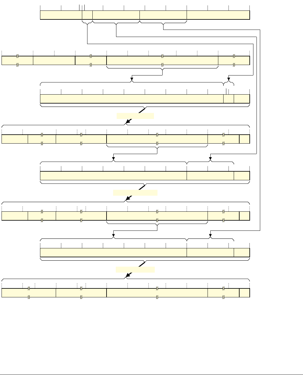
B3 Virtual Memory System Architecture (VMSA)
B3.6 Long-descriptor translation table format
B3-1354 Copyright © 1996-1998, 2000, 2004-2012, 2014 ARM. All rights reserved. ARM DDI 0406C.c
Non-Confidential ID051414
Full translation flow, starting at first-level lookup
Figure B3-21 shows the complete translation flow for a stage 1 translation table walk that starts at a first-level
lookup. For more information about the fields shown in the figure see The address and Properties fields shown in
the translation flows on page B3-1353.
Figure B3-21 Complete Long-descriptor format stage 1 translation, starting at first level
If the first-level lookup or second-level lookup returns a block descriptor then the translation table walk completes
at that level.
Descriptor
address
Input address
First-level lookup
12 1139 32 0
000 Descriptor
address
Descriptor
address
For details of Properties fields, see the register or descriptor description.
UNK/SBZP
40 39
Translation table base address[39:n]UNK/SBZP
63 56 55 48 47 nn-1 0
Properties UNK/SBZP Translation table
base register
n-1
39 n32 0
000
IGNORED
11SBZ
40 39
Second-level table address[39:12]Properties
63 59 58 52 51 0
IGNORED
2112 11 First-level
table descriptor
Second-level lookup
IGNORED
11SBZ
40 39
Third-level table address[39:12]Properties
63 59 58 52 51 0
IGNORED
2112 11
Second-level
table descriptor
12 1139 32 0
000
Third-level lookup
Properties 11SBZ
40 39
Output address[39:12]Properties
63 52 51 02112 11
Third-level
page descriptor
n is {4, 5}
39
n+27 n+26
30 29 0
21 20 12 11
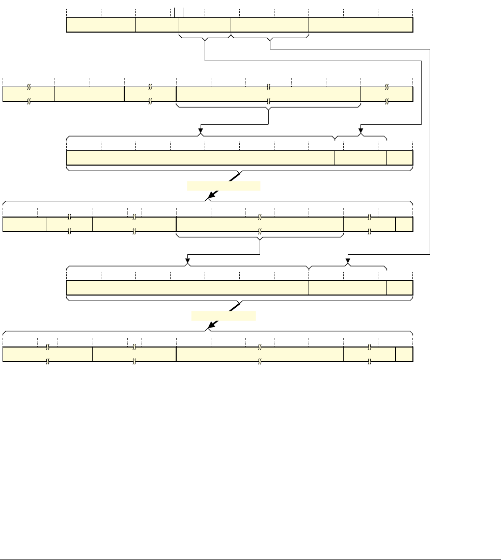
B3 Virtual Memory System Architecture (VMSA)
B3.6 Long-descriptor translation table format
ARM DDI 0406C.c Copyright © 1996-1998, 2000, 2004-2012, 2014 ARM. All rights reserved. B3-1355
ID051414 Non-Confidential
A stage 2 translation that starts at a first-level lookup differs from the translation shown in Figure B3-21 on
page B3-1354 only as follows:
• the possible values of n are 4-13, to support an input address of between 31 and 40 bits
• a descriptor and output addresses are always the PAs.
Full translation flow, starting at second-level lookup
Figure B3-22 shows the complete translation flow for a stage 1 translation table walk that starts at a second-level
lookup. For more information about the fields shown in the figure see The address and Properties fields shown in
the translation flows on page B3-1353.
Figure B3-22 Complete Long-descriptor format stage 1 translation, starting at second level
If the second-level lookup returns a block descriptor then the translation table walk completes at that level.
A stage 2 translation that starts at a second-level lookup differs from the translation shown in Figure B3-22 only as
follows:
• the possible values of n are 7-16, to support an input address of up to 34 bits
• the descriptor and output addresses are always PAs.
Descriptor
address
Input address
12 1139 32 0
000 Descriptor
address
For details of Properties fields, see the register or descriptor description.
Second-level lookup
UNK/SBZP
40 39
Translation table base address[39:n]UNK/SBZP
63 56 55 48 47 nn-1 0
Properties UNK/SBZP Translation table
base register
39 nn-1 32 0
000
IGNORED
11SBZ
40 39
Third-level table address[39:12]Properties
63 59 58 52 51 0
IGNORED
2112 11
Second-level
table descriptor
Third-level lookup
Properties 11SBZ
40 39
Output address[39:12]Properties
63 52 51 02112 11
Third-level
page descriptor
n is {7, …, 12}
39
n+18 n+17
0
21 20 12 113132

B3 Virtual Memory System Architecture (VMSA)
B3.7 Memory access control
B3-1356 Copyright © 1996-1998, 2000, 2004-2012, 2014 ARM. All rights reserved. ARM DDI 0406C.c
Non-Confidential ID051414
B3.7 Memory access control
In addition to an output address, a translation table entry that refers to page or region of memory includes fields that
define properties of the target memory region. Information returned by a translation table lookup on page B3-1320
describes the classification of those fields as address map control, access control, and memory attribute fields. The
access control fields, described in this section, determine whether the processor, in its current state, is permitted to
perform the required access to the output address given in the translation table descriptor. If a translation stage does
not permit the access then an MMU fault is generated for that translation stage, and no memory access is performed.
The following sections describe the memory access controls:
•Access permissions
•Execute-never restrictions on instruction fetching on page B3-1359
•Domains, Short-descriptor format only on page B3-1362
•The Access flag on page B3-1362
•PL2 control of Non-secure access permissions on page B3-1364.
B3.7.1 Access permissions
Note
This section gives a general description of memory access permissions. In an implementation that includes the
Virtualization Extensions, software executing at PL1 in Non-secure state can see only the access permissions
defined by the Non-secure PL1&0 stage 1 translations. However, software executing at PL2 can modify these
permissions, as described in PL2 control of Non-secure access permissions on page B3-1364. This modification is
invisible to Non-secure software executing at PL1 or PL0.
Access permission bits in a translation table descriptor control access to the corresponding memory region. The
Short-descriptor translation table format supports two options for defining the access permissions:
• three bits, AP[2:0], define the access permissions
• two bits, AP[2:1], define the access permissions, and AP[0] can be used as an Access flag.
SCTLR.AFE selects the access permissions option. Setting this bit to 1, to enable the Access flag, also selects use
of AP[2:1] to define access permissions.
The Long-descriptor translation table format uses only AP[2:1] to control the access permissions, and provides an
AF bit for use as an Access flag. This means the VMSA behaves as if SCTLR.AFE is set to 1, regardless of the value
that software has written to this bit.
Note
When use of the Long-descriptor format is enabled, SCTLR.AFE is UNK/SBOP.
From the introduction of the Large Physical Address Extension, ARM deprecates any use of the AP[2:0] scheme
for defining access permissions, see Deprecations relating to using the AP[2:0] scheme for defining MMU access
permissions on page D9-2478.
The Access flag on page B3-1362 describes the Access flag, for both translation table formats.
The XN and PXN bits provide additional access controls for instruction fetches, see Execute-never restrictions on
instruction fetching on page B3-1359.
An attempt to perform a memory access that the translation table access permission bits do not permit generates a
Permission fault, for the corresponding stage of translation. However, when using the Short-descriptor translation
table format, it generates the fault only if the access is to memory in the Client domain, see Domains,
Short-descriptor format only on page B3-1362.

B3 Virtual Memory System Architecture (VMSA)
B3.7 Memory access control
ARM DDI 0406C.c Copyright © 1996-1998, 2000, 2004-2012, 2014 ARM. All rights reserved. B3-1357
ID051414 Non-Confidential
Note
In an implementation that includes the Virtualization Extensions, memory accesses made in Non-secure state at PL1
or PL0 are subject to two stages of translation. Each stage of translation has its own, independent, fault checking.
Fault handling is different for the two stages, see Exception reporting in a VMSA implementation on page B3-1409.
The following sections describe the two access permissions models:
•AP[2:1] access permissions model
•AP[2:0] access permissions control, Short-descriptor format only on page B3-1358. This section includes
some information on access permission control in earlier versions of the ARM VMSA.
AP[2:1] access permissions model
Note
Some documentation describes this as the simplified access permissions model.
This access permissions model is used if the translation is either:
• using the Long-descriptor translation table format
• using Short-descriptor translation table format, and the SCTLR.AFE bit is set to 1.
In this model:
• One bit, AP[2], selects between read-only and read/write access.
• A second bit, AP[1], selects between Application level (PL0) and System level (PL1) control.
For the Non-secure PL2 stage 1 translations, AP[1] is SBO.
In the ARM architecture, this model permits four access combinations:
• read-only at all privilege levels
• read/write at all privilege levels
• read-only at PL1, no access by software executing at PL0
• read/write at PL1, no access by software executing at PL0.
Table B3-6 shows this access control model.
Hierarchical control of access permissions, Long-descriptor format
The Long-descriptor translation table format introduces a mechanism that entries at one level of translation table
lookup can use to set limits on the permitted entries at subsequent levels of lookup. This applies to the access
permissions, and also to the restrictions on instruction fetching described in Hierarchical control of instruction
fetching, Long-descriptor format on page B3-1360.
The restrictions apply only to subsequent levels of lookup at the same stage of translation. The APTable[1:0] field
restricts the access permissions, as Table B3-7 on page B3-1358 shows.
As stated in the table footnote, for the Non-secure PL2 stage 1 translation tables, APTable[0] is reserved, SBZ.
Table B3-6 VMSAv7 AP[2:1] access permissions model
AP[2], disable write access AP[1], enable unprivileged access Access
00a
a. Not valid for Non-secure PL2 stage 1 translation tables. AP[1] is SBO in these tables.
Read/write, only at PL1
0 1 Read/write, at any privilege level
10aRead-only, only at PL1
1 1 Read-only, at any privilege level

B3 Virtual Memory System Architecture (VMSA)
B3.7 Memory access control
B3-1358 Copyright © 1996-1998, 2000, 2004-2012, 2014 ARM. All rights reserved. ARM DDI 0406C.c
Non-Confidential ID051414
Note
The APTable[1:0] settings are combined with the translation table access permissions in the translation tables
descriptors accessed in subsequent levels of lookup. They do not restrict or change the values entered in those
descriptors.
The Long-descriptor format provides APTable[1:0] control only for the stage 1 translations. The corresponding bits
are SBZ in the stage 2 translation table descriptors.
When APTable[1:0] is not set to
0b00
, its effects might be held in one or more TLB entries. Therefore, a change to
APTable[1:0] might require coarse-grained invalidation of the TLB to ensure that the effect of the change is visible
to subsequent memory transactions.
AP[2:0] access permissions control, Short-descriptor format only
This access permissions model applies when using the Short-descriptor translation tables format, and the
SCTLR.AFE bit is set to 0. Table B3-8 shows this access permissions model.
When SCTLR.AFE is set to 0, ensuring that the AP[0] bit is always set to 1 effectively changes the access model to
the simpler model described in AP[2:1] access permissions model on page B3-1357.
Table B3-8 shows the full AP[2:0] access permissions model:
Table B3-7 Effect of APTable[1:0] on subsequent levels of lookup
APTable[1:0] Effect
00 No effect on permissions in subsequent levels of lookup.
01aAccess at PL0 not permitted, regardless of permissions in subsequent levels of lookup.
10 Write access not permitted, at any privilege level, regardless of permissions in subsequent levels of lookup.
11aRegardless of permissions in subsequent levels of lookup:
• write access not permitted, at any privilege level
• read access not permitted at PL0.
a. Not valid for the Non-secure PL2 stage 1 translation tables. In those tables, APTable[0] is SBZ.
Table B3-8 VMSAv7 MMU access permissions
AP[2] AP[1:0] PL1 access Unprivileged access Description
0 00 No access No access All accesses generate Permission faults
01 Read/write No access Access only at PL1
10 Read/write Read-only Writes at PL0 generate Permission faults
11 Read/write Read/write Full access
1 00 - - Reserved
01 Read-only No access Read-only, only at PL1
10 Read-only Read-only Read-only at any privilege level, deprecateda
11 Read-only Read-only Read-only at any privilege levelb
a. From VMSAv7, ARM strongly recommends use of the
0b11
encoding for Read-only at any privilege level.
b. This mapping is introduced in VMSAv7, and is reserved in VMSAv6.

B3 Virtual Memory System Architecture (VMSA)
B3.7 Memory access control
ARM DDI 0406C.c Copyright © 1996-1998, 2000, 2004-2012, 2014 ARM. All rights reserved. B3-1359
ID051414 Non-Confidential
Note
• Before VMSAv7, the SCTLR.S and SCTLR.R bits also affect the access permissions. For more information,
see Translation attributes on page D15-2607.
• VMSAv7 supports the full set of access permissions shown in Table B3-8 on page B3-1358 only when
SCTLR.AFE is set to 0. When SCTLR.AFE is set to 1, the only supported access permissions are those
described in AP[2:1] access permissions model on page B3-1357.
• Some documentation describes the AP[2] bit in the translation table entries as the APX bit.
B3.7.2 Execute-never restrictions on instruction fetching
Execute-never (XN) controls provide an additional level of control on memory accesses permitted by the access
permissions settings. These controls are:
XN, Execute-never
When the XN bit is 1, a Permission fault is generated if the processor attempts to execute an
instruction fetched from the corresponding memory region. However, when using the
Short-descriptor translation table format, the fault is generated only if the access is to memory in the
Client domain, see Domains, Short-descriptor format only on page B3-1362. A processor can
execute instructions from a memory region only if the access permissions for its current state permit
read access, and the XN bit is set to 0.
PXN, Privileged execute-never
When the PXN bit is 1, a Permission fault is generated if the processor is executing at PL1 and
attempts to execute an instruction fetched from the corresponding memory region. As with the XN
bit, when using the Short-descriptor translation table format, the fault is generated only if the access
is to memory in the Client domain.
In both the Short-descriptor format and the Long-descriptor format translation tables, all descriptors for memory
blocks and pages always include an XN bit.
Support for the PXN bit is as follows:
• The Long-descriptor translation table formats always include the PXN bit.
• An implementation that includes the Large Physical Address Extension must:
— support the use of the PXN bit
— use the Short-descriptor translation table formats that include the PXN bit.
• On an implementation that does not include the Large Physical Address Extension, support for use of the
PXN bit is OPTIONAL, and:
— if use of the PXN bit is supported, the Short-descriptor translation table formats include the PXN bit
— otherwise, the Short-descriptor translation table formats do not include the PXN bit.
Short-descriptor translation table first-level descriptor formats on page B3-1326 describes how support for
the PXN bit affects the Short-descriptor translation table formats.
Note
An implementation that does not include the Large Physical Address Extension always uses the Short-descriptor
translation table formats.
In the Non-secure PL2 stage 1 translation tables, the PXN bit is reserved, SBZ.
In addition, the Virtualization Extensions provide controls that enforce execute-never restrictions, regardless of the
settings in the translation tables. Execute-never controls provided by the Virtualization Extensions on page B3-1361
describes these controls.

B3 Virtual Memory System Architecture (VMSA)
B3.7 Memory access control
B3-1360 Copyright © 1996-1998, 2000, 2004-2012, 2014 ARM. All rights reserved. ARM DDI 0406C.c
Non-Confidential ID051414
The execute-never controls apply also to speculative instruction fetching. This means a speculative instruction fetch
from a memory region that is execute-never at the current level of privilege is prohibited.
The XN control means that, when the MMU is enabled, the processor can fetch, or speculatively fetch, an instruction
from a memory location only if all of the following apply:
• If using the Short-descriptor translation table format, the translation table descriptor for the location does not
indicate that it is in a No access domain.
• If using the Long-descriptor translation table format, or using the Short descriptor format and the descriptor
indicates that the location is in a Client domain, in the descriptor for the location the following apply:
— XN is set to 0
— the access permissions permit a read access from the current processor mode
• No other Prefetch Abort condition exists.
Note
• The PXN control applies to the processor privilege when it attempts to execute the instruction. In an
implementation that fetches instructions speculatively, this might not be the privilege when the instruction
was prefetched. Therefore, the architecture does not require the PXN control to prevent instruction fetching.
• Although the execute-never controls apply to speculative fetching, on a speculative instruction fetch from an
execute-never location, no Permission fault is generated unless the processor attempts to execute the
instruction fetched from that location. This means that, if a speculative fetch from an execute-never location
is attempted, but there is no attempt to execute the corresponding instruction, a Permission fault is not
generated.
• The software that defines a translation table must mark any region of memory that is read-sensitive as
execute-never, to avoid the possibility of a speculative fetch accessing the memory region. For example, it
must mark any memory region that corresponds to a read-sensitive peripheral as Execute-never.
• When using the Short-descriptor translation table format, the XN attribute is not checked for domains marked
as Manager. Therefore, the system must not include read-sensitive memory in domains marked as Manager,
because the XN bit does not prevent speculative fetches from a Manager domain.
When no MMU for the translation regime is enabled, memory regions cannot have XN or PXN attributes assigned.
Behavior of instruction fetches when all associated MMUs are disabled on page B3-1316 describes how disabling
all MMUs affects instruction fetching.
Hierarchical control of instruction fetching, Long-descriptor format
The Long-descriptor translation table format introduces a mechanism that entries at one level of translation tables
lookup can use to set limits on the permitted entries at subsequent levels of lookup. This applies to the restrictions
on instruction fetching, and also to the access permissions described in Hierarchical control of access permissions,
Long-descriptor format on page B3-1357.
The restrictions apply only to subsequent levels of lookup at the same stage of translation, and:
• XNTable restricts the XN control:
— when XNTable is set to 1, the XN bit is treated as 1 in all subsequent levels of lookup, regardless of
the actual value of the bit
— when XNTable is set to 0 it has no effect.
• PXNTable restricts the PXN control:
— when PXNTable is set to 1, the PXN bit is treated as 1 in all subsequent levels of lookup, regardless
of the actual value of the bit
— when PXNTable is set to 0 it has no effect.

B3 Virtual Memory System Architecture (VMSA)
B3.7 Memory access control
ARM DDI 0406C.c Copyright © 1996-1998, 2000, 2004-2012, 2014 ARM. All rights reserved. B3-1361
ID051414 Non-Confidential
Note
The XNTable and PXNTable settings are combined with the XN and PXN bits in the translation table descriptors
accessed at subsequent levels of lookup. They do not restrict or change the values entered in those descriptors.
The XNTable and PXNTable controls are provided only in the Long-descriptor translation table format, and only
for stage 1 translations. The corresponding bits are SBZ in the stage 2 translation table descriptors.
When XNTable, or PXNTable, is set to 1, its effects might be held in one or more TLB entries. Therefore, a change
to XNTable or PXNTable might require coarse-grained invalidation of the TLB to ensure that the effect of the
change is visible to subsequent memory transactions.
Execute-never controls provided by the Virtualization Extensions
The Virtualization Extensions provide additional controls that force memory regions to be treated as execute-never,
regardless of the settings in the appropriate translation table descriptors. The following subsections describe these
controls:
•Restriction on Secure instruction fetch
•Preventing execution from writable locations.
Restriction on Secure instruction fetch
The Virtualization Extensions add a Secure instruction fetch bit, SCR.SIF. When this bit is set to 1, any attempt in
Secure state to execute an instruction fetched from Non-secure physical memory causes a Permission fault. As with
all Permission fault checking, when using the Short-descriptor format translation tables the check applies only to
Client domains, see Access permissions on page B3-1356.
ARM expects SCR.SIF to be static during normal operation. In particular, whether the TLB holds the effect of the
SIF bit is IMPLEMENTATION DEFINED. The generic sequence to ensure visibility of a change to the SIF bit is:
Change the SCR.SIF bit
ISB ; This ensures synchronization of the change
Invalidate entire TLB
DSB ; This completes the TLB Invalidation
ISB ; This ensures instruction synchronization
Preventing execution from writable locations
The Virtualization Extensions add control bits that, when the corresponding stage 1 MMU is enabled, force writable
memory to be treated as XN, regardless of the setting of the XN bit:
• For Secure and Non-secure PL1&0 stage 1 translations, when SCTLR.WXN is set to 1, all regions that are
writable at stage 1 of the address translation are treated as XN.
• For Non-secure PL2 stage 1 translations, when HSCTLR.WXN is set to 1, all regions that are writable at
stage 1 of the address translation are treated as XN.
• For Secure and Non-secure PL1&0 stage 1 translations, when SCTLR.UWXN is set to 1, an instruction fetch
is treated as accessing a PXN region if it accesses a region that software executing at PL0 can write to.
For more information about the control bits see SCTLR, System Control Register, VMSA on page B4-1707 and
HSCTLR, Hyp System Control Register, Virtualization Extensions on page B4-1591.
Note
Setting a WXN or UWXN bit to 1 changes the interpretation of the translation table entry, overriding a zero value
of an XN or PXN field. It does not cause any change to the translation table entry.
For any given virtual machine, ARM expects WXN and UWXN to remain static in normal operation. In particular,
it is IMPLEMENTATION DEFINED whether TLB entries associated with a particular VMID reflect the effect of the
values of these bits. A generic sequence to ensure synchronization of a change to these bits, when that change is
made without a corresponding change of VMID, is:

B3 Virtual Memory System Architecture (VMSA)
B3.7 Memory access control
B3-1362 Copyright © 1996-1998, 2000, 2004-2012, 2014 ARM. All rights reserved. ARM DDI 0406C.c
Non-Confidential ID051414
Change the WXN or UWXN bit
ISB ; This ensures synchronization of the change
Invalidate entire TLB of associated entries
DSB ; This completes the TLB Invalidation
ISB ; This ensures instruction synchronization
As with all Permission fault checking, if the stage 1 translation is using the Short-descriptor translation table format,
the permission checks are performed only for Client domains. For more information see Access permissions on
page B3-1356.
For more information about address translation see About address translation on page B3-1311.
B3.7.3 Domains, Short-descriptor format only
A domain is a collection of memory regions. The Short-descriptor translation table format supports 16 domains, and
requires the software that defines a translation table to assign each VMSA memory region to a domain. When using
the Short-descriptor format:
• First-level translation table entries for Page tables and Sections include a domain field.
• Translation table entries for Supersections do not include a domain field. The Short-descriptor format defines
Supersections as being in domain 0.
• Second-level translation table entries inherit a domain setting from the parent first-level Page table entry.
• Each TLB entry includes a domain field.
The domain field specifies which of the 16 domains the entry is in, and a two-bit field in the DACR defines the
permitted access for each domain. The possible settings for each domain are:
No access Any access using the translation table descriptor generates a Domain fault.
Clients On an access using the translation table descriptor, the access permission attributes are checked.
Therefore, the access might generate a Permission fault.
Managers On an access using the translation table descriptor, the access permission attributes are not checked.
Therefore, the access cannot generate a Permission fault.
See The MMU fault-checking sequence on page B3-1398 for more information about how, when using the
Short-descriptor translation table format, the Domain attribute affects the checking of the other attributes in the
translation table descriptor.
Note
A single program might:
• be a Client of some domains
• be a Manager of some other domains
• have no access to the remaining domains.
The Long-descriptor translation table format does not support domains. When a stage of translation is using this
format, all memory is treated as being in a Client domain, and the settings in the DACR are ignored.
B3.7.4 The Access flag
The Access flag indicates when a page or section of memory is accessed for the first time since the Access flag in
the corresponding translation table descriptor was set to 0:
• If address translation is using the Short-descriptor translation table format, it must set SCTLR.AFE to 1 to
enable use of the Access flag, see SCTLR, System Control Register, VMSA on page B4-1707. Setting this bit
to 1 redefines the AP[0] bit in the translation table descriptors as an Access flag, and limits the access
permissions information in the translation table descriptors to AP[2:1], as described in AP[2:1] access
permissions model on page B3-1357.

B3 Virtual Memory System Architecture (VMSA)
B3.7 Memory access control
ARM DDI 0406C.c Copyright © 1996-1998, 2000, 2004-2012, 2014 ARM. All rights reserved. B3-1363
ID051414 Non-Confidential
Note
ARMv6K introduces the Access flag mechanism. In earlier versions of the architecture, the SCTLR.AFE bit
is RAZ/WI. For more information see CP15 c1, System Control Register, SCTLR on page D12-2530.
• The Long-descriptor format always supports an Access flag bit in the translation table descriptors, and
address translation using this format behaves as if SCTLR.AFE is set to 1, regardless of the value of that bit.
The Access flag can be managed by software or by hardware. However, support for hardware management of the
Access flag is OPTIONAL and deprecated. The following subsections describe the management options:
•Software management of the Access flag
•Hardware management of the Access flag.
Software management of the Access flag
An implementation that requires software to manage the Access flag generates an Access flag fault whenever a
translation table entry with the Access flag set to 0 is read into the TLB
Note
When using the Short-descriptor translation table format, Access flag faults are generated only if SCTLR.AFE is
set to 1, to enable use of a translation table descriptor bit as an Access flag.
The Access flag mechanism expects that, when an Access flag fault occurs, software resets the Access flag to 1 in
the translation table entry that caused the fault. This prevents the fault occurring the next time that memory location
is accessed. Entries with the Access flag set to 0 are never held in the TLB, meaning software does not have to flush
the entry from the TLB after setting the flag.
Hardware management of the Access flag
For the Secure and Non-secure PL1&0 stage 1 translations, an implementation can provide hardware management
of the Access flag. In this case, if a translation table entry with the Access flag set to 0 is read into the TLB, the
hardware writes 1 to the Access flag bit of the translation table entry in memory.
An implementation that provides hardware management of the Access flag for the Secure and Non-secure PL1&0
stage 1 translations:
• Uses the HW Access flag field, ID_MMFR2[31:28], to indicate this implementation choice.
• Implements the SCTLR.HA bit. This bit must be set to 1 to enable hardware management of the Access flag.
Note
When using the Short-descriptor translation table format, hardware management of the Access flag is performed
only if both:
•SCTLR.AFE is set to 1, to enable use of an Access flag
•SCTLR.HA is set to 1, to enable hardware management of the Access flag.
The Banking of SCTLR means that these bits are defined independently for the Secure and Non-secure address
translations.
When hardware management of the Access flag, is enabled for a stage of address translation, no Access flag faults
are generated for the corresponding translations.
Any implementation of hardware management of the Access flag must ensure that any software changes to the
translation table are not overwritten. The architecture does not require software that changes translation table entries
to use interlocked operations. The hardware management mechanisms for the Access flag must prevent any loss of
data written to translation table entries that might occur when, for example, a write by another processor occurs
between the read and write phases of a translation table walk that updates the Access flag.

B3 Virtual Memory System Architecture (VMSA)
B3.7 Memory access control
B3-1364 Copyright © 1996-1998, 2000, 2004-2012, 2014 ARM. All rights reserved. ARM DDI 0406C.c
Non-Confidential ID051414
Architecturally, an operating system that uses the Access flag must support the software faulting option that
generates Access flag faults. This provides compatibility between systems that include a hardware implementation
of the Access flag and those systems that do not implement this feature.
ARM deprecates any use of the SCTLR.HA bit. That is, in an implementation where this bit is RW, it deprecates
setting this bit to 1 to enable hardware management of the Access flag.
Hardware management of the Access flag is never supported for:
• Non-secure PL1&0 stage 2 translations
• Non-secure PL2 stage 1 translations.
B3.7.5 PL2 control of Non-secure access permissions
Non-secure software executing at PL2 controls two sets of translation tables, both of which use the Long-descriptor
translation table format:
• The translation tables that control the Non-secure PL2 stage 1 translations. These map VAs to PAs, for
memory accesses made when executing in Non-secure state at PL2, and are indicated and controlled by the
HTTBR and HTCR.
These translations have similar access controls to other Non-secure stage 1 translations using the
Long-descriptor translation table format, as described in:
—AP[2:1] access permissions model on page B3-1357
—Execute-never restrictions on instruction fetching on page B3-1359.
The differences from the Non-secure stage 1 translations are that:
— the APTable[0], PXNTable, and PXN bits are reserved, SBZ
— AP[1] is reserved, SBO.
• The translation tables that control the Non-secure PL1&0 stage 2 translations. These map the IPAs from the
stage 1 translation onto PAs, for memory accesses made when executing in Non-secure state at PL1 or PL0,
and are indicated and controlled by the VTTBR and VTCR.
The descriptors in the virtualization translation tables define a second level of access permissions, that are
overlaid onto the permissions defined in the stage 1 translation. This section describes this overlaying of
access permissions.
Note
In an implementation of virtualization, the second-level access permissions mean a hypervisor can define additional
access restrictions to those defined by a Guest OS in the stage 1 translation tables. For a particular access, the actual
access permission is the more restrictive of the permissions defined by:
• the Guest OS, in the stage 1 translation tables
• the hypervisor, in the stage 2 translation tables.
The stage 2 access controls defined at PL2:
• affect only the Non-secure stage 1 access permissions settings
• take no account of whether the accesses are from a PL1 mode or a PL0 mode
• permit software executing at PL2 to assign a write-only attribute to a memory region.
The HAP[2:1] field in the stage 2 descriptors define the stage 2 access permissions, as Table B3-9 on page B3-1365
shows:

B3 Virtual Memory System Architecture (VMSA)
B3.7 Memory access control
ARM DDI 0406C.c Copyright © 1996-1998, 2000, 2004-2012, 2014 ARM. All rights reserved. B3-1365
ID051414 Non-Confidential
For more information about the HAP[2:1] field see Attribute fields in stage 2 Long-descriptor Block and Page
descriptors on page B3-1343.
If the stage 2 permissions cause a Permission fault, this is a stage 2 MMU fault. Stage 2 MMU faults are taken to
Hyp mode, and reported in the HSR using an EC code of
0x20
or
0x24
. For more information, see Use of the HSR
on page B3-1424.
Note
The combination of the EC code and the STATUS value in the HSR indicate that the fault is a stage 2 MMU fault.
The stage 2 permissions include an XN attribute. If this is set to 1, execution from the region is not permitted,
regardless of the value of the XN attribute in the stage 1 translation. If a Permission fault is generated because the
stage 2 XN bit is set to 1, this is reported as a stage 2 MMU fault.
Prioritization of aborts on page B3-1407 describes the abort prioritization if both stages of a translation generate a
fault.
Table B3-9 Stage 2 control of access permissions
HAP[2:1] Access permission
00 No access permitted
01 Read-only. Writes to the region are not permitted, regardless of the stage 1 permissions.
10 Write-only. Reads from the region are not permitted, regardless of the stage 1 permissions.
11 Read/write. The stage 1 permissions determine the access permissions for the region.

B3 Virtual Memory System Architecture (VMSA)
B3.8 Memory region attributes
B3-1366 Copyright © 1996-1998, 2000, 2004-2012, 2014 ARM. All rights reserved. ARM DDI 0406C.c
Non-Confidential ID051414
B3.8 Memory region attributes
In addition to an output address, a translation table entry that refers to a page or region of memory includes fields
that define properties of that target memory region. Information returned by a translation table lookup on
page B3-1320 describes the classification of those fields as address map control, access control, and memory
attribute fields. The memory region attribute fields control the memory type, accesses to the caches, and whether
the memory region is Shareable and therefore is coherent.
The following sections describe the assignment of memory region attributes for stage 1 translations:
•Overview of memory region attributes for stage 1 translations
•Short-descriptor format memory region attributes, without TEX remap on page B3-1367
•Short-descriptor format memory region attributes, with TEX remap on page B3-1368
•Long-descriptor format memory region attributes on page B3-1372.
For an implementation that does not include the Virtualization Extensions, and for an implementation that includes
the Virtualization Extensions and is operating in Secure state, or in Hyp mode, these assignments define the memory
attributes of the accessed region.
For an implementation that includes the Virtualization Extensions and is operating in a Non-secure PL1 or PL0
mode, the Non-secure PL1&0 stage 2 translation can modify the memory attributes assigned by the stage 1
translation. PL2 control of Non-secure memory region attributes on page B3-1374 describes these stage 2
assignments.
B3.8.1 Overview of memory region attributes for stage 1 translations
The description of the memory region attributes in a translation descriptor divides into:
Memory type and attributes
These are described either:
• Directly, by bits in the translation table descriptor.
• Indirectly, by registers referenced by bits in the table descriptor. This is described as
remapping the memory type and attribute description.
The Short-descriptor translation table format can use either of these approaches, selected by the
SCTLR.TRE bit:
TRE == 0 Remap disabled. The TEX[2:0], C, and B bits in the translation table descriptor define
the memory region attributes. Short-descriptor format memory region attributes,
without TEX remap on page B3-1367 describes this encoding.
Note
With the Short-descriptor format, remapping is called TEX remap, and the SCTLR.TRE
bit is the TEX remap enabled bit.
The description of the TRE == 0 encoding includes information about the encoding in
previous versions of the architecture.
TRE == 1 Remap enabled. The TEX[0], C, and B bits in the translation table descriptor are index
bits to the MMU remap registers, that define the memory region attributes:
• the Primary Region Remap Register, PRRR
• the Normal Memory Remap Register, NMRR.
Short-descriptor format memory region attributes, with TEX remap on page B3-1368
describes this encoding scheme.
This scheme reassigns translation table descriptor bits TEX[2:1] for use as bits managed
by the operating system.
The Long-descriptor translation table format always uses remapping. This means the VMSA
behaves as if SCTLR.TRE is set to 1, regardless of the value that software has written to this bit.

B3 Virtual Memory System Architecture (VMSA)
B3.8 Memory region attributes
ARM DDI 0406C.c Copyright © 1996-1998, 2000, 2004-2012, 2014 ARM. All rights reserved. B3-1367
ID051414 Non-Confidential
Note
When use of the Long-descriptor format is enabled, SCTLR.TRE is UNK/SBOP.
Long-descriptor format memory region attributes on page B3-1372 describes this encoding.
Shareability In the Short-descriptor translation table format, the S bit in the translation table descriptor encodes
whether the region is shareable. Enabling TEX remap extends the shareability description. For more
information see:
•Shareability and the S bit, without TEX remap on page B3-1368
•Shareability and the S bit, with TEX remap on page B3-1370.
In the Long-descriptor translation table format, the SH[1:0] field in the translation table descriptor
encodes shareability information. For more information see Shareability, Long-descriptor format on
page B3-1373.
B3.8.2 Short-descriptor format memory region attributes, without TEX remap
When using the Short-descriptor translation table formats, TEX remap is disabled when SCTLR.TRE is set to 0.
Note
• The Short-descriptor format scheme without TEX remap is the scheme used in VMSAv6.
• The B (Bufferable), C (Cacheable), and TEX (Type extension) bit names are inherited from earlier versions
of the architecture. These names no longer adequately describe the function of the B, C, and TEX bits.
Table B3-10 shows the C, B, and TEX[2:0] encodings when TEX remap is disabled:
Table B3-10 TEX, C, and B encodings when TRE == 0
TEX[2:0] C B Description Memory type Page Shareable
000 0 0 Strongly-ordered Strongly-ordered Shareable
1Shareable DeviceaDevice Shareablea
1 0 Outer and Inner Write-Through, no Write-Allocate Normal S bitb
1 Outer and Inner Write-Back, no Write-Allocate Normal S bitb
001 0 0 Outer and Inner Non-cacheable Normal S bitb
1 Reserved - -
10IMPLEMENTATION DEFINED IMPLEMENTATION
DEFINED
IMPLEMENTATION
DEFINED
1 Outer and Inner Write-Back, Write-Allocate Normal S bitb
010 0 0 Non-shareable DeviceaDevice Non-shareablea
1 Reserved - -
1xReserved - -

B3 Virtual Memory System Architecture (VMSA)
B3.8 Memory region attributes
B3-1368 Copyright © 1996-1998, 2000, 2004-2012, 2014 ARM. All rights reserved. ARM DDI 0406C.c
Non-Confidential ID051414
See Memory types and attributes and the memory order model on page A3-126 for an explanation of Normal,
Strongly-ordered and Device memory types, and of the shareability attribute.
Cacheable memory attributes, without TEX remap
When TEX[2] == 1, the translation table entry describes Cacheable memory, and the rest of the encoding defines
the Inner and Outer cache attributes:
TEX[1:0] Define the Outer cache attribute.
C, B Define the Inner cache attribute.
The translation table entries use the same encoding for the Outer and Inner cache attributes, as Table B3-11 shows.
Shareability and the S bit, without TEX remap
The translation table entries also include an S bit. This bit:
• Is ignored if the entry refers to Device or Strongly-ordered memory.
• For Normal memory, determines whether the memory region is Shareable or Non-shareable:
S==0 Normal memory region is Non-shareable.
S==1 Normal memory region is Shareable.
B3.8.3 Short-descriptor format memory region attributes, with TEX remap
When using the Short-descriptor translation table formats, TEX remap is enabled when SCTLR.TRE is set to 1. In
this configuration:
• The software that defines the translation tables must program the PRRR and NMRR to define seven possible
memory region attributes.
• The TEX[0], C, and B bits of the translation table descriptors define the memory region attributes, by
indexing PRRR and NMRR.
• Hardware makes no use TEX[2:1], see The OS managed translation table bits on page B3-1372.
011 x x Reserved - -
1BB A A Cacheable memory: AA = Inner attributec
BB = Outer attribute
Normal S bitb
a. For more information, see Shareable attribute for Device memory regions on page A3-137. Some implementations make no distinction
between Shareable Device memory and Non-shareable Device memory, and refer to both memory types as Shareable Device memory.
b. For more information, see Shareability and the S bit, without TEX remap.
c. For more information, see Cacheable memory attributes, without TEX remap.
Table B3-10 TEX, C, and B encodings when TRE == 0 (continued)
TEX[2:0] C B Description Memory type Page Shareable
Table B3-11 Inner and Outer cache attribute encoding
Encoding Cache attribute
00 Non-cacheable
01 Write-Back, Write-Allocate
10 Write-Through, no Write-Allocate
11 Write-Back, no Write-Allocate

B3 Virtual Memory System Architecture (VMSA)
B3.8 Memory region attributes
ARM DDI 0406C.c Copyright © 1996-1998, 2000, 2004-2012, 2014 ARM. All rights reserved. B3-1369
ID051414 Non-Confidential
When TEX remap is enabled:
• for seven of the eight possible combinations of the TEX[0], C and B bits, fields in the PRRR and NMRR
define the region attributes, as described in this section:
• the meaning of the eighth combination for the TEX[0], C and B bits is IMPLEMENTATION DEFINED
• four bits in the PRRR define whether the region is shareable, as described in Shareability and the S bit, with
TEX remap on page B3-1370.
For each of the possible encodings of the TEX[0], C, and B bits in a translation table entry, Table B3-12 shows
which fields of the PRRR and NMRR registers describe the memory region attributes.
If an implementation includes the Security Extensions, the TEX remap registers and the SCTLR.TRE bit are Banked
between the Secure and Non-secure security states. For more information, see The effect of the Security Extensions
on TEX remap on page B3-1372.
When TEX remap is enabled, the mappings specified by the PRRR and NMRR determine the mapping of the
TEX[0], C and B bits in the translation tables to memory type and cacheability attributes:
1. The primary mapping, indicated by a field in the PRRR as shown in the Memory region column of
Table B3-12, takes precedence.
2. For any region that the PRRR maps as Normal memory, the NMRR determines the Inner cacheability and
Outer cacheability attributes.
3. If it is supported, the Outer Shareable mapping identifies Shareable memory as either Inner Shareable or
Outer Shareable, see Interpretation of the NOSn fields in the PRRR, with TEX remap on page B3-1371.
The TEX remap registers must be static during normal operation. In particular, when the remap registers are
changed:
• it is IMPLEMENTATION DEFINED when the changes take effect
• it is UNPREDICTABLE whether the TLB caches the effect of the TEX remap on translation tables.
The software sequence to ensure the synchronization of changes to the TEX remap registers is:
1. Perform a DSB. This ensures any memory accesses using the old mapping have completed.
2. Write the TEX remap registers or SCTLR.TRE bit.
Table B3-12 TEX, C, and B encodings when TRE == 1
Encoding
Memory typeaCache attributesa, b:Outer Shareable attributea, c
TEX[0] C B Inner cacheability Outer cacheability
000PRRR[1:0] NMRR[1:0] NMRR[17:16] NOT(PRRR[24])
1PRRR[3:2] NMRR[3:2] NMRR[19:18] NOT(PRRR[25])
10PRRR[5:4] NMRR[5:4] NMRR[21:20] NOT(PRRR[26])
1PRRR[7:6] NMRR[7:6] NMRR[23:22] NOT(PRRR[27])
100PRRR[9:8] NMRR[9:8] NMRR[25:24] NOT(PRRR[28])
1PRRR[11:10] NMRR[11:10] NMRR[27:26] NOT(PRRR[29])
10IMPLEMENTATION DEFINED
1PRRR[15:14] NMRR[15:14] NMRR[31:30] NOT(PRRR[31])
a. For details of the Memory type and Outer Shareable encodings see PRRR, Primary Region Remap Register, VMSA on page B4-1700. For
details of the Cache attributes encodings see Table B3-11 on page B3-1368.
b. Applies only if the memory type for the region is mapped as Normal memory.
c. Applies only if the memory type for the region is mapped as Normal or Device memory and the region is Shareable.

B3 Virtual Memory System Architecture (VMSA)
B3.8 Memory region attributes
B3-1370 Copyright © 1996-1998, 2000, 2004-2012, 2014 ARM. All rights reserved. ARM DDI 0406C.c
Non-Confidential ID051414
3. Perform an ISB. This ensures synchronization of the register updates.
4. Invalidate the entire TLB.
5. Perform a DSB. This ensures completion of the entire TLB operation.
6. Clean and invalidate all caches. This removes any cached information associated with the old mapping.
7. Perform a DSB. This ensures completion of the cache maintenance.
8. Perform an ISB. This ensures instruction synchronization.
This extends the standard rules for the synchronization of changes to CP15 registers described in Synchronization
of changes to system control registers on page B3-1461, and provides implementation freedom as to whether or not
the effect of the TEX remap is cached.
Shareability and the S bit, with TEX remap
The memory type of a region, as indicated in the Memory type column of Table B3-12 on page B3-1369, provides
the first level of control of whether the region is shareable:
• If the memory type is Strongly-ordered then the region is Shareable
• If the memory type is Device then:
— if the implementation includes the Large Physical Address Extension, then no distinction is made
between Shareable and Non-shareable Device memory, and effectively the region is Shareable
— otherwise, the shareability is determined by using the value of the S bit in the translation table
descriptor to index bits in the PRRR.
Some implementations make no distinction between Shareable Device memory and Non-shareable Device
memory, and refer to both memory types as Shareable Device memory.
• If the memory type is Normal then the shareability is determined by using the value of the S bit in the
translation table descriptor to index bits in the PRRR.
Table B3-13 shows this determination:
In the cases where the shareability is remapped, the appropriate bit of the PRRR indicates whether the region is
Shareable or Non-shareable, as follows:
PRRR[n] == 0 Not shareable.
PRRR[n] == 1 Shareable.
Note
When TEX remap is enabled, a translation table entry with S == 0 can be mapped as Shareable memory.
Table B3-13 Determining shareability, with TEX remap
Memory type LPAEa implemented
a. LPAE is an abbreviation for the Large Physical Address Extension.
Remapping when S == 0 Remapping when S == 1
Strongly-ordered - Shareable Shareable
Device No PRRR[16] PRRR[17]
Yes Shareable Shareable
Normal - PRRR[18] PRRR[19]

B3 Virtual Memory System Architecture (VMSA)
B3.8 Memory region attributes
ARM DDI 0406C.c Copyright © 1996-1998, 2000, 2004-2012, 2014 ARM. All rights reserved. B3-1371
ID051414 Non-Confidential
Interpretation of the NOSn fields in the PRRR, with TEX remap
When all of the following apply, the NOSn fields in the PRRR distinguish between Inner Shareable and Outer
Shareable memory regions:
• the SCTLR.TRE bit is set to 1
• the region is mapped as Normal memory, or the implementation does not include the Large Physical Address
Extension and the region is mapped as Device memory
• the Normal memory remapping or Device memory remapping of the S bit value for the entry makes the
region Shareable
• the implementation supports the distinction between Inner Shareable and Outer Shareable.
If the SCTLR.TRE bit is set to 0, an implementation can provide an IMPLEMENTATION DEFINED mechanism to
interpret the NOSn fields in the PRRR, see SCTLR.TRE, SCTLR.M, and the effect of the TEX remap registers.
The values of the NOSn fields in the PRRR have no effect if any of the following apply:
• the SCTLR.TRE bit is set to 0 and the IMPLEMENTATION DEFINED mechanism has not been invoked
• the region is mapped as Strongly-ordered memory
• the implementation includes the Large Physical Address Extension, and the region is mapped as Device
memory
• the Normal memory remapping or Device memory remapping of the S bit value for the entry makes the
region Non-shareable.
The NOSn fields in the PRRR are RAZ/WI if the implementation does not support the distinction between Inner
Shareable and Outer Shareable memory regions.
Note
The meaning of shareability attributes for Device memory is IMPLEMENTATION DEFINED for an implementation that
does not include the Large Physical Address Extension, and otherwise has no meaning. For more information, see
Shareable attribute for Device memory regions on page A3-137.
SCTLR.TRE, SCTLR.M, and the effect of the TEX remap registers
When TEX remap is disabled, because the SCTLR.TRE bit is set to 0:
• the effect of the MMU remap registers can be IMPLEMENTATION DEFINED
• the interpretation of the fields of the PRRR and NMRR registers can differ from the description given earlier
in this section.
VMSAv7 requires that the effect of these registers is limited to remapping the attributes of memory locations. These
registers must not change whether any cache hardware or MMUs are enabled. The mechanism by which the TEX
remap registers have an effect when the SCTLR.TRE bit is set to 0 is IMPLEMENTATION DEFINED. The ARMv7
architecture requires that from reset, if the IMPLEMENTATION DEFINED mechanism has not been invoked:
• If the PL1&0 stage 1 MMU is enabled and is using the Short-descriptor format translation tables, the
architecturally-defined behavior of the TEX[2:0], C, and B bits must apply, without reference to the TEX
remap functionality. In other words, memory attribute assignment must comply with the scheme described
in Short-descriptor format memory region attributes, without TEX remap on page B3-1367.
• If the PL1&0 stage 1 MMU is disabled, then the architecturally-defined behavior of the VMSA with MMUs
disabled must apply, without reference to the TEX remap functionality. See The effects of disabling MMUs
on VMSA behavior on page B3-1314.

B3 Virtual Memory System Architecture (VMSA)
B3.8 Memory region attributes
B3-1372 Copyright © 1996-1998, 2000, 2004-2012, 2014 ARM. All rights reserved. ARM DDI 0406C.c
Non-Confidential ID051414
Possible mechanisms for enabling the IMPLEMENTATION DEFINED effect of the TEX remap registers when
SCTLR.TRE is set to 0 include:
• a control bit in the ACTLR, or in a CP15 c15 register
• changing the behavior when the PRRR and NMRR registers are changed from their IMPLEMENTATION
DEFINED reset values.
In addition, if the MMU is disabled and the SCTLR.TRE bit is set to 1, the architecturally-defined behavior of the
VMSA with the MMU disabled must apply without reference to the TEX remap functionality.
In an implementation that includes the Security Extensions, the IMPLEMENTATION DEFINED effect of these registers
must only take effect in the security state of the registers. See also The effect of the Security Extensions on TEX
remap.
The OS managed translation table bits
When TEX remap is enabled, the TEX[2:1] bits in the translation table descriptors are available as two bits that can
be managed by the operating system. In VMSAv7, as long as the SCTLR.TRE bit is set to 1, the values of the
TEX[2:1] bits are ignored by the memory management hardware. Software can write any value to these bits in the
translation tables.
Note
In a system that implements hardware management of the Access flag, a hardware Access flag update never changes
these bits.
The effect of the Security Extensions on TEX remap
In an implementation that includes the Security Extensions, the TEX remap registers are Banked in the Secure and
Non-secure security states. The register versions for the current security state apply to all PL1&0 stage 1 translation
table lookups in that state. The SCTLR.TRE bit is Banked in the Secure and Non-secure copies of the register, and
the appropriate version of this bit determines whether TEX remap is applied to translation table lookups in the
current security state.
Write accesses to the Secure copies of the TEX remap registers are disabled when the CP15SDISABLE input is
asserted HIGH, meaning the
MCR
operations to access these registers are UNDEFINED. For more information, see The
CP15SDISABLE input on page B3-1458.
B3.8.4 Long-descriptor format memory region attributes
When a processor is using the Long-descriptor translation table format, the AttrIndx[2:0] field in a block or page
translation table descriptor for a stage 1 translation indicates the 8-bit field in the appropriate MAIR, that specifies
the attributes for the corresponding memory region:
• AttrIndx[2] indicates the value of n in MAIRn:
AttrIndx[2] == 0 Use MAIR0.
AttrIndx[2] == 1 Use MAIR1.
• AttrIndx[2:0] indicates the required Attr field, Attrn, where n = AttrIndx[2:0].
Each AttrIndx field defines, for the corresponding memory region:
• The memory type, Strongly-ordered, Device, or Normal.
• For Normal memory:
— the inner and outer cacheability, Non-cacheable, Write-Through, or Write-Back
— for Write-Through Cacheable and Write-Back Cacheable regions, the Read-Allocate and
Write-Allocate policy hints, each of which is Allocate or Do not allocate.

B3 Virtual Memory System Architecture (VMSA)
B3.8 Memory region attributes
ARM DDI 0406C.c Copyright © 1996-1998, 2000, 2004-2012, 2014 ARM. All rights reserved. B3-1373
ID051414 Non-Confidential
For more information about the AttrIndx[2:0] descriptor field, see Attribute fields in stage 1 Long-descriptor Block
and Page descriptors on page B3-1342.
Shareability, Long-descriptor format
When a processor is using the Long-descriptor translation table format, the SH[1:0] field in a block or page
translation table descriptor specifies the Shareability attributes of the corresponding memory region, if the MAIR
entry for that region identifies it as Normal memory. Table B3-14 shows the encoding of this field.
See Overlaying the shareability attribute on page B3-1376 for constraints on the Shareability attributes of a Normal
memory region that is Inner Non-cacheable, Outer Non-cacheable.
For a Device or Strongly-ordered memory region, the value of the SH[1:0] field of the translation table descriptor
is ignored.
Other fields in the Long-descriptor translation table format descriptors
The following subsections describe the other fields in the translation table block and page descriptors when a
processor is using the Long-descriptor translation table format:
•Contiguous bit
•Field reserved for software use on page B3-1374
•IGNORED fields on page B3-1374.
Contiguous bit
The Long-descriptor translation table format descriptors contain a Contiguous bit. Setting this bit to 1 indicates that
16 adjacent translation table entries point to a contiguous output address range. These 16 entries must be aligned in
the translation table so that the top 5 bits of their input addresses, that index their position in the translation table,
are the same. For example, referring to Figure B3-21 on page B3-1354, to use this hint for a block of 16 entries in
the third-level translation table, bits[20:16] of the input addresses for the 16 entries must be the same.
The contiguous output address range must be aligned to size of 16 translation table entries at the same translation
table level.
Use of this bit means that the TLB can cache a single entry to cover the 16 translation table entries.
The architecture does not require a processor to cache TLB entries in this way. To avoid TLB coherency issues, any
TLB maintenance by address must not assume any optimization of the TLB tables that might result from use of this
bit.
Note
• This capability is similar to the approach used, in the Short-descriptor translation table format, for optimized
caching of Large Pages and Supersections in the TLB. However, an important difference in the Contiguous
bit capability is that TLB maintenance must be performed based on the size of the underlying translation table
entries, to avoid TLB coherency issues
• This bit was previously called the Contiguous bit.
Table B3-14 SH[1:0] field encoding for Normal memory, Long-descriptor format
SH[1:0] Normal memory
00 Non-shareable
01 UNPREDICTABLE
10 Outer Shareable
11 Inner Shareable

B3 Virtual Memory System Architecture (VMSA)
B3.8 Memory region attributes
B3-1374 Copyright © 1996-1998, 2000, 2004-2012, 2014 ARM. All rights reserved. ARM DDI 0406C.c
Non-Confidential ID051414
IGNORED fields
For stage 1 and stage 2 Block and Page descriptors, the architecture defines bits[63:59] and bits[58:55] as IGNORED
fields, meaning the architecture guarantees that the processor hardware does not update these fields. In addition:
• Bits[58:55] are reserved for software use, see Field reserved for software use.
• In the stage 2 Block and Page descriptors, bits[63:59] are reserved for use by a System MMU.
Field reserved for software use
The architecture reserves a 4-bit field in the Block and Page table descriptors for software use. In considering
migration from using the Short-descriptor format to the Long-descriptor format, this field is an extension of the
Short-descriptor field described in The OS managed translation table bits on page B3-1372.
B3.8.5 PL2 control of Non-secure memory region attributes
Software executing at PL2 controls two sets of translation tables, both of which use the Long-descriptor translation
table format:
• The translation tables that control Non-secure PL2 stage 1 translations. These map VAs to PAs, and are
indicated and controlled by the HTTBR and HTCR.
These translations have exactly the same memory region attribute controls as any other stage 1 translations,
as described in Long-descriptor format memory region attributes on page B3-1372.
• The translation tables that control Non-secure PL1&0 stage 2 translations. These map the IPAs from the stage
1 translation onto PAs, and are indicated and controlled by the VTTBR and VTCR.
The descriptors in the virtualization translation tables define a second level of memory region attributes, that
are overlaid onto the attributes defined in the stage 1 translation. This section describes this overlaying of
attributes.
Long-descriptor translation table format descriptors on page B3-1339 describes the format of the entries in these
tables.
Note
In a virtualization implementation, a hypervisor might usefully:
• reduce the permitted cacheability of a region
• increase the required shareability of a region.
The overlaying of attributes from stage 1 and stage 2 translations supports both of these options.
In the stage 2 translation table descriptors for memory regions and pages, the MemAttr[3:0] and SH[1:0] fields
describe the stage 2 memory region attributes:
• The definition of the stage 2 SH[1:0] field is identical to the same field for a stage 1 translation, see
Shareability, Long-descriptor format on page B3-1373.
• MemAttr[3:2] give a top-level definition of the memory type, and of the cacheability of a Normal memory
region, as Table B3-15 shows:
Table B3-15 Long-descriptor MemAttr[3:2] encoding, stage 2 translation
MemAttr[3:2] Memory type Cacheability
00 Strongly-ordered or Device, determined by MemAttr[1:0] Not applicable
01 Normal Outer Non-cacheable
10 Outer Write-Through Cacheable
11 Outer Write-Back Cacheable

B3 Virtual Memory System Architecture (VMSA)
B3.8 Memory region attributes
ARM DDI 0406C.c Copyright © 1996-1998, 2000, 2004-2012, 2014 ARM. All rights reserved. B3-1375
ID051414 Non-Confidential
The encoding of MemAttr[1:0] depends on the Memory type indicated by MemAttr[3:2]:
— When MemAttr[3:2]==
0b00
, indicating Strongly-ordered or Device memory, Table B3-16 shows the
encoding of MemAttr[1:0]:
— When MemAttr[3:2]!=
0b00
, indicating Normal memory, Table B3-17 shows the encoding of
MemAttr[1:0]:
Note
The stage 2 translation does not assign any allocation hints.
The following sections describe how the memory type attributes assigned at stage 2 of the translation are overlaid
onto those assigned at stage 1:
•Overlaying the memory type attribute on page B3-1376
•Overlaying the cacheability attribute on page B3-1376
•Overlaying the shareability attribute on page B3-1376.
Note
The following stage 2 translation table attribute settings leave the stage 1 settings unchanged:
• MemAttr[3:2] ==
0b11
, Normal memory, Outer Write-Back Cacheable
• MemAttr[1:0] ==
0b11
, Inner Write-Back Cacheable.
Table B3-16 MemAttr[1:0] encoding for Strongly-ordered or Device memory
MemAttr[1:0] Meaning when MemAttr[3:2] ==
0b00
00 Region is Strongly-ordered memory
01 Region is Device memory
10 UNPREDICTABLE
11 UNPREDICTABLE
Table B3-17 MemAttr[1:0] encoding for Normal memory
MemAttr[1:0] Meaning when MemAttr[3:2] !=
0b00
00 UNPREDICTABLE
01 Inner Non-cacheable
10 Inner Write-Through Cacheable
11 Inner Write-Back Cacheable

B3 Virtual Memory System Architecture (VMSA)
B3.8 Memory region attributes
B3-1376 Copyright © 1996-1998, 2000, 2004-2012, 2014 ARM. All rights reserved. ARM DDI 0406C.c
Non-Confidential ID051414
Overlaying the memory type attribute
Table B3-18 shows how the stage 1 and stage 2 memory type assignments are combined:
See Overlaying the shareability attribute for information about:
• the shareability of a region for which the resultant type is Strongly-ordered or Device
• the shareability requirements of a region with a resultant type of Normal for which the resultant cacheability,
described in Overlaying the cacheability attribute, is Inner Non-cacheable, Outer Non-cacheable.
The overlaying of the memory type attribute means a translation table walk for a stage 1 translation can be made to
Strongly-ordered or Device memory. This is likely to indicate a Guest OS error, and setting the HCR.PTW bit to 1
causes such an access to generate a Translation fault, see Stage 2 fault on a stage 1 translation table walk,
Virtualization Extensions on page B3-1402.
Overlaying the cacheability attribute
For a Normal memory region, Table B3-19 shows how the stage 1 and stage 2 cacheability assignments are
combined. This combination applies, independently, for the Inner cacheability and Outer cacheability attributes:
Note
Only Normal memory has a cacheability attribute.
Overlaying the shareability attribute
A memory region for which the resultant memory type attribute, described in Overlaying the memory type attribute,
is Strongly-ordered or Device, is treated as Outer Shareable, regardless of any shareability assignments at either
stage of translation. For more information about the effect of the Large Physical Address Extension on the
shareability of Device and Strongly-ordered memory, see Device and Strongly-ordered memory shareability, Large
Physical Address Extension on page A3-138.
Table B3-18 Combining the stage 1 and stage 2 memory type assignments
Assignment in stage 1 Assignment in stage 2 Resultant type
Strongly-ordered Any Strongly-ordered
Any Strongly-ordered Strongly-ordered
Device Normal or Device Device
Normal or Device Device Device
Normal Normal Normal
Table B3-19 Combining the stage 1 and stage 2 cacheability assignments
Assignment in stage 1 Assignment in stage 2 Resultant cacheability
Non-cacheable Any Non-cacheable
Any Non-cacheable Non-cacheable
Write-Through Cacheable Write-Through or Write-Back Cacheable Write-Through Cacheable
Write-Through or Write-Back Cacheable Write-Through Cacheable Write-Through Cacheable
Write-Back Cacheable Write-Back Cacheable Write-Back Cacheable

B3 Virtual Memory System Architecture (VMSA)
B3.8 Memory region attributes
ARM DDI 0406C.c Copyright © 1996-1998, 2000, 2004-2012, 2014 ARM. All rights reserved. B3-1377
ID051414 Non-Confidential
For a memory region with a resultant memory type attribute of Normal, Table B3-20 shows how the stage 1 and
stage 2 shareability assignments are combined:
A memory region with a resultant memory type attribute of Normal, and a resultant cacheability attribute of Inner
Non-cacheable, Outer Non-cacheable, must have a resultant shareability attribute of Outer Shareable, otherwise
shareability is UNPREDICTABLE.
Table B3-20 Combining the stage 1 and stage 2 shareability assignments
Assignment in stage 1 Assignment in stage 2 Resultant shareability
Outer Shareable Any Outer Shareable
Inner Shareable Outer Shareable Outer Shareable
Inner Shareable Inner Shareable Inner Shareable
Inner Shareable Non-shareable Inner Shareable
Non-shareable Outer Shareable Outer Shareable
Non-shareable Inner Shareable Inner Shareable
Non-shareable Non-shareable Non-shareable

B3 Virtual Memory System Architecture (VMSA)
B3.9 Translation Lookaside Buffers (TLBs)
B3-1378 Copyright © 1996-1998, 2000, 2004-2012, 2014 ARM. All rights reserved. ARM DDI 0406C.c
Non-Confidential ID051414
B3.9 Translation Lookaside Buffers (TLBs)
Translation Lookaside Buffers (TLBs) are an implementation technique that caches translations or translation table
entries. TLBs avoid the requirement for every memory access to perform a translation table walk in memory. The
ARM architecture does not specify the exact form of the TLB structures for any design. In a similar way to the
requirements for caches, the architecture only defines certain principles for TLBs:
• The architecture has a concept of an entry locked down in the TLB. The method by which lockdown is
achieved is IMPLEMENTATION DEFINED, and an implementation might not support lockdown.
• The architecture does not guarantee that an unlocked TLB entry remains in the TLB.
• The architecture guarantees that a locked TLB entry remains in the TLB. However, a locked TLB entry might
be updated by subsequent updates to the translation tables. Therefore, when a change is made to the
translation tables, the architecture does not guarantee that a locked TLB entry remains incoherent with an
entry in the translation table.
• The architecture guarantees that a translation table entry that generates a Translation fault or an Access flag
fault is not held in the TLB. However a translation table entry that generates a Domain fault or a Permission
fault might be held in the TLB.
• Any translation table entry that does not generate a Translation or Access flag fault and is not out of context
might be allocated to an enabled TLB at any time. The only translation table entries guaranteed not to be held
in the TLB are those that generate a Translation or Access flag fault.
Note
An enabled TLB can hold translation table entries that do not generate a Translation fault but point to
subsequent tables in the translation table walk. This can be referred to as intermediate caching of TLB
entries.
• Software can rely on the fact that between disabling and re-enabling a stage of address translation, entries in
the TLB relating to that stage of translation have not have been corrupted to give incorrect translations.
The following sections give more information about TLB implementation:
•Global and process-specific translation table entries
•TLB matching on page B3-1379
•TLB behavior at reset on page B3-1379
•TLB lockdown on page B3-1379
•TLB conflict aborts on page B3-1380.
See also TLB maintenance requirements on page B3-1381.
B3.9.1 Global and process-specific translation table entries
In a VMSA implementation, system software can divide a virtual memory map used by memory accesses at PL1
and PL0 into global and non-global regions, indicated by the nG bit in the translation table descriptors:
nG == 0 The translation is global, meaning the region is available for all processes.
nG == 1 The translation is non-global, or process-specific, meaning it relates to the current ASID, as defined
by the CONTEXTIDR.
Each non-global region has an associated Address Space Identifier (ASID). These identifiers mean different
translation table mappings can co-exist in a caching structure such as a TLB. This means that software can create a
new mapping of a non-global memory region without removing previous mappings.
For a symmetric multiprocessor cluster where a single operating system is running on the set of processing elements,
ARMv7 requires all ASID values to be assigned uniquely within any single Inner Shareable domain. In other words,
each ASID value must have the same meaning to all processing elements in the system.
The translation regime used for accesses made at PL2 does not support ASIDs, and all pages are treated as global.

B3 Virtual Memory System Architecture (VMSA)
B3.9 Translation Lookaside Buffers (TLBs)
ARM DDI 0406C.c Copyright © 1996-1998, 2000, 2004-2012, 2014 ARM. All rights reserved. B3-1379
ID051414 Non-Confidential
When a processor is using the Long-descriptor translation table format, and is in Secure state, a translation must be
treated as non-global, regardless of the value of the nG bit, if NSTable is set to 1 at any level of the translation table
walk.
For more information see Control of Secure or Non-secure memory access, Long-descriptor format on
page B3-1344.
B3.9.2 TLB matching
A TLB is a hardware caching structure for translation table information. Like other hardware caching structures, it
is mostly invisible to software. However, there are some situations where it can become visible. These are associated
with coherency problems caused by an update to the translation table that has not been reflected in the TLB. Use of
the TLB maintenance operations described in TLB maintenance requirements on page B3-1381 can prevent any
TLB incoherency becoming a problem.
A particular case where the presence of the TLB can become visible is if the translation table entries that are in use
under a particular ASID and VMID are changed without suitable invalidation of the TLB. This is an issue regardless
of whether or not the translation table entries are global. In some cases, the TLB can hold two mappings for the same
address, and this might lead to UNPREDICTABLE behavior
B3.9.3 TLB behavior at reset
The ARMv7 architecture does not require a reset to invalidate the TLBs. ARMv7 recognizes that an implementation
might require caches, including TLBs, to maintain context over a system reset. Possible reasons for doing so include
power management and debug requirements.
For ARMv7:
• All TLBs are disabled from reset. All MMUs are disabled from reset, and the contents of the TLBs have no
effect on address translation. For more information see Enabling MMUs on page B3-1316.
• An implementation can require the use of a specific TLB invalidation routine, to invalidate the TLB arrays
before they are enabled after a reset. The exact form of this routine is IMPLEMENTATION DEFINED, but if an
invalidation routine is required it must be documented clearly as part of the documentation of the device.
ARM recommends that if an invalidation routine is required for this purpose, the routine is based on the
ARMv7 TLB maintenance operations described in TLB maintenance operations, not in Hyp mode on
page B4-1746.
• When TLBs that have not been invalidated by some mechanism since reset are enabled, the state of those
TLBs is UNPREDICTABLE.
Similar rules apply:
• to cache behavior, see Behavior of the caches at reset on page B2-1269
• to branch predictor behavior, see Behavior of the branch predictors at reset on page B2-1273.
B3.9.4 TLB lockdown
ARMv7 recognizes that any TLB lockdown scheme is heavily dependent on the microarchitecture, making it
inappropriate to define a common mechanism across all implementations. This means that:
• ARMv7 does not require TLB lockdown support.
• If TLB lockdown support is implemented, the lockdown mechanism is IMPLEMENTATION DEFINED. However,
key properties of the interaction of lockdown with the architecture must be documented as part of the
implementation documentation.

B3 Virtual Memory System Architecture (VMSA)
B3.9 Translation Lookaside Buffers (TLBs)
B3-1380 Copyright © 1996-1998, 2000, 2004-2012, 2014 ARM. All rights reserved. ARM DDI 0406C.c
Non-Confidential ID051414
This means that:
• In ARMv7, the TLB Type Register, TLBTR, does not define the lockdown scheme in use.
Note
This is a change from previous versions of the architecture, see CP15 c0, TLB Type ID Register, TLBTR,
ARMv6 on page D12-2529.
• A region of the CP15 c10 encodings is reserved for IMPLEMENTATION DEFINED TLB functions, such as TLB
lockdown functions. The reserved encodings are those with:
—
<CRm>
== {c0, c1, c4, c8}
— all values of
<opc2>
and
<opc1>
.
See also IMPLEMENTATION DEFINED TLB control operations, VMSA on page B4-1753.
An implementation might use some of the CP15 c10 encodings that are reserved for IMPLEMENTATION DEFINED
TLB functions to implement additional TLB control functions. These functions might include:
• Unlock all locked TLB entries.
• Preload into a specific level of TLB. This is beyond the scope of the
PLI
and
PLD
hint instructions.
The Virtualization Extensions do not affect the TLB lockdown requirements. However, in a processor that
implements the Virtualization Extensions, exceptions generated by problems related to TLB lockdown, in a
Non-secure PL1 mode, can be routed to either:
• Non-secure Abort mode, using the Non-secure Data Abort exception vector
• Hyp mode, using the Hyp Trap exception vector.
For more information, see Trapping accesses to lockdown, DMA, and TCM operations on page B1-1253.
B3.9.5 TLB conflict aborts
The Large Physical Address Extension introduces the concept of a TLB conflict abort, and adds fault status
encodings for such an abort, for both the Short-descriptor and Long-descriptor translation table formats, see:
•PL1 fault reporting with the Short-descriptor translation table format on page B3-1414
•Fault reporting with the Long-descriptor translation table format on page B3-1416.
An implementation can generate a TLB conflict abort if it detects that the address being looked up in the TLB hits
multiple entries. This can happen if the TLB has been invalidated inappropriately, for example if TLB invalidation
required by this manual has not been performed. If it happens, the resulting behavior is UNPREDICTABLE, but must
not permit access to regions of memory with permissions or attributes that mean they cannot be accessed in the
current Security state at the current privilege level.
In some implementations, multiple hits in the TLB can generate a synchronous Data Abort or Prefetch Abort
exception. In any case where this is possible it is IMPLEMENTATION DEFINED whether the abort is a stage 1 abort or
a stage 2 abort.
Note
A stage 2 abort cannot be generated if the Non-secure PL1&0 stage 2 MMU is disabled.
The priority of the TLB conflict abort is IMPLEMENTATION DEFINED, because it depends on the form of any TLB
that can generate the abort.
Note
The TLB conflict abort must have higher priority than any abort that depends on a value held in the TLB.
An implementation can generate TLB conflict aborts on either or both instruction fetches and data accesses.
On a TLB conflict abort, the fault address register returns the address that generated the fault. That is, it returns the
address that was being looked up in the TLB.

B3 Virtual Memory System Architecture (VMSA)
B3.10 TLB maintenance requirements
ARM DDI 0406C.c Copyright © 1996-1998, 2000, 2004-2012, 2014 ARM. All rights reserved. B3-1381
ID051414 Non-Confidential
B3.10 TLB maintenance requirements
Translation Lookaside Buffers (TLBs) are an implementation mechanism that caches translations or translation
table entries. The ARM architecture does not specify the form of any TLB structures, but defines the mechanisms
by which TLBs can be maintained.The following sections describe the VMSAv7 TLB maintenance operations:
•General TLB maintenance requirements
•Maintenance requirements on changing system control register values on page B3-1385
•Atomicity of register changes on changing virtual machine on page B3-1386
•Synchronization of changes of ASID and TTBR on page B3-1386
•Multiprocessor effects on TLB maintenance operations on page B3-1389
•The scope of TLB maintenance operations on page B3-1389.
B3.10.1 General TLB maintenance requirements
TLB maintenance operations provide a mechanism to invalidate entries from a TLB. As stated at the start of
Translation Lookaside Buffers (TLBs) on page B3-1378, any translation table entry that does not generate a
Translation fault or an Access flag fault might be allocated to an enabled TLB at any time. This means that software
must perform TLB maintenance between updating translation table entries that apply in a particular context and
accessing memory locations whose translation is determined by those entries in that context.
Note
This requirement applies to any translation table entry at any level of the translation tables, including an entry that
points to further levels of the tables, provided that the entry in that level of the tables does not cause a Translation
fault or Access flag fault
In addition to any TLB maintenance requirement, when changing the cacheability attributes of an area of memory,
software must ensure that any cached copies of affected locations are removed from the caches. For more
information see Cache maintenance requirement created by changing translation table attributes on page B3-1394.
Because a TLB never holds any translation table entry that generates a Translation fault or an Access Flag fault, a
change from a translation table entry that causes a Translation or Access flag fault to one that does not fault, does
not require any TLB or branch predictor invalidation.
Special considerations can apply to translation table updates that change the memory type, cacheability, or output
address of an entry, see Using break-before-make when updating translation table entries on page B3-1382.
In addition, software must perform TLB maintenance after updating the system control registers if the updates mean
that the TLB might hold information that applies to a current translation context, but is no longer valid for that
context. Maintenance requirements on changing system control register values on page B3-1385 gives more
information about this maintenance requirement.
Each of the translation regimes defined in Figure B3-1 on page B3-1309 is a different context, and:
• For the Non-secure PL1&0 regime, a change in the VMID or ASID value changes the context.
• For the Secure PL1&0 regime, a change in the ASID value changes the context.
For operation in Non-secure PL1&0 modes, a change of HCR.VM, unless made at the same time as a change of
VMID, requires the invalidation of all TLB entries for the Non-secure PL1&0 translation regime that apply to the
current VMID. Otherwise, there is no guarantee that the effect of the change of HCR.VM is visible to software
executing in the Non-secure PL1&0 modes.
Any TLB operation can affect any other TLB entries that are not locked down.
The architecture defines CP15 c8 functions for TLB maintenance operations, and supports the following operations:
• invalidate all unlocked entries in the TLB
• invalidate a single TLB entry, by MVA, or MVA and ASID for a non-global entry
• invalidate all TLB entries that match a specified ASID.
A TLB maintenance operation that specifies a virtual address that would generate any MMU abort, including a
virtual address that is not in the range of virtual addresses that can be translated, does not generate an abort.

B3 Virtual Memory System Architecture (VMSA)
B3.10 TLB maintenance requirements
B3-1382 Copyright © 1996-1998, 2000, 2004-2012, 2014 ARM. All rights reserved. ARM DDI 0406C.c
Non-Confidential ID051414
The Multiprocessing Extensions add the following operations:
• invalidate all TLB entries that match a specified MVA, regardless of the ASID
• operations that apply across multiprocessors in the same Inner Shareable domain, see Multiprocessor effects
on TLB maintenance operations on page B3-1389.
Note
An address-based TLB maintenance operation that applies to the Inner Shareable domain does so regardless of the
Shareability attributes of the address supplied as an argument to the operation.
The Virtualization Extensions include additional TLB maintenance operations for use at PL2, and have some
implications for the effect of the other TLB maintenance operations, see The scope of TLB maintenance operations
on page B3-1389.
In an implementation that includes the Security Extensions, the TLB operations take account of the current security
state, as part of the address translation required for the TLB operation.
Some TLB operations are defined as operating only on instruction TLBs, or only on data TLBs. ARMv7 includes
these operations for backwards compatibility, and more recent TLB operations do not support this distinction. From
the introduction of ARMv7, ARM deprecates any use of Instruction TLB operations, or of Data TLB operations,
and developers must not rely on this distinction being maintained in future versions of the ARM architecture.
The ARM architecture does not dictate the form in which the TLB stores translation table entries. However, for TLB
invalidate operations, the minimum size of the table entry that is invalidated from the TLB must be at least the size
that appears in the translation table entry.
Note
In an implementation that includes the Large Physical Address Extension and is using the Long-descriptor
translation table format, the Contiguous bit does not affect the minimum size of entry that must be invalidated from
the TLB
TLB maintenance operations, not in Hyp mode on page B4-1746 describes these operations.
Using break-before-make when updating translation table entries
To avoid the effects of TLB caching possibly breaking coherency, ordering guarantees or uniprocessor semantics,
or possibly failing to clear the exclusive monitors, ARM strongly recommends the use of a break-before-make when
changing translation table entries whenever multiple threads of execution can use the same translation tables and
the change to the translation entries involves any of:
• A change of the memory type.
• A change of the cacheability attributes.
• A change of the output address (OA), if the OA of at least one of the old translation table entry and the new
translation table entry is writable.
A break-before-make approach on changing from an old translation table entry to a new translation table entry
requires the following steps:
1. Replace the old translation table entry with an invalid entry, and execute a DSB instruction.
2. Invalidate the translation table entry with a broadcast TLB invalidation instruction, and execute a DSB
instruction to ensure the completion of that invalidation.
3. Write the new translation table entry, and execute a DSB instruction to ensure that the new entry is visible.
This sequence ensures that at no time are both the old and new entries simultaneously visible to different threads of
execution. This means the problems described at the start of this subsection cannot arise.

B3 Virtual Memory System Architecture (VMSA)
B3.10 TLB maintenance requirements
ARM DDI 0406C.c Copyright © 1996-1998, 2000, 2004-2012, 2014 ARM. All rights reserved. B3-1383
ID051414 Non-Confidential
The interaction of TLB lockdown with TLB maintenance operations
The precise interaction of TLB lockdown with the TLB maintenance operations is IMPLEMENTATION DEFINED.
However, the architecturally-defined TLB maintenance operations must comply with these rules:
• The effect on locked entries of the TLB invalidate all unlocked entries and TLB invalidate by MVA all ASID
operations is IMPLEMENTATION DEFINED. However, these operations must implement one of the following
options:
— Have no effect on entries that are locked down.
— Generate an IMPLEMENTATION DEFINED Data Abort exception if an entry is locked down, or might be
locked down. The CP15 c5 fault status register definitions include a fault code for cache and TLB
lockdown faults, see Table B3-23 on page B3-1415 for the codes used with the Short-descriptor
translation table formats, or Table B3-24 on page B3-1416 for the codes used with the Long-descriptor
translation table formats.
In an implementation that includes the Virtualization Extensions, if HCR.TIDCP is set to 1, any such
exceptions taken from a Non-secure PL1 mode are routed to Hyp mode, see Trapping accesses to
lockdown, DMA, and TCM operations on page B1-1253.
This permits a usage model for TLB invalidate routines, where the routine invalidates a large range of
addresses, without considering whether any entries are locked in the TLB.
• The effect on locked entries of the TLB invalidate by MVA and invalidate by ASID match operations is
IMPLEMENTATION DEFINED. However, the implementation must be one of the following:
— A locked entry is invalidated in the TLB.
— The operation has no effect on a locked entry in the TLB. In the case of the Invalidate single entry by
MVA, this means the processor treats the operation as a NOP.
— The operation generates an IMPLEMENTATION DEFINED Data Abort exception if it operates on an entry
that is locked down, or might be locked down. The CP15 c5 fault status register definitions include a
fault code for cache and TLB lockdown faults, see Table B3-23 on page B3-1415 and Table B3-24 on
page B3-1416.
Note
Any implementation that uses an abort mechanism for entries that can be locked down but are not actually locked
down must:
• document the IMPLEMENTATION DEFINED instruction sequences that perform the required operations on
entries that are not locked down
• implement one of the other specified alternatives for the locked entries.
ARM recommends that, when possible, such IMPLEMENTATION DEFINED instruction sequences use the
architecturally-defined operations. This minimizes the number of customized operations required.
In addition, an implementation that uses an abort mechanism for handling TLB maintenance operations on entries
that can be locked down but are not actually locked down must also must provide a mechanism that ensures that no
TLB entries are locked.
Similar rules apply to cache lockdown, see The interaction of cache lockdown with cache maintenance operations
on page B2-1287.
The architecture does not guarantee that any unlocked entry in the TLB remains in the TLB. This means that, as a
side-effect of a TLB maintenance operation, any unlocked entry in the TLB might be invalidated.
TLB maintenance operations and the memory order model
The following rules describe the relations between the memory order model and the TLB maintenance operations:
• A TLB invalidate operation is complete when all memory accesses using the invalidated TLB entries have
been observed by all observers, to the extent that those accesses must be observed. The shareability and
cacheability of the accessed memory locations determine the extent to which the accesses must be observed.

B3 Virtual Memory System Architecture (VMSA)
B3.10 TLB maintenance requirements
B3-1384 Copyright © 1996-1998, 2000, 2004-2012, 2014 ARM. All rights reserved. ARM DDI 0406C.c
Non-Confidential ID051414
In addition, once the TLB invalidate operation is complete, no new memory accesses that can be observed
by those observers will be performed using the invalidated TLB entries.
For a TLB invalidate operation that affects other processors, the set of memory accesses that have been
observed when the TLB maintenance operation is complete.must include the memory accesses from those
processes that used the invalidated TLB entries.
• A TLB maintenance operation is only guaranteed to be complete after the execution of a
DSB
instruction.
•An
ISB
instruction, or a return from an exception, causes the effect of all completed TLB maintenance
operations that appear in program order before the
ISB
or return from exception to be visible to all subsequent
instructions, including the instruction fetches for those instructions.
• An exception causes all completed TLB maintenance operations, that appear in the instruction stream before
the point where the exception was taken, to be visible to all subsequent instructions, including the instruction
fetches for those instructions.
• All TLB Maintenance operations are executed in program order relative to each other.
• The execution of a Data or Unified TLB maintenance operation is only guaranteed to be visible to a
subsequent explicit load or store operation after both:
— the execution of a
DSB
instruction to ensure the completion of the TLB operation
— execution of a subsequent context synchronization operation.
• The execution of an Instruction or Unified TLB maintenance operation is only guaranteed to be visible to a
subsequent instruction fetch after both:
— the execution of a
DSB
instruction to ensure the completion of the TLB operation
— execution of a subsequent context synchronization operation.
The following rules apply when writing translation table entries. They ensure that the updated entries are visible to
subsequent accesses and cache maintenance operations.
For TLB maintenance, the translation table walk is treated as a separate observer. This means:
• A write to the translation tables, after it has been cleaned from the cache if appropriate, is only guaranteed to
be seen by a translation table walk caused by an explicit load or store after the execution of both a
DSB
and an
ISB
.
However, the architecture guarantees that any writes to the translation tables are not seen by any explicit
memory access that occurs in program order before the write to the translation tables.
• For an ARMv7 implementation that does not include the Multiprocessing Extension, and in implementations
of architecture versions before ARMv7, if the translation tables are held in Write-Back Cacheable memory,
the caches must be cleaned to the point of unification after writing to the translation tables and before the
DSB
instruction. This ensures that the updated translation tables are visible to a hardware translation table walk.
• A write to the translation tables, after it has been cleaned from the cache if appropriate, is only guaranteed to
be seen by a translation table walk caused by the instruction fetch of an instruction that follows the write to
the translation tables after both a
DSB
and an
ISB
.
Therefore, an example instruction sequence for writing a translation table entry, covering changes to the instruction
or data mappings in a uniprocessor system is:
STR rx, [Translation table entry] ; write new entry to the translation table
Clean cache line [Translation table entry] : This operation is not required with the
; Multiprocessing Extensions.
DSB ; ensures visibility of the data cleaned from the D Cache
Invalidate TLB entry by MVA (and ASID if non-global) [page address]
Invalidate BTC
DSB ; ensure completion of the Invalidate TLB operation
ISB ; ensure table changes visible to instruction fetch

B3 Virtual Memory System Architecture (VMSA)
B3.10 TLB maintenance requirements
ARM DDI 0406C.c Copyright © 1996-1998, 2000, 2004-2012, 2014 ARM. All rights reserved. B3-1385
ID051414 Non-Confidential
B3.10.2 Maintenance requirements on changing system control register values
The TLB contents can be influenced by control bits in a number of system control registers. This means the TLB
must be invalidated after any changes to these bits, unless the changes are accompanied by a change to the VMID
or ASID that defines the context to which the bits apply. The general form of the required invalidation sequence is
as follows:
; Change control bits in system control registers
ISB ; Synchronize changes to the control bits
; Perform TLB invalidation of all entries that might be affected by the changed control bits
The system control register changes that this applies to are:
• any change to the NMRR, PRRR, MAIRn, or HMAIRn registers
• any change to the SCTLR.AFE bit, see Changing the Access flag enable
• any change to the SCTLR.TRE bit
• any change to the translation table base address in TTBR0
• any change to the translation table base address in TTBR1
• in an implementation that includes the Virtualization Extensions:
— any change to the SCTLR.{WXN, UWXN} bits
— any change to the SCR.SIF bit
— any change to the HCR.VM bit
— any change to HCR.PTW bit, see Changing HCR.PTW
— any change to the HTTBR.BADDR field
— any change to the VTTBR.BADDR field
• in an implementation that includes the Large Physical Address Extension, changing TTBCR.EAE, see
Changing the current Translation table format on page B3-1386
• when using the Short-descriptor translation table format:
— any change to the RGN, IRGN, S, or NOS fields in TTBR0 or TTBR1
— any change to the PD0 or PD1 fields in TTBCR
• when using the Long-descriptor translation table format:
— any change to the TnSZ, ORGNn, IRGNn, SHn, or EPDn fields in the TTBCR, where n is 0 or 1
— any change to the T0SZ, ORGN0, IRGN0, or SH0 fields in the HTCR
— any change to the T0SZ, ORGN0, IRGN0, or SH0 fields in the VTCR.
Changing the Access flag enable
In a processor that is using the Short-descriptor translation table format, it is UNPREDICTABLE whether the TLB
caches the effect of the SCTLR.AFE bit on translation tables. This means that, after changing the SCTLR.AFE bit
software must invalidate the TLB before it relies on the effect of the new value of the SCTLR.AFE bit.
Note
There is no enable bit for use of the Access flag when using the Long-descriptor translation table format.
Changing HCR.PTW
When the Protected table walk bit, HCR.PTW, is set to 1, a stage 1 translation table access in the Non-secure PL1&0
translation regime, to an address that is mapped to Device or Strongly-ordered memory by its stage 2 translation,
generates a stage 2 Permission fault. A TLB associated with a particular VMID might hold entries that depend on
the effect of HCR.PTW. Therefore, if the value of HCR.PTW is changed without a change to the VMID value, all
TLB entries associated with the current VMID must be invalidated before executing software in a Non-secure PL1
or PL0 mode. If this is not done, behavior is UNPREDICTABLE.

B3 Virtual Memory System Architecture (VMSA)
B3.10 TLB maintenance requirements
B3-1386 Copyright © 1996-1998, 2000, 2004-2012, 2014 ARM. All rights reserved. ARM DDI 0406C.c
Non-Confidential ID051414
Changing the current Translation table format
In an implementation that includes the Large Physical Address Extension, the effect of changing TTBCR.EAE when
executing in the translation regime affected by TTBCR.EAE with any MMU for that translation regime enabled is
UNPREDICTABLE. When TTBCR.EAE is changed for a given context, the TLB must be invalidated before resuming
execution in that context, otherwise the effect is UNPREDICTABLE.
B3.10.3 Atomicity of register changes on changing virtual machine
From the viewpoint of software executing in a Non-secure PL1 or PL0 mode, when there is a switch from one virtual
machine to another, the registers that control or affect address translation must be changed atomically. This applies
to the registers for:
• Non-secure PL1&0 stage 1 address translations. This means that all of the following registers must change
atomically:
—PRRR and NMRR, if using the Short-descriptor translation table format
—MAIR0 and MAIR1, if using the Long-descriptor translation table format
—TTBR0, TTBR1, TTBCR, DACR, and CONTEXTIDR
— the SCTLR.
• Non-secure PL1&0 stage 2 address translations. This means that all of the following registers and register
fields must change atomically:
—VTTBR and VTCR
—HMAIR0 and HMAIR1
— the HSCTLR.
Note
Only some bits of SCTLR affect the stage 1 translation, and only some bits of HSCTLR affect the stage 2 translation.
However, in each case, changing these bits requires a write to the register, and that write must be atomic with the
other register updates.
These registers apply to execution in Non-secure PL1&0 modes. However, when updated as part of a switch of
virtual machines they are updated by software executing in Hyp mode. This means the registers are out of context
when they are updated, and no synchronization precautions are required.
Note
By contrast, a translation table change associated with a change of ASID, made by software executing at PL1, can
require changes to registers that are in context. Synchronization of changes of ASID and TTBR describes appropriate
precautions for such a change.
The Virtualization Extensions require that when an implementation is in Hyp mode, or in Secure state, the registers
associated with the Non-secure PL1&0 translation regime must not be used for speculative memory accesses.
B3.10.4 Synchronization of changes of ASID and TTBR
A common virtual memory management requirement is to change the ASID and Translation Table Base Registers
together to associate the new ASID with different translation tables, without any change to the current translation
regime. When using the Short-descriptor translation table format, different registers hold the ASID and the
translation table base address, meaning these two values cannot be updated atomically. Since a processor can
perform a speculative memory access at any time, this lack of atomicity is a problem that software must address.
Such a change is complicated by:
• the depth of speculative fetch being IMPLEMENTATION DEFINED
• the use of branch prediction.

B3 Virtual Memory System Architecture (VMSA)
B3.10 TLB maintenance requirements
ARM DDI 0406C.c Copyright © 1996-1998, 2000, 2004-2012, 2014 ARM. All rights reserved. B3-1387
ID051414 Non-Confidential
When using the Short-descriptor translation table format, the virtual memory management operations must ensure
the synchronization of changes of the ContextID and the translation table registers. For example, some or all of the
TLBs, branch predictors, and other caching of ASID and translation information might become corrupt with invalid
translations. Synchronization is necessary to avoid either:
• the old ASID being associated with translation table walks from the new translation tables
• the new ASID being associated with translation table walks from the old translation tables.
There are a number of possible solutions to this problem, and the most appropriate approach depends on the system.
Example B3-3, Example B3-4, and Example B3-5 on page B3-1388 describe three possible approaches.
Note
Another instance of the synchronization problem occurs if a branch is encountered between changing the ASID and
performing the synchronization. In this case the value in the branch predictor might be associated with the incorrect
ASID. Software can address this possibility using any of these approaches, but might, instead, be written to avoid
such branches.
Example B3-3 Using a reserved ASID to synchronize ASID and TTBR changes
In this approach, a particular ASID value is reserved for use by the operating system, and is used only for the
synchronization of the ASID and Translation Table Base Register. This example uses the value of 0 for this purpose,
but any value could be used.
This approach can be used only when the size of the mapping for any given virtual address is the same in the old
and new translation tables.
The maintenance software uses the following sequence, that must be executed from memory marked as global:
Change ASID to 0
ISB
Change Translation Table Base Register
ISB
Change ASID to new value
This approach ensures that any non-global pages fetched at a time when it is uncertain whether the old or new
translation tables are being accessed are associated with the unused ASID value of 0. Since the ASID value of 0 is
not used for any normal operations these entries cannot cause corruption of execution.
Example B3-4 Using translation tables containing only global mappings when changing the ASID
A second approach involves switching the translation tables to a set of translation tables that only contain global
mappings while switching the ASID.
The maintenance software uses the following sequence, that must be executed from memory marked as global:
Change Translation Table Base Register to the global-only mappings
ISB
Change ASID to new value
ISB
Change Translation Table Base Register to new value
This approach ensures that no non-global pages can be fetched at a time when it is uncertain whether the old or new
ASID value will be used.

B3 Virtual Memory System Architecture (VMSA)
B3.10 TLB maintenance requirements
B3-1388 Copyright © 1996-1998, 2000, 2004-2012, 2014 ARM. All rights reserved. ARM DDI 0406C.c
Non-Confidential ID051414
This approach works without the need for TLB invalidations in systems that have caching of intermediate levels of
translation tables, as described in General TLB maintenance requirements on page B3-1381, provided that the
translation tables containing only global mappings have only level 1 translation table entries of the following kinds:
• Entries that are global.
• Pointers to level 2 tables that hold only global entries, and that are the same level 2 tables that are used for
accessing global entries by both:
— The set of translation tables that were used under the old ASID value.
— The set of translation tables that will be used with the new ASID value.
• Invalid level 1 entries.
In addition, all sets of translation tables in this example should have the same shareability and cacheability
attributes, as held in the TTBR0.{ORGN, IRGN} or TTBR1.{ORGN, IRGN} fields.
If these rules are not followed, then the implementation might cache level 1 translation table entries that require
explicit invalidation.
Example B3-5 Disabling non-global mappings when changing the ASID
In systems where only the translation tables indexed by TTBR0 hold non-global mappings, maintenance software
can use the TTBCR.PD0 field to disable use of TTBR0 during the change of ASID. This means the system does not
require a set of global-only mappings.
The maintenance software uses the following sequence, that must be executed from a memory region with a
translation that is accessed using the base address in the TTBR1 register, and is marked as global:
Set TTBCR.PD0 = 1
ISB
Change ASID to new value
Change Translation Table Base Register to new value
ISB
Set TTBCR.PD0 = 0
This approach ensures that no non-global pages can be fetched at a time when it is uncertain whether the old or new
ASID value will be used.
When using the Long-descriptor translation table format, TTBCR.A1 holds the number, 0 or 1, of the TTBR that
holds the current ASID. This means the current Translation Table Base Register can also hold the current ASID, and
the current translation table base address and ASID can be updated atomically when:
•TTBR0 is the only Translation Table Base Register being used. TTBCR.A1 must be set to 0.
•TTBR0 points to the only translation tables that hold non-global entries, and TTBCR.A1 is set to 0.
•TTBR1 points to the only translation tables that hold non-global entries, and TTBCR.A1 is set to 1.
In these cases, software can update the current translation table base address and ASID atomically, by updating the
appropriate TTBR, and does not require a specific routine to ensure synchronization of the change of ASID and base
address.
However, in all other cases using the Long-descriptor format, the synchronization requirements are identical to
those when using the Short-descriptor formats, and the examples in this section indicate how synchronization might
be achieved.
Note
When using the Long-descriptor translation table format, CONTEXTIDR.ASID has no significance for address
translation, and is only an extension of CONTEXTIDR.

B3 Virtual Memory System Architecture (VMSA)
B3.10 TLB maintenance requirements
ARM DDI 0406C.c Copyright © 1996-1998, 2000, 2004-2012, 2014 ARM. All rights reserved. B3-1389
ID051414 Non-Confidential
B3.10.5 Multiprocessor effects on TLB maintenance operations
For an ARMv7 implementation that does not include the Multiprocessing Extensions, the architecture defines that
a TLB maintenance operation applies only to any TLBs that are used in translating memory accesses made by the
processor performing the maintenance operation.
The ARMv7 Multiprocessing Extensions are an OPTIONAL set of extensions that improve the implementation of a
multiprocessor system. These extensions provide additional TLB maintenance operations that apply to the TLBs of
processors in the same Inner Shareable domain.
Note
The Multiprocessing Extensions can be implemented in a uniprocessor system with no hardware support for cache
coherency. In such a system, the Inner Shareable domain applies only to the single processor, and all instructions
defined to apply to the Inner Shareable domain behave as aliases of the local operations.
B3.10.6 The scope of TLB maintenance operations
TLB maintenance operations provide a mechanism for invalidating entries from TLB caching structures, to ensure
that changes to the translation tables are reflected correctly in the TLB caching structures.
The architecture permits the caching of any translation table entry that has been returned from memory without a
fault and that does not, itself, cause a Translation Fault or an Access Flag fault. This means the TLB:
• Cannot hold an entry that, when used for a translation table lookup, causes a Translation Fault or an Access
Flag fault.
• Can hold an entry for a translation table lookup for a translation that causes a Translation Fault or an Access
Flag fault at a subsequent level of translation table lookup. For example, it can hold an entry for the first level
lookup of a translation that causes a a Translation Fault or an Access Flag fault at the second or third level of
lookup.
This means that entries cached in the TLB can include:
• translation table entries that point to a subsequent table to be used in the current stage of translation
• in an implementation that includes the Virtualization Extensions:
— stage 2 translation table entries that are used as part of a stage 1 translation table walk
— stage 2 translation table entries for translating the output address of a stage 1 translation.
Such entries might be held in intermediate TLB caching structures that are distinct from the data caches, in that they
are not required to be invalidated as the result of writes of the data. The architecture makes no restriction on the form
of these intermediate TLB caching structures.
The architecture does not intend to restrict the form of TLB caching structures used for holding translation table
entries, and in particular for translation regimes that involve two stages of translation, it recognizes that such
caching structures might contain:
• at any level of the translation table walk, entries containing information from stage 1 translation table entries
• in an implementation that includes the Virtualization Extensions:
— at any level of the translation table walk, entries containing information from stage 2 translation table
entries
— at any level of the translation table walk, entries combining information from both stage 1 and stage 2
translation table entries.
Where a TLB maintenance operation is required to apply to stage 1 entries, then it must apply to any cached entry
in the caching structures that includes any stage 1 information that would be used to translate the address being
invalidated, including any entry that combines information from both stage 1 and stage 2 translation table entries.
Where a TLB maintenance operation is required to apply to stage 2 entries it must apply to any cached entry in the
caching structures that includes any information from stage 2 translation table entries, including any entry that
combines information from both stage 1 and stage 2 translation table entries.

B3 Virtual Memory System Architecture (VMSA)
B3.10 TLB maintenance requirements
B3-1390 Copyright © 1996-1998, 2000, 2004-2012, 2014 ARM. All rights reserved. ARM DDI 0406C.c
Non-Confidential ID051414
Table B3-21 summarizes the required effect of the preferred TLB operations that operate only on TLBs on the
processor that executes the instruction. Additional TLB operations:
• In an implementation that includes the Multiprocessing Extensions, apply across all processors in the same
Inner Shareable domain. In such an implementation, each operation shown in the table has an Inner Shareable
equivalent, identified by an IS suffix. For example, the Inner Shareable equivalent of TLBIALL is
TLBIALLIS. See also Virtualization Extensions upgrading of TLB maintenance operations on
page B3-1391.
• Can apply to separate Instruction or Data TLBs, as indicated by a footnote to the table. ARM deprecates any
use of these operations.
Note
• The architecture permits a TLB invalidation operation to affect any unlocked entry in the TLB. Table B3-21
defines only the entries that each operation must invalidate.
• All TLB operations, including those that operate on an MVA match, operate regardless of the value of
SCTLR.M.
When interpreting the table:
Related operations Each operation description applies also to any equivalent operation that either:
• applies to all processors in the same Inner Shareable domain
• applies only to a data TLB, or only to an instruction TLB.
So, for example, the TLBIALL description applies also to TLBIALLIS, ITLBIALL, and
DTLBIALL.
Matches the MVA Means the MVA argument for the operation must match the MVA value in the TLB entry.
Matches the ASID Means the ASID argument for the operation must match the ASID in use when the TLB
entry was assigned.
Matches the current VMID
Means the current VMID must match the VMID in use when the TLB entry was assigned.
This condition applies only on implementations that include the Virtualization Extensions.
The dependency on the VMID applies even when HCR.VM is set to 0, including situations
where there is no use of virtualization. However, VTTBR.VMID resets to zero, meaning
there is a valid VMID from reset.
Execution at PL2 Descriptions of operations at PL2 apply only to an implementation that includes the
Virtualization Extensions.
For the definitions of the translation regimes referred to in the table see About the VMSA on page B3-1308.
Table B3-21 Effect of the TLB maintenance operations
Operation Executed from Effect, must invalidate any entry that matches all stated conditions
State Mode
TLBIALLa, b Secure PL1 All entries for the Secure PL1&0 translation regime. That is, any entry that was
allocated in Secure state.
Non-secure PL1 All entries for stage 1 of the Non-secure PL1&0 translation regime that match the
current VMID.
PL2 All entries for stage 1 or stage 2 of the Non-secure PL1&0 translation regime that
match the current VMID.

B3 Virtual Memory System Architecture (VMSA)
B3.10 TLB maintenance requirements
ARM DDI 0406C.c Copyright © 1996-1998, 2000, 2004-2012, 2014 ARM. All rights reserved. B3-1391
ID051414 Non-Confidential
Virtualization Extensions upgrading of TLB maintenance operations
In an implementation that includes the Virtualization Extensions, when HCR.FB is set to 1, the TLB maintenance
operations that are not broadcast across the Inner Shareable domain are upgraded to operate across the Inner
Shareable domain when performed in a Non-secure PL1 mode. For example, when HCR.FB is set to 1, a TLBIMVA
operation performed in a Non-secure PL1 mode operates as a TLBIMVAIS operation,
TLBIMVAa, b Secure PL1 Any entry for the Secure PL1&0 translation regime that both:
• matches the MVA argument
• matches the ASID argument, or is global.
Non-secure PL1 or
PL2
Any entry for stage 1 of the Non-secure PL1&0 translation regime for which all of
the following apply. The entry:
• matches the MVA argument
• matches the ASID argument, or is global
• matches the current VMID.
TLBIASIDa, b Secure PL1 Any entry for the Secure PL1&0 translation regime that is non-global and matches
the ASID argument.
Non-secure PL1 or
PL2
Any entry for stage 1 of the Non-secure PL1&0 translation regime that both:
• is not global and matches the ASID argument
• matches the current VMID.
TLBIMVAAaSecure PL1 Any entry for the Secure PL1&0 translation regime that matches the MVA argument.
Non-secure PL1 or
PL2
Any entry for stage 1 of the Non-secure PL1&0 translation regime that both:
• matches the MVA argument
• matches the current VMID.
TLBIALLNSNHcSecure Monitor All entries for stage 1 or stage 2 of the Non-secure PL1&0 translation regime,
regardless of the associated VMID.
Non-secure PL2
TLBIALLHcSecure Monitor All entries for the Non-secure PL2 translation regime. That is, any entry that was
allocated in Non-secure state at PL2.
Non-secure PL2
TLBIMVAHcSecure Monitor Any entry for the Non-secure PL2 translation regime that matches the MVA
argument.
Non-secure PL2
a. See TLB maintenance operations, not in Hyp mode on page B4-1746.
b. The architecture defines variants of these operations that apply only to instruction TLBs, and only to data TLBs. ARM deprecates any use
of these variants. For more information, see the referenced description of the operation.
c. Available only in an implementation that includes the Virtualization Extensions, see Hyp mode TLB maintenance operations, Virtualization
Extensions on page B4-1749.
Table B3-21 Effect of the TLB maintenance operations (continued)
Operation Executed from Effect, must invalidate any entry that matches all stated conditions
State Mode

B3 Virtual Memory System Architecture (VMSA)
B3.11 Caches in a VMSA implementation
B3-1392 Copyright © 1996-1998, 2000, 2004-2012, 2014 ARM. All rights reserved. ARM DDI 0406C.c
Non-Confidential ID051414
B3.11 Caches in a VMSA implementation
The ARM architecture describes the required behavior of an implementation of the architecture. As far as possible
it does not restrict the implemented microarchitecture, or the implementation techniques that might achieve the
required behavior.
Maintaining this level of abstraction is difficult when describing the relationship between memory address
translation and caches, especially regarding the indexing and tagging policy of caches. This section:
• summarizes the architectural requirements for the interaction between caches and memory translation
• gives some information about the likely implementation impact of the required behavior.
The following sections give this information:
•Data and unified caches
•Instruction caches
In addition, Cache maintenance requirement created by changing translation table attributes on page B3-1394
describes the cache maintenance required after updating the translation tables to change the attributes of an area of
memory.
For more information about cache maintenance see:
•About ARMv7 cache and branch predictor maintenance functionality on page B2-1274. This section
describes the ARMv7 cache maintenance operations, that apply to both PMSA and VMSA implementations.
•Cache maintenance operations, functional group, VMSA on page B3-1496. This section summarizes the
CP15 encodings used for these operations.
B3.11.1 Data and unified caches
For data and unified caches, the use of memory address translation is entirely transparent to any data access that is
not UNPREDICTABLE.
This means that the behavior of accesses from the same observer to different VAs, that are translated to the same PA
with the same memory attributes, is fully coherent. This means these accesses behave as follows, regardless of
which VA is accessed:
• two writes to the same PA occur in program order
• a read of a PA returns the value of the last successful write to that PA
• a write to a PA that occurs, in program order, after a read of that PA, has no effect on the value returned by
that read.
The memory system behaves in this way without any requirement to use barrier or cache maintenance operations.
In addition, if cache maintenance is performed on a memory location, the effect of that cache maintenance is visible
to all aliases of that physical memory location.
These properties are consistent with implementing all caches that can handle data accesses as Physically-indexed,
physically-tagged (PIPT) caches.
B3.11.2 Instruction caches
In the ARM architecture, an instruction cache is a cache that is accessed only as a result of an instruction fetch.
Therefore, an instruction cache is never written to by any load or store instruction executed by the processor.
The ARMv7 architecture supports three different behaviors for instruction caches. For ease of reference and
description these are identified by descriptions of the associated expected implementation, as follows:
• PIPT instruction caches
•Virtually-indexed, physically-tagged (VIPT) instruction caches
• ASID and VMID tagged Virtually-indexed, virtually-tagged (VIVT) instruction caches.
The CTR identifies the form of the instruction caches, see CTR, Cache Type Register, VMSA on page B4-1556.

B3 Virtual Memory System Architecture (VMSA)
B3.11 Caches in a VMSA implementation
ARM DDI 0406C.c Copyright © 1996-1998, 2000, 2004-2012, 2014 ARM. All rights reserved. B3-1393
ID051414 Non-Confidential
The following subsections describe the behavior associated with these cache types, including any occasions where
explicit cache maintenance is required to make the use of memory address translation transparent to the instruction
cache:
•PIPT instruction caches
•VIPT instruction caches
•ASID and VMID tagged VIVT instruction caches.
Note
For software to be portable between implementations that might use any of PIPT instruction caches, VIPT
instruction caches, or ASID and VMID tagged VIVT instruction caches, the software must invalidate the instruction
cache whenever any condition occurs that would require instruction cache maintenance for at least one of the
instruction cache types.
PIPT instruction caches
For PIPT instruction caches, the use of memory address translation is entirely transparent to all instruction fetches
that are not UNPREDICTABLE.
If cache maintenance is performed on a memory location, the effect of that cache maintenance is visible to all aliases
of that physical memory location.
An implementation that provides PIPT instruction caches implements the IVIPT extension, see IVIPT architecture
extension on page B3-1394.
VIPT instruction caches
For VIPT instruction caches, the use of memory address translation is transparent to all instruction fetches that are
not UNPREDICTABLE, except for the effect of memory address translation on instruction cache invalidate by address
operations.
Note
Cache invalidation is the only cache maintenance operation that can be performed on an instruction cache.
If instruction cache invalidation by address is performed on a memory location, the effect of that invalidation is
visible only to the virtual address supplied with the operation. The effect of the invalidation might not be visible to
any other aliases of that physical memory location.
The only architecturally-guaranteed way to invalidate all aliases of a physical address from a VIPT instruction cache
is to invalidate the entire instruction cache.
An implementation that provides VIPT instruction caches implements the IVIPT extension, see IVIPT architecture
extension on page B3-1394.
ASID and VMID tagged VIVT instruction caches
For ASID and VMID tagged VIVT instruction caches, if the instructions at any virtual address change, for a given
translation regime and a given ASID and VMID, as appropriate, then instruction cache maintenance is required to
ensure that the change is visible to subsequent execution. This maintenance is required when writing new values to
instruction locations. It can also be required as a result of any of the following situations that change the translation
of a virtual address to a physical address, if, as a result of the change to the translation, the instructions at the virtual
addresses change:
• enabling or disabling the MMU
• writing new mappings to the translation tables

B3 Virtual Memory System Architecture (VMSA)
B3.11 Caches in a VMSA implementation
B3-1394 Copyright © 1996-1998, 2000, 2004-2012, 2014 ARM. All rights reserved. ARM DDI 0406C.c
Non-Confidential ID051414
• any change to the TTBR0, TTBR1, or TTBCR registers, unless accompanied by a change to the ContextID,
or a change to the VMID
• changes to the VTTBR or VTCR registers, unless accompanied by a change to the VMID.
Note
For ASID and VMID tagged VIVT instruction caches only, invalidation is not required if the changes to the
translations are such that the instructions associated with the non-faulting translations of a virtual address, for a
given translation regime and a given ASID and VMID, as appropriate, remain unchanged, through the sequence of
changes to the translations. Examples of translation changes to which this applies are:
• changing a valid translation to a translation that generates a MMU fault
• changing a translation that generates a MMU fault to a valid translation.
This does not apply for VIPT or PIPT instruction caches.
If instruction cache invalidation by address is performed on a memory location, the effect of that invalidation is
visible only to the virtual address supplied with the operation. The effect of the invalidation might not be visible to
any other aliases of that physical memory location.
The only architecturally-guaranteed way to invalidate all aliases of a physical address from an ASID and VMID
tagged VIVT instruction cache is to invalidate the entire instruction cache.
IVIPT architecture extension
An implementation in which the instruction cache exhibits the behaviors described in PIPT instruction caches on
page B3-1393, or those described in VIPT instruction caches on page B3-1393, is said to implement the IVIPT
Extension to the ARMv7 architecture.
The formal definition of the IVIPT extension to the ARMv7 architecture is that it reduces the instruction cache
maintenance requirement to the following condition:
• instruction cache maintenance is required only after writing new data to a physical address that holds an
instruction.
B3.11.3 Cache maintenance requirement created by changing translation table attributes
Any change to the translation tables to change the attributes of an area of memory can require maintenance of the
translation tables, as described in General TLB maintenance requirements on page B3-1381. If the change affects
the cacheability attributes of the area of memory, including any change between Write-Through and Write-Back
attributes, software must ensure that any cached copies of affected locations are removed from the caches, typically
by cleaning and invalidating the locations from the levels of cache that might hold copies of the locations affected
by the attribute change. Any of the following changes to the inner cacheability or outer cacheability attribute creates
this maintenance requirement:
• Write-Back to Write-Through
• Write-Back to Non-cacheable
• Write-Through to Non-cacheable
• Write-Through to Write-Back.
The cache clean and invalidate avoids any possible coherency errors caused by mismatched memory attributes.
Similarly, to avoid possible coherency errors caused by mismatched memory attributes, the following sequence
must be followed when changing the shareability attributes of a cacheable memory location:
1. Make the memory location Non-cacheable, Outer Shareable.
2. Clean and invalidate the location from them cache.
3. Change the shareability attributes to the required new values.

B3 Virtual Memory System Architecture (VMSA)
B3.12 VMSA memory aborts
ARM DDI 0406C.c Copyright © 1996-1998, 2000, 2004-2012, 2014 ARM. All rights reserved. B3-1395
ID051414 Non-Confidential
B3.12 VMSA memory aborts
In a VMSAv7 implementation, the following mechanisms cause a processor to take an exception on a failed memory
access:
Debug exception An exception caused by the debug configuration, see About debug exceptions on
page C4-2090.
Alignment fault An Alignment fault is generated if the address used for a memory access does not have the
required alignment for the operation. For more information see Unaligned data access on
page A3-108 and Alignment faults on page B3-1402.
MMU fault An MMU fault is a fault generated by the fault checking sequence for the current translation
regime.
External abort Any memory system fault other than a Debug exception, an Alignment fault, or an MMU
fault.
Collectively, these mechanisms are called aborts. Chapter C4 Debug Exceptions describes Debug exceptions, and
the remainder of this section describes Alignment faults, MMU faults, and External aborts.
The exception generated on a synchronous memory abort:
• on an instruction fetch is called the Prefetch Abort exception
• on a data access is called the Data Abort exception.
Note
The Prefetch Abort exception applies to any synchronous memory abort on an instruction fetch. It is not restricted
to speculative instruction fetches.
In the ARM architecture, asynchronous memory aborts are a type of External abort, and are treated as a special type
of Data Abort exception.
The following sections describe the abort mechanisms:
•Routing of aborts on page B3-1396.
•VMSAv7 MMU fault terminology on page B3-1398
•The MMU fault-checking sequence on page B3-1398
•Alignment faults on page B3-1402
•MMU faults on page B3-1403
•External aborts on page B3-1405
•Prioritization of aborts on page B3-1407.
Note
The introduction of the Large Physical Address Extension changes some aspects of the terminology used for
describing MMU faults, and this section uses the new terminology throughout. For more information, see VMSAv7
MMU fault terminology on page B3-1398.
An access that causes an abort is said to be aborted, and uses the Fault Address Registers (FARs) and Fault Status
Registers (FSRs) to record context information. For more information about the FARs and FSRs, see Exception
reporting in a VMSA implementation on page B3-1409.

B3 Virtual Memory System Architecture (VMSA)
B3.12 VMSA memory aborts
B3-1396 Copyright © 1996-1998, 2000, 2004-2012, 2014 ARM. All rights reserved. ARM DDI 0406C.c
Non-Confidential ID051414
B3.12.1 Routing of aborts
A memory abort is either a Data Abort exception or a Prefetch Abort exception. The mode to which a memory abort
is taken depends on the reason for the exception, the mode the processor is in when it takes the exception, and
configuration settings, as follows:
Memory aborts taken to Monitor mode
If an implementation includes the Security Extensions, when SCR.EA is set to 1, all External aborts
are taken to Monitor mode. This applies to aborts taken from Secure modes and from Non-secure
modes. For more information see Asynchronous exception routing controls on page B1-1175.
Note
• Although the referenced section mostly describes the routing of asynchronous exceptions, it
includes the SCR.EA control that applies to both synchronous and asynchronous external
aborts.
• The SCR is implemented only as part of the Security Extensions.
Memory aborts taken to Secure Abort mode
If an implementation includes the Security Extensions, when the processor is executing in Secure
state, all memory aborts that are not routed to Monitor mode are taken to Secure Abort mode.
Note
The only memory aborts that can be routed to Monitor mode are External aborts.
Memory aborts taken to Hyp mode
If an implementation includes the Virtualization Extensions, when the processor is executing in
Non-secure state, the following aborts are taken to Hyp mode:
• Alignment faults taken:
— When the processor is in Hyp mode.
— When the processor is in a PL1 or PL0 mode and the exception is generated because
the Non-secure PL1&0 stage 2 translation identifies the target of an unaligned access
as Device or Strongly-ordered memory.
— When the processor is in the PL0 mode and HCR.TGE is set to 1. For more
information see Synchronous external abort, when HCR.TGE is set to 1 on
page B1-1193.
• When the processor is using the Non-secure PL1&0 translation regime:
— MMU faults from stage 2 translations, for which the stage 1 translation did not cause
an MMU fault.
— Any abort taken during the stage 2 translation of an address accessed in a stage 1
translation table walk that is not routed to Secure Monitor mode, see Stage 2 fault on
a stage 1 translation table walk, Virtualization Extensions on page B3-1402.
• When the processor is using the Non-secure PL2 translation regime, MMU faults from
stage 1 translations.
Note
The Non-secure PL2 translation regime has only one stage of translation.
• External aborts, if SCR.EA is set to 0 and any of the following applies:
— The processor was executing in Hyp mode when it took the exception.
— The processor was executing in a Non-secure PL0 or PL1 mode when it took the
exception, the abort is asynchronous, and HCR.AMO is set to 1. For more information
see Asynchronous exception routing controls on page B1-1175.

B3 Virtual Memory System Architecture (VMSA)
B3.12 VMSA memory aborts
ARM DDI 0406C.c Copyright © 1996-1998, 2000, 2004-2012, 2014 ARM. All rights reserved. B3-1397
ID051414 Non-Confidential
— The processor was executing in the Non-secure PL0 mode when it took the exception,
the abort is synchronous, and HCR.TGE is set to 1. For more information see
Synchronous external abort, when HCR.TGE is set to 1 on page B1-1193.
— The abort occurred on a stage 2 translation table walk.
• Debug exceptions, if HDCR.TDE is set to 1. For more information, see Routing Debug
exceptions to Hyp mode on page B1-1194.
Memory aborts taken to Non-secure Abort mode
In an implementation that does not include the Security Extensions, all memory aborts are taken to
Abort mode.
Otherwise, when the processor is executing in Non-secure state, the following aborts are taken to
Non-secure Abort mode:
• When the processor is in a Non-secure PL1 or PL0 mode, Alignment faults taken for any of
the following reasons:
—SCTLR.A is set to 1.
— An instruction that does not support unaligned accesses is committed for execution,
and the instruction accesses an unaligned address.
— The implementation includes the Virtualization Extensions, and the PL1&0 stage 1
translation identifies the target of an unaligned access as Device or Strongly-ordered
memory.
Note
In an implementation that does not include the Virtualization Extensions, this case
results in an UNPREDICTABLE memory access, see Cases where unaligned accesses are
UNPREDICTABLE on page A3-109.
In an implementation includes the Virtualization Extensions and is in the Non-secure PL0
mode, these exceptions are taken to Abort mode only if HCR.TGE is set to 0.
• When the processor is using the Non-secure PL1&0 translation regime, MMU faults from
stage 1 translations.
• External aborts, if all of the following apply:
— the abort is not on a stage 2 translation table walk
— the processor is not in Hyp mode
—SCR.EA is set to 0
— the abort is asynchronous, and HCR.AMO is set to 0
— the abort is synchronous, and HCR.TGE is set to 0.
• Virtual Aborts, see Virtual exceptions in the Virtualization Extensions on page B1-1197.
• When HDCR.TDE is set to 0, Debug exceptions. For more information, see Routing Debug
exceptions to Hyp mode on page B1-1194.
Memory aborts with IMPLEMENTATION DEFINED behavior
In addition, a processor can generate an abort for an IMPLEMENTATION DEFINED reason associated
with lockdown, or with a coprocessor. In an implementation that includes the Virtualization
Extensions, whether such an abort is taken to Non-secure Abort mode or taken to Hyp mode is
IMPLEMENTATION DEFINED, and an implementation might include a mechanism to select whether
the abort is routed to Non-secure Abort mode or to Hyp mode.
When the processor is in a Non-secure mode other than Hyp mode, if multiple factors cause an Alignment fault, the
abort is taken to Non-secure Abort mode if any of the factors require the abort to be taken to Abort mode. For
example, if the SCTLR.A bit is set to 1, and the access is an unaligned access to an address that the stage 2
translation tables mark as Strongly-ordered, then the abort is taken to Non-secure Abort mode.
For more information see Exception handling on page B1-1165.

B3 Virtual Memory System Architecture (VMSA)
B3.12 VMSA memory aborts
B3-1398 Copyright © 1996-1998, 2000, 2004-2012, 2014 ARM. All rights reserved. ARM DDI 0406C.c
Non-Confidential ID051414
B3.12.2 VMSAv7 MMU fault terminology
The Large Physical Address Extension introduce new terminology for MMU faults, to provide consistent
terminology across all VMSAv7 implementations. Table B3-22 shows the terminology used in this manual for
MMU faults, compared with older ARM documentation. The current terms are the same for faults that occur with
the Short-descriptor translation table format and with the Long-descriptor format, and also applies to faults in a
third-level lookup when using the Long-descriptor translation table format.
In an implementation that includes the Virtualization Extensions, MMU faults are also classified by the translation
stage at which the fault is generated. This means that a memory access from a Non-secure PL1 or PL0 mode can
generate:
• a stage 1 MMU fault, for example, a stage 1 Translation fault
• a stage 2 MMU fault, for example, a stage 2 Translation fault.
B3.12.3 The MMU fault-checking sequence
This section describes the MMU checks made for the memory accesses required for instruction fetches and for
explicit memory accesses:
• if an instruction fetch faults it generates a Prefetch Abort exception
• if an data memory access faults it generates a Data Abort exception.
For more information about Prefetch Abort exceptions and Data Abort exceptions see Exception handling on
page B1-1165.
In a VMSA implementation, all memory accesses require VA to PA translation. Therefore, when a corresponding
MMU is enabled, each access requires a lookup of the translation table descriptor for the accessed VA. For more
information, see Translation tables on page B3-1318 and subsequent sections of this chapter. MMU fault checking
is performed for each level of translation table lookup. If an implementation includes the Virtualization Extensions
and is operating in Non-secure state, MMU fault checking is performed for each stage of address translation.
Table B3-22 Changes in MMU fault terminology
Current term Old term Note
First level Translation fault Section Translation fault -
Second level Translation fault Page Translation fault -
Third level Translation fault - Long-descriptor translation table format only.
First level Access flag fault Section Access flag fault -
Second level Access flag fault Page Access flag fault -
Third level Access flag fault - Long-descriptor translation table format only.
First level Domain fault Section Domain fault Short-descriptor translation table format only, except for reporting faults
on address translation operations in the 64-bit PAR, see Determining the
PAR format, Large Physical Address Extension on page B3-1441.
Cannot occur at third level.
Second level Domain fault Page Domain fault
First level Permission fault Section Permission fault -
Second level Permission fault Page Permission fault -
Third level Permission fault - Long-descriptor translation table format only.

B3 Virtual Memory System Architecture (VMSA)
B3.12 VMSA memory aborts
ARM DDI 0406C.c Copyright © 1996-1998, 2000, 2004-2012, 2014 ARM. All rights reserved. B3-1399
ID051414 Non-Confidential
Note
For a processor that includes the Virtualization Extensions, operating in Non-secure state, the operating system or
similar Non-secure system software defines the stage 1 translation tables in the IPA address space, and typically is
unaware of the stage 2 translation, from IPA to PA. However, each Non-secure translation table access is subject to
stage 2 address translation, and might be faulted at that stage.
The MMU fault checking sequence is largely independent of the translation table format, as the figures in this
section show. The differences are:
When using the Short-descriptor format
• There are one or two levels of lookup.
• Lookup always starts at the first level.
• The final level of lookup checks the Domain field of the descriptor and:
— faults if there is no access to the Domain
— checks the access permissions only for Client domains.
When using the Long-descriptor format
• There are one, two, or three levels of lookup.
• Lookup starts at either the first level or the second level.
• Domains are not supported. All accesses are treated as Client domain accesses.
The fault-checking sequence shows a translation from an Input address to an Output address. For more information
about this terminology, see About address translation on page B3-1311.
Note
The descriptions in this section do not include the possibility that the attempted address translation generates a TLB
conflict abort, as described in TLB conflict aborts on page B3-1380.
MMU faults on page B3-1403 describes the faults that a MMU fault-checking sequence can report.
Figure B3-23 on page B3-1400 shows the process of fetching a descriptor from the translation table. For the
top-level fetch for any translation, the descriptor is fetched only if the input address passes any required alignment
check. As the figure shows, in an implementation that includes the Virtualization Extensions, if the translation is
stage 1 of the Non-secure PL1&0 translation regime, then the descriptor address is in the IPA address space, and is
subject to a stage 2 translation to obtain the required PA. This stage 2 translation requires a recursive entry to the
fault checking sequence.
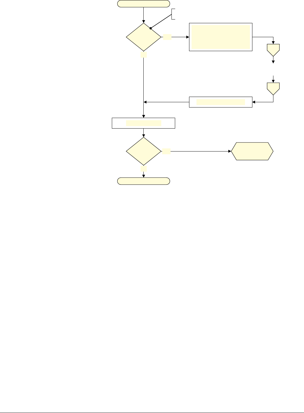
B3 Virtual Memory System Architecture (VMSA)
B3.12 VMSA memory aborts
B3-1400 Copyright © 1996-1998, 2000, 2004-2012, 2014 ARM. All rights reserved. ARM DDI 0406C.c
Non-Confidential ID051414
Figure B3-23 Fetching the descriptor in a translation table walk
Descriptor address
Translation
required
?
Yes
Translate address.
Descriptor address is input
address for stage 2
translation A1
Fault checking sequence,
for stage 2 translation
A2
Returns descriptor PA
Fetch descriptor
No
Yes
External
abort?
External abort
on translation
table walk
Is this address an IPA for a
Non-secure PL0 or PL1 access?
Return descriptor
No
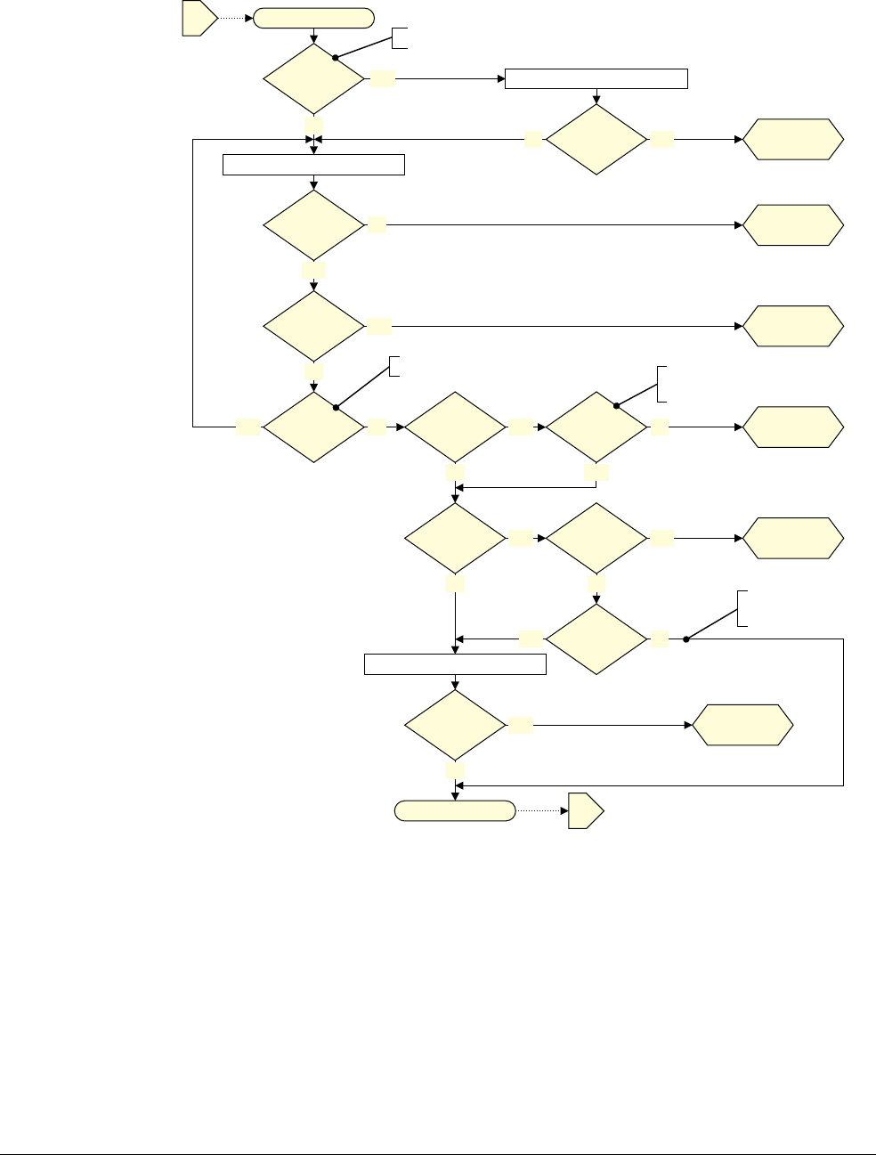
B3 Virtual Memory System Architecture (VMSA)
B3.12 VMSA memory aborts
ARM DDI 0406C.c Copyright © 1996-1998, 2000, 2004-2012, 2014 ARM. All rights reserved. B3-1401
ID051414 Non-Confidential
Figure B3-24 shows the full VMSA fault checking sequence, including the alignment check on the initial access.
Figure B3-24 VMSA fault checking sequence
Input address
Alignment
check? Yes
Is the access subject to an alignment check?
Fetch descriptor ‡
No
Table
entry
?
No
Check address alignment
Misaligned
?
Yes Alignment
fault
Check access permissions
Violation
?
Domain
fault
Output address
Table not possible at lowest level
Yes
Access
flag fault
?
Descriptor
valid?
Yes
No
Translation
fault
No
Access flag
fault
Yes
No
Yes
Short
descriptors
?
No access
domain
?
Yes
Permission
fault
Client
domain
?
Yes No
Manager
domain
* V.Exts. = Virtualization
Extensions
‡ See Fetching the descriptor
flowchart
† Links to and from Fetching the
descriptor flowchart
A1†
A2†
No
Have
V.Exts.*
?
Alignment
fault
Alignment
valid
?
Yes
Fault unaligned access to Device
or Strongly-Ordered memory
No
No
Yes
NoNo
Yes

B3 Virtual Memory System Architecture (VMSA)
B3.12 VMSA memory aborts
B3-1402 Copyright © 1996-1998, 2000, 2004-2012, 2014 ARM. All rights reserved. ARM DDI 0406C.c
Non-Confidential ID051414
Stage 2 fault on a stage 1 translation table walk, Virtualization Extensions
When an implementation that includes the Virtualization Extensions is operating in a Non-secure PL1 or PL0 mode,
any memory access goes through two stages of translation:
• stage 1, from VA to IPA
• stage 2, from IPA to PA.
Note
In a virtualized system, typically, a Guest OS operating in a Non-secure PL1 mode defines the translation tables and
translation table register entries controlling the Non-secure PL1&0 stage 1 translations. A Guest OS has no
awareness of the stage 2 address translation, and therefore believes it is specifying translation table addresses in the
physical address space. However, it actually specifies these addresses in its IPA space. Therefore, to support
virtualization, translation table addresses for the Non-secure PL1&0 stage 1 translations are always defined in the
IPA address space.
On performing a translation table walk for the stage 1 translations, the descriptor addresses must be translated from
IPA to PA, using a stage 2 translation. This means that a memory access made as part of a stage 1 translation table
lookup might generate, on a stage 2 translation:
• a Translation fault, Access flag fault, or Permission fault
• a synchronous external abort on the memory access.
If SCR.EA is set to 1, a synchronous external abort is taken to Secure Monitor mode., Otherwise, these faults are
reported as stage 2 memory aborts. HSR.ISS[7] is set to 1, to indicate a stage 2 fault during a stage 1 translation
table walk, and the part of the ISS field that might contain details of the instruction is invalid. For more information
see Use of the HSR on page B3-1424.
Alternatively, a memory access made as part of a stage 1 translation table lookup might target an area of memory
with the Device or Strongly-ordered attribute assigned on the stage 2 translation of the address accessed. When the
HCR.PTW bit is set to 1, such an access generates a stage 2 Permission fault.
Note
• On most systems, such a mapping to Strongly-ordered or Device memory on the stage 2 translation is likely
to indicate a Guest OS error, where the stage 1 translation table is corrupted. Therefore, it is appropriate to
trap this access to the hypervisor.
A TLB might hold entries that depend on the effect of HCR.PTW. Therefore, if HCR.PTW is changed without
changing the current VMID, the TLBs must be invalidated before executing in a Non-secure PL1 or PL0 mode. For
more information see Changing HCR.PTW on page B3-1385.
A cache maintenance operation performed from a Non-secure PL1 mode can cause a stage 1 translation table walk
that might generate a stage 2 Permission fault, as described in this section. This is an exception to the general rule
that a cache maintenance operation cannot generate a Permission fault.
B3.12.4 Alignment faults
The ARMv7 memory architecture requires support for strict alignment checking. This checking is controlled by
SCTLR.A. In addition, some instructions do not support unaligned accesses, regardless of the value of SCTLR.A.
Unaligned data access on page A3-108 defines when Alignment faults are generated, for both values of SCTLR.A.
An Alignment fault can occur on an access for which the MMU is disabled.
In an implementation that includes the Virtualization Extensions, any unaligned access to memory region with the
Device or Strongly-ordered memory type attribute generates an Alignment fault.

B3 Virtual Memory System Architecture (VMSA)
B3.12 VMSA memory aborts
ARM DDI 0406C.c Copyright © 1996-1998, 2000, 2004-2012, 2014 ARM. All rights reserved. B3-1403
ID051414 Non-Confidential
Note
• In versions of the ARMv7 architecture before the introduction of the Virtualization extensions, the behavior
of an unaligned access to Device or Strongly-ordered memory is architecturally UNPREDICTABLE. Most
implementations generate an abort on such an access.
• In some documentation, including issues A and B of this manual, Alignment faults are classified as a type of
MMU fault. However, the behavior of Alignment faults differs, in a number of ways, from the behavior of
MMU faults. This change in the classification of Alignment faults has no effect on their behavior.
Routing of aborts on page B3-1396 defines the mode to which an Alignment fault is taken.
In an implementation that includes the Virtualization Extensions, the prioritization of Alignment faults depends on
whether the fault was generated because of an access to Device or Strongly-ordered memory, or for another reason.
For more information see Prioritization of aborts on page B3-1407.
B3.12.5 MMU faults
This section describes the faults that might be detected during one of the fault-checking sequences described in The
MMU fault-checking sequence on page B3-1398. Unless indicated otherwise, information in this section applies to
the fault checking sequences for both the Short-descriptor translation table format and the Long-descriptor
translation table format.
MMU faults are always synchronous. For more information, see Terminology for describing exceptions on
page B1-1137.
When an MMU fault generates an abort for a region of memory, no memory access is made if that region is or could
be marked as Strongly-ordered or Device.
The following subsections describe the MMU faults that might be detected during a fault checking sequence:
•External abort on a translation table walk
•Translation fault
•Access flag fault on page B3-1404
•Domain fault, Short-descriptor format translation tables only on page B3-1404
•Permission fault on page B3-1405.
External abort on a translation table walk
The section External aborts on page B3-1405 describes this abort. See, in particular, External abort on a translation
table walk on page B3-1406.
Translation fault
A Translation fault can be generated at any level of lookup, and the reported fault code identifies the lookup level.
A Translation fault is generated if bits[1:0] of a translation table descriptor identify the descriptor as either a Fault
encoding or a reserved encoding. For more information see:
•Short-descriptor translation table format descriptors on page B3-1325
•Long-descriptor translation table format descriptors on page B3-1339.
In addition, if an implementation includes the Virtualization Extensions, then a Translation fault is generated if the
input address for a translation either does not map on to an address range of a Translation Table Base Register, or
the Translation Table Base Register range that it maps on to is disabled. In these cases the fault is reported as a first
level Translation fault on the translation stage at which the mapping to a region described by a Translation Table
Base Register failed.
The architecture guarantees that any translation table entry that causes a Translation fault is not cached, meaning
the TLB never holds such an entry. Therefore, when a Translation fault occurs, the fault handler does not have to
perform any TLB maintenance operations to remove the faulting entry.

B3 Virtual Memory System Architecture (VMSA)
B3.12 VMSA memory aborts
B3-1404 Copyright © 1996-1998, 2000, 2004-2012, 2014 ARM. All rights reserved. ARM DDI 0406C.c
Non-Confidential ID051414
A data or unified cache maintenance operation by MVA can generate a Translation fault. Whether an instruction
cache invalidate by MVA operation can generate a Translation fault is IMPLEMENTATION DEFINED, because it is
IMPLEMENTATION DEFINED whether the operation requires an address translation. If the instruction cache invalidate
by MVA operation requires an address translation then the operation can generate a Translation fault, otherwise it
cannot generate a Translation fault.
Whether branch predictor maintenance operations can generate Translation faults is IMPLEMENTATION DEFINED,
because it is IMPLEMENTATION DEFINED whether the operation requires an address translation. If the branch
predictor maintenance operation requires an address translation then the operation can generate a Translation fault,
otherwise it cannot generate a Translation fault.
Access flag fault
An Access flag fault can be generated at any level of lookup, and the reported fault code identifies the lookup level.
An Access flag fault is generated only if all of the following apply:
• The translation tables support an Access flag bit:
— the Short-descriptor format supports an Access flag only when SCTLR.AFE is set to 1
— the Long-descriptor format always supports an Access flag.
• For the relevant stage of address translation, the processor is not performing hardware management of the
Access flag. Support for hardware management of the Access flag is OPTIONAL and deprecated, but
SCTLR.HA is set to 1 when hardware management is supported and enabled.
Note
Hardware management of the Access flag cannot be supported for either:
— Non-secure PL2 stage 1 address translation
— Non-secure PL1&0 stage 2 address translation.
• A translation table descriptor with the Access flag bit set to 0 is loaded.
For more information about the Access flag bit see:
•Short-descriptor translation table format descriptors on page B3-1325
•Long-descriptor translation table format descriptors on page B3-1339.
The architecture guarantees that any translation table entry that causes an Access flag fault is not cached, meaning
the TLB never holds such an entry. Therefore, when an Access flag fault occurs, the fault handler does not have to
perform any TLB maintenance operations to remove the faulting entry.
Whether any cache maintenance operations by MVA can generate Access flag faults is IMPLEMENTATION DEFINED.
Whether branch predictor invalidate by MVA operations can generate Access flag faults is IMPLEMENTATION
DEFINED.
For more information, see The Access flag on page B3-1362.
Domain fault, Short-descriptor format translation tables only
When using the Short-descriptor translation table format, a Domain fault can be generated at the first level or second
level of lookup. The reported fault code identifies the lookup level. The conditions for generating a Domain fault
are:
First level When a first-level descriptor fetch returns a valid Section first-level descriptor, the domain field of
that descriptor is checked against the DACR. A first-level Domain fault is generated if this check
fails.
Second level When a second-level descriptor fetch returns a valid second-level descriptor, the domain field of the
first-level descriptor that required the second-level fetch is checked against the DACR, and a
second-level Domain fault is generated if this check fails.
For more information, see Domains, Short-descriptor format only on page B3-1362.

B3 Virtual Memory System Architecture (VMSA)
B3.12 VMSA memory aborts
ARM DDI 0406C.c Copyright © 1996-1998, 2000, 2004-2012, 2014 ARM. All rights reserved. B3-1405
ID051414 Non-Confidential
Domain faults cannot occur on cache or branch predictor maintenance operations.
A TLB might hold a translation table entry that cause a Domain fault. Therefore, if the handling of a Domain fault
results in an update to the associated translation tables, the software that updates the translation tables must
invalidate the appropriate TLB entry, to prevent the stale information in the TLB being used on a subsequent
memory access. For more information, see the translation table entry update examples in TLB maintenance
operations and the memory order model on page B3-1383.
Any change to the DACR must be synchronized by a context synchronization operation. For more information see
Synchronization of changes to system control registers on page B3-1461.
Permission fault
A Permission fault can be generated at any level of lookup, and the reported fault code identifies the lookup level.
See Access permissions on page B3-1356 for information about conditions that cause a Permission fault.
Note
When using the Short-descriptor translation table format, the translation table descriptors are checked for
Permission faults only for accesses to memory regions in Client domains.
A TLB might hold a translation table entry that cause a Permission fault. Therefore, if the handling of a Permission
fault results in an update to the associated translation tables, the software that updates the translation tables must
invalidate the appropriate TLB entry, to prevent the stale information in the TLB being used on a subsequent
memory access. For more information, see the translation table entry update examples in TLB maintenance
operations and the memory order model on page B3-1383.
Note
In an implementation that includes the Virtualization Extensions, this maintenance requirement applies to
Permission faults in both stage 1 and stage 2 translations.
Cache or branch predictor maintenance operations cannot cause a Permission fault, except that:
• a stage 1 translation table walk performed as part of a cache or branch predictor maintenance operation can
generate a stage 2 Permission fault as described in Stage 2 fault on a stage 1 translation table walk,
Virtualization Extensions on page B3-1402.
•a DCIMVAC issued in Non-secure state that attempts to update date in a location for which it does not have
stage 2 write access can generate a stage 2 Permission fault, as described in Virtualization Extensions
upgrading of maintenance operations on page B2-1286.
B3.12.6 External aborts
The ARM architecture defines external aborts as errors that occur in the memory system, other than those that are
detected by the MMU or Debug hardware. External aborts include parity errors detected by the caches or other parts
of the memory system. An external abort is one of:
• synchronous
• precise asynchronous
• imprecise asynchronous.
For more information, see Terminology for describing exceptions on page B1-1137.
The ARM architecture does not provide any method to distinguish between precise asynchronous and imprecise
asynchronous aborts.
The ARM architecture handles asynchronous aborts in a similar way to interrupts, except that they are reported to
the processor using the Data Abort exception. Setting the CPSR.A bit to 1 masks asynchronous aborts, see Program
Status Registers (PSRs) on page B1-1147.

B3 Virtual Memory System Architecture (VMSA)
B3.12 VMSA memory aborts
B3-1406 Copyright © 1996-1998, 2000, 2004-2012, 2014 ARM. All rights reserved. ARM DDI 0406C.c
Non-Confidential ID051414
Normally, external aborts are rare. An imprecise asynchronous external abort is likely to be fatal to the process that
is running. An example of an event that might cause an external abort is an uncorrectable parity or ECC failure on
a Level 2 Memory structure.
It is IMPLEMENTATION DEFINED which external aborts, if any, are supported.
VMSAv7 permits external aborts on data accesses, translation table walks, and instruction fetches to be either
synchronous or asynchronous. The reported fault code identifies whether the external abort is synchronous or
asynchronous.
Note
Because imprecise asynchronous external aborts are normally fatal to the process that caused them, ARM
recommends that implementations make external aborts precise wherever possible.
The following subsections give more information about possible external aborts:
•External abort on instruction fetch
•External abort on data read or write
•External abort on a translation table walk
•Behavior of external aborts on a translation table walk caused by address translation on page B3-1407
•Provision for classification of external aborts on page B3-1407
•Parity error reporting on page B3-1407.
The section Exception reporting in a VMSA implementation on page B3-1409 describes the reporting of external
aborts.
External abort on instruction fetch
An external abort on an instruction fetch can be either synchronous or asynchronous. A synchronous external abort
on an instruction fetch is taken precisely.
An implementation can report the external abort asynchronously from the instruction that it applies to. In such an
implementation these aborts behave essentially as interrupts. The aborts are masked when CPSR.A is set to 1,
otherwise they are reported using the Data Abort exception.
External abort on data read or write
Externally-generated errors during a data read or write can be either synchronous or asynchronous.
An implementation can report the external abort asynchronously from the instruction that generated the access. In
such an implementation these aborts behave essentially as interrupts. The aborts are masked when CPSR.A is set
to 1, otherwise they are reported using the Data Abort exception.
External abort on a translation table walk
An external abort on a translation table walk can be either synchronous or asynchronous. An external abort on a
translation table walk is reported:
• if the external abort is synchronous, using:
— a synchronous Prefetch Abort exception if the translation table walk is for an instruction fetch
— a synchronous Data Abort exception if the translation table walk is for a data access
• if the external abort is asynchronous, using an asynchronous Data Abort exception.
If an implementation reports the error in the translation table walk asynchronously from executing the instruction
whose instruction fetch or memory access caused the translation table walk, these aborts behave essentially as
interrupts. The aborts are masked when CPSR.A is set to 1, otherwise they are reported using the Data Abort
exception.

B3 Virtual Memory System Architecture (VMSA)
B3.12 VMSA memory aborts
ARM DDI 0406C.c Copyright © 1996-1998, 2000, 2004-2012, 2014 ARM. All rights reserved. B3-1407
ID051414 Non-Confidential
Behavior of external aborts on a translation table walk caused by address translation
The address translation operations summarized in Address translation operations, functional group on
page B3-1498 require translation table walks. An external abort can occur in the translation table walk. The abort
generates a Data Abort exception, and can be synchronous or asynchronous. For more information, see Handling of
faults and aborts during an address translation operation on page B3-1441.
Provision for classification of external aborts
An implementation can use the DFSR.ExT and IFSR.ExT bits to provide more information about external aborts:
•DFSR.ExT can provide an IMPLEMENTATION DEFINED classification of external aborts on data accesses.
•IFSR.ExT can provide an IMPLEMENTATION DEFINED classification of external aborts on instruction accesses.
•HSR.ISS[9] can provide an IMPLEMENTATION DEFINED classification of external aborts routed to Hyp mode.
For all aborts other than external aborts these bits return a value of 0.
Parity error reporting
The ARM architecture supports the reporting of both synchronous and asynchronous parity errors from the cache
systems. It is IMPLEMENTATION DEFINED what parity errors in the cache systems, if any, result in synchronous or
asynchronous parity errors.
A fault code is defined for reporting parity errors, see Exception reporting in a VMSA implementation on
page B3-1409. However when parity error reporting is implemented it is IMPLEMENTATION DEFINED whether a
parity error is reported using the assigned fault code, or using another appropriate encoding.
For all purposes other than the fault status encoding, parity errors are treated as external aborts.
B3.12.7 Prioritization of aborts
This section describes the abort prioritization that applies to a single memory access that might generate multiple
aborts:
On a single memory access, the following rules apply:
• If a memory access generates an Alignment fault because SCTLR.A is set to 1, or because it is an unaligned
access by an instruction that does not support unaligned accesses, then that access cannot generate any of:
— an MMU fault, on either the stage 1 translation or the stage 2 translation
— an external abort
— a Watchpoint debug event.
In an implementation that includes the Virtualization Extensions, an Alignment fault generated by an
unaligned access to Device or Strongly-ordered memory is prioritized as an MMU fault. For more
information see Alignment faults caused by accessing Device or Strongly-ordered memory on page B3-1408.
• If a memory access generates an MMU fault on its stage 1 translation, and also generates an abort on its stage
2 translation, the fault from the stage 1 translation has priority:
— if a memory access made as part of a stage 1 translation table walk generates an MMU fault on its stage
2 translation, as described in Stage 2 fault on a stage 1 translation table walk, Virtualization
Extensions on page B3-1402, the stage 1 translation table walk does not generate an MMU fault on the
stage 1 translation
— a fault on a particular stage of translation might be a synchronous external abort on a translation table
walk made at that stage of translation.
• If a memory access generates an MMU fault on either its stage 1 translation or on its stage 2 translation, then
the processor cannot generate a Watchpoint debug event on that access.
• If a memory access generates an MMU fault on either its stage 1 translation or on its stage 2 translation, or
generates a synchronous Watchpoint debug event, then the memory access cannot generate an external abort.

B3 Virtual Memory System Architecture (VMSA)
B3.12 VMSA memory aborts
B3-1408 Copyright © 1996-1998, 2000, 2004-2012, 2014 ARM. All rights reserved. ARM DDI 0406C.c
Non-Confidential ID051414
• Except as defined in this list, the architecture does not define any prioritization of asynchronous external
aborts relative to any other asynchronous aborts.
If a single instruction generates aborts on more than one memory access, the architecture does not define any
prioritization between those aborts.
In general, the ARM architecture does not define when asynchronous events are taken, and therefore the
prioritization of asynchronous events is IMPLEMENTATION DEFINED.
Note
Debug event prioritization on page C3-2078 describes:
• the relationship between debug events, MMU faults, and external aborts, for synchronous aborts generated
by the same memory access
• the special requirement that applies to asynchronous watchpoints.
Alignment faults caused by accessing Device or Strongly-ordered memory
In an implementation that includes the Virtualization Extensions, any unaligned access to Device or
Strongly-ordered memory generates an Alignment fault. When applying the prioritization rules, this fault is
prioritized as an MMU fault. The priority of this Alignment fault relative to possible MMU faults is as follows:
• the Alignment fault has lower priority than an Access flag fault
• if the translation stage that generates the Alignment fault:
— can generate Domain faults, the Alignment fault has higher priority than a Domain fault
— cannot generate Domain faults, the Alignment fault has higher priority than a Permission fault.
The MMU fault checking sequence in Figure B3-24 on page B3-1401 shows this prioritization.

B3 Virtual Memory System Architecture (VMSA)
B3.13 Exception reporting in a VMSA implementation
ARM DDI 0406C.c Copyright © 1996-1998, 2000, 2004-2012, 2014 ARM. All rights reserved. B3-1409
ID051414 Non-Confidential
B3.13 Exception reporting in a VMSA implementation
This section describes exception reporting in a VMSA implementation. The Virtualization Extensions introduce an
enhanced reporting mechanism for exceptions taken to the Non-secure PL2 mode, Hyp mode. This means that, for
a VMSA implementation, the exception reporting depends on the mode to which the exception is taken.
About exception reporting introduces the general approach to exception reporting, and the following sections then
describe exception reporting at different privilege levels:
•Reporting exceptions taken to PL1 modes on page B3-1410.
•Fault reporting in PL1 modes on page B3-1414
•Summary of register updates on faults taken to PL1 modes on page B3-1418
•Reporting exceptions taken to the Non-secure PL2 mode on page B3-1420
•Use of the HSR on page B3-1424
•Summary of register updates on exceptions taken to the PL2 mode on page B3-1435.
Note
The registers used for exception reporting also report information about debug exceptions. For more information
see:
•Data Abort exceptions, taken to a PL1 mode on page B3-1411
•Prefetch Abort exceptions, taken to a PL1 mode on page B3-1413
•Reporting exceptions taken to the Non-secure PL2 mode on page B3-1420.
B3.13.1 About exception reporting
In an implementation that includes the Virtualization Extensions, exceptions can be taken to:
•a Secure or Non-secure PL1 mode
• the Non-secure PL2 mode, Hyp mode.
Otherwise, they are taken to a PL1 mode. Exception reporting in the PL2 mode differs significantly from that in the
PL1 modes, but in general, exception reporting returns
• information about the exception:
— on taking an exception to the PL2 mode, the Hyp Syndrome Register, HSR, returns syndrome
information
— on taking an exception to a PL1 mode, a Fault Status Register (FSR) returns status information
• for synchronous exceptions, one or more addresses associated with the exceptions, returned in Fault Address
Registers (FARs)
In both PLI modes and the PL2 mode, additional IMPLEMENTATION DEFINED registers can provide additional
information about exceptions.
Note
• Processor mode for taking exceptions on page B1-1173 describes how the mode to which an exception is
taken is determined.
• The Virtualization Extensions introduce:
— new exception types, that can only be taken from Non-secure PL1 and PL0 modes, and are always
taken to Hyp mode
— new routing controls that can route some exceptions from Non-secure PL1 and PL0 modes to Hyp
mode.
These exceptions are reported using the same mechanism as the PL2 reporting of VMSA memory aborts, as
described in this section.

B3 Virtual Memory System Architecture (VMSA)
B3.13 Exception reporting in a VMSA implementation
B3-1410 Copyright © 1996-1998, 2000, 2004-2012, 2014 ARM. All rights reserved. ARM DDI 0406C.c
Non-Confidential ID051414
Memory system faults generate either a Data Abort exception or a Prefetch Abort exception, as summarized in:
•Reporting exceptions taken to PL1 modes
•Memory fault reporting at PL2 on page B3-1422.
On an access that might have multiple aborts, the MMU fault checking sequence and the prioritization of aborts
determine which abort occurs. For more information, see The MMU fault-checking sequence on page B3-1398 and
Prioritization of aborts on page B3-1407.
B3.13.2 Reporting exceptions taken to PL1 modes
The following sections give general information about the reporting of exceptions when they are taken to a PL1
mode:
•Registers used for reporting exceptions taken to a PL1 mode
•Data Abort exceptions, taken to a PL1 mode on page B3-1411
•Prefetch Abort exceptions, taken to a PL1 mode on page B3-1413.
Fault reporting in PL1 modes on page B3-1414 then describes the fault reporting in these modes, including the
encodings used for reporting the faults.
Registers used for reporting exceptions taken to a PL1 mode
ARMv7 defines the following registers, and register encodings, for exceptions taken to PL1 modes:
• the DFSR holds information about a Data Abort exception
• the DFAR holds the faulting address for some synchronous Data Abort exceptions
• the IFSR holds information about a Prefetch Abort exception
• the IFAR holds the faulting address of a Prefetch Abort exception
• on a Watchpoint debug exception, the DBGWFAR can hold fault information.
Note
Before ARMv7, the Data Fault Address Register (DFAR) was called the Fault Address Register (FAR).
In addition, if implemented, the optional ADFSR and AIFSR can provide additional fault information, see Auxiliary
Fault Status Registers.
Auxiliary Fault Status Registers
The ARMv7 architecture defines the following Auxiliary Fault Status Registers:
• the Auxiliary Data Fault Status Register, ADFSR
• the Auxiliary Instruction Fault Status Register, AIFSR.
The position of these registers is architecturally-defined, but the content and use of the registers is IMPLEMENTATION
DEFINED. An implementation can use these registers to return additional fault status information. An example use
of these registers is to return more information for diagnosing parity errors.
An implementation that does not need to report additional fault information must implement these registers as
UNK/SBZP. This ensures that an attempt to access these registers from software executing at PL1 does not cause
an Undefined Instruction exception.
For more information, see ADFSR and AIFSR, Auxiliary Data and Instruction Fault Status Registers, VMSA on
page B4-1523

B3 Virtual Memory System Architecture (VMSA)
B3.13 Exception reporting in a VMSA implementation
ARM DDI 0406C.c Copyright © 1996-1998, 2000, 2004-2012, 2014 ARM. All rights reserved. B3-1411
ID051414 Non-Confidential
Data Abort exceptions, taken to a PL1 mode
On taking a Data Abort exception to a PL1 mode:
• If the exception is on an instruction cache or branch predictor maintenance operation by MVA, its reporting
depends on the current translation table format. For more information about the registers used when reporting
the exception, see Data Abort on an instruction cache maintenance operation by MVA.
• If the exception is generated by a Watchpoint debug event, then its reporting depends on whether the
Watchpoint debug event is synchronous or asynchronous, and on the Debug architecture version. For more
information, see Data Abort on a Watchpoint debug event on page B3-1412.
Otherwise:
• The DFSR is updated with details of the fault, including the appropriate fault status code.
If the Data Abort exception is synchronous, DFSR.WnR is updated to indicate whether the faulted access was
caused by a read instruction or a write instruction. However, if the fault is:
— On a cache maintenance operation, or on a CP15 address translation operation, WnR is set to 1, to
indicate a write access fault, and if the implementation includes the Large Physical Address Extension,
the CM bit is set to 1
— Generated by an
SWP
or
SWPB
instruction, WnR is set to 0 if a read of the location would have generated
a fault, otherwise it is set to 1.
DFSR.WnR is UNKNOWN on an asynchronous Data Abort exception.
See the register description for more information about the returned fault information.
• If the Data Abort exception is
— synchronous, the DFAR is updated with the VA that caused the exception
— asynchronous, the DFAR becomes UNKNOWN.
For all Data Abort exceptions, if the implementation includes the Security Extensions, the security state of the
processor in the mode to which the Data Abort exception is taken determines whether the Secure or Non-secure
DFSR and DFAR are updated.
Data Abort on an instruction cache maintenance operation by MVA
If an instruction cache or branch predictor invalidation by MVA operation generates a Data Abort exception that is
taken to a PL1 mode, the DFAR is updated to hold the faulting VA. However, the reporting of the fault depends on
the current translation table format:
Short-descriptor format
It is IMPLEMENTATION DEFINED which of the following is used when reporting the fault:
• The DFSR indicates an Instruction cache maintenance operation fault, and the IFSR is valid
and indicates the cause of the fault, a Translation fault or Access flag fault.
• The DFSR indicates the cause of the fault, a Translation fault or Access flag fault. The IFSR
is UNKNOWN.
In either case:
•DFSR.WnR is set to 1
• if the implementation includes the Large Physical Address Extension, DFSR.CM is set to 1,
to indicate a fault on a cache maintenance operation.
Long-descriptor format
•DFSR.CM is set to 1, to indicates a fault on a cache maintenance operation
•DFSR.STATUS indicates the cause of the fault, a Translation or Access flag fault
•DFSR.WnR is set to 1
• the IFSR is UNKNOWN.

B3 Virtual Memory System Architecture (VMSA)
B3.13 Exception reporting in a VMSA implementation
B3-1412 Copyright © 1996-1998, 2000, 2004-2012, 2014 ARM. All rights reserved. ARM DDI 0406C.c
Non-Confidential ID051414
Data Abort on a Watchpoint debug event
On taking a Data Abort exception caused by a Watchpoint debug event, DFSR is updated with the details of the
fault:
• if using the Short-descriptor format, DFSR.FS is updated to indicate a debug event and DFSR.Domain is
UNKNOWN.
• if using the Long-descriptor format, DFSR.STATUS is updated to indicate a debug event.
• if the implementation includes the Large Physical Address Extension, DFSR.CM is updated to indicate
whether the Watchpoint was caused by a cache maintenance operation.
•DFSR.WnR is UNKNOWN.
The remaining register updates depend on the Debug architecture version, and in v7.1 debug, on whether the
Watchpoint debug event is synchronous or asynchronous:
v7 Debug, and for an asynchronous Watchpoint debug event in v7.1 Debug
•DFAR is UNKNOWN
•DBGWFAR is set to the VA of the instruction that caused the watchpointed access, plus an
offset that depends on the instruction set state of the processor for that instruction, as follows:
— 8 for ARM state
— 4 for Thumb or ThumbEE state
—IMPLEMENTATION DEFINED for Jazelle state.
v7.1 Debug, for a synchronous Watchpoint debug event
•DFAR is set to the address that generated the watchpoint
•DBGWFAR is UNKNOWN.
A watchpointed address can be any byte-aligned address. The address reported in DFAR might not
be the watchpointed address, and can be any address between and including:
• the lowest address accessed by the instruction that triggered the watchpoint
• the highest watchpointed address accessed by that instruction.
If multiple watchpoints are set in this range, there is no guarantee of which watchpoint is generated.
Note
In particular, there is no guarantee of generating the watchpoint with the lowest address in the range.
In addition, it is IMPLEMENTATION DEFINED whether there is an additional restriction on the lowest
value that might be reported in the DFAR, see Synchronous Watchpoint debug event additional
restriction on DFAR or HDFAR reporting, v7.1 Debug on page B3-1413.
Note
For a synchronous Watchpoint debug event:
• in v7 Debug, both LR_abt and DBGWFAR indicate the address of the instruction that triggered the
watchpoint, and ARM deprecates using DBGWFAR to determine the address of this instruction.
• in v7.1 Debug, only LR_abt indicates the address of the instruction that triggered the watchpoint

B3 Virtual Memory System Architecture (VMSA)
B3.13 Exception reporting in a VMSA implementation
ARM DDI 0406C.c Copyright © 1996-1998, 2000, 2004-2012, 2014 ARM. All rights reserved. B3-1413
ID051414 Non-Confidential
Synchronous Watchpoint debug event additional restriction on DFAR or HDFAR reporting, v7.1
Debug
In v7.1 Debug, when reporting a synchronous Watchpoint debug event triggered by a Load or Store instruction, it
is IMPLEMENTATION DEFINED whether there is an additional restriction on the lower value of the permitted range of
values that might be reported in the DFAR or HDFAR. ARM recommends that implementations define such a
restriction, and that the restriction requires that:
• For a Watchpoint debug event triggered by a Load or Store instruction, the lowest address that is reported in
the DFAR or HDFAR is both:
— no lower than the address of the watchpointed location rounded down to a multiple of an
IMPLEMENTATION DEFINED number of bytes
— no lower than the lowest address accessed by the instruction that triggered the watchpoint.
• The IMPLEMENTATION DEFINED number of bytes that defines this lowest address is a power of two, and less
than or equal to the cache line size specified in CCSIDR.LineSize.
This additional restriction does not apply to any watchpoint generated by a cache maintenance instruction. For these
instructions, the lowest address accessed by the instruction can be less than the address passed to the operation,
because the operation acts on a whole cache line.
Note
A debugger can choose to ignore this restriction. However, a debugger can use this restriction to refine its
interpretation of the value returned in the DFAR or HDFAR.
There is no mechanism by which software can discover whether this restriction is implementation. The
documentation of any implementation that includes this restriction must include a full description of its
implementation of the restriction.
Prefetch Abort exceptions, taken to a PL1 mode
For a Prefetch Abort exception generated by an instruction fetch, the Prefetch Abort exception is taken
synchronously with the instruction that the abort is reported on. This means:
• If the processor attempts to execute the instruction a Prefetch Abort exception is generated.
• If an instruction fetch is issued but the processor does not attempt to execute the prefetched instruction, no
Prefetch Abort exception is generated for that instruction. For example, if the execution flow branches round
a prefetched instruction, no Prefetch Abort exception is generated.
In addition, debug exceptions caused by a BKPT instruction, Breakpoint, or a Vector catch debug event, generate a
Prefetch Abort exception, see Debug exception on BKPT instruction, Breakpoint, or Vector catch debug events on
page C4-2090.
On taking a Prefetch Abort exception to PL1:
• The IFSR is updated with details of the fault, including the appropriate fault code. If appropriate, the fault
code indicates that the exception was generated by a debug exception.
See the register description for more information about the returned fault information.
• For a Prefetch Abort exception generated by an instruction fetch, the IFAR is updated with the VA that caused
the exception.
• For a Prefetch Abort exception generated by a debug exception, the IFAR is UNKNOWN.
If the implementation includes the Security Extensions, the security state of the processor in the mode to which it
takes the Prefetch Abort exception determines whether the exception updates the Secure or Non-secure IFSR and
IFAR.

B3 Virtual Memory System Architecture (VMSA)
B3.13 Exception reporting in a VMSA implementation
B3-1414 Copyright © 1996-1998, 2000, 2004-2012, 2014 ARM. All rights reserved. ARM DDI 0406C.c
Non-Confidential ID051414
B3.13.3 Fault reporting in PL1 modes
The FSRs provide fault information, including an indication of the fault that occurred. The Large Physical Address
Extension introduces:
• an alternative translation table format, the Long-descriptor format
• an alternative FSR format, used with the Long-descriptor translation tables
• an additional bit in the FSR format used with the Short-descriptor translation tables, FSR.CM.
Therefore, the following subsections describe fault reporting in PL1 modes for each of the translation table formats:
•PL1 fault reporting with the Short-descriptor translation table format
•Fault reporting with the Long-descriptor translation table format on page B3-1416.
Reserved encodings in the IFSR and DFSR encodings tables on page B3-1417 gives some additional information
about the encodings for both formats.
Summary of register updates on faults taken to PL1 modes on page B3-1418 shows which registers are updated on
each of the reported faults.
Reporting of External aborts taken from Non-secure state to Monitor mode describes how the fault status register
format is determined for those aborts. For all other aborts, the current translation table format determines the format
of the fault status registers.
Note
Previous ARM documentation classified faults using the terms precise and imprecise instead of synchronous and
asynchronous. For details of the more exact terminology introduced in this manual see Terminology for describing
exceptions on page B1-1137.
Reporting of External aborts taken from Non-secure state to Monitor mode
When an External abort is taken from Non-secure state to Monitor mode:
• for a Data Abort exception, the Secure DFSR and DFAR hold information about the abort
• for a Prefetch Abort exception, the Secure IFSR and IFAR hold information about the abort
• the abort does not affect the contents of the Non-secure copies of the fault reporting registers.
Normally, the current translation table format determines the format of the DFSR and IFSR. However, when
SCR.EA is set to 1, to route external aborts to Monitor mode, and an external abort is taken from Non-secure state,
this section defines the DFSR and IFSR format.
For an External abort taken from Non-secure state to Monitor mode, the DFSR or IFSR uses the format associated
with the Long-descriptor translation table format, as described in Fault reporting with the Long-descriptor
translation table format on page B3-1416, if any of the following applies:
• the Secure TTBCR.EAE bit is set to 1
• the External abort is synchronous and either:
— it is taken from Hyp mode
— it is taken from a Non-secure PL1 or PL0 mode, and the Non-secure TTBCR.EAE bit is set to 1.
Otherwise, the DFSR or IFSR uses the format associated with the Short-descriptor translation table format, as
described in PL1 fault reporting with the Short-descriptor translation table format.
PL1 fault reporting with the Short-descriptor translation table format
This subsection describes the fault reporting for a fault taken to a PL1 mode when either:
• the implementation does not include the Large Physical Address Extension
• the implementation includes the Large Physical Address Extension, and address translation is using the
Short-descriptor translation table format.

B3 Virtual Memory System Architecture (VMSA)
B3.13 Exception reporting in a VMSA implementation
ARM DDI 0406C.c Copyright © 1996-1998, 2000, 2004-2012, 2014 ARM. All rights reserved. B3-1415
ID051414 Non-Confidential
On taking an exception, bit[9] of the FSR is RAZ, or set to 0, if the processor is using this FSR format.
An FSR encodes the fault in a 5-bit FS field, that comprises FSR[10, 3:0]. Table B3-23 shows the encoding of that
field. Summary of register updates on faults taken to PL1 modes on page B3-1418 shows:
• Whether the corresponding FAR is updated on the fault. That is:
— for a fault reported in the IFSR, whether the IFAR holds a valid address
— for a fault reported in the DFSR, whether the DFAR holds a valid address
• For faults that update DFSR, whether DFSR.Domain is valid
When reading Table B3-23:
• FS values not shown in the table are reserved
• FS values shown as DFSR only are reserved for the IFSR
• LPAE is an abbreviation for the Large Physical Address Extension.
Table B3-23 Short-descriptor format FSR encodings
FS Source Notes
00001 Alignment fault DFSR only. Fault on first lookup
00100 Fault on instruction cache maintenance DFSR only
01100
01110
Synchronous external abort on translation table walk First level
Second level -
11100
11110
Synchronous parity error on translation table walk First level
Second level -
00101
00111
Translation fault First level
Second level MMU fault
00011a
00110
Access flag fault First level
Second level MMU fault
01001
01011
Domain fault First level
Second level
MMU fault
01101
01111
Permission fault First level
Second level
MMU fault
00010 Debug event See About debug events on page C3-2038
01000 Synchronous external abort -
10000 TLB conflict abort See TLB conflict aborts on page B3-1380
10100 IMPLEMENTATION DEFINED Lockdown
11010 IMPLEMENTATION DEFINED Coprocessor abort
11001 Synchronous parity error on memory access -
10110 Asynchronous external abortbDFSR only
11000 Asynchronous parity error on memory accesscDFSR only
a. Previously, this encoding was a deprecated encoding for Alignment fault. The extensive changes in the memory model in VMSAv7
mean there should be no possibility of confusing the new use of this encoding with its previous use
b. Including Virtual Abort and asynchronous data external abort on translation table walk or instruction fetch.
c. Including asynchronous parity error on translation table walk.

B3 Virtual Memory System Architecture (VMSA)
B3.13 Exception reporting in a VMSA implementation
B3-1416 Copyright © 1996-1998, 2000, 2004-2012, 2014 ARM. All rights reserved. ARM DDI 0406C.c
Non-Confidential ID051414
The Domain field in the DFSR
The DFSR includes a Domain field. This is inherited from previous versions of the VMSA. The IFSR does not
include a Domain field. Summary of register updates on faults taken to PL1 modes on page B3-1418 describes when
DFSR.Domain is valid.
ARM deprecates any use of the Domain field in the DFSR. The Long-descriptor translation table format does not
support a Domain field, and future versions of the ARM architecture might not support a Domain field in the
Short-descriptor translation table format. ARM strongly recommends that new software does not use this field.
For both Data Abort exceptions and Prefetch Abort exceptions, software can find the domain information by
performing a translation table read for the faulting address and extracting the Domain field from the translation table
entry.
Fault reporting with the Long-descriptor translation table format
This subsection describes the fault reporting for a fault taken to a PL1 mode in an implementation that includes the
Large Physical Address Extension, when address translation is using the Long-descriptor translation table format.
When the processor takes an exception, bit[9] of the FSR is set to 1 if the processor is using this FSR format.
The FSRs encode the fault in a 6-bit STATUS field, that comprises FSR[5:0]. Table B3-24 shows the encoding of
that field. In addition:
• For a fault taken to a PL1 mode, Summary of register updates on faults taken to PL1 modes on page B3-1418
shows whether the corresponding FAR is updated on the fault. That is:
— for a fault reported in the IFSR, whether the IFAR holds a valid address
— for a fault reported in the DFSR, whether the DFAR holds a valid address
• For a fault taken to the PL2 mode, Summary of register updates on exceptions taken to the PL2 mode on
page B3-1435 shows what registers are updated on the fault
Table B3-24 Long-descriptor format FSR encodings
STATUSaSource Notes
0001LL Translation fault. LL bits indicate levelb.MMU fault
0010LL Access flag fault. LL bits indicate levelb.MMU fault
0011LL Permission fault. LL bits indicate levelb.MMU fault
010000 Synchronous external abort. -
011000 Synchronous parity error on memory access. -
010001 Asynchronous external abortc.DFSR only
011001 Asynchronous parity error on memory access. DFSR only
0101LL Synchronous external abort on translation table walk.
LL bits indicate levelb.
-
0111LL Synchronous parity error on memory access on translation table
walk.
LL bits indicate levelb.
-
100001 Alignment fault. Fault on first lookup
100010 Debug event. See About debug events on page C3-2038
110000 TLB conflict abort. See TLB conflict aborts on page B3-1380

B3 Virtual Memory System Architecture (VMSA)
B3.13 Exception reporting in a VMSA implementation
ARM DDI 0406C.c Copyright © 1996-1998, 2000, 2004-2012, 2014 ARM. All rights reserved. B3-1417
ID051414 Non-Confidential
The level associated with MMU faults
For MMU faults, Table B3-25 shows how the LL bits in the xFSR.STATUS field encode the lookup level associated
with the fault.
The lookup level associated with a fault is:
• For a fault generated on a translation table walk, the lookup level of the walk being performed.
• For a Translation fault, the lookup level of the translation table that gave the fault. If a fault occurs because
an MMU is disabled, or because the input address is outside the range specified by the appropriate base
address register or registers, the fault is reported as a First level fault.
• For an Access flag fault, the lookup level of the translation table that gave the fault.
• For a Permission fault, including a Permission fault caused by hierarchical permissions, the lookup level of
the final level of translation table accessed for the translation. That is, the lookup level of the translation table
that returned a Block or Page descriptor.
Reserved encodings in the IFSR and DFSR encodings tables
With both the Short-descriptor and the Long-descriptor FSR format, the fault encodings reserve a single encoding
for each of:
• Cache and TLB lockdown faults. The details of these faults and any associated subsidiary registers are
IMPLEMENTATION DEFINED.
• Aborts associated with coprocessors. The details of these faults are IMPLEMENTATION DEFINED.
110100 IMPLEMENTATION DEFINED. Lockdown, DFSR only
111010 IMPLEMENTATION DEFINED. Coprocessor abort, DFSR only
1111LL Domain fault.
LL bits indicate levelb.
MMU fault. 64-bit PAR only, First or second
level only. Never used in DFSR, IFSR, or HSRd
a. STATUS values not shown in this table are reserved. STATUS values not supported in the IFSR or DFSR are reserved for the register or
registers in which they are not supported.
b. See The level associated with MMU faults.
c. Including Virtual Abort.
d. A Domain fault can be reported using the Long-descriptor STATUS encodings only as a result of a fault on an address translation operation.
For more information see MMU fault on an address translation operation on page B3-1442.
Table B3-24 Long-descriptor format FSR encodings (continued)
STATUSaSource Notes
Table B3-25 Use of LL bits to encode the lookup level at which the fault occurred
LL bits Meaning
00 Reserved.
01 First level.
10 Second level.
11 Third level. When xFSR.STATUS indicates a Domain fault, this value is reserved.

B3 Virtual Memory System Architecture (VMSA)
B3.13 Exception reporting in a VMSA implementation
B3-1418 Copyright © 1996-1998, 2000, 2004-2012, 2014 ARM. All rights reserved. ARM DDI 0406C.c
Non-Confidential ID051414
B3.13.4 Summary of register updates on faults taken to PL1 modes
For faults that generate exceptions that are taken to a PL1 mode, Table B3-26 shows the registers affected by each
fault. In this table:
• Yes indicates that the register is updated
•UNK indicates that the fault makes the register value UNKNOWN
• a null entry, -, indicates that the fault does not affect the register.
For faults that update the DFSR using the Short-descriptor format FSR encodings, Table B3-27 on page B3-1419
shows whether DFSR.Domain is valid.
Table B3-26 Effect of a fault taken to a PL1 mode on the reporting registers
Fault IFSR IFAR DFSR DFAR DBGWFAR
Faults reported as Prefetch Abort exceptions:
MMU fault, always synchronous. Yes Yes - - -
Synchronous external abort on translation table walk. Yes Yes - - -
Synchronous parity error on translation table walk. Yes Yes - - -
Synchronous external abort. Yes Yes - - -
Synchronous parity error on memory access. Yes Yes - - -
TLB conflict abort. Yes Yes - - -
Fault reported as Data Abort exception:
Alignment fault, always synchronous. - - Yes Yes -
MMU fault, always synchronous. - - Yes Yes -
Fault on instruction cache maintenance, when using Long-descriptor
translation table formata.
UNK -YesYes-
Fault on instruction cache maintenance, when using
Short descriptor translation table formatb.
either Yes- YesYes-
or UNK -YesYes-
Synchronous external abort on translation table walk. - - Yes Yes -
Synchronous parity error on translation table walk. - - Yes Yes -
Synchronous external abort. - - Yes Yes -
Synchronous parity error on memory access. - - Yes Yes -
Asynchronous external abortc.--YesUNK -
Asynchronous parity error on memory access. - - Yes UNK -
TLB conflict abort. - - Yes Yes -

B3 Virtual Memory System Architecture (VMSA)
B3.13 Exception reporting in a VMSA implementation
ARM DDI 0406C.c Copyright © 1996-1998, 2000, 2004-2012, 2014 ARM. All rights reserved. B3-1419
ID051414 Non-Confidential
For those faults for which Table B3-26 on page B3-1418 shows that the DFSR is updated, if the fault is reported
using the Short-descriptor FSR encodings, Table B3-27 shows whether DFSR.Domain is valid. In this table, UNK
indicates that the fault makes DFSR.Domain UNKNOWN.
Debug exceptions:
Breakpoint, BKPT instruction, or Vector catch debug eventd.Yes UNK ---
Synchronous Watchpoint debug evente.v7 Debug - - Yes UNK Yes
v7.1 Debug - - Yes Yes UNK
Asynchronous Watchpoint debug evente.--Yes
UNK Yes
a. When using the Long-descriptor translation table format, there is not a specific fault code for a fault on an instruction cache maintenance
operation. For more information see Data Abort on an instruction cache maintenance operation by MVA on page B3-1411.
b. The two lines of this entry show the alternative ways of reporting the fault when using the Short-descriptor translation table format. It is
IMPLEMENTATION DEFINED which methods is used, see Data Abort on an instruction cache maintenance operation by MVA on page B3-1411.
c. Including Virtual Abort.
d. Generates a Prefetch Abort exception.
e. Generates a Data Abort exception.
Table B3-26 Effect of a fault taken to a PL1 mode on the reporting registers (continued)
Fault IFSR IFAR DFSR DFAR DBGWFAR
Table B3-27 Validity of Domain field on faults that update the DFSR using the Short-descriptor encodings
DFSR.FS Source DFSR.Domain Notes
00001 Alignment fault UNK -
00100 Fault on instruction cache maintenance operation UNK -
01100
01110 Synchronous external abort on translation table walk First level
Second level
UNK
Valid -
11100
11110 Synchronous parity error on translation table walk First level
Second level
UNK
Valid -
00101
00111
Translation fault First level
Second level
UNK
Valid
MMU fault
00011a
00110
Access flag fault First level
Second level
UNK
Valid
MMU fault
01001
01011
Domain fault First level
Second level
Valid
Valid
MMU fault
01101 Permission fault No LPAE
With LPAE
First level
First level
Valid
UNK
MMU fault
01111 No LPAE
With LPAE
Second level
Second level
Valid
UNK
01000 Synchronous external abort UNK -
10000 TLB conflict abort UNK -
11001 Synchronous parity error on memory access UNK -

B3 Virtual Memory System Architecture (VMSA)
B3.13 Exception reporting in a VMSA implementation
B3-1420 Copyright © 1996-1998, 2000, 2004-2012, 2014 ARM. All rights reserved. ARM DDI 0406C.c
Non-Confidential ID051414
Note
As Table B3-27 on page B3-1419 shows, if an implementation includes the Large Physical Address Extension, and
address translation is using the Short-descriptor translation table format, on a Permission fault that causes a Data
Abort exception, the DFSR.Domain field is UNKNOWN. This is a change from the architecturally-required behavior
on an implementation that does not include the Large Physical Address Extension.
B3.13.5 Reporting exceptions taken to the Non-secure PL2 mode
The Virtualization Extensions introduce Hyp mode as the Non-secure PL2 mode. Hyp mode is entered by taking an
exception to Hyp mode.
Note
Software executing in Monitor mode can perform an exception return to Hyp mode. This means Hyp mode is
entered either by taking an exception, or by a permitted exception return.
The following exceptions are taken to Hyp mode:
• Asynchronous external aborts, IRQ exceptions, and FIQ exceptions, from Non-secure PL0 and PL1 modes,
if not routed to Secure Monitor mode, can each be routed to Hyp mode. For more information see
Asynchronous exception routing controls on page B1-1175.
•If HCR.TGE is set to 1, the following exceptions. if taken from the Non-secure PL0 mode, are routed to Hyp
mode:
— Undefined Instruction exceptions
— Supervisor Call exception
— synchronous external aborts
— Alignment faults.
For more information, see Routing general exceptions to Hyp mode on page B1-1192.
•If HCR.TDE is set to 1, any Debug exception take from a Non-secure PL1 or PL0 mode, is routed to Hyp
mode. For more information, see Routing Debug exceptions to Hyp mode on page B1-1194.
• The privilege rules for taking exceptions mean that any exception taken from Hyp mode, if not routed to
Secure Monitor mode, must be taken to Hyp mode. See Exceptions, privilege, and security state on
page B1-1138. This includes a Prefetch Abort exception generated by a Debug exception on a
BKPT
instruction.
Note
Debug exceptions other than the exception on a
BKPT
instruction are not permitted in Hyp mode.
10110 Asynchronous external abortbUNK -
11000 Asynchronous parity error on memory accesscUNK -
00010 Watchpoint debug event, synchronous or asynchronous UNK
a. Previously, this encoding was a deprecated encoding for Alignment fault. The extensive changes in the memory model in
VMSAv7 mean there should be no possibility of confusing the new use of this encoding with its previous use
b. Including asynchronous data external abort on translation table walk or instruction fetch.
c. Including asynchronous parity error on translation table walk.
Table B3-27 Validity of Domain field on faults that update the DFSR using the Short-descriptor encodings (continued)
DFSR.FS Source DFSR.Domain Notes

B3 Virtual Memory System Architecture (VMSA)
B3.13 Exception reporting in a VMSA implementation
ARM DDI 0406C.c Copyright © 1996-1998, 2000, 2004-2012, 2014 ARM. All rights reserved. B3-1421
ID051414 Non-Confidential
• Hypervisor Call exceptions, and Hyp Trap exceptions, are always taken to Hyp mode. These exceptions are
supported only as part of the Virtualization Extensions.
In an implementation that includes the Virtualization Extensions, various operations from Non-secure PL0
and PL1 modes can be trapped to Hyp mode, using the Hyp Trap exception. For more information, see Traps
to the hypervisor on page B1-1248.
These exceptions include any memory system fault that occurs:
• on a memory access from Hyp mode
• on memory access from a Non-secure PL0 or PL1 mode:
— on a stage 2 translation, from IPA to PA
— on the stage 2 translation of an address accessed in performing a stage 1 translation table walk.
Memory fault reporting at PL2 on page B3-1422 gives more information about these faults.
The following exceptions provide syndrome information syndrome information in the HSR:
• Any synchronous exception taken to Hyp mode.
• Some exceptions taken from Debug state that would be taken to Hyp mode if the processor was not in Debug
state, see Exceptions in Debug state on page C5-2107.
Note
— In Debug state, the processor does not change mode on taking an exception.
—As Exceptions in Debug state on page C5-2107 describes, some other exceptions taken from Debug
state make the HSR UNKNOWN.
The syndrome information in the HSR includes the fault status code otherwise provided by the fault status register,
and greatly extends the fault reporting. For more information, see Use of the HSR on page B3-1424.
In addition, for a Debug exception taken to Hyp mode, DBGDSCR.MOE shows what caused the Debug exception.
This bit is valid regardless of whether the Debug exception was taken from Hyp mode or from another Non-secure
mode.
Registers used for reporting exceptions taken to Hyp mode lists all of the registers used for exception reporting at
PL2.
Registers used for reporting exceptions taken to Hyp mode
The Virtualization Extensions define the following registers for exceptions taken to Hyp mode:
• the HSR holds syndrome information for the exception
• the HDFAR holds the VA associated with a Data Abort exception
• the HIFAR holds the VA associated with a Prefetch Abort exception
• the HPFAR holds bits[39:12] of the IPA associated with some aborts on stage 2 address translations.
In addition, if implemented, the optional HADFSR and HAIFSR can provide additional fault information, see Hyp
Auxiliary Fault Syndrome Registers.
Hyp Auxiliary Fault Syndrome Registers
The Virtualization Extensions define the following Hyp Auxiliary Fault Syndrome Registers:
• the Hyp Auxiliary Data Fault Syndrome Register, HADFSR
• the Hyp Auxiliary Instruction Fault Syndrome Register, HAIFSR.
An implementation can use these registers to return additional fault status information for aborts taken to Hyp mode.
They are the Hyp mode equivalents of the registers described in Auxiliary Fault Status Registers on page B3-1410.
An example use of these registers is to return more information for diagnosing parity errors.

B3 Virtual Memory System Architecture (VMSA)
B3.13 Exception reporting in a VMSA implementation
B3-1422 Copyright © 1996-1998, 2000, 2004-2012, 2014 ARM. All rights reserved. ARM DDI 0406C.c
Non-Confidential ID051414
The architectural requirements for the HADFSR and HAIFSR are:
• The position of these registers is architecturally-defined, but the content and use of the registers is
IMPLEMENTATION DEFINED.
• An implementation with no requirement for additional fault reporting can implement these registers as
UNK/SBZP, but the architecture does not require it to do so.
For more information, see HADFSR and HAIFSR, Hyp Auxiliary Fault Syndrome Registers, Virtualization
Extensions on page B4-1576.
Memory fault reporting at PL2
Prefetch Abort and Data Abort exceptions taken to Hyp mode report memory faults. For these aborts, the HSR
contains the following fault status information:
• The HSR.EC field indicates the type of abort, as Table B3-28 shows.
• The HSR.ISS field holds more information about the abort. In particular:
— bits[5:0] of this field hold the STATUS field for the abort, using the encodings defined in Fault
reporting with the Long-descriptor translation table format on page B3-1416
— other subfields of the ISS give more information about the exception, equivalent to the information
returned in the FSR for a memory fault reported at PL1.
See the descriptions of the ISS fields for the memory faults, referenced from the Syndrome description
column of Table B3-28, for information about the returned fault information.
For more information, see Use of the HSR on page B3-1424.
A Prefetch Abort exception is taken synchronously with the instruction that the abort is reported on. This means:
• If the processor attempts to execute the instruction a Prefetch Abort exception is generated.
• If an instruction fetch is issued but the processor does not attempt to execute the prefetched instruction, no
Prefetch Abort exception is generated for that instruction. For example, if the execution flow branches round
a prefetched instruction, no Prefetch Abort exception is generated.
Register updates on exception reporting at PL2
The use of the HSR, and of the other registers listed in Registers used for reporting exceptions taken to Hyp mode
on page B3-1421, depends on the cause of the Abort. In reporting these faults, in general:
• If the fault generates a synchronous Data Abort exception, the HDFAR holds the associated VA.
• If the fault generates a Prefetch Abort exception, the HIFAR holds the associated VA.
• In the following cases, the HPFAR holds the faulting IPA:
— a Translation or Access flag fault on a stage 2 translation
— a fault on the stage 2 translation of an address accessed in a stage 1 translation table walk.
In all other cases, the HPFAR is UNKNOWN.
Table B3-28 HSR.EC encodings for aborts taken to Hyp mode
HSR.EC Abort Syndrome description
0x20
Prefetch Abort taken from Non-secure PL0 or PL1 mode ISS encoding for Prefetch Abort exceptions taken to Hyp
mode on page B3-1431
0x21
Prefetch Abort taken from Hyp mode
0x24
Data Abort taken from Non-secure PL0 or PL1 mode ISS encoding for Data Abort exceptions taken to Hyp mode
on page B3-1433
0x25
Data Abort taken from Hyp mode

B3 Virtual Memory System Architecture (VMSA)
B3.13 Exception reporting in a VMSA implementation
ARM DDI 0406C.c Copyright © 1996-1998, 2000, 2004-2012, 2014 ARM. All rights reserved. B3-1423
ID051414 Non-Confidential
• On a Data Abort exception that is taken to Hyp mode, the HIFAR is UNKNOWN.
• On a Prefetch Abort exception that is taken to Hyp mode, the HDFAR is UNKNOWN.
In addition, the reporting of particular aborts is as follows:
Abort on the stage 1 translation for a memory access from Hyp mode
The HDFAR or HIFAR holds the VA that caused the fault. The STATUS subfield of HSR.ISS
indicates the type of fault, Translation, Access flag, or Permission. The HPFAR is UNKNOWN.
Abort on the stage 2 translation for a memory access from a Non-secure PL1 or PL0 mode
This includes aborts on the stage 2 translation of a memory access made as part of a translation table
walk for a stage 1 translation. The HDFAR or HIFAR holds the VA that caused the fault. The
STATUS subfield of HSR.ISS indicates the type of fault, Translation, Access flag, or Permission.
For any Access flag fault or Translation fault, and also for any Permission fault on the stage 2
translation of a memory access made as part of a translation table walk for a stage 1 translation, the
HPFAR holds the IPA that caused the fault. Otherwise, the HPFAR is UNKNOWN.
Abort caused by a synchronous external abort, or synchronous parity error, and taken to Hyp mode
The HDFAR or HIFAR holds the VA that caused the fault. The HPFAR is UNKNOWN.
Abort caused by a Watchpoint debug event and routed to Hyp mode because HDCR.TDE is set to 1
When HDCR.TDE is set to 1, a debug exception on a Watchpoint debug event, generated in a
Non-secure PL1 or PL0 mode, that would otherwise generate a Data Abort exception, is routed to
Hyp mode and generates a Hyp Trap exception.
The reporting of the exception depends on whether the Watchpoint debug event is synchronous or
asynchronous:
Synchronous Watchpoint debug event
HDFAR is set to the address that generated the watchpoint, and DBGWFAR is
UNKNOWN.
A watchpointed address can be any byte-aligned address. The address reported in
HDFAR might not be the watchpointed address, and can be any address between and
including:
• the lowest address accessed by the instruction that triggered the watchpoint
• the highest watchpointed address accessed by that instruction.
If multiple watchpoints are set in this range, there is no guarantee of which watchpoint
is generated.
Note
In particular, there is no guarantee of generating the watchpoint with the lowest address
in the range.
In addition, it is IMPLEMENTATION DEFINED whether there is an additional restriction on
the lowest value that might be reported in the HDFAR. It is IMPLEMENTATION DEFINED
whether this restriction, described in Synchronous Watchpoint debug event additional
restriction on DFAR or HDFAR reporting, v7.1 Debug on page B3-1413:
• is implemented
• applies to both DFAR and HDFAR, if it is implemented.
Asynchronous Watchpoint debug event
HDFAR is UNKNOWN, and DBGWFAR is set to the VA of the instruction that caused
the watchpointed access, plus an offset that depends on the instruction set state of the
processor for that instruction, as follows:
• 8 for ARM state
• 4 for Thumb or ThumbEE state
•IMPLEMENTATION DEFINED for Jazelle state.

B3 Virtual Memory System Architecture (VMSA)
B3.13 Exception reporting in a VMSA implementation
B3-1424 Copyright © 1996-1998, 2000, 2004-2012, 2014 ARM. All rights reserved. ARM DDI 0406C.c
Non-Confidential ID051414
See also Debug exception on Watchpoint debug event on page C4-2091.
In all cases, HPFAR is UNKNOWN.
Prefetch Abort caused by a Debug exception on a BKPT instruction debug event and taken to Hyp mode
This abort is generated if a
BKPT
instruction is executed in Hyp mode. The abort leaves the HIFAR
and HPFAR UNKNOWN.
See also Debug exception on BKPT instruction, Breakpoint, or Vector catch debug events on
page C4-2090.
Abort caused by a BKPT instruction, Breakpoint, or Vector catch debug event, and routed to Hyp mode
because HDCR.TDE is set to 1
When HDCR.TDE is set to 1, a debug exception, generated in a Non-secure PL1 or PL0 mode, that
would otherwise generate a Prefetch Abort exception, is routed to Hyp mode and generates a Hyp
Trap exception.
The abort leaves the HIFAR and HPFAR UNKNOWN. This is identical to the reporting of a Prefetch
Abort exception caused by a Debug exception on a
BKPT
instruction that is executed in Hyp mode.
Note
The difference between these two cases is:
• the Debug exception on a
BKPT
instruction executed in Hyp mode generates a Prefetch Abort
exception, taken to Hyp mode, and reported in the HSR using EC value
0x21
.
• aborts generated because HDCR.TDE is set to 1 generate a Hyp Trap exception, and are
reported in the HSR using EC value
0x20
.
B3.13.6 Use of the HSR
The HSR holds syndrome information for any synchronous exception taken to Hyp mode. Compared with the
reporting of exceptions taken to PL1 modes, the HSR:
• Always provides details of the fault. The DFSR and IFSR are not used.
• Provides more extensive information, for a wider range of exceptions.
Note
IRQ and FIQ exceptions taken to Hyp mode do not report any syndrome information in the HSR.
The general format of the HSR is that it comprises:
• A 6-bit exception class field, EC, that indicates the cause of the exception.
• An instruction length bit, IL. When an exception is caused by trapping an instruction to Hyp mode, this bit
indicates the length of the trapped instruction, as follows:
0 16-bit instruction trapped.
1 32-bit instruction trapped.
This field is not valid for the following cases:
— when the EC field is
0x00
, indicating an exception with an unknown reason
— Instruction Aborts
— Data Aborts that do not have ISS information, or for which the ISS is not valid.
In these cases, the IL field is UNK/SBZP.
• An instruction specific syndrome field, ISS. Architecturally, this field can be defined independently for each
defined exception class.
This field is not valid, UNK/SBZP, when the EC field is
0x00
, indicating an exception with an unknown
reason.

B3 Virtual Memory System Architecture (VMSA)
B3.13 Exception reporting in a VMSA implementation
ARM DDI 0406C.c Copyright © 1996-1998, 2000, 2004-2012, 2014 ARM. All rights reserved. B3-1425
ID051414 Non-Confidential
Figure B3-25 shows the format of the HSR, with the subdivision of the ISS field that applies to nonzero EC values
with the two most significant bits
0b00
.
Figure B3-25 Format of the HSR, with subdivision of the ISS field for specified EC encodings
HSR exception classes and associated ISS encodings
Table B3-29 shows the encoding of the HSR exception class field, EC. Values of EC not shown in the table are
reserved. The table divides the EC values into three groups, relating to the interpretation of the associated ISS fields.
For each EC value, the table references a subsection that gives information about:
• the cause of the exception, for example the configuration required to enable the trap
• the encoding of the associated ISS.
ISSEC IL
CV
0
31 30 29 26 25 24 23 20 19 0
0
x x
CONDEC nonzero
xx not 00, or EC zero
Table B3-29 HSR.EC field encoding
EC Exception class ISS description, or notes
0x00
Unknown reason Exceptions with an unknown reason on page B3-1426.
Nonzero EC values with HSR[31:30] zeroa
0x01
Trapped
WFI
or
WFE
instruction ISS encoding for trapped WFI or WFE instruction on page B3-1427.
0x03
Trapped
MCR
or
MRC
access to CP15 ISS encoding for trapped MCR or MRC access on page B3-1427.
0x04
Trapped
MCRR
or
MRRC
access to CP15 ISS encoding for trapped MCRR or MRRC access on page B3-1428.
0x05
Trapped
MCR
or
MRC
access to CP14 ISS encoding for trapped MCR or MRC access on page B3-1427.
0x06
Trapped
LDC
or
STC
access to CP14 ISS encoding for trapped LDC or STC access on page B3-1429.
0x07
HCPTR-trapped access to CP0-CP13 ISS encoding for HCPTR-trapped access to CP0-CP13 on page B3-1430.
Includes trap on use of Advanced SIMD.
0x08
Trapped
MRC
or
VMRS
access to CP10,
for ID group traps
ISS encoding for trapped MCR or MRC access on page B3-1427.
This trap is not taken if the HCPTR settings trap the access.
0x0A
Trapped
BXJ
instruction ISS encoding for trapped BXJ execution on page B3-1430.
0x0C
Trapped
MRRC
access to CP14 ISS encoding for trapped MCRR or MRRC access on page B3-1428.

B3 Virtual Memory System Architecture (VMSA)
B3.13 Exception reporting in a VMSA implementation
B3-1426 Copyright © 1996-1998, 2000, 2004-2012, 2014 ARM. All rights reserved. ARM DDI 0406C.c
Non-Confidential ID051414
All EC encodings not shown in Table B3-28 on page B3-1422 are reserved by ARM.
Exceptions with an unknown reason
An HSR.EC value of
0x00
indicates an exception with an unknown reason. Any exception not covered by a nonzero
EC value defined in Table B3-29 on page B3-1425 returns this value. When HSR.EC returns a value of
0x00
, all
other fields of HSR are invalid.
Undefined Instruction exception, when HCR.TGE is set to 1 on page B1-1192 describes the configuration settings
for a trap that returns an HSR.EC value of
0x00
.
Encoding of ISS[24:20] when HSR[31:30] is
0b00
For EC values that are nonzero and have the two most-significant bits
0b00
, ISS[24:20] provides the condition code
field for the trapped instruction, together with a valid flag for this field. The encoding of this part of the ISS field is:
CV, ISS[24] Condition code valid. Possible values of this bit are:
0 The COND field is not valid.
1 The COND field is valid
COND, ISS[23:20]
The condition code for the trapped instruction. This field is valid only when CV is set to 1.
If CV is set to 0, this field is UNK/SBZP.
When an ARM instruction is trapped, CV is set to 1 and:
• if the instruction is conditional, COND is set to the condition code field value from the instruction
• if the instruction is unconditional, COND is set to
0xE
.
A conditional ARM instruction that is known to pass its condition code check can be presented either:
• with COND set to
0xE
, the value for unconditional
• with the COND value held in the instruction.
When a Thumb instruction is trapped, it is IMPLEMENTATION DEFINED whether:
• CV set to 0 and COND is set to an UNKNOWN value
• CV set to 1 and COND is set to the condition code for the condition that applied to the instruction.
When CV is set to 0, software must examine the SPSR.IT field to determine the conditionality of a Thumb
instruction.
EC values with HSR[31:30] nonzero
0x11
Supervisor Call exception routed to
Hyp mode
ISS encoding for Hypervisor Call exception, or Supervisor Call exception
routed to Hyp mode on page B3-1430.
0x12
Hypervisor Call
0x13
Trapped
SMC
instruction ISS encoding for trapped SMC execution on page B3-1431.
0x20
Prefetch Abort routed to Hyp mode ISS encoding for Prefetch Abort exceptions taken to Hyp mode on
page B3-1431.
0x21
Prefetch Abort taken from Hyp mode
0x24
Data Abort routed to Hyp mode ISS encoding for Data Abort exceptions taken to Hyp mode on
page B3-1433.
0x25
Data Abort taken from Hyp mode
a. For more information see Encoding of ISS[24:20] when HSR[31:30] is 0b00.
Table B3-29 HSR.EC field encoding (continued)
EC Exception class ISS description, or notes
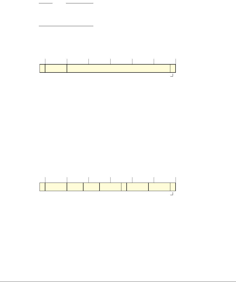
B3 Virtual Memory System Architecture (VMSA)
B3.13 Exception reporting in a VMSA implementation
ARM DDI 0406C.c Copyright © 1996-1998, 2000, 2004-2012, 2014 ARM. All rights reserved. B3-1427
ID051414 Non-Confidential
Except for unconditional Thumb instructions reported with CV set to 0, a trapped unconditional instruction is
reported with CV set to 1 and a COND value of
0x0E
, the condition code value for unconditional.
For an implementation that, for both ARM and Thumb instructions, takes an exception on a trapped conditional
instruction only if the instruction passes its condition code check, these definitions mean that when CV is set to 1 it
is IMPLEMENTATION DEFINED whether the COND field is set to
0xE
, or to the value of any condition that applied to
the instruction.
Note
In some circumstances, it is IMPLEMENTATION DEFINED whether a conditional instruction that fails its condition
code check generates an Undefined Instruction exception, see Conditional execution of undefined instructions on
page B1-1209.
ISS encoding for trapped
WFI
or
WFE
instruction
This is the exception with EC value
0x01
. When HSR.EC returns this value, the encoding of the ISS field is:
ISS[24:20] See Encoding of ISS[24:20] when HSR[31:30] is 0b00 on page B3-1426.
ISS[19:1] Reserved, UNK/SBZP.
ISS[0] Indicates the trapped instruction. The possible values of this bit are:
0
WFI
trapped.
1
WFE
trapped.
Trapping use of the WFI and WFE instructions on page B1-1256 describes the configuration settings for this trap.
ISS encoding for trapped
MCR
or
MRC
access
These are the exceptions with the following EC values:
•
0x03
, trapped
MRC
or
MCR
access to CP15
•
0x05
, trapped
MRC
or
MCR
access to CP14
•
0x08
, trapped
MRC
or
VMRS
access to CP10.
When HSR.EC returns one of these values, the encoding of the ISS field is:
ISS[24:20] See Encoding of ISS[24:20] when HSR[31:30] is 0b00 on page B3-1426.
ISS[19:17] The Opc2 value from the issued instruction.
ISS[16:14] The Opc1 value from the issued instruction.
ISS[13:10] The CRn value from the issued instruction, the coprocessor primary register value.
ISS[9] Reserved, UNK/SBZP.
ISS[8:5] The Rt value from the issued instruction, the ARM core register used for the transfer.
ISS[4:1] The CRm value from the issued instruction.
ISS[0] Indicates the direction of the trapped instruction. The possible values of this bit are:
0 Write to coprocessor.
MCR
instruction.
1 Read from coprocessor.
MRC
or
VMRS
instruction.
24 23 20 19 1 0
CV COND Reserved, UNK/SBZP
Trapped instruction
24 23 20 19 17 16 14 13 10 9 8 5 4 1 0
CV COND Opc2 Opc1 CRn (0) Rt CRm
Direction

B3 Virtual Memory System Architecture (VMSA)
B3.13 Exception reporting in a VMSA implementation
B3-1428 Copyright © 1996-1998, 2000, 2004-2012, 2014 ARM. All rights reserved. ARM DDI 0406C.c
Non-Confidential ID051414
The following sections describe configuration settings for traps that are reported using EC value
0x03
:
•Trapping ID mechanisms on page B1-1251
•Trapping accesses to lockdown, DMA, and TCM operations on page B1-1253
•Trapping accesses to cache maintenance operations on page B1-1254
•Trapping accesses to TLB maintenance operations on page B1-1254
•Trapping accesses to the Auxiliary Control Register on page B1-1254
•Trapping accesses to the Performance Monitors Extension on page B1-1255
•Trapping CPACR accesses on page B1-1258
•Generic trapping of accesses to CP15 system control registers on page B1-1259.
The following sections describe configuration settings for traps that are reported using EC value
0x05
:
•ID group 0, Primary device identification registers on page B1-1252
•Trapping accesses to Jazelle functionality on page B1-1256, for accesses to Jazelle registers
•Trapping accesses to the ThumbEE configuration registers on page B1-1256
•Trapping CP14 accesses to Debug ROM registers on page B1-1260
•Trapping CP14 accesses to OS-related debug registers on page B1-1260
•Trapping general CP14 accesses to debug registers on page B1-1261
•Trapping CP14 accesses to trace registers on page B1-1261.
Trapping ID mechanisms on page B1-1251 describes configuration settings for traps that are reported using EC
value
0x08
.
ISS encoding for trapped
MCRR
or
MRRC
access
These are the exceptions with the following EC values:
•
0x04
, trapped
MRRC
or
MCRR
access to CP15
•
0x0C
, trapped
MRRC
access to CP14.
When HSR.EC returns one of these values, the encoding of the ISS field is:
ISS[24:20] See Encoding of ISS[24:20] when HSR[31:30] is 0b00 on page B3-1426.
ISS[19:16] The Opc1 value from the issued instruction.
ISS[15:14] Reserved, UNK/SBZP.
ISS[13:10] The Rt2 value from the issued instruction, one of the ARM core registers for the transfer.
ISS[9] Reserved, UNK/SBZP.
ISS[8:5] The Rt value from the issued instruction, one of the ARM core registers for the transfer.
ISS[4:1] The CRm value from the issued instruction, the coprocessor primary register value.
ISS[0] Indicates the direction of the trapped instruction. The possible values of this bit are:
0 Write to coprocessor.
MCRR
instruction.
1 Read from coprocessor,
MRRC
instruction.
The following sections describe configuration settings for traps that are reported using EC value
0x04
:
•Trapping writes to virtual memory control registers on page B1-1258
•Generic trapping of accesses to CP15 system control registers on page B1-1259.
The following sections describe configuration settings for traps that are reported using EC value
0x0C
:
•Trapping general CP14 accesses to debug registers on page B1-1261
•Trapping CP14 accesses to Debug ROM registers on page B1-1260.
24 23 20 19 16 15 14 13 10 9 8 5 4 1 0
CV COND Opc1 (0) (0) Rt2 (0) Rt CRm
Direction

B3 Virtual Memory System Architecture (VMSA)
B3.13 Exception reporting in a VMSA implementation
ARM DDI 0406C.c Copyright © 1996-1998, 2000, 2004-2012, 2014 ARM. All rights reserved. B3-1429
ID051414 Non-Confidential
ISS encoding for trapped
LDC
or
STC
access
This is the exception with EC value
0x06
. When HSR.EC returns this value, the encoding of the ISS field is:
ISS[24:20] See Encoding of ISS[24:20] when HSR[31:30] is 0b00 on page B3-1426.
ISS[19:12] imm8. The immediate value from the issued instruction.
ISS[11:9] Reserved, UNK/SBZP.
ISS[8:5] Encoding depends on the instruction form indicated by ISS[3]:
ISS[3]==0 Encodes Rn, the ARM core register that holds the base address. Applies only to
immediate instruction forms.
ISS[3]==1 UNKNOWN. Applies only to literal instruction forms, that are available only for
LDC
instructions
ISS[4] Indicates whether the offset is added or subtracted:
0 Subtract offset.
1 Add offset.
This bit corresponds to the U bit in the instruction encoding.
ISS[3:1] Addressing mode. The permitted values of this field are:
0b000
Immediate unindexed.
0b001
Immediate post-indexed.
0b010
Immediate offset.
0b011
Immediate pre-indexed.
0b100
Literal unindexed.
LDC
instruction in ARM instruction set only.
For a trapped
STC
instruction or a trapped
LDC
Thumb instruction, this encoding is
reserved.
0b101
Reserved.
0b110
Literal offset.
LDC
instruction only.
For a trapped
STC
instruction, this encoding is reserved.
0b111
Reserved.
ISS[3] indicates the instruction form, immediate or literal. See the description of ISS[8:5].
ISS[2:1] correspond to the bits {P, W} in the instruction encoding.
ISS[0] Indicates the direction of the trapped instruction. The possible values of this bit are:
0 Write to coprocessor.
STC
instruction.
1 Read from coprocessor,
LDC
instruction.
Offset sign
Addressing mode
Direction
x
24 23 20 19 12 11 9 8 5 4 3 1 0
CV COND imm8 (0) (0) (0) Rn
UNKNOWN
0
1x
Literal instruction, LDC only
Immediate instruction
Offset form
2
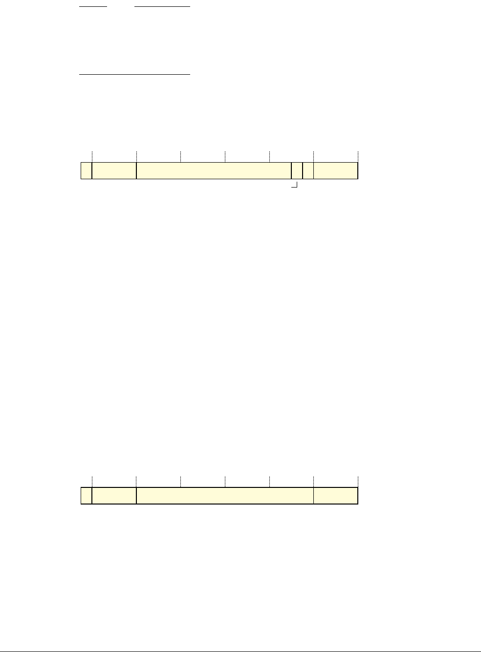
B3 Virtual Memory System Architecture (VMSA)
B3.13 Exception reporting in a VMSA implementation
B3-1430 Copyright © 1996-1998, 2000, 2004-2012, 2014 ARM. All rights reserved. ARM DDI 0406C.c
Non-Confidential ID051414
Note
The only architected uses of these instructions to access CP14 are:
•an
STC
to write to DBGDTRRXint
•an
LDC
to read DBGDTRTXint.
For more information see CP14 debug register interface accesses on page C6-2124.
Trapping general CP14 accesses to debug registers on page B1-1261 describes the configuration settings for the
trap that is reported using EC value
0x06
.
ISS encoding for HCPTR-trapped access to CP0-CP13
This is the exception with EC value
0x07
. When HSR.EC returns this value, the encoding of the ISS field is:
ISS[24:20] See Encoding of ISS[24:20] when HSR[31:30] is 0b00 on page B3-1426.
ISS[19:6] Reserved, UNK/SBZP.
ISS[5] Indicates trapped use of the Advanced SIMD Extension for instructions that are not also VFP
instructions. The possible values of this bit are:
0 Exception was not caused by trapped use of the Advanced SIMD Extension.
1 Exception was caused by trapped use of the Advanced SIMD Extension.
Any use of an Advanced SIMD instruction that is not also a floating point instruction that is trapped
to Hyp mode because of any traps configured in the HCPTR causes this bit to be set to 1.
ISS[4] Reserved, UNK/SBZP.
ISS[3:0] coproc. The number of the coprocessor accessed by the trapped operation, 0-13.
This field is valid only when ISS[5] returns 0. Otherwise, it is UNK/SBZP.
Any use of a Floating-point instruction or access to a Floating-point Extension register that is
trapped to Hyp mode because of a trap configured in the HCPTR sets this field to
0xA
.
The following sections describe the configuration settings for the traps that are reported using EC value
0x07
:
•Trapping of Advanced SIMD functionality on page B1-1257
•General trapping of coprocessor accesses on page B1-1258
ISS encoding for trapped
BXJ
execution
This is the exception with EC value
0x0A
. When HSR.EC returns this value, the encoding of the ISS field is:
ISS[24:20] See Encoding of ISS[24:20] when HSR[31:30] is 0b00 on page B3-1426.
ISS[19:4] Reserved, UNK/SBZP.
Trapping accesses to Jazelle functionality on page B1-1256 describes the configuration settings for this trap.
ISS encoding for Hypervisor Call exception, or Supervisor Call exception routed to Hyp mode
These are the exceptions with the following EC values:
•
0x11
, Supervisor Call exception taken to Hyp mode
•
0x12
, Hypervisor Call exception.
24 23 20 19 6 5 4 3 0
CV COND Reserved, UNK/SBZP (0) coproc
Trapped Advanced SIMD
24 23 20 19 4 3 0
CV COND Reserved, UNK/SBZP Rm

B3 Virtual Memory System Architecture (VMSA)
B3.13 Exception reporting in a VMSA implementation
ARM DDI 0406C.c Copyright © 1996-1998, 2000, 2004-2012, 2014 ARM. All rights reserved. B3-1431
ID051414 Non-Confidential
Note
• A Supervisor Call exception is generated by executing an
SVC
instruction, see SVC (previously SWI) on
page A8-720.
• A Hypervisor Call exception is generated by executing an
HVC
instruction, see HVC on page B9-1984.
When HSR.EC returns one of these values, the encoding of the ISS field is:
ISS[24:16] Reserved, UNK/SBZP.
ISS[15:0] imm16. The value of the immediate field from the issued instruction.
For an
SVC
instruction:
• if the instruction is unconditional:
— for the 16-bit Thumb instruction, this field is zero-extended from the imm8 field of the
instruction
— for the ARM instruction, this field is the bottom 16 bits of the imm24 field of the
instruction
• if the instruction is conditional, this field is UNKNOWN.
Note
The
HVC
instruction is unconditional, and a conditional
SVC
instruction generates a Supervisor Call exception that is
routed to Hyp mode only if it passes its condition code check. Therefore, the syndrome information for these
exceptions does not include conditionality information.
Supervisor Call exception, when HCR.TGE is set to 1 on page B1-1192 describes the configuration settings for the
trap reported with EC value
0x11
.
ISS encoding for trapped
SMC
execution
This is the exception with EC value
0x13
. When HSR.EC returns this value, the ISS field does not return any
syndrome information, and the encoding of the ISS field is:
ISS[24:0] Reserved, UNK/SBZP.
Note
SMC
instructions cannot be trapped if they fail their condition code check. Therefore, the syndrome information for
this exception does not include conditionality information.
Trapping use of the SMC instruction on page B1-1255 describes the configuration settings for this trap, for
instructions executed in Non-secure PL1 modes.
ISS encoding for Prefetch Abort exceptions taken to Hyp mode
These are the exceptions with the following EC values:
•
0x20
, for a Prefetch Abort exception taken from a mode other than Hyp mode and routed to Hyp mode
•
0x21
, for a Prefetch Abort exception taken from Hyp mode.
24 16 15 0
Reserved, UNK/SBZP imm16

B3 Virtual Memory System Architecture (VMSA)
B3.13 Exception reporting in a VMSA implementation
B3-1432 Copyright © 1996-1998, 2000, 2004-2012, 2014 ARM. All rights reserved. ARM DDI 0406C.c
Non-Confidential ID051414
When HSR.EC returns one of these values, the encoding of the ISS field is:
ISS[24:10] Reserved, UNK/SBZP.
ISS[9] EA, External abort type. Can provide an IMPLEMENTATION DEFINED classification of external
aborts. If the implementation does not provide any classification of external aborts, this bit is
UNK/SBZP.
For any abort other than an External abort this bit returns a value of 0.
Note
This bit is equivalent to the IFSR.ExT bit.
ISS[8] Reserved, UNK/SBZP.
ISS[7] S1PTW. For a stage 2 fault, indicates whether the fault was a fault on the stage 2 translation of an
address accessed during a stage 1 translation table walk:
0 Fault not on a stage 2 translation for a stage 1 translation table walk.
1 Fault on the stage 2 translation of an access for a stage 1 translation table walk.
For a stage 1 fault, this bit is UNK/SBZP.
ISS[6] Reserved, UNK/SBZP.
ISS[5:0] IFSC, Instruction fault status code. Indicates the fault that caused the exception, using the fault
codes defined for use with the Long-descriptor translation table format, see Fault reporting with the
Long-descriptor translation table format on page B3-1416.
Note
This field is equivalent to the IFSR.STATUS field, and only valid IFSR.STATUS values are valid
for this field.
The following sections describe cases where Prefetch Abort exceptions can be routed to Hyp mode, generating
exceptions that are reported in the HSR with EC value
0x20
:
•Synchronous external abort, when HCR.TGE is set to 1 on page B1-1193.
•Routing Debug exceptions to Hyp mode on page B1-1194.
EA
24 10 9 8 7 6 5 0
Reserved, UNK/SBZP (0) (0) IFSC
S1PTW

B3 Virtual Memory System Architecture (VMSA)
B3.13 Exception reporting in a VMSA implementation
ARM DDI 0406C.c Copyright © 1996-1998, 2000, 2004-2012, 2014 ARM. All rights reserved. B3-1433
ID051414 Non-Confidential
ISS encoding for Data Abort exceptions taken to Hyp mode
These are the exceptions with the following EC values:
•
0x24
, for a Data Abort exception taken from a mode other than Hyp mode and routed to Hyp mode
•
0x25
, for a Data Abort exception taken from Hyp mode.
When HSR.EC returns one of these values, the encoding of the ISS field is:
ISS[24] Instruction syndrome valid. Indicates whether ISS[24:16] provide a valid instruction syndrome, as
part of the returned ISS. The possible values of this bit are:
0 No valid instruction syndrome. ISS[23:16] are UNK/SBZP.
1 ISS[24:16] hold a valid instruction syndrome.
This bit is 0 for all faults except for those generated by a stage 2 translation. For Data Abort
exceptions generated by a stage 2 translation, this bit is 1 and a valid instruction syndrome is
returned only if all of the following are true:
• the instruction that generated the Data Abort exception:
—is an
LDR
,
LDRT
,
LDRSH
,
LDRSHT
,
LDRH
,
LDRHT
,
LDRSB
,
LDRSBT
,
LDRB
,
LDRBT
,
STR
,
STRT
,
STRH
,
STRHT
,
STRB
, or
STRBT
— is not performing register writeback
— is not using the PC as its destination register.
Note
• For ISS reporting, a stage 2 abort on a stage 1 translation table lookup is treated as a stage 1
Translation fault, and does not return a valid instruction syndrome.
• In the ARM instruction set,
LDR*T
and
STR*T
instructions always perform register writeback
and therefore never return a valid instruction syndrome.
• A valid instruction syndrome provides information that can help a hypervisor to emulate the
instruction efficiently. Instruction syndromes are returned for instructions for which such
accelerated emulation is possible.
ISS[23:16], when ISS[24] is 0
Reserved, UNK/SBZP.
ISS[23:16], when ISS[24] is 1
The remainder of the valid instruction syndrome, defined as follows:
ISS[23:22] SAS, Syndrome access size. Indicate the size of the access attempted by the faulted
operation. The possible values of this field are:
0b00
Byte.
0b01
Halfword.
0b10
Word.
0b11
Reserved.
ISS[21] SSE, Syndrome sign extend. For a byte or halfword load operation, indicates whether
the data item must be sign extended. For these cases, the possible values of this bit are:
0 Sign-extension not required.
1 Data item must be sign-extended.
ISV
(0)
24 23 20 19 18 17 16 15 10 9 8 7 6 5 0
1 SAS SRT
0 Reserved, UNK/SBZP Reserved,
UNK/SBZP DFSC
22 21
SSE
Instruction syndrome
EA
CM
S1PTW
WnR

B3 Virtual Memory System Architecture (VMSA)
B3.13 Exception reporting in a VMSA implementation
B3-1434 Copyright © 1996-1998, 2000, 2004-2012, 2014 ARM. All rights reserved. ARM DDI 0406C.c
Non-Confidential ID051414
For all other operations this bit is 0.
ISS[20] Reserved, UNK/SBZP.
ISS[19:16] SRT, Syndrome Register Transfer. The value of the Rt operand of the faulting
instruction. This specifies:
• the destination register for a load operation
• the source register for a store operation.
Note
Normally, software emulating an instruction must consider both the Rt value and the
Mode value saved in the SPSR, to determine the physical register to access.
ISS[15:10] Reserved, UNK/SBZP.
ISS[9] EA, External abort type. Can provide an IMPLEMENTATION DEFINED classification of external
aborts. If the implementation does not provide any classification of external aborts, this bit is
UNK/SBZP.
For any abort other than an External abort this bit returns a value of 0.
Note
This bit is equivalent to the DFSR.ExT bit.
ISS[8] CM, Cache maintenance. For a synchronous fault, identifies fault that comes from a cache
maintenance or address translation operation. For synchronous faults, the possible values of this bit
are:
0 Fault not generated by a cache maintenance or address translation operation.
1 Fault generated by a cache maintenance or address translation operation.
For asynchronous faults, this bit is 0.
Note
This bit is equivalent to the DFSR.CM bit.
ISS[7] S1PTW. For a stage 2 fault, indicates whether the fault was a fault on the stage 2 translation of an
address accessed during a stage 1 translation table walk:
0 Fault not on a stage 2 translation for a stage 1 translation table walk.
1 Fault on the stage 2 translation of an access for a stage 1 translation table walk.
For a stage 1 fault, this bit is UNK/SBZP.
ISS[6] WnR. Indicates whether a synchronous abort was caused by a write instruction or by a read
instruction. The possible values of this bit are:
0 Abort caused by a read instruction.
1 Abort caused by a write instruction.
For synchronous faults on cache maintenance and address translation operations, this bit always
returns a value of 1.
Note
ISS[8] is set to 1 to identify a fault on a cache maintenance or address translation operation.
For an asynchronous Data Abort exception this bit is UNKNOWN.
For a fault generated by an
SWP
or
SWPB
instruction, the WnR bit is 0 if a read to the location would
have generated a fault, otherwise it is 1.
Note
This bit is equivalent to the DFSR.WnR bit.

B3 Virtual Memory System Architecture (VMSA)
B3.13 Exception reporting in a VMSA implementation
ARM DDI 0406C.c Copyright © 1996-1998, 2000, 2004-2012, 2014 ARM. All rights reserved. B3-1435
ID051414 Non-Confidential
ISS[5:0] DFSC, Data fault status code. Indicates the fault that caused the exception, using the fault codes
defined for use with the Long-descriptor translation table format, see Fault reporting with the
Long-descriptor translation table format on page B3-1416.
Note
This field is equivalent to the DFSR.STATUS field, and all valid DFSR.STATUS values are valid
for this field.
The following describe cases where Data Abort exceptions can be routed to Hyp mode, generating exceptions that
are reported in the HSR with EC value
0x24
:
•Alignment fault, when HCR.TGE is set to 1 on page B1-1193.
•Synchronous external abort, when HCR.TGE is set to 1 on page B1-1193.
•Routing Debug exceptions to Hyp mode on page B1-1194.
B3.13.7 Summary of register updates on exceptions taken to the PL2 mode
For memory system faults that generate exceptions that are taken to Hyp mode, Table B3-30 shows the registers
affected by each fault. In this table:
• Yes indicates that the register is updated
•UNK indicates that the fault makes the register value UNKNOWN
• a null entry, -, indicates that the fault does not affect the register.
Table B3-30 Effect of an exception taken to the PL2 mode on the reporting registers
Fault HSR HIFAR HDFAR HPFAR DBGWFAR
Faults reported as Prefetch Abort exceptions:
MMU faulta at stage 1. Yes Yes UNK UNK -
MMU Translation or Access flag faulta at stage 2. Yes Yes UNK Yes -
MMU Permission faulta at stage 2. Yes Yes UNK UNK -
MMU stage 2 faulta on stage 1 translation. Yes Yes UNK Yes -
Synchronous external abort on translation table walk. Yes Yes UNK UNK -
Synchronous parity error on translation table walk. Yes Yes UNK UNK -
Synchronous external abort. Yes Yes UNK UNK -
Synchronous parity error on memory access. Yes Yes UNK UNK -
TLB conflict abort. Yes Yes UNK UNK -

B3 Virtual Memory System Architecture (VMSA)
B3.13 Exception reporting in a VMSA implementation
B3-1436 Copyright © 1996-1998, 2000, 2004-2012, 2014 ARM. All rights reserved. ARM DDI 0406C.c
Non-Confidential ID051414
Note
Unlike Table B3-26 on page B3-1418, the PL2 fault reporting table does not include an entry for a fault on an
instruction cache maintenance operation. That is because, when the fault is taken to the PL2 mode, the reporting
indicates the cause of the fault, for example a Translation fault, and ISS.CM is set to 1 to indicate that the fault was
on a cache maintenance operation, see ISS encoding for Data Abort exceptions taken to Hyp mode on page B3-1433.
Fault reported as Data Abort exception:
Alignment fault, always synchronous Yes UNK Yes UNK -
MMU faulta at stage 1. Yes UNK Yes UNK -
MMU Translation or Access flag faulta at stage 2. Yes UNK Yes Yes -
MMU Permission faulta at stage 2. Yes UNK Yes UNK -
MMU stage 2 faulta on stage 1 translation. Yes UNK Yes Yes -
Synchronous external abort on translation table walk. Yes UNK Yes UNK -
Synchronous parity error on translation table walk. Yes UNK Yes UNK -
Synchronous external abort. Yes UNK Yes UNK -
Synchronous parity error on memory access. Yes UNK Yes UNK -
Asynchronous external abort. Yes UNK UNK UNK -
Asynchronous parity error on memory access. Yes UNK UNK UNK -
TLB conflict abort. Yes UNK Yes UNK -
Debug exception:
BKPT instruction debug eventb, generates a Prefetch Abort exception. Yes UNK UNK UNK -
Debug exception routed to Hyp mode because HDCR.TDE is set to 1. Generates a Hyp Trap exception.
Breakpoint, BKPT instruction, or Vector catch debug event Yes UNK UNK UNK -
Watchpoint exception, on synchronous watchpoint. Yes UNK Yes UNK UNK
Watchpoint exception, on asynchronous watchpoint. Yes UNK UNK UNK Yes
a. For more information see Classification of MMU faults taken to the PL2 mode on page B3-1437.
b. All other debug exceptions are not permitted in Hyp mode.
Table B3-30 Effect of an exception taken to the PL2 mode on the reporting registers (continued)
Fault HSR HIFAR HDFAR HPFAR DBGWFAR

B3 Virtual Memory System Architecture (VMSA)
B3.13 Exception reporting in a VMSA implementation
ARM DDI 0406C.c Copyright © 1996-1998, 2000, 2004-2012, 2014 ARM. All rights reserved. B3-1437
ID051414 Non-Confidential
Classification of MMU faults taken to the PL2 mode
This subsection gives more information about the MMU faults shown in Table B3-30 on page B3-1435.
Note
All MMU faults are synchronous.
The table uses the following descriptions for MMU faults taken to the PL2 mode:
MMU fault at stage 1 This is an MMU fault generated on a stage 1 translation performed in the Non-secure PL2
translation regime.
MMU fault at stage 2 This is an MMU fault generated on a stage 2 translation performed in the Non-secure
PL1&0 translation regime.
As the table shows, for the faults in this group:
• Translation and Access flag faults update the HPFAR
• Permission faults leave the HPFAR UNKNOWN.
MMU stage 2 fault on a stage 1 translation
This is an MMU fault generated on the stage 2 translation of an address accessed in a stage
1 translation table walk performed in the Non-secure PL1&0 translation regime. For more
information about these faults see Stage 2 fault on a stage 1 translation table walk,
Virtualization Extensions on page B3-1402.
Figure B3-1 on page B3-1309 shows the different translation regimes and associated stages of translation.

B3 Virtual Memory System Architecture (VMSA)
B3.14 Virtual Address to Physical Address translation operations
B3-1438 Copyright © 1996-1998, 2000, 2004-2012, 2014 ARM. All rights reserved. ARM DDI 0406C.c
Non-Confidential ID051414
B3.14 Virtual Address to Physical Address translation operations
CP15 c7 includes operations for Virtual Address (VA) to Physical Address (PA) translation. Address translation
operations, functional group on page B3-1498 summarizes these operations. Each of the following architecture
extensions affects the details of these operations:
• the Security Extensions
• the Large Physical Address Extension
• the Virtualization Extensions.
When using the Short-descriptor translation table format, all VA to PA translations take account of TEX remap when
this is enabled, see Short-descriptor format memory region attributes, with TEX remap on page B3-1368.
Note
A processor that does not implement the Large Physical Address Extension always uses the Short-descriptor
translation table format.
A VA to PA translation operation returns the PA in the PAR. The Large Physical Address Extension extends the PAR
to 64 bits, to hold PAs of up to 40 bits.
The following sections give more information about these operations:
•Naming of the address translation operations, and operation summary
•Encoding and availability of the address translation operations on page B3-1440
•Determining the PAR format, Large Physical Address Extension on page B3-1441
•Handling of faults and aborts during an address translation operation on page B3-1441.
B3.14.1 Naming of the address translation operations, and operation summary
The Virtualization Extensions introduce additional address translation operations. Therefore, the older operations
are renamed to give consistent naming for all operations. The operation names now indicate the corresponding
translation stage. In an implementation that does not include the Virtualization Extensions, there is no distinction
between stage 1 translations and stage 1 and 2 combined translations.
In the stage 1 current state and stages 1 and 2 Non-secure state only operations, the meanings of the last two letters
of the names are:
PR PL1 mode, read operation.
PW PL1 mode, write operation.
UR PL0 mode, read operation.
UW PL0 mode, write operation.
Note
PL0 modes can also be described as unprivileged modes. User mode is the only PL0 mode.
Table B3-31 Naming of address translation operations
Name Old name Description
ATS1CPR, ATS1CPW,
ATS1CUR, ATS1CUW
V2PCWPR, V2PCWPW,
V2PCWUR, V2PCWUW
See Address translation stage 1, current security state on
page B3-1439
ATS12NSOPR, ATS12NSOPW,
ATS12NSOUR, ATS12NSOUW
V2POWPR, V2POWPW,
V2POWUR, V2POWUW
See Address translation stages 1 and 2, Non-secure state only on
page B3-1439
ATS1HR, ATS1HW Not applicableaSee Address translation stage 1, Hyp mode on page B3-1440
a. Operations are part of the Virtualization Extensions and have no equivalent in the older descriptions.

B3 Virtual Memory System Architecture (VMSA)
B3.14 Virtual Address to Physical Address translation operations
ARM DDI 0406C.c Copyright © 1996-1998, 2000, 2004-2012, 2014 ARM. All rights reserved. B3-1439
ID051414 Non-Confidential
In the stage 1 Hyp mode operations, the last letter of the operation name is R for the read operation and W for the
write operation.
The following sections describe the use and availability of these operations:
•Address translation stage 1, current security state
•Address translation stages 1 and 2, Non-secure state only
•Address translation stage 1, Hyp mode on page B3-1440.
Encoding and availability of the address translation operations on page B3-1440 gives the encodings of the
operations.
Address translation stage 1, current security state
These are the ATS1Cxx operations. Any VMSAv7 implementation supports these operations. They can be executed
by any software executing at PL1 or higher, in either security state.
These instructions perform the address translations of the PL1&0 translation regime of the current security state. In
an implementation that includes the Virtualization Extensions, when executed in Non-secure state, they return the
IPA that is the output address of the stage 1 translation. Figure B3-1 on page B3-1309 shows the different translation
regimes.
Note
The Non-secure PL1 and PL0 modes have no visibility of the stage 2 address translations, that can be defined only
at PL2, and translate IPAs to be PAs.
For an implementation that includes the Large Physical Address Extension, see Determining the PAR format, Large
Physical Address Extension on page B3-1441 for the format used when returning the result of these operations.
Address translation stages 1 and 2, Non-secure state only
These are the ATS12NSOxx operations. A VMSAv7 implementation supports these operations only if it includes
the Security Extensions. They can be executed:
• By any software executing in Secure state at PL1.
• If the implementation includes the Virtualization Extensions, by software executing in Non-secure state at
PL2. This means by software executing in Hyp mode.
ARM deprecates use of these operations from any Secure PL1 mode other than Monitor mode.
In Secure state, and in Non-secure Hyp mode on an implementation that includes the Virtualization Extensions,
these operations perform the translations made by the Non-secure PL1&0 translation regime.
These operations always return the PA and final attributes generated by the translation.That is, for an
implementation that includes the Virtualization Extensions, they return:
• the result of the two stages of address translation for the specified Non-secure input address.
• the memory attributes obtained by the combination of the stage 1 and stage 2 attributes.
Note
From Hyp mode, the ATS1Cxx and ATS12NSOxx operations both return the results of address translations that
would be performed in the Non-secure modes other than Hyp mode. The difference is:
• The ATS1Cxx operations return the Non-secure PL1 view of these operations. That is, they return the IPA
output address corresponding to the VA input address.
• The ATS12NSOxx operations return the PL2, or Hyp mode, view of these operations. That is, they return the
PA output address corresponding to the VA input address, generated by two stages of translation.
For an implementation that includes the Large Physical Address Extension, see Determining the PAR format, Large
Physical Address Extension on page B3-1441 for the format used when returning the result of these operations.

B3 Virtual Memory System Architecture (VMSA)
B3.14 Virtual Address to Physical Address translation operations
B3-1440 Copyright © 1996-1998, 2000, 2004-2012, 2014 ARM. All rights reserved. ARM DDI 0406C.c
Non-Confidential ID051414
Address translation stage 1, Hyp mode
These are the ATS1Hx operations. A VMSAv7 implementation supports these operations only if it includes the
Virtualization Extensions. They can be executed by:
• Software executing in Non-secure state at PL2. This means by software executing in Hyp mode.
• Software executing in Secure state in Monitor mode.
These operations are UNPREDICTABLE if used in a Secure PL1 mode other than Monitor mode.
These operations perform the translations made by the Non-secure PL2 translation regime. The operation takes a
VA input address and returns a PA output address.
These operations always return a result in a 64-bit format PAR.
B3.14.2 Encoding and availability of the address translation operations
Software executing at PL0 never has any visibility of the address translation operations, but software executing at
PL1 or higher can use the unprivileged address translation operations to find the address translations used for
memory accesses by software executing at PL0 and PL1.
Note
For information about translations when the MMU is disabled see Address translation operations when the MMU
is disabled on page B4-1752.
Table B3-32 shows the encodings for the address translation operations, and their availability in different
implementations in different processor modes and states.
Table B3-32 CP15 c7 address translation operations
opc1 CRm opc2 Name Type Description
All VMSAv7 implementations, in all modes, at PL1 or higher
0c80ATS1CPR WO PL1 stage 1 read translation, current statea
1ATS1CPW WO PL1 stage 1 write translation, current statea
2ATS1CUR WO Unprivileged stage 1 read translation, current statea
3ATS1CUW WO Unprivileged stage 1 write translation, current statea
Implementations that include the Security Extensions, in Secure PL1 modes and Non-secure Hyp mode
0c84ATS12NSOPR WO Non-secure PL1 stage 1 and 2 read translationb
5ATS12NSOPW WO Non-secure PL1 stage 1 and 2 write translationb
6ATS12NSOUR WO Non-secure unprivileged stage 1 and 2 read translationb
7ATS12NSOUW WO Non-secure unprivileged stage 1 and 2 write translationb
Implementations that include the Virtualization Extensions, in Non-secure Hyp mode and Secure Monitor mode
4c80ATS1HR WO Hyp mode stage 1 read translation c
1ATS1HW WO Hyp mode stage 1 write translationc
a. For more information about these operations see Address translation stage 1, current security state on page B3-1439.
b. For more information about these operations see Address translation stages 1 and 2, Non-secure state only on page B3-1439.
c. For more information about these operations see Address translation stage 1, Hyp mode.

B3 Virtual Memory System Architecture (VMSA)
B3.14 Virtual Address to Physical Address translation operations
ARM DDI 0406C.c Copyright © 1996-1998, 2000, 2004-2012, 2014 ARM. All rights reserved. B3-1441
ID051414 Non-Confidential
The result of an operation is always returned in the PAR. The PAR is a RW register and:
• in all implementations, the 32-bit format PAR is accessed using an
MCR
or
MRC
instruction with CRn set to c7,
CRm set to c4, and opc1 and opc2 both set to 0
• in an implementation that includes the Large Physical Address Extension, the 64-bit format PAR is accessed
using an
MCRR
or
MRRC
instruction with CRm set to c7, and opc1 set to 0.
CP15 c7 address translation operations that are not available in a particular implementation are reserved and
UNPREDICTABLE. For example, in an implementation that does not include the Security Extensions, the encodings
with opc2 values of 4-7, and the encodings with an opc1 value of 4, are reserved and UNPREDICTABLE.
B3.14.3 Determining the PAR format, Large Physical Address Extension
The Large Physical Address Extension extends the PAR to become a 64-bit register, and supports both 32-bit and
64-bit PAR formats. This section describes how the PAR format is determined, for returning a result from each of
the groups of address translation operations. The returned result might be the translated address, or might indicate
a fault on the translation, see Handling of faults and aborts during an address translation operation.
ATS1Cxx operations
Address translations for the current state. From modes other than Hyp mode:
•TTBCR.EAE determines whether the result is returned using the 32-bit or the 64-bit PAR
format.
• If the implementation includes the Security Extensions, the translation performed is for the
current security state and, depending on that state:
— the Secure or Non-secure TTBCR.EAE determines the PAR format.
— the result is returned to the Secure or Non-secure copy of the PAR
Operations from Hyp mode always return a result to the Non-secure PAR, using the 64-bit format.
ATS12NSOxx operations
Address translations for the Non-secure PL1 and PL0 modes. These operations return a result using
the 64-bit PAR format if at least one of the following is true:
• the Non-secure TTBCR.EAE bit is set to 1
• the implementation includes the Virtualization Extensions, and HCR.VM is set to 1.
Otherwise, the operation returns a result using the 32-bit PAR format.
Operations from a Secure PL1 mode return a result to the Secure PAR. Operations from Hyp mode
return a result to the Non-secure PAR.
ATS1Hx operations
Address translations from Hyp mode. These operations always return a result using the 64-bit PAR
format.
Operations from Secure Monitor mode return a result to the Secure PAR. Operations from
Non-secure Hyp mode return a result to the Non-secure PAR.
B3.14.4 Handling of faults and aborts during an address translation operation
When an MMU is enabled, any corresponding address translation operation requires a translation table lookup, and
this might require a translation table walk. However, the input address for the translation might be a faulting address,
either because:
• the translation table entries used for the translation indicate a fault
• a stage 2 fault or an external abort occurs on the required translation table walk.
VMSA memory aborts on page B3-1395 describes the faults that might occur on a translation table walk.

B3 Virtual Memory System Architecture (VMSA)
B3.14 Virtual Address to Physical Address translation operations
B3-1442 Copyright © 1996-1998, 2000, 2004-2012, 2014 ARM. All rights reserved. ARM DDI 0406C.c
Non-Confidential ID051414
How the fault is handled, and whether it generates an exception, depends on the cause of the fault, as described in:
•MMU fault on an address translation operation
•External abort during an address translation operation on page B3-1443
•Stage 2 fault on a current state address translation operation on page B3-1443.
Because an address translation operation does not access the output address of the associated address translation,
watchpoints cannot be generated by address translation operations.
MMU fault on an address translation operation
In the following cases, an MMU fault on an address translation is reported in the PAR, and no abort is taken. This
applies:
• For a faulting address translation operation executed in Hyp mode, or in a Secure PL1 mode.
• For a faulting address translation operation executed in a Non-secure PL1 mode, for cases where the fault
would generate a stage 1 abort if it occurred on the on the equivalent load or store operation.
Using the PAR to report a fault on an address translation operation gives more information about how these faults
are reported.
Note
• The Domain fault encodings shown in Table B3-24 on page B3-1416 are used only for reporting a fault on
an address translation operation that uses the 64-bit PAR format. That is, they are used only in an
implementation that includes the Virtualization Extensions, and are used for reporting a Domain fault on
either:
— an ATS1Cxx operation from Hyp mode
— an ATS12NSOxx operation when HCR.VM is set to 1.
These encodings are never used for fault reporting in the DFSR, IFSR, or HSR.
• For an address translation operation executed in a Non-secure PL1 mode, for a fault that would generate a
stage 2 abort if it occurred on the equivalent load or store operation, the stage 2 abort is generated as described
in Stage 2 fault on a current state address translation operation on page B3-1443.
Using the PAR to report a fault on an address translation operation
For a fault on an address translation operation for which no abort is taken, the PAR is updated with the following
information, to indicate the fault:
• The fault code, that would normally be written to the Fault status register. The code used depends on the
current translation table format, as described in either:
—PL1 fault reporting with the Short-descriptor translation table format on page B3-1414
—Fault reporting with the Long-descriptor translation table format on page B3-1416.
See also the Note at the start of Determining the PAR format, Large Physical Address Extension on
page B3-1441 about the Domain fault encodings shown in Table B3-24 on page B3-1416.
• A status bit, that indicates that the translation operation failed.
The fault does not update any Fault Address Register.

B3 Virtual Memory System Architecture (VMSA)
B3.14 Virtual Address to Physical Address translation operations
ARM DDI 0406C.c Copyright © 1996-1998, 2000, 2004-2012, 2014 ARM. All rights reserved. B3-1443
ID051414 Non-Confidential
External abort during an address translation operation
As stated in Behavior of external aborts on a translation table walk caused by address translation on page B3-1407,
an external abort on a translation table walk generates a Data Abort exception. The abort can be synchronous or
asynchronous, and behaves as follows:
Synchronous external abort on a translation table walk
The fault status and fault address registers of the security state to which the abort is taken are
updated. The fault status register indicates the appropriate external abort on Translation fault, and
the fault address register indicates the input address for the translation.
The PAR is UNKNOWN.
Asynchronous external abort on a translation table walk
The fault status register of the security state to which the abort is taken is updated, to indicate the
asynchronous external abort. No fault address registers are updated.
The PAR is UNKNOWN.
Stage 2 fault on a current state address translation operation
If the processor is in a Non-secure PL1 mode and performs one of the ATS1C** operations, then a fault in the stage
2 translation of an address accessed in a stage 1 translation table lookup generates an exception. This is equivalent
to the case described in Stage 2 fault on a stage 1 translation table walk, Virtualization Extensions on page B3-1402.
When this fault occurs on an ATS1C** address translation operation:
• a Hyp Trap exception is taken to Hyp mode
• the PAR is UNKNOWN
• the HSR indicates that:
— the fault occurred on a translation table walk
— the operation that faulted was a cache maintenance operation
• the HPFAR holds the IPA that faulted
• the HDFAR holds the VA that the executing software supplied to the address translation operation.

B3 Virtual Memory System Architecture (VMSA)
B3.15 About the system control registers for VMSA
B3-1444 Copyright © 1996-1998, 2000, 2004-2012, 2014 ARM. All rights reserved. ARM DDI 0406C.c
Non-Confidential ID051414
B3.15 About the system control registers for VMSA
On an ARMv7-A or ARMv7-R implementation, the system control registers comprise:
• the registers accessed using the System Control Coprocessor, CP15
• registers accessed using the CP14 coprocessor, including:
— debug registers
— trace registers
— execution environment registers.
Note
Do not confuse this general term, system control registers, with the full name of the SCTLR, described in SCTLR,
System Control Register, VMSA on page B4-1707.
Organization of the CP14 registers in a VMSA implementation on page B3-1468 summarizes the CP14 registers,
and indicates where the CP14 registers are described, either in this manual or in other architecture specifications.
Organization of the CP15 registers in a VMSA implementation on page B3-1469 summarizes the CP15 registers,
and indicates where in this manual the CP15 registers are described.
This section gives general information about the control registers, the CP14 and CP15 interfaces to these registers,
and the conventions used in describing these registers.
Note
Many implementations include other interfaces to some functional groups of CP14 and CP15 registers, for example
memory-mapped interfaces to the CP14 Debug registers. These are described in the appropriate sections of this
manual.
This section is organized as follows:
•About system control register accesses
•General behavior of system control registers on page B3-1446
•Classification of system control registers on page B3-1451
•Effect of the LPAE and Virtualization Extensions on the system control registers on page B3-1460
•Synchronization of changes to system control registers on page B3-1461
•Meaning of fixed bit values in register bit assignment diagrams on page B3-1466.
B3.15.1 About system control register accesses
Before the introduction of the Large Physical Address Extension, Virtualization Extensions, and Generic Timer, in
ARMv7 all control registers were 32-bits wide. Accessing 32-bit control registers on page B3-1445 describes how
these registers are accessed.
Note
Optionally, an ARMv6 implementation can include some block transfer operations that are accessed using 64-bit
CP15 accesses, see Block transfer operations on page D12-2536.
The Large Physical Address Extension, Virtualization Extensions, and the OPTIONAL Generic Timer introduce a
small number of 64-bit control registers. Accessing 64-bit control registers on page B3-1445 describes how these
registers are accessed.
When using the
MCR
,
MRC
,
MCRR
, and
MRRC
instructions to access these registers, the instruction arguments include:
• a coprocessor identifier, coproc, as a value p0-p15, corresponding to CP0-CP15
• a coprocessor register, CRn or CRm, as a value c0-c15, to specify a coprocessor register number
• an opcode, opc1 or opc2, as a value in the range 0-7.

B3 Virtual Memory System Architecture (VMSA)
B3.15 About the system control registers for VMSA
ARM DDI 0406C.c Copyright © 1996-1998, 2000, 2004-2012, 2014 ARM. All rights reserved. B3-1445
ID051414 Non-Confidential
Note
• When accessing CP15, the primary coprocessor register is the top-level indicator of the accessed
functionality, and when:
— using an
MCR
or
MRC
instruction, CRn specifies the primary coprocessor register
— using an
MCRR
or
MRRC
instruction, CRm specifies the primary coprocessor register.
• When accessing CP14 using any of these instructions, opc1 is the top-level indicator of the accessed
functionality.
Ordering of reads of system control registers
Reads of the system control registers can occur out of order with respect to earlier instructions executed on the same
processor, provided that the data dependencies between the instructions, specified in Synchronization of changes to
system control registers on page B3-1461, are met.
Note
In particular, system control registers holding self-incrementing counts, for example the Performance Monitors
counters or the Generic Timer counter or timers, can be read early. This means that, for example, if a memory
communication is used to communicate a read of the Generic Timer counter, an
ISB
must be inserted between the
read of the memory location used for this communication and the read of the Generic Timer counter if it is required
that the Generic Timer counter returns a count value that is later than the memory communication.
Accessing 32-bit control registers
Software accesses a 32-bit control register using the generic
MCR
and
MRC
coprocessor interface, specifying:
• A coprocessor identifier, coproc, identifying one of coprocessors CP0-CP15.
• Two coprocessor registers, CRn and CRm. CRn specifies the primary coprocessor register.
• Two coprocessor-specific opcodes, opc1 and opc2.
• An ARM core register to hold a 32-bit value to transfer to or from the coprocessor.
CP15 and CP14 provides the control registers. A processor access to a specific 32-bit control register uses:
• p15 to specify CP15, or p14 to specify CP14
• a unique combination of CRn, opc1, CRm, and opc2, to specify the required control register
• an ARM core register for the transferred 32-bit value.
The processor accesses a 32-bit control register using:
•an
MCR
instruction to write to a control register, see MCR, MCR2 on page A8-476
•an
MRC
instruction to read a control register, see MRC, MRC2 on page A8-492.
Accessing 64-bit control registers
Software accesses a 64-bit control register using the generic
MCRR
and
MRRC
coprocessor interface, specifying:
• A coprocessor identifier, coproc, identifying one of coprocessors CP0-CP15.
• A coprocessor register, CRm. In this case, CRm specifies the primary coprocessor register.
• A single coprocessor-specific opcode, opc1.
• Two ARM core registers to hold two 32-bit values to transfer to or from the coprocessor.
CP15 and CP14 provide the control registers. A processor access to a specific 64-bit control register uses:
• p15 to specify CP15, or p14 to specify CP14
• a unique combination of CRm and opc1, to specify the required 64-bit system control register
• two ARM core registers, each holding 32 bits of the value to transfer.
Therefore, processor accesses a 64-bit control register using:
•an
MCRR
instruction to write to a control register, see MCRR, MCRR2 on page A8-478

B3 Virtual Memory System Architecture (VMSA)
B3.15 About the system control registers for VMSA
B3-1446 Copyright © 1996-1998, 2000, 2004-2012, 2014 ARM. All rights reserved. ARM DDI 0406C.c
Non-Confidential ID051414
•an
MRRC
instruction to read a control register, see MRRC, MRRC2 on page A8-494.
When using a
MCRR
or
MRRC
instruction:
• Rt contains the least-significant 32 bits of the transferred value, and Rt2 contains the most-significant 32 bits
of that value
• the access is 64-bit atomic.
The Large Physical Address Extension extends some registers from 32-bits to 64-bits. The
MCR
and
MRC
encodings
for these registers access the least significant 32 bits of the register. For example, to access the PAR, software can:
• use the following instructions to access all 64 bits of the register:
MRRC p15, 0, <Rt>, <Rt2>, c7 ; Read 64-bit PAR into Rt (low word) and Rt2 (high word)
MCRR p15, 0, <Rt>, <Rt2>, c7 ; Write Rt (low word) and Rt2 (high word) to 64-bit PAR
• use the following instructions to access the least-significant 32 bits of the register:
MRC p15, 0, <Rt>, c7, c4, 0 ; Read PAR[31:0] into Rt
MCR p15, 0, <Rt>, c7, c4, 0 ; Write Rt to PAR[31:0]
B3.15.2 General behavior of system control registers
Except where indicated, system control registers are 32-bits wide. As stated in About system control register
accesses on page B3-1444, there are some 64-bit registers, and these include cases where software can access either
a 32-bit view or a 64-bit view of a register. The register summaries, and the individual register descriptions, identify
the 64-bit registers and how they can be accessed.
The following sections give information about the general behavior of these registers. Unless otherwise indicated,
information applies to both CP14 and CP15 registers:
•Read-only bits in read/write registers
•UNPREDICTABLE and UNDEFINED behavior for CP14 and CP15 accesses
•Reset behavior of CP14 and CP15 registers on page B3-1450.
See also About system control register accesses on page B3-1444 and Meaning of fixed bit values in register bit
assignment diagrams on page B3-1466.
Read-only bits in read/write registers
Some read/write registers include bits that are read-only. These bits ignore writes.
An example of this is the SCTLR.NMFI bit, bit[27].
UNPREDICTABLE and UNDEFINED behavior for CP14 and CP15 accesses
In ARMv7 the following operations are UNDEFINED:
•all
CDP
,
LDC
and
STC
operations to CP14 and CP15, except for the
LDC
access to DBGDTRTXint and the
STC
access to DBGDTRRXint specified in CP14 debug register interface accesses on page C6-2124
•all
MCRR
and
MRRC
operations to CP14 and CP15, except for those explicitly defined as accessing 64-bit CP14
and CP15 registers
•all
CDP2
,
MCR2
,
MRC2
,
MCRR2
,
MRRC2
,
LDC2
,
LDCL
,
LDC2L
,
STC2
,
STCL
and
STC2L
operations to CP14 and CP15.
Unless otherwise indicated in the individual register descriptions:
• reserved fields in registers are UNK/SBZP
• assigning a reserved value to a field can have an UNPREDICTABLE effect.
The following subsections give more information about UNPREDICTABLE and UNDEFINED behavior for CP14 and
CP15 accesses:
•Accesses to unallocated CP14 and CP15 encodings on page B3-1447
•Additional rules for MCR and MRC accesses to CP14 and CP15 registers on page B3-1448
•Effects of the Security Extensions and Virtualization Extensions on CP15 register accesses on page B3-1448.

B3 Virtual Memory System Architecture (VMSA)
B3.15 About the system control registers for VMSA
ARM DDI 0406C.c Copyright © 1996-1998, 2000, 2004-2012, 2014 ARM. All rights reserved. B3-1447
ID051414 Non-Confidential
Accesses to unallocated CP14 and CP15 encodings
The general rules for the behavior of accesses to unallocated register encodings are similar for CP14 and CP15, but
because the primary register specifier is different for CP14 and CP15, the details differ. Therefore, the rules are:
For CP14 For any
MCR
or
MRC
access to CP14, the opc1 value for the instruction is the primary specifier for the
functional group of registers accessed, see Organization of the CP14 registers in a VMSA
implementation on page B3-1468. Accesses to unallocated functional groups of registers are
UNDEFINED. This means any access with
<opc1>
=={2, 3, 4, 5} is UNDEFINED.
For
MCR
or
MRC
accesses to an allocated functional group of registers, the behavior of accesses to
unallocated registers in the functional group depends on the group:
opc1==0, Debug registers
The behavior of accesses to unallocated registers depends on the Debug architecture
version, see:
•Access to unallocated CP14 debug register encodings, v7 Debug on
page C6-2138
•Access to unallocated CP14 debug register encodings, v7.1 Debug on
page C6-2148.
opc1==1, Trace registers
See the appropriate trace architecture specification for the behavior of CP14 accesses to
unallocated Trace registers.
opc1=={6, 7}, ThumbEE and Jazelle registers
Accesses to unallocated register encodings are UNPREDICTABLE.
Note
The opc1==7 functional group, the Jazelle registers, can include registers that are
defined by the Jazelle subarchitecture.
For
MCRR
or
MRRC
accesses to CP14, all accesses are UNDEFINED unless this manual, or the appropriate
trace architecture specification, explicitly defines them as accessing a 64-bit system register:
•Chapter C11 The Debug Registers identifies valid
MCRR
or
MRRC
accesses with opc1==0
• the appropriate trace architecture specification identifies any valid
MCRR
or
MRRC
accesses with
opc1==1
• there are no valid
MCRR
or
MRRC
accesses with opc1==6 or opc1==7.
For CP15 For
an MCR
or
MRC
access to CP15, the CRn value for the instruction is the primary register specifier
for the CP15 space, and the following rules define the behavior of accesses to unallocated
encodings:
1. Accesses to unallocated primary registers are UNDEFINED. For the ARMv7-A Architecture,
this means that:
• For any implementation, accesses to CP15 primary register c4 are UNDEFINED.
• For an implementation that does not include the Security Extensions, accesses to CP15
primary register c12 are UNDEFINED.
• For an implementation that does not include the Generic Timer Extension, accesses to
CP15 primary register c14 are UNDEFINED.
See rule 3 for the behavior of accesses to CP15 primary register c15.
2. In an allocated CP15 primary register, accesses to all unallocated encodings are
UNPREDICTABLE for accesses at PL1 or higher.
This means that any
MCR
or
MRC
access from PL1 or higher with a combination of
<CRn>
,
<opc1>
,
<CRm>
and
<opc2>
values not shown in, or referenced from, Full list of VMSA CP15
registers, by coprocessor register number on page B3-1481, that would access an allocated
CP15 primary register, is UNPREDICTABLE. As indicated by rule 1, for the ARMv7-A
architecture, the allocated CP15 primary registers are:
• in any VMSA implementation, c0-c3, c5-c11, c13, and c15

B3 Virtual Memory System Architecture (VMSA)
B3.15 About the system control registers for VMSA
B3-1448 Copyright © 1996-1998, 2000, 2004-2012, 2014 ARM. All rights reserved. ARM DDI 0406C.c
Non-Confidential ID051414
• in addition, in an implementation that includes the Security Extensions, c12
• in addition, in an implementation that includes the Generic Timer, c14.
Note
As shown in Figure B3-27 on page B3-1471, accesses to unallocated principal ID registers
map onto the MIDR. These are accesses with
<CRn>
= c0,
<opc1>
=0,
<CRm>
= c0, and
<opc2>
= {4, 6, 7}.
3. CP15 primary register c15 is reserved for IMPLEMENTATION DEFINED registers. This means it
is IMPLEMENTATION DEFINED whether this primary register is allocated or unallocated:
• if an implementation does not define any registers in CP15 primary register c15, then
that primary register is unallocated, and all
MCR
and
MRC
accesses to it are UNDEFINED
• otherwise, CP15 primary register c15 is allocated, and
MCR
and
MRC
accesses to
unallocated encodings with CRn set to c15 are UNPREDICTABLE for accesses at PL1 or
higher.
For
MCRR
or
MRRC
accesses to CP15, all accesses are UNDEFINED unless this manual explicitly defines
them as accessing a 64-bit system register. Full list of VMSA CP15 registers, by coprocessor register
number on page B3-1481 identifies the valid
MCRR
and
MRRC
accesses to CP15.
Additional rules for MCR and MRC accesses to CP14 and CP15 registers
All
MCR
operations from the PC are UNPREDICTABLE for all coprocessors, including for CP14 and CP15.
All
MRC
operations to APSR_nzcv are UNPREDICTABLE for CP14 and CP15, except for the CP14
MRC
to APSR_nzcv
shown in CP14 debug register interface accesses on page C6-2124.
Except for CP14 and CP15 encodings that the appropriate register description identifies as accessible by software
executing at PL0, all
MCR
and
MRC
accesses from User mode are UNDEFINED. This applies to all User mode accesses
to unallocated CP14 and CP15 encodings.
Some individual registers can be made inaccessible by setting configuration bits, possibly including
IMPLEMENTATION DEFINED configuration bits, to disable access to the register. The effects of the
architecturally-defined configuration bits are defined individually in this manual. Unless explicitly stated otherwise
in this manual, setting a configuration bit to disable access to a register results in the register becoming UNDEFINED
for
MRC
and
MCR
accesses.
See also Read-only and write-only register encodings on page B3-1449.
Effects of the Security Extensions and Virtualization Extensions on CP15 register accesses
The Security Extensions and Virtualization Extensions introduce classes of system control registers, described in
Classification of system control registers on page B3-1451. Some of these classes of register are either:
• accessible only from certain modes or states
• accessible from certain modes or states only when configuration settings permit the access.
Accesses to these registers that are not permitted are UNDEFINED, meaning execution of the register access
instruction generates an Undefined Instruction exception.
Note
This section applies only to registers that are accessible from some modes and states. That is, it applies only to
register access instructions using an encoding that, under some circumstances, would perform a valid register
access.
The following register classes restrict access in this way:
Restricted access system control registers
This register class is defined in any implementation that includes the Security Extensions.
Restricted access registers other than the NSACR are accessible only from Secure PL1 modes. All
other accessed to these registers are UNDEFINED.

B3 Virtual Memory System Architecture (VMSA)
B3.15 About the system control registers for VMSA
ARM DDI 0406C.c Copyright © 1996-1998, 2000, 2004-2012, 2014 ARM. All rights reserved. B3-1449
ID051414 Non-Confidential
The NSACR is a special case of a Restricted access register and:
• the NSACR is:
— read/write accessible from Secure PL1 modes
— is Read-only accessible from Non-secure PL2 and PL1 modes
• all other accesses to the NSACR are UNDEFINED.
For more information, see Restricted access system control registers on page B3-1453.
Configurable access system control registers
This register class is defined in any implementation that includes the Security Extensions.
Most Configurable access registers are accessible from Non-secure state only if control bits in the
NSACR permit Non-secure access to the register. Otherwise, a Non-secure access to the register is
UNDEFINED.
For other Configurable access registers, control bits in the NSACR control the behavior of bits or
fields in the register when it is accessed from Non-secure state. That is, Non-secure accesses to the
register are permitted, but the NSACR controls how they behave. The only architecturally-defined
register of this type is the CPACR.
For more information, see Configurable access system control registers on page B3-1453.
PL2-mode system control registers
This register class is defined only in an implementation that includes the Virtualization Extensions.
PL2-mode registers are accessible only from:
• the Non-secure PL2 mode, Hyp mode
• Secure Monitor mode when SCR.NS is set to 1.
All other accesses to these registers are UNDEFINED.
For more information, see Banked PL2-mode CP15 read/write registers on page B3-1454 and
PL2-mode encodings for shared CP15 registers on page B3-1456.
PL2-mode write-only operations
This register class is defined only in an implementation that includes the Virtualization Extensions.
PL2-mode write-only operations are accessible only from:
• the Non-secure PL2 mode, Hyp mode
• Secure Monitor mode, regardless of the value of SCR.NS.
Write accesses to these operations are:
•UNPREDICTABLE in Secure PL1 modes other than Monitor mode
•UNDEFINED in Non-secure modes other than Hyp mode.
For more information, see Banked PL2-mode CP15 write-only operations on page B3-1456.
In addition, in any implementation that includes the Security Extensions, if write access to a register is disabled by
the CP15SDISABLE signal then any
MCR
access to that register is UNDEFINED.
Read-only and write-only register encodings
Some system control registers are read-only (RO) or write-only (WO). For example:
• most identification registers are read-only
• most encodings that perform an operation, such as a cache maintenance operation, are write-only.
If this manual defines a register to be RO at a particular privilege level then, at that privilege level:
•an
MCR
access to the register is UNPREDICTABLE
•an
MCRR
access to the register is UNDEFINED, regardless of whether the register can be read by an
MRRC
instruction.

B3 Virtual Memory System Architecture (VMSA)
B3.15 About the system control registers for VMSA
B3-1450 Copyright © 1996-1998, 2000, 2004-2012, 2014 ARM. All rights reserved. ARM DDI 0406C.c
Non-Confidential ID051414
If this manual defines a register to be WO at a particular privilege level then, at that privilege level:
•an
MRC
access to the register is UNPREDICTABLE
•an
MRRC
access to the register is UNDEFINED, regardless of whether the register can be written by an
MCRR
instruction.
Note
• This section applies only to registers that this manual defines as RO or WO. It does not apply to registers for
which other access permissions are explicitly defined.
• Although the FPSID is a RO register, a write using the FPSID encoding is a valid serializing operation, see
Asynchronous bounces, serialization, and Floating-point exception barriers on page B1-1238. Such a write
does not access the register.
Reset behavior of CP14 and CP15 registers
After a reset, only a limited subset of the processor state is guaranteed to be set to defined values. Also, for CP14
debug and trace registers, reset requirements must take account of different levels of reset. For more information
about the reset behavior of CP14 and CP15 registers, see:
•Reset and debug on page C7-2162, for the Debug CP14 registers
• the appropriate Trace architecture specification, for the Trace CP14 registers
•ThumbEE configuration on page A2-95
•Application level configuration and control of the Jazelle extension on page A2-99
•Reset behavior of CP15 registers
•Pseudocode details of resetting CP14 and CP15 registers on page B3-1451.
Reset behavior of CP15 registers
On reset, the VMSAv7 architecture defines a required reset value for all or part of each of the following CP15
registers:
• The SCTLR, CPACR, and TTBCR.
• The FCSEIDR, if the implementation includes the Fast Context Switch Extension (FCSE). This register is
RAZ/WI when the FCSE is not implemented.
• In an implementation that includes the Security Extensions, the SCR, the Secure copy of the VBAR, and the
NSACR.
• In an implementation that includes the Virtualization Extensions, the VPIDR, VMPIDR, HCR, HDCR,
HCPTR, HSTR, and VTTBR.
• In an implementation that includes the Performance Monitors extension, the PMCR, the PMUSERENR, and
in an implementation of PMUv2, the instance of PMXEVTYPER that relates to the cycle counter.
• In an implementation that includes the Generic Timer Extension, the CNTKCTL and CNTHCTL registers.
Note
In an implementation that includes the Security Extensions, unless this manual explicitly states otherwise, only the
Secure copy of a Banked register is reset to the defined value, and software must program the Non-secure copy of
the register with the required values. Typically, this programming is part of the processor boot sequence.
For details of the reset values of these registers see the register descriptions. If the description of a register or register
field does not include its reset value then the architecture does not require that register or field to reset to a defined
value.

B3 Virtual Memory System Architecture (VMSA)
B3.15 About the system control registers for VMSA
ARM DDI 0406C.c Copyright © 1996-1998, 2000, 2004-2012, 2014 ARM. All rights reserved. B3-1451
ID051414 Non-Confidential
The values of all other registers at reset are architecturally UNKNOWN. An implementation can assign an
IMPLEMENTATION DEFINED reset value to a register whose reset value is architecturally UNKNOWN. After a reset,
software must not rely on the value of any read/write register that does not have either an architecturally-defined
reset value or an IMPLEMENTATION DEFINED reset value.
Pseudocode details of resetting CP14 and CP15 registers
The
ResetControlRegisters()
pseudocode function resets all CP14 and CP15 registers, and register fields, that have
defined reset values, as described in this section.
Note
For CP14 debug and trace registers this function resets registers as defined for the appropriate level of reset.
B3.15.3 Classification of system control registers
The Security Extensions and Virtualization Extensions integrate with many features of the architecture. Therefore,
the descriptions of the individual system control registers include information about how these extensions affect the
register. This section:
• summarizes how the Security Extensions and Virtualization Extensions affect the implementation of the
system control registers, and the classification of those registers.
• summarizes how the Security Extensions control access to the system control registers
• describes a Security Extensions signal that can control access to some CP15 registers.
It contains the following subsections:
•Banked system control registers on page B3-1452
•Restricted access system control registers on page B3-1453
•Configurable access system control registers on page B3-1453
•PL2-mode system control registers on page B3-1454
•Common system control registers on page B3-1457
•The CP15SDISABLE input on page B3-1458
•Access to registers from Monitor mode on page B3-1459.
Note
• This section describes the effect of the Security Extensions on all of system control registers, including those
that are added by the Security Extensions, or by the Virtualization Extensions.
• The Security Extensions define the register classifications of Banked, Restricted access, Configurable, and
Common. The Virtualization Extensions add the PL2-mode classification. Some of these classifications can
apply to some coprocessor registers other than the CP14 and CP15 system control registers.
It is IMPLEMENTATION DEFINED whether each IMPLEMENTATION DEFINED register is Banked, Restricted access,
Configurable, PL2-mode, or Common.

B3 Virtual Memory System Architecture (VMSA)
B3.15 About the system control registers for VMSA
B3-1452 Copyright © 1996-1998, 2000, 2004-2012, 2014 ARM. All rights reserved. ARM DDI 0406C.c
Non-Confidential ID051414
Banked system control registers
In an implementation that includes the Security Extensions, some system control registers are Banked. Banked
system control registers have two copies, one Secure and one Non-secure. The SCR.NS bit selects the Secure or
Non-secure copy of the register. Table B3-33 shows which CP15 registers are Banked in this way, and the permitted
access to each register. No CP14 registers are Banked.
Table B3-33 Banked CP15 registers
CRnaBanked register Permitted accessesb
c0 CSSELR, Cache Size Selection Register Read/write only at PL1 or higher
c1 SCTLR, System Control RegistercRead/write only at PL1 or higher
ACTLR, Auxiliary Control RegisterdRead/write only at PL1 or higher
c2 TTBR0, Translation Table Base 0 Read/write only at PL1 or higher
TTBR1, Translation Table Base 1 Read/write only at PL1 or higher
TTBCR, Translation Table Base Control Read/write only at PL1 or higher
c3 DACR, Domain Access Control Register Read/write only at PL1 or higher
c5 DFSR, Data Fault Status Register Read/write only at PL1 or higher
IFSR, Instruction Fault Status Register Read/write only at PL1 or higher
ADFSR, Auxiliary Data Fault Status RegisterdRead/write only at PL1 or higher
AIFSR, Auxiliary Instruction Fault Status RegisterdRead/write only at PL1 or higher
c6 DFAR, Data Fault Address Register Read/write only at PL1 or higher
IFAR, Instruction Fault Address Register Read/write only at PL1 or higher
c7 PAR, Physical Address Register Read/write only at PL1 or higher
c10 PRRR, Primary Region Remap Register Read/write only at PL1 or higher
NMRR, Normal Memory Remap Register Read/write only at PL1 or higher
c12 VBAR, Vector Base Address Register Read/write only at PL1 or higher
c13 FCSEIDR, FCSE PID RegistereRead/write only at PL1 or higher
CONTEXTIDR, Context ID Register Read/write only at PL1 or higher
TPIDRURW, User Read/Write Thread ID Read/write at all privilege levels, including PL0
TPIDRURO, User Read-only Thread ID Read-only at PL0
Read/write at PL1 or higher
TPIDRPRW, PL1 only Thread ID Read/write only at PL1 or higher
a. For accesses to 32-bit registers. More correctly, this is the primary coprocessor register.
b. Any attempt to execute an access that is not permitted results in an Undefined Instruction exception.
c. Some bits are common to the Secure and the Non-secure copies of the register, see SCTLR, System Control Register,
VMSA on page B4-1707.
d. See ADFSR and AIFSR, Auxiliary Data and Instruction Fault Status Registers, VMSA on page B4-1523. Register is
IMPLEMENTATION DEFINED.
e. Banked only in an implementation that includes the FCSE. The FCSE PID Register is RAZ/WI if the FCSE is not
implemented.

B3 Virtual Memory System Architecture (VMSA)
B3.15 About the system control registers for VMSA
ARM DDI 0406C.c Copyright © 1996-1998, 2000, 2004-2012, 2014 ARM. All rights reserved. B3-1453
ID051414 Non-Confidential
A Banked CP15 register can contain a mixture of:
• fields that are Banked
• fields that are read-only in Non-secure PL1 or PL2 modes but read/write in the Secure state.
The System Control Register SCTLR is an example of a register of that contains this mixture of fields.
The Secure copies of the Banked CP15 registers are sometimes referred to as the Secure Banked CP15 registers.
The Non-secure copies of the Banked CP15 registers are sometimes referred to as the Non-secure Banked CP15
registers.
Restricted access system control registers
In an implementation that includes the Security Extensions, some system control registers are present only in the
Secure security state. These are called Restricted access registers, and their read/write access permissions are:
• In Non-secure state, software cannot modify Restricted access registers.
•For the NSACR, in Non-secure state:
— software running at PL1 or higher can read the register
— unprivileged software, meaning software running at PL0, cannot read the register.
This means that Non-secure software running at PL1 or higher can read the access permissions for system
control registers that have Configurable access.
• For all other Restricted access registers, Non-secure software cannot read the register.
Table B3-34 shows the Restricted access CP15 registers in an implementation that includes the Security Extensions.
There are no Restricted access CP14 registers.
Configurable access system control registers
Secure software can configure the access to some system control registers. These registers are called Configurable
access registers, and the control can be:
• A bit in the control register determines whether the register is:
— accessible from Secure state only
— accessible from both Secure and Non-secure states.
• A bit in the control register changes the accessibility of a register bit or field. For example, setting a bit in the
control register might mean that a R/W field behaves as RAZ/WI when accessed from Non-secure state.
Bits in the NSACR control access.
In an ARMv7 implementation of the Security Extensions:
• there are no Configurable access CP14 registers
• the only required Configurable access CP15 register is the CPACR, Coprocessor Access Control Register
Table B3-34 Restricted access CP15 registers
CRna
a. For accesses to 32-bit registers. More correctly, this is the primary coprocessor register.
Register Permitted accessesb
b. Any attempt to execute an access that is not permitted results in an Undefined Instruction exception.
c1 SCR, Secure Configuration Read/write in Secure PL1 modes
SDER, Secure Debug Enable Read/write in Secure PL1 modes
NSACR, Non-Secure Access Control Read/write in Secure PL1 modes
Read-only in Non-secure PL1 and PL2 modes
c12 MVBAR, Monitor Vector Base Address Read/write in Secure PL1 modes

B3 Virtual Memory System Architecture (VMSA)
B3.15 About the system control registers for VMSA
B3-1454 Copyright © 1996-1998, 2000, 2004-2012, 2014 ARM. All rights reserved. ARM DDI 0406C.c
Non-Confidential ID051414
• the following registers in the CP10 and CP11 register space are Configurable access:
— Floating-point Status and Control Register, FPSCR
— Floating-point Exception register, FPEXC
— Floating-point System ID register, FPSID
— Media and VFP Feature Register 0, MVFR0
— Media and VFP Feature Register 1, MVFR1
— Floating-Point Instruction Registers, FPINST and FPINST2, if implemented.
PL2-mode system control registers
An implementation that includes both the Security Extensions and the Virtualization Extensions includes a number
of registers for use in the PL2 mode, Hyp mode. As with other system control register encodings, some of these
register encodings provide write-only operations. Secure software can access the register by moving to Monitor
mode and setting SCR.NS to 1, before accessing the register.
The following subsections describe the PL2-mode registers:
•Banked PL2-mode CP15 read/write registers
•PL2-mode encodings for shared CP15 registers on page B3-1456
•Banked PL2-mode CP15 write-only operations on page B3-1456.
There are no PL2-mode CP14 registers.
Banked PL2-mode CP15 read/write registers
Architecturally, these are an extension of the Banked registers described in Banked system control registers on
page B3-1452, where:
• the processor does not implement the Secure copy of the register
• the Non-secure copy of the register is accessible only at PL2, that is, only from Hyp mode.
Except for accesses to CNTVOFF in an implementation that includes the Security Extensions but not the
Virtualization Extensions, the behavior of accesses to these registers is as follows:
• in Secure state, the registers can be accessed from Monitor mode when SCR.NS is set to 1, see Access to
registers from Monitor mode on page B3-1459
• the following accesses are UNDEFINED:
— accesses from Non-secure PL1 modes
— accesses in Secure state when SCR.NS is set to 0.
In an implementation that includes the Security Extensions but not the Virtualization Extensions, the behavior of
accesses to CNTVOFF is as follows:
• any access from Secure Monitor mode is UNPREDICTABLE, regardless of the value of SCR.NS
• all other accesses are UNDEFINED.
Note
Except for CNTVOFF, the Banked PL2-mode registers are part of the Virtualization Extensions, meaning they are
implemented only if the implementation includes the Virtualization Extensions. However, conceptually, CNTVOFF
is part of any implementation that includes the Generic Timer Extension, see Status of the CNTVOFF register on
page B8-1970. This means the behavior of CNTVOFF in an implementation that includes the Generic Timer
Extension but does not include the Virtualization Extensions is not covered by the general definition of the behavior
of the Banked PL2-mode CP15 read/write registers.

B3 Virtual Memory System Architecture (VMSA)
B3.15 About the system control registers for VMSA
ARM DDI 0406C.c Copyright © 1996-1998, 2000, 2004-2012, 2014 ARM. All rights reserved. B3-1455
ID051414 Non-Confidential
Table B3-35 shows the PL2-mode CP15 read/write registers:
Table B3-35 Banked PL2-mode CP15 read/write registers
CRn or CRmaRegister Width Permitted accessesb
c0 VPIDR 32-bit Read/write. In Non-secure state, accessible only from Hyp mode
VMPIDR 32-bit Read/write. In Non-secure state, accessible only from Hyp mode
c1 HSCTLR 32-bit Read/write. In Non-secure state, accessible only from Hyp mode
HACTLR 32-bit Read/write. In Non-secure state, accessible only from Hyp mode
HCR 32-bit Read/write. In Non-secure state, accessible only from Hyp mode
HDCR 32-bit Read/write. In Non-secure state, accessible only from Hyp mode
HCPTR 32-bit Read/write. In Non-secure state, accessible only from Hyp mode
HSTR 32-bit Read/write. In Non-secure state, accessible only from Hyp mode
HACR 32-bit Read/write. In Non-secure state, accessible only from Hyp mode
c2 HTCR 32-bit Read/write. In Non-secure state, accessible only from Hyp mode
VTCR 32-bit Read/write. In Non-secure state, accessible only from Hyp mode
HTTBR 64-bit Read/write. In Non-secure state, accessible only from Hyp mode
VTTBR 64-bit Read/write. In Non-secure state, accessible only from Hyp mode
c5 HADFSRc32-bit Read/write. In Non-secure state, accessible only from Hyp mode
HAIFSRc32-bit Read/write. In Non-secure state, accessible only from Hyp mode
HSR 32-bit Read/write. In Non-secure state, accessible only from Hyp mode
c6 HPFAR 32-bit Read/write. In Non-secure state, accessible only from Hyp mode
c10 HMAIR0 32-bit Read/write. In Non-secure state, accessible only from Hyp mode
HMAIR1 32-bit Read/write. In Non-secure state, accessible only from Hyp mode
HAMAIR0 32-bit Read/write. In Non-secure state, accessible only from Hyp mode
HAMAIR1 32-bit Read/write. In Non-secure state, accessible only from Hyp mode
c12 HVBAR 32-bit Read/write. In Non-secure state, accessible only from Hyp mode
c13 HTPIDR 32-bit Read/write. In Non-secure state, accessible only from Hyp mode
c14 CNTVOFFd64-bit Read/write. In Non-secure state, accessible only from Hyp mode
a. CRn for accesses to 32-bit registers, CRm for accesses to 64-bit registers. More correctly, this is the primary coprocessor register.
b. Any attempt to execute an access that is not permitted results in an Undefined Instruction exception.
c. See HADFSR and HAIFSR, Hyp Auxiliary Fault Syndrome Registers, Virtualization Extensions on page B4-1576
d. Implemented only in an implementation that includes the Generic Timer Extension. See, also, the Note earlier in this section.

B3 Virtual Memory System Architecture (VMSA)
B3.15 About the system control registers for VMSA
B3-1456 Copyright © 1996-1998, 2000, 2004-2012, 2014 ARM. All rights reserved. ARM DDI 0406C.c
Non-Confidential ID051414
PL2-mode encodings for shared CP15 registers
Some Hyp mode registers share the Secure copy of an existing Banked register. In this case the implementation
includes an encoding for the register that is accessible only in Hyp mode, or in Monitor mode when SCR.NS is set
to 1.
For these registers, the following accesses are UNDEFINED:
• Accesses from Non-secure PL1 modes.
• Accesses in Secure state when SCR.NS is set to 0.
Table B3-36 lists the PL2-mode encodings for shared registers.
In Monitor mode, the Secure copies of these registers can be accessed either:
• using the DFAR or IFAR encoding with SCR.NS set to 0
• using the HDFAR or HIFAR encoding with SCR.NS set to 1.
However, between accessing a register using one alias and accessing the register using the other alias, a Context
synchronization operation is required to ensure the ordering of the accesses.
Banked PL2-mode CP15 write-only operations
Architecturally, these encodings are an extension of the Banked register encodings described in Banked system
control registers on page B3-1452, where:
• the processor does not implement the operation in Secure state
• in Non-secure state, the operation is accessible only at PL2, that is, only from Hyp mode.
In Secure state:
• these operations can be accessed from Monitor mode regardless of the value of SCR.NS, see Access to
registers from Monitor mode on page B3-1459
• accesses to these operations are UNPREDICTABLE if executed in a Secure mode other than Monitor mode.
Accesses to these operations are UNDEFINED if accessed from a Non-secure PL1 mode.
Table B3-37 on page B3-1457 shows the PL2-mode CP15 write-only operations:
Table B3-36 PL2-mode CP15 register encodings for shared registers
CRna
a. For accesses to 32-bit registers. More correctly, this is the primary coprocessor register.
Register Permitted accessesb
b. Any attempt to execute an access that is not permitted results in an Undefined Instruction exception.
Shared register
c6 HDFAR Read/write. In Non-secure state, accessible only from Hyp modec
c. Also accessible from Monitor mode when SCR.NS set to 1.
Secure DFAR
c6 HIFAR Read/write. In Non-secure state, accessible only from Hyp modecSecure IFAR

B3 Virtual Memory System Architecture (VMSA)
B3.15 About the system control registers for VMSA
ARM DDI 0406C.c Copyright © 1996-1998, 2000, 2004-2012, 2014 ARM. All rights reserved. B3-1457
ID051414 Non-Confidential
For more information about these operations, see:
•Address translation stage 1, Hyp mode on page B3-1440
•Hyp mode TLB maintenance operations, Virtualization Extensions on page B4-1749
Common system control registers
Some system control registers and operations are common to the Secure and Non-secure security states. These are
described as the Common access registers, or simply as the Common registers. These registers include:
• read-only registers that hold configuration information
• register encodings used for various memory system operations, rather than to access registers
• the ISR
• all CP14 registers.
Table B3-38 shows the Common CP15 system control registers in an ARMv7-A implementation that includes the
Security Extensions. These registers are not affected by the implementation of the Security Extensions.
Table B3-37 Banked PL2-mode CP15 write-only operations
CRn Register Width Permitted accessesa
c8 ATS1HR 32-bit Write-only. In Non-secure state, accessible only from Hyp mode
ATS1HW 32-bit Write-only. In Non-secure state, accessible only from Hyp mode
TLBIALLHIS 32-bit Write-only. In Non-secure state, accessible only from Hyp mode
TLBIMVAHIS 32-bit Write-only. In Non-secure state, accessible only from Hyp mode
TLBIALLNSNHIS 32-bit Write-only. In Non-secure state, accessible only from Hyp mode
TLBIALLH 32-bit Write-only. In Non-secure state, accessible only from Hyp mode
TLBIMVAH 32-bit Write-only. In Non-secure state, accessible only from Hyp mode
TLBIALLNSNH 32-bit Write-only. In Non-secure state, accessible only from Hyp mode
a. This section describes the behavior of write accesses that are not permitted. See also Read-only and write-only register encodings
on page B3-1449.
Table B3-38 Common CP15 registers
CRnaRegister Permitted accessesb
c0 MIDR, Main ID Register Read-only, only at PL1 or higher
CTR, Cache Type Register Read-only, only at PL1 or higher
TCMTR, TCM Type RegistercRead-only, only at PL1 or higher
TLBTR, TLB Type RegistercRead-only, only at PL1 or higher
MPIDR, Multiprocessor Affinity Register Read-only, only at PL1 or higher
REVIDR, Revision ID Read-only, only at PL1 or higher

B3 Virtual Memory System Architecture (VMSA)
B3.15 About the system control registers for VMSA
B3-1458 Copyright © 1996-1998, 2000, 2004-2012, 2014 ARM. All rights reserved. ARM DDI 0406C.c
Non-Confidential ID051414
Secure CP15 registers
The Secure CP15 registers comprise:
• The Secure copies of the Banked CP15 registers
• The Restricted access CP15 registers
• The Configurable access CP15 registers that are configured to be accessible only from Secure state.
In an implementation that includes the Security Extensions, the Non-secure CP15 registers are the CP15 registers
other than the Secure CP15 registers.
The CP15SDISABLE input
The Security Extensions include an input signal, CP15SDISABLE, that disables write access to some of the Secure
registers when asserted HIGH.
Note
The interaction between CP15SDISABLE and any IMPLEMENTATION DEFINED register is IMPLEMENTATION
DEFINED.
Table B3-39 on page B3-1459 shows the registers and operations affected.
c0 ID_PFRx, Processor Feature Registers Read-only, only at PL1 or higher
ID_DFR0, Debug Feature Register 0 Read-only, only at PL1 or higher
ID_AFR0, Auxiliary Feature Register 0 Read-only, only at PL1 or higher
ID_MMFRx, Memory Model Feature Registers Read-only, only at PL1 or higher
ID_ISARx, Instruction Set Attribute Registers Read-only, only at PL1 or higher
CCSIDR, Cache Size ID Register Read-only, only at PL1 or higher
CLIDR, Cache Level ID Register Read-only, only at PL1 or higher
AIDR, Auxiliary ID RegistercRead-only, only at PL1 or higher
c7 Cache maintenance operations See Cache maintenance operations, functional group, VMSA on
page B3-1496
Address translation operations See Address translation operations, functional group on page B3-1498
Data barrier operations Write-only at all privilege levels, including PL0
c8 TLB maintenance operations Write-only, only at PL1 or higher
c9 Performance monitors See Access permissions on page C12-2330
c12 ISR, Interrupt Status Register Read-only, only at PL1 or higher
a. For accesses to 32-bit registers. More correctly, this is the primary coprocessor register.
b. Any attempt to execute an access that is not permitted results in an Undefined Instruction exception.
c. Register or operation details are IMPLEMENTATION DEFINED.
Table B3-38 Common CP15 registers (continued)
CRnaRegister Permitted accessesb

B3 Virtual Memory System Architecture (VMSA)
B3.15 About the system control registers for VMSA
ARM DDI 0406C.c Copyright © 1996-1998, 2000, 2004-2012, 2014 ARM. All rights reserved. B3-1459
ID051414 Non-Confidential
On a reset by the external system, the CP15SDISABLE input signal must be taken LOW. This permits the Reset
code to set up the configuration of the Security Extensions. When the input is asserted HIGH, any attempt to write
to the Secure registers shown in Table B3-39 results in an Undefined Instruction exception.
The CP15SDISABLE input does not affect reading Secure registers, or reading or writing Non-secure registers. It
is IMPLEMENTATION DEFINED how the input is changed and when changes to this input are reflected in the processor,
and an implementation might not provide any mechanism for driving the CP15SDISABLE input HIGH. However,
in an implementation in which the CP15SDISABLE input can be driven HIGH, changes in the state of
CP15SDISABLE must be reflected as quickly as possible. Any change must occur before completion of a
Instruction Synchronization Barrier operation, issued after the change, is visible to the processor with respect to
instruction execution boundaries. Software must perform a Instruction Synchronization Barrier operation meeting
the above conditions to ensure all subsequent instructions are affected by the change to CP15SDISABLE.
Use of CP15SDISABLE means key Secure features that are accessible only at PL1 can be locked in a known good
state. This provides an additional level of overall system security. ARM expects control of CP15SDISABLE to
reside in the system, in a block dedicated to security.
Access to registers from Monitor mode
When the processor is in Monitor mode, the processor is in Secure state regardless of the value of the SCR.NS bit.
In Monitor mode, the SCR.NS bit determines whether valid uses of the
MRC
,
MCR
,
MRRC
and
MCRR
instructions access
the Secure Banked CP15 registers or the Non-secure Banked CP15 registers. That is, when:
NS == 0 Common, Restricted access, and Secure Banked registers are accessed by CP15
MRC
,
MCR
,
MRRC
and
MCRR
instructions.
If the implementation includes the Virtualization Extensions, the registers listed in Banked
PL2-mode CP15 read/write registers on page B3-1454 and PL2-mode encodings for shared CP15
registers on page B3-1456 are not accessible, and any attempt to access them generates an
Undefined Instruction exception.
Note
The operations listed in Banked PL2-mode CP15 write-only operations on page B3-1456 are
accessible in Monitor mode regardless of the value of SCR.NS.
CP15 operations use the security state to determine all resources used, that is, all CP15-based
operations are performed in Secure state.
Table B3-39 Secure registers affected by CP15SDISABLE
CRn Register name Affected operation
c1 SCTLR, System Control Register
MCR p15, 0, <Rt>, c1, c0, 0
c2 TTBR0, Translation Table Base Register 0
MCR p15, 0, <Rt>, c2, c0, 0
TTBCR, Translation Table Base Control Register
MCR p15, 0, <Rt>, c2, c0, 2
c3 DACR, Domain Access Control Register
MCR p15, 0, <Rt>, c3, c0, 0
c10 PRRR. Primary Region Remap Register
MCR p15, 0, <Rt>, c10, c2, 0
NMRR, Normal Memory Remap Register
MCR p15, 0, <Rt>, c10, c2, 1
c12 VBAR, Vector Base Address Register
MCR p15, 0, <Rt>, c12, c0, 0
MVBAR, Monitor Vector Base Address Register
MCR p15, 0, <Rt>, c12, c0, 1
c13 FCSEIDR, FCSE PID Register a
a. In an implementation that includes the FCSE. The FCSE PID Register is RAZ/WI if the FCSE is not implemented.
MCR p15, 0, <Rt>, c13, c0, 0

B3 Virtual Memory System Architecture (VMSA)
B3.15 About the system control registers for VMSA
B3-1460 Copyright © 1996-1998, 2000, 2004-2012, 2014 ARM. All rights reserved. ARM DDI 0406C.c
Non-Confidential ID051414
NS == 1 Common, Restricted access and Non-secure Banked registers are accessed by CP15
MRC
,
MCR
,
MRRC
and
MCRR
instructions.
If the implementation includes the Virtualization Extensions, all the registers and operations listed
in the subsections of PL2-mode system control registers on page B3-1454 are accessible, using the
MRC
,
MCR
,
MRRC
, or
MCRR
instructions required to access them from Hyp mode.
CP15 operations use the security state to determine all resources used, that is, all CP15-based
operations are performed in Secure state.
The security state determines whether the Secure or Non-secure Banked registers determine the control state.
Note
Where the contents of a register select the value accessed by an
MRC
or
MCR
access to a different register, then the
register that is used for selection is being used as control state. For example, CSSELR selects the current CCSIDR,
and therefore CSSELR is used as control state. Therefore, in Monitor mode:
•SCR.NS determines whether the Secure or Non-secure CSSELR is accessible
• because the processor is in Secure state, the Secure CSSELR selects the current CCSIDR.
B3.15.4 Effect of the LPAE and Virtualization Extensions on the system control registers
The Large Physical Address Extension (LPAE) adds:
• two reserved CP15 encodings, for applying IMPLEMENTATION DEFINED memory attributes, AMAIR0 and
AMAIR1.
• 64-bit encodings of the TTBR0, TTBR1, and PAR
• 64-bit encodings of the DBGDRAR and DBGDSAR.
The Virtualization Extensions add:
• the CP15 registers and operations summarized in Virtualization Extensions registers, functional group on
page B3-1501.
• the PMOVSSET register
• the DBGBXVRs.

B3 Virtual Memory System Architecture (VMSA)
B3.15 About the system control registers for VMSA
ARM DDI 0406C.c Copyright © 1996-1998, 2000, 2004-2012, 2014 ARM. All rights reserved. B3-1461
ID051414 Non-Confidential
B3.15.5 Synchronization of changes to system control registers
In this section, this processor means the processor on which accesses are being synchronized.
Note
See Definitions of direct and indirect reads and writes and their side-effects on page B3-1464 for definitions of the
terms direct write, direct read, indirect write, and indirect read.
A direct write to a system control register might become visible at any point after the change to the register, but
without a Context synchronization operation there is no guarantee that the change becomes visible.
Any direct write to a system control register is guaranteed not to affect any instruction that appears, in program
order, before the instruction that performed the direct write, and any direct write to a system control register must
be synchronized before any instruction that appears after the direct write, in program order, can rely on the effect of
that write. The only exceptions to this are:
• All direct writes to the same register, using the same encoding, are guaranteed to occur in program order.
• All direct writes to a register are guaranteed to occur in program order relative to all direct reads of the same
register using the same encoding.
• If an instruction that appears in program order before the direct write performs a memory access, such as a
memory-mapped register access, that causes an indirect read or write to a register, that memory access is
subject to the ARM ordering model. In this case, if permitted by the ARM ordering model, the instruction
that appears in program order before the direct write can be affected by the direct write.
These rules mean that an instruction that writes to one of the address translation operations described in Virtual
Address to Physical Address translation operations on page B3-1438 must be explicitly synchronized to guarantee
that the result of the address translation operation is visible in the PAR.
Note
In this case, the direct write to the encoding of the address translation operation causes an indirect write to the PAR.
Without a Context synchronization operation after the direct write there is no guarantee that the indirect write to the
PAR is visible.
Conceptually, the explicit synchronization occurs as the first step of any Context synchronization operation. This
means that if the operation uses state that had been changed but not synchronized before the operation occurred, the
operation is guaranteed to use the state as if it had been synchronized.
Note
• This explicit synchronization is applied as the first step of the execution of any instruction that causes the
operation. This means it does not synchronize any effect of system registers that might affect the fetch and
decode of the instructions that cause the operation, such as breakpoints or changes to translation tables.
• For a synchronous exception, the control state in use at the time the exception is generated determines the
exception syndrome information, and this syndrome information is not changed by this synchronization at
the start of taking the exception.
Except for the register reads listed in Registers with some architectural guarantee of ordering or observability on
page B3-1463, if no context synchronization operation is performed, direct reads of system control registers can
occur in any order.
Table B3-40 on page B3-1462 shows the synchronization requirement between two reads or writes that access the
same system control register. In the column headings, First and Second refer to:
• Program order, for any read or write caused by the execution of an instruction by this processor, other than a
read or write caused by a memory access made by that instruction.
• The order of arrival of asynchronous reads or writes made by this processor relative to the execution of
instructions by this processor.

B3 Virtual Memory System Architecture (VMSA)
B3.15 About the system control registers for VMSA
B3-1462 Copyright © 1996-1998, 2000, 2004-2012, 2014 ARM. All rights reserved. ARM DDI 0406C.c
Non-Confidential ID051414
In addition:
• For indirect reads or writes caused by an external agent, such as a debugger, the mechanism that determines
the order of the reads or writes is defined by that external agent. The external agent can provide mechanisms
that ensure that any reads or writes it makes arrive at the processor. These indirect reads and writes are
asynchronous to software execution on the processor.
• For indirect reads or writes caused by memory-mapped reads or writes made by this processor, the ordering
of the memory accesses is subject to the memory order model, including the effect of the memory type of the
accessed memory address. This applies, for example, if this processor reads or writes one of its registers in a
memory-mapped register interface.
The mechanism for ensuring completion of these memory accesses, including ensuring the arrival of the
asynchronous read or write at the processor, is defined by the system.
Note
Such accesses are likely to be given the Device or Strongly-ordered attribute, but requiring this is outside the
scope of the processor architecture.
• For indirect reads or writes caused by autonomous asynchronous events that count, for example events
caused by the passage of time, the events are ordered so that:
— Counts progress monotonically.
— The events arrive at the processor in finite time and without undue delay.
Table B3-40 Synchronization requirements for updates to system control registers
First read or write Second read or write Context synchronization operation required
Direct read Direct read No
Direct write No
Indirect read Noa
Indirect write Noa, but see text in this section for exceptions
a. Although no synchronization is required between a Direct write and a Direct read, or between a Direct read and an
Indirect write, this does not imply that a Direct read causes synchronization of a previous Direct write. This means
that the sequence Direct write followed by Direct read followed by Indirect read, with no intervening context
synchronization, does not guarantee that the Indirect read observes the result of the Direct write.
Direct write Direct read No
Direct write No
Indirect read Yes a
Indirect write No, but see text in this section for exceptions
Indirect read Direct read No
Direct write No
Indirect read No
Indirect write No
Indirect write Direct read Yes, but see text in this section for exceptions
Direct write No, but see text in this section for exceptions
Indirect read Yes, but see text in this section for exceptions
Indirect write No, but see text in this section for exceptions

B3 Virtual Memory System Architecture (VMSA)
B3.15 About the system control registers for VMSA
ARM DDI 0406C.c Copyright © 1996-1998, 2000, 2004-2012, 2014 ARM. All rights reserved. B3-1463
ID051414 Non-Confidential
If the indirect write is to a register that Registers with some architectural guarantee of ordering or observability
shows as having some guarantee of the visibility of an indirect writes, synchronization might not be required.
If a direct read or a direct write to a register is followed by an indirect write to that register that is caused by an
external agent, or by an autonomous asynchronous event, or as a result of a memory-mapped write, then
synchronization is required to guarantee the ordering of the indirect write relative to the direct read or direct write.
If an indirect write caused by a direct write is followed by an indirect write caused by an external agent, or by an
autonomous asynchronous event, or as a result of a memory-mapped write, then synchronization is required to
guarantee the ordering of the two indirect writes.
If a direct read causes an indirect write, synchronization is required to guarantee that the indirect write is visible to
subsequent direct or indirect reads or writes. This synchronization must be performed after the direct read, before
the subsequent direct or indirect reads or writes.
If a direct write causes an indirect write, synchronization is required to guarantee that the indirect write is visible to
subsequent direct or indirect reads or writes. This synchronization must be performed after the direct write, before
the subsequent direct or indirect reads or writes.
Note
Where a register has more that one encoding, a direct write to the register using a particular encoding is not an
indirect write to the same register with a different encoding.
Where an indirect write is caused by the action of an external agent, such as a debugger, or by a memory-mapped
read or write by the processor, then an indirect write by that agent to a register using a particular access mechanism,
followed by an indirect read by that agent to the same register using the same access mechanism and address does
not need synchronization.
For information about the additional synchronization requirements for memory-mapped registers, see
Synchronization requirements for memory-mapped register interfaces on page C6-2117.
To guarantee the visibility of changes to some registers, additional operations might be required before the context
synchronization operation. For such a register, the definition of the register identifies these additional requirements.
In this manual, unless the context indicates otherwise:
•Accessing a system control register refers to a direct read or write of the register.
•Using a system control register refers to an indirect read or write of the register.
Registers with some architectural guarantee of ordering or observability
For the registers for which Table B3-41 shows that the ordering of direct reads is guaranteed, multiple direct reads
of a single register, using the same encoding, occur in program order without any explicit ordering.
For the registers for which Table B3-41 shows that some observability of indirect writes is guaranteed, an indirect
write to the register caused by an external agent, an autonomous asynchronous events, or as a result of a memory
mapped write, is both:
• Observable to direct reads of the register, in finite time, without explicit synchronization.
• Observable to subsequent indirect reads of the register without explicit synchronization.
These two sets of registers are similar, as Table B3-41 shows:
Table B3-41 Registers with a guarantee of ordering or observability, in a VMSA implementation
Register Ordering of direct reads Observability of indirect writes Notes
ISR Guaranteed Guaranteed Interrupt Status Register
DBGCLAIMCLR - Guaranteed Debug claim registers
DBGCLAIMSET Guaranteed Guaranteed

B3 Virtual Memory System Architecture (VMSA)
B3.15 About the system control registers for VMSA
B3-1464 Copyright © 1996-1998, 2000, 2004-2012, 2014 ARM. All rights reserved. ARM DDI 0406C.c
Non-Confidential ID051414
For the specified registers, the observability requirement is more demanding than the observability requirements for
other registers. However, the possibility that direct reads can occur early, in the absence of context synchronization,
described in Ordering of reads of system control registers on page B3-1445, still applies to these registers.
In Debug state, additional synchronization requirements can apply to the registers shown in Table B3-41 on
page B3-1463. For more information, see:
•Synchronization of accesses to the Debug Communications Channel on page C6-2117.
•Synchronization of accesses to the DCC and the DBGITR on page C8-2178.
Definitions of direct and indirect reads and writes and their side-effects
Direct and indirect reads and writes are defined as follows:
Direct read Is a read of a register, using an
MRC
,
MRC2
,
MRRC
,
MRRC2
,
LDC
, or
LDC2
instruction, that the architecture
permits for the current processor state.
If a direct read of a register has a side-effect of changing the value of a register, the effect of a direct
read on that register is defined to be an indirect write, and has the synchronization requirements of
an indirect write. This means the indirect write is guaranteed to have occurred, and to be visible to
subsequent direct or indirect reads and writes only if synchronization is performed after the direct
read.
Note
The indirect write described here can affect either the register written to by the direct write, or some
other register. The synchronization requirement is the same in both cases.
Direct write Is a write to a register, using an
MCR
,
MCR2
,
MCRR
,
MCRR2
,
STC
, or
STC2
instruction, that the architecture
permits for the current processor state.
In the following cases, the side-effect of the direct write is defined to be an indirect write of the
affected register, and has the synchronization requirements of an indirect write:
• If the direct write has a side-effect of changing the value of a register other than the register
accessed by the direct write.
• If the direct write has a side-effect of changing the value of the register accessed by the direct
write, so that the value in that register might not be the value that the direct write wrote to the
register.
DBGDTRRX Guaranteed Guaranteed Debug Communication Channel
registers
DBGDTRTX Guaranteed Guaranteed
CNTPCT Guaranteed Guaranteed Generic Timer Extension registers, if
the implementation includes the
extension
CNTP_TVAL Guaranteed Guaranteed
CNTVCT Guaranteed Guaranteed
CNTV_TVAL Guaranteed Guaranteed
CNTHP_TVAL Guaranteed Guaranteed
PMCCNTR Guaranteed Guaranteed Performance Monitors Extension
registers, if the implementation includes
the extension
PMXEVCNTR Guaranteed Guaranteed
PMOVSSET Guaranteed Guaranteed
Table B3-41 Registers with a guarantee of ordering or observability, in a VMSA implementation (continued)
Register Ordering of direct reads Observability of indirect writes Notes

B3 Virtual Memory System Architecture (VMSA)
B3.15 About the system control registers for VMSA
ARM DDI 0406C.c Copyright © 1996-1998, 2000, 2004-2012, 2014 ARM. All rights reserved. B3-1465
ID051414 Non-Confidential
In both cases, this means that the indirect write is not guaranteed to be visible to subsequent direct
or indirect reads and writes unless synchronization is performed after the direct write.
Note
• As an example of a direct write to a register having an effect that is an indirect write of that
register, writing 1 to a PMCNTENCLR.Px bit is also an indirect write, because if the Px bit
had the value 1 before the direct write, the side-effect of the write changes the value of that
bit to 0.
• The indirect write described here can affect either the register written to by the direct write,
or some other register. The synchronization requirement is the same in both cases.
For example, writing 1 to a PMCNTENCLR.Px bit that is set to 1 also changes the
corresponding PMCNTENSET.Px bit from 1 to 0. This means that the direct write to the
PMCNTENCLR defines indirect writes to both itself and to the PMCNTENSET.
Indirect read Is a use of the register by an instruction to establish the operating conditions for the instruction.
Examples of operating conditions that might be determined by an indirect read are the translation
table base address, or whether a cache is enabled.
Indirect reads include situations where the value of one register determines what value is returned
by a second register. This means that any read of the second register is an indirect read of the register
that determines what value is returned.
Indirect reads also include:
• Reads of the system control registers by external agents, such as debuggers, as described in
Chapter C6 Debug Register Interfaces.
• Memory-mapped reads of the system control registers made by the processor that implements
the system control registers.
Where an indirect read of a register has a side-effect of changing the value of a register, that change
is defined to be an indirect write, and has the synchronization requirements of an indirect write.
Indirect write Is an update to the value of a register as a consequence of either:
• An exception, operation, or execution of an instruction that is not a direct write to that
register.
• The asynchronous operation of some external agent.
This can include:
• The passage of time, as seen in counters or timers, including performance counters.
• The assertion of an interrupt.
• A write from an external agent, such as a debugger.
However, for some registers, the architecture gives some guarantee of visibility without any explicit
synchronization, see Registers with some architectural guarantee of ordering or observability on
page B3-1463.
Note
Taking an exception is a context-synchronizing operation. Therefore, any indirect write performed
as part of an exception entry does not require additional synchronization. This includes the indirect
writes to the registers that report the exception, as described in Exception reporting in a VMSA
implementation on page B3-1409.

B3 Virtual Memory System Architecture (VMSA)
B3.15 About the system control registers for VMSA
B3-1466 Copyright © 1996-1998, 2000, 2004-2012, 2014 ARM. All rights reserved. ARM DDI 0406C.c
Non-Confidential ID051414
B3.15.6 Meaning of fixed bit values in register bit assignment diagrams
In register bit assignment diagrams, fixed bits are indicated by one of following:
0 In any implementation:
• the bit must read as 0
• writes to the bit must be ignored
•software:
— can rely on the bit reading as 0
— must use an SBZP policy to write to the bit.
(0) The Large Physical Address Extension creates a small number of cases where a bit is (0) in some
contexts, and has a different defined behavior in other contexts. The meaning of (0) is modified for
these bits. For a read/write register, this means:
If a register bit is (0) for all uses of the register
• the bit must read as 0
• writes to the bit must be ignored
•software:
— must not rely on the bit reading as 0
— must use an SBZP policy to write to the bit.
Note
This definition applies to all bits marked as (0) in an implementation that does not
include the Large Physical Address Extension.
If a register bit is (0) only for some uses of the register, when that bit is described as (0)
• A read of the bit must return the value last successfully written to the bit,
regardless of the use of the register when the bit was written.
If the bit has not been successfully written since reset, then the read of the bit
returns the reset value if there is one, or otherwise returns an UNKNOWN value.
•A Direct write to the bit must update a storage location associated with the bit.
•An Indirect write to the register sets the bit to 0.
• While the use of the register is such that the bit is described as (0), or as
UNK/SBZP, the value of the bit must have no effect on the operation of the
processor, other than determining the value read back from that bit.
• Software:
— must not rely on the bit reading as 0
— must use an SBZP policy to write to the bit.
Note
This definition applies only to bits that are defined as (0), or as UNK/SBZP, for one use
of a register, and are defined differently for another use of the register.
Fields that are more than one bit wide are sometimes described as UNK/SBZP, instead of having
each bit marked as (0).
In a read-only register, (0) indicates that the bit reads as 0, but software must treat the bit as UNK.
In a write-only register, (0) indicates that software must treat the bit as SBZ.
1 In any implementation:
• the bit must read as 1
• writes to the bit must be ignored.
•software:
— can rely on the bit reading as 1
— must use an SBOP policy to write to the bit.

B3 Virtual Memory System Architecture (VMSA)
B3.15 About the system control registers for VMSA
ARM DDI 0406C.c Copyright © 1996-1998, 2000, 2004-2012, 2014 ARM. All rights reserved. B3-1467
ID051414 Non-Confidential
(1) The Large Physical Address Extension creates a small number of cases where a bit is (1) in some
contexts, and has a different defined behavior in other contexts. The meaning of (1) is modified for
these bits. For a read/write register, this means:
If a register bit is (1) for all uses of the register
• the bit must read as 1
• writes to the bit must be ignored
•software:
— must not rely on the bit reading as 1
— must use an SBOP policy to write to the bit.
Note
This definition applies to all bits marked as (1) in an implementation that does not
include the Large Physical Address Extension.
If a register bit is (1) only for some uses of the register, when that bit is described as (1)
• A read of the bit must return the value last successfully written to the bit,
regardless of the use of the register when the bit was written.
If the bit has not been successfully written since reset, then the read of the bit
returns the reset value if there is one, or otherwise returns an UNKNOWN value.
•A Direct write to the bit must update a storage location associated with the bit.
•An Indirect write to the register sets the bit to 1.
• While the use of the register is such that the bit is described as (1), or as
UNK/SBOP, the value of the bit must have no effect on the operation of the
processor, other than determining the value read back from that bit.
• Software:
— must not rely on the bit reading as 1
— must use an SBOP policy to write to the bit.
Note
This definition applies only to bits that are defined as (1), or as UNK/SBOP, for one use
of a register, and are defined differently for another use of the register.
Fields that are more than one bit wide are sometimes described as UNK/SBOP, instead of having
each bit marked as (1).
In a read-only register, (1) indicates that the bit reads as 1, but software must treat the bit as UNK.
In a write-only register, (1) indicates that software must treat the bit as SBO.

B3 Virtual Memory System Architecture (VMSA)
B3.16 Organization of the CP14 registers in a VMSA implementation
B3-1468 Copyright © 1996-1998, 2000, 2004-2012, 2014 ARM. All rights reserved. ARM DDI 0406C.c
Non-Confidential ID051414
B3.16 Organization of the CP14 registers in a VMSA implementation
The CP14 registers provide a number of distinct control functions, covering:
• Debug
•Trace
• Execution environment control, for the Jazelle and ThumbEE execution environments.
Because these functions are so distinct, the descriptions of these registers are distributed, as follows:
• in this manual:
—Chapter C11 The Debug Registers describes the Debug registers
—ThumbEE configuration on page A2-95 summarizes the ThumbEE registers
—Application level configuration and control of the Jazelle extension on page A2-99 summarizes the
Jazelle registers
• the following ARM trace architecture specifications describe the Trace registers:
—Embedded Trace Macrocell Architecture Specification
—CoreSight Program Flow Trace Architecture Specification.
This section summarizes the allocation of the CP14 registers between these different functions, and the CP14
register encodings that are reserved.
The CP14 register encodings are classified by the {CRn, opc1, CRm, opc2} values required to access them using
an
MCR
or an
MRC
instruction. The opc1 value determines the primary allocation of these registers, as follows:
opc1==0 Debug registers.
opc1==1 Trace registers.
opc1==6 ThumbEE registers.
opc1==7 Jazelle registers. Can include Jazelle SUBARCHITECTURE DEFINED registers.
Other opc1 values
Reserved.
Note
Primary allocation of CP14 register function by opc1 value differs from the allocation of CP15 registers, where
primary allocation is by CRn value.
For the Debug registers, considering accesses using
MCR
or
MCR
instructions:
• Register encodings with CRn values 8-15 are unallocated.
• For registers with CRn values 0-7, the {CRn, opc2, CRm} values used for accessing the registers map onto
a set of register numbers, as defined in Using CP14 to access debug registers on page C6-2123. These
register numbers define the order of the registers in:
— the memory-mapped interfaces to the registers
— the top-level register summary in Debug register summary on page C11-2195.
Note
Some Debug registers are not visible in some of the Debug register interfaces. For more information see Chapter C6
Debug Register Interfaces.
The ARM trace architectures use the same mapping of {CRn, opc2, CRm} values to register numbers for the Trace
registers. The associated opc1 value determines whether a particular CP14 register number refers to the Trace
register or the Debug register.

B3 Virtual Memory System Architecture (VMSA)
B3.17 Organization of the CP15 registers in a VMSA implementation
ARM DDI 0406C.c Copyright © 1996-1998, 2000, 2004-2012, 2014 ARM. All rights reserved. B3-1469
ID051414 Non-Confidential
B3.17 Organization of the CP15 registers in a VMSA implementation
Previous documentation has described the CP15 registers in order of their primary coprocessor register number.
More precisely, the ordered set of values {CRn, opc1, CRm, opc2} determined the register order. As the number of
system control registers has increased this ordering has become less appropriate. Also, it applies only to 32-bit
registers, since 64-bit registers are identified only by {CRm, opc1}, making it difficult to include 32-bit and 64-bit
versions of a single register in a common ordering scheme.
This document now:
• Groups the CP15 registers by functional group. For more information about this grouping in a VMSA
implementation, including a summary of each functional group, see Functional grouping of VMSAv7 system
control registers on page B3-1491.
• Describes all of the system control registers for a VMSA implementation, including the CP15 registers, in
Chapter B4 System Control Registers in a VMSA implementation. The description of each register is in the
section VMSA System control registers descriptions, in register order on page B4-1522.
This section gives additional information about the organization of the CP15 registers in a VMSA implementation,
as follows:
Register ordering by {CRn, opc1, CRm, opc2}
See:
•CP15 register summary by coprocessor register number on page B3-1470
•Full list of VMSA CP15 registers, by coprocessor register number on page B3-1481.
Note
The ordered listing of CP15 registers by the {CRn, opc1, CRm, opc2} encoding of the 32-bit
registers is most likely to be useful to those implementing ARMv7 processors, and to those
validating such implementations. However, otherwise, the grouping of registers by function is more
logical.
Views of the registers, that depend on the current state of the processor
See Views of the CP15 registers on page B3-1488.
Note
The different register views are particularly significant in implementations that include the
Virtualization Extensions.
In addition, the indexes in Appendix D18 Registers Index include all of the CP15 registers.
Note
ARMv7 introduced significant changes to the memory system registers, especially in relation to caches. For more
information about:
• how the ARMv7 registers must be used for discovering what caches can be accessed by the processor, see
Identifying the cache resources in ARMv7 on page B2-1267.
• the CP15 register implementation in VMSAv6, see Organization of CP15 registers for an ARMv6 VMSA
implementation on page D12-2526
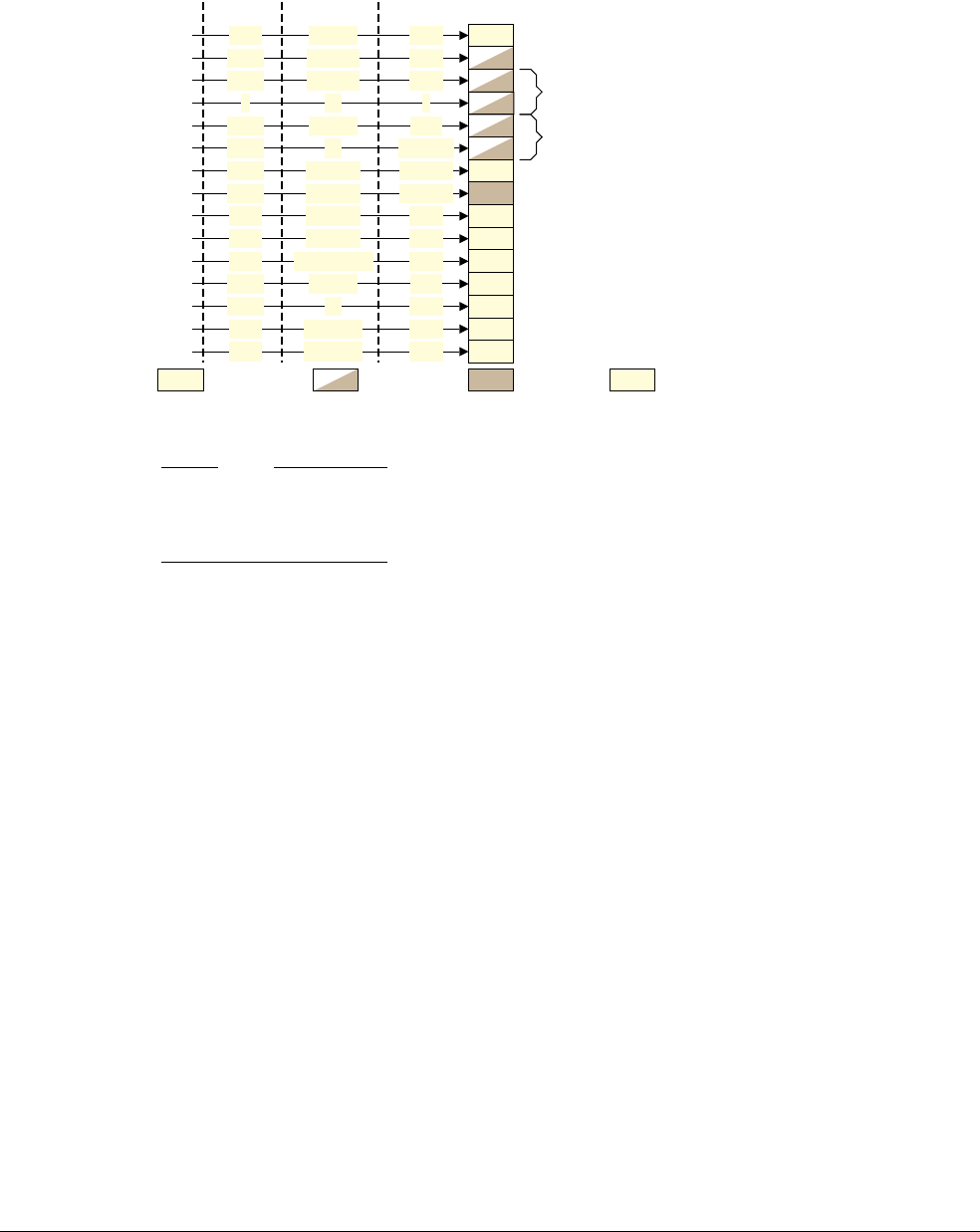
B3 Virtual Memory System Architecture (VMSA)
B3.17 Organization of the CP15 registers in a VMSA implementation
B3-1470 Copyright © 1996-1998, 2000, 2004-2012, 2014 ARM. All rights reserved. ARM DDI 0406C.c
Non-Confidential ID051414
B3.17.1 CP15 register summary by coprocessor register number
Figure B3-26 summarizes the grouping of CP15 registers by primary coprocessor register number for a VMSAv7
implementation.
Figure B3-26 CP15 register grouping by primary coprocessor register, CRn, VMSA implementation
Note
Figure B3-26 gives only an overview of the assigned encodings for each of the CP15 primary registers c0-c15. See
the description of each primary register for the definition of the assigned and unassigned encodings for that register,
including any dependencies on whether the implementation includes architectural extensions.
The following sections give the register assignments for each of the CP15 primary registers, c0-c15:
•VMSA CP15 c0 register summary, identification registers on page B3-1471
•VMSA CP15 c1 register summary, system control registers on page B3-1472
•VMSA CP15 c2 and c3 register summary, Memory protection and control registers on page B3-1473
•CP15 c4, Not used on page B3-1473
•VMSA CP15 c5 and c6 register summary, Memory system fault registers on page B3-1474
•VMSA CP15 c7 register summary, Cache maintenance, address translation, and other functions on
page B3-1475
•VMSA CP15 c8 register summary, TLB maintenance operations on page B3-1476
•VMSA CP15 c9 register summary, reserved for cache and TCM control and performance monitors on
page B3-1477
•VMSA CP15 c10 register summary, memory remapping and TLB control registers on page B3-1478
•VMSA CP15 c11 register summary, reserved for TCM DMA registers on page B3-1478
•VMSA CP15 c12 register summary, Security Extensions registers on page B3-1479
•VMSA CP15 c13 register summary, Process, context and thread ID registers on page B3-1479
•VMSA CP15 c14, reserved for Generic Timer Extension on page B3-1480
•VMSA CP15 c15 register summary, IMPLEMENTATION DEFINED registers on page B3-1480.
Read-only Read/Write Write-only
ID registers
System control registers
Cache maintenance, address translations, miscellaneous
TLB maintenance operations
Reserved for performance monitors and maintenance operations
Reserved for DMA operations for TCM access
Security Extensions registers, if implemented
IMPLEMENTATION
DEFINED
registers
CRn opc1 opc2CRm
{0-7}
{0-2}
0
{0,1}
Various
{0-7}
{0-7}
{0,1}
{0-4}
{0-7}
{c0-c7}
c0
{c0, c1}
{c0, c1}
c0
{c0,c1}
c0
{c0-c8,c15}
{c0,c1}
{c0-c15}
{0-2}
{0, 4}
{0, 4}
0
{0, 4}
{0-7}
{0-7}
{0-7}
c0
c1
c2
c3
c5
c6
c7
c8
c9
c10
c11
c12
c13
c15
¶
{0-7}
Memory protection and
control registers
{0, 2, 4}{0, 4}
Memory system
fault registers
{0, 4} Various ¶
{0, 4} VariousVarious
¶
Various
¶ Memory mapping registers and TLB operations
{0-7} {0-7}Various
¶
¶{0, 4}
¶
{0, 4} Process, context, and thread ID registers
¶
¶ Access depends on the implementation
Generic Timer registers, if implemented
{0-7}{c0-c15}{0-7}c14 ¶
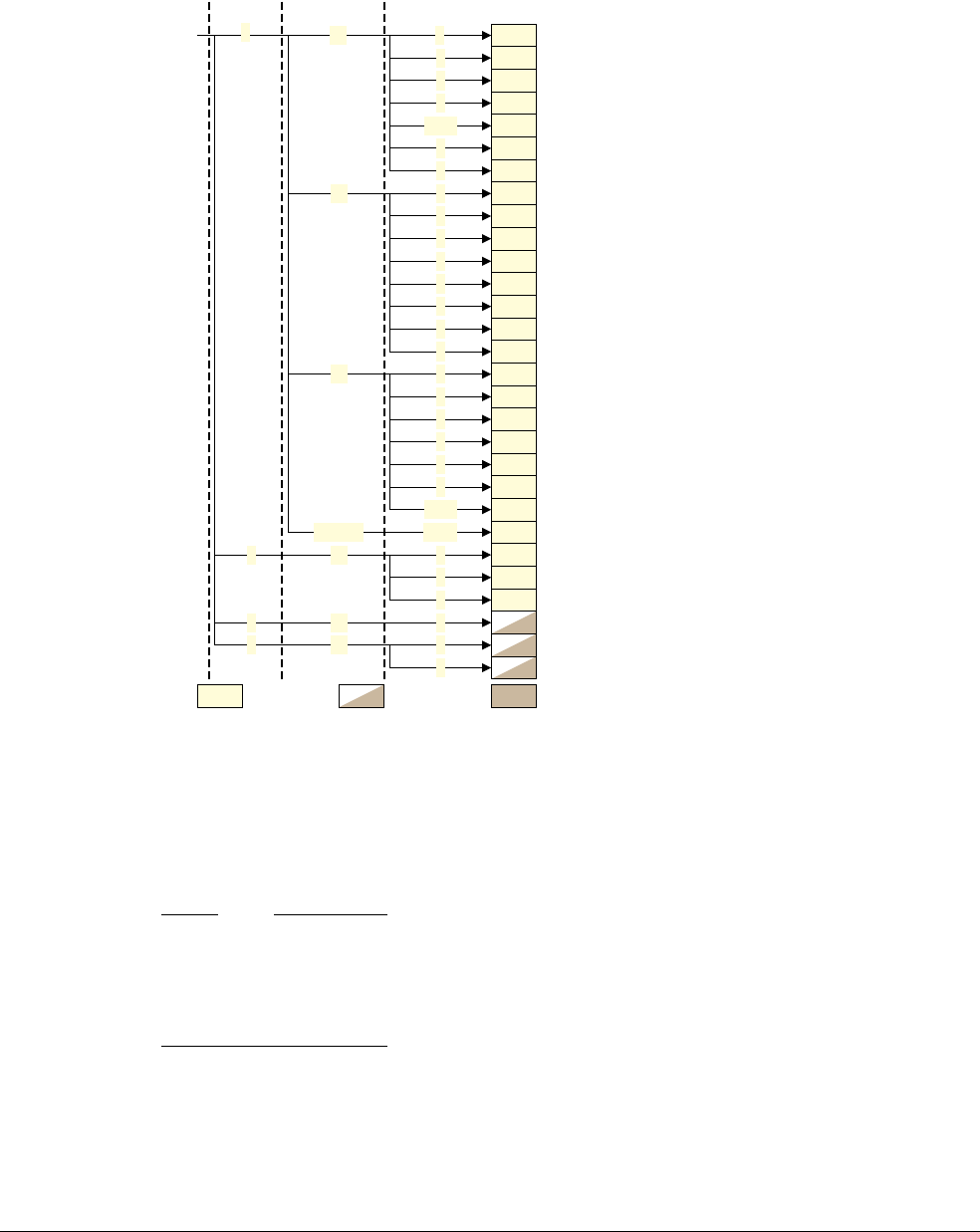
B3 Virtual Memory System Architecture (VMSA)
B3.17 Organization of the CP15 registers in a VMSA implementation
ARM DDI 0406C.c Copyright © 1996-1998, 2000, 2004-2012, 2014 ARM. All rights reserved. B3-1471
ID051414 Non-Confidential
VMSA CP15 c0 register summary, identification registers
The CP15 c0 registers provide processor and feature identification. Figure B3-27 shows the CP15 c0 registers in a
VMSA implementation.
Figure B3-27 CP15 c0 registers in a VMSA implementation
CP15 c0 register encodings not shown in Figure B3-27, and encodings that are part of an unimplemented
architectural extension, are UNPREDICTABLE, see Accesses to unallocated CP14 and CP15 encodings on
page B3-1447.
Note
• Chapter B7 The CPUID Identification Scheme describes the CPUID registers shown in Figure B3-27.
• The CPUID scheme includes information about the implementation of the OPTIONAL Floating-point and
Advanced SIMD architecture extensions. See Advanced SIMD and Floating-point Extensions on page A2-54
for a summary of the implementation options for these features.
Read-only Read/Write
MIDR, Main ID Register
CTR, Cache Type Register
TCMTR, TCM Type Register, details
IMPLEMENTATION
DEFINED
TLBTR, TLB Type Register, details
IMPLEMENTATION
DEFINED
MPIDR, Multiprocessor Affinity Register
Aliases of MIDR
ID_PFR0, Processor Feature Register 0 *
CSSELR, Cache Size Selection Register
CCSIDR, Cache Size ID Registers
Read-As-Zero
CLIDR, Cache Level ID Register
AIDR, Auxiliary ID Register
IMPLEMENTATION
DEFINED
CRn opc1 opc2CRm
0
{6,7}
1
2
3
5
{4,7}
0
1
2
3
5
6
7
0
1
2
4
3
4
5
{0-7}
0
1
7
0
c0
c1
c2
c0
0
c0
ID_PFR1, Processor Feature Register 1 *
ID_DFR0, Debug Feature Register 0 *
ID_AFR0, Auxiliary Feature Register 0 *
ID_MMFR0, Memory Model Feature Register 0 *
ID_MMFR1, Memory Model Feature Register 1 *
ID_MMFR2, Memory Model Feature Register 2 *
ID_MMFR3, Memory Model Feature Register 3 *
ID_ISAR0, ISA Feature Register 0 *
ID_ISAR1, ISA Feature Register 1 *
ID_ISAR2, ISA Feature Register 2 *
ID_ISAR3, ISA Feature Register 3 *
ID_ISAR4, ISA Feature Register 4 *
ID_ISAR5, ISA Feature Register 5 *
Read-As-Zero
c0
{c3-c7}
2
1
Write-only
4 0c0
5
VPIDR, Virtualization Processor ID Register ‡
VMPIDR, Virtualization Multiprocessor ID Register ‡
* CPUID registers
ª Optional register. If not implemented, the encoding is an alias of the MIDR.
REVIDR, Revision ID Register ª
6
‡ Implemented only as part of the Virtualization Extensions.
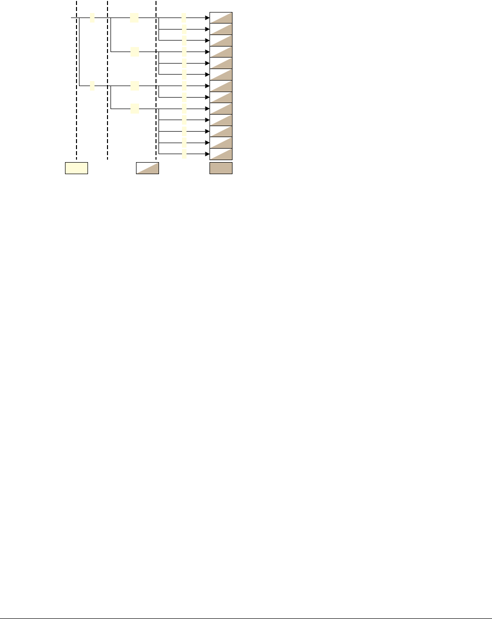
B3 Virtual Memory System Architecture (VMSA)
B3.17 Organization of the CP15 registers in a VMSA implementation
B3-1472 Copyright © 1996-1998, 2000, 2004-2012, 2014 ARM. All rights reserved. ARM DDI 0406C.c
Non-Confidential ID051414
VMSA CP15 c1 register summary, system control registers
The CP15 c1 registers provide system control. Figure B3-28 shows the CP15 c1 registers in a VMSA
implementation.
Figure B3-28 CP15 c1 registers in a VMSA implementation
CP15 c1 register encodings not shown in Figure B3-28, and encodings that are part of an unimplemented
architectural extension, are UNPREDICTABLE. For more information, see Accesses to unallocated CP14 and CP15
encodings on page B3-1447.
Read-only Read/Write
SCTLR, System Control Register
ACTLR, Auxiliary Control Register, IMPLEMENTATION DEFINED
CRn opc1 opc2CRm
0
1
2
c00c1
Write-only
CPACR, Coprocessor Access Control Register
c1 0
1
2
† Implemented only as part of the Security Extensions
SCR, Secure Configuration Register †
SDER, Secure Debug Enable Register †
NSACR, Non-Secure Access Control Register †
‡ Implemented only as part of the Virtualization Extensions
HSCTLR, Hyp System Control Register ‡
HCR, Hyp Configuration Register ‡
HDCR, Hyp Debug Configuration Register ‡
HCPTR, Hyp Coprocessor Trap Register ‡
HSTR, Hyp System Trap Register ‡
c0 0
c1 0
4
1
2
3
HACR, Hyp Auxiliary Configuration Register, IMPLEMENTATION DEFINED ‡7
HACTLR, Hyp Auxiliary Control Register, IMPLEMENTATION DEFINED ‡
1
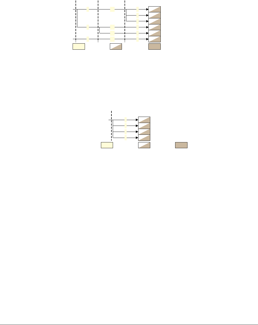
B3 Virtual Memory System Architecture (VMSA)
B3.17 Organization of the CP15 registers in a VMSA implementation
ARM DDI 0406C.c Copyright © 1996-1998, 2000, 2004-2012, 2014 ARM. All rights reserved. B3-1473
ID051414 Non-Confidential
VMSA CP15 c2 and c3 register summary, Memory protection and control registers
On an ARMv7-A implementation, the CP15 c2 and c3 registers provide memory protection and control.
Figure B3-29 shows the 32-bit registers in CP15 primary registers c2 and c3.
Figure B3-29 CP15 32-bit c2 and c3 registers
CP15 c2 and c3 32-bit register encodings not shown in Figure B3-29, and encodings that are part of an
unimplemented architectural extension, are UNPREDICTABLE, see Accesses to unallocated CP14 and CP15
encodings on page B3-1447.
On an ARMv7-A implementation that includes the Large Physical Address Extension or Virtualization Extensions,
the CP15 c2 register includes some 64-bit system control registers. Figure B3-29 shows these registers.
Figure B3-30 CP15 64-bit c2 registers
CP15 c2 64-bit register encodings not shown in Figure B3-30 are UNPREDICTABLE, and the allocations shown in
Figure B3-30 are UNPREDICTABLE when the Virtualization Extensions are not implemented. For more information,
see Accesses to unallocated CP14 and CP15 encodings on page B3-1447.
CP15 c4, Not used
CP15 c4 is not used on any ARMv7 implementation, see Accesses to unallocated CP14 and CP15 encodings on
page B3-1447.
Read-only Read/Write
TTBR0, Translation Table Base Register 0
TTBR1, Translation Table Base Register 1
0
1
2
c00c2
Write-only
TTBCR, Translation Table Base Control Register
0DACR, Domain Access Control Register
c00c3
CRn opc1 opc2CRm
HTCR, Hyp Translation Control Register ‡
‡ Implemented only as part of the Virtualization Extensions
VTCR, Virtualization Translation Control Register ‡
2c04
2c1
Read-only Read/Write
VTTBR, Virtualization Translation Table Base Register ‡
0
6
c2
Write-only
CRm opc1
‡ Implemented only as part of the Virtualization Extensions
HTTBR, Hyp Translation Table Base Register ‡
§ Implemented only as part of the Large Physical Address Extension
4
TTBR0, Translation Table Base Register 0 §
TTBR1, Translation Table Base Register 1 §
1
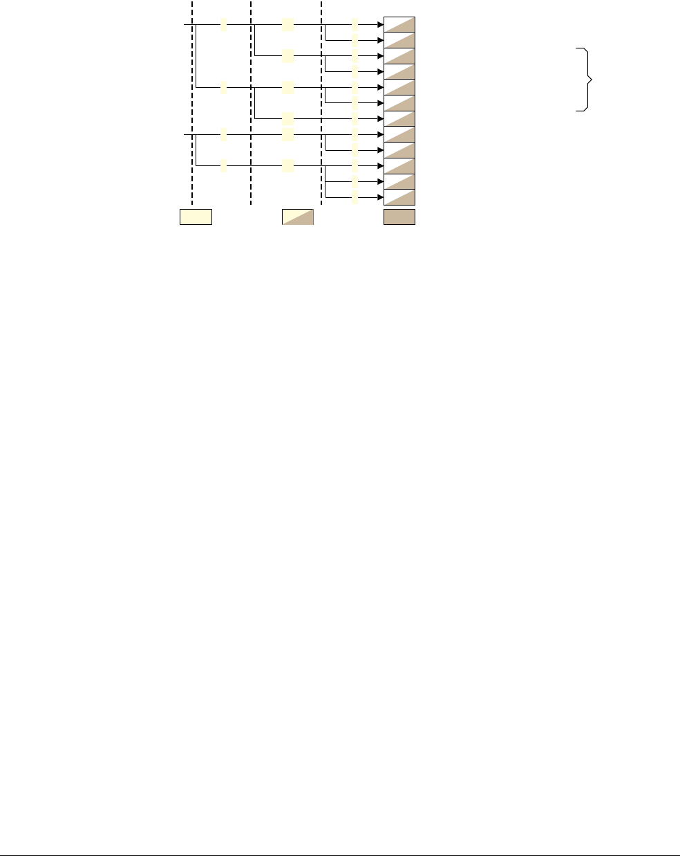
B3 Virtual Memory System Architecture (VMSA)
B3.17 Organization of the CP15 registers in a VMSA implementation
B3-1474 Copyright © 1996-1998, 2000, 2004-2012, 2014 ARM. All rights reserved. ARM DDI 0406C.c
Non-Confidential ID051414
VMSA CP15 c5 and c6 register summary, Memory system fault registers
The CP15 c5 and c6 registers provide memory system fault reporting. Figure B3-31 shows the CP15 c5 and c6
registers in a VMSA implementation.
Figure B3-31 CP15 c5 and c6 registers in a VMSA implementation
CP15 c5 and c6 register encodings not shown in Figure B3-31, and encodings that are part of an unimplemented
architectural extension, are UNPREDICTABLE, see Accesses to unallocated CP14 and CP15 encodings on
page B3-1447.
Read-only Read/Write
DFSR, Data Fault Status Register
IFSR, Instruction Fault Status Register
ADFSR, Auxiliary DFSR
AIFSR, Auxiliary IFSR
DFAR, Data Fault Address Register
IFAR, Instruction Fault Address Register
0
1
0
1
0
2
c00
c5
Details are
IMPLEMENTATION
DEFINED
c6
c1
c00
Write-only
CRn opc1 opc2CRm
0c14
1
c2 0
‡ Implemented only as part of the Virtualization Extensions
HADFSR, Hyp Auxiliary DFSR ‡
HAIFSR, Hyp Auxiliary IFSR ‡
HSR, Hyp Syndrome Register ‡
0c04 HDFAR, Hyp Data Fault Address Register ‡
HIFAR, Hyp Instruction Fault Address Register ‡
2
HPFAR, Hyp IPA Fault Address Register ‡
4
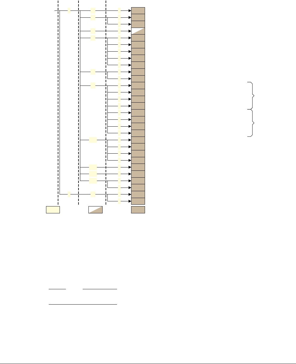
B3 Virtual Memory System Architecture (VMSA)
B3.17 Organization of the CP15 registers in a VMSA implementation
ARM DDI 0406C.c Copyright © 1996-1998, 2000, 2004-2012, 2014 ARM. All rights reserved. B3-1475
ID051414 Non-Confidential
VMSA CP15 c7 register summary, Cache maintenance, address translation, and other
functions
On an ARMv7-A implementation, the CP15 c7 registers provide cache maintenance operations, address translation
operations, and CP15 versions of the memory barrier operations. Figure B3-32 shows the CP15 c7 registers.
Figure B3-32 CP15 32-bit c7 registers in a VMSA implementation
CP15 c7 register encodings not shown in Figure B3-32, and encodings that are part of an unimplemented
architectural extension, are UNPREDICTABLE, see Accesses to unallocated CP14 and CP15 encodings on
page B3-1447.
Note
Figure B3-32 shows only those UNPREDICTABLE CP15 c7 encodings that had defined functions in ARMv6.
Read-only Read/Write
CP15ISB, Instruction Synchronization Barrier operation
4
0
0
0
4
6
Write-only Bold text = Accessible At PL0
ø Introduced as part of the Multiprocessing Extensions
1
4
1
1
0
1
1
opc2
6
1
7
2
1
2
3
4
5
6
7
2
5
2
ICIALLUIS, Invalidate all instruction caches to PoU Inner Shareable ø
BPIALLIS, Invalidate all branch predictors Inner Shareable ø
ICIALLU, Invalidate all instruction caches to PoU
ICIMVAU, Invalidate instruction caches by MVA to PoU
BPIALL, Invalidate all branch predictors
BPIMVA, Invalidate MVA from branch predictors
DCIMVAC, Invalidate data* cache line by MVA to PoC
DCISW, Invalidate data* cache line by set/way
DCCMVAC, Clean data* cache line by MVA to PoC
DCCSW, Clean data* cache line by set/way
DCCMVAU, Clean data* cache line by MVA to PoU
DCCIMVAC, Clean and invalidate data* cache line by MVA to PoC
DCCISW, Clean and invalidate data* cache line by set/way
* data or unified PoU: Point of Unification PoC: Point of Coherency
Stage 1
translation,
current state
ATS1CPR, PL1 read translation
ATS1CPW, PL1 write translation
ATS1CUR, unprivileged read translation
ATS1CUW, unprivileged write translation
ATS12NSOPR, PL1 read translation †
ATS12NSOUW, unprivileged write translation †
ATS12NSOPW, PL1 write translation †
ATS12NSOUR, unprivileged read translation †
Stage 1 and 2
translation,
Non-secure state
PAR, Physical Address Register
UNPREDICTABLE, was Wait For Interrupt (CP15WFI) in ARMv6
CP15DSB, Data Synchronization Barrier operation
CP15DMB, Data Memory Barrier operation
UNPREDICTABLE, was Prefetch instruction by MVA in ARMv6
‡ Implemented only as part of the Virtualization Extensions
† Implemented only as part of the Security Extensions
ATS1HW, Hyp mode write translation ‡
ATS1HR, Hyp mode read translation ‡
0
1
c00
c7
c4
c1
c5
c6
c8
c10
c11
c13
c14
CRn opc1 CRm
c84
B3 Virtual Memory System Architecture (VMSA)
B3.17 Organization of the CP15 registers in a VMSA implementation
B3-1476 Copyright © 1996-1998, 2000, 2004-2012, 2014 ARM. All rights reserved. ARM DDI 0406C.c
Non-Confidential ID051414
On an ARMv7-A implementation that includes the Large Physical Address Extension, the CP15 c7 register includes
a 64-bit implementation of the PAR, as Figure B3-33 shows.
Figure B3-33 CP15 64-bit c7 registers
CP15 c7 64-bit register encodings not shown in Figure B3-33 are UNPREDICTABLE, and the allocations shown in
Figure B3-33 are UNPREDICTABLE when the Large Physical Address Extension is not implemented. For more
information, see Accesses to unallocated CP14 and CP15 encodings on page B3-1447.
VMSA CP15 c8 register summary, TLB maintenance operations
On an ARMv7-A implementation, the CP15 c8 registers provide TLB maintenance functions. Figure B3-34 shows
the CP15 c8 registers.
Figure B3-34 CP15 c8 registers in a VMSA implementation
CP15 c8 register encodings not shown in Figure B3-34, and encodings that are part of an unimplemented
architectural extension, are UNPREDICTABLE, see Accesses to unallocated CP14 and CP15 encodings on
page B3-1447.
Read-only Read/Write
0c7
Write-only
CRm opc1
§ Implemented only as part of the Large Physical Address Extension
PAR, Physical Address Register §
TLBIALLIS, Invalidate entire TLB IS
*
ø
TLBIMVAIS, Invalidate unified TLB entry by MVA and ASID IS
*
ø
TLBIASIDIS, Invalidate unified TLB by ASID match IS
*
ø
TLBIMVAAIS, Invalidate unified TLB entry by MVA all ASID IS
*
ø
ITLBIALL, invalidate instruction TLB
ITLBIMVA, invalidate instruction TLB entry by MVA and ASID
CRn opc1 opc2CRm
0
1
2
3
0
1
c30c8
*
IS = Inner Shareable
DTLBIMVA, invalidate data TLB entry by MVA and ASID
ITLBIASID, invalidate instruction TLB by ASID match
DTLBIALL, invalidate data TLB
2
0
1
DTLBIASID, invalidate data TLB by ASID match
TLBIALL, invalidate unified TLB
TLBIMVAA, invalidate unified TLB entries by MVA all ASID ø
TLBIMVA, invalidate unified TLB entry by MVA and ASID
TLBIASID, invalidate unified TLB by ASID match
c5
c6
2
0
1
2
3
c7
Read-only Read/Write
TLBIALLHIS, Invalidate entire Hyp unified TLB IS
*
‡
TLBIMVAHIS, Invalidate Hyp unified TLB entry by MVA IS
*
‡
TLBIALLNSNHIS, Invalidate entire Non-secure non-Hyp unified TLB IS
*
‡
TLBIALLH, Invalidate entire Hyp unified TLB ‡
TLBIMVAH, Invalidate Hyp unified TLB entry by MVA ‡
TLBIALLNSNH, Invalidate entire Non-secure non-Hyp unified TLB ‡
0
1
4
c34
0
1
4
c7
ø Introduced as part of the Multiprocessing Extensions ‡ Implemented only as part of the Virtualization Extensions
Write-only
B3 Virtual Memory System Architecture (VMSA)
B3.17 Organization of the CP15 registers in a VMSA implementation
ARM DDI 0406C.c Copyright © 1996-1998, 2000, 2004-2012, 2014 ARM. All rights reserved. B3-1477
ID051414 Non-Confidential
VMSA CP15 c9 register summary, reserved for cache and TCM control and performance
monitors
ARMv7 reserves some CP15 c9 encodings for IMPLEMENTATION DEFINED memory system functions, in particular:
• cache control, including lockdown
• TCM control, including lockdown
• branch predictor control.
Additional CP15 c9 encodings are reserved for performance monitors. These encodings fall into two groups:
• the OPTIONAL Performance Monitors Extension described in Chapter C12 The Performance Monitors
Extension
• additional IMPLEMENTATION DEFINED performance monitors.
The reserved encodings permit implementations that are compatible with previous versions of the ARM
architecture, in particular with the ARMv6 requirements. Figure B3-35 shows the reserved CP15 c9 register
encodings in a VMSA implementation.
Figure B3-35 Reserved CP15 c9 encodings
CP15 c9 encodings not shown in Figure B3-35 are UNPREDICTABLE, see Accesses to unallocated CP14 and CP15
encodings on page B3-1447.
Read-only Read/Write
Reserved for Branch Predictor, Cache and TCM operations
{0-7}
{0-7}
{0-7}
{0-7}
{c0-c2}{0-7}
c9
Write-only
{c5-c8}
{c12-c14}
¶
¶
¶
Reserved for Branch Predictor, Cache and TCM operations
Reserved for ARM Performance Monitors Extension
Reserved for IMPLEMENTATION DEFINED performance monitors
¶ Access depends on the operation
c15
CRn opc1 opc2CRm
B3 Virtual Memory System Architecture (VMSA)
B3.17 Organization of the CP15 registers in a VMSA implementation
B3-1478 Copyright © 1996-1998, 2000, 2004-2012, 2014 ARM. All rights reserved. ARM DDI 0406C.c
Non-Confidential ID051414
VMSA CP15 c10 register summary, memory remapping and TLB control registers
On an ARMv7-A implementation, the CP15 c10 registers provide:
• memory remapping registers
• reserved encodings for IMPLEMENTATION DEFINED TLB control functions, including lockdown.
Figure B3-36 shows the CP15 c10 registers and reserved encodings in a VMSA implementation.
Figure B3-36 CP15 c10 registers in a VMSA implementation
CP15 c10 register encodings not shown in Figure B3-36, and encodings that are part of an unimplemented
architectural extension, are UNPREDICTABLE, see Accesses to unallocated CP14 and CP15 encodings on
page B3-1447.
VMSA CP15 c11 register summary, reserved for TCM DMA registers
ARMv7 reserves some CP15 c11 register encodings for IMPLEMENTATION DEFINED DMA operations to and from
TCM. Figure B3-37 shows the reserved CP15 c11 encodings:
Figure B3-37 Reserved CP15 c11 encodings
CP15 c11 encodings not shown in Figure B3-37 are UNPREDICTABLE, see Accesses to unallocated CP14 and CP15
encodings on page B3-1447.
Read-only Read/Write
Reserved for TLB Lockdown operations
{0-7}
0
1
{c0,c1,c4,c8}0c10
Write-only
c2
¶
PRRR or MAIR0, see table
NMRR or MAIR1, see table
CRn opc1 opc2CRm
¶ Access depends on the operation
0
1
c3
0
1
c2
{5-7}
HMAIR0, Hyp Memory Attribute Indirection Register 0 ‡
HMAIR1, Hyp Memory Attribute Indirection Register 1 ‡
‡ Implemented only as part of the Virtualization Extensions
§ Implemented only as part of the Large Physical Address Extension
PRRR, Primary Region Remap Register MAIR0, Memory Attribute Indirection Register 0
NMRR, Normal Memory Remap Register MAIR1, Memory Attribute Indirection Register 1
Without Large Physical Address Extension With Large Physical Address Extension
Reserved for TLB Lockdown operations
{0-7} ¶
{c0,c1,c4,c8}{1-3}
Reserved for TLB Lockdown operations
¶
4 {0-7}{c0,c1,c4,c8}
Reserved for TLB Lockdown operations¶
{0-7}{c0,c1,c4,c8}
HAMAIR0, Hyp Auxiliary Memory Attribute Indirection Register 0 ‡
HAMAIR1, Hyp Auxiliary Memory Attribute Indirection Register 1‡
0
1
c3
AMAIR0, Auxiliary Memory Attribute Indirection Register 0 §
AMAIR1, Auxiliary Memory Attribute Indirection Register 1 §
Read-only Read/Write
Reserved for DMA operations for TCM access
{0-7}
{0-7}
{c0-c8}{0-7}
c11
Write-only
c15
¶
¶
¶ Access depends on the operation
Reserved for DMA operations for TCM access
CRn opc1 opc2CRm
B3 Virtual Memory System Architecture (VMSA)
B3.17 Organization of the CP15 registers in a VMSA implementation
ARM DDI 0406C.c Copyright © 1996-1998, 2000, 2004-2012, 2014 ARM. All rights reserved. B3-1479
ID051414 Non-Confidential
VMSA CP15 c12 register summary, Security Extensions registers
On an ARMv7-A implementation that includes the Security Extensions, the CP15 c12 registers provide Security
Extensions functions. Figure B3-38 shows the CP15 c12 registers.
Figure B3-38 Security Extensions CP15 c12 registers
In an implementation that includes the Security Extensions, CP15 c12 encodings not shown in Figure B3-38, and
encodings that are part of an unimplemented architectural extension, are UNPREDICTABLE. On an implementation
that does not include the Security Extensions all CP15 c12 encodings are UNDEFINED. For more information, see
Accesses to unallocated CP14 and CP15 encodings on page B3-1447.
VMSA CP15 c13 register summary, Process, context and thread ID registers
On an ARMv7-A implementation, the CP15 c13 registers provide:
• an FCSE Process ID Register, that indicates whether the implementation includes the FCSE
• a Context ID Register
• Software Thread ID Registers.
Figure B3-39 shows the CP15 c13 registers:
Figure B3-39 CP15 c13 registers in a VMSA implementation
CP15 c13 encodings not shown in Figure B3-39, and encodings that are part of an unimplemented architectural
extension, are UNPREDICTABLE, see Accesses to unallocated CP14 and CP15 encodings on page B3-1447.
Read-only Read/Write
VBAR, Vector Base Address Register †
0
1
0
c00
c12
Write-only
c1
MVBAR, Monitor Vector Base Address Register †
ISR, Interrupt Status Register †
CRn opc1 opc2CRm
‡ Implemented only as part of the Virtualization Extensions
† Implemented only as part of the Security Extensions
HVBAR, Hyp Vector Base Address Register ‡
0c04
Read-only Read/Write
FCSEIDR, FCSE PID Register
0
1
2
c00c13
Write-only
CONTEXTIDR, Context ID Register
TPIDRURW, User Read/Write
RAZ/WI when FCSE is not implemented, see register description
*
3
4
TPIDRURO, User Read Only ª
TPIDRPRW, PL1 only
Software Thread ID
Registers
*
Bold text = Accessible at PL0
ª Read-only at PL0
CRn opc1 opc2CRm
HTPIDR, Hyp Read/Write ‡
‡ Implemented only as part of the Virtualization Extensions
2c04
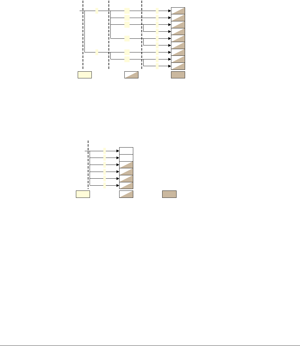
B3 Virtual Memory System Architecture (VMSA)
B3.17 Organization of the CP15 registers in a VMSA implementation
B3-1480 Copyright © 1996-1998, 2000, 2004-2012, 2014 ARM. All rights reserved. ARM DDI 0406C.c
Non-Confidential ID051414
VMSA CP15 c14, reserved for Generic Timer Extension
From issue C.a of this manual, CP15 c14 is reserved for the system control registers of the OPTIONAL Generic Timer
Extension. For more information, see Chapter B8 The Generic Timer. On an implementation that does not include
the Generic Timer, c14 is an unallocated CP15 primary register, see UNPREDICTABLE and UNDEFINED behavior
for CP14 and CP15 accesses on page B3-1446.
Figure B3-40 shows the 32-bit CP15 c14 registers in a VMSAv7 implementation that includes the Generic Timer
Extension:
Figure B3-40 CP15 32-bit c14 registers in a VMSA implementation that includes the Generic Timer Extension
Figure B3-41 shows the 64-bit CP15 c14 registers in a VMSAv7 implementation that includes the Generic Timer
Extension:
Figure B3-41 CP15 64-bit c14 registers in a VMSA implementation that includes the Generic Timer Extension
VMSA CP15 c15 register summary, IMPLEMENTATION DEFINED registers
ARMv7 reserves CP15 c15 for IMPLEMENTATION DEFINED purposes, and does not impose any restrictions on the
use of the CP15 c15 encodings. For more information, see IMPLEMENTATION DEFINED registers, functional
group on page B3-1502.
CNTFRQ, Counter Frequency register ª
0
0
0
c00c14
CNTKCTL, Timer PL1 Control register
CNTP_TVAL, PL1 Physical TimerValue register ª
1
0
CNTP_CTL, PL1 Physical Timer Control register ª
CNTV_TVAL, Virtual TimerValue register ª
CRn opc1 opc2CRm
CNTHCTL, Timer PL2 Control register ‡
‡ Implemented only if the implementation includes the Virtualization Extensions
0c14
c1
c2
c3
1 CNTV_CTL, Virtual Timer Control register ª
0 CNTHP_TVAL, PL2 Physical TimerValue register ‡
1 CNTHP_CTL, PL2 Physical Timer Control register ‡
c2
Read-only Read/Write Write-only
All registers are implemented only as part of the optional Generic Timer Extension
ª Can be configured as accessible at PL0, see the register description for more information
Read-only Read/Write
0
6
c14
Write-only
CRm opc1
CNTP_CVAL, PL1 Physical Timer CompareValue register ª
4
CNTPCT, Physical Count register ª
1 CNTVCT, Virtual Count register ª
2
3 CNTV_CVAL, Virtual Timer CompareValue register ª
CNTVOFF, Virtual Offset register †
CNTHP_CVAL, PL2 Physical Timer CompareValue register ‡
ª Can be configured as accessible at PL0, see the register description for more information
‡ Implemented only if the implementation includes the Virtualization Extensions
All registers are implemented only as part of the optional Generic Timer Extension
† Implemented as RW only if the implementation includes the Virtualization Extensions, see the register
description for more information

B3 Virtual Memory System Architecture (VMSA)
B3.17 Organization of the CP15 registers in a VMSA implementation
ARM DDI 0406C.c Copyright © 1996-1998, 2000, 2004-2012, 2014 ARM. All rights reserved. B3-1481
ID051414 Non-Confidential
B3.17.2 Full list of VMSA CP15 registers, by coprocessor register number
Table B3-42 shows the CP15 registers in a VMSA implementation, in the order of the {CRn, opc1, CRm, opc2}
values used in
MCR
or
MRC
accesses to the 32-bit registers:
• For
MCR
or
MRC
accesses to the 32-bit registers, CRn identifies the CP15 primary register used for the access.
• For
MCRR
or
MRRC
accesses to the 64-bit registers, CRm identifies the CP15 primary register used for the access.
Table B3-42 lists the 64-bit registers with the 32-bit registers accessed using the same CP15 primary register
number.
The table also includes links to the descriptions of each of the CP15 primary registers, c0 to c15.
The only UNPREDICTABLE encodings shown in the table are those that had defined functions in ARMv6.
Table B3-42 Summary of VMSA CP15 register descriptions, in coprocessor register number order
CRn opc1 CRm opc2 Name Width Description
c0 0 c0 0 MIDR 32-bit Main ID Register
1CTR 32-bit Cache Type Register
2TCMTR 32-bit TCM Type Register
3TLBTR 32-bit TLB Type Register
4, 6a, 7 MIDR 32-bit Aliases of Main ID Register
5MPIDR 32-bit Multiprocessor Affinity Register
6aREVIDR 32-bit Revision ID Register
c0 0 c1 0 ID_PFR0 32-bit Processor Feature Register 0
1ID_PFR1 32-bit Processor Feature Register 1
2ID_DFR0 32-bit Debug Feature Register 0
3ID_AFR0 32-bit Auxiliary Feature Register 0
4ID_MMFR0 32-bit Memory Model Feature Register 0
5ID_MMFR1 32-bit Memory Model Feature Register 1
6ID_MMFR2 32-bit Memory Model Feature Register 2
7ID_MMFR3 32-bit Memory Model Feature Register 3
c2 0 ID_ISAR0 32-bit Instruction Set Attribute Register 0
1ID_ISAR1 32-bit Instruction Set Attribute Register 1
2ID_ISAR2 32-bit Instruction Set Attribute Register 2
3ID_ISAR3 32-bit Instruction Set Attribute Register 3
4ID_ISAR4 32-bit Instruction Set Attribute Register 4
5ID_ISAR5 32-bit Instruction Set Attribute Register 5

B3 Virtual Memory System Architecture (VMSA)
B3.17 Organization of the CP15 registers in a VMSA implementation
B3-1482 Copyright © 1996-1998, 2000, 2004-2012, 2014 ARM. All rights reserved. ARM DDI 0406C.c
Non-Confidential ID051414
c0 1 c0 0 CCSIDR 32-bit Cache Size ID Registers
1CLIDR 32-bit Cache Level ID Register
7AIDR 32-bit IMPLEMENTATION DEFINED Auxiliary ID Registerb
2c0 0 CSSELR 32-bit Cache Size Selection Register
4c0 0 VPIDRc32-bit Virtualization Processor ID Register
5VMPIDRc32-bit Virtualization Multiprocessor ID Register
c1 0 c0 0 SCTLR 32-bit System Control Register
1ACTLR 32-bit IMPLEMENTATION DEFINED Auxiliary Control Register
2CPACR 32-bit Coprocessor Access Control Register
c1 0 SCRd32-bit Secure Configuration Register
1SDERd32-bit Secure Debug Enable Register
2NSACRd32-bit Non-Secure Access Control Register
c1 4 c0 0 HSCTLRc32-bit Hyp System Control Register
1HACTLRc32-bit Hyp Auxiliary Control Register
c1 4 c1 0 HCRc32-bit Hyp Configuration Register
1HDCRc32-bit Hyp Debug Configuration Register
2HCPTRc32-bit Hyp Coprocessor Trap Register
3HSTRc32-bit Hyp System Trap Register
7HACRc32-bit Hyp Auxiliary Configuration Register
c2 0 c0 0 TTBR0 32-bit Translation Table Base Register 0
-0c2 - TTBR0e64-bit
c2 0 c0 1 TTBR1 32-bit Translation Table Base Register 1
-1c2 - TTBR1e64-bit
c2 0 c0 2 TTBCR 32-bit Translation Table Base Control Register
4c0 2 HTCRc32-bit Hyp Translation Control Register
c1 2 VTCRc32-bit Virtualization Translation Control Register
-4c2 - HTTBRc64-bit Hyp Translation Table Base Register
-6c2 - VTTBRc64-bit Virtualization Translation Table Base Register
c3 0 c0 0 DACR 32-bit Domain Access Control Register
Table B3-42 Summary of VMSA CP15 register descriptions, in coprocessor register number order (continued)
CRn opc1 CRm opc2 Name Width Description

B3 Virtual Memory System Architecture (VMSA)
B3.17 Organization of the CP15 registers in a VMSA implementation
ARM DDI 0406C.c Copyright © 1996-1998, 2000, 2004-2012, 2014 ARM. All rights reserved. B3-1483
ID051414 Non-Confidential
c5 0 c0 0 DFSR 32-bit Data Fault Status Register
1IFSR 32-bit Instruction Fault Status Register
c1 0 AxFSR 32-bit ADFSR, Auxiliary Data Fault Status Register
1 32-bit AIFSR, Auxiliary Instruction Fault Status Register
4c1 0 HAxFSRc32-bit HADFSR, Hyp Auxiliary Data Fault Syndrome Register
1 32-bit HAIFSR, Hyp Auxiliary Instruction Fault Syndrome
Register
c2 0 HSRc32-bit Hyp Syndrome Register
c6 0 c0 0 DFAR 32-bit Data Fault Address Register
2IFAR 32-bit Instruction Fault Address Register
c6 4 c0 0 HDFARc32-bit Hyp Data Fault Address Register
2HIFARc32-bit Hyp Instruction Fault Address Register
4HPFARc32-bit Hyp IPA Fault Address Register
c7 0 c0 4 UNPREDICTABLE 32-bit See Retired operations on page B3-1499
c1 0 ICIALLUISf32-bit See Cache and branch predictor maintenance operations,
VMSA on page B4-1743
6BPIALLISf32-bit
c7 0 c4 0 PAR 32-bit Physical Address Register
c7 - PARe64-bit
c5 0 ICIALLU 32-bit See Cache and branch predictor maintenance operations,
VMSA on page B4-1743
1ICIMVAU 32-bit
4CP15ISB 32-bit See Data and instruction barrier operations, VMSA on
page B4-1752
6BPIALL 32-bit See Cache and branch predictor maintenance operations,
VMSA on page B4-1743
7BPIMVA 32-bit
c6 1 DCIMVAC 32-bit See Cache and branch predictor maintenance operations,
VMSA on page B4-1743
2DCISW 32-bit
Table B3-42 Summary of VMSA CP15 register descriptions, in coprocessor register number order (continued)
CRn opc1 CRm opc2 Name Width Description

B3 Virtual Memory System Architecture (VMSA)
B3.17 Organization of the CP15 registers in a VMSA implementation
B3-1484 Copyright © 1996-1998, 2000, 2004-2012, 2014 ARM. All rights reserved. ARM DDI 0406C.c
Non-Confidential ID051414
c7 0 c8 0 ATS1CPR 32-bit See Performing address translation operations on
page B4-1750
1ATS1CPW 32-bit
2ATS1CUR 32-bit
3ATS1CUW 32-bit
4ATS12NSOPRd32-bit
5ATS12NSOPWd32-bit
6ATS12NSOURd32-bit
7ATS12NSOUWd32-bit
c10 1 DCCMVAC 32-bit See Cache and branch predictor maintenance operations,
VMSA on page B4-1743
2DCCSW 32-bit
4CP15DSB 32-bit See Data and instruction barrier operations, VMSA on
page B4-1752
5CP15DMB 32-bit
c11 1 DCCMVAU 32-bit See Cache and branch predictor maintenance operations,
VMSA on page B4-1743
c13 1 UNPREDICTABLE 32-bit See Retired operations on page B3-1499
c7 0 c14 1 DCCIMVAC 32-bit See Cache and branch predictor maintenance operations,
VMSA on page B4-1743
2DCCISW 32-bit
4c8 0 ATS1HRc32-bit See Performing address translation operations on
page B4-1750
1ATS1HW c32-bit
c8 0 c3 0 TLBIALLISf32-bit See TLB maintenance operations, not in Hyp mode on
page B4-1746
1TLBIMVAISf32-bit
2TLBIASIDIS f32-bit
3TLBIMVAAIS f32-bit
Table B3-42 Summary of VMSA CP15 register descriptions, in coprocessor register number order (continued)
CRn opc1 CRm opc2 Name Width Description

B3 Virtual Memory System Architecture (VMSA)
B3.17 Organization of the CP15 registers in a VMSA implementation
ARM DDI 0406C.c Copyright © 1996-1998, 2000, 2004-2012, 2014 ARM. All rights reserved. B3-1485
ID051414 Non-Confidential
c8 0 c5 0 ITLBIALL 32-bit See TLB maintenance operations, not in Hyp mode on
page B4-1746
1ITLBIMVA 32-bit
2ITLBIASID 32-bit
c6 0 DTLBIALL 32-bit See TLB maintenance operations, not in Hyp mode on
page B4-1746
1DTLBIMVA 32-bit
2DTLBIASID 32-bit
c7 0 TLBIALL 32-bit See TLB maintenance operations, not in Hyp mode on
page B4-1746
1TLBIMVA 32-bit
2TLBIASID 32-bit
3TLBIMVAAf32-bit
4c3 0 TLBIALLHISc32-bit See Hyp mode TLB maintenance operations,
Virtualization Extensions on page B4-1749
1TLBIMVAHISc32-bit
4TLBIALLNSNHISc32-bit
c7 0 TLBIALLHc32-bit See Hyp mode TLB maintenance operations,
Virtualization Extensions on page B4-1749
1TLBIMVAHc32-bit
4TLBIALLNSNHc32-bit
c9 0-7 c0-c2 0-7 - 32-bit See Cache and TCM lockdown registers, VMSA on
page B4-1753
c5-c8 0-7 - 32-bit
c9 0 c12 0 PMCR 32-bit Performance Monitors Control Register
1PMCNTENSET 32-bit Performance Monitors Count Enable Set register
2PMCNTENCLR 32-bit Performance Monitors Count Enable Clear register
3PMOVSR 32-bit Performance Monitors Overflow Flag Status Register
4PMSWINC 32-bit Performance Monitors Software Increment register
5PMSELR 32-bit Performance Monitors Event Counter Selection Register
6PMCEID0 32-bit Performance Monitors Common Event Identification
register 0
7PMCEID1 32-bit Performance Monitors Common Event Identification
register 1
c9 0 c13 0 PMCCNTR 32-bit Performance Monitors Cycle Count Register
1PMXEVTYPER 32-bit Performance Monitors Event Type Select Register
2PMXEVCNTR 32-bit Performance Monitors Event Count Register
Table B3-42 Summary of VMSA CP15 register descriptions, in coprocessor register number order (continued)
CRn opc1 CRm opc2 Name Width Description

B3 Virtual Memory System Architecture (VMSA)
B3.17 Organization of the CP15 registers in a VMSA implementation
B3-1486 Copyright © 1996-1998, 2000, 2004-2012, 2014 ARM. All rights reserved. ARM DDI 0406C.c
Non-Confidential ID051414
c9 0 c14 0 PMUSERENR 32-bit Performance Monitors User Enable Register
1PMINTENSET 32-bit Performance Monitors Interrupt Enable Set register
2PMINTENCLR 32-bit Performance Monitors Interrupt Enable Clear register
3PMOVSSETc32-bit Performance Monitors Overflow Flag Status Set register
c9 0 c15 0-7 - 32-bit See Performance Monitors, functional group on
page B3-1500
1-7 c12- c15 0-7 - 32-bit
c10 0 c0, c1,
c4, c8
0-7 - See IMPLEMENTATION DEFINED TLB control
operations, VMSA on page B4-1753
c10 0 c2 0 PRRRg32-bit Primary Region Remap Register
MAIR0g32-bit MAIR0, Memory Attribute Indirection Register 0
1NMRRg32-bit Normal Memory Remap Register
MAIR1g32-bit MAIR1, Memory Attribute Indirection Register 1
c3 0 AMAIR0e32-bit AMAIR0, Auxiliary Memory Attribute Indirection
Register 0
1AMAIR1e32-bit AMAIR1, Auxiliary Memory Attribute Indirection
Register 1
4c2 0 HMAIR0c32-bit HMAIR0, Hyp Memory Attribute Indirection Register 0
1HMAIR1c32-bit HMAIR1, Hyp Memory Attribute Indirection Register 1
c3 0 HAMAIR0c32-bit HAMAIR0, Hyp Auxiliary Memory Attribute Indirection
Register 0
1HAMAIR1c32-bit HAMAIR0, Hyp Auxiliary Memory Attribute Indirection
Register 1
c11 0-7 c0-c8 0-7 - 32-bit See DMA support, VMSA on page B4-1754
c15 c15 - 32-bit
c12 0 c0 0 VBARd32-bit Vector Base Address Register
1MVBARd32-bit Monitor Vector Base Address Register
c1 0 ISRd32-bit Interrupt Status Register
4c0 0 HVBARc, d 32-bit Hyp Vector Base Address Register
c13 0 c0 0 FCSEIDR 32-bit FCSE Process ID Register
1CONTEXTIDR 32-bit Context ID Register
2TPIDRURW 32-bit User Read/Write Thread ID Register
3TPIDRURO 32-bit User Read-Only Thread ID Register
4TPIDRPRW 32-bit PL1 only Thread ID Register
4c0 2 HTPIDRc32-bit Hyp Software Thread ID Register
Table B3-42 Summary of VMSA CP15 register descriptions, in coprocessor register number order (continued)
CRn opc1 CRm opc2 Name Width Description

B3 Virtual Memory System Architecture (VMSA)
B3.17 Organization of the CP15 registers in a VMSA implementation
ARM DDI 0406C.c Copyright © 1996-1998, 2000, 2004-2012, 2014 ARM. All rights reserved. B3-1487
ID051414 Non-Confidential
c14 0 c0 0 CNTFRQh32-bit Counter Frequency register
-0c14 - CNTPCTh64-bit Physical Count register
c14 0 c1 0 CNTKCTLh32-bit Timer PL1 Control register
c2 0 CNTP_TVALh32-bit PL1 Physical TimerValue register
1CNTP_CTLh32-bit PL1 Physical Timer Control register
c3 0 CNTV_TVALh32-bit Virtual TimerValue register
1CNTV_CTLh32-bit Virtual Timer Control register
-1c14 - CNTVCTh64-bit Virtual Count register
2CNTP_CVALh64-bit PL1 Physical Timer CompareValue register1
3CNTV_CVALh64-bit Virtual Timer CompareValue register
4CNTVOFFi64-bit Virtual Offset register
c14 4 c1 0 CNTHCTL 32-bit Timer PL2 Control register
c2 0 CNTHP_TVAL 32-bit PL2 Physical TimerValue register
1CNTHP_CTL 32-bit PL2 Physical Timer Control register
-6c14 - CNTHP_CVAL 64-bit PL2 Physical Timer CompareValue register
c15 0-7 c0-c15 0-7 - 32-bit See IMPLEMENTATION DEFINED registers, functional
group on page B3-1502
a. REVIDR is an optional register. If it is not implemented, the encoding with opc2 set to 6 is an alias of MIDR.
b. In some ARMv7 implementations, the AIDR is UNDEFINED.
c. Implemented only as part of the Virtualization Extensions. Otherwise, encoding is unallocated and UNPREDICTABLE, see Accesses to
unallocated CP14 and CP15 encodings on page B3-1447.
d. Implemented only as part of the Security Extensions. Otherwise, as described in Accesses to unallocated CP14 and CP15 encodings on
page B3-1447, encoding is unallocated and:
UNDEFINED, for the registers accessed using CRn set to c12.
UNPREDICTABLE, for the register accessed using CRn values other than c12.
e. Implemented only as part of the Large Physical Address Extension. Otherwise, encoding is unallocated and UNPREDICTABLE, see Accesses
to unallocated CP14 and CP15 encodings on page B3-1447.
f. Added as part of the Multiprocessing Extensions. In earlier ARMv7 implementations, encoding is unallocated and UNPREDICTABLE, see
Accesses to unallocated CP14 and CP15 encodings on page B3-1447.
g. When an implementation is using the Long descriptor translation table format these encodings access the MAIRn registers. Otherwise,
including on any implementation that does not include the Large Physical Address Extension, they access the PRRR and NMRR.
h. Implemented only as part of the Generic Timers Extension. Otherwise, encoding is unallocated and UNDEFINED, see Accesses to unallocated
CP14 and CP15 encodings on page B3-1447.
i. Implemented as RW only as part of the Generic Timers Extension on an implementation that includes the Virtualization Extensions. For
more information see Status of the CNTVOFF register on page B8-1970.
Table B3-42 Summary of VMSA CP15 register descriptions, in coprocessor register number order (continued)
CRn opc1 CRm opc2 Name Width Description

B3 Virtual Memory System Architecture (VMSA)
B3.17 Organization of the CP15 registers in a VMSA implementation
B3-1488 Copyright © 1996-1998, 2000, 2004-2012, 2014 ARM. All rights reserved. ARM DDI 0406C.c
Non-Confidential ID051414
B3.17.3 Views of the CP15 registers
The following sections summarize the different software views of the CP15 registers, for a VMSA implementation:
•PL0 views of the CP15 registers
•PL1 views of the CP15 registers on page B3-1489
•Non-secure PL2 view of the CP15 registers on page B3-1490.
PL0 views of the CP15 registers
Software executing at PL0, unprivileged, can access only a small subset of the CP15 registers, as Table B3-43
shows. This table excludes possible PL0 access to CP15 registers that are part of the following OPTIONAL extensions
to the architecture:
• the Performance Monitors Extension, see Possible PL0 access to the Performance Monitors Extension CP15
registers
• the Generic Timer Extension, see Possible PL0 access to the Generic Timer Extension CP15 registers on
page B3-1489.
Possible PL0 access to the Performance Monitors Extension CP15 registers
In a VMSAv7 implementation that includes the Performance Monitors Extension, when using CP15 to access the
Performance Monitors registers:
• The PMUSERENR is RO from PL0.
• When PMUSERENR.EN is set to 1:
— the PMCR, PMOVSR, PMSELR, PMCCNTR, PMXEVTYPER, PMXEVCNTR, and the
PMCNTENSET, PMCNTENCLR, and PMSWINC registers, are accessible from PL0
— if the implementation includes PMUv2, the PMCEIDn registers are accessible from PL0
— if the implementation includes the Virtualization Extensions, the PMOVSSET register is accessible
from PL0.
When PMUSERENR.EN is set to 1, these registers have the same access permissions from PL0 as they do
from PL1.
For more information, see CP15 c9 performance monitors registers on page C12-2328 and Access permissions on
page C12-2330.
Table B3-43 CP15 registers accessible from PL0
Name Access Description Note
CP15ISB WO Data and instruction barrier operations, VMSA on page B4-1752 ARM deprecates use of these
operations
CP15DSB WO
CP15DMB WO
TPIDRURW RW TPIDRURW, User Read/Write Thread ID Register, VMSA on
page B4-1723
-
TPIDRURO RO TPIDRURO, User Read-Only Thread ID Register, VMSA on
page B4-1722
RW at PL1

B3 Virtual Memory System Architecture (VMSA)
B3.17 Organization of the CP15 registers in a VMSA implementation
ARM DDI 0406C.c Copyright © 1996-1998, 2000, 2004-2012, 2014 ARM. All rights reserved. B3-1489
ID051414 Non-Confidential
Possible PL0 access to the Generic Timer Extension CP15 registers
In a VMSAv7 implementation that includes the Generic Timer Extension, when using CP15 to access the Generic
Timer registers:
•If CNTKCTL.PL0PCTEN is set to 1, then if the physical counter register CNTPCT is accessible from PL1
it is also accessible from PL0. For more information see Accessing the physical counter on page B8-1962.
•If CNTKCTL.PL0PVTEN is set to 1, the virtual counter register CNTVCT is accessible from PL0. For more
information, see Accessing the virtual counter on page B8-1963.
• If at least one of CNTKCTL.{PL0PCTEN, PL0PVTEN} is set to 1, the CNTFRQ register is RO from PL0.
•If:
—CNTKCTL.PL0PTEN is set to 1, the physical timer registers CNTP_CTL, CNTP_CVAL, and
CNTP_TVAL are accessible from PL0
—CNTKCTL.PL0VTEN is set to 1, the virtual timer registers CNTV_CTL, CNTV_CVAL, and
CNTV_TVAL, are accessible from PL0.
For more information, see Accessing the timer registers on page B8-1966.
PL1 views of the CP15 registers
Software executing at PL1 can access all CP15 registers, with the following exceptions:
Non-secure PL1 software
The Security Extensions restrict or prevent access to some registers by Non-secure PL1 software.
In particular:
• the Restricted access CP15 registers are either not accessible to Non-secure PL1 software, or
are read-only to Non-secure PL1 software, see Restricted access system control registers on
page B3-1453
• configuration settings determine whether Non-secure PL1 software can access the
Configurable access CP15 registers, see Configurable access system control registers on
page B3-1453.
The individual register descriptions identify these access restrictions.
In an implementation that includes the Virtualization Extensions, Non-secure PL1 software has no
visibility of the PL2-mode registers summarized in Banked PL2-mode CP15 read/write registers on
page B3-1454. The individual register descriptions identify these registers as PL2-mode registers.
Secure PL1 software
In general, Secure PL1 software has access to all CP15 registers. However:
• The CP15SDISABLE signal disables write access to a number of Secure registers, see The
CP15SDISABLE input on page B3-1458.
• To access the PL2-mode registers, Secure PL1 software must move into Monitor mode, and
set SCR.NS to 1.
Banked PL2-mode CP15 read/write registers on page B3-1454 summarizes these registers.
The individual register descriptions identify:
• the registers affected by the CP15SDISABLE signal
• the PL2-mode registers.

B3 Virtual Memory System Architecture (VMSA)
B3.17 Organization of the CP15 registers in a VMSA implementation
B3-1490 Copyright © 1996-1998, 2000, 2004-2012, 2014 ARM. All rights reserved. ARM DDI 0406C.c
Non-Confidential ID051414
Non-secure PL2 view of the CP15 registers
Non-secure software executing at PL2 can access:
• The registers that are accessible to Non-secure software executing at PL1, as defined in PL1 views of the
CP15 registers on page B3-1489. Access permissions for these registers are identical to those for Non-secure
software executing at PL1.
• The PL2-mode registers summarized in Banked PL2-mode CP15 read/write registers on page B3-1454, and
described in Virtualization Extensions registers, functional group on page B3-1501.

B3 Virtual Memory System Architecture (VMSA)
B3.18 Functional grouping of VMSAv7 system control registers
ARM DDI 0406C.c Copyright © 1996-1998, 2000, 2004-2012, 2014 ARM. All rights reserved. B3-1491
ID051414 Non-Confidential
B3.18 Functional grouping of VMSAv7 system control registers
This section describes how the system control registers in an VMSAv7 implementation divide into functional
groups.Chapter B4 System Control Registers in a VMSA implementation describes these registers, in alphabetical
order of the register names.
These registers are implemented in the CP15 System Control Coprocessor. Therefore, these sections and chapters
describe the CP15 registers for a VMSAv7 implementation.
Table B3-42 on page B3-1481 lists all of the CP15 registers in a VMSAv7 implementation, ordered by:
1. The CP15 primary register used when accessing the register. This is the CRn value for an access to a 32-bit
register, or the CRm value for an access to a 64-bit register.
2. The opc1 value used when accessing the register.
3. For 32-bit registers, the {CRm, opc2} values used when accessing the register.
Entries in this table index the detailed description of each register.
An ARMv7 implementation with a PMSA also implements some of the registers described in this chapter. For more
information, see Functional grouping of PMSAv7 system control registers on page B5-1799.
For other related information see:
•Coprocessors and system control on page B1-1226 for general information about the System Control
Coprocessor, CP15 and the register access instructions
MRC
and
MCR
•About the system control registers for VMSA on page B3-1444 for general information about the CP15
registers in a VMSA implementation, including:
— their organization, both by CP15 primary registers c0 to c15, and by function
— their general behavior
— the effect of different ARMv7 architecture extensions on the registers
— different views of the registers, that depend on the state of the processor
— conventions used in describing the registers.
The remainder of this chapter, and Chapter B4 System Control Registers in a VMSA implementation, assumes you
are familiar with About the system control registers for VMSA on page B3-1444, and uses conventions and other
information from that section without any explanation.
Each of the following sections summarizes a functional group of VMSA system control registers:
•Identification registers, functional group on page B3-1492
•Virtual memory control registers, functional group on page B3-1493
•PL1 Fault handling registers, functional group on page B3-1494
•Other system control registers, functional group on page B3-1494
•Lockdown, DMA, and TCM features, functional group, VMSA on page B3-1495
•Cache maintenance operations, functional group, VMSA on page B3-1496
•TLB maintenance operations, functional group on page B3-1497
•Address translation operations, functional group on page B3-1498
•Miscellaneous operations, functional group on page B3-1499
•Performance Monitors, functional group on page B3-1500
•Security Extensions registers, functional group on page B3-1500
•Virtualization Extensions registers, functional group on page B3-1501
•Generic Timer Extension registers on page B3-1502
•IMPLEMENTATION DEFINED registers, functional group on page B3-1502.

B3 Virtual Memory System Architecture (VMSA)
B3.18 Functional grouping of VMSAv7 system control registers
B3-1492 Copyright © 1996-1998, 2000, 2004-2012, 2014 ARM. All rights reserved. ARM DDI 0406C.c
Non-Confidential ID051414
B3.18.1 Identification registers, functional group
Table B3-44 shows the Identification registers in a VMSA implementation.
The FPSID, MVFR0, MVFR1, and JIDR hold additional identification information.
Table B3-44 Identification registers, VMSA
Name CRn opc1 CRm opc2 Width Type Description
AIDR c0 1 c0 7 32-bit RO IMPLEMENTATION DEFINED Auxiliary ID Register
CCSIDR c0 1 c0 0 32-bit RO Cache Size ID Registers
CLIDR c0 1 c0 1 32-bit RO Cache Level ID Register
CSSELR c0 2 c0 0 32-bit RW Cache Size Selection Register
CTR c0 0 c0 1 32-bit RO Cache Type Register
ID_AFR0 c0 0 c1 3 32-bit RO Auxiliary Feature Register 0a
ID_DFR0 c0 0 c1 2 32-bit RO Debug Feature Register 0a
ID_ISAR0 c0 0 c2 0 32-bit RO Instruction Set Attribute Register 0a
ID_ISAR1 c0 0 c2 1 32-bit RO Instruction Set Attribute Register 1a
ID_ISAR2 c0 0 c2 2 32-bit RO Instruction Set Attribute Register 2a
ID_ISAR3 c0 0 c2 3 32-bit RO Instruction Set Attribute Register 3a
ID_ISAR4 c0 0 c2 4 32-bit RO Instruction Set Attribute Register 4a
ID_ISAR5 c0 0 c2 5 32-bit RO Instruction Set Attribute Register 5a
ID_MMFR0 c0 0 c1 4 32-bit RO Memory Model Feature Register 0a
ID_MMFR1 c0 0 c1 5 32-bit RO Memory Model Feature Register 1a
ID_MMFR2 c0 0 c1 6 32-bit RO Memory Model Feature Register 2a
ID_MMFR3 c0 0 c1 7 32-bit RO Memory Model Feature Register 3a
ID_PFR0 c0 0 c1 0 32-bit RO Processor Feature Register 0a
ID_PFR1 c0 0 c1 1 32-bit RO Processor Feature Register 1a
MIDR c0 0 c0 0 32-bit RO Main ID Register
MPIDR c0 0 c0 5 32-bit RO Multiprocessor Affinity Register
REVIDR c0 0 c0 6 32-bit RO Revision ID Register
TCMTR c0 0 c0 2 32-bit RO TCM Type Register
TLBTR c0 0 c0 3 32-bit RO TLB Type Register
a. CPUID register, see also Chapter B7 The CPUID Identification Scheme.

B3 Virtual Memory System Architecture (VMSA)
B3.18 Functional grouping of VMSAv7 system control registers
ARM DDI 0406C.c Copyright © 1996-1998, 2000, 2004-2012, 2014 ARM. All rights reserved. B3-1493
ID051414 Non-Confidential
B3.18.2 Virtual memory control registers, functional group
Table B3-45 shows the Virtual memory control registers in a VMSA implementation.
The IMPLEMENTATION DEFINED ACTLR might provided additional virtual memory control. For more information
see Other system control registers, functional group on page B3-1494.
Table B3-45 Virtual memory control registers, VMSA only
Name CRn opc1 CRm opc2 Width Type Description
AMAIR0ac10 0 c3 0 32 bit RW Auxiliary Memory Attribute Indirection Register 0
AMAIR1a1 32 bit RW Auxiliary Memory Attribute Indirection Register 1
CONTEXTIDR c13 0 c0 1 32 bit RW Context ID Register
DACR c3 0 c0 0 32 bit RW Domain Access Control Register
MAIR0 c10 0 c2 0 32 bit RW Memory Attribute Indirection Register 0
MAIR1 1 32 bit RW Memory Attribute Indirection Register 1
NMRR c10 0 c2 1 32 bit RW Normal Memory Remap Register
PRRR 0 32 bit RW Primary Region Remap Register
SCTLR c1 0 c0 0 32 bit RW System Control Register
TTBCR c2 0 c0 2 32 bit RW Translation Table Base Control Register
TTBR0 c2 0 c0 0 32 bit RW Translation Table Base Register 0
TTBR0 -0c2- 64 bitbRW Translation Table Base Register 0
TTBR1 c2 0 c0 1 32 bit RW Translation Table Base Register 1
TTBR1 -1c2- 64 bitbRW Translation Table Base Register 1
a. Implemented as part of the Large Physical Address Extension. Otherwise, encodings are unallocated and reserved, see Accesses to
unallocated CP14 and CP15 encodings on page B3-1447
b. Implemented as part of the Large Physical Address Extension. Otherwise, encoding is unallocated and UNDEFINED, see Accesses to
unallocated CP14 and CP15 encodings on page B3-1447.

B3 Virtual Memory System Architecture (VMSA)
B3.18 Functional grouping of VMSAv7 system control registers
B3-1494 Copyright © 1996-1998, 2000, 2004-2012, 2014 ARM. All rights reserved. ARM DDI 0406C.c
Non-Confidential ID051414
B3.18.3 PL1 Fault handling registers, functional group
Table B3-46 shows the PL1 Fault handling registers in a VMSA implementation.
The processor returns fault information using the fault status registers and the fault address registers. For details of
how these registers are used see Exception reporting in a VMSA implementation on page B3-1409.
Note
• These registers also report information about debug exceptions. For more information see:
—Data Abort exceptions, taken to a PL1 mode on page B3-1411
—Prefetch Abort exceptions, taken to a PL1 mode on page B3-1413
—Reporting exceptions taken to the Non-secure PL2 mode on page B3-1420.
• Before ARMv7:
— The DFAR was called the Fault Address Register (FAR).
— The Watchpoint Fault Address Register, DBGWFAR, was implemented in CP15 c6, with
<opc2>
=1.
In ARMv7, the DBGWFAR is only implemented as a CP14 debug register.
The Virtualization Extensions include additional fault handling registers. For more information see Virtualization
Extensions registers, functional group on page B3-1501.
B3.18.4 Other system control registers, functional group
Table B3-47 shows the Other system control registers in a VMSA implementation.
The following sections summarize the system control registers added by the corresponding architecture extension:
•Security Extensions registers, functional group on page B3-1500
•Virtualization Extensions registers, functional group on page B3-1501.
Table B3-46 Fault handling registers, VMSA
Name CRn opc1 CRm opc2 Width Type Description
AxFSR c5 0 c1 0 32-bit RW Auxiliary Data Fault Status Register
1 32-bit RW Auxiliary Instruction Fault Status Register
DFAR c6 0 c0 0 32-bit RW Data Fault Address Register
DFSR c5 0 c0 0 32-bit RW Data Fault Status Register
IFAR c6 0 c0 2 32-bit RW Instruction Fault Address Register
IFSR c5 0 c0 1 32-bit RW Instruction Fault Status Register
Table B3-47 Other system control registers, VMSA
Name CRn opc1 CRm opc2 Width Type Description
ACTLR c1 0 c0 1 32-bit RW IMPLEMENTATION DEFINED Auxiliary Control Register
CPACR c1 0 c0 2 32-bit RW Coprocessor Access Control Register
FCSEIDR c13 0 c0 0 32-bit aFCSE Process ID Register
a. The FCSEIDR is RO if the processor does not implement the FCSE, and RW otherwise. See the register description for more
information.

B3 Virtual Memory System Architecture (VMSA)
B3.18 Functional grouping of VMSAv7 system control registers
ARM DDI 0406C.c Copyright © 1996-1998, 2000, 2004-2012, 2014 ARM. All rights reserved. B3-1495
ID051414 Non-Confidential
B3.18.5 Lockdown, DMA, and TCM features, functional group, VMSA
Table B3-48 shows the Lockdown, DMA, and TCM features registers in a VMSA implementation.
Table B3-48 Lockdown, DMA, and TCM features, VMSA
Name CRn opc1 CRm Width opc2 Type Description
IMPLEMENTATION DEFINED c9 0-7 c0-c2 32-bit 0-7 aCache and TCM lockdown registers, VMSA on
page B4-1753
c5-c8 32-bit 0-7 a
c10 0 c0-c1 32-bit 0-7 aIMPLEMENTATION DEFINED TLB control
operations, VMSA on page B4-1753
c4 32-bit 0-7 a
c8 32-bit 0-7 a
c11 0-7 c0-c8 32-bit 0-7 aDMA support, VMSA on page B4-1754
c15 32-bit 0-7 a
a. Access depends on the register or operation, and is IMPLEMENTATION DEFINED.

B3 Virtual Memory System Architecture (VMSA)
B3.18 Functional grouping of VMSAv7 system control registers
B3-1496 Copyright © 1996-1998, 2000, 2004-2012, 2014 ARM. All rights reserved. ARM DDI 0406C.c
Non-Confidential ID051414
B3.18.6 Cache maintenance operations, functional group, VMSA
Table B3-49 shows the Cache and branch predictor maintenance operations in a VMSA implementation.
As stated in the table footnote, Cache and branch predictor maintenance operations, VMSA on page B4-1743
describes these operations.
Table B3-49 Cache and branch predictor maintenance operations, VMSA
Name CRn opc1 CRm opc2 Width Type Description Limitsa
BPIALLcc7 0 c5 6 32-bit WO Branch predictor invalidate all -
BPIALLISb, c c7 0 c1 6 32-bit WO Branch predictor invalidate all IS
BPIMVAcc7 0 c5 7 32-bit WO Branch predictor invalidate by MVA -
DCCIMVACcc7 0 c14 1 32-bit WO Data cache clean and invalidate by MVA PoC
DCCISWcc7 0 c14 2 32-bit WO Data cache clean and invalidate by set/way -
DCCMVACcc7 0 c10 1 32-bit WO Data cache clean by MVA PoC
DCCMVAUcc7 0 c11 1 32-bit WO Data cache clean by MVA PoU
DCCSWcc7 0 c10 2 32-bit WO Data cache clean by set/way -
DCIMVACcc7 0 c6 1 32-bit WO Data cache invalidate by MVA PoC
DCISWcc7 0 c6 2 32-bit WO Data cache invalidate by set/way -
ICIALLUcc7 0 c5 0 32-bit WO Instruction cache invalidate all PoU
ICIALLUISb, c c7 0 c1 0 32-bit WO Instruction cache invalidate all PoU, IS
ICIMVAUcc7 0 c5 1 32-bit WO Instruction cache invalidate by MVA PoU
a. PoU = to Point of Unification, PoC = to Point of Coherence, IS = Inner Shareable.
b. Introduced in the Multiprocessing Extensions, UNPREDICTABLE in earlier ARMv7 implementations, see Accesses to unallocated CP14
and CP15 encodings on page B3-1447.
c. The links in this column are to a summary of the operation. Cache and branch predictor maintenance operations, VMSA on page B4-1743
describes the operation.

B3 Virtual Memory System Architecture (VMSA)
B3.18 Functional grouping of VMSAv7 system control registers
ARM DDI 0406C.c Copyright © 1996-1998, 2000, 2004-2012, 2014 ARM. All rights reserved. B3-1497
ID051414 Non-Confidential
B3.18.7 TLB maintenance operations, functional group
Table B3-50 shows the TLB maintenance operations in a VMSA implementation that does not implement the
Virtualization Extensions.
TLB maintenance operations, not in Hyp mode on page B4-1746 describes these operations.
The Virtualization Extensions add other TLB operations for use in Hyp mode, see:
•Virtualization Extensions registers, functional group on page B3-1501
•Hyp mode TLB maintenance operations, Virtualization Extensions on page B4-1749.
Table B3-50 TLB maintenance operations, VMSA only
Name CRn opc1 CRm opc2 Width Type Description Limitsa
DTLBIALLb, d c8 0 c6 0 32-bit WO Invalidate entire data TLB -
DTLBIASIDb, d c8 0 c6 2 32-bit WO Invalidate data TLB by ASID -
DTLBIMVAb, d c8 0 c6 1 32-bit WO Invalidate data TLB entry by MVA -
ITLBIALLb, d c8 0 c5 0 32-bit WO Invalidate entire instruction TLB -
ITLBIASIDb, d c8 0 c5 2 32-bit WO Invalidate instruction TLB by ASID -
ITLBIMVAb, d c8 0 c5 1 32-bit WO Invalidate instruction TLB by MVA -
TLBIALLc, d c8 0 c7 0 32-bit WO Invalidate entire unified TLB -
TLBIALLISe, d c8 0 c3 0 32-bit WO Invalidate entire unified TLB IS
TLBIASIDdc8 0 c7 2 32-bit WO Invalidate unified TLB by ASID -
TLBIASIDISe, d c8 0 c3 2 32-bit WO Invalidate unified TLB by ASID IS
TLBIMVAAdc8 0 c7 3 32-bit WO Invalidate unified TLB by MVA, all ASID -
TLBIMVAAISe, d c8 0 c3 3 32-bit WO Invalidate unified TLB by MVA, all ASID IS
TLBIMVA dc8 0 c7 1 32-bit WO Invalidate unified TLB by MVA -
TLBIMVAISe, d c8 0 c3 1 32-bit WO Invalidate unified TLB by MVA IS
a. IS = Inner Shareable.
b. Deprecated. ARM deprecates use of operations that operate only on an Instruction TLB, or only on a Data TLB.
c. The mnemonics for the operations with CRm==c7, opc2=={0, 1, 2} were previously UTLBIALL, UTLBIMVA and UTLBIMASID.
d. The links in this column are to a summary of the operation. TLB maintenance operations, not in Hyp mode on page B4-1746 describes the
operation.
e. Introduced in the Multiprocessing Extensions. In earlier ARMv7 implementations these encodings are unallocated and UNPREDICTABLE, see
Accesses to unallocated CP14 and CP15 encodings on page B3-1447.

B3 Virtual Memory System Architecture (VMSA)
B3.18 Functional grouping of VMSAv7 system control registers
B3-1498 Copyright © 1996-1998, 2000, 2004-2012, 2014 ARM. All rights reserved. ARM DDI 0406C.c
Non-Confidential ID051414
B3.18.8 Address translation operations, functional group
Table B3-51 shows the Address translation register and operations in a VMSA implementation.
Performing address translation operations on page B4-1750 describes how to access the address translation
operations. Virtual Address to Physical Address translation operations on page B3-1438 describes these operations.
Table B3-51 Address translation operations, VMSA only
Name CRn opc1 CRm opc2 Width Type Description
ATS12NSOPRa, c c7 0 c8 4 32-bit WO Stages 1 and 2 Non-secure only PL1 read
ATS12NSOPWa, c c7 0 c8 5 32-bit WO Stages 1 and 2 Non-secure only PL1 write
ATS12NSOURa, c c7 0 c8 6 32-bit WO Stages 1 and 2 Non-secure only unprivileged read
ATS12NSOUWa, c c7 0 c8 7 32-bit WO Stages 1 and 2 Non-secure only unprivileged write
ATS1CPR cc7 0 c8 0 32-bit WO Stage 1 Current state PL1 read
ATS1CPW cc7 0 c8 1 32-bit WO Stage 1 Current state PL1 write
ATS1CUR cc7 0 c8 2 32-bit WO Stage 1 Current state unprivileged read
ATS1CUW cc7 0 c8 3 32-bit WO Stage 1 Current state unprivileged write
ATS1HR b, c c7 4 c8 0 32-bit WO Stage 1 Hyp mode read
ATS1HW b, c c7 4 c8 1 32-bit WO Stage 1 Hyp mode write
PAR c7 0 c4 0 32-bit RW Physical Address Register
-0c7- 64-bitdRW
a. Implemented only as part of the Security Extensions. Otherwise, encoding is unallocated and UNPREDICTABLE, see Accesses to unallocated
CP14 and CP15 encodings on page B3-1447.
b. Implemented only as part of the Virtualization Extensions. Otherwise, encoding is unallocated and UNPREDICTABLE, see Accesses to
unallocated CP14 and CP15 encodings on page B3-1447.
c. Except for the link to the PAR, the links in this column are to a summary of the operation, and Performing address translation operations
on page B4-1750 describes the operation.
d. Implemented as part of the Large Physical Address Extension. Otherwise, encoding is unallocated and UNPREDICTABLE, see Accesses to
unallocated CP14 and CP15 encodings on page B3-1447.

B3 Virtual Memory System Architecture (VMSA)
B3.18 Functional grouping of VMSAv7 system control registers
ARM DDI 0406C.c Copyright © 1996-1998, 2000, 2004-2012, 2014 ARM. All rights reserved. B3-1499
ID051414 Non-Confidential
B3.18.9 Miscellaneous operations, functional group
Table B3-52 shows the Miscellaneous operations in a VMSA implementation.
The only UNPREDICTABLE encodings shown in the table are those that had defined functions in ARMv6.
Retired operations
ARMv6 includes two CP15 c7 operations that are not supported in ARMv7, with encodings that become
UNPREDICTABLE in ARMv7. These are the ARMv6:
•Wait For Interrupt (CP15WFI) operation. In ARMv7 this operation is performed by the
WFI
instruction, that
is available in the ARM and Thumb instruction sets. For more information, see WFI on page A8-1106.
• Prefetch instruction by MVA operation. In ARMv7 this operation is replaced by the
PLI
instruction, that is
available in the ARM and Thumb instruction sets. For more information, see PLI (immediate, literal) on
page A8-530 and PLI (register) on page A8-532.
In ARMv7, the CP15 c7 encodings that were used for these operations are UNPREDICTABLE. These encodings are:
• for the ARMv6 CP15WFI operation:
—an
MCR
instruction with
<opc1>
set to 0,
<CRn>
set to c7,
<CRm>
set to c0, and
<opc2>
set to 4
• for the ARMv6 Prefetch instruction by MVA operation:
—an
MCR
instruction with
<opc1>
set to 0,
<CRn>
set to c7,
<CRm>
set to c13, and
<opc2>
set to 1.
Note
In some ARMv7 implementations, these encodings are write-only operations that perform a NOP.
Table B3-52 Miscellaneous system control operations, VMSA only
Name CRn opc1 CRm opc2 Width TypeaDescription
CP15DMB c7 0 c10 5 32-bit WO, PL0 Data and instruction barrier operations, VMSA on
page B4-1752
CP15DSB c7 0 c10 4 32-bit WO, PL0
CP15ISB c7 0 c5 4 32-bit WO, PL0
HTPIDRbc13 4 c0 2 32-bit RW Hyp Software Thread ID Register
TPIDRPRW c13 0 c0 4 32-bit RW PL1 only Thread ID Register
TPIDRURO c13 0 c0 3 32-bit RW, PL0 User Read-Only Thread ID Register
TPIDRURW c13 0 c0 2 32-bit RW, PL0 User Read/Write Thread ID Register
UNPREDICTABLE c7 0 c0 4 32-bit WO Retired operations
c13 1 32-bit WO
a. PL0 = Accessible from unprivileged software, that is, from software executing at PL0. See the register description for more information.
b. Implemented only as part of the Virtualization Extensions. Otherwise, encoding is unallocated and UNPREDICTABLE, see Accesses to
unallocated CP14 and CP15 encodings on page B3-1447.

B3 Virtual Memory System Architecture (VMSA)
B3.18 Functional grouping of VMSAv7 system control registers
B3-1500 Copyright © 1996-1998, 2000, 2004-2012, 2014 ARM. All rights reserved. ARM DDI 0406C.c
Non-Confidential ID051414
B3.18.10 Performance Monitors, functional group
The Performance Monitors Extension is an OPTIONAL non-invasive debug extension, described in Chapter C12 The
Performance Monitors Extension. When a VMSA implementation includes this extension, it must provide a CP15
register interface to the Performance Monitors. Table B3-53 summarizes the performance monitor register
encodings in a VMSA implementation.
Performance monitors
ARMv7 reserves some encodings in the system control register space for performance monitors. These provide
encodings for:
• The OPTIONAL Performance Monitors Extension registers, summarized in Performance Monitors registers
on page C12-2328.
• Optional additional IMPLEMENTATION DEFINED performance monitors. Table B3-53 shows these reserved
encodings.
B3.18.11 Security Extensions registers, functional group
Table B3-54 shows the Security Extensions registers in a VMSA implementation.
All the encodings shown in Table B3-54 are unallocated and UNPREDICTABLE on a processor that does not
implement the Security Extensions, see Accesses to unallocated CP14 and CP15 encodings on page B3-1447.
Table B3-53 Performance monitors, VMSA
CRn opc1 CRm opc2 Name Width Type Description
c9 0-7 c12-c14 0-7 See Performance Monitors registers on
page C12-2328a
32-bit RW or
ROb
Performance monitors
c15 0-7 IMPLEMENTATION DEFINED 32-bit c
a. The referenced section describes the registers defined by the recommended Performance Monitors Extension.
b. The section referenced in footnote a shows the type of each of the recommended Performance Monitors Extension registers.
c. Access depends on the register or operation, and is IMPLEMENTATION DEFINED.
Table B3-54 Security Extensions registers, VMSA only
Name CRn opc1 CRm opc2 Width Type Description
ISR c12 0 c1 0 32-bit RO Interrupt Status Register
MVBAR c12 0 c0 1 32-bit RW Monitor Vector Base Address Register
NSACR c1 0 c1 2 32-bit RW Non-Secure Access Control Register
SCR c1 0 c1 0 32-bit RW Secure Configuration Register
SDER c1 0 c1 1 32-bit RW Secure Debug Enable Register
VBAR c12 0 c0 0 32-bit RW Vector Base Address Register

B3 Virtual Memory System Architecture (VMSA)
B3.18 Functional grouping of VMSAv7 system control registers
ARM DDI 0406C.c Copyright © 1996-1998, 2000, 2004-2012, 2014 ARM. All rights reserved. B3-1501
ID051414 Non-Confidential
B3.18.12 Virtualization Extensions registers, functional group
This functional group comprises the registers added by the Virtualization Extensions. Table B3-55 shows the
Virtualization Extensions registers in a VMSA implementation.
Table B3-56 on page B3-1502 lists the TLB maintenance operations added in this functional group and summarized
in Table B3-55.
Table B3-55 Virtualization Extensions registers, VMSA with Virtualization Extensions only
Name CRn opc1 CRm opc2 Width Type Description
- c8 4 c3 {0, 1, 4} 32-bit WO Table B3-56 on page B3-1502 and Hyp mode TLB
maintenance operations, Virtualization Extensions on
page B4-1749
c7 {0, 1, 4} 32-bit WO
HACR c1 4 c1 7 32-bit RW Hyp Auxiliary Configuration Register
HACTLR c1 4 c0 1 32-bit RW Hyp Auxiliary Control Register
HAMAIR0 c10 4 c3 0 32-bit RW Hyp Auxiliary Memory Attribute Indirection Register 0
HAMAIR1 1 32-bit RW Hyp Auxiliary Memory Attribute Indirection Register 1
HAxFSR c5 4 c1 0 32-bit RW Hyp Auxiliary Data Fault Syndrome Register
1 32-bit RW Hyp Auxiliary Instruction Fault Syndrome Register
HCPTR c1 4 c1 2 32-bit RW Hyp Coprocessor Trap Register
HCR c1 4 c1 0 32-bit RW Hyp Configuration Register
HDCR c1 4 c1 1 32-bit RW Hyp Debug Configuration Register
HDFAR c6 4 c0 0 32-bit RW Hyp Data Fault Address Register
HIFAR c6 4 c0 2 32-bit RW Hyp Instruction Fault Address Register
HMAIR0 c10 4 c2 0 32-bit RW Hyp Memory Attribute Indirection Register 0
HMAIR1 1 32-bit RW Hyp Memory Attribute Indirection Register 1
HPFAR c6 4 c0 4 32-bit RW Hyp IPA Fault Address Register
HSCTLR c1 4 c0 0 32-bit RW Hyp System Control Register
HSR c5 4 c2 0 32-bit RW Hyp Syndrome Register
HSTR c1 4 c1 3 32-bit RW Hyp System Trap Register
HTCR c2 4 c0 2 32-bit RW Hyp Translation Control Register
HTTBR - 4 c2 - 64-bit RW Hyp Translation Table Base Register
HVBAR c12 4 c0 0 32-bit RW Hyp Vector Base Address Register
VMPIDR c0 4 c0 5 32-bit RW Virtualization Multiprocessor ID Register
VPIDR c0 4 c0 0 32-bit RW Virtualization Processor ID Register
VTCR c2 4 c1 2 32-bit RW Virtualization Translation Control Register
VTTBR - 6 c2 - 64-bit RW Virtualization Translation Table Base Register

B3 Virtual Memory System Architecture (VMSA)
B3.18 Functional grouping of VMSAv7 system control registers
B3-1502 Copyright © 1996-1998, 2000, 2004-2012, 2014 ARM. All rights reserved. ARM DDI 0406C.c
Non-Confidential ID051414
All the encodings shown in Table B3-55 on page B3-1501 are unallocated and UNPREDICTABLE on a processor that
does not implement the Virtualization Extensions, see Accesses to unallocated CP14 and CP15 encodings on
page B3-1447.
In addition to the registers shown in Table B3-55 on page B3-1501, the Virtualization Extensions add:
• the HTPIDR, see Miscellaneous operations, functional group on page B3-1499
• the PMOVSSET register, see Performance Monitors registers on page C12-2328
• the ATS1H* address translation operations, see Address translation operations, functional group on
page B3-1498 and Performing address translation operations on page B4-1750
• the DBGVIDSR, see Sample-based profiling registers on page C11-2202
• the DBGBXVRs, see Software debug event registers on page C11-2201
• if the implementation includes the Generic Timer Extension:
— the CNTHCTL, CNTHP_TVAL, CNTHP_CTL, and CNTHP_CVAL registers, see Generic Timer
registers summary on page B8-1969
— the CNTVOFF register as a RW register, see Status of the CNTVOFF register on page B8-1970.
B3.18.13 Generic Timer Extension registers
ARMv7 reserves CP15 primary coprocessor register c14 for access to the Generic Timer Extension registers. For
more information about these registers see Generic Timer registers summary on page B8-1969.
B3.18.14 IMPLEMENTATION DEFINED registers, functional group
ARMv7 reserves CP15 c15 for IMPLEMENTATION DEFINED purposes, and does not impose any restrictions on the
use of the CP15 c15 encodings. The documentation of the ARMv7 implementation must describe fully any registers
implemented in CP15 c15. Normally, for processor implementations by ARM, this information is included in the
Technical Reference Manual for the processor.
Typically, an implementation uses CP15 c15 to provide test features, and any required configuration options that
are not covered by this manual.
Table B3-56 Hyp mode TLB maintenance operations, VMSA with Virtualization Extensions only
Name CRn opc1 CRm opc2 Width Type Description Limitsa
TLBIALLHbc8 4 c7 0 32-bit WO Invalidate entire Hyp unified TLB -
TLBIALLHISbc8 4 c3 0 32-bit WO Invalidate entire Hyp unified TLB IS
TLBIALLNSNHbc8 4 c7 4 32-bit WO Invalidate entire Non-secure Non-Hyp
unified TLB
-
TLBIALLNSNHISbc8 4 c3 4 32-bit WO Invalidate entire Non-secure Non-Hyp
unified TLB
IS
TLBIMVAHbc8 4 c7 1 32-bit WO Invalidate Hyp unified TLB by MVA -
TLBIMVAHISbc8 4 c3 1 32-bit WO Invalidate Hyp unified TLB by MVA IS
a. IS = Inner Shareable.
b. The links in this column are to a summary of the operation, and Hyp mode TLB maintenance operations, Virtualization Extensions on
page B4-1749 describes the operation.

B3 Virtual Memory System Architecture (VMSA)
B3.19 Pseudocode details of VMSA memory system operations
ARM DDI 0406C.c Copyright © 1996-1998, 2000, 2004-2012, 2014 ARM. All rights reserved. B3-1503
ID051414 Non-Confidential
B3.19 Pseudocode details of VMSA memory system operations
This section contains pseudocode describing VMSA memory operations. The following subsections describe the
pseudocode functions:
•Alignment fault
•FCSE translation
•Address translation on page B3-1504
•Domain checking on page B3-1506
•TLB operations on page B3-1506
•Translation table walk on page B3-1506
•Writing to the HSR on page B3-1519
•Calling the hypervisor on page B3-1519
•Memory access decode when TEX remap is enabled on page B3-1520.
See also the pseudocode for general memory system operations in Pseudocode details of general memory system
operations on page B2-1293.
B3.19.1 Alignment fault
The following pseudocode describes the generation of an Alignment fault Data Abort exception:
// AlignmentFaultV()
// =================
AlignmentFaultV(bits(32) address, boolean iswrite, boolean taketohyp, boolean secondstageabort)
// parameters for calling DataAbort
bits(40) ipaddress = bits(40) UNKNOWN;
bits(4) domain = bits(4) UNKNOWN;
integer level = integer UNKNOWN;
boolean ipavalid = FALSE;
boolean LDFSRformat = taketohyp || TTBCR.EAE == '1';
boolean s2fs1walk = FALSE;
mva = FCSETranslate(address);
DataAbort(mva, ipaddress, domain, level, iswrite, DAbort_Alignment, taketohyp,
secondstageabort, ipavalid, LDFSRformat, s2fs1walk);
B3.19.2 FCSE translation
The following pseudocode describes the FCSE translation:
// FCSETranslate()
// ===============
bits(32) FCSETranslate(bits(32) va)
if va<31:25> == '0000000' then
mva = FCSEIDR.PID:va<24:0>;
// If FCSE is not implemented, FCSEIDR.PID is '0000000'
else
mva = va;
return mva;

B3 Virtual Memory System Architecture (VMSA)
B3.19 Pseudocode details of VMSA memory system operations
B3-1504 Copyright © 1996-1998, 2000, 2004-2012, 2014 ARM. All rights reserved. ARM DDI 0406C.c
Non-Confidential ID051414
B3.19.3 Address translation
The
TranslateAddressV()
pseudocode function describes address translation in a VMSA implementation. This
function calls either:
• the function described in Address translation when the stage 1 MMU is disabled on page B3-1505
• one of the functions described in Translation table walk on page B3-1506.
// TranslateAddressV()
// ===================
AddressDescriptor TranslateAddressV(bits(32) va, boolean ispriv, boolean iswrite,
integer size, boolean wasaligned)
AddressDescriptor result;
s2fs1walk = FALSE;
mva = FCSETranslate(va);
ishyp = CurrentModeIsHyp();
if (ishyp && HSCTLR.M == '1') || (!ishyp && SCTLR.M == '1') then
// Stage 1 translation enabled
if HaveVirtExt() && !IsSecure() && !ishyp && HCR.TGE == '1' then UNPREDICTABLE;
usesLD = ishyp || TTBCR.EAE == '1';
if usesLD then
ia_in = '00000000':mva;
tlbrecordS1 = TranslationTableWalkLD(ia_in, mva, iswrite, TRUE, s2fs1walk, size);
checkdomain = FALSE;
checkpermission = TRUE;
else
tlbrecordS1 = TranslationTableWalkSD(mva, iswrite, size);
checkdomain = TRUE;
checkpermission = TRUE;
else
tlbrecordS1 = TranslateAddressVS1Off(mva);
checkdomain = FALSE;
checkpermission = FALSE;
// Check for alignment issues if memory type is SO or Device
if !wasaligned && tlbrecordS1.addrdesc.memattrs.type IN {MemType_Device,MemType_StronglyOrdered} then
if !HaveVirtExt() then UNPREDICTABLE;
secondstageabort = FALSE;
AlignmentFaultV(mva, iswrite, ishyp, secondstageabort);
// Check domain and permissions
if checkdomain then
checkpermission = CheckDomain(tlbrecordS1.domain, mva, tlbrecordS1.level, iswrite);
if checkpermission then
CheckPermission(tlbrecordS1.perms, mva, tlbrecordS1.level, tlbrecordS1.domain, iswrite,
ispriv, ishyp, usesLD);
if HaveVirtExt() && !IsSecure() && !ishyp then
if HCR.VM == '1' then
// Stage 2 translation enabled
s1outputaddr = tlbrecordS1.addrdesc.paddress.physicaladdress;
tlbrecordS2 = TranslationTableWalkLD(s1outputaddr, mva, iswrite,
FALSE, s2fs1walk, size);
// Check for alignment issues if memory type is SO or Device
if !wasaligned && tlbrecordS2.addrdesc.memattrs.type IN {MemType_Device,
MemType_StronglyOrdered} then
taketohypmode = TRUE;
secondstageabort = TRUE;

B3 Virtual Memory System Architecture (VMSA)
B3.19 Pseudocode details of VMSA memory system operations
ARM DDI 0406C.c Copyright © 1996-1998, 2000, 2004-2012, 2014 ARM. All rights reserved. B3-1505
ID051414 Non-Confidential
AlignmentFaultV(mva, is_write, taketohypmode, secondstageabort);
// Check permissions
CheckPermissionS2(tlbrecordS2.perms, mva, s1outputaddr,
tlbrecordS2.level, iswrite, s2fs1walk);
result = CombineS1S2Desc(tlbrecordS1.addrdesc, tlbrecordS2.addrdesc);
else
result = tlbrecordS1.addrdesc;
else
result = tlbrecordS1.addrdesc;
return result;
Stage 2 translation table walk on page B3-1516 describes the
CheckPermissionS2()
and
CombineS1S2Desc()
pseudocode functions.
Address translation when the stage 1 MMU is disabled
The
TranslateAddressVS1Off()
pseudocode function describes the address translation performed when the stage 1
MMU is disabled.
// TranslateAddressVS1Off()
// ========================
// Only called for data accesses. Does not define instruction fetch behavior.
TLBRecord TranslateAddressVS1Off(bits(32) va)
TLBRecord result;
if !HaveVirtExt() || HCR.DC == '0' || IsSecure() || CurrentModeIsHyp() then
result.addrdesc.memattrs.type = MemType_StronglyOrdered;
result.addrdesc.memattrs.innerattrs = bits(2) UNKNOWN;
result.addrdesc.memattrs.innerhints = bits(2) UNKNOWN;
result.addrdesc.memattrs.outerattrs = bits(2) UNKNOWN;
result.addrdesc.memattrs.outerhints = bits(2) UNKNOWN;
result.addrdesc.memattrs.shareable = TRUE;
result.addrdesc.memattrs.outershareable = TRUE;
else
result.addrdesc.memattrs.type = MemType_Normal;
result.addrdesc.memattrs.innerattrs = '11';
result.addrdesc.memattrs.innerhints = '11';
result.addrdesc.memattrs.outerattrs = '11';
result.addrdesc.memattrs.outerhints = '11';
result.addrdesc.memattrs.shareable = FALSE;
result.addrdesc.memattrs.outershareable = FALSE;
if HCR.VM != '1' then
UNPREDICTABLE;
result.perms.ap = bits(3) UNKNOWN;
result.perms.xn = '0';
result.perms.pxn = '0';
result.nG = bit UNKNOWN;
result.contiguousbit = boolean UNKNOWN;
result.domain = bits(4) UNKNOWN;
result.level = integer UNKNOWN;
result.blocksize = integer UNKNOWN;
result.addrdesc.paddress.physicaladdress = '00000000':va;
result.addrdesc.paddress.NS = if IsSecure() then '0' else '1';
return result;

B3 Virtual Memory System Architecture (VMSA)
B3.19 Pseudocode details of VMSA memory system operations
B3-1506 Copyright © 1996-1998, 2000, 2004-2012, 2014 ARM. All rights reserved. ARM DDI 0406C.c
Non-Confidential ID051414
B3.19.4 Domain checking
The following pseudocode describes domain checking:
// CheckDomain()
// =============
boolean CheckDomain(bits(4) domain, bits(32) mva, integer level, boolean iswrite)
// variables used for dataabort function
bits (40) ipaddress = bits(40) UNKNOWN;
boolean taketohypmode = FALSE;
boolean secondstageabort = FALSE;
boolean ipavalid = FALSE;
boolean LDFSRformat = FALSE;
boolean s2fs1walk = FALSE;
bitpos = 2*UInt(domain);
case DACR<bitpos+1:bitpos> of
when '00' DataAbort(mva, ipaddress, domain, level, iswrite, DAbort_Domain, taketohypmode,
secondstageabort, ipavalid, LDFSRformat, s2fs1walk);
when '01' permissioncheck = TRUE;
when '10' UNPREDICTABLE;
when '11' permissioncheck = FALSE;
return permissioncheck;
B3.19.5 TLB operations
The
TLBRecord
type represents the contents of a TLB entry:
// Types of TLB entry
enumeration TLBRecType { TLBRecType_SmallPage,
TLBRecType_LargePage,
TLBRecType_Section,
TLBRecType_Supersection,
TLBRecType_MMUDisabled};
type TLBRecord is (
Permissions perms,
bit nG, // '0' = Global, '1' = not Global
bits(4) domain,
boolean contiguousbit,
integer level, // generalises Section/Page to Table level
integer blocksize, // describes size of memory translated in KBytes
AddressDescriptor addrdesc
)
B3.19.6 Translation table walk
Because of the complexity of a translation table walk, the following sections describe the different cases:
•Translation table walk using the Short-descriptor translation table format for stage 1 on page B3-1507
•Translation table walk using the Long-descriptor translation table format for stage 1 on page B3-1510
•Stage 2 translation table walk on page B3-1516.

B3 Virtual Memory System Architecture (VMSA)
B3.19 Pseudocode details of VMSA memory system operations
ARM DDI 0406C.c Copyright © 1996-1998, 2000, 2004-2012, 2014 ARM. All rights reserved. B3-1507
ID051414 Non-Confidential
Translation table walk using the Short-descriptor translation table format for stage 1
The
TranslationTableWalkSD()
pseudocode function describes the translation table walk when the stage 1 translation
tables use the Short-descriptor format. It calls the function described in Stage 2 translation table walk on
page B3-1516 if necessary:
// TranslationTableWalkSD()
// ========================
//
// Returns a result of a translation table walk using
// the Short-descriptor format for TLBRecord
//
// Implementations might cache information from memory in any
// number of non-coherent TLB caching structures, and so avoid
// memory accesses that have been expressed in this pseudocode
// The use of such TLBs is not expressed in this pseudocode.
TLBRecord TranslationTableWalkSD(bits(32) mva, boolean is_write, integer size)
// this is only called when the MMU is enabled
TLBRecord result;
AddressDescriptor l1descaddr;
AddressDescriptor l2descaddr;
// variables for DAbort function
taketohypmode = FALSE;
IA = bits(40) UNKNOWN;
ipavalid = FALSE;
stage2 = FALSE;
LDFSRformat = FALSE;
s2fs1walk = FALSE;
// default setting of the domain
domain = bits(4) UNKNOWN;
// Determine correct Translation Table Base Register to use.
bits(64) ttbr;
n = UInt(TTBCR.N);
if n == 0 || IsZero(mva<31:(32-n)>) then
ttbr = TTBR0;
disabled = (TTBCR.PD0 == '1');
else
ttbr = TTBR1;
disabled = (TTBCR.PD1 == '1');
n = 0; // TTBR1 translation always works like N=0 TTBR0 translation
// Check this Translation Table Base Register is not disabled.
if HaveSecurityExt() && disabled then
level = 1;
DataAbort(mva, IA, domain, level, is_write, DAbort_Translation,
taketohypmode, stage2, ipavalid, LDFSRformat, s2fs1walk);
// Obtain First level descriptor.
l1descaddr.paddress.physicaladdress = '00000000' : ttbr<31:(14-n)> : mva<(31-n):20> : '00';
l1descaddr.paddress.NS = if IsSecure() then '0' else '1';
l1descaddr.memattrs.type = MemType_Normal;
l1descaddr.memattrs.shareable = (ttbr<1> == '1');
l1descaddr.memattrs.outershareable = (ttbr<5> == '0' && ttbr<1> == '1');
hintsattrs = ConvertAttrsHints(ttbr<4:3>);
l1descaddr.memattrs.outerattrs = hintsattrs<1:0>;
l1descaddr.memattrs.outerhints = hintsattrs<3:2>;
if HaveMPExt() then
hintsattrs = ConvertAttrsHints(ttbr<0>:ttbr<6>);
l1descaddr.memattrs.innerattrs = hintsattrs<1:0>;
l1descaddr.memattrs.innerhints = hintsattrs<3:2>;
else
if ttbr<0> == '0' then

B3 Virtual Memory System Architecture (VMSA)
B3.19 Pseudocode details of VMSA memory system operations
B3-1508 Copyright © 1996-1998, 2000, 2004-2012, 2014 ARM. All rights reserved. ARM DDI 0406C.c
Non-Confidential ID051414
hintsattrs = ConvertAttrsHints('00');
l1descaddr.memattrs.innerattrs = hintsattrs<1:0>;
l1descaddr.memattrs.innerhints = hintsattrs<3:2>;
else
l1descaddr.memattrs.innerattrs = IMPLEMENTATION_DEFINED 10 or 11;
l1descaddr.memattrs.innerhints = IMPLEMENTATION_DEFINED 01 or 11;
if !HaveVirtExt() || IsSecure() then
// if only 1 stage of translation
l1descaddr2 = l1descaddr;
else
l1descaddr2 = SecondStageTranslate(l1descaddr, mva, 4, is_write);
l1desc = _Mem[l1descaddr2, 4];
if SCTLR.EE == '1' then
l1desc = BigEndianReverse(l1desc, 4);
// Process First level descriptor.
case l1desc<1:0> of
when '00' // Fault, Reserved
level = 1;
DataAbort(mva, IA, domain, level, is_write, DAbort_Translation,
taketohypmode, stage2, ipavalid, LDFSRformat, s2fs1walk);
when '01' // Large page or Small page
domain = l1desc<8:5>;
level = 2;
pxn = l1desc<2>;
NS = l1desc<3>;
// Obtain Second level descriptor.
l2descaddr.paddress.physicaladdress = Zeros(8) : l1desc<31:10>:mva<19:12>:'00';
l2descaddr.paddress.NS = if IsSecure() then '0' else '1';
l2descaddr.memattrs = l1descaddr.memattrs;
if !HaveVirtExt() || IsSecure() then
// if only 1 stage of translation
l2descaddr2 = l2descaddr;
else
l2descaddr2 = SecondStageTranslate(l2descaddr, mva, 4, is_write);
l2desc = _Mem[l2descaddr2, 4];
if SCTLR.EE == '1' then
l2desc = BigEndianReverse(l2desc,4);
// Process Second level descriptor.
if l2desc<1:0> == '00' then
DataAbort(mva, IA, domain, level, is_write, DAbort_Translation,
taketohypmode, stage2, ipavalid, LDFSRformat, s2fs1walk);
S = l2desc<10>;
ap = l2desc<9,5:4>;
nG = l2desc<11>;
if SCTLR.AFE == '1' && l2desc<4> == '0' then
if SCTLR.HA == '0' then
DataAbort(mva, IA, domain, level, is_write, DAbort_AccessFlag,
taketohypmode, stage2, ipavalid, LDFSRformat,
s2fs1walk);
else // Hardware-managed Access flag must be set in memory
if SCTLR.EE == '1' then
_Mem[l2descaddr2,4]<28> = '1';
else
_Mem[l2descaddr2,4]<4> = '1';
if l2desc<1> == '0' then // Large page
texcb = l2desc<14:12,3,2>;
xn = l2desc<15>;
blocksize = 64;

B3 Virtual Memory System Architecture (VMSA)
B3.19 Pseudocode details of VMSA memory system operations
ARM DDI 0406C.c Copyright © 1996-1998, 2000, 2004-2012, 2014 ARM. All rights reserved. B3-1509
ID051414 Non-Confidential
physicaladdressext = '00000000';
physicaladdress = l2desc<31:16>:mva<15:0>;
else // Small page
texcb = l2desc<8:6,3,2>;
xn = l2desc<0>;
blocksize = 4;
physicaladdressext = '00000000';
physicaladdress = l2desc<31:12>:mva<11:0>;
when "1x" // Section or Supersection
texcb = l1desc<14:12,3,2>;
S = l1desc<16>;
ap = l1desc<15,11:10>;
xn = l1desc<4>;
pxn = l1desc<0>;
nG = l1desc<17>;
level = 1;
NS = l1desc<19>;
if SCTLR.AFE == '1' && l1desc<10> == '0' then
if SCTLR.HA == '0' then
DataAbort(mva, IA, domain, level, is_write,
DAbort_AccessFlag, taketohypmode, stage2,
ipavalid, LDFSRformat, s2fs1walk);
else // Hardware-managed Access flag must be set in memory
if SCTLR.EE == '1' then
_Mem[l1descaddr2,4]<18> = '1';
else
_Mem[l1descaddr2,4]<10> = '1';
if l1desc<18> == '0' then // Section
domain = l1desc<8:5>;
blocksize = 1024;
physicaladdressext = '00000000';
physicaladdress = l1desc<31:20>:mva<19:0>;
else // Supersection
domain = '0000';
blocksize = 16384;
physicaladdressext = l1desc<8:5,23:20>;
physicaladdress = l1desc<31:24>:mva<23:0>;
// Decode the TEX, C, B and S bits to produce the TLBRecord's memory attributes
if SCTLR.TRE == '0' then
if RemapRegsHaveResetValues() then
result.addrdesc.memattrs = DefaultTEXDecode(texcb, S);
else
IMPLEMENTATION_DEFINED setting of result.addrdesc.memattrs;
else
result.addrdesc.memattrs = RemappedTEXDecode(texcb, S);
// transient bits are not supported in this format
result.addrdesc.memattrs.innertransient = FALSE;
result.addrdesc.memattrs.outertransient = FALSE;
// Set the rest of the TLBRecord, try to add it to the TLB, and return it.
result.perms.ap = ap;
result.perms.xn = xn;
result.perms.pxn = pxn;
result.nG = nG;
result.domain = domain;
result.level = level;
result.blocksize = blocksize;
result.addrdesc.paddress.physicaladdress = physicaladdressext:physicaladdress;
result.addrdesc.paddress.NS = if IsSecure() then NS else '1';
return result;

B3 Virtual Memory System Architecture (VMSA)
B3.19 Pseudocode details of VMSA memory system operations
B3-1510 Copyright © 1996-1998, 2000, 2004-2012, 2014 ARM. All rights reserved. ARM DDI 0406C.c
Non-Confidential ID051414
The
ConvertAttrsHints()
pseudocode function converts the Normal memory cacheability attribute, from the
translation table base register or the translation table TEX field, into the separate cacheability attribute and cache
allocation hint defined in a Long-descriptor translation table descriptor:
// ConvertAttrsHints()
// ===================
bits(4) ConvertAttrsHints(bits(2) RGN)
// Converts the Short-descriptor attribute fields for Normal memory as used
// in the TTBR and TEX fields to the orthogonal concepts of Attributes and Hints
bits(2) attributes;
bits(2) hints;
if RGN == '00' then // Non-cacheable
attributes = '00';
hints = '00';
elsif RGN<0> == '1' then // Write-Back
attributes = '11';
hints = '1':NOT(RGN<1>);
else
attributes = '10'; // Write-Through
hints = '10';
return hints:attributes;
Translation table walk using the Long-descriptor translation table format for stage 1
The
TranslationTableWalkLD()
pseudocode function describes the translation table walk when the stage 1 translation
tables use the Long-descriptor format. It calls the function described in Stage 2 translation table walk on
page B3-1516 if necessary:
// TranslationTableWalkLD()
// ========================
//
// Returns a result of a translation table walk using
// the longdescriptor in TLBRecord form
//
// Implementations might cache information from memory in any
// number of non-coherent TLB caching structures, and so avoid
// memory accesses that have been expressed in this pseudocode
// The use of such TLBs is not expressed in this pseudocode.
TLBRecord TranslationTableWalkLD(bits(40) IA, bits(32) va,
boolean is_write, boolean stage1,
boolean s2fs1walk, integer size)
TLBRecord result;
AddressDescriptor walkaddr;
domain = bits(4) UNKNOWN;
LDFSRformat = TRUE;
bits(40) BaseAddress;
BaseAddress = Zeros(40);
BaseFound = FALSE;
Disabled = FALSE;
if stage1 then
if CurrentModeIsHyp() then
// executing in Hyp mode
LookupSecure = FALSE;
T0Size = UInt(HTCR.T0SZ);
if T0Size == 0 || IsZero(IA<31:(32-T0Size)>) then
CurrentLevel = (if HTCR.T0SZ<2:1> == '00' then 1 else 2);
BALowerBound = 9*CurrentLevel - T0Size - 4;
BaseAddress = HTTBR<39:BALowerBound>:Zeros(BALowerBound);
if !IsZero(HTTBR<BALowerBound-1:3>) then UNPREDICTABLE;
BaseFound = TRUE;

B3 Virtual Memory System Architecture (VMSA)
B3.19 Pseudocode details of VMSA memory system operations
ARM DDI 0406C.c Copyright © 1996-1998, 2000, 2004-2012, 2014 ARM. All rights reserved. B3-1511
ID051414 Non-Confidential
StartBit = 31-T0Size;
// unpack type information from HTCR
walkaddr.memattrs.type = MemType_Normal;
hintsattrs = ConvertAttrsHints(HTCR.IRGN0);
walkaddr.memattrs.innerhints = hintsattrs<3:2>;
walkaddr.memattrs.innerattrs = hintsattrs<1:0>;
hintsattrs = ConvertAttrsHints(HTCR.ORGN0);
walkaddr.memattrs.outerhints = hintsattrs<3:2>;
walkaddr.memattrs.outerattrs = hintsattrs<1:0>;
walkaddr.memattrs.shareable = (HTCR.SH0<1> == '1');
walkaddr.memattrs.outershareable = (HTCR.SH0 == '10');
walkaddr.memattrs.shareable = (HTCR.SH0<1> == '1');
walkaddr.memattrs.outershareable = (HTCR.SH0 == '10');
walkaddr.paddress.NS = '1';
else
// not executing in Hyp mode
LookupSecure = IsSecure();
T0Size = UInt(TTBCR.T0SZ);
if T0Size == 0 || IsZero(IA<31:(32-T0Size)>) then
CurrentLevel = (if TTBCR.T0SZ<2:1> == '00' then 1 else 2);
BALowerBound = 9*CurrentLevel - T0Size - 4;
BaseAddress = TTBR0<39:BALowerBound>:Zeros(BALowerBound);
if !IsZero(TTBR0<BALowerBound-1:3>) then UNPREDICTABLE;
BaseFound = TRUE;
Disabled = (TTBCR.EPD0 == '1');
StartBit = 31-T0Size;
// unpack type information from TTBCR
walkaddr.memattrs.type = MemType_Normal;
hintsattrs = ConvertAttrsHints(TTBCR.IRGN0);
walkaddr.memattrs.innerhints = hintsattrs<3:2>;
walkaddr.memattrs.innerattrs = hintsattrs<1:0>;
hintsattrs = ConvertAttrsHints(TTBCR.ORGN0);
walkaddr.memattrs.outerhints = hintsattrs<3:2>;
walkaddr.memattrs.outerattrs = hintsattrs<1:0>;
walkaddr.memattrs.shareable = (TTBCR.SH0<1> == '1');
walkaddr.memattrs.outershareable = (TTBCR.SH0 == '10');
T1Size = UInt(TTBCR.T1SZ);
if (T1Size == 0 && !BaseFound) || IsOnes(IA<31:(32-T1Size)>) then
CurrentLevel = (if TTBCR.T1SZ<2:1> == '00' then 1 else 2);
BALowerBound = 9*CurrentLevel - T1Size - 4;
BaseAddress = TTBR1<39:BALowerBound>:Zeros(BALowerBound);
if !IsZero(TTBR1<BALowerBound-1:3>) then UNPREDICTABLE;
BaseFound = TRUE;
Disabled = (TTBCR.EPD1 == '1');
StartBit = 31-T1Size;
// unpack type information from TTBCR
walkaddr.memattrs.type = MemType_Normal;
hintsattrs = ConvertAttrsHints(TTBCR.IRGN1);
walkaddr.memattrs.innerhints = hintsattrs<3:2>;
walkaddr.memattrs.innerattrs = hintsattrs<1:0>;
hintsattrs = ConvertAttrsHints(TTBCR.ORGN1);
walkaddr.memattrs.outerhints = hintsattrs<3:2>;
walkaddr.memattrs.outerattrs = hintsattrs<1:0>;
walkaddr.memattrs.shareable = (TTBCR.SH1<1> == '1');
walkaddr.memattrs.outershareable = (TTBCR.SH1 == '10');
else
// not a stage 1 translation
T0Size = SInt(VTCR.T0SZ);
SLevel = UInt(VTCR.SL0);
BALowerBound = 14 - T0Size - 9*SLevel;
// check UNPREDICTABLE combinations of the Starting level and Size fields
// and check the VTTBR is aligned correctly

B3 Virtual Memory System Architecture (VMSA)
B3.19 Pseudocode details of VMSA memory system operations
B3-1512 Copyright © 1996-1998, 2000, 2004-2012, 2014 ARM. All rights reserved. ARM DDI 0406C.c
Non-Confidential ID051414
if SLevel == 0 && T0Size < -2 then UNPREDICTABLE;
if SLevel == 1 && T0Size > 1 then UNPREDICTABLE;
if VTCR.SL0<1> == '1' then UNPREDICTABLE;
if IsZero(VTTBR<BALowerBound-1:3>) == FALSE then UNPREDICTABLE;
if T0Size == -8 || IsZero(IA<39:(32-T0Size)>) then
CurrentLevel = 2-SLevel;
BaseAddress = VTTBR<39:BALowerBound>:Zeros(BALowerBound);
BaseFound = TRUE;
StartBit = 31-T0Size;
LookupSecure = FALSE;
// unpack type information from VTCR
walkaddr.memattrs.type = MemType_Normal;
hintsattrs = ConvertAttrsHints(VTCR.IRGN0);
walkaddr.memattrs.innerhints = hintsattrs<3:2>;
walkaddr.memattrs.innerattrs = hintsattrs<1:0>;
hintsattrs = ConvertAttrsHints(VTCR.ORGN0);
walkaddr.memattrs.outerhints = hintsattrs<3:2>;
walkaddr.memattrs.outerattrs = hintsattrs<1:0>;
walkaddr.memattrs.shareable = (VTCR.SH0<1> == '1');
walkaddr.memattrs.outershareable = (VTCR.SH0 == '10');
if !BaseFound || Disabled then
taketohypmode = CurrentModeIsHyp() || !stage1;
level = 1;
ipavalid = !stage1;
DataAbort(va, IA, domain, level, is_write, DAbort_Translation,
taketohypmode, !stage1, ipavalid, LDFSRformat, s2fs1walk);
FirstIteration = TRUE;
TableRW = TRUE;
TableUser = TRUE;
TableXN = FALSE;
TablePXN = FALSE;
repeat
LookUpFinished = TRUE;
BlockTranslate = FALSE;
Offset = 9*CurrentLevel;
if FirstIteration then
IASelect = ZeroExtend(IA<StartBit:39-Offset>:'000', 40);
else
IASelect = ZeroExtend(IA<47-Offset:39-Offset>:'000', 40);
LookupAddress = BaseAddress OR IASelect;
FirstIteration = FALSE;
// If there are two stages of translation, then the stage 1
// table walk addresses are themselves subject to translation
walkaddr.paddress.physicaladdress = LookupAddress;
if LookupSecure then
walkaddr.paddress.NS = '0';
else
walkaddr.paddress.NS = '1';
if !HaveVirtExt() || !stage1 || IsSecure() || CurrentModeIsHyp() then
// if only 1 stage of translation
if HaveVirtExt() && (CurrentModeIsHyp() || !stage1) then
bigendian = (HSCTLR.EE == '1');
else
bigendian = (SCTLR.EE == '1');
Descriptor = _Mem[walkaddr,8];
if bigendian then
Descriptor = BigEndianReverse(Descriptor,8);
else
walkaddr2 = SecondStageTranslate(walkaddr, IA<31:0>, 8, is_write);
Descriptor = _Mem[walkaddr2, 8] ;
if SCTLR.EE == '1' then

B3 Virtual Memory System Architecture (VMSA)
B3.19 Pseudocode details of VMSA memory system operations
ARM DDI 0406C.c Copyright © 1996-1998, 2000, 2004-2012, 2014 ARM. All rights reserved. B3-1513
ID051414 Non-Confidential
Descriptor = BigEndianReverse(Descriptor,8);
if Descriptor<0> == '0' then
taketohypmode = CurrentModeIsHyp() || !stage1;
ipavalid = !stage1;
DataAbort(va, IA, domain, CurrentLevel, is_write,
DAbort_Translation, taketohypmode, !stage1,
ipavalid, LDFSRformat, s2fs1walk);
else
if Descriptor<1> == '0' then
if CurrentLevel == 3 then
taketohypmode = CurrentModeIsHyp() || !stage1;
ipavalid = !stage1;
DataAbort(va, IA, domain, CurrentLevel, is_write,
DAbort_Translation, taketohypmode, !stage1,
ipavalid, LDFSRformat, s2fs1walk);
else
BlockTranslate = TRUE;
else
if CurrentLevel == 3 then
BlockTranslate = TRUE;
else // table translation
BaseAddress = Descriptor<39:12>:'000000000000';
LookupSecure = LookupSecure && (Descriptor<63> == '0');
TableRW = TableRW && (Descriptor<62> == '0');
TableUser = TableUser && (Descriptor<61> == '0');
TablePXN = TablePXN || (Descriptor<59> == '1');
TableXN = TableXN || (Descriptor<60> == '1');
LookUpFinished = FALSE;
if BlockTranslate then
OutputAddress = Descriptor<39:39-Offset> : IA<38-Offset:0>;
Attrs = Descriptor<54:52>: Descriptor<11:2>;
if stage1 then
if TableXN then Attrs<12> = '1';
if TablePXN then Attrs<11> = '1';
if IsSecure() && !(LookupSecure) then Attrs<9> = '1';
if !(TableRW) then Attrs<5> = '1';
if !(TableUser) then Attrs<4> = '0';
if !(LookupSecure) then Attrs<3> = '1';
else
CurrentLevel = CurrentLevel + 1;
until LookUpFinished;
// final Attrs<> bus contains:
// 12: XN
// 11: PXN
// 10: Contiguous Bit
// 9: nG
// 8: AccessFlag
// 7:6: Shareability
// 5: Stage 1: ReadOnly 0: Read/Write
// 4: Stage 1: User 0: Privileged only
// 5: Stage 2: Write permission
// 4: Stage 2: Read permission
// 3:0: Stage 2: Memory Type
// 3: Stage 1: Non-secure
// 2:0: Stage 1: Memory Type Index
// check the access flag
if Attrs<8> == '0' then
taketohypmode = CurrentModeIsHyp() || !stage1;
ipavalid = !stage1;
DataAbort(va, IA, domain, CurrentLevel, is_write,
DAbort_AccessFlag, taketohypmode, !stage1,
ipavalid, LDFSRformat, s2fs1walk);

B3 Virtual Memory System Architecture (VMSA)
B3.19 Pseudocode details of VMSA memory system operations
B3-1514 Copyright © 1996-1998, 2000, 2004-2012, 2014 ARM. All rights reserved. ARM DDI 0406C.c
Non-Confidential ID051414
result.perms.xn = Attrs<12>;
result.perms.pxn = Attrs<11>;
result.contiguousbit = Attrs<10>;
result.nG = Attrs<9>;
result.perms.ap<2:1> = Attrs<5:4>;
result.perms.ap<0> = '1';
if stage1 then
result.addrdesc.memattrs = MAIRDecode(Attrs<2:0>);
else
result.addrdesc.memattrs = S2AttrDecode(Attrs<3:0>);
if result.addrdesc.memattrs.type == MemType_Normal then
result.addrdesc.memattrs.shareable = (Attrs<7> == '1');
result.addrdesc.memattrs.outershareable = (Attrs<7:6> == '10');
else
result.addrdesc.memattrs.shareable = TRUE;
result.addrdesc.memattrs.outershareable = TRUE;
result.domain = bits(4) UNKNOWN; // domains not used
result.level = CurrentLevel;
result.blocksize = 512^(3-CurrentLevel)*4;
result.addrdesc.paddress.physicaladdress = OutputAddress<39:0>;
if stage1 then
result.addrdesc.paddress.NS = Attrs<3>;
else
result.addrdesc.paddress.NS = '1';
// not all bits are legal in Hyp mode
if stage1 && CurrentModeIsHyp() then
if Attrs<4> != '1' then UNPREDICTABLE;
if !TableUser then UNPREDICTABLE;
if Attrs<11> != '0' then UNPREDICTABLE;
if !TablePXN then UNPREDICTABLE;
if Attrs<9> != '0' then UNPREDICTABLE;
return result;
This function calls the
ConvertAttrsHints()
pseudocode function that is defined in Translation table walk using the
Short-descriptor translation table format for stage 1 on page B3-1507.
The
MAIRDecode()
pseudocode function uses the MAIRn registers to decode the Attr[2:0] value from a stage 1
translation table descriptor:
// MAIRDecode()
// ============
MemoryAttributes MAIRDecode(bits(3) attr)
// Converts the MAIR attributes to orthogonal attribute and
// hint fields.
MemoryAttributes memattrs;
if CurrentModeIsHyp() then
mair = HMAIR1:HMAIR0;
else
mair = MAIR1:MAIR0;
index = UInt(attr);
attrfield = mair<8*index+7:8*index>;
if attrfield<7:4> == '0000' then
unpackinner = FALSE;
memattrs.innerattrs = bits(2) UNKNOWN;
memattrs.outerattrs = bits(2) UNKNOWN;

B3 Virtual Memory System Architecture (VMSA)
B3.19 Pseudocode details of VMSA memory system operations
ARM DDI 0406C.c Copyright © 1996-1998, 2000, 2004-2012, 2014 ARM. All rights reserved. B3-1515
ID051414 Non-Confidential
memattrs.innerhints = bits(2) UNKNOWN;
memattrs.outerhints = bits(2) UNKNOWN;
memattrs.innertransient = boolean UNKNOWN;
memattrs.outertransient = boolean UNKNOWN;
if attrfield<3:0> == '0000' then
memattrs.type = MemType_StronglyOrdered;
elsif attrfield<3:0> == '0100' then
memattrs.type = MemType_Device;
else
memattrs.type = IMPLEMENTATION_DEFINED;
memattrs.innerattrs = IMPLEMENTATION_DEFINED;
memattrs.outerattrs = IMPLEMENTATION_DEFINED;
memattrs.innerhints = IMPLEMENTATION_DEFINED;
memattrs.outerhints = IMPLEMENTATION_DEFINED;
memattrs.innertransient = IMPLEMENTATION_DEFINED;
memattrs.outertransient = IMPLEMENTATION_DEFINED;
elsif attrfield<7:6> =='00' then
unpackinner = TRUE;
if ImplementationSupportsTransient() then
memattrs.type = MemType_Normal;
memattrs.outerhints = attrfield<5:4>;
memattrs.outerattrs = '10'; //Write-through
memattrs.outertransient = TRUE;
else
memattrs.type = IMPLEMENTATION_DEFINED;
memattrs.outerattrs = IMPLEMENTATION_DEFINED;
memattrs.outerhints = IMPLEMENTATION_DEFINED;
memattrs.outertransient = IMPLEMENTATION_DEFINED;
elsif attrfield<7:6> =='01' then
unpackinner = TRUE;
if attrfield<5:4> == '00' then // Non-cacheable
memattrs.type = MemType_Normal;
memattrs.outerattrs = '00';
memattrs.outerhints = '00';
memattrs.outertransient = FALSE;
else
if ImplementationSupportsTransient() then
memattrs.type = MemType_Normal;
memattrs.outerhints = attrfield<5:4>;
memattrs.outerattrs = '11'; //Write-back
memattrs.outertransient = TRUE;
else
memattrs.type = IMPLEMENTATION_DEFINED;
memattrs.outerattrs = IMPLEMENTATION_DEFINED;
memattrs.outerhints = IMPLEMENTATION_DEFINED;
memattrs.outertransient = IMPLEMENTATION_DEFINED;
else
unpackinner = TRUE;
memattrs.type = MemType_Normal;
memattrs.outerhints = attrfield<5:4>;
memattrs.outerattrs = attrfield<7:6>;
memattrs.outertransient = FALSE;
if unpackinner then
if attrfield<3> == '1' then
memattrs.innerhints = attrfield<1:0>;
memattrs.innerattrs = attrfield<3:2>;
memattrs.innertransient = FALSE;
elsif attrfield<2:0> == '100' then // Non-cacheable
memattrs.innerhints = '00';
memattrs.innerattrs = '00';
memattrs.innertransient = TRUE;
else
if ImplementationSupportsTransient() then
if attrfield<2> == '0' then
memattrs.innerhints = attrfield<1:0>;
memattrs.innerattrs = '10'; //Write-through
memattrs.innertransient = TRUE;

B3 Virtual Memory System Architecture (VMSA)
B3.19 Pseudocode details of VMSA memory system operations
B3-1516 Copyright © 1996-1998, 2000, 2004-2012, 2014 ARM. All rights reserved. ARM DDI 0406C.c
Non-Confidential ID051414
else
memattrs.innerhints = attrfield<1:0>;
memattrs.innerattrs = '11'; //Write-back
memattrs.innertransient = TRUE;
else
memattrs.type = IMPLEMENTATION_DEFINED;
memattrs.innerattrs = IMPLEMENTATION_DEFINED;
memattrs.innerhints = IMPLEMENTATION_DEFINED;
memattrs.innertransient = IMPLEMENTATION_DEFINED;
memattrs.outerattrs = IMPLEMENTATION_DEFINED;
memattrs.outerhints = IMPLEMENTATION_DEFINED;
memattrs.outertransient = IMPLEMENTATION_DEFINED;
return memattrs;
The
S2AttrDecode()
pseudocode function decodes the Attr[3:0] value from a stage 2 translation table descriptor:
// S2AttrDecode()
// ==============
// Converts the Stage 2 attribute fields into
// orthogonal attributes and hints
MemoryAttributes S2AttrDecode(bits(4) attr)
MemoryAttributes memattrs;
if attr<3:2> == '00' then
memattrs.innerattrs = bits(2) UNKNOWN;
memattrs.outerattrs = bits(2) UNKNOWN;
memattrs.innerhints = bits(2) UNKNOWN;
memattrs.outerhints = bits(2) UNKNOWN;
if attr<1:0> == '00' then
memattrs.type = MemType_StronglyOrdered;
elsif attr<1:0> == '01' then
memattrs.type = MemType_Device;
else
memattrs.type = MemType UNKNOWN;
else
memattrs.type = MemType_Normal;
if attr<3> == '0' then // Non-cacheable
memattrs.outerattrs = '00';
memattrs.outerhints = '00';
else // cacheable
memattrs.outerattrs = attr<3:2>;
memattrs.outerhints = '11';
if attr<1:0> == '00' then // Reserved
memattrs.type = MemType UNKNOWN;
memattrs.innerattrs = bits(2) UNKNOWN;
memattrs.outerattrs = bits(2) UNKNOWN;
memattrs.innerhints = bits(2) UNKNOWN;
memattrs.outerhints = bits(2) UNKNOWN;
elsif attr<1> == '0' then // Non-cacheable
memattrs.innerattrs = '00';
memattrs.innerhints = '00';
else // Cacheable
memattrs.innerhints = '11';
memattrs.innerattrs = attr<1:0>;
return memattrs;
Stage 2 translation table walk
The
SecondStageTranslate()
pseudocode function describes the stage 2 translation table walk. Stage 2 translations
tables always use the Long-descriptor format:
// SecondStageTranslate()
// ======================

B3 Virtual Memory System Architecture (VMSA)
B3.19 Pseudocode details of VMSA memory system operations
ARM DDI 0406C.c Copyright © 1996-1998, 2000, 2004-2012, 2014 ARM. All rights reserved. B3-1517
ID051414 Non-Confidential
// This function is called from a stage 1 translation table walk when
// the accesses generated from that requires a second stage of translation
AddressDescriptor SecondStageTranslate(AddressDescriptor s1outaddrdesc, bits(32) mva,
integer size, boolean is_write)
AddressDescriptor result;
TLBRecord tlbrecordS2;
if HaveVirtExt() && !IsSecure() && !CurrentModeIsHyp() then
if HCR.VM == '1' then // second stage enabled
s2ia = s1outaddrdesc.paddress.physicaladdress;
stage1 = FALSE;
s2fs1walk = TRUE;
tlbrecordS2 = TranslationTableWalkLD(s2ia, mva, is_write,
stage1, s2fs1walk, size);
CheckPermissionS2(tlbrecordS2.perms, mva, s2ia, tlbrecordS2.level,
FALSE, s2fs1walk);
if HCR.PTW == '1' then
// protected table walk
if tlbrecordS2.addrdesc.memattrs.type != MemType_Normal then
domain = bits(4) UNKNOWN;
taketohypmode = TRUE;
secondstageabort = TRUE;
ipavalid = TRUE;
LDFSRformat = TRUE;
s2fs1walk = TRUE;
DataAbort(mva, s2ia, domain, tlbrecordS2.level,
is_write, DAbort_Permission, taketohypmode,
secondstageabort, ipavalid, LDFSRformat, s2fs1walk);
result = CombineS1S2Desc(s1outaddrdesc, tlbrecordS2.addrdesc);
else
result = s1outaddrdesc;
return;
The
CheckPermissionS2()
pseudocode function checks the access permissions for the stage 2 translation.
Note
Access permission checking on page B2-1299 describes the equivalent function for stage 1 translations, because that
function is also used in the PMSA pseudocode.
// CheckPermissionS2()
// ===================
CheckPermissionS2(Permissions perms, bits(32) mva, bits(40) ipa,
integer level, boolean iswrite, boolean s2fs1walk)
abort = (iswrite && (perms.ap<2> == '0')) || (!iswrite && (perms.ap<1> == '0'));
if abort then
domain = bits(4) UNKNOWN;
taketohypmode = TRUE;
secondstageabort = TRUE;
ipavalid = s2fs1walk;
LDFSRformat = TRUE;
DataAbort(mva, ipa, domain, level, iswrite, DAbort_Permission,
taketohypmode, secondstageabort, ipavalid, LDFSRformat,
s2fs1walk);
return;
The
CombineS1S2Desc()
pseudocode function combines the stage 1 and stage 2 address descriptors:
// CombineS1S2Desc()
// =================

B3 Virtual Memory System Architecture (VMSA)
B3.19 Pseudocode details of VMSA memory system operations
B3-1518 Copyright © 1996-1998, 2000, 2004-2012, 2014 ARM. All rights reserved. ARM DDI 0406C.c
Non-Confidential ID051414
AddressDescriptor CombineS1S2Desc(AddressDescriptor s1desc,
AddressDescriptor s2desc)
// Combines the address descriptors from stage 1 and stage 2
AddressDescriptor result;
result.paddress = s2desc.paddress;
// default values:
result.memattrs.innerattrs = bits(2) UNKNOWN;
result.memattrs.outerattrs = bits(2) UNKNOWN;
result.memattrs.innerhints = bits(2) UNKNOWN;
result.memattrs.outerhints = bits(2) UNKNOWN;
result.memattrs.shareable = TRUE;
result.memattrs.outershareable = TRUE;
if s2desc.memattrs.type == MemType_StronglyOrdered ||
s1desc.memattrs.type == MemType_StronglyOrdered then
result.memattrs.type = MemType_StronglyOrdered;
elsif s2desc.memattrs.type == MemType_Device ||
s1desc.memattrs.type == MemType_Device then
result.memattrs.type = MemType_Device;
else
result.memattrs.type = MemType_Normal;
if result.memattrs.type == MemType_Normal then
if s2desc.memattrs.innerattrs == '01' ||
s1desc.memattrs.innerattrs == '01' then
// either encoding reserved
result.memattrs.innerattrs = bits(2) UNKNOWN;
elsif s2desc.memattrs.innerattrs == '00' ||
s1desc.memattrs.innerattrs == '00' then
// either encoding Non-cacheable
result.memattrs.innerattrs = '00';
elsif s2desc.memattrs.innerattrs == '10' ||
s1desc.memattrs.innerattrs == '10' then
// either encoding Write-Through cacheable
result.memattrs.innerattrs = '10';
else
// both encodings Write-Back
result.memattrs.innerattrs = '11';
if s2desc.memattrs.outerattrs == '01' ||
s1desc.memattrs.outerattrs == '01' then
// either encoding reserved
result.memattrs.outerattrs = bits(2) UNKNOWN;
if s2desc.memattrs.outerattrs == '00' ||
s1desc.memattrs.outerattrs == '00' then
// either encoding Non-cacheable
result.memattrs.outerattrs = '00';
elsif s2desc.memattrs.outerattrs == '10' ||
s1desc.memattrs.outerattrs == '10' then
// either encoding Write-Through cacheable
result.memattrs.outerattrs = '10';
else
// both encodings Write-Back
result.memattrs.outerattrs = '11';
result.memattrs.innerhints = s1desc.memattrs.innerhints;
result.memattrs.outerhints = s1desc.memattrs.outerhints;
result.memattrs.shareable = (s1desc.memattrs.shareable ||
s2desc.memattrs.shareable);
result.memattrs.outershareable = (s1desc.memattrs.outershareable ||
s2desc.memattrs.outershareable);

B3 Virtual Memory System Architecture (VMSA)
B3.19 Pseudocode details of VMSA memory system operations
ARM DDI 0406C.c Copyright © 1996-1998, 2000, 2004-2012, 2014 ARM. All rights reserved. B3-1519
ID051414 Non-Confidential
if result.memattrs.type == MemType_Normal then
if result.memattrs.innerattrs == '00' &&
result.memattrs.outerattrs == '00' then
// something Non-cacheable at each level is Outer Shareable
result.memattrs.outershareable = TRUE;
result.memattrs.shareable = TRUE;
return result;
B3.19.7 Writing to the HSR
The
WriteHSR()
pseudocode function writes a syndrome value to the HSR:
// WriteHSR()
// ==========
// Writes a syndrome into the HSR
WriteHSR(bits(6) ec, bits(25) HSRString)
bits(32) HSRValue = Zeros(32);
HSRValue<31:26> = ec;
// HSR.IL not valid for unknown reasons (0x00), Prefetch Aborts (0x20, 0x21), and Data
// Aborts (0x24, 0x25) for which the ISS information is not valid.
if UInt(ec) IN {0x00,0x20,0x21) || (UInt(ec) IN {0x24,0x25} && HSRString<24> == '1') then
HSRValue<25> = if ThisInstrLength() == 32 then '1' else '0';
// Condition code valid for EC[5:4] nonzero
if ec<5:4> == '00' && ec<3:0> != '0000' then
if CurrentInstrSet() == InstrSet_ARM then
// in the ARM instruction set
HSRValue<24> = '1';
HSRValue<23:20> = CurrentCond();
else
HSRValue<24> = IMPLEMENTATION_DEFINED;
if HSRValue<24> == '1' then
if ConditionPassed() then
HSRValue<23:20> = IMPLEMENTATION_DEFINED choice between CurrentCond() and '1110';
else
HSRValue<23:20> = CurrentCond();
HSRValue<19:0> = HSRString<19:0>;
else
HSRValue<24:0> = HSRString;
HSR = HSRValue;
return;
B3.19.8 Calling the hypervisor
The
CallHypervisor()
pseudocode function generates an HVC exception. Valid execution of the
HVC
instruction calls
this function.
// CallHypervisor()
// ================
//
// Performs a HVC call
CallHypervisor(bits(16) immediate)
HSRString = Zeros(25);
HSRString<15:0> = immediate;
WriteHSR('010010', HSRString);
TakeHVCException();

B3 Virtual Memory System Architecture (VMSA)
B3.19 Pseudocode details of VMSA memory system operations
B3-1520 Copyright © 1996-1998, 2000, 2004-2012, 2014 ARM. All rights reserved. ARM DDI 0406C.c
Non-Confidential ID051414
B3.19.9 Memory access decode when TEX remap is enabled
When using the Short-descriptor translation table format, the function
RemappedTEXDecode()
decodes the
texcb
and
S
attributes derived from the translation tables when TEX remap is enabled. Short-descriptor format memory region
attributes, with TEX remap on page B3-1368 shows the interpretation of the arguments.
// RemappedTEXDecode()
// ===================
MemoryAttributes RemappedTEXDecode(bits(5) texcb, bit S)
MemoryAttributes memattrs;
bits(4) hintsattrs;
region = UInt(texcb<2:0>); // texcb<4:3> are ignored in this mapping scheme
if region == 6 then
IMPLEMENTATION_DEFINED setting of memattrs;
else
case PRRR<(2*region+1):2*region> of
when '00'
memattrs.type = MemType_StronglyOrdered;
memattrs.innerattrs = bits(2) UNKNOWN;
memattrs.outerattrs = bits(2) UNKNOWN;
memattrs.innerhints = bits(2) UNKNOWN;
memattrs.outerhints = bits(2) UNKNOWN;
memattrs.shareable = TRUE;
memattrs.outershareable = TRUE;
when '01'
memattrs.type = MemType_Device;
memattrs.innerattrs = bits(2) UNKNOWN;
memattrs.outerattrs = bits(2) UNKNOWN;
memattrs.innerhints = bits(2) UNKNOWN;
memattrs.outerhints = bits(2) UNKNOWN;
memattrs.shareable = TRUE;
memattrs.outershareable = TRUE;
when '10'
memattrs.type = MemType_Normal;
hintsattrs = ConvertAttrsHints(NMRR<(2*region+1):2*region>);
memattrs.innerattrs = hintsattrs<1:0>;
memattrs.innerhints = hintsattrs<3:2>;
hintattrs = ConvertAttrsHints(NMRR<(2*region+17):(2*region+16)>);
memattrs.outerattrs = hintsattrs<1:0>;
memattrs.outerhints = hintsattrs<3:2>;
s_bit = if S == '0' then PRRR.NS0 else PRRR.NS1;
memattrs.shareable = (s_bit == '1');
memattrs.outershareable = (s_bit == '1') && (PRRR<region+24> == '0');
when '11' // reserved
memattrs.type = MemType UNKNOWN;
memattrs.innerattrs = bits(2) UNKNOWN;
memattrs.outerattrs = bits(2) UNKNOWN;
memattrs.innerhints = bits(2) UNKNOWN;
memattrs.outerhints = bits(2) UNKNOWN;
memattrs.shareable = boolean UNKNOWN;
memattrs.outershareable = boolean UNKNOWN;
return memattrs;

ARM DDI 0406C.c Copyright © 1996-1998, 2000, 2004-2012, 2014 ARM. All rights reserved. B4-1521
ID051414 Non-Confidential
Chapter B4
System Control Registers in a VMSA
implementation
This chapter describes the system control registers in a VMSA implementation. The registers are described in
alphabetic order. The chapter contains the following sections:
•VMSA System control registers descriptions, in register order on page B4-1522
•VMSA system control operations described by function on page B4-1743.
Note
The architecture defines some registers identically for VMSAv7 and PMSAv7 implementations. Those registers are
described fully both in this chapter and in Chapter B6 System Control Registers in a PMSA implementation.

B4 System Control Registers in a VMSA implementation
B4.1 VMSA System control registers descriptions, in register order
B4-1522 Copyright © 1996-1998, 2000, 2004-2012, 2014 ARM. All rights reserved. ARM DDI 0406C.c
Non-Confidential ID051414
B4.1 VMSA System control registers descriptions, in register order
This section describes all of the system control registers that might be present in a VMSAv7 implementation,
including registers that are part of an OPTIONAL architecture extension. Registers are shown in register name order.
Some register encodings provide functions that form part of a closely-related functional group, for example, the
encodings for cache maintenance operations. VMSA system control operations described by function on
page B4-1743 describes these operations. However, operations that have an architecturally-defined name also have
an alphabetic entry in VMSA System control registers descriptions, in register order. For example, the DCCISW
cache maintenance operation has a short entry in this section, DCCISW, Data Cache Clean and Invalidate by
Set/Way, VMSA on page B4-1559, that references its full description in Cache and branch predictor maintenance
operations, VMSA on page B4-1743.
B4.1.1 ACTLR, IMPLEMENTATION DEFINED Auxiliary Control Register, VMSA
The ACTLR characteristics are:
Purpose The ACTLR provides IMPLEMENTATION DEFINED configuration and control options.
This register is part of the Other system control registers functional group.
Usage constraints Only accessible from PL1 or higher.
Configurations If the implementation includes the Security Extensions, this register is Banked. However,
some bits might define global configuration settings, and be common to the Secure and
Non-secure copies of the register.
Attributes A 32-bit RW register. Because the register is IMPLEMENTATION DEFINED, the register reset
value is IMPLEMENTATION DEFINED. See also Reset behavior of CP14 and CP15 registers
on page B3-1450.
Table B3-47 on page B3-1494 shows the encodings of all of the registers in the Other
system control registers functional group.
The contents of this register are IMPLEMENTATION DEFINED. ARMv7 requires this register to be PL1 read/write
accessible, even if the implementation has not created any control bits in this register.
Accessing the ACTLR
To access the ACTLR, software reads or writes the CP15 registers with
<opc1>
set to 0,
<CRn>
set to c1,
<CRm>
set to
c0, and
<opc2>
set to 1. For example:
MRC p15, 0, <Rt>, c1, c0, 1 ; Read ACTLR into Rt
MCR p15, 0, <Rt>, c1, c0, 1 ; Write Rt to ACTLR

B4 System Control Registers in a VMSA implementation
B4.1 VMSA System control registers descriptions, in register order
ARM DDI 0406C.c Copyright © 1996-1998, 2000, 2004-2012, 2014 ARM. All rights reserved. B4-1523
ID051414 Non-Confidential
B4.1.2 ADFSR and AIFSR, Auxiliary Data and Instruction Fault Status Registers, VMSA
The ADFSR and AIFSR characteristics are:
Purpose The AxFSRs can provide additional IMPLEMENTATION DEFINED fault status information, see
Auxiliary Fault Status Registers on page B3-1410.
These registers are part of the PL1 Fault handling registers functional group.
Usage constraints Only accessible from PL1 or higher.
Configurations These registers are not implemented in architecture versions before ARMv7.
If the implementation includes the Security Extensions, these registers are Banked.
Attributes 32-bit RW registers. Because these registers are IMPLEMENTATION DEFINED, the reset values
are IMPLEMENTATION DEFINED. See also Reset behavior of CP14 and CP15 registers on
page B3-1450.
Table B3-46 on page B3-1494 shows the encodings of all of the registers in the PL1 Fault
handling registers functional group.
The ADFSR and AIFSR bit assignments are IMPLEMENTATION DEFINED.
Accessing the ADFSR and AIFSR
To access the ADFSR or AIFSR, software reads or writes the CP15 registers with
<opc1>
set to 0,
<CRn>
set to c5,
<CRm>
set to c1, and
<opc2>
set to:
• 0 for the ADFSR
• 1 for the AIFSR.
For example:
MRC p15, 0, <Rt>, c5, c1, 0 ; Read ADFSR into Rt
MCR p15, 0, <Rt>, c5, c1, 0 ; Write Rt to ADFSR
MRC p15, 0, <Rt>, c5, c1, 1 ; Read AIFSR into Rt
MCR p15, 0, <Rt>, c5, c1, 1 ; Write Rt to AIFSR

B4 System Control Registers in a VMSA implementation
B4.1 VMSA System control registers descriptions, in register order
B4-1524 Copyright © 1996-1998, 2000, 2004-2012, 2014 ARM. All rights reserved. ARM DDI 0406C.c
Non-Confidential ID051414
B4.1.3 AIDR, IMPLEMENTATION DEFINED Auxiliary ID Register, VMSA
The AIDR characteristics are:
Purpose The AIDR provides IMPLEMENTATION DEFINED identification information.
This register is part of the Identification registers functional group.
Usage constraints Only accessible from PL1 or higher.
The value of this register must be used in conjunction with the value of MIDR.
Configurations This register is not implemented in architecture versions before ARMv7.
In some ARMv7 implementations this register is UNDEFINED.
If the implementation includes the Security Extensions, this register is Common.
Attributes A 32-bit RO register with an IMPLEMENTATION DEFINED value. See also Reset behavior of
CP14 and CP15 registers on page B3-1450.
Table B3-44 on page B3-1492 shows the encodings of all of the registers in the
Identification registers functional group.
The AIDR bit assignments are IMPLEMENTATION DEFINED.
Accessing the AIDR
To access the AIDR, software reads the CP15 registers with
<opc1>
set to 1,
<CRn>
set to c0,
<CRm>
set to c0, and
<opc2>
set to 7. For example:
MRC p15, 1, <Rt>, c0, c0, 7 ; Read AIDR into Rt
B4.1.4 AIFSR, Auxiliary Instruction Fault Status Register, VMSA
ADFSR and AIFSR, Auxiliary Data and Instruction Fault Status Registers, VMSA on page B4-1523 describes the
AIFSR.

B4 System Control Registers in a VMSA implementation
B4.1 VMSA System control registers descriptions, in register order
ARM DDI 0406C.c Copyright © 1996-1998, 2000, 2004-2012, 2014 ARM. All rights reserved. B4-1525
ID051414 Non-Confidential
B4.1.5 AMAIR0 and AMAIR1, Auxiliary Memory Attribute Indirection Registers 0 and 1, VMSA
The AMAIR0 and AMAIR1 characteristics are:
Purpose When using the Long-descriptor format translation tables for stage 1 translations, AMAIR0
and AMAIR1 provide IMPLEMENTATION DEFINED memory attributes for the memory
regions specified by the MAIRn registers.
These registers are part of the Virtual memory control registers functional group.
Usage constraints Only accessible from PL1 or higher.
If an implementation does not provide any IMPLEMENTATION DEFINED memory attributes,
these registers are UNK/SBZP. Otherwise, they are only valid when using the
Long-descriptor translation table format.
In an implementation that includes the Security Extensions:
• the Secure copies of the registers give the values for memory accesses from Secure
state
• the Non-secure copies of the registers give the values for memory accesses from
Non-secure modes other than Hyp mode.
Configurations AMAIR0 and AMAIR1 are implemented only as part of the Large Physical Address
Extension. In an implementation that includes the Security Extensions they:
•are Banked
• have write access to the Secure copy of the register disabled when the
CP15SDISABLE signal is asserted HIGH.
Attributes 32-bit RW registers with UNKNOWN reset values. See also Reset behavior of CP14 and CP15
registers on page B3-1450.
Table B3-45 on page B3-1493 shows the encodings of all of the registers in the Virtual
memory control registers functional group.
The AMAIR0 and AMAIR1 bit assignments are IMPLEMENTATION DEFINED.
Note
In a typical implementation, AMAIR0 and AMAIR1 split into eight one-byte fields, corresponding to the
MAIRn.Attrm fields, but the architecture does not require them to do so.
Any IMPLEMENTATION DEFINED memory attributes are additional qualifiers for the memory locations and must not
change the architected behavior specified by the MAIRn registers.
Accessing AMAIR0 or AMAIR1
To access AMAIR0 or AMAIR1, software reads or writes the CP15 registers with
<opc1>
set to 0,
<CRn>
set to c10,
<CRm>
set to c3, and
<opc2>
set to 0 for AMAIR0, or to 1 for AMAIR1. For example:
MRC p15, 0, <Rt>, c10, c3, 0 ; Read AMAIR0 into Rt
MCR p15, 0, <Rt>, c10, c3, 1 ; Write Rt to AMAIR1

B4 System Control Registers in a VMSA implementation
B4.1 VMSA System control registers descriptions, in register order
B4-1526 Copyright © 1996-1998, 2000, 2004-2012, 2014 ARM. All rights reserved. ARM DDI 0406C.c
Non-Confidential ID051414
B4.1.6 ATS12NSOPR, Address Translate Stages 1 and 2 Non-secure PL1 Read, VMSA only
Performing address translation operations on page B4-1750 describes this address translation operation.
This operation is part of the Address translation operations functional group. Table B3-51 on page B3-1498 shows
the encodings of all of the registers and operations in this functional group.
B4.1.7 ATS12NSOPW, Address Translate Stages 1 and 2 Non-secure PL1 Write, VMSA only
Performing address translation operations on page B4-1750 describes this address translation operation.
This operation is part of the Address translation operations functional group. Table B3-51 on page B3-1498 shows
the encodings of all of the registers and operations in this functional group.
B4.1.8 ATS12NSOUR, Address Translate Stages 1 and 2 Non-secure Unprivileged Read, VMSA only
Performing address translation operations on page B4-1750 describes this address translation operation.
This operation is part of the Address translation operations functional group. Table B3-51 on page B3-1498 shows
the encodings of all of the registers and operations in this functional group.
B4.1.9 ATS12NSOUW, Address Translate Stages 1 and 2 Non-secure Unprivileged Write, VMSA only
Performing address translation operations on page B4-1750 describes this address translation operation.
This operation is part of the Address translation operations functional group. Table B3-51 on page B3-1498 shows
the encodings of all of the registers and operations in this functional group.
B4.1.10 ATS1CPR, Address Translate Stage 1 Current state PL1 Read, VMSA only
Performing address translation operations on page B4-1750 describes this address translation operation.
This operation is part of the Address translation operations functional group. Table B3-51 on page B3-1498 shows
the encodings of all of the registers and operations in this functional group.
B4.1.11 ATS1CPW, Address Translate Stage 1 Current state PL1 Write, VMSA only
Performing address translation operations on page B4-1750 describes this address translation operation.
This operation is part of the Address translation operations functional group. Table B3-51 on page B3-1498 shows
the encodings of all of the registers and operations in this functional group.
B4.1.12 ATS1CUR, Address Translate Stage 1 Current state Unprivileged Read, VMSA only
Performing address translation operations on page B4-1750 describes this address translation operation.
This operation is part of the Address translation operations functional group. Table B3-51 on page B3-1498 shows
the encodings of all of the registers and operations in this functional group.
B4.1.13 ATS1CUW, Address Translate Stage 1 Current state Unprivileged Write, VMSA only
Performing address translation operations on page B4-1750 describes this address translation operation.
This operation is part of the Address translation operations functional group. Table B3-51 on page B3-1498 shows
the encodings of all of the registers and operations in this functional group.
B4.1.14 ATS1HR, Address Translate Stage 1 Hyp mode Read, VMSA only
Performing address translation operations on page B4-1750 describes this address translation operation.
This operation is part of the Address translation operations functional group. Table B3-51 on page B3-1498 shows
the encodings of all of the registers and operations in this functional group.

B4 System Control Registers in a VMSA implementation
B4.1 VMSA System control registers descriptions, in register order
ARM DDI 0406C.c Copyright © 1996-1998, 2000, 2004-2012, 2014 ARM. All rights reserved. B4-1527
ID051414 Non-Confidential
B4.1.15 ATS1HW, Address Translate Stage 1 Hyp mode Write, VMSA only
Performing address translation operations on page B4-1750 describes this address translation operation.
This operation is part of the Address translation operations functional group. Table B3-51 on page B3-1498 shows
the encodings of all of the registers and operations in this functional group.
B4.1.16 BPIALL, Branch Predictor Invalidate All, VMSA
Cache and branch predictor maintenance operations, VMSA on page B4-1743 describes this branch predictor
maintenance operation.
This operation is part of the Cache maintenance operations functional group. Table B3-49 on page B3-1496 shows
the encodings of all of the registers and operations in this functional group.
B4.1.17 BPIALLIS, Branch Predictor Invalidate All, Inner Shareable, VMSA
Cache and branch predictor maintenance operations, VMSA on page B4-1743 describes this branch predictor
maintenance operation.
This operation is part of the Cache maintenance operations functional group. Table B3-49 on page B3-1496 shows
the encodings of all of the registers and operations in this functional group.
B4.1.18 BPIMVA, Branch Predictor Invalidate by MVA, VMSA
Cache and branch predictor maintenance operations, VMSA on page B4-1743 describes this branch predictor
maintenance operation.
This operation is part of the Cache maintenance operations functional group. Table B3-49 on page B3-1496 shows
the encodings of all of the registers and operations in this functional group.
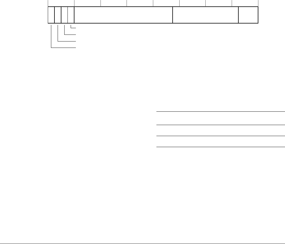
B4 System Control Registers in a VMSA implementation
B4.1 VMSA System control registers descriptions, in register order
B4-1528 Copyright © 1996-1998, 2000, 2004-2012, 2014 ARM. All rights reserved. ARM DDI 0406C.c
Non-Confidential ID051414
B4.1.19 CCSIDR, Cache Size ID Registers, VMSA
The CCSIDR characteristics are:
Purpose The CCSIDR provides information about the architecture of the caches.
This register is part of the Identification registers functional group.
Usage constraints Only accessible from PL1 or higher.
If CSSELR indicates a cache that is not implemented, the result of reading CCSIDR is
UNPREDICTABLE.
Configurations The implementation includes one CCSIDR for each cache that it can access. CSSELR
selects which Cache Size ID Register is accessible.
Architecture versions before ARMv7 do not define these registers.
If the implementation includes the Security Extensions, these registers are Common.
Attributes A 32-bit RO register with an IMPLEMENTATION DEFINED value. See also Reset behavior of
CP14 and CP15 registers on page B3-1450.
Table B3-44 on page B3-1492 shows the encodings of all of the registers in the
Identification registers functional group.
The CCSIDR bit assignments are:
WT, bit[31] Indicates whether the cache level supports write-through, see Table B4-1.
WB, bit[30] Indicates whether the cache level supports write-back, see Table B4-1.
RA, bit[29] Indicates whether the cache level supports read-allocation, see Table B4-1.
WA, bit[28] Indicates whether the cache level supports write-allocation, see Table B4-1.
NumSets, bits[27:13]
(Number of sets in cache) - 1, therefore a value of 0 indicates 1 set in the cache. The number of sets
does not have to be a power of 2.
Associativity, bits[12:3]
(Associativity of cache) - 1, therefore a value of 0 indicates an associativity of 1. The associativity
does not have to be a power of 2.
Table B4-1 WT, WB, RA and WA bit values
WT, WB, RA or WA bit value Meaning
0 Feature not supported
1 Feature supported
LineSize
31 30 29 28 27 13 12 3 2 0
WA
NumSets Associativity
WB
WT
RA

B4 System Control Registers in a VMSA implementation
B4.1 VMSA System control registers descriptions, in register order
ARM DDI 0406C.c Copyright © 1996-1998, 2000, 2004-2012, 2014 ARM. All rights reserved. B4-1529
ID051414 Non-Confidential
LineSize, bits[2:0]
(Log2(Number of words in cache line)) -2. For example:
• For a line length of 4 words: Log2(4) = 2, LineSize entry = 0.
This is the minimum line length.
• For a line length of 8 words: Log2(8) = 3, LineSize entry = 1.
Note
The parameters NumSets, Associativity and LineSize in these registers define the architecturally
visible parameters that are required for the cache maintenance by Set/Way instructions. They are not
guaranteed to represent the actual microarchitectural features of a design. You cannot make any
inference about the actual sizes of caches based on these parameters.
Accessing the currently selected CCSIDR
The CSSELR selects a CCSIDR. To access the currently-selected CCSIDR, software reads the CP15 registers with
<opc1>
set to 1,
<CRn>
set to c0,
<CRm>
set to c0, and
<opc2>
set to 0. For example:
MRC p15, 1, <Rt>, c0, c0, 0 ; Read current CCSIDR into Rt
Any access to the CCSIDR when the value in CSSELR corresponds to a cache that is not implemented returns an
UNKNOWN value.

B4 System Control Registers in a VMSA implementation
B4.1 VMSA System control registers descriptions, in register order
B4-1530 Copyright © 1996-1998, 2000, 2004-2012, 2014 ARM. All rights reserved. ARM DDI 0406C.c
Non-Confidential ID051414
B4.1.20 CLIDR, Cache Level ID Register, VMSA
The CLIDR characteristics are:
Purpose The CLIDR identifies:
• the type of cache, or caches, implemented at each level, up to a maximum of seven
levels
•the Level of Coherence (LoC) and Level of Unification (LoU) for the cache hierarchy.
This register is part of the Identification registers functional group.
Usage constraints Only accessible from PL1 or higher.
Configurations This register is not implemented in architecture versions before ARMv7.
If the implementation includes the Security Extensions, this register is Common.
Attributes A 32-bit RO register with an IMPLEMENTATION DEFINED value. See also Reset behavior of
CP14 and CP15 registers on page B3-1450.
Table B3-44 on page B3-1492 shows the encodings of all of the registers in the
Identification registers functional group.
The CLIDR bit assignments are:
Bits[31:30] Reserved, UNK.
LoUU, bits[29:27]
Level of Unification Uniprocessor for the cache hierarchy, see Terminology for Clean, Invalidate,
and Clean and Invalidate operations on page B2-1275.
LoC, bits[26:24]
Level of Coherence for the cache hierarchy, see Terminology for Clean, Invalidate, and Clean and
Invalidate operations on page B2-1275.
LoUIS, bits[23:21]
Level of Unification Inner Shareable for the cache hierarchy, see Terminology for Clean, Invalidate,
and Clean and Invalidate operations on page B2-1275.
In an implementation that does not include the Multiprocessing Extensions, this field is RAZ.
Ctypen, bits[3(n- 1) + 2:3(n- 1)], for n = 1 to 7
Cache Type fields. Indicate the type of cache implemented at each level, from Level 1 up to a
maximum of seven levels of cache hierarchy. The Level 1 cache field, Ctype1, is bits[2:0], see
register diagram. Table B4-2 shows the possible values for each Ctypen field.
Table B4-2 Ctypen bit values
Ctypen value Meaning, cache implemented at this level
000 No cache
001 Instruction cache only
010 Data cache only
011 Separate instruction and data caches
Ctype1(0)
31 30 29 27 26 24 23 21 20 18 17 15 14 12 11 9 8 6 5 3 2 0
(0) LoUU LoC LoUIS Ctype7 Ctype6 Ctype5 Ctype4 Ctype3 Ctype2

B4 System Control Registers in a VMSA implementation
B4.1 VMSA System control registers descriptions, in register order
ARM DDI 0406C.c Copyright © 1996-1998, 2000, 2004-2012, 2014 ARM. All rights reserved. B4-1531
ID051414 Non-Confidential
If software reads the Cache Type fields from Ctype1 upwards, once it has seen a value of
0b000
, no
caches exist at further-out levels of the hierarchy. So, for example, if Ctype3 is the first Cache Type
field with a value of
0b000
, the values of Ctype4 to Ctype7 must be ignored.
The CLIDR describes only the caches that are under the control of the processor.
Accessing the CLIDR
To access the CLIDR, software reads the CP15 registers with
<opc1>
set to 1,
<CRn>
set to c0,
<CRm>
set to c0, and
<opc2>
set to 1. For example:
MRC p15, 1, <Rt>, c0, c0, 1 ; Read CLIDR into Rt
100 Unified cache
101, 11X Reserved
Table B4-2 Ctypen bit values (continued)
Ctypen value Meaning, cache implemented at this level

B4 System Control Registers in a VMSA implementation
B4.1 VMSA System control registers descriptions, in register order
B4-1532 Copyright © 1996-1998, 2000, 2004-2012, 2014 ARM. All rights reserved. ARM DDI 0406C.c
Non-Confidential ID051414
B4.1.21 CNTFRQ, Counter Frequency register, VMSA
The CNTFRQ register characteristics are:
Purpose The CNTFRQ register indicates the clock frequency of the system counter.
This register is a Generic Timer register.
Usage constraints In an implementation that includes the Security Extensions, RW only from Secure PL1
modes, RO from Non-secure PL1 and PL2 modes.
Otherwise, RW only from PL1 modes.
In all implementations, when CNTKCTL.{PL0VCTEN, PL0PCTEN} is not set to
0b00
, is
also RO from PL0 modes.
Configurations Implemented only as part of the Generic Timers Extension.
The VMSA, PMSA, and system level definitions of the register fields are identical.
In an implementation that includes the Security Extensions, this register is Common.
Attributes A 32-bit RW register with an UNKNOWN reset value.
Table B8-2 on page B8-1969 shows the encodings of all of the Generic Timer registers.
The CNTFRQ bit assignments are:
Clock frequency, bits[31:0]
Indicates the system counter clock frequency, in Hz.
Note
Programming CNTFRQ does not affect the system clock frequency. However, on system initialization, CNTFRQ
must be correctly programmed with the system clock frequency, to make this value available to software. For more
information see Initializing and reading the system counter frequency on page B8-1961.
Accessing CNTFRQ
To access CNTFRQ, software reads or writes the CP15 registers with
<opc1>
set to 0,
<CRn>
set to c14,
<CRm>
set to
c0, and
<opc2>
set to 0. For example:
MRC p15, 0, <Rt>, c14, c0, 0 ; Read CNTFRQ into Rt
MCR p15, 0, <Rt>, c14, c0, 0 ; Write Rt to CNTFRQ
Clock frequency
31 0
B4 System Control Registers in a VMSA implementation
B4.1 VMSA System control registers descriptions, in register order
ARM DDI 0406C.c Copyright © 1996-1998, 2000, 2004-2012, 2014 ARM. All rights reserved. B4-1533
ID051414 Non-Confidential
B4.1.22 CNTHCTL, Timer PL2 Control register, Virtualization Extensions
The CNTHCTL characteristics are:
Purpose Controls:
• access to the following from Non-secure PL1 modes:
— the physical counter
— the Non-secure PL1 physical timer.
• the generation of an event stream from the physical counter.
This register is a Generic Timer register.
Usage constraints Only accessible from Hyp mode, or from Monitor mode when SCR.NS is set to 1, see
PL2-mode system control registers on page B3-1454.
Configurations Implemented only as part of the Generic Timers Extension, and only if the implementation
also includes the Virtualization Extensions.
This is a PL2-mode register, see Banked PL2-mode CP15 read/write registers on
page B3-1454.
Attributes A 32-bit RW register. See the field descriptions for information about the reset values.
Table B8-2 on page B8-1969 shows the encodings of all of the Generic Timer registers.
In an ARMv7 implementation, the CNTHCTL bit assignments are:
Bits[31:8] Reserved, UNK/SBZP.
EVNTI, bits[7:4] Selects which bit of CNTPCT is the trigger for the event stream generated from the physical
counter, when that stream is enabled. For example, if this field is
0b0110
, CNTPCT[6] is the
trigger bit for the virtual counter event stream.
For more information see Event streams on page B8-1964.
This field is UNKNOWN on reset.
EVNTDIR, bit[3] Controls which transition of the CNTPCT trigger bit, defined by EVNTI, generates an
event, when the event stream is enabled:
0 A 0 to 1 transition of the trigger bit triggers an event.
1 A 1 to 0 transition of the trigger bit triggers an event.
For more information see Event streams on page B8-1964.
This bit is UNKNOWN on reset.
EVNTEN, bit[2] Enables the generation of an event stream from the physical counter:
0 Disables the event stream.
1 Enables the event stream.
For more information see Event streams on page B8-1964.
This bit resets to 0.
EVNTI
31 20
Reserved, UNK/SBZP
EVNTEN
EVNTDIR
PL1PCTEN
PL1PCEN
13478

B4 System Control Registers in a VMSA implementation
B4.1 VMSA System control registers descriptions, in register order
B4-1534 Copyright © 1996-1998, 2000, 2004-2012, 2014 ARM. All rights reserved. ARM DDI 0406C.c
Non-Confidential ID051414
PL1PCEN, bit[1] Controls whether the Non-secure copies of the physical timer registers are accessible from
Non-secure PL1 and PL0 modes:
0 The Non-secure CNTP_CVAL, CNTP_TVAL, and CNTP_CTL registers are
not accessible Non-secure PL1 and PL0 modes.
1 The Non-secure CNTP_CVAL, CNTP_TVAL, and CNTP_CTL registers are
accessible from Non-secure PL1 and PL0 modes.
For more information see Accessing the timer registers on page B8-1966.
This bit resets to 1.
PL1PCTEN, bit[0] Controls whether the physical counter, CNTPCT, is accessible from Non-secure PL1 and
PL0 modes:
0 The CNTPCT register is not accessible from Non-secure PL1 and PL0 modes.
1 The CNTPCT register is accessible from Non-secure PL1 and PL0 modes.
For more information see Accessing the physical counter on page B8-1962.
This bit resets to 1.
Accessing CNTHCTL
To access CNTHCTL, software reads or writes the CP15 registers with
<opc1>
set to 4,
<CRn>
set to c14,
<CRm>
set to
c1, and
<opc2>
set to 0. For example:
MRC p15, 4, <Rt>, c14, c1, 0 ; Read CNTHCTL to Rt
MCR p15, 4, <Rt>, c14, c1, 0 ; Write Rt to CNTHCTL

B4 System Control Registers in a VMSA implementation
B4.1 VMSA System control registers descriptions, in register order
ARM DDI 0406C.c Copyright © 1996-1998, 2000, 2004-2012, 2014 ARM. All rights reserved. B4-1535
ID051414 Non-Confidential
B4.1.23 CNTHP_CTL, PL2 Physical Timer Control register, Virtualization Extension
The CNTHP_CTL characteristics are:
Purpose The control register for the Hyp mode physical timer.
This register is a Generic Timer register.
Usage constraints Only accessible from Hyp mode, or from Monitor mode when SCR.NS is set to 1, see
PL2-mode system control registers on page B3-1454.
For more information, see Accessing the timer registers on page B8-1966.
Configurations Implemented only as part of the Generic Timers Extension, and only if the implementation
also includes the Virtualization Extensions.
This is a PL2-mode register, see Banked PL2-mode CP15 read/write registers on
page B3-1454.
Attributes A 32-bit RW register with an UNKNOWN reset value.
Table B8-2 on page B8-1969 shows the encodings of all of the Generic Timer registers.
The bit assignments of CNTHP_CTL are identical to those of CNTP_CTL.
Accessing CNTHP_CTL
To access CNTHP_CTL, software reads or writes the CP15 registers with
<opc1>
set to 4,
<CRn>
set to c14,
<CRm>
set
to c2, and
<opc2>
set to 1. For example:
MRC p15, 4, <Rt>, c14, c2, 1 ; Read CNTHP_CTL into Rt
MCR p15, 4, <Rt>, c14, c2, 1 ; Write Rt to CNTHP_CTL
B4.1.24 CNTHP_CVAL, PL2 Physical Timer CompareValue register, Virtualization Extensions
The CNTHP_CVAL characteristics are:
Purpose Holds the compare value for the Hyp mode physical timer.
This register is a Generic Timer register.
Usage constraints Only accessible from Hyp mode, or from Monitor mode when SCR.NS is set to 1, see
PL2-mode system control registers on page B3-1454.
For more information, see Accessing the timer registers on page B8-1966.
Configurations Implemented only as part of the Generic Timers Extension, and only if the implementation
also includes the Virtualization Extensions.
This is a PL2-mode register, see Banked PL2-mode CP15 read/write registers on
page B3-1454.
Attributes A 64-bit RW register with an UNKNOWN reset value.
Table B8-2 on page B8-1969 shows the encodings of all of the Generic Timer registers.
The bit assignments of CNTHP_CVAL are identical to those of CNTP_CVAL.
Accessing CNTHP_CVAL
To access CNTHP_CVAL, software performs a 64-bit read or write of the CP15 registers with
<CRm>
set to c14 and
<opc1>
set to 6. For example:
MRRC p15, 6, <Rt>, <Rt2>, c14 ; Read 64-bit CNTHP_CVAL into Rt (low word) and Rt2 (high word)
MCRR p15, 6, <Rt>, <Rt2>, c14 ; Write Rt (low word) and Rt2 (high word) to 64-bit CNTHP_CVAL
In these
MRRC
and
MCRR
instructions, Rt holds the least-significant word of CNTHP_CVAL, and Rt2 holds the
most-significant word.

B4 System Control Registers in a VMSA implementation
B4.1 VMSA System control registers descriptions, in register order
B4-1536 Copyright © 1996-1998, 2000, 2004-2012, 2014 ARM. All rights reserved. ARM DDI 0406C.c
Non-Confidential ID051414
B4.1.25 CNTHP_TVAL, PL2 Physical TimerValue register, Virtualization Extensions
The CNTHP_TVAL characteristics are:
Purpose Holds the timer value for the Hyp mode physical timer. This provides a 32-bit downcounter,
see Operation of the TimerValue views of the timers on page B8-1967.
This register is a Generic Timer register.
Usage constraints Only accessible from Hyp mode, or from Monitor mode when SCR.NS is set to 1, see
PL2-mode system control registers on page B3-1454.
For more information, see Accessing the timer registers on page B8-1966.
When CNTHP_CTL.ENABLE is set to 0:
• a write to this register updates the register
• the value held in the register continues to decrement
• a read of the register returns an UNKNOWN value.
Configurations Implemented only as part of the Generic Timers Extension, and only if the implementation
also includes the Virtualization Extensions.
This is a PL2-mode register, see Banked PL2-mode CP15 read/write registers on
page B3-1454.
Attributes A 32-bit RW register with an UNKNOWN reset value.
Table B8-2 on page B8-1969 shows the encodings of all of the Generic Timer registers.
The bit assignments of CNTHP_TVAL are identical to those of CNTP_TVAL.
Accessing CNTHP_TVAL
To access CNTHP_TVAL, software reads or writes the CP15 registers with
<opc1>
set to 4,
<CRn>
set to c14,
<CRm>
set to c2, and
<opc2>
set to 0. For example:
MRC p15, 4, <Rt>, c14, c2, 0 ; Read CNTHP_TVAL into Rt
MCR p15, 4, <Rt>, c14, c2, 0 ; Write Rt to CNTHP_TVAL

B4 System Control Registers in a VMSA implementation
B4.1 VMSA System control registers descriptions, in register order
ARM DDI 0406C.c Copyright © 1996-1998, 2000, 2004-2012, 2014 ARM. All rights reserved. B4-1537
ID051414 Non-Confidential
B4.1.26 CNTKCTL, Timer PL1 Control register, VMSA
The CNTKCTL characteristics are:
Purpose Controls:
• access to the following from PL0 modes:
— the physical counter
— the virtual counter
— the PL1 physical timers
— the virtual timer.
• the generation of an event stream from the virtual counter.
This register is a Generic Timer register.
Usage constraints Accessible from Secure PL1 modes, and Non-secure PL1 and PL2 modes.
Configurations Implemented only as part of the Generic Timers Extension.
The VMSA and PMSA definitions of the register fields are identical.
If the implementation includes the Security Extensions, this register is Common.
Attributes A 32-bit RW register. See the field descriptions for information about the reset values.
Table B8-2 on page B8-1969 shows the encodings of all of the Generic Timer registers.
In an ARMv7 implementation, the CNTKCTL register bit assignments are:
Bits[31:10] Reserved, UNK/SBZP.
PL0PTEN, bit[9] Controls whether the physical timer registers are accessible from PL0 modes:
0 The CNTP_CVAL, CNTP_CTL, and CNTP_TVAL registers are not accessible
from PL0.
1 The CNTP_CVAL, CNTP_CTL, and CNTP_TVAL registers are accessible
from PL0.
This bit resets to 0.
For more information see Accessing the timer registers on page B8-1966.
PL0VTEN, bit[8] Controls whether the virtual timer registers are accessible from PL0 modes:
0 The CNTV_CVAL, CNTV_CTL, and CNTV_TVAL registers are not
accessible from PL0.
1 The CNTV_CVAL, CNTV_CTL, and CNTV_TVAL registers are accessible
from PL0.
This bit resets to 0.
For more information see Accessing the timer registers on page B8-1966.
EVNTI, bits[7:4] Selects which bit of CNTVCT is the trigger for the event stream generated from the virtual
counter, when that stream is enabled. For example, if this field is
0b0110
, CNTVCT[6] is the
trigger bit for the virtual counter event stream.
This field is UNKNOWN on reset.
For more information see Event streams on page B8-1964.
EVNTI
31 20
Reserved, UNK/SBZP
EVNTEN
EVNTDIR
PL0PCTEN
PL0VCTEN
13478910
PL0VTEN
PL0PTEN

B4 System Control Registers in a VMSA implementation
B4.1 VMSA System control registers descriptions, in register order
B4-1538 Copyright © 1996-1998, 2000, 2004-2012, 2014 ARM. All rights reserved. ARM DDI 0406C.c
Non-Confidential ID051414
EVNTDIR, bit[3] Controls which transition of the CNTVCT trigger bit, defined by EVNTI, generates an
event, when the event stream is enabled:
0 A 0 to 1 transition of the trigger bit triggers an event.
1 A 1 to 0 transition of the trigger bit triggers an event.
This bit is UNKNOWN on reset.
For more information see Event streams on page B8-1964.
EVNTEN, bit[2] Enables the generation of an event stream from the virtual counter:
0 Disables the event stream.
1 Enables the event stream.
This bit resets to 0.
For more information see Event streams on page B8-1964.
PL0VCTEN, bit[1] Controls whether the virtual counter, CNTVCT, and the frequency register CNTFRQ, are
accessible from PL0 modes:
0 CNTVCT is not accessible from PL0.
If PL0PCTEN is set to 0, CNTFRQ is not accessible from PL0.
1 CNTVCT and CNTFRQ are accessible from PL0.
This bit resets to 0.
For more information see Accessing the virtual counter on page B8-1963.
PL0PCTEN, bit[0] Controls whether the physical counter, CNTPCT, and the frequency register CNTFRQ, are
accessible from PL0 modes:
0 CNTPCT is not accessible from PL0 modes.
If PL0VCTEN is set to 0, CNTFRQ is not accessible from PL0.
1 CNTPCT and CNTFRQ are accessible from PL0.
This bit resets to 0.
For more information see Accessing the physical counter on page B8-1962.
Note
CNTFRQ is accessible from PL0 modes if either PL0VCTEN or PL0PCTEN is set to 1.
Accessing CNTKCTL
To access CNTKCTL, software reads or writes the CP15 registers with
<opc1>
set to 0,
<CRn>
set to c14,
<CRm>
set to
c1, and
<opc2>
set to 0. For example:
MRC p15, 0, <Rt>, c14, c1, 0 ; Read CNTKCTL to Rt
MCR p15, 0, <Rt>, c14, c1, 0 ; Write Rt to CNTKCTL
B4 System Control Registers in a VMSA implementation
B4.1 VMSA System control registers descriptions, in register order
ARM DDI 0406C.c Copyright © 1996-1998, 2000, 2004-2012, 2014 ARM. All rights reserved. B4-1539
ID051414 Non-Confidential
B4.1.27 CNTP_CTL, PL1 Physical Timer Control register, VMSA
The CNTP_CTL characteristics are:
Purpose The control register for the physical timer.
This register is a Generic Timer register.
Usage constraints In an implementation that does not include the Virtualization Extensions, accessible in PL1
modes.
In an implementation that includes the Virtualization Extensions:
• the Secure copy of the register is accessible in Secure PL1 modes
• the Non-secure copy of the register is accessible in Non-secure Hyp mode, and when
CNTHCTL.PL1PCEN is set to 1, in Non-secure PL1 modes.
When the register is accessible in PL1 modes, in the current security state,
CNTKCTL.PL0PTEN determines whether the register is accessible from the PL0 mode.
For more information, see Accessing the timer registers on page B8-1966.
Configurations Implemented only as part of the Generic Timers Extension.
The VMSA, PMSA, and system level definitions of the register fields are identical.
If the implementation includes the Security Extensions, this register is Banked.
Attributes A 32-bit RW register with an UNKNOWN reset value.
Table B8-2 on page B8-1969 shows the encodings of all of the Generic Timer registers.
In an ARMv7 implementation, the CNTP_CTL bit assignments are:
Bits[31:3] Reserved, UNK/SBZP.
ISTATUS, bit[2] The status of the timer. This bit indicates whether the timer condition is asserted:
0 Timer condition is not asserted.
1 Timer condition is asserted.
When the ENABLE bit is set to 1, ISTATUS indicates whether the timer value meets the
condition for the timer output to be asserted, see Operation of the CompareValue views of
the timers on page B8-1966 and Operation of the TimerValue views of the timers on
page B8-1967. ISTATUS takes no account of the value of the IMASK bit. If ISTATUS is set
to 1 and IMASK is set to 0 then the timer output signal is asserted.
This bit is read-only.
IMASK, bit[1] Timer output signal mask bit. Permitted values are:
0 Timer output signal is not masked.
1 Timer output signal is masked.
For more information, see the description of the ISTATUS bit and Operation of the timer
output signal on page B8-1968.
31 20
Reserved, UNK/SBZP
ISTATUS
ENABLE
IMASK
13

B4 System Control Registers in a VMSA implementation
B4.1 VMSA System control registers descriptions, in register order
B4-1540 Copyright © 1996-1998, 2000, 2004-2012, 2014 ARM. All rights reserved. ARM DDI 0406C.c
Non-Confidential ID051414
ENABLE, bit[0] Enables the timer. Permitted values are:
0 Timer disabled.
1 Timer enabled.
Setting this bit to 0 disables the timer output signal, but the timer value accessible from
CNTP_TVAL continues to count down.
Note
Disabling the output signal might be a power-saving option.
Accessing CNTP_CTL
To access CNTP_CTL, software reads or writes the CP15 registers with
<opc1>
set to 0,
<CRn>
set to c14,
<CRm>
set
to c2, and
<opc2>
set to 1. For example:
MRC p15, 0, <Rt>, c14, c2, 1 ; Read CNTP_CTL into Rt
MCR p15, 0, <Rt>, c14, c2, 1 ; Write Rt to CNTP_CTL

B4 System Control Registers in a VMSA implementation
B4.1 VMSA System control registers descriptions, in register order
ARM DDI 0406C.c Copyright © 1996-1998, 2000, 2004-2012, 2014 ARM. All rights reserved. B4-1541
ID051414 Non-Confidential
B4.1.28 CNTP_CVAL, PL1 Physical Timer CompareValue register, VMSA
The CNTP_CVAL characteristics are:
Purpose Holds the 64-bit compare value for the PL1 physical timer.
This register is a Generic Timer register.
Usage constraints In an implementation that does not include the Virtualization Extensions, accessible in PL1
modes.
In an implementation that includes the Virtualization Extensions:
• the Secure copy of the register is accessible in Secure PL1 modes
• the Non-secure copy of the register is accessible in Non-secure Hyp mode, and when
CNTHCTL.PL1PCEN is set to 1, in Non-secure PL1 modes.
When the register is accessible in PL1 modes, in the current security state,
CNTKCTL.PL0PTEN determines whether the register is accessible from the PL0 mode.
For more information, see Accessing the timer registers on page B8-1966.
Configurations Implemented only as part of the Generic Timers Extension.
The VMSA, PMSA, and system level definitions of the register fields are identical.
If the implementation includes the Security Extensions, this register is Banked.
Attributes A 64-bit RW register with an UNKNOWN reset value.
Table B8-2 on page B8-1969 shows the encodings of all of the Generic Timer registers.
In an ARMv7 implementation, the CNTP_CVAL bit assignments are:
CompareValue, bits[63:0]
Indicates the compare value for the PL1 physical timer.
For more information about the timer see Timers on page B8-1965.
Accessing CNTP_CVAL
To access CNTP_CVAL, software performs a 64-bit read or write of the CP15 registers with
<CRm>
set to c14 and
<opc1>
set to 2. For example:
MRRC p15, 2, <Rt>, <Rt2>, c14 ; Read 64-bit CNTP_CVAL into Rt (low word) and Rt2 (high word)
MCRR p15, 2, <Rt>, <Rt2>, c14 ; Write Rt (low word) and Rt2 (high word) to 64-bit CNTP_CVAL
In these
MRRC
and
MCRR
instructions, Rt holds the least-significant word of CNTP_CVAL, and Rt2 holds the
most-significant word.
CompareValue[63:0]
63 0

B4 System Control Registers in a VMSA implementation
B4.1 VMSA System control registers descriptions, in register order
B4-1542 Copyright © 1996-1998, 2000, 2004-2012, 2014 ARM. All rights reserved. ARM DDI 0406C.c
Non-Confidential ID051414
B4.1.29 CNTP_TVAL, PL1 Physical TimerValue register, VMSA
The CNTP_TVAL characteristics are:
Purpose Holds the timer value for the PL1 physical timer. This provides a 32-bit downcounter, see
Operation of the TimerValue views of the timers on page B8-1967.
This register is a Generic Timer register.
Usage constraints In an implementation that does not include the Virtualization Extensions, accessible in PL1
modes.
In an implementation that includes the Virtualization Extensions:
• the Secure copy of the register is accessible in Secure PL1 modes
• the Non-secure copy of the register is accessible in Non-secure Hyp mode, and when
CNTHCTL.PL1PCEN is set to 1, in Non-secure PL1 modes.
When the register is accessible in PL1 modes, in the current security state,
CNTKCTL.PL0PTEN determines whether the register is accessible from the PL0 mode.
For more information, see Accessing the timer registers on page B8-1966.
When CNTP_CTL.ENABLE is set to 0:
• a write to this register updates the register
• the value held in the register continues to decrement
• a read of the register returns an UNKNOWN value.
Configurations Implemented only as part of the Generic Timers Extension.
The VMSA, PMSA, and system level definitions of the register fields are identical.
If the implementation includes the Security Extensions, this register is Banked.
Attributes A 32-bit RW register with an UNKNOWN reset value.
Table B8-2 on page B8-1969 shows the encodings of all of the Generic Timer registers.
In an ARMv7 implementation, the CNTP_TVAL bit assignments are:
TimerValue, bits[31:0]
Indicates the timer value.
Accessing CNTP_TVAL
To access CNTP_TVAL, software reads or writes the CP15 registers with
<opc1>
set to 0,
<CRn>
set to c14,
<CRm>
set
to c2, and
<opc2>
set to 0. For example:
MRC p15, 0, <Rt>, c14, c2, 0 ; Read CNTP_TVAL into Rt
MCR p15, 0, <Rt>, c14, c2, 0 ; Write Rt to CNTP_TVAL
31 0
TimerValue
B4 System Control Registers in a VMSA implementation
B4.1 VMSA System control registers descriptions, in register order
ARM DDI 0406C.c Copyright © 1996-1998, 2000, 2004-2012, 2014 ARM. All rights reserved. B4-1543
ID051414 Non-Confidential
B4.1.30 CNTPCT, Physical Count register, VMSA
The CNTPCT register characteristics are:
Purpose The CNTPCT register holds the 64-bit physical count value.
This register is a Generic Timer register.
Usage constraints In an implementation that does not include the Virtualization Extensions, always accessible
from PL1 modes, in both security states.
In an implementation that includes the Virtualization Extensions, CNTPCT is:
• always accessible Secure PL1 modes and from Non-secure Hyp mode
• accessible from Non-secure PL1 modes only when CNTHCTL.PL1PCTEN is set
to 1.
When CNTKCTL.PL0PCTEN is set to 1, CNTPCT is also accessible from PL0 modes.
Fore more information about the CNTPCT access controls see Accessing the physical
counter on page B8-1962.
Configurations Implemented only as part of the Generic Timers Extension.
The VMSA, PMSA, and system level definitions of the register fields are identical.
In an implementation that includes the Security Extensions, this register is Common.
Attributes A 64-bit RO register with an UNKNOWN reset value.
Table B8-2 on page B8-1969 shows the encodings of all of the Generic Timer registers.
The CNTPCT bit assignments are:
PhysicalCount, bits[63:0]
Indicates the physical count.
Accessing CNTPCT
To access CNTPCT, software performs a 64-bit read of the CP15 registers with
<CRm>
set to c14 and
<opc1>
set to 0.
For example:
MRRC p15, 0, <Rt>, <Rt2>, c14 ; Read 64-bit CNTPCT into Rt (low word) and Rt2 (high word)
In the
MRRC
instruction, Rt holds the least-significant word of CNTPCT, and Rt2 holds the most-significant word.
PhysicalCount[63:0]
63 0

B4 System Control Registers in a VMSA implementation
B4.1 VMSA System control registers descriptions, in register order
B4-1544 Copyright © 1996-1998, 2000, 2004-2012, 2014 ARM. All rights reserved. ARM DDI 0406C.c
Non-Confidential ID051414
B4.1.31 CNTV_CTL, Virtual Timer Control register, VMSA
The CNTV_CTL register characteristics are:
Purpose The control register for the virtual timer.
This register is a Generic Timer register.
Usage constraints Accessible from Secure PL1 modes and Non-secure PL1 and PL2 modes. When
CNTKCTL.PL0VTEN is set to 1, also accessible from PL0 modes.
For more information, see Accessing the timer registers on page B8-1966.
Configurations Implemented only as part of the Generic Timers Extension.
The VMSA, PMSA, and system level definitions of the register fields are identical.
In an implementation that includes the Security Extensions, this register is Common.
Attributes A 32-bit RW register with an UNKNOWN reset value.
Table B8-2 on page B8-1969 shows the encodings of all of the Generic Timer registers.
The bit assignments of the CNTV_CTL register are identical to those of CNTP_CTL.
Accessing CNTV_CTL
To access CNTV_CTL, software reads or writes the CP15 registers with
<opc1>
set to 0,
<CRn>
set to c14,
<CRm>
set
to c3, and
<opc2>
set to 1. For example:
MRC p15, 0, <Rt>, c14, c3, 1 ; Read CNTV_CTL into Rt
MCR p15, 0, <Rt>, c14, c3, 1 ; Write Rt to CNTV_CTL
B4.1.32 CNTV_CVAL, Virtual Timer CompareValue register, VMSA
The CNTV_CVAL characteristics are:
Purpose Holds the compare value for the virtual timer.
This register is a Generic Timer register.
Usage constraints Accessible from Secure PL1 modes and Non-secure PL1 and PL2 modes. When
CNTKCTL.PL0VTEN is set to 1, also accessible from PL0 modes.
For more information, see Accessing the timer registers on page B8-1966.
Configurations Implemented only as part of the Generic Timers Extension.
The VMSA, PMSA, and system level definitions of the register fields are identical.
In an implementation that includes the Security Extensions, this register is Common.
Attributes A 64-bit RW register with an UNKNOWN reset value.
Table B8-2 on page B8-1969 shows the encodings of all of the Generic Timer registers.
The bit assignments of CNTV_CVAL are identical to those of CNTP_CVAL.
Accessing CNTV_CVAL
To access CNTV_CVAL, software performs a 64-bit read or write of the CP15 registers with
<CRm>
set to c14 and
<opc1>
set to 3. For example:
MRRC p15, 3, <Rt>, <Rt2>, c14 ; Read 64-bit CNTV_CVAL into Rt (low word) and Rt2 (high word)
MCRR p15, 3, <Rt>, <Rt2>, c14 ; Write 64-bit Rt (low word) and Rt2 (high word) to CNTV_CVAL
In these
MRRC
and
MCRR
instructions, Rt holds the least-significant word of CNTV_CVAL, and Rt2 holds the
most-significant word.

B4 System Control Registers in a VMSA implementation
B4.1 VMSA System control registers descriptions, in register order
ARM DDI 0406C.c Copyright © 1996-1998, 2000, 2004-2012, 2014 ARM. All rights reserved. B4-1545
ID051414 Non-Confidential
B4.1.33 CNTV_TVAL, Virtual TimerValue register, VMSA
The CNTV_TVAL characteristics are:
Purpose Holds the timer value for the virtual timer. This provides a 32-bit downcounter, see
Operation of the TimerValue views of the timers on page B8-1967.
This register is a Generic Timer register.
Usage constraints Accessible from Secure PL1 modes and Non-secure PL1 and PL2 modes. When
CNTKCTL.PL0VTEN is set to 1, also accessible from PL0 modes.
For more information, see Accessing the timer registers on page B8-1966.
When CNTV_CTL.ENABLE is set to 0:
• a write to this register updates the register
• the value held in the register continues to decrement
• a read of the register returns an UNKNOWN value.
Configurations Implemented only as part of the Generic Timers Extension.
The VMSA, PMSA, and system level definitions of the register fields are identical.
In an implementation that includes the Security Extensions, this register is Common.
Attributes A 32-bit RW register with an UNKNOWN reset value.
Table B8-2 on page B8-1969 shows the encodings of all of the Generic Timer registers.
The bit assignments of CNTV_TVAL are identical to those of CNTP_TVAL.
Accessing CNTV_TVAL
To access CNTV_TVAL, software reads or writes the CP15 registers with
<opc1>
set to 0,
<CRn>
set to c14,
<CRm>
set
to c3, and
<opc2>
set to 0. For example:
MRC p15, 0, <Rt>, c14, c3, 0 ; Read CNTV_TVAL into Rt
MCR p15, 0, <Rt>, c14, c3, 0 ; Write Rt to CNTV_TVAL

B4 System Control Registers in a VMSA implementation
B4.1 VMSA System control registers descriptions, in register order
B4-1546 Copyright © 1996-1998, 2000, 2004-2012, 2014 ARM. All rights reserved. ARM DDI 0406C.c
Non-Confidential ID051414
B4.1.34 CNTVCT, Virtual Count register, VMSA
The CNTVCT characteristics are:
Purpose Holds the 64-bit virtual count.
Note
The virtual count is obtained by subtracting the virtual offset from the physical count, see
The virtual counter on page B8-1963.
This register is a Generic Timer register.
Usage constraints Always accessible from Secure PL1 modes and Non-secure PL1 and PL2 modes.
When CNTKCTL.PL0VCTEN is set to 1, is also accessible from Secure and Non-secure
PL0 modes. For more information about the CNTVCT access controls see Accessing the
virtual counter on page B8-1963.
Configurations Implemented only as part of the Generic Timers Extension.
The VMSA, PMSA, and system level definitions of the register fields are identical.
In an implementation that includes the Security Extensions, this register is Common.
Attributes A 64-bit RO register with an UNKNOWN reset value.
Table B8-2 on page B8-1969 shows the encodings of all of the Generic Timer registers.
In an ARMv7 implementation, the CNTVCT bit assignments are:
VirtualCount, bits[63:0]
Indicates the virtual count.
Accessing CNTVCT
To access CNTVCT, software performs a 64-bit read of the CP15 registers with
<CRm>
set to c14 and
<opc1>
set to
1. For example:
MRRC p15, 1, <Rt>, <Rt2>, c14 ; Read 64-bit CNTVCT into Rt (low word) and Rt2 (high word)
In the
MRRC
instruction, Rt holds the least-significant word of CNTVCT, and Rt2 holds the most-significant word.
VirtualCount[63:0]
63 0

B4 System Control Registers in a VMSA implementation
B4.1 VMSA System control registers descriptions, in register order
ARM DDI 0406C.c Copyright © 1996-1998, 2000, 2004-2012, 2014 ARM. All rights reserved. B4-1547
ID051414 Non-Confidential
B4.1.35 CNTVOFF, Virtual Offset register, VMSA
The CNTVOFF characteristics are:
Purpose Holds the 64-bit virtual offset.
This register is a Generic Timer register.
Usage constraints Only accessible from Hyp mode, or from Monitor mode when SCR.NS is set to 1, see
PL2-mode system control registers on page B3-1454.
Configurations Implemented only as part of the Generic Timers Extension.
This is a PL2-mode register, see Banked PL2-mode CP15 read/write registers on
page B3-1454.
The implementation of this register depends on whether the implementation includes the
Virtualization Extensions:
• If the implementation includes the Virtualization Extensions this is a RW register,
accessible from Hyp mode, and from Monitor mode when SCR.NS is set to 1.
• If the implementation includes the Security Extensions but not the Virtualization
Extensions, an
MCRR
or
MRRC
to the CNTVOFF encoding is UNPREDICTABLE if
executed in Monitor mode, regardless of the value of SCR.NS.
For more information, see Status of the CNTVOFF register on page B8-1970.
The VMSA and system level definitions of the register fields are identical.
Attributes If the Virtualization Extensions are implemented, this is a 64-bit RW register with an
UNKNOWN reset value. If the Virtualization Extensions are not implemented, for all purposes
other than direct reads and writes this register behaves as if it contains the value 0.
Table B8-2 on page B8-1969 shows the encodings of all of the Generic Timer registers.
In an ARMv7 implementation that also includes the Virtualization Extensions, the CNTVOFF bit assignments are:
VirtualOffset, bits[63:0]
Indicates the virtual offset.
Accessing CNTVOFF
To access CNTVOFF, software performs a 64-bit read or write of the CP15 registers with
<CRm>
set to c14 and
<opc1>
set to 4. For example:
MRRC p15, 4, <Rt>, <Rt2>, c14 ; Read 64-bit CNTVOFF into Rt (low word) and Rt2 (high word)
MCRR p15, 4, <Rt>, <Rt2>, c14 ; Write Rt (low word) and Rt2 (high word) to 64-bit CNTVOFF
In these
MRRC
and
MCRR
instructions, Rt holds the least-significant word of CNTVOFF, and Rt2 holds the
most-significant word.
VirtualOffset[63:0]
63 0

B4 System Control Registers in a VMSA implementation
B4.1 VMSA System control registers descriptions, in register order
B4-1548 Copyright © 1996-1998, 2000, 2004-2012, 2014 ARM. All rights reserved. ARM DDI 0406C.c
Non-Confidential ID051414
B4.1.36 CONTEXTIDR, Context ID Register, VMSA
The CONTEXTIDR characteristics are:
Purpose CONTEXTIDR identifies the current Process Identifier (PROCID) and, when using the
Short-descriptor translation table format, the Address Space Identifier (ASID).
This register is part of the Virtual memory control registers functional group.
Usage constraints Only accessible from PL1 or higher.
Configurations The register format depends on whether address translation is using the Long-descriptor or
the Short-descriptor translation table format.
In an implementation that includes the Security Extensions, this register is Banked.
Attributes A 32-bit RW register with an UNKNOWN reset value. See also Reset behavior of CP14 and
CP15 registers on page B3-1450.
Table B3-45 on page B3-1493 shows the encodings of all of the registers in the Virtual
memory control registers functional group.
In a VMSA implementation, the CONTEXTIDR bit assignments are:
PROCID, bits[31:0], when using the Long-descriptor translation table format
PROCID, bits[31:8], when using the Short-descriptor translation table format
Process Identifier. This field must be programmed with a unique value that identifies the current
process. See also Using the CONTEXTIDR.
ASID, bits[7:0], when using the Short-descriptor translation table format
Address Space Identifier. This field is programmed with the value of the current ASID.
Note
When using the Long-descriptor translation table format, either TTBR0 or TTBR1 holds the current
ASID.
Using the CONTEXTIDR
The value of the whole of this register is called the Context ID and is used by:
• the debug logic, for Linked and Unlinked Context ID matching, see Breakpoint debug events on
page C3-2041 and Watchpoint debug events on page C3-2059
• the trace logic, to identify the current process.
The ASID field value is an identifier for a particular process. In the translation tables it identifies entries associated
with a process, and distinguishes them from global entries. This means many cache and TLB maintenance
operations take an ASID argument.
For information about the synchronization of changes to the CONTEXTIDR see Synchronization of changes to
system control registers on page B3-1461. There are particular synchronization requirements when changing the
ASID and Translation Table Base Registers, see Synchronization of changes of ASID and TTBR on page B3-1386.
PROCID
31 8 7 0
PROCID
ASIDShort-descriptor
†
† Current translation table format
Long-descriptor
†

B4 System Control Registers in a VMSA implementation
B4.1 VMSA System control registers descriptions, in register order
ARM DDI 0406C.c Copyright © 1996-1998, 2000, 2004-2012, 2014 ARM. All rights reserved. B4-1549
ID051414 Non-Confidential
Accessing the CONTEXTIDR
To access the CONTEXTIDR, software reads or writes the CP15 registers with
<opc1>
set to 0,
<CRn>
set to c13,
<CRm>
set to c0, and
<opc2>
set to 1. For example:
MRC p15, 0, <Rt>, c13, c0, 1 ; Read CONTEXTIDR into Rt
MCR p15, 0, <Rt>, c13, c0, 1 ; Write Rt to CONTEXTIDR

B4 System Control Registers in a VMSA implementation
B4.1 VMSA System control registers descriptions, in register order
B4-1550 Copyright © 1996-1998, 2000, 2004-2012, 2014 ARM. All rights reserved. ARM DDI 0406C.c
Non-Confidential ID051414
B4.1.37 CP15DMB, CP15 Data Memory Barrier operation, VMSA
Data and instruction barrier operations, VMSA on page B4-1752 describes this deprecated CP15 barrier operation.
B4.1.38 CP15DSB, CP15 Data Synchronization Barrier operation, VMSA
Data and instruction barrier operations, VMSA on page B4-1752 describes this deprecated CP15 barrier operation.
B4.1.39 CP15ISB, CP15 Instruction Synchronization Barrier operation, VMSA
Data and instruction barrier operations, VMSA on page B4-1752 describes this deprecated CP15 barrier operation.

B4 System Control Registers in a VMSA implementation
B4.1 VMSA System control registers descriptions, in register order
ARM DDI 0406C.c Copyright © 1996-1998, 2000, 2004-2012, 2014 ARM. All rights reserved. B4-1551
ID051414 Non-Confidential
B4.1.40 CPACR, Coprocessor Access Control Register, VMSA
The CPACR characteristics are:
Purpose The CPACR:
• Controls access to coprocessors CP0 to CP13 from PL0 and PL1.
• Is used to determine which, if any, of coprocessors CP0 to CP13 are implemented.
This register is part of the Other system control registers functional group.
Usage constraints Only accessible from PL1 or higher.
In an implementation that includes the Virtualization Extensions, the CPACR has no effect
on instructions executed in Hyp mode.
Note
In an implementation that includes the Virtualization Extensions, accesses to coprocessors
other than CP14 and CP15, and to floating-point and Advanced SIMD functionality, from
Hyp mode, are controlled by settings in the NSACR and HCPTR. The NSACR settings take
precedence over the HCPTR settings.
Configurations If the implementation includes the Security Extensions, this is a Configurable access
register, see Configurable access system control registers on page B3-1453. Bits in the
NSACR control Non-secure access to the CPACR fields. See the field descriptions for more
information.
Attributes A 32-bit RW register. See the field descriptions for the reset values. See also Reset behavior
of CP14 and CP15 registers on page B3-1450.
Table B3-47 on page B3-1494 shows the encodings of all of the registers in the Other
system control registers functional group.
The CPACR bit assignments are:
ASEDIS, bit[31]
Disable Advanced SIMD functionality:
0 This bit does not cause any instructions to be UNDEFINED.
1 All instruction encodings identified in the Alphabetical list of instructions on
page A8-300 as being Advanced SIMD instructions, but that are not VFPv3 or VFPv4
instructions, are UNDEFINED when accessed from PL1 and PL0 modes.
Note
On an implementation that includes the Virtualization Extensions, when the HCPTR.TASE bit is set
to 1, any use of these instructions from a Non-secure PL1 or PL0 mode, that is not UNDEFINED, is
trapped to Hyp mode.
On an implementation that:
• Implements the Floating-point Extension and does not implement the Advanced SIMD
Extension, this bit is RAO/WI.
• Does not implement the Floating-point Extension or the Advanced SIMD Extension, this bit
is UNK/SBZP.
cp13 cp0
31 30 29 26 25 24 23 22 21 20 19 18 17 16 15 14 13 12 11 10 9 8 7 6 5 4 3 2 1 0
(0) cp12 cp11 cp10 cp9 cp8 cp7 cp6 cp5 cp4 cp3 cp2 cp1
D32DIS
ASEDIS
28 27
TRCDIS

B4 System Control Registers in a VMSA implementation
B4.1 VMSA System control registers descriptions, in register order
B4-1552 Copyright © 1996-1998, 2000, 2004-2012, 2014 ARM. All rights reserved. ARM DDI 0406C.c
Non-Confidential ID051414
• Implements both the Floating-point Extension and the Advanced SIMD Extension, it is
IMPLEMENTATION DEFINED whether this bit is supported. If it is not supported it is RAZ/WI.
If this bit is implemented as an RW bit:
• it resets to 0
•when NSACR.NSASEDIS is set to 1, it behaves as RAO/WI when accessed from
Non-secure state.
D32DIS, bit[30]
Disable use of D16-D31 of the Floating-point Extension register file:
0 This bit does not cause any instructions to be UNDEFINED.
1 All instruction encodings identified in the Alphabetical list of instructions on
page A8-300 as being VFPv3 or VFPv4 instructions are UNDEFINED if they access any
of registers D16-D31 when executed from a PL1 or PL0 mode.
If this bit is 1 when CPACR.ASEDIS == 0, the result is UNPREDICTABLE.
On an implementation that:
• Does not implement the Floating-point Extension, this bit is UNK/SBZP.
• Implements the Floating-point Extension and does not implement D16-D31, this bit is
RAO/WI.
• Implements the Floating-point Extension and implements D16-D31, it is IMPLEMENTATION
DEFINED whether this bit is supported. If it is not supported it is RAZ/WI.
If this bit is implemented as an RW bit:
• it resets to 0
•when NSACR.NSD32DIS is set to 1, it behaves as RAO/WI when accessed from Non-secure
state.
Bit[29] Reserved, UNK/SBZP.
TRCDIS, bit[28]
Disable CP14 access to trace registers:
0 This bit does not cause any instructions to be UNDEFINED.
1 Any
MRC
or
MCR
instruction with
coproc
set to
0b1110
and
opc1
set to
0b001
is UNDEFINED
when executed from a PL1 or PL0 mode.
Note
On an implementation that includes the Virtualization Extensions, when the HCPTR.TTA bit is set
to 1, any use of these instructions from a Non-secure PL1 or PL0 mode, that is not UNDEFINED, is
trapped to Hyp mode.
On an implementation that:
• Does not include a trace macrocell, or does not include a CP14 interface to the trace
macrocell registers, this bit is RAZ/WI.
• Includes a CP14 interface to trace macrocell registers, it is IMPLEMENTATION DEFINED
whether this bit is supported. If it is not supported it is RAZ/WI.
If this bit is implemented as an RW bit:
• its reset value is UNKNOWN
•when NSACR.NSTRCDIS is set to 1, it behaves as RAO/WI when accessed from
Non-secure state.

B4 System Control Registers in a VMSA implementation
B4.1 VMSA System control registers descriptions, in register order
ARM DDI 0406C.c Copyright © 1996-1998, 2000, 2004-2012, 2014 ARM. All rights reserved. B4-1553
ID051414 Non-Confidential
cpn, bits[2n+1, 2n], for values of n from 0 to 13
Defines the access rights for coprocessor n, for accesses from PL1 and PL0. The possible values of
the field are:
0b00
Access denied. Any attempt to access the coprocessor generates an Undefined
Instruction exception.
0b01
Access at PL1 only. Any attempt to access the coprocessor from software executing at
PL0 generates an Undefined Instruction exception.
0b10
Reserved. The effect of this value is UNPREDICTABLE.
0b11
Full access. The meaning of full access is defined by the appropriate coprocessor.
Note
On an implementation that includes the Virtualization Extensions:
• The Full access setting for a cpn field,
0b11
, cannot permit any accesses from PL2.
• When the corresponding HCPTR.TCPn bit is set to 1, any access to the coprocessor from a
Non-secure PL1 or PL0 mode, that is not UNDEFINED, is trapped to Hyp mode.
For a coprocessor that is not implemented this field is RAZ/WI. Coprocessors 8, 9, 12, and 13 are
reserved for future use by ARM, and therefore cp8, cp9, cp12, and cp13 are RAZ/WI.
If CPACR.cpn is implemented as RW, when NSACR.cpn is set to 0, CPACR.cpn behaves as
RAZ/WI when accessed from Non-secure state.
When implemented as an RW field, cpn resets to zero.
In an implementation that includes the Security Extensions, the NSACR controls whether each coprocessor can be
accessed from the Non-secure state. When the NSACR permits Non-secure access to a coprocessor, the CPACR
determines the level of access permitted. Because the CPACR is not Banked, the options for Non-secure state access
to a coprocessor are:
• no access
• identical access rights to the Secure state.
If more than one coprocessor is required to provide a particular set of functionality, then having different values for
the CPACR fields for those coprocessors can lead to UNPREDICTABLE behavior. An example where this must be
considered is with the Floating-point Extension. This uses CP10 and CP11.
In addition, in an implementation that includes the Security Extensions, the implementation of the
NSACR{NSTRCDIS, NSASEDIS, NSD32DIS} bits must correspond to the implementation of the
CPACR{TRCDIS, ASEDIS, D32DIS} bit, and implemented NSACR bits control Non-secure access to the
associated functionality. For more information see the NSACR bit descriptions.
Typically, an operating system uses this register to control coprocessor resource sharing among applications:
• Initially all applications are denied access to the shared coprocessor-based resources.
• When an application attempts to use a resource it results in an Undefined Instruction exception.
• The Undefined Instruction exception handler can then grant access to the resource by setting the appropriate
field in the CPACR.
Sharing resources among applications requires a state saving mechanism. Two possibilities are:
• during a context switch, if the last executing process or thread had access rights to a coprocessor then the
operating system saves the state of that coprocessor
• on receiving a request for access to a coprocessor, the operating system saves the old state for that
coprocessor with the last process or thread that accessed it.
For details of how software can use this register to check for implemented coprocessors see Access controls on CP0
to CP13 on page B1-1227.

B4 System Control Registers in a VMSA implementation
B4.1 VMSA System control registers descriptions, in register order
B4-1554 Copyright © 1996-1998, 2000, 2004-2012, 2014 ARM. All rights reserved. ARM DDI 0406C.c
Non-Confidential ID051414
Accessing the CPACR
To access the CPACR, software reads or writes the CP15 registers with
<opc1>
set to 0,
<CRn>
set to c1,
<CRm>
set to
c0, and
<opc2>
set to 2. For example:
MRC p15, 0, <Rt>, c1, c0, 2 ; Read CPACR into Rt
MCR p15, 0, <Rt>, c1, c0, 2 ; Write Rt to CPACR
Normally, software uses a read, modify, write sequence to update the CPACR, to avoid unwanted changes to the
access settings for other coprocessors.

B4 System Control Registers in a VMSA implementation
B4.1 VMSA System control registers descriptions, in register order
ARM DDI 0406C.c Copyright © 1996-1998, 2000, 2004-2012, 2014 ARM. All rights reserved. B4-1555
ID051414 Non-Confidential
B4.1.41 CSSELR, Cache Size Selection Register, VMSA
The CSSELR characteristics are:
Purpose The CSSELR selects the current CCSIDR, by specifying:
• The required cache level.
• The cache type, either:
— Instruction cache, if the memory system implements separate instruction and
data caches.
— Data cache. The data cache argument must be used for a unified cache.
This register is part of the Identification registers functional group.
Usage constraints Only accessible from PL1 or higher.
Configurations This register is not implemented in architecture versions before ARMv7.
If the implementation includes the Security Extensions, this register is Banked.
Attributes A 32-bit RW register with an UNKNOWN reset value. See also Reset behavior of CP14 and
CP15 registers on page B3-1450.
Table B3-44 on page B3-1492 shows the encodings of all of the registers in the
Identification registers functional group.
The CSSELR bit assignments are:
Bits[31:4] Reserved, UNK/SBZP.
Level, bits[3:1]
Cache level of required cache. Permitted values are from
0b000
, indicating Level 1 cache, to
0b110
indicating Level 7 cache.
If this field is set to an unimplemented level of cache, the effect is UNPREDICTABLE.
InD, bit[0] Instruction not Data bit. Permitted values are:
0 Data or unified cache
1 Instruction cache.
See the Note in Access to registers from Monitor mode on page B3-1459 for a description of how SCR.NS controls
whether Monitor mode accesses are to the Secure or Non-secure copy of the selected CCSIDR.
Accessing CSSELR
To access CSSELR, software reads or writes the CP15 registers with
<opc1>
set to 2,
<CRn>
set to c0,
<CRm>
set to c0,
and
<opc2>
set to 0. For example:
MRC p15, 2, <Rt>, c0, c0, 0 ; Read CSSELR into Rt
MCR p15, 2, <Rt>, c0, c0, 0 ; Write Rt to CSSELR
InD
Reserved, UNK/SBZP
31 43 10
Level

B4 System Control Registers in a VMSA implementation
B4.1 VMSA System control registers descriptions, in register order
B4-1556 Copyright © 1996-1998, 2000, 2004-2012, 2014 ARM. All rights reserved. ARM DDI 0406C.c
Non-Confidential ID051414
B4.1.42 CTR, Cache Type Register, VMSA
The CTR characteristics are:
Purpose The CTR provides information about the architecture of the caches.
This register is part of the Identification registers functional group.
Usage constraints Only accessible from PL1 or higher.
Configurations If the implementation includes the Security Extensions, this register is Common.
ARMv7 changes the format of the CTR, This section describes only the ARMv7 format. For
more information see the description of the Format field, bits[31:29].
Attributes A 32-bit RO register with an IMPLEMENTATION DEFINED value. See also Reset behavior of
CP14 and CP15 registers on page B3-1450.
Table B3-44 on page B3-1492 shows the encodings of all of the registers in the
Identification registers functional group.
In an ARMv7 VMSA implementation, the CTR bit assignments are:
Format, bits[31:29]
Indicates the implemented CTR format. The possible values of this are:
0b000
ARMv6 format, see CP15 c0, Cache Type Register, CTR, ARMv4 and ARMv5 on
page D15-2617.
0b100
ARMv7 format. This is the format described in this section.
Bit[28] RAZ.
CWG, bits[27:24]
Cache Write-back Granule. The maximum size of memory that can be overwritten as a result of the
eviction of a cache entry that has had a memory location in it modified, encoded as Log2 of the
number of words.
A value of
0b0000
indicates that the CTR does not provide Cache Write-back Granule information
and either:
• the architectural maximum of 512 words (2Kbytes) must be assumed
• the Cache Write-back Granule can be determined from maximum cache line size encoded in
the Cache Size ID Registers.
Values greater than
0b1001
are reserved.
ERG, bits[23:20]
Exclusives Reservation Granule. The maximum size of the reservation granule that has been
implemented for the Load-Exclusive and Store-Exclusive instructions, encoded as Log2 of the
number of words. For more information, see Tagging and the size of the tagged memory block on
page A3-121.
A value of
0b0000
indicates that the CTR does not provide Exclusives Reservation Granule
information and the architectural maximum of 512 words (2Kbytes) must be assumed.
Values greater than
0b1001
are reserved.
DminLine, bits[19:16]
Log2 of the number of words in the smallest cache line of all the data caches and unified caches that
are controlled by the processor.
IminLine1
31 29 28 27 24 23 20 19 16 15 14 13 4 3 0
0 0 0 CWG ERG DminLine L1Ip 0 0 0 0 0 0 0 0 0 0
Format

B4 System Control Registers in a VMSA implementation
B4.1 VMSA System control registers descriptions, in register order
ARM DDI 0406C.c Copyright © 1996-1998, 2000, 2004-2012, 2014 ARM. All rights reserved. B4-1557
ID051414 Non-Confidential
L1Ip, bits[15:14]
Level 1 instruction cache policy. Indicates the indexing and tagging policy for the L1 instruction
cache. Table B4-3 shows the possible values for this field.
Bits[13:4] RAZ.
IminLine, bits[3:0]
Log2 of the number of words in the smallest cache line of all the instruction caches that are
controlled by the processor.
Accessing the CTR
To access the CTR, software reads the CP15 registers with
<opc1>
set to 0,
<CRn>
set to c0,
<CRm>
set to c0, and
<opc2>
set to 1. For example
MRC p15, 0, <Rt>, c0, c0, 1 ; Read CTR into Rt
Table B4-3 Level 1 instruction cache policy field values
L1Ip bits L1 instruction cache indexing and tagging policy
00 Reserved
01 ASID-tagged Virtual Index, Virtual Tag (AIVIVT)
10 Virtual Index, Physical Tag (VIPT)
11 Physical Index, Physical Tag (PIPT)

B4 System Control Registers in a VMSA implementation
B4.1 VMSA System control registers descriptions, in register order
B4-1558 Copyright © 1996-1998, 2000, 2004-2012, 2014 ARM. All rights reserved. ARM DDI 0406C.c
Non-Confidential ID051414
B4.1.43 DACR, Domain Access Control Register, VMSA
The DACR characteristics are:
Purpose DACR defines the access permission for each of the sixteen memory domains.
This register is part of the Virtual memory control registers functional group.
Usage constraints Only accessible from PL1 or higher.
Configurations If the implementation includes the Security Extensions, this register:
•is Banked
• has write access to the Secure copy of the register disabled when the
CP15SDISABLE signal is asserted HIGH.
In an implementation that includes the Large Physical Address Extension, this register has
no function when TTBCR.EAE is set to 1, to select the Long-descriptor translation table
format.
Attributes A 32-bit RW register with an UNKNOWN reset value. For more information see Reset
behavior of CP14 and CP15 registers on page B3-1450.
Table B3-45 on page B3-1493 shows the encodings of all of the registers in the Virtual
memory control registers functional group.
The DACR bit assignments are:
Dn, bits[(2n+1):2n]
Domain n access permission, where n = 0 to 15. Permitted values are:
0b00
No access. Any access to the domain generates a Domain fault.
0b01
Client. Accesses are checked against the permission bits in the translation tables.
0b10
Reserved, effect is UNPREDICTABLE.
0b11
Manager. Accesses are not checked against the permission bits in the translation tables.
For more information, see Domains, Short-descriptor format only on page B3-1362.
Accessing the DACR
To access the DACR, software reads or writes the CP15 registers with
<opc1>
set to 0,
<CRn>
set to c3,
<CRm>
set to
c0, and
<opc2>
set to 0. For example:
MRC p15, 0, <Rt>, c3, c0, 0 ; Read DACR into Rt
MCR p15, 0, <Rt>, c3, c0, 0 ; Write Rt to DACR
D0
31 30 29 28 27 26 25 24 23 22 21 20 19 18 17 16 15 14 13 12 11 10 9 8 7 6 5 4 3 2 1 0
D15 D14 D13 D12 D11 D10 D9 D8 D7 D6 D5 D4 D3 D2 D1

B4 System Control Registers in a VMSA implementation
B4.1 VMSA System control registers descriptions, in register order
ARM DDI 0406C.c Copyright © 1996-1998, 2000, 2004-2012, 2014 ARM. All rights reserved. B4-1559
ID051414 Non-Confidential
B4.1.44 DCCIMVAC, Data Cache Clean and Invalidate by MVA to PoC, VMSA
Cache and branch predictor maintenance operations, VMSA on page B4-1743 describes this cache maintenance
operation.
This operation is part of the Cache maintenance operations functional group. Table B3-49 on page B3-1496 shows
the encodings of all of the registers and operations in this functional group.
B4.1.45 DCCISW, Data Cache Clean and Invalidate by Set/Way, VMSA
Cache and branch predictor maintenance operations, VMSA on page B4-1743 describes this cache maintenance
operation.
This operation is part of the Cache maintenance operations functional group. Table B3-49 on page B3-1496 shows
the encodings of all of the registers and operations in this functional group.
B4.1.46 DCCMVAC, Data Cache Clean by MVA to PoC, VMSA
Cache and branch predictor maintenance operations, VMSA on page B4-1743 describes this cache maintenance
operation.
This operation is part of the Cache maintenance operations functional group. Table B3-49 on page B3-1496 shows
the encodings of all of the registers and operations in this functional group.
B4.1.47 DCCMVAU, Data Cache Clean by MVA to PoU, VMSA
Cache and branch predictor maintenance operations, VMSA on page B4-1743 describes this cache maintenance
operation.
This operation is part of the Cache maintenance operations functional group. Table B3-49 on page B3-1496 shows
the encodings of all of the registers and operations in this functional group.
B4.1.48 DCCSW, Data Cache Clean by Set/Way, VMSA
Cache and branch predictor maintenance operations, VMSA on page B4-1743 describes this cache maintenance
operation.
This operation is part of the Cache maintenance operations functional group. Table B3-49 on page B3-1496 shows
the encodings of all of the registers and operations in this functional group.
B4.1.49 DCIMVAC, Data Cache Invalidate by MVA to PoC, VMSA
Cache and branch predictor maintenance operations, VMSA on page B4-1743 describes this cache maintenance
operation.
This operation is part of the Cache maintenance operations functional group. Table B3-49 on page B3-1496 shows
the encodings of all of the registers and operations in this functional group.
B4.1.50 DCISW, Data Cache Invalidate by Set/Way, VMSA
Cache and branch predictor maintenance operations, VMSA on page B4-1743 describes this cache maintenance
operation.
This operation is part of the Cache maintenance operations functional group. Table B3-49 on page B3-1496 shows
the encodings of all of the registers and operations in this functional group.

B4 System Control Registers in a VMSA implementation
B4.1 VMSA System control registers descriptions, in register order
B4-1560 Copyright © 1996-1998, 2000, 2004-2012, 2014 ARM. All rights reserved. ARM DDI 0406C.c
Non-Confidential ID051414
B4.1.51 DFAR, Data Fault Address Register, VMSA
The DFAR characteristics are:
Purpose The DFAR holds the VA of the faulting address that caused a synchronous Data Abort
exception.
This register is part of the PL1 Fault handling registers functional group.
Usage constraints Only accessible from PL1 or higher.
Configurations If the implementation includes the Security Extensions, this register is Banked.
Before ARMv7 the DFAR was called the Fault Address Register (FAR).
Attributes A 32-bit RW register with an UNKNOWN reset value. See also Reset behavior of CP14 and
CP15 registers on page B3-1450.
Table B3-46 on page B3-1494 shows the encodings of all of the registers in the PL1 Fault
handling registers functional group.
The DFAR bit assignments are:
For information about using the DFAR, and when the value in the DFAR is valid, see Exception reporting in a VMSA
implementation on page B3-1409.
A debugger can write to the DFAR to restore its value.
Accessing the DFAR
To access the DFAR, software reads or writes the CP15 registers with
<opc1>
set to 0,
<CRn>
set to c6,
<CRm>
set to
c0, and
<opc2>
set to 0. For example:
MRC p15, 0, <Rt>, c6, c0, 0 ; Read DFAR into Rt
MCR p15, 0, <Rt>, c6, c0, 0 ; Write Rt to DFAR
VA of faulting address of synchronous Data Abort exception
31 0
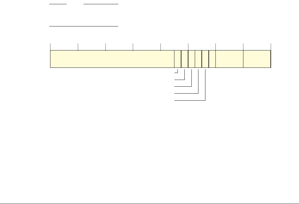
B4 System Control Registers in a VMSA implementation
B4.1 VMSA System control registers descriptions, in register order
ARM DDI 0406C.c Copyright © 1996-1998, 2000, 2004-2012, 2014 ARM. All rights reserved. B4-1561
ID051414 Non-Confidential
B4.1.52 DFSR, Data Fault Status Register, VMSA
The DFSR characteristics are:
Purpose The DFSR holds status information about the last data fault.
This register is part of the PL1 Fault handling registers functional group.
Usage constraints Only accessible from PL1 or higher.
Configurations The Large Physical Address Extension adds an alternative format for the register. If an
implementation includes the Large Physical Address Extension then the current translation
table format determines which format of the register is used.
If the implementation includes the Security Extensions, this register is Banked.
Attributes A 32-bit RW register with an UNKNOWN reset value. See also Reset behavior of CP14 and
CP15 registers on page B3-1450.
Table B3-46 on page B3-1494 shows the encodings of all of the registers in the PL1 Fault
handling registers functional group.
For information about using the DFSR see Exception reporting in a VMSA implementation on page B3-1409.
The following sections describe the alternative DFSR formats:
•DFSR format when using the Short-descriptor translation table format
•DFSR format when using the Long-descriptor translation table format on page B4-1563.
DFSR format when using the Short-descriptor translation table format
In a VMSAv7 implementation that does not include the Large Physical Address Extension, or in an implementation
that includes the Large Physical Address Extension when TTBCR.EAE is 0, indicating that address translation uses
the Short-descriptor translation table format.
Note
In an implementation that includes the Large Physical Address Extension, TTBCR.EAE resets to 0 in both the
Secure and the Non-secure copies of the register.
The DFSR bit assignments are:
Bits[31:14] Reserved, UNK/SBZP.
Reserved, UNK/SBZP
31 14 13 12 11 10 9 8 7 4 3 0
0*(0) Domain FS[3:0]
ExT
WnR
FS[4]
CM†
† Only on an implementation that includes the Large Physical Address Extension.
For more information, see the field description.
LPAE†
* Returned value, but might be overwritten, because the bit is RW.

B4 System Control Registers in a VMSA implementation
B4.1 VMSA System control registers descriptions, in register order
B4-1562 Copyright © 1996-1998, 2000, 2004-2012, 2014 ARM. All rights reserved. ARM DDI 0406C.c
Non-Confidential ID051414
CM, bit[13], if implementation includes the Large Physical Address Extension
Cache maintenance fault. For synchronous faults, this bit indicates whether a cache maintenance
operation generated the fault. The possible values of this bit are:
0 . Abort not caused by a cache maintenance operation.
1 . Abort caused by a cache maintenance operation.
On a asynchronous Data Abort on a translation table walk, this bit is UNKNOWN.
On an asynchronous fault, this bit is UNKNOWN.
Bit[13], if implementation does not include the Large Physical Address Extension
Reserved, UNK/SBZP.
ExT, bit[12] External abort type. This bit can provide an IMPLEMENTATION DEFINED classification of external
aborts.
For aborts other than external aborts this bit always returns 0.
In an implementation that does not provide any classification of external aborts, this bit is
UNK/SBZP.
WnR, bit[11] Write not Read bit. On a synchronous exception, indicates whether the abort was caused by a write
instruction or by a read instruction. The possible values of this bit are:
0 Abort caused by a read instruction.
1 Abort caused by a write instruction.
For synchronous faults on CP15 cache maintenance operations, including the address translation
operations, this bit always returns a value of 1.
This bit is UNKNOWN on:
• An asynchronous Data Abort exception
• A Data Abort exception caused by a debug exception.
FS, bits[10, 3:0]
Fault status bits. For the valid encodings of these bits when using the Short-descriptor translation
table format, see Table B3-23 on page B3-1415. All encodings not shown in the table are reserved.
LPAE, bit[9], if the implementation includes the Large Physical Address Extension
On taking a Data Abort exception, this bit is set to 0 to indicate use of the Short-descriptor
translation table formats.
Hardware does not interpret this bit to determine the behavior of the memory system, and therefore
software can set this bit to 0 or 1 without affecting operation. Unless the register has been updated
to report a fault, a subsequent read of the register returns the value written to it.
Bit[9], if the implementation does not include the Large Physical Address Extension
Reserved, UNK/SBZP.
Bit[8] Reserved, UNK/SBZP.
Domain, bits[7:4]
The domain of the fault address.
ARM deprecates any use of this field, see The Domain field in the DFSR on page B3-1416.
This field is UNKNOWN on a Data Abort exception:
• caused by a debug exception
• caused by a Permission fault in an implementation includes the Large Physical Address
Extension.
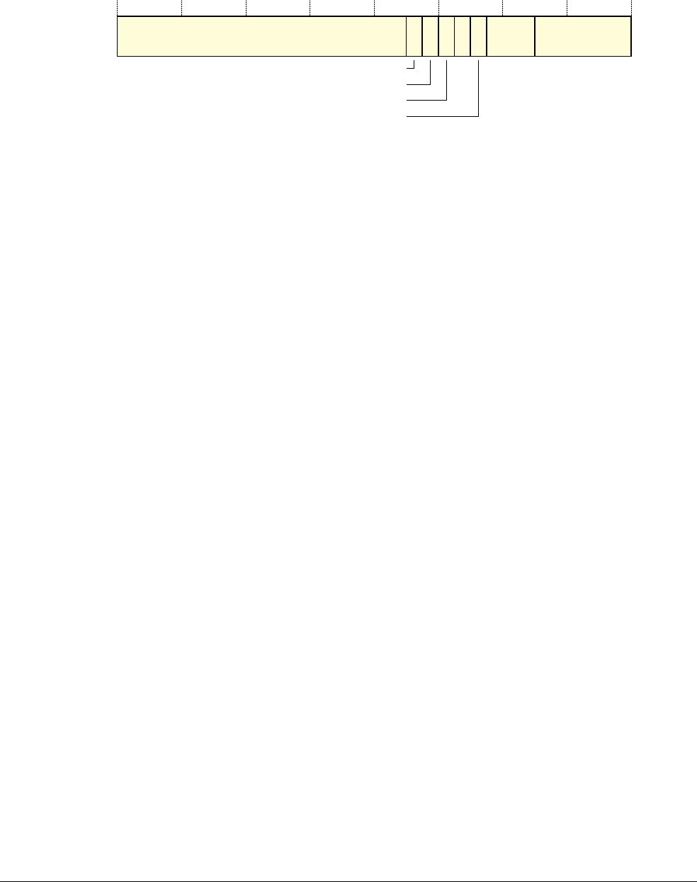
B4 System Control Registers in a VMSA implementation
B4.1 VMSA System control registers descriptions, in register order
ARM DDI 0406C.c Copyright © 1996-1998, 2000, 2004-2012, 2014 ARM. All rights reserved. B4-1563
ID051414 Non-Confidential
DFSR format when using the Long-descriptor translation table format
In a VMSAv7 implementation that includes the Large Physical Address Extension, when TTBCR.EAE is 1, the
DFSR bit assignments are:
Bits[31:14] Reserved, UNK/SBZP.
CM, bit[13] Cache maintenance fault. For synchronous faults, this bit indicates whether a cache maintenance
operation generated the fault. The possible values of this bit are:
0 Abort not caused by a cache maintenance operation.
1 Abort caused by a cache maintenance operation.
On an asynchronous fault, this bit is UNKNOWN.
ExT, bit[12] External abort type. This bit can provide an IMPLEMENTATION DEFINED classification of external
aborts.
For aborts other than external aborts this bit always returns 0.
In an implementation that does not provide any classification of external aborts, this bit is
UNK/SBZP.
WnR, bit[11] Write not Read bit. On a synchronous exception, indicates whether the abort was caused by a write
instruction or by a read instruction. The possible values of this bit are:
0 Abort caused by a read instruction.
1 Abort caused by a write instruction.
For synchronous faults on CP15 cache maintenance operations, including the address translation
operations, this bit always returns a value of 1.
This bit is UNKNOWN on:
• An asynchronous Data Abort exception
• A Data Abort exception caused by a debug exception.
Bit[10] Reserved, UNK/SBZP.
LPAE, bit[9] On taking a Data Abort exception, this bit is set to 1 to indicate use of the Long-descriptor
translation table formats.
Hardware does not interpret this bit to determine the behavior of the memory system, and therefore
software can set this bit to 0 or 1 without affecting operation. Unless the register has been updated
to report a fault, a subsequent read of the register returns the value written to it.
Bits[8:6] Reserved, UNK/SBZP.
STATUS, bits[5:0]
Fault status bits. For the valid encodings of these bits when using the Long-descriptor translation
table format, see Table B3-24 on page B3-1416. All encodings not shown in the table are reserved.
1*
(0)Reserved, UNK/SBZP
31 30 29 28 27 26 25 24 23 22 21 20 19 18 17 16 15 14 13 12 11 10 6 5 0
UNK/
SBZP STATUS
ExT
WnR
CM
98
LPAE
* Returned value, but might be overwritten, because the bit is RW.

B4 System Control Registers in a VMSA implementation
B4.1 VMSA System control registers descriptions, in register order
B4-1564 Copyright © 1996-1998, 2000, 2004-2012, 2014 ARM. All rights reserved. ARM DDI 0406C.c
Non-Confidential ID051414
Accessing the DFSR
To access the DFSR, software reads or writes the CP15 registers with
<opc1>
set to 0,
<CRn>
set to c5,
<CRm>
set to
c0, and
<opc2>
set to 0. For example:
MRC p15, 0, <Rt>, c5, c0, 0 ; Read DFSR into Rt
MCR p15, 0, <Rt>, c5, c0, 0 ; Write Rt to DFSR

B4 System Control Registers in a VMSA implementation
B4.1 VMSA System control registers descriptions, in register order
ARM DDI 0406C.c Copyright © 1996-1998, 2000, 2004-2012, 2014 ARM. All rights reserved. B4-1565
ID051414 Non-Confidential
B4.1.53 DTLBIALL, Data TLB Invalidate All, VMSA only
TLB maintenance operations, not in Hyp mode on page B4-1746 describes this TLB maintenance operation.
This operation is part of the TLB maintenance operations functional group. Table B3-50 on page B3-1497 shows
the encodings of all of the registers and operations in this functional group.
B4.1.54 DTLBIASID, Data TLB Invalidate by ASID, VMSA only
TLB maintenance operations, not in Hyp mode on page B4-1746 describes this TLB maintenance operation.
This operation is part of the TLB maintenance operations functional group. Table B3-50 on page B3-1497 shows
the encodings of all of the registers and operations in this functional group.
B4.1.55 DTLBIMVA, Data TLB Invalidate by MVA, VMSA only
TLB maintenance operations, not in Hyp mode on page B4-1746 describes this TLB maintenance operation.
This operation is part of the TLB maintenance operations functional group. Table B3-50 on page B3-1497 shows
the encodings of all of the registers and operations in this functional group.

B4 System Control Registers in a VMSA implementation
B4.1 VMSA System control registers descriptions, in register order
B4-1566 Copyright © 1996-1998, 2000, 2004-2012, 2014 ARM. All rights reserved. ARM DDI 0406C.c
Non-Confidential ID051414
B4.1.56 FCSEIDR, FCSE Process ID Register, VMSA
The FCSEIDR characteristics are:
Purpose The FCSEIDR identifies the current Process ID (PID) for the Fast Context Switch Extension
(FCSE).
This register is part of the Other system control registers functional group.
Usage constraints Only accessible from PL1 or higher.
Access depends on whether the implementation includes the FCSE, see the Attributes
description.
In an implementation that includes the Security Extensions, software must program the
Non-secure copy of the register with the required initial value, as part of the processor boot
sequence.
Configurations In an implementation that includes the Security Extensions:
• this register is Banked
• if the implementation includes the FCSE, write access to the Secure copy of the
FCSEIDR is disabled when the CP15SDISABLE signal is asserted HIGH.
Attributes A 32-bit register that:
• In an implementation that includes the FCSE, is RW and resets to zero. If the
implementation also includes the Security Extensions, this reset value applies only to
the Secure copy of the register.
• In an implementation that does not include the FCSE, the register is RAZ/WI.
See also Reset behavior of CP14 and CP15 registers on page B3-1450.
Table B3-47 on page B3-1494 shows the encodings of all of the registers in the Other
system control registers functional group.
In an implementation that includes the FCSE, the FCSEIDR bit assignments are:
PID, bits[31:25]
The current Process ID, for the FCSE. If the FCSE is not implemented this field is RAZ/WI.
Bits[24:0] Reserved:
• in an implementation that includes the FCSE, this field is UNK/SBZP
• if the FCSE is not implemented this field is RAZ/WI.
In ARMv7, the FCSE is OPTIONAL and deprecated, but the FCSEIDR must be implemented regardless of whether
the implementation includes the FCSE. Software can access this register to determine whether the implementation
includes the FCSE.
Note
• Changing the PID changes the overall virtual-to-physical address mapping. Because of this, software must
ensure that instructions that might have been speculatively fetched are not affected by the address mapping
change.
• From ARMv6, ARM deprecates any use of the FCSE. The FCSE is:
—OPTIONAL and deprecated in an ARMv7 implementation that does not include the Multiprocessing
Extensions.
— Obsolete from the addition of the Multiprocessing Extensions.
Reserved, UNK/SBZP
31 25 24 0
PID

B4 System Control Registers in a VMSA implementation
B4.1 VMSA System control registers descriptions, in register order
ARM DDI 0406C.c Copyright © 1996-1998, 2000, 2004-2012, 2014 ARM. All rights reserved. B4-1567
ID051414 Non-Confidential
Accessing the FCSEIDR
To access the FCSEIDR, software reads or writes the CP15 registers with
<opc1>
set to 0,
<CRn>
set to c13,
<CRm>
set
to c0, and
<opc2>
set to 0. For example:
MRC p15, 0, <Rt>, c13, c0, 0 ; Read FCSEIDR into Rt
MCR p15, 0, <Rt>, c13, c0, 0 ; Write Rt to FCSEIDR
B4 System Control Registers in a VMSA implementation
B4.1 VMSA System control registers descriptions, in register order
B4-1568 Copyright © 1996-1998, 2000, 2004-2012, 2014 ARM. All rights reserved. ARM DDI 0406C.c
Non-Confidential ID051414
B4.1.57 FPEXC, Floating-Point Exception Control register, VMSA
The FPEXC register characteristics are:
Purpose Provides a global enable for the Advanced SIMD and Floating-point (VFP) Extensions, and
indicates how the state of these extensions is recorded.
Usage constraints Only accessible by software executing at PL1 or higher. See Enabling Advanced SIMD and
floating-point support on page B1-1229 for more information.
Configurations Implemented only if the implementation includes one or both of:
• the Floating-point Extension
• the Advanced SIMD Extension.
In an implementation that includes the Security Extensions, FPEXC is a Configurable
access register. When the settings in the CPACR permit access to the register:
• it is accessible in Non-secure state only if the NSACR.{CP11, CP10} bits are both
set to 1
• if the implementation also includes the Virtualization Extensions then bits in the
HCPTR also control Non-secure access to the register.
For more information, see Access controls on CP0 to CP13 on page B1-1227.
The VFP subarchitecture might define additional bits in the FPEXC, see Additions to the
Floating-Point Exception Register, FPEXC on page D6-2441.
Attributes A 32-bit RW register. See the register field descriptions for information about the reset
value.
Table B1-24 on page B1-1236 shows the encodings of all of the Advanced SIMD and
Floating-point Extension system registers.
The FPEXC bit assignments are:
EX, bit[31] Exception bit. A status bit that specifies how much information must be saved to record the state of
the Advanced SIMD and Floating-point system:
0 The only significant state is the contents of the registers:
• D0 - D15.
• D16 - D31, if implemented.
•FPSCR.
•FPEXC.
A context switch can be performed by saving and restoring the values of these registers.
1 There is additional state that must be handled by any context switch system.
The reset value of this bit is UNKNOWN.
The behavior of the EX bit on writes is SUBARCHITECTURE DEFINED, except that in any
implementation a write of 0 to this bit must be a valid operation, and must return a value of 0 if read
back before any subsequent write to the register.
31 30 29 0
SUBARCHITECTURE
DEFINED
EX
EN

B4 System Control Registers in a VMSA implementation
B4.1 VMSA System control registers descriptions, in register order
ARM DDI 0406C.c Copyright © 1996-1998, 2000, 2004-2012, 2014 ARM. All rights reserved. B4-1569
ID051414 Non-Confidential
EN, bit[30] Enable bit. A global enable for the Advanced SIMD and Floating-point Extensions:
0 The Advanced SIMD and Floating-point Extensions are disabled. For details of how the
system operates when EN == 0 see Enabling Advanced SIMD and floating-point
support on page B1-1229.
1 The Advanced SIMD and Floating-point Extensions are enabled and operate normally.
This bit is always a normal read/write bit. It has a reset value of 0.
Bits[29:0] SUBARCHITECTURE DEFINED. An implementation can use these bits to communicate exception
information between the floating-point hardware and the support code. The subarchitectural
definition of these bits includes their read/write access. This can be defined on a bit by bit basis. This
means that the reset value of these bits is SUBARCHITECTURE DEFINED.
A constraint on these bits is that if EX == 0 it must be possible to save and restore all significant
state for the floating-point system by saving and restoring only the two Advanced SIMD and
Floating-point Extension registers FPSCR and FPEXC.
Accessing the FPEXC register
Software reads or writes the FPEXC register using the
VMRS
and
VMSR
instructions. For more information, see VMRS
on page A8-954 and VMSR on page A8-956. For example:
VMRS <Rt>, FPEXC ; Read Floating-point Exception Control Register
VMSR FPEXC, <Rt> ; Write Floating-point Exception Control Register
Writes to the FPEXC can have side-effects on various aspects of processor operation. All of these side-effects are
synchronous to the FPEXC write. This means they are guaranteed not to be visible to earlier instructions in the
execution stream, and they are guaranteed to be visible to later instructions in the execution stream.
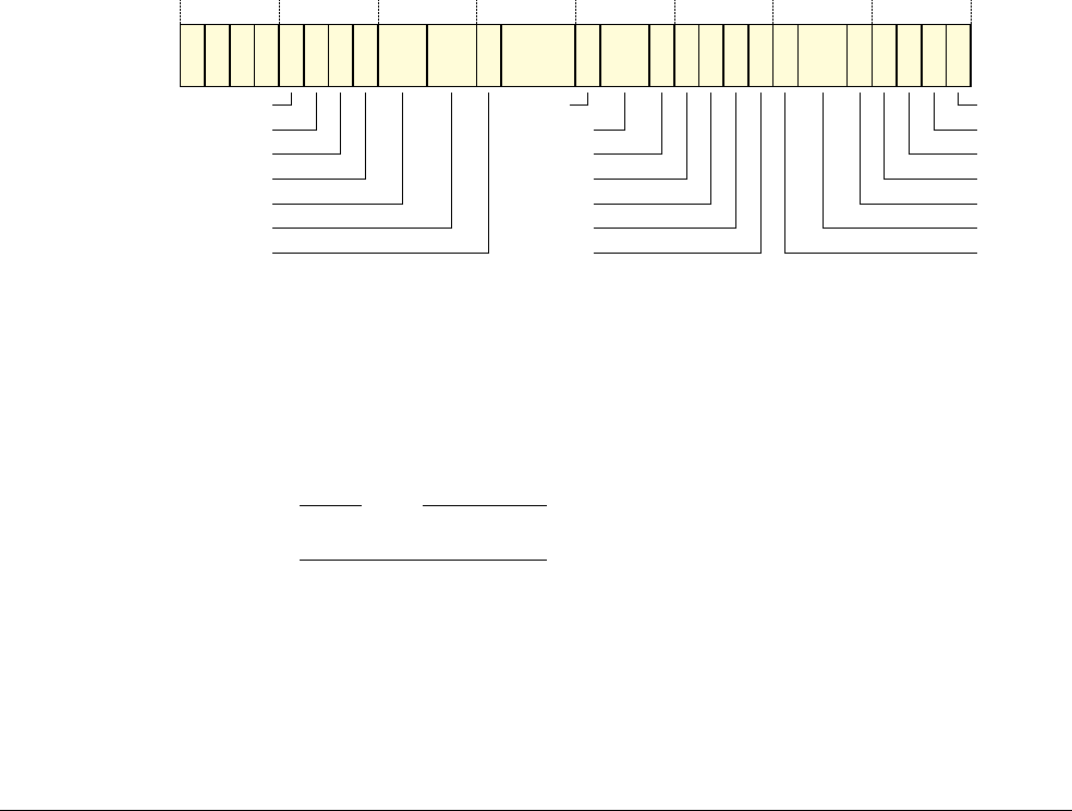
B4 System Control Registers in a VMSA implementation
B4.1 VMSA System control registers descriptions, in register order
B4-1570 Copyright © 1996-1998, 2000, 2004-2012, 2014 ARM. All rights reserved. ARM DDI 0406C.c
Non-Confidential ID051414
B4.1.58 FPSCR, Floating-point Status and Control Register, VMSA
The FPSCR characteristics are:
Purpose Provides floating-point system status information and control.
Usage constraints There are no usage constraints, but see Enabling Advanced SIMD and floating-point
support on page B1-1229 for information about enabling access to this register.
Configurations Implemented only if the implementation includes one or both of:
• the Floating-point Extension
• the Advanced SIMD Extension.
In an implementation that includes the Security Extensions, FPSCR is a Configurable
access register. When the settings in the CPACR permit access to the register:
• it is accessible in Non-secure state only if the NSACR.{CP11, CP10} bits are both
set to 1
• if the implementation also includes the Virtualization Extensions then bits in the
HCPTR also control Non-secure access to the register.
For more information, see Access controls on CP0 to CP13 on page B1-1227.
Attributes A 32-bit RW register. The reset value of the register fields are UNKNOWN except where the
field descriptions indicate otherwise.
Table B1-24 on page B1-1236 shows the encodings of all of the Advanced SIMD and
Floating-point Extension system registers.
The FPSCR bit assignments are:
Bits[31:28] Condition flags. These are updated by floating-point comparison operations, as shown in Effect of
a Floating-point comparison on the condition flags on page A2-80.
N, bit[31] Negative condition flag.
Z, bit[30] Zero condition flag.
C, bit[29] Carry condition flag.
V, bit[28] Overflow condition flag.
Note
Advanced SIMD operations never update these bits.
QC, bit[27] Cumulative saturation bit, Advanced SIMD only. This bit is set to 1 to indicate that an Advanced
SIMD integer operation has saturated since 0 was last written to this bit. For details of saturation,
see Pseudocode details of saturation on page A2-44.
If the implementation does not include the Advanced SIMD Extension, this bit is UNK/SBZP.
(0)(0)
QC
AHP
DN
FZ
RMode
Stride
Reserved
IDE IOC
DZC
OFC
Reserved
UFC
IXC
IXE
UFE
OFE
DZE
IOE IDC
Reserved
N
31 30 29 28 27 26 25 24 23 22 21 20 19 18 16 15 14 13 12 11 10 9 8 7 6 5 4 3 2 1 0
Z C V (0) Len (0) (0)
See the field descriptions for implementation differences in different VFP versions

B4 System Control Registers in a VMSA implementation
B4.1 VMSA System control registers descriptions, in register order
ARM DDI 0406C.c Copyright © 1996-1998, 2000, 2004-2012, 2014 ARM. All rights reserved. B4-1571
ID051414 Non-Confidential
AHP, bit[26] Alternative half-precision control bit:
0 IEEE half-precision format selected.
1 Alternative half-precision format selected.
For more information see Advanced SIMD and Floating-point half-precision formats on
page A2-66.
If the implementation does not include the Half-precision Extension, this bit is UNK/SBZP.
DN, bit[25] Default NaN mode control bit:
0 NaN operands propagate through to the output of a floating-point operation.
1 Any operation involving one or more NaNs returns the Default NaN.
For more information, see NaN handling and the Default NaN on page A2-69.
The value of this bit only controls Floating-point arithmetic. Advanced SIMD arithmetic always
uses the Default NaN setting, regardless of the value of the DN bit.
FZ, bit[24] Flush-to-zero mode control bit:
0 Flush-to-zero mode disabled. Behavior of the floating-point system is fully compliant
with the IEEE 754 standard.
1 Flush-to-zero mode enabled.
For more information, see Flush-to-zero on page A2-68.
The value of this bit only controls Floating-point arithmetic. Advanced SIMD arithmetic always
uses the Flush-to-zero setting, regardless of the value of the FZ bit.
RMode, bits[23:22]
Rounding Mode control field. The encoding of this field is:
0b00
Round to Nearest (RN) mode
0b01
Round towards Plus Infinity (RP) mode
0b10
Round towards Minus Infinity (RM) mode
0b11
Round towards Zero (RZ) mode.
The specified rounding mode is used by almost all floating-point instructions that are part of the
Floating-point Extension. Advanced SIMD arithmetic always uses the Round to Nearest setting,
regardless of the value of the RMode bits.
Note
The rounding mode names are based on the IEEE 754-1985 terminology. See Floating-point
standards, and terminology on page A2-55 for the corresponding terms in the IEEE 754-2008
revision of the standard.
Stride, bits[21:20] and Len, bits[18:16]
ARM deprecates use of nonzero values of these fields. For details of their use in previous versions
of the ARM architecture see Appendix D11 VFP Vector Operation Support.
The values of these fields are ignored by the Advanced SIMD Extension.
Bits[19, 14:13, 6:5]
Reserved, UNK/SBZP.
Bits[15, 12:8] Floating-point exception trap enable bits. These bits are supported only in VFPv2, VFPv3U, and
VFPv4U. They are reserved, RAZ/WI, on a system that implements VFPv3 or VFPv4.
The possible values of each bit are:
0 Untrapped exception handling selected. If the floating-point exception occurs then the
corresponding cumulative exception bit is set to 1.
1 Trapped exception handling selected. If the floating-point exception occurs, hardware
does not update the corresponding cumulative exception bit. The trap-handling software
can decide whether to set the cumulative exception bit to 1.

B4 System Control Registers in a VMSA implementation
B4.1 VMSA System control registers descriptions, in register order
B4-1572 Copyright © 1996-1998, 2000, 2004-2012, 2014 ARM. All rights reserved. ARM DDI 0406C.c
Non-Confidential ID051414
The values of these bits control only Floating-point arithmetic. Advanced SIMD arithmetic always
uses untrapped exception handling, regardless of the values of these bits.
For more information, see Floating-point exceptions on page A2-70.
The floating-point trap enable bits are:
IDE, bit[15] Input Denormal exception trap enable.
Note
Denormal corresponds to the term denormalized number in the
IEEE 754-1985 standard. Floating-point standards, and terminology on
page A2-55 describes the terminology changes in the IEEE 754-2008
revision of the standard.
IXE, bit[12] Inexact exception trap enable.
UFE, bit[11] Underflow exception trap enable.
OFE, bit[10] Overflow exception trap enable.
DZE, bit[9] Division by Zero exception trap enable.
IOE, bit[8] Invalid Operation exception trap enable.
Bits[7, 4:0] Cumulative exception bits for floating-point exceptions. Each of these bits is set to 1 to indicate that
the corresponding exception has occurred since 0 was last written to it. How floating-point
instructions update these bits depends on the value of the corresponding exception trap enable bits,
see the description of bits[15, 12:8].
Advanced SIMD instructions set each cumulative exception bit if the corresponding exception
occurs in one or more of the floating-point calculations performed by the instruction, regardless of
the setting of the trap enable bits.
For more information, see Floating-point exceptions on page A2-70.
IDC, bit[7] Input Denormal cumulative exception bit. Updated by hardware only when
IDE, bit[15], is set to 0.
IXC, bit[4] Inexact cumulative exception bit. Updated by hardware only when IXE,
bit[12], is set to 0.
UFC, bit[3] Underflow cumulative exception bit. Updated by hardware only when UFE,
bit[11], is set to 0.
OFC, bit[2] Overflow cumulative exception bit. Updated by hardware only when OFE,
bit[10], is set to 0.
DZC, bit[1] Division by Zero cumulative exception bit. Updated by hardware only when
DZE, bit[9], is set to 0.
IOC, bit[0] Invalid Operation cumulative exception bit. Updated by hardware only
when IOE, bit[8], is set to 0.
If the implementation includes the integer-only Advanced SIMD Extension and does not include the Floating-point
Extension, all of these bits except QC are UNK/SBZP.
Writes to the FPSCR can have side-effects on various aspects of processor operation. All of these side-effects are
synchronous to the FPSCR write. This means they are guaranteed not to be visible to earlier instructions in the
execution stream, and they are guaranteed to be visible to later instructions in the execution stream.
Accessing the FPSCR
Software reads or writes the FPSCR, or transfers the FPSCR.{N, Z, C, V} flags to the APSR, using the
VMRS
and
VMSR
instructions. For more information, see VMRS on page A8-954 and VMSR on page A8-956. For example:
VMRS <Rt>, FPSCR ; Read Floating-point System Control Register
VMSR FPSCR, <Rt> ; Write Floating-point System Control Register
VMRS APSR_nzcv, FPSCR ; Write FPSCR.{N, Z, C, V} flags to APSR.{N, Z, C, V}
B4 System Control Registers in a VMSA implementation
B4.1 VMSA System control registers descriptions, in register order
ARM DDI 0406C.c Copyright © 1996-1998, 2000, 2004-2012, 2014 ARM. All rights reserved. B4-1573
ID051414 Non-Confidential
B4.1.59 FPSID, Floating-point System ID Register, VMSA
The FPSID register characteristics are:
Purpose Provides top-level information about the floating-point implementation.
Usage constraints Only accessible from PL1 or higher. See Enabling Advanced SIMD and floating-point
support on page B1-1229 for more information.
This register complements the information provided by the CPUID scheme described in
Chapter B7 The CPUID Identification Scheme.
Configurations FPSID can be implemented in a system that provides only software emulation of the ARM
floating-point instructions, and must be implemented if the implementation includes one or
both of:
• the Floating-point Extension
• the Advanced SIMD Extension.
The VMSA and PMSA definitions of the register fields are identical.
In an implementation that includes the Security Extensions, FPSID is a Configurable access
register. When the settings in the CPACR permit access to the register:
• it is accessible in Non-secure state only if the NSACR.{CP11, CP10} bits are both
set to 1
• if the implementation also includes the Virtualization Extensions then bits in the
HCPTR also control Non-secure access to the register.
For more information, see Access controls on CP0 to CP13 on page B1-1227.
Attributes A 32-bit RO register.
Note
Although the FPSID is a RO register, a write using the FPSID encoding is a valid serializing
operation, see Asynchronous bounces, serialization, and Floating-point exception barriers
on page B1-1238. Such a write does not access the register.
Table B1-24 on page B1-1236 shows the encodings of all of the Advanced SIMD and
Floating-point Extension system registers.
In ARMv7, the FPSID bit assignments are:
Implementer, bits[31:24]
Implementer codes are the same as those used for the MIDR.
For an implementation by ARM this field is
0x41
, the ASCII code for A.
SW, bit[23] Software bit. This bit indicates whether a system provides only software emulation of the
floating-point instructions that are provided by the Floating-point Extension:
0 The system includes hardware support for the floating-point instructions provided by
the Floating-point Extension.
1 The system provides only software emulation of the floating-point instructions provided
by the Floating-point Extension.
Implementer
31 24 23 22 16 15 8 7 4 3 0
Subarchitecture Part number Variant Revision
SW

B4 System Control Registers in a VMSA implementation
B4.1 VMSA System control registers descriptions, in register order
B4-1574 Copyright © 1996-1998, 2000, 2004-2012, 2014 ARM. All rights reserved. ARM DDI 0406C.c
Non-Confidential ID051414
Subarchitecture, bits[22:16]
Subarchitecture version number. For an implementation by ARM, permitted values are:
0b0000000
VFPv1 architecture with an IMPLEMENTATION DEFINED subarchitecture.
Not permitted in an ARMv7 implementation.
0b0000001
VFPv2 architecture with Common VFP subarchitecture v1.
Not permitted in an ARMv7 implementation.
0b0000010
VFPv3 architecture, or later, with Common VFP subarchitecture v2. The VFP
architecture version is indicated by the MVFR0 and MVFR1 registers.
0b0000011
VFPv3 architecture, or later, with no subarchitecture. The entire floating-point
implementation is in hardware, and no software support code is required. The VFP
architecture version is indicated by the MVFR0 and MVFR1 registers.
This value can be used only by an implementation that does not support the trap enable
bits in the FPSCR.
0b0000100
VFPv3 architecture, or later, with Common VFP subarchitecture v3. The VFP
architecture version is indicated by the MVFR0 and MVFR1 registers.
For a subarchitecture designed by ARM the most significant bit of this field, register bit[22], is 0.
Values with a most significant bit of 0 that are not listed here are reserved.
When the subarchitecture designer is not ARM, the most significant bit of this field, register bit[22],
must be 1. Each implementer must maintain its own list of subarchitectures it has designed, starting
at subarchitecture version number
0x40
.
Part number, bits[15:8]
An IMPLEMENTATION DEFINED part number for the floating-point implementation, assigned by the
implementer.
Variant, bits[7:4]
An IMPLEMENTATION DEFINED variant number. Typically, this field distinguishes between different
production variants of a single product.
Revision, bits[3:0]
An IMPLEMENTATION DEFINED revision number for the floating-point implementation.
Accessing the FPSID register
Software accesses the FPSID register using the
VMRS
instruction, see VMRS on page B9-2014. For example:
VMRS <Rt>, FPSID ; Read FPSID into Rt

B4 System Control Registers in a VMSA implementation
B4.1 VMSA System control registers descriptions, in register order
ARM DDI 0406C.c Copyright © 1996-1998, 2000, 2004-2012, 2014 ARM. All rights reserved. B4-1575
ID051414 Non-Confidential
B4.1.60 HACR, Hyp Auxiliary Configuration Register, Virtualization Extensions
The HACR characteristics are:
Purpose The HACR controls the trapping to Hyp mode of IMPLEMENTATION DEFINED aspects of
Non-secure PL1 or PL0 operation.
This register is part of the Virtualization Extensions registers functional group.
Usage constraints Only accessible from Hyp mode, or from Monitor mode when SCR.NS is set to 1, see
PL2-mode system control registers on page B3-1454.
Configurations Implemented only as part of the Virtualization Extensions.
This is Banked PL2-mode register, see Banked PL2-mode CP15 read/write registers on
page B3-1454.
Attributes A 32-bit RW register with an IMPLEMENTATION DEFINED reset value. See also Reset
behavior of CP14 and CP15 registers on page B3-1450.
Table B3-55 on page B3-1501 shows the encoding of all of the Virtualization Extensions
registers.
The HACR bit assignments are IMPLEMENTATION DEFINED.
Accessing the HACR
To access the HACR, software reads or writes the CP15 registers with
<opc1>
set to 4,
<CRn>
set to c1,
<CRm>
set to
c1, and
<opc2>
set to 7. For example:
MRC p15, 4, <Rt>, c1, c1, 7 ; Read HACR into Rt
MCR p15, 4, <Rt>, c1, c1, 7 ; Write Rt to HACR
B4.1.61 HACTLR, Hyp Auxiliary Control Register, Virtualization Extensions
The HACTLR characteristics are:
Purpose The HACTLR controls IMPLEMENTATION DEFINED features of Hyp mode operation.
This register is part of the Virtualization Extensions registers functional group.
Usage constraints Only accessible from Hyp mode, or from Monitor mode when SCR.NS is set to 1, see
PL2-mode system control registers on page B3-1454.
Configurations Implemented only as part of the Virtualization Extensions.
This is PL2-mode register, see Banked PL2-mode CP15 read/write registers on
page B3-1454.
Attributes A 32-bit RW register with an IMPLEMENTATION DEFINED reset value. See also Reset
behavior of CP14 and CP15 registers on page B3-1450.
Table B3-55 on page B3-1501 shows the encoding of all of the Virtualization Extensions
registers.
The HACTLR bit assignments are IMPLEMENTATION DEFINED.
Accessing the HACTLR
To access the HACTLR, software reads or writes the CP15 registers with
<opc1>
set to 4,
<CRn>
set to c1,
<CRm>
set
to c0, and
<opc2>
set to 1. For example:
MRC p15, 4, <Rt>, c1, c0, 1 ; Read HACTLR into Rt
MCR p15, 4, <Rt>, c1, c0, 1 ; Write Rt to HACTLR

B4 System Control Registers in a VMSA implementation
B4.1 VMSA System control registers descriptions, in register order
B4-1576 Copyright © 1996-1998, 2000, 2004-2012, 2014 ARM. All rights reserved. ARM DDI 0406C.c
Non-Confidential ID051414
B4.1.62 HADFSR and HAIFSR, Hyp Auxiliary Fault Syndrome Registers, Virtualization Extensions
The Hyp Auxiliary Data Fault Syndrome Register, HADFSR, and Hyp Auxiliary Instruction Fault Syndrome
Register, HAIFSR, characteristics are:
Purpose The HAxFSR contain additional IMPLEMENTATION DEFINED syndrome information for:
• Data Abort exceptions taken to Hyp mode, for the HADFSR
• Prefetch Abort exceptions taken to Hyp mode, for the HAIFSR.
These registers are part of the Virtualization Extensions registers functional group.
Usage constraints Only accessible from Hyp mode, or from Monitor mode when SCR.NS is set to 1, see
PL2-mode system control registers on page B3-1454.
Configurations Implemented only as part of the Virtualization Extensions. These are optional registers. An
implementation that does not require one or both of these registers can implement the
registers that are not required as UNK/SBZP.
These are Banked PL2-mode register, see Banked PL2-mode CP15 read/write registers on
page B3-1454.
Attributes 32-bit RW registers with UNKNOWN reset values. See also Reset behavior of CP14 and CP15
registers on page B3-1450.
Table B3-55 on page B3-1501 shows the encoding of all of the Virtualization Extensions
registers.
The HADFSR and HAIFSR bit assignments are IMPLEMENTATION DEFINED.
Accessing the HADFSR and HAIFSR
To access the HADFSR or HAIFSR, software reads or writes the CP15 registers with
<opc1>
set to 4,
<CRn>
set to
c5,
<CRm>
set to c1, and
<opc2>
set to 0 for the HADFSR, or to 1 for the HAIFSR. For example:
MRC p15, 4, <Rt>, c5, c1, 0 ; Read HADFSR into Rt
MCR p15, 4, <Rt>, c5, c1, 0 ; Write Rt to HADFSR
MRC p15, 4, <Rt>, c5, c1, 1 ; Read HAIFSR into Rt
MCR p15, 4, <Rt>, c5, c1, 1 ; Write Rt to HAIFSR

B4 System Control Registers in a VMSA implementation
B4.1 VMSA System control registers descriptions, in register order
ARM DDI 0406C.c Copyright © 1996-1998, 2000, 2004-2012, 2014 ARM. All rights reserved. B4-1577
ID051414 Non-Confidential
B4.1.63 HAMAIR0 and HAMAIR1, Hyp Auxiliary Memory Attribute Indirection Registers 0 and 1
The HAMAIR0 and HAMAIR1 characteristics are
Purpose The HAMAIR0 and HAMAIR1 registers provide IMPLEMENTATION DEFINED memory
attributes for the memory attribute encodings defined by the HMAIR0 and HMAIR1
registers.
These IMPLEMENTATION DEFINED attributes can only provide additional qualifiers for the
memory attribute encodings, and cannot change the memory attributes defined in the
HMAIR0 and HMAIR1 registers.
These registers are part of the Virtualization Extensions registers functional group.
Usage constraints Only accessible from Hyp mode, or from Monitor mode when SCR.NS is set to 1, see
PL2-mode system control registers on page B3-1454.
If an implementation does not provide any IMPLEMENTATION DEFINED memory attributes
these registers are UNK/SBZP.
Configurations Implemented only as part of the Virtualization Extensions.
These are Banked PL2-mode registers, see Banked PL2-mode CP15 read/write registers on
page B3-1454.
Attributes 32-bit RW registers with an UNKNOWN reset values. See also Reset behavior of CP14 and
CP15 registers on page B3-1450.
Table B3-55 on page B3-1501 shows the encoding of all of the Virtualization Extensions
registers.
The HAMAIRn registers bit assignments are IMPLEMENTATION DEFINED.
Note
Although all aspects of the HAMAIRn register bit assignments are IMPLEMENTATION DEFINED, a likely usage model
is that the two HAMAIRn registers provide eight 8-bit fields, indexed by the AttrIndx[2:0] value from the
translation table descriptor, as described for the HMAIR registers.
Accessing the HAMAIR0 or HAMAIR1
To access the HAMAIR0 or HAMAIR1, software reads or writes the CP15 registers with
<opc1>
set to 4,
<CRn>
set
to c10,
<CRm>
set to c3, and
<opc2>
set to 0 for HAMAIR0, or to 1 for HAMAIR1. For example:
MRC p15, 4, <Rt>, c10, c3, 0 ; Read HAMAIR0 into Rt
MCR p15, 4, <Rt>, c10, c3, 1 ; Write Rt to HAMAIR1
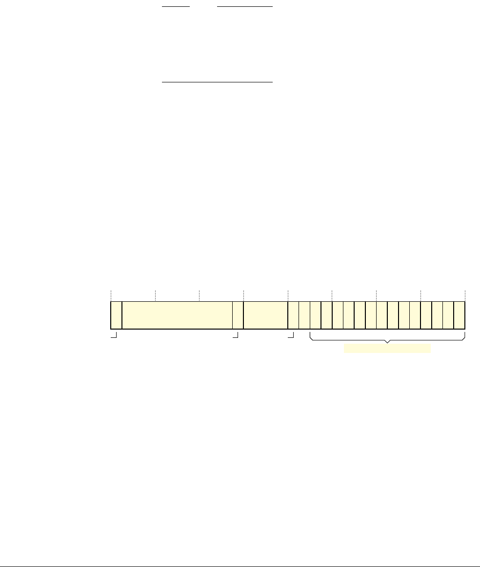
B4 System Control Registers in a VMSA implementation
B4.1 VMSA System control registers descriptions, in register order
B4-1578 Copyright © 1996-1998, 2000, 2004-2012, 2014 ARM. All rights reserved. ARM DDI 0406C.c
Non-Confidential ID051414
B4.1.64 HCPTR, Hyp Coprocessor Trap Register, Virtualization Extensions
The HCPTR characteristics are:
Purpose The HCPTR controls the trapping to Hyp mode of Non-secure accesses, at PL1 or lower, to
coprocessors other than CP14 and CP15, and to floating-point and Advanced SIMD
functionality. It also controls the access to coprocessors other than CP14 and CP15, and to
floating-point and Advanced SIMD functionality, from Hyp mode.
Note
Accesses to coprocessors other than CP14 and CP15, and to floating-point and Advanced
SIMD functionality, from Hyp mode:
• Are not affected by settings in the CPACR.
• Are affected by settings in the NSACR, and the NSACR settings take precedence
over the HCPTR settings. See the Usage Constraints for more information.
This register is part of the Virtualization Extensions registers functional group.
Usage constraints Only accessible from Hyp mode, or from Monitor mode when SCR.NS is set to 1, see
PL2-mode system control registers on page B3-1454.
If a bit in the NSACR prohibits a Non-secure access, then the corresponding bit in the
HCPTR behaves as RAO/WI for Non-secure accesses. See the bit descriptions for more
information.
Configurations Implemented only as part of the Virtualization Extensions.
This is Banked PL2-mode register, see Banked PL2-mode CP15 read/write registers on
page B3-1454.
Attributes A 32-bit RW register that resets to zero. See also Reset behavior of CP14 and CP15 registers
on page B3-1450.
Table B3-55 on page B3-1501 shows the encoding of all of the Virtualization Extensions
registers.
The HCPTR bit assignments are:
In the descriptions of the HCPTR fields, an otherwise-valid Non-secure access means an access that, if the bit was
set to 0, would not be UNDEFINED or UNPREDICTABLE.
For more information about all of these bits see Trapping accesses to coprocessors on page B1-1257.
For more information about control of access to functionality provided by the Advanced SIMD and Floating-point
Extensions, see Enabling Advanced SIMD and floating-point support on page B1-1229.
TCPAC, bit[31]
Trap CPACR accesses. The possible values of this bit are:
0 Has no effect on accesses to the CPACR.
1 Any access to the CPACR from a Non-secure PL1 mode generates an exception that is
taken to Hyp mode. For more information, see Trapping CPACR accesses on
page B1-1258.
Bits[30:21] Reserved, UNK/SBZP.
TCP13 to TCP0, see text
TASE
TCPAC
31 30 21 20 19 16 15 14 13 12 11 10 9 8 7 6 5 4 3 2 1 0
Reserved, UNK/SBZP Reserved,
UNK/SBZP (0)
TTA

B4 System Control Registers in a VMSA implementation
B4.1 VMSA System control registers descriptions, in register order
ARM DDI 0406C.c Copyright © 1996-1998, 2000, 2004-2012, 2014 ARM. All rights reserved. B4-1579
ID051414 Non-Confidential
TTA, bit[20] Trap Trace Access. The possible values of this bit are:
0 Has no effect on accesses to the CP14 trace registers from Non-secure PL1 and PL2
modes.
1 Any otherwise-valid access to the CP14 trace registers from a Non-secure PL1 mode
generates an exception that is taken to Hyp mode. For more information see Trapping
CP14 accesses to trace registers on page B1-1261.
Any access to the CP14 trace registers from Non-secure Hyp mode is UNDEFINED.
Note
The NSACR.NSTRCDIS bit can make this bit behave as RAO/WI, regardless of its actual value.
In an implementation that does not include a trace macrocell, or does not include a CP14 interface
to the trace macrocell registers, it is IMPLEMENTATION DEFINED whether this bit:
• Is RAO/WI.
•Is RAZ/WI.
• Can be written from Hyp mode, and from Secure Monitor mode when the value of SCR.NS
is 1.
Bits[19:16] Reserved, UNK/SBZP.
TASE, bit[15] Trap Advanced SIMD Extension use. The possible values of this bit are:
0 Has no effect on accesses to Advanced SIMD functionality from Non-secure PL2, PL1
and PL0 modes.
1 Any otherwise-valid access to Advanced SIMD functionality from a Non-secure PL1 or
PL0 mode generates an exception that is taken to Hyp mode. For more information, see
Trapping of Advanced SIMD functionality on page B1-1257.
Any access to Advanced SIMD functionality from Hyp mode is UNDEFINED. This means
that any instruction encoding that Alphabetical list of instructions on page A8-300
identifies as being an Advanced SIMD instruction but does not also identify as being a
VFPv3 or VFPv4 instruction, is UNDEFINED if executed in Hyp mode.
Note
• If TCP10 and TCP11 are set to 1 then all otherwise-valid Advanced SIMD use by Non-secure
PL1 and PL0 modes is trapped to Hyp mode, regardless of the value of this field.
• The NSACR.NSASEDIS bit can make this bit behave as RAO/WI, regardless of its actual
value.
For more information, see Summary of access controls for Advanced SIMD functionality on
page B1-1233.
On an implementation that:
• Implements the Floating-point Extension but does not implement the Advanced SIMD
Extension, this bit is RAO/WI.
• Does not implement the Floating-point Extension or the Advanced SIMD Extension, this bit
is RAO/WI.
• Implements both the Floating-point Extension and the Advanced SIMD Extension, it is
IMPLEMENTATION DEFINED whether this bit is supported. If it is not supported, it is RAZ/WI.
Bit[14] Reserved, UNK/SBZP.

B4 System Control Registers in a VMSA implementation
B4.1 VMSA System control registers descriptions, in register order
B4-1580 Copyright © 1996-1998, 2000, 2004-2012, 2014 ARM. All rights reserved. ARM DDI 0406C.c
Non-Confidential ID051414
TCPn, bit[n], for values of n from 0 to 13
Trap coprocessor n (CPn). For each bit, the possible values are:
0 Has no effect on accesses to coprocessor CPn from Non-secure PL2, PL1 and PL0
modes.
1 Any otherwise-valid Non-secure access to CPn generates an exception that is taken to
Hyp mode. For more information, see General trapping of coprocessor accesses on
page B1-1258.
Any access to the coprocessor from Hyp mode is UNDEFINED.
For more information, see Summary of general controls of CP10 and CP11 functionality on
page B1-1231.
Note
Each NSACR.cpn bit can make the corresponding HCPTR.TCPn bit behave as RAO/WI, regardless
of its actual value.
For values of n that correspond to coprocessors that are not implemented, it is IMPLEMENTATION
DEFINED whether TCPn:
• is RAO/WI
• can be written by software that has write access to HCPTR.
Coprocessors 8, 9, 12, and 13 are reserved for possible use by ARM, and therefore are never
implemented.
If a set of functionality requires the use of more than one coprocessor, then setting the TCPn bits
corresponding to those coprocessors to different values can cause UNPREDICTABLE behavior. For
example, since CP10 and CP11 provide the Floating-point Extension and Advanced SIMD
Extension functionality, TCP10 and TCP11 must be set to the same value.
Accessing the HCPTR
To access the HCPTR, software reads or writes the CP15 registers with
<opc1>
set to 4,
<CRn>
set to c1,
<CRm>
set to
c1, and
<opc2>
set to 2. For example:
MRC p15, 4, <Rt>, c1, c1, 2 ; Read HCPTR into Rt
MCR p15, 4, <Rt>, c1, c1, 2 ; Write Rt to HCPTR
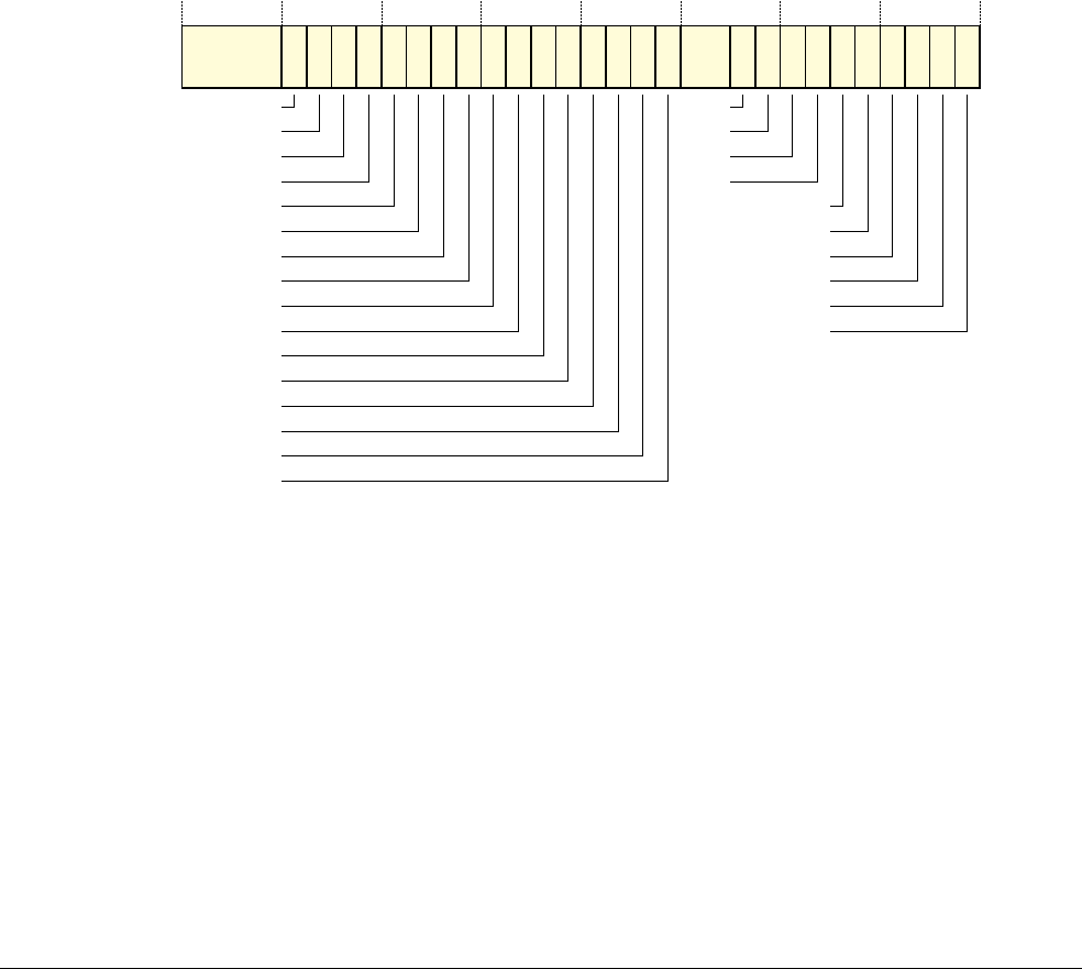
B4 System Control Registers in a VMSA implementation
B4.1 VMSA System control registers descriptions, in register order
ARM DDI 0406C.c Copyright © 1996-1998, 2000, 2004-2012, 2014 ARM. All rights reserved. B4-1581
ID051414 Non-Confidential
B4.1.65 HCR, Hyp Configuration Register, Virtualization Extensions
The HCR characteristics are:
Purpose The HCR provides configuration controls for virtualization, including defining whether
various Non-secure operations are trapped to Hyp mode.
This register is part of the Virtualization Extensions registers functional group.
Usage constraints Only accessible from Hyp mode, or from Monitor mode when SCR.NS is set to 1, see
PL2-mode system control registers on page B3-1454.
Configurations Implemented only as part of the Virtualization Extensions.
This is Banked PL2-mode register, see Banked PL2-mode CP15 read/write registers on
page B3-1454.
Attributes A 32-bit RW register that resets to zero. See also Reset behavior of CP14 and CP15 registers
on page B3-1450.
Table B3-55 on page B3-1501 shows the encoding of all of the Virtualization Extensions
registers.
The HCR bit assignments are:
In the descriptions of the HCR fields:
• Descriptions of bits describe the effect of setting the bit to 1. If the bit is set to 0 it has no effect on the
operation of the processor.
•A valid Non-secure PL1 or PL0 access means an access from a Non-secure PL1 or PL0 mode that, if the bit
was set to 0, would not be UNDEFINED or UNPREDICTABLE.
Bits[31:28] Reserved, UNK/SBZP.
TGE, bit[27] Trap general exceptions. When this bit is set to 1, and the processor is executing at PL0 in
Non-secure state, Undefined Instruction exceptions, Supervisor Call exceptions, synchronous
External aborts, and some Alignment faults, are taken to Hyp mode. For more information see
Routing general exceptions to Hyp mode on page B1-1192.
TVM, bit[26] Trap virtual memory controls. When this bit is set to 1, any valid Non-secure PL1 or PL0 write to a
virtual memory control register is trapped to Hyp mode. For more information see Trapping writes
to virtual memory control registers on page B1-1258.
Reserved,
UNK/SBZP
31 28 27 26 25 24 23 22 21 20 19 18 17 16 15 14 13 12 11 10 9 8 7 6 5 4 3 2 1 0
BSU
TGE
TVM
TTLB
TPU
TPC
TSW
TAC
TIDCP
TSC
TID3
TID2
TID1
TID0
TWE
TWI
DC
FB
VA
VI
VF
AMO
IMO
FMO
PTW
SWIO
VM

B4 System Control Registers in a VMSA implementation
B4.1 VMSA System control registers descriptions, in register order
B4-1582 Copyright © 1996-1998, 2000, 2004-2012, 2014 ARM. All rights reserved. ARM DDI 0406C.c
Non-Confidential ID051414
TTLB, bit[25] Trap TLB maintenance operations. When this bit is set to 1, any valid Non-secure PL1 or PL0 access
to a TLB maintenance operation is trapped to Hyp mode. For more information see Trapping
accesses to TLB maintenance operations on page B1-1254.
TPU, bit[24] Trap cache maintenance to point of unification operations. When this bit is set to 1, any valid
Non-secure PL1 or PL0 access to a cache maintenance operation that operates to the point of
unification is trapped to Hyp mode. For more information see Trapping accesses to cache
maintenance operations on page B1-1254.
TPC, bit[23] Trap cache maintenance to point of coherency operations. When this bit is set to 1, any valid
Non-secure PL1 or PL0 access to a cache maintenance operation that operates to the point of
coherency is trapped to Hyp mode. For more information see Trapping accesses to cache
maintenance operations on page B1-1254.…
TSW, bit[22] Trap set/way cache maintenance operations. When this bit is set to 1, any valid Non-secure PL1 or
PL0 access to a cache maintenance operation that operates by set/way is trapped to Hyp mode. For
more information see Trapping accesses to cache maintenance operations on page B1-1254.
TAC, bit[21] Trap ACTLR accesses. When this bit is set to 1, any valid Non-secure PL1 or PL0 access to the
ACTLR is trapped to Hyp mode. For more information see Trapping accesses to the Auxiliary
Control Register on page B1-1254.
TIDCP, bit[20]
Trap lockdown. When this bit is set to 1, any valid Non-secure PL1 or PL0 access to a CP15
lockdown, DMA, or TCM operation, is trapped to Hyp mode. For more information, including the
handling of Non-secure accesses at PL0, see Trapping accesses to lockdown, DMA, and TCM
operations on page B1-1253.
TSC, bit[19] Trap
SMC
instruction.When this bit is set to 1, attempts to execute
SMC
instructions in Non-secure PL1
modes are trapped to Hyp mode. For more information, including the interaction with the SCR.SCD
bit, see Trapping use of the SMC instruction on page B1-1255.
TIDn, for values of n from 3 to 0, bits[18:15]
Trap ID register groups. When one of these bits is set to 1, any valid Non-secure read of a register
in the corresponding group is trapped to Hyp mode. For more information, including the registers
in each group, see Trapping ID mechanisms on page B1-1251.
TID3 is bit[18], TID2 is bit[17], TID1 is bit[16], and TID0 is bit[15].
TWE, bit[14] Trap
WFE
instruction. When this bit is set to 1, any attempt, from a Non-secure PL1or PL0 mode, to
execute an
WFE
instruction that might otherwise cause the processor to suspend execution is trapped
to Hyp mode. For more information see Trapping use of the WFI and WFE instructions on
page B1-1256.
TW1, bit[13] Trap
WFI
instruction. When this bit is set to 1, any attempt, from a Non-secure PL1 or PL0 mode, to
execute an
WFI
instruction that might otherwise cause the processor to suspend execution is trapped
to Hyp mode. For more information see Trapping use of the WFI and WFE instructions on
page B1-1256
DC, bit[12] Default cacheable. When the Non-secure PL1&0 stage 1 MMU is disabled, this bit affects the
memory type and attributes determined by a Non-secure PL1&0 stage 1 translation. For more
information see VMSA behavior when a stage 1 MMU is disabled on page B3-1314.
BSU, bits[11:10]
Barrier shareability upgrade. When this field is nonzero, it upgrades the required shareability of
DMB
and
DSB
barrier instructions executed in a Non-secure PL1 or PL0 mode, beyond the effect specified
in the instruction. For more information, including the encoding of this field, see Shareability and
access limitations on the data barrier operations on page A3-153.

B4 System Control Registers in a VMSA implementation
B4.1 VMSA System control registers descriptions, in register order
ARM DDI 0406C.c Copyright © 1996-1998, 2000, 2004-2012, 2014 ARM. All rights reserved. B4-1583
ID051414 Non-Confidential
FB, bit[9] Force broadcast. When this bit is set to 1, TLB maintenance operations, branch predictor invalidate
all operations, and instruction cache invalidate all operations performed in Non-secure PL1 modes,
are broadcast across the Inner Shareable domain. For more information see Virtualization
Extensions upgrading of maintenance operations on page B2-1286 and Virtualization Extensions
upgrading of TLB maintenance operations on page B3-1391.
Virtual asynchronous exception bits, bits[8:6]
Subject to other controls, when one of these bits is set to 1 the corresponding virtual asynchronous
exception is generated when the processor is executing in Non-secure state at PL1 or PL0. For more
information see Virtual exceptions in the Virtualization Extensions on page B1-1197.
The virtual asynchronous exception bits are:
VA, bit[8] Virtual asynchronous abort.
VI, bit[7] Virtual IRQ.
VF, bit[6] Virtual FIQ.
Mask override bits, bits[5:3]
Setting one of these bits to 1 can modify the effect of the corresponding CPSR exception mask bit
when the processor is in Non-secure state. For more information see Asynchronous exception
masking on page B1-1184.
The mask override bits are:
AMO, bit[5] Overrides the CPSR.A bit, and enables signaling by the VA bit.
IMO, bit[4] Overrides the CPSR.I bit, and enables signaling by the VI bit.
FMO, bit[3] Overrides the CPSR.F bit, and enables signaling by the VF bit.
Note
These bits also affect the signaling of virtual asynchronous exceptions.
PTW, bit[2] Protected table walk. When this bit is set to 1 it enables the generation of a stage 2 Permission fault
on a memory access made as part of a stage 1 translation table lookup in the Non-secure PL1&0
translation regime if the stage 2 translation of the access address assigns the Device or
Strongly-ordered attribute. For more information see Stage 2 fault on a stage 1 translation table
walk, Virtualization Extensions on page B3-1402.
SWIO, bit[1] Set/way invalidation override. When this bit is set to 1, it forces invalidate by set/way operations
executed in a Non-secure PL1 mode to be treated as clean and invalidate by set/way operations. For
more information see Virtualization Extensions upgrading of maintenance operations on
page B2-1286.
VM, bit[0] Virtualization MMU enable bit. This is a global enable bit for the PL1&0 stage 2 MMU. The
possible values of this bit are:
0 PL1&0 stage 2 MMU disabled.
For more information see The effects of disabling MMUs on VMSA behavior on
page B3-1314.
1 PL1&0 stage 2 MMU enabled.
Accessing the HCR
To access the HCR, software reads or writes the CP15 registers with
<opc1>
set to 4,
<CRn>
set to c1,
<CRm>
set to c1,
and
<opc2>
set to 0. For example:
MRC p15, 4, <Rt>, c1, c1, 0 ; Read HCR into Rt
MCR p15, 4, <Rt>, c1, c1, 0 ; Write Rt to HCR
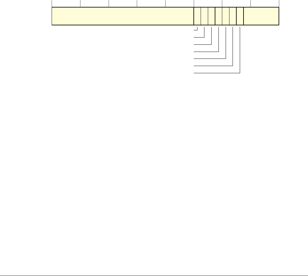
B4 System Control Registers in a VMSA implementation
B4.1 VMSA System control registers descriptions, in register order
B4-1584 Copyright © 1996-1998, 2000, 2004-2012, 2014 ARM. All rights reserved. ARM DDI 0406C.c
Non-Confidential ID051414
B4.1.66 HDCR, Hyp Debug Configuration Register, Virtualization Extensions
The HDCR characteristics are:
Purpose The HDCR controls the trapping to Hyp mode of Non-secure accesses, at PL1 or lower, to
functions provided by the debug and trace architectures.
This register is part of the Virtualization Extensions registers functional group.
Usage constraints Only accessible from Hyp mode, or from Monitor mode when SCR.NS is set to 1, see
PL2-mode system control registers on page B3-1454.
Configurations Implemented only as part of the Virtualization Extensions.
This is Banked PL2-mode register, see Banked PL2-mode CP15 read/write registers on
page B3-1454.
Attributes A 32-bit RW register. See the field descriptions for the reset value of the register. See also
Reset behavior of CP14 and CP15 registers on page B3-1450.
Table B3-55 on page B3-1501 shows the encoding of all of the Virtualization Extensions
registers.
The HDCR bit assignments are:
In the descriptions of the HDCR fields, a valid Non-secure access means an access from a Non-secure PL1 or PL0
mode that, if the bit was set to 0, would not be UNDEFINED or UNPREDICTABLE.
Bits[31:12] Reserved, UNK/SBZP.
TDRA, bit[11] Trap Debug ROM access. When this bit is set to 1, any valid Non-secure access to the
DBGDRAR or DBGDSAR is trapped to Hyp mode. For more information, including
dependencies on the values of other HDCR bits, see Trapping CP14 accesses to Debug
ROM registers on page B1-1260.
This bit resets to 0.
TDOSA, bit[10] Trap debug OS-related register access. When this bit is set to 1, any valid Non-secure CP14
access to the OS-related registers is trapped to Hyp mode. For more information, including
dependencies on the values of other HDCR bits and a summary of the OS-related registers,
see Trapping CP14 accesses to OS-related debug registers on page B1-1260.
This bit resets to 0.
TDA, bit[9] Trap debug access. When this bit is set to 1, any valid Non-secure access to the CP14 Debug
registers, other than the registers trapped by the TDRA and TDOSA bits, is trapped to Hyp
mode. For more information, including dependencies on the values of other HDCR bits, see
Trapping general CP14 accesses to debug registers on page B1-1261.
This bit resets to 0.
Reserved, UNK/SBZP
31 12 11 10 9 8 7 6 5 4 0
HPMN
†
TDRA
TDA
TDE
HPME
†
TPM
†
TPMCR
†
TDOSA
† Only on an implementation that includes the Performance Monitors Extension.
For more information, see the field description.

B4 System Control Registers in a VMSA implementation
B4.1 VMSA System control registers descriptions, in register order
ARM DDI 0406C.c Copyright © 1996-1998, 2000, 2004-2012, 2014 ARM. All rights reserved. B4-1585
ID051414 Non-Confidential
TDE, bit[8] Trap Debug exceptions. When this bit is set to 1, any Debug exception taken to Non-secure
state is routed to Hyp mode. For more information, including dependencies on the values of
other HDCR bits, see Routing Debug exceptions to Hyp mode on page B1-1194.
This bit resets to 0.
Bits[7:0], on an implementation that does not include the Performance Monitors Extension
Reserved, UNK/SBZP.
HPME, bit[7], on an implementation that includes the Performance Monitors Extension
Hypervisor Performance Monitors Enable. The possible values of this bit are:
0 Hyp mode Performance Monitors counters disabled.
1 Hyp mode Performance Monitors counters enabled.
When this bit is set to 1, the Performance Monitors counters that are reserved for use from
Hyp mode are enabled. For more information see the description of the HPMN field and
Counter enables on page C12-2313.
The reset value of this bit is UNKNOWN.
TPM, bit[6], on an implementation that includes the Performance Monitors Extension
Trap Performance Monitors accesses. The possible values of this bit are:
0 Has no effect on Performance Monitors accesses.
1 Trap valid Non-secure Performance Monitors accesses to Hyp mode.
When this bit is set to 1, any valid Non-secure access to the Performance Monitors registers
is trapped to Hyp mode. For more information see Trapping accesses to the Performance
Monitors Extension on page B1-1255.
This bit resets to 0.
TPMCR, bit[5], on an implementation that includes the Performance Monitors Extension
Trap PMCR accesses. The possible values of this bit are:
0 Has no effect on PMCR accesses.
1 Trap valid Non-secure PMCR accesses to Hyp mode.
When this bit is set to 1, any valid Non-secure access to the PMCR is trapped to Hyp mode.
For more information see Trapping accesses to the Performance Monitors Extension on
page B1-1255.
This bit resets to 0.
HPMN, bits[4:0], on an implementation that includes the Performance Monitors Extension
Defines the number of Performance Monitors counters that are accessible from Non-secure
PL1 modes, and from Non-secure PL0 modes if unprivileged access is enabled.
In Non-secure state, HPMN divides the Performance Monitors counters as follows. If
PMXEVCNTR is accessing Performance Monitors counter n then, in Non-secure state:
• If n is in the range 0≤n<HPMN, the counter is accessible from PL1 and PL2, and
from PL0 if unprivileged access to the counters is enabled.
• If n is in the range HPMN≤n<PMCR.N, the counter is accessible only from PL2.
The HPME bit enables the operation of the counters in this range.
The behavior of the Performance Monitors counters is UNPREDICTABLE if this field is set
zero, or to a value greater than PMCR.N.
For more information see Counter access on page C12-2314.
This field resets to the value of PMCR.N.
Permitted combinations of {TDRA, TDOSA, TDA, TDE} bits
The permitted values of the HDCR.{TDRA, TDOSA, TDA, TDE} bits are
0b0000
,
0b0100
,
0b1000
,
0b1100
,
0b1110
,
and
0b1111
. If these bits are set to any other values, behavior is UNPREDICTABLE.

B4 System Control Registers in a VMSA implementation
B4.1 VMSA System control registers descriptions, in register order
B4-1586 Copyright © 1996-1998, 2000, 2004-2012, 2014 ARM. All rights reserved. ARM DDI 0406C.c
Non-Confidential ID051414
Accessing the HDCR
To access the HDCR, software reads or writes the CP15 registers with
<opc1>
set to 4,
<CRn>
set to c1,
<CRm>
set to
c1, and
<opc2>
set to 1. For example:
MRC p15, 4, <Rt>, c1, c1, 1 ; Read HDCR into Rt
MCR p15, 4, <Rt>, c1, c1, 1 ; Write Rt to HDCR

B4 System Control Registers in a VMSA implementation
B4.1 VMSA System control registers descriptions, in register order
ARM DDI 0406C.c Copyright © 1996-1998, 2000, 2004-2012, 2014 ARM. All rights reserved. B4-1587
ID051414 Non-Confidential
B4.1.67 HDFAR, Hyp Data Fault Address Register, Virtualization Extensions
The HDFAR characteristics are:
Purpose The HDFAR holds the VA of the faulting address that caused a synchronous Data Abort
exception that is taken to Hyp mode.
This register is part of the Virtualization Extensions registers functional group.
Usage constraints Only accessible from Hyp mode, or from Monitor mode when SCR.NS is set to 1, see
PL2-mode system control registers on page B3-1454.
Any execution in a Non-secure PL1 mode, or in Secure state, makes the HDFAR UNKNOWN.
Configurations Implemented only as part of the Virtualization Extensions.
This is PL2-mode register, see Banked PL2-mode CP15 read/write registers on
page B3-1454.
This register is shared with the Secure copy of the DFAR, and the CP15 encoding for the
HDFAR provides Hyp mode access to an alias of the Secure DFAR, see PL2-mode
encodings for shared CP15 registers on page B3-1456.
Attributes A 32-bit RW register with an UNKNOWN reset value. See also Reset behavior of CP14 and
CP15 registers on page B3-1450.
Table B3-55 on page B3-1501 shows the encoding of all of the Virtualization Extensions
registers.
The HDFAR bit assignments are:
VA, bits[31:0] The VA of the address used in the access that faulted, generating a synchronous Data Abort
exception.
Accessing the HDFAR
To access the HDFAR, software reads or writes the CP15 registers with
<opc1>
set to 4,
<CRn>
set to c6,
<CRm>
set to
c0, and
<opc2>
set to 0. For example:
MRC p15, 4, <Rt>, c6, c0, 0 ; Read HDFAR into Rt
MCR p15, 4, <Rt>, c6, c0, 0 ; Write Rt to HDFAR
VA of faulting address of synchronous Data Abort exception
31 0

B4 System Control Registers in a VMSA implementation
B4.1 VMSA System control registers descriptions, in register order
B4-1588 Copyright © 1996-1998, 2000, 2004-2012, 2014 ARM. All rights reserved. ARM DDI 0406C.c
Non-Confidential ID051414
B4.1.68 HIFAR, Hyp Instruction Fault Address Register, Virtualization Extensions
The HIFAR characteristics are:
Purpose The HIFAR holds the VA of the faulting address that caused a synchronous Prefetch Abort
exception that is taken to Hyp mode.
This register is part of the Virtualization Extensions registers functional group.
Usage constraints Only accessible from Hyp mode, or from Monitor mode when SCR.NS is set to 1, see
PL2-mode system control registers on page B3-1454.
Any execution in a Non-secure PL1 mode, or in Secure state, makes the HIFAR UNKNOWN.
Configurations Implemented only as part of the Virtualization Extensions.
This is PL2-mode register, see Banked PL2-mode CP15 read/write registers on
page B3-1454.
This register is shared with the Secure copy of the IFAR, and the CP15 encoding for the
HIFAR provides Hyp mode access to an alias of the Secure IFAR, see PL2-mode encodings
for shared CP15 registers on page B3-1456.
Attributes A 32-bit RW register with an UNKNOWN reset value. See also Reset behavior of CP14 and
CP15 registers on page B3-1450.
Table B3-55 on page B3-1501 shows the encoding of all of the Virtualization Extensions
registers.
The HIFAR bit assignments are:
VA, bits[31:0] The VA of the instruction address used in the instruction fetch that faulted, generating a synchronous
Prefetch Abort exception.
Accessing the HIFAR
To access the HIFAR, software reads or writes the CP15 registers with
<opc1>
set to 4,
<CRn>
set to c6,
<CRm>
set to
c0, and
<opc2>
set to 2. For example:
MRC p15, 4, <Rt>, c6, c0, 2 ; Read HIFAR into Rt
MCR p15, 4, <Rt>, c6, c0, 2 ; Write Rt to HIFAR
VA of faulting address of synchronous Prefetch Abort exception
31 0

B4 System Control Registers in a VMSA implementation
B4.1 VMSA System control registers descriptions, in register order
ARM DDI 0406C.c Copyright © 1996-1998, 2000, 2004-2012, 2014 ARM. All rights reserved. B4-1589
ID051414 Non-Confidential
B4.1.69 HMAIRn, Hyp Memory Attribute Indirection Registers 0 and 1, Virtualization Extensions
The HMAIR0 and HMAIR1 characteristics are:
Purpose The HMAIR0 and HMAIR1 registers provide the memory attribute encodings
corresponding to the possible AttrIndx values in a translation table entry for stage 1
translations for memory accesses from Hyp mode. For more information about the AttrIndx
field, see Long-descriptor format memory region attributes on page B3-1372.
Note
Memory accesses from Hyp mode always use the Long-descriptor translation table format.
These registers are part of the Virtualization Extensions registers functional group.
Usage constraints Only accessible from Hyp mode, or from Monitor mode when SCR.NS is set to 1, see
PL2-mode system control registers on page B3-1454.
AttrIndx[2], from the translation table descriptor, selects the appropriate HMAIR:
• setting AttrIndx[2] to 0 selects HMAIR0
• setting AttrIndx[2] to 1 selects HMAIR1.
Configurations Implemented only as part of the Virtualization Extensions.
These are Banked PL2-mode registers, see Banked PL2-mode CP15 read/write registers on
page B3-1454.
Attributes 32-bit RW registers with an UNKNOWN reset values. See also Reset behavior of CP14 and
CP15 registers on page B3-1450.
Table B3-55 on page B3-1501 shows the encoding of all of the Virtualization Extensions
registers.
The HMAIRn bit assignments and encodings are identical to those for MAIRn.
Accessing the HMAIR0 or HMAIR1
To access the HMAIR0 or HMAIR1, software reads or writes the CP15 registers with
<opc1>
set to 4,
<CRn>
set to
c10,
<CRm>
set to c2, and
<opc2>
set to 0 for HMAIR0, or to 1 for HMAIR1. For example:
MRC p15, 4, <Rt>, c10, c2, 0 ; Read HMAIR0 into Rt
MCR p15, 4, <Rt>, c10, c2, 1 ; Write Rt to HMAIR1

B4 System Control Registers in a VMSA implementation
B4.1 VMSA System control registers descriptions, in register order
B4-1590 Copyright © 1996-1998, 2000, 2004-2012, 2014 ARM. All rights reserved. ARM DDI 0406C.c
Non-Confidential ID051414
B4.1.70 HPFAR, Hyp IPA Fault Address Register, Virtualization Extensions
The HPFAR characteristics are:
Purpose For some aborts on a stage 2 translation, taken to Hyp mode, HPFAR holds the faulting IPA.
This register is part of the Virtualization Extensions registers functional group.
Usage constraints Only accessible from Hyp mode, or from Monitor mode when SCR.NS is set to 1, see
PL2-mode system control registers on page B3-1454.
Execution in any Non-secure mode other than Hyp mode makes this register UNKNOWN.
Configurations Implemented only as part of the Virtualization Extensions.
This is Banked PL2-mode register, see Banked PL2-mode CP15 read/write registers on
page B3-1454.
Attributes A 32-bit RW register with an UNKNOWN reset value. See also Reset behavior of CP14 and
CP15 registers on page B3-1450.
Table B3-55 on page B3-1501 shows the encoding of all of the Virtualization Extensions
registers.
The HPFAR bit assignments are:
FIPA, bits[31:4]
Bits[39:12] of the faulting IPA.
Bits[3:0] Reserved, UNK/SBZP.
Accessing the HPFAR
To access the HPFAR, software reads or writes the CP15 registers with
<opc1>
set to 4,
<CRn>
set to c6,
<CRm>
set to
c0, and
<opc2>
set to 4. For example:
MRC p15, 4, <Rt>, c6, c0, 4 ; Read HPFAR into Rt
MCR p15, 4, <Rt>, c6, c0, 4 ; Write Rt to HPFAR
FIPA[39:12]
31 43 0
Reserved,
UNK/SBZP

B4 System Control Registers in a VMSA implementation
B4.1 VMSA System control registers descriptions, in register order
ARM DDI 0406C.c Copyright © 1996-1998, 2000, 2004-2012, 2014 ARM. All rights reserved. B4-1591
ID051414 Non-Confidential
B4.1.71 HSCTLR, Hyp System Control Register, Virtualization Extensions
The HSCTLR characteristics are:
Purpose The HSCTLR provides top level control of the system operation in Hyp mode. This register
provides Hyp mode control of features controlled by the Banked SCTLR bits, and shows
the values of the non-Banked SCTLR bits.
This register is part of the Virtualization Extensions registers functional group.
Usage constraints Only accessible from Hyp mode, or from Monitor mode when SCR.NS is set to 1, see
PL2-mode system control registers on page B3-1454.
Configurations Implemented only as part of the Virtualization Extensions.
This is Banked PL2-mode register, see Banked PL2-mode CP15 read/write registers on
page B3-1454.
Attributes A 32-bit RW register with an UNKNOWN reset value. See also Reset behavior of CP14 and
CP15 registers on page B3-1450.
Table B3-55 on page B3-1501 shows the encoding of all of the Virtualization Extensions
registers.
The HSCTLR bit assignments are:
Bit[31] Reserved, UNK/SBZP.
TE, bit[30] Thumb Exception enable. This bit controls whether exceptions taken to Hyp mode are taken in
ARM or Thumb state. The possible values of this bit are:
0 Exceptions taken in ARM state
1 Exceptions taken in Thumb state.
For more information about the use of this bit see Instruction set state on exception entry on
page B1-1182.
Bits[29:28] Reserved, UNK/SBOP.
Bits[27:26] Reserved, UNK/SBZP.
EE, bit[25] Exception Endianness bit. The value of this bit defines the value of the CPSR.E bit on entry to an
exception vector in Hyp mode. This value also indicates the endianness of the translation table data
for translation table lookups for the Non-secure PL1&0 stage 2 and PL2 stage 1 address translations.
The possible values of this bit are:
0 Little-endian.
1 Big-endian.
Bit[24] Reserved, UNK/SBZP.
Bits[23:22] Reserved, UNK/SBOP.
FI, bit[21] Fast interrupts configuration enable bit. The possible values of this bit are:
0 All performance features enabled.
1 Low interrupt latency configuration. Some performance features disabled.
Setting this bit to 1 can reduce interrupt latency in an implementation by disabling
IMPLEMENTATION DEFINED performance features.
This is a read-only bit that takes the value of the SCTLR.FI bit.
For more information, see Low interrupt latency configuration on page B1-1198.
M(0)
31 30 29 28 27 26 25 24 23 22 21 20 19 18 17 16 15 14 13 12 11 10 9 8 7 6 5 4 3 2 1 0
(1) (1) (0) (0) (0) (1) (1) FI (0) (1) (0) (1) (0) (0) (0) I (1) (0) (0) (0) (0) (1) (1) (1) C A
TE WXNEE CP15BEN

B4 System Control Registers in a VMSA implementation
B4.1 VMSA System control registers descriptions, in register order
B4-1592 Copyright © 1996-1998, 2000, 2004-2012, 2014 ARM. All rights reserved. ARM DDI 0406C.c
Non-Confidential ID051414
Bit[20] Reserved, UNK/SBZP.
WXN, bit[19] Write permission implies XN. The possible values of this bit are:
0 Hyp translations that permit write are not forced to XN.
1 Hyp translations that permit write are forced to XN.
For more information see Preventing execution from writable locations on page B3-1361.
Bit[18] Reserved, UNK/SBOP.
Bit[17] Reserved, UNK/SBZP.
Bit[16] Reserved, UNK/SBOP.
Bits[15:13] Reserved, UNK/SBZP.
I, bit[12] Instruction cache enable bit: This is a global enable bit for instruction caches, for memory accesses
made in Hyp mode. The possible values of this bit are:
0 Instruction caches disabled.
1 Instruction caches enabled.
If the system does not implement any instruction caches that can be accessed by the processor, at
any level of the memory hierarchy, this bit is RAZ/WI.
If the system implements any instruction caches that can be accessed by the processor then it must
be possible to disable them by setting this bit to 0.
For more information see Cache enabling and disabling on page B2-1270.
Bit[11] Reserved, UNK/SBOP.
Bits[10:7] Reserved, UNK/SBZP.
Bit[6] Reserved, UNK/SBOP.
CP15BEN, bit[5]
CP15 barrier enable. If implemented, this is an enable bit for use of the CP15 DMB, DSB, and ISB
barrier operations from Hyp mode:
0 CP15 barrier operations disabled. Their encodings are UNDEFINED.
1 CP15 barrier operations enabled.
This bit is optional. If not implemented, bit[5] is RAO/WI. However, it must be implemented if
SCTLR.CP15BEN is implemented.
Note
SCTLR.CP15BEN controls the use of these operations from PL1 and PL0 modes.
For more information about these operations see Data and instruction barrier operations, VMSA on
page B4-1752.
Bits[4:3] Reserved, UNK/SBOP.
C, bit[2] Cache enable bit. This is a global enable bit for data and unified caches, for memory accesses made
in Hyp mode. The possible values of this bit are:
0 Data or unified caches disabled.
1 Data or unified caches enabled.
If the system does not implement any data or unified caches that can be accessed by the processor,
at any level of the memory hierarchy, this bit is RAZ/WI.
If the system implements any data or unified caches that can be accessed by the processor then it
must be possible to disable them by setting this bit to 0.
For more information see Cache enabling and disabling on page B2-1270.

B4 System Control Registers in a VMSA implementation
B4.1 VMSA System control registers descriptions, in register order
ARM DDI 0406C.c Copyright © 1996-1998, 2000, 2004-2012, 2014 ARM. All rights reserved. B4-1593
ID051414 Non-Confidential
A, bit[1] Alignment bit. This is the enable bit for Alignment fault checking, for memory accesses made in
Hyp mode. The possible values of this bit are:
0 Alignment fault checking disabled.
1 Alignment fault checking enabled.
For more information, see Unaligned data access on page A3-108.
M, bit[0] MMU enable bit. This is a global enable bit for the PL2 stage 1 MMU. The possible values of this
bit are:
0 PL2 stage 1 MMU disabled.
1 PL2 stage 1 MMU enabled.
For more information, see The effects of disabling MMUs on VMSA behavior on page B3-1314.
Accessing the HSCTLR
To access the HSCTLR, software reads or writes the CP15 registers with
<opc1>
set to 4,
<CRn>
set to c1,
<CRm>
set
to c0, and
<opc2>
set to 0. For example:
MRC p15, 4, <Rt>, c1, c0, 0 ; Read HSCTLR into Rt
MCR p15, 4, <Rt>, c1, c0, 0 ; Write Rt to HSCTLR
B4 System Control Registers in a VMSA implementation
B4.1 VMSA System control registers descriptions, in register order
B4-1594 Copyright © 1996-1998, 2000, 2004-2012, 2014 ARM. All rights reserved. ARM DDI 0406C.c
Non-Confidential ID051414
B4.1.72 HSR, Hyp Syndrome Register, Virtualization Extensions
The HSR characteristics are:
Purpose The HSR holds syndrome information for an exception taken to Hyp mode.
This register is part of the Virtualization Extensions registers functional group.
Usage constraints Only accessible from Hyp mode, or from Monitor mode when SCR.NS is set to 1, see
PL2-mode system control registers on page B3-1454.
Execution in any Non-secure mode other than Hyp mode makes this register UNKNOWN.
Configurations Implemented only as part of the Virtualization Extensions.
This is Banked PL2-mode register, see Banked PL2-mode CP15 read/write registers on
page B3-1454.
Attributes A 32-bit RW register with an UNKNOWN reset value. See also Reset behavior of CP14 and
CP15 registers on page B3-1450.
Table B3-55 on page B3-1501 shows the encoding of all of the Virtualization Extensions
registers.
The HSR bit assignments are:
EC, bits[31:26]
Exception class. The exception class for the exception that is taken to Hyp mode:
• When zero, this field indicates that the reason for the exception is not known. In this case, the
other fields in the register are UNKNOWN.
• Otherwise, the field holds the Exception class for the exception, as described in Use of the
HSR on page B3-1424.
IL, bit[25] Instruction length. Indicates the size of the instruction that has been trapped to Hyp mode. The
possible values of this bit are:
0 16-bit instruction.
1 32-bit instruction.
For information about the validity of the IL field see Use of the HSR on page B3-1424. When the
field is not valid it is UNK/SBZP.
ISS, bits[24:0] Instruction-specific syndrome. The interpretation of this field depends on the value of the EC field.
For more information see Use of the HSR on page B3-1424.
Accessing the HSR
To access the HSR, software reads or writes the CP15 registers with
<opc1>
set to 4,
<CRn>
set to c5,
<CRm>
set to c2,
and
<opc2>
set to 0. For example:
MRC p15, 4, <Rt>, c5, c2, 0 ; Read HSR into Rt
MCR p15, 4, <Rt>, c5, c2, 0 ; Write Rt to HSR
EC
31 26 25 24 0
ISS
IL
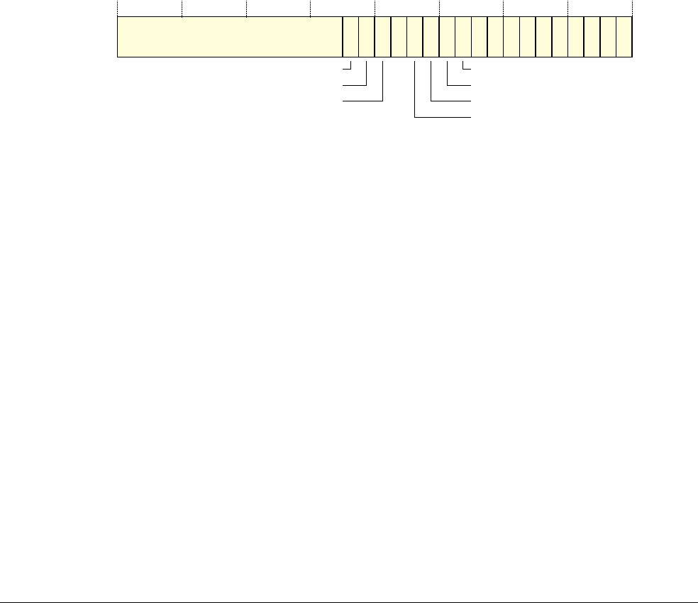
B4 System Control Registers in a VMSA implementation
B4.1 VMSA System control registers descriptions, in register order
ARM DDI 0406C.c Copyright © 1996-1998, 2000, 2004-2012, 2014 ARM. All rights reserved. B4-1595
ID051414 Non-Confidential
B4.1.73 HSTR, Hyp System Trap Register, Virtualization Extensions
The HSTR characteristics are:
Purpose The HSTR controls the trapping to Hyp mode of Non-secure accesses, at PL1 or lower, of:
• use of Jazelle or ThumbEE
• access to each of the CP15 primary coprocessor registers, {c0-c3, c5-c13, c15}.
This register is part of the Virtualization Extensions registers functional group.
Usage constraints Only accessible from Hyp mode, or from Monitor mode when SCR.NS is set to 1, see
PL2-mode system control registers on page B3-1454.
Configurations Implemented only as part of the Virtualization Extensions.
This is Banked PL2-mode register, see Banked PL2-mode CP15 read/write registers on
page B3-1454.
Attributes A 32-bit RW register that resets to zero. See also Reset behavior of CP14 and CP15 registers
on page B3-1450.
Table B3-55 on page B3-1501 shows the encoding of all of the Virtualization Extensions
registers.
The HSTR bit assignments are:
In the descriptions of the HSTR fields, a valid Non-secure access means an access that, if the bit was set to 0, would
not be UNDEFINED or UNPREDICTABLE.
Bits[31:18, 14, 4]
Reserved, UNK/SBZP.
TJDBX, bit[17]
Trap Jazelle operations. When this bit is set to 1, any valid Non-secure access to Jazelle functionality
is trapped to Hyp mode. For more information see Trapping accesses to Jazelle functionality on
page B1-1256.
TTEE, bit[16] Trap ThumbEE operations. When this bit is set to 1, any valid Non-secure access to the ThumbEE
configuration registers is trapped to Hyp mode. For more information see Trapping accesses to the
ThumbEE configuration registers on page B1-1256.
Tx, bit[x], for values of x in the set {0-3, 5-13, 15}
Trap coprocessor primary register. When Tx is set to 1, Non-secure accesses from PL1 and PL0
modes to CP15 primary coprocessor register cx are trapped to Hyp mode. This means that, when Tx
is set to 1, the following accesses are trapped to Hyp mode:
• an access using an
MCR
or
MRC
instruction with CRn set to
cx
:
— from a Non-secure PL1 mode
— from the Non-secure PL0 mode, if the access would not be UNDEFINED if Tx was set
to 0
T0Reserved, UNK/SBZP
31 18 17 16 15 14 13 12 11 10 9 8 7 6 5 4 3 2 1 0
(0) T9 T8 T7 T6 T5 (0) T3 T2 T1
TJDBX
TTEE
T10
T11
T12
T13
T15

B4 System Control Registers in a VMSA implementation
B4.1 VMSA System control registers descriptions, in register order
B4-1596 Copyright © 1996-1998, 2000, 2004-2012, 2014 ARM. All rights reserved. ARM DDI 0406C.c
Non-Confidential ID051414
• any access using an
MCRR
or
MRRC
instruction with CRm set to
cx
:
— from a Non-secure PL1 mode
— from the Non-secure PL0 mode, if the access would not be UNDEFINED if Tx was set
to 0.
For more information see Generic trapping of accesses to CP15 system control registers on
page B1-1259.
Note
A Tn bit traps all accesses to the corresponding CP15 primary coprocessor register. This is unlike
most traps to Hyp mode, including the traps controlled by the TJDBX and TTEE bits, that trap only
otherwise-valid accesses.
Accessing the HSTR
To access the HSTR, software reads or writes the CP15 registers with
<opc1>
set to 4,
<CRn>
set to c1,
<CRm>
set to
c1, and
<opc2>
set to 3. For example:
MRC p15, 4, <Rt>, c1, c1, 3 ; Read HSTR into Rt
MCR p15, 4, <Rt>, c1, c1, 3 ; Write Rt to HSTR
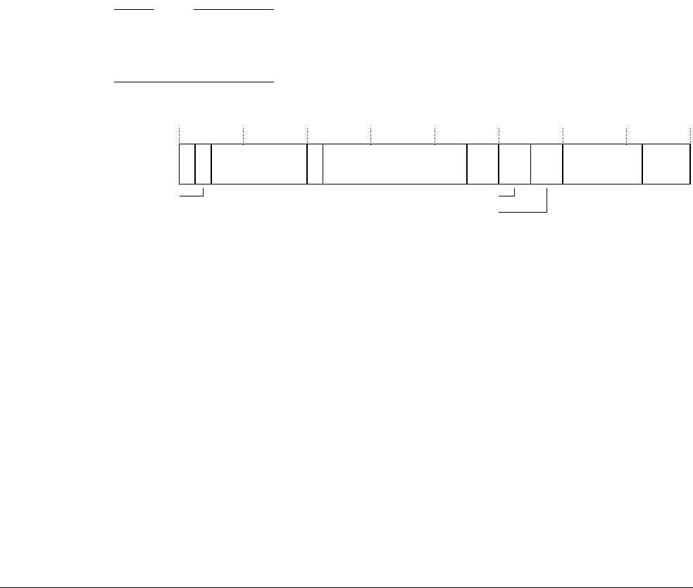
B4 System Control Registers in a VMSA implementation
B4.1 VMSA System control registers descriptions, in register order
ARM DDI 0406C.c Copyright © 1996-1998, 2000, 2004-2012, 2014 ARM. All rights reserved. B4-1597
ID051414 Non-Confidential
B4.1.74 HTCR, Hyp Translation Control Register, Virtualization Extensions
The HTCR characteristics are:
Purpose The HTCR controls the translation table walks required for the stage 1 translation of
memory accesses from Hyp mode, and holds cacheability and shareability information for
the accesses.
This register is part of the Virtualization Extensions registers functional group.
Usage constraints Used in conjunction with HTTBR, that defines the translation table base address for the
translations.
Only accessible from Hyp mode, or from Monitor mode when SCR.NS is set to 1, see
PL2-mode system control registers on page B3-1454.
Configurations Implemented only as part of the Virtualization Extensions.
This is Banked PL2-mode register, see Banked PL2-mode CP15 read/write registers on
page B3-1454.
Attributes A 32-bit RW register with an UNKNOWN reset value. See also Reset behavior of CP14 and
CP15 registers on page B3-1450.
Table B3-55 on page B3-1501 shows the encoding of all of the Virtualization Extensions
registers.
Note
For other address translations, the following registers are equivalent to the HTCR and HTTBR:
• for stage 1 translations for accesses from modes other than Hyp mode, the TTBCR, TTBR0, and TTBR1
• for stage 2 translations, the VTCR and VTTBR.
The HTCR bit assignments are:
Bit[31] Reserved, UNK/SBOP.
IMPLEMENTATION DEFINED, bit[30]
An IMPLEMENTATION DEFINED bit.
Bits[29:24] Reserved, UNK/SBZP.
Bits[23] Reserved, UNK/SBOP.
Bits[22:14] Reserved, UNK/SBZP.
SH0, bits[13:12]
Shareability attribute for memory associated with translation table walks using HTTBR. This field
is encoded as described in Shareability, Long-descriptor format on page B3-1373.
IMPLEMENTATION DEFINED ORGN0
IRGN0
T0SZ
31 30 29 24 23 22 14 13 12 11 10 9 8 7 3 2 0
Reserved,
UNK/SBZP
SH0Reserved, UNK/SBZP(1)
Reserved,
UNK/SBZP
(1)

B4 System Control Registers in a VMSA implementation
B4.1 VMSA System control registers descriptions, in register order
B4-1598 Copyright © 1996-1998, 2000, 2004-2012, 2014 ARM. All rights reserved. ARM DDI 0406C.c
Non-Confidential ID051414
ORGN0, bits[11:10]
Outer cacheability attribute for memory associated with translation table walks using HTTBR.
Table B4-4 shows the encoding of this field.
IRGN0, bits[9:8]
Inner cacheability attribute for memory associated with translation table walks using HTTBR.
Table B4-5 shows the encoding of this field.
Bits[7:3] Reserved, UNK/SBZP.
T0SZ, bits[2:0]
The size offset of the memory region addressed by HTTBR. This field is encoded as a three-bit
unsigned integer, and the region size is 2(32-T0SZ) bytes.
HTTBR, Hyp Translation Table Base Register, Virtualization Extensions on page B4-1600 describes
how the value of this field determines the width of the translation table base address defined by
HTTBR.
Accessing the HTCR
To access the HTCR, software reads or writes the CP15 registers with
<opc1>
set to 4,
<CRn>
set to c2,
<CRm>
set to
c0, and
<opc2>
set to 2. For example:
MRC p15, 4, <Rt>, c2, c0, 2 ; Read HTCR into Rt
MCR p15, 4, <Rt>, c2, c0, 2 ; Write Rt to HTCR
Table B4-4 HTCR.ORGN0 field encoding
ORGN0 Meaning
00 Normal memory, Outer Non-cacheable
01 Normal memory, Outer Write-Back Write-Allocate Cacheable
10 Normal memory, Outer Write-Through Cacheable
11 Normal memory, Outer Write-Back no Write-Allocate Cacheable
Table B4-5 HTCR.IRGN0 field encoding
IRGN0 Meaning
00 Normal memory, Inner Non-cacheable
01 Normal memory, Inner Write-Back Write-Allocate Cacheable
10 Normal memory, Inner Write-Through Cacheable
11 Normal memory, Inner Write-Back no Write-Allocate Cacheable

B4 System Control Registers in a VMSA implementation
B4.1 VMSA System control registers descriptions, in register order
ARM DDI 0406C.c Copyright © 1996-1998, 2000, 2004-2012, 2014 ARM. All rights reserved. B4-1599
ID051414 Non-Confidential
B4.1.75 HTPIDR, Hyp Software Thread ID Register, Virtualization Extensions
The HTPIDR characteristics are:
Purpose The HTPIDR provides a location where software running in Hyp mode can store thread
identifying information that is not visible to Non-secure software executing at PL0 or PL1,
for hypervisor management purposes.
This register is part of the Miscellaneous operations functional group.
Usage constraints Only accessible from Hyp mode, or from Monitor mode when SCR.NS is set to 1, see
PL2-mode system control registers on page B3-1454.
Processor hardware never updates this register.
Configurations Implemented only as part of the Virtualization Extensions.
This is a Banked PL2-mode register, see Banked PL2-mode CP15 read/write registers on
page B3-1454.
Attributes A 32-bit RW register with an UNKNOWN reset value. See also Reset behavior of CP14 and
CP15 registers on page B3-1450.
Table B3-52 on page B3-1499 shows the encodings of all of the registers in the
Miscellaneous operations functional group.
Accessing the HTPIDR
To access the HTPIDR, software executing in Hyp mode reads or writes the CP15 registers with
<opc1>
set to 4,
<CRn>
set to c13,
<CRm>
set to c0, and
<opc2>
set to 2.
For example:
MRC p15, 4, <Rt>, c13, c0, 2 ; Read HTPIDR into Rt
MCR p15, 4, <Rt>, c13, c0, 2 ; Write Rt to HTPIDR

B4 System Control Registers in a VMSA implementation
B4.1 VMSA System control registers descriptions, in register order
B4-1600 Copyright © 1996-1998, 2000, 2004-2012, 2014 ARM. All rights reserved. ARM DDI 0406C.c
Non-Confidential ID051414
B4.1.76 HTTBR, Hyp Translation Table Base Register, Virtualization Extensions
The HTTBR characteristics are:
Purpose The HTTBR holds the base address of the translation table for the stage 1 translation of
memory accesses from Hyp mode.
Note
These translations are always defined using the Long-descriptor format translation tables.
This register is part of the Virtualization Extensions registers functional group.
Usage constraints Used in conjunction with the HTCR.
Only accessible from Hyp mode, or from Monitor mode when SCR.NS is set to 1, see
PL2-mode system control registers on page B3-1454.
Configurations Implemented only as part of the Virtualization Extensions.
This is a Banked PL2-mode register, see Banked PL2-mode CP15 read/write registers on
page B3-1454.
Attributes A 64-bit RW register with an UNKNOWN reset value. See also Reset behavior of CP14 and
CP15 registers on page B3-1450.
Table B3-55 on page B3-1501 shows the encoding of all of the Virtualization Extensions
registers.
Note
See HTCR, Hyp Translation Control Register, Virtualization Extensions on page B4-1597 for a summary of the
registers that define the translation tables for other address translations.
The HTTBR bit assignments are:
Bits[63:40] Reserved, UNK/SBZP.
BADDR, bits[39:x]
Translation table base address, bits[39:x]. See the text in this section for a description of how x is
defined.
The value of x determines the required alignment of the translation table, which must be aligned to
2x bytes.
Bits[x-1:0] Reserved, UNK/SBZP.
The HTCR.T0SZ field determines the width of the defined translation table base address, indicated by the value of
x in the HTTBR description. The following pseudocode calculates the value of x:
T0Size = UInt(HTCR.T0SZ);
if T0Size > 1 then
x = 14 - T0Size;
else
x = 5 - T0Size;
Accessing the HTTBR
To access HTTBR, software performs a 64-bit read or write of the CP15 registers with
<CRm>
set to c2 and
<opc1>
set to 4. For example:
MRRC p15, 4, <Rt>, <Rt2>, c2 ; Read 64-bit HTTBR into Rt (low word) and Rt2 (high word)
x x-1
Reserved, UNK/SBZP
40 39
Reserved, UNK/SBZP BADDR[39:x]
63 0

B4 System Control Registers in a VMSA implementation
B4.1 VMSA System control registers descriptions, in register order
ARM DDI 0406C.c Copyright © 1996-1998, 2000, 2004-2012, 2014 ARM. All rights reserved. B4-1601
ID051414 Non-Confidential
MCRR p15, 4, <Rt>, <Rt2>, c2 ; Write Rt (low word) and Rt2 (high word) to 64-bit HTTBR
In these
MRRC
and
MCRR
instructions, Rt holds the least-significant word of HTTBR, and Rt2 holds the
most-significant word.

B4 System Control Registers in a VMSA implementation
B4.1 VMSA System control registers descriptions, in register order
B4-1602 Copyright © 1996-1998, 2000, 2004-2012, 2014 ARM. All rights reserved. ARM DDI 0406C.c
Non-Confidential ID051414
B4.1.77 HVBAR, Hyp Vector Base Address Register, Virtualization Extensions
The HVBAR characteristics are:
Purpose The HVBAR holds the exception base address for any exception that is taken to Hyp mode,
see Exception vectors and the exception base address on page B1-1165.
This register is part of the Virtualization Extensions registers functional group.
Usage constraints Only accessible from Hyp mode, or from Monitor mode when SCR.NS is set to 1, see
PL2-mode system control registers on page B3-1454.
Configurations Implemented only as part of the Virtualization Extensions.
This is Banked PL2-mode register, see Banked PL2-mode CP15 read/write registers on
page B3-1454.
Attributes A 32-bit RW register with an UNKNOWN reset value. See also Reset behavior of CP14 and
CP15 registers on page B3-1450.
Table B3-55 on page B3-1501 shows the encoding of all of the Virtualization Extensions
registers.
The HVBAR bit assignments are:
Hyp_Vector_Base_Address, bits[31:5]
Bits[31:5] of the base address of the exception vectors for exceptions that are taken to Hyp mode.
Bits[4:0] of an exception vector is the exception offset, see Table B1-3 on page B1-1167.
Bits[4:0] Reserved, UNK/SBZP.
For details of how the HVBAR determines the exception addresses see Exception vectors and the exception base
address on page B1-1165.
Accessing the HVBAR
To access the HVBAR, software reads or writes the CP15 registers with
<opc1>
set to 4,
<CRn>
set to c12,
<CRm>
set
to c0, and
<opc2>
set to 0. For example:
MRC p15, 4, <Rt>, c12, c0, 0 ; Read HVBAR into Rt
MCR p15, 4, <Rt>, c12, c0, 0 ; Write Rt to HVBAR
Hyp_Vector_Base_Address
31 54 0
Reserved,
UNK/SBZP

B4 System Control Registers in a VMSA implementation
B4.1 VMSA System control registers descriptions, in register order
ARM DDI 0406C.c Copyright © 1996-1998, 2000, 2004-2012, 2014 ARM. All rights reserved. B4-1603
ID051414 Non-Confidential
B4.1.78 ICIALLU, Instruction Cache Invalidate All to PoU, VMSA
Cache and branch predictor maintenance operations, VMSA on page B4-1743 describes this cache maintenance
operation.
This operation is part of the Cache maintenance operations functional group. Table B3-49 on page B3-1496 shows
the encodings of all of the registers and operations in this functional group.
B4.1.79 ICIALLUIS, Instruction Cache Invalidate All to PoU, Inner Shareable, VMSA
Cache and branch predictor maintenance operations, VMSA on page B4-1743 describes this cache maintenance
operation.
This operation is part of the Cache maintenance operations functional group. Table B3-49 on page B3-1496 shows
the encodings of all of the registers and operations in this functional group.
B4.1.80 ICIMVAU, Instruction Cache Invalidate by MVA to PoU, VMSA
Cache and branch predictor maintenance operations, VMSA on page B4-1743 describes this cache maintenance
operation.
This operation is part of the Cache maintenance operations functional group. Table B3-49 on page B3-1496 shows
the encodings of all of the registers and operations in this functional group.
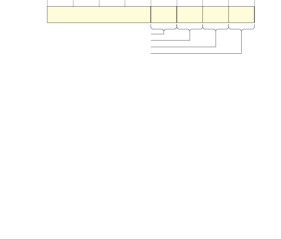
B4 System Control Registers in a VMSA implementation
B4.1 VMSA System control registers descriptions, in register order
B4-1604 Copyright © 1996-1998, 2000, 2004-2012, 2014 ARM. All rights reserved. ARM DDI 0406C.c
Non-Confidential ID051414
B4.1.81 ID_AFR0, Auxiliary Feature Register 0, VMSA
The ID_AFR0 characteristics are:
Purpose ID_AFR0 provides information about the IMPLEMENTATION DEFINED features of the
processor.
This register is a CPUID register, and is part of the Identification registers functional group.
Usage constraints Only accessible from PL1 or higher.
Must be interpreted with the Main ID Register, see MIDR, Main ID Register, VMSA on
page B4-1649.
Configurations The VMSA and PMSA definitions of the register fields are identical.
In a VMSA implementation that includes the Security Extensions, this is a Common
register.
Attributes A 32-bit RO register with an IMPLEMENTATION DEFINED value:
•Table B7-1 on page B7-1952 shows the encodings of all of the CPUID registers
•Table B3-44 on page B3-1492 shows the encodings of all of the registers in the
Identification registers functional group.
The ID_AFR0 bit assignments are:
Bits[31:16] Reserved, UNK.
IMPLEMENTATION DEFINED, bits[15:12]
IMPLEMENTATION DEFINED, bits[11:8]
IMPLEMENTATION DEFINED, bits[7:4]
IMPLEMENTATION DEFINED, bits[3:0]
The Auxiliary Feature Register 0 has four 4-bit IMPLEMENTATION FIELDS. These fields are defined by the
implementer of the design. The implementer is identified by the Implementer field of the MIDR.
The Auxiliary Feature Register 0 enables implementers to include additional design features in the CPUID scheme.
Field definitions for the Auxiliary Feature Register 0 might:
• differ between different implementers
• be subject to change
• migrate over time, for example if they are incorporated into the main architecture.
Accessing ID_AFR0
To access ID_AFR0, software reads the CP15 registers with
<opc1>
set to 0,
<CRn>
set to c0,
<CRm>
set to c1, and
<opc2>
set to 3. For example:
MRC p15, 0, <Rt>, c0, c1, 3 ; Read ID_AFR0 into Rt
Reserved, UNK
31 16 15 12 11 8 7 4 3 0
IMPLEMENTATION DEFINED
IMPLEMENTATION DEFINED
IMPLEMENTATION DEFINED
IMPLEMENTATION DEFINED
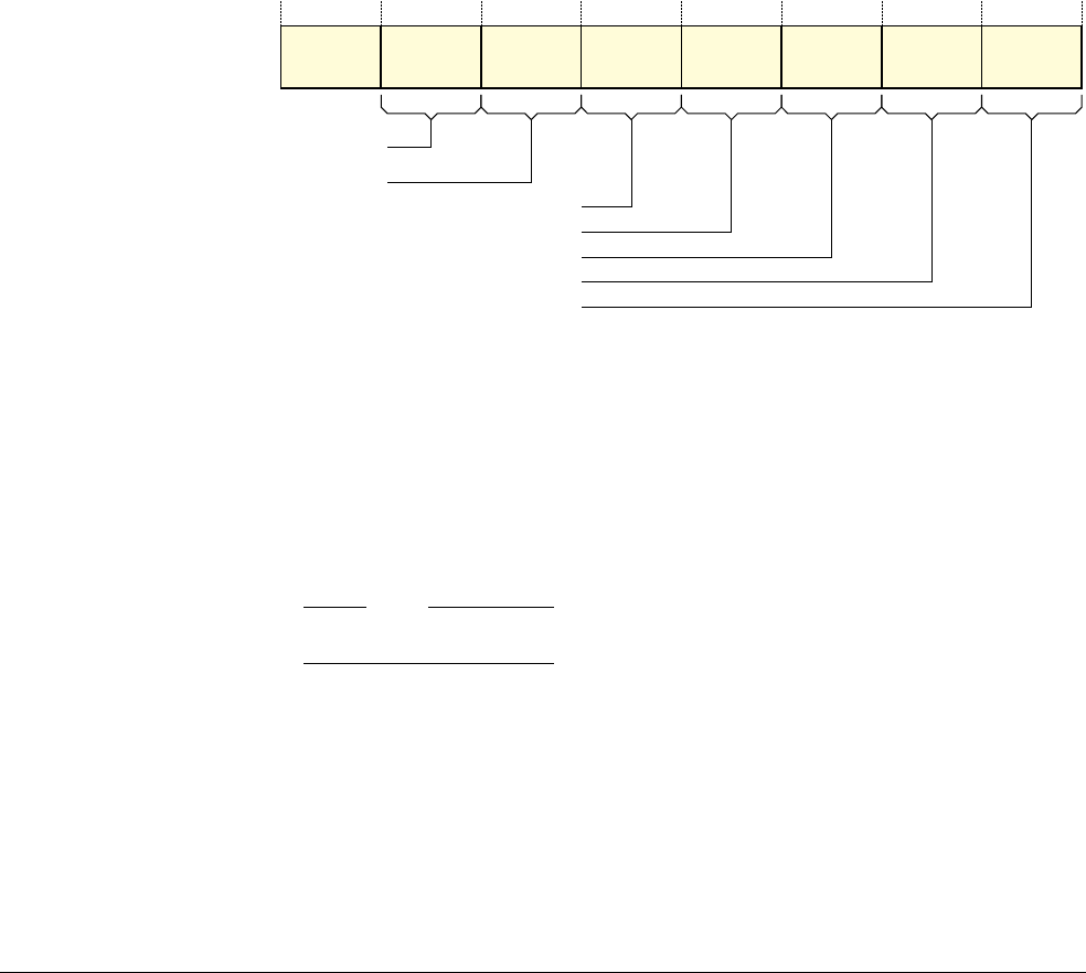
B4 System Control Registers in a VMSA implementation
B4.1 VMSA System control registers descriptions, in register order
ARM DDI 0406C.c Copyright © 1996-1998, 2000, 2004-2012, 2014 ARM. All rights reserved. B4-1605
ID051414 Non-Confidential
B4.1.82 ID_DFR0, Debug Feature Register 0, VMSA
The ID_DFR0 characteristics are:
Purpose ID_DFR0 provides top level information about the debug system.
This register is a CPUID register, and is part of the Identification registers functional group.
Usage constraints Only accessible from PL1 or higher.
Configurations The VMSA and PMSA definitions of the register fields are identical.
In a VMSA implementation that includes the Security Extensions, this is a Common
register.
Attributes A 32-bit RO register with an IMPLEMENTATION DEFINED value:
•Table B7-1 on page B7-1952 shows the encodings of all of the CPUID registers
•Table B3-44 on page B3-1492 shows the encodings of all of the registers in the
Identification registers functional group.
All field values not shown in the field descriptions are reserved.
The ID_DFR0 bit assignments are:
Bits[31:28] Reserved, UNK.
Performance Monitors Extension, A and R profiles, bits[27:24]
Support for coprocessor-based ARM Performance Monitors Extension, for A and R profile
processors. Permitted values are:
0b0000
PMUv2 not supported.
0b0001
Support for Performance Monitors Extension, PMUv1.
0b0010
Support for Performance Monitors Extension, PMUv2.
0b1111
No ARM Performance Monitors Extension support.
Note
A value of
0b0000
gives no indication of whether PMUv1 monitors are supported.
Debug model, M profile, bits[23:20]
Support for memory-mapped debug model for M profile processors. Permitted values are:
0b0000
Not supported.
0b0001
Support for M profile Debug architecture, with memory-mapped access.
Debug model, M profile
Memory-mapped trace model
Coprocessor trace model
Memory-mapped debug model, A and R profiles
Coprocessor Secure debug model, A profile only
Coprocessor debug model, A and R profiles
Reserved,
UNK
31 28 27 24 23 20 19 16 15 12 11 8 7 4 3 0
Performance Monitors
Extension, A and R profiles

B4 System Control Registers in a VMSA implementation
B4.1 VMSA System control registers descriptions, in register order
B4-1606 Copyright © 1996-1998, 2000, 2004-2012, 2014 ARM. All rights reserved. ARM DDI 0406C.c
Non-Confidential ID051414
Memory-mapped trace model, bits[19:16]
Support for memory-mapped trace model. Permitted values are:
0b0000
Not supported.
0b0001
Support for ARM trace architecture, with memory-mapped access.
The ID register, register
0x079
, gives more information about the implementation. See
also Trace on page C1-2024.
Coprocessor trace model, bits[15:12]
Support for coprocessor-based trace model. Permitted values are:
0b0000
Not supported.
0b0001
Support for ARM trace architecture, with CP14 access.
The ID register, register
0x079
, gives more information about the implementation. See
also Trace on page C1-2024.
Memory-mapped debug model, A and R profiles, bits[11:8]
Support for memory-mapped debug model, for A and R profile processors. Permitted values are:
0b0000
Not supported, or pre-ARMv6 implementation.
0b0100
Support for v7 Debug architecture, with memory-mapped access.
0b0101
Support for v7.1 Debug architecture, with memory-mapped access.
Note
The permitted field values are not continuous, and values
0b0001
,
0b0010
, and
0b0011
are reserved.
Coprocessor Secure debug model, bits[7:4]
Support for coprocessor-based Secure debug model, for an A profile processor that includes the
Security Extensions. Permitted values are:
0b0000
Not supported.
0b0011
Support for v6.1 Debug architecture, with CP14 access.
0b0100
Support for v7 Debug architecture, with CP14 access.
0b0101
Support for v7.1 Debug architecture, with CP14 access.
Note
The permitted field values are not continuous, and values
0b0001
and
0b0010
are reserved.
Coprocessor debug model, bits[3:0]
Support for coprocessor based debug model, for A and R profile processors. Permitted values are:
0b0000
Not supported.
0b0010
Support for v6 Debug architecture, with CP14 access.
0b0011
Support for v6.1 Debug architecture, with CP14 access.
0b0100
Support for v7 Debug architecture, with CP14 access.
0b0101
Support for v7.1 Debug architecture, with CP14 access.
Note
The permitted field values are not continuous, and value
0b0001
is reserved.
Note
Software can obtain more information about the debug implementation from the debug infrastructure, see Debug
identification registers on page C11-2198.

B4 System Control Registers in a VMSA implementation
B4.1 VMSA System control registers descriptions, in register order
ARM DDI 0406C.c Copyright © 1996-1998, 2000, 2004-2012, 2014 ARM. All rights reserved. B4-1607
ID051414 Non-Confidential
Accessing ID_DFR0
To access ID_DFR0, software reads the CP15 registers with
<opc1>
set to 0,
<CRn>
set to c0,
<CRm>
set to c1, and
<opc2>
set to 2. For example:
MRC p15, 0, <Rt>, c0, c1, 2 ; Read ID_DFR0 into Rt
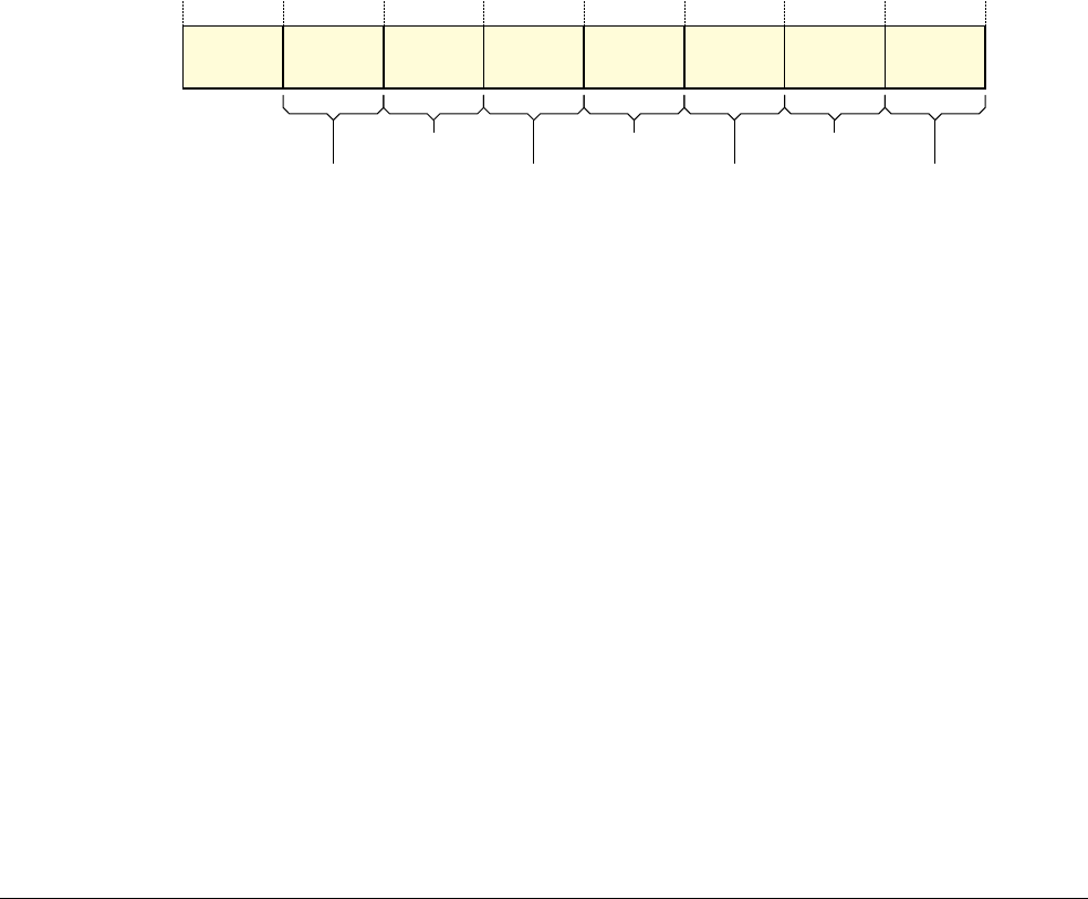
B4 System Control Registers in a VMSA implementation
B4.1 VMSA System control registers descriptions, in register order
B4-1608 Copyright © 1996-1998, 2000, 2004-2012, 2014 ARM. All rights reserved. ARM DDI 0406C.c
Non-Confidential ID051414
B4.1.83 ID_ISAR0, Instruction Set Attribute Register 0, VMSA
The ID_ISAR0 characteristics are:
Purpose ID_ISAR0 provides information about the instruction sets implemented by the processor.
For more information see About the Instruction Set Attribute registers on page B7-1952.
This register is a CPUID register, and is part of the Identification registers functional group.
Usage constraints Only accessible from PL1 or higher.
Must be interpreted with ID_ISAR1, ID_ISAR2, ID_ISAR3, and ID_ISAR4. For more
information see About the Instruction Set Attribute registers on page B7-1952.
Configurations The VMSA and PMSA definitions of the register fields are identical.
In a VMSA implementation that includes the Security Extensions, this is a Common
register.
Attributes A 32-bit RO register with an IMPLEMENTATION DEFINED value:
•Table B7-1 on page B7-1952 shows the encodings of all of the CPUID registers
•Table B3-44 on page B3-1492 shows the encodings of all of the registers in the
Identification registers functional group.
All field values not shown in the field descriptions are reserved.
The ID_ISAR0 bit assignments are:
Bits[31:28] Reserved, UNK.
Divide_instrs, bits[27:24]
Indicates the implemented Divide instructions. Permitted values are:
0b0000
None implemented.
0b0001
Adds
SDIV
and
UDIV
in the Thumb instruction set.
0b0010
As for
0b0001
, and adds
SDIV
and
UDIV
in the ARM instruction set.
Debug_instrs, bits[23:20]
Indicates the implemented Debug instructions. Permitted values are:
0b0000
None implemented.
0b0001
Adds
BKPT
.
Coproc_instrs, bits[19:16]
Indicates the implemented Coprocessor instructions. Permitted values are:
0b0000
None implemented, except for instructions separately attributed by the architecture,
including CP15, CP14, Advanced SIMD Extension and the Floating-point Extension.
0b0001
Adds generic
CDP
,
LDC
,
MCR
,
MRC
, and
STC
.
0b0010
As for
0b0001
, and adds generic
CDP2
,
LDC2
,
MCR2
,
MRC2
, and
STC2
.
0b0011
As for
0b0010
, and adds generic
MCRR
and
MRRC
.
0b0100
As for
0b0011
, and adds generic
MCRR2
and
MRRC2
.
Reserved,
UNK
31 16 15 12 11 8 7 4 3 028 27 24 23 20 19
Divide_instrs
Debug_instrs
Coproc_instrs
CmpBranch_instrs
Bitfield_instrs
BitCount_instrs
Swap_instrs

B4 System Control Registers in a VMSA implementation
B4.1 VMSA System control registers descriptions, in register order
ARM DDI 0406C.c Copyright © 1996-1998, 2000, 2004-2012, 2014 ARM. All rights reserved. B4-1609
ID051414 Non-Confidential
CmpBranch_instrs, bits[15:12]
Indicates the implemented combined Compare and Branch instructions in the Thumb instruction
set. Permitted values are:
0b0000
None implemented.
0b0001
Adds
CBNZ
and
CBZ
.
Bitfield_instrs, bits[11:8]
Indicates the implemented BitField instructions. Permitted values are:
0b0000
None implemented.
0b0001
Adds
BFC
,
BFI
,
SBFX
, and
UBFX
.
BitCount_instrs, bits[7:4]
Indicates the implemented Bit Counting instructions. Permitted values are:
0b0000
None implemented.
0b0001
Adds
CLZ
.
Swap_instrs, bits[3:0]
Indicates the implemented Swap instructions in the ARM instruction set. Permitted values are:
0b0000
None implemented.
0b0001
Adds
SWP
and
SWPB
.
Accessing ID_ISAR0
To access ID_ISAR0, software reads the CP15 registers with
<opc1>
set to 0,
<CRn>
set to c0,
<CRm>
set to c2, and
<opc2>
set to 0. For example:
MRC p15, 0, <Rt>, c0, c2, 0 ; Read ID_ISAR0 into Rt
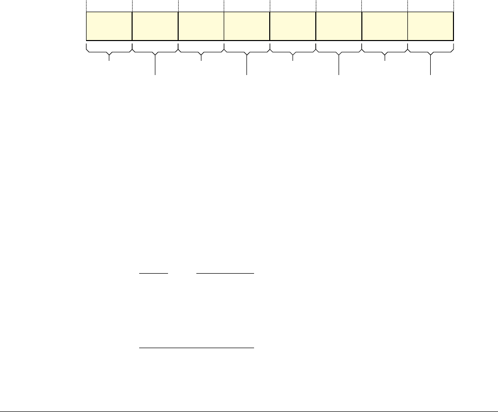
B4 System Control Registers in a VMSA implementation
B4.1 VMSA System control registers descriptions, in register order
B4-1610 Copyright © 1996-1998, 2000, 2004-2012, 2014 ARM. All rights reserved. ARM DDI 0406C.c
Non-Confidential ID051414
B4.1.84 ID_ISAR1, Instruction Set Attribute Register 1, VMSA
The ID_ISAR1 characteristics are:
Purpose ID_ISAR1 provides information about the instruction sets implemented by the processor.
For more information see About the Instruction Set Attribute registers on page B7-1952.
This register is a CPUID register, and is part of the Identification registers functional group.
Usage constraints Only accessible from PL1 or higher.
Must be interpreted with ID_ISAR0, ID_ISAR2, ID_ISAR3, and ID_ISAR4. For more
information see About the Instruction Set Attribute registers on page B7-1952.
Configurations The VMSA and PMSA definitions of the register fields are identical.
In a VMSA implementation that includes the Security Extensions, this is a Common
register.
Attributes A 32-bit RO register with an IMPLEMENTATION DEFINED value:
•Table B7-1 on page B7-1952 shows the encodings of all of the CPUID registers
•Table B3-44 on page B3-1492 shows the encodings of all of the registers in the
Identification registers functional group.
All field values not shown in the field descriptions are reserved.
The ID_ISAR1 bit assignments are:
Jazelle_instrs, bits[31:28]
Indicates the implemented Jazelle extension instructions. Permitted values are:
0b0000
No support for Jazelle.
0b0001
Adds the
BXJ
instruction, and the J bit in the PSR.
This setting might indicate a trivial implementation of the Jazelle extension.
Interwork_instrs, bits[27:24]
Indicates the implemented Interworking instructions. Permitted values are:
0b0000
None implemented.
0b0001
Adds the
BX
instruction, and the T bit in the PSR.
0b0010
As for
0b0001
, and adds the
BLX
instruction. PC loads have
BX
-like behavior.
0b0011
As for
0b0010
, and guarantees that data-processing instructions in the ARM instruction
set with the PC as the destination and the S bit clear have
BX
-like behavior.
Note
A value of
0b0000
,
0b0001
, or
0b0010
in this field does not guarantee that an ARM data-processing
instruction with the PC as the destination and the S bit clear behaves like an old
MOV PC
instruction,
ignoring bits[1:0] of the result. With these values of this field:
• if bits[1:0] of the result value are
0b00
then the processor remains in ARM state
• if bits[1:0] are
0b01
,
0b10
or
0b11
, the result must be treated as UNPREDICTABLE.
31 16 15 12 11 8 7 4 3 028 27 24 23 20 19
Jazelle_instrs
Interwork_instrs
Immediate_instrs Extend_instrs
IfThen_instrs Except_AR_instrs
Except_instrs
Endian_instrs

B4 System Control Registers in a VMSA implementation
B4.1 VMSA System control registers descriptions, in register order
ARM DDI 0406C.c Copyright © 1996-1998, 2000, 2004-2012, 2014 ARM. All rights reserved. B4-1611
ID051414 Non-Confidential
Immediate_instrs, bits[23:20]
Indicates the implemented data-processing instructions with long immediates. Permitted values are:
0b0000
None implemented.
0b0001
Adds:
• the
MOVT
instruction
• the
MOV
instruction encodings with zero-extended 16-bit immediates
• the Thumb
ADD
and
SUB
instruction encodings with zero-extended 12-bit
immediates, and the other
ADD
,
ADR
and
SUB
encodings cross-referenced by the
pseudocode for those encodings.
IfThen_instrs, bits[19:16]
Indicates the implemented If-Then instructions in the Thumb instruction set. Permitted values are:
0b0000
None implemented.
0b0001
Adds the
IT
instructions, and the IT bits in the PSRs.
Extend_instrs, bits[15:12]
Indicates the implemented Extend instructions. Permitted values are:
0b0000
No scalar sign-extend or zero-extend instructions are implemented, where scalar
instructions means non-Advanced SIMD instructions.
0b0001
Adds the
SXTB
,
SXTH
,
UXTB
, and
UXTH
instructions.
0b0010
As for
0b0001
, and adds the
SXTB16
,
SXTAB
,
SXTAB16
,
SXTAH
,
UXTB16
,
UXTAB
,
UXTAB16
, and
UXTAH
instructions.
Note
In addition:
• the shift options on these instructions are available only if the WithShifts_instrs attribute is
0b0011
or greater
• the
SXTAB16
,
SXTB16
,
UXTAB16
, and
UXTB16
instructions are implemented only if both:
— the Extend_instrs attribute is
0b0010
or greater
— the SIMD_instrs attribute is
0b0011
or greater.
Except_AR_instrs, bits[11:8]
Indicates the implemented A and R profile exception-handling instructions. Permitted values are:
0b0000
None implemented.
0b0001
Adds the
SRS
and
RFE
instructions, and the A and R profile forms of the
CPS
instruction.
Except_instrs, bits[7:4]
Indicates the implemented exception-handling instructions in the ARM instruction set. Permitted
values are:
0b0000
Not implemented. This indicates that the User registers and exception return forms of
the
LDM
and
STM
instructions are not implemented.
0b0001
Adds the
LDM
(exception return),
LDM
(User registers) and
STM
(User registers) instruction
versions.
Endian_instrs, bits[3:0]
Indicates the implemented Endian instructions. Permitted values are:
0b0000
None implemented.
0b0001
Adds the
SETEND
instruction, and the E bit in the PSRs.

B4 System Control Registers in a VMSA implementation
B4.1 VMSA System control registers descriptions, in register order
B4-1612 Copyright © 1996-1998, 2000, 2004-2012, 2014 ARM. All rights reserved. ARM DDI 0406C.c
Non-Confidential ID051414
Accessing ID_ISAR1
To access ID_ISAR1, software reads the CP15 registers with
<opc1>
set to 0,
<CRn>
set to c0,
<CRm>
set to c2, and
<opc2>
set to 1. For example:
MRC p15, 0, <Rt>, c0, c2, 1 ; Read ID_ISAR1 into Rt
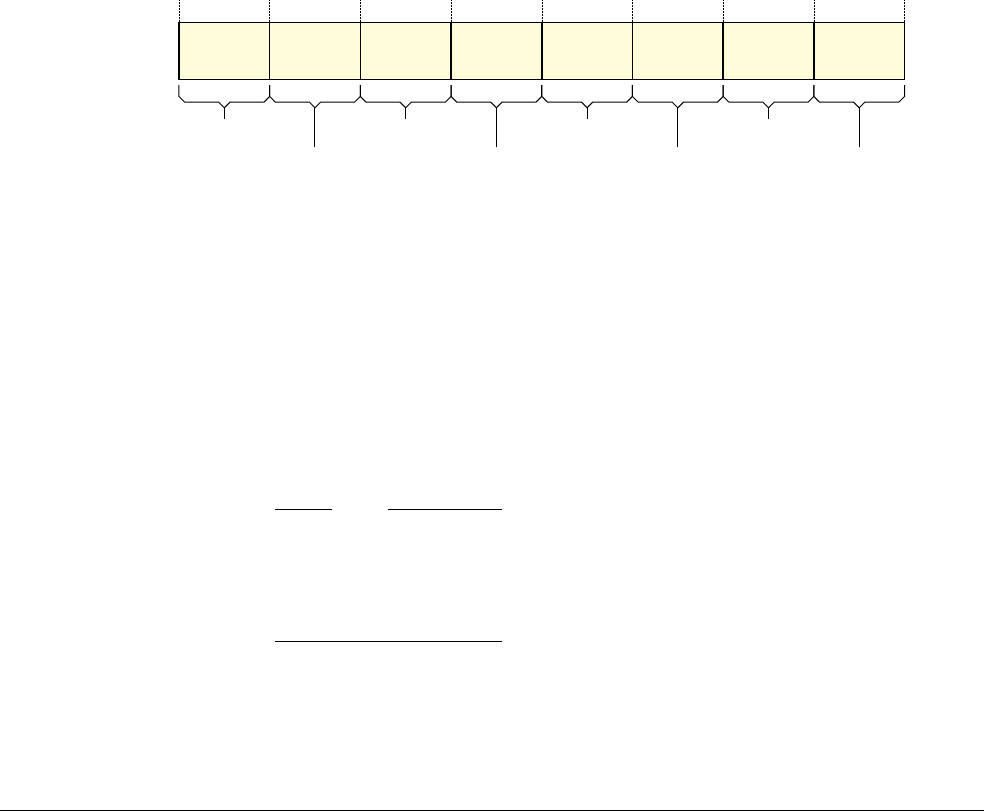
B4 System Control Registers in a VMSA implementation
B4.1 VMSA System control registers descriptions, in register order
ARM DDI 0406C.c Copyright © 1996-1998, 2000, 2004-2012, 2014 ARM. All rights reserved. B4-1613
ID051414 Non-Confidential
B4.1.85 ID_ISAR2, Instruction Set Attribute Register 2, VMSA
The ID_ISAR2 characteristics are:
Purpose ID_ISAR2 provides information about the instruction sets implemented by the processor.
For more information see About the Instruction Set Attribute registers on page B7-1952.
This register is a CPUID register, and is part of the Identification registers functional group.
Usage constraints Only accessible from PL1 or higher.
Must be interpreted with ID_ISAR0, ID_ISAR1, ID_ISAR3, and ID_ISAR4. For more
information see About the Instruction Set Attribute registers on page B7-1952.
Configurations The VMSA and PMSA definitions of the register fields are identical.
In a VMSA implementation that includes the Security Extensions, this is a Common
register.
Attributes A 32-bit RO register with an IMPLEMENTATION DEFINED value:
•Table B7-1 on page B7-1952 shows the encodings of all of the CPUID registers
•Table B3-44 on page B3-1492 shows the encodings of all of the registers in the
Identification registers functional group.
All field values not shown in the field descriptions are reserved.
The ID_ISAR2 bit assignments are:
Reversal_instrs, bits[31:28]
Indicates the implemented Reversal instructions. Permitted values are:
0b0000
None implemented.
0b0001
Adds the
REV
,
REV16
, and
REVSH
instructions.
0b0010
As for
0b0001
, and adds the
RBIT
instruction.
PSR_AR_instrs, bits[27:24]
Indicates the implemented A and R profile instructions to manipulate the PSR. Permitted values are:
0b0000
None implemented.
0b0001
Adds the
MRS
and
MSR
instructions, and the exception return forms of data-processing
instructions described in SUBS PC, LR (Thumb) on page B9-2010 and SUBS PC, LR
and related instructions (ARM) on page B9-2012.
Note
The exception return forms of the data-processing instructions are:
• In the ARM instruction set, data-processing instructions with the PC as the destination and
the S bit set. These instructions might be affected by the WithShifts attribute.
• In the Thumb instruction set, the
SUBS PC, LR, #N
instruction.
31 16 15 12 11 8 7 4 3 028 27 24 23 20 19
Reversal_instrs
PSR_AR_instrs
MultU_instrs Mult_instrs
MultS_instrs MultiAccessInt_instrs
MemHint_instrs
LoadStore_instrs

B4 System Control Registers in a VMSA implementation
B4.1 VMSA System control registers descriptions, in register order
B4-1614 Copyright © 1996-1998, 2000, 2004-2012, 2014 ARM. All rights reserved. ARM DDI 0406C.c
Non-Confidential ID051414
MultU_instrs, bits[23:20]
Indicates the implemented advanced unsigned Multiply instructions. Permitted values are:
0b0000
None implemented.
0b0001
Adds the
UMULL
and
UMLAL
instructions.
0b0010
As for
0b0001
, and adds the
UMAAL
instruction.
MultS_instrs, bits[19:16]
Indicates the implemented advanced signed Multiply instructions. Permitted values are:
0b0000
None implemented.
0b0001
Adds the
SMULL
and
SMLAL
instructions.
0b0010
As for
0b0001
, and adds the
SMLABB
,
SMLABT
,
SMLALBB
,
SMLALBT
,
SMLALTB
,
SMLALTT
,
SMLATB
,
SMLATT
,
SMLAWB
,
SMLAWT
,
SMULBB
,
SMULBT
,
SMULTB
,
SMULTT
,
SMULWB
, and
SMULWT
instructions.
Also adds the Q bit in the PSRs.
0b0011
As for
0b0010
, and adds the
SMLAD
,
SMLADX
,
SMLALD
,
SMLALDX
,
SMLSD
,
SMLSDX
,
SMLSLD
,
SMLSLDX
,
SMMLA
,
SMMLAR
,
SMMLS
,
SMMLSR
,
SMMUL
,
SMMULR
,
SMUAD
,
SMUADX
,
SMUSD
, and
SMUSDX
instructions.
Mult_instrs, bits[15:12]
Indicates the implemented additional Multiply instructions. Permitted values are:
0b0000
No additional instructions implemented. This means only
MUL
is implemented.
0b0001
Adds the
MLA
instruction.
0b0010
As for
0b0001
, and adds the
MLS
instruction.
MultiAccessInt_instrs, bits[11:8]
Indicates the support for interruptible multi-access instructions. Permitted values are:
0b0000
No support. This means the
LDM
and
STM
instructions are not interruptible.
0b0001
LDM
and
STM
instructions are restartable.
0b0010
LDM
and
STM
instructions are continuable. Not permitted in ARMv7-A or ARMv7-R.
MemHint_instrs, bits[7:4]
Indicates the implemented Memory Hint instructions. Permitted values are:
0b0000
None implemented.
0b0001
Adds the
PLD
instruction.
0b0010
Adds the
PLD
instruction.
In the MemHint_instrs field, entries of
0b0001
and
0b0010
have identical meanings.
0b0011
As for
0b0001
(or
0b0010
), and adds the
PLI
instruction.
0b0100
As for
0b0011
, and adds the
PLDW
instruction.
LoadStore_instrs, bits[3:0]
Indicates the implemented additional load/store instructions. Permitted values are:
0b0000
No additional load/store instructions implemented.
0b0001
Adds the
LDRD
and
STRD
instructions.
Accessing ID_ISAR2
To access ID_ISAR2, software reads the CP15 registers with
<opc1>
set to 0,
<CRn>
set to c0,
<CRm>
set to c2, and
<opc2>
set to 2. For example:
MRC p15, 0, <Rt>, c0, c2, 2 ; Read ID_ISAR2 into Rt

B4 System Control Registers in a VMSA implementation
B4.1 VMSA System control registers descriptions, in register order
ARM DDI 0406C.c Copyright © 1996-1998, 2000, 2004-2012, 2014 ARM. All rights reserved. B4-1615
ID051414 Non-Confidential
B4.1.86 ID_ISAR3, Instruction Set Attribute Register 3, VMSA
The ID_ISAR3 characteristics are:
Purpose ID_ISAR3 provides information about the instruction sets implemented by the processor.
For more information see About the Instruction Set Attribute registers on page B7-1952.
This register is a CPUID register, and is part of the Identification registers functional group.
Usage constraints Only accessible from PL1 or higher.
Must be interpreted with ID_ISAR0, ID_ISAR1, ID_ISAR2, and ID_ISAR4. For more
information see About the Instruction Set Attribute registers on page B7-1952.
Configurations The VMSA and PMSA definitions of the register fields are identical.
In a VMSA implementation that includes the Security Extensions, this is a Common
register.
Attributes A 32-bit RO register with an IMPLEMENTATION DEFINED value:
•Table B7-1 on page B7-1952 shows the encodings of all of the CPUID registers
•Table B3-44 on page B3-1492 shows the encodings of all of the registers in the
Identification registers functional group.
All field values not shown in the field descriptions are reserved.
The ID_ISAR3 bit assignments are:
ThumbEE_extn_instrs, bits[31:28]
Indicates the implemented Thumb Execution Environment (ThumbEE) Extension instructions.
Permitted values are:
0b0000
None implemented.
0b0001
Adds the
ENTERX
and
LEAVEX
instructions, and modifies the load behavior to include null
checking.
Note
This field can only have a value other than
0b0000
when the ID_PFR0.State3 field has a value of
0b0001
.
TrueNOP_instrs, bits[27:24]
Indicates the implemented True
NOP
instructions. Permitted values are:
0b0000
None implemented. This means there are no
NOP
instructions that do not have any
register dependencies.
0b0001
Adds true
NOP
instructions in both the Thumb and ARM instruction sets. This also
permits additional NOP-compatible hints.
ThumbCopy_instrs, bits[23:20]
Indicates the support for Thumb non flag-setting
MOV
instructions. Permitted values are:
0b0000
Not supported. This means that in the Thumb instruction set, encoding T1 of the
MOV
(register) instruction does not support a copy from a low register to a low register.
0b0001
Adds support for Thumb instruction set encoding T1 of the
MOV
(register) instruction,
copying from a low register to a low register.
31 16 15 12 11 8 7 4 3 028 27 24 23 20 19
TrueNOP_instrs
ThumbEE_extn_instrs ThumbCopy_instrs
TabBranch_instrs
SynchPrim_instrs
SVC_instrs
SIMD_instrs
Saturate_instrs

B4 System Control Registers in a VMSA implementation
B4.1 VMSA System control registers descriptions, in register order
B4-1616 Copyright © 1996-1998, 2000, 2004-2012, 2014 ARM. All rights reserved. ARM DDI 0406C.c
Non-Confidential ID051414
TabBranch_instrs, bits[19:16]
Indicates the implemented Table Branch instructions in the Thumb instruction set. Permitted values
are:
0b0000
None implemented.
0b0001
Adds the
TBB
and
TBH
instructions.
SynchPrim_instrs, bits[15:12]
This field is used with the ID_ISAR4.SynchPrim_instrs_frac field to indicate the implemented
Synchronization Primitive instructions. Table B4-6 shows the permitted values of these fields:
All combinations of SynchPrim_instrs and SynchPrim_instrs_frac not shown in Table B4-6 are
reserved.
SVC_instrs, bits[11:8]
Indicates the implemented
SVC
instructions. Permitted values are:
0b0000
Not implemented.
0b0001
Adds the
SVC
instruction.
Note
The
SVC
instruction was called the
SWI
instruction in previous versions of the ARM architecture.
SIMD_instrs, bits[7:4]
Indicates the implemented SIMD instructions. Permitted values are:
0b0000
None implemented.
0b0001
Adds the
SSAT
and
USAT
instructions, and the Q bit in the PSRs.
0b0011
As for
0b0001
, and adds the
PKHBT
,
PKHTB
,
QADD16
,
QADD8
,
QASX
,
QSUB16
,
QSUB8
,
QSAX
,
SADD16
,
SADD8
,
SASX
,
SEL
,
SHADD16
,
SHADD8
,
SHASX
,
SHSUB16
,
SHSUB8
,
SHSAX
,
SSAT16
,
SSUB16
,
SSUB8
,
SSAX
,
SXTAB16
,
SXTB16
,
UADD16
,
UADD8
,
UASX
,
UHADD16
,
UHADD8
,
UHASX
,
UHSUB16
,
UHSUB8
,
UHSAX
,
UQADD16
,
UQADD8
,
UQASX
,
UQSUB16
,
UQSUB8
,
UQSAX
,
USAD8
,
USADA8
,
USAT16
,
USUB16
,
USUB8
,
USAX
,
UXTAB16
, and
UXTB16
instructions.
Also adds support for the GE[3:0] bits in the PSRs.
Note
• In the SIMD_instrs field, the permitted values are not continuous, and the value
0b0010
is
reserved.
• The
SXTAB16
,
SXTB16
,
UXTAB16
, and
UXTB16
instructions are implemented only if both:
— the Extend_instrs attribute is
0b0010
or greater
— the SIMD_instrs attribute is
0b0011
or greater.
• The SIMD_instrs field relates only to implemented instructions that perform SIMD
operations on the ARM core registers. MVFR0 and MVFR1 give information about the
SIMD instructions implemented by the optional Advanced SIMD Extension.
Table B4-6 Implemented Synchronization Primitive instructions
SynchPrim_instrs SynchPrim_instrs_frac Implemented Synchronization Primitives
0000 0000
None implemented
0001 0000
Adds the
LDREX
and
STREX
instructions
0001 0011
As for [
0001
,
0000
], and adds the
CLREX
,
LDREXB
,
LDREXH
,
STREXB
, and
STREXH
instructions
0010 0000
As for [
0001
,
0011
], and adds the
LDREXD
and
STREXD
instructions

B4 System Control Registers in a VMSA implementation
B4.1 VMSA System control registers descriptions, in register order
ARM DDI 0406C.c Copyright © 1996-1998, 2000, 2004-2012, 2014 ARM. All rights reserved. B4-1617
ID051414 Non-Confidential
Saturate_instrs, bits[3:0]
Indicates the implemented Saturate instructions. Permitted values are:
0b0000
None implemented. This means no non-Advanced SIMD saturate instructions are
implemented.
0b0001
Adds the
QADD
,
QDADD
,
QDSUB
, and
QSUB
instructions, and the Q bit in the PSRs.
Accessing ID_ISAR3
To access ID_ISAR3, software reads the CP15 registers with
<opc1>
set to 0,
<CRn>
set to c0,
<CRm>
set to c2, and
<opc2>
set to 3. For example:
MRC p15, 0, <Rt>, c0, c2, 3 ; Read ID_ISAR3 into Rt
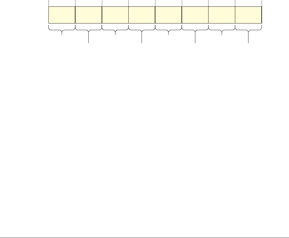
B4 System Control Registers in a VMSA implementation
B4.1 VMSA System control registers descriptions, in register order
B4-1618 Copyright © 1996-1998, 2000, 2004-2012, 2014 ARM. All rights reserved. ARM DDI 0406C.c
Non-Confidential ID051414
B4.1.87 ID_ISAR4, Instruction Set Attribute Register 4, VMSA
The ID_ISAR4 characteristics are:
Purpose ID_ISAR4 provides information about the instruction sets implemented by the processor.
For more information see About the Instruction Set Attribute registers on page B7-1952.
This register is a CPUID register, and is part of the Identification registers functional group.
Usage constraints Only accessible from PL1 or higher.
Must be interpreted with ID_ISAR0, ID_ISAR1, ID_ISAR2, and ID_ISAR3. For more
information see About the Instruction Set Attribute registers on page B7-1952.
Configurations The VMSA and PMSA definitions of the register fields are identical.
In a VMSA implementation that includes the Security Extensions, this is a Common
register.
Attributes A 32-bit RO register with an IMPLEMENTATION DEFINED value:
•Table B7-1 on page B7-1952 shows the encodings of all of the CPUID registers
•Table B3-44 on page B3-1492 shows the encodings of all of the registers in the
Identification registers functional group.
All field values not shown in the field descriptions are reserved.
The ID_ISAR4 bit assignments are:
SWP_frac, bits[31:28]
Indicates support for the memory system locking the bus for
SWP
or
SWPB
instructions. Permitted
values are:
0b0000
SWP
or
SWPB
instructions not implemented.
0b0001
SWP
or
SWPB
implemented but only in a uniprocessor context.
SWP
and
SWPB
do not
guarantee whether memory accesses from other masters can come between the load
memory access and the store memory access of the
SWP
or
SWPB
.
This field is valid only if the ID_ISAR0.Swap_instrs field is zero.
PSR_M_instrs, bits[27:24]
Indicates the implemented M profile instructions to modify the PSRs. Permitted values are:
0b0000
None implemented.
0b0001
Adds the M profile forms of the
CPS
,
MRS
and
MSR
instructions.
SynchPrim_instrs_frac, bits[23:20]
This field is used with the ID_ISAR3.SynchPrim_instrs field to indicate the implemented
Synchronization Primitive instructions. Table B4-6 on page B4-1616 shows the permitted values of
these fields.
All combinations of SynchPrim_instrs and SynchPrim_instrs_frac not shown in Table B4-6 on
page B4-1616 are reserved.
31 16 15 12 11 8 7 4 3 028 27 24 23 20 19
PSR_M_instrs
SWP_frac
Barrier_instrs
SynchPrim_instrs_frac
Writeback_instrs
SMC_instrs
Unpriv_instrs
WithShifts_instrs

B4 System Control Registers in a VMSA implementation
B4.1 VMSA System control registers descriptions, in register order
ARM DDI 0406C.c Copyright © 1996-1998, 2000, 2004-2012, 2014 ARM. All rights reserved. B4-1619
ID051414 Non-Confidential
Barrier_instrs, bits[19:16]
Indicates the implemented Barrier instructions in the ARM and Thumb instruction sets. Permitted
values are:
0b0000
None implemented. Barrier operations are provided only as CP15 operations.
0b0001
Adds the
DMB
,
DSB
, and
ISB
barrier instructions.
SMC_instrs, bits[15:12]
Indicates the implemented
SMC
instructions. Permitted values are:
0b0000
None implemented.
0b0001
Adds the
SMC
instruction.
Note
The
SMC
instruction was called the
SMI
instruction in previous versions of the ARM architecture.
Writeback_instrs, bits[11:8]
Indicates the support for Writeback addressing modes. Permitted values are:
0b0000
Basic support. Only the
LDM
,
STM
,
PUSH
,
POP
,
SRS
, and
RFE
instructions support writeback
addressing modes. These instructions support all of their writeback addressing modes.
0b0001
Adds support for all of the writeback addressing modes defined in ARMv7.
WithShifts_instrs, bits[7:4]
Indicates the support for instructions with shifts. Permitted values are:
0b0000
Nonzero shifts supported only in
MOV
and shift instructions.
0b0001
Adds support for shifts of loads and stores over the range LSL 0-3.
0b0011
As for
0b0001
, and adds support for other constant shift options, both on load/store and
other instructions.
0b0100
As for
0b0011
, and adds support for register-controlled shift options.
Note
• In this field, the permitted values are not continuous, and the value
0b0010
is reserved.
• Additions to the basic support indicated by the
0b0000
field value only apply when the
encoding supports them. In particular, in the Thumb instruction set there is no difference
between the
0b0011
and
0b0100
levels of support.
•
MOV
instructions with shift options are treated as
ASR
,
LSL
,
LSR
,
ROR
or
RRX
instructions, as
described in Data-processing instructions on page B7-1953.
Unpriv_instrs, bits[3:0]
Indicates the implemented unprivileged instructions. Permitted values are:
0b0000
None implemented. No
T
variant instructions are implemented.
0b0001
Adds the
LDRBT
,
LDRT
,
STRBT
, and
STRT
instructions.
0b0010
As for
0b0001
, and adds the
LDRHT
,
LDRSBT
,
LDRSHT
, and
STRHT
instructions.
Accessing ID_ISAR4
To access ID_ISAR4, software reads the CP15 registers with
<opc1>
set to 0,
<CRn>
set to c0,
<CRm>
set to c2, and
<opc2>
set to 4. For example:
MRC p15, 0, <Rt>, c0, c2, 4 ; Read ID_ISAR4 into Rt

B4 System Control Registers in a VMSA implementation
B4.1 VMSA System control registers descriptions, in register order
B4-1620 Copyright © 1996-1998, 2000, 2004-2012, 2014 ARM. All rights reserved. ARM DDI 0406C.c
Non-Confidential ID051414
B4.1.88 ID_ISAR5, Instruction Set Attribute Register 5, VMSA
The ID_ISAR5 characteristics are:
Purpose ID_ISAR5 is reserved for future expansion of the information about the instruction sets
implemented by the processor.
This register is a CPUID register, and is part of the Identification registers functional group.
Usage constraints Only accessible from PL1 or higher.
Configurations The VMSA and PMSA definitions of the register fields are identical.
In a VMSA implementation that includes the Security Extensions, this is a Common
register.
Attributes A 32-bit RO register:
•Table B7-1 on page B7-1952 shows the encodings of all of the CPUID registers
•Table B3-44 on page B3-1492 shows the encodings of all of the registers in the
Identification registers functional group.
The ID_ISAR5 bit assignments are:
Bits[31:0] Reserved, UNK.
Accessing ID_ISAR5
To access ID_ISAR5, software reads the CP15 registers with
<opc1>
set to 0,
<CRn>
set to c0,
<CRm>
set to c2, and
<opc2>
set to 5. For example:
MRC p15, 0, <Rt>, c0, c2, 5 ; Read ID_ISAR5 into Rt
Reserved, UNK
31 0

B4 System Control Registers in a VMSA implementation
B4.1 VMSA System control registers descriptions, in register order
ARM DDI 0406C.c Copyright © 1996-1998, 2000, 2004-2012, 2014 ARM. All rights reserved. B4-1621
ID051414 Non-Confidential
B4.1.89 ID_MMFR0, Memory Model Feature Register 0, VMSA
The ID_MMFR0 characteristics are:
Purpose ID_MMFR0 provides information about the implemented memory model and memory
management support.
This register is a CPUID register, and is part of the Identification registers functional group.
Usage constraints Only accessible from PL1 or higher.
Must be interpreted with ID_MMFR1, ID_MMFR2, and ID_MMFR3.
Configurations The VMSA and PMSA definitions of the register fields are identical.
In a VMSA implementation that includes the Security Extensions, this is a Common
register.
Attributes A 32-bit RO register with an IMPLEMENTATION DEFINED value:
•Table B7-1 on page B7-1952 shows the encodings of all of the CPUID registers
•Table B3-44 on page B3-1492 shows the encodings of all of the registers in the
Identification registers functional group.
All field values not shown in the field descriptions are reserved.
The ID_MMFR0 bit assignments are:
Innermost shareability, bits[31:28]
Indicates the innermost shareability domain implemented. Permitted values are:
0b0000
Implemented as Non-cacheable.
0b0001
Implemented with hardware coherency support.
0b1111
Shareability ignored.
This field is valid only if the implementation distinguishes between Inner Shareable and Outer
Shareable, by implementing two levels of shareability, as indicated by the value of the Shareability
levels field, bits[15:12].
When the Shareability levels field is zero, this field is reserved, UNK.
FCSE support, bits[27:24]
Indicates whether the implementation includes the FCSE. Permitted values are:
0b0000
Not supported.
0b0001
Support for FCSE.
The value of
0b0001
is only permitted when the VMSA_support field has a value greater than
0b0010
.
Auxiliary registers, bits[23:20]
Indicates support for Auxiliary registers. Permitted values are:
0b0000
None supported.
0b0001
Support for Auxiliary Control Register only.
0b0010
Support for Auxiliary Fault Status Registers (AIFSR and ADFSR) and Auxiliary
Control Register.
Innermost
shareability
FCSE
support
Auxiliary
registers
TCM
support
31 16 15 12 11 8 7 4 3 0
Shareability
levels
Outermost
shareability
PMSA
support
VMSA
support
28 27 24 23 20 19

B4 System Control Registers in a VMSA implementation
B4.1 VMSA System control registers descriptions, in register order
B4-1622 Copyright © 1996-1998, 2000, 2004-2012, 2014 ARM. All rights reserved. ARM DDI 0406C.c
Non-Confidential ID051414
TCM support, bits[19:16]
Indicates support for TCMs and associated DMAs. Permitted values are:
0b0000
Not supported.
0b0001
Support is IMPLEMENTATION DEFINED. ARMv7 requires this setting.
0b0010
Support for TCM only, ARMv6 implementation.
0b0011
Support for TCM and DMA, ARMv6 implementation.
Note
An ARMv7 implementation might include an ARMv6 model for TCM support. However, in
ARMv7 this is an IMPLEMENTATION DEFINED option, and therefore it must be represented by the
0b0001
encoding in this field.
Shareability levels, bits[15:12]
Indicates the number of shareability levels implemented. Permitted values are:
0b0000
One level of shareability implemented.
0b0001
Two levels of shareability implemented.
Outermost shareability, bits[11:8]
Indicates the outermost shareability domain implemented. Permitted values are:
0b0000
Implemented as Non-cacheable.
0b0001
Implemented with hardware coherency support.
0b1111
Shareability ignored.
PMSA support, bits[7:4]
Indicates support for a PMSA. Permitted values are:
0b0000
Not supported.
0b0001
Support for IMPLEMENTATION DEFINED PMSA.
0b0010
Support for PMSAv6, with a Cache Type Register implemented.
0b0011
Support for PMSAv7, with support for memory subsections. ARMv7-R profile.
When the PMSA support field is set to a value other than
0b0000
the VMSA support field must be
set to
0b0000
.
VMSA support, bits[3:0]
Indicates support for a VMSA. Permitted values are:
0b0000
Not supported.
0b0001
Support for IMPLEMENTATION DEFINED VMSA.
0b0010
Support for VMSAv6, with Cache and TLB Type Registers implemented.
0b0011
Support for VMSAv7, with support for remapping and the Access flag. ARMv7-A
profile.
0b0100
As for
0b0011
, and adds support for the PXN bit in the Short-descriptor translation table
format descriptors.
0b0101
As for
0b0100
, and adds support for the Long-descriptor translation table format.
When the VMSA support field is set to a value other than
0b0000
the PMSA support field must be
set to
0b0000
.
Accessing ID_MMFR0
To access ID_MMFR0, software reads the CP15 registers with
<opc1>
set to 0,
<CRn>
set to c0,
<CRm>
set to c1, and
<opc2>
set to 4. For example:
MRC p15, 0, <Rt>, c0, c1, 4 ; Read ID_MMFR0 into Rt

B4 System Control Registers in a VMSA implementation
B4.1 VMSA System control registers descriptions, in register order
ARM DDI 0406C.c Copyright © 1996-1998, 2000, 2004-2012, 2014 ARM. All rights reserved. B4-1623
ID051414 Non-Confidential
B4.1.90 ID_MMFR1, Memory Model Feature Register 1, VMSA
The ID_MMFR1 characteristics are:
Purpose ID_MMFR1 provides information about the implemented memory model and memory
management support.
This register is a CPUID register, and is part of the Identification registers functional group.
Usage constraints Only accessible from PL1 or higher.
Must be interpreted with ID_MMFR0, ID_MMFR2, and ID_MMFR3.
Configurations The VMSA and PMSA definitions of the register fields are identical.
In a VMSA implementation that includes the Security Extensions, this is a Common
register.
Attributes A 32-bit RO register with an IMPLEMENTATION DEFINED value:
•Table B7-1 on page B7-1952 shows the encodings of all of the CPUID registers
•Table B3-44 on page B3-1492 shows the encodings of all of the registers in the
Identification registers functional group.
All field values not shown in the field descriptions are reserved.
The ID_MMFR1 bit assignments are:
Branch predictor, bits[31:28]
Indicates branch predictor management requirements. Permitted values are:
0b0000
No branch predictor, or no MMU present. Implies a fixed MPU configuration.
0b0001
Branch predictor requires flushing on:
• enabling or disabling the MMU
• writing new data to instruction locations
• writing new mappings to the translation tables
• any change to the TTBR0, TTBR1, or TTBCR registers
• changes of FCSE ProcessID or ContextID.
0b0010
Branch predictor requires flushing on:
• enabling or disabling the MMU
• writing new data to instruction locations
• writing new mappings to the translation tables
• any change to the TTBR0, TTBR1, or TTBCR registers without a corresponding
change to the FCSE ProcessID or ContextID.
0b0011
Branch predictor requires flushing only on writing new data to instruction locations.
0b0100
For execution correctness, branch predictor requires no flushing at any time.
Note
The branch predictor is described in some documentation as the Branch Target Buffer.
L1 cache
test and
clean
L1 Harvard
cache VA
31 24 23 20 19 16 15 12 11 8 7 4 3 0
Branch
predictor
L1 unified
cache
L1 Harvard
cache
L1 unified
cache
set/way
L1 Harvard
cache
set/way
L1 unified
cache VA
28 27

B4 System Control Registers in a VMSA implementation
B4.1 VMSA System control registers descriptions, in register order
B4-1624 Copyright © 1996-1998, 2000, 2004-2012, 2014 ARM. All rights reserved. ARM DDI 0406C.c
Non-Confidential ID051414
L1 cache test and clean, bits[27:24]
Indicates the supported Level 1 data cache test and clean operations, for Harvard or unified cache
implementations. Permitted values are:
0b0000
None supported. This is the required setting for ARMv7.
0b0001
Supported Level 1 data cache test and clean operations are:
• Test and clean data cache.
0b0010
As for
0b0001
, and adds:
• Test, clean, and invalidate data cache.
L1 unified cache, bits[23:20]
Indicates the supported entire Level 1 cache maintenance operations, for a unified cache
implementation. Permitted values are:
0b0000
None supported. This is the required setting for ARMv7, because ARMv7 requires a
hierarchical cache implementation.
0b0001
Supported entire Level 1 cache operations are:
• Invalidate cache, including branch predictor if appropriate
• Invalidate branch predictor, if appropriate.
0b0010
As for
0b0001
, and adds:
• Clean cache. Uses a recursive model, using the cache dirty status bit.
• Clean and invalidate cache. Uses a recursive model, using the cache dirty status
bit.
If this field is set to a value other than
0b0000
then the L1 Harvard cache field, bits[19:16], must be
set to
0b0000
.
L1 Harvard cache, bits[19:16]
Indicates the supported entire Level 1 cache maintenance operations, for a Harvard cache
implementation. Permitted values are:
0b0000
None supported. This is the required setting for ARMv7, because ARMv7 requires a
hierarchical cache implementation.
0b0001
Supported entire Level 1 cache operations are:
• Invalidate instruction cache, including branch predictor if appropriate
• Invalidate branch predictor, if appropriate.
0b0010
As for
0b0001
, and adds:
• Invalidate data cache
• Invalidate data cache and instruction cache, including branch predictor if
appropriate.
0b0011
As for
0b0010
, and adds:
• Clean data cache. Uses a recursive model, using the cache dirty status bit.
• Clean and invalidate data cache. Uses a recursive model, using the cache dirty
status bit.
If this field is set to a value other than
0b0000
then the L1 unified cache field, bits[23:20], must be
set to
0b0000
.

B4 System Control Registers in a VMSA implementation
B4.1 VMSA System control registers descriptions, in register order
ARM DDI 0406C.c Copyright © 1996-1998, 2000, 2004-2012, 2014 ARM. All rights reserved. B4-1625
ID051414 Non-Confidential
L1 unified cache set/way, bits[15:12]
Indicates the supported Level 1 cache line maintenance operations by set/way, for a unified cache
implementation. Permitted values are:
0b0000
None supported. This is the required setting for ARMv7, because ARMv7 requires a
hierarchical cache implementation.
0b0001
Supported Level 1 unified cache line maintenance operations by set/way are:
• Clean cache line by set/way.
0b0010
As for
0b0001
, and adds:
• Clean and invalidate cache line by set/way.
0b0011
As for
0b0010
, and adds:
• Invalidate cache line by set/way.
If this field is set to a value other than
0b0000
then the L1 Harvard cache s/w field, bits[11:8], must
be set to
0b0000
.
L1 Harvard cache set/way, bits[11:8]
Indicates the supported Level 1 cache line maintenance operations by set/way, for a Harvard cache
implementation. Permitted values are:
0b0000
None supported. This is the required setting for ARMv7, because ARMv7 requires a
hierarchical cache implementation.
0b0001
Supported Level 1 Harvard cache line maintenance operations by set/way are:
• Clean data cache line by set/way
• Clean and invalidate data cache line by set/way.
0b0010
As for
0b0001
, and adds:
• Invalidate data cache line by set/way.
0b0011
As for
0b0010
, and adds:
• Invalidate instruction cache line by set/way.
If this field is set to a value other than
0b0000
then the L1 unified cache s/w field, bits[15:12], must
be set to
0b0000
.
L1 unified cache VA, bits[7:4]
Indicates the supported Level 1 cache line maintenance operations by MVA, for a unified cache
implementation. Permitted values are:
0b0000
None supported. This is the required setting for ARMv7, because ARMv7 requires a
hierarchical cache implementation.
0b0001
Supported Level 1 unified cache line maintenance operations by MVA are:
• Clean cache line by MVA
• Invalidate cache line by MVA
• Clean and invalidate cache line by MVA.
0b0010
As for
0b0001
, and adds:
• Invalidate branch predictor by MVA, if branch predictor is implemented.
If this field is set to a value other than
0b0000
then the L1 Harvard cache VA field, bits[3:0], must be
set to
0b0000
.

B4 System Control Registers in a VMSA implementation
B4.1 VMSA System control registers descriptions, in register order
B4-1626 Copyright © 1996-1998, 2000, 2004-2012, 2014 ARM. All rights reserved. ARM DDI 0406C.c
Non-Confidential ID051414
L1 Harvard cache VA, bits[3:0]
Indicates the supported Level 1 cache line maintenance operations by MVA, for a Harvard cache
implementation. Permitted values are:
0b0000
None supported. This is the required setting for ARMv7, because ARMv7 requires a
hierarchical cache implementation.
0b0001
Supported Level 1 Harvard cache line maintenance operations by MVA are:
• Clean data cache line by MVA
• Invalidate data cache line by MVA
• Clean and invalidate data cache line by MVA
• Clean instruction cache line by MVA.
0b0010
As for
0b0001
, and adds:
• Invalidate branch predictor by MVA, if branch predictor is implemented.
If this field is set to a value other than
0b0000
then the L1 unified cache VA field, bits[7:4], must be
set to
0b0000
.
Accessing ID_MMFR1
To access ID_MMFR1, software reads the CP15 registers with
<opc1>
set to 0,
<CRn>
set to c0,
<CRm>
set to c1, and
<opc2>
set to 5. For example:
MRC p15, 0, <Rt>, c0, c1, 5 ; Read ID_MMFR1 into Rt

B4 System Control Registers in a VMSA implementation
B4.1 VMSA System control registers descriptions, in register order
ARM DDI 0406C.c Copyright © 1996-1998, 2000, 2004-2012, 2014 ARM. All rights reserved. B4-1627
ID051414 Non-Confidential
B4.1.91 ID_MMFR2, Memory Model Feature Register 2, VMSA
The ID_MMFR2 characteristics are:
Purpose ID_MMFR2 provides information about the implemented memory model and memory
management support.
This register is a CPUID register, and is part of the Identification registers functional group.
Usage constraints Only accessible from PL1 or higher.
Must be interpreted with ID_MMFR0, ID_MMFR1, and ID_MMFR3.
Configurations The VMSA and PMSA definitions of the register fields are identical.
In a VMSA implementation that includes the Security Extensions, this is a Common
register.
Attributes A 32-bit RO register with an IMPLEMENTATION DEFINED value:
•Table B7-1 on page B7-1952 shows the encodings of all of the CPUID registers
•Table B3-44 on page B3-1492 shows the encodings of all of the registers in the
Identification registers functional group.
All field values not shown in the field descriptions are reserved.
The ID_MMFR2 bit assignments are:
HW Access flag, bits[31:28]
Indicates support for a Hardware Access flag, as part of the VMSAv7 implementation. Permitted
values are:
0b0000
Not supported.
0b0001
Support for VMSAv7 Access flag, updated in hardware.
On an ARMv7-R implementation this field must be
0b0000
.
WFI stall, bits[27:24]
Indicates the support for Wait For Interrupt (WFI) stalling. Permitted values are:
0b0000
Not supported.
0b0001
Support for WFI stalling.
Mem barrier, bits[23:20]
Indicates the supported CP15 memory barrier operations:
0b0000
None supported.
0b0001
Supported CP15 Memory barrier operations are:
• Data Synchronization Barrier (DSB). In previous versions of the ARM
architecture, DSB was named Data Write Barrier (DWB).
0b0010
As for
0b0001
, and adds:
• Instruction Synchronization Barrier (ISB). In previous versions of the ARM
architecture, the ISB operation was called Prefetch Flush.
• Data Memory Barrier (DMB).
Note
ARM deprecates the use of these operations. ID_ISAR4.Barrier_instrs indicates the level of support
for the preferred barrier instructions.
HW
Access flag
WFI
stall
Mem
barrier
Unified
TLB
31 16 15 12 11 8 7 4 3 0
Harvard
TLB
L1 Harvard
range
L1 Harvard
bg fetch
L1 Harvard
fg fetch
28 27 24 23 20 19

B4 System Control Registers in a VMSA implementation
B4.1 VMSA System control registers descriptions, in register order
B4-1628 Copyright © 1996-1998, 2000, 2004-2012, 2014 ARM. All rights reserved. ARM DDI 0406C.c
Non-Confidential ID051414
Unified TLB, bits[19:16]
Indicates the supported TLB maintenance operations, for a unified or Harvard TLB implementation.
Permitted values are:
0b0000
Not supported.
0b0001
Supported unified TLB maintenance operations are:
• Invalidate all entries in the TLB
• Invalidate TLB entry by MVA.
0b0010
As for
0b0001
, and adds:
• Invalidate TLB entries by ASID match.
0b0011
As for
0b0010
and adds:
• Invalidate instruction TLB and data TLB entries by MVA All ASID. This is a
shared unified TLB operation.
0b0100
As for
0b0011
and adds:
• Invalidate Hyp mode unified TLB entry by MVA
• Invalidate entire Non-secure PL1&0 unified TLB
• Invalidate entire Hyp mode unified TLB.
Harvard TLB, bits[15:12]
Indicates the supported TLB maintenance operations, for a Harvard TLB implementation. Permitted
values are:
0b0000
If the Unified TLB field is not
0b0000
, then the meaning of this field is IMPLEMENTATION
DEFINED, and must be ignored by software.
0b0001
Supported Harvard TLB maintenance operations are:
• Invalidate all entries in the ITLB and the DTLB.
This is a shared unified TLB operation.
• Invalidate all ITLB entries.
• Invalidate all DTLB entries.
• Invalidate ITLB entry by MVA.
• Invalidate DTLB entry by MVA.
0b0010
As for
0b0001
, and adds:
• Invalidate ITLB and DTLB entries by ASID match.
This is a shared unified TLB operation.
• Invalidate ITLB entries by ASID match
• Invalidate DTLB entries by ASID match.
Note
This field is defined only for legacy reasons. It is replaced by the Unified TLB field, bits19:16], and
it must be ignored by software if the Unified TLB field is not
0b0000
.
L1 Harvard range, bits[11:8]
Indicates the supported Level 1 cache maintenance range operations, for a Harvard cache
implementation. Permitted values are:
0b0000
Not supported.
0b0001
Supported Level 1 Harvard cache maintenance range operations are:
• Invalidate data cache range by VA
• Invalidate instruction cache range by VA
• Clean data cache range by VA
• Clean and invalidate data cache range by VA.

B4 System Control Registers in a VMSA implementation
B4.1 VMSA System control registers descriptions, in register order
ARM DDI 0406C.c Copyright © 1996-1998, 2000, 2004-2012, 2014 ARM. All rights reserved. B4-1629
ID051414 Non-Confidential
L1 Harvard bg fetch, bits[7:4]
Indicates the supported Level 1 cache background fetch operations, for a Harvard cache
implementation. When supported, background fetch operations are non-blocking operations.
Permitted values are:
0b0000
Not supported.
0b0001
Supported Level 1 Harvard cache background fetch operations are:
• Fetch instruction cache range by VA
• Fetch data cache range by VA.
L1 Harvard fg fetch, bits[3:0]
Indicates the supported Level 1 cache foreground fetch operations, for a Harvard cache
implementation. When supported, foreground fetch operations are blocking operations. Permitted
values are:
0b0000
Not supported.
0b0001
Supported Level 1 Harvard cache foreground fetch operations are:
• Fetch instruction cache range by VA
• Fetch data cache range by VA.
Accessing ID_MMFR2
To access ID_MMFR2, software reads the CP15 registers with
<opc1>
set to 0,
<CRn>
set to c0,
<CRm>
set to c1, and
<opc2>
set to 6. For example:
MRC p15, 0, <Rt>, c0, c1, 6 ; Read ID_MMFR2 into Rt
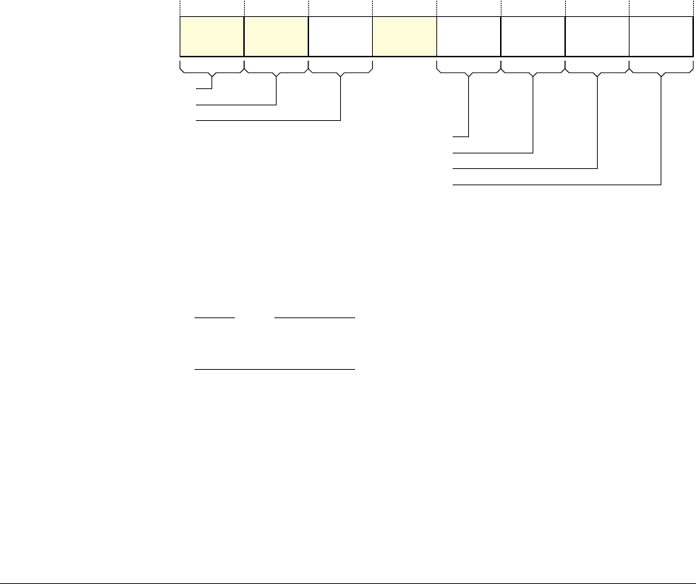
B4 System Control Registers in a VMSA implementation
B4.1 VMSA System control registers descriptions, in register order
B4-1630 Copyright © 1996-1998, 2000, 2004-2012, 2014 ARM. All rights reserved. ARM DDI 0406C.c
Non-Confidential ID051414
B4.1.92 ID_MMFR3, Memory Model Feature Register 3, VMSA
The ID_MMFR3 characteristics are:
Purpose ID_MMFR3 provides information about the implemented memory model and memory
management support.
This register is a CPUID register, and is part of the Identification registers functional group.
Usage constraints Only accessible from PL1 or higher.
Must be interpreted with ID_MMFR0, ID_MMFR1, and ID_MMFR2.
Configurations The VMSA and PMSA definitions of the register fields are identical.
In a VMSA implementation that includes the Security Extensions, this is a Common
register.
Attributes A 32-bit RO register with an IMPLEMENTATION DEFINED value:
•Table B7-1 on page B7-1952 shows the encodings of all of the CPUID registers
•Table B3-44 on page B3-1492 shows the encodings of all of the registers in the
Identification registers functional group.
All field values not shown in the field descriptions are reserved.
The ID_MMFR3 bit assignments are:
Supersection support, bits[31:28]
On a VMSA implementation, indicates whether Supersections are supported. Permitted values are:
0b0000
Supersections supported.
0b1111
Supersections not supported.
Note
The sense of this identification is reversed from the normal usage in the CPUID mechanism, with
the value of zero indicating that the feature is supported.
Cached memory size, bits[27:24]
Indicates the physical memory size supported by the processor caches. Permitted values are:
0b0000
4GBbyte, corresponding to a 32-bit physical address range.
0b0001
64GBbyte, corresponding to a 36-bit physical address range.
0b0010
1TBbyte, corresponding to a 40-bit physical address range.
31 28 27 16 15 12 11 8 7 4 3 0
Reserved,
UNK
Supersection support
BP maintain
Cache maintenance set/way
Cache maintenance MVA
Maintenance broadcast
1920
2324
Coherent walk
Cached memory size
†
† Only on an implementation that includes the Large Physical Address Extension, otherwise reserved.

B4 System Control Registers in a VMSA implementation
B4.1 VMSA System control registers descriptions, in register order
ARM DDI 0406C.c Copyright © 1996-1998, 2000, 2004-2012, 2014 ARM. All rights reserved. B4-1631
ID051414 Non-Confidential
Coherent walk, bits[23:20]
Indicates whether translation table updates require a clean to the point of unification. Permitted
values are:
0b0000
Updates to the translation tables require a clean to the point of unification to ensure
visibility by subsequent translation table walks.
0b0001
Updates to the translation tables do not require a clean to the point of unification to
ensure visibility by subsequent translation table walks.
Bits[19:16] Reserved, UNK.
Maintenance broadcast, bits[15:12]
Indicates whether Cache, TLB and branch predictor operations are broadcast. Permitted values are:
0b0000
Cache, TLB and branch predictor operations only affect local structures.
0b0001
Cache and branch predictor operations affect structures according to shareability and
defined behavior of instructions. TLB operations only affect local structures.
0b0010
Cache, TLB and branch predictor operations affect structures according to shareability
and defined behavior of instructions.
BP maintain, bits[11:8]
Indicates the supported branch predictor maintenance operations in an implementation with
hierarchical cache maintenance operations. Permitted values are:
0b0000
None supported.
0b0001
Supported branch predictor maintenance operations are:
• Invalidate all branch predictors.
0b0010
As for
0b0001
, and adds:
• Invalidate branch predictors by MVA.
Cache maintain set/way, bits[7:4]
Indicates the supported cache maintenance operations by set/way, in an implementation with
hierarchical caches. Permitted values are:
0b0000
None supported.
0b0001
Supported hierarchical cache maintenance operations by set/way are:
• Invalidate data cache by set/way
• Clean data cache by set/way
• Clean and invalidate data cache by set/way.
In a unified cache implementation, the data cache operations apply to the unified caches.
Cache maintain MVA, bits[3:0]
Indicates the supported cache maintenance operations by MVA, in an implementation with
hierarchical caches. Permitted values are:
0b0000
None supported.
0b0001
Supported hierarchical cache maintenance operations by MVA are:
• Invalidate data cache by MVA
• Clean data cache by MVA
• Clean and invalidate data cache by MVA
• Invalidate instruction cache by MVA
• Invalidate all instruction cache entries.
In a unified cache implementation, the data cache operations apply to the unified caches, and the
instruction cache operations are not implemented.

B4 System Control Registers in a VMSA implementation
B4.1 VMSA System control registers descriptions, in register order
B4-1632 Copyright © 1996-1998, 2000, 2004-2012, 2014 ARM. All rights reserved. ARM DDI 0406C.c
Non-Confidential ID051414
Accessing ID_MMFR3
To access ID_MMFR3, software reads the CP15 registers with
<opc1>
set to 0,
<CRn>
set to c0,
<CRm>
set to c1, and
<opc2>
set to7. For example:
MRC p15, 0, <Rt>, c0, c1, 7 ; Read ID_MMFR3 into Rt

B4 System Control Registers in a VMSA implementation
B4.1 VMSA System control registers descriptions, in register order
ARM DDI 0406C.c Copyright © 1996-1998, 2000, 2004-2012, 2014 ARM. All rights reserved. B4-1633
ID051414 Non-Confidential
B4.1.93 ID_PFR0, Processor Feature Register 0, VMSA
The ID_PFR0 characteristics are:
Purpose ID_PFR0 gives information about the programmers’ model and top-level information about
the instruction sets supported by the processor.
This register is a CPUID register, and is part of the Identification registers functional group.
Usage constraints Only accessible from PL1 or higher.
Must be interpreted with ID_PFR1.
Configurations The VMSA and PMSA definitions of the register fields are identical.
In a VMSA implementation that includes the Security Extensions, this is a Common
register.
Attributes A 32-bit RO register with an IMPLEMENTATION DEFINED value:
•Table B7-1 on page B7-1952 shows the encodings of all of the CPUID registers
•Table B3-44 on page B3-1492 shows the encodings of all of the registers in the
Identification registers functional group.
All field values not shown in the field descriptions are reserved.
The ID_PFR0 bit assignments are:
Bits[31:16] Reserved, UNK.
State3, bits[15:12]
ThumbEE instruction set support. Permitted values are:
0b0000
Not implemented.
0b0001
ThumbEE instruction set implemented.
The value of
0b0001
is only permitted when State1 ==
0b0011
.
State2, bits[11:8]
Jazelle extension support. Permitted values are:
0b0000
Not implemented.
0b0001
Jazelle extension implemented, without clearing of JOSCR.CV on exception entry.
0b0010
Jazelle extension implemented, with clearing of JOSCR.CV on exception entry.
A trivial implementation of the Jazelle extension is indicated by the value
0b0001
.
State1, bits[7:4]
Thumb instruction set support. Permitted values are:
0b0000
Thumb instruction set not implemented.
0b0001
Thumb encodings before the introduction of Thumb-2 technology implemented:
• all instructions are 16-bit
•a
BL
or
BLX
is a pair of 16-bit instructions
• 32-bit instructions other than
BL
and
BLX
cannot be encoded.
0b0010
Reserved.
0b0011
Thumb encodings after the introduction of Thumb-2 technology implemented, for all
16-bit and 32-bit Thumb basic instructions.
Reserved, UNK
31 16 15 12 11 8 7 4 3 0
State3 State2 State1 State0

B4 System Control Registers in a VMSA implementation
B4.1 VMSA System control registers descriptions, in register order
B4-1634 Copyright © 1996-1998, 2000, 2004-2012, 2014 ARM. All rights reserved. ARM DDI 0406C.c
Non-Confidential ID051414
State0, bits[3:0]
ARM instruction set support. Permitted values are:
0b0000
ARM instruction set not implemented.
0b0001
ARM instruction set implemented.
Accessing ID_PFR0
To access ID_PFR0, software reads the CP15 registers with
<opc1>
set to 0,
<CRn>
set to c0,
<CRm>
set to c1, and
<opc2>
set to 0. For example:
MRC p15, 0, <Rt>, c0, c1, 0 ; Read ID_PFR0 into Rt
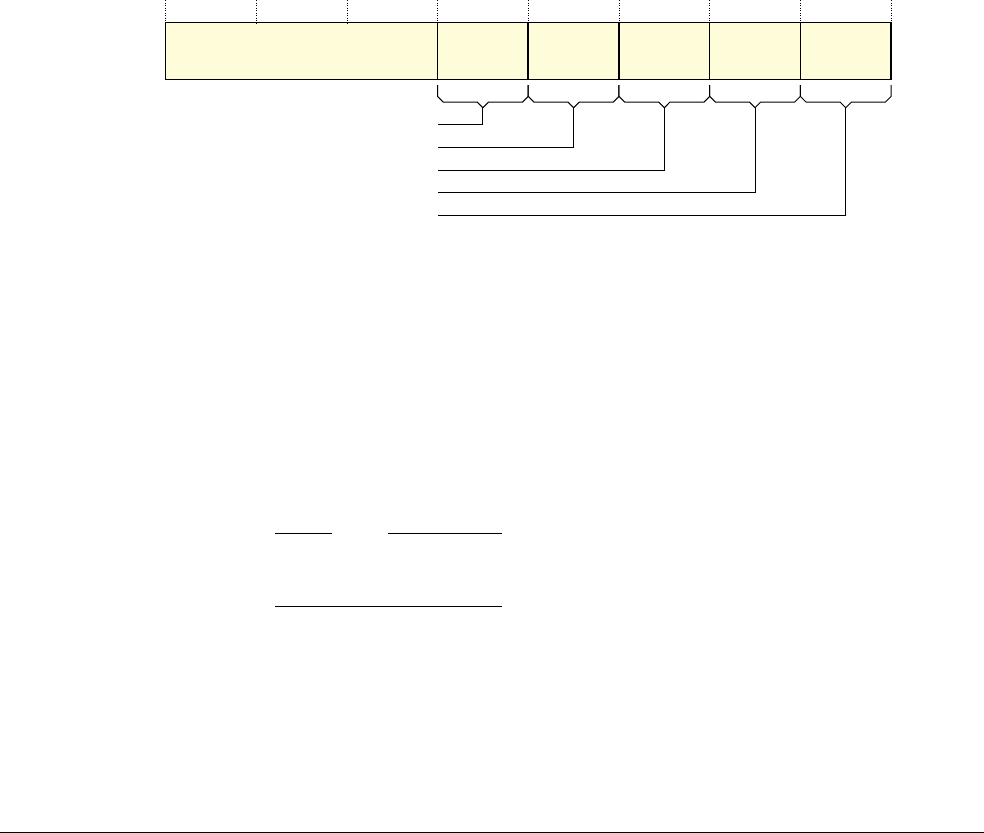
B4 System Control Registers in a VMSA implementation
B4.1 VMSA System control registers descriptions, in register order
ARM DDI 0406C.c Copyright © 1996-1998, 2000, 2004-2012, 2014 ARM. All rights reserved. B4-1635
ID051414 Non-Confidential
B4.1.94 ID_PFR1, Processor Feature Register 1, VMSA
The ID_PFR1 characteristics are:
Purpose ID_PFR1 gives information about the programmers’ model and Security Extensions
support.
This register is a CPUID register, and is part of the Identification registers functional group.
Usage constraints Only accessible from PL1 or higher.
Must be interpreted with ID_PFR0.
Configurations The VMSA and PMSA definitions of the register fields are identical.
In a VMSA implementation that includes the Security Extensions, this is a Common
register.
Attributes A 32-bit RO register with an IMPLEMENTATION DEFINED value:
•Table B7-1 on page B7-1952 shows the encodings of all of the CPUID registers
•Table B3-44 on page B3-1492 shows the encodings of all of the registers in the
Identification registers functional group.
All field values not shown in the field descriptions are reserved.
The ID_PFR1 bit assignments are:
Bits[31:20] Reserved, UNK.
Generic Timer Extension, bits[19:16]
Permitted values are:
0b0000
Not implemented.
0b0001
Generic Timer Extension implemented.
Virtualization Extensions, bits[15:12]
Permitted values are:
0b0000
Not implemented.
0b0001
Virtualization Extensions implemented.
Note
A value of
0b0001
implies implementation of the
HVC
,
ERET
,
MRS
(Banked register), and
MSR
(Banked
register) instructions. The ID_ISARs do not identify whether these instructions are implemented.
Programmers’ model
M profile programmers’ model
Security Extensions
Virtualization Extensions
Reserved, UNK
31 20 19 16 15 12 11 8 7 4 3 0
Generic Timer

B4 System Control Registers in a VMSA implementation
B4.1 VMSA System control registers descriptions, in register order
B4-1636 Copyright © 1996-1998, 2000, 2004-2012, 2014 ARM. All rights reserved. ARM DDI 0406C.c
Non-Confidential ID051414
M profile programmers’ model, bits[11:8]
Permitted values are:
0b0000
Not supported.
0b0010
Support for two-stack programmers’ model.
Note
In this field, the permitted values are not continuous, and the value of
0b0001
is reserved.
Security Extensions, bits[7:4]
Permitted values are:
0b0000
Not implemented.
0b0001
Security Extensions implemented.
This includes support for Monitor mode and the
SMC
instruction.
0b0010
As for
0b0001
, and adds the ability to set the NSACR.RFR bit.
Programmers’ model, bits[3:0]
Support for the standard programmers’ model for ARMv4 and later. Model must support User, FIQ,
IRQ, Supervisor, Abort, Undefined and System modes. Permitted values are:
0b0000
Not supported.
0b0001
Supported.
Accessing ID_PFR1
To access ID_PFR1, software reads the CP15 registers with
<opc1>
set to 0,
<CRn>
set to c0,
<CRm>
set to c1, and
<opc2>
set to 1. For example:
MRC p15, 0, <Rt>, c0, c1, 1 ; Read ID_PFR1 into Rt

B4 System Control Registers in a VMSA implementation
B4.1 VMSA System control registers descriptions, in register order
ARM DDI 0406C.c Copyright © 1996-1998, 2000, 2004-2012, 2014 ARM. All rights reserved. B4-1637
ID051414 Non-Confidential
B4.1.95 IFAR, Instruction Fault Address Register, VMSA
The IFAR characteristics are:
Purpose The IFAR holds the VA of the faulting access that caused a synchronous Prefetch Abort
exception.
This register is part of the PL1 Fault handling registers functional group.
Usage constraints Only accessible from PL1 or higher.
Configurations If the implementation includes the Security Extensions, this register is Banked.
Attributes A 32-bit RW register with an UNKNOWN reset value. See also Reset behavior of CP14 and
CP15 registers on page B3-1450.
Table B3-46 on page B3-1494 shows the encodings of all of the registers in the PL1 Fault
handling registers functional group.
The IFAR bit assignments are:
For information about using the IFAR see Exception reporting in a VMSA implementation on page B3-1409.
A debugger can write to the IFAR to restore its value.
Accessing the IFAR
To access the IFAR, software reads or writes the CP15 registers with
<opc1>
set to 0,
<CRn>
set to c6,
<CRm>
set to c0,
and
<opc2>
set to 2. For example:
MRC p15, 0, <Rt>, c6, c0, 2 ; Read IFAR into Rt
MCR p15, 0, <Rt>, c6, c0, 2 ; Write Rt to IFAR
VA of faulting address of synchronous Prefetch Abort exception
31 0
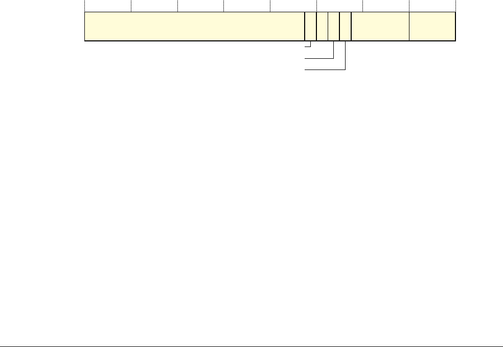
B4 System Control Registers in a VMSA implementation
B4.1 VMSA System control registers descriptions, in register order
B4-1638 Copyright © 1996-1998, 2000, 2004-2012, 2014 ARM. All rights reserved. ARM DDI 0406C.c
Non-Confidential ID051414
B4.1.96 IFSR, Instruction Fault Status Register, VMSA
The IFSR characteristics are:
Purpose The IFSR holds status information about the last instruction fault.
This register is part of the PL1 Fault handling registers functional group.
Usage constraints Only accessible from PL1 or higher.
Configurations The Large Physical Address Extension adds an alternative format for the register. If an
implementation includes the Large Physical Address Extension then the current translation
table format determines which format of the register is used.
If the implementation includes the Security Extensions, this register is Banked.
Attributes A 32-bit RW register with an UNKNOWN reset value. See also Reset behavior of CP14 and
CP15 registers on page B3-1450.
Table B3-46 on page B3-1494 shows the encodings of all of the registers in the PL1 Fault
handling registers functional group.
For information about using the IFSR see Exception reporting in a VMSA implementation on page B3-1409.
The following sections describe the alternative IFSR formats:
•IFSR format when using the Short-descriptor translation table format
•IFSR format when using the Long-descriptor translation table format on page B4-1639.
IFSR format when using the Short-descriptor translation table format
In a VMSAv7 implementation that does not include the Large Physical Address Extension, or in an implementation
that includes the Large Physical Address Extension when address translation is using the Short-descriptor
translation table format, the IFSR bit assignments are:
Bits[31:13] Reserved, UNK/SBZP.
ExT, bit[12] External abort type. This bit can provide an IMPLEMENTATION DEFINED classification of external
aborts.
For aborts other than external aborts this bit always returns 0.
In an implementation that does not provide any classification of external aborts, this bit is
UNK/SBZP.
Bit[11] Reserved, UNK/SBZP.
FS, bits[10, 3:0]
Fault status bits. For the valid encodings of these bits when using the Short-descriptor translation
table format, see Table B3-23 on page B3-1415. All encodings not shown in the table are reserved.
LPAE, bit[9], if the implementation includes the Large Physical Address Extension
On taking an exception, this bit is set to 0 to indicate use of the Short-descriptor translation table
format.
ExT
FS[4]
† Only on an implementation that includes the Large Physical Address Extension.
For more information, see the field description.
LPAE†
Reserved, UNK/SBZP
31 13 12 11 10 9 8 4 3 0
(0) 0*Reserved,
UNK/SBZP FS[3:0]
* Returned value, but might be overwritten, because the bit is RW.
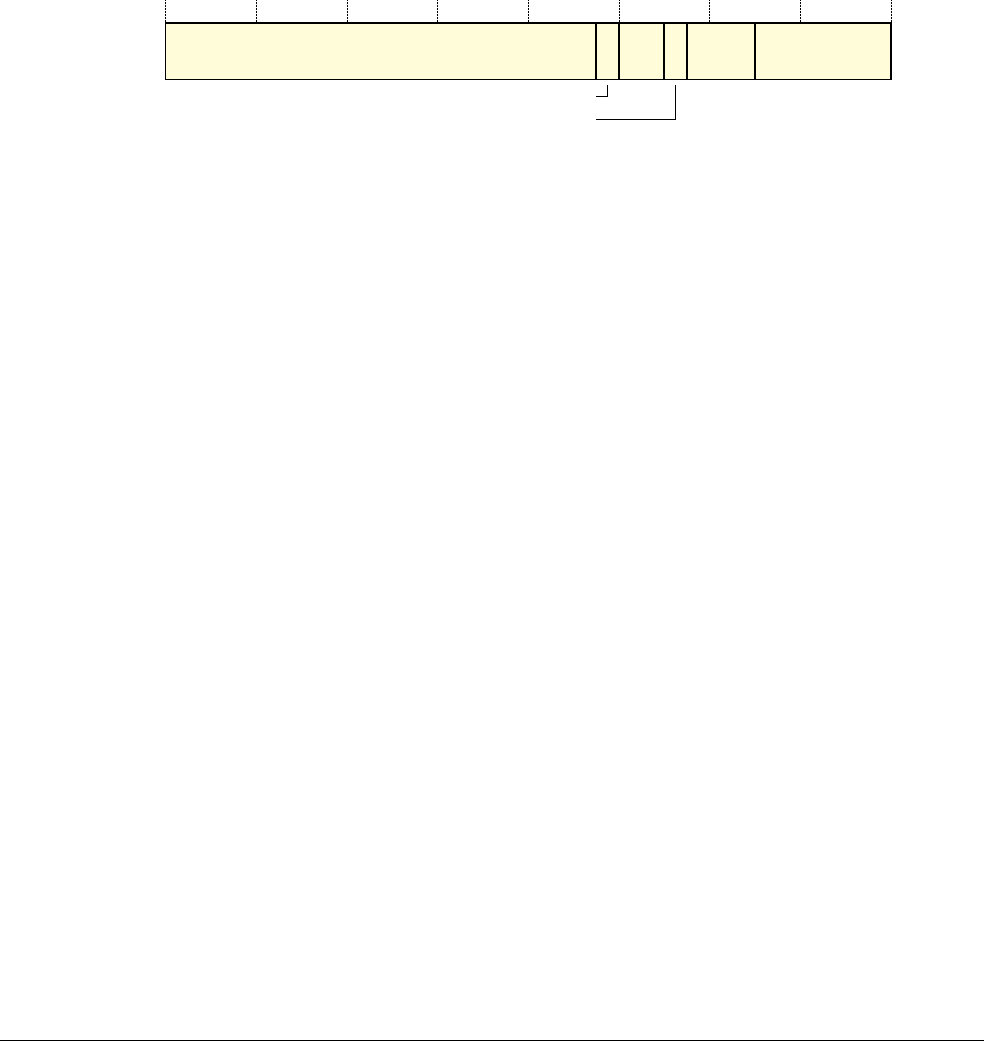
B4 System Control Registers in a VMSA implementation
B4.1 VMSA System control registers descriptions, in register order
ARM DDI 0406C.c Copyright © 1996-1998, 2000, 2004-2012, 2014 ARM. All rights reserved. B4-1639
ID051414 Non-Confidential
Hardware does not interpret this bit to determine the behavior of the memory system, and therefore
software can set this bit to 0 or 1 without affecting operation. Unless the register has been updated
to report a fault, a subsequent read of the register returns the value written to it.
Bits[9], if the implementation does not include the Large Physical Address Extension
Reserved, UNK/SBZP.
Bits[8:4] Reserved, UNK/SBZP.
IFSR format when using the Long-descriptor translation table format
In a VMSAv7 implementation that includes the Large Physical Address Extension, when address translation is using
the Long-descriptor translation table format, the IFSR bit assignments are:
Bits[31:13] Reserved, UNK/SBZP.
ExT, bit[12] External abort type. This bit can provide an IMPLEMENTATION DEFINED classification of external
aborts.
For aborts other than external aborts this bit always returns 0.
In an implementation that does not provide any classification of external aborts, this bit is
UNK/SBZP.
Bits[11:10] Reserved, UNK/SBZP.
LPAE, bit[9] On taking an exception, this bit is set to 1 to indicate use of the Long-descriptor translation table
format.
Hardware does not interpret this bit to determine the behavior of the memory system, and therefore
software can set this bit to 0 or 1 without affecting operation. Unless the register has been updated
to report a fault, a subsequent read of the register returns the value written to it.
Bits[8:6] Reserved, UNK/SBZP.
STATUS, bits[5:0]
Fault status bits. For the valid encodings of these bits when using the Long-descriptor translation
table format, see Table B3-24 on page B3-1416. All encodings not shown in the table are reserved.
Accessing the IFSR
To access the IFSR, software reads or writes the CP15 registers with
<opc1>
set to 0,
<CRn>
set to c5,
<CRm>
set to c0,
and
<opc2>
set to 1. For example:
MRC p15, 0, <Rt>, c5, c0, 1 ; Read IFSR into Rt
MCR p15, 0, <Rt>, c5, c0, 1 ; Write Rt to IFSR
(0) (0)(0) (0) 1*
ExT
Reserved, UNK/SBZP
31 13 12 11 6 5 0
(0) STATUS
LPAE
10 9 8
* Returned value, but might be overwritten, because the bit is RW.
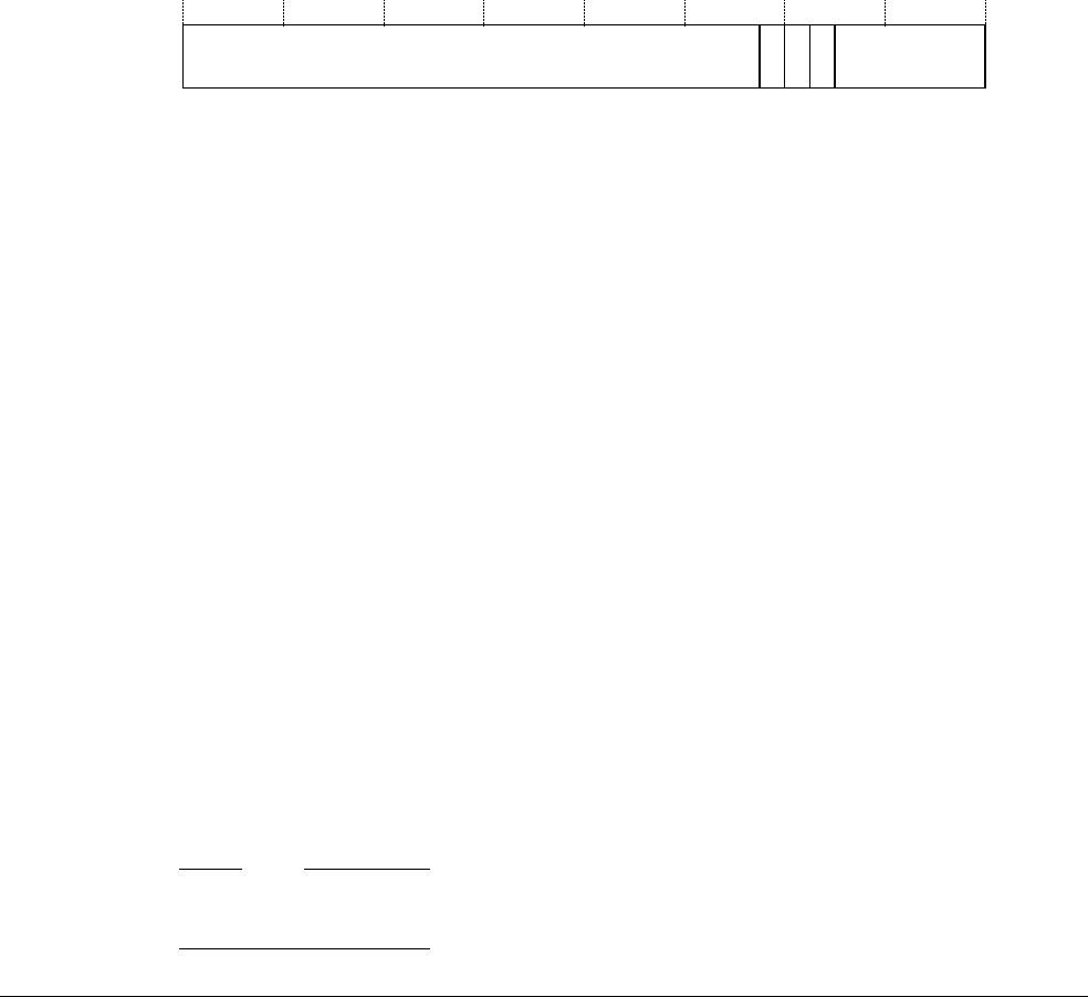
B4 System Control Registers in a VMSA implementation
B4.1 VMSA System control registers descriptions, in register order
B4-1640 Copyright © 1996-1998, 2000, 2004-2012, 2014 ARM. All rights reserved. ARM DDI 0406C.c
Non-Confidential ID051414
B4.1.97 ISR, Interrupt Status Register, Security Extensions
The ISR characteristics are:
Purpose The ISR shows whether an IRQ, FIQ, or external abort is pending. In an implementation
that includes the Virtualization Extensions, an indicated pending abort might be a physical
abort or a virtual abort.
This register is part of the Security Extensions registers functional group.
Usage constraints Only accessible from PL1 or higher.
Configurations Only present in an implementation that includes the Security Extensions.
A Common register, meaning it is available in the Secure and Non-secure states.
Attributes A 32-bit RO register with an UNKNOWN reset value. See also Reset behavior of CP14 and
CP15 registers on page B3-1450.
Table B3-54 on page B3-1500 shows the encoding of all of the Security Extensions
registers.
The ISR bit assignments are:
Bits[31:9] Reserved, UNK.
A, bit[8] External abort pending bit:
0 No pending external abort.
1 An external abort is pending.
I, bit[7] IRQ pending bit. Indicates whether an IRQ interrupt is pending:
0 No pending IRQ.
1 An IRQ interrupt is pending.
F, bit[6] FIQ pending bit. Indicates whether an FIQ interrupt is pending:
0 No pending FIQ.
1 An FIQ interrupt is pending.
Bits[5:0] Reserved, UNK.
If the ISR is indicating the status of physical external aborts, IRQs, and FIQs, then:
• The ISR.F and ISR.I bits directly reflect the state of the FIQ and IRQ inputs.
• The ISR.A bit is set to 1 when an asynchronous abort is recognized, and is cleared to 0 automatically when
the abort is taken.
On an implementation that does not include the Virtualization Extensions, or if executing in Secure state or in Hyp
mode, the ISR always indicates the status of physical external aborts, IRQs, and FIQs.
On an implementation that includes the Virtualization Extensions, and is in a Non-secure PL1 mode, the
HCR.AMO, HCR.IMO, and HCR.FMO mask override bits determine whether the corresponding ISR bit shows the
status of the physical or the virtual abort or interrupt. When an HCR mask override bit:
• is set to 0, the ISR bit shows the status of the corresponding physical abort or interrupt
• is set to 1, the ISR bit shows the status of the corresponding virtual abort or interrupt.
Note
Non-secure software executing at PL1 cannot access the HCR. When an ISR bit is set to 1 this software cannot
determine whether the reported abort or interrupt is physical or virtual.
Reserved, UNK
31 98765 0
A I F Reserved, UNK

B4 System Control Registers in a VMSA implementation
B4.1 VMSA System control registers descriptions, in register order
ARM DDI 0406C.c Copyright © 1996-1998, 2000, 2004-2012, 2014 ARM. All rights reserved. B4-1641
ID051414 Non-Confidential
The bit positions of the A, I and F bits in the ISR match the A, I and F bits in the CPSR. This means software can
use the same masks to extract the bits from the register value.
Accessing the ISR
To access the ISR, software reads the CP15 registers with
<opc1>
set to 0,
<CRn>
set to c12,
<CRm>
set to c1, and
<opc2>
set to 0. For example:
MRC p15, 0, <Rt>, c12, c1, 0 ; Read ISR into Rt
B4.1.98 ITLBIALL, Instruction TLB Invalidate All, VMSA only
TLB maintenance operations, not in Hyp mode on page B4-1746 describes this TLB maintenance operation.
This operation is part of the TLB maintenance operations functional group. Table B3-50 on page B3-1497 shows
the encodings of all of the registers and operations in this functional group.
B4.1.99 ITLBIASID, Instruction TLB Invalidate by ASID, VMSA only
TLB maintenance operations, not in Hyp mode on page B4-1746 describes this TLB maintenance operation.
This operation is part of the TLB maintenance operations functional group. Table B3-50 on page B3-1497 shows
the encodings of all of the registers and operations in this functional group.
B4.1.100 ITLBIMVA, Instruction TLB Invalidate by MVA, VMSA only
TLB maintenance operations, not in Hyp mode on page B4-1746 describes this TLB maintenance operation.
This operation is part of the TLB maintenance operations functional group. Table B3-50 on page B3-1497 shows
the encodings of all of the registers and operations in this functional group.

B4 System Control Registers in a VMSA implementation
B4.1 VMSA System control registers descriptions, in register order
B4-1642 Copyright © 1996-1998, 2000, 2004-2012, 2014 ARM. All rights reserved. ARM DDI 0406C.c
Non-Confidential ID051414
B4.1.101 JIDR, Jazelle ID Register, VMSA
The JIDR characteristics are:
Purpose Identifies the Jazelle architecture and subarchitecture versions.
This register is a Jazelle register.
Usage constraints Read access rights depend on the execution privilege and the value of the JOSCR.CD bit.
Write accesses are UNPREDICTABLE at PL1 or higher, and UNDEFINED at PL0. See Access to
Jazelle registers on page A2-100.
Configurations The VMSA and PMSA definitions of the register fields are identical.
Always implemented, but can be implemented as RAZ on a processor with a trivial
implementation of the Jazelle extension.
Note
An implementation that includes the Virtualization Extensions must implement a trivial
implementation of the Jazelle extension.
In an implementation that includes the Security Extensions, JIDR is a Common register.
Attributes A 32-bit RO register.
Table A2-17 on page A2-100 shows the encodings of all the Jazelle registers.
The JIDR bit assignments are:
Architecture, bits[31:28]
Architecture code. This uses the same Architecture code that appears in the MIDR.
On a trivial implementation of the Jazelle extension this field must be RAZ.
Implementer, bits[27:20]
Implementer code of the designer of the subarchitecture. This uses the same Implementer code that
appears in the MIDR.
On a trivial implementation of the Jazelle extension this field must be RAZ.
Subarchitecture, bits[19:12]
Contain the subarchitecture code. The following subarchitecture code is defined:
0x00
Jazelle v1 subarchitecture, or trivial implementation of Jazelle extension if the
Implementer field is RAZ.
On a trivial implementation of the Jazelle extension this field must be RAZ.
Bits[11:0] Can contain additional SUBARCHITECTURE DEFINED information.
Accessing the JIDR
To access the JIDR, software reads the CP14 registers with
<opc1>
set to 7,
<CRn>
set to c0,
<CRm>
set to c0, and
<opc2>
set to 0. For example:
MRC p14, 7, <Rt>, c0, c0, 0 ; Read JIDR into Rt
Architecture
31 28 27 20 19 12 11 0
Implementer Subarchitecture SUBARCHITECTURE DEFINED

B4 System Control Registers in a VMSA implementation
B4.1 VMSA System control registers descriptions, in register order
ARM DDI 0406C.c Copyright © 1996-1998, 2000, 2004-2012, 2014 ARM. All rights reserved. B4-1643
ID051414 Non-Confidential
B4.1.102 JMCR, Jazelle Main Configuration Register, VMSA
The JMCR characteristics are:
Purpose Provides control of the Jazelle extension.
This register is a Jazelle register.
Usage constraints Access rights depend on the execution privilege and the value of the JOSCR.CD bit, see
Access to Jazelle registers on page A2-100.
Configurations The VMSA and PMSA definitions of the register fields are identical.
Always implemented. A processor with a trivial implementation of the Jazelle extension
must implement JMCR as RAZ/WI.
In an implementation that includes the Security Extensions, JMCR is a Common register.
Attributes A 32-bit RW register. See the field descriptions for details about the reset value.
Table A2-17 on page A2-100 shows the encodings of all the Jazelle registers.
The JMCR bit assignments are:
Bits[31:1] SUBARCHITECTURE DEFINED information. This means the reset value of this field is also
SUBARCHITECTURE DEFINED.
JE, bit[0] Jazelle Enable bit:
0 Jazelle extension disabled. The
BXJ
instruction does not cause Jazelle state execution.
BXJ
behaves exactly as a
BX
instruction, see Jazelle state entry instruction, BXJ on
page A2-98.
1 Jazelle extension enabled.
The reset value of this bit is 0.
Accessing the JMCR
To access the JMCR, read or write the CP14 registers with
<opc1>
set to 7,
<CRn>
set to c2,
<CRm>
set to c0, and
<opc2>
set to 0. For example:
MRC p14, 7, <Rt>, c2, c0, 0 ; Read JMCR into Rt
MCR p14, 7, <Rt>, c2, c0, 0 ; Write Rt to JMCR
JE
31 10
SUBARCHITECTURE DEFINED

B4 System Control Registers in a VMSA implementation
B4.1 VMSA System control registers descriptions, in register order
B4-1644 Copyright © 1996-1998, 2000, 2004-2012, 2014 ARM. All rights reserved. ARM DDI 0406C.c
Non-Confidential ID051414
B4.1.103 JOSCR, Jazelle OS Control Register, VMSA
The JOSCR characteristics are:
Purpose Provides operating system control of the use of the Jazelle extension by processes and
threads.
This register is a Jazelle register.
Usage constraints Accessible only from PL1 or higher.
Normally used in conjunction with the JMCR.JE bit.
Configurations The VMSA and PMSA definitions of the register fields are identical.
Always implemented. A processor with a trivial implementation of the Jazelle extension
must implement JOSCR either:
•as RAZ/WI
• so that it can be read or written, but the processor ignores the effect of any read or
write.
In an implementation that includes the Security Extensions, JOSCR is a Common register.
Attributes A 32-bit RW register that resets to zero.
Table A2-17 on page A2-100 shows the encodings of all the Jazelle registers.
The JOSCR bit assignments are:
Bits[31:2] Reserved, UNK/SBZP.
CV, bit[1] Configuration Valid bit. This bit is used by an operating system to signal to the EJVM that it must
rewrite its configuration to the configuration registers. The possible values are:
0 Configuration not valid. The EJVM must rewrite its configuration to the configuration
registers before it executes another bytecode instruction.
1 Configuration valid. The EJVM does not need to update the configuration registers.
When the JMCR.JE bit is set to 1, the CV bit also controls entry to Jazelle state, see Controlling
entry to Jazelle state on page B1-1243.
CD, bit[0] Configuration Disabled bit. This bit is used by an operating system to disable User mode access to
the JIDR and configuration registers:
0 Configuration enabled. Access to the Jazelle registers, including User mode accesses,
operate normally. For more information, see the register descriptions in Application
level configuration and control of the Jazelle extension on page A2-99.
1 Configuration disabled in User mode. User mode access to the Jazelle registers are
UNDEFINED, and all User mode accesses to the Jazelle registers cause an Undefined
Instruction exception.
For more information about the use of this bit see Monitoring and controlling User mode access to
the Jazelle extension on page B1-1244.
The JOSCR provides a control mechanism that is independent of the subarchitecture of the Jazelle extension. An
operating system can use this mechanism to control access to the Jazelle extension, see Jazelle state configuration
and control on page B1-1243.
Reserved, UNK/SBZP
31 210
CV
CD

B4 System Control Registers in a VMSA implementation
B4.1 VMSA System control registers descriptions, in register order
ARM DDI 0406C.c Copyright © 1996-1998, 2000, 2004-2012, 2014 ARM. All rights reserved. B4-1645
ID051414 Non-Confidential
Accessing the JOSCR
To access the JOSCR, read or write the CP14 registers with
<opc1>
set to 7,
<CRn>
set to c1,
<CRm>
set to c0, and
<opc2>
set to 0. For example:
MRC p14, 7, <Rt>, c1, c0, 0 ; Read JOSCR into Rt
MCR p14, 7, <Rt>, c1, c0, 0 ; Write Rt to JOSCR
B4 System Control Registers in a VMSA implementation
B4.1 VMSA System control registers descriptions, in register order
B4-1646 Copyright © 1996-1998, 2000, 2004-2012, 2014 ARM. All rights reserved. ARM DDI 0406C.c
Non-Confidential ID051414
B4.1.104 MAIR0 and MAIR1, Memory Attribute Indirection Registers 0 and 1, VMSA
The MAIR0 and MAIR1 characteristics are:
Purpose MAIR0 and MAIR1 provide the memory attribute encodings corresponding to the possible
AttrIndx values in a Long-descriptor format translation table entry for stage 1 translations.
For more information about the AttrIndx field see Long-descriptor format memory region
attributes on page B3-1372.
These registers are part of the Virtual memory control registers functional group.
Usage constraints Only accessible from PL1 or higher.
Only accessible when using the Long-descriptor translation table format. When using the
Short-descriptor format see PRRR, Primary Region Remap Register, VMSA on
page B4-1700 and NMRR, Normal Memory Remap Register, VMSA on page B4-1660.
AttrIndx[2] selects the appropriate MAIR:
• setting AttrIndx[2] to 0 selects MAIR0
• setting AttrIndx[2] to 1 selects MAIR1.
In the implementation includes the Security Extensions:
• the Secure copies of the registers give the values for memory accesses from Secure
state
• the Non-secure copies of the registers give the values for memory accesses from
Non-secure modes other than Hyp mode.
Configurations MAIR0 and MAIR1 are implemented only as part of the Large Physical Address Extension.
In an implementation that includes the Security Extensions they:
•are Banked
• have write access to the Secure copy of the register disabled when the
CP15SDISABLE signal is asserted HIGH.
Attributes 32-bit RW registers with UNKNOWN reset values. See also Reset behavior of CP14 and CP15
registers on page B3-1450.
Table B3-45 on page B3-1493 shows the encodings of all of the registers in the Virtual
memory control registers functional group.
The MAIR0 and MAIR1 bit assignments are:
Attrm[7:0], for values of m from 0 to 7
The memory attribute encoding for an AttrIndx[2:0] entry in a Long descriptor format translation
table entry, where:
• AttrIndx[2] defines which MAIR to access
• AttrIndx[2:0] gives the value of m in Attrm.
Table B4-7 on page B4-1647 shows the encoding of Attrn[7:4].
Attr7 Attr6 Attr5 Attr4
Attr3
31 24 23 16 15 8 7 0
Attr2 Attr1 Attr0MAIR0
MAIR1

B4 System Control Registers in a VMSA implementation
B4.1 VMSA System control registers descriptions, in register order
ARM DDI 0406C.c Copyright © 1996-1998, 2000, 2004-2012, 2014 ARM. All rights reserved. B4-1647
ID051414 Non-Confidential
The encoding of Attrn[3:0] depends on the value of Attrn[7:4], as Table B4-8 shows.
Table B4-7 MAIRn.Attrm[7:4] encoding
Attrm[7:4] Meaning
0000 Strongly-ordered or Device memory, see encoding of Attrm[3:0].
00RW, RW not 00 It is IMPLEMENTATION DEFINED whether the encoding is:
•UNPREDICTABLE
• Normal memory, Outer Write-Throughb Transient.
0100 Normal memory, Outera Non-cacheable.
a. See encoding of Attrm[3:0], shown in Table B4-8, for Inner cacheability policies.
01RW, RW not 00 It is IMPLEMENTATION DEFINED whether the encoding is:
•UNPREDICTABLE
• Normal memory, Outer Write-Backb Transient.
10RW Normal memory, Outer a Write-Through Cacheableb, Non-transientc.
b. R defines the Outer Read-Allocate policy, and W defined the Outer Write-Allocate policy, see
Table B4-9 on page B4-1648.
c. Non-transient if the implementation includes support for the Transient attribute.
11RW Normal memory, Outera Write-Back Cacheableb, Non-transientc.
Table B4-8 MAIRn.Attrm[3:0] encoding
Attrm[3:0] Meaning when Attrm[7:4] is
0b0000
Meaning when Attrm[7:4] is not
0b0000
0000 Strongly-ordered memory UNPREDICTABLE.
00RW,
RW not 00
UNPREDICTABLE It is IMPLEMENTATION DEFINED whether the encoding is:
•UNPREDICTABLE
• Normal memory, Inner Write-Througha Transient.
0100 Device memory Normal memory, Inner Non-cacheable.
01RW,
RW not 00
UNPREDICTABLE It is IMPLEMENTATION DEFINED whether the encoding is:
•UNPREDICTABLE
• Normal memory, Inner Write-Backa Transient.
10RW UNPREDICTABLE Normal memory, Inner Write-Through Cacheablea, Non-transientb.
11RW UNPREDICTABLE Normal memory, Inner Write-Back Cacheablea, Non-transientb.
a. R defines the Inner Read-Allocate policy, and W defines the Inner Write-Allocate policy, see Table B4-9 on page B4-1648.
b. Non-transient if the implementation includes support for the Transient attribute.

B4 System Control Registers in a VMSA implementation
B4.1 VMSA System control registers descriptions, in register order
B4-1648 Copyright © 1996-1998, 2000, 2004-2012, 2014 ARM. All rights reserved. ARM DDI 0406C.c
Non-Confidential ID051414
Table B4-9 shows the encoding of the R and W bits that are used, in some Attrm encodings in
Table B4-7 on page B4-1647 and Table B4-8 on page B4-1647, to define the read-allocate and
write-allocate policies:
The IMPLEMENTATION DEFINED meanings of the Attrm[7:4] Attrm[3:0]
0b0xyy
encodings must be
consistent. This means that the IMPLEMENTATION DEFINED choice is that either:
• all of these encodings are UNPREDICTABLE
• this set of encodings provides the Normal memory Write-Through transient and Write-Back
transient encodings.
See Transient cacheability attribute, Large Physical Address Extension on page A3-135 for more
information about the Transient attribute.
Accessing MAIR0 or MAIR1
To access MAIR0 or MAIR1, software reads or writes the CP15 registers with
<opc1>
set to 0,
<CRn>
set to c10,
<CRm>
set to c2, and
<opc2>
set to 0 for MAIR0, or to 1 for MAIR1. For example:
MRC p15, 0, <Rt>, c10, c2, 0 ; Read MAIR0 into Rt
MCR p15, 0, <Rt>, c10, c2, 1 ; Write Rt to MAIR1
Table B4-9 Encoding of R and W bits in some Attrm fields
R or W Meaning
0 Do not allocate
1 Allocate

B4 System Control Registers in a VMSA implementation
B4.1 VMSA System control registers descriptions, in register order
ARM DDI 0406C.c Copyright © 1996-1998, 2000, 2004-2012, 2014 ARM. All rights reserved. B4-1649
ID051414 Non-Confidential
B4.1.105 MIDR, Main ID Register, VMSA
The MIDR characteristics are:
Purpose The MIDR provides identification information for the processor, including an implementer
code for the device and a device ID number.
This register is part of the Identification registers functional group.
Usage constraints Only accessible from PL1 or higher.
Configurations If the implementation includes the Security Extensions, this register is Common.
Some fields of the MIDR are IMPLEMENTATION DEFINED. For details of the values of these
fields for a particular ARMv7 implementation, and any implementation-specific
significance of these values, see the product documentation.
Attributes A 32-bit RO register with an IMPLEMENTATION DEFINED value. See also Reset behavior of
CP14 and CP15 registers on page B3-1450.
Table B3-44 on page B3-1492 shows the encodings of all of the registers in the
Identification registers functional group.
The MIDR bit assignments are:
Implementer, bits[31:24]
The Implementer code. Table B4-10 shows the permitted values for this field:
All other values are reserved by ARM and must not be used.
Variant, bits[23:20]
An IMPLEMENTATION DEFINED variant number. Typically, this field distinguishes between different
product variants, or major revisions of a product.
Table B4-10 Implementer codes
Bits[31:24] ASCII character Implementer
0x41
A ARM Limited
0x44
D Digital Equipment Corporation
0x4D
M Motorola, Freescale Semiconductor Inc.
0x51
Q Qualcomm Inc.
0x56
V Marvell Semiconductor Inc.
0x69
i Intel Corporation
Revision
31 24 23 20 19 16 15 4 3 0
Implementer Variant Architecture Primary part number

B4 System Control Registers in a VMSA implementation
B4.1 VMSA System control registers descriptions, in register order
B4-1650 Copyright © 1996-1998, 2000, 2004-2012, 2014 ARM. All rights reserved. ARM DDI 0406C.c
Non-Confidential ID051414
Architecture, bits[19:16]
Table B4-11 shows the permitted values for this field:
All other values are reserved by ARM and must not be used.
Primary part number, bits[15:4]
An IMPLEMENTATION DEFINED primary part number for the device.
Note
• On processors implemented by ARM, if the top four bits of the primary part number are
0x0
or
0x7
, the variant and architecture are encoded differently, see the description of the MIDR
in Appendix D15 ARMv4 and ARMv5 Differences.
• Processors implemented by ARM have an Implementer code of
0x41
.
Revision, bits[3:0]
An IMPLEMENTATION DEFINED revision number for the device.
ARMv7 requires all implementations to use the CPUID scheme, described in Chapter B7 The CPUID Identification
Scheme, and an implementation is described by the MIDR with the CPUID registers.
Note
For an ARMv7 implementation by ARM, the MIDR is interpreted as:
Bits[31:24] Implementer code, must be
0x41
.
Bits[23:20] Major revision number, rX.
Bits[19:16] Architecture code, must be
0xF
.
Bits[15:4] ARM part number.
Bits[3:0] Minor revision number, pY.
Accessing the MIDR
To access the MIDR, software reads the CP15 registers with
<opc1>
set to 0,
<CRn>
set to c0,
<CRm>
set to c0, and
<opc2>
set to 0. For example:
MRC p15, 0, <Rt>, c0, c0, 0 ; Read MIDR into Rt
Table B4-11 Architecture codes
Bits[19:16] Architecture
0x1
ARMv4
0x2
ARMv4T
0x3
ARMv5 (obsolete)
0x4
ARMv5T
0x5
ARMv5TE
0x6
ARMv5TEJ
0x7
ARMv6
0xF
Defined by CPUID scheme

B4 System Control Registers in a VMSA implementation
B4.1 VMSA System control registers descriptions, in register order
ARM DDI 0406C.c Copyright © 1996-1998, 2000, 2004-2012, 2014 ARM. All rights reserved. B4-1651
ID051414 Non-Confidential
B4.1.106 MPIDR, Multiprocessor Affinity Register, VMSA
The MPIDR characteristics are:
Purpose In a multiprocessor system, the MPIDR provides an additional processor identification
mechanism for scheduling purposes, and indicates whether the implementation includes the
Multiprocessing Extensions.
This register is part of the Identification registers functional group.
Usage constraints Only accessible from PL1 or higher.
Configurations This register is not implemented in architecture versions before ARMv7.
In a uniprocessor system ARM recommends that each Affn field of this register returns a
value of 0.
If the implementation includes the Security Extensions, the register is Common.
Attributes A 32-bit RO register with an IMPLEMENTATION DEFINED value. See also Reset behavior of
CP14 and CP15 registers on page B3-1450.
Table B3-44 on page B3-1492 shows the encodings of all of the registers in the
Identification registers functional group.
In an implementation that does not include the Multiprocessing Extensions, the MPIDR bit assignments are:
In an implementation that includes the Multiprocessing Extensions, the MPIDR bit assignments are:
Note
In the MPIDR bit definitions, a processor in the system can be a physical processor or a virtual machine.
Bits[31:24], ARMv7 without Multiprocessing Extensions
Reserved, RAZ.
Bits[31], in an implementation that includes the Multiprocessing Extensions
RAO. Indicates that the implementation uses the Multiprocessing Extensions register format.
U, bit[30], in an implementation that includes the Multiprocessing Extensions
Indicates a Uniprocessor system, as distinct from processor 0 in a multiprocessor system. The
possible values of this bit are:
0 Processor is part of a multiprocessor system.
1 Processor is part of a uniprocessor system.
Bits[29:25], in an implementation that includes the Multiprocessing Extensions
Reserved, UNK.
Reserved, RAZ
31 24 23 16 15 8 7 0
Aff2 Aff1 Aff0
1
31 30 29 25 24 23 16 15 8 7 0
UReserved,
UNK Aff2 Aff1 Aff0
MT

B4 System Control Registers in a VMSA implementation
B4.1 VMSA System control registers descriptions, in register order
B4-1652 Copyright © 1996-1998, 2000, 2004-2012, 2014 ARM. All rights reserved. ARM DDI 0406C.c
Non-Confidential ID051414
MT, bit[24], in an implementation that includes the Multiprocessing Extensions
Indicates whether the lowest level of affinity consists of logical processors that are implemented
using a multi-threading type approach. The possible values of this bit are:
0 Performance of processors at the lowest affinity level is largely independent.
1 Performance of processors at the lowest affinity level is very interdependent.
For more information about the meaning of this bit see Multi-threading approach to lowest affinity
levels, Multiprocessing Extensions.
Aff2, bits[23:16]
Affinity level 2. The least significant affinity level field, for this processor in the system.
Aff1, bits[15:8]
Affinity level 1. The intermediate affinity level field, for this processor in the system.
Aff0, bits[7:0]
Affinity level 0. The most significant affinity level field, for this processor in the system.
See Recommended use of the MPIDR for clarification of the meaning of most significant and least significant
affinity levels.
The assigned value of the MPIDR.{Aff0, Aff1, Aff2} set of fields must be unique for each processor in the system
as a whole.
When matching against an affinity level field, scheduler software checks for a value equal to or greater than a
required value.
Recommended use of the MPIDR includes a description of an example multiprocessor system and the affinity level
field values it might use.
The interpretation of these fields is IMPLEMENTATION DEFINED, and must be documented as part of the
documentation of the multiprocessor system. ARM recommends that this register might be used as described in
Recommended use of the MPIDR.
The software mechanism to discover the total number of affinity numbers used at each level is IMPLEMENTATION
DEFINED, and is part of the general system identification task.
Multi-threading approach to lowest affinity levels, Multiprocessing Extensions
In an implementation that includes the Multiprocessing Extensions, if the MPIDR.MT bit is set to 1, this indicates
that the processors at affinity level 0 are logical processors, implemented using a multi-threading type approach. In
such an approach, there can be a significant performance impact if a new thread is assigned the processor with:
• a different affinity level 0 value to some other thread, referred to as the original thread
• a pair of values for affinity levels 1 and 2 that are the same as the pair of values of the original thread.
In this situation, the performance of the original thread might be significantly reduced.
Note
In this description, thread always refers to a thread or a process.
Recommended use of the MPIDR
In a multiprocessor system the register might provide two important functions:
• Identifying special functionality of a particular processor in the system. In general, the actual meaning of the
affinity level fields is not important. In a small number of situations, an affinity level field value might have
a special IMPLEMENTATION DEFINED significance. Possible examples include booting from reset and
powerdown events.

B4 System Control Registers in a VMSA implementation
B4.1 VMSA System control registers descriptions, in register order
ARM DDI 0406C.c Copyright © 1996-1998, 2000, 2004-2012, 2014 ARM. All rights reserved. B4-1653
ID051414 Non-Confidential
• Providing affinity information for the scheduling software, to help the scheduler run an individual thread or
process on either:
— the same processor, or as similar a processor as possible, as the processor it was running on previously
— a processor on which a related thread or process was run.
MPIDR provides a mechanism with up to three levels of affinity information, but the meaning of those levels of
affinity is entirely IMPLEMENTATION DEFINED. The levels of affinity provided can have different meanings.
Table B4-12 shows two possible implementations:
The scheduler maintains affinity level information for all threads and processes. When it has to reschedule a thread
or process, the scheduler:
1. Looks for an available processor that matches at all three affinity levels.
2. If step 1 fails, the scheduler might look for a processor that matches at levels 1 and 2 only.
3. If the scheduler still cannot find an available processor it might look for a match at level 2 only.
A multiprocessor system corresponding to Example system 1 in Table B4-12 might implement affinity values as
shown in Table B4-13:
Accessing the MPIDR
To access MPIDR, software reads the CP15 registers with
<opc1>
set to 0,
<CRn>
set to c0,
<CRm>
set to c0, and
<opc2>
set to 5. For example:
MRC p15, 0, <Rt>, c0, c0, 5 ; Read MPIDR into Rt
Table B4-12 Possible implementations of the affinity levels
Affinity level Example system 1 Example system 2
0 Virtual CPUs in a multi-threaded processor Processors in an SMP cluster
1 Processors in an Symmetric Multi Processor (SMP) cluster Clusters with a system
2 Clusters in a system No meaning, fixed as 0
Table B4-13 Example of possible affinity values at different affinity levels
Aff2, Cluster level, values Aff1, Processor level, values Aff0, Virtual CPU level, values
0 0 0, 1
0 1 0, 1
0 2 0, 1
0 3 0, 1
1 0 0, 1
1 1 0, 1
1 2 0, 1
1 3 0, 1

B4 System Control Registers in a VMSA implementation
B4.1 VMSA System control registers descriptions, in register order
B4-1654 Copyright © 1996-1998, 2000, 2004-2012, 2014 ARM. All rights reserved. ARM DDI 0406C.c
Non-Confidential ID051414
B4.1.107 MVBAR, Monitor Vector Base Address Register, Security Extensions
The MVBAR characteristics are:
Purpose The MVBAR holds the exception base address for all exceptions that are taken to Monitor
mode, see Exception vectors and the exception base address on page B1-1165.
This register is part of the Security Extensions registers functional group.
Usage constraints Only accessible from Secure PL1 modes.
Secure software must program the MVBAR with the required initial value as part of the
processor boot sequence.
Configurations Only present in an implementation that includes the Security Extensions.
A Restricted access register, meaning it exists only in the Secure state.
Attributes A 32-bit RW register with an UNKNOWN reset value. See also Reset behavior of CP14 and
CP15 registers on page B3-1450.
Table B3-54 on page B3-1500 shows the encoding of all of the Security Extensions
registers.
The MVBAR bit assignments are:
Monitor_Vector_Base_Address, bits[31:5]
Bits[31:5] of the base address of the exception vectors for exceptions that are taken to Monitor
mode. Bits[4:0] of an exception vector is the exception offset, see Table B1-3 on page B1-1167.
Bits[4:0] Reserved, UNK/SBZP.
For details of how the MVBAR determines the exception addresses see Exception vectors and the exception base
address on page B1-1165.
Accessing the MVBAR
To access the MVBAR, software reads or writes the CP15 registers with
<opc1>
set to 0,
<CRn>
set to c12,
<CRm>
set
to c0, and
<opc2>
set to 1. For example:
MRC p15, 0, <Rt>, c12, c0, 1 ; Read MVBAR into Rt
MCR p15, 0, <Rt>, c12, c0, 1 ; Write Rt to MVBAR
Monitor_Vector_Base_Address
31 54 0
Reserved,
UNK/SBZP

B4 System Control Registers in a VMSA implementation
B4.1 VMSA System control registers descriptions, in register order
ARM DDI 0406C.c Copyright © 1996-1998, 2000, 2004-2012, 2014 ARM. All rights reserved. B4-1655
ID051414 Non-Confidential
B4.1.108 MVFR0, Media and VFP Feature Register 0, VMSA
The MVFR0 characteristics are:
Purpose Describes the features provided by the Advanced SIMD and Floating-point Extensions.
Usage constraints Only accessible from PL1 or higher. See Accessing the Advanced SIMD and Floating-point
Extension system registers on page B1-1237 for more information.
Must be interpreted with MVFR1. This register complements the information provided by
the CPUID scheme described in Chapter B7 The CPUID Identification Scheme.
Configurations Implemented only if the implementation includes one or both of:
• the Floating-point Extension
• the Advanced SIMD Extension.
The VMSA and PMSA definitions of the register fields are identical.
In an implementation that includes the Security Extensions, MVFR0 is a Configurable
access register. When the settings in the CPACR permit access to the register:
• it is accessible in Non-secure state only if the NSACR.{CP11, CP10} bits are both
set to 1
• if the implementation also includes the Virtualization Extensions then bits in the
HCPTR also control Non-secure access to the register.
For more information, see Access controls on CP0 to CP13 on page B1-1227.
Attributes A 32-bit RO register.
Table B1-24 on page B1-1236 shows the encodings of all of the Advanced SIMD and
Floating-point Extension system registers
The MVFR0 bit assignments are:
VFP rounding modes, bits[31:28]
Indicates the rounding modes supported by the Floating-point Extension hardware. Permitted values
are:
0b0000
Only Round to Nearest mode supported, except that Round towards Zero mode is
supported for
VCVT
instructions that always use that rounding mode regardless of the
FPSCR setting.
0b0001
All rounding modes supported.
Short vectors, bits[27:24]
Indicates the hardware support for VFP short vectors. Permitted values are:
0b0000
Not supported.
0b0001
Short vector operation supported.
Square root, bits[23:20]
Indicates the hardware support for the Floating-point Extension square root operations. Permitted
values are:
0b0000
Not supported in hardware.
0b0001
Supported.
Note
• the
VSQRT.F32
instruction also requires the single-precision Floating-point attribute, bits[7:4]
• the
VSQRT.F64
instruction also requires the double-precision Floating-point attribute,
bits[11:8].
VFP
rounding
modes
Short
vectors
Square
root Divide
31 16 15 12 11 8 7 4 3 0
VFP
exception
trapping
Double-
precision
Single-
precision
A_SIMD
registers
28 27 24 23 20 19

B4 System Control Registers in a VMSA implementation
B4.1 VMSA System control registers descriptions, in register order
B4-1656 Copyright © 1996-1998, 2000, 2004-2012, 2014 ARM. All rights reserved. ARM DDI 0406C.c
Non-Confidential ID051414
Divide, bits[19:16]
Indicates the hardware support for Floating-point Extension divide operations. Permitted values are:
0b0000
Not supported in hardware.
0b0001
Supported.
Note
• the
VDIV.F32
instruction also requires the single-precision Floating-point attribute, bits[7:4]
• the
VDIV.F64
instruction also requires the double-precision Floating-point attribute,
bits[11:8].
VFP exception trapping, bits[15:12]
Indicates whether the Floating-point Extension hardware implementation supports exception
trapping. Permitted values are:
0b0000
Not supported. This is the value for VFPv3 and VFPv4.
0b0001
Supported by the hardware. This is the value for VFPv2, and for VFPv3U and VFPv4U.
When exception trapping is supported, support code is required to handle the trapped
exceptions.
Note
This value does not indicate that trapped exception handling is available. Because
trapped exception handling requires support code, only the support code can provide
this information.
Double-precision, bits[11:8]
Indicates the hardware support for the Floating-point Extension double-precision operations.
Permitted values are:
0b0000
Not supported in hardware.
0b0001
Supported, VFPv2.
0b0010
Supported, VFPv3 or VFPv4.
VFPv3 adds an instruction to load a double-precision floating-point constant, and
conversions between double-precision and fixed-point values.
A value of
0b0001
or
0b0010
indicates support for all the floating-point double-precision instructions
in the supported version of the Floating-point Extension, except that, in addition to this field being
nonzero:
•
VSQRT.F64
is available only if the Square root field is
0b0001
•
VDIV.F64
is available only if the Divide field is
0b0001
• conversion between double-precision and single-precision is available only if the
single-precision field is nonzero.

B4 System Control Registers in a VMSA implementation
B4.1 VMSA System control registers descriptions, in register order
ARM DDI 0406C.c Copyright © 1996-1998, 2000, 2004-2012, 2014 ARM. All rights reserved. B4-1657
ID051414 Non-Confidential
Single-precision, bits[7:4]
Indicates the hardware support for the Floating-point Extension single-precision operations.
Permitted values are:
0b0000
Not supported in hardware.
0b0001
Supported, VFPv2.
0b0010
Supported, VFPv3 or VFPv4.
VFPv3 adds an instruction to load a single-precision floating-point constant, and
conversions between single-precision and fixed-point values.
A value of
0b0001
or
0b0010
indicates support for all floating-point single-precision instructions in
the supported version of the Floating-point Extension, except that, in addition to this field being
nonzero:
•
VSQRT.F32
is only available if the Square root field is
0b0001
•
VDIV.F32
is only available if the Divide field is
0b0001
• conversion between double-precision and single-precision is only available if the
double-precision field is nonzero.
A_SIMD registers, bits[3:0]
Indicates support for the Advanced SIMD register bank. Permitted values are:
0b0000
Not supported.
0b0001
Supported, 16 × 64-bit registers.
0b0010
Supported, 32 × 64-bit registers.
If this field is nonzero:
• all Floating-point Extension
LDC
,
STC
,
MCR
, and
MRC
instructions are supported
• if the CPUID register shows that the
MCRR
and
MRRC
instructions are supported then the
corresponding Floating-point Extension instructions are supported.
Accessing MVFR0
Software accesses MVFR0 using the
VMRS
instruction, see VMRS on page B9-2014. For example:
VMRS <Rt>, MVFR0 ; Read MVFR0 into Rt

B4 System Control Registers in a VMSA implementation
B4.1 VMSA System control registers descriptions, in register order
B4-1658 Copyright © 1996-1998, 2000, 2004-2012, 2014 ARM. All rights reserved. ARM DDI 0406C.c
Non-Confidential ID051414
B4.1.109 MVFR1, Media and VFP Feature Register 1, VMSA
The MVFR1 characteristics are:
Purpose Describes the features provided by the Advanced SIMD and Floating-point Extensions.
Usage constraints Only accessible from PL1 or higher. See Accessing the Advanced SIMD and Floating-point
Extension system registers on page B1-1237 for more information.
Must be interpreted with MVFR0. These registers complement the information provided by
the CPUID scheme described in Chapter B7 The CPUID Identification Scheme.
Configurations Implemented only if the implementation includes one or both of:
• the Floating-point Extension
• the Advanced SIMD Extension.
The VMSA and PMSA definitions of the register fields are identical.
In an implementation that includes the Security Extensions, MVFR1 is a Configurable
access register. When the settings in the CPACR permit access to the register:
• it is accessible in Non-secure state only if the NSACR.{CP11, CP10} bits are both
set to 1
• if the implementation also includes the Virtualization Extensions then bits in the
HCPTR also control Non-secure access to the register.
For more information, see Access controls on CP0 to CP13 on page B1-1227.
Attributes A 32-bit RO register.
Table B1-24 on page B1-1236 shows the encodings of all of the Advanced SIMD and
Floating-point Extension system registers
The MVFR1 bit assignments are:
A_SIMD FMAC, bits[31:28]
Indicates whether any implemented Floating-point or Advanced SIMD Extension implements the
fused multiply accumulate instructions. Permitted values are:
0b0000
Not implemented.
0b0001
Implemented.
If an implementation includes both the Floating-point Extension and the Advanced SIMD
Extension, both extensions must provide the same level of support for these instructions.
VFP HPFP, bits[27:24]
Indicates whether the Floating-point Extension implements half-precision floating-point conversion
instructions. Permitted values are:
0b0000
Not implemented.
0b0001
Implemented.
A_SIMD HPFP, bits[23:20]
Indicates whether the Advanced SIMD Extension implements half-precision floating-point
conversion instructions. Permitted values are:
0b0000
Not implemented.
0b0001
Implemented. This value is permitted only if the A_SIMD SPFP field is
0b0001
.
A_SIMD
FMAC
VFP
HPFP
A_SIMD
HPFP
A_SIMD
SPFP
31 16 15 12 11 8 7 4 3 0
A_SIMD
integer
A_SIMD
load/store
D_NaN
mode
FtZ
mode
28 27 24 23 20 19

B4 System Control Registers in a VMSA implementation
B4.1 VMSA System control registers descriptions, in register order
ARM DDI 0406C.c Copyright © 1996-1998, 2000, 2004-2012, 2014 ARM. All rights reserved. B4-1659
ID051414 Non-Confidential
A_SIMD SPFP, bits[19:16]
Indicates whether the Advanced SIMD Extension implements single-precision floating-point
instructions. Permitted values are:
0b0000
Not implemented.
0b0001
Implemented. This value is permitted only if the A_SIMD integer field is
0b0001
.
A_SIMD integer, bits[15:12]
Indicates whether the Advanced SIMD Extension implements integer instructions. Permitted values
are:
0b0000
Not implemented.
0b0001
Implemented.
A_SIMD load/store, bits[11:8]
Indicates whether the Advanced SIMD Extension implements load/store instructions. Permitted
values are:
0b0000
Not implemented.
0b0001
Implemented.
D_NaN mode, bits[7:4]
Indicates whether the Floating-point Extension hardware implementation supports only the Default
NaN mode. Permitted values are:
0b0000
Hardware supports only the Default NaN mode. If a VFP subarchitecture is
implemented its support code might include support for propagation of NaN values.
0b0001
Hardware supports propagation of NaN values.
FtZ mode, bits[3:0]
Indicates whether the Floating-point Extension hardware implementation supports only the
Flush-to-Zero mode of operation. Permitted values are:
0b0000
Hardware supports only the Flush-to-Zero mode of operation. If a VFP subarchitecture
is implemented its support code might include support for full denormalized number
arithmetic.
0b0001
Hardware supports full denormalized number arithmetic.
Accessing MVFR1
Software accesses MVFR1 using the
VMRS
instruction, see VMRS on page B9-2014. For example:
VMRS <Rt>, MVFR1 ; Read MVFR1 into Rt

B4 System Control Registers in a VMSA implementation
B4.1 VMSA System control registers descriptions, in register order
B4-1660 Copyright © 1996-1998, 2000, 2004-2012, 2014 ARM. All rights reserved. ARM DDI 0406C.c
Non-Confidential ID051414
B4.1.110 NMRR, Normal Memory Remap Register, VMSA
The NMRR characteristics are:
Purpose Under the conditions described in Architectural status of PRRR and NMRR on
page B4-1702, NMRR provides additional mapping controls for memory regions that are
mapped as Normal memory by their entry in the PRRR. For more information see
Short-descriptor format memory region attributes, with TEX remap on page B3-1368.
This register is part of the Virtual memory control registers functional group.
Usage constraints Only accessible from PL1 or higher.
Used in conjunction with the PRRR.
In a processor that implements the Large Physical Address Extension, not accessible when
using the Long-descriptor translation table format. See, instead, MAIR0 and MAIR1,
Memory Attribute Indirection Registers 0 and 1, VMSA on page B4-1646.
See also Architectural status of PRRR and NMRR on page B4-1702.
Configurations In an implementation that includes the Security Extensions, the NMRR:
•is Banked
• has write access to the Secure copy of the register disabled when the
CP15SDISABLE signal is asserted HIGH.
Attributes A 32-bit RW register with an UNKNOWN reset value. See also Reset behavior of CP14 and
CP15 registers on page B3-1450.
Table B3-45 on page B3-1493 shows the encodings of all of the registers in the Virtual
memory control registers functional group.
The NMRR bit assignments are:
ORn, bits[2n+17:2n+16], for values of n from 0 to 7
Outer Cacheable property mapping for memory attributes n, if the region is mapped as Normal
memory by the PRRR.TRn entry. n is the value of the TEX[0], C and B bits, see Table B4-28 on
page B4-1702. The possible values of this field are:
00 Region is Non-cacheable.
01 Region is Write-Back, Write-Allocate.
10 Region is Write-Through, no Write-Allocate.
11 Region is Write-Back, no Write-Allocate.
The meaning of the field with n = 6 is IMPLEMENTATION DEFINED and might differ from the meaning
given here. This is because the meaning of the attribute combination {TEX[0] = 1, C = 1, B = 0} is
IMPLEMENTATION DEFINED.
IRn, bits[2n+1:2n], for values of n from 0 to 7
Inner Cacheable property mapping for memory attributes n, if the region is mapped as Normal
memory by the PRRR.TRn entry. n is the value of the TEX[0], C and B bits, see Table B4-28 on
page B4-1702. The possible values of this field are the same as those given for the ORn field.
The meaning of the field with n = 6 is IMPLEMENTATION DEFINED and might differ from the meaning
given here. This is because the meaning of the attribute combination {TEX[0] = 1, C = 1, B = 0} is
IMPLEMENTATION DEFINED.
For more information about the NMRR see Short-descriptor format memory region attributes, with TEX remap on
page B3-1368.
IR0
31 30 29 28 27 26 25 24 23 22 21 20 19 18 17 16 15 14 13 12 11 10 9 8 7 6 5 4 3 2 1 0
OR7 OR6 OR5 OR4 OR3 OR2 OR1 OR0 IR7 IR6 IR5 IR4 IR3 IR2 IR1

B4 System Control Registers in a VMSA implementation
B4.1 VMSA System control registers descriptions, in register order
ARM DDI 0406C.c Copyright © 1996-1998, 2000, 2004-2012, 2014 ARM. All rights reserved. B4-1661
ID051414 Non-Confidential
Accessing the NMRR
To access the NMRR, software reads or writes the CP15 registers with
<opc1>
set to 0,
<CRn>
set to c10,
<CRm>
set to
c2, and
<opc2>
set to 1. For example:
MRC p15, 0, <Rt>, c10, c2, 1 ; Read NMRR into Rt
MCR p15, 0, <Rt>, c10, c2, 1 ; Write Rt to NMRR
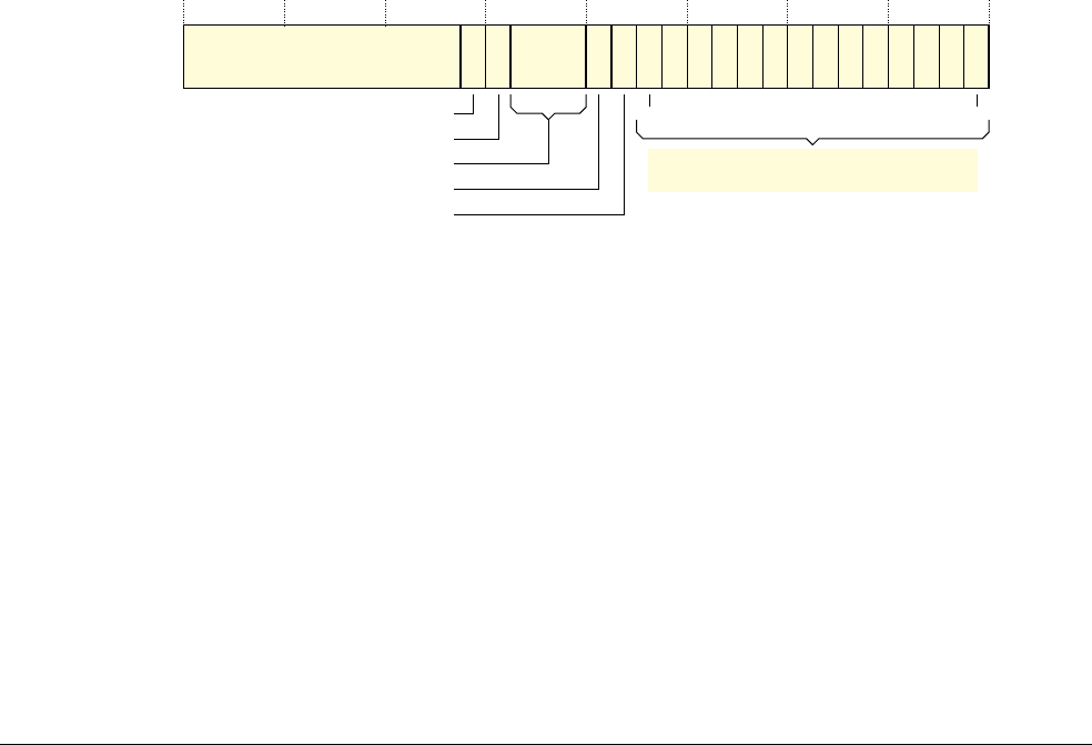
B4 System Control Registers in a VMSA implementation
B4.1 VMSA System control registers descriptions, in register order
B4-1662 Copyright © 1996-1998, 2000, 2004-2012, 2014 ARM. All rights reserved. ARM DDI 0406C.c
Non-Confidential ID051414
B4.1.111 NSACR, Non-Secure Access Control Register, Security Extensions
The NSACR characteristics are:
Purpose The NSACR:
• Defines the Non-secure access permissions to coprocessors CP0 to CP13.
• Can include additional IMPLEMENTATION DEFINED bits that define Non-secure access
permissions for IMPLEMENTATION DEFINED functionality.
• In an implementation that includes the Virtualization Extensions, controls Hyp mode
access to:
— coprocessors CP0 to CP13
— floating-point and Advanced SIMD functionality.
This register is part of the Security Extensions registers functional group.
Usage constraints Only accessible from PL1 or higher, with access rights that depend on the mode and security
state:
• the NSACR is read/write in Secure PL1 modes
• the NSACR is read-only in Non-secure PL1 and PL2 modes.
Configurations The NSCAR is implemented only as part of the Security Extensions. It is a Restricted access
register, but can be read from Non-secure state.
Attributes A 32-bit RW register with a reset value that depends on the implementation. For more
information, see the register field descriptions. See also Reset behavior of CP14 and CP15
registers on page B3-1450.
Table B3-54 on page B3-1500 shows the encoding of all of the Security Extensions
registers.
The NSACR bit assignments are:
Bits[31:21] Reserved, UNK/SBZP.
NSTRCDIS, bit[20]
Disable Non-secure access to CP14 trace registers.
The implementation of this bit must correspond to the implementation of the CPACR.TRCDIS bit:
•if CPACR.TRCDIS is RAZ/WI then this bit is RAZ/WI
•if CPACR.TRCDIS is RW then this bit is RW.
If NSTRCDIS is RW its possible values are:
0 This bit has no effect on the ability to write to CPACR.TRCDIS.
1 When executing in Non-secure state:
•CPACR.TRCDIS behaves as RAO/WI, regardless of its actual value.
• In an implementation that includes the Virtualization Extensions, HCPTR.TTA
behaves as RAO/WI, regardless of its actual value.
See the CPACR.TRCDIS description for more information about when this bit can be RW.
If this bit is implemented as an RW bit, it resets to 0.
RFR
NSASEDIS
NSD32DIS
Coprocessor Non-secure access enables,
cp13 to cp0, see text
cp13 cp0
Reserved, UNK/SBZP
31 21 20 19 18 16 15 14 13 12 11 10 9 8 7 6 5 4 3 2 1 0
NSTRCDIS
IMPLEMENTATION
DEFINED

B4 System Control Registers in a VMSA implementation
B4.1 VMSA System control registers descriptions, in register order
ARM DDI 0406C.c Copyright © 1996-1998, 2000, 2004-2012, 2014 ARM. All rights reserved. B4-1663
ID051414 Non-Confidential
RFR, bit[19] Reserve FIQ Registers:
0 FIQ mode and the FIQ Banked registers are accessible in Secure and Non-secure states.
1 FIQ mode and the FIQ Banked registers are accessible in Secure security state only. Any
attempt to access any FIQ Banked register in Non-secure security state is
UNPREDICTABLE. Any attempt to enter FIQ mode with SCR.NS set to 1 is
UNPREDICTABLE.
It is IMPLEMENTATION DEFINED whether this bit is supported. If it is not supported it is RAZ/WI.
If this bit is implemented as an RW bit, it resets to 0.
If NSACR.RFR is set to 1 when SCR.FIQ == 0, instruction execution is UNPREDICTABLE in
Non-secure state.
From the introduction of the Virtualization Extensions, ARM deprecates any use of this bit.
Bits[18:16] IMPLEMENTATION DEFINED.
These bits can define the Non-secure access permissions for IMPLEMENTATION DEFINED features.
NSASEDIS, bit[15]
Disable Non-secure Advanced SIMD functionality.
The implementation of this bit must correspond to the implementation of the CPACR.ASEDIS bit.
This means:
• If a processor:
— implements the Floating-point Extension but does not implement the Advanced SIMD
Extension, this bit is RAO/WI
— does not implement the Floating-point Extension or the Advanced SIMD Extension,
this bit is this bit is UNK/SBZP.
• If a processor implements both the Floating-point Extension and the Advanced SIMD
Extension, it is IMPLEMENTATION DEFINED whether CPACR.ASEDIS is RAZ/WI or RW, and
the NSASEDIS bit must behave in the same way.
If NSASEDIS is RW, its possible values are:
0 This bit has no effect on the ability to write to CPACR.ASEDIS.
1 When executing in Non-secure state:
•CPACR.ASEDIS behaves as RAO/WI, regardless of its actual value.
• In an implementation that includes the Virtualization Extensions, HCPTR.TASE
behaves as RAO/WI, regardless of its actual value.
If this bit is implemented as an RW bit, it resets to 0.
NSD32DIS, bit[14]
Disable Non-secure use of registers D16-D31 of the Floating-point Extension register file
The implementation of this bit must correspond to the implementation of the CPACR.D32DIS bit.
This means:
• If a processor:
— implements the Floating-point Extension but does not implement D16-D31, this bit is
RAO/WI
— does not implement Floating-point Extension, this bit is UNK/SBZP.
• If a processor implements the Floating-point Extension and implements D16-D31, it is
IMPLEMENTATION DEFINED whether CPACR.D32DIS is RAZ/WI or RW, and the NSD32DIS
must behave in the same way.
If NSD32DIS is RW, its possible values are:
0 This bit has no effect on the ability to write to CPACR.D32DIS.
1 When executing in Non-secure state, CPACR.D32DIS is RAO/WI.

B4 System Control Registers in a VMSA implementation
B4.1 VMSA System control registers descriptions, in register order
B4-1664 Copyright © 1996-1998, 2000, 2004-2012, 2014 ARM. All rights reserved. ARM DDI 0406C.c
Non-Confidential ID051414
When this bit is RW, if it is set to 1 when NSACR.NSASEDIS is set to 0, the result is
UNPREDICTABLE.
If this bit is implemented as an RW bit, it resets to 0.
cpn, bit[n], for values of n from 0 to 13
Non-secure access to coprocessor n enable. Each bit enables access to the corresponding
coprocessor from Non-secure state:
0 Coprocessor n can be accessed only from Secure state. Any attempt to access
coprocessor n in Non-secure state results in an Undefined Instruction exception.
If the processor is in Non-secure state:
• The corresponding field in the CPACR reads as
0b00
, and ignores writes,
regardless of its actual value.
• In an implementation that includes the Virtualization Extensions, HCPTR.TCPn
behaves as RAO/WI, regardless of its actual value.
1 Coprocessor n can be accessed from any security state.
If Non-secure access to a coprocessor is enabled, for accesses from Non-secure modes other than
Hyp mode, the CPACR must be checked to determine the level of access that is permitted.
If multiple coprocessors are required to control a particular feature then the Non-secure access
enable bits for those coprocessors must be set to the same value, otherwise behavior is
UNPREDICTABLE. For example, in an implementation that includes the Floating-point Extension, the
extension is controlled by coprocessors 10 and 11, and bits[10, 11] of the NSACR must be set to the
same value.
For bits that correspond to coprocessors that are not implemented, it is IMPLEMENTATION DEFINED
whether the bits:
• behave as RAZ/WI
• can be written by Secure PL1 modes.
Coprocessors 8, 9, 12, and 13 are reserved for future use by ARM, and therefore are never
implemented.
Accessing the NSACR
To access the NSACR, software reads or writes the CP15 registers with
<opc1>
set to 0,
<CRn>
set to c1,
<CRm>
set to
c1, and
<opc2>
set to 2. For example:
MRC p15, 0, <Rt>, c1, c1, 2 ; Read NSACR into Rt
MCR p15, 0, <Rt>, c1, c1, 2 ; Write Rt to NSACR

B4 System Control Registers in a VMSA implementation
B4.1 VMSA System control registers descriptions, in register order
ARM DDI 0406C.c Copyright © 1996-1998, 2000, 2004-2012, 2014 ARM. All rights reserved. B4-1665
ID051414 Non-Confidential
B4.1.112 PAR, Physical Address Register, VMSA
The PAR characteristics are:
Purpose Receives the PA from any address translation operation.
This register is part of the Address translation operations functional group.
Usage constraints Only accessible from PL1 or higher.
An implementation that does not support a memory attribute can report its corresponding
behavior instead of the actual value in the translation table entry.
Write access to the register means its contents can be context switched.
Configurations If the implementation includes the Large Physical Address Extension, the PAR is extended
to be a 64-bit register and:
• The 64-bit PAR format is used if any of the following applies:
— When using the Long-descriptor translation table format.
— If the stage 1 MMU is disabled and TTBCR.EAE is set to 1.
— In an implementation that includes the Virtualization Extensions, for the result
of an ATS1Cxx operation performed from Hyp mode.
• The 32-bit PAR format is used:
— When not in Hyp mode, when using the Short-descriptor translation table
format.
— When in Hyp mode, for the result of an ATS12NSOxx operation performed
when the value of HCR.VM is 0 and the value of TTBCR.EAE is 0.
In these cases, PAR[63:32] is UNK/SBZP.
Otherwise, the PAR is a 32-bit register.
If the implementation includes the Security Extensions, this register is Banked.
Attributes A 32-bit or 64-bit RW register with an UNKNOWN reset value. See also Reset behavior of
CP14 and CP15 registers on page B3-1450.
Table B3-51 on page B3-1498 shows the encodings of all of the registers and operations in
the Address translation operations functional group.
For both the 32-bit and the 64-bit PAR formats, the format depends on the value of bit[0]. Bit[0] indicates whether
the address translation operation completed successfully. The following subsections describe the PAR formats:
•32-bit PAR format on page B4-1666
•64-bit PAR format on page B4-1668.
Virtual Address to Physical Address translation operations on page B3-1438 describes the operations that use the
PAR, including the handling of faults on these operations.
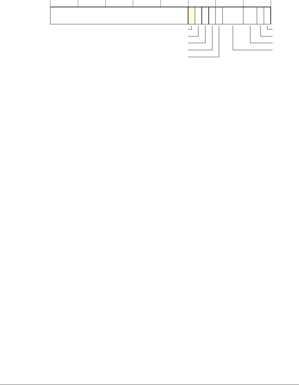
B4 System Control Registers in a VMSA implementation
B4.1 VMSA System control registers descriptions, in register order
B4-1666 Copyright © 1996-1998, 2000, 2004-2012, 2014 ARM. All rights reserved. ARM DDI 0406C.c
Non-Confidential ID051414
32-bit PAR format
For a translation that returns a 32-bit address and completes successfully, the PAR bit assignments are:
PA, bits[31:12]
Physical Address. The physical address corresponding to the supplied virtual address. This field
returns address bits[31:12].
LPAE, bit[11], if the implementation includes the Large Physical Address Extension
When updating the PAR with the result of a translation operation, this bit is set to 0 to indicate use
of the Short-descriptor translation table formats. This indicates that the PAR returns a 32-bit value.
Hardware does not interpret this bit to determine the behavior of the memory system, and therefore
software can set this bit to 0 or 1 without affecting operation. Unless the register has been updated
as a result of an address translation operation, a subsequent read of the register returns the value
written to it.
Bit[11], if the implementation does not include the Large Physical Address Extension
Reserved, UNK/SBZP.
Bits[10:1] Return memory attributes for the region:
NOS, bit[10]
Not Outer Shareable attribute. Indicates whether Shareable physical memory is Outer
Shareable:
0 Memory is Outer Shareable.
1 Memory is not Outer Shareable.
If the physical memory is not Shareable, this bit is UNKNOWN.
On an implementation that does not distinguish between Inner Shareable and Outer
Shareable, this bit is UNK/SBZP.
On an implementation that includes the Large Physical Address Extension and is using
the Short-descriptor translation table format:
• For a Strongly-ordered or Device memory region, this field returns the value 0,
regardless of any shareability attributes applied to the region. This means that any
PRRR.{NOS, DS0, DS1} bits that apply to the region have no effect on the
returned value.
• For a Normal memory region with the Inner Non-cacheable, Outer
Non-cacheable attribute, it is IMPLEMENTATION DEFINED whether this bit returns
the Outer Shareable attribute for the region, or returns 0.
NS, bit[9] Non-secure. The NS attribute for a translation table entry read from Secure state.
This bit is UNKNOWN for a translation table entry read from Non-secure state.
Bit[8] IMPLEMENTATION DEFINED.
SH, bit[7] Shareable attribute. Indicates whether the physical memory is Shareable:
0 Memory is Non-shareable.
1 Memory is Shareable.
0*0*
PA
31 12 11 10 9 8 7 6 4 3 2 1 0
NOS
IMPLEMENTATION DEFINED Inner[2:0]
NS
SH
Outer[1:0]
SS
FLPAE†
* Returned value, but might be overwritten, because the bit is RW.
† Reserved before the introduction of the Large Physical Address Extension, see text for more information.

B4 System Control Registers in a VMSA implementation
B4.1 VMSA System control registers descriptions, in register order
ARM DDI 0406C.c Copyright © 1996-1998, 2000, 2004-2012, 2014 ARM. All rights reserved. B4-1667
ID051414 Non-Confidential
On an implementation that includes the Large Physical Address Extension and is using
the Short-descriptor translation table format:
• For a Strongly-ordered or Device memory region, this field returns the value 1,
regardless of any shareability attributes applied to the region. This means that any
PRRR.{NOS, DS0, DS1} bits that apply to the region have no effect on the
returned value.
• For a Normal memory region with the Inner Non-cacheable, Outer
Non-cacheable attribute, it is IMPLEMENTATION DEFINED whether this bit returns
the Shareable attribute for the region, or returns 1.
An implementation that does not make use of this attribute can return the value that
corresponds to its behavior, instead of the value in the translation table entry.
Inner[2:0], bits[6:4]
Inner memory attributes. Permitted values are:
0b111
Write-Back, no Write-Allocate.
0b110
Write-Through.
0b101
Write-Back, Write-Allocate.
0b011
Device.
0b001
Strongly-ordered.
0b000
Non-cacheable.
Other encodings for Inner[2:0] are reserved.
An implementation that does not support all of the defined attributes can return the
behavior that the cache supports, instead of the value in the translation table entry.
Outer[1:0], bits[3:2]
Outer memory attributes. Possible values are:
0b11
Write-Back, no Write-Allocate.
0b10
Write-Through, no Write-Allocate.
0b01
Write-Back, Write-Allocate.
0b00
Non-cacheable.
An implementation that does not support all of the defined attributes can return the
behavior that the cache supports, instead of the value in the translation table entry.
SS, bit[1] Supersection. Indicates whether the result is a Supersection:
0 Page is not a Supersection, that is, PAR[31:12] contains PA[31:12],
regardless of the page size.
1 Page is part of a Supersection, and:
• PAR[31:24] contains PA[31:24]
• PAR[23:16] contains PA[39:32]
• PAR[15:12] contains
0b0000
.
If an implementation supports less than 40 bits of physical address, the bits
in the PAR field that correspond to physical address bits that are not
implemented are UNKNOWN.
Note
PA[23:12] is the same as VA[23:12] for Supersections.
F, bit[0] RAZ. Indicates that the conversion completed successfully.

B4 System Control Registers in a VMSA implementation
B4.1 VMSA System control registers descriptions, in register order
B4-1668 Copyright © 1996-1998, 2000, 2004-2012, 2014 ARM. All rights reserved. ARM DDI 0406C.c
Non-Confidential ID051414
For a translation that should return a 32-bit address, if the translation aborts without generating an exception the
PAR bit assignments are:
Bits[31:12] Reserved, UNK/SBZP.
LPAE, bit[11], if the implementation includes the Large Physical Address Extension
When updating the PAR with the result of a translation operation, this bit is set to 0 to indicate use
of the Short-descriptor translation table formats.
Hardware does not interpret this bit to determine the behavior of the memory system, and therefore
software can set this bit to 0 or 1 without affecting operation.
Bit[11], if the implementation does not include the Large Physical Address Extension
Reserved, UNK/SBZP.
Bits[10:7] Reserved, UNK/SBZP.
FS, bits[6:1] Fault status bits. Bits[12, 10, 3:0] from the Data Fault Status Register, indicate the source of the
abort. For more information, see DFSR, Data Fault Status Register, VMSA on page B4-1561.
F, bit[0] RAO. Indicates that the conversion aborted.
64-bit PAR format
For a translation that returns a 64-bit address and completes successfully, the PAR bit assignments are:
ATTR, bits[63:56]
Memory attributes for the returned PA, as indicated by the translation table entry. This field uses the
same encoding as the Attrn fields in the MAIRn registers.
An implementation that does not support all of the defined attribute can return the value
corresponding to its behavior, instead of the value in the translation table entry.
Bits[55:40] Reserved, UNK/SBZP.
PA[39:12], bits[39:12]
Physical Address. The physical address corresponding to the supplied virtual address. This field
returns address bits[39:12].
LPAE, bit[11] When updating the PAR with the result of a translation operation, this bit is set to 1 to indicate use
of the Long-descriptor translation table format. This indicates that the PAR returns a 64-bit value.
F
1*
Reserved, UNK/SBZP
31 12 11 10 7 6 1 0
0*Reserved,
UNK/SBZP FS
LPAE†
† Reserved before the introduction of the Large Physical Address Extension, see text for more information.
* Returned value, but might be overwritten, because the bit is RW.
0*
1*SH Reserved,
UNK/SBZP
Reserved, UNK/SBZP PA[39:12]
12 11 10 9 8 7 6 156 55
ATTR
LPAE
IMPLEMENTATION
DEFINED
NS
F
40 3963 0
* Returned value, but might be overwritten, because the bit is RW.
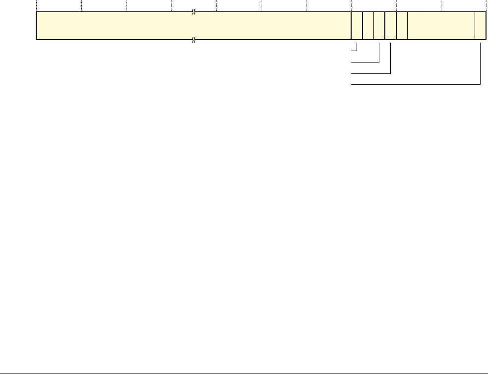
B4 System Control Registers in a VMSA implementation
B4.1 VMSA System control registers descriptions, in register order
ARM DDI 0406C.c Copyright © 1996-1998, 2000, 2004-2012, 2014 ARM. All rights reserved. B4-1669
ID051414 Non-Confidential
Hardware does not interpret this bit to determine the behavior of the memory system, and therefore
software can set this bit to 0 or 1 without affecting operation. Unless the register has been updated
as a result of an address translation operation, a subsequent read of the register returns the value
written to it.
IMPLEMENTATION DEFINED, bit[10]
An IMPLEMENTATION DEFINED bit.
NS, bit[9] Non-secure. The NS attribute for a translation table entry read from Secure state. For more
information, see Control of Secure or Non-secure memory access, Long-descriptor format on
page B3-1344.
This bit is UNKNOWN for a translation table entry read from Non-secure state.
SH[1:0], bits[8:7]
Shareability attribute, from the translation table entry for the returned PA. For more information,
including the encoding of this field, see Shareability, Long-descriptor format on page B3-1373. If
the returned PA is in a Device or Strongly-ordered memory region this field returns the value
0b10
.
An implementation that does not make use of this attribute can return the value that corresponds to
its behavior, instead of the value in the translation table entry.
Bits[6:1] Reserved, UNK/SBZP.
F, bit[0] RAZ. Indicates that the conversion completed successfully.
For a translation that should return a 64-bit address, if the translation aborts without generating an exception the
PAR bit assignments are:
Bits[63:12] Reserved, UNK/SBZP.
LPAE, bit[11] After an address translation operation, in this format of the PAR, this bit is set to 1 to indicate that
the translation used the Long-descriptor translation table formats, and returns a 64-bit PAR value.
Hardware does not interpret this bit to determine the behavior of the memory system, and therefore
software can set this bit to 0 or 1 without affecting operation.
Bit[10] Reserved, UNK/SBZP.
FSTAGE, bit[9]
Indicates the translation stage at which the translation aborted:
0 Translation aborted because of a fault in the stage 1 translation.
1 Translation aborted because of a fault in the stage 2 translation.
S2WLK, bit[8]
This bit is set to 1 to indicate that the translation aborted because of a stage 2 fault during a stage 1
translation table walk. Otherwise, it is set to 0.
Bit[7] Reserved, UNK/SBZP.
FS, bits[6:1] Fault status field. The field uses the fault encoding described in Fault reporting with the
Long-descriptor translation table format on page B3-1416.
(0)
FSTAGE
S2WLK
LPAE
1*
1*(0) FSReserved, UNK/SBZP
12 11 10 9 8 7 6 1
F
63 0
* Returned value, but might be overwritten, because the bit is RW.

B4 System Control Registers in a VMSA implementation
B4.1 VMSA System control registers descriptions, in register order
B4-1670 Copyright © 1996-1998, 2000, 2004-2012, 2014 ARM. All rights reserved. ARM DDI 0406C.c
Non-Confidential ID051414
F, bit[0] RAO. Indicates that the conversion aborted.
Accessing the PAR
To access the PAR in an implementation that does not include the Large Physical Address Extension, or bits[31:0]
of the PAR in an implementation that includes the Large Physical Address Extension, software reads or writes the
CP15 registers with an
MRC
or
MCR
instruction with
<opc1>
set to 0,
<CRn>
set to c7,
<CRm>
set to c4, and
<opc2>
set to
0. For example:
MRC p15, 0, <Rt>, c7, c4, 0 ; Read PAR[31:0] into Rt
MCR p15, 0, <Rt>, c7, c4, 0 ; Write Rt to PAR[31:0]
In an implementation that includes the Large Physical Address Extension, to access all 64 bits of the PAR, software
reads or writes the CP15 registers with an
MRRC
or
MCRR
instruction with
<opc1>
set to 0 and
<CRn>
set to c7. For
example:
MRRC p15, 0, <Rt>, <Rt2>, c7 ; Read 64-bit PAR into Rt (low word) and Rt2 (high word)
MCRR p15, 0, <Rt>, <Rt2>, c7 ; Write Rt (low word) and Rt2 (high word) to 64-bit PAR
For examples of accessing the PAR as part of an address translation operation, see Accessing the PAR and the
address translation operations on page B4-1751.

B4 System Control Registers in a VMSA implementation
B4.1 VMSA System control registers descriptions, in register order
ARM DDI 0406C.c Copyright © 1996-1998, 2000, 2004-2012, 2014 ARM. All rights reserved. B4-1671
ID051414 Non-Confidential
B4.1.113 PMCCNTR, Performance Monitors Cycle Count Register, VMSA
When accessed through the CP15 interface, the PMCCNTR characteristics are:
Purpose The PMCCNTR holds the value of the processor Cycle Counter, CCNT, that counts
processor clock cycles.
This register is a Performance Monitors register.
Usage constraints The PMCCNTR is accessible in:
• all modes executing at PL1 or higher
• User mode when PMUSERENR.EN == 1.
See Access permissions on page C12-2330 for more information.
The PMCR.D bit configures whether PMCCNTR increments once every clock cycle, or
once every 64 clock cycles.
In PMUv2, the PMXEVTYPER accessed when PMSELR.SEL is set to
0b11111
determines
the modes and states in which the PMCCNTR can increment.
Configurations Implemented only as part of the Performance Monitors Extension.
The VMSA and PMSA definitions of the register fields are identical.
In a VMSA implementation that includes the Security Extensions, this is a Common
register.
Attributes A 32-bit RW register with a reset value that is UNKNOWN on a non-debug logic reset. See
also Power domains and Performance Monitors registers reset on page C12-2329.
Table C12-7 on page C12-2329 shows the CP15 encodings of all of the Performance
Monitors registers.
Note
Differences in the memory-mapped views of the Performance Monitors registers on page D2-2354 describes how
the characteristics of the PMCCNTR differ when it is accessed through an external debug interface or a
memory-mapped interface.
The PMCCNTR bit assignments are:
CCNT, bits[31:0] Cycle count. Depending on the value of the PMCR.D bit, this field increments either:
• once every processor clock cycle
• once every 64 processor clock cycles.
The PMCCNTR.CCNT value can be reset to zero by writing a 1 to the PMCR.C bit.
Accessing the PMCCNTR
To access the PMCCNTR, read or write the CP15 registers with
<opc1>
set to 0,
<CRn>
set to c9,
<CRm>
set to c13, and
<opc2>
set to 0. For example:
MRC p15, 0, <Rt>, c9, c13, 0 : Read PMCCNTR into Rt
MCR p15, 0, <Rt>, c9, c13, 0 : Write Rt to PMCCNTR
CCNT
31 0

B4 System Control Registers in a VMSA implementation
B4.1 VMSA System control registers descriptions, in register order
B4-1672 Copyright © 1996-1998, 2000, 2004-2012, 2014 ARM. All rights reserved. ARM DDI 0406C.c
Non-Confidential ID051414
B4.1.114 PMCEID0 and PMCEID1, Performance Monitors Common Event ID registers, VMSA
When accessed through the CP15 interface, the PMCEID0 and PMCEID1 register characteristics are:
Purpose The PMCEIDn registers define which common architectural and common
microarchitectural feature events are implemented.
These registers are Performance Monitors registers.
Usage constraints The PMCEIDn registers are accessible in:
• all modes executing at PL1 or higher
• User mode when PMUSERENR.EN is set to 1.
See Access permissions on page C12-2330 for more information.
Configurations Implemented only as part of the Performance Monitors Extension.
The VMSA and PMSA definitions of the register fields are identical.
In a VMSA implementation that includes the Security Extensions, this is a Common
register.
Attributes A 32-bit RO register.
Table C12-7 on page C12-2329 shows the CP15 encodings of all of the Performance
Monitors registers.
Note
Differences in the memory-mapped views of the Performance Monitors registers on page D2-2354 describes how
the characteristics of the PMCEID0 and PMCEID1 registers differ when they are accessed through an external
debug interface or a memory-mapped interface.
Table B4-14 shows the PMCEID0 bit assignments with the event implemented or not implemented when the
associated bit is set to 1 or 0.
PMCEID1[31:0] is reserved and must be implemented as RAZ. Software must not rely on the bits reading as 0.
Table B4-14 PMCEID0 bit assignments
Bit Event number Event implemented if set to 1 or not implemented if set to 0
[31]
0x1F
Reserved, UNK.
[30]
0x1E
[29]
0x1D
Bus cycle.
[28]
0x1C
Instruction architecturally executed, condition code check pass, write to TTBR.
[27]
0x1B
Instruction speculatively executed.
[26]
0x1A
Local memory error.
[25]
0x19
Bus access.
[24]
0x18
Level 2 data cache write-back.
[23]
0x17
Level 2 data cache refill.
[22]
0x16
Level 2 data cache access.
[21]
0x15
Level 1 data cache write-back.
[20]
0x14
Level 1 instruction cache access.
[19]
0x13
Data memory access.

B4 System Control Registers in a VMSA implementation
B4.1 VMSA System control registers descriptions, in register order
ARM DDI 0406C.c Copyright © 1996-1998, 2000, 2004-2012, 2014 ARM. All rights reserved. B4-1673
ID051414 Non-Confidential
Accessing the PMCEID0 or PMCEID1 register
To access the PMCEID0 or PMCEID1 register, software reads the CP15 register with
<opc1>
set to 0,
<CRn>
set to
c9,
<CRm>
set to c12, and:
•
<opc2>
set to 6 for the PMCEID0 register
•
<opc2>
set to 7 for the PMCEID1 register.
For example:
MRC p15, 0, <Rt>, c9, c12, 6 ; Read PMCEID0 into Rt
MRC p15, 0, <Rt>, c9, c12, 7 ; Read PMCEID1 into Rt
[18]
0x12
Predictable branch speculatively executed. If the implementation includes program flow prediction, this bit
is RAO.
[17]
0x11
Cycle, this bit is RAO.
[16]
0x10
Mispredicted or not predicted branch speculatively executed. If the implementation includes program flow
prediction resources, this bit is RAO.
[15]
0x0F
Instruction architecturally executed, condition code check pass, unaligned load or store.
[14]
0x0E
Instruction architecturally executed, condition code check pass, procedure return.
[13]
0x0D
Instruction architecturally executed, immediate branch.
[12]
0x0C
Instruction architecturally executed, condition code check pass, software change of the PC.
[11]
0x0B
Instruction architecturally executed, condition code check pass, write to CONTEXTIDR.
[10]
0x0A
Instruction architecturally executed, condition code check pass, exception return.
[9]
0x09
Exception taken.
[8]
0x08
Instruction architecturally executed.
[7]
0x07
Instruction architecturally executed, condition code check pass, store.
[6]
0x06
Instruction architecturally executed, condition code check pass, load.
[5]
0x05
Level 1 data TLB refill.
[4]
0x04
Level 1 data cache access. If the implementation includes a L1 data or unified cache, this bit is RAO.
[3]
0x03
Level 1 data cache refill. If the implementation includes a L1 data or unified cache, this bit is RAO.
[2]
0x02
Level 1 instruction TLB refill.
[1]
0x01
Level 1 instruction cache refill.
[0]
0x00
Instruction architecturally executed, condition code check pass, software increment. This bit is RAO.
Table B4-14 PMCEID0 bit assignments (continued)
Bit Event number Event implemented if set to 1 or not implemented if set to 0

B4 System Control Registers in a VMSA implementation
B4.1 VMSA System control registers descriptions, in register order
B4-1674 Copyright © 1996-1998, 2000, 2004-2012, 2014 ARM. All rights reserved. ARM DDI 0406C.c
Non-Confidential ID051414
B4.1.115 PMCNTENCLR, Performance Monitors Count Enable Clear register, VMSA
When accessed through the CP15 interface, the PMCNTENCLR register characteristics are:
Purpose The PMCNTENCLR register disables the Cycle Count Register, PMCCNTR, and any
implemented event counters, PMNx. Reading this register shows which counters are
enabled.
This register is a Performance Monitors register.
Usage constraints The PMCNTENCLR register is accessible in:
• all modes executing at PL1 or higher
• User mode when PMUSERENR.EN == 1.
Note
In an implementation that includes the Virtualization Extensions, in Non-secure PL1 and
PL0 modes, the value of HDCR.HPMN can change the behavior of accesses to
PMCNTENCLR, see the description of the Px bit.
See Access permissions on page C12-2330 for more information. See also Counter enables
on page C12-2313 and Counter access on page C12-2314.
PMCNTENCLR is used in conjunction with the PMCNTENSET Register.
Configurations Implemented only as part of the Performance Monitors Extension.
The VMSA and PMSA definitions of the register fields are identical.
In a VMSA implementation that includes the Security Extensions, this is a Common
register.
Attributes A 32-bit RW register with a reset value that is UNKNOWN on a non-debug logic reset. See
also Power domains and Performance Monitors registers reset on page C12-2329.
Table C12-7 on page C12-2329 shows the CP15 encodings of all of the Performance
Monitors registers.
Note
Differences in the memory-mapped views of the Performance Monitors registers on page D2-2354 describes how
the characteristics of the PMCNTENCLR register differ when it is accessed through an external debug interface or
a memory-mapped interface.
The PMCNTENCLR register bit assignments are:
Note
In the description of the PMCNTENCLR register, N and x have the meanings used in the description of the
PMCNTENSET register.
C, bit[31] PMCCNTR disable bit. Table B4-15 shows the behavior of this bit on reads and writes.
Table B4-15 Read and write values for the PMCNTENCLR.C bit
Value Meaning on read Action on write
0 Cycle counter disabled No action, write is ignored
1 Cycle counter enabled Disable the cycle counter
C
31 30 N N–1 0
Reserved, RAZ/WI Event counter disable bits, Px, for x = 0 to (N–1)

B4 System Control Registers in a VMSA implementation
B4.1 VMSA System control registers descriptions, in register order
ARM DDI 0406C.c Copyright © 1996-1998, 2000, 2004-2012, 2014 ARM. All rights reserved. B4-1675
ID051414 Non-Confidential
Bits[30:N] Reserved, RAZ/WI.
Px, bit[x], for x = 0 to (N–1)
Event counter x, PMNx, disable bit.
In an implementation that includes the Virtualization Extensions, in Non-secure PL1 and
PL0 modes, if x≥HDCR.HPMN then Px is RAZ/WI, see Counter access on
page C12-2314. Otherwise, Table B4-16 shows the behavior of this bit on reads and writes.
Note
PMCR.E can override the settings in this register and disable all counters including PMCCNTR. PMCNTENCLR
retains its value when PMCR.E is 0, even though its settings are ignored.
Accessing the PMCNTENCLR register
To access the PMCNTENCLR register, read or write the CP15 registers with
<opc1>
set to 0,
<CRn>
set to c9,
<CRm>
set to c12, and
<opc2>
set to 2. For example:
MRC p15, 0, <Rt>, c9, c12, 2 : Read PMCNTENCLR into Rt
MCR p15, 0, <Rt>, c9, c12, 2 : Write Rt to PMCNTENCLR
Table B4-16 Read and write values for the PMCNTENCLR.Px bits
Px value Meaning on read Action on write
0PMNx event counter disabled No action, write is ignored
1PMNx event counter enabled Disable the PMNx event counter

B4 System Control Registers in a VMSA implementation
B4.1 VMSA System control registers descriptions, in register order
B4-1676 Copyright © 1996-1998, 2000, 2004-2012, 2014 ARM. All rights reserved. ARM DDI 0406C.c
Non-Confidential ID051414
B4.1.116 PMCNTENSET, Performance Monitors Count Enable Set register, VMSA
When accessed through the CP15 interface, the PMCNTENSET register characteristics are:
Purpose The PMCNTENSET register enables the Cycle Count Register, PMCCNTR, and any
implemented event counters, PMNx. Reading this register shows which counters are
enabled.
This register is a Performance Monitors register.
Usage constraints The PMCNTENSET register is accessible in:
• all modes executing at PL1 or higher
• User mode when PMUSERENR.EN is set to 1.
Note
In an implementation that includes the Virtualization Extensions, in Non-secure PL1 and
PL0 modes, the value of HDCR.HPMN can change the behavior of accesses to
PMCNTENSET, see the description of the Px bit.
See Access permissions on page C12-2330 for more information. See also Counter enables
on page C12-2313 and Counter access on page C12-2314.
PMCNTENSET is used in conjunction with PMCNTENCLR.
Configurations Implemented only as part of the Performance Monitors Extension.
The VMSA and PMSA definitions of the register fields are identical.
In a VMSA implementation that includes the Security Extensions, this is a Common
register.
Attributes A 32-bit RW register with a reset value that is UNKNOWN on a non-debug logic reset. See
also Power domains and Performance Monitors registers reset on page C12-2329.
Table C12-7 on page C12-2329 shows the CP15 encodings of all of the Performance
Monitors registers.
Note
Differences in the memory-mapped views of the Performance Monitors registers on page D2-2354 describes how
the characteristics of the PMCNTENSET register differ when it is accessed through an external debug interface or
a memory-mapped interface.
The PMCNTENSET register bit assignments are:
Note
In the description of the PMCNTENSET register:
• N is the number of event counters implemented, as defined by the PMCR.N field. For Virtualization
Extensions, in Non-secure modes other than Hyp mode the number of accessible event counters might be less
than PMCR.N indicates.
•x refers to a single event counter, and takes values from 0 to (N–1).
C
31 30 N N–1 0
Reserved, RAZ/WI Event counter enable bits, Px, for x = 0 to (N–1)

B4 System Control Registers in a VMSA implementation
B4.1 VMSA System control registers descriptions, in register order
ARM DDI 0406C.c Copyright © 1996-1998, 2000, 2004-2012, 2014 ARM. All rights reserved. B4-1677
ID051414 Non-Confidential
C, bit[31] PMCCNTR enable bit. Table B4-17 shows the behavior of this bit on reads and writes.
Bits[30:N] Reserved, RAZ/WI.
Px, bit[x], for x = 0 to (N–1)
Event counter x, PMNx, enable bit.
In an implementation that includes the Virtualization Extensions, in Non-secure PL1 and PL0
modes, if x≥HDCR.HPMN then Px is RAZ/WI, see Counter access on page C12-2314. Otherwise,
Table B4-18 shows the behavior of this bit on reads and writes.
Accessing the PMCNTENSET register
To access the PMCNTENSET register, read or write the CP15 registers with
<opc1>
set to 0,
<CRn>
set to c9,
<CRm>
set
to c12, and
<opc2>
set to 1. For example:
MRC p15, 0, <Rt>, c9, c12, 1 ; Read PMCNTENSET into Rt
MCR p15, 0, <Rt>, c9, c12, 1 ; Write Rt to PMCNTENSET
Table B4-17 Read and write bit values for the PMCNTENSET.C bit
Value Meaning on read Action on write
0 Cycle counter disabled No action, write is ignored
1 Cycle counter enabled Enable the PMCCNTR cycle counter
Table B4-18 Read and write values for the PMCNTENSET.Px bits
Px value Meaning on read Action on write
0PMNx event counter disabled No action, write is ignored
1PMNx event counter enabled Enable the PMNx event counter
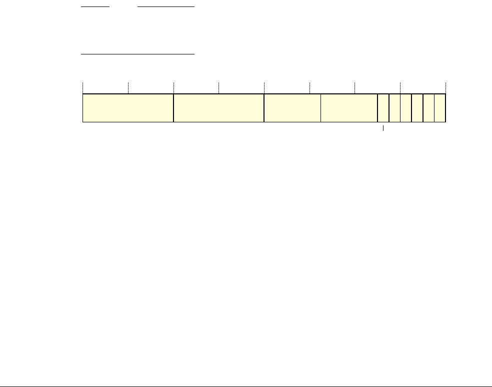
B4 System Control Registers in a VMSA implementation
B4.1 VMSA System control registers descriptions, in register order
B4-1678 Copyright © 1996-1998, 2000, 2004-2012, 2014 ARM. All rights reserved. ARM DDI 0406C.c
Non-Confidential ID051414
B4.1.117 PMCR, Performance Monitors Control Register, VMSA
When accessed through the CP15 interface, the PMCR characteristics are:
Purpose The PMCR provides details of the Performance Monitors implementation, including the
number of counters implemented, and configures and controls the counters.
This register is a Performance Monitors register.
Usage constraints The PMCR is accessible in:
• all modes executing at PL1 or higher
• User mode when PMUSERENR.EN is set to 1.
See Access permissions on page C12-2330 for more information. See also Counter enables
on page C12-2313 and Counter access on page C12-2314.
Configurations Implemented only as part of the Performance Monitors Extension.
The VMSA and PMSA definitions of the register fields are identical.
In a VMSA implementation that includes the Security Extensions, this is a Common
register.
Attributes A 32-bit RW register with a reset value that depends on the register implementation. For
more information see the register bit descriptions and Power domains and Performance
Monitors registers reset on page C12-2329.
Table C12-7 on page C12-2329 shows the CP15 encodings of all of the Performance
Monitors registers.
Note
Differences in the memory-mapped views of the Performance Monitors registers on page D2-2354 describes how
the characteristics of the PMCR differ when it is accessed through an external debug interface or a memory-mapped
interface.
The PMCR bit assignments are:
IMP, bits[31:24] Implementer code. This field is RO with an IMPLEMENTATION DEFINED value.
The implementer codes are allocated by ARM. Values have the same interpretation as
bits[31:24] of the MIDR.
IDCODE, bits[23:16] Identification code. This field is RO with an IMPLEMENTATION DEFINED value.
Each implementer must maintain a list of identification codes that is specific to the
implementer. A specific implementation is identified by the combination of the implementer
code and the identification code.
N, bits[15:11] Number of event counters. This field is RO with an IMPLEMENTATION DEFINED value that
indicates the number of counters implemented.
The value of this field is the number of counters implemented, from
0b00000
for no counters
to
0b11111
for 31 counters.
An implementation can implement only the Cycle Count Register, PMCCNTR. This is
indicated by a value of
0b00000
for the N field.
EIMP
31 24 23 16 15 11 6 5 4 3 2 1 0
IDCODE N Reserved,
UNK/SBZP X D C P
10
DP

B4 System Control Registers in a VMSA implementation
B4.1 VMSA System control registers descriptions, in register order
ARM DDI 0406C.c Copyright © 1996-1998, 2000, 2004-2012, 2014 ARM. All rights reserved. B4-1679
ID051414 Non-Confidential
In an implementation that includes the Virtualization Extensions:
• In Non-secure modes other than Hyp mode, this field reads the value of
HDCR.HPMN.
• In Secure state and Hyp mode, this field reads the IMPLEMENTATION DEFINED number
of event counters.
Bits[10:6] Reserved, UNK/SBZP.
DP, bit[5] Disable PMCCNTR when event counting is prohibited. The possible values of this bit are:
0 Cycle counter operates regardless of the non-invasive debug authentication
settings.
1 Cycle counter is disabled if non-invasive debug is not permitted.
For more information, see Effects of non-invasive debug authentication on the Performance
Monitors on page C12-2304 and Chapter C9 Non-invasive Debug Authentication.
Note
In an implementation that includes the Security Extensions, a Non-secure process can set
this bit to 1, to discard cycle counts that might be accumulated during periods when the other
counts are prohibited because of security prohibitions. It is not a control to enhance security.
The function of this bit is to avoid corruption of the count. See also Effect of the Security
Extensions and Virtualization Extensions on page C12-2309.
This bit is RW. Its non-debug logic reset value is 0.
X, bit[4] Export enable. The possible values of this bit are:
0 Export of events is disabled.
1 Export of events is enabled.
This bit enables the exporting of events to another debug device, such as a trace macrocell,
over an event bus. If the implementation does not include such an event bus, this bit is
RAZ/WI.
This bit does not affect the generation of Performance Monitors interrupts, that can be
implemented as a signal exported from the processor to an interrupt controller.
This bit is RW. Its non-debug logic reset value is 0.
D, bit[3] Cycle counter clock divider. The possible values of this bit are:
0 When enabled, PMCCNTR counts every clock cycle.
1 When enabled, PMCCNTR counts once every 64 clock cycles.
This bit is RW. Its non-debug logic reset value is 0.
C, bit[2] Cycle counter reset. This bit is WO. The effects of writing to this bit are:
0 No action.
1 Reset PMCCNTR to zero.
Note
Resetting PMCCNTR does not clear the PMCCNTR overflow bit to 0. For more
information, see the description of PMOVSR.
This bit is always RAZ.

B4 System Control Registers in a VMSA implementation
B4.1 VMSA System control registers descriptions, in register order
B4-1680 Copyright © 1996-1998, 2000, 2004-2012, 2014 ARM. All rights reserved. ARM DDI 0406C.c
Non-Confidential ID051414
P, bit[1] Event counter reset. This bit is WO. The effects of writing to this bit are:
0 . No action.
1 . Reset all event counters, except PMCCNTR, to zero.
Note
. Resetting the event counters does not clear any overflow bits to 0. For more information,
see the description of PMOVSR.
In an implementation that includes the Virtualization Extensions:
• In Non-secure modes other than Hyp mode:
— A write of 1 to this bit by an
MCR
instruction does not reset event counters that
the HDCR.HPMN field reserves for Hyp mode use.
—It is UNPREDICTABLE whether a write of 1 to this bit through a
memory-mapped interface or an external debug interface resets the event
counters that the HDCR.HPMN field reserves for Hyp mode use.
For more information about these interfaces, see Appendix D2 Recommended
Memory-mapped and External Debug Interfaces for the Performance
Monitors.
• In Secure state and Hyp mode, a write of 1 to this bit resets all the event counters.
This bit is always RAZ.
E, bit[0] Enable. The possible values of this bit are:
0 All counters, including PMCCNTR, are disabled.
1 All counters are enabled.
In an implementation that includes the Virtualization Extensions, the value of this bit does
not affect the operation of event counters that HDCR.HPMN reserves for use in Hyp mode.
For more information, see Counter enables on page C12-2313.
This bit is RW. Its non-debug logic reset value is 0.
Accessing the PMCR
To access PMCR, read or write the CP15 registers with
<opc1>
set to 0,
<CRn>
set to c9,
<CRm>
set to c12, and
<opc2>
set to 0. For example:
MRC p15, 0, <Rt>, c9, c12, 0 ; Read PMCR into Rt
MCR p15, 0, <Rt>, c9, c12, 0 ; Write Rt to PMCR

B4 System Control Registers in a VMSA implementation
B4.1 VMSA System control registers descriptions, in register order
ARM DDI 0406C.c Copyright © 1996-1998, 2000, 2004-2012, 2014 ARM. All rights reserved. B4-1681
ID051414 Non-Confidential
B4.1.118 PMINTENCLR, Performance Monitors Interrupt Enable Clear register, VMSA
When accessed through the CP15 interface, the PMINTENCLR register characteristics are:
Purpose The PMINTENCLR register disables the generation of interrupt requests on overflows
from:
• the Cycle Count Register, PMCCNTR
• each implemented event counter, PMNx.
Reading the register shows which overflow interrupt requests are enabled.
This register is a Performance Monitors register.
Usage constraints The PMINTENCLR is accessible from PL1 or higher.
Note
In an implementation that includes the Virtualization Extensions, in Non-secure PL1 modes,
the value of HDCR.HPMN can change the behavior of accesses to PMINTENCLR, see the
description of the Px bit.
In User mode, instructions that access the register are always UNDEFINED, even if
PMUSERENR.EN is set to 1.
See Access permissions on page C12-2330 for more information. See also Counter access
on page C12-2314.
PMINTENCLR is used in conjunction with the PMINTENSET register.
Configurations Implemented only as part of the Performance Monitors Extension.
The VMSA and PMSA definitions of the register fields are identical.
In a VMSA implementation that includes the Security Extensions, this is a Common
register.
Attributes A 32-bit RW register with a reset value that is UNKNOWN on a non-debug logic reset. See
also Power domains and Performance Monitors registers reset on page C12-2329.
Table C12-7 on page C12-2329 shows the CP15 encodings of all of the Performance
Monitors registers.
Note
Differences in the memory-mapped views of the Performance Monitors registers on page D2-2354 describes how
the characteristics of the PMINTENCLR register differ when it is accessed through an external debug interface or
a memory-mapped interface.
The PMINTENCLR register bit assignments are:
Note
In the description of the PMINTENCLR register, N and x have the meanings used in the description of the
PMCNTENSET register.
C
31 30 N N–1 0
Reserved, RAZ/WI Event counter overflow interrupt request disable bits, Px, for x = 0 to (N–1)

B4 System Control Registers in a VMSA implementation
B4.1 VMSA System control registers descriptions, in register order
B4-1682 Copyright © 1996-1998, 2000, 2004-2012, 2014 ARM. All rights reserved. ARM DDI 0406C.c
Non-Confidential ID051414
C, bit[31] PMCCNTR overflow interrupt request disable bit.
Table B4-19 shows the behavior of this bit on reads and writes.
Bits[30:N] Reserved, RAZ/WI.
Px, bit[x], for x = 0 to (N–1)
Event counter x, PMNx, overflow interrupt request disable bit.
In an implementation that includes the Virtualization Extensions, in Non-secure PL1 modes, if
x≥HDCR.HPMN then Px is RAZ/WI, see Counter access on page C12-2314. Otherwise,
Table B4-20 shows the behavior of this bit on reads and writes.
For more information about counter overflow interrupt requests see PMINTENSET, Performance Monitors
Interrupt Enable Set register, VMSA on page B4-1683.
Accessing the PMINTENCLR register
To access the PMINTENCLR register, read or write the CP15 registers with
<opc1>
set to 0,
<CRn>
set to c9,
<CRm>
set
to c14, and
<opc2>
set to 2. For example:
MRC p15, 0, <Rt>, c9, c14, 2 : Read PMINTENCLR into Rt
MCR p15, 0, <Rt>, c9, c14, 2 : Write Rt to PMINTENCLR
Table B4-19 Read and write values for the PMINTENCLR.C bit
Value Meaning on read Action on write
0 Cycle count interrupt request disabled No action, write is ignored
1 Cycle count interrupt request enabled Disable the cycle count interrupt request
Table B4-20 Read and write values for the PMINTENCLR.Px bits
Px value Meaning on read Action on write
0PMNx interrupt request disabled No action, write is ignored
1PMNx interrupt request enabled Disable the PMNx interrupt request

B4 System Control Registers in a VMSA implementation
B4.1 VMSA System control registers descriptions, in register order
ARM DDI 0406C.c Copyright © 1996-1998, 2000, 2004-2012, 2014 ARM. All rights reserved. B4-1683
ID051414 Non-Confidential
B4.1.119 PMINTENSET, Performance Monitors Interrupt Enable Set register, VMSA
When accessed through the CP15 interface, the PMINTENSET register characteristics are:
Purpose The PMINTENSET register enables the generation of interrupt requests on overflows from:
• the Cycle Count Register, PMCCNTR
• each implemented event counter, PMNx.
Reading the register shows which overflow interrupt requests are enabled.
This register is a Performance Monitors register.
Usage constraints The PMINTENSET register is accessible from PL1 or higher.
Note
In an implementation that includes the Virtualization Extensions, in Non-secure PL1 modes,
the value of HDCR.HPMN can change the behavior of accesses to PMINTENSET, see the
description of the Px bit.
In User mode, instructions that access the register are always UNDEFINED, even if
PMUSERENR.EN is set to 1.
See Access permissions on page C12-2330 for more information. See also Counter access
on page C12-2314.
PMINTENSET is used in conjunction with the PMINTENCLR register.
Configurations Implemented only as part of the Performance Monitors Extension.
The VMSA and PMSA definitions of the register fields are identical.
In a VMSA implementation that includes the Security Extensions, this is a Common
register.
Attributes A 32-bit RW register with a reset value that is UNKNOWN on a non-debug logic reset. See
also Power domains and Performance Monitors registers reset on page C12-2329.
Table C12-7 on page C12-2329 shows the CP15 encodings of all of the Performance
Monitors registers.
Note
Differences in the memory-mapped views of the Performance Monitors registers on page D2-2354 describes how
the characteristics of the PMINTENSET register differ when it is accessed through an external debug interface or a
memory-mapped interface.
The PMINTENSET register bit assignments are:
Note
In the description of the PMINTENSET register, N and x have the meanings used in the description of the
PMCNTENSET Register.
C
31 30 N N–1 0
Reserved, RAZ/WI Event counter overflow interrupt request enable bits, Px, for x = 0 to (N–1)

B4 System Control Registers in a VMSA implementation
B4.1 VMSA System control registers descriptions, in register order
B4-1684 Copyright © 1996-1998, 2000, 2004-2012, 2014 ARM. All rights reserved. ARM DDI 0406C.c
Non-Confidential ID051414
C, bit[31] PMCCNTR overflow interrupt request enable bit.
Table B4-21 shows the behavior of this bit on reads and writes.
Bits[30:N] Reserved, RAZ/WI.
Px, bit[x], for x = 0 to (N–1)
Event counter x, PMNx, overflow interrupt request enable bit.
In an implementation that includes the Virtualization Extensions, in Non-secure PL1 modes, if
x≥HDCR.HPMN then Px is RAZ/WI, see Counter access on page C12-2314. Otherwise,
Table B4-22 shows the behavior of this bit on reads and writes.
The debug logic does not signal an interrupt request if the PMCR.E enable bit is set to 0.
When an interrupt is signaled, software can remove it by writing a 1 to the corresponding overflow bit in the
PMOVSR.
Note
ARM expects that the interrupt request that can be generated on a counter overflow is exported from the processor,
meaning it can be factored into a system interrupt controller if applicable. This means that normally the system has
more levels of control of the interrupt generated.
Accessing the PMINTENSET register
To access the PMINTENSET register, read or write the CP15 registers with
<opc1>
set to 0,
<CRn>
set to c9,
<CRm>
set
to c14, and
<opc2>
set to 1. For example:
MRC p15, 0, <Rt>, c9, c14, 1 : Read PMINTENSET into Rt
MCR p15, 0, <Rt>, c9, c14, 1 : Write Rt to PMINTENSET
Table B4-21 Read and write values for the PMINTENSET.C bit
Value Meaning on read Action on write
0 Cycle count interrupt request disabled No action, write is ignored
1 Cycle count interrupt request enabled Enable the cycle count interrupt request
Table B4-22 Read and write values for the PMINTENSET.Px bits
Px value Meaning on read Action on write
0PMNx interrupt request disabled No action, write is ignored
1PMNx interrupt request enabled Enable the PMNx interrupt request

B4 System Control Registers in a VMSA implementation
B4.1 VMSA System control registers descriptions, in register order
ARM DDI 0406C.c Copyright © 1996-1998, 2000, 2004-2012, 2014 ARM. All rights reserved. B4-1685
ID051414 Non-Confidential
B4.1.120 PMOVSR, Performance Monitors Overflow Flag Status Register, VMSA
When accessed through the CP15 interface, the PMOVSR characteristics are:
Purpose The PMOVSR holds the state of the overflow bit for:
• the Cycle Count Register, PMCCNTR
• each of the implemented event counters, PMNx.
Software must write to this register to clear these bits.
This register is a Performance Monitors register.
Usage constraints The PMOVSR is accessible in:
• all modes executing at PL1 or higher
• User mode when PMUSERENR.EN is set to 1.
Note
In an implementation that includes the Virtualization Extensions, in Non-secure PL1 and
PL0 modes, the value of HDCR.HPMN can change the behavior of accesses to PMOVSR,
see the description of the Px bit.
See Access permissions on page C12-2330 for more information. See also Counter access
on page C12-2314.
Configurations Implemented only as part of the Performance Monitors Extension.
The VMSA and PMSA definitions of the register fields are identical.
In a VMSA implementation that includes the Security Extensions, this is a Common
register.
Attributes A 32-bit RW register with a reset value that is UNKNOWN on a non-debug logic reset. See
also Power domains and Performance Monitors registers reset on page C12-2329.
Table C12-7 on page C12-2329 shows the CP15 encodings of all of the Performance
Monitors registers.
Note
Differences in the memory-mapped views of the Performance Monitors registers on page D2-2354 describes how
the characteristics of the PMOVSR differ when it is accessed through an external debug interface or a
memory-mapped interface.
The PMOVSR bit assignments are:
Note
In the description of the PMOVSR, N and x have the meanings used in the description of the PMCNTENSET
Register.
C
31 30 N N–1 0
Reserved, RAZ/WI Event counter overflow bits, Px, for x = 0 to (N–1)

B4 System Control Registers in a VMSA implementation
B4.1 VMSA System control registers descriptions, in register order
B4-1686 Copyright © 1996-1998, 2000, 2004-2012, 2014 ARM. All rights reserved. ARM DDI 0406C.c
Non-Confidential ID051414
C, bit[31] PMCCNTR overflow bit.
Table B4-23 shows the behavior of this bit on reads and writes.
Bits[30:N] Reserved, RAZ/WI.
Px, bit[x], for x = 0 to (N–1)
Event counter x, PMNx, overflow bit.
In an implementation that includes the Virtualization Extensions, in Non-secure PL1 and
PL0 modes, if x≥HDCR.HPMN then Px is RAZ/WI, see Counter access on
page C12-2314. Otherwise, Table B4-24 shows the behavior of this bit on reads and writes.
Note
The overflow bit values for individual counters are retained until cleared to 0 by a write to the PMOVSR or
processor reset, even if the counter is later disabled by writing to the PMCNTENCLR register or through the
PMCR.E Enable bit. The overflow bits are also not cleared to 0 when the counters are reset through the Event
counter reset or Clock counter reset bits in the PMCR.
Accessing the PMOVSR
To access the PMOVSR, read or write the CP15 registers with
<opc1>
set to 0,
<CRn>
set to c9,
<CRm>
set to c12, and
<opc2>
set to 3. For example:
MRC p15, 0, <Rt>, c9, c12, 3; Read PMOVSR into Rt
MCR p15, 0, <Rt>, c9, c12, 3; Write Rt to PMOVSR
Table B4-23 Read and write values for the PMOVSR.C bit
Value Meaning on read Action on write
0 Cycle counter has not overflowed No action, write is ignored
1 Cycle counter has overflowed Clear bit to 0
Table B4-24 Read and write values for the PMOVSR.Px bits
Px value Meaning on read Action on write
0PMNx event counter has not overflowed No action, write is ignored
1PMNx event counter has overflowed Clear bit to 0

B4 System Control Registers in a VMSA implementation
B4.1 VMSA System control registers descriptions, in register order
ARM DDI 0406C.c Copyright © 1996-1998, 2000, 2004-2012, 2014 ARM. All rights reserved. B4-1687
ID051414 Non-Confidential
B4.1.121 PMOVSSET, Performance Monitors Overflow Flag Status Set register, Virtualization
Extensions
When accessed through the CP15 interface, the PMOVSSET register characteristics are:
Purpose The PMOVSSET register sets the state of the overflow bit for:
• the Cycle Count Register, PMCCNTR
• each of the implemented event counters, PMNx.
This register is a Performance Monitors register.
Usage constraints The PMOVSSET register is accessible in:
• all modes executing at PL1 or higher
• User mode when PMUSERENR.EN == 1.
Note
In Non-secure PL1 and PL0 modes, the value of HDCR.HPMN can change the behavior of
accesses to PMOVSSET, see the description of the Px bit.
See Access permissions on page C12-2330 for more information. See also Counter access
on page C12-2314.
Configurations Implemented only as part of the Performance Monitors Extension, and only if the processor
implementation includes the Virtualization Extensions.
This is a Common register.
Attributes A 32-bit RW register with a reset value that is UNKNOWN on a non-debug logic reset. See
also Power domains and Performance Monitors registers reset on page C12-2329.
Table C12-7 on page C12-2329 shows the CP15 encodings of all of the Performance
Monitors registers.
Note
Differences in the memory-mapped views of the Performance Monitors registers on page D2-2354 describes how
the characteristics of the PMOVSSET register differ when it is accessed through an external debug interface or a
memory-mapped interface.
The PMOVSSET bit assignments are:
Note
In the description of the PMOVSSET register, N and x have the meanings used in the description of the
PMCNTENSET register.
C, bit[31] PMCCNTR overflow bit.
Table B4-25 shows the behavior of this bit on reads and writes.
Table B4-25 Read and write values for the PMOVSSET.C bit
Value Meaning on read Action on write
0 Cycle counter has not overflowed No action, write is ignored
1 Cycle counter has overflowed Set bit to 1
C
31 30 N N–1 0
Reserved, RAZ/WI Event counter overflow bits, Px, for x = 0 to (N–1)

B4 System Control Registers in a VMSA implementation
B4.1 VMSA System control registers descriptions, in register order
B4-1688 Copyright © 1996-1998, 2000, 2004-2012, 2014 ARM. All rights reserved. ARM DDI 0406C.c
Non-Confidential ID051414
Bits[30:N] Reserved, RAZ/WI.
Px, bit[x], for x = 0 to (N–1)
Event counter x, PMNx, overflow bit.
In Non-secure PL1 and PL0 modes, if x≥HDCR.HPMN then Px is RAZ/WI, see Counter
access on page C12-2314. Otherwise, Table B4-26 shows the behavior of this bit on reads
and writes.
Note
Software can write to the PMOVSSET even when the counter is disabled. This is true regardless of why the counter
is disabled, which can be any of:
• because 1 has been written to the appropriate bit in the PMCNTENCLR
• because the PMCR.E bit is set to 0
• by the non-invasive debug authentication.
Accessing the PMOVSSET register
Read or write the CP15 registers with
<opc1>
set to 0,
<CRn>
set to c9,
<CRm>
set to c14, and
<opc2>
set to 3. For
example:
MRC p15, 0, <Rt>, c9, c14, 3 : Read PMOVSSET into Rt
MCR p15, 0, <Rt>, c9, c14, 3 : Write Rt to PMOVSSET
Table B4-26 Read and write values for the PMOVSSET.Px bits
Px value Meaning on read Action on write
0PMNx event counter has not overflowed No action, write is ignored
1PMNx event counter has overflowed Set bit to 1

B4 System Control Registers in a VMSA implementation
B4.1 VMSA System control registers descriptions, in register order
ARM DDI 0406C.c Copyright © 1996-1998, 2000, 2004-2012, 2014 ARM. All rights reserved. B4-1689
ID051414 Non-Confidential
B4.1.122 PMSELR, Performance Monitors Event Counter Selection Register, VMSA
The PMSELR characteristics are:
Purpose • In PMUv1, PMSELR selects an event counter, PMNx.
• In PMUv2, PMSELR selects an event counter, PMNx, or the cycle counter, CCNT.
The PMSELR.SEL value of 31 selects the cycle counter.
This register is a Performance Monitors register.
Usage constraints The PMSELR is accessible in:
• all modes executing at PL1 or higher
• User mode when PMUSERENR.EN == 1.
See Access permissions on page C12-2330 for more information. See also Counter access
on page C12-2314.
PMSELR is not visible in an external debug interface or a memory-mapped interface to the
Performance Monitors registers.
When using CP15 to access the Performance Monitors registers, PMSELR is used in
conjunction with:
•PMXEVTYPER, to determine:
— the event that increments a selected event counter
— in PMUv2, the modes and states in which the selected counter increments.
•PMXEVCNTR, to determine the value of a selected event counter.
Configurations Implemented only as part of the Performance Monitors Extension.
The VMSA and PMSA definitions of the register fields are identical.
In a VMSA implementation that includes the Security Extensions, this is a Common
register.
Attributes A 32-bit RW register with a reset value that is UNKNOWN on a non-debug logic reset. See
also Power domains and Performance Monitors registers reset on page C12-2329.
Table C12-7 on page C12-2329 shows the CP15 encodings of all of the Performance
Monitors registers.
The PMSELR bit assignments are:
Bits[31:5] Reserved, UNK/SBZP.
Reserved, UNK/SBZP
31 54 0
SEL

B4 System Control Registers in a VMSA implementation
B4.1 VMSA System control registers descriptions, in register order
B4-1690 Copyright © 1996-1998, 2000, 2004-2012, 2014 ARM. All rights reserved. ARM DDI 0406C.c
Non-Confidential ID051414
SEL, bits[4:0] Selects event counter, PMNx, where x is the value held in this field. That is, the SEL field
identifies which event counter, PMNSEL, is accessed, when a subsequent access to
PMXEVTYPER or PMXEVCNTR occurs. In:
PMUv1 This field can take any value from 0 (
0b00000
) to (PMCR.N)-1. The value of
0b11111
is reserved and must not be used.
If this field is set to a value greater than or equal to the number of implemented
counters the results are UNPREDICTABLE.
PMUv2 This field can take any value from 0 (
0b00000
) to (PMCR.N)-1, or 31 (
0b11111
).
When PMSELR.SEL is
0b11111
:
• it selects the PMXEVTYPER for the cycle counter
• a read or write of PMXEVCNTR is UNPREDICTABLE.
If this field is set to a value greater than or equal to the number of implemented
counters, but not equal to 31, the results are UNPREDICTABLE.
Note
PMCR.N defines the number of implemented counters.
Accessing the PMSELR
To access the PMSELR, read or write the CP15 registers with
<opc1>
set to 0,
<CRn>
set to c9,
<CRm>
set to c12, and
<opc2>
set to 5. For example:
MRC p15, 0, <Rt>, c9, c12, 5 ; Read PMSELR into Rt
MCR p15, 0, <Rt>, c9, c12, 5 ; Write Rt to PMSELR

B4 System Control Registers in a VMSA implementation
B4.1 VMSA System control registers descriptions, in register order
ARM DDI 0406C.c Copyright © 1996-1998, 2000, 2004-2012, 2014 ARM. All rights reserved. B4-1691
ID051414 Non-Confidential
B4.1.123 PMSWINC, Performance Monitors Software Increment register, VMSA
When accessed through the CP15 interface, the PMSWINC register characteristics are:
Purpose The PMSWINC register increments a counter that is configured to count the Software
increment event, event
0x00
.
This register is a Performance Monitors register.
Usage constraints The PMSWINC register is accessible in:
• all modes executing at PL1 or higher
• User mode when PMUSERENR.EN is set to 1.
Note
In an implementation that includes the Virtualization Extensions, in Non-secure PL1 and
PL0 modes, the value of HDCR.HPMN can change the behavior of writes to PMSWINC,
see the description of the Px bit.
See Access permissions on page C12-2330 for more information.
Configurations Implemented only as part of the Performance Monitors Extension.
The VMSA and PMSA definitions of the register fields are identical.
In a VMSA implementation that includes the Security Extensions, this is a Common
register.
Attributes A 32-bit WO register. See also Power domains and Performance Monitors registers reset
on page C12-2329.
Table C12-7 on page C12-2329 shows the CP15 encodings of all of the Performance
Monitors registers.
Note
Differences in the memory-mapped views of the Performance Monitors registers on page D2-2354 describes how
the characteristics of the PMSWINC register differ when it is accessed through an external debug interface or a
memory-mapped interface.
The PMSWINC register bit assignments are:
Note
In the description of the PMSWINC register, N and x have the meanings used in the description of the
PMCNTENSET register.
Bits[31:N] Reserved, WI.
31 N N–1 0
Reserved, WI Event counter software increment bits, Px, for x = 0 to (N–1)

B4 System Control Registers in a VMSA implementation
B4.1 VMSA System control registers descriptions, in register order
B4-1692 Copyright © 1996-1998, 2000, 2004-2012, 2014 ARM. All rights reserved. ARM DDI 0406C.c
Non-Confidential ID051414
Px, bit[x], for x = 0 to (N–1)
Event counter x, PMNx, software increment bit.
In an implementation that includes the Virtualization Extensions, in Non-secure PL1 and PL0
modes, if x≥HDCR.HPMN then Px is WI, see Counter access on page C12-2314. Otherwise, the
effects of writing to this bit are:
0 No action, the write is ignored.
1, if PMNx is enabled and configured to count the Software increment event
Increment the PMNx event counter by 1.
1, if PMNx is disabled or not configured to count the Software increment event
The behavior depends on the PMU version:
PMUv1 UNPREDICTABLE.
PMUv2 No action, the write is ignored.
Accessing the PMSWINC register
To access the PMSWINC register, write the CP15 registers with
<opc1>
set to 0,
<CRn>
set to c9,
<CRm>
set to c12, and
<opc2>
set to 4. For example:
MCR p15, 0, <Rt>, c9, c12, 4 ; Write Rt to PMSWINC

B4 System Control Registers in a VMSA implementation
B4.1 VMSA System control registers descriptions, in register order
ARM DDI 0406C.c Copyright © 1996-1998, 2000, 2004-2012, 2014 ARM. All rights reserved. B4-1693
ID051414 Non-Confidential
B4.1.124 PMUSERENR, Performance Monitors User Enable Register, VMSA
When accessed through the CP15 interface, the PMUSERENR characteristics are:
Purpose The PMUSERENR enables or disables User mode access to the Performance Monitors.
This register is a Performance Monitors register.
Usage constraints The PMUSERENR is accessible in:
• all modes executing at PL1 or higher
• User mode as RO.
See Access permissions on page C12-2330 for more information.
Configurations Implemented only as part of the Performance Monitors Extension.
The VMSA and PMSA definitions of the register fields are identical.
In a VMSA implementation that includes the Security Extensions, this is a Common
register.
Attributes A 32-bit RW register. PMUSERENR.EN is set to 0 on a non-debug logic reset. See also
Power domains and Performance Monitors registers reset on page C12-2329.
Table C12-7 on page C12-2329 shows the CP15 encodings of all of the Performance
Monitors registers.
Note
Differences in the memory-mapped views of the Performance Monitors registers on page D2-2354 describes how
the characteristics of the PMUSERENR differ when it is accessed through an external debug interface or a
memory-mapped interface.
The PMUSERENR bit assignments are:
Bits[31:1] Reserved, UNK/SBZP.
EN, bit[0] User mode access enable bit. The possible values of this bit are:
0 User mode access to the Performance Monitors disabled.
1 User mode access to the Performance Monitors enabled.
Some
MCR
and
MRC
instruction accesses to the Performance Monitors are UNDEFINED in User mode when the EN bit
is set to 0. For more information, see Access permissions on page C12-2330.
Accessing the PMUSERENR
To access the PMUSERENR, read or write the CP15 registers with
<opc1>
set to 0,
<CRn>
set to c9,
<CRm>
set to c14,
and
<opc2>
set to 0. For example:
MRC p15, 0, <Rt>, c9, c14, 0 : Read PMUSERENR into Rt
MCR p15, 0, <Rt>, c9, c14, 0 : Write Rt to PMUSERENR
Reserved, UNK/SBZP
31 10
EN

B4 System Control Registers in a VMSA implementation
B4.1 VMSA System control registers descriptions, in register order
B4-1694 Copyright © 1996-1998, 2000, 2004-2012, 2014 ARM. All rights reserved. ARM DDI 0406C.c
Non-Confidential ID051414
B4.1.125 PMXEVCNTR, Performance Monitors Event Count Register, VMSA
When accessed through the CP15 interface, the PMXEVCNTR characteristics are:
Purpose The PMXEVCNTR reads or writes the value of the selected event counter, PMNx.
PMSELR.SEL determines which event counter is selected.
This register is a Performance Monitors register.
Usage constraints The PMXEVCNTR is accessible in:
• all modes executing at PL1 or higher
• User mode when PMUSERENR.EN is set to 1.
If PMSELR.SEL selects a counter that is not accessible then reads and writes of
PMXEVCNTR are UNPREDICTABLE.
This applies:
• If PMSELR.SEL is larger than the number of implemented counters.
• In an implementation that includes the Virtualization Extensions, in Non-secure PL1
and PL0 modes, if PMSELR.SEL≥HDCR.HPMN.
The definition of UNPREDICTABLE means that, in this case, a read of PMXEVCNTR
must not return, and a write of PMXEVCNTR must not update the register value.
For more information, see Counter access on page C12-2314 and Access permissions on
page C12-2330.
Configurations Implemented only as part of the Performance Monitors Extension.
The VMSA and PMSA definitions of the register fields are identical.
In a VMSA implementation that includes the Security Extensions, this is a Common
register.
Attributes A 32-bit RW register with a reset value that is UNKNOWN on a non-debug logic reset. See
also Power domains and Performance Monitors registers reset on page C12-2329.
Table C12-7 on page C12-2329 shows the CP15 encodings of all of the Performance
Monitors registers.
Note
Differences in the memory-mapped views of the Performance Monitors registers on page D2-2354 describes how
the characteristics of the PMXEVCNTR differ when it is accessed through an external debug interface or a
memory-mapped interface.
The PMXEVCNTR bit assignments are:
Note
See the Usage constraints for the conditions in which PMXEVCNTR is accessible through CP15.
PMNx
31 0

B4 System Control Registers in a VMSA implementation
B4.1 VMSA System control registers descriptions, in register order
ARM DDI 0406C.c Copyright © 1996-1998, 2000, 2004-2012, 2014 ARM. All rights reserved. B4-1695
ID051414 Non-Confidential
PMNX, bits[31:0] The value of the selected event counter, PMNx.
Note
Software can write to the PMXEVCNTR even when the counter is disabled. This is true regardless of why the
counter is disabled, which can be any of:
• because 1 has been written to the appropriate bit in the PMCNTENCLR register
• because the PMCR.E bit is set to 0
• by the non-invasive debug authentication.
Accessing the PMXEVCNTR
To access the PMXEVCNTR:
1. Update the PMSELR to select the required event counter, PMNx.
2. Read or write the CP15 registers with
<opc1>
set to 0,
<CRn>
set to c9,
<CRm>
set to c13, and
<opc2>
set to 2. For
example:
MRC p15, 0, <Rt>, c9, c13, 2 : Read PMXEVCNTR into Rt
MCR p15, 0, <Rt>, c9, c13, 2 : Write Rt to PMXEVCNTR

B4 System Control Registers in a VMSA implementation
B4.1 VMSA System control registers descriptions, in register order
B4-1696 Copyright © 1996-1998, 2000, 2004-2012, 2014 ARM. All rights reserved. ARM DDI 0406C.c
Non-Confidential ID051414
B4.1.126 PMXEVTYPER, Performance Monitors Event Type Select Register, VMSA
When accessed through the CP15 interface, the PMXEVTYPER characteristics are:
Purpose When PMSELR.SEL selects an event counter, PMNx, PMXEVTYPER configures which
event increments that event counter.
In PMUv2 PMXEVTYPER also determines the modes in which PMNx or PMCCNTR
increments.
PMSELR.SEL determines which event counter is selected, or if PMCCNTR is selected.
Note
A PMSELR.SEL value of
0b11111
:
• in PMUv1, is reserved
• in PMUv2, selects the PMXEVTYPER for PMCCNTR.
This register is a Performance Monitors register.
Usage constraints The PMXEVTYPER is accessible in:
• all modes executing at PL1 or higher
• User mode when PMUSERENR.EN == 1.
If PMSELR.SEL selects a counter that is not accessible then reads and writes of
PMXEVTYPER are UNPREDICTABLE.
This applies:
• In an implementation that includes PMUv1, if PMSELR.SEL is larger than the
number of implemented counters.
• In an implementation that includes PMUv2, when PMSELR.SEL is not
0b11111
:
— If PMSELR.SEL is larger than the number of implemented counters.
— In an implementation that includes the Virtualization Extensions, in
Non-secure PL1 and PL0 modes, if PMSELR.SEL≥HDCR.HPMN.
Note
The Virtualization Extensions cannot be implemented with PMUv1 and
therefore this case applies only to the PMUv2 register format.
The definition of UNPREDICTABLE means that, in this case, a read of
PMXEVTYPER must not return, and a write of PMXEVTYPER must not
update the register value.
For more information, see Counter access on page C12-2314 and Access permissions on
page C12-2330.
Configurations Implemented only as part of the Performance Monitors Extension.
In PMUv1, the VMSA and PMSA definitions of the register fields are identical.
In a VMSA implementation that includes the Security Extensions, this is a Common
register.
Attributes A 32-bit RW register. See PMXEVTYPER reset values on page B4-1699 for information
about the non-debug logic reset value. See also Power domains and Performance Monitors
registers reset on page C12-2329.
Table C12-7 on page C12-2329 shows the CP15 encodings of all of the Performance
Monitors registers.
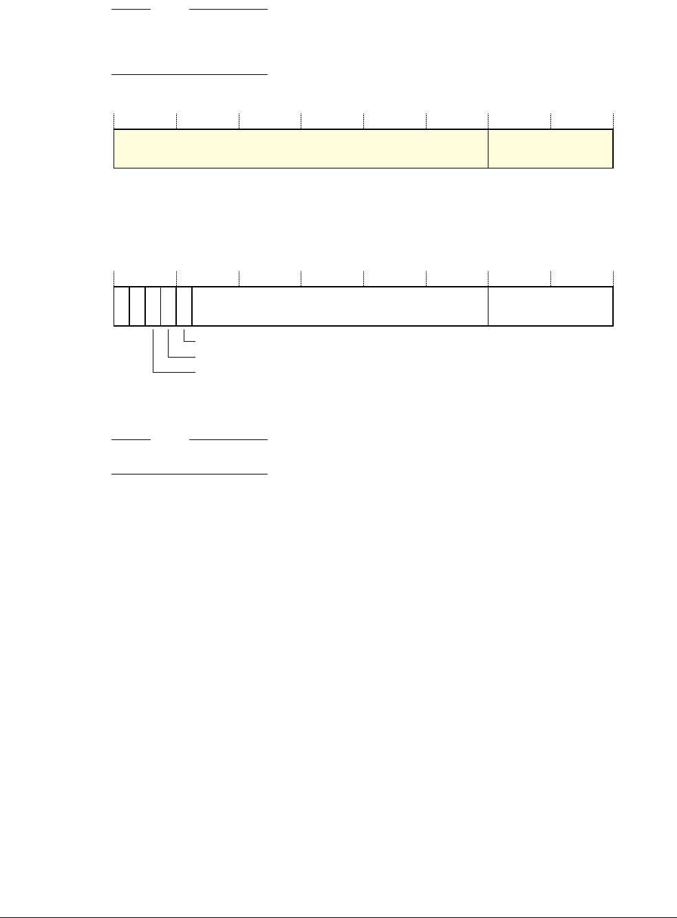
B4 System Control Registers in a VMSA implementation
B4.1 VMSA System control registers descriptions, in register order
ARM DDI 0406C.c Copyright © 1996-1998, 2000, 2004-2012, 2014 ARM. All rights reserved. B4-1697
ID051414 Non-Confidential
Note
Differences in the memory-mapped views of the Performance Monitors registers on page D2-2354 describes how
the characteristics of the PMXEVTYPER differ when it is accessed through an external debug interface or a
memory-mapped interface.
In PMUv1, the PMXEVTYPER bit assignments are:
Bits[31:8] Reserved, UNK/SBZP.
evtCount, bits[7:0] Event to count. The event number of the event that is counted by the selected event counter,
PMNx. For more information, see Event numbers on page B4-1699.
In PMUv2, in a VMSA implementation, the PMXEVTYPER bit assignments are:
Note
See the Usage constraints for the conditions in which PMXEVTYPER is not accessible.
P, bit[31] Privileged execution filtering bit. Controls counting when execution is at PL1. The possible
values of this bit are:
0 Count events when executing at PL1.
1 Do not count events when executing at PL1.
On an implementation that includes the Security Extensions, in Non-secure state:
• the NSK bit provides an additional control on the counting of events at PL1
• on an implementation that includes the Virtualization Extensions, the NSH bit
controls the counting of events when executing at PL2, independent of the value of P.
U, bit[30] Unprivileged execution filtering bit. Controls counting when execution is at PL0. The
possible values of this bit are:
0 Count events when executing at PL0.
1 Do not count events in when executing at PL0.
On an implementation that includes the Security Extensions, in Non-secure state, the NSU
bit provides an additional control on the counting of events in the PL0 mode.
NSK, bit[29], Security Extensions implemented
Non-secure PL1 control bit. Controls counting when executing in Non-secure state at PL1.
The behavior depends on the combined values of the P and NSK bits:
P == NSK In Non-secure state, count events when executing at PL1.
P!= NSK In Non-secure state, do not count events when executing at PL1.
Bit[29:28], Security Extensions not implemented
Reserved, UNK/SBZP.
Reserved, UNK/SBZP
31 8 7 0
evtCount
PU
NSK†
Reserved, UNK/SBZP
31 8 7 0
evtCount
2630 29 28 27
NSU†
NSH‡
† Reserved, UNK/SBZP, if the implementation does not include the Security Extensions
‡ Reserved, UNK/SBZP, if the implementation does not include the Virtualization Extensions

B4 System Control Registers in a VMSA implementation
B4.1 VMSA System control registers descriptions, in register order
B4-1698 Copyright © 1996-1998, 2000, 2004-2012, 2014 ARM. All rights reserved. ARM DDI 0406C.c
Non-Confidential ID051414
NSU, bit[28], Security Extensions implemented
Non-secure unprivileged control bit. Controls counting in when executing in Non-secure at
PL0. The behavior depends on the combined values of the U and NSU bits:
U == NSU In Non-secure state, count events when executing at PL0.
U != NSU In Non-secure state, do not count events when executing at PL0.
NSH, bit[27], Virtualization Extensions implemented
Non-secure PL2 enable bit. The possible values of this bit are:
0 In Non-secure state, do not count events when executing at PL2.
1 In Non-secure state, count events when executing at PL2.
Note
The value of the P bit does not affect whether events are counted when executing in
Non-secure state at PL2.
Bit[27], Virtualization Extensions not implemented
Reserved, UNK/SBZP.
Bits[26:8] Reserved, UNK/SBZP.
evtCount, bits[7:0] Event to count. The event number of the event that is counted by the selected event counter,
PMNx. For more information, see Event numbers on page B4-1699.
This field is reserved when PMSELR.SEL is set to 31, to select PMCCNTR.
Table B4-27 shows the combination of reserved encodings that software must not select. However, they are not
UNPREDICTABLE encodings and hardware must implement the P, U, NSK, NSU, and NSH filtering bits as described.
Note
• In some documentation published before issue C.a of this manual, the PMXEVTYPER register accessed
when PMSELR.SEL is set to 31 is described as the PMCCFILTR.
• In issue C.a of this manual:
— the P bit is called the PL1 bit
— the NSK bit is called the NSPL1 bit.
Table B4-27 Reserved encodings, must not be used
P U NSK NSU NSH Modes in which events are counted
110 00Never
0 1 1 1 0 Secure PL1 modes and Non-secure User mode
1 0 1 1 0 Secure User mode and Non-secure PL1 modes
0 1 1 1 1 Secure PL1 modes, Non-secure User mode, and Hyp mode
1 0 1 1 1 Secure User mode, Non-secure PL1 modes, and Hyp mode
1 0 0 0 1 User mode and Hyp mode
1 0 0 1 1 Secure User mode and Hyp mode
1 1 0 1 1 Non-secure User mode and Hyp mode

B4 System Control Registers in a VMSA implementation
B4.1 VMSA System control registers descriptions, in register order
ARM DDI 0406C.c Copyright © 1996-1998, 2000, 2004-2012, 2014 ARM. All rights reserved. B4-1699
ID051414 Non-Confidential
PMXEVTYPER reset values
Immediately after a non-debug logic reset:
• The values of the instances of PMXEVTYPER that relate to an event counter are UNKNOWN. That is, if m is
one less than the number of implemented event counters, the non-debug reset values of PMXEVTYPER0 to
PMXEVTYPERm are UNKNOWN.
• In PMUv2, the reset values of the defined fields of the instance of PMXEVTYPER that relates to the cycle
counter are zero. That is, the non-debug reset value of each implemented bit of
PMXEVTYPER31.{P, U, NSK, NSU, NSH} is 0.
Event numbers
The PMXEVTYPER uses event numbers to determine the event that causes an event counter to increment. These
event numbers are split into two ranges:
0x00
-
0x3F
Common features. Reserved for the specified events. When an ARMv7 processor supports
monitoring of an event that is assigned a number in this range, if possible it must use that number
for the event. Unassigned values are reserved and might be used for additional common events in
future versions of the architecture. For more information about the assigned values in the common
features range, see Common event numbers on page C12-2318.
0x40
-
0xFF
IMPLEMENTATION DEFINED features. For more information, see IMPLEMENTATION DEFINED
event numbers on page C12-2327.
Accessing the PMXEVTYPER
To access the PMXEVTYPER:
1. Update PMSELR to select the required event counter, PMNx, or, in PMUv2, PMCCNTR.
2. Read or write the CP15 registers with
<opc1>
set to 0,
<CRn>
set to c9,
<CRm>
set to c13, and
<opc2>
set to 1. For
example:
MRC p15, 0, <Rt>, c9, c13, 1 : Read PMXEVTYPER into Rt
MCR p15, 0, <Rt>, c9, c13, 1 : Write Rt to PMXEVTYPER
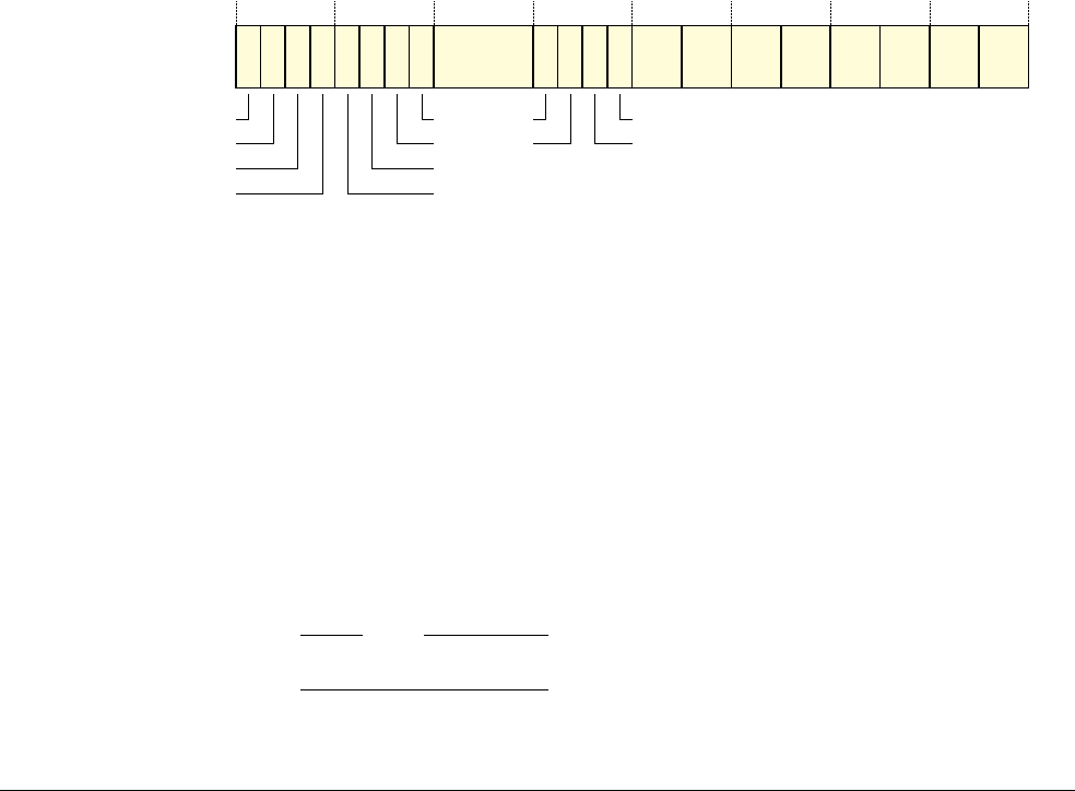
B4 System Control Registers in a VMSA implementation
B4.1 VMSA System control registers descriptions, in register order
B4-1700 Copyright © 1996-1998, 2000, 2004-2012, 2014 ARM. All rights reserved. ARM DDI 0406C.c
Non-Confidential ID051414
B4.1.127 PRRR, Primary Region Remap Register, VMSA
The PRRR characteristics are:
Purpose Under the conditions described in Architectural status of PRRR and NMRR on
page B4-1702, PRRR controls the top level mapping of the TEX[0], C, and B memory
region attributes. For more information see Short-descriptor format memory region
attributes, with TEX remap on page B3-1368.
This register is part of the Virtual memory control registers functional group.
Usage constraints Only accessible from PL1 or higher.
In a processor that implements the Large Physical Address Extension, not accessible when
using the Long-descriptor translation table format. See, instead, MAIR0 and MAIR1,
Memory Attribute Indirection Registers 0 and 1, VMSA on page B4-1646.
See also Architectural status of PRRR and NMRR on page B4-1702.
Configurations In an implementation that includes the Security Extensions, the PRRR:
•is Banked
• has write access to the Secure copy of the register disabled when the
CP15SDISABLE signal is asserted HIGH.
Attributes A 32-bit RW register with an UNKNOWN reset value. See also Reset behavior of CP14 and
CP15 registers on page B3-1450.
Table B3-45 on page B3-1493 shows the encodings of all of the registers in the Virtual
memory control registers functional group.
The PRRR bit assignments are:
NOSn, bit[24+n], for values of n from 0 to 7
Outer Shareable property mapping for memory attributes n, if the region is mapped as Normal or
Device memory that is Shareable. n is the value of the TEX[0], C and B bits, see Table B4-28 on
page B4-1702. The possible values of each NOSn bit are:
0 Memory region is Outer Shareable.
1 Memory region is Inner Shareable.
The value of this bit is ignored if the region is Normal or Device memory that is not Shareable. For
more information see Interpretation of the NOSn fields in the PRRR, with TEX remap on
page B3-1371.
The meaning of the field with n =6 is IMPLEMENTATION DEFINED and might differ from the meaning
given here. This is because the meaning of the attribute combination {TEX[0] = 1, C = 1, B = 0} is
IMPLEMENTATION DEFINED.
If the implementation does not distinguish between Inner Shareable and Outer Shareable then these
bits are reserved, RAZ/WI.
Note
For Device memory, for some implementations, the NOSn field has no significance.
Bits[23:20] Reserved, UNK/SBZP.
31 30 29 28 27 26 25 24 23 20 19 18 17 16 15 14 13 12 11 10 9 8 7 6 5 4 3 2 1 0
Reserved,
UNK/SBZP TR7 TR6 TR5 TR4 TR3 TR2 TR1 TR0
DS0
DS1
NS1
NS0
NOS0
NOS1
NOS2
NOS3
NOS7
NOS6
NOS5
NOS4

B4 System Control Registers in a VMSA implementation
B4.1 VMSA System control registers descriptions, in register order
ARM DDI 0406C.c Copyright © 1996-1998, 2000, 2004-2012, 2014 ARM. All rights reserved. B4-1701
ID051414 Non-Confidential
NS1, bit[19] Mapping of S = 1 attribute for Normal memory. This bit gives the mapped Shareable attribute for a
region of memory that:
• is mapped as Normal memory
• has the S bit set to 1.
The possible values of the bit are:
0 Region is not Shareable
1 Region is Shareable.
NS0, bit[18] Mapping of S = 0 attribute for Normal memory. This bit gives the mapped Shareable attribute for a
region of memory that:
• is mapped as Normal memory
• has the S bit set to 0.
The possible values of the bit are the same as those given for the NS1 bit, bit[19].
DS1, bit[17] Mapping of S = 1 attribute for Device memory. This bit gives the mapped Shareable attribute for a
region of memory that:
• is mapped as Device memory
• has the S bit set to 1.
The possible values of the bit are the same as those given for the NS1 bit, bit[19].
Note
For Device memory, for some implementations, the DSn fields have no significance.
DS0, bit[16] Mapping of S = 0 attribute for Device memory. This bit gives the mapped Shareable attribute for a
region of memory that:
• is mapped as Device memory
• has the S bit set to 0.
The possible values of the bit are the same as those given for the NS1 bit, bit[19].
Note
For Device memory, for some implementations, the DSn fields have no significance.
TRn, bits[2n+1:2n] for values of n from 0 to 7
Primary TEX mapping for memory attributes n. n is the value of the TEX[0], C and B bits, see
Table B4-28 on page B4-1702. This field defines the mapped memory type for a region with
attributes n. The possible values of the field are:
00 Strongly-ordered.
01 Device.
10 Normal memory.
11 Reserved, effect is UNPREDICTABLE.
The meaning of the field with n =6 is IMPLEMENTATION DEFINED and might differ from the meaning
given here. This is because the meaning of the attribute combination {TEX[0] = 1, C = 1, B = 0} is
IMPLEMENTATION DEFINED.

B4 System Control Registers in a VMSA implementation
B4.1 VMSA System control registers descriptions, in register order
B4-1702 Copyright © 1996-1998, 2000, 2004-2012, 2014 ARM. All rights reserved. ARM DDI 0406C.c
Non-Confidential ID051414
Table B4-28 shows the mapping between the memory region attributes and the n value used in the PRRR.NOSn and
PRRR.TRn field descriptions.
For more information about the PRRR, see Short-descriptor format memory region attributes, with TEX remap on
page B3-1368.
Architectural status of PRRR and NMRR
The function of these registers is architecturally defined only when the processor is using the Short-descriptor
translation table formats and either:
•SCTLR.TRE is set to 1
•SCTLR.TRE is set to 0 and the processor has not invoked any IMPLEMENTATION DEFINED mechanism using
MMU remap.
Otherwise, when the processor is using the Short-descriptor translation table formats, their behavior is
IMPLEMENTATION DEFINED, see SCTLR.TRE, SCTLR.M, and the effect of the TEX remap registers on page B3-1371.
When an implementation includes the Large Physical Address Extension, and address translation is using the
Long-descriptor translation table formats, MAIR0 replaces the PRRR, and MAIR1 replaces the NMRR.
Accessing the PRRR
To access the PRRR, software reads or writes the CP15 registers with
<opc1>
set to 0,
<CRn>
set to c10,
<CRm>
set to
c2, and
<opc2>
set to 0. For example:
MRC p15, 0, <Rt>, c10, c2, 0 ; Read PRRR into Rt
MCR p15, 0, <Rt>, c10, c2, 0 ; Write Rt to PRRR
Table B4-28 Memory attributes and the n value for the PRRR field descriptions
Attributes
n value
TEX[0] C B
0000
0011
0102
0113
1004
1015
1106
1117

B4 System Control Registers in a VMSA implementation
B4.1 VMSA System control registers descriptions, in register order
ARM DDI 0406C.c Copyright © 1996-1998, 2000, 2004-2012, 2014 ARM. All rights reserved. B4-1703
ID051414 Non-Confidential
B4.1.128 REVIDR, Revision ID Register, VMSA
The REVIDR characteristics are:
Purpose The REVIDR provides implementation-specific minor revision information that can only be
interpreted in conjunction with the MIDR.
This register is part of the Identification registers functional group.
Usage constraints Only accessible from PL1 or higher.
Configurations An optional register. When REVIDR is not implemented, its encoding is an alias of the
MIDR.
This register is not implemented in architecture versions before ARMv7.
If the implementation includes the Security Extensions, the register is Common.
Attributes A 32-bit RO register with an IMPLEMENTATION DEFINED value. See also Reset behavior of
CP14 and CP15 registers on page B3-1450.
Table B3-44 on page B3-1492 shows the encodings of all of the registers in the
Identification registers functional group.
The REVIDR bit assignments are IMPLEMENTATION DEFINED.
Note
To determine whether REVIDR is implemented, software can:
•Read MIDR.
• Read REVIDR.
• Compare the two values. If they are identical, REVIDR is not implemented.
Accessing the REVIDR
To access REVIDR, software reads the CP15 registers with
<opc1>
set to 0,
<CRn>
set to c0,
<CRm>
set to c0, and
<opc2>
set to 6. For example:
MRC p15, 0, <Rt>, c0, c0, 6 ; Read REVIDR into Rt

B4 System Control Registers in a VMSA implementation
B4.1 VMSA System control registers descriptions, in register order
B4-1704 Copyright © 1996-1998, 2000, 2004-2012, 2014 ARM. All rights reserved. ARM DDI 0406C.c
Non-Confidential ID051414
B4.1.129 SCR, Secure Configuration Register, Security Extensions
The SCR characteristics are:
Purpose The SCR defines the configuration of the current security state. It specifies:
• the security state of the processor, Secure or Non-secure
• what mode the processor branches to if an IRQ, FIQ or external abort occurs
• whether the CPSR.{F, A} bits can be modified when SCR.NS == 1.
This register is part of the Security Extensions registers functional group.
Usage constraints Only accessible from Secure PL1 modes.
Configurations The SCR is implemented only as part of the Security Extensions. It is a Restricted access
register, meaning it exists only in the Secure state.
Attributes A 32-bit RW register that resets to zero.
Table B3-54 on page B3-1500 shows the encoding of all of the Security Extensions
registers.
The SCR bit assignments are:
Bits[31:10] Reserved, UNK/SBZP.
SIF, bit[9], when implementation includes the Virtualization Extensions
Secure instruction fetch. When the processor is in Secure state, this bit disables instruction fetches
from Non-secure memory. The possible values of this bit are:
0 Secure state instruction fetches from Non-secure memory are permitted.
1 Secure state instruction fetches from Non-secure memory are not permitted.
For more information, see Restriction on Secure instruction fetch on page B3-1361.
HCE, bit[8], when implementation includes the Virtualization Extensions
Hyp Call enable. This bit enables use of the
HVC
instruction from Non-secure PL1 modes. The
possible values of this bit are:
0
HVC
instruction is UNDEFINED in Non-secure PL1 modes, and UNPREDICTABLE in Hyp
mode.
1
HVC
instruction is enabled in Non-secure PL1 modes, and performs a Hyp Call.
For more information, see Hyp mode on page B1-1141.
SCD, bit[7], when implementation includes the Virtualization Extensions
Secure Monitor Call disable. Makes the
SMC
instruction UNDEFINED in Non-secure state. The
possible values of this bit are:
0
SMC
executes normally in Non-secure state, performing a Secure Monitor Call.
1
SMC
instruction is UNDEFINED in Non-secure state.
A trap of the
SMC
instruction to Hyp mode takes priority over the value of this bit, see Trapping use
of the SMC instruction on page B1-1255.
For more information, see SMC (previously SMI) on page B9-2002.
IRQnET
AW
FW
EA
FIQ
NS
Reserved, UNK/SBZP
31 109876543210
HCE
†
SCD
†
SIF
†
† Reserved before the introduction of the Virtualization Extensions, see text for more information.

B4 System Control Registers in a VMSA implementation
B4.1 VMSA System control registers descriptions, in register order
ARM DDI 0406C.c Copyright © 1996-1998, 2000, 2004-2012, 2014 ARM. All rights reserved. B4-1705
ID051414 Non-Confidential
Bits[9:7], when implementation does not include the Virtualization Extensions
Reserved, UNK/SBZP.
nET, bit[6] Not Early Termination. This bit disables early termination. The possible values of this bit are:
0 Early termination permitted. Execution time of data operations can depend on the data
values.
1 Disable early termination. The number of cycles required for data operations is forced
to be independent of the data values.
This IMPLEMENTATION DEFINED mechanism can disable data dependent timing optimizations from
multiplies and data operations. It can provide system support against information leakage that might
be exploited by timing correlation types of attack.
On implementations that do not support early termination or do not support disabling early
termination, this bit is UNK/SBZP.
AW, bit[5] A bit writable. In an implementation that does not include the Virtualization Extensions, this bit
controls whether CPSR.A can be modified in Non-secure state, and the possible values of this bit
are:
0 CPSR.A can be modified only in Secure state.
1 CPSR.A can be modified in any security state.
In an implementation that includes the Virtualization Extensions, this bit:
• Is part of the control of whether CPSR.A masks asynchronous external aborts that are taken
from Non-secure state and routed to Monitor mode. When all of the following apply, CPSR.A
has no effect on any asynchronous external abort taken from Non-secure state:
— the EA bit is set to 1, to route external aborts to Monitor mode
— this bit is set to 0
—HCR.AMO is set to 0.
For more information, see Asynchronous exception masking on page B1-1184.
• Otherwise, has no effect.
Note
This means that, in an implementation that includes the Virtualization Extensions, this bit has
no effect on updates to CPSR.A, and CPSR.A can be modified in either security state.
FW, bit[4] F bit writable. In an implementation that does not include the Virtualization Extensions, this bit
controls whether CPSR.F can be modified in Non-secure state, and the possible values of this bit
are:
0 CPSR.F can be modified only in Secure state.
1 CPSR.F can be modified in any security state.
In an implementation that includes the Virtualization Extensions, this bit:
• Is part of the control of whether CPSR.F masks FIQ taken from Non-secure state that are
routed to Monitor mode. When all of the following apply, CPSR.F has no effect on any FIQ
taken from Non-secure state:
— the FIQ bit is set to 1, to route FIQs to Monitor mode
— this bit is set to 0
—HCR.FMO is set to 0.
For more information, see Asynchronous exception masking on page B1-1184.
• Otherwise, has no effect.
Note
This means that, in an implementation that includes the Virtualization Extensions, this bit has
no effect on updates to CPSR.F, and CPSR.F can be modified in either security state.

B4 System Control Registers in a VMSA implementation
B4.1 VMSA System control registers descriptions, in register order
B4-1706 Copyright © 1996-1998, 2000, 2004-2012, 2014 ARM. All rights reserved. ARM DDI 0406C.c
Non-Confidential ID051414
EA, bit[3] External Abort handler. This bit controls whether external aborts are taken to Monitor mode. The
possible values of this bit are:
0 External aborts not taken to Monitor mode.
1 External aborts taken to Monitor mode.
For more information, see Asynchronous exception routing controls on page B1-1175.
Note
As described in the referenced section, the EA bit controls the routing of both synchronous and
asynchronous external aborts.
FIQ, bit[2] FIQ handler. This bit controls whether FIQ exceptions are taken to Monitor mode. The possible
values of this bit are:
0 FIQs not taken to Monitor mode.
1 FIQs taken to Monitor mode.
For more information, see Asynchronous exception routing controls on page B1-1175.
IRQ, bit[1] IRQ handler. This bit controls whether IRQ exceptions are taken to Monitor mode. The possible
values of this bit are:
0 IRQs not taken to Monitor mode.
1 IRQs taken to Monitor mode.
For more information, see Asynchronous exception routing controls on page B1-1175.
NS, bit[0] Non-secure bit. Except when the processor is in Monitor mode, this bit determines the security state
of the processor. Table B4-29 shows the security settings:
For more information, see Changing from Secure to Non-secure state on page B1-1157.
The value of the NS bit also affects the accessibility of the Banked CP15 registers in Monitor mode,
see Access to registers from Monitor mode on page B3-1459.
Unless the processor is in Debug state, when an exception occurs in Monitor mode the hardware sets
the NS bit to 0.
Note
The Virtualization Extensions introduce additional exception routing controls that can apply when an
SCR.{EA, FIQ, IRQ} bit does not route the corresponding exception to Monitor mode. Asynchronous exception
routing controls on page B1-1175 describes these controls.
Whenever the processor changes security state, the monitor software can change the value of the EA, FIQ and IRQ
bits. This means that the behavior of IRQ, FIQ and External Abort exceptions can be different in each security state.
Accessing the SCR
To access the SCR, software reads or writes the CP15 registers with
<opc1>
set to 0,
<CRn>
set to c1,
<CRm>
set to c1,
and
<opc2>
set to 0. For example:
MRC p15, 0, <Rt>, c1, c1, 0 ; Read SCR into Rt
MCR p15, 0, <Rt>, c1, c1, 0 ; Write Rt to SCR
Table B4-29 Processor security state
SCR.NS Processor mode, from CPSR.M bits
Monitor mode All modes except Monitor mode
0 Secure state Secure state
1 Secure state Non-secure state
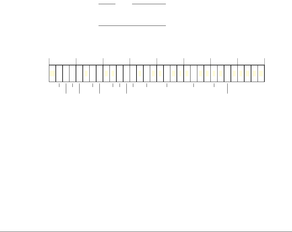
B4 System Control Registers in a VMSA implementation
B4.1 VMSA System control registers descriptions, in register order
ARM DDI 0406C.c Copyright © 1996-1998, 2000, 2004-2012, 2014 ARM. All rights reserved. B4-1707
ID051414 Non-Confidential
B4.1.130 SCTLR, System Control Register, VMSA
The SCTLR characteristics are:
Purpose The SCTLR provides the top level control of the system, including its memory system.
This register is part of the Virtual memory control registers functional group.
Usage constraints Only accessible from PL1 or higher.
Control bits in the SCTLR that are not applicable to a VMSA implementation read as the
value that most closely reflects that implementation, and ignore writes.
In ARMv7, some bits in the register are read-only. These bits relate to non-configurable
features of an ARMv7 implementation, and are provided for compatibility with previous
versions of the architecture.
Configurations In an implementation that includes the Security Extensions, the SCTLR:
• is Banked, with some bits common to the Secure and Non-secure copies of the
register
• has write access to the Secure copy of the register disabled when the
CP15SDISABLE signal is asserted HIGH.
For more information, see Classification of system control registers on page B3-1451.
Attributes A 32-bit RW register with an IMPLEMENTATION DEFINED reset value, see Reset value of the
SCTLR on page B4-1713. See also Reset behavior of CP14 and CP15 registers on
page B3-1450.
Note
In an implementation that includes the Virtualization Extensions, some reset requirements
apply to the Non-secure copy of SCTLR.
Table B3-45 on page B3-1493 shows the encodings of all of the registers in the Virtual
memory control registers functional group.
In a VMSAv7 implementation, the SCTLR bit assignments are:
Bit[31] Reserved, UNK/SBZP.
TE, bit[30] Thumb Exception enable. This bit controls whether exceptions are taken in ARM or Thumb state.
The possible values of this bit are:
0 Exceptions, including reset, taken in ARM state.
1 Exceptions, including reset, taken in Thumb state.
In an implementation that includes the Security Extensions, this bit is Banked between the Secure
and Non-secure copies of the register.
An implementation can include a configuration input signal that determines the reset value of the
TE bit. If there is no configuration input signal to determine the reset value of this bit then it resets
to 0 in an ARMv7-A implementation.
For more information about the use of this bit, see Instruction set state on exception entry on
page B1-1182.
0 1 1 1 1 0 V I Z 0 0 0 1 1 1 C A M
31 30 29 28 27 26 25 24 23 22 21 20 19 18 17 16 15 14 13 12 11 10 9 8 7 6 5 4 3 2 1 0
(0)
NMFI
TE
AFE
TRE EE
VE
U FI HA RR SW B
UWXN†
WXN†
† Reserved before the introduction of the Virtualization Extensions, see text for more information.
CP15BEN

B4 System Control Registers in a VMSA implementation
B4.1 VMSA System control registers descriptions, in register order
B4-1708 Copyright © 1996-1998, 2000, 2004-2012, 2014 ARM. All rights reserved. ARM DDI 0406C.c
Non-Confidential ID051414
AFE, bit[29] Access flag enable. The possible values of this bit are:
0 In the translation table descriptors, AP[0] is an access permissions bit. The full range of
access permissions is supported. No Access flag is implemented.
1 In the translation table descriptors, AP[0] is the Access flag. Only the simplified model
for access permissions is supported.
Setting this bit to 1 enables use of the AP[0] bit in the translation table descriptors as the Access flag.
It also restricts access permissions in the translation table descriptors to the simplified model
described in AP[2:1] access permissions model on page B3-1357.
In an implementation that includes the Security Extensions, this bit is Banked between the Secure
and Non-secure copies of the register.
In an implementation that includes the Large Physical Address Extension, when the value of
TTBCR.EAE is 1, enabling use of the Long-descriptor translation table format, this bit is
UNK/SBOP.
TRE, bit[28] TEX remap enable. The possible values of this bit are:
0 TEX remap disabled. TEX[2:0] are used, with the C and B bits, to describe the memory
region attributes.
1 TEX remap enabled. TEX[2:1] are reassigned for use as bits managed by the operating
system. The TEX[0], C and B bits, with the MMU remap registers, describe the memory
region attributes.
Setting this bit to 1 enables remapping of the TEX[2:1] bits for use as two translation table bits that
can be managed by the operating system. Enabling this remapping also changes the scheme that
defines the memory region attributes in the VMSA.
In an implementation that includes the Security Extensions, this bit is Banked between the Secure
and Non-secure copies of the register.
In an implementation that includes the Large Physical Address Extension, when the value of
TTBCR.EAE is 1, enabling use of the Long-descriptor translation table format, this bit is
UNK/SBOP.
For more information, see Memory region attributes on page B3-1366.
NMFI, bit[27]
Non-maskable FIQ (NMFI) support. The possible values of this bit are:
0 Software can mask FIQs by setting the CPSR.F bit to 1.
1 Software cannot set the CPSR.F bit to 1. This means software cannot mask FIQs.
This bit is read-only.
In an implementation that includes the Security Extensions this bit is common to the Secure and
Non-secure versions of the register.
The Virtualization Extensions do not support NMFIs. On an implementation that includes the
Virtualization Extensions, this bit is RAZ. Otherwise, it is IMPLEMENTATION DEFINED whether an
implementation supports NMFIs, and this bit is:
• RAZ if NMFIs are not supported
• determined by a configuration input signal if NMFIs are supported.
For more information, see Non-maskable FIQs on page B1-1151.
Bit[26] Reserved, RAZ/SBZP.
EE, bit[25] Exception Endianness. This bit defines the value of the CPSR.E bit on entry to an exception vector,
including reset. The possible values of this bit are:
0 Little-endian.
1 Big-endian.
This bit value also defines the endianness of the translation table data for translation table lookups.
In an implementation that includes the Security Extensions, this bit is Banked between the Secure
and Non-secure copies of the register.

B4 System Control Registers in a VMSA implementation
B4.1 VMSA System control registers descriptions, in register order
ARM DDI 0406C.c Copyright © 1996-1998, 2000, 2004-2012, 2014 ARM. All rights reserved. B4-1709
ID051414 Non-Confidential
This is a read/write bit. An implementation can include a configuration input signal that determines
the reset value of the EE bit. If there is no configuration input signal to determine the reset value of
this bit then it resets to 0.
VE, bit[24] Interrupt Vectors Enable. This bit controls the vectors used for the FIQ and IRQ interrupts. The
possible values of this bit are:
0 Use the FIQ and IRQ vectors from the vector table, see the V bit entry.
1 Use the IMPLEMENTATION DEFINED values for the FIQ and IRQ vectors.
In an implementation that includes the Security Extensions, this bit is Banked between the Secure
and Non-secure copies of the register.
In an implementation that includes the Virtualization Extensions, when at least one of HCR.FMO
and HCR.IMO is set to 1, the processor behaves as if the Non-secure copy of this bit is set to 0,
regardless of its actual value.
For more information, see Vectored interrupt support on page B1-1168.
If the implementation does not support IMPLEMENTATION DEFINED FIQ and IRQ vectors then this
bit is RAZ/WI.
From the introduction of the Virtualization Extensions, ARM deprecates any use of this bit.
Bit[23] Reserved, RAO/SBOP.
U, bit[22] In ARMv7 this bit is RAO/SBOP, indicating use of the alignment model described in Alignment
support on page A3-108.
For details of this bit in earlier versions of the architecture see Alignment on page D12-2506.
FI, bit[21] Fast interrupts configuration enable. The possible values of this bit are:
0 All performance features enabled.
1 Low interrupt latency configuration. Some performance features disabled.
Setting this bit to 1 can reduce interrupt latency in an implementation, by disabling
IMPLEMENTATION DEFINED performance features.
In an implementation that includes the Security Extensions, this bit is common to the Secure and
Non-secure versions of the register.
This bit is:
• a read/write bit if the implementation does not include the Security Extensions
• if the implementation includes the Security Extensions:
— a read/write bit if the processor is in Secure state
— a read-only bit if the processor is in Non-secure state.
For more information, see Low interrupt latency configuration on page B1-1198.
If the implementation does not support a mechanism for selecting a low interrupt latency
configuration this bit is RAZ/WI.
UWXN, bit[20], if implementation includes the Virtualization Extensions
Unprivileged write permission implies PL1 XN. The possible values of this bit are:
0 Regions with unprivileged write permission are not forced to XN.
1 Regions with unprivileged write permission are forced to XN for PL1 accesses.
Setting this bit to 1 requires all memory regions with unprivileged write permission to be treated as
XN for any access from software that is executing at PL1.
For more information, see Preventing execution from writable locations on page B3-1361.

B4 System Control Registers in a VMSA implementation
B4.1 VMSA System control registers descriptions, in register order
B4-1710 Copyright © 1996-1998, 2000, 2004-2012, 2014 ARM. All rights reserved. ARM DDI 0406C.c
Non-Confidential ID051414
WXN, bit[19], if implementation includes the Virtualization Extensions
Write permission implies XN. The possible values of this bit are:
0 Regions with write permission are not forced to XN.
1 Regions with write permission are forced to XN.
Setting this bit to 1 requires all memory regions with write permission to be treated as XN.
For more information, see Preventing execution from writable locations on page B3-1361.
Bit[20:19], if implementation does not include the Virtualization Extensions
Reserved, RAZ/SBZP.
Bit[18] Reserved, RAO/SBOP.
HA, bit[17] Hardware Access flag enable. If the implementation provides hardware management of the Access
flag this bit enables the Access flag management. The possible values of this bit are:
0 Hardware management of Access flag disabled.
1 Hardware management of Access flag enabled.
In an implementation that includes the Security Extensions, bit is Banked between the Secure and
Non-secure copies of the register.
If the implementation does not provide hardware management of the Access flag then this bit is
RAZ/WI.
For more information, see Hardware management of the Access flag on page B3-1363.
From the introduction of the Large Physical Address Extension, ARM deprecates any use of this bit.
Bit[16] Reserved, RAO/SBOP.
Bit[15] Reserved, RAZ/SBZP.
RR, bit[14] Round Robin select. If the cache implementation supports the use of an alternative replacement
strategy that has a more easily predictable worst-case performance, this bit controls whether it is
used. The possible values of this bit are:
0 Normal replacement strategy, for example, random replacement.
1 Predictable strategy, for example, round-robin replacement.
In an implementation that includes the Security Extensions, this bit is common to the Secure and
Non-secure versions of the register.
This bit is:
• a read/write bit if the implementation does not include the Security Extensions
• if the implementation includes the Security Extensions:
— a read/write bit if the processor is in Secure state
— a read-only bit if the processor is in Non-secure state.
The replacement strategy associated with each value of the RR bit is IMPLEMENTATION DEFINED.
If the implementation does not support multiple IMPLEMENTATION DEFINED replacement strategies
this bit is RAZ/WI.
V, bit[13] Vectors bit. This bit selects the base address of the exception vectors. The possible values of this bit
are:
0 Low exception vectors, base address
0x00000000
.
In an implementation that includes the Security Extensions, this base address can be
re-mapped.
1 High exception vectors (Hivecs), base address
0xFFFF0000
.
This base address is never remapped.
In an implementation that includes the Security Extensions, this bit is Banked between the Secure
and Non-secure copies of the register.
An implementation can include a configuration input signal that determines the reset value of the V
bit. If there is no configuration input signal to determine the reset value of this bit then it resets to 0.

B4 System Control Registers in a VMSA implementation
B4.1 VMSA System control registers descriptions, in register order
ARM DDI 0406C.c Copyright © 1996-1998, 2000, 2004-2012, 2014 ARM. All rights reserved. B4-1711
ID051414 Non-Confidential
For more information, see Exception vectors and the exception base address on page B1-1165.
I, bit[12] Instruction cache enable: This is a global enable bit for instruction caches. The possible values of
this bit are:
0 Instruction caches disabled.
1 Instruction caches enabled.
In an implementation that includes the Security Extensions, this bit is Banked between the Secure
and Non-secure copies of the register.
If the system does not implement any instruction caches that can be accessed by the processor, at
any level of the memory hierarchy, this bit is RAZ/WI.
If the system implements any instruction caches that can be accessed by the processor then it must
be possible to disable them by setting this bit to 0.
For more information see Cache enabling and disabling on page B2-1270.
Z, bit[11] Branch prediction enable. The possible values of this bit are:
0 Program flow prediction disabled.
1 Program flow prediction enabled.
Setting this bit to 1 enables branch prediction, also called program flow prediction.
In an implementation that includes the Security Extensions, this bit is Banked between the Secure
and Non-secure copies of the register.
If program flow prediction cannot be disabled, this bit is RAO/WI. Program flow prediction
includes all possible forms of speculative change of instruction stream prediction. Examples include
static prediction, dynamic prediction, and return stacks.
If the implementation does not support program flow prediction this bit is RAZ/WI.
SW, bit[10] SWP and SWPB enable. This bit enables the use of
SWP
and
SWPB
instructions. The possible values
of this bit are:
0
SWP
and
SWPB
are UNDEFINED.
1
SWP
and
SWPB
perform as described in SWP, SWPB on page A8-722.
In an implementation that includes the Security Extensions, this bit is Banked between the Secure
and Non-secure copies of the register. The bit is reset to 0.
This bit is part of the Multiprocessing Extensions. In implementations that do not implement the
Multiprocessing Extensions this bit is RAZ and
SWP
and
SWPB
instructions perform as described in
SWP, SWPB on page A8-722.
The Virtualization Extensions make the
SWP
and
SWPB
instructions optional. In an implementation
that does not include the
SWP
and
SWPB
instructions, the SW bit is RAZ/WI.
Note
When use of this bit is supported, at reset, it disables
SWP
and
SWPB
. This means that operating
systems have to choose to use
SWP
or
SWPB
.
Bits[9:8] Reserved, RAZ/SBZP.
B, bit[7] In ARMv7 this bit is RAZ/SBZP, indicating use of the endianness model described in Endian
support on page A3-110.
For details of this bit in earlier versions of the architecture see:
• for ARMv6, Endian support on page D12-2507
• for ARMv4 and ARMv5, Endian support on page D15-2593.
Bit[6] Reserved, RAO/SBOP.

B4 System Control Registers in a VMSA implementation
B4.1 VMSA System control registers descriptions, in register order
B4-1712 Copyright © 1996-1998, 2000, 2004-2012, 2014 ARM. All rights reserved. ARM DDI 0406C.c
Non-Confidential ID051414
CP15BEN, bit[5]
CP15 barrier enable. If implemented, this is an enable bit for the CP15 DMB, DSB, and ISB barrier
operations, and the possible values of this bit are:
0 CP15 barrier operations disabled. Their encodings are UNDEFINED.
1 CP15 barrier operations enabled.
This bit is optional. If not implemented, bit[5] is RAO/WI.
If this bit is implemented, its reset value is 1.
In an implementation that includes the Security Extensions, this bit is Banked between the Secure
and Non-secure copies of the register.
In an implementation that included the Virtualization Extensions:
• If this bit is implemented then HSCTLR.CP15BEN must be implemented.
• This bit controls the use of these operations from PL1 and PL0 modes. HSCTLR.CP15BEN
controls their use from Non-secure PL2 mode.
Note
This bit is first defined with the introduction of the Virtualization Extensions. However, it can be
implemented on any ARMv7-A or ARMv7-R processor.
For more information about these operations see Data and instruction barrier operations, VMSA on
page B4-1752.
Bits[4:3] Reserved, RAO/SBOP.
C, bit[2] Cache enable. This is a global enable bit for data and unified caches. The possible values of this bit
are:
0 Data and unified caches disabled.
1 Data and unified caches enabled.
In an implementation that includes the Security Extensions, this bit is Banked between the Secure
and Non-secure copies of the register.
If the system does not implement any data or unified caches that can be accessed by the processor,
at any level of the memory hierarchy, this bit is RAZ/WI.
If the system implements any data or unified caches that can be accessed by the processor then it
must be possible to disable them by setting this bit to 0.
For more information about the effect of this bit see Cache enabling and disabling on
page B2-1270.
A, bit[1] Alignment check enable. This is the enable bit for Alignment fault checking. The possible values of
this bit are:
0 Alignment fault checking disabled.
1 Alignment fault checking enabled.
In an implementation that includes the Security Extensions, this bit is Banked between the Secure
and Non-secure copies of the register.
For more information, see Unaligned data access on page A3-108.
M, bit[0] MMU enable. This is a global enable bit for the PL1&0 stage 1 MMU. The possible values of this
bit are:
0 PL1&0 stage 1 MMU disabled.
1 PL1&0 stage 1 MMU enabled.
In an implementation that includes the Security Extensions, this bit is Banked between the Secure
and Non-secure copies of the register.
For more information, see The effects of disabling MMUs on VMSA behavior on page B3-1314.
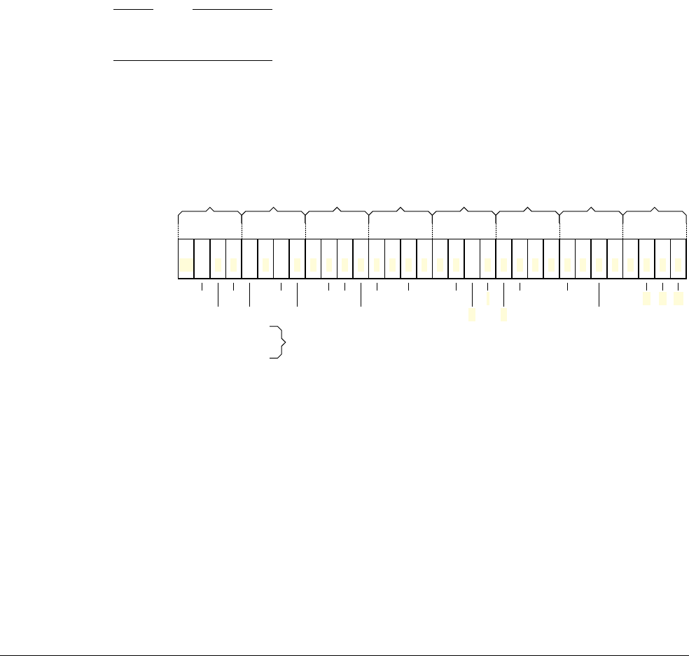
B4 System Control Registers in a VMSA implementation
B4.1 VMSA System control registers descriptions, in register order
ARM DDI 0406C.c Copyright © 1996-1998, 2000, 2004-2012, 2014 ARM. All rights reserved. B4-1713
ID051414 Non-Confidential
Reset value of the SCTLR
The SCTLR has an IMPLEMENTATION DEFINED reset value. There are different types of bits in the SCTLR:
• Some bits are defined as RAZ or RAO, and have the same value in all VMSAv7 implementations.
Figure B4-1 shows the values of these bits.
• Some bits are read-only and either:
— have an IMPLEMENTATION DEFINED value
— have a value that is determined by a configuration input signal.
• Some bits are read/write and either:
— reset to zero
— reset to an IMPLEMENTATION DEFINED value
— reset to a value that is determined by a configuration input signal.
Figure B4-1 shows the reset value, or how the reset value is defined, for each bit of the SCTLR. It also shows the
possible values of each half byte of the register.
Note
Figure B4-1 is not a bit assignment diagram and therefore some of the descriptions in Meaning of fixed bit values
in register bit assignment diagrams on page B3-1466 do not apply.
In an implementation that includes the Security Extensions:
• The IMPLEMENTATION DEFINED reset value applies only to the Secure copy of the SCTLR.
• On startup or after a reset, software must program the Banked read/write bits of the Non-secure copy of the
register with the required values.
Figure B4-1 Reset value of the SCTLR, VMSAv7
Accessing the SCTLR
To access the SCTLR, software reads or writes the CP15 registers with
<opc1>
set to 0,
<CRn>
set to c1,
<CRm>
set to
c0, and
<opc2>
set to 0. For example:
MRC p15, 0, <Rt>, c1, c0, 0 ; Read SCTLR into Rt
MCR p15, 0, <Rt>, c1, c0, 0 ; Write Rt to SCTLR
00 1 1 0 0 1 1 0
V
I
Z
0 0 0 1 1 1 1
C A M
31 30 29 28 27 26 25 24 23 22 21 20 19 18 17 16 15 14 13 12 11 10 9 8 7 6 5 4 3 2 1 0
(0)
NMFI
TE
AFE
TRE EE
VE
U FI HA RR SW B
*
‡‡‡ ‡
** ** (*) (*)*(*)*
0 0 0 0 0 0
******
(†)
0
*
0000
0xA, 0x8,
0x2 or 0x0
0x4 or 0x0 0xC 0x5 0x8 or 0x00x2 or 0x0 0x7 0x8
(*) (*) (*)
UWXN†
WXN†
(‡)
CP15BEN
* Read-only bits, including RAZ and RAO bits.
(*)Can be RAZ. Otherwise read/write, resets to 0.
(†) Can be read-only, with IMPLEMENTATION DEFINED value. Otherwise resets to 0.
0
1
(0)
(‡) Can be read-only, RAO. Otherwise resets to 1.
‡ Value or reset value can depend on configuration input. Otherwise RAZ or resets to 0.
Reserved before the introduction of the Virtualization Extensions, see text for more information.†
Bit resets to 0.
Bit resets to 1.
UNK/SBZP, as defined in Meaning of fixed bits in register bit assignment diagrams.
Might be qualified by another label for the bit.

B4 System Control Registers in a VMSA implementation
B4.1 VMSA System control registers descriptions, in register order
B4-1714 Copyright © 1996-1998, 2000, 2004-2012, 2014 ARM. All rights reserved. ARM DDI 0406C.c
Non-Confidential ID051414
Note
Additional configuration and control bits might be added to the SCTLR in future versions of the ARM architecture.
ARM strongly recommends that software always uses a read, modify, write sequence to update the SCTLR. This
prevents software modifying any bit that is currently unallocated, and minimizes the chance of the register update
having undesired side-effects.
B4 System Control Registers in a VMSA implementation
B4.1 VMSA System control registers descriptions, in register order
ARM DDI 0406C.c Copyright © 1996-1998, 2000, 2004-2012, 2014 ARM. All rights reserved. B4-1715
ID051414 Non-Confidential
B4.1.131 SDER, Secure Debug Enable Register, Security Extensions
The SDER characteristics are:
Purpose The SDER controls invasive and non-invasive debug in the Secure PL0 mode.
This register is part of the Security Extensions registers functional group.
Usage constraints Only accessible from Secure PL1 modes.
Configurations The SDER is implemented only as part of the Security Extensions. It is a Restricted access
register, meaning it exists only in the Secure state.
Attributes A 32-bit RW register with an UNKNOWN reset value. For more information, see Reset
behavior of CP14 and CP15 registers on page B3-1450.
Table B3-54 on page B3-1500 shows the encoding of all of the Security Extensions
registers.
The SDER bit assignments are:
Bits[31:2] Reserved, UNK/SBZP.
SUNIDEN, bit[1]
Secure User Non-Invasive Debug Enable:
0 Non-invasive debug not permitted in Secure PL0 mode.
1 Non-invasive debug permitted in Secure PL0 mode.
SUIDEN, bit[0]
Secure User Invasive Debug Enable:
0 Invasive debug not permitted in Secure PL0 mode.
1 Invasive debug permitted in Secure PL0 mode.
For more information about the use of the SUNIDEN and SUIDEN bits see:
•Chapter C2 Invasive Debug Authentication
•Chapter C9 Non-invasive Debug Authentication.
Note
• Secure PL0 mode is synonymous with Secure User mode.
• Invasive and non-invasive debug in Secure PL1 modes is controlled by hardware only. For more information,
see Chapter C2 Invasive Debug Authentication and Chapter C9 Non-invasive Debug Authentication.
Accessing the SDER
To access the SDER, software reads or writes the CP15 registers with
<opc1>
set to 0,
<CRn>
set to c1,
<CRm>
set to
c1, and
<opc2>
set to 1. For example:
MRC p15, 0, <Rt>, c1, c1, 1 ; Read SDER into Rt
MCR p15, 0, <Rt>, c1, c1, 1 ; Write Rt to SDER
Reserved, UNK/SBZP
31 210
SUNIDEN
SUIDEN
B4 System Control Registers in a VMSA implementation
B4.1 VMSA System control registers descriptions, in register order
B4-1716 Copyright © 1996-1998, 2000, 2004-2012, 2014 ARM. All rights reserved. ARM DDI 0406C.c
Non-Confidential ID051414
B4.1.132 TCMTR, TCM Type Register, VMSA
The TCMTR characteristics are:
Purpose The TCMTR provides information about the implementation of the TCM.
This register is part of the Identification registers functional group.
Usage constraints Only accessible from PL1 or higher.
Configurations If the implementation includes the Security Extensions, this register is Common.
In ARMv7:
• this register must be implemented
• when the ARMv7 format is used, the meaning of bits[28:0] is IMPLEMENTATION
DEFINED
• the ARMv6 format of the register remains a valid usage model
• if no TCMs are implemented the ARMv6 format is used as shown in this section.
Attributes A 32-bit RO register with an IMPLEMENTATION DEFINED value. See also Reset behavior of
CP14 and CP15 registers on page B3-1450.
Table B3-44 on page B3-1492 shows the encodings of all of the registers in the
Identification registers functional group.
In the ARMv7 format, the TCMTR bit assignments are:
Format, bits[31:29]
Indicates the implemented TCMTR format. The possible values of this are:
0b000
ARMv6 format, or no TCMs implemented. For more information, see the description
of TCMTR in Appendix D12 ARMv6 Differences.
0b100
ARMv7 format.
All other values are reserved.
Bits[28:0] IMPLEMENTATION DEFINED in the ARMv7 register format.
If no TCMs are implemented, the TCMTR must be implemented with the ARMv6 format. In this format the
TCMTR bit assignments are:
Accessing the TCMTR
To access the TCMTR, software reads the CP15 registers with
<opc1>
set to 0,
<CRn>
set to c0,
<CRm>
set to c0, and
<opc2>
set to 2. For example:
MRC p15, 0, <Rt>, c0, c0, 2 ; Read TCMTR into Rt
IMPLEMENTATION DEFINED1
31 29 28 0
00
Format
00
31 29 28 19 18 16 15 3 2 0
0 0 Reserved, UNK 0 0 0 Reserved, UNK 0 0
Format

B4 System Control Registers in a VMSA implementation
B4.1 VMSA System control registers descriptions, in register order
ARM DDI 0406C.c Copyright © 1996-1998, 2000, 2004-2012, 2014 ARM. All rights reserved. B4-1717
ID051414 Non-Confidential
B4.1.133 TEECR, ThumbEE Configuration Register, VMSA
The TEECR characteristics are:
Purpose A ThumbEE register. Controls unprivileged access to the TEEHBR.
Usage constraints Access rights depend on the execution privilege:
• the result of an unprivileged write to the register is UNDEFINED
• unprivileged reads, and reads and writes at PL1 or higher, are permitted.
Configurations The VMSA and PMSA definitions of the register fields are identical.
Implemented in any system that implements the ThumbEE Extension.
In an implementation that includes the Security Extensions, TEECR is a Common register.
Attributes A 32-bit RW register that resets to zero.
Table A2-14 on page A2-95 shows the encodings of all of the ThumbEE registers.
The TEECR bit assignments are:
Bits[31:1] Reserved, UNK/SBZP.
XED, bit[0] Execution Environment Disable bit. Controls unprivileged access to the ThumbEE Handler Base
Register:
0 Unprivileged access permitted.
1 Unprivileged access disabled.
The effects of a write to this register on ThumbEE configuration are only guaranteed to be visible to subsequent
instructions after the execution of a context synchronization operation. However, a read of this register always
returns the value most recently written to the register.
Note
See Context synchronization operation for the definition of this term.
Accessing the TEECR
To access the TEECR, read or write the CP14 registers with
<opc1>
set to 6,
<CRn>
set to c0,
<CRm>
set to c0, and
<opc2>
set to 0. For example:
MRC p14, 6, <Rt>, c0, c0, 0 ; Read TEECR into Rt
MCR p14, 6, <Rt>, c0, c0, 0 ; Write Rt to TEECR
XED
31 10
Reserved, UNK/SBZP
B4 System Control Registers in a VMSA implementation
B4.1 VMSA System control registers descriptions, in register order
B4-1718 Copyright © 1996-1998, 2000, 2004-2012, 2014 ARM. All rights reserved. ARM DDI 0406C.c
Non-Confidential ID051414
B4.1.134 TEEHBR, ThumbEE Handler Base Register, VMSA
The TEEHBR characteristics are:
Purpose A ThumbEE register. Holds the base address for ThumbEE handlers.
Usage constraints Access rights depend on the execution privilege and the value of TEECR.XED:
• accesses at PL1 or higher are always permitted
• when TEECR.XED is 0, unprivileged accesses are permitted
• when TEECR.XED is 1, the result of an unprivileged access is UNDEFINED.
Configurations The VMSA and PMSA definitions of the register fields are identical.
Implemented in any system that implements the ThumbEE Extension.
In an implementation that includes the Security Extensions, TEEHBR is a Common register.
Attributes A 32-bit RW register with an UNKNOWN reset value.
Table A2-14 on page A2-95 shows the encodings of all of the ThumbEE registers.
The TEEHBR bit assignments are:
HandlerBase, bits[31:2]
The address of the ThumbEE Handler_00 implementation. This is the address of the first of the
ThumbEE handlers.
Bits[1:0] Reserved, UNK/SBZP.
The effects of a write to this register on ThumbEE handler entry are only guaranteed to be visible to subsequent
instructions after the execution of a context synchronization operation. However, a read of this register always
returns the value most recently written to the register.
Accessing the TEEHBR
To access the TEEHBR, read or write the CP14 registers with
<opc1>
set to 6,
<CRn>
set to c1,
<CRm>
set to c0, and
<opc2>
set to 0. For example:
MRC p14, 6, <Rt>, c1, c0, 0 ; Read TEEHBR into Rt
MCR p14, 6, <Rt>, c1, c0, 0 ; Write Rt to TEEHBR
(0)(0)
31 10
HandlerBase
2
Reserved

B4 System Control Registers in a VMSA implementation
B4.1 VMSA System control registers descriptions, in register order
ARM DDI 0406C.c Copyright © 1996-1998, 2000, 2004-2012, 2014 ARM. All rights reserved. B4-1719
ID051414 Non-Confidential
B4.1.135 TLBIALL, TLB Invalidate All, VMSA only
TLB maintenance operations, not in Hyp mode on page B4-1746 describes this TLB maintenance operation.
This operation is part of the TLB maintenance operations functional group. Table B3-50 on page B3-1497 shows
the encodings of all of the registers and operations in this functional group.
B4.1.136 TLBIALLH, TLB Invalidate All, Hyp mode, Virtualization Extensions
Hyp mode TLB maintenance operations, Virtualization Extensions on page B4-1749 describes this TLB
maintenance operation.
This operation is part of the TLB maintenance operations functional group. Table B3-50 on page B3-1497 shows
the encodings of all of the registers and operations in this functional group.
B4.1.137 TLBIALLHIS, TLB Invalidate All, Hyp mode, Inner Shareable, Virtualization Extensions
Hyp mode TLB maintenance operations, Virtualization Extensions on page B4-1749 describes this TLB
maintenance operation.
This operation is part of the TLB maintenance operations functional group. Table B3-50 on page B3-1497 shows
the encodings of all of the registers and operations in this functional group.
B4.1.138 TLBIALLIS, TLB Invalidate All, Inner Shareable, VMSA only
TLB maintenance operations, not in Hyp mode on page B4-1746 describes this TLB maintenance operation.
This operation is part of the TLB maintenance operations functional group. Table B3-50 on page B3-1497 shows
the encodings of all of the registers and operations in this functional group.
B4.1.139 TLBIALLNSNH, TLB Invalidate all Non-secure Non-Hyp, Virtualization Extensions
Hyp mode TLB maintenance operations, Virtualization Extensions on page B4-1749 describes this TLB
maintenance operation.
This operation is part of the TLB maintenance operations functional group. Table B3-50 on page B3-1497 shows
the encodings of all of the registers and operations in this functional group.
B4.1.140 TLBIALLNSNHIS, TLB Invalidate all Non-secure Non-Hyp IS, Virtualization Extensions
IS indicates Inner Shareable. Hyp mode TLB maintenance operations, Virtualization Extensions on page B4-1749
describes this TLB maintenance operation.
This operation is part of the TLB maintenance operations functional group. Table B3-50 on page B3-1497 shows
the encodings of all of the registers and operations in this functional group.
B4.1.141 TLBIASID, TLB Invalidate by ASID, VMSA only
TLB maintenance operations, not in Hyp mode on page B4-1746 describes this TLB maintenance operation.
This operation is part of the TLB maintenance operations functional group. Table B3-50 on page B3-1497 shows
the encodings of all of the registers and operations in this functional group.
B4.1.142 TLBIASIDIS, TLB Invalidate by ASID, Inner Shareable, VMSA only
TLB maintenance operations, not in Hyp mode on page B4-1746 describes this TLB maintenance operation.
This operation is part of the TLB maintenance operations functional group. Table B3-50 on page B3-1497 shows
the encodings of all of the registers and operations in this functional group.

B4 System Control Registers in a VMSA implementation
B4.1 VMSA System control registers descriptions, in register order
B4-1720 Copyright © 1996-1998, 2000, 2004-2012, 2014 ARM. All rights reserved. ARM DDI 0406C.c
Non-Confidential ID051414
B4.1.143 TLBIMVA, TLB Invalidate by MVA, VMSA only
TLB maintenance operations, not in Hyp mode on page B4-1746 describes this TLB maintenance operation.
This operation is part of the TLB maintenance operations functional group. Table B3-50 on page B3-1497 shows
the encodings of all of the registers and operations in this functional group.
B4.1.144 TLBIMVAA, TLB Invalidate by MVA, all ASIDs, VMSA only
TLB maintenance operations, not in Hyp mode on page B4-1746 describes this TLB maintenance operation.
This operation is part of the TLB maintenance operations functional group. Table B3-50 on page B3-1497 shows
the encodings of all of the registers and operations in this functional group.
B4.1.145 TLBIMVAAIS, TLB Invalidate by MVA, all ASIDs, Inner Shareable, VMSA only
TLB maintenance operations, not in Hyp mode on page B4-1746 describes this TLB maintenance operation.
This operation is part of the TLB maintenance operations functional group. Table B3-50 on page B3-1497 shows
the encodings of all of the registers and operations in this functional group.
B4.1.146 TLBIMVAH, TLB Invalidate by MVA, Hyp mode, Virtualization Extensions
Hyp mode TLB maintenance operations, Virtualization Extensions on page B4-1749 describes this TLB
maintenance operation.
This operation is part of the TLB maintenance operations functional group. Table B3-50 on page B3-1497 shows
the encodings of all of the registers and operations in this functional group.
B4.1.147 TLBIMVAHIS, TLB Invalidate by MVA, Hyp mode, Inner Shareable, Virtualization Extensions
Hyp mode TLB maintenance operations, Virtualization Extensions on page B4-1749 describes this TLB
maintenance operation.
This operation is part of the TLB maintenance operations functional group. Table B3-50 on page B3-1497 shows
the encodings of all of the registers and operations in this functional group.
B4.1.148 TLBIMVAIS, TLB Invalidate by MVA, Inner Shareable, VMSA only
TLB maintenance operations, not in Hyp mode on page B4-1746 describes this TLB maintenance operation.
This operation is part of the TLB maintenance operations functional group. Table B3-50 on page B3-1497 shows
the encodings of all of the registers and operations in this functional group.

B4 System Control Registers in a VMSA implementation
B4.1 VMSA System control registers descriptions, in register order
ARM DDI 0406C.c Copyright © 1996-1998, 2000, 2004-2012, 2014 ARM. All rights reserved. B4-1721
ID051414 Non-Confidential
B4.1.149 TLBTR, TLB Type Register, VMSA
The TLBTR characteristics are:
Purpose: The TLBTR provides information about the TLB implementation. The register must define
whether the implementation provides separate instruction and data TLBs, or a unified TLB.
Normally, the IMPLEMENTATION DEFINED information in this register includes the number
of lockable entries in the TLB.
This register is part of the Identification registers functional group.
Usage Constraints Only accessible from PL1 or higher.
Configurations This register is only implemented in a VMSA implementation.
If the implementation includes the Security Extensions, this register is Common.
Attributes A 32-bit RO register with an IMPLEMENTATION DEFINED value. See also Reset behavior of
CP14 and CP15 registers on page B3-1450.
Table B3-44 on page B3-1492 shows the encodings of all of the registers in the
Identification registers functional group.
The TLBTR bit assignments are:
Bits[31:1] IMPLEMENTATION DEFINED.
nU, bit[0] Not Unified TLB. Indicates whether the implementation has a unified TLB:
nU == 0 Unified TLB.
nU == 1 Separate Instruction and Data TLBs.
Note
In ARMv7, the TLB lockdown mechanism is IMPLEMENTATION DEFINED, and therefore the details of bits[31:1] of
the TLB Type Register are IMPLEMENTATION DEFINED.
Accessing the TLBTR
To access the TLBTR, software reads the CP15 registers with
<opc1>
set to 0,
<CRn>
set to c0,
<CRm>
set to c0, and
<opc2>
set to 3. For example:
MRC p15, 0, <Rt>, c0, c0, 3 ; Read TLBTR into Rt
31 10
IMPLEMENTATION DEFINED
nU

B4 System Control Registers in a VMSA implementation
B4.1 VMSA System control registers descriptions, in register order
B4-1722 Copyright © 1996-1998, 2000, 2004-2012, 2014 ARM. All rights reserved. ARM DDI 0406C.c
Non-Confidential ID051414
B4.1.150 TPIDRPRW, PL1 only Thread ID Register, VMSA
The TPIDRPRW register characteristics are:
Purpose The TPIDRPRW provides a location where software executing at PL1 or higher can store
thread identifying information that is not visible to software executing at PL0, for OS
management purposes.
This register is part of the Miscellaneous operations functional group.
Usage constraints The TPIDRPRW is only accessible from PL1 or higher.
Processor hardware never updates this register.
Configurations Not implemented in architecture versions before ARMv7.
In an implementation that includes the Security Extensions, the register is Banked.
Attributes A 32-bit RW register with an UNKNOWN reset value. See also Reset behavior of CP14 and
CP15 registers on page B3-1450.
Table B3-52 on page B3-1499 shows the encodings of all of the registers in the
Miscellaneous operations functional group.
Accessing the TPIDRPRW register
To access the TPIDRPRW register, software reads or writes the CP15 registers with
<opc1>
set to 0,
<CRn>
set to c13,
<CRm>
set to c0, and
<opc2>
set to 4.
For example:
MRC p15, 0, <Rt>, c13, c0, 4 ; Read TPIDRPRW into Rt
MCR p15, 0, <Rt>, c13, c0, 4 ; Write Rt to TPIDRPRW
B4.1.151 TPIDRURO, User Read-Only Thread ID Register, VMSA
The TPIDRURO register characteristics are:
Purpose The TPIDRURO provides a location where software executing at PL1 or higher can store
thread identifying information that is visible to software executing at PL0, for OS
management purposes.
This register is part of the Miscellaneous operations functional group.
Usage constraints The TPIDRURO is read-only from software executing at PL0.
Processor hardware never updates this register.
Configurations Not implemented in architecture versions before ARMv7.
In an implementation that includes the Security Extensions, the register is Banked.
Attributes A 32-bit RW register with an UNKNOWN reset value. See also Reset behavior of CP14 and
CP15 registers on page B3-1450.
Table B3-52 on page B3-1499 shows the encodings of all of the registers in the
Miscellaneous operations functional group.
Accessing the TPIDRURO register
To access the TPIDRURO register, software reads or writes the CP15 registers with
<opc1>
set to 0,
<CRn>
set to c13,
<CRm>
set to c0, and
<opc2>
set to 3.
For example:
MRC p15, 0, <Rt>, c13, c0, 3 ; Read TPIDRURO into Rt
MCR p15, 0, <Rt>, c13, c0, 3 ; Write Rt to TPIDRURO

B4 System Control Registers in a VMSA implementation
B4.1 VMSA System control registers descriptions, in register order
ARM DDI 0406C.c Copyright © 1996-1998, 2000, 2004-2012, 2014 ARM. All rights reserved. B4-1723
ID051414 Non-Confidential
B4.1.152 TPIDRURW, User Read/Write Thread ID Register, VMSA
The TPIDRURW register characteristics are:
Purpose The TPIDRURW provides a location where software executing at PL0 can store thread
identifying information, for OS management purposes.
This register is part of the Miscellaneous operations functional group.
Usage constraints No usage constraints. The TPIDRURW is accessible from all privilege levels.
Processor hardware never updates this register.
Configurations Not implemented in architecture versions before ARMv7.
In an implementation that includes the Security Extensions, the register is Banked.
Attributes A 32-bit RW register with an UNKNOWN reset value. See also Reset behavior of CP14 and
CP15 registers on page B3-1450.
Table B3-52 on page B3-1499 shows the encodings of all of the registers in the
Miscellaneous operations functional group.
Accessing the TPIDRURW register
To access the TPIDRURW register, software reads or writes the CP15 registers with
<opc1>
set to 0,
<CRn>
set to c13,
<CRm>
set to c0, and
<opc2>
set to 2.
For example:
MRC p15, 0, <Rt>, c13, c0, 2 ; Read TPIDRURW into Rt
MCR p15, 0, <Rt>, c13, c0, 2 ; Write Rt to TPIDRURW

B4 System Control Registers in a VMSA implementation
B4.1 VMSA System control registers descriptions, in register order
B4-1724 Copyright © 1996-1998, 2000, 2004-2012, 2014 ARM. All rights reserved. ARM DDI 0406C.c
Non-Confidential ID051414
B4.1.153 TTBCR, Translation Table Base Control Register, VMSA
The TTBCR characteristics are:
Purpose TTBCR determines which of the Translation Table Base Registers, TTBR0 or TTBR1,
defines the base address for a translation table walk required for the stage 1 translation of a
memory access from any mode other than Hyp mode.
If the implementation includes the Large Physical Address Extension, the TTBCR also:
• Controls the translation table format.
• When using the Long-descriptor translation table format, holds cacheability and
shareability information for the accesses.
Note
When using the Short-descriptor translation table format, TTBR0 and TTBR1 hold
this cacheability and shareability information.
This register is part of the Virtual memory control registers functional group.
Usage constraints Only accessible from PL1 or higher.
Configurations The Large Physical Address Extension adds an alternative format for the register. If an
implementation includes the Large Physical Address Extension then the current translation
table format determines which format of the register is used.
If the implementation includes the Security Extensions, this register:
•is Banked
• has write access to the Secure copy of the register disabled when the
CP15SDISABLE signal is asserted HIGH.
Attributes A 32-bit RW register that resets to zero. If the implementation includes the Security
Extensions this defined reset value applies only to the Secure copy of the register, except for
the EAE bit in an implementation that includes the Large Physical Address Extension. For
more information see the field descriptions. See also Reset behavior of CP14 and CP15
registers on page B3-1450.
Table B3-45 on page B3-1493 shows the encodings of all of the registers in the Virtual
memory control registers functional group.
Note
For other address translations, the following registers are equivalent to the TTBCR and TTBRs:
• for stage 1 translations for accesses from Hyp mode, the HTCR and HTTBR
• for stage 2 translations, the VTCR and VTTBR.
For more information about the use of TTBCR see:
•Selecting between TTBR0 and TTBR1, Short-descriptor translation table format on page B3-1330
•Selecting between TTBR0 and TTBR1, Long-descriptor translation table format on page B3-1345.
The following sections describe the alternative TTBCR formats:
•TTBCR format when using the Short-descriptor translation table format on page B4-1725
•TTBCR format when using the Long-descriptor translation table format on page B4-1726.
B4 System Control Registers in a VMSA implementation
B4.1 VMSA System control registers descriptions, in register order
ARM DDI 0406C.c Copyright © 1996-1998, 2000, 2004-2012, 2014 ARM. All rights reserved. B4-1725
ID051414 Non-Confidential
TTBCR format when using the Short-descriptor translation table format
In an implementation that includes the Security Extensions and is using the Short-descriptor translation table format,
the TTBCR bit assignments are:
In an implementation that does not include the Security Extensions, and is using the Short-descriptor translation
table format, the TTBCR bit assignments are:
EAE, bit[31], if implementation includes the Large Physical Address Extension
Extended Address Enable. The meanings of the possible values of this bit are:
0 Use the 32-bit translation system, with the Short-descriptor translation table format. In
this case, the format of the TTBCR is as described in this section.
1 Use the 40-bit translation system, with the Long-descriptor translation table format. In
this case, the format of the TTBCR is as described in TTBCR format when using the
Long-descriptor translation table format on page B4-1726.
This bit resets to 0, in both the Secure and the Non-secure copies of the TTBCR.
Bit[31], if implementation does not include the Large Physical Address Extension
Reserved, UNK/SBZP.
Bits[30:6, 3] Reserved, UNK/SBZP.
PD1, bit[5], in an implementation that includes the Security Extensions
Translation table walk disable for translations using TTBR1. This bit controls whether a translation
table walk is performed on a TLB miss, for an address that is translated using TTBR1. The encoding
of this bit is:
0 Perform translation table walks using TTBR1.
1 A TLB miss on an address that is translated using TTBR1 generates a Translation fault.
No translation table walk is performed.
PD0, bit[4], in an implementation that includes the Security Extensions
Translation table walk disable for translations using TTBR0. This bit controls whether a translation
table walk is performed on a TLB miss for an address that is translated using TTBR0. The meanings
of the possible values of this bit are equivalent to those for the PD1 bit.
Bits[5:4], in an implementation that does not include the Security Extensions
Reserved, UNK/SBZP.
Reserved, UNK/SBZP
31 32 0
N
456
(0)
PD1
PD0
30
EAE†
† Reserved, UNK/SBZP, if the implementation does not include the Large Physical Address Extension.
Reserved, UNK/SBZP
31 32 0
N
31
EAE
†
† Reserved, UNK/SBZP, if the implementation does not include the Large Physical Address Extension.

B4 System Control Registers in a VMSA implementation
B4.1 VMSA System control registers descriptions, in register order
B4-1726 Copyright © 1996-1998, 2000, 2004-2012, 2014 ARM. All rights reserved. ARM DDI 0406C.c
Non-Confidential ID051414
N, bits[2:0] Indicate the width of the base address held in TTBR0. In TTBR0, the base address field is
bits[31:14-N]. The value of N also determines:
•whether TTBR0 or TTBR1 is used as the base address for translation table walks.
• the size of the translation table pointed to by TTBR0.
N can take any value from 0 to 7, that is, from
0b000
to
0b111
.
When N has its reset value of 0, the translation table base is compatible with ARMv5 and ARMv6.
TTBCR format when using the Long-descriptor translation table format
When using the Long-descriptor translation table format, the TTBCR bit assignments are:
EAE, bit[31] Extended Address Enable. The meanings of the possible values of this bit are:
0 Use the 32-bit translation system, with the Short-descriptor translation table format. In
this case, the format of the TTBCR is as described in TTBCR format when using the
Short-descriptor translation table format on page B4-1725.
1 Use the 40-bit translation system, with the Long-descriptor translation table format. In
this case, the format of the TTBCR is as described in this section.
This bit resets to 0, in both the Secure and the Non-secure copies of the TTBCR.
IMPLEMENTATION DEFINED, bit[30]
An IMPLEMENTATION DEFINED bit.
SH1, bits[29:28]
Shareability attribute for memory associated with translation table walks using TTBR1. This field
is encoded as described in Shareability, Long-descriptor format on page B3-1373.
ORGN1, bits[27:26]
Outer cacheability attribute for memory associated with translation table walks using TTBR1.
Table B4-30 shows the encoding of this field.
31 30 29 28 27 26 25 24 23 22 21 19 18 16 15 14 13 12 11 10 9 8 7 6 3 2 0
SH1 A1 (0) (0) (0) T1SZ (0) (0) SH0 (0) (0) (0) (0) T0SZ
IMPLEMENTATION DEFINED
EAE
ORGN1
IRGN1
EPD1
ORGN0
IRGN0
EPD0
Table B4-30 TTBCR.ORGNx field encoding
ORGNx Meaning
00 Normal memory, Outer Non-cacheable
01 Normal memory, Outer Write-Back Write-Allocate Cacheable
10 Normal memory, Outer Write-Through Cacheable
11 Normal memory, Outer Write-Back no Write-Allocate Cacheable

B4 System Control Registers in a VMSA implementation
B4.1 VMSA System control registers descriptions, in register order
ARM DDI 0406C.c Copyright © 1996-1998, 2000, 2004-2012, 2014 ARM. All rights reserved. B4-1727
ID051414 Non-Confidential
IRGN1, bits[25:24]
Inner cacheability attribute for memory associated with translation table walks using TTBR1.
Table B4-31 shows the encoding of this field.
EPD1, bit[23] Translation table walk disable for translations using TTBR1. This bit controls whether a translation
table walk is performed on a TLB miss, for an address that is translated using TTBR1. The encoding
of this bit is:
0 Perform translation table walks using TTBR1.
1 A TLB miss on an address that is translated using TTBR1 generates a Translation fault.
No translation table walk is performed.
Note
This bit has the same function as the TTBCR.PD1 bit in the TTBCR format described in TTBCR
format when using the Short-descriptor translation table format on page B4-1725.
A1, bit[22] Selects whether TTBR0 or TTBR1 defines the ASID. The encoding of this bit is:
0 TTBR0.ASID defines the ASID.
1 TTBR1.ASID defines the ASID.
Bits[21:19] Reserved, UNK/SBZP.
T1SZ, bits[18:16]
The size offset of the memory region addressed by TTBR1. This field is encoded as a three-bit
unsigned integer, and the region size is 2(32-T1SZ) bytes.
Defining the translation table base address width on page B4-1732 describes how the value of this
field determines the width of the translation table base address defined by TTBR1.
Bits[15:14] Reserved, UNK/SBZP.
SH0, bits[13:12]
Shareability attribute for memory associated with translation table walks using TTBR0.
Shareability, Long-descriptor format on page B3-1373 defines the encoding of this field.
ORGN0, bits[11:10]
Outer cacheability attribute for memory associated with translation table walks using TTBR0.
Table B4-30 on page B4-1726 shows the encoding of this field.
IRGN0, bits[9:8]
Inner cacheability attribute for memory associated with translation table walks using TTBR0.
Table B4-31 shows the encoding of this field.
Table B4-31 TTBCR.IRGNx field encoding
IRGNx Meaning
00 Normal memory, Inner Non-cacheable
01 Normal memory, Inner Write-Back Write-Allocate Cacheable
10 Normal memory, Inner Write-Through Cacheable
11 Normal memory, Inner Write-Back no Write-Allocate Cacheable

B4 System Control Registers in a VMSA implementation
B4.1 VMSA System control registers descriptions, in register order
B4-1728 Copyright © 1996-1998, 2000, 2004-2012, 2014 ARM. All rights reserved. ARM DDI 0406C.c
Non-Confidential ID051414
EPD0, bit[7] Translation table walk disable for translations using TTBR0. This bit controls whether a translation
table walk is performed on a TLB miss, for an address that is translated using TTBR0. The meanings
of the possible values of this bit are equivalent to those for the EPD1 bit
Note
This bit has the same function as the TTBCR.PD0 bit in the TTBCR format described in TTBCR
format when using the Short-descriptor translation table format on page B4-1725.
Bits[6:3] Reserved, UNK/SBZP.
T0SZ, bits[2:0]
The size offset of the memory region addressed by TTBR0. This field is encoded as a three-bit
unsigned integer, and the region size is 2(32-T0SZ) bytes.
Defining the translation table base address width on page B4-1732 describes how the value of this
field determines the width of the translation table base address defined by TTBR1.
Accessing TTBCR
To access TTBCR, software reads or writes the CP15 registers with
<opc1>
set to 0,
<CRn>
set to c2,
<CRm>
set to c0,
and
<opc2>
set to 2. For example:
MRC p15, 0, <Rt>, c2, c0, 2 ; Read TTBCR into Rt
MCR p15, 0, <Rt>, c2, c0, 2 ; Write RT to TTBCR
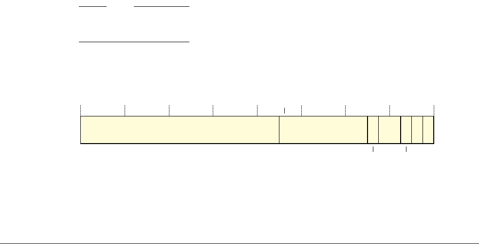
B4 System Control Registers in a VMSA implementation
B4.1 VMSA System control registers descriptions, in register order
ARM DDI 0406C.c Copyright © 1996-1998, 2000, 2004-2012, 2014 ARM. All rights reserved. B4-1729
ID051414 Non-Confidential
B4.1.154 TTBR0, Translation Table Base Register 0, VMSA
The TTBR0 characteristics are:
Purpose TTBR0 holds the base address of translation table 0, and information about the memory it
occupies. This is one of the translation tables for the stage 1 translation of memory accesses
from modes other than Hyp mode.
This register is part of the Virtual memory control registers functional group.
Usage constraints Only accessible from PL1 or higher.
Used in conjunction with the TTBCR. When the 64-bit TTBR0 format is used, cacheability
and shareability information is held in the TTBCR, not in TTBR0.
Configurations The Multiprocessing Extensions change the TTBR0 32-bit register format.
The Large Physical Address Extension extends TTBR0 to a 64-bit register. In an
implementation that includes the Large Physical Address Extension, TTBCR.EAE
determines which TTBR0 format is used:
EAE==0 32-bit format is used. TTBR0[63:32] are ignored.
EAE==1 64-bit format is used.
If the implementation includes the Security Extensions, this register:
•is Banked
• has write access to the Secure copy of the register disabled when the
CP15SDISABLE signal is asserted HIGH.
Attributes A 32-bit or 64-bit RW register with a reset value that depends on the register
implementation. For more information see the register bit descriptions. See also Reset
behavior of CP14 and CP15 registers on page B3-1450.
Table B3-45 on page B3-1493 shows the encodings of all of the registers in the Virtual
memory control registers functional group.
The following subsections describe the TTBR0 formats:
•32-bit TTBR0 format
•64-bit TTBR0 and TTBR1 format on page B4-1731.
See TTBCR, Translation Table Base Control Register, VMSA on page B4-1724 for more information about using
this register.
Note
See TTBCR, Translation Table Base Control Register, VMSA on page B4-1724 for a summary of the registers that
define the translation tables for other address translations.
32-bit TTBR0 format
In an implementation that does not include the Multiprocessing Extensions, the 32-bit TTBR0 bit assignments are:
C
31 x
x-1
6543210
Translation table base 0 address Reserved, UNK/SBZP RGN S
NOS IMP

B4 System Control Registers in a VMSA implementation
B4.1 VMSA System control registers descriptions, in register order
B4-1730 Copyright © 1996-1998, 2000, 2004-2012, 2014 ARM. All rights reserved. ARM DDI 0406C.c
Non-Confidential ID051414
In an implementation that includes the Multiprocessing Extensions, the 32-bit TTBR0 bit assignments are:
In these assignments, x is (14-(TTBCR.N)).
Bits[31:x] Translation table base 0 address, bits[31:x].
The value of x determines the required alignment of the translation table, which must be aligned to
2x bytes.
Bits[x-1:6], ARMv7-A without Multiprocessing Extensions
Reserved, UNK/SBZP.
Bits[x-1:7], in an implementation that includes the Multiprocessing Extensions
Reserved, UNK/SBZP.
IRGN[0], bit[6], in an implementation that includes the Multiprocessing Extensions
See the description of bit[0] for an implementation that includes the Multiprocessing Extensions.
NOS, bit[5] Not Outer Shareable bit. Indicates the Outer Shareable attribute for the memory associated with a
translation table walk that has the Shareable attribute, indicated by TTBR0.S == 1:
0 Outer Shareable
1 Inner Shareable.
This bit is ignored when TTBR0.S == 0.
ARMv7 introduces this bit. If an implementation does not distinguish between Inner Shareable and
Outer Shareable, this bit is UNK/SBZP.
RGN, bits[4:3]
Region bits. Indicates the Outer cacheability attributes for the memory associated with the
translation table walks:
0b00
Normal memory, Outer Non-cacheable.
0b01
Normal memory, Outer Write-Back Write-Allocate Cacheable.
0b10
Normal memory, Outer Write-Through Cacheable.
0b11
Normal memory, Outer Write-Back no Write-Allocate Cacheable.
IMP, bit[2] The effect of this bit is IMPLEMENTATION DEFINED. If the translation table implementation does not
include any IMPLEMENTATION DEFINED features this bit is UNK/SBZP.
S, bit[1] Shareable bit. Indicates the Shareable attribute for the memory associated with the translation table
walks:
0 Non-shareable
1 Shareable.
C, bit[0], ARMv7-A without Multiprocessing Extensions
Cacheable bit. Indicates whether the translation table walk is to Inner Cacheable memory.
0 Inner Non-cacheable
1 Inner Cacheable.
For regions marked as Inner Cacheable, it is IMPLEMENTATION DEFINED whether the read has the
Write-Through, Write-Back no Write-Allocate, or Write-Back Write-Allocate attribute.
31 x
x-1
6543210
Translation table base 0 address Reserved,
UNK/SBZP RGN S
NOS
7
IRGN[0]
IRGN[1]
IMP

B4 System Control Registers in a VMSA implementation
B4.1 VMSA System control registers descriptions, in register order
ARM DDI 0406C.c Copyright © 1996-1998, 2000, 2004-2012, 2014 ARM. All rights reserved. B4-1731
ID051414 Non-Confidential
IRGN, bits[6, 0], in an implementation that includes the Multiprocessing Extensions
Inner region bits. Indicates the Inner Cacheability attributes for the memory associated with the
translation table walks. The possible values of IRGN[1:0] are:
0b00
Normal memory, Inner Non-cacheable.
0b01
Normal memory, Inner Write-Back Write-Allocate Cacheable.
0b10
Normal memory, Inner Write-Through Cacheable.
0b11
Normal memory, Inner Write-Back no Write-Allocate Cacheable.
Note
The encoding of the IRGN bits is counter-intuitive, with register bit[6] being IRGN[0] and register
bit[0] being IRGN[1]. This encoding is chosen to give a consistent encoding of memory region
types and to ensure that software written for the ARMv7 architecture without the Multiprocessing
Extensions can run unmodified on an implementation that includes the Multiprocessing Extensions.
64-bit TTBR0 and TTBR1 format
The bit assignments for the 64-bit implementations of TTBR0 and TTBR1 are identical, and are:
Defining the translation table base address width on page B4-1732 defines how x is derived from the TTBCR.T0SZ
or TTBCR.T1SZ field value.
Note
The value of x for TTBR0 is independent of its value for TTBR1.
Bits[63:56] Reserved, UNK/SBZP.
ASID, bits[55:48]
An ASID for the translation table base address. The TTBCR.A1 field selects either TTBR0.ASID
or TTBR1.ASID.
Bits[47:40] Reserved, UNK/SBZP.
BADDR, bits[39:x]
Translation table base address, bits[39:x]. Defining the translation table base address width on
page B4-1732 describes how x is defined.
The value of x determines the required alignment of the translation table, which must be aligned to
2x bytes.
Bits[x-1:0] Reserved, UNK/SBZP.
BADDR[39:x] Reserved,
UNK/SBZP
Reserved,
UNK/SBZP
48 47
ASID
56 55
Reserved,
UNK/SBZP
40 3963 0x
x-1

B4 System Control Registers in a VMSA implementation
B4.1 VMSA System control registers descriptions, in register order
B4-1732 Copyright © 1996-1998, 2000, 2004-2012, 2014 ARM. All rights reserved. ARM DDI 0406C.c
Non-Confidential ID051414
Defining the translation table base address width
The value of x in the descriptions of the bit assignments of the 64-bit TTBR formats defines the width of the
translation table base address. When using the 64-bit TTBR0 and TTBR1 formats:
• the TTBCR.T0SZ field determines the x value for TTBR0
• the TTBCR.T1SZ field determines the x value for TTBR1.
If
TxSZ
indicates either the T0SZ or the T1SZ field, the following pseudocode calculates the value of x for the
corresponding TTBR:
TxSize = UInt(TTBCR.TxSZ);
if TxSize > 1 then
x = 14 - TxSize;
else
x = 5 - TxSize;
Accessing TTBR0
To access TTBR0 in an implementation that does not include the Large Physical Address Extension, or bits[31:0]
of TTBR0 in an implementation that includes the Large Physical Address Extension, software reads or writes the
CP15 registers with
<opc1>
set to 0,
<CRn>
set to c2,
<CRm>
set to c0, and
<opc2>
set to 0. For example:
MRC p15, 0, <Rt>, c2, c0, 0 ; Read 32-bit TTBR0 into Rt
MCR p15, 0, <Rt>, c2, c0, 0 ; Write Rt to 32-bit TTBR0
In an implementation that includes the Large Physical Address Extension, to access all 64 bits of TTBR0, software
performs a 64-bit read or write of the CP15 registers with
<CRm>
set to c2 and
<opc1>
set to 0. For example:
MRRC p15, 0, <Rt>, <Rt2>, c2 ; Read 64-bit TTBR0 into Rt (low word) and Rt2 (high word)
MCRR p15, 0, <Rt>, <Rt2>, c2 ; Write Rt (low word) and Rt2 (high word) to 64-bit TTBR0
In these
MRRC
and
MCRR
instructions, Rt holds the least-significant word of TTBR0, and Rt2 holds the most-significant
word.
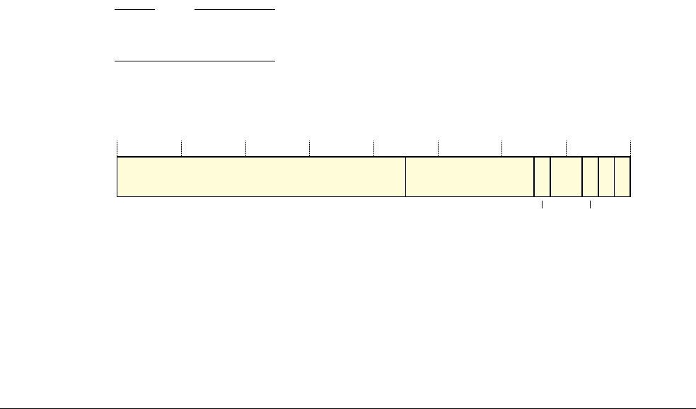
B4 System Control Registers in a VMSA implementation
B4.1 VMSA System control registers descriptions, in register order
ARM DDI 0406C.c Copyright © 1996-1998, 2000, 2004-2012, 2014 ARM. All rights reserved. B4-1733
ID051414 Non-Confidential
B4.1.155 TTBR1, Translation Table Base Register 1, VMSA
The TTBR1 characteristics are:
Purpose TTBR1 holds the base address of translation table 1, and information about the memory it
occupies. This is one of the translation tables for the stage 1 translation of memory accesses
from modes other than Hyp mode.
This register is part of the Virtual memory control registers functional group.
Usage constraints Only accessible from PL1 or higher.
Used in conjunction with the TTBCR. When the 64-bit TTBR1 format is used, cacheability
and shareability information is held in the TTBCR, not in TTBR1.
Configurations The Multiprocessing Extensions change the TTBR0 32-bit register format.
The Large Physical Address Extension extends TTBR1 to a 64-bit register. In an
implementation that includes the Large Physical Address Extension, TTBCR.EAE
determines which TTBR1 format is used:
EAE==0 32-bit format is used. TTBR1[63:32] are ignored.
EAE==1 64-bit format is used.
If the implementation includes the Security Extensions, this register is Banked.
Attributes A 32-bit or 64-bit RW register with a reset value that depends on the register
implementation. For more information see the register bit descriptions. See also Reset
behavior of CP14 and CP15 registers on page B3-1450.
Table B3-45 on page B3-1493 shows the encodings of all of the registers in the Virtual
memory control registers functional group.
The 64-bit format of TTBR1 is identical to the corresponding format for TTBR0, see 64-bit TTBR0 and TTBR1
format on page B4-1731.
The following subsection describes the 32-bit TTBR1 formats.
See TTBCR, Translation Table Base Control Register, VMSA on page B4-1724 for more information about using
this register.
Note
See TTBCR, Translation Table Base Control Register, VMSA on page B4-1724 for a summary of the registers that
define the translation tables for other address translations.
32-bit TTBR1 format
In an implementation that does not include the Multiprocessing Extensions, the 32-bit TTBR1 bit assignments are:
C
31 14 13 6 5 4 3 2 1 0
Translation table base 1 address Reserved, UNK/SBZP RGN S
NOS IMP

B4 System Control Registers in a VMSA implementation
B4.1 VMSA System control registers descriptions, in register order
B4-1734 Copyright © 1996-1998, 2000, 2004-2012, 2014 ARM. All rights reserved. ARM DDI 0406C.c
Non-Confidential ID051414
In an implementation that includes the Multiprocessing Extensions, the 32-bit TTBR1 bit assignments are:
Bits[31:14] Translation table base 1 address, bits[31:14]. The translation table must be aligned on a 16KByte
boundary.
Bits[13:6], ARMv7-A without Multiprocessing Extensions
Reserved, UNK/SBZP.
Bits[13:7], in an implementation that includes the Multiprocessing Extensions
Reserved, UNK/SBZP.
IRGN[0:1], bits[6, 0], in an implementation that includes the Multiprocessing Extensions
See the definition given for TTBR0.
NOS, RGN, IMP, S, bits[5:1]
See the definitions given for TTBR0.
C, bit[0], ARMv7-A without Multiprocessing Extensions
See the definition given for TTBR0.
Accessing TTBR1
To access TTBR1 in an implementation that does not include the Large Physical Address Extension, or bits[31:0]
of TTBR1 in an implementation that includes the Large Physical Address Extension, software reads or writes the
CP15 registers with
<opc1>
set to 0,
<CRn>
set to c2,
<CRm>
set to c0, and
<opc2>
set to 1. For example:
MRC p15, 0, <Rt>, c2, c0, 1 ; Read 32-bit TTBR1 into Rt
MCR p15, 0, <Rt>, c2, c0, 1 ; Write Rt to 32-bit TTBR1
In an implementation that includes the Large Physical Address Extension, to access all 64 bits of TTBR1, software
performs a 64-bit read or write of the CP15 registers with
<CRm>
set to c2 and
<opc1>
set to 1. For example:
MRRC p15, 1, <Rt>, <Rt2>, c2 ; Read 64-bit TTBR1 into Rt (low word) and Rt2 (high word)
MCRR p15, 1, <Rt>, <Rt2>, c2 ; Write Rt (low word) and Rt2 (high word) to 64-bit TTBR1
In these
MRRC
and
MCRR
instructions, Rt holds the least-significant word of TTBR1, and Rt2 holds the most-significant
word.
31 14 13 6 5 4 3 2 1 0
Translation table base 1 address Reserved,
UNK/SBZP RGN S
NOS
7
IRGN[0]
IMP
IRGN[1]

B4 System Control Registers in a VMSA implementation
B4.1 VMSA System control registers descriptions, in register order
ARM DDI 0406C.c Copyright © 1996-1998, 2000, 2004-2012, 2014 ARM. All rights reserved. B4-1735
ID051414 Non-Confidential
B4.1.156 VBAR, Vector Base Address Register, Security Extensions
The VBAR characteristics are:
Purpose When high exception vectors are not selected, the VBAR holds the exception base address
for exceptions that are not taken to Monitor mode or to Hyp mode, see Exception vectors
and the exception base address on page B1-1165.
This register is part of the Security Extensions registers functional group.
Usage constraints Only accessible from PL1 or higher.
Software must program the Non-secure copy of the register with the required initial value
as part of the processor boot sequence.
Configurations A Banked register that is only present in an implementation that includes the Security
Extensions.
Has write access to the Secure copy of the register disabled when the CP15SDISABLE
signal is asserted HIGH.
Attributes A 32-bit RW register. The Secure copy of the register resets to an IMPLEMENTATION
DEFINED value, see Reset on page B1-1205.
See also Reset behavior of CP14 and CP15 registers on page B3-1450.
Table B3-54 on page B3-1500 shows the encoding of all of the Security Extensions
registers.
The VBAR bit assignments are:
The Secure copy of the VBAR holds the vector base address for Secure state, described as the Secure exception base
address.
The Non-secure copy of the VBAR holds the vector base address for Non-secure state, described as the Non-secure
exception base address.
Vector_Base_Address, bits[31:5]
Bits[31:5] of the base address of the low exception vectors. Bits[4:0] of an exception vector is the
exception offset, see Table B1-3 on page B1-1167.
Bits[4:0] Reserved, UNK/SBZP.
For details of how the VBAR registers determine the exception addresses see Exception vectors and the exception
base address on page B1-1165.
Note
The high exception vectors always have the base address
0xFFFF0000
and are not affected by the value of VBAR.
Accessing the VBAR
To access the VBAR, software reads or writes the CP15 registers with
<opc1>
set to 0,
<CRn>
set to c12,
<CRm>
set to
c0, and
<opc2>
set to 0. For example:
MRC p15, 0, <Rt>, c12, c0, 0 ; Read VBAR into Rt
MCR p15, 0, <Rt>, c12, c0, 0 ; Write Rt to VBAR
Vector_Base_Address
31 54 0
Reserved,
UNK/SBZP

B4 System Control Registers in a VMSA implementation
B4.1 VMSA System control registers descriptions, in register order
B4-1736 Copyright © 1996-1998, 2000, 2004-2012, 2014 ARM. All rights reserved. ARM DDI 0406C.c
Non-Confidential ID051414
B4.1.157 VMPIDR, Virtualization Multiprocessor ID Register, Virtualization Extensions
The VMPIDR characteristics are:
Purpose The VMPIDR holds the value of the Virtualization Multiprocessor ID. A Non-secure read
of the MPIDR from PL1 returns the value of this register.
This register is part of the Virtualization Extensions registers functional group.
Usage constraints Only accessible from Hyp mode, or from Monitor mode when SCR.NS is set to 1, see
PL2-mode system control registers on page B3-1454.
Configurations Implemented only as part of the Virtualization Extensions.
This is Banked PL2-mode register, see Banked PL2-mode CP15 read/write registers on
page B3-1454.
Attributes A 32-bit RW register that resets to the value of the MPIDR. See also Reset behavior of CP14
and CP15 registers on page B3-1450.
Table B3-55 on page B3-1501 shows the encoding of all of the Virtualization Extensions
registers.
The VMPIDR bit assignments are:
VMPIDR, bits[31:0]
MPIDR value returned by Non-secure PL1 reads of the MPIDR. The MPIDR description defines
the subdivision of this value. Fields that are UNK in the MPIDR are UNK/SBZP in the VMPIDR.
Accessing the VMPIDR
To access the VMPIDR, software reads or writes the CP15 registers with
<opc1>
set to 4,
<CRn>
set to c0,
<CRm>
set
to c0, and
<opc2>
set to 5. For example:
MRC p15, 4, <Rt>, c0, c0, 5 ; Read VMPIDR into Rt
MCR p15, 4, <Rt>, c0, c0, 5 ; Write Rt to VMPIDR
VMPIDR
31 0

B4 System Control Registers in a VMSA implementation
B4.1 VMSA System control registers descriptions, in register order
ARM DDI 0406C.c Copyright © 1996-1998, 2000, 2004-2012, 2014 ARM. All rights reserved. B4-1737
ID051414 Non-Confidential
B4.1.158 VPIDR, Virtualization Processor ID Register, Virtualization Extensions
The VPIDR characteristics are:
Purpose The VPIDR holds the value of the Virtualization Processor ID. A Non-secure read of the
MIDR from PL1 returns the value of this register.
This register is part of the Virtualization Extensions registers functional group.
Usage constraints Only accessible from Hyp mode, or from Monitor mode when SCR.NS is set to 1, see
PL2-mode system control registers on page B3-1454.
Configurations Implemented only as part of the Virtualization Extensions.
This is Banked PL2-mode register, see Banked PL2-mode CP15 read/write registers on
page B3-1454.
Attributes A 32-bit RW register that resets to the value of the MIDR. See also Reset behavior of CP14
and CP15 registers on page B3-1450.
Table B3-55 on page B3-1501 shows the encoding of all of the Virtualization Extensions
registers.
The VPIDR bit assignments are:
VPIDR, bits[31:0]
MIDR value returned by Non-secure PL1 reads of the MIDR. The MIDR description defines the
subdivision of this value.
Accessing the VPIDR
To access the VPIDR, software reads or writes the CP15 registers with
<opc1>
set to 4,
<CRn>
set to c0,
<CRm>
set to
c0, and
<opc2>
set to 0. For example:
MRC p15, 4, <Rt>, c0, c0, 0 ; Read VPIDR into Rt
MCR p15, 4, <Rt>, c0, c0, 0 ; Write Rt to VPIDR
VPIDR
31 0

B4 System Control Registers in a VMSA implementation
B4.1 VMSA System control registers descriptions, in register order
B4-1738 Copyright © 1996-1998, 2000, 2004-2012, 2014 ARM. All rights reserved. ARM DDI 0406C.c
Non-Confidential ID051414
B4.1.159 VTCR, Virtualization Translation Control Register, Virtualization Extensions
The VTCR characteristics are:
Purpose The VTCR controls the translation table walks required for the stage 2 translation of
memory accesses from Non-secure modes other than Hyp mode, and holds cacheability and
shareability information for the accesses.
This register is part of the Virtualization Extensions registers functional group.
Usage constraints Only accessible from Hyp mode, or from Monitor mode when SCR.NS is set to 1, see
PL2-mode system control registers on page B3-1454.
Used in conjunction with VTTBR, that defines the translation table base address for the
translations.
Configurations Implemented only as part of the Virtualization Extensions.
This is Banked PL2-mode register, see Banked PL2-mode CP15 read/write registers on
page B3-1454.
Attributes A 32-bit RW register with an UNKNOWN reset value. See also Reset behavior of CP14 and
CP15 registers on page B3-1450.
Table B3-55 on page B3-1501 shows the encoding of all of the Virtualization Extensions
registers.
Note
For other address translations, the following registers are equivalent to the VTCR and VTTBR:
• for stage 1 translations for accesses from modes other than Hyp mode, the TTBCR, TTBR0, and TTBR1
• for stage 1 translations for accesses from Hyp mode, the HTCR and HTTBR.
The VTCR bit assignments are:
Bit[31] Reserved, UNK/SBOP.
Bits[30:14] Reserved, UNK/SBZP.
SH0, bits[13:12]
Shareability attribute for memory associated with translation table walks using VTTBR. This field
is encoded as described in Shareability, Long-descriptor format on page B3-1373.
ORGN0, bits[11:10]
Outer cacheability attribute for memory associated with translation table walks using VTTBR.
Table B4-32 shows the encoding of this field.
Table B4-32 VTCR.ORGN0 field encoding
ORGN0 Meaning
00 Normal memory, Outer Non-cacheable
01 Normal memory, Outer Write-Back Write-Allocate Cacheable
(1)
31 30 14 13 12 11 10 9 8 7 6 3 2 0
Reserved, UNK/SBZP SH0 SL0 (0) S T0SZ
ORGN0
IRGN0
54

B4 System Control Registers in a VMSA implementation
B4.1 VMSA System control registers descriptions, in register order
ARM DDI 0406C.c Copyright © 1996-1998, 2000, 2004-2012, 2014 ARM. All rights reserved. B4-1739
ID051414 Non-Confidential
IRGN0, bits[9:8]
Inner cacheability attribute for memory associated with translation table walks using VTTBR.
Table B4-33 shows the encoding of this field.
SL0, bits[7:6]
Starting level for translation table walks using VTTBR. Table B4-34 shows the encoding of this
field.
Behavior is UNPREDICTABLE if the programming of this field is not consistent with the programming
of T0SZ. For more information, see the T0SZ description.
Bit[5] Reserved, UNK/SBZP.
S, bit[4] Sign extension bit. This bit must be programmed to the value of T0SZ[3], otherwise behavior is
UNPREDICTABLE.
T0SZ, bits[3:0]
The size offset of the memory region addressed by VTTBR. This field is encoded as a four-bit
signed integer, and the region size is 2(32-T0SZ) bytes.
Determining the required first lookup level for stage 2 translations on page B3-1352 describes the
constraints on programming the SL0 and T0SZ fields. Behavior is UNPREDICTABLE if these
constraints are not followed. See the description of the VTTBR for more information about how the
values of the T0SZ and SL0 fields together determine the width of the translation table base address
defined by the VTTBR.
10 Normal memory, Outer Write-Through Cacheable
11 Normal memory, Outer Write-Back no Write-Allocate Cacheable
Table B4-33 VTCR.IRGN0 field encoding
IRGN0 Meaning
00 Normal memory, Inner Non-cacheable
01 Normal memory, Inner Write-Back Write-Allocate Cacheable
10 Normal memory, Inner Write-Through Cacheable
11 Normal memory, Inner Write-Back no Write-Allocate Cacheable
Table B4-34 VTCR.SL0 field encoding
SL0 Meaning
00 Start at second level
01 Start at first level
10, 11 Reserved, UNPREDICTABLE
Table B4-32 VTCR.ORGN0 field encoding (continued)
ORGN0 Meaning

B4 System Control Registers in a VMSA implementation
B4.1 VMSA System control registers descriptions, in register order
B4-1740 Copyright © 1996-1998, 2000, 2004-2012, 2014 ARM. All rights reserved. ARM DDI 0406C.c
Non-Confidential ID051414
Accessing the VTCR
To access the VTCR, software reads or writes the CP15 registers with
<opc1>
set to 4,
<CRn>
set to c2,
<CRm>
set to
c1, and
<opc2>
set to 2. For example:
MRC p15, 4, <Rt>, c2, c1, 2 ; Read VTCR into Rt
MCR p15, 4, <Rt>, c2, c1, 2 ; Write Rt to VTCR
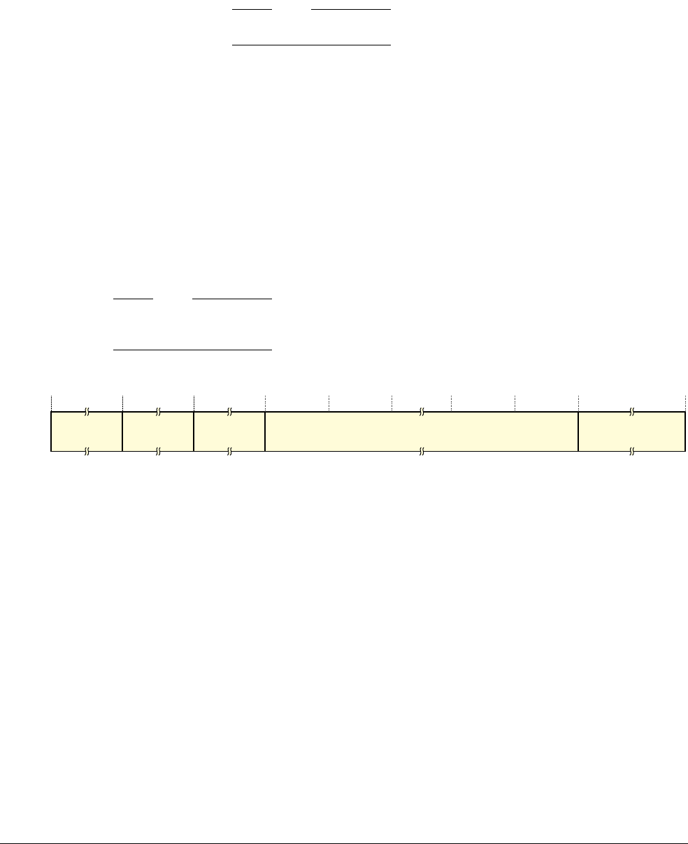
B4 System Control Registers in a VMSA implementation
B4.1 VMSA System control registers descriptions, in register order
ARM DDI 0406C.c Copyright © 1996-1998, 2000, 2004-2012, 2014 ARM. All rights reserved. B4-1741
ID051414 Non-Confidential
B4.1.160 VTTBR, Virtualization Translation Table Base Register, Virtualization Extensions
The VTTBR characteristics are:
Purpose The VTTBR holds the base address of the translation table for the stage 2 translation of
memory accesses from Non-secure modes other than Hyp mode.
Note
These translations are always defined using Long-descriptor format translation tables.
This register is part of the Virtualization Extensions registers functional group.
Usage constraints Only accessible from Hyp mode, or from Monitor mode when SCR.NS is set to 1, see
PL2-mode system control registers on page B3-1454.
Used in conjunction with the VTCR.
Configurations Implemented only as part of the Virtualization Extensions.
This is a Banked PL2-mode register, see Banked PL2-mode CP15 read/write registers on
page B3-1454.
Attributes A 64-bit RW register. See the field descriptions for information about the reset value. See
also Reset behavior of CP14 and CP15 registers on page B3-1450.
Table B3-55 on page B3-1501 shows the encoding of all of the Virtualization Extensions
registers.
Note
See VTCR, Virtualization Translation Control Register, Virtualization Extensions on page B4-1738 for a summary
of the registers that define the translation tables for other address translations.
The VTTBR bit assignments are:
Bits[63:56] Reserved, UNK/SBZP.
VMID, bits[55:48]
The VMID for the translation table.
The reset value of this field is zero.
Bits[47:40] Reserved, UNK/SBZP.
BADDR, bits[39:x]
Translation table base address, bits[39:x]. See the text in this section for a description of how x is
defined.
The value of x determines the required alignment of the translation table, which must be aligned to
2x bytes.
Bits[x-1:0] Reserved, UNK/SBZP.
The VTCR.T0SZ and VTCR.SL0 fields determines the width of the defined translation table base address, indicated
by the value of x in the VTTBR description. The following pseudocode calculates the value of x:
T0Size = SInt(VTCR.T0SZ);
if VTCR.SL0 == '00' then
x = 14 - T0Size;
else
x = 5 - T0Size;
BADDR[39:x] Reserved,
UNK/SBZP
Reserved,
UNK/SBZP
48 47
VMID
56 55
Reserved,
UNK/SBZP
40 3963 0x x-1

B4 System Control Registers in a VMSA implementation
B4.1 VMSA System control registers descriptions, in register order
B4-1742 Copyright © 1996-1998, 2000, 2004-2012, 2014 ARM. All rights reserved. ARM DDI 0406C.c
Non-Confidential ID051414
Accessing the VTTBR
To access VTTBR, software performs a 64-bit read or write of the CP15 registers with
<CRm>
set to c2 and
<opc1>
set to 6. For example:
MRRC p15, 6, <Rt>, <Rt2>, c2 ; Read 64-bit VTTBR to Rt (low word) and Rt2 (high word)
MCRR p15, 6, <Rt>, <Rt2>, c2 ; Write Rt (low word) and Rt2 (high word) to 64-bit VTTBR
In these
MRRC
and
MCRR
instructions, Rt holds the least-significant word of VTTBR, and Rt2 holds the
most-significant word.

B4 System Control Registers in a VMSA implementation
B4.2 VMSA system control operations described by function
ARM DDI 0406C.c Copyright © 1996-1998, 2000, 2004-2012, 2014 ARM. All rights reserved. B4-1743
ID051414 Non-Confidential
B4.2 VMSA system control operations described by function
This section describes the system control operations that are available in a VMSA implementation and that are
described as part of a functional group. Architecturally-defined operations have an entry, under the operation name,
in VMSA System control registers descriptions, in register order on page B4-1522, that references the appropriate
functional description in this section.
This section contains the following subsections:
•Cache and branch predictor maintenance operations, VMSA
•TLB maintenance operations, not in Hyp mode on page B4-1746
•Hyp mode TLB maintenance operations, Virtualization Extensions on page B4-1749
•Performing address translation operations on page B4-1750
•Data and instruction barrier operations, VMSA on page B4-1752
•Cache and TCM lockdown registers, VMSA on page B4-1753
•IMPLEMENTATION DEFINED TLB control operations, VMSA on page B4-1753
•DMA support, VMSA on page B4-1754.
B4.2.1 Cache and branch predictor maintenance operations, VMSA
This section describes the cache and branch predictor maintenance operations. These are:
• 32-bit write-only operations
• can be executed only by software executing at PL1 or higher.
Table B3-49 on page B3-1496 shows the encodings for these operations.
For more information about the terms used in this section see Terms used in describing the maintenance operations
on page B2-1274.
Note
• The architecture includes branch predictor operations with cache maintenance operations because they
operate in a similar way.
• ARMv7 introduces significant changes in the CP15 c7 operations. Most of these changes are because
ARMv7 introduces support for multiple levels of cache. This section only describes the ARMv7
requirements for these operations. For details of these operations in previous versions of the architecture see:
—CP15 c7, Cache and branch predictor operations on page D12-2533 for ARMv6
—CP15 c7, Cache and branch predictor operations on page D15-2629 for ARMv4 and ARMv5.
The Multiprocessing Extensions change the set of caches affected by these operations, see Scope of cache and
branch predictor maintenance operations on page B2-1281.
See The interaction of cache lockdown with cache maintenance operations on page B2-1287 for information about
the interaction of these maintenance operations with cache lockdown.
Table B4-35 on page B4-1744 lists these operations. For the entries in the table:
• The Rt data column specifies what data is required in the register Rt specified by the
MCR
instruction that
performs the operation, see Data formats for the cache and branch predictor operations on page B4-1744.
•Terms used in describing the maintenance operations on page B2-1274 describes Modified Virtual Address
(MVA), point of coherency (PoC) and point of unification (PoU).

B4 System Control Registers in a VMSA implementation
B4.2 VMSA system control operations described by function
B4-1744 Copyright © 1996-1998, 2000, 2004-2012, 2014 ARM. All rights reserved. ARM DDI 0406C.c
Non-Confidential ID051414
Branch predictor maintenance operations can perform a NOP if the operation of Branch Prediction hardware is not
architecturally-visible.
Data formats for the cache and branch predictor operations
Table B4-35 shows three possibilities for the data in the register Rt specified by the
MCR
instruction. These are
described in the following subsections:
•Ignored
•MVA
•Set/way on page B4-1745.
Ignored
The value in the register specified by the
MCR
instruction is ignored. Software does not have to write a value to the
register before issuing the
MCR
instruction.
MVA
For more information about the possible meaning when the table shows that an MVA is required see Terms used in
describing the maintenance operations on page B2-1274. When the data is stated to be an MVA, it does not have to
be cache line aligned.
Table B4-35 CP15 c7 cache and branch predictor maintenance operations, VMSA
Operation Type Description Rt data
ICIALLUIS WO Invalidate all instruction caches Inner Shareable to PoU. If branch predictors are
architecturally-visible, also flushes branch predictors.a
Ignored
BPIALLIS WO Invalidate all entries from branch predictors Inner Shareable. Ignored
ICIALLU WO Invalidate all instruction caches to PoU. If branch predictors are architecturally-visible, also
flushes branch predictors.a
Ignored
ICIMVAU WO Invalidate instruction cache line by MVA to PoU.aMVA
BPIALL WO Invalidate all entries from branch predictors. Ignored
BPIMVA WO Invalidate MVA from branch predictors. MVA
DCIMVAC WO Invalidate data or unified cache line by MVA to PoC. MVA
DCISW WO Invalidate data or unified cache line by set/way. Set/way
DCCMVAC WO Clean data or unified cache line by MVA to PoC. MVA
DCCSW WO Clean data or unified cache line by set/way. Set/way
DCCMVAU WO Clean data or unified cache line by MVA to PoU. MVA
DCCIMVAC WO Clean and Invalidate data or unified cache line by MVA to PoC. MVA
DCCISW WO Clean and Invalidate data or unified cache line by set/way. Set/way
a. Only applies to separate instruction caches, does not apply to unified caches.

B4 System Control Registers in a VMSA implementation
B4.2 VMSA system control operations described by function
ARM DDI 0406C.c Copyright © 1996-1998, 2000, 2004-2012, 2014 ARM. All rights reserved. B4-1745
ID051414 Non-Confidential
Set/way
For an operation by set/way, the data identifies the cache line that the operation is to be applied to by specifying:
• the cache set the line belongs to
• the way number of the line in the set
• the cache level.
The format of the register data for a set/way operation is:
Where:
A =Log
2(ASSOCIATIVITY), rounded up to the next integer if necessary.
B =(L+S).
L =Log
2(LINELEN).
S =Log
2(NSETS), rounded up to the next integer if necessary.
ASSOCIATIVITY, LINELEN (line length, in bytes) and NSETS (number of sets) have their usual
meanings and are the values for the cache level being operated on.
The values of A and S are rounded up to the next integer.
Level ((Cache level to operate on) -1)
For example, this field is 0 for operations on L1 cache, or 1 for operations on L2 cache.
Set The number of the set to operate on.
Way The number of the way to operate on.
Note
• If L = 4 then there is no SBZ field between the set and level fields in the register.
• If A = 0 there is no way field in the register, and register bits[31:B] are SBZ.
• If the level, set or way field in the register is larger than the size implemented in the cache then the effect of
the operation is UNPREDICTABLE.
Accessing the CP15 c7 cache and branch predictor maintenance operations
To perform one of the cache maintenance operations, software writes to the CP15 registers with
<opc1>
set to 0,
<CRn>
set to c7, and
<CRm>
and
<opc2>
set to the values shown in Table B4-35 on page B4-1744.
That is:
MCR p15, 0, <Rt>, c7, <CRm>, <opc2>
For example:
MCR p15, 0, <Rt>, c7, c5, 0 ; ICIALLU, Instruction cache invalidate all to PoU. Ignores Rt value.
MCR p15, 0, <Rt>, c7, c10, 2 ; Use Rt as input to DCCSW, Data cache clean by set/way
0Way
31 32–A
31–A
B
B–1
L
L–1
43210
SBZ Set SBZ Level

B4 System Control Registers in a VMSA implementation
B4.2 VMSA system control operations described by function
B4-1746 Copyright © 1996-1998, 2000, 2004-2012, 2014 ARM. All rights reserved. ARM DDI 0406C.c
Non-Confidential ID051414
B4.2.2 TLB maintenance operations, not in Hyp mode
This section describes the TLB operations that are implemented on all ARMv7-A implementations. These:
• are 32-bit write-only operations
• can be executed only by software executing at PL1 or higher.
Table B3-50 on page B3-1497 shows the encodings for these operations.
Note
The Multiprocessing Extensions introduce the TLBIALLIS, TLBIMVAIS, TLBIASIDIS, TLBIMVAAIS, and
TLBIMVAA operations. Therefore, these are not available on earlier ARMv7 implementations.
If an implementation includes the Virtualization Extensions, those extensions define the additional TLB
maintenance operations described in Hyp mode TLB maintenance operations, Virtualization Extensions on
page B4-1749.
These TLB maintenance functions:
• are write-only operations
• can be executed only in by software executing at PL1 or higher.
Table B4-36 shows these TLB maintenance operations. For these operations:
• on an implementation with separate data and instruction TLBs, any unified TLB operation operates on both
TLBs
• on an implementation with a unified TLB, any instruction TLB operation, and any data TLB operation,
operates on the unified TLB
• ARM deprecates use of instruction TLB operations and data TLB operations, and recommends that software
always uses the unified TLB operations.
Table B4-36 CP15 c8 TLB maintenance operations, without Virtualization Extensions
Name Description Rt dataa
TLBIALLISbInvalidate entire unified TLB Inner Shareable Ignored
TLBIMVAISbInvalidate unified TLB entry by MVA and ASID, Inner Shareable MVA
TLBIASIDISbInvalidate unified TLB by ASID match Inner Shareable ASID
TLBIMVAAISbInvalidate unified TLB entry by MVA all ASID Inner Shareable MVA
ITLBIALLcInvalidate entire instruction TLB Ignored
ITLBIMVAcInvalidate instruction TLB entry by MVA and ASID MVA
ITLBIASIDcInvalidate instruction TLB by ASID match ASID
DTLBIALLcInvalidate entire data TLB Ignored
DTLBIMVAcInvalidate data TLB entry by MVA and ASID MVA
DTLBIASIDcInvalidate data TLB by ASID match ASID
TLBIALLdInvalidate entire unified TLB Ignored
TLBIMVAdInvalidate unified TLB entry by MVA and ASID MVA

B4 System Control Registers in a VMSA implementation
B4.2 VMSA system control operations described by function
ARM DDI 0406C.c Copyright © 1996-1998, 2000, 2004-2012, 2014 ARM. All rights reserved. B4-1747
ID051414 Non-Confidential
About the TLB maintenance operations
For more information about TLBs and their maintenance see Translation Lookaside Buffers (TLBs) on
page B3-1378, and in particular TLB maintenance requirements on page B3-1381.
For more information about the Inner Shareable operations see Multiprocessor effects on TLB maintenance
operations on page B3-1389.
For information about the effect of these operations on locked TLB entries see The interaction of TLB lockdown
with TLB maintenance operations on page B3-1383.
As stated in the footnotes to Table B4-36 on page B4-1746:
• If an Instruction TLB or Data TLB operation is used on a system that implements a Unified TLB then the
operation is performed on the Unified TLB
• If a Unified TLB operation is used on a system that implements separate Instruction and Data TLBs then the
operation is performed on both the Instruction TLB and the Data TLB.
• The mnemonics for the operations to invalidate a unified TLB that are defined for an ARMv7 implementation
that does not include the Multiprocessing Extensions were previously UTLBIALL, UTLBIMVA, and
UTLBIASID. These remain synonyms for these operations, but ARM deprecates the use of the older names.
These are the operations with CRm==c7, opc2=={0, 1, 2}.
For information about the synchronization of the TLB maintenance operations see TLB maintenance operations and
the memory order model on page B3-1383.
TLB operations and associated Rt data formats
The following subsections give more information about the different TLB operations and the associated Rt data
formats shown in Table B4-36 on page B4-1746.
Invalidate entire TLB
The Invalidate entire TLB operations invalidate all unlocked entries in the TLB. The operation ignores the value in
the register Rt specified by the
MCR
instruction that performs the operation. Software does not have to write a value
to the register before issuing the
MCR
instruction.
Invalidate single TLB entry by MVA and ASID
The Invalidate single entry operations invalidate a TLB entry that matches the MVA and ASID values provided as
an argument to the operation. The required register format is:
With global entries in the TLB, the supplied ASID value is not checked.
TLBIASIDdInvalidate unified TLB by ASID match ASID
TLBIMVAAbInvalidate unified TLB entries by MVA all ASID MVA
a. See TLB operations and associated Rt data formats for definitions of these formats.
b. Introduced in the Multiprocessing Extensions.
c. Deprecated. ARM deprecates use of operations that operate only on an Instruction TLB, or only on a Data TLB.
d. These mnemonics have changed. TLBIALL was previously UTLBIALL, TLBIMVA was previously UTLBIMVA, and
TLBIASID was previously UTLBIMASID.
Table B4-36 CP15 c8 TLB maintenance operations, without Virtualization Extensions (continued)
Name Description Rt dataa
ASIDMVA
31 12 11 8 7 0
SBZ

B4 System Control Registers in a VMSA implementation
B4.2 VMSA system control operations described by function
B4-1748 Copyright © 1996-1998, 2000, 2004-2012, 2014 ARM. All rights reserved. ARM DDI 0406C.c
Non-Confidential ID051414
Invalidate TLB entries by ASID match
The Invalidate on ASID match operations invalidate all TLB entries for non-global pages that match the ASID value
provided as an argument to the operation. The required register format is:
Invalidate TLB entries by MVA all ASID
The Invalidate TLB entries by MVA all ASID operations invalidate all unlocked TLB entries that match the MVA
provided as an argument to the operation regardless of the ASID. The required register format is:
Accessing the CP15 c8 TLB maintenance operations
To perform one of the TLB maintenance operations, software writes to the CP15 registers with
<opc1>==0
,
<CRn>==c8
, and
<CRm>
and
<opc2>
set to the values shown in Table B4-36 on page B4-1746. That is:
MCR p15, 0, <Rt>, c8, <CRm>, <opc2>
For example:
MCR p15, 0, <Rt>, c8, c5, 0 ; ITLBIALL, Instruction TLB invalidate all. Operation ignores Rt value.
MCR p15, 0, <Rt>, c8, c6, 2 ; DTLBIASID, Data TLB invalidate by ASID
ASIDSBZ
31 8 7 0
SBZMVA
31 0
12 11

B4 System Control Registers in a VMSA implementation
B4.2 VMSA system control operations described by function
ARM DDI 0406C.c Copyright © 1996-1998, 2000, 2004-2012, 2014 ARM. All rights reserved. B4-1749
ID051414 Non-Confidential
B4.2.3 Hyp mode TLB maintenance operations, Virtualization Extensions
The Virtualization Extensions add additional TLB maintenance operations, for use in Hyp mode.
These Hyp mode TLB maintenance operations:
• are write-only operations
• can be executed only in Hyp mode, or in Monitor mode
•are
UNDEFINED if executed in any Non-secure mode other than Hyp mode
•are
UNPREDICTABLE if executed in any Secure PL1 mode other than Monitor mode.
Table B4-37 summarizes the Hyp mode TLB maintenance operations. Table B3-56 on page B3-1502 shows the
encodings for these operations.
About the Hyp mode TLB maintenance operations
For more information about TLBs and their maintenance see Translation Lookaside Buffers (TLBs) on
page B3-1378, and in particular TLB maintenance requirements on page B3-1381.
All of these operations are defined as operating on unified TLBs. In a system that implements separate data and
instruction TLBs they operate on both TLBs.
Operations defined as operating on Hyp TLB entries apply to Non-secure TLB entries associated with software
execution in Hyp mode. Operations defined as operating on non-Hyp TLB entries apply to TLB entries, for all
VMIDs, associated with software execution in any Non-secure mode other than Hyp mode.
For more information about the Inner Shareable operations see Multiprocessor effects on TLB maintenance
operations on page B3-1389.
For information about the effect of these operations on locked TLB entries see The interaction of TLB lockdown
with TLB maintenance operations on page B3-1383.
For information about the synchronization of the TLB maintenance operations see TLB maintenance operations and
the memory order model on page B3-1383.
Hyp mode TLB operations and associated Rt data formats
The following subsections give more information about the different Hyp mode TLB operations and the associated
Rt data formats shown in Table B4-37.
Invalidate entire TLB
The Invalidate entire TLB operations invalidate all unlocked entries in the specified TLB. These operations ignore
the value in the register Rt specified by the
MCR
instruction that performs the operation. Software does not have to
write a value to the register before issuing the
MCR
instruction.
Table B4-37 CP15 c8 Hyp mode TLB maintenance operations, opc1==4
Name Description Rt dataa
a. See Hyp mode TLB operations and associated Rt data formats for definitions of these formats. The MVA format
differs from that used for the operations by MVA and ASID shown in Table B4-36 on page B4-1746.
TLBIALLHIS Invalidate entire Hyp unified TLB Inner Shareable Ignored
TLBIMVAHIS Invalidate Hyp unified TLB entry by MVA Inner Shareable MVA
TLBIALLNSNHIS Invalidate entire Non-secure Non-Hyp unified TLB Inner Shareable Ignored
TLBIALLH Invalidate entire Hyp unified TLB Ignored
TLBIMVAH Invalidate Hyp unified TLB entry by MVA MVA
TLBIALLNSNH Invalidate entire Non-secure Non-Hyp unified TLB Ignored

B4 System Control Registers in a VMSA implementation
B4.2 VMSA system control operations described by function
B4-1750 Copyright © 1996-1998, 2000, 2004-2012, 2014 ARM. All rights reserved. ARM DDI 0406C.c
Non-Confidential ID051414
Invalidate single TLB entry by MVA
The Invalidate single entry operations invalidate a TLB entry that matches the MVA value provided as an argument
to the operation. The required register format is:
Accessing the CP15 c8 Hyp mode TLB maintenance operations
To perform one of the TLB maintenance operations, software writes to the CP15 registers with
<opc1> == 4
,
<CRn>==c8
, and
<CRm>
and
<opc2>
set to the values shown in Table B4-36 on page B4-1746. That is:
MCR p15, 4, <Rt>, c8, <CRm>, <opc2>
For example:
MCR p15, 4, <Rt>, c8, c3, 1 ; TLBIMVAHIS, Invalidate Hyp TLB by MVA value given in Rt, Inner Shareable
MCR p15, 4, <Rt>, c8, c7, 0 ; TLBIALLH, Invalidate entire Hyp TLB, operation ignores the Rt value
B4.2.4 Performing address translation operations
As summarized in Address translation operations, functional group on page B3-1498, the system control registers
include a register and a set of operations that a processor can use to perform the address translation, either from VA
to PA or from VA to IPA, that the MMU would perform for a memory access. This set of CP15 c7 registers
comprises:
• A single Physical Address Register, PAR, that returns the result of the required address translation.
Depending on the implementation, and on the translation performed, this register can be a 32-bit register or
a 64-bit registers.
• A set of address translation operations:
ATS1C** Stage 1 current state operations:
•ATS1CPR, Stage 1 current state PL1 read.
•ATS1CPW, Stage 1 current state PL1 write.
•ATS1CUR, Stage 1 current state unprivileged (PL0) read.
•ATS1CUW, Stage 1 current state unprivileged (PL0) write.
In an implementation that includes the Virtualization Extensions, in Non-secure state, these
operations return the result of a VA to IPA translation. Otherwise, they return the result of a VA
to PA translation.
ATS12NSO**
Stages 1 and 2 Non-secure only operations:
•ATS12NSOPR, Stages 1 and 2 Non-secure PL1 read.
•ATS12NSOPW, Stages 1 and 2 Non-secure PL1 write.
•ATS12NSOUR, Stages 1 and 2 Non-secure unprivileged (PL0) read.
•ATS12NSOUW, Stages 1 and 2 Non-secure unprivileged (PL0) write.
These operations always return the result of a VA to PA translation.
ATS1H* Stage 1 Hyp mode operations:
•ATS1HR, Stage 1 Hyp mode read.
•ATS1HW, Stage 1 Hyp mode write.
These operations always return the result of a VA to PA translation.
The available translations depend on whether the implementation includes:
— The Security Extensions. The ATS12NSO** operations are part of the Security Extensions.
— The Virtualization Extensions. ATS1H* operations are part of the Virtualization Extensions.
Any VMSAv7 implementation includes the ATS1C** operations.
MVA
31 12 11 0
SBZ

B4 System Control Registers in a VMSA implementation
B4.2 VMSA system control operations described by function
ARM DDI 0406C.c Copyright © 1996-1998, 2000, 2004-2012, 2014 ARM. All rights reserved. B4-1751
ID051414 Non-Confidential
• The address translation operations are:
— 32-bit write-only operations.
— For the ATS1C** operations, accessible only at PL1 or higher.
— For the ATS12NSO** operations, accessible only in Secure PL1 modes and in Non-secure Hyp mode.
Note
ARM deprecates using these operations from any Secure PL1 mode other than Monitor mode.
— For the ATS1H* operations, accessible only in Secure Monitor mode and in Non-secure Hyp mode.
Table B3-51 on page B3-1498 summarizes the PAR and the translation operations, and shows their encodings.
For more information about these operations, see Virtual Address to Physical Address translation operations on
page B3-1438.
Software performs an address translation by writing to one of the operations shown in Table B3-51 on
page B3-1498. If successful, the operation returns a PA in the PAR, otherwise the PAR returns fault information.
Accessing the PAR and the address translation operations
To access one of the address translation operations, software writes to the CP15 registers with
<CRn>
set to c7,
<CRm>
set to c8, and
<opc1>
and
<opc2>
set to the values shown in Table B3-51 on page B3-1498.
With register
Rt
containing the original VA this gives:
MCR p15, <opc1>, <Rt>, c7, c8, <opc2> ; Address translation operation, as defined by <opc1> and <opc2>
To read the 32-bit PAR, software reads the CP15 registers with
<opc1>
set to 0,
<CRn>
set to c7,
<CRm>
set to c4, and
<opc2>
set to 0. This means that, to return the translated PA in register Rt, it uses:
MRC p15, 0, <Rt>, c7, c4, 0 ; Read 32-bit PAR into Rt
To read the 64-bit PAR, software performs a 64-bit read of the CP15 registers with
<opc1>
set to 0 and
<CRm>
set to
c7. This means that, to return the least-significant word of the PAR to register Rt, and the most-significant word to
register Rt2, it uses:
MRRC p15, 0, <Rt>, <Rt2>, c7 ; Read 64-bit PAR into Rt (low word) and Rt2 (high word)
Note
When the PAR is a 64-bit register, 32-bit accesses to the PAR, using
MRC
or
MCR
instructions, access the
least-significant word of the PAR.
The PAR is a read/write register, and software can perform a CP15 register write, using the same encodings, to write
to the register. No translation operation requires writing to this register, but the write operation might be required to
restore the PAR value after a context switch.
An example of an address translation on a processor that does not implement the Security Extensions is:
MCR p15, 0, <Rt>, c7, c8, 2 ; ATS1CUR operation on address supplied in Rt, Stage 1 unprivileged read
ISB ; Ensure completion of the MCR write to CP15
MRC p15, 0, <Rt>, c7, c4, 0 ; Read result from 32-bit PAR into Rt
An example of an address translation on a processor that implements the Security Extensions and is in the Secure
state is:
MCR p15, 0, <Rt>, c7, c8, 5 ; ATS12NSOPW operation on address supplied in Rt, Stage 1 and 2 PL1 write
; Performs VA to PA translation for Non-secure security state
ISB ; Ensure completion of the MCR write to CP15
MRC p15, 0, <Rt>, c7, c4, 0 ; Read result from 32-bit PAR into Rt

B4 System Control Registers in a VMSA implementation
B4.2 VMSA system control operations described by function
B4-1752 Copyright © 1996-1998, 2000, 2004-2012, 2014 ARM. All rights reserved. ARM DDI 0406C.c
Non-Confidential ID051414
An example of an address translation on a processor that implements the Virtualization Extensions and is in Hyp
mode is:
MCR p15, 4, <Rt>, c7, c8, 1 ; ATS1HW operation on address supplied in Rt, Stage 1 Hyp mode write
; Performs VA to PA translation for Hyp mode memory access
ISB ; Ensure completion of the MCR write to CP15
MRRC p15, 0, <Rt>, <Rt2>, c7 ; Read result from 64-bit PAR into Rt (low word) and Rt2 (high word)
Address translation operations when the MMU is disabled
The address translation operations can be performed even when the MMU is disabled. The operations then report
the flat address mapping and the MMU-disabled value of the attributes and permissions for the data side accesses.
In a processor that is using the Short-descriptor translation table formats:
• these include any MMU-disabled re-mapping specified by the TEX remap facilities
• the SuperSection bit is 0 when the MMU is disabled.
For more information about the address and attributes returned when the MMU is disabled see The effects of
disabling MMUs on VMSA behavior on page B3-1314.
In an implementation that includes the Security Extensions, this information applies when the MMU is disabled in
the security state for which the address translation is performed. In this case, if the implementation includes the
Large Physical Address Extension and the stage 1 MMU is disabled, TTBCR.EAE determines the PAR format used
to return the result of the address translation operation.
B4.2.5 Data and instruction barrier operations, VMSA
ARMv6 includes two CP15 c7 operations to perform data barrier operations, and another operation to perform an
instruction barrier operation. In ARMv7:
• The ARM and Thumb instruction sets include instructions to perform the barrier operations, that can be
executed at any level of privilege, see Memory barriers on page A3-151.
• The CP15 c7 operations are defined as write-only operations, that can be executed at any level of privilege.
Table B3-52 on page B3-1499 shows the encodings for these operations, and the following sections describe
them:
—CP15ISB, Instruction Synchronization Barrier operation on page B4-1753
—CP15DSB, Data Synchronization Barrier operation on page B4-1753
—CP15DMB, Data Memory Barrier operation on page B4-1753.
The
MCR
instruction that performs a barrier operation specifies a register, Rt, as an argument. However, the
operation ignores the value of this register, and software does not have to write a value to the register before
issuing the
MCR
instruction.
In ARMv7, ARM deprecates any use of these CP15 c7 operations, and strongly recommends that software
uses the
ISB
,
DSB
, and
DMB
instructions instead.
Note
• In ARMv6 and earlier documentation, the Instruction Synchronization Barrier operation is referred to as a
Prefetch Flush (PFF).
• In versions of the ARM architecture before ARMv6 the Data Synchronization Barrier operation is described
as a Data Write Barrier (DWB).
If the implementation supports the SCTLR.CP15BEN bit and this bit is set to 0, these operations are disabled and
their encodings are UNDEFINED. For more information see SCTLR, System Control Register, VMSA on
page B4-1707.

B4 System Control Registers in a VMSA implementation
B4.2 VMSA system control operations described by function
ARM DDI 0406C.c Copyright © 1996-1998, 2000, 2004-2012, 2014 ARM. All rights reserved. B4-1753
ID051414 Non-Confidential
CP15ISB, Instruction Synchronization Barrier operation
In ARMv7, the
ISB
instruction performs an Instruction Synchronization Barrier operation, see ISB on page A8-389.
The deprecated CP15 c7 encoding for an Instruction Synchronization Barrier is an
MCR
instruction with
<opc1>
set to
0,
<CRn>
set to c7,
<CRm>
set to c5, and
<opc2>
set to 4.
CP15DSB, Data Synchronization Barrier operation
In ARMv7, the
DSB
instruction performs a Data Synchronization Barrier operation, see DSB on page A8-380.
The deprecated CP15 c7 encoding for a Data Synchronization Barrier is an
MCR
instruction with
<opc1>
set to 0,
<CRn>
set to c7,
<CRm>
set to c10, and
<opc2>
set to 4. This operation performs the full system barrier performed by the
DSB
instruction.
CP15DMB, Data Memory Barrier operation
In ARMv7, the
DMB
instruction performs a Data Memory Barrier operation, see DMB on page A8-378.
The deprecated CP15 c7 encoding for a Data Memory Barrier is an
MCR
instruction with
<opc1>
set to 0,
<CRn>
set to
c7,
<CRm>
set to c10, and
<opc2>
set to 5. This operation performs the full system barrier performed by the
DMB
instruction.
B4.2.6 Cache and TCM lockdown registers, VMSA
Some CP15 c9 encodings are reserved for IMPLEMENTATION DEFINED memory system functions, in particular:
• cache control, including lockdown
• TCM control, including lockdown
• branch predictor control.
The reserved encodings support implementations that are compatible with previous versions of the ARM
architecture, in particular with the ARMv6 requirements. For details of the ARMv6 implementation see CP15 c9,
Cache lockdown support on page D12-2539.
In ARMv6, CP15 c9 provides cache lockdown functions. With the ARMv7 abstraction of the hierarchical memory
model, for CP15 c9, all encodings with CRm = {c0-c2, c5-c8} are reserved for IMPLEMENTATION DEFINED cache,
branch predictor and TCM operations.
The naming and behavior of registers or operations defined in these regions is IMPLEMENTATION DEFINED.
Note
In an ARMv6 implementation that implements the Security Extensions, a Cache Behavior Override Register is
required in CP15 c9, with CRm = 8, see CP15 c9, Cache Behavior Override Register, CBOR on page D12-2543.
This register is not architecturally-defined in ARMv7, and therefore the CP15 c9 encoding with CRm = 8 is
IMPLEMENTATION DEFINED. However, an ARMv7 implementation can include the CBOR, in which case ARM
recommends that this encoding is used for it.
B4.2.7 IMPLEMENTATION DEFINED TLB control operations, VMSA
In VMSAv6, CP15 c10 provides TLB lockdown functions. In VMSAv7, the TLB lockdown mechanism is
IMPLEMENTATION DEFINED and some CP15 c10 encodings are reserved for IMPLEMENTATION DEFINED TLB control
operations. These are the encodings with
<CRn>
== c10,
<opc1>
== 0,
<CRm>
== {c0, c1, c4, c8}, and
<opc2>
== {0-7}.

B4 System Control Registers in a VMSA implementation
B4.2 VMSA system control operations described by function
B4-1754 Copyright © 1996-1998, 2000, 2004-2012, 2014 ARM. All rights reserved. ARM DDI 0406C.c
Non-Confidential ID051414
B4.2.8 DMA support, VMSA
Some CP15 c11 encodings are reserved for IMPLEMENTATION DEFINED registers or operations to provide DMA
support. The reserved encodings are those 32-bit CP15 accesses with CRn==c11, opc1=={0-7}, CRm=={c0-c8,
c15}, opc2=={0-7}.
All other CP15 c11 encodings are UNPREDICTABLE, see Accesses to unallocated CP14 and CP15 encodings on
page B3-1447.
The reserved encodings permit implementations that are compatible with previous versions of the ARM
architecture, in particular with the ARMv6 implementations of DMA support for TCMs described in The ARM
Architecture Reference Manual (DDI 0100). As stated in Appendix D12 ARMv6 Differences, ARM considers this
support to be an IMPLEMENTATION DEFINED feature of those ARMv6 implementations.
The naming and behavior of registers or operations defined in these encoding regions is IMPLEMENTATION DEFINED.

ARM DDI 0406C.c Copyright © 1996-1998, 2000, 2004-2012, 2014 ARM. All rights reserved. B5-1755
ID051414 Non-Confidential
Chapter B5
Protected Memory System Architecture (PMSA)
This chapter provides a system level view of the memory system. It contains the following sections:
•About the PMSA on page B5-1756
•Memory access control on page B5-1761
•Memory region attributes on page B5-1762
•PMSA memory aborts on page B5-1765
•Exception reporting in a PMSA implementation on page B5-1769
•About the system control registers for PMSA on page B5-1774
•Organization of the CP14 registers in a PMSA implementation on page B5-1786
•Organization of the CP15 registers in a PMSA implementation on page B5-1787
•Functional grouping of PMSAv7 system control registers on page B5-1799
•Pseudocode details of PMSA memory system operations on page B5-1806.
Note
For an ARMv7-R implementation, this chapter must be read with Chapter B2 Common Memory System
Architecture Features.

B5 Protected Memory System Architecture (PMSA)
B5.1 About the PMSA
B5-1756 Copyright © 1996-1998, 2000, 2004-2012, 2014 ARM. All rights reserved. ARM DDI 0406C.c
Non-Confidential ID051414
B5.1 About the PMSA
The PMSA is based on a Memory Protection Unit (MPU). The PMSA provides a much simpler memory protection
scheme than the MMU based VMSA described in Chapter B3 Virtual Memory System Architecture (VMSA). The
simplification applies to both the hardware and the software. A PMSAv7 processor is identified by the presence of
the MPU Type Register, see MPUIR, MPU Type Register, PMSA on page B6-1899.
The main simplification is that the MPU does not use translation tables. Instead, System Control Coprocessor
(CP15) registers define protection regions. The protection regions eliminate the need for:
• Hardware to perform translation table walks.
• Software to set up and maintain the translation tables.
The use of protection regions has the benefit of making the memory checking fully deterministic. However, the level
of control is region based rather than page based, meaning the control is considerably less fine-grained than in the
VMSA.
A second simplification is that the PMSA does not support virtual to physical address mapping other than flat
address mapping. The physical memory address accessed is the same as the virtual address generated by the
processor.
B5.1.1 Protection regions
In a PMSA implementation, software uses CP15 registers to define protection regions in the physical memory map.
When describing a PMSA implementation, protection regions are often referred to as regions.
This means the PMSA has the following features:
• For each defined region, CP15 registers specify:
— the region size.
— the base address.
— the memory attributes, for example, memory type and access permissions.
Regions of 256 bytes or larger can be split into 8 subregions for improved granularity of memory access
control.
The minimum region size supported is IMPLEMENTATION DEFINED.
• Memory region control, requiring read and write access to the region configuration registers, is possible only
from PL1.
• Regions can overlap. If an address is defined in multiple regions, a fixed priority scheme defines the
properties of the address being accessed. This scheme gives priority to the region with the highest region
number.
• The PMSA can be configured so that an access to an address that is not defined in any region either:
— Causes a memory abort.
— If it is an access from PL1, uses the default memory map.
• All addresses are physical addresses, address translation is not supported.
• Instruction and data address spaces can be either:
— Unified, so a single region descriptor applies to both instruction and data accesses.
— Separated between different instruction region descriptors and data region descriptors.
When the processor generates a memory access, the MPU compares the memory address with the programmed
memory regions:
• If a matching memory region is not found, then:
— The access can be mapped onto a background region, see Using the default memory map as a
background region on page B5-1758.
— Otherwise, a Background fault memory abort is signaled to the processor.
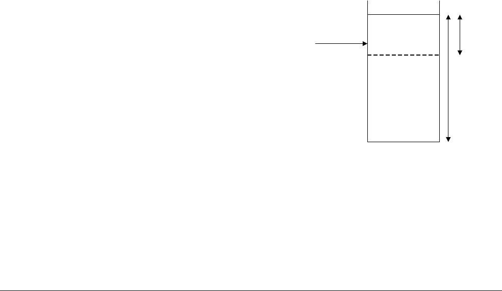
B5 Protected Memory System Architecture (PMSA)
B5.1 About the PMSA
ARM DDI 0406C.c Copyright © 1996-1998, 2000, 2004-2012, 2014 ARM. All rights reserved. B5-1757
ID051414 Non-Confidential
• If a matching memory region is found:
— The access permission bits determine whether the access is permitted. If the access is not permitted,
the MPU signals a Permission fault memory abort. Otherwise, the access proceeds. See Memory
access control on page B5-1761 for a description of the access permission bits.
— The memory region attributes determine the memory type, as described in Memory region attributes
on page B5-1762.
B5.1.2 Subregions
A region of the PMSA memory map can be split into eight equal sized, non-overlapping subregions:
• Any region size between 256bytes and 4Gbytes supports 8 subregions.
• Region sizes below 256 bytes do not support subregions.
In the Region Size Register for each region, there is a Subregion disable bit for each subregion. This means that each
subregion is either:
• Part of the region, if its Subregion disable bit is 0.
• Not part of the region, if its Subregion disable bit is 1.
If the region size is smaller than 256 bytes then all eight of the Subregion bits are UNK/SBZP.
If a subregion is part of the region then the protection and memory type attributes of the region apply to the
subregion. If a subregion is not part of the region then the addresses covered by the subregion do not match as part
of the region.
Subregions are not supported in versions of the PMSA before PMSAv7.
B5.1.3 Overlapping regions
The MPU can be programmed with two or more overlapping regions. When memory regions overlap, a fixed
priority scheme determines the region whose attributes are applied to the memory access. The higher the region
number the higher the priority. Therefore, for example, in an implementation that supports eight memory regions,
the attributes for region 7 have highest priority and those for region 0 have lowest priority.
Figure B5-1 shows a case where the MPU is programmed with overlapping memory regions.
Figure B5-1 Overlapping memory regions in the MPU
In this example:
• Data region 2 is programmed to be 4KB in size, starting from address
0x3000
with AP[2:0] ==
0b010
, giving
PL1 modes full access, and User mode read-only access.
• Data region 1 is programmed to be 16KB in size, starting from address
0x0
with AP[2:0] ==
0b001
, giving
access from PL1 modes only.
0x4000
0x3000
0x3010
Region 2
Region 1
0x0000

B5 Protected Memory System Architecture (PMSA)
B5.1 About the PMSA
B5-1758 Copyright © 1996-1998, 2000, 2004-2012, 2014 ARM. All rights reserved. ARM DDI 0406C.c
Non-Confidential ID051414
If the processor performs a data load from address
0x3010
while in User mode, the address is in both region 1 and
region 2. Region 2 has the higher priority, therefore the region 2 attributes apply to the access. This means the load
does not abort.
B5.1.4 The background region
Background region refers to a region that matches the entire 4GB physical address map, and has a lower priority
than any other region. Therefore, a background region provides the memory attributes for any memory access that
does not match any of the defined memory regions.
When the SCTLR.BR bit is set to 0, the MPU behaves as if there is a background region that generates a Background
fault memory abort on any access. This means that any memory access that does not match any of the programmed
memory regions generates a Background fault memory abort. This is the same as the behavior in PMSAv6.
If a system requires a background region with a different set of memory attributes, region 0 can be programmed as
a 4GB region with the required attributes. Because region 0 has the lowest priority this region then acts as a
background region.
Using the default memory map as a background region
The default memory map is defined in The default memory map on page B5-1759. Before PMSAv7, the default
memory map is used only to define the behavior of memory accesses when the MPU is disabled or not implemented.
From PMSAv7, when the SCTLR.BR bit is set to 1, and the MPU is present and enabled:
• The default memory map defines the background region for memory accesses from PL1, meaning that a PL1
access that does not match any of the programmed memory regions takes the properties defined for that
address in the default memory map.
• An unprivileged memory access that does not match any of the defined memory regions generates a
Background fault memory abort.
Using the default memory map as the background region means that all of the programmable memory region
definitions are available to define protection regions in the 4GB memory address space.
B5.1.5 Enabling and disabling the MPU
Software can use the SCTLR.M bit to enable and disable the MPU. On reset, this bit is cleared to 0, meaning the
MPU is disabled after a reset.
Software must program all relevant CP15 registers before enabling the MPU. This includes at least one of:
• Setting up at least one memory region.
• Setting the SCTLR.BR bit to 1, to use the default memory map as a background region, see Using the default
memory map as a background region.
The considerations described in Synchronization of changes to system control registers on page B5-1779 apply to
any change that enables or disables the MPU or the caches.
Behavior when the MPU is disabled
When the MPU is disabled:
• Instruction accesses use the default memory map and attributes shown in Table B5-1 on page B5-1759. An
access to a memory region with the Execute-never attribute generates a Permission fault, see The XN
(Execute-never) attribute and instruction fetching on page B5-1761. No other permission checks are
performed. Additional control of the cacheability is made by:
— The SCTLR.I bit if separate instruction and data caches are implemented.
— The SCTLR.C bit if unified caches are implemented.
• Data accesses use the default memory map and attributes shown in Table B5-2 on page B5-1759. No memory
access permission checks are performed, and no aborts can be generated.

B5 Protected Memory System Architecture (PMSA)
B5.1 About the PMSA
ARM DDI 0406C.c Copyright © 1996-1998, 2000, 2004-2012, 2014 ARM. All rights reserved. B5-1759
ID051414 Non-Confidential
• Program flow prediction functions as normal, controlled by the value of the SCTLR.Z bit.
• All of the CP15 cache operations work as normal.
• Speculative instruction and data fetch operations work as normal, based on the default memory map:
— Speculative data fetch operations have no effect if the data cache is disabled.
— Speculative instruction fetch operations have no effect if the instruction cache is disabled.
• The Outer memory attributes are the same as those for the Inner memory system.
The default memory map
The PMSAv7 default memory map is fixed and not configurable, and is shown in:
•Table B5-1 for the instruction access attributes
•Table B5-2 for the data access attributes.
The regions of the default memory map are identical in both tables. The information about the memory map is split
into two tables only to improve the presentation of the information.
Table B5-1 Default memory map, showing instruction access attributes
Address range HIVECS
Instruction memory type
Execute-never, XN
Caching enabledaCaching disableda
0xFFFFFFFF
-
0xF0000000
0 Not applicable Not applicable Execute-never
0xFFFFFFFF
-
0xF0000000
1bNormal, Non-cacheable Normal, Non-cacheable Execution permitted
0xEFFFFFFF
-
0xC0000000
x Not applicable Not applicable Execute-never
0xBFFFFFFF
-
0xA0000000
x Not applicable Not applicable Execute-never
0x9FFFFFFF
-
0x80000000
x Not applicable Not applicable Execute-never
0x7FFFFFFF
-
0x60000000
xNormal, Non-shareable,
Write-Through Cacheable
Normal, Non-shareable,
Non-cacheable Execution permitted
0x5FFFFFFF
-
0x40000000
xNormal, Non-shareable,
Write-Through Cacheable
Normal, Non-shareable,
Non-cacheable Execution permitted
0x3FFFFFFF
-
0x00000000
xNormal, Non-shareable,
Write-Through Cacheable
Normal, Non-shareable,
Non-cacheable Execution permitted
a. When separate instruction and data caches are implemented, caching is enabled for instruction accesses if the instruction caches are enabled.
When unified caches are implemented caching is enabled if the data or unified caches are enabled. See the descriptions of the C and I bits
in SCTLR, System Control Register, PMSA on page B6-1932.
b. ARM deprecates the use of HIVECS == 1 in PMSAv7, see Exception vectors and the exception base address on page B1-1165.
Table B5-2 Default memory map, showing data access attributes
Address range
Data memory type
Caching enabledaCaching disabled
0xFFFFFFFF
-
0xC0000000
Strongly-ordered Strongly-ordered
0xBFFFFFFF
-
0xA0000000
Shareable Device Shareable Device
0x9FFFFFFF
-
0x80000000
Non-shareable Device Non-shareable Device

B5 Protected Memory System Architecture (PMSA)
B5.1 About the PMSA
B5-1760 Copyright © 1996-1998, 2000, 2004-2012, 2014 ARM. All rights reserved. ARM DDI 0406C.c
Non-Confidential ID051414
Behavior of an implementation that does not include an MPU
If a PMSAv7 implementation does not include an MPU, it must adopt the default memory map behavior described
in Behavior when the MPU is disabled on page B5-1758.
A PMSAv7 implementation that does not include an MPU is identified by an MPU Type Register entry that shows
a Unified MPU with zero Data or Unified regions, see MPUIR, MPU Type Register, PMSA on page B6-1899.
B5.1.6 Finding the minimum supported region size
Software can use the DRBAR to find the minimum region size supported by an implementation, by following this
procedure:
1. Write a valid memory region number to the RGNR. Normally software uses region number 0, because this
is always a valid region number.
2. Write the value
0xFFFFFFFC
to the DRBAR. This value sets all valid bits in the register to 1.
3. Read back the value of the DRBAR. In the returned value the least significant bit set indicates the resolution
of the selected region. If the least significant bit set is bit M the resolution of the region is 2M bytes.
If the MPU implements separate data and instruction regions this process gives the minimum size for data regions.
To find the minimum size for instruction regions, use the same procedure with the IRBAR.
0x7FFFFFFF
-
0x60000000
Normal, Shareable, Non-cacheable Normal, Shareable, Non-cacheable
0x5FFFFFFF
-
0x40000000
Normal, Non-shareable, Write-Through Cacheable Normal, Shareable, Non-cacheable
0x3FFFFFFF
-
0x00000000
Normal, Non-shareable, Write-Back, Write-Allocate Cacheable Normal, Shareable, Non-cacheable
a. Caching is enabled for data accesses if the data or unified caches are enabled. See the description of the C bit in SCTLR, System Control
Register, PMSA on page B6-1932.
Table B5-2 Default memory map, showing data access attributes (continued)
Address range
Data memory type
Caching enabledaCaching disabled

B5 Protected Memory System Architecture (PMSA)
B5.2 Memory access control
ARM DDI 0406C.c Copyright © 1996-1998, 2000, 2004-2012, 2014 ARM. All rights reserved. B5-1761
ID051414 Non-Confidential
B5.2 Memory access control
Access to a memory region is controlled by the access permission bits for each region, held in the DRACR and
IRACR.
B5.2.1 Access permissions
Access permission bits control access to the corresponding memory region. If an access is made to an area of
memory without the required permissions, a Permission fault is generated. In the appropriate Region Access Control
Register:
• The AP bits determine the access permissions.
• The XN bit provides an additional permission bit for instruction fetches.
The access permissions are a three-bit field, DRACR.AP[2:0] or IRACR.AP[2:0]. Table B5-3 shows the possible
values of this field.
The XN (Execute-never) attribute and instruction fetching
Each memory region can be tagged as not containing executable code. If the XN bit, the Execute-never bit, is set to
1, any attempt to execute an instruction in that region results in a Permission fault, and the implementation must not
access the region to fetch instructions speculatively. If the XN bit is 0, code can execute from that memory region.
Note
The XN bit acts as an additional permission check. The address must also have a valid read access permission.
In ARMv7, all regions of memory that contain read-sensitive peripherals must be marked as XN to avoid the
possibility of a speculative fetch accessing the locations.
Table B5-3 Access permissions
AP[2:0] PL1 permissions PL0 permissions Description
000 No access No access All accesses generate a Permission fault
001 Read/Write No access All unprivileged accesses generate Permission faults
010 Read/Write Read-only User mode write accesses generate Permission faults
011 Read/Write Read/Write Full access
100 UNPREDICTABLE UNPREDICTABLE Reserved
101 Read-only No Access PL1 read-only, all other accesses generate Permission faults
110 Read-only Read-only All write accesses generate Permission faults
111 UNPREDICTABLE UNPREDICTABLE Reserved

B5 Protected Memory System Architecture (PMSA)
B5.3 Memory region attributes
B5-1762 Copyright © 1996-1998, 2000, 2004-2012, 2014 ARM. All rights reserved. ARM DDI 0406C.c
Non-Confidential ID051414
B5.3 Memory region attributes
Each memory region has an associated set of memory region attributes. These control the memory type, accesses to
the caches, and whether the memory region is Shareable and therefore must be kept coherent. These attributes are
encoded in the C, B, TEX[2:0] and S bits of the appropriate Region Access Control Register.
Note
The Bufferable (B), Cacheable (C), and Type Extension (TEX) bit names are inherited from earlier versions of the
architecture. These names no longer adequately describe the function of the B, C, and TEX bits.
The following sections give more information:
•C, B, and TEX[2:0] encodings
•Programming the MPU region attributes on page B5-1763
•Cache maintenance requirement created by changing MPU region attributes on page B5-1764.
B5.3.1 C, B, and TEX[2:0] encodings
The TEX[2:0] field must be considered with the C and B bits to give a five bit encoding of the access attributes for
an MPU memory region. Table B5-4 shows these encodings.
For Normal memory regions, the S (Shareable) bit gives more information about whether the region is Shareable.
A Shareable region can be shared by multiple processors. A Normal memory region is Shareable if the S bit for the
region is set to 1. For other memory types, the value of the S bit is ignored.
Table B5-4 C, B and TEX[2:0] encodings
TEX[2:0] C B Description Memory type Shareable?
000 0 0 Strongly-ordered Strongly-ordered Shareable
000 0 1 Shareable Device Device Shareable
000 1 0 Outer and Inner Write-Through, no Write-Allocate Normal S bita
000 1 1 Outer and Inner Write-Back, no Write-Allocate Normal S bita
001 0 0 Outer and Inner Non-cacheable Normal S bita
001 0 1 Reserved - -
001 1 0 IMPLEMENTATION DEFINED IMP. DEF.bIMP. DEF.b
001 1 1 Outer and Inner Write-Back, Write-Allocate Normal S bita
010 0 0 Non-shareable Device Device Non-shareable
010 0 1 Reserved - -
010 1 x Reserved - -
011 x x Reserved - -
1BB A A Cacheable memory: AA = Inner attributec
BB = Outer policy
Normal S bita
a. Region is Shareable if S == 1, and Non-shareable if S == 0. See DRACR, Data Region Access Control Register, PMSA
on page B6-1840 and IRACR, Instruction Region Access Control Register, PMSA on page B6-1887.
b. IMP. DEF. = IMPLEMENTATION DEFINED.
c. For more information see Cacheable memory attributes on page B5-1763.

B5 Protected Memory System Architecture (PMSA)
B5.3 Memory region attributes
ARM DDI 0406C.c Copyright © 1996-1998, 2000, 2004-2012, 2014 ARM. All rights reserved. B5-1763
ID051414 Non-Confidential
For an explanation of Normal, Strongly-ordered and Device memory types, and the Shareable attribute, see Memory
types and attributes and the memory order model on page A3-126.
Cacheable memory attributes
When TEX[2] == 1, the memory region is Cacheable memory, and the rest of the encoding defines the Inner and
Outer cache attributes:
TEX[1:0] defines the Outer cache attribute
C, B defines the Inner cache attribute
The same encoding is used for the Outer and Inner cache attributes. Table B5-5 shows the encoding.
B5.3.2 Programming the MPU region attributes
When the PMSA is implemented, software uses CP15 registers to configure the MPU memory regions. There are
three registers for each memory region supported by the MPU:
• A Base Address Register, that defines the start address of the region in the memory map.
• A Region Size and Enable Register, that:
— Has a single enable bit for the region.
— Defines the size of the region.
— Has a disable bit for each of the eight subregions in the region.
• A Region Access Control Register that defines the memory attributes for the region.
The multiple copies of these registers map onto three or six registers in CP15 c6, and the MPU Region Number
Register, RGNR, selects the current memory region. The mapping of the region registers onto the CP15 registers
depends on whether the MPU implements a unified memory map, or separate Instruction and Data memory maps:
Separate Instruction and Data memory maps
The multiple copies of the registers that describe each memory region map onto six CP15 registers:
• For the memory regions in the Instruction memory map:
— The multiple Region Base Address Registers map onto the Instruction Region Base
Address Register, IRBAR.
— The multiple Region Size and Enable Registers map onto the Instruction Region Size
and Enable Register, IRSR.
— The multiple Region Access Control Registers map onto the Instruction Region
Access Control Register, IRACR.
• For the memory regions in the Data memory map:
— The multiple Region Base Address Registers map onto the Data Region Base Address
Register, DRBAR.
— The multiple Region Size and Enable Registers map onto the Data Region Size and
Enable Register, DRSR.
— The multiple Region Access Control Registers map onto the Data Region Access
Control Register, DRACR.
Table B5-5 Inner and Outer cache attribute encoding
Memory attribute encoding Cache attribute
00 Non-cacheable
01 Write-Back, Write-Allocate
10 Write-Through, no Write-Allocate
11 Write-Back, no Write-Allocate

B5 Protected Memory System Architecture (PMSA)
B5.3 Memory region attributes
B5-1764 Copyright © 1996-1998, 2000, 2004-2012, 2014 ARM. All rights reserved. ARM DDI 0406C.c
Non-Confidential ID051414
The value in the RGNR is the index value for both the instruction region and the data region
registers. The RGNR value indicates the current memory region for both the instruction and the data
memory maps. However, a particular value might not be valid for both memory maps.
Unified memory maps
The multiple copies of the registers that describe each memory region map onto three CP15
registers:
• The multiple Region Base Address Registers map onto the Data Region Base Address
Register, DRBAR.
• The multiple Region Size and Enable Registers map onto the Data Region Size and Enable
Register, DRSR.
• The multiple Region Access Control Registers map onto the Data Region Access Control
Register, DRACR.
The IRBAR, IRSR, and IRACR are not implemented, and their encodings are reserved.
The value in the RGNR is the index value for the data region registers. Its value indicates the current
memory region in the unified memory map.
The read-only MPUIR indicates:
• Whether the MPU implements separate Instruction and Data address maps, or a Unified address map.
• The number of Data or Unified regions the MPU supports.
• If separate Instruction and Data address maps are implemented, the number of Instruction regions the MPU
suppor1ts.
Table B5-6 summarizes the register implementations for unified and separate memory maps.
B5.3.3 Cache maintenance requirement created by changing MPU region attributes
If a change to the MPU region attributes affects the cacheability attributes of a memory region, including any change
between Write-Through and Write-Back attributes, software must ensure that any cached copies of affected
locations are removed from the caches, typically by cleaning and invalidating the locations from the levels of cache
that might hold copies of the locations affected by the attribute change. Any of the following changes to the inner
cacheability or outer cacheability attribute creates this maintenance requirement:
• Write-Back to Write-Through.
• Write-Back to Non-cacheable.
• Write-Through to Non-cacheable.
• Write-Through to Write-Back.
The cache clean and invalidate avoids any possible coherency errors caused by mismatched memory attributes.
Similarly, to avoid possible coherency errors caused by mismatched memory attributes, the following sequence
must be followed when changing the shareability attributes of a cacheable memory location:
1. Make the memory location Non-cacheable, Outer Shareable.
2. Clean and invalidate the location from them cache.
3. Change the shareability attributes to the required new values.
Table B5-6 Memory region registers
Register All implementations Separate memory mapsa
a. These additional registers are implemented only if the MPU implements separate Instruction and Data memory maps.
Base Address DRBAR IRBAR
Size and Enable DRSR IRSR
Access Control DRACR IRACR

B5 Protected Memory System Architecture (PMSA)
B5.4 PMSA memory aborts
ARM DDI 0406C.c Copyright © 1996-1998, 2000, 2004-2012, 2014 ARM. All rights reserved. B5-1765
ID051414 Non-Confidential
B5.4 PMSA memory aborts
In a PMSAv7 implementation, the following mechanisms cause a processor to take an exception on a failed memory
access:
Debug exception An exception caused by the debug configuration, see About debug exceptions on
page C4-2090.
Alignment fault An Alignment fault is generated if the address used for a memory access does not have the
required alignment for the operation. For more information see Unaligned data access on
page A3-108 and Alignment faults.
MPU fault The MPU detects an access restriction generates an exception.
External abort A memory system component other than the MPU signals an illegal or faulting external
memory access.
Collectively, these mechanisms are called aborts. Chapter C4 Debug Exceptions describes Debug exceptions, and
the remainder of this section describes Alignment faults, MPU faults, and External aborts.
The exception generated on a synchronous memory abort:
• On an instruction fetch is called the Prefetch Abort exception.
• On a data access is called the Data Abort exception.
Note
The Prefetch Abort exception applies to any synchronous memory abort on an instruction fetch. It is not restricted
to speculative instruction fetches.
In the ARM architecture, asynchronous memory aborts are a type of External abort, and are treated as a special type
of Data Abort exception.
The following sections describe the different abort mechanisms:
•Alignment faults.
•MPU faults on page B5-1766.
•External aborts on page B5-1767.
An access that causes an abort is said to be aborted, and uses the Fault Address Registers (FARs) and Fault Status
Registers (FSRs) to record context information. The FARs and FSRs are described in Exception reporting in a
PMSA implementation on page B5-1769.
B5.4.1 Alignment faults
The ARMv7 memory architecture requires support for strict alignment checking. This checking is controlled by the
SCTLR.A bit. Unaligned data access on page A3-108 defines when Alignment faults are generated, for both values
of SCTLR.A.
Alignment faults can occur when the MPU is disabled.
Note
In some documentation, including issues A and B of this manual, Alignment faults are classified as a type of MPU
fault. However, the behavior of Alignment faults differs, in a number of ways, from the behavior of MPU faults.
This change in the classification of Alignment faults has no effect on their behavior.

B5 Protected Memory System Architecture (PMSA)
B5.4 PMSA memory aborts
B5-1766 Copyright © 1996-1998, 2000, 2004-2012, 2014 ARM. All rights reserved. ARM DDI 0406C.c
Non-Confidential ID051414
B5.4.2 MPU faults
The MPU checks the memory accesses required for instruction fetches and for explicit memory accesses:
• If an instruction fetch faults it generates a Prefetch Abort exception.
• If an explicit memory access faults it generates a Data Abort exception.
For more information about Prefetch Abort exceptions and Data Abort exceptions see Exception handling on
page B1-1165.
MPU faults are always synchronous. For more information, see Terminology for describing exceptions on
page B1-1137.
When the MPU generates an abort for a region of memory, no memory access is made if that region is or could be
marked as Strongly-ordered or Device.
The following subsections describe the types of fault the MPU can generate:
•Background fault.
•Permission fault.
The MPU fault checking sequence on page B5-1767 describes the fault checking sequence.
Background fault
If the memory access address does not match one of the programmed MPU memory regions, and the default
memory map is not being used, a Background fault memory abort is generated.
Background faults cannot occur on any cache or branch predictor maintenance operation.
Permission fault
The access permissions, defined in Memory access control on page B5-1761, are checked against the processor
memory access. If the access is not permitted, a Permission fault memory abort is generated.
In a PMSA implementation, Permission faults cannot occur on cache or branch predictor maintenance operation.
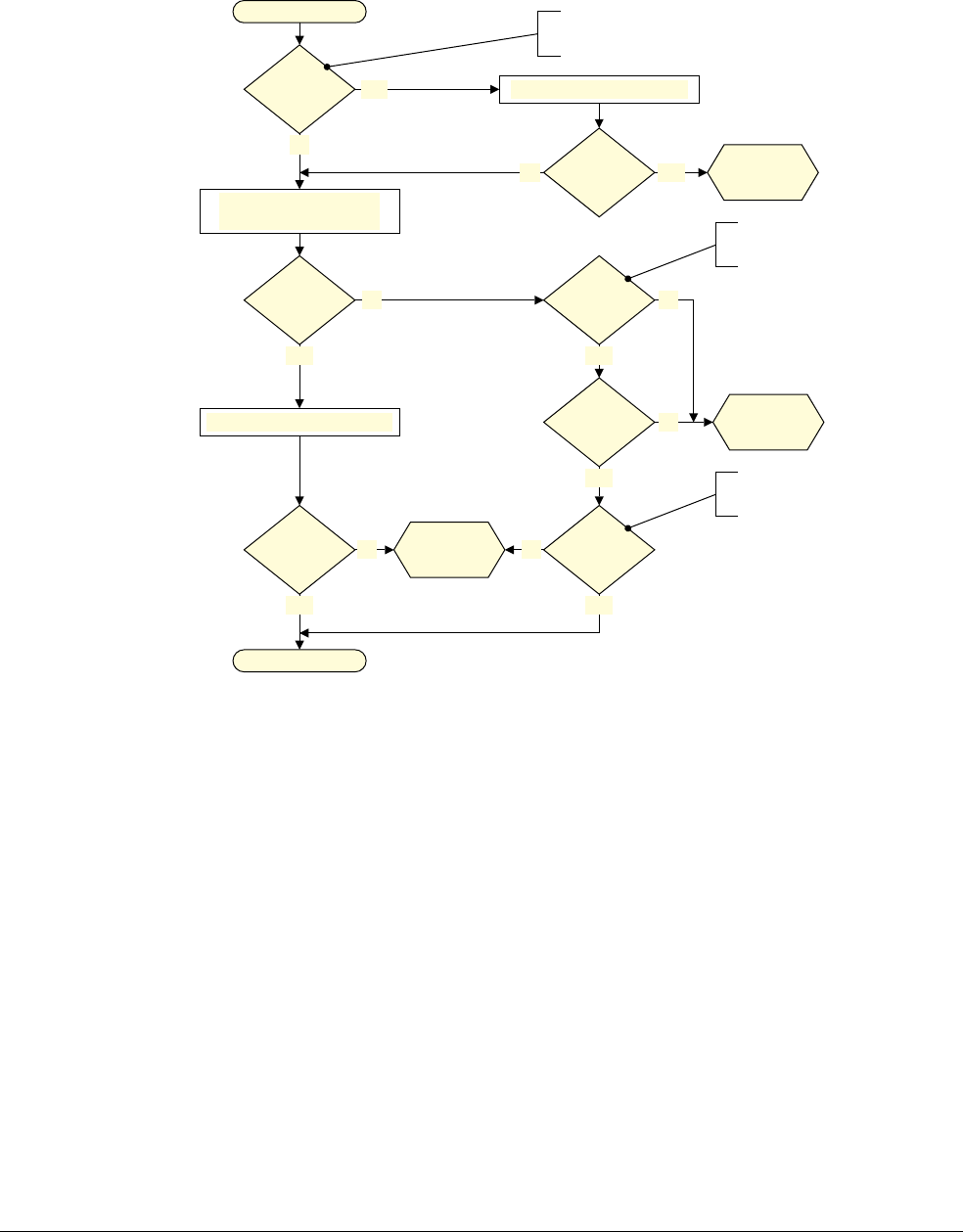
B5 Protected Memory System Architecture (PMSA)
B5.4 PMSA memory aborts
ARM DDI 0406C.c Copyright © 1996-1998, 2000, 2004-2012, 2014 ARM. All rights reserved. B5-1767
ID051414 Non-Confidential
The MPU fault checking sequence
Figure B5-2 shows the MPU fault checking sequence, when the MPU is enabled.
Figure B5-2 MPU fault checking sequence
B5.4.3 External aborts
External memory errors are defined as errors that occur in the memory system other than those that are detected by
the MPU or Debug hardware. They include parity errors detected by the caches or other parts of the memory system.
An external abort is one of:
• Synchronous.
• Precise asynchronous.
• Imprecise asynchronous.
For more information, see Terminology for describing exceptions on page B1-1137.
The ARM architecture does not provide a method to distinguish between precise asynchronous and imprecise
asynchronous aborts.
The ARM architecture handles asynchronous aborts in a similar way to interrupts, except that they are reported to
the processor using the Data Abort exception. Setting the CPSR.A bit to 1 masks asynchronous aborts, see Program
Status Registers (PSRs) on page B1-1147.
Normally, external aborts are rare. An imprecise asynchronous external abort is likely to be fatal to the process that
is running. An example of an event that might cause an external abort is an uncorrectable parity or ECC failure on
a Level 2 memory structure.
It is IMPLEMENTATION DEFINED which external aborts, if any, are supported.
Memory address
Alignment
check? Check address alignmentYes
Does the access require
an alignment check?
No
Check address is in a
defined memory region
No
Address
in a region
?
No
Is use of default memory map as
a Background region enabled?
Permission
fault
Valid
permissions
?
No No Execution
permitted
?
Misaligned
?
Alignment
fault
Yes
Background
region
?
PL1
access
?
Yes
Background
fault
No
No
Yes
Yes
Yes
Access memory
Yes
Is access to an XN area in
the Background region?
Check access permissions

B5 Protected Memory System Architecture (PMSA)
B5.4 PMSA memory aborts
B5-1768 Copyright © 1996-1998, 2000, 2004-2012, 2014 ARM. All rights reserved. ARM DDI 0406C.c
Non-Confidential ID051414
PMSAv7 permits external aborts on data accesses and instruction fetches to be either synchronous or asynchronous.
The DFSR indicates whether the external abort is synchronous or asynchronous.
Note
Because imprecise asynchronous external aborts are normally fatal to the process that caused them, ARM
recommends that implementations make external aborts precise wherever possible.
More information about possible external aborts is given in the subsections:
•External abort on instruction fetch.
•External abort on data read or write.
•Parity error reporting.
For information about how external aborts are reported see Exception reporting in a PMSA implementation on
page B5-1769.
External abort on instruction fetch
An external abort on an instruction fetch can be either synchronous or asynchronous. A synchronous external abort
on an instruction fetch is taken precisely.
An implementation can report the external abort asynchronously from the instruction that it applies to. In such an
implementation these aborts behave essentially as interrupts. They are masked by the CPSR.A bit when it is set to
1, otherwise they are reported using the Data Abort exception.
External abort on data read or write
Externally generated errors during a data read or write can be either synchronous or asynchronous.
An implementation can report the external abort asynchronously from the instruction that generated the access. In
such an implementation these aborts behave essentially as interrupts. They are masked by the CPSR.A bit when it
is set to 1, otherwise they are reported using the Data Abort exception.
Parity error reporting
The ARM architecture supports the reporting of both synchronous and asynchronous parity errors from the cache
systems. It is IMPLEMENTATION DEFINED what parity errors in the cache systems, if any, result in synchronous or
asynchronous parity errors.
A fault status code is defined for reporting parity errors, see Exception reporting in a PMSA implementation on
page B5-1769. However when parity error reporting is implemented it is IMPLEMENTATION DEFINED whether the
assigned fault status code or another appropriate encoding is used for reporting parity errors.
For all purposes other than the fault status encoding, parity errors are treated as external aborts.
B5.4.4 Prioritization of aborts
The prioritization of synchronous aborts generated by different memory accesses from the same instruction is
IMPLEMENTATION DEFINED. In general, the ARM architecture does not define when asynchronous events are taken,
and therefore the prioritization of asynchronous events is IMPLEMENTATION DEFINED.
Note
Debug event prioritization on page C3-2078 describes:
• The relationship between debug events, MPU faults, and external aborts. for synchronous aborts generated
by the same memory access.
• The special requirement that applies to asynchronous watchpoints.

B5 Protected Memory System Architecture (PMSA)
B5.5 Exception reporting in a PMSA implementation
ARM DDI 0406C.c Copyright © 1996-1998, 2000, 2004-2012, 2014 ARM. All rights reserved. B5-1769
ID051414 Non-Confidential
B5.5 Exception reporting in a PMSA implementation
This section describes the Fault Status and Fault Address registers, and how they report information about PMSA
aborts. It contains the following subsections:
•About the Fault Status and Fault Address registers
•Data Abort exceptions
•Prefetch Abort exceptions on page B5-1771
•Fault Status Register encodings for the PMSA on page B5-1771
•Provision for classification of external aborts on page B5-1772
•Auxiliary Fault Status Registers on page B5-1773.
Also, these registers are used for reporting information about debug exceptions. For more information see Data
Abort exceptions and Prefetch Abort exceptions on page B5-1771.
B5.5.1 About the Fault Status and Fault Address registers
PMSAv7 provides four registers for reporting fault address and status information:
• The Data Fault Status Register (DFSR) is updated on taking a Data Abort exception.
• The Instruction Fault Status Register (IFSR) is updated on taking a Prefetch Abort exception.
• The Data Fault Address Register (DFAR). In some cases, on taking a synchronous Data Abort exception the
DFAR is updated with the faulting address. See Terminology for describing exceptions on page B1-1137 for
a description of synchronous exceptions.
• The Instruction Fault Address Register (IFAR) is updated with the faulting address on taking a Prefetch Abort
exception.
In addition, the architecture provides encodings for two IMPLEMENTATION DEFINED Auxiliary Fault Status
Registers, see Auxiliary Fault Status Registers on page B5-1773.
Note
Before ARMv7, the Data Fault Address Register was called the Fault Address Register (FAR).
On a Watchpoint debug exception, the Watchpoint Fault Address Register (DBGWFAR) holds fault information.
On a watchpoint access the DBGWFAR is updated with the address of the instruction that generated the Data Abort
exception.
B5.5.2 Data Abort exceptions
On taking a Data Abort exception, if the exception is generated by a Watchpoint debug event, then its reporting
depends on whether the Watchpoint debug event is synchronous or asynchronous, and on the Debug architecture
version. For more information, see Data Abort exception on a Watchpoint debug event on page B5-1770.
Otherwise:
• The DFSR is updated with details of the fault, including the appropriate fault status code.
If the Data Abort exception is synchronous, DFSR.WnR is updated to indicate whether the faulted access was
caused by a read instruction or by a write instruction. However, if the fault is:
— On a cache maintenance operation, WnR is set to 1, to indicate a write access fault.
— Generated by an
SWP
or
SWPB
instruction, WnR is set to 0 if a read of the location would have generated
a fault, otherwise it is set to 1.
• If the Data Abort exception is:
— Synchronous, the DFAR is updated with the address that caused the Data Abort exception.
— Asynchronous, the DFAR becomes UNKNOWN.

B5 Protected Memory System Architecture (PMSA)
B5.5 Exception reporting in a PMSA implementation
B5-1770 Copyright © 1996-1998, 2000, 2004-2012, 2014 ARM. All rights reserved. ARM DDI 0406C.c
Non-Confidential ID051414
On any access that might have multiple aborts, the MPU fault checking sequence and the prioritization of aborts
determine which abort occurs. For more information, see The MPU fault checking sequence on page B5-1767 and
Prioritization of aborts on page B5-1768.
Data Abort exception on a Watchpoint debug event
On taking a Data Abort exception caused by a Watchpoint debug event, DFSR.FS is updated to indicate a debug
event, and DFSR.WnR is UNKNOWN.
The remaining register updates depend on the Debug architecture version, and in v7.1 debug, on whether the
Watchpoint debug event is synchronous or asynchronous:
v7 Debug, and for an asynchronous Watchpoint debug event in v7.1 Debug
•DFAR is UNKNOWN.
•DBGWFAR is set to the VA of the instruction that caused the watchpointed access, plus an
offset that depends on the instruction set state of the processor for that instruction, as follows:
— 8 for ARM state.
— 4 for Thumb or ThumbEE state.
—IMPLEMENTATION DEFINED for Jazelle state.
v7.1 Debug, for a synchronous Watchpoint debug event
•DFAR is set to the address that generated the watchpoint.
•DBGWFAR is UNKNOWN.
A watchpointed address can be any byte-aligned address. The address reported in DFAR might not
be the watchpointed address, and can be any address between and including:
• The lowest address accessed by the instruction that triggered the watchpoint.
• The highest watchpointed address accessed by that instruction.
If multiple watchpoints are set in this range, there is no guarantee of which watchpoint is generated.
Note
In particular, there is no guarantee of generating the watchpoint with the lowest address in the range.
In addition, it is IMPLEMENTATION DEFINED whether there is an additional restriction on the lowest
value that might be reported in the DFAR, see Synchronous Watchpoint debug event additional
restriction on DFAR or HDFAR reporting, v7.1 Debug on page B3-1413.
Note
For a synchronous Watchpoint debug event:
• In v7 Debug, both LR_abt and DBGWFAR indicate the address of the instruction that triggered the
watchpoint, and ARM deprecates using DBGWFAR to determine the address of this instruction.
• In v7.1 Debug, only LR_abt indicates the address of the instruction that triggered the watchpoint

B5 Protected Memory System Architecture (PMSA)
B5.5 Exception reporting in a PMSA implementation
ARM DDI 0406C.c Copyright © 1996-1998, 2000, 2004-2012, 2014 ARM. All rights reserved. B5-1771
ID051414 Non-Confidential
B5.5.3 Prefetch Abort exceptions
For a Prefetch Abort exception generated by an instruction fetch, the Prefetch Abort exception is taken
synchronously with the instruction that the abort is reported on. This means:
• If the processor attempts to execute the instruction a Prefetch Abort exception is generated.
• If the instruction fetch is issued but the processor does not attempt to execute the instruction, no Prefetch
Abort exception is generated for that instruction. For example, if the processor branches round a prefetched
instruction no Prefetch Abort exception is generated.
On taking a Prefetch Abort exception:
• The IFSR is updated with details of the fault, including the appropriate fault code. If appropriate, the fault
code indicates that the exception was generated by a debug exception. See the register description for more
information about the returned fault information.
• For a Prefetch Abort exception generated by an instruction fetch, the IFAR is updated with the VA that caused
the exception.
• For a Prefetch Abort exception generated by a debug exception, the IFAR is UNKNOWN.
B5.5.4 Fault Status Register encodings for the PMSA
For the PMSA fault status encodings in priority order see:
•Table B5-7 for the IFSR encodings
•Table B5-8 on page B5-1772 for the DFSR encodings.
Table B5-7 PMSAv7 IFSR encodings
IFSR[10, 3:0]aSources IFAR Notes
00001 Alignment fault Valid -
00000 Background fault Valid MPU fault
01101 Permission fault Valid MPU fault
00010 Debug event that generates a Prefetch Abort exception UNKNOWN See About debug events on page C3-2038
01000 Synchronous external abort Valid -
10100 IMPLEMENTATION DEFINED - Lockdown
11010 IMPLEMENTATION DEFINED - Coprocessor abort
11001 Memory access synchronous parity error Valid -
a. All IFSR[10, 3:0] values not listed in this table are reserved.

B5 Protected Memory System Architecture (PMSA)
B5.5 Exception reporting in a PMSA implementation
B5-1772 Copyright © 1996-1998, 2000, 2004-2012, 2014 ARM. All rights reserved. ARM DDI 0406C.c
Non-Confidential ID051414
Note
In previous ARM documentation, the terms precise and imprecise were used instead of synchronous and
asynchronous. For details of the more exact terminology introduced in this manual see Terminology for describing
exceptions on page B1-1137.
Reserved encodings in the IFSR and DFSR encodings tables
A single encoding is reserved for cache lockdown faults. The details of these faults and any associated subsidiary
registers are IMPLEMENTATION DEFINED.
A single encoding is reserved for aborts associated with coprocessors. The details of these faults are
IMPLEMENTATION DEFINED.
B5.5.5 Provision for classification of external aborts
An implementation can use the DFSR.ExT and IFSR.ExT bits to provide more information about external aborts:
•DFSR.ExT can provide an IMPLEMENTATION DEFINED classification of external aborts on data accesses.
•IFSR.ExT can provide an IMPLEMENTATION DEFINED classification of external aborts on instruction accesses.
For all aborts other than external aborts these bits return a value of 0.
Table B5-8 PMSAv7 DFSR encodings
DFSR[10, 3:0]aSources DFAR Notes
00001 Alignment fault Valid -
00000 Background fault Valid MPU fault
01101 Permission fault Valid MPU fault
00010 Synchronous Watchpoint debug eventbv7 Debug UNKNOWN See About debug events on
page C3-2038
v7.1 Debug Valid
Asynchronous Watchpoint debug eventbUNKNOWN
01000 Synchronous external abort Valid -
10100 IMPLEMENTATION DEFINED - Lockdown
11010 IMPLEMENTATION DEFINED - Coprocessor abort
11001 Memory access synchronous parity error c-
10110 Asynchronous external abort UNKNOWN -
11000 Memory access asynchronous parity error UNKNOWN -
a. All DFSR[10, 3:0] values not listed in this table are reserved.
b. These are the only debug events that generate a Data Abort exception.
c. It is IMPLEMENTATION DEFINED whether the DFAR is updated for a synchronous parity error.

B5 Protected Memory System Architecture (PMSA)
B5.5 Exception reporting in a PMSA implementation
ARM DDI 0406C.c Copyright © 1996-1998, 2000, 2004-2012, 2014 ARM. All rights reserved. B5-1773
ID051414 Non-Confidential
B5.5.6 Auxiliary Fault Status Registers
ARMv7 architects two Auxiliary Fault Status Registers, described as the AxFSRs:
• The Auxiliary Data Fault Status Register (ADFSR).
• The Auxiliary Instruction Fault Status Register (AIFSR).
These registers enable additional fault status information to be returned:
• The position of these registers is architecturally-defined, but the content and use of the registers is
IMPLEMENTATION DEFINED.
• An implementation that does not need to report additional fault information must implement these registers
as UNK/SBZP. This ensures that an attempt to access these registers from PL1 is not faulted.
An example use of these registers would be to return more information for diagnosing parity errors.

B5 Protected Memory System Architecture (PMSA)
B5.6 About the system control registers for PMSA
B5-1774 Copyright © 1996-1998, 2000, 2004-2012, 2014 ARM. All rights reserved. ARM DDI 0406C.c
Non-Confidential ID051414
B5.6 About the system control registers for PMSA
On an ARMv7-A or ARMv7-R implementation, the control registers comprise:
• The registers accessed using the System Control Coprocessor, CP15.
• Registers accessed using the CP14 coprocessor, including:
— Debug registers.
— Trace registers.
— Execution environment registers.
Organization of the CP14 registers in a PMSA implementation on page B5-1786 summarizes the CP14 registers,
and indicates where the CP14 registers are described, either in this manual or in other architecture specifications.
Organization of the CP15 registers in a PMSA implementation on page B5-1787 summarizes the CP15 registers,
and indicates where in this manual the CP15 registers are described.
This section gives general information about the control registers, the CP14 and CP15 interfaces to these registers,
and the conventions used in describing these registers.
Note
Many implementations include other interfaces to some functional groups of CP14 and CP15 registers, for example,
memory-mapped interfaces to the CP14 Debug registers. These are described in the appropriate sections of this
manual.
This section is organized as follows:
•About system control register accesses.
•General behavior of system control registers on page B5-1776.
•Synchronization of changes to system control registers on page B5-1779.
•Meaning of fixed bit values in register bit assignment diagrams on page B5-1785.
B5.6.1 About system control register accesses
In a PMSAv7 implementation that does not include the OPTIONAL Generic Timer, all control registers are 32-bits
wide. Accessing 32-bit control registers on page B5-1775 describes how these registers are accessed.
A PMSA implementation that includes the OPTIONAL Generic Timer must also implement a small number of 64-bit
control registers. Accessing 64-bit control registers on page B5-1775 describes how these registers are accessed.
Note
• In addition, the Large Physical Address Extension and the Virtualization Extensions introduce a small
number of 64-bit control registers to the processor implementation. and to the associated debug
implementation. A PMSA implementation cannot include these extensions.
• Optionally, an ARMv6 implementation can include some block transfer operations that are accessed using
64-bit CP15 accesses, see Block transfer operations on page D12-2536.
When using the
MCR
and
MRC
instructions to access these registers, the instruction arguments include:
• A coprocessor identifier, coproc, as a value p0-p15, corresponding to CP0-CP15.
• A coprocessor register, CRn, as a value c0-c15, to specify a coprocessor register number.
• An opcode, opc1, as a value in the range 0-7.
Note
• When accessing CP15, the primary coprocessor register is the top-level indicator of the accessed
functionality, and when using an
MCR
or
MRC
instruction, CRn specifies the primary coprocessor register.
• When accessing CP14 using these instructions, opc1 is the top-level indicator of the accessed functionality.

B5 Protected Memory System Architecture (PMSA)
B5.6 About the system control registers for PMSA
ARM DDI 0406C.c Copyright © 1996-1998, 2000, 2004-2012, 2014 ARM. All rights reserved. B5-1775
ID051414 Non-Confidential
Ordering of reads of system control registers
Reads of the system control registers can occur out of order with respect to earlier instructions executed on the same
processor, provided that the data dependencies between the instructions, specified in Synchronization of changes to
system control registers on page B5-1779, are met.
Note
In particular, system control registers holding self-incrementing counts, for example the Performance Monitors
counters or the Generic Timer counter or timers, can be read early. This means that, for example, if a memory
communication is used to communicate a read of the Generic Timer counter, an
ISB
must be inserted between the
read of the memory location used for this communication and the read of the Generic Timer counter if it is required
that the Generic Timer counter returns a count value that is later than the memory communication.
Accessing 32-bit control registers
Software accesses a 32-bit control register using the generic
MCR
and
MRC
coprocessor interface, specifying:
• A coprocessor identifier, coproc, identifying one of the coprocessors CP0-CP15.
• Two coprocessor registers, CRn and CRm. CRn specifies the primary coprocessor register.
• Two coprocessor-specific opcodes, opc1 and opc2.
• An ARM core register to hold a 32-bit value to transfer to or from the coprocessor.
CP15 and CP14 provides the control registers. A processor access to a specific 32-bit control register uses:
• p15 to specify CP15, or p14 to specify CP14.
• A unique combination of CRn, opc1, CRm, and opc2, to specify the required control register.
• An ARM core register for the transferred 32-bit value.
The processor accesses a 32-bit control register using:
•An
MCR
instruction to write to a control register, see MCR, MCR2 on page A8-476.
•An
MRC
instruction to read a control register, see MRC, MRC2 on page A8-492.
Accessing 64-bit control registers
As indicated at the start of this section, a PMSA implementation includes 64-bit control registers only if it includes
the OPTIONAL Generic Timer.
Software accesses a 64-bit control register using the generic
MCRR
and
MRRC
coprocessor interface, specifying:
• A coprocessor identifier, coproc, identifying one of coprocessors CP0-CP15.
• A coprocessor register, CRm. In this case, CRm specifies the primary coprocessor register.
• A single coprocessor-specific opcode, opc1.
• Two ARM core registers to hold two 32-bit values to transfer to or from the coprocessor.
CP15 and CP14 provide the control registers. A processor access to a specific 64-bit control register uses:
• p15 to specify CP15, or p14 to specify CP14.
• A unique combination of CRm and opc1, to specify the required 64-bit system control register.
• Two ARM core registers, each holding 32 bits of the value to transfer.
Therefore, processor accesses a 64-bit control register using:
•An
MCRR
instruction to write to a control register, see MCRR, MCRR2 on page A8-478.
•An
MRRC
instruction to read a control register, see MRRC, MRRC2 on page A8-494.
When using a
MCRR
or
MRRC
instruction:
• Rt contains the least-significant 32 bits of the transferred value, and Rt2 contains the most-significant 32 bits
of that value.
• The access is 64-bit atomic.

B5 Protected Memory System Architecture (PMSA)
B5.6 About the system control registers for PMSA
B5-1776 Copyright © 1996-1998, 2000, 2004-2012, 2014 ARM. All rights reserved. ARM DDI 0406C.c
Non-Confidential ID051414
B5.6.2 General behavior of system control registers
Except where indicated, system control registers are 32-bits wide. As stated in About system control register
accesses on page B5-1774, there are some 64-bit registers, and these include cases where software can access either
a 32-bit view or a 64-bit view of a register. The register summaries, and the individual register descriptions, identify
the 64-bit registers and how they can be accessed.
The following sections give information about the general behavior of these registers. Unless otherwise indicated,
information applies to both CP14 and CP15 registers:
•Read-only bits in read/write registers.
•UNPREDICTABLE and UNDEFINED behavior for CP14 and CP15 accesses.
•Reset behavior of CP14 and CP15 registers on page B5-1778.
See also About system control register accesses on page B5-1774 and Meaning of fixed bit values in register bit
assignment diagrams on page B5-1785.
Read-only bits in read/write registers
Some read/write registers include bits that are read-only. These bits ignore writes.
An example of this is the SCTLR.NMFI bit, bit[27].
UNPREDICTABLE and UNDEFINED behavior for CP14 and CP15 accesses
In PMSAv7 the following operations are UNDEFINED:
•All
CDP
,
LDC
and
STC
operations to CP14 and CP15, except for the
LDC
access to DBGDTRTXint and the
STC
access to DBGDTRRXint specified in CP14 debug register interface accesses on page C6-2124.
•All
MCRR
and
MRRC
operations to CP14 and CP15, except for those explicitly defined as accessing 64-bit CP14
and CP15 registers.
•All
CDP2
,
MCR2
,
MRC2
,
MCRR2
,
MRRC2
,
LDC2
,
LDCL
,
LDC2L
,
STC2
,
STCL
and
STC2L
operations to CP14 and CP15.
Unless otherwise indicated in the individual register descriptions:
• Reserved fields in registers are UNK/SBZP.
• Assigning a reserved value to a field can have an UNPREDICTABLE effect.
The following subsections give more information about UNPREDICTABLE and UNDEFINED behavior for CP14 and
CP15 accesses:
•Accesses to unallocated CP14 and CP15 encodings.
•Additional rules for MCR and MRC accesses to CP14 and CP15 registers on page B5-1777.
Accesses to unallocated CP14 and CP15 encodings
The general rules for the behavior of accesses to unallocated register encodings are similar for CP14 and CP15, but
because the primary register specifier is different for CP14 and CP15, the details differ. Therefore, the rules are:
For CP14 For any
MCR
or
MRC
access to CP14, the opc1 value for the instruction is the primary specifier for the
functional group of registers accessed, see Organization of the CP14 registers in a PMSA
implementation on page B5-1786. Accesses to unallocated functional groups of registers are
UNDEFINED. This means any access with
<opc1>
=={2, 3, 4, 5} is UNDEFINED.
For
MCR
or
MRC
accesses to an allocated functional group of registers, the behavior of accesses to
unallocated registers in the functional group depends on the group:
opc1==0, Debug registers
The behavior of accesses to unallocated registers depends on the Debug architecture
version, see:
•Access to unallocated CP14 debug register encodings, v7 Debug on
page C6-2138

B5 Protected Memory System Architecture (PMSA)
B5.6 About the system control registers for PMSA
ARM DDI 0406C.c Copyright © 1996-1998, 2000, 2004-2012, 2014 ARM. All rights reserved. B5-1777
ID051414 Non-Confidential
•Access to unallocated CP14 debug register encodings, v7.1 Debug on
page C6-2148.
opc1==1, Trace registers
See the appropriate trace architecture specification for the behavior of CP14 accesses to
unallocated Trace registers.
opc1=={6, 7}, ThumbEE and Jazelle registers
Accesses to unallocated register encodings are UNPREDICTABLE.
Note
The opc1==7 functional group, the Jazelle registers, can include registers that are
defined by the Jazelle subarchitecture.
For CP15 For
an MCR
or
MRC
access to CP15, the CRn value for the instruction is the primary register specifier
for the CP15 space, and the following rules define the behavior of accesses to unallocated
encodings:
1. Accesses to unallocated primary registers are UNDEFINED. For the ARMv7-R Architecture,
this means that:
• For any ARMv7-R implementation, accesses to CP15 primary registers {c2, c3,
c4, c8, c10, c12} are UNDEFINED.
• For an implementation that does not include the Generic Timer Extension, accesses to
CP15 primary register c14 are UNDEFINED.
See rule 3 for the behavior of accesses to CP15 primary register c15.
2. In an allocated CP15 primary register,
MCR
and
MRC
accesses to all unallocated encodings are
UNPREDICTABLE for accesses at PL1.
This means that any
MCR
and
MRC
accesses from PL1 with a combination of
<CRn>
,
<opc1>
,
<CRm>
and
<opc2>
values not shown in, or referenced from, Full list of PMSA CP15 registers,
by coprocessor register number on page B5-1794, that would access an allocated CP15
primary register, is UNPREDICTABLE. As indicated by rule 1, for the ARMv7-R architecture,
the allocated CP15 primary registers are:
• In any PMSA implementation, c0, c1, c5-c7, c9, c11, and c13.
• In addition, in an implementation that includes the Generic Timer, c14.
Note
As shown in Figure B5-4 on page B5-1789, accesses to unallocated principal ID registers
map onto the MIDR. These are accesses with
<CRn>
= c0,
<opc1>
=0,
<CRm>
= c0, and
<opc2>
= {3, 6, 7}.
3. CP15 primary register c15 is reserved for IMPLEMENTATION DEFINED registers. This means it
is IMPLEMENTATION DEFINED whether this primary register is allocated or unallocated:
• If an implementation does not define any registers in CP15 primary register c15, then
that primary register is unallocated, and all
MCR
and
MRC
accesses to it are UNDEFINED.
• Otherwise, CP15 primary register c15 is allocated, and
MCR
and
MRC
accesses to
unallocated encodings with CRn set to c15 are UNPREDICTABLE for accesses at PL1.
Additional rules for MCR and MRC accesses to CP14 and CP15 registers
All
MCR
operations from the PC are UNPREDICTABLE for all coprocessors, including for CP14 and CP15.
All
MRC
operations to APSR_nzcv are UNPREDICTABLE for CP14 and CP15, except for the CP14 MRC to
APSR_nzcv shown in CP14 debug register interface accesses on page C6-2124.
Except for CP14 and CP15 encodings that the appropriate register description identifies as accessible by software
executing at PL0, all
MCR
and
MRC
accesses from User mode are UNDEFINED. This applies to all User mode accesses
to unallocated CP14 and CP15 encodings.

B5 Protected Memory System Architecture (PMSA)
B5.6 About the system control registers for PMSA
B5-1778 Copyright © 1996-1998, 2000, 2004-2012, 2014 ARM. All rights reserved. ARM DDI 0406C.c
Non-Confidential ID051414
Some individual registers can be made inaccessible by setting configuration bits, possibly including
IMPLEMENTATION DEFINED configuration bits, to disable access to the register. The effects of the
architecturally-defined configuration bits are defined individually in this manual. Unless explicitly stated otherwise
in this manual, setting a configuration bit to disable access to a register results in the register becoming UNDEFINED
for
MRC
and
MCR
accesses.
See also Read-only and write-only register encodings.
Read-only and write-only register encodings
Some system control registers are read-only (RO) or write-only (WO). For example:
• Most identification registers are read-only.
• Most encodings that perform an operation, such as a cache maintenance operation, are write-only.
If this manual defines a register to be RO at a particular privilege level then, at that privilege level:
•An
MCR
access to the register is UNPREDICTABLE.
•An
MCRR
access to the register is UNDEFINED, regardless of whether the register can be read by an
MRRC
instruction.
If this manual defines a register to be WO at a particular privilege level then, at that privilege level:
•An
MRC
access to the register is UNPREDICTABLE.
•An
MRRC
access to the register is UNDEFINED, regardless of whether the register can be written by an
MCRR
instruction.
Note
• This section applies only to registers that this manual defines as RO or WO. It does not apply to registers for
which other access permissions are explicitly defined.
• Although the FPSID is a RO register, a write using the FPSID encoding is a valid serializing operation, see
Asynchronous bounces, serialization, and Floating-point exception barriers on page B1-1238. Such a write
does not access the register.
Reset behavior of CP14 and CP15 registers
After a reset, only a limited subset of the processor state is guaranteed to be set to defined values. Also, for CP14
debug and trace registers, reset requirements must take account of different levels of reset. For more information
about the reset behavior of CP14 and CP15 registers, see:
•Reset and debug on page C7-2162, for the Debug CP14 registers
• the appropriate Trace architecture specification, for the Trace CP14 registers
•ThumbEE configuration on page A2-95
•Application level configuration and control of the Jazelle extension on page A2-99.
•Reset behavior of CP15 registers
•Pseudocode details of resetting CP14 and CP15 registers on page B5-1779.
Reset behavior of CP15 registers
On reset, the PMSAv7 architecture defines a required reset value for all or part of each of the following CP15
registers:
• The SCTLR, DRSR, IRSR, and the CPACR.
• In an implementation that includes the Performance Monitors extension, the PMCR, the PMUSERENR, and
in an implementation of PMUv2, the instance of PMXEVTYPER that relates to the cycle counter.
• In an implementation that includes the Generic Timer Extension, the CNTKCTL register.

B5 Protected Memory System Architecture (PMSA)
B5.6 About the system control registers for PMSA
ARM DDI 0406C.c Copyright © 1996-1998, 2000, 2004-2012, 2014 ARM. All rights reserved. B5-1779
ID051414 Non-Confidential
For details of the reset values of these registers see the register descriptions. If the description of a register or register
field does not include its reset value then the architecture does not require that register or field to reset to a defined
value.
The values of all other registers at reset are architecturally UNKNOWN. An implementation can assign an
IMPLEMENTATION DEFINED reset value to a register whose reset value is architecturally UNKNOWN. After a reset,
software must not rely on the value of any read/write register that does not have either an architecturally-defined
reset value or an IMPLEMENTATION DEFINED reset value.
Pseudocode details of resetting CP14 and CP15 registers
The
ResetControlRegisters()
pseudocode function resets all CP14 and CP15 registers, and register fields, that have
defined reset values, as described in this section.
Note
For CP14 debug and trace registers this function resets registers as defined for the appropriate level of reset.
B5.6.3 Synchronization of changes to system control registers
In this section, this processor means the processor on which accesses are being synchronized.
Note
See Definitions of direct and indirect reads and writes and their side-effects on page B5-1783 for definitions of the
terms direct write, direct read, indirect write, and indirect read.
A direct write to a system control register might become visible at any point after the change to the register, but
without a Context synchronization operation there is no guarantee that the change becomes visible.
Any direct write to a system control register is guaranteed not to affect any instruction that appears, in program
order, before the instruction that performed the direct write, and any direct write to a system control register must
be synchronized before any instruction that appears after the direct write, in program order, can rely on the effect of
that write. The only exceptions to this are:
• All direct writes to the same register, using the same encoding, are guaranteed to occur in program order.
• All direct writes to a register are guaranteed to occur in program order relative to all direct reads of the same
register using the same encoding.
• If an instruction that appears in program order before the direct write performs a memory access, such as a
memory-mapped register access, that causes an indirect read or write to a register, that memory access is
subject to the ARM ordering model. In this case, if permitted by the ARM ordering model, the instruction
that appears in program order before the direct write can be affected by the direct write.
Conceptually, the explicit synchronization occurs as the first step of any Context synchronization operation. This
means that if the operation uses state that had been changed but not synchronized before the operation occurred, the
operation is guaranteed to use the state as if it had been synchronized.
Note
• This explicit synchronization is applied as the first step of the execution of any instruction that causes the
operation. This means it does not synchronize any effect of system registers that might affect the fetch and
decode of the instructions that cause the operation, such as breakpoints or changes to translation tables.
• For a synchronous exception, the control state in use at the time the exception is generated determines the
exception syndrome information, and this syndrome information is not changed by this synchronization at
the start of taking the exception.
Except for the register reads listed in Registers with some architectural guarantee of ordering or observability on
page B5-1782, if no context synchronization operation is performed, direct reads of system control registers can
occur in any order.

B5 Protected Memory System Architecture (PMSA)
B5.6 About the system control registers for PMSA
B5-1780 Copyright © 1996-1998, 2000, 2004-2012, 2014 ARM. All rights reserved. ARM DDI 0406C.c
Non-Confidential ID051414
Table B5-9 shows the synchronization requirement between two reads or writes that access the same system control
register. In the column headings, First and Second refer to:
• Program order, for any read or write caused by the execution of an instruction by this processor, other than a
read or write caused by a memory access made by that instruction.
• The order of arrival of asynchronous reads or writes made by this processor relative to the execution of
instructions by this processor.
In addition:
• For indirect reads or writes caused by an external agent, such as a debugger, the mechanism that determines
the order of the reads or writes is defined by that external agent. The external agent can provide mechanisms
that ensure that any reads or writes it makes arrive at the processor. These indirect reads and writes are
asynchronous to software execution on the processor.
• For indirect reads or writes caused by memory-mapped reads or writes made by this processor, the ordering
of the memory accesses is subject to the memory order model, including the effect of the memory type of the
accessed memory address. This applies, for example, if this processor reads or writes one of its registers in a
memory-mapped register interface.
The mechanism for ensuring completion of these memory accesses, including ensuring the arrival of the
asynchronous read or write at the processor, is defined by the system.
Note
Such accesses are likely to be given the Device or Strongly-ordered attribute, but requiring this is outside the
scope of the processor architecture.
• For indirect reads or writes caused by autonomous asynchronous events that count, for example events
caused by the passage of time, the events are ordered so that:
— Counts progress monotonically.
— The events arrive at the processor in finite time and without undue delay.
Table B5-9 Synchronization requirements for updates to system control registers
First read or write Second read or write Context synchronization operation required
Direct read Direct read No
Direct write No
Indirect read Noa
Indirect write Noa, but see text in this section for exceptions
Direct write Direct read No
Direct write No
Indirect read Yes a
Indirect write No, but see text in this section for exceptions
Indirect read Direct read No
Direct write No
Indirect read No
Indirect write No

B5 Protected Memory System Architecture (PMSA)
B5.6 About the system control registers for PMSA
ARM DDI 0406C.c Copyright © 1996-1998, 2000, 2004-2012, 2014 ARM. All rights reserved. B5-1781
ID051414 Non-Confidential
If the indirect write is to a register that Registers with some architectural guarantee of ordering or observability on
page B5-1782 shows as having some guarantee of the visibility of an indirect writes, synchronization might not be
required.
If a direct read or a direct write to a register is followed by an indirect write to that register that is caused by an
external agent, or by an autonomous asynchronous event, or as a result of a memory-mapped write, then
synchronization is required to guarantee the ordering of the indirect write relative to the direct read or direct write.
If an indirect write caused by a direct write is followed by an indirect write caused by an external agent, or by an
autonomous asynchronous event, or as a result of a memory-mapped write, then synchronization is required to
guarantee the ordering of the two indirect writes.
If a direct read causes an indirect write, synchronization is required to guarantee that the indirect write is visible to
subsequent direct or indirect reads or writes. This synchronization must be performed after the direct read, before
the subsequent direct or indirect reads or writes.
If a direct write causes an indirect write, synchronization is required to guarantee that the indirect write is visible to
subsequent direct or indirect reads or writes. This synchronization must be performed after the direct write that
causes the update and before the subsequent direct or indirect reads or writes.
Note
Where a register has more that one encoding, a direct write to the register using a particular encoding is not an
indirect write to the same register with a different encoding.
Where an indirect write is caused by the action of an external agent, such as a debugger, or by a memory-mapped
read or write by the processor, then an indirect write by that agent to a register using a particular access mechanism,
followed by an indirect read by that agent to the same register using the same access mechanism and address does
not need synchronization.
For information about the additional synchronization requirements for memory-mapped registers, see
Synchronization requirements for memory-mapped register interfaces on page C6-2117.
To guarantee the visibility of changes to some registers, additional operations might be required, before the context
synchronization operation. For such a register, the definition of the register identifies these additional requirements.
In this manual, unless the context indicates otherwise:
•Accessing a system control register refers to a direct read or write of the register.
•Using a system control register refers to an indirect read or write of the register.
Indirect write Direct read Yes, but see text in this section for exceptions
Direct write No, but see text in this section for exceptions
Indirect read Yes, but see text in this section for exceptions
Indirect write No, but see text in this section for exceptions
a. Although no synchronization is required between a Direct write and a Direct read, or between a Direct read and an
Indirect write, this does not imply that a Direct read causes synchronization of a previous Direct write. This means
that the sequence Direct write followed by Direct read followed by Indirect read, with no intervening context
synchronization, does not guarantee that the Indirect read observes the result of the Direct write.
Table B5-9 Synchronization requirements for updates to system control registers (continued)
First read or write Second read or write Context synchronization operation required

B5 Protected Memory System Architecture (PMSA)
B5.6 About the system control registers for PMSA
B5-1782 Copyright © 1996-1998, 2000, 2004-2012, 2014 ARM. All rights reserved. ARM DDI 0406C.c
Non-Confidential ID051414
Registers with some architectural guarantee of ordering or observability
For the registers for which Table B5-10 shows that the ordering of direct reads is guaranteed, multiple direct reads
of a single register, using the same encoding, occur in program order without any explicit ordering.
For the registers for which Table B5-10 shows that some observability of indirect writes is guaranteed, an indirect
write to the register caused by an external agent, an autonomous asynchronous events, or as a result of a memory
mapped write, is both:
• Observable to direct reads of the register, in finite time, without explicit synchronization.
• Observable to subsequent indirect reads of the register without explicit synchronization.
These two sets of registers are similar, as Table B5-10 shows:
For the specified registers, the observability requirement is more demanding than the observability requirements for
other registers. However, the possibility that direct reads can occur early, in the absence of context synchronization,
described in Ordering of reads of system control registers on page B5-1775, still applies to these registers.
In Debug state, additional synchronization requirements can apply to the registers shown in Table B5-10. For more
information, see:
•Synchronization of accesses to the Debug Communications Channel on page C6-2117.
•Synchronization of accesses to the DCC and the DBGITR on page C8-2178.
Table B5-10 Registers with a guarantee of ordering or observability, in a PMSA implementation
Register Ordering of direct reads Observability of indirect writes Notes
DBGCLAIMCLR - Guaranteed Debug claim registers
DBGCLAIMSET Guaranteed Guaranteed
DBGDTRRX Guaranteed Guaranteed Debug Communication Channel
registers
DBGDTRTX Guaranteed Guaranteed
CNTPCT Guaranteed Guaranteed Generic Timer Extension registers, if
the implementation includes the
extension
CNTP_TVAL Guaranteed Guaranteed
CNTVCT Guaranteed Guaranteed
CNTV_TVAL Guaranteed Guaranteed
PMCCNTR Guaranteed Guaranteed Performance Monitors Extension
registers, if the implementation includes
the extension
PMXEVCNTR Guaranteed Guaranteed

B5 Protected Memory System Architecture (PMSA)
B5.6 About the system control registers for PMSA
ARM DDI 0406C.c Copyright © 1996-1998, 2000, 2004-2012, 2014 ARM. All rights reserved. B5-1783
ID051414 Non-Confidential
Definitions of direct and indirect reads and writes and their side-effects
Direct and indirect reads and writes are defined as follows:
Direct read Is a read of a register, using an
MRC
,
MRC2
,
MRRC
,
MRRC2
,
LDC
, or
LDC2
instruction, that the architecture
permits for the current processor state.
If a direct read of a register has a side-effect of changing the value of a register, the effect of a direct
read on that register is defined to be an indirect write, and has the synchronization requirements of
an indirect write. This means the indirect write is guaranteed to have occurred, and to be visible to
subsequent direct or indirect reads and writes only if synchronization is performed after the direct
read.
Note
The indirect write described here can affect either the register written to by the direct write, or some
other register. The synchronization requirement is the same in both cases.
Direct write Is a write to a register, using an
MCR
,
MCR2
,
MCRR
,
MCRR2
,
STC
, or
STC2
instruction, that the architecture
permits for the current processor state.
In the following cases, the side-effect of the direct write is defined to be an indirect write of the
affected register, and has the synchronization requirements of an indirect write:
• If the direct write has a side-effect of changing the value of a register other than the register
accessed by the direct write.
• If the direct write has a side-effect of changing the value of the register accessed by the direct
write, so that the value in that register might not be the value that the direct write wrote to the
register.
In both cases, this means that the indirect write is not guaranteed to be visible to subsequent direct
or indirect reads and writes unless synchronization is performed after the direct write.
Note
• As an example of a direct write to a register having an effect that is an indirect write of that
register, writing 1 to a PMCNTENCLR.Px bit is also an indirect write, because if the Px bit
had the value 1 before the direct write, the side-effect of the write changes the value of that
bit to 0.
• The indirect write described here can affect either the register written to by the direct write,
or some other register. The synchronization requirement is the same in both cases.
For example, writing 1 to a PMCNTENCLR.Px bit that is set to 1 also changes the
corresponding PMCNTENSET.Px bit from 1 to 0. This means that the direct write to the
PMCNTENCLR defines indirect writes to both itself and to the PMCNTENSET.
Indirect read Is a use of the register by an instruction to establish the operating conditions for the instruction.
Examples of operating conditions that might be determined by an indirect read are the translation
table base address, or whether a cache is enabled.
Indirect reads include situations where the value of one register determines what value is returned
by a second register. This means that any read of the second register is an indirect read of the register
that determines what value is returned.
Indirect reads also include:
• Reads of the system control registers by external agents, such as debuggers, as described in
Chapter C6 Debug Register Interfaces.
• Memory-mapped reads of the system control registers made by the processor that implements
the system control registers.
Where an indirect read of a register has a side-effect of changing the value of a register, that change
is defined to be an indirect write, and has the synchronization requirements of an indirect write.

B5 Protected Memory System Architecture (PMSA)
B5.6 About the system control registers for PMSA
B5-1784 Copyright © 1996-1998, 2000, 2004-2012, 2014 ARM. All rights reserved. ARM DDI 0406C.c
Non-Confidential ID051414
Indirect write Is an update to the value of a register as a consequence of either:
• An exception, operation, or execution of an instruction that is not a direct write to that
register.
• The asynchronous operation of some external agent.
This can include:
• The passage of time, as seen in counters or timers, including performance counters.
• The assertion of an interrupt.
• A write from an external agent, such as a debugger.
However, for some registers, the architecture gives some guarantee of visibility without any explicit
synchronization, see Registers with some architectural guarantee of ordering or observability on
page B5-1782.
Note
Taking an exception is a context-synchronizing operation. Therefore, any indirect write performed
as part of an exception entry does not require additional synchronization. This includes the indirect
writes to the registers that report the exception, as described in Exception reporting in a PMSA
implementation on page B5-1769.

B5 Protected Memory System Architecture (PMSA)
B5.6 About the system control registers for PMSA
ARM DDI 0406C.c Copyright © 1996-1998, 2000, 2004-2012, 2014 ARM. All rights reserved. B5-1785
ID051414 Non-Confidential
B5.6.4 Meaning of fixed bit values in register bit assignment diagrams
In register bit assignment diagrams, fixed bits are indicated by one of following:
0 In any implementation:
• The bit must read as 0.
• Writes to the bit must be ignored.
•Software:
— can rely on the bit reading as 0.
— must use an SBZP policy to write to the bit.
(0) In any implementation, for a read/write register:
• The bit must read as 0.
• Writes to the bit must be ignored.
•Software:
— must not rely on the bit reading as 0.
— must use an SBZP policy to write to the bit.
Fields that are more than 1 bit wide are sometimes described as UNK/SBZP, instead of having each
bit marked as (0).
In a read-only register, (0) indicates that the bit reads as 0, but software must treat the bit as UNK.
In a write-only register, (0) indicates that software must treat the bit as SBZ.
1 In any implementation:
• The bit must read as 1.
• Writes to the bit must be ignored.
•Software:
— can rely on the bit reading as 1.
— must use an SBOP policy to write to the bit.
(1) In any implementation, for a read/write register:
• The bit must read as 1.
• Writes to the bit must be ignored.
•Software:
— must not rely on the bit reading as 1.
— must use an SBOP policy to write to the bit.
In a read-only register, (1) indicates that the bit reads as 1, but software must treat the bit as UNK.
In a write-only register, (1) indicates that software must treat the bit as SBO.

B5 Protected Memory System Architecture (PMSA)
B5.7 Organization of the CP14 registers in a PMSA implementation
B5-1786 Copyright © 1996-1998, 2000, 2004-2012, 2014 ARM. All rights reserved. ARM DDI 0406C.c
Non-Confidential ID051414
B5.7 Organization of the CP14 registers in a PMSA implementation
The organization of CP14 registers is identical in VMSA and PMSA implementations. For more information see
Organization of the CP14 registers in a VMSA implementation on page B3-1468.

B5 Protected Memory System Architecture (PMSA)
B5.8 Organization of the CP15 registers in a PMSA implementation
ARM DDI 0406C.c Copyright © 1996-1998, 2000, 2004-2012, 2014 ARM. All rights reserved. B5-1787
ID051414 Non-Confidential
B5.8 Organization of the CP15 registers in a PMSA implementation
Previous issues of this document described the CP15 registers in order of their primary coprocessor register number.
More precisely, the ordered set of values {CRn, opc1, CRm, opc2} determined the register order. As the number of
system control registers has increased this ordering has become less appropriate. Also, it applies only to 32-bit
registers, since 64-bit registers are identified only by {CRm, opc1}, making it difficult to include 32-bit and 64-bit
versions of a single register in a common ordering scheme.
This document now:
• Groups the CP15 registers by functional group. For more information about this grouping in a PMSA
implementation, including a summary of each functional group, see Functional grouping of PMSAv7 system
control registers on page B5-1799.
• Describes all of the system control registers for a PMSA implementation, including the CP15 registers, in
Chapter B6 System Control Registers in a PMSA implementation. The description of each register is in the
section PMSA System control registers descriptions, in register order on page B6-1810.
This section gives additional information about the organization of the CP15 registers in a PMSA implementation,
as follows:
Register ordering by {CRn, opc1, CRm, opc2}
See:
•PMSA CP15 register summary by coprocessor register number on page B5-1788
•Full list of PMSA CP15 registers, by coprocessor register number on page B5-1794.
Note
The ordered listing of CP15 registers by the {CRn, opc1, CRm, opc2} encoding of the 32-bit
registers is most likely to be useful to those implementing ARMv7 processors, and to those
validating such implementations. However, otherwise, the grouping of registers by function is more
logical.
Views of the registers, that depend on the current state of the processor
See Views of the CP15 registers on page B5-1797.
Note
Because a PMSA implementation cannot include the Security Extensions or the Virtualization
Extensions, these views as more limited than those in a VMSA implementation.
In addition, the indexes in Appendix D18 Registers Index include all of the CP15 registers.
Note
ARMv7 introduced significant changes to the memory system registers, especially in relation to caches. For details
of:
• The CP15 register implementation in PMSAv6, see Organization of CP15 registers for an ARMv6 PMSA
implementation on page D12-2527.
• How software can use the ARMv7 registers to discover what caches can be accessed by the processor, see
Identifying the cache resources in ARMv7 on page B2-1267.

B5 Protected Memory System Architecture (PMSA)
B5.8 Organization of the CP15 registers in a PMSA implementation
B5-1788 Copyright © 1996-1998, 2000, 2004-2012, 2014 ARM. All rights reserved. ARM DDI 0406C.c
Non-Confidential ID051414
B5.8.1 PMSA CP15 register summary by coprocessor register number
Figure B5-3 summarizes the grouping of CP15 registers by primary coprocessor register number for a PMSAv7
implementation.
Figure B5-3 CP15 register grouping by primary coprocessor register, CRn, PMSA implementation
Note
Figure B5-3 gives only an overview of the assigned encodings for each of the CP15 primary registers c0-c15. See
the description of each primary register for the definition of the assigned and unassigned encodings for that register,
including any dependencies on whether the implementation includes architectural extensions.
The following sections give the register assignments for each of the CP15 primary registers, c0-c15:
•PMSA CP15 c0 register summary, identification registers on page B5-1789.
•PMSA CP15 c1 register summary, system control registers on page B5-1790.
•PMSA CP15 c2 and c3 register summary, not used on a PMSA implementation on page B5-1790.
•PMSA CP15 c4 register summary, not used on page B5-1790.
•PMSA CP15 c5 and c6 register summary, memory system fault registers on page B5-1790.
•PMSA CP15 c7 register summary, cache maintenance and other functions on page B5-1791.
•PMSA CP15 c8 register summary, not used on a PMSA implementation on page B5-1791.
•PMSA CP15 c9 register summary, reserved for cache and TCM lockdown registers and performance
monitors on page B5-1791.
•PMSA CP15 c10 register summary, not used on a PMSA implementation on page B5-1792.
•PMSA CP15 c11 register summary, reserved for TCM DMA registers on page B5-1792.
•PMSA CP15 c12 register summary, not used on a PMSA implementation on page B5-1792.
•PMSA CP15 c13 register summary, context and thread ID registers on page B5-1792.
•PMSA CP15 c14, reserved for Generic Timer Extension on page B5-1793.
•PMSA CP15 c15 register summary, IMPLEMENTATION DEFINED registers on page B5-1793.
Full list of PMSA CP15 registers, by coprocessor register number on page B5-1794 then lists all of the PMSA CP15
registers, ordered by {CRn, opc1, CRm, opc2} values.
Read-only Read/Write
ID registers
System control registers
Cache maintenance, address translations, miscellaneous
Reserved for performance monitors and maintenance operations
Reserved for DMA operations for TCM access
Generic Timer registers, if implemented
CRn opc1 opc2CRm
{0-7}
{0,1}
Various
{0-7}
{0-7}
{1-4}
{0-7}
{c0-c2}
c0
c0
{c0,c1}
{c0,c1,c2}
{c0-c8,c15}
{c0-c15}
{0-2}
0
0
{0-7}
{0-7}
{0-7}
c0
c1
c5
c6
c7
c9
c11
c13
c14
¶
{0-2}
Various0 Memory system fault registers
0 Various ¶
¶
Various
¶
¶
0 Process, context, and thread ID registers
¶
¶ Access depends on the operation
IMPLEMENTATION DEFINED registers
{0-7}{c0-c15}{0-7}c15 ¶
B5 Protected Memory System Architecture (PMSA)
B5.8 Organization of the CP15 registers in a PMSA implementation
ARM DDI 0406C.c Copyright © 1996-1998, 2000, 2004-2012, 2014 ARM. All rights reserved. B5-1789
ID051414 Non-Confidential
PMSA CP15 c0 register summary, identification registers
The CP15 c0 registers provide processor and feature identification. Figure B5-4 shows the CP15 c0 registers in a
PMSA implementation.
Figure B5-4 CP15 c0 registers in a PMSA implementation
CP15 c0 register encodings not shown in Figure B5-4, and encodings that are part of an unimplemented
architectural extension, are UNPREDICTABLE, see Accesses to unallocated CP14 and CP15 encodings on
page B5-1776.
Note
• Chapter B7 The CPUID Identification Scheme describes the CPUID registers shown in Figure B5-4.
• The CPUID scheme described in Chapter B7 The CPUID Identification Scheme includes information about
the implementation of the OPTIONAL Floating-point and Advanced SIMD architecture extensions. See
Advanced SIMD and Floating-point Extensions on page A2-54 for a summary of the implementation options
for these features.
MIDR, Main ID Register
CTR, Cache Type Register
TCMTR, TCM Type Register, details
IMPLEMENTATION
DEFINED
MPUIR, MPU Type Register
MPIDR, Multiprocessor Affinity Register
Aliases of Main ID Register
ID_PFR0, Processor Feature Register 0 *
CLIDR, Cache Level ID Register
AIDR, Auxiliary ID Register,
IMPLEMENTATION
DEFINED
0
{6,7}
1
2
4
5
{3,7}
0
1
2
3
5
6
7
0
1
2
4
3
4
5
{0-7}
0
1
7
c0
c0
c1
c2
c0
0
c0
Read-As-Zero
CCSIDR, Cache Size ID Registers
CSSELR, Cache Size Selection Register
2
1
{c3-c7}
0
ID_PFR1, Processor Feature Register 1 *
ID_DFR0, Debug Feature Register 0 *
ID_AFR0, Auxiliary Feature Register 0 *
ID_MMFR0, Memory Model Feature Register 0 *
ID_MMFR1, Memory Model Feature Register 1 *
ID_MMFR2, Memory Model Feature Register 2 *
ID_MMFR3, Memory Model Feature Register 3 *
ID_ISAR0, ISA Feature Register 0 *
ID_ISAR1, ISA Feature Register 1 *
ID_ISAR2, ISA Feature Register 2 *
ID_ISAR3, ISA Feature Register 3 *
ID_ISAR4, ISA Feature Register 4 *
ID_ISAR5, ISA Feature Register 5 *
Read-As-Zero
CRn opc1 opc2CRm
Read/WriteRead-only * CPUID registers
ª Optional register. If not implemented, the encoding is an alias of the MIDR.
REVIDR, Revision ID Register ª
6
B5 Protected Memory System Architecture (PMSA)
B5.8 Organization of the CP15 registers in a PMSA implementation
B5-1790 Copyright © 1996-1998, 2000, 2004-2012, 2014 ARM. All rights reserved. ARM DDI 0406C.c
Non-Confidential ID051414
PMSA CP15 c1 register summary, system control registers
The CP15 c1 registers provide system control. Figure B5-5 shows the CP15 c1 registers in a PMSA implementation.
Figure B5-5 CP15 c1 registers in a PMSA implementation
CP15 c1 register encodings not shown in Figure B5-5, and encodings that are part of an unimplemented
architectural extension, are UNPREDICTABLE, see Accesses to unallocated CP14 and CP15 encodings on
page B5-1776.
PMSA CP15 c2 and c3 register summary, not used on a PMSA implementation
The CP15 c2 and c3 register encodings are not used on an ARMv7-R implementation, see Accesses to unallocated
CP14 and CP15 encodings on page B5-1776.
PMSA CP15 c4 register summary, not used
CP15 c4 is not used on any ARMv7 implementation, see Accesses to unallocated CP14 and CP15 encodings on
page B5-1776.
PMSA CP15 c5 and c6 register summary, memory system fault registers
The CP15 c5 and c6 registers provide memory system fault reporting. In addition, c6 provides the MPU Region
registers. Figure B5-6 shows the CP15 c5 and c6 registers in a PMSA implementation.
Figure B5-6 CP15 c5 and c6 registers in a PMSA implementation
CP15 c5 and c6 register encodings not shown in Figure B5-6, and encodings that are part of an unimplemented
architectural extension, are UNPREDICTABLE, see Accesses to unallocated CP14 and CP15 encodings on
page B5-1776.
Read/Write
SCTLR, System Control Register
ACTLR, Auxiliary Control Register,
IMPLEMENTATION
DEFINED
0
1
2
c00c1
Write-only
CPACR, Coprocessor Access Control Register
CRn opc1 opc2CRm
Read-only
Read-only Read/Write
DFSR, Data Fault Status Register
IFSR, Instruction Fault Status Register
ADFSR, Auxiliary DFSR
AIFSR, Auxiliary IFSR
DFAR, Data Fault Address Register
IFAR, Instruction Fault Address Register
0
1
0
1
0
2
c00c5
c1
Write-only
DRSR, Data Region Size and Enable Register
IRSR, Instruction Region Size and Enable Register
DRACR, Data Region Access Control Register
IRACR, Instruction Region Access Control Register
RGNR, MPU Region Number Register
DRBAR, Data Region Base Address Register
IRBAR, Instruction Region Base Address Register
0
3
5
4
1
2
0
c1
c2
c00c6
Details are
IMPLEMENTATION
DEFINED
CRn opc1 opc2CRm
B5 Protected Memory System Architecture (PMSA)
B5.8 Organization of the CP15 registers in a PMSA implementation
ARM DDI 0406C.c Copyright © 1996-1998, 2000, 2004-2012, 2014 ARM. All rights reserved. B5-1791
ID051414 Non-Confidential
PMSA CP15 c7 register summary, cache maintenance and other functions
The CP15 c7 registers provide cache maintenance operations and CP15 versions of the memory barrier operations.
Figure B5-7 shows the CP15 c7 registers in a PMSA implementation.
Figure B5-7 CP15 c7 registers in a PMSA implementation
CP15 c7 encodings not shown in Figure B5-7, and encodings that are part of an unimplemented architectural
extension, are UNPREDICTABLE, see Accesses to unallocated CP14 and CP15 encodings on page B5-1776.
Note
Figure B5-7 shows only those UNPREDICTABLE CP15 c7 encodings that had defined functions in ARMv6.
PMSA CP15 c8 register summary, not used on a PMSA implementation
CP15 c8 is not used on an ARMv7-R implementation, see Accesses to unallocated CP14 and CP15 encodings on
page B5-1776.
PMSA CP15 c9 register summary, reserved for cache and TCM lockdown registers and
performance monitors
ARMv7 reserves some CP15 c9 encodings for IMPLEMENTATION DEFINED memory system functions, in particular:
• Cache control, including lockdown.
• TCM control, including lockdown.
• Branch predictor control.
Additional CP15 c9 encodings are reserved for performance monitors. These encodings fall into two groups:
• The OPTIONAL Performance Monitors Extension described in Chapter C12 The Performance Monitors
Extension.
• Additional IMPLEMENTATION DEFINED performance monitors.
Read-only Read/Write
CP15ISB, Instruction Synchronization Barrier operation
4
0
0
4
6
Write-only Bold text = Accessible At PL0
ø Introduced as part of the Multiprocessing Extensions
1
4
1
1
1
1
opc2
6
1
7
2
2
5
2
ICIALLUIS, Invalidate all instruction caches to PoU Inner Shareable ø
BPIALLIS, Invalidate all branch predictors Inner Shareable ø
ICIALLU, Invalidate all instruction caches to PoU
ICIMVAU, Invalidate instruction caches by MVA to PoU
BPIALL, Invalidate all branch predictors
BPIMVA, Invalidate MVA from branch predictors
DCIMVAC, Invalidate data
*
cache line by MVA to PoC
DCISW, Invalidate data
*
cache line by set/way
DCCMVAC, Clean data
*
cache line by MVA to PoC
DCCSW, Clean data
*
cache line by set/way
DCCMVAU, Clean data
*
cache line by MVA to PoU
DCCIMVAC, Clean and invalidate data
*
cache line by MVA to PoC
DCCISW, Clean and invalidate data
*
cache line by set/way
*
data or unified PoU: Point of Unification PoC: Point of Coherency
UNPREDICTABLE
, was Wait For Interrupt (CP15WFI) in ARMv6
CP15DSB, Data Synchronization Barrier operation
CP15DMB, Data Memory Barrier operation
UNPREDICTABLE
, was Prefetch instruction by MVA in ARMv6
c00
c7
c1
c5
c6
c10
c11
c13
c14
CRn opc1 CRm
B5 Protected Memory System Architecture (PMSA)
B5.8 Organization of the CP15 registers in a PMSA implementation
B5-1792 Copyright © 1996-1998, 2000, 2004-2012, 2014 ARM. All rights reserved. ARM DDI 0406C.c
Non-Confidential ID051414
The reserved encodings permit implementations that are compatible with previous versions of the ARM
architecture, in particular with the ARMv6 requirements. Figure B5-8 shows the reserved CP15 c9 register
encodings in a PMSA implementation.
Figure B5-8 Reserved CP15 c9 encodings
CP15 c9 encodings not shown in Figure B5-8 are UNPREDICTABLE, see Accesses to unallocated CP14 and CP15
encodings on page B5-1776.
PMSA CP15 c10 register summary, not used on a PMSA implementation
CP15 c10 is not used on an ARMv7-R implementation, see Accesses to unallocated CP14 and CP15 encodings on
page B5-1776.
PMSA CP15 c11 register summary, reserved for TCM DMA registers
ARM reserves some CP15 c11 encodings for IMPLEMENTATION DEFINED DMA operations to and from TCM.
Figure B5-9 shows the reserved CP15 c11 encodings.
Figure B5-9 Reserved CP15 c11 encodings
All CP15 c11 encodings not shown in Figure B5-9 are UNPREDICTABLE, see Accesses to unallocated CP14 and
CP15 encodings on page B5-1776.
PMSA CP15 c12 register summary, not used on a PMSA implementation
CP15 c12 is not used on an ARMv7-R implementation, see Accesses to unallocated CP14 and CP15 encodings on
page B5-1776.
PMSA CP15 c13 register summary, context and thread ID registers
The CP15 c13 registers provide:
• a Context ID Register.
• Software Thread ID Registers.
Figure B5-10 shows the CP15 c13 registers in a PMSA implementation.
Figure B5-10 CP15 c13 registers in a PMSA implementation
Read-only Read/Write
Reserved for Branch Predictor, Cache and TCM operations
{0-7}
{0-7}
{0-7}
{0-7}
{c0-c2}{0-7}
c9
Write-only
{c5-c8}
{c12-c14}
¶
¶
¶
Reserved for Branch Predictor, Cache and TCM operations
Reserved for ARM Performance Monitors Extension
Reserved for IMPLEMENTATION DEFINED performance monitors
¶ Access depends on the operation
c15
CRn opc1 opc2CRm
Read-only Read/Write
Reserved for DMA operations for TCM access
{0-7}
{0-7}
{c0-c8}{0-7}
c11
Write-only
c15
¶
¶
¶ Access depends on the operation
Reserved for DMA operations for TCM access
CRn opc1 opc2CRm
Read-only Read/Write
CONTEXTIDR, Context ID Register
1
2
3
4
c00
c13
Write-only
TPIDRURW, User Read/Write
TPIDRURO, User Read Only ª
TPIDRPRW, PL1 only
Software Thread ID
Registers
CRn opc1 opc2CRm
Bold text = Accessible at PL0
ª Read-only at PL0
B5 Protected Memory System Architecture (PMSA)
B5.8 Organization of the CP15 registers in a PMSA implementation
ARM DDI 0406C.c Copyright © 1996-1998, 2000, 2004-2012, 2014 ARM. All rights reserved. B5-1793
ID051414 Non-Confidential
CP15 c13 encodings not shown in Figure B5-10 on page B5-1792, and encodings that are part of an unimplemented
architectural extension, are UNPREDICTABLE, see Accesses to unallocated CP14 and CP15 encodings on
page B5-1776.
PMSA CP15 c14, reserved for Generic Timer Extension
From issue C.a of this manual, CP15 c14 is reserved for the system control registers of the OPTIONAL Generic Timer
Extension. For more information, see Chapter B8 The Generic Timer. On an implementation that does not include
the Generic Timer, c14 is an unallocated CP15 primary register, see UNPREDICTABLE and UNDEFINED behavior
for CP14 and CP15 accesses on page B5-1776.
Figure B5-11 shows the 32-bit CP15 c14 registers in a PMSAv7 implementation that includes the Generic Timer
Extension:
Figure B5-11 CP15 32-bit c14 registers in a PMSA implementation that includes the Generic Timer Extension
Figure B5-12 shows the 64-bit CP15 c14 registers in a PMSAv7 implementation that includes the Generic Timer
Extension:
Figure B5-12 CP15 64-bit c14 registers in a PMSA implementation that includes the Generic Timer Extension
See also Status of the CNTVOFF register on page B8-1970.
PMSA CP15 c15 register summary, IMPLEMENTATION DEFINED registers
ARMv7 reserves CP15 c15 for IMPLEMENTATION DEFINED purposes, and does not impose any restrictions on the
use of the CP15 c15 encodings. For more information, see IMPLEMENTATION DEFINED registers, functional
group on page B5-1805.
CNTFRQ, Counter Frequency register ª
0
0
0
c00c14
CNTKCTL, Timer PL1 Control register
CNTP_TVAL, PL1 Physical TimerValue register ª
1
0
CNTP_CTL, PL1 Physical Timer Control register ª
CNTV_TVAL, Virtual TimerValue register ª
CRn opc1 opc2CRm
c1
c2
c3
1 CNTV_CTL, Virtual Timer Control register ª
Read-only Read/Write Write-only
All registers are implemented only as part of the optional Generic Timer Extension
ª Can be configured as accessible at PL0, see the register description for more information
Read-only Read/Write
0c14
Write-only
CRm opc1
CNTP_CVAL, PL1 Physical Timer CompareValue register ª
CNTPCT, Physical Count register ª
1 CNTVCT, Virtual Count register ª
2
3 CNTV_CVAL, Virtual Timer CompareValue register ª
All registers are implemented only as part of the optional Generic Timer Extension
ª Can be configured as accessible at PL0, see the register description for more information

B5 Protected Memory System Architecture (PMSA)
B5.8 Organization of the CP15 registers in a PMSA implementation
B5-1794 Copyright © 1996-1998, 2000, 2004-2012, 2014 ARM. All rights reserved. ARM DDI 0406C.c
Non-Confidential ID051414
B5.8.2 Full list of PMSA CP15 registers, by coprocessor register number
Table B5-11 shows the CP15 registers in a PMSA implementation, in {CRn, opc1, CRm, opc2} order. The table
also includes links to the descriptions of each of the CP15 primary registers, c0 to c15.
The only UNPREDICTABLE encodings shown in the table are those that had defined functions in ARMv6.
Table B5-11 Summary of PMSA CP15 register descriptions, in coprocessor register number order
CRn opc1 CRm opc2 Name Width Description
c0 0 c0 0 MIDR 32-bit Main ID Register
1CTR 32-bit Cache Type Register
2TCMTR 32-bit TCM Type Register
3, 6a, 7 MIDR 32-bit Aliases of Main ID Register
4MPUIR 32-bit MPU Type Register
5MPIDR 32-bit Multiprocessor Affinity Register
6aREVIDR 32-bit Revision ID Register
c1 0 ID_PFR0 32-bit Processor Feature Register 0
1ID_PFR1 32-bit Processor Feature Register 1
2ID_DFR0 32-bit Debug Feature Register 0
c1 3 ID_AFR0 32-bit Auxiliary Feature Register 0
4ID_MMFR0 32-bit Memory Model Feature Register 0
5ID_MMFR1 32-bit Memory Model Feature Register 1
6ID_MMFR2 32-bit Memory Model Feature Register 2
7ID_MMFR3 32-bit Memory Model Feature Register 3
c0 0 c2 0 ID_ISAR0 32-bit Instruction Set Attribute Register 0
1ID_ISAR1 32-bit Instruction Set Attribute Register 1
2ID_ISAR2 32-bit Instruction Set Attribute Register 2
3ID_ISAR3 32-bit Instruction Set Attribute Register 3
4ID_ISAR4 32-bit Instruction Set Attribute Register 4
5ID_ISAR5 32-bit Instruction Set Attribute Register 5
c0 1 c0 0 CCSIDR 32-bit Cache Size ID Registers
1CLIDR 32-bit Cache Level ID Register
7AIDR 32-bit IMPLEMENTATION DEFINED Auxiliary ID Register
c0 2 c0 0 CSSELR 32-bit Cache Size Selection Register
c1 0 c0 0 SCTLR 32-bit System Control Register
1ACTLR 32-bit IMPLEMENTATION DEFINED Auxiliary Control Register
2CPACR 32-bit Coprocessor Access Control Register

B5 Protected Memory System Architecture (PMSA)
B5.8 Organization of the CP15 registers in a PMSA implementation
ARM DDI 0406C.c Copyright © 1996-1998, 2000, 2004-2012, 2014 ARM. All rights reserved. B5-1795
ID051414 Non-Confidential
c5 0 c0 0 DFSR 32-bit Data Fault Status Register
1IFSR 32-bit Instruction Fault Status Register
c5 0 c1 0 AxFSR 32-bit ADFSR, Auxiliary Data Fault Status Register
1 32-bit AIFSR, Auxiliary Instruction Fault Status Register
c6 0 c0 0 DFAR 32-bit Data Fault Address Register
2IFAR 32-bit Instruction Fault Address Register
c6 0 c1 0 DRBAR 32-bit Data Region Base Address Register
1IRBAR 32-bit Instruction Region Base Address Register
2DRSR 32-bit Data Region Size and Enable Register
3IRSR 32-bit Instruction Region Size and Enable Register
4DRACR 32-bit Data Region Access Control Register
5IRACR 32-bit Instruction Region Access Control Register
c6 0 c2 0 RGNR 32-bit MPU Region Number Register
c7 0 c0 4 UNPREDICTABLE 32-bit See Retired operations on page B5-1804
c7 0 c1 0 ICIALLUISb32-bit See Cache and branch predictor maintenance operations,
PMSA on page B6-1943
6BPIALLISb32-bit
c7 0 c5 0 ICIALLU 32-bit See Cache and branch predictor maintenance operations,
PMSA on page B6-1943
1ICIMVAU 32-bit
4CP15ISB 32-bit See Data and instruction barrier operations, PMSA on
page B6-1945
6BPIALL 32-bit See Cache and branch predictor maintenance operations,
PMSA on page B6-1943
7BPIMVA 32-bit
c7 0 c6 1 DCIMVAC 32-bit See Cache and branch predictor maintenance operations,
PMSA on page B6-1943
2DCISW 32-bit
c7 0 c10 1 DCCMVAC 32-bit See Cache and branch predictor maintenance operations,
PMSA on page B6-1943
2DCCSW 32-bit
4CP15DSB 32-bit See Data and instruction barrier operations, PMSA on
page B6-1945
5CP15DMB 32-bit
c7 0 c11 1 DCCMVAU 32-bit See Cache and branch predictor maintenance operations,
PMSA on page B6-1943
c7 0 c13 1 UNPREDICTABLE 32-bit See Retired operations on page B5-1804
c7 0 c14 1 DCCIMVAC 32-bit See Cache and branch predictor maintenance operations,
PMSA on page B6-1943
2DCCISW 32-bit
Table B5-11 Summary of PMSA CP15 register descriptions, in coprocessor register number order (continued)
CRn opc1 CRm opc2 Name Width Description

B5 Protected Memory System Architecture (PMSA)
B5.8 Organization of the CP15 registers in a PMSA implementation
B5-1796 Copyright © 1996-1998, 2000, 2004-2012, 2014 ARM. All rights reserved. ARM DDI 0406C.c
Non-Confidential ID051414
c9 0-7 c0-c2 0-7 - 32-bit Lockdown and DMA features, functional group on
page B5-1802
c5-c8 0-7 - 32-bit
c9 0 c12 0 PMCR 32-bit Performance Monitors Control Register
1PMCNTENSET 32-bit Performance Monitors Count Enable Set register
2PMCNTENCLR 32-bit Performance Monitors Count Enable Clear register
3PMOVSR 32-bit Performance Monitors Overflow Flag Status Register
4PMSWINC 32-bit Performance Monitors Software Increment register
5PMSELR 32-bit Performance Monitors Event Counter Selection Register
6PMCEID0 32-bit Performance Monitors Common Event Identification
register 0
7PMCEID1 32-bit Performance Monitors Common Event Identification
register 1
c9 0 c13 0 PMCCNTR 32-bit Performance Monitors Cycle Count Register
1PMXEVTYPER 32-bit Performance Monitors Event Type Select Register
2PMXEVCNTR 32-bit Performance Monitors Event Count Register
c9 0 c14 0 PMUSERENR 32-bit Performance Monitors User Enable Register
1PMINTENSET 32-bit Performance Monitors Interrupt Enable Set register
2PMINTENCLR 32-bit Performance Monitors Interrupt Enable Clear register
c9 0 c15 0-7 - 32-bit See Performance Monitors, functional group on page B5-1805
1-7 c12- c15 0-7 - 32-bit
c11 0-7 c0-c8 0-7 - 32-bit See Lockdown and DMA features, functional group on
page B5-1802
c15 0-7 - 32-bit
c13 0 c0 1 CONTEXTIDR 32-bit Context ID Register
2TPIDRURW 32-bit User Read/Write Thread ID Register
3TPIDRURO 32-bit User Read-Only Thread ID Register
4TPIDRPRW 32-bit PL1 only Thread ID Register
c14 0 c0 0 CNTFRQc32-bit Counter Frequency register
-0c14 - CNTPCTc64-bit Physical Count register
c14 0 c1 0 CNTKCTLc32-bit Timer PL1 Control register
c2 0 CNTP_TVALc32-bit PL1 Physical TimerValue register
1CNTP_CTLc32-bit PL1 Physical Timer Control register
c3 0 CNTV_TVALc32-bit Virtual TimerValue register
1CNTV_CTLc32-bit Virtual Timer Control register
Table B5-11 Summary of PMSA CP15 register descriptions, in coprocessor register number order (continued)
CRn opc1 CRm opc2 Name Width Description

B5 Protected Memory System Architecture (PMSA)
B5.8 Organization of the CP15 registers in a PMSA implementation
ARM DDI 0406C.c Copyright © 1996-1998, 2000, 2004-2012, 2014 ARM. All rights reserved. B5-1797
ID051414 Non-Confidential
B5.8.3 Views of the CP15 registers
The following sections summarize the different software views of the CP15 registers, for a PMSA implementation:
•PL0 views of the CP15 registers.
•PL1 views of the CP15 registers on page B5-1798.
PL0 views of the CP15 registers
Software executing at PL0, unprivileged, can access only a small subset of the CP15 registers, as Table B5-12
shows. This table excludes possible PL0 access to CP15 registers that are part of the following OPTIONAL extensions
to the architecture:
• The Performance Monitors Extension, see Possible PL0 access to the Performance Monitors Extension
CP15 registers on page B5-1798.
•The Generic Timer Extension, see Possible PL0 access to the Generic Timer Extension CP15 registers on
page B5-1798.
-1c14 - CNTVCTc64-bit Virtual Count register
2CNTP_CVALc64-bit PL1 Physical Timer CompareValue register1
3CNTV_CVALc64-bit Virtual Timer CompareValue register
c15 0-7 c0- c15 0-7 - 32-bit See IMPLEMENTATION DEFINED registers, functional
group on page B5-1805
a. REVIDR is an optional register. If it is not implemented, the encoding with opc2 set to 6 is an alias of MIDR.
b. Added as part of the Multiprocessing Extensions. In earlier ARMv7 implementations, encoding is unallocated and UNPREDICTABLE, see
Accesses to unallocated CP14 and CP15 encodings on page B5-1776.
c. Implemented only as part of the Generic Timers Extension. Otherwise, encoding is unallocated and UNPREDICTABLE, see Accesses to
unallocated CP14 and CP15 encodings on page B5-1776.
Table B5-11 Summary of PMSA CP15 register descriptions, in coprocessor register number order (continued)
CRn opc1 CRm opc2 Name Width Description
Table B5-12 CP15 registers accessible from PL0
Name Access Description Note
CP15ISB WO Data and instruction barrier operations, PMSA on page B6-1945 ARM deprecates use of these
operations
CP15DSB WO
CP15DMB WO
TPIDRURW RW TPIDRURW, User Read/Write Thread ID Register, PMSA on
page B6-1942
-
TPIDRURO RO TPIDRURO, User Read-Only Thread ID Register, PMSA on
page B6-1941
RW at PL1

B5 Protected Memory System Architecture (PMSA)
B5.8 Organization of the CP15 registers in a PMSA implementation
B5-1798 Copyright © 1996-1998, 2000, 2004-2012, 2014 ARM. All rights reserved. ARM DDI 0406C.c
Non-Confidential ID051414
Possible PL0 access to the Performance Monitors Extension CP15 registers
In a PMSAv7 implementation that includes the Performance Monitors Extension, when using CP15 to access the
Performance Monitors registers:
• The PMUSERENR is RO from PL0.
• When PMUSERENR.EN is set to 1:
— The PMCR, PMOVSR, PMSELR, PMCCNTR, PMXEVCNTR, PMXEVTYPER, and the
PMCNTENCLR, PMCNTENSET, and PMSWINC registers, are accessible from PL0.
— If the implementation includes PMUv2, the PMCEIDn registers are accessible from PL0.
• When PMUSERENR.EN is set to 1, these registers have the same access permissions from PL0 as they do
from PL1.
For more information, see CP15 c9 performance monitors registers on page C12-2328 and Access permissions on
page C12-2330.
Possible PL0 access to the Generic Timer Extension CP15 registers
In a PMSAv7 implementation that includes the Generic Timer Extentension, when using CP15 to access the Generic
Timer registers:
•If CNTKCTL.PL0PCTEN is set to 1, the physical counter register CNTPCT is accessible from PL0. For
more information see Accessing the physical counter on page B8-1962.
•If CNTKCTL.PL0PVTEN is set to 1, the virtual counter register CNTVCT is accessible from PL0. For more
information, see Accessing the virtual counter on page B8-1963.
• If at least one of CNTKCTL.{PL0PCTEN, PL0PVTEN} is set to 1, the CNTFRQ register is RO from PL0.
•If:
—CNTKCTL.PL0PTEN is set to 1, the physical timer registers CNTP_CTL, CNTP_CVAL, and
CNTP_TVAL are accessible from PL0
—CNTKCTL.PL0VTEN is set to 1, the virtual timer registers CNTV_CTL, CNTV_CVAL, and
CNTV_TVAL, are accessible from PL0.
For more information, see Accessing the timer registers on page B8-1966.
PL1 views of the CP15 registers
Software executing at PL1 can access all implemented CP15 registers.
Note
•See Full list of PMSA CP15 registers, by coprocessor register number on page B5-1794.
• PMSA cannot include the Security Extensions, or the Virtualization Extensions, or any associated registers.

B5 Protected Memory System Architecture (PMSA)
B5.9 Functional grouping of PMSAv7 system control registers
ARM DDI 0406C.c Copyright © 1996-1998, 2000, 2004-2012, 2014 ARM. All rights reserved. B5-1799
ID051414 Non-Confidential
B5.9 Functional grouping of PMSAv7 system control registers
This section describes how the system control registers in a PMSAv7 implementation divide into functional groups.
Chapter B6 System Control Registers in a PMSA implementation describes these registers, in alphabetical order of
the register names.
These registers are implemented in the CP15 System Control Coprocessor. Therefore, these sections and chapters
describe the CP15 registers for a PMSAv7 implementation.
In addition, Table B5-11 on page B5-1794 lists all of the CP15 registers in a PMSAv7 implementation, ordered by:
1. The CP15 primary register used when accessing the register. This is the CRn value for an access to a 32-bit
register, or the CRm value for an access to a 64-bit register.
Note
A PMSAv7 implementation includes 64-bit registers only if it includes the OPTIONAL Generic Timer
Extension. In that case, the implemented 64-bit registers are part of that extension.
2. The opc1 value used when accessing the register.
3. For 32-bit registers, the {CRm, opc2} values used when accessing the register.
Entries in this table index the detailed description of each register.
An ARMv7 implementation with a VMSA also implements some of the registers described in this chapter. For more
information, see Functional grouping of VMSAv7 system control registers on page B3-1491.
For other related information see:
•Coprocessors and system control on page B1-1226 for general information about the System Control
Coprocessor, CP15 and the register access instructions
MRC
and
MCR
.
•About the system control registers for PMSA on page B5-1774 for general information about the CP15
registers in a PMSA implementation, including:
— Their organization, both by CP15 primary registers c0 to c15, and by function.
— Their general behavior.
— The effect of different ARMv7 architecture extensions on the registers.
— Different views of the registers, that depend on the state of the processor.
— Conventions used in describing the registers.
The remainder of this chapter, and Chapter B6 System Control Registers in a PMSA implementation, assumes you
are familiar with About the system control registers for PMSA on page B5-1774, and uses conventions and other
information from that section without any explanation.
Each of the following sections summarizes a functional group of PMSA system control registers:
•Identification registers, functional group on page B5-1800.
•MMU control registers, functional group on page B5-1801.
•PL1 Fault handling registers, functional group on page B5-1801.
•Other system control registers, functional group on page B5-1802.
•Lockdown and DMA features, functional group on page B5-1802.
•Cache maintenance operations, functional group on page B5-1803.
•Miscellaneous operations, functional group on page B5-1804.
•Performance Monitors, functional group on page B5-1805.
•Generic Timer Extension registers on page B5-1805.
•IMPLEMENTATION DEFINED registers, functional group on page B5-1805.

B5 Protected Memory System Architecture (PMSA)
B5.9 Functional grouping of PMSAv7 system control registers
B5-1800 Copyright © 1996-1998, 2000, 2004-2012, 2014 ARM. All rights reserved. ARM DDI 0406C.c
Non-Confidential ID051414
B5.9.1 Identification registers, functional group
Table B5-13 shows the identification registers in a PMSA implementation.
The FPSID, MVFR0, MVFR1, and JIDR hold additional identification information.
Table B5-13 Identification registers, PMSA
Name CRn opc1 CRm opc2 Width Type Description
AIDR c0 1 c0 7 32-bit RO IMPLEMENTATION DEFINED Auxiliary ID Register
CCSIDR c0 1 c0 0 32-bit RO Cache Size ID Registers
CLIDR c0 1 c0 1 32-bit RO Cache Level ID Register
CSSELR c0 2 c0 0 32-bit RW Cache Size Selection Register
CTR c0 0 c0 1 32-bit RO Cache Type Register
ID_AFR0 c0 0 c1 3 32-bit RO Auxiliary Feature Register 0a
ID_DFR0 c0 0 c1 2 32-bit RO Debug Feature Register 0a
ID_ISAR0 c0 0 c2 0 32-bit RO Instruction Set Attribute Register 0a
ID_ISAR1 c0 0 c2 1 32-bit RO Instruction Set Attribute Register 1a
ID_ISAR2 c0 0 c2 2 32-bit RO Instruction Set Attribute Register 2a
ID_ISAR3 c0 0 c2 3 32-bit RO Instruction Set Attribute Register 3a
ID_ISAR4 c0 0 c2 4 32-bit RO Instruction Set Attribute Register 4a
ID_ISAR5 c0 0 c2 5 32-bit RO Instruction Set Attribute Register 5a
ID_MMFR0 c0 0 c1 4 32-bit RO Memory Model Feature Register 0a
ID_MMFR1 c0 0 c1 5 32-bit RO Memory Model Feature Register 1a
ID_MMFR2 c0 0 c1 6 32-bit RO Memory Model Feature Register 2a
ID_MMFR3 c0 0 c1 7 32-bit RO Memory Model Feature Register 3a
ID_PFR0 c0 0 c1 0 32-bit RO Processor Feature Register 0a
ID_PFR1 c0 0 c1 1 32-bit RO Processor Feature Register 1a
MIDR c0 0 c0 0 32-bit RO Main ID Register
MPIDR c0 0 c0 5 32-bit RO Multiprocessor Affinity Register
MPUIR c0 0 c0 4 32-bit RO MPU Type Register
REVIDR c0 0 c0 6 32-bit RO Revision ID Register
TCMTR c0 0 c0 2 32-bit RO TCM Type Register
a. CPUID register, see also Chapter B7 The CPUID Identification Scheme.

B5 Protected Memory System Architecture (PMSA)
B5.9 Functional grouping of PMSAv7 system control registers
ARM DDI 0406C.c Copyright © 1996-1998, 2000, 2004-2012, 2014 ARM. All rights reserved. B5-1801
ID051414 Non-Confidential
B5.9.2 MMU control registers, functional group
Table B5-14 shows the MMU control registers in a PMSA implementation.
B5.9.3 PL1 Fault handling registers, functional group
Table B5-15 shows the PL1 Fault handling registers in a PMSA implementation.
The processor returns fault information using the fault status registers and the fault address registers. For details of
how these registers are used see Exception reporting in a PMSA implementation on page B5-1769.
Note
• These registers also report information about debug exceptions. For more information see Data Abort
exceptions on page B5-1769 and Prefetch Abort exceptions on page B5-1771.
• Before ARMv7:
— The DFAR was called the Fault Address Register, FAR.
— The Watchpoint Fault Address Register, DBGWFAR, was implemented in CP15 c6, with
<opc2>
=1.
In ARMv7, the DBGWFAR is only implemented as a CP14 debug register.
Table B5-14 MMU control registers, PMSA
Name CRn opc1 CRm opc2 Width Type Description
CONTEXTIDR c13 0 c0 1 32-bit RW Context ID Register
DRACR c6 0 c1 4 32-bit RW Data Region Access Control Register
DRBAR c6 0 c1 0 32-bit RW Data Region Base Address Register
DRSR c6 0 c1 2 32-bit RW Data Region Size and Enable Register
IRACR c6 0 c1 5 32-bit RW Instruction Region Access Control Register
IRBAR c6 0 c1 1 32-bit RW Instruction Region Base Address Register
IRSR c6 0 c1 3 32-bit RW Instruction Region Size and Enable Register
RGNR c6 0 c2 0 32-bit RW MPU Region Number Register
SCTLR c1 0 c0 0 32-bit RW System Control Register
Table B5-15 Fault handling registers, PMSA
Name CRn opc1 CRm opc2 Width Type Description
AxFSR c5 0 c1 0 32-bit RW Auxiliary Data Fault Status Register
1 32-bit RW Auxiliary Instruction Fault Status Register
DFAR c6 0 c0 0 32-bit RW Data Fault Address Register
DFSR c5 0 c0 0 32-bit RW Data Fault Status Register
IFAR c6 0 c0 2 32-bit RW Instruction Fault Address Register
IFSR c5 0 c0 1 32-bit RW Instruction Fault Status Register

B5 Protected Memory System Architecture (PMSA)
B5.9 Functional grouping of PMSAv7 system control registers
B5-1802 Copyright © 1996-1998, 2000, 2004-2012, 2014 ARM. All rights reserved. ARM DDI 0406C.c
Non-Confidential ID051414
B5.9.4 Other system control registers, functional group
Table B5-16 shows the Other system control registers in a PMSA implementation.
B5.9.5 Lockdown and DMA features, functional group
Table B5-17 shows the Lockdown and DMA features registers in a PMSA implementation.
Table B5-16 Other system control registers, PMSA
Name CRn opc1 CRm opc2 Width Type Description
ACTLR c1 0 c0 1 32-bit RW IMPLEMENTATION DEFINED Auxiliary Control Register
CPACR c1 0 c0 2 32-bit RW Coprocessor Access Control Register
Table B5-17 Lockdown and DMA features, PMSA
Name CRn opc1 CRm opc2 Width Type Description
IMPLEMENTATION DEFINED c9 0-7 c0-c2 0-7 32-bit aCache and TCM lockdown registers, PMSA on
page B6-1946
c5-c8 0-7 32-bit a
c11 0-7 c0-c8 0-7 32-bit aDMA support, PMSA on page B6-1947
c15 0-7 32-bit a
a. Access depends on the register or operation, and is IMPLEMENTATION DEFINED.

B5 Protected Memory System Architecture (PMSA)
B5.9 Functional grouping of PMSAv7 system control registers
ARM DDI 0406C.c Copyright © 1996-1998, 2000, 2004-2012, 2014 ARM. All rights reserved. B5-1803
ID051414 Non-Confidential
B5.9.6 Cache maintenance operations, functional group
Table B5-18 shows the Cache and branch predictor maintenance operations in a PMSA implementation.
As stated in the table footnote, Cache and branch predictor maintenance operations, PMSA on page B6-1943
describes these operations.
Table B5-18 Cache and branch predictor maintenance operations, PMSA
Name CRn opc1 CRm opc2 Width Type Description Limitsa
BPIALLcc7 0 c5 6 32-bit WO Branch predictor invalidate all -
BPIALLISb, c c7 0 c1 6 32-bit WO Branch predictor invalidate all IS
BPIMVAcc7 0 c5 7 32-bit WO Branch predictor invalidate by address -
DCCIMVACcc7 0 c14 1 32-bit WO Data cache clean and invalidate by address PoC
DCCISWcc7 0 c14 2 32-bit WO Data cache clean and invalidate by set/way -
DCCMVACcc7 0 c10 1 32-bit WO Data cache clean by address PoC
DCCMVAUcc7 0 c11 1 32-bit WO Data cache clean by address PoU
DCCSWcc7 0 c10 2 32-bit WO Data cache clean by set/way -
DCIMVACcc7 0 c6 1 32-bit WO Data cache invalidate by address PoC
DCISWcc7 0 c6 2 32-bit WO Data cache invalidate by set/way -
ICIALLUcc7 0 c5 0 32-bit WO Instruction cache invalidate all PoU
ICIALLUISb, c c7 0 c1 0 32-bit WO Instruction cache invalidate all PoU, IS
ICIMVAUcc7 0 c5 1 32-bit WO Instruction cache invalidate by address PoU
a. PoU = to Point of Unification, PoC = to Point of Coherence, IS = Inner Shareable.
b. Introduced in the Multiprocessing Extensions, UNPREDICTABLE in earlier ARMv7 implementations, see Accesses to unallocated CP14 and
CP15 encodings on page B5-1776.
c. The links in this column are to a summary of the operation. Cache and branch predictor maintenance operations, PMSA on page B6-1943.

B5 Protected Memory System Architecture (PMSA)
B5.9 Functional grouping of PMSAv7 system control registers
B5-1804 Copyright © 1996-1998, 2000, 2004-2012, 2014 ARM. All rights reserved. ARM DDI 0406C.c
Non-Confidential ID051414
B5.9.7 Miscellaneous operations, functional group
Table B5-19 shows the Miscellaneous operations in a PMSA implementation.
The only UNPREDICTABLE encodings shown in the table are those that had defined functions in ARMv6.
Retired operations
ARMv6 includes two CP15 c7 operations that are not supported in ARMv7, with encodings that become
UNPREDICTABLE in ARMv7. These are the ARMv6:
•Wait For Interrupt (CP15WFI) operation. In ARMv7 this operation is performed by the
WFI
instruction, that
is available in the ARM and Thumb instruction sets. For more information, see WFI on page A8-1106.
• Prefetch instruction by MVA operation. In ARMv7 this operation is replaced by the
PLI
instruction, that is
available in the ARM and Thumb instruction sets. For more information, see PLI (immediate, literal) on
page A8-530, and PLI (register) on page A8-532.
In ARMv7, the CP15 c7 encodings that were used for these operations are UNPREDICTABLE. These encodings are:
• For the ARMv6 CP15WFI operation:
—An
MCR
instruction with
<opc1>
set to 0,
<CRn>
set to c7,
<CRm>
set to c0, and
<opc2>
set to 4.
• For the ARMv6 Prefetch instruction by MVA operation:
—An
MCR
instruction with
<opc1>
set to 0,
<CRn>
set to c7,
<CRm>
set to c13, and
<opc2>
set to 1.
Note
In some ARMv7 implementations, these encodings are write-only operations that perform a NOP.
Table B5-19 Miscellaneous system control operations, PMSA
Name CRn opc1 CRm opc2 Width Type aDescription
CP15DMB c7 0 c10 5 32-bit WO, PL0 Data and instruction barrier operations, PMSA on
page B6-1945
CP15DSB c7 0 c10 4 32-bit WO, PL0
CP15ISB c7 0 c5 4 32-bit WO, PL0
TPIDRPRW c13 0 c0 4 32-bit RW PL1 only Thread ID Register
TPIDRURO c13 0 c0 3 32-bit RW, PL0 User Read-Only Thread ID Register
TPIDRURW c13 0 c0 2 32-bit RW, PL0 User Read/Write Thread ID Register
UNPREDICTABLE c7 0 c0 4 32-bit WO Retired operations
c13 1 32-bit WO
a. PL0 = Accessible from unprivileged software, that is, from software executing at PL0. See the register description for more information.

B5 Protected Memory System Architecture (PMSA)
B5.9 Functional grouping of PMSAv7 system control registers
ARM DDI 0406C.c Copyright © 1996-1998, 2000, 2004-2012, 2014 ARM. All rights reserved. B5-1805
ID051414 Non-Confidential
B5.9.8 Performance Monitors, functional group
Table B5-20 shows the performance monitor register encodings in a PMSA implementation.
Performance monitors
ARMv7 reserves some encodings in the system control register space for performance monitors. These provide
encodings for:
• The OPTIONAL Performance Monitors Extension registers, summarized in Chapter C12 The Performance
Monitors Extension.
• Optional additional IMPLEMENTATION DEFINED performance monitors. Table B5-20 shows these reserved
encodings.
B5.9.9 Generic Timer Extension registers
ARMv7 reserves CP15 primary coprocessor register c14 for access to the Generic Timer Extension registers. For
more information about these registers see Generic Timer registers summary on page B8-1969.
B5.9.10 IMPLEMENTATION DEFINED registers, functional group
ARMv7 reserves CP15 c15 for IMPLEMENTATION DEFINED purposes, and does not impose any restrictions on the
use of the CP15 c15 encodings. The documentation of the ARMv7 implementation must describe fully any registers
implemented in CP15 c15. Normally, for processor implementations by ARM, this information is included in the
Technical Reference Manual for the processor.
Typically, an implementation uses CP15 c15 to provide test features, and any required configuration options that
are not covered by this manual.
Table B5-20 Performance monitors, PMSA
CRn opc1 CRm opc2 Name Width Type Description
c9 0-7 c12-c14 0-7 See Performance Monitors registers on
page C12-2328a
32-bit RW or
ROb
Performance monitors
c15 0-7 IMPLEMENTATION DEFINED 32-bit c
a. The referenced section describes the registers defined by the recommended Performance Monitors Extension.
b. The section referenced in footnote a shows the type of each of the recommended Performance Monitors Extension registers.
c. Access depends on the register or operation, and is IMPLEMENTATION DEFINED.

B5 Protected Memory System Architecture (PMSA)
B5.10 Pseudocode details of PMSA memory system operations
B5-1806 Copyright © 1996-1998, 2000, 2004-2012, 2014 ARM. All rights reserved. ARM DDI 0406C.c
Non-Confidential ID051414
B5.10 Pseudocode details of PMSA memory system operations
This section contains pseudocode describing PMSA-specific memory operations. The following subsections
describe the pseudocode functions:
•Alignment fault.
•Address translation.
•Default memory map attributes on page B5-1807.
See also the pseudocode for general memory system operations in Pseudocode details of general memory system
operations on page B2-1293.
B5.10.1 Alignment fault
The following pseudocode describes the Alignment fault in a PMSA implementation:
// AlignmentFaultP()
// =================
AlignmentFaultP(bits(32) address, boolean iswrite)
// fixed values for calling DataAbort
bits(40) ipaddress = bits(40) UNKNOWN;
bits(4) domain = bits(4) UNKNOWN;
integer level = integer UNKNOWN;
boolean taketohypmode = FALSE;
boolean secondstageabort = FALSE;
boolean ipavalid = FALSE;
boolean LDFSRformat = FALSE;
boolean s2fs1walk = FALSE;
DataAbort(address, ipaddress, domain, level, iswrite, DAbort_Alignment,
taketohypmode, secondstageabort, ipavalid, LDFSRformat, s2fs1walk);
B5.10.2 Address translation
The following pseudocode describes address translation in a PMSA implementation:
// TranslateAddressP()
// ===================
AddressDescriptor TranslateAddressP(bits(32) va, boolean ispriv, boolean iswrite, boolean wasaligned)
AddressDescriptor result;
Permissions perms;
// PMSA only does flat mapping and security domain is effectively
// IMPLEMENTATION DEFINED.
result.paddress.physicaladdress = '00000000':va;
IMPLEMENTATION_DEFINED setting of result.paddress.NS;
if SCTLR.M == 0 then // MPU is disabled
result.memattrs = DefaultMemoryAttributes(va);
else // MPU is enabled
// Scan through regions looking for matching ones. If found, the last
// one matched is used.
region_found = FALSE;
texcb = bits(5) UNKNOWN; // defined if region_found == TRUE
for r = 0 to UInt(MPUIR.DRegion) - 1
size_enable = DRSR[r];
base_address = DRBAR[r];
access_control = DRACR[r];
if size_enable<0> == '1' then // Region is enabled
lsbit = UInt(size_enable<5:1>) + 1;

B5 Protected Memory System Architecture (PMSA)
B5.10 Pseudocode details of PMSA memory system operations
ARM DDI 0406C.c Copyright © 1996-1998, 2000, 2004-2012, 2014 ARM. All rights reserved. B5-1807
ID051414 Non-Confidential
if lsbit < 2 then UNPREDICTABLE;
if lsbit > 2 && IsZero(base_address<lsbit-1:2>) == FALSE then
UNPREDICTABLE;
if lsbit == 32 || va<31:lsbit> == base_address<31:lsbit> then
if lsbit >= 8 then // can have subregions
subregion = UInt(va<lsbit-1:lsbit-3>);
hit = (size_enable<subregion+8> == '0');
else
hit = TRUE;
if hit then
texcb = access_control<5:3,1:0>;
S = access_control<2>;
perms.ap = access_control<10:8>;
perms.xn = access_control<12>;
region_found = TRUE;
// Generate the memory attributes, and also the permissions if no region found.
if region_found then
result.memattrs = DefaultTEXDecode(texcb, S);
else
if SCTLR.BR == '0' || !ispriv then
// fixed values for calling DataAbort
ipaddress = bits(40) UNKNOWN;
domain = bits(4) UNKNOWN;
level = integer UNKNOWN;
taketohypmode = FALSE;
secondstageabort = FALSE;
ipavalid = FALSE;
LDFSRformat = FALSE;
s2fs1walk = FALSE;
DataAbort(va, ipaddress, domain, level, iswrite,
DAbort_Background, taketohypmode, secondstageabort,
ipavalid, LDFSRformat, s2fs1walk);
else
result.memattrs = DefaultMemoryAttributes(va);
perms.ap = '011';
perms.xn = if va<31:28> == '1111' then NOT(SCTLR.V) else va<31>;
perms.pxn = '0';
// Check for alignment issues if memory type is SO or Device
if !wasaligned && result.memattrs.type IN {MemType_Device,MemType_StronglyOrdered} then
UNPREDICTABLE;
// Check the permissions.
CheckPermission(perms, va, integer UNKNOWN, bits(4) UNKNOWN, iswrite, ispriv,
FALSE, FALSE);
return result;
B5.10.3 Default memory map attributes
The following pseudocode describes the default memory map attributes in a PMSA implementation:
// DefaultMemoryAttributes()
// =========================
MemoryAttributes DefaultMemoryAttributes(bits(32) va)
MemoryAttributes memattrs;
case va<31:30> of
when '00'
if SCTLR.C == '0' then
memattrs.type = MemType_Normal;
memattrs.innerattrs = '00'; // Non-cacheable

B5 Protected Memory System Architecture (PMSA)
B5.10 Pseudocode details of PMSA memory system operations
B5-1808 Copyright © 1996-1998, 2000, 2004-2012, 2014 ARM. All rights reserved. ARM DDI 0406C.c
Non-Confidential ID051414
memattrs.shareable = TRUE;
else
memattrs.type = MemType_Normal;
memattrs.innerattrs = '01'; // Write-Back Write-Allocate cacheable
memattrs.shareable = FALSE;
when '01'
if SCTLR.C == '0' || va<29> == '1' then
memattrs.type = MemType_Normal;
memattrs.innerattrs = '00'; // Non-cacheable
memattrs.shareable = TRUE;
else
memattrs.type = MemType_Normal;
memattrs.innerattrs = '10'; // Write-Through cacheable
memattrs.shareable = FALSE;
when '10'
memattrs.type = MemType_Device;
memattrs.innerattrs = '00'; // Non-cacheable
memattrs.shareable = (va<29> == '1');
when '11'
memattrs.type = MemType_StronglyOrdered;
memattrs.innerattrs = '00'; // Non-cacheable
memattrs.shareable = TRUE;
// Outer attributes are the same as the inner attributes in all cases.
memattrs.outerattrs = memattrs.innerattrs;
memattrs.outershareable = memattrs.shareable;
return memattrs;

ARM DDI 0406C.c Copyright © 1996-1998, 2000, 2004-2012, 2014 ARM. All rights reserved. B6-1809
ID051414 Non-Confidential
Chapter B6
System Control Registers in a PMSA
implementation
This chapter describes the system control registers in a PMSA implementation. The registers are described in
alphabetic order. The chapter contains the following section. It contains the following section:
•PMSA System control registers descriptions, in register order on page B6-1810
•PMSA system control operations described by function on page B6-1943.
Note
The architecture defines some registers identically for VMSAv7 and PMSAv7 implementations. Those registers are
described fully both in this chapter and in Chapter B4 System Control Registers in a VMSA implementation.

B6 System Control Registers in a PMSA implementation
B6.1 PMSA System control registers descriptions, in register order
B6-1810 Copyright © 1996-1998, 2000, 2004-2012, 2014 ARM. All rights reserved. ARM DDI 0406C.c
Non-Confidential ID051414
B6.1 PMSA System control registers descriptions, in register order
This section describes all of the system control registers that might be present in a PMSAv7 implementation,
including registers that are part of an OPTIONAL architecture extension. Registers are shown in register name order.
Some register encodings provide functions that form part of a closely-related functional group, for example, the
encodings for cache maintenance operations. PMSA system control operations described by function on
page B6-1943 describes these operations. However, operations that have an architecturally-defined name also have
an alphabetic entry in PMSA System control registers descriptions, in register order. For example, the DCCISW
cache maintenance operation has a short entry in this section, DCISW, Data Cache Invalidate by Set/Way, PMSA on
page B6-1837, that references its full description in Cache and branch predictor maintenance operations, PMSA on
page B6-1943.
B6.1.1 ACTLR, IMPLEMENTATION DEFINED Auxiliary Control Register, PMSA
The ACTLR characteristics are:
Purpose The ACTLR provides IMPLEMENTATION DEFINED configuration and control options.
This register is part of the Other system control registers functional group.
Usage constraints Only accessible from PL1.
Configurations Always implemented.
Attributes A 32-bit RW register. Because the register is IMPLEMENTATION DEFINED, the register reset
value is IMPLEMENTATION DEFINED. See also Reset behavior of CP14 and CP15 registers
on page B5-1778.
Table B5-16 on page B5-1802 shows the encodings of all of the registers in the Other
system control registers functional group.
The contents of this register are IMPLEMENTATION DEFINED. ARMv7 requires this register to be PL1 read/write
accessible, even if the implementation has not created any control bits in this register.
Accessing the ACTLR
To access the ACTLR, software reads or writes the CP15 registers with
<opc1>
set to 0,
<CRn>
set to c1,
<CRm>
set to
c0, and
<opc2>
set to 1. For example:
MRC p15, 0, <Rt>, c1, c0, 1 ; Read ACTLR into Rt
MCR p15, 0, <Rt>, c1, c0, 1 ; Write Rt to ACTLR

B6 System Control Registers in a PMSA implementation
B6.1 PMSA System control registers descriptions, in register order
ARM DDI 0406C.c Copyright © 1996-1998, 2000, 2004-2012, 2014 ARM. All rights reserved. B6-1811
ID051414 Non-Confidential
B6.1.2 AIDR, IMPLEMENTATION DEFINED Auxiliary ID Register, PMSA
The AIDR characteristics are:
Purpose Provides IMPLEMENTATION DEFINED ID information.
This register is part of the Identification registers functional group.
Usage constraints Only accessible from PL1.
The value of this register must be used in conjunction with the value of MIDR.
Configurations This register is not implemented in architecture versions before ARMv7.
Attributes A 32-bit RO register with an IMPLEMENTATION DEFINED value. See also Reset behavior of
CP14 and CP15 registers on page B5-1778.
Table B5-13 on page B5-1800 shows the encodings of all of the registers in the
Identification registers functional group.
The AIDR bit assignments are IMPLEMENTATION DEFINED.
Accessing the AIDR
To access the AIDR, software reads the CP15 registers with
<opc1>
set to 1,
<CRn>
set to c0,
<CRm>
set to c0, and
<opc2>
set to 7. For example:
MRC p15, 1, <Rt>, c0, c0, 7 ; Read AIDR into Rt

B6 System Control Registers in a PMSA implementation
B6.1 PMSA System control registers descriptions, in register order
B6-1812 Copyright © 1996-1998, 2000, 2004-2012, 2014 ARM. All rights reserved. ARM DDI 0406C.c
Non-Confidential ID051414
B6.1.3 ADFSR and AIFSR, Auxiliary Data and Instruction Fault Status Registers, PMSA
The AxFSR characteristics are:
Purpose The ADFSR and AIFSR can return additional IMPLEMENTATION DEFINED fault status
information, see Auxiliary Fault Status Registers on page B5-1773.
These registers are part of the PL1 Fault handling registers functional group.
Usage constraints Only accessible from PL1.
Configurations These registers are not implemented in architecture versions before ARMv7.
Attributes 32-bit RW registers. Because these registers are IMPLEMENTATION DEFINED, the reset values
are IMPLEMENTATION DEFINED. See also Reset behavior of CP14 and CP15 registers on
page B5-1778.
Table B5-15 on page B5-1801 shows the encodings of all of the registers in the PL1 Fault
handling registers functional group.
The AxFSR bit assignments are IMPLEMENTATION DEFINED.
Accessing the ADFSR and AIFSR
To access the AxFSR registers, software reads or writes the CP15 registers with
<opc1>
set to 0,
<CRn>
set to c5,
<CRm>
set to c1, and
<opc2>
set to:
• 0 for the ADFSR
• 1 for the AIFSR.
For example:
MRC p15, 0, <Rt>, c5, c1, 0 ; Read ADFSR into Rt
MCR p15, 0, <Rt>, c5, c1, 0 ; Write Rt to ADFSR
MRC p15, 0, <Rt>, c5, c1, 1 ; Read AIFSR into Rt
MCR p15, 0, <Rt>, c5, c1, 1 ; Write Rt to AIFSR

B6 System Control Registers in a PMSA implementation
B6.1 PMSA System control registers descriptions, in register order
ARM DDI 0406C.c Copyright © 1996-1998, 2000, 2004-2012, 2014 ARM. All rights reserved. B6-1813
ID051414 Non-Confidential
B6.1.4 BPIALL, Branch Predictor Invalidate All, PMSA
Cache and branch predictor maintenance operations, PMSA on page B6-1943 describes this cache maintenance
operation.
This operation is part of the Cache maintenance operations functional group. Table B5-18 on page B5-1803 shows
the encodings of all of the registers and operations in this functional group.
B6.1.5 BPIALLIS, Branch Predictor Invalidate All, Inner Shareable, PMSA
Cache and branch predictor maintenance operations, PMSA on page B6-1943 describes this cache maintenance
operation.
This operation is part of the Cache maintenance operations functional group. Table B5-18 on page B5-1803 shows
the encodings of all of the registers and operations in this functional group.
B6.1.6 BPIMVA, Branch Predictor Invalidate by MVA, PMSA
Cache and branch predictor maintenance operations, PMSA on page B6-1943 describes this cache maintenance
operation.
This operation is part of the Cache maintenance operations functional group. Table B5-18 on page B5-1803 shows
the encodings of all of the registers and operations in this functional group.

B6 System Control Registers in a PMSA implementation
B6.1 PMSA System control registers descriptions, in register order
B6-1814 Copyright © 1996-1998, 2000, 2004-2012, 2014 ARM. All rights reserved. ARM DDI 0406C.c
Non-Confidential ID051414
B6.1.7 CCSIDR, Cache Size ID Registers, PMSA
The CCSIDR characteristics are:
Purpose The CCSIDR provides information about the architecture of the caches.
This register is part of the Identification registers functional group.
Usage constraints Only accessible from PL1.
If CSSELR indicates a cache that is not implemented, the result of reading CCSIDR is
UNPREDICTABLE.
Configurations The implementation includes one CCSIDR for each cache that it can access. CSSELR
selects which Cache Size ID register is accessible.
These registers are not implemented in architecture versions before ARMv7.
Attributes 32-bit RO registers with IMPLEMENTATION DEFINED values. See also Reset behavior of
CP14 and CP15 registers on page B5-1778.
Table B5-13 on page B5-1800 shows the encodings of all of the registers in the
Identification registers functional group.
The CCSIDR bit assignments are:
WT, bit[31] Indicates whether the cache level supports write-through, see Table B6-1.
WB, bit[30] Indicates whether the cache level supports write-back, see Table B6-1.
RA, bit[29] Indicates whether the cache level supports read-allocation, see Table B6-1.
WA, bit[28] Indicates whether the cache level supports write-allocation, see Table B6-1.
NumSets, bits[27:13]
(Number of sets in cache)–1, therefore a value of 0 indicates 1 set in the cache. The number of sets
does not have to be a power of 2.
Associativity, bits[12:3]
(Associativity of cache)–1, therefore a value of 0 indicates an associativity of 1. The associativity
does not have to be a power of 2.
Table B6-1 WT, WB, RA and WA bit values
WT, WB, RA or WA bit value Meaning
0 Feature not supported
1 Feature supported
LineSize
31 30 29 28 27 13 12 3 2 0
WA
NumSets Associativity
WB
WT
RA

B6 System Control Registers in a PMSA implementation
B6.1 PMSA System control registers descriptions, in register order
ARM DDI 0406C.c Copyright © 1996-1998, 2000, 2004-2012, 2014 ARM. All rights reserved. B6-1815
ID051414 Non-Confidential
LineSize, bits[2:0]
(Log2(Number of words in cache line))–2. For example:
• For a line length of 4 words: Log2(4) = 2, LineSize entry = 0.
This is the minimum line length.
• For a line length of 8 words: Log2(8) = 3, LineSize entry = 1.
Note
The parameters NumSets, Associativity and LineSize in these registers define the architecturally
visible parameters that are required for the cache maintenance by Set/Way instructions. They are not
guaranteed to represent the actual microarchitectural features of a design. You cannot make any
inference about the actual sizes of caches based on these parameters.
Accessing the currently selected CCSIDR
The CSSELR selects a CCSIDR. To access the currently-selected CCSIDR, software reads the CP15 registers with
<opc1>
set to 1,
<CRn>
set to c0,
<CRm>
set to c0, and
<opc2>
set to 0. For example:
MRC p15, 1, <Rt>, c0, c0, 0 ; Read current CCSIDR into Rt
Any access to the CCSIDR when the value in CSSELR corresponds to a cache that is not implemented returns an
UNKNOWN value.

B6 System Control Registers in a PMSA implementation
B6.1 PMSA System control registers descriptions, in register order
B6-1816 Copyright © 1996-1998, 2000, 2004-2012, 2014 ARM. All rights reserved. ARM DDI 0406C.c
Non-Confidential ID051414
B6.1.8 CLIDR, Cache Level ID Register, PMSA
The CLIDR characteristics are:
Purpose Identifies:
• the type of cache, or caches, implemented at each level, up to a maximum of seven
levels
•the Level of Coherence (LoC) and Level of Unification (LoU) for the cache hierarchy.
This register is part of the Identification registers functional group.
Usage constraints Only accessible from PL1.
Configurations This register is not implemented in architecture versions before ARMv7.
Attributes A 32-bit RO register with an IMPLEMENTATION DEFINED value. See also Reset behavior of
CP14 and CP15 registers on page B5-1778.
Table B5-13 on page B5-1800 shows the encodings of all of the registers in the
Identification registers functional group.
The CLIDR bit assignments are:
Bits[31:30] Reserved, UNK.
LoUU, bits[29:27]
Level of Unification Uniprocessor for the cache hierarchy, see Terminology for Clean, Invalidate,
and Clean and Invalidate operations on page B2-1275.
LoC, bits[26:24]
Level of Coherence for the cache hierarchy, see Terminology for Clean, Invalidate, and Clean and
Invalidate operations on page B2-1275.
LoUIS, bits[23:21]
Level of Unification Inner Shareable for the cache hierarchy, see Terminology for Clean, Invalidate,
and Clean and Invalidate operations on page B2-1275.
In an implementation that does not include the Multiprocessing Extensions, this field is RAZ.
CtypeX, bits[3(x–1) + 2:3(x–1)], for x = 1 to 7
Cache type fields. Indicate the type of cache implemented at each level, from Level 1 up to a
maximum of seven levels of cache hierarchy. The Level 1 cache type field, Ctype1, is bits[2:0], see
register diagram. Table B6-2 shows the possible values for each CtypeX field.
Table B6-2 Ctype bit values
CtypeX bits Meaning, cache implemented at this level
000 No cache
001 Instruction cache only
010 Data cache only
011 Separate instruction and data caches
100 Unified cache
101, 11X Reserved
Ctype1(0)
31 30 29 27 26 24 23 21 20 18 17 15 14 12 11 9 8 6 5 3 2 0
(0) LoUU LoC LoUIS Ctype7 Ctype6 Ctype5 Ctype4 Ctype3 Ctype2

B6 System Control Registers in a PMSA implementation
B6.1 PMSA System control registers descriptions, in register order
ARM DDI 0406C.c Copyright © 1996-1998, 2000, 2004-2012, 2014 ARM. All rights reserved. B6-1817
ID051414 Non-Confidential
If software read the Cache type fields from Ctype1 upwards, once it has seen a value of
0b000
, no
caches exist at further-out levels of the hierarchy. So, for example, if Ctype3 is the first Cache type
field with a value of
0b000
, the values of Ctype4 to Ctype7 must be ignored.
The CLIDR describes only the caches that are under the control of the processor.
Accessing the CLIDR
To access the CLIDR, software reads the CP15 registers with
<opc1>
set to 1,
<CRn>
set to c0,
<CRm>
set to c0, and
<opc2>
set to 1. For example:
MRC p15, 1, <Rt>, c0, c0, 1 ; Read CLIDR into Rt

B6 System Control Registers in a PMSA implementation
B6.1 PMSA System control registers descriptions, in register order
B6-1818 Copyright © 1996-1998, 2000, 2004-2012, 2014 ARM. All rights reserved. ARM DDI 0406C.c
Non-Confidential ID051414
B6.1.9 CNTFRQ, Counter Frequency register, PMSA
The CNTFRQ register characteristics are:
Purpose The CNTFRQ register indicates the clock frequency of the system counter.
This register is a Generic Timer register.
Usage constraints The CNTFRQ register is accessible:
• as RW from PL1 modes
• when CNTKCTL.{PL0VCTEN, PL0PCTEN} is not set to
0b00
, as RO from User
mode.
Configurations Implemented only as part of the Generic Timers Extension.
The VMSA, PMSA, and system level definitions of the register fields are identical.
Attributes A 32-bit RW register with an UNKNOWN reset value.
Table B8-2 on page B8-1969 shows the encodings of all of the Generic Timer registers.
The CNTFRQ register bit assignments are:
Clock frequency, bits[31:0]
Indicates the system counter clock frequency, in Hz.
Note
Programming CNTFRQ does not affect the system clock frequency. However, on system initialization, CNTFRQ
must be correctly programmed with the system clock frequency, to make this value available to software. For more
information see Initializing and reading the system counter frequency on page B8-1961.
Accessing the CNTFRQ register
To access the CNTFRQ register, software reads or writes the CP15 registers with
<opc1>
set to 0,
<CRn>
set to c14,
<CRm>
set to c0, and
<opc2>
set to 0. For example:
MRC p15, 0, <Rt>, c14, c0, 0 ; Read CNTFRQ into Rt
MCR p15, 0, <Rt>, c14, c0, 0 ; Write Rt to CNTFRQ
Clock frequency
31 0
B6 System Control Registers in a PMSA implementation
B6.1 PMSA System control registers descriptions, in register order
ARM DDI 0406C.c Copyright © 1996-1998, 2000, 2004-2012, 2014 ARM. All rights reserved. B6-1819
ID051414 Non-Confidential
B6.1.10 CNTKCTL, Timer PL1 Control register, PMSA
The CNTKCTL register characteristics are:
Purpose The CNTKCTL register controls:
• access to the following from PL0 modes:
— the physical counter
— the virtual counter
— the PL1 physical timers
— the virtual timer.
• the generation of an event stream from the virtual counter.
This register is a Generic Timer register.
Usage constraints The CNTKCTL register is accessible only from PL1 modes.
Configurations Implemented only as part of the Generic Timers Extension.
The VMSA and PMSA definitions of the register fields are identical.
If the implementation includes the Security Extensions, this register is Common.
Attributes A 32-bit RW register. See the field descriptions for information about the reset values.
Table B8-2 on page B8-1969 shows the encodings of all of the Generic Timer registers.
In an ARMv7 implementation, the CNTKCTL register bit assignments are:
Bits[31:10] Reserved, UNK/SBZP.
PL0PTEN, bit[9] Controls whether the physical timer registers are accessible from PL0 modes:
0 The CNTP_CVAL, CNTP_CTL, and CNTP_TVAL registers are not accessible
from PL0.
1 The CNTP_CVAL, CNTP_CTL, and CNTP_TVAL registers are accessible
from PL0.
This bit resets to 0.
For more information see Accessing the timer registers on page B8-1966.
PL0VTEN, bit[8] Controls whether the virtual timer registers are accessible from PL0 modes:
0 The CNTV_CVAL, CNTV_CTL, and CNTV_TVAL registers are not
accessible from PL0.
1 The CNTV_CVAL, CNTV_CTL, and CNTV_TVAL registers are accessible
from PL0.
This bit resets to 0.
For more information see Accessing the timer registers on page B8-1966.
EVNTI, bits[7:4] Selects which bit of CNTVCT is the trigger for the event stream generated from the virtual
counter, when that stream is enabled. For example, if this field is
0b0110
, CNTVCT[6] is the
trigger bit for the virtual counter event stream.
This field is UNKNOWN on reset.
For more information see Event streams on page B8-1964.
EVNTI
31 20
Reserved, UNK/SBZP
EVNTEN
EVNTDIR
PL0PCTEN
PL0VCTEN
13478910
PL0VTEN
PL0PTEN

B6 System Control Registers in a PMSA implementation
B6.1 PMSA System control registers descriptions, in register order
B6-1820 Copyright © 1996-1998, 2000, 2004-2012, 2014 ARM. All rights reserved. ARM DDI 0406C.c
Non-Confidential ID051414
EVNTDIR, bit[3] Controls which transition of the CNTVCT trigger bit, defined by EVNTI, generates an
event, when the event stream is enabled:
0 A 0 to 1 transition of the trigger bit triggers an event.
1 A 1 to 0 transition of the trigger bit triggers an event.
This bit is UNKNOWN on reset.
For more information see Event streams on page B8-1964.
EVNTEN, bit[2] Enables the generation of an event stream from the virtual counter:
0 Disables the event stream.
1 Enables the event stream.
This bit resets to 0.
For more information see Event streams on page B8-1964.
PL0VCTEN, bit[1] Controls whether the virtual counter, CNTVCT, and the frequency register CNTFRQ, are
accessible from PL0 modes:
0 CNTVCT is not accessible from PL0.
If PL0PCTEN is set to 0, CNTFRQ is not accessible from PL0.
1 CNTVCT and CNTFRQ are accessible from PL0.
This bit resets to 0.
For more information see Accessing the virtual counter on page B8-1963.
PL0PCTEN, bit[0] Controls whether the physical counter, CNTPCT, and the frequency register CNTFRQ, are
accessible from PL0 modes:
0 CNTPCT is not accessible from PL0 modes.
If PL0VCTEN is set to 0, CNTFRQ is not accessible from PL0.
1 CNTPCT and CNTFRQ are accessible from PL0.
This bit resets to 0.
For more information see Accessing the physical counter on page B8-1962.
Note
CNTFRQ is accessible from PL0 modes if either PL0VCTEN or PL0PCTEN is set to 1.
Accessing the CNTKCTL register
To access the CNTKCTL register, software reads or writes the CP15 registers with
<opc1>
set to 0,
<CRn>
set to c14,
<CRm>
set to c1, and
<opc2>
set to 0. For example:
MRC p15, 0, <Rt>, c14, c1, 0 ; Read CNTKCTL to Rt
MCR p15, 0, <Rt>, c14, c1, 0 ; Write Rt to CNTKCTL

B6 System Control Registers in a PMSA implementation
B6.1 PMSA System control registers descriptions, in register order
ARM DDI 0406C.c Copyright © 1996-1998, 2000, 2004-2012, 2014 ARM. All rights reserved. B6-1821
ID051414 Non-Confidential
B6.1.11 CNTP_CTL, PL1 Physical Timer Control register, PMSA
The CNTP_CTL register characteristics are:
Purpose The CNTP_CTL register is the control register for the physical timer.
This register is a Generic Timer register.
Usage constraints In a PMSA implementation, the CNTP_CTL register is always accessible from PL1 modes,
and when CNTKCTL.PL0PTEN is set to 1, is also accessible from the PL0 mode.
For more information, see Accessing the timer registers on page B8-1966.
Configurations Implemented only as part of the Generic Timers Extension.
The VMSA, PMSA, and system level definitions of the register fields are identical.
Attributes A 32-bit RW register with an UNKNOWN reset value.
Table B8-2 on page B8-1969 shows the encodings of all of the Generic Timer registers.
In an ARMv7 implementation, the CNTP_CTL register bit assignments are:
Bits[31:3] Reserved, UNK/SBZP.
ISTATUS, bit[2] The status of the timer. This bit indicates whether the timer condition is asserted:
0 Timer condition is not asserted.
1 Timer condition is asserted.
When the ENABLE bit is set to 1, ISTATUS indicates whether the timer value meets the
condition for the timer output to be asserted, see Operation of the CompareValue views of
the timers on page B8-1966 and Operation of the TimerValue views of the timers on
page B8-1967. ISTATUS takes no account of the value of the IMASK bit. If ISTATUS is set
to 1 and IMASK is set to 0 then the timer output signal is asserted.
This bit is read-only.
IMASK, bit[1] Timer output signal mask bit. Permitted values are:
0 Timer output signal is not masked.
1 Timer output signal is masked.
For more information, see the description of the ISTATUS bit and Operation of the timer
output signal on page B8-1968.
ENABLE, bit[0] Enables the timer. Permitted values are:
0 Timer disabled.
1 Timer enabled.
Setting this bit to 0 disables the timer output signal, but the timer value accessible from
CNTP_TVAL continues to count down.
Note
Disabling the output signal might be a power-saving option.
31 20
Reserved, UNK/SBZP
ISTATUS
ENABLE
IMASK
13

B6 System Control Registers in a PMSA implementation
B6.1 PMSA System control registers descriptions, in register order
B6-1822 Copyright © 1996-1998, 2000, 2004-2012, 2014 ARM. All rights reserved. ARM DDI 0406C.c
Non-Confidential ID051414
Accessing the CNTP_CTL register
To access the CNTP_CTL register, software reads or writes the CP15 registers with
<opc1>
set to 0,
<CRn>
set to c14,
<CRm>
set to c2, and
<opc2>
set to 1. For example:
MRC p15, 0, <Rt>, c14, c2, 1 ; Read CNTP_CTL into Rt
MCR p15, 0, <Rt>, c14, c2, 1 ; Write Rt to CNTP_CTL

B6 System Control Registers in a PMSA implementation
B6.1 PMSA System control registers descriptions, in register order
ARM DDI 0406C.c Copyright © 1996-1998, 2000, 2004-2012, 2014 ARM. All rights reserved. B6-1823
ID051414 Non-Confidential
B6.1.12 CNTP_CVAL, PL1 Physical Timer CompareValue register, PMSA
The CNTP_CVAL register characteristics are:
Purpose The CNTP_CVAL register holds the 64-bit compare value for the PL1 physical timer.
This register is a Generic Timer register.
Usage constraints In a PMSA implementation, the CNTP_CVAL register is always accessible from PL1
modes, and when CNTKCTL.PL0PTEN is set to 1, is also accessible from the PL0 mode.
For more information, see Accessing the timer registers on page B8-1966.
Configurations Implemented only as part of the Generic Timers Extension.
The VMSA, PMSA, and system level definitions of the register fields are identical.
Attributes A 64-bit RW register with an UNKNOWN reset value.
Table B8-2 on page B8-1969 shows the encodings of all of the Generic Timer registers.
In an ARMv7 implementation, the CNTP_CVAL register bit assignments are:
CompareValue, bits[63:0]
Indicates the compare value for the PL1 physical timer.
For more information about the timer see Timers on page B8-1965.
Accessing the CNTP_CVAL register
To access the CNTP_CVAL register, software performs a 64-bit read or write of the CP15 registers with
<CRm>
set
to c14 and
<opc1>
set to 2. For example:
MRRC p15, 2, <Rt>, <Rt2>, c14 ; Read 64-bit CNTP_CVAL into Rt (low word) and Rt2 (high word)
MCRR p15, 2, <Rt>, <Rt2>, c14 ; Write Rt (low word) and Rt2 (high word) to 64-bit CNTP_CVAL
In these
MRRC
and
MCRR
instructions, Rt holds the least-significant word of the CNTP_CVAL register, and Rt2 holds
the most-significant word.
CompareValue[63:0]
63 0

B6 System Control Registers in a PMSA implementation
B6.1 PMSA System control registers descriptions, in register order
B6-1824 Copyright © 1996-1998, 2000, 2004-2012, 2014 ARM. All rights reserved. ARM DDI 0406C.c
Non-Confidential ID051414
B6.1.13 CNTP_TVAL, PL1 Physical TimerValue register, PMSA
The CNTP_TVAL register characteristics are:
Purpose Holds the timer value for the PL1 physical timer. This provides a 32-bit downcounter, see
Operation of the TimerValue views of the timers on page B8-1967.
This register is a Generic Timer register.
Usage constraints In a PMSA implementation, the CNTP_TVAL register is always accessible from PL1
modes, and when CNTKCTL.PL0PTEN is set to 1, is also accessible from the PL0 mode.
For more information, see Accessing the timer registers on page B8-1966.
When CNTP_CTL.ENABLE is set to 0:
• a write to this register updates the register
• the value held in the register continues to decrement
• a read of the register returns an UNKNOWN value.
Configurations Implemented only as part of the Generic Timers Extension.
The VMSA, PMSA, and system level definitions of the register fields are identical.
Attributes A 32-bit RW register with an UNKNOWN reset value.
Table B8-2 on page B8-1969 shows the encodings of all of the Generic Timer registers.
In an ARMv7 implementation, the CNTP_TVAL register bit assignments are:
TimerValue, bits[31:0]
Indicates the timer value.
Accessing the CNTP_TVAL register
To access the CNTP_TVAL register, software reads or writes the CP15 registers with
<opc1>
set to 0,
<CRn>
set to
c14,
<CRm>
set to c2, and
<opc2>
set to 0. For example:
MRC p15, 0, <Rt>, c14, c2, 0 ; Read CNTP_TVAL into Rt
MCR p15, 0, <Rt>, c14, c2, 0 ; Write Rt to CNTP_TVAL
31 0
TimerValue

B6 System Control Registers in a PMSA implementation
B6.1 PMSA System control registers descriptions, in register order
ARM DDI 0406C.c Copyright © 1996-1998, 2000, 2004-2012, 2014 ARM. All rights reserved. B6-1825
ID051414 Non-Confidential
B6.1.14 CNTPCT, Physical Count register, PMSA
The CNTPCT register characteristics are:
Purpose The CNTPCT register holds the 64-bit physical count value.
This register is a Generic Timer register.
Usage constraints The CNTPCT register is accessible:
• from PL1 modes
• from User mode when CNTKCTL.PL0PCTEN is set to 1.
For more information about the CNTPCT register access controls see Accessing the
physical counter on page B8-1962.
Configurations Implemented only as part of the Generic Timers Extension.
The VMSA, PMSA, and system level definitions of the register fields are identical.
Attributes A 64-bit RO register with an UNKNOWN reset value.
Table B8-2 on page B8-1969 shows the encodings of all of the Generic Timer registers.
The CNTPCT bit assignments are:
PhysicalCount, bits[63:0]
Indicates the physical count.
Accessing the CNTPCT register
To access the CNTPCT register, software performs a 64-bit read of the CP15 registers with
<CRm>
set to c14 and
<opc1>
set to 0. For example:
MRRC p15, 0, <Rt>, <Rt2>, c14 ; Read 64-bit CNTPCT into Rt (low word) and Rt2 (high word)
In the
MRRC
instruction, Rt holds the least-significant word of the CNTPCT register, and Rt2 holds the
most-significant word.
PhysicalCount[63:0]
63 0

B6 System Control Registers in a PMSA implementation
B6.1 PMSA System control registers descriptions, in register order
B6-1826 Copyright © 1996-1998, 2000, 2004-2012, 2014 ARM. All rights reserved. ARM DDI 0406C.c
Non-Confidential ID051414
B6.1.15 CNTV_CTL, Virtual Timer Control register, PMSA
The CNTV_CTL register characteristics are:
Purpose The CNTV_CTL register is the control register for the virtual timer.
This register is a Generic Timer register.
Usage constraints The CNTV_CTL register is accessible from PL1 modes, and when CNTKCTL.PL0PCTEN
is set to 1, is also accessible from the PL0 mode.
For more information, see Accessing the timer registers on page B8-1966.
Configurations Implemented only as part of the Generic Timers Extension.
The VMSA, PMSA, and system level definitions of the register fields are identical.
Attributes A 32-bit RW register with an UNKNOWN reset value.
Table B8-2 on page B8-1969 shows the encodings of all of the Generic Timer registers.
The bit assignments of the CNTV_CTL register are identical to those of the CNTP_CTL register.
Accessing CNTV_CTL
To access the CNTV_CTL register, software reads or writes the CP15 registers with
<opc1>
set to 0,
<CRn>
set to c14,
<CRm>
set to c3, and
<opc2>
set to 1. For example:
MRC p15, 0, <Rt>, c14, c3, 1 ; Read CNTV_CTL into Rt
MCR p15, 0, <Rt>, c14, c3, 1 ; Write Rt to CNTV_CTL
B6.1.16 CNTV_CVAL, Virtual Timer CompareValue register, PMSA
The CNTV_CVAL register characteristics are:
Purpose The CNTV_CVAL register holds the compare value for the virtual timer.
This register is a Generic Timer register.
Usage constraints The CNTV_CVAL register is accessible from PL1 modes, and when
CNTKCTL.PL0PCTEN is set to 1, is also accessible from the PL0 mode.
For more information, see Accessing the timer registers on page B8-1966.
Configurations Implemented only as part of the Generic Timers Extension.
The VMSA, PMSA, and system level definitions of the register fields are identical.
Attributes A 64-bit RW register with an UNKNOWN reset value.
Table B8-2 on page B8-1969 shows the encodings of all of the Generic Timer registers.
The bit assignments of the CNTV_CVAL register are identical to those of the CNTP_CVAL register.
Accessing CNTV_CVAL
To access the CNTV_CVAL register, software performs a 64-bit read or write of the CP15 registers with
<CRm>
set
to c14 and
<opc1>
set to 3. For example:
MRRC p15, 3, <Rt>, <Rt2>, c14 ; Read 64-bit CNTV_CVAL into Rt (low word) and Rt2 (high word)
MCRR p15, 3, <Rt>, <Rt2>, c14 ; Write 64-bit Rt (low word) and Rt2 (high word) to CNTV_CVAL
In these
MRRC
and
MCRR
instructions, Rt holds the least-significant word of CNTV_CVAL, and Rt2 holds the
most-significant word.

B6 System Control Registers in a PMSA implementation
B6.1 PMSA System control registers descriptions, in register order
ARM DDI 0406C.c Copyright © 1996-1998, 2000, 2004-2012, 2014 ARM. All rights reserved. B6-1827
ID051414 Non-Confidential
B6.1.17 CNTV_TVAL, Virtual TimerValue register, PMSA
The CNTV_TVAL register characteristics are:
Purpose The CNTV_TVAL register holds the timer value for the virtual timer. This provides a 32-bit
downcounter, see Operation of the TimerValue views of the timers on page B8-1967.
This register is a Generic Timer register.
Usage constraints The CNTV_TVAL register is accessible from PL1 modes, and when
CNTKCTL.PL0PCTEN is set to 1, is also accessible from the PL0 mode.
For more information, see Accessing the timer registers on page B8-1966.
When CNTV_CTL.ENABLE is set to 0:
• a write to this register updates the register
• the value held in the register continues to decrement
• a read of the register returns an UNKNOWN value.
Configurations Implemented only as part of the Generic Timers Extension.
The VMSA, PMSA, and system level definitions of the register fields are identical.
Attributes A 32-bit RW register with an UNKNOWN reset value.
Table B8-2 on page B8-1969 shows the encodings of all of the Generic Timer registers.
The bit assignments of the CNTV_TVAL register are identical to those of the CNTP_TVAL register.
Accessing CNTV_TVAL
To access the CNTV_TVAL register, software reads or writes the CP15 registers with
<opc1>
set to 0,
<CRn>
set to
c14,
<CRm>
set to c3, and
<opc2>
set to 0. For example:
MRC p15, 0, <Rt>, c14, c3, 0 ; Read CNTV_TVAL into Rt
MCR p15, 0, <Rt>, c14, c3, 0 ; Write Rt to CNTV_TVAL

B6 System Control Registers in a PMSA implementation
B6.1 PMSA System control registers descriptions, in register order
B6-1828 Copyright © 1996-1998, 2000, 2004-2012, 2014 ARM. All rights reserved. ARM DDI 0406C.c
Non-Confidential ID051414
B6.1.18 CNTVCT, Virtual Count register, PMSA
The CNTVCT register characteristics are:
Purpose The CNTVCT register holds the 64-bit virtual count.
Note
The virtual count is obtained by subtracting the virtual offset from the physical count, see
The virtual counter on page B8-1963. In a PMSA implementation, the virtual offset is zero.
This register is a Generic Timer register.
Usage constraints The CNTVCT register is accessible:
• from PL1 modes
• from User mode when CNTKCTL.PL0PCTEN is set to 1.
For more information about the CNTVCT register access controls see Accessing the virtual
counter on page B8-1963.
Configurations Implemented only as part of the Generic Timers Extension.
The VMSA, PMSA, and system level definitions of the register fields are identical.
Attributes A 64-bit RO register with an UNKNOWN reset value.
Table B8-2 on page B8-1969 shows the encodings of all of the Generic Timer registers.
In an ARMv7 implementation, the CNTVCT bit assignments are:
VirtualCount, bits[63:0]
Indicates the virtual count.
Accessing the CNTVCT register
To access the CNTVCT register, software performs a 64-bit read of the CP15 registers with
<CRm>
set to c14 and
<opc1>
set to 1. For example:
MRRC p15, 1, <Rt>, <Rt2>, c14 ; Read 64-bit CNTVCT into Rt (low word) and Rt2 (high word)
In the
MRRC
instruction, Rt holds the least-significant word of the CNTVCT register, and Rt2 holds the
most-significant word.
VirtualCount[63:0]
63 0

B6 System Control Registers in a PMSA implementation
B6.1 PMSA System control registers descriptions, in register order
ARM DDI 0406C.c Copyright © 1996-1998, 2000, 2004-2012, 2014 ARM. All rights reserved. B6-1829
ID051414 Non-Confidential
B6.1.19 CONTEXTIDR, Context ID Register, PMSA
The CONTEXTIDR characteristics are:
Purpose The CONTEXTIDR identifies the current context by specifying a Context Identifier
(Context ID).
This register is part of the MMU control registers functional group.
Usage constraints Only accessible from PL1.
Configurations Always implemented.
Note
Previously, PMSA implementations identified this Context ID as a Process Identifier
(PROCID), and called this CP15 c13 register the Process ID Register.
Attributes A 32-bit RW register with an UNKNOWN reset value. See also Reset behavior of CP14 and
CP15 registers on page B5-1778.
Table B5-14 on page B5-1801 shows the encodings of all of the registers in the MMU
control registers functional group.
In a PMSA implementation, the CONTEXTIDR bit assignments are:
ContextID, bits[31:0]
Context Identifier. This field must be programmed with a unique context identifier value that
identifies the current process. It is used by the trace logic and the debug logic to identify the process
that is running currently.
This register is used by:
• the debug logic, for Linked and Unlinked Context ID matching, see Breakpoint debug events on
page C3-2041 and Watchpoint debug events on page C3-2059
• the trace logic, to identify the current process.
Accessing the CONTEXTIDR
To access the CONTEXTIDR, software reads or writes the CP15 registers with
<opc1>
set to 0,
<CRn>
set to c13,
<CRm>
set to c0, and
<opc2>
set to 1. For example:
MRC p15, 0, <Rt>, c13, c0, 1 ; Read CONTEXTIDR into Rt
MCR p15, 0, <Rt>, c13, c0, 1 ; Write Rt to CONTEXTIDR
ContextID
31 0

B6 System Control Registers in a PMSA implementation
B6.1 PMSA System control registers descriptions, in register order
B6-1830 Copyright © 1996-1998, 2000, 2004-2012, 2014 ARM. All rights reserved. ARM DDI 0406C.c
Non-Confidential ID051414
B6.1.20 CP15DMB, CP15 Data Memory Barrier operation, PMSA
Data and instruction barrier operations, PMSA on page B6-1945 describes this deprecated CP15 barrier operation.
B6.1.21 CP15DSB, CP15 Data Synchronization Barrier operation, PMSA
Data and instruction barrier operations, PMSA on page B6-1945 describes this deprecated CP15 barrier operation.
B6.1.22 CP15ISB, CP15 Instruction Synchronization Barrier operation, PMSA
Data and instruction barrier operations, PMSA on page B6-1945 describes this deprecated CP15 barrier operation.
B6 System Control Registers in a PMSA implementation
B6.1 PMSA System control registers descriptions, in register order
ARM DDI 0406C.c Copyright © 1996-1998, 2000, 2004-2012, 2014 ARM. All rights reserved. B6-1831
ID051414 Non-Confidential
B6.1.23 CPACR, Coprocessor Access Control Register, PMSA
The CPACR characteristics are:
Purpose The CPACR:
• controls access to coprocessors CP0 to CP13
• is used for determining which, if any, of coprocessors CP0 to CP13 are implemented.
This register is part of the Other system control registers functional group.
Usage constraints Only accessible from PL1.
Configurations Always implemented.
Attributes A 32-bit RW register. See the field descriptions for the reset values. See also Reset behavior
of CP14 and CP15 registers on page B5-1778.
Table B5-16 on page B5-1802 shows the encodings of all of the registers in the Other
system control registers functional group.
The CPACR bit assignments are:
ASEDIS, bit[31]
Disable Advanced SIMD functionality:
0 This bit does not cause any instructions to be UNDEFINED.
1 All instruction encodings identified in the Alphabetical list of instructions on
page A8-300 as being Advanced SIMD instructions, but that are not VFPv3 or VFPv4
instructions, are UNDEFINED.
On an implementation that:
• Implements the Floating-point Extension and does not implement the Advanced SIMD
Extension, this bit is RAO/WI.
• Does not implement the Floating-point Extension or the Advanced SIMD Extension, this bit
is UNK/SBZP.
• Implements both the Floating-point and Advanced SIMD Extensions, it is IMPLEMENTATION
DEFINED whether this bit is supported. If it is not supported it is RAZ/WI.
If this bit is implemented as an RW bit it resets to 0.
cp13 cp0
31 30 29 26 25 24 23 22 21 20 19 18 17 16 15 14 13 12 11 10 9 8 7 6 5 4 3 2 1 0
(0) cp12 cp11 cp10 cp9 cp8 cp7 cp6 cp5 cp4 cp3 cp2 cp1
D32DIS
ASEDIS
28 27
TRCDIS

B6 System Control Registers in a PMSA implementation
B6.1 PMSA System control registers descriptions, in register order
B6-1832 Copyright © 1996-1998, 2000, 2004-2012, 2014 ARM. All rights reserved. ARM DDI 0406C.c
Non-Confidential ID051414
D32DIS, bit[30]
Disable use of D16-D31 of the Floating-point Extension register file:
0 This bit does not cause any instructions to be UNDEFINED.
1 All instruction encodings identified in the Alphabetical list of instructions on
page A8-300 as being VFPv3 or VFPv4 instructions are UNDEFINED if they access any
of registers D16-D31.
If this bit is 1 when CPACR.ASEDIS == 0, the result is UNPREDICTABLE.
On an implementation that:
• Does not implement the Floating-point Extension, this bit is UNK/SBZP.
• Implements the Floating-point Extension and does not implement D16-D31, this bit is
RAO/WI.
• Implements the Floating-point Extension and implements D16-D31, it is IMPLEMENTATION
DEFINED whether this bit is supported. If it is not supported it is RAZ/WI.
If this bit is implemented as an RW bit it resets to 0.
Bit[29] Reserved, UNK/SBZP.
TRCDIS, bit[28]
Disable CP14 access to trace registers:
0 This bit does not cause any instructions to be UNDEFINED.
1 Any
MRC
or
MCR
instruction with
coproc
set to
0b1110
and
opc1
set to
0b001
is UNDEFINED.
On an implementation that:
• Does not include a trace macrocell, or does not include a CP14 interface to the trace
macrocell registers, this bit is RAZ/WI.
• Includes a CP14 interface to trace macrocell registers, it is IMPLEMENTATION DEFINED
whether this bit is supported. If it is not supported it is RAZ/WI.
If this bit is implemented as an RW bit its reset value is UNKNOWN.
cp<n>, bits[2n+1, 2n], for n = 0 to 13
Defines the access rights for coprocessor n. The possible values of the field are:
00 Access denied. Any attempt to access the coprocessor generates an Undefined
Instruction exception.
01 Accessible from PL1 only. Any attempt to access the coprocessor from unprivileged
software generates an Undefined Instruction exception.
10 Reserved. The effect of this value is UNPREDICTABLE.
11 Full access. The meaning of full access is defined by the appropriate coprocessor.
For a coprocessor that is not implemented this field is RAZ/WI. Coprocessors 8, 9, 12, and 13 are
reserved for future use by ARM, and therefore cp8, cp9, cp12, and cp13 are RAZ/WI.
When implemented as an RW field, cpn resets to zero.
If more than one coprocessor is required to provide a particular set of functionality, then having different values for
the CPACR fields for those coprocessors can lead to UNPREDICTABLE behavior. An example where this must be
considered is with the Floating-point Extension, that uses CP10 and CP11.
Typically, an operating system uses this register to control coprocessor resource sharing among applications:
• Initially all applications are denied access to the shared coprocessor-based resources.
• When an application attempts to use a resource it results in an Undefined Instruction exception.
• The Undefined Instruction exception handler can then grant access to the resource by setting the appropriate
field in the CPACR.

B6 System Control Registers in a PMSA implementation
B6.1 PMSA System control registers descriptions, in register order
ARM DDI 0406C.c Copyright © 1996-1998, 2000, 2004-2012, 2014 ARM. All rights reserved. B6-1833
ID051414 Non-Confidential
Sharing resources among applications requires a state saving mechanism. Two possibilities are:
• during a context switch, if the last executing process or thread had access rights to a coprocessor then the
operating system saves the state of that coprocessor
• on receiving a request for access to a coprocessor, the operating system saves the old state for that
coprocessor with the last process or thread that accessed it.
For details of how software can use this register to check for implemented coprocessors see Access controls on CP0
to CP13 on page B1-1227.
Accessing the CPACR
To access the CPACR, software reads or writes the CP15 registers with
<opc1>
set to 0,
<CRn>
set to c1,
<CRm>
set to
c0, and
<opc2>
set to 2. For example:
MRC p15, 0, <Rt>, c1, c0, 2 ; Read CPACR into Rt
MCR p15, 0, <Rt>, c1, c0, 2 ; Write Rt to CPACR
Normally, software uses a read, modify, write sequence to update the CPACR, to avoid unwanted changes to the
access settings for other coprocessors.

B6 System Control Registers in a PMSA implementation
B6.1 PMSA System control registers descriptions, in register order
B6-1834 Copyright © 1996-1998, 2000, 2004-2012, 2014 ARM. All rights reserved. ARM DDI 0406C.c
Non-Confidential ID051414
B6.1.24 CSSELR, Cache Size Selection Register, PMSA
CSSELR characteristics are:
Purpose The CSSELR selects the current CCSIDR, by specifying:
• The required cache level.
• The cache type, either:
— Instruction cache, if the memory system implements separate instruction and
data caches.
— Data cache. The data cache argument must be used for a unified cache.
This register is part of the Identification registers functional group.
Usage constraints Only accessible from PL1.
Configurations This register is not implemented in architecture versions before ARMv7.
Attributes A 32-bit RW register with an UNKNOWN reset value. See also Reset behavior of CP14 and
CP15 registers on page B5-1778.
Table B5-13 on page B5-1800 shows the encodings of all of the registers in the
Identification registers functional group.
The CSSELR bit assignments are:
Bits[31:4] Reserved, UNK/SBZP.
Level, bits[3:1] Cache level of required cache. Permitted values are from
0b000
, indicating Level 1 cache, to
0b110
indicating Level 7 cache.
If this field is set to an unimplemented level of cache, the effect is UNPREDICTABLE.
InD, bit[0] Instruction not data bit. Permitted values are:
0 Data or unified cache.
1 Instruction cache.
Accessing CSSELR
To access CSSELR, software reads or writes the CP15 registers with
<opc1>
set to 2,
<CRn>
set to c0,
<CRm>
set to c0,
and
<opc2>
set to 0. For example:
MRC p15, 2, <Rt>, c0, c0, 0 ; Read CSSELR into Rt
MCR p15, 2, <Rt>, c0, c0, 0 ; Write Rt to CSSELR
InD
Reserved, UNK/SBZP
31 43 10
Level
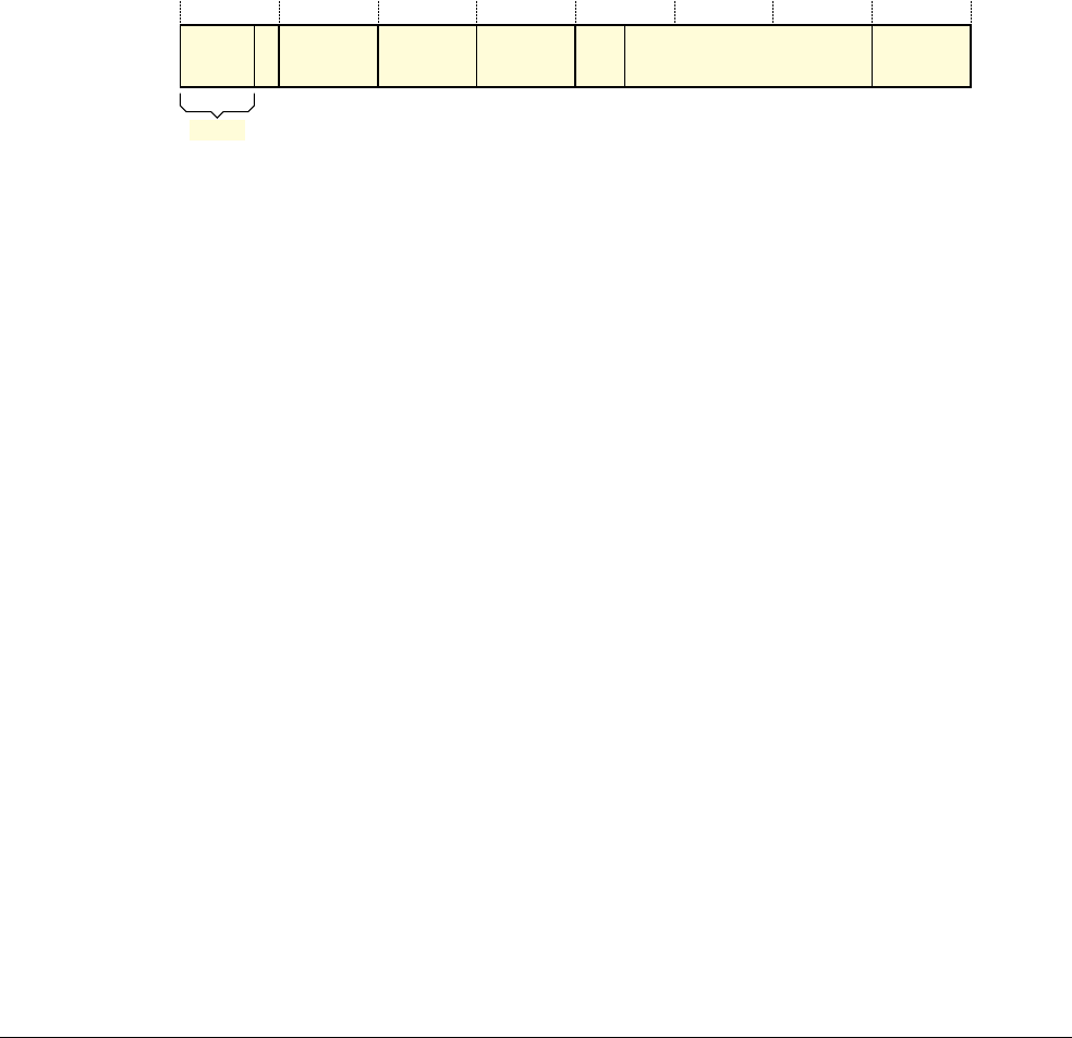
B6 System Control Registers in a PMSA implementation
B6.1 PMSA System control registers descriptions, in register order
ARM DDI 0406C.c Copyright © 1996-1998, 2000, 2004-2012, 2014 ARM. All rights reserved. B6-1835
ID051414 Non-Confidential
B6.1.25 CTR, Cache Type Register, PMSA
The CTR characteristics are:
Purpose The CTR provides information about the architecture of the caches.
This register is part of the Identification registers functional group.
Usage constraints Only accessible from PL1.
Configurations ARMv7 changes the format of the CTR, This section describes only the ARMv7 format. For
more information see the description of the Format field, bits[31:29].
Attributes A 32-bit RO register with an IMPLEMENTATION DEFINED value. See also Reset behavior of
CP14 and CP15 registers on page B5-1778.
Table B5-13 on page B5-1800 shows the encodings of all of the registers in the
Identification registers functional group.
In an ARMv7 PMSA implementation, the CTR bit assignments are:
Format, bits[31:29] Indicates the implemented CTR format. The possible values of this are:
0b000
ARMv6 format, see CP15 c0, Cache Type Register, CTR, ARMv4 and ARMv5
on page D15-2617.
0b100
ARMv7 format. This is the format described in this section.
All other values are reserved.
Bit[28] RAZ.
CWG, bits[27:24] Cache Write-back Granule. The maximum size of memory that can be overwritten as a
result of the eviction of a cache entry that has had a memory location in it modified, encoded
as Log2 of the number of words.
A value of
0b0000
indicates that the CTR does not provide Cache Write-back Granule
information and either:
• the architectural maximum of 512 words (2Kbytes) must be assumed
• the Cache Write-back Granule can be determined from maximum cache line size
encoded in the Cache Size ID Registers.
Values greater than
0b1001
are reserved.
ERG, bits[23:20] Exclusives Reservation Granule. The maximum size of the reservation granule that has been
implemented for the Load-Exclusive and Store-Exclusive instructions, encoded as Log2 of
the number of words. For more information, see Tagging and the size of the tagged memory
block on page A3-121.
A value of
0b0000
indicates that the CTR does not provide Exclusives Reservation Granule
information and the architectural maximum of 512 words (2Kbytes) must be assumed.
Values greater than
0b1001
are reserved.
DminLine, bits[19:16]
Log2 of the number of words in the smallest cache line of all the data caches and unified
caches that are controlled by the processor.
Bit[15:14] RAO.
Bits[13:4] RAZ.
1
31 29 28 27 24 23 20 19 16 15 14 4 3 0
0 0 0 CWG ERG DminLine 1 1 0 0 0 0 0 0 0 0 0 0 IminLine
Format
13

B6 System Control Registers in a PMSA implementation
B6.1 PMSA System control registers descriptions, in register order
B6-1836 Copyright © 1996-1998, 2000, 2004-2012, 2014 ARM. All rights reserved. ARM DDI 0406C.c
Non-Confidential ID051414
IminLine, bits[3:0] Log2 of the number of words in the smallest cache line of all the instruction caches that are
controlled by the processor.
Accessing the CTR
To access the CTR, software reads the CP15 registers with
<opc1>
set to 0,
<CRn>
set to c0,
<CRm>
set to c0, and
<opc2>
set to 1. For example
MRC p15, 0, <Rt>, c0, c0, 1 ; Read CTR into Rt

B6 System Control Registers in a PMSA implementation
B6.1 PMSA System control registers descriptions, in register order
ARM DDI 0406C.c Copyright © 1996-1998, 2000, 2004-2012, 2014 ARM. All rights reserved. B6-1837
ID051414 Non-Confidential
B6.1.26 DCCIMVAC, Data Cache Clean and Invalidate by MVA to PoC, PMSA
Cache and branch predictor maintenance operations, PMSA on page B6-1943 describes this cache maintenance
operation.
This operation is part of the Cache maintenance operations functional group. Table B5-18 on page B5-1803 shows
the encodings of all of the registers and operations in this functional group.
B6.1.27 DCCISW, Data Cache Clean and Invalidate by Set/Way, PMSA only
Cache and branch predictor maintenance operations, PMSA on page B6-1943 describes this cache maintenance
operation.
This operation is part of the Cache maintenance operations functional group. Table B5-18 on page B5-1803 shows
the encodings of all of the registers and operations in this functional group.
B6.1.28 DCCMVAC, Data Cache Clean by MVA to PoC, PMSA
Cache and branch predictor maintenance operations, PMSA on page B6-1943 describes this cache maintenance
operation.
This operation is part of the Cache maintenance operations functional group. Table B5-18 on page B5-1803 shows
the encodings of all of the registers and operations in this functional group.
B6.1.29 DCCMVAU, Data Cache Clean by MVA to PoU, PMSA
Cache and branch predictor maintenance operations, PMSA on page B6-1943 describes this cache maintenance
operation.
This operation is part of the Cache maintenance operations functional group. Table B5-18 on page B5-1803 shows
the encodings of all of the registers and operations in this functional group.
B6.1.30 DCCSW, Data Cache Clean by Set/Way, PMSA
Cache and branch predictor maintenance operations, PMSA on page B6-1943 describes this cache maintenance
operation.
This operation is part of the Cache maintenance operations functional group. Table B5-18 on page B5-1803 shows
the encodings of all of the registers and operations in this functional group.
B6.1.31 DCIMVAC, Data Cache Invalidate by MVA to PoC, PMSA
Cache and branch predictor maintenance operations, PMSA on page B6-1943 describes this cache maintenance
operation.
This operation is part of the Cache maintenance operations functional group. Table B5-18 on page B5-1803 shows
the encodings of all of the registers and operations in this functional group.
B6.1.32 DCISW, Data Cache Invalidate by Set/Way, PMSA
Cache and branch predictor maintenance operations, PMSA on page B6-1943 describes this cache maintenance
operation.
This operation is part of the Cache maintenance operations functional group. Table B5-18 on page B5-1803 shows
the encodings of all of the registers and operations in this functional group.

B6 System Control Registers in a PMSA implementation
B6.1 PMSA System control registers descriptions, in register order
B6-1838 Copyright © 1996-1998, 2000, 2004-2012, 2014 ARM. All rights reserved. ARM DDI 0406C.c
Non-Confidential ID051414
B6.1.33 DFAR, Data Fault Address Register, PMSA
The DFAR characteristics are:
Purpose The DFAR holds the faulting address that caused a synchronous Data Abort exception.
This register is part of the PL1 Fault handling registers functional group.
Usage constraints Only accessible from PL1.
Configurations Always implemented.
Attributes A 32-bit RW register with an UNKNOWN reset value. See also Reset behavior of CP14 and
CP15 registers on page B5-1778.
Table B5-15 on page B5-1801 shows the encodings of all of the registers in the PL1 Fault
handling registers functional group.
The DFAR bit assignments are:
For information about using the DFAR, including when the value in the DFAR is valid, see Exception reporting in
a PMSA implementation on page B5-1769.
A debugger can write to the DFAR to restore its value.
Accessing the DFAR
To access the DFAR, software reads or writes the CP15 registers with
<opc1>
set to 0,
<CRn>
set to c6,
<CRm>
set to
c0, and
<opc2>
set to 0. For example:
MRC p15, 0, <Rt>, c6, c0, 0 ; Read DFAR into Rt
MCR p15, 0, <Rt>, c6, c0, 0 ; Write Rt to DFAR
Faulting address of synchronous Data Abort exception
31 0
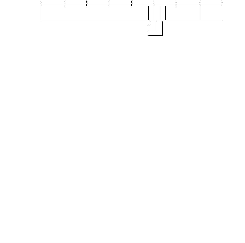
B6 System Control Registers in a PMSA implementation
B6.1 PMSA System control registers descriptions, in register order
ARM DDI 0406C.c Copyright © 1996-1998, 2000, 2004-2012, 2014 ARM. All rights reserved. B6-1839
ID051414 Non-Confidential
B6.1.34 DFSR, Data Fault Status Register, PMSA
The DFSR characteristics are:
Purpose The DFSR holds status information about the last data fault.
This register is part of the PL1 Fault handling registers functional group.
Usage constraints Only accessible from PL1.
Configurations Always implemented.
Attributes A 32-bit RW register with an UNKNOWN reset value. See also Reset behavior of CP14 and
CP15 registers on page B5-1778.
Table B5-15 on page B5-1801 shows the encodings of all of the registers in the PL1 Fault
handling registers functional group.
In a PMSA implementation, the DFSR bit assignments are:
Bits[31:13, 9:4] Reserved, UNK/SBZP.
ExT, bit[12] External abort type. This bit can provide an IMPLEMENTATION DEFINED classification of
external aborts.
For aborts other than external aborts this bit always returns 0.
In an implementation that does not provide any classification of external aborts, this bit is
UNK/SBZP.
WnR, bit[11] Write not Read bit. On a synchronous exception, indicates whether the abort was caused by
a write instruction or a by read instruction:
0 Abort caused by a read instruction.
1 Abort caused by a write instruction.
For synchronous faults on CP15 cache maintenance operations this bit always returns the
value 1.
This bit is UNKNOWN on:
• An asynchronous Data Abort exception
• A Data Abort exception caused by a debug exception.
FS, bits[10, 3:0] Fault status bits. For the valid encodings of these bits in an ARMv7-R implementation with
a PMSA, see Table B5-8 on page B5-1772.
All encodings not shown in the table are reserved.
For information about using the DFSR see Exception reporting in a PMSA implementation on page B5-1769.
Accessing the DFSR
To access the DFSR, software reads or writes the CP15 registers with
<opc1>
set to 0,
<CRn>
set to c5,
<CRm>
set to
c0, and
<opc2>
set to 0. For example:
MRC p15, 0, <Rt>, c5, c0, 0 ; Read DFSR into Rt
MCR p15, 0, <Rt>, c5, c0, 0 ; Write Rt to DFSR
FS[3:0]
31 13 12 11 10 9 4 3 0
Reserved, UNK/SBZP
ExT
Reserved,
UNK/SBZP
WnR
FS[4]
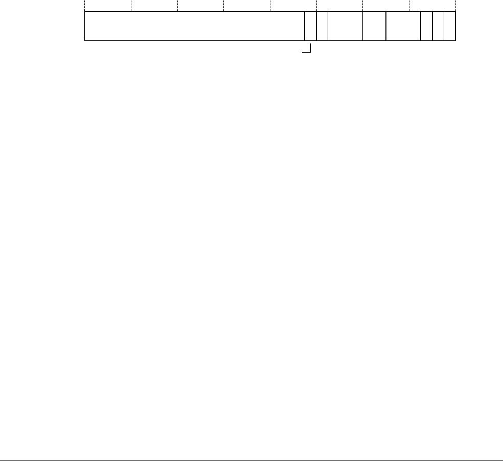
B6 System Control Registers in a PMSA implementation
B6.1 PMSA System control registers descriptions, in register order
B6-1840 Copyright © 1996-1998, 2000, 2004-2012, 2014 ARM. All rights reserved. ARM DDI 0406C.c
Non-Confidential ID051414
B6.1.35 DRACR, Data Region Access Control Register, PMSA
The DRACR characteristics are:
Purpose The DRACR defines the memory attributes for the current memory region in the data or
unified address map.
This register is part of the MMU control registers functional group.
Usage constraints Only accessible from PL1.
Used in conjunction with the other MPU Memory region programming registers, see
Programming the MPU region attributes on page B5-1763.
Configurations Always implemented.
Attributes A 32-bit RW register with an UNKNOWN reset value. See also Reset behavior of CP14 and
CP15 registers on page B5-1778.
Table B5-14 on page B5-1801 shows the encodings of all of the registers in the MMU
control registers functional group.
The DRACR bit assignments are:
Bit[31:13, 11, 7:6] Reserved, UNK/SBZP.
XN, bit[12] Execute-never bit. Indicates whether instructions can be fetched from this region:
0 Region can contain executable code.
1 Region is an execute-never region, and any attempt to execute an instruction
from the region results in a Permission fault.
If the MPU implements separate Instruction and Data memory maps this bit is UNK/SBZP.
For more information, see The XN (Execute-never) attribute and instruction fetching on
page B5-1761.
AP[2:0], bits[10:8] Access Permissions field. Indicates the read and write access permissions for unprivileged
and PL1 accesses to the memory region.
For more information, see Access permissions on page B5-1761.
TEX[2:0], C, B, bits[5:3, 1:0]
Memory attributes. For more information, see C, B, and TEX[2:0] encodings on
page B5-1762.
S, bit[2] Shareable bit, for Normal memory regions:
0 If region is Normal memory, memory is Non-shareable.
1 If region is Normal memory, memory is Shareable.
The value of this bit is ignored if the region is not Normal memory.
The current memory region is selected by the value held in the RGNR.
If software accesses this register when the RGNR does not point to a valid region in the MPU data or unified address
map, the result is UNPREDICTABLE.
BCS
31 13 12 11 10 8 7 6 5 3 2 1 0
Reserved, UNK/SBZP
XN
(0) (0) TEX[2:0](0) AP[2:0]

B6 System Control Registers in a PMSA implementation
B6.1 PMSA System control registers descriptions, in register order
ARM DDI 0406C.c Copyright © 1996-1998, 2000, 2004-2012, 2014 ARM. All rights reserved. B6-1841
ID051414 Non-Confidential
Accessing the DRACR
To access the DRACR, software reads or writes the CP15 registers with
<opc1>
set to 0,
<CRn>
set to c6,
<CRm>
set to
c1, and
<opc2>
set to 4. For example:
MRC p15, 0, <Rt>, c6, c1, 4 ; Read DRACR into Rt
MCR p15, 0, <Rt>, c6, c1, 4 ; Write Rt to DRACR

B6 System Control Registers in a PMSA implementation
B6.1 PMSA System control registers descriptions, in register order
B6-1842 Copyright © 1996-1998, 2000, 2004-2012, 2014 ARM. All rights reserved. ARM DDI 0406C.c
Non-Confidential ID051414
B6.1.36 DRBAR, Data Region Base Address Register, PMSA
The DRBAR characteristics are:
Purpose The DRBAR indicates the base address of the current memory region in the data or unified
address map.
This register is part of the MMU control registers functional group.
Usage constraints Only accessible from PL1.
Used in conjunction with the other MPU Memory region programming registers, see
Programming the MPU region attributes on page B5-1763.
Configurations Always implemented.
Attributes A 32-bit RW register with an UNKNOWN reset value. See also Reset behavior of CP14 and
CP15 registers on page B5-1778.
Table B5-14 on page B5-1801 shows the encodings of all of the registers in the MMU
control registers functional group.
The DRBAR bit assignments are:
Region Base Address, bits[31:2]
The Base Address for the region, in the Data or Unified address map.
Bit[1:0] Reserved, UNK/SBZP.
The base address must be aligned to the region size, otherwise behavior is UNPREDICTABLE. The current memory
region is selected by the value held in the RGNR.
Software can use the DRBAR to find the size of the supported physical address space for the Data or Unified
memory map, see Finding the minimum supported region size on page B5-1760.
Accessing the DRBAR
To access the DRBAR, software reads or writes the CP15 registers with
<opc1>
set to 0,
<CRn>
set to c6,
<CRm>
set to
c1, and
<opc2>
set to 0. For example:
MRC p15, 0, <Rt>, c6, c1, 0 ; Read DRBAR into Rt
MCR p15, 0, <Rt>, c6, c1, 0 ; Write Rt to DRBAR
(0)Region Base Address
31 210
(0)
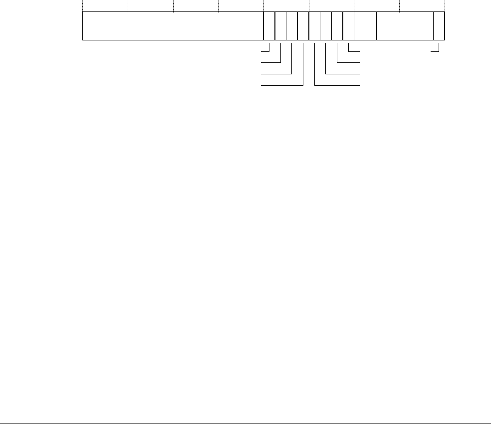
B6 System Control Registers in a PMSA implementation
B6.1 PMSA System control registers descriptions, in register order
ARM DDI 0406C.c Copyright © 1996-1998, 2000, 2004-2012, 2014 ARM. All rights reserved. B6-1843
ID051414 Non-Confidential
B6.1.37 DRSR, Data Region Size and Enable Register, PMSA
The DRSR characteristics are:
Purpose The DRSR indicates the size of the current memory region in the data or unified address
map, and can enable or disable:
• the entire region
• each of the eight subregions, if the region is enabled.
This register is part of the MMU control registers functional group.
Usage constraints Only accessible from PL1.
Used in conjunction with the other MPU Memory region programming registers, see
Programming the MPU region attributes on page B5-1763.
Configurations Always implemented.
Attributes A 32-bit RW register that resets to zero. See also Reset behavior of CP14 and CP15 registers
on page B5-1778.
Table B5-14 on page B5-1801 shows the encodings of all of the registers in the MMU
control registers functional group.
The DRSR bit assignments are:
Bit[31:16, 7:6] Reserved, UNK/SBZP.
SnD, bit[n+8], for values of n from 0 to 7
Subregion disable bit for region n. Indicates whether the subregion is part of this region:
0 Subregion is part of this region.
1 Subregion disabled. The subregion is not part of this region.
The region is divided into exactly eight equal sized subregions. Subregion 0 is the subregion
at the least significant address. For more information, see Subregions on page B5-1757.
If the size of this region, indicated by the RSize field, is less than 256 bytes then the SnD
fields are not defined, and register bits[15:8] are UNK/SBZP.
RSize, bits[5:1] Region Size field. Indicates the size of the current memory region:
• A value of 0 is not permitted, this value is reserved and UNPREDICTABLE.
• If N is the value in this field, the region size is 2N+1 bytes.
En, bit[0] Enable bit for the region:
0 Region is disabled.
1 Region is enabled.
Because this register resets to zero, all memory regions are disabled on reset.
All memory regions must be enabled before they are used.
The current memory region is selected by the value held in the RGNR.
The minimum region size supported is IMPLEMENTATION DEFINED, but if the memory system implementation
includes a cache, ARM strongly recommends that the minimum region size is a multiple of the cache line length.
This prevents cache attributes changing mid-way through a cache line.
En
31 16 15 14 13 12 11 10 9 8 7 6 5 4 3 2 1 0
Reserved, UNK/SBZP
S7D
(0) (0) RSize
S6D
S5D
S4D
S0D
S1D
S2D
S3D

B6 System Control Registers in a PMSA implementation
B6.1 PMSA System control registers descriptions, in register order
B6-1844 Copyright © 1996-1998, 2000, 2004-2012, 2014 ARM. All rights reserved. ARM DDI 0406C.c
Non-Confidential ID051414
Behavior is UNPREDICTABLE if software:
• writes a region size that is outside the range supported by the implementation
• accesses this register when the RGNR does not point to a valid region in the MPU Data or Unified address
map.
Accessing the DRSR
To access the DRSR, software reads or writes the CP15 registers with
<opc1>
set to 0,
<CRn>
set to c6,
<CRm>
set to
c1, and
<opc2>
set to 2. For example:
MRC p15, 0, <Rt>, c6, c1, 2 ; Read DRSR into Rt
MCR p15, 0, <Rt>, c6, c1, 2 ; Write Rt to DRSR

B6 System Control Registers in a PMSA implementation
B6.1 PMSA System control registers descriptions, in register order
ARM DDI 0406C.c Copyright © 1996-1998, 2000, 2004-2012, 2014 ARM. All rights reserved. B6-1845
ID051414 Non-Confidential
B6.1.38 FPEXC, Floating-Point Exception Control register, PMSA
The FPEXC register characteristics are:
Purpose The FPEXC provides a global enable for the Advanced SIMD and Floating-point
Extensions, and indicates how the state of these extensions is recorded.
This register is an Advanced SIMD and Floating-point Extension system register.
Usage constraints Only accessible by software executing at PL1 or higher. See Enabling Advanced SIMD and
floating-point support on page B1-1229 for more information.
Configurations Implemented only if the implementation includes one or both of:
• the Floating-point Extension
• the Advanced SIMD Extension.
The VFP subarchitecture might define additional bits in the FPEXC, see Additions to the
Floating-Point Exception Register, FPEXC on page D6-2441.
Attributes A 32-bit RW register. See the register field descriptions for information about the reset
value.
Table B1-24 on page B1-1236 shows the encodings of all of the Advanced SIMD and
Floating-point Extension system registers
The FPEXC bit assignments are:
EX, bit[31] Exception bit. A status bit that specifies how much information must be saved to record the state of
the Advanced SIMD and Floating-point system:
0 The only significant state is the contents of the registers:
• D0 - D15
• D16 - D31, if implemented
•FPSCR
•FPEXC.
A context switch can be performed by saving and restoring the values of these registers.
1 There is additional state that must be handled by any context switch system.
The reset value of this bit is UNKNOWN.
The behavior of the EX bit on writes is SUBARCHITECTURE DEFINED, except that in any
implementation a write of 0 to this bit must be a valid operation, and must return a value of 0 if read
back before any subsequent write to the register.
EN, bit[30] Enable bit. A global enable for the Advanced SIMD and Floating-point Extensions:
0 The Advanced SIMD and Floating-point Extensions are disabled. For details of how the
system operates when EN == 0 see Enabling Advanced SIMD and floating-point
support on page B1-1229.
1 The Advanced SIMD and Floating-point Extensions are enabled and operate normally.
This bit is always a normal read/write bit. It has a reset value of 0.
31 30 29 0
SUBARCHITECTURE
DEFINED
EX
EN

B6 System Control Registers in a PMSA implementation
B6.1 PMSA System control registers descriptions, in register order
B6-1846 Copyright © 1996-1998, 2000, 2004-2012, 2014 ARM. All rights reserved. ARM DDI 0406C.c
Non-Confidential ID051414
Bits[29:0] SUBARCHITECTURE DEFINED. An implementation can use these bits to communicate exception
information between the floating-point hardware and the support code. The subarchitectural
definition of these bits includes their read/write access. This can be defined on a bit by bit basis. This
means that the reset value of these bits is SUBARCHITECTURE DEFINED.
A constraint on these bits is that if EX == 0 it must be possible to save and restore all significant
state for the floating-point system by saving and restoring only the two Advanced SIMD and
Floating-point Extension registers FPSCR and FPEXC.
Accessing the FPEXC register
Software reads or writes the FPEXC register using the
VMRS
and
VMSR
instructions. For more information, see VMRS
on page A8-954 and VMSR on page A8-956. For example:
VMRS <Rt>, FPEXC ; Read Floating-point Exception Control Register
VMSR FPEXC, <Rt> ; Write Floating-point Exception Control Register
Writes to the FPEXC can have side-effects on various aspects of processor operation. All of these side-effects are
synchronous to the FPEXC write. This means they are guaranteed not to be visible to earlier instructions in the
execution stream, and they are guaranteed to be visible to later instructions in the execution stream.
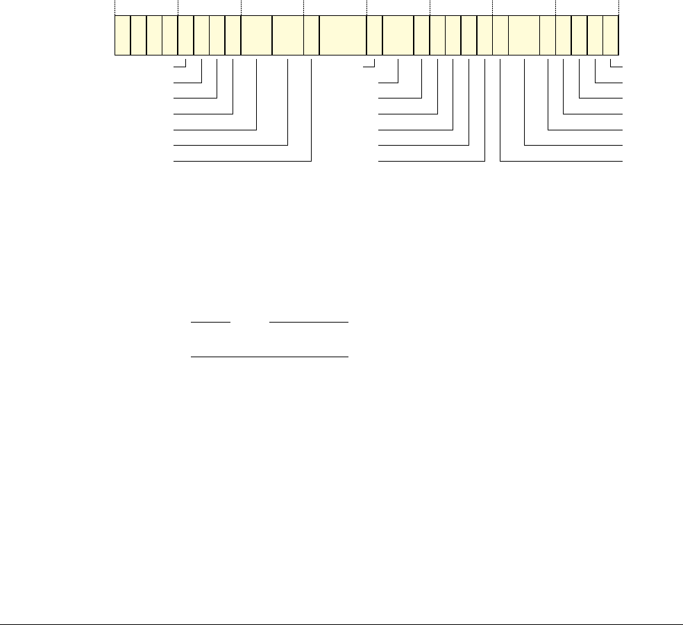
B6 System Control Registers in a PMSA implementation
B6.1 PMSA System control registers descriptions, in register order
ARM DDI 0406C.c Copyright © 1996-1998, 2000, 2004-2012, 2014 ARM. All rights reserved. B6-1847
ID051414 Non-Confidential
B6.1.39 FPSCR, Floating-point Status and Control Register, PMSA
The FPSCR characteristics are:
Purpose Provides floating-point system status information and control.
This register is an Advanced SIMD and Floating-point Extension system register.
Usage constraints There are no usage constraints, but see Enabling Advanced SIMD and floating-point
support on page B1-1229 for information about enabling access to this register.
Configurations Implemented only if the implementation includes one or both of:
• the Floating-point Extension
• the Advanced SIMD Extension.
Attributes A 32-bit RW register. The reset value of the register fields are UNKNOWN except where the
field descriptions indicate otherwise.
Table B1-24 on page B1-1236 shows the encodings of all of the Advanced SIMD and
Floating-point Extension system registers
The FPSCR bit assignments are:
Bits[31:28] Condition flags. These are updated by floating-point comparison operations, as shown in Effect of
a Floating-point comparison on the condition flags on page A2-80.
N, bit[31] Negative condition flag.
Z, bit[30] Zero condition flag.
C, bit[29] Carry condition flag.
V, bit[28] Overflow condition flag.
Note
Advanced SIMD operations never update these bits.
QC, bit[27] Cumulative saturation bit, Advanced SIMD only. This bit is set to 1 to indicate that an Advanced
SIMD integer operation has saturated since 0 was last written to this bit. For details of saturation,
see Pseudocode details of saturation on page A2-44.
If the implementation does not include the Advanced SIMD Extension, this bit is UNK/SBZP.
AHP, bit[26] Alternative half-precision control bit:
0 IEEE half-precision format selected.
1 Alternative half-precision format selected.
For more information see Advanced SIMD and Floating-point half-precision formats on
page A2-66.
If the implementation does not include the Half-precision Extension, this bit is UNK/SBZP.
(0)(0)
QC
AHP
DN
FZ
RMode
Stride
Reserved
IDE IOC
DZC
OFC
Reserved
UFC
IXC
IXE
UFE
OFE
DZE
IOE IDC
Reserved
N
31 30 29 28 27 26 25 24 23 22 21 20 19 18 16 15 14 13 12 11 10 9 8 7 6 5 4 3 2 1 0
Z C V (0) Len (0) (0)
See the field descriptions for implementation differences in different VFP versions

B6 System Control Registers in a PMSA implementation
B6.1 PMSA System control registers descriptions, in register order
B6-1848 Copyright © 1996-1998, 2000, 2004-2012, 2014 ARM. All rights reserved. ARM DDI 0406C.c
Non-Confidential ID051414
DN, bit[25] Default NaN mode control bit:
0 NaN operands propagate through to the output of a floating-point operation.
1 Any operation involving one or more NaNs returns the Default NaN.
For more information, see NaN handling and the Default NaN on page A2-69.
The value of this bit only controls Floating-point arithmetic. Advanced SIMD arithmetic always
uses the Default NaN setting, regardless of the value of the DN bit.
FZ, bit[24] Flush-to-zero mode control bit:
0 Flush-to-zero mode disabled. Behavior of the floating-point system is fully compliant
with the IEEE 754 standard.
1 Flush-to-zero mode enabled.
For more information, see Flush-to-zero on page A2-68.
The value of this bit only controls Floating-point arithmetic. Advanced SIMD arithmetic always
uses the Flush-to-zero setting, regardless of the value of the FZ bit.
RMode, bits[23:22]
Rounding Mode control field. The encoding of this field is:
0b00
Round to Nearest (RN) mode
0b01
Round towards Plus Infinity (RP) mode
0b10
Round towards Minus Infinity (RM) mode
0b11
Round towards Zero (RZ) mode.
The specified rounding mode is used by almost all floating-point instructions provided by the
Floating-point Extension. Advanced SIMD arithmetic always uses the Round to Nearest setting,
regardless of the value of the RMode bits.
Note
The rounding mode names are based on the IEEE 754-1985 terminology. See Floating-point
standards, and terminology on page A2-55 for the corresponding terms in the IEEE 754-2008
revision of the standard.
Stride, bits[21:20] and Len, bits[18:16]
ARM deprecates use of nonzero values of these fields. For details of their use in previous versions
of the ARM architecture see Appendix D11 VFP Vector Operation Support.
The values of these fields are ignored by the Advanced SIMD Extension.
Bits[19, 14:13, 6:5]
Reserved, UNK/SBZP.
Bits[15, 12:8] Floating-point exception trap enable bits. These bits are supported only in VFPv2, VFPv3U, and
VFPv4U. They are reserved, RAZ/WI, on a system that implements VFPv3 or VFPv4.
The possible values of each bit are:
0 Untrapped exception handling selected. If the floating-point exception occurs then the
corresponding cumulative exception bit is set to 1.
1 Trapped exception handling selected. If the floating-point exception occurs, hardware
does not update the corresponding cumulative exception bit. The trap handling software
can decide whether to set the cumulative exception bit to 1.
The values of these bits control only floating-point arithmetic. Advanced SIMD arithmetic always
uses untrapped exception handling, regardless of the values of these bits.
For more information, see Floating-point exceptions on page A2-70.

B6 System Control Registers in a PMSA implementation
B6.1 PMSA System control registers descriptions, in register order
ARM DDI 0406C.c Copyright © 1996-1998, 2000, 2004-2012, 2014 ARM. All rights reserved. B6-1849
ID051414 Non-Confidential
The floating-point trap enable bits are:
IDE, bit[15] Input Denormal exception trap enable.
Note
Denormal corresponds to the term denormalized number in the
IEEE 754-1985 standard. Floating-point standards, and terminology on
page A2-55 describes the terminology changes in the IEEE 754-2008
revision of the standard.
IXE, bit[12] Inexact exception trap enable.
UFE, bit[11] Underflow exception trap enable.
OFE, bit[10] Overflow exception trap enable.
DZE, bit[9] Division by Zero exception trap enable.
IOE, bit[8] Invalid Operation exception trap enable.
Bits[7, 4:0] Cumulative exception bits for floating-point exceptions. Each of these bits is set to 1 to indicate that
the corresponding exception has occurred since 0 was last written to it. How floating-point
instructions update these bits depends on the value of the corresponding exception trap enable bits,
see the descriptions of bits[15, 12:8].
Advanced SIMD instructions set each cumulative exception bit if the corresponding exception
occurs in one or more of the floating-point calculations performed by the instruction, regardless of
the setting of the trap enable bits.
For more information, see Floating-point exceptions on page A2-70.
IDC, bit[7] Input Denormal cumulative exception bit. Updated by hardware only when
IDE, bit[15], is set to 0.
IXC, bit[4] Inexact cumulative exception bit. Updated by hardware only when IXE,
bit[12], is set to 0.
UFC, bit[3] Underflow cumulative exception bit. Updated by hardware only when UFE,
bit[11], is set to 0.
OFC, bit[2] Overflow cumulative exception bit. Updated by hardware only when OFE,
bit[10], is set to 0.
DZC, bit[1] Division by Zero cumulative exception bit. Updated by hardware only when
DZE, bit[9], is set to 0.
IOC, bit[0] Invalid Operation cumulative exception bit. Updated by hardware only
when IOE, bit[8], is set to 0.
If the implementation includes the integer-only Advanced SIMD Extension and does not include the Floating-point
Extension, all of these bits except QC are UNK/SBZP.
Writes to the FPSCR can have side-effects on various aspects of processor operation. All of these side-effects are
synchronous to the FPSCR write. This means they are guaranteed not to be visible to earlier instructions in the
execution stream, and they are guaranteed to be visible to later instructions in the execution stream.
Accessing the FPSCR
Software reads or writes the FPSCR or transfers the FPSCR.{N, Z, C, V} flags to the APSR, using the
VMRS
and
VMSR
instructions. For more information, see VMRS on page A8-954 and VMSR on page A8-956. For example:
VMRS <Rt>, FPSCR ; Read Floating-point System Control Register
VMSR FPSCR, <Rt> ; Write Floating-point System Control Register
VMRS APSR_nzcv, FPSCR ; Write FPSCR.{N, Z, C, V} flags to APSR.{N, Z, C, V}
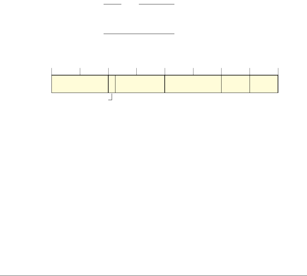
B6 System Control Registers in a PMSA implementation
B6.1 PMSA System control registers descriptions, in register order
B6-1850 Copyright © 1996-1998, 2000, 2004-2012, 2014 ARM. All rights reserved. ARM DDI 0406C.c
Non-Confidential ID051414
B6.1.40 FPSID, Floating-point System ID Register, PMSA
The FPSID register characteristics are:
Purpose The FPSID register provides top-level information about the floating-point implementation.
This register is an Advanced SIMD and Floating-point Extension system register.
Usage constraints Only accessible from PL1 or higher. See Enabling Advanced SIMD and floating-point
support on page B1-1229 for more information.
This register complements the information provided by the CPUID scheme described in
Chapter B7 The CPUID Identification Scheme.
Configurations The FPSID register can be implemented in a system that provides only software emulation
of the ARM floating-point instructions, and must be implemented if the implementation
includes one or both of:
• the Floating-point Extension
• the Advanced SIMD Extension.
The VMSA and PMSA definitions of the register fields are identical.
Attributes A 32-bit RO register.
Note
Although the FPSID is a RO register, a write using the FPSID encoding is a valid serializing
operation, see Asynchronous bounces, serialization, and Floating-point exception barriers
on page B1-1238. Such a write does not access the register.
Table B1-24 on page B1-1236 shows the encodings of all of the Advanced SIMD and
Floating-point Extension system registers.
In ARMv7, the FPSID register bit assignments are:
Implementer, bits[31:24]
Implementer codes are the same as those used for the MIDR.
For an implementation by ARM this field is
0x41
, the ASCII code for A.
SW, bit[23] Software bit. This bit indicates whether a system provides only software emulation of the
floating-point instructions that are provided by the Floating-point Extension:
0 The system includes hardware support for the floating-point instructions that are
provided by the Floating-point Extension.
1 The system provides only software emulation of the floating-point instructions that are
provided by the Floating-point Extension.
Implementer
31 24 23 22 16 15 8 7 4 3 0
Subarchitecture Part number Variant Revision
SW

B6 System Control Registers in a PMSA implementation
B6.1 PMSA System control registers descriptions, in register order
ARM DDI 0406C.c Copyright © 1996-1998, 2000, 2004-2012, 2014 ARM. All rights reserved. B6-1851
ID051414 Non-Confidential
Subarchitecture, bits[22:16]
Subarchitecture version number. For an implementation by ARM, permitted values are:
0b0000000
VFPv1 architecture with an IMPLEMENTATION DEFINED subarchitecture.
Not permitted in an ARMv7 implementation.
0b0000001
VFPv2 architecture with Common VFP subarchitecture v1.
Not permitted in an ARMv7 implementation.
0b0000010
VFPv3 architecture, or later, with Common VFP subarchitecture v2. The VFP
architecture version is indicated by the MVFR0 and MVFR1 registers.
0b0000011
VFPv3 architecture, or later, with no subarchitecture. The entire floating-point
implementation is in hardware, and no software support code is required. The VFP
architecture version is indicated by the MVFR0 and MVFR1 registers.
This value can be used only by an implementation that does not support the trap enable
bits in the FPSCR.
0b0000100
VFPv3 architecture, or later, with Common VFP subarchitecture v3. The VFP
architecture version is indicated by the MVFR0 and MVFR1 registers.
For a subarchitecture designed by ARM the most significant bit of this field, register bit[22], is 0.
Values with a most significant bit of 0 that are not listed here are reserved.
When the subarchitecture designer is not ARM, the most significant bit of this field, register bit[22],
must be 1. Each implementer must maintain its own list of subarchitectures it has designed, starting
at subarchitecture version number
0x40
.
Part number, bits[15:8]
An IMPLEMENTATION DEFINED part number for the floating-point implementation, assigned by the
implementer.
Variant, bits[7:4]
An IMPLEMENTATION DEFINED variant number. Typically, this field distinguishes between different
production variants of a single product.
Revision, bits[3:0]
An IMPLEMENTATION DEFINED revision number for the floating-point implementation.
Accessing the FPSID register
Software accesses the FPSID register using the
VMRS
instruction, see VMRS on page B9-2014. For example:
VMRS <Rt>, FPSID ; Read FPSID into Rt

B6 System Control Registers in a PMSA implementation
B6.1 PMSA System control registers descriptions, in register order
B6-1852 Copyright © 1996-1998, 2000, 2004-2012, 2014 ARM. All rights reserved. ARM DDI 0406C.c
Non-Confidential ID051414
B6.1.41 ICIALLU, Instruction Cache Invalidate All to PoU, PMSA
Cache and branch predictor maintenance operations, PMSA on page B6-1943 describes this cache maintenance
operation.
This operation is part of the Cache maintenance operations functional group. Table B5-18 on page B5-1803 shows
the encodings of all of the registers and operations in this functional group.
B6.1.42 ICIALLUIS, Instruction Cache Invalidate All to PoU, Inner Shareable, PMSA
Cache and branch predictor maintenance operations, PMSA on page B6-1943 describes this cache maintenance
operation.
This operation is part of the Cache maintenance operations functional group. Table B5-18 on page B5-1803 shows
the encodings of all of the registers and operations in this functional group.
B6.1.43 ICIMVAU, Instruction Cache Invalidate by MVA to PoU, PMSA
Cache and branch predictor maintenance operations, PMSA on page B6-1943 describes this cache maintenance
operation.
This operation is part of the Cache maintenance operations functional group. Table B5-18 on page B5-1803 shows
the encodings of all of the registers and operations in this functional group.
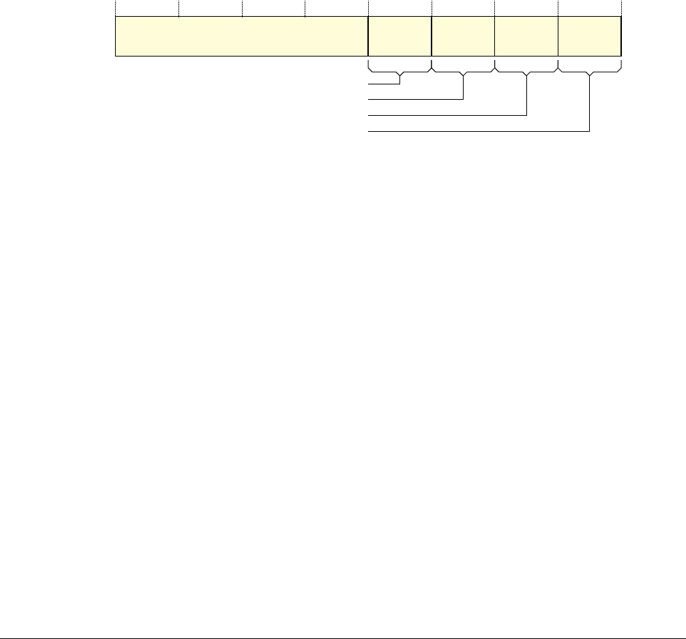
B6 System Control Registers in a PMSA implementation
B6.1 PMSA System control registers descriptions, in register order
ARM DDI 0406C.c Copyright © 1996-1998, 2000, 2004-2012, 2014 ARM. All rights reserved. B6-1853
ID051414 Non-Confidential
B6.1.44 ID_AFR0, Auxiliary Feature Register 0, PMSA
The ID_AFR0 characteristics are:
Purpose ID_AFR0 provides information about the IMPLEMENTATION DEFINED features of the
processor.
This register is a CPUID register, and is part of the Identification registers functional group.
Usage constraints Only accessible from PL1.
Must be interpreted with the MIDR.
Configurations The VMSA and PMSA definitions of the register fields are identical.
Attributes A 32-bit RO register with an IMPLEMENTATION DEFINED value:
•Table B7-1 on page B7-1952 shows the encodings of all of the CPUID registers
•Table B5-13 on page B5-1800 shows the encodings of all of the registers in the
Identification registers functional group.
The ID_AFR0 bit assignments are:
Bits[31:16] Reserved, UNK.
IMPLEMENTATION DEFINED, bits[15:12]
IMPLEMENTATION DEFINED, bits[11:8]
IMPLEMENTATION DEFINED, bits[7:4]
IMPLEMENTATION DEFINED, bits[3:0]
The Auxiliary Feature Register 0 has four 4-bit IMPLEMENTATION FIELDS. These fields are defined by the
implementer of the design. The implementer is identified by the Implementer field of the MIDR.
The Auxiliary Feature Register 0 enables implementers to include additional design features in the CPUID scheme.
Field definitions for the Auxiliary Feature Register 0 might:
• differ between different implementers
• be subject to change
• migrate over time, for example if they are incorporated into the main architecture.
Accessing ID_AFR0
To access ID_AFR0, software reads the CP15 registers with
<opc1>
set to 0,
<CRn>
set to c0,
<CRm>
set to c1, and
<opc2>
set to 3. For example:
MRC p15, 0, <Rt>, c0, c1, 3 ; Read ID_AFR0 into Rt
Reserved, UNK
31 16 15 12 11 8 7 4 3 0
IMPLEMENTATION DEFINED
IMPLEMENTATION DEFINED
IMPLEMENTATION DEFINED
IMPLEMENTATION DEFINED
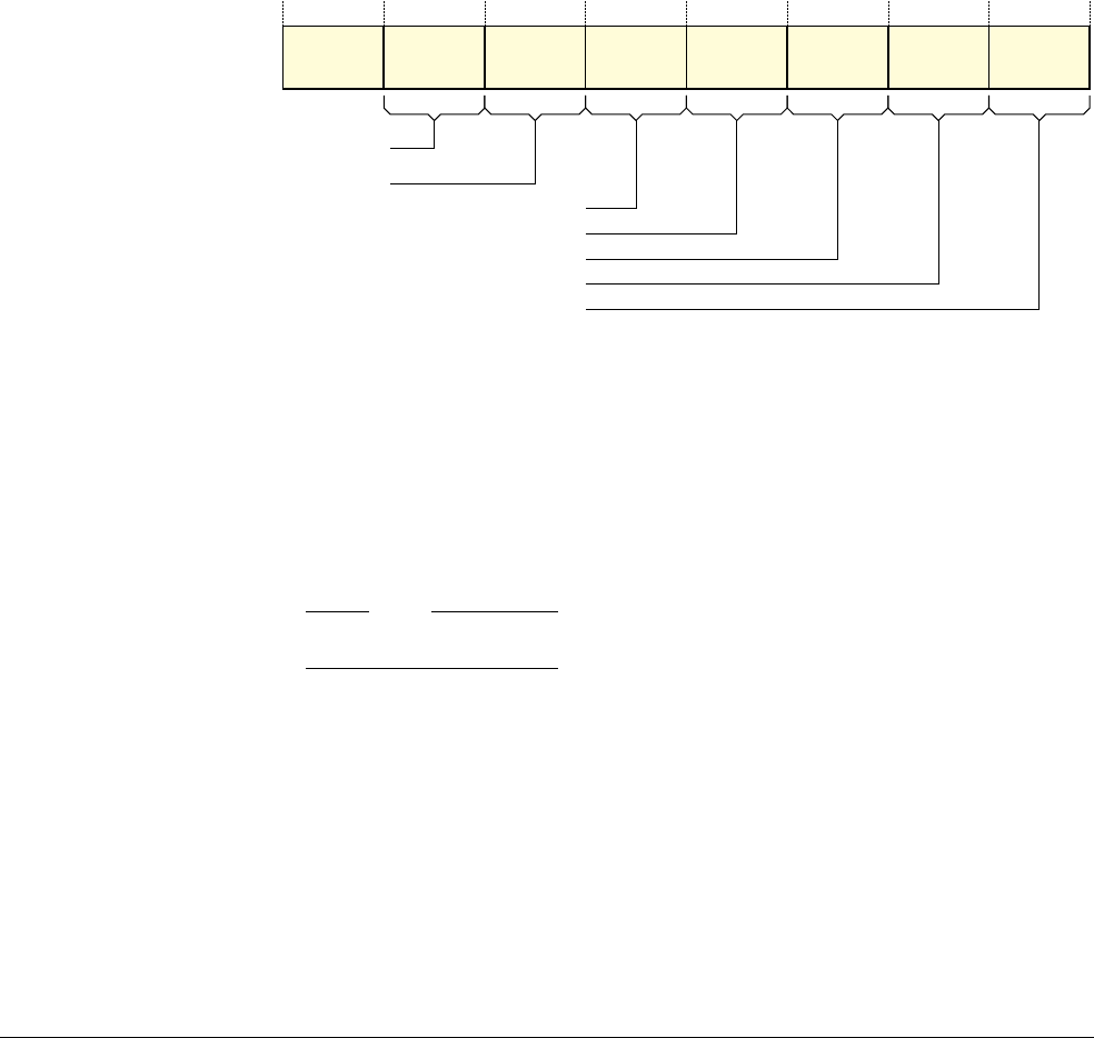
B6 System Control Registers in a PMSA implementation
B6.1 PMSA System control registers descriptions, in register order
B6-1854 Copyright © 1996-1998, 2000, 2004-2012, 2014 ARM. All rights reserved. ARM DDI 0406C.c
Non-Confidential ID051414
B6.1.45 ID_DFR0, Debug Feature Register 0, PMSA
The ID_DFR0 characteristics are:
Purpose ID_DFR0 provides top level information about the debug system.
This register is a CPUID register, and is part of the Identification registers functional group.
Usage constraints Only accessible from PL1.
Configurations The VMSA and PMSA definitions of the register fields are identical.
Attributes A 32-bit RO register with an IMPLEMENTATION DEFINED value:
•Table B7-1 on page B7-1952 shows the encodings of all of the CPUID registers
•Table B5-13 on page B5-1800 shows the encodings of all of the registers in the
Identification registers functional group.
All field values not shown in the field descriptions are reserved.
The ID_DFR0 bit assignments are:
Bits[31:28] Reserved, UNK.
Performance Monitors Extension, A and R profiles, bits[27:24]
Support for coprocessor-based ARM Performance Monitors Extension, for A and R profile
processors. Permitted values are:
0b0000
PMUv2 not supported.
0b0001
Support for Performance Monitors Extension, PMUv1.
0b0010
Support for Performance Monitors Extension, PMUv2.
0b1111
No ARM Performance Monitors Extension support.
Note
A value of
0b0000
gives no indication of whether PMUv1 monitors are supported.
Debug model, M profile, bits[23:20]
Support for memory-mapped debug model for M profile processors. Permitted values are:
0b0000
Not supported.
0b0001
Support for M profile Debug architecture, with memory-mapped access.
Memory-mapped trace model, bits[19:16]
Support for memory-mapped trace model. Permitted values are:
0b0000
Not supported.
0b0001
Support for ARM trace architecture, with memory-mapped access.
The ID register, register
0x079
, gives more information about the implementation. See
also Trace on page C1-2024.
Debug model, M profile
Memory-mapped trace model
Coprocessor trace model
Memory-mapped debug model, A and R profiles
Coprocessor Secure debug model, A profile only
Coprocessor debug model, A and R profiles
Reserved,
UNK
31 28 27 24 23 20 19 16 15 12 11 8 7 4 3 0
Performance Monitors
Extension, A and R profiles

B6 System Control Registers in a PMSA implementation
B6.1 PMSA System control registers descriptions, in register order
ARM DDI 0406C.c Copyright © 1996-1998, 2000, 2004-2012, 2014 ARM. All rights reserved. B6-1855
ID051414 Non-Confidential
Coprocessor trace model, bits[15:12]
Support for coprocessor-based trace model. Permitted values are:
0b0000
Not supported.
0b0001
Support for ARM trace architecture, with CP14 access.
The ID register, register
0x079
, gives more information about the implementation. See
also Trace on page C1-2024.
Memory-mapped debug model, A and R profiles, bits[11:8]
Support for memory-mapped debug model, for A and R profile processors. Permitted values are:
0b0000
Not supported, or pre-ARMv6 implementation.
0b0100
Support for v7 Debug architecture, with memory-mapped access.
0b0101
Support for v7.1 Debug architecture, with memory-mapped access.
Note
The permitted field values are not continuous, and values
0b0001
,
0b0010
, and
0b0011
are reserved.
Coprocessor Secure debug model, bits[7:4]
Support for coprocessor-based Secure debug model, for an A profile processor that includes the
Security Extensions. Permitted values are:
0b0000
Not supported.
0b0011
Support for v6.1 Debug architecture, with CP14 access.
0b0100
Support for v7 Debug architecture, with CP14 access.
0b0101
Support for v7.1 Debug architecture, with CP14 access.
Note
The permitted field values are not continuous, and values
0b0001
and
0b0010
are reserved.
Coprocessor debug model, bits[3:0]
Support for coprocessor based debug model, for A and R profile processors. Permitted values are:
0b0000
Not supported.
0b0010
Support for v6 Debug architecture, with CP14 access.
0b0011
Support for v6.1 Debug architecture, with CP14 access.
0b0100
Support for v7 Debug architecture, with CP14 access.
0b0101
Support for v7.1 Debug architecture, with CP14 access.
Note
The permitted field values are not continuous, and value
0b0001
is reserved.
Note
Software can obtain more information about the debug implementation from the debug infrastructure, see Debug
identification registers on page C11-2198.
Accessing ID_DFR0
To access ID_DFR0, software reads the CP15 registers with
<opc1>
set to 0,
<CRn>
set to c0,
<CRm>
set to c1, and
<opc2>
set to 2. For example:
MRC p15, 0, <Rt>, c0, c1, 2 ; Read ID_DFR0 into Rt
B6 System Control Registers in a PMSA implementation
B6.1 PMSA System control registers descriptions, in register order
B6-1856 Copyright © 1996-1998, 2000, 2004-2012, 2014 ARM. All rights reserved. ARM DDI 0406C.c
Non-Confidential ID051414
B6.1.46 ID_ISAR0, Instruction Set Attribute Register 0, PMSA
The ID_ISAR0 characteristics are:
Purpose ID_ISAR0 provides information about the instruction sets implemented by the processor.
For more information see About the Instruction Set Attribute registers on page B7-1952.
This register is a CPUID register, and is part of the Identification registers functional group.
Usage constraints Only accessible from PL1.
Must be interpreted with ID_ISAR1, ID_ISAR2, ID_ISAR3, and ID_ISAR4. For more
information see About the Instruction Set Attribute registers on page B7-1952.
Configurations The VMSA and PMSA definitions of the register fields are identical.
Attributes A 32-bit RO register with an IMPLEMENTATION DEFINED value:
•Table B7-1 on page B7-1952 shows the encodings of all of the CPUID registers
•Table B5-13 on page B5-1800 shows the encodings of all of the registers in the
Identification registers functional group.
All field values not shown in the field descriptions are reserved.
The ID_ISAR0 bit assignments are:
Bits[31:28] Reserved, UNK.
Divide_instrs, bits[27:24]
Indicates the implemented Divide instructions. Permitted values are:
0b0000
None implemented.
0b0001
Adds
SDIV
and
UDIV
in the Thumb instruction set.
0b0010
As for
0b0001
, and adds
SDIV
and
UDIV
in the ARM instruction set.
Debug_instrs, bits[23:20]
Indicates the supported Debug instructions. Permitted values are:
0b0000
None implemented.
0b0001
Adds
BKPT
.
Coproc_instrs, bits[19:16]
Indicates the supported Coprocessor instructions. Permitted values are:
0b0000
None implemented, except for instructions separately attributed by the architecture,
including CP15, CP14, and the Advanced SIMD and Floating-point Extensions.
0b0001
Adds generic
CDP
,
LDC
,
MCR
,
MRC
, and
STC
.
0b0010
As for
0b0001
, and adds generic
CDP2
,
LDC2
,
MCR2
,
MRC2
, and
STC2
.
0b0011
As for
0b0010
, and adds generic
MCRR
and
MRRC
.
0b0100
As for
0b0011
, and adds generic
MCRR2
and
MRRC2
.
CmpBranch_instrs, bits[15:12]
Indicates the implemented combined Compare and Branch instructions in the Thumb instruction
set. Permitted values are:
0b0000
None implemented.
0b0001
Adds
CBNZ
and
CBZ
.
Reserved,
UNK
31 16 15 12 11 8 7 4 3 028 27 24 23 20 19
Divide_instrs
Debug_instrs
Coproc_instrs
CmpBranch_instrs
Bitfield_instrs
BitCount_instrs
Swap_instrs

B6 System Control Registers in a PMSA implementation
B6.1 PMSA System control registers descriptions, in register order
ARM DDI 0406C.c Copyright © 1996-1998, 2000, 2004-2012, 2014 ARM. All rights reserved. B6-1857
ID051414 Non-Confidential
Bitfield_instrs, bits[11:8]
Indicates the implemented BitField instructions. Permitted values are:
0b0000
None implemented.
0b0001
Adds
BFC
,
BFI
,
SBFX
, and
UBFX
.
BitCount_instrs, bits[7:4]
Indicates the implemented Bit Counting instructions. Permitted values are:
0b0000
None implemented.
0b0001
Adds
CLZ
.
Swap_instrs, bits[3:0]
Indicates the implemented Swap instructions in the ARM instruction set. Permitted values are:
0b0000
None implemented.
0b0001
Adds
SWP
and
SWPB
.
Accessing ID_ISAR0
To access ID_ISAR0, software reads the CP15 registers with
<opc1>
set to 0,
<CRn>
set to c0,
<CRm>
set to c2, and
<opc2>
set to 0. For example:
MRC p15, 0, <Rt>, c0, c2, 0 ; Read ID_ISAR0 into Rt
B6 System Control Registers in a PMSA implementation
B6.1 PMSA System control registers descriptions, in register order
B6-1858 Copyright © 1996-1998, 2000, 2004-2012, 2014 ARM. All rights reserved. ARM DDI 0406C.c
Non-Confidential ID051414
B6.1.47 ID_ISAR1, Instruction Set Attribute Register 1, PMSA
The ID_ISAR1 characteristics are:
Purpose ID_ISAR1 provides information about the instruction sets implemented by the processor.
For more information see About the Instruction Set Attribute registers on page B7-1952.
This register is a CPUID register, and is part of the Identification registers functional group.
Usage constraints Only accessible from PL1.
Must be interpreted with ID_ISAR0, ID_ISAR2, ID_ISAR3, and ID_ISAR4. For more
information see About the Instruction Set Attribute registers on page B7-1952.
Configurations The VMSA and PMSA definitions of the register fields are identical.
Attributes A 32-bit RO register with an IMPLEMENTATION DEFINED value:
•Table B7-1 on page B7-1952 shows the encodings of all of the CPUID registers
•Table B5-13 on page B5-1800 shows the encodings of all of the registers in the
Identification registers functional group.
All field values not shown in the field descriptions are reserved.
The ID_ISAR1 bit assignments are:
Jazelle_instrs, bits[31:28]
Indicates the implemented Jazelle extension instructions. Permitted values are:
0b0000
No support for Jazelle.
0b0001
Adds the
BXJ
instruction, and the J bit in the PSR.
This setting might indicate a trivial implementation of the Jazelle extension.
Interwork_instrs, bits[27:24]
Indicates the implemented Interworking instructions. Permitted values are:
0b0000
None implemented.
0b0001
Adds the
BX
instruction, and the T bit in the PSR.
0b0010
As for
0b0001
, and adds the
BLX
instruction. PC loads have
BX
-like behavior.
0b0011
As for
0b0010
, and guarantees that data-processing instructions in the ARM instruction
set with the PC as the destination and the S bit clear have
BX
-like behavior.
Note
A value of
0b0000
,
0b0001
, or
0b0010
in this field does not guarantee that an ARM data-processing
instruction with the PC as the destination and the S bit clear behaves like an old
MOV PC
instruction,
ignoring bits[1:0] of the result. With these values of this field:
• if bits[1:0] of the result value are
0b00
then the processor remains in ARM state
• if bits[1:0] are
0b01
,
0b10
or
0b11
, the result must be treated as UNPREDICTABLE.
31 16 15 12 11 8 7 4 3 028 27 24 23 20 19
Jazelle_instrs
Interwork_instrs
Immediate_instrs Extend_instrs
IfThen_instrs Except_AR_instrs
Except_instrs
Endian_instrs

B6 System Control Registers in a PMSA implementation
B6.1 PMSA System control registers descriptions, in register order
ARM DDI 0406C.c Copyright © 1996-1998, 2000, 2004-2012, 2014 ARM. All rights reserved. B6-1859
ID051414 Non-Confidential
Immediate_instrs, bits[23:20]
Indicates the implemented data-processing instructions with long immediates. Permitted values are:
0b0000
None implemented.
0b0001
Adds:
• the
MOVT
instruction
• the
MOV
instruction encodings with zero-extended 16-bit immediates
• the Thumb
ADD
and
SUB
instruction encodings with zero-extended 12-bit
immediates, and the other
ADD
,
ADR
and
SUB
encodings cross-referenced by the
pseudocode for those encodings.
IfThen_instrs, bits[19:16]
Indicates the implemented If-Then instructions in the Thumb instruction set. Permitted values are:
0b0000
None implemented.
0b0001
Adds the
IT
instructions, and the IT bits in the PSRs.
Extend_instrs, bits[15:12]
Indicates the implemented Extend instructions. Permitted values are:
0b0000
No scalar sign-extend or zero-extend instructions are supported, where scalar
instructions means non-Advanced SIMD instructions.
0b0001
Adds the
SXTB
,
SXTH
,
UXTB
, and
UXTH
instructions.
0b0010
As for
0b0001
, and adds the
SXTB16
,
SXTAB
,
SXTAB16
,
SXTAH
,
UXTB16
,
UXTAB
,
UXTAB16
, and
UXTAH
instructions.
Note
In addition:
• the shift options on these instructions are available only if the WithShifts_instrs attribute is
0b0011
or greater
• the
SXTAB16
,
SXTB16
,
UXTAB16
, and
UXTB16
instructions are implemented only if both:
— the Extend_instrs attribute is
0b0010
or greater
— the SIMD_instrs attribute is
0b0011
or greater.
Except_AR_instrs, bits[11:8]
Indicates the implemented A and R profile exception-handling instructions. Permitted values are:
0b0000
None implemented.
0b0001
Adds the
SRS
and
RFE
instructions, and the A and R profile forms of the
CPS
instruction.
Except_instrs, bits[7:4]
Indicates the supported exception-handling instructions in the ARM instruction set. Permitted
values are:
0b0000
Not implemented. This indicates that the User registers and exception return forms of
the
LDM
and
STM
instructions are not implemented.
0b0001
Adds the
LDM
(exception return),
LDM
(User registers) and
STM
(User registers) instruction
versions.
Endian_instrs, bits[3:0]
Indicates the implemented Endian instructions. Permitted values are:
0b0000
None implemented.
0b0001
Adds the
SETEND
instruction, and the E bit in the PSRs.

B6 System Control Registers in a PMSA implementation
B6.1 PMSA System control registers descriptions, in register order
B6-1860 Copyright © 1996-1998, 2000, 2004-2012, 2014 ARM. All rights reserved. ARM DDI 0406C.c
Non-Confidential ID051414
Accessing ID_ISAR1
To access ID_ISAR1, software reads the CP15 registers with
<opc1>
set to 0,
<CRn>
set to c0,
<CRm>
set to c2, and
<opc2>
set to 1. For example:
MRC p15, 0, <Rt>, c0, c2, 1 ; Read ID_ISAR1 into Rt
B6 System Control Registers in a PMSA implementation
B6.1 PMSA System control registers descriptions, in register order
ARM DDI 0406C.c Copyright © 1996-1998, 2000, 2004-2012, 2014 ARM. All rights reserved. B6-1861
ID051414 Non-Confidential
B6.1.48 ID_ISAR2, Instruction Set Attribute Register 2, PMSA
The ID_ISAR2 characteristics are:
Purpose ID_ISAR2 provides information about the instruction sets implemented by the processor.
For more information see About the Instruction Set Attribute registers on page B7-1952.
This register is a CPUID register, and is part of the Identification registers functional group.
Usage constraints Only accessible from PL1.
Must be interpreted with ID_ISAR0, ID_ISAR1, ID_ISAR3, and ID_ISAR4. For more
information see About the Instruction Set Attribute registers on page B7-1952.
Configurations The VMSA and PMSA definitions of the register fields are identical.
Attributes A 32-bit RO register with an IMPLEMENTATION DEFINED value:
•Table B7-1 on page B7-1952 shows the encodings of all of the CPUID registers
•Table B5-13 on page B5-1800 shows the encodings of all of the registers in the
Identification registers functional group.
All field values not shown in the field descriptions are reserved.
The ID_ISAR2 bit assignments are:
Reversal_instrs, bits[31:28]
Indicates the implemented Reversal instructions. Permitted values are:
0b0000
None implemented.
0b0001
Adds the
REV
,
REV16
, and
REVSH
instructions.
0b0010
As for
0b0001
, and adds the
RBIT
instruction.
PSR_AR_instrs, bits[27:24]
Indicates the implemented A and R profile instructions to manipulate the PSR. Permitted values are:
0b0000
None implemented.
0b0001
Adds the
MRS
and
MSR
instructions, and the exception return forms of data-processing
instructions described in SUBS PC, LR (Thumb) on page B9-2010 and SUBS PC, LR
and related instructions (ARM) on page B9-2012.
Note
The exception return forms of the data-processing instructions are:
• In the ARM instruction set, data-processing instructions with the PC as the destination and
the S bit set. These instructions might be affected by the WithShifts attribute.
• In the Thumb instruction set, the
SUBS PC, LR, #N
instruction.
MultU_instrs, bits[23:20]
Indicates the implemented advanced unsigned Multiply instructions. Permitted values are:
0b0000
None implemented.
0b0001
Adds the
UMULL
and
UMLAL
instructions.
0b0010
As for
0b0001
, and adds the
UMAAL
instruction.
31 16 15 12 11 8 7 4 3 028 27 24 23 20 19
Reversal_instrs
PSR_AR_instrs
MultU_instrs Mult_instrs
MultS_instrs MultiAccessInt_instrs
MemHint_instrs
LoadStore_instrs

B6 System Control Registers in a PMSA implementation
B6.1 PMSA System control registers descriptions, in register order
B6-1862 Copyright © 1996-1998, 2000, 2004-2012, 2014 ARM. All rights reserved. ARM DDI 0406C.c
Non-Confidential ID051414
MultS_instrs, bits[19:16]
Indicates the implemented advanced signed Multiply instructions. Permitted values are:
0b0000
None implemented.
0b0001
Adds the
SMULL
and
SMLAL
instructions.
0b0010
As for
0b0001
, and adds the
SMLABB
,
SMLABT
,
SMLALBB
,
SMLALBT
,
SMLALTB
,
SMLALTT
,
SMLATB
,
SMLATT
,
SMLAWB
,
SMLAWT
,
SMULBB
,
SMULBT
,
SMULTB
,
SMULTT
,
SMULWB
, and
SMULWT
instructions.
Also adds the Q bit in the PSRs.
0b0011
As for
0b0010
, and adds the
SMLAD
,
SMLADX
,
SMLALD
,
SMLALDX
,
SMLSD
,
SMLSDX
,
SMLSLD
,
SMLSLDX
,
SMMLA
,
SMMLAR
,
SMMLS
,
SMMLSR
,
SMMUL
,
SMMULR
,
SMUAD
,
SMUADX
,
SMUSD
, and
SMUSDX
instructions.
Mult_instrs, bits[15:12]
Indicates the implemented additional Multiply instructions. Permitted values are:
0b0000
No additional instructions implemented. This means only
MUL
is supported.
0b0001
Adds the
MLA
instruction.
0b0010
As for
0b0001
, and adds the
MLS
instruction.
MultiAccessInt_instrs, bits[11:8]
Indicates the support for interruptible multi-access instructions. Permitted values are:
0b0000
No support. This means the
LDM
and
STM
instructions are not interruptible.
0b0001
LDM
and
STM
instructions are restartable.
0b0010
LDM
and
STM
instructions are continuable. Not permitted in ARMv7-A or ARMv7-R.
MemHint_instrs, bits[7:4]
Indicates the implemented Memory Hint instructions. Permitted values are:
0b0000
None implemented.
0b0001
Adds the
PLD
instruction.
0b0010
Adds the
PLD
instruction.
In the MemHint_instrs field, entries of
0b0001
and
0b0010
have identical meanings.
0b0011
As for
0b0001
(or
0b0010
), and adds the
PLI
instruction.
0b0100
As for
0b0011
, and adds the
PLDW
instruction.
LoadStore_instrs, bits[3:0]
Indicates the implemented additional load/store instructions. Permitted values are:
0b0000
No additional load/store instructions implemented.
0b0001
Adds the
LDRD
and
STRD
instructions.
Accessing ID_ISAR2
To access ID_ISAR2, software reads the CP15 registers with
<opc1>
set to 0,
<CRn>
set to c0,
<CRm>
set to c2, and
<opc2>
set to 2. For example:
MRC p15, 0, <Rt>, c0, c2, 2 ; Read ID_ISAR2 into Rt
B6 System Control Registers in a PMSA implementation
B6.1 PMSA System control registers descriptions, in register order
ARM DDI 0406C.c Copyright © 1996-1998, 2000, 2004-2012, 2014 ARM. All rights reserved. B6-1863
ID051414 Non-Confidential
B6.1.49 ID_ISAR3, Instruction Set Attribute Register 3, PMSA
The ID_ISAR3 characteristics are:
Purpose ID_ISAR3 provides information about the instruction sets implemented by the processor.
For more information see About the Instruction Set Attribute registers on page B7-1952.
This register is a CPUID register, and is part of the Identification registers functional group.
Usage constraints Only accessible from PL1.
Must be interpreted with ID_ISAR0, ID_ISAR1, ID_ISAR2, and ID_ISAR4. For more
information see About the Instruction Set Attribute registers on page B7-1952.
Configurations The VMSA and PMSA definitions of the register fields are identical.
Attributes A 32-bit RO register with an IMPLEMENTATION DEFINED value:
•Table B7-1 on page B7-1952 shows the encodings of all of the CPUID registers
•Table B5-13 on page B5-1800 shows the encodings of all of the registers in the
Identification registers functional group.
All field values not shown in the field descriptions are reserved.
The ID_ISAR3 bit assignments are:
ThumbEE_extn_instrs, bits[31:28]
Indicates the implemented Thumb Execution Environment (ThumbEE) Extension instructions.
Permitted values are:
0b0000
None implemented.
0b0001
Adds the
ENTERX
and
LEAVEX
instructions, and modifies the load behavior to include null
checking.
Note
This field can only have a value other than
0b0000
when the ID_PFR0.State3 field has a value of
0b0001
.
TrueNOP_instrs, bits[27:24]
Indicates the implemented True
NOP
instructions. Permitted values are:
0b0000
None implemented. This means there are no
NOP
instructions that do not have any
register dependencies.
0b0001
Adds true
NOP
instructions in both the Thumb and ARM instruction sets. This also
permits additional NOP-compatible hints.
ThumbCopy_instrs, bits[23:20]
Indicates the support for Thumb non flag-setting
MOV
instructions. Permitted values are:
0b0000
Not supported. This means that in the Thumb instruction set, encoding T1 of the
MOV
(register) instruction does not support a copy from a low register to a low register.
0b0001
Adds support for Thumb instruction set encoding T1 of the
MOV
(register) instruction,
copying from a low register to a low register.
31 16 15 12 11 8 7 4 3 028 27 24 23 20 19
TrueNOP_instrs
ThumbEE_extn_instrs ThumbCopy_instrs
TabBranch_instrs
SynchPrim_instrs
SVC_instrs
SIMD_instrs
Saturate_instrs

B6 System Control Registers in a PMSA implementation
B6.1 PMSA System control registers descriptions, in register order
B6-1864 Copyright © 1996-1998, 2000, 2004-2012, 2014 ARM. All rights reserved. ARM DDI 0406C.c
Non-Confidential ID051414
TabBranch_instrs, bits[19:16]
Indicates the implemented Table Branch instructions in the Thumb instruction set. Permitted values
are:
0b0000
None implemented.
0b0001
Adds the
TBB
and
TBH
instructions.
SynchPrim_instrs, bits[15:12]
This field is used with the ID_ISAR4.SynchPrim_instrs_frac field to indicate the implemented
Synchronization Primitive instructions. Table B6-3 shows the permitted values of these fields:
All combinations of SynchPrim_instrs and SynchPrim_instrs_frac not shown in Table B6-3 are
reserved.
SVC_instrs, bits[11:8]
Indicates the implemented
SVC
instructions. Permitted values are:
0b0000
Not implemented.
0b0001
Adds the
SVC
instruction.
Note
The
SVC
instruction was called the
SWI
instruction in previous versions of the ARM architecture.
SIMD_instrs, bits[7:4]
Indicates the implemented SIMD instructions. Permitted values are:
0b0000
None implemented.
0b0001
Adds the
SSAT
and
USAT
instructions, and the Q bit in the PSRs.
0b0011
As for
0b0001
, and adds the
PKHBT
,
PKHTB
,
QADD16
,
QADD8
,
QASX
,
QSUB16
,
QSUB8
,
QSAX
,
SADD16
,
SADD8
,
SASX
,
SEL
,
SHADD16
,
SHADD8
,
SHASX
,
SHSUB16
,
SHSUB8
,
SHSAX
,
SSAT16
,
SSUB16
,
SSUB8
,
SSAX
,
SXTAB16
,
SXTB16
,
UADD16
,
UADD8
,
UASX
,
UHADD16
,
UHADD8
,
UHASX
,
UHSUB16
,
UHSUB8
,
UHSAX
,
UQADD16
,
UQADD8
,
UQASX
,
UQSUB16
,
UQSUB8
,
UQSAX
,
USAD8
,
USADA8
,
USAT16
,
USUB16
,
USUB8
,
USAX
,
UXTAB16
, and
UXTB16
instructions.
Also adds support for the GE[3:0] bits in the PSRs.
Note
• In the SIMD_instrs field, the permitted values are not continuous, and the value
0b0010
is
reserved.
• The
SXTAB16
,
SXTB16
,
UXTAB16
, and
UXTB16
instructions are implemented only if both:
— the Extend_instrs attribute is
0b0010
or greater
— the SIMD_instrs attribute is
0b0011
or greater.
• The SIMD_instrs field relates only to implemented instructions that perform SIMD
operations on the ARM core registers. MVFR0 and MVFR1 give information about the
SIMD instructions implemented by the OPTIONAL Advanced SIMD Extension.
Table B6-3 Implemented Synchronization Primitive instructions
SynchPrim_instrs SynchPrim_instrs_frac Implemented Synchronization Primitives
0000 0000
None implemented
0001 0000
Adds the
LDREX
and
STREX
instructions
0001 0011
As for [
0001
,
0000
], and adds the
CLREX
,
LDREXB
,
LDREXH
,
STREXB
, and
STREXH
instructions
0010 0000
As for [
0001
,
0011
], and adds the
LDREXD
and
STREXD
instructions

B6 System Control Registers in a PMSA implementation
B6.1 PMSA System control registers descriptions, in register order
ARM DDI 0406C.c Copyright © 1996-1998, 2000, 2004-2012, 2014 ARM. All rights reserved. B6-1865
ID051414 Non-Confidential
Saturate_instrs, bits[3:0]
Indicates the implemented Saturate instructions. Permitted values are:
0b0000
None implemented. This means no non-Advanced SIMD saturate instructions are
implemented.
0b0001
Adds the
QADD
,
QDADD
,
QDSUB
, and
QSUB
instructions, and the Q bit in the PSRs.
Accessing ID_ISAR3
To access ID_ISAR3, software reads the CP15 registers with
<opc1>
set to 0,
<CRn>
set to c0,
<CRm>
set to c2, and
<opc2>
set to 3. For example:
MRC p15, 0, <Rt>, c0, c2, 3 ; Read ID_ISAR3 into Rt
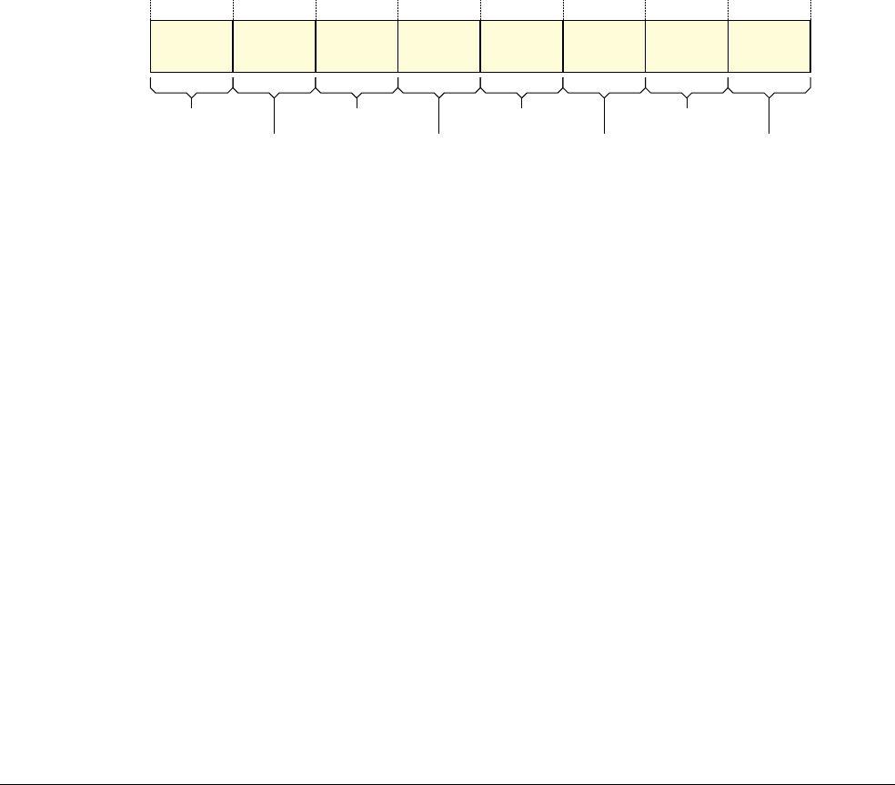
B6 System Control Registers in a PMSA implementation
B6.1 PMSA System control registers descriptions, in register order
B6-1866 Copyright © 1996-1998, 2000, 2004-2012, 2014 ARM. All rights reserved. ARM DDI 0406C.c
Non-Confidential ID051414
B6.1.50 ID_ISAR4, Instruction Set Attribute Register 4, PMSA
The ID_ISAR4 characteristics are:
Purpose ID_ISAR4 provides information about the instruction sets implemented by the processor.
For more information see About the Instruction Set Attribute registers on page B7-1952.
This register is a CPUID register, and is part of the Identification registers functional group.
Usage constraints Only accessible from PL1.
Must be interpreted with ID_ISAR0, ID_ISAR1, ID_ISAR2, and ID_ISAR3. For more
information see About the Instruction Set Attribute registers on page B7-1952.
Configurations The VMSA and PMSA definitions of the register fields are identical.
Attributes A 32-bit RO register with an IMPLEMENTATION DEFINED value:
•Table B7-1 on page B7-1952 shows the encodings of all of the CPUID registers
•Table B5-13 on page B5-1800 shows the encodings of all of the registers in the
Identification registers functional group.
All field values not shown in the field descriptions are reserved.
The ID_ISAR4 bit assignments are:
SWP_frac, bits[31:28]
Indicates support for the memory system locking the bus for
SWP
or
SWPB
instructions. Permitted
values are:
0b0000
SWP
or
SWPB
instructions not implemented.
0b0001
SWP
or
SWPB
implemented but only in a uniprocessor context.
SWP
and
SWPB
do not
guarantee whether memory accesses from other masters can come between the load
memory access and the store memory access of the
SWP
or
SWPB
.
This field is valid only if the ID_ISAR0.Swap_instrs field is zero.
PSR_M_instrs, bits[27:24]
Indicates the implemented M profile instructions to modify the PSRs. Permitted values are:
0b0000
None implemented.
0b0001
Adds the M profile forms of the
CPS
,
MRS
and
MSR
instructions.
SynchPrim_instrs_frac, bits[23:20]
This field is used with the ID_ISAR3.SynchPrim_instrs field to indicate the implemented
Synchronization Primitive instructions. Table B6-3 on page B6-1864 shows the permitted values of
these fields.
All combinations of SynchPrim_instrs and SynchPrim_instrs_frac not shown in Table B6-3 on
page B6-1864 are reserved.
Barrier_instrs, bits[19:16]
Indicates the implemented Barrier instructions in the ARM and Thumb instruction sets. Permitted
values are:
0b0000
None implemented. Barrier operations are provided only as CP15 operations.
0b0001
Adds the
DMB
,
DSB
, and
ISB
barrier instructions.
31 16 15 12 11 8 7 4 3 028 27 24 23 20 19
PSR_M_instrs
SWP_frac
Barrier_instrs
SynchPrim_instrs_frac
Writeback_instrs
SMC_instrs
Unpriv_instrs
WithShifts_instrs

B6 System Control Registers in a PMSA implementation
B6.1 PMSA System control registers descriptions, in register order
ARM DDI 0406C.c Copyright © 1996-1998, 2000, 2004-2012, 2014 ARM. All rights reserved. B6-1867
ID051414 Non-Confidential
SMC_instrs, bits[15:12]
Indicates the implemented
SMC
instructions. Permitted values are:
0b0000
Not implemented.
0b0001
Adds the
SMC
instruction.
Note
The
SMC
instruction was called the
SMI
instruction in previous versions of the ARM architecture.
Writeback_instrs, bits[11:8]
Indicates the support for Writeback addressing modes. Permitted values are:
0b0000
Basic support. Only the
LDM
,
STM
,
PUSH
,
POP
,
SRS
, and
RFE
instructions support writeback
addressing modes. These instructions support all of their writeback addressing modes.
0b0001
Adds support for all of the writeback addressing modes defined in ARMv7.
WithShifts_instrs, bits[7:4]
Indicates the support for instructions with shifts. Permitted values are:
0b0000
Nonzero shifts supported only in
MOV
and shift instructions.
0b0001
Adds support for shifts of loads and stores over the range LSL 0-3.
0b0011
As for
0b0001
, and adds support for other constant shift options, both on load/store and
other instructions.
0b0100
As for
0b0011
, and adds support for register-controlled shift options.
Note
• In this field, the permitted values are not continuous, and the value
0b0010
is reserved.
• Additions to the basic support indicated by the
0b0000
field value only apply when the
encoding supports them. In particular, in the Thumb instruction set there is no difference
between the
0b0011
and
0b0100
levels of support.
•
MOV
instructions with shift options are treated as
ASR
,
LSL
,
LSR
,
ROR
or
RRX
instructions, as
described in Data-processing instructions on page B7-1953.
Unpriv_instrs, bits[3:0]
Indicates the implemented unprivileged instructions. Permitted values are:
0b0000
None implemented. No
T
variant instructions are implemented.
0b0001
Adds the
LDRBT
,
LDRT
,
STRBT
, and
STRT
instructions.
0b0010
As for
0b0001
, and adds the
LDRHT
,
LDRSBT
,
LDRSHT
, and
STRHT
instructions.
Accessing ID_ISAR4
To access ID_ISAR4, software reads the CP15 registers with
<opc1>
set to 0,
<CRn>
set to c0,
<CRm>
set to c2, and
<opc2>
set to 4. For example:
MRC p15, 0, <Rt>, c0, c2, 4 ; Read ID_ISAR4 into Rt

B6 System Control Registers in a PMSA implementation
B6.1 PMSA System control registers descriptions, in register order
B6-1868 Copyright © 1996-1998, 2000, 2004-2012, 2014 ARM. All rights reserved. ARM DDI 0406C.c
Non-Confidential ID051414
B6.1.51 ID_ISAR5, Instruction Set Attribute Register 5, PMSA
The ID_ISAR5 characteristics are:
Purpose ID_ISAR5 is reserved for future expansion of the information about the instruction sets
implemented by the processor.
This register is a CPUID register, and is part of the Identification registers functional group.
Usage constraints Only accessible from PL1.
Configurations The VMSA and PMSA definitions of the register fields are identical.
Attributes A 32-bit RO register:
•Table B7-1 on page B7-1952 shows the encodings of all of the CPUID registers
•Table B5-13 on page B5-1800 shows the encodings of all of the registers in the
Identification registers functional group.
The ID_ISAR5 bit assignments are:
Bits[31:0] Reserved, UNK.
Accessing ID_ISAR5
To access ID_ISAR5, software reads the CP15 registers with
<opc1>
set to 0,
<CRn>
set to c0,
<CRm>
set to c2, and
<opc2>
set to 5. For example:
MRC p15, 0, <Rt>, c0, c2, 5 ; Read ID_ISAR5 into Rt
Reserved, UNK
31 0

B6 System Control Registers in a PMSA implementation
B6.1 PMSA System control registers descriptions, in register order
ARM DDI 0406C.c Copyright © 1996-1998, 2000, 2004-2012, 2014 ARM. All rights reserved. B6-1869
ID051414 Non-Confidential
B6.1.52 ID_MMFR0, Memory Model Feature Register 0, PMSA
The ID_MMFR0 characteristics are:
Purpose ID_MMFR0 provides information about the implemented memory model and memory
management support.
This register is a CPUID register, and is part of the Identification registers functional group.
Usage constraints Only accessible from PL1.
Must be interpreted with ID_MMFR1, ID_MMFR2, and ID_MMFR3.
Configurations The VMSA and PMSA definitions of the register fields are identical.
Attributes A 32-bit RO register with an IMPLEMENTATION DEFINED value:
•Table B7-1 on page B7-1952 shows the encodings of all of the CPUID registers
•Table B5-13 on page B5-1800 shows the encodings of all of the registers in the
Identification registers functional group.
All field values not shown in the field descriptions are reserved.
The ID_MMFR0 bit assignments are:
Innermost shareability, bits[31:28]
Indicates the innermost shareability domain implemented. Permitted values are:
0b0000
Implemented as Non-cacheable.
0b0001
Implemented with hardware coherency support.
0b1111
Shareability ignored.
This field is valid only if the implementation distinguishes between Inner Shareable and Outer
Shareable, by implementing two levels of shareability, as indicated by the value of the Shareability
levels field, bits[15:12].
When the Shareability levels field is zero, this field is reserved, UNK.
FCSE support, bits[27:24]
Indicates whether the implementation includes the FCSE. Permitted values are:
0b0000
Not supported.
0b0001
Support for FCSE.
The value of
0b0001
is only permitted when the VMSA_support field has a value greater than
0b0010
.
Auxiliary registers, bits[23:20]
Indicates support for Auxiliary registers. Permitted values are:
0b0000
None supported.
0b0001
Support for Auxiliary Control Register only.
0b0010
Support for Auxiliary Fault Status Registers (AIFSR and ADFSR) and Auxiliary
Control Register.
Innermost
shareability
FCSE
support
Auxiliary
registers
TCM
support
31 16 15 12 11 8 7 4 3 0
Shareability
levels
Outermost
shareability
PMSA
support
VMSA
support
28 27 24 23 20 19

B6 System Control Registers in a PMSA implementation
B6.1 PMSA System control registers descriptions, in register order
B6-1870 Copyright © 1996-1998, 2000, 2004-2012, 2014 ARM. All rights reserved. ARM DDI 0406C.c
Non-Confidential ID051414
TCM support, bits[19:16]
Indicates support for TCMs and associated DMAs. Permitted values are:
0b0000
Not supported.
0b0001
Support is IMPLEMENTATION DEFINED. ARMv7 requires this setting.
0b0010
Support for TCM only, ARMv6 implementation.
0b0011
Support for TCM and DMA, ARMv6 implementation.
Note
An ARMv7 implementation might include an ARMv6 model for TCM support. However, in
ARMv7 this is an IMPLEMENTATION DEFINED option, and therefore it must be represented by the
0b0001
encoding in this field.
Shareability levels, bits[15:12]
Indicates the number of shareability levels implemented. Permitted values are:
0b0000
One level of shareability implemented.
0b0001
Two levels of shareability implemented.
Outermost shareability, bits[11:8]
Indicates the outermost shareability domain implemented. Permitted values are:
0b0000
Implemented as Non-cacheable.
0b0001
Implemented with hardware coherency support.
0b1111
Shareability ignored.
PMSA support, bits[7:4]
Indicates support for a PMSA. Permitted values are:
0b0000
Not supported.
0b0001
Support for IMPLEMENTATION DEFINED PMSA.
0b0010
Support for PMSAv6, with a Cache Type Register implemented.
0b0011
Support for PMSAv7, with support for memory subsections. ARMv7-R profile.
When the PMSA support field is set to a value other than
0b0000
the VMSA support field must be
set to
0b0000
.
VMSA support, bits[3:0]
Indicates support for a VMSA. Permitted values are:
0b0000
Not supported.
0b0001
Support for IMPLEMENTATION DEFINED VMSA.
0b0010
Support for VMSAv6, with Cache and TLB Type Registers implemented.
0b0011
Support for VMSAv7, with support for remapping and the Access flag. ARMv7-A
profile.
0b0100
As for
0b0011
, and adds support for the PXN bit in the Short-descriptor translation table
format descriptors.
0b0101
As for
0b0100
, and adds support for the Long-descriptor translation table format.
When the VMSA support field is set to a value other than
0b0000
the PMSA support field must be
set to
0b0000
.
Accessing ID_MMFR0
To access ID_MMFR0, software reads the CP15 registers with
<opc1>
set to 0,
<CRn>
set to c0,
<CRm>
set to c1, and
<opc2>
set to 4. For example:
MRC p15, 0, <Rt>, c0, c1, 4 ; Read ID_MMFR0 into Rt

B6 System Control Registers in a PMSA implementation
B6.1 PMSA System control registers descriptions, in register order
ARM DDI 0406C.c Copyright © 1996-1998, 2000, 2004-2012, 2014 ARM. All rights reserved. B6-1871
ID051414 Non-Confidential
B6.1.53 ID_MMFR1, Memory Model Feature Register 1, PMSA
The ID_MMFR1 characteristics are:
Purpose ID_MMFR1 provides information about the implemented memory model and memory
management support.
This register is a CPUID register, and is part of the Identification registers functional group.
Usage constraints Only accessible from PL1.
Must be interpreted with ID_MMFR0, ID_MMFR2, and ID_MMFR3.
Configurations The VMSA and PMSA definitions of the register fields are identical.
Attributes A 32-bit RO register with an IMPLEMENTATION DEFINED value:
•Table B7-1 on page B7-1952 shows the encodings of all of the CPUID registers
•Table B5-13 on page B5-1800 shows the encodings of all of the registers in the
Identification registers functional group.
All field values not shown in the field descriptions are reserved.
The ID_MMFR1 bit assignments are:
Branch predictor, bits[31:28]
Indicates branch predictor management requirements. Permitted values are:
0b0000
No branch predictor, or no MMU present. Implies a fixed MPU configuration.
0b0001
Branch predictor requires flushing on:
• enabling or disabling the MMU
• writing new data to instruction locations
• writing new mappings to the translation tables
• any change to the TTBR0, TTBR1, or TTBCR registers
• changes of FCSE ProcessID or ContextID.
0b0010
Branch predictor requires flushing on:
• enabling or disabling the MMU
• writing new data to instruction locations
• writing new mappings to the translation tables
• any change to the TTBR0, TTBR1, or TTBCR registers without a corresponding
change to the FCSE ProcessID or ContextID.
0b0011
Branch predictor requires flushing only on writing new data to instruction locations.
0b0100
For execution correctness, branch predictor requires no flushing at any time.
Note
The branch predictor is described in some documentation as the Branch Target Buffer.
L1 cache
test and
clean
L1 Harvard
cache VA
31 24 23 20 19 16 15 12 11 8 7 4 3 0
Branch
predictor
L1 unified
cache
L1 Harvard
cache
L1 unified
cache
set/way
L1 Harvard
cache
set/way
L1 unified
cache VA
28 27

B6 System Control Registers in a PMSA implementation
B6.1 PMSA System control registers descriptions, in register order
B6-1872 Copyright © 1996-1998, 2000, 2004-2012, 2014 ARM. All rights reserved. ARM DDI 0406C.c
Non-Confidential ID051414
L1 cache test and clean, bits[27:24]
Indicates the supported Level 1 data cache test and clean operations, for Harvard or unified cache
implementations. Permitted values are:
0b0000
None supported. This is the required setting for ARMv7.
0b0001
Supported Level 1 data cache test and clean operations are:
• Test and clean data cache.
0b0010
As for
0b0001
, and adds:
• Test, clean, and invalidate data cache.
L1 unified cache, bits[23:20]
Indicates the supported entire Level 1 cache maintenance operations, for a unified cache
implementation. Permitted values are:
0b0000
None supported. This is the required setting for ARMv7, because ARMv7 requires a
hierarchical cache implementation.
0b0001
Supported entire Level 1 cache operations are:
• Invalidate cache, including branch predictor if appropriate
• Invalidate branch predictor, if appropriate.
0b0010
As for
0b0001
, and adds:
• Clean cache. Uses a recursive model, using the cache dirty status bit.
• Clean and invalidate cache. Uses a recursive model, using the cache dirty status
bit.
If this field is set to a value other than
0b0000
then the L1 Harvard cache field, bits[19:16], must be
set to
0b0000
.
L1 Harvard cache, bits[19:16]
Indicates the supported entire Level 1 cache maintenance operations, for a Harvard cache
implementation. Permitted values are:
0b0000
None supported. This is the required setting for ARMv7, because ARMv7 requires a
hierarchical cache implementation.
0b0001
Supported entire Level 1 cache operations are:
• Invalidate instruction cache, including branch predictor if appropriate
• Invalidate branch predictor, if appropriate.
0b0010
As for
0b0001
, and adds:
• Invalidate data cache
• Invalidate data cache and instruction cache, including branch predictor if
appropriate.
0b0011
As for
0b0010
, and adds:
• Clean data cache. Uses a recursive model, using the cache dirty status bit.
• Clean and invalidate data cache. Uses a recursive model, using the cache dirty
status bit.
If this field is set to a value other than
0b0000
then the L1 unified cache field, bits[23:20], must be
set to
0b0000
.

B6 System Control Registers in a PMSA implementation
B6.1 PMSA System control registers descriptions, in register order
ARM DDI 0406C.c Copyright © 1996-1998, 2000, 2004-2012, 2014 ARM. All rights reserved. B6-1873
ID051414 Non-Confidential
L1 unified cache set/way, bits[15:12]
Indicates the supported Level 1 cache line maintenance operations by set/way, for a unified cache
implementation. Permitted values are:
0b0000
None supported. This is the required setting for ARMv7, because ARMv7 requires a
hierarchical cache implementation.
0b0001
Supported Level 1 unified cache line maintenance operations by set/way are:
• Clean cache line by set/way.
0b0010
As for
0b0001
, and adds:
• Clean and invalidate cache line by set/way.
0b0011
As for
0b0010
, and adds:
• Invalidate cache line by set/way.
If this field is set to a value other than
0b0000
then the L1 Harvard cache s/w field, bits[11:8], must
be set to
0b0000
.
L1 Harvard cache set/way, bits[11:8]
Indicates the supported Level 1 cache line maintenance operations by set/way, for a Harvard cache
implementation. Permitted values are:
0b0000
None supported. This is the required setting for ARMv7, because ARMv7 requires a
hierarchical cache implementation.
0b0001
Supported Level 1 Harvard cache line maintenance operations by set/way are:
• Clean data cache line by set/way
• Clean and invalidate data cache line by set/way.
0b0010
As for
0b0001
, and adds:
• Invalidate data cache line by set/way.
0b0011
As for
0b0010
, and adds:
• Invalidate instruction cache line by set/way.
If this field is set to a value other than
0b0000
then the L1 unified cache s/w field, bits[15:12], must
be set to
0b0000
.
L1 unified cache VA, bits[7:4]
Indicates the supported Level 1 cache line maintenance operations by MVA, for a unified cache
implementation. Permitted values are:
0b0000
None supported. This is the required setting for ARMv7, because ARMv7 requires a
hierarchical cache implementation.
0b0001
Supported Level 1 unified cache line maintenance operations by MVA are:
• Clean cache line by MVA
• Invalidate cache line by MVA
• Clean and invalidate cache line by MVA.
0b0010
As for
0b0001
, and adds:
• Invalidate branch predictor by MVA, if branch predictor is implemented.
If this field is set to a value other than
0b0000
then the L1 Harvard cache VA field, bits[3:0], must be
set to
0b0000
.

B6 System Control Registers in a PMSA implementation
B6.1 PMSA System control registers descriptions, in register order
B6-1874 Copyright © 1996-1998, 2000, 2004-2012, 2014 ARM. All rights reserved. ARM DDI 0406C.c
Non-Confidential ID051414
L1 Harvard cache VA, bits[3:0]
Indicates the supported Level 1 cache line maintenance operations by MVA, for a Harvard cache
implementation. Permitted values are:
0b0000
None supported. This is the required setting for ARMv7, because ARMv7 requires a
hierarchical cache implementation.
0b0001
Supported Level 1 Harvard cache line maintenance operations by MVA are:
• Clean data cache line by MVA
• Invalidate data cache line by MVA
• Clean and invalidate data cache line by MVA
• Clean instruction cache line by MVA.
0b0010
As for
0b0001
, and adds:
• Invalidate branch predictor by MVA, if branch predictor is implemented.
If this field is set to a value other than
0b0000
then the L1 unified cache VA field, bits[7:4], must be
set to
0b0000
.
Accessing ID_MMFR1
To access ID_MMFR1, software reads the CP15 registers with
<opc1>
set to 0,
<CRn>
set to c0,
<CRm>
set to c1, and
<opc2>
set to 5. For example:
MRC p15, 0, <Rt>, c0, c1, 5 ; Read ID_MMFR1 into Rt

B6 System Control Registers in a PMSA implementation
B6.1 PMSA System control registers descriptions, in register order
ARM DDI 0406C.c Copyright © 1996-1998, 2000, 2004-2012, 2014 ARM. All rights reserved. B6-1875
ID051414 Non-Confidential
B6.1.54 ID_MMFR2, Memory Model Feature Register 2, PMSA
The ID_MMFR2 characteristics are:
Purpose ID_MMFR2 provides information about the implemented memory model and memory
management support.
This register is a CPUID register, and is part of the Identification registers functional group.
Usage constraints Only accessible from PL1.
Must be interpreted with ID_MMFR0, ID_MMFR1, and ID_MMFR3.
Configurations The VMSA and PMSA definitions of the register fields are identical.
Attributes A 32-bit RO register with an IMPLEMENTATION DEFINED value:
•Table B7-1 on page B7-1952 shows the encodings of all of the CPUID registers
•Table B5-13 on page B5-1800 shows the encodings of all of the registers in the
Identification registers functional group.
All field values not shown in the field descriptions are reserved.
The ID_MMFR2 bit assignments are:
HW Access flag, bits[31:28]
Indicates support for a Hardware Access flag, as part of the VMSAv7 implementation. Permitted
values are:
0b0000
Not supported.
0b0001
Support for VMSAv7 Access flag, updated in hardware.
On an ARMv7-R implementation this field must be
0b0000
.
WFI stall, bits[27:24]
Indicates the support for Wait For Interrupt (WFI) stalling. Permitted values are:
0b0000
Not supported.
0b0001
Support for WFI stalling.
Mem barrier, bits[23:20]
Indicates the supported CP15 memory barrier operations:
0b0000
None supported.
0b0001
Supported CP15 Memory barrier operations are:
• Data Synchronization Barrier (DSB). In previous versions of the ARM
architecture, DSB was named Data Write Barrier (DWB).
0b0010
As for
0b0001
, and adds:
• Instruction Synchronization Barrier (ISB). In previous versions of the ARM
architecture, the ISB operation was called Prefetch Flush.
• Data Memory Barrier (DMB).
Note
ARM deprecates the use of these operations. ID_ISAR4.BarrierInstrs indicates the level of support
for the preferred barrier instructions.
HW
Access flag
WFI
stall
Mem
barrier
Unified
TLB
31 16 15 12 11 8 7 4 3 0
Harvard
TLB
L1 Harvard
range
L1 Harvard
bg fetch
L1 Harvard
fg fetch
28 27 24 23 20 19

B6 System Control Registers in a PMSA implementation
B6.1 PMSA System control registers descriptions, in register order
B6-1876 Copyright © 1996-1998, 2000, 2004-2012, 2014 ARM. All rights reserved. ARM DDI 0406C.c
Non-Confidential ID051414
Unified TLB, bits[19:16]
Indicates the supported TLB maintenance operations, for a unified or Harvard TLB implementation.
Permitted values are:
0b0000
Not supported.
0b0001
Supported unified TLB maintenance operations are:
• Invalidate all entries in the TLB
• Invalidate TLB entry by MVA.
0b0010
As for
0b0001
, and adds:
• Invalidate TLB entries by ASID match.
0b0011
As for
0b0010
and adds:
• Invalidate instruction TLB and data TLB entries by MVA All ASID. This is a
shared unified TLB operation.
0b0100
As for
0b0011
and adds:
• Invalidate Hyp mode unified TLB entry by MVA
• Invalidate entire Non-secure PL1&0 unified TLB
• Invalidate entire Hyp mode unified TLB.
If this field is set to a value other than
0b0000
then the Harvard TLB field, bits[15:12], must be set
to
0b0000
.
Harvard TLB, bits[15:12]
Indicates the supported TLB maintenance operations, for a Harvard TLB implementation. Permitted
values are:
0b0000
Not supported.
0b0001
Supported Harvard TLB maintenance operations are:
• Invalidate all entries in the ITLB and the DTLB.
This is a shared unified TLB operation.
• Invalidate all ITLB entries.
• Invalidate all DTLB entries.
• Invalidate ITLB entry by MVA.
• Invalidate DTLB entry by MVA.
0b0010
As for
0b0001
, and adds:
• Invalidate ITLB and DTLB entries by ASID match.
This is a shared unified TLB operation.
• Invalidate ITLB entries by ASID match
• Invalidate DTLB entries by ASID match.
If this field is set to a value other than
0b0000
then the Unified TLB field, bits[19:16], must be set to
0b0000
.
Note
This field is defined only for legacy reasons. It is replaced by the Unified TLB field, bits19:16].
L1 Harvard range, bits[11:8]
Indicates the supported Level 1 cache maintenance range operations, for a Harvard cache
implementation. Permitted values are:
0b0000
Not supported.
0b0001
Supported Level 1 Harvard cache maintenance range operations are:
• Invalidate data cache range by VA
• Invalidate instruction cache range by VA
• Clean data cache range by VA
• Clean and invalidate data cache range by VA.

B6 System Control Registers in a PMSA implementation
B6.1 PMSA System control registers descriptions, in register order
ARM DDI 0406C.c Copyright © 1996-1998, 2000, 2004-2012, 2014 ARM. All rights reserved. B6-1877
ID051414 Non-Confidential
L1 Harvard bg fetch, bits[7:4]
Indicates the supported Level 1 cache background fetch operations, for a Harvard cache
implementation. When supported, background fetch operations are non-blocking operations.
Permitted values are:
0b0000
Not supported.
0b0001
Supported Level 1 Harvard cache background fetch operations are:
• Fetch instruction cache range by VA
• Fetch data cache range by VA.
L1 Harvard fg fetch, bits[3:0]
Indicates the supported Level 1 cache foreground fetch operations, for a Harvard cache
implementation. When supported, foreground fetch operations are blocking operations. Permitted
values are:
0b0000
Not supported.
0b0001
Supported Level 1 Harvard cache foreground fetch operations are:
• Fetch instruction cache range by VA
• Fetch data cache range by VA.
Accessing ID_MMFR2
To access ID_MMFR2, software reads the CP15 registers with
<opc1>
set to 0,
<CRn>
set to c0,
<CRm>
set to c1, and
<opc2>
set to 6. For example:
MRC p15, 0, <Rt>, c0, c1, 6 ; Read ID_MMFR2 into Rt
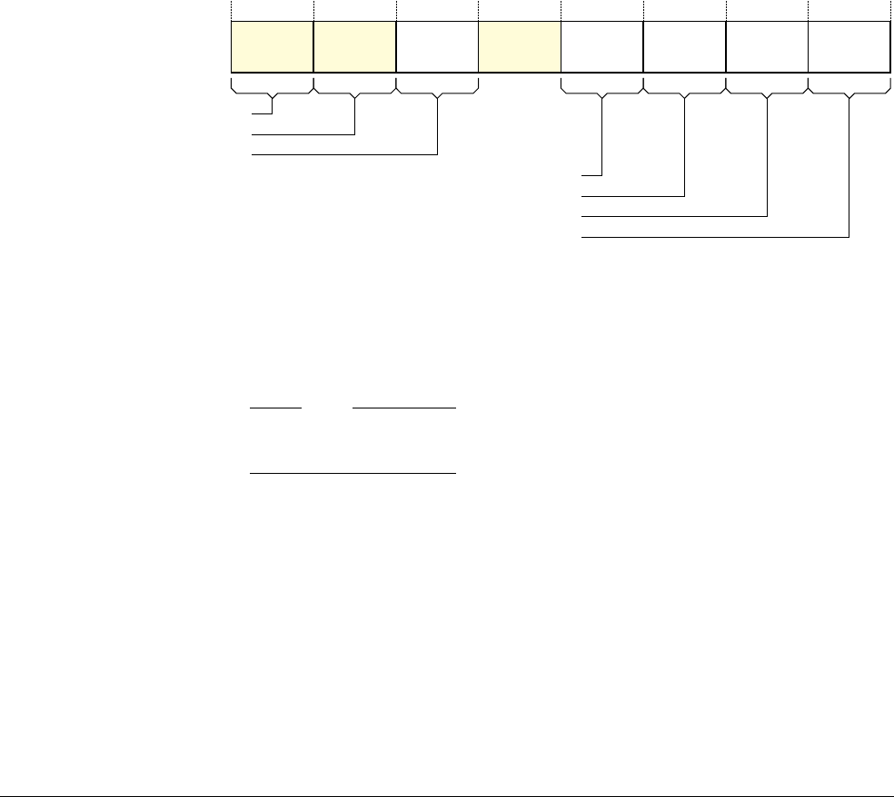
B6 System Control Registers in a PMSA implementation
B6.1 PMSA System control registers descriptions, in register order
B6-1878 Copyright © 1996-1998, 2000, 2004-2012, 2014 ARM. All rights reserved. ARM DDI 0406C.c
Non-Confidential ID051414
B6.1.55 ID_MMFR3, Memory Model Feature Register 3, PMSA
The ID_MMFR3 characteristics are:
Purpose ID_MMFR3 provides information about the implemented memory model and memory
management support.
This register is a CPUID register, and is part of the Identification registers functional group.
Usage constraints Only accessible from PL1.
Must be interpreted with ID_MMFR0, ID_MMFR1, and ID_MMFR2.
Configurations The VMSA and PMSA definitions of the register fields are identical.
Attributes A 32-bit RO register with an IMPLEMENTATION DEFINED value:
•Table B7-1 on page B7-1952 shows the encodings of all of the CPUID registers
•Table B5-13 on page B5-1800 shows the encodings of all of the registers in the
Identification registers functional group.
All field values not shown in the field descriptions are reserved.
The ID_MMFR3 bit assignments are:
Supersection support, bits[31:28]
On a VMSA implementation, indicates whether Supersections are supported. Permitted values are:
0b0000
Supersections supported.
0b1111
Supersections not supported.
Note
The sense of this identification is reversed from the normal usage in the CPUID mechanism, with
the value of zero indicating that the feature is supported.
Cached memory size, bits[27:24]
Indicates the physical memory size supported by the processor caches. Permitted values are:
0b0000
4GBbyte, corresponding to a 32-bit physical address range.
0b0001
64GBbyte, corresponding to a 36-bit physical address range.
0b0010
1TBbyte, corresponding to a 40-bit physical address range.
31 28 27 16 15 12 11 8 7 4 3 0
Reserved,
UNK
Supersection support
BP maintain
Cache maintenance set/way
Cache maintenance MVA
Maintenance broadcast
1920
2324
Coherent walk
Cached memory size
†
† Only on an implementation that includes the Large Physical Address Extension, otherwise reserved.

B6 System Control Registers in a PMSA implementation
B6.1 PMSA System control registers descriptions, in register order
ARM DDI 0406C.c Copyright © 1996-1998, 2000, 2004-2012, 2014 ARM. All rights reserved. B6-1879
ID051414 Non-Confidential
Coherent walk, bits[23:20]
Indicates whether translation table updates require a clean to the point of unification. Permitted
values are:
0b0000
Updates to the translation tables require a clean to the point of unification to ensure
visibility by subsequent translation table walks.
0b0001
Updates to the translation tables do not require a clean to the point of unification to
ensure visibility by subsequent translation table walks.
Bits[19:16] Reserved, UNK.
Maintenance broadcast, bits[15:12]
Indicates whether Cache, TLB and branch predictor operations are broadcast. Permitted values are:
0b0000
Cache, TLB and branch predictor operations only affect local structures.
0b0001
Cache and branch predictor operations affect structures according to shareability and
defined behavior of instructions. TLB operations only affect local structures.
0b0010
Cache, TLB and branch predictor operations affect structures according to shareability
and defined behavior of instructions.
BP maintain, bits[11:8]
Indicates the supported branch predictor maintenance operations in an implementation with
hierarchical cache maintenance operations. Permitted values are:
0b0000
None supported.
0b0001
Supported branch predictor maintenance operations are:
• Invalidate all branch predictors.
0b0010
As for
0b0001
, and adds:
• Invalidate branch predictors by MVA.
Cache maintain set/way, bits[7:4]
Indicates the supported cache maintenance operations by set/way, in an implementation with
hierarchical caches. Permitted values are:
0b0000
None supported.
0b0001
Supported hierarchical cache maintenance operations by set/way are:
• Invalidate data cache by set/way
• Clean data cache by set/way
• Clean and invalidate data cache by set/way.
In a unified cache implementation, the data cache operations apply to the unified caches.
Cache maintain MVA, bits[3:0]
Indicates the supported cache maintenance operations by MVA, in an implementation with
hierarchical caches. Permitted values are:
0b0000
None supported.
0b0001
Supported hierarchical cache maintenance operations by MVA are:
• Invalidate data cache by MVA
• Clean data cache by MVA
• Clean and invalidate data cache by MVA
• Invalidate instruction cache by MVA
• Invalidate all instruction cache entries.
In a unified cache implementation, the data cache operations apply to the unified caches, and the
instruction cache operations are not implemented.

B6 System Control Registers in a PMSA implementation
B6.1 PMSA System control registers descriptions, in register order
B6-1880 Copyright © 1996-1998, 2000, 2004-2012, 2014 ARM. All rights reserved. ARM DDI 0406C.c
Non-Confidential ID051414
Accessing ID_MMFR3
To access ID_MMFR3, software reads the CP15 registers with
<opc1>
set to 0,
<CRn>
set to c0,
<CRm>
set to c1, and
<opc2>
set to7. For example:
MRC p15, 0, <Rt>, c0, c1, 7 ; Read ID_MMFR3 into Rt

B6 System Control Registers in a PMSA implementation
B6.1 PMSA System control registers descriptions, in register order
ARM DDI 0406C.c Copyright © 1996-1998, 2000, 2004-2012, 2014 ARM. All rights reserved. B6-1881
ID051414 Non-Confidential
B6.1.56 ID_PFR0, Processor Feature Register 0, PMSA
The ID_PFR0 characteristics are:
Purpose ID_PFR0 gives information about the programmers’ model and top-level information about
the instruction sets supported by the processor.
This register is a CPUID register, and is part of the Identification registers functional group.
Usage constraints Only accessible from PL1.
Must be interpreted with ID_PFR1.
Configurations The VMSA and PMSA definitions of the register fields are identical.
Attributes A 32-bit RO register with an IMPLEMENTATION DEFINED value:
•Table B7-1 on page B7-1952 shows the encodings of all of the CPUID registers
•Table B5-13 on page B5-1800 shows the encodings of all of the registers in the
Identification registers functional group.
All field values not shown in the field descriptions are reserved.
The ID_PFR0 bit assignments are:
Bits[31:16] Reserved, UNK.
State3, bits[15:12]
ThumbEE instruction set support. Permitted values are:
0b0000
Not implemented.
0b0001
ThumbEE instruction set implemented.
The value of
0b0001
is only permitted when State1 ==
0b0011
.
State2, bits[11:8]
Jazelle extension support. Permitted values are:
0b0000
Not implemented.
0b0001
Jazelle extension implemented, without clearing of JOSCR.CV on exception entry.
0b0010
Jazelle extension implemented, with clearing of JOSCR.CV on exception entry.
A trivial implementation of the Jazelle extension is indicated by the value
0b0001
.
State1, bits[7:4]
Thumb instruction set support. Permitted values are:
0b0000
Thumb instruction set not implemented.
0b0001
Thumb encodings before the introduction of Thumb-2 technology implemented:
• all instructions are 16-bit
•a
BL
or
BLX
is a pair of 16-bit instructions
• 32-bit instructions other than
BL
and
BLX
cannot be encoded.
0b0010
Reserved.
0b0011
Thumb encodings after the introduction of Thumb-2 technology implemented, for all
16-bit and 32-bit Thumb basic instructions.
State0, bits[3:0]
ARM instruction set support. Permitted values are:
0b0000
ARM instruction set not implemented.
0b0001
ARM instruction set implemented.
Reserved, UNK
31 16 15 12 11 8 7 4 3 0
State3 State2 State1 State0

B6 System Control Registers in a PMSA implementation
B6.1 PMSA System control registers descriptions, in register order
B6-1882 Copyright © 1996-1998, 2000, 2004-2012, 2014 ARM. All rights reserved. ARM DDI 0406C.c
Non-Confidential ID051414
Accessing ID_PFR0
To access ID_PFR0, software reads the CP15 registers with
<opc1>
set to 0,
<CRn>
set to c0,
<CRm>
set to c1, and
<opc2>
set to 0. For example:
MRC p15, 0, <Rt>, c0, c1, 0 ; Read ID_PFR0 into Rt
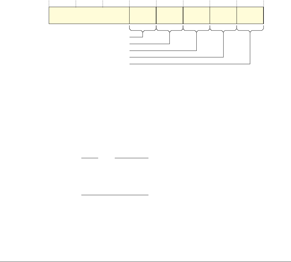
B6 System Control Registers in a PMSA implementation
B6.1 PMSA System control registers descriptions, in register order
ARM DDI 0406C.c Copyright © 1996-1998, 2000, 2004-2012, 2014 ARM. All rights reserved. B6-1883
ID051414 Non-Confidential
B6.1.57 ID_PFR1, Processor Feature Register 1, PMSA
The ID_PFR1 characteristics are:
Purpose ID_PFR1 gives information about the programmers’ model and Security Extensions
support.
This register is a CPUID register, and is part of the Identification registers functional group.
Usage constraints Only accessible from PL1.
Must be interpreted with ID_PFR0.
Configurations The VMSA and PMSA definitions of the register fields are identical.
Attributes A 32-bit RO register with an IMPLEMENTATION DEFINED value:
•Table B7-1 on page B7-1952 shows the encodings of all of the CPUID registers
•Table B5-13 on page B5-1800 shows the encodings of all of the registers in the
Identification registers functional group.
All field values not shown in the field descriptions are reserved.
The ID_PFR1 bit assignments are:
Bits[31:20] Reserved, UNK.
Generic Timer Extension, bits[19:16]
Permitted values are:
0b0000
Not implemented.
0b0001
Generic Timer Extension implemented.
Virtualization Extensions, bits[15:12]
Permitted values are:
0b0000
Not implemented.
0b0001
Virtualization Extensions implemented.
Note
• A value of
0b0001
implies the implementation of the
HVC
,
ERET
,
MRS
(Banked register), and
MSR
(Banked register) instructions. The ID_ISARs do not identify whether these instructions are
implemented.
• This field must have the value
0b0000
in a PMSA implementation.
Programmers’ model
M profile programmers’ model
Security Extensions
Virtualization Extensions
Reserved, UNK
31 20 19 16 15 12 11 8 7 4 3 0
Generic Timer

B6 System Control Registers in a PMSA implementation
B6.1 PMSA System control registers descriptions, in register order
B6-1884 Copyright © 1996-1998, 2000, 2004-2012, 2014 ARM. All rights reserved. ARM DDI 0406C.c
Non-Confidential ID051414
M profile programmers’ model, bits[11:8]
Permitted values are:
0b0000
Not supported.
0b0010
Support for two-stack programmers’ model.
Note
In this field, the permitted values are not continuous, and the value of
0b0001
is reserved.
Security Extensions, bits[7:4]
Permitted values are:
0b0000
Not implemented.
0b0001
Security Extensions implemented.
This includes support for Monitor mode and the
SMC
instruction.
0b0010
As for
0b0001
, and adds the ability to set the NSACR.RFR bit.
Note
This field must have the value
0b0000
in a PMSA implementation.
Programmers’ model, bits[3:0]
Support for the standard programmers’ model for ARMv4 and later. Model must support User, FIQ,
IRQ, Supervisor, Abort, Undefined and System modes. Permitted values are:
0b0000
Not supported.
0b0001
Supported.
Accessing ID_PFR1
To access ID_PFR1, software reads the CP15 registers with
<opc1>
set to 0,
<CRn>
set to c0,
<CRm>
set to c1, and
<opc2>
set to 1. For example:
MRC p15, 0, <Rt>, c0, c1, 1 ; Read ID_PFR1 into Rt

B6 System Control Registers in a PMSA implementation
B6.1 PMSA System control registers descriptions, in register order
ARM DDI 0406C.c Copyright © 1996-1998, 2000, 2004-2012, 2014 ARM. All rights reserved. B6-1885
ID051414 Non-Confidential
B6.1.58 IFAR, Instruction Fault Address Register, PMSA
The IFAR characteristics are:
Purpose The IFAR holds the address of the access that caused a synchronous Prefetch Abort
exception.
This register is part of the PL1 Fault handling registers functional group.
Usage constraints Only accessible from PL1.
Configurations Always implemented.
Attributes A 32-bit RW register with an UNKNOWN reset value. See also Reset behavior of CP14 and
CP15 registers on page B5-1778.
Table B5-15 on page B5-1801 shows the encodings of all of the registers in the PL1 Fault
handling registers functional group.
The IFAR bit assignments are:
For information about using the IFAR, including when the value in the IFAR is valid, see Exception reporting in a
PMSA implementation on page B5-1769.
A debugger can write to the IFAR to restore its value.
Accessing the IFAR
To access the IFAR, software reads or writes the CP15 registers with
<opc1>
set to 0,
<CRn>
set to c6,
<CRm>
set to c0,
and
<opc2>
set to 2. For example:
MRC p15, 0, <Rt>, c6, c0, 2 ; Read IFAR into Rt
MCR p15, 0, <Rt>, c6, c0, 2 ; Write Rt to IFAR
Faulting address of synchronous Prefetch Abort exception
31 0
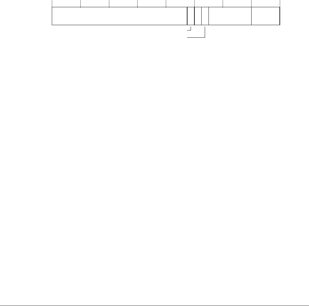
B6 System Control Registers in a PMSA implementation
B6.1 PMSA System control registers descriptions, in register order
B6-1886 Copyright © 1996-1998, 2000, 2004-2012, 2014 ARM. All rights reserved. ARM DDI 0406C.c
Non-Confidential ID051414
B6.1.59 IFSR, Instruction Fault Status Register, PMSA
The IFSR characteristics are:
Purpose The IFSR holds status information about the last instruction fault.
This register is part of the PL1 Fault handling registers functional group.
Usage constraints Only accessible from PL1.
Configurations Always implemented.
Attributes A 32-bit RW register with an UNKNOWN reset value. See also Reset behavior of CP14 and
CP15 registers on page B5-1778.
Table B5-15 on page B5-1801 shows the encodings of all of the registers in the PL1 Fault
handling registers functional group.
The IFSR bit assignments are:
Bits[31:13, 11, 9:4] Reserved, UNK/SBZP.
ExT, bit[12] External abort type. This bit can provide an IMPLEMENTATION DEFINED classification of
external aborts.
For aborts other than external aborts this bit always returns 0.
In an implementation that does not provide any classification of external aborts, this bit is
UNK/SBZP.
FS, bits[10, 3:0] Fault status bits.
See Table B5-7 on page B5-1771 for the valid encodings of these bits. All encodings not
shown in the table are reserved.
For information about using the IFSR see Exception reporting in a PMSA implementation on page B5-1769.
Accessing the IFSR
To access the IFSR, software reads or writes the CP15 registers with
<opc1>
set to 0,
<CRn>
set to c5,
<CRm>
set to c0,
and
<opc2>
set to 1. For example:
MRC p15, 0, <Rt>, c5, c0, 1 ; Read IFSR into Rt
MCR p15, 0, <Rt>, c5, c0, 1 ; Write Rt to IFSR
(0) FS[3:0]
31 13 12 11 10 9 4 3 0
Reserved, UNK/SBZP
ExT
Reserved,
UNK/SBZP
FS[4]

B6 System Control Registers in a PMSA implementation
B6.1 PMSA System control registers descriptions, in register order
ARM DDI 0406C.c Copyright © 1996-1998, 2000, 2004-2012, 2014 ARM. All rights reserved. B6-1887
ID051414 Non-Confidential
B6.1.60 IRACR, Instruction Region Access Control Register, PMSA
The IRACR characteristics are:
Purpose The IRACR defines the memory attributes for the current memory region in the instruction
address map.
This register is part of the MMU control registers functional group.
Usage constraints Only accessible from PL1.
Used in conjunction with the other MPU Memory region programming registers, see
Programming the MPU region attributes on page B5-1763.
Configurations Only implemented when the PMSA implements separate instruction and data memory
maps.
Attributes A 32-bit RW register with an UNKNOWN reset value. See also Reset behavior of CP14 and
CP15 registers on page B5-1778.
Table B5-14 on page B5-1801 shows the encodings of all of the registers in the MMU
control registers functional group.
The IRACR bit assignments are identical to the DRACR assignments.
Note
The XN bit, bit[12], is always valid in the IRACR.
The current memory region is selected by the value held in the RGNR.
If software accesses this register when the RGNR does not point to a valid region in the MPU instruction address
map, the result is UNPREDICTABLE.
Accessing the IRACR
To access the IRACR, software reads or writes the CP15 registers with
<opc1>
set to 0,
<CRn>
set to c6,
<CRm>
set to
c1, and
<opc2>
set to 5. For example:
MRC p15, 0, <Rt>, c6, c1, 5 ; Read IRACR into Rt
MCR p15, 0, <Rt>, c6, c1, 5 ; Write Rt to IRACR

B6 System Control Registers in a PMSA implementation
B6.1 PMSA System control registers descriptions, in register order
B6-1888 Copyright © 1996-1998, 2000, 2004-2012, 2014 ARM. All rights reserved. ARM DDI 0406C.c
Non-Confidential ID051414
B6.1.61 IRBAR, Instruction Region Base Address Register, PMSA
The IRBAR characteristics are:
Purpose The IRBAR indicates the base address of the current memory region in the Instruction
address map.
This register is part of the MMU control registers functional group.
Usage constraints Only accessible from PL1.
Used in conjunction with the other MPU Memory region programming registers, see
Programming the MPU region attributes on page B5-1763.
Configurations Only implemented when the PMSA implements separate instruction and data memory
maps.
Attributes A 32-bit RW register with an UNKNOWN reset value. See also Reset behavior of CP14 and
CP15 registers on page B5-1778.
Table B5-14 on page B5-1801 shows the encodings of all of the registers in the MMU
control registers functional group.
The IRBAR bit assignments are identical to the DRBAR assignments.
The base address must be aligned to the region size, otherwise behavior is UNPREDICTABLE. The current memory
region is selected by the value held in the RGNR.
Software can use the IRBAR to find the minimum region size supported by the implementation, see Finding the
minimum supported region size on page B5-1760.
Accessing the IRBAR
To access the IRBAR, software reads or writes the CP15 registers with
<opc1>
set to 0,
<CRn>
set to c6,
<CRm>
set to
c1, and
<opc2>
set to 1. For example:
MRC p15, 0, <Rt>, c6, c1, 1 ; Read IRBAR into Rt
MCR p15, 0, <Rt>, c6, c1, 1 ; Write Rt to IRBAR

B6 System Control Registers in a PMSA implementation
B6.1 PMSA System control registers descriptions, in register order
ARM DDI 0406C.c Copyright © 1996-1998, 2000, 2004-2012, 2014 ARM. All rights reserved. B6-1889
ID051414 Non-Confidential
B6.1.62 IRSR, Instruction Region Size and Enable Register, PMSA
The IRSR characteristics are:
Purpose The IRSR indicates the size of the current memory region in the instruction address map,
and software can use it to enable or disable:
• the entire region
• each of the eight subregions, if the region is enabled.
This register is part of the MMU control registers functional group.
Usage constraints Only accessible from PL1.
Used in conjunction with the other MPU Memory region programming registers, see
Programming the MPU region attributes on page B5-1763.
Configurations Only implemented when the PMSA implements separate instruction and data memory
maps.
Attributes A 32-bit RW register that resets to zero. See also Reset behavior of CP14 and CP15 registers
on page B5-1778.
Table B5-14 on page B5-1801 shows the encodings of all of the registers in the MMU
control registers functional group.
The IRSR bit assignments are identical to the DRSR assignments.
All memory regions must be enabled before they are used.
The current memory region is selected by the value held in the RGNR.
The minimum region size supported is IMPLEMENTATION DEFINED, but if the memory system implementation
includes an instruction cache, ARM strongly recommends that the minimum region size is a multiple of the
instruction cache line length. This prevents cache attributes changing mid-way through a cache line.
Behavior is UNPREDICTABLE if software:
• writes a region size that is outside the range supported by the implementation
• accesses this register when the RGNR does not point to a valid region in the MPU instruction address map.
Accessing the IRSR
To access the IRSR, software reads or writes the CP15 registers with
<opc1>
set to 0,
<CRn>
set to c6,
<CRm>
set to c1,
and
<opc2>
set to 3. For example:
MRC p15, 0, <Rt>, c6, c1, 3 ; Read IRSR into Rt
MCR p15, 0, <Rt>, c6, c1, 3 ; Write Rt to IRSR

B6 System Control Registers in a PMSA implementation
B6.1 PMSA System control registers descriptions, in register order
B6-1890 Copyright © 1996-1998, 2000, 2004-2012, 2014 ARM. All rights reserved. ARM DDI 0406C.c
Non-Confidential ID051414
B6.1.63 JIDR, Jazelle ID Register, PMSA
The JIDR characteristics are:
Purpose Identifies the Jazelle architecture and subarchitecture versions.
This register is a Jazelle register.
Usage constraints Read access rights depend on the execution privilege and the value of the JOSCR.CD bit.
Write accesses are UNPREDICTABLE at PL1 or higher, and UNDEFINED at PL0. See Access to
Jazelle registers on page A2-100.
Configurations The VMSA and PMSA definitions of the register fields are identical.
Always implemented, but can be implemented as RAZ on a processor with a trivial
implementation of the Jazelle extension.
Attributes A 32-bit RO register.
Table A2-16 on page A2-99 shows the encodings of all the Jazelle registers.
The JIDR bit assignments are:
Architecture, bits[31:28]
Architecture code. This uses the same Architecture code that appears in the MIDR.
On a trivial implementation of the Jazelle extension this field must be RAZ.
Implementer, bits[27:20]
Implementer code of the designer of the subarchitecture. This uses the same Implementer code that
appears in the MIDR.
On a trivial implementation of the Jazelle extension this field must be RAZ.
Subarchitecture, bits[19:12]
Contain the subarchitecture code. The following subarchitecture code is defined:
0x00
Jazelle v1 subarchitecture, or trivial implementation of the Jazelle extension if the
Implementer field is RAZ.
On a trivial implementation of the Jazelle extension this field must be RAZ.
Bits[11:0] Can contain additional SUBARCHITECTURE DEFINED information.
Accessing the JIDR
To access the JIDR, software reads the CP14 registers with
<opc1>
set to 7,
<CRn>
set to c0,
<CRm>
set to c0, and
<opc2>
set to 0. For example:
MRC p14, 7, <Rt>, c0, c0, 0 ; Read JIDR into Rt
Architecture
31 28 27 20 19 12 11 0
Implementer Subarchitecture SUBARCHITECTURE DEFINED

B6 System Control Registers in a PMSA implementation
B6.1 PMSA System control registers descriptions, in register order
ARM DDI 0406C.c Copyright © 1996-1998, 2000, 2004-2012, 2014 ARM. All rights reserved. B6-1891
ID051414 Non-Confidential
B6.1.64 JMCR, Jazelle Main Configuration Register, PMSA
The JMCR characteristics are:
Purpose Provides control of the Jazelle extension.
This register is a Jazelle register.
Usage constraints Access rights depend on the execution privilege and the value of the JOSCR.CD bit, see
Access to Jazelle registers in a non-trivial Jazelle implementation on page A2-100.
Configurations The VMSA and PMSA definitions of the register fields are identical.
Always implemented. A processor with a trivial implementation of the Jazelle extension
must implement JMCR as RAZ/WI.
Attributes A 32-bit RW register. See the field descriptions for details about the reset value.
Table A2-16 on page A2-99 shows the encodings of all the Jazelle registers.
The JMCR bit assignments are:
Bits[31:1] SUBARCHITECTURE DEFINED information. This means the reset value of this field is also
SUBARCHITECTURE DEFINED.
JE, bit[0] Jazelle Enable bit:
0 Jazelle extension disabled. The
BXJ
instruction does not cause Jazelle state execution.
BXJ
behaves exactly as a
BX
instruction, see Jazelle state entry instruction, BXJ on
page A2-98.
1 Jazelle extension enabled.
The reset value of this bit is 0.
Accessing the JMCR
To access the JMCR, software reads or writes the CP14 registers with
<opc1>
set to 7,
<CRn>
set to c2,
<CRm>
set to
c0, and
<opc2>
set to 0. For example:
MRC p14, 7, <Rt>, c2, c0, 0 ; Read JMCR into Rt
MCR p14, 7, <Rt>, c2, c0, 0 ; Write Rt to JMCR
JE
31 10
SUBARCHITECTURE DEFINED

B6 System Control Registers in a PMSA implementation
B6.1 PMSA System control registers descriptions, in register order
B6-1892 Copyright © 1996-1998, 2000, 2004-2012, 2014 ARM. All rights reserved. ARM DDI 0406C.c
Non-Confidential ID051414
B6.1.65 JOSCR, Jazelle OS Control Register, PMSA
The JOSCR characteristics are:
Purpose Provides operating system control of the use of the Jazelle extension by processes and
threads.
This register is a Jazelle register
Usage constraints Accessible only from PL1 or higher.
Normally used in conjunction with the JMCR.JE bit.
Configurations The VMSA and PMSA definitions of the register fields are identical.
Always implemented. A processor with a trivial implementation of the Jazelle extension
must implement JOSCR either:
•as RAZ/WI
• so that it can be read or written, but the processor ignores the effect of any read or
write.
Attributes A 32-bit RW register that resets to zero.
Table A2-16 on page A2-99 shows the encodings of all the Jazelle registers.
The JOSCR bit assignments are:
Bits[31:2] Reserved, UNK/SBZP.
CV, bit[1] Configuration Valid bit. This bit is used by an operating system to signal to the EJVM that it must
rewrite its configuration to the configuration registers. The possible values are:
0 Configuration not valid. The EJVM must rewrite its configuration to the configuration
registers before it executes another bytecode instruction.
1 Configuration valid. The EJVM does not need to update the configuration registers.
When JMCR.JE is set to 1, the CV bit also controls entry to Jazelle state, see Controlling entry to
Jazelle state on page B1-1243.
CD, bit[0] Configuration Disabled bit. This bit is used by an operating system to disable User mode access to
the JIDR and configuration registers:
0 Configuration enabled. Access to the Jazelle registers, including User mode accesses,
operate normally. For more information, see the register descriptions in Application
level configuration and control of the Jazelle extension on page A2-99.
1 Configuration disabled in User mode. User mode access to the Jazelle registers are
UNDEFINED, and all User mode accesses to the Jazelle registers cause an Undefined
Instruction exception.
For more information about the use of this bit see Monitoring and controlling User mode access to
the Jazelle extension on page B1-1244.
The JOSCR provides a control mechanism that is independent of the subarchitecture of the Jazelle extension. An
operating system can use this mechanism to control access to the Jazelle extension, see Jazelle state configuration
and control on page B1-1243.
Reserved, UNK/SBZP
31 210
CV
CD

B6 System Control Registers in a PMSA implementation
B6.1 PMSA System control registers descriptions, in register order
ARM DDI 0406C.c Copyright © 1996-1998, 2000, 2004-2012, 2014 ARM. All rights reserved. B6-1893
ID051414 Non-Confidential
Accessing the JOSCR
To access the JOSCR, software reads or writes the CP14 registers with
<opc1>
set to 7,
<CRn>
set to c1,
<CRm>
set to
c0, and
<opc2>
set to 0. For example:
MRC p14, 7, <Rt>, c1, c0, 0 ; Read JOSCR into Rt
MCR p14, 7, <Rt>, c1, c0, 0 ; Write Rt to JOSCR

B6 System Control Registers in a PMSA implementation
B6.1 PMSA System control registers descriptions, in register order
B6-1894 Copyright © 1996-1998, 2000, 2004-2012, 2014 ARM. All rights reserved. ARM DDI 0406C.c
Non-Confidential ID051414
B6.1.66 MIDR, Main ID Register, PMSA
The MIDR characteristics are:
Purpose The MIDR provides identification information for the processor, including an implementer
code for the device and a device ID number.
This register is part of the Identification registers functional group.
Usage constraints Only accessible from PL1.
Configurations Some fields of the MIDR are IMPLEMENTATION DEFINED. For details of the values of these
fields for a particular ARMv7 implementation, and any implementation-specific
significance of these values, see the product documentation.
Attributes A 32-bit RO register with an IMPLEMENTATION DEFINED value. See also Reset behavior of
CP14 and CP15 registers on page B5-1778.
Table B5-13 on page B5-1800 shows the encodings of all of the registers in the
Identification registers functional group.
The MIDR bit assignments are:
Implementer, bits[31:24]
The Implementer code. Table B6-4 shows the permitted values for this field.
All other values are reserved by ARM and must not be used.
Variant, bits[23:20]
An IMPLEMENTATION DEFINED variant number. Typically, this field distinguishes between different
product variants, for example implementations of the same product with different cache sizes.
Table B6-4 Implementer codes
Bits[31:24] ASCII character Implementer
0x41
A ARM Limited
0x44
D Digital Equipment Corporation
0x4D
M Motorola, Freescale Semiconductor Inc.
0x51
Q Qualcomm Inc.
0x56
V Marvell Semiconductor Inc.
0x69
i Intel Corporation
Revision
31 24 23 20 19 16 15 4 3 0
Implementer Variant Architecture Primary part number

B6 System Control Registers in a PMSA implementation
B6.1 PMSA System control registers descriptions, in register order
ARM DDI 0406C.c Copyright © 1996-1998, 2000, 2004-2012, 2014 ARM. All rights reserved. B6-1895
ID051414 Non-Confidential
Architecture, bits[19:16]
Table B6-5 shows the permitted values for this field.
All other values are reserved by ARM and must not be used.
Primary part number, bits[15:4]
An IMPLEMENTATION DEFINED primary part number for the device.
Note
• On processors implemented by ARM, if the top four bits of the primary part number are
0x0
or
0x7
, the variant and architecture are encoded differently, see the description of the MIDR
in Appendix D15 ARMv4 and ARMv5 Differences.
• Processors implemented by ARM have an Implementer code of
0x41
.
Revision, bits[3:0]
An IMPLEMENTATION DEFINED revision number for the device.
ARMv7 requires all implementations to use the CPUID scheme, described in Chapter B7 The CPUID Identification
Scheme, and an implementation is described by the MIDR and the CPUID registers.
Note
For an ARMv7 implementation by ARM, the MIDR is interpreted as:
Bits[31:24] Implementer code, must be
0x41
.
Bits[23:20] Major revision number, rX.
Bits[19:16] Architecture code, must be
0xF
.
Bits[15:4] ARM part number.
Bits[3:0] Minor revision number, pY.
Accessing the MIDR
To access the MIDR, software reads the CP15 registers with
<opc1>
set to 0,
<CRn>
set to c0,
<CRm>
set to c0, and
<opc2>
set to 0. For example:
MRC p15, 0, <Rt>, c0, c0, 0 ; Read MIDR into Rt
Table B6-5 Architecture codes
Bits[19:16] Architecture
0x1
ARMv4
0x2
ARMv4T
0x3
ARMv5 (obsolete)
0x4
ARMv5T
0x5
ARMv5TE
0x6
ARMv5TEJ
0x7
ARMv6
0xF
Defined by CPUID scheme
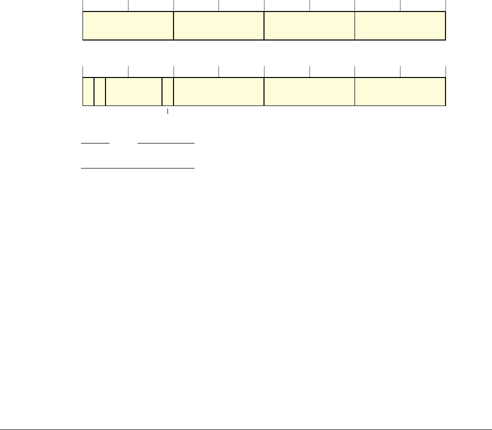
B6 System Control Registers in a PMSA implementation
B6.1 PMSA System control registers descriptions, in register order
B6-1896 Copyright © 1996-1998, 2000, 2004-2012, 2014 ARM. All rights reserved. ARM DDI 0406C.c
Non-Confidential ID051414
B6.1.67 MPIDR, Multiprocessor Affinity Register, PMSA
The MPIDR characteristics are:
Purpose In a multiprocessor system, the MPIDR provides an additional processor identification
mechanism for scheduling purposes, and indicates whether the implementation includes the
Multiprocessing Extensions.
This register is part of the Identification registers functional group.
Usage constraints Only accessible from PL1.
Configurations This register is not implemented in architecture versions before ARMv7.
In a uniprocessor system ARM recommends that each Affn field of this register returns a
value of 0.
Attributes A 32-bit RO register with an IMPLEMENTATION DEFINED value. See also Reset behavior of
CP14 and CP15 registers on page B5-1778.
Table B5-13 on page B5-1800 shows the encodings of all of the registers in the
Identification registers functional group.
In an ARMv7 implementation that does not include the Multiprocessing Extensions, the MPIDR bit assignments
are:
In an implementation that includes the Multiprocessing Extensions, the MPIDR bit assignments are:
Note
In the MPIDR bit definitions, a processor in the system can be a physical processor or a virtual machine.
Bits[31:24], ARMv7 without the Multiprocessing Extensions
Reserved, RAZ.
Bits[31], in an implementation that includes the Multiprocessing Extensions
RAO. Indicates that the implementation uses the Multiprocessing Extensions register format.
U, bit[30], in an implementation that includes the Multiprocessing Extensions
Indicates a Uniprocessor system, as distinct from processor 0 in a multiprocessor system. The
possible values of this bit are:
0 Processor is part of a multiprocessor system.
1 Processor is part of a uniprocessor system.
Bits[29:25], in an implementation that includes the Multiprocessing Extensions
Reserved, UNK.
Reserved, RAZ
31 24 23 16 15 8 7 0
Aff2 Aff1 Aff0
1
31 30 29 25 24 23 16 15 8 7 0
UReserved,
UNK Aff2 Aff1 Aff0
MT

B6 System Control Registers in a PMSA implementation
B6.1 PMSA System control registers descriptions, in register order
ARM DDI 0406C.c Copyright © 1996-1998, 2000, 2004-2012, 2014 ARM. All rights reserved. B6-1897
ID051414 Non-Confidential
MT, bit[24], in an implementation that includes the Multiprocessing Extensions
Indicates whether the lowest level of affinity consists of logical processors that are implemented
using a multi-threading type approach. The possible values of this bit are:
0 Performance of processors at the lowest affinity level is largely independent.
1 Performance of processors at the lowest affinity level is very interdependent.
For more information about the meaning of this bit see Multi-threading approach to lowest affinity
levels, Multiprocessing Extensions.
Aff2, bits[23:16]
Affinity level 2. The least significant affinity level field, for this processor in the system.
Aff1, bits[15:8]
Affinity level 1. The intermediate affinity level field, for this processor in the system.
Aff0, bits[7:0]
Affinity level 0. The most significant affinity level field, for this processor in the system.
See Recommended use of the MPIDR for clarification of the meaning of most significant and least significant
affinity levels.
The assigned value of the MPIDR.{Aff0, Aff1, Aff0} set of fields must be unique for each processor in the system
as a whole.
When matching against an affinity level field, scheduler software checks for a value equal to or greater than a
required value.
Recommended use of the MPIDR includes a description of an example multiprocessor system and the affinity level
field values it might use.
The interpretation of these fields is IMPLEMENTATION DEFINED, and must be documented as part of the
documentation of the multiprocessor system. ARM recommends that this register might be used as described in
Recommended use of the MPIDR.
The software mechanism to discover the total number of affinity numbers used at each level is IMPLEMENTATION
DEFINED, and is part of the general system identification task.
Multi-threading approach to lowest affinity levels, Multiprocessing Extensions
In an implementation that includes the Multiprocessing Extensions, if the MPIDR.MT bit is set to 1, this indicates
that the processors at affinity level 0 are logical processors, implemented using a multi-threading type approach. In
such an approach, there can be a significant performance impact if a new thread is assigned the processor with:
• a different affinity level 0 value to some other thread, referred to as the original thread
• a pair of values for affinity levels 1 and 2 that are the same as the pair of values of the original thread.
In this situation, the performance of the original thread might be significantly reduced.
Note
In this description, thread always refers to a thread or a process.
Recommended use of the MPIDR
In a multiprocessor system the register might provide two important functions:
• Identifying special functionality of a particular processor in the system. In general, the actual meaning of the
affinity level fields is not important. In a small number of situations, an affinity level field value might have
a special IMPLEMENTATION DEFINED significance. Possible examples include booting from reset and
powerdown events.

B6 System Control Registers in a PMSA implementation
B6.1 PMSA System control registers descriptions, in register order
B6-1898 Copyright © 1996-1998, 2000, 2004-2012, 2014 ARM. All rights reserved. ARM DDI 0406C.c
Non-Confidential ID051414
• Providing affinity information for the scheduling software, to help the scheduler run an individual thread or
process on either:
— the same processor, or as similar a processor as possible, as the processor it was running on previously
— a processor on which a related thread or process was run.
The MPIDR provides a mechanism with up to three levels of affinity information, but the meaning of those levels
of affinity is entirely IMPLEMENTATION DEFINED. The levels of affinity provided can have different meanings.
Table B6-6 shows two possible implementations.
The scheduler maintains affinity level information for all threads and processes. When it has to reschedule a thread
or process, the scheduler:
1. Looks for an available processor that matches at all three affinity levels.
2. If step 1 fails, the scheduler might look for a processor that matches at levels 2 and 3 only.
3. If the scheduler still cannot find an available processor it might look for a match at level 3 only.
A multiprocessor system corresponding to Example system 1 in Table B6-6 might implement affinity values as
shown in Table B6-7.
Accessing the MPIDR
To access the MPIDR, software reads the CP15 registers with
<opc1>
set to 0,
<CRn>
set to c0,
<CRm>
set to c0, and
<opc2>
set to 5. For example:
MRC p15, 0, <Rt>, c0, c0, 5 ; Read MPIDR into Rt
Table B6-6 Possible implementations of the affinity levels
Affinity level Example system 1 Example system 2
0 Virtual CPUs in a in a multi-threaded processor Processors in an SMP cluster
1 Processors in an Symmetric Multi Processor (SMP) cluster Clusters with a system
2 Clusters in a system No meaning, fixed as 0
Table B6-7 Example of possible affinity values at different affinity levels
A2, Cluster level, values Aff1, Processor level, values Aff0, Virtual CPU level, values
0 0 0, 1
0 1 0, 1
0 2 0, 1
0 3 0, 1
1 0 0, 1
1 1 0, 1
1 2 0, 1
1 3 0, 1

B6 System Control Registers in a PMSA implementation
B6.1 PMSA System control registers descriptions, in register order
ARM DDI 0406C.c Copyright © 1996-1998, 2000, 2004-2012, 2014 ARM. All rights reserved. B6-1899
ID051414 Non-Confidential
B6.1.68 MPUIR, MPU Type Register, PMSA
The MPUIR characteristics are:
Purpose The MPUIR identifies the following features of the MPU implementation:
• whether the MPU implements:
— a Unified address map, also referred to as a von Neumann architecture
— separate Instruction and Data address maps, also referred to as a Harvard
architecture.
• the number of memory regions implemented by the MPU.
This register is part of the Identification registers functional group.
Usage constraints Only accessible from PL1.
Configurations Implemented only when the PMSA is implemented.
Attributes A 32-bit RO register with an IMPLEMENTATION DEFINED value. See also Reset behavior of
CP14 and CP15 registers on page B5-1778.
Table B5-13 on page B5-1800 shows the encodings of all of the registers in the
Identification registers functional group.
The MPUIR bit assignments are:
Bits[31:24] Reserved, UNK.
IRegion, bits[23:16] Specifies the number of Instruction regions implemented by the MPU.
If the MPU implements a Unified memory map this field is UNK.
DRegion, bits[15:8] Specifies the number of Data or Unified regions implemented by the MPU.
If this field is zero, no MPU is implemented, and the default memory map is in use.
Bits[7:1] Reserved, UNK.
nU, bit[0] Not Unified MPU. Indicates whether the MPU implements a unified memory map:
0 Unified memory map. Bits[23:16] of the register are zero.
1 Separate Instruction and Data memory maps.
Accessing the MPUIR
To access the MPUIR, software reads the CP15 registers with
<opc1>
set to 0,
<CRn>
set to c0,
<CRm>
set to c0, and
<opc2>
set to 4. For example:
MRC p15, 0, <Rt>, c0, c0, 4 ; Read MOUIR into Rt
nU
Reserved, UNK
31 24 23 16 15 8 7 1 0
IRegion DRegion Reserved, UNK

B6 System Control Registers in a PMSA implementation
B6.1 PMSA System control registers descriptions, in register order
B6-1900 Copyright © 1996-1998, 2000, 2004-2012, 2014 ARM. All rights reserved. ARM DDI 0406C.c
Non-Confidential ID051414
B6.1.69 MVFR0, Media and VFP Feature Register 0, PMSA
The MVFR0 characteristics are:
Purpose The MVFR0 describes the features provided by the Advanced SIMD and Floating-point
Extensions.
This register is an Advanced SIMD and Floating-point Extension system register.
Usage constraints Only accessible from PL1 or higher. See Accessing the Advanced SIMD and Floating-point
Extension system registers on page B1-1237 for more information.
Must be interpreted with MVFR1. This register complements the information provided by
the CPUID scheme described in Chapter B7 The CPUID Identification Scheme.
Configurations Implemented only if the implementation includes one or both of:
• the Floating-point Extension
• the Advanced SIMD Extension.
The VMSA and PMSA definitions of the register fields are identical.
Attributes A 32-bit RO register.
Table B1-24 on page B1-1236 shows the encodings of all of the Advanced SIMD and
Floating-point Extension system registers
The MVFR0 bit assignments are:
VFP rounding modes, bits[31:28]
Indicates the rounding modes supported by the Floating-point Extension hardware. Permitted values
are:
0b0000
Only Round to Nearest mode supported, except that Round towards Zero mode is
supported for
VCVT
instructions that always use that rounding mode regardless of the
FPSCR setting.
0b0001
All rounding modes supported.
Short vectors, bits[27:24]
Indicates the hardware support for VFP short vectors. Permitted values are:
0b0000
Not supported.
0b0001
Short vector operation supported.
Square root, bits[23:20]
Indicates the hardware support for the Floating-point Extension square root operations. Permitted
values are:
0b0000
Not supported in hardware.
0b0001
Supported.
Note
• the
VSQRT.F32
instruction also requires the single-precision floating-point attribute, bits[7:4]
• the
VSQRT.F64
instruction also requires the double-precision floating-point attribute,
bits[11:8].
VFP
rounding
modes
Short
vectors
Square
root Divide
31 16 15 12 11 8 7 4 3 0
VFP
exception
trapping
Double-
precision
Single-
precision
A_SIMD
registers
28 27 24 23 20 19

B6 System Control Registers in a PMSA implementation
B6.1 PMSA System control registers descriptions, in register order
ARM DDI 0406C.c Copyright © 1996-1998, 2000, 2004-2012, 2014 ARM. All rights reserved. B6-1901
ID051414 Non-Confidential
Divide, bits[19:16]
Indicates the hardware support for Floating-point Extension divide operations. Permitted values are:
0b0000
Not supported in hardware.
0b0001
Supported.
Note
• the
VDIV.F32
instruction also requires the single-precision floating-point attribute, bits[7:4]
• the
VDIV.F64
instruction also requires the double-precision floating-point attribute, bits[11:8].
VFP exception trapping, bits[15:12]
Indicates whether the Floating-point Extension hardware implementation supports exception
trapping. Permitted values are:
0b0000
Not supported. This is the value for VFPv3 and VFPv4.
0b0001
Supported by the hardware. This is the value for VFPv2, and for VFPv3U and VFPv4U.
When exception trapping is supported, support code is required to handle the trapped
exceptions.
Note
This value does not indicate that trapped exception handling is available. Because
trapped exception handling requires support code, only the support code can provide
this information.
Double-precision, bits[11:8]
Indicates the hardware support for Floating-point Extension double-precision operations. Permitted
values are:
0b0000
Not supported in hardware.
0b0001
Supported, VFPv2.
0b0010
Supported, VFPv3 or VFPv4.
VFPv3 adds an instruction to load a double-precision floating-point constant, and
conversions between double-precision and fixed-point values.
A value of
0b0001
or
0b0010
indicates support for all Floating-point Extension double-precision
instructions in the supported version of the extension, except that, in addition to this field being
nonzero:
•
VSQRT.F64
is only available if the Square root field is
0b0001
•
VDIV.F64
is only available if the Divide field is
0b0001
• conversion between double-precision and single-precision is only available if the
single-precision field is nonzero.

B6 System Control Registers in a PMSA implementation
B6.1 PMSA System control registers descriptions, in register order
B6-1902 Copyright © 1996-1998, 2000, 2004-2012, 2014 ARM. All rights reserved. ARM DDI 0406C.c
Non-Confidential ID051414
Single-precision, bits[7:4]
Indicates the hardware support for Floating-point Extension single-precision operations. Permitted
values are:
0b0000
Not supported in hardware.
0b0001
Supported, VFPv2.
0b0010
Supported, VFPv3 or VFPv4.
VFPv3 adds an instruction to load a single-precision floating-point constant, and
conversions between single-precision and fixed-point values.
A value of
0b0001
or
0b0010
indicates support for all Floating-point Extension single-precision
instructions in the supported version of the extension, except that, in addition to this field being
nonzero:
•
VSQRT.F32
is only available if the Square root field is
0b0001
•
VDIV.F32
is only available if the Divide field is
0b0001
• conversion between double-precision and single-precision is only available if the
double-precision field is nonzero.
A_SIMD registers, bits[3:0]
Indicates support for the Advanced SIMD register bank. Permitted values are:
0b0000
Not supported.
0b0001
Supported, 16 × 64-bit registers.
0b0010
Supported, 32 × 64-bit registers.
If this field is nonzero:
• all Floating-point Extension
LDC
,
STC
,
MCR
, and
MRC
instructions are supported
• if the CPUID register shows that the
MCRR
and
MRRC
instructions are supported then the
corresponding Floating-point Extension instructions are supported.
Accessing MVFR0
Software accesses MVFR0 using the
VMRS
instruction, see VMRS on page B9-2014. For example:
VMRS <Rt>, MVFR0 ; Read MVFR0 into Rt

B6 System Control Registers in a PMSA implementation
B6.1 PMSA System control registers descriptions, in register order
ARM DDI 0406C.c Copyright © 1996-1998, 2000, 2004-2012, 2014 ARM. All rights reserved. B6-1903
ID051414 Non-Confidential
B6.1.70 MVFR1, Media and VFP Feature Register 1, PMSA
The MVFR1 characteristics are:
Purpose The MVFR1 describes the features provided by the Advanced SIMD and Floating-point
Extensions.
This register is an Advanced SIMD and Floating-point Extension system register.
Usage constraints Only accessible from PL1 or higher. See Accessing the Advanced SIMD and Floating-point
Extension system registers on page B1-1237 for more information.
Must be interpreted with MVFR0. These registers complement the information provided by
the CPUID scheme described in Chapter B7 The CPUID Identification Scheme.
Configurations Implemented only if the implementation includes one or both of:
• the Floating-point Extension
• the Advanced SIMD Extension.
The VMSA and PMSA definitions of the register fields are identical.
Attributes A 32-bit RO register.
Table B1-24 on page B1-1236 shows the encodings of all of the Advanced SIMD and
Floating-point Extension system registers
The MVFR1 bit assignments are:
A_SIMD FMAC, bits[31:28]
Indicates whether any implemented Floating-point or Advanced SIMD Extension implements the
fused multiply accumulate instructions. Permitted values are:
0b0000
Not implemented.
0b0001
Implemented.
If an implementation includes both the Floating-point Extension and the Advanced SIMD
Extension, both extensions must provide the same level of support for these instructions.
VFP HPFP, bits[27:24]
Indicates whether the Floating-point Extension supports half-precision floating-point conversion
instructions. Permitted values are:
0b0000
Not supported.
0b0001
Supported.
A_SIMD HPFP, bits[23:20]
Indicates whether the Advanced SIMD Extension implements half-precision floating-point
conversion instructions. Permitted values are:
0b0000
Not implemented.
0b0001
Implemented. This value is permitted only if the A_SIMD SPFP field is
0b0001
.
A_SIMD SPFP, bits[19:16]
Indicates whether the Advanced SIMD Extension implements single-precision floating-point
instructions. Permitted values are:
0b0000
Not implemented.
0b0001
Implemented. This value is permitted only if the A_SIMD integer field is
0b0001
.
A_SIMD
FMAC
VFP
HPFP
A_SIMD
HPFP
A_SIMD
SPFP
31 16 15 12 11 8 7 4 3 0
A_SIMD
integer
A_SIMD
load/store
D_NaN
mode
FtZ
mode
28 27 24 23 20 19

B6 System Control Registers in a PMSA implementation
B6.1 PMSA System control registers descriptions, in register order
B6-1904 Copyright © 1996-1998, 2000, 2004-2012, 2014 ARM. All rights reserved. ARM DDI 0406C.c
Non-Confidential ID051414
A_SIMD integer, bits[15:12]
Indicates whether the Advanced SIMD Extension implements integer instructions. Permitted values
are:
0b0000
Not implemented.
0b0001
Implemented.
A_SIMD load/store, bits[11:8]
Indicates whether the Advanced SIMD Extension implements load/store instructions. Permitted
values are:
0b0000
Not implemented.
0b0001
Implemented.
D_NaN mode, bits[7:4]
Indicates whether the Floating-point Extension hardware implementation supports only the Default
NaN mode. Permitted values are:
0b0000
Hardware supports only the Default NaN mode. If a VFP subarchitecture is
implemented its support code might include support for propagation of NaN values.
0b0001
Hardware supports propagation of NaN values.
FtZ mode, bits[3:0]
Indicates whether the Floating-point Extension hardware implementation supports only the
Flush-to-Zero mode of operation. Permitted values are:
0b0000
Hardware supports only the Flush-to-Zero mode of operation. If a VFP subarchitecture
is implemented its support code might include support for full denormalized number
arithmetic.
0b0001
Hardware supports full denormalized number arithmetic.
Accessing MVFR1
Software accesses MVFR1 using the
VMRS
instruction, see VMRS on page B9-2014. For example:
VMRS <Rt>, MVFR1 ; Read MVFR1 into Rt

B6 System Control Registers in a PMSA implementation
B6.1 PMSA System control registers descriptions, in register order
ARM DDI 0406C.c Copyright © 1996-1998, 2000, 2004-2012, 2014 ARM. All rights reserved. B6-1905
ID051414 Non-Confidential
B6.1.71 PMCCNTR, Performance Monitors Cycle Count Register, PMSA
When accessed through the CP15 interface, the PMCCNTR characteristics are:
Purpose The PMCCNTR holds the value of the processor Cycle Counter, CCNT, that counts
processor clock cycles.
This register is a Performance Monitors register.
Usage constraints The PMCCNTR is accessible in:
• all PL1 modes
• User mode when PMUSERENR.EN == 1.
See Access permissions on page C12-2330 for more information.
The PMCR.D bit configures whether PMCCNTR increments once every clock cycle, or
once every 64 clock cycles.
In PMUv2, the PMXEVTYPER accessed when PMSELR.SEL is set to
0b11111
determines
the modes and states in which the PMCCNTR can increment.
Configurations Implemented only as part of the Performance Monitors Extension.
The VMSA and PMSA definitions of the register fields are identical.
Attributes A 32-bit RW register with a reset value that is UNKNOWN on a non-debug logic reset. See
also Power domains and Performance Monitors registers reset on page C12-2329.
Table C12-7 on page C12-2329 shows the CP15 encodings of all of the Performance
Monitors registers.
Note
Differences in the memory-mapped views of the Performance Monitors registers on page D2-2354 describes how
the characteristics of the PMCCNTR differ when it is accessed through an external debug interface or a
memory-mapped interface.
The PMCCNTR bit assignments are:
CCNT, bits[31:0] Cycle count. Depending on the value of PMCR.D, this field increments either:
• once every processor clock cycle
• once every 64 processor clock cycles.
The PMCCNTR.CCNT value can be reset to zero by writing a 1 to PMCR.C.
Accessing the PMCCNTR
To access the PMCCNTR, read or write the CP15 registers with
<opc1>
set to 0,
<CRn>
set to c9,
<CRm>
set to c13, and
<opc2>
set to 0. For example:
MRC p15, 0, <Rt>, c9, c13, 0 : Read PMCCNTR into Rt
MCR p15, 0, <Rt>, c9, c13, 0 : Write Rt to PMCCNTR
CCNT
31 0

B6 System Control Registers in a PMSA implementation
B6.1 PMSA System control registers descriptions, in register order
B6-1906 Copyright © 1996-1998, 2000, 2004-2012, 2014 ARM. All rights reserved. ARM DDI 0406C.c
Non-Confidential ID051414
B6.1.72 PMCEID0 and PMCEID1, Performance Monitors Common Event ID registers, PMSA
When accessed through the CP15 interface, the PMCEID0 and PMCEID1 register characteristics are:
Purpose The PMCEIDn registers define which common architectural and common
microarchitectural feature events are implemented.
These registers are Performance Monitors registers.
Usage constraints The PMCEIDn registers are accessible in:
• all PL1 modes
• User mode when PMUSERENR.EN is set to 1.
See Access permissions on page C12-2330 for more information.
Configurations Implemented only as part of the Performance Monitors Extension.
The VMSA and PMSA definitions of the register fields are identical.
Attributes A 32-bit RO register.
Table C12-7 on page C12-2329 shows the CP15 encodings of all of the Performance
Monitors registers.
Note
Differences in the memory-mapped views of the Performance Monitors registers on page D2-2354 describes how
the characteristics of the PMCEID0 and PMCEID1 registers differ when they are accessed through an external
debug interface or a memory-mapped interface.
Table B6-8 shows the PMCEID0 bit assignments with event implemented or not implemented when the associated
bit is set to 1 or 0.
PMCEID1[31:0] is reserved and must be implemented as RAZ. Software must not rely on the bits reading as 0.
Table B6-8 PMCEID0 bit assignments
Bit Event number Event implemented if set to 1 or not implemented if set to 0
[31]
0x1F
Reserved, UNK.
[30]
0x1E
[29]
0x1D
Bus cycle.
[28]
0x1C
Instruction architecturally executed, condition code check pass, write to TTBR.
[27]
0x1B
Instruction speculatively executed.
[26]
0x1A
Local memory error.
[25]
0x19
Bus access.
[24]
0x18
Level 2 data cache write-back.
[23]
0x17
Level 2 data cache refill.
[22]
0x16
Level 2 data cache access.
[21]
0x15
Level 1 data cache write-back.
[20]
0x14
Level 1 instruction cache access.
[19]
0x13
Data memory access.
[18]
0x12
Predictable branch speculatively executed. If the implementation includes program flow prediction, this bit
is RAO.

B6 System Control Registers in a PMSA implementation
B6.1 PMSA System control registers descriptions, in register order
ARM DDI 0406C.c Copyright © 1996-1998, 2000, 2004-2012, 2014 ARM. All rights reserved. B6-1907
ID051414 Non-Confidential
Accessing the PMCEID0 or PMCEID1 register
To access the PMCEID0 or PMCEID1 register, software reads the CP15 register with
<opc1>
set to 0,
<CRn>
set to
c9,
<CRm>
set to c12, and:
•
<opc2>
set to 6 for the PMCEID0 register
•
<opc2>
set to 7 for the PMCEID1 register.
For example:
MRC p15, 0, <Rt>, c9, c12, 6 ; Read PMCEID0 into Rt
MRC p15, 0, <Rt>, c9, c12, 7 ; Read PMCEID1 into Rt
[17]
0x11
Cycle, this bit is RAO.
[16]
0x10
Mispredicted or not predicted branch speculatively executed. If the implementation includes program flow
prediction resources, this bit is RAO.
[15]
0x0F
Instruction architecturally executed, condition code check pass, unaligned load or store.
[14]
0x0E
Instruction architecturally executed, condition code check pass, procedure return.
[13]
0x0D
Instruction architecturally executed, immediate branch.
[12]
0x0C
Instruction architecturally executed, condition code check pass, software change of the PC.
[11]
0x0B
Instruction architecturally executed, condition code check pass, write to CONTEXTIDR.
[10]
0x0A
Instruction architecturally executed, condition code check pass, exception return.
[9]
0x09
Exception taken.
[8]
0x08
Instruction architecturally executed.
[7]
0x07
Instruction architecturally executed, condition code check pass, store.
[6]
0x06
Instruction architecturally executed, condition code check pass, load.
[5]
0x05
Level 1 data TLB refill.
[4]
0x04
Level 1 data cache access. If the implementation includes a L1 data or unified cache, this bit is RAO.
[3]
0x03
Level 1 data cache refill. If the implementation includes a L1 data or unified cache, this bit is RAO.
[2]
0x02
Level 1 instruction TLB refill.
[1]
0x01
Level 1 instruction cache refill.
[0]
0x00
Instruction architecturally executed, condition code check pass, software increment. This bit is RAO.
Table B6-8 PMCEID0 bit assignments (continued)
Bit Event number Event implemented if set to 1 or not implemented if set to 0

B6 System Control Registers in a PMSA implementation
B6.1 PMSA System control registers descriptions, in register order
B6-1908 Copyright © 1996-1998, 2000, 2004-2012, 2014 ARM. All rights reserved. ARM DDI 0406C.c
Non-Confidential ID051414
B6.1.73 PMCNTENCLR, Performance Monitors Count Enable Clear register, PMSA
When accessed through the CP15 interface, the PMCNTENCLR register characteristics are:
Purpose The PMCNTENCLR register disables the Cycle Count Register, PMCCNTR, and any
implemented event counters, PMNx. Reading this register shows which counters are
enabled.
This register is a Performance Monitors register.
Usage constraints PMCNTENCLR is accessible in:
• all PL1 modes
• User mode when PMUSERENR.EN == 1.
See Access permissions on page C12-2330 for more information. See also Counter enables
on page C12-2313 and Counter access on page C12-2314.
PMCNTENCLR is used in conjunction with the PMCNTENSET register.
Configurations Implemented only as part of the Performance Monitors Extension.
The VMSA and PMSA definitions of the register fields are identical.
Attributes A 32-bit RW register with a reset value that is UNKNOWN on a non-debug logic reset. See
also Power domains and Performance Monitors registers reset on page C12-2329.
Table C12-7 on page C12-2329 shows the CP15 encodings of all of the Performance
Monitors registers.
Note
Differences in the memory-mapped views of the Performance Monitors registers on page D2-2354 describes how
the characteristics of the PMCNTENCLR register differ when it is accessed through an external debug interface or
a memory-mapped interface.
The PMCNTENCLR register bit assignments are:
Note
In the description of the PMCNTENCLR register, N and x have the meanings used in the description of the
PMCNTENSET register.
C, bit[31] PMCCNTR disable bit. Table B6-9 shows the behavior of this bit on reads and writes.
Bits[30:N] RAZ/WI.
Table B6-9 Read and write values for the PMCNTENCLR.C bit
Value Meaning on read Action on write
0 Cycle counter disabled No action, write is ignored
1 Cycle counter enabled Disable the cycle counter
C
31 30 N N–1 0
Reserved, RAZ/WI Event counter disable bits, Px, for x = 0 to (N–1)

B6 System Control Registers in a PMSA implementation
B6.1 PMSA System control registers descriptions, in register order
ARM DDI 0406C.c Copyright © 1996-1998, 2000, 2004-2012, 2014 ARM. All rights reserved. B6-1909
ID051414 Non-Confidential
Px, bit[x], for x = 0 to (N–1)
Event counter x, PMNx, disable bit.
Table B6-10 shows the behavior of this bit on reads and writes.
Note
PMCR.E can override the settings in this register and disable all counters including PMCCNTR. PMCNTENCLR
retains its value when PMCR.E is 0, even though its settings are ignored.
Accessing the PMCNTENCLR register
To access the PMCNTENCLR register, read or write the CP15 registers with
<opc1>
set to 0,
<CRn>
set to c9,
<CRm>
set to c12, and
<opc2>
set to 2. For example:
MRC p15, 0, <Rt>, c9, c12, 2 : Read PMCNTENCLR into Rt
MCR p15, 0, <Rt>, c9, c12, 2 : Write Rt to PMCNTENCLR
Table B6-10 Read and write values for the PMCNTENCLR.Px bits
Px value Meaning on read Action on write
0PMNx event counter disabled No action, write is ignored
1PMNx event counter enabled Disable the PMNx event counter

B6 System Control Registers in a PMSA implementation
B6.1 PMSA System control registers descriptions, in register order
B6-1910 Copyright © 1996-1998, 2000, 2004-2012, 2014 ARM. All rights reserved. ARM DDI 0406C.c
Non-Confidential ID051414
B6.1.74 PMCNTENSET, Performance Monitors Count Enable Set register, PMSA
When accessed through the CP15 interface, the PMCNTENSET register characteristics are:
Purpose The PMCNTENSET register enables the Cycle Count Register, PMCCNTR, and any
implemented event counters, PMNx. Reading this register shows which counters are
enabled.
This register is a Performance Monitors register.
Usage constraints PMCNTENSET is accessible in:
• all PL1 modes
• User mode when PMUSERENR.EN is set to 1.
See Access permissions on page C12-2330 for more information. See also Counter enables
on page C12-2313 and Counter access on page C12-2314.
PMCNTENSET is used in conjunction with PMCNTENCLR.
Configurations Implemented only as part of the Performance Monitors Extension.
The VMSA and PMSA definitions of the register fields are identical.
Attributes A 32-bit RW register with a reset value that is UNKNOWN on a non-debug logic reset. See
also Power domains and Performance Monitors registers reset on page C12-2329.
Table C12-7 on page C12-2329 shows the CP15 encodings of all of the Performance
Monitors registers.
Note
Differences in the memory-mapped views of the Performance Monitors registers on page D2-2354 describes how
the characteristics of the PMCNTENSET register differ when it is accessed through an external debug interface or
a memory-mapped interface.
The PMCNTENSET register bit assignments are:
Note
In the description of the PMCNTENSET register:
• N is the number of event counters implemented, as defined by the PMCR.N field.
•x refers to a single event counter, and takes values from 0 to (N–1).
C, bit[31] PMCCNTR enable bit.
Table B6-11 shows the behavior of this bit on reads and writes.
Bits[30:N] RAZ/WI.
Table B6-11 Read and write bit values for the PMCNTENSET.C bit
Value Meaning on read Action on write
0 Cycle counter disabled No action, write is ignored
1 Cycle counter enabled Enable the PMCCNTR cycle counter
C
31 30 N N–1 0
Reserved, RAZ/WI Event counter enable bits, Px, for x = 0 to (N–1)

B6 System Control Registers in a PMSA implementation
B6.1 PMSA System control registers descriptions, in register order
ARM DDI 0406C.c Copyright © 1996-1998, 2000, 2004-2012, 2014 ARM. All rights reserved. B6-1911
ID051414 Non-Confidential
Px, bit[x], for x = 0 to (N–1)
Event counter x, PMNx, enable bit.
Table B6-12 shows the behavior of this bit on reads and writes.
Accessing the PMCNTENSET register
To access the PMCNTENSET register, read or write the CP15 registers with
<opc1>
set to 0,
<CRn>
set to c9,
<CRm>
set
to c12, and
<opc2>
set to 1. For example:
MRC p15, 0, <Rt>, c9, c12, 1 ; Read PMCNTENSET into Rt
MCR p15, 0, <Rt>, c9, c12, 1 ; Write Rt to PMCNTENSET
Table B6-12 Read and write values for the PMCNTENSET.Px bits
Px value Meaning on read Action on write
0PMNx event counter disabled No action, write is ignored
1PMNx event counter enabled Enable the PMNx event counter
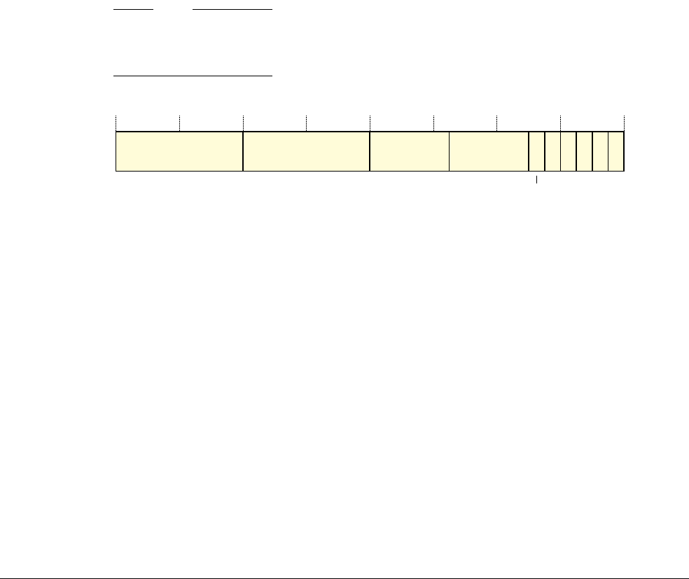
B6 System Control Registers in a PMSA implementation
B6.1 PMSA System control registers descriptions, in register order
B6-1912 Copyright © 1996-1998, 2000, 2004-2012, 2014 ARM. All rights reserved. ARM DDI 0406C.c
Non-Confidential ID051414
B6.1.75 PMCR, Performance Monitors Control Register, PMSA
When accessed through the CP15 interface, the PMCR characteristics are:
Purpose The PMCR provides details of the Performance Monitors implementation, including the
number of counters implemented, and configures and controls the counters.
This register is a Performance Monitors register.
Usage constraints The PMCR is accessible in:
• all PL1 modes
• User mode when PMUSERENR.EN is set to 1.
See Access permissions on page C12-2330 for more information. See also Counter enables
on page C12-2313 and Counter access on page C12-2314.
Configurations Implemented only as part of the Performance Monitors Extension.
The VMSA and PMSA definitions of the register fields are identical.
Attributes A 32-bit RW register with a reset value that depends on the register implementation. For
more information see the register bit descriptions and Power domains and Performance
Monitors registers reset on page C12-2329.
Table C12-7 on page C12-2329 shows the CP15 encodings of all of the Performance
Monitors registers.
Note
Differences in the memory-mapped views of the Performance Monitors registers on page D2-2354 describes how
the characteristics of the PMCR differ when it is accessed through an external debug interface or a memory-mapped
interface.
The PMCR bit assignments are:
IMP, bits[31:24] Implementer code. This field is RO with an IMPLEMENTATION DEFINED value.
The implementer codes are allocated by ARM. Values have the same interpretation as
bits[31:24] of the MIDR.
IDCODE, bits[23:16] Identification code. This field is RO with an IMPLEMENTATION DEFINED value.
Each implementer must maintain a list of identification codes that is specific to the
implementer. A specific implementation is identified by the combination of the implementer
code and the identification code.
N, bits[15:11] Number of event counters. This field is RO with an IMPLEMENTATION DEFINED value that
indicates the number of counters implemented.
The value of this field is the number of counters implemented, from
0b00000
for no counters
to
0b11111
for 31 counters.
An implementation can implement only the Cycle Count Register, PMCCNTR. This is
indicated by a value of
0b00000
for the N field.
Bits[10:6] Reserved, UNK/SBZP.
EIMP
31 24 23 16 15 11 6 5 4 3 2 1 0
IDCODE N Reserved,
UNK/SBZP X D C P
10
DP

B6 System Control Registers in a PMSA implementation
B6.1 PMSA System control registers descriptions, in register order
ARM DDI 0406C.c Copyright © 1996-1998, 2000, 2004-2012, 2014 ARM. All rights reserved. B6-1913
ID051414 Non-Confidential
DP, bit[5] Disable PMCCNTR when event counting is prohibited. The possible values of this bit are:
0 Cycle counter operates regardless of the non-invasive debug authentication
settings.
1 Cycle counter is disabled if non-invasive debug is not permitted.
For more information, see Effects of non-invasive debug authentication on the Performance
Monitors on page C12-2304 and Chapter C9 Non-invasive Debug Authentication.
This bit is RW. Its non-debug logic reset value is 0.
X, bit[4] Export enable. The possible values of this bit are:
0 Export of events is disabled.
1 Export of events is enabled.
This bit enables the exporting of events to another debug device, such as a trace macrocell,
over an event bus. If the implementation does not include such an event bus, this bit is
RAZ/WI.
This bit does not affect the generation of Performance Monitors interrupts, that can be
implemented as a signal exported from the processor to an interrupt controller.
This bit is RW. Its non-debug logic reset value is 0.
D, bit[3] Cycle counter clock divider. The possible values of this bit are:
0 When enabled, PMCCNTR counts every clock cycle.
1 When enabled, PMCCNTR counts once every 64 clock cycles.
This bit is RW. Its non-debug logic reset value is 0.
C, bit[2] Cycle counter reset. This bit is WO. The effects of writing to this bit are:
0 No action.
1 Reset PMCCNTR to zero.
Note
Resetting PMCCNTR does not clear the PMCCNTR overflow bit to 0. For more
information, see the description of PMOVSR.
This bit is always RAZ.
P, bit[1] Event counter reset. This bit is WO. The effects of writing to this bit are:
0 No action.
1 Reset all event counters, not including PMCCNTR, to zero.
Note
Resetting the event counters does not clear any overflow bits to 0. For more information,
see the description of PMOVSR.
This bit is always RAZ.
E, bit[0] Enable. The possible values of this bit are:
0 All counters, including PMCCNTR, are disabled.
1 All counters are enabled.
For more information, see Counter enables on page C12-2313.
This bit is RW. Its non-debug logic reset value is 0.

B6 System Control Registers in a PMSA implementation
B6.1 PMSA System control registers descriptions, in register order
B6-1914 Copyright © 1996-1998, 2000, 2004-2012, 2014 ARM. All rights reserved. ARM DDI 0406C.c
Non-Confidential ID051414
Accessing the PMCR
To access PMCR, read or write the CP15 registers with
<opc1>
set to 0,
<CRn>
set to c9,
<CRm>
set to c12, and
<opc2>
set to 0. For example:
MRC p15, 0, <Rt>, c9, c12, 0 ; Read PMCR into Rt
MCR p15, 0, <Rt>, c9, c12, 0 ; Write Rt to PMCR

B6 System Control Registers in a PMSA implementation
B6.1 PMSA System control registers descriptions, in register order
ARM DDI 0406C.c Copyright © 1996-1998, 2000, 2004-2012, 2014 ARM. All rights reserved. B6-1915
ID051414 Non-Confidential
B6.1.76 PMINTENCLR, Performance Monitors Interrupt Enable Clear register, PMSA
When accessed through the CP15 interface, the PMINTENCLR register characteristics are:
Purpose The PMINTENCLR register disables the generation of interrupt requests on overflows
from:
• the Cycle Count Register, PMCCNTR
• each implemented event counter, PMNx.
Reading the register shows which overflow interrupt requests are enabled.
This register is a Performance Monitors register.
Usage constraints The PMINTENCLR register is accessible in all PL1 modes.
In User mode, instructions that access the register are always UNDEFINED, even if
PMUSERENR.EN is set to 1.
See Access permissions on page C12-2330 for more information. See also Counter access
on page C12-2314.
PMINTENCLR is used in conjunction with the PMINTENSET register.
Configurations Implemented only as part of the Performance Monitors Extension.
The VMSA and PMSA definitions of the register fields are identical.
Attributes A 32-bit RW register with a reset value that is UNKNOWN on a non-debug logic reset. See
also Power domains and Performance Monitors registers reset on page C12-2329.
Table C12-7 on page C12-2329 shows the CP15 encodings of all of the Performance
Monitors registers.
Note
Differences in the memory-mapped views of the Performance Monitors registers on page D2-2354 describes how
the characteristics of the PMINTENCLR register differ when it is accessed through an external debug interface or
a memory-mapped interface.
The PMINTENCLR register bit assignments are:
Note
In the description of the PMINTENCLR register, N and x have the meanings used in the description of the
PMCNTENSET register.
C, bit[31] PMCCNTR overflow interrupt request disable bit.
Table B6-13 shows the behavior of this bit on reads and writes.
Bits[30:N] RAZ/WI.
Table B6-13 Read and write values for the PMINTENCLR.C bit
Value Meaning on read Action on write
0 Cycle count interrupt request disabled No action, write is ignored
1 Cycle count interrupt request enabled Disable the cycle count interrupt request
C
31 30 N N–1 0
Reserved, RAZ/WI Event counter overflow interrupt request disable bits, Px, for x = 0 to (N–1)

B6 System Control Registers in a PMSA implementation
B6.1 PMSA System control registers descriptions, in register order
B6-1916 Copyright © 1996-1998, 2000, 2004-2012, 2014 ARM. All rights reserved. ARM DDI 0406C.c
Non-Confidential ID051414
Px, bit[x], for x = 0 to (N–1)
Event counter x, PMNx, overflow interrupt request disable bit.
Table B6-14 shows the behavior of this bit on reads and writes.
For more information about counter overflow interrupt requests see the PMINTENSET register description.
Accessing the PMINTENCLR register
To access the PMINTENCLR register, read or write the CP15 registers with
<opc1>
set to 0,
<CRn>
set to c9,
<CRm>
set
to c14, and
<opc2>
set to 2. For example:
MRC p15, 0, <Rt>, c9, c14, 2 : Read PMINTENCLR into Rt
MCR p15, 0, <Rt>, c9, c14, 2 : Write Rt to PMINTENCLR
Table B6-14 Read and write values for the PMINTENCLR.Px bits
Px value Meaning on read Action on write
0PMNx interrupt request disabled No action, write is ignored
1PMNx interrupt request enabled Disable the PMNx interrupt request

B6 System Control Registers in a PMSA implementation
B6.1 PMSA System control registers descriptions, in register order
ARM DDI 0406C.c Copyright © 1996-1998, 2000, 2004-2012, 2014 ARM. All rights reserved. B6-1917
ID051414 Non-Confidential
B6.1.77 PMINTENSET, Performance Monitors Interrupt Enable Set register, PMSA
When accessed through the CP15 interface, the PMINTENSET register characteristics are:
Purpose The PMINTENSET register enables the generation of interrupt requests on overflows from:
• the Cycle Count Register, PMCCNTR
• each implemented event counter, PMNx.
Reading the register shows which overflow interrupt requests are enabled.
This register is a Performance Monitors register.
Usage constraints The PMINTENSET register is accessible in all PL1 modes.
In User mode, instructions that access the register are always UNDEFINED, even if
PMUSERENR.EN is set to 1.
See Access permissions on page C12-2330 for more information. See also Counter access
on page C12-2314.
PMINTENSET is used in conjunction with the PMINTENCLR register.
Configurations Implemented only as part of the Performance Monitors Extension.
The VMSA and PMSA definitions of the register fields are identical.
Attributes A 32-bit RW register with a reset value that is UNKNOWN on a non-debug logic reset. See
also Power domains and Performance Monitors registers reset on page C12-2329.
Table C12-7 on page C12-2329 shows the CP15 encodings of all of the Performance
Monitors registers.
Note
Differences in the memory-mapped views of the Performance Monitors registers on page D2-2354 describes how
the characteristics of the PMINTENSET register differ when it is accessed through an external debug interface or a
memory-mapped interface.
The PMINTENSET register bit assignments are:
Note
In the description of the PMINTENSET register, N and x have the meanings used in the description of the
PMCNTENSET register.
C, bit[31] PMCCNTR overflow interrupt request enable bit.
Table B6-15 shows the behavior of this bit on reads and writes.
Bits[30:N] RAZ/WI.
Table B6-15 Read and write values for the PMINTENSET.C bit
Value Meaning on read Action on write
0 Cycle count interrupt request disabled No action, write is ignored
1 Cycle count interrupt request enabled Enable the cycle count interrupt request
C
31 30 N N–1 0
Reserved, RAZ/WI Event counter overflow interrupt request enable bits, Px, for x = 0 to (N–1)

B6 System Control Registers in a PMSA implementation
B6.1 PMSA System control registers descriptions, in register order
B6-1918 Copyright © 1996-1998, 2000, 2004-2012, 2014 ARM. All rights reserved. ARM DDI 0406C.c
Non-Confidential ID051414
Px, bit[x], for x = 0 to (N–1)
Event counter x, PMNx, overflow interrupt request enable bit.
Table B6-16 shows the behavior of this bit on reads and writes.
The debug logic does not signal an interrupt request if the PMCR.E enable bit is set to 0.
When an interrupt is signaled, software can remove it by writing a 1 to the corresponding overflow bit in the
PMOVSR.
Note
ARM expects that the interrupt request that can be generated on a counter overflow is exported from the processor,
meaning it can be factored into a system interrupt controller if applicable. This means that normally the system has
more levels of control of the interrupt generated.
Accessing the PMINTENSET register
To access the PMINTENSET register, read or write the CP15 registers with
<opc1>
set to 0,
<CRn>
set to c9,
<CRm>
set
to c14, and
<opc2>
set to 1. For example:
MRC p15, 0, <Rt>, c9, c14, 1 : Read PMINTENSET into Rt
MCR p15, 0, <Rt>, c9, c14, 1 : Write Rt to PMINTENSET
Table B6-16 Read and write values for the PMINTENSET.Px bits
Px value Meaning on read Action on write
0PMNx interrupt request disabled No action, write is ignored
1PMNx interrupt request enabled Enable the PMNx interrupt request

B6 System Control Registers in a PMSA implementation
B6.1 PMSA System control registers descriptions, in register order
ARM DDI 0406C.c Copyright © 1996-1998, 2000, 2004-2012, 2014 ARM. All rights reserved. B6-1919
ID051414 Non-Confidential
B6.1.78 PMOVSR, Performance Monitors Overflow Flag Status Register, PMSA
When accessed through the CP15 interface, the PMOVSR characteristics are:
Purpose The PMOVSR holds the state of the overflow bits for:
• the Cycle Count Register, PMCCNTR
• each of the implemented event counters, PMNx.
Software must write to this register to clear these bits.
This register is a Performance Monitors register.
Usage constraints The PMOVSR is accessible in:
• all PL1 modes
• User mode when PMUSERENR.EN is set to 1.
See Access permissions on page C12-2330 for more information. See also Counter access
on page C12-2314.
Configurations Implemented only as part of the Performance Monitors Extension.
The VMSA and PMSA definitions of the register fields are identical.
Attributes A 32-bit RW register with a reset value that is UNKNOWN on a non-debug logic reset. See
also Power domains and Performance Monitors registers reset on page C12-2329.
Table C12-7 on page C12-2329 shows the CP15 encodings of all of the Performance
Monitors registers.
Note
Differences in the memory-mapped views of the Performance Monitors registers on page D2-2354 describes how
the characteristics of the PMOVSR differ when it is accessed through an external debug interface or a
memory-mapped interface.
The PMOVSR bit assignments are:
Note
In the description of the PMOVSR, N and x have the meanings used in the description of the PMCNTENSET
register.
C, bit[31] PMCCNTR overflow bit.
Table B6-17 shows the behavior of this bit on reads and writes.
Bits[30:N] RAZ/WI.
Table B6-17 Read and write values for the PMOVSR.C bit
Value Meaning on read Action on write
0 Cycle counter has not overflowed No action, write is ignored
1 Cycle counter has overflowed Clear bit to 0
C
31 30 N N–1 0
Reserved, RAZ/WI Event counter overflow bits, Px, for x = 0 to (N–1)

B6 System Control Registers in a PMSA implementation
B6.1 PMSA System control registers descriptions, in register order
B6-1920 Copyright © 1996-1998, 2000, 2004-2012, 2014 ARM. All rights reserved. ARM DDI 0406C.c
Non-Confidential ID051414
Px, bit[x], for x = 0 to (N–1)
Event counter x, PMNx, overflow bit.
Table B6-18 shows the behavior of this bit on reads and writes.
Note
The overflow bit values for individual counters are retained until cleared to 0 by a write to PMOVSR or processor
reset, even if the counter is later disabled by writing to the PMCNTENCLR register or through the PMCR.E enable
bit. The overflow bits are also not cleared to 0 when the counters are reset through the Event counter reset or Clock
counter reset bits in the PMCR.
Accessing the PMOVSR
To access the PMOVSR, read or write the CP15 registers with
<opc1>
set to 0,
<CRn>
set to c9,
<CRm>
set to c12, and
<opc2>
set to 3. For example:
MRC p15, 0, <Rt>, c9, c12, 3; Read PMOVSR into Rt
MCR p15, 0, <Rt>, c9, c12, 3; Write Rt to PMOVSR
Table B6-18 Read and write values for the PMOVSR.Px bits
Px value Meaning on read Action on write
0PMNx event counter has not overflowed No action, write is ignored
1PMNx event counter has overflowed Clear bit to 0

B6 System Control Registers in a PMSA implementation
B6.1 PMSA System control registers descriptions, in register order
ARM DDI 0406C.c Copyright © 1996-1998, 2000, 2004-2012, 2014 ARM. All rights reserved. B6-1921
ID051414 Non-Confidential
B6.1.79 PMSELR, Performance Monitors Event Counter Selection Register, PMSA
The PMSELR characteristics are:
Purpose • In PMUv1, PMSELR selects an event counter, PMNx.
• In PMUv2, PMSELR selects an event counter, PMNx, or the cycle counter, CCNT.
The PMSELR.SEL value of 31 selects the cycle counter.
This register is a Performance Monitors register.
Usage constraints The PMSELR is accessible in:
• all PL1 modes
• User mode when PMUSERENR.EN == 1.
See Access permissions on page C12-2330 for more information. See also Counter access
on page C12-2314.
PMSELR is not visible in an external debug interface or a memory-mapped interface to the
Performance Monitors registers.
When using CP15 to access the Performance Monitors registers, PMSELR is used in
conjunction with:
•PMXEVTYPER, to determine:
— the event that increments a selected event counter
— in PMUv2, the modes and states in which the selected counter increments.
•PMXEVCNTR, to determine the value of a selected event counter.
Configurations Implemented only as part of the Performance Monitors Extension.
The VMSA and PMSA definitions of the register fields are identical.
Attributes A 32-bit RW register with a reset value that is UNKNOWN on a non-debug logic reset. See
also Power domains and Performance Monitors registers reset on page C12-2329.
Table C12-7 on page C12-2329 shows the CP15 encodings of all of the Performance
Monitors registers.
The PMSELR bit assignments are:
Bits[31:5] Reserved, UNK/SBZP.
SEL, bits[4:0] Selects event counter, PMNx, where x is the value held in this field. That is, the SEL field
identifies which event counter, PMNSEL, is accessed, when a subsequent access to
PMXEVTYPER or PMXEVCNTR occurs. In:
PMUv1 This field can take any value from 0 (
0b00000
) to (PMCR.N)-1. The value of
0b11111
is Reserved and must not be used.
If this field is set to a value greater than or equal to the number of implemented
counters the results are UNPREDICTABLE.
PMUv2 This field can take any value from 0 (
0b00000
) to (PMCR.N)-1, or 31 (
0b11111
).
When PMSELR.SEL is
0b11111
:
• it selects the it selects the PMXEVTYPER for the cycle counter
• a read or write of PMXEVCNTR is UNPREDICTABLE.
If this field is set to a value greater than or equal to the number of implemented
counters, but not equal to 31, the results are UNPREDICTABLE.
Note
The number of implemented counters is defined by the PMCR.N field.
Reserved, UNK/SBZP
31 54 0
SEL

B6 System Control Registers in a PMSA implementation
B6.1 PMSA System control registers descriptions, in register order
B6-1922 Copyright © 1996-1998, 2000, 2004-2012, 2014 ARM. All rights reserved. ARM DDI 0406C.c
Non-Confidential ID051414
Accessing the PMSELR
To access the PMSELR, read or write the CP15 registers with
<opc1>
set to 0,
<CRn>
set to c9,
<CRm>
set to c12, and
<opc2>
set to 5. For example:
MRC p15, 0, <Rt>, c9, c12, 5 ; Read PMSELR into Rt
MCR p15, 0, <Rt>, c9, c12, 5 ; Write Rt to PMSELR

B6 System Control Registers in a PMSA implementation
B6.1 PMSA System control registers descriptions, in register order
ARM DDI 0406C.c Copyright © 1996-1998, 2000, 2004-2012, 2014 ARM. All rights reserved. B6-1923
ID051414 Non-Confidential
B6.1.80 PMSWINC, Performance Monitors Software Increment register, PMSA
When accessed through the CP15 interface, the PMSWINC register characteristics are:
Purpose The PMSWINC register increments a counter that is configured to count the Software
increment event, event
0x00
.
This register is a Performance Monitors register.
Usage constraints The PMSWINC register is accessible in:
• all PL1 modes
• User mode when PMUSERENR.EN is set to 1.
See Access permissions on page C12-2330 for more information.
Configurations Implemented only as part of the Performance Monitors Extension.
The VMSA and PMSA definitions of the register fields are identical.
Attributes A 32-bit WO register. See also Power domains and Performance Monitors registers reset
on page C12-2329.
Table C12-7 on page C12-2329 shows the CP15 encodings of all of the Performance
Monitors registers.
Note
Differences in the memory-mapped views of the Performance Monitors registers on page D2-2354 describes how
the characteristics of the PMSWINC register differ when it is accessed through an external debug interface or a
memory-mapped interface.
The PMSWINC register bit assignments are:
Note
In the description of the PMSWINC register, N and x have the meanings used in the description of the
PMCNTENSET register.
Bits[31:N] Reserved, WI.
Px, bit[x], for x = 0 to (N–1)
Event counter x, PMNx, software increment bit. This bit is WO. The effects of writing to this bit are:
0 No action, the write is ignored.
1, if PMNx is enabled and configured to count the Software increment event
Increment the PMNx event counter by 1.
1, if PMNx is disabled or not configured to count the Software increment event
The behavior depends on the PMU version:
PMUv1 UNPREDICTABLE.
PMUv2 No action, the write is ignored.
Accessing the PMSWINC register
To access the PMSWINC register, write the CP15 registers with
<opc1>
set to 0,
<CRn>
set to c9,
<CRm>
set to c12, and
<opc2>
set to 4. For example:
MCR p15, 0, <Rt>, c9, c12, 4 ; Write Rt to PMSWINC
31 N N–1 0
Reserved, WI Event counter software increment bits, Px, for x = 0 to (N–1)

B6 System Control Registers in a PMSA implementation
B6.1 PMSA System control registers descriptions, in register order
B6-1924 Copyright © 1996-1998, 2000, 2004-2012, 2014 ARM. All rights reserved. ARM DDI 0406C.c
Non-Confidential ID051414
B6.1.81 PMUSERENR, Performance Monitors User Enable Register, PMSA
When accessed through the CP15 interface, the PMUSERENR characteristics are:
Purpose PMUSERENR enables or disables User mode access to the Performance Monitors.
This register is a Performance Monitors register.
Usage constraints The PMUSERENR is accessible in:
• all PL1 modes
• User mode, as RO.
See Access permissions on page C12-2330 for more information.
Configurations Implemented only as part of the Performance Monitors Extension.
The VMSA and PMSA definitions of the register fields are identical.
Attributes A 32-bit RW register. PMUSERENR.EN is set to 0 on a non-debug logic reset. See also
Power domains and Performance Monitors registers reset on page C12-2329.
Table C12-7 on page C12-2329 shows the CP15 encodings of all of the Performance
Monitors registers.
Note
Differences in the memory-mapped views of the Performance Monitors registers on page D2-2354 describes how
the characteristics of the PMUSERENR differ when it is accessed through an external debug interface or a
memory-mapped interface.
The PMUSERENR bit assignments are:
Bits[31:1] Reserved, UNK/SBZP.
EN, bit[0] User mode access enable bit. The possible values of this bit are:
0 User mode access to the Performance Monitors disabled.
1 User mode access to the Performance Monitors enabled.
Some
MCR
and
MRC
instruction accesses to the Performance Monitors are UNDEFINED in User mode when the EN bit
is set to 0. For more information, see Access permissions on page C12-2330.
Accessing the PMUSERENR
To access the PMUSERENR, read or write the CP15 registers with
<opc1>
set to 0,
<CRn>
set to c9,
<CRm>
set to c14,
and
<opc2>
set to 0. For example:
MRC p15, 0, <Rt>, c9, c14, 0 : Read PMUSERENR into Rt
MCR p15, 0, <Rt>, c9, c14, 0 : Write Rt to PMUSERENR
Reserved, UNK/SBZP
31 10
EN

B6 System Control Registers in a PMSA implementation
B6.1 PMSA System control registers descriptions, in register order
ARM DDI 0406C.c Copyright © 1996-1998, 2000, 2004-2012, 2014 ARM. All rights reserved. B6-1925
ID051414 Non-Confidential
B6.1.82 PMXEVCNTR, Performance Monitors Event Count Register, PMSA
When accessed through the CP15 interface, the PMXEVCNTR characteristics are:
Purpose The PMXEVCNTR reads or writes the value of the selected event counter, PMNx.
PMSELR.SEL determines which event counter is selected.
This register is a Performance Monitors register.
Usage constraints The PMXEVCNTR is accessible in:
• all PL1 modes
• User mode when PMUSERENR.EN is set to 1.
If PMSELR.SEL selects a counter that is not accessible then reads and writes of
PMXEVCNTR are UNPREDICTABLE.
This applies if PMSELR.SEL is larger than the number of implemented counters.
For more information, see Counter access on page C12-2314 and Access permissions on
page C12-2330.
Configurations Implemented only as part of the Performance Monitors Extension.
The VMSA and PMSA definitions of the register fields are identical.
Attributes A 32-bit RW register with a reset value that is UNKNOWN on a non-debug logic reset. See
also Power domains and Performance Monitors registers reset on page C12-2329.
Table C12-7 on page C12-2329 shows the CP15 encodings of all of the Performance
Monitors registers.
Note
Differences in the memory-mapped views of the Performance Monitors registers on page D2-2354 describes how
the characteristics of the PMXEVCNTR differ when it is accessed through an external debug interface or a
memory-mapped interface.
The PMXEVCNTR bit assignments are:
PMNX, bits[31:0] Value of the selected event counter, PMNx.
Note
Software can write to the PMXEVCNTR even when the counter is disabled. This is true regardless of why the
counter is disabled, which can be any of:
• because 1 has been written to the appropriate bit in the PMCNTENCLR register
• because the PMCR.E bit is set to 0
• by the non-invasive debug authentication.
Accessing the PMXEVCNTR
To access the PMXEVCNTR:
1. Update the PMSELR to select the required event counter, PMNx.
2. Read or write the CP15 registers with
<opc1>
set to 0,
<CRn>
set to c9,
<CRm>
set to c13, and
<opc2>
set to 2. For
example:
MRC p15, 0, <Rt>, c9, c13, 2 : Read PMXEVCNTR into Rt
MCR p15, 0, <Rt>, c9, c13, 2 : Write Rt to PMXEVCNTR
PMNx
31 0

B6 System Control Registers in a PMSA implementation
B6.1 PMSA System control registers descriptions, in register order
B6-1926 Copyright © 1996-1998, 2000, 2004-2012, 2014 ARM. All rights reserved. ARM DDI 0406C.c
Non-Confidential ID051414
B6.1.83 PMXEVTYPER, Performance Monitors Event Type Select Register, PMSA
When accessed through the CP15 interface, the PMXEVTYPER characteristics are:
Purpose When PMSELR.SEL selects an event counter, PMNx, PMXEVTYPER configures which
event increments that event counter.
In PMUv2 PMXEVTYPER also determines the modes in which PMNx or PMCCNTR
increments.
The PMSELR.SEL determines which event counter is selected, or if PMCCNTR is selected.
Note
A PMSELR.SEL value of
0b11111
:
• in PMUv1, is reserved
• in PMUv2, selects the PMXEVTYPER for PMCCNTR.
This register is a Performance Monitors register.
Usage constraints The PMXEVTYPER is accessible in:
• all PL1 modes
• User mode when PMUSERENR.EN == 1.
If PMSELR.SEL selects a counter that is not accessible, then reads and writes of
PMXEVTYPER are UNPREDICTABLE.
This applies:
• in an implementation that includes PMUv1, if PMSELR.SEL is larger than the
number of implemented counters
• in an implementation that includes PMUv2, if PMSELR.SEL is larger than the
number of implemented counters, but not
0b11111
.
For more information, see Counter access on page C12-2314 and Access permissions on
page C12-2330.
Configurations Implemented only as part of the Performance Monitors Extension.
In PMUv1, the VMSA and PMSA definitions of the register fields are identical.
Attributes A 32-bit RW register. See PMXEVTYPER reset values on page B6-1927 for information
about the non-debug logic reset value. See also Power domains and Performance Monitors
registers reset on page C12-2329.
Table C12-7 on page C12-2329 shows the CP15 encodings of all of the Performance
Monitors registers.
Note
Differences in the memory-mapped views of the Performance Monitors registers on page D2-2354 describes how
the characteristics of the PMXEVTYPER differ when it is accessed through an external debug interface or a
memory-mapped interface.
In PMUv1, the PMXEVTYPER bit assignments are:
Bits[31:8] Reserved, UNK/SBZP.
evtCount, bits[7:0] Event to count. The event number of the event that is counted by the selected event counter,
PMNx. For more information, see Event numbers on page B6-1927.
Reserved, UNK/SBZP
31 8 7 0
evtCount

B6 System Control Registers in a PMSA implementation
B6.1 PMSA System control registers descriptions, in register order
ARM DDI 0406C.c Copyright © 1996-1998, 2000, 2004-2012, 2014 ARM. All rights reserved. B6-1927
ID051414 Non-Confidential
In PMUv2, in a PMSA implementation, the PMXEVTYPER bit assignments are:
P, bit[31] Privileged execution filtering bit. Controls counting when execution is at PL1. The possible
values of this bit are:
0 Count events when executing at PL1.
1 Do not count events when executing at PL1.
U, bit[30] Unprivileged execution filtering bit. Controls counting when execution is at PL0. The
possible values of this bit are:
0 Count events when executing at PL0.
1 Do not count events when executing at PL0.
Bits[29:8] Reserved, UNK/SBZP.
evtCount, bits[7:0] Event to count. The event number of the event that is counted by the selected event counter,
PMNx. For more information, see Event numbers.
This field is reserved when PMSELR.SEL is set to 31, to select PMCCNTR.
ARM strongly recommends that software does not program both PMXEVTYPER.P and PMXEVTYPER.U to 1.
That is, ARM recommends that software does not use these bits to disable counting.
Note
• In some documentation published before issue C.a of this manual, the PMXEVTYPER register accessed
when PMSELR.SEL is set to 31 is described as the PMCCFILTR.
• In issue C.a of this manual, the P bit is called the PL1 bit.
PMXEVTYPER reset values
Immediately after a non-debug logic reset:
• The values of the instances of PMXEVTYPER that relate to a event counter are UNKNOWN. That is, if m is
one less than the number of implemented event counters, the non-debug reset values of PMXEVTYPER0 to
PMXEVTYPERm are UNKNOWN.
• In PMUv2, the reset values of the defined fields of the instance of PMXEVTYPER that relates to the cycle
counter are zero. That is, the non-debug reset value of PMXEVTYPER31.{P, U} is {0, 0}.
Event numbers
The PMXEVTYPER uses event numbers to determine the event that causes an event counter to increment. These
event numbers are split into two ranges:
0x00
-
0x3F
Common features. Reserved for the specified events. When an ARMv7 processor supports
monitoring of an event that is assigned a number in this range, if possible it must use that number
for the event. Unassigned values are reserved and might be used for additional common events in
future versions of the architecture. For more information about the assigned values in the common
features range, see Common event numbers on page C12-2318.
0x40
-
0xFF
IMPLEMENTATION DEFINED features. For more information, see IMPLEMENTATION DEFINED
event numbers on page C12-2327.
U Reserved, UNK/SBZP
31 8 7 0
evtCount
30 29
P

B6 System Control Registers in a PMSA implementation
B6.1 PMSA System control registers descriptions, in register order
B6-1928 Copyright © 1996-1998, 2000, 2004-2012, 2014 ARM. All rights reserved. ARM DDI 0406C.c
Non-Confidential ID051414
Accessing the PMXEVTYPER
To access the PMXEVTYPER:
1. Update the PMSELR to select the required event counter, PMNx, or, in PMUv2, PMCCNTR.
2. Read or write the CP15 registers with
<opc1>
set to 0,
<CRn>
set to c9,
<CRm>
set to c13, and
<opc2>
set to 1. For
example:
MRC p15, 0, <Rt>, c9, c13, 1 : Read PMXEVTYPER into Rt
MCR p15, 0, <Rt>, c9, c13, 1 : Write Rt to PMXEVTYPER

B6 System Control Registers in a PMSA implementation
B6.1 PMSA System control registers descriptions, in register order
ARM DDI 0406C.c Copyright © 1996-1998, 2000, 2004-2012, 2014 ARM. All rights reserved. B6-1929
ID051414 Non-Confidential
B6.1.84 REVIDR, Revision ID Register, PMSA
The REVIDR characteristics are:
Purpose The REVIDR provides implementation-specific minor revision information that can only be
interpreted in conjunction with the MIDR.
This register is part of the Identification registers functional group.
Usage constraints Only accessible from PL1 or higher.
Configurations An optional register. When REVIDR is not implemented, its encoding is an alias of the
MIDR.
This register is not implemented in architecture versions before ARMv7.
Attributes A 32-bit RO register with an IMPLEMENTATION DEFINED value. See also Reset behavior of
CP14 and CP15 registers on page B5-1778.
Table B5-13 on page B5-1800 shows the encodings of all of the registers in the
Identification registers functional group.
The REVIDR bit assignments are IMPLEMENTATION DEFINED.
Note
To determine whether REVIDR is implemented, software can:
•Read MIDR.
• Read REVIDR.
• Compare the two values. If they are identical, REVIDR is not implemented.
Accessing the REVIDR
To access REVIDR, software reads the CP15 registers with
<opc1>
set to 0,
<CRn>
set to c0,
<CRm>
set to c0, and
<opc2>
set to 6. For example:
MRC p15, 0, <Rt>, c0, c0, 6 ; Read REVIDR into Rt

B6 System Control Registers in a PMSA implementation
B6.1 PMSA System control registers descriptions, in register order
B6-1930 Copyright © 1996-1998, 2000, 2004-2012, 2014 ARM. All rights reserved. ARM DDI 0406C.c
Non-Confidential ID051414
B6.1.85 RGNR, MPU Region Number Register, PMSA
The RGNR characteristics are:
Purpose The RGNR defines the current memory region in:
• the MPU data or unified address map
• the MPU instruction address map, if the implementation supports separate data and
instruction address maps.
The value in the RGNR identifies the memory region description accessed by:
• the DRBAR, DRSR, and DRACR
• the IRBAR, IRSR, and IRACR, if the implementation supports separate data and
instruction address maps.
This register is part of the MMU control registers functional group.
Usage constraints Only accessible from PL1.
Used in conjunction with the other MPU Memory region programming registers, see
Programming the MPU region attributes on page B5-1763.
Configurations Always implemented.
Attributes A 32-bit RW register with an UNKNOWN reset value. See also Reset behavior of CP14 and
CP15 registers on page B5-1778.
Table B5-14 on page B5-1801 shows the encodings of all of the registers in the MMU
control registers functional group.
The RGNR bit assignments are:
Bit[31:N] Reserved, UNK/SBZP.
Region, bits[N–1:0]
The number of the current region in the Data or Unified address map, and in the Instruction address
map if the MPU implements separate Data and Instruction address maps.
The value of N is Log2(Number of regions supported), rounded up to an integer.
Memory region numbering starts at 0 and goes up to one less than the number of regions supported.
Writing a value to this register that is greater than or equal to the number of memory regions supported has
UNPREDICTABLE results.
In the context of the RGNR description, when the MPU implements separate Data and Instruction address maps:
• There is only a single MPU Region Number Register. and the current region number is always identical for
both address maps. This might mean that the current region number is valid for one address map but invalid
for the other map.
• The number of memory regions supported is the greater of:
— number of Data memory regions supported
— number of Instruction memory regions supported.
For more information see Programming the MPU region attributes on page B5-1763.
Region
31 NN–1 0
Reserved, UNK/SBZP

B6 System Control Registers in a PMSA implementation
B6.1 PMSA System control registers descriptions, in register order
ARM DDI 0406C.c Copyright © 1996-1998, 2000, 2004-2012, 2014 ARM. All rights reserved. B6-1931
ID051414 Non-Confidential
Accessing the RGNR
To access the RGNR, software reads or writes the CP15 registers with
<opc1>
set to 0,
<CRn>
set to c6,
<CRm>
set to
c2, and
<opc2>
set to 0. For example:
MRC p15, 0, <Rt>, c6, c2, 0 ; Read RGNR into Rt
MCR p15, 0, <Rt>, c6, c2, 0 ; Write Rt to RGNR

B6 System Control Registers in a PMSA implementation
B6.1 PMSA System control registers descriptions, in register order
B6-1932 Copyright © 1996-1998, 2000, 2004-2012, 2014 ARM. All rights reserved. ARM DDI 0406C.c
Non-Confidential ID051414
B6.1.86 SCTLR, System Control Register, PMSA
The SCTLR characteristics are:
Purpose The SCTLR provides the top level control of the system, including its memory system.
This register is part of the MMU control registers functional group.
Usage constraints Only accessible from PL1.
Control bits in the SCTLR that are not applicable to a PMSA implementation read as the
value that most closely reflects the implementation, and ignore writes.
In ARMv7, some bits in the register are read-only. These bits relate to non-configurable
features of an ARMv7 implementation, and are provided for compatibility with previous
versions of the architecture.
Configurations Always implemented.
Attributes A 32-bit RW register with an IMPLEMENTATION DEFINED reset value, see Reset value of the
SCTLR on page B6-1936. See also Reset behavior of CP14 and CP15 registers on
page B5-1778.
Table B5-14 on page B5-1801 shows the encodings of all of the registers in the MMU
control registers functional group.
In an ARMv7-R implementation the SCTLR bit assignments are:
IE, bit[31] Instruction Endianness. This bit indicates the endianness of the instructions issued to the processor.
The possible values of this bit are:
0 Little-endian byte ordering in the instructions.
1 Big-endian byte ordering in the instructions.
When set to 1, this bit causes the byte order of instructions to be reversed at runtime.
This bit is read-only. It is IMPLEMENTATION DEFINED which instruction endianness is used by an
ARMv7-R implementation, and this bit must indicate the implemented endianness.
If IE == 1 and EE == 0, behavior is UNPREDICTABLE.
TE, bit[30] Thumb Exception enable. This bit controls whether exceptions are taken in ARM or Thumb state.
The possible values of this bit are:
0 Exceptions, including reset, taken in ARM state.
1 Exceptions, including reset, taken in Thumb state.
An implementation can include a configuration input signal that determines the reset value of the
TE bit. If the implementation does not include a configuration signal for this purpose then this bit
resets to zero in an ARMv7-R implementation.
For more information about the use of this bit, see Instruction set state on exception entry on
page B1-1182.
Bits[29:28] Reserved, RAZ/SBZP.
TE NMFI
MIE
31 30 29 28 27 26 25 24 23 22 21 20 19 18 17 16 15 14 13 12 11 10 9 8 7 6 5 4 3 2 1 0
0 0 0 1 1 FI 0 1 1 0 V I Z 0 0 0 1 1 1 C A
EE
VE
U DZ BR RR SW B
CP15BEN

B6 System Control Registers in a PMSA implementation
B6.1 PMSA System control registers descriptions, in register order
ARM DDI 0406C.c Copyright © 1996-1998, 2000, 2004-2012, 2014 ARM. All rights reserved. B6-1933
ID051414 Non-Confidential
NMFI, bit[27]
Non-maskable FIQ (NMFI) support. The possible values of this bit are:
0 Software can mask FIQs by setting the CPSR.F bit to 1.
1 Software cannot set the CPSR.F bit to 1. This means software cannot mask FIQs.
This bit is read-only. It is IMPLEMENTATION DEFINED whether an implementation supports NMFIs.
This bit is:
• RAZ if NMFIs are not supported
• determined by a configuration input signal if NMFIs are supported.
For more information, see Non-maskable FIQs on page B1-1151.
Bit[26] Reserved, RAZ/SBZP.
EE, bit[25] Exception Endianness bit. This bit defines the value of the CPSR.E bit on entry to an exception
vector, including reset. The possible values of this bit are:
0 Little-endian.
1 Big-endian.
This is a read/write bit. An implementation can include a configuration input signal that determines
the reset value of the EE bit. If the implementation does not include a configuration signal for this
purpose then this bit resets to zero.
If IE == 1 and EE == 0, behavior is UNPREDICTABLE.
VE, bit[24] Interrupt Vectors Enable bit. This bit controls the vectors used for the FIQ and IRQ interrupts. The
permitted values of this bit are:
0 Use the FIQ and IRQ vectors from the vector table, see the V bit entry.
1 Use the IMPLEMENTATION DEFINED values for the FIQ and IRQ vectors.
For more information, see Vectored interrupt support on page B1-1168.
If the implementation does not support IMPLEMENTATION DEFINED FIQ and IRQ vectors then this
bit is RAZ/WI.
From the introduction of the Virtualization Extensions, ARM deprecates any use of this bit.
Bit[23] Reserved, RAO/SBOP.
U, bit[22] In ARMv7 this bit is RAO/SBOP, indicating use of the alignment model described in Alignment
support on page A3-108.
For details of this bit in earlier versions of the architecture see Alignment on page D12-2506.
FI, bit[21] Fast interrupts configuration enable bit. The permitted values of this bit are:
0 All performance features enabled.
1 Low interrupt latency configuration. Some performance features disabled.
Setting this bit to 1 can reduce the interrupt latency in an implementation, by disabling
IMPLEMENTATION DEFINED performance features.
If the implementation does not support a mechanism for selecting a low interrupt latency
configuration this bit is RAZ/WI.
For more information, see Low interrupt latency configuration on page B1-1198.
Bit[20] Reserved, RAZ/SBZP.

B6 System Control Registers in a PMSA implementation
B6.1 PMSA System control registers descriptions, in register order
B6-1934 Copyright © 1996-1998, 2000, 2004-2012, 2014 ARM. All rights reserved. ARM DDI 0406C.c
Non-Confidential ID051414
DZ, bit[19] Divide by Zero fault enable bit. Any ARMv7-R implementation includes instructions to perform
unsigned and signed division, see Divide instructions on page A4-172. This bit controls whether an
integer divide by zero causes an Undefined Instruction exception:
0 Divide by zero returns the result zero, and no exception is taken.
1 Attempting a divide by zero causes an Undefined Instruction exception on the
SDIV
or
UDIV
instruction.
Note
An ARMv7-A implementation that supports integer divide instructions does not support generation
of an Undefined Instruction exception on a divide by zero.
Bit[18] Reserved, RAO/SBOP.
BR, bit[17] Background Region bit. When the MPU is enabled this bit controls how an access that does not map
to any MPU memory region is handled:
0 Any access to an address that is not mapped to an MPU region generates a Background
fault memory abort. This is the PMSAv6 behavior.
1 The default memory map is used as a background region:
• a PL1 access to an address that does not map to an MPU region takes the
properties defined for that address in the default memory map
• an unprivileged access to an address that does not map to an MPU region
generates a Background fault memory abort.
For more information, see Using the default memory map as a background region on page B5-1758.
Bit[16] Reserved, RAO/SBOP.
Bit[15] Reserved, RAZ/SBZP.
RR, bit[14] Round Robin bit. If the cache implementation supports the use of an alternative replacement
strategy that has a more easily predictable worst-case performance, this bit controls whether it is
used. The possible values of this bit are:
0 Normal replacement strategy, for example, random replacement.
1 Predictable strategy, for example, round-robin replacement.
The RR bit must reset to 0.
The replacement strategy associated with each value of the RR bit is IMPLEMENTATION DEFINED.
If the implementation does not support multiple IMPLEMENTATION DEFINED replacement strategies
this bit is RAZ/WI.
V, bit[13] Vectors bit. This bit selects the base address of the exception vectors. The possible values of this bit
are:
0 Low exception vectors, base address
0x00000000
.
1 High exception vectors (Hivecs), base address
0xFFFF0000
.
For more information, see Exception vectors and the exception base address on page B1-1165.
Note
ARM deprecates the use of the Hivecs setting, V == 1, in an ARMv7-R implementation.
An implementation can include a configuration input signal that determines the reset value of the V
bit. If the implementation does not include a configuration signal for this purpose then this bit resets
to zero.

B6 System Control Registers in a PMSA implementation
B6.1 PMSA System control registers descriptions, in register order
ARM DDI 0406C.c Copyright © 1996-1998, 2000, 2004-2012, 2014 ARM. All rights reserved. B6-1935
ID051414 Non-Confidential
I, bit[12] Instruction cache enable bit. This is a global enable bit for instruction caches. The possible values
of this bit are:
0 Instruction caches disabled.
1 Instruction caches enabled.
If the system does not implement any instruction caches that can be accessed by the processor, at
any level of the memory hierarchy, this bit is RAZ/WI.
If the system implements any instruction caches that can be accessed by the processor then it must
be possible to disable them by setting this bit to 0.
Cache enabling and disabling on page B2-1270 describes the effect of enabling the caches.
Z, bit[11] Branch prediction enable bit. The possible values of this bit are:
0 Program flow prediction disabled.
1 Program flow prediction enabled.
Setting this bit to 1 enables branch prediction, also called program flow prediction.
If program flow prediction cannot be disabled, this bit is RAO/WI.
If the implementation does not support program flow prediction then this bit is RAZ/WI.
SW, bit[10] SWP/SWPB enable bit. This bit enables the use of
SWP
and
SWPB
instructions. The possible values of
this bit are:
0
SWP
and
SWPB
are UNDEFINED.
1
SWP
and
SWPB
perform as described in SWP, SWPB on page A8-722.
This bit is added as part of the Multiprocessing Extensions.
From the introduction of the Virtualization Extensions, support for the
SWP
and
SWPB
instructions is
OPTIONAL and deprecated. In an implementation that does include the
SWP
and
SWPB
instructions, the
SW bit is RAZ/WI.
Note
• Although the Virtualization Extensions cannot form part of an ARMv7-R implementation,
from their introduction the
SWP
and
SWPB
instructions become OPTIONAL and deprecated,
meaning ARM recommends that an ARMv7-R implementation does not include support for
these instructions, see OPTIONAL. This is the only effect of the Virtualization Extensions on
ARMv7-R.
• When use of this bit is supported, at reset, this bit disables
SWP
and
SWPB
. This means that
operating systems have to choose to use
SWP
and
SWPB
.
Bits[9:8] Reserved, RAZ/SBZP.
B, bit[7] In ARMv7 this bit is RAZ/SBZP, indicating use of the endianness model described in Endian
support on page A3-110.
For details of this bit in earlier versions of the architecture see:
• for ARMv6, Endian support on page D12-2507
• for ARMv4 and ARMv5, Endian support on page D15-2593.
Bit[6] Reserved, RAO/SBOP.

B6 System Control Registers in a PMSA implementation
B6.1 PMSA System control registers descriptions, in register order
B6-1936 Copyright © 1996-1998, 2000, 2004-2012, 2014 ARM. All rights reserved. ARM DDI 0406C.c
Non-Confidential ID051414
CP15BEN, bit[5]
CP15 barrier enable. If implemented, this is an enable bit for the CP15 DMB, DSB, and ISB barrier
operations, and the possible values of this bit are:
0 CP15 barrier operations disabled. Their encodings are UNDEFINED.
1 CP15 barrier operations enabled.
This bit is optional. If not implemented, bit[5] is RAO/WI.
If this bit is implemented, its reset value is 1.
Note
This bit is first defined with the introduction of the Virtualization Extensions. However, it can be
implemented on any ARMv7-A or ARMv7-R processor.
For more information about these operations see Data and instruction barrier operations, PMSA on
page B6-1945.
Bits[4:3] Reserved, RAO/SBOP.
C, bit[2] Cache enable bit. This is a global enable bit for data and unified caches. The possible values of this
bit are:
0 Data and unified caches disabled.
1 Data and unified caches enabled.
If the system does not implement any data or unified caches that can be accessed by the processor,
at any level of the memory hierarchy, this bit is RAZ/WI.
If the system implements any data or unified caches that can be accessed by the processor then it
must be possible to disable them by setting this bit to 0.
For more information about the effect of this bit see Cache enabling and disabling on
page B2-1270.
A, bit[1] Alignment bit. This is the enable bit for Alignment fault checking. The possible values of this bit
are:
0 Alignment fault checking disabled.
1 Alignment fault checking enabled.
For more information, see Unaligned data access on page A3-108.
M, bit[0] MPU enable bit. This is a global enable bit for the MPU. The possible values of this bit are:
0 MPU disabled.
1 MPU enabled.
For more information, see Enabling and disabling the MPU on page B5-1758.
Reset value of the SCTLR
The SCTLR has an IMPLEMENTATION DEFINED reset value. There are different types of bit in the SCTLR:
• Some bits are defined as RAZ or RAO, and have the same value in all PMSAv7 implementations.
Figure B6-1 on page B6-1937 shows the values of these bits.
• Some bits are read-only and either:
— have an IMPLEMENTATION DEFINED value
— have a value that is determined by a configuration input signal.
• Some bits are read/write and either:
— reset to zero
— reset to an IMPLEMENTATION DEFINED value
— reset to a value that is determined by a configuration input signal.

B6 System Control Registers in a PMSA implementation
B6.1 PMSA System control registers descriptions, in register order
ARM DDI 0406C.c Copyright © 1996-1998, 2000, 2004-2012, 2014 ARM. All rights reserved. B6-1937
ID051414 Non-Confidential
Figure B6-1 shows the reset value, or how the reset value is defined, for each bit of the SCTLR. It also shows the
possible values of each half byte of the register.
Note
Figure B6-1 is not a bit assignment diagram and therefore some of the descriptions in Meaning of fixed bit values
in register bit assignment diagrams on page B5-1785 do not apply.
Figure B6-1 Reset value of the SCTLR, PMSAv7
Accessing the SCTLR
To access SCTLR, software reads or writes the CP15 registers with
<opc1>
set to 0,
<CRn>
set to c1,
<CRm>
set to c0,
and
<opc2>
set to 0. For example:
MRC p15, 0, <Rt>, c1, c0, 0 ; Read SCTLR into Rt
MCR p15, 0, <Rt>, c1, c0, 0 ; Write Rt to SCTLR
Note
Additional configuration and control bits might be added to the SCTLR in future versions of the ARM architecture.
ARM strongly recommends that software always uses a read, modify, write sequence to update the SCTLR. This
prevents software modifying any bit that is currently unallocated, and minimizes the chance of the register update
having undesired side-effects.
(‡)
31 30 29 28 27 26 25 24 23 22 21 20 19 18 17 16 15 14 13 12 11 10 9 8 7 6 5 4 3 2 1 0
00 0 11 1 100‡00 0001111
†‡ ‡ ‡0 0 000 0 000
0xC 0x5 0x2 or 0x0 0x8 or 0x0 0x7 0x8
0xC, 0x8,
0x4 or 0x0
0xA, 0x8,
0x2 or 0x0
*
TE
IE
****
NMFI
EE
VE
******
UFI DZ BR RR I
V
(*)(‡)(*)*
Z
SW
B
*** **
(*)
C A M
CP15BEN
Value is IMPLEMENTATION DEFINED.
*
(*)
(†)
‡
Read-only bits, including RAZ and RAO bits.
Can be RAZ. Otherwise read/write, resets to 0.
Can be read-only, with IMPLEMENTATION DEFINED value. Otherwise resets to 0.
Value or reset value can depend on configuration input. Otherwise RAZ or resets to 0.
†
(‡) Can be read-only, RAO. Otherwise resets to 1.
0
1
Bit resets to 0.
Bit resets to 1. Might be qualified by another label for the bit.
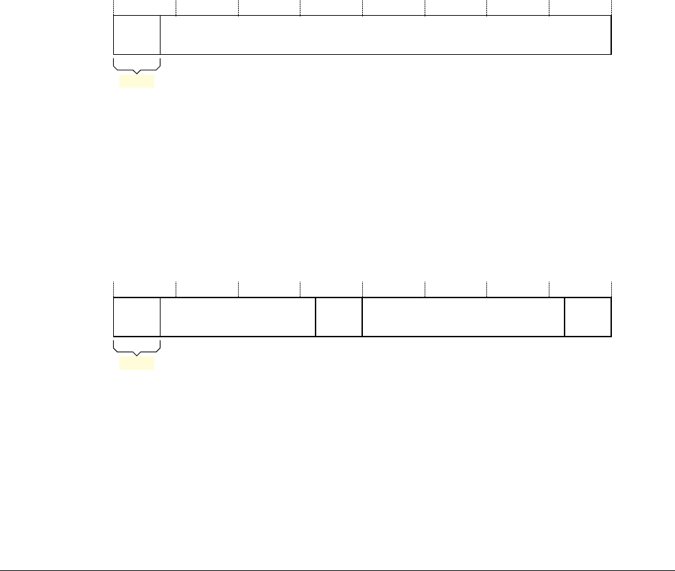
B6 System Control Registers in a PMSA implementation
B6.1 PMSA System control registers descriptions, in register order
B6-1938 Copyright © 1996-1998, 2000, 2004-2012, 2014 ARM. All rights reserved. ARM DDI 0406C.c
Non-Confidential ID051414
B6.1.87 TCMTR, TCM Type Register, PMSA
The TCMTR characteristics are:
Purpose The TCMTR provides information about the implementation of the TCM.
This register is part of the Identification registers functional group.
Usage constraints Only accessible from PL1.
Configurations In ARMv7:
• this register must be implemented
• when the ARMv7 format is used, the meaning of register bits[28:0] is
IMPLEMENTATION DEFINED
• the ARMv6 format of the register remains a valid usage model
• if no TCMs are implemented the ARMv6 format is used as shown in this section.
Attributes A 32-bit RO register with an IMPLEMENTATION DEFINED value. See also Reset behavior of
CP14 and CP15 registers on page B5-1778.
Table B5-13 on page B5-1800 shows the encodings of all of the registers in the
Identification registers functional group.
In the ARMv7 format, the TCMTR bit assignments are:
Format, bits[31:29]
Indicates the implemented TCMTR format. The possible values of this are:
0b000
ARMv6 format, or no TCMs implemented. For more information, see the description
of TCMTR in Appendix D12 ARMv6 Differences.
0b100
ARMv7 format.
All other values are reserved.
Bits[28:0] IMPLEMENTATION DEFINED in the ARMv7 register format.
If no TCMs are implemented, the TCMTR must be implemented with the ARMv6 format. In this format the
TCMTR bit assignments are:
Accessing the TCMTR
To access the TCMTR, software reads the CP15 registers with
<opc1>
set to 0,
<CRn>
set to c0,
<CRm>
set to c0, and
<opc2>
set to 2. For example:
MRC p15, 0, <Rt>, c0, c0, 2 ; Read TCMTR into Rt
IMPLEMENTATION DEFINED1
31 29 28 0
00
Format
00
31 29 28 19 18 16 15 3 2 0
0 0 Reserved, UNK 0 0 0 Reserved, UNK 0 0
Format

B6 System Control Registers in a PMSA implementation
B6.1 PMSA System control registers descriptions, in register order
ARM DDI 0406C.c Copyright © 1996-1998, 2000, 2004-2012, 2014 ARM. All rights reserved. B6-1939
ID051414 Non-Confidential
B6.1.88 TEECR, ThumbEE Configuration Register, PMSA
The TEECR characteristics are:
Purpose The TEECR controls unprivileged access to the TEEHBR.
This register is a ThumbEE register.
Usage constraints Access rights depend on the execution privilege:
• the result of an unprivileged write to the register is UNDEFINED
• unprivileged reads, and reads and writes at PL1 or higher, are permitted.
Configurations The VMSA and PMSA definitions of the register fields are identical.
Implemented in any system that includes the ThumbEE Extension.
Attributes A 32-bit RW register that resets to zero.
Table A2-14 on page A2-95 shows the encodings of all of the ThumbEE registers.
The TEECR bit assignments are:
Bits[31:1] Reserved, UNK/SBZP.
XED, bit[0] Execution Environment Disable bit. Controls unprivileged access to the ThumbEE Handler Base
Register:
0 Unprivileged access permitted.
1 Unprivileged access disabled.
The effects of a write to this register on ThumbEE configuration are only guaranteed to be visible to subsequent
instructions after the execution of a context synchronization operation. However, a read of this register always
returns the value most recently written to the register.
Note
See Context synchronization operation for the definition of this term.
Accessing the TEECR
To access the TEECR, software reads or writes the CP14 registers with
<opc1>
set to 6,
<CRn>
set to c0,
<CRm>
set to
c0, and
<opc2>
set to 0. For example:
MRC p14, 6, <Rt>, c0, c0, 0 ; Read TEECR into Rt
MCR p14, 6, <Rt>, c0, c0, 0 ; Write Rt to TEECR
XED
31 10
Reserved, UNK/SBZP

B6 System Control Registers in a PMSA implementation
B6.1 PMSA System control registers descriptions, in register order
B6-1940 Copyright © 1996-1998, 2000, 2004-2012, 2014 ARM. All rights reserved. ARM DDI 0406C.c
Non-Confidential ID051414
B6.1.89 TEEHBR, ThumbEE Handler Base Register, PMSA
The TEEHBR characteristics are:
Purpose The TEEHBR holds the base address for ThumbEE handlers.
This register is a ThumbEE register.
Usage constraints Access rights depend on the execution privilege and the value of TEECR.XED:
• accesses at PL1 or higher are always permitted
• when TEECR.XED is 0, unprivileged accesses are permitted
• when TEECR.XED is 1, the result of an unprivileged access is UNDEFINED.
Configurations The VMSA and PMSA definitions of the register fields are identical.
Implemented in any system that implements the ThumbEE Extension.
In an implementation that includes the Security Extensions, TEEHBR is a Common register.
Attributes A 32-bit RW register with an UNKNOWN reset value.
Table A2-14 on page A2-95 shows the encodings of all of the ThumbEE registers.
The TEEHBR bit assignments are:
HandlerBase, bits[31:2]
The address of the ThumbEE Handler_00 implementation. This is the address of the first of the
ThumbEE handlers.
Bits[1:0] Reserved, UNK/SBZP.
The effects of a write to this register on ThumbEE handler entry are only guaranteed to be visible to subsequent
instructions after the execution of a context synchronization operation. However, a read of this register always
returns the value most recently written to the register.
Accessing the TEEHBR
To access the TEEHBR, software reads or writes the CP14 registers with
<opc1>
set to 6,
<CRn>
set to c1,
<CRm>
set
to c0, and
<opc2>
set to 0. For example:
MRC p14, 6, <Rt>, c1, c0, 0 ; Read TEEHBR into Rt
MCR p14, 6, <Rt>, c1, c0, 0 ; Write Rt to TEEHBR
(0)(0)
31 10
HandlerBase
2
Reserved

B6 System Control Registers in a PMSA implementation
B6.1 PMSA System control registers descriptions, in register order
ARM DDI 0406C.c Copyright © 1996-1998, 2000, 2004-2012, 2014 ARM. All rights reserved. B6-1941
ID051414 Non-Confidential
B6.1.90 TPIDRPRW, PL1 only Thread ID Register, PMSA
The TPIDRPRW register characteristics are:
Purpose Provides a location where software executing at PL1 can store thread identifying
information that is not visible to unprivileged software, for OS management purposes.
This register is part of the Miscellaneous operations functional group.
Usage constraints The TPIDRPRW is only accessible from PL1.
Processor hardware never updates this register.
Configurations Not implemented in architecture versions before ARMv7.
Attributes A 32-bit RW register with an UNKNOWN reset value. See also Reset behavior of CP14 and
CP15 registers on page B5-1778.
Table B5-19 on page B5-1804 shows the encodings of all of the registers in the
Miscellaneous operations functional group.
Accessing the TPIDRPRW register
To access the TPIDRPRW register, software reads or writes the CP15 registers with
<opc1>
set to 0,
<CRn>
set to c13,
<CRm>
set to c0, and
<opc2>
set to 4.
For example:
MRC p15, 0, <Rt>, c13, c0, 4 ; Read TPIDRPRW into Rt
MCR p15, 0, <Rt>, c13, c0 4 ; Write Rt to TPIDRPRW
B6.1.91 TPIDRURO, User Read-Only Thread ID Register, PMSA
The TPIDRURO register characteristics are:
Purpose Provides a location where software executing at PL1 can store thread identifying
information that is visible to unprivileged software, for OS management purposes.
This register is part of the Miscellaneous operations functional group.
Usage constraints The TPIDRURO is read-only in User mode.
Processor hardware never updates this register.
Configurations Not implemented in architecture versions before ARMv7.
Attributes A 32-bit RW register with an UNKNOWN reset value. See also Reset behavior of CP14 and
CP15 registers on page B5-1778.
Table B5-19 on page B5-1804 shows the encodings of all of the registers in the
Miscellaneous operations functional group.
Accessing the TPIDRURO register
To access the TPIDRURO register, software reads or writes the CP15 registers with
<opc1>
set to 0,
<CRn>
set to c13,
<CRm>
set to c0, and
<opc2>
set to 3.
For example:
MRC p15, 0, <Rt>, c13, c0, 3 ; Read TPIDRURO into Rt
MCR p15, 0, <Rt>, c13, c0, 3 ; Write Rt to TPIDRURO

B6 System Control Registers in a PMSA implementation
B6.1 PMSA System control registers descriptions, in register order
B6-1942 Copyright © 1996-1998, 2000, 2004-2012, 2014 ARM. All rights reserved. ARM DDI 0406C.c
Non-Confidential ID051414
B6.1.92 TPIDRURW, User Read/Write Thread ID Register, PMSA
The TPIDRURW register characteristics are:
Purpose Provides a location where software running in User mode can store thread identifying
information, for OS management purposes.
This register is part of the Miscellaneous operations functional group.
Usage constraints No usage constraints. The TPIDRURW is accessible at all levels of privilege.
Processor hardware never updates this register.
Configurations Not implemented in architecture versions before ARMv7.
Attributes A 32-bit RW register with an UNKNOWN reset value. See also Reset behavior of CP14 and
CP15 registers on page B5-1778.
Table B5-19 on page B5-1804 shows the encodings of all of the registers in the
Miscellaneous operations functional group.
Accessing the TPIDRURW register
To access the TPIDRURW register, software reads or writes the CP15 registers with
<opc1>
set to 0,
<CRn>
set to c13,
<CRm>
set to c0, and
<opc2>
set to 2.
For example:
MRC p15, 0, <Rt>, c13, c0, 2 ; Read TPIDRURW into Rt
MCR p15, 0, <Rt>, c13, c0, 2 ; Write Rt to TPIDRURW

B6 System Control Registers in a PMSA implementation
B6.2 PMSA system control operations described by function
ARM DDI 0406C.c Copyright © 1996-1998, 2000, 2004-2012, 2014 ARM. All rights reserved. B6-1943
ID051414 Non-Confidential
B6.2 PMSA system control operations described by function
This section describes the system control operations that are available in a PMSA implementation and that are
described as part of a functional group. Architecturally-defined operations have an entry, under the operation name,
in PMSA System control registers descriptions, in register order on page B6-1810, that references the appropriate
functional description in this section.
This section contains the following subsections:
•Cache and branch predictor maintenance operations, PMSA
•Data and instruction barrier operations, PMSA on page B6-1945
•Cache and TCM lockdown registers, PMSA on page B6-1946
•DMA support, PMSA on page B6-1947.
B6.2.1 Cache and branch predictor maintenance operations, PMSA
This section describes the cache and branch predictor maintenance operations. These are:
• 32-bit write-only operations
• can be executed only by software executing at PL1.
Table B5-18 on page B5-1803 shows the encodings for these operations.
For more information about the terms used in this section see Terms used in describing the maintenance operations
on page B2-1274.
Note
• The architecture includes branch predictor operations with cache maintenance operations because they
operate in a similar way.
• ARMv7 introduces significant changes in the CP15 c7 operations. Most of these changes are because
ARMv7 introduces support for multiple levels of cache. This section only describes the ARMv7
requirements for these operations. For details of these operations in previous versions of the architecture see:
—CP15 c7, Cache and branch predictor operations on page D12-2533 for ARMv6
—CP15 c7, Cache and branch predictor operations on page D15-2629 for ARMv4 and ARMv5.
The Multiprocessing Extensions change the set of caches affected by these operations, see Scope of cache and
branch predictor maintenance operations on page B2-1281.
See The interaction of cache lockdown with cache maintenance operations on page B2-1287 for information about
the interaction of these maintenance operations with cache lockdown.
Table B6-19 lists these operations. For the entries in the table:
• The Rt data column specifies what data is required in the register Rt specified by the
MCR
instruction that
performs the operation, see Data formats for the cache and branch predictor operations on page B6-1944.
•Terms used in describing the maintenance operations on page B2-1274 describes Address, point of
coherency (PoC) and point of unification (PoU).
Table B6-19 CP15 c7 cache and branch predictor maintenance operations, PMSA
Operation Type Description Rt data
ICIALLUIS WO Invalidate all instruction caches to PoU Inner Shareable. If branch predictors are
architecturally-visible, also flushes branch predictors.a
Ignored
BPIALLIS WO Invalidate all entries from branch predictors Inner Shareable. Ignored
ICIALLU WO Invalidate all instruction caches to PoU. If branch predictors are architecturally-visible, also
flushes branch predictors.a
Ignored

B6 System Control Registers in a PMSA implementation
B6.2 PMSA system control operations described by function
B6-1944 Copyright © 1996-1998, 2000, 2004-2012, 2014 ARM. All rights reserved. ARM DDI 0406C.c
Non-Confidential ID051414
Branch predictor maintenance operations can perform a NOP if the operation of Branch Prediction hardware is not
visible architecturally.
Data formats for the cache and branch predictor operations
Table B6-19 on page B6-1943 shows three possibilities for the data in the register Rt specified by the
MCR
instruction.
These are described in the following subsections:
•Ignored
•Address
•Set/way.
Ignored
The value in the register specified by the
MCR
instruction is ignored. Software does not have to write a value to the
register before issuing the
MCR
instruction.
Address
In general descriptions of the maintenance operations, operations that require a memory address are described as
operating by MVA. For more information, see Terms used in describing the maintenance operations on
page B2-1274. In a PMSA implementation, these operations require the physical address in the memory map. When
the data is stated to be an address, it does not have to be cache line aligned.
Set/way
For a set/way operation, the data identifies the cache line that the operation is to be applied to by specifying:
• the cache set the line belongs to
• the way number of the line in the set
• the cache level.
ICIMVAU WO Invalidate instruction cache line by address to PoU.a, b Address
BPIALL WO Invalidate all entries from branch predictors. Ignored
BPIMVA WO Invalidate address from branch predictors. bAddress
DCIMVAC WO Invalidate data or unified cache line by address to PoC. bAddress
DCISW WO Invalidate data or unified cache line by set/way. Set/way
DCCMVAC WO Clean data or unified cache line by address to PoC. bAddress
DCCSW WO Clean data or unified cache line by set/way. Set/way
DCCMVAU WO Clean data or unified cache line by address to PoU. bAddress
DCCIMVAC WO Clean and invalidate data or unified cache line by address to PoC. bAddress
DCCISW WO Clean and invalidate data or unified cache line by set/way. Set/way
a. Only applies to separate instruction caches, does not apply to unified caches.
b. In general descriptions of the cache operations, these functions are described as operating by MVA (Modified Virtual Address). In a PMSA
implementation the MVA and the PA have the same value, and so the functions operate using a physical address in the memory map.
Table B6-19 CP15 c7 cache and branch predictor maintenance operations, PMSA (continued)
Operation Type Description Rt data

B6 System Control Registers in a PMSA implementation
B6.2 PMSA system control operations described by function
ARM DDI 0406C.c Copyright © 1996-1998, 2000, 2004-2012, 2014 ARM. All rights reserved. B6-1945
ID051414 Non-Confidential
The format of the register data for a set/way operation is:
Where:
A =Log
2(ASSOCIATIVITY), rounded up to the next integer if necessary.
B =(L+S).
L =Log
2(LINELEN).
S =Log
2(NSETS), rounded up to the next integer if necessary.
ASSOCIATIVITY, LINELEN (line length, in bytes) and NSETS (number of sets) have their usual
meanings and are the values for the cache level being operated on.
The values of A and S are rounded up to the next integer.
Level ((Cache level to operate on)–1).
For example, this field is 0 for operations on L1 cache, or 1 for operations on L2 cache.
Set The number of the set to operate on.
Way The number of the way to operate on.
Note
• If L = 4 then there is no SBZ field between the set and level fields in the register.
• If A = 0 there is no way field in the register, and register bits[31:B] are SBZ.
• If the level, set or way field in the register is larger than the size implemented in the cache then the effect of
the operation is UNPREDICTABLE.
Accessing the CP15 c7 cache and branch predictor maintenance operations
To perform one of the cache maintenance operations, software writes to the CP15 registers with
<opc1>
set to 0,
<CRn>
set to c7, and
<CRm>
and
<opc2>
set to the values shown in Table B6-19 on page B6-1943.
That is:
MCR p15, 0, <Rt>, c7, <CRm>, <opc2>
For example:
MCR p15, 0, <Rt>, c7, c5, 0 ; ICIALLU, Instruction cache invalidate all to PoU. Ignores Rt value.
MCR p15, 0, <Rt>, c7, c10, 2 ; Use Rt as input to DCCSW, Data cache clean by set/way
B6.2.2 Data and instruction barrier operations, PMSA
ARMv6 includes two CP15 c7 operations to perform data barrier operations, and another operation to perform an
instruction barrier operation. In ARMv7:
• The ARM and Thumb instruction sets include instructions to perform the barrier operations, that can be
executed at any level of privilege, see Memory barriers on page A3-151.
• The CP15 c7 operations are defined as write-only operations, that can be executed at any level of privilege.
Table B5-19 on page B5-1804 shows the encodings for these operations, and the following sections describe
them:
—CP15ISB, Instruction Synchronization Barrier operation on page B6-1946
—CP15DSB, Data Synchronization Barrier operation on page B6-1946
—CP15DMB, Data Memory Barrier operation on page B6-1946.
The
MCR
instruction that performs a barrier operation specifies a register, Rt, as an argument. However, the
operation ignores the value of this register, and software does not have to write a value to the register before
issuing the
MCR
instruction.
0Way
31 32–A
31–A
B
B–1
L
L–1
43210
SBZ Set SBZ Level

B6 System Control Registers in a PMSA implementation
B6.2 PMSA system control operations described by function
B6-1946 Copyright © 1996-1998, 2000, 2004-2012, 2014 ARM. All rights reserved. ARM DDI 0406C.c
Non-Confidential ID051414
In ARMv7, ARM deprecates any use of these CP15 c7 operations, and strongly recommends that software
uses the
ISB
,
DSB
, and
DMB
instructions instead.
Note
• In ARMv6 and earlier documentation, the Instruction Synchronization Barrier operation is referred to as a
Prefetch Flush.
• In versions of the ARM architecture before ARMv6 the Data Synchronization Barrier operation is described
as a Data Write Barrier (DWB).
If the implementation supports the SCTLR.CP15BEN bit and this bit is set to 0, these operations are disabled and
their encodings are UNDEFINED.
CP15ISB, Instruction Synchronization Barrier operation
In ARMv7, use the
ISB
instruction to perform an Instruction Synchronization Barrier, see ISB on page A8-389.
The deprecated CP15 c7 encoding for an Instruction Synchronization Barrier is an
MCR
instruction with
<opc1>
set to
0,
<CRn>
set to c7,
<CRm>
set to c5, and
<opc2>
set to 4.
CP15DSB, Data Synchronization Barrier operation
In ARMv7, use the
DSB
instruction to perform a Data Synchronization Barrier, see DSB on page A8-380.
The deprecated CP15 c7 encoding for a Data Synchronization Barrier is an
MCR
instruction with
<opc1>
set to 0,
<CRn>
set to c7,
<CRm>
set to c10, and
<opc2>
set to 4. This operation performs the full system barrier performed by the
DSB
instruction.
CP15DMB, Data Memory Barrier operation
In ARMv7, use the
DMB
instruction to perform a Data Memory Barrier, see DMB on page A8-378.
The deprecated CP15 c7 encoding for a Data Memory Barrier is an
MCR
instruction with
<opc1>
set to 0,
<CRn>
set to
c7,
<CRm>
set to c10, and
<opc2>
set to 5. This operation performs the full system barrier performed by the
DMB
instruction.
B6.2.3 Cache and TCM lockdown registers, PMSA
Some CP15 c9 encodings are reserved for IMPLEMENTATION DEFINED memory system functions, in particular:
• cache control, including lockdown
• TCM control, including lockdown
• branch predictor control.
The reserved encodings support implementations that are compatible with previous versions of the ARM
architecture, in particular with the ARMv6 requirements. For details of the ARMv6 implementation see CP15 c9,
Cache lockdown support on page D12-2539.
In ARMv6, CP15 c9 provides cache lockdown functions. With the ARMv7 abstraction of the hierarchical memory
model, for CP15 c9, all encodings with CRm = {c0-c2, c5-c8} are reserved for IMPLEMENTATION DEFINED cache,
branch predictor and TCM operations.
The naming and behavior of registers or operations defined in these regions is IMPLEMENTATION DEFINED.

B6 System Control Registers in a PMSA implementation
B6.2 PMSA system control operations described by function
ARM DDI 0406C.c Copyright © 1996-1998, 2000, 2004-2012, 2014 ARM. All rights reserved. B6-1947
ID051414 Non-Confidential
B6.2.4 DMA support, PMSA
Some CP15 c11 encodings are reserved for IMPLEMENTATION DEFINED registers or operations to provide DMA
support. The reserved encodings are those 32-bit CP15 accesses with CRn==c11, opc1=={0-7}, CRm=={c0-c8,
c15}, opc2=={0-7}.
All other CP15 c11 encodings are UNPREDICTABLE, see Accesses to unallocated CP14 and CP15 encodings on
page B5-1776.
The reserved encodings permit implementations that are compatible with previous versions of the ARM
architecture, in particular with the ARMv6 implementations of DMA support for TCMs described in The ARM
Architecture Reference Manual (DDI 0100). As stated in Appendix D12 ARMv6 Differences, ARM considers this
support to be an IMPLEMENTATION DEFINED feature of those ARMv6 implementations.
The naming and behavior of registers or operations defined in these encoding regions is IMPLEMENTATION DEFINED.

B6 System Control Registers in a PMSA implementation
B6.2 PMSA system control operations described by function
B6-1948 Copyright © 1996-1998, 2000, 2004-2012, 2014 ARM. All rights reserved. ARM DDI 0406C.c
Non-Confidential ID051414

ARM DDI 0406C.c Copyright © 1996-1998, 2000, 2004-2012, 2014 ARM. All rights reserved. B7-1949
ID051414 Non-Confidential
Chapter B7
The CPUID Identification Scheme
This chapter describes the CPUID scheme introduced as a requirement in ARMv7. This scheme provides registers
that identify the architecture version and many features of the processor implementation. This chapter also describes
the registers that identify the implemented Advanced SIMD and Floating-point Extension features, if any.
This chapter contains the following sections:
•Introduction to the CPUID scheme on page B7-1950
•The CPUID registers on page B7-1951
•Advanced SIMD and Floating-point Extension feature identification registers on page B7-1957.
Note
• The other chapters of this manual describe the permitted combinations of architectural features for the
ARMv7-A and ARMv7-R architecture profiles, and some of the appendixes give this information for
previous versions of the architecture. Typically, permitted features are associated with a named architecture
version, or version and profile, such as ARMv7-A or ARMv6.
The CPUID scheme is a mechanism for describing these permitted combinations in a way that software can
use to determine the capabilities of the hardware it is running on.
The CPUID scheme does not extend the permitted combinations of architectural features beyond those
associated with named architecture versions and profiles. The fact that the CPUID scheme can describe other
combinations does not imply that those combinations are permitted ARM architecture variants.
• Both Chapter B4 System Control Registers in a VMSA implementation and Chapter B6 System Control
Registers in a PMSA implementation include the descriptions of the CPUID registers. These registers are
included in both VMSA and PMSA implementations, and the bit assignments are identical in VMSA and
PMSA implementations. However, most register references in this chapter link to the register descriptions in
Chapter B4.

B7 The CPUID Identification Scheme
B7.1 Introduction to the CPUID scheme
B7-1950 Copyright © 1996-1998, 2000, 2004-2012, 2014 ARM. All rights reserved. ARM DDI 0406C.c
Non-Confidential ID051414
B7.1 Introduction to the CPUID scheme
In ARM architecture versions before ARMv7, the architecture version is indicated by the Architecture field in the
Main ID Register, see either:
•MIDR, Main ID Register, VMSA on page B4-1649
•MIDR, Main ID Register, PMSA on page B6-1894.
The ARMv7 architecture implements an extended processor identification scheme, using a number of registers in
CP15 c0. ARMv7 requires the use of this scheme, and use of the scheme is indicated by a value of
0xF
in the
Architecture field of the Main ID Register.
Note
Some ARMv6 processors implemented the scheme before its formal adoption in the architecture.
The CPUID scheme provides information about the implemented:
• processor features
• debug features
• auxiliary features, in particular IMPLEMENTATION DEFINED features
• memory model features
• instruction set features.
The following sections give more information about the CPUID registers:
•Organization of the CPUID registers on page B7-1951
•General properties of the CPUID registers on page B7-1952.
The CPUID registers on page B7-1951 gives detailed descriptions of the registers.
This chapter also describes the identification registers for any Advanced SIMD or Floating-point Extension
implementation. These are registers in the shared register space for the Advanced SIMD and Floating-point
Extensions, in CP 10 and CP 11. Advanced SIMD and Floating-point Extension feature identification registers on
page B7-1957 describes these registers.
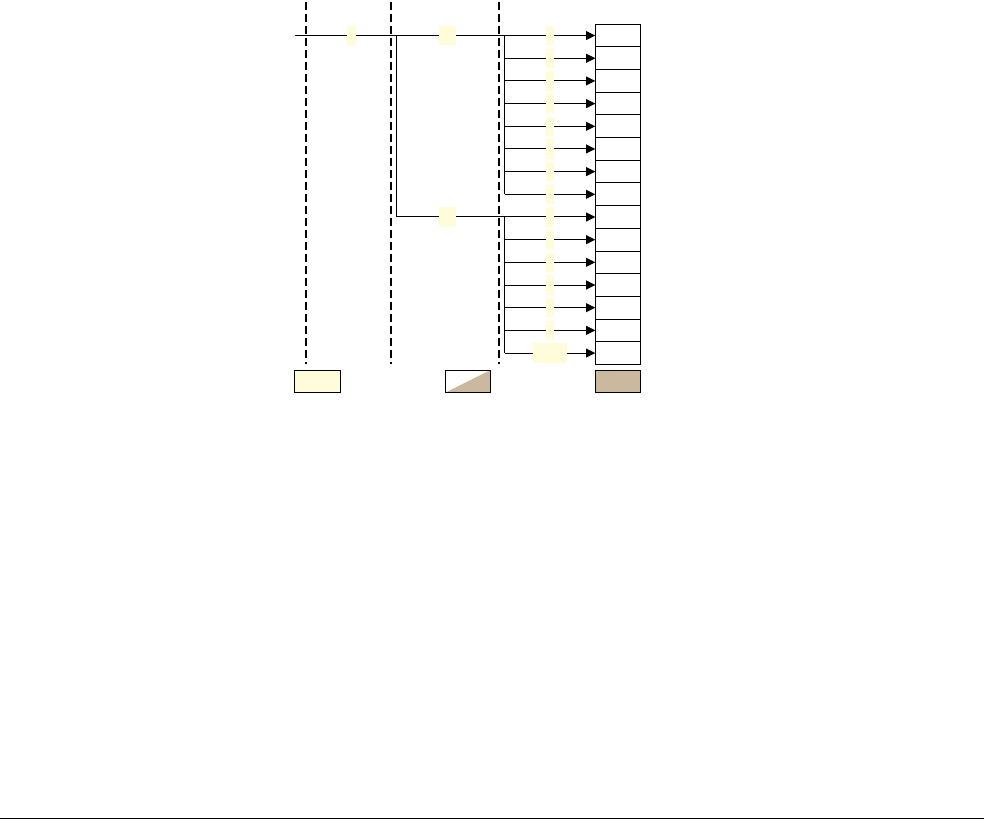
B7 The CPUID Identification Scheme
B7.2 The CPUID registers
ARM DDI 0406C.c Copyright © 1996-1998, 2000, 2004-2012, 2014 ARM. All rights reserved. B7-1951
ID051414 Non-Confidential
B7.2 The CPUID registers
The CPUID registers consist of:
• Two Processor Feature Registers that give information about the programmers’ model and top-level
information about the instruction set implementation.
• One Debug Feature Register that gives top level information about the debug system for the processor.
• One Auxiliary Feature Register that gives information about the IMPLEMENTATION DEFINED features of the
processor.
• Four Memory Model Feature registers, that give general information about the implemented memory model
and memory management support, including the supported cache and TLB operations.
• Six Instruction Set Attribute registers, that give information about the instruction sets implemented by the
processor.
B7.2.1 Organization of the CPUID registers
Figure B7-1 shows the CPUID registers and their encodings in CP15. Two of the encodings shown, with
<CRm>
== c2 and
<opc2>
== {6, 7}, are reserved for future expansion of the CPUID scheme. In addition, all CP15 c0
encodings with
<CRm>
== {c3-c7} and
<opc2>
== {0-7} are reserved for future expansion of the scheme. These
reserved encodings must be RAZ.
Figure B7-1 CPUID register encodings
Read-only Read/Write
ID_PFR0, Processor Feature Register 0
0
1
2
3
c10c0
Write-only
CRn opc1 opc2CRm
ID_PFR1, Processor Feature Register 1
ID_DFR0, Debug Feature Register 0
ID_AFR0, Auxiliary Feature Register 0
ID_MMFR0, Memory Model Feature Register 0
ID_MMFR1, Memory Model Feature Register 1
ID_MMFR2, Memory Model Feature Register 2
ID_MMFR3, Memory Model Feature Register 3
4
5
6
7
ID_ISAR0, ISA Feature Register 0
1
2
3
4
5
{6-7}
ID_ISAR1, ISA Feature Register 1
ID_ISAR2, ISA Feature Register 2
ID_ISAR3, ISA Feature Register 3
ID_ISAR4, ISA Feature Register 4
Reserved
ID_ISAR5, ISA Feature Register 5
0c2

B7 The CPUID Identification Scheme
B7.2 The CPUID registers
B7-1952 Copyright © 1996-1998, 2000, 2004-2012, 2014 ARM. All rights reserved. ARM DDI 0406C.c
Non-Confidential ID051414
Table B7-1 lists the CPUID registers and shows where each register is described in full
General properties of the CPUID registers
All of the CPUID registers are 32-bit read-only registers. Each register is divided into eight 4-bit fields, and the
possible field values are defined individually for each field. Some registers do not use all of these fields.
B7.2.2 About the Instruction Set Attribute registers
The Instruction Set Attribute registers, ID_ISAR0 to ID_ISAR5, provide information about the instruction sets
implemented by the processor. The instruction set is divided into:
• The basic instructions, for the ARM, Thumb, and ThumbEE instruction sets. If ID_PFR0 indicates that an
instruction set is implemented, then all basic instructions that have encodings in that instruction set must be
implemented.
• The non-basic instructions. The Instruction Set Attribute registers indicate which of these instructions are
implemented.
Instruction set descriptions in the CPUID scheme on page B7-1953 describes the division of the instruction set into
basic and non-basic instructions.
Summary of Instruction Set Attribute register attribute fields on page B7-1954 lists all of the attributes and shows
which register holds each attribute.
Table B7-1 CPUID register summary
Name, VMSAaName, PMSAaopc1 CRm opc2 Type Description
ID_PFR0 ID_PFR0 0 c1 0 RO Processor Feature Register 0
ID_PFR1 ID_PFR1 1 RO Processor Feature Register 1
ID_DFR0 ID_DFR0 2 RO Debug Feature Register 0
ID_AFR0 ID_AFR0 3 RO Auxiliary Feature Register 0
ID_MMFR0 ID_MMFR0 4 RO Memory Model Feature Register 0
ID_MMFR1 ID_MMFR1 5 RO Memory Model Feature Register 1
ID_MMFR2 ID_MMFR2 6 RO Memory Model Feature Register 2
ID_MMFR3 ID_MMFR3 7 RO Memory Model Feature Register 3
ID_ISAR0 ID_ISAR0 c2 0 RO Instruction Set Attribute Register 0
ID_ISAR1 ID_ISAR1 1 RO Instruction Set Attribute Register 1
ID_ISAR2 ID_ISAR2 2 RO Instruction Set Attribute Register 2
ID_ISAR3 ID_ISAR3 3 RO Instruction Set Attribute Register 3
ID_ISAR4 ID_ISAR4 4 RO Instruction Set Attribute Register 4
ID_ISAR5 ID_ISAR5 5 RO Instruction Set Attribute Register 5
- - {6-7} - Reserved
a. VMSA and PMSA definitions of the register fields are identical. These columns link to the descriptions in Chapter B4 and Chapter B6.

B7 The CPUID Identification Scheme
B7.2 The CPUID registers
ARM DDI 0406C.c Copyright © 1996-1998, 2000, 2004-2012, 2014 ARM. All rights reserved. B7-1953
ID051414 Non-Confidential
Instruction set descriptions in the CPUID scheme
The following subsections describe how the CPUID scheme describes the instruction set, and how instructions are
classified as either basic or non-basic:
•General rules for instruction classification
•Data-processing instructions
•Multiply instructions
•Branches
•Load or Store single word instructions on page B7-1954
•Load or Store multiple word instructions on page B7-1954
•Q flag support in the PSRs on page B7-1954.
General rules for instruction classification
Two general rules apply to the description of instruction classification given in this section:
1. The rules about an instruction being basic do not guarantee that it is available in any particular instruction
set. For example, the rules given in this section classify
MOV R0, #123456789
as a basic instruction, but this
instruction is not available in any existing ARM instruction set.
2. Whether an instruction is conditional or unconditional never makes any difference to whether it is a basic
instruction.
Data-processing instructions
The data-processing instructions are:
ADC ADD AND ASR BIC CMN CMP EOR LSL LSR MOV MVN
NEG ORN ORR ROR RRX RSB RSC SBC SUB TEQ TST
An instruction from this group is a basic instruction if these conditions both apply:
• The second source operand, or the only source operand of a
MOV
or
MVN
instruction, is an immediate or an
unshifted register.
Note
A
MOV
instruction with a shifted register source operand must be treated as the equivalent
ASR
,
LSL
,
LSR
,
ROR
,
or
RRX
instruction, see MOV (shifted register) on page A8-490.
• The instruction is not one of the exception return instructions described in SUBS PC, LR (Thumb) on
page B9-2010 and SUBS PC, LR and related instructions (ARM) on page B9-2012.
If either of these conditions does not apply then the instruction is a non-basic instruction. The
ID_ISAR2.PSR_AR_instrs and ID_ISAR4.WithShifts_instrs attributes show the implemented non-basic
data-processing instructions.
Multiply instructions
The classification of multiply instructions is:
•
MUL
instructions are always basic instructions
• all other multiply instructions, and all multiply accumulate instructions, are non-basic instructions.
Branches
All
B
and
BL
instructions are basic instructions.

B7 The CPUID Identification Scheme
B7.2 The CPUID registers
B7-1954 Copyright © 1996-1998, 2000, 2004-2012, 2014 ARM. All rights reserved. ARM DDI 0406C.c
Non-Confidential ID051414
Load or Store single word instructions
The instructions in this group are:
LDR LDRB LDRH LDRSB LDRSH STR STRB STRH
An instruction in this group is a basic instruction if its addressing mode is one of these forms:
•
[Rn, #immediate]
•
[Rn, #-immediate]
•
[Rn, Rm]
•
[Rn, -Rm]
.
A Load or Store single word instruction with any other addressing mode is a non-basic instruction. The
ID_ISAR4.{WithShifts_instrs, Writeback_instrs, Unpriv_instrs} attributes show the support for these non-basic
addressing modes.
Load or Store multiple word instructions
The Load or Store multiple word instructions are:
LDM<mode> STM<mode> PUSH POP
A limited number of variants of these instructions are non-basic. The ID_ISAR1.Except_instrs attribute shows
whether these instructions are implemented. For more information about these non-basic instructions see the
ID_ISAR1 field description.
All other forms of these instructions are always basic instructions.
Q flag support in the PSRs
The Q flag is present in the CPSR and SPSRs when one or more of these conditions applies:
•ID_ISAR2.MultS_instrs ≥2
•ID_ISAR3.Saturate_instrs ≥1
•ID_ISAR3.SIMD_instrs ≥1.
Summary of Instruction Set Attribute register attribute fields
The Instruction Set Attribute registers use a set of attributes to indicate the non-basic instructions implemented by
the processor. The descriptions of the non-basic instructions in Instruction set descriptions in the CPUID scheme
on page B7-1953 include the attribute or attributes that indicate support for each category of non-basic instructions.
Table B7-2 lists all of the attributes in alphabetical order, and shows which Instruction Set Attribute register holds
each attribute, by links to the register descriptions in Chapter B4 System Control Registers in a VMSA
implementation and Chapter B6 System Control Registers in a PMSA implementation.
Note
The register definitions are identical in the VMSA and PMSA chapters. However, some register field descriptions
include Notes on constraints that apply to the corresponding memory system.
Table B7-2 Alphabetic list of Instruction Set Attribute registers attribute fields
Attribute field Register, VMSA Register, PMSA
Barrier_instrs ID_ISAR4 ID_ISAR4
BitCount_instrs ID_ISAR0 ID_ISAR0
Bitfield_instrs ID_ISAR0 ID_ISAR0
CmpBranch_instrs ID_ISAR0 ID_ISAR0

B7 The CPUID Identification Scheme
B7.2 The CPUID registers
ARM DDI 0406C.c Copyright © 1996-1998, 2000, 2004-2012, 2014 ARM. All rights reserved. B7-1955
ID051414 Non-Confidential
Coproc_instrs ID_ISAR0 ID_ISAR0
Debug_instrs ID_ISAR0 ID_ISAR0
Divide_instrs ID_ISAR0 ID_ISAR0
Endian_instrs ID_ISAR1 ID_ISAR1
Except_AR_instrs ID_ISAR1 ID_ISAR1
Except_instrs ID_ISAR1 ID_ISAR1
Extend_instrs ID_ISAR1 ID_ISAR1
IfThen_instrs ID_ISAR1 ID_ISAR1
Immediate_instrs ID_ISAR1 ID_ISAR1
Interwork_instrs ID_ISAR1 ID_ISAR1
Jazelle_instrs ID_ISAR1 ID_ISAR1
LoadStore_instrs ID_ISAR2 ID_ISAR2
MemHint_instrs ID_ISAR2 ID_ISAR2
Mult_instrs ID_ISAR2 ID_ISAR2
MultiAccessInt_instrs ID_ISAR2 ID_ISAR2
MultS_instrs ID_ISAR2 ID_ISAR2
MultU_instrs ID_ISAR2 ID_ISAR2
PSR_AR_instrs ID_ISAR2 ID_ISAR2
PSR_M_instrs ID_ISAR4 ID_ISAR4
Reversal_instrs ID_ISAR2 ID_ISAR2
Saturate_instrs ID_ISAR3 ID_ISAR3
SIMD_instrs ID_ISAR3 ID_ISAR3
SMC_instrs ID_ISAR4 ID_ISAR4
SWP_frac ID_ISAR4 ID_ISAR4
SVC_instrs ID_ISAR3 ID_ISAR3
Swap_instrs ID_ISAR0 ID_ISAR0
SynchPrim_instrs ID_ISAR3 ID_ISAR3
SynchPrim_instrs_frac ID_ISAR4 ID_ISAR4
TabBranch_instrs ID_ISAR3 ID_ISAR3
ThumbCopy_instrs ID_ISAR3 ID_ISAR3
ThumbEE_extn_instrs ID_ISAR3 ID_ISAR3
TrueNOP_instrs ID_ISAR3 ID_ISAR3
Table B7-2 Alphabetic list of Instruction Set Attribute registers attribute fields (continued)
Attribute field Register, VMSA Register, PMSA

B7 The CPUID Identification Scheme
B7.2 The CPUID registers
B7-1956 Copyright © 1996-1998, 2000, 2004-2012, 2014 ARM. All rights reserved. ARM DDI 0406C.c
Non-Confidential ID051414
Unpriv_instrs ID_ISAR4 ID_ISAR4
WithShifts_instrs ID_ISAR4 ID_ISAR4
Writeback_instrs ID_ISAR4 ID_ISAR4
Table B7-2 Alphabetic list of Instruction Set Attribute registers attribute fields (continued)
Attribute field Register, VMSA Register, PMSA

B7 The CPUID Identification Scheme
B7.3 Advanced SIMD and Floating-point Extension feature identification registers
ARM DDI 0406C.c Copyright © 1996-1998, 2000, 2004-2012, 2014 ARM. All rights reserved. B7-1957
ID051414 Non-Confidential
B7.3 Advanced SIMD and Floating-point Extension feature identification registers
In the ARMv7-A and ARMv-7-R architecture profiles, when an implementation includes one or both of the
OPTIONAL Advanced SIMD and Floating-point Extensions, the feature identification registers for the extensions are
implemented in a common register block with the Advanced SIMD and Floating-point Extension system registers.
The Advanced SIMD and Floating-point Extensions are implemented using coprocessors CP10 and CP11, and
software uses the coprocessor instructions
VMRS
and
VMSR
instructions to access the registers. For more information,
see Advanced SIMD and Floating-point Extension system registers on page B1-1236.
B7.3.1 About the Media and VFP Feature registers
The Media and VFP Feature registers describe the features provided by the Advanced SIMD and Floating-point
Extensions, when an implementation includes either or both of these extensions. For details of the implementation
options for these extensions see Advanced SIMD and Floating-point Extensions on page A2-54.
In VFPv2, it is IMPLEMENTATION DEFINED whether the Media and VFP Feature registers are implemented.
Note
Often, the complete implementation of a Floating-point (VFP) architecture uses support code to provide some
floating-point functionality. In such an implementation, only the support code can provide full details of the
supported features. In this case the Media and VFP Feature registers are not used directly.

B7 The CPUID Identification Scheme
B7.3 Advanced SIMD and Floating-point Extension feature identification registers
B7-1958 Copyright © 1996-1998, 2000, 2004-2012, 2014 ARM. All rights reserved. ARM DDI 0406C.c
Non-Confidential ID051414

ARM DDI 0406C.c Copyright © 1996-1998, 2000, 2004-2012, 2014 ARM. All rights reserved. B8-1959
ID051414 Non-Confidential
Chapter B8
The Generic Timer
This chapter describes the implementation of the ARM Generic Timer as an OPTIONAL extension to an ARMv7-A
or ARMv7-R processor implementation. It includes the definition of the system control register interface to an ARM
Generic Timer.
It contains the following sections:
•About the Generic Timer on page B8-1960
•Generic Timer registers summary on page B8-1969.
Appendix D5 System Level Implementation of the Generic Timer describes the system level implementation of the
Generic Timer.
Note
Both Chapter B4 System Control Registers in a VMSA implementation and Chapter B6 System Control Registers in
a PMSA implementation include the descriptions of the Generic Timer CP15 registers. Most of the registers are
included in both VMSA and PMSA implementations, and for these registers the bit assignments are identical in
VMSA and PMSA implementations. However, most register references in this chapter link to the register
descriptions in Chapter B4.
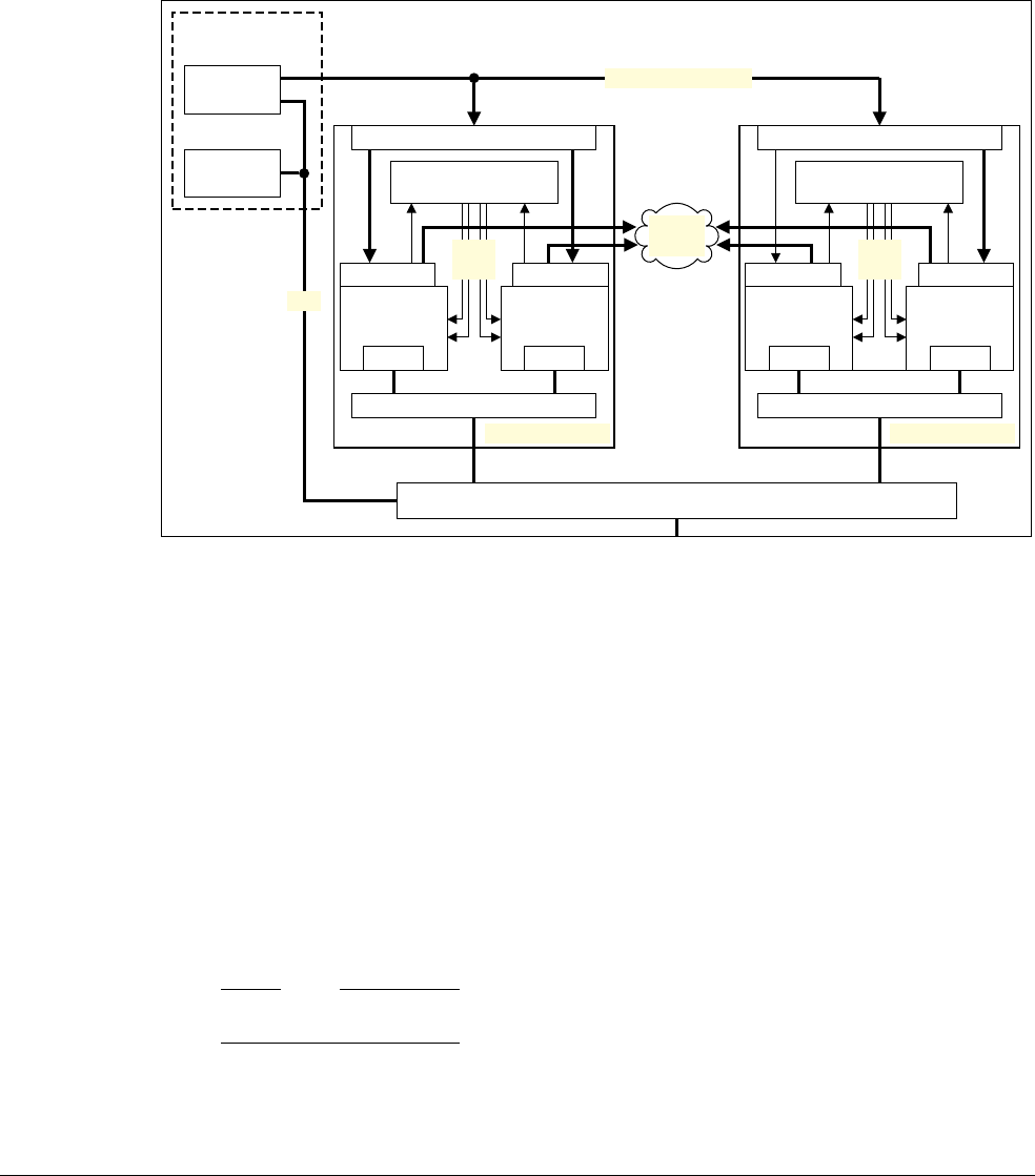
B8 The Generic Timer
B8.1 About the Generic Timer
B8-1960 Copyright © 1996-1998, 2000, 2004-2012, 2014 ARM. All rights reserved. ARM DDI 0406C.c
Non-Confidential ID051414
B8.1 About the Generic Timer
Figure B8-1 shows an example system-on-chip that uses the Generic Timer as a system timer. In this figure:
• This manual defines the architecture of the individual processors in the multiprocessor blocks.
• The ARM Generic Interrupt Controller Architecture Specification defines a possible architecture for the
GICs.
• Generic Timer functionality is distributed across multiple components.
Figure B8-1 Generic Timer example
This chapter:
• Gives a general description of the Generic Timer.
• Defines the system control register interface to the Generic Timer. Each processor shown in Figure B8-1
includes an implementation of this interface.
The Generic Timer:
• Provides a system counter, that measures the passing of time in real-time.
• In a system that includes support for virtualization, support virtual counters that measure the passing of
virtual time. That is, a virtual counter can measure the passing of time on a particular virtual machine.
• Provides timers, that can assert a timer output signal after a period of time has passed. The timers:
— Can be used as count-up or as count-down timers.
— In a component that supports virtualization, can operate in real-time or in virtual-time.
Note
A timer output signal can be used as a level-sensitive interrupt signal.
System
counter
Always-powered
domain
Power
controller
System Timer Bus
APB
Counter interface
GIC
Timer_0
Processor_0
Timer_1
Processor_1
Shared cache
PPI_0 PPI_1
Memory interconnect and memory controller
Counter interface
GIC
Timer_0
Processor_0
Timer_1
Processor_1
Shared cache
PPI_0 PPI_1
System
events
System-on-Chip
nFIQ,
nIRQ
nFIQ,
nIRQ
Cache Cache Cache Cache
Multiprocessor A Multiprocessor B

B8 The Generic Timer
B8.1 About the Generic Timer
ARM DDI 0406C.c Copyright © 1996-1998, 2000, 2004-2012, 2014 ARM. All rights reserved. B8-1961
ID051414 Non-Confidential
B8.1.1 System counter
The Generic Timer provides a system counter with the following specification:
Width At least 56 bits wide.
The value returned by any 64-bit read of the counter is zero-extended to 64 bits.
Frequency Increments at a fixed frequency, typically in the range 1-50MHz.
Can support one or more alternative operating modes in which it increments by larger amounts at a
lower frequency, typically for power-saving.
Roll-over Roll-over time of not less than 40 years.
Accuracy ARM does not specify a required accuracy, but recommends that the counter does not gain or lose
more than ten seconds in a 24-hour period.
Use of lower-frequency modes must not affect the implemented accuracy.
Start-up Starts operating from zero.
The system counter must provide a uniform view of system time. More precisely, it must be impossible for the
following sequence of events to show system time going backwards:
1. Device A reads the time from the system counter.
2. Device A communicates with another agent in the system, Device B.
3. After recognizing the communication from Device A, Device B reads the time from the system counter.
The system counter must be implemented in an always-on power domain.
To support lower-power operating modes, the counter can increment by larger amounts at a lower frequency. For
example, a 10MHz system counter might either increment either:
• By 1 at 10MHz.
• By 500 at 20kHz, when the system lowers the clock frequency, to reduce power consumption.
In this case, the counter must support transitions between high-frequency, high-precision operation, and
lower-frequency, lower-precision operation, without any impact on the required accuracy of the counter.
Software can access the CNTFRQ register to read the clock frequency of the system counter, and software with
sufficient privilege can modify the value of this register. For more information, see Initializing and reading the
system counter frequency.
The mechanism by which the count from the system counter is distributed to system components is
IMPLEMENTATION DEFINED, but each processor with a system control register interface to the system counter must
include a counter input that can capture each increment of the counter.
Note
So that the system counter can be clocked independently from the processor, the count value might be distributed
using a Gray code sequence. Gray-count scheme for timer distribution scheme on page D5-2427 gives more
information about this possibility.
Initializing and reading the system counter frequency
Typically, the system drives the system counter at a fixed frequency and the CNTFRQ register must be programmed
to this value during the system boot process. In an implementation that supports the ARM Security Extensions, only
software executing in a Secure PL1 mode can write to CNTFRQ. If a system permits any configuration of the system
counter frequency then it must ensure that CNTFRQ is always programmed to the correct system counter frequency.
Note
The CNTFRQ register is UNKNOWN at reset, and therefore the counter frequency must be written to CNTFRQ as
part of the system boot process.

B8 The Generic Timer
B8.1 About the Generic Timer
B8-1962 Copyright © 1996-1998, 2000, 2004-2012, 2014 ARM. All rights reserved. ARM DDI 0406C.c
Non-Confidential ID051414
Software can read the CNTFRQ register, to determine the current system counter frequency, in the following states
and modes:
• Non-secure PL2 mode.
• Secure and Non-secure PL1 modes.
• When CNTKCTL.PL0PCTEN is set to 1, Secure and Non-secure PL0 modes.
Memory-mapped controls of the system counter
Some system counter controls are accessible only through the memory-mapped interface to the system counter.
These controls are:
• Enabling and disabling the counter.
• Setting the counter value.
• Changing the operating mode, to change the update frequency and increment value.
• Enabling Halt-on-debug, that a debugger can then use to suspend counting.
For descriptions of these controls, see Appendix D5 System Level Implementation of the Generic Timer.
B8.1.2 The physical counter
The processor provides a physical counter that contains the count value of the system counter. The CNTPCT register
holds the current physical counter value.
Accessing the physical counter
Software with sufficient privilege can read CNTPCT using a 64-bit system control register read.
In an implementation that does not include the Virtualization Extensions, CNTPCT is always accessible from PL1
modes, regardless of the security state.
In an implementation that includes the Virtualization Extensions, CNTPCT:
• Is always accessible from Secure PL1 modes, and from Non-secure Hyp mode.
• Is accessible from Non-secure PL1 modes only when CNTHCTL.PL1PCTEN is set to 1. When
CNTHCTL.PL1PCTEN is set to 0, any attempt to access CNTPCT from a Non-secure PL1 mode generates
a Hyp Trap exception, see Hyp Trap exception on page B1-1209.
In addition, when CNTKCTL.PL0PCTEN is set to 1, if CNTPCT is accessible from PL1 modes in the current
security state then it is also accessible from PL0 mode in that security state.
When CNTKCTL.PL0PCTEN is set to 0, any attempt to access CNTPCT from a PL0 mode generates an Undefined
Instruction exception.
In an implementation that includes the Virtualization Extensions:
• The CNTKCTL control has priority over the CNTHCTL control. When both of the following apply, this
means that an attempt to access CNTPCT from the Non-secure PL0 mode generates an Undefined Instruction
exception:
—CNTHCTL.PL1PCTEN is set to 0, to disable accesses from Non-secure PL1 modes
—CNTKCTL.PL0PCTEN is set to 0, to disable accesses from PL0 modes.
• When PL0 accesses are enabled, the CNTHCTL applies to Non-secure PL0 accesses. When both of the
following apply, this means that an attempt to access CNTPCT from the Non-secure PL0 mode generates a
Hyp Trap exception:
—CNTHCTL.PL1PCTEN is set to 0, to disable accesses from Non-secure PL1 modes
—CNTKCTL.PL0PCTEN is set to 1, to enable accesses from PL0 modes.
Reads of CNTPCT can occur speculatively and out of order relative to other instructions executed on the same
processor. For example, if a read from memory is used to obtain a signal from another agent that indicates that
CNTPCT must be read, an ISB must be used to ensure that the read of CNTPCT occurs after the signal has been
read from memory, as shown in the following code sequence:

B8 The Generic Timer
B8.1 About the Generic Timer
ARM DDI 0406C.c Copyright © 1996-1998, 2000, 2004-2012, 2014 ARM. All rights reserved. B8-1963
ID051414 Non-Confidential
loop ; polling for some communication to indicate a requirement to read the timer
LDR R1, [R2]
CMP R1, #1
BNE loop
ISB ; without this, CNTPCT might be read before the memory location in [R2]
; has had the value 1 written to it
MRRC p15, 0, R1, R2, c14 ; Read 64-bit CNTPCT into R1 (low word) and R2 (high word)
B8.1.3 The virtual counter
An implementation of the Generic Timer always includes a virtual counter, that indicates virtual time:
• In a processor implementation that does not include the Virtualization Extensions, virtual time is identical to
physical time, and the virtual counter contains the same value as the physical counter.
• In a processor implementation that includes the Virtualization Extensions, the virtual counter contains the
value of the physical counter minus a 64-bit virtual offset. When executing in a Non-secure PL1 or PL0
mode, the virtual offset value relates to the current virtual machine.
In a processor implementation that includes the Virtualization Extensions, the CNTVOFF register contains the
virtual offset. CNTVOFF is only accessible from Hyp mode, or from Monitor mode when SCR.NS is set to 1.
Note
All implementations of the Generic Timer include the virtual counter. However, only a system that supports
virtualization provides a clear distinction between physical time and virtual time, and:
• In a system that supports virtualization, CNTVOFF is implemented as a RW register.
• In a system that does not support virtualization:
— If the system includes the Security Extensions, accesses to CNTVOFF from Secure Monitor mode are
UNPREDICTABLE.
— The virtual counter behaves as if CNTVOFF is zero.
See Status of the CNTVOFF register on page B8-1970 for more information.
The CNTVCT register holds the current virtual counter value.
Accessing the virtual counter
Software with sufficient privilege can read CNTVCT using a 64-bit system control register read.
CNTVCT is always accessible from Secure PL1 modes, and from Non-secure PL1 and PL2 modes.
In addition, when CNTKCTL.PL0VCTEN is set to 1, CNTVCT is accessible from PL0 modes.
When CNTKCTL.PL0VCTEN is set to 0, any attempt to access CNTVCT from a PL0 mode generates an
Undefined Instruction exception.
Reads of CNTVCT can occur speculatively and out of order relative to other instructions executed on the same
processor. For example, if a read from memory is used to obtain a signal from another agent that indicates that
CNTVCT must be read, an ISB must be used to ensure that the read of CNTVCT occurs after the signal has been
read from memory, as shown in the following code sequence:
loop ; polling for some communication to indicate a requirement to read the timer
LDR R1, [R2]
CMP R1, #1
BNE loop
ISB ; without this, CNTVCT might be read before the memory location in [R2]
; has had the value 1 written to it
MRRC p15, 1, R1, R2, c14 ; Read 64-bit CNTVCT into R1 (low word) and R2 (high word)

B8 The Generic Timer
B8.1 About the Generic Timer
B8-1964 Copyright © 1996-1998, 2000, 2004-2012, 2014 ARM. All rights reserved. ARM DDI 0406C.c
Non-Confidential ID051414
B8.1.4 Event streams
An implementation that includes the Generic Timer can use the system counter to generate one or more event
streams, to generate periodic wake-up events as part of the mechanism described in Wait For Event and Send Event
on page B1-1200.
Note
An event stream might be used:
• To impose a time-out on a Wait For Event polling loop.
• To safeguard against any programming error that means an expected event is not generated.
An event stream is configured by:
• Selecting which bit, from the bottom 16 bits of a counter, generates the event. This determines the frequency
of the events in the stream.
• Selecting whether the event is generated on each 0 to 1 transition, or each 1 to 0 transition, of the selected
counter bit.
The CNTKCTL.{EVNTEN, EVNTDIR, EVNTI} fields define an event stream that is generated from the virtual
counter.
In an implementation that includes the Virtualization Extensions, the CNTHCTL.{EVNTEN, EVNTDIR, EVNTI}
fields define an event stream that is generated from the physical counter.
The operation of an event stream is as follows:
• The pseudocode variables
PreviousCNTVCT
and
PreviousCNTPCT
are declared as:
// Variables used for generation of the timer event stream.
bits(64) PreviousCNTVCT;
bits(64) PreviousCNTPCT;
• The pseudocode functions
TestEventCNTV()
and
TestEventCNTP()
are called on each cycle of the processor
clock.
• The
TestEventCNTx()
pseudocode template defines the functions
TestEventCNTV()
and
TestEventCNTP()
:
// TestEventCNTx()
// ===============
// Template for the TestEventCNTV() and TestEventCNTP() functions:
// CNTxCT is CNTVCT or CNTPCT 64-bit count value
// CNTxCTL is CNTVCTL or CNTPCTL Control register
// PreviousCNTxCT is PreviousCNTVCT or PreviousCNTPCT
TestEventCNTx()
if CNTxCTL.EVNTEN == '1' then
n = UInt(CNTxCTL.EVNTI);
SampleBit = CNTxCT<n>;
PreviousBit = PreviousCNTxCT<n>;
if CNTxCTL.EVNTDIR == '0' then
if PreviousBit == '0' && SampleBit == '1' then SendEventLocal();
else
if PreviousBit == '1' && SampleBit == '0' then SendEventLocal();
PreviousCNTxCT = CNTxCT;
return;

B8 The Generic Timer
B8.1 About the Generic Timer
ARM DDI 0406C.c Copyright © 1996-1998, 2000, 2004-2012, 2014 ARM. All rights reserved. B8-1965
ID051414 Non-Confidential
B8.1.5 Timers
The number of timers provided by an implementation of the Generic Timer depends on whether the implementation
includes the Security Extensions and the Virtualization Extensions, as follows:
Security Extensions not implemented
The implementation provides a physical timer and a virtual timer.
Security Extensions implemented, Virtualization Extensions not implemented
The implementation provides:
• A Non-secure physical timer.
• A Secure physical timer.
• A virtual timer.
Virtualization Extensions implemented
The implementation provides:
• A Non-secure PL1 physical timer.
• A Secure PL1 physical timer.
• A Non-secure PL2 physical timer.
• A virtual timer.
The output of each implemented timer:
• Provides an output signal to the system.
• If the processor interfaces to a Generic Interrupt Controller (GIC), signals a Private Peripheral Interrupt
(PPI) to that GIC. In a multiprocessor implementation, each processor must use the same interrupt number
for each timer.
Each timer is implemented as three registers:
• A 64-bit CompareValue register, that provides a 64-bit unsigned upcounter.
• A 32-bit TimerValue register, that provides a 32-bit signed downcounter.
• A 32-bit Control register.
In a processor implementation that includes the Security Extensions, the registers for the PL1 physical timer are
Banked, to provide the Secure and Non-secure implementations of the timer. Table B8-1 shows the Timer registers.
Table B8-2 on page B8-1969 includes references to the descriptions of these registers.
The following sections describe the operation of the timers:
•Accessing the timer registers on page B8-1966.
•Operation of the CompareValue views of the timers on page B8-1966.
•Operation of the TimerValue views of the timers on page B8-1967.
•Operation of the timer output signal on page B8-1968.
Table B8-1 Timer registers summary for the Generic Timer
PL1 physical timera
a. Registers are Banked in a processor implementation that includes the Security Extensions.
PL2 physical timerb
b. Implemented only in a processor implementation that includes the Virtualization Extensions.
Virtual timer
CompareValue register CNTP_CVAL CNTHP_CVAL CNTV_CVAL
TimerValue register CNTP_TVAL CNTHP_TVAL CNTV_TVAL
Control register CNTP_CTL CNTHP_CTL CNTV_CTL

B8 The Generic Timer
B8.1 About the Generic Timer
B8-1966 Copyright © 1996-1998, 2000, 2004-2012, 2014 ARM. All rights reserved. ARM DDI 0406C.c
Non-Confidential ID051414
Accessing the timer registers
For each timer, all timer registers have the same access permissions, as follows:
PL1 physical timer Accessible from PL1 modes, except that if the implementation includes the Virtualization
Extensions, Non-secure software executing at PL2 controls access from Non-secure PL1
modes.
When access from PL1 modes is permitted, CNTKCTL.PL0PTEN determines whether the
registers are accessible from PL0 modes. If an access is not permitted because
CNTKCTL.PL0PTEN is set to 0, an attempted access from a PL0 mode generates an
Undefined Instruction exception.
If the implementation includes the Security Extensions:
• Except for accesses from Monitor mode, accesses are to the registers for the current
security state.
• For accesses from Monitor mode, the value of SCR.NS determines whether accesses
are to the Secure or the Non-secure registers.
If the implementation includes the Virtualization Extensions:
• The Non-secure registers are accessible from Hyp mode.
•CNTHCTL.PL1PCEN determines whether the Non-secure registers are accessible
from Non-secure PL1 modes. If this bit is set to 1, to enable access from Non-secure
PL1 modes, CNTKCTL.PL0PTEN determines whether the registers are accessible
from Non-secure PL0 modes.
If an access is not permitted because CNTHCTL.PL1PCEN is set to 0, an attempted
access from a Non-secure PL1 or PL0 mode generates a Hyp Trap exception.
However, if CNTKCTL.PL0PTEN is set to 0, this control takes priority, and an
attempted access from PL0 generates an Undefined Instruction exception.
Virtual timer Accessible from Secure and Non-secure PL1 modes, and from Hyp mode.
CNTKCTL.PL0VTEN determines whether the registers are accessible from PL0 modes. If
an access is not permitted because CNTKCTL.PL0VTEN is set to 0, an attempted access
from a PL0 mode generates an Undefined Instruction exception.
PL2 physical timer Accessible from Non-secure Hyp mode, and from Secure Monitor mode when SCR.NS is
set to 1.
Operation of the CompareValue views of the timers
The CompareValue view of a timer operates as a 64-bit upcounter. The timer condition is met when the appropriate
counter reaches the value programmed into a CompareValue register. When the timer condition is met, the timer
output signal is asserted only if the timer is enabled and the signal is not masked in the corresponding timer control
register, CNTP_CTL, CNTHP_CTL, or CNTV_CTL.
Note
• The timer output signal can be used as a level-sensitive interrupt signal.
• In the pseudocode description of the operation of the CompareValue view,
EventTriggered
indicates whether
the timer condition is met. It does not indicate whether the timer output signal is asserted.
The operation of this view of a timer is:
EventTriggered = (((Counter[63:0] – Offset[63:0])[63:0] - CompareValue[63:0]) >= 0)
Where:
EventTriggered
Is TRUE if the condition for this timer is met, and FALSE otherwise.

B8 The Generic Timer
B8.1 About the Generic Timer
ARM DDI 0406C.c Copyright © 1996-1998, 2000, 2004-2012, 2014 ARM. All rights reserved. B8-1967
ID051414 Non-Confidential
Counter
The physical counter value, that can be read from the CNTPCT register.
Note
The virtual counter value, that can be read from the CNTVCT register, is the value:
(Counter - Offset)
Offset
For a physical timer, and for the virtual timer in an implementation that does not include the
Virtualization Extensions,
Offset
is zero. For the virtual timer in an implementation that
includes the Virtualization Extensions,
Offset
is the virtual offset, held in the CNTVOFF
register.
CompareValue
The value of the appropriate CompareValue register, CNTP_CVAL, CNTHP_CVAL, or
CNTV_CVAL.
In this view of a timer,
Counter
,
Offset
, and
CompareValue
are all 64-bit unsigned values.
Note
This means that the timer condition for a timer with a
CompareValue
of, or close to,
0xFFFFFFFFFFFFFFFF
might never
be met. However, there is no practical requirement to use values close to the counter wrap value.
Operation of the TimerValue views of the timers
The TimerValue view of a timer operates as a signed 32-bit downcounter. A TimerValue register is programmed
with a count value. This value decrements on each increment of the appropriate counter, and the timer condition is
met when the value reaches zero. When the timer condition is met, the timer output signal is asserted only if the
timer is enabled and the signal is not masked in the corresponding timer control register, CNTP_CTL,
CNTHP_CTL, or CNTV_CTL.
Note
• The timer output signal can be used as a level-sensitive interrupt signal.
• In the pseudocode description of the operation of the CompareValue view,
EventTriggered
indicates whether
the timer condition is met. It does not indicate whether the timer output signal is asserted.
This view of a timer depends on the following behavior of accesses to TimerValue registers:
Reads
TimerValue = (CompareValue – (Counter - Offset))[31:0]
Writes
CompareValue = ((Counter - Offset)[63:0] + SignExtend(TimerValue))[63:0]
Where the arguments have the definitions used in Operation of the CompareValue views of the timers on
page B8-1966, and in addition:
TimerValue
The value of a TimerValue register, CNTP_TVAL, CNTHP_TVAL, or CNTV_TVAL.
The operation of this view of a timer is, effectively:
EventTriggered = (TimerValue
≤
0)
In this view of a timer, all values are signed, in standard two’s complement form.
After the timer condition is met, a read of a TimerValue register indicates the time since the condition was met.
Note
Programming TimerValue to a negative number with magnitude greater than (Counter-Offset) can lead to an
arithmetic overflow that causes the CompareValue to be an extremely large positive value. This potentially means
the timer condition is not met for an extremely long period of time.

B8 The Generic Timer
B8.1 About the Generic Timer
B8-1968 Copyright © 1996-1998, 2000, 2004-2012, 2014 ARM. All rights reserved. ARM DDI 0406C.c
Non-Confidential ID051414
Operation of the timer output signal
The timer output signal is asserted whenever all of the following conditions are met:
• At least one of the timer conditions is met, see Operation of the CompareValue views of the timers on
page B8-1966 and Operation of the TimerValue views of the timers on page B8-1967.
• In the timer control register CNTP_CTL, CNTHP_CTL, or CNTV_CTL:
— The timer is enabled.
— The timer output signal is not masked.
This means that, to deassert the timer output signal, software must do one of the following:
• Reprogram the timer registers so that neither of the timer conditions is met.
• Mask the timer output signal, in the timer control register.
• Disable the timer, in the timer control register.

B8 The Generic Timer
B8.2 Generic Timer registers summary
ARM DDI 0406C.c Copyright © 1996-1998, 2000, 2004-2012, 2014 ARM. All rights reserved. B8-1969
ID051414 Non-Confidential
B8.2 Generic Timer registers summary
Table B8-2 shows the CP15 registers in an implementation that includes the Generic Timer Extension. The set of
registers implemented depends on whether the implementation also includes the Virtualization Extensions.
Table B8-2 Generic Timer registers
Name, VMSAaName,
PMSAaCRn opc1 CRm opc2 Width Type Description
CNTFRQ CNTFRQ c14 0 c0 0 32-bit RW Counter Frequency register
CNTPCT CNTPCT - 0 c14 - 64-bit RO Physical Count register
CNTKCTL CNTKCTL c14 0 c1 0 32-bit RW Timer PL1 Control register
CNTP_TVAL CNTP_TVAL c2 0 32-bit RW PL1 Physical TimerValue register
CNTP_CTL CNTP_CTL 1 32-bit RW PL1 Physical Timer Control register
CNTV_TVAL CNTV_TVAL c3 0 32-bit RW Virtual TimerValue register
CNTV_CTL CNTV_CTL 1 32-bit RW Virtual Timer Control register
CNTVCT CNTVCT - 1 c14 - 64-bit RO Virtual Count register
CNTP_CVAL CNTP_CVAL 2 64-bit RW PL1 Physical Timer CompareValue
register
CNTV_CVAL CNTV_CVAL 3 64-bit RW Virtual Timer CompareValue register
CNTVOFFb-b4 64-bit RWbVirtual Offset register
CNTHCTLc-cc14 4 c1 0 32-bit RW Timer PL2 Control register
CNTHP_TVALc-cc2 0 32-bit RW PL2 Physical TimerValue register
CNTHP_CTLc-c1 32-bit RW PL2 Physical Timer Control register
CNTHP_CVALc-c- 6 c14 - 64-bit RW PL2 Physical Timer CompareValue
register
a. For registers that are included in a PMSA implementation, the VMSA and PMSA definitions of the register fields are identical. These
columns link to the descriptions in Chapter B4 and Chapter B6.
b. Implemented as a RW register only as part of the Virtualization Extensions. For more information, see Status of the CNTVOFF register on
page B8-1970.
c. Implemented only as part of the Virtualization Extensions. Otherwise, encoding is unallocated and UNDEFINED, see Accesses to unallocated
CP14 and CP15 encodings on page B3-1447 or Accesses to unallocated CP14 and CP15 encodings on page B5-1776. This means the
encoding is unallocated and UNDEFINED in a PMSA implementation.

B8 The Generic Timer
B8.2 Generic Timer registers summary
B8-1970 Copyright © 1996-1998, 2000, 2004-2012, 2014 ARM. All rights reserved. ARM DDI 0406C.c
Non-Confidential ID051414
B8.2.1 Status of the CNTVOFF register
All implementations of the Generic Timers Extension include the virtual counter. Therefore, conceptually, all
implementations include the CNTVOFF register that defines the virtual offset between the physical count and the
virtual count. In an implementation that does not support virtualization, this offset is zero. CNTVOFF is defined as
a PL2-mode register, see Banked PL2-mode CP15 read/write registers on page B3-1454. This means:
• In an implementation that includes the Virtualization Extensions, CNTVOFF is a RW register, accessible
from Non-secure Hyp mode, and from Secure Monitor mode when SCR.NS is set to 1. An
MCRR
or
MRRC
to the
CNTVOFF encoding is UNDEFINED:
— If executed in Monitor mode when SCR.NS is set to 0.
— If executed in a mode other than Monitor mode or Hyp mode.
• In an implementation that includes the Security Extensions but does not include the Virtualization
Extensions, an
MCRR
or
MRRC
to the CNTVOFF encoding is:
—UNPREDICTABLE if executed in Monitor mode, regardless of the value of SCR.NS.
—UNDEFINED if executed in a mode other than Monitor mode.
• In an implementation that does not include the Security Extensions, including any PMSA implementation,
although the register is conceptually present, there is no way of accessing it. The
MCRR
and
MRRC
instruction
encodings for the register are UNDEFINED.
In all cases where the CNTVOFF register is not defined as a RW register, the virtual counter uses a fixed virtual
offset value of zero.

ARM DDI 0406C.c Copyright © 1996-1998, 2000, 2004-2012, 2014 ARM. All rights reserved. B9-1971
ID051414 Non-Confidential
Chapter B9
System Instructions
This chapter describes the instructions that are only available, or that behave differently, when executed at PL1 or
higher. It contains the following sections:
•General restrictions on system instructions on page B9-1972
•Encoding and use of Banked register transfer instructions on page B9-1973
•Alphabetical list of instructions on page B9-1978.

B9 System Instructions
B9.1 General restrictions on system instructions
B9-1972 Copyright © 1996-1998, 2000, 2004-2012, 2014 ARM. All rights reserved. ARM DDI 0406C.c
Non-Confidential ID051414
B9.1 General restrictions on system instructions
This section describes some restrictions that apply to a number of system instructions. The descriptions of the
individual instructions refer to the following subsections when they apply:
•Restrictions on exception return instructions
•Restrictions on updates to the CPSR.M field.
B9.1.1 Restrictions on exception return instructions
A system instruction that is an exception return instruction is UNPREDICTABLE if:
• It is executed in User mode.
• For an exception return instruction other than
RFE
, it is executed in System mode.
• It is executed in ThumbEE state.
• It attempts to return to Hyp mode and ThumbEE state.
• The SPSR value it restores to the CPSR is not permitted because of the restrictions described in Restrictions
on updates to the CPSR.M field.
Note
An exception return instruction that is executed in Hyp mode can set CPSR.M to a value other than
'11010'
,
the value for Hyp mode. However, this does not apply to the following exception return instructions, because
the instructions are UNDEFINED in Hyp mode:
—
LDM
(exception return)
—
SUBS PC, LR, #<const>
with a nonzero constant.
B9.1.2 Restrictions on updates to the CPSR.M field
A system instruction that updates the CPSR.M field is UNPREDICTABLE if it attempts to change to a mode that is not
accessible from the context in which the instruction is executed. This means that a system instruction is
UNPREDICTABLE if it:
• Attempts to change CPSR.M to a value that does not correspond to a processor mode. Table B1-1 on
page B1-1139 shows the values of M that correspond to a processor mode.
• Is executed in Non-secure state and attempts to either:
—Set CPSR.M to
'10110'
, the value for Monitor mode.
—Set CPSR.M to
'10001'
, the value for FIQ mode, when NSACR.RFR is set to 1.
• Attempts to set CPSR.M to
'11010'
, the value for Hyp mode, when any of the following applies:
— It is executed in a Non-secure mode other than Hyp mode.
— It is executed in a Secure mode other than Monitor mode.
— It is executed in Monitor mode when SCR.NS is set to 0.
— It is executed in Monitor mode and it is not an exception return instruction.
• Is not an exception return instruction, and is executed in Hyp mode, and attempts to set CPSR.M to a value
other than
'11010'
, the value for Hyp mode.

B9 System Instructions
B9.2 Encoding and use of Banked register transfer instructions
ARM DDI 0406C.c Copyright © 1996-1998, 2000, 2004-2012, 2014 ARM. All rights reserved. B9-1973
ID051414 Non-Confidential
B9.2 Encoding and use of Banked register transfer instructions
In an implementation that includes the Virtualization Extensions, software executing at PL1 or higher can use the
MRS
(Banked register) and
MSR
(Banked register) instructions to transfer values between the ARM core registers and
Special registers. One particular use of these instructions is for a hypervisor to save or restore the register values of
a Guest OS. The following sections give more information about these instructions:
•Register arguments in the Banked register transfer instructions
•Usage restrictions on the Banked register transfer instructions on page B9-1974
•Encoding the register argument in the Banked register transfer instructions on page B9-1975
•Pseudocode support for the Banked register transfer instructions on page B9-1976.
For descriptions of the instructions see MRS (Banked register) on page B9-1992 and MSR (Banked register) on
page B9-1994.
B9.2.1 Register arguments in the Banked register transfer instructions
Figure B9-1 shows the Banked ARM core registers and Special registers for an implementation that includes the
Virtualization Extensions:
Figure B9-1 Banking of ARM core registers and Special registers
Figure B9-1 is based on Figure B1-1 on page B1-1141, that shows the complete set of ARM core registers and
Special registers accessible in each mode.
Note
• System mode uses the same set of registers as User mode. Neither of these modes can access an SPSR, except
that System mode can use the
MRS
(Banked register) and
MSR
(Banked register) instructions to access some
SPSRs, as described in Usage restrictions on the Banked register transfer instructions on page B9-1974.
• ARM core registers R0-R7, that are not Banked, cannot be accessed using the
MRS
(Banked register) and
MSR
(Banked register) instructions.
Software using an
MRS
(Banked register) or
MSR
(Banked register) instruction specifies one of these registers using a
name shown in Figure B9-1, or an alternative name for SP or LR. These registers can be grouped as follows:
R8-R12 Each of these registers has two Banked copies, _usr and _fiq, for example R8_usr and R8_fiq.
SP There is a Banked copy of SP for every mode except System mode. For example, SP_svc is the SP
for Supervisor mode.
User or
System Supervisor Abort Undefined IRQ FIQ
R8_usr
R9_usr
R10_usr
R11_usr
R12_usr
SP_usr
LR_usr
SPSR_svc SPSR_abt SPSR_irq SPSR_fiq
LR_svc LR_abt LR_irq LR_fiq
SP_svc SP_abt SP_irq SP_fiq
R8_fiq
R9_fiq
R10_fiq
R11_fiq
R12_fiq
LR_und
SP_und
SPSR_und
Monitor
SPSR_mon
LR_mon
SP_mon
Associated mode
Hyp
SP_hyp
SPSR_hyp
For the ARM core registers, if no other register is shown, the current mode register is the _usr register.
So, for example, the full set of current mode registers, including the registers that are not banked:
• For Hyp mode, is {R0_usr - R12_usr, SP_hyp, LR_usr, SPSR_hyp, ELR_hyp}.
• For Abort mode, is {R0_usr - R12_usr, SP_abt, LR_abt, SPSR_abt}.
ELR_hyp
ARM
core
registers
Special
registers

B9 System Instructions
B9.2 Encoding and use of Banked register transfer instructions
B9-1974 Copyright © 1996-1998, 2000, 2004-2012, 2014 ARM. All rights reserved. ARM DDI 0406C.c
Non-Confidential ID051414
LR There is a Banked copy of LR for every mode except System mode and Hyp mode. For example,
LR_svc is the LR for Supervisor mode.
SPSR There is a Banked copy of SPSR for every mode except System mode and User mode.
ELR_hyp Except for the operations provided by
MRS
(Banked register) and
MSR
(Banked register), ELR_hyp is
accessible only from Hyp mode. It is not Banked.
B9.2.2 Usage restrictions on the Banked register transfer instructions
When software uses an
MRS
(Banked register) or
MSR
(Banked register) instruction, the current mode determines the
permitted values of the register argument. This determination depends on the rules that an
MRS
(Banked register) or
MSR
(Banked register) instruction cannot access:
• A register that is not accessible from the current privilege level and security state. This means that, for
example:
— Non-secure software executing at PL1 or PL2 cannot access any Monitor mode registers
— Non-secure software executing at PL1 cannot access any Hyp mode registers
— except in Monitor mode, Secure software cannot access any Hyp mode registers.
• A register that can be accessed, from the current mode, using a different instruction.
Note
NSACR.RFR determines whether FIQ mode registers are accessible in Non-secure state.
This means that, for each mode, the registers that cannot be accessed are as follows:
Hyp mode The current mode registers R8_usr-R12_usr, SP_hyp, LR_usr, and SPSR_hyp.
The Monitor mode registers SP_mon, LR_mon, and SPSR_mon.
If NSACR.RFR is set to 1, the FIQ mode registers R8_fiq-R12_fiq, SP_fiq, LR_fiq, and SPSR_fiq.
Monitor mode The current mode registers R8_usr-R12_usr, SP_mon, LR_mon, and SPSR_mon.
FIQ mode The current mode registers R8_fiq-R12_fiq, SP_fiq, LR_fiq, and SPSR_fiq.
The Hyp mode registers SP_hyp, SPSR_hyp, and ELR_hyp.
In Non-secure state, the Monitor mode registers SP_mon, LR_mon, and SPSR_mon.
Note
If the value of NSACR.RFR is set to 1, operation is UNPREDICTABLE if the processor is in FIQ mode
in Non-secure state.
System mode The current mode registers R8_usr-R12_usr, SP_usr, and LR_usr.
The Hyp mode registers SP_hyp, SPSR_hyp, and ELR_hyp.
In Non-secure state:
• the Monitor mode registers SP_mon, LR_mon, and SPSR_mon
•if NSACR.RFR is set to 1, the FIQ mode registers R8_fiq-R12_fiq, SP_fiq, LR_fiq, and
SPSR_fiq.
Supervisor mode, Abort mode, Undefined mode, and IRQ mode
The current mode registers R8_usr-R12_usr, SP_<current_mode>, LR_<current_mode>, and
SPSR_<current_mode>.
The Hyp mode registers SP_hyp, SPSR_hyp, and ELR_hyp.
In Non-secure state:
• the Monitor mode registers SP_mon, LR_mon, and SPSR_mon

B9 System Instructions
B9.2 Encoding and use of Banked register transfer instructions
ARM DDI 0406C.c Copyright © 1996-1998, 2000, 2004-2012, 2014 ARM. All rights reserved. B9-1975
ID051414 Non-Confidential
•if NSACR.RFR is set to 1, the FIQ mode registers R8_fiq-R12_fiq, SP_fiq, LR_fiq, and
SPSR_fiq.
User mode
MRS
(Banked register) and
MSR
(Banked register) instructions are always UNPREDICTABLE.
In Debug state, the behavior of these instructions is identical to their behavior in Non-debug state.
If software attempts to use an
MRS
(Banked register) or
MSR
(Banked register) instruction to access a register from a
state from which this section states that the register cannot be accessed, the
MRS
or
MSR
instruction is UNPREDICTABLE.
For more information, see:
•Encoding the register argument in the Banked register transfer instructions.
•Pseudocode support for the Banked register transfer instructions on page B9-1976.
•MRS (Banked register) on page B9-1992.
•MSR (Banked register) on page B9-1994.
Note
UNPREDICTABLE behavior must not give access to registers that are associated with a mode that cannot be entered,
from the current mode, using a
CP
S or
MSR
instruction.
B9.2.3 Encoding the register argument in the Banked register transfer instructions
The
MRS
(Banked register) and
MSR
(Banked register) instructions include a 5-bit field, SYSm, and an R bit, that
together encode the register argument for the instruction.
When the R bit is set to 0, the argument is a register other than a Banked copy of the SPSR, and Table B9-1 shows
how the SYSm field defines the required register argument.
Table B9-1 Banked register encodings when R==0
SYSm<4:3>
SYSm<2:0>
0b00 0b01 0b10 0b11
0b000
R8_usr R8_fiq LR_irq UNPREDICTABLE
0b001
R9_usr R9_fiq SP_irq UNPREDICTABLE
0b010
R10_usr R10_fiq LR_svc UNPREDICTABLE
0b011
R11_usr R11_fiq SP_svc UNPREDICTABLE
0b100
R12_usr R12_fiq LR_abt LR_mon
0b101
SP_usr SP_fiq SP_abt SP_mon
0b110
LR_usr LR_fiq LR_und ELR_hyp
0b111
UNPREDICTABLE UNPREDICTABLE SP_und SP_hyp

B9 System Instructions
B9.2 Encoding and use of Banked register transfer instructions
B9-1976 Copyright © 1996-1998, 2000, 2004-2012, 2014 ARM. All rights reserved. ARM DDI 0406C.c
Non-Confidential ID051414
When the R bit is set to 1, the argument is a Banked copy of the SPSR, and Table B9-2 shows how the SYSm field
defines the required register argument.
B9.2.4 Pseudocode support for the Banked register transfer instructions
The pseudocode functions
BankedRegisterAccessValid()
and
SPSRaccessValid()
check the validity of
MRS
(Banked
register) and
MSR
(Banked register) accesses. That is, they filter the accesses that are UNPREDICTABLE either because:
• they attempt to access a register that Usage restrictions on the Banked register transfer instructions on
page B9-1974 shows is not accessible
• they use an
SYSm<4:0>
encoding that Encoding the register argument in the Banked register transfer
instructions on page B9-1975 shows as UNPREDICTABLE.
BankedRegisterAccessValid()
applies to accesses to the Banked ARM core registers, or to ELR_hyp, and
SPSRaccessValid()
applies to accesses to the SPSRs.
// BankedRegisterAccessValid()
// ===========================
// Checks for MRS (Banked register) or MSR (Banked register) accesses to registers
// other than the SPSRs that are invalid. This includes ELR_hyp accesses.
BankedRegisterAccessValid(bits(5) SYSm, bits(5) mode)
if SYSm<4:3> == '00' then // User mode registers
if SYSm<2:0> == '111' then
UNPREDICTABLE;
elsif SYSm<2:0> == '110' then // LR_usr
if mode IN {'11010','11111'} then // Not from Hyp or System mode
UNPREDICTABLE;
elsif SYSm<2:0> == '101' then // SP_usr
if mode == '11111' then // Not from System mode
UNPREDICTABLE;
elsif mode != '10001' then // FIQ mode only
UNPREDICTABLE;
elsif SYSm<4:3> == '01' then // FIQ mode registers
if SYSm<2:0> == '111' || mode == '10001' || (NSACR.RFR == '1' && !IsSecure()) then
UNPREDICTABLE;
elsif SYSm<4:3> == '11' then // Registers for Monitor or Hyp mode
if SYSm<2> == '0' then
UNPREDICTABLE;
Table B9-2 Banked register encodings when R==1
SYSm<4:3>
SYSm<2:0>
0b00 0b01 0b10 0b11
0b000
UNPREDICTABLE UNPREDICTABLE SPSR_irq UNPREDICTABLE
0b001
UNPREDICTABLE UNPREDICTABLE UNPREDICTABLE UNPREDICTABLE
0b010
UNPREDICTABLE UNPREDICTABLE SPSR_svc UNPREDICTABLE
0b011
UNPREDICTABLE UNPREDICTABLE UNPREDICTABLE UNPREDICTABLE
0b100
UNPREDICTABLE UNPREDICTABLE SPSR_abt SPSR_mon
0b101
UNPREDICTABLE UNPREDICTABLE UNPREDICTABLE UNPREDICTABLE
0b110
UNPREDICTABLE SPSR_fiq SPSR_und SPSR_hyp
0b111
UNPREDICTABLE UNPREDICTABLE UNPREDICTABLE UNPREDICTABLE

B9 System Instructions
B9.2 Encoding and use of Banked register transfer instructions
ARM DDI 0406C.c Copyright © 1996-1998, 2000, 2004-2012, 2014 ARM. All rights reserved. B9-1977
ID051414 Non-Confidential
elsif SYSm<1> == '0' then // LR_mon or SP_mon
if !IsSecure() || mode == '10110' then // Not from Non-secure or Monitor mode
UNPREDICTABLE;
elsif SYSm<0> == '0' then // ELR_hyp, only from Monitor or Hyp mode
if !((mode == '10110') || (mode == '11010')) then
UNPREDICTABLE;
else // SP_hyp, only from Monitor mode
if mode != '10110' then
UNPREDICTABLE;
return;
// SPSRaccessValid()
// =================
// Checks for MRS (Banked register) or MSR (Banked register) accesses to the SPSRs
// that are UNPREDICTABLE.
SPSRaccessValid(bits(5) SYSm, bits(5) mode)
case SYSm of
when '01110' // SPSR_fiq
if (!IsSecure() && NSACR.RFR == '1') || mode == '10001' then
UNPREDICTABLE; // 10001 is FIQ mode
when '10000' // SPSR_irq
if mode == '10010' then UNPREDICTABLE; // 10010 is IRQ mode
when '10010' // SPSR_svc
if mode == '10011' then UNPREDICTABLE; // 10011 is Supervisor mode
when '10100' // SPSR_abt
if mode == '10111' then UNPREDICTABLE; // 10111 is Abort mode
when '10110' // SPSR_und
if mode == '11011' then UNPREDICTABLE; // 11011 is Undefined mode
when '11100' // SPSR_mon
if mode == '10110' || !IsSecure() then UNPREDICTABLE; // 10110 is Monitor mode
when '11110' // SPSR_hyp
if mode != '10110' then UNPREDICTABLE;
otherwise
UNPREDICTABLE;
return;
B9 System Instructions
B9.3 Alphabetical list of instructions
B9-1978 Copyright © 1996-1998, 2000, 2004-2012, 2014 ARM. All rights reserved. ARM DDI 0406C.c
Non-Confidential ID051414
B9.3 Alphabetical list of instructions
This section lists every instruction that behaves differently when executed at PL1 or higher, or that is only available
at PL1 or higher. For information about privilege levels see Processor privilege levels, execution privilege, and
access privilege on page A3-142.
B9.3.1 CPS (Thumb)
Change Processor State changes one or more of the CPSR.{A, I, F} interrupt mask bits and the CPSR.M mode field,
without changing the other CPSR bits.
CPS
is treated as
NOP
if executed in User mode.
CPS
is UNPREDICTABLE if it is either:
• attempting to change to a mode that is not permitted in the context in which it is executed, see Restrictions
on updates to the CPSR.M field on page B9-1972
• executed in Debug state.
if A:I:F == '000' then UNPREDICTABLE;
enable = (im == '0'); disable = (im == '1'); changemode = FALSE;
affectA = (A == '1'); affectI = (I == '1'); affectF = (F == '1');
if InITBlock() then UNPREDICTABLE;
if imod == '00' && M == '0' then SEE "Hint instructions";
if mode != '00000' && M == '0' then UNPREDICTABLE;
if (imod<1> == '1' && A:I:F == '000') || (imod<1> == '0' && A:I:F != '000') then UNPREDICTABLE;
enable = (imod == '10'); disable = (imod == '11'); changemode = (M == '1');
affectA = (A == '1'); affectI = (I == '1'); affectF = (F == '1');
if imod == '01' || InITBlock() then UNPREDICTABLE;
Hint instructions
In encoding T2, if the
imod
field is
'00'
and the
M
bit is
'0'
, a hint instruction is encoded. To determine which hint
instruction, see Change Processor State, and hints on page A6-236.
Encoding T1 ARMv6*, ARMv7
CPS<effect> <iflags>
Not permitted in IT block.
Encoding T2 ARMv6T2, ARMv7
CPS<effect>.W <iflags>{, #<mode>}
Not permitted in IT block.
CPS #<mode>
Not permitted in IT block.
1 0 1 1 0 1 1 0 0 1 1 im (0) A I F
15 14 13 12 11 10 9 8 7 6 5 4 3 2 1 0
1 1 1 0 0 1 1 1 0 1 0 (1) (1) (1) (1) 1 0 (0) 0 (0) imod M A I F mode
15 14 13 12 11 10 9 8 7 6 5 4 3 2 1 0
1
1514131211109876543210

B9 System Instructions
B9.3 Alphabetical list of instructions
ARM DDI 0406C.c Copyright © 1996-1998, 2000, 2004-2012, 2014 ARM. All rights reserved. B9-1979
ID051414 Non-Confidential
Assembler syntax
CPS<effect>{<q>} <iflags> {, #<mode>}
CPS{<q>} #<mode>
where:
<effect>
The effect required on the A, I, and F bits in the CPSR. This is one of:
IE
Interrupt Enable. This sets the specified bits to 0.
ID
Interrupt Disable. This sets the specified bits to 1.
If
<effect>
is specified, the bits to be affected are specified by
<iflags>
. The mode can optionally
be changed by specifying a mode number as
<mode>
.
If
<effect>
is not specified, then:
•
<iflags>
is not specified and interrupt settings are not changed
•
<mode>
specifies the new mode number.
<q>
See Standard assembler syntax fields on page A8-287. A
CPS
instruction must be unconditional.
<iflags>
Is a sequence of one or more of the following, specifying which interrupt mask bits are affected:
a
Sets the A bit in the instruction, causing the specified effect on CPSR.A, the
asynchronous abort bit.
i
Sets the I bit in the instruction, causing the specified effect on CPSR.I, the IRQ interrupt
bit.
f
Sets the F bit in the instruction, causing the specified effect on CPSR.F, the FIQ interrupt
bit.
<mode>
The number of the mode to change to. If this option is omitted, no mode change occurs.
Operation
EncodingSpecificOperations();
if CurrentModeIsNotUser() then
cpsr_val = CPSR;
if enable then
if affectA then cpsr_val<8> = '0';
if affectI then cpsr_val<7> = '0';
if affectF then cpsr_val<6> = '0';
if disable then
if affectA then cpsr_val<8> = '1';
if affectI then cpsr_val<7> = '1';
if affectF then cpsr_val<6> = '1';
if changemode then
cpsr_val<4:0> = mode;
// CPSRWriteByInstr() checks for illegal mode changes
CPSRWriteByInstr(cpsr_val, '1111', FALSE);
if CPSR<4:0> == '11010' && CPSR.J == '1' && CPSR.T == '1' then UNPREDICTABLE;
Exceptions
None.

B9 System Instructions
B9.3 Alphabetical list of instructions
B9-1980 Copyright © 1996-1998, 2000, 2004-2012, 2014 ARM. All rights reserved. ARM DDI 0406C.c
Non-Confidential ID051414
B9.3.2 CPS (ARM)
Change Processor State changes one or more of the CPSR.{A, I, F} interrupt mask bits and the CPSR.M mode field,
without changing the other CPSR bits.
CPS
is treated as
NOP
if executed in User mode.
CPS
is UNPREDICTABLE if it is either:
• attempting to change to a mode that is not permitted in the context in which it is executed, see Restrictions
on updates to the CPSR.M field on page B9-1972
• executed in Debug state.
if mode != '00000' && M == '0' then UNPREDICTABLE;
if (imod<1> == '1' && A:I:F == '000') || (imod<1> == '0' && A:I:F != '000') then UNPREDICTABLE;
enable = (imod == '10'); disable = (imod == '11'); changemode = (M == '1');
affectA = (A == '1'); affectI = (I == '1'); affectF = (F == '1');
if (imod == '00' && M == '0') || imod == '01' then UNPREDICTABLE;
Encoding A1 ARMv6*, ARMv7
CPS<effect> <iflags>{, #<mode>}
CPS #<mode>
1 1 1 0 0 0 1 0 0 0 0 imod M 0 (0) (0) (0) (0) (0) (0) (0) A I F 0 mode
31 30 29 28 27 26 25 24 23 22 21 20 19 18 17 16 15 14 13 12 11 10 9 8 7 6 5 4 3 2 1 0
1

B9 System Instructions
B9.3 Alphabetical list of instructions
ARM DDI 0406C.c Copyright © 1996-1998, 2000, 2004-2012, 2014 ARM. All rights reserved. B9-1981
ID051414 Non-Confidential
Assembler syntax
CPS<effect>{<q>} <iflags> {, #<mode>}
CPS{<q>} #<mode>
where:
<effect>
The effect required on the A, I, and F bits in the CPSR. This is one of:
IE
Interrupt Enable. This sets the specified bits to 0.
ID
Interrupt Disable. This sets the specified bits to 1.
If
<effect>
is specified, the bits to be affected are specified by
<iflags>
. The mode can optionally
be changed by specifying a mode number as
<mode>
.
If
<effect>
is not specified, then:
•
<iflags>
is not specified and interrupt settings are not changed
•
<mode>
specifies the new mode number.
<q>
See Standard assembler syntax fields on page A8-287. A
CPS
instruction must be unconditional.
<iflags>
Is a sequence of one or more of the following, specifying which interrupt mask bits are affected:
a
Sets the A bit in the instruction, causing the specified effect on CPSR.A, the
asynchronous abort bit.
i
Sets the I bit in the instruction, causing the specified effect on CPSR.I, the IRQ interrupt
bit.
f
Sets the F bit in the instruction, causing the specified effect on CPSR.F, the FIQ interrupt
bit.
<mode>
The number of the mode to change to. If this option is omitted, no mode change occurs.
Operation
EncodingSpecificOperations();
if CurrentModeIsNotUser() then
cpsr_val = CPSR;
if enable then
if affectA then cpsr_val<8> = '0';
if affectI then cpsr_val<7> = '0';
if affectF then cpsr_val<6> = '0';
if disable then
if affectA then cpsr_val<8> = '1';
if affectI then cpsr_val<7> = '1';
if affectF then cpsr_val<6> = '1';
if changemode then
cpsr_val<4:0> = mode;
// CPSRWriteByInstr() checks for illegal mode changes
CPSRWriteByInstr(cpsr_val, '1111', FALSE);
Exceptions
None.

B9 System Instructions
B9.3 Alphabetical list of instructions
B9-1982 Copyright © 1996-1998, 2000, 2004-2012, 2014 ARM. All rights reserved. ARM DDI 0406C.c
Non-Confidential ID051414
B9.3.3 ERET
When executed in Hyp mode, Exception Return loads the PC from ELR_hyp and loads the CPSR from SPSR_hyp.
When executed in a Secure or Non-secure PL1 mode,
ERET
behaves as:
•
MOVS PC, LR
in the ARM instruction set, see SUBS PC, LR and related instructions (ARM) on page B9-2012
• the equivalent
SUBS PC, LR, #0
in the Thumb instruction set, see SUBS PC, LR (Thumb) on page B9-2010.
ERET
is UNPREDICTABLE:
• in the cases described in Restrictions on exception return instructions on page B9-1972
• if it is executed in Debug state.
Note
In an implementation that includes the Virtualization Extensions:
• The T1 encoding of
ERET
is not a new encoding but, is the preferred synonym of
SUBS PC, LR, #0
in the Thumb
instruction set. See SUBS PC, LR (Thumb) on page B9-2010 for more information.
• Because
ERET
is the preferred encoding, when decoding Thumb instructions, a disassembler will report an
ERET
where the original assembler code used
SUBS PC, LR, #0
.
if InITBlock() && !LastInITBlock() then UNPREDICTABLE;
if imm8 != '00000000' then SEE SUBS PC, LR and related instructions;
// No additional decoding required
Encoding T1 ARMv6T2, ARMv7VE, see syntax rows.
SUBS PC, LR, #0
Outside or last in IT block. ARMv6T2, ARMv7
ERET<c>
Outside or last in IT block. ARMv7VE
Encoding A1 ARMv7VE
ERET<c>
(1)(1) (1)(1)(0)(1) (1)(1)1 1 1 0 0 1 1 1 1 0 1 1 0 (0) 0 imm8
15 14 13 12 11 10 9 8 7 6 5 4 3 2 1 0
1
1514131211109876543210
0 0 0 1 0 1 1 0 (0) (0) (0) (0) (0) (0) (0) (0) (0) (0) (0) (0) 0 1 1 0 (1) (1) (1) (0)
31 30 29 28 27 26 25 24 23 22 21 20 19 18 17 16 15 14 13 12 11 10 9 8 7 6 5 4 3 2 1 0
cond

B9 System Instructions
B9.3 Alphabetical list of instructions
ARM DDI 0406C.c Copyright © 1996-1998, 2000, 2004-2012, 2014 ARM. All rights reserved. B9-1983
ID051414 Non-Confidential
Assembler syntax
ERET{<c>}{<q>}
where:
<c>, <q>
See Standard assembler syntax fields on page A8-287.
Operation
if ConditionPassed() then
EncodingSpecificOperations();
if (CurrentModeIsUserOrSystem() || CurrentInstrSet() == InstrSet_ThumbEE) then
UNPREDICTABLE;
else
new_pc_value = if CurrentModeIsHyp() then ELR_hyp else R[14];
CPSRWriteByInstr(SPSR[], '1111', TRUE);
if CPSR<4:0> == '11010' && CPSR.J == '1' && CPSR.T == '1' then
UNPREDICTABLE; // Cannot return to Hyp mode and ThumbEE state
else
BranchWritePC(new_pc_value);
Exceptions
None.

B9 System Instructions
B9.3 Alphabetical list of instructions
B9-1984 Copyright © 1996-1998, 2000, 2004-2012, 2014 ARM. All rights reserved. ARM DDI 0406C.c
Non-Confidential ID051414
B9.3.4 HVC
Hypervisor Call causes a Hypervisor Call exception. For more information see Hypervisor Call (HVC) exception
on page B1-1212. Non-secure software executing at PL1 can use this instruction to call the hypervisor to request a
service.
The
HVC
instruction is:
•UNDEFINED in Secure state, and in User mode in Non-secure state
• when SCR.HCE is set to 0, UNDEFINED in Non-secure PL1 modes and UNPREDICTABLE in Hyp mode
•UNPREDICTABLE in Debug state.
On executing an
HVC
instruction, the HSR reports the exception as a Hypervisor Call exception, using the EC value
0x12
, and captures the value of the immediate argument, see Use of the HSR on page B3-1424.
if InITBlock() then UNPREDICTABLE;
imm16 = imm4:imm12;
// imm16 is for assembly/disassembly. It is reported in the HSR but otherwise is ignored by
// hardware. An HVC handler might interpret imm16, for example to determine the required service.
For the case when
cond
is
0b1111
, see Unconditional instructions on page A5-216.
if cond != '1110' then UNPREDICTABLE;
imm16 = imm12:imm4;
// imm16 is for assembly/disassembly. It is reported in the HSR but otherwise is ignored by
// hardware. An HVC handler might interpret imm16, for example to determine the required service.
Encoding T1 ARMv7VE
HVC #<imm>
Encoding A1 ARMv7VE
HVC #<imm>
1 1 1 0 1 1 1 1 1 1 0 imm4 1 0 0 0 imm12
15 14 13 12 11 10 9 8 7 6 5 4 3 2 1 0
1
1514131211109876543210
0 0 0 1 0 1 0 0 imm12 0 1 1 1 imm4
31 30 29 28 27 26 25 24 23 22 21 20 19 18 17 16 15 14 13 12 11 10 9 8 7 6 5 4 3 2 1 0
cond

B9 System Instructions
B9.3 Alphabetical list of instructions
ARM DDI 0406C.c Copyright © 1996-1998, 2000, 2004-2012, 2014 ARM. All rights reserved. B9-1985
ID051414 Non-Confidential
Assembler syntax
HVC{<q>} {#}<imm16>
where:
<q>
See Standard assembler syntax fields on page A8-287. An
HVC
instruction must be unconditional.
<imm16>
Specifies a 16-bit immediate constant.
Operation
EncodingSpecificOperations();
if !HaveVirtExt() || IsSecure() || !CurrentModeIsNotUser() then
UNDEFINED;
elsif SCR.HCE == '0' then
if CurrentModeIsHyp() then
UNPREDICTABLE;
else
UNDEFINED;
else
CallHypervisor(imm16);
Exceptions
Hypervisor Call.
B9 System Instructions
B9.3 Alphabetical list of instructions
B9-1986 Copyright © 1996-1998, 2000, 2004-2012, 2014 ARM. All rights reserved. ARM DDI 0406C.c
Non-Confidential ID051414
B9.3.5 LDM (exception return)
Load Multiple (exception return) loads multiple registers from consecutive memory locations using an address from
a base register. The SPSR of the current mode is copied to the CPSR. An address adjusted by the size of the data
loaded can optionally be written back to the base register.
The registers loaded include the PC. The word loaded for the PC is treated as an address and a branch occurs to that
address.
LDM
(exception return) is:
•UNDEFINED in Hyp mode
•UNPREDICTABLE in:
— the cases described in Restrictions on exception return instructions on page B9-1972
— Debug state.
For the case when
cond
is
0b1111
, see Unconditional instructions on page A5-216.
n = UInt(Rn); registers = register_list;
wback = (W == '1'); increment = (U == '1'); wordhigher = (P == U);
if n == 15 then UNPREDICTABLE;
if wback && registers<n> == '1' && ArchVersion() >= 7 then UNPREDICTABLE;
Assembler syntax
LDM{<amode>}{<c>}{<q>} <Rn>{!}, <registers_with_pc>^
where:
<amode>
is one of:
DA
Decrement After. The consecutive memory addresses end at the address in the base
register. Encoded as P = 0, U = 0.
FA
Full Ascending. For this instruction, a synonym for
DA
.
DB
Decrement Before. The consecutive memory addresses end one word below the address
in the base register. Encoded as P = 1, U = 0.
EA
Empty Ascending. For this instruction, a synonym for
DB
.
IA
Increment After. The consecutive memory addresses start at the address in the base
register. This is the default. Encoded as P = 0, U = 1.
FD
Full Descending. For this instruction, a synonym for
IA
.
IB
Increment Before. The consecutive memory addresses start one word above the address
in the base register. Encoded as P = 1, U = 1.
ED
Empty Descending. For this instruction, a synonym for
IB
.
<c>, <q>
See Standard assembler syntax fields on page A8-287.
<Rn>
The base register. This register can be the SP.
!
Causes the instruction to write a modified value back to
<Rn>
. Encoded as W = 1.
If
!
is omitted, the instruction does not change
<Rn>
in this way. Encoded as W = 0.
Encoding A1 ARMv4*, ARMv5T*, ARMv6*, ARMv7
LDM{<amode>}<c> <Rn>{!}, <registers_with_pc>^
cond 1 0 0 P U 1 W 1 Rn 1 register_list
31 30 29 28 27 26 25 24 23 22 21 20 19 18 17 16 15 14 13 12 11 10 9 8 7 6 5 4 3 2 1 0

B9 System Instructions
B9.3 Alphabetical list of instructions
ARM DDI 0406C.c Copyright © 1996-1998, 2000, 2004-2012, 2014 ARM. All rights reserved. B9-1987
ID051414 Non-Confidential
<registers_with_pc>
Is a list of one or more registers, separated by commas and surrounded by
{
and
}
. It specifies the
set of registers to be loaded. The registers are loaded with the lowest-numbered register from the
lowest memory address, through to the highest-numbered register from the highest memory address.
The PC must be specified in the register list, and the instruction causes a branch to the address (data)
loaded into the PC. See also Encoding of lists of ARM core registers on page A8-295.
The pre-UAL syntax
LDM<c>{<amode>}
is equivalent to
LDM{<amode>}<c>
.
Note
Instructions with similar syntax but without the PC included in the registers list are described in LDM (User
registers) on page B9-1988.
Operation
if ConditionPassed() then
EncodingSpecificOperations();
if CurrentModeIsHyp() then
UNDEFINED;
elsif (CurrentModeIsUserOrSystem() || CurrentInstrSet() == InstrSet_ThumbEE) then
UNPREDICTABLE;
else
length = 4*BitCount(registers) + 4;
address = if increment then R[n] else R[n]-length;
if wordhigher then address = address+4;
for i = 0 to 14
if registers<i> == '1' then
R[i] = MemA[address,4]; address = address + 4;
new_pc_value = MemA[address,4];
if wback && registers<n> == '0' then R[n] = if increment then R[n]+length else R[n]-length;
if wback && registers<n> == '1' then R[n] = bits(32) UNKNOWN;
CPSRWriteByInstr(SPSR[], '1111', TRUE);
if CPSR<4:0> == '11010' && CPSR.J == '1' && CPSR.T == '1' then
UNPREDICTABLE;
else
BranchWritePC(new_pc_value);
Exceptions
Data Abort.

B9 System Instructions
B9.3 Alphabetical list of instructions
B9-1988 Copyright © 1996-1998, 2000, 2004-2012, 2014 ARM. All rights reserved. ARM DDI 0406C.c
Non-Confidential ID051414
B9.3.6 LDM (User registers)
In a PL1 mode other than System mode, Load Multiple (User registers) loads multiple User mode registers from
consecutive memory locations using an address from a base register. The registers loaded cannot include the PC.
The processor reads the base register value normally, using the current mode to determine the correct Banked
version of the register. This instruction cannot writeback to the base register.
LDM
(user registers) is UNDEFINED in Hyp mode, and UNPREDICTABLE in User and System modes.
For the case when
cond
is
0b1111
, see Unconditional instructions on page A5-216.
n = UInt(Rn); registers = register_list; increment = (U == '1'); wordhigher = (P == U);
if n == 15 || BitCount(registers) < 1 then UNPREDICTABLE;
Encoding A1 ARMv4*, ARMv5T*, ARMv6*, ARMv7
LDM{<amode>}<c> <Rn>, <registers_without_pc>^
cond 1 0 0 P U 1 (0) 1 Rn 0 register_list
31 30 29 28 27 26 25 24 23 22 21 20 19 18 17 16 15 14 13 12 11 10 9 8 7 6 5 4 3 2 1 0

B9 System Instructions
B9.3 Alphabetical list of instructions
ARM DDI 0406C.c Copyright © 1996-1998, 2000, 2004-2012, 2014 ARM. All rights reserved. B9-1989
ID051414 Non-Confidential
Assembler syntax
LDM{<amode>}{<c>}{<q>} <Rn>, <registers_without_pc>^
where:
<amode>
is one of:
DA
Decrement After. The consecutive memory addresses end at the address in the base
register. Encoded as P = 0, U = 0.
FA
Full Ascending. For this instruction, a synonym for
DA
.
DB
Decrement Before. The consecutive memory addresses end one word below the address
in the base register. Encoded as P = 1, U = 0.
EA
Empty Ascending. For this instruction, a synonym for
DB
.
IA
Increment After. The consecutive memory addresses start at the address in the base
register. This is the default. Encoded as P = 0, U = 1.
FD
Full Descending. For this instruction, a synonym for
IA
.
IB
Increment Before. The consecutive memory addresses start one word above the address
in the base register. Encoded as P = 1, U = 1.
ED
Empty Descending. For this instruction, a synonym for
IB
.
<c>, <q>
See Standard assembler syntax fields on page A8-287.
<Rn>
The base register. This register can be the SP.
<registers_without_pc>
Is a list of one or more registers, separated by commas and surrounded by
{
and
}
. It specifies the
set of registers to be loaded by the
LDM
instruction. The registers are loaded with the
lowest-numbered register from the lowest memory address, through to the highest-numbered
register from the highest memory address. The PC must not be in the register list. See also Encoding
of lists of ARM core registers on page A8-295.
The pre-UAL syntax
LDM<c>{<amode>}
is equivalent to
LDM{<amode>}<c>
.
Note
Instructions with similar syntax but with the PC included in
<registers_without_pc>
are described in LDM
(exception return) on page B9-1986.
Operation
if ConditionPassed() then
EncodingSpecificOperations();
if CurrentModeIsHyp() then UNDEFINED;
elsif CurrentModeIsUserOrSystem() then UNPREDICTABLE;
else
length = 4*BitCount(registers);
address = if increment then R[n] else R[n]-length;
if wordhigher then address = address+4;
for i = 0 to 14
if registers<i> == '1' then // Load User mode ('10000') register
Rmode[i, '10000'] = MemA[address,4]; address = address + 4;
Exceptions
Data Abort.
B9 System Instructions
B9.3 Alphabetical list of instructions
B9-1990 Copyright © 1996-1998, 2000, 2004-2012, 2014 ARM. All rights reserved. ARM DDI 0406C.c
Non-Confidential ID051414
B9.3.7 LDRBT, LDRHT, LDRSBT, LDRSHT, and LDRT
Even when executed at PL1 or higher, loads from memory by these instructions are restricted in the same way as
unprivileged loads from memory. The
MemA_unpriv[]
and
MemU_unpriv[]
pseudocode functions describe this
restriction. For more information see Aligned memory accesses on page B2-1295 and Unaligned memory accesses
on page B2-1296.
These instructions are UNPREDICTABLE in Hyp mode.
For descriptions of the instructions see:
•LDRBT on page A8-424
•LDRHT on page A8-448
•LDRSBT on page A8-456
•LDRSHT on page A8-464
•LDRT on page A8-466.
B9.3.8 MRS
Move to Register from Special register moves the value from the CPSR or SPSR of the current mode into an ARM
core register.
An
MRS
that accesses the SPSR is UNPREDICTABLE if executed in User or System mode.
An
MRS
that is executed in User mode and accesses the CPSR returns an UNKNOWN value for the
CPSR.{E, A, I, F, M} fields.
Note
MRS on page A8-496 describes the valid application level uses of the
MRS
instruction.
d = UInt(Rd); read_spsr = (R == '1');
if d IN {13,15} then UNPREDICTABLE;
For the case when
cond
is
0b1111
, see Unconditional instructions on page A5-216.
d = UInt(Rd); read_spsr = (R == '1');
if d == 15 then UNPREDICTABLE;
Encoding T1 ARMv6T2, ARMv7
MRS<c> <Rd>, <spec_reg>
Encoding A1 ARMv4*, ARMv5T*, ARMv6*, ARMv7
MRS<c> <Rd>, <spec_reg>
1 1 1 0 0 1 1 1 1 1 R (1) (1) (1) (1) 1 0 (0) 0 Rd (0) (0) 0 (0) (0) (0) (0) (0)
15 14 13 12 11 10 9 8 7 6 5 4 3 2 1 0
1
1514131211109876543210
cond 0 0 0 1 0 R 0 0 (1) (1) (1) (1) Rd (0) (0) 0 (0) 0 0 0 0 (0) (0) (0) (0)
31 30 29 28 27 26 25 24 23 22 21 20 19 18 17 16 15 14 13 12 11 10 9 8 7 6 5 4 3 2 1 0

B9 System Instructions
B9.3 Alphabetical list of instructions
ARM DDI 0406C.c Copyright © 1996-1998, 2000, 2004-2012, 2014 ARM. All rights reserved. B9-1991
ID051414 Non-Confidential
Assembler syntax
MRS{<c>}{<q>} <Rd>, <spec_reg>
where:
<c>, <q>
See Standard assembler syntax fields on page A8-287.
<Rd>
The destination register.
<spec_reg>
Is one of:
•
APSR
•
CPSR
•
SPSR
.
ARM recommends that software uses the
APSR
form when only the N, Z, C, V, Q, or GE[3:0] bits of
the read value are going to be used, see The Application Program Status Register (APSR) on
page A2-49.
Operation
if ConditionPassed() then
EncodingSpecificOperations();
if read_spsr then
if CurrentModeIsUserOrSystem() then
UNPREDICTABLE;
else
R[d] = SPSR[];
else
// CPSR is read with execution state bits other than E masked out.
R[d] = CPSR AND '11111000 11111111 00000011 11011111';
if !CurrentModeIsNotUser() then
// If accessed from User mode return UNKNOWN values for M, bits<4:0>,
// and for the E, A, I, F bits, bits<9:6>
R[d]<4:0> = bits(5) UNKNOWN;
R[d]<9:6> = bits(4) UNKNOWN;
Exceptions
None.
B9 System Instructions
B9.3 Alphabetical list of instructions
B9-1992 Copyright © 1996-1998, 2000, 2004-2012, 2014 ARM. All rights reserved. ARM DDI 0406C.c
Non-Confidential ID051414
B9.3.9 MRS (Banked register)
Move to Register from Banked or Special register moves the value from the Banked ARM core register or SPSR of
the specified mode, or the value of ELR_hyp, to an ARM core register.
MRS
(Banked register) is UNPREDICTABLE if executed in User mode.
The effect of using an
MRS
(Banked register) instruction with a register argument that is not valid for the current mode
is UNPREDICTABLE. For more information see Usage restrictions on the Banked register transfer instructions on
page B9-1974.
d = UInt(Rd); read_spsr = (R == '1');
if d IN {13,15} then UNPREDICTABLE;
SYSm = M:M1;
For the case when
cond
is
0b1111
, see Unconditional instructions on page A5-216.
d = UInt(Rd); read_spsr = (R == '1');
if d == 15 then UNPREDICTABLE;
SYSm = M:M1;
Assembler syntax
MRS{<c>}{<q>} <Rd>, <banked_reg>
where:
<c>, <q>
See Standard assembler syntax fields on page A8-287.
<Rd>
The destination register.
<banked_reg>
Is one of:
•
<Rm>_<mode>
, encoded with R==0.
•
ELR_hyp
, encoded with R==0.
•
SPSR_<mode>
, encoded with R==1.
For a full description of the encoding of this field, see Encoding and use of Banked register transfer
instructions on page B9-1973.
Encoding T1 ARMv7VE
MRS<c> <Rd>, <banked_reg>
Encoding A1 ARMv7VE
MRS<c> <Rd>, <banked_reg>
1(0) (0) (0) (0)RdM11 1 1 0 0 1 1 1 1 1 R 1 0 (0) 0(0) (0) M
15 14 13 12 11 10 9 8 7 6 5 4 3 2 1 0
1
1514131211109876543210
1cond 0 0 0 1 0 R 0 0 M1 Rd (0) (0) M 0 0 0 0 (0) (0) (0) (0)
31 28 27 20 19 18 17 16 15 14 13 12 11 10 9 8 7 6 5 4 3 2 1 0
30 29 26 25 24 23 22 21

B9 System Instructions
B9.3 Alphabetical list of instructions
ARM DDI 0406C.c Copyright © 1996-1998, 2000, 2004-2012, 2014 ARM. All rights reserved. B9-1993
ID051414 Non-Confidential
Operation
if ConditionPassed() then
EncodingSpecificOperations();
if !HaveVirtExt() then
UNDEFINED;
elsif !CurrentModeIsNotUser() then
UNPREDICTABLE;
else
mode = CPSR.M;
if read_spsr then
SPSRaccessValid(SYSm, mode); // Check for UNPREDICTABLE cases
case SYSm of
when '01110' R[d] = SPSR_fiq;
when '10000' R[d] = SPSR_irq;
when '10010' R[d] = SPSR_svc;
when '10100' R[d] = SPSR_abt;
when '10110' R[d] = SPSR_und;
when '11100' R[d] = SPSR_mon;
when '11110' R[d] = SPSR_hyp;
else
BankedRegisterAccessValid(SYSm, mode); // Check for UNPREDICTABLE cases
if SYSm<4:3> == '00' then // Access the User registers
m = UInt(SYSm<2:0>) + 8;
R[d] = Rmode[m,'10000'];
elsif SYSm<4:3> == '01' then // Access the FIQ registers
m = UInt(SYSm<2:0>) + 8;
R[d] = Rmode[m,'10001'];
elsif SYSm<4:3> == '11' then
if SYSm<1> == '0' then // Access Monitor registers
m = 14 - UInt(SYSm<0>); // LR when SYSm<0> == 0, otherwise SP
R[d] = Rmode[m,'10110'];
else // Access Hyp registers
if SYSm<0> == '1' then // access SP_hyp
R[d] = Rmode[13,'11010'];
else
R[d] = ELR_hyp;
else // Other Banked registers
bits(5) targetmode; // (SYSm<4:3> == '10' case)
targetmode<0> = SYSm<2> OR SYSm<1>;
targetmode<1> = '1';
targetmode<2> = SYSm<2> AND NOT SYSm<1>;
targetmode<3> = SYSm<2> AND SYSm<1>;
targetmode<4> = '1';
if mode == targetmode then
UNPREDICTABLE;
else
m = 14 - UInt(SYSm<0>); // LR when SYSm<0> == 0, otherwise SP
R[d] = Rmode[m,targetmode];
Exceptions
None.
B9 System Instructions
B9.3 Alphabetical list of instructions
B9-1994 Copyright © 1996-1998, 2000, 2004-2012, 2014 ARM. All rights reserved. ARM DDI 0406C.c
Non-Confidential ID051414
B9.3.10 MSR (Banked register)
Move to Banked or Special register from ARM core register moves the value of an ARM core register to the Banked
ARM core register or SPSR of the specified mode, or to ELR_hyp.
MSR
(Banked register) is UNPREDICTABLE if executed in User mode.
The effect of using an
MSR
(Banked register) instruction with a register argument that is not valid for the current mode
is UNPREDICTABLE. For more information see Usage restrictions on the Banked register transfer instructions on
page B9-1974.
n = UInt(Rn); write_spsr = (R == '1');
if n IN {13,15} then UNPREDICTABLE;
SYSm = M:M1;
For the case when
cond
is
0b1111
, see Unconditional instructions on page A5-216.
n = UInt(Rn); write_spsr = (R == '1');
if n == 15 then UNPREDICTABLE;
SYSm = M:M1;
Assembler syntax
MSR{<c>}{<q>} <banked_reg>, <Rn>
where:
<c>, <q>
See Standard assembler syntax fields on page A8-287.
<banked_reg>
Is one of:
•
<Rm>_<mode>
, encoded with R==0.
•
ELR_hyp
, encoded with R==0.
•
SPSR_<mode>
, encoded with R==1.
For a full description of the encoding of this field, see Encoding and use of Banked register transfer
instructions on page B9-1973.
<Rn>
Is the ARM core register to be transferred to
<banked_reg>
.
Encoding T1 ARMv7VE
MSR<c> <banked_reg>, <Rn>
Encoding A1 ARMv7VE
MSR<c> <banked_reg>, <Rn>
1(0) (0) (0) (0)Rn1 1 1 0 0 1 1 1 0 0 R 1 0 (0) 0(0) (0) M
15 14 13 12 11 10 9 8 7 6 5 4 3 2 1 0
1
1514131211109876543210
M1
1cond 0 0 0 1 0 R 1 0 M1 (0) (0) M 0 0 0 0 Rn
31 28 27 20 19 18 17 16 15 14 13 12 11 10 9 8 7 6 5 4 3 2 1 0
30 29 26 25 24 23 22 21
(1) (1) (1)(1)

B9 System Instructions
B9.3 Alphabetical list of instructions
ARM DDI 0406C.c Copyright © 1996-1998, 2000, 2004-2012, 2014 ARM. All rights reserved. B9-1995
ID051414 Non-Confidential
Operation
if ConditionPassed() then
EncodingSpecificOperations();
if !HaveVirtExt() then
UNDEFINED;
elsif !CurrentModeIsNotUser() then
UNPREDICTABLE;
else
mode = CPSR.M;
if write_spsr then
SPSRaccessValid(SYSm, mode); // Check for UNPREDICTABLE cases
case SYSm of
when '01110' SPSR_fiq = R[n];
when '10000' SPSR_irq = R[n];
when '10010' SPSR_svc = R[n];
when '10100' SPSR_abt = R[n];
when '10110' SPSR_und = R[n];
when '11100' SPSR_mon = R[n];
when '11110' SPSR_hyp = R[n];
else
BankedRegisterAccessValid(SYSm, mode); // Check for UNPREDICTABLE cases
integer m;
if SYSm<4:3> == '00' then // Access the User registers
m = UInt(SYSm<2:0>) + 8;
Rmode[m,'10000'] = R[n];
elsif SYSm<4:3> == '01' then // Access the FIQ registers
m = UInt(SYSm<2:0>) + 8;
Rmode[m,'10001'] = R[n];
elsif SYSm<4:3> == '11' then
if SYSm<1> == '0' then // Access Monitor registers
m = 14 - UInt(SYSm<0>); // LR when SYSm<0> == 0, otherwise SP
Rmode[m,'10110'] = R[n];
else // Access Hyp registers
if SYSm<0> == '1' then // access SP_hyp
Rmode[13,'11010'] = R[n];
else
ELR_hyp = R[n];
else // Other Banked registers
bits(5) targetmode; // (SYSm<4:3> == '10' case)
targetmode<0> = SYSm<2> OR SYSm<1>;
targetmode<1> = '1';
targetmode<2> = SYSm<2> AND NOT SYSm<1>;
targetmode<3> = SYSm<2> AND SYSm<1>;
targetmode<4> = '1';
if mode == targetmode then
UNPREDICTABLE;
else
m = 14 - UInt(SYSm<0>); // LR when SYSm<0> == 0, otherwise SP
Rmode[m,targetmode] = R[n];
Exceptions
None.

B9 System Instructions
B9.3 Alphabetical list of instructions
B9-1996 Copyright © 1996-1998, 2000, 2004-2012, 2014 ARM. All rights reserved. ARM DDI 0406C.c
Non-Confidential ID051414
B9.3.11 MSR (immediate)
Move immediate value to Special register moves selected bits of an immediate value to the CPSR or the SPSR of
the current mode.
MSR
(immediate) is UNPREDICTABLE if:
• In Non-debug state, it is attempting to update the CPSR, and that update would change to a mode that is not
permitted in the context in which the instruction is executed, see Restrictions on updates to the CPSR.M field
on page B9-1972.
• In Debug state, it is attempting an update to the CPSR with a
<fields>
value that is not
<fsxc>
. See Behavior
of MRS and MSR instructions that access the CPSR in Debug state on page C5-2099.
An
MSR
(immediate) executed in User mode:
•is
UNPREDICTABLE if it attempts to update the SPSR
• otherwise, does not update any CPSR field that is accessible only at PL1 or higher,
Note
MSR (immediate) on page A8-498 describes the valid application level uses of the
MSR
(immediate) instruction.
An
MSR
(immediate) executed in System mode is UNPREDICTABLE if it attempts to update the SPSR.
For the case when
cond
is
0b1111
, see Unconditional instructions on page A5-216.
if mask == '0000' && R == '0' then SEE "Related encodings";
imm32 = ARMExpandImm(imm12); write_spsr = (R == '1');
if mask == '0000' then UNPREDICTABLE;
Encoding A1 ARMv4*, ARMv5T*, ARMv6*, ARMv7
MSR<c> <spec_reg>, #<const>
Related encodings See MSR (immediate), and hints on page A5-206.
cond 0 0 1 1 0 R 1 0 mask (1) (1) (1) (1) imm12
31 30 29 28 27 26 25 24 23 22 21 20 19 18 17 16 15 14 13 12 11 10 9 8 7 6 5 4 3 2 1 0

B9 System Instructions
B9.3 Alphabetical list of instructions
ARM DDI 0406C.c Copyright © 1996-1998, 2000, 2004-2012, 2014 ARM. All rights reserved. B9-1997
ID051414 Non-Confidential
Assembler syntax
MSR{<c>}{<q>} <spec_reg>, #<const>
where:
<c>, <q>
See Standard assembler syntax fields on page A8-287.
<spec_reg>
Is one of:
•
APSR_<bits>
•
CPSR_<fields>
•
SPSR_<fields>
.
ARM recommends the
APSR
forms when only the N, Z, C, V, Q, and GE[3:0] bits are being written.
For more information, see The Application Program Status Register (APSR) on page A2-49.
<const>
The immediate value to be transferred to
<spec_reg>
. See Modified immediate constants in ARM
instructions on page A5-200 for the range of values.
<bits>
Is one of
nzcvq
,
g
, or
nzcvqg
.
In the A and R profiles:
•
APSR_nzcvq
is the same as
CPSR_f
(mask == '1000')
•
APSR_g
is the same as
CPSR_s
(mask == '0100')
•
APSR_nzcvqg
is the same as
CPSR_fs
(mask == '1100').
<fields>
Is a sequence of one or more of the following:
c
mask<0> = '1' to enable writing of bits<7:0> of the destination PSR
x
mask<1> = '1' to enable writing of bits<15:8> of the destination PSR
s
mask<2> = '1' to enable writing of bits<23:16> of the destination PSR
f
mask<3> = '1' to enable writing of bits<31:24> of the destination PSR.
Operation
if ConditionPassed() then
EncodingSpecificOperations();
if write_spsr then
SPSRWriteByInstr(imm32, mask);
else
CPSRWriteByInstr(imm32, mask, FALSE); // Does not affect execution state bits other than E
if CPSR<4:0> == '11010' && CPSR.J == '1' && CPSR.T == '1' then UNPREDICTABLE;
Exceptions
None.
E bit
The CPSR.E bit is writable from any mode using an
MSR
instruction. ARM deprecates using this to change its value.
Use the
SETEND
instruction instead.
B9 System Instructions
B9.3 Alphabetical list of instructions
B9-1998 Copyright © 1996-1998, 2000, 2004-2012, 2014 ARM. All rights reserved. ARM DDI 0406C.c
Non-Confidential ID051414
B9.3.12 MSR (register)
Move to Special register from ARM core register moves the value of an ARM core register to the CPSR or the SPSR
of the current mode.
MSR
(register) is UNPREDICTABLE if:
• In Non-debug state, it is attempting to update the CPSR, and that update would change to a mode that is not
permitted in the context in which the instruction is executed, see Restrictions on updates to the CPSR.M field
on page B9-1972.
• In Debug state, it is attempting an update to the CPSR with a
<fields>
value that is not
<fsxc>
. See Behavior
of MRS and MSR instructions that access the CPSR in Debug state on page C5-2099.
An
MSR
(register) executed in User mode:
•is
UNPREDICTABLE if it attempts to update the SPSR
• otherwise, does not update any CPSR field that is accessible only at PL1 or higher,
Note
MSR (register) on page A8-500 describes the valid application level uses of the
MSR
(register) instruction.
An
MSR
(register) executed in System mode is UNPREDICTABLE if it attempts to update the SPSR.
n = UInt(Rn); write_spsr = (R == '1');
if mask == '0000' then UNPREDICTABLE;
if n IN {13,15} then UNPREDICTABLE;
For the case when
cond
is
0b1111
, see Unconditional instructions on page A5-216.
n = UInt(Rn); write_spsr = (R == '1');
if mask == '0000' then UNPREDICTABLE;
if n == 15 then UNPREDICTABLE;
Encoding T1 ARMv6T2, ARMv7
MSR<c> <spec_reg>, <Rn>
Encoding A1 ARMv4*, ARMv5T*, ARMv6*, ARMv7
MSR<c> <spec_reg>, <Rn>
1 1 1 0 0 1 1 1 0 0 R Rn 1 0 (0) 0 mask (0) (0) 0 (0) (0) (0) (0) (0)
15 14 13 12 11 10 9 8 7 6 5 4 3 2 1 0
1
1514131211109876543210
cond 0 0 0 1 0 R 1 0 mask (1) (1) (1) (1) (0) (0) 0 (0) 0 0 0 0 Rn
31 30 29 28 27 26 25 24 23 22 21 20 19 18 17 16 15 14 13 12 11 10 9 8 7 6 5 4 3 2 1 0

B9 System Instructions
B9.3 Alphabetical list of instructions
ARM DDI 0406C.c Copyright © 1996-1998, 2000, 2004-2012, 2014 ARM. All rights reserved. B9-1999
ID051414 Non-Confidential
Assembler syntax
MSR{<c>}{<q>} <spec_reg>, <Rn>
where:
<c>, <q>
See Standard assembler syntax fields on page A8-287.
<spec_reg>
Is one of:
•
APSR_<bits>
•
CPSR_<fields>
•
SPSR_<fields>
.
ARM recommends the
APSR
forms when only the N, Z, C, V, Q, and GE[3:0] bits are being written.
For more information, see The Application Program Status Register (APSR) on page A2-49.
<Rn>
Is the ARM core register to be transferred to
<spec_reg>
.
<bits>
Is one of
nzcvq
,
g
, or
nzcvqg
.
In the A and R profiles:
•
APSR_nzcvq
is the same as
CPSR_f
(mask == '1000')
•
APSR_g
is the same as
CPSR_s
(mask == '0100')
•
APSR_nzcvqg
is the same as
CPSR_fs
(mask == '1100').
<fields>
Is a sequence of one or more of the following:
c
mask<0> = '1' to enable writing of bits<7:0> of the destination PSR
x
mask<1> = '1' to enable writing of bits<15:8> of the destination PSR
s
mask<2> = '1' to enable writing of bits<23:16> of the destination PSR
f
mask<3> = '1' to enable writing of bits<31:24> of the destination PSR.
Operation
if ConditionPassed() then
EncodingSpecificOperations();
if write_spsr then
SPSRWriteByInstr(R[n], mask);
else
CPSRWriteByInstr(R[n], mask, FALSE); // Does not affect execution state bits other than E
if CPSR<4:0> == '11010' && CPSR.J == '1' && CPSR.T == '1' then UNPREDICTABLE;
Exceptions
None.
E bit
The CPSR.E bit is writable from any mode using an
MSR
instruction. ARM deprecates using this to change its value.
Use the
SETEND
instruction instead.
B9 System Instructions
B9.3 Alphabetical list of instructions
B9-2000 Copyright © 1996-1998, 2000, 2004-2012, 2014 ARM. All rights reserved. ARM DDI 0406C.c
Non-Confidential ID051414
B9.3.13 RFE
Return From Exception loads the PC and the CPSR from the word at the specified address and the following word
respectively. For information about memory accesses see Memory accesses on page A8-294.
RFE
is:
•UNDEFINED in Hyp mode.
•UNPREDICTABLE in:
— The cases described in Restrictions on exception return instructions on page B9-1972.
Note
As identified in Restrictions on exception return instructions on page B9-1972,
RFE
differs from other
exception return instructions in that it can be executed in System mode.
— Debug state.
if CurrentInstrSet() == InstrSet_ThumbEE then UNPREDICTABLE;
n = UInt(Rn); wback = (W == '1'); increment = FALSE; wordhigher = FALSE;
if n == 15 then UNPREDICTABLE;
if InITBlock() && !LastInITBlock() then UNPREDICTABLE;
if CurrentInstrSet() == InstrSet_ThumbEE then UNPREDICTABLE;
n = UInt(Rn); wback = (W == '1'); increment = TRUE; wordhigher = FALSE;
if n == 15 then UNPREDICTABLE;
if InITBlock() && !LastInITBlock() then UNPREDICTABLE;
n = UInt(Rn);
wback = (W == '1'); increment = (U == '1'); wordhigher = (P == U);
if n == 15 then UNPREDICTABLE;
Encoding T1 ARMv6T2, ARMv7
RFEDB<c> <Rn>{!}
Outside or last in IT block
Encoding T2 ARMv6T2, ARMv7
RFE{IA}<c> <Rn>{!}
Outside or last in IT block
Encoding A1 ARMv6*, ARMv7
RFE{<amode>} <Rn>{!}
1 1 0 1 0 0 0 0 0 W 1 Rn (1) (1) (0) (0) (0) (0) (0) (0) (0) (0) (0) (0) (0) (0) (0) (0)
15 14 13 12 11 10 9 8 7 6 5 4 3 2 1 0
1
1514131211109876543210
1 1 0 1 0 0 1 1 0 W 1 Rn (1) (1) (0) (0) (0) (0) (0) (0) (0) (0) (0) (0) (0) (0) (0) (0)
15 14 13 12 11 10 9 8 7 6 5 4 3 2 1 0
1
1514131211109876543210
1 1 1 1 0 0 P U 0 W 1 Rn (0) (0) (0) (0) (1) (0) (1) (0) (0) (0) (0) (0) (0) (0) (0) (0)
31 30 29 28 27 26 25 24 23 22 21 20 19 18 17 16 15 14 13 12 11 10 9 8 7 6 5 4 3 2 1 0
1

B9 System Instructions
B9.3 Alphabetical list of instructions
ARM DDI 0406C.c Copyright © 1996-1998, 2000, 2004-2012, 2014 ARM. All rights reserved. B9-2001
ID051414 Non-Confidential
Assembler syntax
RFE{<amode>}{<c>}{<q>} <Rn>{!}
where:
<amode>
is one of:
DA
Decrement After. ARM instructions only. The consecutive memory addresses end at the
address in the base register. Encoded as P = 0, U = 0 in encoding A1.
DB
Decrement Before. The consecutive memory addresses end one word below the address
in the base register. Encoding T1, or encoding A1 with P = 1, U = 0.
IA
Increment After. The consecutive memory addresses start at the address in the base
register. This is the default. Encoding T2, or encoding A1 with P = 0, U = 1.
IB
Increment Before. ARM instructions only. The consecutive memory addresses start one
word above the address in the base register. Encoded as P = 1, U = 1 in encoding A1.
<c>, <q>
See Standard assembler syntax fields on page A8-287. An ARM
RFE
instruction must be
unconditional.
<Rn>
The base register.
!
Causes the instruction to write a modified value back to
<Rn>
. If
!
is omitted, the instruction does
not change
<Rn>
.
RFEFA
,
RFEEA
,
RFEFD
, and
RFEED
are pseudo-instructions for
RFEDA
,
RFEDB
,
RFEIA
, and
RFEIB
respectively, referring to
their use for popping data from Full Ascending, Empty Ascending, Full Descending, and Empty Descending stacks.
Operation
if ConditionPassed() then
EncodingSpecificOperations();
if CurrentModeIsHyp() then
UNDEFINED;
elsif (!CurrentModeIsNotUser() || CurrentInstrSet() == InstrSet_ThumbEE) then
UNPREDICTABLE;
else
address = if increment then R[n] else R[n]-8;
if wordhigher then address = address+4;
new_pc_value = MemA[address,4];
spsr_value = MemA[address+4,4];
if wback then R[n] = if increment then R[n]+8 else R[n]-8;
CPSRWriteByInstr(spsr_value, '1111', TRUE);
if CPSR<4:0> == '11010' && CPSR.J == '1' && CPSR.T == '1' then
UNPREDICTABLE;
else
BranchWritePC(new_pc_value);
Exceptions
Data Abort.
B9 System Instructions
B9.3 Alphabetical list of instructions
B9-2002 Copyright © 1996-1998, 2000, 2004-2012, 2014 ARM. All rights reserved. ARM DDI 0406C.c
Non-Confidential ID051414
B9.3.14 SMC (previously SMI)
Secure Monitor Call causes a Secure Monitor Call exception. For more information see Secure Monitor Call (SMC)
exception on page B1-1211.
SMC
is available only from software executing at PL1 or higher. It is UNDEFINED in User mode.
In an implementation that includes the Virtualization Extensions:
•If HCR.TSC is set to 1, execution of an
SMC
instruction in a Non-secure PL1 mode generates a Hyp Trap
exception, regardless of the value of SCR.SCD. For more information see Trapping use of the SMC
instruction on page B1-1255.
• Otherwise, when SCR.SCD is set to 1, the
SMC
instruction is:
—UNDEFINED in Non-secure state
—UNPREDICTABLE if executed in a Secure PL1 mode.
imm32 = ZeroExtend(imm4, 32);
// imm32 is for assembly/disassembly only and is ignored by hardware
if InITBlock() && !LastInITBlock() then UNPREDICTABLE;
For the case when
cond
is
0b1111
, see Unconditional instructions on page A5-216.
imm32 = ZeroExtend(imm4, 32);
// imm32 is for assembly/disassembly only and is ignored by hardware
Encoding T1 Security Extensions (not in ARMv6K)
SMC<c> #<imm4>
Encoding A1 Security Extensions
SMC<c> #<imm4>
1 1 1 0 1 1 1 1 1 1 1 imm4 1 0 0 0 (0) (0) (0) (0) (0) (0) (0) (0) (0) (0) (0) (0)
15 14 13 12 11 10 9 8 7 6 5 4 3 2 1 0
1
1514131211109876543210
cond 0 0 0 1 0 1 1 0 (0) (0) (0) (0) (0) (0) (0) (0) (0) (0) (0) (0) 0 1 1 1 imm4
31 30 29 28 27 26 25 24 23 22 21 20 19 18 17 16 15 14 13 12 11 10 9 8 7 6 5 4 3 2 1 0

B9 System Instructions
B9.3 Alphabetical list of instructions
ARM DDI 0406C.c Copyright © 1996-1998, 2000, 2004-2012, 2014 ARM. All rights reserved. B9-2003
ID051414 Non-Confidential
Assembler syntax
SMC{<c>}{<q>} {#}<imm4>
where:
<c>, <q>
See Standard assembler syntax fields on page A8-287.
<imm4>
Is a 4-bit immediate value. This is ignored by the ARM processor. The Secure Monitor Call
exception handler (Secure Monitor code) can use this value to determine what service is being
requested, but ARM does not recommend this.
The pre-UAL syntax
SMI<c>
is equivalent to
SMC<c>
.
Operation
if ConditionPassed() then
EncodingSpecificOperations();
if HaveSecurityExt() && CurrentModeIsNotUser() then
if HaveVirtExt() && !IsSecure() && !CurrentModeIsHyp() && HCR.TSC == '1' then
HSRString = Zeros(25);
WriteHSR('010011', HSRString);
TakeHypTrapException();
else
if SCR.SCD == '1' then
if IsSecure() then
UNPREDICTABLE;
else
UNDEFINED;
else
TakeSMCException();
else
UNDEFINED;
Exceptions
Secure Monitor Call, Hyp Trap.
B9 System Instructions
B9.3 Alphabetical list of instructions
B9-2004 Copyright © 1996-1998, 2000, 2004-2012, 2014 ARM. All rights reserved. ARM DDI 0406C.c
Non-Confidential ID051414
B9.3.15 SRS (Thumb)
Store Return State stores the LR and SPSR of the current mode to the stack of a specified mode. For information
about memory accesses see Memory accesses on page A8-294.
SRS
is:
•UNDEFINED in Hyp mode
•UNPREDICTABLE if:
— it is executed in ThumbEE state
— it is executed in User or System mode
— it attempts to store the Monitor mode SP when in Non-secure state
—NSACR.RFR is set to 1 and it attempts to store the FIQ mode SP when in Non-secure state
— it attempts to store the Hyp mode SP.
if CurrentInstrSet() == InstrSet_ThumbEE then UNPREDICTABLE;
wback = (W == '1'); increment = FALSE; wordhigher = FALSE;
if CurrentInstrSet() == InstrSet_ThumbEE then UNPREDICTABLE;
wback = (W == '1'); increment = TRUE; wordhigher = FALSE;
Encoding T1 ARMv6T2, ARMv7
SRSDB<c> SP{!}, #<mode>
Encoding T2 ARMv6T2, ARMv7
SRS{IA}<c> SP{!}, #<mode>
1 1 0 1 0 0 0 0 0 W 0 (1) (1) (0) (1) (1) (1) (0) (0) (0) (0) (0) (0) (0) (0) (0) mode
15 14 13 12 11 10 9 8 7 6 5 4 3 2 1 0
1
1514131211109876543210
1 1 0 1 0 0 1 1 0 W 0 (1) (1) (0) (1) (1) (1) (0) (0) (0) (0) (0) (0) (0) (0) (0) mode
15 14 13 12 11 10 9 8 7 6 5 4 3 2 1 0
1
1514131211109876543210

B9 System Instructions
B9.3 Alphabetical list of instructions
ARM DDI 0406C.c Copyright © 1996-1998, 2000, 2004-2012, 2014 ARM. All rights reserved. B9-2005
ID051414 Non-Confidential
Assembler syntax
SRS{<amode>}{<c>}{<q>} SP{!}, #<mode>
where:
<amode>
is one of:
DB
Decrement Before. The consecutive memory addresses end one word below the address
in the base register. Encoding T1.
IA
Increment After. The consecutive memory addresses start at the address in the base
register. This is the default. Encoding T2.
<c>, <q>
See Standard assembler syntax fields on page A8-287.
!
Causes the instruction to write a modified value back to the base register (encoded as W = 1). If
!
is omitted, the instruction does not change the base register (encoded as W = 0).
<mode>
The number of the mode whose Banked SP is used as the base register. For details of processor
modes and their numbers see ARM processor modes on page B1-1139.
SRSEA
is a pseudo-instruction for
SRSIA
, and
SRSFD
is a pseudo-instruction for
SRSDB
, referring to their use for pushing
data onto Empty Ascending and Full Descending stacks.
Operation
if ConditionPassed() then
EncodingSpecificOperations();
if CurrentModeIsHyp() then
UNDEFINED;
elsif CurrentModeIsUserOrSystem() then
UNPREDICTABLE;
elsif mode == '11010' then // Check for attempt to access Hyp mode ('11010') SP
UNPREDICTABLE;
else
if !IsSecure() then
// In Non-secure state, check for attempts to access Monitor mode ('10110'), or FIQ when the
// Security Extensions are reserving the FIQ registers. The definition of UNPREDICTABLE does
// not permit this to be a security hole.
if mode == '10110' || (mode == '10001' && NSACR.RFR == '1') then
UNPREDICTABLE;
base = Rmode[13,mode];
address = if increment then base else base-8;
if wordhigher then address = address+4;
MemA[address,4] = LR;
MemA[address+4,4] = SPSR[];
if wback then Rmode[13,mode] = if increment then base+8 else base-8;
Exceptions
Data Abort.

B9 System Instructions
B9.3 Alphabetical list of instructions
B9-2006 Copyright © 1996-1998, 2000, 2004-2012, 2014 ARM. All rights reserved. ARM DDI 0406C.c
Non-Confidential ID051414
B9.3.16 SRS (ARM)
Store Return State stores the LR and SPSR of the current mode to the stack of a specified mode. For information
about memory accesses see Memory accesses on page A8-294.
SRS
is:
•UNDEFINED in Hyp mode
•UNPREDICTABLE if:
— it is executed in User or System mode
— it attempts to store the Monitor mode SP when in Non-secure state
—NSACR.RFR is set to 1 and it attempts to store the FIQ mode SP when in Non-secure state
— if it attempts to store the Hyp mode SP.
wback = (W == '1'); increment = (U == '1'); wordhigher = (P == U);
Encoding A1 ARMv6*, ARMv7
SRS{<amode>} SP{!}, #<mode>
1 1 1 1 0 0 P U 1 W 0 (1) (1) (0) (1) (0) (0) (0) (0) (0) (1) (0) (1) (0) (0) (0) mode
31 30 29 28 27 26 25 24 23 22 21 20 19 18 17 16 15 14 13 12 11 10 9 8 7 6 5 4 3 2 1 0
1

B9 System Instructions
B9.3 Alphabetical list of instructions
ARM DDI 0406C.c Copyright © 1996-1998, 2000, 2004-2012, 2014 ARM. All rights reserved. B9-2007
ID051414 Non-Confidential
Assembler syntax
SRS{<amode>}{<c>}{<q>} SP{!}, #<mode>
where:
<amode>
is one of:
DA
Decrement After. The consecutive memory addresses end at the address in the base
register. Encoded as P = 0, U = 0.
DB
Decrement Before. The consecutive memory addresses end one word below the address
in the base register. Encoded as P = 1, U = 0.
IA
Increment After. The consecutive memory addresses start at the address in the base
register. This is the default. Encoded as P = 0, U = 1.
IB
Increment Before. ARM instructions only. The consecutive memory addresses start one
word above the address in the base register. Encoded as P = 1, U = 1.
<c>, <q>
See Standard assembler syntax fields on page A8-287. In the ARM instruction set, an
SRS
instruction
must be unconditional.
!
Causes the instruction to write a modified value back to the base register (encoded as W = 1). If
!
is omitted, the instruction does not change the base register (encoded as W = 0).
<mode>
The number of the mode whose Banked SP is used as the base register. For details of processor
modes and their numbers see ARM processor modes on page B1-1139.
SRSFA
,
SRSEA
,
SRSFD
, and
SRSED
are pseudo-instructions for
SRSIB
,
SRSIA
,
SRSDB
, and
SRSDA
respectively, referring to
their use for pushing data onto Full Ascending, Empty Ascending, Full Descending, and Empty Descending stacks.
Operation
if ConditionPassed() then
EncodingSpecificOperations();
if CurrentModeIsHyp() then
UNDEFINED;
elsif CurrentModeIsUserOrSystem() then
UNPREDICTABLE;
elsif mode == '11010' then // Check for attempt to access Hyp mode ('11010') SP
UNPREDICTABLE;
else
if !IsSecure() then
// In Non-secure state, check for attempts to access Monitor mode ('10110'), or FIQ when the
// Security Extensions are reserving the FIQ registers. The definition of UNPREDICTABLE does
// not permit this to be a security hole.
if mode == '10110' || (mode == '10001' && NSACR.RFR == '1') then
UNPREDICTABLE;
base = Rmode[13,mode];
address = if increment then base else base-8;
if wordhigher then address = address+4;
MemA[address,4] = LR;
MemA[address+4,4] = SPSR[];
if wback then Rmode[13,mode] = if increment then base+8 else base-8;
Exceptions
Data Abort.

B9 System Instructions
B9.3 Alphabetical list of instructions
B9-2008 Copyright © 1996-1998, 2000, 2004-2012, 2014 ARM. All rights reserved. ARM DDI 0406C.c
Non-Confidential ID051414
B9.3.17 STM (User registers)
In a PL1 mode other than System mode, Store Multiple (user registers) stores multiple User mode registers to
consecutive memory locations using an address from a base register. The processor reads the base register value
normally, using the current mode to determine the correct Banked version of the register. This instruction cannot
writeback to the base register.
STM
(User registers) is UNDEFINED in Hyp mode, and UNPREDICTABLE in User or System modes.
For the case when
cond
is
0b1111
, see Unconditional instructions on page A5-216.
n = UInt(Rn); registers = register_list; increment = (U == '1'); wordhigher = (P == U);
if n == 15 || BitCount(registers) < 1 then UNPREDICTABLE;
Encoding A1 ARMv4*, ARMv5T*, ARMv6*, ARMv7
STM{<amode>}<c> <Rn>, <registers>^
cond 1 0 0 P U 1 (0) 0 Rn register_list
31 30 29 28 27 26 25 24 23 22 21 20 19 18 17 16 15 14 13 12 11 10 9 8 7 6 5 4 3 2 1 0

B9 System Instructions
B9.3 Alphabetical list of instructions
ARM DDI 0406C.c Copyright © 1996-1998, 2000, 2004-2012, 2014 ARM. All rights reserved. B9-2009
ID051414 Non-Confidential
Assembler syntax
STM{<amode>}{<c>}{<q>} <Rn>, <registers>^
where:
<amode>
is one of:
DA
Decrement After. The consecutive memory addresses end at the address in the base
register. Encoded as P = 0, U = 0.
ED
Empty Descending. For this instruction, a synonym for
DA
.
DB
Decrement Before. The consecutive memory addresses end one word below the address
in the base register. Encoded as P = 1, U = 0.
FD
Full Descending. For this instruction, a synonym for
DB
.
IA
Increment After. The consecutive memory addresses start at the address in the base
register. This is the default. Encoded as P = 0, U = 1.
EA
Empty Ascending. For this instruction, a synonym for
IA
.
IB
Increment Before. The consecutive memory addresses start one word above the address
in the base register. Encoded as P = 1, U = 1.
FA
Full Ascending. For this instruction, a synonym for
IB
.
<c>, <q>
See Standard assembler syntax fields on page A8-287.
<Rn>
The base register. This register can be the SP.
<registers>
Is a list of one or more registers, separated by commas and surrounded by
{
and
}
. It specifies the
set of registers to be stored by the
STM
instruction. The registers are stored with the lowest-numbered
register to the lowest memory address, through to the highest-numbered register to the highest
memory address. See also Encoding of lists of ARM core registers on page A8-295.
The pre-UAL syntax
STM<c>{<amode>}
is equivalent to
STM{<amode>}<c>
.
Operation
if ConditionPassed() then
EncodingSpecificOperations();
if CurrentModeIsHyp() then
UNDEFINED;
elsif CurrentModeIsUserOrSystem() then
UNPREDICTABLE;
else
length = 4*BitCount(registers);
address = if increment then R[n] else R[n]-length;
if wordhigher then address = address+4;
for i = 0 to 14
if registers<i> == '1' then // Store User mode ('10000') register
MemA[address,4] = Rmode[i, '10000'];
address = address + 4;
if registers<15> == '1' then
MemA[address,4] = PCStoreValue();
Exceptions
Data Abort.

B9 System Instructions
B9.3 Alphabetical list of instructions
B9-2010 Copyright © 1996-1998, 2000, 2004-2012, 2014 ARM. All rights reserved. ARM DDI 0406C.c
Non-Confidential ID051414
B9.3.18 STRBT, STRHT, and STRT
Even in Secure and Non-secure PL1 modes, stores to memory by these instructions are restricted in the same way
as unprivileged stores to memory. The
MemA_unpriv[]
and
MemU_unpriv[]
pseudocode functions describe this
restriction. For more information see Aligned memory accesses on page B2-1295 and Unaligned memory accesses
on page B2-1296.
These instructions are UNPREDICTABLE in Hyp mode.
For descriptions of the instructions see:
•STRBT on page A8-684
•STRHT on page A8-704
•STRT on page A8-706.
B9.3.19 SUBS PC, LR (Thumb)
The
SUBS PC, LR, #<const>
instruction provides an exception return without the use of the stack. It subtracts the
immediate constant from LR, branches to the resulting address, and also copies the SPSR to the CPSR.
Note
• The instruction
SUBS PC, LR, #0
is equivalent to
MOVS PC, LR
and
ERET
.
• For an implementation that includes the Virtualization Extensions,
ERET
is the preferred disassembly of the
T1 encoding defined in this section. Therefore, a disassembler might report an
ERET
where the original
assembler code used
SUBS PC, LR, #0
.
When executing in Hyp mode:
• the encoding for
SUBS PC, LR, #0
is the encoding of the
ERET
instruction, see ERET on page B9-1982
•
SUBS PC, LR, #<const>
with a nonzero constant is UNDEFINED.
SUBS PC, LR, #<const>
is UNPREDICTABLE:
• in the cases described in Restrictions on exception return instructions on page B9-1972
• if it is executed in Debug state.
if IsZero(imm8) then SEE ERET;
if CurrentInstrSet() == InstrSet_ThumbEE then UNPREDICTABLE;
if CurrentModeIsHyp() then UNDEFINED; // UNDEFINED in Hyp mode when not ERET
n = 14; imm32 = ZeroExtend(imm8, 32);
if InITBlock() && !LastInITBlock() then UNPREDICTABLE;
Encoding T1 ARMv6T2, ARMv7
SUBS<c> PC, LR, #<imm8>
Outside or last in IT block
1 1 1 0 0 1 1 1 1 0 1 (1) (1) (1) (0) 1 0 (0) 0 (1) (1) (1) (1) imm8
15 14 13 12 11 10 9 8 7 6 5 4 3 2 1 0
1
1514131211109876543210

B9 System Instructions
B9.3 Alphabetical list of instructions
ARM DDI 0406C.c Copyright © 1996-1998, 2000, 2004-2012, 2014 ARM. All rights reserved. B9-2011
ID051414 Non-Confidential
Assembler syntax
SUBS{<c>}{<q>} PC, LR, #<const>
where:
<c>, <q>
See Standard assembler syntax fields on page A8-287.
<const>
The immediate constant, in the range 0-255.
In the Thumb instruction set,
MOVS{<c>}{<q>} PC, LR
is a pseudo-instruction for
SUBS{<c>}{<q>} PC, LR, #0
.
Operation
if ConditionPassed() then
EncodingSpecificOperations();
if (CurrentModeIsUserOrSystem() || CurrentInstrSet() == InstrSet_ThumbEE) then
UNPREDICTABLE;
else
operand2 = imm32;
(result, -, -) = AddWithCarry(R[n], NOT(operand2), '1');
CPSRWriteByInstr(SPSR[], '1111', TRUE);
if CPSR<4:0> == '11010' && CPSR.J == '1' && CPSR.T == '1' then
UNPREDICTABLE;
else
BranchWritePC(result);
Exceptions
None.
B9 System Instructions
B9.3 Alphabetical list of instructions
B9-2012 Copyright © 1996-1998, 2000, 2004-2012, 2014 ARM. All rights reserved. ARM DDI 0406C.c
Non-Confidential ID051414
B9.3.20 SUBS PC, LR and related instructions (ARM)
The
SUBS PC, LR, #<const>
instruction provides an exception return without the use of the stack. It subtracts the
immediate constant from LR, branches to the resulting address, and also copies the SPSR to the CPSR. The ARM
instruction set contains similar instructions based on other data-processing operations, or with a wider range of
operands, or both. ARM deprecates using these other instructions, except for
MOVS PC, LR
.
All of these instructions are:
•UNDEFINED in Hyp mode
•UNPREDICTABLE:
— in the cases described in Restrictions on exception return instructions on page B9-1972
— if executed in Debug state.
For the case when
cond
is
0b1111
, see Unconditional instructions on page A5-216.
n = UInt(Rn); imm32 = ARMExpandImm(imm12); register_form = FALSE;
For the case when
cond
is
0b1111
, see Unconditional instructions on page A5-216.
n = UInt(Rn); m = UInt(Rm); register_form = TRUE;
(shift_t, shift_n) = DecodeImmShift(type, imm5);
Assembler syntax
where:
<c>, <q>
See Standard assembler syntax fields on page A8-287.
<opc1>
The operation.
<opc1>
is one of
ADC
,
ADD
,
AND
,
BIC
,
EOR
,
ORR
,
RSB
,
RSC
,
SBC
, and
SUB
. ARM deprecates
the use of all of these operations except
SUB
.
<opc2>
The operation.
<opc2>
is
MOV
or
MVN
. ARM deprecates the use of
MVN
.
<opc3>
The operation.
<opc3>
is
ASR
,
LSL
,
LSR
, or
ROR
. ARM deprecates the use of all of these operations.
Encoding A1 ARMv4*, ARMv5T*, ARMv6*, ARMv7
<opc1>S<c> PC, <Rn>, #<const>
<opc2>S<c> PC, #<const>
Encoding A2 ARMv4*, ARMv5T*, ARMv6*, ARMv7
<opc1>S<c> PC, <Rn>, <Rm>{, <shift>}
<opc2>S<c> PC, <Rm>{, <shift>}
<opc3>S<c> PC, <Rn>, #<const>
RRXS<c> PC, <Rn>
SUBS{<c>}{<q>} PC, LR, #<const>
Encoding A1
<opc1>S{<c>}{<q>} PC, <Rn>, #<const>
Encoding A1
<opc1>S{<c>}{<q>} PC, <Rn>, <Rm> {, <shift>}
Encoding A2, deprecated
<opc2>S{<c>}{<q>} PC, #<const>
Encoding A1, deprecated
<opc2>S{<c>}{<q>} PC, <Rm> {, <shift>}
Encoding A2
<opc3>S{<c>}{<q>} PC, <Rn>, #<const>
Encoding A2, deprecated
RRXS{<c>}{<q>} PC, <Rn>
Encoding A2, deprecated
cond 0 0 1 opcode 1 Rn 1 1 1 1 imm12
31 30 29 28 27 26 25 24 23 22 21 20 19 18 17 16 15 14 13 12 11 10 9 8 7 6 5 4 3 2 1 0
cond 0 0 0 opcode 1 Rn 1 1 1 1 imm5 type 0 Rm
31 30 29 28 27 26 25 24 23 22 21 20 19 18 17 16 15 14 13 12 11 10 9 8 7 6 5 4 3 2 1 0

B9 System Instructions
B9.3 Alphabetical list of instructions
ARM DDI 0406C.c Copyright © 1996-1998, 2000, 2004-2012, 2014 ARM. All rights reserved. B9-2013
ID051414 Non-Confidential
<Rn>
The first operand register. ARM deprecates the use of any register except
LR
.
<const>
The immediate constant. See Modified immediate constants in ARM instructions on page A5-200
for the range of available values.
<Rm>
The optionally shifted second or only operand register. ARM deprecates the use of any register
except LR.
<shift>
The shift to apply to the value read from
<Rm>
. If absent, no shift is applied. Constant shifts on
page A8-291 describes the shifts and how they are encoded. ARM deprecates the use of
<shift>
.
The required operation,
<opc1>
,
<opc2>
,
<opc3>
, or
RRXS
, is encoded in the opcode field of the instruction, and in some
cases in the
imm5
field of encoding T2. For the opcode values for different operations see Operation.
The pre-UAL syntax
<opc1><c>S
is equivalent to
<opc1>S<c>
. The pre-UAL syntax
<opc2><c>S
is equivalent to
<opc2>S<c>
.
Operation
if ConditionPassed() then
EncodingSpecificOperations();
if CurrentModeIsHyp() then
UNDEFINED;
elsif CurrentModeIsUserOrSystem() then
UNPREDICTABLE;
else
operand2 = if register_form then Shift(R[m], shift_t, shift_n, APSR.C) else imm32;
case opcode of
when '0000' result = R[n] AND operand2; // AND
when '0001' result = R[n] EOR operand2; // EOR
when '0010' (result, -, -) = AddWithCarry(R[n], NOT(operand2), '1'); // SUB
when '0011' (result, -, -) = AddWithCarry(NOT(R[n]), operand2, '1'); // RSB
when '0100' (result, -, -) = AddWithCarry(R[n], operand2, '0'); // ADD
when '0101' (result, -, -) = AddWithCarry(R[n], operand2, APSR.C); // ADC
when '0110' (result, -, -) = AddWithCarry(R[n], NOT(operand2), APSR.C); // SBC
when '0111' (result, -, -) = AddWithCarry(NOT(R[n]), operand2, APSR.C); // RSC
when '1100' result = R[n] OR operand2; // ORR
when '1101' // MOV, if NOT(register_form)
// Otherwise, ASR, LSL, LSR, ROR, or RRX, and
// DecodeImmShift() decodes the different shifts
result = operand2;
when '1110' result = R[n] AND NOT(operand2); // BIC
when '1111' result = NOT(operand2); // MVN
CPSRWriteByInstr(SPSR[], '1111', TRUE);
// Return to Hyp mode in ThumbEE is UNPREDICTABLE
if CPSR<4:0> == '11010' && CPSR.J == '1' && CPSR.T == '1' then
UNPREDICTABLE;
else
BranchWritePC(result);
Exceptions
None.
B9 System Instructions
B9.3 Alphabetical list of instructions
B9-2014 Copyright © 1996-1998, 2000, 2004-2012, 2014 ARM. All rights reserved. ARM DDI 0406C.c
Non-Confidential ID051414
B9.3.21 VMRS
Move to ARM core register from Advanced SIMD and Floating-point Extension System Register moves the value
of an extension system register to an ARM core register. When the specified Floating-point Extension System
Register is the FPSCR, a form of the instruction transfers the FPSCR.{N, Z, C, V} condition flags to the APSR.{N,
Z, C, V} condition flags.
Depending on settings in the CPACR, NSACR, HCPTR, and FPEXC registers, and the security state and mode in
which the instruction is executed, an attempt to execute a
VMRS
instruction might be UNDEFINED, or trapped to Hyp
mode. Summary of general controls of CP10 and CP11 functionality on page B1-1231 and Summary of access
controls for Advanced SIMD functionality on page B1-1233 summarize these controls.
When these settings permit the execution of floating-point and Advanced SIMD instructions, if the specified
Floating-point Extension System Register is not the FPSCR, the instruction is UNDEFINED if executed in User mode.
In an implementation that includes the Virtualization Extensions, when HCR.TID0 is set to 1, any
VMRS
access to
FPSID from a Non-secure PL1 mode, that would be permitted if HCR.TID0 was set to 0, generates a Hyp Trap
exception. For more information, see ID group 0, Primary device identification registers on page B1-1252.
Note
• VMRS on page A8-954 describes the valid application level uses of the
VMRS
instruction
• for simplicity, the
VMRS
pseudocode does not show the possible trap to Hyp mode.
For the case when
cond
is
0b1111
, see Unconditional instructions on page A5-216.
t = UInt(Rt);
if t == 13 && CurrentInstrSet() != InstrSet_ARM then UNPREDICTABLE;
if t == 15 && reg != '0001' then UNPREDICTABLE;
Encoding T1/A1 VFPv2, VFPv3, VFPv4, Advanced SIMD
VMRS<c> <Rt>, <spec_reg>
reg1 1 0 1 1 1 0 1 1 1 1 Rt 1 0 1 0 (0) (0) (0) 1 (0) (0) (0) (0)
15 14 13 12 11 10 9 8 7 6 5 4 3 2 1 0
1
1514131211109876543210
1 1 1 0 1 1 1 1 reg Rt 1 0 1 0 (0) (0) (0) 1 (0) (0) (0) (0)
31 30 29 28 27 26 25 24 23 22 21 20 19 18 17 16 15 14 13 12 11 10 9 8 7 6 5 4 3 2 1 0
cond

B9 System Instructions
B9.3 Alphabetical list of instructions
ARM DDI 0406C.c Copyright © 1996-1998, 2000, 2004-2012, 2014 ARM. All rights reserved. B9-2015
ID051414 Non-Confidential
Assembler syntax
VMRS{<c>}{<q>} <Rt>, <spec_reg>
where:
<c>, <q>
See Standard assembler syntax fields on page A8-287.
<Rt>
The destination ARM core register. This register can be R0-R14.
If
<spec_reg>
is
FPSCR
, it is also permitted to be
APSR_nzcv
, encoded as Rt = '1111'. This instruction
transfers the FPSCR.{N, Z, C, V} condition flags to the APSR.{N, Z, C, V} condition flags.
<spec_reg>
Is one of:
FPSID
reg = '0000'
FPSCR
reg = '0001'
MVFR1
reg = '0110'
MVFR0
reg = '0111'
FPEXC
reg = '1000'.
If the Common VFP subarchitecture is implemented, see Subarchitecture additions to the
Floating-point Extension system registers on page D6-2441 for additional values of
<spec_reg>
.
The pre-UAL instruction
FMSTAT
is equivalent to
VMRS APSR_nzcv, FPSCR
.
Operation
if ConditionPassed() then
EncodingSpecificOperations();
if IsNotAllocatedVFP(reg) then UNPREDICTABLE;
if reg == '0001' then // FPSCR
CheckVFPEnabled(TRUE); SerializeVFP(); VFPExcBarrier();
if t == 15 then
APSR.N = FPSCR.N; APSR.Z = FPSCR.Z; APSR.C = FPSCR.C; APSR.V = FPSCR.V;
else
R[t] = FPSCR;
else // Non-FPSCR registers are accessible only at PL1 or above and not affected by FPEXC.EN
if !CurrentModeIsNotUser() then
UNDEFINED;
else
CheckVFPEnabled(FALSE);
case reg of
when '0000' SerializeVFP(); R[t] = FPSID;
// Pseudocode does not consider possible trap of Non-secure FPSID access to Hyp mode
// '0001' already handled
when '001x', '010x' UNPREDICTABLE;
when '0110' SerializeVFP(); R[t] = MVFR1;
when '0111' SerializeVFP(); R[t] = MVFR0;
when '1000' SerializeVFP(); R[t] = FPEXC;
otherwise SUBARCHITECTURE_DEFINED register access;
Exceptions
Undefined Instruction, Hyp Trap.
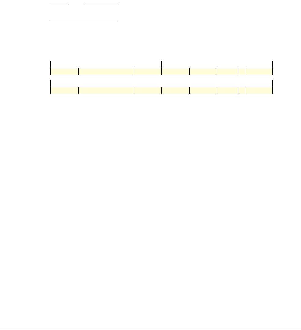
B9 System Instructions
B9.3 Alphabetical list of instructions
B9-2016 Copyright © 1996-1998, 2000, 2004-2012, 2014 ARM. All rights reserved. ARM DDI 0406C.c
Non-Confidential ID051414
B9.3.22 VMSR
Move to Advanced SIMD and Floating-point Extension System Register from ARM core register moves the value
of an ARM core register to a Floating-point system register.
Depending on settings in the CPACR, NSACR, HCPTR, and FPEXC registers, and the security state and mode in
which the instruction is executed, an attempt to execute a
VMSR
instruction might be UNDEFINED, or trapped to Hyp
mode. Summary of general controls of CP10 and CP11 functionality on page B1-1231 and Summary of access
controls for Advanced SIMD functionality on page B1-1233 summarize these controls.
When these settings permit the execution of floating-point and Advanced SIMD instructions, if the specified
Floating-point Extension System Register is not the FPSCR, the instruction is UNDEFINED if executed in User mode.
Note
VMSR on page A8-956 describes the valid application level uses of the
VMSR
instruction.
For the case when
cond
is
0b1111
, see Unconditional instructions on page A5-216.
t = UInt(Rt);
if t == 15 || (t == 13 && CurrentInstrSet() != InstrSet_ARM) then UNPREDICTABLE;
Encoding T1/A1 VFPv2, VFPv3, VFPv4, Advanced SIMD
VMSR<c> <spec_reg>, <Rt>
1 1 0 1 1 1 0 1 1 1 0 reg Rt 1 0 1 0 (0) (0) (0) 1 (0) (0) (0) (0)
15 14 13 12 11 10 9 8 7 6 5 4 3 2 1 0
1
1514131211109876543210
1 1 1 0 1 1 1 0 reg Rt 1 0 1 0 (0) (0) (0) 1 (0) (0) (0) (0)
31 30 29 28 27 26 25 24 23 22 21 20 19 18 17 16 15 14 13 12 11 10 9 8 7 6 5 4 3 2 1 0
cond

B9 System Instructions
B9.3 Alphabetical list of instructions
ARM DDI 0406C.c Copyright © 1996-1998, 2000, 2004-2012, 2014 ARM. All rights reserved. B9-2017
ID051414 Non-Confidential
Assembler syntax
VMSR{<c>}{<q>} <spec_reg>, <Rt>
where:
<c>, <q>
See Standard assembler syntax fields on page A8-287.
<spec_reg>
Is one of:
FPSID
reg = '0000'
FPSCR
reg = '0001'
FPEXC
reg = '1000'.
If the Common VFP subarchitecture is implemented, see Subarchitecture additions to the
Floating-point Extension system registers on page D6-2441 for additional values of
<spec_reg>
.
<Rt>
The ARM core register to be transferred to
<spec_reg>
.
Operation
if ConditionPassed() then
EncodingSpecificOperations();
if IsNotAllocatedVFP(reg) then UNPREDICTABLE;
if reg == '0001' then // FPSCR
CheckVFPEnabled(TRUE); SerializeVFP(); VFPExcBarrier();
FPSCR = R[t];
else // Non-FPSCR registers are accessible only at PL1 or above and not affected by FPEXC.EN
if !CurrentModeIsNotUser() then
UNDEFINED;
else
CheckVFPEnabled(FALSE);
case reg of
when '0000' SerializeVFP(); //FPSID is read-only
// '0001' already dealt with above
when "001x", "01xx" UNPREDICTABLE;
when '1000' SerializeVFP(); FPEXC = R[t];
otherwise SUBARCHITECTURE_DEFINED register access;
Exceptions
Undefined Instruction, Hyp Trap.

B9 System Instructions
B9.3 Alphabetical list of instructions
B9-2018 Copyright © 1996-1998, 2000, 2004-2012, 2014 ARM. All rights reserved. ARM DDI 0406C.c
Non-Confidential ID051414
Part C
Debug Architecture

ARM DDI 0406C.c Copyright © 1996-1998, 2000, 2004-2012, 2014 ARM. All rights reserved. C1-2021
ID051414 Non-Confidential
Chapter C1
Introduction to the ARM Debug Architecture
This chapter introduces part C of this manual, and the ARM Debug architecture for ARMv7. It contains the
following sections:
•Scope of part C of this manual on page C1-2022
•About the ARM Debug architecture on page C1-2023
•Security Extensions and debug on page C1-2027
•Register interfaces on page C1-2028.

C1 Introduction to the ARM Debug Architecture
C1.1 Scope of part C of this manual
C1-2022 Copyright © 1996-1998, 2000, 2004-2012, 2014 ARM. All rights reserved. ARM DDI 0406C.c
Non-Confidential ID051414
C1.1 Scope of part C of this manual
Part C of this manual defines the debug features of ARMv7. It describes the following versions of the Debug
architecture:
• v7 Debug, first defined in issue A of this manual
• v7.1 Debug, first defined in issue C.a of this manual, and required by any ARMv7 implementation that
includes the Virtualization Extensions.
Any processor that implements the ARMv7 architecture must implement a version of ARMv7 Debug.
Note
In issues A and B of this manual, this chapter included information about:
• The debug architectures for ARMv6, v6 Debug and v6.1 Debug. This information is now in Appendix D13
v6 Debug and v6.1 Debug Differences.
• Secure User halting debug, see Support for Secure User halting debug.
Major differences between the ARMv6 and ARMv7 Debug architectures on page D13-2550 summarizes the features
introduced in v7 Debug.
C1.1.1 Support for Secure User halting debug
On a processor that includes the Security Extensions, Secure User halting debug (SUHD) refers to permitting those
debug events that cause entry to Debug state in Secure User mode when invasive debug is not permitted in Secure
PL1 modes. For a processor that implements the Security Extensions, the architectural requirements for SUHD are:
v6.1 Debug Required.
v7 Debug A permitted option. When v7 Debug is implemented, ARM deprecates any use of SUHD.
v7.1 Debug Not permitted.
Part C of this manual describes only ARMv7 debug implementations that do not implement SUHD. Appendix D14
Secure User Halting Debug describes SUHD.

C1 Introduction to the ARM Debug Architecture
C1.2 About the ARM Debug architecture
ARM DDI 0406C.c Copyright © 1996-1998, 2000, 2004-2012, 2014 ARM. All rights reserved. C1-2023
ID051414 Non-Confidential
C1.2 About the ARM Debug architecture
ARM processors implement two types of debug support:
Invasive debug All debug features that permit modification of processor state. For more information, see
Invasive debug.
Non-invasive debug All debug features that permit data and program flow observation. For more information,
see Non-invasive debug on page C1-2024.
The following sections introduce invasive and non-invasive debug. Summary of the ARM debug component
descriptions on page C1-2026 gives a summary of the rest of part C of this manual.
C1.2.1 Invasive debug
The invasive debug component of the Debug architecture is intended primarily for run-control debugging.
Note
This part of this manual often refers to invasive debug simply as debug. For example, debug events, debug
exceptions, and Debug state are all part of the invasive debug component.
Software can use the programmers’ model to manage and control debug events. Watchpoints and breakpoints are
two examples of debug events. Chapter C3 Debug Events describes these events.
A debugger programs the Debug Status and Control Register, DBGDSCR, to configure which debug-mode is used:
Monitor debug-mode
In Monitor debug-mode, a debug event causes a debug exception to occur:
• a debug exception that relates to instruction execution generates a Prefetch Abort exception
• a debug exception that relates to a data access generates a Data Abort exception.
Chapter C4 Debug Exceptions describes these exceptions.
Halting debug-mode
In Halting debug-mode, a debug event causes the processor to enter Debug state. In Debug state,
the processor stops executing instructions from the location indicated by the program counter, but
is instead controlled through the external debug interface, in particular using the Instruction
Transfer Register, DBGITR. This enables an external agent, such as a debugger, to interrogate
processor context, and control all subsequent instruction execution. Because the processor is
stopped, it ignores the system and cannot service interrupts.
Chapter C5 Debug State describes this state.
A debug solution can use a mixture of the two methods, for example to support an OS or RTOS with both:
•Running System Debug (RSD) using Monitor debug-mode
• Halting debug-mode support available as a fallback for system failure and boot time debug.
The architecture supports the ability to switch between these two debug-modes.
When no debug-mode is selected, debug is restricted to monitor solutions. Such a monitor might use standard
system features, such as a UART or Ethernet connection, to communicate with a debug host. Alternatively, it might
use the Debug Communications Channel (DCC) as an out-of-band communications channel to the host. Using the
DCC minimizes the system resources required for debug.
The Debug architecture provides a software interface that includes:
•a Debug Identification Register, DBGDIDR
• status and control registers, including the Debug Status and Control Register, DBGDSCR
• hardware breakpoint and watchpoint support
• the DCC
• features to support the debug of reset, powerdown and the operating system.

C1 Introduction to the ARM Debug Architecture
C1.2 About the ARM Debug architecture
C1-2024 Copyright © 1996-1998, 2000, 2004-2012, 2014 ARM. All rights reserved. ARM DDI 0406C.c
Non-Confidential ID051414
The Debug architecture requires an external debug interface that supports the debug programmers’ model.
Description of invasive debug features
The following chapters describe the invasive debug component:
•Chapter C2 Invasive Debug Authentication
•Chapter C3 Debug Events
•Chapter C4 Debug Exceptions
•Chapter C5 Debug State.
In addition, see:
•Chapter C6 Debug Register Interfaces for a description of the register interfaces to the debug components
•Chapter C11 The Debug Registers for descriptions of the registers that configure and control debug
operations
•Appendix D1 Recommended External Debug Interface for a description of the recommended external
interface to the debug components.
C1.2.2 Non-invasive debug
Non-invasive debug includes all debug features that permit data and program flow to be observed, but that do not
permit modification of the main processor state.
The Debug architecture defines the following areas of non-invasive debug:
• Instruction trace and, in some implementations, data trace. Trace support is typically implemented using a
trace macrocell, see Trace.
• Sample-based profiling, see Sample-based profiling on page C1-2025.
• Performance monitors, see Performance monitors on page C1-2025.
A processor implementation might include other forms of non-invasive debug.
Chapter C9 Non-invasive Debug Authentication describes the authentication of non-invasive debug operations.
Trace
Trace support is an architecture extension. This manual describes such an extension as a trace macrocell. A trace
macrocell constructs a real-time trace stream corresponding to the operation of the processor. How the trace stream
is handled is IMPLEMENTATION DEFINED. For example, the trace stream might be:
• stored locally in an Embedded Trace Buffer (ETB) for independent download and analysis
• exported directly through a trace port to a Trace Port Analyzer (TPA) and its associated host-based trace
debug tools.
Typically, use of a trace macrocell is non-invasive. Development tools can connect to the trace macrocell, configure
it, capture trace and download the trace without affecting the operation of the processor in any way. A trace
macrocell provides an enhanced level of runtime system observation and debug granularity. It is particularly useful
when:
• Stopping the processor affects the behavior of the system.
• By the time a problem is detected the visible state is insufficient to be able to determine its cause. Trace
provides a mechanism for system logging and back tracing of faults.
Trace might also perform analysis of software running on the processor, such as performance analysis or code
coverage analysis.

C1 Introduction to the ARM Debug Architecture
C1.2 About the ARM Debug architecture
ARM DDI 0406C.c Copyright © 1996-1998, 2000, 2004-2012, 2014 ARM. All rights reserved. C1-2025
ID051414 Non-Confidential
Typically, a trace architecture defines:
• the trace macrocell programmers’ model
• permitted trace protocol formats
• the physical trace port connector.
The following documents define the ARM trace architectures:
•Embedded Trace Macrocell Architecture Specification
•CoreSight Program Flow Trace Architecture Specification.
The ARM trace architectures have a common identification mechanism. This means development tools can detect
which architecture is implemented.
Sample-based profiling
Sample-based profiling is an OPTIONAL non-invasive component of the Debug architecture, that enables debug
software to profile a program. For more information, see Chapter C10 Sample-based Profiling.
Performance monitors
The ARMv7 architecture defines an OPTIONAL Performance Monitors Extension. The basic form of this is:
• A cycle counter, with the ability to count every cycle or every sixty-fourth cycle.
• A number of event counters. Software can program the event counted by each counter:
— Previous implementations provided up to four counters
— In ARMv7, space is provided for up to 31 counters. The actual number of counters is
IMPLEMENTATION DEFINED, and an identification mechanism is provided.
• Controls for
— enabling and resetting counters
— indicating overflows
— enabling interrupts on overflow.
The cycle counter can be enabled independently from the event counters.
The set of events that can be monitored is divided into:
• events that are likely to be consistent across many microarchitectures
• other events, that are likely to be implementation-specific.
As a result, the architecture defines a common set of events to be used across many microarchitectures, and reserves
a large space for IMPLEMENTATION DEFINED events. The full set of events for any given implementation is
IMPLEMENTATION DEFINED. There is no requirement to implement any of the common set of events, but the numbers
allocated for the common set of events must not be used except as defined.
Chapter C12 The Performance Monitors Extension describes this extension.

C1 Introduction to the ARM Debug Architecture
C1.2 About the ARM Debug architecture
C1-2026 Copyright © 1996-1998, 2000, 2004-2012, 2014 ARM. All rights reserved. ARM DDI 0406C.c
Non-Confidential ID051414
C1.2.3 Summary of the ARM debug component descriptions
Table C1-1 shows the main debug components, and where they are described.
For more information, see:
•Chapter C11 The Debug Registers
•Appendix D1 Recommended External Debug Interface.
Table C1-1 v7 Debug components
Component Debug version Status Type Reference
Run-control Debug v7 and v7.1 Required Invasive Chapter C2 Invasive Debug Authentication
Chapter C3 Debug Events
Chapter C4 Debug Exceptions
Chapter C5 Debug State
Chapter C6 Debug Register Interfaces
Trace v7 and v7.1 Optional Non-invasiveaTrace on page C1-2024
Sample-based profiling v7 OPTIONAL Non-invasiveaChapter C10 Sample-based Profiling
v7.1 Required
Performance Monitors v7 and v7.1 OPTIONAL Non-invasiveaChapter C12 The Performance Monitors Extension
a. For information about authentication of these components see Chapter C9 Non-invasive Debug Authentication.

C1 Introduction to the ARM Debug Architecture
C1.3 Security Extensions and debug
ARM DDI 0406C.c Copyright © 1996-1998, 2000, 2004-2012, 2014 ARM. All rights reserved. C1-2027
ID051414 Non-Confidential
C1.3 Security Extensions and debug
The Security Extensions include independent controls of when:
• Debug events are enabled. The options are:
— in all processor modes, in both Secure and Non-secure security state
— only in Non-secure state
— in Non-secure state and, if it will not cause entry to Debug state, in Secure User mode.
• Non-invasive debug is enabled. The options are:
— in all processor modes, in both Secure and Non-secure security state
— only in Non-secure state
— in Non-secure state and in Secure User mode.
This is controlled by two bits in the Secure Debug Enable Register, and four input signals in the recommended
external debug interface:
• In the Secure Debug Enable Register:
— the Secure User Invasive Debug Enable bit, SDER.SUIDEN
— the Secure User Non-invasive Debug Enable bit, SDER.SUNIDEN
• in the recommended external debug interface:
— the Debug Enable signal, DBGEN
— the Non-Invasive Debug Enable signal, NIDEN
— the Secure PL1 Invasive Debug Enable signal, SPIDEN
— the Secure PL1 Non-Invasive Debug Enable signal, SPNIDEN.
For more information, see:
•Chapter C2 Invasive Debug Authentication
•Chapter C9 Non-invasive Debug Authentication
• Secure Debug Enable Register, SDER for details of the SUIDEN and SUNIDEN bits
•Authentication signals on page D1-2340 for details of the DBGEN, NIDEN, SPIDEN and SPNIDEN
signals.

C1 Introduction to the ARM Debug Architecture
C1.4 Register interfaces
C1-2028 Copyright © 1996-1998, 2000, 2004-2012, 2014 ARM. All rights reserved. ARM DDI 0406C.c
Non-Confidential ID051414
C1.4 Register interfaces
This section introduces the debug register interfaces defined by v7 Debug and v7.1 Debug. The most important
distinction is between:
• the external debug interface, that defines how an external debugger can access the debug resources
• the processor interface, that describes how an ARMv7 processor can access its own debug resources.
ARM strongly recommends an external debug interface based on the ARM Debug Interface v5 Architecture
Specification (ADIv5). This interface supports external debug over powerdown of the processor.
Although the ADIv5 interface is not required for compliance with ARMv7, the ARM debug tools require this
interface to be implemented.
ADIv5 supports both a JTAG wire interface and a low pin-count Serial Wire Debug (SWD) interface. The ARM
debug tools support either wire interface.
An ADIv5 interface enables a debug object, such as an ARM processor, to abstract a set of resources as a
memory-mapped peripheral. Accesses to debug resources are made as 32-bit read or write transfers. The debug
architecture supports debug of powerdown by permitting accesses to certain resources to return an error response if
the resource is unavailable, just as a memory-mapped peripheral can return a slave-generated error response in
exceptional circumstances.
The debug architecture requires that some debug registers are accessible to software executing on the processor, so
that the debug architecture can be used by a self-hosted debug monitor. To meet this requirement:
v7.1 Debug Requires these debug registers to be accessible using CP14 register accesses.
v7 Debug Requires a subset of these debug registers to be accessible using CP14 accesses, and the remainder
of these registers to be accessible from one or both of the following:
• the CP14 interface
• a memory-mapped debug register interface.
For more information, see Chapter C6 Debug Register Interfaces.
If an implementation includes an optional trace macrocell, the appropriate trace architecture specification defines
the interface to the trace macrocell registers. The ARM trace macrocell architectures, referred to in Trace on
page C1-2024, define optional CP14 and memory-mapped interfaces to the registers. v7 Debug requires that, if an
ARM trace macrocell implements the CP14 register interface, the v7 Debug implementation must provide CP14
access to all the registers for which Table C6-5 on page C6-2130 has a Yes entry in the CP14 or MM column.
ARM recommends that, if an implementation includes a memory-mapped interface to either the trace registers or
the debug registers, it implements memory-mapped interfaces to both sets of registers.
The OPTIONAL Performance Monitors Extension:
• requires a CP15 register interface
• also defines an optional memory-mapped register interface.

ARM DDI 0406C.c Copyright © 1996-1998, 2000, 2004-2012, 2014 ARM. All rights reserved. C2-2029
ID051414 Non-Confidential
Chapter C2
Invasive Debug Authentication
This chapter describes the authentication controls on invasive debug operations. It contains the following sections:
•About invasive debug authentication on page C2-2030
•Invasive debug with no Security Extensions on page C2-2031
•Invasive debug with the Security Extensions on page C2-2033
•Invasive debug authentication security considerations on page C2-2035.
Note
For information about using the interface to control non-invasive debug see Chapter C9 Non-invasive Debug
Authentication.
This chapter describes only ARMv7 debug implementations that do not implement Secure User Halting (SUHD).
Appendix D14 Secure User Halting Debug describes SUHD.

C2 Invasive Debug Authentication
C2.1 About invasive debug authentication
C2-2030 Copyright © 1996-1998, 2000, 2004-2012, 2014 ARM. All rights reserved. ARM DDI 0406C.c
Non-Confidential ID051414
C2.1 About invasive debug authentication
Debug events include software and halting debug events. About debug events on page C3-2038 gives an overview
of all debug events.
Invasive debug authentication controls whether an debug event:
• causes the processor to enter Debug state
• generates a debug exception
• is ignored
• becomes pending.
See Chapter C3 Debug Events for information on how debug events are generated, and their effects.
Note
• The recommended external debug interface provides an authentication interface that controls both invasive
debug and non-invasive debug, as described in Authentication signals on page D1-2340. This chapter
describes how you can use this interface to control invasive debug. For more information about using the
authentication signals see Changing the authentication signals on page D1-2340.
• As well as the authentication controls, the effect of debug events can be changed by the OS Lock and, in v7.1
Debug, the OS Double Lock. See Chapter C7 Debug Reset and Powerdown Support for details.
Invasive debug authentication can be controlled dynamically, meaning that the effect of a debug event can change
while the processor is running, or when the processor is in Debug state.
The following signals, register fields, and processor states control invasive debug authentication:
DBGEN The Debug Enable signal enables invasive debug.
SPIDEN In an implementation that includes the Security Extensions, the Secure PL1 Invasive Debug Enable
signal enables debug events in Secure PL1 modes.
DBGDSCR.HDBGen
Enables Halting debug-mode.
DBGDSCR.MDBGen
Enables Monitor debug-mode.
SDER.SUIDEN
In an implementation that includes the Security Extensions, when Monitor debug-mode is selected,
the Secure User Invasive Debug enable bit enables debug events in the Secure PL0 mode.
Privilege level In an implementation that includes the Security Extensions, the privilege level of source of the
debug event can affect how the debug event is handled.
If the implementation also includes the Virtualization Extensions, then debug events at PL2 are
handled differently in Monitor debug-mode.
Security state In an implementation that includes the Security Extensions, the security state of the processor
affects how the debug event is handled.
The following sections show how the controls are used, with and without the Security Extensions:
•Invasive debug with no Security Extensions on page C2-2031
•Invasive debug with the Security Extensions on page C2-2033.

C2 Invasive Debug Authentication
C2.2 Invasive debug with no Security Extensions
ARM DDI 0406C.c Copyright © 1996-1998, 2000, 2004-2012, 2014 ARM. All rights reserved. C2-2031
ID051414 Non-Confidential
C2.2 Invasive debug with no Security Extensions
If an implementation does not include the Security Extensions, the DBGEN signal controls whether invasive debug
is enabled or not:
•If DBGEN is LOW, all Software and Halting debug events are disabled, except the BKPT instruction debug
event, which remains enabled and generates a debug exception.
•If DBGEN is HIGH, all Software and Halting debug events are enabled.
The result of a debug event depends on the current debug-mode:
Halting debug-mode
All debug events cause the processor to enter Debug state.
Monitor debug-mode
Halting debug events cause the processor to enter Debug state.
Software debug events generate a debug exception.
No debug-mode set
Halting debug events cause the processor to enter Debug state.
The BKPT instruction debug event generates a debug exception.
All other Software debug events are ignored.
See Chapter C3 Debug Events for more information on how debug events are defined, and the types of debug
exceptions that are generated.
See Chapter C7 Debug Reset and Powerdown Support for details of how the OS Lock and OS Double Lock can
affect the outcome of a debug event.
Figure C2-1 on page C2-2032 shows how DBGEN and the debug-mode, configured by the
DBGDSCR.{MDBGen, HDBGen} bits, determine the outcome of an debug event.
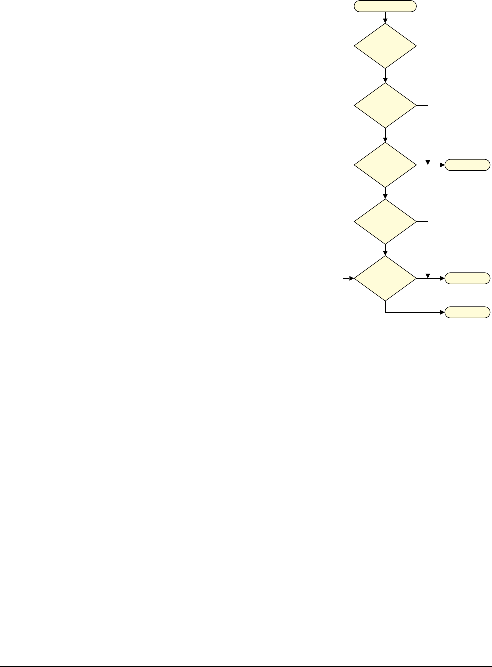
C2 Invasive Debug Authentication
C2.2 Invasive debug with no Security Extensions
C2-2032 Copyright © 1996-1998, 2000, 2004-2012, 2014 ARM. All rights reserved. ARM DDI 0406C.c
Non-Confidential ID051414
Figure C2-1 Invasive debug authentication with no Security Extensions
Debug event
DBGEN
Halting
Event?
DBGDSCR.
HDBGen
DBGDSCR.
MDBGen
Halt
Exception
Ignore
BKPT?
LOW
HIGH
Yes
No
1
0
1
0
Yes
No

C2 Invasive Debug Authentication
C2.3 Invasive debug with the Security Extensions
ARM DDI 0406C.c Copyright © 1996-1998, 2000, 2004-2012, 2014 ARM. All rights reserved. C2-2033
ID051414 Non-Confidential
C2.3 Invasive debug with the Security Extensions
If an implementation includes the Security Extensions, the DBGEN signal controls whether invasive debug is
enabled or not:
•If DBGEN is LOW, all Software and Halting debug events are disabled, except the BKPT instruction debug
event, which remains enabled and generates a debug exception.
•If DBGEN is HIGH, the effect of a debug event is determined by the SPIDEN signal, SDER.SUIDEN, and
the privilege level and security state of the processor.
When DBGEN is HIGH, the result of a debug event also depends on the current debug-mode and the type of debug
event, as shown in the following sections.
See Chapter C3 Debug Events for more information on how debug events are defined, and the types of debug
exceptions that are generated.
See Chapter C7 Debug Reset and Powerdown Support for details of how the OS Lock and OS Double Lock can
affect the outcome of a debug event.
C2.3.1 Halting debug events
A Halting debug event causes the processor to enter Debug state, except when the processor is in Secure state and
SPIDEN is LOW. In this case the Halting debug event becomes pending. See Halting debug events on
page C3-2075 for details on how pending events are handled.
C2.3.2 BKPT instruction debug event
A
BKPT
instruction causes the processor to enter Debug state in the following cases:
• in Halting debug-mode, in Non-secure state, at any privilege level including PL2
• in Halting debug-mode, in Secure state, and SPIDEN is HIGH.
Otherwise, a
BKPT
instruction generates a debug exception.
C2.3.3 Other Software debug events
The results of the Breakpoint, Watchpoint, and Vector catch debug events depend on the debug-mode, as shown
below:
Halting debug-mode
The other Software debug events cause the processor to enter Debug state, except when in Secure
state, and SPIDEN is LOW, when the events are ignored.
Monitor debug-mode
The other Software debug events generate a debug exception, apart from the following cases:
• in PL2, the event is ignored
• in PL1, in Secure state, and SPIDEN is LOW, the event is ignored
• in PL0, in Secure state, SPIDEN is LOW, and SDER.SUIDEN==0, the event is ignored.
No debug-mode set
The other Software debug events are ignored.
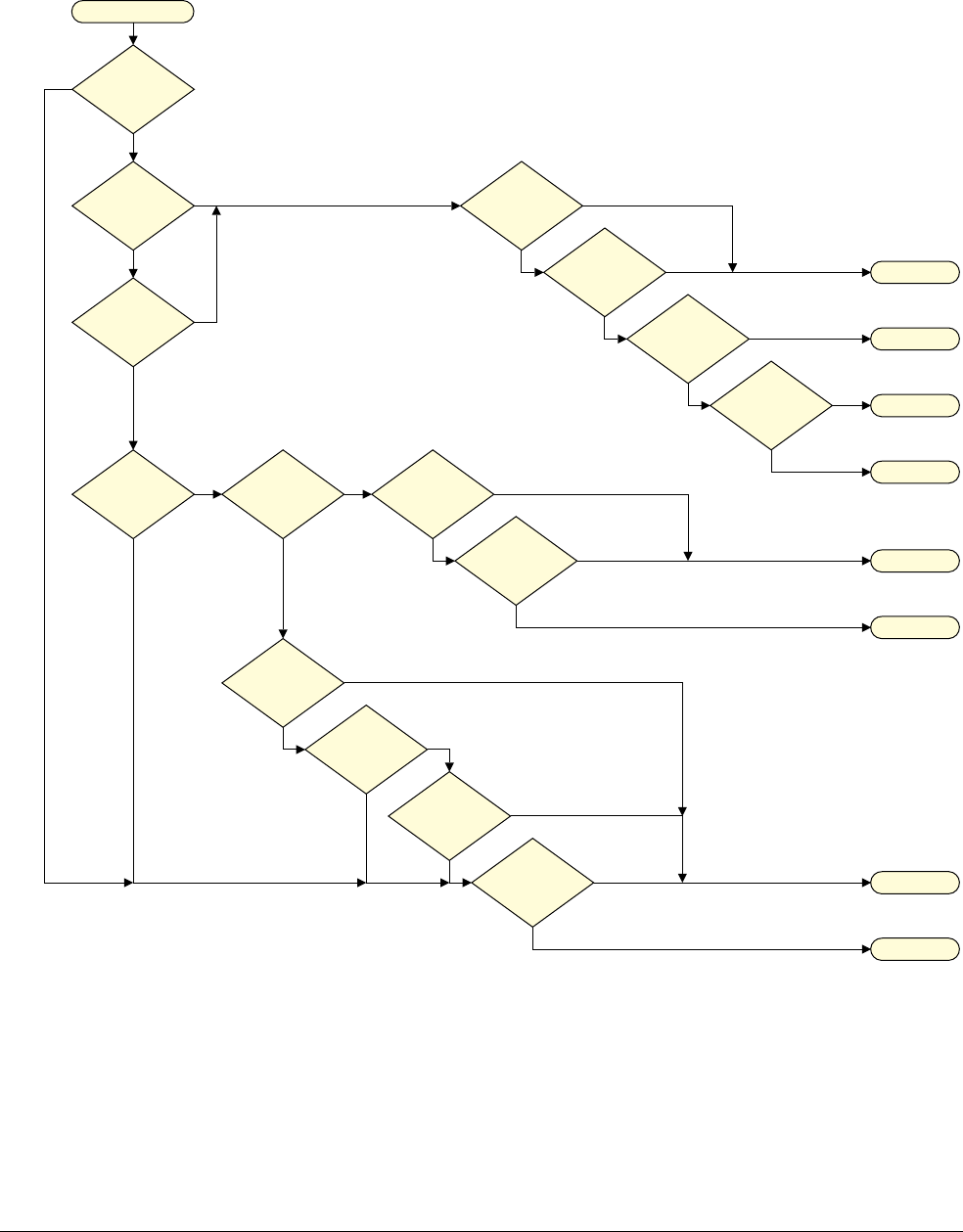
C2 Invasive Debug Authentication
C2.3 Invasive debug with the Security Extensions
C2-2034 Copyright © 1996-1998, 2000, 2004-2012, 2014 ARM. All rights reserved. ARM DDI 0406C.c
Non-Confidential ID051414
C2.3.4 Summary of invasive debug authentication with the Security Extensions
Figure C2-2 shows how DBGEN and other settings determine the outcome of a debug event.
Figure C2-2 Invasive debug authentication with the Security Extensions
Debug event
DBGEN
Halting
Event?
DBGDSCR.
HDBGen
DBGDSCR.
MDBGen
Secure?
SPIDEN
Halting
Event?
Halt
Pending
SPIDEN
Exception
Ignore
BKPT?
PL2?
PL0?
BKPT?
LOW
HIGH
Yes
No
1
0
1
0
No
Yes
SDER.
SUIDEN
HIGH
LOW Yes
No Yes
No
HIGH
LOW
Secure?
Yes
No
Exception
No
BKPT?
Yes
No Ignore
Yes
Exception
Ignore
Yes
No
Yes
No
0
1

C2 Invasive Debug Authentication
C2.4 Invasive debug authentication security considerations
ARM DDI 0406C.c Copyright © 1996-1998, 2000, 2004-2012, 2014 ARM. All rights reserved. C2-2035
ID051414 Non-Confidential
C2.4 Invasive debug authentication security considerations
Invasive and non-invasive debug authentication mean a developer can protect Secure processing from direct
observation or invasion by a debugger that they do not trust.
Note
System designers must be aware that security attacks can be aided by the invasive and non-invasive debug facilities.
For example, Debug state or the DBGDSCR.INTdis bit might be used for a denial of service attack, and the
Non-secure performance monitors might be used for measuring the side-effects of Secure processing on Non-secure
software.
ARM recommends that, where such attacks are a concern, invasive and non-invasive debug are disabled in all
modes. However system designers must be aware of the limitations on the protection that debug authentication can
provide, because similar attacks can be made by running malicious software on the processor in Non-secure state.
Caution
When Secure debugging is enabled, Secure operations are visible to the external debugger, and in some cases to
software running in Non-secure state.
ARM recommends that devices are split into development and production devices:
• Development devices can have secure debugging enabled by authorized developers. All secure data must be
replaced by test data suitable for development purposes, where there are no security issues if the test data is
disclosed.
• Production devices can never have secure debugging enabled. These devices are loaded with the real secure
data.
For more information about the authentication interface and its control, see the CoreSight Architecture
Specification.

C2 Invasive Debug Authentication
C2.4 Invasive debug authentication security considerations
C2-2036 Copyright © 1996-1998, 2000, 2004-2012, 2014 ARM. All rights reserved. ARM DDI 0406C.c
Non-Confidential ID051414

ARM DDI 0406C.c Copyright © 1996-1998, 2000, 2004-2012, 2014 ARM. All rights reserved. C3-2037
ID051414 Non-Confidential
Chapter C3
Debug Events
This chapter describes debug events. Debug events trigger invasive debug operations. It contains the following
sections:
•About debug events on page C3-2038
•BKPT instruction debug events on page C3-2040
•Breakpoint debug events on page C3-2041
•Watchpoint debug events on page C3-2059
•Vector catch debug events on page C3-2067
•Halting debug events on page C3-2075
•Generation of debug events on page C3-2076
•Debug event prioritization on page C3-2078
•Pseudocode details of Software debug events on page C3-2080.

C3 Debug Events
C3.1 About debug events
C3-2038 Copyright © 1996-1998, 2000, 2004-2012, 2014 ARM. All rights reserved. ARM DDI 0406C.c
Non-Confidential ID051414
C3.1 About debug events
A debug event can be either:
• A Software debug event, which is one of the following:
BKPT instruction Causes a software breakpoint to occur. For more information, see BKPT instruction
debug events on page C3-2040
Breakpoint Based on instruction address match, instruction address mismatch, or context match.
For more information, see Breakpoint debug events on page C3-2041.
Watchpoint Based on data address match. For more information, see Watchpoint debug events on
page C3-2059.
Vector catch Trap of exceptions based on vector address or exception type. For more information,
see Vector catch debug events on page C3-2067.
See also Pseudocode details of Software debug events on page C3-2080.
• A Halting debug event, which is one of the following:
External Debug Request
The system requests the processor to enter Debug state.
Halt Request The debugger requests the processor to enter Debug state by writing to the
DBGDRCR.HRQ, Halt request bit.
OS Unlock Catch The OS Lock is unlocked. This event is enabled in DBGECR.
See Halting debug events on page C3-2075 for more information.
A processor responds to a debug event in one of the following ways:
• Ignores the debug event.
• Takes a debug exception, see Chapter C4 Debug Exceptions.
• Enters Debug state, see Chapter C5 Debug State.
• Marks the event as pending. This only occurs when invasive debug is enabled, but entering Debug state is
not permitted. See Halting debug events on page C3-2075 for more information.
The response depends on whether invasive debug is enabled, and the debug-mode selected. This is shown in
Table C3-1 and in Figure C3-1 on page C3-2039. In an implementation that includes the Security Extensions, the
response is changed by the security settings. See Invasive debug with the Security Extensions on page C2-2033 for
details.
For more detailed information on setting the configuration and debug event behavior, see Generation of debug
events on page C3-2076.
See Chapter C7 Debug Reset and Powerdown Support for details of how the OS Lock and OS Double Lock can
affect the outcome of a debug event.
Table C3-1 Processor behavior on debug events
Event Invasive debug
disabled
Invasive debug enabled, debug-mode:
None Monitor Halting
BKPT Debug exception Debug exception Debug exception Debug state entry
Breakpoint, Watchpoint, or Vector catch Ignored Ignored Debug exception Debug state entry
Halting Ignored Debug state entry Debug state entry Debug state entry
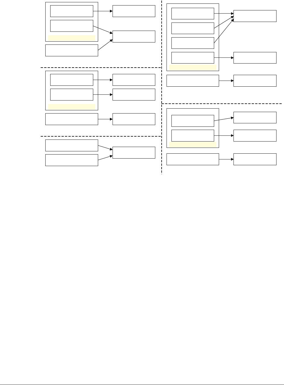
C3 Debug Events
C3.1 About debug events
ARM DDI 0406C.c Copyright © 1996-1998, 2000, 2004-2012, 2014 ARM. All rights reserved. C3-2039
ID051414 Non-Confidential
Figure C3-1 Processor behavior on debug events
Avoiding debug exceptions that might cause UNPREDICTABLE behavior on page C4-2092 describes cases where
a debugger, or a debug monitor, must be careful not to define Software debug events that might cause
UNPREDICTABLE behavior.
Software debug events
BKPT instruction Debug exception
(Prefetch Abort)
Other
Ignored
Debug disabled
Software debug events
BKPT instruction Debug exception
(Prefetch Abort)
Other Ignored
Debug state entry
Debug-mode: None
Software debug events
BKPT instruction Debug exception
(Prefetch Abort)
Breakpoint
Watchpoint
Vector catch
Debug exception
(Data Abort)
Debug-mode: Monitor, privilege level PL0 or PL1
Debug state entry
Debug-mode: Halting
Halting debug events
Software debug events
Halting debug events
Halting debug events
Debug state entryHalting debug events
Software debug events
BKPT instruction
Debug exception
(Prefetch Abort)
Other Ignored
Debug-mode: Monitor, privilege level PL2
Halting debug events Debug state entry

C3 Debug Events
C3.2 BKPT instruction debug events
C3-2040 Copyright © 1996-1998, 2000, 2004-2012, 2014 ARM. All rights reserved. ARM DDI 0406C.c
Non-Confidential ID051414
C3.2 BKPT instruction debug events
A BKPT instruction debug event occurs when a
BKPT
instruction is committed for execution.
BKPT
is an unconditional
instruction.
BKPT instruction debug events are synchronous. That is, the debug event acts like an exception that cancels the
BKPT
instruction.
A BKPT instruction debug event generates a Prefetch Abort exception, except when Halting debug-mode is
enabled, when a BKPT instruction debug event causes the processor to enter Debug state. For more information,
see Generation of debug events on page C3-2076 and Chapter C5 Debug State.
On a BKPT instruction debug event, the DBGDSCR.MOE, Method of debug entry, field is set to BKPT instruction
debug event. See DBGDSCR, Debug Status and Control Register on page C11-2243.
For details of the
BKPT
instruction and its encodings in the ARM and Thumb instruction sets see BKPT on
page A8-346.

C3 Debug Events
C3.3 Breakpoint debug events
ARM DDI 0406C.c Copyright © 1996-1998, 2000, 2004-2012, 2014 ARM. All rights reserved. C3-2041
ID051414 Non-Confidential
C3.3 Breakpoint debug events
To define a Breakpoint debug event, a debugger programs two or three registers to create a breakpoint. Each
breakpoint comprises:
•a Breakpoint Control Register, DBGBCR, that holds control information for the breakpoint
•a Breakpoint Value Register, DBGBVR, that holds the value used in breakpoint matching. This can be an
instruction address or a value for Context matching
• optionally, in an implementation that includes the Virtualization Extensions, a Breakpoint Extended Value
Register, DBGBXVR, that holds a Virtual machine identifier (VMID) for Context matching.
The number of breakpoints that can be created is specified by the DBGDIDR.BRPs field, and can be between 2 and
16. See DBGDIDR, Debug ID Register on page C11-2231 for details.
For each breakpoint, the associated registers are numbered, from 0 to 15, for example, DBGBCR3, DBGBVR3, and
optionally, DBGBXVR3 define breakpoint 3. For details of the breakpoint registers see:
•DBGBVR, Breakpoint Value Registers on page C11-2218
•DBGBCR, Breakpoint Control Registers on page C11-2213
•DBGBXVR, Breakpoint Extended Value Registers on page C11-2219.
A debugger can define a Breakpoint debug event:
• Based on a comparison of an instruction address with the value held in a DBGBVR. The address in the
DBGBVR must be the virtual address of the instruction.
• Based on a comparison of one or both of:
— the Context ID with the value held in a DBGBVR
— the VMID with the value held in a DBGBXVR.
For more information, see Context matching comparisons for debug event generation on page C3-2053.
Some breakpoints might not support Context matching. The DBGDIDR.CTX_CMPs field specifies the
number of breakpoints that support Context matching.
• By linking one breakpoint to a second breakpoint, to define a single Breakpoint debug event. One breakpoint
defines an instruction address match, and the second breakpoint defines a Context match.
In all cases, the DBGBCR defines some additional conditions that must be met for the breakpoint to generate a
Breakpoint debug event, including whether the breakpoint is enabled.
The terms hit and miss describe whether the conditions defined in the breakpoint are met:
• a hit occurs when the conditions are met
• a miss occurs when a condition is not met, meaning the processor does not generate a debug event.
Hit and miss can also describe part of the defined conditions, for example the required address comparison either
hits or misses.
The following sections describe Breakpoint debug events:
•Generation of Breakpoint debug events on page C3-2042
•Breakpoint types defined by the DBGBCR on page C3-2042
•Conditions for debug event generation defined by the DBGBCR on page C3-2046
•Byte address selection and masking defined by the DBGBCR on page C3-2047
•Instruction address comparisons for debug event generation on page C3-2048
•Context matching comparisons for debug event generation on page C3-2053
•Linked comparisons for debug event generation on page C3-2055
•Summary of breakpoint generation options on page C3-2057.

C3 Debug Events
C3.3 Breakpoint debug events
C3-2042 Copyright © 1996-1998, 2000, 2004-2012, 2014 ARM. All rights reserved. ARM DDI 0406C.c
Non-Confidential ID051414
C3.3.1 Generation of Breakpoint debug events
For each instruction in the program flow, the debug logic tests all the breakpoints. For each breakpoint, the debug
logic generates a Breakpoint debug event only if all of the following apply:
• When the breakpoint is tested, the conditions specified in the DBGBCR are met, see Conditions for debug
event generation defined by the DBGBCR on page C3-2046.
• The comparison with the value in the DBGBVR is successful.
• If the breakpoint is linked to a second breakpoint, the comparison made by the second breakpoint is
successful.
• The instruction is committed for execution.
Note
The processor tests for any possible Breakpoint debug events before executing an instruction. The debug
logic might test a breakpoint when an instruction is fetched speculatively. However, it does not generate a
Breakpoint debug event if the instruction is not committed for execution.
If all of these conditions are met, the debug logic generates the Breakpoint debug event regardless of whether the
instruction passes its condition code check. The debug logic generates the debug event regardless of the type of
instruction.
For more information about the possible comparisons, see Breakpoint types defined by the DBGBCR.
Breakpoint debug events are synchronous. That is, the debug event acts like an exception that cancels the
breakpointed instruction.
When invasive debug is enabled and Monitor debug-mode is selected, and if debug events are permitted, a
Breakpoint debug event generates a Prefetch Abort exception. For more information, see Generation of debug
events on page C3-2076.
When invasive debug is enabled and Halting debug-mode is selected, and if Breakpoint debug events are permitted,
a Breakpoint debug event causes the processor to enter Debug state. See Chapter C5 Debug State.
On a Breakpoint debug event, the DBGDSCR.MOE, Method of debug entry, field is set to Breakpoint debug event.
See DBGDSCR, Debug Status and Control Register on page C11-2243.
C3.3.2 Breakpoint types defined by the DBGBCR
The different types of breakpoint, and how breakpoints can be linked, are controlled by the following field in the
DBGBCR:
Breakpoint type, BT
Defines the breakpoint type, that can be:
• an instruction address match
• an instruction address mismatch
• a Context match.
In addition, an instruction address match or mismatch breakpoint can be linked to a Context match
breakpoint. The Breakpoint type specifies if the breakpoint is unlinked or linked.
The supported BT values and associated Breakpoint types are:
0b0000
, Unlinked instruction address match
Generation of the breakpoint depends on both:
• the DBGBCR.{SSC, HMC, PMC} controls described in Conditions for debug event
generation defined by the DBGBCR on page C3-2046
• a successful address match comparison, as described in Instruction address comparisons for
debug event generation on page C3-2048.

C3 Debug Events
C3.3 Breakpoint debug events
ARM DDI 0406C.c Copyright © 1996-1998, 2000, 2004-2012, 2014 ARM. All rights reserved. C3-2043
ID051414 Non-Confidential
This breakpoint is not linked to any other breakpoint or watchpoint. DBGBCR.LBN must be
programmed to
0b0000
, otherwise the generation of Breakpoint debug events by this breakpoint is
UNPREDICTABLE.
0b0001
, Linked instruction address match
Generation of a breakpoint depends on all of:
• the DBGBCR.{SSC, HMC, PMC} controls described in Conditions for debug event
generation defined by the DBGBCR on page C3-2046
• a successful address match comparison using the DBGBVR for this breakpoint, as described
in Instruction address comparisons for debug event generation on page C3-2048
• a successful context match defined by the breakpoint indicated by DBGBCR.LBN.
Note
This BT value is used to program the breakpoint that defines the instruction address match.
For more information, see Linked comparisons for debug event generation on page C3-2055.
0b0010
, Unlinked Context ID match
Generation of the breakpoint depends on both:
• the DBGBCR.{SSC, HMC, PMC} controls described in Conditions for debug event
generation defined by the DBGBCR on page C3-2046
• a successful Context ID match, as described in Context matching comparisons for debug
event generation on page C3-2053.
This breakpoint is not linked to any other breakpoint or watchpoint. DBGBCR.LBN must be
programmed to
0b0000
, otherwise the generation of Breakpoint debug events by this breakpoint is
UNPREDICTABLE.
DBGBCR.BAS must be programmed to
0b1111
, otherwise the generation of Breakpoint debug
events by this breakpoint is UNPREDICTABLE.
See UNPREDICTABLE cases when Monitor debug-mode is selected on page C3-2047 for
additional restrictions for this type of breakpoint when using Monitor debug-mode.
0b0011
, Linked Context ID match
Either:
• generation of a breakpoint depends on both:
— a successful instruction address match, or a successful instruction address mismatch,
defined by a breakpoint that is linked to this breakpoint
— a successful Context ID match defined by this breakpoint
• generation of a watchpoint depends on both:
— a successful data address match defined by a watchpoint that is linked to this
breakpoint, see Generation of Watchpoint debug events on page C3-2059
— a successful Context ID match defined by this breakpoint.
Note
• This BT value is used when programming the breakpoint that defines the Context ID match
part of a Linked Context ID match breakpoint or watchpoint.
• This breakpoint can define the Context ID match part of multiple Context ID match
breakpoints and watchpoints.
• Linking is defined in the linked Breakpoint or Watchpoint definitions, not in this breakpoint
definition.
Context matching comparisons for debug event generation on page C3-2053 describes the
requirements for a successful Context ID match by this breakpoint.

C3 Debug Events
C3.3 Breakpoint debug events
C3-2044 Copyright © 1996-1998, 2000, 2004-2012, 2014 ARM. All rights reserved. ARM DDI 0406C.c
Non-Confidential ID051414
DBGBCR.BAS must be programmed to
0b1111
and DBGBCR.LBN must be programmed to
0b0000
,
otherwise the generation of Breakpoint or Watchpoint debug events by breakpoints and watchpoints
linked to this breakpoint is UNPREDICTABLE.
If no breakpoint or watchpoint of the correct type is linked to this breakpoint, no Breakpoint or
Watchpoint debug events are generated for this breakpoint.
For more information, see Linked comparisons for debug event generation on page C3-2055.
0b0100
, Unlinked instruction address mismatch
Generation of the breakpoint depends on both:
• the DBGBCR.{SSC, HMC, PMC} controls described in Conditions for debug event
generation defined by the DBGBCR on page C3-2046
• a successful address mismatch comparison, as described in Instruction address comparisons
for debug event generation on page C3-2048.
This breakpoint is not linked to any other breakpoint or watchpoint. DBGBCR.LBN must be
programmed to
0b0000
, otherwise the generation of Breakpoint debug events by this breakpoint is
UNPREDICTABLE.
See UNPREDICTABLE cases when Monitor debug-mode is selected on page C3-2047 for
additional restrictions for this type of breakpoint when using Monitor debug-mode.
0b0101
, Linked instruction address mismatch
Generation of a breakpoint depends on all of:
• the DBGBCR.{SSC, HMC, PMC} controls described in Conditions for debug event
generation defined by the DBGBCR on page C3-2046
• a successful address mismatch comparison using the DBGBVR for this breakpoint, as
described in Instruction address comparisons for debug event generation on page C3-2048
• a successful context match defined by the breakpoint indicated by DBGBCR.LBN.
Note
This BT value is used to program the breakpoint that defines the instruction address mismatch.
For more information, see Linked comparisons for debug event generation on page C3-2055.
See UNPREDICTABLE cases when Monitor debug-mode is selected on page C3-2047 for
additional restrictions for this type of breakpoint when using Monitor debug-mode.
0b1000
, Unlinked VMID match
Generation of the breakpoint depends on both:
• the DBGBCR.{SSC, HMC, PMC} controls described in Conditions for debug event
generation defined by the DBGBCR on page C3-2046
• a successful VMID match, as described in Context matching comparisons for debug event
generation on page C3-2053.
DBGBCR.BAS must be programmed to
0b1111,
DBGBCR.LBN must be programmed to
0b0000
,
and the associated DBGBVR must be programmed to
0x00000000
, otherwise the generation of
Breakpoint debug events by this breakpoint is UNPREDICTABLE.
See UNPREDICTABLE cases when Monitor debug-mode is selected on page C3-2047 for
additional restrictions for this type of breakpoint when using Monitor debug-mode.
This breakpoint type is supported only if the implementation includes the Virtualization Extensions.

C3 Debug Events
C3.3 Breakpoint debug events
ARM DDI 0406C.c Copyright © 1996-1998, 2000, 2004-2012, 2014 ARM. All rights reserved. C3-2045
ID051414 Non-Confidential
0b1001
, Linked VMID match
Either:
• generation of a breakpoint depends on both:
— a successful instruction address match, or a successful instruction address mismatch,
defined by a breakpoint that is linked to this breakpoint
— a successful VMID match defined by this breakpoint
• generation of a watchpoint depends on both:
— a successful data address match defined by a watchpoint that is linked to this
breakpoint, see Generation of Watchpoint debug events on page C3-2059
— a successful VMID match defined by this breakpoint.
Note
• This BT value is used when programming the breakpoint that defines the VMID match part
of a Linked VMID match breakpoint or watchpoint.
• This breakpoint can define the VMID match part of multiple VMID match breakpoints and
watchpoints.
• Linking is defined in the linked Breakpoint or Watchpoint definitions, not in this breakpoint
definition.
Context matching comparisons for debug event generation on page C3-2053 describes the
requirements for a successful VMID match by this breakpoint.
DBGBCR.BAS must be programmed to
0b1111
, DBGBCR.LBN must be programmed to
0b0000
,
and the associated DBGBVR must be programmed to
0x00000000
, otherwise the generation of
Breakpoint and Watchpoint debug events by breakpoints and watchpoints linked to this breakpoint
is UNPREDICTABLE.
If no breakpoint or watchpoint of the correct type is linked to this breakpoint, no Breakpoint or
Watchpoint debug events are generated for this breakpoint.
For more information see Linked comparisons for debug event generation on page C3-2055.
This breakpoint type is supported only if the implementation includes the Virtualization Extensions.
0b1010
, Unlinked VMID match and Context ID match
Generation of the breakpoint depends on all of:
• the DBGBCR.{SSC, HMC, PMC} controls described in Conditions for debug event
generation defined by the DBGBCR on page C3-2046
• a successful Context ID match, defined by this breakpoint
• a successful VMID match, defined by this breakpoint.
Context matching comparisons for debug event generation on page C3-2053 describes the
requirements for a successful Context ID match and a successful VMID match by this breakpoint.
DBGBCR.BAS must be programmed to
0b1111
and DBGBCR.LBN must be programmed to
0b0000
,
otherwise the generation of Breakpoint debug events by this breakpoint is UNPREDICTABLE.
If no breakpoint or watchpoint of the correct type is linked to this breakpoint, no Breakpoint or
Watchpoint debug events are generated for this breakpoint.
See UNPREDICTABLE cases when Monitor debug-mode is selected on page C3-2047 for
additional restrictions for this type of breakpoint when using Monitor debug-mode.
This breakpoint type is supported only if the implementation includes the Virtualization Extensions.

C3 Debug Events
C3.3 Breakpoint debug events
C3-2046 Copyright © 1996-1998, 2000, 2004-2012, 2014 ARM. All rights reserved. ARM DDI 0406C.c
Non-Confidential ID051414
0b1011
, Linked VMID and Context ID match, only available with Virtualization Extensions
Either:
• generation of a breakpoint depends on all of:
— a successful instruction address match, or a successful instruction address mismatch,
defined by a breakpoint that is linked to this breakpoint
— a successful Context ID match, defined by this breakpoint
— a successful VMID match, defined by this breakpoint.
• generation of a watchpoint depends on all of:
— a successful data address match defined by a watchpoint that is linked to this
breakpoint, see Generation of Watchpoint debug events on page C3-2059
— a successful Context ID match, defined by this breakpoint
— a successful VMID match, defined by this breakpoint.
Context matching comparisons for debug event generation on page C3-2053 describes the
requirements for a successful Context ID match and a successful VMID match by this breakpoint.
If no breakpoint or watchpoint of the correct type is linked to this breakpoint, no Breakpoint or
Watchpoint debug events are generated for this breakpoint.
Note
• This BT value is used when programming the breakpoint that defines the VMID and Context
ID match parts of a Linked VMID and Context ID match breakpoint or watchpoint.
• This breakpoint can define the VMID and Context ID match parts of multiple Context ID
match breakpoints and watchpoints.
• Linking is defined in the linked Breakpoint or Watchpoint definitions, not in this breakpoint
definition.
DBGBCR.BAS must be programmed to
0b1111
and DBGBCR.LBN must be programmed to
0b0000
,
otherwise the generation of Breakpoint and Watchpoint debug events by breakpoints and
watchpoints linked to this breakpoint is UNPREDICTABLE.
For more information see Linked comparisons for debug event generation on page C3-2055.
This breakpoint type is supported only if the implementation includes the Virtualization Extensions.
C3.3.3 Conditions for debug event generation defined by the DBGBCR
For each breakpoint, the DBGBCR defines some general properties of the breakpoint, including some conditions
for generating a Breakpoint debug event, using the following register fields:
Enable, E Controls whether the breakpoint is enabled. A breakpoint never generates a Breakpoint debug event
if the breakpoint is disabled.
Linked breakpoint number, LBN
If the breakpoint is a linked instruction address match or mismatch breakpoint, this field gives the
number of the linked breakpoint.
When two breakpoints are linked to define a single Breakpoint debug event, the breakpoint that
defines the address comparison also defines the privileged mode control, Hyp mode control, and
security state control.
For more information, see Linked comparisons for debug event generation on page C3-2055.

C3 Debug Events
C3.3 Breakpoint debug events
ARM DDI 0406C.c Copyright © 1996-1998, 2000, 2004-2012, 2014 ARM. All rights reserved. C3-2047
ID051414 Non-Confidential
Privileged mode control, PMC
Controls whether the breakpoint defines a Breakpoint debug event that can occur:
• only in User mode
• only in a PL1 mode
• only in User, System or Supervisor modes
• in any mode.
Security state control, SSC
If the implementation includes the Security Extensions, this field controls whether the Breakpoint
debug event can occur only in Secure state, only in Non-secure state, or in either security state. The
comparison is made with the security state of the processor, not the NS attribute of the instruction
fetch access.
Hyp mode control, HMC
If the implementation includes the Virtualization Extensions, this field controls whether the
Breakpoint debug event can or cannot occur in Hyp mode.
For more information about the DBGBCR.{PMC, SSC, HMC} fields, and valid combinations of their values, see
Breakpoint state control fields on page C11-2217.
UNPREDICTABLE cases when Monitor debug-mode is selected
When invasive debug is enabled and Monitor debug-mode is selected, in Secure state and in Non-secure state when
debug events are not routed to PL2, the behavior on the following events is UNPREDICTABLE in PL1 and PL0 modes,
and can lead to an unrecoverable state:
• Unlinked Context match Breakpoint debug events that are configured to be generated at PL1.
• Linked or unlinked instruction address mismatch Breakpoint debug events that are configured to be generated
at PL1.
C3.3.4 Byte address selection and masking defined by the DBGBCR
The DBGBCR.{MASK, BAS} fields define byte address selection or masking as follows:
• For an instruction address comparison, a debugger can use one of these fields to specify how the address in
the DBGBVR is used in the comparison. That is, it can either:
— Use the Byte address selection field, DBGBCR BAS, to specify the bytes in the DBGBVR that are
used in the comparison. In this case, if DBGBCR MASK is implemented, the debugger must also
program DBGBCR MASK to
0b00000
, so that no mask is set.
—Use the DBGBCR.MASK field, if it is implemented, to define an address mask, that specifies the
low-order bits of the instruction address and DBGBVR values that are excluded from the comparison.
In this case it must also program DBGBCR BAS to
0b1111
, to disable any byte address selection.
Note
For instruction address comparison:
— A debugger can use either byte address selection or address range masking, if it is implemented.
However, it must not attempt to use both at the same time
— The address in the DBGBVR must be word-aligned.
• For a Context ID comparison, if the DBGBCR.MASK field is implemented, a debugger can use it to exclude
the bottom 8 bits of the CONTEXTIDR value from the comparison.
Note
v7 Debug and v7.1 Debug deprecate any use of the DBGBCR.MASK field.

C3 Debug Events
C3.3 Breakpoint debug events
C3-2048 Copyright © 1996-1998, 2000, 2004-2012, 2014 ARM. All rights reserved. ARM DDI 0406C.c
Non-Confidential ID051414
For more information, see Instruction address comparisons for debug event generation and Context matching
comparisons for debug event generation on page C3-2053.
C3.3.5 Instruction address comparisons for debug event generation
The result of an address comparison depends on the value in the DBGBVR either matching or mismatching the
instruction address.
When a debugger programs the DBGBCR for an instruction address match or mismatch, the debug logic generates
a Breakpoint debug event only if all the other conditions for the breakpoint are met, and the address comparison is
successful. That is, all other conditions are met and, taking account of any masking, or byte address selection:
• for an address match, the instruction address value equals the value in the DBGBVR
• for an address mismatch, the instruction address value does not equal the value in the DBGBVR.
The following subsections give more information about the address comparisons:
•Condition for breakpoint generation on address match, with byte address selection
•Condition for breakpoint generation on address mismatch, with byte address selection on page C3-2049
•Breakpoint address range masking behavior on page C3-2051.
DBGBVR values must be word-aligned, and DBGBVR[1:0] are never used for address comparison.
Note
A debugger can use address mismatch to generate a Breakpoint debug event when the processor executes any
instruction other than the instruction indicated by the DBGBVR within the context specified by the DBGBCR and
an option linked Context matching breakpoint. The debugger can use this for single-stepping, for breakpointing all
instructions outside a range of instruction addresses, or for breakpointing all instructions in a given context.
Condition for breakpoint generation on address match, with byte address selection
When a debugger programs a breakpoint for instruction address match, without address range masking, and all other
conditions for generating a breakpoint are met, the debug logic generates a Breakpoint debug event only if both:
• bits[31:2] of the address are equal to the value of bits[31:2] of DBGBVR
•DBGBCR.BAS, the Byte address select field, is programmed for an instruction address match for the current
Instruction set state and address[1:0] value. See Byte address selection behavior on instruction address match
or mismatch on page C3-2049.
Note
When programming a breakpoint for instruction address comparison without address range masking the debugger
must set DBGBCR.MASK, the Address range mask field, to zero.

C3 Debug Events
C3.3 Breakpoint debug events
ARM DDI 0406C.c Copyright © 1996-1998, 2000, 2004-2012, 2014 ARM. All rights reserved. C3-2049
ID051414 Non-Confidential
Condition for breakpoint generation on address mismatch, with byte address selection
When a debugger programs a breakpoint for instruction address mismatch, without address range masking, and all
other conditions for generating a breakpoint are met, the debug logic generates a Breakpoint debug event only if
either:
• bits[31:2] of the address are not equal to the value of bits[31:2] of DBGBVR
•DBGBCR.BAS, the Byte address select field, is programmed for an instruction address mismatch for the
current Instruction set state and address[1:0] value. See Byte address selection behavior on instruction
address match or mismatch.
Note
When programming a breakpoint for instruction address comparison without address range masking the debugger
must set DBGBCR.MASK, the Address range mask field, to zero.
Byte address selection behavior on instruction address match or mismatch
A debugger programs DBGBVR with a word address. If the debugger programs the breakpoint instruction address
match or mismatch, it can program DBGBCR.BAS, the Byte address select field, so that the breakpoint hits only if
certain byte addresses are accessed. The exact interpretation depends on the processor instruction set state, as
indicated by the CPSR.{J, T} bits, and on the bottom two bits of the address. Table C3-2 shows the operation of
byte address range masking using the DBGBCR.BAS field.
Table C3-2 Effect of byte address selection on Breakpoint generation
Instruction set stateaInstruction addressbDBGBCR.BAS, byte
address select
Breakpoint programmed for
Match Mismatch
Any Any address
0b0000
Miss Hit
ARM DBGBVR[31:2]:00
0b1111
Hit Miss
0b0000
Miss Hit
Any other value UNPREDICTABLE
Any other address
0bxxxx
Miss Hit
Thumb or ThumbEE DBGBVR[31:2]:00
0bxx11
Hit Miss
0bxx10
UNPREDICTABLE
0bxx01
UNPREDICTABLE
0bxx00
Miss Hit
DBGBVR[31:2]:10
0b11xx
Hit Miss
0b10xx
UNPREDICTABLE
0b01xx
UNPREDICTABLE
0b00xx
Miss Hit
Any other address
0bxxxx
Miss Hit

C3 Debug Events
C3.3 Breakpoint debug events
C3-2050 Copyright © 1996-1998, 2000, 2004-2012, 2014 ARM. All rights reserved. ARM DDI 0406C.c
Non-Confidential ID051414
In a processor with a trivial implementation of the Jazelle extension, generation of Breakpoint debug events is
UNPREDICTABLE, and the value of a subsequent read from DBGBCR.BAS is UNKNOWN, if the value written to
DBGBCR.BAS has either DBGBCR.BAS[3] != DBGBCR.BAS[2], or DBGBCR.BAS[1] != DBGBCR.BAS[0].
For a description of the trivial implementation of the Jazelle extension see Trivial implementation of the Jazelle
extension on page B1-1245.
Note
•In Table C3-2 on page C3-2049, the instruction address value is the address of the first byte of the instruction.
For more information, including what happens when the breakpoint does not match all bytes of an instruction,
see Instruction address comparisons in different instruction set states on page C3-2051.
• In the ARMv7-R profile, the value of the Instruction Endianness bit, SCTLR.IE, does not affect the
generation of Breakpoint debug events. For more information about instruction endianness. See Instruction
endianness on page A3-111.
When address range matching is not being used, the debugger can set DBGBCR.BAS to zero when using a
mismatch breakpoint to set a breakpoint that hits on every address comparison. Otherwise, the debugger must use
DBGBCR.BAS to precisely specify a single instruction. ARM deprecates using DBGBCR.BAS to define a single
breakpoint that covers more than one instruction.
Note
Using DBGBCR.BAS to define a single breakpoint that covers more than one instruction is possible only when
setting breakpoints on Thumb or ThumbEE instructions, or on Java bytecodes.
See Instruction address comparisons in different instruction set states on page C3-2051 for more information about
how the instruction set state affects how a debugger must define a breakpoint.
For examples of how to program a breakpoint using byte address selection see Instruction address comparison
programming examples on page C3-2052.
Jazelle DBGBVR[31:2]:00
0bxxx1
Hit Miss
0bxxx0
Miss Hit
DBGBVR[31:2]:01
0bxx1x
Hit Miss
0bxx0x
Miss Hit
DBGBVR[31:2]:10
0bx1xx
Hit Miss
0bx0xx
Miss Hit
DBGBVR[31:2]:11
0b1xxx
Hit Miss
0b0xxx
Miss Hit
Any other address
0bxxxx
Miss Hit
a. As indicated by the CPSR.{J, T} bits.
b. For more information see the Note that follows this table.
Table C3-2 Effect of byte address selection on Breakpoint generation (continued)
Instruction set stateaInstruction addressbDBGBCR.BAS, byte
address select
Breakpoint programmed for
Match Mismatch

C3 Debug Events
C3.3 Breakpoint debug events
ARM DDI 0406C.c Copyright © 1996-1998, 2000, 2004-2012, 2014 ARM. All rights reserved. C3-2051
ID051414 Non-Confidential
Breakpoint address range masking behavior
Support for breakpoint address range masking is OPTIONAL and deprecated, and:
•DBGBCR.MASK is RAZ/WI if the implementation does not support breakpoint address range masking and
either:
—DBGDIDR.DEVID_imp is RAZ
—DBGDIDR.DEVID_imp is RAO and DBGDEVID.{CIDMask, BPAddrMask} are both RAZ.
•Otherwise:
—DBGDEVID.BPAddrMask indicates whether the implementation supports breakpoint address range
masking.
— If the implementation does not support breakpoint address range masking and does not support
Context ID masking then DBGBCR.MASK is UNK/SBZP.
In an implementation that supports breakpoint address range masking:
• When a debugger programs a breakpoint for instruction address matching, the debug logic masks the
comparison using the value held in DBGBCR.MASK, the address range mask field.
• A debugger can use the MASK field when programming the breakpoint for instruction address mismatch,
that is, when DBGBCR.MASK !=
0b00000
and the Breakpoint type is Instruction address mismatch. In this
case, the address comparison part of breakpoint generation hits for all addresses outside the masked address
region.
To use breakpoint address range masking, the debugger must also set DBGBCR.BAS, the Byte address select field,
to
0b1111
.
ARM deprecates any use of breakpoint address range masking.
Note
There is no encoding for a full 32-bit mask. This mask would have the effect of setting a breakpoint that hits on
every address comparison, and a debugger can achieve this by setting:
•DBGBCR.BT, Breakpoint type field, to either
0b0100
or
0b0101
to select an instruction address mismatch
•DBGBCR.BAS, Byte address select field, to
0b0000
.
Instruction address comparisons in different instruction set states
Whether the current instruction set is fixed-length or variable-length affects the behavior of instruction address
comparisons.
The ARM instruction set is a fixed-length instruction set. In the ARM instruction set the size of each instruction is
one word, and ARM instructions are always word-aligned. The Thumb and ThumbEE instruction sets, and Java
bytecodes, are variable-length instruction sets. In the Thumb and ThumbEE instruction sets the size of each
instruction is either one or two halfwords, and Thumb and ThumbEE instructions are always halfword-aligned. A
Java bytecode and associated parameters can be one or more bytes, at any address alignment.
The generation of a Breakpoint debug event can be UNPREDICTABLE, depending on the instruction set type. That is,
it is UNPREDICTABLE whether the breakpoint generates a Breakpoint debug event under the following conditions:
For ARM instructions
If DBGBCR.MASK ==
0b00000
and DBGBCR.BAS !=
0b1111
.

C3 Debug Events
C3.3 Breakpoint debug events
C3-2052 Copyright © 1996-1998, 2000, 2004-2012, 2014 ARM. All rights reserved. ARM DDI 0406C.c
Non-Confidential ID051414
For Thumb and ThumbEE instructions
• If DBGBCR.MASK ==
0b00000
and:
— for an instruction at a word-aligned address, DBGBCR.BAS[1:0] !=
0b11
— for an instruction not at a word-aligned address, DBGBCR.BAS[3:2] !=
0b11
.
• Unless DBGBCR.MASK ==
0b00000
and DBGBCR.BT specifies an address mismatch
breakpoint, if the first halfword of a 32-bit instruction misses and the second halfword hits.
Note
For an unmasked address mismatch breakpoint, a hit on the second halfword is ignored.
For Java bytecodes
Unless DBGBCR.MASK ==
0b00000
and DBGBCR.BT specifies an address mismatch breakpoint,
if the first byte of the Java bytecode and associated parameters misses but a subsequent byte hits.
Note
For an unmasked address mismatch breakpoint, a hit on the second or any subsequent byte is
ignored.
Instruction address comparison programming examples
Note
The examples given in this subsection also work with earlier versions of the Debug architecture. See Instruction
address comparison programming examples for ARMv6 on page D13-2554 for more information.
• To breakpoint on a Java bytecode at address
0x8001
, a debugger must set DBGBVR to
0x8000
and
DBGBCR.BAS, Byte address select field, to
0b0010
.
• To breakpoint on a 16-bit Thumb or ThumbEE instruction starting at address
0x8002
, a debugger must set
DBGBVR to
0x8000
and DBGBCR.BAS to
0b1100
.
• To breakpoint on an ARM instruction starting at address
0x8004
, a debugger must set DBGBVR to
0x8004
and
DBGBCR.BAS to
0b1111
.
• A debugger sets a breakpoint on a 32-bit Thumb instruction, or on a 16-bit or a 32-bit ThumbEE instruction,
in exactly the same way as on a 16-bit Thumb instruction. For example, to breakpoint on a 16-bit or a 32-bit
Thumb or ThumbEE instruction starting at address
0x8000
, the debugger must set DBGBVR to
0x8000
and
DBGBCR.BAS to
0b0011
.
Note
When programming DBGBVR for instruction address match or mismatch, the debugger must program
DBGBVR[1:0] to
0b00
, otherwise Breakpoint debug event generation is UNPREDICTABLE.
Use of instruction address mismatch breakpoints for single-stepping
Programming a breakpoint for instruction address mismatch with byte address selection means it can be used for
single stepping. On branching into the mode and state in which the target instruction address matches the breakpoint,
the target instruction is executed and a Breakpoint debug event is generated on the next instruction.
If an exception is taken the behavior depends on the DBGBCR.{SSC, HMC, PMC} breakpoint conditions, and on
any linked Context matching breakpoint. By programming these such that the breakpoint only matches in certain
modes, states and contexts, the breakpoint can provide the illusion of stepping over exceptions.
If the target instruction address does not match the breakpoint, a Breakpoint debug event is generated immediately.
For example, this happens when returning from an exception handler to the next instruction, such as might happen
when stepping an
SVC
instruction.

C3 Debug Events
C3.3 Breakpoint debug events
ARM DDI 0406C.c Copyright © 1996-1998, 2000, 2004-2012, 2014 ARM. All rights reserved. C3-2053
ID051414 Non-Confidential
However, it is UNPREDICTABLE whether a Breakpoint debug event is generated on the next instruction if any of:
• The instruction branches to itself, so the instruction address continues to match the breakpoint. This means
that the instruction is re-executed an UNKNOWN, possibly infinite, number of times before the Breakpoint
debug event is generated unless the instruction stops branching to itself, for example because of an exception.
Such instructions include branches and load instructions that write the PC.
• The breakpoint also matches the address of the next instruction. For example, if the instructions are a pair of
16-bit Thumb instructions packed into a single word and DBGBCR.BAS field of the breakpoint is 0b1111.
• Another instruction address mismatch breakpoint matches the address of the next instruction.
If another breakpoint generates a Breakpoint debug event on the target instruction, or a Vector catch debug event is
generated by the target instruction, then it is UNPREDICTABLE whether the instruction is stepped or the debug event
is taken.
By programming the DBGBCR.BAS field in the breakpoint to 0b0000, no target address can match the breakpoint.
This has the effect of setting a breakpoint that hits on every address comparison.
C3.3.6 Context matching comparisons for debug event generation
The result of a Context matching comparison depends on either or both of:
• The value in the DBGBVR matching the Context ID, held in the CONTEXTIDR.
• The value in the DBGBXVR matching the virtual machine identifier held in the VTTBR.VMID field.
Note
• Context matching is only available for a set number of breakpoints, which can be discovered by reading
DBGDIDR.CTX_CMPs.
• VMID comparison is only available in an implementation that includes the Virtualization Extensions.
A debugger programs DBGBCR.BT for one of the following Context matches:
• a Context ID match
• a VMID match
• a Context ID match and a VMID match.
The debug logic generates a Breakpoint debug event only if all other conditions for breakpoint are met, and the
Context match comparison is successful.
Note
• A debugger cannot define a Breakpoint debug event based on a Context ID mismatch.
• A debugger cannot define a Breakpoint debug event based on a VMID mismatch.
• A debugger must program DBGBCR.BAS to
0b1111
for all Context match comparisons.
• A debugger can link a breakpoint programmed for linked Context matching to any number of:
— Breakpoints programmed for Linked instruction address match or mismatch
— Watchpoints programmed for Linked data address match.
This means a debugger can use a single breakpoint to define the Context match for multiple breakpoints and
watchpoints.

C3 Debug Events
C3.3 Breakpoint debug events
C3-2054 Copyright © 1996-1998, 2000, 2004-2012, 2014 ARM. All rights reserved. ARM DDI 0406C.c
Non-Confidential ID051414
Condition for breakpoint generation on Context ID match in a PMSA implementation
In a PMSA implementation, when a debugger programs a breakpoint for a Context ID match, and all other
conditions for generating a breakpoint are met, the debug logic generates a Breakpoint debug event only if bits[31:0]
of the CONTEXTIDR are equal to the value of bits[31:0] of DBGBVR. A PMSA implementation does not support
Context ID masking. This means that DBGDEVID.CIDMask is RAZ in a PMSAv7 implementation that includes
the DBGDEVID register.
Condition for breakpoint generation on Context ID match in a VMSA implementation
In a VMSA implementation, when using the Short-descriptor translation table format, the CONTEXTIDR includes
two fields:
• the Process Identifier, PROCID, bits[31:8]
• the Address Space Identifier, ASID, bits[7:0].
In the lifetime of a process, some operating systems may use different ASID values, resulting in different
CONTEXTIDR values. When using the Long-descriptor translation table format, the ASID is specified by a TTBR
register.
It is IMPLEMENTATION DEFINED whether a VMSAv7 implementation supports Context ID masking. If
DBGDIDR.DEVID_imp is RAZ, or DBGDEVID.CIDMask is RAZ, then the implementation does not support
Context ID masking.
In an implementation that supports Context ID masking, DBGBCR.MASK, the address range mask field, can be
programmed so that only the PROCID field is used for the Context ID match.
When a debugger programs a breakpoint for a Context ID match, and all other conditions for generating the
breakpoint are met, the debug logic generates a Breakpoint debug event only if either:
•CONTEXTIDR[31:0], the PROCID and ASID fields, is equal to the value of DBGBVR[31:0], and
DBGBCR.MASK is set to
0b00000
• in an implementation that supports Context ID masking, CONTEXTIDR[31:8], the PROCID field, is equal
to the value of DBGBVR[31:8], and DBGBCR.MASK is set to
0b01000
.
In an implementation that includes the Virtualization Extensions, Context ID matches never occur when executing
at Non-secure PL2.
Context ID masking operates regardless of the translation table format being used. However, ARM deprecates any
use of Context ID masking when using the Long-descriptor translation table format.
Note
The generation of a Breakpoint debug event is UNPREDICTABLE unless either:
•DBGBCR.MASK is set to
0b00000
•DBGBCR.MASK is set to
0b01000
and Context ID masking is supported.
Condition for breakpoint generation on VMID match
VMID matching is only available in a VMSA implementation that includes the Virtualization Extensions.
When a debugger programs a breakpoint for a VMID match, and all other conditions for generating a breakpoint
are met, the debug logic generates a Breakpoint debug event only if VTTBR.VMID is equal to DBGBXVR.VMID.
VMID matches never occur when executing in Secure state or at Non-secure PL2.

C3 Debug Events
C3.3 Breakpoint debug events
ARM DDI 0406C.c Copyright © 1996-1998, 2000, 2004-2012, 2014 ARM. All rights reserved. C3-2055
ID051414 Non-Confidential
Condition for breakpoint generation on Context ID match and VMID match
Combined Context ID and VMID matching is only available in a VMSA implementation that includes the
Virtualization Extensions.
When a debugger programs a breakpoint for a Context ID and VMID match, and all other conditions for generating
a breakpoint are met, the debug logic generates a Breakpoint debug event only if both:
• One of the following conditions is true:
— bits[31:0] of the CONTEXTIDR, that is PROCID and ASID, are equal to the value of bits[31:0] of
DBGBVR, and DBGBCR.MASK is set to
0b00000
— bits[31:8] of the CONTEXTIDR, that is PROCID only, are equal to the value of bits[31:8] of
DBGBVR, DBGBCR.MASK is set to
0b01000
, and Context ID masking is supported.
See Condition for breakpoint generation on Context ID match in a VMSA implementation on
page C3-2054 for more information on Context ID masking.
• VTTBR.VMID is equal to DBGBXVR.VMID.
C3.3.7 Linked comparisons for debug event generation
For linked comparisons, a comparison includes a Context match, defined by a breakpoint, with an address
comparison defined by another breakpoint or watchpoint linked to the Context match, comprising:
• another breakpoint, programmed to define a linked instruction address match
• another breakpoint, programmed to define a linked instruction address mismatch
• a watchpoint, programmed to define a linked data address match.
The debug logic generates a Breakpoint or Watchpoint debug event only if both:
• the defined Context matches
• a defined instruction address match or mismatch, or a defined data address match.
In this description:
• breakpoint m is programmed to define the Context match
• breakpoint n is programmed to define a linked instruction address match or mismatch, and is linked to
breakpoint m
• watchpoint n is programmed to define a linked data address match, and is linked to breakpoint m.
If there are no breakpoints and no watchpoints linked to breakpoint m then breakpoint m cannot generate any debug
events. The rest of this description assumes at least one breakpoint or watchpoint is linked to breakpoint m.
The programming requirements of the different comparisons are:
Programming breakpoint m to define the Context match part of the linked Context match
• if required, program DBGBVRm with the Context ID to be matched
• if required, program DBGBXVRm.VMID with the VMID to be matched
• program DBGBCRm.BT, Breakpoint type, to one of:
—
0b0011
, linked Context ID comparison
—
0b1010
, linked VMID comparison
—
0b1011
, linked Context ID and VMID comparison
• program either:
—DBGBCRm.MASK with
0b01000
, ignore ASID
—DBGBCRm.MASK with
0b00000
, mask not defined
• program DBGBCRm.LBN, Linked breakpoint number, to
0b0000
, linked breakpoint number
not defined
• program DBGBCRm.SSC, Security state control, to
0b00

C3 Debug Events
C3.3 Breakpoint debug events
C3-2056 Copyright © 1996-1998, 2000, 2004-2012, 2014 ARM. All rights reserved. ARM DDI 0406C.c
Non-Confidential ID051414
• program DBGBCRm.BAS, Byte address select, to
0b1111
, byte address select not defined
• program DBGBCRm.PMC, Privileged mode control, to
0b11
• if the implementation includes the Virtualization Extensions, program DBGBCRm.HMC,
Hyp mode control, to 0.
Programming breakpoint n to define the instruction address match or mismatch part of a linked Context
match
• program DBGBVRn[31:2] with the address for comparison, and DBGBVRn[1:0] to
0b00
• program DBGBCRn.BT, Breakpoint type, to either:
—
0b0001
, for linked instruction address match
—
0b0101
, for linked instruction address mismatch
• program either:
—DBGBCRn.MASK with the required address range mask, and DBGBCRn.BAS to
0b1111
—DBGBCRn.BAS with the required Byte address select value, and DBGBCRn.MASK
to
0b00000
• program DBGBCRn.LBN, Linked breakpoint number, to m, the number of the breakpoint
that defines the Context match
• if required, program DBGBCRn.SSC, Security state control, DBGBCRn.PMC, Privileged
mode control and, if the implementation includes the Virtualization Extensions,
DBGBCRn.HMC, Hyp mode control, to include the state of the processor in the comparison.
Programming watchpoint n to define the data address match part of a linked Context match
• program DBGWVRn[31:2] with the address for comparison, and DBGWVRn[1:0] to
0b00
• program DBGWCRn.WT, Watchpoint type, to 1, to enable linking
• program one of the following:
—DBGWCRn.MASK with the required address range mask, and DBGWCRn.BAS to
0b1111
, if the implementation uses 4-bit WCR byte select fields
—DBGWCRn.MASK with the required address range mask, and DBGWCRn.BAS to
0b11111111
, if the implementation uses 8-bit WCR byte select fields
—DBGBCRn.BAS with the required Byte address select value, and DBGBCRn.MASK
to
0b00000
• program DBGWCRn.LBN, Linked breakpoint number to m, the number of the breakpoint
that defines the Context match
• if required, program DBGWCRn.SSC, Security state control, DBGWCRn.PAC, Privileged
access control, and, if the implementation includes the Virtualization Extensions,
DBGWCRn.HMC, Hyp mode control, to include the state of the processor in the comparison
• if required, program DBGWCRn.LSC, Load/store access control, to include the type of the
data access in the comparison.
With linked comparisons, whether a Breakpoint or Watchpoint debug event is generated is UNPREDICTABLE if:
• the programming of the DBGBCR, DBGBVR, DBGWCR and DBGWVR registers does not meet the
requirements of the comparison, as defined in this section
• breakpoint n is linked to breakpoint m but is not programmed for Linked instruction address match or Linked
instruction address mismatch
• watchpoint n is linked to breakpoint m but is not programmed to enable linking
• watchpoint n or breakpoint n is linked to breakpoint m and either:
— breakpoint m does not support Linked Context matching
— breakpoint m is not programmed for Linked Context matching.

C3 Debug Events
C3.3 Breakpoint debug events
ARM DDI 0406C.c Copyright © 1996-1998, 2000, 2004-2012, 2014 ARM. All rights reserved. C3-2057
ID051414 Non-Confidential
In addition:
• for any linked comparisons to succeed, the debugger must program DBGBCRm.E to 1 to enable the Context
match
• for a linked instruction address comparison to succeed, the debugger must program DBGBCRn.E to 1, to
enable the address comparison
• for a linked data address comparison to succeed, the debugger must program DBGWCRn.E to 1, to enable
the address comparison.
Note
• For linked breakpoints, if the debugger does not enable both breakpoints, breakpoint n never generates a
Breakpoint debug event.
• For linked watchpoints, if the debugger does not enable both breakpoint m and watchpoint n, watchpoint n
never generates a Watchpoint debug event.
C3.3.8 Summary of breakpoint generation options
Table C3-3 on page C3-2058 shows which values are compared and which are not for each type of breakpoint. In
this table:
• Entries in
bold monospaced
indicate an element of the comparison that is made. Reading across the
Comparison columns for a row of the table gives the comparison to be made. For example, for the Linked
instruction address mismatch (
0b0101
), the comparison is:
Not (
Equals
[Address] AND
Selected
[Byte address]) AND
Match
[State] AND
Link
[Linked Breakpoint]
• The Breakpoint type bits are in DBGBCR.BT, the Breakpoint type field. The Breakpoint type field is 3 bits,
unless the implementation includes the Virtualization Extensions, when it is 4 bits, to include VMID
matching.
• The address comparison matches address[31:2] against DBGBVR[31:2], taking account of any address range
masking. See Breakpoint address range masking behavior on page C3-2051.
• The Byte address selection matches address [1:0] against DBGBCR.BAS. See Byte address selection
behavior on instruction address match or mismatch on page C3-2049.
• The Context ID comparison matches CONTEXTIDR[31:0] against DBGBVR[31:0]. Optionally, in a VMSA
implementation, the Context ID comparison only matches CONTEXTIDR.PROCID against
DBGBVR[31:8], taking into account any masking. See Context matching comparisons for debug event
generation on page C3-2053.
• For a VMSA implementation that includes the Virtualization Extensions, the VMID comparison matches
VTTBR.VMID against DBGBXVR.VMID. See Context matching comparisons for debug event generation
on page C3-2053.
• The State comparison is the processor state comparison, made according to the values of DBGBCR.SSC,
Security state control, DBGBCR.HMC, Hyp mode control, and DBGBCR.PMC, Privileged mode control.

C3 Debug Events
C3.3 Breakpoint debug events
C3-2058 Copyright © 1996-1998, 2000, 2004-2012, 2014 ARM. All rights reserved. ARM DDI 0406C.c
Non-Confidential ID051414
The tables assume the debugger performs all breakpoint programming correctly.
The
BreakpointMatch()
pseudocode function describes breakpoint generation. See Breakpoints and Vector catches
on page C3-2080.
Table C3-3 Breakpoint type bits summary
Breakpoint
type Description
Comparison
Address Byte address
select Context
ID VMID State Linked
0b0000
Address match
Equals
AND
Selected
AND
Match
0b0001
Linked address match
Equals
AND
Selected
AND
Match
AND
Link
0b0010
Context ID matcha
Equals
AND
Match
0b0011
Linked Context ID matcha
Equals
AND
Link
0b0100
Address mismatchaNot (
Equals
AND
Selected
)AND
Match
0b0101
Linked address mismatchaNot (
Equals
AND
Selected
)AND
Match
AND
Link
0b011x
Reserved - - - - - -
0b1000
VMID matcha
Equals
AND
Match
0b1001
Linked VMID match
Equals
AND
Link
0b1010
Context ID + VMID matcha
Equals Equals
AND
Match
0b1011
Linked Context ID + VMID
match
Equals Equals
AND
Link
0b11xx
Reserved - - - - - -
a. When Monitor debug-mode is selected, take care when programming DBGBCR.PMC, Privileged mode control. For more information see
UNPREDICTABLE cases when Monitor debug-mode is selected on page C3-2047.

C3 Debug Events
C3.4 Watchpoint debug events
ARM DDI 0406C.c Copyright © 1996-1998, 2000, 2004-2012, 2014 ARM. All rights reserved. C3-2059
ID051414 Non-Confidential
C3.4 Watchpoint debug events
To define a Watchpoint debug event, a debugger programs a pair of registers to create a watchpoint. Each watchpoint
comprises:
•a Watchpoint Control Register, DBGWCR, which holds control information for the watchpoint
•a Watchpoint Value Register, DBGWVR, which holds the address used in watchpoint matching.
The DBGDIDR.WRPs field specifies the number of watchpoints implemented. See DBGDIDR, Debug ID Register
on page C11-2231, and can be between 1 and 16.
For each watchpoint, the associated registers are numbered, from 0 to 15. for example, DBGWCR3, and
DBGWVR3 define watchpoint 3. For details of the Watchpoint registers see:
•DBGWVR, Watchpoint Value Registers on page C11-2299
•DBGWCR, Watchpoint Control Registers on page C11-2293.
A debugger can define a Watchpoint debug event:
• Based on comparison of a data address with the value held in a DBGWVR. The address in the DBGWVR
must be the virtual address of the data.
• By linking a watchpoint to a breakpoint, to define a single Watchpoint debug event. The watchpoint holds a
data address for comparison, and the breakpoint holds a Context match value. For more information, see
Linked comparisons for debug event generation on page C3-2055.
In all cases, the DBGWCR defines some additional conditions that must be met for the watchpoint to generate a
Watchpoint debug event, including whether the watchpoint is enabled.
The terms hit and miss are describe whether the conditions defined in the watchpoint are met. See Breakpoint debug
events on page C3-2041 for more information.
The following sections describe Watchpoint debug events:
•Generation of Watchpoint debug events
•Conditions for debug event generation defined by the DBGWCR on page C3-2061
•Byte address selection and masking defined by the DBGWCR on page C3-2062
•Synchronous and asynchronous Watchpoint debug events on page C3-2064.
C3.4.1 Generation of Watchpoint debug events
For a given watchpoint, the debug logic generates a Watchpoint debug event only if all of the following apply:
• When the processor tests the watchpoint, all the conditions of DBGWCR are met, see Conditions for debug
event generation defined by the DBGWCR on page C3-2061.
• The data address used with either byte address selection or address range masking, matches the value in
DBGWVR.
• If the watchpoint is linked to a breakpoint for Context matching, then the comparison made by the breakpoint
is successful.
• The instruction that initiated the memory access is committed for execution. The debug logic generates a
Watchpoint debug event only if the instruction passes its condition code check.
For more information about the comparisons that might be required for a linked breakpoint, see:
•Breakpoint debug events on page C3-2041
•Linked comparisons for debug event generation on page C3-2055
Any instruction that is defined as a memory access instruction can generate a Watchpoint debug event. For
information about which instructions are memory accesses see Reads and writes on page A3-146. Watchpoint
debug event generation can be conditional on whether the memory access is a load access or a store access.

C3 Debug Events
C3.4 Watchpoint debug events
C3-2060 Copyright © 1996-1998, 2000, 2004-2012, 2014 ARM. All rights reserved. ARM DDI 0406C.c
Non-Confidential ID051414
For a Store-Exclusive instruction, if the target address of the instruction would generate a Watchpoint debug event,
but no write to memory occurs because the check of whether the Store-Exclusive operation has control of the
exclusive monitors fails, then it is IMPLEMENTATION DEFINED whether the debug logic generates the Watchpoint
debug event.
For each of the memory hint instructions,
PLD
,
PLDW
, and
PLI
, it is IMPLEMENTATION DEFINED whether the instruction
generates Watchpoint debug events. If the instruction can generate Watchpoint debug events and the other
conditions for generating a Watchpoint debug event are met, the behavior must be:
•For the
PLI
instruction:
— the debug logic does not generate a watchpoint in a situation where, if the instruction was a real fetch
rather than a hint, the real fetch would generate a Prefetch Abort exception
— in all other situations the debug logic generates a Watchpoint debug event.
•For the
PLD
and
PLDW
instructions:
— the debug logic does not generate a watchpoint in a situation where, if the instruction was a real
memory access rather than a hint, the real memory access would generate a Data Abort exception
— in all other situations the debug logic generates a Watchpoint debug event.
• When watchpoint generation is conditional on the type of memory access, a memory hint instruction is
treated as generating a load access.
It is IMPLEMENTATION DEFINED whether the following cache maintenance operations can generate Watchpoint
debug events:
• Clean data or unified cache line by MVA to PoU, DCCMVAU
• Clean data or unified cache line by MVA to PoC, DCCMVAC
• Invalidate data or unified cache line by MVA to PoC, DCIMVAC
• Invalidate instruction cache line by MVA to PoU, ICIMVAU
• Clean and Invalidate data or unified cache line by MVA to PoC, DCCIMVAC.
When an implementation supports Watchpoint debug event generation by these cache maintenance operations, and
the other conditions for generating a Watchpoint debug event are met, the behavior must be:
• the cache maintenance operation generates a Watchpoint debug event on a data address match, regardless of
whether the data is stored in any cache
• when watchpoint generation is conditional on the type of memory access, the debug logic treats a cache
maintenance operation as generating a store access.
For regular data accesses, the debug logic considers the size of the access when determining whether a watched byte
is being accessed. The size of the access is IMPLEMENTATION DEFINED for:
• memory hint instructions,
PLD
,
PLDW
, and
PLI
• cache maintenance operations.
Instruction fetches do not generate Watchpoint debug events.
Watchpoint debug events are precise and can be synchronous or asynchronous:
• a synchronous Watchpoint debug event acts like a synchronous abort exception on the memory access
instruction itself
• an asynchronous Watchpoint debug event acts like a precise asynchronous abort exception that cancels a later
instruction.
For more information, see Synchronous and asynchronous Watchpoint debug events on page C3-2064.

C3 Debug Events
C3.4 Watchpoint debug events
ARM DDI 0406C.c Copyright © 1996-1998, 2000, 2004-2012, 2014 ARM. All rights reserved. C3-2061
ID051414 Non-Confidential
For the ordering of debug events, ARMv7 requires that the following apply:
• Regardless of the actual ordering of memory accesses, Watchpoint debug events must be taken in program
order. See Debug event prioritization on page C3-2078.
• Watchpoint debug events must behave as if the processor tested for any possible Watchpoint debug event
before the memory access was observed, regardless of whether the Watchpoint debug event is synchronous
or asynchronous. See Generation of debug events on page C3-2076.
C3.4.2 Conditions for debug event generation defined by the DBGWCR
For each watchpoint, the DBGWCR defines some general properties of the watchpoint, including some conditions
for generating a Watchpoint debug event, using the following register fields:
Watchpoint type, WT
A data address match watchpoint can be linked to a Context match breakpoint. The WT bit indicates
whether the watchpoint is unlinked or linked.
Linked breakpoint number, LBN
If the watchpoint is a linked data address match watchpoint, this field gives the number of the linked
Context match breakpoint.
When a watchpoint is linked to a Context match breakpoint to define a single Watchpoint debug
event, the watchpoint defines the privileged mode control, Hyp mode control, and security state
control.
For more information see Linked comparisons for debug event generation on page C3-2055.
Security state control, SSC
If the implementation includes the Security Extensions, this field controls whether the Watchpoint
debug event can occur only in Secure state, only in Non-secure state, or in either security state. The
comparison is made with the security state of the processor, not the NS attribute of the data access.
Hyp mode control, HMC
If the implementation includes the Virtualization Extensions, this field controls whether the
Watchpoint debug event can or cannot occur in Hyp mode.
Load/store access control, LSC
Controls whether the data accesses that can generate a Watchpoint debug event are:
• only load, Load-Exclusive, and swap accesses
• only store, Store-Exclusive, and swap accesses
• all accesses.
Privileged access control, PAC
Controls whether the data accesses that can generate a Watchpoint debug event are:
• Only unprivileged data accesses. This includes accesses by
LDRT
,
STRT
, and related
instructions made by software executing at PL1.
• Only privileged data accesses. This includes any data access by software executing at PL2.
• All data accesses.
Enable, E Controls whether the watchpoint is enabled. A watchpoint never generates a Watchpoint debug
event if the watchpoint is disabled.
For more information about the DBGWCR.{SSC, HMC, PAC} fields, and valid combinations of their values, see
Watchpoint state control fields on page C11-2296.

C3 Debug Events
C3.4 Watchpoint debug events
C3-2062 Copyright © 1996-1998, 2000, 2004-2012, 2014 ARM. All rights reserved. ARM DDI 0406C.c
Non-Confidential ID051414
C3.4.3 Byte address selection and masking defined by the DBGWCR
For a data access comparison, when the DBGWVR must specify a word-aligned address, one of the following fields
in the DBGWCR specifies how the debug logic uses that address in the comparison:
Byte address select, BAS
Specifies the bytes in the word at the address. If the address is doubleword-aligned then it is
IMPLEMENTATION DEFINED whether BAS can specify all eight bytes in the doubleword at the
address.
Address range mask, MASK
Specifies the low-order bits of the data address and DBGWVR values that are excluded from the
comparison.
Implementation of the MASK field is OPTIONAL in v7 Debug and required in v7.1 Debug.
For more information, see Byte address selection behavior on data address match and Watchpoint address range
masking behavior on page C3-2064.
Note
For data address comparison, a debugger must use either byte address selection or address range masking to restrict
the comparison made. However, it cannot use both at the same time.
Byte address selection behavior on data address match
For each watchpoint, the debugger programs the DBGWVR with a word-aligned address. It can program the Byte
address select bits of the DBGWCR so that the watchpoint hits if only certain bytes of the watched address are
accessed:
• in an implementation that supports a 4-bit Byte address select field, the debugger can program
DBGWCR.BAS to enable the watchpoint to hit on any access to one or more of the four bytes starting at the
word-aligned address in the associated DBGWVR
• in an implementation that supports an 8-bit Byte address select field, the debugger can program
DBGWCR.BAS to enable the watchpoint to hit on any access to one or more of the eight bytes starting at the
doubleword-aligned address in the associated DBGWVR.
For example, if the debugger sets a watchpoint on all of the bytes in the word starting at
0x1000
, and unaligned
accesses are enabled, the debug logic generates a match on a word access of address
0x0FFD
, because both the word
being watched and the word being accessed contain the byte at
0x1000
.
In all cases, the debug logic generates a Watchpoint debug event if an access hits any byte being watched, even if:
• the access size is smaller or larger than the size of the region being watched
• the access is unaligned, and the base address of the access is not in the word or doubleword of memory
addressed by DBGWVR.
Table C3-4 and Table C3-5 on page C3-2063 show the meaning of the Byte address select values. Table C3-4 shows
the values that a debugger can program in any implementation.
Table C3-4 Byte address select values, word-aligned address
DBGWCR.BAS value Description
0b00000000
Watchpoint never hits
0bxxxxxxx1
Watchpoint hits if byte at address DBGWVR[31:2]:00 is accessed

C3 Debug Events
C3.4 Watchpoint debug events
ARM DDI 0406C.c Copyright © 1996-1998, 2000, 2004-2012, 2014 ARM. All rights reserved. C3-2063
ID051414 Non-Confidential
Whether an implementation uses a 4-bit or an 8-bit Byte address select field is IMPLEMENTATION DEFINED:
• If the implementation uses a 4-bit Byte address select field, then DBGWCR.BAS[7:4] is RAZ/WI.
• If the implementation uses an 8-bit Byte address select field, then a debugger can program
DBGWCR.BAS[7:0] and, for a given watchpoint:
— The debugger can program the DBGWVR with a doubleword-aligned address, with DBGWVR[2] set
to 0. In this case it can program DBGWCR.BAS to match any of the 8 bytes in that doubleword value.
—If DBGWVR[2] is set to 1, indicating a word-aligned address that is not doubleword-aligned, then the
debugger must program DBGWCR.BAS[7:4] with zero.
If DBGWVR[2] is set to 1 and DBGWCR.BAS[7:4] is not set to
0b0000
, the generation of Watchpoint
debug events by this watchpoint is UNPREDICTABLE.
Table C3-5 shows the additional Byte address select field encodings that are available, when DBGWVR[2] == 0,
on an implementation that supports an 8-bit Byte address select field.
Note
Debuggers can use the same programming model on implementations that support:
• an 8-bit Byte address select field, DBGWCR.BAS[7:0]
• a 4-bit Byte address select field, DBGWCR.BAS[3:0].
This is because, on an implementation that supports only a 4-bit Byte address select field, writes to DBGWCR[7:4]
are ignored.
Using the DBGWCRn.BAS field, a debugger can use a single watchpoint to set a watchpoint either:
• on any single byte within the naturally-aligned word or doubleword indicated by DBGWVRn
• on multiple contiguous bytes within the naturally-aligned word or doubleword indicated by DBGWVRn.
ARM deprecates using DBGWCR.BAS to set watchpoints on multiple non-contiguous bytes within the word or
doubleword indicated by DBGWVR. Whenever there is a requirement to set watchpoints on non-contiguous blocks
of memory, ARM strongly recommends that a debugger always uses a different watchpoint for each watchpointed
block, even if multiple blocks are in a single naturally-aligned word or doubleword.
Note
In this context, a block of memory might be a single byte.
0bxxxxxx1x
Watchpoint hits if byte at address DBGWVR[31:2]:01 is accessed
0bxxxxx1xx
Watchpoint hits if byte at address DBGWVR[31:2]:10 is accessed
0bxxxx1xxx
Watchpoint hits if byte at address DBGWVR[31:2]:11 is accessed
Table C3-5 Additional Byte address select values, doubleword-aligned address
DBGWCR.BAS value Description
0bxxx1xxxx
Watchpoint hits if byte at address DBGWVR[31:3]:100 is accessed
0bxx1xxxxx
Watchpoint hits if byte at address DBGWVR[31:3]:101 is accessed
0bx1xxxxxx
Watchpoint hits if byte at address DBGWVR[31:3]:110 is accessed
0b1xxxxxxx
Watchpoint hits if byte at address DBGWVR[31:3]:111 is accessed
Table C3-4 Byte address select values, word-aligned address (continued)
DBGWCR.BAS value Description

C3 Debug Events
C3.4 Watchpoint debug events
C3-2064 Copyright © 1996-1998, 2000, 2004-2012, 2014 ARM. All rights reserved. ARM DDI 0406C.c
Non-Confidential ID051414
Watchpoint address range masking behavior
In v7 Debug, support for watchpoint address range masking is OPTIONAL, meaning ARM recommends that it is
supported, but the architecture does not require it to be supported. This means:
•DBGWCR.MASK is RAZ/WI if the implementation does not support watchpoint address range masking and
either:
—DBGDIDR.DEVID_imp is RAZ
—DBGDIDR.DEVID_imp is RAO and DBGDEVID.WPAddrMask is RAZ
•Otherwise, DBGDEVID.WPAddrMask indicates whether the implementation supports watchpoint address
range masking. If DBGDEVID.WPAddrMask is RAZ, DBGWCR.MASK is UNK/SBZP.
In v7.1 Debug, watchpoint address range masking must be supported and DBGDEVID.WPAddrMask must read as
0b0001
.
In an implementation that supports watchpoint address range masking, the debug logic masks the watchpoint
comparison using the value held in DBGWCR.MASK, the address range mask field.
To use watchpoint address range masking, the debugger must also set DBGWCR.BAS, the Byte address select field,
to:
•
0b1111
, if a 4-bit Byte address select field is implemented
•
0b11111111
, if an 8-bit Byte address select field is implemented.
Note
• There is no encoding for a full 32-bit mask.
• To define a watchpoint that hits on any access to a doubleword-aligned region of size 8 bytes, ARM
recommends that debuggers set:
—DBGWCR.MASK to
0b00011
, indicating an address range mask of
0x00000007
—DBGWCR.BAS, Byte address select field, to
0b11111111
.
This setting is compatible with both implementations with an 8-bit Byte address select field and
implementations with a 4-bit Byte address select field, because implementations with a 4-bit Byte address
select field ignore writes to DBGWCR.BAS[7:4]
C3.4.4 Synchronous and asynchronous Watchpoint debug events
ARMv7 permits watchpoints to be either synchronous or asynchronous. An implementation can implement
synchronous watchpoints, asynchronous watchpoints, or both. It is IMPLEMENTATION DEFINED under what
circumstances a watchpoint is synchronous or asynchronous.
Synchronous Watchpoint debug events
A synchronous Watchpoint debug event acts like a synchronous abort, taken before any following instructions or
exceptions have altered the state of the processor.
When invasive debug is enabled and Watchpoint debug events are permitted, a synchronous Watchpoint debug
event:
• Is ignored if Halting debug-mode and Monitor debug-mode are both disabled.
•Otherwise:
— If Halting debug-mode is enabled, causes the processor to enter Debug state. For more information,
see Chapter C5 Debug State.
— If Monitor debug-mode is enabled, generates a synchronous Data Abort exception. For more
information, see Generation of debug events on page C3-2076.

C3 Debug Events
C3.4 Watchpoint debug events
ARM DDI 0406C.c Copyright © 1996-1998, 2000, 2004-2012, 2014 ARM. All rights reserved. C3-2065
ID051414 Non-Confidential
See Effects of data-aborted instructions on page B1-1217 for information about the effect of the
watchpointed instruction on the memory locations and registers it accesses, and on the exclusive monitors.
If an instruction that generates multiple memory accesses addresses Device or Strongly-ordered memory, and
execution of the instruction generates a Watchpoint debug event on an access other than the first access generated
by the instruction, then:
• the order and number of memory accesses can differ from that required by the memory type
• memory accesses might be repeated.
Example C3-1 describes one case of how this can happen. The
LDM
,
STM
, and
LDC
instructions are examples of
instructions that cause multiple memory operations.
Example C3-1 Illegal memory accesses caused by a watchpoint on Device or Strongly-ordered
memory
If the first memory operation of an
STM
instruction does not generate a Watchpoint, but the second memory operation
of that instruction generates a synchronous Watchpoint debug event, then when the instruction is re-tried following
processing of the debug event, the first memory operation is repeated. This behavior is not normally permitted for
accesses to Device or Strongly-ordered memory.
Note
Example C3-1 describes a simple case of a watchpoint generating an illegal memory access. However, other illegal
access cases are possible, including cases where an illegal access occurs regardless of whether the original
instruction is retried. Ensuring that the watchpoint is generated on the first access made by any instruction that
generates multiple memory accesses avoids these possible illegal accesses.
ARM strongly recommends that a debugger does not set a watchpoint on any address in a region of Device or
Strongly-ordered memory that the watchpointed instruction might access other than as the first memory access that
it generates. A debugger can use the address range masking features of watchpoints to set a watchpoint on an entire
region of Device or Strongly-ordered memory, ensuring a synchronous Watchpoint debug event is taken on the first
access made by such an instruction.
On a synchronous Watchpoint debug event, the DBGDSCR.MOE, Method of debug entry field, is set to
Synchronous watchpoint debug event. See DBGDSCR, Debug Status and Control Register on page C11-2243.
Asynchronous Watchpoint debug events
An asynchronous Watchpoint debug event acts like a precise asynchronous abort. Its behavior is:
• The watchpointed instruction must have completed, and other instructions that followed it, in program order,
might have completed.
• The processor must take the watchpoint before it takes any exceptions that occur in program order after the
watchpoint is triggered.
• All the registers written by the watchpointed instruction are updated.
• Any memory accessed by the watchpointed instruction is updated.
Note
When SCTLR.FI is set to 1, to enable the low interrupt latency configuration, an implementation can permit
interrupts and asynchronous aborts to be taken during a sequence of memory transactions generated by a load/store
instruction. For more information, see Low interrupt latency configuration on page B1-1198. This means an
exception can be generated after the watchpoint is generated, but before the instruction completes. In this case, the
exception is taken, and the watchpoint is regenerated when the exception handler completes and re-executes the
instruction. This means that a write might update the memory location without the watchpoint being taken.

C3 Debug Events
C3.4 Watchpoint debug events
C3-2066 Copyright © 1996-1998, 2000, 2004-2012, 2014 ARM. All rights reserved. ARM DDI 0406C.c
Non-Confidential ID051414
Low interrupt latency configuration does not permit an asynchronous watchpoint to be taken before the instruction
completes.
When invasive debug is enabled and Watchpoint debug events are permitted, an asynchronous Watchpoint debug
event:
• Is ignored if Halting debug-mode and Monitor debug-mode are both disabled.
•Otherwise:
— If Halting debug-mode is enabled, causes the processor to enter Debug state. For more information,
see Chapter C5 Debug State.
— If Monitor debug-mode is enabled, generates a precise asynchronous Data Abort exception. For more
information, see Generation of debug events on page C3-2076.
An asynchronous Watchpoint debug event is not an external abort or an asynchronous abort. An asynchronous
Watchpoint debug event:
• is not affected by the SCR.EA bit
• is not ignored when the CPSR.A bit is set to 1.
On an asynchronous Watchpoint debug event, the DBGDSCR.MOE, Method of debug entry field, is set to
Asynchronous watchpoint debug event.

C3 Debug Events
C3.5 Vector catch debug events
ARM DDI 0406C.c Copyright © 1996-1998, 2000, 2004-2012, 2014 ARM. All rights reserved. C3-2067
ID051414 Non-Confidential
C3.5 Vector catch debug events
The Vector Catch Register, DBGVCR, controls Vector catch debug events, which trap exceptions based on the
vector address or exception type. This section gives general information about Vector catch debug events.
Vector catch debug events are generated in one of the following ways:
Address matching A debug event occurs if the virtual address of an instruction matches the vector address for
an exception. The debug event occurs when the instruction is committed for execution,
regardless of whether the instruction passes its condition code check.
Vector catch using address matching on page C3-2069 described this method of generating
Vector catch debug events.
Exception trapping A debug event occurs when an exception occurs. This feature is only available in v7.1
Debug.
Vector catch using exception trapping on page C3-2073 described this method of generating
Vector catch debug events.
Note
An enabled address-matching Vector catch catches any access to the corresponding vector address. An enabled
exception-trapping Vector catch catches any exception that would be handled using the corresponding vector
address. This means that, in an implementation that includes the Virtualization Extensions, Vector catch applied to
Virtual IRQs, Virtual FIQs, and Virtual Aborts, as well to the physical exceptions.
For more information on exception handling and vectoring see Exception handling on page B1-1165.
If DBGDIDR.DEVID_imp is RAZ, meaning DBGDEVID is not implemented, then the Address matching form of
Vector catch is implemented. Otherwise, the Debug Device ID Register, DBGDEVID, indicates the implemented
form of Vector catch.
In both cases, the processor checks that the value of the appropriate bit of the DBGVCR is 1, indicating that vector
catch is enabled for that vector or exception.
The behavior of Vector catch when using address matching or exception trapping differs in the following ways:
• In address matching, any instruction address that matches with a vector address, generates a debug event,
provided all other conditions are met. Testing does not check if the instruction is executed as a result of an
exception entry.
That is, there might be spurious Vector catch debug events that are not generated by exceptions, but by
branches to the exception vector address. For example, on return from a nested exception or when simulating
an exception entry.
• In exception trapping, matches only occur as part of exception entry, meaning Vector catch debug events are
not generated for other branches to the exception vectors.
• In address matching, the Vector catch debug event has lower priority than a Prefetch Abort exception
generated by the instruction fetch from the vector address. The exception entry can also be abandoned to take
a pending asynchronous exception. In both cases the Vector catch debug event will be generated again when
the nested exception handler branches back to the exception address.
• In exception trapping, the Vector catch is outside the scope of the prioritization described in Exception
priority order on page B1-1169 and Debug event prioritization on page C3-2078, because it causes a debug
event as part of the exception entry for an exception that has been prioritized as described in those sections.
ARM deprecates any use of Vector catch when Monitor debug-mode is selected.
The following sections describe Vector catch debug events
•Generation of Vector catch debug events on page C3-2068
•Vector catch using address matching on page C3-2069
•Vector catch using exception trapping on page C3-2073.

C3 Debug Events
C3.5 Vector catch debug events
C3-2068 Copyright © 1996-1998, 2000, 2004-2012, 2014 ARM. All rights reserved. ARM DDI 0406C.c
Non-Confidential ID051414
C3.5.1 Generation of Vector catch debug events
If all the conditions for a Vector catch debug event are met, the debug logic generates the event regardless of the
mode in which the processor is executing:
• When using address matching, the debug logic tests for any possible Vector catch debug events before the
processor executes the instruction. See Vector catch using address matching on page C3-2069 for details.
• When using exception trapping, the debug logic tests for any possible Vector catch debug events when the
exception is generated. See Vector catch using exception trapping on page C3-2073 for details.
When invasive debug is enabled and Vector catch debug events are permitted, a Vector catch debug event:
• Causes the processor to enter Debug state when Halting debug-mode is enabled. See Chapter C5 Debug
State.
• Generates a Prefetch Abort exception when Monitor debug-mode is enabled. For more information, see
Generation of debug events on page C3-2076.
• Is ignored if Halting debug-mode and Monitor debug-mode are both disabled.
On a Vector catch debug event, the DBGDSCR.MOE, Method of debug entry field, is set to Vector catch debug
event.
Note
A Vector catch debug event is taken only when the instruction is committed for execution and therefore might not
be taken if another exception occurs. See Debug event prioritization on page C3-2078.
When invasive debug is enabled and Monitor debug-mode is selected, the behavior of a Vector catch debug event
defined on the Prefetch Abort vector or the Data Abort vector is UNPREDICTABLE, and can lead to an unrecoverable
state, if either:
• the processor is in Secure state
• the processor is in a Non-secure PL1 or PL0 mode and debug events from these modes are not routed to PL2.
This applies to both address matching and exception trap Vector catch debug events.
ARM deprecates any use of Vector catch when Monitor debug mode is selected.
Monitor debug-mode Vector catch on Secure Monitor Call
If Vector catch is used when invasive debug is enabled and Monitor debug-mode is selected, care must be taken if
programming a Vector catch debug event on the Secure Monitor Call vector. If such an event is programmed, the
following sequence can occur:
1. Non-secure code executes an
SMC
instruction.
2. The processor takes the Secure Monitor Call exception, branching to the Secure Monitor Call vector in
Monitor mode. The value of the SCR.NS bit is 1, indicating the
SMC
was executed in Non-secure state.
3. The processor takes the Vector catch debug event. Although SCR.NS is set to 1, the processor is in the Secure
state because it is in Monitor mode.
4. The processor jumps to the Secure Prefetch Abort vector, and sets SCR.NS to 0.
Note
Taking an abort in Secure state sets SCR.NS to 0.
5. The exception handler at the Secure Prefetch Abort exception handler can tell a Vector catch debug event
occurred, and can determine the address of the
SMC
instruction from LR_mon. However, it cannot determine
whether that is a Secure or Non-secure address.

C3 Debug Events
C3.5 Vector catch debug events
ARM DDI 0406C.c Copyright © 1996-1998, 2000, 2004-2012, 2014 ARM. All rights reserved. C3-2069
ID051414 Non-Confidential
Therefore, ARM recommends that debuggers do not program a Vector catch debug event on the Secure Monitor
Call vector when invasive debug is enabled and Monitor debug-mode is selected.
Note
This is not a security issue, because the sequence given here can only occur when invasive debug is enabled for
Secure PL1 mode.
C3.5.2 Vector catch using address matching
For Vector catch debug events, other than the Reset Vector catch, the debug logic determines whether to generate a
Vector catch debug event by comparing the address of every instruction committed for execution with an address
from a set of vector addresses for which Vector catch is enabled. The set of vector addresses used depends on which
extensions the implementation includes:
• If the implementation does not include the Security Extensions, the debug logic compares every instruction
fetch, in all modes, with the Local vector addresses.
• If the implementation includes the Security Extensions, the debug logic compares:
— every Secure instruction fetch at PL0 and PL1 with both the Secure Local vector addresses and the
Monitor vector addresses.
— every Non-secure instruction fetch at PL0 and PL1 with the Non-secure Local vector addresses.
— every Non-secure instruction fetch at PL2 with the Hyp vector addresses, if the implementation
includes the Virtualization Extensions.
For Reset Vector catch debug events, if enabled, the debug logic determines whether to generate a Vector catch
debug event by comparing the address of every instruction committed for execution at PL0 or PL1 against a single
Reset vector address. See Reset Vector catch using address matching on page C3-2073.
Vector address sets
Vector catch is enabled by bits in the DBGVCR. The following tables show these controls, and the caught vectors,
for each of the possible vector address sets.
Local vector addresses
The Local vector addresses are used if the implementation does not include the Security Extensions.
Table C3-6 shows the vector addresses that are used. The vector addresses used depends on whether
the SCTLR.V bit is set for low or high exception vectors.
Table C3-6 Local vector addresses
Vector catch enable Exception vectors
DBGVCR control bit Exception Low, SCTLR.V == 0 High, SCTLR.V == 1
SF FIQ interrupt
0x0000001C 0xFFFF001C
SI IRQ interrupt
0x00000018 0xFFFF0018
SD Data Abort
0x00000010 0xFFFF0010
SA Prefetch Abort
0x0000000C 0xFFFF000C
SS Supervisor Call
0x00000008 0xFFFF0008
SU Undefined Instruction
0x00000004 0xFFFF0004

C3 Debug Events
C3.5 Vector catch debug events
C3-2070 Copyright © 1996-1998, 2000, 2004-2012, 2014 ARM. All rights reserved. ARM DDI 0406C.c
Non-Confidential ID051414
Secure Local vector addresses
If the implementation includes the Security Extensions, the Secure Local vector addresses are used,
along with the Monitor vector addresses, for every Secure instruction fetch at PL0 and PL1.
Table C3-7 shows the vector addresses used. If SCTLR.V is set for low exception vectors, then the
address is Vector_Base Address field in the Secure copy of the Vector Base Address Register,
VBARS, combined with the offset shown in the table.
Non-secure Local vector addresses
If the implementation includes the Security Extensions, the Non-secure Local vector addresses are
used for every Non-secure instruction fetch at PL0 and PL1.
Table C3-8 shows the vector addresses used. If SCTLR.V is set for low exception vectors, then the
address is Vector_Base Address field in the Non-secure copy of the Vector Base Address Register,
VBARNS, combined with the offset shown in the table.
Table C3-7 Secure Local vector addresses
Vector catch enable Configured exception vectors
DBGVCR control bit Exception Low, SCTLR.V == 0 High, SCTLR.V == 1
SF FIQ interrupt VBARS +
0x0000001C 0xFFFF001C
SI IRQ interrupt VBARS+
0x00000018 0xFFFF0018
SD Data Abort VBARS+
0x00000010 0xFFFF0010
SA Prefetch Abort VBARS+
0x0000000C 0xFFFF000C
SS Supervisor Call VBARS+
0x00000008 0xFFFF0008
SU Undefined Instruction VBARS+
0x00000004 0xFFFF0004
Table C3-8 Non-secure Local vector addresses
Vector catch enable Configured exception vectors
DBGVCR control bit Exception Low, SCTLR.V == 0 High, SCTLR.V == 1
NSF FIQ interrupt VBARNS +
0x0000001C 0xFFFF001C
NSI IRQ interrupt VBARNS +
0x00000018 0xFFFF0018
NSD Data Abort VBARNS +
0x00000010 0xFFFF0010
NSP Prefetch Abort VBARNS +
0x0000000C 0xFFFF000C
NSS Supervisor Call VBARNS +
0x00000008 0xFFFF0008
NSU Undefined Instruction VBARNS +
0x00000004 0xFFFF0004

C3 Debug Events
C3.5 Vector catch debug events
ARM DDI 0406C.c Copyright © 1996-1998, 2000, 2004-2012, 2014 ARM. All rights reserved. C3-2071
ID051414 Non-Confidential
Monitor vector addresses
If the implementation includes the Security Extensions, the Monitor vector addresses are used,
along with the Secure Local vector addresses, for every Secure instruction fetch at PL0 and PL1.
Table C3-9 shows the vector addresses used. The address is Vector_Base Address field in the
Monitor Vector Base Address Register (MVBAR), combined with the offset shown in the table.
Hyp vector addresses
If the implementation includes the Virtualization Extensions, the Hyp vector addresses are used for
every Non-secure instruction fetch at PL2.
Table C3-10 shows the vector addresses used. The address is Vector_Base Address field in the Hyp
Vector Base Address Register, HVBAR, combined with the offset shown in the table.
Generating Vector catch debug events using address matching
The debug logic generates a Vector catch debug event when all of the following apply:
• The address of an instruction matches a vector address.
• The instruction is committed for execution.
• The appropriate bit in the DBGVCR is set to 1.
Any instruction address match with an exception vector address triggers a Vector catch debug event. Testing for
possible Vector catch debug events does not check whether the instruction is executed as a result of an exception
entry.
Table C3-9 Monitor vector addresses
Vector catch enable Monitor vector addresses
DBGVCR control bit Exception
MF FIQ interrupt MVBAR +
0x0000001C
MI IRQ interrupt MVBAR +
0x00000018
MD Data Abort MVBAR +
0x00000010
MP Prefetch Abort MVBAR +
0x0000000C
MS Secure Monitor Call MVBAR +
0x00000008
Table C3-10 Hyp vector addresses
Vector catch enable Hyp vector addresses
DBGVCR control bit Exception
NSHF FIQ interrupt HVBAR +
0x0000001C
NSHI IRQ interrupt HVBAR +
0x00000018
NSHE Hyp Trap, or Hyp mode entrya
a. For more information, see Use of offset 0x14 in the Hyp vector table on page B1-1168.
HVBAR +
0x00000014
NSHD Data Abort, from Hyp mode HVBAR +
0x00000010
NSHP Prefetch Abort, from Hyp mode HVBAR +
0x0000000C
NSHC Hypervisor Call, from Hyp mode HVBAR +
0x00000008
NSHU Undefined Instruction, from Hyp mode HVBAR +
0x00000004

C3 Debug Events
C3.5 Vector catch debug events
C3-2072 Copyright © 1996-1998, 2000, 2004-2012, 2014 ARM. All rights reserved. ARM DDI 0406C.c
Non-Confidential ID051414
Whether the debug logic generates a Vector catch debug event for an instruction is UNPREDICTABLE if:
• The exception vector address is word-aligned, the instruction address is not the exception vector address, but
one of the following applies:
— the instruction is a Thumb or ThumbEE instruction, and the instruction address is
(exception vector address + 2)
— the instruction is a 32-bit Thumb or ThumbEE instruction, and the instruction address is
(exception vector address - 2)
— the instruction is a Java bytecode, and at least one byte of the Java bytecode and its associated
parameters is in the word of memory at the exception vector address.
• The exception vector address is not word-aligned but is halfword-aligned, the instruction address is not the
exception vector address, but one of the following applies:
— the instruction is an ARM instruction, or a 32-bit Thumb or ThumbEE instruction, and the instruction
address is (exception vector address - 2)
— the instruction is a Java bytecode, and at least one byte of the Java bytecode and its associated
parameters is in the halfword of memory at the exception vector address.
Note
Normally, exception vector addresses must be word-aligned. However, when SCTLR.VE is set to 1,
enabling vectored interrupt support, the exception vector address for one or both of the IRQ and FIQ
vectors might not be word-aligned. Support for exception vector addresses that are not word-aligned
is IMPLEMENTATION DEFINED. See Vectored interrupt support on page B1-1168.
Address matching when an implementation includes the Security Extensions
Generation of Vector catch debug events also depends on the security state of the processor:
• the Non-secure state Vector catches are generated only in Non-secure PL0 and Non-secure PL1 modes
• the Secure state Vector catches are generated only in Secure state.
If Reset Vector catch is enabled, when using address matching, the debug logic generates Reset Vector catches
regardless of the security state of the processor.
Generation of Vector catch debug events using address matching takes no account of the SCR.{IRQ, FIQ, EA}
values. For example, if the DBGVCR is programmed to catch Secure state IRQs on the Monitor mode vector, by
setting DBGVCR.MI to 1, and the processor is in the Secure state, the debug logic generates a Vector catch debug
event on any instruction fetch from (MVBAR +
0x18
). It generates this debug event even if SCR.IRQ is programmed
for IRQs to be taken to IRQ mode.
In addition, in am implementation that does not include the Virtualization Extensions, a debugger might need to
consider the implications of the SCR on a Vector catch debug event set on the FIQ vector, when all of the following
apply:
• the SCR.FW bit set to 0, so the CPSR.F bit cannot be modified in Non-secure state
• the SCR.FIQ bit set to 0, so that FIQs are taken to FIQ mode
• the address matching form of Vector catch implemented, or Monitor debug-mode selected.
With this configuration, if an FIQ occurs in Non-secure state, the processor does not set CPSR.F to 1 to disable FIQs,
and so the processor repeatedly takes the FIQ exception.
It might not be possible to debug this situation using the Vector catch on FIQ because the instruction at the FIQ
exception vector is never committed for execution and therefore the debug event never occurs.
Address matching when an implementation includes the Virtualization Extensions
When an implementation includes the Virtualization Extensions, the addresses used for comparison are both:
• as described for the Security Extensions
• the Hyp vector addresses for every Non-secure instruction fetch at PL2.
Reset Vector catches are only generated in PL0 and PL1 modes. See also Reset Vector catch using address matching.

C3 Debug Events
C3.5 Vector catch debug events
ARM DDI 0406C.c Copyright © 1996-1998, 2000, 2004-2012, 2014 ARM. All rights reserved. C3-2073
ID051414 Non-Confidential
Generation of Vector catch debug events using address matching takes no account of the values of
HCR.{IMO, FMO, AMO}. For example, if the DBGVCR is programmed to catch Hyp mode IRQs, by setting
DBGVCR.NSHI to 1, and the processor is in the Non-secure PL2 mode, the debug logic generates a Vector catch
debug event on any instruction fetch from (HVBAR +
0x18
). It generates this debug event even if HCR.IMO is
programmed for physical IRQs to be taken to a PL1 mode.
Reset Vector catch using address matching
The value of the Reset vector is:
•
0x00000000
if SCTLR.V==0
•
0xFFFF0000
if SCTLR.V==1.
That is, it is always independent of the Vector_Base_Address field in the VBAR, MVBAR, or HVBAR registers.
An implementation can include a configuration input signal that determines the reset value of the SCTLR.V bit. For
the Reset vector only, it is IMPLEMENTATION DEFINED whether the value of the Reset vector address depends on this
reset value or on the current value of SCTLR.V.
When Reset Vector catch is enabled, the address comparison is made for all instructions executed at PL0 or at PL1.
If the implementation includes the Security Extension they are made in both security states.
Vector catch using address matching and vectored interrupt support
The ARM architecture provides support for vectored interrupts, where an interrupt controller provides the interrupt
vector address directly to the processor. The mechanism for defining the vectors is IMPLEMENTATION DEFINED.
Software enables the use of vectored interrupts by setting the SCTLR.VE bit to 1.
From the introduction of the Virtualization Extensions, ARM deprecates any use of the SCTLR.VE bit.
For more information see Vectored interrupt support on page B1-1168.
If SCTLR.VE is set to 1, then the Local vector addresses for interrupts are the addresses supplied by the interrupt
controller. In this case:
• if the interrupt controller has not supplied an interrupt address to the processor since vectored interrupt
support was enabled then the debug logic does not generate any Vector catch debug events using Local vector
addresses
• if Vector catch on a particular interrupt vector is otherwise enabled and permitted, it is UNPREDICTABLE
whether the debug logic generates a Vector catch debug event when the address of an instruction matches that
Local vector address if either:
— Vector catch on that vector was not enabled, or not permitted, when the interrupt controller supplied
the corresponding vector address to the processor
— Vector catch on that vector has been disabled, or become not permitted, since the interrupt controller
supplied the corresponding vector address to the processor.
C3.5.3 Vector catch using exception trapping
When the supported form of Vector catch is exception trapping, the taking of an exception generates a Vector catch
debug event. This means that, when a trapped exception is generated:
1. The exception entry for that exception is performed, see Overview of exception entry on page B1-1171.
2. The Vector catch debug event is generated.
The processor does not execute any instructions between these two stages.
Note
• The exception trapping form is only available in v7.1 Debug.
• Because the generation of the Vector catch debug event always occurs as an additional step at the end of an
exception entry, the exception trap form of Vector catch debug events is outside the scope of Exception
priority order on page B1-1169

C3 Debug Events
C3.5 Vector catch debug events
C3-2074 Copyright © 1996-1998, 2000, 2004-2012, 2014 ARM. All rights reserved. ARM DDI 0406C.c
Non-Confidential ID051414
If the implementation does not include the Security Extensions, the debug logic determines whether to generate a
Vector catch debug event by comparing the type of exception with a control bit in the DBGVCR. The exceptions
trapped are:
• those shown in Table C3-6 on page C3-2069
• Reset, controlled by DBGVCR.R.
If the implementation includes the Security Extensions, the debug logic determines whether to generate a Vector
catch debug event using the following bits in the DBGVCR:
• The following sets of bits:
— A set for exceptions taken to Non-secure PL1 modes. The exceptions trapped are shown in Table C3-8
on page C3-2070.
— A set for exceptions taken to Secure PL1 modes other than Monitor mode. The exceptions trapped are
shown in Table C3-7 on page C3-2070.
— A set for exceptions taken to Monitor mode. The exceptions trapped are shown in Table C3-9 on
page C3-2071.
•DBGVCR.R, that controls trapping of the Reset exception. When Vector catch using exception trapping is
implemented, Reset can be trapped only in Secure state.
Note
By contrast, when Vector catch using address matching is implemented, Reset Vector catches can be
generated in either security state.
If the implementation includes the Virtualization Extensions, the debug logic also uses an additional set of bits in
the DBGVCR:
• A set for exceptions taken to Hyp mode. The exceptions trapped are shown in Table C3-10 on page C3-2071.
Note
The determination of whether a vector is trapped takes account of where the exception is routed, as well as
the exception type. For example, when HCR.TGE is set to 1, an Undefined Instruction generated in the
Non-secure PL0 mode is routed to Hyp mode. Therefore, whether a Vector catch debug event is generated on
the exception depends only on DBGVCR.NSHE, and not on DBGVCR.NSHU or DBGVCR.NSU, because:
—DBGVCR.NSHU controls only whether an Undefined Instruction exception taken from Hyp mode
generates a Vector catch debug event
—DBGVCR.NSU controls only whether an Undefined Instruction exception not routed to Hyp mode
generates a Vector catch debug event.
The debug logic generates a Vector catch debug event when all of the following apply:
• An exception is generated.
• The appropriate bit in the DBGVCR is set to 1.
When an exception is taken from Secure User mode, any corresponding Vector catch debug event is generated in a
Secure PL1 mode, and therefore the debug event is taken only if debug events are permitted in Secure PL1 modes.

C3 Debug Events
C3.6 Halting debug events
ARM DDI 0406C.c Copyright © 1996-1998, 2000, 2004-2012, 2014 ARM. All rights reserved. C3-2075
ID051414 Non-Confidential
C3.6 Halting debug events
A Halting debug event is one of the following:
• An External debug request debug event. This is a request from the system for the processor to enter Debug
state.
The method of generating an External debug request is IMPLEMENTATION DEFINED. Typically it is by
asserting an External debug request input to the processor.
• A Halt request debug event. This occurs when the debug logic receives a Halt request command. A debugger
generates a Halt request command by writing 1 to DBGDRCR.HRQ, the Halt request bit.
• An OS Unlock catch debug event. This occurs when both:
— the OS Unlock catch is enabled in the Event Catch Register
— the OS Lock transitions from the locked to the unlocked condition.
For details see DBGECR, Event Catch Register on page C11-2263 and DBGOSLAR, OS Lock Access
Register on page C11-2269.
If invasive debug is disabled when one of these events occurs, the request is ignored and no Halting debug event
occurs. See Chapter C2 Invasive Debug Authentication for a description of when invasive debug is disabled.
While invasive debug is enabled, if a Halting debug event occurs when it is not permitted, the Halting debug event
becomes pending. A Halting debug event is not permitted:
• In an implementation that includes the Security Extensions, if the processor is in Secure state, and halting
debug is not permitted in Secure PL1 modes. For more information, see Halting debug events on
page C2-2033.
• In an implementation that has separate core and debug power domains, if the core power domain is powered
down. For more information, see Power domains and debug on page C7-2151.
Note
OS Unlock catch debug events cannot occur when the core power domain is powered down.
• In a v7.1 Debug implementation, if the DBGPRSR.DLK bit is set to 1.
If a Halting debug event is pending, the processor enters Debug state when the Halting debug event becomes
permitted. A Halting debug event can only occur and become pending while invasive debug is enabled and the
debug logic is powered up. However, if after the Halting debug event occurred and became pending:
• Invasive debug is disabled, then whether the event remains pending is UNPREDICTABLE.
• The debug power domain is powered down, or the debug logic in the debug power domain is reset, the
processor must remove any pending Halt request debug event. Whether it must remove a pending External
debug request debug event is IMPLEMENTATION DEFINED.
Note
The IMPLEMENTATION DEFINED details of an External debug request implementation might specify that the
peripheral driving the request keeps the request pending until the processor acknowledges the request by
entering Debug state. Such a system typically holds the pending request over a debug logic reset.
• The core power domain is powered down, or the debug logic in the core power domain is reset, the processor
must remove any pending OS Unlock catch debug event.
If a Halting debug event occurs when debug is enabled and the event is permitted, or a Halting debug event becomes
permitted while it is pending, then Debug state is entered by the end of the next context synchronization operation.
See Run-control and cross-triggering signals on page D1-2342 for details of the recommended external debug
interface.

C3 Debug Events
C3.7 Generation of debug events
C3-2076 Copyright © 1996-1998, 2000, 2004-2012, 2014 ARM. All rights reserved. ARM DDI 0406C.c
Non-Confidential ID051414
C3.7 Generation of debug events
The generation of BKPT, Breakpoint, Watchpoint, and Vector catch debug events can depend on the context of the
processor, including:
• the current processor mode
• the settings in system registers, including CONTEXTIDR, VBAR, MVBAR, and HVBAR
• the security state, if the implementation includes Security Extensions
The generation of debug events also depends on the state of the debug logic:
• Breakpoint debug events depend on the settings of the relevant breakpoint
• Watchpoint debug events depend on the settings of the relevant watchpoint
• Linked Breakpoint or Watchpoint debug events depend on the settings of the linked breakpoint
• Vector catch debug events depend on the settings in the DBGVCR
• OS Unlock catch debug events depend on the setting of the Event Catch Register, DBGECR.
In addition, as shown in Table C3-1 on page C3-2038, the processing of debug events depends on:
• the invasive debug authentication settings, see Chapter C2 Invasive Debug Authentication
• the values of the DBGDSCR.HDBGen, Halting debug enable, and DBGDSCR.MDBGen, Monitor debug
enable, see DBGDSCR, Debug Status and Control Register on page C11-2243.
The following operations are guaranteed to affect the generation and processing of debug events by the end of the
next context synchronization operation:
• Context changing operations, including:
— mode changes
— writes to system registers
— security state changes.
• Operations that change the state of the debug logic, including:
— writes to debug registers
— changes to the authentication signals.
To ensure an operation has completed before a particular event or piece of code is debugged you must include a
context synchronization operation after the operation. In the absence of a context synchronization operation, it is
UNPREDICTABLE when the operation takes effect. Between such an operation and the end of the next context
synchronization operation it is UNPREDICTABLE whether the generation and processing of debug events depends on
the old or the new context. Example C3-2 describes such a case.
Example C3-2 Unpredictability in debug event generation
A breakpoint is set at an address programmed in a DBGBVR and configured through a DBGBCR. In this example:
•DBGBCR is programmed to only match in User, Supervisor or System modes
• the address in the DBGBVR is the address of an instruction in an exception handler routine normally entered
from the Prefetch Abort exception vector in Abort mode, but located after that handler switches from Abort
mode to Supervisor mode using a
CPS
instruction.
If there is no context synchronization operation between the
CPS
instruction and the instruction at the breakpoint
address, it is UNPREDICTABLE whether a breakpoint debug event is generated, even though the instruction is
executed in Supervisor mode.
Such an context synchronization operation is usually not required to ensure correct operation of the program. In this
example because the program is switching between two PL1 modes an ISB is not required to ensure correct
operation of the memory system.

C3 Debug Events
C3.7 Generation of debug events
ARM DDI 0406C.c Copyright © 1996-1998, 2000, 2004-2012, 2014 ARM. All rights reserved. C3-2077
ID051414 Non-Confidential
Note
Usually, an exception return sequence is a context change operation as well as a context synchronization operation,
in which case the context change operation is guaranteed to take effect on the debug logic by the end of that
exception return sequence.
ARMv7 does not require that such changes take effect on instruction fetches from the memory system, or on
memory accesses made by the processor, at the same point as they take effect on the debug logic. The only
architectural requirement is that such a change executed before a context synchronization operation must be visible
to both the memory system and the debug logic for all instructions executed after the context synchronization
operation. This requirement is described earlier in this section.
The processor must test for any possible:
• Watchpoint debug event before a memory access operation is observed
• Breakpoint debug event before the instruction is executed, that is, before the instruction has any effect on the
architectural state of the processor.
• Vector catch debug event after any exception has had its effect on the architectural state of the processor and
before the instruction at the vector has executed, that is, before the instruction has any effect on the
architectural state of the processor.
As a result, for an instruction that modifies the context in which the processor tests for debug events, the processor
must test for all possible debug events using the context before the memory access operation is observed or the
instruction executes. For example:
• In a debug implementation that uses the memory-mapped interface, a write to the DBGWCR to enable a
watchpoint on the virtual address of the DBGWCR itself must not trigger the watchpoint.
Conversely, a write to the DBGWCR to disable the same watchpoint must trigger the watchpoint. For more
information, see Debug exceptions in debug monitors on page C4-2092.
• An instruction that writes to a DBGBCR or DBGVCR to enable a debug event on the virtual address of the
instruction itself must not trigger the debug event.
Conversely, a write to the DBGBCR or DBGVCR to disable the same debug event must trigger the debug
event.

C3 Debug Events
C3.8 Debug event prioritization
C3-2078 Copyright © 1996-1998, 2000, 2004-2012, 2014 ARM. All rights reserved. ARM DDI 0406C.c
Non-Confidential ID051414
C3.8 Debug event prioritization
Debug events can be synchronous or asynchronous:
• Breakpoint, Vector catch, BKPT instruction, and synchronous Watchpoint debug events are all synchronous
debug events
• asynchronous Watchpoint debug events and all Halting debug events are asynchronous debug events.
A single instruction can generate a number of synchronous debug events. It can also generate a number of
synchronous exceptions. The behavior described in Exception priority order on page B1-1169 applies to those
exceptions and debug events. In addition:
• An instruction fetch that generates an MMU fault, MPU fault, or synchronous external abort cannot generate
a Breakpoint debug event.
• An instruction fetch from an exception vector address that generates an MMU fault, MPU fault, or
synchronous external abort cannot generate an address matching Vector catch debug event.
Note
If fetching a single instruction generates debug events or aborts on more than one instruction fetch, the
architecture does not define any prioritization between those debug events and aborts. See also Single-copy
atomicity on page A3-128.
• If a single instruction fetch has more than one of the following debug events associated with it, it is
UNPREDICTABLE which is taken:
— Breakpoint debug event
— Address matching Vector catch debug event.
• A memory access that generates an MMU fault or an MPU fault cannot generate a Watchpoint debug event.
• If a single instruction generates aborts or Watchpoint debug events on more than one memory access, the
architecture does not define any prioritization between those aborts or Watchpoint debug events.
The Exception trapping form of the Vector catch debug event, introduced in v7.1 Debug, causes a debug event as a
result of trapping an exception that has been prioritized as described in Exception priority order on page B1-1169
and this section. This means it is outside the scope of the description in this section. For more information see Vector
catch debug events on page C3-2067.
Note
• If such a Vector catch debug event is generated, whether the processor makes an instruction fetch request
from the exception vector address is UNPREDICTABLE.
• In v7 Debug, the only supported Vector catch debug events are address matching Vector catch debug events.
The ARM architecture does not define when asynchronous debug events other than asynchronous Watchpoint
debug events are taken. Therefore the prioritization of asynchronous debug events other than asynchronous
Watchpoint debug events is IMPLEMENTATION DEFINED.
Debug events must be taken in the execution order of the sequential execution model. This means that if an
instruction causes a debug event then that event must be taken before any debug event on any instruction that, in the
sequential execution model, would execute after that instruction.
If the execution of an instruction generates an asynchronous Watchpoint debug event:
• the asynchronous Watchpoint debug event must not be taken if the instruction also generates any synchronous
debug event
• if the instruction does not generate any synchronous debug event, then the asynchronous Watchpoint debug
event must be taken before any subsequent:
— synchronous or asynchronous debug event

C3 Debug Events
C3.8 Debug event prioritization
ARM DDI 0406C.c Copyright © 1996-1998, 2000, 2004-2012, 2014 ARM. All rights reserved. C3-2079
ID051414 Non-Confidential
— synchronous or asynchronous precise exception.
If the execution of an instruction generates an asynchronous Watchpoint debug event but the processor takes an
imprecise asynchronous Data Abort exception before taking the debug event, it is UNPREDICTABLE whether it takes
the debug event.
Note
The definition of UNPREDICTABLE requires that, when invasive debug is disabled or not permitted in Secure PL1
modes, the debug event is not taken if, as a result of taking the imprecise exception, SCR.NS is 0. This is because
taking the debug event would be a security hole.
If the taking of an exception generates an Exception trapping form of the Vector catch debug event, then the Vector
catch debug event must be taken before any subsequent asynchronous precise exception.

C3 Debug Events
C3.9 Pseudocode details of Software debug events
C3-2080 Copyright © 1996-1998, 2000, 2004-2012, 2014 ARM. All rights reserved. ARM DDI 0406C.c
Non-Confidential ID051414
C3.9 Pseudocode details of Software debug events
The following subsections give pseudocode details of Software debug events:
•Debug events
•Breakpoints and Vector catches
•Watchpoints on page C3-2087.
C3.9.1 Debug events
The following functions cause the corresponding debug events to occur:
BKPTInstrDebugEvent()
BreakpointDebugEvent()
VectorCatchDebugEvent()
WatchpointDebugEvent()
If the debug event is not permitted, it is ignored by the processor.
C3.9.2 Breakpoints and Vector catches
If invasive debug is enabled, on each instruction the
Debug_CheckInstruction()
function checks for Breakpoint and
Vector catch matches. If a match is found the function calls
BreakpointDebugEvent()
or
VectorCatchDebugEvent()
. If
the debug event is not permitted, it is ignored by the processor.
On a simple sequential execution model, the
Debug_CheckInstruction()
call for an instruction occurs just before the
operation pseudocode for the instruction is executed, and any call it generates to
BreakpointDebugEvent()
or
VectorCatchDebugEvent()
must happen at that time. However, the architecture does not define when the checks for
Breakpoint and Vector catch matches are made, other than that they must be made at or before that time. Therefore
an implementation can perform the checks much earlier in an instruction pipeline, marking the instruction as
breakpointed, and cause the marked instruction to call
BreakpointDebugEvent()
or
VectorCatchDebugEvent()
if and
when it is about to execute.
The
BreakpointMatch()
function checks an individual breakpoint match.To check for a match, this function calls the
BreakpointValueMatch()
and
BreakpointWatchpointStateMatch()
functions, that in turn, if necessary call the
BreakpointLinkMatch()
function to check whether the linked breakpoint matches.
For all functions in this subsection, between a context changing operation and a context synchronization operation,
it is UNPREDICTABLE whether the values of
CurrentModeIsNotUser()
, CPSR.M,
CurrentInstrSet()
,
FindSecure()
,
and the CONTEXTIDR used by
BreakpointMatch()
,
BreakpointValueMatch()
,
BreakpointWatchpointStateMatch()
,
BreakpointLinkMatch()
, and
VCRMatch()
are the old or the new values.
// Debug_CheckInstruction()
// ========================
Debug_CheckInstruction(bits(32) address, integer length)
// Do nothing if debug disabled.
if DBGDSCR.HDBGen == '0' && DBGDSCR.MDBGen == '0' then return;
case CurrentInstrSet() of
when InstrSet_ARM
step = 4;
when InstrSet_Thumb, InstrSet_ThumbEE
step = 2;
when InstrSet_Jazelle
step = 1;
length = length DIV step;
vcr_match = FALSE;
breakpoint_match = FALSE;
// Each unit of the instruction is checked against the VCR and the breakpoints.
// VCRMatch() and BreakpointMatch() might return UNKNOWN, as in some cases the
// generation of Debug events is UNPREDICTABLE.
for W = 0 to length-1

C3 Debug Events
C3.9 Pseudocode details of Software debug events
ARM DDI 0406C.c Copyright © 1996-1998, 2000, 2004-2012, 2014 ARM. All rights reserved. C3-2081
ID051414 Non-Confidential
// This code only illustrates the address-matching form of Vector catch.
vcr_match = VCRMatch(address, W == 0) || vcr_match;
// This code does not take into account the case where a mismatch breakpoint
// does not match the address of an instruction but another breakpoint or
// Vector catch does match the instruction. In that situation, generation of
// the Debug event is UNPREDICTABLE.
for N = 0 to UInt(DBGDIDR.BRPs)
breakpoint_match = BreakpointMatch(N, address, W == 0) || breakpoint_match;
address = address + step;
// A suitable debug event occurs if there has been a Breakpoint match or a VCR match. If
// both have occurred, just one debug event occurs, and its type is IMPLEMENTATION
// DEFINED.
if vcr_match || breakpoint_match then
if !vcr_match then BreakpointDebugEvent();
elsif !breakpoint_match then VectorCatchDebugEvent();
else IMPLEMENTATION_DEFINED either BreakpointDebugEvent() or VectorCatchDebugEvent();
return;
// BreakpointMatch()
// =================
boolean BreakpointMatch(integer N, bits(32) address, boolean first)
assert N <= UInt(DBGDIDR.BRPs);
// If this breakpoint is not enabled, return immediately.
if DBGBCR[N].E == '0' then return FALSE;
state_match = BreakpointWatchpointStateMatch(DBGBCR[N].SSC, DBGBCR[N].HMC, DBGBCR[N].PMC,
DBGBCR[N].BT IN "0x01" /*linked*/,
DBGBCR[N].LBN, FALSE/*T*/, TRUE/*allow_SSU*/);
(BVR_match,mon_debug_ok) = BreakpointValueMatch(N, FALSE/*linked_to*/, address, first);
match = BVR_match && state_match;
// When Monitor debug-mode is configured some types of event are UNPREDICTABLE.
if match && !mon_debug_ok && DBGDSCR.MDBGen == '1' && DBGDSCR.HDBGen == '0' then
// If Virtualization Extensions are implemented, then these cases are only
// UNPREDICTABLE if the debug exception is not routed to PL2.
if !HaveVirtExt() || IsSecure() || CurrentModeIsHyp() || HDCR.TDE == '0' then
UNPREDICTABLE;
return match;
// BreakpointLinkMatch()
// =====================
boolean BreakpointLinkMatch(integer M)
if M > UInt(DBGDIDR.BRPs) || M < UInt(DBGDIDR.BRPs - DBGDIDR.CTX_CMPs) then
unk_match = TRUE;
elsif DBGBCR[M].E == '0' then return FALSE;
// Check all control fields are set to their required values
if DBGBCR[M].PMC != '11' then unk_match = TRUE;
if DBGBCR[M].BAS != '1111' then unk_match = TRUE;
if DBGBCR[M].SSC != '00' then unk_match = TRUE;
if DBGBCR[M].HMC != '0' then unk_match = TRUE;
if DBGBCR[M].LBN != '0000' then unk_match = TRUE;
// Check this is configured as a linked context matching breakpoint
if DBGBCR[M].BT IN "0x0x" then unk_match = TRUE; // Address matching
if DBGBCR[M].BT<0> != '1' then unk_match = TRUE; // Not linked
if unk_match then

C3 Debug Events
C3.9 Pseudocode details of Software debug events
C3-2082 Copyright © 1996-1998, 2000, 2004-2012, 2014 ARM. All rights reserved. ARM DDI 0406C.c
Non-Confidential ID051414
return boolean UNKNOWN;
else
(match,-) = BreakpointValueMatch(M, TRUE, bits(32) UNKNOWN, boolean UNKNOWN);
return match;
// BreakpointValueMatch()
// ======================
(boolean,boolean) BreakpointValueMatch(integer N, boolean linked_to, bits(32) address,
boolean first)
assert N <= UInt(DBGDIDR.BRPs);
// Returns a tuple of (match,mon_debug_ok)
// Decode the breakpoint type
match_addr = DBGBCR[N].BT<3,1> == '00';
match_vmid = DBGBCR[N].BT<3> == '1';
mismatch = DBGBCR[N].BT<2> == '1';
match_cid = DBGBCR[N].BT<1> == '1';
linked = DBGBCR[N].BT<0> == '1';
// Linked context match does not match directly, only via link, so terminate early
if !linked_to && linked && !match_addr then return (FALSE,TRUE);
// BreakpointLinkMatch ensures this function is not called if the breakpoint linked
// to is not configured for Linked context match
if match_addr then assert !linked_to;
// Address mask
case DBGBCR[N].MASK of
when '00000'
if match_addr then
// This implies no mask, but the byte address is always dealt with by
// byte_select_match, so the mask always has the bottom two bits set.
mask = ZeroExtend('11', 32);
else
mask = Zeros(32);
when '00001','00010'
unk_match = TRUE;
otherwise
mask = ZeroExtend(Ones(UInt(DBGBCR[N].MASK)), 32);
if !IsOnes(DBGBCR[N].BAS) then unk_match = TRUE;
// Mismatch address and Unlinked context match are not okay in certain conditions
mon_debug_ok = (if match_addr then !mismatch else linked);
if match_addr then
// If address masking is not implemented, the mask must be zero
if DBGDEVID.BPAddrMask == '1111' && !IsZero(mask) then unk_match = TRUE;
elsif match_cid then
// If context ID masking is not implemented, the mask must be zero
// If context ID masking is implemented, the mask must be zero or 0xFF
if DBGDEVID.CIDMask == '0000' then
if !IsZero(mask) then unk_match = TRUE;
elsif !IsZero(mask<31:8>) && !(IsZero(mask<7:0>) || IsOnes(mask<7:0>)) then
unk_match = TRUE;
else
// If neither address nor Context ID matching, then mask must be zero
if !IsZero(mask) then unk_match = TRUE;
// Masked bits of the DBGBVR must be zero
if (match_addr || match_cid) && !IsZero(DBGBVR[N] AND mask) then
unk_match = TRUE;
// Do the actual comparison
if match_addr then
// Byte address select
byte = UInt(address<1:0>);

C3 Debug Events
C3.9 Pseudocode details of Software debug events
ARM DDI 0406C.c Copyright © 1996-1998, 2000, 2004-2012, 2014 ARM. All rights reserved. C3-2083
ID051414 Non-Confidential
byte_select_match = (DBGBCR[N].BAS<byte> == '1');
// In ARM, Thumb and ThumbEE instruction sets, BAS must match for all bytes
// of the word or halfword (as appropriate). Otherwise a match is UNPREDICTABLE.
if CurrentInstrSet() == InstrSet_ARM then
assert byte == 0;
if !(DBGBCR[N].BAS IN {'0000','1111'}) then unk_match = TRUE;
elsif CurrentInstrSet() IN {InstrSet_Thumb, InstrSet_ThumbEE} then
assert byte IN {0,2};
if !(DBGBCR[N].BAS<byte+1:byte> IN {'00','11'}) then unk_match = TRUE;
match = (address AND NOT(mask)) == DBGBVR[N] && byte_select_match;
else
// For context-matching breakpoints, this must be a context-aware breakpoint and
// BAS must be all-ones.
if N < UInt(DBGDIDR.BRPs - DBGDIDR.CTX_CMPs) || !IsOnes(DBGBCR[N].BAS) then
unk_match = TRUE;
if match_cid then
match = (!CurrentModeIsHyp() && (CONTEXTIDR AND NOT(mask)) == DBGBVR[N]);
else
// If not matching address or context ID, DBGBVRn must be zero.
if !IsZero(DBGBVR[N]) then unk_match = TRUE;
match = TRUE;
if match_vmid then
if !HaveVirtExt() then unk_match = TRUE;
match = match && !IsSecure() && !CurrentModeIsHyp() && VTTBR.VMID == DBGBXVR[N].VMID;
// Invert if this is a mismatch address match
if mismatch then
match = !match;
if !match_addr then unk_match = TRUE;
// If this is not the first unit of the instruction and there is an address match, then
// the breakpoint match is UNPREDICTABLE, except in the "single-step" case where it is a
// mismatch breakpoint without a range set. If there is a match on the first unit of the
// instruction, that will override the UNKNOWN case here. In the single-step case, matches
// on the subsequent units of the instruction are ignored.
if match && !first then
if mismatch && DBGBCR[N].MASK == '00000' then // Single-step case
match = FALSE;
else
unk_match = TRUE;
if unk_match then
return (boolean UNKNOWN,mon_debug_ok);
else
return (match,mon_debug_ok);
// BreakpointWatchpointStateMatch()
// ================================
boolean BreakpointWatchpointStateMatch(bits(2) SSC, bit HMC, bits(2) PxC, boolean linked,
bits(4) LBN, boolean T, boolean allow_SSU)
// 'SSC', HMC','PxC' and 'LBN' are the SSC, HMC, PMC (breakpoints) or PAC (watchpoints)
// and LBN control fields from the DBGBCR (breakpoints) or DBGWCR (watchpoints)
// 'linked' indicates this is a linked address matching type
// 'T' is guaranteed to be FALSE for a Breakpoint
// 'allow_SSU' is guaranteed to be FALSE for a Watchpoint
if !HaveVirtExt() then assert HMC == '0'; // Field is reserved
if !HaveSecurityExt() then assert SSC == '00'; // Field is reserved
// Check for illegal combinations of HMC, SSC, PxC and LBN fields
if HMC == '1' then
case SSC of
when "0x" if PxC<0> == '0' then unk_match = TRUE;
when '10' unk_match = TRUE;

C3 Debug Events
C3.9 Pseudocode details of Software debug events
C3-2084 Copyright © 1996-1998, 2000, 2004-2012, 2014 ARM. All rights reserved. ARM DDI 0406C.c
Non-Confidential ID051414
when '11' if PxC != '00' then unk_match = TRUE;
elsif SSC == '11' then
unk_match = TRUE;
if !linked && LBN != '0000' then unk_match = TRUE;
// Security state
case SSC of
when '00' secure_state_match = TRUE; // Any state (or no Security Extensions)
when '01' secure_state_match = !IsSecure(); // Non-secure only
when '10' secure_state_match = IsSecure(); // Secure only
when '11' secure_state_match = TRUE; // Any state
// Privilege control match (breakpoints) or privilege access match (watchpoints)
PL0_match = PxC<1> == '1';
PL1_match = PxC<0> == '1';
PL2_match = HMC == '1';
SSU_match = HMC == '0' && PxC == '00' && SSC != '11';
if SSU_match then
if !allow_SSU then
unk_match= TRUE; priv_match = FALSE;
else
priv_match = CPSR.M IN {'10000'/*User*/,'10011'/*Svc*/,'11111'/*System*/};
elsif CurrentModeIsHyp() then
priv_match = PL2_match;
elsif CurrentModeIsNotUser() && !T then
priv_match = PL1_match;
else
priv_match = PL0_match;
// If linked (and not linked to), check the linked BRP.
linked_match = !linked || BreakpointLinkMatch(UInt(LBN));
if unk_match then
return boolean UNKNOWN;
else
return priv_match && secure_state_match && linked_match;
When vectored interrupt support is enabled, the following variables record information about the most recent IRQ
and FIQ interrupts, for use by the
VCRMatch()
pseudocode function. These variables are updated by the
VCR_OnTakingInterrupt()
function, that is called each time the processor takes an IRQ or FIQ interrupt exception.
// Variables used to record information about the most recent IRQ and FIQ interrupts.
bits(32) VCR_Recent_IRQ_S;
bits(32) VCR_Recent_IRQ_NS;
bits(32) VCR_Recent_FIQ_S;
bits(32) VCR_Recent_FIQ_NS;
boolean VCR_Recent_IRQ_S_Valid;
boolean VCR_Recent_IRQ_NS_Valid;
boolean VCR_Recent_FIQ_S_Valid;
boolean VCR_Recent_FIQ_NS_Valid;
// VCR_OnTakingInterrupt()
// =======================
VCR_OnTakingInterrupt(bits(32) vector, boolean FIQnIRQ)
if SCTLR.VE == '1' then
if FIQnIRQ && IsSecure() then
if DBGVCR.SF == '0' || (HaveSecurityExt() && SCR.FIQ == '1') then
IMPLEMENTATION_DEFINED whether the variables are updated;
else
VCR_Recent_FIQ_S = vector;
VCR_Recent_FIQ_S_Valid = TRUE;
elsif FIQnIRQ && !IsSecure() then
if DBGVCR.NSF == '0' || (HaveSecurityExt() && SCR.FIQ == '1') then
IMPLEMENTATION_DEFINED whether the variables are updated;
else
VCR_Recent_FIQ_NS = vector;

C3 Debug Events
C3.9 Pseudocode details of Software debug events
ARM DDI 0406C.c Copyright © 1996-1998, 2000, 2004-2012, 2014 ARM. All rights reserved. C3-2085
ID051414 Non-Confidential
VCR_Recent_FIQ_NS_Valid = TRUE;
elsif !FIQnIRQ && IsSecure() then
if DBGVCR.SI == '0' || (HaveSecurityExt() && SCR.IRQ == '1') then
IMPLEMENTATION_DEFINED whether the variables are updated;
else
VCR_Recent_IRQ_S = vector;
VCR_Recent_IRQ_S_Valid = TRUE;
elsif !FIQnIRQ && !IsSecure() then
if DBGVCR.NSI == '0' || (HaveSecurityExt() && SCR.IRQ == '1') then
IMPLEMENTATION_DEFINED whether the variables are updated;
else
VCR_Recent_IRQ_NS = vector;
VCR_Recent_IRQ_NS_Valid = TRUE;
return;
When address matching Vector catch is implemented, the
VCRMatch()
function checks for a Vector catch debug
event.
Note
When Exception trapping Vector catch is implemented, the Vector catch debug event is generated on taking the
exception. This form of Vector catch does not require a pseudocode description.
// VCRMatch()
// ==========
boolean VCRMatch(bits(32) address, boolean first)
a_match = FALSE; // Boolean for a match on an abort vector
match = FALSE; // Boolean for a match on any other vector
// Check for reset matches
// In v7 Debug this check is made regardless of the security state.
if DBGVCR.R == '1' && !CurrentModeIsHyp() then
// It is IMPLEMENTATION DEFINED whether the reset catch matches against a
// vector address generated by the current value of SCTLR.V, or the value
// this register will take at reset, usually determined by a configuration
// input signal.
if boolean IMPLEMENTATION_DEFINED "condition" then
reset_vector = bits(32) IMPLEMENTATION_DEFINED "reset vector address";
else
reset_vector = if SCTLR.V == '1' then Ones(16):Zeros(16) else Zeros(32);
match = match || VCRVectorMatch(address, first, reset_vector);
base = ExcVectorBase();
if IsSecure() then
// Check for Secure matches
match = (match ||
(DBGVCR.SU == '1' && VCRVectorMatch(address, first, base+4)) ||
(DBGVCR.SS == '1' && VCRVectorMatch(address, first, base+8)));
a_match = (a_match ||
(DBGVCR.SP == '1' && VCRVectorMatch(address, first, base+12)) ||
(DBGVCR.SD == '1' && VCRVectorMatch(address, first, base+16)));
// Check for interrupt vector matches
if SCTLR.VE == '0' then
VCR_Recent_IRQ_S_Valid = FALSE; VCR_Recent_FIQ_S_Valid = FALSE;
match = (match ||
(DBGVCR.SI == '1' && VCRVectorMatch(address, first, base+24)) ||
(DBGVCR.SF == '1' && VCRVectorMatch(address, first, base+28)));
else
if HaveSecurityExt() && SCR.IRQ == '1' then
IMPLEMENTATION_DEFINED what test is made, if any;
elsif VCR_Recent_IRQ_S_Valid && DBGVCR.SI == '1' then
match = match || VCRVectorMatch(address, first, VCR_Recent_IRQ_S);

C3 Debug Events
C3.9 Pseudocode details of Software debug events
C3-2086 Copyright © 1996-1998, 2000, 2004-2012, 2014 ARM. All rights reserved. ARM DDI 0406C.c
Non-Confidential ID051414
if HaveSecurityExt() && SCR.FIQ == '1' then
IMPLEMENTATION_DEFINED what test is made, if any;
elsif VCR_Recent_FIQ_S_Valid && DBGVCR.SF == '1' then
match = match || VCRVectorMatch(address, first, VCR_Recent_FIQ_S);
// If we have the Security Extensions then also check for Monitor matches.
if HaveSecurityExt() then
match = (match ||
(DBGVCR.MS == '1' && VCRVectorMatch(address, first, MVBAR+8)) ||
(DBGVCR.MI == '1' && VCRVectorMatch(address, first, MVBAR+24)) ||
(DBGVCR.MF == '1' && VCRVectorMatch(address, first, MVBAR+28)));
a_match = (a_match ||
(DBGVCR.MP == '1' && VCRVectorMatch(address, first, MVBAR+12)) ||
(DBGVCR.MD == '1' && VCRVectorMatch(address, first, MVBAR+16)));
elsif CurrentModeIsHyp() then
// If we have the Virtualization Extensions and are in Non-secure Hyp mode,
// then check for Hyp matches. These always update 'match,' not 'a_match'.
match = (match ||
(DBGVCR.NSHU == '1' && VCRVectorMatch(address, first, HVBAR+4)) ||
(DBGVCR.NSHC == '1' && VCRVectorMatch(address, first, HVBAR+8)) ||
(DBGVCR.NSHP == '1' && VCRVectorMatch(address, first, HVBAR+12)) ||
(DBGVCR.NSHD == '1' && VCRVectorMatch(address, first, HVBAR+16)) ||
(DBGVCR.NSHE == '1' && VCRVectorMatch(address, first, HVBAR+20)) ||
(DBGVCR.NSHI == '1' && VCRVectorMatch(address, first, HVBAR+24)) ||
(DBGVCR.NSHF == '1' && VCRVectorMatch(address, first, HVBAR+28)));
else
// Check for Non-secure, non-Hyp mode matches
match = (match ||
(DBGVCR.NSU == '1' && VCRVectorMatch(address, first, base+4)) ||
(DBGVCR.NSS == '1' && VCRVectorMatch(address, first, base+8)));
a_match = (a_match ||
(DBGVCR.NSP == '1' && VCRVectorMatch(address, first, base+12)) ||
(DBGVCR.NSD == '1' && VCRVectorMatch(address, first, base+16)));
// Check for interrupt vector matches
if SCTLR.VE == '0' then
VCR_Recent_IRQ_NS_Valid = FALSE; VCR_Recent_FIQ_NS_Valid = FALSE;
match = (match ||
(DBGVCR.NSI == '1' && VCRVectorMatch(address, first, base+24)) ||
(DBGVCR.NSF == '1' && VCRVectorMatch(address, first, base+28)));
else
if HaveSecurityExt() && SCR.IRQ == '1' then
IMPLEMENTATION_DEFINED what test is made, if any;
elsif VCR_Recent_IRQ_NS_Valid && DBGVCR.NSI == '1' then
match = match || VCRVectorMatch(address, first, VCR_Recent_IRQ_NS);
if HaveSecurityExt() && SCR.FIQ == '1' then
IMPLEMENTATION_DEFINED what test is made, if any;
elsif VCR_Recent_FIQ_NS_Valid && DBGVCR.NSF == '1' then
match = match || VCRVectorMatch(address, first, VCR_Recent_FIQ_NS);
// When Monitor debug-mode is configured, abort Vector catches are UNPREDICTABLE
// in v7 Debug if not trapped into Hyp mode.
if a_match && DBGDSCR.MDBGen == '1' && DBGDSCR.HDBGen == '0' &&
(!HaveVirtExt() || HDCR.TDE == '0') then UNPREDICTABLE;
return match || a_match;
// VCRVectorMatch()
// ================
boolean VCRVectorMatch(bits(32) iaddr, boolean first, bits(32) eaddr)
// The result of this function says whether iaddr and eaddr match for Vector catch:
// TRUE if they definitely match
// boolean UNKNOWN if it is UNPREDICTABLE whether they match
// FALSE if they definitely do not match

C3 Debug Events
C3.9 Pseudocode details of Software debug events
ARM DDI 0406C.c Copyright © 1996-1998, 2000, 2004-2012, 2014 ARM. All rights reserved. C3-2087
ID051414 Non-Confidential
match = FALSE;
unk_match = FALSE;
if eaddr<31:2> == iaddr<31:2> then
if eaddr<1:0> == iaddr<1:0> then
// Exact address match is a definite match if on the first unit of the instruction,
// otherwise an UNPREDICTABLE match.
if first then match = TRUE; else unk_match = TRUE;
else
// Check for other cases of UNPREDICTABLE matches.
case CurrentInstrSet() of
when InstrSet_ARM
unk_match = TRUE;
when InstrSet_Thumb, InstrSet_ThumbEE
if iaddr<1> == eaddr<1> then unk_match = TRUE;
if iaddr<1:0> == '10' && eaddr<1:0> == '00' then unk_match = TRUE;
when InstrSet_Jazelle
if eaddr<1:0> == '00' then unk_match = TRUE;
if eaddr<1:0> == '10' && iaddr<1:0> == '11' then unk_match = TRUE;
if match then
return TRUE;
elsif unk_match then
return boolean UNKNOWN;
else
return FALSE;
C3.9.3 Watchpoints
If invasive debug is enabled, the
Debug_CheckDataAccess()
function checks watchpoint matches for each data access.
If the implementation includes IMPLEMENTATION DEFINED support for watchpoint generation on memory hint
operations, or on cache maintenance operations, the function also checks for watchpoint matches on the appropriate
operations. If a match is found the function calls
WatchpointDebugEvent()
. If the debug event is not permitted, it is
ignored by the processor.
On a simple sequential execution model, the processor performs the
Debug_CheckDataAccess()
test before the data
access, and:
• for a synchronous watchpoint, if the processor takes the Watchpoint debug event then it does not perform the
data access
• for an asynchronous watchpoint, the processor does not take the Watchpoint debug event until after the
instruction that causes the data access is complete.
For more information see Synchronous and asynchronous Watchpoint debug events on page C3-2064.
The
WatchpointMatch()
function checks an individual watchpoint match. To check for a match, this function calls
the
BreakpointWatchpointStateMatch()
function, which in turn, if necessary calls the
BreakpointLinkMatch()
function to check whether the linked breakpoint matches.
It is IMPLEMENTATION DEFINED whether watchpoint matching uses eight bits or four bits for byte address select. The
HaveEightBitWatchpointBAS()
function returns TRUE if it uses eight bits and FALSE if it uses four bits.
boolean HaveEightBitWatchpointBAS()
For these functions the parameters
read
,
write
,
privileged
and
secure
are determined at the point the access is made,
and not from the state of the processor at the point where
WatchpointMatch
is executed. For
SWP
and
SWPB
,
read
=
write
=TRUE.
// Debug_CheckDataAccess()
// =======================
boolean Debug_CheckDataAccess(bits(32) address, integer size, boolean T,
boolean read, boolean write)
// Do nothing if debug disabled;
if DBGDSCR.HDBGen == '0' && DBGDSCR.MDBGen == '0' then return;

C3 Debug Events
C3.9 Pseudocode details of Software debug events
C3-2088 Copyright © 1996-1998, 2000, 2004-2012, 2014 ARM. All rights reserved. ARM DDI 0406C.c
Non-Confidential ID051414
match = FALSE;
// Each byte accessed by the data access is checked
for byte = address to address + size - 1
for N = 0 to UInt(DBGDIDR.WRPs)
if WatchpointMatch(N, byte, T, read, write) then match = TRUE;
if match then WatchpointDebugEvent();
return;
// WatchpointMatch()
// =================
boolean WatchpointMatch(integer N, bits(32) address, boolean T, boolean read, boolean write)
assert N <= UInt(DBGDIDR.WRPs);
// If watchpoint is not enabled, return immediately
if DBGWCR[N].E == '0' then return FALSE; // Not enabled
unk_match = FALSE;
// Check security state, Hyp mode, privilege state
state_match = BreakpointWatchpointStateMatch(DBGWCR[N].SSC, DBGWCR[N].HMC, DBGWCR[N].PAC,
DBGWCR[N].WT == '1', DBGWCR[N].LBN, T, FALSE);
// Load/store control
case DBGWCR[N].LSC of
when '00' unk_match = TRUE; load_store_match = FALSE;
when '01' load_store_match = read;
when '10' load_store_match = write;
when '11' load_store_match = TRUE;
// Address comparison
case DBGWCR[N].MASK of
when '00000' // No mask
// If implementation includes 8 byte address select bits, DBGWVR[N]<2> == '1'
// selects 4-bit byte address select behavior.
if DBGWVR[N]<2> == '1' then
nbits = 2;
if !IsZero(DBGWCR[N].BAS<7:4>) then unk_match = TRUE;
else
nbits = (if HaveEightBitWatchpointBAS() then 3 else 2);
mask = ZeroExtend(Ones(nbits), 32);
if !IsZero(DBGWVR[N]<1:0>) then unk_match = TRUE;
byte = UInt(address<nbits-1:0>);
WVR_match = (address AND NOT(mask)) == DBGWVR[N] && DBGWCR[N].BAS<byte> == '1';
when '00001','00010' // Reserved
unk_match = TRUE;
otherwise // Masked address check
mask = ZeroExtend(Ones(UInt(DBGWCR[N]<28:24>)), 32);
if !IsZero(DBGWVR[N] AND mask) then unk_match = TRUE;
if !IsOnes(DBGWCR[N].BAS<3:0>) then unk_match = TRUE;
if HaveEightBitWatchpointBAS() && !IsOnes(DBGWCR[N].BAS<7:4>) then
unk_match = TRUE;
WVR_match = (address AND NOT(mask)) == DBGWVR[N];
match = WVR_match && state_match && load_store_match;
if unk_match then
return boolean UNKNOWN;
else
return match;

ARM DDI 0406C.c Copyright © 1996-1998, 2000, 2004-2012, 2014 ARM. All rights reserved. C4-2089
ID051414 Non-Confidential
Chapter C4
Debug Exceptions
This chapter describes debug exceptions, that handle Software debug events. It contains the following section:
•About debug exceptions on page C4-2090
•Avoiding debug exceptions that might cause UNPREDICTABLE behavior on page C4-2092.

C4 Debug Exceptions
C4.1 About debug exceptions
C4-2090 Copyright © 1996-1998, 2000, 2004-2012, 2014 ARM. All rights reserved. ARM DDI 0406C.c
Non-Confidential ID051414
C4.1 About debug exceptions
A debug exception is taken when:
• A permitted Breakpoint, Vector catch or Watchpoint debug event occurs when invasive debug is enabled and
Monitor debug-mode is selected.
Software configures the processor to use Monitor debug-mode by setting DBGDSCR.MDBGen, Monitor
debug-mode enable, to 1. See DBGDSCR, Debug Status and Control Register on page C11-2243. If
DBGDSCR.HDBGen, Halting debug-mode enable, is also set to 1, then the processor is configured to use
Halting debug-mode, that is, HDBGen has priority over MDBGen.
• A BKPT instruction debug event occurs and Halting debug-mode is not selected.
For more information, see Table C3-1 on page C3-2038. When programming events, software must ensure the
processor cannot be left in an unrecoverable state. See Avoiding debug exceptions that might cause
UNPREDICTABLE behavior on page C4-2092 and UNPREDICTABLE cases when Monitor debug-mode is selected
on page C3-2047.
How the processor handles the debug exception depends on the cause of the exception, and is described in:
•Debug exception on BKPT instruction, Breakpoint, or Vector catch debug events
•Debug exception on Watchpoint debug event on page C4-2091.
Halting debug events never cause a debug exception.
When the processor is in Hyp mode, the only permitted debug exception is the debug exception on a
BKPT
instruction.
C4.1.1 Debug exception on BKPT instruction, Breakpoint, or Vector catch debug events
If the cause of the debug exception is a BKPT instruction, Breakpoint, or a Vector catch debug event, then a Prefetch
Abort exception is generated
However, in an implementation that includes the Virtualization Extensions, when HDCR.TDE is set to 1, when the
processor is executing in a Non-secure PL1 or PL0 mode, these debug exceptions generate a Hyp Trap exception,
instead of a Prefetch Abort exception. For more information, see Routing Debug exceptions to Hyp mode on
page B1-1194 and Hyp Trap exception on page B1-1209.
When an exception is generated on a BKPT instruction, Breakpoint, or a Vector catch debug event, then:
• The DBGDSCR.MOE bits are set as shown in Table C11-22 on page C11-2257.
• The exception is reported as described in:
—Reporting exceptions taken to PL1 modes on page B3-1410, for an exception taken to a PL1 mode in
a VMSA implementation
—Reporting exceptions taken to the Non-secure PL2 mode on page B3-1420, for an exception taken to
the PL2 mode in a VMSA implementation
—Prefetch Abort exceptions on page B5-1771, for a PMSA implementation.
Note
In a VMSA implementation that includes the Virtualization Extensions, debug exceptions on Breakpoint or Vector
catch debug events are not permitted in Hyp mode.
The Prefetch Abort exception handler must check the IFSR bits, or the HSR.IFSC bits, to find out whether the
exception entry was caused by a debug exception. If it was, typically the handler branches to the debug monitor.
See also Prefetch Abort exception on page B1-1213.

C4 Debug Exceptions
C4.1 About debug exceptions
ARM DDI 0406C.c Copyright © 1996-1998, 2000, 2004-2012, 2014 ARM. All rights reserved. C4-2091
ID051414 Non-Confidential
C4.1.2 Debug exception on Watchpoint debug event
If the cause of the debug exception is a Watchpoint debug event, then a Data Abort exception is generated.
However, in an implementation that includes the Virtualization Extensions, when HDCR.TDE is set to 1, when the
processor is executing in a Non-secure PL1 or PL0 mode, a debug exception on a Watchpoint debug event generates
a Hyp Trap exception, instead of a Data Abort exception. For more information, see Routing Debug exceptions to
Hyp mode on page B1-1194 and Hyp Trap exception on page B1-1209.
When a Data Abort exception is generated on a debug event, then:
• The DBGDSCR.MOE bits are set to either to Asynchronous Watchpoint Occurred or to Synchronous
Watchpoint Occurred.
Note
The CPSR.A bit has no effect on the taking of an exception generated by a Watchpoint debug event,
regardless of whether that exception is asynchronous or synchronous.
• The exception is reported as described in:
—Reporting exceptions taken to PL1 modes on page B3-1410, for an exception taken to a PL1 mode in
a VMSA implementation
—Reporting exceptions taken to the Non-secure PL2 mode on page B3-1420, for an exception taken to
the PL2 mode in a VMSA implementation
—Data Abort exceptions on page B5-1769, for a PMSA implementation.
Note
In a VMSA implementation that includes the Virtualization Extensions, Debug exceptions on Watchpoint debug
events are not permitted in Hyp mode.
When the Watchpoint debug event generates a Data Abort exception, the Data Abort exception handler must check
the DFSR bits, or the HSR.DFSC bits, to find out whether the exception entry was caused by a debug exception. If
it was, typically the handler branches to the debug monitor.
For more information, see Data Abort exception on page B1-1215 and Synchronous and asynchronous Watchpoint
debug events on page C3-2064.

C4 Debug Exceptions
C4.2 Avoiding debug exceptions that might cause UNPREDICTABLE behavior
C4-2092 Copyright © 1996-1998, 2000, 2004-2012, 2014 ARM. All rights reserved. ARM DDI 0406C.c
Non-Confidential ID051414
C4.2 Avoiding debug exceptions that might cause UNPREDICTABLE behavior
A debugger or debug monitor must avoid defining a Software debug event that, when generated, might overwrite
context and therefore cause UNPREDICTABLE behavior. The following subsections give more information:
•Debug exceptions in exception handlers
•Debug exceptions in debug monitors.
C4.2.1 Debug exceptions in exception handlers
When Monitor debug-mode is being used and debug exceptions are not being routed to Hyp mode, a debugger
should take care when setting a debug event that might be taken from inside a Prefetch Abort or Data Abort
exception handler, or any handler for exceptions taken from Non-secure state to Monitor mode.
In general, only set debug events inside an exception handler that can be taken at a point after the handler has saved
the context that would be corrupted by a debug exception.
Otherwise, a debug exception might occur before the handler has saved the context of the exception, causing the
context to be overwritten. This debug exception handler cannot recover the lost context, that might result in
UNPREDICTABLE software behavior. The context that might be corrupted by such a debug exception includes
LR_abt, SPSR_abt, IFAR, DFAR, DFSR, and SCR.NS.
If debug exceptions from Non-secure state are routed to Hyp mode, then debug exceptions from Non-secure state
will not corrupt these registers, and it is safe to debug Non-secure PL1 exception handlers in this way,
Debug events taken to Debug state do not corrupt these registers.
C4.2.2 Debug exceptions in debug monitors
Because debug exceptions generate Data Abort or Prefetch Abort exceptions, the precautions outlined in the section
Debug exceptions in exception handlers also apply to debug monitors. ARM strongly recommends that, when
programming breakpoints and watchpoints, great care is taken to avoid then being generated in the debug monitor.
The section Generation of debug events on page C3-2076 identifies two problem cases:
• A write to the DBGWCR using a memory-mapped register interface for a watchpoint set on the address of
that DBGWCR, to disable that watchpoint, triggers the watchpoint.
In this case:
— if watchpoints are asynchronous, the write to the DBGWCR still takes place and the watchpoint is
disabled. The debug software must then deal with the re-entrant debug exception
— if watchpoints are synchronous the value in the DBGWCR after the watchpoint is signaled is
unchanged, and the debug event is left enabled.
• An instruction that disables a breakpoint on that instruction triggers the breakpoint.
In this case, the debug exception is taken before the debug event is disabled.
In both of these cases it might be impossible to recover.

ARM DDI 0406C.c Copyright © 1996-1998, 2000, 2004-2012, 2014 ARM. All rights reserved. C5-2093
ID051414 Non-Confidential
Chapter C5
Debug State
This chapter describes Debug state, which is entered if a debug event occurs under certain conditions. It contains
the following sections:
•About Debug state on page C5-2094
•Entering Debug state on page C5-2095
•Executing instructions in Debug state on page C5-2098
•Behavior of non-invasive debug in Debug state on page C5-2106
•Exceptions in Debug state on page C5-2107
•Memory system behavior in Debug state on page C5-2111
•Exiting Debug state on page C5-2112.

C5 Debug State
C5.1 About Debug state
C5-2094 Copyright © 1996-1998, 2000, 2004-2012, 2014 ARM. All rights reserved. ARM DDI 0406C.c
Non-Confidential ID051414
C5.1 About Debug state
When invasive debug is enabled, the processor switches to a special state called Debug state if one of the following
happens:
• a permitted Software debug event occurs and Halting debug-mode is selected
• a permitted Halting debug event occurs
• a Halting debug event becomes permitted while it is pending.
For more information about Debug state, see State on page B1-1135. In Debug state, control of the processor passes
to an external agent.
Note
The external agent is usually a debugger. However it might be some other agent connecting to the debug port of the
processor. This could be another processor in the same System on Chip (SoC) device. In part C of this manual this
agent is often referred to as a debugger.
Software configures the processor to use Halting debug-mode by setting DBGDSCR.HDBGen, Halting
debug-mode enable, to 1, see DBGDSCR, Debug Status and Control Register on page C11-2243.
Parts A and B of this manual describe how an ARMv7 processor behaves when it is not in Debug state, that is, when
it is in Non-debug state. In Debug state, the processor behavior changes as follows:
• PC accesses behave as described in Behavior of reads of the PC in Debug state on page C5-2102.
•CPSR accesses behave as described in Behavior of MRS and MSR instructions that access the CPSR in
Debug state on page C5-2099.
• The debugger can force the processor to execute instructions by writing to the Instruction Transfer Register,
DBGITR, see Executing instructions in Debug state on page C5-2098.
• The processor can execute only instructions from the ARM instruction set.
• The rules about modes and execution privilege are different to those in Non-debug state, see Executing
instructions in Debug state on page C5-2098.
• Non-invasive debug features are disabled, see Behavior of non-invasive debug in Debug state on
page C5-2106.
• Exceptions are treated as described in Exceptions in Debug state on page C5-2107. Debug events and
interrupts are ignored.
• If the implementation supports Direct Memory Access (DMA) to Tightly Coupled Memory (TCM), its
behavior is IMPLEMENTATION DEFINED.
• If the implementation includes a cache or other local memory that it keeps coherent with other memories in
the system during normal operation, it must continue to service coherency requests from the other memories.
Once a processor has entered Debug state it remains in Debug state until either it receives a signal to exit Debug
state or a Reset exception occurs. For more information see Exiting Debug state on page C5-2112.

C5 Debug State
C5.2 Entering Debug state
ARM DDI 0406C.c Copyright © 1996-1998, 2000, 2004-2012, 2014 ARM. All rights reserved. C5-2095
ID051414 Non-Confidential
C5.2 Entering Debug state
About Debug state on page C5-2094 describes the situations that cause the processor to switch to Debug state.
On entering Debug state the processor follows this sequence:
1. The processor signals to the system that it is entering Debug state, if it implements this signaling. Details of
the signaling method, including whether it is implemented, are IMPLEMENTATION DEFINED.
2. Processing halts, meaning the processor flushes the instruction pipeline and does not fetch any more
instructions from memory.
3. The processor is ready for an external agent to take control. It enters Debug state and:
• Signals to the system that it is in Debug state. Details of the signaling method, including whether it is
implemented, are IMPLEMENTATION DEFINED.
•Sets:
— the DBGDSCR.HALTED bit to 1
— the DBGDSCR.MOE field as shown in Table C11-22 on page C11-2257.
During this sequence, the processor might:
• First, ensure that all Non-debug state memory operations complete.
• Signal to the system that all Non-debug state memory operations are complete. Details of this signaling,
including whether it is implemented, are IMPLEMENTATION DEFINED.
• Set the DBGDSCR.ADAdiscard bit to 1.
However, how the processor handles memory accesses that are outstanding at Debug state entry is IMPLEMENTATION
DEFINED. For more information see Asynchronous aborts and Debug state entry on page C5-2096.
The following sections describe the effect of Debug state entry on registers:
•Effect of entering Debug state on ARM core registers and program status registers
•Effect of entering Debug state on CP15 registers and the DBGWFAR on page C5-2096.
Note
• The recommended external debug interface includes an implementation of the signaling described in this
section. For more information see Run-control and cross-triggering signals on page D1-2342 and DBGACK
and DBGCPUDONE on page D1-2344.
• Entering Debug state does not ensure that the effect of any context changing operation performed before
Debug state entry is visible to instructions executed in Debug state.
C5.2.1 Effect of entering Debug state on ARM core registers and program status registers
The values of the following do not change on entering Debug state:
• the ARM core registers R0-R12, SP, and LR
• all the program status registers, including the CPSR, the SPSRs, and, on an implementation that includes the
Virtualization Extensions, ELR_hyp.
On entry to Debug state, the value of the PC is the preferred return address for a return to Non-debug state, and the
CPSR is the value that the instruction at the preferred return address would have been executed with, if the debug
event had not caused entry to Debug state.
Note
This means that, on entry to Debug state, the CPSR.IT bits apply to the instruction at the return address.

C5 Debug State
C5.2 Entering Debug state
C5-2096 Copyright © 1996-1998, 2000, 2004-2012, 2014 ARM. All rights reserved. ARM DDI 0406C.c
Non-Confidential ID051414
For more information about the behavior and use of the PC and CPSR in Debug state see Executing instructions in
Debug state on page C5-2098 and Exiting Debug state on page C5-2112.
C5.2.2 Effect of entering Debug state on CP15 registers and the DBGWFAR
The actions taken on entering Debug state depend on what caused the Debug state entry:
• If Debug state was entered following a Watchpoint debug event, then, in v7 Debug and for asynchronous
Watchpoint debug events, the Watchpoint Fault Address Register, DBGWFAR, is updated with the virtual
address of the instruction that accessed the watchpointed address, plus an offset that depends on the
instruction set state of the processor when the debug event was generated:
— 8 in ARM state
— 4 in Thumb and ThumbEE states
—IMPLEMENTATION DEFINED in Jazelle state.
In v7.1 Debug, for synchronous Watchpoint debug events, the DBGWFAR is UNKNOWN.
•Otherwise, the DBGWFAR is unchanged on entry to Debug state.
Note
In v7 Debug, if a watchpoint is synchronous:
• both the PC and DBGWFAR indicate the address of the instruction that triggered the watchpoint
• ARM deprecates using DBGWFAR to determine the address of the instruction that triggered the watchpoint.
In v7.1 Debug, only the PC indicates the address of the instruction that triggered the watchpoint.
All CP15 registers are unchanged on entry to Debug state.
C5.2.3 Asynchronous aborts and Debug state entry
On entry to Debug state, it is IMPLEMENTATION DEFINED whether a processor ensures that all memory operations
complete and that all possible outstanding asynchronous aborts have been recognized before it signals that it has
entered Debug state.
The value of the DBGDSCR.ADAdiscard bit indicates the behavior on entry to Debug state:
• In v7 Debug, this bit applies to all asynchronous aborts.
• In v7.1 Debug, this bit applies only to external asynchronous aborts, and it is IMPLEMENTATION DEFINED
which external asynchronous aborts are discarded when the bit is set to 1.
Note
In v7.1 Debug, DBGDSCR.ADAdiscard indicates a request to discard external asynchronous aborts caused
by debugger activity, that is, caused by instructions issued through DBGITR. An external asynchronous abort
is not discarded if either:
— the processor determines that the asynchronous abort is not caused by an instruction issued through
DBGITR
— the processor cannot determine whether the asynchronous abort was caused by an instruction issued
through DBGITR, or was caused by other system activity.
How a processor makes such determinations is IMPLEMENTATION DEFINED.
The possible values of DBGDSCR.ADAdiscard are:
If DBGDSCR.ADAdiscard == 1
The processor has ensured that all possible outstanding asynchronous aborts, to which the value of
this bit applies, have been recognized, and the debugger has no additional action to take.

C5 Debug State
C5.2 Entering Debug state
ARM DDI 0406C.c Copyright © 1996-1998, 2000, 2004-2012, 2014 ARM. All rights reserved. C5-2097
ID051414 Non-Confidential
If, on entry to Debug state, the processor logic automatically checks that any outstanding
asynchronous aborts to which the value of this bit applies have been recognized, and sets
DBGDSCR.ADAdiscard to 1, then DBGDSCR.ADAdiscard is implemented as a read-only bit.
If DBGDSCR.ADAdiscard == 0
The following sequence must occur:
1. The debugger must execute an IMPLEMENTATION DEFINED sequence to determine whether all
possible outstanding asynchronous aborts, to which the value of this bit applies, have been
recognized.
An asynchronous abort recognized as a result of this sequence is not acted on immediately.
Instead, the processor latches the abort event and its type. The asynchronous abort is acted
on when the processor exits Debug state.
2. Either the processor or the debugger must set DBGDSCR.ADAdiscard to 1.
The possible ways of meeting this requirement are:
• The processor automatically sets this bit to 1 on detecting the execution of the
IMPLEMENTATION DEFINED sequence. In this case, DBGDSCR.ADAdiscard is
implemented as a read-only bit.
• The IMPLEMENTATION DEFINED sequence sets DBGDSCR.ADAdiscard to 1, using the
processor interface to the debug resources. In this case, DBGDSCR.ADAdiscard is
implemented as a read/write bit.
It is IMPLEMENTATION DEFINED which of these is required.
When the processor has completed all Non-debug state memory operations it signals this to the system. In an
implementation where, on entering Debug state, the processor does not ensure that all Non-debug state memory
operations are complete, it does not signal the system until all these operations have completed. This completion
might be linked to the debugger executing the IMPLEMENTATION DEFINED sequence that determines whether all
possible outstanding asynchronous aborts, to which the value of DBGDSCR.ADAdiscard applies, have been
recognized.
However, the method of signaling to the system that Non-debug state memory operations are complete, including
whether any such method is implemented, is IMPLEMENTATION DEFINED.

C5 Debug State
C5.3 Executing instructions in Debug state
C5-2098 Copyright © 1996-1998, 2000, 2004-2012, 2014 ARM. All rights reserved. ARM DDI 0406C.c
Non-Confidential ID051414
C5.3 Executing instructions in Debug state
In Debug state the processor executes instructions issued through the Instruction Transfer Register, DBGITR. A
debugger enables this mechanism by setting DBGDSCR.ITRen, to 1. For more information, see Chapter C8 The
Debug Communications Channel and Instruction Transfer Register.
The following conditions apply to executing instructions through DBGITR:
• The processor interprets instructions issued through the DBGITR as ARM instruction set opcodes, regardless
of the setting of the CPSR.{J, T} bits. However, if CPSR.{J, T} are not set to {0, 0}, the values for ARM
state, some instructions might not function correctly. In particular, some aspects of the behavior of
instructions that read or write the PC are determined by the actual values of the CPSR.{J, T} bits. For more
information, see Behavior of Data-processing instructions that access the PC in Debug state on
page C5-2102.
Some ARM instructions are UNPREDICTABLE if executed in Debug state. This list identifies these instructions.
Otherwise, except for the specific cases identified in this list, instructions executed in Debug state operate as
specified for their operation in ARM state.
Note
Operation as specified for ARM state means that, in any pseudocode description of instruction operation, a
call of
CurrentInstrSet()
returns the value
InstrSet_ARM
, regardless of the values of the CPSR.{J, T} bits.
• The PC does not increment on instruction execution.
• Instruction execution ignores the CPSR.IT execution state bits. This means that the value of CPSR.IT has no
effect on whether any instruction issued through the DBGITR fails its condition code check. However, any
instruction issued through the DBGITR is treated as ARM instruction set opcode, and if an instruction
includes a condition code this is treated as it would be in ARM state, see Conditional execution on
page A4-161 and Conditional execution on page A8-288.
The CPSR.IT execution state bits are preserved and do not change when instructions are executed, unless an
MSR
instruction explicitly modifies these bits, as described in Behavior of MRS and MSR instructions that
access the CPSR in Debug state on page C5-2099.
• All memory read and memory write instructions with the PC as the base address register use an UNKNOWN
value for the base address.
• The following instructions are UNPREDICTABLE in Debug state:
— Instructions that load a value from memory into the PC.
— Conditional instructions that write explicitly to the PC.
— The branch instructions
B
,
BL
,
BLX
(immediate),
BLX
(register),
BX
, and
BXJ
.
— The hint instructions
WFI
,
WFE
and
YIELD
.
— The CPSR-modifying instructions
CPS
and
SETEND
.
— All forms of
MSR CPSR
except for
MSR CPSR_fsxc
. For more information, see Behavior of MRS and MSR
instructions that access the CPSR in Debug state on page C5-2099.
— The exception return instructions
LDM
(exception return),
RFE
, and
ERET
.
— The exception-generating instructions
SVC
,
HVC
, and
SMC
.
— The software breakpoint instruction,
BKPT
.
Note
The definition of UNPREDICTABLE means that an UNPREDICTABLE instruction executed in Debug state must
not put the processor into a state or mode in which debug is not permitted, or change the state of any register
that cannot be accessed from the current state and mode.
Altering CPSR privileged bits in Debug state on page C5-2100 and Behavior of Data-processing instructions
that access the PC in Debug state on page C5-2102 define other cases where instructions are
UNPREDICTABLE.

C5 Debug State
C5.3 Executing instructions in Debug state
ARM DDI 0406C.c Copyright © 1996-1998, 2000, 2004-2012, 2014 ARM. All rights reserved. C5-2099
ID051414 Non-Confidential
• There are differences in the forms of the
MSR
instruction that updates the CPSR, and in the behavior of
accesses to the privileged bits of the CPSR, see Behavior of MRS and MSR instructions that access the CPSR
in Debug state.
• There are differences in the behavior of data-processing instructions that access the PC, including additional
restrictions on writes to the PC, see Behavior of Data-processing instructions that access the PC in Debug
state on page C5-2102.
• The privilege of User mode accesses to CP14 and CP15 registers is escalated to PL1. In all other respects,
the behavior of coprocessor and Advanced SIMD instructions in Debug state is identical to their behavior in
Non-debug state. For more information, see Behavior of coprocessor and Advanced SIMD instructions in
Debug state on page C5-2104.
However, a coprocessor can impose additional constraints or usage guidelines for executing coprocessor
instructions in Debug state. For example a coprocessor that signals internal exception conditions
asynchronously using the Undefined Instruction exception, as described in Undefined Instruction exception
on page B1-1206, might require particular sequences of instructions to avoid the corruption of coprocessor
state associated with the exception condition. See Context switching on page D6-2440 for the requirements
for executing floating-point instructions in Debug state.
• The rules for accessing memory, and ARM core registers other than the PC, are the same in Debug state as
in Non-debug state. For more information, see Accessing memory and ARM core registers in Debug state on
page C5-2105.
C5.3.1 Behavior of MRS and MSR instructions that access the CPSR in Debug state
In Debug state,
MRS
and
MSR
instructions that read and write an SPSR, and, in an implementation that includes the
Virtualization Extensions, the
MRS
(Banked register) and
MSR
(Banked register) instructions, behave as they do in
Non-debug state. However, the behavior of
MRS
and
MSR
instructions that read and write the CPSR are different in
Debug state:
• The restrictions on updates to the privileged CPSR bits are less restrictive in Debug state than they are in
Non-debug state, see Altering CPSR privileged bits in Debug state on page C5-2100.
• In Non-debug state:
— the execution state bits, other than the E bit, are RAZ when read by an
MRS
instruction
— writes to the execution state bits, other than the E bit, by an
MSR
instruction are ignored.
• in Debug state:
—An
MSR
instruction that does not write to all fields of the CPSR is UNPREDICTABLE. This means that, in
Debug state the only form of the
MSR
instruction that can update the CPSR is
MSR CPSR_fsxc
.
— The execution state bits return their correct values when read by an
MRS
instruction.
— Writes to the execution state bits by an
MSR
instruction update the execution state bits.
In addition, in Debug state:
• if a debugger uses an
MSR
instruction to directly modify the execution state bits of the CPSR, it must then
perform a context synchronization operation by executing an
ISB
instruction
•if an
MRS
instruction reads the CPSR after an
MSR
writes the execution state bits, and before an
ISB
instruction,
the value returned is UNKNOWN
• if the processor exits Debug state after an
MSR
writes the execution state bits, and before an
ISB
instruction,
the behavior of the processor is UNPREDICTABLE.

C5 Debug State
C5.3 Executing instructions in Debug state
C5-2100 Copyright © 1996-1998, 2000, 2004-2012, 2014 ARM. All rights reserved. ARM DDI 0406C.c
Non-Confidential ID051414
Altering CPSR privileged bits in Debug state
The CPSR privileged bits are the CPSR bits that, in Non-debug state, can only be written at PL1 or higher.
In Debug state,
MSR CPSR_fsxc
is the only form of the
MSR
instruction that can modify the CPSR, and this form of the
instruction can modify the CPSR privileged bits. The following gives more information about the permitted updates,
including any restrictions that apply:
When the implementation includes the Security Extensions
When the processor is in Non-secure state and Debug state, in the following cases the
MSR
instruction
that attempts to change the CPSR is UNPREDICTABLE:
• if invasive debug is not permitted in Secure PL1 modes, and the
MSR
attempts to set the
CPSR.M field to
0b10110
, Monitor mode
•if NSACR.RFR is set to 1, the
MSR
attempts to set the CPSR.M field to
0b10001
, FIQ mode.
Note
The definition of UNPREDICTABLE means that, in these cases, if the processor is in Non-secure state:
• it must not enter Monitor mode
•if NSACR.RFR is set to 1, it must not enter FIQ mode.
In any update to the CPSR, the SCR.{AW, FW} and SCTLR.NMFI bits have the same effects on
writes to the CPSR.{A, F} bits as they do in Non-debug state, see Asynchronous exception masking
on page B1-1184 and Non-maskable FIQs on page B1-1151.
When the implementation includes the Virtualization Extensions
Note
A processor that implements the Virtualization Extensions must implement the Security Extensions,
and therefore all the restrictions associated with the Security Extensions apply to any
implementation that includes the Virtualization Extensions.
When the processor is in Non-secure state and Debug state:
• A write that sets CPSR.M to
0b11010
, the value for Hyp mode, is:
—UNPREDICTABLE if either SCR.NS is set to 0, indicating Secure state, or the values
written to CPSR.{J, T} are {1, 1}, indicating ThumbEE state
— otherwise, permitted.
• If the processor is in Hyp mode, a write that sets CPSR.M to a value other than
0b11010
, the
value for Hyp mode, is:
—UNPREDICTABLE if it does not meet the restrictions on changes to CPSR.M that apply
to any implementation that includes the Security Extensions
— otherwise, permitted.
When the implementation does not include the Security Extensions
Any CPSR update that is permitted in software executing at PL1 or higher when in Non-debug state,
is permitted in Debug state.
Note
In all cases, when the processor is in User mode in Debug state, ARM deprecates updating any CPSR privileged
bits other than the M field.

C5 Debug State
C5.3 Executing instructions in Debug state
ARM DDI 0406C.c Copyright © 1996-1998, 2000, 2004-2012, 2014 ARM. All rights reserved. C5-2101
ID051414 Non-Confidential
Being in Debug state when invasive halting debug is disabled or not permitted
A processor can be in Debug state when the current mode, security state or debug authentication signals indicate
that, in Non-debug state, debug events would be ignored. The situations where this can occur are:
• Between a change in the debug authentication signals and the end of the next context synchronization
operation. At this point it is UNPREDICTABLE whether the behavior of any debug event that is generated
follows the old or the new authentication signal settings. For more information see Generation of debug
events on page C3-2076.
• Because it is possible to change the authentication signals while in Debug state. If this happens, the processor
remains in Debug state, but the operations available to the processor might change. For more information see
Changing the authentication signals on page D1-2340.
For example, in a system using the recommended authentication interface, the following sequence of events can
occur:
1. The processor is in a Secure PL1 mode and invasive halting debug is permitted in Secure PL1 modes.
2. An instruction is fetched that matches all the conditions for a breakpoint to occur.
3. That instruction is committed for execution.
4. At the same time, an external device writes to the peripheral that controls the enable signal for invasive
halting debug in Secure PL1 modes, causing it to deassert that signal.
5. The signal changes, but the processor is already committed to entering Debug state.
6. The processor enters Debug state and is in a Secure PL1 mode, even though invasive halting debug is not
permitted in Secure PL1 modes.
If this series of events occurs, a write to the CPSR to change to another Secure PL1 mode, including Monitor mode,
is UNPREDICTABLE, even though the processor is in a Secure PL1 mode. In addition, if the processor exits Secure
state or moves to Secure User mode, it might not be able to return to a Secure PL1 mode.
See Chapter C2 Invasive Debug Authentication for a description of when invasive debug is disabled.

C5 Debug State
C5.3 Executing instructions in Debug state
C5-2102 Copyright © 1996-1998, 2000, 2004-2012, 2014 ARM. All rights reserved. ARM DDI 0406C.c
Non-Confidential ID051414
C5.3.2 Behavior of Data-processing instructions that access the PC in Debug state
The following subsections describe the behavior of permitted reads and writes of the PC in Debug state:
•Behavior of reads of the PC in Debug state
•Behavior of writes to the PC in Debug state on page C5-2103.
Behavior of reads of the PC in Debug state
Immediately after the processor enters Debug state, a read of the PC returns a preferred return address (PRA) plus
an offset. The PRA depends on the type of debug event that caused the entry to Debug state, and the offset depends
on the instruction set state of the processor when it entered Debug state. Table C5-1 shows the values returned by a
read of the PC. The PRA is the address of the first instruction that the processor must execute on exit from Debug
state, if program execution is to continue from where it stopped. For more information, see Exception return on
page B1-1194.
While the processor is in Debug state, any read of the PC returns the appropriate value from Table C5-1, provided
no instruction executed in Debug state either:
• explicitly updates the PC
• updates the CPSR.
However, if an instruction executed in Debug state has updated the CPSR, or explicitly updated the PC, any
subsequent read of the PC returns an UNKNOWN value. For more information see Executing instructions in Debug
state on page C5-2098.
Table C5-1 PC value while in Debug state
Debug event
PC value, for instruction set state on Debug entry Meaning of PRA obtained from
PC read
ARM Thumb,
ThumbEE Jazellea
Breakpoint PRA + 8 PRA + 4 PRA + Offset Breakpointed instruction address
Synchronous Watchpoint PRA + 8 PRA + 4 PRA + Offset Address of the instruction that triggered
the watchpointb
Asynchronous Watchpoint PRA + 8 PRA + 4 PRA + Offset Instruction address at which to restartc
BKPT instruction PRA + 8 PRA + 4 PRA + Offset
BKPT
instruction address
Vector catch PRA + 8 PRA + 4 PRA + Offset Vector address
External debug request PRA + 8 PRA + 4 PRA + Offset Instruction address at which to restart
Halt request PRA + 8 PRA + 4 PRA + Offset Instruction address at which to restart
OS Unlock catch PRA + 8 PRA + 4 PRA + Offset Instruction address at which to restart
a. In the Jazelle entries, Offset is an IMPLEMENTATION DEFINED value that is constant and documented.
b. Returning to PRA has the effect of retrying the instruction. This can have implications under the memory order model. See Synchronous
and asynchronous Watchpoint debug events on page C3-2064.
c. PRA is not the address of the instruction that triggered the watchpoint, but one that was executed some number of instructions later. The
address of the instruction that triggered the watchpoint can be discovered from the value in the DBGWFAR.

C5 Debug State
C5.3 Executing instructions in Debug state
ARM DDI 0406C.c Copyright © 1996-1998, 2000, 2004-2012, 2014 ARM. All rights reserved. C5-2103
ID051414 Non-Confidential
While the processor is in Debug state, any value read from the PC is aligned according to the rules of the instruction
set state indicated by the CPSR.{J, T} execution state bits, regardless of the fact that the processor only executes
the ARM instruction set in Debug state. This means that:
•if CPSR.{J, T} is {0, 0}, indicating ARM state, bits[1:0] of the value read from the PC are
0b00
•if CPSR.{J, T} is {x, 1}, indicating Thumb state or ThumbEE state, bit[0] of the value read from the PC is
0
•if CPSR.{J, T} is {1, 0}, indicating Jazelle state, no alignment is applied to the value read from the PC.
When executed in Non-debug state, some instructions perform an additional alignment of the PC value as part of
their operation. This additional alignment is shown in their operation pseudocode. When one of these instructions
is executed in Debug state, it is UNPREDICTABLE whether this additional alignment is performed. For more
information about the instructions that perform this additional alignment see Use of labels in UAL instruction syntax
on page A4-162.
CPSR and PC values on exit from Debug state on page C5-2113 describes the PC value used on exiting Debug state.
Behavior of writes to the PC in Debug state
The ARM encodings of the instructions
ADC
,
ADD
,
AND
,
ASR
,
BIC
,
EOR
,
LSL
,
LSR
,
MOV
,
MVN
,
ORR
,
ROR
,
RRX
,
RSB
,
RSC
,
SBC
, and
SUB
write to the PC if their Rd field is
0b1111
. When in Non-debug state, these ARM instruction encodings can be
executed only in the ARM instruction set state, and their behavior is described in:
•SUBS PC, LR and related instructions (ARM) on page B9-2012, if the S bit of the instruction is 1.
•Chapter A8 Instruction Descriptions, if the S bit of the instruction is 0. The
ALUWritePC()
pseudocode
function describes these operations, see Pseudocode details of operations on ARM core registers on
page A2-47.
In Debug state, the behavior of these ARM instruction encodings is as follows:
• If the S bit of the instruction is 1, behavior is UNPREDICTABLE.
• If the S bit of the instruction is 0, the instruction can be executed regardless of the instruction set state
indicated by CPSR.{J, T}, and its behavior is either an explicit write to the PC, or UNPREDICTABLE,
depending on both:
— the instruction set state, as indicated by the CPSR.{J, T} bits
— the value of bits[1:0] of the
result
calculated by the instruction.
Table C5-2 shows this behavior.
Table C5-2 Debug state rules for data-processing instructions that write to the PC
CPSR.{J, T} Instruction set state
result<1:0>
Operationa
a. Pseudocode description of behavior, when the behavior is not UNPREDICTABLE.
00 ARM 00
BranchTo(result<31:2>:'00')
b
b. Pseudocode details of ARM core register operations on page B1-1144 defines the
BranchTo()
pseudocode function.
x1 UNPREDICTABLEc
c. In these cases, the behavior is changed from the behavior in Non-debug state. In all other cases,
the behavior described is unchanged from the behavior in Non-debug state.
10 UNPREDICTABLE
x1 Thumb or ThumbEE x0 UNPREDICTABLEc
x1
BranchTo(result<31:1>:'0')
b
10 Jazelle xx
BranchTo(result<31:0>)
b

C5 Debug State
C5.3 Executing instructions in Debug state
C5-2104 Copyright © 1996-1998, 2000, 2004-2012, 2014 ARM. All rights reserved. ARM DDI 0406C.c
Non-Confidential ID051414
C5.3.3 Behavior of coprocessor and Advanced SIMD instructions in Debug state
The following sections describe the behavior of the coprocessor and Advanced SIMD instructions in Debug state:
•Instructions for CP0 to CP13, and Advanced SIMD instructions
•Instructions for CP14 and CP15.
Instructions for CP0 to CP13, and Advanced SIMD instructions
This subsection describes:
• Coprocessor instructions for CP0 to CP13. These include the instructions provided by the Floating-point
Extension.
• In an implementation that includes the Advanced SIMD Extension, the instruction encodings described in
Advanced SIMD data-processing instructions on page A7-261 and Advanced SIMD element or structure
load/store instructions on page A7-275.
Access controls for these instructions in Debug state are the same as in Non-debug state, see Access controls on CP0
to CP13 on page B1-1227 and Enabling Advanced SIMD and floating-point support on page B1-1229.
Instructions for CP14 and CP15
This subsection describes the behavior of coprocessor instructions that access the internal coprocessors CP14 and
CP15. Support for SUHD significantly changes the information given here, see Coprocessor instructions for CP14
and CP15 when SUHD is supported on page D14-2585.
In Debug state, if the processor is in User mode, for accesses to CP14 and CP15 registers the privilege level is
escalated to PL1. This means that, in Debug state in User mode:
• Instructions that access CP14 or CP15 registers that are not UNDEFINED and not UNPREDICTABLE if executed
at PL1 in the current security state in Non-debug state are permitted. There is no requirement to change to a
mode with a higher level of privilege before issuing the instruction, even if the target register cannot be
accessed from User mode in Non-debug state.
• Any CP14 or CP15 register access instruction that is UNDEFINED if executed at PL1 in the current security
state in Non-debug state is UNDEFINED, and generates an Undefined Instruction exception. For details of how
Undefined Instruction exceptions are handled in Debug state see Exceptions in Debug state on page C5-2107.
• Any CP14 or CP15 register access instruction that is UNPREDICTABLE if executed at PL1 in the current
security state in Non-debug state is UNPREDICTABLE.
Note
Except for accesses to the DBGDTRRXint and DBGDTRTXint registers, ARM deprecates accessing any CP14 or
CP15 register from User mode in Debug state if that register cannot be accessed from User mode in Non-debug
state.
Otherwise, the current mode and security state define the privilege level and access controls for accessing these
registers from Debug state, and:
• If the implementation includes the Security Extensions, any access to a Banked CP15 register accesses the
copy for the current security state. If the processor is in Monitor mode, the Non-debug state rules for
accessing CP15 registers in Monitor mode apply.
• If the implementation includes the Virtualization Extensions, then in Non-secure PL0 and PL1 modes:
— reads of MIDR return the value of VPIDR
— reads of MPIDR return the value of VMPIDR.

C5 Debug State
C5.3 Executing instructions in Debug state
ARM DDI 0406C.c Copyright © 1996-1998, 2000, 2004-2012, 2014 ARM. All rights reserved. C5-2105
ID051414 Non-Confidential
These rules mean that, for example:
• If the processor is stopped in Non-secure state and invasive debug is not permitted in Secure PL1 modes, then
the debugger has access only to those CP15 registers accessible in Non-secure state in Non-debug mode.
• If the processor is stopped with invasive debug permitted in Secure PL1 modes, then the debugger has access
to all CP15 registers. If the processor is in Non-secure state, the debugger can switch the processor to Monitor
mode to access the SCR.NS bit, to give access to all CP15 registers.
Chapter C2 Invasive Debug Authentication describes when invasive debug is permitted in Secure PL1 modes.
In Debug state. the CP15SDISABLE input to the processor operates in exactly the same way as in Non-debug state,
see The CP15SDISABLE input on page B3-1458.
C5.3.4 Accessing memory and ARM core registers in Debug state
The rules for accessing memory, and ARM core registers other than the PC, are the same in Debug state as in
Non-debug state. For example, if CPSR.M indicates that the processor is in Supervisor mode:
• reads of ARM core registers return the Supervisor mode registers
• normal load and store operations make privileged memory accesses
• the instructions
LDRT
,
LDRBT
,
LDRHT
,
LDRSBT
,
LDRSHT
,
STRT
,
STRBT
, and
STRHT
make unprivileged memory
accesses.
Note
On a processor that implements the Security Extensions, the values of LR_mon and SPSR_mon are UNKNOWN when
the processor is in Non-secure state. This means that if a processor in Debug state is in Non-secure state and the
debugger sets CPSR.M to
0b10110
, Monitor mode, subsequent reads of LR_mon and SPSR_mon return UNKNOWN
values.

C5 Debug State
C5.4 Behavior of non-invasive debug in Debug state
C5-2106 Copyright © 1996-1998, 2000, 2004-2012, 2014 ARM. All rights reserved. ARM DDI 0406C.c
Non-Confidential ID051414
C5.4 Behavior of non-invasive debug in Debug state
The following sections describe the effects of being in Debug state on the non-invasive debug components:
•Trace on page C9-2187
•Reads of the Program Counter Sampling Register on page C10-2191
•Effects of non-invasive debug authentication on the Performance Monitors on page C12-2304.
Note
When the DBGDSCR.DBGack bit, Force Debug Acknowledge, is set to 1 and the processor is in Non-debug state,
the behavior of non-invasive debug features is IMPLEMENTATION DEFINED. However, in this case non-invasive
debug features must behave either as if in Debug state or as if Non-debug state.

C5 Debug State
C5.5 Exceptions in Debug state
ARM DDI 0406C.c Copyright © 1996-1998, 2000, 2004-2012, 2014 ARM. All rights reserved. C5-2107
ID051414 Non-Confidential
C5.5 Exceptions in Debug state
When the processor is in Debug state, exceptions are handled as follows:
Reset On a Reset exception, the processor exits Debug state. The reset handler runs in Non-debug state,
see Reset on page B1-1205.
Note
This only applies to a reset that in Non-debug state would cause a Reset exception. It does not apply
to a debug logic reset. For more information on debug logic reset, see Reset and debug on
page C7-2162.
Prefetch Abort
A Prefetch Abort exception cannot be generated because no instructions are fetched in Debug state.
Supervisor Call
The
SVC
instruction is UNPREDICTABLE.
Hypervisor Call
The
HVC
instruction is UNPREDICTABLE.
Secure Monitor Call
The
SMC
instruction is UNPREDICTABLE.
BKPT The
BKPT
instruction is UNPREDICTABLE.
Debug events Debug events are ignored in Debug state.
Interrupts IRQ and FIQ exceptions are disabled and not taken in Debug state.
Note
This behavior does not depend on the values of the CPSR.{I, F} bits, and the values of these bits are
not changed on entering Debug state.
However, if the Interrupt Status Register (ISR) is implemented, the ISR.I and ISR.F bits continue
to reflect the values of the IRQ and FIQ inputs to the processor.
Hyp Trap Hyp Trap exceptions are ignored in Debug state. However, Undefined Instruction exceptions in Hyp
mode caused by the values of HCPTR.{TCPn, TASE, TTA} are not ignored.
Note
Because a hypervisor can use HCPTR to implement lazy context switching, when the processor is
in a Non-secure mode other than Hyp mode, a debugger must check HCPTR before reading what
might be stale register data.
Undefined Instruction
In Debug state, Undefined Instruction exceptions are generated for the same reasons as in
Non-debug state.
When an Undefined Instruction exception is generated in Debug state, the processor takes the
exception as follows:
•PC, CPSR, SPSR_und, LR_und, SCR.NS, and DBGDSCR.MOE are unchanged. If the
implementation includes the Virtualization Extensions are implemented, HSR is unchanged.
• The processor remains in Debug state.
•DBGDSCR.UND_l, the Sticky Undefined Instruction bit, is set to 1.
For more information, see the description of the DBGDSCR.UND_l bit.

C5 Debug State
C5.5 Exceptions in Debug state
C5-2108 Copyright © 1996-1998, 2000, 2004-2012, 2014 ARM. All rights reserved. ARM DDI 0406C.c
Non-Confidential ID051414
Synchronous Data Abort
In Debug state, a synchronous abort on a data access generates a Data Abort exception.
When a Data Abort exception is generated synchronously in Debug state, the processor takes the
exception as follows:
•PC, CPSR, SPSR_abt, LR_abt, SCR.NS, and DBGDSCR.MOE are unchanged.
• The processor remains in Debug state.
•DBGDSCR.SDABORT_l, the Sticky Synchronous Data Abort bit, is set to 1.
• A fault status register and a fault address register are updated:
— If the implementation does not include the Virtualization Extensions, the DFSR and
DFAR are updated. However, if the implementation supports Secure User halting
debug, there are some situations in which it is IMPLEMENTATION DEFINED whether
DFSR and DFAR are updated, see Effect of SUHD on exception handling in Debug
state on page D14-2587.
— If the implementation includes the Virtualization Extensions, and the processor is in
Secure state, the DFSR and DFAR are updated.
— If the implementation includes the Virtualization Extensions, and the processor is in
Non-secure state, Handling of synchronous Data Aborts in Non-secure state,
Virtualization Extensions on page C5-2109 describes which registers are updated.
• If the ISR is implemented, the ISR.A bit is not changed, because no abort is pended.
See also the description of the SDABORT_l bit in DBGDSCR, Debug Status and Control Register
on page C11-2243.
Asynchronous abort
When an asynchronous abort is signaled in Debug state, no Data Abort exception is generated and
the processor behaves as follows:
• The setting of the CPSR.A bit is ignored.
•PC, CPSR, SPSR_abt, LR_abt, SCR.NS, and DBGDSCR.MOE are unchanged.
• The processor remains in Debug state.
• The DFSR is unchanged.
• Other behavior depends on the value of DBGDSCR.ADAdiscard, and for some
asynchronous aborts on the Debug architecture version. This is because, as described in
Asynchronous aborts and Debug state entry on page C5-2096:
— in v7 Debug, DBGDSCR.ADAdiscard applies to all asynchronous aborts
— in v7.1 Debug, DBGDSCR.ADAdiscard applies only to external asynchronous aborts,
and when this bit is set to 1 it is IMPLEMENTATION DEFINED which external
asynchronous aborts are discarded.
When DBGDSCR.ADAdiscard is 0
•DBGDSCR.ADABORT_l is unchanged
• on exit from Debug state, this asynchronous abort is acted on
• if the asynchronous abort is an external asynchronous abort, and the ISR
is implemented, ISR.A is set to 1 indicating that an external abort is
pending.
When DBGDSCR.ADAdiscard is 1
•DBGDSCR.ADABORT_l, the Sticky Asynchronous Abort bit, is set to 1.
• In v7 Debug, and in v7.1 Debug for an asynchronous abort to which
ADAdiscard applies:
— on exit from Debug state, this asynchronous abort is not acted on
—if the ISR is implemented, the ISR.A bit is not changed, because no
abort is pending.

C5 Debug State
C5.5 Exceptions in Debug state
ARM DDI 0406C.c Copyright © 1996-1998, 2000, 2004-2012, 2014 ARM. All rights reserved. C5-2109
ID051414 Non-Confidential
• In v7.1 Debug for an asynchronous abort to which ADAdiscard does not
apply:
— on exit from Debug state, this asynchronous abort is acted on
— if the asynchronous abort is an external asynchronous abort, and the
ISR is implemented, the ISR.A bit is set to 1 indicating that an
external abort is pending.
See also:
•Asynchronous aborts and Debug state entry on page C5-2096
•Effect of asynchronous aborts when the processor is in Debug state on page C5-2110
•Effect of asynchronous aborts on exiting Debug state on page C5-2113.
Note
In Debug state, all instructions operate as specified for ARM state. Therefore, ThumbEE null check faults cannot
occur in Debug state.
C5.5.1 Handling of synchronous Data Aborts in Non-secure state, Virtualization Extensions
The Virtualization Extensions have no effect on the handling of synchronous Data Abort exceptions in Debug State
if the processor is in Secure state. In this state, on a synchronous Data Abort exception, the DFSR and DFAR are
updated.
When in Debug state and Non-secure state, the fault that caused the synchronous Data Abort exception determines
which registers are updated, as follows:
Synchronous Data Abort exceptions that update the Non-secure DFSR and DFAR
In Debug state and Non-secure state, the following synchronous Data Abort exceptions update the
DFSR and DFAR:
• When HCR.TGE is set to 0, any Alignment fault, other than an Alignment fault caused by an
unaligned access to Device or Strongly-ordered memory, that is generated in a Non-secure
mode other than Hyp mode.
• Any Alignment fault that occurs, when in a Non-secure mode other than Hyp mode, because
the PL1&0 stage 1 translation identifies the target of an unaligned access as Device or
Strongly-ordered memory.
• Any MMU fault from a stage 1 address translation in the Non-secure PL1&0 translation
regime.
Note
MMU faults do not include Alignment faults.
• When HCR.TGE is set to 0, any external abort from a Non-secure mode other than Hyp
mode, except for an external abort on a stage 2 translation in the Non-secure PL1&0
translation regime.
• Any virtual abort.
Synchronous Data Abort exceptions that update the HSR and HDFAR
In Debug state and Non-secure state, the following synchronous Data Abort exceptions update the
HSR and HDFAR:
• When HCR.TGE is set to 1, any Alignment fault, other than an Alignment fault caused by an
unaligned access to Device or Strongly-ordered memory, that is generated in a Non-secure
mode other than Hyp mode.
• Any Alignment fault that occurs, when in a Non-secure mode other than Hyp mode, because
the PL1&0 stage 2 translation identifies the target of an unaligned access as Device or
Strongly-ordered memory.

C5 Debug State
C5.5 Exceptions in Debug state
C5-2110 Copyright © 1996-1998, 2000, 2004-2012, 2014 ARM. All rights reserved. ARM DDI 0406C.c
Non-Confidential ID051414
• Any MMU fault from a stage 2 address translation in the Non-secure PL1&0 translation
regime.
Note
MMU faults do not include Alignment faults.
• Any MMU fault or Translation fault from a stage 1 address translation in the Non-secure PL2
translation regime.
• Any synchronous external abort:
— when HCR.TGE is set to 1, that is generated in a Non-secure mode other than Hyp
mode
— that is generated in Hyp mode
— that occurs on a stage 2 address translation.
For a synchronous Data Abort exception generated in a Non-secure PL0 or PL1 mode, an external debugger can use
DBGDSCR.FS and HCR.TGE to determine whether a Data Abort exception updated the DFSR and DFAR, or
updated the HSR and HDFAR.
When in Debug state and Non-secure state, an abort never updates the Secure DFSR or IFSR.
C5.5.2 Effect of asynchronous aborts when the processor is in Debug state
While the processor is in Debug state and DBGDSCR.ADAdiscard is set to 1, DBGDSCR.ADABORT_l, the Sticky
Asynchronous Abort bit, is set to 1 by any asynchronous abort that occurs.
Note
• In v7 Debug, when DBGDSCR.ADAdiscard is set to 1, any asynchronous abort that occurs while the
processor is in Debug state is discarded. However, v7.1 Debug restricts the asynchronous aborts that are
discarded when ADAdiscard is set to 1, as described in Asynchronous aborts and Debug state entry on
page C5-2096.
• In issue B of this manual, some descriptions of the behavior of DBGDSCR.ADABORT_l when
DBGDSCR.ADAdiscard is set to 1 refer to ADABORT_l being set to 1 when an asynchronous abort is
discarded, but v7 Debug requires all asynchronous aborts to be discarded when DBGDSCR.ADAdiscard is
set to 1. v7.1 Debug changes the required effect of setting DBGDSCR.ADAdiscard to 1, but does not change
the behavior of DBGDSCR.ADABORT_l.
An asynchronous abort that is discarded has no other effect on the state of the processor. The cause and type of the
abort are not recorded. On a processor that implements the Security Extensions, because the abort does not become
pending, if the asynchronous abort is an external asynchronous abort, the ISR.A bit is not updated.
Note
The ISR is implemented only on processors that include the Security Extensions.
A discarded asynchronous abort does not overwrite any asynchronous abort that was latched before or during the
entry to Debug state sequence. This means the processor does not discard the latched abort if it detects another
asynchronous abort while DBGDSCR.ADAdiscard is set to 1. The processor acts on the latched abort on exit from
Debug state. On a processor that implements the Security Extensions, if the asynchronous abort is an external
asynchronous abort the ISR.A bit reads as 1, indicating that an external abort is pending.

C5 Debug State
C5.6 Memory system behavior in Debug state
ARM DDI 0406C.c Copyright © 1996-1998, 2000, 2004-2012, 2014 ARM. All rights reserved. C5-2111
ID051414 Non-Confidential
C5.6 Memory system behavior in Debug state
The Debug architecture places requirements on the memory system. In particular, memory coherency must be
maintained during debugging.
In v7 Debug, a debugger can use the Debug State Cache Control Register, DBGDSCCR and the Debug State MMU
Control Register, DBGDSMCR to reduce the possible impact of debugging on the memory system.
Note
• There can be IMPLEMENTATION DEFINED limits on the behavior of DBGDSCCR and DBGDSMCR, and v7.1
Debug does not support these registers.
• Any debug implementation can include IMPLEMENTATION DEFINED support for cache behavior override and,
on a VMSA implementation, for TLB debug control.
In Debug state, reads must behave as in Non-debug state:
• cache hits return data from the cache
• cache misses fetch from external memory.
A debugger must use cache, branch predictor, and TLB maintenance operations to:
• maintain coherency between instruction and data memory
• maintain coherency in a multiprocessor system.
For an implementation that includes SUHD, see Memory system behavior in Debug state when SUHD is supported
on page D14-2585 for additional restrictions on the interaction between the debug architecture and the memory
system.

C5 Debug State
C5.7 Exiting Debug state
C5-2112 Copyright © 1996-1998, 2000, 2004-2012, 2014 ARM. All rights reserved. ARM DDI 0406C.c
Non-Confidential ID051414
C5.7 Exiting Debug state
The processor exits Debug state:
• on a Reset exception, see Exceptions in Debug state on page C5-2107
• when it receives a restart request.
A restart request can be one of the following:
• An External Restart request. This is a request from the system for the processor to exit Debug state. The
External Restart request enables multiple processors to be restarted synchronously.
The External Restart request is generated by IMPLEMENTATION DEFINED means. Typically this is by asserting
an External Restart request input to the processor.
• A restart request command.A debugger issues a restart request command by writing 1 to DBGDRCR.RRQ,
the Restart request bit.
The result is UNPREDICTABLE if the processor is signaled to exit Debug state when any of the following is true:
• The sticky exception bits, DBGDSCR[8:6], are not set to
0b000
.
Note
The debugger clears the sticky exception bits to 0 by writing 1 to the DBGDRCR.CSE, the Clear Sticky
Exception Flags bit. This operation can be combined with the restart request command.
• The Execute ARM Instruction Enable bit, DBGDSCR.ITRen, is set to 1.
• The Latched Instruction Complete bit, DBGDSCR.InstrCompl_l, is set to 0, or an instruction issued through
the DBGITR has not completed its changes to the architectural state of the processor.
Note
The InstrCompl flag, that indicates that execution of all instructions issued through the DBGITR is complete,
is not visible in any register. To check the value of the InstrCompl flag, software must read DBGDSCRext.
This copies the value of InstrCompl to DBGDSCR.InstrCompl_l, and returns the updated value of
InstrCompl_l.
On receipt of a restart request, the processor performs a sequence of operations to exit Debug state.
If DBGDSCR is read during the restart sequence, DBGDSCR.RESTARTED must read as 0 and
DBGDSCR.HALTED must read as 1. At all other times DBGDSCR.RESTARTED must read as 1.
On completion of the restart sequence, the processor exits Debug state:
•DBGDSCR.HALTED is set to 0.
• The processor stops ignoring debug events and starts executing instructions from the restart address held in
the PC, in the mode and instruction set state indicated by the current value of the CPSR, as described in CPSR
and PC values on exit from Debug state on page C5-2113.
• Unless the DBGDSCR.DBGack bit is set to 1, the processor signals to the system that it is in Non-debug state.
Details of this signaling method, including whether it is implemented, are IMPLEMENTATION DEFINED.

C5 Debug State
C5.7 Exiting Debug state
ARM DDI 0406C.c Copyright © 1996-1998, 2000, 2004-2012, 2014 ARM. All rights reserved. C5-2113
ID051414 Non-Confidential
Note
Exiting Debug state is not a context synchronization or memory barrier operation. This means that:
• If a debugger executes any context changing operations in Debug state, it must perform a context
synchronization operation by executing an
ISB
instruction before exiting Debug state.
• If the debugger executes any memory access instructions in Debug state, it must execute a Data
Synchronization Barrier (
DSB
) instruction before exiting Debug state, to ensure those accesses are complete.
This
DSB
might form part of the IMPLEMENTATION DEFINED sequence of instructions required to ensure that
the processor has recognized any asynchronous aborts, as described in Effect of asynchronous aborts on
exiting Debug state.
For details of the recommended external debug interface, see Run-control and cross-triggering signals on
page D1-2342 and DBGACK and DBGCPUDONE on page D1-2344.
C5.7.1 CPSR and PC values on exit from Debug state
When the processor exits Debug state, Non-debug state execution restarts as follows:
• The mode and state of the processor are determined by the last value written to the CPSR while the processor
was in Debug state, or, if no values were written to the CPSR while in Debug state, by the value of the CPSR
on entry to Debug state. In either case, this includes restarting the IT state machine for Thumb instructions,
with the current value applying to the first value executed.
• The address at which execution restarts is determined as follows:
— if, while in Debug state, there was a write to the CPSR without a subsequent write to the PC, the
address at which execution restarts is UNKNOWN
— in v7 Debug, if, while in Debug state, there was no write to the PC, the address at which execution
restarts is UNKNOWN
— in v7.1 Debug, if, while in Debug state, there was no write to the PC, the address at which execution
restarts is the PRA shown in Table C5-1 on page C5-2102, without any offset
— otherwise, execution restarts at the last address written to the PC while in Debug state.
C5.7.2 Effect of asynchronous aborts on exiting Debug state
If the debugger has executed any memory access instructions, before exiting Debug state it must issue an
IMPLEMENTATION DEFINED sequence of operations that ensures that any asynchronous aborts to which
DBGDSCR.ADAdiscard applies have been recognized and discarded.
Note
In v7 Debug, DBGDSCR.ADAdiscard applies to all asynchronous aborts. However, in v7.1 Debug the scope of this
bit is restricted as described in Asynchronous aborts and Debug state entry on page C5-2096.
On exit from Debug state, the processor automatically clears DBGDSCR.ADAdiscard to 0.
If an asynchronous abort is pending then the processor acts on the asynchronous abort on exit from Debug state:
•if the CPSR.A bit is 1, the abort is pended, and is taken when the A bit is cleared to 0
•if the CPSR.A bit is 0, the abort is taken by the processor.
For details of the recommended external debug interface, see Run-control and cross-triggering signals on
page D1-2342 and DBGACK and DBGCPUDONE on page D1-2344.

C5 Debug State
C5.7 Exiting Debug state
C5-2114 Copyright © 1996-1998, 2000, 2004-2012, 2014 ARM. All rights reserved. ARM DDI 0406C.c
Non-Confidential ID051414

ARM DDI 0406C.c Copyright © 1996-1998, 2000, 2004-2012, 2014 ARM. All rights reserved. C6-2115
ID051414 Non-Confidential
Chapter C6
Debug Register Interfaces
This chapter describes the debug register interfaces. It contains the following sections:
•About the debug register interfaces on page C6-2116
•Synchronization of debug register updates on page C6-2117
•Access permissions on page C6-2119
•The CP14 debug register interface on page C6-2123
•The memory-mapped and recommended external debug interfaces on page C6-2128
•Summary of the v7 Debug register interfaces on page C6-2130
•Summary of the v7.1 Debug register interfaces on page C6-2139.

C6 Debug Register Interfaces
C6.1 About the debug register interfaces
C6-2116 Copyright © 1996-1998, 2000, 2004-2012, 2014 ARM. All rights reserved. ARM DDI 0406C.c
Non-Confidential ID051414
C6.1 About the debug register interfaces
The Debug architecture defines a set of debug registers. Chapter C11 The Debug Registers describes the registers
in detail.
The debug register interfaces provide access to these registers. This chapter describes the different possible
implementations of the debug register interfaces.
The debug register interfaces provide access to the debug registers from:
• software running on the processor, see Processor interfaces to the debug registers
• an external debugger, see External debug interface to the debug registers
• optionally, other processors in a multiprocessor system.
C6.1.1 Processor interfaces to the debug registers
The possible interfaces between the software running on the processor and the debug registers are:
• The CP14 interface. This provides access to a subset of the debug registers through a set of coprocessor
instructions. These registers and this interface must be implemented by all processors. See CP14 debug
register interface accesses on page C6-2124.
• The memory-mapped interface. This is an optional interface that provides memory-mapped access to a subset
of the debug registers. When it is implemented, it is IMPLEMENTATION DEFINED whether the memory-mapped
interface is visible only to the processor in which the debug registers are implemented, or is also visible to
other processors in the system.
See The memory-mapped and recommended external debug interfaces on page C6-2128.
In v7 and v7.1 Debug, there are different registers and requirements for which registers are required in each
interface. These are described in Summary of the v7 Debug register interfaces on page C6-2130 and Summary of
the v7.1 Debug register interfaces on page C6-2139.
C6.1.2 External debug interface to the debug registers
Every debug implementation must include an external debug interface. This interface gives an external debugger
access to a subset of the debug registers through a Debug Access Port (DAP). This interface is IMPLEMENTATION
DEFINED, and provides a memory-mapped view of the debug registers. For details of the interface recommended by
ARM see the ARM Debug Interface v5 Architecture Specification.
The Debug architecture does not require implementation of the recommended interface. However:
• The ARM debug tools require the recommended interface.
• ARM recommends this interface for compatibility with other tool chains.
See The memory-mapped and recommended external debug interfaces on page C6-2128.

C6 Debug Register Interfaces
C6.2 Synchronization of debug register updates
ARM DDI 0406C.c Copyright © 1996-1998, 2000, 2004-2012, 2014 ARM. All rights reserved. C6-2117
ID051414 Non-Confidential
C6.2 Synchronization of debug register updates
The debug registers are system control registers. For general information about the synchronization of register
changes, see:
•Synchronization of changes to system control registers on page B3-1461 for VMSA implementations.
•Synchronization of changes to system control registers on page B5-1779 for PMSA implementations.
Additional synchronization requirements apply to some debug register accesses, as described in:
•Synchronization of accesses to the Debug Communications Channel.
•Synchronization requirements for memory-mapped register interfaces.
C6.2.1 Synchronization of accesses to the Debug Communications Channel
In Debug state, special rules apply to maintain communication between a debugger and the processor debug logic.
This means the effects of any completed
MCR
or
MRC
access to the DBGDTRTXint or DBGDTRRXint registers must
be observable to reads and writes of DBGDSCRext, DBGITR, DBGDTRTXext, and DBGDTRRXext, without any
explicit context synchronization operation. For more information, see Chapter C8 The Debug Communications
Channel and Instruction Transfer Register.
C6.2.2 Synchronization requirements for memory-mapped register interfaces
Note
Except where it refers to specific features of the memory-mapped interfaces to the debug registers, the section
applies to all memory-mapped register interfaces described in this manual. That is, it applies to memory-mapped
accesses to:
• the debug registers
• the Performance Monitors registers, see Appendix D2 Recommended Memory-mapped and External Debug
Interfaces for the Performance Monitors
• the Generic Timer registers, see Appendix D5 System Level Implementation of the Generic Timer.
For a memory-mapped register interface, the following synchronization rules apply:
• All memory-mapped registers must be mapped to Strongly-ordered or Device memory, otherwise the effect
of any access to the memory-mapped debug registers is UNPREDICTABLE.
Note
Memory-mapped registers might not be idempotent for reads or writes, meaning a repeated access might not
have the same result each time. Therefore, the region of memory occupied by the registers must not be
marked as Normal memory, because the memory order model permits accesses to Normal memory locations
that are not appropriate for such registers.
• Any change to a memory-mapped register that appears in program order after an explicit memory operation
is guaranteed not to affect that previous memory operation only if the order is guaranteed by the memory
order model or by the use of memory barrier operations between the memory operation and the register
change.
• A DSB operation causes the completion of all writes to memory-mapped registers that appear in program
order before the DSB.
• With respect to other accesses by the same processor to the memory-mapped registers, all accesses to
memory-mapped registers take effect in the order in which the accesses occur, as determined by the memory
order model and the use of memory barrier operations.
• Any completed access to a memory-mapped register becomes visible at some point, but a context
synchronization operation might be required to guarantee that the effects of the access are visible to
subsequent instructions, see Synchronization of changes to system control registers on page B3-1461. In

C6 Debug Register Interfaces
C6.2 Synchronization of debug register updates
C6-2118 Copyright © 1996-1998, 2000, 2004-2012, 2014 ARM. All rights reserved. ARM DDI 0406C.c
Non-Confidential ID051414
particular, a context synchronization operation is required to guarantee that a memory-mapped update to the
debug registers affects the generation of Software debug events and OS Unlock catch debug events by
subsequent instructions. For more information see Generation of debug events on page C3-2076.
Otherwise, reads and writes to memory-mapped debug registers have their effects on completion of the read
or write operation.
Synchronization between register updates made through an external debug interface and updates made by software
running on the processor is IMPLEMENTATION DEFINED. However:
• If the external debug interface is implemented through the same port as the memory-mapped interface, then
updates made through the external debug interface have the same properties as updates made through the
memory-mapped interface. Any guarantees of ordering or completion of accesses made through the external
debug interface are IMPLEMENTATION DEFINED. For more information, see Recommended debug slave port
on page D1-2346.
• As described in Synchronization of accesses to the Debug Communications Channel on page C6-2117, in
Debug state, the effect of any completed
MCR
or
MRC
access to the DBGDTRTXint or DBGDTRRXint registers
must be observable immediately to reads and writes of DBGDSCRext, DBGITR, DBGDTRTXext, and
DBGDTRRXext, without any explicit context synchronization operation.

C6 Debug Register Interfaces
C6.3 Access permissions
ARM DDI 0406C.c Copyright © 1996-1998, 2000, 2004-2012, 2014 ARM. All rights reserved. C6-2119
ID051414 Non-Confidential
C6.3 Access permissions
This section describes the basic concepts of the access permissions model for debug registers.
The restrictions for accessing the registers divide into the following categories:
Privilege level of the access
The Debug architecture requires some of the following accesses to be at PL1 or higher:
• Accesses from processors in the system to the memory-mapped registers.
• Accesses to coprocessor registers.
For more information, see Permissions in relation to the privilege level of the access.
Locks Can lock out different parts of the register map so they cannot be accessed.
For more information, see Permissions in relation to locks on page C6-2120.
Powerdown Registers in the core power domain cannot be accessed when that domain is powered down.
For more information, see Permissions in relation to powerdown on page C6-2121.
The access permission and the effect of the various controls on the registers are summarized in:
•Summary of the v7 Debug register interfaces on page C6-2130.
•Summary of the v7.1 Debug register interfaces on page C6-2139.
If software does not have permission to access a register, the access causes an error. The nature of this error depends
on the interface:
• For the CP14 interface, the error is an UNDEFINED instruction, which causes an Undefined Instruction
exception.
• For the memory-mapped interface, the error is IMPLEMENTATION DEFINED, but the access must either be
ignored or signaled to the processor as an external abort.
• For the external debug interface, the error must be signaled to the debugger by the Debug Access Port. With
an ADIv5 implementation, this means the error sets a sticky flag in the DAP.
In addition to the required access permissions for the debug registers, in an implementation the includes the
Virtualization Extensions, when the processor is in Non-secure state and executing software at PL0 or PL1, an
access to a CP14 debug register that is permitted by the access permissions described in this section can generate a
Hyp Trap exception. For more information, see Trapping CP14 accesses to debug registers on page B1-1260.
Holding the processor in warm reset, whether by using an external warm reset signal or by using the Device
Powerdown and Reset Control Register, DBGPRCR, does not affect the behavior of the memory-mapped or
external debug interface. The Hold core warm reset control bit of the register enables an external debugger to keep
the processor in warm reset while programming other debug registers.
C6.3.1 Permissions in relation to the privilege level of the access
For the CP14 interface, software executing at PL1 or higher can control access from PL0 to a subset of the registers,
defined in CP14 debug register interface accesses on page C6-2124. The remaining CP14 debug registers can be
accessed only by software executing at PL1 or higher.
For the memory-mapped interface, it is IMPLEMENTATION DEFINED whether the system restricts register accesses,
for example by not permitting accesses from PL0. However, ARM strongly recommends that systems do not impose
stronger restrictions, such as only permitting Secure PL1 accesses.
Note
Such an access restriction relates to the privilege level of the initiator of the access, not to the current mode of the
processor being accessed.

C6 Debug Register Interfaces
C6.3 Access permissions
C6-2120 Copyright © 1996-1998, 2000, 2004-2012, 2014 ARM. All rights reserved. ARM DDI 0406C.c
Non-Confidential ID051414
C6.3.2 Permissions in relation to locks
A debugger or an operating system can lock the debug registers, to restrict access to these registers.
The Debug architecture provides the following locks. Some of the locks only apply to some interfaces:
Software Lock
The Software Lock only applies to accesses made through the memory-mapped interface.
By default, software is locked out so the debug registers cannot be modified. A debug monitor must
leave this lock set when not accessing the debug registers, to reduce the chance of errant software
modifying debug settings. When this lock is set, and all other controls permit access to the registers,
when using the memory-mapped interface to access the debug registers:
• Reads return the value of the register, but with no side-effects.
• Writes are ignored, and have no side effects.
For more information see DBGLAR, Lock Access Register on page C11-2266 and DBGLSR, Lock
Status Register on page C11-2267.
OS Lock An OS must set this lock on the debug registers before starting an OS Save or OS Restore sequence,
so that software, other than the software performing the OS Save or OS Restore sequence, cannot
read or write these registers during the sequence.
Because the OS Save and Restore operations are different in v7 Debug and v7.1 Debug, the effects
on register accesses in the different interfaces is different.
For details of the effects in v7 Debug see:
•v7 Debug register access in the CP14 interface on page C6-2132.
•v7 Debug register access in the memory-mapped and external debug interfaces on
page C6-2134.
For details of the effects in v7.1 Debug see:
•v7.1 Debug register access in the CP14 interface on page C6-2141.
•v7.1 Debug register access in the memory-mapped and external debug interfaces on
page C6-2144.
Note
An external debugger can clear this lock at any time, even if an OS Save or OS Restore operation is
in progress.
For more information see DBGOSLAR, OS Lock Access Register on page C11-2269 and
DBGOSLSR, OS Lock Status Register on page C11-2270.
OS Double Lock
v7.1 Debug only. This locks out an external debugger completely. This lock must not be set at any
time other than immediately before a powerdown sequence. Halting debug events are ignored and
the memory-mapped interface and the external debug interface in the core power domain are forced
to be idle.
The processor ignores the OS Double Lock control setting if either of the following applies:
•DBGPRCR.CORENPDRQ, Core no powerdown request, is set to 1.
• The processor is in Debug state.
The status of this lock can be read from DBGPRSR.DLK, OS Double Lock status bit.
For more information see DBGOSDLR, OS Double Lock Register on page C11-2268, DBGPRCR,
Device Powerdown and Reset Control Register on page C11-2280, and DBGPRSR, Device
Powerdown and Reset Status Register on page C11-2284.

C6 Debug Register Interfaces
C6.3 Access permissions
ARM DDI 0406C.c Copyright © 1996-1998, 2000, 2004-2012, 2014 ARM. All rights reserved. C6-2121
ID051414 Non-Confidential
Debug Software Enable
This controls access to all debug registers through the memory-mapped interface, and access to
certain debug registers through the CP14 interface.
An external debugger can use the Debug Software Enable function to control access by a debug
monitor or other software running on the system. When the Debug Software Enable function is on,
normal access is permitted. When the function is off access is denied.
The Debug Software Enable function is ignored for accesses through the external debug interface.
In v7.1 Debug, if the OS Lock is set, the Debug Software Enable function is ignored for CP14
accesses.
The Debug Software Enable is a required function of the Debug Access Port, and is implemented
as part of the ARM Debug Interface v5. For more information see the ARM Debug Interface v5
Architecture Specification, and DBGSWENABLE on page D1-2351.
Note
• The Software Lock and Debug Software Enable are always in the debug power domain. The Software Lock
is set by a debug logic reset.
• In v7 Debug, the OS Lock is in the debug power domain.The OS Lock is set to an IMPLEMENTATION DEFINED
value by a debug logic reset. See DBGOSLOCKINIT on page D1-2349.
• In v7.1 Debug, the OS Lock and OS Double Lock are in the core power domain. The OS Lock is set by a core
powerup reset. The OS Double Lock is cleared by a non-debug logic reset.
• On a SinglePower system, over a powerdown:
— The Software Lock and OS Lock are lost.
—It is IMPLEMENTATION DEFINED whether the Debug Software Enable is lost, because it is
IMPLEMENTATION DEFINED whether the single processor power domain includes the Debug Access
Port.
C6.3.3 Permissions in relation to powerdown
Accesses made through all interfaces are affected if the core power domain or the debug power domain are powered
down, and are described in the following sections.
Core power domain powered down
Accesses cannot be made through the CP14 interface when the core power domain is powered down.
Access to registers in the core power domain is not possible when the domain is powered down. Any access to these
registers is ignored, and the system returns an error.
Note
Returning this error response, rather than ignoring writes, means that the debugger and the debug monitor detect the
debug session interruption as soon as it occurs. This makes re-starting the session, after powerup, considerably
easier.
When the core power domain powers down, DBGPRSR.SPD, the Sticky Powerdown status bit, is set to 1. This bit
remains set to 1 until it is cleared to 0 by a read of the DBGPRSR after the core power domain has powered up. If
the register is read while the core power domain is still powered down, the bit remains set to 1.

C6 Debug Register Interfaces
C6.3 Access permissions
C6-2122 Copyright © 1996-1998, 2000, 2004-2012, 2014 ARM. All rights reserved. ARM DDI 0406C.c
Non-Confidential ID051414
A debugger can poll the DBGPRSR to determine whether the core power domain is powered down. However, so
that a debugger does not need to continually poll this register to test whether the values of debug registers in the
core power domain have been lost, the architecture provides additional mechanisms to detect that the core power
domain has powered down. The mechanism depends on the debug architecture version:
v7 Debug When DBGPRSR.SPD is 1 the behavior is as if the core power domain is powered down, meaning
the processor ignores accesses to registers in the core power domain and the system returns an error.
v7.1 Debug The OS Lock is set on a core powerup reset, meaning that accesses from the external debug interface
to registers in the core power domain will return errors until the OS Lock is explicitly cleared. For
more information see Permissions in relation to locks on page C6-2120.
Note
• In v7 Debug, the OS Lock is maintained over core powerdown, meaning it is set after powerup only if
software had set it before powerdown.
• In v7.1 Debug DBGPRSR.SPD does not affect register accesses and is provided for information only.
• This behavior is useful because when the external debugger tries to access a register whose contents might
have been lost by a powerdown, it gets the same response regardless of whether the core power domain is
currently powered down or has powered back up. This means that, if the external debugger does not access
the external debug interface during the window where the core power domain is powered down, the processor
still reports the occurrence of the powerdown event.
Debug logic domain powered down
Access to all debug registers is not possible if the debug logic is powered down. In this situation:
• When the debug power domain is powered down the system must respond to any access made through the
memory-mapped or external debug interface. ARM recommends that the system generates an error response.
• In v7 Debug, accesses through the CP14 interface are UNPREDICTABLE.
• In v7.1 Debug, accesses through the CP14 interface are unaffected.
The debug logic is powered down:
• When the debug power domain is powered down, in an implementation with separate core and debug power
domains.
• When the processor is powered down, in a SinglePower implementation.
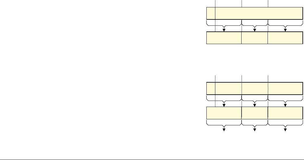
C6 Debug Register Interfaces
C6.4 The CP14 debug register interface
ARM DDI 0406C.c Copyright © 1996-1998, 2000, 2004-2012, 2014 ARM. All rights reserved. C6-2123
ID051414 Non-Confidential
C6.4 The CP14 debug register interface
The following subsections describe the CP14 debug register interfaces:
•Using CP14 to access debug registers
•CP14 debug register interface accesses on page C6-2124
•CP14 interface instruction arguments on page C6-2126.
C6.4.1 Using CP14 to access debug registers
Accesses to registers that are visible in the CP14 interface generally use the following coprocessor instructions:
•
MRC
for read accesses.
•
MCR
for write accesses.
In addition, the following coprocessors instructions are defined for specific registers accesses:
MRRC
Read access to the Debug ROM Address Register, DBGDRAR, and the Debug Self Address Offset
Register, DBGDSAR, in an implementation that includes the Large Physical Address Extension.
STC
Read access to the Host to Target Data Transfer Register, DBGDTRRXint.
LDC
Write access to the Target to Host Data Transfer Register, DBGDTRTXint.
Form of MRC and MCR instructions
The form of the
MRC
and
MCR
instructions used for accessing debug registers through the CP14 interface is:
MRC p14, 0, <Rt>, <CRn>, <CRm>, <opc2> ; Read
MCR p14, 0, <Rt>, <CRn>, <CRm>, <opc2> ; Write
Where
<Rt>
refers to any of the ARM core registers R0-R14. Use of R13 is UNPREDICTABLE in Thumb and
ThumbEE states, and is deprecated in ARM state.
<CRn>
,
<CRm>
, and
<opc2>
are mapped from the debug register
number as shown in Figure C6-1
The use of the
MRC APSR_nzcv
form of the
MRC
instruction is permitted for reads of the DBGDSCRint only. Use with
other registers is UNPREDICTABLE. See CP14 interface 32-bit access instructions, required in all versions of the
Debug architecture on page C6-2124 for more information.
For accesses to the debug registers,
<CRn>
<=
0b0111
and therefore bit[10] of the value in the figure is 0.
Figure C6-1 Mapping from debug register number to CP14 instruction arguments
Figure C6-2 shows this mapping for register 194.
Figure C6-2 Register mapping example, register 194
CRn[3:0]
109876543210
0 Register number[9:0]
opc2[2:0] CRm[3:0]
Value
Arguments
0 0 1 1 0 0 0 0 1 00
0 0 1 1 0 0 0 0 1 0
109876543210
0
Register 194
Arguments
CRm = c2opc2 = 4CRn = c1

C6 Debug Register Interfaces
C6.4 The CP14 debug register interface
C6-2124 Copyright © 1996-1998, 2000, 2004-2012, 2014 ARM. All rights reserved. ARM DDI 0406C.c
Non-Confidential ID051414
The mapping in Figure C6-2 on page C6-2123 means that the instruction to read register 194 is:
MRC p14, 0, <Rt>, c1, c2, 4 ; Read DBGOSSRR
An implementation that includes the Large Physical Address Extension extends the DBGDRAR and DBGDSAR
registers to 64 bits. In such an implementation, the
MRC
instruction that reads the register returns bits[31:0] of the
register.
Table C6-3 on page C6-2126 lists all registers visible in the CP14 interface, with their associated instruction
arguments.
Form of the MRRC instruction, when supported
In an implementation that includes the Large Physical Address Extension, the form of the
MRRC
instruction used for
accessing all 64 bits of a 64-bit debug register through the CP14 interface is:
MRRC p14, 0, <Rt>, <Rt2>, <CRm> ; Read
As Table C6-2 on page C6-2125 shows, the only 64-bit registers are DBGDRAR and DBGDSAR.
<CRm>
is
c1
for
accesses to DBGDRAR and
c2
for accesses to DBGDSAR.
Form of the STC and LDC instructions
The form of the
STC
and
LDC
instructions used for accessing the DBGDTRRXint and DBGDTRTXint registers
through the CP14 interface is:
STC p14, c5, <addr_mode> ; Read DBGDTRRXint
LDC p14, c5, <addr_mode> ; Write DBGDTRTXint
C6.4.2 CP14 debug register interface accesses
Table C6-1 shows the debug instructions that make 32-bit register accesses and must be implemented in all versions
of the Debug architecture.
Table C6-1 CP14 interface 32-bit access instructions, required in all versions of the Debug architecture
Instruction Register:
Name Number Description
MRC p14, 0, <Rt>, c0, c0, 0
DBGDIDR 0DBGDIDR, Debug ID Register on page C11-2231
MRC p14, 0, <Rt>, c0, c1, 0
MRC p14, 0, APSR_nzcv, c0, c1, 0
a
DBGDSCRint 1 DBGDSCR internal view. See DBGDSCR, Debug Status and
Control Register on page C11-2243
MRC p14, 0, <Rt>, c1, c0, 0
DBGDRAR 128 DBGDRAR, Debug ROM Address Register on page C11-2234
MRC p14, 0, <Rt>, c2, c0, 0
DBGDSAR 256 DBGDSAR, Debug Self Address Offset Register on
page C11-2239
MCR p14, 0, <Rt>, c0, c5, 0
LDC p14, c5, <addr_mode>
DBGDTRTXint 5 DBGDTRTX internal view. See DBGDTRTX, Target to Host
Data Transfer register on page C11-2262
MRC p14, 0, <Rt>, c0, c5, 0
STC p14, c5, <addr_mode>
DBGDTRRXint 5 DBGDTRRX internal view. See DBGDTRRX, Host to Target
Data Transfer register on page C11-2261
a. Transfers DBGDSCR[31:28] to the N, Z, C and V condition flags. For more information, see Program Status Registers (PSRs) on
page B1-1147.

C6 Debug Register Interfaces
C6.4 The CP14 debug register interface
ARM DDI 0406C.c Copyright © 1996-1998, 2000, 2004-2012, 2014 ARM. All rights reserved. C6-2125
ID051414 Non-Confidential
Table C6-2 shows the debug instructions that make 64-bit register accesses and must be implemented, for any
version of the Debug architecture, if the implementation includes the Large Physical Address Extension.
For more information about register internal and external views see Internal and external views of the DBGDSCR
and the DCC registers on page C8-2167.
This baseline CP14 interface is sufficient to boot-strap access to the register file, and enables software to determine
the version of the debug architecture implemented, and, for v7 Debug only, whether software access to the
remaining debug registers must use the CP14 interface or the memory-mapped interface.
v7 Debug deprecated uses of the CP14 interface
ARM deprecates using the CP14 interface to:
• Access the DBGDRCR, see DBGDRCR, Debug Run Control Register on page C11-2236.
• Access the DBGECR, see DBGECR, Event Catch Register on page C11-2263.
• Access registers other than DBGDTRRXint and DBGDTRTXint in Debug state at PL0.
• Write to DBGPRCR.HCWR, Hold core warm reset bit, or DBGPRCR.CWRR, Core warm reset request bit.
Table C6-2 CP14 interface 64-bit access instructions, Large Physical Address Extension
Instruction Register:
Name Number Description
MRRC p14, 0, <Rt>, <Rt2>, c1
DBGDRAR 128 DBGDRAR, Debug ROM Address Register on page C11-2234
MRRC p14, 0, <Rt>, <Rt2>, c2
DBGDSAR 256 DBGDSAR, Debug Self Address Offset Register on page C11-2239

C6 Debug Register Interfaces
C6.4 The CP14 debug register interface
C6-2126 Copyright © 1996-1998, 2000, 2004-2012, 2014 ARM. All rights reserved. ARM DDI 0406C.c
Non-Confidential ID051414
C6.4.3 CP14 interface instruction arguments
Form of MRC and MCR instructions on page C6-2123 describes the form of the
MCR
and
MRC
instructions used for
making 32-bit accesses to CP14 registers. Table C6-3 shows the instruction arguments required for accesses to each
register than can be visible in the CP14 interface.
Table C6-3 Mapping of CP14 MCR and MRC instruction arguments to registers
Register number CRn opc2 CRm Access Register name Description
0c00c0RODBGDIDR Debug ID
1c00c1RODBGDSCRint Debug Status and Control internal
5c00c5RODBGDTRRXint Host to Target Data Transfer internal
5 c0 0 c5 WO DBGDTRTXint Target to Host Data Transfer internal
6c00c6RWDBGWFAR Watchpoint Fault Address
7c00c7RWDBGVCR Vector Catch
9c00c9RW
DBGECRaEvent Catch
10 c0 0 c10 RW DBGDSCCRbDebug State Cache Control
11 c0 0 c11 RW DBGDSMCRbDebug State MMU Control
32 c0 2 c0 RW DBGDTRRXext Host to Target Data Transfer external
34 c0 2 c2 RW DBGDSCRext Debug Status and Control external
35 c0 2 c3 RW DBGDTRTXext Target to Host Data Transfer external
36 c0 2 c4 RW DBGDRCRaDebug Run Control
64-79 c0 4 c0-15 RW DBGBVRm Breakpoint Value
80-95 c0 5 c0-15 RW DBGBCRm Breakpoint Control
96-111 c0 6 c0-15 RW DBGWVRm Watchpoint Value
112-127 c0 7 c0-15 RW DBGWCRm Watchpoint Control
128 c1 0 c0 RO DBGDRAR Debug ROM Address
144-159 c1 1 c0-15 RW DBGBXVRmcBreakpoint Extended Value
192 c1 4 c0 WO DBGOSLAR OS Lock Access
193 c1 4 c1 RO DBGOSLSR OS Lock Status
194 c1 4 c2 RW DBGOSSRRbOS Save and Restore
195 c1 4 c3 RW DBGOSDLRdOS Double Lock
196 c1 4 c4 RW DBGPRCR Device Powerdown and Reset Control
197 c1 4 c5 RO DBGPRSRaDevice Powerdown and Reset Status
256 c2 0 c0 RO DBGDSAR Debug Self Address Offset
512-575 c4 0-3 c0-15 IMP DEF -IMPLEMENTATION DEFINED
928-959 c7 2-3 c0-15 IMP DEF - Integration registers
960 c7 4 c0 IMP DEF DBGITCTRL Integration Mode Control

C6 Debug Register Interfaces
C6.4 The CP14 debug register interface
ARM DDI 0406C.c Copyright © 1996-1998, 2000, 2004-2012, 2014 ARM. All rights reserved. C6-2127
ID051414 Non-Confidential
Form of the MRRC instruction, when supported on page C6-2124 describes the form of the
MRRC
instruction used
for reading a 64-bit CP14 register, in an implementation that includes the Large Physical Address Extension.
Table C6-4 shows the instruction arguments required for accesses to the 64-bit registers than can be visible in the
CP14 interface.
1000 c7 6 c8 RW DBGCLAIMSET Claim Tag Set
1001 c7 6 c9 RW DBGCLAIMCLR Claim Tag Clear
1006 c7 6 c14 RO DBGAUTHSTATUS Authentication Status
1008 c7 7 c0 RO DBGDEVID2dReserved, UNK
1009 c7 7 c1 RO DBGDEVID1dDevice ID 1
1010 c7 7 c2 RO DBGDEVID Device ID 0
a. v7 Debug only. In v7.1 Debug, the register is not visible in the CP14 interface.
b. v7 Debug only. The register is not implemented in v7.1 Debug.
c. Virtualization Extensions only.
d. v7.1Debug only.
Table C6-3 Mapping of CP14 MCR and MRC instruction arguments to registers (continued)
Register number CRn opc2 CRm Access Register name Description
Table C6-4 Mapping of CP14 MRRC instruction arguments to registers, Large Physical Address Extension
Register number CRm Access Register name Description
128 c1 RO DBGDRAR Debug ROM Address, 64-bit register
256 c2 RO DBGDSAR Debug Self Address Offset, 64-bit register

C6 Debug Register Interfaces
C6.5 The memory-mapped and recommended external debug interfaces
C6-2128 Copyright © 1996-1998, 2000, 2004-2012, 2014 ARM. All rights reserved. ARM DDI 0406C.c
Non-Confidential ID051414
C6.5 The memory-mapped and recommended external debug interfaces
The external debug interface is IMPLEMENTATION DEFINED. This section describes the ARM recommendations for
this interface.
The memory-mapped interface to the debug registers is optional.
As defined in CP14 debug register interface accesses on page C6-2124, for all ARMv7 debug implementations,
there is a small subset of debug registers that must be visible in the CP14 register interface.
In v7 Debug, in addition, a larger subset of debug registers must be accessible to software running on the processor,
and it is IMPLEMENTATION DEFINED whether these registers are visible in the CP14 interface or in the
memory-mapped interface. For v7 Debug, Table C6-5 on page C6-2130 shows these register subsets.
In v7.1 Debug, Table C6-10 on page C6-2139 shows which registers are visible in the different interfaces, and
where it is IMPLEMENTATION DEFINED if a register is visible.
The Debug architecture defines both the memory-mapped interface and the recommended external debug interface
as an addressable register file mapped onto a region of memory.
This section describes:
• The view of the debug registers from the processor through the memory-mapped interface.
• The recommended external debug interface.
C6.5.1 Register map
The register map occupies 4KB of physical address space. The base address is IMPLEMENTATION DEFINED and must
be aligned to a 4KB boundary.
Note
All memory-mapped debug registers must be mapped to Strongly-ordered or Device memory, see Synchronization
of debug register updates on page C6-2117. In a system that implements PMSAv7 this requirement applies even
when the MPU is disabled.
Each register is mapped at an offset that is the register number multiplied by 4, the size of a word. For example,
DBGWVR7, register 103, is mapped at offset
0x19C
(412).
See Debug registers summary on page C11-2195 for the complete list of debug registers.
C6.5.2 Shared interface port for the memory-mapped and external debug interfaces
Which components in a system can access the memory-mapped interface is IMPLEMENTATION DEFINED. Typically,
the processor itself and other processors in the system can access this interface. An external debugger might be able
to access the debug registers through the memory-mapped interface, as well as through the external debug interface.
Because the memory-mapped interface and external debug interface share the same memory map and many of the
same properties, both interfaces can be implemented as a single physical interface port to the processor.
When the memory-mapped interface and external debug interface are implemented as a single physical interface
port, the debug logic must be able to distinguish between accesses from:
• An external debugger.
• Software running on a processor, including the ARM processor itself, in the target system.
For example, the Software Lock does not affect accesses by an external debugger.
The recommended memory-mapped interface and the external debug interface use the PADDRDBG[31] signal to
distinguish between these accesses, see PADDRDBG on page D1-2346.

C6 Debug Register Interfaces
C6.5 The memory-mapped and recommended external debug interfaces
ARM DDI 0406C.c Copyright © 1996-1998, 2000, 2004-2012, 2014 ARM. All rights reserved. C6-2129
ID051414 Non-Confidential
C6.5.3 Endianness
The recommended memory-mapped and external debug interface port, referred to as the debug port, only supports
word accesses, and has a fixed byte order. The debug port ignores bits[1:0] of the address, and these bits are not
present in the recommended debug port interface.
To connect to an external debugger, the debug port must connect to a Debug Access Port (DAP). The DAP and the
interface between the DAP and the debug port form part of the external debug interface, and must support word
accesses from the external debugger to the debug registers.
ARM recommends that the DAP and its interface to the debug port are provided by an ARM Debug Interface v5
(ADIv5) DAP. An ADIv5 implementation must ensure that it preserves the bit order of a 32-bit access by the
debugger, through the DAP, to the debug registers. The ARM Debug Interface v5 Architecture Specification defines
this interface.
If an implementation also includes a memory-mapped interface, the system must support word accesses to the debug
registers. When accessing the debug registers, the behavior of an access that is not word-sized is UNPREDICTABLE.
The detailed behavior of any connection between a system bus and the debug port is outside the scope of the
architecture. The ADIv5 DAP specification includes an optional bridge that can connect a system bus to the
interface between the DAP and the debug port.
Accesses to registers made through the debug port are not affected by the endianness configuration of the processor
in which the registers are implemented. However, they are affected by the endianness configuration of the bus
master making the access, and by the nature and configuration of the fabric that connects the two.
When describing accesses to the debug registers through the memory-mapped and external debug interfaces, this
manual assumes that the external interface to the debug port is little-endian. For example, if a processor configured
for little-endian operation uses a
LDR
instruction to access its own DBGDIDR through the memory-mapped
interface, the destination register for the instruction returns the bit pattern defined by DBGDIDR.
A memory-mapped interface to the debug registers is a memory-mapped peripheral, and therefore the endianness
of this interface is IMPLEMENTATION DEFINED. However, all of the debug registers in single processor, when
accessed through such an interface, have the same endianness.
Software might read the any of the Debug Component ID Registers, DBGCID0, DBGCID1, DBGCID2, or
DBGCID3, to determine the endianness of the memory-mapped interface. See About the Debug Component
Identification Registers on page C11-2210.

C6 Debug Register Interfaces
C6.6 Summary of the v7 Debug register interfaces
C6-2130 Copyright © 1996-1998, 2000, 2004-2012, 2014 ARM. All rights reserved. ARM DDI 0406C.c
Non-Confidential ID051414
C6.6 Summary of the v7 Debug register interfaces
This section shows how the v7 Debug registers can be accessed through the different interfaces, and how the access
is affected by the privilege level, locks, and powerdown settings:
•v7 Debug register visibility in the different interfaces
•v7 Debug register access in the CP14 interface on page C6-2132
•v7 Debug register access in the memory-mapped and external debug interfaces on page C6-2134
•Accesses to reserved and unallocated registers, v7 Debug on page C6-2137.
C6.6.1 v7 Debug register visibility in the different interfaces
Table C6-5 shows the required visibility of the debug registers in a v7 Debug implementation, as follows:
• A group of debug registers must be visible in the CP14 interface. The CP14 column identifies the registers
in this group.
• A group of debug registers must be visible in either the CP14 interface or the memory-mapped interface. The
CP14 or MM column identifies the registers in this group, and:
— These registers can be visible in both of these interfaces.
— If all of these registers are visible in the CP14 interface then implementation of the memory-mapped
interface is optional. DBGDIDR.Version indicates whether the CP14 interface is extended to provide
access to these registers.
— If the memory-mapped interface is implemented then all of these registers must be visible in the
memory-mapped interface. Therefore, all of these registers also have a Yes entry in the MM column.
• A group of debug registers must be visible in the external debug interface. The ED column identifies the
registers in this group.
• A group of debug registers must be visible in the memory-mapped interface if that interface is implemented.
The MM column identifies the registers in this group. This includes all the registers in the CP14 or MM group.
In Table C6-5:
Ye s Indicates that the register is part of the group.
Optional Indicates that, in v7 Debug, it is IMPLEMENTATION DEFINED whether the register is implemented. If
it is implemented, then unless otherwise indicated by a footnote to the Optional entry, it must be part
of the group. Where appropriate, the register description gives more information about whether an
implementation should include the register.
- Indicates that the register is not part of the group.
Table C6-5 v7 Debug registers required visibility
Number Name Description Required in:
CP14 CP14 or MM ED MM
0DBGDIDR Debug ID Yes - Yes Yes
1DBGDSCRint Debug Status and Control Yes - - -
5DBGDTRTXint, WO Host to Target Data Transfer Yes - - -
DBGDTRRXint, RO Target to Host Data Transfer Yes - - -
6DBGWFAR Watchpoint Fault Address - Yes Yes Yes
7DBGVCR Vector Catch - Yes Yes Yes
9DBGECR Event Catch - Optional Optional Optional

C6 Debug Register Interfaces
C6.6 Summary of the v7 Debug register interfaces
ARM DDI 0406C.c Copyright © 1996-1998, 2000, 2004-2012, 2014 ARM. All rights reserved. C6-2131
ID051414 Non-Confidential
10 DBGDSCCR Debug State Cache Control - Yes Yes Yes
11 DBGDSMCR Debug State MMU Control - Yes Yes Yes
32 DBGDTRRXext Host to Target Data Transfer - Yes Yes Yes
33 DBGITR, WO Instruction Transfer - - Yes Yes
DBGPCSR, RO Program Counter Sampling - - OptionalaOptionala
34 DBGDSCRext Debug Status and Control - Yes Yes Yes
35 DBGDTRTXext Target to Host Data Transfer - Yes Yes Yes
36 DBGDRCR Debug Run Control - Yes Yes Yes
40 DBGPCSR Program Counter Sampling - - Optional Optional
41 DBGCIDSR Context ID Sampling - - Optional Optional
42 DBGVIDSR Virtualization ID Sampling - - Optional Optional
64-79 DBGBVRm Breakpoint Value - Yes Yes Yes
80-95 DBGBCRm Breakpoint Control - Yes Yes Yes
96-111 DBGWVRm Watchpoint Value - Yes Yes Yes
112-127 DBGWCRm Watchpoint Control - Yes Yes Yes
128 DBGDRAR Debug ROM Address Yes - - -
192 DBGOSLAR OS Lock Access - Optional Optional Optional
193 DBGOSLSR OS Lock Status - Yes Yes Yes
194 DBGOSSRR OS Save and Restore - Optional Optional Optional
196 DBGPRCR Powerdown and Reset Control - Yes Yes Yes
197 DBGPRSR Powerdown and Reset Status - Yes Yes Yes
256 DBGDSAR Debug Self Address Offset Yes - - -
512-575 - IMPLEMENTATION DEFINED -OptionalbOptionalbOptionalb
832-895 Various Processor ID registers - - Yes Yes
928-959 Various Integration registers - OptionalbOptionalbOptionalb
960 DBGITCTRL Integration Mode Control - OptionalbOptionalbOptionalb
1000 DBGCLAIMSET Claim Tag Set - Yes Yes Yes
1001 DBGCLAIMCLR Claim Tag Clear - Yes Yes Yes
1004 DBGLAR Lock Access - - - Yes
1005 DBGLSR Lock Status - - - Yes
1006 DBGAUTHSTATUS Authentication Status - Yes Yes Yes
Table C6-5 v7 Debug registers required visibility (continued)
Number Name Description Required in:
CP14 CP14 or MM ED MM

C6 Debug Register Interfaces
C6.6 Summary of the v7 Debug register interfaces
C6-2132 Copyright © 1996-1998, 2000, 2004-2012, 2014 ARM. All rights reserved. ARM DDI 0406C.c
Non-Confidential ID051414
C6.6.2 v7 Debug register access in the CP14 interface
This section summarizes register access in the CP14 interface for v7 Debug. See The CP14 debug register interface
on page C6-2123 and CP14 interface instruction arguments on page C6-2126 for more information on the CP14
interface.
In v7 Debug, all register accesses through the CP14 interface are UNPREDICTABLE when the debug power domain
is powered down.
Access in the CP14 interface is affected by the locks and settings shown in Table C6-6. A control is described as
active if it affects the behavior of some or all CP14 accesses:
1008 DBGDEVID2 Debug Device ID 2 - - UNK/SBZPcUNK/SBZPc
1009 DBGDEVID1 Debug Device ID 1 - - OptionalcOptionalc
1010 DBGDEVID Debug Device ID - Optional OptionalcOptional c
1011 DBGDEVTYPE Device Type - - Yes Yes
1012 DBGPID4 Debug Peripheral ID 4 - - Yes Yes
1016-1019 DBGPID0-DBGPID3 Debug Peripheral ID 0-3 - - Yes Yes
1020-1023 DBGCID0-DBGCID3 Debug Component ID 0-3 - - Yes Yes
a. When the DBGPCSR is visible as register 40, ARM deprecates accessing the DBGPCSR as register 33, and strongly recommends that the
register is accessed only as register 40.
b. Visibility and access is IMPLEMENTATION DEFINED.
c. In the memory-mapped interface and the external interface, software cannot distinguish between a register location being reserved and the
register being implemented with all fields RAZ.
Table C6-5 v7 Debug registers required visibility (continued)
Number Name Description Required in:
CP14 CP14 or MM ED MM
Table C6-6 Locks and settings affecting CP14 accesses, v7 Debug
Control Description
DSE Debug Software Enable function. If the function is off, access to certain registers becomes UNDEFINED.
PL0 When the processor is in Non-debug state and the privilege level is PL0, access to certain registers becomes UNDEFINED.
UDCC When the processor is in Non-debug state, the privilege level is PL0, and the User mode access to DCC disable bit,
DBGDSCR.UDCCdis, is set to 1, the access to certain registers becomes UNDEFINED.
OSL If the OS Save and Restore mechanism is implemented, and the OS Lock is set, access to certain registers becomes
UNDEFINED or UNPREDICTABLE. When this condition applies, an access that the OSL column shows as UNPREDICTABLE is
UNDEFINED if one of the PL0 and UDCC controls is active and the corresponding column shows the access to be
UNDEFINED.
Note
It is not possible to access CP14 registers in Debug state when the OS Lock is set, since when the OS Lock is set accesses
to the DBGITR through the memory-mapped or external debug interfaces return an error, so it is not possible to execute
CP14 instructions.
SPD When the Sticky Powerdown status bit, DBGPRSR.SPD, is set to 1, access to certain registers becomes UNDEFINED or
UNPREDICTABLE.

C6 Debug Register Interfaces
C6.6 Summary of the v7 Debug register interfaces
ARM DDI 0406C.c Copyright © 1996-1998, 2000, 2004-2012, 2014 ARM. All rights reserved. C6-2133
ID051414 Non-Confidential
The entries in the Control on page C6-2132 column of Table C6-6 on page C6-2132 are used as column headings
in Table C6-7, and:
• If no control is active, the behavior shown in the Default access column of Table C6-7 applies.
• An entry of - indicates that the control has no effect on the behavior of accesses to that register. This means:
— If no other control affects the behavior, the Default access behavior applies.
— However, another active control might determine the behavior.
• Otherwise, the appropriate Control column of Table C6-7 defines the behavior.
For example, for DBGDSCRint:
• The DSE, PL0, and SPD controls have no effect on the behavior
•If the OSL control is active, all accesses are UNPREDICTABLE, except for accesses that the UDCC control
makes UNDEFINED.
Table C6-7 uses the following abbreviations to describe the behavior of CP14 accesses:
UND UNDEFINED
UNP UNPREDICTABLE
IMP DEF IMPLEMENTATION DEFINED.
If a register is not shown in Table C6-7 it is not visible in the CP14 interface, and any access is treated as an access
to an unallocated CP14 register encoding, see Accesses to reserved and unallocated registers, v7 Debug on
page C6-2137.
Table C6-7 v7 Debug CP14 interface access behavior
Register number Register name Default access DSE PL0 UDCC OSL SPD
0DBGDIDR ROa- - UND - -
1DBGDSCRint ROa- - UND UNP -
5DBGDTRRXint RO - - UND UNP -
DBGDTRTXint WO - - UND UNP -
6DBGWFAR RW aUND UND UND UND UND
7DBGVCR RWaUND UND UND UND UND
9DBGECR RWaUND UND UND - -
10 DBGDSCCR RWaUND UND UND UND UND
11 DBGDSMCR RWaUND UND UND UND UND
32 DBGDTRRXext RWaUND UND UND UND UND
34 DBGDSCRext RWaUND UND UND UND UND
35 DBGDTRTXext RWaUND UND UND UND UND
36 DBGDRCR WOaUND UND UND - -
64-79 DBGBVRmRWaUND UND UND UND UND
80-95 DBGBCRmRWaUND UND UND UND UND
96-111 DBGWVRmRWaUND UND UND UND UND
112-127 DBGWCRmRWaUND UND UND UND UND
128 DBGDRAR ROa- - UND ROb-

C6 Debug Register Interfaces
C6.6 Summary of the v7 Debug register interfaces
C6-2134 Copyright © 1996-1998, 2000, 2004-2012, 2014 ARM. All rights reserved. ARM DDI 0406C.c
Non-Confidential ID051414
C6.6.3 v7 Debug register access in the memory-mapped and external debug interfaces
This section summarizes register access in the memory-mapped interface and external debug interface for v7
Debug. See The memory-mapped and recommended external debug interfaces on page C6-2128 for more
information on the interfaces.
In v7 Debug, access to the debug registers visible in the memory-mapped and external debug interfaces is affected
by:
• Core and debug power domain settings.
If the debug power domain is powered down, any access to a register through either register interface
produces an error.
If a single power domain is implemented and is powered down, any access to a register through either register
interface produces an error.
If the core power domain is powered down, access to some registers through either interface produces an
error, as shown in Table C6-9 on page C6-2136.
• Debug Software Enable function. If this function is off, access through the memory-mapped interface
produces an error. Access through the external debug interface is unaffected.
• Software Lock. If all other controls permit access to the registers, and the Software Lock is set, access to all
registers through the memory-mapped interface is restricted as follows:
— Reads return the value of the register, but with no side-effects.
— Writes are ignored, and have no side effects.
For more information about the behavior of the accesses, see Table C6-9 on page C6-2136.
192 DBGOSLARcWOa- UND UND - -
193 DBGOSLSR ROa- UND UND - -
194 DBGOSSRRcUNP - UND UND RWd-
196 DBGPRCR RWaUND UND UND - -
197 DBGPRSR ROa- UND UND - -
256 DBGDSAR ROa- - UND ROb-
512-575 IMPLEMENTATION DEFINED IMP DEF UND IMP DEF IMP DEF IMP DEF IMP DEF
928-959 Integration registers IMP DEF UND UND UND IMP DEF IMP DEF
960 DBGITCTRL IMP DEF UND UND UND IMP DEF IMP DEF
1000 DBGCLAIMSET RWaUND UND UND - -
1001 DBGCLAIMCLR RWaUND UND UND - -
1006 DBGAUTHSTATUS ROaUND UND UND - -
1010 DBGDEVID ROaUND UND UND - -
a. ARM deprecates the use of this register from privilege level PL0 in Debug state.
b. Access is UNDEFINED if the UDCC control is active. Otherwise, if the memory-mapped interface is not implemented, the access is
UNPREDICTABLE.
c. Access to this register is always UNPREDICTABLE if the implementation does not include the OS Save and Restore mechanism.
d. Access is UNDEFINED if either the PL0 control or the UDCC control is active.
Table C6-7 v7 Debug CP14 interface access behavior (continued)
Register number Register name Default access DSE PL0 UDCC OSL SPD

C6 Debug Register Interfaces
C6.6 Summary of the v7 Debug register interfaces
ARM DDI 0406C.c Copyright © 1996-1998, 2000, 2004-2012, 2014 ARM. All rights reserved. C6-2135
ID051414 Non-Confidential
Access to the DBGLAR, which sets and releases the Software Lock, is not affected.
Access through the external debug interface is not affected by the Software Lock.
• Sticky powerdown setting, if implemented. If DBGPRSR.SPD, the Sticky powerdown status bit, is set to 1,
access to some registers through either interface produces an error, as shown in Table C6-9 on page C6-2136.
• OS Lock. If the OS Save and Restore mechanism is implemented, and the OS Lock is set, access to some
registers through either interface is affected, as shown in Table C6-9 on page C6-2136.
For the accesses that produce an error response, the error response is IMPLEMENTATION DEFINED:
• For the memory-mapped interface, the error is IMPLEMENTATION DEFINED, but the access must either be
ignored or signaled to the processor as an external abort.
• For the external debug interface, the error must be signaled to the debugger by the Debug Access Port. With
an ADIv5 implementation, this means the error sets a sticky flag in the DAP.
Accesses in the memory-mapped and external debug interfaces are affected by the locks and settings shown in
Table C6-8. A control is described as active if it affects the behavior of some or all memory-mapped and external
debug interface accesses:
The entries in the Control column of Table C6-8 are used as column headings in Table C6-9 on page C6-2136, and:
• If no control is active, the behavior shown in the Default access on page C6-2136 column of Table C6-9 on
page C6-2136 applies.
• An entry of - indicates that the control has no effect on the behavior of accesses to that register. This means:
— If no other control affects the behavior, the Default access on page C6-2136 behavior applies.
— However, another active control might determine the behavior.
• Otherwise, the appropriate Control column of Table C6-9 on page C6-2136 defines the behavior.
For example, in an implementation that includes the OS Save and Restore mechanism, for DBGOSLAR:
• The SPD and OSL controls have no effect on the behavior.
•If the CPD control is active, all accesses are UNPREDICTABLE.
•If the CPD control is not active, but the SLK control is active, a write to the register using the
memory-mapped interface is ignored.
Table C6-9 on page C6-2136 uses the following abbreviations:
Err Error. For an access when multiple controls are active, Err has priority over any other possible
outcome.
UNP UNPREDICTABLE.
IMP DEF IMPLEMENTATION DEFINED.
Table C6-8 Locks and settings affecting memory-mapped and external debug interface accesses, v7 Debug
Control Description
CPD When core power domain is powered down, accesses to some registers through either interface produce an error.
SPD When DBGPRSR.SPD, the Sticky powerdown status bit, is set to 1, accesses to some registers through either
interface produce an error.
OSL When the OS Lock is set, accesses to some registers through either interface produce an error.
SLK When the Software Lock is set, if all other controls permit accesses to the registers, accesses through the
memory-mapped interface are read-only and have no side-effects. An access that is UNPREDICTABLE is
guaranteed not to perform a register write.

C6 Debug Register Interfaces
C6.6 Summary of the v7 Debug register interfaces
C6-2136 Copyright © 1996-1998, 2000, 2004-2012, 2014 ARM. All rights reserved. ARM DDI 0406C.c
Non-Confidential ID051414
If a register is not shown in Table C6-9 it is not visible in the memory-mapped interface or in the external debug
interface, and any access to it is treated as an access to a reserved register. Accesses to reserved and unallocated
registers, v7 Debug on page C6-2137 describes the behavior of accesses to reserved register addresses.
Table C6-9 v7 Debug memory-mapped and external debug interfaces access behavior
Register
number Offset Register name Default
access CPD SPD OSL SLKa
0
0x000
DBGDIDR RO - - - -
6
0x018
DBGWFAR RW Err Err Err RO
7
0x01C
DBGVCR RW Err Err Err RO
9
0x024
DBGECR RW - - - RO
10
0x028
DBGDSCCR RW Err Err Err RO
11
0x02C
DBGDSMCR RW Err Err Err RO
32
0x080
DBGDTRRXext RW Err Err Err ROb
33
0x084
DBGPCSR RO Err Err Err ROb
0x084
DBGITR WOcErr Err Err WI
34
0x088
DBGDSCRext RW Err Err Err ROb
35
0x08C
DBGDTRTXext RW Err Err Err ROb
36
0x090
DBGDRCR WO WOd-- WI
40
0x0A0
DBGPCSR RO Err Err Err ROb
41
0x0A4
DBGCIDSR RO Err Err Err -
42
0x0A8
DBGVIDSR RO Err Err Err -
64-79
0x100-0x13C
DBGBVRm RW Err Err Err RO
80-95
0x140-0x17C
DBGBCRm RW Err Err Err RO
96-111
0x180-0x1BC
DBGWVRm RW Err Err Err RO
112-127
0x1C0-0x1FC
DBGWCRm RW Err Err Err RO
192
0x300
DBGOSLAReWO UNP - - WIa
193
0x304
DBGOSLSR RO - - - -
194
0x308
DBGOSSRReUNP - - RW or RAZ/WIfROb
196
0x310
DBGPRCR RW - - - RO
197
0x314
DBGPRSR RO ROdROd-ROb
512-575
0x800-0x8FC
IMPLEMENTATION DEFINED IMP DEF IMP DEF IMP DEF IMP DEF IMP DEFa
832-895
0xD00-0xDFC
Processor IDs RO - - - -
928-959
0xE80-0xEFC
Integration registers IMP DEF IMP DEF IMP DEF IMP DEF IMP DEFa
960
0xF00
DBGITCTRL IMP DEF IMP DEF IMP DEF IMP DEF IMP DEFa
1000
0xFA0
DBGCLAIMSET RW - - - RO

C6 Debug Register Interfaces
C6.6 Summary of the v7 Debug register interfaces
ARM DDI 0406C.c Copyright © 1996-1998, 2000, 2004-2012, 2014 ARM. All rights reserved. C6-2137
ID051414 Non-Confidential
C6.6.4 Accesses to reserved and unallocated registers, v7 Debug
For v7 Debug, the following subsections describe the behavior of accesses to reserved registers in the
memory-mapped and external debug interfaces, and to unallocated CP14 debug register encodings:
•Accesses to reserved registers in the memory-mapped interface, v7 Debug
•Accesses to reserved registers in the external debug interface, v7 Debug on page C6-2138
•Access to unallocated CP14 debug register encodings, v7 Debug on page C6-2138.
Note
Unimplemented breakpoint and watchpoint registers are reserved registers.
Accesses to reserved registers in the memory-mapped interface, v7 Debug
When the Debug Software Enable function is disabling software access to the debug registers, any access to a
reserved register through the memory-mapped interface returns an error response. This includes accesses to
reserved registers in the management registers space, register numbers 832-1023.
When the Debug Software Enable function is not disabling software access to the debug registers:
• Reserved registers in the management registers space, except for reserved registers in the IMPLEMENTATION
DEFINED integration registers space, are UNK/SBZP.
1001
0xFA4
DBGCLAIMCLR RW - - - RO
1004
0xFB0
DBGLARgWO - - - -g
1005
0xFB4
DBGLSRgRO - - - -
1006
0xFB8
DBGAUTHSTATUS RO - - - -
1008
0xFC0
DBGDEVID2 RO - - - -
1009
0xFC4
DBGDEVID1 RO - - - -
1010
0xFC8
DBGDEVID RO - - - -
1011
0xFCC
DBGDEVTYPE RO - - - -
1012
0xFD0
DBGPID4 RO - - - -
1016-1019
0xFE0-0xFEC
DBGPID0 - DBGPID3 RO - - - -
1020-1023
0xFF0-0xFFC
DBGCID0 - DBGCID3 RO - - - -
a. SLK has no effect on accesses through the external debug interface. For the memory-mapped interface, when the Software Lock is set,
accesses to registers other than DBGLAR is restricted so that at least writes are ignored and reads have no side-effects. This applies even
when the access is UNPREDICTABLE or IMPLEMENTATION DEFINED. DBGLAR is always WO in the memory-mapped interface, regardless
of the state of the Software Lock.
b. A read returns the value of the register, but any other side-effect of the read is suppressed.
c. DBGITR can only be accessed in Debug state. See Behavior of accesses to the DBGITR on page C8-2176 for more information.
d. This condition changes the behavior of accesses to the register. For more information, see the register description.
e. Access to this register is always UNPREDICTABLE if the implementation does not include the OS Save and Restore mechanism.
f. In an implementation that includes the OS Save and Restore mechanism, if DBGOSSRR is not visible in the memory-mapped and
external debug interfaces, it is RAZ/WI when the OS Lock is set.
g. Only visible in the memory-mapped interface. Access is UNPREDICTABLE in the external debug interface.
Table C6-9 v7 Debug memory-mapped and external debug interfaces access behavior (continued)
Register
number Offset Register name Default
access CPD SPD OSL SLKa

C6 Debug Register Interfaces
C6.6 Summary of the v7 Debug register interfaces
C6-2138 Copyright © 1996-1998, 2000, 2004-2012, 2014 ARM. All rights reserved. ARM DDI 0406C.c
Non-Confidential ID051414
• For all other reserved registers, it is UNPREDICTABLE whether a register access returns an error response if
any of the following applies:
— The core power domain is powered down.
—DBGPRSR.SPD, the Sticky powerdown status bit, is set to 1.
— The OS Lock is implemented and is set.
— The Software Lock is set.
If none of these applies then the reserved register is UNK/SBZP.
Accesses to reserved registers in the external debug interface, v7 Debug
Reserved registers in the management registers space, register numbers 832-1023, except for reserved registers in
the IMPLEMENTATION DEFINED integration registers space, are UNK/SBZP.
For all other reserved registers:
• It is UNPREDICTABLE whether a register access returns an error response if any of the following applies:
— The core power domain is powered down.
—DBGPRSR.SPD, the Sticky powerdown status bit, is set to 1.
— The OS Lock is implemented and is set.
• If none of these applies then the reserved register is UNK/SBZP.
Access to unallocated CP14 debug register encodings, v7 Debug
In v7 Debug, the behavior of accesses to unallocated CP14 debug register encodings depends on:
• Whether the implementation includes all of the CP14 debug registers, as indicated by the DBGDIDR.Version
field.
• Whether the Debug Software Enable function permits software access to the debug registers, see Permissions
in relation to locks on page C6-2120.
This means that accesses to unallocated CP14 debug register encodings, from PL1 or higher, are:
•UNPREDICTABLE if any of the following applies:
—DBGDIDR.Version is
0b0100
, indicating that only the baseline CP14 registers are implemented.
— The register encoding has CRn >=
0b1000
.
— The Debug Software Enable function permits access to the debug registers.
•Otherwise,
UNDEFINED.
Note
As stated in General behavior of system control registers on page B3-1446 and General behavior of system control
registers on page B5-1776, all
MRC
and
MCR
accesses to unallocated CP14 register encodings from User mode are
UNDEFINED.

C6 Debug Register Interfaces
C6.7 Summary of the v7.1 Debug register interfaces
ARM DDI 0406C.c Copyright © 1996-1998, 2000, 2004-2012, 2014 ARM. All rights reserved. C6-2139
ID051414 Non-Confidential
C6.7 Summary of the v7.1 Debug register interfaces
The following sections show how the v7.1 Debug registers can be accessed through the different interfaces, and how
the access is affected by the privilege level, locks, and powerdown settings:
•v7.1 Debug register visibility in the different interfaces
•v7.1 Debug register access in the CP14 interface on page C6-2141
•v7.1 Debug register access in the memory-mapped and external debug interfaces on page C6-2144
•Access to reserved and unallocated registers, v7.1 Debug on page C6-2147.
C6.7.1 v7.1 Debug register visibility in the different interfaces
Table C6-10 shows the required visibility of the debug registers in a v7.1 Debug implementation, as follows:
• A group of debug registers must be visible in the CP14 interface. The CP14 column identifies the registers
in this group.
• A group of debug registers must be visible in the external debug interface. The ED column identifies the
registers in this group.
• If the memory-mapped debug interface is implemented, a group of debug registers must be visible in that
interface. The MM column identifies the registers in this group.
In Table C6-10:
Ye s Indicates that the register is part of the group.
Optional Indicates that, in v7.1 Debug, it is IMPLEMENTATION DEFINED whether the register is implemented.
If it is implemented, then unless otherwise indicated by a footnote to the Optional entry, it must be
part of the group.
- Indicates that the register is not part of the group.
Table C6-10 v7.1 Debug register visibility
Register
number Name Description Interface
CP14 ED MM
0DBGDIDR Debug ID Yes Yes Yes
1DBGDSCRint Debug Status and Control Yes - -
5DBGDTRTXint, WO Target to Host Data Transfer Yes - -
DBGDTRRXint, RO Host to Target Data Transfer Yes - -
6DBGWFAR Watchpoint Fault Address Yes Yes Yes
7DBGVCR Vector Catch Yes Yes Yes
9DBGECR Event Catch - Yes Yes
32 DBGDTRRXext Host to Target Data Transfer Yes Yes Yes
33 DBGITR, WO Instruction Transfer - Yes Yes
DBGPCSR, RO Program Counter Sampling - OPTIONALaOPTIONALa
34 DBGDSCRext Debug Status and Control Yes Yes Yes
35 DBGDTRTXext Target to Host Data Transfer Yes Yes Yes
36 DBGDRCR Debug Run Control - Yes Yes

C6 Debug Register Interfaces
C6.7 Summary of the v7.1 Debug register interfaces
C6-2140 Copyright © 1996-1998, 2000, 2004-2012, 2014 ARM. All rights reserved. ARM DDI 0406C.c
Non-Confidential ID051414
37 DBGEACR External Auxiliary Control - Yes Yes
40 DBGPCSR Program Counter Sampling - Optional Optional
41 DBGCIDSR Context ID Sampling - Optional Optional
42 DBGVIDSR Virtualization ID Sampling - Optional Optional
64-79 DBGBVRm Breakpoint Value Yes Yes Yes
80-95 DBGBCRm Breakpoint Control Yes Yes Yes
96-111 DBGWVRm Watchpoint Value Yes Yes Yes
112-127 DBGWCRm Watchpoint Control Yes Yes Yes
128 DBGDRAR Debug ROM Address Yes - -
144-159 DBGBXVRmBreakpoint Extended ValuebYes bYes bYes b
192 DBGOSLAR OS Lock Access Yes Yes Yes
193 DBGOSLSR OS Lock Status Yes Yes Yes
195 DBGOSDLR OS Double Lock Yes - -
196 DBGPRCR Powerdown and Reset Control Yes cYes Yes
197 DBGPRSR Powerdown and Reset Status - Yes Yes
256 DBGDSAR Debug Self Address Offset Yes - -
512-575 - IMPLEMENTATION DEFINED OptionaldOptionaldOptionald
832-895 Various Processor IDs - Yes Yes
928-959 Various Integration registers OptionaldOptionaldOptionald
960 DBGITCTRL Integration Mode Control OptionaldOptionaldOptionald
1000 DBGCLAIMSET Claim Tag Set Yes Yes Yes
1001 DBGCLAIMCLR Claim Tag Clear Yes Yes Yes
1004 DBGLAR Lock Access - - Yes
1005 DBGLSR Lock Status - - Yes
1006 DBGAUTHSTATUS Authentication Status Yes Yes Yes
1008 DBGDEVID2 Debug Device ID 2 UNK/SBZP UNK/SBZP UNK/SBZP
1009 DBGDEVID1 Debug Device ID 1 Yes Yes Yes
1010 DBGDEVID Debug Device ID Yes Yes Yes
1011 DBGDEVTYPE Device Type - Yes Yes
Table C6-10 v7.1 Debug register visibility (continued)
Register
number Name Description Interface
CP14 ED MM

C6 Debug Register Interfaces
C6.7 Summary of the v7.1 Debug register interfaces
ARM DDI 0406C.c Copyright © 1996-1998, 2000, 2004-2012, 2014 ARM. All rights reserved. C6-2141
ID051414 Non-Confidential
C6.7.2 v7.1 Debug register access in the CP14 interface
This section summarizes register access in the CP14 interface for v7.1 Debug. See The CP14 debug register
interface on page C6-2123 and CP14 interface instruction arguments on page C6-2126 for more information on the
CP14 interface.
In an implementation that includes the Virtualization Extensions, in Non-secure state when executing at PL1 or PL0,
an access to a CP14 debug register that is permitted by the access permissions described in this section can generate
a Hyp Trap exception. For more information, see Trapping CP14 accesses to debug registers on page B1-1260.
Access is not affected by the Software Lock setting. This only applies to registers in the memory-mapped interface.
Access in the CP14 interface is affected by the locks and settings shown in Table C6-11. A control is described as
active if it affects the behavior of some or all CP14 accesses:
1012 DBGPID4 Debug Peripheral ID 4 - Yes Yes
1016-1019 DBGPID0-DBGPID3 Debug Peripheral ID 0-3 - Yes Yes
1020-1023 DBGCID0-DBGCID3 Debug Component ID 0-3 - Yes Yes
a. Implementation of an alias of DBGPCSR as register 33 is OPTIONAL and deprecated. This means ARM deprecates accessing the
DBGPCSR as register 33, and strongly recommends that the register is accessed only as register 40.
b. Only in an implementation that includes the Virtualization Extensions.
c. Only some bits are visible in the CP14 interface. For more information, see the register description.
d. Visibility and access is IMPLEMENTATION DEFINED.
Table C6-10 v7.1 Debug register visibility (continued)
Register
number Name Description Interface
CP14 ED MM
Table C6-11 Locks and settings affecting CP14 accesses, v7.1 Debug
Control Description
Hyp trap In an implementation that includes the Virtualization Extensions, a Non-secure access from PL0 or PL1 to a register
that is not UNDEFINED and is not UNPREDICTABLE generates a Hyp Trap exception if the HDCR bit shown in this
column is set to 1. For more information, see Trapping CP14 accesses to debug registers on page B1-1260.
Accesses from PL2, Hyp mode, are unaffected by HDCR bit settings.
DSE When the Debug Software Enable function is off, and the OS Lock is not set, access to some registers becomes
UNDEFINED.
PL0 When the processor is in Non-debug state and the privilege level is PL0, access to some registers becomes
UNDEFINED.
UDCC When the processor is in Non-debug state, the privilege level is PL0, and the User mode access to DCC disable bit,
DBGDSCR.UDCCdis, is set to 1, then the access to some registers becomes UNDEFINED. Access to the
IMPLEMENTATION DEFINED registers in the range 512-575 is IMPLEMENTATION DEFINED.
OSL When the OS Lock is set, and the value of DBGPRSR.DLK, the OS Double Lock status bit is 0, access to some
registers is modified or becomes UNPREDICTABLE. However, the access is UNDEFINED if one of the PL0 or UDCC
controls is active and the applicable column shows the access to be UNDEFINED.
Note
It is not possible to access CP14 registers in Debug state when the OS Lock is set, since when the OS Lock is set
accesses to the DBGITR through the memory-mapped or external debug interfaces return an error, so it is not
possible to execute CP14 instructions.

C6 Debug Register Interfaces
C6.7 Summary of the v7.1 Debug register interfaces
C6-2142 Copyright © 1996-1998, 2000, 2004-2012, 2014 ARM. All rights reserved. ARM DDI 0406C.c
Non-Confidential ID051414
The entries in the Control on page C6-2141 column of Table C6-11 on page C6-2141 are used as column headings
in Table C6-12, and:
• If no control is active, the behavior shown in the Default access column of Table C6-12 applies.
• An entry of - indicates that the control that the control has no effect on the behavior of the accesses to that
register. This means:
— If no other control affects the behavior, the Default access behavior applies.
— However, another active control might determine the behavior.
• Otherwise, the appropriate Control column of Table C6-12 defines the behavior.
For example, for DBGDSCRint:
• The DSE, PL0, OSDL and OSL controls have no effect on the behavior.
•If the UDCC control is active, the access is UNDEFINED.
• Otherwise, if the Hyp trap control is active and the value of HDCR.TDA is 1, the access generates a Hyp
Trap exception.
For more information about the behavior of CP14 accesses when in Debug state, see Behavior of coprocessor and
Advanced SIMD instructions in Debug state on page C5-2104.
Table C6-12 uses the following abbreviations:
UND UNDEFINED.
UNP UNPREDICTABLE.
IMP DEF IMPLEMENTATION DEFINED.
If a register is not shown in Table C6-12 it is not visible in the CP14 interface, and any access to it is treated as an
access to an unallocated register encoding, see Access to reserved and unallocated registers, v7.1 Debug on
page C6-2147.
OSDL When DBGPRSR.DLK, the OS Double Lock status bit, is set to 1, access to some registers becomes
UNPREDICTABLE. However, the access is UNDEFINED if the applicable one of the PL0 and UDCC columns shows the
access to be UNDEFINED.
Table C6-11 Locks and settings affecting CP14 accesses, v7.1 Debug (continued)
Control Description
Table C6-12 v7.1 Debug CP14 interface access behavior
Register
number Register name Default
access Hyp
trap DSE PL0 UDCC OSDL OSL
0DBGDIDR ROaTDA - - UND - -
1DBGDSCRint ROaTDA - - UND UNP UNP
5DBGDTRRXint RO TDA - - UND UNP UNP
DBGDTRTXint WO TDA - - UND UNP UNP
6DBGWFAR RWaTDA UND UND UND UNP -
7DBGVCR RWaTDA UND UND UND UNP -
32 DBGDTRRXext RWaTDA UND UND UND UNP RWb
34 DBGDSCRext RWaTDA UND UND UND UNP RWb

C6 Debug Register Interfaces
C6.7 Summary of the v7.1 Debug register interfaces
ARM DDI 0406C.c Copyright © 1996-1998, 2000, 2004-2012, 2014 ARM. All rights reserved. C6-2143
ID051414 Non-Confidential
35 DBGDTRTXext RWaTDA UND UND UND UNP RWb
64-79 DBGBVRmRWaTDA UND UND UND UNP -
80-95 DBGBCRmRWaTDA UND UND UND UNP -
96-111 DBGWVRmRWaTDA UND UND UND UNP -
112-127 DBGWCRmRWaTDA UND UND UND UNP -
128 DBGDRAR ROaTDRA - - UND - -
144-159 DBGBXVRmRWaTDA UND UND UND UNP -
192 DBGOSLAR WOaTDOSA - UND UND UNP -
193 DBGOSLSR ROaTDOSA - UND UND UNP -
195 DBGOSDLR RWaTDOSA - UND UND - -
196 DBGPRCRcRWaTDOSA UND UND UND UNP -
256 DBGDSAR ROaTDRA - - UND - -
512-575 IMPLEMENTATION DEFINED IMP DEF VariousdUND IMP DEF IMP DEF IMP DEF IMP DEF
928-959 Integration registers IMP DEF TDOSA UND UND UND IMP DEF IMP DEF
960 DBGITCTRL IMP DEF TDOSA UND UND UND IMP DEF IMP DEF
1000 DBGCLAIMSET RWaTDA UND UND UND UNP -
1001 DBGCLAIMCLR RWaTDA UND UND UND UNP -
1006 DBGAUTHSTATUS ROaTDA UND UND UND UNP -
1008 DBGDEVID2 ROaTDA UND UND UND UNP -
1009 DBGDEVID1 ROaTDA UND UND UND UNP -
1010 DBGDEVID ROaTDA UND UND UND UNP -
a. ARM deprecates the use of this register from privilege level PL0 in Debug state.
b. The behavior on reads and writes is changed. For more information, see the register description.
c. Only some bits are visible in the CP14 interface. See DBGPRCR, Device Powerdown and Reset Control Register on page C11-2280
for details.
d. In an implementation that includes the Virtualization Extensions, ARM strongly recommends that any IMPLEMENTATION DEFINED
register is implemented with an HDCR.{TDA, TDRA, TDOSA}, that depends on the function of register, so that Non-secure PL1 or
PL0 accesses to the register can be trapped to Hyp mode.
Table C6-12 v7.1 Debug CP14 interface access behavior (continued)
Register
number Register name Default
access Hyp
trap DSE PL0 UDCC OSDL OSL

C6 Debug Register Interfaces
C6.7 Summary of the v7.1 Debug register interfaces
C6-2144 Copyright © 1996-1998, 2000, 2004-2012, 2014 ARM. All rights reserved. ARM DDI 0406C.c
Non-Confidential ID051414
C6.7.3 v7.1 Debug register access in the memory-mapped and external debug interfaces
This section summarizes register access in the memory-mapped interface and external debug interface for v7.1
Debug. See The memory-mapped and recommended external debug interfaces on page C6-2128 for more
information on the interfaces.
In v7.1 Debug, access to the debug registers visible in the memory-mapped and external debug interfaces is affected
by:
• The core and debug power domain settings.
If the debug power domain is powered down, any access to a register through either register interface
produces an error.
If the core power domain is powered down, access to some registers through either interface produces an
error, as shown in Table C6-14 on page C6-2145.
• The Debug Software Enable function. If this function is off, any access through the memory-mapped
interface produces an error. Access through the external debug interface is unaffected.
• The Software Lock. If all other controls permit access to the registers, and the Software Lock is set, access
to all registers through the memory-mapped interface is restricted as follows:
— Reads return the value of the register, but with no side-effects.
— Writes are ignored, and have no side-effects.
For more information about the behavior of the accesses, see Table C6-14 on page C6-2145.
Access to the DBGLAR, which sets and releases the Software Lock, is not affected.
Access through the external debug interface is not affected by the Software Lock.
• The OS Lock. If the OS Lock is set, access to some registers through the external debug interface produces
an error, as shown in Table C6-14 on page C6-2145.
Access through the memory-mapped interface is affected for the DBGDTRRXext, DBGDSCRext, and
DBGDTRTXext, as Table C6-14 on page C6-2145 shows.
• The OS Double Lock. If DBGPRSR.DLK, the OS Double Lock status bit, is set to 1, access to some registers
through either interface produces an error, as Table C6-14 on page C6-2145 shows.
For the accesses that produce an error response, the error response is IMPLEMENTATION DEFINED:
• For the memory-mapped interface, the error is IMPLEMENTATION DEFINED, but the access must either be
ignored or signaled to the processor as an external abort.
• For the external debug interface, the error must be signaled to the debugger by the Debug Access Port. With
an ADIv5 implementation, this means the error sets a sticky flag in the DAP.
Accesses in the memory-mapped and external debug interfaces are affected by the locks and settings shown in
Table C6-13 on page C6-2145. A control is described as active if it affects the behavior of some or all
memory-mapped and external debug interface accesses.

C6 Debug Register Interfaces
C6.7 Summary of the v7.1 Debug register interfaces
ARM DDI 0406C.c Copyright © 1996-1998, 2000, 2004-2012, 2014 ARM. All rights reserved. C6-2145
ID051414 Non-Confidential
The entries in the Control column of Table C6-13 are used as column heading in Table C6-14, and:
• If no control is active, the behavior shown in the Default access column of Table C6-14 applies.
• An entry of - indicates that the control has no effect on the behavior of accesses to that register. This means:
— If no other control affects the behavior, the Default access behavior applies.
— However, another active control might determine the behavior.
• Otherwise, the appropriate Control column of Table C6-14 defines the behavior.
For example, in an implementation that includes the OS Save and Restore mechanism, for DBGOSLAR:
• For both the external debug and memory-mapped interfaces, the OSL control has no effect on the behavior.
•If the CPD or OSDL control is active, an attempted access to the register, using either interface, generates an
error.
•If the CPD or OSDL control is not active, but the SLK control is active, a write to the register using the
memory-mapped interface is ignored.
Table C6-14 uses the following abbreviations:
Err Error. For an access when multiple controls are active, Err has priority over any other possible
outcome.
UNP UNPREDICTABLE
IMP DEF IMPLEMENTATION DEFINED
If a register is not shown in Table C6-14 it is not visible in the memory-mapped interface or the external debug
interface, and any access is treated as an access to a reserved register. Access to reserved and unallocated registers,
v7.1 Debug on page C6-2147 describes the behavior of accesses to reserved register addresses.
Table C6-13 Locks and settings affecting the memory-mapped and external debug interface accesses, v7.1 Debug
Control Description
CPD or OSDL When core power is off, or DBGPRSR.DLK, the OS Double Lock status bit, is set to 1, then an access to
some registers, through either interface, produces an error.
OSL, ED When the OS Lock is set, the behavior of accesses to some registers through the external debug interface
are affected.
OSL, MM When the OS Lock is set, the behavior of accesses to some registers through the memory-mapped interface
are affected.
SLK When the Software Lock is set, if all other controls permit accesses to the registers, accesses through the
memory-mapped interface are read-only and have no side-effects. An access that is UNPREDICTABLE is
guaranteed not to perform a register write.
Table C6-14 v7.1 Debug memory-mapped and external debug interfaces access behavior
Register
number Offset Register name Default
access CPD or
OSDL OSL, ED OSL, MM SLKa
0
0x000
DBGDIDR RO----
6
0x018
DBGWFAR RW Err Err - RO
7
0x01C
DBGVCR RW Err Err - RO
9
0x024
DBGECR RW---RO
32
0x080
DBGDTRRXext RW Err Err RW bROa

C6 Debug Register Interfaces
C6.7 Summary of the v7.1 Debug register interfaces
C6-2146 Copyright © 1996-1998, 2000, 2004-2012, 2014 ARM. All rights reserved. ARM DDI 0406C.c
Non-Confidential ID051414
33
0x084
DBGITR WOcErr Err UNPcWI
DBGPCSRdRO Err Err - ROa
34
0x088
DBGDSCRext RW Err Err RW bROa
35
0x08C
DBGDTRTXext RW Err Err RW bROa
36
0x090
DBGDRCR WO WOb--WI
37
0x094
DBGEACR RW IMP DEF IMP DEF -RO
40
0x0A0
DBGPCSR RO Err Err - RO a
41
0x0A4
DBGCIDSR RO Err Err - -
42
0x0A8
DBGVIDSR RO Err Err - -
64-79
0x100-0x13C
DBGBVRmRWErrErr-RO
80-95
0x140-0x17C
DBGBCRmRWErrErr-RO
96-111
0x180-0x1BC
DBGWVRmRWErrErr-RO
112-127
0x1C0-0x1FC
DBGWCRmRWErrErr-RO
144-159
0x240-0x27C
DBGBXVRmRWErrErr-RO
192
0x300
DBGOSLAR WO Err - - WI
193
0x304
DBGOSLSR RO ROb---
196
0x310
DBGPRCR RW RWbRW b-RO
197
0x314
DBGPRSR RO ROb--RO a
512-575
0x800-0x8FC
IMPLEMENTATION
DEFINED
IMP DEF IMP DEF IMP DEF IMP DEF IMP DEFa
832-895
0xD00-0xDFC
Processor IDs RO - - - -
928-959
0xE80-0xEFC
Integration registers IMP DEF IMP DEF IMP DEF IMP DEF IMP DEF a
960
0xF00
DBGITCTRL IMP DEF IMP DEF IMP DEF IMP DEF IMP DEF a
1000
0xFA0
DBGCLAIMSET RW Err Err - RO
1001
0xFA4
DBGCLAIMCLR RW Err Err - RO
1004
0xFB0
DBGLAReWO - UNPe-e-e
1005
0xFB4
DBGLSReRO - UNPe-e-
1006
0xFB8
DBGAUTHSTATUS RO----
1008
0xFC0
DBGDEVID2 RO - - - -
1009
0xFC4
DBGDEVID1 RO----
1010
0xFC8
DBGDEVID RO----
Table C6-14 v7.1 Debug memory-mapped and external debug interfaces access behavior (continued)
Register
number Offset Register name Default
access CPD or
OSDL OSL, ED OSL, MM SLKa

C6 Debug Register Interfaces
C6.7 Summary of the v7.1 Debug register interfaces
ARM DDI 0406C.c Copyright © 1996-1998, 2000, 2004-2012, 2014 ARM. All rights reserved. C6-2147
ID051414 Non-Confidential
C6.7.4 Access to reserved and unallocated registers, v7.1 Debug
For v7.1 Debug, the following subsections describe the behavior of accesses to reserved registers in the
memory-mapped and external debug interfaces, and to unallocated CP14 debug register encodings:
•Accesses to reserved registers in the memory-mapped interface, v7.1 Debug
•Accesses to reserved registers in the external debug interface, v7.1 Debug on page C6-2148
•Access to unallocated CP14 debug register encodings, v7.1 Debug on page C6-2148.
Note
Unimplemented breakpoint and watchpoint registers are reserved registers.
Accesses to reserved registers in the memory-mapped interface, v7.1 Debug
When the Debug Software Enable function is disabling software access to the debug registers, any access to a
reserved register through the memory-mapped interface returns an error response. This includes accesses to
reserved registers in the management registers space, register numbers 832-1023.
When the Debug Software Enable function is not disabling software access to the debug registers:
• Reserved registers in the management registers space, except for reserved registers in the IMPLEMENTATION
DEFINED integration registers space, are UNK/SBZP.
• For all other reserved registers, it is UNPREDICTABLE whether a register access returns an error response if
any of the following applies:
— The core power domain is powered down.
—DBGPRSR.DLK, the OS Double Lock status bit, is set to 1.
— The Software Lock is set.
If none of these applies then the reserved register is UNK/SBZP.
1011
0xFCC
DBGDEVTYPE RO----
1012
0xFD0
DBGPID4 RO----
1016-1019
0xFE0
-
0xFEC
DBGPID0 - DBGPID3 RO----
1020-1023
0xFF0
-
0xFFC
DBGCID0 - DBGCID3 RO----
a. SLK has no effect on accesses through the external debug interface. For the memory-mapped interface, when the Software Lock is set,
accesses to registers other than DBGLAR is restricted so that at least writes are ignored and reads have no side-effects. This applies even
when the access is UNPREDICTABLE or IMPLEMENTATION DEFINED. DBGLAR is always WO in the memory-mapped interface, regardless of
the state of the Software Lock.
b. This condition changes the behavior of accesses to the register. For more information see the register description.
c. Only accessible when in Debug state. See Behavior of accesses to the DBGITR on page C8-2176 for more information.
d. When the DBGPCSR is visible as register 40, ARM deprecates accessing the DBGPCSR as register 33, and strongly recommends that the
register is accessed only as register 40.
e. Only visible in the memory-mapped interface. Accesses are UNPREDICTABLE in the external debug interface.
Table C6-14 v7.1 Debug memory-mapped and external debug interfaces access behavior (continued)
Register
number Offset Register name Default
access CPD or
OSDL OSL, ED OSL, MM SLKa

C6 Debug Register Interfaces
C6.7 Summary of the v7.1 Debug register interfaces
C6-2148 Copyright © 1996-1998, 2000, 2004-2012, 2014 ARM. All rights reserved. ARM DDI 0406C.c
Non-Confidential ID051414
Accesses to reserved registers in the external debug interface, v7.1 Debug
Reserved registers in the management registers space, register numbers 832-1023, except for reserved registers in
the IMPLEMENTATION DEFINED integration registers space, are UNK/SBZP.
For all other reserved registers:
• if any of the following applies, it is UNPREDICTABLE whether a register access returns an error response:
— The core power domain is powered down.
—DBGPRSR.DLK, the OS Double Lock status bit, is set to 1.
• if none of these applies then the reserved register is UNK/SBZP.
Access to unallocated CP14 debug register encodings, v7.1 Debug
In v7.1 Debug, accesses to unallocated CP14 debug register encodings are UNPREDICTABLE at PL1 or higher.
Note
As stated in General behavior of system control registers on page B3-1446 and General behavior of system control
registers on page B5-1776, all
MRC
and
MCR
accesses to unallocated CP14 register encodings from User mode are
UNDEFINED.

ARM DDI 0406C.c Copyright © 1996-1998, 2000, 2004-2012, 2014 ARM. All rights reserved. C7-2149
ID051414 Non-Confidential
Chapter C7
Debug Reset and Powerdown Support
This chapter describes the reset and powerdown support in the Debug architecture. It contains the following
sections:
•Debug guidelines for systems with energy management capability on page C7-2150
•Power domains and debug on page C7-2151
•The OS Save and Restore mechanism on page C7-2154
•Reset and debug on page C7-2162.

C7 Debug Reset and Powerdown Support
C7.1 Debug guidelines for systems with energy management capability
C7-2150 Copyright © 1996-1998, 2000, 2004-2012, 2014 ARM. All rights reserved. ARM DDI 0406C.c
Non-Confidential ID051414
C7.1 Debug guidelines for systems with energy management capability
A processor implementation can include energy management capabilities. This section describes how to debug
software running on such an implementation.
The Debug architecture only defines how to debug software running on a system where:
• Only the operating system takes energy-saving measures.
• The operating system takes energy-saving measures only when the processor is in an idle state.
Note
In particular, the Debug architecture does not specify how to debug software on a system that dynamically adjusts
the energy consumption to the load. How to debug software on such a system is IMPLEMENTATION DEFINED.
The measures that the OS can take to save energy in an idle state can be split in two groups:
Standby The OS takes some measures, including using IMPLEMENTATION DEFINED measures, to reduce
energy consumption. The processor preserves the processor state, including the debug logic state.
Changing from standby to normal operation does not involve a reset of the processor.
For more information about architecturally-defined standby states, see Wait For Event and Send
Event on page B1-1200 and Wait For Interrupt on page B1-1203.
Powerdown The OS takes some measures to reduce energy consumption. These measures mean the processor
cannot preserve the processor state, and therefore the measures must include the OS saving any
processor state it requires to be preserved over the powerdown. Changing from powerdown to
normal operation must include:
• A reset of the processor, after the power level has been restored.
• The OS restoring the saved processor state.
Standby is the least invasive OS energy saving state. Standby implies only that the processor is unavailable, and
does not clear any debug settings. For standby, the Debug architecture requires only the following:
• If the processor is in standby, when invasive debug is enabled, if a permitted asynchronous debug event
occurs the processor must exit standby to handle the debug event. If the processor executed a
WFE
or
WFI
instruction to enter standby then it retires that instruction.
• If the processor is in standby and the external debug or memory-mapped interface is accessed, the processor
must respond to that access. ARM recommends that, if the processor executed a
WFI
or
WFE
instruction to enter
standby, then it does not retire that instruction.
The Debug architecture includes features that can aid software debugging in a system that dynamically powers
down the processor. The following sections describe the use of these features.

C7 Debug Reset and Powerdown Support
C7.2 Power domains and debug
ARM DDI 0406C.c Copyright © 1996-1998, 2000, 2004-2012, 2014 ARM. All rights reserved. C7-2151
ID051414 Non-Confidential
C7.2 Power domains and debug
This section discusses how the debug registers can be split between different power domains to implement support
for external debug over powerdown and re-powering of the processor.
Note
• External debug over powerdown refers only to debug by an external debugger. This requires architectural
support to keep the Debug Communications Channel (DCC) and other interfaces to the external debugger
working over a powerdown.
• Self-hosted debug over powerdown refers only to debug by a self-hosted debug tool. This requires keeping
the debug resources required by the self-hosted debug tool alive over powerdown, and does not require any
specific support from the Debug architecture.
In v7 Debug, it is IMPLEMENTATION DEFINED whether a processor supports external debug over powerdown:
• External debug over powerdown requires the processor to implement the features summarized in this section
• When an implementation includes the features required for external debug over powerdown, it is
IMPLEMENTATION DEFINED whether a system that includes that processor supports external debug over
powerdown.
• Usually, a system that does not support external debug over powerdown implements a single power domain.
Note
A processor with a single power domain cannot support external debug over powerdown.
In v7.1 Debug, the features required for external debug over powerdown are required. The features required for
external debug over powerdown are different from those required for v7 Debug, and are described in more detail
later in this chapter. However, it is IMPLEMENTATION DEFINED whether a system that includes the processor supports
external debug over powerdown.
The number of power domains supported by a processor is IMPLEMENTATION DEFINED. However, ARM
recommends that at least two are implemented to provide support for external debug over powerdown. The two
power domains required for this are:
•A debug power domain.
•A core power domain.
The debug power domain contains the external debug interface control logic and a subset of the debug resources.
This subset is determined by physical placement constraints and other considerations that are explained in this
chapter. Figure C7-1 on page C7-2153 shows an example of such a system. For example, this arrangement is useful
for debugging a system where several processors connect to the same debug bus and where one or more of the
processors can powerdown at any time. It has two advantages:
• The debug bus remains available if the core power domain powers down:
— If the debugger tries to access the processor with the core power domain powered down, the external
debug interface can return a slave-generated error response, instead of this access locking the system.
— If the debugger tries to access another processor, the access proceeds normally.
The debug bus might be, for example, an AMBA® Advanced Peripheral Bus (APB3) or internal debug bus.
• Some debug registers are unaffected by powerdown. This means that a debugger can, for example, identify
the processor while the core power domain is powered down.

C7 Debug Reset and Powerdown Support
C7.2 Power domains and debug
C7-2152 Copyright © 1996-1998, 2000, 2004-2012, 2014 ARM. All rights reserved. ARM DDI 0406C.c
Non-Confidential ID051414
To provide full support for external debug over powerdown and re-powering of the processor, and to rationalize the
the split between the core and debug power domains in the register map, the following registers must be in the debug
power domain:
•Event Catch Register, DBGECR.
•Debug Run Control Register, DBGDRCR.
•OS Lock Status Register, DBGOSLSR.
In v7 Debug, the OS Lock Status is in the debug power domain.
In v7.1 Debug, although DBGOSLSR is in the debug power domain, the OS Lock Status is in the core power
domain. This means DBGOSLSR.OSLK is:
—UNKNOWN when the core power domain is powered down.
— Reset to 1 by a core powerup reset.
•OS Save and Restore Register, DBGOSSRR, in v7 Debug only.
•Device Powerdown and Reset Control Register, DBGPRCR
In v7.1 Debug, DBGPRCR.CORENPDRQ, the Core no powerdown request bit, is implemented in the core
power domain.
•Claim Tag Set Register, DBGCLAIMSET, in v7 Debug only.
•Claim Tag Clear Register, DBGCLAIMCLR, in v7 Debug only.
•Lock Access Register, DBGLAR.
•Lock Status Register, DBGLSR.
•Authentication Status Register, DBGAUTHSTATUS.
The following read-only registers, whose values are fixed, or whose values are fixed when the core power domain
is powered down, can be implemented in either or both power domains:
•Debug ID Register, DBGDIDR.
• The registers described in Processor identification registers on page C11-2205.
•Device Powerdown and Reset Status Register, DBGPRSR.
•Debug Device ID register, DBGDEVID.
•Debug Device ID register 1, DBGDEVID1.
•Device Type Register, DBGDEVTYPE.
• Peripheral ID and Component ID registers. See Other Debug management registers on page C11-2207.
For all other registers, including any IMPLEMENTATION DEFINED registers, it is IMPLEMENTATION DEFINED whether
the register is implemented in the core or the debug power domain.
Figure C7-1 on page C7-2153 shows the recommended power domain split. There are small differences in the
recommended power domain split between v7 Debug and v7.1 Debug which are described in detail later in this
chapter.
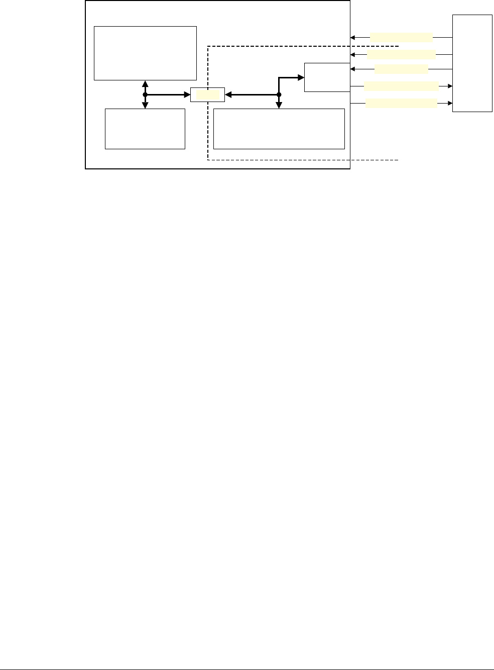
C7 Debug Reset and Powerdown Support
C7.2 Power domains and debug
ARM DDI 0406C.c Copyright © 1996-1998, 2000, 2004-2012, 2014 ARM. All rights reserved. C7-2153
ID051414 Non-Confidential
Figure C7-1 Recommended power domain split between core and debug power domains
The signals DBGPWRUPREQ, DBGNOPWRDWN, and DBGPWRDUP shown in Figure C7-1 provide an
interface between the power controller and the processor debug logic that is in the debug power domain. They are
part of the recommended interface, see Appendix D1 Recommended External Debug Interface. With this interface:
• The external debugger can request the power controller to emulate powerdown, simplifying the requirements
on software by sacrificing entirely realistic behavior.
• The external debugger can request the power controller to powerup the core power domain.
• The external debug interface knows when the core power domain is powered down, and can communicate
this information to the external debugger.
DBGNOPWRDWN on page D1-2348 and DBGPWRDUP on page D1-2349 describe these signals.
Debug behavior over powerdown depends on the debug version, as follows:
v7 Debug If the core power domain is not being powered down at the same time as the debug power domain
then invasive debug must be disabled before power is removed from the debug power domain. The
behavior of the debug logic, and in particular the generation of debug events, is UNPREDICTABLE if
invasive debug is enabled when the debug power domain is not powered. Disabling invasive debug
ensures that debug events are ignored by the processor. For more information, see Chapter C2
Invasive Debug Authentication.
Reads and writes of debug registers through all interfaces when the debug power domain is powered
down are UNPREDICTABLE.
v7.1 Debug Powering down the debug power domain does not affect invasive debug enable.
Reads and writes of debug registers through the memory-mapped and external debug interfaces
when the debug power domain is powered down return an error. Reads and writes through the CP14
interface are unaffected, so the use of Monitor debug-mode is unaffected.
The performance monitors must be implemented in the core power domain, and must continue to operate when the
debug power domain is powered down, see Chapter C12 The Performance Monitors Extension.
Unless otherwise indicated, descriptions in the rest of this part of this manual assume that two power domains are
implemented as described in this section, and that therefore the implementation supports external debug over
powerdown. However, the descriptions identify features that are not required for an implementation with a single
power domain, a SinglePower implementation, and indicate the differences in behavior of such a system. A
SinglePower implementation cannot support external debug over powerdown.
Processor
External
debug
interface
All other
debug registers
Debug power
domain registers
Power
controller
Core domain Vdd
Debug domain Vdd
DBGPWRDUP
DBGNOPWRDWN †
Remainder of
processor logic
Power domain boundary
Debug
power domain
Core
power domain
Bridge
DBGPWRUPREQ ‡
† In v7.1 DBGNOPWRDWN comes from the core power domain
‡ In v7.1 Debug only

C7 Debug Reset and Powerdown Support
C7.3 The OS Save and Restore mechanism
C7-2154 Copyright © 1996-1998, 2000, 2004-2012, 2014 ARM. All rights reserved. ARM DDI 0406C.c
Non-Confidential ID051414
C7.3 The OS Save and Restore mechanism
The requirements for an implementation that supports external debug over powerdown are:
• The operating system must be able to save and restore the debug logic state over a powerdown. The OS Save
and Restore mechanism meets this requirement.
• A debugger must be able to detect that a processor has powered down. For more information, see Permissions
in relation to powerdown on page C6-2121.
The OS Save and Restore mechanism enables an operating system to save the debug registers before powerdown
and restore them when power is restored.
In v7 Debug:
• If an implementation supports external debug over powerdown, then it must implement the OS Save and
Restore mechanism.
• On a SinglePower implementation, and on any other implementation that does not support external debug
over powerdown, it is IMPLEMENTATION DEFINED whether the OS Save and Restore mechanism is
implemented.
• If an implementation does not support the OS Save and Restore mechanism:
— It must implement DBGOSLSR.OSLM as RAZ.
— Accesses to the other OS Save and Restore mechanism registers are UNPREDICTABLE.
In v7.1 Debug, all mechanisms required for external debug over powerdown are required by the architecture.
The following sections describe the OS Save and Restore mechanism:
•The debug logic state to preserve over a powerdown.
•v7 Debug OS Save and Restore on page C7-2156.
•v7.1 Debug OS Save and Restore on page C7-2159.
Appendix D4 Example OS Save and Restore Sequences for External Debug Over Powerdown gives software
examples of the OS Save and Restore processes, for v7 Debug and v7.1 Debug.
C7.3.1 The debug logic state to preserve over a powerdown
For debug over powerdown, software must preserve the following state:
• Debug registers in the core power domain that are writable.
• Certain bits in the DBGDSCR.
Table C7-1 on page C7-2155 shows the different requirements for self-hosted debug over powerdown and external
debug over powerdown:
• In v7 Debug, the requirements for external debug over powerdown apply to the implementation of the OS
Save and Restore mechanism.
• In v7.1 Debug, the requirements for external debug over powerdown apply to the software making use of the
OS Save and Restore mechanism.
• The self-hosted column lists registers that software must preserve over powerdown so that it can support
self-hosted debug over powerdown. This does not require use of the OS Save and Restore mechanism.
The software does not have to preserve any debug logic state that is not lost when the core power domain is powered
down. That is, it does not have to preserve any debug logic state that is in the debug power domain, see Power
domains and debug on page C7-2151.

C7 Debug Reset and Powerdown Support
C7.3 The OS Save and Restore mechanism
ARM DDI 0406C.c Copyright © 1996-1998, 2000, 2004-2012, 2014 ARM. All rights reserved. C7-2155
ID051414 Non-Confidential
The restore sequence always overwrites the debug registers with the values that were saved. In particular, the values
of the DBGDTRTX and DBGDTRRX registers, and of the DCC status bits, are set to the saved values when the
restore sequence completes.
If there are valid values in the debug registers immediately before the restore sequence then those values are lost.
Table C7-1 Register state to save, for debug over powerdown
Register FieldaDescription Self-hosted External Notes
DBGDSCR RXfull Debug Status and Control No Yes See DCC registers on page C7-2156
TXfull No Yes
RXfull_l No Yes
TXfull_l No Yes
ExtDCCmode No Yes -
MDBGen Yes Yes
HDBGen No Yes
ITRen No Yes
UDCCdis Yes Yes
INTdis No Yes
DBGack No Yes
MOE Yes Yes
DBGWFAR Watchpoint Fault Address Yes Yes -
DBGBCRs Breakpoint Control Yes Yes -
DBGBVRs Breakpoint Value Yes Yes -
DBGBXVRs Breakpoint Extended Value Yes Yes Virtualization Extensions only
DBGWVRs Watchpoint Value Yes Yes -
DBGWCRs Watchpoint Control Yes Yes -
DBGVCR Vector Catch Yes Yes -
DBGDSCCR Debug State Cache Control No Yes In v7 Debug only
DBGDSMCR Debug State MMU Control No Yes In v7 Debug only
DBGCLAIMSET Claim Tag Set No Yes See Claim Tag registers on
page C7-2156
DBGCLAIMCLR Claim Tag Clear No Yes
DBGDTRTX Target to Host Data Transfer No Yes See DCC registers on page C7-2156
DBGDTRRX Host to Target Data Transfer No Yes
a. DBGDSCR only. For all other registers, the same requirement applies to the entire register.

C7 Debug Reset and Powerdown Support
C7.3 The OS Save and Restore mechanism
C7-2156 Copyright © 1996-1998, 2000, 2004-2012, 2014 ARM. All rights reserved. ARM DDI 0406C.c
Non-Confidential ID051414
Claim Tag registers
In v7 Debug, these registers are in the debug power domain so their values do not have to be preserved.
In v7.1 Debug, these registers are in the core power domain so their values must be preserved. Use
DBGCLAIMCLR to read the values in the save sequence, and DBGCLAIMSET to write the values in the restore
sequence.
DCC registers
For external debug over powerdown, software must preserve the status of the Debug Communications Channel
(DCC). This means it must preserve:
• The data transfer registers DBGDTRTX and DBGDTRRX, subject to the values of DBGDSCR.TXfull and
DBGDSCR.RXfull when the save sequence is performed:
—If DBGDSCR.TXfull is set to 1 then the value of DBGDTRTX must be saved and restored.
—if DBGDSCR.RXfull is set to 1 then the value of DBGDTRRX must be saved and restored.
If either of these bits is not set to 1 when the OS Save sequence is performed then the value of the
corresponding register is UNKNOWN after the OS Restore sequence.
• The DCC status bits, DBGDSCR.{TXfull, TXfull_l, RXfull, RXfull_l}.
C7.3.2 v7 Debug OS Save and Restore
In v7 Debug the following registers provide the OS Save and Restore mechanism:
• The OS Save and Restore Register, DBGOSSRR, that is accessed to save or restore the contents of the debug
registers.
• The OS Lock Access Register, DBGOSLAR, sets the OS Lock to restrict access to debug registers before
starting an OS Save sequence, and releases the OS Lock after an OS Restore sequence.
• The OS Lock Status Register, DBGOSLSR, shows the status of the OS Lock.
• The Event Catch Register, DBGECR, generates a debug event when the OS Lock is cleared.
Software can read the DBGOSLSR to detect whether the v7 Debug OS Save and Restore mechanism is
implemented. If it is not implemented the read of the DBGOSLSR returns a value of 0 for DBGOSLSR.OSLM[0].
The following subsections describe the v7 Debug OS Save and Restore mechanism:
•v7 Debug OS Save sequence.
•v7 Debug OS Restore sequence on page C7-2157.
•v7 Debug behavior when the OS Lock is set on page C7-2157.
•v7 Debug behavior when the OS Lock is cleared on page C7-2158.
•Behavior of the DBGOSSRR on page C7-2158.
•Removing power from a v7 Debug implementation on page C7-2159.
v7 Debug OS Save sequence
To preserve the debug logic state over a powerdown, this state must be saved to non-volatile storage. This means
the OS Save sequence must:
1. Set the OS Lock by writing the key value,
0xC5ACCE55
, to the DBGOSLAR. This also initializes the
DBGOSSRR.
2. If using the CP14 interface, execute an
ISB
instruction.
3. Perform an initial read of DBGOSSRR. This returns the number of reads of the DBGOSSRR that are required
to save the entire debug logic state. This number is IMPLEMENTATION DEFINED but must be less than or equal
to 128.

C7 Debug Reset and Powerdown Support
C7.3 The OS Save and Restore mechanism
ARM DDI 0406C.c Copyright © 1996-1998, 2000, 2004-2012, 2014 ARM. All rights reserved. C7-2157
ID051414 Non-Confidential
Record this number in the non-volatile storage.
4. Perform additional reads of DBGOSSRR, as indicated in step 3, and record each value, in order, in the
non-volatile storage.
5. Leave the OS Lock set, to prevent any changes to the debug registers.
v7 Debug OS Restore sequence
After a powerdown, to restore the debug logic state from the non-volatile storage, the OS Restore sequence must:
1. Set the OS Lock by writing the key value,
0xC5ACCE55
, to the DBGOSLAR. This also initializes the
DBGOSSRR.
2. If using the CP14 interface, execute an
ISB
instruction.
3. Read DBGPRSR, to clear the Sticky Powerdown status bit.
4. If using the CP14 interface, execute an
ISB
instruction.
5. Perform an initial read of DBGOSSRR and discard the value returned.
6. From the non-volatile storage, retrieve the number that was recorded in step 3 of the OS Save sequence. This
value indicates the number of writes of DBGOSSRR that are required to restore the entire debug logic state.
7. Perform a word read from the non-volatile storage and then write the value to DBGOSSRR.
Repeat this step until the number of writes to DBGOSSRR matches the value retrieved at step 6.
At this point, all of the debug logic state saved to non-volatile memory by the OS save sequence has been
restored.
8. If using the CP14 interface, execute an
ISB
instruction.
9. Clear the OS Lock by writing any non-key value to the DBGOSLAR.
10. If using the memory-mapped interface, execute a
DSB
instruction.
11. Execute a Context synchronization operation before using the debug registers.
Note
The number of accesses required, and the order and interpretation of the data are IMPLEMENTATION DEFINED, but
the number of accesses and the order of the data must be the same for the OS Save and OS Restore sequences.
Software must ensure that the OS Restore mechanism writes values back to the DBGOSSRR in the same order that
it read them in the OS Save mechanism. That is, the first item read in the OS Save mechanism must be the first item
written in the OS Restore mechanism.
v7 Debug behavior when the OS Lock is set
The main purpose of the OS Lock is to prevent updates to debug registers during an OS Save or OS Restore
operation. In a v7 Debug implementation, the state of the OS Lock is IMPLEMENTATION DEFINED on a debug logic
reset.
When the OS Lock is set:
• Access to debug registers through all interfaces is restricted to prevent modification of the registers that are
being saved or restored. For more information, see v7 Debug register access in the CP14 interface on
page C6-2132 and v7 Debug register access in the memory-mapped and external debug interfaces on
page C6-2134.
•DBGOSSRR can be used to read and write registers without side-effects, so the current debug state can be
saved or restored, including restoring fields in the DBGDSCR that are normally read-only.

C7 Debug Reset and Powerdown Support
C7.3 The OS Save and Restore mechanism
C7-2158 Copyright © 1996-1998, 2000, 2004-2012, 2014 ARM. All rights reserved. ARM DDI 0406C.c
Non-Confidential ID051414
• The effect of the OS Lock on Software debug events is IMPLEMENTATION DEFINED, but an implementation
must either:
— For any Software debug event, depending on the currently-selected debug-mode, either generate a
debug exception or enter Debug state.
— Regardless of the currently-selected debug-mode, ignore any Software debug event other than a BKPT
instruction debug event. This is because the generation of the debug event uses the debug registers that
are being restored. However, on a BKPT instruction debug event the implementation must generate a
debug exception.
The OS Lock has no effect on Halting debug events.
v7 Debug behavior when the OS Lock is cleared
When the OS Lock is cleared, an OS Unlock catch debug event is generated if DBGECR.OUCE, the OS Unlock
catch enable bit, is set to 1. See Halting debug events on page C3-2075.
The debug logic state of the processor is unchanged if the OS Lock is cleared during or following an OS Save
sequence. The sequence is restarted the next time the OS Lock is set.
Behavior of the DBGOSSRR
The DBGOSSRR works in conjunction with an internal sequence counter, so that a series of reads or writes of this
register saves or restores the complete debug logic state of the processor. The processor loses this state when it is
powered down. Writing the key, 0xC5ACCE55, to the DBGOSLAR resets the internal sequence counter to the start
of the sequence.
The first access to the DBGOSSRR following the reset of the internal sequence counter must be a read:
• When performing an OS Save sequence this read returns the number of reads from the DBGOSSRR that are
required to save the entire debug logic state.
• When performing an OS Restore sequence the value returned by this read is UNKNOWN.
The result of issuing a write to the DBGOSSRR following a reset of the internal sequence counter is
UNPREDICTABLE.
Note
An implementation that includes the OS Save and Restore mechanism might not provide access to the DBGOSSRR
through the external debug interface. In this case:
• The DBGOSLSR, DBGOSLAR, and DBGECR are accessible through the external debug interface.
• Through the external debug interface, the DBGOSSRR is RAZ/WI.
• Because the first read of the DBGOSSRR through the external debug interface returns zero, this correctly
indicates that the debug registers cannot be saved or restored through the external debug interface.
The subsequent accesses to the DBGOSSRR must be either all reads or all writes. Behavior is UNPREDICTABLE if
any of the following are true:
• Reads and writes are mixed.
• More accesses are performed than the number of registers to be saved or restored, as returned by the first read
in the OS Save sequence.
• The subsequent accesses are writes, but the OS Lock is cleared with fewer writes performed than the number
of registers to be restored.
When the core power domain is powered down or when the OS Lock is not set, reads of DBGOSSRR return an
UNKNOWN value and writes are UNPREDICTABLE.

C7 Debug Reset and Powerdown Support
C7.3 The OS Save and Restore mechanism
ARM DDI 0406C.c Copyright © 1996-1998, 2000, 2004-2012, 2014 ARM. All rights reserved. C7-2159
ID051414 Non-Confidential
Removing power from a v7 Debug implementation
ARM strongly recommends that v7 Debug implementations provide an IMPLEMENTATION DEFINED mechanism that
can be used, before removing power from the debug power domain, to both:
• Force the debug interfaces into a quiescent state.
• Cause the debug logic to ignore Halting debug events.
Note
• The v7.1 Debug OS Double Lock mechanism, described in Behavior when the OS Double Lock is set on
page C7-2161, might be used as a model for this mechanism,
• This mechanism might be implemented using IMPLEMENTATION DEFINED registers, or using appropriate
handshake signals.
C7.3.3 v7.1 Debug OS Save and Restore
In v7.1 Debug the following registers provide the OS Save and Restore mechanism:
• The OS Lock Access Register, DBGOSLAR, sets the OS Lock to restrict access to debug registers before
starting an OS Save sequence, and releases the OS Lock after an OS Restore sequence.
• The OS Lock Status Register, DBGOSLSR, shows the status of the OS Lock.
• The Event Catch Register, DBGECR, generates a debug event when the OS Lock is cleared.
• The OS Double Lock Register, DBGOSDLR, locks out an external debugger entirely. Only used immediately
before a powerdown sequence.
Software can read the DBGOSLSR to detect whether the v7.1 Debug OS Save and Restore mechanism is
implemented. If it is implemented the read of the DBGOSLSR returns a value of
0b10
for DBGOSLSR.OSLM.
The following subsections describe the v7.1 Debug OS Save and Restore mechanism:
•v7.1 Debug OS Save sequence.
•v7.1 Debug OS Restore sequence on page C7-2160.
•v7.1 Debug behavior when the OS Lock is set on page C7-2160.
•v7.1 Debug behavior when the OS Lock is cleared on page C7-2160.
•Behavior when the OS Double Lock is set on page C7-2161.
v7.1 Debug OS Save sequence
To preserve the debug logic state over a powerdown, this state must be saved to non-volatile storage. This means
the OS Save sequence must:
1. Set the OS Lock by writing the key value,
0xC5ACCE55
, to the DBGOSLAR.
2. Execute an
ISB
instruction.
3. Walk through the registers listed in The debug logic state to preserve over a powerdown on page C7-2154,
and save the values to the non-volatile storage.
4. Leave the OS Lock set, to prevent any changes to the debug registers.
Before removing power from the core power domain, software must:
1. Set the OS Double Lock, by writing 1 to DBGOSDLR.DLK.
2. Execute a Context synchronization operation.

C7 Debug Reset and Powerdown Support
C7.3 The OS Save and Restore mechanism
C7-2160 Copyright © 1996-1998, 2000, 2004-2012, 2014 ARM. All rights reserved. ARM DDI 0406C.c
Non-Confidential ID051414
v7.1 Debug OS Restore sequence
After a powerdown, to restore the debug logic state from the non-volatile storage, the OS Restore sequence must:
1. Set the OS Lock by writing the key value,
0xC5ACCE55
, to the DBGOSLAR. The lock is set by the core
powerup reset, but this ensures it is set.
2. Execute an
ISB
instruction.
3. Walk through the registers listed in The debug logic state to preserve over a powerdown on page C7-2154,
and restore the values from the non-volatile storage.
4. Execute an
ISB
instruction.
5. Clear the OS Lock by writing any non-key value to the DBGOSLAR.
6. Execute a Context synchronization operation.
v7.1 Debug behavior when the OS Lock is set
The main purpose of the OS Lock is to prevent updates to debug registers during an OS Save or OS Restore
operation. In a v7.1 Debug implementation, the OS Lock is set on a core powerup reset.
When the OS Lock is set:
• Access to debug registers through the CP14 interface and memory-mapped interface is mainly unchanged,
except that:
— For accesses through the CP14 interface, the Debug Software Enable function is ignored.
— The registers can be read and written without side-effects.
— Fields in DBGDSCRext that are normally UNKNOWN or read-only when accessed using the CP14
interface become read/write.
These changes mean the current state can be saved or restored. For more information, see v7.1 Debug register
access in the CP14 interface on page C6-2141 and v7.1 Debug register access in the memory-mapped and
external debug interfaces on page C6-2144.
• Access to debug registers through external debug interface is restricted to prevent an external debugger
modifying the registers that are being saved or restored.
• Software debug events other than BKPT instruction debug events are ignored.
• Regardless of the currently-selected debug-mode, BKPT instruction debug events generate a debug
exception.
The OS Lock has no effect on Halting debug events.
v7.1 Debug behavior when the OS Lock is cleared
When the OS Lock is cleared, an OS Unlock catch debug event is generated if DBGECR.OUCE, the OS Unlock
catch enable bit, is set to 1. See Halting debug events on page C3-2075.

C7 Debug Reset and Powerdown Support
C7.3 The OS Save and Restore mechanism
ARM DDI 0406C.c Copyright © 1996-1998, 2000, 2004-2012, 2014 ARM. All rights reserved. C7-2161
ID051414 Non-Confidential
Behavior when the OS Double Lock is set
OS Double Lock is implemented only as part of a v7.1 Debug implementation.
The OS Double Lock is set immediately before a powerdown sequence. When the OS Double Lock is set:
• Access to most debug registers through the CP14 interface is UNPREDICTABLE. For more information, see
v7.1 Debug register access in the CP14 interface on page C6-2141.
• Access to debug registers through the external debug and memory-mapped interfaces is restricted, so that
these interfaces are quiescent prior to removing power. For more information, see v7.1 Debug register access
in the memory-mapped and external debug interfaces on page C6-2144.
Note
A debug register access might be in progress when software sets DBGOSDLR.DLK to 1. An implementation
must not permit the synchronization of setting the OS Double Lock to stall indefinitely waiting for that access
to complete. This means that any debug register access that is in progress when software sets
DBGOSDLR.DLK to 1 must complete or return an error as soon as possible. A Context synchronization
operation is required to synchronize a change to DBGOSDLR.
• Software debug events, other than BKPT instruction debug events, are ignored.
• Halting debug events do not cause entry to Debug state, and become pending. See Halting debug events on
page C3-2075 for more information about pending Halting debug events.
Note
Pending Halting debug events might be lost when core power is removed.
• No asynchronous debug events are WFI or WFE wake-up events, see Halting debug events on page C3-2075.
Software must synchronize the update to DBGOSDLR before it indicates to the system that power can be removed.
Typically, software indicates that power can be removed by entering the Wait For Interrupt state, see Wait For
Interrupt on page B1-1203, and if this method is used, software must synchronize the DBGOSDLR update before
issuing the
WFI
instruction.
DBGOSDLR.DLK is ignored and the OS Double Lock is not set if either:
• The processor is in Debug state.
•DBGPRCR.CORENPDRQ, Core no powerdown request bit, is set to 1.
Note
It is possible to enter Debug state with DBGOSDLR.DLK, OS Double Lock control bit, set to 1. This is because a
Context synchronization operation is required to ensure the OS Double Lock is set, meaning that Debug state might
be entered before the DBGOSDLR update is synchronized. A processor implementation must not permit entry to
Debug state once the write to DBGOSDLR.DLK has been synchronized by a Context synchronization operation.

C7 Debug Reset and Powerdown Support
C7.4 Reset and debug
C7-2162 Copyright © 1996-1998, 2000, 2004-2012, 2014 ARM. All rights reserved. ARM DDI 0406C.c
Non-Confidential ID051414
C7.4 Reset and debug
The processor reset scheme is IMPLEMENTATION DEFINED. The ARM architecture, described in parts A and B of this
manual, does not define different levels of reset. However, in a typical system, there are a number of reasons why
multiple levels of reset might exist. In particular, for debug:
• In any reset scheme, a debugger must be able to debug the reset sequence. This requires support for:
— Setting the debug register values while the processor is in a reset state.
— A processor reset not resetting the debug register values.
For more information see Debug register accesses when the implementation is in a non-debug logic reset
state on page C7-2163.
• Providing separate power domains means you might need to reset the debug logic independently from the
logic in the core power domain.
For these reasons, v7 Debug introduces a distinction between debug logic reset and non-debug logic reset. These
resets can be applied independently. The reset descriptions in parts A and B of this manual describe the non-debug
logic reset. Part C describes the debug logic reset and its interaction with the non-debug logic reset. The following
sections give more information about this:
•Recommended reset scheme.
•Debug register accesses when the implementation is in a non-debug logic reset state on page C7-2163.
•Debug register accesses when the implementation is in a non-debug logic reset state on page C7-2163.
C7.4.1 Recommended reset scheme
ARM recommends use of the following reset signals for an implementation that supports these independent resets:
nSYSPORESET System powerup reset signal. This signal must be asserted LOW on powerup of both the
core power domain and the debug power domain. It sets both non-debug logic and debug
logic, in both the core power domain and the debug power domain, to a known state.
nCOREPORESET Core powerup reset signal. If the core power domain is powered down while the system is
still powered up, this signal must be asserted LOW when the core power domain is powered
back up. It sets both non-debug logic and debug logic in the core power domain to a known
state. Also, this reset initializes the debug registers that are in the core power domain.
nRESET Warm reset signal. This signal is asserted LOW to generate a warm reset, that is, a reset
where the system wants to set the processor to a known state but the reset has nothing to do
with any powerdown, for example a watchdog reset. It sets parts of the non-debug logic to
a known state. This reset must not affect any debug session.
PRESETDBGn Debug logic reset signal. The debugger asserts this signal LOW to set parts of the debug
logic to a known state. This signal must be asserted LOW on powerup of the debug logic.
In the recommended reset scheme, the PRESETDBGn reset signal can be asserted at any time, not just at powerup.
This signal has similar effects to nSYSPORESET, that is, it clears all debug registers, unless otherwise noted by
the register definition. For more information, see Appendix D1 Recommended External Debug Interface.
However, asynchronously asserting PRESETDBGn can lead to UNPREDICTABLE behavior. For example, the reset
might change the values of debug registers that are in use or will be used by software.
For more information about this reset scheme, contact ARM.
Table C7-2 on page C7-2163 summarizes the recommended reset scheme.

C7 Debug Reset and Powerdown Support
C7.4 Reset and debug
ARM DDI 0406C.c Copyright © 1996-1998, 2000, 2004-2012, 2014 ARM. All rights reserved. C7-2163
ID051414 Non-Confidential
For a SinglePower system, ARM recommends implementing only nSYSPORESET, nRESET, and
PRESETDBGn.
C7.4.2 Debug register accesses when the implementation is in a non-debug logic reset state
It must be possible to write to a debug register if the following conditions are met:
1. The debug logic in the debug power domain is not in reset. That is, the debug logic reset is not asserted.
2. The register being written to is not itself being reset. For example, when a warm reset is asserted, it is not a
register in the core power domain that is reset by a warm reset.
When condition 1 is met, if the register being written to is being reset, then the write to the register is accepted.
However when the reset of that register is deasserted the value of that register is:
• its architecturally-defined reset value, if the architecture defines a reset value for the register
•UNKNOWN, otherwise.
This means that, while the processor is in a warm reset, a debugger can write to the debug registers that are in the
core power domain but are not reset by a warm reset.
A debugger can set DBGPRCR.HCWR to hold the processor in a warm reset. It might do this while it writes to
debug registers that are not reset by a warm reset.
C7.4.3 Debug behavior when the implementation is in a debug logic reset state
Table C7-2 shows how the debug logic can be split across two power domains, meaning some debug registers are
implemented in the debug power domain, and other debug registers are implemented in the core power domain.
As long as a debug logic reset is asserted:
• Any access to a register that is in debug logic reset, using any interface to the debug registers, is
UNPREDICTABLE, except for CP14 reads of the read-only registers DBGDIDR, DBGDSAR, and DBGDRAR.
• If the debug power domain is in debug logic reset, or in a SinglePower system, any access through the
external debug register interface, or through the memory-mapped debug register interface, is
UNPREDICTABLE.
• It is UNPREDICTABLE whether a debug event that would have been generated by the state of the debug logic
immediately before the debug logic reset is generated.
• The debug logic must not generate any debug event that would not have been generated if the system was not
in debug logic reset.
Table C7-2 Recommended reset scheme
Signal Debug power domain Core power domain
Debug logic Debug logic Non-debug logic
nSYSPORESET Reset ResetaReset
nCOREPORESET Not reset ResetaReset
nRESET Not reset Not reset Reset
PRESETDBGn Reset ResetaNot reset
a. If the core power domain is not powered, or in v7 Debug only if the Sticky Powerdown status bit DBGPRSR.SPD is set
to 1, it is UNPREDICTABLE whether the registers are reset. If power is not applied to the core power domain,
nCOREPORESET must be driven LOW when power is restored to the core power domain. This resets these registers.

C7 Debug Reset and Powerdown Support
C7.4 Reset and debug
C7-2164 Copyright © 1996-1998, 2000, 2004-2012, 2014 ARM. All rights reserved. ARM DDI 0406C.c
Non-Confidential ID051414

ARM DDI 0406C.c Copyright © 1996-1998, 2000, 2004-2012, 2014 ARM. All rights reserved. C8-2165
ID051414 Non-Confidential
Chapter C8
The Debug Communications Channel and
Instruction Transfer Register
This section describes communication between a debugger and the processor debug logic, using the Debug
Communications Channel (DCC) and the Instruction Transfer Register, DBGITR. It contains the following
sections:
•About the DCC and DBGITR on page C8-2166
•Operation of the DCC and Instruction Transfer Register on page C8-2169
•Behavior of accesses to the DCC registers and DBGITR on page C8-2173.
•Synchronization of accesses to the DCC and the DBGITR on page C8-2178.

C8 The Debug Communications Channel and Instruction Transfer Register
C8.1 About the DCC and DBGITR
C8-2166 Copyright © 1996-1998, 2000, 2004-2012, 2014 ARM. All rights reserved. ARM DDI 0406C.c
Non-Confidential ID051414
C8.1 About the DCC and DBGITR
This section introduces the Debug Communications Channel (DCC) and the Instruction Transfer Register,
DBGITR.
The DCC provides a communications channel between:
• An external debugger, described as the debug host.
• The debug implementation on the processor, described as the debug target.
Debug software can use the DCC to transfer a data word between the debug host and debug target using:
• The Host to Target Data Transfer Register, DBGDTRRX.
• The Target to Host Data Transfer Register, DBGDTRTX.
In addition, when the processor is in Debug state, debug software can use the DBGITR to transfer an ARM
instruction to the processor for execution.
A debugger can use the DCC and DBGITR to examine and modify the state of the processor.
Bits in the Debug Status and Control Register, DBGDSCR, control the operation of the DCC and DBGITR. Some
bits provide software control of these features, and other bits are status bits that affect operation. The DBGDSCR
sets the External DCC access mode that controls the access mode for the external views of the DCC registers and
the DBGITR.
For more information see:
•DCC overview.
•DBGITR overview on page C8-2167.
•Internal and external views of the DBGDSCR and the DCC registers on page C8-2167.
The remainder of this chapter describes how the DCC and DBGITR operate, and the relation between them.
C8.1.1 DCC overview
The DCC comprises two registers, and a set of status bits in the DBGDSCR:
• The DBGDTRRX.
• The DBGDTRTX.
• The following status bits in the DBGDSCR:
— RXfull and RXfull_l, indicating the DBGDTRRX status.
— TXfull and TXfull_l, indicating the DBGDTRTX status.
RXfull_l is a latched copy of the RXfull bit, and TXfull_l is a latched copy of the TXfull bit.
In addition, the following DBGDSCR fields control features of the DCC:
•DBGDSCR.ExtDCCmode controls the External DCC access mode. The possible modes are:
Non-blocking
If the DCC cannot perform a requested transfer it ignores the transfer request. If the debug logic
cannot issue the DBGITR instruction for execution it ignores a write to DBGITR. This is the
default external access mode.
Stall If the DCC cannot perform a requested transfer, or the debug logic cannot issue the DBGITR
instruction for execution, the associated register access stalls until the debug logic can perform
the required operation.
Fast A debugger can use Fast mode to issue a single instruction multiple times, without updating
DBGITR. If the DCC cannot perform a requested transfer, the associated register access stalls.
Also, a write to DBGITR can stall.
Operation of the External DCC access modes on page C8-2169 gives more information about each of the
access modes.
•DBGDSCR.UDCCdis controls User mode access to the DCC.

C8 The Debug Communications Channel and Instruction Transfer Register
C8.1 About the DCC and DBGITR
ARM DDI 0406C.c Copyright © 1996-1998, 2000, 2004-2012, 2014 ARM. All rights reserved. C8-2167
ID051414 Non-Confidential
C8.1.2 DBGITR overview
DBGITR, Instruction Transfer Register on page C11-2265 describes the DBGITR.
DBGDSCR.InstrCompl_l is a latched status bit that indicates when the processor has completed execution of an
instruction issued through the DBGITR, see DBGDSCR, Debug Status and Control Register on page C11-2243.
Note
The internal InstrCompl flag indicates when the processor has completed execution of an instruction issued through
the DBGITR. InstrCompl is not visible in any register, but DBGDSCR.InstrCompl_l is a latched copy of this
internal flag.
In addition, the DBGDSCR.ITRen bit enables the execution of ARM instructions through the DBGITR.
The external DCC access mode affects the behavior of writes to the DBGITR, see Operation of the DCC and
Instruction Transfer Register on page C8-2169.
The Sticky Synchronous Data Abort bit and issuing instructions from DBGITR on page C8-2172 describes the
conditions under which an instruction, held in DBGITR, is issued for execution.
The behavior of accesses to DBGITR is restricted by various locks and processor states. See Accesses to the
registers in v7.1 Debug on page C8-2173 for details.
C8.1.3 Internal and external views of the DBGDSCR and the DCC registers
A debug implementation provides internal and external views of each of the registers DBGDSCR, DBGDTRTX
and DBGDTRRX, see Figure C8-1. The int and ext suffixes denote the internal and external views. The differences
between these views relate to the handling of the DCC, and in particular the TXfull, RXfull, and InstrCompl_l status
bits. The view names internal and external are based on the DCC usage model.
Figure C8-1 Internal (int) and external (ext) views of the DCC registers
In the DBGDSCR, in addition to the updates to TXfull_l and RXfull_l shown in Figure C8-1, a read of
DBGDSCRext copies the internal InstrCompl flag to the InstrCompl_l bit, see DBGDSCR, Debug Status and
Control Register on page C11-2243. The value of InstrCompl_l is visible only in the DBGDSCRext view.
DBGDSCR
RXfull_l
RXfull
Copy on read of
DBGDSCRext
TXfull_l
TXfull
Copy on read of
DBGDSCRext
RX
write
logic ‡
TX
read
logic ‡
DBGDTRTX DBGDTRTXext
read/write
DBGDTRRX DBGDTRRXext
read/write
DBGDTRTXint
write-only
DBGDTRRXint
read-only
1, on writes
0, on reads
DBGDSCRext
read/write
DBGDSCRint
read-only
Internal view External view
‡ TX reads and RX writes are possible only through the external view

C8 The Debug Communications Channel and Instruction Transfer Register
C8.1 About the DCC and DBGITR
C8-2168 Copyright © 1996-1998, 2000, 2004-2012, 2014 ARM. All rights reserved. ARM DDI 0406C.c
Non-Confidential ID051414
Software can access DBGDSCRint, DBGDTRRXint, and DBGDTRTXint only through the CP14 interface, see
CP14 debug register interface accesses on page C6-2124.
Software can access DBGDSCRext, DBGDTRRXext, and DBGDTRTXext through:
• The CP14 interface:
— In v7 Debug it is IMPLEMENTATION DEFINED if these registers are visible in the CP14 interface.
— In v7.1 Debug these registers are required in the CP14 interface.
• The memory-mapped interface, if implemented,
• The external debug interface.
The behavior of accesses to these registers is restricted by various locks and processor states. For more information,
see:
•Accesses to the registers in v7 Debug on page C8-2173.
•Accesses to the registers in v7.1 Debug on page C8-2173.
If at any given time software attempts to access DBGDSCRext, DBGDTRRXext, or DBGDTRTXext through more
than one interface the behavior is UNPREDICTABLE. If an implementation provides a single port to handle external
debug interface accesses and memory-mapped interface accesses, that port might serialize accesses to the registers
from the two interfaces. However, the effects of reads and writes to these registers are such that the behavior
observed from either interface is UNPREDICTABLE.
Note
• DBGDSCRint and DBGDSCRext only provide different views onto the underlying DBGDSCR.
•DBGDTRRXint and DBGDTRRXext only provide different views onto the underlying DBGDTRRX
register.
•DBGDTRTXint and DBGDTRTXext only provide different views onto the underlying DBGDTRTX register.

C8 The Debug Communications Channel and Instruction Transfer Register
C8.2 Operation of the DCC and Instruction Transfer Register
ARM DDI 0406C.c Copyright © 1996-1998, 2000, 2004-2012, 2014 ARM. All rights reserved. C8-2169
ID051414 Non-Confidential
C8.2 Operation of the DCC and Instruction Transfer Register
This section describes the operation of the DCC and Instruction Transfer Register:
•General operation of the DCC and Instruction Transfer Register introduces these operations.
•Operation of the External DCC access modes gives a full description of each of the External DCC access
modes.
C8.2.1 General operation of the DCC and Instruction Transfer Register
The debug logic includes a number of controls on the operation of the DCC registers and the DBGITR. The External
DCC access mode determines how external accesses to the DCC and DBGITR behave, when other controls permit
an operation. The function of the DBGDSCR status bits is:
• RXfull and RXfull_l control whether the processor can accept a write to DBGDTRRXext, and the behavior
when it cannot accept a write.
• TXfull and TXfull_l control whether the processor can accept a read of DBGDTRTXext, and the behavior
when it cannot accept a read.
• The internal InstrCompl_l flag controls whether the processor can accept a write to DBGITR. In Fast mode
the InstrComp_1 flag also controls whether the processor can accept writes to DBGDTRRXext and reads
from DBGDTRTXext.
C8.2.2 Operation of the External DCC access modes
This section describes the operation of each of the External DCC access modes. For descriptions of the registers
used in these operations see:
•DBGDSCR, Debug Status and Control Register on page C11-2243.
•DBGDTRRX, Host to Target Data Transfer register on page C11-2261.
•DBGDTRTX, Target to Host Data Transfer register on page C11-2262.
•DBGITR, Instruction Transfer Register on page C11-2265.
The DBGDSCR.ExtDCCmode field determines the External DCC access mode. The following subsections
describe these modes:
•Non-blocking mode on page C8-2170.
•Stall mode on page C8-2170.
•Fast mode on page C8-2170.
Non-blocking mode is the default mode. Inappropriate use of the other modes can deadlock the memory-mapped or
external debug interface.
Note
The DBGDSCR.ExtDCCmode field has no effect on accesses to DBGDTRRXint and DBGDTRTXint.
The descriptions in this section assume that any required access and operation is permitted. For more information
about permitted accesses to the Debug registers see:
•Summary of the v7 Debug register interfaces on page C6-2130.
•Summary of the v7.1 Debug register interfaces on page C6-2139.
For all of these modes:
•The Sticky Synchronous Data Abort bit and issuing instructions from DBGITR on page C8-2172 describes
when instructions are issued from DBGITR for execution.
•Behavior of accesses to the DCC registers and DBGITR on page C8-2173 summarizes the behavior of the
register accesses.

C8 The Debug Communications Channel and Instruction Transfer Register
C8.2 Operation of the DCC and Instruction Transfer Register
C8-2170 Copyright © 1996-1998, 2000, 2004-2012, 2014 ARM. All rights reserved. ARM DDI 0406C.c
Non-Confidential ID051414
Non-blocking mode
In Non-blocking mode:
• If RXfull_l is 1, writes to DBGDTRRXext are ignored.
• If InstrCompl_l is 0, writes to DBGITR are ignored.
• If TXfull_l is 0, reads from DBGDTRTXext are ignored, and the reads return UNKNOWN values.
Following a successful write to DBGDTRRXext, the RXfull and RXfull_l bits are set to 1.
Following a successful read from DBGDTRTXext, the TXfull and TXfull_l bits are set to 0.
Following a successful write to DBGITR, the internal InstrCompl flag and the InstrCompl_l bit are set to 0.
A debugger accessing a DCC register or DBGITR must first read DBGDSCRext. This has the side-effect of copying
RXfull and TXfull to RXfull_l and TXfull_l, and setting InstrCompl_l to the current value of the internal
InstrCompl flag. The debugger can then use the returned value to determine whether a subsequent access to these
registers will be ignored.
Stall mode
In Stall mode:
• The effect of any access to DBGDTRRXext or DBGDTRTXext through the CP14 interface is
UNPREDICTABLE.
• Accesses through the external debug interface or the memory-mapped interface stall as follows:
— If RXfull is 1, any write to DBGDTRRXext stalls until RXfull is 0.
— If InstrCompl is 0, any write to DBGITR stalls until InstrCompl is 1.
— If TXfull is 0, any read from DBGDTRTXext stalls until TXfull is 1.
If an access is stalled in this way software cannot access any of the debug registers until the stalled DBGDTRRXext,
DBGDTRTXext, or DBGITR access completes. For more information about stalled accesses see Stalling of
accesses to the DCC registers on page C8-2172.
Following a write to DBGDTRRXext or DBGITR, or a read from DBGDTRTXext, the internal InstrCompl flag,
and the InstrCompl_l, RXfull, RXfull_l, TXfull, and TXfull_l bits, are set as described in Non-blocking mode.
Note
• Whether an access stalls depends on the value of the RXfull or TXfull status bit, or the internal InstrCompl
flag, not on the corresponding latched bits.
• The Non-blocking mode rules for ignoring accesses based on the values of the latched bits InstrCompl_l,
RXfull_l, and TXfull_l do not apply in Stall mode.
When the processor is in Non-debug state, software can program the DBGDSCR.ExtDCCmode field to select Stall
mode. However, because Stall mode blocks the interface to the debug registers until the processor issues the correct
MCR
or
MRC
instruction to unblock the access, ARM recommends that you do not use Stall mode in cases where the
external debugger does not have complete control over the instructions executing on the processor.
Fast mode
A debugger can use Fast mode to make the processor execute a single instruction repeatedly, without reloading the
DBGITR. However, if DBGDSCR.ExtDCCmode is programmed to select Fast mode, the result of writing to
DBGITR, writing to DBGDTRRXext, or reading DBGDTRTXext, is UNPREDICTABLE if either:
•DBGDSCR.ITRen is 0.
• The processor is in Non-debug state.

C8 The Debug Communications Channel and Instruction Transfer Register
C8.2 Operation of the DCC and Instruction Transfer Register
ARM DDI 0406C.c Copyright © 1996-1998, 2000, 2004-2012, 2014 ARM. All rights reserved. C8-2171
ID051414 Non-Confidential
In Fast mode:
• A write to the DBGITR does not trigger an instruction for execution. Instead, the debug logic latches the
instruction written to DBGITR, and retains this value until either a new value is written to DBGITR, or
software changes the access mode. If the processor is executing a previously-issued instruction when the
debugger writes to DBGITR, the write must not affect the execution of that instruction. To achieve this
requirement, an implementation can stall the write to DBGITR until InstrCompl is set to 1.
• The effect of any access to DBGDTRRXext or DBGDTRTXext through the CP14 interface is
UNPREDICTABLE.
• For accesses through the external debug interface or the memory-mapped interface:
— When an instruction is latched, any read of DBGDTRTXext or write to DBGDTRRXext causes the
processor to execute the latched instruction, as described in this subsection.
— When no instruction is latched, the effect of any access to DBGDTRRXext or DBGDTRTXext is
UNPREDICTABLE.
• A write to DBGDTRRXext:
— Does not complete until InstrCompl is set to 1.
— Writes the data to the DBGDTRRX.
— issues the instruction last written to DBGITR.
If RXfull is set to 1 before the write, then after the write the values of DBGDTRRX, the DBGDSCR.RXfull
bit, and the DBGDSCR.RXfull_l bit, are UNKNOWN.
If the issued instruction reads from DBGDTRRXint, the instruction reads the value written to
DBGDTRRXext by the write that triggered the instruction issue. The issued instruction does not complete
until RXfull is set to 0. This means that InstrCompl remains set to 0 until RXfull is set to 0, to indicate that
the processor is ready to accept another write to DBGDTRRXext.
• A read from DBGDTRTXext:
— Does not complete until InstrCompl is set to 1.
— Returns the data from the DBGDTRTX.
— Issues the instruction last written to the DBGITR.
If TXfull is set to 0 before the read, then the read returns an UNKNOWN value, and after the read the values of
DBGDTRTX, the DBGDSCR.TXfull bit, and the DBGDSCR.TXfull_l bit, are UNKNOWN.
If the issued instruction writes to DBGDTRTXint, the instruction does not affect the value returned from this
read of DBGDTRTXext. That is, this instruction can write the next DBGDTRTXext value to be read. The
issued instruction does not complete until TXfull is set to 1. This means that InstrCompl remains set to 0 until
TXfull is set to 1, to indicate that the processor is ready to accept another read from DBGDTRTXext.
If a Fast mode access is stalled, software cannot access any of the debug registers until the stalled DBGDTRRXext,
DBGDTRTXext, or DBGITR access completes. For more information about stalled accesses see Stalling of
accesses to the DCC registers on page C8-2172.
Note
The Non-blocking mode rules for ignoring accesses based on the values of the latched bits InstrCompl_l, RXfull_l
and TXfull_l do not apply in Fast mode.
Following a write to DBGDTRRXext or DBGITR, or a read from DBGDTRTXext, the internal InstrCompl flag,
and the InstrCompl_l, RXfull, RXfull_l, TXfull, and TXfull_l bits, are set as described in Non-blocking mode on
page C8-2170.

C8 The Debug Communications Channel and Instruction Transfer Register
C8.2 Operation of the DCC and Instruction Transfer Register
C8-2172 Copyright © 1996-1998, 2000, 2004-2012, 2014 ARM. All rights reserved. ARM DDI 0406C.c
Non-Confidential ID051414
Stalling of accesses to the DCC registers
In Stall mode and Fast mode, accesses to the DCC registers can stall:
• The mechanism by which an access is stalled by the external debug interface must be defined by the
documentation of that interface. For details of how accesses are stalled by the recommended ARM Debug
Interface v5, see the ARM Debug Interface v5 Architecture Specification.
• The mechanism by which an access is stalled by the memory-mapped interface is IMPLEMENTATION DEFINED.
• A stall is a side-effect of an access. If the debug logic is in a state where an access must have no side-effects,
the access does not stall. For more information about debug logic states in which accesses have no
side-effects see:
—Summary of the v7 Debug register interfaces on page C6-2130.
—Summary of the v7.1 Debug register interfaces on page C6-2139.
The Sticky Synchronous Data Abort bit and issuing instructions from DBGITR
The sections Non-blocking mode on page C8-2170, Stall mode on page C8-2170, and Fast mode on page C8-2170
describe the operations that an cause instruction to be issued from DBGITR, for execution. The instruction is issued
only if the Sticky Synchronous Data Abort bit, DBGDSCR.SDABORT_l, is set to 0. When this bit is set to 0, the
instruction is issued:
• In Non-blocking mode and in Stall mode, on a write to DBGITR.
• In Fast mode on:
— A write to DBGDTRRXext.
— A read from DBGTRTXext.
When DBGDSCR.SDABORT_l is set to 1, no instruction is issued for execution. That means that, for an operation
that would issue an instruction when DBGDSCR.SDABORT_l is set to 0:
• The internal InstrCompl flag and the InstrCompl_l bit are unchanged.
• In Fast mode:
— For a write to DBGDTRRXext, the write completes immediately, the processor ignores the write, and
the values of DBGTRRX, RXfull, and RXfull_l become UNKNOWN.
— For a read from DBGDTRTXext, the read completes immediately, the value returned is UNKNOWN,
and the values of DBGTRTX, TXfull, and TXfull_l become UNKNOWN.
— For a write to DBGITR, the write completes immediately, and the processor can ignore the write.
• In Non-blocking or Stall mode, a write to DBGITR completes immediately, and the processor must ignore
the write.
This behavior means an external debugger can issue a series of memory access instructions without checking for a
synchronous Data Abort exception after each instruction issue.
In Fast mode, if a debugger writes to DBGITR when DBGDSCR.SDABORT_l is set to 1, the value of the latched
instruction becomes UNKNOWN. This means that, when DBGDSCR.SDABORT_l is cleared to 0, if the DCC
remains in Fast mode, the instruction issued on a write to DBGDTRRXext or a read from DBGTRTXext is also
UNKNOWN.
Note
The values of the Sticky Asynchronous Abort and Sticky Undefined Instruction bits, DBGDSCR.ADABORT_l and
DBGDSCR.UND_l, have no effect on whether instructions are issued from the DBGITR.
For more information about the SDABORT_l bit see DBGDSCR, Debug Status and Control Register on
page C11-2243.

C8 The Debug Communications Channel and Instruction Transfer Register
C8.3 Behavior of accesses to the DCC registers and DBGITR
ARM DDI 0406C.c Copyright © 1996-1998, 2000, 2004-2012, 2014 ARM. All rights reserved. C8-2173
ID051414 Non-Confidential
C8.3 Behavior of accesses to the DCC registers and DBGITR
The following sections describe the behavior of accesses to the internal and external views of the DCC registers,
DBGDSCRext, and to the DBGITR:
•Accesses to the registers in v7 Debug.
•Accesses to the registers in v7.1 Debug.
•Behavior of accesses to DBGDTRRX on page C8-2174.
•Behavior of accesses to DBGDTRTX on page C8-2175.
•Behavior of accesses to the DBGITR on page C8-2176.
Access to the registers must permit reads and writes of the DCC registers and DBGITR to set control bits in the
DBGDSCRext. Access can be restricted by locks, controls and traps in the different interfaces. For more
information on the how the locks, controls, and traps are set, see Access permissions on page C6-2119.
C8.3.1 Accesses to the registers in v7 Debug
Summary of the v7 Debug register interfaces on page C6-2130 gives full information about the behavior of debug
register accesses in v7 Debug. This subsection summarizes the general rules that apply to those accesses.
In v7 Debug:
• Full register access is available through:
— The CP14 interface when no locks or controls are set and the processor is in Non-debug state at
privilege level PL1.
— The memory-mapped and external debug interfaces when the core and debug power domains are both
powered up, and no locks or controls are set, and for the DBGITR, the processor must be in Debug
state.
• Otherwise, access to a register might be UNPREDICTABLE or generate an error.
C8.3.2 Accesses to the registers in v7.1 Debug
Summary of the v7.1 Debug register interfaces on page C6-2139 gives full information about the behavior of debug
register accesses in v7.1 Debug. This subsection summarizes the general rules that apply to those accesses.
In v7.1 Debug:
• Full register access is available:
— Through the CP14 interface when no locks, controls, or traps are set and the processor is in Non-debug
state at privilege level PL1 or PL2. ARM deprecates accessing the DBGDTRRXext and
DBGDTRTXext through the CP14 interface except when the OS Lock is set.
— Through the memory-mapped and external debug interfaces when the core and debug power domains
are both powered up, and no locks or controls are set, and for the DBGITR, the processor must be in
Debug state.
• When the OS Lock is set, restricted access to DBGDTRRXext and DBGDTRTXext is available:
— Through the CP14 interface.
— If the Software Lock is not set, through the memory-mapped interface.
Restricted access means that register reads and writes are permitted, but the accesses do not change any status
flags in the DBGDSCR. This level of access can be used when saving and restoring the DCC registers as part
of external debug over powerdown. For more information, see Chapter C7 Debug Reset and Powerdown
Support.
• Otherwise, access to a registers might be UNPREDICTABLE, generate an error, or generate a Hyp Trap
exception.

C8 The Debug Communications Channel and Instruction Transfer Register
C8.3 Behavior of accesses to the DCC registers and DBGITR
C8-2174 Copyright © 1996-1998, 2000, 2004-2012, 2014 ARM. All rights reserved. ARM DDI 0406C.c
Non-Confidential ID051414
C8.3.3 Behavior of accesses to DBGDTRRX
Software can access DBGDTRRXext through:
• The CP14 interface, except that:
— in Debug state these accesses are UNPREDICTABLE
— in v7 Debug it is IMPLEMENTATION DEFINED whether DBGDTRRXext is visible in the CP14 interface.
• The memory-mapped interface, if implemented.
• The external debug interface.
Note
• The value of DBGDSCR.RXfull_l does not affect the behavior of accesses to DBGDTRRXint.
• Accesses to DBGDTRRXint do not update the value of DBGDSCR.RXfull_l.
To access DBGDTRRXint through the CP14 interface, software reads the CP14 register using either:
•An
MRC
instruction with
<opc1>
set to 0,
<CRn>
set to c0,
<CRm>
set to c5, and
<opc2>
set to 0.
•An
STC
instruction with
<CRd>
set to c5.
Both instructions read only one word from the DBGDTRRXint register. For example:
MRC p14, 0, <Rd>, c0, c5, 0 ; Read DBGDTRRXint register
STC p14, c5, [<Rn>], #4 ; Read a word from the DBGDTRRXint register and write it to memory
If an
STC
instruction that reads DBGDTRRXint generates a Data Abort exception, the contents of DBGDTRRX and
the value of the DBGDSCR.RXfull bit are UNKNOWN.
The remainder of this section describes the behavior of accesses to the different views of DBGDTRRX. In the tables
that describe this behavior:
• The entry in the Condition column identifies which of the DCC status bits controls the access. The access
does not depend on the value of any other DCC bits.
• The New RXfull and New RXfull_l entries give the values of those DCC status bits after the specified access.
•Operation of the External DCC access modes on page C8-2169 gives more information about the possible
entries in the Access mode column of Table C8-2 on page C8-2175.
Table C8-1 shows the behavior of accesses to DBGDTRRXint
The following sections describe possible restrictions on accesses to DBGDTRRXext, and how these restrictions
affect the behavior of those accesses:
•Accesses to the registers in v7 Debug on page C8-2173.
•Accesses to the registers in v7.1 Debug on page C8-2173.
Table C8-1 Behavior of accesses to DBGDTRRXint
Access Condition Action New RXfull
Read RXfull == 0 Returns an UNKNOWN value. Unchanged
RXfull == 1 Returns DBGDTRRX contents 0
Write - Not possible. There is no operation that writes to DBGDTRRXint -

C8 The Debug Communications Channel and Instruction Transfer Register
C8.3 Behavior of accesses to the DCC registers and DBGITR
ARM DDI 0406C.c Copyright © 1996-1998, 2000, 2004-2012, 2014 ARM. All rights reserved. C8-2175
ID051414 Non-Confidential
If none of these restrictions apply, Table C8-2 shows the behavior of accesses to DBGDTRRXext.
C8.3.4 Behavior of accesses to DBGDTRTX
Software can access DBGDTRTXext through:
• The CP14 interface, except that:
— In Debug state these accesses are UNPREDICTABLE.
— In v7 Debug it is IMPLEMENTATION DEFINED whether DBGDTRTXext is visible in the CP14 interface.
• The memory-mapped interface, if implemented.
• The external debug interface.
Note
• The value of DBGDSCR.TXfull_l does not affect the behavior of accesses to DBGDTRTXint.
• Accesses to DBGDTRTXint do not affect the value of DBGDSCR.TXfull_l.
To access the DBGDTRTXint Register through the CP14 interface, software writes the CP14 register using either:
•An
MCR
instruction with
<opc1>
set to 0,
<CRn
> set to c0,
<CRm>
set to c5, and
<opc2>
set to 0.
•An
LDC
instruction with
<CRd>
set to c5.
Both instructions write only one word to the DBGDTRTXint Register. For example:
MCR p14, 0, <Rd>, c0, c5, 0 ; Write DBGDTRTXint Register
LDC p14, c5, [<Rn>], #4 ; Read a word from memory and write it to the DBGDTRTXint Register
If an
LDC
instruction that writes to DBGDTRTXint generates a Data Abort exception, the contents of DBGDTRTX
and the value of the DBGDSCR.TXfull bit become UNKNOWN.
The remainder of this section describes the behavior of accesses to the different views of DBGDTRTX. In the tables
that describe this behavior:
• The entry in the Condition column identifies which of the DCC status bits controls the access. The access
does not depend on the value of any other DCC bits.
• The New TXfull and New TXfull_l entries give the values of DBGDSCR status bits after the specified access.
•Operation of the External DCC access modes on page C8-2169 gives more information about the possible
entries in the Access mode column of Table C8-4 on page C8-2176.
Table C8-2 Behavior of accesses to DBGDTRRXext
Access Access mode Condition Action New RXfull and RXfull_l
Read - RXfull == 0 Returns an UNKNOWN value Unchanged
RXfull == 1 Returns DBGDTRRX contents Unchanged
Write Non-blocking RXfull_l == 0 Writes to DBGDTRRX 1
RXfull_l == 1 Write is ignored. Unchanged
Stall RXfull == 0 Writes to DBGDTRRX 1
RXfull == 1 Stalls until (RXfull == 0) -
Fast InstrCompl == 0 Stalls until (InstrCompl == 1) -
InstrCompl == 1 Writes to DBGDTRRX and issues the
instruction from the DBGITR
1

C8 The Debug Communications Channel and Instruction Transfer Register
C8.3 Behavior of accesses to the DCC registers and DBGITR
C8-2176 Copyright © 1996-1998, 2000, 2004-2012, 2014 ARM. All rights reserved. ARM DDI 0406C.c
Non-Confidential ID051414
Table C8-3 shows the behavior of accesses to DBGDTRTXint
The following sections describe possible restrictions on accesses to DBGDTRTXext, and how these restrictions
affect the behavior of those accesses:
•Accesses to the registers in v7 Debug on page C8-2173.
•Accesses to the registers in v7.1 Debug on page C8-2173.
If none of these restrictions apply, Table C8-4 shows the behavior of accesses to DBGDTRTXext.
C8.3.5 Behavior of accesses to the DBGITR
Writes to the DBGITR are UNPREDICTABLE when either of the following apply:
• The processor is in Non-debug state.
•DBGDSCR.ITRen is set to 0.
Note
This means that, if invasive debug is disabled or halting debug is not permitted in the current state, the write to
DBGITR must not be permitted to alter the behavior of the program executing in Non-debug state.
Table C8-5 on page C8-2177 shows the behavior of writes to the DBGITR when all of the following apply:
• The processor is in Debug state.
•DBGDSCR.ITRen is set to 1.
Table C8-3 Behavior of accesses to DBGDTRTXint
Access Condition Action New TXfull
Read - Not possible. There is no operation that reads from DBGDTRTXint. -
Write TXfull == 0 Writes value to DBGDTRTX.1
TXfull == 1 UNPREDICTABLE.-
Table C8-4 Behavior of accesses to DBGDTRTXext
Access Access mode Condition Action New TXfull and TXfull_l
Write x - Updates DBGDTRTX valueaUnchanged
Read Non-blocking TXfull_l == 0 Returns an UNKNOWN value. Unchanged
TXfull_l == 1 Returns DBGDTRTX contents 0
Stall TXfull == 0 Stalls until (TXfull == 1) -
TXfull == 1 Returns DBGDTRTX contents 0
Fast InstrCompl == 0 Stalls until (InstrCompl == 1) -
InstrCompl == 1 Returns DBGDTRTX contents and issues the
instruction in the DBGITR
0
a. In the event of a race condition with writes to both DBGDTRTXint and DBGDTRTXext occurring, the result is UNPREDICTABLE.
Software writes to DBGDTRTXext must be under controlled circumstances, for example when the processor is in Debug state.

C8 The Debug Communications Channel and Instruction Transfer Register
C8.3 Behavior of accesses to the DCC registers and DBGITR
ARM DDI 0406C.c Copyright © 1996-1998, 2000, 2004-2012, 2014 ARM. All rights reserved. C8-2177
ID051414 Non-Confidential
•Accesses to the registers in v7 Debug on page C8-2173 or Accesses to the registers in v7.1 Debug on
page C8-2173 do not apply.
• The Sticky Synchronous Data Abort bit, DBGDSCR.SDABORT_l, is set to 0. For more information see The
Sticky Synchronous Data Abort bit and issuing instructions from DBGITR on page C8-2172.
In this table:
• The entry in the Condition column identifies which of the DCC status bits controls the access. The access
does not depend on the value of any other status bits.
• The New InstrCompl and New InstrCompl_l entries give the values of the internal InstrCompl flag and the
InstrCompl_l bit after the specified access.
•Operation of the External DCC access modes on page C8-2169 gives more information about the entries in
the Access mode column.
When the processor is in Non-debug state, writes to the DBGITR must not have any effect on the instructions
executed by the processor.
Table C8-5 Behavior of write accesses to DBGITR
Access mode Condition Effect New InstrCompl and InstrCompl_l
Non-blocking InstrCompl_l == 0 Write is ignored Unchanged
InstrCompl_l == 1 Issue instruction 0
Stall InstrCompl == 0 Stall until (InstrCompl == 1) -
InstrCompl == 1 Issue instruction 0
Fast - Save instruction in DBGITRa-
a. In Fast mode, on a write to DBGITR when InstrCompl is set to 0, an implementation can stall the write until InstrCompl is
set to 1, but is not required to do so. See Fast mode on page C8-2170.

C8 The Debug Communications Channel and Instruction Transfer Register
C8.4 Synchronization of accesses to the DCC and the DBGITR
C8-2178 Copyright © 1996-1998, 2000, 2004-2012, 2014 ARM. All rights reserved. ARM DDI 0406C.c
Non-Confidential ID051414
C8.4 Synchronization of accesses to the DCC and the DBGITR
This section describes the synchronization requirements that apply for accesses to the Debug Communications
Channel (DCC) registers summarized in DCC overview on page C8-2166, and to the DBGITR. These requirements
are additional to the requirements described:
• For accesses using the CP14 interface, in either:
—Synchronization of changes to system control registers on page B3-1461, for VMSA implementations.
—Synchronization of changes to system control registers on page B5-1779, for PMSA implementations.
• For accesses using the external debug interface or the memory-mapped interface, in Synchronization
requirements for memory-mapped register interfaces on page C6-2117.
In this section, accesses from the external debug interface and the memory-mapped interface are referred to as
external reads and external writes. Accesses to system registers are referred to as direct reads, direct writes, indirect
reads and indirect writes.
Note
Synchronization of changes to system control registers on page B3-1461 and Synchronization of changes to system
control registers on page B5-1779 describe external reads and external writes as forms of indirect reads and indirect
writes. This section gives more information about external reads and external writes and their synchronization
requirements.
The DCC comprises the DBGDTRTX and DBGDTRRX registers and the DBGDSCR.{TXfull, RXfull, TXfull_l,
RXfull_l} flags, and provides a communications channel, with one end operating asynchronously to the other. Any
implementation must respect the ordering of accesses to these registers in order to maintain correct behavior of the
DCC.
Accesses to DBGDTRRXext and DBGDTRTXext are asynchronous to direct reads of DBGDTRRXint and direct
writes to DBGDTRTXint made through the CP14 interface. The direct reads and direct writes indirectly write to the
DCC flags in the DBGDSCR. The external reads and external writes read the DCC flags to implement the current
External DCC access mode, specified by DBGDSCR.ExtDCCmode, see DCC overview on page C8-2166.
C8.4.1 DCC accesses in Non-debug state
In Non-debug state:
• If a direct read of DBGDSCRint returns an RXfull value of 1, then a following direct read of DBGDTRRXint
returns valid data and indirectly writes 0 to DBGDSCRint.RXfull as a side-effect.
• If a direct read of DBGDSCRint returns a TXfull value of 0, then a following direct write to DBGDTRTXint
writes the intended value, and indirectly writes 1 to DBGDSCRint.TXfull as a side-effect.
No context synchronization operation is required between the DBGDSCRint access and the DBGDTRRXint or
DBGDTRTXint access. The action of the External DCC access modes prevent intervening external reads and
external writes affecting the outcome of the second access.
Because the direct read of DBGDTRRXint is an indirect write to DBGDSCRint.RXfull, it must not be executed
speculatively before the read of DBGDSCRint, meaning it must not return a speculative value for DBGDTRRX that
predates the RXfull flag value returned by the read of DBGDSCRint. The direct write to DBGDTRTXint must not
be executed speculatively.
Direct reads of DBGDTRRXint and DBGDSCRint occur in program order with respect to other direct reads of the
same register using the same encoding.
All accesses must be observable in the same order by all observers.
Note
This requirement applies only for ordered accesses. It does not create order where order does not otherwise exist.

C8 The Debug Communications Channel and Instruction Transfer Register
C8.4 Synchronization of accesses to the DCC and the DBGITR
ARM DDI 0406C.c Copyright © 1996-1998, 2000, 2004-2012, 2014 ARM. All rights reserved. C8-2179
ID051414 Non-Confidential
The following accesses have an implied order:
• In the simple sequential execution of the program, the indirect write to the DCC flags in the DBGDSCR
occurs immediately after the direct access to DBGDTRRXint or DBGDTRTXint.
• In the simple sequential execution model, the check of the DCC flags in the DBGDSCR occurs immediately
before an external read of DBGDTRTXext or external write of DBGDTRRXext. If the external access is
successful, the update of the DCC flags then occurs immediately after the DBGDTRRXext or
DBGDTRTXext access.
The effect of this ordering depends on the External DCC access mode specified by DBGDSCR.ExtDCCmode:
Non-blocking mode
• Following a direct read of DBGDTRRXint made when RXfull is set to 1, if an external read
of DBGDSCRext returns 0 for both RXfull and RXfull_l, the value written by a following
external write to DBGDTRRXext does not affect the value returned by the previous direct
read.
• Following a direct write of DBGDTRTXint made when TXfull is set to 0, if an external read
of DBGDSCRext returns 1 for both TXfull and TXfull_l, then the value returned by a
following external read of DBGDTRTXext must be the value written by the previous direct
write.
• Following an external read of DBGDTRTXext made when TXfull_l is set to 1, if a direct read
of DBGDSCRint returns 0 for TXfull, then the value returned by the external read must not
be affected by a following direct write to DBGDTRTXint.
• Following an external write of DBGDTRRXext made when RXfull_l is set to 0, if a direct
read of DBGDSCRint returns 1 for RXfull, then the value returned by a following direct read
of DBGDTRRXint must be the value written by the previous external write.
Stall mode • Following a direct read of DBGDTRRXint made when RXfull is set to 1, if an external write
to DBGDTRRXext stalls until RXfull is set to 0, then the value returned by the previous
direct read must not be affected by the external write.
• Following a direct write of DBGDTRTXint made when TXfull is set to 0, if an external read
of DBGDTRTXint stalls until TXfull is set to 1, the value returned by the external read must
be the value written by the previous direct write.
• Following a completed external read of DBGDTRTXext, if a direct read of DBGDSCRint
returns 0 for TXfull, then the value returned by the external read must not be affected by a
following direct write to DBGDTRTXint.
• Following a completed external write of DBGDTRRXext, if a direct read of DBGDSCRint
returns 1 for RXfull, then the value returned by a following direct read of DBGDTRRXint
must be the value written by the previous external write.
Note
Use of Fast mode is not permitted in Non-debug state.
Without explicit synchronization following external writes and external reads:
• A value externally written to DBGDTRRXext must be observable to direct reads of DBGDTRRXint in finite
time.
• The DCC flags in the DBGDSCR that are updated as a side-effect of the external write or external read must
be observable:
— To direct reads of DBGDSCRint in finite time.
— To subsequent external reads of DBGDSCRext.
—If DBGDSCR.ExtDCCmode specifies Stall mode, to a subsequent external read of DBGDTRRXext
or external write of DBGDTRTXext when checking the flags to determine whether to stall the access.

C8 The Debug Communications Channel and Instruction Transfer Register
C8.4 Synchronization of accesses to the DCC and the DBGITR
C8-2180 Copyright © 1996-1998, 2000, 2004-2012, 2014 ARM. All rights reserved. ARM DDI 0406C.c
Non-Confidential ID051414
Explicit synchronization is required to guarantee that a direct read of DBGDSCRint returns up-to-date DCC flags.
This means that if a signal is received from another agent that indicates that DBGDSCRint must be read, an
ISB
is
required to ensure that the read of DBGDSCRint occurs after the signal has been received. This will also
synchronize the value in DBGDTRRXint, if applicable. However, if that signal is an interrupt triggered by
COMMTX or COMMRX, the exception entry is sufficient synchronization. For more information, see
Synchronization of DCC interrupt request signals.
Explicit synchronization is required following a direct read or direct write:
• To guarantee that a value directly written to DBGDTRTXint is observable to external reads of
DBGDTRTXext.
• To guarantee that the indirect writes to the DCC flags in the DBGDSCR caused as a side-effect of the direct
read or direct write have occurred, and therefore that the updated values are:
— Observable to external reads of DBGDSCRext.
—If DBGDSCR.ExtDCCmode specifies Stall mode, observable to an external read of DBGDTRRXext
or an external write of DBGDTRTXext when checking the flags to determine whether to stall the
access.
— Returned by a following direct read of DBGDSCRint.
See also Synchronization requirements for memory-mapped register interfaces on page C6-2117.
Note
These ordering rules mean that software:
• Must not read DBGDTRRXint without first checking DBGDSCRint.RXfull, or if the previously-read value
of DBGDSCRint.RXfull is 0.
It is not sufficient to read both registers and then later decide whether to discard the read value, as there might
be an intervening write from the external debug or memory-mapped interfaces.
• Must not write DBGDTRTXint without first checking DBGDSCRint.TXfull, or if the previously-read value
of DBGDSCRint.TXfull is 1.
When the previous read value of DBGDSCRint.TXfull is 1, a write to DBGDTRTXint overwrites the value
in DBGDTRTX, and the external debugger might or might not have read this value.
• Must ensure there is an explicit context synchronization operation following a DTR access, even if not
immediately returning to read DBGDSCRint again. This synchronization operation can be an exception
return.
C8.4.2 Synchronization of DCC interrupt request signals
Following an external read or external write access to the DBGDTRTX or DBGDTRRX, the interrupt request
signals, COMMTX and COMMRX, must be updated in finite time without explicit synchronization.
Also, the updated values must be observable to a direct read or direct write of DBGDSCRint, DBGDTRTXint, or
DBGDTRRXint performed after the taking of an exception generated by the interrupt request.
After a direct read of DBGDTRRXint or a direct write of DBGDTRTXint, software must execute a context
synchronization operation to ensure the interrupt request signals are updated. This synchronization operation can be
an exception return.

C8 The Debug Communications Channel and Instruction Transfer Register
C8.4 Synchronization of accesses to the DCC and the DBGITR
ARM DDI 0406C.c Copyright © 1996-1998, 2000, 2004-2012, 2014 ARM. All rights reserved. C8-2181
ID051414 Non-Confidential
C8.4.3 DCC and ITR accesses in Debug state
In Debug state, more strict observability rules apply for instructions issued through DBGITR, to maintain
communication between a debugger and the processor debug logic without requiring excessive explicit
synchronization.
This means that, in Debug state:
• A direct read of DBGDTRRXint or a direct write of DBGDTRTXint by an instruction written to DBGITR
must be observable to external reads and external writes, without explicit synchronization, in finite time. The
effects that must be visible include both the effect of the direct access made by the instruction and the indirect
write to the DCC flags in the DBGDSCR.
This means that:
— In Stall mode or Fast mode, a subsequent external read of DBGDTRTXext or external write of
DBGDTRRXext will not stall indefinitely waiting for the appropriate DBGDSCR flag to be updated.
— In Non-blocking mode, an external debugger must check the InstrCompl_l and DCC flags in
DBGDSCRext before accessing DBGDTRTXext or DBGDTRRXext.
• Successful external reads and external writes to DBGDTRRX or DBGDTRTX must be observable to an
instruction subsequently written to DBGITR. This includes the update to the DCC flags in the DBGDSCR.
This means that if the instruction is a direct read of DBGDTRRXint or a direct write of DBGDTRTXint, it
observes the external write or external read without explicit synchronization and without the need to first
check the DCC flags in DBGDSCRint.
• On completion of a successful write to DBGITR in Non-blocking or Stall mode, the instruction written is
executed immediately without explicit synchronization. The order of external writes to DBGITR creates a
simple sequential execution model order for the instructions.
In Fast mode, these requirements apply to the instructions latched in DBGITR and issued on external reads of
DBGDTRTXext and external writes of DBGDTRRXext.

C8 The Debug Communications Channel and Instruction Transfer Register
C8.4 Synchronization of accesses to the DCC and the DBGITR
C8-2182 Copyright © 1996-1998, 2000, 2004-2012, 2014 ARM. All rights reserved. ARM DDI 0406C.c
Non-Confidential ID051414

ARM DDI 0406C.c Copyright © 1996-1998, 2000, 2004-2012, 2014 ARM. All rights reserved. C9-2183
ID051414 Non-Confidential
Chapter C9
Non-invasive Debug Authentication
This chapter describes the authentication controls on non-invasive debug operations. It contains the following
sections:
•About non-invasive debug authentication on page C9-2184
•Non-invasive debug authentication on page C9-2185
•Effects of non-invasive debug authentication on page C9-2187.
Note
The recommended external debug interface provides an authentication interface that controls both invasive debug
and non-invasive debug, as described in Authentication signals on page D1-2340. This chapter describes how a
system can use this interface to control non-invasive debug. For information about using the interface to control
invasive debug see Chapter C2 Invasive Debug Authentication.

C9 Non-invasive Debug Authentication
C9.1 About non-invasive debug authentication
C9-2184 Copyright © 1996-1998, 2000, 2004-2012, 2014 ARM. All rights reserved. ARM DDI 0406C.c
Non-Confidential ID051414
C9.1 About non-invasive debug authentication
A debugger can use the external debug interface to enable or disable Non-invasive debug. In addition, if an
implementation includes the Security Extensions, signals control whether non-invasive debug operations are
permitted or not permitted.
The difference between enabled and permitted is that the permitted non-invasive debug operations depend on both
the processor mode and the security state. The alternatives for when non-invasive debug is permitted are:
• In all processor modes, in both Secure and Non-secure security states.
• Only in Non-secure state.
• In Non-secure state and in Secure User mode.
Whether non-invasive debug operations are permitted in Secure User mode depends on the value of the
SDER.SUNIDEN bit.
Non-invasive debug authentication can be controlled dynamically, meaning that whether non-invasive debug is
permitted can change while the processor is running, or while the processor is in Debug state. For more information,
see Generation of debug events on page C3-2076.
In the recommended external debug interface, the signals that control the enabling and permitting of non-invasive
debug are DBGEN, SPIDEN, NIDEN and SPNIDEN, see Authentication signals on page D1-2340. SPIDEN and
SPNIDEN are only implemented on processors that implement Security Extensions.
Part C of this manual assumes that the recommended external debug interface is implemented.
Note
• DBGEN and SPIDEN also control invasive debug, see About invasive debug authentication on
page C2-2030.
• For more information about use of the authentication signals see Changing the authentication signals on
page D1-2340.
If the implementation includes the recommended external debug interface, when both DBGEN and NIDEN are
LOW, no non-invasive debug is permitted.
Non-invasive debug authentication on page C9-2185 describes non-invasive debug authentication.
The following sections describe the behavior of the non-invasive debug components when non-invasive debug is
not enabled or not permitted. These sections also describe the behavior when the processor is in Debug state:
•Trace on page C9-2187.
•Reads of the Program Counter Sampling Register on page C10-2191.
•Chapter C12 The Performance Monitors Extension.
Also see Invasive debug authentication security considerations on page C2-2035 for details on how a developer can
protect Secure processing from direct observation or invasion by a debugger that they do not trust.

C9 Non-invasive Debug Authentication
C9.2 Non-invasive debug authentication
ARM DDI 0406C.c Copyright © 1996-1998, 2000, 2004-2012, 2014 ARM. All rights reserved. C9-2185
ID051414 Non-Confidential
C9.2 Non-invasive debug authentication
This section describes non-invasive debug authentication on a processor that implements the recommended external
debug interface.
On processors that do not implement Security Extensions, if NIDEN is asserted HIGH, non-invasive debug is
enabled and permitted in all modes.
If DBGEN is asserted HIGH the system behaves as if NIDEN is asserted HIGH, regardless of the actual state of
the NIDEN signal.
Table C9-1 shows the required behavior when the implementation does not include the Security Extensions.
On a processor that implements the Security Extensions:
•If both NIDEN and SPNIDEN are asserted HIGH, non-invasive debug is enabled and permitted in all modes
and security states.
•If NIDEN is HIGH and SPNIDEN is LOW:
— Non-invasive debug is enabled and permitted in Non-secure state.
— Non-invasive debug is not permitted in Secure PL1 modes.
— Whether non-invasive debug is permitted in Secure User mode depends on the value of the
SDER.SUNIDEN bit.
If DBGEN is HIGH, the system behaves as if NIDEN is HIGH, regardless of the actual state of the NIDEN signal
If SPIDEN is HIGH, the system behaves as if SPNIDEN is HIGH, regardless of the actual state of the SPNIDEN
signal.
Table C9-2 on page C9-2186 shows the required behavior when the implementation includes the Security
Extensions.
Table C9-1 Non-invasive debug authentication, no Security Extensions
DBGEN NIDEN Modes in which non-invasive debug is permitted
LOW LOW None. Non-invasive debug is disabled.
x HIGH All modes.
HIGH LOW All modes.

C9 Non-invasive Debug Authentication
C9.2 Non-invasive debug authentication
C9-2186 Copyright © 1996-1998, 2000, 2004-2012, 2014 ARM. All rights reserved. ARM DDI 0406C.c
Non-Confidential ID051414
Note
The value of the SDER.SUIDEN bit does not have any effect on non-invasive debug.
Table C9-2 v7 Debug non-invasive debug authentication, with Security Extensions
Signals SDER.SUNIDEN Modes in which non-invasive debug is
permitted
DBGEN NIDEN SPIDEN SPNIDEN
LOW LOW x x x None. Non-invasive debug is disabled.
LOW HIGH LOW LOW 0 All modes in Non-secure state
LOW HIGH LOW LOW 1 All modes in Non-secure state, Secure User mode.
LOW HIGH LOW HIGH x All modes in both security states.
LOW HIGH HIGH x x All modes in both security states.
HIGH x LOW LOW 0 All modes in Non-secure state.
HIGH x LOW LOW 1 All modes in Non-secure state, Secure User mode.
HIGH x LOW HIGH x All modes in both security states.
HIGH x HIGH x x All modes in both security states.

C9 Non-invasive Debug Authentication
C9.3 Effects of non-invasive debug authentication
ARM DDI 0406C.c Copyright © 1996-1998, 2000, 2004-2012, 2014 ARM. All rights reserved. C9-2187
ID051414 Non-Confidential
C9.3 Effects of non-invasive debug authentication
The following sections describe the effects of the non-invasive debug authentication on the non-invasive debug
components:
•Trace.
•Reads of the Program Counter Sampling Register on page C10-2191.
•Effects of non-invasive debug authentication on the Performance Monitors on page C12-2304.
C9.3.1 Trace
All instructions and data transfers are ignored by the trace device when:
• Non-invasive debug is disabled.
• The processor is in a mode or state where non-invasive debug is not permitted.
• The processor is in Debug state.
For more information see the Embedded Trace Macrocell Architecture Specification and the CoreSight Program
Flow Trace Architecture Specification.

C9 Non-invasive Debug Authentication
C9.3 Effects of non-invasive debug authentication
C9-2188 Copyright © 1996-1998, 2000, 2004-2012, 2014 ARM. All rights reserved. ARM DDI 0406C.c
Non-Confidential ID051414

ARM DDI 0406C.c Copyright © 1996-1998, 2000, 2004-2012, 2014 ARM. All rights reserved. C10-2189
ID051414 Non-Confidential
Chapter C10
Sample-based Profiling
This chapter describes sample-based profiling, that is an OPTIONAL non-invasive debug component. It contains the
following section:
•Sample-based profiling on page C10-2190.

C10 Sample-based Profiling
C10.1 Sample-based profiling
C10-2190 Copyright © 1996-1998, 2000, 2004-2012, 2014 ARM. All rights reserved. ARM DDI 0406C.c
Non-Confidential ID051414
C10.1 Sample-based profiling
In both v7 Debug and v7.1 Debug, Sample-based profiling is an OPTIONAL extension to the debug architecture. It
provides a mechanism for coarse-grained profiling of software executing on the processor, without changing the
behavior of that software. The following sections describe this extension:
•The implemented Sample-based profiling registers
•Reads of the Program Counter Sampling Register on page C10-2191
C10.1.1 The implemented Sample-based profiling registers
In an implementation that includes the Sample-based profiling extension, the register requirements depend on the
debug architecture version, as described in:
•Sample-based profiling registers in a v7 Debug implementation
•Sample-based profiling registers in a v7.1 Debug implementation on page C10-2191.
Determining which registers are implemented on page C10-2191 describes how software can determine whether an
implementation supports Sample-based profiling, and if so, how the extension is implemented.
Sample-based profiling registers in a v7 Debug implementation
A v7 Debug implementation that includes the Sample-based profiling extension must implement the Program
Counter Sampling Register, DBGPCSR. It is IMPLEMENTATION DEFINED whether the Context ID Sampling Register,
DBGCIDSR is implemented.
Note
A v7 Debug implementation that does not include the Sample-based profiling extension cannot implement
DBGPCSR, DBGCIDSR, or DBGVIDSR.
If the DBGCIDSR is implemented and the implementation includes the Security Extensions, it is IMPLEMENTATION
DEFINED whether the Virtualization ID Sampling Register, DBGVIDSR, is implemented. Despite its name, in v7
Debug, this register only provides a Non-secure state sample bit.If an implementation includes only DBGPCSR, it
is IMPLEMENTATION DEFINED whether it is implemented as register 33, as register 40, or as both register 33 and
register 40.
If a implementation includes DBGPCSR as both register 33 and register 40, the two register numbers are aliases of
a single register. ARM deprecates reading DBGPCSR as register 33 on an implementation that also implements it
as register 40.
If an implementation includes both DBGPCSR and DBGCIDSR:
• It must implement:
—DBGPCSR as register 40.
—DBGCIDSR as register 41.
• It is IMPLEMENTATION DEFINED whether it also implements DBGPCSR as register 33.
If an implementation includes DBGPCSR, DBGCIDSR and DBGVIDSR:
• It must implement:
—DBGPCSR as register 40.
—DBGCIDSR as register 41.
—DBGVIDSR as register 42.
• It is IMPLEMENTATION DEFINED whether it also implements DBGPCSR as register 33.

C10 Sample-based Profiling
C10.1 Sample-based profiling
ARM DDI 0406C.c Copyright © 1996-1998, 2000, 2004-2012, 2014 ARM. All rights reserved. C10-2191
ID051414 Non-Confidential
Note
ARM recommends that a v7 Debug implementation that includes the Sample-based profiling extension:
• Implements both DBGPCSR and DBGCIDSR.
• Implements DBGPCSR as register 40.
• In an implementation that includes the Security Extensions, implements DBGVIDSR.
• Also implements DBGPCSR as register 33, for backwards compatibility with implementations that
implement it only as register 33.
Sample-based profiling registers in a v7.1 Debug implementation
A v7 Debug implementation that includes the Sample-based profiling extension must implement the registers as
follows:
•DBGPCSR as register 40. It is IMPLEMENTATION DEFINED if the register is also implemented as register 33.
•DBGCIDSR as register 41.
• If the implementation includes the Security Extensions, DBGVIDSR as register 42.
Determining which registers are implemented
To determine which, if any, of the Sample-based profiling registers are implemented, and the register numbers used
for any implemented registers, software can:
1. Read DBGDIDR.PCSR_imp, to determine whether DBGPCSR is implemented as register 33.
2. Read DBGDIDR.DEVID_imp, to determine whether DBGDEVID is implemented.
Note
DBGDEVID must be implemented by:
• Any v7 Debug implementation that implements DBGPCSR as register 40.
• All v7.1 Debug implementations.
3. If DBGDEVID is implemented, read DBGDEVID.PCsample to determine:
• Whether DBGPCSR is implemented as register 40.
• Whether either, or both, of DBGCIDSR and DBGVIDSR are implemented.
C10.1.2 Reads of the Program Counter Sampling Register
A read of the DBGPCSR normally:
• Returns a value that indicates the address of an instruction recently executed by the processor.
If the processor is in Jazelle state, the significance of the value returned is IMPLEMENTATION DEFINED.
•Sets the DBGCIDSR, if implemented, to the current value of the CONTEXTIDR.
•Sets the DBGVIDSR, if implemented, to contain:
— The security state associated with the DBGPCSR sample.
— In an implementation that includes the Virtualization Extensions, the Hyp mode status and VMID of
the most recent DBGPCSR sample.
Alternatively, when any of the following is true, and the processor is not in reset state, a read of DBGPCSR returns
0xFFFFFFFF
and sets the DBGCIDSR and DBGVIDSR, if implemented, to an UNKNOWN value:
• Non-invasive debug is disabled.
• The processor is in a mode or state where non-invasive debug is not permitted.
• The processor is in Debug state.

C10 Sample-based Profiling
C10.1 Sample-based profiling
C10-2192 Copyright © 1996-1998, 2000, 2004-2012, 2014 ARM. All rights reserved. ARM DDI 0406C.c
Non-Confidential ID051414
If the processor is in reset state, a read of DBGPCSR returns an UNKNOWN value, and makes the values of
DBGCIDSR and DBGVIDSR, if implemented, UNKNOWN. See Reset state on page C11-2287.
If the DBGCIDSR is implemented, and has not been made UNKNOWN by a read of DBGPCSR, reading it returns
the last value to which it was set.
If the DBGVIDSR is implemented, and has not been made UNKNOWN by a read of DBGPCSR, reading it returns
the last value to which it was set.
Note
The ARM architecture does not define recently executed. The delay between an instruction being executed by the
processor and its address appearing in the DBGPCSR is not defined. For example, if a piece of software reads the
DBGPCSR of the processor it is running on, there is no guaranteed relationship between the program counter value
corresponding to that piece of software and the value read. The DBGPCSR is intended only for use by an external
agent to provide statistical information for software profiling.
The value in the DBGPCSR always references a committed instruction. Under normal operating conditions, the
sample must be precise, meaning the implementation must not sample values that reference instructions that are
fetched but not committed for execution. In exceptional circumstances, such as a change in security state or other
boundary condition, it is acceptable for the sample to be imprecise.
Under very unusual non-repeating pathological cases the sample can be imprecise. These cases are likely to occur
as a result of asynchronous exceptions, such as interrupts, where the chance of a systematic error in sampling is very
unlikely.
If DBGPCSR is implemented, it must be possible to sample references to branch targets. It is IMPLEMENTATION
DEFINED whether references to other instructions can be sampled. ARM recommends that a reference to any
instruction can be sampled.
The branch target for a conditional branch instruction that fails its condition code check is the instruction that
follows the conditional branch instruction. The branch target for an exception is the exception vector address.
If an instruction writes to the CONTEXTIDR, it is UNPREDICTABLE whether the DBGCIDSR is set to the original
or new value of CONTEXTIDR if a read of the DBGPCSR samples an instruction that occurs after the write to the
CONTEXTIDR but before the next context synchronization operation.
If an instruction writes to VTTBR.VMID, it is UNPREDICTABLE whether the DBGVIDSR is set to the original or
new value of the VMID if a read of the DBGPCSR samples an instruction that occurs after the write to
VTTBR.VMID but before the next context synchronization operation.

ARM DDI 0406C.c Copyright © 1996-1998, 2000, 2004-2012, 2014 ARM. All rights reserved. C11-2193
ID051414 Non-Confidential
Chapter C11
The Debug Registers
This chapter describes the debug registers. It contains the following sections:
•About the debug registers on page C11-2194
•Debug register summary on page C11-2195
•Debug identification registers on page C11-2198
•Control and status registers on page C11-2199
•Instruction and data transfer registers on page C11-2200
•Software debug event registers on page C11-2201
•Sample-based profiling registers on page C11-2202
•OS Save and Restore registers on page C11-2203
•Memory system control registers on page C11-2204
•Management registers on page C11-2205.
•Register descriptions, in register order on page C11-2211.

C11 The Debug Registers
C11.1 About the debug registers
C11-2194 Copyright © 1996-1998, 2000, 2004-2012, 2014 ARM. All rights reserved. ARM DDI 0406C.c
Non-Confidential ID051414
C11.1 About the debug registers
Chapter C6 Debug Register Interfaces describes the interfaces to the debug registers.
The debug registers are numbered sequentially from 0 to 1023. Registers 832-1023 are the management registers.
Debug register offsets, given in this chapter and elsewhere, refer to the offsets in the v7 Debug memory-mapped or
external debug interface. The offset of a register is four times its register number.
There is a standard mapping from debug register number to coprocessor instructions in the CP14 interface, see
Using CP14 to access debug registers on page C6-2123.
Note
The ARM Debug Interface v5 Architecture Specification describes the recommended external debug interface.
C11.1.1 Effect of the Security Extensions on the debug registers
In an implementation that includes the Security Extensions, all debug registers are Common registers, meaning they
are common to the Secure and Non-secure states. For more information, see Common system control registers on
page B3-1457.
C11.1.2 Registers that are not visible in a particular interface
Some debug registers, when implemented, are not visible in one or more of the debug register interfaces. The
register descriptions identify these registers. See:
•v7 Debug register visibility in the different interfaces on page C6-2130.
•v7.1 Debug register visibility in the different interfaces on page C6-2139.
C11.1.3 Registers that are IMPLEMENTATION DEFINED
Some debug registers, or access to the registers, are IMPLEMENTATION DEFINED. The register descriptions identify
these registers.

C11 The Debug Registers
C11.2 Debug register summary
ARM DDI 0406C.c Copyright © 1996-1998, 2000, 2004-2012, 2014 ARM. All rights reserved. C11-2195
ID051414 Non-Confidential
C11.2 Debug register summary
This manual describes the debug registers in functional groups. Table C11-1 shows all of the debug registers in
register number order, and the group for each register.
Except where indicated, debug registers are 32-bits wide. The Large Physical Address Extension introduces some
64-bit registers. The register summaries, and the individual register descriptions, identify these 64-bit registers.
The register descriptions are then organized in functional groups. The register group summaries list the registers in
name order, so that different views or alternative implementations of the same register are grouped together, and
show:
• The register name.
• The register number. If the register is not visible in the CP14 interface, or if ARM deprecates accessing the
register through the CP14 interface, the register number is shown in brackets.
• The offset value, given only for a registers that is visible in the memory-mapped interface.
Note
A register offset is 4×(register number).
• The default access to the register, in the Type column. The access can change in different interfaces and also
depends on various processor states and locks. For more information see Summary of the v7 Debug register
interfaces on page C6-2130 and Summary of the v7.1 Debug register interfaces on page C6-2139.
In addition:
• In the register diagrams, the properties of fixed bits as described in:
— For a VMSA implementation, Meaning of fixed bit values in register bit assignment diagrams on
page B3-1466.
— For a PMSA implementation, Meaning of fixed bit values in register bit assignment diagrams on
page B5-1785.
• If a register is not visible in a particular debug register interface, any corresponding register number or
memory word is reserved in that interface, see Registers that are not visible in a particular interface on
page C11-2194.
Table C11-1 Debug registers summary
Register
number Name Description Register group
0DBGDIDR Debug ID Debug identification registers on page C11-2198
1DBGDSCR internal view Debug Status and Control Control and status registers on page C11-2199
2-4 - Reserved.
5DBGDTRRX internal view Host to Target Data Transfer Instruction and data transfer registers on
page C11-2200
DBGDTRTX internal view Target to Host Data Transfer
6DBGWFAR Watchpoint Fault Address Control and status registers on page C11-2199
7DBGVCR Vector Catch Software debug event registers on page C11-2201
8 - - Reserved.
9DBGECR Event Catch OS Save and Restore registers on page C11-2203

C11 The Debug Registers
C11.2 Debug register summary
C11-2196 Copyright © 1996-1998, 2000, 2004-2012, 2014 ARM. All rights reserved. ARM DDI 0406C.c
Non-Confidential ID051414
10 DBGDSCCR Debug State Cache Control Memory system control registers on page C11-2204
11 DBGDSMCR Debug State MMU Control
12-31 - - Reserved.
32 DBGDTRRX external view Host to Target Data Transfer Instruction and data transfer registers on
page C11-2200
33 DBGITR Instruction Transfer
DBGPCSR Program Counter Sampling Sample-based profiling registers on page C11-2202
34 DBGDSCR external view Debug Status and Control Control and status registers on page C11-2199
35 DBGDTRTX external view Target to Host Data Transfer Instruction and data transfer registers on
page C11-2200
36 DBGDRCR Debug Run Control Control and status registers on page C11-2199
37 DBGEACR Debug External Auxiliary
Control
38-39 - Reserved.
40 DBGPCSR Program Counter Sampling Sample-based profiling registers on page C11-2202
41 DBGCIDSR Context ID Sampling
42 DBGVIDSR Virtualization ID Sampling
43-63 - - Reserved.
64-79 DBGBVR Breakpoint Value Software debug event registers on page C11-2201
80-95 DBGBCR Breakpoint Control
96-111 DBGWVR Watchpoint Value
112-127 DBGWCR Watchpoint Control
128 DBGDRAR Debug ROM Address Debug identification registers on page C11-2198
129-143 - - Reserved.
144-159 DBGBXVR Breakpoint Extended Value Software debug event registers on page C11-2201
160-191 - - Reserved.
192 DBGOSLAR OS Lock Access OS Save and Restore registers on page C11-2203
193 DBGOSLSR OS Lock Status
194 DBGOSSRR OS Save and Restore
195 DBGOSDLR OS Double Lock
196 DBGPRCR Device Powerdown and Reset
Control
Control and status registers on page C11-2199
197 DBGPRSR Device Powerdown and Reset
Status
Table C11-1 Debug registers summary (continued)
Register
number Name Description Register group

C11 The Debug Registers
C11.2 Debug register summary
ARM DDI 0406C.c Copyright © 1996-1998, 2000, 2004-2012, 2014 ARM. All rights reserved. C11-2197
ID051414 Non-Confidential
198-255 - - Reserved.
256 DBGDSAR Debug Self Address Offset Debug identification registers on page C11-2198
257-511 - - Reserved.
512-575 - - IMPLEMENTATION DEFINED.
576-831 - - Reserved.
832-895 Processor ID registers - Processor identification registers on page C11-2205
896-927 - - Reserved.
928-959 - - Integration registersa
960 DBGITCTRL Integration Mode Control Other Debug management registers on
page C11-2207
961-999 - - Reserved
1000 DBGCLAIMSET Claim Tag Set Other Debug management registers on
page C11-2207
1001 DBGCLAIMCLR Claim Tag Clear
1002-1003 - - Reserved.
1004 DBGLAR Lock Access Other Debug management registers on
page C11-2207
1005 DBGLSR Lock Status
1006 DBGAUTHSTATUS Authentication Status
1007 - - Reserved.
1008 DBGDEVID2 Debug Device ID 2 Debug identification registers on page C11-2198
1009 DBGDEVID1 Debug Device ID 1
1010 DBGDEVID Debug Device ID
1011 DBGDEVTYPE Device Type Other Debug management registers on
page C11-2207
1012 DBGPID4 Peripheral ID 4
1016-1019 DBGPID0 - DBGPID3 Peripheral ID 0-3
1020-1023 DBGCID0 - DBGCID3 Component ID 0-3
a. IMPLEMENTATION DEFINED integration registers. See the CoreSight Architecture Specification for more information.
Table C11-1 Debug registers summary (continued)
Register
number Name Description Register group

C11 The Debug Registers
C11.3 Debug identification registers
C11-2198 Copyright © 1996-1998, 2000, 2004-2012, 2014 ARM. All rights reserved. ARM DDI 0406C.c
Non-Confidential ID051414
C11.3 Debug identification registers
This section describes the Debug identification registers.
C11.3.1 About the Debug identification registers
Table C11-2 shows the Debug identification registers, in name order, and their attributes.
Table C11-2 Debug identification registers
Name Register number Offset Type Description
DBGDEVID 1010
0xFC8
RO DBGDEVID, Debug Device ID register on page C11-2226.
DBGDEVID1 1009
0xFC4
RO DBGDEVID1, Debug Device ID register 1 on page C11-2229.
In v7 Debug, it is IMPLEMENTATION DEFINED whether this register is
implemented, or is UNK/SBZP.
DBGDEVID2 1008
0xFC0
RO In v7 Debug, this register is reserved.
In v7.1 Debug, this register is implemented but is for future use, so is
UNK.
DBGDIDR 0
0x000
RO DBGDIDR, Debug ID Register on page C11-2231.
DBGDRAR 128 - RO DBGDRAR, Debug ROM Address Register on page C11-2234.
DBGDSAR 256 - RO DBGDSAR, Debug Self Address Offset Register on page C11-2239.

C11 The Debug Registers
C11.4 Control and status registers
ARM DDI 0406C.c Copyright © 1996-1998, 2000, 2004-2012, 2014 ARM. All rights reserved. C11-2199
ID051414 Non-Confidential
C11.4 Control and status registers
This section describes the Debug control and status registers.
C11.4.1 About the Debug control and status registers
Table C11-3 shows the Debug control and status registers, in name order, and their attributes. A register number in
brackets, for example (36), indicates that, in a v7.1 Debug implementation, the register is not visible in the CP14
interface, see v7.1 Debug register visibility in the different interfaces on page C6-2139.
Note
For information about debug register visibility in a v7 Debug implementation, see v7 Debug register visibility in the
different interfaces on page C6-2130.
Table C11-3 Debug control and status registers
Name Register
number Offset Type Description Note
DBGDRCR (36)
0x090
WO DBGDRCR, Debug Run Control Register on page C11-2236 -
DBGDSCRext 34
0x088
RW DBGDSCR, Debug Status and Control Register on
page C11-2243
-
DBGDSCRint 1 - RO
DBGEACR (37)
0x094
RW DBGEACR, External Auxiliary Control Register on
page C11-2263
v7.1 Debug
only
DBGPRCR 196
0x310
RW DBGPRCR, Device Powerdown and Reset Control Register on
page C11-2280
-
DBGPRSR (197)
0x314
RO DBGPRSR, Device Powerdown and Reset Status Register on
page C11-2284
-
DBGWFAR 6
0x018
RW DBGWFAR, Watchpoint Fault Address Register on
page C11-2298
-

C11 The Debug Registers
C11.5 Instruction and data transfer registers
C11-2200 Copyright © 1996-1998, 2000, 2004-2012, 2014 ARM. All rights reserved. ARM DDI 0406C.c
Non-Confidential ID051414
C11.5 Instruction and data transfer registers
This section describes the registers that are can transfer data between an external debugger and the ARM processor.
C11.5.1 About the Debug instruction transfer and data transfer registers
Table C11-4 shows the Debug instruction transfer and data transfer registers, in name order, and their attributes. A
register number in brackets, for example (33), indicates that, in a v7.1 Debug implementation, the register is not
visible in the CP14 interface, see v7.1 Debug register visibility in the different interfaces on page C6-2139.
Note
For information about debug register visibility in a v7 Debug implementation, see v7 Debug register visibility in the
different interfaces on page C6-2130.
The DBGDTRRX and DBGDTRTX Registers, and some status bits in the DBGDSCR, form the Debug
Communications Channel, see DCC overview on page C8-2166.
Table C11-4 Debug instruction transfer and data transfer registers
Name Register
number Offset Type Description
DBGDTRRX internal view 5 - RO DBGDTRRX, Host to Target Data Transfer register on
page C11-2261
DBGDTRRX external view 32
0x080
RW
DBGDTRTX internal view 5 - WO DBGDTRTX, Target to Host Data Transfer register on
page C11-2262
DBGDTRTX external view 35
0x08C
RW
DBGITR (33)
0x084
WO DBGITR, Instruction Transfer Register on page C11-2265

C11 The Debug Registers
C11.6 Software debug event registers
ARM DDI 0406C.c Copyright © 1996-1998, 2000, 2004-2012, 2014 ARM. All rights reserved. C11-2201
ID051414 Non-Confidential
C11.6 Software debug event registers
This section describes the Software debug event registers:
C11.6.1 About the Software debug event registers
Table C11-5 shows the Software debug event registers, in name order, and their attributes.
In addition to the registers shown in Table C11-5, a debugger can use the DBGECR to enable generation of a Halting
debug event when the OS Lock is cleared, see DBGECR, Event Catch Register on page C11-2263. In v7 Debug this
is only available if the OS Save and Restore mechanism is implemented.
Table C11-5 Software debug event registers
Name Register
number Offset Type Description Note
DBGBCR 80-95
0x140
-
0x17C
RW DBGBCR, Breakpoint Control Registers on page C11-2213 -
DBGBVR 64-79
0x100
-
0x13C
RW DBGBVR, Breakpoint Value Registers on page C11-2218 -
DBGVCR 7
0x01C
RW DBGVCR, Vector Catch Register on page C11-2288 -
DBGWCR 112-127
0x1C0
-
0x1FC
RW DBGWCR, Watchpoint Control Registers on page C11-2293 -
DBGWVR 96-111
0x180
-
0x1BC
RW DBGWVR, Watchpoint Value Registers on page C11-2299 -
DBGBXVR 144-159
0x240-0x27C
RW DBGBXVR, Breakpoint Extended Value Registers on
page C11-2219
Virtualization
extensions
only

C11 The Debug Registers
C11.7 Sample-based profiling registers
C11-2202 Copyright © 1996-1998, 2000, 2004-2012, 2014 ARM. All rights reserved. ARM DDI 0406C.c
Non-Confidential ID051414
C11.7 Sample-based profiling registers
This section describes the sample-based profiling registers.
C11.7.1 About the sample-based profiling registers
Table C11-6 shows the sample-based profiling registers, in name order, and their attributes. A register number in
brackets, for example (41), indicates that, in a v7.1 Debug implementation, the register is not visible in the CP14
interface, see v7.1 Debug register visibility in the different interfaces on page C6-2139.
Note
For information about debug register visibility in a v7 Debug implementation, see v7 Debug register visibility in the
different interfaces on page C6-2130.
Table C11-6 Sample-based profiling registers
Name Register
number Offset Type Description
DBGCIDSR (41)
0x0A4
RO DBGCIDSR, Context ID Sampling Register on page C11-2223
DBGPCSR (33)
0x084
RO DBGPCSR, Program Counter Sampling Register on page C11-2273
(40)
0x0A0
DBGVIDSR (42)
0x0A8
RO DBGVIDSR, Virtualization ID Sampling Register on page C11-2291

C11 The Debug Registers
C11.8 OS Save and Restore registers
ARM DDI 0406C.c Copyright © 1996-1998, 2000, 2004-2012, 2014 ARM. All rights reserved. C11-2203
ID051414 Non-Confidential
C11.8 OS Save and Restore registers
Any implementation that does not support the OS Save and Restore mechanism must implement the DBGOSLSR
with DBGOSLSR.OSLM as RAZ.
In v7 Debug, if an implementation supports external debug over powerdown, then it must implement the OS Save
and Restore mechanism registers. On SinglePower systems, and on any other system that does not support external
debug over powerdown, it is IMPLEMENTATION DEFINED whether the OS Save and Restore mechanism is
implemented.
In v7.1 Debug, the required OS Save and Restore registers must be implemented, even in SinglePower systems.
Note
DBGOSSRR is a v7 Debug only register.
The OS Save and Restore mechanism includes the OS Unlock catch debug event, controlled by the DBGECR.
C11.8.1 About the OS Save and Restore registers
Table C11-5 on page C11-2201 shows the OS Save and Restore registers, in name order, and their attributes. A
register number in brackets, for example (9), indicates that, in a v7.1 Debug implementation, the register is not
visible in the CP14 interface, see v7.1 Debug register visibility in the different interfaces on page C6-2139.
Note
For information about debug register visibility in a v7 Debug implementation, see v7 Debug register visibility in the
different interfaces on page C6-2130.
Table C11-7 OS Save and Restore registers
Name Register
number Offset Type Description Note
DBGECR (9)
0x024
RW DBGECR, Event Catch Register on page C11-2263 -
DBGOSDLR 195
0x30C
RW DBGOSDLR, OS Double Lock Register on page C11-2268 v7.1 Debug only
DBGOSLAR 192
0x300
WO DBGOSLAR, OS Lock Access Register on page C11-2269 -
DBGOSLSR 193
0x304
RO DBGOSLSR, OS Lock Status Register on page C11-2270 -
DBGOSSRR 194
0x308
RW DBGOSSRR, OS Save and Restore Register on page C11-2272 v7 Debug only

C11 The Debug Registers
C11.9 Memory system control registers
C11-2204 Copyright © 1996-1998, 2000, 2004-2012, 2014 ARM. All rights reserved. ARM DDI 0406C.c
Non-Confidential ID051414
C11.9 Memory system control registers
This section describes the Memory system control registers. Some processor implementations include a Cache
Behavior Override Register, CBOR, in an IMPLEMENTATION DEFINED region of the CP15 register space, see Cache
and TCM lockdown registers, VMSA on page B4-1753. The functions of the CBOR overlap with those of the
Memory system control registers.
In v7.1 Debug, the Memory system control registers are not implemented.
C11.9.1 About the Debug memory system control registers
Table C11-8 shows the Debug memory system control registers, and their attributes:
The DBGDSCCR and DBGDSMCR control cache and TLB behavior for memory operations issued by a debugger
when the processor is in Debug state. A debugger can use these to request the minimum amount of intrusion to the
processor caches that the implementation permits. It is IMPLEMENTATION DEFINED what levels of cache and TLB
are controlled by these requests, and it is IMPLEMENTATION DEFINED to what extent the intrusion is limited.
The DBGDSCCR also provides a mechanism for a debugger to force writes to memory through to the point of
coherency without the overhead of performing additional operations.
The DBGDSCCR and DBGDSMCR controls must apply for all memory operations issued in Debug state when
DBGDSCR.ADAdiscard, the Asynchronous Aborts Discarded bit, is set to 1. When this bit is set to 0, whether
memory operations issued in Debug state are affected by the DBGDSCCR and DBGDSMCR is IMPLEMENTATION
DEFINED.
Table C11-8 Debug memory system control registers
Name Register
number Offset Type Description Note
DBGDSCCR 10
0x028
RW DBGDSCCR, Debug State Cache Control Register on
page C11-2241
v7 Debug only
DBGDSMCR 11
0x02C
RW DBGDSMCR, Debug State MMU Control Register on
page C11-2259
v7 Debug only

C11 The Debug Registers
C11.10 Management registers
ARM DDI 0406C.c Copyright © 1996-1998, 2000, 2004-2012, 2014 ARM. All rights reserved. C11-2205
ID051414 Non-Confidential
C11.10 Management registers
This section:
• Summarizes the Debug management registers. Some of these, the processor identification registers, are
aliases of CP15 identification registers.
• Defines additional Debug management registers.
Note
The registers described in Debug identification registers on page C11-2198 can also be considered as management
registers, and some of them are in the management register space. For more information, see Other Debug
management registers on page C11-2207.
C11.10.1 About the Debug management registers
This section summarizes the Debug management registers, registers 832-1023. The layout of these registers,
complies with the CoreSight Architecture Specification. These registers are grouped as follows:
• Registers 832-895, see Processor identification registers.
• Registers 896-1023, see Other Debug management registers on page C11-2207.
Processor identification registers
The processor identification registers return the values stored in the Main ID and feature registers of the processor.
The processor identification registers are:
• Debug registers 832-895, at offsets
0xD00-0xDFC
.
• Except for register 838, aliases of the CP15 processor identification registers.
• Read-only registers.
• In v7.1 Debug, not visible in the CP14 interface. Therefore, in Table C11-9 their register numbers are shown
in brackets.
Note
• For information about debug register visibility in a v7 Debug implementation, see v7 Debug register visibility
in the different interfaces on page C6-2130.
• If external debug over powerdown is supported, these registers can be implemented in either or both power
domains.
Table C11-9 lists the processor identification registers, in register name order. The register name entries are links to
the register descriptions in Chapter B4 System Control Registers in a VMSA implementation and Chapter B6 System
Control Registers in a PMSA implementation.
Table C11-9 Processor identification registers
Register Register number Offset TypeaDescription
VMSA PMSA
CTR CTR (833)
0xD04
RO Cache Type Registerb
ID_AFR0 ID_AFR0 (843)
0xD2C
RO Auxiliary Feature Register 0
ID_DFR0 ID_DFR0 (842)
0xD28
RO Debug Feature Register 0
ID_ISAR0 ID_ISAR0 (848)
0xD40
RO Instruction Set Attribute Register 0
ID_ISAR1 ID_ISAR1 (849)
0xD44
RO Instruction Set Attribute Register 1

C11 The Debug Registers
C11.10 Management registers
C11-2206 Copyright © 1996-1998, 2000, 2004-2012, 2014 ARM. All rights reserved. ARM DDI 0406C.c
Non-Confidential ID051414
Some of these registers form part of the CPUID scheme and are described in Chapter B7 The CPUID Identification
Scheme. The other ARMv7 registers are described in either or both of:
•Functional grouping of VMSAv7 system control registers on page B3-1491
•Functional grouping of PMSAv7 system control registers on page B5-1799.
ID_ISAR2 ID_ISAR2 (850)
0xD48
RO Instruction Set Attribute Register 2
ID_ISAR3 ID_ISAR3 (851)
0xD4C
RO Instruction Set Attribute Register 3
ID_ISAR4 ID_ISAR4 (852)
0xD50
RO Instruction Set Attribute Register 4
ID_ISAR5 ID_ISAR5 (853)
0xD54
RO Instruction Set Attribute Register 5
ID_MMFR0 ID_MMFR0 (844)
0xD30
RO Memory Model Feature Register 0
ID_MMFR1 ID_MMFR1 (845)
0xD34
RO Memory Model Feature Register 1
ID_MMFR2 ID_MMFR2 (846)
0xD38
RO Memory Model Feature Register 2
ID_MMFR3 ID_MMFR3 (847)
0xD3C
RO Memory Model Feature Register 3
ID_PFR0 ID_PFR0 (840)
0xD20
RO Processor Feature Register 0
ID_PFR1 ID_PFR1 (841)
0xD24
RO Processor Feature Register 1
MIDR MIDR (832)
0xD00
RO Main ID Registerb
MPIDR MPIDR (837)
0xD14
RO Multiprocessor Affinity Registerb
Alias of MIDR MPUIR (836)
0cD10
RO MPU Type Registerb
TCMTR TCMTR (834)
0xD08
RO TCM Type Registerb
TLBTR Alias of MIDR (835)
0xD0C
RO TLB Type Registerb
REVIDR REVIDR (838)
0xD18
UNK Revision ID Registerc
Alias of MIDR Alias of MIDR (839)
0xD1C
RO Alias of Main ID Registerb
- - 854-895
0xD58
-
0xDFC
- Reserved
a. For more information, see Access permissions on page C6-2119.
b. Except for the case described in footnote c when REVIDR is implemented, identification registers with register numbers 832-839 return the
same value as a CP15
MRC
instruction
MRC p15, 0, <Rt>, c0, c0, <opc2>,
where
<opc2>
= (register number - 832). In an implementation that
includes the Virtualization Extensions, reads of these registers are not affected by the VPIDR or VMPIDR. That is, in Non-secure state, they
return the register value that would be seen when reading the CP15 register from Hyp mode.
c. If REVIDR is not implemented this is a RO alias of the Main ID Register. However, when REVIDR is implemented, this register is UNK.
The REVIDR value can be read only using the CP15 register access.
Table C11-9 Processor identification registers (continued)
Register Register number Offset TypeaDescription
VMSA PMSA

C11 The Debug Registers
C11.10 Management registers
ARM DDI 0406C.c Copyright © 1996-1998, 2000, 2004-2012, 2014 ARM. All rights reserved. C11-2207
ID051414 Non-Confidential
Other Debug management registers
Table C11-10 shows the other Debug management registers, in name order, and their attributes. A register number
in brackets, for example (1020), indicates that, in a v7.1 Debug implementation, the register is not visible in the
CP14 interface, see v7.1 Debug register visibility in the different interfaces on page C6-2139.
Note
For information about debug register visibility in a v7 Debug implementation, see v7 Debug register visibility in the
different interfaces on page C6-2130.
These registers include the CoreSight Peripheral ID and Component ID registers. For more information see About
the Debug Peripheral Identification Registers on page C11-2208 and About the Debug Component Identification
Registers on page C11-2210. In addition, the DBGDEVIDn registers, described in Debug identification registers on
page C11-2198, are in the CoreSight register address space and are included in Table C11-10, for completeness.
Table C11-10 Debug management registers, other than the processor identification registers
Name Register
number Offset Type Description
DBGAUTHSTATUS 1006
0xFB8
RO DBGAUTHSTATUS, Authentication Status register on page C11-2211
DBGCID0 (1020)
0xFF0
RO DBGCID0, Debug Component ID Register 0 on page C11-2220
DBGCID1 (1021)
0xFF4
RO DBGCID1, Debug Component ID Register 1 on page C11-2221
DBGCID2 (1022)
0xFF8
RO DBGCID2, Debug Component ID Register 2 on page C11-2222
DBGCID3 (1023)
0xFFC
RO DBGCID3, Debug Component ID Register 3 on page C11-2222
DBGCLAIMCLR 1001
0xFA4
RW DBGCLAIMCLR, Claim Tag Clear register on page C11-2224
DBGCLAIMSET 1000
0xFA0
RW DBGCLAIMSET, Claim Tag Set register on page C11-2225
DBGDEVID 1010
0xFC8
RO Debug Device ID registers, see Debug identification registers on
page C11-2198
DBGDEVID1 1009
0xFC4
RO
DBGDEVID2 1008
0xFC0
RO
DBGDEVTYPE (1011)
0xFCC
RO DBGDEVTYPE, Device Type Register on page C11-2230
DBGITCTRL 960a
0xF00
RW DBGITCTRL, Integration Mode Control register on page C11-2264
DBGLAR (1004)
0xFB0
WO DBGLAR, Lock Access Register on page C11-2266
DBGLSR (1005)
0xFB4
RO DBGLSR, Lock Status Register on page C11-2267
DBGPID0 (1016)
0xFE0
RO DBGPID0, Debug Peripheral ID Register 0 on page C11-2275
DBGPID1 (1017)
0xFE4
RO DBGPID1, Debug Peripheral ID Register 1 on page C11-2276
DBGPID2 (1018)
0xFE8
RO DBGPID2, Debug Peripheral ID Register 2 on page C11-2277
DBGPID3 (1019)
0xFEC
RO DBGPID3, Debug Peripheral ID Register 3 on page C11-2278
DBGPID4 (1012)
0xFD0
RO DBGPID4, Debug Peripheral ID Register 4 on page C11-2279
a. Visibility is IMPLEMENTATION DEFINED.
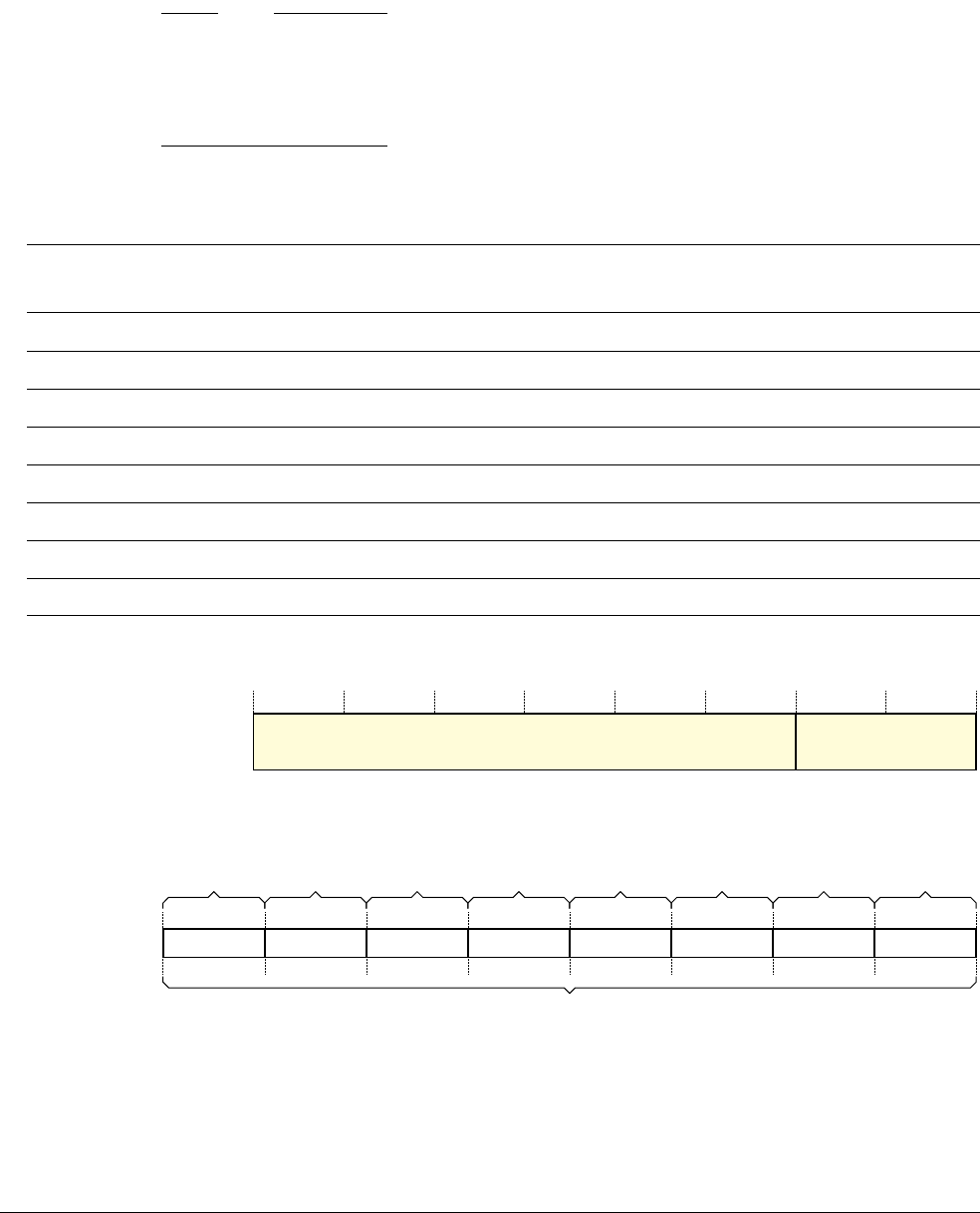
C11 The Debug Registers
C11.10 Management registers
C11-2208 Copyright © 1996-1998, 2000, 2004-2012, 2014 ARM. All rights reserved. ARM DDI 0406C.c
Non-Confidential ID051414
C11.10.2 About the Debug Peripheral Identification Registers
The Debug Peripheral Identification Registers provide standard information required by all components that
conform to the ARM Debug Interface v5 Architecture Specification, that implements the CoreSight identification
scheme. They identify a peripheral in a particular namespace.See also the CoreSight Architecture Specification.
Note
• ARMv7 only defines Debug Peripheral ID Registers 0 to 4, and reserves space for Debug Peripheral ID
Registers 5 to 7.
• The register offset order of the Debug Peripheral ID Registers does not match the numerical order ID0 to ID7,
see Table C11-11.
Table C11-11 lists the Debug Peripheral Identification Registers in register offset order.
Only bits[7:0] of each Debug Peripheral ID Register are used. This means that the bit assignments of each register
are:
Software can consider the eight Debug Peripheral ID Registers as defining a single 64-bit Peripheral ID, as shown
in Figure C11-1.
Figure C11-1 Mapping between Debug Peripheral ID Registers and a 64-bit Peripheral ID value
Figure C11-2 on page C11-2209 shows the fields in the 64-bit Peripheral ID value, and includes the field values for
fields that:
• Have fixed values, including the bits that are reserved, RAZ.
• Have fixed values in an implementation that is designed by ARM.
Table C11-11 Debug Peripheral Identification Registers
Register
offset Description Reference
0xFD0
Debug Peripheral ID4 DBGPID4, Debug Peripheral ID Register 4 on page C11-2279
0xFD4
Reserved for Debug Peripheral ID5, DBGPID5 -
0xFD8
Reserved for Debug Peripheral ID6, DBGPID6 -
0xFDC
Reserved for Debug Peripheral ID7, DBGPID7 -
0xFE0
Debug Peripheral ID0 DBGPID0, Debug Peripheral ID Register 0 on page C11-2275
0xFE4
Debug Peripheral ID1 DBGPID1, Debug Peripheral ID Register 1 on page C11-2276
0xFE8
Debug Peripheral ID2 DBGPID2, Debug Peripheral ID Register 2 on page C11-2277
0xFEC
Debug Peripheral ID3 DBGPID3, Debug Peripheral ID Register 3 on page C11-2278
Reserved, UNK
31 8 7 0
Peripheral ID data
0
Actual Peripheral ID Register fields
DBGPID0
707070707070707
DBGPID1DBGPID2DBGPID3DBGPID4DBGPID5DBGPID6
DBGPID7
63 16 15 8 0724 2332 3140 3948 4756 55
Conceptual 64-bit Peripheral ID

C11 The Debug Registers
C11.10 Management registers
ARM DDI 0406C.c Copyright © 1996-1998, 2000, 2004-2012, 2014 ARM. All rights reserved. C11-2209
ID051414 Non-Confidential
For more information about the fields and their values see Table C11-12.
Figure C11-2 Peripheral ID fields, with values for a implementation designed by ARM
Table C11-12 shows the fields in the Peripheral ID.
A component is identified uniquely by the combination of the following fields:
• JEP106 continuation code.
• JEP106 identity code.
• Part number.
• Revision.
• Customer Modified.
• RevAnd.
0 00 0 0 0 0 0 0 00 0 0 0 0 0 0 00 0 0 0 0 0 0 00 0 0 1 0 0 1 0 1 1 11 0 1
Conceptual 64-bit Peripheral ID
70 07
Reserved, RAZ
DBGPID0DBGPID1DBGPID2DBGPID3DBGPID4DBGPID5DBGPID6DBGPID7
Part number
JEP106
ID code
4KB
count
RevAnd
JEP106
Continuation code
Customer
modified
Revision
63 0
43070707070707 2343434
Uses JEP106 ID code
Table C11-12 Fields in the Debug Peripheral Identification Registers
Name Size Description Register
4KB count 4 bits Log2 of the number of 4KB blocks occupied by the implementation. In an ARMv7
implementation, the debug registers occupy a single 4KB block, so this field is always
0x0
.
DBGPID4
JEP106 code 4+7
bits
Identifies the designer of the implementation. This value consists of:
a 4-bit continuation code, also described as the bank number
a 7-bit identification code.
For implementations designed by ARM, the continuation code is
0x4
, indicating bank 5, and
the identity code is
0x3B
.
For more information, see JEP106, Standard Manufacturers Identification Code.
DBGPID1,
DBGPID2,
DBGPID4
RevAnd 4 bits Manufacturing revision number. Indicates a late modification to the implementation, usually
as a result of an Engineering Change Order (ECO).
This field starts at
0x0
and is incremented by the integrated circuit manufacturer on metal
fixes.
DBGPID3
Customer
modified
4 bits Indicates an endorsed modification to the implementation.
If the system designer cannot modify the implementation supplied by the implementation
designer then this field is RAZ.
DBGPID3
Revision 4 bits Revision number for the implementation.
Starts at
0x0
and increments by 1 at both major and minor revisions.
DBGPID2
Uses JEP106
ID code
1 bit This bit is set to 1 when a JEP106 identification code is used.
This bit must be 1 on all ARMv7 implementations.
DBGPID2
Part number 12 bits Part number for the implementation. Each organization designing to the ARM Debug
architecture specification keeps its own part number list.
DBGPID0,
DBGPID1
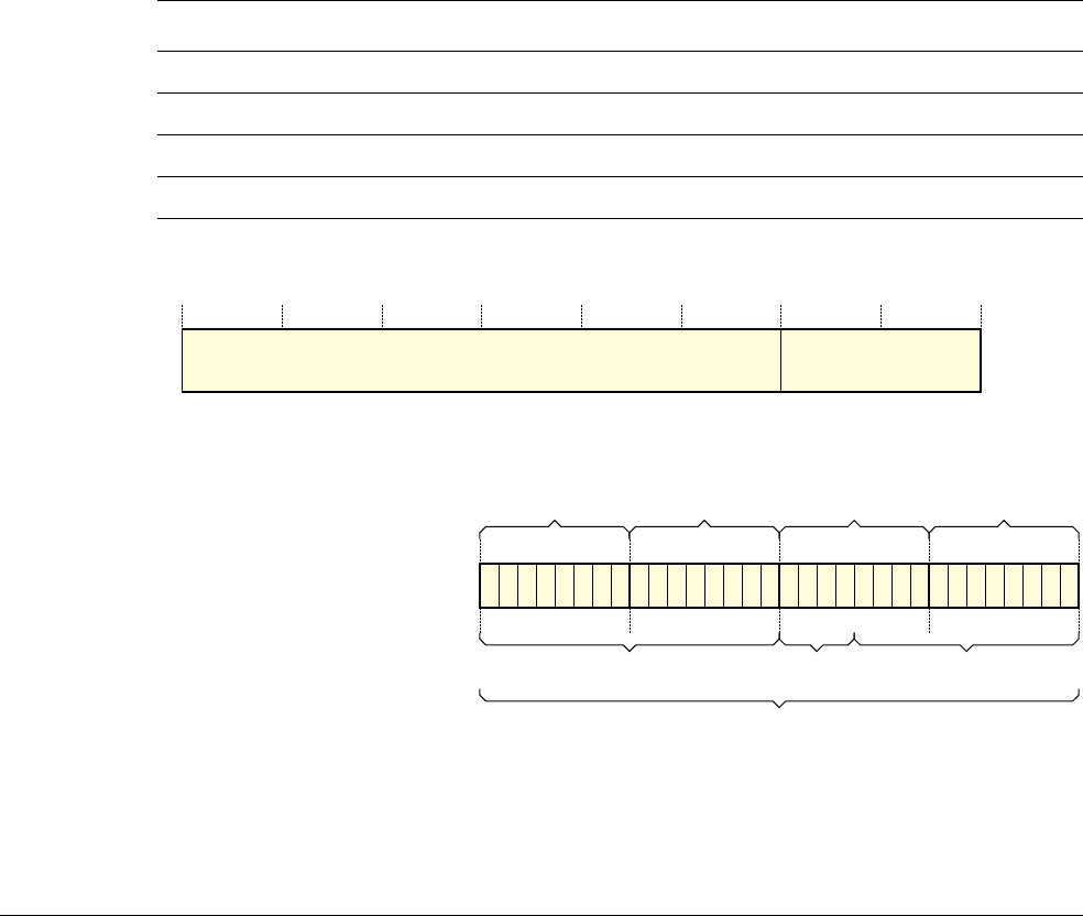
C11 The Debug Registers
C11.10 Management registers
C11-2210 Copyright © 1996-1998, 2000, 2004-2012, 2014 ARM. All rights reserved. ARM DDI 0406C.c
Non-Confidential ID051414
For components with a Component class of
0x9
, Debug component, indicated by the Component Identification
Registers, multiple components can have the same Part number, provided each component has a different CoreSight
Device type. However, ARM strongly recommends that each device has a unique Part number. For more
information:
• About the Component Identification Registers, see About the Debug Component Identification Registers.
• About the CoreSight Device type, see DBGDEVTYPE, Device Type Register on page C11-2230.
• About CoreSight components and their identification, see the ARM Debug Interface v5 Architecture
Specification.
C11.10.3 About the Debug Component Identification Registers
The Debug Component Identification Registers identify the processor as an ARM Debug Interface v5 component.
For more information, see the ARM Debug Interface v5 Architecture Specification and the CoreSight Architecture
Specification.
The Debug Component Identification Registers occupy the last four words of the 4KB block of debug registers, see
Table C11-1 on page C11-2195:
Table C11-13 lists the Debug Component Identification Registers, in register offset order.
Only bits[7:0] of each Debug Component ID Register are used. This means that the bit assignments of each register
are:
Software can consider the four Debug Component ID Registers as defining a single 32-bit Component ID, as shown
in Figure C11-3. The value of this Component ID is fixed.
Figure C11-3 Mapping between Debug Component ID Registers and the 32-bit Component ID value
Table C11-13 Debug Component Identification Registers
Register offset Description Reference
0xFF0
Debug Component ID0 DBGCID0, Debug Component ID Register 0 on page C11-2220
0xFF4
Debug Component ID1 DBGCID1, Debug Component ID Register 1 on page C11-2221
0xFF8
Debug Component ID2 DBGCID2, Debug Component ID Register 2 on page C11-2222
0xFFC
Debug Component ID3 DBGCID3, Debug Component ID Register 3 on page C11-2222
Reserved, UNK
31 8 7 0
Component ID data
DBGCID3
Conceptual 32-bit component ID
Actual ComponentID register fields DBGCID2 DBGCID1 DBGCID0
Component ID
Preamble
10110001000001011001000000001101
70707070
31 2423 1615 8 7 01211
Preamble
34
Component
class
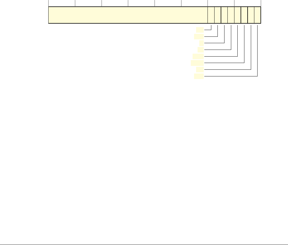
C11 The Debug Registers
C11.11 Register descriptions, in register order
ARM DDI 0406C.c Copyright © 1996-1998, 2000, 2004-2012, 2014 ARM. All rights reserved. C11-2211
ID051414 Non-Confidential
C11.11 Register descriptions, in register order
The subsections in this section describe each of the debug registers. Registers are shown in register name order.
C11.11.1 DBGAUTHSTATUS, Authentication Status register
The DBGAUTHSTATUS register characteristics are:
Purpose Indicates the implemented debug authentication features and provides the current values of
the configuration inputs that determine the debug permissions.
Usage constraints There are no usage constraints.
Configurations This register is required in all implementations.
If external debug over powerdown is supported, this register must be implemented in the
debug power domain.
Some bit assignments differ if the implementation includes the Security Extensions. See the
field descriptions for details.
Attributes A 32-bit RO register. DBGAUTHSTATUS is in the Other Debug management registers
group, see the registers summary in Table C11-10 on page C11-2207.
In an implementation that includes the Security Extensions, the DBGAUTHSTATUS register bit assignments are:
Bits[31:8] Reserved, UNK.
SNI, bit[7] Secure non-invasive debug features implemented. This bit is RAO, Secure non-invasive debug
features are implemented.
SNE, bit[6] Secure non-invasive debug enabled. This bit indicates whether non-invasive debug is permitted in
Secure PL1 modes. If the implementation includes the recommended external debug interface it
indicates the logical result of:
(DBGEN OR NIDEN) AND (SPIDEN OR SPNIDEN).
SI, bit[5] Secure invasive debug features implemented. This bit is RAO, Secure invasive debug features are
implemented.
SE, bit[4] Secure invasive debug enabled.This bit indicates whether invasive halting debug is permitted in
Secure PL1 modes. If the implementation includes the recommended external debug interface it
indicates the logical result of (DBGEN AND SPIDEN).
NSNI, bit[3] Non-secure non-invasive debug features implemented. This bit is RAO, Non-secure non-invasive
debug features are implemented.
NSNE, bit[2] Non-secure non-invasive debug enabled. If the implementation includes the recommended external
debug interface it indicates the logical result of (DBGEN OR NIDEN)
NSI, bit[1] Non-secure invasive debug features implemented. This bit is RAO, Non-secure invasive debug
features are implemented.
Reserved, UNK
31 876543210
1 1 1 1
SNI
SNE
SI
SE
NSNI
NSNE
NSI
NSE

C11 The Debug Registers
C11.11 Register descriptions, in register order
C11-2212 Copyright © 1996-1998, 2000, 2004-2012, 2014 ARM. All rights reserved. ARM DDI 0406C.c
Non-Confidential ID051414
NSE, bit[0] Non-secure invasive debug enabled. If the implementation includes the recommended external
debug interface it indicates the logical state of the DBGEN signal.
In an implementation that does not include the Security Extensions, the DBGAUTHSTATUS register bit
assignments are:
Bits[31:8] Reserved, UNK.
SNI, bit[7] Secure non-invasive debug features implemented. This bit is RAO, Secure non-invasive debug
features are implemented.
SNE, bit[6] Secure non-invasive debug enabled. If the implementation includes the recommended external
debug interface it indicates the logical result of (DBGEN OR NIDEN).
SI, bit[5] Secure invasive debug features implemented. This bit reads is RAO, Secure invasive debug features
are implemented.
SE, bit[4] Secure invasive debug enabled. If the implementation includes the recommended external debug
interface it indicates the logical state of the DBGEN signal.
NSNI, bit[3] Non-secure non-invasive debug features implemented. This bit is RAZ, Non-secure non-invasive
debug features are not implemented.
NSNE, bit[2] Non-secure non-invasive debug enabled bit. This bit is RAZ.
NSI, bit[1] Non-secure invasive debug features implemented. This bit is RAZ, Non-secure invasive debug
features are not implemented.
NSE, bit[0] Non-secure invasive debug enabled. This bit is RAZ.
Note
If a processor does not implement the Security Extensions, it does not recognize the existence of two security states
and is described as:
• Implementing Secure debug features.
• Not implementing any Non-secure debug features.
0Reserved, UNK
31 876543210
1 1 0 0 0
SNI
SNE
SI
SE
NSNI
NSNE
NSI
NSE
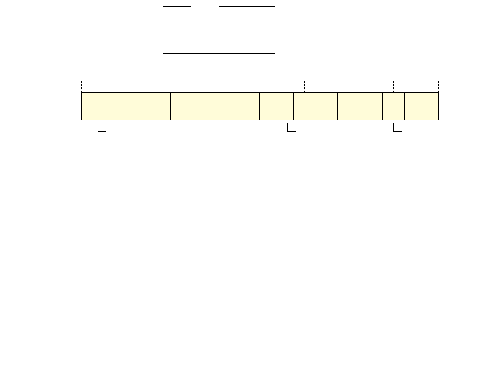
C11 The Debug Registers
C11.11 Register descriptions, in register order
ARM DDI 0406C.c Copyright © 1996-1998, 2000, 2004-2012, 2014 ARM. All rights reserved. C11-2213
ID051414 Non-Confidential
C11.11.2 DBGBCR, Breakpoint Control Registers
The DBGBCR characteristics are:
Purpose Holds control information for a breakpoint.
Used in conjunction with a Breakpoint Value Register, DBGBVR. DBGBVRn is associated
with DBGBCRn to form breakpoint n.
If the implementation includes the Virtualization Extensions, and this breakpoint supports
Context matching, DBGBVR can be associated with a Breakpoint Extended Value Register,
DBGBXVR, for VMID matching.
Usage constraints Some breakpoints might not support Context matching. For more information, see the
description of the DBGDIDR.CTX_CMPs field.
Configurations These registers are required in all implementations.
The number of breakpoints is IMPLEMENTATION DEFINED, between 2 and 16, and is
specified by the DBGDIDR.BRPs field. Any registers that are not implemented are
reserved.
Some bit assignments differ if the implementation includes the Security Extensions and the
Virtualization Extensions. See the field descriptions for details.
Attributes A 32-bit RW register. DBGBCR is in the Software debug event registers group, see the
registers summary in Table C11-5 on page C11-2201.
The debug logic reset value of a DBGBCR is UNKNOWN.
Note
After a debug logic reset a debugger must ensure that DBGBCR.E has a defined value for
all implemented registers before it programs DBGDSCR.MDBGen or
DBGDSCR.HDBGen to enable Monitor debug-mode or Halting debug-mode.
The DBGBCR bit assignments are:
Bits[31:29, 12:9, 4:3]
Reserved, UNK/SBZP.
MASK, bits[28:24]
Address range mask. Whether masking is supported is IMPLEMENTATION DEFINED.
If an implementation does not support address range masking then this field is RAZ /WI if either of
the following applies:
• The DBGDEVID register is not implemented.
• The DBGDEVID register is implemented, and DBGDEVID.{CIDmask, BPAddrMask} are
both RAZ.
Otherwise:
• If the implementation does not support either Context ID masking or address range masking,
this field is UNK/SBZP.
• If Context ID masking is supported, but address range masking is not, then for breakpoints
that do not support Context matching, this field is UNK/SBZP.
(0)(0) (0)(0) E
31 29 28 24 23 20 19 16 15 14 13 9 8 5 4 3 2 1 0
MASK BT LBN SSC Reserved,
UNK/SBZP BAS (0) PMC
12
Reserved ReservedHMC

C11 The Debug Registers
C11.11 Register descriptions, in register order
C11-2214 Copyright © 1996-1998, 2000, 2004-2012, 2014 ARM. All rights reserved. ARM DDI 0406C.c
Non-Confidential ID051414
If address range masking is supported, this field can set a breakpoint on a range of addresses by
masking lower order address bits out of the breakpoint comparison. The value of this field is the
number of low order bits of the address that are masked off, except that values of 1 and 2 are
reserved. Therefore, the meaning of the address range mask values for address breakpoints are:
0b00000
No mask.
0b00001
Reserved.
0b00010
Reserved.
0b00011
0x00000007
mask for instruction address, three bits masked.
0b00100
0x0000000F
mask for instruction address, four bits masked.
0b00101
0x0000001F
mask for instruction address, five bits masked.
.
.
.
0b11111
0x7FFFFFFF
mask for instruction address, 31 bits masked.
If Context ID masking is supported, this field can mask the bottom 8 bits from a CONTEXTIDR
comparison. The meaning of the address range mask values for Context matching breakpoints are:
0b00000
No mask.
0b01000
0x000000FF
mask for CONTEXTIDR, eight bits masked.
All other values are reserved.
ARM deprecates the use of Context ID masking when the implementation includes the Large
Physical Address Extension.
A debugger must program this field to
0b00000
if either:
• This breakpoint is programmed for Context matching, and either Context ID masking is not
supported or only the VMID value is being compared.
• The Byte address select field is programmed to a value other than
0b1111
.
If this is not done, the generation of debug events by this breakpoint is UNPREDICTABLE.
If this field is not zero, the DBGBVR bits that are not included in the comparison must be zero,
otherwise the generation of debug events by this breakpoint is UNPREDICTABLE.
For more information about the use of this field see Breakpoint address range masking behavior on
page C3-2051 and Context matching comparisons for debug event generation on page C3-2053.
BT, bits[23:20]
Breakpoint type. This field controls the behavior of debug event generation. This includes the
meaning of the value held in the associated DBGBVR, indicating whether it is an instruction address
match or mismatch or a Context match. It also controls whether the breakpoint is linked to another
breakpoint.
Breakpoint types on page C11-2216 gives the permitted values of this field.
For more information about instruction address matching and mismatching see:
•Byte address selection behavior on instruction address match or mismatch on page C3-2049.
•Breakpoint address range masking behavior on page C3-2051.
•Instruction address comparisons in different instruction set states on page C3-2051.
See Breakpoint types on page C11-2216 for detailed descriptions of the different Breakpoint types.
Reading this register returns an UNKNOWN value for this field, and the generation of debug events
by this breakpoint is UNPREDICTABLE if this field is programmed to a value that is reserved or is not
supported by this breakpoint.
LBN bits[19:16]
Linked breakpoint number. If this breakpoint is programmed for Linked instruction address match
or mismatch then this field must be programmed with the number of the breakpoint that holds the
Context match to be used in the combined instruction address and Context comparison. Otherwise,
this field must be programmed to
0b0000
.

C11 The Debug Registers
C11.11 Register descriptions, in register order
ARM DDI 0406C.c Copyright © 1996-1998, 2000, 2004-2012, 2014 ARM. All rights reserved. C11-2215
ID051414 Non-Confidential
Reading this register returns an UNKNOWN value for this field, and the generation of debug events
by this breakpoint is UNPREDICTABLE, if either:
• This breakpoint is not programmed for Linked instruction address match or mismatch and
this field is not programmed to
0b0000
.
• This breakpoint is programmed for Linked instruction address match or mismatch and the
breakpoint indicated by this field does not support Context matching or is not programmed
for Linked Context matching, or does not exist.
See also Generation of debug events on page C3-2076.
SSC, bits[15:14], Implementation includes the Security Extensions
Security state control. In an implementation that includes the Security Extensions, this field enables
the breakpoint to be conditional on the security state of the processor.
This field is used with the HMC, Hyp mode control, and PMC, Privileged mode control, fields. See
Breakpoint state control fields on page C11-2217 for possible values.
This field must be programmed to
0b00
if DBGBCR.BT is programmed for Linked Context match.
If this is not done, the generation of debug events by this breakpoint is UNPREDICTABLE.
Note
When this field is set to a value other than
0b00
, the SSC field controls the processor security state
in which the access matches, not the required security attribute of the access.
See also Generation of debug events on page C3-2076.
Bits[15:14], Implementation does not include the Security Extensions
Reserved, UNK/SBZP.
HMC, bit[13], Implementation includes the Virtualization Extensions
Hyp mode control bit.
This field is used with the SSC, Security state control, and PMC, Privileged mode control, fields.
See Breakpoint state control fields on page C11-2217 for possible values.
This field must be programmed to 0 if DBGBCR.BT is programmed for Linked Context match. If
this is not done, the generation of debug events by this breakpoint is UNPREDICTABLE.
Bit[13], Implementation does not include the Virtualization Extensions
Reserved, UNK/SBZP.
BAS, bits[8:5] Byte address select. This field enables match or mismatch comparisons on only certain bytes of the
word address held in the DBGBVR. The operation of this field depends also on:
• The Breakpoint type field being programmed for instruction address match or mismatch.
• The MASK field being programmed to
0b00000
, no mask.
• The instruction set state of the processor, indicated by the CPSR.{J, T} bits.
For details of the use of this field see Byte address selection behavior on instruction address match
or mismatch on page C3-2049.
This field must be programmed to
0b1111
if either:
•DBGBCR.BT is programmed for Linked or Unlinked Context ID match.
•DBGBCR.MASK is programmed to a value other than
0b00000
.
If this is not done, the generation of debug events by this breakpoint is UNPREDICTABLE.

C11 The Debug Registers
C11.11 Register descriptions, in register order
C11-2216 Copyright © 1996-1998, 2000, 2004-2012, 2014 ARM. All rights reserved. ARM DDI 0406C.c
Non-Confidential ID051414
PMC, bits[2:1]
Privileged mode control. This field enables breakpoint matching conditional on the mode of the
processor.
This field is used with the SSC, Security state control, and HMC, Hyp mode control, fields. See
Breakpoint state control fields on page C11-2217 for possible values.
This field must be programmed to
0b11
if DBGBCR.BT is programmed for Linked Context match.
If this is not done, the generation of debug events by this breakpoint is UNPREDICTABLE.
E, bit[0] Breakpoint enable. The meaning of this bit is:
0 Breakpoint disabled.
1 Breakpoint enabled.
A breakpoint never generates debug events when it is disabled.
Breakpoint types
DBGBCR.BT, the Breakpoint type field, determines the type of comparison made by the breakpoint. Table C11-14
shows the permitted values of this field, and their meanings.
All values of BT not shown in Table C11-14 are reserved.
Breakpoint debug events on page C3-2041 describes the generation of the different breakpoint types. In particular,
Breakpoint types defined by the DBGBCR on page C3-2042 gives more information about each breakpoint type, and
identifies the subsections of Chapter C3 that describe that breakpoint type.
Table C11-14 Breakpoint types
DBGBCR.BT Breakpoint type Notes
0b0000
Unlinked instruction address match -
0b0001
Linked instruction address match -
0b0010
Unlinked Context ID match -
0b0011
Linked Context ID match -
0b0100
Unlinked instruction address mismatch -
0b0101
Linked instruction address mismatch -
0b1000
Unlinked VMID match Requires Virtualization Extensionsa
a. Only supported if the implementation includes the Virtualization Extensions. Otherwise, the BT value is reserved
0b1001
Linked VMID match Requires Virtualization Extensionsa
0b1010
Unlinked VMID match and Context ID match Requires Virtualization Extensionsa
0b1011
Linked VMID match and Context ID match Requires Virtualization Extensionsa

C11 The Debug Registers
C11.11 Register descriptions, in register order
ARM DDI 0406C.c Copyright © 1996-1998, 2000, 2004-2012, 2014 ARM. All rights reserved. C11-2217
ID051414 Non-Confidential
Breakpoint state control fields
Breakpoint debug event generation can be made conditional on the current state of the processor. The following
fields in DBGBCR control the checks on the current state:
• SSC, Security state control, only if the implementation includes the Security extensions.
• HMC, Hyp mode control, only if the implementation includes the Virtualization Extensions.
• PMC, Privileged mode control.
Table C11-15 shows the possible values of the fields, and the modes and security states that can be tested.
Note
All other combinations of values are Reserved, and the generation of Breakpoint debug events by this breakpoint is
UNPREDICTABLE if used.
Table C11-15 Breakpoint state control
SSC HMC PMC Secure modes Non-secure modes
0b00 0 0b00
PL0, Supervisor and System modes only PL0, Supervisor and System modes only
0b00 0 0b01
PL1 modes only PL1 modes only
0b00 0 0b10
PL0 mode only PL0 mode only
0b00 0 0b11
All modes PL1 and PL0 modes only
0b00 1 0b01
PL1 modes only PL2 and PL1 modes only
0b00 1 0b11
All modes All modes
0b01 0 0b00
- PL0, Supervisor and System modes only
0b01 0 0b01
- PL1 modes only
0b01 0 0b10
- PL0 mode only
0b01 0 0b11
- PL1 and PL0 modes only
0b01 1 0b01
- PL2 and PL1 modes only
0b01 1 0b11
- All modes
0b10 0 0b00
PL0, Supervisor and System modes only -
0b10 0 0b01
PL1 modes only -
0b10 0 0b10
PL0 mode only -
0b10 0 0b11
All modes -
0b11 1 0b00
- PL2 mode only

C11 The Debug Registers
C11.11 Register descriptions, in register order
C11-2218 Copyright © 1996-1998, 2000, 2004-2012, 2014 ARM. All rights reserved. ARM DDI 0406C.c
Non-Confidential ID051414
C11.11.3 DBGBVR, Breakpoint Value Registers
The DBGBVR characteristics are:
Purpose Holds a value for use in breakpoint matching, either the virtual address of an instruction, or
a Context ID.
Used in conjunction with a Breakpoint Control Register, DBGBCR. DBGBVRn is
associated with DBGBCRn to form breakpoint n.
If the implementation includes the Virtualization Extensions, and this breakpoint supports
Context matching, DBGBVR can be associated with a Breakpoint Extended Value Register,
DBGBXVR, for Context matching.
Usage constraints Some breakpoints might not support Context matching. For more information, see the
description of the DBGDIDR.CTX_CMPs field.
Configurations These registers are required in all implementations.
The number of breakpoints is IMPLEMENTATION DEFINED, between 2 and 16, and is
specified by the DBGDIDR.BRPs field. Any registers that are not implemented are
reserved.
Attributes A 32-bit RW register. DBGBVR is in the Software debug event registers group, see the
registers summary in Table C11-5 on page C11-2201.
The debug logic reset value of a DBGBVR is UNKNOWN.
When used for address comparison the DBGBVR bit assignments are:
When used for Context ID comparison the DBGBVR bit assignments are:
Bits[31:2], when register is used for address comparison
Bits[31:2] of the virtual address value for comparison.
When breakpoint address range masking is used, the masked bits of the address must be set to 0,
otherwise the generation of Breakpoint debug events by this breakpoint is UNPREDICTABLE. For
more information, see Breakpoint address range masking behavior on page C3-2051.
Bits[1:0], when register used for address comparison
Must be written as
0b00
, otherwise the generation of Breakpoint debug events by this breakpoint is
UNPREDICTABLE.
Bits[31:0], when register used for Context ID comparison
Bits[31:0] of the value for comparison, ContextID[31:0].
When Context ID masking is used, bits[7:0] of this value must be set to 0, otherwise the generation
of debug events by this breakpoint is UNPREDICTABLE. For more information, see Condition for
breakpoint generation on Context ID match in a VMSA implementation on page C3-2054.
If the breakpoint does not support Context matching then bits[1:0] are UNK/SBZP.
If the implementation includes the Virtualization Extensions, and if the breakpoint is configured for VMID
comparison without Context ID comparison, DBGBVR must be programmed as zero. Otherwise the generation of
debug events by this breakpoint is UNPREDICTABLE.
The debug logic generates a debug event when an instruction that matches the breakpoint is committed for
execution. For more information, see Breakpoint debug events on page C3-2041.
0Instruction address[31:2]
31 210
0
ContextID[31:0]
31 0

C11 The Debug Registers
C11.11 Register descriptions, in register order
ARM DDI 0406C.c Copyright © 1996-1998, 2000, 2004-2012, 2014 ARM. All rights reserved. C11-2219
ID051414 Non-Confidential
C11.11.4 DBGBXVR, Breakpoint Extended Value Registers
The DBGBXVR characteristics are:
Purpose Holds a value for use in breakpoint matching, to support VMID matching.
Used in conjunction with a Breakpoint Control Register DBGBCR, and a Breakpoint Value
Register DBGBVR.
Usage constraints There are no usage constraints.
Configurations In v7 Debug, these registers are not implemented.
In v7.1 Debug, these registers are only implemented if the implementation includes the
Virtualization Extensions. In this case, DBGBXVR is implemented only for breakpoints
that support Context matching.
The total number of breakpoints is IMPLEMENTATION DEFINED, between 2 and 16, and is
specified by the DBGDIDR.BRPs field.
The number of Breakpoint Extended Value Registers is IMPLEMENTATION DEFINED, and is
specified by the DBGDIDR.CTX_CMPs field. Any registers that are not implemented are
reserved.
Attributes A 32-bit RW register. DBGBXVR is in the Software debug event registers group, see the
registers summary in Table C11-5 on page C11-2201.
The DBGBXVR bit assignments are:
Bits[31:8],
Reserved, UNK/SBZP.
VMID, bit[7:0]
VMID value. Compared with VTTBR.VMID, the virtual machine identifier field.
The debug logic generates a debug event when an instruction that matches the breakpoint is committed for
execution. For more information, see Context matching comparisons for debug event generation on page C3-2053.
Reserved, UNK/SBZP
31 8 7 0
VMID
C11 The Debug Registers
C11.11 Register descriptions, in register order
C11-2220 Copyright © 1996-1998, 2000, 2004-2012, 2014 ARM. All rights reserved. ARM DDI 0406C.c
Non-Confidential ID051414
C11.11.5 DBGCID0, Debug Component ID Register 0
The DBGCID0 Register characteristics are:
Purpose Provides bits[7:0] of the 32-bit conceptual Component ID, see Figure C11-3 on
page C11-2210.
Usage constraints DBGCID0 is not visible in the CP14 interface.
Configurations This register is required in all implementations.
If external debug over powerdown is supported, this register can be implemented in either
or both power domains.
Attributes A 32-bit RO register. DBGCID0 is in the Other Debug management registers group, see the
registers summary in Table C11-10 on page C11-2207.
The DBGCID0 register bit assignments are:
Bits[31:8] Reserved, UNK.
Preamble byte 0, bits[7:0]
This byte has the value
0x0D
.
For more information, see About the Debug Component Identification Registers on page C11-2210.
110000 1Reserved, UNK
31 8 7 0
0
Preamble byte 0
C11 The Debug Registers
C11.11 Register descriptions, in register order
ARM DDI 0406C.c Copyright © 1996-1998, 2000, 2004-2012, 2014 ARM. All rights reserved. C11-2221
ID051414 Non-Confidential
C11.11.6 DBGCID1, Debug Component ID Register 1
The DBGCID1 Register characteristics are:
Purpose Provides bits[15:8] of the 32-bit conceptual Component ID, see Figure C11-3 on
page C11-2210.
Usage constraints DBGCID1 is not visible in the CP14 interface.
Configurations This register is required in all implementations.
If external debug over powerdown is supported, this register can be implemented in either
or both power domains.
Attributes A 32-bit RO register. DBGCID1 is in the Other Debug management registers group, see the
registers summary in Table C11-10 on page C11-2207.
The DBGCID1 register bit assignments are:
Bits[31:8] Reserved, UNK.
Component class, bits[7:4]
This field has the value
0x9
, indicating a debug component, with CoreSight architecture compliant
management registers.
Preamble, bits[3:0]
This field has the value
0x0
.
For more information, see About the Debug Component Identification Registers on page C11-2210.
001001 0Reserved, UNK
31 8 7 0
0
43
Preamble[11:8]
Component class
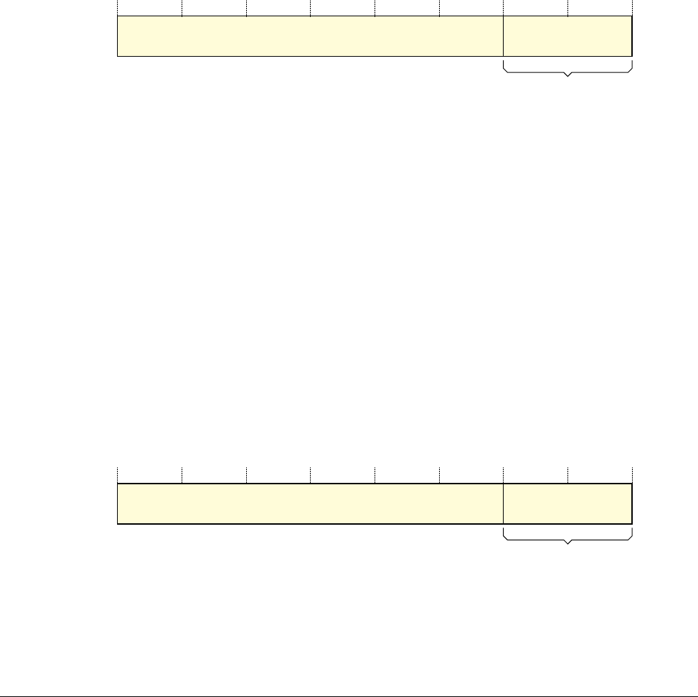
C11 The Debug Registers
C11.11 Register descriptions, in register order
C11-2222 Copyright © 1996-1998, 2000, 2004-2012, 2014 ARM. All rights reserved. ARM DDI 0406C.c
Non-Confidential ID051414
C11.11.7 DBGCID2, Debug Component ID Register 2
The DBGCID2 Register characteristics are:
Purpose Provides bits[23:16] of the 32-bit conceptual Component ID, see Figure C11-3 on
page C11-2210.
Usage constraints DBGCID2 is not visible in the CP14 interface.
Configurations This register is required in all implementations.
If external debug over powerdown is supported, this register can be implemented in either
or both power domains.
Attributes A 32-bit RO register. DBGCID2 is in the Other Debug management registers group, see the
registers summary in Table C11-10 on page C11-2207.
The DBGCID2 register bit assignments are:
Bits[31:8] Reserved, UNK.
Preamble byte 2, bits[7:0]
This field has the value
0x05
.
For more information, see About the Debug Component Identification Registers on page C11-2210.
C11.11.8 DBGCID3, Debug Component ID Register 3
The DBGCID3 Register characteristics are:
Purpose Provides bits[31:24] of the 32-bit conceptual Component ID, see Figure C11-3 on
page C11-2210.
Usage constraints DBGCID3 is not visible in the CP14 interface.
Configurations This register is required in all implementations.
If external debug over powerdown is supported, this register can be implemented in either
or both power domains.
Attributes A 32-bit RO register. DBGCID3 is in the Other Debug management registers group, see the
registers summary in Table C11-10 on page C11-2207.
The DBGCID3 register bit assignments are:
Bits[31:8] Reserved, UNK.
Preamble byte 3, bits[7:0]
This field has the value
0xB1
.
For more information, see About the Debug Component Identification Registers on page C11-2210.
100000 1Reserved, UNK
31 8 7 0
0
Preamble byte 2
001101 1Reserved, UNK
31 8 7 0
0
Preamble byte 3

C11 The Debug Registers
C11.11 Register descriptions, in register order
ARM DDI 0406C.c Copyright © 1996-1998, 2000, 2004-2012, 2014 ARM. All rights reserved. C11-2223
ID051414 Non-Confidential
C11.11.9 DBGCIDSR, Context ID Sampling Register
The DBGCIDSR characteristics are:
Purpose Samples the CONTEXTIDR whenever the DBGPCSR samples the program counter. This
enables a debugger to associate a program counter sample with the process running on the
processor.
The DBGCIDSR is a Sample-based profiling register.
Usage constraints Used in conjunction with the DBGPCSR.
DBGCIDSR is not visible in the CP14 interface.
Configurations Implementation of the Sample-based profiling extension is OPTIONAL. In an implementation
that includes the Sample-based profiling extension:
• in a v7 Debug implementation, it is IMPLEMENTATION DEFINED whether DBGCIDSR
is implemented
• in a v7.1 Debug implementation, DBGCIDSR must be implemented.
When implemented, DBGCIDSR is debug register 41.
An implementation that does not include the Sample-based profiling extension cannot
implement DBGCIDSR.
When DBGCIDSR is not implemented, debug register 41 is reserved.
Attributes A 32-bit RO register. DBGCIDSR is in the Sample-based profiling registers group, see the
registers summary in Table C11-6 on page C11-2202.
The non-debug logic reset value of the DBGCIDSR is UNKNOWN.
The DBGCIDSR bit assignments are:
CONTEXTIDR sample value, bits[31:0]
The value of the Context ID Register, CONTEXTIDR, associated with the last PC sample read from
DBGPCSR.
The implemented Sample-based profiling registers on page C10-2190 describes the Sample-based profiling
implementation options, and how software can determine whether and how the Sample-based profiling registers are
implemented.
For more information about program counter sampling, see Sample-based profiling on page C10-2190.
CONTEXTIDR sample value
31 0

C11 The Debug Registers
C11.11 Register descriptions, in register order
C11-2224 Copyright © 1996-1998, 2000, 2004-2012, 2014 ARM. All rights reserved. ARM DDI 0406C.c
Non-Confidential ID051414
C11.11.10 DBGCLAIMCLR, Claim Tag Clear register
The DBGCLAIMCLR register characteristics are:
Purpose Used by software to read the values of the CLAIM bits, and to clear these bits to zero.
Used in conjunction with the DBGCLAIMSET register.
Usage constraints The architecture does not define any functionality for the CLAIM bits.
Configurations This register is required in all implementations.
In v7 Debug, this register must be implemented in the debug power domain, if external
debug over powerdown is supported.
In v7.1 Debug, this register is implemented in the core power domain.
Attributes A 32-bit RW register. See the field descriptions for information about the reset value of the
register. DBGCLAIMCLR is in the Other Debug management registers group, see the
registers summary in Table C11-10 on page C11-2207.
The DBGCLAIMCLR register bit assignments are:
Bits[31:8] Reserved, RAZ/SBZ.
Software can rely on these bits reading-as-zero, and must use a should-be-zero policy on writes.
Implementations must ignore writes to these bits.
CLAIM, bits[7:0]
Writing a 1 to one of these bits clears the corresponding CLAIM bit to 0. A single write operation
can clear multiple bits to 0.
Writing 0 to one of these bits has no effect.
Reading the register returns the current values of these bits.
The debug logic reset value of these bits is 0.
For more information about the CLAIM bits and how they might be used, see DBGCLAIMSET, Claim Tag Set
register on page C11-2225.
Note
In v7.1 Debug, software routines for Save and Restore must include save and restore for the CLAIM bits.
Reserved, RAZ/SBZ
31 8 7 0
CLAIM

C11 The Debug Registers
C11.11 Register descriptions, in register order
ARM DDI 0406C.c Copyright © 1996-1998, 2000, 2004-2012, 2014 ARM. All rights reserved. C11-2225
ID051414 Non-Confidential
C11.11.11 DBGCLAIMSET, Claim Tag Set register
The DBGCLAIMSET register characteristics are:
Purpose Used by software to set CLAIM bits to 1.
Used in conjunction with the DBGCLAIMCLR Register.
Usage constraints The architecture does not define any functionality for the CLAIM bits.
Configurations This register is required in all implementations.
In v7 Debug, this register must be implemented in the debug power domain, if external
debug over powerdown is supported.
In v7.1 Debug, this register is implemented in the core power domain.
Attributes A 32-bit RW register. DBGCLAIMSET is in the Other Debug management registers group,
see the registers summary in Table C11-10 on page C11-2207.
The DBGCLAIMSET register bit assignments are:
Bits[31:8] Reserved, RAZ/SBZ.
Software can rely on these bits reading-as-zero, and must use a should-be-zero policy on writes.
Implementations must ignore writes to these bits.
CLAIM, bits[7:0]
Writing a 1 to one of these bits sets the corresponding CLAIM bit to 1. A single write operation can
set multiple bits to 1.
Writing 0 to one of these bits has no effect.
The CLAIM bits are RAO.
You must use the DBGCLAIMCLR register to:
• read the values of the CLAIM bits
• clear a CLAIM bit to 0.
If software reads this register, the bits that are set to 1 correspond to the implemented CLAIM bits. This enables a
debugger to identify the number of CLAIM bits that are implemented.
See DBGCLAIMCLR, Claim Tag Clear register on page C11-2224 for details of how to:
• clear CLAIM bits to 0
• read the current values of the CLAIM bits.
The CLAIM bits do not have any specific functionality. ARM expects the usage model to be that an external
debugger and a debug monitor can set specific bits to 1 to claim the corresponding debug resources.
Note
In v7.1 Debug, software routines for Save and Restore must include save and restore for the CLAIM bits.
Reserved, RAZ/SBZ
31 8 7 0
CLAIM
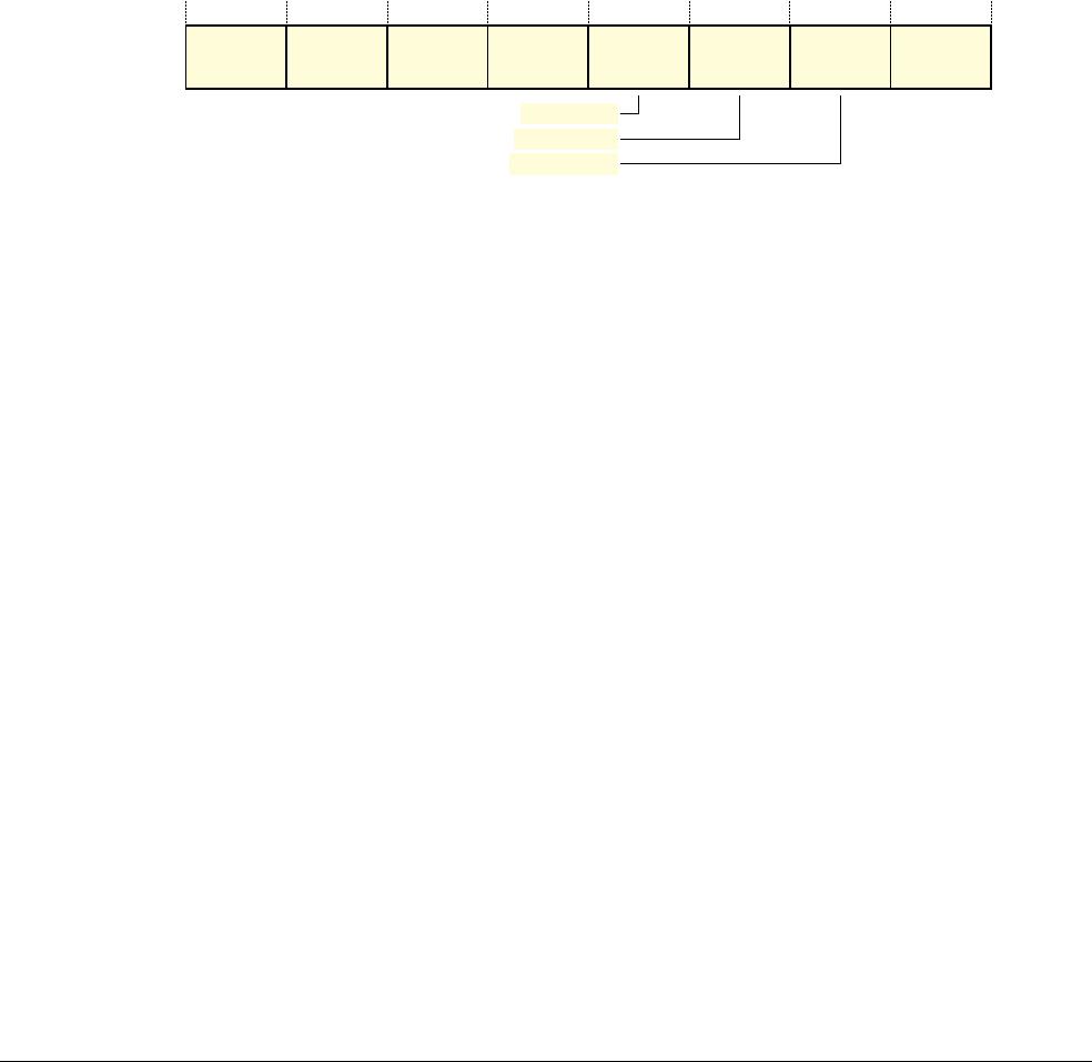
C11 The Debug Registers
C11.11 Register descriptions, in register order
C11-2226 Copyright © 1996-1998, 2000, 2004-2012, 2014 ARM. All rights reserved. ARM DDI 0406C.c
Non-Confidential ID051414
C11.11.12 DBGDEVID, Debug Device ID register
The DBGDEVID register characteristics are:
Purpose Adds to the information given by the DBGDIDR by describing other features of the debug
implementation.
Usage constraints There are no usage constraints.
Configurations In v7 Debug, this register is OPTIONAL in all implementations.
In v7.1 Debug, this register is required in all implementations.
If external debug over powerdown is supported, this register can be implemented in either
or both power domains.
Attributes A 32-bit RO register. DBGDEVID is in the Debug identification registers group, see the
registers summary in Table C11-2 on page C11-2198.
The DBGDEVID register bit assignments are:
CIDMask, bits[31:28]
This field indicates the level of support for the Context ID matching breakpoint masking capability.
The permitted values of this field are:
0b0000
Context ID masking is not implemented.
0b0001
Context ID masking is implemented. Only permitted in a VMSA implementation.
Other values are reserved.
See also the description of the BPAddrMask field.
AuxRegs, bits[27:24]
This field indicates the presence of the External Auxiliary Control Register, DBGEACR. The
permitted values of this field are:
0b0000
The DBGEACR is not present.
0b0001
The DBGEACR is present.
Other values are reserved.
In v7 Debug, this field must be
0b0000
.
In v7.1 Debug, this field can take either value.
DoubleLock, bits[23:20]
This field indicates the presence of the DBGOSDLR, OS Double Lock Register. The permitted
values of this field are:
0b0000
The DBGOSDLR is not present.
0b0001
The DBGOSDLR is present.
Other values are reserved.
In v7 Debug, this field must be
0b0000
.
In v7.1 Debug, this field must be
0b0001
.
CIDMask
31 28 27 24 23 20 19 16 15 12 11 8 7 4 3 0
AuxRegs DoubleLock VirtExtns PCsample
VectorCatch
BPAddrMask
WPAddrMask

C11 The Debug Registers
C11.11 Register descriptions, in register order
ARM DDI 0406C.c Copyright © 1996-1998, 2000, 2004-2012, 2014 ARM. All rights reserved. C11-2227
ID051414 Non-Confidential
VirtExtns, bits[19:16]
This field indicates whether the Virtualization Extensions to Debug are implemented. The permitted
values of this field are:
0b0000
The implementation does not include the Virtualization Extensions.
0b0001
The implementation includes the Virtualization Extensions.
Other values are reserved.
In v7 Debug, this field must be
0b0000
.
VectorCatch, bits[15:12]
This field defines the form of Vector catch debug event implemented. The permitted values of this
field are:
0b0000
Address matching form.
0b0001
Exception matching form.
Other values are reserved.
In v7 Debug, this field must be
0b0000
.
BPAddrMask, bits[11:8]
This field indicates the level of support for the IVA matching breakpoint masking capability. The
permitted values of this field are:
0b0000
Breakpoint address masking might be implemented.
0b0001
Breakpoint address masking is implemented.
0b1111
Breakpoint address masking is not implemented.
Other values are reserved.
In v7 Debug, all values listed in this description are permitted.
In v7.1 Debug:
• in an implementation that follows the ARM implementation recommendations, this field is
0b1111
• this field must not be
0b0000
.
If Breakpoint address masking is not implemented and Context ID masking is not implemented:
• if BPAddrMask is
0b0000
, then DBGBCRn.MASK is RAZ/WI
• if BPAddrMask is
0b1111
, then DBGBCRn.MASK is UNK/SBZP.
ARM deprecates the use of Breakpoint address masking, and recommends that implementations do
not include support for this feature.
WPAddrMask, bits[7:4]
This field indicates the level of support for the data VA matching watchpoint masking capability.
The permitted values of this field are:
0b0000
Watchpoint address masking may be implemented. If not implemented,
DBGWCRn.MASK is RAZ/WI.
0b0001
Watchpoint address masking is implemented.
0b1111
Watchpoint address masking is not implemented. DBGWCRn.MASK is UNK/SBZP.
Other values are reserved.
In v7 Debug, all values listed in this description are permitted.
In v7.1 Debug, this field must be
0b0001
.

C11 The Debug Registers
C11.11 Register descriptions, in register order
C11-2228 Copyright © 1996-1998, 2000, 2004-2012, 2014 ARM. All rights reserved. ARM DDI 0406C.c
Non-Confidential ID051414
PCsample, bits[3:0]
This field indicates the level of program counter sampling support using debug registers 40, 41, and
42. The permitted values of this field are:
0b0000
Program Counter Sampling Register, DBGPCSR, is not implemented as register 40,
Context ID Sampling Register, DBGCIDSR, and Virtualization ID Sampling Register,
DBGVIDSR, are not implemented.
0b0001
DBGPCSR is implemented as register 40. DBGCIDSR and DBGVIDSR are not
implemented.
0b0010
DBGPCSR is implemented as register 40, DBGCIDSR is implemented as register 41,
and DBGVIDSR is not implemented.
0b0011
DBGPCSR is implemented as register 40, DBGCIDSR is implemented as register 41,
and DBGVIDSR is implemented as register 42. Only permitted if the implementation
includes the Security Extensions.
Other values are reserved.
If an implementation does not include the Sample-based profiling extension, this field must be zero.
Otherwise:
• in v7 Debug, the permitted values are:
—
0b0001
or
0b0010
if the implementation does not include the Security Extensions
—
0b0001
,
0b0010
, or
0b0011
if the implementation includes the Security Extensions.
• in v7.1 Debug, the value must be:
—
0b0010
if the implementation does not include the Security Extensions
—
0b0011
if the implementation includes the Security Extensions.
Note
The DBGPCSR can be implemented as register 33, as register 40, or as both register 33 and register 40. The
DBGDEVID.PCsample field only indicates whether it is implemented as register 40. The implemented
Sample-based profiling registers on page C10-2190 describes the Sample-based profiling implementation options,
and how software can determine whether and how the Sample-based profiling registers are implemented.
The DBGDIDR.DEVID_imp bit indicates whether the DBGDEVID register is implemented, see DBGDIDR,
Debug ID Register on page C11-2231. If the DBGDEVID register is not implemented:
• the Program Counter Sampling Register, DBGPCSR, is not implemented as register 40
• the Context ID Sampling Register, DBGCIDSR, is not implemented
• the Virtualization ID Sampling Register, DBGVIDSR, is not implemented.
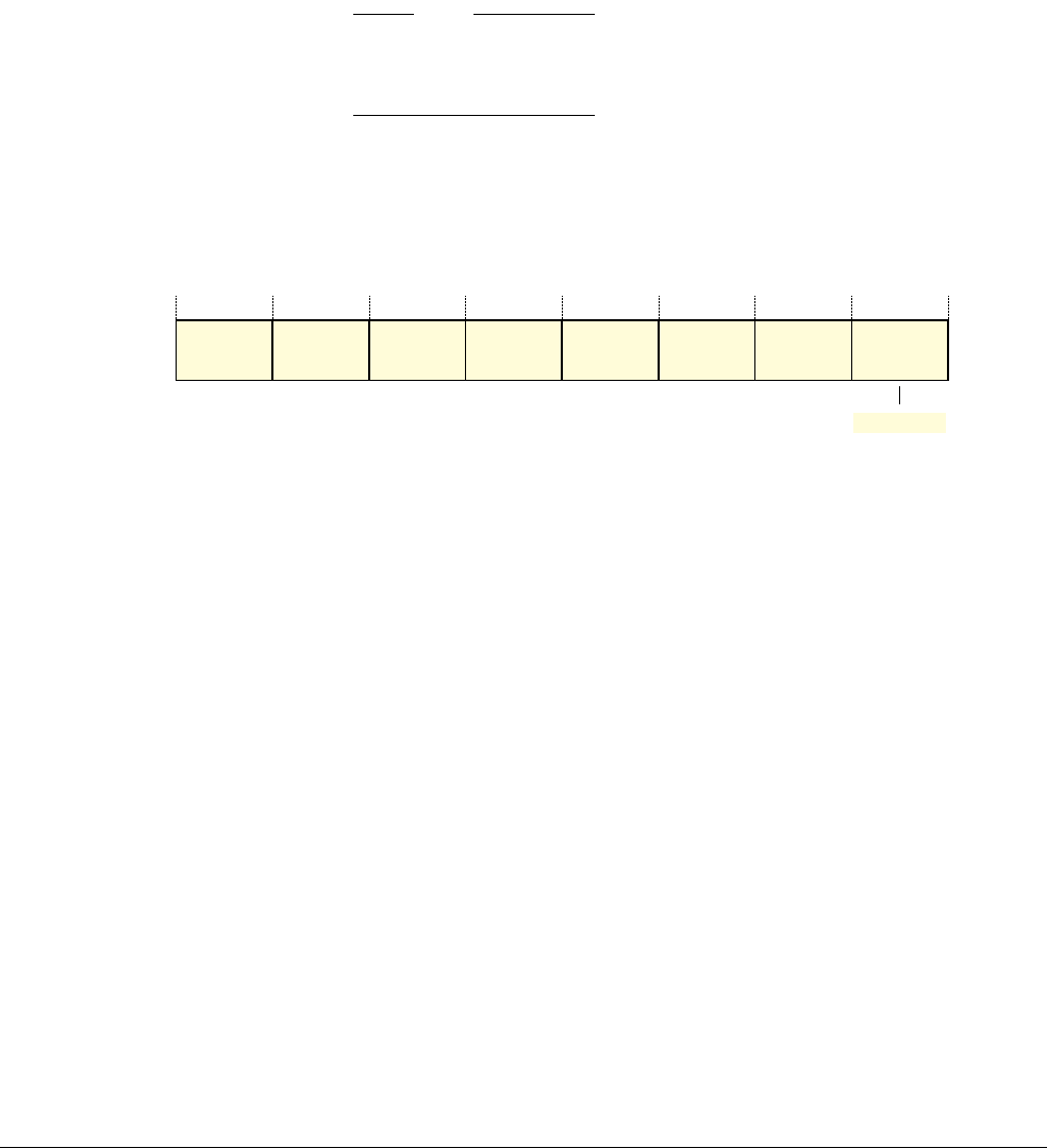
C11 The Debug Registers
C11.11 Register descriptions, in register order
ARM DDI 0406C.c Copyright © 1996-1998, 2000, 2004-2012, 2014 ARM. All rights reserved. C11-2229
ID051414 Non-Confidential
C11.11.13 DBGDEVID1, Debug Device ID register 1
The DBGDEVID1 characteristics are:
Purpose Adds to the information given by the DBGDIDR by describing other features of the debug
implementation.
Usage constraints There are no usage constraints.
Configurations In v7 Debug the CP14 access instruction that corresponds to this register is always
UNPREDICTABLE at PL1 or higher.
In v7.1 Debug, this register is required in all implementations.
Note
This register is first described in issue C.a of this manual. This means its location was
previously reserved, UNK/SBZP in the memory-mapped interface and in the external debug
interface.
If external debug over powerdown is supported, this register can be implemented in either
or both power domains.
Attributes A 32-bit RO register. DBGDEVID1 is in the Debug identification registers group, see the
registers summary in Table C11-2 on page C11-2198.
The DBGDEVID1 bit assignments are:
Bits[31:4] Reserved, UNK.
PCSROffset, bits[3:0]
This field defines the offset applied to DBGPCSR samples. The permitted values of this field are:
0b0000
DBGPCSR samples are offset by a value that depends on the instruction set state.
0b0001
No offset is applied to the DBGPCSR samples.
For more information about the applied offsets, see the DBGPCSR description.
UNK
31 28 27 24 23 20 19 16 15 12 11 8 7 4 3 0
UNK UNK UNK UNK UNK UNK
PCSROffset

C11 The Debug Registers
C11.11 Register descriptions, in register order
C11-2230 Copyright © 1996-1998, 2000, 2004-2012, 2014 ARM. All rights reserved. ARM DDI 0406C.c
Non-Confidential ID051414
C11.11.14 DBGDEVTYPE, Device Type Register
The DBGDEVTYPE Register characteristics are:
Purpose Provides the CoreSight device type information for the Debug architecture.
Usage constraints DBGDEVTYPE is not visible in the CP14 interface.
Configurations This register is required in all implementations.
If external debug over powerdown is supported, this register can be implemented in either
or both power domains.
Attributes A 32-bit RO register. DBGDEVTYPE is in the Other Debug management registers group,
see the registers summary in Table C11-10 on page C11-2207.
The DBGDEVTYPE bit assignments are:
Bits[31:8] Reserved, UNK.
T, bits[7:4] Sub type. This field reads as
0x1
, indicating a processor.
C, bits[3:0] Main class. This field reads as
0x5
, indicating debug logic.
For more information about the CoreSight registers see the CoreSight Architecture Specification.
1Reserved, UNK
31 8 7 4 3 0
0 0 0 1 0 1 0
T
C
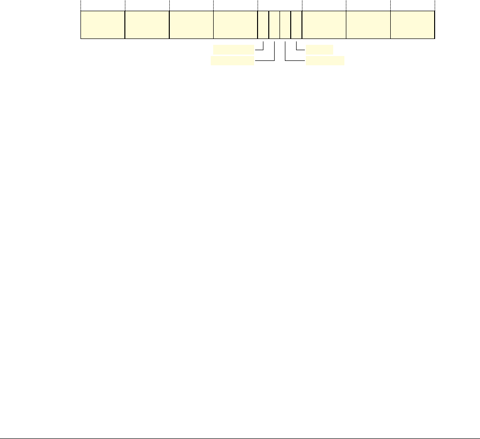
C11 The Debug Registers
C11.11 Register descriptions, in register order
ARM DDI 0406C.c Copyright © 1996-1998, 2000, 2004-2012, 2014 ARM. All rights reserved. C11-2231
ID051414 Non-Confidential
C11.11.15 DBGDIDR, Debug ID Register
The DBGDIDR characteristics are:
Purpose Specifies:
• which version of the Debug architecture is implemented
• some features of the debug implementation.
DBGDEVID and DBGDEVID1, if implemented, provides more information about the
debug implementation.
Usage constraints There are no usage constraints.
Configurations This register is required in all implementations.
If external debug over powerdown is supported, this register can be implemented in either
or both power domains.
Attributes A 32-bit RO register. DBGDIDR is in the Debug identification registers group, see the
registers summary in Table C11-2 on page C11-2198.
The DBGDIDR bit assignments are:
WRPs, bits[31:28]
The number of watchpoints implemented. The number of implemented watchpoints is one more
than the value of this field. The permitted values of the field are from
0b0000
for 1 implemented
watchpoint, to
0b1111
for 16 implemented watchpoints.
The minimum number of watchpoints is 1.
BRPs, bits[27:24]
The number of breakpoints implemented. The number of implemented breakpoints is one more than
value of this field. The permitted values of the field are from
0b0001
for 2 implemented breakpoints,
to
0b1111
for 16 implemented breakpoints.
The value of
0b0000
is reserved.
The minimum number of breakpoints is 2.
CTX_CMPs, bits[23:20]
The number of breakpoints that can be used for Context matching. This is one more than the value
of this field. The permitted values of the field are from
0b0000
for 1 Context matching breakpoint,
to
0b1111
for 16 Context matching breakpoints.
The minimum number of Context matching breakpoints is 1. The value in this field cannot be
greater than the value in the BRPs field.
The Context matching breakpoints must be the highest addressed breakpoints. For example, if six
breakpoints are implemented and two are Context matching breakpoints, they must be breakpoints
4 and 5.
WRPs
31 28 27 24 23 20 19 16 15 14 13 12 11 8 7 4 3 0
BRPs CTX_CMPs Version UNK Variant Revision
DEVID_imp
nSUHD_imp
SE_imp
PCSR_imp

C11 The Debug Registers
C11.11 Register descriptions, in register order
C11-2232 Copyright © 1996-1998, 2000, 2004-2012, 2014 ARM. All rights reserved. ARM DDI 0406C.c
Non-Confidential ID051414
Version, bits[19:16]
The Debug architecture version. The permitted values of this field are:
0b0001
ARMv6, v6 Debug architecture.
0b0010
ARMv6, v6.1 Debug architecture.
0b0011
ARMv7, v7 Debug architecture, with all CP14 registers implemented.
0b0100
ARMv7, v7 Debug architecture, with only the baseline CP14 registers implemented.
0b0101
ARMv7, v7.1 Debug architecture.
All other values are reserved.
DEVID_imp, bit[15]
Debug Device ID Register, DBGDEVID, implemented. The meanings of the values of this bit are:
0 DBGDEVID is not implemented. Debug register 1010 is reserved.
1 DBGDEVID is implemented.
In v7 Debug, when this bit is set to 1:
•DBGDEVID is implemented in the external debug and memory-mapped interfaces, and in
the CP14 interface
•DBGDEVID1 and DBGDEVID2 are implemented as RO in the external debug and
memory-mapped interfaces, but are not implemented in the CP14 interface.
In v7.1 Debug DBGDEVID is always implemented, so this bit is RAO, and use of this bit by
software is deprecated.
nSUHD_imp, bit[14]
Secure User halting debug not implemented. When the SE_imp bit is set to 1, indicating that the
implementation includes the Security Extensions, the meanings of the values of this bit are:
0 Secure User halting debug is implemented.
1 Secure User halting debug is not implemented.
If the Security Extensions are not implemented:
• Secure User halting debug cannot be implemented
• this bit is RAZ.
See also Appendix D14 Secure User Halting Debug.
In v7.1 Debug the value must match DBGDIDR.SE_imp.
ARM deprecates any use of Secure User Halting Debug by software.
PCSR_imp, bit[13]
Program Counter Sampling Register, DBGPCSR, implemented as register 33. The meanings of the
values of this bit are:
0 DBGPCSR is not implemented as register 33.
1 DBGPCSR is implemented as register 33.
Note
The DBGPCSR can be implemented as register 33, as register 40, or as both register 33 and register
40 The implemented Sample-based profiling registers on page C10-2190 describes the
Sample-based profiling implementation options, and how software can determine whether and how
the Sample-based profiling registers are implemented.
The use of DBGPCSR as register 33 is deprecated.
SE_imp, bit[12]
Security Extensions implemented. The meanings of the values of this bit are:
0 The implementation does not include the Security Extensions.
1 The implementation includes the Security Extensions.

C11 The Debug Registers
C11.11 Register descriptions, in register order
ARM DDI 0406C.c Copyright © 1996-1998, 2000, 2004-2012, 2014 ARM. All rights reserved. C11-2233
ID051414 Non-Confidential
Bits[11:8] Reserved, UNK.
Variant, bits[7:4]
This field holds an IMPLEMENTATION DEFINED variant number. This number is incremented on
functional changes. The value must match bits[23:20] of the CP15 Main ID Register.
Revision, bits[3:0]
This field holds an IMPLEMENTATION DEFINED revision number. This number is incremented on
functional changes. Usually, this field matches the Revision field, bits[3:0] of the CP15 Main ID
Register. This field is permitted to differ from MIDR.Revision only when MIDR.Revision is
incremented to indicate a minor revision to functionality that has no effect on the Debug
architecture, for example on an Engineering change order (ECO) fix. In this case the
DBGDIDR.Revision value will be less than the MIDR.Revision value.
For details of the CP15 Main ID Register see:
•MIDR, Main ID Register, VMSA on page B4-1649, for a VMSA implementation
•MIDR, Main ID Register, PMSA on page B6-1894, for a PMSA implementation.

C11 The Debug Registers
C11.11 Register descriptions, in register order
C11-2234 Copyright © 1996-1998, 2000, 2004-2012, 2014 ARM. All rights reserved. ARM DDI 0406C.c
Non-Confidential ID051414
C11.11.16 DBGDRAR, Debug ROM Address Register
The DBGDRAR characteristics are:
Purpose Defines the base physical address of a memory-mapped debug component, usually a ROM
Table that locates and describes the memory-mapped debug components in the system.
However, if this processor is the only memory-mapped debug component in the system, or
the only memory-mapped debug component visible to this processor, then DBGDRAR
defines the base physical address of this processor's debug registers.
Usage constraints This register is only visible in the CP14 interface.
Configurations This register is required in all implementations.
If no memory-mapped debug components are implemented, DBGDRAR.Valid is RAZ.
If the implementation includes the Large Physical Address Extension, the DBGDRAR is
extended to be a 64-bit register.
Note
ROM Tables only support 32-bit offsets.
Otherwise, the DBGDRAR is a 32-bit register. The 32-bit version, accessed by
MRC
, is
always implemented.
Attributes A 64-bit or 32-bit RO register, see the Configurations description. DBGDRAR is in the
Debug identification registers group, see the registers summary in Table C11-2 on
page C11-2198.
It is IMPLEMENTATION DEFINED how the processor determines the value that is returned as the base physical address.
If the processor cannot determine the value, the Valid field in the register must be RAZ. The ARM recommended
debug interface includes configuration signals to indicate both the ROM table address and whether the ROM table
address is valid, see DBGROMADDR and DBGROMADDRV on page D1-2350.
A ROM Table enables a debugger to discover other memory-mapped debug components. For more information, see
the ARM Debug Interface v5 Architecture Specification.
The ROM Table base physical address must be aligned to a 4KB boundary. The debug component must occupy at
least 4KB of physical address space, aligned to a 4KB boundary. If the debug component occupies more than 4KB
of physical address space then the base physical address is at the start of the last 4KB of component address space,
not the base address of the component.
32-bit DBGDRAR format
The DBGDRAR 32-bit assignments are:
ROMADDR[31:12], bits[31:12]
Bits[31:12] of the debug component physical address. Bits[11:0] of the address are zero.
If DBGDRAR.Valid is zero the value of this field is UNKNOWN.
Bits[11:2] Reserved, UNK.
Valid, bits[1:0]
This field indicates whether the address is valid. The permitted values of this field are:
0b00
Address is not valid.
0b11
Address is valid.
Other values are reserved.
ROMADDR[31:12]
31 12 11 2 1 0
Reserved, UNK Valid

C11 The Debug Registers
C11.11 Register descriptions, in register order
ARM DDI 0406C.c Copyright © 1996-1998, 2000, 2004-2012, 2014 ARM. All rights reserved. C11-2235
ID051414 Non-Confidential
64-bit DBGDRAR format
The DBGDRAR 64-bit assignments are:
Bits[63:40, 11:2] Reserved, UNK.
ROMADDR[39:12], bits[39:12]
Bits[39:12] of the debug component physical address. Bits[11:0] of the address are zero.
If DBGDRAR.Valid is zero the value of this field is UNKNOWN.
Valid, bits[1:0] This field indicates whether the ROM Table address is valid. The permitted values of this
field are:
0b00
Address is not valid.
0b11
Address is valid.
Other values are reserved.
Reserved,
UNK
210
Valid
12 11
ROMADDR[39:12]Reserved, UNK
40 3963 0
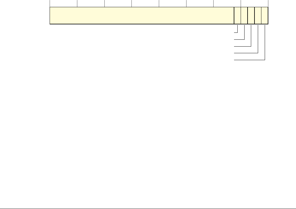
C11 The Debug Registers
C11.11 Register descriptions, in register order
C11-2236 Copyright © 1996-1998, 2000, 2004-2012, 2014 ARM. All rights reserved. ARM DDI 0406C.c
Non-Confidential ID051414
C11.11.17 DBGDRCR, Debug Run Control Register
The DBGDRCR characteristics are:
Purpose Software uses this register to:
• request the processor to enter or exit Debug state
• clear to 0 the sticky exception bits in the DBGDSCR
• cancel bus requests
• clear to 0 DBGDSCR.PipeAdv, the Sticky Pipeline Advance bit.
Usage constraints In v7 Debug, ARM deprecates using the CP14 interface to access DBGDRCR.
In v7.1 Debug, DBGDRCR is not visible in the CP14 interface.
This register is write-only. Reads through the CP14 interface in v7 Debug are
UNPREDICTABLE. For reads through the memory-mapped or external debug interfaces, this
register is UNK.
Configurations This register is required in all implementations.
If external debug over powerdown is supported, this register must be implemented in the
debug power domain. However, some bits affect state that is held in the core power domain.
For these bits, the effect of writing a 1 to the bit is UNPREDICTABLE:
• In any implementation when the core power domain is powered down.
• In a v7.1 Debug implementation, when DBGPRSR.DLK is set to 1.
For more information, see the field descriptions.
Attributes A 32-bit WO register. DBGDRCR is in the Debug control and status registers group, see the
registers summary in Table C11-3 on page C11-2199.
The DBGDRCR bit assignments are:
Bits[31:5] Reserved, SBZ.
CBRRQ, bit[4] Cancel Bus Requests Request. The actions on writing to this bit are:
0 No action.
1 Request cancel of pending accesses.
See Cancel Bus Requests on page C11-2237. It is IMPLEMENTATION DEFINED whether this feature
is supported. If this feature is not implemented, writes to this bit are ignored.
It is UNPREDICTABLE whether a write of 1 to this bit has any effect when the core power domain is
powered down or, in v7.1 Debug, when DBGPRSR.DLK is set to 1.
CSPA, bit[3] Clear Sticky Pipeline Advance. Writing 1 to this bit clears the DBGDSCR.PipeAdv bit to 0. The
actions on writing to this bit are:
0 No action.
1 Clear the DBGDSCR.PipeAdv bit to 0.
Writes to this bit are ignored:
• If the core power domain is powered down.
• In v7.1 Debug, if DBGPRSR.DLK is set to 1.
31 543210
Reserved, SBZ
CBRRQ
CSPA
CSE
RRQ
HRQ

C11 The Debug Registers
C11.11 Register descriptions, in register order
ARM DDI 0406C.c Copyright © 1996-1998, 2000, 2004-2012, 2014 ARM. All rights reserved. C11-2237
ID051414 Non-Confidential
CSE, bit[2] Clear Sticky Exceptions. Writing 1 to this bit clears the DBGDSCR sticky exceptions bits to 0. The
actions on writing to this bit are:
0 No action.
1 Clears DBGDSCR.{UND_l, ADABORT_l, SDABORT_l} sticky exceptions bits to 0.
When the processor is in Debug state, it can exit Debug state by performing a single write to
DBGDRCR with DBGDRCR.{CSE, RRQ} ==
0b11
. This:
•clears DBGDSCR.{UND_l, ADABORT_l, SDABORT_l} to
0b000
• requests exit from Debug state.
If the processor is not in Debug state, writes to this bit are ignored.
Note
The effect of being in Non-debug state with a DBGDSCR sticky exceptions bit set to 1 is
UNPREDICTABLE, therefore there is never a requirement for software executing in Non-debug state
to write 1 to this bit.
RRQ, bit[1] Restart request. The actions on writing to this bit are:
0 No action.
1 Request exit from Debug state.
Writing 1 to this bit requests that the processor exits Debug state. This request is held until the
processor exits Debug state.
Once the request has been made, the debugger can poll the DBGDSCR.RESTARTED bit until it
reads as 1.
If the processor is not in Debug state, writes to this bit are ignored.
HRQ, bit[0] Halt request. The actions on writing to the this bit are:
0 No action.
1 Request entry to Debug state, by generating a Halt request debug event.
In an implementation that has separate core and debug power domains, a debugger can write 1 to
this bit when the core domain is powered down. This makes the Halt request become pending.
If the processor is in Debug state, writes to this bit are ignored.
Once a Halt request has been made, the debugger can test for entry to Debug state as follows:
• Poll the DBGDSCR.HALTED bit until it reads as 1.
• In v7.1 Debug, poll the DBGPRSR.HALTED bit until it reads as 1. This test has the
advantage that the debugger can read DBGPRSR when the OS Lock is set, and when the core
power domain is powered down.
For more information about the effect of writing 1 to this bit, see Halting debug events on
page C3-2075.
Cancel Bus Requests
When support for Cancel Bus Requests is implemented, if software writes 1 to the Cancel Bus Requests Request
bit, the system cancels any pending memory accesses until Debug state is entered. This means it cancels any pending
accesses to the system bus. When this request is made an implementation must abandon all data load and store
accesses. It is IMPLEMENTATION DEFINED whether other accesses, including instruction fetches and cache
operations, are also abandoned.
Debug state entry is the acknowledge event that clears this request.
Abandoned accesses have the following behavior:
• an abandoned data store writes an UNKNOWN value to the target address
• an abandoned data load returns an UNKNOWN value to the destination register
• an abandoned instruction fetch returns an UNKNOWN instruction for execution
• an abandoned cache operation leaves the memory system in an UNPREDICTABLE state.

C11 The Debug Registers
C11.11 Register descriptions, in register order
C11-2238 Copyright © 1996-1998, 2000, 2004-2012, 2014 ARM. All rights reserved. ARM DDI 0406C.c
Non-Confidential ID051414
However, an abandoned access does not cause any exception.
Additional memory accesses after Debug state has been entered, have UNPREDICTABLE behavior.
The number of ports on the processor and their protocols are implementation-specific and, therefore, the detailed
behavior of this bit is IMPLEMENTATION DEFINED. It is also IMPLEMENTATION DEFINED whether this behavior is
supported on all ports of a processor. For example, an implementation can choose not to implement this behavior
on instruction fetches.
This control bit enables the debugger to release a deadlock on the system bus so that it can enter Debug state. At the
point where the deadlock is released, one of the following must be pending:
• a Halt request, made by also writing 1 to DBGDRCR.HRQ
• an External debug request.
It might not be easy to infer the cause of the deadlock by reading the PC value after entering Debug state if, for
example, the processor can execute beyond a deadlocked load or store.
The processor ignores any write to this bit unless invasive debug is permitted in all processor states and modes.
For details of invasive debug authentication see Chapter C2 Invasive Debug Authentication.

C11 The Debug Registers
C11.11 Register descriptions, in register order
ARM DDI 0406C.c Copyright © 1996-1998, 2000, 2004-2012, 2014 ARM. All rights reserved. C11-2239
ID051414 Non-Confidential
C11.11.18 DBGDSAR, Debug Self Address Offset Register
The DBGDSAR characteristics are:
Purpose Defines the offset from the base address defined by DBGDRAR of the physical base address
of the debug registers for the processor.
Usage constraints This register is only visible in the CP14 interface.
In v7.1 Debug, ARM deprecates the use of DBGDSAR. The DBGDSAR is primarily
intended for self-hosted monitor debugging in a system with no CP14 interface, and v7.1
Debug does not support such implementations.
Configurations This register is required in all implementations.
If DBGDRAR.Valid is
0b00
, DBGDSAR is UNKNOWN, otherwise the register is
implemented as described in this section.
If no memory-mapped interface is provided, DBGDSAR.Valid is RAZ. If the base address
defined by DBGDRAR is the base address of the debug registers for the processor, then
DBGDSAR.Valid is RAO and DBGDSAR.SELFOFFSET is RAZ.
In an implementation that includes the Large Physical Address Extension, the DBGDSAR
is a 64-bit register.
Otherwise, the DBGDSAR is a 32-bit register. The 32-bit version, accessed by
MRC
, is
always implemented.
Attributes A 64-bit or 32-bit RO register, see the Configurations description. DBGDSAR is in the
Debug identification registers group, see the registers summary in Table C11-2 on
page C11-2198.
It is IMPLEMENTATION DEFINED how the processor determines the value that is returned as the debug self address
offset. If the processor cannot determine the value, the Valid field in the register must be RAZ. The ARM
recommended debug interface includes configuration signals to indicate both the debug self address offset and
whether the debug self address offset is valid, see DBGSELFADDR and DBGSELFADDRV on page D1-2350.
This register format applies regardless of the implemented scheme for identifying the debug self address offset.
32-bit DBGDSAR format
The 32-bit DBGDSAR bit assignments are:
SELFOFFSET [31:12], bits[31:12]
Bits[31:12] of the two’s complement offset from the base address defined by DBGDRAR to the
physical address where the debug registers are mapped. Bits[11:0] of the address are zero.
If DBGDSAR.Valid is zero the value of this field is UNKNOWN.
Bits[11:2] Reserved, UNK.
Valid, bits[1:0]
This field indicates whether the debug self address offset is valid. The permitted values of this field
are:
0b00
Offset is not valid.
0b11
Offset is valid.
Other values are reserved.
SELFOFFSET [31:12]
31 12 11 2 1 0
Reserved, UNK Valid

C11 The Debug Registers
C11.11 Register descriptions, in register order
C11-2240 Copyright © 1996-1998, 2000, 2004-2012, 2014 ARM. All rights reserved. ARM DDI 0406C.c
Non-Confidential ID051414
64-bit DBGDSAR format
The 64-bit DBGDSAR bit assignments are:
SGN, bits[63:40]
Sign extension. Each bit must be the same as DBGDSAR[39].
SELFOFFSET [39:12], bits[39:12]
Bits[39:12] of the two’s complement offset from the base address defined by DBGDRAR to the
physical address where the debug registers are mapped. Bits[11:0] of the address are zero.
If DBGDSAR.Valid is zero the value of this field is UNKNOWN.
Bits[11:2] Reserved, UNK.
Valid, bits[1:0]
This field indicates whether the debug self address offset is valid. The permitted values of this field
are:
0b00
Offset is not valid.
0b11
Offset is valid.
Other values are reserved.
Reserved,
UNK
210
Valid
12 11
SELFOFFSET[39:12]SGN
40 3963 0
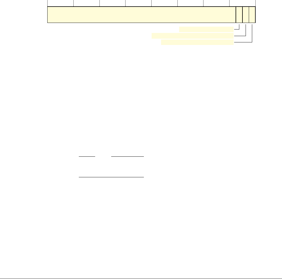
C11 The Debug Registers
C11.11 Register descriptions, in register order
ARM DDI 0406C.c Copyright © 1996-1998, 2000, 2004-2012, 2014 ARM. All rights reserved. C11-2241
ID051414 Non-Confidential
C11.11.19 DBGDSCCR, Debug State Cache Control Register
The DBGDSCCR characteristics are:
Purpose Controls cache behavior when the processor is in Debug state.
Usage constraints There are no usage constraints.
Configurations In v7 Debug, this register is required in all implementations. Some defined bits might not
be implemented, unimplemented bits are RO.
In v7.1 Debug, this register is not implemented.
Attributes A 32-bit RW register. DBGDSCCR is in the Debug memory system control registers group,
see the registers summary in Table C11-8 on page C11-2204.
Debug logic reset values of implemented bits are UNKNOWN.
The DBGDSCCR bit assignments are:
Bits[31:3] Reserved, UNK/SBZP.
Force Write-Through, nWT, bit[2]
If implemented, the possible values of this bit are:
0 Force Write-Through behavior for memory operations issued by a debugger when the
processor is in Debug state.
1 Normal operation for memory operations issued by a debugger when the processor is in
Debug state.
In Debug state, if the nWT bit is set to 0, when a write to memory completes the effect of the write
must be visible at all levels of memory to the point of coherency. This means a debugger can write
through to the point of coherency without having to perform any cache clean operations.
If implemented, the nWT control must act at all levels of memory to the point of coherency.
If the nWT control is not implemented this bit is RO, and it is IMPLEMENTATION DEFINED whether
the bit is RAZ or RAO, but the processor behaves as if the bit is set to 1.
Note
The nWT bit does not force the ordering of writes, and does not force writes to complete
immediately. A debugger might have to insert a barrier operations to ensure ordering.
Cache linefill and eviction bits, bits[1:0]
If implemented these bits are:
nIL, bit[1] Instruction cache, where separate data and instruction caches are
implemented.
nDL, bit[0] Data or unified cache.
The possible values each bit are:
0 Request disabling of cache linefills and evictions for memory operations issued by a
debugger when the processor is in Debug state.
1 Normal operation of cache linefills and evictions for memory operations issued by a
debugger when the processor is in Debug state.
Reserved, UNK/SBZP
31 210
Force Write-Through, nWT
Instruction cache linefill and eviction, nIL
Data cache linefill and eviction, nDL
3

C11 The Debug Registers
C11.11 Register descriptions, in register order
C11-2242 Copyright © 1996-1998, 2000, 2004-2012, 2014 ARM. All rights reserved. ARM DDI 0406C.c
Non-Confidential ID051414
Either or both of these bits might not be implemented. A bit that is not implemented is RO, and it is
IMPLEMENTATION DEFINED whether the bit is RAZ or RAO, but the processor behaves as if the bit
is set to 1.
Any memory access that would be checked against a cache in Non-debug state is checked against
the cache in Debug state and:
• If a match is found, the cached result is used.
• If no match is found the next level of memory is used. However, if the appropriate cache
linefill and eviction bit is set to 0, the result of this access is not cached, and no cache entries
are evicted.
The next level of memory can refer to looking in the next level of cache, or to accessing external
memory, depending on the numbers of levels of cache implemented.
When the processor is in Debug state, cache maintenance operations are not affected by the nDL
and nIL control bits, and have their normal architecturally-defined behavior.
The memory hint instructions
PLD
,
PLDW
, and
PLI
have UNPREDICTABLE behavior in Debug state when
the corresponding nDL or nIL control bit is implemented and set to 0.
Because the debug logic reset values of the implemented bits are UNKNOWN, when the processor is in Debug state,
before issuing instructions through the DBGITR a debugger must ensure the DBGDSCCR has a defined state.
Permitted IMPLEMENTATION DEFINED limits
The DBGDSCCR is required. However, there can be IMPLEMENTATION DEFINED limits on its behavior.
Table C11-16 lists some examples of possible options for implementations.
Table C11-16 Permitted IMPLEMENTATION DEFINED limits on DBGDSCCR behavior
Limit Description Notes
Full DBGDSCCR Bits[2:0] implemented -
No write-back support Bit[2] is ROa-
No write-through
support Bit[2] is ROaForce Write-Through feature not implemented.
No instruction cache
control Bit[1] is ROaInstruction cache linefill and eviction disable features not implemented.
Instruction fetches are disabled in Debug state. For most implementations no
instruction cache accesses take place in Debug state, and nIL is not required.
Unified cache Bit[1] is ROa-
Cache evictions
always enabled
Bits[1:0] implemented
as described
nIL and nDL disable cache linefills in Debug state. However cache evictions might
still take place even when these control bits are set to 0.
No linefill control Bits[1:0] are ROaNo cache linefill and eviction disable features are implemented.
a. It is IMPLEMENTATION DEFINED whether each bit is RAZ or RAO, but the processor behaves as if each bit is set to 1.
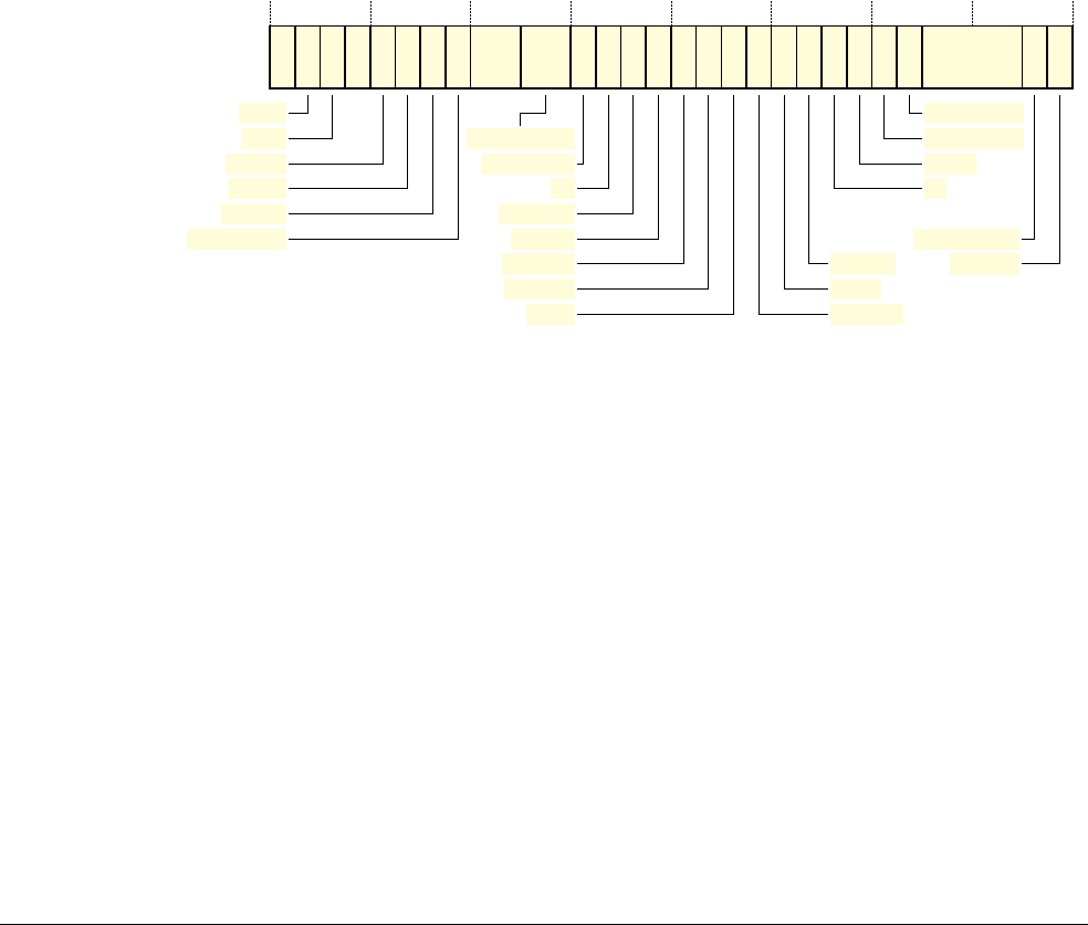
C11 The Debug Registers
C11.11 Register descriptions, in register order
ARM DDI 0406C.c Copyright © 1996-1998, 2000, 2004-2012, 2014 ARM. All rights reserved. C11-2243
ID051414 Non-Confidential
C11.11.20 DBGDSCR, Debug Status and Control Register
The DBGDSCR characteristics are:
Purpose The main control register for the debug implementation.
Usage constraints The debug implementation provides internal and external views of the DBGDSCR,
DBGDSCRint and DBGDSCRext. The behavior of the register on reads of the DBGDSCR
is different for the two views. For more information, see the register field descriptions and
Internal and external views of the DBGDSCR and the DCC registers on page C8-2167.
Configurations This register is required in all debug implementations.
Some bit assignments differ if the implementation includes the Virtualization Extensions.
See the field descriptions for details.
Attributes A 32-bit register that is RW in the external view, and RO in the internal view. DBGDSCR
is in the Debug control and status registers group, see the registers summary in Table C11-3
on page C11-2199.
For more information, see Access to DBGDSCR bits on page C11-2253.
The debug logic reset value of bits and fields in the DBGDSCR are zero, except where
stated in the bit and field descriptions.
The DBGDSCR bit assignments are:
Bits[31, 28, 23:22]
Reserved, UNK/SBZP.
RXfull, bit[30]
DBGDTRRX register full. The possible values of this bit are:
0 DBGDTRRX register empty.
1 DBGDTRRX register full.
The bit is read-only except that, in a v7.1 Debug implementation, it is read/write when the OS Lock
is set.
For more information about the behavior of RXfull and DBGDTRRX, see Operation of the DCC
and Instruction Transfer Register on page C8-2169.
ARM deprecates any use of a value of this bit returned by a read of DBGDSCRext using the CP14
interface, except for uses for OS save or restore in a v7.1 Debug implementation when the OS Lock
is set.
(0)
31 30 29 28 27 26 25 24 23 22 21 20 19 18 17 16 15 14 13 12 11 10 9 8 7 6 5 2 1 0
(0) (0) (0) MOE
RXfull
TXfull
RXfull_l
TXfull_l
PipeAdv
InstrCompl_l
ExtDCCmode
ADAdiscard
SPNIDdis
SPIDdis
MDBGen
HDBGen
ITRen UDCCdis
INTdis
DBGack
SDABORT_l
ADABORT_l
UND_l
RESTARTED
HALTED
NS FS

C11 The Debug Registers
C11.11 Register descriptions, in register order
C11-2244 Copyright © 1996-1998, 2000, 2004-2012, 2014 ARM. All rights reserved. ARM DDI 0406C.c
Non-Confidential ID051414
TXfull, bit[29]
DBGDTRTX register full. The possible values of this bit are:
0 DBGDTRTX register empty.
1 DBGDTRTX register full.
The bit is read-only except that, in a v7.1 Debug implementation, it is read/write when the OS Lock
is set.
For more information about the behavior of TXfull and DBGDTRTX, see Operation of the DCC
and Instruction Transfer Register on page C8-2169.
ARM deprecates any use of a value of this bit returned by a read of DBGDSCRext using the CP14
interface, except for uses for OS save or restore in a v7.1 Debug implementation when the OS Lock
is set.
RXfull_l, bit[27]
Latched RXfull. This controls the behavior of the processor on writes to DBGDTRRXext.
The bit is read-only except that, in a v7.1 Debug implementation, it is read/write when the OS Lock
is set.
This bit is UNKNOWN:
• On reads of DBGDSCRint.
• In a v7.1 Debug implementation, on reads of DBGDSCRext using the CP14 interface when
the OS Lock is clear.
For more information about the behavior of RXfull_l and DBGDTRRX, see Operation of the DCC
and Instruction Transfer Register on page C8-2169.
ARM deprecates any use of a value of this bit returned by a read of DBGDSCRext using the CP14
interface, except for uses for OS save or restore in a v7.1 Debug implementation when the OS Lock
is set.
TXfull_l, bit[26]
Latched TXfull. This controls the behavior of the processor on reads of DBGDTRTXext.
The bit is read-only except that, in a v7.1 Debug implementation, it is read/write when the OS Lock
is set.
This bit is UNKNOWN:
• On reads of DBGDSCRint.
• In a v7.1 Debug implementation, on reads of DBGDSCRext using the CP14 interface when
the OS Lock is clear.
For more information about the behavior of TXfull_l and DBGDTRTX, see Operation of the DCC
and Instruction Transfer Register on page C8-2169.
ARM deprecates any use of a value of this bit returned by a read of DBGDSCRext using the CP14
interface, except for uses for OS save or restore in a v7.1 Debug implementation when the OS Lock
is set.
PipeAdv, bit[25]
Sticky Pipeline Advance bit. This bit is set to 1 whenever the processor pipeline advances by retiring
one or more instructions. It is cleared to 0 only by a write to DBGDRCR.CSPA.
Note
The architecture does not define precisely when this bit is set to 1. It requires only that this happens
periodically in Non-debug state, to indicate that software execution is progressing.
This bit is read-only.
In v7.1 Debug, this bit is UNKNOWN on reads using the CP14 interface.
This bit enables a debugger to detect that the processor is idle. In some situations this might indicate
that the processor is deadlocked.

C11 The Debug Registers
C11.11 Register descriptions, in register order
ARM DDI 0406C.c Copyright © 1996-1998, 2000, 2004-2012, 2014 ARM. All rights reserved. C11-2245
ID051414 Non-Confidential
The debug logic reset value of this bit is UNKNOWN.
ARM deprecates any use of a value of this bit returned by the CP14 interface.
InstrCompl_l, bit[24]
Latched Instruction Complete. This is a copy of the internal InstrCompl flag, taken on each read of
DBGDSCRext. InstrCompl signals whether the processor has completed execution of an instruction
issued through DBGITR. InstrCompl is not visible directly in any register.
On a read of DBGDSCRext when the processor is in Debug state, InstrCompl_l always returns the
current value of InstrCompl. The meanings of the values of InstrCompl_l are:
0 An instruction previously issued through the DBGITR has not completed its changes to
the architectural state of the processor.
1 All instructions previously issued through the DBGITR have completed their changes
to the architectural state of the processor.
This bit is read-only.
This bit is UNKNOWN:
• When the processor is in Non-debug state.
• On reads using the CP14 interface.
Normally, InstrCompl:
• Is cleared to 0 following issue of an instruction through DBGITR.
• Becomes 1 once the instruction completes.
The taking of an exception marks the completion of the instruction. InstrCompl is set to 1 if an
instruction generates an Undefined Instruction or Data Abort exception.
InstrCompl is set to 1 on entry to Debug state. For more information about the behavior of
InstrCompl, InstrCompl_l and the DBGITR when the processor is in Debug state, see Operation of
the DCC and Instruction Transfer Register on page C8-2169.
The debug logic reset value of this bit is UNKNOWN.
ExtDCCmode, bits[21:20]
External DCC access mode. This field controls the access mode for the external views of the DCC
registers and the DBGITR. Possible values are:
0b00
Non-blocking mode.
0b01
Stall mode.
0b10
Fast mode.
The value
0b11
is reserved.
In v7.1 Debug, when the OS Lock is clear, for accesses using the CP14 interface:
• This field is UNKNOWN on reads.
• For accesses to DBGDSCRext:
— The field ignores writes.
— Software must treat the field as SBZP.
For more information see Operation of the External DCC access modes on page C8-2169.
ARM deprecates any use of this field by either:
• A read of DBGDSCRint.
• An access to DBGDSCRext using the CP14 interface, except for uses for OS save or restore
in a v7.1 Debug implementation when the OS Lock is set.
ADAdiscard, bit[19]
Asynchronous Aborts Discarded. The possible values of this bit are:
0 Asynchronous aborts handled normally.
1 On an asynchronous abort to which this bit applies, the processor sets the Sticky
Asynchronous Abort bit, ADABORT_l, to 1 but otherwise discards the abort.

C11 The Debug Registers
C11.11 Register descriptions, in register order
C11-2246 Copyright © 1996-1998, 2000, 2004-2012, 2014 ARM. All rights reserved. ARM DDI 0406C.c
Non-Confidential ID051414
Note
In v7 Debug this bit applies to all asynchronous aborts. v7.1 Debug restricts the asynchronous aborts
to which this action applies, as described in Asynchronous aborts and Debug state entry on
page C5-2096.
Asynchronous aborts and Debug state entry on page C5-2096 describes the conditions for setting
this bit to 1.
It is IMPLEMENTATION DEFINED whether:
• This bit is read-only or read/write in Debug state.
• The hardware automatically sets this bit to 1 on entry to Debug state.
In v7.1 Debug, if this bit is RO in Debug state, then its value is UNKNOWN when read through the
CP14 interface in Debug state.
For more information, see Asynchronous aborts and Debug state entry on page C5-2096.
When the processor is in Non-debug state, software must treat this bit as UNK/SBZP. Writing 1 to
this bit when the processor is in Non-debug state might cause UNPREDICTABLE behavior, but it is
always safe to handle the bit as SBZP, for example, in a read-modify-write update to the register, or
for a save and restore of DBGDSCR over powerdown.
Note
This behavior is an extension of the standard definition of SBZP.
The processor clears this bit to 0 on exit from Debug state.
NS, bit[18]
Non-secure state status. If the implementation includes the Security Extensions, this bit indicates
whether the processor is in the Secure state. The possible values of this bit are:
0 The processor is in the Secure state.
1 The processor is in the Non-secure state.
This bit is read-only. If the processor does not implement Security Extensions, this bit is RAZ.
The debug logic reset value of this read-only status bit reflects the current status of the processor.
ARM deprecates any use of a value of this bit returned by a read using the CP14 interface.
SPNIDdis, bit[17]
Secure PL1 Non-Invasive Debug Disabled. This bit shows if non-invasive debug is permitted in
Secure PL1 modes. The possible values of the bit are:
0 Non-invasive debug is permitted in Secure PL1 modes.
1 Non-invasive debug is not permitted in Secure PL1 modes.
This bit is read-only.
If the Security Extensions are not implemented, then PL1 modes are equivalent to Secure PL1
modes.
The debug logic reset value of this read-only status bit reflects the current status of the processor.
ARM deprecates any use of the value of this bit.
SPIDdis, bit[16]
Secure PL1 Invasive Debug Disabled bit. This bit shows if invasive debug is permitted in Secure
PL1 modes. The possible values of the bit are:
0 Invasive debug is permitted in Secure PL1 modes.
1 Invasive debug is not permitted in Secure PL1 modes.
This bit is read-only.
If the Security Extensions are not implemented, then PL1 modes are equivalent to Secure PL1
modes.

C11 The Debug Registers
C11.11 Register descriptions, in register order
ARM DDI 0406C.c Copyright © 1996-1998, 2000, 2004-2012, 2014 ARM. All rights reserved. C11-2247
ID051414 Non-Confidential
The debug logic reset value of this read-only status bit reflects the current status of the processor.
ARM deprecates any use of the value of this bit.
MDBGen, bit[15]
Monitor debug-mode enable. The possible values of this bit are:
0 Monitor debug-mode disabled.
1 Monitor debug-mode enabled.
The MDBGen bit reads as 0:
• In v7 Debug, when invasive debug is disabled in all modes and states.
• In v7.1 Debug, when both:
— Invasive debug is disabled in all modes and states.
— The OS Lock is clear.
In these cases, a register write updates this bit, but the bit reads as zero regardless of its programmed
value.
Note
This definition of the behavior of this bit means that whenever;
• Invasive debug is enabled but debug events are ignored because of the current mode and
state, a read of the register returns the programmed value of this bit.
• At least one of the following applies, the value returned by a read of the register, and the
behavior of the processor, correspond to the programmed value:
— Invasive debug is enabled.
— In v7.1 Debug, the OS Lock is set.
In v7 Debug, in a powerdown sequence, the DBGOSSRR saves the programmed value of the
MDBGen bit, not the value returned by reads of the DBGDSCR. For more information, see The OS
Save and Restore mechanism on page C7-2154.
In v7.1 Debug, when the OS Lock is set, the MDBGen bit is RW.
If Halting debug-mode is enabled, because the HDBGen bit is set to 1, then Monitor debug-mode
is disabled regardless of the value of the MDBGen bit.
See Chapter C2 Invasive Debug Authentication for information about enabling invasive debug.
ARM deprecates any use of a value of this bit returned by a read of DBGDSCRint.
HDBGen, bit[14]
Halting debug-mode enable. The possible values of this bit are:
0 Halting debug-mode disabled.
1 Halting debug-mode enabled.
The HDBGen bit reads as 0:
• In v7 Debug, in all interfaces when invasive debug is disabled in all modes and states.
• In v7.1 Debug, in the memory-mapped and external debug interfaces when both:
— Invasive debug is disabled in all modes and states.
— The OS Lock is clear.
In these cases, a register write updates this bit, but the bit reads as zero regardless of its programmed
value.
Note
This definition of the behavior of this bit means that for v7 Debug accesses in all interfaces, and for
v7.1 Debug accesses in the memory-mapped and external debug interfaces, whenever:
• Invasive debug is enabled but debug events are ignored because of the current mode and
state, a read of the register returns the programmed value of this bit.

C11 The Debug Registers
C11.11 Register descriptions, in register order
C11-2248 Copyright © 1996-1998, 2000, 2004-2012, 2014 ARM. All rights reserved. ARM DDI 0406C.c
Non-Confidential ID051414
• At least one of the following applies, the value returned by a read of the register, and the
behavior of the processor, correspond to the programmed value:
— Invasive debug is enabled.
— In v7.1 Debug, the OS Lock is set.
In v7 Debug, in a powerdown sequence, the DBGOSSRR saves the programmed value of the
HDBGen bit, not the value returned by reads of the DBGDSCR. For more information, see The OS
Save and Restore mechanism on page C7-2154.
In v7.1 Debug:
• When the OS Lock is set, this bit is RW in the CP14 and memory-mapped interfaces.
• When the OS Lock is clear, in the CP14 interface:
— Reads of this bit return an UNKNOWN value.
— Writes to this bit in DBGDSCRext are ignored. Software must use a SBZP policy
when writing to this bit in DBGDSCRext.
See Chapter C2 Invasive Debug Authentication for information about enabling invasive debug.
ARM deprecates any use of this bit by either:
• A read of DBGDSCRint.
• An access to DBGDSCRext using the CP14 interface, except for uses for OS save or restore
in a v7.1 Debug implementation when the OS Lock is set.
ITRen, bit[13]
Execute ARM instruction enable. This bit enables the execution of ARM instructions through the
DBGITR. The possible values of this bit are:
0 ITR mechanism disabled.
1 The ITR mechanism for forcing the processor to execute instructions in Debug state via
the external debug interface is enabled.
When the processor is in Non-debug state, software must treat this bit as UNK/SBZP. Writing 1 to
this bit when the processor is in Non-debug state might cause UNPREDICTABLE behavior, but it is
always safe to handle the bit as SBZP, for example, in a read-modify-write update to the register, or
for a save and restore of DBGDSCR over powerdown.
Note
This behavior is an extension of the standard definition of SBZP.
The effect of writing to DBGITR when this bit is set to 0 is UNPREDICTABLE.
In v7.1 Debug, in Debug state, for accesses to DBGDSCR using the CP14 interface:
• This field is UNKNOWN on reads.
• For accesses to DBGDSCRext:
— The field ignores writes.
— Software must treat the field as SBOP.
In v7 Debug, ARM deprecates setting this bit to 0 through the CP14 interface when the processor
is in Debug state.
UDCCdis, bit[12]
User mode access to Debug Communications Channel (DCC) disable. The possible values of this
bit are:
0 User mode access to DCC enabled.
1 User mode access to DCC disabled.
When this bit is set to 1, if a User mode process tries to access the DBGDIDR, DBGDRAR,
DBGDSAR, DBGDSCRint, DBGDTRRXint, or DBGDTRTXint through CP14 operations, an
Undefined Instruction exception is generated.

C11 The Debug Registers
C11.11 Register descriptions, in register order
ARM DDI 0406C.c Copyright © 1996-1998, 2000, 2004-2012, 2014 ARM. All rights reserved. C11-2249
ID051414 Non-Confidential
Note
All other CP14 registers are UNDEFINED in User mode, regardless of the value of this bit. Therefore,
setting this bit to 1 prevents User mode access to any CP14 debug register.
ARM deprecates any use of a value of this bit returned by a read of DBGDSCRint.
INTdis, bit[11]
Interrupts Disable. Setting this bit to 1 masks the taking of IRQs and FIQs. The possible values of
this bit are:
0 Interrupts enabled.
1 Interrupts disabled.
In v7.1 Debug, when the OS Lock is clear, for accesses using the CP14 interface:
• This field is UNKNOWN on reads.
• For accesses to DBGDSCRext:
— The field ignores writes.
— Software must treat the field as SBZP.
If the external debugger needs to execute a piece of software in Non-debug state as part of the
debugging process, but that software must not be interrupted, the external debugger sets this bit to 1.
For example, when single stepping instructions in a system with a periodic timer interrupt, the
period of the interrupt is likely to be more frequent than the stepping frequency of the debugger. In
this situation, if the debugger steps the target without setting the INTdis bit to 1 for the duration of
the step, the interrupt is pending. This means that, if interrupts are enabled in the CPSR, the interrupt
is taken as soon as the processor exits Debug state.
The INTdis bit is ignored if at least one of the following applies:
• DBGDSCR.{MDBGen, HDBGen} ==
0b00
.
• Invasive debug is disabled.
For more information about enabling invasive debug see Chapter C2 Invasive Debug
Authentication.
Note
If implemented, the ISR always reflects the status of the IRQ and FIQ signals, regardless of the
value of the INTdis bit.
ARM deprecates any use of a value of this bit returned by either:
• A read of DBGDSCRint.
• A read of DBGDSCRext using the CP14 interface, except for uses for OS save or restore in
in a v7.1 Debug implementation when the OS Lock is set.
DBGack, bit[10]
Force Debug Acknowledge. A debugger can use this bit to force any implemented debug
acknowledge output signals to be asserted. The possible values of this bit are:
0 Debug acknowledge signals under normal processor control.
1 Debug acknowledge signals asserted, regardless of the processor state.
In v7.1 Debug, when the OS Lock is clear, for accesses using the CP14 interface:
• This field is UNKNOWN on reads.
• For accesses to DBGDSCRext:
— The field ignores writes.
— Software must treat the field as SBZP.
For details of the recommended external debug interface, see Run-control and cross-triggering
signals on page D1-2342 and DBGACK and DBGCPUDONE on page D1-2344.
If a debugger sets this bit to 1, it can then cause the processor to execute instructions in Non-debug
state, while the rest of the system behaves as if the processor is in Debug state.

C11 The Debug Registers
C11.11 Register descriptions, in register order
C11-2250 Copyright © 1996-1998, 2000, 2004-2012, 2014 ARM. All rights reserved. ARM DDI 0406C.c
Non-Confidential ID051414
Note
The effect of setting DBGack to 1 takes no account of whether invasive debug is enabled or
permitted. This means it asserts the debug acknowledge signals regardless of the invasive debug
authentication settings.
ARM deprecates any use of a value of this bit returned by either:
• A read of DBGDSCRint.
• A read of DBGDSCRext using the CP14 interface, except for uses for OS save or restore in
in a v7.1 Debug implementation when the OS Lock is set.
Bit[9], Implementation does not include the Virtualization Extensions
Reserved, UNK/SBZP.
FS, bit[9], Implementation includes the Virtualization Extensions
Fault status. This bit is updated on every Data Abort exception generated in Debug state, and might
indicate that the exception syndrome information was written to the PL2 exception syndrome
registers. The possible values are:
0 Software must use the current state and mode and the value of HCR.TGE to determine
which of the following sets of registers holds information about the Data Abort
exception:
• The PL1 fault reporting registers, meaning the DFSR and DFAR, and the ADFSR
if it is implemented.
• The PL2 fault syndrome registers, meaning the HSR, HDFAR, and HPFAR, and
the HADFSR if it is implemented.
1 Fault status information was written to the PL2 fault syndrome registers.
Note
• A Data Abort Exception always updates either the DFSR or the HSR. Whether any other
registers are updated depends on the cause of the exception.
• A debugger uses this bit in determining where the fault information for a Data Abort is held.
A Data Abort exception generated in Debug state in a Non-secure PL1 or PL0 mode sets this bit to:
1 If the exception was generated by a stage 2 abort, meaning one of:
• An MMU fault from a stage 2 address translation.
• An Alignment fault generated because the stage 2 translation identifies the target
of an unaligned access as Device or Strongly-ordered memory.
• A synchronous external abort that occurs on a stage 2 address translation.
An UNKNOWN value, 0 or 1
If HCR.TGE is set to 1 and the exception was generated by one of:
• An Alignment fault other than an Alignment fault caused by an unaligned access
to Device or Strongly-ordered memory.
• A synchronous external abort other than a synchronous external abort that occurs
on a stage 2 address translation.
These cases always write the fault status information to the PL2 fault syndrome
registers, regardless of whether they set the FS bit to 1.
0 For any other Data Abort exception generated in a Non-secure PL1 or PL0 mode.
A Data Abort exception generated in Debug state in the Non-secure PL2 mode sets this bit to 0.
A Data Abort exception generated in Debug state in Secure state sets this bit to 0.
For more information see Exceptions in Debug state on page C5-2107.
In Debug state, for accesses using the CP14 interface:
• This field is UNKNOWN on reads.

C11 The Debug Registers
C11.11 Register descriptions, in register order
ARM DDI 0406C.c Copyright © 1996-1998, 2000, 2004-2012, 2014 ARM. All rights reserved. C11-2251
ID051414 Non-Confidential
• For accesses to DBGDSCRext:
— The field ignores writes.
— Software must treat the field as SBZP.
When the processor is in Non-debug state, this bit is not set to 1 by any Data Abort exception, and
this bit is UNK/SBZP.
The value of this bit is not changed by writes to DBGDRCR.CSE, Clear sticky exceptions.
The debug logic reset value of this bit is UNKNOWN.
UND_l, bit[8]
Sticky Undefined Instruction. This bit is set to 1 by any Undefined Instruction exceptions generated
by instructions issued to the processor while in Debug state. The possible values of this bit are:
0 No Undefined Instruction exception has been generated since the last time this bit was
cleared to 0.
1 An Undefined Instruction exception has been generated since the last time this bit was
cleared to 0.
This bit is read-only.
In v7.1 Debug, when the processor is in Debug state, this bit is UNKNOWN on reads using the CP14
interface.
This bit is cleared to 0 by writing to DBGDRCR.CSE.
Exiting Debug state with this bit set to 1 causes UNPREDICTABLE behavior.
When the processor is in Non-debug state this bit is not set to 1 by an Undefined Instruction
exception.
For more information, see Exceptions in Debug state on page C5-2107.
ADABORT_l, bit[7]
Sticky Asynchronous Abort. When the ADAdiscard bit, bit[19], is set to 1, ADABORT_l is set to 1
by any asynchronous abort that occurs when the processor is in Debug state.
The possible values of this bit are:
0 No asynchronous abort has been generated since the last time this bit was cleared to 0.
1 Since the last time this bit was cleared to 0, an asynchronous abort has been generated
while ADAdiscard was set to 1.
Note
When ADAdiscard is set to 1, and the processor is in Debug state, any asynchronous abort sets
ADABORT_l to 1:
• In v7 Debug the asynchronous abort is discarded.
• In v7.1 it is IMPLEMENTATION DEFINED which asynchronous aborts are discarded, but
ADABORT_l is set to 1 regardless of whether the abort is discarded.
This bit is read-only.
In v7.1 Debug, when the processor is in Debug state, this bit is UNKNOWN on reads using the CP14
interface.
This bit is cleared to 0 by writing to DBGDRCR.CSE.
Exiting Debug state with this bit set to 1 causes UNPREDICTABLE behavior.
When the processor is in Non-debug state this bit is not set to 1 by an asynchronous abort.
For more information, see the information about asynchronous aborts in Exceptions in Debug state
on page C5-2107.

C11 The Debug Registers
C11.11 Register descriptions, in register order
C11-2252 Copyright © 1996-1998, 2000, 2004-2012, 2014 ARM. All rights reserved. ARM DDI 0406C.c
Non-Confidential ID051414
SDABORT_l, bit[6]
Sticky Synchronous Data Abort. This bit is set to 1 by any Data Abort exception that is generated
synchronously when the processor is in Debug state. The possible values of this bit are:
0 No synchronous Data Abort exception has been generated since the last time this bit was
cleared to 0.
1 A synchronous Data Abort exception has been generated since the last time this bit was
cleared to 0.
This bit is read-only.
In v7.1 Debug, when the processor is in Debug state, this bit is UNKNOWN on reads using the CP14
interface.
The behavior of the DBGITR depends on the value of the SDABORT_l bit, see The Sticky
Synchronous Data Abort bit and issuing instructions from DBGITR on page C8-2172.
Exiting Debug state with this bit set to 1 causes UNPREDICTABLE behavior.
This bit is cleared to 0 by writing to DBGDRCR.CSE.
If the processor is in Non-debug state this bit is not set to 1 by a synchronous Data Abort exception.
For more information, see Exceptions in Debug state on page C5-2107.
MOE, bits[5:2]
Method of Debug entry. For details of this field see Method of Debug entry on page C11-2257.
RESTARTED, bit[1]
Processor Restarted. The possible values of this bit are:
0 The processor is exiting Debug state. This bit only reads as 0 between receiving a restart
request, and restarting Non-debug state operation.
1 The processor has exited Debug state. This bit remains set to 1 if the processor re-enters
Debug state.
This bit is read-only.
After making a restart request, the debugger can poll this bit until it is set to 1. At that point it knows
that the restart request has taken effect and the processor has exited Debug state.
Note
Polling the HALTED bit until it is set to 0 is not a reliable way for a debugger to determine whether
the processor has left Debug state, because the processor might re-enter Debug state as a result of
another debug event before the debugger samples the DBGDSCR.
See Chapter C5 Debug State for a definition of Debug state.
The debug logic reset value of this read-only status bit reflects the current status of the processor.
In v7.1 Debug, when the processor is in Debug state, the value of this bit is UNKNOWN when read
using the CP14 interface.
ARM deprecates any use of a value of this bit returned by a read using the CP14 interface.
HALTED, bit[0]
Processor Halted. The possible values of this bit are:
0 The processor is in Non-debug state.
1 The processor is in Debug state.
Note
Between receiving a restart request and restarting Non-debug state operation, the
processor is in Debug state and this bit reads as 1.
This bit is read-only.
After programming a debug event, the external debugger can poll this bit until it is set to 1. At that
point it knows that the processor has entered Debug state.

C11 The Debug Registers
C11.11 Register descriptions, in register order
ARM DDI 0406C.c Copyright © 1996-1998, 2000, 2004-2012, 2014 ARM. All rights reserved. C11-2253
ID051414 Non-Confidential
See Chapter C5 Debug State for a definition of Debug state.
The debug logic reset value of this read-only status bit reflects the current status of the processor.
In v7.1 Debug, when the processor is in Debug state, the value of this bit is UNKNOWN when read
using the CP14 interface.
ARM deprecates any use of a value of this bit returned by a read using the CP14 interface.
Access to DBGDSCR bits
The following tables show the behavior of access to the DBGDSCR bits:
• For a v7 Debug implementation:
—Table C11-17 shows the behavior of accesses in Non-debug state.
—Table C11-18 on page C11-2254 shows the bits with different behavior in Debug state.
• For a v7.1 Debug implementation:
—Table C11-19 on page C11-2255 shows the behavior of accesses in Non-debug state with the OS Lock
clear.
—Table C11-20 on page C11-2256 shows the bits with different behavior in when the OS Lock is set.
—Table C11-21 on page C11-2257 shows the bits with different behavior in Debug state.
Table C11-17 shows the behavior of accesses to each field of the DBGDSCR in v7 Debug, in Non-debug state.
Table C11-17 DBGDSCR bit access in Non-debug state, v7 Debug
Bits Field name DBGEN DBGDSCRint DBGDSCRext
[31] Reserved - - -
[30] RXfull - RO ROa
[29] TXfull - RO ROa
[28] Reserved - - -
[27] RXfull_la-UNKNOWN Same as RXfull
[26] TXfull_la-UNKNOWN Same as TXfull
[25] PipeAdva-RO RO
[24] InstrCompl_la, b -UNKNOWN UNKNOWN
[23:22] Reserved - - -
[21:20] ExtDCCmodea-RO RW
[19] ADAdiscarda, b - UNK UNK/SBZc
[18] NSa-RO RO
[17] SPNIDdisa-RO RO
[16] SPIDdisa-RO RO
[15] MDBGen HIGH ROaRW
LOW RAZaWritable, RAZd
[14] HDBGenaHIGH RO RW
LOW RAZ Writable, RAZd

C11 The Debug Registers
C11.11 Register descriptions, in register order
C11-2254 Copyright © 1996-1998, 2000, 2004-2012, 2014 ARM. All rights reserved. ARM DDI 0406C.c
Non-Confidential ID051414
Table C11-18 shows how the behavior of accesses to some fields of the DBGDSCR in v7 Debug changes when in
Debug state. Fields not shown in Table C11-18 behave as shown in Table C11-17 on page C11-2253.
Table C11-19 on page C11-2255 shows the behavior of accesses to each field of the DBGDSCR, in v7.1 Debug,
when in Non-debug state, with the OS Lock clear.
[13] ITRena, b - UNK UNK/SBZc
[12] UDCCdis - ROaRW
[11] INTdisa-RO RW
[10] DBGacka-RO RW
[9] Reserved - - -
[8] UND_lb- UNK UNK/SBZP
[7] ADABORT_lb- UNK UNK/SBZP
[6] SDABORT_lb- UNK UNK/SBZP
[5:2] MOE - RO RW
[1] RESTARTEDa, b -RAORAO/WI
[0] HALTEDa, b -RAZRAZ/WI
a. ARM deprecates some or all uses of this field, see the field description for more information.
b. Access to this bit or field is modified in Debug state. See Table C11-18 for details.
c. See the bit description for more information about the behavior of this bit.
d. Bit is writable, but reads-as-zero. If DBGEN goes HIGH, the most recently written value is exposed.
Table C11-18 DBGDSCR bits with modified access in Debug state, v7 Debug
Bits Field name DBGDSCRint DBGDSCRext
[24] InstrCompl_l UNKNOWN ROa
a. UNKNOWN when DBGDSCRext is read through the CP14 interface.
[19] ADAdiscard RO IMPLEMENTATION DEFINEDb
b. It is IMPLEMENTATION DEFINED whether this bit is RO or RW.
[13] ITRen RO RW
[8] UND_l RO RO
[7] ADABORT_l RO RO
[6] SDABORT_l RAZc
c. Can never read as 1 because the CP14 interface cannot be accessed when SDABORT_l==1.
RO
[1] RESTARTED RAO RAO/WId
d. Whilst exiting Debug state, this bit reads-as-zero. The CP14 interface cannot be accessed whilst
exiting from Debug state.
[0] HALTED RAO RAO/WI
Table C11-17 DBGDSCR bit access in Non-debug state, v7 Debug (continued)
Bits Field name DBGEN DBGDSCRint DBGDSCRext

C11 The Debug Registers
C11.11 Register descriptions, in register order
ARM DDI 0406C.c Copyright © 1996-1998, 2000, 2004-2012, 2014 ARM. All rights reserved. C11-2255
ID051414 Non-Confidential
Table C11-19 DBGDSCR bit access in Non-debug state with OS Lock clear, v7.1 Debug
Bits Field name DBGEN DBGDSCRint,
CP14 interface DBGDSCRext,
CP14 interface DBGDSCRext, memory-mapped
and external debug interfaces
[31] Reserved - - - -
[30] RXfulla-RO ROb, c RO
[29] TXfulla-RO ROb, c RO
[28] Reserved - - - -
[27] RXfull_la-UNKNOWN UNKNOWNdSame as RXfull
[26] TXfull_la-UNKNOWN UNKNOWNdSame as TXfull
[25] PipeAdv - UNKNOWN UNKNOWNdRO
[24] InstrCompl_le-UNKNOWN UNKNOWNdUNKNOWN
[23:22] Reserved - - - -
[21:20] ExtDCCmodea-UNKNOWN UNKNOWNdRW
[19] ADAdiscarde- UNK UNK/SBZfUNK/SBZf
[18] NS - RObROb, c RO
[17] SPNIDdis - RObROb, c ROb
[16] SPIDdis - RObROb, c ROb
[15] MDBGenaHIGH RObRW RW
LOW RAZbWritable, RAZgWritable, RAZg
[14] HDBGenaHIGH UNKNOWN UNKNOWNdRW
LOW UNKNOWN UNKNOWNdWritable, RAZg
[13] ITRene- UNK UNK/SBZfUNK/SBZf
[12] UDCCdis - RObRW RW
[11] INTdisa-UNKNOWN UNKNOWNdRW
[10] DBGacka-UNKNOWN UNKNOWNdRW
[9] FSe, h - UNK UNK/SBZP UNK/SBZP
[8] UND_le- UNK UNK/SBZP UNK/SBZP
[7] ADABORT_le- UNK UNK/SBZP UNK/SBZP
[6] SDABORT_le- UNK UNK/SBZP UNK/SBZP
[5:2] MOE - RO RW RW

C11 The Debug Registers
C11.11 Register descriptions, in register order
C11-2256 Copyright © 1996-1998, 2000, 2004-2012, 2014 ARM. All rights reserved. ARM DDI 0406C.c
Non-Confidential ID051414
Table C11-20 shows how the behavior of accesses through the CP14 and memory-mapped interface changes for
some fields of the DBGDSCR in v7.1 Debug when the OS Lock is set. Fields not shown in Table C11-20 behave as
shown in Table C11-19 on page C11-2255.
Note
In v7.1 Debug, when the OS Lock is set, reads of DBGDSCRint through the CP14 interface are UNPREDICTABLE,
and accesses to DBGDSCRext through the external debug interface return an error.
[1] RESTARTEDe-UNKNOWN UNKNOWNdRAO/WI
[0] HALTEDe- UNK UNK/SBZP RAZ/WI
a. Access to this bit or field is modified in the CP14 and memory-mapped interfaces with OS Lock set. See Table C11-20 for details.
b. ARM deprecates some or all uses of this field, see the field description for more information.
c. Reads return an UNKNOWN value.
d. Reads return an UNKNOWN value. Software must treat as SBZP on writes. Hardware must ignore writes.
e. Access to this bit is modified in Debug state. See Table C11-21 on page C11-2257 for details.
f. See the bit description for more information about the behavior of this bit.
g. Bit is writable, but reads-as-zero. If DBGEN goes HIGH, the most recently written value is exposed.
h. Only if the implementation includes the Virtualization Extensions.
Table C11-19 DBGDSCR bit access in Non-debug state with OS Lock clear, v7.1 Debug (continued)
Bits Field name DBGEN DBGDSCRint,
CP14 interface DBGDSCRext,
CP14 interface DBGDSCRext, memory-mapped
and external debug interfaces
Table C11-20 DBGDSCRext bits with modified access when OS Lock is set, CP14 and
memory-mapped interfaces, v7.1 Debug
Bits Field name Access
[30] RXfull RW
[29] TXfull RW
[27] RXfull_l RWa
a. OS Save and Restore software must not ascribe any meaning to these bits
when saving or restoring them.
[26] TXfull_l RWa
[21:20] ExtDCCmode RWa
[15] MDBGen RWb
b. When the OS Lock is set, the effect of some accesses reading as zero when
DBGEN is LOW is disabled, see the bit descriptions for more information.
[14] HDBGen RWa, b
[11] INTdis RWa
[10] DBGack RWa

C11 The Debug Registers
C11.11 Register descriptions, in register order
ARM DDI 0406C.c Copyright © 1996-1998, 2000, 2004-2012, 2014 ARM. All rights reserved. C11-2257
ID051414 Non-Confidential
Table C11-21 shows how the behavior of accesses to some fields of the DBGDSCR changes in v7.1 Debug when
in Debug state. Fields not shown in Table C11-21 behave as shown in Table C11-19 on page C11-2255.
Method of Debug entry
The DBGDSCR.MOE field indicates the method of debug entry. Table C11-22 shows the meanings of the possible
values of the DBGDSCR.MOE field, and also shows the section where the corresponding debug event is described.
Table C11-21 DBGDSCRext bits with modified access in Debug state, v7.1 Debug
Bit Field name DBGDSCRint,
CP14 interface DBGDSCRext,
CP14 interface DBGDSCRext, memory-mapped
and external debug interfaces
[24] InstrCompl_l UNKNOWN UNKNOWNaRO
[19] ADAdiscard UNKNOWN IMPLEMENTATION DEFINEDbIMPLEMENTATION DEFINEDb
[13] ITRen UNKNOWN UNKNOWNcRW
[9] FS UNKNOWN UNKNOWNaRW
[8] UND_l UNKNOWN UNKNOWNaRO
[7] ADABORT_l UNKNOWN UNKNOWNaRO
[6] SDABORT_l UNKNOWN UNKNOWNaRO
[1] RESTARTED UNKNOWN UNKNOWNaRAO/WId
[0] HALTED UNKNOWN UNKNOWNaRAO/WI
a. Reads return an UNKNOWN value. Software must treat as SBZP on writes. Hardware must ignore writes.
b. It is IMPLEMENTATION DEFINED whether this bit is RO or RW in Debug state. If the bit is RO its value is UNKNOWN when
read through the CP14 interface in Debug state.
c. Reads return an UNKNOWN value. Software must treat as SBOP on writes. Hardware must ignore writes.
d. Whilst exiting Debug state, this bit reads-as-zero. The CP14 interface cannot be accessed whilst exiting from Debug state.
Table C11-22 Meaning of Method of Debug Entry values
MOE bits Debug entry caused by: Section
0b0000
Halt request debug event Halting debug events on page C3-2075
0b0001
Breakpoint debug event Breakpoint debug events on page C3-2041
0b0010
Asynchronous watchpoint debug event Watchpoint debug events on page C3-2059
0b0011
BKPT instruction debug event BKPT instruction debug events on page C3-2040
0b0100
External debug request debug event Halting debug events on page C3-2075
0b0101
Vector catch debug event Vector catch debug events on page C3-2067
0b0110
,
0b0111
Reserved -
0b1000
OS Unlock catch debug event Halting debug events on page C3-2075
0b1001
Reserved -
0b1010
Synchronous watchpoint debug event Watchpoint debug events on page C3-2059
0b1011-0b1111
Reserved -

C11 The Debug Registers
C11.11 Register descriptions, in register order
C11-2258 Copyright © 1996-1998, 2000, 2004-2012, 2014 ARM. All rights reserved. ARM DDI 0406C.c
Non-Confidential ID051414
A Prefetch Abort or Data Abort exception handler can determine whether a debug event occurred by checking the
value of the relevant Fault Status Register, IFSR or DFSR. It then uses the DBGDSCR.MOE bits to determine the
specific debug event.
When debug is disabled, and when debug events are not permitted, the
BKPT
instruction generates a debug exception
rather than being ignored. This sets the DBGDSCR.MOE and CP15 registers as if a BKPT instruction debug
exception occurred. For more information, see Debug exception on BKPT instruction, Breakpoint, or Vector catch
debug events on page C4-2090. For security reasons, monitor software might need to check that debug was enabled
and that the debug event was permitted before communicating with an external debugger.
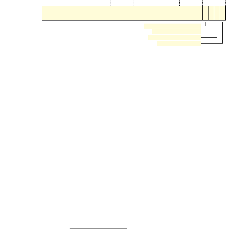
C11 The Debug Registers
C11.11 Register descriptions, in register order
ARM DDI 0406C.c Copyright © 1996-1998, 2000, 2004-2012, 2014 ARM. All rights reserved. C11-2259
ID051414 Non-Confidential
C11.11.21 DBGDSMCR, Debug State MMU Control Register
The DBGDSMCR characteristics are:
Purpose Controls TLB behavior when the processor is in Debug state.
Usage constraints There are no usage constraints.
Configurations In v7 Debug, this register is required in all implementations. Some defined bits might not
be implemented, unimplemented bits are RO.
In v7.1 Debug, this register is not implemented.
Attributes A 32-bit RW register. DBGDSMCR is in the Debug memory system control registers group,
see the registers summary in Table C11-8 on page C11-2204.
Debug logic reset values are UNKNOWN.
The DBGDSMCR bit assignments are:
Bits[31:4] Reserved, UNK/SBZP.
TLB matching bits, bits[3:2]
If implemented, these bits are:
nIUM, bit[3] Instruction TLB matching bit, where separate Data and Instruction TLBs
are implemented.
nDUM, bit[2] Data or Unified TLB matching bit.
The possible values of each bit are:
0 Request disabling of TLB matching for memory operations issued by a debugger when
the processor is in Debug state.
1 Normal operation of TLB matching for memory operations issued by a debugger when
the processor is in Debug state.
Either or both of these bits might not be implemented. A bit that is not implemented is RO, and it is
IMPLEMENTATION DEFINED whether the bit is RAZ or RAO, but the processor behaves as if the bit
is set to 1.
When TLB matching is disabled:
• Any memory access that would be checked against a TLB in Non-debug state is not checked
against the TLB.
• For every access the next level of translation is performed and used for the access, but he
results are not cached in the TLB, and no TLB entries are evicted.
The next level of translation might mean looking in the next level TLB, or doing a translation table
walk, depending on the numbers of levels of TLB implemented.
Note
If TLB matching is disabled, and TLB maintenance functions have not been correctly performed by
the system being debugged, for example, if the TLB has not been flushed following a change to the
translation tables, memory accesses made by the debugger might not undergo the same virtual to
physical memory mappings as the application being debugged.
Instruction TLB matching, nIUM
Reserved, UNK/SBZP
31 43210
Data TLB matching, nDUM
Instruction TLB loading, nIUL
Data TLB loading, nDUL

C11 The Debug Registers
C11.11 Register descriptions, in register order
C11-2260 Copyright © 1996-1998, 2000, 2004-2012, 2014 ARM. All rights reserved. ARM DDI 0406C.c
Non-Confidential ID051414
A debugger can create temporary alternative memory mappings by altering the contents of the
external translation tables and disabling all levels of TLB matching. However, for normal
debugging operations, ARM recommends that any implemented TLB matching bit is set to 1.
TLB loading bits, bits[1:0]
If implemented, these bits are:
nIUL, bit[1] Instruction TLB loading bit, where separate Data and Instruction TLBs are
implemented.
nDUL, bit[0] Data or Unified TLB loading bit.
The possible values of each bit are:
0 Request disabling of TLB load and flush for memory operations issued by a debugger
when the processor is in Debug state.
1 Normal operation of TLB loading and flushing for memory operations issued by a
debugger when the processor is in Debug state.
Either or both of these bits might not be implemented. A bit that is not implemented is RO, and it is
IMPLEMENTATION DEFINED whether the bit is RAZ or RAO, but the processor behaves as if the bit
is set to 1.
When TLB load and flush is disabled, all memory accesses normally checked against a TLB are
checked against the TLB. If a match is found, the cached result is used. If no match is found the next
level of translation is performed, but the result is not cached in the TLB, and no TLB entries are
evicted.
The next level of translation might mean looking in the next level TLB, or doing a translation table
walk, depending on the numbers of levels of TLB implemented.
In Debug state, TLB maintenance operations are not affected by the nDUL and nIUL control bits,
and have their normal architecturally-defined behavior.
Because the debug logic reset values of the implemented bits are UNKNOWN, when the processor is in Debug state,
before issuing instructions through the DBGITR a debugger must ensure the DBGDSMCR has a defined state.
Permitted IMPLEMENTATION DEFINED limits
The DBGDSMCR is required. However, there can be IMPLEMENTATION DEFINED limits on its behavior.
Table C11-23 lists six permitted options for implementations. Some of these options are orthogonal.
Table C11-23 Permitted IMPLEMENTATION DEFINED limits on DBGDSMCR behavior
Limit Description Notes
Full DBGDSMCR Bits[3:0] implemented -
No instruction
TLB controls Bits[3, 1] are ROaInstruction fetches disabled in Debug state. For most implementations no instruction
TLB accesses take place in Debug state, and nIUL and nIUM are not required.
Unified TLB Bits[3, 1] are ROa-
No matching
control Bits[3:2] are ROaTLB matching disable features not implemented.
TLB evictions
always enabled
Bits[1:0] implemented
as described
nIUL and nDUL disable TLB loading in Debug state. However TLB evictions can
still take place even when these control bits are set to 0.
No loading control Bits[1:0] are ROaTLB loading disable features not implemented.
a. It is IMPLEMENTATION DEFINED whether each bit is RAZ or RAO, but the processor behaves as if each bit is set to 1.

C11 The Debug Registers
C11.11 Register descriptions, in register order
ARM DDI 0406C.c Copyright © 1996-1998, 2000, 2004-2012, 2014 ARM. All rights reserved. C11-2261
ID051414 Non-Confidential
C11.11.22 DBGDTRRX, Host to Target Data Transfer register
The DBGDTRRX characteristics are:
Purpose Transfers data from an external host to the ARM processor. For example it is used by a
debugger transferring commands and data to a debug target. It is a component of the Debug
Communication Channel (DCC).
Usage constraints The behavior of accesses to DBGDTRRX depends on:
• which view is accessed, see Configurations below
• the values of bits in the DBGDSCR
• locks applied to the register.
For more information, see Behavior of accesses to DBGDTRRX on page C8-2174, and also
Summary of the v7 Debug register interfaces on page C6-2130 and Summary of the v7.1
Debug register interfaces on page C6-2139.
ARM deprecates reads and writes of the external view of this register through the CP14
interface when the OS Lock is not set.
Configurations This register is required in all implementations.
All debug implementations provide both internal and external views of DBGDTRRX, see
Internal and external views of the DBGDSCR and the DCC registers on page C8-2167.
Attributes A 32-bit register that is RW in the external view and RO in the internal view. DBGDTRRX
is in the Debug instruction transfer and data transfer registers group, see the registers
summary in Table C11-4 on page C11-2200.
The debug logic reset value of DBGDTRRX is UNKNOWN.
The DBGDTRRX bit assignments are:
Host to target data, bits[31:0]
One word of data for transfer from the debug host to the debug target.
For information about the behavior of accesses to DBGDTRRX see Behavior of accesses to DBGDTRRX on
page C8-2174.
Host to target data
31 0

C11 The Debug Registers
C11.11 Register descriptions, in register order
C11-2262 Copyright © 1996-1998, 2000, 2004-2012, 2014 ARM. All rights reserved. ARM DDI 0406C.c
Non-Confidential ID051414
C11.11.23 DBGDTRTX, Target to Host Data Transfer register
The DBGDTRTX characteristics are:
Purpose Transfers data from the ARM processor to an external host. For example it is used by a
debug target to transfer data to the debugger. It is a component of the Debug Communication
Channel (DCC).
Usage constraints The behavior of accesses to DBGDTRTX depends on:
• which view is accessed, see Configurations
• the values of bits in the DBGDSCR
• locks applied to the register.
For more information, see Behavior of accesses to DBGDTRTX on page C8-2175, and also
Summary of the v7 Debug register interfaces on page C6-2130 and Summary of the v7.1
Debug register interfaces on page C6-2139.
ARM deprecates reads and writes of the external view of this register through the CP14
interface when the OS Lock is not set.
Configurations This register is required in all implementations.
All debug implementations provide both internal and external views of DBGDTRTX, see
Internal and external views of the DBGDSCR and the DCC registers on page C8-2167.
Attributes A 32-bit register that is RW in the external view and WO in the internal view. DBGDTRTX
is in the Debug instruction transfer and data transfer registers group, see the registers
summary in Table C11-4 on page C11-2200.
The debug logic reset value of DBGDTRTX is UNKNOWN.
The DBGDTRTX bit assignments are:
Target to host data, bits[31:0]
One word of data for transfer from the debug target to the debug host.
For information about the behavior of accesses to DBGDTRTX see Behavior of accesses to DBGDTRTX on
page C8-2175.
Target to host data
31 0
C11 The Debug Registers
C11.11 Register descriptions, in register order
ARM DDI 0406C.c Copyright © 1996-1998, 2000, 2004-2012, 2014 ARM. All rights reserved. C11-2263
ID051414 Non-Confidential
C11.11.24 DBGEACR, External Auxiliary Control Register
The DBGEACR characteristics are:
Purpose Provides IMPLEMENTATION DEFINED control options.
Usage constraints DBGEACR is not accessible from the CP14 interface.
Configurations In v7 Debug, this register is not implemented.
In v7.1 Debug, this is an optional register.
Attributes A 32-bit RW register. DBGEACR is in the Debug control and status registers group, see the
registers summary in Table C11-3 on page C11-2199.
Access to the DBGEACR is IMPLEMENTATION DEFINED. Any bits implemented in the core power domain will not
be preserved over powerdown.
A debugger can read DBGDEVID.AuxRegs to determine whether the DBGEACR is implemented.
The DBGEACR bit assignments are IMPLEMENTATION DEFINED.
C11.11.25 DBGECR, Event Catch Register
The DBGECR characteristics are:
Purpose Configures the debug logic to generate the OS Unlock catch debug event when the OS Lock
is cleared.
Usage constraints ARM deprecates using the CP14 interface to access DBGECR.
In v7.1 Debug, DBGECR is not visible in the CP14 interface.
Configurations In v7 Debug, this register is only implemented if the OS Save and Restore mechanism is
implemented.
If external debug over powerdown is supported, this register must be implemented in the
debug power domain.
Attributes A 32-bit RW register. DBGECR is in the OS Save and Restore registers group, see the
registers summary in Table C11-7 on page C11-2203.
The DBGECR bit assignments are:
Bits[31:1] Reserved, UNK/SBZP.
OSUCE, bit[0] OS Unlock catch. The possible values of this bit are:
0 OS Unlock catch disabled.
1 OS Unlock catch enabled.
When this bit is set to 1, an OS Unlock catch debug event is generated when the OS Lock
is cleared by writing to the DBGOSLAR.
The debug logic reset value of this bit is 0.
If the OS Unlock catch debug event is not supported then this bit is UNK/SBZP.
The OS Unlock catch debug event is a Halting debug event, see Halting debug events on page C3-2075. If a
debugger is monitoring an application running on top of an OS with OS Save and Restore capability, this event
indicates the right time for the debug session to continue.
Reserved, UNK/SBZP
31 10
OSUCE

C11 The Debug Registers
C11.11 Register descriptions, in register order
C11-2264 Copyright © 1996-1998, 2000, 2004-2012, 2014 ARM. All rights reserved. ARM DDI 0406C.c
Non-Confidential ID051414
C11.11.26 DBGITCTRL, Integration Mode Control register
The DBGITCTRL characteristics are:
Purpose Switches the processor from its default functional mode into integration mode, where test
software can control directly the inputs and outputs of the processor, for integration testing
or topology detection. When the processor is in integration mode, the test software uses the
IMPLEMENTATION DEFINED integration registers to drive output values and to read inputs.
Usage constraints Access to DBGITCTRL is IMPLEMENTATION DEFINED.
Configurations This register is required in all implementations.
Attributes A 32-bit RW register. DBGITCTRL is in the Other Debug management registers group, see
the registers summary in Table C11-10 on page C11-2207.
The DBGITCTRL bit assignments are:
Bits[31:1] Reserved, UNK/SBZP.
IME, bit[0] Integration mode enable. The possible values of this bit are:
0 Normal operation.
1 Integration mode enabled.
When this bit is set to 1, the device reverts to an integration mode to enable integration testing or
topology detection. The integration mode behavior is IMPLEMENTATION DEFINED.
Reserved, UNK/SBZP
31 10
IME

C11 The Debug Registers
C11.11 Register descriptions, in register order
ARM DDI 0406C.c Copyright © 1996-1998, 2000, 2004-2012, 2014 ARM. All rights reserved. C11-2265
ID051414 Non-Confidential
C11.11.27 DBGITR, Instruction Transfer Register
The DBGITR characteristics are:
Purpose When the processor is in Debug state, transfers an ARM instruction to the processor for
execution.
Usage constraints Access to the DBGITR is IMPLEMENTATION DEFINED and depends on:
• the processor state
• the values of:
—the DBGDSCR.{RXfull, RXfull_l, TXfull, TXfull_l, InstrCompl_l,
ExtDCCmode, ITRen} fields
— the internal InstrCompl flag, see About the DCC and DBGITR on
page C8-2166.
For more information, see Behavior of accesses to the DBGITR on page C8-2176.
DBGITR is not visible in the CP14 interface.
Configurations This register is required in all implementations.
Attributes A 32-bit WO register. DBGITR is in the Debug instruction transfer and data transfer
registers group, see the registers summary in Table C11-4 on page C11-2200.
The debug logic reset value of the DBGITR is UNKNOWN.
The DBGITR bit assignments are:
ARM instruction to execute on the processor, bits[31:0]
The 32-bit encoding of an ARM instruction to execute on the processor.
For information see Behavior of accesses to the DBGITR on page C8-2176.
ARM instruction to execute on the processor
31 0

C11 The Debug Registers
C11.11 Register descriptions, in register order
C11-2266 Copyright © 1996-1998, 2000, 2004-2012, 2014 ARM. All rights reserved. ARM DDI 0406C.c
Non-Confidential ID051414
C11.11.28 DBGLAR, Lock Access Register
The DBGLAR characteristics are:
Purpose Provides a Software Lock on writes to the debug registers through the memory-mapped
interface.
Used in conjunction with the DBGLSR. Use the DBGLSR to check the current status of the
Software Lock.
Usage constraints DBGLAR is only visible in the memory-mapped interface.
Configurations This register is required in all implementations that include the memory-mapped interface.
If external debug over powerdown is supported, this register must be implemented in the
debug power domain.
Attributes A 32-bit WO register. DBGLAR is in the Other Debug management registers group, see the
registers summary in Table C11-10 on page C11-2207.
The Software Lock is set on debug logic reset.
The DBGLAR bit assignments are:
Lock Access control, bits[31:0]
Writing the key value
0xC5ACCE55
to this field clears the Software Lock, enabling write accesses to
the debug registers through the memory-mapped interface.
Writing any other value to this field sets the Software Lock, meaning write accesses to the debug
registers through the memory-mapped interface are ignored.
In an implementation with separate core and debug power domains, the Software Lock is maintained in the debug
power domain. Its state is unaffected by the core power domain powering down.
Note
• Use of this Software Lock mechanism reduces the risk of accidental damage to the contents of the debug
registers. It does not, and cannot, prevent all accidental or malicious damage.
• Do not confuse the Software Lock mechanism with the OS Lock described in The OS Save and Restore
mechanism on page C7-2154.
• Accesses through the memory-mapped interface to locked debug registers are ignored. For more information,
see Permissions in relation to locks on page C6-2120.
Lock Access control
31 0

C11 The Debug Registers
C11.11 Register descriptions, in register order
ARM DDI 0406C.c Copyright © 1996-1998, 2000, 2004-2012, 2014 ARM. All rights reserved. C11-2267
ID051414 Non-Confidential
C11.11.29 DBGLSR, Lock Status Register
The DBGLSR characteristics are:
Purpose Provides status information for the Software Lock on the debug registers.
Used in conjunction with DBGLAR. Use DBGLAR to lock or unlock the Software Lock.
Usage constraints DBGLSR is only visible in the memory-mapped interface.
Configurations This register is required in all implementations that include the memory-mapped interface.
If external debug over powerdown is supported, this register must be implemented in the
debug power domain.
Attributes A 32-bit RO register. DBGLSR is in the Other Debug management registers group, see the
registers summary in Table C11-10 on page C11-2207.
The DBGLSR bit assignments are:
Bits[31:3] Reserved, UNK.
nTT, bit[2] Not 32-bit access. This bit is always RAZ. It indicates that software must perform a 32-bit access to
write the key to the Lock Access Register.
SLK, bit[1] Software Lock status. This bit indicates the status of the debug registers lock. The possible values
are:
0 Software Lock clear.
1 Software Lock set.
The debug registers lock is set or cleared by writing to the DBGLAR.
Setting the lock restricts access to debug registers. For more information see Permissions in relation
to locks on page C6-2120.
The debug logic reset value of this bit is 1.
SLI, bit[0] Software Lock implemented. This bit is RAO.
For more information about the Software Lock see DBGLAR, Lock Access Register on page C11-2266.
Reserved, UNK
31 3210
nTT
SLK
SLI

C11 The Debug Registers
C11.11 Register descriptions, in register order
C11-2268 Copyright © 1996-1998, 2000, 2004-2012, 2014 ARM. All rights reserved. ARM DDI 0406C.c
Non-Confidential ID051414
C11.11.30 DBGOSDLR, OS Double Lock Register
The DBGOSDLR characteristics are:
Purpose Locks out an external debugger entirely.
Usage constraints This register is only visible in the CP14 interface.
Software must only set the OS Double Lock immediately prior to a powerdown sequence.
If the processor is in Debug state, or if DBGPRCR.CORENPDRQ is set to 1, then the value
of DBGOSDLR.DLK is ignored, and DBGPRSR.DLK reads as 0.
When DBGPRCR.CORENPDRQ is set to 0 and the processor is in Non-debug state, then
if DBGOSDLR.DLK is set to 1 the OS Double Lock is set, and DBGPRSR.DLK reads as 1.
Configurations In v7 Debug, this register is not implemented.
In v7.1 Debug, this register is required in all implementations.
This register must be implemented in the core power domain.
Attributes A 32-bit RW register. DBGOSDLR is in the OS Save and Restore registers group, see the
registers summary in Table C11-7 on page C11-2203.
The non-debug logic reset value of the register is zero.
The DBGOSDLR bit assignments are:
Bits[31:1]
Reserved, UNK/SBZP.
DLK, bit[0] OS Double Lock control bit. The possible values are:
0 OS Double Lock not set.
1 OS Double Lock set, if DBGPRCR.CORENPDRQ is set to 0 and the processor is in
Non-debug state.
See The OS Save and Restore mechanism on page C7-2154 for a description of using the OS Save and Restore
mechanism registers, including the behavior when the OS Double Lock is set.
Reserved, UNK/SBZP
31 10
DLK

C11 The Debug Registers
C11.11 Register descriptions, in register order
ARM DDI 0406C.c Copyright © 1996-1998, 2000, 2004-2012, 2014 ARM. All rights reserved. C11-2269
ID051414 Non-Confidential
C11.11.31 DBGOSLAR, OS Lock Access Register
The DBGOSLAR characteristics are:
Purpose Provides a lock for the debug registers.
Writing the key value to the DBGOSLAR also resets the internal counter for the OS Save
or OS Restore operation.
The OS Lock may also disable Software debug events.
Use DBGOSLSR to check the current status of the lock.
Usage constraints In v7 Debug, the effect of this register on Software debug events is IMPLEMENTATION
DEFINED.
Configurations In v7 Debug, this register is only implemented if the OS Save and Restore mechanism is
implemented, and must be accessible when the core power domain is powered down.
In v7.1 Debug, this register is required, and is not accessible:
• When the core power domain is powered down.
• When DBGPRSR.DLK is set to 1.
Attributes A 32-bit WO register. DBGOSLAR is in the OS Save and Restore registers group, see the
registers summary in Table C11-7 on page C11-2203.
The DBGOSLAR bit assignments are:
OS Lock Access, bits[31:0]
Writing the key value
0xC5ACCE55
to this field locks the debug registers. In v7 Debug, the write also
resets the internal counter for the OS Save or OS Restore operation.
Writing any other value to this register unlocks the debug registers if they are locked.
See The OS Save and Restore mechanism on page C7-2154 for a description of using the OS Save and Restore
mechanism registers, including the behavior when the OS Lock is set.
In v7 Debug, it is IMPLEMENTATION DEFINED whether Software debug events are not permitted when the OS Lock
is set. See About invasive debug authentication on page C2-2030.
In v7.1 Debug, Software debug events are not permitted when the OS Lock is set.
If DBGECR.OSUCE, OS Unlock catch, is set to 1, then when the OS Lock is cleared, an OS Unlock catch debug
event is generated, see DBGECR, Event Catch Register on page C11-2263.
OS Lock Access
31 0
C11 The Debug Registers
C11.11 Register descriptions, in register order
C11-2270 Copyright © 1996-1998, 2000, 2004-2012, 2014 ARM. All rights reserved. ARM DDI 0406C.c
Non-Confidential ID051414
C11.11.32 DBGOSLSR, OS Lock Status Register
The DBGOSLSR characteristics are:
Purpose Provides status information for the OS Lock.
In any implementation, software can read this register to detect whether the OS Save and
Restore mechanism is implemented. If it is not implemented the read of
DBGOSLSR.OSLM returns zero.
Usage constraints There are no usage constraints.
Configurations In v7 Debug, this register is only implemented if the OS Save and Restore mechanism is
implemented, and must be implemented in the debug power domain.
In v7.1 Debug, this register is required, and if external debug over powerdown is supported
it must be implemented in the debug power domain. However, DBGOSLSR.OSLK
indicates state from the core power domain and is UNKNOWN when the core power domain
is powered down. For more information, see the bit description.
Attributes A 32-bit RO register. DBGOSLSR is in the OS Save and Restore registers group, see the
registers summary in Table C11-7 on page C11-2203.
The DBGOSLSR bit assignments are:
Bits[31:4] Reserved, UNK.
OSLM, bits[3, 0]
OS Lock Model implemented field. This field identifies the form of OS Save and Restore
mechanism implemented. The possible values are:
0b00
No OS Save and Restore mechanism implemented. OS Lock not implemented.
v7 Debug only.
0b01
OS Lock and DBGOSSRR implemented. v7 Debug only.
0b10
OS Lock implemented. DBGOSSRR not implemented. v7.1 Debug only.
0b11
Reserved.
Note
This field is split across two non-contiguous bits in the register.
nTT, bit[2] Not 32-bit access. This bit is always RAZ. It indicates that a 32-bit access is needed to write the key
to the OS Lock Access Register.
Reserved, UNK
31 3210
4
nTT
OSLK
OSLM[0]
OSLM[1]

C11 The Debug Registers
C11.11 Register descriptions, in register order
ARM DDI 0406C.c Copyright © 1996-1998, 2000, 2004-2012, 2014 ARM. All rights reserved. C11-2271
ID051414 Non-Confidential
OSLK, bit[1] OS Lock Status. The possible values are:
0 OS Lock not set.
1 OS Lock set.
If the OS Save and Restore mechanism is not implemented this bit is UNK.
The OS Lock is set or cleared by writing to the DBGOSLAR.
Setting the OS Lock restricts access to debug registers. For more information see The OS Save and
Restore mechanism on page C7-2154.
In v7 Debug:
• The OS Lock is:
— Maintained over core power down.
— Readable when the core power domain is powered down.
— Unaffected by a core powerup reset that is not also a debug logic reset.
• On a debug logic reset the state of the OS Lock and the value of this bit are IMPLEMENTATION
DEFINED. If the implementation includes the recommended external debug interface they are
determined by the value of the DBGOSLOCKINIT signal as follows:
LOW The OS Lock is not set, and the Locked bit is 0.
HIGH The OS Lock is set, and the Locked bit is 1.
In v7.1 Debug:
• The value of OSLK is UNKNOWN if the register is read when either:
— The core power domain is powered down.
— The OS Double Lock status bit, DBGPRSR.DLK, is set to 1.
• The OS Lock is set to 1 on a core powerup reset.

C11 The Debug Registers
C11.11 Register descriptions, in register order
C11-2272 Copyright © 1996-1998, 2000, 2004-2012, 2014 ARM. All rights reserved. ARM DDI 0406C.c
Non-Confidential ID051414
C11.11.33 DBGOSSRR, OS Save and Restore Register
The DBGOSSRR characteristics are:
Purpose Software can save or restore the debug logic state of the processor by performing a series of
reads or writes of the DBGOSSRR.
This register works in conjunction with an internal sequence counter to perform the OS Save
or OS Restore operation. Writing the lock value to the DBGOSLAR resets this counter.
Usage constraints In v7 Debug, this register is only implemented if the OS Save and Restore mechanism is
implemented.
In v7.1 Debug, this register is not implemented.
If external debug over powerdown is supported, this register must be implemented in the
debug power domain.
Configurations If the OS Save and Restore mechanism is not implemented, accesses to this register are
UNPREDICTABLE.
Attributes A 32-bit RW register. DBGOSSRR is in the OS Save and Restore registers group, see the
registers summary in Table C11-7 on page C11-2203.
For more information about access permissions in an implementation that includes the OS
Save and Restore mechanism but does not provide access to the DBGOSSRR through the
external debug interface, see The OS Save and Restore mechanism on page C7-2154.
The DBGOSSRR bit assignments are:
OS Save or Restore value, bits[31:0]
After a write to the DBGOSLAR to lock the debug registers, the first access to the DBGOSSRR
must be a read:
• when performing an OS Save sequence this read returns the number of reads from the
DBGOSSRR that are needed to save the entire debug logic state
• when performing an OS Restore sequence the value of this read is UNKNOWN and must be
discarded.
After that first read access:
• a read of this register returns the next debug logic state value to be saved
• a write to this register restores the next debug logic state value.
Before accessing the DBGOSSRR, you must write to the DBGOSLAR to set the OS Lock. This write to the
DBGOSLAR resets the internal counter for the OS Save or OS Restore operation.
The result is UNPREDICTABLE if:
• software accesses the DBGOSSRR when the OS Lock is not set
• after setting the OS Lock, the first access to the DBGOSSRR is not a read.
See The OS Save and Restore mechanism on page C7-2154 for a description of using the OS Save and Restore
mechanism registers.
OS Save or Restore value
31 0

C11 The Debug Registers
C11.11 Register descriptions, in register order
ARM DDI 0406C.c Copyright © 1996-1998, 2000, 2004-2012, 2014 ARM. All rights reserved. C11-2273
ID051414 Non-Confidential
C11.11.34 DBGPCSR, Program Counter Sampling Register
The DBGPCSR characteristics are:
Purpose Enables a debugger to sample the program counter (PC).
The DBGPCSR is a Sample-based profiling register.
Usage constraints ARM deprecates reading a PC sample through register 33 when the DBGPCSR is also
implemented as register 40.
DBGPCSR is not visible in the CP14 interface.
The significance of the value returned by a read of the DBGPCSR when the processor is in
Jazelle state is IMPLEMENTATION DEFINED.
Reading the DBGPCSR has the side-effect of updating DBGCIDSR and DBGVIDSR, if
they are implemented.
Configurations Implementation of the Sample-based profiling extension is OPTIONAL:
•It is IMPLEMENTATION DEFINED whether DBGPCSR is:
— not implemented
— in v7 Debug, implemented only as debug register 33, at offset
0x084
— implemented only as debug register 40, at offset
0x0A0
— implemented both as debug register 33 and as debug register 40.
• When DBGPCSR is implemented both as debug register 33 and as debug register 40,
the two register numbers are aliases of each other.
Attributes A 32-bit RO register. DBGPCSR is in the Sample-based profiling registers group, see the
registers summary in Table C11-6 on page C11-2202.
On an implementation that includes the Sample-based profiling extension, a read of this
register always returns a PC sample value. Therefore, it does not have a meaningful reset
value.
The DBGPCSR bit assignments are:
PCS, bits[31:1]
Program counter sample value. The sampled value of bits[31:1] of the PC. The sampled value is
either the virtual address of an instruction, or the virtual address of an instruction address plus an
offset that depends on the processor instruction set state.
DBGDEVID1.PCSROffset indicates whether an offset is applied to the sampled addresses.
If the DBGPCSR is read when the processor is in Jazelle state, the significance of the value returned
is IMPLEMENTATION DEFINED.
If the processor is in Debug state, or Non-invasive debug is not permitted, the value of
DBGPCSR[31:0] returned by a read of the register is
0xFFFFFFFF
, see Reads of the Program Counter
Sampling Register on page C10-2191.
T, bit[0] This bit indicates whether the sampled address is an ARM instruction, or a Thumb or ThumbEE
instruction:
0 If DBGPCSR[1] is 0, the sampled address is an ARM instruction. Otherwise, the
significance of the PCS value is IMPLEMENTATION DEFINED.
1 The sampled address is a Thumb or ThumbEE instruction.
If the DBGPCSR is read when the processor is in Jazelle state, the significance of the value returned
is IMPLEMENTATION DEFINED.
See the description of the PCS field for the value returned when the processor is in Debug state or
Non-invasive debug is not permitted.
TPCS
31 10

C11 The Debug Registers
C11.11 Register descriptions, in register order
C11-2274 Copyright © 1996-1998, 2000, 2004-2012, 2014 ARM. All rights reserved. ARM DDI 0406C.c
Non-Confidential ID051414
Note
Issue C.a of this manual redefines the bit assignments of the DBGPCSR. This change simplifies the description of
the behavior of the register, but does not change the functionality of the register.
A profiling tool can use the value of the T bit to calculate the instruction address as follows:
When an offset is applied to the sampled address
• if T is 0 and DBGPCSR[1] is 0, ((DBGPCSR[31:2] << 2) - 8) is the address of the sampled
ARM instruction
• if T is 0 and DBGPCSR[1] is 1, the instruction address is IMPLEMENTATION DEFINED
• if T is 1, ((DBGPCSR[31:1] << 1) - 4) is the address of the sampled Thumb or ThumbEE
instruction.
When no offset is applied to the sampled address
• if T is 0 and DBGPCSR[1] is 0, (DBGPCSR[31:2] << 2) is the address of the sampled ARM
instruction
• if T is 0 and DBGPCSR[1] is 1, the instruction address is IMPLEMENTATION DEFINED
• if T is 1, (DBGPCSR[31:1] << 1) is the address of the sampled Thumb or ThumbEE
instruction.
The implemented Sample-based profiling registers on page C10-2190 describes the Sample-based profiling
implementation options, and how software can determine whether and how the Sample-based profiling registers are
implemented.
For more information about program counter sampling, see Sample-based profiling on page C10-2190.

C11 The Debug Registers
C11.11 Register descriptions, in register order
ARM DDI 0406C.c Copyright © 1996-1998, 2000, 2004-2012, 2014 ARM. All rights reserved. C11-2275
ID051414 Non-Confidential
C11.11.35 DBGPID0, Debug Peripheral ID Register 0
The DBGPID0 characteristics are:
Purpose Provides bits[7:0] of the 64-bit conceptual Peripheral ID, see Figure C11-1 on
page C11-2208.
Usage constraints DBGPID0 is not visible in the CP14 interface.
Configurations This register is required in all implementations.
If external debug over powerdown is supported, this register can be implemented in either
or both power domains.
Attributes A 32-bit RO register. DBGPID0 is in the Other Debug management registers group, see the
registers summary in Table C11-10 on page C11-2207.
The DBGPID0 bit assignments are:
Bits[31:8] Reserved, UNK.
Part number[7:0], bits[7:0]
Bits[7:0] of the IMPLEMENTATION DEFINED part number.
For more information, see About the Debug Peripheral Identification Registers on page C11-2208.
Part number[7:0]Reserved, UNK
31 8 7 0
C11 The Debug Registers
C11.11 Register descriptions, in register order
C11-2276 Copyright © 1996-1998, 2000, 2004-2012, 2014 ARM. All rights reserved. ARM DDI 0406C.c
Non-Confidential ID051414
C11.11.36 DBGPID1, Debug Peripheral ID Register 1
The DBGPID1 characteristics are:
Purpose Provides bits[15:8] of the 64-bit conceptual Peripheral ID, see Figure C11-1 on
page C11-2208.
Usage constraints DBGPID1 is not visible in the CP14 interface.
Configurations This register is required in all implementations.
If external debug over powerdown is supported, this register can be implemented in either
or both power domains.
Attributes A 32-bit RO register. DBGPID1 is in the Other Debug management registers group, see the
registers summary in Table C11-10 on page C11-2207.
The DBGPID1 bit assignments are:
Bits[31:8] Reserved, UNK.
JEP106 ID code[3:0], bits[7:4]
Bits[3:0] of the IMPLEMENTATION DEFINED JEP106 ID code.
For an implementation designed by ARM the JEP106 ID code is
0x3B
and therefore this field is
0xB
.
Part number[11:8], bits[3:0]
Bits[11:8] of the IMPLEMENTATION DEFINED part number.
For more information, see About the Debug Peripheral Identification Registers on page C11-2208.
1101Reserved, UNK
31 8 7 0
43
Part number[11:8]
JEP106 ID code[3:0]
C11 The Debug Registers
C11.11 Register descriptions, in register order
ARM DDI 0406C.c Copyright © 1996-1998, 2000, 2004-2012, 2014 ARM. All rights reserved. C11-2277
ID051414 Non-Confidential
C11.11.37 DBGPID2, Debug Peripheral ID Register 2
The DBGPID2 characteristics are:
Purpose Provides bits[23:16] of the 64-bit conceptual Peripheral ID, see Figure C11-1 on
page C11-2208.
Usage constraints DBGPID2 is not visible in the CP14 interface.
Configurations This register is required in all implementations.
If external debug over powerdown is supported, this register can be implemented in either
or both power domains.
Attributes A 32-bit RO register. DBGPID2 is in the Other Debug management registers group, see the
registers summary in Table C11-10 on page C11-2207.
The DBGPID2 bit assignments are:
Bits[31:8] Reserved, UNK.
Revision, bits[7:4]
The IMPLEMENTATION DEFINED revision number for the implementation.
Uses JEP106 ID code, bit[3]
For an ARMv7 implementation this bit must be 1, indicating that the Peripheral ID uses a JEP106
ID code.
JEP106 ID code[6:4], bits[2:0]
Bits[6:4] of the IMPLEMENTATION DEFINED JEP106 ID code.
For an implementation designed by ARM the JEP106 ID code is
0x3B
and therefore this field is
0b011
.
For more information, see About the Debug Peripheral Identification Registers on page C11-2208.
0 1 11Reserved, UNK
31 8 7 0
43
JEP106 ID code[6:4]
2
Uses JEP106 ID code
Revision
C11 The Debug Registers
C11.11 Register descriptions, in register order
C11-2278 Copyright © 1996-1998, 2000, 2004-2012, 2014 ARM. All rights reserved. ARM DDI 0406C.c
Non-Confidential ID051414
C11.11.38 DBGPID3, Debug Peripheral ID Register 3
The DBGPID3 characteristics are:
Purpose Provides bits[31:24] of the 64-bit conceptual Peripheral ID, see Figure C11-1 on
page C11-2208.
Usage constraints DBGPID3 is not visible in the CP14 interface.
Configurations This register is required in all implementations.
If external debug over powerdown is supported, this register can be implemented in either
or both power domains.
Attributes A 32-bit RO register. DBGPID3 is in the Other Debug management registers group, see the
registers summary in Table C11-10 on page C11-2207.
The DBGPID3 bit assignments are:
Bits[31:8] Reserved, UNK.
RevAnd, bits[7:4]
The IMPLEMENTATION DEFINED manufacturing revision number for the implementation.
Customer modified, bits[3:0]
An IMPLEMENTATION DEFINED value that indicates an endorsed modification to the implementation.
If the system designer cannot modify the implementation supplied by the processor designer then
this field is RAZ.
For more information, see About the Debug Peripheral Identification Registers on page C11-2208.
Reserved, UNK
31 8 7 0
43
Customer modified
RevAnd
C11 The Debug Registers
C11.11 Register descriptions, in register order
ARM DDI 0406C.c Copyright © 1996-1998, 2000, 2004-2012, 2014 ARM. All rights reserved. C11-2279
ID051414 Non-Confidential
C11.11.39 DBGPID4, Debug Peripheral ID Register 4
The DBGPID4 characteristics are:
Purpose Provides bits[39:32] of the 64-bit conceptual Peripheral ID, see Figure C11-1 on
page C11-2208.
Usage constraints DBGPID4 is not visible in the CP14 interface.
Configurations This register is required in all implementations.
If external debug over powerdown is supported, this register can be implemented in either
or both power domains.
Attributes A 32-bit RO register. DBGPID4 is in the Other Debug management registers group, see the
registers summary in Table C11-10 on page C11-2207.
The DBGPID4 bit assignments are:
Bits[31:8] Reserved, UNK.
4KB count, bits[7:4]
This field is RAZ for all ARMv7 implementations.
JEP106 continuation code, bits[3:0]
The IMPLEMENTATION DEFINED JEP106 continuation code.
For an implementation designed by ARM this field is
0x4
.
For more information, see About the Debug Peripheral Identification Registers on page C11-2208.
1 0 000000Reserved, UNK
31 8 7 0
43
JEP106
Continuation code
4KB count
C11 The Debug Registers
C11.11 Register descriptions, in register order
C11-2280 Copyright © 1996-1998, 2000, 2004-2012, 2014 ARM. All rights reserved. ARM DDI 0406C.c
Non-Confidential ID051414
C11.11.40 DBGPRCR, Device Powerdown and Reset Control Register
The DBGPRCR characteristics are:
Purpose Controls processor functionality related to reset and powerdown.
Usage constraints In v7 Debug, ARM deprecates using the CP14 interface to write to DBGPRCR.HCWR or
DBGPRCR.CWRR.
In v7.1 Debug, not all bits are visible in the CP14 interface.
Configurations This register is required in all implementations.
If external debug over powerdown is supported, this register must be implemented in the
debug power domain. However, in v7.1 Debug, DBGPRCR.{CWRR, CORENPDRQ}
indicate state from the core power domain and are UNKNOWN when the core power domain
is powered down. For more information, see the bit descriptions.
Attributes A 32-bit RW register. DBGPRCR is in the Debug control and status registers group, see the
registers summary in Table C11-3 on page C11-2199.
For details of the register reset value see the register bit assignments.
The DBGPRCR bit assignments are:
Bits[31:4] Reserved, UNK/SBZP.
Bit[3], in v7 Debug
Reserved, UNK/SBZP.
COREPURQ, bit[3], in v7.1 Debug
Core powerup request. A debugger can use this bit to request that the power controller powers up
the core, enabling access to the debug register in the core power domain. The possible values of this
bit are:
0 No effect.
1 Request the power controller to powerup the core.
In an implementation that includes the recommended external debug interface, this bit drives the
DBGPWRUPREQ signal.
This bit is only defined for the memory-mapped and the external debug interfaces. For accesses to
DBGPRCR from CP14 this bit is UNK/SBZP.
This bit can be read and written both:
• when the core power domain is powered down
•when DBGPRSR.DLK is set to 1.
On powerup the processor is reset. DBGPRCR.COREPURQ can be written with 1 at the same time
as DBGPRCR.HCWR to prevent the processor taking a Reset exception immediately.
The power controller should not permit the core power domain to powerdown until this bit is cleared
to zero.
This bit is set to zero on debug logic reset of the debug power domain.
Reserved, UNK/SBZP
31 3210
HCWR
CWRR
CORENPDRQ
4
COREPURQ

C11 The Debug Registers
C11.11 Register descriptions, in register order
ARM DDI 0406C.c Copyright © 1996-1998, 2000, 2004-2012, 2014 ARM. All rights reserved. C11-2281
ID051414 Non-Confidential
Support for this bit is IMPLEMENTATION DEFINED, and may lie outside the scope of the processor
implementation.
Note
Writes to this bit are permitted regardless of the state of any implemented invasive debug
authentication. This means that a debugger can request Core powerup regardless of whether
invasive debug is permitted.
HCWR, bit[2] Hold core warm reset. The effects of the possible values of this bit are:
0 Do not hold the non-debug logic reset on powerup or warm reset.
1 Hold the non-debug logic of the processor in reset on powerup or warm reset. The
processor is held in this state until this bit is cleared to 0.
Note
In issue B of this manual, this bit was called the Hold non-debug logic reset bit. The definition of
the bit, for a v7 Debug implementation, has not changed from the description given in issue B.
In v7 Debug, this bit is accessible through the CP14 interface, but ARM deprecates changing this
bit through that interface.
In v7.1 Debug, this bit is only defined for the memory-mapped and the external debug interfaces.
For accesses to DBGPRCR from CP14 this bit is UNK/SBZP.
This bit can be read and written both:
• when the core power domain is powered down
•when DBGPRSR.DLK is set to 1.
Hold core warm reset is an IMPLEMENTATION DEFINED feature. If it is implemented writing 1 to this
bit means the non-debug logic of the processor is held in reset after a core powerup or warm reset.
Note
This bit never affects system powerup, because when implemented it resets to 0.
An external debugger can use this bit to prevent the processor running again before the debugger
has had the chance to detect a powerdown occurrence and restore the state of the debug registers in
the core power domain. Also, this bit can be used in conjunction with an external reset controller to
take the processor into reset and hold it there while the rest of the system comes out of reset. This
means a debugger can hold the processor in reset while programming other debug registers.
The processor ignores the value of this bit unless invasive debug is permitted in all processor states
and modes.
If both features are supported, the bit can be written at the same time as the DBGPRCR.CWRR,
Core warm reset request bit, to force the processor into reset and hold it there, for example while
programming other debug registers such as setting DBGDRCR.HRQ, Halt request bit, to take the
processor into Debug state on exiting reset.
Note
When this bit is set to 1 the processor is not held in Debug state, and cannot enter Debug state until
released from reset. While the processor is held in reset it must not accept instructions issued
through the DBGITR.
If Hold core warm reset is not implemented this bit is RAZ/WI.
When this bit is implemented, its debug logic reset value is 0.

C11 The Debug Registers
C11.11 Register descriptions, in register order
C11-2282 Copyright © 1996-1998, 2000, 2004-2012, 2014 ARM. All rights reserved. ARM DDI 0406C.c
Non-Confidential ID051414
CWRR, bit[1] Core warm reset request. The actions on writing to this bit are:
0 No action.
1 Request internal reset.
Note
In issue B of this manual, this bit was called the Warm reset request bit. The definition of the bit, for
a v7 Debug implementation, has not changed from the description given in issue B.
In an implementation that includes the recommended external debug interface, this bit drives the
DBGRSTREQ signal.
Reads of this bit are UNKNOWN, and writes to this bit are ignored, when any of the following apply:
• the core power domain is powered down
• in v7.1 Debug only, either:
—DBGPRSR.DLK, OS Double Lock status bit, is set to 1
— for the external debug interface, the OS Lock is set.
Otherwise, including for reads from the CP14 interface, this bit is RAZ.
Core warm reset request is an IMPLEMENTATION DEFINED feature. If an implementation does not
support core warm reset request this bit is RAZ/WI.
If an implementation supports core warm reset request, writing 1 to this bit issues a request for a
warm reset. Typically the request is passed to an external reset controller. This means that even when
an implementation supports Core warm reset request, whether a request causes a reset might be an
IMPLEMENTATION DEFINED feature of the system.
Note
• Software must read DBGPRSR.SR, Sticky Reset status bit, to determine the current reset
status of the processor.
•See Reset and debug on page C7-2162 for more information about warm resets.
The external debugger can use this bit to force the processor into reset if it does not have access to
the warm reset signal. The reset behavior is the same as warm reset driven by the warm reset signal.
The processor ignores any write to this bit unless invasive debug is permitted in all processor states
and modes.
Unless Hold core warm reset, bit[2], is set to 1, the reset must be held only for long enough to reset
the processor. The processor then exits the reset state.
Note
If an implementation supports both features, both the Core warm reset request and Hold core warm
reset bits can be set to 1 in a single write to the DBGPRCR. In this case the processor enters reset
and is held there.
When this bit is implemented, its debug logic reset value is 0.
CORENPDRQ, bit[0]
Core no powerdown request. This bit requests emulation of powerdown. The possible values of this
bit are:
0 On a powerdown request, the system powers down.
1 On a powerdown request, the system emulates powerdown.
Note
. In issue B of this manual, this bit was called the DBGnoPWRDWN bit. The definition of the bit, for
a v7 Debug implementation, has not changed from the description given in issue B.
In v7 Debug, this bit is read-write when the core power domain is powered down. The value is not
lost through the powerdown.

C11 The Debug Registers
C11.11 Register descriptions, in register order
ARM DDI 0406C.c Copyright © 1996-1998, 2000, 2004-2012, 2014 ARM. All rights reserved. C11-2283
ID051414 Non-Confidential
In v7.1 Debug, this bit is UNKNOWN on reads and ignores writes when any of the following apply:
• The core power domain is powered down.
If the CORENPDRQ bit was 1 it loses this value through the powerdown.
•DBGPRSR.DLK, OS Double Lock status bit is set to 1.
• For the external debug interface, the OS Lock is set.
Emulation of powerdown is an IMPLEMENTATION DEFINED feature. If it is implemented, setting this
bit to 1 requests the power controller to work in an emulation mode when it receives a powerdown
request. In this emulation mode the processor is not actually powered down. In an implementation
that includes the recommended external debug interface, this bit drives the DBGNOPWRDWN
signal. For more information, see DBGNOPWRDWN on page D1-2348.
In v7 Debug, if the processor does not implement this feature, this bit is RAZ/WI.
In v7.1 Debug, this bit is always implemented, but support for this feature is IMPLEMENTATION
DEFINED.
In v7 Debug, the debug logic reset value is 0.
In v7.1 Debug, this bit is set to the value of the COREPURQ bit on core powerup reset. The value
of the bit is not changed by either a warm reset or by a debug logic reset that is not also a core
powerup reset.
Note
Writes to this bit are permitted regardless of the state of any implemented invasive debug
authentication. This means that a debugger can request Core no powerdown regardless of whether
invasive debug is permitted.
For details of invasive debug authentication see Chapter C2 Invasive Debug Authentication.
C11 The Debug Registers
C11.11 Register descriptions, in register order
C11-2284 Copyright © 1996-1998, 2000, 2004-2012, 2014 ARM. All rights reserved. ARM DDI 0406C.c
Non-Confidential ID051414
C11.11.41 DBGPRSR, Device Powerdown and Reset Status Register
The DBGPRSR characteristics are:
Purpose Holds information about the reset and powerdown state of the processor.
Usage constraints Reading this register resets some bits in the register. See the bit assignment descriptions for
more information. This side effect is stopped for reads from the memory-mapped interface
when the Software Lock is set. See Summary of the v7 Debug register interfaces on
page C6-2130 and Summary of the v7 Debug register interfaces on page C6-2130 for
details.
Configurations This register is required in all implementations.
If external debug over powerdown is supported, this register must be implemented in the
debug power domain. However, some bits indicate state that is held in the core power
domain, and are UNKNOWN if read when the core power domain is powered down. For more
information, see the bit descriptions.
In v7.1 DBGPRSR is not visible in the CP14 interface.
Some bit assignments differ in v7 Debug and v7.1 Debug. See below for details.
Attributes A 32-bit RO register. DBGPRSR is in the Debug control and status registers group, see the
registers summary in Table C11-3 on page C11-2199.
For more information about the reset values of the bits see the register bit assignments.
The DBGPRSR bit assignments are:
Bits[31:7] Reserved, UNK.
Bits[6:4], v7 Debug
Reserved, UNK.
DLK, bit[6], v7.1 Debug
OS Double Lock status. The possible values are:
0 OS Double Lock not set.
1 OS Double Lock set.
For more information, see the description of the DBGOSDLR DLK bit.
If the processor is in Debug state or if DBGPRCR.CORENPDRQ is set to 1, then
DBGOSDLR.DLK is ignored and DBGPRSR.DLK reads as 0. Otherwise, when
DBGPRCR.CORENPDRQ is set to 0 and the processor is in Non-debug state, DBGPRSR.DLK
reads as DBGOSDLR.DLK.
This bit is UNKNOWN on reads when the core power domain is powered down, indicated by
DBGPRSR.PU reading as 0.
31 6543210
Reserved, UNK R
7
OSLK
SR
PU
DLK
SPD
HALTED

C11 The Debug Registers
C11.11 Register descriptions, in register order
ARM DDI 0406C.c Copyright © 1996-1998, 2000, 2004-2012, 2014 ARM. All rights reserved. C11-2285
ID051414 Non-Confidential
OSLK, bit[5], v7.1 Debug
OS Lock status. The possible values are:
0 OS Lock not set.
1 OS Lock set.
For more information, see the description of the DBGOSLSR.OSLK bit.
This bit is UNKNOWN on reads when:
• The core power domain is powered down, indicated by DBGPRSR.PU reading as 0.
• In v7.1 Debug, the OS Double Lock is set, indicated by DBGPRSR.DLK reading as 1.
• The Non-debug logic is held in reset, indicated by DBGPRSR.R reading as 1.
HALTED, bit[4], v7.1 Debug
Halted. See DBGDSCR.HALTED. The possible values are:
0 The processor is in Non-debug state.
1 The processor is in Debug state.
This bit is UNKNOWN on reads when the core power domain is powered down, indicated by
DBGPRSR.PU reading as 0.
SR, bit[3] Sticky Reset status. The possible values are:
0 The non-debug logic of the processor has not been reset since the last time this register
was read.
1 The non-debug logic of the processor has been reset since the last time this register was
read.
The processor clears this bit to 0 on a read of the DBGPRSR when the non-debug logic is not in
reset state.
When the non-debug logic of the processor is in reset state, the processor sets this bit to 1.
A read of DBGPRSR made when the non-debug logic of the processor is in reset state returns 1 for
Sticky Reset status and does not change the value of Sticky Reset status.
A read of DBGPRSR made when the non-debug logic of the processor is not in reset state returns
the current value of Sticky Reset status, and then clears Sticky Reset status to 0.
Note
•Reset state on page C11-2287 defines Reset state.
• On a read access, the Sticky Reset status bit can be cleared only as a side-effect of the read.
When a read is made through the memory-mapped interface with the Software Lock set,
side-effects are not permitted, and therefore the bit is not cleared.
• Bits[3:2] of DBGPRSR never read as
0b01
.
On a debug logic reset that is not also a non-debug logic reset, the value of the SR bit is UNKNOWN.
This bit is UNKNOWN on reads when:
• The core power domain is powered down, indicated by DBGPRSR.PU reading as 0.
• In v7.1 Debug, the OS Double Lock is set, indicated by DBGPRSR.DLK reading as 1.
R, bit[2] Reset status. The possible values are:
0 The non-debug logic of the processor is not currently held in reset state.
1 The non-debug logic of the processor is currently held in reset state.
This bit is UNKNOWN on reads when:
• The core power domain is powered down, indicated by DBGPRSR.PU reading as 0.
• In v7.1 Debug, the OS Double Lock is set, indicated by DBGPRSR.DLK reading as 1.
Note
Reset state on page C11-2287 defines reset state.

C11 The Debug Registers
C11.11 Register descriptions, in register order
C11-2286 Copyright © 1996-1998, 2000, 2004-2012, 2014 ARM. All rights reserved. ARM DDI 0406C.c
Non-Confidential ID051414
A read of the DBGPRSR made when the non-debug logic of the processor is in reset state returns 1
for the Reset status.
A read of the DBGPRSR made when the non-debug logic of the processor is not in reset state returns
0 for the Reset status.
SPD, bit[1] Sticky Powerdown status. The possible values are:
0 The core power domain has not powered down since the last time this register was read.
1 The core power domain has powered down since the last time this register was read.
In a v7 Debug implementation, if the implementation does not provide separate core and debug
power domains, it is IMPLEMENTATION DEFINED whether this bit is implemented. If this bit is not
implemented, it is RAZ,
In v7.1 Debug, this bit is UNKNOWN on reads when both:
• The core power domain is powered up, indicated by DBGPRSR.PU reading as 1
• The OS Double Lock is set, indicated by DBGPRSR.DLK reading as 1.
Note
If the implementation supports separate core and debug power domains, the Sticky Powerdown
status bit reflects the state of the core power domain. Powered up state on page C11-2287 defines
the terms powered up and powered down.
A read of DBGPRSR made when the core power domain is powered up returns the current value of
Sticky Powerdown status, and then clears Sticky Powerdown status to 0.
A read of DBGPRSR made when the core power domain is powered down does not change the
value of Sticky Powerdown status, and returns:
0 It is not known whether the values of the debug registers in the core power domain will
be reset on core powerup.
1 The values of the debug registers in the core power domain will be reset on power up.
On core powerup reset, the processor sets the Sticky Powerdown status bit is 1.
Note
On a read access, the Sticky Powerdown status bit can be cleared only as a side-effect of the read.
When a read is made through the memory-mapped interface with the Software Lock set, side-effects
are not permitted, and therefore the bit is not cleared.
In v7 Debug, if this bit is set to 1, accesses to certain registers return an error response. For more
information, see Permissions in relation to powerdown on page C6-2121.
On a debug logic reset that is not also a core powerup reset, the value of the SPD bit is UNKNOWN.
PU, bit[0] Powerup status. The possible values are:
0 The core power domain is powered down. Certain debug registers cannot be accessed.
1 The core power domain is powered up. All debug registers can be accessed.
If the implementation does not provide separate core and debug power domains, this bit is RAO.
Note
If the implementation supports separate core and debug power domains, the Powerup status bit
reflects the state of the core power domain. Powered up state on page C11-2287 defines the terms
powered up and powered down.
If the recommended external debug interface is implemented, the Powerup status bit reads the value
of the DBGPWRDUP input on the external debug interface. For details of the DBGPWRDUP
input see DBGPWRDUP on page D1-2349.

C11 The Debug Registers
C11.11 Register descriptions, in register order
ARM DDI 0406C.c Copyright © 1996-1998, 2000, 2004-2012, 2014 ARM. All rights reserved. C11-2287
ID051414 Non-Confidential
A read of DBGPRSR made when the core power domain is in the powered up state returns 1 for
Powerup status.
A read of DBGPRSR made when the core power domain is in the powered down state returns 0 for
Powerup status.
For more information, see Power domains and debug on page C7-2151.
Reset state
When a reset input is asserted, the non-debug logic of the processor enters reset state. For more information see
Reset and debug on page C7-2162.
In addition, writing 1 to DBGPRCR.CWRR, Core warm reset request bit, might cause the non-debug logic of the
processor to enter reset state, see DBGPRCR, Device Powerdown and Reset Control Register on page C11-2280.
The processor stops executing instructions before it enters reset state.
After entering reset state, the non-debug logic of the processor remains in reset state until:
• all reset signals are deasserted
•DBGPRCR.CWRR, Core warm reset request, is 0.
Note
If the reset scheme described in Reset and debug on page C7-2162 is implemented, one effect of asserting the
system powerup reset is to place the debug logic into a reset state. In this state the DBGPRSR is not accessible.
On exiting reset state, the processor resumes execution of instructions with the Reset exception.
Powered up state
The processor is in the powered up state when power is on, and is in the powered down state when power is off.
Changing from powered down state to powered up state requires a powerup reset of the processor.
If the implementation supports separate core and debug power domains, powered up and powered down state refer
to the state of the core power domain.
Powered up status is not affected by the reset state of the processor, whether that reset is:
• a powerup reset
• a warm reset
• a reset occurring because DBGPRCR.HCWR, the Hold core warm reset bit, is set to 1.
For more information, see:
•Chapter C7 Debug Reset and Powerdown Support
•Reset and debug on page C7-2162, for information about powerup and warm resets.
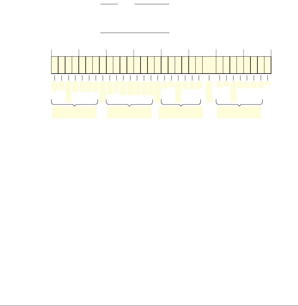
C11 The Debug Registers
C11.11 Register descriptions, in register order
C11-2288 Copyright © 1996-1998, 2000, 2004-2012, 2014 ARM. All rights reserved. ARM DDI 0406C.c
Non-Confidential ID051414
C11.11.42 DBGVCR, Vector Catch Register
The DBGVCR characteristics are:
Purpose Controls Vector catch debug events, see Vector catch debug events on page C3-2067.
Usage constraints There are no usage constraints.
Configurations This register is required in all implementations.
Some bit assignments differ in an implementation that includes the Security Extensions and
Virtualization Extensions. See the field descriptions for details.
Attributes A 32-bit RW register. DBGBVCR is in the Software debug event registers group, see the
registers summary in Table C11-5 on page C11-2201.
The debug logic reset value of DBGVCR is UNKNOWN.
Note
After a debug logic reset a debugger must ensure that DBGVCR has a defined value for all
implemented registers before it programs DBGDSCR.MDBGen or DBGDSCR.HDBGen
to enable Monitor or Halting debug-mode.
The DBGVCR bit assignments are:
Bits[29, 24, 16, 13, 9:8, 5]
Reserved, UNK/SBZP.
Bits[31:30, 28:25], Implementation includes the Security Extensions
Non-secure local Vector catch enable bits. These are the Vector catch enable bits for exceptions
taken to Non-secure PL1 modes.
The Non-secure local Vector catch enable bits are:
NSF, bit[31] FIQ interrupt exception Vector catch enable in Non-secure state.
NSI, bit[30] IRQ interrupt exception Vector catch enable in Non-secure state.
NSD, bit[28] Data Abort exception Vector catch enable in Non-secure state.
NSP, bit[27] Prefetch Abort exception Vector catch enable in Non-secure state.
NSS, bit[26] Supervisor Call exception Vector catch enable in Non-secure state.
NSU, bit[25] Undefined Instruction exception Vector catch enable in Non-secure state.
Bits[31:30, 28:25], Implementation does not include the Security Extensions
Reserved, UNK/SBZP.
(0)(0) (0) (0) (0) (0)
31 30 29 28 27 26 25 24 16 15 14 13 12 11 10 9 8 7 6 5 4 3 2 1 0
(0)
23 22 21 20 19 18 17
Vector catch enable,
Secure local
Vector catch enable,
Monitor †
Vector catch enable,
Non-secure local
†
SF
SI
SD
SP
SS
SU
Reserved
Reserved
R
MF
MI
MD
MP
MS
Reserved
NSHF
NSHI
NSHD
NSHP
NSHC
NSHU
NSHE
NSF
NSI
NSD
NSP
NSS
NSU
Reserved
Vector catch enable,
Hyp ‡
Reserved
Reserved
‡ Only when the implementation includes Virtualization Extensions
† Only when the implementation includes the Security Extensions

C11 The Debug Registers
C11.11 Register descriptions, in register order
ARM DDI 0406C.c Copyright © 1996-1998, 2000, 2004-2012, 2014 ARM. All rights reserved. C11-2289
ID051414 Non-Confidential
Bits[23:17], Implementation includes the Virtualization Extensions
Hyp Vector catch enable bits. These are the Vector catch enable bits for exceptions taken to Hyp
mode in Non-secure state.
The Hyp Vector catch enable bits are:
NSHF, bit[23] FIQ interrupt exception Vector catch enable in Non-secure state.
NSHI, bit[22] IRQ interrupt exception Vector catch enable in Non-secure state.
NSHE, bit[21] Hyp Trap or Hyp mode entry exception Vector catch enable in Non-secure
state.
NSHD, bit[20] Data Abort, from Hyp mode exception Vector catch enable in Non-secure
state.
NSHP, bit[19] Prefetch Abort, from Hyp mode exception Vector catch enable in
Non-secure state.
NSHC, bit[18] Hypervisor Call. from Hyp mode exception Vector catch enable in
Non-secure state.
NSHU, bit[17] Undefined Instruction, from Hyp mode exception Vector catch enable in
Non-secure state.
Bits[23:17], Implementation does not include the Virtualization Extensions
Reserved, UNK/SBZP.
Bits[15:14, 12:10], Implementation includes the Security Extensions
Monitor Vector catch enable bits. These are the Vector catch enable bits for exceptions taken to
Monitor mode in Secure state.
The Monitor Vector catch enable bits are:
MF, bit[15] FIQ interrupt exception Vector catch enable, in Secure state on Monitor
mode vector.
MI, bit[14] IRQ interrupt exception Vector catch enable in Secure state on Monitor
mode vector.
MD, bit[12] Data Abort exception Vector catch enable in Secure state on Monitor mode
vector.
MP, bit[11] Prefetch Abort exception Vector catch enable in Secure state on Monitor
mode vector.
MS, bit[10] Secure Monitor Call exception Vector catch enable in Secure state.
Bits[15:14, 12:10], Implementation does not include the Security Extensions
Reserved, UNK/SBZP.
Bits[7:6, 4:1] Implementation does not include the Security Extensions
Local Vector catch enable bits.
Implementation includes the Security Extensions
Secure local Vector catch enable bits. These are the Vector catch enable bits for
exceptions taken to Secure state that are not taken to Monitor mode. These exceptions
are taken on the Secure local vectors.
The Local Vector catch or Secure local Vector catch enable bits are:
SF, bit[7] FIQ interrupt exception Vector catch enable in Secure state.
SI, bit[6] IRQ interrupt exception Vector catch enable in Secure state.
SD, bit[4] Data Abort exception Vector catch enable in Secure state.
SP, bit[3] Prefetch Abort exception Vector catch enable in Secure state.
SS, bit[2] SVC, Supervisor Call, exception Vector catch enable in Secure state.
SU, bit[1] Undefined Instruction exception Vector catch enable in Secure state.

C11 The Debug Registers
C11.11 Register descriptions, in register order
C11-2290 Copyright © 1996-1998, 2000, 2004-2012, 2014 ARM. All rights reserved. ARM DDI 0406C.c
Non-Confidential ID051414
R, bit[0] Reset Vector catch enable.
When Monitor debug-mode is configured and enabled, DBGVCR.{SD, SP} must be programmed to
0b00
.
Additionally, if the implementation includes the Security Extensions and debug exceptions are not being trapped to
the Hypervisor, DBGVCR.{NSD, NSP} must be programmed to
0b00
, see UNPREDICTABLE cases when Monitor
debug-mode is selected on page C3-2047.
For more information about these Vector catch operations see Vector catch debug events on page C3-2067.
C11 The Debug Registers
C11.11 Register descriptions, in register order
ARM DDI 0406C.c Copyright © 1996-1998, 2000, 2004-2012, 2014 ARM. All rights reserved. C11-2291
ID051414 Non-Confidential
C11.11.43 DBGVIDSR, Virtualization ID Sampling Register
The DBGVIDSR characteristics are:
Purpose Samples the VMID, Hyp mode status, and NS state whenever the DBGPCSR samples the
program counter. This enables a debugger to associate a program counter sample with the
virtual machine running on the processor.
In implementations that do not include Virtualization Extensions, DBGVIDSR is a
Non-secure state sample register.
The DBGVIDSR is a Sample-based profiling register.
Usage constraints Used in conjunction with the DBGPCSR.
DBGVIDSR is not visible in the CP14 interface.
Configurations Implementation of the Sample-based profiling extension is OPTIONAL. In an implementation
that includes the Sample-based profiling extension:
• DBGVIDSR is not implemented if the implementation does not include the Security
Extensions
• in an implementation that includes the Security Extensions:
— in a v7 Debug implementation, it is IMPLEMENTATION DEFINED whether
DBGVIDSR is implemented
— in a v7.1 Debug implementation, DBGVIDSR must be implemented.
When implemented, DBGVIDSR is debug register 42.
An implementation that does not include the Sample-based profiling extension cannot
implement DBGVIDSR.
In an implementation that includes DBGVIDSR but does not includes the Virtualization
Extensions, bits[30:0] of the register are reserved, UNK.
When DBGVIDSR is not implemented, debug register 42 is reserved.
Attributes A 32-bit RO register. DBGVIDSR is in the Sample-based profiling registers group, see the
registers summary in Table C11-6 on page C11-2202.
The non-debug logic reset value of the DBGVIDSR is UNKNOWN.
The DBGVIDSR bit assignments are:
NS, bit[31] NS state sample. Indicates the Secure or Non-secure state associated with the last PC sample read
from DBGPCSR.
0 Secure state.
1 Non-secure state.
This is the NS state, not the value of the SCR.NS bit. In Monitor mode it is sampled as zero,
regardless of the value of SCR.NS.
Bit[30], Implementation does not include the Virtualization Extensions
Reserved, UNK.
31 30 29 8 7 0
H Reserved, UNK VMID
NS

C11 The Debug Registers
C11.11 Register descriptions, in register order
C11-2292 Copyright © 1996-1998, 2000, 2004-2012, 2014 ARM. All rights reserved. ARM DDI 0406C.c
Non-Confidential ID051414
H, bit[30], Implementation includes the Virtualization Extensions
Hyp mode sample. Indicates whether the last PC sample read from DBGPCSR was associated with
Hyp mode.
0 Not associated with Hyp mode.
1 Associated with Hyp mode.
If DBGVIDSR.NS is 0, then this field is UNK.
Bits[29:8] Reserved, UNK.
Bits[7:0], Implementation does not include the Virtualization Extensions
Reserved, UNK.
VMID, bits[7:0], Implementation includes the Virtualization Extensions
VMID sample. The value of the VMID field from the VTTBR, associated with the last PC sample
read from DBGPCSR. See VTTBR, Virtualization Translation Table Base Register, Virtualization
Extensions on page B4-1741 for more information.
If DBGVIDSR.NS is 0 or DBGVIDSR.H is 1, then this field is UNK.
The implemented Sample-based profiling registers on page C10-2190 describes the Sample-based profiling
implementation options, and how software can determine whether and how the Sample-based profiling registers are
implemented.
For more information about program counter sampling, see Sample-based profiling on page C10-2190.
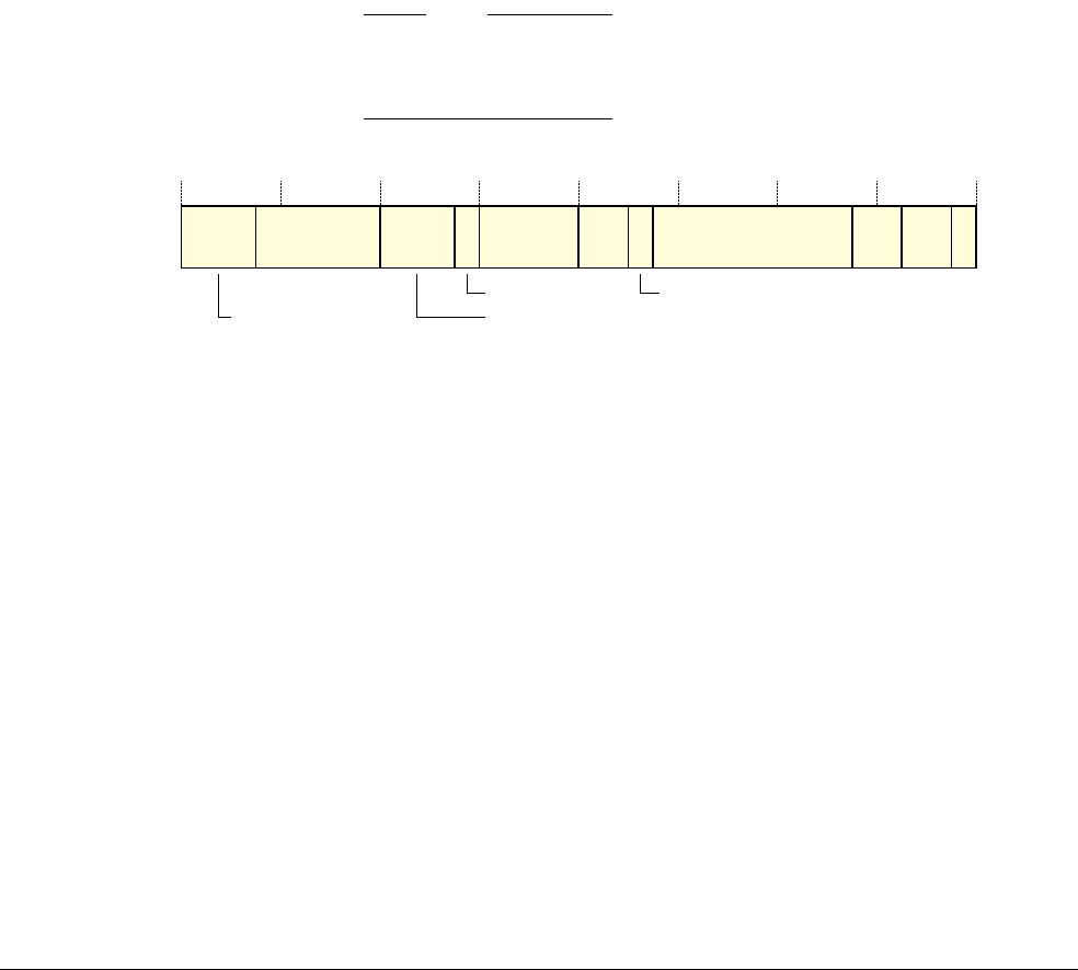
C11 The Debug Registers
C11.11 Register descriptions, in register order
ARM DDI 0406C.c Copyright © 1996-1998, 2000, 2004-2012, 2014 ARM. All rights reserved. C11-2293
ID051414 Non-Confidential
C11.11.44 DBGWCR, Watchpoint Control Registers
The DBGWCR characteristics are:
Purpose Holds control information for a watchpoint.
Used in conjunction with a Watchpoint Value Register, DBGWVR. DBGWVRn is
associated with DBGWCRn to form watchpoint n.
Usage constraints There are no usage constraints.
Configurations These registers are required in all implementations.
The number of watchpoints is IMPLEMENTATION DEFINED, between 1 and 16, and is
specified by the DBGDIDR.WRPs field. Any registers that are not implemented are
reserved.
Some bit assignments differ if the implementation includes the Security Extensions and
Virtualization Extensions. See the field descriptions for details.
Attributes A 32-bit RW register. DBGWCR is in the Software debug event registers group, see the
registers summary in Table C11-5 on page C11-2201.
The debug logic reset value of a DBGWCR is UNKNOWN.
Note
After a debug logic reset a debugger must ensure that DBGWCR.E has a defined value for
all implemented registers before it programs DBGDSCR.MDBGen or
DBGDSCR.HDBGen to enable Monitor debug-mode or Halting debug-mode.
The DBGWCR bit assignments are:
Bits[31:29, 23:21]
Reserved, UNK/SBZP.
MASK, bits[28:24]
Address range mask. In v7 Debug, support for watchpoint address range masking is optional. If it
is not supported then:
•if the DBGDEVID register is not implemented, or DBGDEVID.WPAddrMask is
0b0000
, then
these bits are RAZ/WI
• otherwise, these bits are UNK/SBZP.
In v7.1 Debug, support for watchpoint address range masking is required.
If watchpoint address range masking is supported, this field can set a watchpoint on a range of
addresses by masking lower order address bits out of the watchpoint comparison. The value of this
field is the number of low order bits of the address that are masked off, except that values of 1 and
2 are reserved. Therefore, the meaning of Watchpoint Address range mask values are:
0b00000
No mask.
0b00001
Reserved.
0b00010
Reserved.
0b00011
0x00000007
mask for data address, three bits masked.
0b00100
0x0000000F
mask for data address, four bits masked.
(0)(0) (0) (0)(0)
MASK
(0) E
31 29 28 24 23 20 19 16 15 14 13 5 4 3 2 1 0
LBN SSC BAS LSC PAC
1221
HMC
Reserved Reserved
WT

C11 The Debug Registers
C11.11 Register descriptions, in register order
C11-2294 Copyright © 1996-1998, 2000, 2004-2012, 2014 ARM. All rights reserved. ARM DDI 0406C.c
Non-Confidential ID051414
0b00101
0x0000001F
mask for data address, five bits masked.
.
.
.
0b11111
0x7FFFFFFF
mask for data address, 31 bits masked.
This field must be programmed to
0b00000
if either:
• DBGWCR.BAS !=
0b11111111
, if an 8-bit Byte address select field is implemented
• DBGWCR.BAS !=
0b1111
, if a 4-bit Byte address select field is implemented.
If this is not done, the generation of Watchpoint debug events by this watchpoint is UNPREDICTABLE.
If this field is not zero, the DBGWVR bits that are not included in the comparison must be zero,
otherwise the generation of Watchpoint debug events by this watchpoint is UNPREDICTABLE.
To watch for an access to any byte in an doubleword-aligned region of size 8 bytes, ARM
recommends that debuggers set:
• DBGWCR.MASK to
0b00011
, indicating an address range mask of
0x00000007
• DBGWCR.BAS, Byte address select field to
0b11111111
.
This setting is compatible with both implementations with an 8-bit Byte address select field and
implementations with a 4-bit Byte address select field, because implementations with a 4-bit Byte
address select field ignore writes to DBGWCR.BAS[7:4].
WT, bit[20] Watchpoint type. This bit is set to 1 to link the watchpoint to a breakpoint to create a linked
watchpoint that requires both data address matching and Context matching. The possible values of
this bit are:
0 Unlinked data address match.
1 Linked data address match.
When this bit is set to 1 the LBN field indicates the breakpoint to which this watchpoint is linked.
For more information, see Linked comparisons for debug event generation on page C3-2055.
LBN, bits[19:16]
Linked breakpoint number. If this watchpoint is programmed with the WT field set to Linked data
address match then this field must be programmed with the number of the breakpoint that defines
the Context match to be combined with data address comparison. Otherwise, this field must be
programmed to
0b0000
.
Reading this register returns an UNKNOWN value for this field, and the generation of Watchpoint
debug events by this watchpoint is UNPREDICTABLE, if either:
• this watchpoint does not have linking enabled and this field is not programmed to
0b0000
• this watchpoint has linking enabled and the breakpoint indicated by this field does not
support Context matching, is not programmed for Context matching, or does not exist.
SSC, bits[15:14], implementation includes the Security Extensions
Security state control. This field enables the watchpoint to be conditional on the security state of the
processor.
Note
As Watchpoint state control fields on page C11-2296 shows, SSC controls the modes in which an
access matches. Whether an access matches is not affected by the security attribute of the access.
This field is used with the HMC, Hyp mode control, and PAC, Privileged access control, fields. See
Watchpoint state control fields on page C11-2296 for possible values.
Bits[15:14], implementation does not include the Security Extensions
Reserved, UNK/SBZP.

C11 The Debug Registers
C11.11 Register descriptions, in register order
ARM DDI 0406C.c Copyright © 1996-1998, 2000, 2004-2012, 2014 ARM. All rights reserved. C11-2295
ID051414 Non-Confidential
HMC, bit[13], implementation includes the Virtualization Extensions
Hyp mode control.
This field is used with the SSC, Security state control, and PAC, Privileged access control, fields.
See Watchpoint state control fields on page C11-2296 for possible values.
Bit[13], implementation does not include the Virtualization Extensions
Reserved, UNK/SBZP.
BAS, bits[12:5] or bits[8:5]
Byte address select. It is IMPLEMENTATION DEFINED whether a 4-bit or an 8-bit Byte address select
field is implemented:
• an 8-bit Byte address select field is DBGWCR[12:5]
• a 4-bit Byte address select field is DBGWCR[8:5]. DBGWCR[12:9] is RAZ/WI.
A DBGWVR is programmed with a word-aligned address. This field enables the watchpoint to hit
only if certain bytes of the addressed word are accessed. The watchpoint hits if an access hits any
byte being watched, even if:
• the access size is larger than the size of the region being watched
• the access is unaligned, and the base address of the access is not in the same word of memory
as the address in the DBGWVR
• the access size is smaller than the size of region being watched.
For details of the use of this field see Byte address selection behavior on data address match on
page C3-2062.
If the MASK field is implemented and programmed to a value other than
0b00000,
no mask, then
this field must be programmed to:
•
0b1111
, if a 4-bit Byte address select field is implemented
•
0b11111111
, an 8-bit Byte address select field is implemented.
If this is not done, the generation of Watchpoint debug events by this watchpoint is UNPREDICTABLE.
ARM deprecates values of this field that set watchpoints on multiple non-contiguous bytes using a
single set of watchpoint registers. Table C11-24 shows examples of deprecated BAS values, and of
values that are not deprecated.
Table C11-24 Example BAS values
BAS field Deprecated
0b00000001
No
0b00001111
No
0b00111100
No
0b11110001
Yes
0b11110111
Yes
0b00101010
Yes
0b00000000
Yes

C11 The Debug Registers
C11.11 Register descriptions, in register order
C11-2296 Copyright © 1996-1998, 2000, 2004-2012, 2014 ARM. All rights reserved. ARM DDI 0406C.c
Non-Confidential ID051414
LSC, bits[4:3]
Load/store access control. This field enables watchpoint matching on the type of access being made.
Possible values of this field are:
0b00
Reserved.
0b01
Match on any load, Load-Exclusive, or swap.
0b10
Match on any store, Store-Exclusive, or swap.
0b11
Match on all types of access.
If an implementation supports watchpoint generation by:
• a memory hint instruction, then that instruction is treated as generating a load access
• a cache maintenance operation, then that operation is treated as generating a store access.
PAC, bits[2:1] Privileged access control. This field enables watchpoint matching conditional on the mode of the
processor.
This field is used with the SSC, Security state control, and HMC, Hyp mode control, fields. See
Watchpoint state control fields for possible values.
E, bit[0] Watchpoint enable. The meaning of this bit is:
0 Watchpoint disabled.
1 Watchpoint enabled.
A watchpoint never generates a Watchpoint debug event when it is disabled.
For more information about possible watchpoint values see DBGWVR, Watchpoint Value Registers on
page C11-2299.
Watchpoint state control fields
Watchpoint debug event generation can be made conditional on the current state of the processor. The following
fields in DBGWCR check the current state:
• SSC, Security state control, if the implementation includes the Security Extensions
• HMC, Hyp mode control, if the implementation includes the Virtualization Extensions
• PAC, Privileged access control.
Table C11-25 shows the possible values of the fields, and the access modes and security states that can be tested.
Table C11-25 Watchpoint state control
SSC HMC PAC Secure modes Non-secure modes
0b00 0 0b01
PL1 only PL1 only
0b10
Unprivileged only Unprivileged only
0b11
PL1, and unprivileged PL1, and unprivileged
1 0b01
PL1 PL2 and PL1
0b11
All All
0b01 0 0b01
- PL1 only
0b10
- Unprivileged only
0b11
- PL1, and unprivileged
1 0b01
- PL2 and PL1
0b11
- PL2, PL1, and unprivileged

C11 The Debug Registers
C11.11 Register descriptions, in register order
ARM DDI 0406C.c Copyright © 1996-1998, 2000, 2004-2012, 2014 ARM. All rights reserved. C11-2297
ID051414 Non-Confidential
Note
•In Table C11-25 on page C11-2296, unprivileged means accesses made at PL0, and
LDRT
and
STRT
accesses
made at PL1.
• The SSC field controls the processor security state in which the access matches, not the required security
attribute of the access.
• All other combinations of values are reserved, and the generation of Watchpoint debug events by this
watchpoint is UNPREDICTABLE if used.
0b10 0 0b01
PL1 only -
0b10
Unprivileged only -
0b11
PL1, and unprivileged -
0b11 1 0b00
- PL2 only
Table C11-25 Watchpoint state control (continued)
SSC HMC PAC Secure modes Non-secure modes

C11 The Debug Registers
C11.11 Register descriptions, in register order
C11-2298 Copyright © 1996-1998, 2000, 2004-2012, 2014 ARM. All rights reserved. ARM DDI 0406C.c
Non-Confidential ID051414
C11.11.45 DBGWFAR, Watchpoint Fault Address Register
The DBGWFAR characteristics are:
Purpose Returns information about the address of the instruction that accessed a watchpointed
address.
Usage constraints ARM deprecates using DBGWFAR to determine the address of the instruction that
triggered a synchronous watchpoint. For more information see:
• for a VMSA implementation, Data Abort on a Watchpoint debug event on
page B3-1412 and Register updates on exception reporting at PL2 on page B3-1422
• for a PMSA implementation, Data Abort exception on a Watchpoint debug event on
page B5-1770
•Effect of entering Debug state on CP15 registers and the DBGWFAR on
page C5-2096
In v7.1 Debug, DBGWFAR must not be used for synchronous watchpoints as it is
UNKNOWN.
Configurations This register is required in all implementations.
In v7.1 Debug, if a processor never generates asynchronous watchpoints this register can be
implemented as RAZ/WI.
Attributes A 32-bit RW register. DBGWFAR is in the Debug control and status registers group, see the
registers summary in Table C11-3 on page C11-2199.
The debug logic reset value of the DBGWFAR is UNKNOWN.
The DBGWFAR bit assignments are:
(Instruction address) + offset, bits[31:0]
When Watchpoint debug events are permitted, on every Watchpoint debug event the DBGWFAR is
updated with the virtual address of the instruction that accessed the watchpointed address plus an
offset that depends on the processor instruction set state when the instruction was executed:
• 8 if the processor was in ARM state
• 4 if the processor was in Thumb or ThumbEE state
•an
IMPLEMENTATION DEFINED offset if the processor was in Jazelle state.
In v7.1 Debug, when DBGWFAR is implemented as a RW register, this field is UNKNOWN following
a synchronous watchpoint. LR_abt indicates the address of the instruction that triggered the
watchpoint.
A processor with a trivial implementation of the Jazelle extension can implement DBGWFAR[0] as RAZ/WI, see
Trivial implementation of the Jazelle extension on page B1-1245 for more information. In such an implementation,
software must use a SBZP policy when writing to DBGWFAR[0].
(Instruction address) + offset
31 0

C11 The Debug Registers
C11.11 Register descriptions, in register order
ARM DDI 0406C.c Copyright © 1996-1998, 2000, 2004-2012, 2014 ARM. All rights reserved. C11-2299
ID051414 Non-Confidential
C11.11.46 DBGWVR, Watchpoint Value Registers
The DBGWVR characteristics are:
Purpose Holds a data address value for use in watchpoint matching. The address used must be the
virtual address of the data.
Used with a Watchpoint Control Register, DBGWCR. DBGWVRn is associated with
DBGWCRn to form watchpoint n.
Usage constraints There are no usage constraints.
Configurations These registers are required in all implementations.
The number of watchpoints is IMPLEMENTATION DEFINED, between 1 and 16, and is
specified by the DBGDIDR.WRPs field. Any registers that are not implemented are
reserved.
Attributes A 32-bit RW register. DBGBWVR is in the Software debug event registers group, see the
registers summary in Table C11-5 on page C11-2201.
The debug logic reset value of a DBGWVR is UNKNOWN.
The DBGWVR bit assignments are:
Bits[31:2] Bits[31:2] of the value for comparison, address[31:2].
Bits[1:0] Reserved, UNK/SBZP.
The debug logic generates a debug event when the watchpoint is matched. For more information, see Watchpoint
debug events on page C3-2059.
(0)(0)Data address[31:2]
31 210
Reserved

C11 The Debug Registers
C11.11 Register descriptions, in register order
C11-2300 Copyright © 1996-1998, 2000, 2004-2012, 2014 ARM. All rights reserved. ARM DDI 0406C.c
Non-Confidential ID051414

ARM DDI 0406C.c Copyright © 1996-1998, 2000, 2004-2012, 2014 ARM. All rights reserved. C12-2301
ID051414 Non-Confidential
Chapter C12
The Performance Monitors Extension
This chapter describes the Performance Monitors Extension, that is an OPTIONAL non-invasive debug component.
It describes version 1 and 2 of the Performance Monitor Unit (PMU) architecture, PMUv1 and PMUv2, and
contains the following sections:
•About the Performance Monitors on page C12-2302
•Accuracy of the Performance Monitors on page C12-2306
•Behavior on overflow on page C12-2307
•Effect of the Security Extensions and Virtualization Extensions on page C12-2309
•Event filtering, PMUv2 on page C12-2311
•Counter enables on page C12-2313
•Counter access on page C12-2314
•Event numbers and mnemonics on page C12-2315
•Performance Monitors registers on page C12-2328.
Note
Both Chapter B4 System Control Registers in a VMSA implementation and Chapter B6 System Control Registers in
a PMSA implementation describe the Performance Monitors Extension registers. Most of the registers are included
in both VMSA and PMSA implementations, and for these registers the bit assignments are identical in VMSA and
PMSA implementations. However, most register references in this chapter link to the register descriptions in
Chapter B4.

C12 The Performance Monitors Extension
C12.1 About the Performance Monitors
C12-2302 Copyright © 1996-1998, 2000, 2004-2012, 2014 ARM. All rights reserved. ARM DDI 0406C.c
Non-Confidential ID051414
C12.1 About the Performance Monitors
The Performance Monitors are part of the ARM Debug architecture. Many ARMv6 processors included
performance monitors, but before ARMv7 they were not part of the architecture. Publication of the ARM
Architecture Reference Manual, ARMv7-A and ARMv7-R edition was the first architectural specification of the
Performance Monitors, and that specification was derived from the earlier ARM implementations. The versions of
the Performance Monitors are:
• Performance Monitors Extension version 1, PMUv1
• Performance Monitors Extension version 2, PMUv2.
In ARMv7, the Performance Monitors Extension is an OPTIONAL feature of an implementation, but ARM strongly
recommends that ARMv7-A and ARMv7-R implementations include the Performance Monitors Extension.
The basic form of the Performance Monitors is:
• A cycle counter, with the ability to count every cycle or every 64th cycle.
• A number of event counters. The event counted by each counter is programmable. ARMv7 provides space
for up to 31 counters. The actual number of counters is IMPLEMENTATION DEFINED, and the specification
includes an identification mechanism.
• Controls for:
— Enabling and resetting counters.
— Flagging overflows.
— Enabling interrupts on overflow.
Monitoring software can enable the cycle counter independently of the event counters.
The events that can be monitored split into:
• Architectural and microarchitectural events that are likely to be consistent across many microarchitectures.
• Implementation-specific events.
The PMU architecture uses event numbers to identify an event. It:
• Defines event numbers for common events, for use across many architectures and microarchitectures.
Note
On processors that implement PMUv1, there is no requirement to implement any of the common events.
Processors that implement PMUv2 must, as a minimum requirement, implement a limited subset of the
common events.
• Reserves a large event number space for IMPLEMENTATION DEFINED events.
The full set of events for an implementation is IMPLEMENTATION DEFINED. ARM recommends that processors
implement as many of the events as are appropriate to the architecture profile and microarchitecture of the
implementation.
The event numbers of the common events are reserved for the specified events. Each of these event numbers must
either:
• Be used for its assigned event.
• Not be used.
If the configuration of the event to be counted specifies an event number that is not used, or an event number for
which no event is defined, then the counter never increments.
When a processor supports monitoring of an event that is assigned a common event number, ARM strongly
recommends that it uses that number for the event. However, software might encounter implementations where an
event assigned a number in this range is monitored using an event number from the IMPLEMENTATION DEFINED
range.

C12 The Performance Monitors Extension
C12.1 About the Performance Monitors
ARM DDI 0406C.c Copyright © 1996-1998, 2000, 2004-2012, 2014 ARM. All rights reserved. C12-2303
ID051414 Non-Confidential
Note
Future revisions of the PMU architecture might define other common event numbers. This is one reason why
software must not assume that an event with an assigned common event number is never monitored using an event
number from the IMPLEMENTATION DEFINED range.
ARMv7 defines the following possible interfaces to the Performance Monitors registers:
• A system control coprocessor (CP15) interface. This interface is mandatory.
• A memory-mapped interface. This interface is optional.
• An external debug interface. This interface is optional.
An operating system running on the processor can use the CP15 interface to access the counters. This supports a
number of uses, including:
• dynamic compilation techniques
• energy management.
Also, if required, the operating system can enable application software to access the counters. This enables an
application to monitor its own performance with fine grain control without requiring operating system support. For
example, an application might implement per-function performance monitoring.
There are many situations where performance monitoring features integrated into the processor are valuable for
applications and for application development. When an operating system does not use the Performance Monitors
itself, ARM recommends that it enables application software access to the Performance Monitors.
To enable interaction with external monitoring, an implementation might consider additional enhancements, such
as providing:
• A set of events, from which a selection can be exported onto a bus for use as external events.
• The ability to count external events. This enhancement means the processor must also implement a set of
external event input signals.
• Memory-mapped and external debug access to the Performance Monitors registers. This means the counter
resources can be used for system monitoring in a system where they are not used by the software running on
the processor. See Appendix D2 Recommended Memory-mapped and External Debug Interfaces for the
Performance Monitors for more information.
C12.1.1 About the Performance Monitors v2
The main changes in Performance Monitors v2 are:
• Filtering of event counting by processor state. See PMXEVTYPER, Performance Monitors Event Type Select
Register, VMSA on page B4-1696 or PMXEVTYPER, Performance Monitors Event Type Select Register,
PMSA on page B6-1926.
• Changes the names of some of the events defined in PMUv1. These name changes do not affect what the
event counts.
• Performance Monitors implementations must implement at least a limited subset of the common events.
C12.1.2 Identification of the Performance Monitors Extension version
The introduction of PMUv2 adds a field to the CP15 Debug Feature Register 0, ID_DFR0, to identify the
Performance Monitors Extension version, see ID_DFR0, Debug Feature Register 0, VMSA on page B4-1605.

C12 The Performance Monitors Extension
C12.1 About the Performance Monitors
C12-2304 Copyright © 1996-1998, 2000, 2004-2012, 2014 ARM. All rights reserved. ARM DDI 0406C.c
Non-Confidential ID051414
C12.1.3 PMU versions, and status in the ARM architecture
ARMv7 reserves CP15 registers for ARM-recommended Performance Monitors, and for IMPLEMENTATION
DEFINED performance monitors, see VMSA CP15 c9 register summary, reserved for cache and TCM control and
performance monitors on page B3-1477 or PMSA CP15 c9 register summary, reserved for cache and TCM
lockdown registers and performance monitors on page B5-1791.
ARM strongly recommends that performance monitors are implemented using the Performance Monitors Extension
described in this chapter.
Note
• This chapter describes PMUv1 and PMUv2. Where there are differences between the two versions, the
information is described accordingly.
• If an implementation includes v7.1 Debug and also includes the PMU, then it must implement PMUv2.
C12.1.4 Interaction with trace
It is IMPLEMENTATION DEFINED whether the processor exports counter events to a trace macrocell, or other external
monitoring agent, to provide triggering information. The form of any exporting is also IMPLEMENTATION DEFINED.
If implemented, this exporting might be enabled as part of the performance monitoring control functionality.
ARM recommends system designers include a mechanism for importing a set of external events to be counted, but
such a feature is IMPLEMENTATION DEFINED. When implemented, this feature enables the trace module to pass in
events to be counted.
C12.1.5 Interaction with power saving operations
All counters are subject to any changes in clock frequency, including clock stopping caused by the
WFI
and
WFE
instructions.
C12.1.6 Interaction with Save and Restore operations
For PMUv2 implementations that include the Virtualization Extensions, software can use the PMOVSSET register
to restore the state of PMOVSR.
C12.1.7 Effects of non-invasive debug authentication on the Performance Monitors
Table C12-1 describes the behavior of the Performance Monitors when non-invasive debug is disabled or not
permitted, and in Debug state.
Table C12-1 Behavior of Performance Monitors when non-invasive debug not permitted
Debug state Non-invasive debug permittedaPMCR.DPbEvent counters enabled
and events exportedb, cPMCCNTR enabled
Yes x x No No
No Yes x Yes Yes
No 0 No Yes
1No No
a. Chapter C9 Non-invasive Debug Authentication describes when non-invasive debug is permitted and enabled.
b. See PMCR, Performance Monitors Control Register, VMSA on page B4-1678, or PMCR, Performance Monitors Control Register, PMSA
on page B6-1912. The VMSA and PMSA definitions of the DP bit are identical.
c. The events are exported only if the PMCR.X bit is set to 1.

C12 The Performance Monitors Extension
C12.1 About the Performance Monitors
ARM DDI 0406C.c Copyright © 1996-1998, 2000, 2004-2012, 2014 ARM. All rights reserved. C12-2305
ID051414 Non-Confidential
Note
Some documentation describes the conditions under which non-invasive debug is not permitted as being defined by
prohibited software regions, or prohibited regions.
Entry to and exit from Debug state can affect the accuracy of the Performance Monitors, see Accuracy of the
Performance Monitors on page C12-2306.

C12 The Performance Monitors Extension
C12.2 Accuracy of the Performance Monitors
C12-2306 Copyright © 1996-1998, 2000, 2004-2012, 2014 ARM. All rights reserved. ARM DDI 0406C.c
Non-Confidential ID051414
C12.2 Accuracy of the Performance Monitors
The Performance Monitors provide approximately accurate count information. To keep the implementation and
validation cost low, a reasonable degree of inaccuracy in the counts is acceptable. ARM does not define a reasonable
degree of inaccuracy but recommends the following guidelines:
• Under normal operating conditions, the counters must present an accurate value of the count.
• In exceptional circumstances, such as a change in security state or other boundary condition, it is acceptable
for the count to be inaccurate.
• Under very unusual nonrepeating pathological cases then counts can be inaccurate. These cases are likely to
occur as a result of asynchronous exceptions, such as interrupts, where the chance of a systematic error in the
count is very unlikely.
Note
An implementation must not introduce inaccuracies that can be triggered systematically by the execution of normal
pieces of software. For example, dropping a branch count in a loop due to the structure of the loop gives a systematic
error that makes the count of branch behavior very inaccurate, and this is not reasonable. However, dropping a single
branch count as the result of a rare interaction with an interrupt is acceptable.
The permitted inaccuracy limits the possible uses of the Performance Monitors. In particular, the architecture does
not define the point in a pipeline where the event counter is incremented, relative to the point where a read of the
event counters is made. This means that pipelining effects can cause some imprecision.
A change of security state can affect the accuracy of the Performance Monitors, see Interaction with Security
Extensions on page C12-2309.
Entry to and exit from Debug state can also disturb the normal running of the processor, causing additional
inaccuracy in the Performance Monitors. Disabling the counters while in Debug state limits the extent of this
inaccuracy. An implementation can limit this inaccuracy to a greater extent, for example by disabling the counters
as soon as possible during the Debug state entry sequence.
An implementation must document any particular scenarios where significant inaccuracies are expected.

C12 The Performance Monitors Extension
C12.3 Behavior on overflow
ARM DDI 0406C.c Copyright © 1996-1998, 2000, 2004-2012, 2014 ARM. All rights reserved. C12-2307
ID051414 Non-Confidential
C12.3 Behavior on overflow
Events are counted in 32-bit wrapping counters. A counter overflows when it wraps. On a Performance Monitors
counter overflow:
• An overflow status bit is set to 1. See PMOVSR, Performance Monitors Overflow Flag Status Register, VMSA
on page B4-1685.
• An interrupt request is generated if the processor is configured to generate counter overflow interrupts. For
more information, see Generating overflow interrupt requests.
• The counter continues counting events.
C12.3.1 Generating overflow interrupt requests
Software can program the Performance Monitors so that an overflow interrupt request is generated when a counter
overflows. See PMINTENSET, Performance Monitors Interrupt Enable Set register, VMSA on page B4-1683 and
PMINTENCLR, Performance Monitors Interrupt Enable Clear register, VMSA on page B4-1681.
Note
The mechanism by which an interrupt request from the Performance Monitors generates an FIQ or IRQ exception
is IMPLEMENTATION DEFINED.
Software can write to the counters to control the frequency at which interrupt requests occur. For example, software
might set a counter to
0xFFFF0000
, to generate another counter overflow after 65536 increments, and reset it to this
value every time an overflow interrupt occurs.
For implementations that do not include the Virtualization Extensions:
• The overflow interrupt request is a level-sensitive request.
• The processor signals a request:
— for any given PMNx counter, when PMOVSR[x] == 1 and PMINTENSET[x]==1
— when PMOVSR[31] == 1 and PMINTENSET[31] == 1.
• It is IMPLEMENTATION DEFINED whether the processor signals a request when PMCR.E == 0.
For PMUv2 implementations that include the Virtualization Extensions:
• The overflow interrupt request is a level-sensitive request.
• The processor signals a request for any given PMNx counter, when PMOVSR[x]==1,
PMINTENSET[x] == 1 and either:
—x < HDCR.HPMN and PMCR.E == 1
—x ≥ HDCR.HPMN and HDCR.HPME == 1.
• The processor signals a request when PMOVSR[31] == 1, PMINTENSET[31] == 1, and PMCR.E == 1.
The overflow interrupt request is active in both Secure and Non-secure states. In particular, overflow events from
PMNx where x≥HDCR.HPMN can be signaled from all modes and states but only if HDCR.HPME == 1. The
interrupt handler for the counter overflow request must cancel the interrupt request, by writing to PMOVSR[x] to
clear the overflow bit to 0.
C12.3.2 Pseudocode details of overflow interrupt requests
The
PMUIRQ()
pseudocode function returns a value corresponding to the level-sensitive overflow interrupt request.
// PMUIRQ
// ======
boolean PMUIRQ()
// Returns the state of the Performance Monitors overflow interrupt request signal.
if HaveVirtExt() then
global_irqen = (PMCR.E == '1');

C12 The Performance Monitors Extension
C12.3 Behavior on overflow
C12-2308 Copyright © 1996-1998, 2000, 2004-2012, 2014 ARM. All rights reserved. ARM DDI 0406C.c
Non-Confidential ID051414
hyp_irqen = (HDCR.HPME == '1');
else
global_irqen = IMPLEMENTATION_DEFINED either TRUE or (PMCR.E == '1');
pmuirq = (global_irqen && PMINTEN<31> == '1' && PMOVSR<31> == '1'); // interrupt for PMCCNT
for n = 0 to UInt(PMCR.N) - 1
irqen = (if HaveVirtExt() && n >= UInt(HDCR.HPMN) then hyp_irqen else global_irqen);
if irqen && PMINTEN<n> == '1' && PMOVSR<n> == '1' then pmuirq = TRUE;
return pmuirq;

C12 The Performance Monitors Extension
C12.4 Effect of the Security Extensions and Virtualization Extensions
ARM DDI 0406C.c Copyright © 1996-1998, 2000, 2004-2012, 2014 ARM. All rights reserved. C12-2309
ID051414 Non-Confidential
C12.4 Effect of the Security Extensions and Virtualization Extensions
This section describes the effects of the Security Extensions and Virtualization Extensions on the Performance
Monitors. It contains the following subsections:
•Interaction with Security Extensions
•Interaction with Virtualization Extensions on page C12-2310.
C12.4.1 Interaction with Security Extensions
The Performance Monitors provide a non-invasive debug feature, and therefore are controlled by the non-invasive
debug authentication signals. About non-invasive debug authentication on page C9-2184 describes how the
Security Extensions interact with non-invasive debug.
Effects of non-invasive debug authentication on the Performance Monitors on page C12-2304 describes the
behavior of the Performance Monitors when any of the following applies:
• non-invasive debug is disabled
• the processor is in a mode or state where non-invasive debug is not permitted
• the processor is in Debug state.
The PMCR.DP bit controls whether the non-invasive debug authentication signals control the operation of the Cycle
Counter Register, PMCCNTR. The effect of the PMCR.DP bit is as follows:
0 PMCCNTR counting operates regardless of the non-invasive debug authentication settings.
1 PMCCNTR counting is disabled when non-invasive debug is not permitted.
Note
Controls in the:
•PMCR, and the PMCNTENCLR and PMCNTENSET registers can disable the event counters and the
PMCCNTR
•PMXEVTYPER registers, if PMUv2 is implemented, can filter out events and cycles based on processor
mode and security state.
This disabling of counters or filtering of events takes precedence over the authentication controls.
The Performance Monitors registers are Common registers, see Common system control registers on page B3-1457.
They are always accessible regardless of the values of the authentication signals and the SDER.SUNIDEN bit.
Authentication controls whether the counters count events. It does not control access to the Performance Monitors
registers.
The Performance Monitors are not intended to be completely accurate, see Accuracy of the Performance Monitors
on page C12-2306. In particular, some inaccuracy is permitted at the point of changing security state. However, to
avoid information leaking from the Secure state, the permitted inaccuracy is that:
• Some transactions that should be counted, according to the Performance Monitors configuration, might not
be counted.
• Wherever possible, transactions that the Performance Monitors configuration prohibits from being counted
must not be counted, but if they are counted then that counting must not degrade security.

C12 The Performance Monitors Extension
C12.4 Effect of the Security Extensions and Virtualization Extensions
C12-2310 Copyright © 1996-1998, 2000, 2004-2012, 2014 ARM. All rights reserved. ARM DDI 0406C.c
Non-Confidential ID051414
C12.4.2 Interaction with Virtualization Extensions
If an implementation includes the Virtualization Extensions and also includes the Performance Monitors Extension,
then it must implement PMUv2.
In PMUv2, in an implementation that includes the Virtualization Extensions, Non-secure software executing at PL2
can:
• Trap any attempt by the Guest OS to access the PMU. This means the hypervisor can identify which Guest
OSs are using the PMU and intelligently employ switching of the PMU state.
•Use the PMOVSSET register to restore the state of PMOVSR.
• Trap accesses to the Performance Monitors Control Register (PMCR), so that it can fully virtualize the PMU
identity registers, PMCR.IMP and PMCR.IDCODE.
• Reserve the highest-numbered counters for its own use by overriding the value of PMCR.N seen by the Guest
OS. The processor implementation must not permit a Guest OS to access the reserved counters.
The HDCR controls virtualization. For more information see:
•Counter enables on page C12-2313
•Counter access on page C12-2314.

C12 The Performance Monitors Extension
C12.5 Event filtering, PMUv2
ARM DDI 0406C.c Copyright © 1996-1998, 2000, 2004-2012, 2014 ARM. All rights reserved. C12-2311
ID051414 Non-Confidential
C12.5 Event filtering, PMUv2
PMUv2 can filter events by various combination of:
• privilege level, for example PL0, Non-secure PL1, PL2, or Secure PL1
• security state such as Secure or Non-secure.
This gives software more flexibility for counting events across multiple processes.
C12.5.1 Accuracy of event filtering
The PMU architecture does not require event filtering to be accurate. Normally, it is acceptable for an event to leak
through from one state to another.
For most events, it is acceptable that, during a transition between states, events generated by instructions executed
in one state are counted in the other state. The following sections describe the cases where event counts must not
leak into the wrong state:
•Exception-related events
•Software increment events.
Exception-related events
The PMU must filter events related to exceptions and exception handling according to the mode from which the
exception was taken. These events are:
• exception taken
• instruction architecturally executed, condition code check pass, exception return
• instruction architecturally executed, condition code check pass, write to CONTEXTIDR
• instruction architecturally executed, condition code check pass, write to translation table base.
It is not acceptable for the PMU to count an exception after it had been taken because this could systematically
report a result of zero exceptions in User mode. Similarly, it is not acceptable for the PMU to count exception returns
or writes to CONTEXTIDR after the return from the exception.
Note
Unprivileged software cannot write to CONTEXTIDR.
Software increment events
The PMU must filter software increment events according to the mode in which the software increment occurred.
Software increment counting must also be precise, meaning the PMU must count every architecturally-executed
software increment event, and must not count any speculatively-executed software increment.
Software increment events must also be counted without the need for synchronization barriers. Although the event
is a write to a CP15 register, the state is not updated so a barrier is unnecessary. For example, two software
increments executed without an intervening barrier must increment the event counter twice.
C12.5.2 Pseudocode details of event filtering
The
CounterEnabled()
pseudocode function returns TRUE if PMNx counts events in the current mode and state.
// CounterEnabled
// ==============
boolean CounterEnabled(integer n)
assert n == 31 || n < UInt(PMCR.N);
// Returns TRUE if and only if PMNn should count events in the current mode and state.
// n == 31 is used to mean PMCCNTR, the cycle counter.
filter = PMXEVTYPER[n]<31:27>;

C12 The Performance Monitors Extension
C12.5 Event filtering, PMUv2
C12-2312 Copyright © 1996-1998, 2000, 2004-2012, 2014 ARM. All rights reserved. ARM DDI 0406C.c
Non-Confidential ID051414
H = (if HaveVirtExt() then filter<0> else '0');
P = filter<4>;
U = filter<3>;
if !IsSecure() then
kpmuen = DBGAUTHSTATUS.NSNE == '1' || (n == 31 && PMCR.DP == '0');
upmuen = kpmuen;
P = P EOR filter<2>;
U = U EOR filter<1>;
else
kpmuen = DBGAUTHSTATUS.SNE == '1' || (n == 31 && PMCR.DP == '0');
upmuen = (kpmuen ||
(HaveSecurityExt() && DBGAUTHSTATUS.NSNE == '1' && SDER.SUNIDEN == '1'));
E = (if !HaveVirtExt() || n == 31 || n < UInt(HDCR.HPMN) then PMCR.E else HDCR.HPME);
if CurrentModeIsHyp() then enable = kpmuen && H == '1';
elsif CurrentModeIsNotUser() then enable = kpmuen && P == '0';
else enable = upmuen && U == '0';
return enable && E == '1' && PMCNTEN<n> == '1' && DBGDSCR.HALTED == '0';

C12 The Performance Monitors Extension
C12.6 Counter enables
ARM DDI 0406C.c Copyright © 1996-1998, 2000, 2004-2012, 2014 ARM. All rights reserved. C12-2313
ID051414 Non-Confidential
C12.6 Counter enables
If the processor does not implement the Virtualization Extensions, the PMCR.E bit is a global counter enable bit,
and PMCNTENSET provides an enable bit for each counter, as Table C12-2 shows.
For more information about the enable bits, see PMCR, Performance Monitors Control Register, VMSA on
page B4-1678, and PMCNTENSET, Performance Monitors Count Enable Set register, VMSA on page B4-1676.
If the implementation includes the Virtualization Extensions, then in addition to the PMCR.E and PMCNTENSET
enable bits:
• The HDCR.HPME bit overrides the value of the PMCR.E bit for counters configured for access in Hyp mode.
• The HDCR.HPMN bit specifies the number of performance counters that the Guest OS can access. The
minimum permitted value of HDCR.HPMN is 1, meaning there must be at least one counter that the
Guest OS can access.
Table C12-3 shows the combined effect of all the counter enable controls.
Note
The effect of HDCR.HPME and HDCR.HPMN on the counter enables applies in both security states. However, in
Secure state the value returned for PMCR.N is not affected by HDCR.HPMN.
The Virtualization Extensions do not affect the enabling of PMCCNTR. Table C12-4 shows the PMCCNTR
enables, for all implementations.
Table C12-2 Event counter enables when an implementation does not include the Virtualization
Extensions
PMCR.E PMCNTENSET[x] = 0 PMCNTENSET[x] = 1
0PMNx disabled PMNx disabled
1PMNx disabled PMNx enabled
Table C12-3 Event counter enables when an implementation includes the Virtualization
Extensions
PMCNTENSET[x] = 0 PMCNTENSET[x] = 1
HDCR.HPME PMCR.E x < HDCR.HPMN x ≥ HDCR.HPMN
00PMNx disabled PMNx disabled PMNx disabled
01PMNx disabled PMNx enabled PMNx disabled
10PMNx disabled PMNx disabled PMNx enabled
11PMNx disabled PMNx enabled PMNx enabled
Table C12-4 Cycle counter enables
PMCR.E PMCNTENSET[31] = 0 PMCNTENSET[31] = 1
0PMCCNTR disabled PMCCNTR disabled
1PMCCNTR disabled PMCCNTR enabled

C12 The Performance Monitors Extension
C12.7 Counter access
C12-2314 Copyright © 1996-1998, 2000, 2004-2012, 2014 ARM. All rights reserved. ARM DDI 0406C.c
Non-Confidential ID051414
C12.7 Counter access
Counters are accessible in Secure PL1 modes and Hyp mode. If the hypervisor uses HDCR.HPMN to reserve an
event counter, software cannot access that counter from Non-secure PL1 modes or from Non-secure User mode. See
HDCR, Hyp Debug Configuration Register, Virtualization Extensions on page B4-1584 for more information.
Note
This section describes a counter as being accessible from a particular mode and state. However, access to the
registers are subject to the access permissions described in Access permissions on page C12-2330. In particular,
accesses from a PL0 mode might be UNDEFINED and accesses from Non-secure PL1 and PL0 modes might cause a
Hyp Trap exception.
C12.7.1 PMNx event counters
For a processor that implements the Virtualization Extensions, Table C12-5 shows how the values of the
HDCR.HPMN field controls the behavior of accesses to the PMNx event counter registers.
Where Table C12-5 shows no access:
•if PMSELR.SEL is x then:
— a read of PMXEVTYPER or PMXEVCNTR returns UNKNOWN
— a write to PMXEVTYPER or PMXEVCNTR is UNPREDICTABLE.
•PMOVSR[x], PMOVSSET[x], PMCNTENSET[x], PMCNTENCLR[x], PMINTENSET[x], and
PMINTENCLR[x] are RAZ/WI
• writes to PMSWINC[x] are ignored
• a write of 1 to PMCR.P does not reset PMNx.
Note
In Secure state, and in the Non-secure PL2 mode, the value of HDCR.HPMN does not affect the value returned for
PMCR.N.
C12.7.2 CCNT cycle counter
The PMU does not provide any control that a hypervisor can use to reserve the cycle counter for its own use. The
only control over the cycle counter is an access permission control for User mode. See Access permissions on
page C12-2330.
Table C12-5 Result of PMNx event counter accesses
x < HDCR.HPMN Secure modes Non-secure modes
PL1 PL0 PL2 PL1 PL0
Yes Succeeds Succeeds Succeeds Succeeds Succeeds
No Succeeds Succeeds Succeeds No access No access

C12 The Performance Monitors Extension
C12.8 Event numbers and mnemonics
ARM DDI 0406C.c Copyright © 1996-1998, 2000, 2004-2012, 2014 ARM. All rights reserved. C12-2315
ID051414 Non-Confidential
C12.8 Event numbers and mnemonics
The following sections describe the event numbers, and the mnemonics for the events:
•Definition of terms
•Common event numbers on page C12-2318
•Common architectural event numbers on page C12-2319
•Common microarchitectural event numbers on page C12-2322
•Required events on page C12-2326
•IMPLEMENTATION DEFINED event numbers on page C12-2327.
Note
In this section, references to Performance Monitors registers refer to the descriptions of those registers in
Chapter B4 System Control Registers in a VMSA implementation. As CP15 c9 performance monitors registers on
page C12-2328 shows, most of these registers are also described in Chapter B6 System Control Registers in a PMSA
implementation.
C12.8.1 Definition of terms
Speculatively executed
Many events relate to speculatively executed instructions. Here, speculatively executed means the
processor did some work associated with one or more instructions but the instructions were not
necessarily architecturally executed.
An instruction might create one or more microarchitectural operations (µ-ops) at any point in the
execution pipeline. For the purpose of event counting, the µ-ops are also counted. An architecture
instruction might create more than one speculatively executed instruction. µ-ops might also be
removed or merged in the execution stream, so an architecture instruction might create no
speculatively executed instructions. Any arbitrary translation of architecture instructions to an
equivalent sequence of µ-ops is permitted.
This means there is no architecturally guaranteed relationship between a speculatively executed
µ-op and an architecturally executed instruction.
The counting of speculatively executed instructions can indicate the workload on the processor.
However, there is no requirement for operations to represent similar amounts of work, and there is
no requirement for direct comparisons between different microarchitectures to be meaningful.
The results of such an operation can also be discarded, if it transpires that the operation was not
required, such as a mispredicted branch. Therefore, the operation is speculatively executed.
For example, an implementation can split an
LDM
instruction of six registers into six µ-ops, one for
each load, and a seventh address-generation operation to determine the base address or writeback
address. Also, for doubleword alignment, the six load µ-ops might combine into four operations,
that is, a word load, two doubleword loads, and a second word load. This single instruction can then
be counted as five, or possibly six, events:
• 4 × Instruction speculatively executed - Load
• 1 × Instruction speculatively executed - Integer data processing
• 1 × Instruction speculatively executed - Software change of the PC, if the PC was one of the
six registers in the
LDM
instruction.
Different groups of events are permitted to have different IMPLEMENTATION DEFINED definitions of
speculatively executed. Such groups share a common base type, which the event name denotes.
Each of the events in the previous example are of the base type, Instruction speculatively executed.
For groups of events with a common base type, speculatively executed operations are all counted
on the same basis, which normally means at the same point in the pipeline. It is possible to compare
the counts and make meaningful observations about the program being profiled.
Within these groups, events are commonly defined with reference to a particular architecture
instruction or group of instructions. In the case of speculatively executed operations this means
operations with semantics that map to that type of instruction.

C12 The Performance Monitors Extension
C12.8 Event numbers and mnemonics
C12-2316 Copyright © 1996-1998, 2000, 2004-2012, 2014 ARM. All rights reserved. ARM DDI 0406C.c
Non-Confidential ID051414
Instruction memory access
A processor acquires instructions for execution through instruction fetches. Instruction fetches
might be due to:
• fetching instructions that are architecturally executed
• the result of the execution of an instruction preload instruction,
PLI
• speculation that a particular instruction might be executed in the future.
The relationship between the fetch of an individual instruction and an instruction memory access is
IMPLEMENTATION DEFINED. For example, an implementation might fetch many instructions
including a non-integer number of instructions in a single instruction memory access.
Memory-read operations
A processor accesses memory through memory-read and memory-write operations. A memory-read
operation might be due to:
• the result of an architecturally executed memory-reading instructions
• the result of a speculatively executed memory-reading instructions
• a translation table walk.
For levels of cache hierarchy beyond the Level 1 caches, memory-read operations also include
accesses made as part of a refill of another cache closer to the processor. Such refills might be due to:
• memory-read operations or memory-write operations that miss in the cache
• the execution of a data preload instruction,
PLD
or
PLDW
• or a unified cache, the execution of an instruction preload instruction,
PLI
• the execution of a cache maintenance operation
Note
A preload instruction or cache maintenance operation is not, in itself, an access to that cache.
However, it might generate cache refills which are then treated as memory-read operations
beyond that cache.
• speculation that a future instruction might access the memory location.
This list is not exhaustive.
The relationship between memory-reading instructions and memory-read operations is
IMPLEMENTATION DEFINED. For example, for some implementations an
LDM
instruction that reads
two registers might generate one memory-read operation if the address is doubleword-aligned, but
for other addresses it generates two memory-read operations.
Memory-write operations
Memory-write operations might be due to:
• the result of an architecturally executed memory-writing instructions
• the result of a speculatively executed memory-writing instructions.
Note
Speculatively executed memory-writing instructions that do not become architecturally executed
must not alter the architecturally defined view of memory. They can, however, generate a
memory-write operation that is later undone in some implementation-specific way.

C12 The Performance Monitors Extension
C12.8 Event numbers and mnemonics
ARM DDI 0406C.c Copyright © 1996-1998, 2000, 2004-2012, 2014 ARM. All rights reserved. C12-2317
ID051414 Non-Confidential
For levels of cache hierarchy beyond the Level 1 caches, memory-write operations also include
accesses made as part of a write-back from another cache closer to the processor. Such write-backs
might be due to:
• evicting a dirty line from the cache, to allocate a cache line for a cache refill, see
memory-read operations
• the execution of a cache maintenance operation
Note
A cache maintenance operation is not in itself an access to that cache. However, it might
generate write-backs which are then treated as memory-write operations beyond that cache.
• the result of a coherency request from another processor.
This list is not exhaustive.
The relationship between memory-writing instructions and memory-write operations is
IMPLEMENTATION DEFINED. For example, for some implementations an
STM
instruction that writes
two registers might generate one memory-write operation if the address is doubleword-aligned, but
for other addresses it generates two memory-write operations. In other implementations, the result
of two
STR
instructions that write to adjacent memory might be merged into a single memory-write
operation.
Note
The data written back from a cache that is shared with other processors might not be data that was
written by the processor that performs the operation that leads to the write-back. Nevertheless, the
event is counted as a write-back event for that processor.
Instruction architecturally executed
Instruction architecturally executed is a class of event that counts for each instruction of the
specified type. Architecturally executed means that the program flow is such that the counted
instruction would be executed in a sequential execution of the program. Therefore an instruction that
has been executed and retired is defined to be architecturally executed. In processors that perform
speculative execution, an instruction is not architecturally executed if the processor discards the
results of the speculative execution.
Each architecturally executed instruction is counted once, even if the implementation splits the
instruction into multiple operations.Instructions that have no visible effect on the architectural state
of the processor are architecturally executed if they form part of the architecturally executed
program flow. The point where such instructions are retired is IMPLEMENTATION DEFINED.
Examples of instructions that have no visible effect are:
•a
NOP
• a conditional instruction that fails its condition code check
• a Compare and Branch on Zero,
CBZ
, instruction that does not branch
• a Compare and Branch on Nonzero,
CBNZ
, instruction that does not branch.
The point at which an event causes an event counter to be updated is not defined.
Unless otherwise stated, all instructions of the specified type are counted even if they have no visible
effect on the architectural state of the processor. This includes a conditional instruction that fails its
condition code check.
For events that count only the execution of instructions that update context state, such as writes to
the CONTEXTIDR, if such an instruction is executed twice without an intervening context
synchronization operation, it is UNPREDICTABLE whether the first instruction is counted if it is
UNPREDICTABLE whether this instruction had any effect on the context state.
Note
See Context synchronization operation for the definition of this term.

C12 The Performance Monitors Extension
C12.8 Event numbers and mnemonics
C12-2318 Copyright © 1996-1998, 2000, 2004-2012, 2014 ARM. All rights reserved. ARM DDI 0406C.c
Non-Confidential ID051414
Instruction architecturally executed, condition code check pass
Instruction architecturally executed, condition code check pass is a class of events that explicitly do
not occur for:
• a conditional instruction that fails its condition code check
• a Compare and Branch on Zero,
CBZ
, instruction that does not branch
• a Compare and Branch on Nonzero,
CBNZ
, instruction that does not branch
• a Store-Exclusive instruction that does not write to memory.
Otherwise, the definition of architecturally executed is the same as for Instruction architecturally
executed.
C12.8.2 Common event numbers
Table C12-6 lists the PMU architectural and microarchitectural event numbers in event number order.
Table C12-6 PMU event numbers
Event
number Event type Event mnemonic Description
0x00
Architectural SW_INCR Instruction architecturally executed, condition code check
pass, software increment
0x01
Microarchitectural L1I_CACHE_REFILL Level 1 instruction cache refill
0x02
Microarchitectural L1I_TLB_REFILL Level 1 instruction TLB refill
0x03
Microarchitectural L1D_CACHE_REFILL Level 1 data cache refill
0x04
Microarchitectural L1D_CACHE Level 1 data cache access
0x05
Microarchitectural L1D_TLB_REFILL Level 1 data TLB refill
0x06
Architectural LD_RETIRED Instruction architecturally executed, condition code check
pass, load
0x07
Architectural ST_RETIRED Instruction architecturally executed, condition code check
pass, store
0x08
Architectural INST_RETIRED Instruction architecturally executed
0x09
Architectural EXC_TAKEN Exception taken
0x0A
Architectural EXC_RETURN Instruction architecturally executed, condition code check
pass, exception return
0x0B
Architectural CID_WRITE_RETIRED Instruction architecturally executed, condition code check
pass, write to CONTEXTIDR
0x0C
Architectural PC_WRITE_RETIRED Instruction architecturally executed, condition code check
pass, software change of the PC
0x0D
Architectural BR_IMMED_RETIRED Instruction architecturally executed, immediate branch
0x0E
Architectural BR_RETURN_RETIRED Instruction architecturally executed, condition code check
pass, procedure return
0x0F
Architectural UNALIGNED_LDST_RETIRED Instruction architecturally executed, condition code check
pass, unaligned load or store
0x10
Microarchitectural BR_MIS_PRED Mispredicted or not predicted branch speculatively executed

C12 The Performance Monitors Extension
C12.8 Event numbers and mnemonics
ARM DDI 0406C.c Copyright © 1996-1998, 2000, 2004-2012, 2014 ARM. All rights reserved. C12-2319
ID051414 Non-Confidential
C12.8.3 Common architectural event numbers
This section describes the defined common architectural event numbers.
For the common features, normally the counters must increment only once for each event. The event descriptions
include any exceptions to this rule.
In these definitions, the term architecturally executed means that the instruction flow is such that the counted
instruction would have been executed in a simple sequential execution model.
The common architectural event numbers are:
0x00
, Instruction architecturally executed, condition code check pass, software increment
The counter increments on writes to the PMSWINC register.
If the processor performs two architecturally executed writes to the PMSWINC without an
intervening context synchronization operation, then the event is counted twice.
0x06
, Instruction architecturally executed, condition code check pass, load
The counter increments for every executed memory-reading instruction, including
SWP
. See Reads
on page A3-147 for the definition of a memory-reading instruction. That section lists the return of
status information by a
STREX
,
STREXB
,
STREXD
, or
STREXH
as having the semantics of a load. However,
despite that return of status information, these instructions are not memory-reading instructions, and
event
0x06
does not count the execution of these instructions.
Whether the preload instructions
PLD
,
PLDW
, and
PLI
, count as memory-reading instructions is
IMPLEMENTATION DEFINED. ARM recommends that if the instruction is not implemented as a
NOP
then it is counted as a memory-reading instruction.
0x11
Microarchitectural CPU_CYCLES Cycle
0x12
Microarchitectural BR_PRED Predictable branch speculatively executed
0x13
Microarchitectural MEM_ACCESS Data memory access
0x14
Microarchitectural L1I_CACHE Level 1 instruction cache access
0x15
Microarchitectural L1D_CACHE_WB Level 1 data cache write-back
0x16
Microarchitectural L2D_CACHE Level 2 data cache access
0x17
Microarchitectural L2D_CACHE_REFILL Level 2 data cache refill
0x18
Microarchitectural L2D_CACHE_WB Level 2 data cache write-back
0x19
Microarchitectural BUS_ACCESS Bus access
0x1A
Microarchitectural MEMORY_ERROR Local memory error
0x1B
Microarchitectural INST_SPEC Instruction speculatively executed
0x1C
Architectural TTBR_WRITE_RETIRED Instruction architecturally executed, condition code check
pass, write to TTBR
0x1D
Microarchitectural BUS_CYCLES Bus cycle
Table C12-6 PMU event numbers (continued)
Event
number Event type Event mnemonic Description

C12 The Performance Monitors Extension
C12.8 Event numbers and mnemonics
C12-2320 Copyright © 1996-1998, 2000, 2004-2012, 2014 ARM. All rights reserved. ARM DDI 0406C.c
Non-Confidential ID051414
0x07
, Instruction architecturally executed, condition code check pass, store
The counter increments for every executed memory-writing instruction, including
SWP
. See Writes
on page A3-147 for the definition of a memory-writing instruction.
The counter does not increment for a Store-Exclusive instruction that fails.
0x08
, Instruction architecturally executed
The counter increments for every architecturally executed instruction.
0x09
, Exception taken
The counter increments for each exception taken. See Exception-related events on page C12-2311.
Note
The counter counts only the processor exceptions described in Exception handling on
page B1-1165. It does not count untrapped floating-point exceptions or ThumbEE null checks and
index checks.
0x0A
, Instruction architecturally executed, condition code check pass, exception return
The counter increments for each executed exception return instruction. Exception return on
page B1-1194 defines the counted instructions. See Exception-related events on page C12-2311.
0x0B
, Instruction architecturally executed, condition code check pass, write to CONTEXTIDR
The counter increments for every write to the CONTEXTIDR. See Exception-related events on
page C12-2311.
Note
In an implementation that includes the Large Physical Address Extension, to count the number of
ASID updates:
• If the TTBCR.EAE bit is 0, use this event.
• Otherwise, use event
0x1C
, Instruction architecturally executed, condition code check pass,
write to TTBR.
If the processor performs multiple architecturally-executed writes to the CONTEXTIDR without
intervening context synchronization operations, the number of events counted is an UNPREDICTABLE
value between a minimum of 1 and a maximum of the total number of executed writes to the
CONTEXTIDR.
0x0C
, Instruction architecturally executed, condition code check pass, software change of the PC
The counter increments for every software change of the PC. This includes all:
• branch instructions
• memory-reading instructions that explicitly write to the PC
• data processing instructions that explicitly write to the PC
• exception return instructions.
It is IMPLEMENTATION DEFINED whether the counter increments for any or all of:
•
BKPT
instructions
• Undefined Instruction exceptions.
• exception-generating instructions,
SVC
,
HVC
and
SMC
.
It is IMPLEMENTATION DEFINED whether an
ISB
is counted as a software change of the PC.
The counter does not increment for exceptions other than those explicitly identified in these lists.

C12 The Performance Monitors Extension
C12.8 Event numbers and mnemonics
ARM DDI 0406C.c Copyright © 1996-1998, 2000, 2004-2012, 2014 ARM. All rights reserved. C12-2321
ID051414 Non-Confidential
0x0D
, Instruction architecturally executed, immediate branch
The counter counts all immediate branch instructions that are architecturally executed.
The counter increments each time the processor executes one of the following instructions:
•
B{L} <label>
•
BLX <label>
•
CB{N}Z <Rn>, <label>
• In ThumbEE state only,
HB{L} #HandlerId
• In ThumbEE state only,
HB{L}P #<imm>, #HandlerId
.
If an
ISB
is counted as a software change of the PC instruction then it is IMPLEMENTATION DEFINED
whether an
ISB
is counted as an immediate branch instruction.
0x0E
, Instruction architecturally executed, condition code check pass, procedure return
The counter counts the following procedure return instructions:
•
BX R14
•
MOV PC, LR
•
POP {…, PC}
•
LDR PC, [SP], #offset
• In ThumbEE state only,
LDMIA R9!, {…, PC}
• In ThumbEE state only,
LDR PC, [R9], #offset
.
Note
The counter counts only the listed instructions as procedure returns. For example, it does not count
the following as procedure return instructions:
•
BX R0
, because Rm != R14
•
MOV PC, R0
, because Rm != R14
•
LDM SP, {…, PC}
, because writeback is not specified
•
LDR PC, [SP, #offset]
, because this specifies the wrong addressing mode.
0x0F
, Instruction architecturally executed, condition code check pass, unaligned load or store
The counter counts each memory-reading instruction or memory-writing instruction that accesses
an unaligned address. It is IMPLEMENTATION DEFINED whether this event also counts each
Alignment fault Data Abort exception.
See Unaligned data access on page A3-108 for more information.
0x1C
, Instruction architecturally executed, condition code check pass, write to TTBR
The counter counts writes to the translation table base registers, TTBR0 and TTBR1. See
Exception-related events on page C12-2311.
Note
In an implementation that includes the Large Physical Address Extension, to count the number of
ASID updates:
• If the TTBCR.EAE bit is 1, use this event.
• Otherwise, use event
0x0B
, Instruction architecturally executed, condition code check pass,
write to CONTEXTIDR.
If the processor performs multiple architecturally-executed writes to TTBR0, or TTBR1, without
intervening context synchronization operations, the number of events counted is an UNPREDICTABLE
value between a minimum of 1 and a maximum of the total number of executed writes to the TTBRn
registers.

C12 The Performance Monitors Extension
C12.8 Event numbers and mnemonics
C12-2322 Copyright © 1996-1998, 2000, 2004-2012, 2014 ARM. All rights reserved. ARM DDI 0406C.c
Non-Confidential ID051414
Note
If the implementation includes:
• the Security Extensions, then writes to the Banked copies of TTBR0 and TTBR1 are counted
• the Virtualization Extensions, then writes to the HTTBR and VTTBR are not counted.
ARM recommends that this event is implemented if the implementation includes the Large Physical
Address Extension.
C12.8.4 Common microarchitectural event numbers
This section describes the defined common microarchitectural event numbers.
The common microarchitectural events are features that are likely to be implemented across a wide range of
implementations. Unlike the common architectural events, there can be some IMPLEMENTATION DEFINED variation
between definitions on different implementations.
Unless otherwise stated, the common microarchitectural features relate only to events resulting from the operation
of the processor counting the events. Events resulting from the operation of other processors that might share a
resource must not be counted. Where a resource can be subject to events that do not result from the operation of any
of the ARM processors that share it, ARM recommends that the resource implements its own event counters. An
example of a resource that might require its own event counters is a shared Level 2 cache that is subject to accesses
from a system coherency port on that cache.
The event definitions relating to Level 2 caches generally assume the Level 2 cache is shared. The event definitions
relating to Level 1 caches generally assume the Level 1 cache is not shared.
The common microarchitectural event numbers are:
0x01
, Level 1 instruction cache refill
The counter counts instruction memory accesses that cause a refill of at least the Level 1 instruction
or unified cache. This includes each instruction memory access that causes a refill from outside the
cache. It excludes accesses that do not cause a new cache refill but are satisfied from refilling data
of a previous miss.
CP15 cache maintenance operations do not count as events.
0x02
, Level 1 instruction TLB refill
The counter counts instruction memory accesses that cause a TLB refill of at least the Level 1
instruction TLB. This includes each instruction memory access that causes an access to a level of
memory system due to a translation table walk or an access to another level of TLB caching. It is
IMPLEMENTATION DEFINED whether the count increments when:
• a refill results in a Translation fault
• a refill is not allocated in the TLB.
The counter does not count:
• a TLB miss that does not cause a refill but does generate a translation table walk
• CP15 TLB maintenance operations.

C12 The Performance Monitors Extension
C12.8 Event numbers and mnemonics
ARM DDI 0406C.c Copyright © 1996-1998, 2000, 2004-2012, 2014 ARM. All rights reserved. C12-2323
ID051414 Non-Confidential
0x03
, Level 1 data cache refill
The counter counts each memory-read operation or memory-write operation that causes a refill of
at least the Level 1 data or unified cache from outside the Level 1 cache. Each access that causes a
new linefill is counted, including those from instructions that generate multiple accesses, such as
load or store multiples, and
PUSH
and
POP
instructions. In particular, the counter counts accesses to
the Level 1 cache that cause a refill that is satisfied by another Level 1 data or unified cache, or a
Level 2 cache, or memory.
The counter does not count:
• accesses that do not cause a new Level 1 cache refill but are satisfied from refilling data of a
previous miss
• accesses that generate a memory access but not a new linefill, such as write-throughs
• CP15 cache maintenance operations.
0x04
, Level 1 data cache access
The counter counts each memory-read operation or memory-write operation that causes a cache
access to at least the Level 1 data or unified cache. Each access to a cache line is counted including
the multiple accesses of instructions, such as
LDM
or
STM
. Each access to other Level 1 data or unified
memory structures, for example refill buffers, write buffers, and write-back buffers, is also counted.
CP15 cache maintenance operations do not count as events.
0x05
, Level 1 data TLB refill
The counter counts each memory-read operation or memory-write operation that causes a TLB refill
of at least the Level 1 data or unified TLB. It counts each read or write that causes a refill, in the
form of a translation table walk or an access to another level of TLB caching. It is IMPLEMENTATION
DEFINED whether the count increments when:
• a refill results in a Translation fault
• a refill is not allocated in the TLB.
The counter does not count:
• a TLB miss that does not cause a refill but does generate a translation table walk
• CP15 TLB maintenance operations.
0x10
, Mispredicted or not predicted branch speculatively executed
The counter counts each correction to the predicted program flow that occurs because of a
misprediction from, or no prediction from, the branch prediction resources and that relates to
instructions that the branch prediction resources are capable of predicting.
0x11
, Cycle The counter increments on every cycle.
Note
Unlike PMCCNTR, this count is not affected by PMCR.DP, PMCR.D, or PMCR.C:
• The counter is not incremented if non invasive debug is not permitted, so is not affected by
PMCR.DP.
• The counter increments on every cycle, regardless of the setting of PMCR.D.
• The counter is reset when event counters are reset by PMCR.P, never by PMCR.C.
0x12
, Predictable branch speculatively executed
The counter counts every branch or other change in the program flow that the branch prediction
resources are capable of predicting.

C12 The Performance Monitors Extension
C12.8 Event numbers and mnemonics
C12-2324 Copyright © 1996-1998, 2000, 2004-2012, 2014 ARM. All rights reserved. ARM DDI 0406C.c
Non-Confidential ID051414
0x13
, Data memory access
The counter counts memory-read or memory-write operations that the processor made. The counter
increments whether the access results in an access to a Level 1 data or unified cache, a Level 2 data
or unified cache, or neither of these.
The counter does not increment as a result of:
• instruction memory access, see Definition of terms on page C12-2315
• translation table walks
• CP15 cache maintenance operations
• write-back from any cache
• refilling of any cache.
0x14
, Level 1 instruction cache access
The counter counts instruction memory accesses that access at least the Level 1 instruction or
unified cache. Each access to other Level 1 instruction memory structures, such as refill buffers, is
also counted.
0x15
, Level 1 data cache write-back
The counter counts every write-back of data from the Level 1 data or unified cache. The counter
counts each write-back that causes data to be written from the Level 1 cache to outside of the
Level 1 cache. For example, the counter counts the following cases:
• A write-back that causes data to be written to a Level 2 cache or memory.
• A write-back of a recently fetched cache line that has not been allocated to the Level 1 cache.
• Transfer of data from the Level 1 cache to outside of this cache made as a result of a
coherency request. The conditions to which of these are counted for transfers to other Level 1
caches within the same multiprocessor cluster are IMPLEMENTATION DEFINED.
Each write-back is counted once, even if multiple accesses are required to complete the write-back.
Whether this also includes write-backs made as a result of CP15 cache maintenance operations is
IMPLEMENTATION DEFINED.
The counter does not count:
• the invalidation of a cache line without any write-back to a Level 2 cache or memory
• writes from the processor that write through the Level 1 cache to outside of the Level 1 cache.
0x16
, Level 2 data cache access
The counter counts memory-read or memory-write operations, that the processor made, that access
at least the Level 2 data or unified cache. Each access to a cache line is counted including refills of
and write-backs from the Level 1 data, instruction, or unified caches. Each access to other Level 2
data or unified memory structures, such as refill buffers, write buffers, and write-back buffers, is
also counted.
The counter does not count:
• operations made by other processors that share this cache
• CP15 cache maintenance operations.

C12 The Performance Monitors Extension
C12.8 Event numbers and mnemonics
ARM DDI 0406C.c Copyright © 1996-1998, 2000, 2004-2012, 2014 ARM. All rights reserved. C12-2325
ID051414 Non-Confidential
0x17
, Level 2 data cache refill
The counter counts memory-read or memory-write operations, that the processor made, that access
at least the Level 2 data or unified cache and cause a refill of a Level 1 data, instruction, or unified
cache or of the Level 2 data or unified cache. Each read from or write to the cache that causes a refill
from outside the Level 1 and Level 2 caches is counted.
For example, the counter counts:
• accesses to the Level 2 cache that cause a refill that is satisfied by another Level 2 cache, a
Level 3 cache, or memory
• refills of and write-backs from any Level 1 data, instruction or unified cache that cause a refill
from outside the Level 1 and Level 2 caches
• accesses to the Level 2 cache that cause a refill of a Level 1 cache from outside of the Level 1
and Level 2 caches, even if there is no refill of the Level 2 cache.
The counter does not count:
• accesses that do not cause a new cache refill but are satisfied from refilling data of a previous
miss
• accesses to the Level 2 cache that generate a memory access but not a new linefill, such as
write-through writes that hit in the Level 2 cache
• accesses to the Level 2 cache that are part of a Level 1 cache refill or write-back that hit in
the Level 2 cache so do not cause a refill from outside of the Level 1 and Level 2 caches
• operations made by other processors that share this cache, as events on this processor
• CP15 cache maintenance operations.
0x18
, Level 2 data cache write-back
The counter counts every write-back of data from the Level 2 data or unified cache that occurs as a
result of an operation by this processor. It counts each write-back that causes data to be written from
the Level 2 cache to outside the Level 1 and Level 2 caches. For example, the counter counts:
• a write-back that causes data to be written to a Level 3 cache or memory
• a write-back of a recently fetched cache line that has not been allocated to the Level 2 cache.
Each write-back is counted once, even if it requires multiple accesses to complete the write-back.
It is IMPLEMENTATION DEFINED whether the counter counts:
• A transfer of data from the Level 2 cache to outside the Level 1 and Level 2 cache made as a
result of a coherency request. However, if the Level 2 cache is shared then the transfer is not
counted because the transfer cannot be attributed to an operation by this processor.
• Write-backs made as a result of CP15 cache maintenance operations.
The counter does not count:
• the invalidation of a cache line without any write-back to a Level 3 cache or memory
• writes from the processor or Level 1 data or unified cache that write through the Level 2
cache to outside the Level 1 and Level 2 caches
• transfers of data from the Level 2 cache to a Level 1 cache, to satisfy a Level 1 cache refill.
0x19
, Bus access
The counter counts memory-read or memory-write operations that access outside of the boundary
of the processor and its closely-coupled caches. Where this boundary lies with respect to any
implemented caches is IMPLEMENTATION DEFINED. It must count accesses beyond the cache furthest
from the processor for which accesses can be counted.
This means that:
• if Level 2 cache access events are implemented and no IMPLEMENTATION DEFINED events can
count accesses for any caches outside a Level 2 cache, this counter increments for an access
beyond the Level 2 cache
• if Level 2 cache access events are not implemented and Level 1 cache access events are
implemented, this counter increments for an access beyond the Level 1 cache

C12 The Performance Monitors Extension
C12.8 Event numbers and mnemonics
C12-2326 Copyright © 1996-1998, 2000, 2004-2012, 2014 ARM. All rights reserved. ARM DDI 0406C.c
Non-Confidential ID051414
• if neither Level 1 or Level 2 cache access events are implemented, this counter increments
for all data accesses that the processor made.
The definition of a bus access is IMPLEMENTATION DEFINED but physically is a single beat rather
than a burst. That is, for each bus cycle for which the bus is active.
Bus accesses include refills of and write-backs from Level 1 and Level 2 data, instruction, and
unified caches. Whether bus accesses include operations that do use the bus but not explicitly
transfer data, such as barrier operations, is IMPLEMENTATION DEFINED.
Where an implementation has multiple external buses, this event counts the sum of accesses across
all buses.
If a bus supports multiple accesses per cycle, for example through multiple channels, the counter
increments once for each channel that is active on a cycle, and so it might increment by more than
one in any given cycle.
0x1A
, Local memory error
The counter counts every occurrence of a memory error signaled by a memory closely coupled to
this processor. The definition of local memories is IMPLEMENTATION DEFINED but includes caches,
tightly-coupled memories, and TLB arrays.
Memory error refers to a physical error detected by the hardware, such as a parity error. It includes
errors that are correctable and those that are not. It does not include errors as defined in the
architecture, such as MMU and MPU faults.
0x1B
, Instruction speculatively executed
The counter counts instructions that are speculatively executed by the processor. This includes
instructions that are subsequently not architecturally executed. As a result, this event counts a larger
number of instructions than the number of instructions architecturally executed. The definition of
speculatively executed is IMPLEMENTATION DEFINED.
0x1D
, Bus cycle
The counter increments on every cycle of the external memory interface of the processor.
Note
If the processor clocks the external memory interface at the same rate as the processor, the counter
counts every cycle.
C12.8.5 Required events
A processor that implements PMU version 2 must implement the following common events:
•
0x00
, Instruction architecturally executed, condition code check pass, software increment
•
0x03
, Level 1 data cache refill
•
0x04
, Level 1 data cache access
•
0x10
, Mispredicted or not predicted branch speculatively executed
•
0x11
, Cycle
•
0x12
, Predictable branch speculatively executed
• at least one of:
—
0x08
, Instruction architecturally executed
—
0x1B
, Instruction speculatively executed.
Note
ARM recommends that events
0x08
and
0x1B
are implemented.
The following exceptions apply:
• a processor without a Level 1 data or unified cache does not have to implement events
0x03
and
0x04
• a processor with no program flow prediction resources does not have to implement events
0x10
and
0x12
.

C12 The Performance Monitors Extension
C12.8 Event numbers and mnemonics
ARM DDI 0406C.c Copyright © 1996-1998, 2000, 2004-2012, 2014 ARM. All rights reserved. C12-2327
ID051414 Non-Confidential
C12.8.6 IMPLEMENTATION DEFINED event numbers
For IMPLEMENTATION DEFINED event numbers, each counter is defined, independently, to either:
• increment only once for each event
• count the duration for which an event occurs.
ARM recommends that implementers establish a standardized numbering scheme for their IMPLEMENTATION
DEFINED events, with common definitions, and common count numbers, applied to all the processors they
implement. In general, the recommended approach is for standardization across implementations with common
features. However, ARM recognizes that attempting to standardize the encoding of microarchitectural features
across too wide a range of implementations is not productive.
ARM strongly recommends that at least the following classes of event are identified in the IMPLEMENTATION
DEFINED events:
• Cumulative duration of stalls resulting from the holes in the instruction availability, separating out counts for
key buffering points that might exist.
• Cumulative duration data-dependent stalls, separating out counts for key dependency classes that might exist.
• Cumulative duration of stalls due to unavailability of execution resources, including, for example, write
buffers, separating out counts for key resources that might exist.
• Missed superscalar issue opportunities, if relevant, separating out counts for key classes of issue that might
exist.
• Miss rates for different levels of caches and TLBs.
• Any external events passed to the processor through an IMPLEMENTATION DEFINED mechanism.
• Cumulative durations for which the CPSR.I and CPSR.F interrupt mask bits are set to 1.
• Any other microarchitectural features that the implementer considers are valuable to count.
The IMPLEMENTATION DEFINED event numbers are
0x40
to
0xFF
. Appendix D3 Recommendations for Performance
Monitors Event Numbers for IMPLEMENTATION DEFINED Events lists the ARM recommended standardized
numbering scheme for these events.
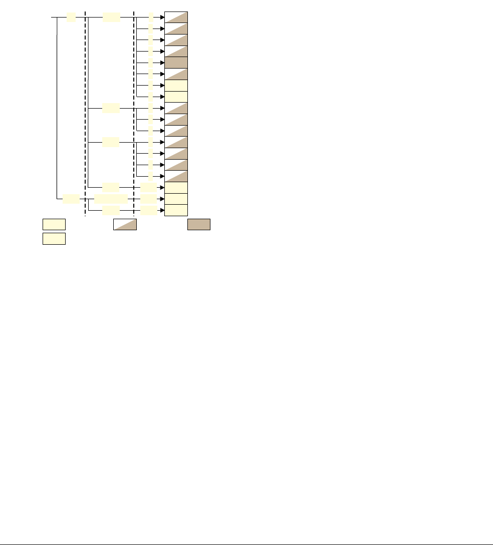
C12 The Performance Monitors Extension
C12.9 Performance Monitors registers
C12-2328 Copyright © 1996-1998, 2000, 2004-2012, 2014 ARM. All rights reserved. ARM DDI 0406C.c
Non-Confidential ID051414
C12.9 Performance Monitors registers
This section describes the Performance Monitors Extension registers.
C12.9.1 CP15 c9 performance monitors registers
The Performance Monitors Extension registers are part of the CP15 register map. Figure C12-1 shows the CP15 c9
encodings for these registers, and the reserved encodings for:
• possible extensions to the ARM Performance Monitors Extension
•IMPLEMENTATION DEFINED performance monitors.
Figure C12-1 CP15 c9 Performance Monitors registers
See Access permissions on page C12-2330 for information about User mode access to the Performance Monitors.
Table C12-7 on page C12-2329 lists the Performance Monitors Extension registers and shows where each register
is described in full.
An implementation can provide either or both:
• Access to the Performance Monitors registers through an external debug interface
• A memory-mapped interface to the Performance Monitors registers.
Compared to the CP15 view of the Performance Monitors registers, when using one of these interfaces there are
some differences in both the registers that are visible and the behavior of register accesses. For more information,
see Appendix D2 Recommended Memory-mapped and External Debug Interfaces for the Performance Monitors.
Read-only Read/Write
CRn opc1 opc2CRm
0
1
2
3
4
5
c12 0
c9
Write-only
0
0
2
1
1
2
{0-7}
c13
c14
c15
PMCR, Performance Monitors Control Register †
PMCNTENSET, Performance Monitors Count Enable Set register †
PMCNTENCLR, Performance Monitors Count Enable Clear register †
PMOVSR, Performance Monitors Overflow Flag Status Register †
PMSWINC, Performance Monitors Software Increment register †
PMSELR, Performance Monitors Event Counter Selection Register †
PMXEVCNTR, Performance Monitors Event Count Register †
PMUSERENR, Performance Monitors User Enable Register *
PMINTENSET, Performance Monitors Interrupt Enable Set register
PMINTENCLR, Performance Monitors Interrupt Enable Clear register
Reserved for
IMPLEMENTATION
DEFINED
Performance Monitors
PMCCNTR, Performance Monitors Cycle Count Register †
PMXEVTYPER, Performance Monitors Event Type Select Register †
Access depends on the operation † Accessible in User mode when PMUSERENR.EN == 1
* Read-only in User mode
6 PMCEID0, Performance Monitors Common Event Identification register 0, PMUv2 †
7 PMCEID1, Performance Monitors Common Event Identification register 1, PMUv2 †
{0-7}
{0-7}
{1-7} {c12-c14} Reserved for ARM Performance Monitors Extension
Reserved for
IMPLEMENTATION
DEFINED
Performance Monitorsc15
3PMOVSSET, Performance Monitors Overflow Flag Status Set register, PMUv2 † §
§ Implemented only if implementation includes the
Virtualization Extensions
¶
¶
¶
¶

C12 The Performance Monitors Extension
C12.9 Performance Monitors registers
ARM DDI 0406C.c Copyright © 1996-1998, 2000, 2004-2012, 2014 ARM. All rights reserved. C12-2329
ID051414 Non-Confidential
Power domains and Performance Monitors registers reset
For ARMv7 implementations, ARM recommends that performance monitors are implemented as part of the core
power domain, not as part of a separate debug power domain. There is no interface to access the Performance
Monitors registers when the core power domain is powered down.
A non-debug logic reset sets the Performance Monitors registers to their reset values. A debug logic reset does not
change the values of the Performance Monitors registers.
For more information about the reset scheme recommended for a v7 Debug implementation see Reset and debug on
page C7-2162.
Table C12-7 Performance Monitors register summary
Name, VMSA aName, PMSAaopc1 CRmbopc2 Type Description
PMCR PMCR 0 c12 0 RW Performance Monitors Control Register
PMCNTENSET PMCNTENSET 1 RW Performance Monitors Count Enable Set register
PMCNTENCLR PMCNTENCLR 2 RW Performance Monitors Count Enable Clear register
PMOVSR PMOVSR 3 RW Performance Monitors Overflow Flag Status Register
PMSWINC PMSWINC 4 WO Performance Monitors Software Increment register
PMSELR PMSELR 5 RW Performance Monitors Event Counter Selection
Register
PMCEID0PMCEID0 6 RO Performance Monitors Common Event Identification
register 0
PMCEID1PMCEID1 7 RO Performance Monitors Common Event Identification
register 1
PMCCNTR PMCCNTR c13 0 RW Performance Monitors Cycle Count Register
PMXEVTYPER PMXEVTYPER 1 RW Performance Monitors Event Type Select Register
PMXEVCNTR PMXEVCNTR 2 RW Performance Monitors Event Count Register
PMUSERENR PMUSERENR c14 0 RWcPerformance Monitors User Enable Register
PMINTENSET PMINTENSET 1 RW Performance Monitors Interrupt Enable Set register
PMINTENCLR PMINTENCLR 2 RW Performance Monitors Interrupt Enable Clear register
PMOVSSETd-d3 RW Performance Monitors Overflow Flag Status Set
register
a. VMSA and PMSA definitions of the register fields are identical. These columns link to the descriptions in Chapter B4 and Chapter B6.
b. CP15 c9 encodings with CRm == {c12-c14} not listed in the table are reserved. For details of the behavior of accesses to these encodings
see Accesses to unallocated CP14 and CP15 encodings on page B3-1447.
c. RO in User mode.
d. Implemented only as part of the Virtualization Extensions, otherwise encoding is reserved.

C12 The Performance Monitors Extension
C12.9 Performance Monitors registers
C12-2330 Copyright © 1996-1998, 2000, 2004-2012, 2014 ARM. All rights reserved. ARM DDI 0406C.c
Non-Confidential ID051414
Access permissions
Normally the Performance Monitors registers are accessible from all modes executing at PL1 or higher. However,
the access permissions for PMU registers can be modified by:
• Setting the PMUSERENR.EN bit to 1, to permit access from software executing in User mode, for example
for instrumentation and profiling purposes.
• Setting HDCR.TPM to 1, to trap to Hyp mode access to all registers from Non-secure modes executing at
PL1 or lower.
• Setting HDCR.TPMCR to 1, to trap to Hyp mode access to PMCR from Non-secure modes executing at PL1
or lower.
The access permissions for the Performance Monitors registers divide the registers into four groups. Therefore, the
following sections describe the access permissions for the Performance Monitors registers:
•Access from Secure PL1 modes and Hyp mode
•Group 1 on page C12-2331
•Group 2 on page C12-2331
•Group 3 on page C12-2332
•Group 4 on page C12-2332
•Reserved registers on page C12-2333.
These sections use the following terms to describe the access permissions:
Proceed The behavior on reads or writes further depends on what counter access is granted for each
counter in the current mode and state.
UNDEFINED Generates an Undefined Instruction exception that is taken locally.
Hyp Trap Generates a Hyp Trap exception. This is reported in the HSR as a Trapped
MCR
or
MRC
access
to CP15, using EC value
0x03
.
UNPREDICTABLE The behavior is UNPREDICTABLE.
In the access permissions tables:
x Indicates that the control does not affect the permissions.
- Indicates that the control is not applicable. In particular, in an implementation that does not include
the Virtualization Extensions, the HDCR controls are not applicable.
Access from Secure PL1 modes and Hyp mode
The Performance Monitors registers are always accessible in Secure PL1 modes and, in an implementation that
includes the Virtualization Extensions, from Hyp mode. This means:
In an implementation that does not include the Virtualization Extensions
Any access from a Secure PL1 mode proceeds, regardless of the value of PMUSERENR.EN.
In an implementation that includes the Virtualization Extensions
Any access from a Secure PL1 mode, or from Hyp mode, proceeds, regardless of the values of
PMUSERENR.EN and HDCR.{TPM, TPMCR}.

C12 The Performance Monitors Extension
C12.9 Performance Monitors registers
ARM DDI 0406C.c Copyright © 1996-1998, 2000, 2004-2012, 2014 ARM. All rights reserved. C12-2331
ID051414 Non-Confidential
Group 1
Table C12-8 describes the access permissions for the following registers and accesses:
•PMUSERENR,
MCR
only.
Note
See Group 2 for the behavior of write accesses to the PMUSERENR.
•PMINTENSET,
MRC
and
MCR
•PMINTENCLR,
MRC
and
MCR
.
These register accesses are never permitted in PL0 modes. Accesses from Non-secure PL1 modes are trapped to the
hypervisor when HDCR.TPM is set to 1.
Group 2
Table C12-9 describes the access permissions for the following register and access:
•PMUSERENR,
MRC
only.
Note
See Group 1 for the behavior of read accesses to the PMUSERENR.
This register is normally readable in PL0 modes. Read accesses from Non-secure modes are trapped to the
hypervisor when HDCR.TPM is set to 1.
Table C12-8 Access permissions for Performance Monitors registers, group 1
HDCR.PMUSERENR.EN Secure User mode Non-secure modes
TPM TPMCR PL1 User
ARMv7 implementation with Virtualization Extensions
0xx UNDEFINED Proceed UNDEFINED
1xx UNDEFINED Hyp Trap UNDEFINED
ARMv7 implementation without Virtualization Extensions
-x UNDEFINED Proceed UNDEFINED
Table C12-9 Read access permissions for Performance Monitors registers, group 2
HDCR.PMUSERENR.EN Secure User mode Non-secure modes
TPM TPMCR PL1 User
ARMv7 implementation with Virtualization Extensions
0 x x Proceed Proceed Proceed
1 x x Proceed Hyp Trap Hyp Trap
ARMv7 implementation without Virtualization Extensions
- x Proceed Proceed Proceed

C12 The Performance Monitors Extension
C12.9 Performance Monitors registers
C12-2332 Copyright © 1996-1998, 2000, 2004-2012, 2014 ARM. All rights reserved. ARM DDI 0406C.c
Non-Confidential ID051414
Group 3
Table C12-10 describes the access permissions for the following register and accesses:
•PMCR,
MRC
and
MCR
.
This register is normally RW in PL0 modes only when PL0 mode access is enabled, otherwise reads of and writes
to PMCR are locally UNDEFINED. Accesses to PMCR from Non-secure modes that are not locally UNDEFINED are
trapped to the hypervisor when HDCR.TPM or HDCR.TPMCR is set to 1.
Group 4
Table C12-11 on page C12-2333 describes the access permissions for the following registers in group 4:
•PMCNTENSET,
MRC
and
MCR
•PMCNTENCLR,
MRC
and
MCR
•PMOVSR,
MRC
and
MCR
•PMSWINC,
MCR
only
•PMSELR,
MRC
and
MCR
•PMCEIDn,
MRC
only, PMUv2 only
•PMCCNTR,
MRC
and
MCR
•PMXEVTYPER,
MRC
and
MCR
•PMXEVCNTR,
MRC
and
MCR
•PMOVSSET,
MRC
and
MCR
, for ARMv7 implementations that include the Virtualization Extensions.
Note
The following are reserved registers, see Reserved registers on page C12-2333:
• in PMUv1, the PMCEID0 and PMCEID1 registers
• in an implementation that does not include the Virtualization Extensions, the PMOVSSET register.
Table C12-10 Access permissions for Performance Monitors registers, group 3
HDCR.PMUSERENR.EN Secure User mode Non-secure modes
TPM TPMCR PL1 User
ARMv7 implementation with Virtualization Extensions
000 UNDEFINED Proceed UNDEFINED
0 0 1 Proceed Proceed Proceed
x10 UNDEFINED Hyp Trap UNDEFINED
1x
x 1 1 Proceed Hyp Trap Hyp Trap
1x
ARMv7 implementation without Virtualization Extensions
-0 UNDEFINED Proceed UNDEFINED
- 1 Proceed Proceed Proceed

C12 The Performance Monitors Extension
C12.9 Performance Monitors registers
ARM DDI 0406C.c Copyright © 1996-1998, 2000, 2004-2012, 2014 ARM. All rights reserved. C12-2333
ID051414 Non-Confidential
These registers are normally accessible in PL0 modes when PL0 mode access is enabled, otherwise accesses are
locally UNDEFINED. Accesses to these registers from Non-secure modes that are not locally UNDEFINED are trapped
to the hypervisor when HDCR.TPM is set to 1.
Reserved registers
The behavior of accesses to reserved registers in the Performance Monitors register space, including the behavior
of read accesses to WO registers and write accesses to RO registers, is described in:
•General behavior of system control registers on page B3-1446, for a VMSA implementation
•General behavior of system control registers on page B5-1776, for a PMSA implementation.
This applies to the following accesses in both Secure and Non-secure state:
• all accesses to reserved register encodings
•
MRC
accesses to PMSWINC
• in PMUv2,
MCR
accesses to the PMCEIDn registers.
Table C12-11 Access permissions for Performance Monitors registers, group 4
HDCR.PMUSERENR.EN Secure User mode Non-secure modes
TPM TPMCR PL1 PL0
ARMv7 implementation with Virtualization Extensions
0x0 UNDEFINED Proceed UNDEFINED
0 x 1 Proceed Proceed Proceed
1x0 UNDEFINED Hyp Trap UNDEFINED
1 x 1 Proceed Hyp Trap Hyp Trap
ARMv7 implementation without Virtualization Extensions
-0 UNDEFINED Proceed UNDEFINED
- 1 Proceed Proceed Proceed

C12 The Performance Monitors Extension
C12.9 Performance Monitors registers
C12-2334 Copyright © 1996-1998, 2000, 2004-2012, 2014 ARM. All rights reserved. ARM DDI 0406C.c
Non-Confidential ID051414
Part D
Appendixes

ARM DDI 0406C.c Copyright © 1996-1998, 2000, 2004-2012, 2014 ARM. All rights reserved. D1-2337
ID051414 Non-Confidential
Appendix D1
Recommended External Debug Interface
This appendix describes the recommended external debug interface. It contains the following sections:
•About the recommended external debug interface on page D1-2338
•Authentication signals on page D1-2340
•Run-control and cross-triggering signals on page D1-2342
•Recommended debug slave port on page D1-2346
•Other debug signals on page D1-2348.
Note
This recommended external debug interface specification is not part of the ARM architecture specification.
Implementers and users of the ARMv7 architecture must not consider this appendix as a requirement of the
architecture. It is included as an appendix to this manual only:
• as reference material for users of ARM products that implement this interface
• as an example of how an external debug interface might be implemented.
The inclusion of this appendix is no indication of whether any ARM products might, or might not, implement this
external debug interface. For details of the implemented external debug interface you must always see the
appropriate product documentation.

Appendix D1 Recommended External Debug Interface
D1.1 About the recommended external debug interface
D1-2338 Copyright © 1996-1998, 2000, 2004-2012, 2014 ARM. All rights reserved. ARM DDI 0406C.c
Non-Confidential ID051414
D1.1 About the recommended external debug interface
See the Note on the first page of this appendix for information about the architectural status of this recommended
debug interface.
The recommended debug interface includes a recommended debug slave port that provides both the
memory-mapped interface and the external debug interface. Table D1-1 shows the signals in the recommended
interface.
Table D1-1 Recommended debug interface signals
Name Direction VersionsaDescription Section
DBGEN In All Debug Enable Authentication signals
on page D1-2340
NIDEN In All Non-Invasive Debug Enable
SPIDEN In v6.1, v7, v7.1 Secure PL1 Invasive Debug Enable
SPNIDEN In v6.1, v7, v7.1 Secure PL1 Non-Invasive Debug Enable
DBGRESTART In v7, v7.1 External restart request Run-control and
cross-triggering signals
on page D1-2342
DBGRESTARTED Out v7, v7.1 Handshake for DBGRESTART
DBGTRIGGER Out v7, v7.1 Debug Acknowledge
EDBGRQ In All External debug request
DBGACK Out All Debug Acknowledge
DBGCPUDONE Out v7, v7.1 Debug Acknowledge
COMMRX Out All DBGDTRRX full Other debug signals on
page D1-2348
COMMTX Out All DBGDTRTX empty
DBGOSLOCKINIT In v7 only Initialize OS Lock on reset
DBGNOPWRDWN Out All No powerdown request
DBGPWRUPREQ Out v7.1 only Powerup request
DBGRSTREQ Out v7, v7.1 Warm reset request
DBGPWRDUP In v7, v7.1 Processor powered up
DBGBUSCANCELREQ Out v7, v7.1 Request to cancel bus requests
DBGROMADDR[N:12]bIn v7, v7.1 ROM Table physical address
DBGROMADDRV In v7, v7.1 ROM Table physical address valid
DBGSELFADDR[N:12]bIn v7, v7.1 Debug self-address offset
DBGSELFADDRV In v7, v7.1 Debug self-address offset valid
DBGSWENABLE In v7, v7.1 Debug software access enable
PRESETDBGn In v7, v7.1 Debug logic reset
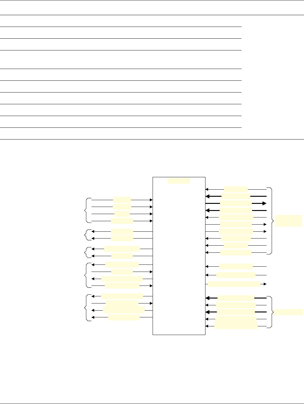
Appendix D1 Recommended External Debug Interface
D1.1 About the recommended external debug interface
ARM DDI 0406C.c Copyright © 1996-1998, 2000, 2004-2012, 2014 ARM. All rights reserved. D1-2339
ID051414 Non-Confidential
Figure D1-1 shows the recommended debug interface.
Figure D1-1 Recommended external debug interface, including APB3 slave port
In Figure D1-1, signals with a lower-case n suffix are active LOW and all other signals are active HIGH.
PSELDBG In v7, v7.1 Selects the external debug interface Recommended debug
slave port on
page D1-2346
PRDATADBG[31:0] Out v7, v7.1 Read data
PWDATADBG[31:0] In v7, v7.1 Write data
PENABLEDBG In v7, v7.1 Indicates a second or subsequent cycle of a
transfer
PREADYDBG Out v7, v7.1 Extends a transfer, by inserting wait states
PWRITEDBG In v7, v7.1 LOW for a read, HIGH for a write
PCLKDBG In v7, v7.1 Clock
PCLKENDBG In v7, v7.1 Clock enable for PCLKDBG
PADDRDBG[31, 11:2] In v7, v7.1 Slave port, address
PSLVERRDBG Out v7, v7.1 Slave port, slave-generated error response
a. Indicates the debug versions in which the signal can be implemented. The signal descriptions indicate whether the signal is required.
b. In an implementation that includes the Large Physical Address Extension, N is 39, otherwise it is 31.
Table D1-1 Recommended debug interface signals (continued)
Name Direction VersionsaDescription Section
DBGEN
SPIDEN
NIDEN
SPNIDEN
Processor
Authentication
interface
COMMTX
COMMRX
DCC
handshake
DBGTRIGGER
DBGCPUDONE
DBGACK
EDBGRQ
DBGRESTARTED
DBGRESTART
Cross-trigger
interface
DBGNOPWRDWN
DBGPWRDUP
Power and reset
controller
interface
PSELDBG
PADDRDBG
PRDATADBG
PWDATADBG
PENABLEDBG
PREADYDBG
PSLVERRDBG
PWRITEDBG
PCLKDBG
PCLKENDBG
PRESETDBGn
Debug slave
port, APB3
DBGSWENABLE
Configuration
Debug state
entry
DBGROMADDR
DBGROMADDRV
DBGSELFADDR
DBGSELFADDRV
DBGOSLOCKINIT†
† v7 Debug only
‡ v7.1 Debug only
See text for the signaling requirements for v6 Debug and v6.1 Debug
DBGPWRUPREQ‡
DBGRSTREQ
DBGBUSCANCELREQ

Appendix D1 Recommended External Debug Interface
D1.2 Authentication signals
D1-2340 Copyright © 1996-1998, 2000, 2004-2012, 2014 ARM. All rights reserved. ARM DDI 0406C.c
Non-Confidential ID051414
D1.2 Authentication signals
DBGEN, NIDEN, SPIDEN and SPNIDEN are the authentication signals.
NIDEN and SPNIDEN can be omitted if no non-invasive debug features are implemented.
SPIDEN and SPNIDEN can be omitted if the implementation does not include the Security Extensions.
When DBGEN is LOW, indicating that debug is disabled:
• Halting debug events are ignored
• Except for ignoring Halting debug events, the processor behaves as if DBGDSCR[15:14] ==
0b00
, meaning
that Monitor debug-mode and Halting debug-mode are both disabled.
For details of how these signals control enabling of invasive and non-invasive debug see Chapter C2 Invasive
Debug Authentication and Chapter C9 Non-invasive Debug Authentication.
Note
The v7 Debug and v7.1 Debug architecture authentication signal interface described here is compatible with the
CoreSight architecture requirements for the authentication interface of a debug component. However the CoreSight
architecture places additional requirements on other components in the system. For more information, see the
CoreSight Architecture Specification.
SPIDEN also controls permissions in Debug state. For details see About invasive debug authentication on
page C2-2030.
See also DBGAUTHSTATUS, Authentication Status register on page C11-2211.
D1.2.1 Changing the authentication signals
In v6.1 Debug, v7 Debug, and v7.1 Debug the NIDEN, DBGEN, SPIDEN, and SPNIDEN authentication signals
can be controlled dynamically, meaning that they might change while the processor is running, or while the
processor is in Debug state.
Note
In v6 Debug DBGEN is a static signal and can be changed only while the processor is in reset.
Normally, these signals are driven by the system, meaning that they are driven by a peripheral connected to the ARM
processor. If the software running on the ARM processor has to change any of these signals it must follow this
procedure:
1. Execute an implementation-specific sequence of instructions to change the signal value. For example, this
might be an instruction to write a value to a control register in a system peripheral.
2. If step 1 involves any memory operation, perform a Data Synchronization Barrier (DSB).
3. Poll the debug registers to check the signal values seen by the processor. This is required because the
processor might not see the signal change until several cycles after the DSB completes.
4. Perform a context synchronization operation.
The software cannot perform debug or analysis operations that rely on the new value until this procedure has been
completed. The same rules apply for instructions executed through the DBGITR while in Debug state. The
processor view of the authentication signals can be polled through DBGDSCR[17:16] and the DBGAUTHSTATUS
register.

Appendix D1 Recommended External Debug Interface
D1.2 Authentication signals
ARM DDI 0406C.c Copyright © 1996-1998, 2000, 2004-2012, 2014 ARM. All rights reserved. D1-2341
ID051414 Non-Confidential
Note
•See Context synchronization operation for the definition of this term.
• Exceptionally, the processor might be in Debug state even though the mode, security state and authentication
signal settings are such that, in Non-debug state, debug events would be ignored. Being in Debug state when
invasive halting debug is disabled or not permitted on page C5-2101 describes how this can occur.

Appendix D1 Recommended External Debug Interface
D1.3 Run-control and cross-triggering signals
D1-2342 Copyright © 1996-1998, 2000, 2004-2012, 2014 ARM. All rights reserved. ARM DDI 0406C.c
Non-Confidential ID051414
D1.3 Run-control and cross-triggering signals
ARM recommends implementation of the run-control and cross-triggering signals EDBGRQ, DBGTRIGGER,
DBGRESTART, and DBGRESTARTED. These signals are particularly useful in a multiprocessor system,
because using them:
• A debugger can signal a group of processors to enter Debug state.
• A debugger can signal a group of processors to exit Debug state.
• A system component can signal a group of processors to enter Debug state when any one of them enters
Debug state because of a debug event on that processor. This is called cross-triggering.
If you implement the recommended signaling in your system hardware, this signaling means all of the processors
in the group enter or exit Debug state nearly simultaneously.
These signals can also be used in a uniprocessor implementation. For example, debug events not defined by the
Debug architecture might be generated externally to the processor. When one of these events occurs the external
system can use these signals to cause the processor to enter Debug state. A trace macrocell might use these signals
in this way.
Contact ARM for details of a recommended Embedded Cross Trigger (ECT) peripheral that you can use in a
multiprocessor system to implement this signaling.
The following subsections describe each of the recommended signals:
•EDBGRQ
•DBGTRIGGER
•DBGRESTART and DBGRESTARTED on page D1-2343
•DBGACK and DBGCPUDONE on page D1-2344.
D1.3.1 EDBGRQ
EDBGRQ is the recommended implementation of the External debug request mechanism, see Halting debug events
on page C3-2075.
EDBGRQ is active-HIGH.
Once EDBGRQ is asserted it must be held HIGH until it is acknowledged:
• An implementation can use either DBGACK or DBGTRIGGER to acknowledge EDBGRQ, see:
—DBGACK and DBGCPUDONE on page D1-2344
—DBGTRIGGER.
• Alternatively, debugger software might use an IMPLEMENTATION DEFINED method to acknowledge
EDBGRQ. For example, once the processor has entered Debug state the debugger might reprogram the
peripheral that is driving EDBGRQ.
D1.3.2 DBGTRIGGER
The processor asserts DBGTRIGGER to indicate that it is committed to entering Debug state. Therefore, the
system can use DBGTRIGGER to acknowledge EDBGRQ. See Chapter C5 Debug State for the definition of
Debug state.
DBGTRIGGER is active-HIGH.
The processor must assert DBGTRIGGER as early as possible, so that the system can use its rising edge to signal
to other devices that the processor is entering Debug state. DBGTRIGGER can be used for cross-triggering. For
example, in a multiprocessor system, when one processor halts, the DBGTRIGGER signal from that processor can
generate an External debug request for the other processors.
See DBGACK and DBGCPUDONE on page D1-2344 for details of the recommended External debug request
handshaking between EDBGRQ and DBGTRIGGER.

Appendix D1 Recommended External Debug Interface
D1.3 Run-control and cross-triggering signals
ARM DDI 0406C.c Copyright © 1996-1998, 2000, 2004-2012, 2014 ARM. All rights reserved. D1-2343
ID051414 Non-Confidential
In addition, the processor asserts DBGTRIGGER whenever the DBGDSCR.DBGack bit is set to 1, see
DBGDSCR, Debug Status and Control Register on page C11-2243.
If the DBGDSCR.DBGack bit is 0, the processor deasserts DBGTRIGGER on exit from Debug state.
Note
Setting DBGDSCR.DBGack to 1 takes no account of the DBGEN and SPIDEN signals. Setting
DBGDSCR.DBGack to 1 asserts DBGTRIGGER regardless of the security settings.
A v7 Debug or v7.1 Debug implementation of these recommendations might not implement DBGTRIGGER if it
would have identical behavior to DBGACK.
Before v7 Debug, DBGTRIGGER is not part of the recommended external debug interface.
D1.3.3 DBGRESTART and DBGRESTARTED
DBGRESTART is the recommended implementation of the External Restart request, see Exiting Debug state on
page C5-2112. DBGRESTARTED is a handshake signal for DBGRESTART.
DBGRESTART and DBGRESTARTED are active-HIGH.
Once DBGRESTART is asserted, it must be held HIGH until DBGRESTARTED is deasserted. The processor
ignores DBGRESTART if it is not in Debug state.
To avoid possible race conditions, restart must be a multi-phase process. Example D1-1 show how this might be
achieved.
Note
Example D1-1 only represents how a restart handshake might be achieved. It does not show the restart process of a
particular implementation of the ARM architecture. Contact ARM if you need more information about a particular
restart handshake.
Example D1-1 Possible multi-phase restart handshake
The diagram shows a four-phase handshake between DBGRESTART and DBGRESTARTED. It is diagrammatic
only, and does not imply any timings.
The numbers in the diagram have the following meanings:
1. If DBGRESTARTED is asserted HIGH the peripheral asserts DBGRESTART HIGH and waits for
DBGRESTARTED to go LOW
2. The processor drives DBGRESTARTED LOW to deassert the signal and waits for DBGRESTART to go
LOW
3. The peripheral drives DBGRESTART LOW to deassert the signal. This event indicates to the processor that
it can start the transition from Debug state to Non-debug state.
4. The processor exits Debug state and asserts DBGRESTARTED HIGH.
DBGRESTART
DBGRESTARTED
1 2 3 4
Debug state Non-debug state
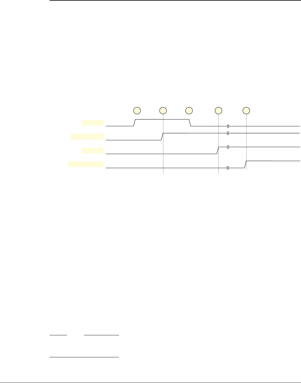
Appendix D1 Recommended External Debug Interface
D1.3 Run-control and cross-triggering signals
D1-2344 Copyright © 1996-1998, 2000, 2004-2012, 2014 ARM. All rights reserved. ARM DDI 0406C.c
Non-Confidential ID051414
In the process of exiting Debug state the processor normally deasserts the DBGACK, DBGTRIGGER, and
DBGCPUDONE signals. It is IMPLEMENTATION DEFINED when this change occurs relative to the changes in
DBGRESTART and DBGRESTARTED.
D1.3.4 DBGACK and DBGCPUDONE
DBGACK and DBGCPUDONE are active-HIGH.
The processor asserts DBGACK to indicate that it is in Debug state. Therefore, the system can use DBGACK as a
handshake for EDBGRQ, instead of using DBGTRIGGER.
In v6 Debug and v6.1 Debug, the system can use DBGACK for cross-triggering.
The processor asserts DBGCPUDONE only after it has completed all Non-debug state memory accesses. Therefore
the system can use DBGCPUDONE as an indicator that all memory accesses issued by the processor result from
operations performed by a debugger.
Figure D1-2 shows the signaling sequence for entry to Debug state. It is diagrammatic only, and does not imply any
timings.
Figure D1-2 Signaling for Debug state entry on an External debug request
In Figure D1-2 these events must occur in order:
1. The peripheral asserts EDBGRQ and waits for it to be acknowledged.
2. The processor takes the debug event and starts the Debug state entry sequence. The processor asserts
DBGTRIGGER.
3. The processor completes the Debug state entry sequence and asserts DBGACK.
4. The processor completes all Non-debug state memory accesses and asserts DBGCPUDONE. It might do this
only after intervention by an external debugger, see Asynchronous aborts and Debug state entry on
page C5-2096.
Event a, the peripheral deasserting EDBGRQ, can occur at any time after the assertion of EDBGRQ is
acknowledged, and generation of this event might require intervention by the external debugger. In the example
shown in Figure D1-2, the system is using DBGTRIGGER to acknowledge EDBGRQ, and therefore event a is
not ordered relative to events 3 and 4.
In addition, the processor asserts DBGCPUDONE and DBGACK when the DBGDSCR.DBGack bit is set to 1.
If the DBGDSCR.DBGack bit is 0, the processor deasserts DBGCPUDONE and DBGACK on exit from Debug
state.
Note
Setting DBGDSCR.DBGack to 1 takes no account of the DBGEN and SPIDEN signals. Setting
DBGDSCR.DBGack to 1 asserts DBGCPUDONE and DBGACK regardless of the security settings.
EDBGRQ
DBGTRIGGER
DBGACK
DBGCPUDONE
1 2 3 4a
Debug state entry Debug stateNon-debug state
See the text for more information about the ordering of transition a.

Appendix D1 Recommended External Debug Interface
D1.3 Run-control and cross-triggering signals
ARM DDI 0406C.c Copyright © 1996-1998, 2000, 2004-2012, 2014 ARM. All rights reserved. D1-2345
ID051414 Non-Confidential
A v7 Debug or v7.1 Debug implementation of these recommendations might not implement DBGCPUDONE if it
would have identical behavior to DBGACK.
Before v7 Debug, DBGCPUDONE was not part of the recommended external debug interface.

Appendix D1 Recommended External Debug Interface
D1.4 Recommended debug slave port
D1-2346 Copyright © 1996-1998, 2000, 2004-2012, 2014 ARM. All rights reserved. ARM DDI 0406C.c
Non-Confidential ID051414
D1.4 Recommended debug slave port
This slave port is not required in v6 Debug and v6.1 Debug.
The memory-mapped interface is optional on v7 Debug and v7.1 Debug. This section describes the recommended
AMBA® Advanced Peripheral Bus (APB3) slave port. It provides both the memory-mapped and external debug
interfaces.
A valid external debug interface for v7 Debug or v7.1 Debug is any access mechanism that enables the external
debugger to complete reads or writes to the memory-mapped registers described in The memory-mapped and
recommended external debug interfaces on page C6-2128.
In v7 Debug or v7.1 Debug, a memory-mapped interface can be implemented to provide access to the debug
registers using load and store operations. Such an interface is sufficient for the requirements of the external debug
interface, and therefore it is possible to implement both the memory-mapped and external debug interfaces using a
single memory slave port on the processor.
This section describes the v7 Debug and v7.1 Debug recommendations for an APB3 memory slave port
implemented as part of the external debug interface. In addition, ARM recommends a Debug Access Port capable
of mastering an APB3 bus and compatible with the ARM Debug Interface v5 (ADIv5). Figure D1-1 on
page D1-2339 shows the recommendations.
ARM recommends that the debug registers are accessible through an APB3 external debug interface. This APB3
interface:
• is 32 bits wide
• supports only 32-bit reads and writes
• has accesses that can be stalled
• has slave-generated aborts
• has 10 address bits ([11:2]) mapping 4KB of memory.
The recommended Debug Access Port treats this APB3 interface as Strongly-ordered memory.
See Table D1-1 on page D1-2338 for a description of the signals PSELDBG, PRDATADBG[31:0],
PWDATADBG[31:0], PENABLEDBG, PREADYDBG, PWRITEDBG, PCLKDBG, and PCLKENDBG.
The following subsections describe the other debug slave port signals:
•PADDRDBG
•PSLVERRDBG on page D1-2347.
D1.4.1 PADDRDBG
PADDRDBG selects the register to read or write.
The recommended debug slave port implements both the external debug interface and the memory-mapped
interface. In this implementation, the interface must be able to distinguish an external debug interface access from
a memory-mapped interface access. The recommended slave port uses APB3, and aliases the complete register set
twice:
• the first view, the memory-mapped interface view, starts at
0x0
• the second view, the external debug interface view, starts at
0x80000000
.
This means that the additional signal bit PADDRDBG[31] informs the debug slave port of the source of an access:
PADDRDBG[31] == 0 Access from system
PADDRDBG[31] == 1 Access from external debugger.
Note
The only bits of PADDRDBG that are specified are PADDRDBG[31, 11:2]. Bits[1:0] are not required because all
registers are word-sized, and bit[31] is used as described to indicate the source of the access. Because some HDL
languages do not permit partial buses to be specified in this way an actual implementation might use a different
name for PADDRDBG[31], such as PADDRDBG31.

Appendix D1 Recommended External Debug Interface
D1.4 Recommended debug slave port
ARM DDI 0406C.c Copyright © 1996-1998, 2000, 2004-2012, 2014 ARM. All rights reserved. D1-2347
ID051414 Non-Confidential
D1.4.2 PSLVERRDBG
PSLVERRDBG signals an aborted access.
PSLVERRDBG has the same timing as the ready response, PREADYDBG. Under the v7 Debug and v7.1 Debug
model, accesses are only aborted, by asserting PSLVERRDBG HIGH, in a situation related to powerdown. These
include the OS lock mechanism, and in v7.1 Debug, the OS Double Lock. For more information see Access
permissions on page C6-2119.

Appendix D1 Recommended External Debug Interface
D1.5 Other debug signals
D1-2348 Copyright © 1996-1998, 2000, 2004-2012, 2014 ARM. All rights reserved. ARM DDI 0406C.c
Non-Confidential ID051414
D1.5 Other debug signals
This section describes:
• the DCC handshake signals, see COMMRX and COMMTX
•DBGNOPWRDWN, DBGPWRDUP, DBGPWRUPREQ, and DBGRSTREQ, see The power and reset
controller interface signals
• the configuration signals DBGOSLOCKINIT, DBGROMADDR, DBGROMADDRV,
DBGSELFADDR, and DBGSELFADDRV, see The configuration signals on page D1-2349
• the debug software enable signal, see DBGSWENABLE on page D1-2351
• the debug reset signal, see PRESETDBGn on page D1-2351
• the request cancellation of bus requests signal, see DBGBUSCANCELREQ on page D1-2351.
D1.5.1 COMMRX and COMMTX
COMMRX and COMMTX reflect the state of DBGDSCR[30:29] through the external debug interface:
•COMMTX is the inverse of DBGDSCR[29], TXfull. The processor is ready to transmit.
•COMMRX is equivalent to DBGDSCR[30], RXfull.
See DBGDSCR, Debug Status and Control Register on page C11-2243 for descriptions of the TXfull and RXfull
bits.
These signals are active HIGH indicators of when the Debug Communications Channel (DCC) requires processing
by the target system. They permit interrupt-driven communications over the DCC. By connecting these signals to
an interrupt controller, software using the DCC can be interrupted whenever there is new data on the channel or
when the channel is clear for transmission.
Note
There can be race conditions between reading the DCC bits through a read of DBGDSCRext and a read of the
DBGDTRTXint Register or a write to the DBGDTRRXint Register through the Baseline CP14 interface. However
the timing of these signals with respect to the DCC registers must be such that target software executing off an
interrupt triggered by either of these signals must be able to write to DBGDTRTXint and read DBGDTRRXint
without race conditions.
D1.5.2 The power and reset controller interface signals
The following subsections describe the power controller interface signals:
•DBGNOPWRDWN
•DBGPWRDUP on page D1-2349
•DBGPWRUPREQ on page D1-2349
•DBGRSTREQ on page D1-2349.
DBGNOPWRDWN
DBGNOPWRDWN is equivalent to the value of DBGPRCR.CORENPDRQ. See the bit description for the
implementation requirements for this bit in different Debug architecture versions. When the CORENPDRQ bit is
implemented so that it can be set to 1 to request that, on a powerdown request, the system emulates powerdown,
then ARM strongly recommends that the DBGNOPWRDWN signal is implemented in the external debug
interface.
The processor power controller must work in emulate mode when this signal is HIGH.

Appendix D1 Recommended External Debug Interface
D1.5 Other debug signals
ARM DDI 0406C.c Copyright © 1996-1998, 2000, 2004-2012, 2014 ARM. All rights reserved. D1-2349
ID051414 Non-Confidential
DBGPWRDUP
DBGPWRDUP is not required in:
• v6 Debug and v6.1 Debug
• a SinglePower system, that is, it is not required in a design that has only one power domain.
The DBGPWRDUP input signal is HIGH when the processor is powered up, and LOW otherwise. The
DBGPWRDUP signal determines the value of DBGPRSR.PU.
See also Permissions in relation to powerdown on page C6-2121.
DBGPWRUPREQ
DBGPWRUPREQ is not supported in v6 Debug, v6.1 Debug, and v7 Debug.
In v7.1 Debug, DBGPWRUPREQ is an optional signal that is equivalent to the value of DBGPRCR.COREPURQ.
When this signal is HIGH, it signals a request to the power controller to powerup the core power domain.
DBGRSTREQ
DBGRSTREQ is not supported in v6 Debug and v6.1 Debug.
In v7 Debug and v7.1 Debug, DBGRSTREQ is an optional signal that is equivalent to the value of
DBGPRCR.CWRR. When this signal is HIGH, it signals a request to the reset controller to perform a warm reset
of the processor.
D1.5.3 The configuration signals
The following subsections describe the configuration signals:
•DBGOSLOCKINIT
•DBGROMADDR and DBGROMADDRV on page D1-2350
•DBGSELFADDR and DBGSELFADDRV on page D1-2350.
DBGOSLOCKINIT
DBGOSLOCKINIT is not required in:
• v6 Debug and v6.1 Debug
• v7.1 Debug.
In v7 Debug, DBGOSLOCKINIT is a configuration signal that determines the state of the OS Lock immediately
after a debug logic reset. On a debug logic reset:
•if DBGOSLOCKINIT is HIGH then the OS Lock is set from the reset
•if DBGOSLOCKINIT is LOW then the OS Lock is clear from the reset.
Normally, DBGOSLOCKINIT is tied off LOW.
For a description of debug logic reset see Reset and debug on page C7-2162. For details of the OS Lock see OS Save
and Restore registers on page C11-2203.
See also Permissions in relation to locks on page C6-2120.

Appendix D1 Recommended External Debug Interface
D1.5 Other debug signals
D1-2350 Copyright © 1996-1998, 2000, 2004-2012, 2014 ARM. All rights reserved. ARM DDI 0406C.c
Non-Confidential ID051414
DBGROMADDR and DBGROMADDRV
DBGROMADDR and DBGROMADDRV are not required in v6 Debug and v6.1 Debug. They are required in
v7 Debug and v7.1 Debug if the memory-mapped interface is implemented.
DBGROMADDR specifies the most significant bits of the ROM Table table physical address:
• in an implementation that includes the Large Physical Address Extension, it specifies address bits[39:12]
• otherwise, it specifies address bits[31:12].
This is a configuration input, that provides the DBGDRAR.ROMADDR field value. It must be either:
• be a tie-off
• change only while the processor is in reset.
In a system with multiple ROM Tables, this address must be tied off to the top-level ROM Table address.
In a system with no ROM Table this address must be tied off with the physical address where the debug registers
are memory-mapped. Debug software can use the debug component identification registers at the end of the 4KB
block addressed by DBGROMADDR to distinguish a ROM table from a processor.
Note
If the system implements more than one debug component, for example a processor and a trace macrocell, a ROM
Table must be provided.
DBGROMADDRV is the valid signal for DBGROMADDR. If the address cannot be determined,
DBGROMADDR must be tied off to zero and DBGROMADDRV tied LOW.
The format of ROM Tables is defined in the ARM Debug Interface v5 Architecture Specification.
ARM recommends that the ROM table, addressed by DBGROMADDR, and the Self Address specified by
DBGSELFADDR and described in DBGSELFADDR and DBGSELFADDRV, are:
• in a VMSA implementation, implemented in the bottom 4GB of physical memory, so they can be accessed
when the MMUs are disabled
• implemented in the same 2GB half of the 4GB memory region.
DBGSELFADDR and DBGSELFADDRV
DBGSELFADDR and DBGSELFADDRV are not required in v6 Debug and v6.1 Debug.
In v7 Debug and v7.1 Debug, DBGSELFADDR and DBGSELFDDRV are required if the memory-mapped
interface is implemented. If DBGROMADDR and DBGROMADDRV are not implemented, DBGSELFADDR
and DBGSELFADDRV must not be implemented.
DBGSELFADDR specifies the most significant bits of the two’s complement signed offset from the ROM Table
physical address to the physical address where the debug registers are Memory-mapped:
• in an implementation that includes the Large Physical Address Extension, it specifies address bits[39:12]
• otherwise, it specifies address bits[31:12].
This is a configuration input, that provides the DBGDSAR.SELFOFFSET field value. It must either:
• be a tie-off
• change only while the processor is in reset.
If there is no ROM Table, DBGROMADDR must be configured as described in the section DBGROMADDR and
DBGROMADDRV, and DBGSELFADDR must be tied off to zero with DBGSELFADDRV tied HIGH.
DBGSELFADDRV is the valid signal for DBGSELFADDR. If the offset cannot be determined,
DBGSELFADDR must be tied off to zero and DBGSELFADDRV tied LOW.

Appendix D1 Recommended External Debug Interface
D1.5 Other debug signals
ARM DDI 0406C.c Copyright © 1996-1998, 2000, 2004-2012, 2014 ARM. All rights reserved. D1-2351
ID051414 Non-Confidential
D1.5.4 DBGSWENABLE
DBGSWENABLE is not required in v6 Debug and v6.1 Debug.
In v7 Debug and v7.1 Debug, DBGSWENABLE is driven by the Debug Access Port. For details see the ARM
Debug Interface v5 Architecture Specification.
DBGSWENABLE is an active-HIGH signal that must be asserted to enable system access to the debug register
file. That is, if deasserted it prevents access through the memory-mapped interface and, for most registers, through
the CP14 interface. This gives the debugger full control over the debug registers in the processor.
When this signal is deasserted by the debugger by a means that is IMPLEMENTATION DEFINED, memory-mapped
interface accesses return an error response and most CP14 operations become UNDEFINED. However, the
architecture permits implementations in which software can continue to use Save and Restore debug registers over
a powerdown. For more information, see:
•Summary of the v7 Debug register interfaces on page C6-2130
•Summary of the v7.1 Debug register interfaces on page C6-2139
•The OS Save and Restore mechanism on page C7-2154.
Note
In v7 Debug, if DBGOSLSR, DBGOSLAR, and DBGOSSRR are not visible in the CP14 interface, then save and
restore when DBGSWENABLE is LOW is not possible.
In the ARM Debug Interface v5, DBGSWENABLE is asserted by setting the DbgSwEnable control bit in the
access port Control Status Word Register (CSW) to 1. For the memory-mapped interface, when the DbgSwEnable
control bit is set to 0 the generation of slave-generated errors is a function of the ADIv5 Debug Access Port, and
therefore the processor ignores the DBGSWENABLE signal for the memory-mapped interface. For details see the
ARM Debug Interface v5 Architecture Specification.
The DBGSWENABLE signal has no effect on accesses through the external debug interface.
Normally, the DBGSWENABLE signal must be asserted at debug logic reset and deasserted under debugger
control.
D1.5.5 PRESETDBGn
PRESETDBGn is not required in v6 Debug and v6.1 Debug. The debug logic is only reset on system powerup
reset.
The reset signal resets all debug registers. See also Reset and debug on page C7-2162.
Note
Do not use the PRESETDBGn signal to reset the debug registers if the debug system is connected to a debug
monitor that uses the CP14 debug interface.
D1.5.6 DBGBUSCANCELREQ
DBGBUSCANCELREQ is not supported in v6 Debug and v6.1 Debug.
In v7 Debug and v7.1 Debug, DBGBUSCANCELREQ is an optional signal that is equivalent to the value of
DBGDRCR.CBRRQ. When this signal is HIGH, it signals a request to cancel any outstanding bus requests.

Appendix D1 Recommended External Debug Interface
D1.5 Other debug signals
D1-2352 Copyright © 1996-1998, 2000, 2004-2012, 2014 ARM. All rights reserved. ARM DDI 0406C.c
Non-Confidential ID051414

ARM DDI 0406C.c Copyright © 1996-1998, 2000, 2004-2012, 2014 ARM. All rights reserved. D2-2353
ID051414 Non-Confidential
Appendix D2
Recommended Memory-mapped and External
Debug Interfaces for the Performance Monitors
This appendix describes the recommended memory-mapped and external debug interfaces to the Performance
Monitors. It contains the following sections:
•About the memory-mapped views of the Performance Monitors registers on page D2-2354
•PMU register descriptions for memory-mapped register views on page D2-2363.

Appendix D2 Recommended Memory-mapped and External Debug Interfaces for the Performance Monitors
D2.1 About the memory-mapped views of the Performance Monitors registers
D2-2354 Copyright © 1996-1998, 2000, 2004-2012, 2014 ARM. All rights reserved. ARM DDI 0406C.c
Non-Confidential ID051414
D2.1 About the memory-mapped views of the Performance Monitors registers
An implementation can provide:
• A memory-mapped interface to the Performance Monitors registers. Software running on any processor in a
system can use this interface to access counters in the Performance Monitors.
• Access to the Performance Monitors registers through an external debug interface. A debugger can use this
interface to access counters in the Performance Monitors.
ARM recommends that any external debug interface is implemented as defined in the ARM Debug Interface
v5 Architecture Specification.
An external debug interface provides a memory-mapped view of the Performance Monitors registers.
The following sections describe the memory-mapped views of the Performance Monitors registers. That is, they
describe accessing the registers through either a memory-mapped interface or an external debug interface.
•Differences in the memory-mapped views of the Performance Monitors registers
•Behavior of simultaneous accesses through CP15 and memory-mapped views on page D2-2355
•Performance Monitors memory-mapped register views on page D2-2355
•Access permissions for memory-mapped views of the Performance Monitors on page D2-2358.
In this appendix, unless the context explicitly indicates otherwise, any reference to a memory-mapped view applies
equally to a register view using:
• an external debug interface
• a memory-mapped interface.
D2.1.1 Differences in the memory-mapped views of the Performance Monitors registers
A memory-mapped view of the Performance Monitors registers accesses the same registers as the CP15 interface
described in Performance Monitors registers on page C12-2328, except that:
1. The PMSELR is accessible only in the CP15 interface.
2. The PMCFGR, PMLAR, PMLSR, PMAUTHSTATUS, PMDEVTYPE, PMPID0-PMPID4, and
PMCID0-PMCID3 registers are accessible only in memory-mapped views. PMU register descriptions for
memory-mapped register views on page D2-2363 describes these registers.
3. The CP15 interface provides access to a single PMXEVCNTR and a single PMXEVTYPER. PMSELR.SEL
selects which {PMXEVCNTRx, PMXEVTYPERx} register pair is accessible. In a memory-mapped view,
each of the PMXEVCNTRx and PMXEVTYPERx registers is visible at a different offset in the interface.
4. In the CP15 interface, the PMXEVTYPER that corresponds to the PMCCNTR is accessible only by setting
PMSELR.SEL to 31. In a memory-mapped view, this register is always visible, as PMXEVTYPER31 at
offset
0x47C
.
5. For Performance Monitors registers that are accessible in both the CP15 interface and a memory-mapped
view, the register descriptions in Chapter B4 System Control Registers in a VMSA implementation and
Chapter B6 System Control Registers in a PMSA implementation apply, except that:
• Any reference to controls in PMSELR does not apply to the memory-mapped views. See items 1, 3,
and 4 in this list.
• Any reference to the modes in which the register can be accessed does not apply to accesses using a
memory-mapped view. This includes:
— the information in Access permissions on page C12-2330 and Counter access on
page C12-2314
— the PMUSERENR.EN control on accesses from User mode
— in an implementation that includes the Virtualization Extensions, the HDCR.HPMN control.
See, instead, Access permissions for memory-mapped views of the Performance Monitors on
page D2-2358.

Appendix D2 Recommended Memory-mapped and External Debug Interfaces for the Performance Monitors
D2.1 About the memory-mapped views of the Performance Monitors registers
ARM DDI 0406C.c Copyright © 1996-1998, 2000, 2004-2012, 2014 ARM. All rights reserved. D2-2355
ID051414 Non-Confidential
• In an implementation that includes the Virtualization Extensions, any references to the effect of the
HDCR.HPMN on the behavior of accesses to the register from Non-secure modes other than Hyp does
not apply to accesses using a memory-mapped view, unless otherwise stated.
• The information in the Accessing the register subsection of the register description does not apply to
accesses using a memory-mapped view. For example, the subsection Accessing the PMCCNTR on
page B4-1671 does not apply to PMCCNTR accesses using a memory-mapped view.
• Accesses to PMCCNTR, PMXEVCNTRx, or PMXEVTYPERx read or update the appropriate
register, and have no dependence on the value of PMSELR.SEL.
Note
In this section, links to Performance Registers that can be accessed in the CP15 interface, for example
PMCCNTR, link to their description in Chapter B4 System Control Registers in a VMSA implementation.
D2.1.2 Behavior of simultaneous accesses through CP15 and memory-mapped views
If a Performance Monitors register is visible in both the CP15 interface and a memory-mapped view, and is accessed
simultaneously through those two mechanisms, behavior is UNPREDICTABLE. In this context, simultaneously means
that the register is accessed by one mechanism before all side-effects of an access through the other mechanism are
visible.
D2.1.3 Performance Monitors memory-mapped register views
Table D2-1 shows the memory-mapped view of the Performance Monitors registers.
Note
• Implementers must ensure that the 4KB region containing the PMU registers immediately follows, in
physical memory, the 4KB region containing the debug registers.
• In an implementation that includes the Virtualization Extensions, counters that are reserved because
HDCR.HPMN has been changed from its reset value remain visible in any memory-mapped view.
• The registers that relate to an implemented event counter, PMNx, are PMXEVCNTRx and PMXEVTYPERx.
Table D2-1 Performance Monitors memory-mapped register views
Offset Type Name, VMSA Name, PMSA Description
0x0nn
RW PMXEVCNTRxaPMXEVCNTRxaPerformance Monitors Event Count Register.
nn
is 4 times the event counter number, x.
Note
For memory-mapped or debug interface accesses, the value
of the CP15 register PMSELR has no effect on the selection
of a Performance Monitors Event Count Register.
0x0nn
-
0x078
- - - Reserved.
nn
is 4 times the number of implemented event
counters, that is,
nn
=4×PMCR.N.
0x07C
RW PMCCNTRaPMCCNTRaPerformance Monitors Cycle Count Register.
0x080
-
0x3FC
- - - Reserved.

Appendix D2 Recommended Memory-mapped and External Debug Interfaces for the Performance Monitors
D2.1 About the memory-mapped views of the Performance Monitors registers
D2-2356 Copyright © 1996-1998, 2000, 2004-2012, 2014 ARM. All rights reserved. ARM DDI 0406C.c
Non-Confidential ID051414
0x4nn
RW PMXEVTYPERxaPMXEVTYPERxaPerformance Monitors Event Type Select Register.
nn
is 4 times the event counter number, x.
Note
For memory-mapped or debug interface accesses, the value
of the CP15 register PMSELR has no effect on the selection
of an Event Type Select Register.
0x4nn
-
0x478
- - - Reserved.
nn
is 4 times the number of implemented event
counters, that is,
nn
=4×PMCR.N.
0x47C
RW PMXEVTYPER31aPMXEVTYPER31aPerformance Monitors Event Type Select Register for the
cycle counter, PMCCNTR (VMSA) or PMCCNTR (PMSA).
Note
For memory-mapped or debug interface accesses, the value
of the CP15 register PMSELR has no effect on the selection
of an Event Type Select Register.
0x480
-
0x9FC
- - - Reserved.
0xA00
-
0xBFC
-- - IMPLEMENTATION DEFINED.
0xC00
RW PMCNTENSETaPMCNTENSETaPerformance Monitors Count Enable Set register.
0xC04
-
0xC1C
- - - Reserved.
0xC20
RW PMCNTENCLRaPMCNTENCLRaPerformance Monitors Count Enable Clear register.
0xC24
-
0xC3C
- - - Reserved.
0xC40
RW PMINTENSETaPMINTENSETaPerformance Monitors Interrupt Enable Set register.
0xC44
-
0xC5C
- - - Reserved.
0xC60
RW PMINTENCLRaPMINTENCLRaPerformance Monitors Interrupt Enable Clear register.
0xC64
-
0xC7C
- - - Reserved.
0xC80
RW PMOVSRaPMOVSRaPerformance Monitors Overflow Flag Status Register.
0xC84
-
0xC9C
- - - Reserved.
0xCA0
WO PMSWINCaPMSWINCaPerformance Monitors Software Increment register.
0xCA4
-
0xCBC
- - - Reserved.
0xCC0
RW PMOVSSETa- Performance Monitors Overflow Flag Status Set register.
Reserved in a PMSA implementation, and in a VMSA
implementation that does not include the Virtualization
Extensions.
0xCC4
-
0xD7C
- - - Reserved.
0xD80
-
0xDFC
-- - IMPLEMENTATION DEFINED.
0xE00
RO PMCFGRbPerformance Monitors Configuration Register.
Table D2-1 Performance Monitors memory-mapped register views (continued)
Offset Type Name, VMSA Name, PMSA Description

Appendix D2 Recommended Memory-mapped and External Debug Interfaces for the Performance Monitors
D2.1 About the memory-mapped views of the Performance Monitors registers
ARM DDI 0406C.c Copyright © 1996-1998, 2000, 2004-2012, 2014 ARM. All rights reserved. D2-2357
ID051414 Non-Confidential
0xE04
RW PMCRaPMCRaPerformance Monitors Control Register.
0xE08
RW PMUSERENRaPMUSERENRaPerformance Monitors User Enable Register.
0xE0C
-
0xE1C
- - - Reserved.
0xE20
RO PMCEID0aPMCEID0aPerformance Monitors Common Event Identification
register 0.
0xE24
RO PMCEID1aPMCEID1aPerformance Monitors Common Event Identification
register 1.
0xE28
-
0xE7C
- - - Reserved.
0xE80
-
0xEFC
- - - Reserved for IMPLEMENTATION DEFINED integration
registers, UNK/SBZP.
0xF00
- - - Reserved for Integration Mode Control register, RAZ/WI.
0xF04
-
0xF9C
- - - Reserved.
0xFA0
-PMCLAIMSETbReserved for Claim Set register, RAZ/WI.
0xFA4
-PMCLAIMCLRbReserved for Claim Tag Clear register, RAZ/WI.
0xFA8
-
0xFAC
--Reserved.
0xFB0
WO PMLARbPerformance Monitors Lock Access Register.
0xFB4
RO PMLSRbPerformance Monitors Lock Status Register.
0xFB8
RO PMAUTHSTATUSbPerformance Monitors Authentication Status register.
0xFBC
-
0xFC4
--Reserved.
0xFC8
-PMDEVIDbReserved for DEVID register, UNK/SBZP.
0xFCC
RO PMDEVTYPEbPerformance Monitors Device Type register.
0xFD0
RO PMPID4bPerformance Monitors Peripheral Identification register 4.
0xFD4
-
0xFDC
-PMPID5-PMPID7bReserved for Performance Monitors Peripheral Identification
registers 5-7, UNK/SBZP.
0xFE0
RO PMPID0bPerformance Monitors Peripheral Identification register 0.
0xFE4
RO PMPID1bPerformance Monitors Peripheral Identification register 1.
0xFE8
RO PMPID2bPerformance Monitors Peripheral Identification register 2.
0xFEC
RO PMPID3bPerformance Monitors Peripheral Identification register 3.
0xFF0
RO PMCID0bPerformance Monitors Component Identification register 0.
0xFF4
RO PMCID1bPerformance Monitors Component Identification register 1.
Table D2-1 Performance Monitors memory-mapped register views (continued)
Offset Type Name, VMSA Name, PMSA Description

Appendix D2 Recommended Memory-mapped and External Debug Interfaces for the Performance Monitors
D2.1 About the memory-mapped views of the Performance Monitors registers
D2-2358 Copyright © 1996-1998, 2000, 2004-2012, 2014 ARM. All rights reserved. ARM DDI 0406C.c
Non-Confidential ID051414
D2.1.4 Access permissions for memory-mapped views of the Performance Monitors
The access permissions for accesses to the Performance Monitors registers using the recommended
memory-mapped interface, or using the external debug interface, are a simplified version of the permissions for
accesses to the debug registers described in Chapter C6 Debug Register Interfaces. The following subsections
describe these access permissions:
•Accesses to memory-mapped views of the Performance Monitors, v7 Debug
•Accesses to memory-mapped views of the Performance Monitors, v7.1 Debug on page D2-2360.
Accesses to memory-mapped views of the Performance Monitors, v7 Debug
These access permissions are a simplified version of the permissions for accesses to the debug registers described
in v7 Debug register access in the memory-mapped and external debug interfaces on page C6-2134. Table D2-2 on
page D2-2359 shows the access permissions for the Performance Monitors registers in a v7 Debug implementation.
This table uses the following abbreviations:
CPD When core power domain is powered down, accesses to some registers produce an error. Applies to
both interfaces.
SPD When DBGPRSR.SPD, the Sticky powerdown status bit, is set to 1, accesses to some registers
produce an error. Applies to both interfaces.
OSL When the OS Lock is set, in the DBGOSLAR, accesses to some registers produce an error. Applies
to both interfaces.
SLK When the Performance Monitors Software Lock is set, in the PMLAR, if all other controls permit
accesses to the registers, accesses through the memory-mapped interface are read-only and have no
side-effects. An access that is UNPREDICTABLE is guaranteed not to perform a register write.
Note
SLK applies only to the memory-mapped interface.
Err Indicates that the access gives an error response.
- Indicates that the control has no effect on the behavior of the access:
• If no other control affects the behavior, the Default access behavior applies.
• However, another control might determine the behavior.
WI Indicates that the write access is ignored.
0xFF8
RO PMCID2bPerformance Monitors Component Identification register 2.
0xFFC
RO PMCID3bPerformance Monitors Component Identification register 3.
a. These registers are also defined in the CP15 interface to the Performance Monitors, and are described in Chapter B4 System Control Registers
in a VMSA implementation and Chapter B6 System Control Registers in a PMSA implementation, as appropriate. The entries in the Name,
VMSA and Name, PMSA columns link to the descriptions in those chapters.
b. These registers are defined only in the memory-mapped views of the Performance Monitors. Each register description includes any
additional constraints on the implementation of the register.
Table D2-1 Performance Monitors memory-mapped register views (continued)
Offset Type Name, VMSA Name, PMSA Description

Appendix D2 Recommended Memory-mapped and External Debug Interfaces for the Performance Monitors
D2.1 About the memory-mapped views of the Performance Monitors registers
ARM DDI 0406C.c Copyright © 1996-1998, 2000, 2004-2012, 2014 ARM. All rights reserved. D2-2359
ID051414 Non-Confidential
Table D2-2 v7 Debug memory-mapped and external debug interfaces Performance Monitors access behavior
Offset Register name Default access CPD SPD or OSL SLKa
0x0nn
PMXEVCNTRxRW Err Err RO
0x07C
PMCCNTR RW Err Err RO
0x4nn
PMXEVTYPERxRW Err Err RO
0x47C
PMXEVTYPER31 RW Err Err RO
0xA00
-
0xBFC
IMPLEMENTATION DEFINED Access is IMPLEMENTATION DEFINED
0xC00
PMCNTENSET RW Err Err RO
0xC20
PMCNTENCLR RW Err Err RO
0xC40
PMINTENSET RW Err Err RO
0xC60
PMINTENCLR RW Err Err RO
0xC80
PMOVSR RW Err Err RO
0xCA0
PMSWINC WO Err Err WI
0xCC0
Reserved in v7 Debug UNK/SBZP See Accesses to reserved and unallocated registers, v7
Debug on page C6-2137
0xD80
-
0xDFC
IMPLEMENTATION DEFINED Access is IMPLEMENTATION DEFINED
0xE00
PMCFGR RO Err Err -
0xE04
PMCR RW Err Err RO
0xE08
PMUSERENR RW Err Err RO
0xE20
PMCEID0ROErrErr-
0xE24
PMCEID1ROErrErr-
All other registers in the range
0x000
-
0xE7C
, reserved See Accesses to reserved and unallocated registers, v7 Debug on
page C6-2137
0xE80
-
0xEFC
Integration registers Access is IMPLEMENTATION DEFINED
0xF00
Integration Mode Control register Access is IMPLEMENTATION DEFINED
0xFB0
PMLARbWOb-b-WOb
0xFB4
PMLSRbROb-b--
0xFB8
PMAUTHSTATUS RO - - -
0xFCC
PMDEVTYPE RO - - -
0xFD0
PMPID4 RO - - -
0xFD4
-
0xFDC
Reserved for PMPID5-PMPID7 UNK/SBZP - - -
0xFE0
PMPID0 RO - - -
0xFE4
PMPID1 RO - - -
0xFE8
PMPID2 RO - - -

Appendix D2 Recommended Memory-mapped and External Debug Interfaces for the Performance Monitors
D2.1 About the memory-mapped views of the Performance Monitors registers
D2-2360 Copyright © 1996-1998, 2000, 2004-2012, 2014 ARM. All rights reserved. ARM DDI 0406C.c
Non-Confidential ID051414
Accesses to memory-mapped views of the Performance Monitors, v7.1 Debug
These access permissions are a simplified version of the permissions for accesses to the debug registers described
in v7.1 Debug register access in the memory-mapped and external debug interfaces on page C6-2144. Table D2-3
on page D2-2361 shows the access permissions for the Performance Monitors registers in a v7.1 Debug
implementation. This table uses the following abbreviations:
CPD When core power domain is powered down, accesses to some registers produce an error. Applies to
both interfaces.
OSL, ED When the OS Lock is set, in the DBGOSLAR, accesses to some registers produce an error. This
column shows the effect of this control on accesses using the external debug interface.
OSL, MM When the OS Lock is set, in the DBGOSLAR, accesses to some registers produce an error. This
column shows the effect of this control on accesses using the memory-mapped interface.
SLK When the Performance Monitors Software Lock is set, in the PMLAR, if all other controls permit
accesses to the registers, accesses through the memory-mapped interface are read-only and have no
side-effects. An access that is UNPREDICTABLE is guaranteed not to perform a register write.
Note
SLK applies only to the memory-mapped interface.
Err Indicates that the access gives an error response.
- Indicates that the control has no effect on the behavior of the access:
• If no other control affects the behavior, the Default access behavior applies.
• However, another control might determine the behavior.
WI Indicates that the write access is ignored.
0xFEC
PMPID3 RO - - -
0xFF0
PMCID0 RO - - -
0xFF4
PMCID1 RO - - -
0xFF8
PMCID2 RO - - -
0xFFC
PMCID3 RO - - -
All other registers in the range
0xF00
-
0xFFC
, reserved UNK/SBZP - - -
a. SLK has no effect on accesses through the external debug interface. For the memory-mapped interface, when the Software Lock is set,
accesses to registers other than the PMLAR is restricted so that at least writes are ignored and reads have no side-effects. This applies even
when the access is UNPREDICTABLE or IMPLEMENTATION DEFINED. The PMLAR is always WO in the memory-mapped interface, regardless
of the state of the Software Lock.
b. Memory-mapped interface only. When using the external debug interface, accesses to the PMLAR are UNPREDICTABLE, and reads of the
PMLSR return an UNKNOWN value.
Table D2-2 v7 Debug memory-mapped and external debug interfaces Performance Monitors access behavior
Offset Register name Default access CPD SPD or OSL SLKa

Appendix D2 Recommended Memory-mapped and External Debug Interfaces for the Performance Monitors
D2.1 About the memory-mapped views of the Performance Monitors registers
ARM DDI 0406C.c Copyright © 1996-1998, 2000, 2004-2012, 2014 ARM. All rights reserved. D2-2361
ID051414 Non-Confidential
Table D2-3 v7.1 Debug memory-mapped and external debug interfaces Performance Monitors access behavior
Offset Register name Default
access CPD OSL, ED OSL, MM SLKa
0x0nn
PMXEVCNTRxRW Err Err - RO
0x07C
PMCCNTR RW Err Err - RO
0x4nn
PMXEVTYPERxRW Err Err - RO
0x47C
PMXEVTYPER31 RW Err Err - RO
0xA00
-
0xBFC
IMPLEMENTATION DEFINED Access is IMPLEMENTATION DEFINED
0xC00
PMCNTENSET RW Err Err - RO
0xC20
PMCNTENCLR RW Err Err - RO
0xC40
PMINTENSET RW Err Err - RO
0xC60
PMINTENCLR RW Err Err - RO
0xC80
PMOVSR RW Err Err - RO
0xCA0
PMSWINC WO Err Err - WI
0xCC0
PMOVSSETbRW Err Err - RO
0xD80
-
0xDFC
IMPLEMENTATION DEFINED Access is IMPLEMENTATION DEFINED
0xE00
PMCFGR RO Err Err - -
0xE04
PMCR RW Err Err - RO
0xE08
PMUSERENR RW Err Err - RO
0xE20
-
0xE24
PMCEID RO Err Err - -
All other registers in the range
0x000
-
0xE7C
, reserved See Accesses to reserved and unallocated registers, v7 Debug on
page C6-2137
0xE80
-
0xEFC
Integration registers Access is IMPLEMENTATION DEFINED
0xF00
Integration Mode Control register Access is IMPLEMENTATION DEFINED
0xFB0
PMLARcWOc-cUNPREDICTABLE --c
0xFB4
PMLSRcROc-cUNKNOWN --
0xFB8
PMAUTHSTATUS RO - - - -
0xFCC
PMDEVTYPE RO - - - -
0xFD0
PMPID4 RO - - - -
0xFD4
-
0xFDC
Reserved for PMPID5-PMPID7 UNK/SBZP - - - -
0xFE0
PMPID0 RO - - - -
0xFE4
PMPID1 RO - - - -
0xFE8
PMPID2 RO - - - -
0xFEC
PMPID3 RO - - - -
0xFF0
PMCID0 RO - - - -

Appendix D2 Recommended Memory-mapped and External Debug Interfaces for the Performance Monitors
D2.1 About the memory-mapped views of the Performance Monitors registers
D2-2362 Copyright © 1996-1998, 2000, 2004-2012, 2014 ARM. All rights reserved. ARM DDI 0406C.c
Non-Confidential ID051414
0xFF4
PMCID1 RO - - - -
0xFF8
PMCID2 RO - - - -
0xFFC
PMCID3 RO - - - -
All other registers in the range
0xF00
-
0xFFC
, reserved UNK/SBZP - - - -
a. SLK has no effect on accesses through the external debug interface. For the memory-mapped interface, when the Software Lock is set,
accesses to registers other than the PMLAR is restricted so that at least writes are ignored and reads have no side-effects. This applies even
when the access is UNPREDICTABLE or IMPLEMENTATION DEFINED. The PMLAR is always WO in the memory-mapped interface, regardless
of the state of the Software Lock.
b. Only if the implementation includes the Virtualization Extensions. Otherwise, this offset is reserved, see Access to reserved and unallocated
registers, v7.1 Debug on page C6-2147.
c. Memory-mapped interface only. When using the external debug interface, accesses to the PMLAR are UNPREDICTABLE, and reads of the
PMLSR return an UNKNOWN value.
Table D2-3 v7.1 Debug memory-mapped and external debug interfaces Performance Monitors access behavior
Offset Register name Default
access CPD OSL, ED OSL, MM SLKa
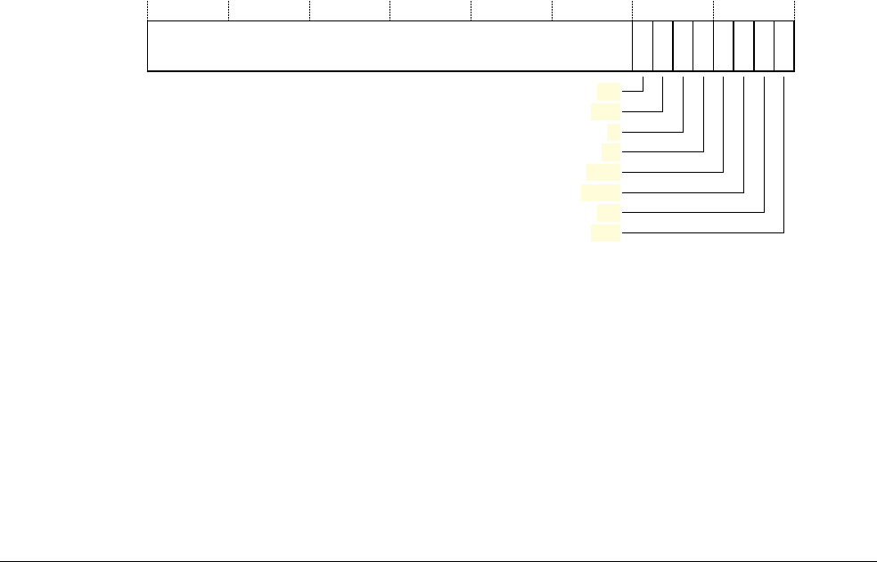
Appendix D2 Recommended Memory-mapped and External Debug Interfaces for the Performance Monitors
D2.2 PMU register descriptions for memory-mapped register views
ARM DDI 0406C.c Copyright © 1996-1998, 2000, 2004-2012, 2014 ARM. All rights reserved. D2-2363
ID051414 Non-Confidential
D2.2 PMU register descriptions for memory-mapped register views
This section describes the Performance Monitors registers that are not defined in Chapter B4 System Control
Registers in a VMSA implementation and Chapter B6 System Control Registers in a PMSA implementation but are
implemented in one or both of:
• an external debug interface to the Performance Monitors
• a memory-mapped interface to the Performance Monitors.
Table D2-1 on page D2-2355 lists all registers that are visible in these memory-mapped views of the Performance
Monitors registers.
D2.2.1 PMAUTHSTATUS, Performance Monitors Authentication Status register
The PMAUTHSTATUS characteristics are:
Purpose Indicates the implemented debug features and provides the current values of the
configuration inputs that determine the debug permissions.
This register is a Performance Monitors register that is visible only in the memory-mapped
views of the Performance Monitors registers.
Usage constraints There are no usage constraints.
Configurations Implemented only if an implementation of the Performance Monitors Extension provides a
memory-mapped view of the Performance Monitors registers.
If implemented in a processor that includes the Security Extensions, this is a Common
register.
Attributes A 32-bit RO register, at offset
0xFB8
.
Table D2-1 on page D2-2355 shows the register map for the memory-mapped views of the
Performance Monitors registers.
In an implementation that includes the Security Extensions, the PMAUTHSTATUS bit assignments are:
Bits[31:8] Reserved, UNK.
SNI, bit[7] Secure non-invasive debug features implemented. This bit is RAO, Secure non-invasive debug
features are implemented.
SNE, bit[6] Secure non-invasive debug enabled. This bit indicates whether non-invasive debug is permitted in
Secure PL1 modes. For the recommended external debug interface, this bit is the logical result of
(DBGEN OR NIDEN) AND (SPIDEN OR SPNIDEN).
SI, bit[5] Secure invasive debug features implemented. This bit is RAZ, Secure invasive debug features are
not implemented.
SE, bit[4] Secure invasive debug enabled. This bit is RAZ.
Reserved, UNK
31 876543210
1010
SNI
SNE
SI
SE
NSNI
NSNE
NSI
NSE
00
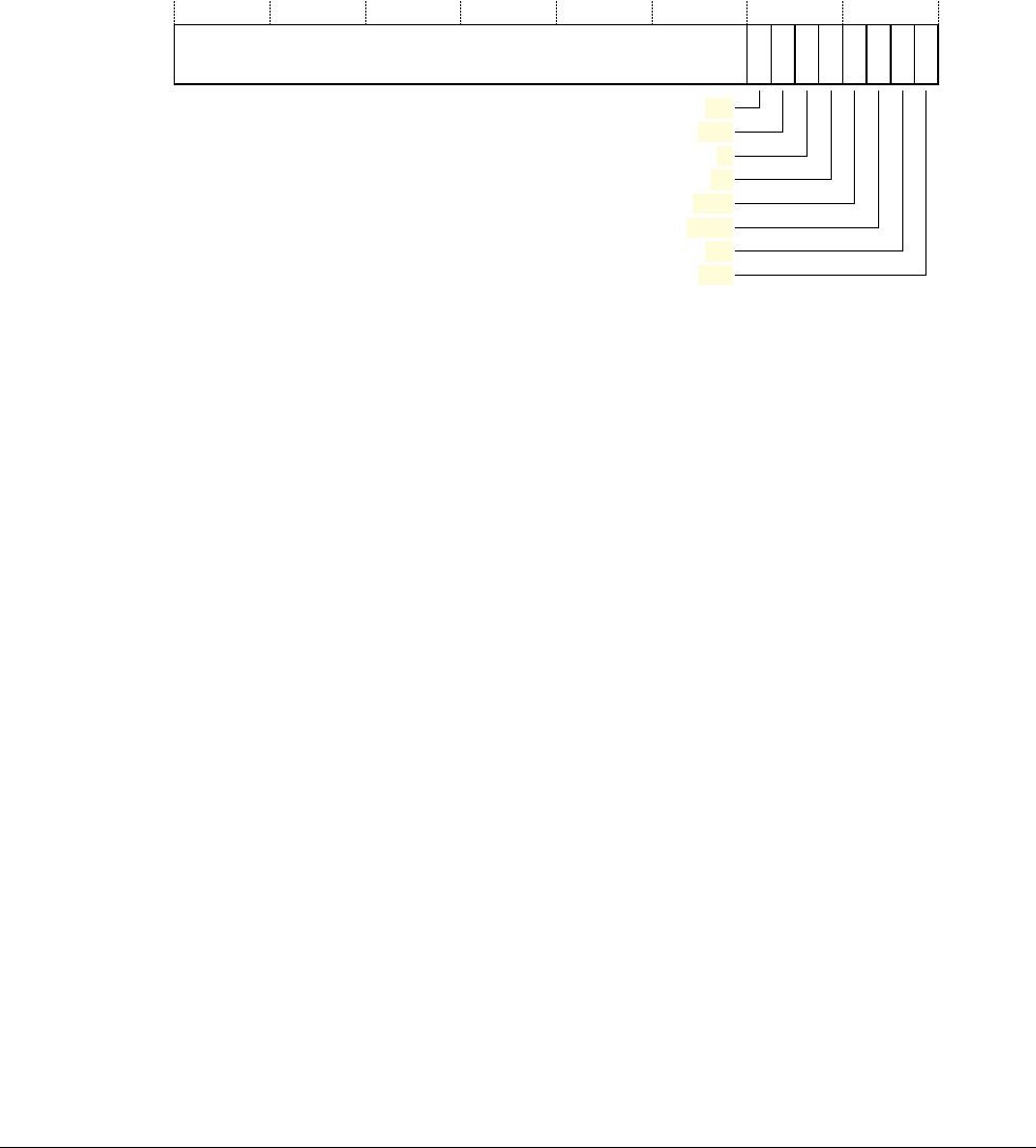
Appendix D2 Recommended Memory-mapped and External Debug Interfaces for the Performance Monitors
D2.2 PMU register descriptions for memory-mapped register views
D2-2364 Copyright © 1996-1998, 2000, 2004-2012, 2014 ARM. All rights reserved. ARM DDI 0406C.c
Non-Confidential ID051414
NSNI, bit[3] Non-secure non-invasive debug features implemented. This bit is RAO, Non-secure non-invasive
debug features are implemented.
NSNE, bit[2] Non-secure non-invasive debug enabled. For the recommended external debug interface, this bit
indicates the logical result of DBGEN OR NIDEN.
NSI, bit[1] Non-secure invasive debug features implemented. This bit is RAZ, Non-secure invasive debug
features are not implemented.
NSE, bit[0] Non-secure invasive debug enabled. This bit is RAZ.
In an implementation that does not include the Security Extensions, the PMAUTHSTATUS bit assignments are:
Bits[31:8] Reserved, UNK.
SNI, bit[7] Secure non-invasive debug features implemented. This bit is RAO, Secure non-invasive debug
features are implemented.
SNE, bit[6] Secure non-invasive debug enabled. This bit indicates whether non-invasive debug is permitted in
Secure PL1 modes. For the recommended external debug interface, this bit is the logical result of
DBGEN OR NIDEN.
SI, bit[5] Secure invasive debug features implemented. This bit is RAZ, Secure invasive debug features are
not implemented.
SE, bit[4] Secure invasive debug enabled. This bit is RAZ. It indicates whether invasive halting debug is
permitted in Secure PL1 modes.
NSNI, bit[3] Non-secure non-invasive debug features implemented. This bit is RAZ, Non-secure non-invasive
debug features are not implemented.
NSNE, bit[2] Non-secure non-invasive debug enabled. This bit is RAZ, Non-secure non-invasive debug is not
enabled.
NSI, bit[1] Non-secure invasive debug features implemented. This bit is RAZ, Non-secure invasive debug
features are not implemented.
NSE, bit[0] Non-secure invasive debug enabled. This bit is RAZ, Non-secure invasive debug is not enabled.
00Reserved, UNK
31 876543210
10000
SNI
SNE
SI
SE
NSNI
NSNE
NSI
NSE
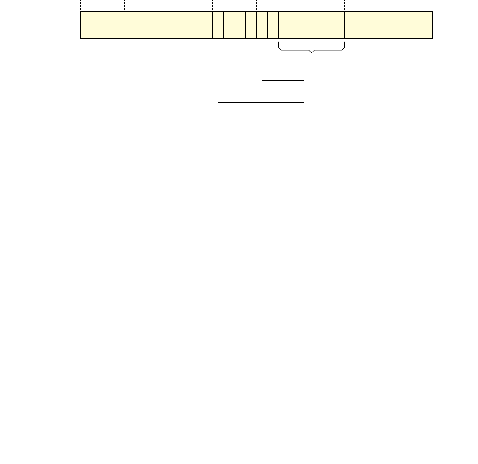
Appendix D2 Recommended Memory-mapped and External Debug Interfaces for the Performance Monitors
D2.2 PMU register descriptions for memory-mapped register views
ARM DDI 0406C.c Copyright © 1996-1998, 2000, 2004-2012, 2014 ARM. All rights reserved. D2-2365
ID051414 Non-Confidential
D2.2.2 PMCFGR, Performance Monitors Configuration Register
The PMCFGR characteristics are:
Purpose Contains PMU-specific configuration data.
This register is a Performance Monitors register that is visible only in the memory-mapped
views of the Performance Monitors registers.
Usage constraints There are no usage constraints.
Configurations Implemented only if an implementation of the Performance Monitors Extension provides a
memory-mapped view of the Performance Monitors registers.
Attributes A 32-bit RO register, at offset
0xE00
.
Table D2-1 on page D2-2355 shows the register map for the memory-mapped views of the
Performance Monitors registers.
The PMCFGR bit assignments are:
Bits[31:20] Reserved, UNK.
UEN, bit[19] User-mode Enable Register implemented. This bit is RAO. Its meaning is:
1 User-mode Enable Register implemented.
Bit[18:17] Reserved, UNK.
EX, bit[16] Export supported. This bit is RO and the value is IMPLEMENTATION DEFINED:
0 Export is not supported. PMCR.X is RAZ/WI.
1 Export is supported. PMCR.X is writable.
CCD, bit[15] Cycle counter clock divider implemented. This bit is RAO. Its meaning is:
1 Cycle count divider implemented. This means PMCR.D is writable.
CC, bit[14] Cycle counter implemented. This bit is RAO. Its meaning is:
1 Cycle counter implemented. This means PMCR.C, the cycle counter reset bit,
is writable.
SIZE, bits[13:8] Counter size. This field is RO and reads as
0b011111
. Its meaning is:
0b011111
32-bit counters.
N, bits[7:0] Number of event counters. This field is RO with a value that indicates the number of
implemented event counters, from
0b00000000
if the implementation has no event counters,
to
0b00011111
if it has 31 event counters.
Note
The cycle counter is not included in the value indicated by the N field.
In an implementation that includes the Virtualization Extensions, the value of
HDCR.HPMN has no effect on the value returned by this field.
Reserved, UNK
31 20 19 18 17 16 15 14 13 8 7 0
1 (0) (0) 1 1 0 1 1 1 11 N
EX
CC
CCD
Size
UEN

Appendix D2 Recommended Memory-mapped and External Debug Interfaces for the Performance Monitors
D2.2 PMU register descriptions for memory-mapped register views
D2-2366 Copyright © 1996-1998, 2000, 2004-2012, 2014 ARM. All rights reserved. ARM DDI 0406C.c
Non-Confidential ID051414
D2.2.3 PMCID0, Performance Monitors Component ID register 0
The PMCID0 characteristics are:
Purpose Provides bits[7:0] of the 32-bit conceptual Component ID.
This register is a Performance Monitors register that is visible only in the memory-mapped
views of the Performance Monitors registers.
Usage constraints There are no usage constraints.
Configurations Implemented only if an implementation of the Performance Monitors Extension provides a
memory-mapped view of the Performance Monitors registers.
If implemented in a processor that includes the Security Extensions, this is a Common
register.
Attributes A 32-bit RO register, at offset
0xFF0
.
Table D2-1 on page D2-2355 shows the register map for the memory-mapped views of the
Performance Monitors registers.
The PMCID0 bit assignments are:
Bits[31:8] Reserved, UNK.
Preamble byte 0, bits[7:0]
This field has the value
0x0D
.
D2.2.4 PMCID1, Performance Monitors Component ID register 1
The PMCID1 characteristics are:
Purpose Provides bits[15:8] of the 32-bit conceptual Component ID.
This register is a Performance Monitors register that is visible only in the memory-mapped
views of the Performance Monitors registers.
Usage constraints There are no usage constraints.
Configurations Implemented only if an implementation of the Performance Monitors Extension provides a
memory-mapped view of the Performance Monitors registers.
If implemented in a processor that includes the Security Extensions, this is a Common
register.
Attributes A 32-bit RO register, at offset
0xFF4
.
Table D2-1 on page D2-2355 shows the register map for the memory-mapped views of the
Performance Monitors registers.
The PMCID1 bit assignments are:
Bits[31:8] Reserved, UNK.
Component class, bits[7:4]
This field has the value
0x9
, indicating an ARM Debug component.
Preamble, bits[3:0] This field has the value
0x0
.

Appendix D2 Recommended Memory-mapped and External Debug Interfaces for the Performance Monitors
D2.2 PMU register descriptions for memory-mapped register views
ARM DDI 0406C.c Copyright © 1996-1998, 2000, 2004-2012, 2014 ARM. All rights reserved. D2-2367
ID051414 Non-Confidential
D2.2.5 PMCID2, Performance Monitors Component ID register 2
The PMCID2 characteristics are:
Purpose Provides bits[23:16] of the 32-bit conceptual Component ID.
This register is a Performance Monitors register that is visible only in the memory-mapped
views of the Performance Monitors registers.
Usage constraints There are no usage constraints.
Configurations Implemented only if an implementation of the Performance Monitors Extension provides a
memory-mapped view of the Performance Monitors registers.
If implemented in a processor that includes the Security Extensions, this is a Common
register.
Attributes A 32-bit RO register, at offset
0xFF8
.
Table D2-1 on page D2-2355 shows the register map for the memory-mapped views of the
Performance Monitors registers.
The PMCID2 bit assignments are:
Bits[31:8] Reserved, UNK.
Preamble byte 2, bits[7:0]
This field has the value
0x05
.
D2.2.6 PMCID3, Performance Monitors Component ID register 3
The PMCID3 characteristics are:
Purpose Provides bits[31:24] of the 32-bit conceptual Component ID.
This register is a Performance Monitors register that is visible only in the memory-mapped
views of the Performance Monitors registers.
Usage constraints There are no usage constraints.
Configurations Implemented only if an implementation of the Performance Monitors Extension provides a
memory-mapped view of the Performance Monitors registers.
If implemented in a processor that includes the Security Extensions, this is a Common
register.
Attributes A 32-bit RO register, at offset
0xFFC
.
Table D2-1 on page D2-2355 shows the register map for the memory-mapped views of the
Performance Monitors registers.
The PMCID3 bit assignments are:
Bits[31:8] Reserved, UNK.
Preamble byte 3, bits[7:0]
This field has the value
0xB1
.
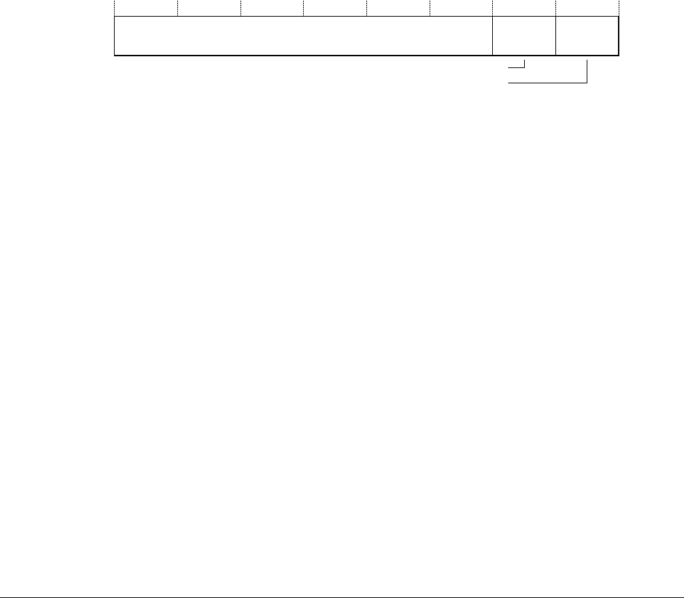
Appendix D2 Recommended Memory-mapped and External Debug Interfaces for the Performance Monitors
D2.2 PMU register descriptions for memory-mapped register views
D2-2368 Copyright © 1996-1998, 2000, 2004-2012, 2014 ARM. All rights reserved. ARM DDI 0406C.c
Non-Confidential ID051414
D2.2.7 PMDEVTYPE, Performance Monitors Device Type register
The PMDEVTYPE characteristics are:
Purpose Provides the CoreSight device type information for the Performance Monitors. Every
CoreSight component must implement a Device Type register, to indicate the type of debug
component.
This register is a Performance Monitors register that is visible only in the memory-mapped
views of the Performance Monitors registers.
Usage constraints There are no usage constraints.
Configurations Implemented only if an implementation of the Performance Monitors Extension provides a
memory-mapped view of the Performance Monitors registers.
If implemented in a processor that includes the Security Extensions, this is a Common
register.
Attributes A 32-bit RO register, at offset
0xFC8
.
Table D2-1 on page D2-2355 shows the register map for the memory-mapped views of the
Performance Monitors registers.
The PMDEVTYPE bit assignments are:
Bits[31:8] Reserved, UNK.
T, bits[7:4] Sub type. This field reads as
0x1
, indicating a processor.
C, bits[3:0] Main class. This field reads as
0x6
, indicating Performance Monitors.
For more information about the CoreSight registers, see the CoreSight Architecture Specification.
0Reserved, UNK
31 8 7 4 3 0
0010110
T
C

Appendix D2 Recommended Memory-mapped and External Debug Interfaces for the Performance Monitors
D2.2 PMU register descriptions for memory-mapped register views
ARM DDI 0406C.c Copyright © 1996-1998, 2000, 2004-2012, 2014 ARM. All rights reserved. D2-2369
ID051414 Non-Confidential
D2.2.8 PMLAR, Performance Monitors Lock Access Register
The PMLAR characteristics are:
Purpose Provides a Software Lock on writes to the Performance Monitors registers through the
memory-mapped interface. Use of this lock mechanism reduces the risk of accidental
damage to the contents of the Performance Monitors registers. It does not prevent all
accidental or malicious damage.
This register is a Performance Monitors register that is visible only in the memory-mapped
interface, see Usage constraints.
Usage constraints Used in conjunction with PMLSR. The PMLAR is UNPREDICTABLE in the external debug
interface.
Configurations Implemented only if an implementation of the Performance Monitors Extension includes
the memory-mapped register interface.
If implemented in a processor that includes the Security Extensions, this is a Common
register.
Attributes A 32-bit WO register, at offset
0xFB0
.
Table D2-1 on page D2-2355 shows the register map for the memory-mapped interface to
the Performance Monitors registers.
The PMLAR bit assignments are:
Lock Access Control, bits[31:0]
Writing the key value
0xC5ACCE55
to this field clears the lock, enabling write accesses to the
Performance Monitors registers through the memory-mapped interface.
Writing any other value to this register sets the lock, disabling write accesses to the
Performance Monitors registers through the memory-mapped interface.
A debugger reads PMLSR to check the status of the Software Lock.
Note
• The Software Lock of the Performance Monitors registers is independent of the Software Lock of the debug
registers.
• The PMLAR is not required to be maintained over a powerdown.
31 0
Lock Access Control
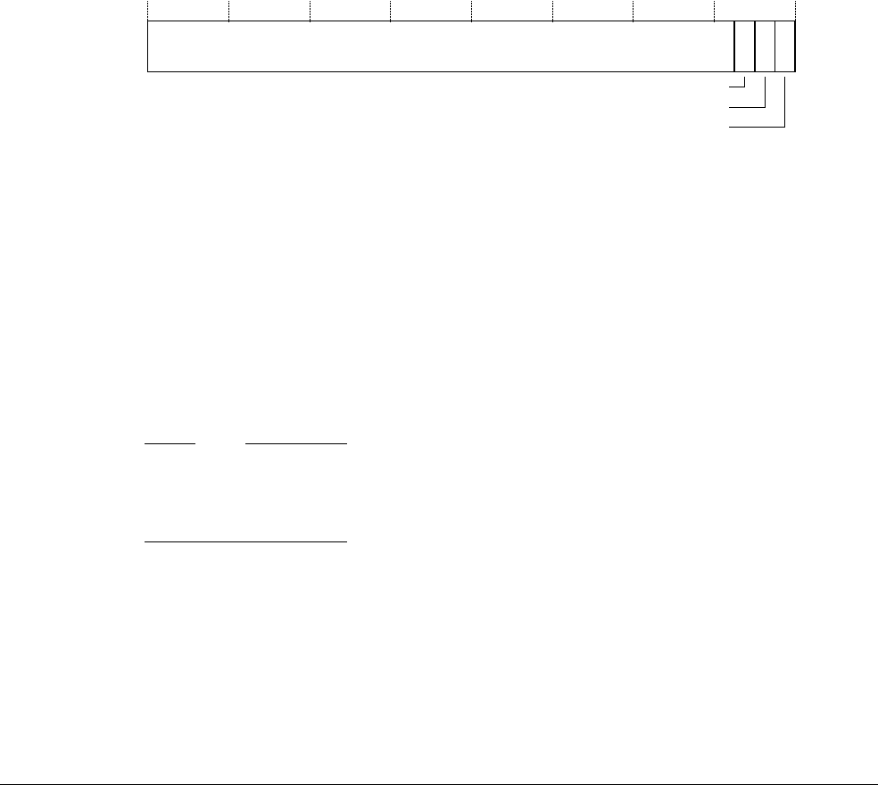
Appendix D2 Recommended Memory-mapped and External Debug Interfaces for the Performance Monitors
D2.2 PMU register descriptions for memory-mapped register views
D2-2370 Copyright © 1996-1998, 2000, 2004-2012, 2014 ARM. All rights reserved. ARM DDI 0406C.c
Non-Confidential ID051414
D2.2.9 PMLSR, Performance Monitors Lock Status Register
The PMLSR characteristics are:
Purpose Shows the status of the Software Lock on the Performance Monitors registers.
This register is a Performance Monitors register that is visible only in the memory-mapped
interface, see Usage constraints.
Usage constraints Used in conjunction with PMLAR. The PMLSR is UNKNOWN in the external debug
interface.
Configurations Implemented only if an implementation of the Performance Monitors Extension includes
the memory-mapped register interface.
If implemented in a processor that includes the Security Extensions, this is a Common
register.
Attributes A 32-bit RO register, at offset
0xFB4
.
Table D2-1 on page D2-2355 shows the register map for the memory-mapped interface to
the Performance Monitors registers.
The PMLSR bit assignments are:
Bits[31:3] Reserved, UNK.
nTT, bit[2] Not 32-bit. This bit is always RAZ. It indicates that software must perform a 32-bit access to write
the key to the PMLAR.
SLK, bit[1] Software Lock status. This bit indicates the status of the Performance Monitors registers lock. The
possible values are:
0 Lock clear.
1 Lock set.
A debugger sets or clears the Performance Monitors registers lock by writing to the PMLAR.
The debug logic reset value of this bit is 1.
SLI, bit[0] Software Lock implemented. This bit is RAO.
Note
• The Software Lock of the Performance Monitors registers is independent of the Software Lock of the debug
registers.
• The PMLSR is not required to be maintained over a powerdown.
31 0
Reserved, UNK
321
nTT
SLK
SLI
10

Appendix D2 Recommended Memory-mapped and External Debug Interfaces for the Performance Monitors
D2.2 PMU register descriptions for memory-mapped register views
ARM DDI 0406C.c Copyright © 1996-1998, 2000, 2004-2012, 2014 ARM. All rights reserved. D2-2371
ID051414 Non-Confidential
D2.2.10 PMPID0, Performance Monitors Peripheral ID register 0
The PMPID0 characteristics are:
Purpose Provides bits[7:0] of the 64-bit conceptual Peripheral ID.
This register is a Performance Monitors register that is visible only in the memory-mapped
views of the Performance Monitors registers.
Usage constraints There are no usage constraints.
Configurations Implemented only if an implementation of the Performance Monitors Extension provides a
memory-mapped view of the Performance Monitors registers.
If implemented in a processor that includes the Security Extensions, this is a Common
register.
Attributes A 32-bit RO register, at offset
0xFE0
.
Table D2-1 on page D2-2355 shows the register map for the memory-mapped views of the
Performance Monitors registers.
The PMPID0 bit assignments are:
Bits[31:8] Reserved, UNK.
Part number[7:0], bits[7:0]
Bits[7:0] of the IMPLEMENTATION DEFINED part number.
Note
This is the part number for the Performance Monitors block. It is not the same part number
as the processor debug block.

Appendix D2 Recommended Memory-mapped and External Debug Interfaces for the Performance Monitors
D2.2 PMU register descriptions for memory-mapped register views
D2-2372 Copyright © 1996-1998, 2000, 2004-2012, 2014 ARM. All rights reserved. ARM DDI 0406C.c
Non-Confidential ID051414
D2.2.11 PMPID1, Performance Monitors Peripheral ID register 1
The PMPID1 characteristics are:
Purpose Provides bits[15:8] of the 64-bit conceptual Peripheral ID.
This register is a Performance Monitors register that is visible only in the memory-mapped
views of the Performance Monitors registers.
Usage constraints There are no usage constraints.
Configurations Implemented only if an implementation of the Performance Monitors Extension provides a
memory-mapped view of the Performance Monitors registers.
If implemented in a processor that includes the Security Extensions, this is a Common
register.
Attributes A 32-bit RO register, at offset
0xFE4
.
Table D2-1 on page D2-2355 shows the register map for the memory-mapped views of the
Performance Monitors registers.
The PMPID1 bit assignments are:
Bits[31:8] Reserved, UNK.
JEP identification code[3:0], bits[7:4]
Bits[3:0] of the IMPLEMENTATION DEFINED JEP identification code.
For an implementation designed by ARM the JEP106 identification code is
0x3B
and
therefore this field is
0xB
.
Part number[11:8], bits[3:0]
Bits[11:8] of the IMPLEMENTATION DEFINED part number. For more information see the Part
number field in PMPID0.

Appendix D2 Recommended Memory-mapped and External Debug Interfaces for the Performance Monitors
D2.2 PMU register descriptions for memory-mapped register views
ARM DDI 0406C.c Copyright © 1996-1998, 2000, 2004-2012, 2014 ARM. All rights reserved. D2-2373
ID051414 Non-Confidential
D2.2.12 PMPID2, Performance Monitors Peripheral ID register 2
The PMPID2 characteristics are:
Purpose Provides bits[23:16] of the 64-bit conceptual Peripheral ID.
This register is a Performance Monitors register that is visible only in the memory-mapped
views of the Performance Monitors registers.
Usage constraints There are no usage constraints.
Configurations Implemented only if an implementation of the Performance Monitors Extension provides a
memory-mapped view of the Performance Monitors registers.
If implemented in a processor that includes the Security Extensions, this is a Common
register.
Attributes A 32-bit RO register, at offset
0xFE8
.
Table D2-1 on page D2-2355 shows the register map for the memory-mapped views of the
Performance Monitors registers.
The PMPID2 bit assignments are:
Bits[31:8] Reserved, UNK.
Revision, bits[7:4] The IMPLEMENTATION DEFINED revision number for the implementation.
Uses JEP code, bit[3]
For an ARMv7 implementation this bit must be one, indicating that the Peripheral ID uses
a JEP106 identification code.
JEP identification code[6:4], bits[2:0]
Bits[6:4] of the IMPLEMENTATION DEFINED JEP identification code.
For an implementation designed by ARM the JEP106 identification code is
0x3B
and
therefore this field is
0b011
.

Appendix D2 Recommended Memory-mapped and External Debug Interfaces for the Performance Monitors
D2.2 PMU register descriptions for memory-mapped register views
D2-2374 Copyright © 1996-1998, 2000, 2004-2012, 2014 ARM. All rights reserved. ARM DDI 0406C.c
Non-Confidential ID051414
D2.2.13 PMPID3, Performance Monitors Peripheral ID register 3
The PMPID3 characteristics are:
Purpose Provides bits[31:24] of the 64-bit conceptual Peripheral ID.
This register is a Performance Monitors register that is visible only in the memory-mapped
views of the Performance Monitors registers.
Usage constraints There are no usage constraints.
Configurations Implemented only if an implementation of the Performance Monitors Extension provides a
memory-mapped view of the Performance Monitors registers.
If implemented in a processor that includes the Security Extensions, this is a Common
register.
Attributes A 32-bit RO register, at offset
0xFEC
.
Table D2-1 on page D2-2355 shows the register map for the memory-mapped views of the
Performance Monitors registers.
The PMPID3 bit assignments are:
Bits[31:8] Reserved, UNK.
RevAnd, bits[7:4] The IMPLEMENTATION DEFINED manufacturing revision number for the implementation.
Customer modified, bits[3:0]
An IMPLEMENTATION DEFINED value that indicates an endorsed modification to the
implementation.
If the system designer cannot modify the RTL supplied by the processor designer then this
field is RAZ.

Appendix D2 Recommended Memory-mapped and External Debug Interfaces for the Performance Monitors
D2.2 PMU register descriptions for memory-mapped register views
ARM DDI 0406C.c Copyright © 1996-1998, 2000, 2004-2012, 2014 ARM. All rights reserved. D2-2375
ID051414 Non-Confidential
D2.2.14 PMPID4, Performance Monitors Peripheral ID register 4
The PMPID4 characteristics are:
Purpose Provides bits[39:32] of the 64-bit conceptual Peripheral ID.
This register is a Performance Monitors register that is visible only in the memory-mapped
views of the Performance Monitors registers.
Usage constraints There are no usage constraints.
Configurations Implemented only if an implementation of the Performance Monitors Extension provides a
memory-mapped view of the Performance Monitors registers.
If implemented in a processor that includes the Security Extensions, this is a Common
register.
Attributes A 32-bit RO register, at offset
0xFD0
.
Table D2-1 on page D2-2355 shows the register map for the memory-mapped views of the
Performance Monitors registers.
The PMPID4 bit assignments are:
Bits[31:8] Reserved, UNK.
4KB count, bits[7:4] This field is RAZ for all ARMv7 implementations.
JEP106 continuation code, bits[3:0]
The IMPLEMENTATION DEFINED JEP106 continuation code.
For an implementation designed by ARM this field is
0x4
.

Appendix D2 Recommended Memory-mapped and External Debug Interfaces for the Performance Monitors
D2.2 PMU register descriptions for memory-mapped register views
D2-2376 Copyright © 1996-1998, 2000, 2004-2012, 2014 ARM. All rights reserved. ARM DDI 0406C.c
Non-Confidential ID051414

ARM DDI 0406C.c Copyright © 1996-1998, 2000, 2004-2012, 2014 ARM. All rights reserved. D3-2377
ID051414 Non-Confidential
Appendix D3
Recommendations for Performance Monitors Event
Numbers for IMPLEMENTATION DEFINED Events
This appendix describes the ARM recommendations for the use of the IMPLEMENTATION DEFINED event numbers.
It contains the following section:
•ARM recommendations for IMPLEMENTATION DEFINED event numbers on page D3-2378.

Appendix D3 Recommendations for Performance Monitors Event Numbers for IMPLEMENTATION DEFINED Events
D3.1 ARM recommendations for IMPLEMENTATION DEFINED event numbers
D3-2378 Copyright © 1996-1998, 2000, 2004-2012, 2014 ARM. All rights reserved. ARM DDI 0406C.c
Non-Confidential ID051414
D3.1 ARM recommendations for IMPLEMENTATION DEFINED event numbers
These are the ARM recommendations for the use of the IMPLEMENTATION DEFINED event numbers. ARM does not
define these events as rigorously as those in the architectural and microarchitectural event lists, and an
implementation might:
• Modify the definition of an event to better correspond to the implementation.
• Not use some, or many, of these event numbers.
Note
In these definitions, in an implementation that includes the Security Extensions or the Virtualization Extensions, an
exception that is taken locally means an exception that is taken to the default mode at the default offset, and is not
routed to another mode. See Processor mode for taking exceptions on page B1-1173 for more information.
Table D3-1 lists the PMU IMPLEMENTATION DEFINED event numbers in event number order. As the table shows:
• Event numbers
0x90
-
0xBF
are reserved for future expansion of the recommended event numbers.
• Event numbers
0xC0
-
0xFF
are available for IMPLEMENTATION DEFINED events.
Table D3-1 PMU IMPLEMENTATION DEFINED event numbers
Event number Event mnemonic Description
0x40
L1D_CACHE_LD Level 1 data cache access, read
0x41
L1D_CACHE_ST Level 1 data cache access, write
0x42
L1D_CACHE_REFILL_LD Level 1 data cache refill, read
0x43
L1D_CACHE_REFILL_ST Level 1 data cache refill, write
0x44
L1D_CACHE_REFILL_INNER Level 1 data cache refill, inner
0x45
L1D_CACHE_REFILL_OUTER Level 1 data cache refill, outer
0x46
L1D_CACHE_WB_VICTIM Level 1 data cache write-back, victim
0x47
L1D_CACHE_WB_CLEAN Level 1 data cache write-back, cleaning and coherency
0x48
L1D_CACHE_INVAL Level 1 data cache invalidate
0x49
-
0x4B
- Reserved
0x4C
L1D_TLB_REFILL_LD Level 1 data TLB refill, read
0x4D
L1D_TLB_REFILL_ST Level 1 data TLB refill, write
0x4E
-
0x4F
- Reserved
0x50
L2D_CACHE_LD Level 2 data cache access, read
0x51
L2D_CACHE_ST Level 2 data cache access, write
0x52
L2D_CACHE_REFILL_LD Level 2 data cache refill, read
0x53
L2D_CACHE_REFILL_ST Level 2 data cache refill, write
0x54
-
0x55
- Reserved
0x56
L2D_CACHE_WB_VICTIM Level 2 data cache write-back, victim
0x57
L2D_CACHE_WB_CLEAN Level 2 data cache write-back, cleaning and coherency
0x58
L2D_CACHE_INVAL Level 2 data cache invalidate

Appendix D3 Recommendations for Performance Monitors Event Numbers for IMPLEMENTATION DEFINED Events
D3.1 ARM recommendations for IMPLEMENTATION DEFINED event numbers
ARM DDI 0406C.c Copyright © 1996-1998, 2000, 2004-2012, 2014 ARM. All rights reserved. D3-2379
ID051414 Non-Confidential
0x59
-
0x5F
- Reserved
0x60
BUS_ACCESS_LD Bus access, read
0x61
BUS_ACCESS_ST Bus access, write
0x62
BUS_ACCESS_SHARED Bus access, Normal, Cacheable, Shareable
0x63
BUS_ACCESS_NOT_SHARED Bus access, not Normal, Cacheable, Shareable
0x64
BUS_ACCESS_NORMAL Bus access, normal
0x65
BUS_ACCESS_PERIPH Bus access, peripheral
0x66
MEM_ACCESS_LD Data memory access, read
0x67
MEM_ACCESS_ST Data memory access, write
0x68
UNALIGNED_LD_SPEC Unaligned access, read
0x69
UNALIGNED_ST_SPEC Unaligned access, write
0x6A
UNALIGNED_LDST_SPEC Unaligned access
0x6B
- Reserved
0x6C
LDREX_SPEC Exclusive instruction speculatively executed,
LDREX
0x6D
STREX_PASS_SPEC Exclusive instruction speculatively executed,
STREX
pass
0x6E
STREX_FAIL_SPEC Exclusive instruction speculatively executed,
STREX
fail
0x6F
STREX_SPEC Exclusive instruction speculatively executed,
STREX
0x70
LD_SPEC Instruction speculatively executed, load
0x71
ST_SPEC Instruction speculatively executed, store
0x72
LDST_SPEC Instruction speculatively executed, load or store
0x73
DP_SPEC Instruction speculatively executed, integer data processing
0x74
ASE_SPEC Instruction speculatively executed, Advanced SIMD data processing
0x75
VFP_SPEC Instruction speculatively executed, Floating-point data processing
0x76
PC_WRITE_SPEC Instruction speculatively executed, software change of the PC
0x77
- Reserved
0x78
BR_IMMED_SPEC Branch speculatively executed, immediate branch
0x79
BR_RETURN_SPEC Branch speculatively executed, procedure return
0x7A
BR_INDIRECT_SPEC Branch speculatively executed, indirect branch
0x7B
- Reserved
0x7C
ISB_SPEC Barrier speculatively executed,
ISB
0x7D
DSB_SPEC Barrier speculatively executed,
DSB
0x7E
DMB_SPEC Barrier speculatively executed,
DMB
Table D3-1 PMU IMPLEMENTATION DEFINED event numbers (continued)
Event number Event mnemonic Description

Appendix D3 Recommendations for Performance Monitors Event Numbers for IMPLEMENTATION DEFINED Events
D3.1 ARM recommendations for IMPLEMENTATION DEFINED event numbers
D3-2380 Copyright © 1996-1998, 2000, 2004-2012, 2014 ARM. All rights reserved. ARM DDI 0406C.c
Non-Confidential ID051414
0x40
, Level 1 data cache access, read
This event is similar to the Level 1 data cache access event, event
0x04
, but the counter counts only
memory-read operations that access at least the Level 1 data or unified cache.
0x41
, Level 1 data cache access, write
This event is similar to the Level 1 data cache access event, event
0x04
, but the counter counts only
memory-write operations that access at least the Level 1 data or unified cache.
0x42
, Level 1 data cache refill, read
This event is similar to the Level 1 data cache refill event, event
0x03
, but the counter counts only
memory-read operations that cause a refill of at least the Level 1 data or unified cache.
0x43
, Level 1 data cache refill, write
This event is similar to the Level 1 data cache refill event, event
0x03
, but the counter counts only
memory-write operations that cause a refill of at least the Level 1 data or unified cache.
0x44
, Level 1 data cache refill, inner
This event is similar to the Level 1 data cache refill event, event
0x03
, but the counter counts only
memory-read and memory-write operations that generate refills satisfied by transfer from another
cache inside of the immediate cluster.
0x7F
-
0x80
- Reserved
0x81
EXC_UNDEF Exception taken, Undefined Instruction
0x82
EXC_SVC Exception taken, Supervisor Call
0x83
EXC_PABORT Exception taken, Prefetch Abort
0x84
EXC_DABORT Exception taken, Data Abort
0x85
- Reserved
0x86
EXC_IRQ Exception taken, IRQ
0x87
EXC_FIQ Exception taken, FIQ
0x88
EXC_SMC Exception taken, Secure Monitor Call
0x89
- Reserved
0x8A
EXC_HVC Exception taken, Hypervisor Call
0x8B
EXC_TRAP_PABORT Exception taken, Prefetch Abort not taken locally
0x8C
EXC_TRAP_DABORT Exception taken, Data Abort not taken locally
0x8D
EXC_TRAP_OTHER Exception taken, other hypervisor traps
0x8E
EXC_TRAP_IRQ Exception taken, IRQ not taken locally
0x8F
EXC_TRAP_FIQ Exception taken, FIQ not taken locally
0x90
-
0xBF
- Reserved for future extension of these recommendations
0xC0
-
0xFF
- Available for IMPLEMENTATION DEFINED events
Table D3-1 PMU IMPLEMENTATION DEFINED event numbers (continued)
Event number Event mnemonic Description

Appendix D3 Recommendations for Performance Monitors Event Numbers for IMPLEMENTATION DEFINED Events
D3.1 ARM recommendations for IMPLEMENTATION DEFINED event numbers
ARM DDI 0406C.c Copyright © 1996-1998, 2000, 2004-2012, 2014 ARM. All rights reserved. D3-2381
ID051414 Non-Confidential
Note
The boundary between inner and outer is IMPLEMENTATION DEFINED, and it is not necessarily linked
to other similar boundaries, such as the boundary between Inner Cacheable and Outer Cacheable or
the boundary between Inner Shareable and Outer Shareable.
0x45
, Level 1 data cache refill, outer
This event is similar to the Level 1 data cache refill event, event
0x03
, but the counter counts only
memory-read and memory-write operations that generate refills satisfied from outside of the
immediate cluster.
0x46
, Level 1 data cache write-back, victim
This event is similar to the Level 1 data cache write-back event, event
0x15
, but the counter counts
only write-backs that are a result of the line being allocated for an access made by the processor.
CP15 cache maintenance operations do not count as events.
0x47
, Level 1 data cache write-back, cleaning and coherency
This event is similar to the Level 1 data cache write-back event, event
0x15
, but the counter counts
only write-backs that are a result of a coherency operation made by another processor, or from a
CP15 cache maintenance operation. Whether write-backs made as a result of CP15 cache
maintenance operations are counted is IMPLEMENTATION DEFINED.
Note
The transfer of a dirty cache line from the Level 1 data cache of this processor to the Level 1 data
cache of another processor due to a hardware coherency operation is not counted unless the dirty
cache line is also written back to a Level 2 cache or memory.
0x48
, Level 1 data cache invalidate
The counter counts each invalidation of a cache line in the Level 1 data or unified cache.
The counter does not count events:
• if a cache refill invalidates a line
• for locally executed CP15 cache set/way maintenance operations.
0x4C
, Level 1 data TLB refill, read
This event is similar to the Level 1 data TLB refill event, event
0x05
, but the counter counts only
memory-read operations that cause a data TLB refill of a least the Level 1 data or unified TLB.
0x4D
, Level 1 data TLB refill, write
This event is similar to the Level 1 data TLB refill event, event
0x05
, but the counter counts only
memory-write operations that cause a data TLB refill of a least the Level 1 data or unified TLB.
0x50
, Level 2 data cache access, read
This event is similar to the Level 2 data cache access event, event
0x16
, but the counter counts only
memory-read operations that access at least the Level 2 data or unified cache.
0x51
, Level 2 data cache access, write
This event is similar to the Level 2 data cache access event, event
0x16
, but the counter counts only
memory-write operations that access at least the Level 2 data or unified cache.
0x52
, Level 2 data cache refill, read
This event is similar to the Level 2 data cache refill event, event
0x17
, but the counter counts only
memory-read operations that cause a refill of at least the Level 2 data or unified cache.
0x53
, Level 2 data cache refill, write
This event is similar to the Level 2 data cache refill event, event
0x17
, but the counter counts only
memory-write operations that cause a refill of at least the Level 2 data or unified cache.

Appendix D3 Recommendations for Performance Monitors Event Numbers for IMPLEMENTATION DEFINED Events
D3.1 ARM recommendations for IMPLEMENTATION DEFINED event numbers
D3-2382 Copyright © 1996-1998, 2000, 2004-2012, 2014 ARM. All rights reserved. ARM DDI 0406C.c
Non-Confidential ID051414
0x56
, Level 2 data cache write-back, victim
This event is similar to the Level 2 data cache write-back event, event
0x18
, but the counter counts
only write-backs that are a result of the line being allocated for an access made by the processor.
CP15 cache maintenance operations do not count as events.
0x57
, Level 2 data cache write-back, cleaning and coherency
This event is similar to the Level 2 data cache write-back event, event
0x18
, but the counter counts
only write-backs that are a result of a coherency operation made by another processor, or from a
CP15 cache maintenance operation. Whether write-backs made as a result of CP15 cache
maintenance operations are counted is IMPLEMENTATION DEFINED.
Note
The transfer of a dirty cache line from the Level 2 data cache of this processor to the Level 2 data
cache of another processor due to a hardware coherency operation is not counted unless the dirty
cache line is also written back to a Level 3 cache or memory.
0x58
, Level 2 data cache invalidate
The counter counts each invalidation of a cache line in the Level 2 data or unified cache.
The counter does not count events:
• if a cache refill invalidates a line
• for locally executed CP15 set/way cache maintenance operations.
Note
Software that uses this event must know whether the Level 2 data cache is shared with other
processors. This event does not follow the general rule of Level 2 data cache events of only counting
events that directly affect this processor.
0x60
, Bus access, read
This event is similar to the Bus access event, event
0x19
, but the counter counts only memory-read
operations that access outside the boundary of the processor and its closely-coupled caches.
0x61
, Bus access, write
This event is similar to the Bus access event, event
0x19
, but the counter counts only memory-write
operations that access outside the boundary of the processor and its closely-coupled caches.
0x62
, Bus access, Normal, Cacheable, Shareable
This event is similar to the Bus access event, event
0x19
, but the counter counts only memory-read
and memory-write operations that make Normal, Cacheable, Shareable accesses outside the
boundary of the processor and its closely-coupled caches.
Note
It is IMPLEMENTATION DEFINED how the processor translates the attributes from the translation table
entry for a region to the attributes on the bus.
In particular, a region of memory designated as Normal, Cacheable, Inner Shareable, Not Outer
Shareable by a translation table entry, might be marked as either Shareable or Not Shareable at the
boundary of the processor and its closely-coupled caches. This depends on where the
IMPLEMENTATION DEFINED boundary lies, between Inner and Outer Shareable.
If the Inner Shareable extends beyond the processor boundary, and the bus indicates the distinction
between Inner and Outer Shareable, then either is counted as Shareable for the purposes of defining
this event.

Appendix D3 Recommendations for Performance Monitors Event Numbers for IMPLEMENTATION DEFINED Events
D3.1 ARM recommendations for IMPLEMENTATION DEFINED event numbers
ARM DDI 0406C.c Copyright © 1996-1998, 2000, 2004-2012, 2014 ARM. All rights reserved. D3-2383
ID051414 Non-Confidential
0x63
, Bus access, not Normal, Cacheable, Shareable
This event is similar to the Bus access event, event
0x19
, but the counter counts only memory-read
and memory-write operations that make accesses outside the boundary of the processor and its
closely-coupled caches that are not Normal, Cacheable, Shareable. For example, the counter counts
accesses marked as:
• Normal, Cacheable, Not Shareable
• Normal, Not Cacheable
•Device
• Strongly-ordered.
Note
See the Note to event
0x62
, Bus access, Normal, Cacheable, Shareable, about how the processor
translates the attributes from the translation table entries for a region to the attributes on the bus.
0x64
, Bus access, normal
This event is similar to the Bus access event, event
0x19
, but the counter counts only memory-read
and memory-write operations that make Normal accesses outside the boundary of the processor and
its closely-coupled caches. For example, the counter counts Normal, Cacheable and Normal, Not
Cacheable accesses but does not count Device and Strongly-ordered accesses.
0x65
, Bus access, peripheral
This event is similar to the Bus access event, event
0x19
, but the counter counts only memory-read
and memory-write operations that make Device or Strongly-ordered accesses outside the boundary
of the processor and its closely-coupled caches.
0x66
, Data memory access, read
This event is similar to the Data memory access event, event
0x13
, but the counter counts only
memory-read operations made by the processor.
0x67
, Data memory access, write
This event is similar to the Data memory access event, event
0x13
, but the counter counts only
memory-write operations made by the processor.
0x68
, Unaligned access, read
This event is similar to the Data memory access event, event
0x13
, but the counter counts only
unaligned memory-read operations that the processor made. It also counts unaligned accesses if they
are subsequently changed into multiple aligned accesses.
0x69
, Unaligned access, write
This event is similar to the Data memory access event, event
0x13
, but the counter counts only
unaligned memory-read operations that the processor made. It also counts unaligned accesses that
are subsequently changed into multiple aligned accesses.
0x6A
, Unaligned access
This event is similar to the Data memory access event, event
0x13
, but the counter counts only
unaligned memory-read operations and unaligned memory-write operations that the processor
made. It also counts unaligned accesses that are subsequently changed into multiple aligned
accesses.
0x6C
, Exclusive instruction speculatively executed,
LDREX
The counter counts Load-Exclusive instructions speculatively executed.
The definition of speculatively executed is IMPLEMENTATION DEFINED.

Appendix D3 Recommendations for Performance Monitors Event Numbers for IMPLEMENTATION DEFINED Events
D3.1 ARM recommendations for IMPLEMENTATION DEFINED event numbers
D3-2384 Copyright © 1996-1998, 2000, 2004-2012, 2014 ARM. All rights reserved. ARM DDI 0406C.c
Non-Confidential ID051414
0x6D
, Exclusive instruction speculatively executed,
STREX
pass
The counter counts Store-Exclusive instructions speculatively executed that completed a write.
The definition of speculatively executed is IMPLEMENTATION DEFINED but must be the same as for
the Exclusive instruction speculatively executed,
LDREX
event, event
0x6C
.
0x6E
, Exclusive instruction speculatively executed,
STREX
fail
The counter counts Store-Exclusive instructions speculatively executed that fail to complete a write.
It is within the IMPLEMENTATION DEFINED definition of speculatively executed whether this
includes conditional instructions that fail the condition code check.
The definition of speculatively executed is IMPLEMENTATION DEFINED but must be the same as for
the Exclusive instruction speculatively executed,
LDREX
event, event
0x6C
.
0x6F
, Exclusive instruction speculatively executed,
STREX
The counter counts Store-Exclusive instructions speculatively executed.
The definition of speculatively executed is IMPLEMENTATION DEFINED but it must be the same as for
the Exclusive instruction speculatively executed,
LDREX
event.
ARM recommends that this event is implemented if it is not possible to implement the Exclusive
instruction speculatively executed,
STREX
pass and Exclusive instruction speculatively executed,
STREX
fail events with the same degree of speculation as the Exclusive instruction speculatively
executed,
LDREX
event, event
0x6C
.
0x70
, Instruction speculatively executed, load
This event is similar to the Instruction speculatively executed event, event
0x1B
, but the counter
counts only memory-reading instructions, as defined by the Instruction architecturally executed,
condition code check pass, load event, event
0x06
.
The definition of speculatively executed is IMPLEMENTATION DEFINED but must be the same as for
the Instruction speculatively executed event, event
0x1B
.
0x71
, Instruction speculatively executed, store
This event is similar to the Instruction speculatively executed event, event
0x1B
, but the counter
counts only memory-writing instructions, as defined by the Instruction architecturally executed,
condition code check pass, store event, event
0x07
.
The definition of speculatively executed is IMPLEMENTATION DEFINED but must be the same as for
the Instruction speculatively executed event, event
0x1B
.
0x72
, Instruction speculatively executed, load or store
This event is similar to the Instruction speculatively executed event, event
0x1B
, but the counter
counts only memory-reading instructions and memory-writing instructions, as defined by the
Instruction architecturally executed, condition code check pass, load and Instruction architecturally
executed, condition code check pass, store events, events
0x06
and
0x07
. It is IMPLEMENTATION
DEFINED whether the speculative execution of an
SWP
or
SWPB
instruction is counted only once.
The definition of speculatively executed is IMPLEMENTATION DEFINED but must be the same as for
the Instruction speculatively executed event, event
0x1B
.

Appendix D3 Recommendations for Performance Monitors Event Numbers for IMPLEMENTATION DEFINED Events
D3.1 ARM recommendations for IMPLEMENTATION DEFINED event numbers
ARM DDI 0406C.c Copyright © 1996-1998, 2000, 2004-2012, 2014 ARM. All rights reserved. D3-2385
ID051414 Non-Confidential
0x73
, Instruction speculatively executed, integer data processing
This event is similar to the Instruction speculatively executed event, event
0x1B
, but counts only
integer data processing instructions. It includes:
• all the operations that operate on the ARM core registers, except for those which explicitly
write to the PC or access memory
• all the instructions that Data-processing instructions on page A4-165 lists, including
MOV
and
MVN
.
This event also includes the following miscellaneous instructions that are not traditionally classified
as integer data processing operations but are included for completeness:
•Status register access instructions on page A4-174
•Banked register access instructions on page A4-174
•Miscellaneous instructions on page A4-178, other than
ISB
, preloads, and swap
•Coprocessor instructions on page A4-180, other than load and store coprocessor instructions
•Advanced SIMD and Floating-point register transfer instructions on page A4-183.
If the preload instructions
PLD
,
PLDW
, and
PLI
, do not count as memory-reading instructions then they
must count as integer data processing instructions.
If
ISB
s do not count as software change of the PC then they must count as integer data processing
instructions.
The definition of speculatively executed is IMPLEMENTATION DEFINED, but must be the same as for
the Instruction speculatively executed event, event
0x1B
.
0x74
, Instruction speculatively executed, Advanced SIMD data processing
This event is similar to the Instruction speculatively executed event, event
0x1B
, but the counter
counts only Advanced SIMD data processing instructions, see Advanced SIMD data-processing
instructions on page A4-184. This includes all operations that operate on the extended registers,
except those that are Floating-point data processing instructions, memory-reading instructions, or
memory-writing instructions.
The definition of speculatively executed is IMPLEMENTATION DEFINED, but must be the same as for
the Instruction speculatively executed event, event
0x1B
.
0x75
, Instruction speculatively executed, Floating-point data processing
This event is similar to the Instruction speculatively executed event, event
0x1B
, but the counter
counts only Floating-point data processing instructions, see Floating-point data-processing
instructions on page A4-191. This includes all operations in the instruction set provided by the
Floating-point Extension, including operations in VFP vector mode. It does not include
Floating-point loads and stores.
The definition of speculatively executed is IMPLEMENTATION DEFINED, but must be the same as for
the Instruction speculatively executed event, event
0x1B
.
0x76
, Instruction speculatively executed, software change of the PC
This event is similar to the Instruction speculatively executed event, event
0x1B
, but the counter
counts only software changes of the PC, as defined by the Instruction architecturally executed,
condition code check pass, software change of the PC event, event
0x0C
.
The definition of speculatively executed is IMPLEMENTATION DEFINED but must be the same as for
the Instruction speculatively executed event, event
0x1B
.
0x78
, Branch speculatively executed, immediate branch
The counter counts immediate branch instructions speculatively executed, as defined by the
Instruction architecturally executed, immediate branch event, event
0x0D
.
The definition of speculatively executed is IMPLEMENTATION DEFINED.

Appendix D3 Recommendations for Performance Monitors Event Numbers for IMPLEMENTATION DEFINED Events
D3.1 ARM recommendations for IMPLEMENTATION DEFINED event numbers
D3-2386 Copyright © 1996-1998, 2000, 2004-2012, 2014 ARM. All rights reserved. ARM DDI 0406C.c
Non-Confidential ID051414
0x79
, Branch speculatively executed, procedure return
The counter counts procedure return instructions speculatively executed, as defined by the
Instruction architecturally executed, condition code check pass, procedure return event, event
0x0E
.
The definition of speculatively executed is IMPLEMENTATION DEFINED.
0x7A
, Branch speculatively executed, indirect branch
The counter counts indirect branch instructions speculatively executed. This includes software
changes of the PC other than exception-generating instructions and immediate branch instructions.
The definition of speculatively executed is IMPLEMENTATION DEFINED.
0x7C
, Barrier speculatively executed,
ISB
The counter counts Instruction Synchronization Barrier instructions speculatively executed,
including CP15ISB operations.
The definition of speculatively executed is IMPLEMENTATION DEFINED.
0x7D
, Barrier speculatively executed,
DSB
The counter counts Data Synchronization Barrier instructions speculatively executed, including
CP15DSB operations.
The definition of speculatively executed is IMPLEMENTATION DEFINED.
0x7E
, Barrier speculatively executed,
DMB
The counter counts Data Memory Barrier instructions speculatively executed, including CP15DMB
operations.
The definition of speculatively executed is IMPLEMENTATION DEFINED.
0x81
, Exception taken, Undefined Instruction
This event is similar to the Exception taken event, event
0x09
, but the counter counts only Undefined
Instruction exceptions. If an implementation includes the Virtualization Extensions, this event
counts only exceptions taken locally.
0x82
, Exception taken, Supervisor Call
This event is similar to the Exception taken event, event
0x09
, but the counter counts only Supervisor
Call exceptions. If an implementation includes the Virtualization Extensions, this event counts only
exceptions taken locally.
0x83
, Exception taken, Prefetch Abort
This event is similar to the Exception taken event, event
0x09
, but the counter counts only Prefetch
Abort exceptions. If an implementation includes the Security Extensions or the Virtualization
Extensions, this event counts only exceptions taken locally.
0x84
, Exception taken, Data Abort
This event is similar to the Exception taken event, event
0x09
, but the counter counts only Data Abort
exceptions. If an implementation includes the Security Extensions or the Virtualization Extensions,
the counter counts only exceptions taken locally.
0x86
, Exception taken, IRQ
This event is similar to the Exception taken event, event
0x09
, but the counter counts only IRQ
exceptions. If an implementation includes the Security Extensions or the Virtualization Extensions,
the counter counts only exceptions taken locally, including Virtual IRQ exceptions.
0x87
, Exception taken, FIQ
This event is similar to the Exception taken event, event
0x09
, but the counter counts only FIQ
exceptions. If an implementation includes the Security Extensions or the Virtualization Extensions,
the counter counts only exceptions taken locally, including Virtual FIQ exceptions.

Appendix D3 Recommendations for Performance Monitors Event Numbers for IMPLEMENTATION DEFINED Events
D3.1 ARM recommendations for IMPLEMENTATION DEFINED event numbers
ARM DDI 0406C.c Copyright © 1996-1998, 2000, 2004-2012, 2014 ARM. All rights reserved. D3-2387
ID051414 Non-Confidential
0x88
, Exception taken, Secure Monitor Call
This event is similar to the Exception taken event, event
0x09
, but the counter counts only Secure
Monitor Call exceptions. The counter does not increment on
SMC
instructions trapped as a Hyp Trap
exception.
0x8A
, Exception taken, Hypervisor Call
This event is similar to the Exception taken event, event
0x09
, but the counter counts only
Hypervisor Call exceptions. The counter counts for both Hypervisor Call exceptions taken locally
in the hypervisor and those taken as an exception from Non-secure PL1.
0x8B
, Exception taken, Prefetch Abort not taken locally
This event is similar to the Exception taken event, event
0x09
, but the counter counts only Prefetch
Abort exceptions not taken locally.
0x8C
, Exception taken, Data Abort not taken locally
This event is similar to the Exception taken event, event
0x09
, but the counter counts only Data Abort
exceptions not taken locally.
0x8D
, Exception taken, other hypervisor traps
This event is similar to the Exception taken event, event
0x09
, but the counter counts only hypervisor
entries, other than those counted as:
•Exception taken, Hypervisor Call event, event
0x8A
.
•Exception taken, Prefetch Abort not taken locally event, event
0x8B
.
•Exception taken, Data Abort not taken locally event, event
0x8C
.
•Exception taken, IRQ not taken locally event, event
0x8E
.
•Exception taken, FIQ not taken locally event, event
0x8F
.
0x8E
, Exception taken, IRQ not taken locally
This event is similar to the Exception taken event, event
0x09
, but the counter counts only IRQ
exceptions not taken locally.
0x8F
, Exception taken, FIQ not taken locally
This event is similar to the Exception taken event, event
0x09
, but the counter counts only FIQ
exceptions not taken locally.
D3.1.1 Effect of selecting an unused or reserved event number
An implementation that follows these recommendations must not use an event number defined in Table D3-1 on
page D3-2378 for any event other than the event defined in the table.
If an implementation that follows these recommendations does not support the counting of an event listed in
Table D3-1 on page D3-2378, then the corresponding event number is reserved. If the configuration of the event to
be counted specifies a reserved event number then the counter never increments. This applies to:
• Any event number that Table D3-1 on page D3-2378 shows as reserved, including one that is reserved for
future extension of these recommendations.
• An event number that does not correspond to an event that the implementation can count. This means either:
— The number corresponds to an event that the implementation does not support.
— The number is available for IMPLEMENTATION DEFINED events, but the implementation does not define
any event for that number.

Appendix D3 Recommendations for Performance Monitors Event Numbers for IMPLEMENTATION DEFINED Events
D3.1 ARM recommendations for IMPLEMENTATION DEFINED event numbers
D3-2388 Copyright © 1996-1998, 2000, 2004-2012, 2014 ARM. All rights reserved. ARM DDI 0406C.c
Non-Confidential ID051414

ARM DDI 0406C.c Copyright © 1996-1998, 2000, 2004-2012, 2014 ARM. All rights reserved. D4-2389
ID051414 Non-Confidential
Appendix D4
Example OS Save and Restore Sequences for
External Debug Over Powerdown
This appendix gives possible OS Save and Restore sequences for a v7 Debug implementation. It includes the
following section:
•Example OS Save and Restore sequences for v7 Debug on page D4-2390
•Example OS Save and Restore sequences for v7.1 Debug on page D4-2394.

Appendix D4 Example OS Save and Restore Sequences for External Debug Over Powerdown
D4.1 Example OS Save and Restore sequences for v7 Debug
D4-2390 Copyright © 1996-1998, 2000, 2004-2012, 2014 ARM. All rights reserved. ARM DDI 0406C.c
Non-Confidential ID051414
D4.1 Example OS Save and Restore sequences for v7 Debug
v7 Debug OS Save and Restore on page C7-2156 described the OS Save and Restore sequence for v7 Debug. The
following subsections give examples of using these OS Save and Restore sequences:
•v7 Debug OS Save and Restore sequences using memory-mapped interface, v7 Debug
•v7 Debug OS Save and Restore sequences using the CP14 interface, v7 Debug on page D4-2392.
D4.1.1 v7 Debug OS Save and Restore sequences using memory-mapped interface, v7 Debug
On a v7 Debug implementation that includes the OS Save and Restore mechanism and a memory-mapped interface:
•Example D4-1 shows the correct sequence for saving the debug logic state, using the memory-mapped
interface, before powering down
•Example D4-2 on page D4-2391 shows the correct sequence for restoring the debug logic state, using the
memory-mapped interface, when the system is powered up again.
When the debug logic state is restored, if the DBGECR.OUCE bit is set to 1 a debug event is triggered when the
DBGOSLAR is cleared. This event might be used by an external debugger to restart a debugging session.
Example D4-1 OS debug register save sequence, memory-mapped interface, v7 Debug
; On entry, R0 points to a block of non-volatile storage to save the debug registers in.
SaveDebugRegisters
PUSH {R4, LR}
MOV R4, R0 ; Save pointer
; (1) Set the OS Lock by writing the key value, 0xC5ACCE55, to the DBGOSLAR. This
; also initializes the DBGOSSRR. The architecture requires that DBGOSLAR and
; the other debug registers have at least the Device memory attribute.
BL GetDebugRegisterBase ; Returns base in R0
LDR R1, =0xC5ACCE55
STR R1, [R0, #0x300] ; Write DBGOSLAR
; (2) If using the CP14 interface, execute an ISB instruction. Not applicable.
; (3) Perform an initial read of DBGOSSRR. This returns the number of reads of the
; DBGOSSRR that are required to save the entire debug logic state. Record this
; number in the non-volatile storage.
LDR R1, [R0, #0x308] ; DBGOSSRR returns size
STR R1, [R4], #4 ; Push on to the save stack
; (4) Perform additional reads of DBGOSSRR, as indicated in step 3, and record each
; value, in order, in the non-volatile storage.
CMP R1, #0 ; Check for zero
SaveDebugRegisters_Loop
ITTT NE
LDRNE R2, [R0, #0x308] ; Load a word of data
STRNE R2, [R4], #4 ; Push on to the save stack
SUBSNE R1, R1, #1
BNE SaveDebugRegisters_Loop
; (5) Return the pointer to first word not written to. Leave OS Lock set, to prevent
; any further changes to the debug registers.
MOV R0, R4
POP {R4, PC}

Appendix D4 Example OS Save and Restore Sequences for External Debug Over Powerdown
D4.1 Example OS Save and Restore sequences for v7 Debug
ARM DDI 0406C.c Copyright © 1996-1998, 2000, 2004-2012, 2014 ARM. All rights reserved. D4-2391
ID051414 Non-Confidential
Example D4-2 OS debug register restore sequence, memory-mapped interface, v7 Debug
; On entry, R0 points to a block of non-volatile storage containing the saved debug registers.
RestoreDebugRegisters
PUSH {R4, LR}
MOV R4, R0 ; Save pointer
; (1) Set the OS Lock by writing the key value, 0xC5ACCE55, to the DBGOSLAR. This
; also initializes the DBGOSSRR.
; The architecture requires that DBGOSLAR and the other debug registers have at
; the Device memory attribute.
BL GetDebugRegisterBase ; Returns base in R0
LDR R1, =0xC5ACCE55
STR R1, [R0, #0x300] ; Write R1 to DBGOSLAR
; (2) If using the CP14 interface, execute an ISB instruction. Not applicable.
; (3) Read DBGPRSR to clear the Sticky Powerdown status bit.
LDR R1, [R0, #0x314]
; (4) If using the CP14 interface, execute an ISB instruction. Not applicable.
; (5) Perform an initial read of DBGOSSRR and discard the value returned.
LDR R1, [R0, #0x308]
; (6) From the non-volatile storage, retrieve the number that was recorded in
; step 3 of the OS Save sequence. This value indicates the number of writes
; of DBGOSSRR that are required to restore the entire debug logic state.
LDR R1, [R4], #4
; (7) Perform a word read from the non-volatile storage and then write the value
; to DBGOSSRR, and repeat until all the values are read, that step 4 of the
; OS Save sequence stored.
CMP R1, #0 ; Check for zero
RestoreDebugRegisters_Loop
ITTT NE
LDRNE R2, [R4], #4 ; Load a word from the save stack
STRNE R2, [R0, #0x308] ; Store a word of data
SUBSNE R1, R1, #1
BNE RestoreDebugRegisters_Loop
; (8) If using the CP14 interface, execute an ISB instruction. Not applicable.
; (9) Clear the OS Lock by writing any non-key value to the DBGOSLAR. Use the
; zero value in R1.
STR R1, [R0, #0x300]
; (10) If using the memory-mapped interface, execute a DSB instruction.
DSB
; (11) Execute a context synchronization operation before using the debug
; registers.
ISB
; (12) Return the pointer to first word not read.
MOV R0, R4
POP {R4, PC}

Appendix D4 Example OS Save and Restore Sequences for External Debug Over Powerdown
D4.1 Example OS Save and Restore sequences for v7 Debug
D4-2392 Copyright © 1996-1998, 2000, 2004-2012, 2014 ARM. All rights reserved. ARM DDI 0406C.c
Non-Confidential ID051414
D4.1.2 v7 Debug OS Save and Restore sequences using the CP14 interface, v7 Debug
On a v7 Debug implementation that includes the OS Save and Restore mechanism and the CP14 interface:
•Example D4-3 shows the correct sequence for saving the debug logic state, using the CP14 interface, before
powering down
•Example D4-4 shows the correct sequence, using the CP14 interface, for restoring the debug logic state when
the system is powered up again.
When the debug logic state is restored, if the DBGECR.OUCE bit is set to 1 a debug event is triggered when the OS
Lock is cleared. This event might be used by an external debugger to restart a debugging session.
Example D4-3 OS debug register save sequence, CP14 interface, v7 Debug
; On entry, R0 points to a block of non-volatile storage to save the debug registers in.
SaveDebugRegisters
; (1) Set the OS Lock by writing the key value, 0xC5ACCE55, to the DBGOSLAR. This
; also initializes the DBGOSSRR.
LDR R1, =0xC5ACCE55
MCR p14, 0, R1, c1, c0, 4 ; Write R1 to DBGOSLAR
; (2) If using the CP14 interface, execute an ISB instruction.
ISB
; (3) Perform an initial read of DBGOSSRR. This returns the number of reads of the
; DBGOSSRR that are required to save the entire debug logic state. Record this
; number in the non-volatile storage.
MRC p14, 0, R1, c1, c2, 4 ; DBGOSSRR returns size
STR R1, [R0], #4 ; Push on to the save stack
; (4) Perform additional reads of DBGOSSRR, as indicated in step 3, and record each
; value, in order, in the non-volatile storage.
CMP R1, #0 ; Check for zero
SaveDebugRegisters_Loop
ITTT NE
MRCNE p14, 0, R2, c1, c2, 4 ; Load a word of data
STRNE R2, [R0], #4 ; Push on to the save stack
SUBSNE R1, R1, #1
BNE SaveDebugRegisters_Loop
; (5) Return the pointer to first word not written to. Leave OS Lock set, to prevent
; any further changes to the debug registers.
BX LR
Example D4-4 OS debug register restore sequence, CP14 interface, v7 Debug
; On entry, R0 points to a block of non-volatile storage containing the saved debug registers.
RestoreDebugRegisters
; (1) Set the OS Lock by writing the key value, 0xC5ACCE55, to the DBGOSLAR. This
; also initializes the DBGOSSRR.
LDR R1, =0xC5ACCE55
MCR p14, 0, R1, c1, c0, 4 ; Write R1 to DBGOSLAR
; (2) If using the CP14 interface, execute an ISB instruction.
ISB

Appendix D4 Example OS Save and Restore Sequences for External Debug Over Powerdown
D4.1 Example OS Save and Restore sequences for v7 Debug
ARM DDI 0406C.c Copyright © 1996-1998, 2000, 2004-2012, 2014 ARM. All rights reserved. D4-2393
ID051414 Non-Confidential
; (3) Read DBGPRSR to clear the Sticky Powerdown status bit.
MRC p14, 0, R1, c1, c5, 4
; (4) If using the CP14 interface, execute an ISB instruction.
ISB
; (5) Perform an initial read of DBGOSSRR and discard the value returned.
MRC p14, 0, R1, c1, c2, 4
; (6) From the non-volatile storage, retrieve the number that was recorded in
; step 3 of the OS Save sequence. This value indicates the number of writes
; of DBGOSSRR that are required to restore the entire debug logic state.
LDR R1, [R0], #4
; (7) Perform a word read from the non-volatile storage and then write the value
; to DBGOSSRR, and repeat until all the values are read, that step 4 of the
; OS Save sequence stored.
CMP R1, #0 ; Check for zero
RestoreDebugRegisters_Loop
ITTT NE
LDRNE R2, [R0], #4 ; Load a word from the save stack
MCRNE p14, 0, R2, c1, c2, 4 ; Write R2 to DBGOSSRR to store a data word
SUBSNE R1, R1, #1
BNE RestoreDebugRegisters_Loop
; (8) If using the CP14 interface, execute an ISB instruction.
ISB
; (9) Clear the OS Lock by writing any non-key value to the DBGOSLAR. Use the
; zero value in R1.
MCR p14, 0, R1, c1, c0, 4
; (10) If using the memory-mapped interface, execute a DSB instruction. Not
; applicable.
; (11) Execute a context synchronization operation before using the debug
; registers.
ISB
; (7) Return the pointer to first word not read. This pointer is already in R0,
; so all that is needed is to return from this function.
BX LR

Appendix D4 Example OS Save and Restore Sequences for External Debug Over Powerdown
D4.2 Example OS Save and Restore sequences for v7.1 Debug
D4-2394 Copyright © 1996-1998, 2000, 2004-2012, 2014 ARM. All rights reserved. ARM DDI 0406C.c
Non-Confidential ID051414
D4.2 Example OS Save and Restore sequences for v7.1 Debug
On a v7.1 Debug implementation:
•Example D4-5 shows the correct sequence for saving the debug logic state, using the CP14 interface, before
powering down
•Example D4-6 on page D4-2395 shows the correct sequence, using the CP14 interface, for restoring the
debug logic state when the system is powered up again.
Note
Because all v7.1 Debug implementations support OS Save and Restore using the CP14 interface, this section does
not include any OS Save and Restore examples using a memory-mapped interface.
Example D4-5 OS debug register save sequence, CP14 interface, v7.1 Debug
;; On entry, R0 points to a block of non-volatile storage to save the debug registers in.
SaveDebugRegisters
; (1) Set OS Lock by writing the key value, 0xC5ACCE55, to DBGOSLAR.
LDR R2, =0xC5ACCE55
MCR p14, 0, R2, c1, c0, 4 ; Write DBGOSLAR
; (2) Execute an ISB instruction.
ISB
; (3) Walk through the registers, listed in "The debug logic state to preserve over a
; powerdown" and save the values to the non-volatile storage.
; (a) Miscellaneous
MRC p14, 0, R1, c0, c0, 2 ; Read DBGDTRRXext
MRC p14, 0, R2, c0, c3, 2 ; Read DBGDTRTXext
MRC p14, 0, R3, c0, c2, 2 ; Read DBGDSCRext
STM R0!, {R1-R3} ; Save { DTRRXext, DTRTXext, DSCR }
MRC p14, 0, R1, c0, c6, 0 ; Read DBGWFAR
MRC p14, 0, R2, c0, c7, 0 ; Read DBGVCR
MRC p14, 0, R3, c7, c9, 6 ; Read CLAIM through DBGCLAIMCLR
STM R0!, {R1-R3} ; Save { WFAR,VCR,CLAIM }
;; Macro for saving a breakpoint or watchpoint "register pair".
MACRO
SaveRP $num, $opc2vr, $opc2cr
CMP R1, #$num
MRCLE p14, 0, R2, c0, $num, $opc2vr ; Read DBGxVRn
MRCLE p14, 0, R3, c0, $num, $opc2cr ; Read DBGxCRn
STMLE R0!, {R2-R3} ; Save { xVRn,xCRn }
MEND
;; Macro for saving a Breakpoint Extended Value Register
MACRO
SaveXR $num
CMP R1, #$num
BGT SaveDebugRegisters_SkipBXVRs
CMP R2, #$num
MRCGE p14, 0, R3, c1, $num, 1 ; Read DBGBXVRn
STRGE R3, [R0], #4 ; Save { DBGBXVRn }
MEND
; (b) Breakpoints
MRC p14, 0, R1, c7, c2, 7 ; Read DBGDEVID
UBFX R1, R1, #16, #4 ; Extract VirtExtns field
CMP R1, #0
BEQ SaveDebugRegisters_SkipBXVRs

Appendix D4 Example OS Save and Restore Sequences for External Debug Over Powerdown
D4.2 Example OS Save and Restore sequences for v7.1 Debug
ARM DDI 0406C.c Copyright © 1996-1998, 2000, 2004-2012, 2014 ARM. All rights reserved. D4-2395
ID051414 Non-Confidential
MRC p14, 0, R1, c0, c0, 0 ; Read DBGDIDR
UBFX R2, R1, #20, #4 ; Extract CTX_CMPs field
UBFX R1, R1, #24, #4 ; Extract BRPs field
SUB R2, R1, R2 ; R2 = index of first
SaveXR 0
SaveXR 1
SaveXR 2
;; ... and so on up to ...
SaveXR 15
SaveDebugRegisters_SkipBXVRs
SaveRP 0, 4, 5
SaveRP 1, 4, 5
SaveRP 2, 4, 5
;; ... and so on up to ...
SaveRP 15, 4, 5
SaveDebugRegisters_Watchpoints
; (c) Watchpoints
MRC p14, 0, R1, c0, c0, 0 ; Read DBGDIDR
UBFX R1, R1, #28, #4 ; Extract WRPs field
SaveRP 0, 6, 7
SaveRP 1, 6, 7
SaveRP 2, 6, 7
;; ... and so on up to ...
SaveRP 15, 6, 7
; (4) Return the pointer to first word not written to. Leave the OS Lock set, to prevent any
; changes to the debug registers.
; Before removing power from the core power domain, software must:
; (i) Set the OS Double Lock, by writing 1 to DBGOSDLR.DLK.
; (ii) Execute a context synchronization operation
BX LR
Example D4-6 OS debug register restore sequence, CP14 interface, v7.1 Debug
;; On entry, R0 points to a block of non-volatile storage containing the saved debug registers.
RestoreDebugRegisters
; (1) Set OS Lock by writing the key value, 0xC5ACCE55, to the DBGOSLAR. The lock is set by
; the core powerup reset, but this ensures it is set.
LDR R1, =0xC5ACCE55
MCR p14, 0, R1, c1, c0, 4; Write DBGOSLAR
; (2) Execute an ISB instruction.
ISB
; (3) Walk through the registers listed in "The debug logic state to preserve over a
; powerdown" and restore the values from the non-volatile storage.
; (a) Miscellaneous
LDM R0!, {R1-R3} ; Read { DTRRXext,DTRTXext DSCR }
MCR p14, 0, R1, c0, c0, 2 ; Restore DBGDTRRXext
MCR p14, 0, R2, c0, c3, 2 ; Restore DBGDTRTXext
MCR p14, 0, R3, c0, c2, 2 ; Restore DBGDSCRext
LDM R0!, {R1-R3} ; Read { WFAR,VCR,CLAIM }
MCR p14, 0, R1, c0, c6, 0 ; Restore DBGWFAR
MCR p14, 0, R2, c0, c7, 0 ; Restore DBGVCR
MCR p14, 0, R3, c7, c8, 6 ; Restore CLAIM tags through DBGCLAIMSET
;; Macro for restoring a breakpoint or watchpoint "register pair"
MACRO

Appendix D4 Example OS Save and Restore Sequences for External Debug Over Powerdown
D4.2 Example OS Save and Restore sequences for v7.1 Debug
D4-2396 Copyright © 1996-1998, 2000, 2004-2012, 2014 ARM. All rights reserved. ARM DDI 0406C.c
Non-Confidential ID051414
RestRP $num, $opc2vr, $opc2cr
CMP R1, #$num
LDMLE R0!, {R2-R3} ; Read { xVRn,xCRn }
MCRLE p14, 0, R2, c0, $num, $opc2vr ; Restore DBGxVRn
MCRLE p14, 0, R3, c0, $num, $opc2cr ; Restore DBGxCRn
MEND
;; Macro for restoring a Breakpoint Extended Value Register
MACRO
RestXR $num
CMP R1, #$num
BGT RestoreDebugRegisters_SkipBXVRs
CMP R2, #$num
LDRGE R3, [R0], #4 ; Read { DBGBXVRn }
MCRGE p14, 0, R3, c1, $num, 1 ; Restore DBGBXVRn
MEND
; (b) Breakpoints
MRC p14, 0, R1, c7, c2, 7 ; Read DBGDEVID
UBFX R1, R1, #16, #4 ; Extract VirtExtns field
CMP R1, #0
BEQ RestoreDebugRegisters_SkipBXVRs
MRC p14, 0, R1, c0, c0, 0 ; Read DBGDIDR
UBFX R2, R1, #20, #4 ; Extract CTX_CMPs field
UBFX R1, R1, #24, #4 ; Extract BRPs field
SUB R2, R1, R2 ; R2 = index of first
RestXR 0
RestXR 1
RestXR 2
;; ... and so on up to ...
RestXR 15
RestoreDebugRegisters_SkipBXVRs
RestRP 0, 4 ,5
RestRP 1, 4, 5
RestRP 2, 4, 5
;; ... and so on up to ...
RestRP 15, 4, 5
RestoreDebugRegisters_Watchpoints
; (c) Watchpoints
MRC p14, 0, R1, c0, c0, 0 ; Read DBGDIDR
UBFX R1, R1, #28, #4 ; Extract WRPs field
RestRP 0, 6, 7
RestRP 1, 6, 7
RestRP 2, 6, 7
;; ... and so on up to ...
RestRP 15, 6, 7
; (4) Execute an ISB instruction.
ISB
; (5) Clear the OS Lock by writing any non-key value to the DBGOSLAR.
MCR p14, 0, R1, c1, c0, 4; Write DBGOSLAR
; (6) Execute a final Context synchronization operation.
ISB
; (7) Return the pointer to first word not read. This pointer is already in R0, so
; all that is needed is to return from this function.
BX LR

ARM DDI 0406C.c Copyright © 1996-1998, 2000, 2004-2012, 2014 ARM. All rights reserved. D5-2397
ID051414 Non-Confidential
Appendix D5
System Level Implementation of the Generic Timer
This appendix defines the system level implementation of the OPTIONAL Generic Timer. It contains the following
sections:
•About the Generic Timer specification on page D5-2398
•Memory-mapped counter module on page D5-2399
•Counter module control and status register summary on page D5-2402
•About the memory-mapped view of the counter and timer on page D5-2404
•The CNTBaseN and CNTPL0BaseN frames on page D5-2405
•The CNTCTLBase frame on page D5-2407
•System level Generic Timer register descriptions, in register order on page D5-2408
•Providing a complete set of counter and timer features on page D5-2425
•Gray-count scheme for timer distribution scheme on page D5-2427.
Chapter B8 The Generic Timer gives a general description of the Generic Timer, and describes the system control
register interface to the Generic Timer.

Appendix D5 System Level Implementation of the Generic Timer
D5.1 About the Generic Timer specification
D5-2398 Copyright © 1996-1998, 2000, 2004-2012, 2014 ARM. All rights reserved. ARM DDI 0406C.c
Non-Confidential ID051414
D5.1 About the Generic Timer specification
Chapter B8 The Generic Timer describes the ARM Generic Timer, and its implementation as an OPTIONAL extension
to an ARMv7-A or ARMv7-R processor implementation. Chapter B8 included the definition of the low-latency
CP15 register interface to the Generic Timer Extension. However, the ARM Generic Timer architecture requires the
implementation of some parts of the timer at the system level. This system level implementation includes a
memory-mapped interface to the timer that:
• Provides some top-level management of the Generic Timer, that is not available from the CP15 interface from
any processor in the system.
• Provides memory-mapped access to Generic Timer features, for system components that cannot implement
a CP15 interface to the timer. The latency of this memory-mapped access can be significantly higher than the
latency of CP15 accesses.
The Generic Timer architecture defines both a counter and a timer. The counter and timer work in combination, but
each has a distinct purpose:
• the counter counts the passing of time
• the timer schedules the triggering of events.
See About the Generic Timer on page B8-1960 for more information about the timer and the counter. Generic Timer
example on page B8-1960 shows a system-wide implementation of the Generic Timer.
Most of this appendix describes the system level implementation of the Generic Timer. Gray-count scheme for timer
distribution scheme on page D5-2427 describes a possible scheme for distributing the counter value across this
system.
D5.1.1 The memory-mapped view of the Generic Timer
The memory-mapped view of the Generic Timer provides:
• Access to the system level features of the Generic Timer:
—Memory-mapped counter module on page D5-2399 describes these features
—Counter module control and status register summary on page D5-2402 describes the memory-mapped
interface to those features.
• Memory-mapped access to the Generic Timer features defined in Chapter B8 The Generic Timer. This
provides memory-mapped access to different views of the system control registers described in that chapter.
About the memory-mapped view of the counter and timer on page D5-2404 describes this access.

Appendix D5 System Level Implementation of the Generic Timer
D5.2 Memory-mapped counter module
ARM DDI 0406C.c Copyright © 1996-1998, 2000, 2004-2012, 2014 ARM. All rights reserved. D5-2399
ID051414 Non-Confidential
D5.2 Memory-mapped counter module
The memory-mapped counter module provide top-level control of the system counter. It provides:
• An RW control register CNTCR, that provides:
— An enable bit for the system counter.
— An enable bit for Halt-on-Debug. When this is enabled, if the debug halt signal into the system counter
is asserted, it halts the system counter. Otherwise, the system counter ignores the state of this halt
signal. For more information about Halt-on-Debug, contact ARM.
— A field that can be written to request a change to the update frequency of the system counter, with a
corresponding change to the increment made at each update. For more information see Control of
counter operating frequency and increment on page D5-2400.
Writes to this register are rare. In a system that uses security, this register is writable only by Secure writes.
• A RO status register, CNTSR, that provides:
— A bit that indicates whether the system counter is halted because of an asserted Halt-on-Debug signal.
— A field that indicates the current update frequency of the system counter. This field can be polled to
determine when a requested change to the update frequency has been made.
• Two contiguous RW registers that hold the current system counter value, CNTCV. If the system supports
64-bit atomic accesses, these two registers must be accessible by such accesses.
The system counter must be disabled before writing to these registers, otherwise the effect of the write is
UNPREDICTABLE.
Writes to these registers are rare. In a system that uses security, these registers are writable only by Secure
writes.
• A table of one or more 32-bit entries, where:
— The first entry defines the base frequency of the system counter. This is the maximum frequency at
which the counter updates.
— Each subsequent entry defines an alternative frequency of the system counter, and must be an exact
divisor of the base frequency.
A 32-bit zero entry immediately follows the last table entry.
This table can be WO or RW. For more information, see The frequency modes table on page D5-2400.
• Two contiguous RO registers that hold the current system counter value, CNTCV. If the system supports
64-bit atomic accesses, these two registers must be accessible by such accesses.
These registers are located in two memory frames, identified by different base addresses:
• the locations of the RO copies of CNTCV are defined relative to the CNTReadBase base address
• the locations of all the other registers are defined relative to the CNTControlBase base address.
Note
The final twelve words of the first or only 4KB block of a register memory frame is an ID block.
Counter module control and status register summary on page D5-2402 describes CNTReadBase and
CNTControlBase memory maps, and the registers in each frame.

Appendix D5 System Level Implementation of the Generic Timer
D5.2 Memory-mapped counter module
D5-2400 Copyright © 1996-1998, 2000, 2004-2012, 2014 ARM. All rights reserved. ARM DDI 0406C.c
Non-Confidential ID051414
D5.2.1 Control of counter operating frequency and increment
The system counter has a fixed base frequency, and must maintain the required counter accuracy, meaning ARM
recommends that it does not gain or lose more than ten seconds in a 24-hour period, see System counter on
page B8-1961. However, the counter can increment at a lower frequency than the base frequency, using a
correspondingly larger increment. For example, it can increment by four at a quarter of the base frequency. Any
lower-frequency operation, and any switching between operating frequencies, must not reduce the accuracy of the
counter.
Control of the system counter frequency and increment is provided only through the memory-mapped counter
module. The following sections describe this control:
•The frequency modes table
•Changing the system counter frequency and increment on page D5-2401.
The frequency modes table
The frequency modes table starts at offset
0x20
from CNTControlBase.
Table entries are 32-bits, and each entry specifies a system counter update frequency, in Hz.
The first entry in the table specifies the base frequency of the system counter.
To ensure overall counter accuracy is maintained, any subsequent entries in the table must be exact divisors of the
base frequency. That is, ARM strongly recommends that all frequency values in the table are integer power-of-two
divisors of the base frequency.
When the system timer is operating at a lower frequency than the base frequency, the increment applied at each
counter update is given by:
increment = (base_frequency) / (selected_frequency)
A 32-bit word of zero value marks the end of the table. That is, the word of memory immediately after the last entry
in the table must be zero.
The only required entry in the table is the entry for the base frequency.
Typically, the frequency modes table will be in read-only memory. However, a system implementation might use
read/write memory for the table, and initialize the table entries as part of its start-up sequence. Therefore, the
CNTControlBase memory map shows the table region as RO or RW.
ARM strongly recommends that the frequency modes table is not updated once the system is running.
The architecture can support up to 24 entries in the frequency modes table, and the maximum number of entries is
IMPLEMENTATION DEFINED, up to this limit.
Note
ARM believes that implementations will require significantly fewer entries than the architectural limit.

Appendix D5 System Level Implementation of the Generic Timer
D5.2 Memory-mapped counter module
ARM DDI 0406C.c Copyright © 1996-1998, 2000, 2004-2012, 2014 ARM. All rights reserved. D5-2401
ID051414 Non-Confidential
Changing the system counter frequency and increment
The value of the CNTCR.FREQ field specifies which frequency modes table entry specifies the system counter
update frequency.
Changing the value of CNTCR.FREQ requests a change to the system counter update frequency. To ensure the
frequency change does not affect the overall accuracy of the counter, it is made as follows:
• When changing from a higher frequency to a lower frequency, the counter:
1. continues running at the higher frequency until the count reaches an integer multiple of the required
lower frequency
2. switches to operating at the lower frequency.
• When changing from a lower frequency to a higher frequency, the counter:
1. waits until the end of the current lower-frequency cycle
2. makes the counter increment required for operation at that lower frequency
3. switches to operating at the higher frequency.
When the frequency has changed, CNTSR is updated to indicate the new frequency. Therefore, a system component
that is waiting for a frequency change can poll CNTSR to detect the change.

Appendix D5 System Level Implementation of the Generic Timer
D5.3 Counter module control and status register summary
D5-2402 Copyright © 1996-1998, 2000, 2004-2012, 2014 ARM. All rights reserved. ARM DDI 0406C.c
Non-Confidential ID051414
D5.3 Counter module control and status register summary
The Counter module control and status registers are memory-mapped registers in the following register memory
frames:
• a control frame, with base address CNTControlBase
• a status frame, with base address CNTReadBase.
Each of these register memory frames is at least 4KB in size, or is at least the size of the memory protection granule
if this granule size is larger than 4KB. Similarly, each base address must be aligned to 4KB, or to the memory
protection granule if that is larger than 4KB.
Note
The memory protection granule is either 4KB or 64KB.
In each register memory frame, the memory at offset
0xFD0
-
0xFFF
is reserved for twelve 32-bit IMPLEMENTATION
DEFINED ID registers, see the CounterIDn register descriptions for more information.
The counter is assumed to be little-endian.
In an implementation that supports Secure and Non-secure memory spaces, CNTControlBase is implemented only
in the Secure memory space.
Table D5-1 shows the CNTControlBase control registers, in order of their offsets from CNTControlBase.
System level Generic Timer register descriptions, in register order on page D5-2408 describes each of these
registers.
Table D5-1 CNTControlBase memory map
Offset Name Type Description
0x000
CNTCR RW Counter Control Register.
0x004
CNTSR RO Counter Status Register.
0x008
CNTCV[31:0] RW Counter Count Value register.
0x00C
CNTCV[63:32] RW
0x010
-
0x01C
- UNK/SBZP Reserved.
0x020
CNTFID0 RO or RW Frequency modes table.
CNTFID0 is the base frequency, and each CNTFIDn is an alternative
frequency. For more information see The frequency modes table on
page D5-2400.
0x020
+4naCNTFIDnRO or RW
0x024
+4na- RO or RW RAZ. Marker for end of Frequency modes table.
(
0x028
+4n)-
0x0BC
a- UNK/SBZP Reserved.
0x0C0
-
0x0FC
-IMPLEMENTATION
DEFINED
Reserved for IMPLEMENTATION DEFINED registers.
0x100
-
0xFCC
- UNK/SBZP Reserved.
0xFD0
-
0xFFC
CounterIDn RO Counter ID registers 0-11.
a. n is in the range 0-23.

Appendix D5 System Level Implementation of the Generic Timer
D5.3 Counter module control and status register summary
ARM DDI 0406C.c Copyright © 1996-1998, 2000, 2004-2012, 2014 ARM. All rights reserved. D5-2403
ID051414 Non-Confidential
Table D5-2 shows the CNTReadBase control registers, in order of their offsets from CNTReadBase.
System level Generic Timer register descriptions, in register order on page D5-2408 describes each of these
registers.
Table D5-2 CNTReadBase memory map
Offset Name Type Description
0x000
CNTCV[31:0] RO Counter Count Value register
0x004
CNTCV[63:32] RO
0x008
-
0xFCC
- UNK/SBZP Reserved
0xFD0
-
0xFFC
CounterIDn RO Counter ID registers 0-11

Appendix D5 System Level Implementation of the Generic Timer
D5.4 About the memory-mapped view of the counter and timer
D5-2404 Copyright © 1996-1998, 2000, 2004-2012, 2014 ARM. All rights reserved. ARM DDI 0406C.c
Non-Confidential ID051414
D5.4 About the memory-mapped view of the counter and timer
To provide the Generic Timer functionality to any programmable system components that cannot implement a
coprocessor interface to the Generic Timer, the Generic Timer specification defines a memory-mapped component
that can be placed close to such a component. ARM recommends that the system implementation includes an
instance of this memory-mapped structure for each system component requiring memory-mapped access to the
Generic Timer.
The memory map consists of up to 8 timer frames. Each timer frame:
• Provides its own set of timers and associated timer output signals.
Note
A timer output signal can be used as a level-sensitive interrupt signal.
• Is in its own memory protection region that is:
— in its own memory protection region, with a system-defined size of 4KB or 64KB
— at a start address that is aligned to 4KB.
Note
The 4KB alignment requirement applies regardless of the memory protection region size.
The base address of a frame is CNTBaseN, where N numbers from 0 up to a maximum permitted value of 7.
The system provides a second view of each implemented CNTBaseN frame. The base address of the second view
of the CNTBaseN frame is CNTPL0BaseN, and in this view:
• all registers visible in CNTBaseN are visible, except for CNTVOFF and CNTPL0ACR
• the offsets of all visible registers are the same as their offsets in the CNTBaseN frame.
In addition, the system provides a control frame at base address CNTCTLBase.
The memory protection region and alignment requirements for the CNTPL0BaseN and CNTCTLBase frames are
the same as the requirements for the CNTBaseN frames.
The system defines the position of each frame in the memory map. This means the values of each of the CNTBaseN,
CNTPL0BaseN, and CNTCTLBase base addresses is IMPLEMENTATION DEFINED.
The memory-mapped timers are assumed to be little-endian.
The following sections describe the implementation of a memory-mapped view of the counter and timer:
•The CNTBaseN and CNTPL0BaseN frames on page D5-2405
•The CNTCTLBase frame on page D5-2407
•Providing a complete set of counter and timer features on page D5-2425.

Appendix D5 System Level Implementation of the Generic Timer
D5.5 The CNTBaseN and CNTPL0BaseN frames
ARM DDI 0406C.c Copyright © 1996-1998, 2000, 2004-2012, 2014 ARM. All rights reserved. D5-2405
ID051414 Non-Confidential
D5.5 The CNTBaseN and CNTPL0BaseN frames
Table D5-3 shows the CNTBaseN registers, in order of their offsets from CNTBaseN. Whether a frame includes a
virtual timer is IMPLEMENTATION DEFINED. If it does not then memory at offsets
0x030
-
0x03C
is RAZ/WI. Except for
CNTPL0ACR and the CounterIDn registers, these registers are also implemented in the system control register
interface to the Generic Timer.
System level Generic Timer register descriptions, in register order on page D5-2408 describes each of these
registers.
Table D5-3 CNTBaseN memory map
Offset Register, VMSA Type Description
0x000
CNTPCT[31:0]aRO Physical Count register
0x004
CNTPCT[63:32]aRO
0x008
CNTVCT[31:0]aRO Virtual Count register
0x00C
CNTVCT[63:32]aRO
0x010
CNTFRQaRObCounter Frequency register
0x014
CNTPL0ACR RWcCounter PL0 Access Control Register, optional in the CNTBaseN memory
map
0x018
CNTVOFF[31:0]aROdVirtual Offset register, Virtualization Extensions
0x01C
CNTVOFF[63:32]aROd
0x020
CNTP_CVAL[31:0]aRW PL1 Physical Timer CompareValue register
0x024
CNTP_CVAL[63:32]aRW
0x028
CNTP_TVALaRW PL1 Physical TimerValue register
0x02C
CNTP_CTL aRW PL1 Physical Timer Control register
0x030
CNTV_CVAL[31:0]aRWcVirtual Timer CompareValue register, optional in the CNTBaseN memory
map
0x034
CNTV_CVAL[63:32]aRWc
0x038
CNTV_TVALaRWcVirtual TimerValue register, optional in the CNTBaseN memory map
0x03C
CNTV_CTLaRWcVirtual Timer Control register, optional in the CNTBaseN memory map
0x040
-
0xFCF
- UNK/SBZP Reserved
0xFD0
-
0xFFC
CounterIDn RO Counter ID registers 0-11
a. These registers are also defined in the CP15 interface to the Generic Timer, and therefore are also described in Chapter B4 System Control
Registers in a VMSA implementation and, for registers other than the CNTVOFF register, in Chapter B6 System Control Registers in a PMSA
implementation. The bit assignments of the registers are identical in the CP15 interface and in the memory-mapped system level interface.
b. But must be writable for initial configuration.
c. Address is reserved, RAZ/WI if register not implemented
d. The CNTCTLBase frame includes a RW view of this register.

Appendix D5 System Level Implementation of the Generic Timer
D5.5 The CNTBaseN and CNTPL0BaseN frames
D5-2406 Copyright © 1996-1998, 2000, 2004-2012, 2014 ARM. All rights reserved. ARM DDI 0406C.c
Non-Confidential ID051414
For any value of N, the layout of the registers in the frame at CNTPL0BaseN is identical to that at CNTBaseN,
except that:
•CNTVOFF is not visible, and the memory at
0x018
-
0x01C
is RAZ/WI.
•CNTPL0ACR is never visible, and the memory at
0x014
is always RAZ/WI.
• If implemented in the frame at CNTBaseN, CNTPL0ACR controls whether CNTPCT, CNTVCT, CNTFRQ,
the PL1 Physical Timer, and the Virtual Timer registers are visible in the frame at CNTPL0BaseN.
If CNTPL0ACR is not implemented then these registers are not visible in the frame at CNTPL0BaseN, and
their addresses are RAZ/WI.
•If CNTFRQ is visible it is always RO. That is, it is not RW for initial configuration.
If an implementation supports 64-bit atomic accesses, then CNTPCT, CNTVCT, CNTVOFF, CNTP_CVAL, and
CNTV_CVAL must be accessible as atomic 64-bit values.

Appendix D5 System Level Implementation of the Generic Timer
D5.6 The CNTCTLBase frame
ARM DDI 0406C.c Copyright © 1996-1998, 2000, 2004-2012, 2014 ARM. All rights reserved. D5-2407
ID051414 Non-Confidential
D5.6 The CNTCTLBase frame
The CNTCTLBase frame contains an identification register for the features of the memory-mapped counter and
timer implementation, access controls for each CNTBaseN frame, and a virtual offset register for frames that
implement a virtual timer. Table D5-4 shows the CNTCTLBase registers, in order of their offsets from
CNTCTLBase. The CNTFRQ and CNTVOFF registers are also implemented in the Secure system control register
interface to the Generic Timer.
System level Generic Timer register descriptions, in register order on page D5-2408 describes each of these
registers.
Table D5-4 CNTCTLBase memory map
Offset Register Type Security Description
0x000
CNTFRQaRW Secure Counter Frequency register
0x004
CNTNSAR RW Secure Counter Non-Secure Access Register
0x008
CNTTIDR RO Both Counter Timer ID Register
0x00C
-
0x03F
- UNK/SBZP - Reserved
0x040
+4NbCNTACRNRW ConfigurablecCounter Access Control Register N
0x060
-
0x07F
- UNK/SBZP - Reserved
0x080
+8NbCNTVOFFN[31:0]aRWdConfigurablecVirtual Offset register, optional in the CNTCTLBase
memory map
0x080
+8NbCNTVOFFN[63:32]aRWd
0x0C0-0x0FC
- UNK/SBZP - Reserved
0x100-0x7FC
---IMPLEMENTATION DEFINED
0x800-0xFBC
- UNK/SBZP - Reserved
0xFC0-0xFCF
---IMPLEMENTATION DEFINED
0xFD0
-
0xFFC
CounterIDn RO Both Counter ID registers 0-11
a. These registers are also defined in the Secure CP15 interface to the Generic Timer, and therefore are also described in Chapter B4 System
Control Registers in a VMSA implementation. The bit assignments of the registers are identical in the CP15 interface and in the
memory-mapped system level interface.
b. Implemented for each value of N from 0 to 7.
c. The CNTNSAR determines the Non-secure accessibility of the CNTACRs and the CNTVOFFs in the CNTCTLBase frame. For more
information, see the register descriptions.
d. Address is reserved, RAZ/WI if register not implemented
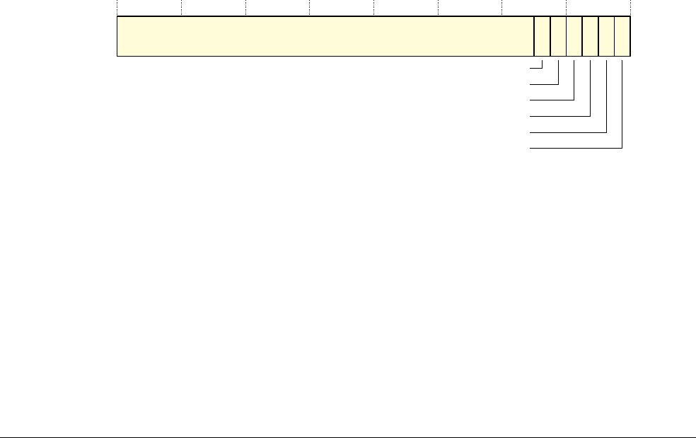
Appendix D5 System Level Implementation of the Generic Timer
D5.7 System level Generic Timer register descriptions, in register order
D5-2408 Copyright © 1996-1998, 2000, 2004-2012, 2014 ARM. All rights reserved. ARM DDI 0406C.c
Non-Confidential ID051414
D5.7 System level Generic Timer register descriptions, in register order
This section describes all of the registers that are implemented in a system level implementation of the Generic
Timer.
D5.7.1 CNTACRn, Counter Access Control Register
The CNTACRn characteristics are:
Purpose Provides top-level access controls for the elements of a timer frame. CNTACRn provides
the controls for frame CNTBaseN.
In addition to the CNTACRn control:
•CNTNSAR controls whether CNTACRn is accessible from Non-secure state
• if frame CNTPL0BaseN is implemented, the CNTPL0ACR in frame CNTBaseN
provides additional controls of accesses to frame CNTPL0BaseN.
This register is a Generic Timer register, implemented only in the memory-mapped
interface.
Usage constraints Accessible by Secure accesses. CNTNSAR.NSn determines whether CNTACRn is
accessible by Non-secure accesses.
Configurations Implemented, in the CNTCTLBase frame, only if CNTTIDR.FIn is RAO.
An implementation of the counters might not provide configurable access to some or all of
the features. In this case, the associated field in the CNTACRn register is:
• RAZ/WI if access is always denied
• RAO/WI if access is always permitted.
Attributes 32-bit RW registers, that start at offset
0x040
. The reset values of the registers are UNKNOWN.
Table D5-4 on page D5-2407 shows the register map of the CNTCTLBase registers.
The CNTACRn bit assignments are:
Bits[31:6] Reserved, UNK/SBZP.
RWPT, bit[5] Read/write access to the PL1 Physical Timer registers CNTP_CVAL, CNTP_TVAL, and
CNTP_CTL, in frame N. The possible values of this bit are:
0 No access to the PL1 Physical Timer registers in frame N. The registers are RAZ/WI.
1 Read/write access to the PL1 Physical Timer registers in frame N.
RWVT, bit[4] Read/write access to the Virtual Timer registers CNTV_CVAL, CNTV_TVAL, and CNTV_CTL, in
frame N. The possible values of this bit are:
0 No access to the Virtual Timer registers in frame N. The registers are RAZ/WI.
1 Read/write access to the Virtual Timer registers in frame N.
Reserved, UNK/SBZP
31 6543210
RWPT
RWVT
RVOFF
RFRQ
RVCT
RPCT

Appendix D5 System Level Implementation of the Generic Timer
D5.7 System level Generic Timer register descriptions, in register order
ARM DDI 0406C.c Copyright © 1996-1998, 2000, 2004-2012, 2014 ARM. All rights reserved. D5-2409
ID051414 Non-Confidential
RVOFF, bit[3]
Read-only access to CNTVOFF, in frame N. The possible values of this bit are:
0 No access CNTVOFF frame N. The register address is RAZ.
1 Read-only access to CNTVOFF in frame N.
RFRQ, bit[2] Read-only access to CNTFRQ, in frame N. The possible values of this bit are:
0 No access CNTFRQ in frame N. The register address is RAZ.
1 Read-only access to CNTFRQ in frame N.
RVCT, bit[1] Read-only access to CNTVCT, in frame N. The possible values of this bit are:
0 No access CNTVCT in frame N. The register address is RAZ.
1 Read-only access to CNTVCT in frame N.
RPCT, bit[1] Read-only access to CNTPCT, in frame N. The possible values of this bit are:
0 No access CNTPCT in frame N. The register address is RAZ.
1 Read-only access to CNTPCT in frame N.

Appendix D5 System Level Implementation of the Generic Timer
D5.7 System level Generic Timer register descriptions, in register order
D5-2410 Copyright © 1996-1998, 2000, 2004-2012, 2014 ARM. All rights reserved. ARM DDI 0406C.c
Non-Confidential ID051414
D5.7.2 CNTCR, Counter Control Register
The CNTCR characteristics are:
Purpose Enables the counter, controls the counter frequency setting, and controls counter behavior
during debug.
This register is a Generic Timer register in the system level Counter module.
Usage constraints In a system that uses security, this register is writable only by Secure writes.
Configurations Always implemented, in the CNTControlBase register map.
Attributes A 32-bit RW register, at offset
0x000
.
Table D5-1 on page D5-2402 shows the register map of the CNTControlBase registers.
See the field descriptions for the reset values.
The CNTCR bit assignments are:
Bits[31:m+1] Reserved, UNK/SBZP.
FCREQ, bits[m:8] Frequency change request. Indicates the number of the entry in the frequency table to select.
Selecting an unimplemented entry, or an entry that contains 0, has no effect on the counter.
The value of m is IMPLEMENTATION DEFINED and depends on the size of the implemented
frequency modes table.
This field resets to 0.
For more information, see Control of counter operating frequency and increment on
page D5-2400.
Bits[7:2] Reserved, UNK/SBZP.
HDBG, bit[1] Halt-on-debug. Controls whether a Halt-on-debug signal halts the system counter:
0 System counter ignores Halt-on-debug.
1 Asserted Halt-on-debug signal halts system counter update.
The reset value of this field is UNKNOWN.
EN, bit[0] Enables the counter:
0 System counter disabled.
1 System counter enabled.
This bit resets to 0.
After an change to the FCREQ field, when the system counter switches to the new update frequency,
CNTSR.FCACK is updated to indicate the table value for that frequency. That is, CNTSR.FCACK is updated to
match the new value written to FCREQ.
EN
HDBG
Reserved, UNK/SBZP
31 m+1 m87 210
FCREQ Reserved,
UNK/SBZP
Appendix D5 System Level Implementation of the Generic Timer
D5.7 System level Generic Timer register descriptions, in register order
ARM DDI 0406C.c Copyright © 1996-1998, 2000, 2004-2012, 2014 ARM. All rights reserved. D5-2411
ID051414 Non-Confidential
D5.7.3 CNTCV, Counter Count Value register
The CNTCV characteristics are:
Purpose Indicates the current count value.
This register is a Generic Timer register in the system level Counter module.
Usage constraints In a system that uses security, for the writable copy of the register:
• the register is writable only by Secure writes
• the effect of writing the register when the counter is enabled is UNPREDICTABLE.
In an implementation that supports 64-bit atomic memory accesses, this register must be
accessible using a 64-bit atomic access.
A write to CNTCV must be visible in the CNTPCT register of each running processor in a
finite time.
Configurations This register is available in two register memory frames:
• a read/write copy in the CNTControlBase memory map
• a read-only copy in the CNTReadBase memory map.
Attributes A 64-bit register, at offset:
•
0x008
in the CNTControlBase memory map. This means the most significant word of
the register is at offset
0x00C
in this memory map.
•
0x000
in the CNTReadBase memory map. This means the most significant word of
the register is at offset
0x004
in this memory map.
Table D5-1 on page D5-2402 shows the register map of the CNTControlBase registers.
CNTCV is RW in this memory frame.
Table D5-2 on page D5-2403 shows the register map of the CNTReadBase registers.
CNTCV is RO in this memory frame.
In an ARMv7 implementation, the CNTCV bit assignments are:
CountValue, bits[63:0]
Indicates the counter value.
CountValue[63:0]
63 0

Appendix D5 System Level Implementation of the Generic Timer
D5.7 System level Generic Timer register descriptions, in register order
D5-2412 Copyright © 1996-1998, 2000, 2004-2012, 2014 ARM. All rights reserved. ARM DDI 0406C.c
Non-Confidential ID051414
D5.7.4 CNTFRQ, Counter Frequency register, system level
The CNTFRQ register characteristics are:
Purpose The CNTFRQ register indicates the clock frequency of the system counter.
This register is a Generic Timer register.
Usage constraints See the Attributes description.
Configurations See the Attributes description.
The VMSA, PMSA, and system level definitions of the register fields are identical.
Attributes A 32-bit register with an UNKNOWN reset value, implemented:
• In the CNTBaseN frame at offset
0x010
. CNTFRQ is RO in the CNTBaseN frame, but
must be writable for initial configuration.
Table D5-3 on page D5-2405 shows the register map of the CNTBaseN registers.
• In the CNTCTLBase frame at offset
0x000
. CNTFRQ is RW in the CNTCTLBase
frame, and in a system that uses security, is accessible only by Secure accesses.
Table D5-4 on page D5-2407 shows the register map of the CNTCTLBase registers.
The CNTFRQ bit assignments are:
Clock frequency, bits[31:0]
Indicates the system counter clock frequency, in Hz.
Note
Programming CNTFRQ does not affect the system clock frequency. However, on system initialization, CNTFRQ
must be correctly programmed with the system clock frequency, to make this value available to software. For more
information see Initializing and reading the system counter frequency on page B8-1961.
Clock frequency
31 0
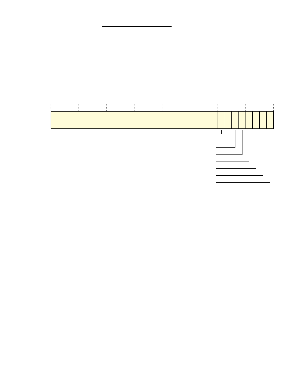
Appendix D5 System Level Implementation of the Generic Timer
D5.7 System level Generic Timer register descriptions, in register order
ARM DDI 0406C.c Copyright © 1996-1998, 2000, 2004-2012, 2014 ARM. All rights reserved. D5-2413
ID051414 Non-Confidential
D5.7.5 CNTNSAR, Counter Non-Secure Access Register
The CNTNSAR characteristics are:
Purpose Provides the highest-level control of whether frames CNTBaseN and CNTPL0BaseN are
accessible by Non-secure accesses.
Note
If frame N is not accessible to Non-secure accesses, then in the CNTCTLBase frame
CNTACRN and CNTVOFFN are not accessible to Non-secure accesses.
This register is a Generic Timer register, visible only in the memory-mapped interface.
Usage constraints Accessible only by Secure accesses.
Configurations Always implemented, in the CNTCTLBase frame, in any memory-mapped view of the
timers and counters.
Attributes A 32-bit RW register, at offset
0x004
. The reset value of the register is UNKNOWN.
Table D5-4 on page D5-2407 shows the register map of the CNTCTLBase registers.
The CNTNSAR bit assignments are:
Bits[31:8] Reserved, UNK/SBZP.
NSN, bit[N], for values of N from 0 to 7
Non-secure access to frame n. The possible values of this bit are:
0 Secure access only:
• frames CNTBaseN and CNTPL0BaseN behave as RAZ/WI to Non-secure
accesses
• in the CNTCTLBase frame, CNTACRN and CNTVOFFN behave as RAZ/WI to
Non-secure accesses.
1 Secure and Non-secure accesses permitted, to:
• frames CNTBaseN and CNTPL0BaseN
• in the CNTCTLBase frame, CNTACRN and CNTVOFFN.
If frame CNTBasen:
• is not implemented, NSn is RAZ/WI
• is not Configurable access, and is accessible only by Secure accesses, NSn is RAZ/WI
• is not Configurable access, and is accessible by both Secure and Non-secure accesses, NSn
is RAO/WI.
Reserved, UNK/SBZP
31 876543210
NS7
NS6
NS5
NS4
NS3
NS2
NS1
NS0
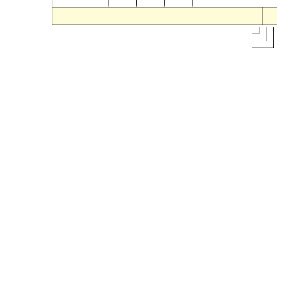
Appendix D5 System Level Implementation of the Generic Timer
D5.7 System level Generic Timer register descriptions, in register order
D5-2414 Copyright © 1996-1998, 2000, 2004-2012, 2014 ARM. All rights reserved. ARM DDI 0406C.c
Non-Confidential ID051414
D5.7.6 CNTP_CTL, PL1 Physical Timer Control register, system level
The CNTP_CTL characteristics are:
Purpose The control register for the physical timer.
This register is a Generic Timer register.
Usage constraints CNTACR.RWPT enables access to this register.
Configurations Always implemented, in the CNTBaseN register map.
The VMSA, PMSA, and system level definitions of the register fields are identical.
Attributes A 32-bit RW register at offset
0x02C
, with an UNKNOWN reset value.
Table D5-3 on page D5-2405 shows the register map of the CNTBaseN registers.
In an ARMv7 implementation, the CNTP_CTL bit assignments are:
Bits[31:3] Reserved, UNK/SBZP.
ISTATUS, bit[2] The status of the timer. This bit indicates whether the timer condition is asserted:
0 Timer condition is not asserted.
1 Timer condition is asserted.
When the ENABLE bit is set to 1, ISTATUS indicates whether the timer value meets the
condition for the timer output to be asserted, see Operation of the CompareValue views of
the timers on page B8-1966 and Operation of the TimerValue views of the timers on
page B8-1967. ISTATUS takes no account of the value of the IMASK bit. If ISTATUS is set
to 1 and IMASK is set to 0 then the timer output signal is asserted.
This bit is read-only.
IMASK, bit[1] Timer output signal mask bit. Permitted values are:
0 Timer output signal is not masked.
1 Timer output signal is masked.
For more information, see the description of the ISTATUS bit and Operation of the timer
output signal on page B8-1968.
ENABLE, bit[0] Enables the timer. Permitted values are:
0 Timer disabled.
1 Timer enabled.
Setting this bit to 0 disables the timer output signal, but the timer value accessible from
CNTP_TVAL continues to count down.
Note
Disabling the output signal might be a power-saving option.
31 20
Reserved, UNK/SBZP
ISTATUS
ENABLE
IMASK
13

Appendix D5 System Level Implementation of the Generic Timer
D5.7 System level Generic Timer register descriptions, in register order
ARM DDI 0406C.c Copyright © 1996-1998, 2000, 2004-2012, 2014 ARM. All rights reserved. D5-2415
ID051414 Non-Confidential
D5.7.7 CNTP_CVAL, PL1 Physical Timer CompareValue register, system level
The CNTP_CVAL characteristics are:
Purpose Holds the 64-bit compare value for the PL1 physical timer.
This register is a Generic Timer register.
Usage constraints CNTACR.RWPT enables access to this register.
If the implementation supports 64-bit atomic accesses, then the CNTP_CVAL register must
be accessible as an atomic 64-bit value.
Configurations Always implemented, in the CNTBaseN register map.
The VMSA, PMSA, and system level definitions of the register fields are identical.
Attributes A 64-bit RW register at offset
0x020
, with an UNKNOWN reset value.
Table D5-3 on page D5-2405 shows the register map of the CNTBaseN registers.
In an ARMv7 implementation, the CNTP_CVAL bit assignments are:
CompareValue, bits[63:0]
Indicates the compare value for the PL1 physical timer.
For more information about the timer see Timers on page B8-1965.
CompareValue[63:0]
63 0

Appendix D5 System Level Implementation of the Generic Timer
D5.7 System level Generic Timer register descriptions, in register order
D5-2416 Copyright © 1996-1998, 2000, 2004-2012, 2014 ARM. All rights reserved. ARM DDI 0406C.c
Non-Confidential ID051414
D5.7.8 CNTP_TVAL, PL1 Physical TimerValue register, system level
The CNTP_TVAL characteristics are:
Purpose Holds the timer value for the PL1 physical timer. This provides a 32-bit downcounter, see
Operation of the TimerValue views of the timers on page B8-1967.
This register is a Generic Timer register.
Usage constraints CNTACR.RWPT enables access to this register.
Configurations Always implemented, in the CNTBaseN register map.
The VMSA, PMSA, and system level definitions of the register fields are identical.
Attributes A 32-bit RW register at offset
0x028
, with an UNKNOWN reset value.
Table D5-3 on page D5-2405 shows the register map of the CNTBaseN registers.
In an ARMv7 implementation, the CNTP_TVAL bit assignments are:
TimerValue, bits[31:0]
Indicates the timer value.
D5.7.9 CNTPCT, Physical Count register, system level
The CNTPCT register characteristics are:
Purpose The CNTPCT register holds the 64-bit physical count value.
This register is a Generic Timer register.
Usage constraints CNTACR.RPCT enables access to this register
If the implementation supports 64-bit atomic accesses, then the CNTPCT register must be
accessible as an atomic 64-bit value.
Configurations Always implemented, in the CNTBaseN register map.
The VMSA, PMSA, and system level definitions of the register fields are identical.
Attributes A 64-bit RO register at offset
0x000
, with an UNKNOWN reset value.
Table D5-3 on page D5-2405 shows the register map of the CNTBaseN registers.
The CNTPCT bit assignments are:
PhysicalCount, bits[63:0]
Indicates the physical count.
31 0
TimerValue
PhysicalCount[63:0]
63 0

Appendix D5 System Level Implementation of the Generic Timer
D5.7 System level Generic Timer register descriptions, in register order
ARM DDI 0406C.c Copyright © 1996-1998, 2000, 2004-2012, 2014 ARM. All rights reserved. D5-2417
ID051414 Non-Confidential
D5.7.10 CNTPL0ACR, Counter PL0 Access Control Register
The CNTPL0ACR characteristics are:
Purpose An implementation of CNTPL0ACR in the frame at CNTBaseN controls whether the
CNTPCT, CNTVCT, CNTFRQ, PL1 Physical Timer, and Virtual Timer registers are visible
in the frame at CNTPL0BaseN.
This register is a Generic Timer register, defined only in the memory-mapped interface.
Usage constraints No usage constraints.
Configurations In each implemented CNTBaseN frame, CNTPL0ACR is optional and if not implemented:
• its location is RAZ/WI
• the controlled registers are not visible in the corresponding CNTPL0BaseN frame.
Attributes A 32-bit RW register, at offset
0x014
. The reset value of the register is UNKNOWN.
Table D5-3 on page D5-2405 shows the register map of the CNTBaseN registers.
The CNTPL0ACR bit assignments are:
Bits[31:10] Reserved, UNK/SBZP.
PL0PTEN, bit[9] Second view read/write access control for the PL1 Physical Timer registers. This bit
controls whether the CNTP_CVAL, CNTP_TVAL, and CNTP_CTL registers in the current
CNTBaseN frame are also accessible in the corresponding CNTPL0BaseN frame. The
possible values of this bit are:
0 No access. Registers are RAZ/WI in the second view.
1 Access permitted. If the registers are accessible in the current frame then they
are accessible in the second view.
PL0VTEN, bit[8] Second view read/write access control for the Virtual Timer registers. This bit controls
whether the CNTV_CVAL, CNTV_TVAL, and CNTV_CTL registers in the current
CNTBaseN frame are also accessible in the corresponding CNTPL0BaseN frame. The
possible values of this bit are:
0 No access. Registers are RAZ/WI in the second view.
1 Access permitted. If the registers are accessible in the current frame then they
are accessible in the second view.
Note
The definition of this bit means that, if the Virtual Timer registers are not implemented in
the current CNTBaseN frame, then the Virtual Timer register addresses are RAZ/WI in the
corresponding CNTPL0BaseN frame, regardless of the value of this bit.
Bits[7:2] Reserved, UNK/SBZP.
PL0VCTEN, bit[1] Second view read access control for CNTVCT and CNTFRQ. The possible values of this
bit are:
0 CNTVCT is not visible in the second view.
If PL0PCTEN is set to 0, CNTFRQ is not visible in the second view.
1 Access permitted. If CNTVCT and CNTFRQ are visible in the current frame
then they are visible in the second view.
Reserved, UNK/SBZP
31 10 9 8 7 2 1 0
Reserved,
UNK/SBZP
PL0PCTEN
PL0VCTEN
PL0VTEN
PL0PTEN

Appendix D5 System Level Implementation of the Generic Timer
D5.7 System level Generic Timer register descriptions, in register order
D5-2418 Copyright © 1996-1998, 2000, 2004-2012, 2014 ARM. All rights reserved. ARM DDI 0406C.c
Non-Confidential ID051414
PL0PCTEN, bit[0] Second view read access control for CNTPCT and CNTFRQ. The possible values of this bit
are:
0 CNTPCT is not visible in the second view.
If PL0VCTEN is set to 0, CNTFRQ is not visible in the second view.
1 Access permitted. If CNTPCT and CNTFRQ are visible in the current frame
then they are visible in the second view.
Appendix D5 System Level Implementation of the Generic Timer
D5.7 System level Generic Timer register descriptions, in register order
ARM DDI 0406C.c Copyright © 1996-1998, 2000, 2004-2012, 2014 ARM. All rights reserved. D5-2419
ID051414 Non-Confidential
D5.7.11 CNTSR, Counter Status Register
The CNTSR characteristics are:
Purpose Provides counter frequency status information.
This register is a Generic Timer register in the system level Counter module.
Usage constraints There are no usage constraints.
Configurations Always implemented, in the CNTControlBase register map.
Attributes A 32-bit RO register, at offset
0x004
.
Table D5-1 on page D5-2402 shows the register map of the CNTControlBase registers.
See the field descriptions for the reset values.
In an ARMv7 implementation, the CNTSR bit assignments are:
Bits[31:m+1] Reserved, UNK. See the FCACK description for more information about the value of m.
FCACK, bits[m:8] Frequency change acknowledge. Indicates the currently selected entry in the frequency
table.
The value of m is IMPLEMENTATION DEFINED and depends on the size of the implemented
frequency modes table.
This field resets to 0.
For more information about the use of this field, see Control of counter operating frequency
and increment on page D5-2400.
Bits[7:2] Reserved, UNK.
DBGH, bit[1] Indicates whether the counter is halted because the Halt-on-Debug signal is asserted:
0 Counter is not halted.
1 Counter is halted.
The reset value of this bit is UNKNOWN.
Bit[0] Reserved, UNK.
Reserved
DBGH
(0)Reserved, UNK
31 m+1 m87 210
FCACK Reserved, UNK

Appendix D5 System Level Implementation of the Generic Timer
D5.7 System level Generic Timer register descriptions, in register order
D5-2420 Copyright © 1996-1998, 2000, 2004-2012, 2014 ARM. All rights reserved. ARM DDI 0406C.c
Non-Confidential ID051414
D5.7.12 CNTTIDR, Counter Timer ID Register
The CNTTIDR characteristics are:
Purpose Indicates the implemented timers in the memory map, and their features. For each value of
N from 0 to 7 it indicates whether:
• frame CNTBaseN is a view of an implemented timer
• frame CNTBaseN has a second view, CNTPL0BaseN
• frame CNTBaseN has a virtual timer capability.
This register is a Generic Timer register, visible only in the memory-mapped interface.
Usage constraints No usage constraints.
Configurations Always implemented, in the CNTCTLBase frame, in any memory-mapped view of the
timers and counters
Attributes A 32-bit RO register, at offset
0x008
. The reset value of the register is IMPLEMENTATION
DEFINED.
Table D5-4 on page D5-2407shows the register map of the CNTCTLBase registers.
The CNTTIDR bit assignments are:
Bits[4N+3], for values of N from 0 to 7
Reserved, UNK.
FPL0N, bit[4N+2], for values of N from 0 to 7
Frame N has second view. Indicates whether frame CNTBaseN has a second view, CNTPL0BaseN.
The possible values of this bit are:
0 Frame N does not have a second view. CNTPL0BaseN is RAZ/WI.
1 Frame N has a second view, CNTPL0BaseN.
If FIN is 0, this bit is RAZ.
FVIN, bit[4N+1], for values of N from 0 to 7
Frame N has virtual capability. Indicates whether both:
• frame CNTBaseN implements the virtual timer registers CNTV_CVAL, CNTV_TVAL, and
CNTV_CTL.
• this CNTCTLBase frame implements the virtual timer offset register CNTVOFFN.
The possible values of this bit are:
0 Frame N does not have virtual capability. The virtual time and offset registers are
RAZ/WI.
1 Frame N has virtual capability. The virtual time and offset registers are implemented.
If FIN is 0, this bit is RAZ.
FIN, bit[4N], for values of N from 0 to 7
Frame N implemented. The possible values of this bit are:
0 Frame N not implemented. All registers associated with the frame are RAZ/WI.
1 Frame N is implemented.
(0)
31 30 29 28 27 26 25 24 23 22 21 20 19 18 17 16 15 14 13 12 11 10 9 8 7 6 5 4 3 2 1 0
(0) (0) (0) (0) (0) (0) (0)
FI0
FVI0
FPL00
FI1
FVI1
FPL01
FI2
FVI2
FPL02
FI3
FVI3
FPL03
FI4
FVI4
FPL04
FI5
FVI5
FPL05
FI6
FVI6
FPL06
FI7
FVI7
FPL07

Appendix D5 System Level Implementation of the Generic Timer
D5.7 System level Generic Timer register descriptions, in register order
ARM DDI 0406C.c Copyright © 1996-1998, 2000, 2004-2012, 2014 ARM. All rights reserved. D5-2421
ID051414 Non-Confidential
D5.7.13 CNTV_CTL, Virtual Timer Control register, system level
The CNTV_CTL characteristics are:
Purpose The control register for the virtual timer.
This register is a Generic Timer register.
Usage constraints An optional register in a system level implementation of the Generic Timer.
CNTTIDR.FVIN indicates whether CNTV_CTL is implemented for frame N. When
implemented, CNTACR.RWVT enables access to the register.
If CNTV_CTL is not implemented, the register location is RAZ/WI.
Configurations An optional register in the CNTBaseN register map.
The VMSA, PMSA, and system level definitions of the register fields are identical.
Attributes A 32-bit RW register at offset
0x03C
, with an UNKNOWN reset value.
Table D5-3 on page D5-2405 shows the register map of the CNTBaseN registers.
The bit assignments of CNTV_CTL are identical to those of CNTP_CTL.
D5.7.14 CNTV_CVAL, Virtual Timer CompareValue register, system level
The CNTV_CVAL characteristics are:
Purpose Holds the compare value for the virtual timer.
This register is a Generic Timer register.
Usage constraints An optional register in a system level implementation of the Generic Timer.
CNTTIDR.FVIN indicates whether CNTV_CVAL is implemented for frame N. When
implemented, CNTACR.RWVT enables access to the register.
If the implementation supports 64-bit atomic accesses, then the CNTV_CVAL register must
be accessible as an atomic 64-bit value.
If CNTV_CVAL is not implemented, the register location is RAZ/WI.
Configurations An optional register in the CNTBaseN register map.
The VMSA, PMSA, and system level definitions of the register fields are identical.
Attributes A 64-bit RW register at offset
0x030
, with an UNKNOWN reset value.
Table D5-3 on page D5-2405 shows the register map of the CNTBaseN registers.
The bit assignments of CNTV_CVAL are identical to those of CNTP_CVAL.

Appendix D5 System Level Implementation of the Generic Timer
D5.7 System level Generic Timer register descriptions, in register order
D5-2422 Copyright © 1996-1998, 2000, 2004-2012, 2014 ARM. All rights reserved. ARM DDI 0406C.c
Non-Confidential ID051414
D5.7.15 CNTV_TVAL, Virtual TimerValue register, system level
The CNTV_TVAL characteristics are:
Purpose Holds the timer value for the virtual timer.
This register is a Generic Timer register.
Usage constraints An optional register in a system level implementation of the Generic Timer.
CNTTIDR.FVIN indicates whether CNTV_TVAL is implemented for frame N. When
implemented, CNTACR.RWVT enables access to the register.
If CNTV_TVAL is not implemented, the register location is RAZ/WI.
Configurations An optional register in the CNTBaseN register map.
The VMSA, PMSA, and system level definitions of the register fields are identical.
Attributes A 32-bit RW register at offset
0x38
, with an UNKNOWN reset value.
Table D5-3 on page D5-2405 shows the register map of the CNTBaseN registers.
The bit assignments of CNTV_TVAL are identical to those of CNTP_TVAL.
D5.7.16 CNTVCT, Virtual Count register, system level
The CNTVCT characteristics are:
Purpose Holds the 64-bit virtual count.
Note
The virtual count is obtained by subtracting the virtual offset from the physical count:
• for a CNTBaseN frame that has virtual capacity, CNTVOFF holds the virtual offset
• otherwise, the virtual offset is zero.
This register is a Generic Timer register.
Usage constraints CNTACR.RVCT enables access to the CNTVCT register.
If the implementation supports 64-bit atomic accesses, then the CNTVCT register must be
accessible as an atomic 64-bit value.
Configurations Always implemented, in the CNTBaseN register map.
The VMSA, PMSA, and system level definitions of the register fields are identical.
Attributes A 64-bit RO register at offset
0x008
, with an UNKNOWN reset value.
Table D5-3 on page D5-2405 shows the register map of the CNTBaseN registers.
In an ARMv7 implementation, the CNTVCT bit assignments are:
VirtualCount, bits[63:0]
Indicates the virtual count.
VirtualCount[63:0]
63 0

Appendix D5 System Level Implementation of the Generic Timer
D5.7 System level Generic Timer register descriptions, in register order
ARM DDI 0406C.c Copyright © 1996-1998, 2000, 2004-2012, 2014 ARM. All rights reserved. D5-2423
ID051414 Non-Confidential
D5.7.17 CNTVOFFn, Virtual Offset register, system level
The CNTVOFF characteristics are:
Purpose Holds the 64-bit virtual offset.
This register is a Generic Timer register.
Usage constraints If the implementation supports 64-bit atomic accesses, then each CNTVOFFn register must
be accessible as an atomic 64-bit value.
Accessible by Secure accesses. CNTNSAR.NSn determines whether CNTVOFFn is
accessible by Non-secure accesses.
See also the Configurations and Attributes descriptions.
Configurations Always implemented as a RO register in the CNTBaseN register map. CNTACR.RVOFF
enables access to the register.
Note
In a CNTBaseN frame that does not have virtual capacity, CNTVOFF is RAZ.
If CNTBaseN frame has virtual capacity, indicated by CNTTIDR.FVIN having the value 1,
then CNTVOFFN is implemented as a RW register in the CNTCTLBase register map. The
CNTCTLBase register map has a RW instance of CNTVOFF for each CNTBaseN frame
that has virtual capacity.
In the CNTCTLBase register map, unimplemented instances of CNTVOFF are RAZ/WI.
The VMSA and system level definitions of the register fields are identical.
Attributes A 64-bit register with an UNKNOWN reset value, implemented:
• In the CNTBaseN frame at offset
0x018
, as a RO register.
Table D5-3 on page D5-2405 shows the register map of the CNTBaseN registers.
• In the CNTCTLBase frame as a RW instance for each CNTBaseN frame that has
virtual capacity. If CNTBaseN frame N has virtual capacity then a RW instance of
CNTVOFF is implemented at offset
0x080
+8N.
Table D5-4 on page D5-2407 shows the register map of the CNTCTLBase registers.
For a CNTBaseN frame that has virtual capacity, the CNTVOFF bit assignments are:
VirtualOffset, bits[63:0]
Indicates the virtual offset.
VirtualOffset[63:0]
63 0

Appendix D5 System Level Implementation of the Generic Timer
D5.7 System level Generic Timer register descriptions, in register order
D5-2424 Copyright © 1996-1998, 2000, 2004-2012, 2014 ARM. All rights reserved. ARM DDI 0406C.c
Non-Confidential ID051414
D5.7.18 CounterIDn, Counter ID registers 0-11
The Counter ID register characteristics are:
Purpose IMPLEMENTATION DEFINED identification registers, for each register memory frame.
These registers are Generic Timer registers defined only in memory-mapped interfaces.
Usage constraints No usage constraints.
Configurations Always implemented, in the CNTControlBase, CNTReadBase, CNTBaseN, and
CNTCTLBase memory maps.
Note
These registers are implemented independently in each of the frames accessed through the
different memory maps.
Attributes 32-bit RO registers, at offsets
0xFD0
-
0xFFC
.
Table D5-1 on page D5-2402 shows the register map of the CNTControlBase registers.
Table D5-2 on page D5-2403 shows the register map of the CNTReadBase registers.
Table D5-3 on page D5-2405 shows the register map of the CNTBaseN registers.
Table D5-4 on page D5-2407 shows the register map of the CNTCTLBase registers.
The Counter ID registers are IMPLEMENTATION DEFINED registers. If the implementation of the Counter ID registers
requires an architecture version, the value for this version of the ARM Generic Timer is version 0.
Note
The Counter ID registers can be implemented as a set of CoreSight ID registers, comprising Peripheral ID Registers
and Component ID Registers, as defined by the CoreSight™ Architecture Specification. The ARM Debug
architecture includes an implementation of the CoreSight ID registers, see:
•About the Debug Peripheral Identification Registers on page C11-2208
•About the Debug Component Identification Registers on page C11-2210.
Any implementation of the CoreSight ID Registers has a similar organization. However, the Debug architecture
implementation uses a Component class value of
0x9
. An implementation of these registers for the Generic Timer
must use a Component class value of
0xF
.

Appendix D5 System Level Implementation of the Generic Timer
D5.8 Providing a complete set of counter and timer features
ARM DDI 0406C.c Copyright © 1996-1998, 2000, 2004-2012, 2014 ARM. All rights reserved. D5-2425
ID051414 Non-Confidential
D5.8 Providing a complete set of counter and timer features
Using the general model for implementing a memory-mapped interface to the Generic Timer described in this
section, the feature set of a CP15 counter and timer, in a system that supports the Security Extensions and the
Virtualization Extensions, can be implemented using the following set of timer frames:
• a CNTCTLBase control frame
• the following CNTBaseN timer frames:
Frame 0 Accessible from Non-secure state, with second view and virtual capability. This provide the
Non-secure PL1&0 timers.
Frame 1 Accessible from Non-secure state, with no second view and no virtual capability. This provide
the Non-secure PL2 timers.
Frame 2 Accessible only Secure state, with a second view but no virtual capability. This provide the
Secure PL1&0 timers.
In this implementation, the full set of implemented frames, and their configuration in the memory map, is as follows:
CNTCTLBase
The control frame. This frame is located in both Secure and Non-secure physical memory, and:
• in the Secure PL1&0 translation regime, this frame is accessible only at PL1
• in the Non-secure PL2 translation regime, this frame is accessible
• in the Non-secure PL1&0 translation regime, this frame is not accessible.
CNTBase0 The first view of the Non-secure PL1&0 timers. This frame is located only in Non-secure physical
memory, and:
• in the Secure PL1&0 translation regime, this frame is accessible only at PL1
• in the Non-secure PL2 translation regime, this frame is accessible
• in the Non-secure PL1&0 translation regime, this frame is accessible only at PL1.
CNTPL0Base0
The second view of CNTBase0, meaning it is the PL0 view of the Non-secure PL1&0 timers. This
frame is located only in Non-secure physical memory, and:
• in the Secure PL1&0 translation regime, this frame can be accessible at PL1, or at PL1 and
PL0, but this is not required
• in the Non-secure PL2 translation regime, this frame is accessible
• in the Non-secure PL1&0 translation regime, this frame is accessible at PL1 and PL0.
CNTBase1 The first and only view of the Non-secure PL2 timers. This frame is located only in Non-secure
physical memory, and:
• in the Secure PL1&0 translation regime, this frame is accessible only at PL1
• in the Non-secure PL2 translation regime, this frame is accessible
• in the Non-secure PL1&0 translation regime, this frame is not accessible.
CNTBase2 The first view of the Secure PL1&0 timers. This frame is located only in Secure physical memory,
and:
• in the Secure PL1&0 translation regime, this frame is accessible only at PL1
• because the frame is in Secure memory, it is not accessible in any Non-secure translation
regime.

Appendix D5 System Level Implementation of the Generic Timer
D5.8 Providing a complete set of counter and timer features
D5-2426 Copyright © 1996-1998, 2000, 2004-2012, 2014 ARM. All rights reserved. ARM DDI 0406C.c
Non-Confidential ID051414
CNTPL0Base2
The second view of CNTBase2, meaning it is the PL0 view of the Secure PL1&0 timers. This frame
is located only in Secure physical memory, and:
• in the Secure PL1&0 translation regime, this frame is accessible at PL1 and PL0
• because the frame is in Secure memory, it is not accessible in any Non-secure translation
regime.
Note
About the VMSA on page B3-1308 describes the translation regimes.

Appendix D5 System Level Implementation of the Generic Timer
D5.9 Gray-count scheme for timer distribution scheme
ARM DDI 0406C.c Copyright © 1996-1998, 2000, 2004-2012, 2014 ARM. All rights reserved. D5-2427
ID051414 Non-Confidential
D5.9 Gray-count scheme for timer distribution scheme
The distribution of the Counter value using a Gray-code provides a relatively simple mechanism to avoid any danger
of the count being sampled with an intermediate value even if the clocking is asynchronous. It has a further
advantage that the distribution is relatively low power, since only one bit changes on the main distribution wires for
each clock tick.
A suitable Gray-coding scheme can be achieved with the following logic:
Gray[N] = Count[N]
Gray[i] = (XOR(Gray[N:i+1])) XOR Count[i] for N-1 >= i >= 0
Count[i] = XOR(Gray[N:i]) for N >= i >= 0
This is for an N+1 bit counter, where Count is a conventional binary count value, and Gray is the corresponding
Gray count value.
Note
This scheme has the advantage of being relatively simple to switch, in either direction, between operating with
low-frequency and low precision, and operating with high-frequency and high-precision. To achieve this, the ratio
of the frequencies must be 2n, where n is an integer. A switch-over must occur on the 2(n+1) boundary to avoid losing
the Gray-coding property on a switch-over.

Appendix D5 System Level Implementation of the Generic Timer
D5.9 Gray-count scheme for timer distribution scheme
D5-2428 Copyright © 1996-1998, 2000, 2004-2012, 2014 ARM. All rights reserved. ARM DDI 0406C.c
Non-Confidential ID051414

ARM DDI 0406C.c Copyright © 1996-1998, 2000, 2004-2012, 2014 ARM. All rights reserved. D6-2429
ID051414 Non-Confidential
Appendix D6
Common VFP Subarchitecture Specification
This appendix describes version 3 of the Common VFP subarchitecture, and the differences in the earlier versions
of the Common VFP subarchitecture. It contains the following sections:
•Scope of this appendix on page D6-2431
•Introduction to the Common VFP subarchitecture on page D6-2432
•Exception processing on page D6-2434
•Support code requirements on page D6-2438
•Context switching on page D6-2440
•Subarchitecture additions to the Floating-point Extension system registers on page D6-2441
•Earlier versions of the Common VFP subarchitecture on page D6-2448.
Note
• This VFP subarchitecture specification is not part of the ARM architecture specification. Implementers and
users of the ARMv7 architecture must not consider this appendix as a requirement of the architecture. It is
included as an appendix to this manual only:
— as reference material for users of ARM floating-point products that implement this subarchitecture
— as an example of how a floating-point subarchitecture might be implemented.
The inclusion of this appendix is no indication of whether any ARMv7 floating-point (VFP) implementation
by ARM might, or might not, implement this Common VFP subarchitecture. For details of the implemented
VFP subarchitecture you must always see the appropriate product documentation.
• The ARM Floating-point Extension was previously called the VFP Extension. This common floating-point
subarchitecture specification retains the VFP naming.

Appendix D6 Common VFP Subarchitecture Specification
D6-2430 Copyright © 1996-1998, 2000, 2004-2012, 2014 ARM. All rights reserved. ARM DDI 0406C.c
Non-Confidential ID051414
Note
Both Chapter B4 System Control Registers in a VMSA implementation and Chapter B6 System Control Registers in
a PMSA implementation include the descriptions of the Floating-point system registers. These registers are included
any implementation, VMSA or PMSA, that includes the Floating-point (VFP) Extension. The register bit
assignments are identical in VMSA and PMSA implementations, but the register references in this chapter link to
the register descriptions in Chapter B4.

Appendix D6 Common VFP Subarchitecture Specification
D6.1 Scope of this appendix
ARM DDI 0406C.c Copyright © 1996-1998, 2000, 2004-2012, 2014 ARM. All rights reserved. D6-2431
ID051414 Non-Confidential
D6.1 Scope of this appendix
This specification describes the Common VFP subarchitecture. This is not part of the ARMv7 architecture
specification, see the Note on the cover page of this appendix.
The Common VFP subarchitecture is an interface provided by the Floating-point (VFP) Extension to support code
in an operating system.
This appendix is for engineers implementing and validating the Floating-point Extension, and for engineers
implementing support code in an operating system.
The main sections of this appendix describe version 3 of the Common VFP subarchitecture. Version 3 is an
extension to the previously-published version 2 of the subarchitecture. Version 3 of the Common VFP
subarchitecture includes more support for synchronous exception reporting.
For more information about version 2 of the subarchitecture, see Differences between version 2 and version 3 of the
Common VFP subarchitecture on page D6-2448.
Support code for version 1 of the subarchitecture differs from subarchitecture version 2 only when trapped
exception handling of the Inexact exception is enabled. For more information, see Differences between version 1
and version 2 of the Common VFP subarchitecture on page D6-2448.

Appendix D6 Common VFP Subarchitecture Specification
D6.2 Introduction to the Common VFP subarchitecture
D6-2432 Copyright © 1996-1998, 2000, 2004-2012, 2014 ARM. All rights reserved. ARM DDI 0406C.c
Non-Confidential ID051414
D6.2 Introduction to the Common VFP subarchitecture
The VFP subarchitecture describes the interface to application software provided by an implementation of the ARM
Floating-point Extension. A complete implementation of the Floating-point Extension architecture might include
both a hardware coprocessor and a software component, called the support code. Support code must signal trapped
floating-point exceptions to application software, and provide other implementation-dependent functions. The
Common VFP subarchitecture describes an interface between the Floating-point Extension and support code.
D6.2.1 Floating-point support code and bounced instructions
Support code is entered through the ARM Undefined Instruction exception vector, when the floating-point hardware
does not respond to a floating-point instruction. This software entry is called a bounce.
The bounce mechanism supports trapped floating-point exceptions. Trapped floating-point exceptions, called traps,
are floating-point exceptions that an implementation must pass back for application software to resolve. See
Trapped floating-point exception handling on page D6-2437.
Support code might perform other tasks, in addition to trap handler calls. These tasks are determined by the
implementation. Typically, additional support code functions might handle rare conditions that are either difficult
to implement in hardware, or gate-intensive in hardware. This approach permits software behavior to be consistent
across implementations with varying degrees of hardware support.
D6.2.2 Exception processing terminology
A condition that causes a floating-point instruction to call support code is called an exceptional condition.
The floating-point instruction that contains the floating-point operation requiring support code is called the
exception-generating instruction.
The floating-point instruction that causes a bounce to occur is called the trigger instruction.
An implementation can use both synchronous and asynchronous exception signaling:
• if an exception is signaled synchronously, the exception-generating instruction is also the trigger instruction.
• if an exception is signaled asynchronously, the trigger instruction is a floating-point instruction that occurs
after the exception-generating instruction.
An implementation can issue and complete additional floating-point instructions before bouncing the trigger
instruction.
An implementation can issue a maximum of one additional floating-point instruction that it cannot complete. This
instruction is called the bypassed instruction. This instruction is retired in the ARM processor and cannot be
reissued. Therefore, it must be executed by the floating-point support code.
D6.2.3 Hardware and software implementation
The Common VFP subarchitecture requires the floating-point hardware implementation to perform completely all
load, store and register transfer instructions. These instructions cannot generate floating-point exceptions.
The division of labor between the hardware and software components of a floating-point implementation for
CDP
operations is IMPLEMENTATION DEFINED.
Typically, the hardware handles all common cases, to optimize performance. When the hardware encounters a case
that it cannot handle on its own it calls the software component, the support code for the hardware, to deal with it.
For more information, see Advanced SIMD and Floating-point Extensions on page A2-54.

Appendix D6 Common VFP Subarchitecture Specification
D6.2 Introduction to the Common VFP subarchitecture
ARM DDI 0406C.c Copyright © 1996-1998, 2000, 2004-2012, 2014 ARM. All rights reserved. D6-2433
ID051414 Non-Confidential
D6.2.4 Common VFP subarchitecture system registers
The Common VFP subarchitecture adds two instruction registers, FPINST and FPINST2:
• for asynchronous exceptions, the FPINST register contains the exception-generating instruction
• the FPINST2 register contains the bypassed instruction, if there is one.
Both instruction registers are optional:
• The FPINST register is required only if at least one supported configuration can bounce instructions
asynchronously.
• The FPINST2 register is required only if the processor can commit to issuing a floating-point instruction
before an exceptional case is detected in an earlier floating-point instruction.
The Common VFP subarchitecture adds new fields to the FPEXC Register:
• the FPEXC.VECITR field contains an encoding that gives the remaining vector length of the
exception-generating instruction
• the FPEXC.FP2V bit indicates whether the FPINST2 register contains an instruction that the support code
must execute
• the FPEXC.DEX bit is set when a synchronous bounce is caused by a floating-point exception, indicating
that the support code must execute the bounced instruction
• the FPEXC.VV bit is set when a synchronous bounce is caused by a floating-point exception, and the
FPEXC.VECITR field is valid
•an
IMPLEMENTATION DEFINED field, for the implementation to give more information about the exceptional
condition that caused the bounce.
See FPEXC, Floating-Point Exception Control register, VMSA on page B4-1568 for a description of the minimum
implementation of the FPEXC required by the Floating-point Extension architecture. and Additions to the
Floating-Point Exception Register, FPEXC on page D6-2441 for more information about the Common VFP
subarchitecture additions to the register.
Note
In version 2 of the Common VFP subarchitecture the FPEXC.EX bit is set to 1 only when an asynchronous bounce
occurs.
Software can detect the presence of the instruction registers by testing the FPEXC.EX and FPEXC.FP2V bits, as
described in Detecting which VFP Common subarchitecture registers are implemented on page D6-2447.

Appendix D6 Common VFP Subarchitecture Specification
D6.3 Exception processing
D6-2434 Copyright © 1996-1998, 2000, 2004-2012, 2014 ARM. All rights reserved. ARM DDI 0406C.c
Non-Confidential ID051414
D6.3 Exception processing
The following sections describe exception processing in the Common VFP subarchitecture:
•Asynchronous exceptions
•Synchronous exceptions on page D6-2436
•Floating-point Access Permission faults on page D6-2437
•Unallocated floating-point instruction encodings on page D6-2437
•Trapped floating-point exception handling on page D6-2437.
D6.3.1 Asynchronous exceptions
In the Common VFP subarchitecture, an exceptional condition can be detected after executing the exceptional
instruction. This means an implementation can detect an exceptional condition after an instruction has passed the
point for exception handling in the ARM processor pipeline.
Handling this condition is called asynchronous exception handling, because the exceptional condition can be
detected some time after it is generated. In this case the exception handling:
• is signaled synchronously with respect to the trigger instruction
• is not signaled synchronously with respect to the instruction that generated the exceptional condition.
When it detects an exceptional condition, the Floating-point Extension enters the asynchronous exceptional state,
setting the FPEXC.EX bit to 1. At the application level, subsequent floating-point instructions are rejected. This
causes an Undefined Instruction exception, and information about the exceptional instruction is copied to:
• the FPINST and FPINST2 registers
• the FPEXC.VECITR field.
For details of the FPEXC see:
•FPEXC, Floating-Point Exception Control register, VMSA on page B4-1568 for the VFPv3 architectural
requirements for the register
•Additions to the Floating-Point Exception Register, FPEXC on page D6-2441 for the Common VFP
subarchitecture extensions to the register.
In some implementations it is possible for two floating-point instructions to issue before an exceptional condition
is detected in the first instruction. In this case the second instruction is copied to FPINST2, see The Floating-Point
Instruction Registers, FPINST and FPINST2 on page D6-2445. This instruction must be executed by the support
code. If there is a dependency between the instructions copied into FPINST and FPINST2 then the instruction in
FPINST must be executed before the instruction in FPINST2.
The trigger instruction might not be the floating-point instruction immediately following the exceptional
instruction, and depending on the instruction sequence, the bounce can occur many instructions later. An
implementation can continue to execute some floating-point instructions before detecting the exceptional condition,
provided:
• these instructions are not themselves exceptional
• these instructions are independent of the exceptional instruction
• the operands for the exceptional instruction are still available after the execution of the instructions.
Determination of the trigger instruction
VMSR
and
VMRS
instructions that access the FPEXC, FPSID, FPINST or FPINST2 registers do not trigger exception
processing.
These system registers are not used in normal floating-point application software, but are designed for use by
support code and the operating system. Accesses to these registers do not bounce when the processor is in an
asynchronous exceptional state, indicated by FPEXC.EX == 1. This means the support code can read information
out of these registers, before clearing the exceptional condition by setting FPEXC.EX to 0.

Appendix D6 Common VFP Subarchitecture Specification
D6.3 Exception processing
ARM DDI 0406C.c Copyright © 1996-1998, 2000, 2004-2012, 2014 ARM. All rights reserved. D6-2435
ID051414 Non-Confidential
All other floating-point instructions, including
VMSR
and
VMRS
instructions that access the FPSCR, trigger exception
processing if there is an outstanding exceptional condition. For more information, see Floating-point support code
on page B1-1237.
Exception processing for scalar instructions
When an exceptional condition is detected in a scalar
CDP
instruction:
• the exception-generating instruction is copied to the FPINST Register, see The Floating-Point Instruction
Registers, FPINST and FPINST2 on page D6-2445
• the FPEXC.VECITR field is set to
0b111
to indicate that no short vector iterations are required
• the FPEXC.EX bit is set to 1
• all the operand registers to the instruction are restored to their original values, so that the instruction can be
re-executed in support code
• If the execution of the instruction would set the cumulative exception bits for any exception, hardware might
or might not set these bits.
Note
Because the cumulative exception bits are cumulative, it is always acceptable for the support code to set the
exception bits to 1 as a result of emulating the instruction, even if the hardware has set them.
If there is a bypassed instruction then this is copied to the FPINST2 Register, and the FPEXC.FP2V bit is set to 1.
The next floating-point instruction issued becomes the trigger instruction and causes entry to the operating system.
Exception processing for short vector instructions
With a short vector instruction, any iteration might be exceptional. When an exceptional condition is detected for a
vector iteration, previous iterations can complete. For the exceptional iteration:
• The exception-generating instruction is copied to the FPINST register, see The Floating-Point Instruction
Registers, FPINST and FPINST2 on page D6-2445. The source and destination registers are modified to
point to the exceptional iteration.
• The FPEXC.VECITR field is written with the number of iterations remaining after the exceptional iteration.
• The FPEXC.EX bit is set to 1.
• The input operand registers to that iteration, and subsequent iterations, are restored to their original values.
• If the execution of the exception iteration, or subsequent iterations, would set the cumulative exception bits
for any exception, hardware might or might not set these bits.
Note
Because the cumulative exception bits are cumulative, it is always acceptable for the support code to set the
exception bits to 1 as a result of emulating the iterations of the instruction, even if the hardware has set them.
If there is a bypassed instruction then this is copied to the FPINST2 Register, and the FPEXC.FP2V bit is set to 1.
The next floating-point instruction issued becomes the trigger instruction and causes entry to the operating system.

Appendix D6 Common VFP Subarchitecture Specification
D6.3 Exception processing
D6-2436 Copyright © 1996-1998, 2000, 2004-2012, 2014 ARM. All rights reserved. ARM DDI 0406C.c
Non-Confidential ID051414
D6.3.2 Synchronous exceptions
In the Common VFP subarchitecture, an implementation can signal a floating-point exception synchronously.
When an exceptional condition is detected in a
CDP
instruction, and the implementation chooses to signal the
condition synchronously:
• if the exceptional condition is a trapped floating-point exception the FPEXC.DEX bit is set to 1
• if the reason for the exceptional condition is IMPLEMENTATION DEFINED then the value of the FPEXC.DEX
bit is IMPLEMENTATION DEFINED
• the instruction is bounced, causing an Undefined Instruction exception
•FPEXC.EX is not set to 1.
The FPINST and FPINST2 registers are not used in this case.
For scalar
CDP
instructions:
• All the operand registers to the instruction are restored to their original values, so that the instruction can be
re-executed in support code.
•It is IMPLEMENTATION DEFINED whether the FPEXC.VV bit is set to 1. If it is, the FPEXC.VECITR field will
contain
0b111
.
• If the execution of the instruction would set the cumulative exception bits for any exception, hardware might
or might not set these bits.
Note
Because the cumulative exception bits are cumulative, it is always acceptable for the support code to set the
exception bits to 1 as a result of emulating the instruction, even if the hardware has set them.
For short vector instructions, any iteration might be exceptional. When an exceptional condition is detected for a
vector iteration, previous iterations can complete. For the exceptional iteration:
• The FPEXC.VECITR field is written with a value that encodes the number of iterations remaining after the
exceptional iteration. For details of the encoding see Subarchitecture additions to the Floating-point
Extension system registers on page D6-2441.
• The FPEXC.VV bit is set to 1.
• The input operand registers to that iteration, and subsequent iterations, are restored to their original values.
• If the execution of the exception iteration, or subsequent iterations, would set the cumulative exception bits
for any exception, hardware might or might not set these bits.
Note
Because the cumulative exception bits are cumulative, it is always acceptable for the support code to set the
exception bits to 1 as a result of emulating the iterations of the instruction, even if the hardware has set them.
Note
• In version 1 of the Common VFP subarchitecture, all exceptions are signaled synchronously when the
FPSCR.IXE bit is set to 1. The FPEXC.DEX bit is RAZ/WI. For more information, see Subarchitecture v1
exception handling when FPSCR.IXE is set to 1 on page D6-2448.
• In version 2 of the Common VFP subarchitecture, exceptional conditions that cause synchronous exceptions
are signaled by setting FPEXC.DEX to 1. For more information, see Differences between version 2 and
version 3 of the Common VFP subarchitecture on page D6-2448.

Appendix D6 Common VFP Subarchitecture Specification
D6.3 Exception processing
ARM DDI 0406C.c Copyright © 1996-1998, 2000, 2004-2012, 2014 ARM. All rights reserved. D6-2437
ID051414 Non-Confidential
D6.3.3 Floating-point Access Permission faults
When the floating-point register bank is disabled by disabling coprocessors 10 and 11 in a coprocessor access
control register, any attempt to use a floating-point instruction will bounce. When the floating-point register bank
is disabled by clearing the FPEXC.EN bit to 0, any attempt to access a floating-point register, except the FPEXC or
FPINST register, will bounce.
In a system where the Floating-point Extension can be disabled, handler software must check that the Floating-point
Extension is enabled before processing a floating-point exception.
D6.3.4 Unallocated floating-point instruction encodings
Unallocated floating-point instruction encodings are those coprocessor 10 and 11 instruction encodings that are not
allocated for floating-point instructions by ARM.
An unallocated floating-point instruction encoding bounces synchronously to the floating-point Undefined
Instruction exception handler. In this case the floating-point state is not modified, the FPEXC.EX bit is set to 0, and
the FPEXC.DEX bit is set to 0. Unallocated instruction exception handling is synchronous.
The floating-point exception handler can check the FPEXC.EX bit, to find out if the floating-point implementation
is using asynchronous exception handling to handle a previous exceptional condition.
If FPEXC.EX=1, the support code is called to process a previous exceptional instruction. On return from the support
code the trigger instruction is reissued, and if the trigger instruction is an unallocated instruction the Undefined
Instruction exception handler is re-entered, with FPEXC.EX=0.
If FPEXC.EN == 1, FPEXC.EX == 0 and FPEXC.DEX == 0, the exception handler might have been called as a
result of an unallocated instruction encoding or as a result of an allocated instruction encoding which has not been
implemented:
• If the instruction is not a
CDP
instruction, the instruction is an unallocated instruction encoding and execution
can jump to the unallocated instructions handler provided by the system.
• If the instruction is a
CDP
instruction, the support code must identify whether the instruction is one that it can
handle. If it is not, then execution can jump to the unallocated instructions handler provided by the system.
D6.3.5 Trapped floating-point exception handling
Trapped floating-point exceptions are never handled by hardware. When a trapped exception is detected by
hardware the exception-generating instruction must be re-executed by the support code. The support code must
re-detect and signal the exception.

Appendix D6 Common VFP Subarchitecture Specification
D6.4 Support code requirements
D6-2438 Copyright © 1996-1998, 2000, 2004-2012, 2014 ARM. All rights reserved. ARM DDI 0406C.c
Non-Confidential ID051414
D6.4 Support code requirements
When an instruction is bounced, control passes to the Undefined Instruction exception handler provided by the
operating system.
The operating system is expected to:
1. Perform a standard exception entry sequence, preserving process state and re-enabling interrupts.
2. Decode the bounced instruction sufficiently to determine whether it is a coprocessor instruction, and if so,
for which coprocessor.
3. Check whether the bounced instruction is conditional, and if it is conditional, check whether it passed its
condition code check. This ensures correct execution on implementations that perform the bounce even for
an instructions that would fail its condition code check.
4. Check whether the coprocessor is enabled in the access control register, and take appropriate action if not.
For example, in the lazy context switch case described in Context switching with the Advanced SIMD and
Floating-point Extensions on page B1-1237, the operating system context switches the floating-point state.
5. Call an appropriate second-level handler for the coprocessor, passing in:
• the instruction that bounced
• the state of the associated process.
6. The second-level handler must indicate whether the bounced instruction is to be retried or skipped. It can also
signal an additional exception that must be passed on to the application.
7. Restore the original process, transferring control to an exception handler in the application context if
necessary.
If the bounced instruction is a floating-point instruction, control is passed to a second-level handler for
floating-point instructions. For the Common VFP subarchitecture this:
1. Uses the FPEXC.EX and FPEXC.DEX bits to determine the bounced instruction and associated handling.
The three possible cases are:
FPEXC.EX == 0, FPEXC.DEX == 0
The bounce was synchronous. The exception-generating instruction is the instruction that
bounced:
• If the exception-generating instruction is not a
CDP
instruction, or the version of the
subarchitecture is before version 3, the bounce was caused by an unallocated instruction
encoding or a floating-point access permission fault. Branch to operating system specific
software that takes appropriate action.
• If the exception-generating instruction is a
CDP
instruction, check whether the bounce was
caused by a floating-point access permission fault:
— If it is a floating-point access permission fault, branch to operating system specific
software that takes appropriate action.
— If it is a not a floating-point access permission fault, determine the iteration count
from FPSCR.Len, and set the return address to the instruction following the
bounced instruction. Then continue processing from step 2.
FPEXC.EX == 0, FPEXC.DEX == 1
The bounced instruction was executed as a valid floating-point operation, and it bounced because
of an exceptional condition.
The exception-generating instruction is the instruction that bounced.
The iteration count is determined from either FPSCR.Len or FPEXC.VECITR, depending on the
value of FPEXC.VV:
•if FPEXC.VV is set to 0, the iteration count is determined from FPSCR.Len
•if FPEXC.VV is set to 1, the iteration count is determined from FPEXC.VECITR.

Appendix D6 Common VFP Subarchitecture Specification
D6.4 Support code requirements
ARM DDI 0406C.c Copyright © 1996-1998, 2000, 2004-2012, 2014 ARM. All rights reserved. D6-2439
ID051414 Non-Confidential
Clear the FPEXC.DEX bit to 0, and set the return address to the instruction following the bounced
instruction.
Continue processing from step 2.
FPEXC.EX == 1
The floating-point bounce resulted from an asynchronous exception.
Collect information about the exceptional instruction, and any other instructions that are to be
executed by support code. Clear the exceptional condition. For each instruction the data collected
include the instruction encoding and the number of vector iterations.
This involves:
• Read the FPINST Register to find the exception-generating instruction.
Read the FPEXC.VECITR field to find the remaining iteration count for this instruction.
• Check FPEXC.FP2V. If it is set to 1 there is a bypassed instruction:
— Read the FPINST2 Register to find the bypassed instruction
— Clear the FPEXC.EX and FPEXC.FP2V bits to 0.
— Read the FPSCR.Len field to find the iteration count for the bypassed instruction.
The FPSCR can be read-only when FPEXC.EX == 0.
Otherwise there is no bypassed instruction:
—Clear FPEXC.EX to 0.
FPEXC.EX == 0 indicates there is no subarchitecture state to context switch.
Set the return address to re-execute the trigger instruction.
Note
In version 1 of the Common VFP subarchitecture, the meaning of the FPEXC.EX bit changes
when the FPSCR.IXE bit is set to 1. The FPSCR.IXE bit can be checked only after the
FPEXC.EX bit is cleared to 0. If FPSCR.IXE is 0, go to step 2 below. If FPSCR.IXE is set to 1:
• the information collected from the floating-point registers and the calculated return
address are ignored
• the exception-generating instruction is the instruction that bounced, and the iteration count
is the FPSCR.Len value, as for the FPEXC.DEX == 1 case.
• set the return address to the instruction following the bounced instruction.
2. Packages up the information about the floating-point instruction and iteration count into pairs in a form
suitable to pass to the Computation Engine, described in step 3.
At this point the packaged information can be sent as a signal to another exception handler in the application, where
the support code continues. Continuing in the application context makes it possible for the support code to call trap
handlers directly, in the application.
3. Executes in software the instruction iterations described in step 2. All configuration information except
vector length is read from the FPSCR.
In previous support code implementations by ARM, this execution is performed by the floating-point
Computation Engine function.
If trapped floating-point exceptions are enabled, the Computation Engine calls trap handlers as required.
If the exceptional condition is an unallocated instruction, the Computation Engine will call a suitable error
routine.
4. Returns to the appropriate return address.

Appendix D6 Common VFP Subarchitecture Specification
D6.5 Context switching
D6-2440 Copyright © 1996-1998, 2000, 2004-2012, 2014 ARM. All rights reserved. ARM DDI 0406C.c
Non-Confidential ID051414
D6.5 Context switching
Context switch software must check the FPEXC.EX bit when saving or restoring floating-point state.
If the FPEXC.EX bit is set to 1 then additional subarchitecture information must be saved. Any attempt to access
other registers while the FPEXC.EX bit is set to 1 might bounce.
For the Common VFP subarchitecture, if the FPEXC.EX bit is set to 1:
• the FPINST register contains a bounced instruction and must be saved
•if the FPEXC.FP2V bit is set, the FPINST2 register must be saved.
The FPEXC register must always be saved.
When the subarchitecture specific information has been saved, context switch software must clear the FPEXC.EX
bit to 0 before saving other registers.
When restoring state, check the saved values of the FPEXC.EX bit and FPEXC.FP2V bit to determine whether the
extra registers must be restored.
Note
Context switch software can be written to always save and restore the subarchitecture registers. In this case
appropriate context switch software must be chosen based on the registers implemented, using the detection
mechanism described in Detecting which VFP Common subarchitecture registers are implemented on
page D6-2447.
The process described in this section applies, also, to executing floating-point instructions in Debug state. This
means that a debugger must:
• save the floating-point state before executing any floating-point instructions
• restore this saved floating-point state before exiting Debug state.
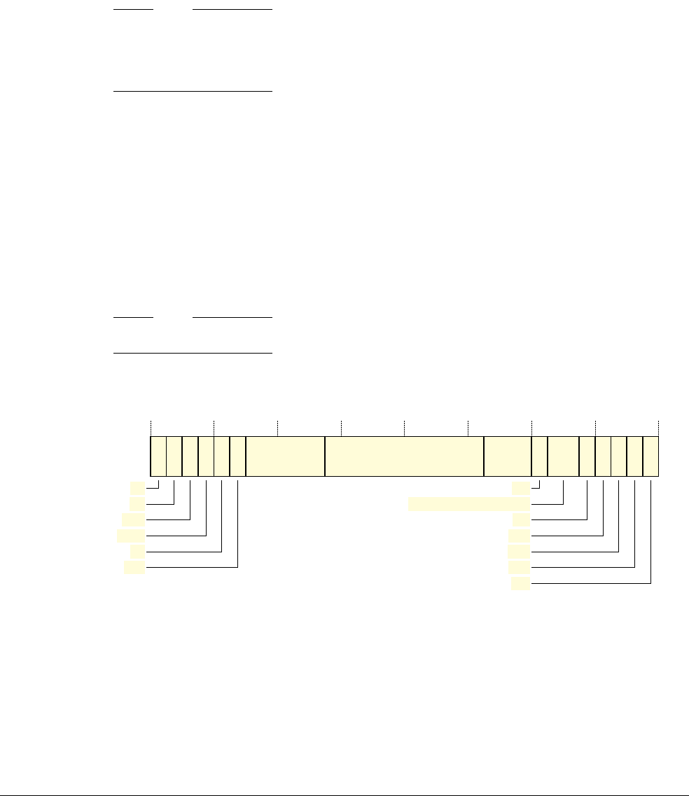
Appendix D6 Common VFP Subarchitecture Specification
D6.6 Subarchitecture additions to the Floating-point Extension system registers
ARM DDI 0406C.c Copyright © 1996-1998, 2000, 2004-2012, 2014 ARM. All rights reserved. D6-2441
ID051414 Non-Confidential
D6.6 Subarchitecture additions to the Floating-point Extension system registers
The Common VFP subarchitecture requires additions to the Floating-point Extension system register
implementation:
• extra fields are defined in the FPEXC, see Additions to the Floating-Point Exception Register, FPEXC
• additional Floating-point Extension system registers might be defined, see The Floating-Point Instruction
Registers, FPINST and FPINST2 on page D6-2445.
Note
The architecturally-defined Floating-point Extension system registers are described in both Chapter B4 System
Control Registers in a VMSA implementation and Chapter B6 System Control Registers in a PMSA implementation.
As indicated at the start of this appendix, most links from this chapter are to the register descriptions in the VMSA
chapter.
Also, the Subarchitecture field of the FPSID must identify the Common VFP subarchitecture version.
For more information about the Floating-point Extension register implementation for the Common VFP
subarchitecture see:
•Detecting which VFP Common subarchitecture registers are implemented on page D6-2447
•Accessing the VFP Common subarchitecture registers on page D6-2446.
D6.6.1 Additions to the Floating-Point Exception Register, FPEXC
See FPEXC, Floating-Point Exception Control register, VMSA on page B4-1568 or FPEXC, Floating-Point
Exception Control register, PMSA on page B6-1845 for the architectural definition of the FPEXC, including its
purpose and accessibility.
Note
The VMSA and PMSA descriptions of the register are identical.
The FPEXC bit assignments when version 3 of the Common VFP subarchitecture is implemented are:
EX, bit[31] See the FPEXC architectural description for the definition of this bit.
On an implementation that does not require asynchronous exception handling this bit is RAZ/WI.
In this case the FPINST and FPINST2 registers are not implemented.
For details of how, in Common VFP subarchitecture v1, the meaning of the EX bit changes when
the FPSCR.IEX bit is set to 1, see Subarchitecture v1 exception handling when FPSCR.IXE is set to
1 on page D6-2448.
EN, bit[30] See the FPEXC architectural description for the definition of this bit.
31 30 29 28 27 26 25 21 20 11 10 8 7 6 5 4 3 2 1 0
Reserved,
UNK/SBZP
IMPLEMENTATION
DEFINED
VECITR
DEX
FP2V
VV
IDF
IMPLEMENTATION
DEFINED
IXF
UFF
OFF
DZF
IOF
TFV
EX
EN

Appendix D6 Common VFP Subarchitecture Specification
D6.6 Subarchitecture additions to the Floating-point Extension system registers
D6-2442 Copyright © 1996-1998, 2000, 2004-2012, 2014 ARM. All rights reserved. ARM DDI 0406C.c
Non-Confidential ID051414
DEX, bit[29] Defined synchronous instruction exceptional bit. This field is valid only if FPEXC.EX == 0.
When a floating-point synchronous exception has occurred:
• if the exception was caused by an allocated floating-point instruction that is not implemented
in hardware then it is IMPLEMENTATION DEFINED whether DEX is set to 0 or 1
• otherwise, the meaning of this bit is:
0 A synchronous exception occurred when processing an unallocated instruction in
CP10 or CP 11.
1 A synchronous exception occurred on an allocated floating-point instruction that
encountered an exceptional condition.
The exception-handling routine must clear DEX to 0.
On an implementation that does not require synchronous exception handling this bit is RAZ/WI.
FP2V, bit[28] FPINST2 instruction valid bit. This field is valid only if FPEXC.EX == 1.
When an asynchronous floating-point exception has occurred, the meaning of this bit is:
0 The FPINST2 Register does not contain a valid instruction.
1 The FPINST2 Register contains a valid instruction.
FP2V must be cleared to 0 by the exception-handling routine.
If the FPINST2 Register is not implemented this bit is RAZ/WI.
VV, bit[27] VECITR valid bit. This field is valid only if FPEXC.DEX == 1.
When a synchronous floating-point exception has occurred, the meaning of this bit is:
0 FPEXC.VECITR field is not valid, and the number of remaining vector steps can be
determined from FPSCR.Len.
1 FPEXC.VECITR field is valid, and the number of remaining vector steps can be
determined from FPEXC.VECITR.
VV must be cleared to 0 by the exception-handling routine.
If the VV field s not implemented this bit is RAZ/WI.
TFV, bit[26] Trapped Fault Valid bit. Indicates whether FPEXC bits[7, 4:0] indicate trapped exceptions, or have
an IMPLEMENTATION DEFINED meaning:
0 FPEXC bits[7, 4:0] have an IMPLEMENTATION DEFINED meaning
1 FPEXC bits[7, 4:0] indicate the presence of trapped exceptions that have occurred at the
time of the exception. All trapped exceptions that occurred at the time of the exception
have their bits set.
This bit has a fixed value and ignores writes.
Bits[25:21] Reserved, UNK/SBZP.
Bits[20:11, 6:5]
IMPLEMENTATION DEFINED.
These bits are IMPLEMENTATION DEFINED. They can contain IMPLEMENTATION DEFINED
information about the cause of an exception. They might be used by the implementation to indicate
why an instruction was bounced to support code.
These bits must be cleared to zero by the exception-handling routine.

Appendix D6 Common VFP Subarchitecture Specification
D6.6 Subarchitecture additions to the Floating-point Extension system registers
ARM DDI 0406C.c Copyright © 1996-1998, 2000, 2004-2012, 2014 ARM. All rights reserved. D6-2443
ID051414 Non-Confidential
VECITR, bits[10:8]
Vector iteration count for the floating-point instruction with the exceptional condition. This field is
valid only if either:
• FPEXC.EX == 1
• FPEXC.DEX == 1 and FPEXC.VV == 1.
This field contains the number of short vector iterations remaining after the iteration in which a
potential exception was detected. Possible values are:
0b000
1 iteration
0b001
2 iterations
0b010
3 iterations
0b011
4 iterations
0b100
5 iterations
0b101
6 iterations
0b110
7 iterations
0b111
0 iterations.
The count held in this field does not include the iteration in which the exception occurred. This field
reads as
0b111
if:
• the final iteration of an instruction is bounced to the support code
• the instruction is a scalar operation.
The exception-handling routine must clear VECITR to
0b000
.
IDF, bit[7] Input Denormal trapped exception bit, or IMPLEMENTATION DEFINED. The meaning of this bit
depends on the value of FPEXC.TFV:
FPEXC.TFV == 0
This bit is IMPLEMENTATION DEFINED. It can contain IMPLEMENTATION DEFINED
information about the cause of an exception. It might be used by the implementation to
indicate why an instruction was bounced to support code.
FPEXC.TFV == 1
This bit is the Input Denormal trapped exception bit. It indicates whether an Input
Denormal exception occurred while FPSCR.IDE was 1.
In this case, the meaning of this bit is:
0 Input denormal exception has not occurred.
1 Input denormal exception has occurred.
Input Denormal exceptions can occur only when FPSCR.FZ is 1.
In both cases this bit must be cleared to 0 by the exception-handling routine.
IXF, bit[4] Inexact trapped exception bit, or IMPLEMENTATION DEFINED. The meaning of this bit depends on the
value of FPEXC.TFV:
FPEXC.TFV == 0
This bit is IMPLEMENTATION DEFINED. It can contain IMPLEMENTATION DEFINED
information about the cause of an exception. It might be used by the implementation to
indicate why an instruction was bounced to support code.
FPEXC.TFV == 1
This bit is the Inexact trapped exception bit. It indicates whether an Inexact exception
occurred while FPSCR.IXE was 1.
In this case, the meaning of this bit is:
0 Inexact exception has not occurred.
1 Inexact exception has occurred.
In both cases this bit must be cleared to 0 by the exception-handling routine.

Appendix D6 Common VFP Subarchitecture Specification
D6.6 Subarchitecture additions to the Floating-point Extension system registers
D6-2444 Copyright © 1996-1998, 2000, 2004-2012, 2014 ARM. All rights reserved. ARM DDI 0406C.c
Non-Confidential ID051414
UFF, bit[3] Underflow trapped exception bit, or IMPLEMENTATION DEFINED. The meaning of this bit depends on
the value of FPEXC.TFV:
FPEXC.TFV == 0
This bit is IMPLEMENTATION DEFINED. It can contain IMPLEMENTATION DEFINED
information about the cause of an exception. It might be used by the implementation to
indicate why an instruction was bounced to support code.
FPEXC.TFV == 1
This bit is the Underflow trapped exception bit. It indicates whether an Underflow
exception occurred while FPSCR.UFE was 1.
In this case, the meaning of this bit is:
0 Underflow exception has not occurred.
1 Underflow exception has occurred.
Note
An Underflow trapped exception can occur only when FPSCR.FZ is 0, because when
FPSCR.FZ is 1, FPSCR.UFE is ignored and treated as 0.
In both cases this bit must be cleared to 0 by the exception-handling routine.
OFF, bit[2] Overflow trapped exception bit, or IMPLEMENTATION DEFINED. The meaning of this bit depends on
the value of FPEXC.TFV:
FPEXC.TFV == 0
This bit is IMPLEMENTATION DEFINED. It can contain IMPLEMENTATION DEFINED
information about the cause of an exception. It might be used by the implementation to
indicate why an instruction was bounced to support code.
FPEXC.TFV == 1
This bit is the Overflow trapped exception bit. It indicates whether an Overflow
exception occurred while FPSCR.OFE was 1.
In this case, the meaning of this bit is:
0 Overflow exception has not occurred.
1 Overflow exception has occurred.
In both cases this bit must be cleared to 0 by the exception-handling routine.
DZF, bit[1] Divide-by-zero trapped exception bit, or IMPLEMENTATION DEFINED. The meaning of this bit
depends on the value of FPEXC.TFV:
FPEXC.TFV == 0
This bit is IMPLEMENTATION DEFINED. It can contain IMPLEMENTATION DEFINED
information about the cause of an exception. It might be used by the implementation to
indicate why an instruction was bounced to support code.
FPEXC.TFV == 1
This bit is the Divide-by-zero trapped exception bit. It indicates whether a
Divide-by-zero exception occurred while FPSCR.DZE was 1.
In this case, the meaning of this bit is:
0 Divide-by-zero exception has not occurred.
1 Divide-by-zero exception has occurred.
In both cases this bit must be cleared to 0 by the exception-handling routine.
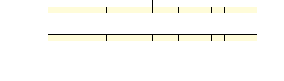
Appendix D6 Common VFP Subarchitecture Specification
D6.6 Subarchitecture additions to the Floating-point Extension system registers
ARM DDI 0406C.c Copyright © 1996-1998, 2000, 2004-2012, 2014 ARM. All rights reserved. D6-2445
ID051414 Non-Confidential
IOF, bit[0] Invalid Operation trapped exception bit, or IMPLEMENTATION DEFINED. The meaning of this bit
depends on the value of FPEXC.TFV:
FPEXC.TFV == 0
This bit is IMPLEMENTATION DEFINED. It can contain IMPLEMENTATION DEFINED
information about the cause of an exception. It might be used by the implementation to
indicate why an instruction was bounced to support code.
FPEXC.TFV == 1
This bit is the Invalid Operation trapped exception bit. It indicates whether an Invalid
Operation exception occurred while FPSCR.IOE was 1.
In this case, the meaning of this bit is:
0 Invalid Operation exception has not occurred.
1 Invalid Operation exception has occurred.
In both cases this bit must be cleared to 0 by the exception-handling routine.
D6.6.2 The Floating-Point Instruction Registers, FPINST and FPINST2
The Floating-Point Instruction Registers hold floating-point instructions relating to floating-point exception
handling in a system that implements the Common VFP subarchitecture:
• FPINST contains the exception-generating instruction
• FPINST2 contains the bypassed instruction.
FPINST and FPINST2 are:
• In the CP10 and CP11 register space.
• Present only when the Common VFP subarchitecture is implemented. A Common VFP subarchitecture
implementation can support:
— both FPINST and FPINST2
— FPINST but not FPINST2
— neither of the Floating-Point Instruction Registers.
• 32-bit read/write registers.
• Accessible only by software executing at privilege level PL1 or higher, and only if both:
— access to coprocessors CP10 and CP11 is enabled in the CPACR, see CPACR, Coprocessor Access
Control Register, VMSA on page B4-1551 for a VMSA implementation, or CPACR, Coprocessor
Access Control Register, PMSA on page B6-1831 for a PMSA implementation
— the Floating-point Extension is enabled by setting the FPEXC.EN bit to 1.
• If the implementation includes the Security Extensions, Configurable access registers. FPINST and FPINST2
are only accessible in the Non-secure state if the CP10 and CP11 bits in the NSACR are set to 1.
• If the implementation includes the Virtualization Extensions, accessible from Hyp mode only if the CP10 and
CP11 bits in the HCPTR to 1 are set to 1.
The format of a Thumb instruction in FPINST or FPINST2 is:
The format of an ARM instruction in FPINST or FPINST2 is:
1 1 0 1 1 1 0 D Vn Vd cp_num N Q M 0 Vm
15 14 13 12 11 10 9 8 7 6 5 4 3 2 1 0
1
1514131211109876543210
1 1 0 1 1 1 0 D Vn Vd cp_num N Q M 0 Vm
31 30 29 28 27 26 25 24 23 22 21 20 19 18 17 16 15 14 13 12 11 10 9 8 7 6 5 4 3 2 1 0
1

Appendix D6 Common VFP Subarchitecture Specification
D6.6 Subarchitecture additions to the Floating-point Extension system registers
D6-2446 Copyright © 1996-1998, 2000, 2004-2012, 2014 ARM. All rights reserved. ARM DDI 0406C.c
Non-Confidential ID051414
The format is the same as the format of the issued instruction, with a number of modifications. For more
information, see Floating-point data-processing instructions on page A7-272. The modifications from the issued
instruction are:
• In the Thumb encoding, bits[15:8] of the first halfword and bit[4] of the second halfword are reserved. In the
ARM encoding, bits[31:24, 4] are reserved:
— software must ignore these bits when reading this register, and must not modify these bits when writing
to this register
— hardware must set these bits to the values shown in the encoding diagrams, that map to the encoding
of an ARM
CDP
instruction with the
AL
(always) condition.
• If the instruction is a short vector instruction:
— for the FPINST Register, the source and destination registers that reference vectors are updated to
point to the source and destination registers of the exceptional iteration. The FPEXC.VECITR field
contains the number of iterations remaining. For more information, see Exception processing for short
vector instructions on page D6-2435.
— for the FPINST Register, the full vector must be processed by support code, using the current vector
length from the FPSCR. Source and destination registers that reference vectors are unchanged from
the issued instruction.
Both
MRS
register read and
MSR
register write instructions are provided for the FPINST and FPINST2 registers, see
Accessing the VFP Common subarchitecture registers.
When an exceptional instruction is bounced to support code and placed in the FPINST Register, the FPEXC.EX bit
is set to 1. This indicates that valid information is available in the FPINST Register. In addition. when a second
issued instruction is copied to the FPINST2 Register, the FPEXC.FP2V bit is set to 1. This indicates that valid
information is available in the FPINST2 Register.
When the FPEXC.EX bit is 0, indicating the floating-point implementation is not in an asynchronous exceptional
state, reads of the FPINST and FPINST2 Registers are UNPREDICTABLE and the values returned might change.
When the FPEXC.FP2V bit is 0, indicating that no second instruction was issued, reads of the FPINST2 Register
are UNPREDICTABLE and the value returned might change.
Any value read from a Floating-Point Instruction Register can be written back to the same register. This means
context switch and debugger software can save and restore Floating-Point Instruction Register values. Writing a
value that has not been read from the same register writes an UNKNOWN value to the Floating-Point Instruction
Register. For example, attempting to write an instruction with coprocessor number 0 writes an UNKNOWN value to
the Floating-Point Instruction Register.
D6.6.3 Accessing the VFP Common subarchitecture registers
Use the
VMRS
and
VMSR
instructions to access the registers for the VFP Common subarchitecture implementation, see:
•VMRS on page B9-2014
•VMSR on page B9-2016.
The additional registers in the VFP Common subarchitecture are accessed using:
•reg ==
0b1001
for FPINST
•reg ==
0b1010
for FPINST2
If FPINST or FPINST2 is not defined, the corresponding
VMRS
and
VMSR
instructions are UNPREDICTABLE.
The
VMRS
and
VMSR
instructions with reg ==
0b1011
and reg ==
0b11xx
are UNPREDICTABLE.

Appendix D6 Common VFP Subarchitecture Specification
D6.6 Subarchitecture additions to the Floating-point Extension system registers
ARM DDI 0406C.c Copyright © 1996-1998, 2000, 2004-2012, 2014 ARM. All rights reserved. D6-2447
ID051414 Non-Confidential
D6.6.4 Detecting which VFP Common subarchitecture registers are implemented
An implementation can choose not to implement FPINST and FPINST2, if these registers are not required.
System software can detect which registers are present as follows:
Set FPEXC.EX=1 and FPEXC.FP2V=1
Read back the FPEXC register
if FPEXC.EX == 0 then
Neither FPINST nor FPINST2 are implemented
else
if FPEXC.FP2V == 0 then
FPINST is implemented, FPINST2 is not implemented.
else
Both FPINST and FPINST2 are implemented.
Clean up

Appendix D6 Common VFP Subarchitecture Specification
D6.7 Earlier versions of the Common VFP subarchitecture
D6-2448 Copyright © 1996-1998, 2000, 2004-2012, 2014 ARM. All rights reserved. ARM DDI 0406C.c
Non-Confidential ID051414
D6.7 Earlier versions of the Common VFP subarchitecture
The following subsections describe the differences in earlier versions of the Common VFP subarchitecture:
D6.7.1 Differences between version 2 and version 3 of the Common VFP subarchitecture
Version 2 of the Common VFP subarchitecture can be identified by checking FPSID bits[22:16]. This field is
0b0000010
for version 2.
Version 2 of the Common VFP subarchitecture has three differences from version 3 of the subarchitecture. Before
version 3 of the Common VFP subarchitecture:
• The FPEXC.EX == 0, FPEXC.DEX == 0 encoding is used only for unallocated instructions or permission
faults. As a result, the determination that an instruction should be passed to the Computation Engine is
simpler than it is for version 3 of the Common VFP subarchitecture.
• Bounces are not handled synchronously on short vector instructions unless all iterations of the vector are to
be handled in software. This means that the FPEXC.VV bit is always 0 before version 3.
• The FPEXC.TFV bit is set to 0, so the additional information bits[7, 4:0] of FPEXC is IMPLEMENTATION
DEFINED.
D6.7.2 Differences between version 1 and version 2 of the Common VFP subarchitecture
Version 1 of the Common VFP subarchitecture version can be identified by checking FPSID bits[22:16]. This field
is
0b0000001
for version 1.
Version 1 of the Common VFP subarchitecture differs from version 2 of the subarchitecture in the following ways:
• the FPEXC.DEX bit is RAZ/WI.
• the subarchitecture has special behavior when the FPSCR.IXE bit is set to 1, as described in the following
subsection.
Subarchitecture v1 exception handling when FPSCR.IXE is set to 1
In version 1 of the Common VFP subarchitecture, the mechanism for bouncing instructions changes when the
FPSCR.IXE bit, the Inexact exception enable bit, is set to 1.
When FPSCR.IXE is set to 1, the FPEXC.EX bit signals a synchronous exception, in the same way as the
FPEXC.DEX bit. In this case:
• the exceptional instruction is the instruction that caused the Undefined Instruction exception
• the FPINST Register and the FPEXC.VECITR field are not valid.
When FPSCR.IXE is 0 the FPEXC.EX bit signals an asynchronous exception, as for later versions of the
subarchitecture.

ARM DDI 0406C.c Copyright © 1996-1998, 2000, 2004-2012, 2014 ARM. All rights reserved. D7-2449
ID051414 Non-Confidential
Appendix D7
Barrier Litmus Tests
This appendix gives examples of the use of the barrier instructions provided by the ARMv7 architecture. It contains
the following sections:
•Introduction on page D7-2450
•Simple ordering and barrier cases on page D7-2453
•Exclusive accesses and barriers on page D7-2460
•Using a mailbox to send an interrupt on page D7-2462
•Cache and TLB maintenance operations and barriers on page D7-2463.
Note
This information is not part of the ARM architecture specification. It is included here as supplementary information,
for the convenience of developers and users who might require this information.

Appendix D7 Barrier Litmus Tests
D7.1 Introduction
D7-2450 Copyright © 1996-1998, 2000, 2004-2012, 2014 ARM. All rights reserved. ARM DDI 0406C.c
Non-Confidential ID051414
D7.1 Introduction
The exact rules for the insertion of barriers into code sequences is a very complicated subject, and this appendix
describes many of the corner cases and behaviors that are possible in an implementation of the ARMv7 architecture
that includes the ARMv7 Multiprocessing Extensions.
This appendix is to help programmers, hardware design engineers, and validation engineers understand the need for
the different kinds of barriers.
D7.1.1 Overview of memory consistency
Early generations of microprocessors were relatively simple processing engines that executed each instruction in
program order. In such processors, the effective behavior was that each instruction was executed in its entirety
before a subsequent instruction started to be executed. This behavior is sometimes referred to as the Sequential
Execution Model (SEM).
In later processor generations, the needs to increase processor performance, both in terms of the frequency of
operation and the number of instructions executed each cycle, mean that such a simple form of execution is
abandoned. Many techniques, such as pipelining, write buffering, caching, speculation, and out-of-order execution,
are introduced to provide improved performance.
For general purpose processors, such as ARM, these microarchitectural innovations are largely hidden from the
programmer by a number of microarchitectural techniques. These techniques ensure that, within an individual
processor, the behavior of the processor largely remains the same as the SEM. There are some exceptions to this
where explicit synchronization is required. In the ARM architecture, these are limited to cases such as:
• synchronization of changes to the instruction stream
• synchronization of changes to system control registers.
In both these cases, the
ISB
instruction provides the necessary synchronization.
While the effect of ordering is largely hidden from the programmer within a single processor, the microarchitectural
innovations have a profound impact on the ordering of memory accesses. Write buffering, speculation, and cache
coherency protocols, in particular, can all mean that the order in which memory accesses occur, as seen by an
external observer, differs significantly from the order of accesses that would appear in the SEM. This is usually
invisible in a uniprocessor environment, but the effect becomes much more significant when multiple processors
are trying to communicate in memory. In reality, these effects are often only significant at particular synchronization
boundaries between the different threads of execution.
The problems that arise from memory ordering considerations are sometimes described as the problem of memory
consistency. Processor architectures have adopted one or more memory consistency models, or memory models, that
describe the permitted limits of the memory re-ordering that can be performed by an implementation of the
architecture. The comparison and categorization of these has generated significant research and comment in
academic circles, and ARM recommends the Memory Consistency Models for Shared Memory-Multiprocessors
paper as an excellent detailed treatment of this subject.
This appendix does not reproduce such a work, but instead concentrates on some cases that demonstrate the features
of the weakly-ordered memory model of the ARM architecture from ARMv6. In particular, the examples show how
the use of the
DMB
and
DSB
memory barrier instructions can provide the necessary safeguards to limit memory
ordering effects at the required synchronization points.
D7.1.2 Barrier operation definitions
The following reference, or provide, definitions of terms used in this appendix:
DMB See Data Memory Barrier (DMB) on page A3-152.
DSB See Data Synchronization Barrier (DSB) on page A3-153.
ISB See Instruction Synchronization Barrier (ISB) on page A3-153.
Observer, Completion
See Observability and completion on page A3-147.

Appendix D7 Barrier Litmus Tests
D7.1 Introduction
ARM DDI 0406C.c Copyright © 1996-1998, 2000, 2004-2012, 2014 ARM. All rights reserved. D7-2451
ID051414 Non-Confidential
Program order
The order of instructions as they appear in an assembly language program. This appendix does not
attempt to describe or define the legal transformations from a program written in a higher level
programming language, such as C or C++, into the machine language that can then be disassembled
to give an equivalent assembly language program. Such transformations are a function of the
semantics of the higher level language and the capabilities and options on the compiler.
D7.1.3 Conventions
Many of the examples are written in a stylized extension to ARM assembler, to avoid confusing the examples with
unnecessary code sequences. In particular, the construct WAIT([Rx]==1) describes the following sequence:
loop
LDR R12, [Rx]
CMP R12, #1
BNE loop
R12 is chosen as an arbitrary temporary register that is not in use. It is named to permit the generation of a false
dependency to ensure ordering.
For each example, a code sequence is preceded by an identifier of the observer running it:
• P0, P1…Px refer to caching coherent processors that implement the ARMv7 architecture with
Multiprocessing Extensions, and are in the same shareability domain.
• E0, E1…Ex refer to non-caching observers, that do not participate in the coherency protocol, but execute
ARM instructions and have a weakly-ordered memory model. This does not preclude these observers being
different objects, such as DMA engines or other system masters.
These observers are unsynchronized other than as required by the documented code sequence.
Note
Throughout this appendix, ARM instruction and instruction refer to instructions from the ARM or Thumb
instruction set, as implemented on ARMv7 processors.
Results are expressed in terms of <agent>:<register>, such as P0:R5. The results can be described as:
Permissible This does not imply that the results expressed are required or are the only possible results.
In most cases they are results that would not be possible under a sequentially consistent
running of the code sequences on the agents involved. In general terms, this means that these
results might be unexpected to anyone unfamiliar with memory consistency issues.
Not permissible Results that the architecture expressly forbids.
Required Results that the architecture expressly requires.
The examples omit the required shareability domain arguments of
DMB
and
DSB
instructions. The arguments are
assumed to be selected appropriately for the shareability domains of the observers.
Where the barrier function in the litmus test can be achieved by a
DMB ST
, that is a barrier to stores only, this is shown
by the use of
DMB [ST]
. This indicates that the
ST
qualifier can be omitted without affecting the result of the test. In
some implementations
DMB ST
is faster than
DMB
.

Appendix D7 Barrier Litmus Tests
D7.1 Introduction
D7-2452 Copyright © 1996-1998, 2000, 2004-2012, 2014 ARM. All rights reserved. ARM DDI 0406C.c
Non-Confidential ID051414
Except where otherwise stated, other conventions are:
• All memory initializes to 0.
• R0 contains the value 1.
• R1 - R4 contain arbitrary independent addresses that initialize to the same value on all processors. The
addresses held in these registers are Shareable and:
— the addresses held in R1 and R2 are in Write-Back Cacheable Normal memory
— the address held in R3 is in Write-Through Cacheable Normal memory
— the address held in R4 is in Non-cacheable Normal memory.
• R5 - R8 contain:
— when used with an
STR
instruction,
0x55
,
0x66
,
0x77
, and
0x88
respectively
— when used with an
LDR
instruction, the value 0.
• R11 contains a new instruction or new translation table entry, as appropriate, and R10 contains the virtual
address and the ASID, for use in this change of translation table entry.
• Memory locations are Normal memory locations unless otherwise stated.
The examples use mnemonics for the cache maintenance and TLB maintenance operations. The following tables
describe the mnemonics:
•Cache and branch predictor maintenance operations, VMSA on page B3-1496
•TLB maintenance operations, VMSA only on page B3-1497.
Notes on timing effects
Implementations that include the Multiprocessing Extensions are required to ensure that all writes complete in a
finite time. This means that any observer that is waiting for the observation of a store, for example as a result of a
WAIT([Rx]==1)
loop, is guaranteed to make forward progress without software intervention.
On implementations that do not include the Multiprocessing Extensions, a store can take an unbounded time to
complete. Therefore, a
WAIT([Rx]==1)
loop can take an unbounded time to see the increment
[Rx]
. On such an
implementation, a
DSB
instruction can be used to guarantee the completion of a store. In general, the examples in this
appendix associated with ordering assume that stores eventually become observable. Therefore, the examples omit
a final
DSB
instruction to ensure the completion of stores.

Appendix D7 Barrier Litmus Tests
D7.2 Simple ordering and barrier cases
ARM DDI 0406C.c Copyright © 1996-1998, 2000, 2004-2012, 2014 ARM. All rights reserved. D7-2453
ID051414 Non-Confidential
D7.2 Simple ordering and barrier cases
ARM implements a weakly consistent memory model for Normal memory. In general terms, this means that the
order of memory accesses observed by other observers might not be the order that appears in the program, for either
loads or stores.
This section includes examples of this.
D7.2.1 Simple weakly consistent ordering example
P1:
STR R5, [R1]
LDR R6, [R2]
P2:
STR R6, [R2]
LDR R5, [R1]
In the absence of barriers, the result of P1: R6=0, P2: R5=0 is permissible.
D7.2.2 Message passing
The following sections describe:
•Weakly-ordered message passing problem
•Message passing with multiple observers on page D7-2455.
Weakly-ordered message passing problem
P1:
STR R5, [R1] ; set new data
STR R0, [R2] ; send flag indicating data ready
P2:
WAIT([R2]==1) ; wait on flag
LDR R5, [R1] ; read new data
In the absence of barriers, an end result of P2: R5=0 is permissible.
Resolving by the addition of barriers
The addition of barriers, to ensure the observed order of the reads and the writes, ensures that data is transferred so
that the result P2:R5==
0x55
is guaranteed, as follows:
P1:
STR R5, [R1] ; set new data
DMB [ST] ; ensure all observers observe data before the flag
STR R0, [R2] ; send flag indicating data ready
P2:
WAIT([R2]==1) ; wait on flag
DMB ; ensure that the load of data is after the flag has been observed
LDR R5, [R1]

Appendix D7 Barrier Litmus Tests
D7.2 Simple ordering and barrier cases
D7-2454 Copyright © 1996-1998, 2000, 2004-2012, 2014 ARM. All rights reserved. ARM DDI 0406C.c
Non-Confidential ID051414
Resolving by the use of barriers and address dependency
There is a rule within the ARM architecture that:
• Where the value returned by a read is used for computation of the virtual address of a subsequent read or
write, then these two memory accesses are observed in program order.
Where the value returned by a read is used for computation of the virtual address of a subsequent read or
write, this is called an address dependency. An address dependency exists even if the value returned by the
first read has no effect on the virtual address. This might occur if the value returned is masked off before it
is used, or if it confirms a predicted address value that it might have changed.
This restriction applies only when the data value returned by a read is used as a data value to calculate the
address of a subsequent read or write. It does not apply if the data value returned by a read determines the
condition flags values, and the values of the flags are used for condition code evaluation to determine the
address of a subsequent read, either through conditional execution or the evaluation of a branch. This is called
a control dependency.
Where both a control and address dependency exist, the ordering behavior is consistent with the address
dependency.
Table D7-1 shows examples of address dependencies, control dependencies, and an address and control
dependency.
This means that the data transfer example of Weakly-ordered message passing problem on page D7-2453 can also
be satisfied as shown in the following example:
P1:
STR R5, [R1] ; set new data
DMB [ST] ; ensure all observers observe data before the flag
STR R0, [R2] ; send flag indicating data ready
P2:
WAIT([R2]==1)
AND R12, R12, #0 ; R12 is destination of LDR in WAIT macro
LDR R5, [R1, R12] ; Load is dependent and so is ordered after the flag has been seen
The load of R5 by P2 is ordered with respect to the load from [R2] because there is an address dependency using
R12. P1 uses a
DMB
to ensure that P2 does not observe the write of [R2] before the write of [R1].
Table D7-1 Dependency examples
Address dependency Control dependency Address and control dependencya
(a) (b) (c) (d) (e)
LDR r1, [r0]
LDR r2, [r1]
LDR r1, [r0]
AND r1, r1, #0
LDR r2, [r3, r1]
LDR r1, [r0]
CMP r1, #55
LDRNE r2, [r3]
LDR r1, [r0]
CMP r1, #55
MOVNE r4, #22
LDR r2, [r3, r4]
LDR r1, [r0]
CMP r1, #0
LDRNE r2, [r1]
a. The address dependency takes priority.

Appendix D7 Barrier Litmus Tests
D7.2 Simple ordering and barrier cases
ARM DDI 0406C.c Copyright © 1996-1998, 2000, 2004-2012, 2014 ARM. All rights reserved. D7-2455
ID051414 Non-Confidential
Message passing with multiple observers
Where the ordering of Normal memory accesses is not resolved by the use of barriers or dependencies, then different
observers might observe the accesses in a different order, as shown in the following example:
P1:
STR R5, [R1] ; set new data
STR R0, [R2] ; send flag indicating data ready
P2:
WAIT([R2]==1)
AND R12, R12, #0 ; R12 is destination of LDR in WAIT macro
LDR R5, [R1, R12] ; Load is dependent and so is ordered after the flag has been seen
P3:
WAIT([R2]==1)
AND R12, R12, #0 ; R12 is destination of LDR in WAIT macro
LDR R5, [R1, R12] ; Load is dependent and so is ordered after the flag has been seen
In this case, it is permissible for P2:R5 and P3:R5 to contain different values, because there is no order guaranteed
between the two stores performed by P1.
Resolving by the addition of barriers
The addition of a barrier by P1, as shown in the following example, ensures the observed order of the writes,
transferring data so that P2:R5 and P3:R5 both contain the value
0x55
:
P1:
STR R5, [R1] ; set new data
DMB [ST] ; ensure all observers observe data before the flag
STR R0, [R2] ; send flag indicating data ready
P2:
WAIT([R2]==1)
AND R12, R12, #0 ; R12 is destination of LDR in WAIT macro
LDR R5, [R1, R12] ; Load is dependent and so is ordered after the flag has been seen
P3:
WAIT([R2]==1)
AND R12, R12, #0 ; R12 is destination of LDR in WAIT macro
LDR R5, [R1, R12] ; Load is dependent and so is ordered after the flag has been seen

Appendix D7 Barrier Litmus Tests
D7.2 Simple ordering and barrier cases
D7-2456 Copyright © 1996-1998, 2000, 2004-2012, 2014 ARM. All rights reserved. ARM DDI 0406C.c
Non-Confidential ID051414
D7.2.3 Address dependency with object construction
When accessing an object-oriented data structure, the address dependency rule means that barriers are not required,
even when initializing the object:
P1:
STR R5, [R1, #offset] ; set new data in a field
DMB [ST] ; ensure all observers observe data before base address is updated
STR R1, [R2] ; update base address
P2:
LDR R1, [R2] ; read for base address
CMP R1, #0 ; check if it is valid
BEQ null_trap
LDR R5, [R1, #offset] ; use base address to read field
If the null_trap is not taken, it is required that P2:R5==
0x55
. This avoids P2 observing a partially constructed object
from P1. Significantly, P2 does not require a barrier to ensure this behavior.
P1 requires a barrier to ensure the observed order of the writes by P1. In general, the impact of requiring a barrier
during the construction phase is much less than the impact of requiring a barrier for every read access.
D7.2.4 Causal consistency issues with multiple observers
The fact that different observers can observe memory accesses in different orders extends, in the absence of barriers,
to behaviors that do not fit naturally expected causal properties, as the following example shows:
P1:
STR R0, [R2] ; set new data
P2:
WAIT([R2]==1) ; wait to see new data from P1
STR R0, [R3] ; send flag, must be after the new data has been by P2 as stores
; must not be speculative
P3:
WAIT([R3]==1) ; wait for P2's flag
AND R12, R12, #0 ; dependency to ensure order
LDR R0, [R2, R12] ; read P1's data
In this example, P3:R0==0 is permissible. P3 is not guaranteed to seethe stores from P1 and P2 in any particular
order. This applies despite the fact that the store from P2 can only happen after P2 has observed the store from P1.
This example shows that the ARM memory ordering model for Normal memory does not conform to causal
consistency. This means that the apparently transitive causal relationship between two variables is not guaranteed
to be transitive.
The following example shows the insertion of a barrier by P2 to create causal consistency:
P1:
STR R0, [R2] ; set new data
P2:
WAIT([R2]==1) ; wait to see new data from P1
DMB ; ensure P1's data is observed by all observers before any following store
STR R0, [R3] ; send flag
P3:
WAIT([R3]==1) ; wait for P2's flag
AND R12, R12, #0 ; dependency to ensure order
LDR R0, [R2, R12] ; read P1's data

Appendix D7 Barrier Litmus Tests
D7.2 Simple ordering and barrier cases
ARM DDI 0406C.c Copyright © 1996-1998, 2000, 2004-2012, 2014 ARM. All rights reserved. D7-2457
ID051414 Non-Confidential
This creates causal consistency because a
DMB
is required to order all accesses that the executing processor observed
before the
DMB
, not only those it issued, before any of the accesses that follow the
DMB
.
D7.2.5 Multiple observers of writes to multiple locations
The ARM weakly consistent memory model means that different observers can observe writes to different locations
in different orders, as the following example shows:
P1:
STR R0, [R1] ; set new data
P2:
STR R0, [R2] ; set new data
P3:
LDR R10, [R2] ; read P2's data before P1's
LDR R9, [R1] ;
BIC R9, R10, R9 ; R9 <- R10 && ~R9
; R9 contains 1 iff read from [R2] is observed to be 1 and
; read from [R1] is observed to be 0.
P4:
LDR R9, [R1]
LDR R10, [R2]
BIC R9, R9, R10 ; R9 <- R9 && ~R10
; R9 contains 1 iff read from [R2] is observed to be 0 and
; read from [R1] is observed to be 1.
In this example, the result P3:R9==1 and P4:R9==1 is permissible. This means that P3 and P4 observed the stores
from P1 and P2 in different orders.
The following example shows the use of
DMB
instructions to ensure sequential consistency:
P1:
STR R0, [R1] ; set new data
P2:
STR R0, [R2] ; set new data
P3:
LDR R10, [R2] ; read P2's data before P1's
DMB
LDR R9, [R1]
BIC R9, R10, R9 ; R9 <- R10 && ~R9
; R9 contains 1 iff read from [R2] is observed to be 1 and
; read from [R1] is observed to be 0.
P4:
LDR R9, [R1] ; read P1's data before P2's
DMB
LDR R10, [R2]
BIC R9, R9, R10 ; R9 <- R9 && ~R10
; R9 contains 1 iff read from [R2] is observed to be 0 and
; read from [R1] is observed to be 1.

Appendix D7 Barrier Litmus Tests
D7.2 Simple ordering and barrier cases
D7-2458 Copyright © 1996-1998, 2000, 2004-2012, 2014 ARM. All rights reserved. ARM DDI 0406C.c
Non-Confidential ID051414
In this example:
• the
DMB
executed by P3 ensures that, if the P3 load from [R2] observes the P2 store to [R2], then all observers
observe the P2 store to [R2] before they observe the P3 load from [R1]
• the
DMB
executed by P4 ensures that, if the P4 load from [R1] observes the P1 store to [R1], then all observers
observe the P1 store to [R1 before they observe the P4 load from [R2].
If the P3 load from [R1] returns 0, then it has not observed the P1 store to [R1]. Also, if the P3 load of [R2] returns 1,
then all observers must have observed the P2 store to [R2] before they observed the P1 store to [R1]. This means
that P4 cannot observe the P1 store to [R1] without also observing the P2 store to [R2].
Alternatively, if the P4 load from [R2] returns 0, then it has not observed the P2 store to [R2]. If, also, the P4 load
of [R1] returns 1, then all observers must have observed the P1 store to [R1] before they observed the P2 store to
[R2]. This means that P3 cannot observe the P2 store to [R2] without also observing the P1 store to [R1].
This shows that, of the four possible results for {P3:R9, P4:R9}, the insertion of these barriers makes the result
{1, 1} impossible.
D7.2.6 Posting a store before polling for acknowledgement
In the case where an observer stores to a location, and then polls for an acknowledge from a different observer, the
weak ordering of the memory model can lead to a deadlock, as the following example shows:
P1:
STR R0, [R2]
WAIT ([R3]==1)
P2:
WAIT ([R2]==1)
STR R0, [R3]
This can deadlock because P2 might not observe the store by P1 for an indefinite period of time.
The addition of a
DMB
instruction prevents this deadlock:
P1:
STR R0, [R2]
DMB
WAIT ([R3]==1)
P2:
WAIT ([R2]==1)
STR R0, [R3]
The
DMB
executed by P1 ensures that P2 observes the store by P1 before it observes the load by P1. This ensures a
timely completion.
The following example is a variant of the previous example, where the two observers poll the same memory
location:
P1:
STR R0, [R2]
WAIT ([R2]==2)
P2:
WAIT ([R2]==1)
LDR R0, [R2]
ADD R0, R0, #1
STR R0, [R2]

Appendix D7 Barrier Litmus Tests
D7.2 Simple ordering and barrier cases
ARM DDI 0406C.c Copyright © 1996-1998, 2000, 2004-2012, 2014 ARM. All rights reserved. D7-2459
ID051414 Non-Confidential
In this example, the same deadlock can occur, because the architecture permits P1 to read the result of its own store
to [R2] early, and continue doing so for an indefinite amount of time. The addition of a
DMB
instruction prevents this
deadlock:
P1:
STR R0, [R2]
DMB
WAIT ([R2]==2)
P2:
WAIT ([R2]==1)
LDR R0, [R2]
ADD R0, R0, #1
STR R0, [R2]
D7.2.7
WFE
and
WFI
and barriers
The Wait For Event and Wait For Interrupt instructions permit the processor to suspend execution and enter a
low-power state. A
DSB
barrier instruction is required if it is necessary to ensure that memory accesses made before
the
WFI
or
WFE
are visible to other observers, unless some other mechanism has ensured this visibility. Examples of
other mechanism that would guarantee the required visibility are the
DMB
described in Posting a store before polling
for acknowledgement on page D7-2458, or a dependency on a load.
The following example requires the
DSB
to ensure that the store is visible:
P1:
STR R0, [R2]
DSB
Loop
WFI
B Loop
However, if the example in Posting a store before polling for acknowledgement on page D7-2458 is extended to
include a WFE, there is no risk of a deadlock. The extended example is:
P1:
STR R0, [R2]
DMB
Loop
LDR R12, [R3]
CMP R12, #1
WFENE
BNE Loop
P2:
WAIT ([R2]==1)
STR R0, [R3]
DSB
SEV
In this example:
• the
DMB
by P1 ensures that P2 observes the store by P1 before it observes the load by P1
• the dependency of the
WFE
on the result of the load by P1 means that this load must complete before P1
executes the
WFE
.
For more information about
SEV
, see Use of Wait For Event (WFE) and Send Event (SEV) with Locks on
page D7-2460.

Appendix D7 Barrier Litmus Tests
D7.3 Exclusive accesses and barriers
D7-2460 Copyright © 1996-1998, 2000, 2004-2012, 2014 ARM. All rights reserved. ARM DDI 0406C.c
Non-Confidential ID051414
D7.3 Exclusive accesses and barriers
The Load-Exclusive and Store-Exclusive instructions, described in Synchronization and semaphores on
page A3-114, are predictable only with Normal memory. These instructions do not have any implicit barrier
functionality. Therefore, any use of these instructions to implement locks of any type requires the addition of explicit
barriers.
D7.3.1 Acquiring a lock
A common use of Load-Exclusive and Store-Exclusive instructions is to claim a lock to permit entry into a critical
region. This is typically performed by testing a lock variable that indicates 0 for a free lock and some other value,
commonly 1 or an identifier of the process holding the lock, for a taken lock.
The lack of implicit barriers in the Load-Exclusive and Store-Exclusive instructions means that the mechanism
requires a
DMB
instruction between acquiring a lock and making the first access to the critical region, to ensure that
all observers observe the successful claim of the lock before they observe any subsequent loads or stores to the
region. This example shows Px acquiring a lock:
Px:
Loop
LDREX R5, [R1] ; read lock
CMP R5, #0 ; check if 0
STREXEQ R5, R0, [R1] ; attempt to store new value
CMPEQ R5, #0 ; test if store succeeded
BNE Loop ; retry if not
DMB ; ensures that all subsequent accesses are observed after the
; gaining of the lock is observed
; loads and stores in the critical region can now be performed
D7.3.2 Releasing a lock
The converse operation of releasing a lock does not require the use of Load-Exclusive and Store-Exclusive
instructions, because only a single observer is able to write to the lock. However, often it is necessary for any
observer to observe any memory updates, or any values that are loaded into memory, before they observe the release
of the lock. Therefore, a
DMB
usually precedes the lock release, as the following example shows.
Px:
; loads and stores in the critical region
MOV R0, #0
DMB ; ensure all previous accesses are observed before the lock is cleared
STR R0, [R1] ; clear the lock
D7.3.3 Use of Wait For Event (WFE) and Send Event (SEV) with Locks
The ARMv7 architecture includes Wait For Event and Send Event instructions, that can be executed to reduce the
required number of iterations of a lock-acquire loop, or spinlock, to reduce power. The basic mechanism involves
an observer that is in a spinlock executing a
WFE
instruction that suspends execution on that observer until an
asynchronous exception or an explicit event, sent by some other observer using the
SEV
instruction, is seen by the
suspended observer. An observer that holds the lock executes an
SEV
instruction to send an event after it has released
the lock.
The Event signal is a non-memory communication, and therefore the memory update that releases the lock must be
observable by all observers before the
SEV
instruction is executed and the event is sent. This requires the use of
DSB
instruction, rather than
DMB
.
Therefore, the following is an example of lock acquire code using
WFE
:
Px:
Loop
LDREX R5, [R1] ; read lock
CMP R5, #0 ; check if 0

Appendix D7 Barrier Litmus Tests
D7.3 Exclusive accesses and barriers
ARM DDI 0406C.c Copyright © 1996-1998, 2000, 2004-2012, 2014 ARM. All rights reserved. D7-2461
ID051414 Non-Confidential
WFENE ; sleep if the lock is held
STREXEQ R5, R0, [R1] ; attempt to store new value
CMPEQ R5, #0 ; test if store succeeded
BNE Loop ; retry if not
DMB ; ensures that all subsequent accesses are observed after the
; gaining of the lock is observed
; loads and stores in the critical region can now be performed
And the following is an example of lock release code using
SEV
:
Px:
; loads and stores in the critical region
MOV R0, #0
DMB ; ensure all previous accesses are observed before the lock is cleared
STR R0, [R1] ; clear the lock
DSB ; ensure completion of the store that cleared the lock before
; sending the event
SEV

Appendix D7 Barrier Litmus Tests
D7.4 Using a mailbox to send an interrupt
D7-2462 Copyright © 1996-1998, 2000, 2004-2012, 2014 ARM. All rights reserved. ARM DDI 0406C.c
Non-Confidential ID051414
D7.4 Using a mailbox to send an interrupt
In some message passing systems, it is common for one observer to update memory and then notify a second
observer of the update by sending an interrupt, using a mailbox.
Although a memory access might be made to initiate the sending of the mailbox interrupt, a
DSB
instruction is
required to ensure the completion of previous memory accesses.
Therefore, the following sequence is required to ensure that P2 observes the updated value.
P1:
STR R5, [R1] ; message stored to shared memory location
DSB [ST]
STR R1, [R4] ; R4 contains the address of a mailbox
P2:
; interrupt service routine
LDR R5, [R1]
Even if R4 is a pointer to Strongly-Ordered memory, the update to R1 might not be visible unless P1 executes a
DSB
instruction.
Note
The
DSB
executed by P1 ensures global observation of the store to [R1]. The interrupt timing ensures that the code
executed by P2 is executed after the global observation of the update to [R1], and therefore must see this update. In
some implementations, this might be implemented by requiring that interrupts flush non-coherent buffers that hold
speculatively loaded data.

Appendix D7 Barrier Litmus Tests
D7.5 Cache and TLB maintenance operations and barriers
ARM DDI 0406C.c Copyright © 1996-1998, 2000, 2004-2012, 2014 ARM. All rights reserved. D7-2463
ID051414 Non-Confidential
D7.5 Cache and TLB maintenance operations and barriers
The following sections describe the use of barriers with cache and TLB maintenance operations:
•Data cache maintenance operations
•Instruction cache maintenance operations on page D7-2465
•TLB maintenance operations and barriers on page D7-2467.
D7.5.1 Data cache maintenance operations
The following sections describe the use of barriers with data cache maintenance operations:
•Message passing to non-caching observers
•Multiprocessing message passing to non-caching observers
•Invalidating DMA buffers, nonfunctional example on page D7-2464
•Invalidating DMA buffers, functional example with single processor on page D7-2464
•Invalidating DMA buffers, functional example with multiple coherent processors on page D7-2465.
Message passing to non-caching observers
The ARMv7 architecture requires the use of
DMB
instructions to ensure the ordering of data cache maintenance
operations and their effects. This means the following message passing approaches can be used when
communicating between caching observers and non-caching observers:
P1:
STR R5, [R1] ; update data (assumed to be in P1's cache)
DCCMVAC R1 ; clean cache to point of coherency
DMB ; ensure effects of the clean will be observed before the flag is set
STR R0, [R4] ; send flag to external agent (Non-cacheable location)
E1:
WAIT ([R4] == 1) ; wait for the flag
DMB ; ensure that flag has been seen before reading data
LDR R5, [R1] ; read the data
In this example, it is required that E1:R5==
0x55
.
Multiprocessing message passing to non-caching observers
The broadcast nature of the cache maintenance operations in an implementation that includes the Multiprocessing
Extensions, combined with properties of barriers, means that the message passing principle for non-caching
observers is:
P1:
STR R5, [R1] ; update data (assumed to be in P1's cache)
DMB [ST] ; ensure new data is observed before the flag to P2 is set
STR R0, [R2] ; send flag to P2
P2:
WAIT ([R2] == 1) ; wait for flag from P1
DMB ; ensure cache clean is observed after P1's flag is observed
DCCMVAC R1 ; clean cache to point of coherency - this cleans the cache of P1
DMB ; ensure effects of the clean are observed before the flag to E1 is set
STR R0, [R4] ; send flag to E1
E1:
WAIT ([R4] == 1) ; wait for flag from P2
DMB ; ensure that flag has been observed before reading the data
LDR R5, [R1] ; read the data

Appendix D7 Barrier Litmus Tests
D7.5 Cache and TLB maintenance operations and barriers
D7-2464 Copyright © 1996-1998, 2000, 2004-2012, 2014 ARM. All rights reserved. ARM DDI 0406C.c
Non-Confidential ID051414
In this example, it is required that E1:R5==
0x55
. The clean operation executed by P2 affects the data location in the
P1 cache. The cast-out from the P1 cache is guaranteed to be observed before P2 updates [R4].
Invalidating DMA buffers, nonfunctional example
The basic scheme for communicating with an external observer that is a process that passes data in to a Cacheable
memory region must take account of the architectural requirement that regions marked as Cacheable can be
allocated into a cache at any time, for example as a result of speculation. The following example shows this
possibility:
P1:
DCIMVAC R1 ; ensure cache clean with respect to memory. A clean operation could be
; used but the DMA overwrites this region so an invalidate operation
; is sufficient and usually more efficient
DMB ; ensures cache invalidation is observed before the next store is observed
STR R0, [R3] ; send flag to external agent
WAIT ([R4]==1) ; wait for a different flag from an external agent
DMB ; observe flag from external agent before reading new data. However [R1]
; could have been brought into cache earlier
LDR R5, [R1]
E1:
WAIT ([R3] == 1) ; wait for flag
STR R5, [R1] ; store new data
DMB
STR R0, [R4] ; send a flag
If a speculative access occurs, there is no guarantee that the cache line containing [R1] is not brought back into the
cache after the cache invalidation, but before [R1] is written by E1. Therefore, the result P1:R5=0 is permissible.
Invalidating DMA buffers, functional example with single processor
P1:
DCIMVAC R1 ; ensure cache clean with respect to memory. A clean operation could be
; used but the DMA overwrites this region so an invalidate operation
; is sufficient and usually more efficient
DMB ; ensures cache invalidation is observed before the next store is observed
STR R0, [R3] ; send flag to external agent
WAIT ([R4]==1) ; wait for a different flag from an external agent
DMB ; ensure that cache invalidate is observed after the flag
; from external agent is observed
DCIMVAC R1 ; ensure cache discards stale copies before use
LDR R5, [R1]
E1:
WAIT ([R3] == 1) ; wait for flag
STR R5, [R1] ; store new data
DMB [ST]
STR R0, [R4] ; send a flag
In this example, the result P1:R5 ==
0x55
is required. Including a cache invalidation after the store by E1 to [R1] is
observed ensures that the line is fetched from external memory after it has been updated.

Appendix D7 Barrier Litmus Tests
D7.5 Cache and TLB maintenance operations and barriers
ARM DDI 0406C.c Copyright © 1996-1998, 2000, 2004-2012, 2014 ARM. All rights reserved. D7-2465
ID051414 Non-Confidential
Invalidating DMA buffers, functional example with multiple coherent processors
The broadcasting of cache maintenance operations, and the use of
DMB
instructions to ensure their observability,
means that the previous example extends naturally to a multiprocessor system. Typically this requires a transfer of
ownership of the region that the external observer is updating.
P0:
(Use data from [R1], potentially using [R1] as scratch space)
DMB
STR R0, [R2] ; signal release of [R1]
WAIT ([R2] == 0) ; wait for new value from DMA
DMB
LDR R5, [R1]
P1:
WAIT ([R2] == 1) ; wait for release of [R1] by P0
DCIMVAC R1 ; ensure caches are clean with respect to memory, invalidate is sufficient
DMB
STR R0, [R3] ; request new data for [R1]
WAIT ([R4] == 1) ; wait for new data
DMB
DCIMVAC R1 ; ensure caches discard stale copies before use
DMB
MOV R0, #0
STR R0, [R2] ; signal availability of new [R1]
E1:
WAIT ([R3] == 1) ; wait for new data request
STR R5, [R1] ; send new [R1]
DMB [ST]
STR R0, [R4] ; indicate new data available to P1
In this example, the result P0:R5 ==
0x55
is required. The
DMB
issued by P1 after the first data cache invalidation
ensures that effect of the cache invalidation on P0 is seen by E1 before the store by E1 to [R1]. The
DMB
issued by
P1 after the second data cache invalidation ensures that its effects are seen before the store of 0 to the semaphore
location in [R2].
D7.5.2 Instruction cache maintenance operations
The following sections describe the use of barriers with instruction cache maintenance operations:
•Ensuring the visibility of updates to instructions for a uniprocessor
•Ensuring the visibility of updates to instructions for a multiprocessor on page D7-2466.
Ensuring the visibility of updates to instructions for a uniprocessor
On a single processor, the agent that causes instruction fetches, or instruction cache linefills, is a separate memory
system observer from the agent that causes data accesses. Therefore, any operations to invalidate the instruction
cache can rely only on seeing updates to memory that are complete. This must be ensured by the use of a
DSB
instruction.
Also, instruction cache maintenance operations are only guaranteed to complete after the execution of a
DSB
, and an
ISB
is required to discard any instructions that might have been prefetched before the instruction cache invalidation
completed. Therefore, on a uniprocessor, to ensure the visibility of an update to code and to branch to it, the
following sequence is required:

Appendix D7 Barrier Litmus Tests
D7.5 Cache and TLB maintenance operations and barriers
D7-2466 Copyright © 1996-1998, 2000, 2004-2012, 2014 ARM. All rights reserved. ARM DDI 0406C.c
Non-Confidential ID051414
P1:
STR R11, [R1] ; R11 contains a new instruction to store in program memory
DCCMVAU R1 ; clean to PoU makes visible to instruction cache
DSB
ICIMVAU R1 ; ensure instruction cache and branch predictor discards stale data
BPIMVA R1
DSB ; ensure completion of the invalidation
ISB ; ensure instruction fetch path observes new instruction cache state
BX R1
Ensuring the visibility of updates to instructions for a multiprocessor
The Multiprocessing Extensions require a processor that performs an instruction cache maintenance operation to
execute a
DSB
instruction to ensure completion of the maintenance operation. This ensures that the cache
maintenance operation is complete on all processors in the Inner Shareable shareability domain.
An
ISB
is not broadcast, and so does not affect other processors. This means that any other processor must perform
its own
ISB
synchronization after it knows that the update is visible, if it is necessary to ensure its synchronization
with the update. The following example shows how this might be done:
P1:
STR R11, [R1] ; R11 contains a new instruction to store in program memory
DCCMVAU R1 ; clean to PoU makes visible to instruction cache
DSB ; ensure completion of the clean on all processors
ICIMVAU R1 ; ensure instruction cache/branch predictor discards stale data
BPIMVA R1
DSB ; ensure completion of the ICache and branch predictor
; invalidation on all processors
STR R0, [R2] ; set flag to signal completion
ISB ; synchronize context on this processor
BX R1 ; branch to new code
P2-Px:
WAIT ([R2] == 1) ; wait for flag signaling completion
ISB ; synchronize context on this processor
BX R1 ; branch to new code
Nonfunctional approach
The following sequence does not have the same effect, because a
DSB
is not required to complete the instruction
cache maintenance operations that other processors issue:
P1:
STR R11, [R1] ; R11 contains a new instruction to store in program memory
DCCMVAU R1 ; clean to PoU makes visible to instruction cache
DSB ; ensure completion of the clean on all processors
ICIMVAU R1 ; ensure instruction cache/branch predictor discards stale data
BPIMVA R1
DMB ; ensure ordering of the store after the invalidation
; DOES NOT guarantee completion of instruction cache/branch
; predictor on other processors
STR R0, [R2] ; set flag to signal completion
DSB ; ensure completion of the invalidation on all processors
ISB ; synchronize context on this processor
BX R1 ; branch to new code
P2-Px:
WAIT ([R2] == 1) ; wait for flag signaling completion
DSB ; this DSB does not guarantee completion of P1's ICIMVAU/BPIMVA
ISB
BX R1
In this example, P2…Px might not see the updated region of code at R1.

Appendix D7 Barrier Litmus Tests
D7.5 Cache and TLB maintenance operations and barriers
ARM DDI 0406C.c Copyright © 1996-1998, 2000, 2004-2012, 2014 ARM. All rights reserved. D7-2467
ID051414 Non-Confidential
D7.5.3 TLB maintenance operations and barriers
The following sections describe the use of barriers with TLB maintenance operations:
•Ensuring the visibility of updates to translation tables for a uniprocessor
•Ensuring the visibility of updates to translation tables for a multiprocessor
•Paging memory in and out on page D7-2468.
Ensuring the visibility of updates to translation tables for a uniprocessor
On a single processor, the agent that causes translation table walks is a separate memory system observer from the
agent that causes data accesses. Therefore, any operations to invalidate the TLB can only rely on seeing updates to
memory that are complete. This must be ensured by the use of a
DSB
instruction.
The Multiprocessing Extensions require that translation table walks look in the data or unified caches at L1, so such
systems do not require data cache cleaning.
After the translation tables update, any old copies of entries that might be held in the TLBs must be invalidated. This
operation is only guaranteed to affect all instructions, including instruction fetches and data accesses, after the
execution of a
DSB
and an
ISB
. Therefore, the code for updating a translation table entry is:
P1:
STR R11, [R1] ; update the translation table entry
DSB ; ensure visibility of the update to translation table walks
TLBIMVA R10
BPIALL
DSB ; ensure completion of the BP and TLB invalidation
ISB ; synchronize context on this processor
;
; new translation table entry can be relied upon at this point and all accesses
; generated by this observer using the old mapping have been completed
Importantly, by the end of this sequence, all accesses that used the old translation table mappings have been
observed by all observers.
An example of this is where a translation table entry is marked as invalid. Such a system must provide a mechanism
to ensure that any access to a region of memory being marked as invalid has completed before any action is taken
as a result of the region being marked as invalid.
Ensuring the visibility of updates to translation tables for a multiprocessor
The same code sequence can be used in a multiprocessing system. The Multiprocessing Extensions require a
processor that performs a TLB maintenance operation to execute a
DSB
instruction to ensure completion of the
maintenance operation. This ensures that the TLB maintenance operation is complete on all processors in the Inner
Shareable shareability domain.
The completion of a
DSB
that completes a TLB maintenance operation ensures that all accesses that used the old
mapping have completed.
P1:
STR R11, [R1] ; update the translation table entry
DSB ; ensure visibility of the update to translation table walks
TLBIMVAIS R10
BPIALLIS
DSB ; ensure completion of the BP and TLB invalidation
ISB ; Note ISB is not broadcast and must be executed locally on other processors
;
; new translation table entry can be relied upon at this point and all accesses generated by any
; observers affected by the broadcast TLBIMVAIS operation using the old mapping have completed
The completion of the TLB maintenance operation is guaranteed only by the execution of a
DSB
by the observer that
performed the TLB maintenance operation. The execution of a
DSB
by a different observer does not have this effect,
even if the
DSB
is known to be executed after the TLB maintenance operation is observed by that different observer.

Appendix D7 Barrier Litmus Tests
D7.5 Cache and TLB maintenance operations and barriers
D7-2468 Copyright © 1996-1998, 2000, 2004-2012, 2014 ARM. All rights reserved. ARM DDI 0406C.c
Non-Confidential ID051414
Paging memory in and out
In a multiprocessor system there is a requirement to ensure the visibility of translation table updates when paging
regions of memory into RAM from a backing store. This might, or might not, also involve paging existing locations
in memory from RAM to a backing store. In such situations, the operating system selects one or more pages of
memory that might be in use but are suitable to discard, with or without copying to a backing store, depending on
whether or not the region of memory is writable. Disabling the translation table mappings for a page, and ensuring
the visibility of that update to the translation tables, prevents agents accessing the page.
For this reason, it is important that the
DSB
that is performed after the TLB invalidation ensures that no other updates
to memory using those mappings are possible.
A example sequence for the paging out of an updated region of memory, and the subsequent paging in of memory,
is as follows:
P1:
STR R11, [R1] ; update the translation table for the region being paged out
DSB ; ensure visibility of the update to translation table walks
TLBIMVAIS R10 ; invalidate the old entry
DSB ; ensure completion of the invalidation on all processors
ISB ; ensure visibility of the invalidation
BL SaveMemoryPageToBackingStore
BL LoadMemoryFromBackingStore
DSB ; ensure completion of the memory transfer (this could be part of
; LoadMemoryFromBackingStore
ICIALLUIS ; also invalidates the branch predictor
STR R9, [R1] ; create a new translation table entry with a new mapping
DSB ; ensure completion of instruction cache and branch predictor invalidation
; and ensure visibility of the new translation table mapping
ISB ; ensure synchronization of this instruction stream
This example assumes the memory copies are performed by an observer that is coherent with the caches of processor
P1. This observer might be P1 itself, using a specific paging mapping. For clarity, the example omits the functional
descriptions of
SaveMemoryPageToBackingStore
and
LoadMemoryFromBackingStore
.
LoadMemoryFromBackingStore
is
required to ensure that the memory updates that it makes are visible to instruction fetches.
In this example, the use of ICIALLUIS to invalidate the entire instruction cache is a simplification, that might not
be optimal for performance. An alternative approach involves invalidating all of the lines in the caches using
ICIMVAU operations. This invalidation must be done when the mapping used for the ICIMVAU operations is valid
but not executable.

ARM DDI 0406C.c Copyright © 1996-1998, 2000, 2004-2012, 2014 ARM. All rights reserved. D8-2469
ID051414 Non-Confidential
Appendix D8
Legacy Instruction Mnemonics
This appendix describes the legacy mnemonics in the ARM instruction sets, and their Unified Assembler Language
(UAL) equivalents. It contains the following sections:
•Thumb instruction mnemonics on page D8-2470
•Other UAL mnemonic changes on page D8-2471
•Pre-UAL pseudo-instruction NOP on page D8-2474.

Appendix D8 Legacy Instruction Mnemonics
D8.1 Thumb instruction mnemonics
D8-2470 Copyright © 1996-1998, 2000, 2004-2012, 2014 ARM. All rights reserved. ARM DDI 0406C.c
Non-Confidential ID051414
D8.1 Thumb instruction mnemonics
Table D8-1 lists the UAL equivalents of the mnemonics used in pre-UAL Thumb assembly language. Except where
noted, the Thumb mnemonics conflict with UAL and cannot be supported by assemblers as synonyms. Software
written in Thumb assembly language cannot be correctly assembled by a UAL assembler unless these changes are
made.
All other Thumb instructions are the same in UAL as in Thumb assembler language, or can be supported as
synonyms.
Table D8-1 Thumb instruction mnemonics
Former Thumb assembler mnemonic UAL equivalent
ADC ADCS
ADD ADDS
a
a. If either or both of the operands is R8-R15,
ADD
not
ADDS
.
AND ANDS
ASR ASRS
BIC BICS
EOR EORS
LSL LSLS
MOV <Rd>, #<imm> MOVS <Rd>, #<imm>
MOV <Rd>, <Rn> ADDS <Rd>, <Rn>, #0
b
b. If either or both of the operands is R8-R15,
MOV <Rd>, <Rn>
not
ADDS <Rd>, <Rn>,
#0
.
MUL MULS
MVN MVNS
ORR ORRS
ROR RORS
SBC SBCS
SUB SUBS
c
c. If the operand register is
SP
,
SUB
not
SUBS
.

Appendix D8 Legacy Instruction Mnemonics
D8.2 Other UAL mnemonic changes
ARM DDI 0406C.c Copyright © 1996-1998, 2000, 2004-2012, 2014 ARM. All rights reserved. D8-2471
ID051414 Non-Confidential
D8.2 Other UAL mnemonic changes
Table D8-2 lists the instruction mnemonics, other than the Thumb mnemonics listed in Thumb instruction
mnemonics on page D8-2470, that are changed by the introduction of UAL.
Note
Most of these changes are in the mnemonics for VFP instructions. UAL does not define new mnemonics for the
FLDMX
and
FSTMX
instructions. For more information see FLDMX, FSTMX on page A8-388.
Table D8-2 Instruction mnemonics changed by the introduction of UAL
Pre-UAL mnemonic UAL equivalent See
FABSD
,
FABSS VABS
VABS on page A8-824
FADDD
,
FADDS VADD
VADD (floating-point) on page A8-830
FCMP
,
FCMPE
,
FCMPEZ
,
FCMPZ VCMP{E}
VCMP, VCMPE on page A8-864
FCONSTD
,
FCONSTS VMOV
VMOV (immediate) on page A8-936
FCPYD
,
FCPYS VMOV
VMOV (register) on page A8-938
FCVTDS
,
FCVTSD VCVT
VCVT (between double-precision and single-precision) on page A8-876
FDIVD
,
FDIVS VDIV
VDIV on page A8-882
FLDD VLDR
VLDR on page A8-924
FLDMD
,
FLDMS VLDM
,
VPOP
VLDM on page A8-922, VPOP on page A8-990
FLDS VLDR
VLDR on page A8-924
FMACD
,
FMACS VMLA
VMLA, VMLS (floating-point) on page A8-932
FMDHR
,
FMDLR VMOV
VMOV (ARM core register to scalar) on page A8-940
FMDRR VMOV
VMOV (between two ARM core registers and a doubleword extension register) on
page A8-948
FMRDH
,
FMRDL VMOV
VMOV (scalar to ARM core register) on page A8-942
FMRRD VMOV
VMOV (between two ARM core registers and a doubleword extension register) on
page A8-948
FMRRS VMOV
VMOV (between two ARM core registers and two single-precision registers) on
page A8-946
FMRS VMOV
VMOV (between ARM core register and single-precision register) on page A8-944
FMRX VMRS
VMRS on page B9-2014
FMSCD
,
FMSCS VNMLS
VNMLA, VNMLS, VNMUL on page A8-970
FMSR VMOV
VMOV (between ARM core register and single-precision register) on page A8-944
FMSRR VMOV
VMOV (between two ARM core registers and two single-precision registers) on
page A8-946
FMSTAT VMRS
VMRS on page A8-954
FMULD
,
FMULS VMUL
VMUL (floating-point) on page A8-960

Appendix D8 Legacy Instruction Mnemonics
D8.2 Other UAL mnemonic changes
D8-2472 Copyright © 1996-1998, 2000, 2004-2012, 2014 ARM. All rights reserved. ARM DDI 0406C.c
Non-Confidential ID051414
FMXR VMSR
VMSR on page B9-2016
FNEGD
,
FNEGS VNEG
VNEG on page A8-968
FNMACD
,
FNMACS VMLS
VMLA, VMLS (floating-point) on page A8-932
FNMSCD
,
FNMSCS VNMLA
VNMLA, VNMLS, VNMUL on page A8-970
FNMULD
,
FNMULS VNMUL
VNMLA, VNMLS, VNMUL on page A8-970
FSHTOD
,
FSHTOS VCVT
VCVT (between floating-point and fixed-point, Floating-point) on page A8-874
FSITOD
,
FSITOS VCVT
VCVT, VCVTR (between floating-point and integer, Floating-point) on
page A8-870
FSLTOD
,
FSLTOS VCVT
VCVT (between floating-point and fixed-point, Floating-point) on page A8-874
FSQRTD
,
FSQRTS VSQRT
VSQRT on page A8-1058
FSTD VSTR
VSTR on page A8-1082
FSTMD
,
FSTMS VSTM
,
VPUSH
VSTM on page A8-1080, VPUSH on page A8-992
FSTS VSTR
VSTR on page A8-1082
FSUBD
,
FSUBS VSUB
VSUB (floating-point) on page A8-1086
FTOSHD
,
FTOSHS VCVT
VCVT (between floating-point and fixed-point, Floating-point) on page A8-874
FTOSI{Z}D
,
FTOSI{Z}S VCVT{R}
VCVT, VCVTR (between floating-point and integer, Floating-point) on
page A8-870
FTOSL
,
FTOUH VCVT
VCVT (between floating-point and fixed-point, Floating-point) on page A8-874
FTOUI{Z}D
,
FTOUI{Z}S VCVT{R}
VCVT, VCVTR (between floating-point and integer, Floating-point) on
page A8-870
FTOULD
,
FTOULS
,
FUHTOD
,
FUHTOS
VCVT
VCVT (between floating-point and fixed-point, Floating-point) on page A8-874
FUITOD
,
FUITOS VCVT
VCVT, VCVTR (between floating-point and integer, Floating-point) on
page A8-870
FULTOD
,
FULTOS VCVT
VCVT (between floating-point and fixed-point, Floating-point) on page A8-874
LSLS <Rd>, <Rn>, #0 MOVS <Rd>, <Rm>
MOV (register, Thumb) on page A8-486, MOV (register, ARM) on page A8-488
NEG <Rd>, <Rm> RSB <Rd>, <Rn>, #0
RSB (immediate) on page A8-574
QADDSUBX QASX
QASX on page A8-546
QSUBADDX QSAX
QSAX on page A8-552
SADDSUBX SASX
SASX on page A8-590
SHADDSUBX SHASX
SHASX on page A8-612
SHSUBADDX SHSAX
SHSAX on page A8-614
SMI SMC
SMC (previously SMI) on page B9-2002
SSUBADDX SSAX
SSAX on page A8-656
Table D8-2 Instruction mnemonics changed by the introduction of UAL (continued)
Pre-UAL mnemonic UAL equivalent See

Appendix D8 Legacy Instruction Mnemonics
D8.2 Other UAL mnemonic changes
ARM DDI 0406C.c Copyright © 1996-1998, 2000, 2004-2012, 2014 ARM. All rights reserved. D8-2473
ID051414 Non-Confidential
SWI SVC
SVC (previously SWI) on page A8-720
UADDSUBX UASX
UASX on page A8-754
UEXT16 UXTH
UXTH on page A8-816
UEXT8 UXTB
UXTB on page A8-812
UHADDSUBX UHASX
UHASX on page A8-766
UHSUBADDX UHSAX
UHSAX on page A8-768
UQADDSUBX UQASX
UQASX on page A8-784
UQSUBADDX UQSAX
UQSAX on page A8-786
USUBADDX USAX
USAX on page A8-800
Table D8-2 Instruction mnemonics changed by the introduction of UAL (continued)
Pre-UAL mnemonic UAL equivalent See

Appendix D8 Legacy Instruction Mnemonics
D8.3 Pre-UAL pseudo-instruction NOP
D8-2474 Copyright © 1996-1998, 2000, 2004-2012, 2014 ARM. All rights reserved. ARM DDI 0406C.c
Non-Confidential ID051414
D8.3 Pre-UAL pseudo-instruction NOP
In pre-UAL assembler,
NOP
is a pseudo-instruction, equivalent to:
•
MOV R0, R0
in the ARM instruction set
•
MOV R8, R8
in the Thumb instruction set.
Assembling the
NOP
mnemonic as UAL will not change the functionality of the assembled software, but will change:
• the instruction encoding selected
• the architecture variants on which the resulting binary will execute successfully, because the
NOP
instruction
was introduced in ARMv6K and ARMv6T2.
To avoid these changes, replace
NOP
in the assembler source code with the appropriate one of
MOV R0, R0
and
MOV R8, R8
, before assembling as UAL.

ARM DDI 0406C.c Copyright © 1996-1998, 2000, 2004-2012, 2014 ARM. All rights reserved. D9-2475
ID051414 Non-Confidential
Appendix D9
Deprecated and Obsolete Features
This appendix contains the following sections:
•Deprecated features on page D9-2476
•Obsolete features on page D9-2485
•Use of the SP as a general-purpose register on page D9-2486
•Explicit use of the PC in ARM instructions on page D9-2487
•Deprecated Thumb instructions on page D9-2488.

Appendix D9 Deprecated and Obsolete Features
D9.1 Deprecated features
D9-2476 Copyright © 1996-1998, 2000, 2004-2012, 2014 ARM. All rights reserved. ARM DDI 0406C.c
Non-Confidential ID051414
D9.1 Deprecated features
The features described in this section are present in ARMv7 for backwards compatibility. You must avoid using
them in new applications where possible. They might not be present in future versions of the ARM architecture.
See also Explicit use of the PC in ARM instructions on page D9-2487.
Note
Use of the SP as a general-purpose register on page D9-2486 describes cases that were deprecated in earlier issues
of this manual but are no longer deprecated.
The following subsections give more information about the deprecated features:
•Use of SWP and SWPB semaphore instructions on page D9-2477
•Use of VFP vector mode on page D9-2477
•Use of VFP FLDMX and FSTMX instructions on page D9-2477
•Use of the Fast Context Switch Extension on page D9-2477
•Direct manipulation of the Endianness bit on page D9-2477
•Ordering of instructions that change the CPSR interrupt masks on page D9-2477
•Shareability of Device memory regions on page D9-2477
•Unaligned exception returns on page D9-2478
•Deprecations relating to using the AP[2:0] scheme for defining MMU access permissions on page D9-2478
•Use of the Domain field in the DFSR on page D9-2478
•Use of the CP15 memory barrier operations on page D9-2478
•Deprecations that affect use of the SCTLR on page D9-2479
•Interrupts or asynchronous aborts in a sequence of memory transactions on page D9-2479
•Use of Instruction TLB and Data TLB operations on page D9-2479
•Use of old mnemonics for operations to invalidate entries in a unified TLB on page D9-2480
•Use of ATS12NSO** and ATS1H* operations from Secure modes at PL1 on page D9-2480
•Use of old mnemonics for address translation operations on page D9-2481
•Use of the NSACR.RFR bit on page D9-2481
•Conditional execution of Advanced SIMD instructions on page D9-2481
•Use of ThumbEE instructions on page D9-2481
•Deprecations that apply to Debug operation on page D9-2482.

Appendix D9 Deprecated and Obsolete Features
D9.1 Deprecated features
ARM DDI 0406C.c Copyright © 1996-1998, 2000, 2004-2012, 2014 ARM. All rights reserved. D9-2477
ID051414 Non-Confidential
D9.1.1 Use of
SWP
and
SWPB
semaphore instructions
The ARM instruction set includes two semaphore instructions, Swap (
SWP
) and Swap Byte (
SWPB
), that are provided
for process synchronization. Both instructions generate a load access and a store access to the same memory
location, such that no other access to that location is permitted between the load access and the store access. This
enables a memory semaphore to be loaded and altered without interruption. These semaphore instructions do not
provide a compare and conditional write facility. If this is required, it must be done explicitly.
From ARMv6, ARM deprecates any use of the
SWP
and
SWPB
instructions, and strongly recommends that all software
uses the Load-Exclusive and Store-Exclusive synchronization primitives. For more information see
Synchronization and semaphores on page A3-114 and the descriptions of the
CLREX
,
LDREX
,
LDREXB
,
LDREXD
,
LDREXH
,
STREX
,
STREXB
,
STREXD
and
STREXH
instructions.
From the introduction of the Virtualization Extensions, implementation of
SWP
and
SWPB
is optional. If an
implementation does not support the
SWP
and
SWPB
instructions, the ID_ISAR0.Swap_instrs and
ID_ISAR4.SWP_frac fields are zero, see About the Instruction Set Attribute registers on page B7-1952.
Note
Although an implementation of the ARMv7-R profile cannot include the Virtualization Extensions, the
SWP
and
SWPB
instructions become optional in both the ARMv7-A profile and the ARMv7-R profile.
D9.1.2 Use of VFP vector mode
From ARMv7, ARM deprecates any use of VFP vector mode. For more information see Appendix D11 VFP Vector
Operation Support.
D9.1.3 Use of VFP FLDMX and FSTMX instructions
From ARMv6, ARM deprecates any use of
VLDM.64
and
VSTM.64
instruction encodings with an odd immediate offset.
This deprecation includes any use of their pre-UAL mnemonics
FLDMX
and
FSTMX
, except for disassembly purposes.
For details see FLDMX, FSTMX on page A8-388.
D9.1.4 Use of the Fast Context Switch Extension
From ARMv6, ARM deprecates any use of the Fast Context Switch Extension (FCSE), and the Multiprocessing
Extensions make the FCSE obsolete. For more information see Fast Context Switch Extension on page D9-2485.
D9.1.5 Direct manipulation of the Endianness bit
ARM deprecates the use of the
MSR
instruction to write the Endianness bit in User mode, and strongly recommends
that software executing in User mode uses the
SETEND
instruction.
D9.1.6 Ordering of instructions that change the CPSR interrupt masks
ARMv6 deprecated any dependence on an ordering of instructions that change the CPSR interrupt masks that is
required in ARMv5, and ARMv7 makes this ordering requirement obsolete. For more information see Ordering of
instructions that change the CPSR interrupt masks on page D9-2485.
D9.1.7 Shareability of Device memory regions
ARM deprecates the marking of Device memory with a shareability attribute other than Outer Shareable or
Shareable. This means that ARM strongly recommends that Device memory is never marked as Non-shareable or
as Inner Shareable. See Shareable attribute for Device memory regions on page A3-137.

Appendix D9 Deprecated and Obsolete Features
D9.1 Deprecated features
D9-2478 Copyright © 1996-1998, 2000, 2004-2012, 2014 ARM. All rights reserved. ARM DDI 0406C.c
Non-Confidential ID051414
D9.1.8 Unaligned exception returns
ARM deprecates any dependence on the requirements that the hardware ignores bits of the address transferred to
the PC on an exception return. See Alignment of exception returns on page B1-1196.
D9.1.9 Deprecations relating to using the AP[2:0] scheme for defining MMU access permissions
For more information about the deprecations described in this section see Access permissions on page B3-1356.
From the introduction of the Large Physical Address Extension, ARM deprecates any use of the AP[2:0] scheme
for defining MMU access permissions. This deprecation applies to software for all ARMv7-A implementations,
regardless of whether they include the Large Physical Address Extension.
Use of AP[2] = 1, AP[1:0] =
0b10
For any ARMv7 implementation, in any application that uses AP[2:0] scheme to define the MMU access
permissions, ARM deprecates using the encoding with AP[2] = 1, AP[1:0] =
0b10
. This encoding means read-only
for accesses at all privilege levels. Instead, applications should use the encoding AP[2] = 1, AP[1:0] =
0b11
.
D9.1.10 Use of the Domain field in the DFSR
ARM deprecates any use of the Domain field in the DFSR. For more information see The Domain field in the DFSR
on page B3-1416.
Note
The new translation table format introduced by the Large Physical Address Extension does not support Domains.
D9.1.11 Use of the CP15 memory barrier operations
ARM deprecates any use of the CP15 c7 memory barrier operations. The ARM and Thumb instruction sets include
instructions that perform these operations. Table D9-1 shows the deprecated CP15 encodings and the replacement
ARMv7 instructions.
Table D9-1 Deprecated CP15 c7 memory barrier operations
Deprecated CP15 encoding Operation Instruction description
CRn opc1 CRm opc2
c7 0 c5 4 Instruction Synchronization Barrier See ISB on page A8-389
c7 0 c10 4 Data Synchronization Barrier See DSB on page A8-380
c7 0 c10 5 Data Memory Barrier See DMB on page A8-378

Appendix D9 Deprecated and Obsolete Features
D9.1 Deprecated features
ARM DDI 0406C.c Copyright © 1996-1998, 2000, 2004-2012, 2014 ARM. All rights reserved. D9-2479
ID051414 Non-Confidential
Deprecated barrier terminology
In versions of the ARM architecture before ARMv7, some barrier operations were provided as CP15 operations.
Some documentation uses different names for these barriers. Table D9-2 shows terms that were used in earlier
editions of the ARM Architecture Reference Manual, and the supplements to it, that are no longer used. The
replacement terms are not in general exact synonyms, but might reflect altered behavior more accurately.
D9.1.12 Deprecations that affect use of the SCTLR
The following subsections describe deprecations that affect software use of the System Control Register, SCTLR.
Use of Hivecs exception base address in PMSA implementations
ARM deprecates any use of the high vector exception base address (Hivecs) of
0xFFFF0000
in PMSA
implementations. ARM strongly recommends that Hivecs is used only in VMSA implementations. This means that,
for a PMSA implementation, ARM strongly recommends that, in a PMSA implementation, software never sets
SCTLR.V to 1. For more information, see Exception vectors and the exception base address on page B1-1165.
Hardware management of the Access flag
From the introduction of the Virtualization Extensions, ARM deprecates implementation or use of hardware
management of the Access flag. On an implementation that support hardware management of the Access flag, ARM
deprecates setting SCTLR.HA to 1 to enable this feature. For more information see Hardware management of the
Access flag on page B3-1363.
Use of the SCTLR.VE bit
From the introduction of the Virtualization Extensions, ARM deprecates any use of the SCTLR.VE bit. For more
information see Vectored interrupt support on page B1-1168. This deprecation applies to all ARMv7
implementations, including PMSAv7 implementations, regardless of whether they implement any of the optional
architectural extensions described in this manual.
D9.1.13 Interrupts or asynchronous aborts in a sequence of memory transactions
ARM deprecates any reliance by software on the behavior that an interrupt or asynchronous abort cannot occur in
a sequence of single-copy atomic memory transactions generated by a single load/store instruction to Normal
memory. For more information, see Low interrupt latency configuration on page B1-1198.
D9.1.14 Use of Instruction TLB and Data TLB operations
Previous versions of the ARM architecture defined TLB operations that were specific to Instruction TLBs, or to
Data TLBs. ARMv7 supports these instructions only for backwards compatibility, and ARM deprecates their use.
The deprecated operations are:
• the instruction TLB operations ITLBIALL, ITLBIMVA, and ITLBIASID
• the data TLB operations DTLBIALL, DTLBIMVA, and DTLBIASID.
For more information see:
•General TLB maintenance requirements on page B3-1381
•TLB maintenance operations, not in Hyp mode on page B4-1746.
Table D9-2 Deprecated terminology
Current terminology Deprecated old terminology
Data Synchronization Barrier (DSB) Drain Write Buffer, Data Write Barrier (DWB)
Instruction Synchronization Barrier (ISB) Prefetch Flush (PFF)

Appendix D9 Deprecated and Obsolete Features
D9.1 Deprecated features
D9-2480 Copyright © 1996-1998, 2000, 2004-2012, 2014 ARM. All rights reserved. ARM DDI 0406C.c
Non-Confidential ID051414
D9.1.15 Use of old mnemonics for operations to invalidate entries in a unified TLB
The ARMv7-A architecture, without the multiprocessing extensions, defines three CP15 c8 operations to invalidate
entries in a unified TLB. The mnemonics for these defined in issue A of this manual have changed, each dropping
the initial U. The original mnemonics remain synonyms for the operations, but ARM deprecates using the old
mnemonics. Table D9-3 shows the changed mnemonics and the encodings of the operations.
For more information about these operations see TLB maintenance operations, not in Hyp mode on page B4-1746.
D9.1.16 Use of ATS12NSO** and ATS1H* operations from Secure modes at PL1
From the introduction of the Large Physical Address Extension, ARM deprecates using the ATS12NSO** and
ATS1H* translation table operations from Secure modes other than Monitor mode, that is, from Secure modes in
which software executes at PL1. This deprecation applies to the following operations:
•ATS12NSOPR, ATS12NSOPW, ATS12NSOUR, and ATS12NSOUW
•ATS1HR and ATS1HW.
These are the Non-secure address translation stages 1 and 2 operations, and the Hyp mode address translation
stage 1 operations.
Note
• Use of old mnemonics for address translation operations on page D9-2481 summarizes a change to the
mnemonics for the ATS12NSO** operations, also introduced with the Large Physical Address Extension.
• The ATS1H* operations are part of the Virtualization Extensions.
• This deprecation applies to any use of these operations, not only to the use of their mnemonics.
For more information see Naming of the address translation operations, and operation summary on page B3-1438.
Table D9-3 Changed mnemonics for CP15 c8 unified TLB operations
Encoding Operation Mnemonic
CRn opc1 CRm opc2 New Deprecated
c8 0 c7 0 Invalidate entire unified TLB TLBIALL UTLBIALL
1 Invalidate unified TLB by MVA and ASID TLBIMVA UTLBIMVA
2 Invalidate unified TLB by ASID match TLBIASID UTLBIASID

Appendix D9 Deprecated and Obsolete Features
D9.1 Deprecated features
ARM DDI 0406C.c Copyright © 1996-1998, 2000, 2004-2012, 2014 ARM. All rights reserved. D9-2481
ID051414 Non-Confidential
D9.1.17 Use of old mnemonics for address translation operations
The introduction of the Large Physical Address Extension renames the mnemonics for the CP15 c7 address
translation operations. To maximize future compatibility, ARM deprecates using the old mnemonics in software
written for any processor that supports the new mnemonics. Table D9-4 shows the changed mnemonics and the
encodings of the operations.
Note
The Virtualization Extensions introduce additional address translation operations. The only mnemonics for these
operations use the new naming scheme.
For more information see Naming of the address translation operations, and operation summary on page B3-1438.
D9.1.18 Use of the NSACR.RFR bit
From the introduction of the Virtualization Extensions, ARM deprecates any use of the NSACR.RFR bit. This
deprecation applies to any ARMv7 implementation that includes the Security Extensions, regardless of whether the
implementation also includes the Virtualization Extensions.
D9.1.19 Conditional execution of Advanced SIMD instructions
ARM deprecates any conditional execution of any instruction encoding provided by the Advanced SIMD extension
that is not also provided by the Floating-point (VFP) Extension. For more information, see Conditional execution
on page A8-288.
D9.1.20 Use of ThumbEE instructions
From the publication of issue C.a of this manual, ARM deprecates any use of ThumbEE instructions.
This deprecation applies to all implementations of ARMv7.
Table D9-4 Changed mnemonics for CP15 c7 address translation operations
Encoding Operation Mnemonic
CRn opc1 CRm opc2 New Deprecated
c7 0 c8 0 PL1stage 1 read translation, current state ATS1CPR V2PCWPR
1 PL1 stage 1 write translation, current state ATS1CPW V2PCWPW
2 Unprivileged stage 1 read translation, current state ATS1CUR V2PCWUR
3 Unprivileged stage 1 write translation, current state ATS1CUW V2PCWUW
c7 0 c8 4 Non-secure PL1 stage 1 and 2 read translation ATS12NSOPR V2POWPR
5 Non-secure PL1 stage 1 and 2 write translation ATS12NSOPW V2POWPW
6 Non-secure unprivileged stage 1 and 2 read translation ATS12NSOUR V2POWUR
7 Non-secure unprivileged stage 1 and 2 write translation ATS12NSOUW V2POWUW

Appendix D9 Deprecated and Obsolete Features
D9.1 Deprecated features
D9-2482 Copyright © 1996-1998, 2000, 2004-2012, 2014 ARM. All rights reserved. ARM DDI 0406C.c
Non-Confidential ID051414
D9.1.21 Deprecations that apply to Debug operation
The following subsections describe deprecations that apply to Debug operation. That is, they apply to features
described in part C of this manual:
•Debug Status and Control Register deprecations
•Watchpoint Fault Address Register deprecations
•Escalation of privilege level on CP14 and CP15 accesses in Debug state
•Use of Secure User halting debug
•Reading the Debug Program Counter Sampling Register as register 33 on page D9-2483
•Escalation of privilege level by Debug state writes to the CPSR on page D9-2483
•Use of the CP14 interface to access certain registers and register bits on page D9-2483
•Use of CP14 accesses to the DCC when the OS Lock is not set on page D9-2483
•Use of a single breakpoint to set breakpoints on more than one instruction on page D9-2483
•Use of breakpoint address masks on page D9-2483
•Use of a byte address select in DBGWCR that is not continuous on page D9-2483
•Use of a byte address select in DBGWCR that is not continuous on page D9-2483.
Debug Status and Control Register deprecations
ARM deprecates a number of possibly uses of fields in the DBGDSCR. Some of the deprecations apply only to
particular views of the register, or to particular methods of access to the register.
Note
These deprecations apply to all ARMv7 implementations. Some of the deprecated uses are not supported by v7.1
Debug.
For more information, see the register description and Internal and external views of the DBGDSCR and the DCC
registers on page C8-2167.
Watchpoint Fault Address Register deprecations
ARM deprecates any use of the CP15 alias of the Watchpoint Fault Address Register (DBGWFAR), and strongly
recommends that software uses the CP14 DBGWFAR instead. For more information see The CP14 debug register
interface on page C6-2123.
ARM also deprecates using DBGWFAR to determine the address of the instruction that triggered a synchronous
Watchpoint debug event. For more information see:
• for a VMSA implementation, Data Abort on a Watchpoint debug event on page B3-1412 and Register
updates on exception reporting at PL2 on page B3-1422
• for a PMSA implementation, Data Abort exception on a Watchpoint debug event on page B5-1770
•Effect of entering Debug state on CP15 registers and the DBGWFAR on page C5-2096.
Escalation of privilege level on CP14 and CP15 accesses in Debug state
Except for DBGDTRRXint and DBGDTRTXint, ARM deprecates accessing any CP14 or CP15 register from User
mode in Debug state if that register cannot be accessed from User mode in Non-debug state. For more information,
see Behavior of coprocessor and Advanced SIMD instructions in Debug state on page C5-2104.
Use of Secure User halting debug
From v7 Debug, ARM deprecates the use of Secure User halting debug, and v7.1 Debug makes Secure User halting
debug obsolete. See Secure User halting debug on page D9-2485.

Appendix D9 Deprecated and Obsolete Features
D9.1 Deprecated features
ARM DDI 0406C.c Copyright © 1996-1998, 2000, 2004-2012, 2014 ARM. All rights reserved. D9-2483
ID051414 Non-Confidential
Reading the Debug Program Counter Sampling Register as register 33
ARM deprecates reading the DBGPCSR as debug register 33 when it is also implemented as debug register 40. For
more information see Sample-based profiling on page C10-2190.
Escalation of privilege level by Debug state writes to the CPSR
When the processor is in User mode in Debug state, ARM deprecates updating any CPSR bit or field other than
CPSR.M if software running in User mode in Non-debug state cannot update that field. For more information see
Altering CPSR privileged bits in Debug state on page C5-2100.
Use of the CP14 interface to access certain registers and register bits
In v7 Debug, ARM deprecates using the CP14 interface to:
• access the DBGDRCR
• access the DBGECR
• write to the following bits of the DBGPRCR:
—DBGPRCR.HCWR, Hold core warm reset
—DBGPRCR.CWRR, Core warm reset request.
Use of CP14 accesses to the DCC when the OS Lock is not set
When DBGOSLSR.OSLK is set to 0, meaning the OS Lock is not set, ARM deprecates using the CP14 interface to:
•read DBGDSCRext
•write to DBGDSCRext, if the processor is in Debug state
• access DBGDTRRXext or DBGDTRTXext.
For more information see Accesses to the registers in v7.1 Debug on page C8-2173.
This deprecation is made with the introduction of v7.1 Debug, but applies to all ARMv7 implementations.
Use of a single breakpoint to set breakpoints on more than one instruction
When setting breakpoints on Thumb or ThumbEE instructions, or on Java bytecodes, it is possible use
DBGBCR.BAS to define a single breakpoint that covers more than one instruction. ARM deprecates doing so.
For more information see Byte address selection behavior on instruction address match or mismatch on
page C3-2049.
Use of breakpoint address masks
DBGBCR.MASK is a breakpoint address mask field. ARM deprecates setting DBGBCR.MASK to a nonzero value.
For more information, see Breakpoint address range masking behavior on page C3-2051.
Use of a byte address select in DBGWCR that is not continuous
DBGWCR.BAS is a byte address select mask field. ARM deprecates setting discontinuous bits in this field. This
means that, for example:
• in an implementation with a 4-bit BAS field:
— field values of
0b0001
,
0b0011
,
0b0110
,
0b1110
, and similar, are permitted
— field values of
0b0101
,
0b1001
,
0b1011
,
0b1101
, and similar, are deprecated
• in an implementation with a 8-bit BAS field:
— field values of
0b00000001
,
0b00011000
,
0b00111000
, and similar, are permitted
— field values of
0b00001010
,
0b00100011
,
0b01011010
,
0b11010110
, and similar, are deprecated.
ARM also deprecates setting the BAS field to zero.

Appendix D9 Deprecated and Obsolete Features
D9.1 Deprecated features
D9-2484 Copyright © 1996-1998, 2000, 2004-2012, 2014 ARM. All rights reserved. ARM DDI 0406C.c
Non-Confidential ID051414
For more information see the DBGWCR description and Byte address selection behavior on data address match on
page C3-2062.
Use of Vector catch debug events with Monitor debug-mode
DBGVCR controls generation of Vector catch debug events. ARM deprecates use of DBGVCR by self-hosted
debug software using Monitor debug-mode.

Appendix D9 Deprecated and Obsolete Features
D9.2 Obsolete features
ARM DDI 0406C.c Copyright © 1996-1998, 2000, 2004-2012, 2014 ARM. All rights reserved. D9-2485
ID051414 Non-Confidential
D9.2 Obsolete features
The features described in the following sections are obsolete.
D9.2.1 Rotated aligned accesses
Unaligned accesses, where permitted, were treated as rotated aligned accesses before ARMv6. This behavior was
configurable, but deprecated, in ARMv6. It is obsolete in ARMv7. For more information, see Alignment on
page D12-2506.
D9.2.2 Ordering of instructions that change the CPSR interrupt masks
Any ARMv5 instruction that implicitly or explicitly changes the interrupt masks in the CPSR and appears in
program order after a Strongly-ordered access must wait for the Strongly-ordered memory access to complete, see
Ordering of instructions that change the CPSR interrupt masks on page D12-2508 for more information.
ARMv6 deprecated any reliance on this behavior, and this behavior is obsolete in ARMv7. Software must not rely
on this behavior. ARM strongly recommends that software uses an explicit memory barrier instead.
D9.2.3 ARM LDM and POP instructions that both writeback and load their base registers
LDM
instructions and multi-register
POP
instructions that specify base register writeback and load their base register
are permitted but deprecated before ARMv7, as described in Different definition of some LDM and POP instructions
on page D12-2514. Use of such instructions is obsolete in ARMv7.
D9.2.4 Fast Context Switch Extension
ARMv6 and ARMv7 deprecate use of the Fast Context Switch Extension (FCSE). The FCSE is optional in ARMv7,
and it is obsolete from the ARMv7 Multiprocessing Extensions.
For details of the FCSE see Appendix D10 Fast Context Switch Extension (FCSE).
D9.2.5 Support for BE-32 endianness model
BE-32 is a legacy byte-invariant big endian memory model supported in ARMv4 and ARMv5, see Endian support
on page D15-2593 in Appendix D15 ARMv4 and ARMv5 Differences. In ARMv6, it is IMPLEMENTATION DEFINED
whether an implementation supports BE-32. ARMv7 does not support BE-32. See Instruction endianness on
page A3-111 for more information.
D9.2.6 Secure User halting debug
From v7 Debug, ARM deprecates the use of Secure User halting debug, and v7.1 Debug makes Secure User halting
debug obsolete. For more information, see About invasive debug authentication on page C2-2030.

Appendix D9 Deprecated and Obsolete Features
D9.3 Use of the SP as a general-purpose register
D9-2486 Copyright © 1996-1998, 2000, 2004-2012, 2014 ARM. All rights reserved. ARM DDI 0406C.c
Non-Confidential ID051414
D9.3 Use of the SP as a general-purpose register
In the Thumb instruction set, software can use the SP (R13) only in a restricted set of instructions. This set covers
the legitimate uses of the SP as a stack pointer. An attempt to encode any other instruction with SP in place of a
legitimate register results in either UNPREDICTABLE behavior, or a different instruction. In addition, ARM deprecates
the use of SP (R13) in some 16-bit Thumb instructions, as described in Deprecated Thumb instructions on
page D9-2488.
Most ARM instructions, unlike Thumb instructions, provide exactly the same access to the SP as to R0-R12. This
means that it is possible to use the SP as a general-purpose register. Earlier issues of this manual deprecated the use
of SP in an ARM instruction, in any way that is deprecated, not permitted, or not possible in the corresponding
Thumb instruction. However, user feedback indicates a number of cases where these instructions are useful.
Therefore, ARM no longer deprecates these instruction uses.

Appendix D9 Deprecated and Obsolete Features
D9.4 Explicit use of the PC in ARM instructions
ARM DDI 0406C.c Copyright © 1996-1998, 2000, 2004-2012, 2014 ARM. All rights reserved. D9-2487
ID051414 Non-Confidential
D9.4 Explicit use of the PC in ARM instructions
The explicit use of the PC in an ARM instruction is not usually useful, and except for specific instances that are
useful, ARM deprecates any such use. Table D9-5 shows where ARM instructions can explicitly use the PC. ARM
deprecates all other explicit use of the PC.
Note
Implicit use of the PC, for example in branch instructions or load (literal) instructions, is never deprecated.
Table D9-5 Non-deprecated uses of the PC in ARM instructions
Instruction Non-deprecated use of PC
All load and preload instructions As destination register or base register. a
ADD (immediate, ARM) on page A8-308 As destination register.
ADD (register, ARM) on page A8-312 As destination register, source register, or both.
ADD (SP plus immediate) on page A8-316 As destination register.
ADR on page A8-322 As destination register.b
BX on page A8-352 As the branch target register.
MOV (register, ARM) on page A8-488 As destination register or source register, but not both.c
SUB (immediate, ARM) on page A8-710 As destination register.
SUB (register) on page A8-712 As destination register.
SUB (SP minus immediate) on page A8-716 As destination register.
SUB (SP minus register) on page A8-718 As destination register.
SUBS PC, LR and related instructions (ARM) on page B9-2012. This applies
only to some of the formats of the
MOVS
and
SUBS
instructions, as described in
that section.
As destination register.d
a. Only if the instruction description permits the register to be the PC.
b. Some forms of the
ADR
instruction can be expressed as forms of
ADD
or
SUB
, with the PC as Rn. Those forms of
ADD
and
SUB
are permitted, and
not deprecated.
c. ARM deprecates transfer of the PC to or update of the PC from the SP.
d. This is the only row of this table that describes
MOVS
and
SUBS
instructions with the PC as the destination register.

Appendix D9 Deprecated and Obsolete Features
D9.5 Deprecated Thumb instructions
D9-2488 Copyright © 1996-1998, 2000, 2004-2012, 2014 ARM. All rights reserved. ARM DDI 0406C.c
Non-Confidential ID051414
D9.5 Deprecated Thumb instructions
Most deprecated instructions are in the ARM instruction set. Deprecated Thumb instructions are:
• use of PC as <Rd> or <Rm> in a 16-bit
ADD
(SP plus register) instruction
• use of SP as <Rm> in:
— a 16-bit
ADD
(SP plus register) instruction
— a 16-bit
CMP
(register) instruction
— a 16-bit
BLX
(register) or
BX
instruction
• use of
MOV
(register) instructions in which both <Rd> and <Rm> are the SP or PC
• use of Rn as the lowest-numbered register in the register list of a 16-bit
STM
instruction with base register
writeback
• use of
UDF
in an IT block.

ARM DDI 0406C.c Copyright © 1996-1998, 2000, 2004-2012, 2014 ARM. All rights reserved. D10-2489
ID051414 Non-Confidential
Appendix D10
Fast Context Switch Extension (FCSE)
This appendix describes the Fast Context Switch Extension (FCSE). It contains the following sections:
•About the FCSE on page D10-2490
•Modified virtual addresses on page D10-2491
•Debug and trace on page D10-2493.
Note
• From ARMv6, ARM deprecates any use of the FCSE mechanism. The FCSE is optional in ARMv7, and the
ARMv7 Multiprocessing Extensions obsolete the FCSE.
• Use of both the FCSE and the ASID based memory attribute results in UNPREDICTABLE behavior. Either the
FCSE must be cleared, or all memory declared as global.

Appendix D10 Fast Context Switch Extension (FCSE)
D10.1 About the FCSE
D10-2490 Copyright © 1996-1998, 2000, 2004-2012, 2014 ARM. All rights reserved. ARM DDI 0406C.c
Non-Confidential ID051414
D10.1 About the FCSE
The Fast Context Switch Extension (FCSE) modifies the behavior of an ARM memory system. This modification
permits multiple programs running on the ARM processor to use identical address ranges, while ensuring that the
addresses they present to the rest of the memory system differ.
Normally, in a VMSA implementation, a swap between two software processes whose address ranges overlap
requires changes to be made to the virtual-to-physical address mapping defined by the MMU translation tables, see
Short-descriptor translation table format on page B3-1324. Before ARMv6, this also typically caused cache and
TLB contents to become invalid, because they related to the old virtual-to-physical address mapping, and therefore
required caches and TLBs to be flushed. As a result, each process swap had a considerable overhead, both directly
because of the cost of changing the translation tables and indirectly because of the cost of subsequently reloading
caches and TLBs.
By presenting different addresses to the rest of the memory system for different software processes even when they
are using identical addresses, the FCSE avoided this overhead. It also permitted software processes to use identical
address ranges even if the rest of the memory system did not support virtual-to-physical address mapping.
ARMv6 removed the maintenance and subsequent reload overhead of such process swaps, effectively removing the
benefit of the FCSE. Therefore, from ARMv6, ARM deprecated any use of the FCSE mechanism. The FCSE is
optional in ARMv7, and the ARMv7 Multiprocessing Extensions obsolete the FCSE.
In a VMSA implementation, the FCSE translation is the first stage of the memory access sequence. That is, the
processor performs the FCSE translation before it starts the address translation summarized in About address
translation on page B3-1311. The FCSE translates a Virtual Address (VA) supplied by the processor to a Modified
Virtual Address (MVA).
D10.1.1 FCSE requirements when the MMU is disabled
The FCSE PID is SBZ when the MMU is disabled. This is the reset value for the FCSE PID. Behavior is
UNPREDICTABLE if the FCSE PID is not zero when the MMU is disabled.
Software must clear the FCSE PID to zero before disabling the MMU.
D10.1.2 Memory system restrictions when the FCSE is implemented
When FCSEIDR[31:25] is not
0b0000000
, the use of non-global memory regions is UNPREDICTABLE.
D10.1.3 Use of CP15 c7 address translation operations when the FCSE is implemented
If an implementation includes the FCSE, the VA required as the input address for the CP15 c7 address translation
operations is the VA before any modification by the FCSE, not the MVA. For more information about these
operations see:
•Virtual Address to Physical Address translation operations on page B3-1438
•Performing address translation operations on page B4-1750.

Appendix D10 Fast Context Switch Extension (FCSE)
D10.2 Modified virtual addresses
ARM DDI 0406C.c Copyright © 1996-1998, 2000, 2004-2012, 2014 ARM. All rights reserved. D10-2491
ID051414 Non-Confidential
D10.2 Modified virtual addresses
The 4GB virtual address space is divided into 128 process blocks, each of size 32MB. Each process block can
contain a program that has been compiled to use the address range
0x00000000
to
0x01FFFFFF
. For each of i=0 to 127,
process block i runs from address (i ×
0x02000000
) to address (i ×
0x02000000
+
0x01FFFFFF
).
The FCSE processes each virtual address for a memory access generated by the ARM processor to produce a
modified virtual address, that is sent to the rest of the memory system to be used in place of the normal virtual
address. For an MMU-based memory system, the process is illustrated in Figure D10-1:
Figure D10-1 Address flow in MMU memory system with FCSE
When the ARM processor generates a memory access, the translation of the Virtual Address (VA) into the Modified
Virtual Address (MVA) is described by the
FCSETranslate()
function in FCSE translation on page B3-1503.
When the top seven bits of the address are zero, the translation replaces these bits by the value of FCSEIDR.PID,
and otherwise the translation leaves the address unchanged. When FCSEIDR.PID has its reset value of
0b0000000
,
the FCSE always leaves the address unchanged, meaning that the FCSE is effectively disabled.
The value of FCSEIDR.PID is also called the FCSE process ID of the current process.
The effect of setting the FCSEIDR to a nonzero value at a time when any translation table entries have enabled the
alternative Context ID, ASID-based support (nG bit == 1) is UNPREDICTABLE. For more information about ASIDs
see About the VMSA on page B3-1308.
Note
Virtual addresses are sometimes passed to the memory system as data. For these operations, no address modification
occurs, and MVA = VA.
Each process is compiled to use the address range
0x00000000
to
0x01FFFFFF
. When referring to its own instructions
and data, therefore, the program generates VAs whose top seven bits are all zero. The resulting MVAs have their top
seven bits replaced by FCSEIDR.PID, and so lie in the process block of the current process.
The program can also generate VAs whose top seven bits are not all zero. When this happens, the MVA is equal to
the VA. This enables the program to address the process block of another process, provided the other process does
not have process ID 0. Provided access permissions are set correctly, this can be used for inter-process
communication.
Note
ARM recommends that only process IDs 1 and above are used for general-purpose processes, because the process
with process ID 0 cannot be communicated with in this fashion.
Processor
core
FCSE
Main
memory
MMU
Cache
Modified
Virtual Address
(MVA)
Physical Address
(PA)
Virtual Address
(VA)

Appendix D10 Fast Context Switch Extension (FCSE)
D10.2 Modified virtual addresses
D10-2492 Copyright © 1996-1998, 2000, 2004-2012, 2014 ARM. All rights reserved. ARM DDI 0406C.c
Non-Confidential ID051414
Use of the FCSE therefore reduces the cost of a process swap to:
• The cost of a write of the FCSEIDR.PID.
• The cost of changing access permissions if they need changing for the new process. In an MMU-based
system, this might involve changing the translation table entries individually, or pointing to a new translation
table by changing one or more of TTBR0, TTBR1, and TTBCR. Any change to the translation tables is likely
to involve invalidation of the TLB entries affected. However, this is usually significantly cheaper than the
cache flush that would be required without the FCSE. Also, in some cases, changes to the translation table,
and the associated explicit TLB management, can be avoided by the use of domains. This reduces the cost to
that of a write to the Domain Access Control Register, see Domains, Short-descriptor format only on
page B3-1362.
As stated at the start of this appendix, ARMv6 deprecates use of the FCSE, and the FCSE is:
• obsoleted from the introduction of the ARMv7 Multiprocessing Extensions
• optional in earlier ARMv7 implementations.

Appendix D10 Fast Context Switch Extension (FCSE)
D10.3 Debug and trace
ARM DDI 0406C.c Copyright © 1996-1998, 2000, 2004-2012, 2014 ARM. All rights reserved. D10-2493
ID051414 Non-Confidential
D10.3 Debug and trace
It is IMPLEMENTATION DEFINED whether a VA or MVA is used by breakpoint and watchpoint mechanisms. However,
ARM strongly recommends that any implementation that includes the FCSE uses MVAs, to avoid trigger aliasing.
The implementation can support watchpoint generation on cache maintenance operations by MVA, as described in
Generation of Watchpoint debug events on page C3-2059, only if it uses MVAs for watchpoint generation.
D10.3.1 Addresses used for the generation of debug events
On a processor that implements the Fast Context Switch Extension (FCSE):
• It is IMPLEMENTATION DEFINED whether the address used in generating Breakpoint debug events is the
Modified Virtual Address (MVA) or Virtual Address (VA) of the instruction.
•It is IMPLEMENTATION DEFINED whether the address used in generating Watchpoint debug events is the MVA
or VA of the data access.
• The address used in generating Vector catch debug events is always the VA of the instruction.
• The Watchpoint Fault Address Register, DBGWFAR, returns a VA plus an offset that depends on the
processor instruction set state.
• The Program Counter Sampling Register, DBGPCSR, if implemented, returns a VA plus an offset that
depends on the processor instruction set state.

Appendix D10 Fast Context Switch Extension (FCSE)
D10.3 Debug and trace
D10-2494 Copyright © 1996-1998, 2000, 2004-2012, 2014 ARM. All rights reserved. ARM DDI 0406C.c
Non-Confidential ID051414

ARM DDI 0406C.c Copyright © 1996-1998, 2000, 2004-2012, 2014 ARM. All rights reserved. D11-2495
ID051414 Non-Confidential
Appendix D11
VFP Vector Operation Support
This appendix provides reference information about VFP vector operation.
This appendix contains the following sections:
•About VFP vector mode on page D11-2496
•Vector length and stride control on page D11-2497
•VFP register banks on page D11-2498
•VFP instruction type selection on page D11-2499.
Note
• ARM deprecates any use of VFP vector mode. This information is provided for backwards compatibility
only.
• Both Chapter B4 System Control Registers in a VMSA implementation and Chapter B6 System Control
Registers in a PMSA implementation describe the VFP control registers, that are included in both VMSA and
PMSA implementations, with identical bit assignments. However, most register references in this appendix
link to the register descriptions in Chapter B4.

Appendix D11 VFP Vector Operation Support
D11.1 About VFP vector mode
D11-2496 Copyright © 1996-1998, 2000, 2004-2012, 2014 ARM. All rights reserved. ARM DDI 0406C.c
Non-Confidential ID051414
D11.1 About VFP vector mode
The single-precision registers can hold short vectors of up to 8 single-precision values. Arithmetic operations on all
the elements of such a vector can be specified by just one single-precision arithmetic instruction.
Similarly, the double-precision registers can hold short vectors of up to 4 double-precision values, and
double-precision arithmetic instructions can specify operations on these vectors.
A vector consists of 2-8 registers from a single bank. VFP register banks on page D11-2498 describes the division
of the VFP register set into banks.
The FPSCR.Len field controls the number of elements in a vector. The register number in the instruction specifies
the register that contains the first element of the vector. The FPSCR.Stride field controls the increment between the
register numbers of the elements of the vector. If the total increment causes the register number to overflow the top
of a register bank, the register number wraps around to the bottom of the bank, as shown in VFP register banks on
page D11-2498.
For details of the FPSCR.{Len, Stride} fields see Vector length and stride control on page D11-2497.
A VFP instruction can operate on:
• operand vectors with Len elements, producing a result vector with Len elements
• an operand vector with Len elements and a scalar operand, producing a result vector with Len elements
• scalar operands, producing a scalar result.
These three operation types are identical if Len == 1.
To control which type of operation an instruction performs, you choose the registers for the instruction from
different register banks. VFP instruction type selection on page D11-2499 describes how to select the instruction
type.
D11.1.1 Affected instructions
The following VFP instructions are affected by VFP vector mode:
All other VFP instructions behave as described in their instruction descriptions regardless of the values of
FPSCR.{Len, Stride}.
VABS VADD VDIV VMLA VMLS
VMOV
(immediate)
VMOV
(register)
VMUL VNEG VNMLA
VNMLS VNMUL VSQRT VSUB

Appendix D11 VFP Vector Operation Support
D11.2 Vector length and stride control
ARM DDI 0406C.c Copyright © 1996-1998, 2000, 2004-2012, 2014 ARM. All rights reserved. D11-2497
ID051414 Non-Confidential
D11.2 Vector length and stride control
The FPSCR.Len field, bits[18:16], controls the vector length for VFP instructions that operate on short vectors, that
is, how many registers are in a vector operand. Similarly, the FPSCR.Stride field, bits[21:20], controls the vector
stride, that is, how far apart the registers in a vector lie in the register bank.
Table D11-1 shows the permitted combinations of {Len, Stride}. All other combinations of {Len, Stride} produce
UNPREDICTABLE results.
The combination Len ==
0b000
, Stride ==
0b00
is called scalar mode. When it is in effect, all arithmetic instructions
specify scalar operations. Otherwise, most arithmetic instructions specify a scalar operation if their destination is in
the range:
• S0-S7 for a single-precision operation
• D0-D3 or D16-D19 for a double-precision operation.
For the full rules used for determining which operands are vectors, and full details of how vector operands are
specified, see VFP instruction type selection on page D11-2499.
The rules for vector operands do not permit the same register to appear twice or more in a vector. The permitted
{Len, Stride} combinations shown in Table D11-1 never cause this to happen for single-precision instructions, so
single-precision scalar and vector instructions can be used with all of these {Len, Stride} combinations.
For double-precision vector instructions, some of the permitted {Len, Stride} combinations would cause the same
register to appear twice in a vector. If a double-precision vector instruction is executed when such a {Len, Stride}
combination in applies, the instruction is UNPREDICTABLE. The last column of Table D11-1 indicates which
{Len, Stride} combinations this applies to. Double-precision scalar instructions work normally with all of the
permitted {Len, Stride} combinations.
Table D11-1 Vector length and stride combinations
Len Stride Vector length Vector stride Double-precision vector instructions
0b000
0b00
1 - All instructions are scalar
0b001
0b00
2 1 Work as described in this appendix
0b001
0b11
2 2 Work as described in this appendix
0b010
0b00
3 1 Work as described in this appendix
0b010
0b11
32UNPREDICTABLE
0b011
0b00
4 1 Work as described in this appendix
0b011
0b11
42UNPREDICTABLE
0b100
0b00
51UNPREDICTABLE
0b101
0b00
61UNPREDICTABLE
0b110
0b00
71UNPREDICTABLE
0b111
0b00
81UNPREDICTABLE
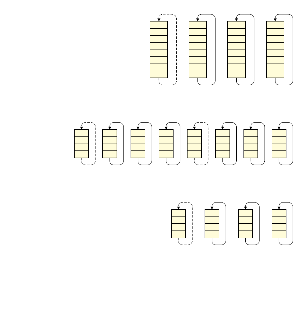
Appendix D11 VFP Vector Operation Support
D11.3 VFP register banks
D11-2498 Copyright © 1996-1998, 2000, 2004-2012, 2014 ARM. All rights reserved. ARM DDI 0406C.c
Non-Confidential ID051414
D11.3 VFP register banks
The Advanced SIMD and VFP registers are divided into banks as follows:
• The single-precision registers are divided into four banks of eight. This is shown in Figure D11-1. The first
bank is a scalar bank, and the other three are vector banks.
• In a processor with 32 double-precision registers, the double-precision registers are divided into eight banks
of four. This is shown in Figure D11-2. The first and fifth banks are scalar banks, and the other six are vector
banks.
• In a processor with 16 double-precision registers, the double-precision registers are divided into four banks
of four. This is shown in Figure D11-3. The first bank is a scalar bank, and the other three are vector banks.
Figure D11-1 Register banks, single-precision
Figure D11-2 Register banks, 32 double-precision registers, VFP
Figure D11-3 Register banks, 16 double-precision registers, VFP
s0
s7
s6
s5
s4
s3
s2
s1
s8
s15
s14
s13
s12
s11
s10
s9
s16
s23
s22
s21
s20
s19
s18
s17
s24
s31
s30
s29
s28
s27
s26
s25
Scalar
bank
Vector
bank
Vector
bank
Vector
bank
d31
d30
d29
d28
Vector
bank
d27
d26
d25
d24
d23
d22
d21
d20
d19
d18
d17
d16
d15
d14
d13
d12
d11
d10
d9
d8
d7
d6
d5
d4
d3
d2
d1
d0
Vector
bank
Vector
bank
Scalar
bank
Vector
bank
Vector
bank
Vector
bank
Scalar
bank
d15
d14
d13
d12
d11
d10
d9
d8
d7
d6
d5
d4
d3
d2
d1
d0
Vector
bank
Vector
bank
Vector
bank
Scalar
bank

Appendix D11 VFP Vector Operation Support
D11.4 VFP instruction type selection
ARM DDI 0406C.c Copyright © 1996-1998, 2000, 2004-2012, 2014 ARM. All rights reserved. D11-2499
ID051414 Non-Confidential
D11.4 VFP instruction type selection
Table D11-2 shows how the selection of registers in an instruction controls the operation of the instruction.
• If the instruction has two operands:
— If the destination register is in a scalar register bank, the operands and result are all scalars.
— If the destination register is in a vector register bank and the second operand is in a scalar bank, the
second operand is a scalar, but both the destination and the first operand are vectors. Each element of
the result is produced by an operation on the corresponding element of the first operand and the same
scalar.
— If the destination register and the second operand are both in vector register banks, the operands and
result are all vectors. Each element of the result is produced by an operation on corresponding
elements of both operands.
• If the instruction has one operand:
— If the destination register is in a scalar register bank, the operand and result are both scalars.
— If the destination register is in a vector register bank and the operand is in a scalar bank, the result is a
vector and the operand is a scalar. The result is duplicated to each element of the destination vector.
— If the destination register and the operand are both in vector register banks, the operand and result are
both vectors. Each element of the result is produced by an operation on the corresponding element of
the operand.
Some VFP instructions have three operands, but in these cases one of the operand vectors is also the result vector.
They operate in the same way as two operand instructions.
Table D11-2 Determination of VFP operation by selected register banks
Destination
register bank 1st operand
bank 2nd operand
bank Destination
type 1st operand
type 2nd operand
type
Scalar Any Any Scalar Scalar Scalar
Vector Any Scalar Vector Vector Scalar
Vector Any Vector Vector Vector Vector
Scalar Any None Scalar Scalar -
Vector Scalar None Vector Scalar -
Vector Vector None Vector Vector -

Appendix D11 VFP Vector Operation Support
D11.4 VFP instruction type selection
D11-2500 Copyright © 1996-1998, 2000, 2004-2012, 2014 ARM. All rights reserved. ARM DDI 0406C.c
Non-Confidential ID051414

ARM DDI 0406C.c Copyright © 1996-1998, 2000, 2004-2012, 2014 ARM. All rights reserved. D12-2501
ID051414 Non-Confidential
Appendix D12
ARMv6 Differences
This appendix describes how ARMv6 differs from ARMv7. It relates only to the architectural descriptions in parts
A and B of this manual. See Appendix D13 v6 Debug and v6.1 Debug Differences for information about how
ARMv6 debug differs from the description in part C of this manual.
This appendix contains the following sections:
•Introduction to ARMv6 on page D12-2502
•Application level register support on page D12-2503
•Application level memory support on page D12-2506
•Instruction set support on page D12-2510
•System level register support on page D12-2515
•System level memory model on page D12-2518
•System Control coprocessor, CP15, support on page D12-2525.
Note
In this appendix, unless otherwise stated, the description ARMvN refers to all architecture variants of ARM
architecture vN described in this manual. In particular, ARMv6 refers to all variants of ARM architecture v6,
meaning it refers to ARMv6, ARMv6K, and ARMv6T2, including ARMv6K with the Security Extensions. The
description ARMv6 base architecture refers only to the ARMv6 variant.

Appendix D12 ARMv6 Differences
D12.1 Introduction to ARMv6
D12-2502 Copyright © 1996-1998, 2000, 2004-2012, 2014 ARM. All rights reserved. ARM DDI 0406C.c
Non-Confidential ID051414
D12.1 Introduction to ARMv6
This appendix describes how, for non-debug operation, an implementation of the ARMv6 architecture differs from
the description of ARMv7 given in parts A and B of this manual.
Note
Appendix D13 v6 Debug and v6.1 Debug Differences and Appendix D14 Secure User Halting Debug describe how
ARMv6 debug differs from ARMv7 debug.
ARMv7 incorporates and extends features that were introduced as architecture extensions during the life of ARMv6,
including:
• the extension of the Thumb instruction set using Thumb-2 technology, introduced in ARMv6T2
• the optional Security Extensions, first supported by ARMv6K.
In addition, key changes introduced in ARMv7 are:
• Hierarchical cache support.
• The alternative memory system architectures are formalized into different architecture profiles:
— the ARMv7-A profile provides a Virtual Memory System Architecture (VMSA)
— the ARMv7-R profile provides a Protected Memory System Architecture (PMSA).
• The optional Advanced SIMD Extension.
• The Thumb Execution Environment (ThumbEE), that supports the ThumbEE instruction set.
From the publication of issue C.a of this manual, ARM deprecates any use of ThumbEE instructions.
This appendix summarizes the features supported in ARMv6, highlighting:
• the similarities and differences relative to ARMv7
• legacy support for ARMv4 and ARMv5.
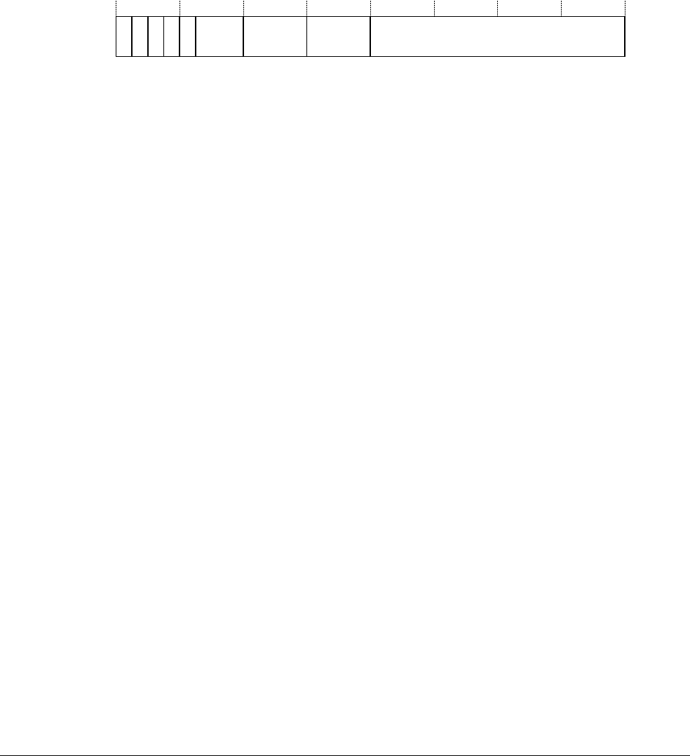
Appendix D12 ARMv6 Differences
D12.2 Application level register support
ARM DDI 0406C.c Copyright © 1996-1998, 2000, 2004-2012, 2014 ARM. All rights reserved. D12-2503
ID051414 Non-Confidential
D12.2 Application level register support
The ARMv6 core registers are the same as the ARMv7 core registers. For more information, see ARM core registers
on page A2-45. The following sections give more information about ARMv6 application level register support:
•APSR support
•Instruction set state.
D12.2.1 APSR support
Application Program Status Register (APSR) support in ARMv6 is identical to ARMv7. Program status is reported
in the 32-bit APSR. The APSR bit assignments are:
See The Application Program Status Register (APSR) on page A2-49 for the APSR bit definitions.
Earlier versions of this manual do not use the term APSR. They refer to the APSR as the CPSR with restrictions
on reserved fields determined by whether the access to the register is unprivileged, or at a higher privilege level.
D12.2.2 Instruction set state
Instruction set state support in ARMv6 is in general the same as the support available in ARMv7. The only
differences are that:
• ThumbEE state is not supported in ARMv6. It is introduced in ARMv7.
• In ARMv6 and ARMv6K, but not in ARMv6T2, when the processor is in executing at PL1, software must
not attempt to change the instruction set state by writing nonzero values to CPSR.{J. T} with an
MSR
instruction. For more information, see Format of the CPSR and SPSRs on page D12-2516.
All ARMv6 implementations support the ARM instruction set. The ARMv6 base architecture and ARMv6K also
support a subset of the Thumb instruction set that can be executed entirely as 16-bit instructions. The only 32-bit
instructions in this subset are restricted-range versions of the
BL
and
BLX
(immediate) instructions. See BL and BLX
(immediate) instructions, before ARMv6T2 on page D12-2504 for a description of how these instructions can be
executed as 16-bit instructions.
The supported ARM and Thumb instructions in the ARMv6 base architecture and ARMv6K are summarized in
Instruction set support on page D12-2510, and the instruction descriptions in Chapter A8 Instruction Descriptions
give details of the architecture variants that support each instruction encoding.
Jazelle state is supported as in ARMv7. For more information, see:
•Jazelle direct bytecode execution support on page A2-97, for application level information
•Jazelle direct bytecode execution on page B1-1241, for system level information.
ARMv6T2 supports the full Thumb instruction set, apart from a few instructions that are introduced in ARMv7.
Interworking
In ARMv6, the instructions that provide interworking branches between ARM and Thumb states are:
•
BL
and
BLX
•
LDR
,
LDM
, and
POP
instructions that load the PC.
In ARMv7, the following ARM instructions also perform interworking branches if their destination register is the
PC and the
S
option is not specified:
•
ADC
,
ADD
,
AND
,
ASR
,
BIC
,
EOR
,
LSL
,
LSR
,
MOV
,
MVN
,
ORR
,
ROR
,
RRX
,
RSB
,
RSC
,
SBC
, and
SUB
.
The instructions do not perform interworking branches in ARMv6, and the corresponding Thumb instructions do
not perform interworking branches in either ARMv6 or ARMv7. This functionality is described by the
ALUWritePC()
pseudocode function. See Pseudocode details of operations on ARM core registers on page A2-47.
Reserved, UNKNOWN/SBZPN
31 30 29 28 27 26 24 23 20 19 16 15 0
ZCVQ Reserved,
UNK/SBZP GE[3:0]
RAZ/
SBZP
Appendix D12 ARMv6 Differences
D12.2 Application level register support
D12-2504 Copyright © 1996-1998, 2000, 2004-2012, 2014 ARM. All rights reserved. ARM DDI 0406C.c
Non-Confidential ID051414
BL and BLX (immediate) instructions, before ARMv6T2
In implementations that support the Thumb instruction set but do not include Thumb-2 technology, meaning
ARMv4T, ARMv5T, ARMv5TE, ARMv5TEJ, ARMv6, and ARMv6K implementations, the
BL
and
BLX
(immediate) instructions are the only 32-bit Thumb instructions, and the maximum range of the branches that they
specify is restricted to approximately ±4MB. This means that:
• each of the two halfwords of these instructions has top five bits
0b11101
,
0b11110
, or
0b11111
• it is possible to execute the two halfwords as separate 16-bit instructions.
The following descriptions use the format described in Instruction encodings on page A8-282, except that they:
• name the encodings H1, H2 and H3
• have pseudocode that defines the entire operation of the instruction, instead of separate encoding-specific
pseudocode and Operation pseudocode.
When the two halfwords of a
BL
or
BLX
(immediate) instruction are executed separately, their behavior is as follows:
LR = PC + SignExtend(imm11:Zeros(12), 32);
next_instr_addr = PC - 2;
BranchWritePC(LR + ZeroExtend(imm11:'0', 32));
LR = next_instr_addr<31:1> : '1';
if op == '0' then
next_instr_addr = PC - 2;
SelectInstrSet(InstrSet_ARM);
BranchWritePC(Align(LR,4) + ZeroExtend(imm10:'00', 32));
LR = next_instr_addr;
else
UNDEFINED;
An encoding H1 instruction must be followed by an encoding H2 or encoding H3 instruction. Similarly, an encoding
H2 or encoding H3 instruction must be preceded by an encoding H1 instruction. Otherwise, the behavior is
UNPREDICTABLE.
Note
When assembling Thumb instructions for an implementation that supports the Thumb instruction set but does not
include Thumb-2 technology:
•
BL <label>
assembles as H1 followed by H2
•
BLX <label>
assembles as H1 followed by H3.
Encoding H1 ARMv4T, ARMv5T*, ARMv6, ARMv6K Used for
BL
and
BLX
No disassembly syntax First of two 16-bit instructions
Encoding H2 ARMv4T, ARMv5T*, ARMv6, ARMv6K Used for
BL
No disassembly syntax Second of two 16-bit instructions
Encoding H3 ARMv5T*, ARMv6, ARMv6K Used for
BLX
No disassembly syntax Second of two 16-bit instructions
1 1 1 1 0 imm11
15 14 13 12 11 10 9 8 7 6 5 4 3 2 1 0
1 1 1 1 1 imm11
15 14 13 12 11 10 9 8 7 6 5 4 3 2 1 0
op1 1 1 0 1 imm10
15 14 13 12 11 10 9 8 7 6 5 4 3 2 1 0

Appendix D12 ARMv6 Differences
D12.2 Application level register support
ARM DDI 0406C.c Copyright © 1996-1998, 2000, 2004-2012, 2014 ARM. All rights reserved. D12-2505
ID051414 Non-Confidential
It is IMPLEMENTATION DEFINED whether processor exceptions can occur between the two instructions of a
BL
or
BLX
pair. If they can, the ARM exception return instructions must be able to return correctly to the second instruction of
the pair. The exception handler does not have to take special precautions. See Exception return on page B1-1194 for
the definition of exception return instructions.
Note
There are no Thumb exception return instructions in the architecture versions that support separate execution of the
two halfwords of
BL
and
BLX
(immediate) instructions. Also, the ARM
RFE
instruction is only defined from ARMv6
onwards.

Appendix D12 ARMv6 Differences
D12.3 Application level memory support
D12-2506 Copyright © 1996-1998, 2000, 2004-2012, 2014 ARM. All rights reserved. ARM DDI 0406C.c
Non-Confidential ID051414
D12.3 Application level memory support
Memory support covers address alignment, endianness support, semaphore support, memory order model, and
caches. The following sections give an application level description of ARMv6 memory support:
•Alignment
•Endian support on page D12-2507
•Semaphore support on page D12-2508
•Memory model and memory ordering on page D12-2508.
D12.3.1 Alignment
ARMv6 supports:
• a legacy alignment configuration compatible with ARMv5
• the ARMv7 alignment configuration that supports unaligned loads and stores of 16-bit halfwords and 32-bit
words, and is described in Alignment support on page A3-108.
The alignment configuration is controlled by SCTLR.U. Table D12-1 shows the permitted values of SCTLR.U for
the different architecture versions.
From the introduction of ARMv6T2, ARM deprecated use of SCTLR.U == 0.
The meaning of the different possible values of SCTLR.U is:
SCTLR.U == 0
ARMv5 compatible alignment support, see Alignment on page D15-2592, except for the
LDRD
and
STRD
instructions.
LDRD
and
STRD
must be doubleword-aligned, otherwise:
•if SCTLR.A == 0, the instruction is UNPREDICTABLE
•if SCTLR.A == 1, the instruction causes an Alignment fault.
Note
The behavior of
LDRD
and
STRD
with SCTLR.A == 0 is compatible with ARMv5. When
SCTLR.A == 1, whether the alignment check is for word or doubleword alignment is:
•IMPLEMENTATION DEFINED in ARMv5
• required to be for doubleword alignment in ARMv6.
Table D12-1 SCTLR.U bit values for different architecture versions
Architecture version SCTLR.U value
Before ARMv6 0
ARMv6 0 or 1
ARMv7 1

Appendix D12 ARMv6 Differences
D12.3 Application level memory support
ARM DDI 0406C.c Copyright © 1996-1998, 2000, 2004-2012, 2014 ARM. All rights reserved. D12-2507
ID051414 Non-Confidential
SCTLR.U == 1
Unaligned access support for loads and stores of single 16-bit halfwords and 32-bit words, using the
LDR
,
LDRH
,
LDRHT
,
LDRSH
,
LDRSHT
,
LDRT
,
STRH
,
STRHT
,
STR,
and
STRT
instructions. Some of these
instructions were introduced in ARMv6T2.
The following requirements also apply:
•
LDREX
and
STREX
exclusive access instructions must be word-aligned, otherwise the instruction
generates an abort.
• In ARMv6K, an abort is generated if:
—an
LDREXH
or
STREXH
exclusive access instruction is not halfword-aligned
—an
LDREXD
or
STREXD
exclusive access instruction is not doubleword-aligned.
•
SWP
must be word-aligned, otherwise the instruction generates an abort. From ARMv6, ARM
deprecates any use of the
SWP
instruction.
• All multi-word load/store instructions must be word-aligned, otherwise the instruction
generates an abort.
• Unaligned access support only applies to Normal memory. Unaligned accesses to
Strongly-ordered or Device memory are UNPREDICTABLE.
In both configurations, setting the SCTLR.A bit forces an abort on an unaligned access.
Note
In ARMv7, SCTLR.U is always set to 1. ARMv7 alignment support is the same as ARMv6K in this configuration.
From ARMv7, use of a value of 0 for SCTLR.U is obsolete.
In common with ARMv7, all instruction fetches must be aligned.
D12.3.2 Endian support
ARMv6 supports the same Big-endian (BE) and Little-endian (LE) support model as ARMv7, see Endian support
on page A3-110. It is IMPLEMENTATION DEFINED if the legacy big-endian model (BE-32) defined for ARMv4 and
ARMv5 is also supported. For more information about BE-32 see Endian support on page D15-2593.
For configuration and control information, see Endian configuration and control on page D12-2518.
BE-32 DBGWCR Byte address select values
Using the BE-32 endianness model changes the meaning of the Byte address select values in DBGWCR[8:5]. When
using BE-32 endianness, use Table D12-2 to interpret these values. Do not use Table C3-4 on page C3-2062.
Table D12-2 Byte address select values, word-aligned address, ARMv6 BE-32 endianness
DBGWCR[8:5] value Description
0000 Watchpoint never hits
xxx1 Watchpoint hits if byte at address
DBGWVR<31:2>:'11'
is accessed
xx1x Watchpoint hits if byte at address
DBGWVR<31:2>:'10'
is accessed
x1xx Watchpoint hits if byte at address
DBGWVR<31:2>:'01'
is accessed
1xxx Watchpoint hits if byte at address
DBGWVR<31:2>:'00'
is accessed

Appendix D12 ARMv6 Differences
D12.3 Application level memory support
D12-2508 Copyright © 1996-1998, 2000, 2004-2012, 2014 ARM. All rights reserved. ARM DDI 0406C.c
Non-Confidential ID051414
D12.3.3 Semaphore support
ARM deprecates the use of the ARM semaphore instructions
SWP
and
SWPB
, in favour of the exclusive access
mechanism described in Synchronization and semaphores on page A3-114, and:
• ARMv6 provided a pair of synchronization primitives,
LDREX
and
STREX
in the ARM instruction set
• ARMv6T2 adds the
LDREX
and
STREX
instructions to the Thumb instruction set
• ARMv6K adds the following instructions to the ARM instruction set only:
— Clear-Exclusive,
CLREX
— byte Load-Exclusive and Store-Exclusive,
LDREXB
and
STREXB
— halfword Load-Exclusive and Store-Exclusive,
LDREXH
and
STREXH
— doubleword Load-Exclusive and Store-Exclusive,
LDREXD
and
STREXD
.
All Load-Exclusive and Store-Exclusive access instructions must be naturally aligned. An unaligned Exclusive
access instruction generates an unaligned access Data Abort exception.
D12.3.4 Memory model and memory ordering
The memory model was formalized in ARMv6. This included:
• defining Normal, Device, and Strongly-ordered memory types
• adding a Shareable memory attribute
• extending the memory attributes to support two cache policies, associated with Inner and Outer levels of
cache and including a write allocation hint capability
• adding Data Memory Barrier (DMB) and Data Synchronization Barrier (DSB) operations, to support the
formalized memory ordering requirements
• adding an Instruction Synchronization Barrier (ISB) operation, to guarantee that instructions complete
before any instructions that come after them in program order are executed.
ARMv6 provided barrier operations as CP15 c7 operations. These migrated to the ARM and Thumb instruction sets
as follows:
• ARMv6 required DMB, DSB, and ISB operations in CP15, see CP15 c7, Miscellaneous functions on
page D15-2631. The functionality of these operations is the same as that described for ARMv7 in Memory
barriers on page A3-151.
• ARMv7 adds
DMB
,
DSB
, and
ISB
instructions to the ARM and Thumb instruction sets.
ARM deprecates use of the CP15 barrier operations.
Ordering of instructions that change the CPSR interrupt masks
In ARMv6, any instruction that implicitly or explicitly changes the interrupt masks in the CPSR and appears in
program order after a Strongly-ordered access must wait for the Strongly-ordered memory access to complete.
These instructions are:
•An
MSR
with the control field mask bit set.
• The flag-setting variants of arithmetic and logical instructions with the PC as the destination register. These
instructions copy the SPSR to CPSR.
ARM deprecates any reliance on this behavior, and this behavior is obsolete from ARMv7. Instead, when
synchronization is required, include an explicit memory barrier between the memory access and the following
instruction, see Data Synchronization Barrier (DSB) on page A3-153.
Caches
For details of cache support in ARMv6, see Cache support on page D12-2519.

Appendix D12 ARMv6 Differences
D12.3 Application level memory support
ARM DDI 0406C.c Copyright © 1996-1998, 2000, 2004-2012, 2014 ARM. All rights reserved. D12-2509
ID051414 Non-Confidential
Tightly Coupled Memory support
Tightly Coupled Memory (TCM) provides low latency memory that the processor can use without the
unpredictability of caches. TCM can hold critical routines, scratchpad data, or data types with locality properties
that are not suitable for caching. An implementation can use TCM at the application or at the system level. For more
information about ARMv6 TCM support see TCM support on page D12-2520.
DMA support
Direct Memory Access (DMA) enables a peripheral to read and write data directly from and to main memory. In
ARMv6, the coherency of DMA and processor memory accesses is IMPLEMENTATION DEFINED. DMA support for
TCM is IMPLEMENTATION DEFINED.

Appendix D12 ARMv6 Differences
D12.4 Instruction set support
D12-2510 Copyright © 1996-1998, 2000, 2004-2012, 2014 ARM. All rights reserved. ARM DDI 0406C.c
Non-Confidential ID051414
D12.4 Instruction set support
ARMv6 supports the following instruction sets:
• the ARM instruction set
• the Thumb instruction set.
Note
• ARMv6 also supports the Jazelle instruction set state, see Instruction set state on page D12-2503 and the
referenced information in parts A and B of this manual.
• ARMv6 does not support ThumbEE state, and setting CPSR.{J, T} to {1, 1} has the effect described in
Unimplemented instruction sets on page B1-1155. CPSR.{J, T} might be set to {1, 1} by an exception return
that uses a modified SPSR value.
ARMv6 floating-point support, called VFPv2, is the same as that supported in ARMv5. The instructions use
coprocessors 10 and 11 and are documented with all other instructions in Alphabetical list of instructions on
page A8-300. The following VFP instructions are not supported in ARMv6. These instructions are introduced in
ARMv7, as part of VFPv3:
•
VMOV
(immediate)
•
VCVT
(between floating-point and fixed-point).
Note
• Floating point (VFP) instruction mnemonics previously started with an F. However the Unified Assembler
Language (UAL) introduced in ARMv6T2 changes this to a V prefix, and in many cases the rest of the
mnemonic is changed to be more compatible with other instructions. This aligns the scalar floating-point
instructions in the Floating-point extension with the ARMv7 Advanced SIMD instructions in the Advanced
SIMD Extension. The floating-point and Advanced SIMD instructions share some load, store, and move
instructions that access a common register file.
• The VFPv2 instructions are summarized in F*, former Floating-point instruction mnemonics on
page A8-388. This includes the two deprecated instructions in VFPv2 that do not have UAL mnemonics, the
FLDMX
and
FSTMX
instructions.
ARMv6 introduces new instructions in addition to supporting all the ARM and Thumb instructions available in
ARMv5TEJ. For more information, see Instruction set support on page D15-2597, ARM instruction set support on
page D12-2511, and Thumb instruction set support on page D12-2513.
The ARM and Thumb instruction sets grew significantly in ARMv6 and ARMv6T2, compared with
ARMv5TEJ.The changes include the addition of:
• the parallel addition and subtraction SIMD instructions
• many 32-bit Thumb instructions in ARMv6T2.
ARMv6K adds instructions associated with the optional support for energy-saving Wait For Interrupt and Wait For
Event mechanisms, and additional Load-Exclusive and Store-Exclusive instructions. It also permits the use of the
optional Security Extensions and the
SMC
instruction.
ARMv7 extends the instruction sets as defined for ARMv6 and the ARMv6 architecture variants and extensions as
follows:
• the introduction of barrier instructions to the ARM and Thumb instruction sets
• the ThumbEE Extension in ARMv7
• the new instructions added in VFPv3 and VFPv4
• the Advanced SIMD Extension in ARMv7.

Appendix D12 ARMv6 Differences
D12.4 Instruction set support
ARM DDI 0406C.c Copyright © 1996-1998, 2000, 2004-2012, 2014 ARM. All rights reserved. D12-2511
ID051414 Non-Confidential
Note
This appendix describes the instructions included as a mnemonic in ARMv6. For any mnemonic, to determine
which associated instruction encodings appear in a particular architecture variant, see the subsections of
Alphabetical list of instructions on page A8-300 that describe the mnemonic. Each encoding diagram shows the
architecture variants or extensions that include the encoding.
The following sections give more information about ARMv6 instruction set support:
•ARM instruction set support
•Thumb instruction set support on page D12-2513
•System level instruction support on page D12-2514.
D12.4.1 ARM instruction set support
ARMv6 includes all the ARM instructions present in ARMv5TEJ, see ARM instruction set support on
page D15-2598. Table D12-3 shows the ARM instruction changes in the ARMv6 base architecture.
Table D12-3 ARM instruction changes in ARMv6
Instruction ARMv6 change
CPS
Introduced
LDREX
Introduced
MCRR2
Introduced
MRRC2
Introduced
PKH
Introduced
QADD16
Introduced
QADD8
Introduced
QASX
Introduced
QSUB16
Introduced
QSUB8
Introduced
QSAX
Introduced
REV
,
REV16
,
REVSH
Introduced
RFE
Introduced
SADD8
,
SADD16
,
SASX
Introduced
SEL
Introduced
SETEND
Introduced
SHADD8
,
SHADD16
Introduced
SHSUB8
,
SHSUB16
Introduced
SMLAD
Introduced
SMLALD
Introduced
SMLSD
Introduced
SMLSLD
Introduced

Appendix D12 ARMv6 Differences
D12.4 Instruction set support
D12-2512 Copyright © 1996-1998, 2000, 2004-2012, 2014 ARM. All rights reserved. ARM DDI 0406C.c
Non-Confidential ID051414
The
SMC
instruction is added as part of the Security Extensions.
The
CLREX
,
LDREXB
,
LDREXD
,
LDREXH
,
NOP
,
SEV
,
STREXB
,
STREXD
,
STREXH
,
WFE
,
WFI
, and
YIELD
instructions are added as part
of ARMv6K.
ARM instructions introduced in ARMv6T2
ARMv6T2 adds the following ARM instructions:
BFC
,
BFI
,
LDRHT
,
LDRSBT
,
LDRSHT
,
MLS
,
MOVT
,
RBIT
,
SBFX
,
STRHT
, and
UBFX
.
SMMLA
Introduced
SMMLS
Introduced
SMMUL
Introduced
SMUAD
Introduced
SMUSD
Introduced
SRS
Introduced
SSAT
,
SSAT16
Introduced
SSUB8
,
SSUB16
,
SSAX
Introduced
STREX
Introduced
SWP
Deprecated
SWPB
Deprecated
SXTAB
,
SXTAB16
,
SXTAH
Introduced
SXTB
,
SXTB16
,
SXTH
Introduced
UADD8
,
UADD16
,
UASX
Introduced
UHADD8
,
UHADD16
,
UHASX
Introduced
UHSUB8
,
UHSUB16
,
UHSAX
Introduced
UMAAL
Introduced
UQADD8
,
UQADD16
,
UQASX
Introduced
UQSUB8
,
UQSUB16
,
UQSAX
Introduced
USAD8
,
USADA8
Introduced
USAT
,
USAT16
Introduced
USUB8
,
USUB16
,
USAX
Introduced
UXTAB
,
UXTAB16
,
UXTAH
Introduced
UXTB
,
UXTB16
,
UXTH
Introduced
Table D12-3 ARM instruction changes in ARMv6 (continued)
Instruction ARMv6 change

Appendix D12 ARMv6 Differences
D12.4 Instruction set support
ARM DDI 0406C.c Copyright © 1996-1998, 2000, 2004-2012, 2014 ARM. All rights reserved. D12-2513
ID051414 Non-Confidential
Instructions that are only in the ARM instruction set in ARMv6T2
The following ARM instructions have no Thumb equivalents in ARMv6T2:
• register-shifted forms of the
ADC
,
ADD
,
AND
,
BIC
,
CMN
,
CMP
,
EOR
,
MVN
,
ORR
,
RSB
,
SBC
,
SUB
,
TEQ
, and
TST
instructions
• all forms of the
RSC
instruction
•
LDMDA
,
LDMIB
,
STMDA
, and
STMIB
•
SWP
and
SWPB
.
ARM instructions introduced in ARMv7
The
DMB
,
DSB
,
ISB
,
PLI
,
SDIV
, and
UDIV
instructions are added in ARMv7 and are not present in any form in ARMv6.
ARMv7 implementation requirements and options for the divide instructions on page A4-172 describes the
implementation options for the
SDIV
and
UDIV
instructions, in the ARM and Thumb instruction sets.
The
DBG
hint instruction is added in ARMv7. It is UNDEFINED in the ARMv6 base architecture, and executes as a
NOP
instruction in ARMv6K and ARMv6T2.
D12.4.2 Thumb instruction set support
ARMv6 includes all the Thumb instructions present in ARMv5TE, see Thumb instruction set support on
page D15-2600. The 16-bit Thumb instructions added in the ARMv6 base architecture are:
•
CPS
•
CPY
•
REV
,
REV16
,
REVSH
•
SETEND
•
SXTB
,
SXTH
•
UXTB
,
UXTH
.
Thumb instruction set and ARMv6T2
From the ARMv6T2 version of the Thumb instruction set:
• The Thumb instruction set provides 16-bit and 32-bit instructions that are executed in Thumb state.
• Most forms of ARM instructions have an equivalent Thumb encoding. Instructions that are only in the ARM
instruction set in ARMv6T2 lists the exceptions to this in ARMv6T2.
The
CBZ
,
CBNZ
, and
IT
instructions are only in the Thumb instruction set and are introduced in ARMv6T2.
Before ARMv6T2, a
BL
or
BLX
(immediate) Thumb instruction can be executed as a pair of 16-bit instructions, rather
than as a single 32-bit instruction. For more information, see BL and BLX (immediate) instructions, before
ARMv6T2 on page D12-2504. From ARMv6T2 these instructions are always executed as a single 32-bit instruction.
From ARMv6T2, the branch range of the
BL
and
BLX
(immediate) instructions is increased from approximately
±4MB to approximately ±16MB.
Thumb instructions introduced in ARMv7
The
CLREX
,
LDREXB
,
LDREXD
,
LDREXH
,
STREXB
,
STREXD
, and
STREXH
instructions are added to the Thumb instruction set in
ARMv7. They are Thumb equivalents to the ARM instructions added in ARMv6K. These instructions are
UNDEFINED in ARMv6T2.
The
SEV
,
WFE
,
WFI
, and
YIELD
hint instructions are added to the Thumb instruction set in ARMv7. They execute as
NOP
instructions in ARMv6T2. The 16-bit encodings of the
SEV
,
WFE
,
WFI
, and
YIELD
instructions are UNDEFINED in the
ARMv6 base architecture and in ARMv6K.
The
DMB
,
DSB
,
ISB
,
PLI
,
SDIV
, and
UDIV
instructions are added in ARMv7 and are not present in any form in ARMv6.
ARMv7 implementation requirements and options for the divide instructions on page A4-172 describes the
implementation options for the
SDIV
and
UDIV
instructions, in the ARM and Thumb instruction sets.

Appendix D12 ARMv6 Differences
D12.4 Instruction set support
D12-2514 Copyright © 1996-1998, 2000, 2004-2012, 2014 ARM. All rights reserved. ARM DDI 0406C.c
Non-Confidential ID051414
The
DBG
hint instruction is added in ARMv7. It is UNDEFINED in the ARMv6 base architecture and in ARMv6K, and
executes as a
NOP
instruction in ARMv6T2.
D12.4.3 System level instruction support
The system instructions supported in ARMv6 are the same as those listed for ARMv7 in Alphabetical list of
instructions on page B9-1978, except that:
• The
ERET
instruction is added in ARMv7VE.
The Thumb encoding of
ERET
is:
—UNDEFINED in the ARMv6 base architecture and in ARMv6K
— an encoding of
SUBS PC, LR, #0
in ARMv6T2 and ARMv7.
The ARM encoding of
ERET
is UNDEFINED in versions of the architecture before ARMv7VE.
• The
HVC
,
MRS
(Banked register), and
MSR
(Banked register) instructions are added in ARMv7VE. Their
encodings are UNDEFINED in versions of the architecture before ARMv7VE.
In addition:
• the
SMC
instruction only applies to the Security Extensions
• the
VMRS
and
VMSR
instructions only apply to the Floating Point extension.
D12.4.4 Different definition of some LDM and POP instructions
This difference applies to:
•
LDM
instructions that have the base register in the register list and specify base register writeback
•
POP
instructions that load at least two registers, including the base register SP.
In ARMv6, ARM instructions of these types made the value of the base register UNKNOWN, and Thumb instructions
of these types were UNPREDICTABLE. ARM deprecates any use of ARM instructions of these types.
In ARMv7, all instructions of these types are UNPREDICTABLE.

Appendix D12 ARMv6 Differences
D12.5 System level register support
ARM DDI 0406C.c Copyright © 1996-1998, 2000, 2004-2012, 2014 ARM. All rights reserved. D12-2515
ID051414 Non-Confidential
D12.5 System level register support
The general registers and processor modes are the same as ARMv7, except that the Security Extensions and Monitor
mode are permitted only in ARMv6K. For more information, see Figure B1-2 on page B1-1144. The following
sections give information about ARMv6 system level register support:
•Program Status Registers (PSRs)
•The exception model on page D12-2516
•Jazelle direct bytecode execution support on page D12-2517
•Handling a Prefetch Abort exception taken from Jazelle state on page D12-2517.
D12.5.1 Program Status Registers (PSRs)
The Application level programmers’ model provides the Application Program Status Register, see APSR support on
page D12-2503. This is an application level alias for the Current Program Status Register (CPSR). The system level
view of the CPSR extends the register, adding state that:
• is used by exceptions
• controls the processor mode.
Each of the PL1 modes to which an exception can be taken has its own saved copy of the CPSR, the Saved Program
Status Register (SPSR), as shown in Figure B1-2 on page B1-1144. For example, the SPSR for Monitor mode is
called SPSR_mon.
The Current Program Status Register (CPSR)
The CPSR holds the following processor status and control information:
•The APSR, see APSR support on page D12-2503.
• The current instruction set state. See Instruction set state register, ISETSTATE on page A2-50, except that
ThumbEE state is not supported in ARMv6.
• The current endianness, see Endianness mapping register, ENDIANSTATE on page A2-53.
• The current processor mode.
• Interrupt and asynchronous abort disable bits.
• In ARMv6T2, the execution state bits for the Thumb If-Then instruction, see IT block state register, ITSTATE
on page A2-51.
The non-APSR bits of the CPSR have defined reset values. These are shown in the
TakeReset()
pseudocode function
described in Reset on page B1-1205, except that before ARMv6T2:
• CPSR.IT[7:0] are not defined and so do not have reset values
• the reset value of CPSR.T is 0.
The rules described in The Current Program Status Register (CPSR) on page B1-1147 about when mode changes
take effect apply with the modification that the ISB can only be the ISB operation described in CP15 c7,
Miscellaneous functions on page D12-2538.
The Saved Program Status Registers (SPSRs)
The SPSRs are defined as they are in ARMv7, see The Saved Program Status Registers (SPSRs) on page B1-1148,
except that the IT[7:0] bits are not implemented before ARMv6T2.

Appendix D12 ARMv6 Differences
D12.5 System level register support
D12-2516 Copyright © 1996-1998, 2000, 2004-2012, 2014 ARM. All rights reserved. ARM DDI 0406C.c
Non-Confidential ID051414
Format of the CPSR and SPSRs
The CPSR and SPSR bit assignments are the same as the ARMv7 assignments:
In ARMv6T2, the definitions and general rules for PSR bits and support of Non-maskable FIQs (NMFI) are the
same as ARMv7. For more information, see Format of the CPSR and SPSRs on page B1-1148 and Non-maskable
FIQs on page B1-1151.
ARMv6 and ARMv6K have the following differences:
• Bits[26:25] are RAZ/WI.
• Bits[15:10] are reserved.
• The J and T bits of the CPSR must not be changed when the CPSR is written by an
MSR
instruction, or else
the behavior is UNPREDICTABLE.
MSR
instructions exist only in ARM state in these architecture variants, so
this is equivalent to saying the
MSR
instructions executing at PL1 or higher must treat these bits as SBZP.
MSR
instructions in User mode still ignore writes to these bits.
D12.5.2 The exception model
The exception vector offsets and priorities as stated in Exception vectors and the exception base address on
page B1-1165 and Exception priority order on page B1-1169 are the same for ARMv6 and ARMv7.
See Exception return on page B1-1194 for the definition of exception return instructions.
The ARM abort model
ARMv6 and ARMv7 use a Base Restored Abort Model (BRAM), as defined in The ARM abort model on
page D15-2604.
Exception entry
Entry to exceptions in ARMv6 is generally as described in the sections:
•Reset on page B1-1205
•Undefined Instruction exception on page B1-1206
•Supervisor Call (SVC) exception on page B1-1210
•Secure Monitor Call (SMC) exception on page B1-1211
•Prefetch Abort exception on page B1-1213
•Data Abort exception on page B1-1215
•IRQ exception on page B1-1219
•FIQ exception on page B1-1222.
These ARMv7 descriptions are modified as follows:
• pseudocode statements that set registers, bits and fields that do not exist in the ARMv6 architecture variant
are ignored
•CPSR.T is set to SCTLR.TE in ARMv6T2, as described by the pseudocode, but to 0 in ARMv6 and
ARMv6K.
N
31 30 29 28 27 26 25 24 23 20 19 16 15 10 9 8 7 6 5 4 3 2 1 0
Z C V Q J Reserved,
RAZ/SBZP GE[3:0] IT[7:2] E A I F T M[4:0]
IT[1:0]
Condition flags Mask bits

Appendix D12 ARMv6 Differences
D12.5 System level register support
ARM DDI 0406C.c Copyright © 1996-1998, 2000, 2004-2012, 2014 ARM. All rights reserved. D12-2517
ID051414 Non-Confidential
Fault reporting
In previous ARM documentation, in descriptions of exceptions associated with memory system faults, the terms
precise and imprecise are used instead of synchronous and asynchronous. For details of the terminology used for
describing exceptions in ARMv7, see Terminology for describing exceptions on page B1-1137.
ARMv6 only supports synchronous reporting of external aborts on instruction fetches and translation table walks.
In ARMv7, these faults can be reported as synchronous or asynchronous aborts. Asynchronous aborts are always
reported as Data Abort exceptions.
From ARMv6, ARM deprecates the following fault status encodings:
•
0b00011
was assigned as an alignment error encoding and is re-assigned as an Access flag section fault in
ARMv6K and ARMv7
•
0b01010
was assigned as an external abort encoding and is a reserved value in ARMv7.
ARMv6 and ARMv7 provide alternative alignment and synchronous external abort error encodings that are
common to both versions of the architecture.
D12.5.3 Jazelle direct bytecode execution support
In ARMv6, the JOSCR.CV bit is not changed on exception entry in any implementation of Jazelle.
D12.5.4 Handling a Prefetch Abort exception taken from Jazelle state
As described in Prefetch Abort exceptions on page B1-1242, on a Prefetch Abort exception, LR_abt points to the
start of the instruction that caused the abort. For a Prefetch Abort exception on a multi-byte bytecode instruction
that crosses a page boundary, the Prefetch Abort exception handler must determine the faulting page. In an ARMv6
implementation, it is IMPLEMENTATION DEFINED whether an implementation includes the IFAR, and therefore the
abort handler might not be able to use the IFAR for this purpose. When the IFAR is not implemented, a Prefetch
Abort exception handler can use the following technique:
IF the page pointed to by (LR_abt – 4) is not mapped
THEN map the page
ELSE map the page following the page including (LR_abt – 4)
ENDIF
retry the instruction
Note
An OS designer must write the Prefetch Abort exception handler so it can handle a Prefetch Abort exception
generated in either of the two pages spanned by a multi-byte bytecode instruction that crosses a page boundary. To
ensure ARMv6 subarchitecture independence, such an abort handler might use the technique described in this
section.

Appendix D12 ARMv6 Differences
D12.6 System level memory model
D12-2518 Copyright © 1996-1998, 2000, 2004-2012, 2014 ARM. All rights reserved. ARM DDI 0406C.c
Non-Confidential ID051414
D12.6 System level memory model
The pseudocode listed in Aligned memory accesses on page B2-1295 and Unaligned memory accesses on
page B2-1296 covers the alignment behavior of all architecture variants from ARMv4. ARMv6 supports two
alignment models, and the SCTLR.U bit controls the alignment configuration. For more information, see Alignment
on page D12-2506.
Note
• ARMv4 and ARMv5 only support the SCTLR.U = 0 alignment model.
• ARMv7 only supports the SCTLR.U = 1 alignment model.
The following sections describe the system level memory model:
•Endian configuration and control
•Cache support on page D12-2519
•TCM support on page D12-2520
•VMSA support on page D12-2521
•PMSA on page D12-2524.
D12.6.1 Endian configuration and control
Endian control and configuration is supported by two bits in the CP15 SCTLR, and a PSR bit:
SCTLR.B BE-32 configuration bit. This bit must be RAZ/WI when BE-32 is not supported. BE-32 is the
legacy big-endian model. See Endian support on page D12-2507.
SCTLR.EE This bit updates CPSR.E on exception entry and provide endianness information for translation
table walks.
CPSR.E The bit is updated on exception entry to the value of the SCTLR.EE bit. Otherwise it is controlled
by the
SETEND
instruction. From ARMv6, ARM deprecates writing the bit using an
MSR
instruction.
Note
BE and BE-32 are mutually exclusive. When SCTLR.B is set, SCTLR.EE and CPSR.E must be clear, otherwise the
endianness behavior is UNPREDICTABLE.
Endian behavior can be configured on reset using the CFGEND[1:0] pins. Table D12-4 defines the CFGEND[1:0]
encoding and associated configurations.
Note
When an implementation does not include the CFGEND[1:0] signal, a value of
0b00
is assumed.
Table D12-4 Configuration options on reset
CFGEND[1:0] CP15 System Control Register, SCTLR PSR
EE bit U bit A bit B bit E bit
00 00000
01a
a. This configuration is reserved in implementations that do not support BE-32. In this case, the B bit is RAZ.
00010
10 01000
11 11001

Appendix D12 ARMv6 Differences
D12.6 System level memory model
ARM DDI 0406C.c Copyright © 1996-1998, 2000, 2004-2012, 2014 ARM. All rights reserved. D12-2519
ID051414 Non-Confidential
ARMv6 does not support the static instruction endianness configuration feature described in Instruction endianness
static configuration, ARMv7-R only on page A3-112.
D12.6.2 Cache support
ARMv7 can detect and manage a multi-level cache topology. ARMv6 only detects and manages level 1 caches, and
the cache type is stored in the Cache Type Register. See CP15 c0, Cache Type Register, CTR, ARMv4 and ARMv5
on page D15-2617.
In ARMv6, the L1 cache must appear to software to behave as follows:
• the entries in the cache do not need to be cleaned, invalidated, or cleaned and invalidated by software for
different virtual to physical mappings
• for memory regions that are described in the translation tables as being Cacheable, aliases to the same
physical address can exist, subject to the restrictions for 4KB small pages described in Virtual to physical
translation mapping restrictions on page D12-2523.
Note
These requirements are different from the required ARMv7 cache behavior described in Caches in a VMSA
implementation on page B3-1392.
ARMv6 defines a standard set of cache operations for level 1 instruction, data, and unified caches. The cache
operations required are:
• for an instruction cache:
— invalidate all entries
— invalidate entries by Modified Virtual Address (MVA)
— invalidate entries by set/way
• for a data cache:
— invalidate all entries, clean all entries
— invalidate entries by MVA, clean entries by MVA
— invalidate entries by set/way, clean entries by set/way
• for a unified cache:
— invalidate all entries
— invalidate entries by MVA, clean entries by MVA
— invalidate entries by set/way, clean entries by set/way
Note
In ARMv7:
• cache operations are defined as affecting the caches when the caches are disabled.
• address based cache maintenance operations are defined as affecting all memory types.
Before ARMv7 these features of the cache operations are IMPLEMENTATION DEFINED.
ARMv6 defines a number of optional cache range operations. The defined range operations are:
• for an instruction cache:
— invalidate range by VA
• for a data cache:
— invalidate range by VA
— clean range by VA
— clean and invalidate range by VA
• operations related to speculative fetches:
— prefetch instruction range by VA
— prefetch data range by VA
— stop prefetch range.

Appendix D12 ARMv6 Differences
D12.6 System level memory model
D12-2520 Copyright © 1996-1998, 2000, 2004-2012, 2014 ARM. All rights reserved. ARM DDI 0406C.c
Non-Confidential ID051414
For more information, see Block transfer operations on page D12-2536.
CP15 also supports configuration and control of cache lockdown. For details of the CP15 cache operation and
lockdown support in ARMv6, see:
•CP15 c7, Cache and branch predictor operations on page D12-2533
•CP15 c9, Cache lockdown support on page D12-2539.
Cache behavior at reset
In ARMv6, all cache lines in a cache, and all cached entries associated with branch prediction support, are
invalidated by a reset. This is different to the ARMv7 behavior described in Behavior of the caches at reset on
page B2-1269.
D12.6.3 TCM support
Tightly Coupled Memory support on page D12-2509 introduced TCMs and their use at the Application level. In
addition, TCMs can hold critical system level routines such as interrupt handlers, and critical data structures such
as interrupt stacks. Using TCMs can avoid indeterminate cache accesses.
ARMv6 supports up to four banks of data TCM and up to four banks of instruction TCM. You must program each
bank to be in a different location in the physical memory map.
ARMv6 expects TCM to be used as part of the physical memory map of the system, and not to be backed by a level
of external memory with the same physical addresses. For this reason, TCM behaves differently from a cache for
regions of memory that are marked as being Write-Through Cacheable. In such regions, a write to a memory
locations in the TCM never causes an external write.
A particular memory location must be contained either in the TCM or in the cache, and cannot be in both. In
particular, no coherency mechanisms are supported between the TCM and the cache. This means that it is important
when allocating the TCM base addresses to ensure that the same address ranges are not contained in the cache.
TCM support and VMSA
TCMs are supported in ARMv6 with VMSA support. However, there are some usage restrictions.
Restriction on translation table mappings
In a VMSA implementation, the TCM must appear to be implemented as Physically-Indexed, Physically-Addressed
memory. This means it must behave as follows:
• Entries in the TCM do not have to be cleaned or invalidated by software for different virtual to physical
address mappings.
• Aliases to the same physical address can exist in memory regions that are held in the TCM. This means the
translation table mapping restrictions for TCM are less restrictive than for cache memory. See Virtual to
physical translation mapping restrictions on page D12-2523 for cache memory restrictions.
Restriction on translation table attributes
In a VMSA implementation, the translation table entries that describe areas of memory that are handled by the TCM
can be Cacheable or Non-cacheable, but must not be marked as Shareable. If they are marked as either Device or
Strongly-ordered, or have the Shareable attribute set, the locations that are contained in the TCM are treated as being
Non-shareable, Non-cacheable.

Appendix D12 ARMv6 Differences
D12.6 System level memory model
ARM DDI 0406C.c Copyright © 1996-1998, 2000, 2004-2012, 2014 ARM. All rights reserved. D12-2521
ID051414 Non-Confidential
TCM CP15 configuration and control
In ARMv7, a TCM Type Register is required. However, its format can be compatible with ARMv6 or
IMPLEMENTATION DEFINED. For more information, see TCMTR, TCM Type Register, VMSA on page B4-1716.
In ARMv6, CP15 c0 and c9 registers configure and control the TCMs in a system. For more information, see:
•CP15 c0, TCM Type Register, TCMTR, ARMv6 on page D12-2529
•CP15 c9, TCM support on page D12-2540.
Note
In addition to the basic TCM support model in ARMv6, a set of range operations that can operate on caches and
TCMs are documented. Range operations are considered optional in ARMv6. See Block transfer operations on
page D12-2536.
The ARM Architecture Reference Manual (DDI 0100) described an ARMv6 feature called SmartCache, and a
level 1 DMA model associated with TCM support. Both of these features are considered as IMPLEMENTATION
DEFINED, and are not described in this manual.
In some implementations of ARMv4 and ARMv5, bits in the CP15 System Control Register, SCTLR[19:16] or a
subset, are used for TCM control. From ARMv6 these bits have fixed values, and no SCTLR bits are used for TCM
control.
D12.6.4 VMSA support
A key component of the VMSA is the use of translation tables. ARMv6 supports two formats of virtual memory
translation table:
• a legacy format for ARMv4 and ARMv5 compatibility
• a revised format, called the VMSAv6 format, that is also used in ARMv7.
Both table formats support use of the Fast Context Switch Extension (FCSE), but ARM deprecates use of the FCSE,
and the FCSE is optional in ARMv7. For the differences in VMSAv6 format support between ARMv6 and
ARMv6K, see VMSAv6 translation table format on page D12-2522.
Note
• ARMv7 does not support the legacy format.
• ARMv7 VMSA support, when using the Short-descriptor translation table format, is the same as that
supported by the revised format in ARMv6K, except for the removal of the address mapping restrictions
described in Virtual to physical translation mapping restrictions on page D12-2523.
• For more information about the FCSE see Appendix D10 Fast Context Switch Extension (FCSE).
Execute-never, XN
The ARMv7 requirement that instruction fetches are not made from read-sensitive devices also applies to earlier
versions of the architecture:
• ARMv7 requires you to mark all read-sensitive devices with the XN (Execute-never) attribute to ensure that
this requirement is met, see Execute-never restrictions on instruction fetching on page B3-1359
• before ARMv7, how this requirement is met is IMPLEMENTATION DEFINED.
Appendix D12 ARMv6 Differences
D12.6 System level memory model
D12-2522 Copyright © 1996-1998, 2000, 2004-2012, 2014 ARM. All rights reserved. ARM DDI 0406C.c
Non-Confidential ID051414
Legacy translation table format
ARMv6 legacy support only includes the coarse translation table type as described in Second level Coarse page
table descriptor format on page D15-2608. ARMv6 does not support the fine second level Page table format.
Therefore the legacy translation table format includes subpage access permissions but does not support 1KB Tiny
pages. Table D12-5 shows the legacy first level translation table entry formats.
Note
ARMv5TE includes optional support for Supersections, Shareable memory, and the TEX field. See Virtual memory
support on page D15-2606.
ARM deprecates use of the SCTLR.S and SCTLR.R bits described in Table D15-7 on page D15-2607. They are
implemented for use only with the legacy format translation tables, and VMSAv6 and VMSAv7 do not support their
use.
VMSAv6 translation table format
The VMSAv6 translation table format is fully compatible with the virtual memory support in ARMv7-A. It includes
the following features:
• the ability to mark a virtual address as either global or context-specific
• the ability to encode the Normal, Device, or Strongly-ordered memory type into the translation tables
• the Shareable attribute
• the XN (Execute-never) access permission attribute
• a third AP bit
• a TEX field used with the C and B bits to define the cache attributes for each page of memory
• support for an Address Space Identifier (ASID) or a global identifier
• 16MB Supersections, and the ability to map a Supersection to a 16MB range.
Related to this new translation table format, VMSAv6 provides:
• support for two translation table base registers and an associated control register
• independent fault status and fault address registers for reporting Prefetch Abort exceptions and Data Abort
exceptions
• a Context ID Register, CONTEXTIDR.
ARMv6K added the following features to VMSAv6:
• An additional access permission encoding, AP[2:0] ==
0b111
, and an associated simplified access
permissions model. See Access permissions on page B3-1356, and AP[2:1] access permissions model on
page B3-1357.
• The Access flag feature. See The Access flag on page B3-1362.
•TEX remap. See Short-descriptor format memory region attributes, with TEX remap on page B3-1368.
Table D12-5 Legacy first level descriptor format
31 2019 14 12111098 543210
Fault IGN 0 0
Coarse
page table Coarse page table base address
I
M
P
Domain SBZ 0 1
Section Section base address SBZ TEX AP
I
M
P
Domain
S
B
Z
CB1 0
Reserved 1 1

Appendix D12 ARMv6 Differences
D12.6 System level memory model
ARM DDI 0406C.c Copyright © 1996-1998, 2000, 2004-2012, 2014 ARM. All rights reserved. D12-2523
ID051414 Non-Confidential
Virtual to physical translation mapping restrictions
An ARMv6 implementation can restrict the mapping of pages that remap virtual address bits[13:12]. This
restriction, called page coloring, supports the handling of aliases by an implementation that uses VIPT caches. On
an implementation that imposes this restriction, the most significant bit of the cache size fields for the instruction
and data caches in the CTR is Read-As-One.
To avoid alias problems, this restriction enables these bits of the virtual address to be used as an index into the cache
without requiring hardware support. The restriction supports virtual indexing on caches where a cache way has a
maximum size of 16KB. There is no restriction on the number of ways supported. Cache ways of 4KB or less do
not suffer from this restriction, because any address, virtual or physical, can only be assigned to a single cache set.
Where
NSETS
is the number of sets, and
LINELEN
is the cache line length, the ARMv6 cache policy associated with
virtual indexing is:
Log
2
(NSETS×LINELEN) =< 12 ; no VI restriction
12 < Log
2
(NSETS×LINELEN) =< 14 ; VI restrictions apply
Log
2
(NSETS×LINELEN) > 14 ; PI only, VI not supported
If a page is marked as Non-shareable, then if the most significant bits of the cache size fields are RAO, the
implementation requires the remapping restriction and the following restrictions apply:
• If multiple virtual addresses are mapped onto the same physical addresses, then for all mappings bits[13:12]
of the virtual address must be equal, and must also be equal to bits[13:12] of the physical address. The same
physical address can be mapped by TLB entries of different page sizes. These can be 4KB, 64KB, or sections.
• If all mappings to a physical address are of a page size equal to 4KB, the restriction that bits[13:12] of the
virtual address must equal bits[13:12] of the physical address is not required. Bits[13:12] of all virtual address
aliases must still be equal.
There is no restriction on the more significant bits in the virtual address.
If a page is marked as Shareable and Cacheable, memory coherency must be maintained across the shareability
domain. In ARMv7, software manages instruction coherency, and data caches must be transparent. See Shareable,
Inner Shareable, and Outer Shareable Normal memory on page A3-133 for more information.
Note
In some implementations, marking areas of memory as Shareable can have substantial performance effects, because
those areas might not be held in caches.
ARMv6 and the Security Extensions
The Security Extensions provide virtual memory support for two physical address spaces as described in Secure and
Non-secure address spaces on page B3-1323 and are supported from ARMv6K. Support is the same as in ARMv7
with the following exceptions:
• ARMv6 only supports CP15 operations for virtual to physical address translation as part of the Security
Extensions. All ARMv7 VMSA implementations support these operations. For details see Virtual Address to
Physical Address translation operations on page B3-1438.
• Additional bits are allocated in the NSACR. See CP15 c1, VMSA Security Extensions support on
page D12-2531.
• When implemented, the Cache Dirty Status Register is a Banked register. See CP15 c7, Cache Dirty Status
Register, CDSR on page D12-2534.
• A Cache Behavior Override Register is defined. See CP15 c9, Cache Behavior Override Register, CBOR on
page D12-2543.
• TCM access support registers are defined. See CP15 c9, TCM Non-Secure Access Control Registers,
DTCM-NSACR and ITCM-NSACR on page D12-2545.
CP15 support for the Security Extensions in ARMv7 is defined in Classification of system control registers on
page B3-1451.

Appendix D12 ARMv6 Differences
D12.6 System level memory model
D12-2524 Copyright © 1996-1998, 2000, 2004-2012, 2014 ARM. All rights reserved. ARM DDI 0406C.c
Non-Confidential ID051414
CP15SDISABLE input
The effect of this input is described for ARMv7 in The CP15SDISABLE input on page B3-1458. In ARMv6K, TCM
support is affected as follows:
• the DTCM_NSAC and ITM_NSAC registers are added to the controlled register list
• any TCM region registers restricted to Secure access only by the NSACR settings are added to the controlled
register list.
D12.6.5 PMSA
PMSA in ARMv5 is IMPLEMENTATION DEFINED. The method described in Protected memory support on
page D15-2611 is only supported in ARMv4 and ARMv5. PMSA is formalized in ARMv6 under a different CP15
support model.
The PMSA support in ARMv6 (PMSAv6) differs from PMSAv7 in the following ways:
• PMSAv6 does not support subregions as defined in Subregions on page B5-1757.
• The default memory map shown in Table B5-1 on page B5-1759 and Table B5-2 on page B5-1759 does not
support the XN bit for restricting instruction fetches. The affected addresses are treated as Normal,
Non-cacheable in PMSAv6.
• The default memory map applies only when the MPU is disabled. The SCTLR.BR bit is not supported in
PMSAv6.
• TCM memory behaves as normal when the TCM region is enabled and the MPU is disabled.
In all other respects, PMSAv6 is as described for ARMv7 in Chapter B5 Protected Memory System Architecture
(PMSA).
Execute-never, XN
The ARMv7 requirement that instruction fetches are not made from read-sensitive devices also applies to earlier
versions of the architecture:
• ARMv7 requires software to mark all read-sensitive devices with the XN attribute to ensure that this
requirement is met, see Execute-never restrictions on instruction fetching on page B3-1359
• before ARMv7, how this requirement is met is IMPLEMENTATION DEFINED.

Appendix D12 ARMv6 Differences
D12.7 System Control coprocessor, CP15, support
ARM DDI 0406C.c Copyright © 1996-1998, 2000, 2004-2012, 2014 ARM. All rights reserved. D12-2525
ID051414 Non-Confidential
D12.7 System Control coprocessor, CP15, support
Much of the CP15 support is common to VMSAv6 and PMSAv6. However:
• some registers are unique to each memory system architecture
• some registers have different functionality in the two memory system architectures, for example the SCTLR.
The following sections summarize the ARMv6 implementations of the CP15 registers:
•Organization of CP15 registers for an ARMv6 VMSA implementation on page D12-2526
•Organization of CP15 registers for an ARMv6 PMSA implementation on page D12-2527.
The rest of this section describes the ARMv6 CP15 support in order of the CRn value. The description of each
register:
• indicates whether the register is unique to VMSA or PMSA
• indicates any differences between the two implementations if the register is included in both VMSA and
PMSA implementations.
Note
This approach is different from that taken in Part B of this manual, where:
•Functional grouping of VMSAv7 system control registers on page B3-1491 is a complete description of CP15
support in a VMSAv7 implementation
•Functional grouping of PMSAv7 system control registers on page B5-1799 is a complete description of CP15
support in a PMSAv7 implementation.
The convention used for fixed fields in the CP15 register definitions is defined in Meaning of fixed bit values in
register bit assignment diagrams on page B3-1466.
In ARMv6 the execution of an
MCR
or
MRC
instruction with an unallocated CP15 register encoding is UNPREDICTABLE.
ARMv6 provides some
MCRR
instructions to support block transfers, see Block transfer operations on
page D12-2536.
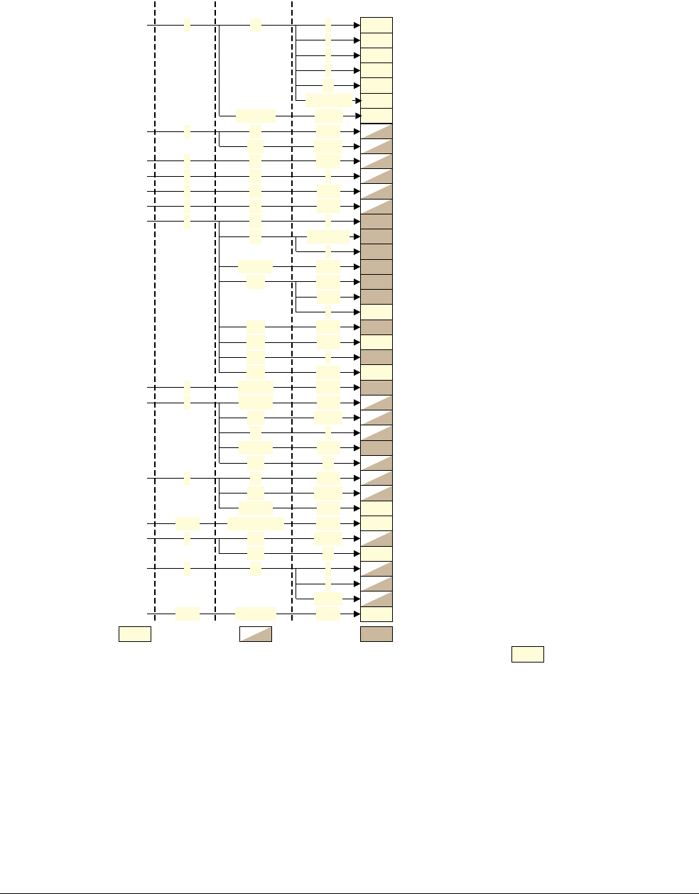
Appendix D12 ARMv6 Differences
D12.7 System Control coprocessor, CP15, support
D12-2526 Copyright © 1996-1998, 2000, 2004-2012, 2014 ARM. All rights reserved. ARM DDI 0406C.c
Non-Confidential ID051414
D12.7.1 Organization of CP15 registers for an ARMv6 VMSA implementation
Figure D12-1 shows the CP15 registers in a VMSAv6 implementation:
Figure D12-1 CP15 registers in a VMSAv6 implementation
¶
¶
¶
Read-only Read/Write Write-only Bold text = Accessible in User mode
MIDR, Main ID Register
CTR, Cache Type Register
TCMTR, TCM Type Register
TLBTR, TLB Type Register
MPIDR, Multiprocessor Affinity Register *
Aliases of Main ID Register
CPUID registers, optional
Translation Table Base Registers
DACR, Domain Access Control Register
Fault Status Registers
Fault Address Registers
CP15WFI, Wait for interrupt operation
Data barrier operations
Cache prefetch operation, optional
Cache maintenance operations
Cache and branch predictor maintenance operations
CP15ISB, Instruction barrier operation
Cache maintenance operations
Cache maintenance operations
TLB maintenance operations
Cache Lockdown (format C) and TCM Region registers
TLB Lockdown Registers
Reserved for DMA support for TCM operations
Security Extensions registers †
ISR, Interrupt Status Register †
FCSEIDR, FCSE PID Register
Software Thread ID registers *
IMPLEMENTATION DEFINED registers
CRn opc1 opc2CRm
0
{0-2,6,7}
1
2
3
*5
{4,*5,6,7}
*{0-7}
{0-2}
0
{0,1}
{0,2}
4
4
{0-2}
{0-3}
{4,5}
{0-2}
1
{0-3}
{0-2}
{0,1}
{0,1}
{0,1}
{0-7}
*{0,1}
*0
0
*{2-4}
{0-7}
c0
c5
c10
c0
*{c1-c7}
c0
c0
c0
c0
c0
{c6,c7}
c11
c13
c14
{c5-c7}
{c0,c1}
c0
{c4,c8}
{c0-c8,c15}
*c0
*c1
{c0-c15}
0
0
0
0
0
0
0
0
0
{0-7}
0
0
{0-7}
c0
c1
c2
c3
c5
c6
c7
c8
c9
c10
c11
c12
c13
c15
System control registers
Security Extensions registers †
{0-2}
*{0-2}
c0
*c1
0
6 CDSR, Cache Dirty Status register
Cache maintenance operations
¶Block transfer support operations, optional
{4,5}c12
¶
*{2,3}*c1 TCM Non-Secure Access Control Registers †
0c2 TCMSR, TCM Selection Register
{0,1}{c5,c6}
*0*c8
Cache Lockdown (format D) operations
CBOR, Cache Behavior Override Register †
*{0,1}*c2 TEX remap registers (PRRR, NMRR) *
TLB Lockdown operations and registers, optional
CONTEXTIDR, Context ID Register
1
* Not available in all versions of ARMv6 ¶Access depends on operation† If Security Extensions implemented
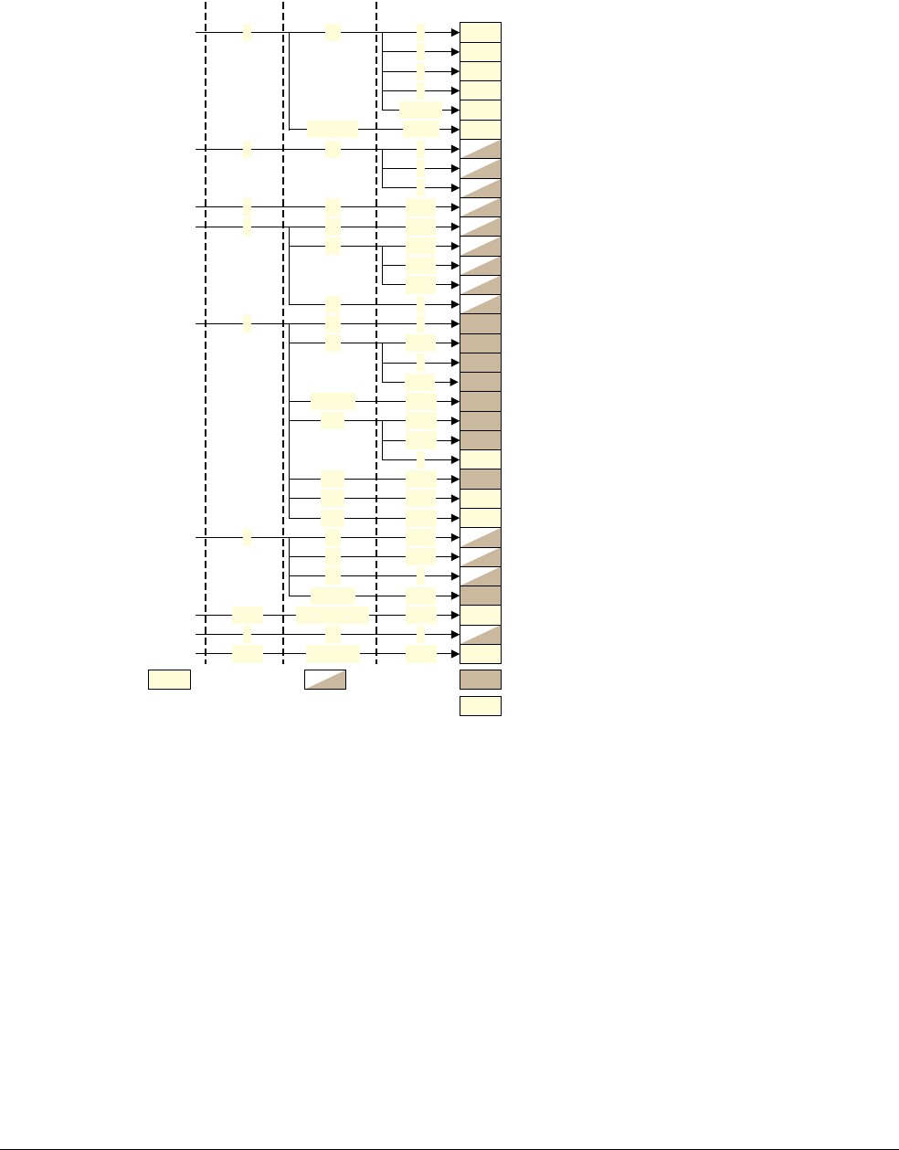
Appendix D12 ARMv6 Differences
D12.7 System Control coprocessor, CP15, support
ARM DDI 0406C.c Copyright © 1996-1998, 2000, 2004-2012, 2014 ARM. All rights reserved. D12-2527
ID051414 Non-Confidential
D12.7.2 Organization of CP15 registers for an ARMv6 PMSA implementation
Figure D12-2 shows the CP15 registers in an PMSAv6 implementation:
Figure D12-2 CP15 registers in an PMSAv6 implementation
Read-only Read/Write Write-only Bold text = Accessible in User mode
MIDR, Main ID Register
CTR, Cache Type Register
TCMTR, TCM Type Register
MPUIR, MPU Type Register
Aliases of Main ID Register
CPUID registers, optional *
0
1
2
4
{3,5-7}
*{0-7}
{0,1}
c0
*{c1-c7}
{c5,c6}
0
0
0
c0
c5
c9 Cache Lockdown (format C) operations
CRn opc1 opc2CRm
SCTLR, System Control Register
ACTLR, Auxiliary Control Register,
IMPLEMENTATION
DEFINED
CPACR, Coprocessor Access Control Register
0
1
2
c00c1
Fault Status Registers
{0,1}c0
{0,2}c00c6
Memory Region Base Address registers
{0,1}c1
{2,3} Memory Region Size and Enable registers
Memory Region Access Control registers{4,5}
RGNR, MPU Region Number Register0c2
CP15WFI, Wait For Interrupt operation4c00c7
Cache maintenance operations
{0,2}c5
CP15ISB, Instruction barrier operation
4
Branch predictor maintenance operations
{6,7}
{0-2}{c6,c7} Cache maintenance operations
{0-3}c10 Cache maintenance operations
{4-5} Data barrier operations
6 CDSR, Cache Dirty Status Register
Cache maintenance operations
{0-2}c11
¶
{4,5}c12 Block transfer operations, optional
¶
{0-3}c14 Cache maintenance operations
{0,1}c0
TCM Region registers
{0,1}c1
TCMSR, TCM Selection Register
0c2
Cache Lockdown (format D) operations
Reserved for DMA support for TCM operations
{0-7}c11 {c0-c8,c15}{0-7} ¶
CONTEXTIDR, Context ID Register
1c0c13 0
¶
IMPLEMENTATION
DEFINED
Registers
{0-7}{c0-c15}{0-7}c15
¶Access depends on the operation* Not available in all versions of ARMv6
Fault Address Registers
{4-5} Data barrier operations

Appendix D12 ARMv6 Differences
D12.7 System Control coprocessor, CP15, support
D12-2528 Copyright © 1996-1998, 2000, 2004-2012, 2014 ARM. All rights reserved. ARM DDI 0406C.c
Non-Confidential ID051414
D12.7.3 CP15 c0, ID support
ARMv6 implementations include a Main ID Register, see:
•MIDR, Main ID Register, VMSA on page B4-1649, for a VMSA implementation
•MIDR, Main ID Register, PMSA on page B6-1894, for a PMSA implementation.
In this register, the architecture variant field either takes the assigned ARMv6 value or indicates support for an
identification scheme based on a set of CPUID registers. The CPUID identification scheme is required in ARMv7
and recommended for ARMv6, and is described in Chapter B7 The CPUID Identification Scheme.
Three other ID registers provide information about cache, TCM, and TLB provisions. From ARMv6K, there is also
a Multiprocessor Affinity Register.
All of the CP15 c0 ID registers are read-only registers, They are accessed using
MRC
instructions, as shown in
Table D12-6.
The Cache Type Register is as defined for ARMv4 and ARMv5, see CP15 c0, Cache Type Register, CTR, ARMv4
and ARMv5 on page D15-2617. In ARMv6, the CType values of
0b0110
and
0b0111
are reserved and must not be
used.
Note
The ARMv6 format of the Cache Type Register is significantly different from the ARMv7 implementation
described in CTR, Cache Type Register, VMSA on page B4-1556. However, the general properties described by the
register, and the access rights for the register, are unchanged.
The TCM Type Register is defined in CP15 c0, TCM Type Register, TCMTR, ARMv6 on page D12-2529.
The TLB Type ID Register and the Multiprocessor Affinity Register are as defined for ARMv7, see:
•CP15 c0, TLB Type ID Register, TLBTR, ARMv6 on page D12-2529
•MPIDR, Multiprocessor Affinity Register, VMSA on page B4-1651, for a VMSA implementation
•MPIDR, Multiprocessor Affinity Register, PMSA on page B6-1896, for a PMSA implementation.
The MPU Type Register is as defined for ARMv7, see MPUIR, MPU Type Register, PMSA on page B6-1899. In an
ARMv6 PMSA implementation, if the MPU is not implemented use of the default memory map is optional.
Table D12-6 ID register support
Register CRn opc1 CRm opc2
MIDR, Main ID Register c0 0 c0 0
CTR, Cache Type ID Register c0 0 c0 1
TCMTR, TCM Type Register c0 0 c0 2
TLBTR, TLB Type Registera
a. VMSA processors only.
c0 0 c0 3
MPUIR, MPU Type Registercc0 0 c0 4
MPIDR, Multiprocessor Affinity Registerb
b. ARMv6K processors with VMSA only.
c0 0 c0 5
Aliases of MIDR c0 0 c0 3c, 4a, 5d, 6, 7
c. PMSA processors only.
d. All ARMv6 processors except ARMv6K VMSA implementations.
CPUID registers, if implemented c0 0 c1 0-7
c0 0 c2 0-5
Appendix D12 ARMv6 Differences
D12.7 System Control coprocessor, CP15, support
ARM DDI 0406C.c Copyright © 1996-1998, 2000, 2004-2012, 2014 ARM. All rights reserved. D12-2529
ID051414 Non-Confidential
CP15 c0, TCM Type Register, TCMTR, ARMv6
The TCMTR must be implemented in ARMv6 and ARMv7. In ARMv7, the register can have a different format
from that given here, see:
•TCMTR, TCM Type Register, VMSA on page B4-1716, for a VMSA implementation
•TCMTR, TCM Type Register, PMSA on page B6-1938, for a PMSA implementation.
In ARMv7, TCM support is IMPLEMENTATION DEFINED. For ARMv6, see CP15 c9, TCM support on
page D12-2540 and CP15 c9, TCM Non-Secure Access Control Registers, DTCM-NSACR and ITCM-NSACR on
page D12-2545 where the Security Extensions are supported.
In ARMv6, the TCMTR bit assignments are:
Bits[31:29] Set to
0b000
before ARMv7.
Bits[28:19, 15:3] Reserved, UNK.
DTCM, Bits[18:16] Indicate the number of Data TCMs implemented. This value lies in the range 0 to 4,
0b000
to
0b100
. All other values are reserved.
ITCM, Bits[2:0] Indicate the number of Instruction or Unified TCMs implemented. This value lies in the
range 0 to 4,
0b000
to
0b100
. All other values are reserved.
Instruction TCMs are accessible to both instruction and data sides.
CP15 c0, TLB Type ID Register, TLBTR, ARMv6
In an ARMv6 VMSA implementation the TLB Type Register, TLBTR, is a read-only register that defines whether
the implementation provides separate instruction and data TLBs, or a unified TLB. It also defines the number of
lockable TLB entries. The ARMv7-A description of the register describes the general features of the register and
how to access it. See TLBTR, TLB Type Register, VMSA on page B4-1721. However, the register format is different
in ARMv6. The ARMv6 TLBTR bit assignments are:
Bits[31:24, 7:1] Reserved, UNK.
I_nlock, bits[23:16] Number of lockable entries in the instruction TLB. The value of this field gives the number
of lockable entries, between
0b00000000
for no lockable entries, and
0b11111111
for 255
lockable entries.
When nU == 0 this field is reserved.
D_nlock, bits[15:8] Number of lockable entries in the data TLB. The value of this field gives the number of
lockable entries, between
0b00000000
for no lockable entries, and
0b11111111
for 255
lockable entries.
nU, bit[0] Not Unified TLB. Indicates whether the implementation has a unified TLB:
nU == 0 Unified TLB.
nU == 1 Separate instruction and data TLBs.
0
31 29 28 19 18 16 15 3 2 0
0 0 Reserved, UNK DTCM Reserved, UNK ITCM
nUReserved, UNK
31 24 23 16 15 8 7 0
I_nlock D_nlock Reserved, UNK
1
Appendix D12 ARMv6 Differences
D12.7 System Control coprocessor, CP15, support
D12-2530 Copyright © 1996-1998, 2000, 2004-2012, 2014 ARM. All rights reserved. ARM DDI 0406C.c
Non-Confidential ID051414
D12.7.4 CP15 c1, System control support
ARMv6 implements the same system control registers as ARMv7:
• for a VMSA implementation, see VMSA CP15 c1 register summary, system control registers on
page B3-1472
• for a PMSA implementation, see PMSA CP15 c1 register summary, system control registers on
page B5-1790.
CP15 c1, System Control Register, SCTLR
This register is the primary system configuration register in CP15. It is defined differently for VMSA and PMSA.
In a VMSAv6 implementation, the SCTLR bit assignments are:
In an ARMv6K VMSA implementation, the SCTLR bit assignments are:
Note
In an implementation that includes the Security Extensions, some SCTLR bits are Banked as described in SCTLR,
System Control Register, VMSA on page B4-1707.
In a PMSAv6 implementation, the SCTLR bit assignments are:
M(0)
31 30 29 28 27 26 25 24 23 22 21 20 19 18 17 16 15 14 13 12 11 10 9 8 7 6 5 4 3 2 1 0
(0) (0) U 0 0 1 (0) 1 V I Z (0) R S B 1 1 1 W C A
NMFI
TE L2
EE
VE
XP
FI
L4
RR
(0)0 0 1 1 V I Z R S B 1 1 1 W C A M
31 30 29 28 27 26 25 24 23 22 21 20 19 18 17 16 15 14 13 12 11 10 9 8 7 6 5 4 3 2 1 0
(0)
NMFI
TE
AFE
TRE
EE
VE FI HA RRL2
XP
U
L4
(0) (0)(0) M(0)
31 30 29 28 27 26 25 24 23 22 21 20 19 18 17 16 15 14 13 12 11 10 9 8 7 6 5 4 3 2 1 0
(0) (0) U 0 0 1 (0) 1 V I Z (0) B 1 1 1 W C A
NMFI
TE L2
EE
VE FI
L4
RR

Appendix D12 ARMv6 Differences
D12.7 System Control coprocessor, CP15, support
ARM DDI 0406C.c Copyright © 1996-1998, 2000, 2004-2012, 2014 ARM. All rights reserved. D12-2531
ID051414 Non-Confidential
The differences from ARMv7 are:
• ARMv6 does not support the SCTLR.IE and SCTLR.BR, bits 31 and 17.
• ARMv7 does not support:
— The L2, L4, R, S, B, and W bits. These bits provide legacy support with ARMv4 and ARMv5. See
CP15 c1, System Control Register, SCTLR, ARMv4 and ARMv5 on page D15-2621 for their definition.
The B bit must also meet the requirements defined in Endian support on page D12-2507.
— The U bit. This bit is always 1 in ARMv7. It selects the ARMv4 and ARMv5 or the ARMv6 and
ARMv7 alignment model. For details see Alignment on page D12-2506.
— The XP bit. This bit is always 1 in ARMv7. The bit selects the virtual memory support model of
ARMv6 and ARMv7 when SCTLR.XP = 1, and the legacy support for ARMv4 and ARMv5 when
SCTLRR.XP = 0. For ARMv6 and ARMv7 support, see VMSAv6 translation table format on
page D12-2522 and Chapter B3 Virtual Memory System Architecture (VMSA), and for ARMv4 and
ARMv5 support, see Legacy translation table format on page D12-2522 and Virtual memory support
on page D15-2606.
• The TE bit is defined for ARMv6T2 only. In ARMv6T2 it is the same as in ARMv7.
For the definition of bits supported in ARMv6 and ARMv7, see:
•SCTLR, System Control Register, VMSA on page B4-1707 for a VMSA implementation
•SCTLR, System Control Register, PMSA on page B6-1932 for a PMSA implementation.
D12.7.5 CP15 c1, VMSA Security Extensions support
An ARMv6 implementation that includes the Security Extensions provides:
• the Banking of bits in SCTLR, see CP15 c1, System Control Register, SCTLR on page D12-2530
• features that are include in an ARMv7 implementation of the Security Extensions, see:
—SCR, Secure Configuration Register, Security Extensions on page B4-1704
—SDER, Secure Debug Enable Register, Security Extensions on page B4-1715
—NSACR, Non-Secure Access Control Register, Security Extensions on page B4-1662
In addition, ARMv6 defines the following additional bits in the NSACR:
Bit[18], DMA DMA control register access for support in CP15 c11 in the Non-secure address space. For more
information, see CP15 c11, DMA support on page D12-2546.
Bit[17], TL TLB Lockdown Register access for support in CP15 c10 in the Non-secure address space. For
information on TLB lockdown support in ARMv6 see CP15 c10, VMSA TLB lockdown support on
page D12-2546.
Bit[16], CL Cache Lockdown Register access for support in CP15 c9 in the Non-secure address space. For
information on cache lockdown support in ARMv6 see CP15 c9, Cache lockdown support on
page D12-2539.
In all cases:
• a value of 0 in the bit position specifies that the associated registers cannot be accessed in the Non-secure
address space
• a value of 1 in the bit position specifies that the associated registers can be accessed in the Secure and
Non-secure address spaces.
Support of these additional bits and more details on how DMA support for TCMs, TLB lockdown, and cache
lockdown are inhibited in the Non-secure address space is IMPLEMENTATION DEFINED.

Appendix D12 ARMv6 Differences
D12.7 System Control coprocessor, CP15, support
D12-2532 Copyright © 1996-1998, 2000, 2004-2012, 2014 ARM. All rights reserved. ARM DDI 0406C.c
Non-Confidential ID051414
D12.7.6 CP15 c2 and c3, VMSA memory protection and control registers
ARMv6 and ARMv7 provide the same CP15 support:
• two Translation Table Base Registers, TTBR0 and TTBR1
• a Translation Table Base Control Register, TTBCR
• a Domain Access Control Register, DACR.
The translation table registers are defined in VMSA CP15 c2 and c3 register summary, Memory protection and
control registers on page B3-1473.
Note
In an implementation that includes the Security Extensions, these registers are Banked registers.
D12.7.7 CP15 c5 and c6, VMSA memory system support
The support in ARMv6 is the same as ARMv7 with the following exceptions:
• Bit 12 of the DFSR and IFSRis not defined in ARMv6.
• The Auxiliary Data Fault Status Register and the Auxiliary Instruction Fault Status Register (the AxFSRs)
are not defined in ARMv6.
• The Access flag faults shown in Table B3-23 on page B3-1415 are only supported in ARMv6K.
Note
• Before ARMv7, the DFAR was called the Fault Address Register (FAR).
• In an implementation that includes the Security Extensions, these registers are Banked registers.
• In ARMv6 variants other than ARMv6T2, the IFAR is optional.
D12.7.8 CP15 c5 and c6, PMSA memory system support
The support in ARMv6 is the same as ARMv7 with the following exceptions:
• The SCTLR.BR bit, bit[17], is not supported in ARMv6.
• Bit 12 of the DFSR and IFSRis not defined in ARMv6.
• The Auxiliary Data Fault Status Register and the Auxiliary Instruction Fault Status Register (the AxFSRs)
are not defined in ARMv6.
• Subregions are not supported. This means that DRSR[15:8] and IRSR[15:8] are not defined in ARMv6.
Note
• Before ARMv7, the DFAR was called the Fault Address Register (FAR).
• In ARMv6 variants other than ARMv6T2, the IFAR is optional.

Appendix D12 ARMv6 Differences
D12.7 System Control coprocessor, CP15, support
ARM DDI 0406C.c Copyright © 1996-1998, 2000, 2004-2012, 2014 ARM. All rights reserved. D12-2533
ID051414 Non-Confidential
D12.7.9 CP15 c6, Watchpoint Fault Address Register, DBGWFAR
From v6.1 of the Debug architecture, this register is also implemented as DBGWFAR in CP14, and ARM deprecates
the use of CP15 DBGWFAR. See DBGWFAR, Watchpoint Fault Address Register on page C11-2298 for a
description of the register.
In an ARMv6 implementation that includes the Security Extensions, CP15 DBGWFAR is a Restricted access
register, and can be accessed only from Secure PL1 modes. For more information, see Restricted access system
control registers on page B3-1453.
For more information about this register see:
• for a VMSA implementation, Data Abort on a Watchpoint debug event on page B3-1412 and Register
updates on exception reporting at PL2 on page B3-1422
• for a PMSA implementation, Data Abort exception on a Watchpoint debug event on page B5-1770
•Effect of entering Debug state on CP15 registers and the DBGWFAR on page C5-2096.
D12.7.10 CP15 c7, Cache and branch predictor operations
Table D12-8 shows the cache operations defined for ARMv6. They are performed as
MCR
instructions and only
operate on a level 1 cache associated with a specific processor. The equivalent operations in ARMv7 operate on
multiple levels of cache. See VMSA CP15 c7 register summary, Cache maintenance, address translation, and other
functions on page B3-1475. For a list of required operations in ARMv6, see Cache support on page D12-2519.
Support of additional operations is IMPLEMENTATION DEFINED.
Table D12-7 Debug fault address support
Register CRn opc1 CRm opc2
Watchpoint Fault Address Register, DBGWFAR c6 0 c0 1
Table D12-8 Cache operation support
Operation CRn opc1 CRm opc2
Invalidate instruction cacheac7 0 c5 0
Invalidate instruction cache line by MVAac7 0 c5 1
Invalidate instruction cache line by set/way c7 0 c5 2
Invalidate all branch predictorsac7 0 c5 6
Invalidate branch predictor entry by MVAac7 0 c5 7
Invalidate data cache c7 0 c6 0
Invalidate data cache line by MVAac7 0 c6 1
Invalidate data cache line by set/wayac7 0 c6 2
Invalidate unified cache, or instruction cache and data cache c7 0 c7 0
Invalidate unified cache line by MVA c7 0 c7 1
Invalidate unified cache line by set/way c7 0 c7 2
Clean data cache c7 0 c10 0
Clean data cache line by MVAac7 0 c10 1
Clean data cache line by set/wayac7 0 c10 2

Appendix D12 ARMv6 Differences
D12.7 System Control coprocessor, CP15, support
D12-2534 Copyright © 1996-1998, 2000, 2004-2012, 2014 ARM. All rights reserved. ARM DDI 0406C.c
Non-Confidential ID051414
CP15 c7, Cache Dirty Status Register, CDSR
The Cache Dirty Status Register, CDSR, indicates whether the data or unified cache has been written to since the
last successful cache clean. For more information, see Cleaning and invalidating operations for the entire data
cache on page D12-2535.
The Cache Dirty Status Register is:
• a 32-bit read-only register
• accessible only at PL1 or higher
• in an implementation that includes the Security Extensions, a Banked register.
The Cache Dirty Status Register bit assignments are:
Bits[31:1] Reserved, UNK.
C, bit[0] Cache Dirty Status. The meaning of this bit is:
0 Cache clean. No write has hit the cache since the last cache clean or reset successfully
cleaned the cache.
1 The cache might contain dirty data.
Test and Clean data cachebc7 0 c10 3
Cache Dirty Status Registercc7 0 c10 6
Clean entire unified cache c7 0 c11 0
Clean unified cache line by MVAac7 0 c11 1
Clean unified cache line by set/way c7 0 c11 2
Prefetch instruction cache line by MVAdc7 0 c13 1
Clean and Invalidate data cache c7 0 c14 0
Clean and Invalidate data cache line by MVAac7 0 c14 1
Clean and Invalidate data cache line by set/wayac7 0 c14 2
Test and Clean and Invalidate data cachebc7 0 c14 3
Clean and Invalidate unified cache line by MVA c7 0 c15 1
Clean and Invalidate unified cache line by set/way c7 0 c15 2
a. Of the ARMv6 operations shown in this table, these are the only operations available in ARMv7, see Cache
maintenance operations, functional group, VMSA on page B3-1496. In ARMv7
• the operations are multi-level operations
• the ARMv6 data cache operations are redefined as data or unified cache operations.
b. For more information about these cache operations see Test and clean operations on page D15-2630.
c. Used with the Clean or Clean and Invalidate entire data cache and entire unified cache operations.
d. VMSA implementations only, used with TLB lockdown. See The TLB lock by entry model on page D15-2638.
Table D12-8 Cache operation support (continued)
Operation CRn opc1 CRm opc2
CReserved, UNK
31 10

Appendix D12 ARMv6 Differences
D12.7 System Control coprocessor, CP15, support
ARM DDI 0406C.c Copyright © 1996-1998, 2000, 2004-2012, 2014 ARM. All rights reserved. D12-2535
ID051414 Non-Confidential
Accessing the Cache Dirty Status Register
To access the Cache Dirty Status Register, read the CP15 registers with
<opc1>
set to 0,
<CRn>
set to c7,
<CRm>
set to
c10, and
<opc2>
set to 6. For example:
MRC p15, 0, <Rt>, c7, c10, 6 ; Read Cache Dirty Status Register into Rt
Cleaning and invalidating operations for the entire data cache
The CP15 c7 encodings include operations for cleaning the entire data cache, and for performing a clean and
invalidate of the entire data cache. If these operations are interrupted, the LR value that is captured on the interrupt
is (address of instruction that launched the cache operation + 4). This permits the standard return mechanism for
interrupts to restart the operation.
If a particular operation requires that the cache is clean, or clean and invalid, then it is essential that the sequence of
instructions for cleaning or cleaning and invalidating the cache can cope with the arrival of an interrupt at any time
when interrupts are not disabled. This is because interrupts might write to a previously cleaned cache block. For this
reason, the Cache Dirty Status Register indicates whether the cache has been written to since the last successful
cache clean.
You can interrogate the Cache Dirty Status Register to determine whether the cache is clean, and if you do this while
interrupts are disabled, a subsequent operation can rely on having a clean cache. The following sequence illustrates
this approach.
; The following code assumes interrupts are enabled at this point.
Loop1
MOV R1, #0
MCR p15, 0, R1, c7, c10, 0 ; Clean data cache. For Clean and Invalidate,
; use MCR p15, 0, R1, c7, c14, 0 instead
MRS R2, CPSR ; Save PSR context
CPSID iaf ; Disable interrupts
MRC p15, 0, R1, c7, c10, 6 ; Read Cache Dirty Status Register
TST R1, #1 ; Check if it is clean
BEQ UseClean
MSR CPSR_xc, R2 ; Re-enable interrupts
B Loop1 ; Clean the cache again
UseClean
Do_Clean_Operations ; Perform whatever operation relies on
; the cache being clean or clean and invalid.
; To reduce impact on interrupt latency,
; this sequence should be short.
MCR p15, 0, R1, c7, c6, 0 ; Optional. Can use this Invalidate all command
; to invalidate a Clean loop.
MSR CPSR_xc, R2 ; Re-enable interrupts
Note
The long cache clean operation is performed with interrupts enabled throughout this routine.

Appendix D12 ARMv6 Differences
D12.7 System Control coprocessor, CP15, support
D12-2536 Copyright © 1996-1998, 2000, 2004-2012, 2014 ARM. All rights reserved. ARM DDI 0406C.c
Non-Confidential ID051414
Block transfer operations
ARMv7 does not support CP15 register block transfer operations, and they are optional in ARMv6. Table D12-9
summarizes block transfer operations. Permitted combinations of the block transfer operations are:
• all four operations
• clean, clean and invalidate, and invalidate operations
• none of the operations.
If an operation is not implemented, then it must cause an Undefined Instruction exception.
An
MCRR
instruction starts each of the range operations. The data of the two registers specifies the Block start address
and the Block end address. All block operations are performed on the cache lines that include the range of addresses
between the Block start address and Block end address inclusive. If the Block start address is greater than the Block
end address the effect is UNPREDICTABLE.
ARMv6 supports only one block transfer at a time. Attempting to start a second block transfer while a block transfer
is in progress causes the first block transfer to be abandoned and starts the second block transfer. The Block Transfer
Status Register indicates whether a block transfer is in progress. The register can be polled before starting a block
transfer, to ensure any previous block transfer operation has completed.
All block transfers are interruptible. When blocking transfers are interrupted, the LR value that is captured is
(address of instruction that launched the block operation + 4). This enables the standard return mechanism for
interrupts to restart the operation.
For performance reasons, ARM recommends that implementations permit the following instructions to be executed
while a non-blocking fetch address range instruction is being executed. In such an implementation, the LR value
captured on an interrupt is determined by the instruction set state presented to the interrupt in the following
instruction stream. However, implementations that treat a fetch address range instruction as a blocking operation
must capture the LR value as described in the previous paragraph.
If the FCSE PID is changed while a fetch address range operation is running, it is UNPREDICTABLE at which point
this change is seen by the fetch address range. For information about changing the FCSE PID see FCSEIDR, FCSE
Process ID Register, VMSA on page B4-1566.
Blocking and non-blocking behavior
The cache block transfer operations for cleaning, invalidating, or clean and invalidating a range of addresses from
the cache are blocking operations. Following instructions must not be executed until the block transfer operation
has completed. The fetch address range operation is non-blocking and can permit following instructions to be
executed before the operation is complete. If an exception occurs a non-blocking operation does not signal an
exception to the processor. This enables implementations to retire following instructions while the non-blocking
operation is executing, without the requirement to retain precise processor state.
The blocking operations generate a Data Abort exception on a Translation fault if a valid translation table entry
cannot be fetched. The DFAR indicates the address that caused the fault, and the DFSR indicates the reason for the
fault.
Any fault on a fetch address range operation results in the operation failing without signaling an error.
Table D12-9 Block transfer operations
Operation Blockinga or
non-blocking
a. See Blocking and non-blocking behavior
Instruction or
data Required privilege Exception
behavior
Prefetch range Non-blocking Instruction or data Unprivileged or PL1 None
Clean range Blocking Data only Unprivileged or PL1 Data Abort
Clean and Invalidate range Blocking Data only PL1 Data Abort
Invalidate range Blocking Instruction or data PL1 Data Abort

Appendix D12 ARMv6 Differences
D12.7 System Control coprocessor, CP15, support
ARM DDI 0406C.c Copyright © 1996-1998, 2000, 2004-2012, 2014 ARM. All rights reserved. D12-2537
ID051414 Non-Confidential
Register encodings
Table D12-10 shows the block operations supported using CP15. The operations are performed using an
MCRR
instruction. See MCRR, MCRR2 on page A8-478.
The instruction format for block operations is:
MCRR p15, <Opc>, <Rt>, <Rn>, <CRm>
Note
The ARMv6
MCRR
encodings that support block operations are UNDEFINED in ARMv7.
The range operations operate on cache lines. The first cache line operated on is the line that contains the start
address. The operation is then applied to every cache line up to and including the line that contains the end address.
The format of the start address and end address data values passed by the
MCRR
instructions is:
Start address Virtual Address bits[31:L]
The first virtual address of the block transfer.
End address Virtual Address bits[31:L]
The virtual address at which the block transfer stops. This address is at the start
of the line containing the last address to be handled by the block transfer.
L is Log2(LINELEN), where LINELEN is the cache line length parameter. Because the least significant address bits
are ignored, the transfer automatically adjusts to a line length multiple spanning the programmed addresses.
Note
The block operations use virtual addresses, not modified virtual addresses. All other address-based cache operations
use MVAs.
Table D12-10 Enhanced cache control operations using MCRR
CRm Opc Function Rn Data, VA a
a. The true virtual address, before any modification by the FCSE. See Appendix D10 Fast Context Switch Extension
(FCSE). This address is translated by the FCSE logic.
Rt Data, VA a
c5 0 Invalidate instruction cache range b
b. Accessible only from PL1. Results in an Undefined Instruction exception if the operation is attempted in User mode.
Start address End address
c6 0 Invalidate data cache range bStart address End address
c12 0 Clean data cache range c
c. Accessible in both unprivileged and PL1 modes.
Start address End address
c12 1 Prefetch instruction range cStart address End address
c12 2 Prefetch data range cStart address End address
c14 0 Clean and invalidate data cache range bStart address End address
IgnoredVirtual address
31 10
L L-1

Appendix D12 ARMv6 Differences
D12.7 System Control coprocessor, CP15, support
D12-2538 Copyright © 1996-1998, 2000, 2004-2012, 2014 ARM. All rights reserved. ARM DDI 0406C.c
Non-Confidential ID051414
CP15 c7 operations for block transfer management
Two CP15 c7 operations support block transfer management. These operations must be implemented when the
block transfer operations are implemented:
StopPrefetchRange
MCR p15, 0, <Rt>, c7, c12, 5 ; Write-only, <Rt> Should-Be-Zero
PrefetchStatus
MRC p15, 0, <Rt>, c7, c12, 4 ; Read-only, read Block Transfer Status Register
Both operations are accessible in unprivileged and PL1 modes. Because all block operations are mutually exclusive,
that is, only one operation can be active at any time, the PrefetchStatus operation returns the status of the last issued
prefetch request, instruction, or data. This status is held in the Block Transfer Status Register.
CP15 c7, Block Transfer Status Register
The Block Transfer Status Register indicates whether a block transfer is in progress.
The Block Transfer Status Register bit assignments are:
Bits[31:1] Reserved, UNK.
R, bit[0] Block fetch is Running:
0 No block fetch in operation
1 Block fetch in operation.
D12.7.11 CP15 c7, Miscellaneous functions
The Wait For Interrupt operation is used in some implementations as part of a power management support scheme.
From ARMv6, ARM deprecates any use of this operation, and the operation is not supported in ARMv7, where it
behaves as a
NOP
instruction.
Barrier operations are used for system correctness to ensure visibility of memory accesses to other agents in a
system. Barrier functionality was formally defined as part of the memory architecture enhancements introduced in
ARMv6. The definitions are the same as for ARMv7. For details see Memory barriers on page A3-151.
Table D12-11 summarizes the
MCR
instruction encoding details.
D12.7.12 CP15 c7, VMSA virtual to physical address translation support
In an ARMv6K implementation that includes the Security Extensions, virtual to physical address translation support
is provided as described in Virtual Address to Physical Address translation operations on page B3-1438.
RReserved, UNK
31 10
Table D12-11 memory barrier register support
Operation CRn opc1 CRm opc2
Wait For Interrupt, CP15WFI c7 0 c0 4
Instruction Synchronization Barrier, CP15ISBa
a. This operation was previously called Prefetch Flush (PF or PFF).
c7 0 c5 4
Data Synchronization Barrier, CP15DSBb
b. This operation was previously called Data Write Barrier or Drain Write Buffer (DWB).
c7 0 c10 4
Data Memory Barrier, CP15DMB c7 0 c10 5

Appendix D12 ARMv6 Differences
D12.7 System Control coprocessor, CP15, support
ARM DDI 0406C.c Copyright © 1996-1998, 2000, 2004-2012, 2014 ARM. All rights reserved. D12-2539
ID051414 Non-Confidential
D12.7.13 CP15 c8, VMSA TLB support
CP15 TLB operation provision in ARMv6 is the same as for ARMv7-A. For details see TLB maintenance
requirements on page B3-1381 and TLB maintenance operations, not in Hyp mode on page B4-1746.
D12.7.14 CP15 c9, Cache lockdown support
One problem with caches is that although they normally improve average access time to data and instructions, they
usually increase the worst-case access time. This occurs for a number of reasons, including:
• There is a delay before the system determines that a cache miss has occurred and starts the main memory
access.
• If a write-back cache is being used, there might be an extra delay because of the requirement to store the
contents of the cache line that is being reallocated.
• A whole cache line is loaded from main memory, not only the data requested by the ARM processor.
In real-time applications, this increase in the worst-case access time can be significant.
Cache lockdown is an optional feature designed to alleviate this. It enables critical software and data, for example
high priority interrupt routines and the data they access, to be loaded into the cache in such a way that the cache
lines containing them are not subsequently reallocated. This ensures that all subsequent accesses to the software and
data concerned are cache hits and therefore complete as quickly as possible.
From ARMv7, cache lockdown is IMPLEMENTATION DEFINED with no recommended formats or mechanisms on
how it is achieved other than reserved CP15 register space. See Cache lockdown on page B2-1270 and Cache and
TCM lockdown registers, VMSA on page B4-1753.
ARMv4 and ARMv5 specify four formats for the cache lockdown mechanism, called Format A, Format B, Format
C, and Format D. The Cache Type Register contains information on the lockdown mechanism adopted. See CP15
c0, Cache Type Register, CTR, ARMv4 and ARMv5 on page D15-2617. Formats A, B, and C all operate on cache
ways. Format D is a cache entry locking mechanism.
ARMv6 cache lockdown support must comply with Format C or Format D. For more information, see CP15 c9,
cache lockdown support on page D15-2631.
Note
A Format D implementation must use the CP15 lockdown operations with the CRm == {c5, c6} encodings, and not
the alternative encodings with CRm == {c1, c2}.
Interaction with CP15 c7 operations
Cache lockdown only prevents the normal replacement strategy used on cache misses from choosing to reallocate
cache lines in the locked-down region. CP15 c7 operations that invalidate, clean, or clean and invalidate cache
contents affect locked-down cache lines as normal. If invalidate operations are used, you must ensure that they do
not use virtual addresses or cache set/way combinations that affect the locked-down cache lines. Otherwise, if it is
difficult to avoid affecting the locked-down cache lines, repeat the cache lockdown procedure afterwards.

Appendix D12 ARMv6 Differences
D12.7 System Control coprocessor, CP15, support
D12-2540 Copyright © 1996-1998, 2000, 2004-2012, 2014 ARM. All rights reserved. ARM DDI 0406C.c
Non-Confidential ID051414
D12.7.15 CP15 c9, TCM support
In ARMv7, CP15 c9 encodings with CRm == {c0-c2, c5-c8} are reserved for IMPLEMENTATION DEFINED branch
predictor, cache, and TCM operations. In ARMv6, the TCM Type Register can determine the TCM support the
processor provides. See CP15 c0, TCM Type Register, TCMTR, ARMv6 on page D12-2529. Table D12-12
summarizes the additional register support for TCMs in ARMv6.
Each implemented TCM has its own Region register that is Banked onto either the Data TCM Region Register or
the Instruction or unified TCM Region Register. The TCM Selection Register supplies the index for region register
access.
Changing the TCM Region Register while a fetch address range or DMA operation is running has UNPREDICTABLE
effects.
CP15 c9, TCM Selection Register, TCMSR
The TCM Selection Register selects the current TCM Region Registers. Where separate data and instruction TCMs
are implemented, the value in the TCM Selection Register defined the current region for accesses to both the Data
TCM Region Register and the Instruction TCM Region Register, see Table D12-12.
The TCM Selection Register is:
• a 32-bit read/write register
• accessible only from PL1
• in an implementation that includes the Security Extensions, a Banked register.
The TCMSR bit assignments are:
Bits[31:2] Reserved, UNK/SBZP.
TCM, bits[1:0]
TCM number, the index used for accessing a region register. TCM region registers can be accessed
to read or change the details of the selected TCM.
This value resets to 0.
If this field is written with a value greater than or equal to the maximum number of implemented
TCMs then the write is ignored.
Table D12-12 TCM register support
Instruction TCM Register
MRC|MCR p15, 0, <Rt>, c9, c1, 0
Data TCM Region Register, DTCMRR
MRC|MCR p15, 0, <Rt>, c9, c1, 1
Instruction or unified TCM Region Register, ITCMRR
MRC|MCR p15, 0, <Rt>, c9, c2, 0
TCM Selection Register, TCMSR
TCMReserved, UNK/SBZP
31 10
2

Appendix D12 ARMv6 Differences
D12.7 System Control coprocessor, CP15, support
ARM DDI 0406C.c Copyright © 1996-1998, 2000, 2004-2012, 2014 ARM. All rights reserved. D12-2541
ID051414 Non-Confidential
CP15 c9, TCM Region Registers. DTCMRR and ITCMRR
The TCM Region Registers provide control and configuration information for each TCM region.
Each TCM Region Register is:
• A 32-bit read/write register with some bits that are read-only.
• Accessible only from PL1.
• In an implementation that includes the Security Extensions, a Configurable access register with Non-secure
access controlled by the DTCM-NSACR. See CP15 c9, TCM Non-Secure Access Control Registers,
DTCM-NSACR and ITCM-NSACR on page D12-2545.
• Accessed by reading or writing the CP15 registers with
<opc1>
set to 0,
<CRn>
set to c9,
<CRm>
set to c1, and
<opc2>
set to:
— 0 for the current Data TCM Region Register
— 1 for the current Instruction or unified Region Register.
For example:
MRC p15, 0, <Rt>, c9, c1, 0 ; Read current Data TCM Region Register
MCR p15, 0, <Rt>, c9, c1, 0 ; Write current Data TCM Region Register
MRC p15, 0, <Rt>, c9, c1, 1 ; Read current Instruction or unified TCM Region Register
MCR p15, 0, <Rt>, c9, c1, 1 ; Write current Instruction or unified TCM Region Register
The xTCMRR bit assignments are:
BaseAddress, bits[31:12]
The base address of the TCM, given as the physical address of the TCM in the memory map.
BaseAddress is assumed to be aligned to the size of the TCM. Any address bits in the range
[(log2(RAMSize)-1):12] are ignored.
BaseAddress is 0 at reset.
Bits[11:7] Reserved, UNK/SBZP.
Size, bits[6:2]
Indicates the size of the TCM. See Table D12-13 on page D12-2542 for encoding of this field.
This field is read-only and ignores writes.
En, bit[0] TCM enable bit:
En == 0 Disabled. This is the reset value.
En == 1 Enabled.
Note
Bit[1] was defined as a SmartCache enable bit in the previous version of the ARM architecture. SmartCache is now
considered to be IMPLEMENTATION DEFINED and not documented in this manual.
EnBaseAddress
31 12 11 7 6 2 1 0
Reserved,
UNK/SBZP Size (0)

Appendix D12 ARMv6 Differences
D12.7 System Control coprocessor, CP15, support
D12-2542 Copyright © 1996-1998, 2000, 2004-2012, 2014 ARM. All rights reserved. ARM DDI 0406C.c
Non-Confidential ID051414
Table D12-13 shows the encoding of the Size field in the TCM Region Registers:
An attempt to access a TCM region that is not implemented is UNPREDICTABLE. This can occur if the number of data
and instruction TCMs supported is not the same.
The base address of each TCM must be different, and chosen so that no location in memory is contained in more
than one TCM. If a location in memory is contained in more than one TCM, it is UNPREDICTABLE which memory
location the instruction or data is returned from. Implementations must ensure that this situation cannot result in
physical damage to the TCM.
Table D12-13 TCM size field encoding
Size field Memory size
0b00000
0KByte
0b00001
,
0b00010
Reserved
0b00011
4KByte
0b00100
8KByte
0b00101
16KByte
0b00110
32KByte
0b00111
64KByte
0b01000
128KByte
0b01001
256KByte
0b01010
512KByte
0b01011
1MByte
0b01100
2MByte
0b01101
4MByte
0b01110
8MByte
0b01111
16MByte
0b10000
32MByte
0b10001
64MByte
0b10010
128MByte
0b10011
256MByte
0b10100
512MByte
0b10101
1GByte
0b10110
2GByte
0b10111
4GByte
0b11xxx
Reserved
Appendix D12 ARMv6 Differences
D12.7 System Control coprocessor, CP15, support
ARM DDI 0406C.c Copyright © 1996-1998, 2000, 2004-2012, 2014 ARM. All rights reserved. D12-2543
ID051414 Non-Confidential
D12.7.16 CP15 c9, VMSA support for the Security Extensions
ARMv6K with VMSA support and the Security Extensions provides the following CP15 c9 support in addition to
that defined for the Security Extensions in ARMv7-A:
• a Cache Behavior Override Register, CBOR
• where instruction TCM support is implemented, an ITCM Non-Secure Access Control Register,
ITCM_NSAC
• where data TCM support is implemented, a DTCM Non-Secure Access Control Register, DTCM_NSAC.
CP15 c9, Cache Behavior Override Register, CBOR
The Cache Behavior Override Register, CBOR, overrides some aspects of the normal cache behavior. Typically,
these overrides are used for system debugging.
Note
Architecturally, the CBOR is defined only as part of the Security Extensions in ARMv6. It is IMPLEMENTATION
DEFINED whether an ARMv7-A implementation includes the CBOR. An implementation that does not include the
Security Extensions might implement the CBOR, but can implement only bits[2:0] of the register.
The CBOR is:
• a 32-bit read/write register
• accessible only from PL1
• in an implementation that includes the Security Extensions, a Common register, with some bits that can be
accessed only in Secure state.
The CBOR bit assignments are:
The CBOR resets to
0x00000000
.
Register bits[5:3] are accessible only in Secure state. In Non-secure state they are RAZ/WI.
Bits[31:6] Reserved, UNK/SBZP.
S_WT, bit[5] Secure Write-Through. Controls whether Write-Through is forced for regions marked as Secure and
Write-Back. The possible values of this bit are:
0 Do not force Write-Through. This corresponds to normal cache operation.
1 Force Write-Through for regions marked as Secure and Write-Back.
S_IL, bit[4] Secure instruction cache linefill. Setting this bit to 1 disables instruction cache linefill for Secure
regions. The possible values of this bit are:
0 Instruction cache linefill enabled. This corresponds to normal cache operation.
1 Instruction cache linefill disabled for regions marked as Secure.
Reserved, UNK/SBZP
31 6543210
S_WT
S_IL
S_DL
NS_WT
NS_IL
NS_DL

Appendix D12 ARMv6 Differences
D12.7 System Control coprocessor, CP15, support
D12-2544 Copyright © 1996-1998, 2000, 2004-2012, 2014 ARM. All rights reserved. ARM DDI 0406C.c
Non-Confidential ID051414
S_DL, bit[3] Secure data cache linefill. Setting this bit to 1 disables data cache linefill for Secure regions. The
possible values of this bit are:
0 Data cache linefill enabled. This corresponds to normal cache operation.
1 Data cache linefill disabled for regions marked as Secure.
NS_WT, bit[2]
Non-secure Write-Through. Controls whether Write-Through is forced for regions marked as
Non-secure and Write-Back. The possible values of this bit are:
0 Do not force Write-Through. This corresponds to normal cache operation.
1 Force Write-Through for regions marked as Non-secure and Write-Back.
NS_IL, bit[1] Non-secure instruction cache linefill.Setting this bit to 1 disables instruction cache linefill for
Non-secure regions. The possible values of this bit are:
0 Instruction cache linefill enabled. This corresponds to normal cache operation.
1 Instruction cache linefill disabled for regions marked as Non-secure.
NS_DL, bit[0]
Non-secure data cache linefill. Setting this bit to 1 disables data cache linefill for Non-secure
regions. The possible values of this bit are:
0 Data cache linefill enabled. This corresponds to normal cache operation.
1 Data cache linefill disabled for regions marked as Non-secure.
It might be necessary to ensure that cache contents are not changed, for example when debugging or when
processing an interruptible cache operation. The CBOR provides this option.
For example, Clean All, and Clean and Invalidate All operations in Non-secure state might not prevent FIQs to the
Secure side if the FW bit in the SCR is set to 0. In this case, operations in the Secure state can read or write
Non-secure locations in the cache. Such operations might cause the cache to contain valid or dirty Non-secure
entries after the Non-secure Clean All and Clean and Invalidate All operation has completed. To prevent this
problem, the Secure state must be:
• prevented from allocating Non-secure entries into the cache by disabling Non-secure linefill
• made to treat all writes to Non-secure regions that hit in the cache as being write-though by forcing
Non-secure Write-Through.
The CBOR provides separate controls for Secure and Non-secure memory regions, and can prevent cache linefill,
or force Write-Through operation, while leaving the caches enabled. The controls for Secure memory regions can
be accessed only when the processor is in the Secure state.
Accessing the CBOR
To access the CBOR, read or write the CP15 registers with
<opc1>
set to 0,
<CRn>
set to c9,
<CRm>
set to c8, and
<opc2>
set to 0. For example:
MRC p15, 0, <Rt>, c9, c8, 0 ; Read CP15 Cache Behavior Override Register
MCR p15, 0, <Rt>, c9, c8, 0 ; Write CP15 Cache Behavior Override Register

Appendix D12 ARMv6 Differences
D12.7 System Control coprocessor, CP15, support
ARM DDI 0406C.c Copyright © 1996-1998, 2000, 2004-2012, 2014 ARM. All rights reserved. D12-2545
ID051414 Non-Confidential
CP15 c9, TCM Non-Secure Access Control Registers, DTCM-NSACR and ITCM-NSACR
The Data TCM Non-Secure Access Control Register (DTCM-NSACR) defines the accessibility of the Data TCM
Region Register when the processor is in Non-secure state.
The Instruction TCM Non-Secure Access Control Register (ITCM-NSACR) defines the accessibility of the current
Instruction or Unified TCM Region Register when the processor is in Non-secure state.
For information on TCM support, see TCM support on page D12-2520.
The TCM-NSACRs are:
• 32-bit read/write registers
• accessible only from PL1
• implemented only in a VMSAv6 implementation that includes the Security Extensions
• Restricted access registers, see Restricted access system control registers on page B3-1453.
The format of an xTCM-NSACR is:
Bits[31:1] Reserved, UNK/SBZP.
NS_access, bit[0]
Non-secure access. Defines the accessibility of the corresponding current TCM Region Register
from the Non-secure state. The possible values of this bit are:
0 The corresponding TCM Region Register is accessible only in Secure PL1 modes.
The information stored in the corresponding TCM is Secure, and the TCM is visible
only if the processor is in the Secure state and the translation table is marked as Secure.
1 The corresponding TCM Region Register is accessible from PL1 in both Secure and
Non-secure state.
The information stored in the corresponding TCM is Non-secure. The TCM is visible
in the Non-secure state. It is visible in the Secure state only if the translation table is
marked correctly as Non-secure.
The value of the TCM-NSACR.NS_access bit and the processor security state determine whether the TCM is
visible. The value of the NS bit for the translation table entry determines what data is visible in the TCM.
Table D12-14 shows when the TCM is visible, and what data is visible.
Table D12-14 Visibility of TCM and TCM data
Processor
security state TCM-NSACR
NS_access bit Translation table
NS value TCM visibility Data visible
Secure 0 0 Visible Secure
Secure 0 1 Not visible -
Secure 1 0 Not visible -
Secure 1 1 Visible Non-secure
Non-secure 0 x Not visible -
Non-secure 1 x Visible Non-secure
Reserved, UNK/SBZP
31 10
NS_access

Appendix D12 ARMv6 Differences
D12.7 System Control coprocessor, CP15, support
D12-2546 Copyright © 1996-1998, 2000, 2004-2012, 2014 ARM. All rights reserved. ARM DDI 0406C.c
Non-Confidential ID051414
Table D12-15 shows when the TCM Region Register can be accessed, permitting control of the TCM.
Accessing the TCM-NSACRs
To access the TCM-NSACRs, read or write the CP15 registers with
<opc1>
set to 0,
<CRn>
set to c9,
<CRm>
set to c1,
and
<opc2>
set to:
• 2 to access the DTCM-NSACR
• 3 to access the ITCM-NSACR.
For example
MRC p15, 0, <Rt>, c9, c1, 2 ; Read CP15 Data TCM Non-Secure Access Control Register
MCR p15, 0, <Rt>, c9, c1, 2 ; Write CP15 Data TCM Non-Secure Access Control Register
MRC p15, 0, <Rt>, c9, c1, 3 ; Read CP15 Instruction TCM Non-Secure Access Control Register
MCR p15, 0, <Rt>, c9, c1, 3 ; Write CP15 Instruction TCM Non-Secure Access Control Register
D12.7.17 CP15 c10, VMSA memory remapping support
ARMv7-A memory remapping is supported from ARMv6K with the addition of the SCTLR.TRE enable bit and the
PRRR and NMRR.
D12.7.18 CP15 c10, VMSA TLB lockdown support
TLB lockdown is an optional feature that enables the results of specified translation table walks to be loaded into
the TLB, in such a way that they are not overwritten by the results of subsequent translation table walks.
Translation table walks can take a long time, especially as they involve potentially slow main memory accesses. In
real-time interrupt handlers, translation table walks caused by the TLB not containing translations for the handler
or the data it accesses can increase interrupt latency significantly.
Two basic lockdown models are supported:
• a TLB lock by entry model
• a translate and lock model introduced as an alternative model in ARMv5TE.
From ARMv7-A, TLB lockdown is IMPLEMENTATION DEFINED with no recommended formats or mechanisms on
how it is achieved other than reserved CP15 register space. See TLB lockdown on page B3-1379 and VMSA CP15
c10 register summary, memory remapping and TLB control registers on page B3-1478.
For ARMv6, TLB lockdown must comply with one of the lockdown models described in CP15 c10, TLB lockdown
support, VMSA on page D15-2638.
D12.7.19 CP15 c11, DMA support
ARM considers the ARMv6 DMA support for TCMs described in The ARM Architecture Reference Manual (DDI
0100) as an IMPLEMENTATION DEFINED feature, and therefore it is not included in this manual. This means that,
architecturally, ARMv6 is the same as ARMv7. See VMSA CP15 c11 register summary, reserved for TCM DMA
registers on page B3-1478.
Table D12-15 Accessibility of TCM Region Register
Processor security state TCM-NSACR NS_access bit TCM Region Register access
Secure x From PL1 only
Non-secure 0 No access
Non-secure 1 From PL1 only

Appendix D12 ARMv6 Differences
D12.7 System Control coprocessor, CP15, support
ARM DDI 0406C.c Copyright © 1996-1998, 2000, 2004-2012, 2014 ARM. All rights reserved. D12-2547
ID051414 Non-Confidential
D12.7.20 CP15 c12, VMSA support for the Security Extensions
CP15 c12 support for the Security Extensions in ARMv6 is the same as in ARMv7:
• the Vector Base Address Register, VBAR
• the Monitor Base Address Register, MVBAR
• the Interrupt Status Register, ISR.
For details see VMSA CP15 c12 register summary, Security Extensions registers on page B3-1479.
D12.7.21 CP15 c13, Context ID support
Both PMSAv6 and VMSAv6 require the CONTEXTIDR described in:
•CONTEXTIDR, Context ID Register, VMSA on page B4-1548, for a VMSA implementation
•CONTEXTIDR, Context ID Register, PMSA on page B6-1829, for a PMSA implementation.
In addition:
• A VMSAv6 implementation requires the FCSEIDR. In ARMv6 the FCSE must be implemented. For more
information, see Appendix D10 Fast Context Switch Extension (FCSE).
• An ARMv6K implementation requires the Software Thread ID registers described in VMSA CP15 c13
register summary, Process, context and thread ID registers on page B3-1479.
Note
In ARMv6, after any change to the CONTEXTIDR or FCSEIDR, software must use the CP15 branch predictor
maintenance operations to flush the virtual addresses affected by the change. If the branch predictor is not
invalidated in this way, attempting to execute an old branch might cause UNPREDICTABLE behavior. ARMv7 does
not require branch predictors to be invalidated after a change to the CONTEXTIDR or FCSEIDR.
D12.7.22 CP15 c15, IMPLEMENTATION DEFINED
As in ARMv7, CP15 c15 is reserved for IMPLEMENTATION DEFINED use. Typically, it is used for processor-specific
runtime and test features.

Appendix D12 ARMv6 Differences
D12.7 System Control coprocessor, CP15, support
D12-2548 Copyright © 1996-1998, 2000, 2004-2012, 2014 ARM. All rights reserved. ARM DDI 0406C.c
Non-Confidential ID051414

ARM DDI 0406C.c Copyright © 1996-1998, 2000, 2004-2012, 2014 ARM. All rights reserved. D13-2549
ID051414 Non-Confidential
Appendix D13
v6 Debug and v6.1 Debug Differences
This chapter describes how the ARM debug architectures for ARMv6 differ from the v7 Debug implementation
described in part C of this manual. It contains the following sections:
•About v6 Debug and v6.1 Debug on page D13-2550
•Invasive debug authentication, v6 Debug and v6.1 Debug on page D13-2551
•Debug events, v6 Debug and v6.1 Debug on page D13-2552
•Debug exceptions, v6 Debug and v6.1 Debug on page D13-2556
•Debug state, v6 Debug and v6.1 Debug on page D13-2557
•Debug register interfaces, v6 Debug and v6.1 Debug on page D13-2561
•Reset and powerdown support on page D13-2564
•The Debug Communications Channel and Instruction Transfer Register on page D13-2565
•Non-invasive debug authentication, v6 Debug and v6.1 Debug on page D13-2566
•Sample-based profiling, v6 Debug and v6.1 Debug on page D13-2568
•The debug registers, v6 Debug and v6.1 Debug on page D13-2569
•Performance monitors, v6 Debug and v6.1 Debug on page D13-2580.

Appendix D13 v6 Debug and v6.1 Debug Differences
D13.1 About v6 Debug and v6.1 Debug
D13-2550 Copyright © 1996-1998, 2000, 2004-2012, 2014 ARM. All rights reserved. ARM DDI 0406C.c
Non-Confidential ID051414
D13.1 About v6 Debug and v6.1 Debug
This appendix describes how the ARMv6 debug architectures differ from the base v7 Debug architecture described
in part C of this manual.
ARMv6 is the first version of the ARM architecture to include debug. v6 Debug corresponds to the base ARMv6
architecture. The introduction of the ARM architecture Security Extensions extended the Debug architecture,
defining the v6.1 Debug Architecture. This means that:
• ARMv6 processors without the Security Extensions implement v6 Debug
• ARMv6 processors with the Security Extensions implement v6.1 Debug.
Note
v6.1 Debug and v6 Debug are two different versions of the Debug architecture for the ARMv6 architecture. They
might be described as:
• ARMv6, v6.1 Debug
• ARMv6, v6 Debug.
Throughout this appendix the descriptions v6.1 Debug and v6 Debug are used, for brevity.
Major differences between the ARMv6 and ARMv7 Debug architectures summarizes the main differences in the v7
Debug. Each section of this appendix then describes the differences in the corresponding chapter of part C of this
manual.
Chapter C1 Introduction to the ARM Debug Architecture generally applies also to v6 Debug and v6.1 Debug, except
that:
• ARMv7 is the first architecture version to define the Performance Monitors Extension. Performance
monitors were implemented in several processors before ARMv7, but these are not software compatible with
the ARMv7 Performance Monitors Extension.
• v6.1 Debug always supports Secure User halting debug. This means the alternatives for when a debug event
is permitted are:
— in all processor modes, in both Secure and Non-secure security state
— only in Non-secure state
— in Non-secure state and in Secure User mode.
• The register interface requirements and recommendations for v6 Debug and v6.1 Debug are different. These
debug architecture versions:
— require that software running on the processor can access the debug registers using CP14 instructions
— do not recommend the use of ADIv5 as an external debug interface
— do not support external debug over powerdown of the processor using their recommended interfaces.
D13.1.1 Major differences between the ARMv6 and ARMv7 Debug architectures
Compared to v6.1 Debug, v7 Debug introduces additional extensions to support developments in the debug
environment.
The main change in the Debug architecture is the specification of new forms of external debug interface.
ARMv6 Debug does not require a particular debug interface, but can be implemented with access from a JTAG
interface as defined in IEEE Standard Test Access Port and Boundary Scan Architecture (JTAG). However, systems
such as the ARM CoreSight™ architecture require changes in the debug interface. For more information about the
CoreSight architecture see the CoreSight Architecture Specification. ARMv7 Debug addresses some of the aims of
the CoreSight architecture, such as a more system-centric view of debug, and improved debug of powered-down
systems.
v7 Debug also introduces an architecture extension to provide performance monitors.

Appendix D13 v6 Debug and v6.1 Debug Differences
D13.2 Invasive debug authentication, v6 Debug and v6.1 Debug
ARM DDI 0406C.c Copyright © 1996-1998, 2000, 2004-2012, 2014 ARM. All rights reserved. D13-2551
ID051414 Non-Confidential
D13.2 Invasive debug authentication, v6 Debug and v6.1 Debug
A v6.1 Debug implementation must support Secure User halting debug. See Invasive debug authentication in an
implementation that supports SUHD on page D14-2583 for how this affects invasive debug authentication.
v7 Debug introduces the OS Lock mechanism, and v7.1 Debug introduces the OS Double Lock mechanism.
Therefore the effects of setting the OS Lock or OS Double Lock described in About invasive debug authentication
on page C2-2030 never apply to any v6 Debug or v6.1 Debug implementation.
v6.1 Debug supports dynamic control of debug permission, referred to in a Note in About invasive debug
authentication on page C2-2030. However, in v6 Debug, invasive debug authentication can be changed only while
the processor is in reset.
Appendix D13 v6 Debug and v6.1 Debug Differences
D13.3 Debug events, v6 Debug and v6.1 Debug
D13-2552 Copyright © 1996-1998, 2000, 2004-2012, 2014 ARM. All rights reserved. ARM DDI 0406C.c
Non-Confidential ID051414
D13.3 Debug events, v6 Debug and v6.1 Debug
v6 Debug and v6.1 Debug do not support the OS Save and Restore mechanism, and therefore they do not support
the OS Unlock catch Halting debug event. Also, the following additional information applies to Table C3-1 on
page C3-2038:
• When DBGDSCR[15:14] is
0b10
, Monitor Debug-mode selected and enabled, the processor ignores some
Software debug events.
• In v6 Debug only, when DBGDSCR[15:14] is
0b10
, Monitor Debug-mode selected and enabled, or
0b00
, no
Debug-mode selected, it is IMPLEMENTATION DEFINED whether the processor enters Debug state on a Halting
debug event, or ignores the event.
Figure D13-1 summarizes the processor behavior on debug events for these Debug architecture versions.
Figure D13-1 Processor behavior on debug events, for v6 Debug and v6.1 Debug
Debug state entry
Debug disabled or debug event not permitted
Debug state entry
Debug-mode: None
‡
‡
‡
IMPLEMENTATION
DEFINED
alternative
behavior for v6 Debug
Halting debug events
External debug
request
Halt request
Halting debug events
External debug
request
Halt request
Debug exception
(Prefetch Abort)
Debug exception
(Data Abort)
Ignored
Debug exception
(Prefetch Abort)
Debug exception
(Data Abort)
Ignored
†
†
‡
Software debug events
BKPT instruction
Breakpoint
Vector catch
Watchpoint
Software debug events
BKPT instruction
Breakpoint
Vector catch
Watchpoint
Halting debug events
External debug
request
Halt request
Debug state entry
Debug-mode: Monitor
Halting debug events
External debug
request
Halt request
Debug state entry
Debug-mode: Halting
† Some cases are ignored, see text.
‡
‡
IMPLEMENTATION
DEFINED
alternative
behavior for v6 Debug
Debug exception
(Prefetch Abort)
Debug exception
(Data Abort)
Ignored
Debug exception
(Prefetch Abort)
Debug exception
(Data Abort)
Ignored
Software debug events
BKPT instruction
Breakpoint
Vector catch
Watchpoint
Software debug events
BKPT instruction
Breakpoint
Vector catch
Watchpoint

Appendix D13 v6 Debug and v6.1 Debug Differences
D13.3 Debug events, v6 Debug and v6.1 Debug
ARM DDI 0406C.c Copyright © 1996-1998, 2000, 2004-2012, 2014 ARM. All rights reserved. D13-2553
ID051414 Non-Confidential
D13.3.1 Software debug events
This section describes the v6 Debug and v6.1 Debug differences from the information in given in About debug
events on page C3-2038. The debug registers, v6 Debug and v6.1 Debug on page D13-2569 includes other relevant
information.
Note
• Security state control is relevant only to processors that implement the Security Extensions and therefore is
not supported in v6 Debug.
• ARMv7 introduces ThumbEE state and the ThumbEE instruction set. Therefore, any references to ThumbEE
are not relevant to v6 Debug and v6.1 Debug.
Breakpoint debug events
In the section Breakpoint debug events on page C3-2041, the differences for v6 Debug and v6.1 Debug are:
• v7.1 Debug introduces VMID matching and the DBGBXVR.
• v7 Debug introduces address range masking:
— in v6 Debug and v6.1 Debug, instruction address comparisons always use byte address selection
— information given about byte address selection also applies to v6 Debug and v6.1 Debug
— the section Breakpoint address range masking behavior on page C3-2051 applies only from v7 Debug.
• v6.1 Debug introduces instruction address mismatch comparisons. v6 Debug does not support these
comparisons.
• The effects of instruction length on address comparisons are different in v6 Debug and v6.1 Debug:
—Effect of instruction length in v6 Debug and v6.1 Debug describes these effects
—Instruction address comparison programming examples for ARMv6 on page D13-2554 gives
additional programming examples.
In v6 Debug and v6.1 Debug, the processor ignores the following Breakpoint debug events if Monitor debug-mode
is configured, because they could lead to an unrecoverable state:
• Unlinked Context ID Breakpoint debug events, if the processor is running in a PL1 mode
• Linked or Unlinked instruction address mismatch Breakpoint debug events, if the processor is running in a
PL1 mode.
Effect of instruction length in v6 Debug and v6.1 Debug
In v6 Debug and v6.1 Debug:
• If the conditions in the DBGBCR are met, and the instruction is committed for execution, the breakpoint
generates a Breakpoint debug event if the required DBGBVR comparison, taking account of the byte address
selection, hits for the first unit of the instruction.
• It is IMPLEMENTATION DEFINED whether an instruction address comparison hit on the second halfword of a
Thumb instruction, following a breakpoint miss on the first halfword of the instruction, can cause a
Breakpoint debug event.
• For Java bytecodes, a breakpoint comparison hit on an operand does not generate a Breakpoint debug event.
A Breakpoint debug is generated only if the breakpoint hits on the opcode.

Appendix D13 v6 Debug and v6.1 Debug Differences
D13.3 Debug events, v6 Debug and v6.1 Debug
D13-2554 Copyright © 1996-1998, 2000, 2004-2012, 2014 ARM. All rights reserved. ARM DDI 0406C.c
Non-Confidential ID051414
Instruction address comparison programming examples for ARMv6
The examples in Instruction address comparison programming examples on page C3-2052 largely apply also to v6
Debug and v6.1 debug, but this subsection gives additional information about programming breakpoints for
instruction address comparison in these Debug architecture versions.
Before ARMv6T2, on a processor that implements the Thumb instruction set and can take an exception between the
two halfwords of a Thumb
BL
or
BLX
(immediate) instruction, a debugger must treat the two halfwords as separate
instructions, and set breakpoints on both halfwords. This might require two breakpoints.
Note
To ensure compatibility across ARMv6 implementations, a debugger can always treat
BL
or
BLX
(immediate) as two
instructions when debugging software on an ARMv6 processor before ARMv6T2.
In considering the programming examples in Instruction address comparison programming examples on
page C3-2052:
• The example for setting a breakpoint on a 32-bit Thumb instruction applies to setting breakpoints on an
ARMv7 or ARMv6T2 processor.
— To breakpoint on a 16-bit or a 32-bit Thumb or ThumbEE instruction starting at address
0x8000
, the
debugger must set DBGBVRn to
0x8000
and DBGBCRn.BAS to
0b0011
. These are the settings for
breakpointing on any Thumb instruction, including
BL
and
BLX
(immediate).
• In addition, on an ARMv6 or ARMv6K processor:
— To breakpoint on a Thumb
BL
or
BLX
instruction at address
0x8000
, a debugger must set
DBGBVRnto
0x8000
, and DBGBCRn.BAS to
0b1111
.
— To breakpoint on a Thumb
BL
or
BLX
instruction at address
0x8002
, a debugger must set DBGBVRnto
0x8000
, DBGBVRmto
0x8004
, DBGBCRn.BAS to
0b1100
, and DBGBCRm.BAS to
0b0011
.
Note
When programming DBGBVR for instruction address match or mismatch, the debugger must program
DBGBVR[1:0] to
0b00
, otherwise Breakpoint debug event generation is UNPREDICTABLE.
Watchpoint debug events
In the section Watchpoint debug events on page C3-2059, the differences for v6 Debug and v6.1 Debug are:
• v7 Debug introduces support for an 8-bit byte select field:
— In the description in Byte address selection behavior on data address match on page C3-2062, the
reference to an 8-bit byte select field cannot apply to v6 Debug and v6.1 Debug implementations.
— In v6 Debug and v6.1 Debug implementations, DBGWCR[12:9] is UNK/SBZP, and Table C3-5 on
page C3-2063 cannot apply.
• In ARMv6, when using the optional legacy BE-32 endianness model, the values of DBGWCR.BAS[3:0]
shown in Table C3-4 on page C3-2062 have different meanings. For more information see BE-32 DBGWCR
Byte address select values on page D12-2507.
• ARMv6 permits only synchronous watchpoints. The subsection Asynchronous Watchpoint debug events on
page C3-2065 is not relevant to v6 Debug and v6.1 Debug implementations.

Appendix D13 v6 Debug and v6.1 Debug Differences
D13.3 Debug events, v6 Debug and v6.1 Debug
ARM DDI 0406C.c Copyright © 1996-1998, 2000, 2004-2012, 2014 ARM. All rights reserved. D13-2555
ID051414 Non-Confidential
Vector catch debug events
In the section Vector catch debug events on page C3-2067, the differences for v6 Debug and v6.1 Debug are:
• If Monitor debug-mode is selected and enabled, and the vector is either the Prefetch Abort vector or the Data
Abort vector, the debug event is ignored in v6 Debug and v6.1 Debug. This differs from the v7 Debug
information given in the section Generation of Vector catch debug events on page C3-2068.
• In v6.1 Debug, Reset Vector catches are generated only in Secure state, see Reset Vector catch using address
matching on page C3-2073.
Note
The Security Extensions cannot be implemented with v6 Debug.
• An ARMv6 processor that implements the Security Extensions might not implement DBGVCR bits[31, 30,
28:25, 15:14, 12:10]. For such a processor:
— in Non-secure state, DBGVCR[7:6, 4:1] apply to offsets from VBARNS
— in Secure state, DBGVCR[7:6, 4:1] apply to offsets from VBARS and DBGVCR[7:6, 4:2] also apply
to offsets from MVBAR.
In v6 Debug and v6.1 Debug, the processor ignores Vector catch debug events on the Prefetch Abort and Data Abort
vectors if Monitor debug-mode is configured, because they could lead to an unrecoverable state.
D13.3.2 Halting debug events
In the section Halting debug events on page C3-2075, the differences for v6 Debug and v6.1 Debug are:
• v7 Debug introduces the DBGDRCR, and therefore v6 Debug and v6.1 Debug cannot write to this register
to cause a Halt request debug event. However, if the implementation includes the recommended ARM Debug
Interface v4, a debugger can issue a Halt request command through the JTAG interface, by placing the HALT
instruction in the IR and taking the Debug Test Access Port State Machine (Debug TAP State Machine)
through the Run-Test/Idle state.
• v6 Debug and v6.1 Debug do not support OS Unlock catch Halting debug event. This is because they do not
support the OS Save and Restore mechanism.
• In v6 Debug, when Halting debug-mode is not configured and enabled it is IMPLEMENTATION DEFINED
whether Halting debug events cause entry to Debug state, or are ignored.

Appendix D13 v6 Debug and v6.1 Debug Differences
D13.4 Debug exceptions, v6 Debug and v6.1 Debug
D13-2556 Copyright © 1996-1998, 2000, 2004-2012, 2014 ARM. All rights reserved. ARM DDI 0406C.c
Non-Confidential ID051414
D13.4 Debug exceptions, v6 Debug and v6.1 Debug
On a VMSAv6 processor in Monitor debug-mode, an exception is generated as a result of a Watchpoint debug event,
the DFSR Domain field, DFSR[7:4], is updated, and a read of this field returns valid data.

Appendix D13 v6 Debug and v6.1 Debug Differences
D13.5 Debug state, v6 Debug and v6.1 Debug
ARM DDI 0406C.c Copyright © 1996-1998, 2000, 2004-2012, 2014 ARM. All rights reserved. D13-2557
ID051414 Non-Confidential
D13.5 Debug state, v6 Debug and v6.1 Debug
In v6 Debug, when debug is enabled and Halting debug-mode is not selected it is IMPLEMENTATION DEFINED
whether a Halting debug event causes entry to Debug state. For more information, see Debug events, v6 Debug and
v6.1 Debug on page D13-2552.
D13.5.1 Entering Debug state
In the section Entering Debug state on page C5-2095, the differences for v6 Debug and v6.1 Debug are:
• In ARMv6, all CP15 registers except for the DBGWFAR are unchanged on entry to Debug state. The
unchanged registers include the IFSR, DFSR, DFAR, and IFAR. The section Effect of entering Debug state
on CP15 registers and the DBGWFAR on page C5-2096 does not apply to v6 Debug and v6.1 Debug.
• The behavior of asynchronous aborts is different, see Asynchronous aborts and Debug state on
page D13-2560.
D13.5.2 Executing instructions in Debug state
The following subsections describe how instruction execution in v6 Debug and v6.1 Debug differs from the
description given in Executing instructions in Debug state on page C5-2098.
Behavior of instructions that access the CPSR in Debug state
Behavior of MRS and MSR instructions that access the CPSR in Debug state on page C5-2099:
• applies for instructions that modify the CPSR in Debug state in v6.1 Debug.
• does not apply for v6 Debug.
Table D13-1 shows the Debug-state behavior of instructions that modify the CPSR in v6 Debug.
Table D13-1 Debug-state behavior of Instructions that modify the CPSR, v6 Debug
Instruction Behavior
BX
UNPREDICTABLE if CPSR.J is 1. Can be used to set or clear the CPSR.T bit.
BXJ
UNPREDICTABLE if either CPSR.J or CPSR.T is 1. Can be used to set CPSR.J to 1.
SETEND
UNPREDICTABLE.
CPS
UNPREDICTABLE.
<op>S PC, <Rn>, <operand>
a
<op1>S PC, <operand>
b
Can set the restart address, and set the CPSR by copying it from the SPSR of the current mode.
MSR CPSR_<fields>
cUse for setting the CPSR bits other than the execution state bits.
LDM
(exception return),
RFE
UNPREDICTABLE.
a.
<op>
is one of
ADC
,
ADD
,
AND
,
ASR
,
BIC
,
EOR
,
LSL
,
LSR
,
ORR
,
ROR
,
RSB
,
RSC
,
SBC
, or
SUB
. See SUBS PC, LR and related instructions (ARM) on
page B9-2012 for more information about the instructions and the required
<operand>
.
b.
<op1>
is one of
MOV
,
MVN
, or
RRX
. See SUBS PC, LR and related instructions (ARM) on page B9-2012 for more information about the
instructions and the required
<operand>
.
c. For all permitted values of
<fields>
.

Appendix D13 v6 Debug and v6.1 Debug Differences
D13.5 Debug state, v6 Debug and v6.1 Debug
D13-2558 Copyright © 1996-1998, 2000, 2004-2012, 2014 ARM. All rights reserved. ARM DDI 0406C.c
Non-Confidential ID051414
Note
In v6 Debug the CPSR and PC can be written in a single instruction, for example,
MOVS pc, lr
. In this case, the
behavior is as if the CPSR is written first, followed by the PC. That is, if the processor is later forced to restart the
restart address is predictable. This is not possible in v6.1 Debug or v7 Debug, because in these versions of the Debug
architecture such instructions are themselves UNPREDICTABLE in Debug state.
Data-processing instructions that access the PC in Debug state
The general description of these instructions in Behavior of Data-processing instructions that access the PC in
Debug state on page C5-2102 also applies to v6 Debug and v6.1 Debug, except that
• In v6 Debug, when the S bit of the instruction is set to 1, the instruction is not UNPREDICTABLE, and also
updates the CPSR.
• In v6 Debug, and in v6.1 Debug when the S bit of the instruction is set to 0, Table C5-2 on page C5-2103
does not apply, and the instruction sets the restart address and behaves as shown in Table D13-2:
Behavior of coprocessor instructions in Debug state
In general, the information in Behavior of coprocessor and Advanced SIMD instructions in Debug state on
page C5-2104 also applies to v6 Debug and v6.1 Debug, except that:
• In v6 Debug, for coprocessor instructions for CP0 to CP13, it is IMPLEMENTATION DEFINED whether the
privileges and access controls for the instructions are those for the current mode, or those for a PL1 mode.
• A v6.1 Debug implementation that includes the Security Extensions must include support for SUHD, and
therefore the additional information in Coprocessor instructions for CP14 and CP15 when SUHD is
supported on page D14-2585 applies.
Note
ARMv7 introduces the Advanced SIMD instructions, and therefore references to these instructions are not relevant
to v6 Debug and v6.1 Debug.
Table D13-2 Debug state rules for data-processing instructions that write to the PC, ARMv6
CPSR.{J, T}a
a. In ARMv6, a CPSR.{J, T} value of
0b11
is reserved.
Instruction set state
result<1:0>
Operationb
b. Pseudocode description of behavior.
00 ARM xx
BranchTo(result<31:2>:'00')
01 Thumb xx
BranchTo(result<31:1>:'0')
10 Jazelle xx
BranchTo(result<31:0>)

Appendix D13 v6 Debug and v6.1 Debug Differences
D13.5 Debug state, v6 Debug and v6.1 Debug
ARM DDI 0406C.c Copyright © 1996-1998, 2000, 2004-2012, 2014 ARM. All rights reserved. D13-2559
ID051414 Non-Confidential
D13.5.3 Exceptions in Debug state
This subsection describes how exception handling in v6 Debug and v6.1 Debug differs from the description in
Exceptions in Debug state on page C5-2107:
• v6.1 Debug differs only slightly, regarding when asynchronous aborts are recognized.
• v6 Debug differs more significantly.
In v6.1 Debug, the only difference from v7 Debug is:
Asynchronous abort
When an asynchronous abort is signaled in Debug state, if DBGDSCR.ADAdiscard is 0,
DBGDSCR.ADABORT_l is set to 1.
All other aspects of the behavior of asynchronous aborts is the same as in v7 Debug.
In v6 Debug, the following exceptions behave differently to the descriptions in Exceptions in Debug state on
page C5-2107:
Undefined Instruction
In Debug state, Undefined Instruction exceptions are generated for the same reasons as in
Non-debug state.
See Undefined Instruction and Data Abort exceptions in Debug state in v6 Debug.
Synchronous Data Abort
In Debug state, a synchronous abort on a data access generates a Data Abort exception.
See Undefined Instruction and Data Abort exceptions in Debug state in v6 Debug.
Asynchronous abort
When an asynchronous abort is signaled in Debug state, then:
•if the CPSR.A bit is 0, a Data Abort exception is generated, see Undefined Instruction and
Data Abort exceptions in Debug state in v6 Debug
•if the CPSR.A bit is 1, the abort is generated when the CPSR.A bit is cleared to 0.
Undefined Instruction and Data Abort exceptions in Debug state in v6 Debug
In v6 Debug, if an Undefined Instruction exception is generated when the processor is in Jazelle state and Debug
state, the result is UNPREDICTABLE.
Otherwise, in v6 Debug, Undefined Instruction and Data Abort exceptions generated in Debug state are taken by
the processor as follows:
•The PC, CPSR, and SPSR_<mode> are set in the same way as in a normal Non-debug state exception entry.
In addition:
— If the exception is an asynchronous abort that occurred during an exception entry, the PC holds the
address of the exception vector. LR_abt is set to (preferred return address + 8), as it is for exception
entry in Non-debug state.
— In all other cases, LR_<mode> is set to an UNKNOWN value.
• The processor remains in Debug state.
In addition, for a Data Abort exception:
• The DFSR and DFAR are set in the same way as in a normal Non-debug state exception entry. The
DBGWFAR is set to an UNKNOWN value. The IFSR is not modified.
• The DBGDSCR.MOE bits are set to
0b0110
, D-side abort occurred.
• If the exception is a synchronous Data Abort exception, DBGDSCR.SDABORT_l is set to 1.
• If the exception is due to an asynchronous abort, DBGDSCR.ADABORT_l is set to 1.

Appendix D13 v6 Debug and v6.1 Debug Differences
D13.5 Debug state, v6 Debug and v6.1 Debug
D13-2560 Copyright © 1996-1998, 2000, 2004-2012, 2014 ARM. All rights reserved. ARM DDI 0406C.c
Non-Confidential ID051414
For more information about asynchronous aborts in ARMv6 see Asynchronous aborts and Debug state.
Debuggers must take care when processing a debug event that occurred when the processor was executing an
exception handler. The debugger must save the values of SPSR_und and LR_und before performing any operation
that might result in an Undefined Instruction exception being generated in Debug state. The debugger must also save
the values of SPSR_abt and LR_abt, and of the DFSR, DFAR and DBGWFAR before performing an operation that
might generate a Data Abort exception when in Debug state. If this is not done, register values might be overwritten,
resulting in UNPREDICTABLE software behavior.
D13.5.4 Memory system behavior in Debug state
v6.1 Debug recommends implementing the DBGDSCCR and DBGDSMCR, that can disable cache evictions and
linefills, and TLB evictions and replacements, as described in Memory system behavior in Debug state on
page C5-2111. v6 Debug does not define mechanisms for disabling these operations.
Note
• When DBGDSCCR and DBGDSMCR are implemented, there can be IMPLEMENTATION DEFINED limits on
their behavior.
• A processor can execute all valid CP15 instructions in any state and mode if it implements v6 Debug.
D13.5.5 Exiting Debug state
The general description of exiting Debug state in Exiting Debug state on page C5-2112 also applies to v6 Debug
and v6.1 Debug. However these versions of the Debug architecture do not include the DBGDRCR and therefore:
• they cannot use the DBGDRCR to issue a restart request commands
• they do not have the requirement to set bits of the DBGDSCR correctly before exiting Debug state.
In v6 Debug and v6.1 Debug, if the implementation includes the recommended ARM Debug Interface v4, a
debugger issues the restart request command through the JTAG interface, by placing the RESTART instruction in
the IR and taking the Debug TAP State Machine through the Run-Test/Idle state. Connecting multiple JTAG
interfaces in series enables multiple processors to be restarted synchronously.
D13.5.6 Asynchronous aborts and Debug state
On entering Debug state, the behavior of asynchronous aborts differs from the description in Asynchronous aborts
and Debug state entry on page C5-2096, and depends on the Debug architecture version:
v6 Debug DBGDSCR.ADAdiscard bit is not defined. A debugger must always perform a
Data Synchronization Barrier (DSB) following entry to Debug state.
If the CPSR.A bit is 0 and an asynchronous abort is signaled, the processor takes a Data Abort
exception as described in Undefined Instruction and Data Abort exceptions in Debug state in
v6 Debug on page D13-2559. A subsequent read of the processor state by the debugger returns the
updated values of CPSR, LR_abt and SPSR_abt, and the preferred return address is the Data Abort
vector address.
The value of DBGDSCR.ADABORT_l is UNKNOWN when in Non-debug state.
v6.1 Debug A debugger must always perform a DSB following entry to Debug state. This DSB causes
DBGDSCR.ADAdiscard to be set to 1.
DBGDSCR.ADABORT_l is set to 1 on any asynchronous abort detected while the processor is in
Debug state, regardless of the setting of DBGDSCR.ADAdiscard.

Appendix D13 v6 Debug and v6.1 Debug Differences
D13.6 Debug register interfaces, v6 Debug and v6.1 Debug
ARM DDI 0406C.c Copyright © 1996-1998, 2000, 2004-2012, 2014 ARM. All rights reserved. D13-2561
ID051414 Non-Confidential
D13.6 Debug register interfaces, v6 Debug and v6.1 Debug
The general description of the debug register interfaces in About the debug register interfaces on page C6-2116 also
applies to v6 Debug and v6.1 Debug. However:
• The v6 Debug and v6.1 Debug architectures:
— define only a CP14 interface to the debug registers
— require an IMPLEMENTATION DEFINED external interface to the debug registers.
• The ARM Debug Interface v5 Architecture Specification. referred to in External debug interface to the debug
registers on page C6-2116 describes only the recommended external debug interface for an ARMv7 Debug
implementation. Contact ARM for the external debug interface recommendations for an ARMv6
implementation.
The following sections show how the v6 Debug and v6.1 Debug register interfaces differ from the descriptions for
v7 Debug given in Chapter C6 Debug Register Interfaces.
D13.6.1 v6 Debug and v6.1 Debug register visibility
Table D13-3 shows the visibility of debug registers in the CP14 interface in v6 Debug and v6.1 Debug, and
summarizes the registers that are implemented by a v6 Debug or v6.1 Debug implementation. If a register is not
defined in a particular Debug architecture version, the corresponding register number is reserved in that architecture
version.
Table D13-3 v6 Debug and v6.1 Debug CP14 register visibility
Register number Name Description Access v6 Debug v6.1 Debug
0DBGDIDR Debug IDaRO Yes Yes
1DBGDSCRint Debug Status and Control, ARMv6 RW Yes Yes
2-4 - Reserved - - -
5DBGDTRRXint Host to Target Data TransferaRO Yes Yes
DBGDTRTXint Target to Host Data TransferaWO Yes Yes
6DBGWFAR Watchpoint Fault AddressaRW - Yes
7DBGVCR Vector CatchaRW Yes Yes
8-9 - Reserved - - -
10 DBGDSCCR Debug State Cache ControlaRW - Optional
11 DBGDSMCR Debug State MMU ControlaRW - Optional
12-63 - Reserved - - -
64-79 DBGBVR Breakpoint ValueaRW Yes Yes
80-95 DBGBCR Breakpoint ControlaRW Yes Yes
96-111 DBGWVR Watchpoint ValueaRW Yes Yes
112-127 DBGWCR Watchpoint ControlaRW Yes Yes
a. These registers are essentially the same as in a v7 Debug implementation, as described in Chapter C11 The Debug Registers. For
more information, see Register descriptions for v6 Debug and v6.1 Debug on page D13-2569.

Appendix D13 v6 Debug and v6.1 Debug Differences
D13.6 Debug register interfaces, v6 Debug and v6.1 Debug
D13-2562 Copyright © 1996-1998, 2000, 2004-2012, 2014 ARM. All rights reserved. ARM DDI 0406C.c
Non-Confidential ID051414
Note
In v6 Debug and v6.1 Debug, DBGDSCRint is a RW register.
ARMv6 debug features not defined by the Debug architecture
The v7 Debug architecture defines some debug features that are, or might be, implemented elsewhere in v6 Debug
and v6.1 Debug. The following sections summarize those features, and reference the v7 Debug descriptions of those
features:
•Features that must be provided by the external debug interface
•Features that might be provided by the external debug interface.
ARMv6 implementations of these features can differ from the v7 Debug descriptions.
See also DBGWFAR, Watchpoint Fault Address Register on page D13-2577.
Features that must be provided by the external debug interface
Table D13-4 shows the features that an ARMv6 external debug interface must include, and where the equivalent v7
Debug features are described:
Features that might be provided by the external debug interface
Table D13-5 shows possible additional features of an ARMv6 external debug interface, and where the equivalent
v7 Debug features are described:
D13.6.2 v6 Debug and v6.1 Debug register accesses in the CP14 interface
This section summarizes the behavior of register accesses in the CP14 interface in v6 Debug and v6.1 Debug. For
more information about the CP14 debug register interface see The CP14 debug register interface on page C6-2123.
In v6 Debug and v6.1 Debug, the behavior of accesses to registers visible in the CP14 interface is affected by:
• privilege level
• whether the processor is in Debug state
•DBGDSCR.UDCCdis, User mode access to DCC disable bit
•DBGDSCR.MDBGen, Monitor debug-mode enable bit
•DBGDSCR.HDBGen, Halting debug-mode enable bit.
Table D13-4 Required features of an ARMv6 external debug interface
Feature v7 Debug description of equivalent feature
DBGDTRRXext DBGDTRRX, Host to Target Data Transfer register on page C11-2261
DBGDSCRext DBGDSCR, Debug Status and Control Register on page C11-2243
DBGDTRTXext DBGDTRTX, Target to Host Data Transfer register on page C11-2262
DBGITR DBGITR, Instruction Transfer Register on page C11-2265
Table D13-5 Possible additional features of an ARMv6 external debug interface
Feature v7 Debug description of equivalent feature
DBGPCSR DBGPCSR, Program Counter Sampling Register on page C11-2273
DBGCIDSR DBGCIDSR, Context ID Sampling Register on page C11-2223

Appendix D13 v6 Debug and v6.1 Debug Differences
D13.6 Debug register interfaces, v6 Debug and v6.1 Debug
ARM DDI 0406C.c Copyright © 1996-1998, 2000, 2004-2012, 2014 ARM. All rights reserved. D13-2563
ID051414 Non-Confidential
Table D13-6 shows the default access to the registers visible in the CP14 interface. This is the access when either:
• the processor is in Debug state
• the processor is in Non-debug state, and the privilege level is PL1.
The following column headings in Table D13-6 show the settings that change behavior of accesses to the CP14
interface from the default access:
PL0 When the processor is in Non-debug state and the privilege level is PL0, access to certain registers
becomes UNDEFINED.
UDCC When the processor is in Non-debug state, the privilege level is PL0, and the User mode access to
DCC disable bit, DBGDSCR.UDCCdis, is set to 1, access to certain registers becomes UNDEFINED.
MDBGen When the processor is in Non-debug state, and the Monitor debug-mode enable bit,
DBGDSCR.MDBGen, is set to 0, access to some registers becomes UNDEFINED.
HDBGen When the processor is in Non-debug state, and the Halting debug-mode enable bit,
DBGDSCR.HDBGen, is set to 1, access to some registers becomes UNDEFINED.
In the table:
•UND indicates that the access is UNDEFINED. This takes precedence over the effect of any other control.
• - indicates that the control has no effect on the behavior of the access.
Accesses to reserved registers
Any instruction that accesses a register that is only available from v7 Debug is UNDEFINED in earlier versions of the
Debug architecture. For example, the read from DBGDRAR performed by
MRC p14, 0, <Rt>, c1, c0, 0
, shown in
Table C6-1 on page C6-2124, is UNDEFINED in v6 Debug and v6.1 Debug.In v6 Debug and v6.1 Debug, no debug
registers map to CP14 instructions with
<CRn>
set to a value other than
0b0000
. All instruction encodings with
<CRn>
!=
0b0000
and
<opc1>
== 0 are UNDEFINED in User mode and UNPREDICTABLE from PL1. All reserved
encodings with
<CRn>
==
0b0000
are UNDEFINED in all modes.
Table D13-6 v6 Debug and v6.1 Debug CP14 interface access behavior
Register
number Name Description Default
access PL0 UDCC MDBGen HDBGen
0DBGDIDR Debug ID RO - UND --
1DBGDSCRint Debug Status and Control RW RO UND --
5DBGDTRRXint Host to Target Data Transfer RO - UND --
DBGDTRTXint Target to Host Data Transfer WO - UND --
6DBGWFAR Watchpoint Fault Address RW UND UND UND UND
7DBGVCR Vector Catch RW UND UND UND UND
10 DBGDSCCR Debug State Cache Control RW UND UND UND UND
11 DBGDSMCR Debug State MMU Control RW UND UND UND UND
64-79 DBGBVR Breakpoint Value RW UND UND UND UND
80-95 DBGBCR Breakpoint Control RW UND UND UND UND
96-111 DBGWVR Watchpoint Value RW UND UND UND UND
112-127 DBGWCR Watchpoint Control RW UND UND UND UND

Appendix D13 v6 Debug and v6.1 Debug Differences
D13.7 Reset and powerdown support
D13-2564 Copyright © 1996-1998, 2000, 2004-2012, 2014 ARM. All rights reserved. ARM DDI 0406C.c
Non-Confidential ID051414
D13.7 Reset and powerdown support
Note
From issue C.a, this information is moved from Chapter C6 Debug Register Interfaces into a new chapter,
Chapter C7 Debug Reset and Powerdown Support.
Much of this chapter describes features introduced in v7 Debug and therefore does not apply to a v6 Debug or v6.1
Debug implementation. In particular:
• v6 Debug and v6.1 Debug support only a single power domain, and therefore the section Power domains and
debug on page C7-2151 does not apply to these debug architectures
• v7 Debug introduced the OS Save and Restore mechanism, and therefore the section The OS Save and
Restore mechanism on page C7-2154 does not apply to v6 Debug and v6.1 Debug.
• The reset scheme described in The OS Save and Restore mechanism on page C7-2154 was introduced in v7
Debug, but might be applicable to a v6 Debug or v6.1 Debug implementation. However, since these Debug
architectures do not support multiple power domains they can use a less flexible reset scheme, comprising
only system powerup reset and warm reset signals. In such a scheme the debug logic is reset only on asserting
the system powerup reset, and has no independent reset signal.

Appendix D13 v6 Debug and v6.1 Debug Differences
D13.8 The Debug Communications Channel and Instruction Transfer Register
ARM DDI 0406C.c Copyright © 1996-1998, 2000, 2004-2012, 2014 ARM. All rights reserved. D13-2565
ID051414 Non-Confidential
D13.8 The Debug Communications Channel and Instruction Transfer Register
Note
This chapter is added in issue C.a, and brings together information that was split between a number of sections of
the manual:
• This section does not describe v6 Debug and v6.1 Debug differences in About the DCC and DBGITR on
page C8-2166, that introduces the v7 Debug implementation.
• This section describes the v6 Debug and v6.1 Debug differences in the remainder of Chapter C8 The Debug
Communications Channel and Instruction Transfer Register, that give the full description of these debug
features.
• Previous descriptions of the DCC use the term DTR (Data Transfer Register) to describe the DCC data
registers. In those descriptions, the DBGDTRTX Register is named wDTR, and the DBGDTRRX Register
is named rDTR.
The behavior of the DCC and DBGITR is a combination of:
• The behavior of DBGDSCRint, DBGDTRRXint and DBGDTRTXint that is visible in the programmers’
model. This is unchanged by ARMv7.
• The view of DBGDSCRext, DBGDTRRXext, DBGDTRTXext, DBGITR and the
DBGDSCR.ExtDCCmode controls from an external debugger. These are first defined by ARMv7. In v6
Debug and v6.1 Debug, these operations are part of the IMPLEMENTATION DEFINED external debug interface.

Appendix D13 v6 Debug and v6.1 Debug Differences
D13.9 Non-invasive debug authentication, v6 Debug and v6.1 Debug
D13-2566 Copyright © 1996-1998, 2000, 2004-2012, 2014 ARM. All rights reserved. ARM DDI 0406C.c
Non-Confidential ID051414
D13.9 Non-invasive debug authentication, v6 Debug and v6.1 Debug
The general description of non-invasive debug authentication in Chapter C9 Non-invasive Debug Authentication
also applies to v6 Debug and v6.1 Debug, except that:
• The Security Extensions cannot be implemented with v6 Debug.
• In v6 Debug, non-invasive debug authentication can be changed only while the processor is in reset.
•NIDEN is an optional signal in v6 Debug and v6.1 Debug. NIDEN might be implemented on some
non-invasive debug components and not on others. For example, the performance monitoring unit for a
processor might implement NIDEN when the trace macrocell for the same processor does not.
The section Non-invasive debug authentication on page C9-2185 does not apply to v6 Debug and v6.1 Debug.
Instead, see ARMv6 non-invasive debug authentication.
D13.9.1 ARMv6 non-invasive debug authentication
An ARMv6 processor might implement the v7 Debug non-invasive debug authentication signaling described in
Non-invasive debug authentication on page C9-2185.
In general, non-invasive debug authentication in ARMv6 Debug is IMPLEMENTATION DEFINED. For details of the
implemented authentication scheme you must see the appropriate product documentation. In particular:
• it is IMPLEMENTATION DEFINED whether the NIDEN signal is implemented
• the exact roles of the following signals are IMPLEMENTATION DEFINED:
—DBGEN, SPIDEN, and SPNIDEN
—NIDEN, if it is implemented.
However, an ARMv6 non-invasive debug authentication scheme must obey the following rules:
•If NIDEN is implemented then tying NIDEN and DBGEN both LOW guarantees that non-invasive debug
is disabled.
•if NIDEN is not implemented then the mechanism for disabling non-invasive debug is IMPLEMENTATION
DEFINED. An implementation might not support any mechanism for disabling non-invasive debug.
• in an implementation that includes the Security Extensions, tying SPIDEN and SPNIDEN both LOW
guarantees that non-invasive debug is not permitted in Secure PL1 modes.
In addition, if SPIDEN and SPNIDEN are both LOW then setting SDER.SUNIDEN to 0 guarantees that
non-invasive debug is not permitted in Secure User mode.
If non-invasive debug is enabled then if SDER.SUNIDEN is 1, non-invasive debug is permitted in Secure
User mode.
•If NIDEN is implemented then tying NIDEN and SPNIDEN both HIGH is guaranteed to enable and permit
non-invasive debug in all modes in both security states.
If NIDEN is not implemented then tying SPNIDEN HIGH is guaranteed to enable and permit non-invasive
debug in all modes in both security states.
Table D13-7 shows the architectural requirements for non-invasive debug behavior in an ARMv6 Debug
implementation that does not include the Security Extensions.
Table D13-7 ARMv6 non-invasive debug authentication requirements, Security Extensions not
implemented
NIDEN DBGEN Non-invasive debug behavior
Implemented and LOW LOW Disabled.
Implemented and HIGH x Enabled.

Appendix D13 v6 Debug and v6.1 Debug Differences
D13.9 Non-invasive debug authentication, v6 Debug and v6.1 Debug
ARM DDI 0406C.c Copyright © 1996-1998, 2000, 2004-2012, 2014 ARM. All rights reserved. D13-2567
ID051414 Non-Confidential
Table D13-8 shows the architectural requirements for non-invasive debug behavior in an ARMv6 Debug
implementation that includes the Security Extensions.
An ARMv6 Debug implementation that includes the Security Extensions might have other signal combinations that
permit non-invasive debug in Secure PL1 modes. Debug users must take care to avoid unknowingly permitting
non-invasive debug.
There is no mechanism that a debugger can use to determine the implemented mechanism for controlling
non-invasive debug on an ARMv6 processor. You must see the product documentation for this information.
Table D13-8 ARMv6 non-invasive debug authentication requirements, Security Extensions implemented
Signals SDER.
SUNIDEN Non-invasive debug behavior
NIDEN DBGEN SPIDEN SPNIDEN
Implemented and LOW LOW x x x Disabled.
x x LOW LOW 0 Not permitted in any mode in Secure state.
x x LOW LOW 1 Not permitted in Secure PL1 modes.
Permitted in Secure User mode if enabled.
Implemented and HIGH x x x x Permitted in all modes in Non-secure state.
Might also be permitted in Secure state.
Implemented and HIGH x x HIGH x Permitted in all modes and security states.
Not implemented x x HIGH x Permitted in all modes and security states.

Appendix D13 v6 Debug and v6.1 Debug Differences
D13.10 Sample-based profiling, v6 Debug and v6.1 Debug
D13-2568 Copyright © 1996-1998, 2000, 2004-2012, 2014 ARM. All rights reserved. ARM DDI 0406C.c
Non-Confidential ID051414
D13.10 Sample-based profiling, v6 Debug and v6.1 Debug
In ARMv6, the Program Counter Sampling Register (DBGPCSR) is an optional part of the recommended external
debug interface. It is not defined by the architecture. In general, Chapter C10 Sample-based Profiling does not apply
to v6 Debug and v6.1 Debug implementations.

Appendix D13 v6 Debug and v6.1 Debug Differences
D13.11 The debug registers, v6 Debug and v6.1 Debug
ARM DDI 0406C.c Copyright © 1996-1998, 2000, 2004-2012, 2014 ARM. All rights reserved. D13-2569
ID051414 Non-Confidential
D13.11 The debug registers, v6 Debug and v6.1 Debug
v7 Debug introduced many changes to the debug registers. This section of this appendix describes how the
v6 Debug and v6.1 Debug debug register implementations differ from the descriptions in Chapter C11 The Debug
Registers.
In general, the description of the v7 Debug registers in About the debug registers on page C11-2194, and its
subsections, applies to v6 Debug and v6.1 Debug, except that:
• Register locations in an ARMv6 external debug interface might differ from the offset values given in
Chapter C11 The Debug Registers.
• The ARM Debug Interface v5 Architecture Specification description of the recommended external debug
interface applies only from v7 Debug. Contact ARM for details of the ARMv6 recommended external debug
interface.
• The Security Extensions cannot be implemented with v6 Debug.
Debug register summary, v6 Debug and v6.1 Debug summarizes the debug register differences in a v6 Debug or
v6.1 Debug implementation.
D13.11.1 Debug register summary, v6 Debug and v6.1 Debug
The general information about debug registers in Debug register summary on page C11-2195 also applies to
v6 Debug and v6.1 Debug. However, the register summary tables in that section do not apply. Instead, Table D13-3
on page D13-2561 lists the debug registers for v6 Debug and v6.1 Debug.
If a register is not defined in a particular Debug architecture version, the corresponding register number is reserved
in that architecture version.
Note
v6 Debug and v6.1 Debug have no support for CP14 debug register numbers higher than 127. Therefore they cannot
support IMPLEMENTATION DEFINED extensions to the set of CP14 debug registers.
Register descriptions for v6 Debug and v6.1 Debug
Each register in a v6 Debug or v6.1 Debug implementation is in one of the following groups:
• The v6 Debug or v6.1 Debug implementation is identical to the v7 Debug implementation. Register
descriptions, in register order on page C11-2211 describes the register.
• The v6 Debug or v6.1 Debug implementation is similar to the v7 Debug implementation. Register
descriptions, in register order on page C11-2211 describes the register, and a section in this appendix
describes the v6 Debug or v6.1 Debug differences.
• The register is ARMv6 only. A section in this appendix describes the register.
Table D13-9 shows how the v6 Debug and v6.1 Debug registers are described.
Table D13-9 v6 Debug and v6.1 Debug register descriptions
Register
Description Appendix D13 description
Number Namea
0DBGDIDR Debug ID Differences, see DBGDIDR, Debug ID Register on page D13-2571
1DBGDSCRint Debug Status and Control Full, see DBGDSCR, Debug Status and Control Register, ARMv6 on
page D13-2572

Appendix D13 v6 Debug and v6.1 Debug Differences
D13.11 The debug registers, v6 Debug and v6.1 Debug
D13-2570 Copyright © 1996-1998, 2000, 2004-2012, 2014 ARM. All rights reserved. ARM DDI 0406C.c
Non-Confidential ID051414
5DBGDTRRXint Host to Target Data Transfer Differences, see DBGDTRRX, Host to Target Data Transfer Register
on page D13-2576
DBGDTRTXint Target to Host Data Transfer Differences, see DBGDTRTX, Target to Host Data Transfer Register
on page D13-2576
6DBGWFAR Watchpoint Fault Address Differences, see DBGWFAR, Watchpoint Fault Address Register on
page D13-2577
7DBGVCR Vector Catch Differences, see DBGVCR, Vector Catch Register on
page D13-2577
10 DBGDSCCR Debug State Cache Control Differences, see DBGDSCCR, Debug State Cache Control Register
on page D13-2577
11 DBGDSMCR Debug State MMU Control Differences, see DBGDSMCR, Debug State MMU Control Register
on page D13-2579
64-79 DBGBVR Breakpoint Value None
80-95 DBGBCR Breakpoint Control Differences, see DBGBCR, Breakpoint Control Registers on
page D13-2579
96-111 DBGWVR Watchpoint Value None
112-127 DBGWCR Watchpoint Control Differences, see DBGWCR, Watchpoint Control Registers on
page D13-2579
a. For DBGDSCRint, the name links to the register description in this appendix. For all other registers, the name links to the register description
in Chapter C11 The Debug Registers.
Table D13-9 v6 Debug and v6.1 Debug register descriptions (continued)
Register
Description Appendix D13 description
Number Namea

Appendix D13 v6 Debug and v6.1 Debug Differences
D13.11 The debug registers, v6 Debug and v6.1 Debug
ARM DDI 0406C.c Copyright © 1996-1998, 2000, 2004-2012, 2014 ARM. All rights reserved. D13-2571
ID051414 Non-Confidential
D13.11.2 DBGDIDR, Debug ID Register
A v6 Debug or v6.1 Debug implementation of the DBGDIDR is similar to the ARMv7 implementation, except that:
• The following fields have fixed values that are consistent with the field definitions in the v7 Debug
description:
DEVID_imp, bit[15]
RAZ in v6 Debug and v6.1 Debug. DBGDEVID is not implemented.
nSUHD_imp, bit[14]
RAZ in v6 Debug and v6.1 Debug:
• The Security Extensions cannot be implemented with v6 Debug and therefore this bit and
the SE_imp bit are both zero
• a v6.1 Debug implementation on a processor that implements the Security Extensions
must support Secure User halting debug and therefore must have the SE_imp bit set to 1
and the nSUHD_imp bit set to 0,
PCSR_imp, bit[13]
RAZ in v6 Debug and v6.1 Debug. In ARMv6, the Program Counter Sampling Register is an
IMPLEMENTATION DEFINED feature of the external debug interface and is not indicated in the
DBGDIDR.
SE_imp, bit[12]
RAZ in v6 Debug. The Security Extensions cannot be implemented with v6 Debug.
• In the Version field, bits[19:16], values
0b0011
and higher are reserved and this field reads as:
—
0b0001
in a v6 Debug implementation
—
0b0010
in a v6.1 Debug implementation.
All other fields are implemented as described for v7 Debug.
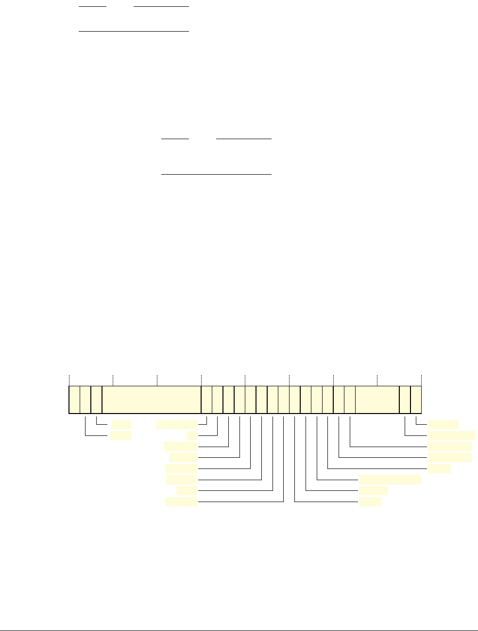
Appendix D13 v6 Debug and v6.1 Debug Differences
D13.11 The debug registers, v6 Debug and v6.1 Debug
D13-2572 Copyright © 1996-1998, 2000, 2004-2012, 2014 ARM. All rights reserved. ARM DDI 0406C.c
Non-Confidential ID051414
D13.11.3 DBGDSCR, Debug Status and Control Register, ARMv6
Note
For the ARMv7 description of the register, see DBGDSCR, Debug Status and Control Register on page C11-2243.
The DBGDSCR characteristics are:
Purpose The main control register for the debug implementation.
Usage constraints The debug implementation provides internal and external views of the DBGDSCR:
• the CP14 interface gives access to the internal view of the register
•the register must be visible in the IMPLEMENTATION DEFINED external debug
interface.
Note
v7 Debug refers to these views as DBGDSCRint and DBGDSCRext. These terms were not
used in v6 Debug and v6.1 Debug.
Table D13-10 on page D13-2575 shows the access attributes for each field of the register in
these different views.
Configurations This register has the following differences in different versions of the Debug architecture:
• v6.1 Debug defines additional bits in the register, see Table D13-10 on
page D13-2575
• v6 Debug defines additional permitted values for the MOE field, see Table D13-11
on page D13-2576.
In a VMSA implementation that includes the Security Extensions, this is a Common
register.
For the v7 Debug definition of this register see DBGDSCR, Debug Status and Control
Register on page C11-2243.
Attributes See the registers summary in Table D13-3 on page D13-2561, the register bit descriptions,
and Table D13-10 on page D13-2575.
In v6.1 Debug, the DBGDSCR bit assignments are:
Reserved, UNK/SBZP(0)
31 30 29 28 20 19 18 17 16 15 14 13 12 11 10 9 8 7 6 5 2 1 0
MOE
RXfull
TXfull ADAdiscard
SPNIDdis
SPIDdis
MDBGen
HDBGen
ITRen
UDCCdis INTdis
DBGack
DBGnoPWRDWN
SDABORT_l
ADABORT_l
UND_l
RESTARTED
HALTED
NS

Appendix D13 v6 Debug and v6.1 Debug Differences
D13.11 The debug registers, v6 Debug and v6.1 Debug
ARM DDI 0406C.c Copyright © 1996-1998, 2000, 2004-2012, 2014 ARM. All rights reserved. D13-2573
ID051414 Non-Confidential
In v6 Debug, the DBGDSCR bit assignments are:
Bit[31] Reserved, UNK/SBZP.
RXfull, bit[30] As for v7 Debug.
TXfull, bit[29] As for v7 Debug.
Bits[28:20] Reserved, UNK/SBZP.
ADAdiscard, bit[19], v6.1 Debug
As for v7 Debug, but see the information about asynchronous aborts in Exceptions in Debug
state on page D13-2559.
NS, bit[18], v6.1 Debug
As for v7 Debug.
SPNIDdis, bit[17], v6.1 Debug
As for v7 Debug.
SPIDdis, bit[16], v6.1 Debug
As for v7 Debug.
Bits[19:16], v6 Debug
Reserved, UNK/SBZP.
MDBGen, bit[15] As for v7 Debug.
HDBGen, bit[14] As for v7 Debug. v6 Debug and v6.1 Debug do not support the OS Save and Restore
mechanism and therefore the Note about the saved value of this bit is not relevant to v6
Debug and v6.1 Debug implementations.
ITRen, bit[13] As for v7 Debug. However, in an ARMv6 implementation, if the external debug interface
does not have a mechanism for forcing the processor to execute instructions in Debug state
via the external debug interface, this bit is RAZ/WI.
UDCCdis, bit[12] As for v7 Debug.
INTdis, bit[11] As for v7 Debug.
DBGack, bit[10] As for v7 Debug.
DBGnoPWRDWN, bit[9]
Note
• The v6 and v6.1 Debug architectures do not define this bit, but many v6 Debug and
v6.1 Debug implementations define DBGDSCR[9] as the DBGnoPWRDWN bit. If
this bit is not implemented, DBGDSCR[9] is RAZ/WI.
• From issue C.a of this manual, this bit is renamed as CORENPDRQ. This renaming
has no effect on the function of the bit.
(0)
31 30 29 28 16 15 14 13 12 11 10 9 8 7 6 5 2 1 0
Reserved, UNK/SBZP (0) MOE
RXfull
TXfull
INTdis
DBGack
DBGnoPWRDWN
SDABORT_l
ADABORT_l
RESTARTED
HALTEDMDBGen
HDBGen
ITRen
UDCCdis

Appendix D13 v6 Debug and v6.1 Debug Differences
D13.11 The debug registers, v6 Debug and v6.1 Debug
D13-2574 Copyright © 1996-1998, 2000, 2004-2012, 2014 ARM. All rights reserved. ARM DDI 0406C.c
Non-Confidential ID051414
No powerdown bit. This bit requests emulation of powerdown. The possible values of this
bit are:
0 On a powerdown request, the system powers-down.
1 On a powerdown request, the system emulates powerdown.
Emulation of powerdown is an IMPLEMENTATION DEFINED feature. If it is implemented,
setting this bit to 1 requests the power controller to work in an emulation mode when it
receives a powerdown request. In this emulation mode the processor is not actually powered
down. For more information, see DBGNOPWRDWN on page D1-2348.
UND_l, bit[8], v6.1 Debug
As for v7 Debug.
Bit[8], v6 Debug Reserved, UNK/SBZP.
ADABORT_l, bit[7] Sticky Asynchronous Abort bit. This bit is set to 1 by any asynchronous abort that occurs
when the processor is in Debug state. The possible values of this bit are:
0 No asynchronous abort has occurred since the last time this bit was cleared to 0
1 An asynchronous abort has occurred since the last time this bit was cleared to 0.
This bit is cleared to 0 when the external debugger reads the DBGDSCR.
Some aspects of the behavior of this bit depend on the version of the Debug architecture:
v6.1 Debug
If the processor is in Non-debug state this bit is not set to 1 on an asynchronous
abort.
v6 Debug The value of this bit is UNKNOWN when either the processor is in Non-debug
state, or the ITRen bit, bit[13], is not set to 1.
For more information, see Asynchronous aborts and Debug state on page D13-2560 and
Exceptions in Debug state on page D13-2559.
SDABORT_l, bit[6] Sticky Synchronous Data Abort bit. This bit is set to 1 by any Data Abort exception that is
generated synchronously when the processor is in Debug state. The possible values of this
bit are:
0 No synchronous Data Abort exception has been generated since the last time
this bit was cleared to 0
1 A synchronous Data Abort exception has been generated since the last time this
bit was cleared to 0.
If the external debug interface includes an ITR, its behavior might depend on the value of
the SDABORT_l bit. See Features that might be provided by the external debug interface
on page D13-2562 for more information about the ITR.
This bit is cleared to 0 when the external debugger reads the DBGDSCR.
Some aspects of the behavior of this bit depend on the version of the Debug architecture:
v6.1 Debug
If the processor is in Non-debug state this bit is not set to 1 on a synchronous
Data Abort exception.
v6 Debug If the processor is in Non-debug state, the value of this bit is UNKNOWN.
For more information, see Exceptions in Debug state on page D13-2559.
MOE, bits[5:2] Method of Debug Entry field. The meaning of this field is generally the same as in
v7 Debug, but v6 Debug permits two additional field values. For more information see
Method of Debug entry on page D13-2576.
RESTARTED, bit[1] As for v7 Debug.
HALTED, bit[0] As for v7 Debug.

Appendix D13 v6 Debug and v6.1 Debug Differences
D13.11 The debug registers, v6 Debug and v6.1 Debug
ARM DDI 0406C.c Copyright © 1996-1998, 2000, 2004-2012, 2014 ARM. All rights reserved. D13-2575
ID051414 Non-Confidential
Table D13-10 shows the access to each field of the DBGDSCR, and the reset value of each field. It also shows the
Debug architecture versions in which each field is defined.
Table D13-10 DBGDSCR bit access and reset values
Bits Field name Version Access
Debug reset valuea
CP14 view External view
[31] - - UNK/SBZP -
[30] RXfull Both Read-only 0
[29] TXfull Both Read-only 0
[28:20] - - UNK/SBZP -
[19] ADAdiscard v6.1 Debug Read-only or Read/writeb0
[18] NS v6.1 Debug Read-only d
[17] SPNIDdis v6.1 Debug Read-only d
[16] SPIDdis v6.1 Debug Read-only d
[15] MDBGen Both Read/Write Read-only 0
[14] HDBGen Both Read-only Read/Write 0
[13] ITRen Both Read-only Read/Write 0
[12] UDCCdis Both Read/Write Read-only 0
[11] INTdis Both Read-only Read/Write 0
[10] DBGack Both Read-only Read/Write 0
[9] DBGnoPWRDWN Both Read-only Read/Write 0
[8] UND_l v6.1 Debug Read-only c0
[7] ADABORT_l Both Read-only c0
[6] SDABORT_l Both Read-only c0
[5:2] MOE Both Read/Write Read-only 0
[1] RESTARTED Both Read-only d
[0] HALTED Both Read-only d
a. The value after a debug logic reset.
b. The ADAdiscard bit can be read/write. This is IMPLEMENTATION DEFINED, see Asynchronous aborts and Debug state entry
on page C5-2096.
c. For details of how these bits are cleared to 0 see the descriptions of the bits.
d. These are read-only status bits that reflect the current state of the processor.

Appendix D13 v6 Debug and v6.1 Debug Differences
D13.11 The debug registers, v6 Debug and v6.1 Debug
D13-2576 Copyright © 1996-1998, 2000, 2004-2012, 2014 ARM. All rights reserved. ARM DDI 0406C.c
Non-Confidential ID051414
Method of Debug entry
The Method of Debug Entry is indicated by the DBGDSCR.MOE field. Table D13-11 shows the meanings of the
possible values of the DBGDSCR.MOE field.
A Prefetch Abort or Data Abort exception handler can determine whether a debug event occurred by checking the
value of the relevant Fault Status Register, IFSR or DFSR. It then uses the DBGDSCR.MOE bits to determine the
specific debug event.
In v6 Debug, the DBGDSCR can be checked first to determine whether an abort has occurred, and hence whether
the exception handler jumps to the debug monitor or not. In v6.1 Debug the D-side abort occurred and I-side abort
occurred encodings are reserved. Therefore, an exception handler must always check the IFSR or DFSR first.
When debug is disabled, and when debug events are not permitted, the
BKPT
instruction generates a debug exception
rather than being ignored. The exception reporting registers are set as if a BKPT instruction debug exception
occurred. For more information, see Debug exception on BKPT instruction, Breakpoint, or Vector catch debug
events on page C4-2090. For security reasons, monitor software might need to check that debug was enabled and
that the debug event was permitted before communicating with an external debugger.
D13.11.4 DBGDTRRX, Host to Target Data Transfer Register
ARMv6 does not define DBGDTRRXext or DBGDTRTXext, but the corresponding functionality must be
implemented as part of the external debug interface.
Note
DBGDTRRX was named rDTR.
In the section Behavior of accesses to DBGDTRRX on page C8-2174:
• Information about access to DBGDTRRXint also applies to access to rDTRin v6 Debug and v6.1 Debug.
• Information about access to DBGDTRRXext does not apply to v6 Debug and v6.1 Debug. In these versions
of the Debug architecture, the external debug interface defines the behavior of accesses to the equivalent
functionality.
D13.11.5 DBGDTRTX, Target to Host Data Transfer Register
ARMv6 does not define DBGDTRRXext or DBGDTRTXext, but the corresponding functionality must be
implemented as part of the external debug interface.
Table D13-11 Meaning of Method of Debug Entry values
MOE bits Version Debug entry caused by:
0000 Both Halt request debug even
0001 Both Breakpoint debug event
0010 Both Asynchronous watchpoint debug event
0011 Both BKPT instruction debug event
0100 Both External debug request debug event
0101 Both Vector catch debug event
0110 v6 only Data-side abort, reserved in v6.1 Debug
0111 v6 only Instruction-side abort, reserved in v6.1 Debug
1000-1111 Both Reserved

Appendix D13 v6 Debug and v6.1 Debug Differences
D13.11 The debug registers, v6 Debug and v6.1 Debug
ARM DDI 0406C.c Copyright © 1996-1998, 2000, 2004-2012, 2014 ARM. All rights reserved. D13-2577
ID051414 Non-Confidential
Note
DBGDTRTX was named wDTR.
In the section Behavior of accesses to DBGDTRTX on page C8-2175:
• Information about access to DBGDTRTXint also applies to access to wDTR in v6 Debug and v6.1 Debug.
• Information about access to DBGDTRTXext does not apply to v6 Debug and v6.1 Debug. In these versions
of the Debug architecture, the external debug interface defines the behavior of accesses to the equivalent
functionality.
D13.11.6 DBGWFAR, Watchpoint Fault Address Register
In v6.1 Debug, the DBGWFAR is implemented as described for v7 Debug. In v6 Debug this register is not
implemented as a debug register.
Note
• In ARMv6 this register is also accessible as processor CP15 register, see CP15 c6, Watchpoint Fault Address
Register, DBGWFAR on page D12-2533. The register implementation is always as described for v7 Debug.
• In v6.1 Debug, ARM deprecates using the CP15 access to the DBGWFAR.
D13.11.7 DBGVCR, Vector Catch Register
In v6 Debug and v6.1 Debug, the DBGVCR is implemented as described for v7 Debug, except that, in v6.1 Debug,
if the implementation includes the Security Extensions, it is optional whether DBGVCR[31, 30, 28:25, 15, 14,
12:10] are implemented. If these bits are not implemented, they are RAZ/WI.
Note
• In an implementation that includes the Security Extensions, ARM recommends that DBGVCR[31, 30, 28:25,
15, 14, 12:10] are implemented.
• The Security Extensions cannot be implemented with v6 Debug.
In v6 Debug and v6.1 Debug, all defined bits reset to 0.
In a v6.1 Debug implementation that includes the Security Extensions, the debug logic generates Reset Vector catch
debug events only when the processor is in Secure state. It is UNPREDICTABLE whether this depends on the security
state when the processor fetches the instruction, or on the security state when it commits the instruction for
execution.
D13.11.8 DBGDSCCR, Debug State Cache Control Register
It is IMPLEMENTATION DEFINED whether a v6.1 Debug implementation includes the DBGDSCCR, or the
DBGDSMCR, but ARM recommends implementing them, to help debuggers maintain memory coherency without
costly explicit coherency operations.
Because the DBGDSCCR is IMPLEMENTATION DEFINED in v6.1 Debug, its implementation might differ from the
description in Chapter C11 The Debug Registers. Therefore, the restrictions given in Permitted
IMPLEMENTATION DEFINED limits on page C11-2242 are not architectural requirements for v6.1 Debug.
The DBGDSCCR is not defined in v6 Debug, but a processor that includes v6 Debug might implement equivalent
functionality using an IMPLEMENTATION DEFINED register.

Appendix D13 v6 Debug and v6.1 Debug Differences
D13.11 The debug registers, v6 Debug and v6.1 Debug
D13-2578 Copyright © 1996-1998, 2000, 2004-2012, 2014 ARM. All rights reserved. ARM DDI 0406C.c
Non-Confidential ID051414
Note
• The IMPLEMENTATION DEFINED Cache Behavior Override Register, CBOR, can be implemented as a CP15
register on an ARMv6 processor. An implementation that includes the Security Extensions must implement
the CBOR.
• If implemented as a CP15 register, the Debug State Cache Control Register is implemented in the
IMPLEMENTATION DEFINED register space.
In a v6.1 Debug implementation of the DBGDSCCR, all defined bits of the register reset to 0.
DBGDSCCR interaction with the CBOR, Cache Behavior Override Register
A processor might implement an IMPLEMENTATION DEFINED CBOR in CP15.
Table D13-12 shows, for a processor that implements both the DBGDSCCR and the CBOR, the relative precedence
of the CBOR and the DBGDSCCR according to the state of the processor.
Note
Table D13-12 assumes that the processor supports the features controlled by the DBGDSCCR.{nWT, nDL, nIL}
bits. If the processor does not support a feature:
• the corresponding control bit is RO
• it is IMPLEMENTATION DEFINED whether the bit is RAZ or RAO
• the processor behaves as if the bit was set to 1.
Table D13-12 Interaction of the CP15 CBOR and the DBGDSCCR
DBGDSCCR CBOR Debug state Behavior
nWT nDL nIL WT DL IL
1- - 0--x Write-back regionsa are write-back
x- - 0--No Write-back regionsa are write-back
x- - 1--x Write-back regionsa are write-through
0- - x--Yes Write-back regionsa are write-through
- 1 - - 0 - x Data or unified cache linefills are enabled
- x - - 0 - No Data or unified cache linefills are enabled
- x - - 1 - x Data or unified cache linefills are disabled
- 0 - - x - Yes Data or unified cache linefills are disabled
- - 1 - - 0 x Instruction cache linefills are enabled
- - x - - 0 No Instruction cache linefills are enabled
- - x - - 1 x Instruction cache linefills are disabled
- - 0 - - x Yes Instruction cache linefills are disabled
a. Memory regions that the region attributes indicate are Write-Back Cacheable.

Appendix D13 v6 Debug and v6.1 Debug Differences
D13.11 The debug registers, v6 Debug and v6.1 Debug
ARM DDI 0406C.c Copyright © 1996-1998, 2000, 2004-2012, 2014 ARM. All rights reserved. D13-2579
ID051414 Non-Confidential
A processor that implements Security Extensions might implement a common CBOR, with CBOR.{WT, IL, DL}
bit settings that apply to both Secure and Non-secure operation. However, it might bank CBOR, providing
independent definition of {WT, IL, DL} for the Secure and Non-secure states. In this case, duplicate Table D13-12
on page D13-2578:
• once for Non-secure operation, using the Non-secure CBOR.{WT, IL, DL} settings
• once for Secure operation, using the Secure CBOR.{WT, IL, DL} settings.
D13.11.9 DBGDSMCR, Debug State MMU Control Register
It is IMPLEMENTATION DEFINED whether a v6.1 Debug implementation includes the DBGDSCCR, or the
DBGDSMCR, but ARM recommends implementing them, to help debuggers maintain memory coherency without
costly explicit coherency operations.
Because the DBGDSMCR is IMPLEMENTATION DEFINED in v6.1 Debug, their implementation might differ from the
descriptions in Chapter C11 The Debug Registers. Therefore, the restrictions given in Permitted
IMPLEMENTATION DEFINED limits on page C11-2242 are not architectural requirements for v6.1 Debug.
The DBGDSMCR is not defined in v6 Debug, but a processor that includes v6 Debug might implement equivalent
functionality using an IMPLEMENTATION DEFINED register.
Note
If implemented as a CP15 register, the Debug State MMU Control Register is implemented in the IMPLEMENTATION
DEFINED register space.
In a v6.1 Debug implementation of the DBGDSMCR, all defined bits of the register reset to 0.
D13.11.10 DBGBCR, Breakpoint Control Registers
In v6 Debug and v6.1 Debug, the DBGBCR is implemented as described for v7 Debug, except that:
Bits[28:24] Reserved, UNK/SBZP, in v6 Debug and v6.1 Debug.
Bit[22] Reserved, UNK/SBZP, in v6 Debug. v6 Debug does not support linked or unlinked instruction
address mismatch comparisons.
Privileged mode control, bits[2:1]
The value of
0b00
is reserved in v6 Debug and v6.1 Debug, and must not be used.
In v6 Debug and v6.1 Debug, DBGBCR[0] is set to 0 on a debug logic reset, disabling the breakpoint.
D13.11.11 DBGWCR, Watchpoint Control Registers
In v6 Debug and v6.1 Debug, the DBGWCR is implemented as described for v7 Debug, except that:
Bits[28:24] Reserved, UNK/SBZP, in v6 Debug and v6.1 Debug.
Bit[12:9] Reserved, UNK/SBZP, in v6 Debug and v6.1 These Debug architecture versions only support a
4-bit Byte address select field.
In v6 Debug and v6.1 Debug, DBGWCR[0] is set to 0 on a debug logic reset, disabling the watchpoint.

Appendix D13 v6 Debug and v6.1 Debug Differences
D13.12 Performance monitors, v6 Debug and v6.1 Debug
D13-2580 Copyright © 1996-1998, 2000, 2004-2012, 2014 ARM. All rights reserved. ARM DDI 0406C.c
Non-Confidential ID051414
D13.12 Performance monitors, v6 Debug and v6.1 Debug
v7 Debug introduces the Performance Monitors Extension as an optional architecture extension. Before v7 Debug,
the debug architecture did not define the performance monitors and therefore, in general, Chapter C12 The
Performance Monitors Extension does not apply to v6 Debug and v6.1 Debug implementations.

ARM DDI 0406C.c Copyright © 1996-1998, 2000, 2004-2012, 2014 ARM. All rights reserved. D14-2581
ID051414 Non-Confidential
Appendix D14
Secure User Halting Debug
This chapter describes the Secure User halting debug (SUHD) feature of debug implementations on processors that
include the Security Extensions. It contains the following sections:
•About Secure User halting debug on page D14-2582
•Invasive debug authentication in an implementation that supports SUHD on page D14-2583
•Effects of SUHD on Debug state on page D14-2584.
Note
On a processor that implements the Security Extensions, SUHD is:
• required in v6.1 Debug
• optional and deprecated in v7 Debug with a processor that implements the ARMv7 architecture without the
Multiprocessing Extensions
• obsolete in v7 Debug from the introduction of the ARMv7 Multiprocessing extensions.

Appendix D14 Secure User Halting Debug
D14.1 About Secure User halting debug
D14-2582 Copyright © 1996-1998, 2000, 2004-2012, 2014 ARM. All rights reserved. ARM DDI 0406C.c
Non-Confidential ID051414
D14.1 About Secure User halting debug
For debug events that cause entry to Debug state, Secure User halting debug (SUHD) refers to permitting these
events in Secure User mode when invasive debug is not permitted in Secure PL1 modes. The debug events that
cause entry to Debug state are:
• Halting debug events
• if Halting debug-mode is selected, Software debug events.
In an implementation that includes the Security Extensions, the Debug architecture requirements for SUHD are:
• v6.1 Debug requires support for SUHD
• in v7 Debug it is IMPLEMENTATION DEFINED whether SUHD is supported, and ARM deprecates the
implementation or use of SUHD
• v7.1 Debug obsoletes SUHD, meaning it never supports it.
On an implementation that includes the Security Extensions but does not support Secure User halting debug the
DBGDIDR.nSUHD_imp bit is RAO.
Note
An ARMv6 implementation that includes the Security Extensions must implement v6.1 Debug. Therefore, SUHD
cannot be implemented with v6 Debug.

Appendix D14 Secure User Halting Debug
D14.2 Invasive debug authentication in an implementation that supports SUHD
ARM DDI 0406C.c Copyright © 1996-1998, 2000, 2004-2012, 2014 ARM. All rights reserved. D14-2583
ID051414 Non-Confidential
D14.2 Invasive debug authentication in an implementation that supports SUHD
If a implementation supports Secure User halting debug, it can be configured so that both invasive halting debug
and invasive nonhalting debug are permitted in Secure User mode when invasive debug is not permitted in Secure
PL1 modes. Therefore, the alternatives for when a debug event is permitted are:
• in all processor modes, in both Secure and Non-secure security states
• only in Non-secure state
• in Non-secure state and also in Secure User mode.
Note
In an implementation that includes the Security Extensions and supports SUHD, the Debug architecture
distinguishes between permitting invasive halting debug and permitting invasive nonhalting debug. However, in
Non-secure state and in Secure PL1 modes whether a debug event is permitted does not depend on whether the event
would cause entry to Debug state. Therefore, the distinction between permitting invasive halting debug and invasive
nonhalting debug applies only in Secure User mode.
Configuration of permissions for non-invasive debug is independent of that for invasive debug, but provides the
same alternatives.
D14.2.1 Effect of SUHD support on invasive debug authentication
Invasive debug with the Security Extensions on page C2-2033 describes invasive debug authentication for a
processor that implements the Security Extensions but does not support Secure User halting debug. However, for
an implementation that includes support for Secure User halting debug, in Secure User mode, whether halting debug
is permitted depends on the value of the SDER.SUIDEN bit.
Table D14-1 shows the complete set of invasive debug authentication controls on an implementation that supports
Secure User halting debug:
Table D14-1 Invasive debug authentication on an implementation that supports Secure User halting debug
DBGENaSPIDENaSDER.SUIDEN Mode Security state SUHD supported Invasive debug
LOW x x Any Either x Disabled
HIGH LOW 0 Any Non-secure x Enabled and permitted
Secure x Enabled but not permitted
1 Any Non-secure x Enabled and permitted
User Secure No Enabled but not permitted
Yes Enabled and permitted
PL1 Secure x Enabled but not permitted
HIGH HIGH x Any Either x Enabled and permitted
a. Authentication signals, see Authentication signals on page D1-2340.

Appendix D14 Secure User Halting Debug
D14.3 Effects of SUHD on Debug state
D14-2584 Copyright © 1996-1998, 2000, 2004-2012, 2014 ARM. All rights reserved. ARM DDI 0406C.c
Non-Confidential ID051414
D14.3 Effects of SUHD on Debug state
The following sections describes the effects of implementing SUHD on the description of Debug state given in
Chapter C5 Debug State:
•Executing instructions in Debug state in an implementation that supports SUHD
•Memory system behavior in Debug state when SUHD is supported on page D14-2585
•Effect of SUHD on exception handling in Debug state on page D14-2587.
D14.3.1 Executing instructions in Debug state in an implementation that supports SUHD
In User mode and Debug state, instructions have additional privileges to access or modify some registers and fields
that cannot be accessed in User mode in Non-debug state. However, on processors that implement the Security
Extensions and support Secure User halting debug, these additional privileges are restricted when all the following
conditions are true:
• the processor is in Debug state
• the processor is in Secure User mode
• invasive debug is not permitted in Secure PL1 modes, see Chapter C2 Invasive Debug Authentication.
Altering CPSR privileged bits in Debug state
In addition to the information given in Altering CPSR privileged bits in Debug state on page C5-2100, a processor
that implements the Security Extensions and supports SUHD prevents updates to the privileged bits of the CPSR
when the processor is in Secure User mode and invasive debug is not permitted in Secure PL1 modes. For such an
implementation, Table D14-2 defines the behavior on writes to the CPSR in Debug state.
The restrictions on CPSR updates on an implementation that includes the Security Extensions, as described in
Altering CPSR privileged bits in Debug state on page C5-2100, also apply to the information given in Table D14-2.
In addition, where Table D14-2 shows that the effect of attempting to modify the CPSR.M field to Monitor mode is
UNPREDICTABLE, the definition of UNPREDICTABLE implies that, if the processor was in User mode before the
attempt to modify the M field, it must not enter a PL1 mode.
Note
When the processor is in User mode in Debug state, ARM deprecates updating any CPSR privileged bit other than
the M field.
Table D14-2 Permitted updates to the CPSR in Debug state in an implementation that supports SUHD
Mode Secure state Invasive debug permitted in
Secure PL1 modes Update privileged
CPSR bitsaModify CPSR.M to
Monitor mode
User Yes No Update ignored UNPREDICTABLE
PL1 Yes No Permitted UNPREDICTABLE
Any No No Permitted UNPREDICTABLE
X Yes Permitted Permitted
a. This column does not apply to changing CPSR.M to
0b10110
, Monitor mode, but does apply to changing CPSR.M to any other
permitted value.

Appendix D14 Secure User Halting Debug
D14.3 Effects of SUHD on Debug state
ARM DDI 0406C.c Copyright © 1996-1998, 2000, 2004-2012, 2014 ARM. All rights reserved. D14-2585
ID051414 Non-Confidential
Coprocessor instructions for CP14 and CP15 when SUHD is supported
In these descriptions, a permitted access is one that is not UNDEFINED, and an access that is not permitted is
UNDEFINED.
In addition to the information given in Instructions for CP14 and CP15 on page C5-2104, when a processor
supports SUHD:
• Instructions that access CP14 or CP15 registers that are permitted in User mode when in Non-debug state,
are always permitted in Debug state.
• Instructions that access CP14 debug registers that are permitted from PL1 when in Non-debug state are
permitted in Debug state, regardless of the debug authentication and the processor mode and security state.
• If the processor is in Secure User mode and the debugger cannot write to the CPSR.M bits to change to a PL1
mode, then any instruction that accesses a CP14 non-debug register or a CP15 register is not permitted in
Debug state if it is not permitted in Secure User mode in Non-debug state.
In addition, if a debug implementation supports SUHD, ARM recommends that certain CP15 instructions that a
debugger requires to maintain memory coherency are permitted in Debug state regardless of debug permissions and
the processor mode, see Access to specific cache management functions in Debug state
Coprocessor instructions for CP0 to CP13, and Advanced SIMD instructions in Debug
state when SUHD is supported
Support for SUHD does not affect the information given in Instructions for CP0 to CP13, and Advanced SIMD
instructions on page C5-2104.
D14.3.2 Memory system behavior in Debug state when SUHD is supported
If an implementation supports SUHD, then in addition to the requirements given in Memory system behavior in
Debug state on page C5-2111, a debugger must be able to:
• maintain coherency between instruction and data memory
• maintain coherency in a multiprocessor system
• reset the memory system of the processor to a known safe and coherent state
• reset any caches of meta-information, such as branch predictors, to a safe and coherent state.
If the processor is in a state and mode where it can execute CP15 instructions at PL1, the debugger can use any CP15
operations. These include the cache maintenance operations, and any implemented TLB maintenance operations.
Note
• A processor can execute all CP15 instructions in any state and mode unless it implements the Security
Extensions and supports SUHD.
• ARM deprecates executing PL1 CP15 instructions from User mode.
Access to specific cache management functions in Debug state
If an implementation includes the Security Extensions and supports Secure User halting debug, it must implement
mechanisms that enable memory system requirements to be met when debugging in Secure User mode when
invasive debug is not permitted in Secure PL1 modes. This is a situation where executing the CP15 cache and TLB
control operations would otherwise be prohibited.
To meet these requirements, ARM recommends that, on a processor that implements the Security Extensions and
supports Secure User halting debug, when the processor is in Debug state:
• the rules for accessing CP15 registers do not apply for a certain set of register access operations
• the set of operations depends on the Debug architecture version, as shown in Table D14-3 on page D14-2586.

Appendix D14 Secure User Halting Debug
D14.3 Effects of SUHD on Debug state
D14-2586 Copyright © 1996-1998, 2000, 2004-2012, 2014 ARM. All rights reserved. ARM DDI 0406C.c
Non-Confidential ID051414
These instructions must be executable in Debug state regardless of any processor setting. However, use of an
operation can generate a Data Abort exception if instruction cache lockdown is in use, see v7 Debug restrictions on
instruction cache invalidation in Secure User debug on page D14-2587.
For more information about debug access to coprocessor instructions, see Behavior of coprocessor and Advanced
SIMD instructions in Debug state on page C5-2104.
For more information about the ARMv7 cache maintenance operations, see:
•Cache and branch predictor maintenance operations, VMSA on page B4-1743 for a VMSA implementation
•Cache and branch predictor maintenance operations, PMSA on page B6-1943 for a PMSA implementation.
If the processor is in a state and mode where it can execute CP15 instructions at PL1, the debugger can use any CP15
operations. These include, but are not limited to, those operations listed in Table D14-3.
Note
A processor can execute all CP15 instructions in any state and mode if:
• it implements v6.1 Debug or v7 Debug and it does not implement the Security Extensions.
• it implements v7 Debug and the Security Extensions but does not support Secure User halting debug.
However, v7 Debug deprecates executing from User mode CP15 instructions that, in Non-debug state, can only be
executed at PL1 or higher.
An implementation that supports SUHD must provide access to the cache clean operations shown in Table D14-3,
even if the DBGDSCCR does not support the force Write-Through feature, as described in Permitted
IMPLEMENTATION DEFINED limits on page C11-2242.
Table D14-3 CP15 operations permitted from User mode in Debug state
Versions Operation Description
v7 Debug
MCR p15, 0, <Rt>, c7, c5, 0
Invalidate all instruction caches to PoU, invalidate branch predictors a
MCR p15, 0, <Rt>, c7, c5, 1
Invalidate instruction caches by MVA to PoUa
MCR p15, 0, <Rt>, c7, c5, 7
Invalidate MVA from branch predictor
MCR p15, 0, <Rt>, c7, c10, 1
Clean data or unified cache line by MVA to point of coherencyb
MCR p15, 0, <Rt>, c7, c10, 2
Clean data or unified cache line by set/wayb
MCR p15, 0, <Rt>, c7, c11, 1
Clean data or unified cache line by MVA to point of unificationb
MCR p15, 0, <Rt>, c7, c1, 0
Invalidate entire instruction cache Inner Shareablec
MCR p15, 0, <Rt>, c7, c1, 6
Invalidate all branch predictors Inner Shareablec
v6.1 Debug
MCRR p15, 0, <Rt>, <Rn>, c5
Invalidate instruction cache by VA range
v6.1 Debug, v7 Debug
MCR p15, 0, <Rt>, c7, c5, 6
Invalidate all branch predictors
a. See also v7 Debug restrictions on instruction cache invalidation in Secure User debug on page D14-2587.
b. A debugger does not have to perform cache cleaning operations if DBGDSCCR.nWT is implemented and is set to 0. This is because when
nWT is set to 0, writes do not leave dirty data in the cache that is not coherent with outer levels of memory. However, the instruction cache
is not updated, so the debugger must perform instruction cache invalidate operations when appropriate.
c. These instructions are part of the Multiprocessing Extensions. See Multiprocessor considerations for cache and similar maintenance
operations on page B2-1273.

Appendix D14 Secure User Halting Debug
D14.3 Effects of SUHD on Debug state
ARM DDI 0406C.c Copyright © 1996-1998, 2000, 2004-2012, 2014 ARM. All rights reserved. D14-2587
ID051414 Non-Confidential
v7 Debug restrictions on instruction cache invalidation in Secure User debug
An ARMv7 implementation that includes the Security Extensions and supports Secure User halting debug must
support Secure User debug access to at least one of these instruction cache invalidation operations:
• Invalidate entire instruction cache, and invalidate branch predictors,
MCR p15, 0, <Rt>, c7, c5, 0
• Invalidate instruction cache by MVA,
MCR p15, 0, <Rt>, c7, c5, 1
.
An implementation might support both of these operations.
If the DSCCR.nWT bit is not implemented, the implementation must also support Secure User debug access to at
least the operation to Clean data or unified cache line by MVA to point of coherency.
A debugger requires access to an instruction cache invalidation operations so that it can maintain coherency between
instruction memory and data memory, and between processors in a multiprocessor system.
In Secure User mode in Debug state, when invasive debug is not permitted in Secure PL1 modes in Non-debug state:
•If the Invalidate all instruction caches operation is supported it must:
— invalidate all unlocked lines in the cache
— leave any locked lines in the cache unchanged.
If there are locked lines in the cache the instruction can generate a Data Abort exception, but only after it has
invalidated all unlocked lines. However, there is no requirement for the operation to abort if there are locked
lines.
•If the Invalidate instruction caches by MVA operation is supported, this operation must not invalidate a locked
line. When an instruction attempts to invalidate a locked line it is IMPLEMENTATION DEFINED whether the
processor consistently:
— ignores the instruction
— generates a Data Abort exception.
These requirements mean that these instructions might operate differently in Debug state to how they operate in
Non-debug state.
Note
In ARMv7, it is IMPLEMENTATION DEFINED whether instruction cache locking is supported.
D14.3.3 Effect of SUHD on exception handling in Debug state
The only effect SUHD has on the description given in Exceptions in Debug state on page C5-2107 is in the reporting
of synchronous Data Abort exceptions. In an implementation that includes support for SUHD, on a synchronous
Data Abort exception:
• if invasive debug is permitted in Secure PL1 modes, or the processor is not in Secure User mode, the DFSR
and DFAR are updated
• otherwise, it is IMPLEMENTATION DEFINED whether the DFSR and DFAR are updated.

Appendix D14 Secure User Halting Debug
D14.3 Effects of SUHD on Debug state
D14-2588 Copyright © 1996-1998, 2000, 2004-2012, 2014 ARM. All rights reserved. ARM DDI 0406C.c
Non-Confidential ID051414

ARM DDI 0406C.c Copyright © 1996-1998, 2000, 2004-2012, 2014 ARM. All rights reserved. D15-2589
ID051414 Non-Confidential
Appendix D15
ARMv4 and ARMv5 Differences
This appendix describes how the ARMv4 and ARMv5 architectures differ from the ARMv6 and ARMv7
architectures. It contains the following sections:
•Introduction to ARMv4 and ARMv5 on page D15-2590
•Application level register support on page D15-2591
•Application level memory support on page D15-2592
•Instruction set support on page D15-2597
•System level register support on page D15-2603
•System level memory model on page D15-2606
•System Control coprocessor, CP15 support on page D15-2614.
Note
In this appendix, unless otherwise stated, the description ARMvN refers to all architecture variants of ARM
architecture vN. For example, ARMv4 refers to all variants of ARM architecture v4, including ARMv4 and
ARMv4T.

Appendix D15 ARMv4 and ARMv5 Differences
D15.1 Introduction to ARMv4 and ARMv5
D15-2590 Copyright © 1996-1998, 2000, 2004-2012, 2014 ARM. All rights reserved. ARM DDI 0406C.c
Non-Confidential ID051414
D15.1 Introduction to ARMv4 and ARMv5
ARMv4 and ARMv5 defined the instruction set support and the programmers’ model that applies to the ARM core
registers and the associated exception model. These architecture versions are fully described in the ARM
Architecture Reference Manual (DDI 0100).
Note
This appendix is a summary of the ARMv4 and ARMv5 architecture variants. ARM expects that this appendix and
the rest of this manual satisfy the majority of requirements for architecture information on ARMv4 and ARMv5.
However the ARM Architecture Reference Manual (DDI 0100) might be required for more information specific to
ARMv4 or ARMv5.
Memory support is IMPLEMENTATION DEFINED in ARMv4 and ARMv5. In practice, use of CP15 to support the
Virtual Memory System Architecture (VMSA) or Protected Memory System Architecture (PMSA) is standard in
ARMv4 and ARMv5 implementations, but this is not an architectural requirement. For this reason, the data sheet
or Technical Reference Manual for a particular ARM processor is the definitive source for its memory and system
control facilities. This appendix does not specify absolute requirements on the functionality of CP15 or other
memory system components. Instead, it contains guidelines designed to maximize compatibility with current and
future ARM software.
This appendix concentrates on the features supported in ARMv4 and ARMv5, highlighting:
• features common across all architecture variants
• features supported for legacy reasons in ARMv6, but not in ARMv7
• features unique to the ARMv4 and ARMv5 variants.
D15.1.1 Debug
Debug is not architecturally-defined in ARMv4 or ARMv5. ARM implementations have traditionally supported
halting debug through a JTAG port. While the support of debug features is similar across ARM implementations,
the timing and control sequencing required for access varies. Debug support in ARMv4 and ARMv5 is
microarchitecture dependent and so in architectural terms is IMPLEMENTATION DEFINED.
D15.1.2 ARMv6 and ARMv7
The ARM architecture was extended considerably in ARMv6. This means that a large proportion of this manual
does not apply to earlier architecture variants and can be ignored with respect to ARMv4 and ARMv5.
The key changes in ARMv6 are:
• the addition of:
— the ARM parallel addition and subtraction instructions, described in Parallel addition and subtraction
instructions on page A4-171, that improve execution of multimedia and other DSP applications
— instructions for improved context switching.
• the introduction of:
— a formal memory model, including level 1 cache support and revisions to alignment and endianness
support
— a requirement to provide either a VMSA or a PMSA for memory management
— a formal debug model
— a requirement to support the CP15 System Control coprocessor
— a new translation table format and additional VMSA features
— the optional Security Extensions
— 32-bit Thumb instructions, in ARMv6T2.
For information about the changes between ARMv6 and ARMv7 see Appendix D12 ARMv6 Differences.
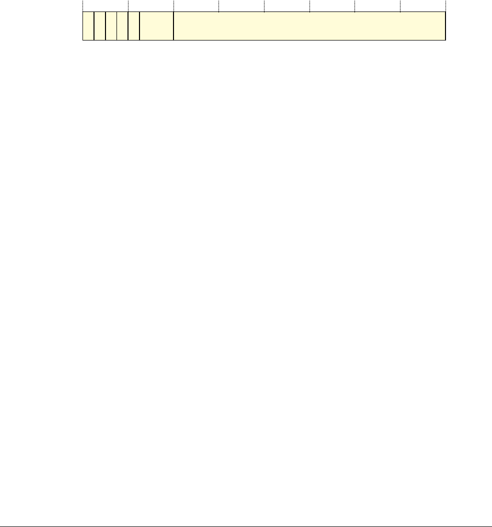
Appendix D15 ARMv4 and ARMv5 Differences
D15.2 Application level register support
ARM DDI 0406C.c Copyright © 1996-1998, 2000, 2004-2012, 2014 ARM. All rights reserved. D15-2591
ID051414 Non-Confidential
D15.2 Application level register support
The ARMv4 and ARMv5 core registers are the same as ARMv7. For more information, see ARM core registers on
page A2-45. The following sections give more information about ARMv4 and ARMv5 application level register
support:
•APSR support
•Instruction set state.
D15.2.1 APSR support
Program status is reported in the 32-bit Application Program Status Register (APSR). The APSR bit assignments
are:
For details of the bit definitions, see The Application Program Status Register (APSR) on page A2-49. In the APSR
descriptions:
• the GE[3:0] field is only defined from ARMv6, and is reserved in ARMv4 and ARMv5
• the Q bit is only defined from ARMv5TE, and is RAZ/WI in ARMv4, ARMv4T and ARMv5T.
Earlier versions of this manual do not use the term APSR. They refer to the APSR as the CPSR with the restriction
on reserved fields governed by whether the register access was unprivileged, or at a higher privilege level.
D15.2.2 Instruction set state
The instruction set states available in ARMv4 and ARMv5 are a subset of the states supported in ARMv7. All
implementations support the ARM instruction set that executes in ARM state. All ARM instructions are 32-bit
instructions. T variants of the architecture also support a 16-bit instruction set that executes in Thumb state. The
supported ARM and Thumb instructions are summarized in Instruction set support on page D15-2597.
Instruction set state support in ARMv4 and ARMv5 differs from the support available in ARMv7 as follows:
• ThumbEE state is not supported
• Jazelle state is supported only in ARMv5TEJ
• With software executing at PL1, you must take care not to attempt to change the instruction set state by
writing nonzero values to CPSR.J and CPSR.T with an
MSR
instruction. For more information, see Format of
the CPSR and SPSRs on page D12-2516.
All ARMv4 and ARMv5 implementations support the ARM instruction set. ARMv4T, ARMv5T, ARMv5TE, and
ARMv5TEJ also support a subset of the Thumb instruction set that can be executed entirely as 16-bit instructions.
The only 32-bit instructions in this subset are restricted-range versions of the
BL
and
BLX
(immediate) instructions.
See BL and BLX (immediate) instructions, before ARMv6T2 on page D12-2504 for a description of how these
instructions can be executed as 16-bit instructions.
Instruction set support on page D15-2597 summarizes the ARM and Thumb instructions supported in ARMv4 and
ARMv5, and the instruction descriptions in Chapter A8 Instruction Descriptions give details of the architecture
variants that support each instruction encoding.
Interworking
In ARMv4T, the only instruction that supports interworking branches between ARM and Thumb states is
BX
.
In ARMv5T, the
BLX
instruction was added to provide interworking procedure calls. The
LDR
,
LDM
and
POP
instructions
were modified to perform interworking branches if they load a value into the PC. This is described by the
LoadWritePC()
pseudocode function. See Pseudocode details of operations on ARM core registers on page A2-47.
N
31 30 29 28 27 26 24 23 0
Z C V Q RAZ/
SBZP Reserved, UNK/SBZP

Appendix D15 ARMv4 and ARMv5 Differences
D15.3 Application level memory support
D15-2592 Copyright © 1996-1998, 2000, 2004-2012, 2014 ARM. All rights reserved. ARM DDI 0406C.c
Non-Confidential ID051414
D15.3 Application level memory support
Memory support covers address alignment, endianness support, semaphore support, memory type, memory order
model, caches, and write buffers.
D15.3.1 Alignment
ARMv4 and ARMv5 behave differently from ARMv7 for unaligned memory accesses. The behavior is the same as
ARMv6 legacy mode except for forcing alignment checks with SCTLR.A == 1.
For ARM instructions when SCTLR.A == 0:
• Non halfword-aligned
LDRH
,
LDRSH
, and
STRH
are UNPREDICTABLE.
• Non word-aligned
LDR
,
LDRT
, and the load access of a
SWP
rotate right the word-aligned data transferred by a
non word-aligned address one, two, or three bytes depending on the value of address[1:0].
• Non word-aligned
STR
,
STRT
, and the store access of a
SWP
ignore address[1:0].
• From ARMv5TE, it is IMPLEMENTATION DEFINED whether
LDRD
and
STRD
must be doubleword-aligned or
word-aligned.
LDRD
and
STRD
instructions that do not meet the alignment requirement are UNPREDICTABLE.
• Non word-aligned
LDM
,
LDC
,
LDC2
, and
POP
ignore address[1:0].
• Non word-aligned
STM
,
STC
,
STC2
, and
PUSH
ignore address[1:0].
For Thumb instructions when SCTLR.A == 0:
• Non halfword-aligned
LDRH
,
LDRSH,
and
STRH
are UNPREDICTABLE.
• Non word-aligned
LDR
, and
STR
are UNPREDICTABLE.
• Non word-aligned
LDMIA
, and
POP
ignore address[1:0].
• Non word-aligned
STMIA,
and
PUSH
ignore address[1:0].
For ARM and Thumb instructions, alignment checking is defined for implementations supporting CP15,
specifically the SCTLR.A bit. When this bit is set, a Data Abort exception indicating an Alignment fault is generated
for unaligned accesses. When SCTLR.A = 1, whether the alignment check for an
LDRD
or
STRD
instruction is for
doubleword-alignment or word-alignment depends on the implementation choice of which alignments are
supported for these instructions when SCTLR.A = 0.
Note
The option of word alignment for
LDRD
and
STRD
instructions is not permitted in the ARMv6 legacy configuration
where SCTLR.U == 0 and SCTLR.A == 1. For more information, see legacy alignment support in Alignment on
page D12-2506.

Appendix D15 ARMv4 and ARMv5 Differences
D15.3 Application level memory support
ARM DDI 0406C.c Copyright © 1996-1998, 2000, 2004-2012, 2014 ARM. All rights reserved. D15-2593
ID051414 Non-Confidential
D15.3.2 Endian support
ARMv4 and ARMv5 support big-endian and little-endian operation. Little-endian support is consistent with
ARMv7. Big-endian control, configuration, and the connectivity of data bytes between the ARM register file and
memory is different. However, the difference is only visible when communicating between big-endian and
little-endian agents using memory. The agents can be different processors or programs running with different
endianness settings on the same processor.
For ARMv4 and ARMv5, the distinction between big-endian memory and little-endian memory is managed by
changing the addresses of the bytes in a word. For ARMv7, the distinction between big-endian memory and
little-endian memory is managed by keeping the byte addresses the same, and reordering the bytes in the halfword
or word. The endianness formats are:
LE Little-endian format used by ARMv4, ARMv5, ARMv6, and ARMv7.
BE Big-endian format used by ARMv6 and ARMv7. For ARMv6 this is the big-endian format
controlled by the
SETEND
instruction.
BE-32 Big-endian format used by ARMv4, ARMv5, and ARMv6. In ARMv6 this is the legacy format, for
which the endianness is controlled by the SCTLR.B bit.
Table D15-1 shows how the addresses of bytes are changed in the BE-32 endianness format. In this table, A is a
doubleword-aligned address and S, T, U, V, W, X, Y, Z are the bytes at addresses A to A+7 in the ARMv7 memory
map.
Aligned memory accesses are performed using these byte addresses as shown in Figure A3-1 on page A3-111 for
the little-endian and big-endian endianness formats. Table D15-2 shows which bytes are accessed by each type of
aligned memory access and the significance order in which they are accessed.
Table D15-1 Addresses of bytes in endianness formats
Byte Address in format BE or LE Address in format BE-32
SA A+3
TA+1 A+2
UA+2 A+1
VA+3 A
WA+4 A+7
XA+5 A+6
YA+6 A+5
ZA+7 A+4
Table D15-2 Bytes accessed by aligned accesses in endianness formats
Memory access: Bytes accessed in endianness format:
Size Address LE BE BE-32
Doubleword A ZYXWVUTS STUVWXYZ VUTSZYXW
Word A VUTS STUV VUTS
Word A+4 ZYXW WXYZ ZYXW
Halfword A TS ST VU
Halfword A+2 VU UV TS

Appendix D15 ARMv4 and ARMv5 Differences
D15.3 Application level memory support
D15-2594 Copyright © 1996-1998, 2000, 2004-2012, 2014 ARM. All rights reserved. ARM DDI 0406C.c
Non-Confidential ID051414
Note
If the ARMv4 and ARMv5 endianness model was extended to unaligned word and halfword accesses, for example
loading a word from byte addresses
0x1001
,
0x1002
,
0x1003
, and
0x1004
, it would not return the same bytes of data to
a big-endian and little-endian agent. However, ARMv4 and ARMv5 do not support unaligned memory access and
therefore this cannot occur. In ARMv4 and ARMv5 where use of an unaligned address is permitted, the actual
memory access is naturally aligned. See Alignment on page D15-2592.
In ARMv7, all big-endian accesses return the same bytes of data from memory as the corresponding little-endian
accesses. It is only the byte order in the returned value that is different.
For an ARMv4 or ARMv5 implementation, whether the endianness of the memory access is fixed, defined by an
input pin on reset, or controlled by the SCTLR.B bit is IMPLEMENTATION DEFINED.
Examples
The distinction between BE and BE-32 is not visible if all agents use the same endianness format, because a given
memory address always accesses the same location in memory. However, if there are two agents with different
endianness the effect is as shown in Example D15-1 and Example D15-2 on page D15-2595.
Example D15-1 Distinction between BE and BE-32 word stores observed by an LE agent
In this example:
• Agent1 is big-endian,
R1=0x1000
,
R2=0x11223344
• Agent2 is little-endian,
R1=0x1000
.
Agent1:
STR R2, [R1]
Agent2:
LDR R2, [R1] // If Agent1 uses BE-32 endianness format: R2 = 0x11223344
// If Agent1 uses BE endianness format: R2 = 0x44332211
Halfword A+4 XW WX ZY
Halfword A+6 ZY YZ XW
Byte A S S V
Byte A+1 T T U
Byte A+2 U U T
Byte A+3 V V S
Byte A+4 W W Z
Byte A+5 X X Y
Byte A+6 Y Y X
Byte A+7 Z Z W
Table D15-2 Bytes accessed by aligned accesses in endianness formats (continued)
Memory access: Bytes accessed in endianness format:
Size Address LE BE BE-32

Appendix D15 ARMv4 and ARMv5 Differences
D15.3 Application level memory support
ARM DDI 0406C.c Copyright © 1996-1998, 2000, 2004-2012, 2014 ARM. All rights reserved. D15-2595
ID051414 Non-Confidential
Example D15-2 Distinction between BE and BE-32 byte stores observed by an LE agent
In this example:
• Agent1 is big-endian,
R1=0x1000
,
R2=0x44
,
R3=0x11
• Agent2 is little-endian,
R1=0x1000
.
Agent1:
STRB R2, [R1]
STRB R3, [R1, #3]
Agent2:
LDRB R2, [R1] // If Agent1 uses BE-32 endianness format: R2 = 0x11
// If Agent1 uses BE endianness format: R2 = 0x44
D15.3.3 Semaphore support
The only semaphore support in ARMv4 and ARMv5 is provided by the
SWP
and
SWPB
ARM instructions. From
ARMv6, ARM deprecates any use of these instructions, in favour of the exclusive access mechanism provided by
LDREX
,
STREX
, and related instructions.
D15.3.4 Memory model and memory ordering
There is no formal definition of the memory model in ARMv4 and ARMv5. ARM implementations generally
adopted a Strongly-ordered approach. However the memory order model is IMPLEMENTATION DEFINED.
Memory type support
In ARMv4 and ARMv5 where CP15 is implemented, memory can be tagged using two control bits:
• the B (Bufferable) bit, to indicate whether write buffering between the processor and memory is permitted
• the C (Cacheable) bit.
Table D15-3 shows the ARMv4 and ARMv5 definitions of the C bit and B bit that are interpreted as the formal
memory types defined in ARMv6 and ARMv7.
Table D15-3 Interpretation of Cacheable and Bufferable bits
C B Memory type
0 0 Strongly-ordered
01Device
1 0 Normal, Write-Through Cacheable
1 1 Normal, Write-Back Cacheable

Appendix D15 ARMv4 and ARMv5 Differences
D15.3 Application level memory support
D15-2596 Copyright © 1996-1998, 2000, 2004-2012, 2014 ARM. All rights reserved. ARM DDI 0406C.c
Non-Confidential ID051414
From ARMv6, the memory attributes are significantly different from those in previous versions of the architecture.
Table D15-4 shows the interpretation of the earlier memory types in the light of this definition.
Table D15-4 Backwards compatibility
ARMv6 and ARMv7 attribute Previous architectures
Strongly-ordered Non-cacheable, Non-bufferable (NCNB)
Devicea
a. Shareable Device in ARMv6, and in ARMv7 implementations that permit Device regions that have
shareability attributes other than Outer Shareable.
Non-cacheable, Bufferable (NCB)
Non-shareable Normal, Write-Through Cacheable Write-Through Cacheable, Bufferable
Non-shareable Normal, Write-Back Cacheable Write-Back Cacheable, Bufferable

Appendix D15 ARMv4 and ARMv5 Differences
D15.4 Instruction set support
ARM DDI 0406C.c Copyright © 1996-1998, 2000, 2004-2012, 2014 ARM. All rights reserved. D15-2597
ID051414 Non-Confidential
D15.4 Instruction set support
Two instruction sets are supported in ARMv4 and ARMv5:
• the ARM instruction set is supported by all variants of ARMv4 and ARMv5
• the Thumb instruction set is supported by ARMv4T, ARMv5T, ARMv5TE, and ARMv5TEJ.
Floating-point support, identified as VFPv2, was added as an option in ARMv5TE. The VFP instructions are a
subset of the coprocessor support in the ARM instruction set, and use coprocessor numbers 10 and 11. The following
instructions are not supported in VFPv2, and are specific to the ARMv7 VFP support in VFPv3:
•
VMOV
(immediate)
•
VCVT
(between floating-point and fixed-point).
Note
• VFP instruction mnemonics previously started with an F. However the Unified Assembler Language (UAL)
introduced in ARMv6T2 changes this to a V prefix, and in many cases the rest of the mnemonic is changed
to be more compatible with other instructions. This aligns the scalar floating-point instructions in the
Floating-point (VFP) Extension with the ARMv7 Advanced SIMD instructions in the Advanced SIMD
Extension. The floating-point and Advanced SIMD instructions share some load, store, and move
instructions that access a common register file.
• The VFPv2 instructions are summarized in F*, former Floating-point instruction mnemonics on
page A8-388. This includes the two deprecated instructions in VFPv2 that do not have UAL mnemonics, the
FLDMX
and
FSTMX
instructions.
The instruction sets have grown significantly in ARMv6 and ARMv7. The changes include:
• the addition of the parallel addition and subtraction SIMD instructions
• improved context switching in ARMv6
• the addition of many 32-bit Thumb instructions in ARMv6T2 and ARMv7
• the ThumbEE Extension in ARMv7
• addition of the
SMC
instruction with the Security Extensions
• the Advanced SIMD Extension in ARMv7.
The ARM and Thumb instruction encodings including the VFP instructions are defined in Alphabetical list of
instructions on page A8-300.
Note
This appendix describes the instructions included as a mnemonic in ARMv4 and ARMv5. For any mnemonic, to
determine which associated instruction encodings appear in a particular architecture variant, see the subsections of
Alphabetical list of instructions on page A8-300 that describe the mnemonic. Each encoding diagram shows the
architecture variants or extensions that include the encoding.
The following sections give more information about ARMv4 and ARMv5 instruction set support:
•ARM instruction set support on page D15-2598
•Thumb instruction set support on page D15-2600
•System level instruction set support on page D15-2602.

Appendix D15 ARMv4 and ARMv5 Differences
D15.4 Instruction set support
D15-2598 Copyright © 1996-1998, 2000, 2004-2012, 2014 ARM. All rights reserved. ARM DDI 0406C.c
Non-Confidential ID051414
D15.4.1 ARM instruction set support
Table D15-5 shows the ARM instructions supported in ARMv4 and ARMv5, excluding VFP instructions.
Table D15-5 ARM instructions, ARMv4 and ARMv5
Instruction v4, v4T, v5T v5TE, v5TEJ
ADC
Yes Yes
ADD
Yes Yes
AND
Yes Yes
B
Yes Yes
BIC
Yes Yes
BKPT
v5T only Yes
BL
Yes Yes
BLX
v5T only Yes
BX
v4T and v5T only Yes
BXJ
No v5TEJ only
CDP
Yes Yes
CDP2
v5T only Yes
CLZ
v5T only Yes
CMN
Yes Yes
CMP
Yes Yes
EOR
Yes Yes
LDC
Yes Yes
LDC2
v5T only Yes
LDM
Yes aYes a
LDR
Yes Yes
LDRB
Yes Yes
LDRD
No Yes
LDRBT
Yes Yes
LDRH
Yes Yes
LDRSB
Yes Yes
LDRSH
Yes Yes
LDRT
Yes Yes
MCR
Yes Yes
MCR2
v5T only Yes
MCRR
No Yes

Appendix D15 ARMv4 and ARMv5 Differences
D15.4 Instruction set support
ARM DDI 0406C.c Copyright © 1996-1998, 2000, 2004-2012, 2014 ARM. All rights reserved. D15-2599
ID051414 Non-Confidential
MLA
bYes Yes
MOV
Yes Yes
MRC
Yes Yes
MRC2
v5T only Yes
MRRC
No Yes
MRS
Yes Yes
MSR
Yes Yes
MUL
bYes Yes
MVN
Yes Yes
ORR
Yes Yes
PLD
No Yes
QADD
No Yes
QDADD
No Yes
QDSUB
No Yes
QSUB
No Yes
RSB
Yes Yes
RSC
Yes Yes
SBC
Yes Yes
SMLAL
cYes Yes
SMLABB
,
SMLABT
,
SMLATB
,
SMLATT
No Yes
SMLALBB
,
SMLALBT
,
SMLALTB
,
SMLALTT
No Yes
SMLAWB, SMLAWT
No Yes
SMULBB
,
SMULBT
,
SMULTB
,
SMULTT
No Yes
SMULL
cYes Yes
SMULWB, SMULWT
No Yes
STC
Yes Yes
STC2
v5T only Yes
STM
Yes Yes
STR
Yes Yes
STRB
Yes Yes
STRBT
Yes Yes
STRD
No Yes
Table D15-5 ARM instructions, ARMv4 and ARMv5 (continued)
Instruction v4, v4T, v5T v5TE, v5TEJ

Appendix D15 ARMv4 and ARMv5 Differences
D15.4 Instruction set support
D15-2600 Copyright © 1996-1998, 2000, 2004-2012, 2014 ARM. All rights reserved. ARM DDI 0406C.c
Non-Confidential ID051414
Restriction on LDM (User registers) before ARMv6
Before ARMv6, the Load Multiple (User registers) form of
LDM
, described in LDM (User registers) on
page B9-1988, must not be followed by an instruction that accesses Banked registers. Software can ensure this
condition is met by inserting a
NOP
instruction after the
LDM
(User registers) instruction.
D15.4.2 Thumb instruction set support
Table D15-6 shows the 16-bit Thumb instructions supported in ARMv4 and ARMv5. ARMv4 before ARMv4T
does not support any Thumb instructions.
STRH
Yes Yes
STRT
Yes Yes
SUB
Yes Yes
SVC (previously SWI)
Yes Yes
SWP
Yes Yes
SWPB
Yes Yes
TEQ
Yes Yes
TST
Yes Yes
UMLAL
cYes Yes
UMULL
cYes Yes
a. See Restriction on LDM (User registers) before ARMv6
b. The value of APSR.C generated by flag-setting versions of these instructions
is UNKNOWN in ARMv4 and is unchanged from ARMv5.
c. The values of APSR.C and APSR.V generated by flag-setting versions of these
instructions are UNKNOWN in ARMv4 and are unchanged from ARMv5.
Table D15-5 ARM instructions, ARMv4 and ARMv5 (continued)
Instruction v4, v4T, v5T v5TE, v5TEJ
Table D15-6 ARMv4 and ARMv5 support for Thumb instructions
Instruction v4T v5T, v5TE, v5TEJ
ADC
Yes Yes
ADD
Yes Yes
AND
Yes Yes
ASR
Yes Yes
B
Yes Yes
BIC
Yes Yes
BKPT
No Yes
BL
Yes Yes
BLX
No Yes
BX
Yes Yes

Appendix D15 ARMv4 and ARMv5 Differences
D15.4 Instruction set support
ARM DDI 0406C.c Copyright © 1996-1998, 2000, 2004-2012, 2014 ARM. All rights reserved. D15-2601
ID051414 Non-Confidential
CMN
Yes Yes
CMP
Yes Yes
EOR
Yes Yes
LDMIA
Yes Yes
LDR
Yes Yes
LDRB
Yes Yes
LDRH
Yes Yes
LDRSB
Yes Yes
LDRSH
Yes Yes
LSL
Yes Yes
LSR
Yes Yes
MOV
Yes Yes
MUL
Yes Yes
MVN
Yes Yes
NEG
Yes Yes
ORR
Yes Yes
POP
Yes Yes
PUSH
Yes Yes
ROR
Yes Yes
SBC
Yes Yes
STMIA
Yes Yes
STR
Yes Yes
STRB
Yes Yes
STRH
Yes Yes
SUB
Yes Yes
SVC
(previously
SWI
)Yes Yes
TST
Yes Yes
Table D15-6 ARMv4 and ARMv5 support for Thumb instructions (continued)
Instruction v4T v5T, v5TE, v5TEJ

Appendix D15 ARMv4 and ARMv5 Differences
D15.4 Instruction set support
D15-2602 Copyright © 1996-1998, 2000, 2004-2012, 2014 ARM. All rights reserved. ARM DDI 0406C.c
Non-Confidential ID051414
D15.4.3 System level instruction set support
The register and immediate forms of the
MRS
and
MSR
instructions are executed to manage the CPSR and SPSR as
applicable. Other system level instructions are:
•
LDM
(exception return) and
LDM
(user registers)
•
LDRBT
and
LDRT
•
STM
(user registers)
•
STRBT
and
STRT
•
SUBS PC, LR
and related instructions
•
VMRS
and
VMSR
where VFP is supported.
All system level support is from ARM state.

Appendix D15 ARMv4 and ARMv5 Differences
D15.5 System level register support
ARM DDI 0406C.c Copyright © 1996-1998, 2000, 2004-2012, 2014 ARM. All rights reserved. D15-2603
ID051414 Non-Confidential
D15.5 System level register support
The general registers and programming modes are the same as ARMv7, except that the Security Extensions and
Monitor mode are not supported. For more information, see Figure B1-2 on page B1-1144. The following sections
give information about ARMv4 and ARMv5 system level register support:
•Program Status Registers (PSRs)
•The exception model on page D15-2604
•Jazelle direct bytecode execution support on page D15-2605.
D15.5.1 Program Status Registers (PSRs)
The Application level programmers’ model provides the Application Program Status Register (APSR). See The
Application Program Status Register (APSR) on page A2-49. This is an application level alias for the CPSR. The
system level view of the CPSR extends the register, adding state that:
• is used by exceptions
• controls the processor mode.
Each of the PL1 modes to which an exception can be taken has its own saved copy of the CPSR, the Saved Program
Status Register (SPSR), as shown in Figure B1-2 on page B1-1144. For example, the SPSR for Abort mode is called
SPSR_abt.
Note
ARMv4 and ARMv5 do not support Monitor mode and the Security Extensions.
The Current Program Status Register (CPSR)
The CPSR holds the following processor status and control information:
•The APSR, see APSR support on page D15-2591
• The current instruction set state. See Instruction set state register, ISETSTATE on page A2-50, except that:
— ThumbEE state is not supported
— Jazelle state is supported only in ARMv5TEJ.
• The current processor mode
• Interrupt disable bits.
The non-APSR bits of the CPSR have defined reset values. These are shown in the
TakeReset()
pseudocode function
described in Reset on page B1-1205, except that:
• the CPSR.IT[7:0], CPSR.E and CPSR.A bits are not defined and so do not have reset values
• before ARMv5TEJ, the CPSR.J bit is not defined and so does not have a reset value
• the reset value of CPSR.T is 0.
The rules described in The Current Program Status Register (CPSR) on page B1-1147 about when mode changes
take effect apply with the modification that the ISB can only be the ISB operation described in CP15 c7,
Miscellaneous functions on page D15-2631.
The Saved Program Status Registers (SPSRs)
The SPSRs are defined as they are in ARMv7, see The Saved Program Status Registers (SPSRs) on page B1-1148,
except that:
• the GE[3:0], IT[7:0], E and A bits are not implemented
• before ARMv5TEJ, the J bit is not implemented.

Appendix D15 ARMv4 and ARMv5 Differences
D15.5 System level register support
D15-2604 Copyright © 1996-1998, 2000, 2004-2012, 2014 ARM. All rights reserved. ARM DDI 0406C.c
Non-Confidential ID051414
Format of the CPSR and SPSRs
The CPSR and SPSR bit assignments are:
The definitions and general rules for the defined PSR bits are the same as ARMv7, see Format of the CPSR and
SPSRs on page B1-1148, except that:
• Before ARMv5TEJ, the J bit is RAZ/WI.
• The T bit of the CPSR, and in ARMv5TEJ the J bit of the CPSR, must not be changed when the CPSR is
written by an
MSR
instruction, or else the behavior is UNPREDICTABLE.
MSR
instructions exist only in ARM state
in these architecture variants, so this is equivalent to saying the
MSR
instructions executed at PL1 must treat
these bits as SBZP.
MSR
instructions in User mode still ignore writes to these bits.
• The IT[7:0], GE[3:0], E, and A field definitions for ARMv7 do not apply to ARMv4 and ARMv5.
• Monitor mode is not supported. The associated M[4:0] encoding is a reserved value in ARMv4 and ARMv5.
D15.5.2 The exception model
The exception vector offsets and priorities are consistent across all variants of the ARM architecture that use the
exception model as stated in Exception handling on page B1-1165. The Security Extensions and low interrupt
latency configuration do not apply to ARMv4 and ARMv5.
In ARMv4 and ARMv5, it is IMPLEMENTATION DEFINED whether high vectors are supported. If they are supported,
a hardware configuration input selects whether the low vectors or the high vectors are used from reset. If high
vectors are not supported then SCTLR.V, bit[13], is reserved, RAZ.
ARMv4 and ARMv5 do not support asynchronous external aborts.
The ARM abort model
ARMv6 and ARMv7 use a Base Restored Abort Model (BRAM). However, in ARMv5 and ARMv4 it is
IMPLEMENTATION DEFINED whether this model, or a Base Updated Abort Model (BUAM) is used. These two abort
models are defined as:
Base Restored Abort Model
The base register of any valid load/store instruction that causes a memory system abort is always
restored to the value it had immediately before that instruction.
Base Updated Abort Model
After an abort, the base register of any valid load/store instruction that causes a memory system
abort is modified by the base register writeback, if any, of that instruction.
The implemented abort model applies uniformly across all instructions.
N
31 30 29 28 27 26 25 24 23 8 7 6 5 4 0
Z C V Q RAZ
/WI J Reserved, UNK/SBZP I F T M[4:0]

Appendix D15 ARMv4 and ARMv5 Differences
D15.5 System level register support
ARM DDI 0406C.c Copyright © 1996-1998, 2000, 2004-2012, 2014 ARM. All rights reserved. D15-2605
ID051414 Non-Confidential
Exception entry
Entry to exceptions in ARMv4 and ARMv5 is generally as described in the sections:
•Reset on page B1-1205
•Undefined Instruction exception on page B1-1206
•Supervisor Call (SVC) exception on page B1-1210
•Secure Monitor Call (SMC) exception on page B1-1211
•Prefetch Abort exception on page B1-1213
•Data Abort exception on page B1-1215
•IRQ exception on page B1-1219
•FIQ exception on page B1-1222.
These ARMv7 descriptions are modified as follows:
• in pseudocode statements that set registers, bits and fields that do not exist in the ARMv4 or ARMv5
architecture variant are ignored
•CPSR.T is set to 0, not to SCTLR.TE.
D15.5.3 Jazelle direct bytecode execution support
In ARMv5TEJ, the JOSCR.CV bit is not changed on exception entry in any implementation of Jazelle.

Appendix D15 ARMv4 and ARMv5 Differences
D15.6 System level memory model
D15-2606 Copyright © 1996-1998, 2000, 2004-2012, 2014 ARM. All rights reserved. ARM DDI 0406C.c
Non-Confidential ID051414
D15.6 System level memory model
The pseudocode listed in Aligned memory accesses on page B2-1295 and Unaligned memory accesses on
page B2-1296 covers the alignment behavior of all architecture variants from ARMv4. For ARMv4 and ARMv5,
SCTLR.U is zero, see Alignment on page D12-2506.
The following sections describe the system level memory model:
•Cache support
•Tightly Coupled Memory support
•Virtual memory support
•Protected memory support on page D15-2611.
D15.6.1 Cache support
CP15 operations are defined that provide cache operations for managing level 1 instruction, data, or unified caches.
Caches can be direct mapped or N-way associative. ARMv4 and ARMv5 define a Cache Type ID Register, to enable
software to determine the level 1 cache topology.
ARMv4 and ARMv5 support virtual (virtually indexed, virtually tagged) or physical caches. In a virtual memory
system that supports virtual cache or caches, there is no coherence support for virtual aliases that map to the same
physical address. When a virtual to physical address mapping changes, caches must be cleaned and invalidated
accordingly.
Cache management and flushing of any write buffer in the processor is IMPLEMENTATION DEFINED and managed by
CP15. CP15 also supports configuration and control of cache lockdown. For more information on cache
management support see System Control coprocessor, CP15 support on page D15-2614, and CP15 c7, Cache and
branch predictor operations on page D15-2629 and CP15 c9, cache lockdown support on page D15-2631.
D15.6.2 Tightly Coupled Memory support
Tightly Coupled Memory (TCM) support in ARMv4 and ARMv5 is IMPLEMENTATION DEFINED.
D15.6.3 Virtual memory support
The ARMv4 and ARMv5 translation tables support a similar two level translation table format to the ARMv7 tables.
However, there are significant differences in the translation table format because of the following:
• ARMv6 introduced additional bits for encoding memory types, attributes, and extended cache attributes.
• The new translation table format in ARMv6 does not support subpage access permissions.
• ARMv4 does not support 16MB Supersections.
• Only ARMv4 and ARMv5 support tiny (1KB) pages. The fine second level page format is not supported from
ARMv6.
For general information about address translation in a VMSA, see About the VMSA on page B3-1308
The Fast Context Switch Extension (FCSE) is an implementation option in ARMv4 and ARMv5 VMSA
implementations. For more information, see Appendix D10 Fast Context Switch Extension (FCSE).
Note
ARMv7 only supports the new translation table format. ARMv6 supports both old and new formats and uses
SCTLR[23] to select which format to use. For more information, see CP15 c1, System Control Register, SCTLR on
page D12-2530.
The Virtual Memory System Architecture (VMSA) in ARMv4 and ARMv5 supports the following:
• 16MB Supersections, optional support from ARMv5TE
• 1MB Sections
• 64KB Large pages

Appendix D15 ARMv4 and ARMv5 Differences
D15.6 System level memory model
ARM DDI 0406C.c Copyright © 1996-1998, 2000, 2004-2012, 2014 ARM. All rights reserved. D15-2607
ID051414 Non-Confidential
• 4KB Small pages
• 1KB Tiny pages.
Section virtual to physical address translation is supported by a single level translation table walk. Page address
translation requires a two level translation table walk. Each level involves an aligned word read from a translation
table in memory with the first level translation table base address held in a CP15 register, TTBR0. Translation table
entries might be cached in a Translation Lookaside Buffer (TLB) in the Memory Management Unit (MMU) of a
given implementation. CP15 operations are executed to manage the TLB. For more information, see CP15 c8,
VMSA TLB support on page D15-2631.
Note
ARMv4 and ARMv5 support a single translation table base address register. TTBR1 and TTBCR were introduced
in ARMv6.
Second level translation table accesses are derived from the additional information provided by the first level
translation table entry. Two sizes of second level translation table are supported:
• a Coarse page table, where each entry translates a 4KB address space
• a Fine page table, where each entry translates a 1KB address space.
Translation tables are always naturally aligned in memory to the address space they occupy. This means that the
least significant n bits of the translation table base address are zero, where n = log2(SIZE), and SIZE is the size of
the table in bytes.
Translation attributes
ARMv4 and ARMv5 support the following translation table attributes:
• domain access as described in Domains, Short-descriptor format only on page B3-1362
• cacheability with the C and B bits, see Interpretation of Cacheable and Bufferable bits on page D15-2595
• access permissions using the AP[1:0], SCTLR.S and SCTLR.R bits as defined in Table D15-7
• from ARMv5TE, the option of marking sections as Shareable and support for extended cache attributes using
the TEX field with the C and B bits. See Table D15-8 on page D15-2608 and Table D15-9 on page D15-2608.
Note
Changes to the SCTLR.{S, R} bits do not affect the access permissions of entries already in the TLB. The TLB must
be flushed for the updated S and R bit values to take effect.
Table D15-7 VMSA access permissions in ARMv4 and ARMv5
SCTLR AP[1:0] PL1
permissions User
permissions Description
SR
0 0 00 No access No access All accesses generate Permission faults
x x 01 Read/write No access PL1 access only
x x 10 Read/write Read-only Writes in User mode generate Permission faults
x x 11 Read/write Read/write Full access
0 1 00 Read-only Read-only Read-only in all modes
1 0 00 Read-only No access PL1 read-only, reads in User mode generate Permission faults
1100 - - Reserved
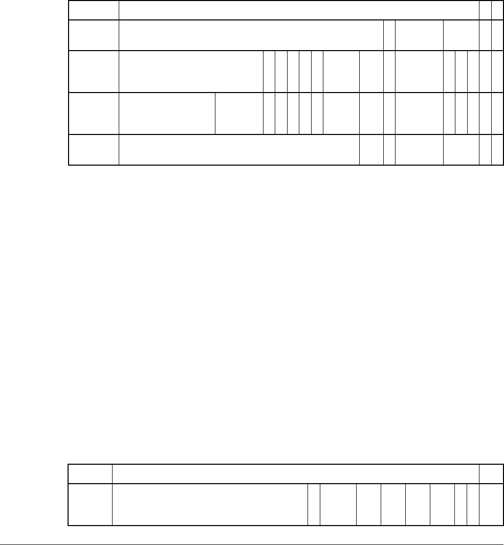
Appendix D15 ARMv4 and ARMv5 Differences
D15.6 System level memory model
D15-2608 Copyright © 1996-1998, 2000, 2004-2012, 2014 ARM. All rights reserved. ARM DDI 0406C.c
Non-Confidential ID051414
First level descriptor formats
Table D15-8 shows the translation table first level descriptor formats:
• Supersection support, the TEX field, and the S bit are only permitted from ARMv5TE. Where these features
are not supported, the corresponding bits must be zero.
• Supersections can support address translation from a 32-bit virtual address to a physical address of up to 40
bits.
Bits[1:0] of the descriptor identify the descriptor type:
0b00
Invalid or fault entry.
0b01
Coarse page table descriptor. Bits[31:10] of the descriptor give the physical address of a second
level translation table.
0b10
Section or Supersection descriptor for the associated Modified Virtual Address (MVA). Bits[31:20]
of the descriptor give the Section address, bits[31:24] provide the Supersection address. Bit[18]
indicates which to use when both are supported.
0b11
Fine page table descriptor. Bits[31:12] of the descriptor give the physical address of a second level
translation table.
Second level Coarse page table descriptor format
In a Coarse page table, each entry provides translation information for 4KB of memory. Large page table entries
must be repeated 16 times to ensure translation of all addresses in the page. Tiny pages are not supported. Coarse
page tables are 1KB in size and must be aligned on a 1KB boundary.
Table D15-9 shows the translation table second level descriptor formats for a second level Coarse page table.
Table D15-8 ARMv4 and ARMv5 first level descriptor format
31 24 23 20 19 15 14 12 11 10 9 8 5 4 3 2 1 0
Fault IGNORED 00
Coarse page
table Coarse page table base address P Domain SBZ 0 1
Section Section base address
S
B
Z
0
S
B
ZSa
S
B
ZTEXbAP P Domain
S
B
Z
CB1 0
Supersection Supersection
base address
PA[35:32]
optional
S
B
Z
1
S
B
Z
S
S
B
Z
TEX AP P PA[39:36]
optional
S
B
Z
CB1 0
Fine page
table Fine page table base address SBZ P Domain SBZ 1 1
a. S=1 indicates Shareable memory. For more information, see Summary of ARMv7 memory attributes on page A3-127.
b. From ARMv5TE, the TEX bits can be used with the C and B bits as described in Short-descriptor format memory
region attributes, without TEX remap on page B3-1367.
Table D15-9 Second level Coarse page descriptor formats
31 161514 1211109876543210
Fault IGNORED 00
Large page Large page base address
S
B
Z
TEX AP3 AP2 AP1 AP0 C B 0 1
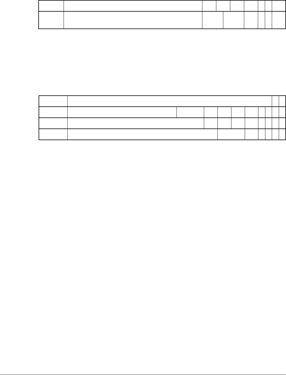
Appendix D15 ARMv4 and ARMv5 Differences
D15.6 System level memory model
ARM DDI 0406C.c Copyright © 1996-1998, 2000, 2004-2012, 2014 ARM. All rights reserved. D15-2609
ID051414 Non-Confidential
Second level Fine page table descriptor format
In a Fine page table, each entry provides translation information for 1KB of memory. Large page table entries must
be repeated 64 times and Small page entries four times to ensure translation of all addresses. Fine tables are 4KB in
size and must be aligned on a 4KB boundary.
Table D15-10 shows the translation table second level descriptor format for a second level Fine page table.
Bits[1:0] of the descriptor identify the descriptor type:
0b00
Invalid or fault entry. The associated MVA is unmapped, and attempting to access it generates a
Translation fault.
0b01
Large page descriptor. Bits[31:16] of the descriptor give the base address of the Large page.
0b10
Small page descriptor. Bits[31:12] of the descriptor give the base address of the Small page.
0b11
Tiny page descriptor. Bits[31:10] of the descriptor give the base address of the Tiny page.
Subpage support
In the Large page and Small page formats in Table D15-10, the page is divided into four equal sized subpages. The
AP0, AP1, AP2, and AP3 fields are the AP bits for subpages 0, 1, 2, and 3 respectively. Subpage 0, controlled by
the AP0 field, is the subpage with the lowest base address.
Small page Small page base address AP3 AP2 AP1 AP0 C B 1 0
Extended
small page
Extended small page base address optional in ARMv5TE,
otherwise reserved SBZ TEX AP C B 1 1
Table D15-9 Second level Coarse page descriptor formats (continued)
31 161514 1211109876543210
Table D15-10 Second level Fine page table descriptor format
31 1615 1211109876543210
Fault IGNORED 00
Large page Large page base address SBZ AP3 AP2 AP1 AP0 C B 0 1
Small page Small page base address AP3 AP2 AP1 AP0 C B 1 0
Tiny page Tiny page base address SBZ AP C B 1 1
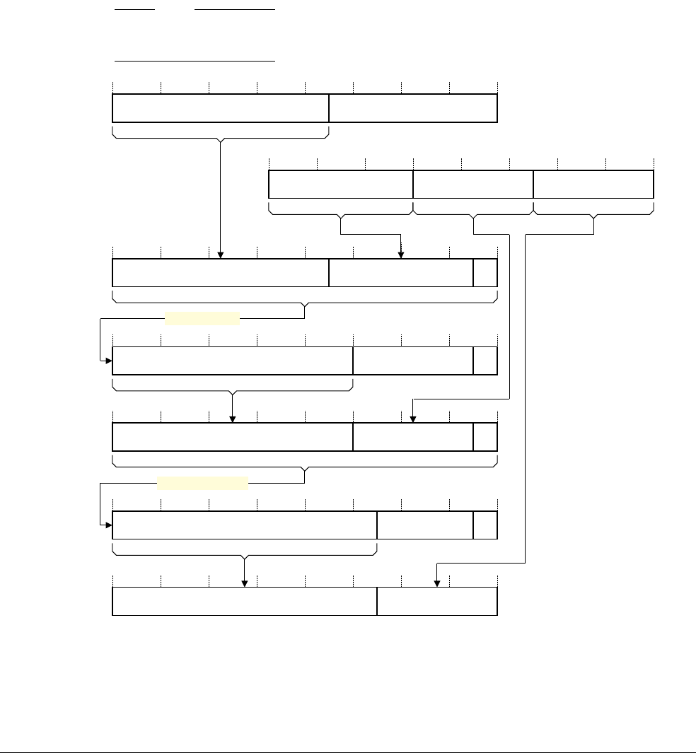
Appendix D15 ARMv4 and ARMv5 Differences
D15.6 System level memory model
D15-2610 Copyright © 1996-1998, 2000, 2004-2012, 2014 ARM. All rights reserved. ARM DDI 0406C.c
Non-Confidential ID051414
Translation table walks
An MVA and TTBR0 are used when accessing translation table information, as follows:
• For a Section translation. See Figure B3-9 on page B3-1335 with N == 0.
• For a Large page translation using a Coarse page table access. See Figure B3-10 on page B3-1336 with
N==0.
• For a Small page translation using a Coarse page table access. See Figure B3-11 on page B3-1337 with
N==0.
• For a Tiny page translation using a Fine page table access. See Figure D15-1.
Note
A Large page table or Small page table translation is performed on a Fine page table access by reducing the second
level translation table base address to bits[31:12] and extending the second level table index to MVA[19:10].
Figure D15-1 Tiny page address translation, VMSAv5 and VMSAv4 only
Access
control fields
31 12 11 2 1 0
Page table base address 1
PA
SBZTranslation base
31 14 13 0
MVA
Translation Table
Base Register
00Translation base
31 0
First-level
table index
2 114 13
First-level
table index
31 20 19 0
Page index
First-level read
First-level
descriptor
10 9
Second-level
table index
00Page table base address
31 0
Second-level
table index
2 112 11
1
Second-level read
Second-level
descriptor
PA of first-level
descriptor
PA of second-level
descriptor
Page index
31 0
Tiny page base address
10 9
Access
control fields
31 10 9 2 1 0
Tiny page base address 1 1

Appendix D15 ARMv4 and ARMv5 Differences
D15.6 System level memory model
ARM DDI 0406C.c Copyright © 1996-1998, 2000, 2004-2012, 2014 ARM. All rights reserved. D15-2611
ID051414 Non-Confidential
D15.6.4 Protected memory support
The MPU based Protected Memory System Architecture (PMSA) is a much simpler memory protection scheme than
the MMU-based VMSA model described in Virtual memory support on page D15-2606. The simplification applies
to both the hardware and the software. PMSA in ARMv4 and ARMv5 differs from that supported in ARMv6 and
ARMv7 in the following ways:
• the programming model is unique to ARMv4 and ARMv5
• the supported number of memory regions is fixed
• background memory support requires use of a region resource
• there is no architecturally-defined recovery mechanism from memory aborts
• there is no default memory map definition.
Control and configuration
Software can use CP15 registers to fully define protection regions, eliminating the VMSA requirements for
hardware to do translation table walks, and for software to set up and maintain the translation tables. This makes
memory checking fully deterministic. However, the level of control is now region based rather than page based. This
means the control is not as fine-grained.
The following features apply:
• The memory is divided into regions. CP15 registers can define the region size, base address, and memory
attributes. For example, cacheability, bufferability, and access permissions of a region.
• Memory region control (read and write access) is permitted only from PL1 modes.
• If an address is defined in multiple regions, a fixed priority scheme (highest region number) defines the
properties of the address being accessed.
• An access to an address that is not defined in any region causes a memory abort.
• All addresses are physical addresses. Address translation is not supported.
• PMSA supports unified (von Neumann) and separate (Harvard) instruction and data address spaces.
Eight regions can be configured, with C, B, and AP[1:0] attribute bits associated with each region. The supported
region sizes are 2NKB, where 2 =< N =< 32. It is IMPLEMENTATION DEFINED if the regions are configurable or fixed
in an implementation:
• as eight unified regions supporting data accesses and instruction fetches
• as eight data regions and eight instruction regions each with independent memory region attributes.
CP15 provides the following support:
• a global MPU enable bit, SCTLR.M
• cacheability register support, a C bit for each region
• bufferability register support, a B bit for each region
• access permission register support that provides AP7[1:0] to AP0[1:0] 2-bit permission fields, an AP field
for each region
• optional extended access permission register support for 4-bit AP fields
• region registers providing a base address, size field, and an enable bit for each region.
For details of the PMSA support in CP15 see CP15 c2, c3, c5, and c6, PMSA support on page D15-2624.

Appendix D15 ARMv4 and ARMv5 Differences
D15.6 System level memory model
D15-2612 Copyright © 1996-1998, 2000, 2004-2012, 2014 ARM. All rights reserved. ARM DDI 0406C.c
Non-Confidential ID051414
The C and B bits are configured according to the type of memory that is to be accessed. For more information, see
Memory type support on page D15-2595. Table D15-11 defines the standard AP bit behavior.
Some implementations also include support for read-only access permission. Table D15-12 defines the extended AP
bit behavior.
Memory access sequence
When the ARM processor generates a memory access, the MPU compares the memory address with the
programmed memory regions as follows:
• If a matching memory region is not found, a memory abort is signaled to the processor.
• If a matching memory region is found, the region information is used as follows:
— The access permission bits determine whether the access is permitted. If the access is not permitted,
the MPU signals a memory abort. Otherwise, the access can proceed.
— The memory region attributes determine the access attributes, for example cacheable or
non-cacheable, as described in Memory type support on page D15-2595.
Note
When a Permission fault occurs, there is no fault status information provision for PMSA in ARMv4 or ARMv5. The
CP15 registers FSR and FAR are only available in implementations with VMSA support.
Table D15-11 PMSA access permissions in ARMv4 and ARMv5
AP[1:0] PL1 permissions User permissions Description
00 No access No access All accesses generate Permission faults
01 Read/write No access PL1 access only
10 Read/write Read-only Writes in User mode generate Permission faults
11 Read/write Read/write Full access
Table D15-12 PMSA extended access permissions in ARMv4 and ARMv5
AP[3:0] PL1 permissions User permissions Description
0000 No access No access All accesses generate a Permission fault
0001 Read/write No access PL1 access only
0010 Read/write Read-only Writes in User mode generate a Permission fault
0011 Read/write Read/write Full access
0100 UNPREDICTABLE UNPREDICTABLE -
0101 Read-only No access PL1 read-only access
0110 Read-only Read-only Read-only access
0111 UNPREDICTABLE UNPREDICTABLE -
1xxx UNPREDICTABLE UNPREDICTABLE -

Appendix D15 ARMv4 and ARMv5 Differences
D15.6 System level memory model
ARM DDI 0406C.c Copyright © 1996-1998, 2000, 2004-2012, 2014 ARM. All rights reserved. D15-2613
ID051414 Non-Confidential
Overlapping regions
The Protection Unit can be programmed with two or more overlapping regions. When overlapping regions are
programmed, a fixed priority scheme is applied to determine the region whose attributes are applied to the memory
access.
Attributes for region 7 take highest priority and those for region 0 take lowest priority. For example:
• Data region 2 is programmed to be 4KB in size, starting from address
0x3000
with AP ==
0b010
(PL1 modes
full access, User mode read-only).
• Data region 1 is programmed to be 16KB in size, starting from address
0x0
with AP ==
0b001
(PL1 modes
access only).
When the processor performs a data load from address
0x3010
while in User mode, the address falls into both region
1 and region 2. Because there is a clash, the attributes associated with region 2 are applied. In this case, the load
would not abort.
Background region
Overlapping regions increase the flexibility of how regions can be mapped onto physical memory devices in the
system. The overlapping properties can also specify a background region. For example, assume a number of
physical memory areas sparsely distributed across the 4GB address space. If only these regions are configured, any
access outside the defined sparse address space aborts. You can override this behavior by programming region 0 to
be a 4GB background region. In this case, if the address does not fall into any of the other regions, the access is
controlled by the attributes specified for region 0.

Appendix D15 ARMv4 and ARMv5 Differences
D15.7 System Control coprocessor, CP15 support
D15-2614 Copyright © 1996-1998, 2000, 2004-2012, 2014 ARM. All rights reserved. ARM DDI 0406C.c
Non-Confidential ID051414
D15.7 System Control coprocessor, CP15 support
Before ARMv6, it is IMPLEMENTATION DEFINED whether a System Control coprocessor, CP15, is implemented.
However, support of ID registers, control registers, cache support, and memory management with virtual or
protected memory support resulted in the widespread adoption of a standard for control and configuration of these
features. That standard is described here. With the exception of a small number of operations and supporting
registers, for example the memory barrier operations described in CP15 c7, Miscellaneous functions on
page D15-2631, all CP15 accesses require PL1 access.
The following sections summarize the CP15 registers known to have been supported in ARMv4 or ARMv5
implementations:
•Organization of CP15 registers in an ARMv4 or ARMv5 VMSA implementation on page D15-2615
•Organization of CP15 registers in an ARMv4 or ARMv5 PMSA implementation on page D15-2616.
For details of the registers provided by a particular implementation see the appropriate Technical Reference Manual,
or other product documentation.
The rest of this section describes the ARMv4 and ARMv5 CP15 support in order of the CRn value.
Note
Definitions of CP15 registers in this appendix apply to both VMSA and PMSA implementations unless otherwise
indicated.
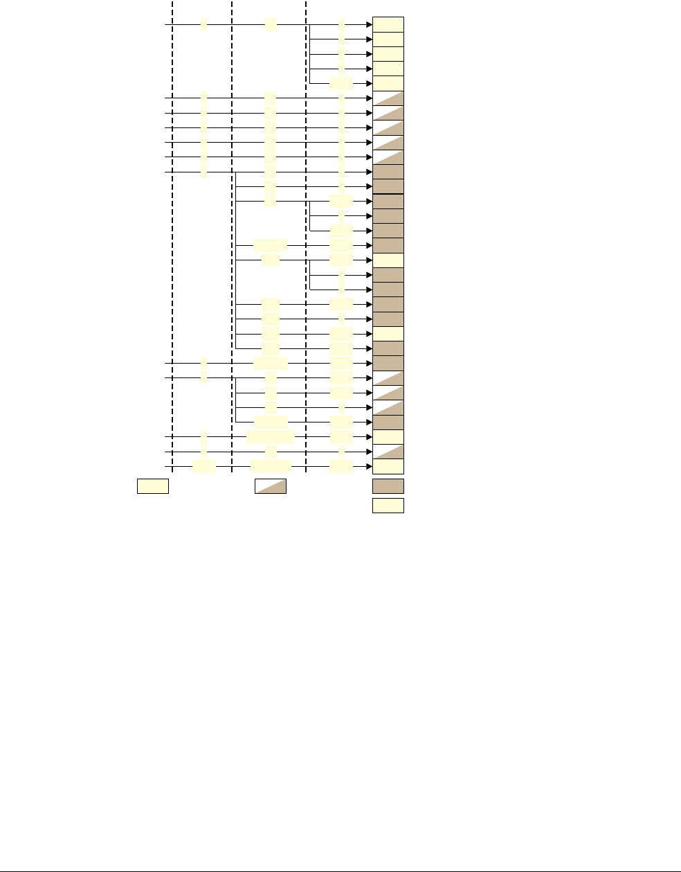
Appendix D15 ARMv4 and ARMv5 Differences
D15.7 System Control coprocessor, CP15 support
ARM DDI 0406C.c Copyright © 1996-1998, 2000, 2004-2012, 2014 ARM. All rights reserved. D15-2615
ID051414 Non-Confidential
D15.7.1 Organization of CP15 registers in an ARMv4 or ARMv5 VMSA implementation
Figure D15-2 shows the CP15 registers in a VMSAv4 or VMSAv5 implementation:
Figure D15-2 CP15 registers in a VMSAv4 or VMSAv5 implementation
¶
MIDR, Main ID Register
CTR, Cache Type Register
TCMTR, TCM Type Register
TLBTR, TLB Type Register
Aliases of Main ID Register
TTBR, Translation Table Base Register
DACR, Domain Access Control Register
FSR, Fault Status Register
FAR, Fault Address Register
CP15WFI, Wait For Interrupt operation
CP15DMB, Data Memory Barrier operation
Cache prefetch operation
Cache maintenance operations
Cache maintenance operations
CP15ISB, Instruction Synchronization Barrier operation
Cache maintenance operations
Cache maintenance operations
TLB maintenance operations
Cache Lockdown (format C) operations
TLB Lockdown Registers
FCSEIDR, FCSE PID Register
IMPLEMENTATION DEFINED registers
CRn opc1 opc2CRm
0
{0-2}
1
2
3
{4-7}
0
0
0
0
4
4
{0-2}
{1-3}
5
{0-2}
1
{1-3}
{0,1}
{0,1}
{0,1}
0
c0
c5
c10
c0
c0
c0
c0
c0
c0
{c6,c7}
c11
c13
c14
{c5-c7}
c0
{c0,c4,c8}
0
0
0
0
0
0
0
0
0
0
c0
c1
c2
c3
c5
c6
c7
c8
c9
c10
c13
c15
SCLTR, System Control Register0c00
Cache maintenance operations
¶
0c2 TCMSR, TCM Selection Register
{0,1}{c5,c6} Cache Lockdown (format C) operations
Cache maintenance operations
5c2
Branch predictor maintenance operations
{6,7}
¶
4 CP15DSB, Data Synchronization Barrier operation
{1-2}c15 Cache maintenance operation
TCM Region registers
{0,1}c1
¶
¶Access depends on operation
Read-only Read/Write Write-only
{0-7} {c0-c15} {0-7}
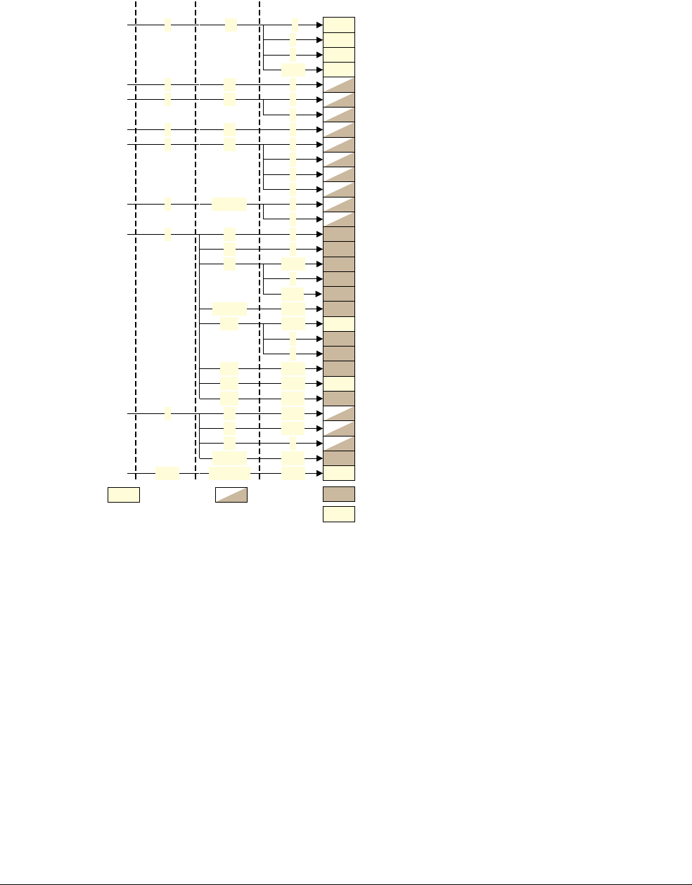
Appendix D15 ARMv4 and ARMv5 Differences
D15.7 System Control coprocessor, CP15 support
D15-2616 Copyright © 1996-1998, 2000, 2004-2012, 2014 ARM. All rights reserved. ARM DDI 0406C.c
Non-Confidential ID051414
D15.7.2 Organization of CP15 registers in an ARMv4 or ARMv5 PMSA implementation
Figure D15-3 shows the CP15 registers in a PMSAv4 or PMSAv5 implementation:
Figure D15-3 CP15 registers in a PMSAv4 or PMSAv5 implementation
MIDR, Main ID Register
CTR, Cache Type Register
TCMTR, TCM Type Register
Aliases of Main ID Register
0
1
2
{3-7}
c00
0
c0
c9 Cache Lockdown (format C) operations
CRn opc1 opc2CRm
SCTLR, System Control Register0
0
1
c00
c1
0{c0-c7}0c6
IAPR, Instruction Region Access Permissions Register
1
1 IMRR0-IMRR7, Instruction Memory Region Registers
IEAPR, Instruction Region Extended Access Permissions Register
3
{0,1}c0
¶
IMPLEMENTATION
DEFINED
Registers{0-7}{c0-c15}{0-7}c15
c00
c2 DCR, Data or unified Region Cacheability Register
ICR, Instruction Region Cacheability Register
0c00c3
0c5 0c0
DBR, Data or unified Region Bufferability Register
DAPR, Data or unified Region Access Permissions Register
DEAPR, Data Region Extended Access Permissions Register
2
DMRR0-DMRR7, Data or unified Memory Region Registers
CP15WFI, Wait For Interrupt operation
c00c7 4
Cache maintenance operation5c2
Cache maintenance operations{0-2}c5
CP15ISB, Instruction Synchronization Barrier operation4
Branch predictor maintenance operations
{6,7}
{0-2}{c6,c7} Cache maintenance operations
{1-3}c10 Cache maintenance operations
4 CP15DSB, Data Synchronization Barrier operation
5 CP15DMB, Data Memory Barrier operation
{0-2}c11
{1,2}c15
¶
{1-3}c14 Cache maintenance operations
¶
Cache maintenance operations
Cache maintenance operation
{0,1}{c5,c6}
TCM Region registers
{0,1}c1
TCMSR, TCM Selection Register
0c2
Cache Lockdown (format D) operations
Read-only Read/Write Write-only
¶Access depends on the operation

Appendix D15 ARMv4 and ARMv5 Differences
D15.7 System Control coprocessor, CP15 support
ARM DDI 0406C.c Copyright © 1996-1998, 2000, 2004-2012, 2014 ARM. All rights reserved. D15-2617
ID051414 Non-Confidential
D15.7.3 CP15 c0, ID support
ARMv4 and ARMv5 implementations support the following ID registers:
•Main ID Register, see CP15 c0, Main ID Register, MIDR, ARMv4 and ARMv5 differences.
•Cache Type Register, see CP15 c0, Cache Type Register, CTR, ARMv4 and ARMv5.
• Optionally, the TCM Type Register, see CP15 c0, TCM Type Register, TCMTR on page D15-2620.
Table D15-13 shows how these read-only registers are accessed using the
MRC
instruction.
CP15 c0, Main ID Register, MIDR, ARMv4 and ARMv5 differences
This register is as described for ARMv7 if either:
• the implementer code in MIDR bits[31:24] is not
0x41
• the top four bits of the primary part number in MIDR bits[15:4] are neither
0x0
nor
0x7
.
If the implementer code is
0x41
and the top four bits of the primary part number are
0x0
, the processor is an obsolete
ARMv2 or ARMv3 processor.
If the implementer code is
0x41
and the top four bits of the primary part number are
0x7
, then:
• If bit[23] is 0, the processor is an obsolete ARMv3 processor.
• If bit[23] is 1, the processor is an ARMv4T processor and bits[22:16] are an IMPLEMENTATION DEFINED
variant number. Bits[31:24, 15:0] are as described for ARMv7.
For the ARMv7 descriptions of the MIDR see:
•MIDR, Main ID Register, VMSA on page B4-1649 for a VMSA implementation
•MIDR, Main ID Register, PMSA on page B6-1894 for a PMSA implementation.
CP15 c0, Cache Type Register, CTR, ARMv4 and ARMv5
The format of the Cache Type Register is significantly different from the ARMv7 definition. However, the general
properties described by the register, and the access rights for the register, are unchanged. For the ARMv7 definition
see:
•CTR, Cache Type Register, VMSA on page B4-1556 for a VMSA implementation
•CTR, Cache Type Register, VMSA on page B4-1556 for a PMSA implementation
This section describes the implementation of the CP15 c0 Cache Type Register and is applicable to a VMSA or
PMSA implementation.
The Cache Type Register supplies the following details about the level 1 cache implementation:
• whether there is a unified cache or separate instruction and data caches
• the cache size, line length, and associativity
• whether it is a write-through cache or a write-back cache
• the cache cleaning and lockdown capabilities.
Table D15-13 ID register support
Register Description CRn opc1 CRm opc2
MIDR Main ID Register c0 0 c0 0
CTR Cache Type ID Register c0 0 c0 1
TCMTR TCM Type Register c0 0 c0 2
- Aliases of MIDR c0 0 c0 3, 4, 5, 6, 7

Appendix D15 ARMv4 and ARMv5 Differences
D15.7 System Control coprocessor, CP15 support
D15-2618 Copyright © 1996-1998, 2000, 2004-2012, 2014 ARM. All rights reserved. ARM DDI 0406C.c
Non-Confidential ID051414
The Cache Type Register bit assignments are:
Bits[31:29] Set to
0b000
before ARMv7.
Ctype, bits[28:25]
Cache type field. Specifies details of the cache not indicated by the S bit and the Dsize and Isize
fields. Table D15-14 shows the encoding of this field. All values not specified in the table are
reserved.
S, bit[24] Separate caches bit. The meaning of this bit is:
0 Unified cache
1 Separate instruction and data caches.
If S == 0, the Isize and Dsize fields both describe the unified cache, and must be identical.
Dsize, bits[23:12]
Specifies the size, line length and associativity of the data cache, or of the unified cache if S == 0.
For details of the encoding see Cache size fields on page D15-2619.
Isize, bits[11:0]
Specifies the size, line length and associativity of the instruction cache, or of the unified cache if
S == 0. For details of the encoding see Cache size fields on page D15-2619.
Table D15-14 shows the Ctype values that can be used in the CTR:
For details of the CP15 c7 operations used for cleaning write-back caches see CP15 c7, Cache and branch predictor
operations on page D15-2629.
Table D15-14 Cache type values
Ctypea
a. CType values not shown are reserved and must not be used.
Cache method Cache lockdownb
b. For details see CP15 c9, cache lockdown support on page D15-2631.
0b0000
Write-through Not supported
0b0010
Write-back Not supported
0b0101
Write-back Format D
0b0110
c
c. In ARMv6 this Ctype value is reserved and must not be used.
Write-back Format A
0b0111
cWrite-back Format B
0b1110
Write-back Format C
0
31 29 28 25 24 23 12 11 0
0 0 Ctype S Dsize Isize

Appendix D15 ARMv4 and ARMv5 Differences
D15.7 System Control coprocessor, CP15 support
ARM DDI 0406C.c Copyright © 1996-1998, 2000, 2004-2012, 2014 ARM. All rights reserved. D15-2619
ID051414 Non-Confidential
Cache size fields
The Dsize and Isize fields in the CTR have the same format:
P For a VMSA implementation, indicates whether the allocation of bits[13:12] of the virtual address
is restricted, imposing the page coloring restriction. The meaning of this field is:
0 No restriction, or PMSA implementation
1 Page coloring restriction applies, see Virtual to physical translation mapping
restrictions on page D12-2523.
Size Indicates the size of the cache, but is qualified by the M bit, see Table D15-15.
Assoc Indicates the associativity of the cache, but is qualified by the M bit, see Cache associativity on
page D15-2620.
M Qualifies the values in the Size and Assoc subfields.
Len Specifies the line length of the cache. The possible values of this field are:
0b00
Line length is 2 words (8 bytes)
0b01
Line length is 4 words (16 bytes)
0b10
Line length is 8 words (32 bytes)
0b11
Line length is 16 words (64 bytes).
Table D15-15 shows how the size of the cache is determined by the Size field and M bit.
Table D15-15 Cache sizes
Size field Size if M == 0 Size if M == 1
0b0000
0.5KB 0.75KB
0b0001
1KB 1.5KB
0b0010
2KB 3KB
0b0011
4KB 6KB
0b0100
8KB 12KB
0b0101
16KB 24KB
0b0110
32KB 48KB
0b0111
64KB 96KB
0b1000
128KB 192KB
11 10 9 6 5 3 2 1 0
P 0 Size Assoc M Len
23 22 21 18 17 15 14 13 12

Appendix D15 ARMv4 and ARMv5 Differences
D15.7 System Control coprocessor, CP15 support
D15-2620 Copyright © 1996-1998, 2000, 2004-2012, 2014 ARM. All rights reserved. ARM DDI 0406C.c
Non-Confidential ID051414
Cache associativity
Table D15-16 show how the associativity of the cache is determined by the Assoc field and the M bit.
The Cache absent encoding overrides all other data in the cache size field.
Excluding the cache absent case (Assoc ==
0b000
, M == 1) you can use the following formulae to determine the
values LINELEN, ASSOCIATIVITY, and NSETS (number of sets) from the Size, Assoc and Len fields of the CTR.
These formulae give the associativity values shown in Table D15-16:
LINELEN = 1 << (Len+3) /* In bytes */
MULTIPLIER = 2 + M
NSETS = 1 << (Size + 6 - Assoc - Len)
ASSOCIATIVITY = MULTIPLIER << (Assoc - 1)
Multiplying these together gives the overall cache size as:
CACHE_SIZE = MULTIPLIER << (Size+8) /* In bytes */
Note
Cache length fields with (Size + 6 - Assoc - Len) < 0 are invalid, because they correspond to impossible
combinations of line length, associativity, and overall cache size. So the formula for NSETS never involves a
negative shift value.
CP15 c0, TCM Type Register, TCMTR
In an ARMv4 or ARMv5 implementation that supports CP15 and TCM, the TCMTR is an optional register. For
details of the TCMTR implementation see CP15 c0, TCM Type Register, TCMTR, ARMv6 on page D12-2529.
Table D15-16 Cache associativity
Assoc field Associativity if:
M == 0 M == 1
0b000
1 way (direct mapped) Cache absent
0b001
2 way 3 way
0b010
4 way 6 way
0b011
8 way 12 way
0b100
16 way 24 way
0b101
32 way 48 way
0b110
64 way 96 way
0b111
128 way 192 way
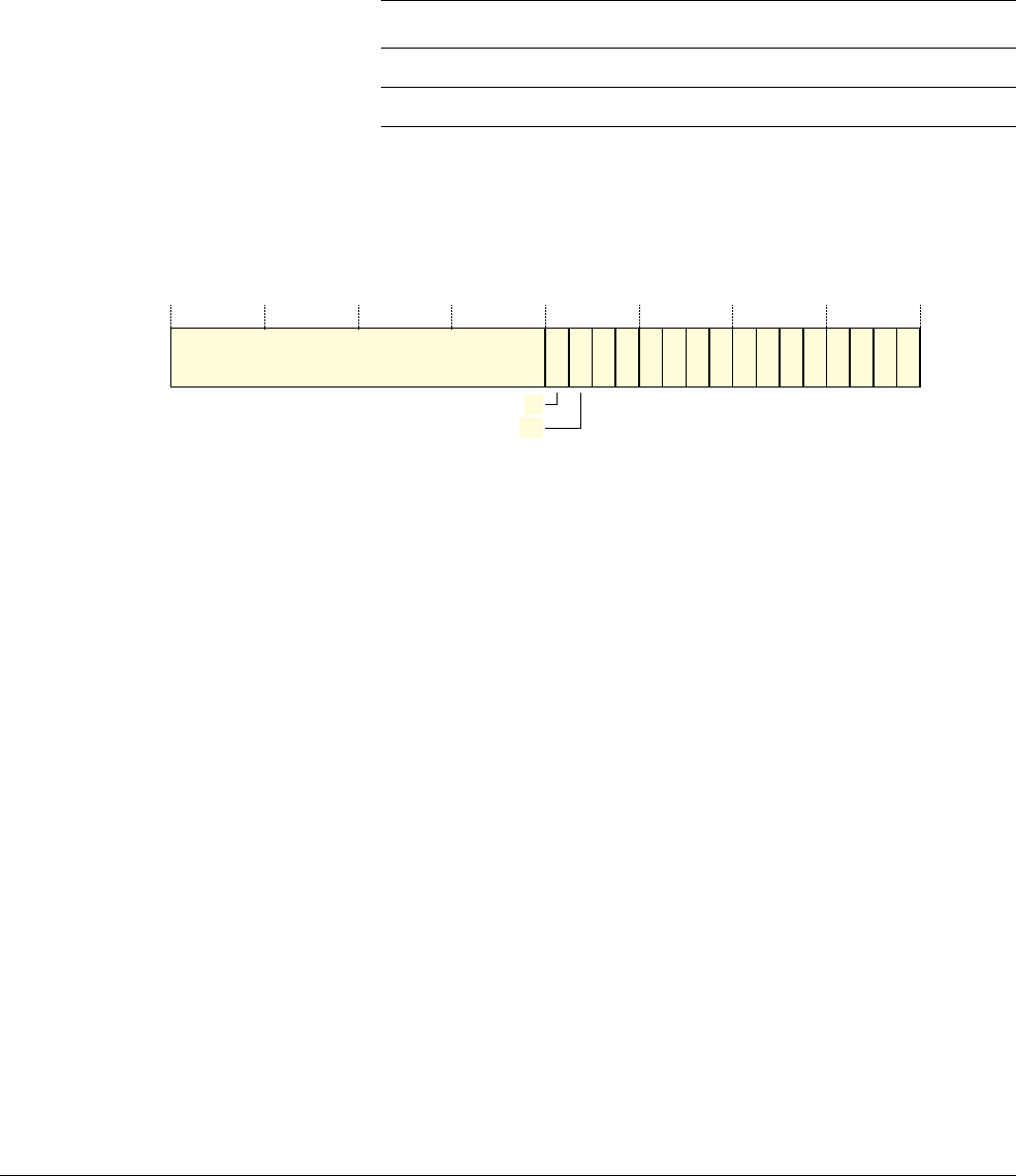
Appendix D15 ARMv4 and ARMv5 Differences
D15.7 System Control coprocessor, CP15 support
ARM DDI 0406C.c Copyright © 1996-1998, 2000, 2004-2012, 2014 ARM. All rights reserved. D15-2621
ID051414 Non-Confidential
D15.7.4 CP15 c1, System control register support
ARMv4 and ARMv5 implementations support the following system control registers:
• a System Control Register, see CP15 c1, System Control Register, SCTLR, ARMv4 and ARMv5
•an
IMPLEMENTATION DEFINED Auxiliary Control Register, ACTLR.
Table D15-17 shows how the registers are accessed using the
MCR
and
MRC
instructions.
SCTLR is the primary system configuration register in CP15.
CP15 c1, System Control Register, SCTLR, ARMv4 and ARMv5
This section describes the implementation of the System Control Register, SCTLR, for ARMv4 and ARMv5. The
SCTLR bit assignments are:
Bits[31:16] Reserved, UNK/SBZP.
These reserved bits in the SCTLR are allocated in some circumstances:
• bits[19:16] can be associated with TCM support
• bit[26], described as the L2 bit, can indicate level 2 cache support, see Level 2 cache support
on page D15-2630.
These usage models are not compatible with ARMv7.
L4, Bit[15] This bit inhibits ARMv5T Thumb interworking behavior when set. It stops bit[0] updating the
CPSR.T bit. From ARMv6, ARM deprecates any use of the feature. ARMv7 does not support this
feature.
RR, bit[14] Round Robin bit. This bit selects an alternative replacement strategy with a more easily predictable
worst-case performance if the cache implementation supports this functionality:
0 Normal replacement strategy, for example random replacement
1 Predictable strategy, for example round robin replacement.
The replacement strategy associated with each value of the RR bit is IMPLEMENTATION DEFINED.
V, bit[13] Vectors bit. This bit selects the base address of the exception vectors:
0 Low exception vectors, base address
0x00000000
1 High exception vectors (Hivecs), base address
0xFFFF0000
.
This base address is never remapped.
Support of the V bit is IMPLEMENTATION DEFINED. An implementation can include a configuration
input signal that determines the reset value of the V bit. If there is no configuration input signal to
determine the reset value of this bit, it resets to 0.
Table D15-17 System control register support
Register Description CRn opc1 CRm opc2
SCTLR System Control Register c1 0 c0 0
ACTLR Auxiliary Control Register c1 0 c0 1
MReserved, UNK/SBZP
31 16 15 14 13 12 11 10 9 8 7 6 5 4 3 2 1 0
V I Z F R S B L D P W C A
L4
RR

Appendix D15 ARMv4 and ARMv5 Differences
D15.7 System Control coprocessor, CP15 support
D15-2622 Copyright © 1996-1998, 2000, 2004-2012, 2014 ARM. All rights reserved. ARM DDI 0406C.c
Non-Confidential ID051414
I, bit[12] Instruction cache enable bit. This is a global enable bit for instruction caches:
0 Instruction caches disabled
1 Instruction caches enabled.
If the system does not implement any instruction caches that can be accessed by the processor at any
level of the memory hierarchy, this bit is RAZ/WI.
If the system implements any instruction caches that can be accessed by the processor then it must
be possible to disable them by setting this bit to 0.
Z, bit[11] Branch prediction enable bit. This bit enables branch prediction, also called program flow
prediction:
0 program flow prediction disabled
1 program flow prediction enabled.
If program flow prediction cannot be disabled, this bit is RAO/WI. Program flow prediction
includes all possible forms of speculative change of instruction stream prediction. Examples include
static prediction, dynamic prediction, and return stacks.
If the implementation does not support program flow prediction this bit is RAZ/WI.
F, bit[10] The meaning of this bit is IMPLEMENTATION DEFINED.
R, bit[9] ROM protection bit, supported for backwards compatibility. The effect of this bit is described in
Table D15-7 on page D15-2607. From ARMv6 ARM deprecates any use of this feature, and
ARMv7 does not support this feature.
S, bit[8] System protection bit, supported for backwards compatibility. The effect of this bit is described in
Table D15-7 on page D15-2607. From ARMv6, ARM deprecates any use of this feature.and
ARMv7 does not support this feature.
B, bit[7] This bit configures the ARM processor to the endianness of the memory system:
0 Little-endian memory system (LE)
1 Big-endian memory system (BE-32).
ARM processors that support both little-endian and big-endian memory systems use this bit to
configure the ARM processor to rename the four byte addresses in a 32-bit word.
Endian support changed in ARMv6. From ARMv6, ARM deprecates any use of this feature, and
ARMv7 does not support this feature.
An implementation can include a configuration input signal that determines the reset value of the B
bit. If there is no configuration input signal to determine the reset value of this bit then it resets to 0.
Bits[6:4] RAO/SBOP.
W, bit[3] This is the enable bit for the write buffer:
0 Write buffer disabled
1 Write buffer enabled.
If the write buffer is not implemented, this bit is RAZ/WI. If the write buffer cannot be disabled, this
bit is RAO and ignores writes. From ARMv6, ARM deprecates any use of this feature. ARMv7 does
not support this feature.
C, bit[2] Cache enable bit. This is a global enable bit for data and unified caches:
0 Data and unified caches disabled
1 Data and unified caches enabled.
If the system does not implement any data or unified caches that can be accessed by the processor
at any level of the memory hierarchy, this bit is RAZ/WI.
If the system implements any data or unified caches that can be accessed by the processor then it
must be possible to disable them by setting this bit to 0.
Appendix D15 ARMv4 and ARMv5 Differences
D15.7 System Control coprocessor, CP15 support
ARM DDI 0406C.c Copyright © 1996-1998, 2000, 2004-2012, 2014 ARM. All rights reserved. D15-2623
ID051414 Non-Confidential
A, bit[1] Alignment bit. This is the enable bit for Alignment fault checking:
0 Alignment fault checking disabled
1 Alignment fault checking enabled.
For more information, see Alignment on page D15-2592.
M, bit[0] Memory control bit. This is a global enable bit to enable an MMU where VMSA is supported, or an
MPU where PMSA is supported:
0 memory management (MMU or MPU) disabled
1 memory management (MMU or MPU) enabled.
D15.7.5 CP15 c2 and c3, VMSA memory protection and control registers
ARMv4 and ARMv5 support a single Translation Table Base Register, TTBR, that is compatible with the ARMv7
TTBR0, and the Domain Access Control Register, DACR.
The TTBR is as defined for the 32-bit TTBR0 for an implementation that does not include the Multiprocessing
Extensions, except that:
• The base address field is a fixed-length field, bits[31:14] (N=0)
• Bit[5] is reserved.
D15.7.6 CP15 c5 and c6, VMSA memory system support
ARMv4 and ARMv5 support a Fault Status Register (FSR) and a Fault Address Register (FAR). These registers are
accessed using
MCR
and
MRC
instructions. Table D15-18 summarizes them.
The FSR is updated on Prefetch Abort exceptions and Data Abort exceptions.
The FAR is equivalent to the ARMv7 DFAR, and is only updated with the MVA on Data Abort exceptions.
CP15 c5, Fault Status Register, FSR, ARMv4 and ARMv5
In ARMv5 and ARMv4 implementations the FSR bit assignments are:
Bits[31:11, 9:8]
Reserved, UNK/SBZP.
Bit[10] FS[4] where defined, otherwise reserved, UNK/SBZP.
Domain, bits[7:4]
The domain of the fault address.
FS, bits[3:0] Fault status bits. Indicate the cause of the fault.
Table D15-18 VMSA fault support
Register Description CRn opc1 CRm opc2
FSR Fault Status Register c5 0 c0 0
FAR Fault Address Register c6 0 c0 0
Reserved, UNK/SBZP
31 11 10 9 8 7 4 3 0
a Domain FS[3:0]
a. It is IMPLEMENTATION DEFINED whether bit[10] is reserved or is an additional fault status bit, FS[4].

Appendix D15 ARMv4 and ARMv5 Differences
D15.7 System Control coprocessor, CP15 support
D15-2624 Copyright © 1996-1998, 2000, 2004-2012, 2014 ARM. All rights reserved. ARM DDI 0406C.c
Non-Confidential ID051414
Table D15-19 lists the base level of fault status encodings returned in the FSR
D15.7.7 CP15 c2, c3, c5, and c6, PMSA support
While the general principles for memory protection in ARMv4 and ARMv5 are the same, CP15 support for
protected memory is different from the programming model of ARMv6 and ARMv7. Memory regions have
configurable base address and size attributes. Other registers define cacheability, bufferability, and access
permissions across the regions. For more information, see Memory model and memory ordering on page D15-2595.
ARMv4 and ARMv5 support a fixed number of memory regions, either:
• eight unified memory regions
• eight data and eight instruction regions.
Table D15-20 shows the PMSA register support.
Table D15-19 VMSAv5 and VMSAv4 FSR encodings
FSR[10] FSR[3:0] Source of fault Domain
0 00x1 Alignment fault Invalid
0 0101
0111 Translation fault Section
Page
Invalid
Valid
0 1001
1011 Domain fault Section
Page
Valid
Valid
0 1100
1110 Translation table walk External Abort First level
Second level
Invalid
Valid
0 1101
1111 Permission fault Section
Page
Valid
Valid
0 0xx0
10x0 IMPLEMENTATION DEFINEDa
a. ARM recommends that any additional codes are compatible with those defined for ARMv6 and
ARMv7 as described in Table B3-23 on page B3-1415.
-
1 xxxx IMPLEMENTATION DEFINEDa-
Table D15-20 PMSA register support
Register Description CRn opc1 CRm opc2
DCR, see xCR Data or unified Cacheability Register c2 0 c0 0
ICR, see xCR Instruction Cacheability Register c2 0 c0 1
DBR Data or unified Bufferability Register c3 0 c0 0
DAPR, see xAPR Data or unified Access Permission Register c5 0 c0 0
IAPR, see xAPR Instruction Access Permission Register c5 0 c0 1
DEAPR, see xEAPR Data or unified Extended Access Permission Register c5 0 c0 2
IEAPR, see xEAPR Instruction Extended Access Permission Register c5 0 c0 3
DMRR0-7, see xMRRn Data or unified Memory Region Registers 0-7 c6 0 c0-c7a0
IMRR0-7, see xMRRn Instruction Memory Region Registers 0-7 c6 0 c0-c7a1
Appendix D15 ARMv4 and ARMv5 Differences
D15.7 System Control coprocessor, CP15 support
ARM DDI 0406C.c Copyright © 1996-1998, 2000, 2004-2012, 2014 ARM. All rights reserved. D15-2625
ID051414 Non-Confidential
If an implementation has a single set of protection regions that apply to both instruction and data accesses, only the
registers that are accessed using even values of
<opc2>
exist. Where separate data and instruction regions are
supported, with the exception of the extended access permission registers, registers associated with data have
<opc2>
== 0 and those associated with instructions have
<opc2>
== 1. All PMSA registers are 32-bit registers and only
accessible from PL1.
CP15 c2, Memory Region Cacheability Registers, DCR and ICR, ARMv4 and ARMv5
The two Memory Region Cacheability Registers are:
• The Data or unified Cacheability Register, DCR.
• The Instruction Cacheability Register, ICR. The ICR is implemented only when the implementation includes
separate data and instruction memory protection region definitions.
A Memory Region Cacheability Registers holds a Cacheability bit, C, for each of the eight memory protection
regions.
The format of an xCR is:
Bits[31:8] Reserved, UNK/SBZP.
Cn, bit[n], for n = 0 to 7
Cacheability bit, C, for memory protection region n.
Accessing the Memory Region Cacheability Registers
To access the Memory Region Cacheability Registers, read or write the CP15 registers with
<opc1>
set to 0,
<CRn>
set
to c2,
<CRm>
set to c0, and
<opc2>
set to:
• 0 for the DCR
• 1 for the IPR.
For example:
MRC p15, 0, <Rt>, c2, c0, 0 ; Read CP15 Data or unified Region Cacheability Register
MCR p15, 0, <Rt>, c2, c0, 0 ; Write CP15 Data or unified Region Cacheability Register
MRC p15, 0, <Rt>, c2, c0, 1 ; Read CP15 Instruction Region Cacheability Register
MCR p15, 0, <Rt>, c2, c0, 1 ; Write CP15 Instruction Region Cacheability Register
CP15 c3, Memory Region Bufferability Register, DBR, ARMv4 and ARMv5
The Memory Region Bufferability Register, DBR, holds Bufferability bit, B, for each of the eight data or unified
memory protection regions.
Only data accesses are bufferable and therefore there is only a single Memory Region Bufferability Register,
regardless of whether the implementation has a single set of protection regions, or separate protection region
definitions for instruction and data accesses.
The DBR bit assignments are:
Bits[31:8] Reserved, UNK/SBZP.
a.
<CRm>
selects the region, for example
<CRm>
== 6 selects the region register for region 6, DMRR6 or IMRR6.
C0Reserved, UNK/SBZP
31 876543210
C7 C6 C5 C4 C3 C2 C1
B0Reserved, UNK/SBZP
31 876543210
B7 B6 B5 B4 B3 B2 B1

Appendix D15 ARMv4 and ARMv5 Differences
D15.7 System Control coprocessor, CP15 support
D15-2626 Copyright © 1996-1998, 2000, 2004-2012, 2014 ARM. All rights reserved. ARM DDI 0406C.c
Non-Confidential ID051414
Bn, bit[n], for n = 0 to 7
Bufferability bit, B, for memory protection region n.
Accessing the Memory Region Bufferability Register
To access the Memory Region Bufferability Register, read or write the CP15 registers with
<opc1>
set to 0,
<CRn>
set
to c3,
<CRm>
set to c0, and
<opc2>
set to 0. For example:
MRC p15, 0, <Rt>, c3, c0, 0 ; Read CP15 Data or unified Region Bufferability Register
MCR p15, 0, <Rt>, c3, c0, 0 ; Write CP15 Data or unified Region Bufferability Register
CP15 c5, Memory Region Access Permissions Registers, DAPR and IAPR, ARMv4 and
ARMv5
The two Memory Region Access Permissions Registers are:
• The Data or unified Access Permissions Register, DAPR.
• The Instruction Access Permissions Register, IAPR. The IAPR is implemented only when the
implementation includes separate data and instruction memory protection region definitions.
A Memory Region Access Permissions Register hold the access permission bits AP[1:0] for each of the eight
memory protection regions.
The format of an xAPR is:
Bits[31:16] Reserved, UNK/SBZP.
APn, bits[2n+1:2n], for n = 0 to 7
Access permission bits AP[1:0] for memory protection region n.
For details of the significance and encoding of these bits see Table D15-11 on page D15-2612.
If the implementation does not permit the requested type of access, it signals an abort to the processor.
Accessing the Memory Region Access Permissions Registers
To access the Memory Region Access Permissions Registers, read or write the CP15 registers with
<opc1>
set to 0,
<CRn>
set to c5,
<CRm>
set to c0, and
<opc2>
set as follows:
• 0 if there is only a single set of protection regions
• when there are separate memory protection regions for data and instructions:
— 0 to access the Data Region Access Permissions Register
— 1 to access the Instruction Region Access Permissions Register.
For example:
MRC p15, 0, <Rt>, c5, c0, 0 ; Read CP15 Data or unified Region Access Permissions Register
MCR p15, 0, <Rt>, c5, c0, 0 ; Write CP15 Data or unified Region Access Permissions Register
MRC p15, 0, <Rt>, c5, c0, 1 ; Read CP15 Instruction Region Access Permissions Register
MCR p15, 0, <Rt>, c5, c0, 1 ; Write CP15 Instruction Region Access Permissions Register
CP15 c5, Memory Region Extended Access Permissions Registers, DEAPR and IEAPR,
ARMv4 and ARMv5
The two Memory Region Extended Access Permissions Registers are:
• The Data or unified Extended Access Permissions Register, DEAPR.
Reserved, UNK/SBZP
31 16 15 14 13 12 11 10 9 8 7 6 5 4 3 2 1 0
AP7 AP6 AP5 AP4 AP3 AP2 AP1 AP0

Appendix D15 ARMv4 and ARMv5 Differences
D15.7 System Control coprocessor, CP15 support
ARM DDI 0406C.c Copyright © 1996-1998, 2000, 2004-2012, 2014 ARM. All rights reserved. D15-2627
ID051414 Non-Confidential
• The Instruction Extended Access Permissions Register, IEAPR. The IEAPR is implemented only when the
implementation includes separate data and instruction memory protection region definitions.
Whether an implementation includes Extended Access Permissions Registers is IMPLEMENTATION DEFINED.
An xEAPR hold the access permission bits AP[3:0] for each of the eight memory protection regions.
The format of an xEAPR is:
APn, bits[4n+3:4n], for n = 0 to 7
Access permission bits AP[3:0] for memory protection region n.
For details of the significance of these bits see Table D15-12 on page D15-2612.
If the implementation does not permit the requested type of access, it signals an abort to the processor.
Accessing the Memory Region Extended Access Permissions Registers
To access the Memory Region Extended Access Permissions Registers, read or write the CP15 registers with
<opc1>
set to 0,
<CRn>
set to c5,
<CRm>
set to c0, and
<opc2>
set as follows:
• 2 if there is only a single set of protection regions
• when there are separate memory protection regions for data and instructions:
— 2 to access the Data Region Extended Access Permissions Register
— 3 to access the Instruction Region Extended Access Permissions Register.
For example:
MRC p15, 0, <Rt>, c5, c0, 2 ; Read CP15 Data or unified Region Extended Access Permissions Register
MCR p15, 0, <Rt>, c5, c0, 2 ; Write CP15 Data or unified Region Extended Access Permissions Register
MRC p15, 0, <Rt>, c5, c0, 3 ; Read CP15 Instruction Region Extended Access Permissions Register
MCR p15, 0, <Rt>, c5, c0, 3 ; Write CP15 Instruction Region Extended Access Permissions Register
CP15 c6, Memory Region Registers, DMRR0-DMRR7 and IMRR0-IMRR7, ARMv4 and
ARMv5
The Memory Region Registers define the MPU memory regions as follows:
• If an implementation supports only a single set of memory region definitions that apply to both data and
instruction accesses, it must provide a single set of eight Data or unified Memory Region Registers,
DMRR0-DMRR7.
• If an implementation supports separate memory region definitions for data and instruction accesses, it must
provide two sets of eight Memory Region Registers:
— eight Data or unified Memory Region Registers, DMRR0-DMRR7
— eight Instruction Memory Region Registers, IMRR0-IMRR7.
Each xMRRn:
• defines a single memory region by specifying its base address and size
• includes an enable bit for the associated memory region.
AP7
31 28 27 24 23 20 19 16 15 12 11 8 7 4 3 0
AP6 AP5 AP4 AP3 AP2 AP1 AP0

Appendix D15 ARMv4 and ARMv5 Differences
D15.7 System Control coprocessor, CP15 support
D15-2628 Copyright © 1996-1998, 2000, 2004-2012, 2014 ARM. All rights reserved. ARM DDI 0406C.c
Non-Confidential ID051414
The format of an xMRRn is:
Region base address, bits[31:12]
Bits[31:12] of the base address for the region. Bits[11:0] of the address must be zero. Therefore, the
smallest region that can be defined is 4KB. Regions must be aligned appropriately, and so for
regions larger than 4KB the least significant bits of this field must be zero. For more information,
see the description of the Size field.
Bits[11:6] Reserved, UNK/SBZP.
Size, bits[5:1]
Encodes the size of the region. Table D15-21 shows the permitted encodings for this field.
Table D15-21 MPU Region size encoding
Encoding Region size Base address constraints
0b01011
4KB None
0b01100
8KB Register bit[12] must be zero
0b01101
16KB Register bits[13:12] must be zero
0b01110
32KB Register bits[14:12] must be zero
0b01111
64KB Register bits[15:12] must be zero
0b10000
128KB Register bits[16:12] must be zero
0b10001
256KB Register bits[17:12] must be zero
0b10010
512KB Register bits[18:12] must be zero
0b10011
1MB Register bits[19:12] must be zero
0b10100
2MB Register bit[20:12] must be zero
0b10101
4MB Register bits[21:12] must be zero
0b10110
8MB Register bits[22:12] must be zero
0b10111
16MB Register bits[23:12] must be zero
0b11000
32MB Register bits[24:12] must be zero
0b11001
64MB Register bits[25:12] must be zero
0b11010
128MB Register bits[26:12] must be zero
0b11011
256MB Register bits[27:12] must be zero
0b11100
512MB Register bits[28:12] must be zero
0b11101
1G Register bits[29:12] must be zero
0b11110
2GB Register bits[30:12] must be zero
0b11111
4GB Register bits[31:12] must be zero
EnRegion base address
31 12 11 6 5 1 0
Reserved,
UNK/SBZP Size

Appendix D15 ARMv4 and ARMv5 Differences
D15.7 System Control coprocessor, CP15 support
ARM DDI 0406C.c Copyright © 1996-1998, 2000, 2004-2012, 2014 ARM. All rights reserved. D15-2629
ID051414 Non-Confidential
Encodings not shown in the table are reserved. The effect of using a reserved value in this field is
UNPREDICTABLE.
En, bit[0] Enable bit for the region:
0 Region is disabled
1 Region is enabled.
This field resets to zero. Therefore all MPU regions are disabled on reset.
The base address constraints given in Table D15-21 on page D15-2628 ensure that the specified region is correctly
aligned in memory, so that its alignment is a multiple of the region size. If a base address is entered that does not
follow these alignment constraints, behavior is UNPREDICTABLE.
Accessing the Region Access Permissions registers
To access the Region Access Permissions registers, read or write the CP15 registers with
<opc1>
set to 0,
<CRn>
set
to c5, and:
•
<CRm>
set to indicate the region number, from
<CRm>
== c0 for memory region 0, to
<CRm>
== c7 for memory
region 7
•
<opc2>
set to:
— 0 if there is only a single set of protection region definitions
— 0 to access the Data Region Access Permissions Register when the data and instruction memory
regions are defined separately
— 1 to access the Instruction Region Access Permissions Register when the data and instruction memory
regions are defined separately.
For example:
MRC p15, 0, <Rt>, c6, c0, 0 ; Read CP15 Data or unified Region Register, Region 0
MCR p15, 0, <Rt>, c6, c0, 0 ; Write CP15 Data or unified Region Register, Region 0
MRC p15, 0, <Rt>, c6, c1, 0 ; Read CP15 Data or unified Region Register, Region 1
MCR p15, 0, <Rt>, c6, c1, 0 ; Write CP15 Data or unified Region Register, Region 1
MRC p15, 0, <Rt>, c6, c2, 1 ; Read CP15 Instruction Memory Region Register, Region 2
MCR p15, 0, <Rt>, c6, c2, 1 ; Write CP15 Instruction Memory Region Register, Region 2
D15.7.8 CP15 c7, Cache and branch predictor operations
Table D15-22 shows the cache operation provision in ARMv4 and ARMv5. All cache operations are performed as
MCR
instructions and only operate on a level 1 cache associated with a specific processor. The equivalent operations
in ARMv7 operate on multiple levels of cache. See Cache and branch predictor maintenance operations, VMSA on
page B4-1743.
Table D15-22 Cache operation support
Operation CRn opc1 CRm opc2
Invalidate instruction cacheac7 0 c5 0
Invalidate instruction cache line by MVAac7 0 c5 1
Invalidate instruction cache line by set/way c7 0 c5 2
Invalidate all branch predictorsac7 0 c5 6
Invalidate branch predictor entry by MVAac7 0 c5 7
Invalidate data cache c7 0 c6 0
Invalidate data cache line by MVAac7 0 c6 1
Invalidate data cache line by set/wayac7 0 c6 2

Appendix D15 ARMv4 and ARMv5 Differences
D15.7 System Control coprocessor, CP15 support
D15-2630 Copyright © 1996-1998, 2000, 2004-2012, 2014 ARM. All rights reserved. ARM DDI 0406C.c
Non-Confidential ID051414
Test and clean operations
This scheme provides an efficient way to clean, or clean and invalidate, a complete data cache by executing an
MRC
instruction with the condition flags as the destination. A global cache dirty status bit is written to the Z flag. How
many lines are tested in each iteration of the instruction is IMPLEMENTATION DEFINED.
To clean an entire data cache with this method the following software loop can be used:
tc_loop MRC p15, 0, APSR_nzcv, c7, c10, 3 ; test and clean
BNE tc_loop
To clean and invalidate an entire data cache with this method, the following software loop can be used:
tci_loop MRC p15, 0, APSR_nzcv, c7, c14, 3 ; test, clean and invalidate
BNE tci_loop
Level 2 cache support
The recommended method for adding closely coupled level 2 cache support from ARMv5TE is to define equivalent
operations to the level 1 support with
<opc1>
== 1 in the appropriate
MCR
instructions. The operations in
Table D15-22 on page D15-2629 that are supported are IMPLEMENTATION DEFINED.
Invalidate unified cache, or instruction cache and data cache c7 0 c7 0
Invalidate unified cache line by MVA c7 0 c7 1
Invalidate unified cache line by set/way c7 0 c7 2
Clean data cache line by MVAac7 0 c10 1
Clean data cache line by set/wayac7 0 c10 2
Clean entire unified cache c7 0 c11 0
Clean unified cache line by MVAac7 0 c11 1
Clean unified cache line by set/way c7 0 c11 2
Prefetch instruction cache line by MVAbc7 0 c13 1
Clean and Invalidate data cache line by MVAac7 0 c14 1
Clean and Invalidate data cache line by set/wayac7 0 c14 2
Clean and Invalidate unified cache line by MVA c7 0 c15 1
Clean and Invalidate unified cache line by set/way c7 0 c15 2
Test and Clean data cache c7 0 c10 3
Test and Clean and Invalidate data cache c7 0 c14 3
a. These are the only cache operations available in ARMv7. The corresponding ARMv7 operations are
multi-level operations, and the data cache operations are defined as data or unified cache operations.
b. Used with TLB lockdown. See TLB lockdown procedure, using the by entry model on page D15-2639.
Table D15-22 Cache operation support (continued)
Operation CRn opc1 CRm opc2

Appendix D15 ARMv4 and ARMv5 Differences
D15.7 System Control coprocessor, CP15 support
ARM DDI 0406C.c Copyright © 1996-1998, 2000, 2004-2012, 2014 ARM. All rights reserved. D15-2631
ID051414 Non-Confidential
D15.7.9 CP15 c7, Miscellaneous functions
The Wait For Interrupt operation is used in some implementations as part of a power management support scheme.
From ARMv6, ARM deprecates any use of this operation. ARMv7 does not support this operation, and it behaves
as a
NOP
instruction.
Barrier operations are used for system correctness to ensure visibility of memory accesses to other agents in a
system. For ARMv4 and ARMv5 the requirement for and use of barrier operations is IMPLEMENTATION DEFINED.
Barrier functionality is formally defined as part of the memory architecture enhancements introduced in ARMv6.
Table D15-23 summarizes the
MCR
instruction encoding details.
D15.7.10 CP15 c8, VMSA TLB support
Table D15-24 illustrates TLB operation provision in ARMv4 and ARMv5. All TLB operations are performed as
MCR
instructions and are a subset of the operations available in ARMv7. See TLB maintenance operations, not in Hyp
mode on page B4-1746.
D15.7.11 CP15 c9, cache lockdown support
One problem with caches is that although they normally improve average access time to data and instructions, they
usually increase the worst-case access time. This is because:
• There is a delay before the system determines that a cache miss has occurred and starts the main memory
access.
• If a write-back cache is being used, there might be more delay because of the requirement to store the contents
of the cache line that is being reallocated.
• A whole cache line is loaded from main memory, not only the data requested by the ARM processor.
In real-time applications, this increase in the worst-case access time can be significant.
Table D15-23 Memory barrier register support
Operation Description CRn opc1 CRm opc2
CP15WFI Wait For Interrupt c7 0 c0 4
CP15ISB Instruction Synchronization Barriera
a. This operation was previously called Prefetch Flush (PF or PFF).
c7 0 c5 4
CP15DSB Data Synchronization Barrierb
b. This operation was previously called Data Write Barrier or Drain Write Buffer (DWB).
c7 0 c10 4
CP15DMB Data Memory Barrier c7 0 c10 5
Table D15-24 TLB operation support
Operation CRn opc1 CRm opc2
Invalidate Instruction TLB c8 0 c5 0
Invalidate Instruction TLB entry by MVA c8 0 c5 1
Invalidate Data TLB c8 0 c6 0
Invalidate Data TLB entry by MVA c8 0 c6 1
Invalidate Unified TLB c8 0 c7 0
Invalidate Unified TLB entry by MVA c8 0 c7 1

Appendix D15 ARMv4 and ARMv5 Differences
D15.7 System Control coprocessor, CP15 support
D15-2632 Copyright © 1996-1998, 2000, 2004-2012, 2014 ARM. All rights reserved. ARM DDI 0406C.c
Non-Confidential ID051414
Cache lockdown is an optional feature designed to alleviate this. It enables critical software and data, for example
high priority interrupt routines and the data they access, to be loaded into the cache in such a way that the cache
lines containing them are not subsequently reallocated. This ensures that all subsequent accesses to this software
and data are cache hits and therefore complete as quickly as possible.
The ARM architecture specifies four formats for the cache lockdown mechanism. These are called Format A,
Format B, Format C, and Format D. The Cache Type Register contains information on the lockdown mechanism
adopted. See CP15 c0, Cache Type Register, CTR, ARMv4 and ARMv5 on page D15-2617.
Formats A, B, and C all operate on cache ways. Format D is a cache entry locking mechanism. Table D15-25
summarizes the CP15 provisions for format A, B, C, and D lockdown mechanisms.
From ARMv7, cache lockdown is IMPLEMENTATION DEFINED with no recommended formats or mechanisms on
how it is achieved other than reserved CP15 register space. See Cache lockdown on page B2-1270 and Cache and
TCM lockdown registers, VMSA on page B4-1753.
General conditions applying to Format A, B, and C lockdown
The instructions that access the CP15 c9 lockdown registers are as follows:
MCR p15, 0, <Rt>, c9, c0, 0 ; write Data or unified Cache Lockdown Register
MRC p15, 0, <Rt>, c9, c0, 0 ; read Data or unified Cache Lockdown Register
MCR p15, 0, <Rt>, c9, c0, 1 ; write Instruction Cache Lockdown Register
MRC p15, 0, <Rt>, c9, c0, 1 ; read Instruction Cache Lockdown Register
Formats A, B, and C all use cache ways for lockdown granularity. Granularity is defined by the lockdown block, and
a cache locking scheme can use any number of lockdown blocks from 1 to (ASSOCIATIVITY-1).
If N lockdown blocks are locked down, they have indices 0 to N-1, and lockdown blocks N to (ASSOCIATIVITY-1)
are available for normal cache operation.
A cache way based lockdown implementation must not lock down the entire cache. At least one cache way must be
left for normal cache operation, otherwise behavior is UNPREDICTABLE.
The lockdown blocks are indexed from 0 to (ASSOCIATIVITY-1). The cache lines in a lockdown block are chosen
to have the same WAY number as the lockdown block index value. So lockdown block n consists of the cache line
with index n from each cache set, and n takes the values from n == 0 to n == (ASSOCIATIVITY-1).
Where
NSETS
is the number of sets, and
LINELEN
is the cache line length, each lockdown block can hold NSETS
memory cache lines, provided each of the memory cache lines is associated with a different cache set. ARM
recommends that systems are designed so that each lockdown block contains a set of NSETS consecutive memory
cache lines. This is NSETS × LINELEN consecutive memory locations, starting at a cache line boundary. Such sets
are easily identified and are guaranteed to consist of one cache line associated with each cache set.
Formats A and B lockdown
Formats A and B use a WAY field that is chosen to be wide enough to hold the way number of any lockdown block.
Its width, W, is given by W = log2(ASSOCIATIVITY), rounded up to the nearest integer if necessary.
Table D15-25 cache lockdown register support
Register Description, or operation Lockdown formats CRn opc1 CRm opc2
DCLR Data or unified Cache Lockdown Register A, B, and C c9 0 c0 0
ICLR Instruction Cache Lockdown Register A, B, and C c9 0 c0 1
- Fetch and lock instruction cache line D c9 0 c5 0
- Unlock instruction cache D c9 0 c5 1
DCLR2 Format D Data or unified Cache Lockdown Register D c9 0 c6 0
- Unlock data cache D c9 0 c6 1
Appendix D15 ARMv4 and ARMv5 Differences
D15.7 System Control coprocessor, CP15 support
ARM DDI 0406C.c Copyright © 1996-1998, 2000, 2004-2012, 2014 ARM. All rights reserved. D15-2633
ID051414 Non-Confidential
The format of a Format A lockdown register is:
Reading a Format A register returns the value last written to it.
Writing a Format A register has the following effects:
• The next cache miss in each cache set replaces the cache line with the specified WAY in that cache set.
• The replacement strategy for the cache is constrained so that it can only select cache lines with the specified
WAY and higher until the register is written again.
The format of a Format B lockdown register is:
Reading a Format B register returns the value last written to it.
Writing a Format B register has the following effects:
• If L == 1, all cache misses replace the cache line with the specified WAY in the relevant cache set until the
register is written again.
•If L ==0:
— If the previous value of L was 0, and the previous value of WAY is smaller than the new value, the
behavior is UNPREDICTABLE.
— If the previous value of L was not 0, the replacement strategy for the cache is constrained so that it can
only select cache lines with the specified WAY and higher until the register is written again.
Format A and B cache lockdown procedure
The procedure for locking down N lockdown blocks is as follows:
1. Ensure that no processor exceptions can occur during the execution of this procedure, for example by
disabling interrupts. If for some reason this is not possible, all software and data used by any exception
handlers that can get called must be treated as software and data used by this procedure for the purpose of
steps 2 and 3.
2. If an instruction cache or a unified cache is being locked down, ensure that all the software executed by this
procedure is in an Non-cacheable area of memory.
3. If a data cache or a unified cache is being locked down, ensure that all data used by the following software
is in an Non-cacheable area of memory, apart from the data that is to be locked down.
4. Ensure that the data or instructions that are to be locked down are in a Cacheable area of memory.
5. Ensure that the data or instructions that are to be locked down are not already in the cache, using cache clean,
invalidate, or clean and invalidate instructions as appropriate.
6. For each value of i from 0 to N-1:
a. Write to the CP15 c9 register with:
• WAY == i, for Formats A and B
• L == 1, for Format B only.
b. For each of the cache lines to be locked down in lockdown block i:
If a data cache or a unified cache is being locked down, use an
LDR
instruction to load a word from the
memory cache line. This ensures that the memory cache line is loaded into the cache.
If an instruction cache is being locked down, use the CP15 c7 prefetch instruction cache line operation
to fetch the memory cache line into the cache.
WAY
31
32-W 31-W
0
Reserved, UNK/SBZP
L
31 30 W W-1 0
Reserved, UNK/SBZP WAY

Appendix D15 ARMv4 and ARMv5 Differences
D15.7 System Control coprocessor, CP15 support
D15-2634 Copyright © 1996-1998, 2000, 2004-2012, 2014 ARM. All rights reserved. ARM DDI 0406C.c
Non-Confidential ID051414
7. Write to the CP15 c9 register with:
• WAY == N, for Formats A and B
• L == 0, for Format B only.
Note
If the FCSE described in Appendix D10 Fast Context Switch Extension (FCSE) is being used, care must be taken
in step 6b because:
• If a data cache or a unified cache is being locked down, the address used for the
LDR
instruction is subject to
modification by the FCSE.
• If an instruction cache is being locked down, the address used for the CP15 c7 operation is treated as data and
so is not subject to modification by the FCSE.
To minimize the possible confusion caused by this, ARM recommends that the lockdown procedure:
• starts by disabling the FCSE (by setting the PID to zero)
• where appropriate, generates modified virtual addresses itself by ORing the appropriate PID value into the
top seven bits of the virtual addresses it uses.
Format A and B cache unlock procedure
To unlock the locked down portion of the cache, write to the CP15 c9 register with:
• WAY == 0, for Formats A and B
• L == 0, for Format B only.
Format C lockdown
Cache lockdown Format C is a different form of cache way based locking. It enables the allocation to each cache
way to be disabled or enabled. This provides some additional control over the cache pollution caused by particular
applications, in addition to a traditional lockdown function for locking critical regions into the cache.
A locking bit for each cache way determines whether the normal cache allocation mechanisms can access that cache
way.
For caches of higher associativity, only cache ways 0 to 31 can be locked.
A maximum of N-1 ways of an N-way cache can be locked. This ensures that a normal cache line replacement can
be performed. Handling a cache miss is UNPREDICTABLE if there are no cache ways that have L==0.
The 32 bits of the lockdown register determine the L bit for the associated cache way. The value of
<opc2>
determines whether the instruction lockdown register or data lockdown register is accessed.
The cache lockdown register is normally modified in a read, modify, write sequence. For example, the following
sequence sets the L bit to 1 for way 0 of the instruction cache:
; In the following code, <Rn> can be any register whose value does not need to be kept.
MRC p15, 0, <Rn>, c9, c0, 1 ; Read Instruction Cache Lockdown Register
ORR <Rn>, <Rn>, #0x01
MCR p15, 0, <Rn>, c9, c0, 1 ; Write Instruction Cache Lockdown Register
; The write sets way 0 L bit for the instruction cache

Appendix D15 ARMv4 and ARMv5 Differences
D15.7 System Control coprocessor, CP15 support
ARM DDI 0406C.c Copyright © 1996-1998, 2000, 2004-2012, 2014 ARM. All rights reserved. D15-2635
ID051414 Non-Confidential
The Format C lockdown register bit assignments are:
Bits[31:0] The L bits for each cache way. If a cache way is not implemented, the L bit for that way is RAO/WI.
Each bit relates to its corresponding cache way, that is bit N refers to way N.
0 Allocation to the cache way is determined by the standard replacement algorithm (reset
state)
1 No Allocation is performed to this cache way.
The Format C lockdown register must only be changed when it is certain that all outstanding accesses that can cause
a cache linefill have completed. For this reason, a Data Synchronization Barrier instruction must be executed before
the lockdown register is changed.
Format C cache lock procedure
The procedure for locking down into a cache way i with N cache ways using Format C involves making it
impossible to allocate to any cache way other than the target cache way i. The architecture defines the following
method for locking data into the caches:
1. Ensure that no processor exceptions can occur during the execution of this procedure, for example by
disabling interrupts. If for some reason this is not possible, all software and data used by any exception
handlers that can get called must be treated as software and data used by this procedure for the purpose of
steps 2 and 3.
2. If an instruction cache or a unified cache is being locked down, ensure that all the software executed by this
procedure is in an Non-cacheable area of memory, including the Tightly Coupled Memory, or in an already
locked cache way.
3. If a data cache or a unified cache is being locked down, ensure that all data used by the following software
(apart from the data that is to be locked down) is in an Non-cacheable area of memory, including the Tightly
Coupled Memory, or is in an already locked cache way.
4. Ensure that the data or instructions that are to be locked down are in a Cacheable area of memory.
5. Ensure that the data or instructions that are to be locked down are not already in the cache, using cache clean,
invalidate, or clean and invalidate instructions as appropriate.
6. Write to the CP15 c9 register with CRm == 0, setting L=0 for bit i and L=1 for all other bits. This enables
allocation to the target cache way i.
7. For each of the cache lines to be locked down in cache way i:
• If a data cache or a unified cache is being locked down, use an
LDR
instruction to load a word from the
memory cache line. This ensures that the memory cache line is loaded into the cache.
• If an instruction cache is being locked down, use the CP15 c7 prefetch instruction cache line operation
to fetch the memory cache line into the cache.
8. Write to the CP15 c9 register with CRm == 0, setting L = 1 for bit i and restoring all the other bits to the
values they had before this routine was started.
Format C cache unlock procedure
To unlock the locked down portion of the cache, write to the CP15 c9 register, setting L == 0 for each bit.
Format D lockdown
This format locks individual L1 cache line entries rather than using a cache way scheme. The methods differ for the
instruction and data caches.
One L bit for each cache way
31 0

Appendix D15 ARMv4 and ARMv5 Differences
D15.7 System Control coprocessor, CP15 support
D15-2636 Copyright © 1996-1998, 2000, 2004-2012, 2014 ARM. All rights reserved. ARM DDI 0406C.c
Non-Confidential ID051414
The instructions that access the CP15 c9 Format D Cache Lockdown Registers and operations are as follows:
MCR p15, 0, <Rt>, c9, c5, 0 ; fetch and lock instruction cache line,
; Rt = MVA
MCR p15, 0, <Rt>, c9, c5, 1 ; unlock instruction cache,
; Rt ignored
MCR p15, 0, <Rt>, c9, c6, 0 ; write Format D Data Cache Lockdown Register,
; Rt = set or clear lockdown mode
MRC p15, 0, <Rt>, c9, c6, 0 ; read Format D Data Cache Lockdown Register,
; Rt = lockdown mode status
MCR p15, 0, <Rt>, c9, c6, 1 ; unlock data cache,
; Rt ignored
Note
Some format D implementations use CRm == {c1, c2} instead of CRm == {c5, c6}. You must check the Technical
Reference Manual to find the encoding uses. The architecture did not require the implementation of CP15, and the
Architecture Reference Manual only gave a recommended implementation. The actual CP15 implementation is
IMPLEMENTATION DEFINED in ARMv4 and ARMv5.
The following rules determine how many entries in a cache set can be locked:
• At least one entry per cache set must be left for normal cache operation, otherwise behavior is
UNPREDICTABLE.
• How many ways in each cache set can be locked is IMPLEMENTATION DEFINED.
MAX_CACHESET_ENTRIES_LOCKED < NWAYS.
• Whether attempts to lock additional entries in Format D are allocated as an unlocked entry or ignored is
IMPLEMENTATION DEFINED.
For the instruction cache, a fetch and lock operation fetches and locks individual cache lines. Each cache line is
specified by its MVA. To lock instructions into the instruction cache, the following rules apply:
• The routine that locks lines into the instruction cache must be executed from Non-cacheable memory.
• The memory that holds the instructions being locked into the instruction cache must be Cacheable.
• The instruction cache must be enabled and invalidated before locking down cache lines.
If these rules are not applied, results are UNPREDICTABLE. Entries must be unlocked using the global instruction
cache unlock command.
Cache lines must be locked into the data cache by first setting a global lock control bit. Data cache linefills occurring
while the global lock control bit is set are locked into the data cache. To lock data into the data cache, the following
rules apply:
• The data being locked must not exist in the cache. Cache clean and invalidate operations might be necessary
to meet this condition.
• The data to be locked must be Cacheable.
• The data cache must be enabled.
CP15 c9, Format D Data or unified Cache Lockdown Register, DCLR2, ARMv4 and ARMv5
The DCLR2, the Format D Data or unified Cache Lockdown Register, bit assignments are:
L, bit[0] Lock bit
0 no locking occurs
1 all data fills are locked while this bit is set.
LReserved, UNK/SBZP
31 10

Appendix D15 ARMv4 and ARMv5 Differences
D15.7 System Control coprocessor, CP15 support
ARM DDI 0406C.c Copyright © 1996-1998, 2000, 2004-2012, 2014 ARM. All rights reserved. D15-2637
ID051414 Non-Confidential
Interaction with CP15 c7 operations
Cache lockdown only prevents the normal replacement strategy used on cache misses choosing to reallocate cache
lines in the locked down region. CP15 c7 operations that invalidate, clean, or clean and invalidate cache contents
affect locked down cache lines as normal. If invalidate operations are used, you must ensure that they do not use
virtual addresses or cache set/way combinations that affect the locked down cache lines. Otherwise, if it is difficult
to avoid affecting the locked down cache lines, repeat the cache lockdown procedure afterwards.
D15.7.12 CP15 c9, TCM support
TCM register support is optional when CP15 and TCM are supported in ARMv4 and ARMv5. For details see CP15
c9, TCM support on page D12-2540.
Appendix D15 ARMv4 and ARMv5 Differences
D15.7 System Control coprocessor, CP15 support
D15-2638 Copyright © 1996-1998, 2000, 2004-2012, 2014 ARM. All rights reserved. ARM DDI 0406C.c
Non-Confidential ID051414
D15.7.13 CP15 c10, TLB lockdown support, VMSA
TLB lockdown is an optional feature that enables the results of specified translation table walks to load into the TLB
in a way that prevents them being overwritten by the results of subsequent translation table walks.
Translation table walks can take a long time because they involve potentially slow main memory accesses. In
real-time interrupt handlers, translation table walks caused by the TLB that do not contain translations for the
handler or the data it accesses can increase interrupt latency significantly.
Two basic lockdown models are supported:
• a TLB lock by entry model
• a translate and lock model introduced as an alternative model in ARMv5TE.
In an ARMv6 implementation that includes the Security Extensions, c10 TLB Lockdown registers are Configurable
access registers, with access controlled by the NSACR. For more information, see:
•Configurable access system control registers on page B3-1453 for general information
•NSACR, Non-Secure Access Control Register, Security Extensions on page B4-1662 and CP15 c1, VMSA
Security Extensions support on page D12-2531 for details of the NSACR.
From ARMv7, TLB lockdown is IMPLEMENTATION DEFINED with no recommended formats or mechanisms on how
it is achieved other than reserved CP15 register space. See TLB lockdown on page B3-1379 and VMSA CP15 c10
register summary, memory remapping and TLB control registers on page B3-1478.
Table D15-26 shows the TLB operations that support the different mechanisms.
The TLB lock by entry model
When a new entry is written to the TLB as the result of a translation table walk following a TLB miss, the Victim
field of the appropriate TLB Lockdown Register is incremented. When the value of the Victim field reaches the
maximum number of TLB entries, the incremented Victim field wraps to the value of the Base field.
The architecture permits a modified form of this where the Base field is fixed as zero. It is particularly appropriate
where an implementation provides dedicated lockable entries (unified or Harvard) as a separate resource from the
general TLB provision. To determine which form of the locking model is provided, write the Base field with all bits
nonzero, read it back and check whether it is a nonzero value.
TLB Lockdown Register format, for the lockdown by entry mechanism
The bit assignments of the CP15 register used for the lockdown by entry mechanism are:
Table D15-26 TLB lockdown register support
Register Description, or operation Type Mechanism CRn opc1 CRm opc2
DTLBLR Data or unified TLB Lockdown Register RW By entry c10 0 c0 0
ITLBLR Instruction TLB Lockdown Register RW By entry c10 0 c0 1
- Lock instruction TLB WO Translate and lock c10 0 c4 0
- Unlock instruction TLB WO Translate and lock c10 0 c4 1
- Lock data TLB WO Translate and lock c10 0 c8 0
- Unlock data TLB WO Translate and lock c10 0 c8 1
PBase
31
32-W 31-W 32-2W 31-2W
10
Victim Reserved, UNK/SBZP
Where W = log2(n), rounded up to an integer if necessary, where n is the number of TLB entries.

Appendix D15 ARMv4 and ARMv5 Differences
D15.7 System Control coprocessor, CP15 support
ARM DDI 0406C.c Copyright © 1996-1998, 2000, 2004-2012, 2014 ARM. All rights reserved. D15-2639
ID051414 Non-Confidential
If the implementation has separate instruction and data TLBs, there are two variants of this register, selected by the
<opc2>
field of the
MCR
or
MRC
instruction that accesses the CP15 c10 register:
<opc2> == 0
Selects the data TLB lockdown register.
<opc2> == 1
Selects the instruction TLB lockdown register.
If the implementation has a unified TLB, only one variant of this register exists, and
<opc2>
must be zero.
CRm must be c0 for
MCR
and
MRC
instructions that access the CP15 c10 register.
Writing the appropriate TLB lockdown by entry register has the following effects:
• The victim field specifies which TLB entry is replaced by the translation table walk result generated by the
next TLB miss.
• The Base field constrains the TLB replacement strategy to only use the TLB entries numbered from (Base)
to ((number of TLB entries)-1), provided the victim field is already in that range.
• Any translation table walk results written to TLB entries when P == 1 are protected from being invalidated
by the CP15 c8 invalidate entire TLB operations. Ones written when P == 0 are invalidated normally by these
operations.
Note
If the number of TLB entries is not a power of two, writing a value to either the Base or Victim fields that is greater
than or equal to the number of TLB entries has UNPREDICTABLE results.
Reading the appropriate TLB lockdown by entry register returns the last values written to the Base field and the P
bit, and the number of the next TLB entry to be replaced in the victim field.
TLB lockdown procedure, using the by entry model
The normal procedure for locking down N TLB entries where the Base field can be modified is as follows:
1. Ensure that no processor exceptions can occur during the execution of this procedure, for example by
disabling interrupts.
2. If an instruction TLB or unified TLB is being locked down, write the appropriate version of register c10 with
Base == N, Victim == N, and P == 0. If appropriate, turn off facilities like branch prediction that make
instruction fetching harder to understand.
3. Invalidate the entire TLB to be locked down.
4. If an instruction TLB is being locked down, ensure that all TLB entries are loaded that relate to any
instruction that could be speculatively fetched by the rest of the lockdown procedure. Provided care is taken
about where the lockdown procedure starts, one TLB entry can usually cover all of these. This means that the
first instruction fetch after the TLB is invalidated can do this job.
If a data TLB is being locked down, ensure that all TLB entries are loaded that relate to any data accessed by
the rest of the lockdown procedure, including any inline literals used by its software. Usually the best way to
do this is to avoid using inline literals in the lockdown procedure, and to put all other data used by it in an
area covered by a single TLB entry, and then to load one data item.
If a unified TLB is being locked down, do both of the above.

Appendix D15 ARMv4 and ARMv5 Differences
D15.7 System Control coprocessor, CP15 support
D15-2640 Copyright © 1996-1998, 2000, 2004-2012, 2014 ARM. All rights reserved. ARM DDI 0406C.c
Non-Confidential ID051414
5. For each of value of i from 0 to N-1:
a. Write to the CP15 c10 register with Base == i, Victim == i, and P == 1.
b. Force a translation table walk to occur for the area of memory whose translation table walk result is to
be locked into TLB entry i as follows:
• If a data TLB or unified TLB is being locked down, load an item of data from the area of
memory.
• If an instruction TLB is being locked down, use the CP15 c7 prefetch instruction cache line
operation defined in Table D15-22 on page D15-2629 to fetch an instruction from the area of
memory.
Note
If the FCSE is being used, take care in step 5b because:
• If a data TLB or a unified TLB is being locked down, the address used for the load instruction is subject
to modification by the FCSE.
• If an instruction TLB is being locked down, the address used for the CP15 c7 operation is being treated
as data and so is not subject to modification by the FCSE.
To minimize the possible confusion caused by this, ARM recommends that the lockdown procedure:
• starts by disabling the FCSE, by setting the PID to zero
• where appropriate, generates modified virtual addresses itself by ORing the appropriate PID value into
the top 7 bits of the virtual addresses it uses.
6. Write to the CP15 c10 register with Base == N, Victim == N, and P == 0.
Where the Base field is fixed at zero, the algorithm can be simplified as follows:
1. Ensure that no processor exceptions can occur during the execution of this procedure, for example by
disabling interrupts.
2. If any current locked entries must be removed, an appropriate sequence of invalidate single entry operations
is required.
3. Turn off branch prediction.
4. If an instruction TLB is being locked down, ensure that all TLB entries are loaded that relate to any
instruction that could be speculatively fetched by the rest of the lockdown procedure. Provided care is taken
about where the lockdown procedure starts, one TLB entry can usually cover all of these. This means that the
first instruction fetch after the TLB is invalidated can do this job.
If a data TLB is being locked down, ensure that all TLB entries are loaded that relate to any data accessed by
the rest of the lockdown procedure, including any inline literals used by its software. Usually the best way to
do this is to avoid using inline literals in the lockdown procedure, and to put all other data used by it in an
area covered by a single TLB entry, and then to load one data item.
If a unified TLB is being locked down, do both of the above.
5. For each value of i from 0 to N-1:
a. Write to the CP15 c10 register with Base == 0, Victim == i, and P == 1.
b. Force a translation table walk to occur for the area of memory whose translation table walk result is to
be locked into TLB entry i as follows:
• If a data TLB or unified TLB is being locked down, load an item of data from the area of
memory.
• If an instruction TLB is being locked down, use the CP15 c7 prefetch instruction cache line
operation defined in Table D15-22 on page D15-2629 to cause an instruction to be fetched from
the area of memory.
6. Clear the appropriate lockdown register.

Appendix D15 ARMv4 and ARMv5 Differences
D15.7 System Control coprocessor, CP15 support
ARM DDI 0406C.c Copyright © 1996-1998, 2000, 2004-2012, 2014 ARM. All rights reserved. D15-2641
ID051414 Non-Confidential
TLB unlock procedure, using the by entry model
To unlock the locked down portion of the TLB after it has been locked down using the above procedure:
1. Use CP15 c8 operations to invalidate each single entry that was locked down.
2. Write to the CP15 c10 register with Base == 0, Victim == 0, and P == 0.
Note
Step 1 ensures that P == 1 entries are not left in the TLB. If they are left in the TLB, the entire TLB invalidation
step of a subsequent TLB lockdown procedure does not have the required effect.
The translate and lock model
This mechanism uses explicit TLB operations to translate and lock specific addresses into the TLB. Entries are
unlocked on a global basis using the unlock operations. Addresses are loaded using their MVA. The following
actions are UNPREDICTABLE:
• accessing these functions with read (
MRC
) commands
• using functions when the MMU is disabled
• trying to translate and lock an address that is already present in the TLB.
Any abort generated during the translation is reported as a lock abort in the FSR. Only external aborts and
Translation faults are guaranteed to be detected. Any access permission, domain, or alignment checks on these
functions are IMPLEMENTATION DEFINED. Operations that generate an abort do not affect the target TLB.
Where this model is applied to a unified TLB, the data TLB operations must be used.
Invalidate_all (
I, D,
or
I and D
) operations have no effect on locked entries.
TLB lockdown procedure, using the translate and lock model
All previously locked entries can be unlocked by issuing the appropriate unlock operation, I or D side. Explicit
lockdown operations are then issued with the required MVA in register Rt.
TLB unlock procedure, using the translate and lock model
Issuing the appropriate unlock (I or D) TLB operation unlocks all locked entries. It is IMPLEMENTATION DEFINED
whether an invalidate by MVA TLB operation removes the lock.
Note
The invalidate behavior is different in the TLB locking by entry model, where the invalidate by MVA operation is
guaranteed to occur.
D15.7.14 CP15 c13, VMSA FCSE support
The FCSE described in Appendix D10 Fast Context Switch Extension (FCSE) is an IMPLEMENTATION DEFINED
option in ARMv4 and ARMv5. The feature is supported by the FCSEIDR. The ARMv7 Context ID and Software
Thread ID registers are not supported in ARMv4 and ARMv5.
D15.7.15 CP15 c15, IMPLEMENTATION DEFINED
CP15 c15 is reserved for IMPLEMENTATION DEFINED use. It is typically used for processor-specific runtime and test
features.

Appendix D15 ARMv4 and ARMv5 Differences
D15.7 System Control coprocessor, CP15 support
D15-2642 Copyright © 1996-1998, 2000, 2004-2012, 2014 ARM. All rights reserved. ARM DDI 0406C.c
Non-Confidential ID051414

ARM DDI 0406C.c Copyright © 1996-1998, 2000, 2004-2012, 2014 ARM. All rights reserved. D16-2643
ID051414 Non-Confidential
Appendix D16
Pseudocode Definition
This appendix provides a definition of the pseudocode used in this manual, and lists the helper procedures and
functions used by pseudocode to perform useful architecture-specific jobs. It contains the following sections:
•About the ARMv7 pseudocode on page D16-2644
•Pseudocode for instruction descriptions on page D16-2645
•Data types on page D16-2647
•Expressions on page D16-2651
•Operators and built-in functions on page D16-2653
•Statements and program structure on page D16-2658
•Miscellaneous helper procedures and functions on page D16-2662.
Note
The pseudocode in this manual describes ARMv7. Where it can reasonably also describe the differences in earlier
versions of the architecture, it does so. However, it does not always do so. For details of the differences in earlier
architectures, see Appendix D12 ARMv6 Differences and Appendix D15 ARMv4 and ARMv5 Differences.

Appendix D16 Pseudocode Definition
D16.1 About the ARMv7 pseudocode
D16-2644 Copyright © 1996-1998, 2000, 2004-2012, 2014 ARM. All rights reserved. ARM DDI 0406C.c
Non-Confidential ID051414
D16.1 About the ARMv7 pseudocode
The ARMv7 pseudocode provides precise descriptions of some areas of the ARMv7 architecture. This includes
description of the decoding and operation of all valid instructions. Pseudocode for instruction descriptions on
page D16-2645 gives general information about this instruction pseudocode, including its limitations.
The following sections describe the ARMv7 pseudocode in detail:
•Data types on page D16-2647
•Expressions on page D16-2651
•Operators and built-in functions on page D16-2653
•Statements and program structure on page D16-2658
Miscellaneous helper procedures and functions on page D16-2662 describes some pseudocode helper functions,
that are used by the pseudocode functions that are described elsewhere in this manual. Appendix D17 contains the
following indexes to the pseudocode:
•Pseudocode operators and keywords on page D17-2668.
•Pseudocode functions and procedures on page D17-2671. This includes the helper functions, and all other
functions and procedures defined in this manual.
D16.1.1 General limitations of ARMv7 pseudocode
The pseudocode statements
IMPLEMENTATION_DEFINED
,
SEE
,
SUBARCHITECTURE_DEFINED
,
UNDEFINED
, and
UNPREDICTABLE
indicate behavior that differs from that indicated by the pseudocode being executed. If one of them is encountered:
• Earlier behavior indicated by the pseudocode is only specified as occurring to the extent required to
determine that the statement is executed.
• No subsequent behavior indicated by the pseudocode occurs. This means that these statements terminate
pseudocode execution.
For more information, see Simple statements on page D16-2658.

Appendix D16 Pseudocode Definition
D16.2 Pseudocode for instruction descriptions
ARM DDI 0406C.c Copyright © 1996-1998, 2000, 2004-2012, 2014 ARM. All rights reserved. D16-2645
ID051414 Non-Confidential
D16.2 Pseudocode for instruction descriptions
Each instruction description includes pseudocode that provides a precise description of what the instruction does,
subject to the limitations described in General limitations of ARMv7 pseudocode on page D16-2644 and Limitations
of the instruction pseudocode on page D16-2646.
In the instruction pseudocode, instruction fields are referred to by the names shown in the encoding diagram for the
instruction. Instruction encoding diagrams and instruction pseudocode gives more information about the
pseudocode provided for each instruction.
D16.2.1 Instruction encoding diagrams and instruction pseudocode
Instruction descriptions in this manual contain:
• An Encoding section, containing one or more encoding diagrams, each followed by some encoding-specific
pseudocode that translates the fields of the encoding into inputs for the common pseudocode of the
instruction, and picks out any encoding-specific special cases.
• An Operation section, containing common pseudocode that applies to all of the encodings being described.
The Operation section pseudocode contains a call to the
EncodingSpecificOperations()
function, either at its
start or after only a condition code check performed by
if ConditionPassed() then
.
An encoding diagram specifies each bit of the instruction as one of the following:
• An obligatory 0 or 1, represented in the diagram as 0 or 1. If this bit does not have this value, the encoding
corresponds to a different instruction.
•A should be 0 or 1, represented in the diagram as (0) or (1). If this bit does not have this value, the instruction
is UNPREDICTABLE.
• A named single bit or a bit in a named multi-bit field. The
cond
field in bits[31:28] of many ARM instructions
has some special rules associated with it.
An encoding diagram matches an instruction if all obligatory bits are identical in the encoding diagram and the
instruction, and one of the following is true:
• the encoding diagram is not for an ARM instruction
• the encoding diagram is for an ARM instruction that does not have a
cond
field in bits[31:28]
• the encoding diagram is for an ARM instruction that has a
cond
field in bits[31:28], and bits[31:28] of the
instruction are not
0b1111
.
In the context of the instruction pseudocode, the execution model for an instruction is:
1. Find all encoding diagrams that match the instruction. It is possible that no encoding diagram matches. In
that case, abandon this execution model and consult the relevant instruction set chapter instead to find out
how the instruction is to be treated. The bit pattern of such an instruction is usually reserved and UNDEFINED,
though there are some other possibilities. For example, unallocated hint instructions are documented as being
reserved and executed as NOPs.
2. If the operation pseudocode for the matching encoding diagrams starts with a condition code check, perform
that check. If the condition code check fails, abandon this execution model and treat the instruction as a NOP.
If there are multiple matching encoding diagrams, either all or none of their corresponding pieces of common
pseudocode start with a condition code check.
3. Perform the encoding-specific pseudocode for each of the matching encoding diagrams independently and in
parallel. Each such piece of encoding-specific pseudocode starts with a bitstring variable for each named bit
or multi-bit field in its corresponding encoding diagram, named the same as the bit or multi-bit field and
initialized with the values of the corresponding bit or bits from the bit pattern of the instruction.

Appendix D16 Pseudocode Definition
D16.2 Pseudocode for instruction descriptions
D16-2646 Copyright © 1996-1998, 2000, 2004-2012, 2014 ARM. All rights reserved. ARM DDI 0406C.c
Non-Confidential ID051414
In a few cases, the encoding diagram contains more than one bit or field with same name. In these cases, the
values of the different instances of those bits or fields must be identical. The encoding-specific pseudocode
contains a special case using the
Consistent()
function to specify what happens if they are not identical.
Consistent()
returns
TRUE
if all instruction bits or fields with the same name as its argument have the same
value, and
FALSE
otherwise.
If there are multiple matching encoding diagrams, all but one of the corresponding pieces of pseudocode must
contain a special case that indicates that it does not apply. Discard the results of all such pieces of pseudocode
and their corresponding encoding diagrams.
There is now one remaining piece of pseudocode and its corresponding encoding diagram left to consider.
This pseudocode might also contain a special case, most commonly one indicating that it is UNPREDICTABLE.
If so, abandon this execution model and treat the instruction according to the special case.
4. Check the should be bits of the encoding diagram against the corresponding bits of the bit pattern of the
instruction. If any of them do not match, abandon this execution model and treat the instruction as
UNPREDICTABLE.
5. Perform the rest of the operation pseudocode for the instruction description that contains the encoding
diagram. That pseudocode starts with all variables set to the values they were left with by the
encoding-specific pseudocode.
The
ConditionPassed()
call in the common pseudocode, if present, performs step 2, and the
EncodingSpecificOperations()
call performs steps 3 and 4.
D16.2.2 Limitations of the instruction pseudocode
The pseudocode descriptions of instruction functionality have a number of limitations. These are mainly due to the
fact that, for clarity and brevity, the pseudocode is a sequential and mostly deterministic language.
These limitations include:
• Pseudocode does not describe the ordering requirements when an instruction generates multiple memory
accesses, except in the case of
SWP
and
SWPB
instructions where the two accesses are to the same memory
location. For a description of the ordering requirements on memory accesses see Memory access order on
page A3-146.
• Pseudocode does not describe the exact rules when an UNDEFINED instruction fails its condition code check.
In such cases, the
UNDEFINED
pseudocode statement lies inside the
if ConditionPassed() then …
structure,
either directly or in the
EncodingSpecificOperations()
function call, and so the pseudocode indicates that the
instruction executes as a NOP. Conditional execution of undefined instructions on page B1-1209 describes
the exact rules.
• Pseudocode does not describe the exact ordering requirements when a single instruction from the
Floating-point Extension instruction set generates more than one floating-point exception and one or more
of those floating-point exceptions is trapped. Combinations of exceptions on page A2-71 describes the exact
rules.
Note
There is no limitation in the case where all the floating-point exceptions are untrapped, because the
pseudocode specifies the same behavior as the cross-referenced section.
• A processor exception can be taken during execution of the pseudocode for an instruction, either explicitly
as a result of the execution of a pseudocode function such as
DataAbort()
, or implicitly, for example if an
interrupt is taken during execution of an
LDM
instruction. If this happens, the pseudocode does not describe
the extent to which the normal behavior of the instruction occurs. To determine that, see the descriptions of
the processor exceptions in Exception handling on page B1-1165.

Appendix D16 Pseudocode Definition
D16.3 Data types
ARM DDI 0406C.c Copyright © 1996-1998, 2000, 2004-2012, 2014 ARM. All rights reserved. D16-2647
ID051414 Non-Confidential
D16.3 Data types
This section describes:
•General data type rules
•Bitstrings
•Integers on page D16-2648
•Reals on page D16-2648
•Booleans on page D16-2648
•Enumerations on page D16-2648
•Lists on page D16-2649
•Arrays on page D16-2650.
D16.3.1 General data type rules
ARM architecture pseudocode is a strongly-typed language. Every constant and variable is of one of the following
types:
• bitstring
•integer
• Boolean
•real
• enumeration
•list
• array.
The type of a constant is determined by its syntax. The type of a variable is normally determined by assignment to
the variable, with the variable being implicitly declared to be of the same type as whatever is assigned to it. For
example, the assignments
x = 1, y = '1'
, and
z = TRUE
implicitly declare the variables
x
,
y
and
z
to have types
integer, bitstring of length 1, and Boolean, respectively.
Variables can also have their types declared explicitly by preceding the variable name with the name of the type.
This is most often done in function definitions for the arguments and the result of the function.
The remaining subsections describe each data type in more detail.
D16.3.2 Bitstrings
A bitstring is a finite-length string of 0s and 1s. Each length of bitstring is a different type. The minimum permitted
length of a bitstring is 1.
The type name for bitstrings of length
N
is
bits(N)
. A synonym of
bits(1)
is
bit
.
Bitstring constants are written as a single quotation mark, followed by the string of 0s and 1s, followed by another
single quotation mark. For example, the two constants of type
bit
are
'0'
and
'1'
. Spaces can be included in
bitstrings for clarity.
A special form of bitstring constant with
'x'
bits is permitted in bitstring comparisons, see Equality and
non-equality testing on page D16-2653.
Every bitstring value has a left-to-right order, with the bits being numbered in standard little-endian order. That is,
the leftmost bit of a bitstring of length N is bit (N–1) and its right-most bit is bit 0. This order is used as the
most-significant-to-least-significant bit order in conversions to and from integers. For bitstring constants and
bitstrings derived from encoding diagrams, this order matches the way they are printed.
Bitstrings are the only concrete data type in pseudocode, in the sense that they correspond directly to the contents
of registers, memory locations, instructions, and so on. All of the remaining data types are abstract.

Appendix D16 Pseudocode Definition
D16.3 Data types
D16-2648 Copyright © 1996-1998, 2000, 2004-2012, 2014 ARM. All rights reserved. ARM DDI 0406C.c
Non-Confidential ID051414
D16.3.3 Integers
Pseudocode integers are unbounded in size and can be either positive or negative. That is, they are mathematical
integers rather than what computer languages and architectures commonly call integers. Computer integers are
represented in pseudocode as bitstrings of the appropriate length, associated with suitable functions to interpret
those bitstrings as integers.
The type name for integers is
integer
.
Integer constants are normally written in decimal, such as
0
,
15
,
-1234
. They can also be written in C-style
hexadecimal, such as
0x55
or
0x80000000
. Hexadecimal integer constants are treated as positive unless they have a
preceding minus sign. For example,
0x80000000
is the integer
+2
31
. If
-2
31
needs to be written in hexadecimal, it must
be written as
-0x80000000
.
D16.3.4 Reals
Pseudocode reals are unbounded in size and precision. That is, they are mathematical real numbers, not computer
floating-point numbers. Computer floating-point numbers are represented in pseudocode as bitstrings of the
appropriate length, associated with suitable functions to interpret those bitstrings as reals.
The type name for reals is
real
.
Real constants are written in decimal with a decimal point. This means
0
is an integer constant, but
0.0
is a real
constant.
D16.3.5 Booleans
A Boolean is a logical TRUE or FALSE value.
The type name for Booleans is
boolean
. This is not the same type as
bit
, which is a length-1 bitstring. Boolean
constants are
TRUE
and
FALSE
.
D16.3.6 Enumerations
An enumeration is a defined set of symbolic constants, such as:
enumeration InstrSet {InstrSet_ARM, InstrSet_Thumb, InstrSet_Jazelle, InstrSet_ThumbEE};
An enumeration always contains at least one symbolic constant, and a symbolic constant must not be shared
between enumerations.
Enumerations must be declared explicitly, although a variable of an enumeration type can be declared implicitly by
assigning one of the symbolic constants to it. By convention, each of the symbolic constants starts with the name of
the enumeration followed by an underscore. The name of the enumeration is its type name, or type, and the symbolic
constants are its possible constants.
Note
A
boolean
is a pre-declared enumeration that does not follow the normal naming convention and that has a special
role in some pseudocode constructs, such as
if
statements. This means the enumeration of a
boolean
is:
enumeration boolean {FALSE, TRUE};

Appendix D16 Pseudocode Definition
D16.3 Data types
ARM DDI 0406C.c Copyright © 1996-1998, 2000, 2004-2012, 2014 ARM. All rights reserved. D16-2649
ID051414 Non-Confidential
D16.3.7 Lists
A list is an ordered set of other data items, separated by commas and enclosed in parentheses, for example:
(bits(32) shifter_result, bit shifter_carry_out)
A list always contains at least one data item.
Lists are often used as the return type for a function that returns multiple results. For example, the list at the start of
this section is the return type of the function
Shift_C()
that performs a standard ARM shift or rotation, when its first
operand is of type
bits(32)
.
Some specific pseudocode operators use lists surrounded by other forms of bracketing than the
(…)
parentheses.
These are:
• Bitstring extraction operators, that use lists of bit numbers or ranges of bit numbers surrounded by angle
brackets
<…>
.
• Array indexing, that uses lists of array indexes surrounded by square brackets
[…]
.
• Array-like function argument passing, that uses lists of function arguments surrounded by square brackets
[…]
.
Each combination of data types in a list is a separate type, with type name given by listing the data types. This means
that the example list at the start of this section is of type
(bits(32), bit)
. The general principle that types can be
declared by assignment extends to the types of the individual list items in a list. For example:
(shift_t, shift_n) = ('00', 0);
implicitly declares
shift_t
,
shift_n
and
(shift_t, shift_n)
to be of types
bits(2)
,
integer
and
(bits(2), integer)
,
respectively.
A list type can also be explicitly named, with explicitly named elements in the list. For example:
type ShiftSpec is (bits(2) shift, integer amount);
After this definition and the declaration:
ShiftSpec abc;
the elements of the resulting list can then be referred to as
abc.shift
and
abc.amount
. This qualified naming of list
elements is only permitted for variables that have been explicitly declared, not for those that have been declared by
assignment only.
Explicitly naming a type does not alter what type it is. For example, after the above definition of
ShiftSpec
,
ShiftSpec
and
(bits(2), integer)
are two different names for the same type, not the names of two different types.
To avoid ambiguity in references to list elements, it is an error to declare a list variable multiple times using different
names of its type or to qualify it with list element names not associated with the name by which it was declared.
An item in a list that is being assigned to can be written as “
-
” to indicate that the corresponding item of the assigned
list value is discarded. For example:
(shifted, -) = LSL_C(operand, amount);
List constants are written as a list of constants of the appropriate types, for example the
('00', 0)
in the earlier
example.

Appendix D16 Pseudocode Definition
D16.3 Data types
D16-2650 Copyright © 1996-1998, 2000, 2004-2012, 2014 ARM. All rights reserved. ARM DDI 0406C.c
Non-Confidential ID051414
D16.3.8 Arrays
Pseudocode arrays are indexed by either enumerations or integer ranges. An integer range is represented by the
lower inclusive end of the range, then
..
, then the upper inclusive end of the range.
For example:
// The names of the Banked core registers.
enumeration RName {RName_0usr, RName_1usr, RName_2usr, RName_3usr, RName_4usr, RName_5usr,
RName_6usr, RName_7usr, RName_8usr, RName_8fiq, RName_9usr, RName_9fiq,
RName_10usr, RName_10fiq, RName_11usr, RName_11fiq, RName_12usr, RName_12fiq,
RName_SPusr, RName_SPfiq, RName_SPirq, RName_SPsvc,
RName_SPabt, RName_SPund, RName_SPmon, RName_SPhyp,
RName_LRusr, RName_LRfiq, RName_LRirq, RName_LRsvc,
RName_LRabt, RName_LRund, RName_LRmon,
RName_PC};
array bits(8) _Memory[0..0xFFFFFFFF];
Arrays are always explicitly declared, and there is no notation for a constant array. Arrays always contain at least
one element, because:
• enumerations always contain at least one symbolic constant
• integer ranges always contain at least one integer.
Arrays do not usually appear directly in pseudocode. The items that syntactically look like arrays in pseudocode are
usually array-like functions such as
R[i]
,
MemU[address, size]
or
Elem[vector, i, size]
. These functions package
up and abstract additional operations normally performed on accesses to the underlying arrays, such as register
banking, memory protection, endian-dependent byte ordering, exclusive-access housekeeping and Advanced SIMD
element processing.

Appendix D16 Pseudocode Definition
D16.4 Expressions
ARM DDI 0406C.c Copyright © 1996-1998, 2000, 2004-2012, 2014 ARM. All rights reserved. D16-2651
ID051414 Non-Confidential
D16.4 Expressions
This section describes:
•General expression syntax
•Operators and functions - polymorphism and prototypes on page D16-2652
•Precedence rules on page D16-2652.
D16.4.1 General expression syntax
An expression is one of the following:
• a constant
• a variable, optionally preceded by a data type name to declare its type
• the word
UNKNOWN
preceded by a data type name to declare its type
• the result of applying a language-defined operator to other expressions
• the result of applying a function to other expressions.
Variable names normally consist of alphanumeric and underscore characters, starting with an alphabetic or
underscore character.
Each register described in the text is to be regarded as declaring a correspondingly named bitstring variable, and
that variable has the stated behavior of the register. For example, if a bit of a register is defined as RAZ/WI, then
the corresponding bit of its variable reads as 0 and ignore writes.
An expression like
bits(32) UNKNOWN
indicates that the result of the expression is a value of the given type, but the
architecture does not specify what value it is and software must not rely on such values. The value produced must
not:
• Return information that cannot be accessed at the current or a lower level of privilege using instructions that
are not UNPREDICTABLE and do not return UNKNOWN values,
• Be promoted as providing any useful information to software.
Note
Some earlier documentation describes this as an UNPREDICTABLE value. UNKNOWN values are similar to the
definition of UNPREDICTABLE, but do not indicate that the entire architectural state becomes unspecified.
Only the following expressions are assignable. This means that these are the only expressions that can be placed on
the left-hand side of an assignment.
• Variables.
• The results of applying some operators to other expressions.
The description of each language-defined operator that can generate an assignable expression specifies the
circumstances under which it does so. For example, those circumstances might require that one or more of
the expressions the operator operates on is an assignable expression.
• The results of applying array-like functions to other expressions. The description of an array-like function
specifies the circumstances under which it can generate an assignable expression.
Every expression has a data type.
• For a constant, this data type is determined by the syntax of the constant.
• For a variable, there are the following possible sources for the data type
— an optional preceding data type name
— a data type the variable was given earlier in the pseudocode by recursive application of this rule
— a data type the variable is being given by assignment, either by direct assignment to the variable, or by
assignment to a list of which the variable is a member).

Appendix D16 Pseudocode Definition
D16.4 Expressions
D16-2652 Copyright © 1996-1998, 2000, 2004-2012, 2014 ARM. All rights reserved. ARM DDI 0406C.c
Non-Confidential ID051414
It is a pseudocode error if none of these data type sources exists for a variable, or if more than one of them
exists and they do not agree about the type.
• For a language-defined operator, the definition of the operator determines the data type.
• For a function, the definition of the function determines the data type.
D16.4.2 Operators and functions - polymorphism and prototypes
Operators and functions in pseudocode can be polymorphic, producing different functionality when applied to
different data types. Each resulting form of an operator or function has a different prototype definition. For example,
the operator
+
has forms that act on various combinations of integers, reals and bitstrings.
One particularly common form of polymorphism is between bitstrings of different lengths. This is represented by
using
bits(N)
,
bits(M)
, or similar, in the prototype definition.
D16.4.3 Precedence rules
The precedence rules for expressions are:
1. Constants, variables and function invocations are evaluated with higher priority than any operators using
their results, except where this prioritization is modified by the use of && and || operators as described in
Operations on Booleans on page D16-2653.
2. Expressions on integers follow the normal operator precedence rules of exponentiation before multiply/divide
before add/subtract, with sequences of multiply/divides or add/subtracts evaluated left-to-right.
3. Other expressions must be parenthesized to indicate operator precedence if ambiguity is possible, but need
not be if all permitted precedence orders under the type rules necessarily lead to the same result. For example,
if
i
,
j
and
k
are integer variables,
i > 0 && j > 0 && k > 0
is acceptable, but
i > 0 && j > 0 || k > 0
is not.

Appendix D16 Pseudocode Definition
D16.5 Operators and built-in functions
ARM DDI 0406C.c Copyright © 1996-1998, 2000, 2004-2012, 2014 ARM. All rights reserved. D16-2653
ID051414 Non-Confidential
D16.5 Operators and built-in functions
This section describes:
•Operations on generic types
•Operations on Booleans
•Bitstring manipulation
•Arithmetic on page D16-2656.
D16.5.1 Operations on generic types
The following operations are defined for all types.
Equality and non-equality testing
Any two values
x
and
y
of the same type can be tested for equality by the expression
x == y
and for non-equality by
the expression
x!=y
. In both cases, the result is of type
boolean
.
A special form of comparison is defined with a bitstring constant that includes
'x'
bits as well as
'0'
and
'1'
bits.
The bits corresponding to the
'x'
bits are ignored in determining the result of the comparison. For example, if
opcode is a 4-bit bitstring,
opcode == '1x0x'
is equivalent to
opcode<3> == '1' && opcode<1> == '0'
.
Note
This special form is permitted in the implied equality comparisons in
when
parts of
case … of …
structures.
Conditional selection
If
x
and
y
are two values of the same type and
t
is a value of type
boolean
, then
if t then x else y
is an expression
of the same type as
x
and
y
that produces
x
if
t
is
TRUE
and
y
if
t
is
FALSE
.
D16.5.2 Operations on Booleans
If
x
is a
boolean
, then
!x
is its logical inverse.
If
x
and
y
are
boolean
s, then
x && y
is the result of ANDing them together. As in the C language, if
x
is
FALSE
, the
result is determined to be
FALSE
without evaluating
y
.
If
x
and
y
are
boolean
s, then
x || y
is the result of ORing them together. As in the C language, if
x
is
TRUE
, the result
is determined to be
TRUE
without evaluating
y
.
Note
If
x
and
y
are
boolean
s, then the result of
x != y
is the same as the result of exclusive-ORing
x
and
y
together.
D16.5.3 Bitstring manipulation
The following bitstring manipulation functions are defined:
Bitstring length and most significant bit
If
x
is a bitstring:
• The bitstring length function
Len(x)
returns the length of
x
as an integer.
•
TopBit(x)
is the leftmost bit of x. Using bitstring extraction, this means:
TopBit(x)= x<Len(x)-1>
.

Appendix D16 Pseudocode Definition
D16.5 Operators and built-in functions
D16-2654 Copyright © 1996-1998, 2000, 2004-2012, 2014 ARM. All rights reserved. ARM DDI 0406C.c
Non-Confidential ID051414
Bitstring concatenation and replication
If
x
and
y
are bitstrings of lengths
N
and
M
respectively, then
x:y
is the bitstring of length
N+M
constructed by
concatenating
x
and
y
in left-to-right order.
If
x
is a bitstring and
n
is an integer with
n > 0
:
•
Replicate(x, n)
is the bitstring of length
n*Len(x)
consisting of
n
copies of
x
concatenated together
•
Zeros(n)
=
Replicate('0', n)
,
Ones(n)
=
Replicate('1', n)
.
Bitstring extraction
The bitstring extraction operator extracts a bitstring from either another bitstring or an integer. Its syntax is
x<integer_list>
, where
x
is the integer or bitstring being extracted from, and
<integer_list>
is a list of integers
enclosed in angle brackets rather than the usual parentheses. The length of the resulting bitstring is equal to the
number of integers in
<integer_list>
. In
x<integer_list>
, each of the integers in
<integer_list>
must be:
•
>= 0
•
< Len(x)
if
x
is a bitstring.
The definition of
x<integer_list>
depends on whether
integer_list
contains more than one integer:
•If
integer_list
contains more than one integer,
x<i, j, k,…, n>
is defined to be the concatenation:
x<i> : x<j> : x<k> : … : x<n>
.
•If
integer_list
consists of just one integer
i
,
x<i>
is defined to be:
—if
x
is a bitstring,
'0'
if bit
i
of
x
is a zero and
'1'
if bit
i
of
x
is a one.
—if
x
is an integer, let
y
be the unique integer in the range
0
to
2^(i+1)-1
that is congruent to
x
modulo
2^(i+1)
. Then
x<i>
is
'0'
if
y < 2^i
and
'1'
if
y >= 2^i
.
Loosely, this definition treats an integer as equivalent to a sufficiently long two’s complement
representation of it as a bitstring.
In
<integer_list>
, the notation
i:j
with
i >= j
is shorthand for the integers in order from
i
down to
j
, with both
end values included. For example,
instr<31:28>
is shorthand for
instr<31, 30, 29, 28>
.
The expression
x<integer_list>
is assignable provided
x
is an assignable bitstring and no integer appears more than
once in
<integer_list>
. In particular,
x<i>
is assignable if
x
is an assignable bitstring and
0 <= i < Len(x)
.
Encoding diagrams for registers frequently show named bits or multi-bit fields. For example, the encoding diagram
for the APSR shows its bit<31> as N. In such cases, the syntax
APSR.N
is used as a more readable synonym for
APSR<31>
.
Logical operations on bitstrings
If
x
is a bitstring,
NOT(x)
is the bitstring of the same length obtained by logically inverting every bit of
x
.
If
x
and
y
are bitstrings of the same length,
x AND y
,
x OR y
, and
x EOR y
are the bitstrings of that same length obtained
by logically ANDing, ORing, and exclusive-ORing corresponding bits of
x
and
y
together.
Bitstring count
If
x
is a bitstring,
BitCount(x)
produces an integer result equal to the number of bits of
x
that are ones.

Appendix D16 Pseudocode Definition
D16.5 Operators and built-in functions
ARM DDI 0406C.c Copyright © 1996-1998, 2000, 2004-2012, 2014 ARM. All rights reserved. D16-2655
ID051414 Non-Confidential
Testing a bitstring for being all zero or all ones
If
x
is a bitstring:
•
IsZero(x)
produces
TRUE
if all of the bits of
x
are zeros and
FALSE
if any of them are ones
•
IsZeroBit(x)
produces
'1'
if all of the bits of
x
are zeros and
'0'
if any of them are ones.
IsOnes(x)
and
IsOnesBit(x)
work in the corresponding ways. This means:
IsZero(x) = (BitCount(x) == 0)
IsOnes(x) = (BitCount(x) == Len(x))
IsZeroBit(x) = if IsZero(x) then '1' else '0'
IsOnesBit(x) = if IsOnes(x) then '1' else '0'
Lowest and highest set bits of a bitstring
If
x
is a bitstring, and
N
=
Len(x)
:
•
LowestSetBit(x)
is the minimum bit number of any of its bits that are ones. If all of its bits are zeros,
LowestSetBit(x) = N
.
•
HighestSetBit(x)
is the maximum bit number of any of its bits that are ones. If all of its bits are zeros,
HighestSetBit(x) = -1
.
•
CountLeadingZeroBits(x)
is the number of zero bits at the left end of x, in the range 0 to N. This means:
CountLeadingZeroBits(x) = N - 1 - HighestSetBit(x)
.
•
CountLeadingSignBits(x)
is the number of copies of the sign bit of x at the left end of x, excluding the sign
bit itself, and is in the range 0 to N-1. This means:
CountLeadingSignBits(x) = CountLeadingZeroBits(x<N-1:1> EOR x<N-2:0>)
.
Zero-extension and sign-extension of bitstrings
If
x
is a bitstring and
i
is an integer, then
ZeroExtend(x, i)
is
x
extended to a length of
i
bits, by adding sufficient
zero bits to its left. That is, if
i == Len(x)
, then
ZeroExtend(x, i) = x
, and if
i > Len(x)
, then:
ZeroExtend(x, i) = Replicate('0', i-Len(x)) : x
If
x
is a bitstring and
i
is an integer, then
SignExtend(x, i)
is
x
extended to a length of
i
bits, by adding sufficient
copies of its leftmost bit to its left. That is, if
i == Len(x)
, then
SignExtend(x, i) = x
, and if
i > Len(x)
, then:
SignExtend(x, i) = Replicate(TopBit(x), i-Len(x)) : x
It is a pseudocode error to use either
ZeroExtend(x, i)
or
SignExtend(x, i)
in a context where it is possible that
i < Len(x)
.
Converting bitstrings to integers
If
x
is a bitstring,
SInt(x)
is the integer whose two’s complement representation is
x
:
// SInt()
// ======
integer SInt(bits(N) x)
result = 0;
for i = 0 to N-1
if x<i> == '1' then result = result + 2^i;
if x<N-1> == '1' then result = result - 2^N;
return result;
UInt(x)
is the integer whose unsigned representation is
x
:
// UInt()
// ======

Appendix D16 Pseudocode Definition
D16.5 Operators and built-in functions
D16-2656 Copyright © 1996-1998, 2000, 2004-2012, 2014 ARM. All rights reserved. ARM DDI 0406C.c
Non-Confidential ID051414
integer UInt(bits(N) x)
result = 0;
for i = 0 to N-1
if x<i> == '1' then result = result + 2^i;
return result;
Int(x, unsigned)
returns either
SInt(x)
or
UInt(x)
depending on the value of its second argument:
// Int()
// =====
integer Int(bits(N) x, boolean unsigned)
result = if unsigned then UInt(x) else SInt(x);
return result;
D16.5.4 Arithmetic
Most pseudocode arithmetic is performed on integer or real values, with operands being obtained by conversions
from bitstrings and results converted back to bitstrings afterwards. As these data types are the unbounded
mathematical types, no issues arise about overflow or similar errors.
Unary plus, minus and absolute value
If
x
is an integer or real, then
+x
is
x
unchanged,
-x
is
x
with its sign reversed, and
Abs(x)
is the absolute value of
x
.
All three are of the same type as
x
.
Addition and subtraction
If
x
and
y
are integers or reals,
x+y
and
x-y
are their sum and difference. Both are of type
integer
if
x
and
y
are both
of type
integer
, and
real
otherwise.
Addition and subtraction are particularly common arithmetic operations in pseudocode, and so it is also convenient
to have definitions of addition and subtraction acting directly on bitstring operands.
If
x
and
y
are bitstrings of the same length
N
, so that
N = Len(x) = Len(y)
, then
x+y
and
x-y
are the least significant
N
bits of the results of converting them to integers and adding or subtracting them. Signed and unsigned conversions
produce the same result:
x+y = (SInt(x) + SInt(y))<N-1:0>
= (UInt(x) + UInt(y))<N-1:0>
x-y = (SInt(x) - SInt(y))<N-1:0>
= (UInt(x) - UInt(y))<N-1:0>
If
x
is a bitstring of length
N
and
y
is an integer,
x+y
and
x-y
are the bitstrings of length
N
defined by
x+y = x + y<N-1:0>
and
x-y = x - y<N-1:0>
. Similarly, if
x
is an integer and
y
is a bitstring of length
M
,
x+y
and
x-y
are the bitstrings of
length
M
defined by
x+y = x<M-1:0> + y
and
x-y = x<M-1:0> - y
.
Comparisons
If
x
and
y
are integers or reals, then
x == y
,
x!=y
,
x < y
,
x <= y, x > y
, and
x >= y
are equal, not equal, less than,
less than or equal, greater than, and greater than or equal comparisons between them, producing Boolean results. In
the case of
==
and
!=
, this extends the generic definition applying to any two values of the same type to also act
between integers and reals.
Multiplication
If
x
and
y
are integers or reals, then
x * y
is the product of
x
and
y
. It is of type
integer
if
x
and
y
are both of type
integer
, and
real
otherwise.
Division and modulo
If
x
and
y
are integers or reals, then
x/y
is the result of dividing
x
by
y
, and is always of type
real
.

Appendix D16 Pseudocode Definition
D16.5 Operators and built-in functions
ARM DDI 0406C.c Copyright © 1996-1998, 2000, 2004-2012, 2014 ARM. All rights reserved. D16-2657
ID051414 Non-Confidential
If
x
and
y
are integers, then
x DIV y
and
x MOD y
are defined by:
x DIV y = RoundDown(x/y)
x MOD y = x - y * (x DIV y)
It is a pseudocode error to use any of
x/y
,
x MOD y
, or
x DIV y
in any context where
y
can be zero.
Square root
If
x
is an integer or a real,
Sqrt(x)
is its square root, and is always of type
real
.
Rounding and aligning
If
x
is a real:
•
RoundDown(x)
produces the largest integer
n
such that
n <= x
•
RoundUp(x)
produces the smallest integer
n
such that
n >= x
•
RoundTowardsZero(x)
produces
RoundDown(x)
if
x > 0.0
,
0 if x == 0.0
, and
RoundUp(x) if x < 0.0
.
If
x
and
y
are both of type
integer
,
Align(x, y) = y * (x DIV y)
is of type
integer
.
If
x
is of type
bitstring
and
y
is of type
integer
,
Align(x, y) = (Align(UInt(x), y))<Len(x)-1:0>
is a
bitstring
of
the same length as
x
.
It is a pseudocode error to use either form of
Align(x, y)
in any context where
y
can be 0. In practice,
Align(x, y)
is only used with
y
a constant power of two, and the bitstring form used with
y = 2^n
has the effect of producing its
argument with its n low-order bits forced to zero.
Scaling
If
x
and
n
are of type
integer
, then:
•
x << n = RoundDown(x * 2^n)
•
x >> n = RoundDown(x * 2^(-n))
.
Maximum and minimum
If
x
and
y
are integers or reals, then
Max(x, y)
and
Min(x, y)
are their maximum and minimum respectively. Both
are of type
integer
if
x
and
y
are both of type
integer
, and
real
otherwise.
Raising to a power
If
x
is an integer or a real and
n
is an integer then
x^n
is the result of raising
x
to the power of
n
, and:
•If
x
is of type
integer
then
x^n
is of type
integer
.
•If
x
is of type
real
then
x^n
is of type
real
.

Appendix D16 Pseudocode Definition
D16.6 Statements and program structure
D16-2658 Copyright © 1996-1998, 2000, 2004-2012, 2014 ARM. All rights reserved. ARM DDI 0406C.c
Non-Confidential ID051414
D16.6 Statements and program structure
This section describes the control statements used in the pseudocode.
D16.6.1 Simple statements
Each of the following simple statements must be terminated with a semicolon, as shown.
Assignments
An assignment statement takes the form:
<assignable_expression> = <expression>;
Procedure calls
A procedure call takes the form:
<procedure_name>(<arguments>);
Return statements
A procedure return takes the form:
return;
and a function return takes the form:
return <expression>;
where
<expression>
is of the type declared in the function prototype line.
UNDEFINED
This subsection describes the statement:
UNDEFINED;
This statement indicates a special case that replaces the behavior defined by the current pseudocode, apart from
behavior required to determine that the special case applies. The replacement behavior is that the Undefined
Instruction exception is taken.
UNPREDICTABLE
This subsection describes the statement:
UNPREDICTABLE;
This statement indicates a special case that replaces the behavior defined by the current pseudocode, apart from
behavior required to determine that the special case applies. The replacement behavior is UNPREDICTABLE.
SEE…
This subsection describes the statement:
SEE <reference>;
This statement indicates a special case that replaces the behavior defined by the current pseudocode, apart from
behavior required to determine that the special case applies. The replacement behavior is that nothing occurs as a
result of the current pseudocode because some other piece of pseudocode defines the required behavior. The
<reference>
indicates where that other pseudocode can be found.
It usually refers to another instruction, but can also refer to another encoding or note of the same instruction.

Appendix D16 Pseudocode Definition
D16.6 Statements and program structure
ARM DDI 0406C.c Copyright © 1996-1998, 2000, 2004-2012, 2014 ARM. All rights reserved. D16-2659
ID051414 Non-Confidential
IMPLEMENTATION_DEFINED
This subsection describes the statement:
IMPLEMENTATION_DEFINED {<text>};
This statement indicates a special case that replaces the behavior defined by the current pseudocode, apart from
behavior required to determine that the special case applies. The replacement behavior is IMPLEMENTATION
DEFINED. An optional
<text>
field can give more information.
SUBARCHITECTURE_DEFINED
This subsection describes the statement:
SUBARCHITECTURE_DEFINED {<text>};
This statement indicates a special case that replaces the behavior defined by the current pseudocode, apart from
behavior required to determine that the special case applies. The replacement behavior is SUBARCHITECTURE
DEFINED. An optional
<text>
field can give more information.
D16.6.2 Compound statements
Indentation normally indicates the structure in compound statements. The statements contained in structures such
as
if … then … else …
or procedure and function definitions are indented more deeply than the statement itself, and
their end is indicated by returning to the original indentation level or less.
Indentation is normally done by four spaces for each level.
if
…
then
…
else
…
A multi-line
if … then … else …
structure takes the form:
if <boolean_expression> then
<statement 1>
<statement 2>
…
<statement n>
elsif <boolean_expression> then
<statement a>
<statement b>
…
<statement z>
else
<statement A>
<statement B>
…
<statement Z>
The block of lines consisting of
elsif
and its indented statements is optional, and multiple
elseif
blocks can be
used.
The block of lines consisting of
else
and its indented statements is optional.
Abbreviated one-line forms can be used when there are only simple statements in the
then
part and in the
else
part,
if it is present, such as:
if <boolean_expression> then <statement 1>
if <boolean_expression> then <statement 1> else <statement A>
if <boolean_expression> then <statement 1> <statement 2> else <statement A>
Note
In these forms,
<statement 1>
,
<statement 2>
and
<statement A>
must be terminated by semicolons. This and the
fact that the
else
part is optional are differences from the
if … then … else …
expression.

Appendix D16 Pseudocode Definition
D16.6 Statements and program structure
D16-2660 Copyright © 1996-1998, 2000, 2004-2012, 2014 ARM. All rights reserved. ARM DDI 0406C.c
Non-Confidential ID051414
repeat
…
until
…
A
repeat … until …
structure takes the form:
repeat
<statement 1>
<statement 2>
…
<statement n>
until <boolean_expression>;
while
…
do
A
while … do
structure takes the form:
while <boolean_expression> do
<statement 1>
<statement 2>
…
<statement n>
for
…
A
for …
structure takes the form:
for <assignable_expression> = <integer_expr1> to <integer_expr2>
<statement 1>
<statement 2>
…
<statement n>
case
…
of
…
A
case … of …
structure takes the form:
case <expression> of
when <constant values>
<statement 1>
<statement 2>
…
<statement n>
… more "when" groups …
otherwise
<statement A>
<statement B>
…
<statement Z>
In this structure,
<constant values>
consists of one or more constant values of the same type as
<expression>
,
separated by commas. Abbreviated one line forms of
when
and
otherwise
parts can be used when they contain only
simple statements.
If
<expression>
has a bitstring type,
<constant values>
can also include bitstring constants containing
'x'
bits. For
details see Equality and non-equality testing on page D16-2653.

Appendix D16 Pseudocode Definition
D16.6 Statements and program structure
ARM DDI 0406C.c Copyright © 1996-1998, 2000, 2004-2012, 2014 ARM. All rights reserved. D16-2661
ID051414 Non-Confidential
Procedure and function definitions
A procedure definition takes the form:
<procedure name>(<argument prototypes>)
<statement 1>
<statement 2>
…
<statement n>
where
<argument prototypes>
consists of zero or more argument definitions, separated by commas. Each argument
definition consists of a type name followed by the name of the argument.
Note
This first prototype line is not terminated by a semicolon. This helps to distinguish it from a procedure call.
A function definition is similar, but also declares the return type of the function:
<return type> <function name>(<argument prototypes>)
<statement 1>
<statement 2>
…
<statement n>
An array-like function is similar, but with square brackets:
<return type> <function name>[<argument prototypes>]
<statement 1>
<statement 2>
…
<statement n>
An array-like function also usually has an assignment prototype:
<function name>[<argument prototypes>] = <value prototypes>
<statement 1>
<statement 2>
…
<statement n>
D16.6.3 Comments
Two styles of pseudocode comment exist:
•
//
starts a comment that is terminated by the end of the line.
•
/*
starts a comment that is terminated by
*/
.

Appendix D16 Pseudocode Definition
D16.7 Miscellaneous helper procedures and functions
D16-2662 Copyright © 1996-1998, 2000, 2004-2012, 2014 ARM. All rights reserved. ARM DDI 0406C.c
Non-Confidential ID051414
D16.7 Miscellaneous helper procedures and functions
The functions described in this section are not part of the pseudocode specification. They are miscellaneous helper
procedures and functions used by pseudocode that are not described elsewhere in this manual. Each has a brief
description and a pseudocode prototype, except that the prototype is omitted where it is identical to the section title.
D16.7.1 ArchVersion()
This function returns the major version number of the architecture.
integer ArchVersion()
D16.7.2 DebugException()
When on a Prefetch Abort or Data Abort exception, this function returns TRUE if the exception is from a Debug
exception.
boolean DebugException()
D16.7.3 EndOfInstruction()
This procedure terminates processing of the current instruction.
EndOfInstruction()
D16.7.4 GenerateCoprocessorException()
This procedure generates the appropriate exception for a rejected coprocessor instruction.
GenerateCoprocessorException()
In all architecture variants and profiles described in this manual,
GenerateCoprocessorException()
generates an
Undefined Instruction exception.
D16.7.5 GenerateIntegerZeroDivide()
This procedure generates the appropriate exception for a division by zero in the integer division instructions
SDIV
and
UDIV
.
GenerateIntegerZeroDivide()
In the ARMv7-R profile,
GenerateIntegerZeroDivide()
generates an Undefined Instruction exception. In an
implementation of the ARMv7-A profile that supports
SDIV
and
UDIV
, division by zero always returns a result of zero,
so the
GenerateIntegerZeroDivide()
procedure is never called.
D16.7.6 HaveLPAE()
This function returns TRUE if the implementation includes the Large Physical Address Extension.
boolean HaveLPAE()
D16.7.7 HaveMPExt()
This function returns TRUE if the implementation includes the Multiprocessing Extensions.
boolean HaveMPExt()
D16.7.8 HaveVirtExt()
This function returns TRUE if the implementation includes the Virtualization Extensions.
boolean HaveVirtExt()

Appendix D16 Pseudocode Definition
D16.7 Miscellaneous helper procedures and functions
ARM DDI 0406C.c Copyright © 1996-1998, 2000, 2004-2012, 2014 ARM. All rights reserved. D16-2663
ID051414 Non-Confidential
D16.7.9 Hint_Debug()
This procedure supplies a hint to the debug system.
Hint_Debug(bits(4) option)
D16.7.10 Hint_PreloadData()
This procedure performs a preload data hint.
Hint_PreloadData(bits(32) address)
D16.7.11 Hint_PreloadDataForWrite()
This procedure performs a preload data hint with a probability that the use will be for a write.
Hint_PreloadDataForWrite(bits(32) address)
D16.7.12 Hint_PreloadInstr()
This procedure performs a preload instructions hint.
Hint_PreloadInstr(bits(32) address)
D16.7.13 Hint_Yield()
This procedure performs a Yield hint.
Hint_Yield()
D16.7.14 InstrIsPL0Undefined()
This function returns TRUE if the instruction identified by
instr
is UNDEFINED at PL0, and FALSE otherwise:
boolean InstrIsPL0Undefined(bits(32) instr)
D16.7.15 IntegerZeroDivideTrappingEnabled()
This function returns TRUE if the trapping of divisions by zero in the integer division instructions
SDIV
and
UDIV
is
enabled, and FALSE otherwise.
boolean IntegerZeroDivideTrappingEnabled()
In the ARMv7-R profile, this is controlled by the SCTLR.DZ bit. The function returns TRUE if the bit is 1, and
FALSE if it is 0.
The ARMv7-A profile does not support trapping of integer division by zero. In an implementation of the ARMv7-A
profile that supports
SDIV
and
UDIV
, this function always returns FALSE.
D16.7.16 IsExternalAbort()
This function returns TRUE if the abort currently being processed is an external abort and FALSE otherwise. It is
used only in exception entry pseudocode.
boolean IsExternalAbort()
D16.7.17 IsAlignmentFault()
This function returns TRUE if the exception currently being processed is generated because of an Alignment fault,
and FALSE otherwise. It is used only in exception entry pseudocode.
boolean IsAlignmentFault()

Appendix D16 Pseudocode Definition
D16.7 Miscellaneous helper procedures and functions
D16-2664 Copyright © 1996-1998, 2000, 2004-2012, 2014 ARM. All rights reserved. ARM DDI 0406C.c
Non-Confidential ID051414
D16.7.18 IsAsyncAbort()
This function returns TRUE if the abort currently being processed is an asynchronous abort, and FALSE otherwise.
It is used only in exception entry pseudocode.
boolean IsAsyncAbort()
D16.7.19 IsNotAllocatedVFP()
This function returns TRUE if the supplied argument is not a valid special register encoding for the instruction that
called the function.
boolean IsNotAllocatedVFP(reg)
D16.7.20 JazelleAcceptsExecution()
This function indicates whether Jazelle hardware will take over execution when a
BXJ
instruction is executed.
boolean JazelleAcceptsExecution()
D16.7.21 LSInstructionSyndrome()
This function returns the extended syndrome information for a fault reported in the HSR.
bits(9) LSInstructionSyndrome()
D16.7.22 MemorySystemArchitecture()
This function returns a value indicating which memory system architecture is in use on the system.
enumeration MemArch {MemArch_VMSA, MemArch_PMSA};
MemArch MemorySystemArchitecture()
D16.7.23 ProcessorID()
This function returns an integer that uniquely identifies the executing processor in the system.
integer ProcessorID()
D16.7.24 RemapRegsHaveResetValues()
This function returns TRUE if the remap registers PRRR and NMRR have their IMPLEMENTATION DEFINED reset
values, and FALSE otherwise.
boolean RemapRegsHaveResetValues()
D16.7.25 SecondStageAbort()
This function returns TRUE when abort occurs on a stage 2 address translation.
boolean SecondStageAbort()
D16.7.26 SwitchToJazelleExecution()
This procedure passes control of execution to Jazelle hardware (for a
BXJ
instruction).
SwitchToJazelleExecution()

Appendix D16 Pseudocode Definition
D16.7 Miscellaneous helper procedures and functions
ARM DDI 0406C.c Copyright © 1996-1998, 2000, 2004-2012, 2014 ARM. All rights reserved. D16-2665
ID051414 Non-Confidential
D16.7.27 ThisInstr()
This function returns the bitstring encoding of the currently-executing instruction.
bits(32) ThisInstr()
Note
Currently, this function is used only on 32-bit instruction encodings.
D16.7.28 ThisInstrLength()
This function returns the length, in bits, of the current instruction. This means it returns 32 or 16:
integer ThisInstrLength()
D16.7.29 TLBLookupCameFromCacheMaintenance()
This function returns TRUE if a TLB lookup is caused by a DCIMVAC, DCCIMVAC, DCCMVAC, DCCMVAU,
or ICIMVAU cache maintenance operation, and otherwise returns FALSE.
boolean TLBLookupCameFromCacheMaintenance()
D16.7.30 UnalignedSupport()
This function returns TRUE if the processor currently provides support for unaligned memory accesses, or FALSE
otherwise. This is always TRUE in ARMv7, controllable by the SCTLR.U bit in ARMv6, and always FALSE before
ARMv6.
boolean UnalignedSupport()

Appendix D16 Pseudocode Definition
D16.7 Miscellaneous helper procedures and functions
D16-2666 Copyright © 1996-1998, 2000, 2004-2012, 2014 ARM. All rights reserved. ARM DDI 0406C.c
Non-Confidential ID051414

ARM DDI 0406C.c Copyright © 1996-1998, 2000, 2004-2012, 2014 ARM. All rights reserved. D17-2667
ID051414 Non-Confidential
Appendix D17
Pseudocode Index
This appendix provides an index to pseudocode operators and functions that occur elsewhere in this manual. It
contains the following sections:
•Pseudocode operators and keywords on page D17-2668
•Pseudocode functions and procedures on page D17-2671.

Appendix D17 Pseudocode Index
D17.1 Pseudocode operators and keywords
D17-2668 Copyright © 1996-1998, 2000, 2004-2012, 2014 ARM. All rights reserved. ARM DDI 0406C.c
Non-Confidential ID051414
D17.1 Pseudocode operators and keywords
Table D17-1 lists the pseudocode operators and keywords, and is an index to their descriptions:
Table D17-1 Pseudocode operators and keywords
Operator Meaning See
-
Unary minus on integers or reals Unary plus, minus and absolute value on
page D16-2656
-
Subtraction of integers, reals and bitstrings Addition and subtraction on page D16-2656
+
Unary plus on integers or reals Unary plus, minus and absolute value on
page D16-2656
+
Addition of integers, reals and bitstrings Addition and subtraction on page D16-2656
.
Extract named member from a list Lists on page D16-2649
.
Extract named bit or field from a register Bitstring extraction on page D16-2654
^
Raise to power Raising to a power on page D16-2657
:
Bitstring concatenation Bitstring concatenation and replication on
page D16-2654
:
Integer range in bitstring extraction operator Bitstring extraction on page D16-2654
!
Boolean NOT Operations on Booleans on page D16-2653
!=
Compare for non-equality (any type) Equality and non-equality testing on page D16-2653
!=
Compare for non-equality (between integers and
reals)
Comparisons on page D16-2656
(…)
Around arguments of procedure Procedure calls on page D16-2658, Procedure and
function definitions on page D16-2661
(…)
Around arguments of function General expression syntax on page D16-2651,
Procedure and function definitions on
page D16-2661
[…]
Around array index Arrays on page D16-2650
[…]
Around arguments of array-like function General expression syntax on page D16-2651,
Procedure and function definitions on
page D16-2661
*
Multiplication of integers and reals Multiplication on page D16-2656
/
Division of integers and reals (real result) Division and modulo on page D16-2656
/*…*/
Comment delimiters Comments on page D16-2661
//
Introduces comment terminated by end of line Comments on page D16-2661
&&
Boolean AND Operations on Booleans on page D16-2653
<
Less than comparison of integers and reals Comparisons on page D16-2656
<…>
Extraction of specified bits of bitstring or integer Bitstring extraction on page D16-2654
<<
Multiply integer by power of 2 (with rounding
towards -infinity)
Scaling on page D16-2657

Appendix D17 Pseudocode Index
D17.1 Pseudocode operators and keywords
ARM DDI 0406C.c Copyright © 1996-1998, 2000, 2004-2012, 2014 ARM. All rights reserved. D17-2669
ID051414 Non-Confidential
<=
Less than or equal comparison of integers and
reals
Comparisons on page D16-2656
=
Assignment Assignments on page D16-2658
==
Compare for equality (any type) Equality and non-equality testing on page D16-2653
==
Compare for equality (between integers and reals) Comparisons on page D16-2656
>
Greater than comparison of integers and reals Comparisons on page D16-2656
>=
Greater than or equal comparison of integers and
reals
Comparisons on page D16-2656
>>
Divide integer by power of 2 (with rounding
towards -infinity)
Scaling on page D16-2657
||
Boolean OR Operations on Booleans on page D16-2653
AND
Bitwise AND of bitstrings Logical operations on bitstrings on page D16-2654
array
Keyword introducing array type definition Arrays on page D16-2650
bit
Bitstring type of length 1 Bitstrings on page D16-2647
bits(N)
Bitstring type of length N Bitstrings on page D16-2647
boolean
Boolean type Booleans on page D16-2648
case … of …
Control structure case … of … on page D16-2660
DIV
Quotient from integer division Division and modulo on page D16-2656
enumeration
Keyword introducing enumeration type definition Enumerations on page D16-2648
EOR
Bitwise EOR of bitstrings Logical operations on bitstrings on page D16-2654
FALSE
Boolean constant Booleans on page D16-2648
for …
Control structure for … on page D16-2660
if … then … else …
Expression selecting between two values Conditional selection on page D16-2653
if … then … else …
Control structure if … then … else … on page D16-2659
IMPLEMENTATION_DEFINED
Describes IMPLEMENTATION DEFINED behavior IMPLEMENTATION_DEFINED on page D16-2659
integer
Unbounded integer type Integers on page D16-2648
MOD
Remainder from integer division Division and modulo on page D16-2656
OR
Bitwise OR of bitstrings Logical operations on bitstrings on page D16-2654
otherwise
Introduces default case in
case … of …
control
structure
case … of … on page D16-2660
real
Real number type Reals on page D16-2648
repeat … until …
Control structure repeat … until … on page D16-2660
return
Procedure or function return Return statements on page D16-2658
SEE
Points to other pseudocode to use instead SEE… on page D16-2658
Table D17-1 Pseudocode operators and keywords (continued)
Operator Meaning See

Appendix D17 Pseudocode Index
D17.1 Pseudocode operators and keywords
D17-2670 Copyright © 1996-1998, 2000, 2004-2012, 2014 ARM. All rights reserved. ARM DDI 0406C.c
Non-Confidential ID051414
SUBARCHITECTURE_DEFINED
Describes SUBARCHITECTURE DEFINED behavior SUBARCHITECTURE_DEFINED on
page D16-2659
TRUE
Boolean constant Booleans on page D16-2648
UNDEFINED
Cause Undefined Instruction exception UNDEFINED on page D16-2658
UNKNOWN
Unspecified value General expression syntax on page D16-2651
UNPREDICTABLE
Unspecified behavior UNPREDICTABLE on page D16-2658
when
Introduces specific case in
case … of …
control
structure
case … of … on page D16-2660
while … do …
Control structure while … do on page D16-2660
Table D17-1 Pseudocode operators and keywords (continued)
Operator Meaning See

Appendix D17 Pseudocode Index
D17.2 Pseudocode functions and procedures
ARM DDI 0406C.c Copyright © 1996-1998, 2000, 2004-2012, 2014 ARM. All rights reserved. D17-2671
ID051414 Non-Confidential
D17.2 Pseudocode functions and procedures
Table D17-2 lists the pseudocode functions and procedures used in this manual, and is an index to their descriptions:
Table D17-2 Pseudocode functions and procedures
Function Meaning See
_D[]
Advanced SIMD and Floating-point
Extension 64-bit extension register bank
Pseudocode details of Advanced SIMD and
Floating-point Extension registers on
page A2-57
_Dclone[]
Copy of Advanced SIMD and Floating-point
Extension 64-bit extension register bank
_Mem[]
aBasic memory accesses Basic memory accesses on page B2-1294
_R[]
The physical array of Banked ARM core
registers
Pseudocode details of ARM core register
operations on page B1-1144
Abs()
aAbsolute value of an integer or real Unary plus, minus and absolute value on
page D16-2656
AddWithCarry()
Addition of bitstrings, with carry input and
carry/overflow outputs
Pseudocode details of addition and
subtraction on page A2-43
AdvancedSIMDExpandImm()
Expansion of immediates for Advanced
SIMD instructions
Advanced SIMD expand immediate
pseudocode on page A7-271
Align()
aAlign integer or bitstring to multiple of an
integer
Rounding and aligning on page D16-2657
AlignmentFault()
Generate an Alignment fault on the memory
system in use
Interfaces to memory system specific
pseudocode on page B2-1294
AlignmentFaultP()
Generate an Alignment fault on the PMSA
memory system
Alignment fault on page B5-1806
AlignmentFaultV()
Generate an Alignment fault on the VMSA
memory system
Alignment fault on page B3-1503
ALUWritePC()
Write value to PC, with interworking for
ARM only from ARMv7
Pseudocode details of operations on ARM
core registers on page A2-47
ArchVersion()
aMajor version number of the architecture ArchVersion() on page D16-2662
ARMExpandImm_C()
Expansion of immediates for ARM
instructions, with carry output
Operation of modified immediate
constants, ARM instructions on
page A5-201
ARMExpandImm()
Expansion of immediates for ARM
instructions
ASR_C()
Arithmetic shift right of a bitstring, with
carry output
Pseudocode details of shift and rotate
operations on page A2-41
ASR()
Arithmetic shift right of a bitstring
BadMode()
Test whether mode number is valid Pseudocode details of mode operations on
page B1-1142
BankedRegisterAccessValid()
Checks for
MRS
or
MSR
accesses to the Banked
ARM core registers that are UNPREDICTABLE
Pseudocode support for the Banked
register transfer instructions on
page B9-1976

Appendix D17 Pseudocode Index
D17.2 Pseudocode functions and procedures
D17-2672 Copyright © 1996-1998, 2000, 2004-2012, 2014 ARM. All rights reserved. ARM DDI 0406C.c
Non-Confidential ID051414
BigEndian()
Returns TRUE if big-endian memory
accesses selected
Pseudocode details of ENDIANSTATE
operations on page A2-53
BigEndianReverse()
Endian-reverse the bytes of a bitstring Reverse endianness on page B2-1298
BitCount()
aCount number of ones in a bitstring Bitstring count on page D16-2654
BKPTInstrDebugEvent()
aGenerate a debug event for a BKPT
instruction
Debug events on page C3-2080
BranchTo()
Continue execution at specified address Pseudocode details of ARM core register
operations on page B1-1144
BranchWritePC()
Write value to PC, without interworking Pseudocode details of operations on ARM
core registers on page A2-47
BreakpointDebugEvent()
aGenerate a debug event for a breakpoint Debug events on page C3-2080
BreakpointLinkMatch()
Check whether an access matches a linked
breakpoint definition
Breakpoints and Vector catches on
page C3-2080
BreakpointMatch()
Check whether an instruction unit access
matches a breakpoint definition
BreakpointValueMatch()
Check whether the value part of a breakpoint
definition matches
BreakpointWatchpointStateMatch()
Check whether the state part of a breakpoint
or watchpoint definition matches
BXWritePC()
Write value to PC, with interworking Pseudocode details of operations on ARM
core registers on page A2-47
CallHypervisor()
Generate exception for
HVC
instruction Calling the hypervisor on page B3-1519
CallSupervisor()
Generate exception for
SVC
instruction Calling the supervisor on page A8-299
CheckAdvSIMDEnabled()
Undefined Instruction exception if the
Advanced SIMD Extension is not enabled
Pseudocode details of enabling the
Advanced SIMD and Floating-point
Extensions on page B1-1235
CheckAdvSIMDOrVFPEnabled()
Undefined Instruction exception if the
specified one of the Advanced SIMD and
Floating-point Extensions is not enabled
CheckDomain()
VMSA check for Domain fault Domain checking on page B3-1506
CheckPermission()
Memory system check of access permissions Access permission checking on
page B2-1299
CheckPermissionS2()
VMSA check of access permissions on a
stage 2 translation
Stage 2 translation table walk on
page B3-1516
CheckVFPEnabled()
Undefined Instruction exception if the
Floating-point Extension is not enabled
Pseudocode details of enabling the
Advanced SIMD and Floating-point
Extensions on page B1-1235
ClearEventRegister()
aClear the Event Register of the current
processor
Pseudocode details of the Wait For Event
lock mechanism on page B1-1202
Table D17-2 Pseudocode functions and procedures (continued)
Function Meaning See

Appendix D17 Pseudocode Index
D17.2 Pseudocode functions and procedures
ARM DDI 0406C.c Copyright © 1996-1998, 2000, 2004-2012, 2014 ARM. All rights reserved. D17-2673
ID051414 Non-Confidential
ClearExclusiveByAddress()
aClear global exclusive monitor records for an
address range
Exclusive monitors operations on
page B2-1298
ClearExclusiveLocal()
aClear local exclusive monitor record of a
processor
CombineS1S2Desc()
Combine the access permissions from
stages 1 and 2 of a VMSA access
Stage 2 translation table walk on
page B3-1516
ConditionPassed()
Returns TRUE if the current instruction
passes its condition code check
Pseudocode details of conditional
execution on page A8-289
Consistent()
aTest identically-named instruction bits or
fields are identical
Instruction encoding diagrams and
instruction pseudocode on page D16-2645
ConvertAttrsHints()
Convert Normal memory cacheability
attribute to separate attribute and allocation
hint
Translation table walk using the
Short-descriptor translation table format
for stage 1 on page B3-1507
Coproc_Accepted()
Determine whether a coprocessor accepts an
instruction
Pseudocode details of coprocessor
operations on page A8-296
Coproc_DoneLoading()
aReturns TRUE if enough words have been
loaded, for an
LDC
or
LDC2
instruction
Coproc_DoneStoring()
aReturns TRUE if enough words have been
stored, for an
STC
or
STC2
instruction
Coproc_GetOneWord()
aGet word from coprocessor, for an
MRC
or
MRC2
instruction
Coproc_GetTwoWords()
aGet two words from coprocessor, for an
MRRC
or
MRRC2
instruction
Coproc_GetWordToStore()
aGet next word to store from coprocessor, for
STC
or
STC2
instruction
Coproc_InternalOperation()
aInstruct coprocessor to perform an internal
operation, for a
CDP
or
CDP2
instruction
Coproc_SendLoadedWord()
aSend next loaded word to coprocessor, for
LDC
or
LDC2
instruction
Coproc_SendOneWord()
aSend word to coprocessor, for an
MCR
or
MCR2
instruction
Coproc_SendTwoWords()
aSend two words to coprocessor, for an
MCRR
or
MCRR2
instruction
CounterEnabled()
Returns TRUE if PMNx counts events in the
current mode and state
Pseudocode details of event filtering on
page C12-2311
CountLeadingSignBits()
aNumber of identical sign bits at left end of
bitstring, excluding the leftmost bit itself
Lowest and highest set bits of a bitstring on
page D16-2655
CountLeadingZeroBits()
aNumber of zeros at left end of bitstring
Table D17-2 Pseudocode functions and procedures (continued)
Function Meaning See

Appendix D17 Pseudocode Index
D17.2 Pseudocode functions and procedures
D17-2674 Copyright © 1996-1998, 2000, 2004-2012, 2014 ARM. All rights reserved. ARM DDI 0406C.c
Non-Confidential ID051414
CP14DebugInstrDecode()
aDecodes an accepted access to a CP14 debug
register
Pseudocode details of coprocessor
operations on page A8-296
CP14JazelleInstrDecode()
aDecodes an accepted access to a CP14
Jazelle register
CP14TraceInstrDecode()
aDecodes an accepted access to a CP14 Trace
register
CP15InstrDecode()
aDecodes an accepted access to a CP15
register
CPSRWriteByInstr()
CPSR write by an instruction Pseudocode details of PSR operations on
page B1-1152
CPxInstrDecode()
Decodes an accepted access to a coprocessor
other than CP10, CP11, CP14 or CP15
Pseudocode details of coprocessor
operations on page A8-296
CurrentCond()
aReturns the condition code for the current
instruction
Pseudocode details of conditional
execution on page A8-289
CurrentInstrSet()
Returns the instruction set currently in use Pseudocode details of ISETSTATE
operations on page A2-51
CurrentModeIsHyp()
Returns TRUE if current mode is Hyp mode Pseudocode details of mode operations on
page B1-1142
CurrentModeIsNotUser()
Returns TRUE if current mode executes at
PL1 or higher
CurrentModeIsUserOrSystem()
Returns TRUE if current mode is User or
System mode
D[]
Doubleword or double-precision view of the
Advanced SIMD and Floating-point
Extension registers
Pseudocode details of Advanced SIMD and
Floating-point Extension registers on
page A2-57
DataAbort()
Cause a Data Abort exception of a specified
type
Data Abort exception on page B2-1302
DataMemoryBarrier()
aPerform a Data Memory Barrier operation Pseudocode details of memory barriers on
page A3-154
DataSynchronizationBarrier()
aPerform a Data Synchronization Barrier
operation
Debug_CheckDataAccess()
Check a data access for watchpoints Watchpoints on page C3-2087
Debug_CheckInstruction()
Check an instruction access for breakpoints
and Vector catches
Breakpoints and Vector catches on
page C3-2080
DebugException()
On a Prefetch Abort or Data Abort exception,
returns TRUE if the exceptions is from a
Debug exception
DebugException() on page D16-2662
DecodeImmShift()
Decode shift type and amount for an
immediate shift
Pseudocode details of instruction-specified
shifts and rotates on page A8-292
DecodeRegShift()
Decode shift type for a register-controlled
shift
Table D17-2 Pseudocode functions and procedures (continued)
Function Meaning See

Appendix D17 Pseudocode Index
D17.2 Pseudocode functions and procedures
ARM DDI 0406C.c Copyright © 1996-1998, 2000, 2004-2012, 2014 ARM. All rights reserved. D17-2675
ID051414 Non-Confidential
DefaultMemoryAttributes()
Determine memory attributes for an address
in the PMSA default memory map
Default memory map attributes on
page B5-1807
DefaultTEXDecode()
Determine default memory attributes for a
set of TEX[2:0], C, B bits
Default memory access decode on
page B2-1300
Din[]
Returns a Doubleword register from the
_DClone[]
copy of the Advanced SIMD and
Floating-point Extension registers
Pseudocode details of Advanced SIMD and
Floating-point Extension registers on
page A2-57
Elem[]
Access element of a vector Advanced SIMD vectors on page A2-60
EncodeLDFSR()
Return the fault encoding for a VMSA access
using the Long-descriptor translation table
format
Data Abort exception on page B2-1302
EncodePMSAFSR()
Return the fault encoding for a PMSA access
EncodeSDFSR()
Return the fault encoding for a VMSA access
using the Short-descriptor translation table
format
EncodingSpecificOperations()
aInvoke encoding-specific pseudocode and
should be checks
Instruction encoding diagrams and
instruction pseudocode on page D16-2645
EndOfInstruction()
aTerminate processing of current instruction EndOfInstruction() on page D16-2662
EnterHypMode()
Performs entry to Hyp mode Additional pseudocode functions for
exception handling on page B1-1224
EnterMonitorMode()
Performs entry to Monitor mode
EventRegistered()
aDetermine whether the Event Register of the
current processor is set
Pseudocode details of the Wait For Event
lock mechanism on page B1-1202
ExclusiveMonitorsPass()
Check whether Store-Exclusive operation
has control of exclusive monitors
Exclusive monitors operations on
page B2-1298
ExcVectorBase()
Return non-Monitor mode exception base
address for current security state
Pseudocode determination of the exception
base address on page B1-1168
FCSETranslate()
FCSE virtual address to modified virtual
address translation
FCSE translation on page B3-1503
FixedToFP()
Convert integer or fixed-point to
floating-point
Floating-point conversions on page A2-90
FPAbs()
Floating-point absolute value Floating-point negation and absolute value
on page A2-75
FPAdd()
Floating-point addition Floating-point addition and subtraction on
page A2-82
FPCompare()
Floating-point comparison, producing
NZCV condition flag result
Floating-point comparisons on page A2-80
FPCompareEQ()
Floating-point test for equality
FPCompareGE()
Floating-point test for greater than or equal
FPCompareGT()
Floating-point test for greater than
Table D17-2 Pseudocode functions and procedures (continued)
Function Meaning See

Appendix D17 Pseudocode Index
D17.2 Pseudocode functions and procedures
D17-2676 Copyright © 1996-1998, 2000, 2004-2012, 2014 ARM. All rights reserved. ARM DDI 0406C.c
Non-Confidential ID051414
FPDefaultNaN()
Generate floating-point default NaN Generation of specific floating-point values
on page A2-73
FPDiv()
Floating-point division Floating-point multiplication and division
on page A2-83
FPDoubleToSingle()
Convert double-precision floating-point to
single-precision floating-point
Floating-point conversions on page A2-90
FPHalfToSingle()
Convert half-precision floating-point to
single-precision floating-point
FPHalvedSub()
Subtracts one floating-point value from
another and halves the result
Floating-point reciprocal square root
estimate and step on page A2-87
FPInfinity()
Generate floating-point infinity Generation of specific floating-point values
on page A2-73
FPMax()
Floating-point maximum Floating-point maximum and minimum on
page A2-81
FPMaxNormal()
Generate maximum normalized
floating-point value
Generation of specific floating-point values
on page A2-73
FPMin()
Floating-point minimum Floating-point maximum and minimum on
page A2-81
FPMul()
Floating-point multiplication Floating-point multiplication and division
on page A2-83
FPMulAdd()
Floating-point fused multiply-add Floating-point fused multiply-add on
page A2-84
FPNeg()
Floating-point negation Floating-point negation and absolute value
on page A2-75
FPProcessException()
Process a floating-point exception Floating-point exception and NaN
handling on page A2-76
FPProcessNaN()
Generate correct result and exceptions for a
NaN operand
FPProcessNaNs()
Perform NaN operand checks and processing
for a 2-operand floating-point operation
FPProcessNaNs3()
Perform NaN operand checks and processing
for a 3-operand floating-point operation
FPRecipEstimate()
Floating-point reciprocal estimate Floating-point reciprocal estimate and step
on page A2-85
FPRecipStep()
Floating-point 2-xy operation for
Newton-Raphson reciprocal iteration
FPRound()
Floating-point rounding Floating-point rounding on page A2-78
FPRSqrtEstimate()
Floating-point reciprocal square root
estimate
Floating-point reciprocal square root
estimate and step on page A2-87
FPRSqrtStep()
Floating-point (3-xy)/2 operation for
Newton-Raphson reciprocal square root
iteration
Table D17-2 Pseudocode functions and procedures (continued)
Function Meaning See

Appendix D17 Pseudocode Index
D17.2 Pseudocode functions and procedures
ARM DDI 0406C.c Copyright © 1996-1998, 2000, 2004-2012, 2014 ARM. All rights reserved. D17-2677
ID051414 Non-Confidential
FPSingleToDouble()
Convert single-precision floating-point to
double-precision floating-point
Floating-point conversions on page A2-90
FPSingleToHalf()
Convert single-precision floating-point to
half-precision floating-point
FPSqrt()
Floating-point square root Floating-point square root on page A2-87
FPSub()
Floating-point subtraction Floating-point addition and subtraction on
page A2-82
FPThree()
Generate floating-point value 3.0 Generation of specific floating-point values
on page A2-73
FPToFixed()
Convert floating-point to integer or
fixed-point
Floating-point conversions on page A2-90
FPTwo()
Generate floating-point value 2.0 Generation of specific floating-point values
on page A2-73
FPUnpack()
Produce type, sign bit and real value of a
floating-point number
Floating-point value unpacking on
page A2-75
FPZero()
Generate floating-point zero Generation of specific floating-point values
on page A2-73
GenerateCoprocessorException()
aGenerate the exception for an unclaimed
coprocessor instruction
GenerateCoprocessorException() on
page D16-2662
GenerateIntegerZeroDivide()
aGenerate the exception for a trapped
divide-by-zero for an integer divide
instruction
GenerateIntegerZeroDivide() on
page D16-2662
HasIMPDEFResetVector()
aReturns TRUE if the implementation has an
IMPLEMENTATION DEFINED reset vector.
Pseudocode description of taking the Reset
exception on page B1-1206
HaveEightBitWatchpointBAS()
aReturns TRUE if watchpoint matching uses
eight bits for byte address select and FALSE
if it uses four
Watchpoints on page C3-2087
HaveLPAE()
aReturns TRUE if the implementation
includes the Large Physical Address
Extension
HaveLPAE() on page D16-2662
HaveMPExt()
aReturns TRUE if the implementation
includes the Multiprocessing Extensions
HaveMPExt() on page D16-2662
HaveSecurityExt()
aReturns TRUE if the implementation
includes the Security Extensions
Pseudocode details of Secure state
operations on page B1-1157
HaveVirtExt()
aReturns TRUE if the implementation
includes the Virtualization Extensions
HaveVirtExt() on page D16-2662
HighestSetBit()
aPosition of leftmost 1 in a bitstring Lowest and highest set bits of a bitstring on
page D16-2655
Hint_Debug()
aPerform function of DBG hint instruction Hint_Debug() on page D16-2663
Hint_PreloadData()
aPerform function of PLD memory hint
instruction
Hint_PreloadData() on page D16-2663
Table D17-2 Pseudocode functions and procedures (continued)
Function Meaning See

Appendix D17 Pseudocode Index
D17.2 Pseudocode functions and procedures
D17-2678 Copyright © 1996-1998, 2000, 2004-2012, 2014 ARM. All rights reserved. ARM DDI 0406C.c
Non-Confidential ID051414
Hint_PreloadDataForWrite()
aPerform function of PLDW Memory hint
instruction
Hint_PreloadDataForWrite() on
page D16-2663
Hint_PreloadInstr()
aPerform function of PLI memory hint
instruction
Hint_PreloadInstr() on page D16-2663
Hint_Yield()
aPerform function of YIELD hint instruction Hint_Yield() on page D16-2663
InITBlock()
Return TRUE if current instruction is in an
IT block
Pseudocode details of ITSTATE operations
on page A2-52
InstrIsPL0Undefined()
aReturn TRUE if instruction is UNDEFINED at
PL0
InstrIsPL0Undefined() on page D16-2663
InstructionSynchronizationBarrier()
aPerform an Instruction Synchronization
Barrier operation
Pseudocode details of memory barriers on
page A3-154
Int()
Convert bitstring to integer in
argument-specified fashion
Converting bitstrings to integers on
page D16-2655
IntegerZeroDivideTrappingEnabled()
aCheck whether divide-by-zero trapping is
enabled for integer divide instructions
IntegerZeroDivideTrappingEnabled() on
page D16-2663
IsAlignmentFault()
aReturns TRUE if exception being processed
is caused by an Alignment fault
IsAlignmentFault() on page D16-2663
IsAsyncAbort()
aReturns TRUE if abort being processed is
asynchronous
IsAsyncAbort() on page D16-2664
IsExclusiveGlobal()
aCheck a global exclusive access record Exclusive monitors operations on
page B2-1298
IsExclusiveLocal()
aCheck a local exclusive access record
IsExternalAbort()
aReturns TRUE if abort being processed is an
external abort
IsExternalAbort() on page D16-2663
IsNotAllocatedVFP()
Returns TRUE if a VMRS or VMSR
instruction uses a special register encoding
that is not valid.
IsNotAllocatedVFP() on page D16-2664
IsOnes()
Test for all-ones bitstring (Boolean result) Testing a bitstring for being all zero or all
ones on page D16-2655
IsOnesBit()
Test for all-ones bitstring (bit result)
IsSecure()
Returns TRUE in Secure state or if no
Security Extensions
Pseudocode details of Secure state
operations on page B1-1157
IsZero()
Test for all-zeros bitstring (Boolean result) Testing a bitstring for being all zero or all
ones on page D16-2655
IsZeroBit()
Test for all-zeros bitstring (bit result)
ITAdvance()
Advance the ITSTATE bits to their values for
the next instruction
Pseudocode details of ITSTATE operations
on page A2-52
JazelleAcceptsExecution()
aReturns TRUE if the Jazelle extension can
start bytecode execution
JazelleAcceptsExecution() on
page D16-2664
LastInITBlock()
Return TRUE if current instruction is the last
instruction of an IT block
Pseudocode details of ITSTATE operations
on page A2-52
Table D17-2 Pseudocode functions and procedures (continued)
Function Meaning See

Appendix D17 Pseudocode Index
D17.2 Pseudocode functions and procedures
ARM DDI 0406C.c Copyright © 1996-1998, 2000, 2004-2012, 2014 ARM. All rights reserved. D17-2679
ID051414 Non-Confidential
Len()
aBitstring length Bitstring length and most significant bit on
page D16-2653
LoadWritePC()
Write value to PC, with
interworking (without it before ARMv5T)
Pseudocode details of operations on ARM
core registers on page A2-47
LookUpRName()
Find Banked register for specified register
number and mode
Pseudocode details of ARM core register
operations on page B1-1144
LowestSetBit()
aPosition of rightmost 1 in a bitstring Lowest and highest set bits of a bitstring on
page D16-2655
LR
Access the LR from the main ARM core
register bank,
R[]
, using current mode
Pseudocode details of ARM core register
operations on page B1-1144
LSInstructionSyndrome()
aReturns extended syndrome information for
a fault reported in the HSR
LSInstructionSyndrome() on
page D16-2664
LSL_C()
Logical shift left of a bitstring, with carry
output
Pseudocode details of shift and rotate
operations on page A2-41
LSL()
Logical shift left of a bitstring
LSR_C()
Logical shift right of a bitstring, with carry
output
LSR()
Logical shift right of a bitstring
MAIRDecode()
Use MAIRn or HMAIRn to decode the
Attr[2:0] field from a translation table
descriptor
Translation table walk using the
Long-descriptor translation table format
for stage 1 on page B3-1510
MarkExclusiveGlobal()
aSet a global exclusive access record Exclusive monitors operations on
page B2-1298
MarkExclusiveLocal()
aSet a local exclusive access record
Max()
aMaximum of integers or reals Maximum and minimum on page D16-2657
MemA_unpriv[]
Memory access that must be aligned,
unprivileged
Aligned memory accesses on page B2-1295
MemA_with_priv[]
Memory access that must be aligned, at
specified privilege level
MemA[]
Memory access that must be aligned, at
current privilege level
MemorySystemArchitecture()
aReturn memory architecture of system,
VMSA or PMSA
MemorySystemArchitecture() on
page D16-2664
MemU_unpriv[]
Memory access without alignment
requirement, unprivileged
Unaligned memory accesses on
page B2-1296
MemU_with_priv[]
Memory access without alignment
requirement, at specified privilege level
MemU[]
Memory access without alignment
requirement, at current privilege level
Min()
aMinimum of integers or reals Maximum and minimum on page D16-2657
Table D17-2 Pseudocode functions and procedures (continued)
Function Meaning See

Appendix D17 Pseudocode Index
D17.2 Pseudocode functions and procedures
D17-2680 Copyright © 1996-1998, 2000, 2004-2012, 2014 ARM. All rights reserved. ARM DDI 0406C.c
Non-Confidential ID051414
NOT()
aBitwise inversion of a bitstring Logical operations on bitstrings on
page D16-2654
NullCheckIfThumbEE()
Perform base register null check if a
ThumbEE instruction
Null checking on page A9-1113
Ones()
aAll-ones bitstring Bitstring concatenation and replication on
page D16-2654
PC
Access the PC from the main ARM core
register bank,
R[]
, using current mode
Pseudocode details of ARM core register
operations on page B1-1144
PCStoreValue()
Value stored when an ARM instruction
stores the PC
Pseudocode details of operations on ARM
core registers on page A2-47
PMUIRQ()
Returns a value that corresponds to the
level-sensitive overflow interrupt request
Pseudocode details of overflow interrupt
requests on page C12-2307
PolynomialMult()
Multiplication of polynomials over {0, 1} Pseudocode details of polynomial
multiplication on page A2-93
ProcessorID()
aReturn integer identifying the processor ProcessorID() on page D16-2664
Q[]
Quadword view of the Advanced SIMD and
Floating-point Extension registers
Pseudocode details of Advanced SIMD and
Floating-point Extension registers on
page A2-57
Qin[]
Returns a Quadword register from the
_DClone[]
copy of the Advanced SIMD and
Floating-point Extension registers
R[]
Access the main ARM core register bank,
using current mode
Pseudocode details of ARM core register
operations on page B1-1144
RBankSelect()
Evaluate register Banking for R8-R14
RemappedTEXDecode()
Determine memory attributes for a set of
TEX[2:0], C, B bits when TEX remap
enabled
Memory access decode when TEX remap is
enabled on page B3-1520
RemapRegsHaveResetValues()
aCheck PRRR and NMRR for reset values RemapRegsHaveResetValues() on
page D16-2664
Replicate()
aBitstring replication Bitstring concatenation and replication on
page D16-2654
ResetControlRegisters()
aResets CP14 and CP15 registers and register
fields to their defined reset values
For VMSAv7, Pseudocode details of
resetting CP14 and CP15 registers on
page B3-1451.
For PMSAv7, Pseudocode details of
resetting CP14 and CP15 registers on
page B5-1779.
RfiqBankSelect()
Evaluate register Banking for R8-R12 Pseudocode details of ARM core register
operations on page B1-1144
Rmode[]
Access the main ARM core register bank,
using specified mode
ROR_C()
Rotate right of a bitstring, with carry output Pseudocode details of shift and rotate
operations on page A2-41
ROR()
Rotate right of a bitstring
Table D17-2 Pseudocode functions and procedures (continued)
Function Meaning See

Appendix D17 Pseudocode Index
D17.2 Pseudocode functions and procedures
ARM DDI 0406C.c Copyright © 1996-1998, 2000, 2004-2012, 2014 ARM. All rights reserved. D17-2681
ID051414 Non-Confidential
RoundDown()
aRound real to integer, rounding towards
–infinity
Rounding and aligning on page D16-2657
RoundTowardsZero()
aRound real to integer (rounding towards
zero)
RoundUp()
aRound real to integer (rounding towards
+infinity)
RRX_C()
Rotate right with extend of a bitstring, with
carry output
Pseudocode details of shift and rotate
operations on page A2-41
RRX()
Rotate right with extend of a bitstring
S[]
Single word/single-precision view of the
Advanced SIMD and Floating-point
Extension registers
Pseudocode details of Advanced SIMD and
Floating-point Extension registers on
page A2-57
S2AttrDecode()
Decode the Attr[3:0] from a stage 2
translation table descriptor
Translation table walk using the
Long-descriptor translation table format
for stage 1 on page B3-1510
Sat()
Convert integer to bitstring with specified
saturation
Pseudocode details of saturation on
page A2-44
SatQ()
Convert integer to bitstring with specified
saturation, with saturated flag output
SecondStageAbort()
aReturns TRUE when abort occurs on a stage
2 address translation
SecondStageAbort() on page D16-2664
SecondStageTranslate()
Perform a stage 2 translation for a VMSA
memory access
Stage 2 translation table walk on
page B3-1516
SelectInstrSet()
Sets the instruction set currently in use Pseudocode details of ISETSTATE
operations on page A2-51
SendEvent()
aSets the Event registers of processors in the
multiprocessor system
Pseudocode details of the Wait For Event
lock mechanism on page B1-1202
SendEventLocal()
aSets the Event register of the local processor
SerializeVFP()
aEnsure exceptional conditions in preceding
Floating-point Extension instructions have
been detected
Asynchronous bounces, serialization, and
Floating-point exception barriers on
page B1-1238
SetExclusiveMonitors()
Set exclusive monitors for a Load-Exclusive
operation
Exclusive monitors operations on
page B2-1298
Shift_C()
Perform a specified shift by a specified
amount on a bitstring, with carry output
Pseudocode details of instruction-specified
shifts and rotates on page A8-292
Shift()
Perform a specified shift by a specified
amount on a bitstring
SignedSat()
Convert integer to bitstring with signed
saturation
Pseudocode details of saturation on
page A2-44
SignedSatQ()
Convert integer to bitstring with signed
saturation, with saturated flag output
Table D17-2 Pseudocode functions and procedures (continued)
Function Meaning See

Appendix D17 Pseudocode Index
D17.2 Pseudocode functions and procedures
D17-2682 Copyright © 1996-1998, 2000, 2004-2012, 2014 ARM. All rights reserved. ARM DDI 0406C.c
Non-Confidential ID051414
SignExtend()
aExtend bitstring to left with copies of its
leftmost bit
Zero-extension and sign-extension of
bitstrings on page D16-2655
SInt()
Convert bitstring to integer in signed (two's
complement) fashion
Converting bitstrings to integers on
page D16-2655
SP
Access the SP from the main ARM core
register bank,
R[]
, using current mode
Pseudocode details of ARM core register
operations on page B1-1144
SPSR[]
Access the SPSR of the current mode Pseudocode details of PSR operations on
page B1-1152
SPSRaccessValid()
Checks for
MRS
or
MSR
accesses to the Banked
SPSRs that are UNPREDICTABLE
Pseudocode support for the Banked
register transfer instructions on
page B9-1976
SPSRWriteByInstr()
SPSR write by an instruction Pseudocode details of PSR operations on
page B1-1152
Sqrt()
aCalculate the square root of an integer or real
number
Square root on page D16-2657
StandardFPSCRValue()
Returns the FPSCR value that selects ARM
standard floating-point arithmetic
Selection of ARM standard floating-point
arithmetic on page A2-80
SwitchToJazelleExecution()
aStart Jazelle extension execution of
bytecodes
SwitchToJazelleExecution() on
page D16-2664
TakeDataAbortException()
Perform a Data Abort exception entry Pseudocode description of taking the Data
Abort exception on page B1-1216
TakeHVCException()
Perform a Hypervisor Call exception entry Pseudocode description of taking the
Hypervisor Call exception on
page B1-1213
TakeHypTrapException()
Perform a Hyp Trap exception entry Pseudocode description of taking the Hyp
Trap exception on page B1-1210
TakePhysicalFIQException()
Perform an FIQ interrupt exception entry Pseudocode description of taking the FIQ
exception on page B1-1222
TakePhysicalIRQException()
Perform an IRQ interrupt exception entry Pseudocode description of taking the IRQ
exception on page B1-1220
TakePrefetchAbortException()
Perform a Prefetch Abort exception entry Pseudocode description of taking the
Prefetch Abort exception on page B1-1214
TakeReset()
Perform a Reset exception entry Pseudocode description of taking the Reset
exception on page B1-1206
TakeSMCException()
Perform a Secure Monitor Call exception
entry
Pseudocode description of taking the
Secure Monitor Call exception on
page B1-1212
TakeSVCException()
Perform a Supervisor Call exception entry Pseudocode description of taking the
Supervisor Call exception on
page B1-1211
Table D17-2 Pseudocode functions and procedures (continued)
Function Meaning See

Appendix D17 Pseudocode Index
D17.2 Pseudocode functions and procedures
ARM DDI 0406C.c Copyright © 1996-1998, 2000, 2004-2012, 2014 ARM. All rights reserved. D17-2683
ID051414 Non-Confidential
TakeUndefInstrException()
Perform an Undefined Instruction exception
entry
Pseudocode description of taking the
Undefined Instruction exception on
page B1-1208
TakeVirtualAbortException()
Perform a Virtual Data Abort exception entry Pseudocode description of taking the
Virtual Abort exception on page B1-1218
TakeVirtualFIQException()
Perform a Virtual FIQ interrupt exception
entry
Pseudocode description of taking the
Virtual FIQ exception on page B1-1224
TakeVirtualIRQException()
Perform a Virtual IRQ interrupt exception
entry
Pseudocode description of taking the
Virtual IRQ exception on page B1-1221
TestEventCNTP()
TestEventCNTx()
TestEventCNTV()
Test the counters to generate an event in the
event stream when required
Event streams on page B8-1964
ThisInstr()
aReturns the bitstring encoding of the current
instruction
ThisInstr() on page D16-2665
ThisInstrLength()
aReturns the length of the current instruction ThisInstrLength() on page D16-2665
ThumbExpandImm_C()
Expansion of immediates for Thumb
instructions, with carry output
Operation of modified immediate
constants, Thumb instructions on
page A6-233.
ThumbExpandImm()
Expansion of immediates for Thumb
instructions
TLBLookupCameFromCacheMaintenance()
aReturns TRUE if a TLB lookup is caused by
a cache maintenance operation
TLBLookupCameFromCacheMaintenance
() on page D16-2665
TopBit()
aLeftmost bit of a bitstring Bitstring length and most significant bit on
page D16-2653
TranslateAddress()
Perform address translation and obtain
memory attributes for a memory access
Interfaces to memory system specific
pseudocode on page B2-1294
TranslateAddressP()
Perform address translation and obtain
memory attributes for a PMSA memory
access
Address translation on page B5-1806
TranslateAddressV()
Perform address translation and obtain
memory attributes for a VMSA memory
access
Address translation on page B3-1504
TranslateAddressVS1Off()
Perform address translation and obtain
memory attributes for a VMSA memory
access when the stage 1 MMU is disabled
Address translation when the stage 1 MMU
is disabled on page B3-1505
TranslationTableWalkLD()
Perform translation table walk using
Long-descriptor format stage 1 translation
tables
Translation table walk using the
Long-descriptor translation table format
for stage 1 on page B3-1510
TranslationTableWalkSD()
Perform translation table walk using
Short-descriptor format stage 1 translation
tables
Translation table walk using the
Short-descriptor translation table format
for stage 1 on page B3-1507
UInt()
Convert bitstring to integer in unsigned
fashion
Converting bitstrings to integers on
page D16-2655
Table D17-2 Pseudocode functions and procedures (continued)
Function Meaning See

Appendix D17 Pseudocode Index
D17.2 Pseudocode functions and procedures
D17-2684 Copyright © 1996-1998, 2000, 2004-2012, 2014 ARM. All rights reserved. ARM DDI 0406C.c
Non-Confidential ID051414
UnalignedSupport()
aCheck whether unaligned memory access
support is in use
UnalignedSupport() on page D16-2665
UnsignedRecipEstimate()
Unsigned fixed-point reciprocal estimate Floating-point reciprocal estimate and step
on page A2-85
UnsignedRSqrtEstimate()
Unsigned fixed-point reciprocal square root
estimate
Floating-point reciprocal square root
estimate and step on page A2-87
UnsignedSat()
Convert integer to bitstring with unsigned
saturation
Pseudocode details of saturation on
page A2-44
UnsignedSatQ()
Convert integer to bitstring with unsigned
saturation, with saturated flag output
VCR_OnTakingInterrupt()
Track most recently used interrupt vectors
for Vector catch purposes
Breakpoints and Vector catches on
page C3-2080
VCRMatch()
Check whether a Vector catch occurs for an
instruction unit access
VCRVectorMatch()
Check whether an instruction unit access
matches a vector
VectorCatchDebugEvent()
aGenerate a debug event for a Vector catch Debug events on page C3-2080
VFPExcBarrier()
aEnsure all outstanding Floating-point
Extension exception processing has occurred
Asynchronous bounces, serialization, and
Floating-point exception barriers on
page B1-1238
VFPExpandImm()
Expansion of immediates for Floating-point
Extension instructions
Operation of modified immediate
constants, Floating-point on page A7-273
VFPSmallRegisterBank()
aReturns TRUE if 16-doubleword
Floating-point Extension register bank
implemented
Pseudocode details of Advanced SIMD and
Floating-point Extension registers on
page A2-57
WaitForEvent()
aWait until
WFE
instruction completes Pseudocode details of the Wait For Event
lock mechanism on page B1-1202
WaitForInterrupt()
aWait until
WFI
instruction completes Pseudocode details of Wait For Interrupt
on page B1-1204
WatchpointDebugEvent()
aGenerate a debug event for a watchpoint Debug events on page C3-2080
WatchpointMatch()
Check whether a data access matches a
watchpoint definition
Watchpoints on page C3-2087
WriteHSR()
Writes a syndrome value to the HSR Writing to the HSR on page B3-1519
ZeroExtend()
aExtend bitstring to left with zero bits Zero-extension and sign-extension of
bitstrings on page D16-2655
Zeros()
aAll-zeros bitstring Bitstring concatenation and replication on
page D16-2654
a. Prototype only. This manual gives only the prototype for the function, and a summary of its purpose.
For all other functions, this manual includes the complete pseudocode function.
Table D17-2 Pseudocode functions and procedures (continued)
Function Meaning See

ARM DDI 0406C.c Copyright © 1996-1998, 2000, 2004-2012, 2014 ARM. All rights reserved. D18-2687
ID051414 Non-Confidential
Appendix D18
Registers Index
This appendix provides an index to the descriptions of the ARM registers in this manual. It contains the following
sections:
•Alphabetic index of ARMv7 registers, by register name on page D18-2688
•Full registers index on page D18-2699.

Appendix D18 Registers Index
D18.1 Alphabetic index of ARMv7 registers, by register name
D18-2688 Copyright © 1996-1998, 2000, 2004-2012, 2014 ARM. All rights reserved. ARM DDI 0406C.c
Non-Confidential ID051414
D18.1 Alphabetic index of ARMv7 registers, by register name
Table D18-1 is an index of all ARMv7 registers, by their register names. It does not include:
•IMPLEMENTATION DEFINED registers for which the architecture does not define the register names, see:
—Cache and TCM lockdown registers, VMSA on page B4-1753 and Cache and TCM lockdown registers,
PMSA on page B6-1946
—IMPLEMENTATION DEFINED TLB control operations, VMSA on page B4-1753
—DMA support, VMSA on page B4-1754 and DMA support, PMSA on page B6-1947
• Registers that are define only in architecture versions before ARMv7.
Note
This section is provided for users of electronic forms of this document. The short links in this table are not useful
in a printed copy of this manual. However, the index in Full registers index on page D18-2699 includes entries for
all of these registers, and gives a page number reference for each register.
For the table entries for:
• Non-debug system control registers, the link in the Name, VMSA column links to the full description of the
register in Chapter B4 System Control Registers in a VMSA implementation, and the link in the Name, PMSA
column links to the full description of the register in Chapter B6 System Control Registers in a PMSA
implementation.
• Some non-debug system control register encodings that are used for operations, a single section describes a
number of related operations. In these cases:
— the links in the Name, VMSA and Name, PMSA columns are to short summary sections
— the entry in the Description column links to the full description of the operation.
•Other registers:
— A link that is centered across the Name, VMSA and Name, PMSA columns links to the full description
of the register. For the Debug system control register these descriptions are all in Chapter C11 The
Debug Registers.
— If the name that is centered across the Name, VMSA and Name, PMSA columns is not a link, the entry
in the Description column links to the full description of the register.
Table D18-1 Alphabetic index of ARMv7 registers, by register name
Name, VMSA Name, PMSA Description
ACTLR ACTLR IMPLEMENTATION DEFINED Auxiliary Control Register
ADFSR ADFSR See entry for AxFSR
AIDR AIDR IMPLEMENTATION DEFINED Auxiliary ID Register
AIFSR AIFSR See entry for AxFSR
AMAIR0 - Auxiliary Memory Attribute Indirection Register 0
AMAIR1 - Auxiliary Memory Attribute Indirection Register 1
APSR Application Program Status Register
ATS12NSOPR -Performing address translation operations on page B4-1750
ATS12NSOPW -Performing address translation operations on page B4-1750
ATS12NSOUR -Performing address translation operations on page B4-1750

Appendix D18 Registers Index
D18.1 Alphabetic index of ARMv7 registers, by register name
ARM DDI 0406C.c Copyright © 1996-1998, 2000, 2004-2012, 2014 ARM. All rights reserved. D18-2689
ID051414 Non-Confidential
ATS12NSOUW -Performing address translation operations on page B4-1750
ATS1CPR -Performing address translation operations on page B4-1750
ATS1CPW -Performing address translation operations on page B4-1750
ATS1CUR -Performing address translation operations on page B4-1750
ATS1CUW -Performing address translation operations on page B4-1750
ATS1HR -Performing address translation operations on page B4-1750
ATS1HW -Performing address translation operations on page B4-1750
AxFSR AxFSR ADFSR and AIFSR, Auxiliary Data and Instruction Fault Status Registers
BPIALL BPIALL Cache and branch predictor maintenance operations, PMSA on page B6-1943
Cache and branch predictor maintenance operations, VMSA on page B4-1743
BPIALLIS BPIALLIS Cache and branch predictor maintenance operations, PMSA on page B6-1943
Cache and branch predictor maintenance operations, VMSA on page B4-1743
BPIMVA BPIMVA Cache and branch predictor maintenance operations, PMSA on page B6-1943
Cache and branch predictor maintenance operations, VMSA on page B4-1743
c0-c15 Full list of PMSA CP15 registers, by coprocessor register number on page B5-1794
Full list of VMSA CP15 registers, by coprocessor register number on page B3-1481
CCSIDR CCSIDR Cache Size ID Registers
CLIDR CLIDR Cache Level ID Register
CNTACR Counter Access Control Registers, memory-mapped interface only
CNTCR Counter Control Register, memory-mapped interface only
CNTCV Counter Count Value register, memory-mapped interface only
CNTFRQ CNTFRQ Counter Frequency register, see also CNTFRQ, Counter Frequency register, system level
on page D5-2412
CNTHCTL - Timer PL2 Control register
CNTHP_CTL - PL2 Physical Timer Control register
CNTHP_CVAL - PL2 Physical Timer CompareValue register
CNTHP_TVAL - PL2 Physical TimerValue register
CNTKCTL CNTKCTL Timer PL1 Control register
CNTNSAR Counter Non-Secure Access Register, memory-mapped interface only
CNTP_CTL CNTP_CTL PL1 Physical Timer Control register, see also CNTP_CTL, PL1 Physical Timer Control
register, system level on page D5-2414
CNTP_CVAL CNTP_CVAL PL1 Physical Timer CompareValue register, see also CNTP_CVAL, PL1 Physical Timer
CompareValue register, system level on page D5-2415
CNTP_TVAL CNTP_TVAL PL1 Physical TimerValue register, see also CNTP_TVAL, PL1 Physical TimerValue
register, system level on page D5-2416
Table D18-1 Alphabetic index of ARMv7 registers, by register name (continued)
Name, VMSA Name, PMSA Description

Appendix D18 Registers Index
D18.1 Alphabetic index of ARMv7 registers, by register name
D18-2690 Copyright © 1996-1998, 2000, 2004-2012, 2014 ARM. All rights reserved. ARM DDI 0406C.c
Non-Confidential ID051414
CNTPCT CNTPCT Physical Count register, see also CNTPCT, Physical Count register, system level on
page D5-2416
CNTPL0ACR Counter PL0 Access Control Register, memory-mapped interface only
CNTSR Counter Status Register, memory-mapped interface only
CNTTIDR Counter Timer ID Register, memory-mapped interface only
CNTV_CTL CNTV_CTL Virtual Timer Control register, see also CNTV_CTL, Virtual Timer Control register, system
level on page D5-2421
CNTV_CVAL CNTV_CVAL Virtual Timer CompareValue register, see also CNTV_CVAL, Virtual Timer CompareValue
register, system level on page D5-2421
CNTV_TVAL CNTV_TVAL Virtual TimerValue register, see also CNTV_TVAL, Virtual TimerValue register, system
level on page D5-2422
CNTVCT CNTVCT Virtual Count register, see also CNTVCT, Virtual Count register, system level on
page D5-2422
CNTVOFF - Virtual Offset register, see also CNTVOFFn, Virtual Offset register, system level on
page D5-2423
CONTEXTIDR CONTEXTIDR Context ID Register
CounterIDn Counter ID registers 0-11, memory-mapped interface only
CP15DMB CP15DMB Data and instruction barrier operations, PMSA on page B6-1945
Data and instruction barrier operations, VMSA on page B4-1752
CP15DSB CP15DSB Data and instruction barrier operations, PMSA on page B6-1945
Data and instruction barrier operations, VMSA on page B4-1752
CP15ISB CP15ISB Data and instruction barrier operations, PMSA on page B6-1945
Data and instruction barrier operations, VMSA on page B4-1752
CPACR CPACR Coprocessor Access Control Register
CPSR Current Program Status Register
CSSELR CSSELR Cache Size Selection Register
CTR CTR Cache Type Register
D0 - D31 Advanced SIMD and Floating-point Extension registers on page A2-56
DACR - Domain Access Control Register
DBGAUTHSTATUS Authentication Status Register, Debug
DBGBCR Breakpoint Control Registers, Debug
DBGBVR Breakpoint Value Registers, Debug
DBGBXVR Breakpoint Extended Value Registers, Debug
DBGCID0 Debug Component ID Register 0
DBGCID1 Debug Component ID Register 1
DBGCID2 Debug Component ID Register 2
Table D18-1 Alphabetic index of ARMv7 registers, by register name (continued)
Name, VMSA Name, PMSA Description

Appendix D18 Registers Index
D18.1 Alphabetic index of ARMv7 registers, by register name
ARM DDI 0406C.c Copyright © 1996-1998, 2000, 2004-2012, 2014 ARM. All rights reserved. D18-2691
ID051414 Non-Confidential
DBGCID3 Debug Component ID Register 3
DBGCIDSR Context ID Sampling Register, Debug
DBGCLAIMCLR Claim Tag Clear Register, Debug
DBGCLAIMSET Claim Tag Set Register, Debug
DBGDEVID Debug Device ID register
DBGDEVID1 Debug Device ID register 1
DBGDEVID2 Debug identification registers on page C11-2198
DBGDEVTYPE Device Type Register, Debug
DBGDIDR Debug ID Register
DBGDRAR Debug ROM Address Register
DBGDRCR Debug Run Control Register
DBGDSAR Debug Self Address Offset Register
DBGDSCCR Debug State Cache Control Register
DBGDSCR Debug Status and Control Register
DBGDSMCR Debug State MMU Control Register
DBGDTRRX Host to Target Data Transfer Register, Debug
DBGDTRTX Target to Host Data Transfer Register, Debug
DBGEACR External Auxiliary Control Register, Debug
DBGECR Event Catch Register, Debug
DBGITCTRL Integration Mode Control Register, Debug
DBGITR Instruction Transfer Register, Debug
DBGLAR Lock Access Register, Debug
DBGLSR Lock Status Register, Debug
DBGOSDLR OS Double Lock Register, Debug
DBGOSLAR OS Lock Access Register, Debug
DBGOSLSR OS Lock Status Register, Debug
DBGOSSRR OS Save and Restore Register, Debug
DBGPCSR Program Counter Sampling Register, Debug
DBGPID0 Debug Peripheral ID Register 0
DBGPID1 Debug Peripheral ID Register 1
DBGPID2 Debug Peripheral ID Register 2
DBGPID3 Debug Peripheral ID Register 3
Table D18-1 Alphabetic index of ARMv7 registers, by register name (continued)
Name, VMSA Name, PMSA Description

Appendix D18 Registers Index
D18.1 Alphabetic index of ARMv7 registers, by register name
D18-2692 Copyright © 1996-1998, 2000, 2004-2012, 2014 ARM. All rights reserved. ARM DDI 0406C.c
Non-Confidential ID051414
DBGPID4 Debug Peripheral ID Register 4
DBGPRCR Device Powerdown and Reset Control Register, Debug
DBGPRSR Device Powerdown and Reset Status Register, Debug
DBGVCR Vector Catch Register, Debug
DBGVIDSR Virtualization ID Sampling Register, Debug
DBGWCR Watchpoint Control Registers, Debug
DBGWFAR Watchpoint Fault Address Register, Debug
DBGWVR Watchpoint Value Registers, Debug
DCC Internal and external views of the DBGDSCR and the DCC registers on page C8-2167
DCCIMVAC DCCIMVAC Cache and branch predictor maintenance operations, PMSA on page B6-1943
Cache and branch predictor maintenance operations, VMSA on page B4-1743
DCCISW DCCISW Cache and branch predictor maintenance operations, PMSA on page B6-1943
Cache and branch predictor maintenance operations, VMSA on page B4-1743
DCCMVAC DCCMVAC Cache and branch predictor maintenance operations, PMSA on page B6-1943
Cache and branch predictor maintenance operations, VMSA on page B4-1743
DCCMVAU DCCMVAU Cache and branch predictor maintenance operations, PMSA on page B6-1943
Cache and branch predictor maintenance operations, VMSA on page B4-1743
DCCSW DCCSW Cache and branch predictor maintenance operations, PMSA on page B6-1943
Cache and branch predictor maintenance operations, VMSA on page B4-1743
DCIMVAC DCIMVAC Cache and branch predictor maintenance operations, PMSA on page B6-1943
Cache and branch predictor maintenance operations, VMSA on page B4-1743
DCISW DCISW Cache and branch predictor maintenance operations, PMSA on page B6-1943
Cache and branch predictor maintenance operations, VMSA on page B4-1743
DFAR DFAR Data Fault Address Register
DFSR DFSR Data Fault Status Register
-DRACR Data Region Access Control Register
-DRBAR Data Region Base Address Register
-DRSR Data Region Size and Enable Register
DTLBIALL -TLB maintenance operations, not in Hyp mode on page B4-1746
DTLBIASID -TLB maintenance operations, not in Hyp mode on page B4-1746
DTLBIMVA -TLB maintenance operations, not in Hyp mode on page B4-1746
ENDIANSTATE Endianness mapping register
Event Event Register
Table D18-1 Alphabetic index of ARMv7 registers, by register name (continued)
Name, VMSA Name, PMSA Description

Appendix D18 Registers Index
D18.1 Alphabetic index of ARMv7 registers, by register name
ARM DDI 0406C.c Copyright © 1996-1998, 2000, 2004-2012, 2014 ARM. All rights reserved. D18-2693
ID051414 Non-Confidential
FAR DFAR, Data Fault Address Register, PMSA on page B6-1838
DFAR, Data Fault Address Register, VMSA on page B4-1560
IFAR, Instruction Fault Address Register, PMSA on page B6-1885
IFAR, Instruction Fault Address Register, VMSA on page B4-1637
DBGWFAR, Watchpoint Fault Address Register on page C11-2298
CP15 c6, Watchpoint Fault Address Register, DBGWFAR on page D12-2533, ARMv6
FCSEIDR - FCSE Process ID Register
FPEXC FPEXC Floating-Point Exception Register
FPINST and FPINST2 Floating-Point Instruction Registers, VFP subarchitecture
FPSCR FPSCR Floating-point Status and Control Register
FPSID FPSID Floating-point System ID Register
FSR DFSR, Data Fault Status Register, PMSA on page B6-1839
DFSR, Data Fault Status Register, VMSA on page B4-1561
IFSR, Instruction Fault Status Register, PMSA on page B6-1886
IFSR, Instruction Fault Status Register, VMSA on page B4-1638
HACR - Hyp Auxiliary Configuration Register, Virtualization Extensions
HACTLR - Hyp Auxiliary Control Register, Virtualization Extensions
HAMAIR0 - Hyp Auxiliary Memory Attribute Indirection Register 0, Virtualization Extensions
HAMAIR1 - Hyp Auxiliary Memory Attribute Indirection Register 1, Virtualization Extensions
HAxFSR - HADFSR and HAIFSR, Hyp Auxiliary Fault Syndrome Registers, Virtualization
Extensions
HCPTR - Hyp Coprocessor Trap Register, Virtualization Extensions
HCR - Hyp Configuration Register, Virtualization Extensions
HDCR - Hyp Debug Configuration Register, Virtualization Extensions
HDFAR - Hyp Data Fault Address Register, Virtualization Extensions
HIFAR - Hyp Instruction Fault Address Register, Virtualization Extensions
HMAIR0 - Hyp Memory Attribute Indirection Register 0, Virtualization Extensions
HMAIR1 - Hyp Memory Attribute Indirection Register 1, Virtualization Extensions
HPFAR - Hyp IPA Fault Address Register, Virtualization Extensions
HSCTLR - Hyp System Control Register, Virtualization Extensions
HSR - Hyp Syndrome Register, Virtualization Extensions
HSTR - Hyp System Trap Register, Virtualization Extensions
HTCR - Hyp Translation Control Register, Virtualization Extensions
HTPIDR -Hyp Software Thread ID Register, Virtualization Extensions
HTTBR - Hyp Translation Table Base Register, Virtualization Extensions
Table D18-1 Alphabetic index of ARMv7 registers, by register name (continued)
Name, VMSA Name, PMSA Description

Appendix D18 Registers Index
D18.1 Alphabetic index of ARMv7 registers, by register name
D18-2694 Copyright © 1996-1998, 2000, 2004-2012, 2014 ARM. All rights reserved. ARM DDI 0406C.c
Non-Confidential ID051414
HVBAR - Hyp Vector Base Address Register, Virtualization Extensions
ICIALLU ICIALLU Cache and branch predictor maintenance operations, PMSA on page B6-1943
Cache and branch predictor maintenance operations, VMSA on page B4-1743
ICIALLUIS ICIALLUIS Cache and branch predictor maintenance operations, PMSA on page B6-1943
Cache and branch predictor maintenance operations, VMSA on page B4-1743
ICIMVAU ICIMVAU Cache and branch predictor maintenance operations, PMSA on page B6-1943
Cache and branch predictor maintenance operations, VMSA on page B4-1743
ID_AFR0 ID_AFR0 Auxiliary Feature Register 0
ID_DFR0 ID_DFR0 Debug Feature Register 0
ID_ISAR0 ID_ISAR0 Instruction Set Attribute Register 0
ID_ISAR1 ID_ISAR1 Instruction Set Attribute Register 1
ID_ISAR2 ID_ISAR2 Instruction Set Attribute Register 2
ID_ISAR3 ID_ISAR3 Instruction Set Attribute Register 3
ID_ISAR4 ID_ISAR4 Instruction Set Attribute Register 4
ID_ISAR5 ID_ISAR5 Instruction Set Attribute Register 5
ID_MMFR0 ID_MMFR0 Memory Model Feature Register 0
ID_MMFR1 ID_MMFR1 Memory Model Feature Register 1
ID_MMFR2 ID_MMFR2 Memory Model Feature Register 2
ID_MMFR3 ID_MMFR3 Memory Model Feature Register 3
ID_PFR0 ID_PFR0 Processor Feature Register 0
ID_PFR1 ID_PFR1 Processor Feature Register 1
IFAR IFAR Instruction Fault Address Register
IFSR IFSR Instruction Fault Status Register
-IRACR Instruction Region Access Control Register
-IRBAR Instruction Region Base Address Register
-IRSR Instruction Region Size and Enable Register
ISETSTATE Instruction set state register
ISR - Interrupt Status Register, Security Extensions
ITLBIALL -TLB maintenance operations, not in Hyp mode on page B4-1746
ITLBIASID -TLB maintenance operations, not in Hyp mode on page B4-1746
ITLBIMVA -TLB maintenance operations, not in Hyp mode on page B4-1746
ITSTATE IT block state register
JIDR JIDR Jazelle ID Register
Table D18-1 Alphabetic index of ARMv7 registers, by register name (continued)
Name, VMSA Name, PMSA Description

Appendix D18 Registers Index
D18.1 Alphabetic index of ARMv7 registers, by register name
ARM DDI 0406C.c Copyright © 1996-1998, 2000, 2004-2012, 2014 ARM. All rights reserved. D18-2695
ID051414 Non-Confidential
JMCR JMCR Jazelle Main Configuration Register
JOSCR JOSCR Jazelle OS Control Register
LR ARM core registers on page A2-45 for application level description
ARM core registers on page B1-1143 for system level description
LR_abt, LR_fiq, LR_irq, LR_mon,
LR_svc, LR_und, LR_usr
ARM core registers on page B1-1143
MAIR0 - Memory Attribute Indirection Register 0
MAIR1 - Memory Attribute Indirection Register 1
MIDR MIDR Main ID Register
MPIDR MPIDR Multiprocessor Affinity Register
-MPUIR MPU Type Register
MVBAR - Monitor Vector Base Address Register, Security Extensions
MVFR0 MVFR0 Media and VFP Feature Register 0
MVFR1 MVFR1 Media and VFP Feature Register 1
NMRR - Normal Memory Remap Register
NSACR - Non-Secure Access Control Register, Security Extensions
PAR - Physical Address Register
PC ARM core registers on page A2-45 for application level description
ARM core registers on page B1-1143 for system level description
PMAUTHSTATUS Performance Monitors Authentication Status register, memory-mapped interface only
PMCCFILTR PMCCFILTR See PMXEVTYPER (VMSA) or PMXEVTYPER (PMSA)
Note
PMCCFILTR is an obsolete name for PMXEVTYPER31.
PMCCNTR PMCCNTR Performance Monitors Cycle Count Register
PMCEID0PMCEID0 Performance Monitors Common Event Identification Register 0
PMCEID1PMCEID1 Performance Monitors Common Event Identification Register 1
PMCFGR Performance Monitors Configuration Register, memory-mapped interface only
PMCID0 Performance Monitors Component ID register 0, memory-mapped interface only
PMCID1 Performance Monitors Component ID register 1, memory-mapped interface only
PMCID2 Performance Monitors Component ID register 2, memory-mapped interface only
PMCID3 Performance Monitors Component ID register 0, memory-mapped interface only
PMCNTENCLR PMCNTENCLR Performance Monitors Count Enable Clear register
PMCNTENSET PMCNTENSET Performance Monitors Count Enable Set register
Table D18-1 Alphabetic index of ARMv7 registers, by register name (continued)
Name, VMSA Name, PMSA Description

Appendix D18 Registers Index
D18.1 Alphabetic index of ARMv7 registers, by register name
D18-2696 Copyright © 1996-1998, 2000, 2004-2012, 2014 ARM. All rights reserved. ARM DDI 0406C.c
Non-Confidential ID051414
PMCR PMCR Performance Monitors Control Register
PMDEVTYPE Performance Monitors Device Type register, memory-mapped interface only
PMINTENCLR PMINTENCLR Performance Monitors Interrupt Enable Clear register
PMINTENSET PMINTENSET Performance Monitors Interrupt Enable Set register
PMLAR Performance Monitors Lock Access Register, memory-mapped interface only
PMLSR Performance Monitors Lock Status Register, memory-mapped interface only
PMOVSR PMOVSR Performance Monitors Overflow Flag Status Register
PMOVSSET - Performance Monitors Overflow Flag Status Set register
PMPID0 Performance Monitors Peripheral ID register 0, memory-mapped interface only
PMPID1 Performance Monitors Peripheral ID register 1, memory-mapped interface only
PMPID2 Performance Monitors Peripheral ID register 2, memory-mapped interface only
PMPID3 Performance Monitors Peripheral ID register 3, memory-mapped interface only
PMPID4 Performance Monitors Peripheral ID register 4, memory-mapped interface only
PMSELR PMSELR Performance Monitors Event Counter Selection Register
PMSWINC PMSWINC Performance Monitors Software Increment register
PMUSERENR PMUSERENR Performance Monitors User Enable Register
PMXEVCNTR PMXEVCNTR Performance Monitors Event Count Register
PMXEVTYPER PMXEVTYPER Performance Monitors Event Type Select Register
PRRR - Primary Region Remap Register
PSR Program Status Registers (PSRs) on page B1-1147
Q0-Q15 Advanced SIMD and Floating-point Extension registers on page A2-56
R0_usr-R12_usr ARM core registers on page B1-1143
R0-R15 ARM core registers on page A2-45 for application level description
ARM core registers on page B1-1143 for system level description
R8_fiq-R12_fiq ARM core registers on page B1-1143
REVIDR REVIDR Revision ID Register
-RGNR MPU Region Number Register
S0-S31 Advanced SIMD and Floating-point Extension registers on page A2-56
SCR - Secure Configuration Register, Security Extensions
SCTLR SCTLR System Control Register
SDER - Secure Debug Enable Register, Security Extensions
SP ARM core registers on page A2-45 for application level description
ARM core registers on page B1-1143 for system level description
Table D18-1 Alphabetic index of ARMv7 registers, by register name (continued)
Name, VMSA Name, PMSA Description

Appendix D18 Registers Index
D18.1 Alphabetic index of ARMv7 registers, by register name
ARM DDI 0406C.c Copyright © 1996-1998, 2000, 2004-2012, 2014 ARM. All rights reserved. D18-2697
ID051414 Non-Confidential
SP_abt, SP_fiq, SP_irq, SP_mon,
SP_svc, SP_und, SP_usr
ARM core registers on page B1-1143
SPSR Saved Program Status Registers
SPSR_abt, SPSR_fiq, SPSR_irq,
SPSR_mon, SPSR_svc, SPSR_und
ARM core registers on page B1-1143
TCMTR TCMTR TCM Type Register
TEECR TEECR ThumbEE Configuration Register
TEEHBR TEEHBR ThumbEE Handler Base Register
TLBIALL -TLB maintenance operations, not in Hyp mode on page B4-1746
TLBIALLH -Hyp mode TLB maintenance operations, Virtualization Extensions on page B4-1749
TLBIALLHIS -Hyp mode TLB maintenance operations, Virtualization Extensions on page B4-1749
TLBIALLIS -TLB maintenance operations, not in Hyp mode on page B4-1746
TLBIALLNSNH -Hyp mode TLB maintenance operations, Virtualization Extensions on page B4-1749
TLBIALLNSNHIS -Hyp mode TLB maintenance operations, Virtualization Extensions on page B4-1749
TLBIASID -TLB maintenance operations, not in Hyp mode on page B4-1746
TLBIASIDIS -TLB maintenance operations, not in Hyp mode on page B4-1746
TLBIMVA -TLB maintenance operations, not in Hyp mode on page B4-1746
TLBIMVAA -TLB maintenance operations, not in Hyp mode on page B4-1746
TLBIMVAAIS -TLB maintenance operations, not in Hyp mode on page B4-1746
TLBIMVAH -Hyp mode TLB maintenance operations, Virtualization Extensions on page B4-1749
TLBIMVAHIS -Hyp mode TLB maintenance operations, Virtualization Extensions on page B4-1749
TLBIMVAIS -TLB maintenance operations, not in Hyp mode on page B4-1746
TLBTR - TLB Type Register
TPIDRPRW TPIDRPRW PL1 only Thread ID Register
TPIDRURO TPIDRURO User Read-Only Thread ID Register
TPIDRURW TPIDRURW User Read/Write Thread ID Register
TTBCR - Translation Table Base Control Register
TTBR0 - Translation Table Base Register 0
TTBR1 - Translation Table Base Register 1
VBAR - Vector Base Address Register, Security Extensions
VMPIDR - Virtualization Multiprocessor ID Register, Virtualization Extensions
Table D18-1 Alphabetic index of ARMv7 registers, by register name (continued)
Name, VMSA Name, PMSA Description

Appendix D18 Registers Index
D18.1 Alphabetic index of ARMv7 registers, by register name
D18-2698 Copyright © 1996-1998, 2000, 2004-2012, 2014 ARM. All rights reserved. ARM DDI 0406C.c
Non-Confidential ID051414
VPIDR - Virtualization Processor ID Register, Virtualization Extensions
VTCR - Virtualization Translation Control Register, Virtualization Extensions
VTTBR - Virtualization Translation Table Base Register, Virtualization Extensions
Table D18-1 Alphabetic index of ARMv7 registers, by register name (continued)
Name, VMSA Name, PMSA Description

Appendix D18 Registers Index
D18.2 Full registers index
ARM DDI 0406C.c Copyright © 1996-1998, 2000, 2004-2012, 2014 ARM. All rights reserved. D18-2699
ID051414 Non-Confidential
D18.2 Full registers index
Table D18-2 is a full alphabetic index of the registers described in this manual, that lists both the register short
names and the descriptive names of all registers, and references the main description of each register. The non-debug
system control registers are described separately for VMSA and PMSA implementations, in:
•Chapter B4 System Control Registers in a VMSA implementation
•Chapter B6 System Control Registers in a PMSA implementation.
Where appropriate, Table D18-2 references both descriptions of a registers. The PMSA and VMSA
implementations of a register can differ.
Table D18-2 Full registers index
Register Description, see
Access Control, Counter CNTACRn, Counter Access Control Register on page D5-2408
Access Control, Counter PL0 CNTPL0ACR, Counter PL0 Access Control Register on page D5-2417
Access Permissions,
pre-ARMv6
CP15 c5, Memory Region Access Permissions Registers, DAPR and IAPR, ARMv4 and ARMv5 on
page D15-2626
ACTLR ACTLR, IMPLEMENTATION DEFINED Auxiliary Control Register, PMSA on page B6-1810
ACTLR, IMPLEMENTATION DEFINED Auxiliary Control Register, VMSA on page B4-1522
ADFSR ADFSR and AIFSR, Auxiliary Data and Instruction Fault Status Registers, PMSA on page B6-1812
ADFSR and AIFSR, Auxiliary Data and Instruction Fault Status Registers, VMSA on page B4-1523
AIDR AIDR, IMPLEMENTATION DEFINED Auxiliary ID Register, PMSA on page B6-1811
AIDR, IMPLEMENTATION DEFINED Auxiliary ID Register, VMSA on page B4-1524
AIFSR ADFSR and AIFSR, Auxiliary Data and Instruction Fault Status Registers, PMSA on page B6-1812
ADFSR and AIFSR, Auxiliary Data and Instruction Fault Status Registers, VMSA on page B4-1523
AMAIR0 AMAIR0 and AMAIR1, Auxiliary Memory Attribute Indirection Registers 0 and 1, VMSA on
page B4-1525
AMAIR1
Application Program Status The Application Program Status Register (APSR) on page A2-49
APSR The Application Program Status Register (APSR) on page A2-49
ATS12NSOPR Performing address translation operations on page B4-1750
ATS12NSOPW
ATS12NSOUR
ATS12NSOUW
ATS1CPR
ATS1CPW
ATS1CUR
ATS1CUW
ATS1HR
ATS1HW

Appendix D18 Registers Index
D18.2 Full registers index
D18-2700 Copyright © 1996-1998, 2000, 2004-2012, 2014 ARM. All rights reserved. ARM DDI 0406C.c
Non-Confidential ID051414
Authentication Status, Debug DBGAUTHSTATUS, Authentication Status register on page C11-2211
Authentication Status,
Performance Monitors
PMAUTHSTATUS, Performance Monitors Authentication Status register on page D2-2363
Auxiliary Control ACTLR, IMPLEMENTATION DEFINED Auxiliary Control Register, PMSA on page B6-1810
ACTLR, IMPLEMENTATION DEFINED Auxiliary Control Register, VMSA on page B4-1522
Auxiliary Fault Status ADFSR and AIFSR, Auxiliary Data and Instruction Fault Status Registers, PMSA on page B6-1812
ADFSR and AIFSR, Auxiliary Data and Instruction Fault Status Registers, VMSA on page B4-1523
Auxiliary Feature 0 ID_AFR0, Auxiliary Feature Register 0, PMSA on page B6-1853
ID_AFR0, Auxiliary Feature Register 0, VMSA on page B4-1604
Auxiliary ID AIDR, IMPLEMENTATION DEFINED Auxiliary ID Register, PMSA on page B6-1811
AIDR, IMPLEMENTATION DEFINED Auxiliary ID Register, VMSA on page B4-1524
Auxiliary Memory Attribute
Indirection
AMAIR0 and AMAIR1, Auxiliary Memory Attribute Indirection Registers 0 and 1, VMSA on
page B4-1525
Block Transfer Status, ARMv6 CP15 c7, Block Transfer Status Register on page D12-2538
BPIALL Cache and branch predictor maintenance operations, PMSA on page B6-1943
Cache and branch predictor maintenance operations, VMSA on page B4-1743
BPIALLIS
BPIMVA
Breakpoint Control, Debug DBGBCR, Breakpoint Control Registers on page C11-2213
Breakpoint Extended Value,
Debug
DBGBXVR, Breakpoint Extended Value Registers on page C11-2219
Breakpoint Value, Debug DBGBVR, Breakpoint Value Registers on page C11-2218
c0 - c15 Full list of PMSA CP15 registers, by coprocessor register number on page B5-1794
Full list of VMSA CP15 registers, by coprocessor register number on page B3-1481
Cache and branch predictor
maintenance operations
Cache and branch predictor maintenance operations, PMSA on page B6-1943
Cache and branch predictor maintenance operations, VMSA on page B4-1743
Cache Behavior Override,
ARMv6 Security Extensions
CP15 c9, Cache Behavior Override Register, CBOR on page D12-2543
Cache Dirty Status, ARMv6 CP15 c7, Cache Dirty Status Register, CDSR on page D12-2534
Cache Level ID CLIDR, Cache Level ID Register, PMSA on page B6-1816
CLIDR, Cache Level ID Register, VMSA on page B4-1530
Cache Lockdown, pre-ARMv7 CP15 c9, cache lockdown support on page D15-2631
Cache Size ID CCSIDR, Cache Size ID Registers, PMSA on page B6-1814
CCSIDR, Cache Size ID Registers, VMSA on page B4-1528
Cache Size Selection CSSELR, Cache Size Selection Register, PMSA on page B6-1834
CSSELR, Cache Size Selection Register, VMSA on page B4-1555
Cache Type CTR, Cache Type Register, PMSA on page B6-1835
CTR, Cache Type Register, VMSA on page B4-1556
Table D18-2 Full registers index (continued)
Register Description, see

Appendix D18 Registers Index
D18.2 Full registers index
ARM DDI 0406C.c Copyright © 1996-1998, 2000, 2004-2012, 2014 ARM. All rights reserved. D18-2701
ID051414 Non-Confidential
Cacheability, pre-ARMv6 CP15 c2, Memory Region Cacheability Registers, DCR and ICR, ARMv4 and ARMv5 on
page D15-2625
CBOR, ARMv6 Security
Extensions
CP15 c9, Cache Behavior Override Register, CBOR on page D12-2543
CCSIDR CCSIDR, Cache Size ID Registers, PMSA on page B6-1814
CCSIDR, Cache Size ID Registers, VMSA on page B4-1528
CDSR, ARMv6 CP15 c7, Cache Dirty Status Register, CDSR on page D12-2534
Claim Tag Clear, Debug DBGCLAIMCLR, Claim Tag Clear register on page C11-2224
Claim Tag Set, Debug DBGCLAIMSET, Claim Tag Set register on page C11-2225
CLIDR CLIDR, Cache Level ID Register, PMSA on page B6-1816
CLIDR, Cache Level ID Register, VMSA on page B4-1530
CNTACRn CNTACRn, Counter Access Control Register on page D5-2408
CNTCR CNTCR, Counter Control Register on page D5-2410
CNTCV CNTCV, Counter Count Value register on page D5-2411
CNTFRQ CNTFRQ, Counter Frequency register, PMSA on page B6-1818
CNTFRQ, Counter Frequency register, system level on page D5-2412
CNTFRQ, Counter Frequency register, VMSA on page B4-1532
CNTHCTL CNTHCTL, Timer PL2 Control register, Virtualization Extensions on page B4-1533
CNTHP_CTL CNTHP_CTL, PL2 Physical Timer Control register, Virtualization Extension on page B4-1535
CNTHP_CVAL CNTHP_CVAL, PL2 Physical Timer CompareValue register, Virtualization Extensions on
page B4-1535
CNTKCTL CNTKCTL, Timer PL1 Control register, PMSA on page B6-1819
CNTKCTL, Timer PL1 Control register, VMSA on page B4-1537
CNTNSAR CNTNSAR, Counter Non-Secure Access Register on page D5-2413
CNTP_CTL CNTP_CTL, PL1 Physical Timer Control register, PMSA on page B6-1821
CNTP_CTL, PL1 Physical Timer Control register, system level on page D5-2414
CNTP_CTL, PL1 Physical Timer Control register, VMSA on page B4-1539
CNTP_CVAL CNTP_CVAL, PL1 Physical Timer CompareValue register, PMSA on page B6-1823
CNTP_CVAL, PL1 Physical Timer CompareValue register, system level on page D5-2415
CNTP_CVAL, PL1 Physical Timer CompareValue register, VMSA on page B4-1541
CNTP_TVAL CNTP_TVAL, PL1 Physical TimerValue register, PMSA on page B6-1824
CNTP_TVAL, PL1 Physical TimerValue register, system level on page D5-2416
CNTP_TVAL, PL1 Physical TimerValue register, VMSA on page B4-1542
CNTPCT CNTPCT, Physical Count register, PMSA on page B6-1825
CNTPCT, Physical Count register, system level on page D5-2416
CNTPCT, Physical Count register, VMSA on page B4-1543
CNTPL0ACR CNTPL0ACR, Counter PL0 Access Control Register on page D5-2417
Table D18-2 Full registers index (continued)
Register Description, see

Appendix D18 Registers Index
D18.2 Full registers index
D18-2702 Copyright © 1996-1998, 2000, 2004-2012, 2014 ARM. All rights reserved. ARM DDI 0406C.c
Non-Confidential ID051414
CNTSR CNTSR, Counter Status Register on page D5-2419
CNTTIDR CNTTIDR, Counter Timer ID Register on page D5-2420
CNTV_CTL CNTV_CTL, Virtual Timer Control register, PMSA on page B6-1826
CNTV_CTL, Virtual Timer Control register, system level on page D5-2421
CNTV_CTL, Virtual Timer Control register, VMSA on page B4-1544
CNTV_CVAL CNTV_CVAL, Virtual Timer CompareValue register, PMSA on page B6-1826
CNTV_CVAL, Virtual Timer CompareValue register, system level on page D5-2421
CNTV_CVAL, Virtual Timer CompareValue register, VMSA on page B4-1544
CNTV_TVAL CNTV_TVAL, Virtual TimerValue register, PMSA on page B6-1827
CNTV_TVAL, Virtual TimerValue register, system level on page D5-2422
CNTV_TVAL, Virtual TimerValue register, VMSA on page B4-1545
CNTVCT CNTVCT, Virtual Count register, PMSA on page B6-1828
CNTVCT, Virtual Count register, system level on page D5-2422
CNTVCT, Virtual Count register, VMSA on page B4-1546
CNTVOFF CNTVOFFn, Virtual Offset register, system level on page D5-2423
CNTVOFF, Virtual Offset register, VMSA on page B4-1547
Component ID, Debug About the Debug Component Identification Registers on page C11-2210
Component ID, Performance
Monitors
PMCID0, Performance Monitors Component ID register 0 on page D2-2366 -
PMCID3, Performance Monitors Component ID register 3 on page D2-2367
Configuration, Hyp HCR, Hyp Configuration Register, Virtualization Extensions on page B4-1581
Configuration, Hyp Auxiliary HACR, Hyp Auxiliary Configuration Register, Virtualization Extensions on page B4-1575
Configuration, Hyp Debug HDCR, Hyp Debug Configuration Register, Virtualization Extensions on page B4-1584
Configuration, Jazelle Main JMCR, Jazelle Main Configuration Register, VMSA on page B4-1643
JMCR, Jazelle Main Configuration Register, PMSA on page B6-1891
Configuration, Performance
Monitors
PMCFGR, Performance Monitors Configuration Register on page D2-2365
Configuration, Secure SCR, Secure Configuration Register, Security Extensions on page B4-1704
Configuration, ThumbEE TEECR, ThumbEE Configuration Register, VMSA on page B4-1717
TEECR, ThumbEE Configuration Register, PMSA on page B6-1939
Context ID CONTEXTIDR, Context ID Register, PMSA on page B6-1829
CONTEXTIDR, Context ID Register, VMSA on page B4-1548
Context ID Sampling, Debug DBGCIDSR, Context ID Sampling Register on page C11-2223
CONTEXTIDR CONTEXTIDR, Context ID Register, PMSA on page B6-1829
CONTEXTIDR, Context ID Register, VMSA on page B4-1548
Control SCTLR, System Control Register, PMSA on page B6-1932
SCTLR, System Control Register, VMSA on page B4-1707
Control, Counter CNTCR, Counter Control Register on page D5-2410
Table D18-2 Full registers index (continued)
Register Description, see

Appendix D18 Registers Index
D18.2 Full registers index
ARM DDI 0406C.c Copyright © 1996-1998, 2000, 2004-2012, 2014 ARM. All rights reserved. D18-2703
ID051414 Non-Confidential
Coprocessor Access Control CPACR, Coprocessor Access Control Register, PMSA on page B6-1831
CPACR, Coprocessor Access Control Register, VMSA on page B4-1551
Count Enable Clear PMCNTENCLR, Performance Monitors Count Enable Clear register, PMSA on page B6-1908
PMCNTENCLR, Performance Monitors Count Enable Clear register, VMSA on page B4-1674
Count Enable Set PMCNTENSET, Performance Monitors Count Enable Set register, PMSA on page B6-1910
PMCNTENSET, Performance Monitors Count Enable Set register, VMSA on page B4-1676
Count Value, Counter CNTCV, Counter Count Value register on page D5-2411
Counter Access Control CNTACRn, Counter Access Control Register on page D5-2408
Counter Control CNTCR, Counter Control Register on page D5-2410
Counter Count Value CNTCV, Counter Count Value register on page D5-2411
Counter Frequency CNTFRQ, Counter Frequency register, PMSA on page B6-1818
CNTFRQ, Counter Frequency register, system level on page D5-2412
CNTFRQ, Counter Frequency register, VMSA on page B4-1532
Counter ID0-Counter ID11 CounterIDn, Counter ID registers 0-11 on page D5-2424
Counter Non-Secure Access CNTNSAR, Counter Non-Secure Access Register on page D5-2413
Counter PL0 Access Control CNTPL0ACR, Counter PL0 Access Control Register on page D5-2417
Counter Status CNTSR, Counter Status Register on page D5-2419
Counter Timer ID CNTTIDR, Counter Timer ID Register on page D5-2420
CP15 Data Memory Barrier
operation
CP15DMB, CP15 Data Memory Barrier operation, PMSA on page B6-1830
CP15DMB, CP15 Data Memory Barrier operation, VMSA on page B4-1550
CP15 Data Synchronization
Barrier operation
CP15DSB, CP15 Data Synchronization Barrier operation, PMSA on page B6-1830
CP15DSB, CP15 Data Synchronization Barrier operation, VMSA on page B4-1550
CP15 Instruction
Synchronization Barrier
operation
CP15ISB, CP15 Instruction Synchronization Barrier operation, PMSA on page B6-1830
CP15ISB, CP15 Instruction Synchronization Barrier operation, VMSA on page B4-1550
CP15DMB CP15DMB, CP15 Data Memory Barrier operation, PMSA on page B6-1830
CP15DMB, CP15 Data Memory Barrier operation, VMSA on page B4-1550
CP15DSB CP15DSB, CP15 Data Synchronization Barrier operation, PMSA on page B6-1830
CP15DSB, CP15 Data Synchronization Barrier operation, VMSA on page B4-1550
CP15ISB CP15ISB, CP15 Instruction Synchronization Barrier operation, PMSA on page B6-1830
CP15ISB, CP15 Instruction Synchronization Barrier operation, VMSA on page B4-1550
CPACR CPACR, Coprocessor Access Control Register, PMSA on page B6-1831
CPACR, Coprocessor Access Control Register, VMSA on page B4-1551
CPSR The Current Program Status Register (CPSR) on page B1-1147
CSSELR CSSELR, Cache Size Selection Register, PMSA on page B6-1834
CSSELR, Cache Size Selection Register, VMSA on page B4-1555
Table D18-2 Full registers index (continued)
Register Description, see

Appendix D18 Registers Index
D18.2 Full registers index
D18-2704 Copyright © 1996-1998, 2000, 2004-2012, 2014 ARM. All rights reserved. ARM DDI 0406C.c
Non-Confidential ID051414
CTR CTR, Cache Type Register, PMSA on page B6-1835
CTR, Cache Type Register, VMSA on page B4-1556
Cycle Count PMCCNTR, Performance Monitors Cycle Count Register, PMSA on page B6-1905
PMCCNTR, Performance Monitors Cycle Count Register, VMSA on page B4-1671
D0 - D31 Advanced SIMD and Floating-point Extension registers on page A2-56
DACR DACR, Domain Access Control Register, VMSA on page B4-1558
DAPR, pre-ARMv6 CP15 c5, Memory Region Access Permissions Registers, DAPR and IAPR, ARMv4 and ARMv5 on
page D15-2626
Data Fault Address DFAR, Data Fault Address Register, PMSA on page B6-1838
DFAR, Data Fault Address Register, VMSA on page B4-1560
Data Fault Status DFSR, Data Fault Status Register, PMSA on page B6-1839
DFSR, Data Fault Status Register, VMSA on page B4-1561
Data Memory Barrier
operation, CP15
CP15DMB, CP15 Data Memory Barrier operation, PMSA on page B6-1830
CP15DMB, CP15 Data Memory Barrier operation, VMSA on page B4-1550
Data Memory Region Access
Permissions, pre-ARMv6
CP15 c5, Memory Region Access Permissions Registers, DAPR and IAPR, ARMv4 and ARMv5 on
page D15-2626
Data Memory Region
Bufferability, pre-ARMv6
CP15 c3, Memory Region Bufferability Register, DBR, ARMv4 and ARMv5 on page D15-2625
Data Memory Region
Cacheability, pre-ARMv6
CP15 c2, Memory Region Cacheability Registers, DCR and ICR, ARMv4 and ARMv5 on
page D15-2625
Data Memory Region Extended
Access Permissions,
pre-ARMv6
CP15 c5, Memory Region Extended Access Permissions Registers, DEAPR and IEAPR, ARMv4 and
ARMv5 on page D15-2626
Data or unified Cache
Lockdown, pre-ARMv7
CP15 c9, cache lockdown support on page D15-2631
Data or unified Memory
Region, pre-ARMv6
CP15 c6, Memory Region Registers, DMRR0-DMRR7 and IMRR0-IMRR7, ARMv4 and ARMv5 on
page D15-2627
Data or unified TLB
Lockdown, pre-ARMv7
CP15 c10, TLB lockdown support, VMSA on page D15-2638
Data Region Access Control DRACR, Data Region Access Control Register, PMSA on page B6-1840
Data Region Base Address DRBAR, Data Region Base Address Register, PMSA on page B6-1842
Data Region Size and Enable DRSR, Data Region Size and Enable Register, PMSA on page B6-1843
Data Synchronization Barrier
operation, CP15
CP15DSB, CP15 Data Synchronization Barrier operation, PMSA on page B6-1830
CP15DSB, CP15 Data Synchronization Barrier operation, VMSA on page B4-1550
Data TCM Non-Secure Access
Control, ARMv6
CP15 c9, TCM Non-Secure Access Control Registers, DTCM-NSACR and ITCM-NSACR on
page D12-2545
Data TCM Region, ARMv6 CP15 c9, TCM Region Registers. DTCMRR and ITCMRR on page D12-2541
Data Transfer, Debug DBGDTRRX, Host to Target Data Transfer register on page C11-2261
DBGDTRTX, Target to Host Data Transfer register on page C11-2262
Table D18-2 Full registers index (continued)
Register Description, see

Appendix D18 Registers Index
D18.2 Full registers index
ARM DDI 0406C.c Copyright © 1996-1998, 2000, 2004-2012, 2014 ARM. All rights reserved. D18-2705
ID051414 Non-Confidential
DBGAUTHSTATUS DBGAUTHSTATUS, Authentication Status register on page C11-2211, Debug
DBGBCR0 - DBGBCR15 DBGBCR, Breakpoint Control Registers on page C11-2213, Debug
DBGBVR0 - DBGBVR15 DBGBVR, Breakpoint Value Registers on page C11-2218, Debug
DBGBXVR0 - DBGBXVR15 DBGBXVR, Breakpoint Extended Value Registers on page C11-2219, Debug
DBGCID0 - DBGCID3 About the Debug Component Identification Registers on page C11-2210, Debug
DBGCIDSR DBGCIDSR, Context ID Sampling Register on page C11-2223, Debug
DBGCLAIMCLR DBGCLAIMCLR, Claim Tag Clear register on page C11-2224, Debug
DBGCLAIMSET DBGCLAIMSET, Claim Tag Set register on page C11-2225, Debug
DBGDEVID DBGDEVID, Debug Device ID register on page C11-2226.
DBGDEVID1 DBGDEVID1, Debug Device ID register 1 on page C11-2229
DBGDEVID2 Debug identification registers on page C11-2198.
DBGDEVTYPE DBGDEVTYPE, Device Type Register on page C11-2230, Debug
DBGDIDR DBGDIDR, Debug ID Register on page C11-2231
DBGDRAR DBGDRAR, Debug ROM Address Register on page C11-2234
DBGDRCR DBGDRCR, Debug Run Control Register on page C11-2236
DBGDSAR DBGDSAR, Debug Self Address Offset Register on page C11-2239
DBGDSCCR DBGDSCCR, Debug State Cache Control Register on page C11-2241
DBGDSCR DBGDSCR, Debug Status and Control Register on page C11-2243
DBGDSCRext Internal and external views of the DBGDSCR and the DCC registers on page C8-2167, Debug
DBGDSCRint
DBGDSMCR DBGDSMCR, Debug State MMU Control Register on page C11-2259
DBGDTRRX DBGDTRRX, Host to Target Data Transfer register on page C11-2261, Debug
DBGDTRRXext Internal and external views of the DBGDSCR and the DCC registers on page C8-2167, Debug
DBGDTRRXint
DBGDTRTX DBGDTRTX, Target to Host Data Transfer register on page C11-2262, Debug
DBGDTRTXext Internal and external views of the DBGDSCR and the DCC registers on page C8-2167
DBGDTRTXint
DBGEACR DBGEACR, External Auxiliary Control Register on page C11-2263, Debug
DBGECR DBGECR, Event Catch Register on page C11-2263, Debug
DBGITCTRL DBGITCTRL, Integration Mode Control register on page C11-2264, Debug
DBGITR DBGITR, Instruction Transfer Register on page C11-2265, Debug
DBGLAR DBGLAR, Lock Access Register on page C11-2266, Debug
Table D18-2 Full registers index (continued)
Register Description, see

Appendix D18 Registers Index
D18.2 Full registers index
D18-2706 Copyright © 1996-1998, 2000, 2004-2012, 2014 ARM. All rights reserved. ARM DDI 0406C.c
Non-Confidential ID051414
DBGLSR DBGLSR, Lock Status Register on page C11-2267, Debug
DBGOSDLR DBGOSDLR, OS Double Lock Register on page C11-2268, Debug
DBGOSLAR DBGOSLAR, OS Lock Access Register on page C11-2269, Debug
DBGOSLSR DBGOSLSR, OS Lock Status Register on page C11-2270, Debug
DBGOSSRR DBGOSSRR, OS Save and Restore Register on page C11-2272, Debug
DBGPCSR DBGPCSR, Program Counter Sampling Register on page C11-2273, Debug
DBGPID0 - DBGPID4 About the Debug Peripheral Identification Registers on page C11-2208
DBGPRCR DBGPRCR, Device Powerdown and Reset Control Register on page C11-2280, Debug
DBGPRSR DBGPRSR, Device Powerdown and Reset Status Register on page C11-2284, Debug
DBGVCR DBGVCR, Vector Catch Register on page C11-2288, Debug
DBGVIDSR DBGVIDSR, Virtualization ID Sampling Register on page C11-2291, Debug
DBGWCR0 - DBGWCR15 DBGWCR, Watchpoint Control Registers on page C11-2293, Debug
DBGWFAR, CP14 DBGWFAR, Watchpoint Fault Address Register on page C11-2298, Debug
DBGWFAR, CP15, ARMv6 CP15 c6, Watchpoint Fault Address Register, DBGWFAR on page D12-2533, Debug
DBGWVR0 - DBGWVR15 DBGWVR, Watchpoint Value Registers on page C11-2299, Debug
DBR, pre-ARMv6 CP15 c3, Memory Region Bufferability Register, DBR, ARMv4 and ARMv5 on page D15-2625
DCC Internal and external views of the DBGDSCR and the DCC registers on page C8-2167
DCCIMVAC Cache and branch predictor maintenance operations, PMSA on page B6-1943
Cache and branch predictor maintenance operations, VMSA on page B4-1743
DCCISW
DCCMVAC
DCCMVAU
DCCSW
DCIMVAC
DCISW
DCLR, pre-ARMv7 CP15 c9, cache lockdown support on page D15-2631
DCLR2, pre-ARMv7 CP15 c9, Format D Data or unified Cache Lockdown Register, DCLR2, ARMv4 and ARMv5 on
page D15-2636
DCR, pre-ARMv6 CP15 c2, Memory Region Cacheability Registers, DCR and ICR, ARMv4 and ARMv5 on
page D15-2625
DEAPR, pre-ARMv6 CP15 c5, Memory Region Extended Access Permissions Registers, DEAPR and IEAPR, ARMv4 and
ARMv5 on page D15-2626
Debug Component ID About the Debug Component Identification Registers on page C11-2210
Debug Context ID Sampling DBGCIDSR, Context ID Sampling Register on page C11-2223
Table D18-2 Full registers index (continued)
Register Description, see

Appendix D18 Registers Index
D18.2 Full registers index
ARM DDI 0406C.c Copyright © 1996-1998, 2000, 2004-2012, 2014 ARM. All rights reserved. D18-2707
ID051414 Non-Confidential
Debug Device ID DBGDEVID, Debug Device ID register on page C11-2226.
Debug Device ID 1 DBGDEVID1, Debug Device ID register 1 on page C11-2229
Debug Device ID 2 Debug identification registers on page C11-2198
Debug Feature 0 ID_DFR0, Debug Feature Register 0, PMSA on page B6-1854
ID_DFR0, Debug Feature Register 0, VMSA on page B4-1605
Debug ID DBGDIDR, Debug ID Register on page C11-2231
Debug Peripheral ID About the Debug Peripheral Identification Registers on page C11-2208
Debug Program Counter
Sampling
DBGPCSR, Program Counter Sampling Register on page C11-2273
Debug ROM Address DBGDRAR, Debug ROM Address Register on page C11-2234
Debug Run Control DBGDRCR, Debug Run Control Register on page C11-2236
Debug Self Address Offset DBGDSAR, Debug Self Address Offset Register on page C11-2239
Debug State Cache Control DBGDSCCR, Debug State Cache Control Register on page C11-2241
Debug State MMU Control DBGDSMCR, Debug State MMU Control Register on page C11-2259
Debug Status and Control DBGDSCR, Debug Status and Control Register on page C11-2243
Device ID 1, Debug DBGDEVID1, Debug Device ID register 1 on page C11-2229
Device ID 2, Debug Debug identification registers on page C11-2198
Device ID, Debug DBGDEVID, Debug Device ID register on page C11-2226
Device Powerdown and Reset
Control, Debug
DBGPRCR, Device Powerdown and Reset Control Register on page C11-2280
Device Powerdown and Reset
Status, Debug
DBGPRSR, Device Powerdown and Reset Status Register on page C11-2284
Device Type, Debug DBGDEVTYPE, Device Type Register on page C11-2230
Device Type, Performance
Monitors
PMDEVTYPE, Performance Monitors Device Type register on page D2-2368
DFAR DFAR, Data Fault Address Register, PMSA on page B6-1838
DFAR, Data Fault Address Register, VMSA on page B4-1560
DFSR DFSR, Data Fault Status Register, PMSA on page B6-1839
DFSR, Data Fault Status Register, VMSA on page B4-1561
DMRR0-DMRR7, pre-ARMv6 CP15 c6, Memory Region Registers, DMRR0-DMRR7 and IMRR0-IMRR7, ARMv4 and ARMv5 on
page D15-2627
Domain Access Control DACR, Domain Access Control Register, VMSA on page B4-1558
Double Lock, OS, Debug DBGOSDLR, OS Double Lock Register on page C11-2268
DRACR DRACR, Data Region Access Control Register, PMSA on page B6-1840
DRBAR DRBAR, Data Region Base Address Register, PMSA on page B6-1842
Table D18-2 Full registers index (continued)
Register Description, see

Appendix D18 Registers Index
D18.2 Full registers index
D18-2708 Copyright © 1996-1998, 2000, 2004-2012, 2014 ARM. All rights reserved. ARM DDI 0406C.c
Non-Confidential ID051414
DRSR DRSR, Data Region Size and Enable Register, PMSA on page B6-1843
DTCM-NSACR, ARMv6 CP15 c9, TCM Non-Secure Access Control Registers, DTCM-NSACR and ITCM-NSACR on
page D12-2545
DTCMRR, ARMv6 CP15 c9, TCM Region Registers. DTCMRR and ITCMRR on page D12-2541
DTLBIALL TLB maintenance operations, not in Hyp mode on page B4-1746
DTLBIASID
DTLBIMVA
DTLBLR, pre-ARMv7 CP15 c10, TLB lockdown support, VMSA on page D15-2638
DWB, pre-ARMv7 Data and instruction barrier operations, PMSA on page B6-1945
Data and instruction barrier operations, VMSA on page B4-1752
ENDIANSTATE Endianness mapping register, ENDIANSTATE on page A2-53
Event The Event Register on page B1-1201
Event Catch, Debug DBGECR, Event Catch Register on page C11-2263
Event Count PMCCNTR, Performance Monitors Cycle Count Register, PMSA on page B6-1905
PMCCNTR, Performance Monitors Cycle Count Register, VMSA on page B4-1671
Event Counter Selection PMSELR, Performance Monitors Event Counter Selection Register, PMSA on page B6-1921
PMSELR, Performance Monitors Event Counter Selection Register, VMSA on page B4-1689
Event Type Select PMXEVTYPER, Performance Monitors Event Type Select Register, PMSA on page B6-1926
PMXEVTYPER, Performance Monitors Event Type Select Register, VMSA on page B4-1696
Extended Access Permissions,
pre-ARMv6
CP15 c5, Memory Region Extended Access Permissions Registers, DEAPR and IEAPR, ARMv4 and
ARMv5 on page D15-2626
External Auxiliary Control,
Debug
DBGEACR, External Auxiliary Control Register on page C11-2263
FAR See Fault Address
Fault Address DFAR, Data Fault Address Register, PMSA on page B6-1838
DFAR, Data Fault Address Register, VMSA on page B4-1560
IFAR, Instruction Fault Address Register, PMSA on page B6-1885
IFAR, Instruction Fault Address Register, VMSA on page B4-1637
DBGWFAR, Watchpoint Fault Address Register on page C11-2298
CP15 c6, Watchpoint Fault Address Register, DBGWFAR on page D12-2533, ARMv6
Fault Status DFSR, Data Fault Status Register, PMSA on page B6-1839
DFSR, Data Fault Status Register, VMSA on page B4-1561
IFSR, Instruction Fault Status Register, PMSA on page B6-1886
IFSR, Instruction Fault Status Register, VMSA on page B4-1638
FCSE Process ID FCSEIDR, FCSE Process ID Register, VMSA on page B4-1566
FCSEIDR FCSEIDR, FCSE Process ID Register, VMSA on page B4-1566
Table D18-2 Full registers index (continued)
Register Description, see

Appendix D18 Registers Index
D18.2 Full registers index
ARM DDI 0406C.c Copyright © 1996-1998, 2000, 2004-2012, 2014 ARM. All rights reserved. D18-2709
ID051414 Non-Confidential
Floating-point Exception FPEXC, Floating-Point Exception Control register, PMSA on page B6-1845
FPEXC, Floating-Point Exception Control register, VMSA on page B4-1568
Floating-point Instruction The Floating-Point Instruction Registers, FPINST and FPINST2 on page D6-2445
Floating-point System ID FPSID, Floating-point System ID Register, PMSA on page B6-1850
FPSID, Floating-point System ID Register, VMSA on page B4-1573
Format D Data Cache
Lockdown, pre-ARMv7
CP15 c9, Format D Data or unified Cache Lockdown Register, DCLR2, ARMv4 and ARMv5 on
page D15-2636
FPEXC FPEXC, Floating-Point Exception Control register, PMSA on page B6-1845
FPEXC, Floating-Point Exception Control register, VMSA on page B4-1568
FPINST, FPINST2 The Floating-Point Instruction Registers, FPINST and FPINST2 on page D6-2445
FPSCR FPSCR, Floating-point Status and Control Register, PMSA on page B6-1847
FPSCR, Floating-point Status and Control Register, VMSA on page B4-1570
FPSID FPSID, Floating-point System ID Register, PMSA on page B6-1850
FPSID, Floating-point System ID Register, VMSA on page B4-1573
FSR See Fault Status
HACR HACR, Hyp Auxiliary Configuration Register, Virtualization Extensions on page B4-1575
HACTLR HACTLR, Hyp Auxiliary Control Register, Virtualization Extensions on page B4-1575
HADFSR HADFSR and HAIFSR, Hyp Auxiliary Fault Syndrome Registers, Virtualization Extensions on
page B4-1576
HAIFSR
HAMAIR0 HAMAIR0 and HAMAIR1, Hyp Auxiliary Memory Attribute Indirection Registers 0 and 1 on
page B4-1577
HAMAIR0
HAxFSR HADFSR and HAIFSR, Hyp Auxiliary Fault Syndrome Registers, Virtualization Extensions on
page B4-1576
HCPTR HCPTR, Hyp Coprocessor Trap Register, Virtualization Extensions on page B4-1578
HCR HCR, Hyp Configuration Register, Virtualization Extensions on page B4-1581
HDCR HDCR, Hyp Debug Configuration Register, Virtualization Extensions on page B4-1584
HDFAR HDFAR, Hyp Data Fault Address Register, Virtualization Extensions on page B4-1587
HIFAR HIFAR, Hyp Instruction Fault Address Register, Virtualization Extensions on page B4-1588
HMAIR0 HMAIRn, Hyp Memory Attribute Indirection Registers 0 and 1, Virtualization Extensions on
page B4-1589
HMAIR1
Host to Target Data Transfer,
Debug
DBGDTRRX, Host to Target Data Transfer register on page C11-2261
HPFAR HPFAR, Hyp IPA Fault Address Register, Virtualization Extensions on page B4-1590
HSCTLR HSCTLR, Hyp System Control Register, Virtualization Extensions on page B4-1591
HSR HSR, Hyp Syndrome Register, Virtualization Extensions on page B4-1594
Table D18-2 Full registers index (continued)
Register Description, see

Appendix D18 Registers Index
D18.2 Full registers index
D18-2710 Copyright © 1996-1998, 2000, 2004-2012, 2014 ARM. All rights reserved. ARM DDI 0406C.c
Non-Confidential ID051414
HSTR HSTR, Hyp System Trap Register, Virtualization Extensions on page B4-1595
HTCR HTCR, Hyp Translation Control Register, Virtualization Extensions on page B4-1597
HTPIDR HTPIDR, Hyp Software Thread ID Register, Virtualization Extensions on page B4-1599
HTTBR HTTBR, Hyp Translation Table Base Register, Virtualization Extensions on page B4-1600
HVBAR HVBAR, Hyp Vector Base Address Register, Virtualization Extensions on page B4-1602
Hyp Auxiliary Configuration HACR, Hyp Auxiliary Configuration Register, Virtualization Extensions on page B4-1575
Hyp Auxiliary Control HACTLR, Hyp Auxiliary Control Register, Virtualization Extensions on page B4-1575
Hyp Auxiliary Fault Syndrome HADFSR and HAIFSR, Hyp Auxiliary Fault Syndrome Registers, Virtualization Extensions on
page B4-1576
Hyp Auxiliary Memory
Attribute Indirection 0 and 1
HAMAIR0 and HAMAIR1, Hyp Auxiliary Memory Attribute Indirection Registers 0 and 1 on
page B4-1577
Hyp Configuration HCR, Hyp Configuration Register, Virtualization Extensions on page B4-1581
Hyp Coprocessor Trap HCPTR, Hyp Coprocessor Trap Register, Virtualization Extensions on page B4-1578
Hyp Data Fault Address HDFAR, Hyp Data Fault Address Register, Virtualization Extensions on page B4-1587
Hyp Debug Configuration HDCR, Hyp Debug Configuration Register, Virtualization Extensions on page B4-1584
Hyp Instruction Fault Address HIFAR, Hyp Instruction Fault Address Register, Virtualization Extensions on page B4-1588
Hyp IPA Fault Address HPFAR, Hyp IPA Fault Address Register, Virtualization Extensions on page B4-1590
Hyp Memory Attribute
Indirection 0 and 1
HMAIRn, Hyp Memory Attribute Indirection Registers 0 and 1, Virtualization Extensions on
page B4-1589
Hyp Software Thread ID HTPIDR, Hyp Software Thread ID Register, Virtualization Extensions on page B4-1599
Hyp Syndrome HSR, Hyp Syndrome Register, Virtualization Extensions on page B4-1594
Hyp System Control HSCTLR, Hyp System Control Register, Virtualization Extensions on page B4-1591
Hyp System Trap HSTR, Hyp System Trap Register, Virtualization Extensions on page B4-1595
Hyp Translation Control HTCR, Hyp Translation Control Register, Virtualization Extensions on page B4-1597
Hyp Translation Table Base HTTBR, Hyp Translation Table Base Register, Virtualization Extensions on page B4-1600
Hyp Vector Base Address HVBAR, Hyp Vector Base Address Register, Virtualization Extensions on page B4-1602
IAPR, pre-ARMv6 CP15 c5, Memory Region Access Permissions Registers, DAPR and IAPR, ARMv4 and ARMv5 on
page D15-2626
ICIALLU Cache and branch predictor maintenance operations, PMSA on page B6-1943
Cache and branch predictor maintenance operations, VMSA on page B4-1743
ICIALLUIS
ICIMVAU
ICLR, pre-ARMv7 CP15 c9, cache lockdown support on page D15-2631
ICR, pre-ARMv6 CP15 c2, Memory Region Cacheability Registers, DCR and ICR, ARMv4 and ARMv5 on
page D15-2625
Table D18-2 Full registers index (continued)
Register Description, see

Appendix D18 Registers Index
D18.2 Full registers index
ARM DDI 0406C.c Copyright © 1996-1998, 2000, 2004-2012, 2014 ARM. All rights reserved. D18-2711
ID051414 Non-Confidential
ID_AFR0 ID_AFR0, Auxiliary Feature Register 0, PMSA on page B6-1853
ID_AFR0, Auxiliary Feature Register 0, VMSA on page B4-1604
ID_DFR0 ID_DFR0, Debug Feature Register 0, PMSA on page B6-1854
ID_DFR0, Debug Feature Register 0, VMSA on page B4-1605
ID_ISAR0 ID_ISAR0, Instruction Set Attribute Register 0, PMSA on page B6-1856
ID_ISAR0, Instruction Set Attribute Register 0, VMSA on page B4-1608
ID_ISAR1 ID_ISAR1, Instruction Set Attribute Register 1, PMSA on page B6-1858
ID_ISAR1, Instruction Set Attribute Register 1, VMSA on page B4-1610
ID_ISAR2 ID_ISAR2, Instruction Set Attribute Register 2, PMSA on page B6-1861
ID_ISAR2, Instruction Set Attribute Register 2, VMSA on page B4-1613
ID_ISAR3 ID_ISAR3, Instruction Set Attribute Register 3, PMSA on page B6-1863
ID_ISAR3, Instruction Set Attribute Register 3, VMSA on page B4-1615
ID_ISAR4 ID_ISAR4, Instruction Set Attribute Register 4, PMSA on page B6-1866
ID_ISAR4, Instruction Set Attribute Register 4, VMSA on page B4-1618
ID_ISAR5 ID_ISAR5, Instruction Set Attribute Register 5, PMSA on page B6-1868
ID_ISAR5, Instruction Set Attribute Register 5, VMSA on page B4-1620
ID_MMFR0 ID_MMFR0, Memory Model Feature Register 0, PMSA on page B6-1869
ID_MMFR0, Memory Model Feature Register 0, VMSA on page B4-1621
ID_MMFR1 ID_MMFR1, Memory Model Feature Register 1, PMSA on page B6-1871
ID_MMFR1, Memory Model Feature Register 1, VMSA on page B4-1623
ID_MMFR2 ID_MMFR2, Memory Model Feature Register 2, PMSA on page B6-1875
ID_MMFR2, Memory Model Feature Register 2, VMSA on page B4-1627
ID_MMFR3 ID_MMFR3, Memory Model Feature Register 3, PMSA on page B6-1878
ID_MMFR3, Memory Model Feature Register 3, VMSA on page B4-1630
ID_PFR0 ID_PFR0, Processor Feature Register 0, PMSA on page B6-1881
ID_PFR0, Processor Feature Register 0, VMSA on page B4-1633
ID_PFR1 ID_PFR1, Processor Feature Register 1, PMSA on page B6-1883
ID_PFR1, Processor Feature Register 1, VMSA on page B4-1635
ID, Counter CounterIDn, Counter ID registers 0-11 on page D5-2424
ID, Debug DBGDIDR, Debug ID Register on page C11-2231
IEAPR, pre-ARMv6 CP15 c5, Memory Region Extended Access Permissions Registers, DEAPR and IEAPR, ARMv4 and
ARMv5 on page D15-2626
IFAR IFAR, Instruction Fault Address Register, PMSA on page B6-1885
IFAR, Instruction Fault Address Register, VMSA on page B4-1637
IFSR IFSR, Instruction Fault Status Register, PMSA on page B6-1886
IFSR, Instruction Fault Status Register, VMSA on page B4-1638
IMRR0-IMRR7, pre-ARMv6 CP15 c6, Memory Region Registers, DMRR0-DMRR7 and IMRR0-IMRR7, ARMv4 and ARMv5 on
page D15-2627
Table D18-2 Full registers index (continued)
Register Description, see

Appendix D18 Registers Index
D18.2 Full registers index
D18-2712 Copyright © 1996-1998, 2000, 2004-2012, 2014 ARM. All rights reserved. ARM DDI 0406C.c
Non-Confidential ID051414
Instruction Cache Lockdown,
pre-ARMv7
CP15 c9, cache lockdown support on page D15-2631
Instruction Fault Address IFAR, Instruction Fault Address Register, PMSA on page B6-1885
IFAR, Instruction Fault Address Register, VMSA on page B4-1637
Instruction Fault Status IFSR, Instruction Fault Status Register, PMSA on page B6-1886
IFSR, Instruction Fault Status Register, VMSA on page B4-1638
Instruction Memory Region
Access Permissions,
pre-ARMv6
CP15 c5, Memory Region Access Permissions Registers, DAPR and IAPR, ARMv4 and ARMv5 on
page D15-2626
Instruction Memory Region
Cacheability, pre-ARMv6
CP15 c2, Memory Region Cacheability Registers, DCR and ICR, ARMv4 and ARMv5 on
page D15-2625
Instruction Memory Region
Extended Access Permissions,
pre-ARMv6
CP15 c5, Memory Region Extended Access Permissions Registers, DEAPR and IEAPR, ARMv4 and
ARMv5 on page D15-2626
Instruction Memory Region,
pre-ARMv6
CP15 c6, Memory Region Registers, DMRR0-DMRR7 and IMRR0-IMRR7, ARMv4 and ARMv5 on
page D15-2627
Instruction Region Access
Control
IRACR, Instruction Region Access Control Register, PMSA on page B6-1887
Instruction Region Base
Address
IRBAR, Instruction Region Base Address Register, PMSA on page B6-1888
Instruction Region Size and
Enable
IRSR, Instruction Region Size and Enable Register, PMSA on page B6-1889
Instruction Set Attribute About the Instruction Set Attribute registers on page B7-1952
Instruction Set Attribute 0 ID_ISAR0, Instruction Set Attribute Register 0, PMSA on page B6-1856
ID_ISAR0, Instruction Set Attribute Register 0, VMSA on page B4-1608
Instruction Set Attribute 1 ID_ISAR1, Instruction Set Attribute Register 1, PMSA on page B6-1858
ID_ISAR1, Instruction Set Attribute Register 1, VMSA on page B4-1610
Instruction Set Attribute 2 ID_ISAR2, Instruction Set Attribute Register 2, PMSA on page B6-1861
ID_ISAR2, Instruction Set Attribute Register 2, VMSA on page B4-1613
Instruction Set Attribute 3 ID_ISAR3, Instruction Set Attribute Register 3, PMSA on page B6-1863
ID_ISAR3, Instruction Set Attribute Register 3, VMSA on page B4-1615
Instruction Set Attribute 4 ID_ISAR4, Instruction Set Attribute Register 4, PMSA on page B6-1866
ID_ISAR4, Instruction Set Attribute Register 4, VMSA on page B4-1618
Instruction Set Attribute 5 ID_ISAR5, Instruction Set Attribute Register 5, PMSA on page B6-1868
ID_ISAR5, Instruction Set Attribute Register 5, VMSA on page B4-1620
Instruction Synchronization
Barrier operation, CP15
CP15ISB, CP15 Instruction Synchronization Barrier operation, PMSA on page B6-1830
CP15ISB, CP15 Instruction Synchronization Barrier operation, VMSA on page B4-1550
Instruction TCM Non-Secure
Access Control, ARMv6
CP15 c9, TCM Non-Secure Access Control Registers, DTCM-NSACR and ITCM-NSACR on
page D12-2545
Table D18-2 Full registers index (continued)
Register Description, see

Appendix D18 Registers Index
D18.2 Full registers index
ARM DDI 0406C.c Copyright © 1996-1998, 2000, 2004-2012, 2014 ARM. All rights reserved. D18-2713
ID051414 Non-Confidential
Instruction TCM Region,
ARMv6
CP15 c9, TCM Region Registers. DTCMRR and ITCMRR on page D12-2541
Instruction TLB Invalidate All ITLBIALL, Instruction TLB Invalidate All, VMSA only on page B4-1641
Instruction TLB Invalidate by
ASID
ITLBIASID, Instruction TLB Invalidate by ASID, VMSA only on page B4-1641
Instruction TLB Invalidate by
MVA
ITLBIMVA, Instruction TLB Invalidate by MVA, VMSA only on page B4-1641
Instruction TLB Lockdown
Register, pre-ARMv7
CP15 c10, TLB lockdown support, VMSA on page D15-2638
Instruction Transfer Register,
Debug
DBGITR, Instruction Transfer Register on page C11-2265
Integration Mode Control,
Debug
DBGITCTRL, Integration Mode Control register on page C11-2264
Interrupt Enable Clear PMINTENCLR, Performance Monitors Interrupt Enable Clear register, PMSA on page B6-1915
PMINTENCLR, Performance Monitors Interrupt Enable Clear register, VMSA on page B4-1681
Interrupt Enable Set PMINTENSET, Performance Monitors Interrupt Enable Set register, PMSA on page B6-1917
PMINTENSET, Performance Monitors Interrupt Enable Set register, VMSA on page B4-1683
Interrupt Status ISR, Interrupt Status Register, Security Extensions on page B4-1640
IRACR IRACR, Instruction Region Access Control Register, PMSA on page B6-1887
IRBAR IRBAR, Instruction Region Base Address Register, PMSA on page B6-1888
IRSR IRSR, Instruction Region Size and Enable Register, PMSA on page B6-1889
ISETSTATE Instruction set state register, ISETSTATE on page A2-50
ISR ISR, Interrupt Status Register, Security Extensions on page B4-1640
ITCM-NSACR, ARMv6 CP15 c9, TCM Non-Secure Access Control Registers, DTCM-NSACR and ITCM-NSACR on
page D12-2545
ITCMRR, ARMv6 CP15 c9, TCM Region Registers. DTCMRR and ITCMRR on page D12-2541
ITLBIALL TLB maintenance operations, not in Hyp mode on page B4-1746
ITLBIASID
ITLBIMVA
ITLBLR, pre-ARMv7 CP15 c10, TLB lockdown support, VMSA on page D15-2638
ITSTATE IT block state register, ITSTATE on page A2-51
Jazelle ID JIDR, Jazelle ID Register, PMSA on page B6-1890
JIDR, Jazelle ID Register, VMSA on page B4-1642
Jazelle Main Configuration JMCR, Jazelle Main Configuration Register, PMSA on page B6-1891
JMCR, Jazelle Main Configuration Register, VMSA on page B4-1643
Jazelle OS Control JOSCR, Jazelle OS Control Register, PMSA on page B6-1892
JOSCR, Jazelle OS Control Register, VMSA on page B4-1644
Table D18-2 Full registers index (continued)
Register Description, see

Appendix D18 Registers Index
D18.2 Full registers index
D18-2714 Copyright © 1996-1998, 2000, 2004-2012, 2014 ARM. All rights reserved. ARM DDI 0406C.c
Non-Confidential ID051414
JIDR JIDR, Jazelle ID Register, PMSA on page B6-1890
JIDR, Jazelle ID Register, VMSA on page B4-1642
JMCR JMCR, Jazelle Main Configuration Register, PMSA on page B6-1891
JMCR, Jazelle Main Configuration Register, VMSA on page B4-1643
JOSCR JOSCR, Jazelle OS Control Register, PMSA on page B6-1892
JOSCR, Jazelle OS Control Register, VMSA on page B4-1644
Lock Access, Debug DBGLAR, Lock Access Register on page C11-2266
Lock Access, OS DBGOSLAR, OS Lock Access Register on page C11-2269
Lock Access, Performance
Monitors
PMLAR, Performance Monitors Lock Access Register on page D2-2369
Lock Status, Debug DBGLSR, Lock Status Register on page C11-2267
Lock Status, OS DBGOSLSR, OS Lock Status Register on page C11-2270
Lock Status, Performance
Monitors
PMLSR, Performance Monitors Lock Status Register on page D2-2370
LR ARM core registers on page A2-45 for application level description
ARM core registers on page B1-1143 for system level description
LR_abt ARM core registers on page B1-1143
LR_fiq
LR_irq
LR_mon
LR_svc
LR_und
LR_usr
Main ID MIDR, Main ID Register, PMSA on page B6-1894
MIDR, Main ID Register, VMSA on page B4-1649
MAIR0 MAIR0 and MAIR1, Memory Attribute Indirection Registers 0 and 1, VMSA on page B4-1646
MAIR1
Media and VFP Feature About the Media and VFP Feature registers on page B7-1957
Memory Attribute Indirection 0 MAIR0 and MAIR1, Memory Attribute Indirection Registers 0 and 1, VMSA on page B4-1646
Memory Attribute Indirection 1
Memory Model Feature 0 ID_MMFR0, Memory Model Feature Register 0, PMSA on page B6-1869
ID_MMFR0, Memory Model Feature Register 0, VMSA on page B4-1621
Memory Model Feature 1 ID_MMFR1, Memory Model Feature Register 1, PMSA on page B6-1871
ID_MMFR1, Memory Model Feature Register 1, VMSA on page B4-1623
Table D18-2 Full registers index (continued)
Register Description, see

Appendix D18 Registers Index
D18.2 Full registers index
ARM DDI 0406C.c Copyright © 1996-1998, 2000, 2004-2012, 2014 ARM. All rights reserved. D18-2715
ID051414 Non-Confidential
Memory Model Feature 2 ID_MMFR2, Memory Model Feature Register 2, PMSA on page B6-1875
ID_MMFR2, Memory Model Feature Register 2, VMSA on page B4-1627
Memory Model Feature 3 ID_MMFR3, Memory Model Feature Register 3, PMSA on page B6-1878
ID_MMFR3, Memory Model Feature Register 3, VMSA on page B4-1630
Memory Region Access
Permissions, pre-ARMv6
CP15 c5, Memory Region Access Permissions Registers, DAPR and IAPR, ARMv4 and ARMv5 on
page D15-2626
Memory Region Bufferability,
pre-ARMv6
CP15 c3, Memory Region Bufferability Register, DBR, ARMv4 and ARMv5 on page D15-2625
Memory Region Cacheability,
pre-ARMv6
CP15 c2, Memory Region Cacheability Registers, DCR and ICR, ARMv4 and ARMv5 on
page D15-2625
Memory Region, pre-ARMv6 CP15 c6, Memory Region Registers, DMRR0-DMRR7 and IMRR0-IMRR7, ARMv4 and ARMv5 on
page D15-2627
Memory Remap VMSA CP15 c10 register summary, memory remapping and TLB control registers on page B3-1478
MIDR MIDR, Main ID Register, PMSA on page B6-1894
MIDR, Main ID Register, VMSA on page B4-1649
Monitor Vector Base Address MVBAR, Monitor Vector Base Address Register, Security Extensions on page B4-1654
MPIDR MPIDR, Multiprocessor Affinity Register, PMSA on page B6-1896
MPIDR, Multiprocessor Affinity Register, VMSA on page B4-1651
MPU Region Number RGNR, MPU Region Number Register, PMSA on page B6-1930
MPU Type MPUIR, MPU Type Register, PMSA on page B6-1899
MPUIR
Multiprocessor affinity MPIDR, Multiprocessor Affinity Register, PMSA on page B6-1896
MPIDR, Multiprocessor Affinity Register, VMSA on page B4-1651
MVBAR MVBAR, Monitor Vector Base Address Register, Security Extensions on page B4-1654
MVFR0 MVFR0, Media and VFP Feature Register 0, PMSA on page B6-1900
MVFR0, Media and VFP Feature Register 0, VMSA on page B4-1655
MVFR1 MVFR1, Media and VFP Feature Register 1, PMSA on page B6-1903
MVFR1, Media and VFP Feature Register 1, VMSA on page B4-1658
NMRR NMRR, Normal Memory Remap Register, VMSA on page B4-1660
Non-Secure Access Control NSACR, Non-Secure Access Control Register, Security Extensions on page B4-1662
Non-Secure Access Control,
ARMv6 differences
CP15 c1, VMSA Security Extensions support on page D12-2531
Non-Secure Access, Counter CNTNSAR, Counter Non-Secure Access Register on page D5-2413
Normal Memory Remap NMRR, Normal Memory Remap Register, VMSA on page B4-1660
NSACR CP15 c9, TCM Non-Secure Access Control Registers, DTCM-NSACR and ITCM-NSACR on
page D12-2545
NSACR, Non-Secure Access Control Register, Security Extensions on page B4-1662
Table D18-2 Full registers index (continued)
Register Description, see

Appendix D18 Registers Index
D18.2 Full registers index
D18-2716 Copyright © 1996-1998, 2000, 2004-2012, 2014 ARM. All rights reserved. ARM DDI 0406C.c
Non-Confidential ID051414
OS Double Lock, Debug DBGOSDLR, OS Double Lock Register on page C11-2268
OS Lock Access, Debug DBGOSLAR, OS Lock Access Register on page C11-2269
OS Lock Status, Debug DBGOSLSR, OS Lock Status Register on page C11-2270
OS Save and Restore, Debug DBGOSSRR, OS Save and Restore Register on page C11-2272
Overflow Flag Status PMOVSR, Performance Monitors Overflow Flag Status Register, PMSA on page B6-1919
PMOVSR, Performance Monitors Overflow Flag Status Register, VMSA on page B4-1685
PAR PAR, Physical Address Register, VMSA on page B4-1665
PC ARM core registers on page A2-45 for application level description
ARM core registers on page B1-1143 for system level description
Performance Monitors
Authentication Status
PMAUTHSTATUS, Performance Monitors Authentication Status register on page D2-2363
Performance Monitors
Common Event Identification 0
PMCEID0 and PMCEID1, Performance Monitors Common Event ID registers, PMSA on
page B6-1906
PMCEID0 and PMCEID1, Performance Monitors Common Event ID registers, VMSA on
page B4-1672
Performance Monitors
Common Event Identification 1
Performance Monitors
Component ID 0-3
PMCID0, Performance Monitors Component ID register 0 on page D2-2366 - PMCID3,
Performance Monitors Component ID register 3 on page D2-2367
Performance Monitors
Configuration
PMCFGR, Performance Monitors Configuration Register on page D2-2365
Performance Monitors Control PMCR, Performance Monitors Control Register, PMSA on page B6-1912
PMCR, Performance Monitors Control Register, VMSA on page B4-1678
Performance Monitors Count
Enable Clear
PMCNTENCLR, Performance Monitors Count Enable Clear register, PMSA on page B6-1908
PMCNTENCLR, Performance Monitors Count Enable Clear register, VMSA on page B4-1674
Performance Monitors Count
Enable Set
PMCNTENSET, Performance Monitors Count Enable Set register, PMSA on page B6-1910
PMCNTENSET, Performance Monitors Count Enable Set register, VMSA on page B4-1676
Performance Monitors Cycle
Count
PMCCNTR, Performance Monitors Cycle Count Register, PMSA on page B6-1905
PMCCNTR, Performance Monitors Cycle Count Register, VMSA on page B4-1671
Performance Monitors Cycle
Count Filter Control
see PMXEVTYPER, Performance Monitors Event Type Select Register, VMSA on page B4-1696
see PMXEVTYPER, Performance Monitors Event Type Select Register, PMSA on page B6-1926
Performance Monitors Device
Type
PMDEVTYPE, Performance Monitors Device Type register on page D2-2368
Performance Monitors Event
Count
PMXEVCNTR, Performance Monitors Event Count Register, PMSA on page B6-1925
PMXEVCNTR, Performance Monitors Event Count Register, VMSA on page B4-1694
Performance Monitors Event
Counter Selection
PMSELR, Performance Monitors Event Counter Selection Register, PMSA on page B6-1921
PMSELR, Performance Monitors Event Counter Selection Register, VMSA on page B4-1689
Performance Monitors Event
Type Select
PMXEVTYPER, Performance Monitors Event Type Select Register, PMSA on page B6-1926
PMXEVTYPER, Performance Monitors Event Type Select Register, VMSA on page B4-1696
Table D18-2 Full registers index (continued)
Register Description, see

Appendix D18 Registers Index
D18.2 Full registers index
ARM DDI 0406C.c Copyright © 1996-1998, 2000, 2004-2012, 2014 ARM. All rights reserved. D18-2717
ID051414 Non-Confidential
Performance Monitors
Interrupt Enable Clear
PMINTENCLR, Performance Monitors Interrupt Enable Clear register, PMSA on page B6-1915
PMINTENCLR, Performance Monitors Interrupt Enable Clear register, VMSA on page B4-1681
Performance Monitors
Interrupt Enable Set
PMINTENSET, Performance Monitors Interrupt Enable Set register, PMSA on page B6-1917
PMINTENSET, Performance Monitors Interrupt Enable Set register, VMSA on page B4-1683
Performance Monitors Lock
Access
PMLAR, Performance Monitors Lock Access Register on page D2-2369
Performance Monitors Lock
Status
PMLSR, Performance Monitors Lock Status Register on page D2-2370
Performance Monitors
Overflow Flag Status
PMOVSR, Performance Monitors Overflow Flag Status Register, PMSA on page B6-1919
PMOVSR, Performance Monitors Overflow Flag Status Register, VMSA on page B4-1685
Performance Monitors
Overflow Flag Status Set
PMOVSSET, Performance Monitors Overflow Flag Status Set register, Virtualization Extensions on
page B4-1687
Performance Monitors
Peripheral ID 0-4
PMPID0, Performance Monitors Peripheral ID register 0 on page D2-2371 - PMPID4,
Performance Monitors Peripheral ID register 4 on page D2-2375
Performance Monitors
Software Increment
PMSWINC, Performance Monitors Software Increment register, PMSA on page B6-1923
PMSWINC, Performance Monitors Software Increment register, VMSA on page B4-1691
Performance Monitors User
Enable
PMUSERENR, Performance Monitors User Enable Register, PMSA on page B6-1924
PMUSERENR, Performance Monitors User Enable Register, VMSA on page B4-1693
Peripheral ID, Debug About the Debug Peripheral Identification Registers on page C11-2208
Peripheral ID, Performance
Monitors
PMPID0, Performance Monitors Peripheral ID register 0 on page D2-2371 - PMPID4,
Performance Monitors Peripheral ID register 4 on page D2-2375
PFF, pre-ARMv7 Data and instruction barrier operations, PMSA on page B6-1945
Data and instruction barrier operations, VMSA on page B4-1752
Physical Address PAR, Physical Address Register, VMSA on page B4-1665
Physical Count CNTPCT, Physical Count register, PMSA on page B6-1825
CNTPCT, Physical Count register, system level on page D5-2416
CNTPCT, Physical Count register, VMSA on page B4-1543
Physical Timer CompareValue,
PL1
CNTP_CVAL, PL1 Physical Timer CompareValue register, PMSA on page B6-1823
CNTP_CVAL, PL1 Physical Timer CompareValue register, system level on page D5-2415
CNTP_CVAL, PL1 Physical Timer CompareValue register, VMSA on page B4-1541
Physical Timer CompareValue,
PL2
CNTHP_CVAL, PL2 Physical Timer CompareValue register, Virtualization Extensions on
page B4-1535
Physical Timer Control, PL1 CNTP_CTL, PL1 Physical Timer Control register, PMSA on page B6-1821
CNTP_CTL, PL1 Physical Timer Control register, system level on page D5-2414
CNTP_CTL, PL1 Physical Timer Control register, VMSA on page B4-1539
Physical Timer Control, PL2 CNTHP_CTL, PL2 Physical Timer Control register, Virtualization Extension on page B4-1535
Physical TimerValue, PL1 CNTP_TVAL, PL1 Physical TimerValue register, PMSA on page B6-1824
CNTP_TVAL, PL1 Physical TimerValue register, system level on page D5-2416
CNTP_TVAL, PL1 Physical TimerValue register, VMSA on page B4-1542
Table D18-2 Full registers index (continued)
Register Description, see

Appendix D18 Registers Index
D18.2 Full registers index
D18-2718 Copyright © 1996-1998, 2000, 2004-2012, 2014 ARM. All rights reserved. ARM DDI 0406C.c
Non-Confidential ID051414
PL1 Physical Timer
CompareValue
CNTP_CVAL, PL1 Physical Timer CompareValue register, PMSA on page B6-1823
CNTP_CVAL, PL1 Physical Timer CompareValue register, system level on page D5-2415
CNTP_CVAL, PL1 Physical Timer CompareValue register, VMSA on page B4-1541
PL1 Physical Timer Control CNTP_CTL, PL1 Physical Timer Control register, PMSA on page B6-1821
CNTP_CTL, PL1 Physical Timer Control register, system level on page D5-2414
CNTP_CTL, PL1 Physical Timer Control register, VMSA on page B4-1539
PL1 Physical TimerValue CNTP_TVAL, PL1 Physical TimerValue register, PMSA on page B6-1824
CNTP_TVAL, PL1 Physical TimerValue register, system level on page D5-2416
CNTP_TVAL, PL1 Physical TimerValue register, VMSA on page B4-1542
PL1 Timer Control CNTKCTL, Timer PL1 Control register, PMSA on page B6-1819
CNTKCTL, Timer PL1 Control register, VMSA on page B4-1537
PL2 Physical Timer
CompareValue
CNTHP_CVAL, PL2 Physical Timer CompareValue register, Virtualization Extensions on
page B4-1535
PL2 Physical Timer Control CNTHP_CTL, PL2 Physical Timer Control register, Virtualization Extension on page B4-1535
PMAUTHSTATUS PMAUTHSTATUS, Performance Monitors Authentication Status register on page D2-2363
PMCCFILTR An obsolete name for PMXEVTYPER31. See either:
•PMXEVTYPER, Performance Monitors Event Type Select Register, VMSA on page B4-1696
•PMXEVTYPER, Performance Monitors Event Type Select Register, PMSA on page B6-1926
PMCCNTR PMCCNTR, Performance Monitors Cycle Count Register, PMSA on page B6-1905
PMCCNTR, Performance Monitors Cycle Count Register, VMSA on page B4-1671
PMCEID0 PMCEID0 and PMCEID1, Performance Monitors Common Event ID registers, PMSA on
page B6-1906
PMCEID0 and PMCEID1, Performance Monitors Common Event ID registers, VMSA on
page B4-1672
PMCEID1
PMCFGR PMCFGR, Performance Monitors Configuration Register on page D2-2365
PMCID0-3 PMCID0, Performance Monitors Component ID register 0 on page D2-2366 - PMCID3,
Performance Monitors Component ID register 3 on page D2-2367
PMCNTENCLR PMCNTENCLR, Performance Monitors Count Enable Clear register, PMSA on page B6-1908
PMCNTENCLR, Performance Monitors Count Enable Clear register, VMSA on page B4-1674
PMCNTENSET PMCNTENSET, Performance Monitors Count Enable Set register, PMSA on page B6-1910
PMCNTENSET, Performance Monitors Count Enable Set register, VMSA on page B4-1676
PMCR PMCR, Performance Monitors Control Register, PMSA on page B6-1912
PMCR, Performance Monitors Control Register, VMSA on page B4-1678
PMDEVTYPE PMDEVTYPE, Performance Monitors Device Type register on page D2-2368
PMINTENCLR PMINTENCLR, Performance Monitors Interrupt Enable Clear register, PMSA on page B6-1915
PMINTENCLR, Performance Monitors Interrupt Enable Clear register, VMSA on page B4-1681
PMINTENSET PMINTENSET, Performance Monitors Interrupt Enable Set register, PMSA on page B6-1917
PMINTENSET, Performance Monitors Interrupt Enable Set register, VMSA on page B4-1683
PMLAR PMLAR, Performance Monitors Lock Access Register on page D2-2369
Table D18-2 Full registers index (continued)
Register Description, see

Appendix D18 Registers Index
D18.2 Full registers index
ARM DDI 0406C.c Copyright © 1996-1998, 2000, 2004-2012, 2014 ARM. All rights reserved. D18-2719
ID051414 Non-Confidential
PMLSR PMLSR, Performance Monitors Lock Status Register on page D2-2370
PMOVSR PMOVSR, Performance Monitors Overflow Flag Status Register, PMSA on page B6-1919
PMOVSR, Performance Monitors Overflow Flag Status Register, VMSA on page B4-1685
PMOVSSET PMOVSSET, Performance Monitors Overflow Flag Status Set register, Virtualization Extensions on
page B4-1687
PMPID0-4 PMPID0, Performance Monitors Peripheral ID register 0 on page D2-2371 - PMPID4,
Performance Monitors Peripheral ID register 4 on page D2-2375
PMSELR PMSELR, Performance Monitors Event Counter Selection Register, PMSA on page B6-1921
PMSELR, Performance Monitors Event Counter Selection Register, VMSA on page B4-1689
PMSWINC PMSWINC, Performance Monitors Software Increment register, PMSA on page B6-1923
PMSWINC, Performance Monitors Software Increment register, VMSA on page B4-1691
PMUSERENR PMUSERENR, Performance Monitors User Enable Register, PMSA on page B6-1924
PMUSERENR, Performance Monitors User Enable Register, VMSA on page B4-1693
PMXEVCNTR PMXEVCNTR, Performance Monitors Event Count Register, PMSA on page B6-1925
PMXEVCNTR, Performance Monitors Event Count Register, VMSA on page B4-1694
PMXEVTYPER PMXEVTYPER, Performance Monitors Event Type Select Register, PMSA on page B6-1926
PMXEVTYPER, Performance Monitors Event Type Select Register, VMSA on page B4-1696
Powerdown and Reset Control DBGPRCR, Device Powerdown and Reset Control Register on page C11-2280
Powerdown and Reset Status DBGPRSR, Device Powerdown and Reset Status Register on page C11-2284
Prefetch Status, ARMv6 CP15 c7, Block Transfer Status Register on page D12-2538
Primary Region Remap PRRR, Primary Region Remap Register, VMSA on page B4-1700
Processor Feature 0 ID_PFR0, Processor Feature Register 0, PMSA on page B6-1881
ID_PFR0, Processor Feature Register 0, VMSA on page B4-1633
Processor Feature 1 ID_PFR1, Processor Feature Register 1, PMSA on page B6-1883
ID_PFR1, Processor Feature Register 1, VMSA on page B4-1635
Program Counter Sampling,
Debug
DBGPCSR, Program Counter Sampling Register on page C11-2273
PRRR PRRR, Primary Region Remap Register, VMSA on page B4-1700
PSR Program Status Registers (PSRs) on page B1-1147
Q0 - Q15 Advanced SIMD and Floating-point Extension registers on page A2-56
R0 - R15 ARM core registers on page A2-45 for application level description
ARM core registers on page B1-1143 for system level description
R0_usr - R12_usr ARM core registers on page B1-1143
R8_fiq - R12_fiq
REVIDR REVIDR, Revision ID Register, PMSA on page B6-1929
REVIDR, Revision ID Register, VMSA on page B4-1703
Revision ID
Table D18-2 Full registers index (continued)
Register Description, see

Appendix D18 Registers Index
D18.2 Full registers index
D18-2720 Copyright © 1996-1998, 2000, 2004-2012, 2014 ARM. All rights reserved. ARM DDI 0406C.c
Non-Confidential ID051414
RGNR RGNR, MPU Region Number Register, PMSA on page B6-1930
Run Control, Debug DBGDRCR, Debug Run Control Register on page C11-2236
S0 - S31 Advanced SIMD and Floating-point Extension registers on page A2-56
SCR SCR, Secure Configuration Register, Security Extensions on page B4-1704
SCTLR SCTLR, System Control Register, PMSA on page B6-1932
SCTLR, System Control Register, VMSA on page B4-1707
SDER SDER, Secure Debug Enable Register, Security Extensions on page B4-1715
Secure Configuration SCR, Secure Configuration Register, Security Extensions on page B4-1704
Secure Debug Enable SDER, Secure Debug Enable Register, Security Extensions on page B4-1715
Software Increment PMSWINC, Performance Monitors Software Increment register, VMSA on page B4-1691
Software Thread ID Miscellaneous operations, functional group on page B5-1804, for PMSA description
Miscellaneous operations, functional group on page B3-1499, for VMSA description
SP ARM core registers on page A2-45 for application level description
ARM core registers on page B1-1143 for system level description
SP_abt ARM core registers on page B1-1143
SP_fiq
SP_irq
SP_mon
SP_svc
SP_und
SP_usr
SPSR The Saved Program Status Registers (SPSRs) on page B1-1148
SPSR_abt ARM core registers on page B1-1143
SPSR_fiq
SPSR_irq
SPSR_mon
SPSR_svc
SPSR_und
Status and Control, Debug DBGDSCR, Debug Status and Control Register on page C11-2243
Status, Counter CNTSR, Counter Status Register on page D5-2419
System Control PMSA CP15 c1 register summary, system control registers on page B5-1790
VMSA CP15 c1 register summary, system control registers on page B3-1472
System Control SCTLR, System Control Register, PMSA on page B6-1932
SCTLR, System Control Register, VMSA on page B4-1707
Table D18-2 Full registers index (continued)
Register Description, see

Appendix D18 Registers Index
D18.2 Full registers index
ARM DDI 0406C.c Copyright © 1996-1998, 2000, 2004-2012, 2014 ARM. All rights reserved. D18-2721
ID051414 Non-Confidential
Target to Host Data Transfer,
Debug
DBGDTRTX, Target to Host Data Transfer register on page C11-2262
TCM Data Region, ARMv6 CP15 c9, TCM Region Registers. DTCMRR and ITCMRR on page D12-2541
TCM Instruction or unified
Region, ARMv6
CP15 c9, TCM Region Registers. DTCMRR and ITCMRR on page D12-2541
TCM Non-Secure Access
Control, ARMv6
CP15 c9, TCM Non-Secure Access Control Registers, DTCM-NSACR and ITCM-NSACR on
page D12-2545
TCM Selection, ARMv6 CP15 c9, TCM Selection Register, TCMSR on page D12-2540
TCM Type TCMTR, TCM Type Register, PMSA on page B6-1938
TCMTR, TCM Type Register, VMSA on page B4-1716
TCMSR, ARMv6 CP15 c9, TCM Selection Register, TCMSR on page D12-2540
TCMTR TCMTR, TCM Type Register, PMSA on page B6-1938
TCMTR, TCM Type Register, VMSA on page B4-1716
TEECR TEECR, ThumbEE Configuration Register, PMSA on page B6-1939
TEECR, ThumbEE Configuration Register, VMSA on page B4-1717
TEEHBR TEEHBR, ThumbEE Handler Base Register, PMSA on page B6-1940
TEEHBR, ThumbEE Handler Base Register, VMSA on page B4-1718
TEX remap VMSA CP15 c10 register summary, memory remapping and TLB control registers on page B3-1478
ThumbEE Configuration TEECR, ThumbEE Configuration Register, PMSA on page B6-1939
TEECR, ThumbEE Configuration Register, VMSA on page B4-1717
ThumbEE Handler Base TEEHBR, ThumbEE Handler Base Register, PMSA on page B6-1940
TEEHBR, ThumbEE Handler Base Register, VMSA on page B4-1718
Timer ID, Counter CNTTIDR, Counter Timer ID Register on page D5-2420
Timer PL1 Control CNTKCTL, Timer PL1 Control register, PMSA on page B6-1819
CNTKCTL, Timer PL1 Control register, VMSA on page B4-1537
Timer PL2 Control CNTHCTL, Timer PL2 Control register, Virtualization Extensions on page B4-1533
TLB Lockdown Register,
pre-ARMv7
CP15 c10, TLB lockdown support, VMSA on page D15-2638
TLB Type TLBTR, TLB Type Register, VMSA on page B4-1721
Table D18-2 Full registers index (continued)
Register Description, see

Appendix D18 Registers Index
D18.2 Full registers index
D18-2722 Copyright © 1996-1998, 2000, 2004-2012, 2014 ARM. All rights reserved. ARM DDI 0406C.c
Non-Confidential ID051414
TLBIALL TLB maintenance operations, not in Hyp mode on page B4-1746
TLBIALLIS
TLBIASID
TLBIASIDIS
TLBIMVA
TLBIMVAA
TLBIMVAAIS
TLBIMVAIS
TLBTR TLBTR, TLB Type Register, VMSA on page B4-1721
TPIDRPRW TPIDRPRW, PL1 only Thread ID Register, PMSA on page B6-1941
TPIDRPRW, PL1 only Thread ID Register, VMSA on page B4-1722
TPIDRURO TPIDRURO, User Read-Only Thread ID Register, PMSA on page B6-1941
TPIDRURO, User Read-Only Thread ID Register, VMSA on page B4-1722
TPIDRURW TPIDRURW, User Read/Write Thread ID Register, PMSA on page B6-1942
TPIDRURW, User Read/Write Thread ID Register, VMSA on page B4-1723
Translation Table Base VMSA CP15 c2 and c3 register summary, Memory protection and control registers on page B3-1473
Translation Table Base 0 TTBR0, Translation Table Base Register 0, VMSA on page B4-1729
Translation Table Base 1 TTBR1, Translation Table Base Register 1, VMSA on page B4-1733
Translation Table Base Control TTBCR, Translation Table Base Control Register, VMSA on page B4-1724
TTBCR TTBCR, Translation Table Base Control Register, VMSA on page B4-1724
TTBR0 TTBR0, Translation Table Base Register 0, VMSA on page B4-1729
TTBR1 TTBR1, Translation Table Base Register 1, VMSA on page B4-1733
User Enable PMUSERENR, Performance Monitors User Enable Register, PMSA on page B6-1924
PMUSERENR, Performance Monitors User Enable Register, VMSA on page B4-1693
UTLBIALL Previous names for the CP15 c8 operations TLBIALL, TLBIASID, and TLBIMVA, see TLB
maintenance operations, not in Hyp mode on page B4-1746
UTLBIASID
UTLBIMVA
V2PCWPR See entry for ATS1CPR and Naming of the address translation operations, and operation summary
on page B3-1438
V2PCWPW See entry for ATS1CPW and Naming of the address translation operations, and operation summary
on page B3-1438
V2PCWUR See entry for ATS1CUR and Naming of the address translation operations, and operation summary
on page B3-1438
V2PCWUW See entry for ATS1CUW and Naming of the address translation operations, and operation summary
on page B3-1438
Table D18-2 Full registers index (continued)
Register Description, see

Appendix D18 Registers Index
D18.2 Full registers index
ARM DDI 0406C.c Copyright © 1996-1998, 2000, 2004-2012, 2014 ARM. All rights reserved. D18-2723
ID051414 Non-Confidential
V2POWPR See entry for ATS12NSOPR and Naming of the address translation operations, and operation
summary on page B3-1438
V2POWPW See entry for ATS12NSOPW and Naming of the address translation operations, and operation
summary on page B3-1438
V2POWUR See entry for ATS12NSOUR and Naming of the address translation operations, and operation
summary on page B3-1438
V2POWUW See entry for ATS12NSOUW and Naming of the address translation operations, and operation
summary on page B3-1438
VBAR VBAR, Vector Base Address Register, Security Extensions on page B4-1735
Vector Base Address VBAR, Vector Base Address Register, Security Extensions on page B4-1735
Vector Catch, Debug DBGVCR, Vector Catch Register on page C11-2288
Virtual Count CNTVCT, Virtual Count register, PMSA on page B6-1828
CNTVCT, Virtual Count register, system level on page D5-2422
CNTVCT, Virtual Count register, VMSA on page B4-1546
Virtual Offset CNTVOFFn, Virtual Offset register, system level on page D5-2423
CNTVOFF, Virtual Offset register, VMSA on page B4-1547
Virtual Timer CompareValue CNTV_CVAL, Virtual Timer CompareValue register, PMSA on page B6-1826
CNTV_CVAL, Virtual Timer CompareValue register, system level on page D5-2421
CNTV_CVAL, Virtual Timer CompareValue register, VMSA on page B4-1544
Virtual Timer Control CNTV_CTL, Virtual Timer Control register, PMSA on page B6-1826
CNTV_CTL, Virtual Timer Control register, system level on page D5-2421
CNTV_CTL, Virtual Timer Control register, VMSA on page B4-1544
Virtual TimerValue CNTV_TVAL, Virtual TimerValue register, PMSA on page B6-1827
CNTV_TVAL, Virtual TimerValue register, system level on page D5-2422
CNTV_TVAL, Virtual TimerValue register, VMSA on page B4-1545
Virtualization ID Sampling,
Debug
DBGVIDSR, Virtualization ID Sampling Register on page C11-2291
Virtualization Multiprocessor
ID
VMPIDR, Virtualization Multiprocessor ID Register, Virtualization Extensions on page B4-1736
Virtualization Processor ID VPIDR, Virtualization Processor ID Register, Virtualization Extensions on page B4-1737
Virtualization Translation
Control
VTCR, Virtualization Translation Control Register, Virtualization Extensions on page B4-1738
Virtualization Translation
Table Base
VTTBR, Virtualization Translation Table Base Register, Virtualization Extensions on page B4-1741
VMPIDR VMPIDR, Virtualization Multiprocessor ID Register, Virtualization Extensions on page B4-1736
VPIDR VPIDR, Virtualization Processor ID Register, Virtualization Extensions on page B4-1737
VTCR VTCR, Virtualization Translation Control Register, Virtualization Extensions on page B4-1738
VTTBR VTTBR, Virtualization Translation Table Base Register, Virtualization Extensions on page B4-1741
Table D18-2 Full registers index (continued)
Register Description, see

Appendix D18 Registers Index
D18.2 Full registers index
D18-2724 Copyright © 1996-1998, 2000, 2004-2012, 2014 ARM. All rights reserved. ARM DDI 0406C.c
Non-Confidential ID051414
Watchpoint Control, Debug DBGWCR, Watchpoint Control Registers on page C11-2293
Watchpoint Fault Address,
CP14, Debug
DBGWFAR, Watchpoint Fault Address Register on page C11-2298
Watchpoint Fault Address,
CP15, ARMv6
CP15 c6, Watchpoint Fault Address Register, DBGWFAR on page D12-2533
Watchpoint Value, Debug DBGWVR, Watchpoint Value Registers on page C11-2299
Table D18-2 Full registers index (continued)
Register Description, see

ARM DDI 0406C.c Copyright © 1996-1998, 2000, 2004-2012, 2014 ARM. All rights reserved. Glossary-2725
ID051414 Non-Confidential
Glossary
Abort An exception caused by an illegal memory access. Aborts can be caused by the external memory system or the
MMU or MPU.
Addressing mode Means a method for generating the memory address used by a load/store instruction.
Advanced SIMD An extension to the ARM architecture that provides SIMD operations on a bank of extension registers. If the
Floating-point extension is also implemented, the two extensions share the register bank and the Advanced SIMD
operations include single-precision floating-point SIMD operations.
Aligned A data item stored at an address that is divisible by the highest power of 2 that divides into its size in bytes. Aligned
halfwords, words and doublewords therefore have addresses that are divisible by 2, 4 and 8 respectively.
An aligned access is one where the address of the access is aligned to the size of each element of the access.
Architecturally executed
An instruction is architecturally executed only if it would be executed in a simple sequential execution of the
program. When such an instruction has been executed and retired is has been architecturally executed. Any
instruction that, in a simple sequential execution of a program, is treated as a
NOP
because it fails its condition code
check, is an architecturally executed instruction.
In a processor that performs speculative execution, an instruction is not architecturally executed if the processor
discards the results of a speculative execution.
ARM core registers
The ARM core registers comprise:
• thirteen general-purpose registers, R0 to R12, that software can use for processing
•SP, the stack pointer, that can also be referred to as R13
•LR, the link register, that can also be referred to as R14
•PC, the program counter, that can also be referred to as R15.

Glossary
Glossary-2726 Copyright © 1996-1998, 2000, 2004-2012, 2014 ARM. All rights reserved. ARM DDI 0406C.c
Non-Confidential ID051414
In some situations, software can use SP, LR, and PC for processing. The instruction descriptions include any
constraints on the use of SP, LR, and PC.
See also High registers.
ARM instruction A word that specifies an operation for a processor in ARM state to perform. ARM instructions must be
word-aligned.
Associativity See Cache associativity.
Atomicity Describes either single-copy atomicity or multi-copy atomicity. Atomicity in the ARM architecture on page A3-128
defines these forms of atomicity for the ARM architecture.
See also Multi-copy atomicity, Single-copy atomicity.
Banked register A register that has multiple instances, with the instance that is in use depending on the processor mode, security
state, or other processor state.
Base register A register specified by a load/store instruction that is used as the base value for the address calculation for the
instruction. Depending on the instruction and its addressing mode, an offset can be added to or subtracted from the
base register value to form the virtual address that is sent to memory.
Base register writeback
Describes writing back a modified value to the base register used in an address calculation.
Big-endian memory
Means that:
• a byte or halfword at a word-aligned address is the most significant byte or halfword in the word at that
address
• a byte at a halfword-aligned address is the most significant byte in the halfword at that address.
Blocking Describes an operation that does not permit following instructions to be executed before the operation completes.
A non-blocking operation can permit following instructions to be executed before the operation completes, and in
the event of encountering an exception does not signal an exception to the processor. This enables implementations
to retire following instructions while the non-blocking operation is executing, without the need to retain precise
processor state.
Branch prediction Is where a processor selects a future execution path to fetch along. For example, after a branch instruction, the
processor can choose to speculatively fetch either the instruction following the branch or the instruction at the
branch target.
See also Prefetching.
Breakpoint A debug event triggered by the execution of a particular instruction, specified by one or both of the address of the
instruction and the state of the processor when the instruction is executed.
Byte An 8-bit data item.
Cache associativity
The number of locations in a cache set to which an address can be assigned. Each location is identified by its way
value.
Cache hit A memory access that can be processed at high speed because the data it addresses is already in the cache.
Cache level The position of a cache in the cache hierarchy. In the ARM architecture, the lower numbered levels are those closest
to the processor. For more information see Terms used in describing the maintenance operations on page B2-1274.
Cache line The basic unit of storage in a cache. Its size in words is always a power of two, usually 4 or 8 words. A cache line
must be aligned to a suitable memory boundary. A memory cache line is a block of memory locations with the same
size and alignment as a cache line. Memory cache lines are sometimes loosely called cache lines.

Glossary
ARM DDI 0406C.c Copyright © 1996-1998, 2000, 2004-2012, 2014 ARM. All rights reserved. Glossary-2727
ID051414 Non-Confidential
Cache lockdown Enables critical software and data to be loaded into the cache so that the cache lines containing them are not
subsequently reallocated. It alleviates the delays caused by accessing a cache in a worst-case situation. This ensures
that all subsequent accesses to the software and data concerned are cache hits and so complete quickly.
Cache miss A memory access that cannot be processed at high speed because the data it addresses is not in the cache.
Cache sets Areas of a cache, divided up to simplify and speed up the process of determining whether a cache hit occurs. The
number of cache sets is always a power of two.
Cache way A cache way consists of one cache line from each cache set. The cache ways are indexed from 0 to (Associativity-1).
Each cache line in a cache way is chosen to have the same index as the cache way. For example, cache way n consists
of the cache line with index n from each cache set.
Coherence order See Coherent.
Coherent Data accesses from a set of observers to a byte in memory are coherent if accesses to that byte in memory by the
members of that set of observers are consistent with there being a single total order of all writes to that byte in
memory by all members of the set of observers. This single total order of all writes to that memory location is the
coherence order for that byte in memory.
Condition code check
The process of determining whether a conditional instruction executes normally or is treated as a
NOP.
For an
instruction that includes a condition code field, that field is compared with the condition flags to determine whether
the instruction is executed normally. For a Thumb instruction in an IT block, the value of the ITSTATE register
determines whether the instruction is executed normally.
See also Condition code field, Condition flags, Conditional execution.
Condition code field
A 4-bit field in an instruction that specifies the condition under which the instruction executes.
See also Condition code check.
Condition flags The N, Z, C, and V bits of the APSR, CPSR, SPSR, or FPSCR. See the register descriptions for more information.
Conditional execution
When a conditional instruction starts executing, if the condition code check returns TRUE, the instruction executes
normally. Otherwise, it is treated as a
NOP
.
See also Condition code check.
Context switch The saving and restoring of computational state when switching between different threads or processes. In this
manual, the term context switch describes any situations where the context is switched by an operating system and
might or might not include changes to the address space.
Context synchronization operation
One of:
• Performing an ISB operation. An ISB operation is performed when an
ISB
instruction is executed and does
not fail its condition code check.
• Taking an exception.
• Returning from an exception.
The architecture requires a context synchronization operation to guarantee visibility of any change to a system
control register.
Deprecated Something that is present in the ARM architecture for backwards compatibility. Whenever possible software must
avoid using deprecated features. Features that are deprecated but are not optional are present in current
implementations of the ARM architecture, but might not be present, or might be deprecated and OPTIONAL, in future
versions of the ARM architecture.
See also OPTIONAL.

Glossary
Glossary-2728 Copyright © 1996-1998, 2000, 2004-2012, 2014 ARM. All rights reserved. ARM DDI 0406C.c
Non-Confidential ID051414
Digital signal processing (DSP)
Algorithms for processing signals that have been sampled and converted to digital form. DSP algorithms often use
saturated arithmetic.
Direct Memory Access (DMA)
An operation that accesses main memory directly, without the processor performing any accesses to the data
concerned.
DMA See Direct Memory Access (DMA).
DNM See Do-Not-Modify (DNM).
Domain In the ARM architecture, domain is used in the following contexts.
Shareability domain Defines a set of observers for which the shareability attributes make the data or unified
caches transparent for data accesses.
Power domain Defines a block of logic with a single, common, power supply.
Memory regions domain
When using the Short-descriptor translation table format, defines a collection of Sections,
Large pages and Small pages of memory, that can have their access permissions switched
rapidly by writing to the Domain Access Control Register (DACR). ARM deprecates any
use of memory regions domains.
Do-Not-Modify (DNM)
Means the value must not be altered by software. DNM fields read as UNKNOWN values, and must only be written
with the value read from the same field on the same processor.
Double-precision value
Consists of two consecutive 32-bit words that are interpreted as a basic double-precision floating-point number
according to the IEEE 754 standard.
Doubleword A 64-bit data item. Doublewords are normally at least word-aligned in ARM systems.
Doubleword-aligned
Means that the address is divisible by 8.
DSP See Digital signal processing (DSP).
Endianness An aspect of the system memory mapping.
See also Big-endian memory and Little-endian memory.
Exception Handles an event. For example, an exception could handle an external interrupt or an undefined instruction.
Exception vector A fixed address that contains the address of the first instruction of the corresponding exception handler.
Execution stream The stream of instructions that would have been executed by sequential execution of the program.
Explicit access A read from memory, or a write to memory, generated by a load or store instruction executed by the processor. Reads
and writes generated by hardware translation table accesses are not explicit accesses.
External abort An abort that is generated by the external memory system.
Fast Context Switch Extension (FCSE)
Modifies the behavior of an ARM memory system to enable multiple programs running on the ARM processor to
use identical address ranges, while ensuring that the addresses they present to the rest of the memory system differ.
From ARMv6, ARM deprecates any use of the FCSE. The FCSE is:
• optional in an ARMv7 implementation that does not include the Multiprocessing Extensions
• obsolete from the introduction of the Multiprocessing Extensions.
FCSE See Fast Context Switch Extension (FCSE).

Glossary
ARM DDI 0406C.c Copyright © 1996-1998, 2000, 2004-2012, 2014 ARM. All rights reserved. Glossary-2729
ID051414 Non-Confidential
Flat address mapping
Is where the physical address for every access is equal to its virtual address.
Flush-to-zero mode
A special processing mode that optimizes the performance of some floating-point algorithms by replacing the
denormalized operands and intermediate results with zeros, without significantly affecting the accuracy of their
final results.
General-purpose registers
An older term for the ARM core registers.
See also ARM core registers.
Halfword A 16-bit data item. Halfwords are normally halfword-aligned in ARM systems.
Halfword-aligned Means that the address is divisible by 2.
High registers ARM core registers 8 to 15, that cannot be accessed by some Thumb instructions.
See also Low registers.
High vectors An alternative location for the exception vectors. The high vector address range is near the top of the address space,
rather than at the bottom.
Hit See Cache hit.
IGNORED Indicates that the architecture guarantees that the bit or field is not interpreted or modified by hardware.
In body text, the term IGNORED is shown in SMALL CAPITALS.
Immediate and offset fields
Are unsigned unless otherwise stated.
Immediate value A value that is encoded directly in the instruction and used as numeric data when the instruction is executed. Many
ARM and Thumb instructions can be used with an immediate argument.
IMP An abbreviation used in diagrams to indicate that one or more bits have IMPLEMENTATION DEFINED behavior.
IMPLEMENTATION DEFINED
Means that the behavior is not architecturally defined, but must be defined and documented by individual
implementations. In body text, the term IMPLEMENTATION DEFINED is shown in SMALL CAPITALS.
Index register A register specified in some load and store instructions. The value of this register is used as an offset to be added to
or subtracted from the base register value to form the virtual address that is sent to memory. Some instruction forms
permit the index register value to be shifted before the addition or subtraction.
Inline literals These are constant addresses and other data items held in the same area as the software itself. They are automatically
generated by compilers, and can also appear in assembler code.
Intermediate Physical Address (IPA)
An implementation of virtualization, the address to which an Guest OS maps a VA.
See also Physical address (PA), Virtual address (VA).
Interworking A method of working that permits branches between software using the ARM and Thumb instruction sets.
IPA See Intermediate Physical Address (IPA).
Level See Cache level.
Level of coherence (LoC)
The last level of cache that must be cleaned or invalidated when cleaning or invalidating to the point of coherency.
For more information see Terms used in describing the maintenance operations on page B2-1274.
See also Cache level, Point of coherency (PoC).

Glossary
Glossary-2730 Copyright © 1996-1998, 2000, 2004-2012, 2014 ARM. All rights reserved. ARM DDI 0406C.c
Non-Confidential ID051414
Level of unification, Inner Shareable (LoUIS)
The last level of cache that must be cleaned or invalidated when cleaning or invalidating to the point of unification
for the Inner Shareable shareability domain. For more information see Terms used in describing the maintenance
operations on page B2-1274.
See also Cache level, Point of unification (PoU).
Level of unification, uniprocessor (LoUU)
For a processor, the last level of cache that must be cleaned or invalidated when cleaning or invalidating to the point
of unification for that processor. For more information see Terms used in describing the maintenance operations on
page B2-1274.
See also Cache level, Point of unification (PoU).
Line See Cache line.
Little-endian memory
Means that:
• a byte or halfword at a word-aligned address is the least significant byte or halfword in the word at that
address
• a byte at a halfword-aligned address is the least significant byte in the halfword at that address.
Load/Store architecture
An architecture where data-processing operations only operate on register contents, not directly on memory
contents.
LoC See Level of coherence (LoC).
LoUIS See Level of unification, Inner Shareable (LoUIS).
LoUU See Level of unification, uniprocessor (LoUU).
Lockdown See Cache lockdown.
Low registers ARM core registers 0 to 7. Unlike the High registers, all Thumb instructions can access the Low registers.
See also High registers.
Memory barrier See Memory barriers on page A3-151
Memory coherencyThe problem of ensuring that when a memory location is read, either by a data read or an instruction fetch, the value
actually obtained is always the value that was most recently written to the location. This can be difficult when there
are multiple possible physical locations, such as main memory and at least one of a write buffer and one or more
levels of cache.
Memory Management Unit (MMU)
Provides detailed control of the part of a memory system that provides a single stage of address translation. Most of
the control is provided using translation tables that are held in memory, and define the attributes of different regions
of the physical memory map.
Memory Protection Unit (MPU)
A hardware unit whose registers provide simple control of a limited number of protection regions in memory.
Miss See Cache miss.
Modified Virtual Address (MVA)
The address produced by the FCSE that is sent to the rest of the memory system to be used in place of the normal
virtual address. When the FCSE is absent or disabled the MVA and the Virtual Address (VA) have the same value.
From ARMv6, ARM deprecates any use of the FCSE. The FCSE is:
• optional in an ARMv7 implementation that does not include the Multiprocessing Extensions
• obsolete from the introduction of the Multiprocessing Extensions.
MMU See Memory Management Unit (MMU).

Glossary
ARM DDI 0406C.c Copyright © 1996-1998, 2000, 2004-2012, 2014 ARM. All rights reserved. Glossary-2731
ID051414 Non-Confidential
MPU See Memory Protection Unit (MPU).
Multi-copy atomicity
The form of atomicity described in Multi-copy atomicity on page A3-130.
See also Atomicity, Single-copy atomicity.
MVA See Modified Virtual Address (MVA).
NaN Special floating-point values that can be used when neither a numeric value nor an infinity is appropriate. NaNs can
be quiet NaNs that propagate through most floating-point operations, or signaling NaNs that cause Invalid
Operation floating-point exceptions when used. For more information, see the IEEE 754 standard.
Observer A processor or mechanism in the system, such as a peripheral device, that can generate reads from or writes to
memory.
Offset addressing Means that the memory address is formed by adding or subtracting an offset to or from the base register value.
OPTIONAL When applied to a feature of the architecture, OPTIONAL indicates a feature that is not required in an implementation
of the ARM architecture:
• If a feature is OPTIONAL and deprecated, this indicates that the feature is being phased out of the architecture.
ARM expects such a features to be included in a new implementation only if there is a known
backwards-compatibility reason for the inclusion of the feature.
A feature that is OPTIONAL and deprecated might not be present in future versions of the architecture.
• A feature that is OPTIONAL but not deprecated is, typically, a feature added to a version of the ARM
architecture after the initial release of that version of the architecture. ARM recommends that such features
are included in all new implementations of the architecture.
In body text, these meanings of the term OPTIONAL are shown in SMALL CAPITALS.
Note: Do not confuse these ARM-specific uses of OPTIONAL with other uses of optional, where it has its usual
meaning. These include:
• Optional arguments in the syntax of many instructions.
• Behavior determined by an implementation choice, for example the optional byte order reversal in an
ARMv7-R implementation, where the SCTLR.IE bit indicates the implemented option.
See also Deprecated.
PA See Physical address (PA).
Physical address (PA)
Identifies a main memory location.
See also Intermediate Physical Address (IPA), Virtual address (VA).
PoC See Point of coherency (PoC).
PoU See Point of unification (PoU).
Point of coherency (PoC)
For a particular MVA, the point at which all agents that can access memory are guaranteed to see the same copy of
a memory location. For more information see Terms used in describing the maintenance operations on
page B2-1274.
Point of unification (PoU)
For a particular processor, the point by which the instruction and data caches and the translation table walks of that
processor are guaranteed to see the same copy of a memory location. For more information see Terms used in
describing the maintenance operations on page B2-1274.
Post-indexed addressing
Means that the memory address is the base register value, but an offset is added to or subtracted from the base
register value and the result is written back to the base register.

Glossary
Glossary-2732 Copyright © 1996-1998, 2000, 2004-2012, 2014 ARM. All rights reserved. ARM DDI 0406C.c
Non-Confidential ID051414
Prefetching Prefetching refers to speculatively fetching instructions or data from the memory system. In particular, instruction
prefetching is the process of fetching instructions from memory before the instructions that precede them, in simple
sequential execution of the program, have finished executing. Prefetching an instruction does not mean that the
instruction has to be executed.
In this manual, references to instruction or data fetching apply also to prefetching, unless the context explicitly
indicates otherwise.
Note, in particular, that the Prefetch Abort exception can be generated on any instruction fetch, and is not limited
to speculative instruction fetches.
Pre-indexed addressing
Means that the memory address is formed in the same way as for offset addressing, but the memory address is also
written back to the base register.
Process ID In the FCSE, this is a 7-bit number that identifies which process block the current process is loaded into.
Protection region A memory region whose position, size, and other properties are defined by Memory Protection Unit registers.
Protection Unit See Memory Protection Unit (MPU).
Pseudo-instructionUAL assembler syntax that assembles to an instruction encoding that is expected to disassemble to a different
assembler syntax, and is described in this manual under that other syntax. For example,
MOV <Rd>, <Rm>, LSL #<n>
is a pseudo-instruction that is expected to disassemble as
LSL <Rd>, <Rm>, #<n>
.
Quadword A 128-bit data item. Quadwords are normally at least word-aligned in ARM systems.
Quadword-aligned Means that the address is divisible by 16.
Quiet NaN A NaN that propagates unchanged through most floating-point operations.
RAO See Read-As-One (RAO)
RAZ See Read-As-Zero (RAZ).
RAO/SBOP Read-As-One, Should-Be-One-or-Preserved on writes.
Hardware must implement the field as Read-as-One, and must ignore writes to the field.
Software can rely on the field reading as all 1s, but must use an SBOP policy to write to the field.
This description can apply to a single bit that reads as 1, or to a field that reads as all 1s.
See also Read-As-One (RAO), Should-Be-One-or-Preserved (SBOP).
RAO/WI Read-As-One, Writes Ignored.
Hardware must implement the field as read as Read-as-One, and must ignore writes to the field.
Software can rely on the field reading as all 1s, and on writes being ignored.
This description can apply to a single bit that reads as 1, or to a field that reads as all 1s.
See also Read-As-One (RAO).
RAZ/SBZP Read-As-Zero, Should-Be-Zero-or-Preserved on writes.
Hardware must implement the field as Read-as-Zero, and must ignore writes to the field.
Software can rely on the field reading as all 0s, but must use an SBZP policy to write to the field.
This description can apply to a single bit that reads as 0, or to a field that reads as all 0s.
See also Read-As-Zero (RAZ), Should-Be-Zero-or-Preserved (SBZP).

Glossary
ARM DDI 0406C.c Copyright © 1996-1998, 2000, 2004-2012, 2014 ARM. All rights reserved. Glossary-2733
ID051414 Non-Confidential
RAZ/WI Read-As-Zero, Writes Ignored.
Hardware must implement the field as Read-as-Zero, and must ignore writes to the field.
Software can rely on the field reading as all 0s, and on writes being ignored.
This description can apply to a single bit that reads as 0, or to a field that reads as all 0s.
See also Read-As-Zero (RAZ).
Read-allocate cache
A cache in which a cache miss on reading data causes a cache line to be allocated into the cache.
Read-As-One (RAO)
Hardware must implement the field as reading as all 1s.
Software can rely on the field reading as all 1s.
This description can apply to a single bit that reads as 1, or to a field that reads as all 1s.
Read-As-Zero (RAZ)
Hardware must implement the field as reading as all 0s.
Software can rely on the field reading as all 0s
This description can apply to a single bit that reads as 0, or to a field that reads as all 0s.
Read, modify, writeIn a read, modify, write instruction sequence, a value is read to a general-purpose register, the relevant fields updated
in that register, and the new value written back.
Reserved Unless otherwise stated:
• instructions that are reserved or that access reserved registers have UNPREDICTABLE behavior
• bit positions described as reserved are:
— in an RW register, UNK/SBZP
— in an RO register, UNK
— in a WO register, SBZ.
RISC Reduced Instruction Set Computer.
Rounding error The value of the rounded result of an arithmetic operation minus the exact result of the operation.
Rounding mode Specifies how the exact result of a floating-point operation is rounded to a value that is representable in the
destination format.
Round to Nearest (RN) mode
Means that the rounded result is the nearest representable number to the unrounded result.
Round towards Plus Infinity (RP) mode
Means that the rounded result is the nearest representable number that is greater than or equal to the exact result.
Round towards Minus Infinity (RM) mode
Means that the rounded result is the nearest representable number that is less than or equal to the exact result.
Round towards Zero (RZ) mode
Means that results are rounded to the nearest representable number that is no greater in magnitude than the
unrounded result.
Saturated arithmetic
Integer arithmetic in which a result that would be greater than the largest representable number is set to the largest
representable number, and a result that would be less than the smallest representable number is set to the smallest
representable number. Signed saturated arithmetic is often used in DSP algorithms. It contrasts with the normal
signed integer arithmetic used in ARM processors, in which overflowing results wrap around from +231–1 to –231
or vice versa.
SBO See Should-Be-One (SBO).

Glossary
Glossary-2734 Copyright © 1996-1998, 2000, 2004-2012, 2014 ARM. All rights reserved. ARM DDI 0406C.c
Non-Confidential ID051414
SBOP See Should-Be-One-or-Preserved (SBOP).
SBZ See Should-Be-Zero (SBZ).
SBZP See Should-Be-Zero-or-Preserved (SBZP).
Security hole A mechanism by which execution at the current level of privilege can achieve an outcome that cannot be achieved
at the current or a lower level of privilege using instructions that are not UNPREDICTABLE. The ARM architecture
forbids security holes.
Self-modifying code
Code that writes one or more instructions to memory and then executes them. When using self-modifying code you
must use cache maintenance and barrier instructions to ensure synchronization. For more information see Ordering
of cache and branch predictor maintenance operations on page B2-1289.
Set See Cache sets.
Should-Be-One (SBO)
Hardware must ignore writes to the field.
Software should write the field as all 1s. If software writes a value that is not all 1s, it must expect an
UNPREDICTABLE result.
This description can apply to a single bit that should be written as 1, or to a field that should be written as all 1s.
Should-Be-One-or-Preserved (SBOP)
The Large Physical Address Extension modifies the definition of SBOP for register bits that are reallocated by the
extension, and as a result are SBOP in some but not all contexts. For more information see Meaning of fixed bit
values in register bit assignment diagrams on page B3-1466. The generic definition of SBOP given here applies
only to bits that are not affected by this modification.
Hardware must ignore writes to the field.
If software has read the field since the processor implementing the field was last reset and initialized, it should
preserve the value of the field by writing the value that it previously read from the field. Otherwise, it should write
the field as all 1s.
If software writes a value to the field that is not a value previously read for the field and is not all 1s, it must expect
an UNPREDICTABLE result.
This description can apply to a single bit that should be written as its preserved value or as 1, or to a field that should
be written as its preserved value or as all 1s.
Should-Be-Zero (SBZ)
Hardware must ignore writes to the field.
Software should write the field as all 0s. If software writes a value that is not all 0s, it must expect an
UNPREDICTABLE result.
This description can apply to a single bit that should be written as 0, or to a field that should be written as all 0s.
Should-Be-Zero-or-Preserved (SBZP)
The Large Physical Address Extension modifies the definition of SBZP for register bits that are reallocated by the
extension, and as a result are SBZP in some but not all contexts. For more information see Meaning of fixed bit
values in register bit assignment diagrams on page B3-1466. The generic definition of SBZP given here applies
only to bits that are not affected by this modification.
Hardware must ignore writes to the field.
If software has read the field since the processor implementing the field was last reset and initialized, it must
preserve the value of the field by writing the value that it previously read from the field. Otherwise, it must write
the field as all 0s.
If software writes a value to the field that is not a value previously read for the field and is not all 0s, it must expect
an UNPREDICTABLE result.

Glossary
ARM DDI 0406C.c Copyright © 1996-1998, 2000, 2004-2012, 2014 ARM. All rights reserved. Glossary-2735
ID051414 Non-Confidential
This description can apply to a single bit that should be written as its preserved value or as 0, or to a field that should
be written as its preserved value or as all 0s.
Signaling NaNs Cause an Invalid Operation exception whenever any floating-point operation receives a signaling NaN as an
operand. Signaling NaNs can be used in debugging, to track down some uses of uninitialized variables.
Signed immediate and offset fields
Are encoded in two’s complement notation unless otherwise stated.
SIMD Single-Instruction, Multiple-Data.
The SIMD instructions in the ARMv7 architecture are:
• The instructions summarized in Parallel addition and subtraction instructions on page A4-171.
• the Advanced SIMD instructions summarized in Chapter A7 Advanced SIMD and Floating-point
Instruction Encoding, when operating on vectors.
Note
In ARMv7, some VFP instructions can operate on vectors. However, ARM deprecates those instruction uses,
and strongly recommends that Advanced SIMD instructions are always used for vector operations.
Simple sequential execution
The behavior of an implementation that fetches, decodes and completely executes each instruction before
proceeding to the next instruction. Such an implementation performs no speculative accesses to memory, including
to instruction memory. The implementation does not pipeline any phase of execution. In practice, this is the
theoretical execution model that the architecture is based on, and ARM does not expect this model to correspond to
a realistic implementation of the architecture.
Single-copy atomicity
The form of atomicity described in Single-copy atomicity on page A3-128.
See also Atomicity, Multi-copy atomicity.
Single-precision value
A 32-bit word that is interpreted as a basic single-precision floating-point number according to the IEEE 754
standard.
Spatial locality The observed effect that after a program has accessed a memory location, it is likely to also access nearby memory
locations in the near future. Caches with multi-word cache lines exploit this effect to improve performance.
SUBARCHITECTURE DEFINED
Means that the behavior is expected to be specified by a subarchitecture definition. This definition might be shared
by multiple implementations, but it must not be relied on by architecturally-portable software.
In this manual, subarchitecture definitions are used for:
• the interface between a VFP implementation and its support code
• the interface between an implementation of the Jazelle extension and an Enabled JVM.
In body text, the term SUBARCHITECTURE DEFINED is shown in SMALL CAPITALS.
Temporal locality The observed effect that after a program has accesses a memory location, it is likely to access the same memory
location again in the near future. Caches exploit this effect to improve performance.
Thumb instruction One or two halfwords that specify an operation for a processor in Thumb state to perform. Thumb instructions must
be halfword-aligned.
TLB See Translation Lookaside Buffer (TLB).
TLB lockdown A way to prevent specific translation table walk results being accessed. This ensures that accesses to the associated
memory areas never cause a translation table walk.

Glossary
Glossary-2736 Copyright © 1996-1998, 2000, 2004-2012, 2014 ARM. All rights reserved. ARM DDI 0406C.c
Non-Confidential ID051414
Translation Lookaside Buffer (TLB)
A memory structure containing the results of translation table walks. They help to reduce the average cost of a
memory access. Usually, there is a TLB for each memory interface of the ARM implementation.
Translation table A table held in memory that defines the properties of memory areas of various sizes from 1KB to 1MB.
Translation table walk
The process of doing a full translation table lookup. It is performed automatically by hardware.
Trap enable bits In VFPv2, VFPv3U, and VFPv4U, determine whether trapped or untrapped exception handling is selected. If
trapped exception handling is selected, the way it is carried out is IMPLEMENTATION DEFINED.
Unaligned An unaligned access is an access where the address of the access is not aligned to the size of an element of the access.
Unaligned memory accesses
Are memory accesses that are not, or might not be, appropriately halfword-aligned, word-aligned, or
doubleword-aligned.
Unallocated Except where otherwise stated, an instruction encoding is unallocated if the architecture does not assign a specific
function to the entire bit pattern of the instruction, but instead describes it as UNDEFINED, UNPREDICTABLE, or an
unallocated hint instruction.
A bit in a register is unallocated if the architecture does not assign a function to that bit.
UNDEFINED Indicates an instruction that generates an Undefined Instruction exception.
In body text, the term UNDEFINED is shown in SMALL CAPITALS.
See also Undefined Instruction exception on page B1-1206.
Unified cache Is a cache used for both processing instruction fetches and processing data loads and stores.
Unindexed addressing
Means addressing in which the base register value is used directly as the virtual address to send to memory, without
adding or subtracting an offset. In most types of load/store instruction, unindexed addressing is performed by using
offset addressing with an immediate offset of 0. The
LDC
,
LDC2
,
STC
, and
STC2
instructions have an explicit unindexed
addressing mode that permits the offset field in the instruction to specify additional coprocessor options.
UNK An abbreviation indicating that software must treat a field as containing an UNKNOWN value.
Hardware must implement the bit as read as 0, or all 0s for a bit field. Software must not rely on the field reading
as zero.
See also UNKNOWN.
UNK/SBOP Hardware must implement the field as Read-As-One, and must ignore writes to the field.
Software must not rely on the field reading as all 1s, and except for writing back to the register it must treat the value
as if it is UNKNOWN. Software must use an SBOP policy to write to the field.
This description can apply to a single bit that should be written as its preserved value or as 1, or to a field that should
be written as its preserved value or as all 1s.
See also Read-As-One (RAO), Should-Be-One-or-Preserved (SBOP), UNKNOWN.
UNK/SBZP Hardware must implement the bit as Read-As-Zero, and must ignore writes to the field.
Software must not rely on the field reading as all 0s, and except for writing back to the register must treat the value
as if it is UNKNOWN. Software must use an SBZP policy to write to the field.
This description can apply to a single bit that should be written as its preserved value or as 0, or to a field that should
be written as its preserved value or as all 0s.
See also Read-As-Zero (RAZ), Should-Be-Zero-or-Preserved (SBZP), UNKNOWN.

Glossary
ARM DDI 0406C.c Copyright © 1996-1998, 2000, 2004-2012, 2014 ARM. All rights reserved. Glossary-2737
ID051414 Non-Confidential
UNKNOWN An UNKNOWN value does not contain valid data, and can vary from moment to moment, instruction to instruction,
and implementation to implementation. An UNKNOWN value must not return information that cannot be accessed at
the current or a lower level of privilege using instructions that are not UNPREDICTABLE and do not return UNKNOWN
values.
An UNKNOWN value must not be documented or promoted as having a defined value or effect.
In body text, the term UNKNOWN is shown in SMALL CAPITALS.
See also UNK.
UNPREDICTABLE Means the behavior cannot be relied upon. UNPREDICTABLE behavior must not perform any function that cannot be
performed at the current or a lower level of privilege using instructions that are not UNPREDICTABLE.
UNPREDICTABLE behavior must not be documented or promoted as having a defined effect.
An instruction that is UNPREDICTABLE can be implemented as UNDEFINED.
In an implementation that includes the Virtualization Extensions, execution in a Non-secure PL1 or PL0 mode of
an instruction that is UNPREDICTABLE can be implemented as generating a Hyp Trap exception, provided that at least
one instruction that is not UNPREDICTABLE causes a Hyp Trap exception.
In body text, the term UNPREDICTABLE is shown in SMALL CAPITALS.
VA See Virtual address (VA).
VFP A coprocessor extension to the ARM architecture, that provides single-precision and double-precision
floating-point arithmetic.
Virtual address (VA)
An address generated by an ARM processor. For a PMSA implementation, the virtual address is identical to the
physical address.
See also Intermediate Physical Address (IPA), Physical address (PA).
Watchpoint A debug event triggered by an access to memory, specified in terms of the address of the location in memory being
accessed.
Way See Cache way.
Word A 32-bit data item. Words are normally word-aligned in ARM systems.
Word-aligned Means that the address is divisible by 4.
Write-allocate cache
A cache in which a cache miss on storing data causes a cache line to be allocated into the cache.
Write-back cache A cache in which when a cache hit occurs on a store access, the data is only written to the cache. Data in the cache
can therefore be more up-to-date than data in main memory. Any such data is written back to main memory when
the cache line is cleaned or reallocated. Another common term for a write-back cache is a copy-back cache.
Write-through cache
A cache in which when a cache hit occurs on a store access, the data is written both to the cache and to main memory.
This is normally done via a write buffer, to avoid slowing down the processor.
Write buffer A block of high-speed memory that optimizes stores to main memory.

Glossary
Glossary-2738 Copyright © 1996-1998, 2000, 2004-2012, 2014 ARM. All rights reserved. ARM DDI 0406C.c
Non-Confidential ID051414
