CRT4275 AVHP4100DVD
User Manual: AVHP4100DVD
Open the PDF directly: View PDF ![]() .
.
Page Count: 204 [warning: Documents this large are best viewed by clicking the View PDF Link!]
- SAFETY INFORMATION
- CONTENTS
- 1. SERVICE PRECAUTIONS
- 1.1 SERVICE PRECAUTIONS
- 1.2 NOTES ON SOLDERING
- 2. SPECIFICATIONS
- 2.1 SPECIFICATIONS
- 2.2 DISC/CONTENT FORMAT
- 2.3 PANEL FACILITIES
- 2.4 CONNECTION DIAGRAM
- 3. BASIC ITEMS FOR SERVICE
- 3.1 CHECK POINTS AFTER SERVICING
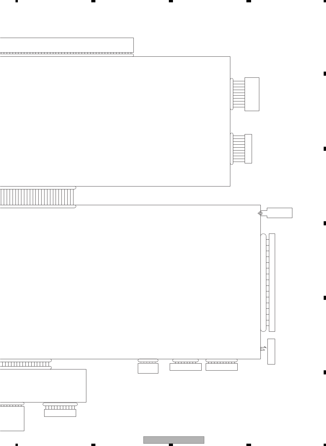
- 3.2 PCB LOCATIONS
- 3.3 JIGS LIST
- 3.4 CLEANING
- 4. BLOCK DIAGRAM
- 4.1 OVERALL CONNECTION DIAGRAM
- 4.2 BLOCK DIAGRAM
- 5. DIAGNOSIS
- 5.1 OPERATIONAL FLOWCHART
- 5.2 INSPECTION METHOD OF PICKUP UNIT
- 5.3 DIAGNOSIS FLOWCHART
- 5.4 ERROR CODE LIST
- 5.5 CONNECTOR FUNCTION DESCRIPTION
- 6. SERVICE MODE
- 6.1 MONITOR TEST MODE
- 6.2 DVD TEST MODE
- 6.3 DVD TOUCH PANEL TEST MODE
- 7. DISASSEMBLY
- 8. EACH SETTING AND ADJUSTMENT
- 8.1 DVD ADJUSTMENT
- 8.2 MONITOR UNIT ADJUSTMENT
- 8.3 PCL OUTPUT CONFIRMATION
- 9. EXPLODED VIEWS AND PARTS LIST
- 9.1 PACKING(AVH-P4100DVD/XN/UC)
- 9.2 PACKING(AVH-P4100DVD/XNEW5, XNUW5)
- 9.3 EXTERIOR(1)
- 9.4 EXTERIOR(2)
- 9.5 EXTERIOR(3)
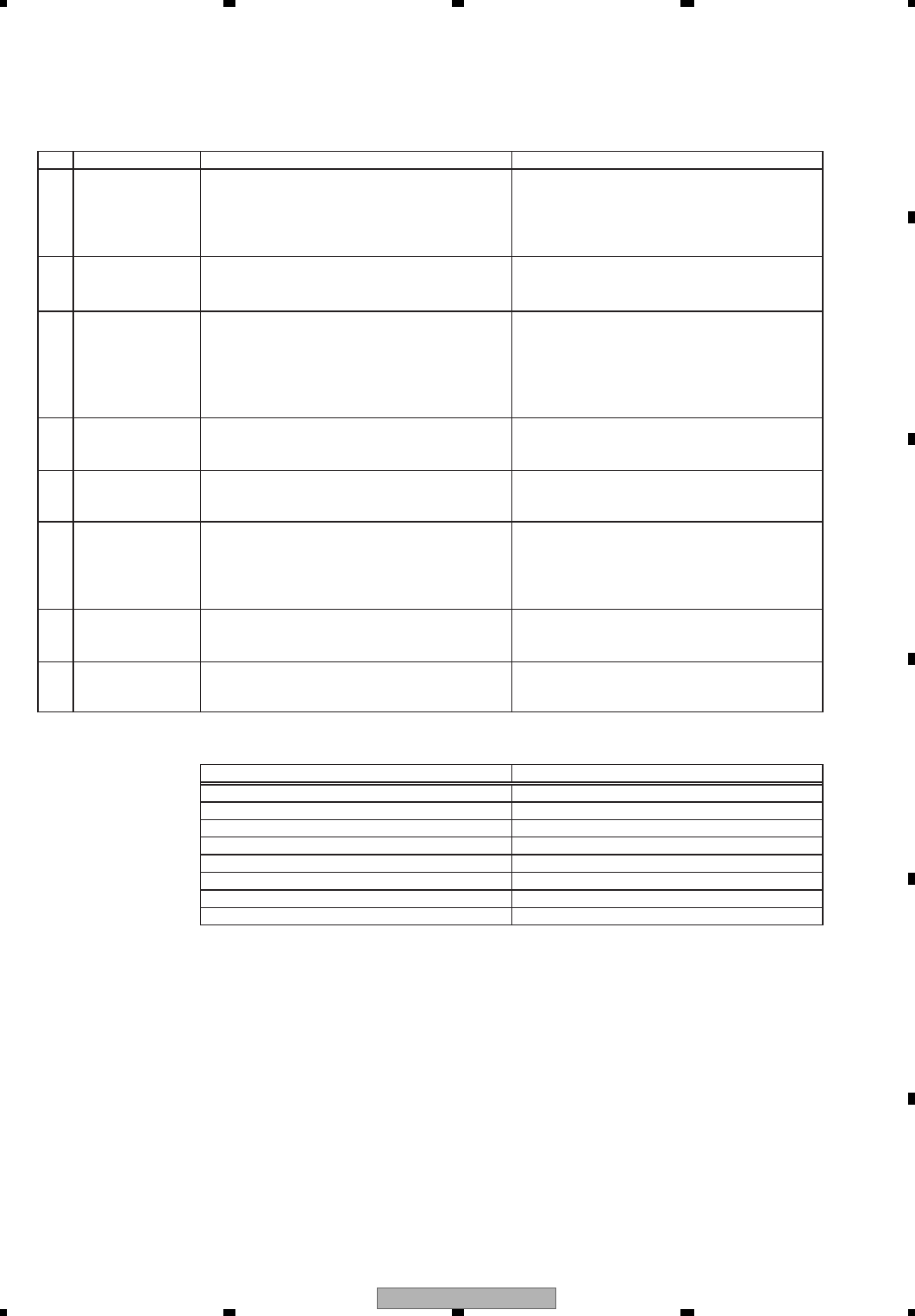
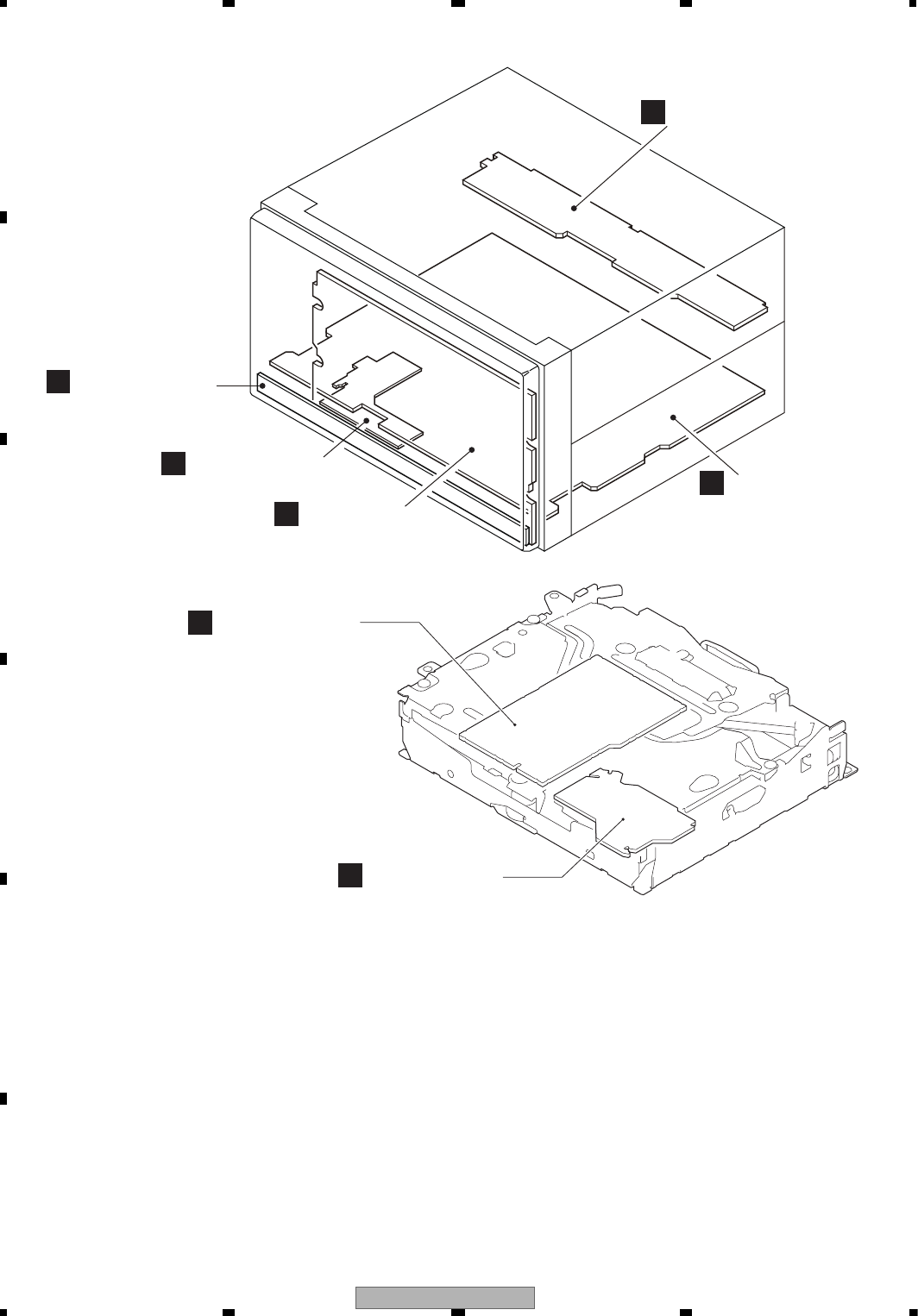
- 9.6 DVD MECHANISM MODULE
- 10. SCHEMATIC DIAGRAM
- 10.1 MOTHER PCB(ANALOG)
- 10.2 MOTHER PCB(TUNER)
- 10.3 MOTHER PCB(SYSTEM)(GUIDE PAGE)
- 10.4 MOTHER PCB(POWER SUPPLY)
- 10.5 IF PCB
- 10.6 DVD CORE UNIT(GUIDE PAGE)
- 10.7 CONNECT PCB
- 10.8 KEYBOARD UNIT
- 10.9 MONITOR UNIT(uCOM)(GUIDE PAGE)
- 10.10 MONITOR UNIT(MONITOR)(GUIDE PAGE)
- 10.11 SERVICE PCB ASSY
- 10.12 WAVEFORMS
- 11. PCB CONNECTION DIAGRAM
- 11.1 MOTHER PCB
- 11.2 DVD CORE UNIT
- 11.3 CONNECT PCB
- 11.4 KEYBOARD UNIT
- 11.5 MONITOR UNIT
- 11.6 SERVICE PCB ASSY
- 11.7 IF PCB
- 12. ELECTRICAL PARTS LIST
ORDER NO.
PIONEER CORPORATION 4-1, Meguro 1-chome, Meguro-ku, Tokyo 153-8654, Japan
PIONEER ELECTRONICS (USA) INC. P.O. Box 1760, Long Beach, CA 90801-1760, U.S.A.
PIONEER EUROPE NV Haven 1087, Keetberglaan 1, 9120 Melsele, Belgium
PIONEER ELECTRONICS ASIACENTRE PTE. LTD. 253 Alexandra Road, #04-01, Singapore 159936
PIONEER CORPORATION 2009
AVH-P4100DVD/XN/UC
CRT4275
DVD AV RECEIVER
AVH-P4100DVD
/XN/UC
DVD RDS AV RECEIVER
AVH-P4100DVD
/XNEW5
AVH-P4100DVD
/XNUW5
This service manual should be used together with the following manual(s):
DTS and DTS Digital Out are registered trademartks and the DTS logos and Symbol are
trademarks of DTS, Inc.
Manufactured under license from Dolby Laboratories. Dolby, Pro Logic, and the double-D
symbol are trademarks of Dolby Laboratories.
Model No. Order No. Mech.Module Remarks
CX-3250 CRT4300 LS1 DVD Mech. Module : Circuit Descriptions, Mech. Descriptions, Disassembly
For details, refer to "Important Check Points for Good Servicing".
K-ZZZ. JAN. 2009 Printed in Japan

AVH-P4100DVD/XN/UC
2
1234
1234
C
D
F
A
B
E
SAFETY INFORMATION
Where in a manufacturer’s service documentation, for example in circuit diagrams or lists
of components, a symbol is used to indicate that a specific component shall be replaced only
by the component specified in that documentation for safety reasons, the following symbol shall
be used:
CAUTION:
USE OF CONTROLS OR ADJUSTMENTS OR PERFORMANCE OF PROCEDURES OTHER THAN THOSE
SPECIFIED HEREIN MAY RESULT IN HAZARDOUS RADIATION EXPOSURE.
- Safety Precautions for those who Service this Unit.
When checking or adjusting the emitting power of the laser diode exercise caution in order to get safe, reliable
results.
Caution:
1. During repair or tests, minimum distance of 13 cm from the focus lens must be kept.
CAUTION
CLASS 1M INVISIBLE LASER RADIATION WHEN OPEN. DO NOT VIEW DIRECTLY WITH OPTICAL INSTRUMENTS
2. During repair or tests, do not view laser beam for 10 seconds or longer.
The backlighting lamp of LCD in this equipment contains mercury. Disposal of this material may be
regulated due to environmental considerations according to Local, State or Federal Laws. For disposal
or recycling information, please contact your local authorities or the Electronics Industries
Alliance: www.eiae.org
This product contains mercury. Disposal of this material may be regulated due to environmental considerations.
For disposal or recycling information, please contact your local authorities or the Electronics Industries
Alliance: www.eiae.org.
CAUTION
WARNING
This product contains certain electrical parts contain chemicals which are known to the State of
California to cause cancer, birth defects or other reproductive harm.
Health & Safety Code Section 25249.6 - Proposition 65
This service manual is intended for qualified service technicians; it is not meant for the casual do-it-yourselfer.
Qualified technicians have the necessary test equipment and tools, and have been trained to properly and safety repair
complex products such as those covered by this manual.
Improperly performed repairs can adversely affect the safety and reliability of the product and may void the warranty.
If you are not qualified to perform the repair of this product properly and safety, you should not risk trying to do so
and refer the repair to a qualified service technician.
AVH-P4100DVD/XN/UC 3
5 678
5678
C
D
F
A
B
E
WARNING!
The AEL (accessible emission level )of the laser power output is less than CLASS 1
but the laser component is capable of emitting radiation exceeding the limit for
CLASS 1.
A specially instructed person should do servicing operation of the apparatus.
Laser diode characteristics
Wave length:
DVD:660 nm to 670 nm
CD:780 nm to 800 nm
Focus lens on Maximum output:
CD:6.26 mW(Emitting period :9 sec.)
DVD:1.27 mW (Emitting period : unlimited)
Additional Laser Caution
Transistors Q1103 and Q1104 in PCB drive the laser diodes for DVD and CD
respectively. When Q1103 or Q1104 is shorted between their terminals,
the laser diodes for DVD or CD will radiate beam. If the top cover is removed
with no disc loaded while such short-circuit is continued, the naked eyes may
be exposed to the laser beam.
AVH-P4100DVD/XN/UC
4
1234
1234
C
D
F
A
B
E
[Important Check Points for Good Servicing]
In this manual, procedures that must be performed during repairs are marked with the below symbol.
Please be sure to confirm and follow these procedures.
1. Product safety
Please conform to product regulations (such as safety and radiation regulations), and maintain a safe servicing environment by
following the safety instructions described in this manual.
1 Use specified parts for repair.
Use genuine parts. Be sure to use important parts for safety.
2 Do not perform modifications without proper instructions.
Please follow the specified safety methods when modification(addition/change of parts) is required due to interferences such as
radio/TV interference and foreign noise.
3 Make sure the soldering of repaired locations is properly performed.
When you solder while repairing, please be sure that there are no cold solder and other debris.
Soldering should be finished with the proper quantity. (Refer to the example)
4 Make sure the screws are tightly fastened.
Please be sure that all screws are fastened, and that there are no loose screws.
5 Make sure each connectors are correctly inserted.
Please be sure that all connectors are inserted, and that there are no imperfect insertion.
6 Make sure the wiring cables are set to their original state.
Please replace the wiring and cables to the original state after repairs.
In addition, be sure that there are no pinched wires, etc.
7 Make sure screws and soldering scraps do not remain inside the product.
Please check that neither solder debris nor screws remain inside the product.
8 There should be no semi-broken wires, scratches, melting, etc. on the coating of the power cord.
Damaged power cords may lead to fire accidents, so please be sure that there are no damages.
If you find a damaged power cord, please exchange it with a suitable one.
9 There should be no spark traces or similar marks on the power plug.
When spark traces or similar marks are found on the power supply plug, please check the connection and advise on secure
connections and suitable usage. Please exchange the power cord if necessary.
a Safe environment should be secured during servicing.
When you perform repairs, please pay attention to static electricity, furniture, household articles, etc. in order to prevent injuries.
Please pay attention to your surroundings and repair safely.
2. Adjustments
To keep the original performance of the products, optimum adjustments and confirmation of characteristics within specification.
Adjustments should be performed in accordance with the procedures/instructions described in this manual.
4. Cleaning
For parts that require cleaning, such as optical pickups, tape deck heads, lenses and mirrors used in projection monitors, proper
cleaning should be performed to restore their performances.
3. Lubricants, Glues, and Replacement parts
Use grease and adhesives that are equal to the specified substance.
Make sure the proper amount is applied.
5. Shipping mode and Shipping screws
To protect products from damages or failures during transit, the shipping mode should be set or the shipping screws should be
installed before shipment. Please be sure to follow this method especially if it is specified in this manual.

AVH-P4100DVD/XN/UC 5
5 678
5678
C
D
F
A
B
E
CONTENTS
SAFETY INFORMATION .....................................................................................................................................2
1. SERVICE PRECAUTIONS................................................................................................................................6
1.1 SERVICE PRECAUTIONS .........................................................................................................................6
1.2 NOTES ON SOLDERING...........................................................................................................................7
2. SPECIFICATIONS.............................................................................................................................................8
2.1 SPECIFICATIONS ......................................................................................................................................8
2.2 DISC/CONTENT FORMAT....................................................................................................................... 11
2.3 PANEL FACILITIES ..................................................................................................................................13
2.4 CONNECTION DIAGRAM........................................................................................................................15
3. BASIC ITEMS FOR SERVICE ........................................................................................................................21
3.1 CHECK POINTS AFTER SERVICING .....................................................................................................21
3.2 PCB LOCATIONS.....................................................................................................................................22
3.3 JIGS LIST .................................................................................................................................................23
3.4 CLEANING ...............................................................................................................................................24
4. BLOCK DIAGRAM ..........................................................................................................................................26
4.1 OVERALL CONNECTION DIAGRAM ......................................................................................................26
4.2 BLOCK DIAGRAM....................................................................................................................................28
5. DIAGNOSIS ....................................................................................................................................................36
5.1 OPERATIONAL FLOWCHART.................................................................................................................36
5.2 INSPECTION METHOD OF PICKUP UNIT .............................................................................................37
5.3 DIAGNOSIS FLOWCHART......................................................................................................................40
5.4 ERROR CODE LIST.................................................................................................................................67
5.5 CONNECTOR FUNCTION DESCRIPTION .............................................................................................70
6. SERVICE MODE.............................................................................................................................................71
6.1 MONITOR TEST MODE...........................................................................................................................71
6.2 DVD TEST MODE ....................................................................................................................................91
6.3 DVD TOUCH PANEL TEST MODE..........................................................................................................95
7. DISASSEMBLY ...............................................................................................................................................96
8. EACH SETTING AND ADJUSTMENT..........................................................................................................105
8.1 DVD ADJUSTMENT...............................................................................................................................105
8.2 MONITOR UNIT ADJUSTMENT ............................................................................................................ 113
8.3 PCL OUTPUT CONFIRMATION ............................................................................................................ 116
9. EXPLODED VIEWS AND PARTS LIST ........................................................................................................ 117
9.1 PACKING(AVH-P4100DVD/XN/UC)....................................................................................................... 118
9.2 PACKING(AVH-P4100DVD/XNEW5, XNUW5) ......................................................................................120
9.3 EXTERIOR(1).........................................................................................................................................122
9.4 EXTERIOR(2).........................................................................................................................................124
9.5 EXTERIOR(3).........................................................................................................................................126
9.6 DVD MECHANISM MODULE.................................................................................................................128
10. SCHEMATIC DIAGRAM..............................................................................................................................132
10.1 MOTHER PCB(ANALOG) ....................................................................................................................132
10.2 MOTHER PCB(TUNER) .......................................................................................................................134
10.3 MOTHER PCB(SYSTEM)(GUIDE PAGE) ............................................................................................136
10.4 MOTHER PCB(POWER SUPPLY).......................................................................................................142
10.5 IF PCB ..................................................................................................................................................144
10.6 DVD CORE UNIT(GUIDE PAGE).........................................................................................................146
10.7 CONNECT PCB....................................................................................................................................152
10.8 KEYBOARD UNIT ................................................................................................................................154
10.9 MONITOR UNIT(uCOM)(GUIDE PAGE) ..............................................................................................156
10.10 MONITOR UNIT(MONITOR)(GUIDE PAGE)......................................................................................162
10.11 SERVICE PCB ASSY .........................................................................................................................168
10.12 WAVEFORMS.....................................................................................................................................170
11. PCB CONNECTION DIAGRAM ..................................................................................................................172
11.1 MOTHER PCB ......................................................................................................................................172
11.2 DVD CORE UNIT..................................................................................................................................176
11.3 CONNECT PCB....................................................................................................................................178
11.4 KEYBOARD UNIT.................................................................................................................................180
11.5 MONITOR UNIT....................................................................................................................................182
11.6 SERVICE PCB ASSY ...........................................................................................................................186
11.7 IF PCB ..................................................................................................................................................188
12. ELECTRICAL PARTS LIST.........................................................................................................................189
AVH-P4100DVD/XN/UC
6
1234
1234
C
D
F
A
B
E
1. SERVICE PRECAUTIONS
1.1 SERVICE PRECAUTIONS
1. You should conform to the regulations governing the product (safety, radio and noise, and other regulations),
and should keep the safety during servicing by following the safety instructions described in this manual.
2. Be careful in handling ICs. Some ICs such as MOS type are so fragile that they can be damaged by electrostatic
induction.
3. Before disassembling the unit, be sure to turn off the power. Unplugging and plugging the connectors during
power-on mode may damage the ICs inside the unit.
4. To protect the pickup unit from electrostatic discharge during servicing, take an appropriate treatment
(shorting-solder) by referring to "the DISASSEMBLY" .
5. After replacing the pickup unit, be sure to skew adjustment.
6. During disassembly, be sure to turn the power off since an internal IC might be destroyed when a connector
is plugged or unplugged.
7. After the replacement of LS1 mecha, connect ACC and BUP, and then press RESET button.
->Some functions such as BOOK mark may not work normally.
8. Connector CN5001 in the monitor unit : When you remove the flexible from the CKS5951,
hold up the end of the flexible holddown part to remove it.
->There is a possibility of breakage of connector pin.
9. Connector CN5001 in the monitor unit : CKS5951 is a connector of both contact points.
If you insert the flexible inversely, there is a possibility of IC damaged because of unintended connection.
So please take care not to insert it inversely. If perchance you insert it inversely, you need to replace the unit.
10. The FFC styling between mother unit and DVD mecha (LS1) requires careful attention. Fold FFC to the
mecha side and style it.
11. Eject lock
How to enter:Reset with [VOL-] key and [SOURCE] key pressed.
Summary:DISC EJECT behavior of built-in DVD mecha is prohibited
It is for DISC antitheft from the storefront display.
With or without DISC, the behavior of pressing EJECT key during the EJECT lock is as follows.
During grille closed
Press EJECT key -> Grille is opened.
*The key is valid at the point of being pressed (BEEP). To Leave the key makes grille opened.
During grille opened
Press EJECT key -> Grille is closed.
*The key is valid at the point of being pressed (BEEP). To Leave the key makes grille opened
Remarks: [Notes] EJECT lock is not unlocked by turning ACC ON or product reset.
To unlock it, you need to operate keys as above.
For existing model (AVH-P9DVA), it is unlocked by turning ACC ON or reset.
12. Background display data is stored in IC5201. So, if you replace the IC, user photo data will be lost.
13. If the gasket (CNN2782) on the FM/AM tuner unit was damaged or lost, then the reception
sensitivity would be poor. So, replace it with the new one.
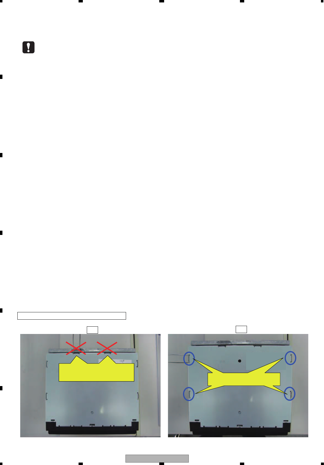
NOTE: When you remove the top case
NG OK
Use these holes to remove the top
case.
Don't put tweezers or something
into these holes to remove the top
case

AVH-P4100DVD/XN/UC 7
5 678
5678
C
D
F
A
B
E
1.2 NOTES ON SOLDERING
For environmental protection, lead-free solder is used on the printed circuit boards mounted in this unit.
Be sure to use lead-free solder and a soldering iron that can meet specifications for use with lead-free solders for repairs
accompanied by reworking of soldering.
Compared with conventional eutectic solders, lead-free solders have higher melting points, by approximately 40 C.
Therefore, for lead-free soldering, the tip temperature of a soldering iron must be set to around 373 C in general, although
the temperature depends on the heat capacity of the PC board on which reworking is required and the weight of the tip of
the soldering iron.
Compared with eutectic solders, lead-free solders have higher bond strengths but slower wetting times and higher melting
temperatures (hard to melt/easy to harden).
The following lead-free solders are available as service parts:
Parts numbers of lead-free solder:
GYP1006 1.0 in dia.
GYP1007 0.6 in dia.
GYP1008 0.3 in dia.
AVH-P4100DVD/XN/UC
8
1234
1234
C
D
F
A
B
E
2. SPECIFICATIONS
2.1 SPECIFICATIONS
Dimensions (W × H × D):
DIN
Chassis................. 178 mm × 100 mm × 165
mm
(7 in. × 3-7/8 in. × 6-1/2 in.)
Nose ....................... 171 mm × 97 mm × 9 mm
(6-3/4 in.× 3-7/8 in.× 3/8 in.)
Weight ..................................... 1.7 kg(3.7 lbs)
Display
Screen size/aspect ratio.......6.95 inch wide/16:9
(effective display area: 155.2
× 81.3 mm)
Pixels ........................................ 336 960 (1 440 × 234)
Display method ..................... TFT active matrix
Color system........................... NTSC
Durable temperature range (power off)
............................................... -20 °C to +80 °C
Audio
Maximum power output ...... 50 W × 4
50 W × 2/4 + 70 W × 1/2
(for subwoofer)
Continuous power output .. 22 W × 4 (1 kHz, 5% THD, 4
load, both channels dri-
ven)
Load impedance ................... 4 to 8 ×4
4to 8 ×2+2 ×1
Preout max output level ..... 4.0 V
Equalizer (3-Band Parametric Equalizer):
Low
Frequency ............. 40/80/100/160 Hz
Q Factor ................. 0.35/0.59/0.95/1.15 (+6 dB
when boosted)
Gain ......................... ±12 dB
Mid
Frequency ............. 200/500/1k/2k Hz
Q Factor ................. 0.35/0.59/0.95/1.15 (+6 dB
when boosted)
Gain ......................... ±12 dB
High
Frequency ............. 3.15k/8k/10k/12.5k Hz
Q Factor ................. 0.35/0.59/0.95/1.15 (+6 dB
when boosted)
Gain ........................ ±12 dB
HPF:
Frequency ..................... 50/63/80/100/125 Hz
Slope ............................... –12 dB/oct
Subwoofer (mono):
Frequency ...................... 50/63/80/100/125 Hz
Slope ............................... –18 dB/oct
Gain ................................. +6 dB to –24 dB
Phase .............................. Normal/Reverse
Bass boost:
Gain ................................. +12 dB to 0 dB
DVD Player
System ..................................... DVD video, Video CD, CD,
WMA, MP3, AAC, DivX,
JPEG system
Usable discs .......................... DVD video, Video CD, CD,
CD-R/RW, DVD-R/RW/RDL
Region number .................... 1
Frequency response ........... 5 Hz to 44 000 Hz (with DVD,
at sampling frequency 96
kHz)
Signal-to-noise ratio............ 96 dB (1 kHz) (IHF-A net-
work) (RCA level)
Output level:
Video ............................... 1.0 Vp -p/75 (±0.2 V)
Number of channels ............. 2 (stereo)
MP3 decoding format ..........MPEG-1 & 2 Audio Layer 3
WMA decoding format ........ Ver. 7,7.1, 8, 9, 10, 11 (2ch
audio)
(Windows Media Player)
AAC decoding format...........MPEG-4 AAC (iTunes en-
coded only) (.m4a)
(Ver. 8.0 and earlier)
DivX decoding format...........Home Theater Ver. 3, 4, 5.2,
6 (.avi, .divx)
USB
USB standard specification
.............................................. USB 1.1, USB 2.0 full speed
Maximum current supply ... 500 mA
USB Class ............................. MSC (Mass Storage Class)
File system............................. FAT16, FAT32
MP3 decoding format ......... MPEG-1 & 2 Audio Layer 3
WMA decoding format ........ Ver. 7,7.1, 8, 9, 10, 11 (2ch
audio)
(Windows Media Player)
AAC decoding format.......... MPEG-4 AAC (iTunes en-
coded only) (.m4a)
(Ver. 8.0 and earlier)
FM tuner
Frequency range .................. 87.9 MHz to 107.9 MHz
Usable sensitivity.................. 9 dBf (0.8 μV/75 , mono,
S/N: 30 dB)
General
Power source .........................14.4 V DC (10.8 V to 15.1 V
allowable)
Grounding system................. Neg ative type
Max. current consumption
...............................................10.0 A
Backup current ....................... 2.2 mA or less
AVH-P4100DVD/XN/UC
AVH-P4100DVD/XN/UC 9
5 678
5678
C
D
F
A
B
E
Signal-to-noise ratio............. 72 dB (IHF-A network)
AM tuner
Frequency range .................. 530 kHz to 1 710 kHz (10
kHz)
Usable sensitivity.................. 25 μV (S/N: 20 dB)
Signal-to-noise ratio............. 62 dB (IHF-A network)
CEA2006 Specifications
Power output ......................... 14 W RMS × 4 Channels (4
and 1 % THD+N)
S/N ratio .................................. 91 dBA (reference: 1 W into
4)
Note
Specifications and the design are subject to mod-
ifications without notice due to improvements.
AVH-P4100DVD/XN/UC
10
1234
1234
C
D
F
A
B
E
Dimensions (W × H × D):
DIN
Chassis.................. 178 mm × 100 mm × 165
mm
Nose ....................... 171 mm × 97 mm × 9 mm
Weight ..................................... 1.7 kg
Display
Screen size/aspect ratio.......6.95 inch wide/16:9
(effective display area: 155.2
× 81.3 mm)
Pixels ....................................... 336 960 (1 440 × 234)
Display method .................... TFT active matrix
Color system.......................... PAL/SECAM compatible
Durable temperature range (power off)
.............................................. -20 °C to +80 °C
Audio
Maximum power output ...... 50 W × 4
50 W × 2/4 + 70 W × 1/2
(for subwoofer)
Continuous power output .. 22 W × 4 (1 kHz, 5% THD, 4
load, both channels dri-
ven)
Load impedance ................... 4 to 8 ×4
4to 8 ×2+2 ×1
Preout max output level ..... 4.0 V
Equalizer (3-Band Parametric Equalizer):
Low
Frequency ............. 40/80/100/160 Hz
Q Factor ................. 0.35/0.59/0.95/1.15 (+6 dB
when boosted)
Gain ........................ ±12 dB
Mid
Frequency ............. 200/500/1k/2k Hz
Q Factor ................. 0.35/0.59/0.95/1.15 (+6 dB
when boosted)
Gain ........................ ±12 dB
High
Frequency ............. 3.15k/8k/10k/12.5k Hz
Q Factor ................. 0.35/0.59/0.95/1.15 (+6 dB
when boosted)
Gain ......................... ±12 dB
HPF:
Frequency ...................... 50/63/80/100/125 Hz
Slope ................................–12 dB/oct
Subwoofer (mono):
Frequency ..................... 50/63/80/100/125 Hz
Slope ............................... –18 dB/oct
Gain ................................. +6 dB to –24 dB
Phase .............................. Normal/Reverse
Bass boost:
Gain ................................. +12 dB to 0 dB
DVD Player
System ..................................... DVD video, DVD-VR, Video
CD, CD, WMA, MP3, AAC,
DivX, JPEG system
Usable discs ......................... DVD video, Video CD, CD,
CD-R/RW, DVD-R/RW/RDL
Region number ..................... 2 (EW5)
5 (UW5)
Frequency response............. 5 Hz to 44 000 Hz (withDVD,
at sampling frequency 96
kHz)
Signal-to-noise ratio ........... 96 dB (1 kHz) (IEC-A net-
work) (RCA level)
Output level:
Video .............................. 1.0 Vp-p/75 (±0.2 V)
Number of channels ............ 2 (stereo)
MP3 decoding format .......... MPEG-1 & 2 Audio Layer 3
WMA decoding format ........ Ver. 7,7.1, 8, 9, 10, 11 (2ch
audio)
(Windows Media Player)
AAC decoding format...........MPEG-4 AAC (iTunes en-
coded only) (.m4a)
(Ver. 8.0 and earlier)
DivX decoding format.......... Home Theater Ver. 3, 4,5.2,
6 (.avi, .divx)
USB
USB standard specification
.............................................. USB 1.1, USB 2.0 full speed
Maximum current supply ... 500 mA
USB Class ............................. MSC (Mass Storage Class)
File system.............................. FAT16, FAT32
MP3 decoding format .......... MPEG-1 & 2 Audio Layer 3
WMA decoding format ....... Ver. 7, 7.1, 8, 9, 10, 11 (2ch
audio)
(Windows Media Player)
AAC decoding format...........MPEG-4 AAC (iTunes en-
coded only) (.m4a)
(Ver. 8.0 and earlier)
FM tuner
Frequency range .................. 87.5 MHz to 108.0 MHz
Usable sensitivity.................. 9 dBf (0.8 μV/75 , mono,
S/N: 30 dB)
Signal-to-noise ratio ............ 72 dB (IEC-A network)
MW tuner
Frequency range .................. 531 kHz to 1 602 kHz (9 kHz)
Usable sensitivity.................. 25 μV (S/N: 20 dB)
Signal-to-noise ratio ............ 62 dB (IEC-A network)
LW tuner
Frequency range .................. 153 kHz to 281 kHz
Usable sensitivity................... 28 μV (S/N: 20 dB)
Signal-to-noise ratio ............ 62 dB (IEC-A network)
Note
Specifications and the design are subject to mod-
ifications without notice due to improvements.
General
Power source .........................14.4 V DC (10.8 V to 15.1 V
allowable)
Grounding system................ Negative type
Max. current consumption
...............................................10.0 A
Backup current ....................... 2.2 mA or less
AVH-P4100DVD/XNEW5, AVH-P4100DVD/XNUW5
AVH-P4100DVD/XN/UC 11
5 678
5678
C
D
F
A
B
E
2.2 DISC/CONTENT FORMAT
Handling guideline of discs
and player
• Use only discs featuring any of following
logos.
DVD video
Video CD
CD
• Use only normal, round discs. If you insert
irregular, non-round, shaped discs they
may jam in the DVD player or not play prop-
erly.
• Check all discs for cracks, scratches or
warping before playing. Discs that have
cracks, scratches or are warped may not
play properly. Do not use such discs.
• Avoid touching the recorded (non-printed)
surface when handling the disc.
• Store discs in their cases when not in use.
• Keep discs out of direct sunlight and do
not expose the discs to high temperatures.
• Do not attach labels, write on or apply che-
micals to the surface of the discs.
• To clean a disc, wipe the disc with a soft
cloth outward from the center.
• If the heater is used in cold weather, con-
densation may form on components inside
the DVD player. Condensation may cause
the DVD player to not operate properly. If
you think that condensation is a problem
turn off the DVD player for an hour or so to
allow it to dry out and wipe any damp discs
with a soft cloth to remove the moisture.
• Road shocks may interrupt disc
playback.

AVH-P4100DVD/XN/UC
12
1234
1234
C
D
F
A
B
E
is a trademark of DVD Format/Logo Licensing Corporation.
AVH-P4100DVD/XN/UC
AVH-P4100DVD/XN/UC 13
5 678
5678
C
D
F
A
B
E
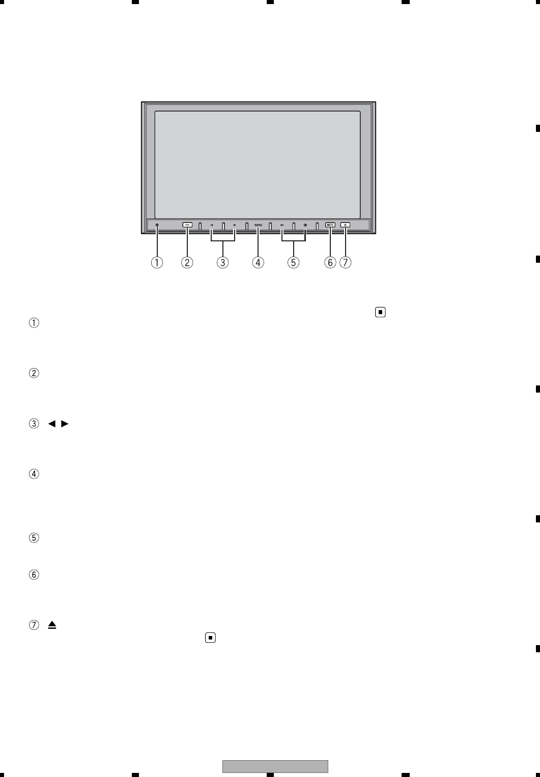
2.3 PANEL FACILITIES
Head unit
RESET button
Press to return to the factory settings (initial
settings).
DISP OFF button
Press to turn the information display on or
off.
/ (TRACK) buttons
Press to do manual seek tuning, fast for-
ward, reverse and track search controls.
SRC/OFF button
Press to cycle through all the available
sources. Press and hold to turn the source
off.
+/–(VOLUME) buttons
Press to increase or decrease the volume.
MUTE button
Press to turn off the sound. To turn on the
sound, press again.
(eject) button
Press to eject a disc from this unit.
Optional remote control
The remote control CD-R55 is sold separately.
For details concerning operations, see the re-
mote control manual.
AVH-P4100DVD/XN/UC, AVH-P4100DVD/XNEW5
AVH-P4100DVD/XN/UC
14
1234
1234
C
D
F
A
B
E
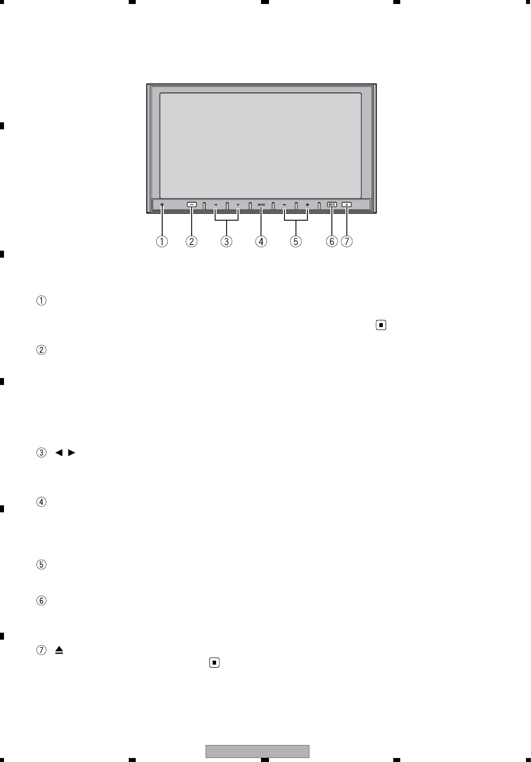
AVH-P4100DVD/XNUW5
Head unit
RESET button
Press to return to the factory settings (initial
settings).
DISP OFFAV/NAVI button
Press to turn the information display on or
off.
If separately sold navigation unit is con-
nected to this unit via RGB cable, pressing
and holding this button switches between
navigation display and audio display.
(TRACK) buttons
Press to do manual seek tuning, fast for-
ward, reverse and track search controls.
SRC/OFF button
Press to cycle through all the available
sources. Press and hold to turn the source
off.
+/–(VOLUME) buttons
Press to increase or decrease the volume.
MUTE button
Press to turn off the sound. To turn on the
sound, press again.
(eject) button
Press to eject a disc from this unit.
Optional remote control
The remote control CD-R55 is sold separately.
For details concerning operations, see the re-
mote control manual.
/
AVH-P4100DVD/XN/UC 15
5 678
5678
C
D
F
A
B
E
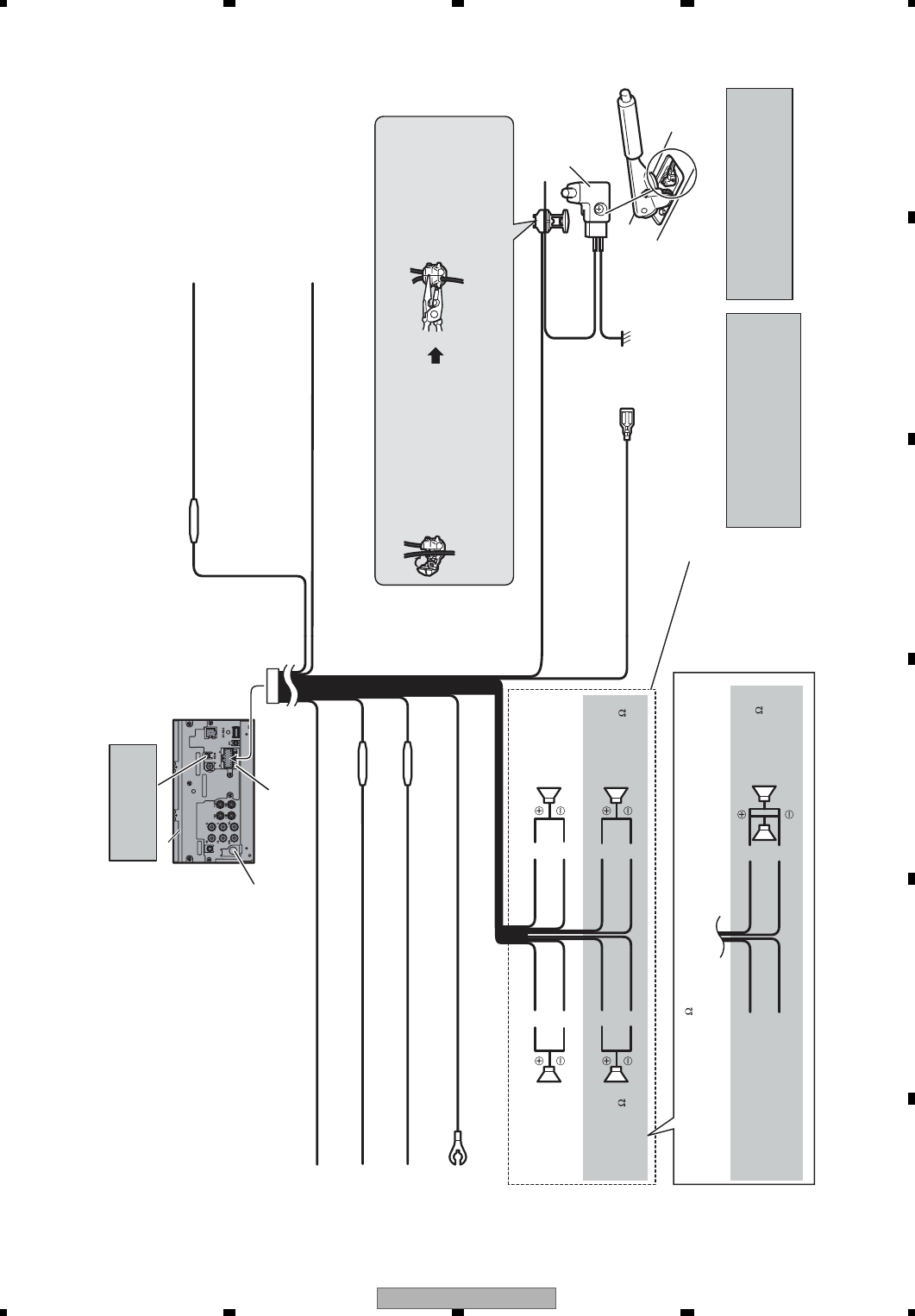
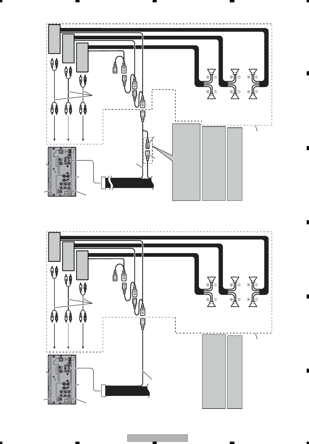
2.4 CONNECTION DIAGRAM
Connecting the power cord
Yellow
Connect to the constant 12 V supply terminal.
Fuse resistor
Red
Connect to terminal controlled by ignition switch (12 V DC).
Black (chassis ground)
Connect to a clean, paint-free metal location.
Left Right
rekaepstnorFrekaepstnorF
Rear speaker or
Subwoofer (4 )
White Gray
Gray/blackWhite/black
Green Violet
Green/black Violet/black
Violet
Violet/black
Not used.
Green
Green/black
When using a subwoofer of 70 W (2 ), be sure to connect with Violet and Violet/black leads of this unit. Do not
connect anything to Green and Green/black leads.
Subwoofer (4 )
× 2
Rear speaker or
Subwoofer (4 )
Fuse (10 A)
Antenna input
Orange/white
Connect to lighting switch terminal.
Fuse resistor
This product
Use a mini plug cable to
connect with auxiliary
device.
AUX jack (3.5 ø)
Connection method
1. Clamp the lead. 2. Clamp firmly with
needle-nosed pliers.
Note:
· The position of the parking brake switch depends on the vehicle model. For details,
consult the vehicle Owner’s Manual or dealer.
Yellow/black
If you use equipment with Mute function, wire this lead to the
Audio Mute lead on that piece of equipment. If not, keep the
Audio Mute lead free of any connections.
Light green
Used to detect the ON/OFF status of the parking
brake. This lead must be connected to the power
supply side of the parking brake switch.
Blue/white
Connect to system control terminal of the power amp or
auto-antenna relay control terminal (max. 300 mA 12 V DC).
Ground side
Power supply side
Parking brake
switch
Fuse resistor
With a 2 speaker system, do not connect anything to the speaker leads
that are not connected to speakers.
Note:
· Change the initial setting of this unit (refer
to the Operation Manual). The subwoofer
output of this unit is monaural.
Violet/white
Of the two lead wires connected to the back lamp, connect the one
in which the voltage changes when the gear shift is in the
REVERSE (R) position. This connection enables the unit to
sense whether the car is moving forwards or backwards.
When you connect the separately sold
multi-channel processor (e.g., DEQ-P8000) to
this unit, do not connect anything to the
speaker leads and systemremote control
(blue/white).
AVH-P4100DVD/XN/UC
AVH-P4100DVD/XN/UC
16
1234
1234
C
D
F
A
B
E
AVH-P4100DVD/XNEW5, AVH-P4100DVD/XNUW5
Connecting the power cord
Orange/white
Connect to lighting switch terminal.
Speaker leads
White: Front left
White/black: Front left
Gray: Front right
Gray/black: Front right
Green: Rear left or subwoofer
Green/black: Rear left or subwoofer
Violet: Rear right or subwoofer
Violet/black: Rear right or subwoofer
ISO connector
Note:
In some vehicles, the ISO connector may be
divided into two. In this case, be sure to connect
to both connectors.
When you connect the separately sold
multi-channel processor (e.g., DEQ-P6600) to
this unit, do not connect anything to the
speaker leads and systemremote control
(blue/white).
Note:
Depending on the kind of vehicle, the
function of 3* and 5* may be different. In
this case, be sure to connect 2* to 5* and
4* to 3*.
1*
2*
4*
3*
5*
Cap (1*)
Do not remove cap if this
terminal is not in use.
Yellow (3*)
Back-up
(or accessory)
Yellow (2*)
Connect to the constant 12 V
supply terminal.
Connect leads of the same
color to each other.
Fuse (10 A)
Fuse resistor
Red (5*)
Accessory
(or back-up)
Red (4*)
Connect to terminal controlled by
ignition switch (12 V DC).
Black (chassis ground)
Connect to a clean, paint-free metal location.
This product
Antenna input
Fuse resistor
Use a mini plug cable to
connect with auxiliary
device.
AUX jack (3.5 ø)
Violet/white
Of the two lead wires connected to the back lamp, connect the one
in which the voltage changes when the gear shift is in the
REVERSE (R) position. This connection enables the unit to
sense whether the car is moving forwards or backwards.
Notes:
· Change the initial setting of this unit (refer to the Operation Manual).
The subwoofer output of this unit is monaural.
· When using a subwoofer of 70 W (2
) , be sure to connect with
Violet and Violet/black leads of this unit. Do not connect anything to
Green and Green/black leads.
Connection method
1. Clamp the lead. 2. Clamp firmly with
needle-nosed pliers.
Note:
· The position of the parking brake switch depends on the vehicle model. For details,
consult the vehicle Owner’s Manual or dealer.
Yellow/black
If you use equipment with Mute function, wire this lead to the
Audio Mute lead on that piece of equipment. If not, keep the
Audio Mute lead free of any connections.
Light green
Used to detect the ON/OFF status of the parking brake. This lead
must be connected to the power supply side of the parking brake
switch.
Blue/white
Connect to system control terminal of the power
amp (max. 300 mA 12 V DC).
Blue/white (7*)
Connect to auto-antenna relay control terminal
(max. 300 mA 12 V DC).
The pin position of the ISO
connector will differ depending on
the type of vehicle. Connect 6* and
7* when Pin 5 is an antenna control
type. In other types of vehicles,
never connect 6* and 7*.
Blue/white (6*)
Ground side
Power supply side
Parking brake
switch
Fuse resistor
AVH-P4100DVD/XN/UC 17
5 678
5678
C
D
F
A
B
E
AVH-P4100DVD/XNEW5, AVH-P4100DVD/XNUW5
When connecting to separately sold power amp
Blue/white
Connect to system control terminal of the
power amp or auto-antenna relay control
terminal. (max. 300 mA 12 V DC).
When you connect the separately sold
multi-channel processor (e.g., DEQ-P8000) to
this unit, do not connect anything to the
speaker leads and system remote control
(blue/white).
This product
Connect with RCA cables
(sold separately)
Rear speaker
Perform these connections when
using the optional amplifier.
System remote control
rekaepstnorFrekaepstnorF
thgiRtfeL
Front output
When you connect the multi-channel processor
to this unit, refer to multi-channel processor’s
installation manual for the connection method.
Rear speaker
Power amp
(sold separately)
Power amp
(sold separately)
Power amp
(sold separately)
Subwoofer Subwoofer
Rear output
Subwoofer output
To front output
To rear output
To subwoofer
output
When connecting to separately sold power amp
Blue/white
Connect to system control
terminal of the power amp
(max. 300 mA 12 V DC).
Blue/white (7*)
Connect to auto-antenna
relay control terminal
(max. 300 mA 12 V DC).
The pin position of the ISO connector will differ
depending on the type of vehicle. Connect 6*
and 7* when Pin 5 is an antenna control type.
In other types of vehicles, never connect 6* and
7*.
Blue/white (6*)
When you connect the separately sold
multi-channel processor (e.g., DEQ-P6600) to
this unit, do not connect anything to the
speaker leads and system remote control
(blue/white).
This product
Connect with RCA cables
(sold separately)
Rear speaker
Perform these connections when
using the optional amplifier.
System remote control
rekaepstnorFrekaepstnorF
thgiRtfeL
Front output
When you connect the multi-channel processor
to this unit, refer to multi-channel processor’s
installation manual for the connection method.
Rear speaker
Power amp
(sold separately)
Power amp
(sold separately)
Power amp
(sold separately)
Subwoofer Subwoofer
Rear output
Subwoofer output
To front output
To rear output
To subwoofer
output
AVH-P4100DVD/XN/UC
AVH-P4100DVD/XN/UC
18
1234
1234
C
D
F
A
B
E
This product
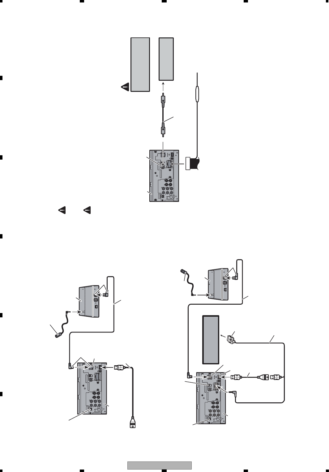
Wired remote input
Hard-wired remote control
adaptor can be connected
(sold separately).
Dock connector
Interface cable
(CD-IU200V) (sold separately)
iPod with video capabilities
(sold separately)
IP-BUS cable
(Supplied with Bluetooth adapter)
Black
Bluetooth adapter
(e.g. CD-BTB200)
(sold separately)
Microphone
for hands-free phoning
(supplied with Bluetooth adapter)
1.5 m
IP-BUS input
USB input
AUX input (AUX IN)
1.5 m
USB cable
When connecting with supplied USB cable
This product
1.5 m (4 ft. 11 in.)
USB cable
Connect to sparately sold
USB device.
Wired remote input
Hard-wired remote control
adaptor can be connected
(sold separately).
IP-BUS cable
(Supplied with Bluetooth adapter)
Black
Bluetooth adapter
(e.g. CD-BTB200)
(sold separately)
Microphone
for hands-free phoning
(supplied with Bluetooth adapter)
Blue
IP-BUS input
1.5 m (4 ft. 11 in.)
When connecting with optional CD-IU200V cable
When connecting with a rear view camera
When this product is used with a rear view camera, it is possible to automatically switch
from the video to rear view image when the gear shift is moved to REVERSE (R).
WARNING
USE INPUT ONLY FOR REVERSE OR MIRROR IMAGE REAR VIEW CAMERA. OTHER USE MAY
RESULT IN INJURY OR DAMAGE.
CAUTION
• The screen image may appear reversed.
• The rear view camera function is to be used as an aid for backing into a tight parking spot.
Do not use this function for entertainment purposes.
• Objects in the rear view may appear closer or more distant than they actually are.
RCA cable
(sold separately)
To video output
Rear view camera
Rear view camera input
(REAR CAMERA IN )
This product
Violet/white
Of the two lead wires connected to the back lamp, connect the one
in which the voltage changes when the gear shift is in the
REVERSE (R) position. This connection enables the unit to
sense whether the car is moving forwards or backwards.
You must use a camera
which outputs mirror
reversed images.
CAUTION
Fuse resistor
• It is necessary to set Camera Polarity properly in System Menu when connecting the rear
view camera.
AVH-P4100DVD/XN/UC 19
5 678
5678
C
D
F
A
B
E
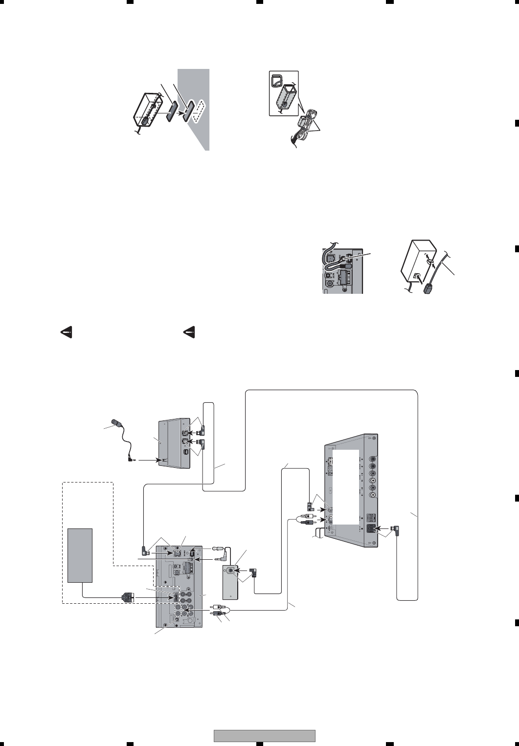
Connecting and installing the optical cable connection box
WARNING
•Avoid installing the optical cable connection
box in locations where the operation of safety
devices such as airbags is prevented by this
unit. Otherwise, there is a danger of a fatal
accident.
•Avoid installing the optical cable connection
box in locations where the operation of the
brake may be prevented. Otherwise, it may
result in a traffic accident.
•Fix the optical cable connection box securely
with the hook and loop fastener or lock tie. If
the unit is loose, it disturbs driving stability,
which may result in a traffic accident.
CAUTION
• Install this unit using only the parts supplied with
this unit. If other parts are used, this unit may be
damaged or could dismount itself, which leads to
an accident or other problems.
• Do not install this unit near the doors where
rainwater is likely to be spilled on the unit.
Incursion of water into the unit may cause smoke
or fire.
Connecting the optical cable
1. Connect the optical cable and ground
lead to the main unit.
Connect the optical cable so that it does not
protrude from the main unit, as shown in the
illustration. Fasten the ground lead to the
protrusion on the back of the main unit.
2. Connect the optical cable to the
optical cable connection box.
Installing the optical cable
connection box
• When installing the optical cable
connection box with the hook and
loop fastener.
Install the optical cable connection box
using the hook and loop fastener in the
ample space of the console box.
• When installing the optical cable
connection box with the lock tie.
Wrap the optical cable and connection box
with the protection tape and fasten with the
power code using the lock tie.
Screw
Optical cable
Hook fastener
Loop fastener
Wrap with the protection tape
Fasten with the lock tie
When connecting with a multi-channel processor
IP-BUS cable (supplied with
multi-channel processor)
RCA cable (supplied with
multi-channel processor)
Optical cable
(supplied with
multi-channel processor)
This product
Wired remote input
Hard-wired remote control
adaptor can be connected
(sold separately).
IP-BUS cable
(Supplied with Bluetooth adapter)
Black
Bluetooth adapter
(e.g. CD-BTB200)
(sold separately)
Microphone
for hands-free phoning
(supplied with Bluetooth adapter)
Blue
Multi-channel processor
(e.g., DEQ-P8000 (UC)
(sold separately)
Black
Optical cable connection box
(supplied with multi-channel processor)
To RL
To RR
Black
Blue
Optical output
(Black)
IP-BUS input
Blue
RGB input
Navigation Unit
(sold separately)
Please contact your dealer to inquire
about the connectable navigation unit.
/ DEQ-P6600 (EW5,UW5))
(UW5)
AVH-P4100DVD/XN/UC
20
1234
1234
C
D
F
A
B
E
When connecting the external video component and the
display
External video
component (sold
separately)
Audio input
(L IN,R IN )
Display with RCA
input jacks (sold
separately)
To video input
To video output
To audio outputs
This product
RCA cables (sold separately)
Video input (V IN )
Rear monitor output
(V OUT )
• It is necessary to change AV Input in System Menu when connecting the external video
component.
When using a display connected to rear video output
This product’s rear video output is for connection of a display to enable passengers in the
rear seats to watch video.
WARNING
Never install the display in a location where it is visible to the driver while driving.
AVH-P4100DVD/XN/UC 21
5 678
5678
C
D
F
A
B
E
3. BASIC ITEMS FOR SERVICE
3.1 CHECK POINTS AFTER SERVICING
To keep the product quality after servicing, please confirm following check points.
No. Procedures Check points
1 Confirm whether the customer complain has
been solved.
If the customer complain occurs with the
specific media, use it for the operation check.
The customer complain must not be
reappeared.
Display, video, audio and operations must be
normal.
2 Flap-mecha Check the operation of the flap mechanism. The flap mechanism operation must be
smooth without making the noise and
scratches.
3 DVD Measure playback error rates at the
innermost and outermost tracks by using the
test mode with the following disc.
DVD test disc (TDV-582)
Deterioration of mecha-drive can be checked.
The error rate must be less than the
threshold value.
(Refer to the chapter of DIAGNOSIS for the
threshold value.)
4 DVD Play back a DVD.
(Menu operation; Title/chapter search)
Display, video, audio and operations must be
normal.
5 CD Play back a CD.
(Track search)
Display, audio and operations must be
normal.
6 FM/AM tuner Check FM/AM tuner action.
(Seek, Preset)
Switch band to check both FM and AM.
7 Check whether no disc is inside the product. The media used for the operating check must
be ejected.
8 Appearance check No scratches or dirt on its appearance after
receiving it for service.
See the table below for the items to be checked regarding video and audio:
Item to be checked regarding video Item to be checked regarding audio
Block-noise Distortion
Horizontal noise Noise
Dot noise Volume too low
Disturbed image (video jumpiness) Volume too high
Too dark Volume fluctuating
Too bright Sound interrupted
Mottled color
Display, audio and operations must be
normal. * If the reception sensitivity is poorer
than normal, the gasket on the FM/AM tuner
unit may be damaged or lost.
AVH-P4100DVD/XN/UC
22
1234
1234
C
D
F
A
B
E
3.2 PCB LOCATIONS
BIF PCB
AMother PCB
EKeyboard Unit
FMonitor Unit
GService PCB Assy
CDVD Core Unit
DConnect PCB
Mother Unit
Consists of
Mother PCB
IF PCB
Unit Number : CWN3794(UC)
Unit Number : CWN3790(EW5)
Unit Number : CWN3795(UW5)
Unit Name : Mother Unit
Unit Number : (UC,EW5)
Unit Number : (UW5)
Unit Name : Keyboard Unit
Unit Number : CWN3797(UC,EW5)
Unit Number : CWN3796(UW5)
Unit Name : Monitor Unit
Unit Number : YWX5007
Unit Name : DVD Core Unit
Unit Number :
Unit Name : Connect PCB
Unit Number : EXX1058
Unit Name : Service PCB Assy
AVH-P4100DVD/XN/UC 23
5 678
5678
C
D
F
A
B
E
3.3 JIGS LIST
- Jigs List
DVD Module
Monitor Unit
GGF1461
Mother PCB
LCD
GGD1170
GGD1380
GGF1495
Drive Unit
GGD1524
Name Jig No. Remarks
60-Pin Relay PCB GGF1495 LCD <--> 60-Pin FFC (GGD1380)
60-Pin FFC GGD1380 60-Pin Relay PCB (GGF1495) <--> Monitor PCB (CN6001)
40-Pin + 20-Pin Relay PCB GGF1461 Monitor Unit (CN5001) <--> FFC (CDE8744)
40-Pin FFC GGD1170 40-Pin + 20-Pin Relay PCB (GGF1461) <--> Mother PCB (CN501)
11-Pin FFC GGD1524 Mother PCB (CN801) <--> Drive Unit
Disc TDV-582 Skew adjustment, Check points after servicing,
Inspection method of Pickup Unit
Disc TCD-782 Inspection method of Pickup Unit
- Grease List
Name
Grease
Grease
Grease
Locking agents
Bond
Bond
Jig No.
GEM1024
GEM1038
GEM1045
1401M
GEM1033
1530
Remarks
DVD Mechanism Module
DVD Mechanism Module
DVD Mechanism Module
Skew adjustment (1401M:produced by THREE BOND)
Skew adjustment
Skew adjustment (1530:produced by THREE BOND)

AVH-P4100DVD/XN/UC
24
1234
1234
C
D
F
A
B
E
3.4 CLEANING
Before shipping out the product, be sure to clean the following portions by using the prescribed cleaning tools:
Portions to be cleaned Cleaning tools
DVD pickup lenses Cleaning liquid : GEM1004
Cleaning paper : GED-008

AVH-P4100DVD/XN/UC 25
5 678
5678
C
D
F
A
B
E
AVH-P4100DVD/XN/UC
26
1234
1234
C
D
F
A
B
E
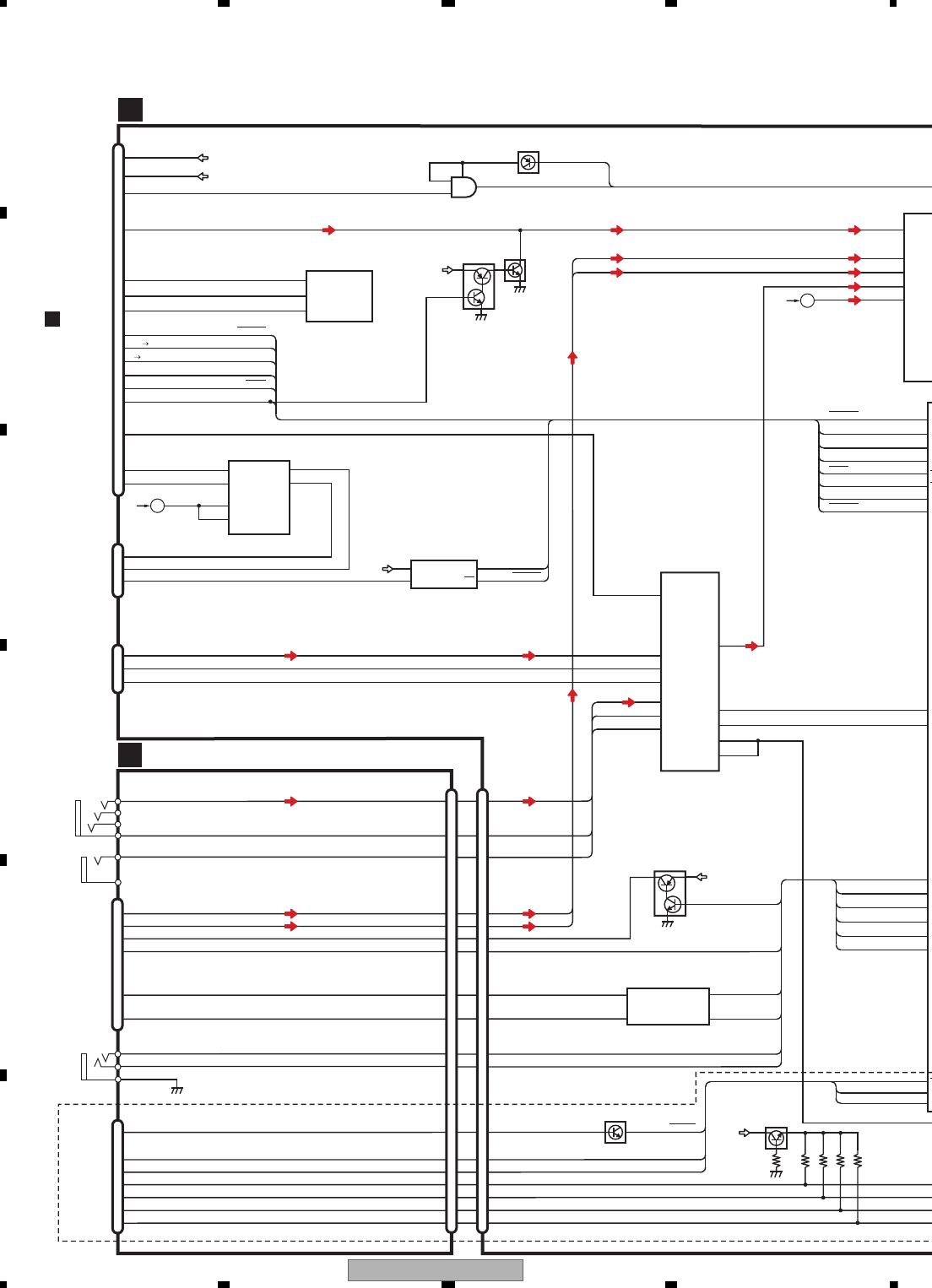
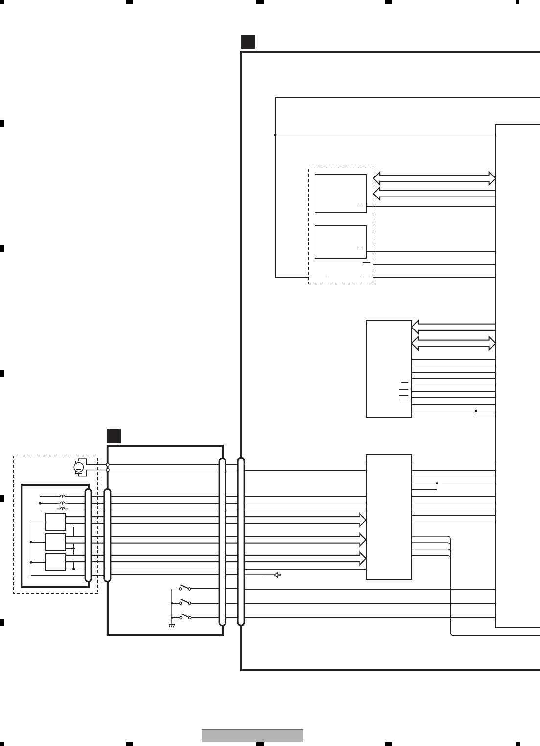
4. BLOCK DIAGRAM
4.1 OVERALL CONNECTION DIAGRAM
CN501
15
16
17
18
19
20
21
22
23
24
25
26
27
28
29
30
31
32
33
34
35
36
37
38
39
40
CN901
1
2
3
4
5
6
7
8
9
10
11
12
13
14
15
16
17
18
19
20
21
22
23
24
25
26
27
28
29
30
40FY-BMGB(LF)(SN)
CN121
ONSEI-
7
ONSEI+
8
GNDAU
9
CCAUR
10
CCAUL
11
GNDSIG
12
CSYNC
13
GNDSIG
14
ANB
15 GNDSIG
16 ANG
17 GNDSIG
18 ANR
19 NC
20 WIRED
21 WIREDAD
22 GNDD
23 GNDV
24 BCAM_VGGND
25 BCAM_IN
26 AUXV
27 AUVGND
28 MAINTEST
29 AUXR
30 AUAGND
31 AUXL
32 BUSL-
33 BUSL+
34 GND
35
BUSR-
36
BUSR+
37
ASENSB0
38
BUS+
39
BUS-40
CN801
1
2
3
4
5
6
7
8
9
10
11
CN5001
1
GNDILM
2
GNDFL
3
GNDFL
4
GNDFL
5
NC
6
PWRFL
7
PWRFL
8
PWRFL
9
NC
10
GNDD
11
GNDD
12
GNDD
13
GNDV
14
MONVBS
15
GNDV
16
GNDRGB
17
CSYNC
18
NAVI_R
19
NAVI_G
20
NAVI_B
21
GNDRGB
22
GNDP
23
GNDP
24
GNDP
25
NC
26
PWRVI
CN5003
1GNDKEY
2SWVDD33
3ILMB
4KDT1
5KDT0
6LEDR2
7LEDG2
8LEDB2
9LEDR1
10 LEDG1
11 LEDB1
12 HDRST
13 GNDKEY
14 REM
1
VCOM
2VCOM
3NC
4
VEE
5
NC
6SPS
7U/L
8CLS
9MODE
10CS
11GND
12NC
13VDD
14NC
15SPR
16
VCC
17VSHD
18NC
19GND
20CLD
21
GND
22GND
23NC
24VSHA
25VSHA
26NC
CN2002
1
2
3
4
5
6
7
8
9
10
11
12
13
14
15
16
17
18
19
20
21
22
23
24
25
26
27
28
29
30
31
32
33
34
JA2002
VIDEO
GND
AUXR
AUXL
1
2
3
4
JA2003
2 B.CAM_IN
1BCV_GND
JA2001
2
3
1
CN2001
1
CCR
2
CCG
3
CCB
4
CCSYNC
5
GNDSIG
6
DVDVBS
7
GNDDVD
8
YS
9
NC
10
CCAUL
11
CCAUR
12
GNDAU
14
ONSEI-
15
REAUR
16
REAUL
17
GNDRAU
18
CCREM
19
DSEN
20
TVON
21
GION
22
MONON
23
VSW5
24
SYS_TO_NAVI
25
NAVI_TO_SYS
26
GNDD
13
ONSEI+
AMUTE
DGND
DGND
DGND
DGND
AGND
VDD5
CPRST
IECOUT
VD
AGND
LS1 SRX
XRES
STANBY
VGND
IRQPWR
PGND
PGND
SLS1TX
DGND
SCK
SDA
VD
D+
AGND
VD
ROUT
D-
COMPOSIT
LOUT
MOTV
HALFSW
HOMESW
OPENSW
MOT5V
PULSE1
PULSE0
MOT1
MOT0
GND
GND
DRIVE UNIT
MINI JACK B.CAM INPUT WIRED REMOTE
NAVI INTERFACE
CXE1173
FMONITOR UNIT
AMOTHER PCB
MOTHER PCB(ANALOG)
1/4
A
MOTHER PCB(TUNER)
2/4
A
MOTHER PCB(SYSTEM)
3/4
A
MOTHER PCB(POWER SUPPLY)
4/4
A
BIF PCB
E
KEYBOARD
UNIT
C
GDVD MECHANISM MODULE
(LS1)
D
MONITOR UNIT(uCOM)
1/2
F
MONITOR UNIT(MONITOR)
2/2
F
AVH-P4100DVD/XN/UC 27
5 678
5678
C
D
F
A
B
E
CN501
1
2
3
4
5
6
7
8
9
10
11
12
13
14
15
16
17
18
19
20
21
22
23
24
25
26
GNDD
1
NAVI_TO_SYS
2
SYS_TO_NAVI
3
GUIDEON
4
TVON
5
NC
6
ONSEI-
7
ONSEI+
8
GNDAU
9
CCAUR
10
CCAUL
11
GNDSIG
12
CSYNC
13
GNDSIG
14
ANB
15 GNDSIG
16 ANG
17 GNDSIG
18
JA141
1
2
3
4
5
6
7
8
9
10
11
12
13
14
15
16
JA101
REAR_R
REAR_L
SW_R
SW_L
FRONT_R
FRONT_L
GND
GND
GND
GND
1
2
3
4
5
6
7
8
9
10
JA102
VCR_RG
1
VCR_RIN
2
VOUT_G
3
VOUT
4
VCR_LG
5
VCR_LIN
6
VCR_VG
7
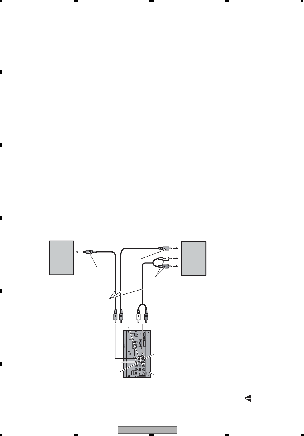
VCR_VIN
8
CN522
USB5V
D-
D+
USBGND
Shield1
Shield2
1
2
3
4
5
6
JA951 2
3
1
CN5001
15
GNDV
16
GNDRGB
17
CSYNC
18
NAVI_R
19
NAVI_G
20
NAVI_B
21
GNDRGB
22
GNDP
23
GNDP
24
GNDP
25
NC
26
PWRVI
27
PWRVI
28
PWRVI
29
SWVDD33
30
SWVDD33
31
ILMB
32
MONRST
33
S_MTX
34
M_SRX
35
MFLPWR
36
HDRST
37
GNDOSD
38
GNDOSD
39
GNDILM
40
GNDILM
CN6101
1
A2+
2
NC
3
A1+
4
NC
5
A1-
6
NC
7
A2-
8
NC
9
TH
10
TH_G
CN5401
1
NC
2
PLYV
3
PLYV
4
PLXV
5
PLXV
6
ADVX
7
ADVX
8
ADVY
9
ADVY
10
NC
CN6001
15SPR
16
VCC
17VSHD
18NC
19GND
20CLD
21
GND
22GND
23NC
24VSHA
25VSHA
26NC
27
GND
28LBR
29
LS
30R5
31
R4
32R3
33R2
34R1
35R0
36
G5
37G4
38
G3
39G2
40G1
41G0
42B5
43B4
44B3
45
B2
46B1
47
B0
48V10
49V9
50NC
51V7
52NC
53V5
54NC
55V3
56NC
57NC
58V0
59SPL
60GND
23
24
25
26
27
28
29
30
31
32
33
34
35
36
37
38
39
40
JA2004
1BUS+
2BUSG
3BUSLG
4MAINTEST
5BUS-
6BUSRG
7BUSL+
8ASENBO
9BUSR+
10 BUSR-
11 BUSL-
19
DSEN
20
TVON
21
GION
22
MONON
23
VSW5
24
SYS_TO_NAVI
25
NAVI_TO_SYS
26
GNDD
JA402 1
2
P.B.
BGSENS
FR+
RR-
ILM
FR-
B.UP
ACC
FL+
MUTE
RR+
RL+
B.REM
RL-
FL-
POWER SUPPLY
RCA OUTVCR IN
USB
S/PDIF OUT
BACKLIGHT TOUCH PANEL
LCD MODULE
CSX1142
IP BUS
CE
FM/AM ANT
CWX3691
AVH-P4100DVD/XN/UC
28
1234
1234
C
D
F
A
B
E
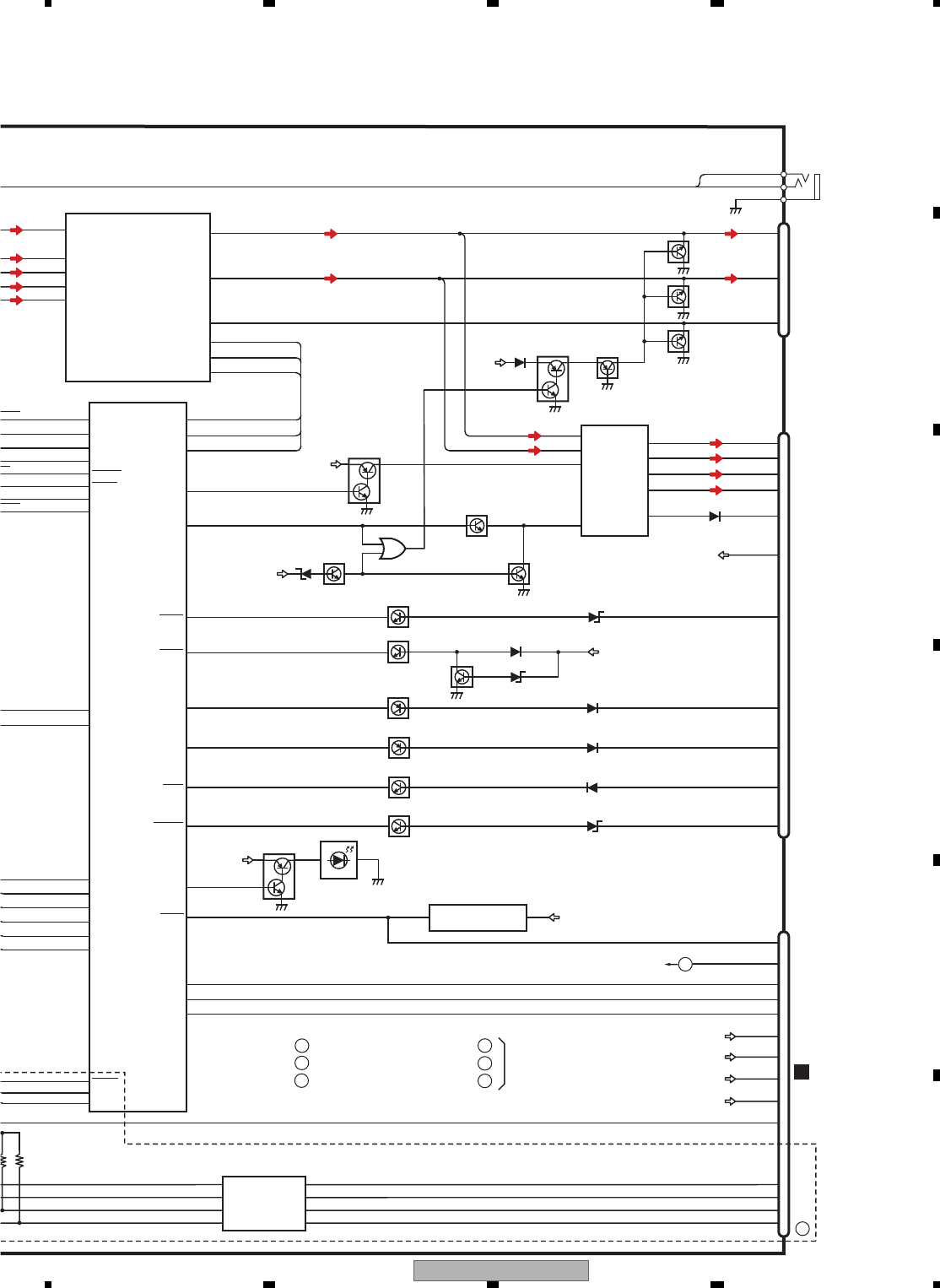
4.2 BLOCK DIAGRAM
6
8
4
VCR IN
LOUT
MOTHER PCB (1/2)
A
CN901
CN522
JA102
CN121
USB
AV SELECTOR
IC301
AN15887A
41
47 V6-1
V3-1
28
LOUT1
34
VOUT1
33
FB1
32
L2-1
V2-1
VOUT2
F
2
3
1
6
14
24
3
4
18
19
20
12
8
9
21
22
23
2
8
11
U
U
36
SCL 144 A
35
SDA 1A
39
VD5
VD8
VDD5
VD
CPRST
SDA
SCK
STANBY
LS1
S
SRX
LS1TX
IRQPWR
XRES
AMUTE
VDCNT5
STNDBY
IRQPW
MS_SRX
S_MSTX
XRES
AMUTE
VCR_LIN
VCR_VIN
VOUT
D+
D-
USB5V
D-
D+
COMPOSIT
IECOUT
10
S
17
R
31 T
I
13
18
27
29
X
A
IRQPW
USBFLG
AMUTE
STNDBY
XRES
MS-SRX
S-MSTX
USBCNT
EN
OC
VOUT
VIN
USB 5V
IC521
R5523N001B
IC951
TC7SET08FUS1
A
W
W
138
M
73 T
R
139
75
123
125
LS_L
BUSL+
BUSL-
LOUT
TUN_L
IN1_L
3
4IN4-_L
IN4+_L
7
IN2_L
6
2IN5+_L
JA2003
CN2002
BUSL+ BUSL+
BUSL-
ASENBO
ASENBO
MAINTEST
BUS-
BUS+
BUSL-
MAINTEST
BUS+
BUS-
IF PCB
B
B.CAMERA
INPUT
IP BUS
7
11
1
5
8
4
7
15
14
9
8
3
12
2
1
19
20
BCAM_INB.CAM_IN
BCV_GND
2
1
JA2002
JA2004
MINI
JACK
AUXL AUX_L
AUX_V
VCR_L
V1-1
37
LS-V
VCR_V
SPDIFSENS
SPDIFOUT
R_VOUT
AUX_V
BCAM_IN
AUXL
GND
4
AUXVVIDEO
1
2
AUXR
3
GNDD
JA2001
WIRED
REMOTE
WIREDAD
WIRED
WIREDAD
WIRED
BUSL+
BUSL-
ASENBO
NC
BUS+
BUS-
BCAM_IN
AUXL
AUXV
WIREDAD
WIRED
2
3
1
CN1901
C
TXIE
RXIE
ASENBO
MAINTEST
1
2
6DIN1
ROUT
BUS+
5BUS-
IP-BUS DRIVER
12
11
3
4
3B1
B2
A2
2
1
5
15
4
2
1
4
13
12
13
A1
1OE
2OE
IC522
TC7MBL6126SFK
Q121
BUP_1
21
22
40
33
38
29
27
26
34
32
39
I
30
28
TO 2/2
I2C_SDA/
SPI_SOMI
I2C_SCL/
SPI_SIMO
nRESET
IPOD CP IC
IC561
341S2162
15 L3-1
AUX_L
DD5
IC751
HA12241FP
Q951
Q902 Q901
SYS+B
E
TO 2/2
USBFLG
USBCNT
CN2001
TVON TVON
SYS_TO_NAVI SYS_TO_NAVI
NAVI_TO_SYS
ANR
CCR
ANG
CSYNC
ANB
NAVI_TO_SYS
CCG
CCB
CCSYNC
NAVI I/F
20
24
25
1
2
3
4
36
38
39
22
24
26
28
R
T
53 R
52
55
TVON
SYS_TO_NAVI
NAVI_TO_SYS
ANR
ANG
ANB
CSYNC
Q601
2
19
17
5
3
15
13
RGBON
TXNADI
RXNAVI
Q771
SYS+B
AVH-P4100DVD/XN/UC 29
5 678
5678
C
D
F
A
B
E
RCA OUT
2
4
6
5
7
6
11
9
14
8
16
5
27
6
7
CN5001
E
POWER
CONNECTOR
Q103 Q105
17
9
7
AMP
IC181
PA2030A
RL+
FL+
FL-
19
RL-
25
B.REMOTE
4STBY
22 MUTE
11
PA_FL FLIN
15
PA_RL RLIN
Q183
SYS+B
JA141
FL-
FL+
RL-
B.REM
B.UP
P.B.
ACC
RL+
BUP_1
Q163(1/2)
Q165
BUP_1
VDD33
SYSTEM uCON
IC601(1/2)
SYSMUTE
AMPPW
135
131
129
9
11
USBCNT
USBFLG
144 AVSCK
1AVSDATA
10
ASENS
8
BSENS
ISENS
BGSENS
12
ILM
13
10
MUTE
BGSENS
Q162(1/2)
Q162(2/2)
Q163(2/2)
Q161
134
137
PBSENS
TELMUTE
67
FLPILM
45
19
CN501
MONVBS
PWVI
PWFL
ACC33
DD8
HDRST
MFLPWRMFLPW
M_SRX
8
9
10
47
RESET
44 S_MTX
MONRST
ILMB
SWVDD33
PWRVI
PWRFL
STANDBY
17
RXLS1
31 TXLS1
IRQPW
13
18
27
29
XRESET
AMUTE
RXMON
TXMON
MONIRST
Q182
(1/2)
Q182
(2/2)
Q181
BUP_1
OFFMUTE
AMPMUTE
PBSENS
ASENS
BSENS
ISENS
Q164
136
BGSENS
TELMUTE
PEG535A8(UC)
PEG534A8
(EW5,UW5)
QPW
SBFLG
MUTE
NDBY
ES
S-SRX
MSTX
SBCNT
ASENBO
WIREDAD
WIRED
138
MAINTEST
73 TXIE
RXIE
139
75
20
21
19
123
125
+
-
T
L
Pre/SW_L
DATA
CLK
STB
110
111
109
EVSDA
EVSCK
EVSEL
EVSDT
EVSCK
EVSTB
EVSDT
EVSCK
EVSTB
IN1_L Front_L
Rear_L
3
4IN4-_L
IN4+_L
7
IN2_L
6
2IN5+_L
12
10
11
RCA MUTE JA101
JA951
REAR_L
SW_L
FRONT_L
RCA_RL
RCA_SWL
RCA_FL
BUP_1
I
15
13
I
35
33
.
12
11
12
RESET
INSERTION LED
IC602
S-80827CNNB-B8M
S/PDIF OUT
SPDIFSENS
SPDIFOUT
GND
2
3
1
E.VOL CAPTAIN6
IC201
PML018A
Q801
D801
DD5
D
TO 2/2
Q101(1/2)
Q105
Q101(2/2)
:AVH-P4100DVD/XN/UC
A
:AVH-P4100DVD/XNEW5
:AVH-P4100DVD/XNUW5
B
C
TO 2/2
E
F
D
24
23
22
CSYNC
NAVI_B
NAVI_G
NAVI_R
RGBON
TXNAVI
53 RXNAVI
52
55
21
10 C_+IN
3
5
12
8
1
7
14
D_+IN
A_+IN
B_+IN
C_OUT
D_OUT
A_OUT
B_OUT
RGB VIDEO ISOLATOR
IC771
NJM2138V
C
AVH-P4100DVD/XN/UC
30
1234
1234
C
D
F
A
B
E
MOTHER PCB(2/2)
A
SYSTEM uCON
IC601(2/2)
PEG535A8(UC)
PEG534A8
(EW5,UW5)
:AVH-P4100DVD/XN/UC
BUP_1
PWVI
VD5
PWVI
MOTV
VD5
DDCCLK 80
VDCONT8 26
VDCONT5 25
2
7
3
IC1001
S-812C33AUA-C2N
Q1001
Q1143
Q1142
Q1141
3
VDD33
P1021
128
SYSPW
92
HIOUTCLK
DD5 24
5
1
TUN33V
EV12
DD8
MOTV
SYSPW
VDCNT5
BUP_1 12
4
SYS+B
SYS+B
IC1061
NJM2388F84
SYSPW
85
BEEP
X601
15MHz
BZ601
BUZZER
22
20
XIN
XOUT
DD5
ACC33
P1202
VDD33V
MOTV
CN801
PWFL
HIOUT12V
Q1002
A
:AVH-P4100DVD/XNEW5
B
:AVH-P4100DVD/XNUW5
C
E
D
VIN VOUT
CONTROL
ACC33V
IC1401
S-1112B33MC-L6S
VIN 5
VOUT
1
3ON/OFF
TUN3.3V
IC1081
NJM2886DL3-33
VIN VOUT
CONT
IC1141
TK11840L
FM/AM TUNER UNIT
U401
Vcc
OSC Out
D/D CONVERTER
IC1201
BD9013KV
SW1
OUTH1
OUTL1
FB1
COMP1
SW2
7
34
27
26
8
OUTH2
OUTL2
FB2
COMP2
EN1
EN2
SYNC
VCC
VCCCL1
VCCCL2
CL1
CL2
EXTVCC
13
12
15
21
22
Q1201
VD8
DD8
P1203
BUP_1
MOT1 33
MOT0 32
NC(OPENSW) 30
HALFSW 36
PULSE1 35
PULSE0 34
HOMESW 37
5
10
3
41
P1201
DD8
P1341
48
1
46
39
38
Q1202
SYS+B
VDD33
TUN33V
ETO 1/2
Q1022
Q1021
PWFL
P1022
D
TO 1/2
4
OPENSW
MOT0
MOT1
PULSE0
PULSE1
HALFSW
HOMESW
9
DRIVE UNIT
INTERFACE
8
7
6
2
3
1
5
Q404
Q403
BC
JA402
AM_ANT
FM_ANT
Lch
SL
TUN_L
1
2
1
3
5119
CE2 114
CE1 113
CK 117
DI 118
DO
TUNSL
TUNPCE2
TUNPCE
TUNPCK
TUNPDO
TUNPDI
116
6
8
9
10
14
LDET
RDS_CK
RDS_DATA
RDS_LOCK
RDS_HSLK
VCC
ROM_VDD
VDD_3.3
LDET
103
RCK
104
RDT
105
RDSLK
107
RDS57K
106
11
18
19
20
21
4
13
17
23
ANTENNA
FTO 1/2
Q1341
F
MOT5V
MFLPW
TO 1/2

AVH-P4100DVD/XN/UC 31
5 678
5678
C
D
F
A
B
E
AVH-P4100DVD/XN/UC
32
1234
1234
C
D
F
A
B
E
MA0-11
MDQ0-15
D0-15
VIDEO+AUD
IC1501
MN2DS0018M
S
S
USB_
TRC
TRC
TRC
T
S
E
F+
E+
D
COM
ST
CMD
ST
IR
E
TRC
NRES
A0-19
HWP(HW+),HWM(HW-)
HVP(HV+),HVM(HV-)
HUP(HU+),HUM(HU-)
HWP(HW+),HWM(HW-)
HVP(HV+),HVM(HV-)
HUP(HU+),HUM(HU-)
XRDNRES 28 214 NEXOE
NEXWE
70 NRES
I
I2
CP
I2
59 XCSSR
213
31
NEXCE
26
12
CE
OE
RESET
SDRAM
IC1480
K4S641632N-LC75
19
38
CS
CLK
XWE16 181 NWE
XCAS
DQM0
DQM1
17 188 NCAS
XRAS18 189 NRAS
XCSM 190 NCSM
20 193 BA0
21 197 BA1
BA0
BA1
15 179 DQM0
39
8
9
12
5
6
7
3
4
1
2
32
31
27
26
28
14
180 DQM1
LDQM
UDQM
MCK
VHALF
TD
FD
CRGDRV
MD
CONT1
CONT2
FOP
FOM
TOP
TOM
183 MCK
185 MCKI
V
CAS
RAS
WE
MOTOR DRIVER
IC1201
BD8231EFV
CTL1
CTL2
FG
FCO+
FCO-
TKO-
TKO+
FCIN
SLIN
VC
TKIN
LDIN
SPIN
W
HB
SL/LDO-
SL/LDO+
V
U
SLOPOUT
CN1201
CN101
CN701
CRG/LE+
COIL_U
17
18
16
6
3
4
5
9
8
7
HALL_BIAS-
HALL_BIAS+
COIL_V
COIL_W
67
127
126
66
71
64
63
FG
CONT2
CONT1
12EJ
08EJ
HOME
62
MD
LDIN
CRGDRV
FD
TD
34
36
35
33
55
49
65
CRG/LE- 110 VHALF
FLASH 16M
IC1401
CWW1753
XCFS2
XCFS1
26
11 XWR1
CE
WE
IC1402
CWW1754
DVD CORE UNIT
C
VCC5
BR
GY
CRG-
CRG+
V COIL V
U COIL U
W COIL W
V
U
W
H- HALL BIAS-
H+
H-
H+ HALL BIAS+
HOME
8SNS
DSCSNS
HOME
8cm
12cm(DSCSNS)
CONNECT PCB
SPINDLE MOTOR
LS1 MECHA UNIT
D
2
1
3
13
16
15
14
10
11
12
1
2
3
4
10
1
2
3
4
10
M
LOADING/CARRIAGE
MOTOR
HOME
S101
8cm
S102
12cm
S103
H3
H2
H1
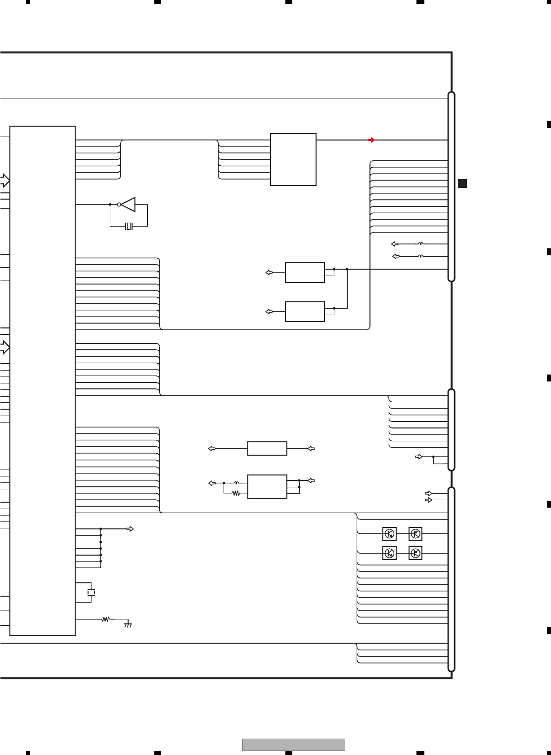
AVH-P4100DVD/XN/UC 33
5 678
5678
C
D
F
A
B
E
VIDEO+AUDIO
IC1501
MN2DS0018MAUB
AVCC5
VOUTL 7
BCK
LRCK
DATA
MD
1
3
2
13
AUDIO 2CH ANALOG OUT
IC1801
PCM1753DBQ
LOUT
ML
MC
SCK
SRCK
LRCK
ADOUT
SDODAC
LTDAC
SCKDAC
DACCK
USB_CLOCK
15
14
16
149
150
151
57
56
58
148
50 2
SRCK
ADOUT
SDODAC
LRCK
LTDAC
SCKDAC
DACCK
TRCST
TRCDATA3
TRCDATA2
TRCDATA1
TRCDATA0
TRCCLK
EXTRG0
1
2
3
4
9
7
12
8
13
5
6
Q1104Q1102
VREF
VCC5
CN1101
CN1951
78LD
F+H_G+H
E+G_E+F
F+H/G+H
E+G/E+F
LPCO2
8
2
3
4
14
15
12
18
17
13
20
22
7
5
11
Q1103Q1101
65LD
VCC
Vref
LPCO1
TRCDATA2 79
TRCDATA3
TRCDATA0
TRCST 80
77
81
TRCCLK 76
SDATA
SCLOCK
SDATA 73
SCLOCK 72
EXTRG0
F+H_G+H
E+G_E+F
VIN4RF
VIN2RF
VIN1RF
VIN3RF
VIN8
DVDMPD
TEMP
RFINP
CDMPD
LPCO2
LPCO1
74
112
111
99
98
97
100
116
105
A
C
D
B
FE1
FE2
RF
122
96
103
106
104
51
3
VIN
VOUT ON/OFF
AVCC5 REG.
IC1003
S-1200B50-M5
VCC5
VD8
54
3
VIN
VOUT ON/OFF
VCC5 REG.
IC1002
S-1133850-U5
A10
B
C
D
FE1
FE2
78MDCDMPD
65MDDVDMPD
TEMP
RF
ROUT
LOUT
COMPOSITE
152
146
144
138
STANDBY 191
CMDCOMN 53
STSCOMN 54
IRQPWR 48
EXTRG1 75
D+
4
D-
AMUTE
24
25
23
26
F-
F+
FOM
FOP
TOP
TOM
T+
T-
TRCDATA1 78
IFCOUT
D+
D-
SCL
SDA
RESET
COMPOSIT
STANBY
SLVSTS
HSTCMD
STSCOMN
CMDCOMN
COMPOSITE
STANDBY
ISC_SCL
I2C_SDA
CP_Reset
IRQPWR
AMUTE
VD8
XRESETNRES
OSCO
OSCI
X1501
156
155
X1950
ANALOG LOUT
CN1901
9
3
17
25
27
28
29
23
11
10
13
8
7
12
1
.
2
22
19
VREF
214 NEXOE
NEXWE
70 NRES
IECOUT
I2C_SDA
CP_Reset
47
46
61
I2C_SCL
59 XCSSR
213
31
NEXCE
181 NWE
188 NCAS
189 NRAS
190 NCSM
193 BA0
197 BA1
179 DQM0
180 DQM1
183 MCK
185
121
MCKI
VDSENS
IC1951
TC7SZU04FU
67
127
126
66
71
64
63
FG
CONT2
CONT1
12EJ
08EJ
HOME
62
MD
LDIN
CRGDRV
FD
TD
120
VIN1
109
VREFH
119
VIN2 118
VIN4 117
VIN3 114
VIN6 113
VIN5
55
49
65
110 VHALF
VIN7 115
13
VCC33 VDD5
VCC33
3.3V REG.
IC1004
NJM2885DL1-33
INOUT
2
8VDD5
VCC12
1.2V REG.
IC1005
R1232D121B
VIN
VDD
CE
LX
5VOUT
VDD5 VD5
PU (DP10)
DEBUG
CN901
A
3
4
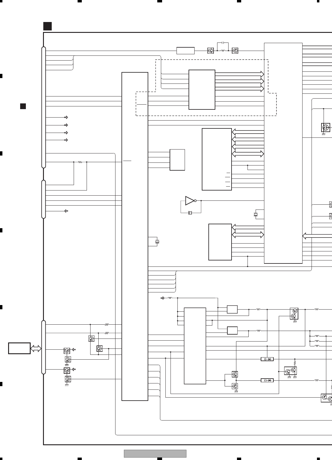
AVH-P4100DVD/XN/UC
34
1234
1234
C
D
F
A
B
E
DVR[0-5]
DVG[0-5]
DVB[0-5]
CN5001
CN5101
LCDCE
GPIO_04
GPIO_03
GPIO_02
SDATA
SCLOCK
X5101
20MHz
X5701
9.597MHz
15
14
X5702
33MHz
180
179
LCD_R_[0-5]
LCD_G_[0-5]
LCD_B_[0-5]
GPIO_05
168
189
LCDCSY 192
LCDDEN 193
LCDHSY 194
LCDVSY
LCDCLK
195
196
COMDC
COMAC
191
190
131
130
123
122
AINP0
GERDA
IC5702
MN103SE60PUB
4
2
XRST
COMAC
EPRDO
MONITOR uCON
IC5101
PE5669A8
X2
EPRDI
COMDC
DIMMER
BLSYNC
BLERR1
TEMPSEN
EPRCE
MONVBS
CS
EPRCK
1
3
DI
3
4
SK
2
6
DO
4
5
EEPROM
IC5102
S-93C56BD0I-J6
IC5701
TC7SHU04FUS1
VADRES
SDA
SCL
X1
LCDICLK
OSCXO
OSCXI
FRWE
FROE
FRCS
XRST
DVVSY
DVHSY
DVCLK
VIDEO_AD
IC5601
AK5406XQ
AVH-P4100DVD/XNUW5 Only
SDA
RESETN
SCL
SOGIN
RIN
GIN
BIN
CSYNC
NAVI_R
NAVI_G
NAVI_B
VSYNCO
HSYNCO
DTCLK
49
54
48
43
14 IC5451
NJM2505AF
C.VIDEO
MONITOR UNIT
F
ADVY
ADVX
PLYV
PLXV
PNLADY
61
PNLADX
62
PNLVD
46
PNLYV
45
TOUCHAD
65
PNLXV
44
TOUCH
PANEL
Q5401
(1/2)
Q5403
(2/2)
Q5403
(1/2)
Q5401
(2/2)
SWVDD33
Q5402
(2/2)
Q5402
(1/2)
SWVDD33
CN5401
14
18
17
NAVI_R
CSYNC
ILMB
SWVDD33
PWRFL
SWVDD33
19
20
33
34
35
31
36
32
RXD0/TSI
53
TXD0/TSO
52
NAVI_B
MFLPW
28
HDRST
RSTIN
RSTOUT
TOOL0
TOOL1
FLMDO
3
4
1
2
10
SWVDD
NAVI_G
S_MTX
MFLPWR
RESET
10
FLMDO
13
TOOL1
8
TOOL0
9
MONRST
M_SRX
A
CN501
uCON
REWRITE
.
30
29
.
9
8
.
9
8
.
7
6
.
3
2
.
5
4
I
8
6
I
28
26 PWRVI
Q6151
57
58
29
75
25
63
64
BLSYNC
DIMMER
TEMPSEN
BLERR1
21
22
23
56
57
61
62
64
65
162
161
160
200
Q5452Q5451
Q61
Q61
32
43
EN1
34 EN3
35 EN4
36 EN5
FIN
27
78
77
76
39
34
35
36
74
68
67
1,2,5,6
1,2,5,6
3
4S
GD
S
GD
3
4
D/D CONVERTER
IC5501
BD6171KV
3.3V REGULATOR
Q5501
11
6
PVCC1
PVCC2
PWCTL2
OUT2 7
VS2 4
PVCC3
PVCC5
23
37
OUT1 10
OUT5 38
OUT4 47
OUT3 22
8V REGULATOR
Q5502
41
42
PVCC
VCC
CHARGE PUMP
REGULATOR
VS1 13
PVCC4 48
MVIPW
ILMLD
ILMCK
ILMDT
FSEL
PWRVI
Q5505
Q5561
Q5504
Q5503
PWCTL1
PWCTL3
PWCTL2
REMIN
KDT0
KDT1
FAD[0-21]
FDATA[0-15]
ROM
IC5201
PEH208A8
RESET
26
CE 85
28
OE 86
11
WE 84
12 135
GRST
SDA[0-11]
SDBA[0,1]
SDM[0,1]
SDD[0-15]
37 SDCKE
MEMCLK
MIMCLK
SDCS
SDRAS
SDCAS
SDWE
RAM
IC5301
K4S281632K-UC75
CKE
CLK
16
38 17
18
19 40
18 41
17 42
16 43
RAS
CS
CAS
WE
RXD1
TXD1 RXD0
50 128
51 127
TXD0
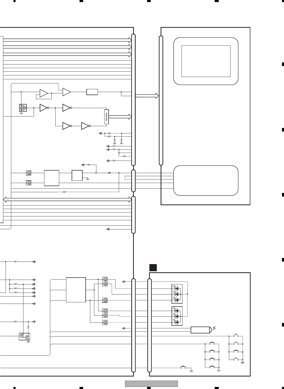
AVH-P4100DVD/XN/UC 35
5 678
5678
C
D
F
A
B
E
LR[0-5]
LG[0-5]
LB[0-5]
16
13
10
4
|
30
35
|
36
41
|
42
47
9
29
59
8
6
20
1
2
28
CN6001
CN5701
CN6101
CN5003
CE
04
03
02
TA
CK
5]
5]
5]
05 MODE189
SY LS192
EN CLS193
SY SPL194
SY
LK
SPS195
CLD
17
VCCM16V
V[0,3,5,7,9,10]
196
COMDC
COMAC
191
190
131
130
123
122
OSC OUT
EaIn
IC6101
TK11840L
LADDER NETWORK
VCOM AMP
IC6005
TC74VHCT04AFTS1
LCD PANEL
LCD
LCD BACKLIGHT
BR/CTL
D1-4
S
G
5 1,2,5,6
4
1
VCC15V
IC6151
NJM082BV
-
+7
6
5
6
51,3
-
+1
3
8
9
2
VCOM DRIVE
Q6001
Q6002
.
25
24
.
.
49
48
.
.
53
51
.
58
55
VCOM
VCOM
VEE
CS
VDD
73
4
VSHD
VCC
LBR
VSHA
A2+
A2-
A1+
A1-
TH
EXTRG0
TRCST
TRCCLK
SDATA
SCLOCK
GRST
GERDA
REWRITE
PWRFL
VCC3.3V
VCC53V
GD33V
3
5
6
8
9
4
KEYBOARD UNIT
E
CN3003
KDT0
HDRST
S3005
RESET
S3006
EJECT
S3007
MUTE
9
3
10
11
12
4
5
14
S3009
VOL+
S3004
VOL-
S3001
SOURCE
S3002
FORWARD
S3003
REVERSE
S3008
DISP,OFF
D3005
LEDG1
LEDR1
ILMB
LEDB1
LEDG1
LEDR1
LEDB1
6
LEDR2
7
LEDG2
8
LEDB2
REM
KDT0
KDT1
9
3
4
2
10
11
LEDG2
LEDR2
LEDB2
6
7
8
SWVDD33
2REM
14
12
5
KDT1
4
ILMB
2
SWVDD33
Q5001
Q5002
Q6151
HDRST
ILMLD
ILMCK
ILMDT
BLSYNC
DIMMER
TEMPSEN
BLERR1
CSB
DI
AO1
AO2
AO3
IC5001
BH2227AFV
RGB LED DRIVER
2
5
12
11
10 1
CLK
Q6103 Q6102
Q6101
D3002
U3001
RS-470
REMOTE CONTROL
SENSOR
OPT IN
VCC8V
3.3V
VCC15V
VCC53V
VCCM16V
VCC3.3V
GD33V
V33A
Q5561
Q5562
Q5003
Q5004
10,12
11,13
2,4
1
7
3
5
9
TRCD[0-3]
.
2
1
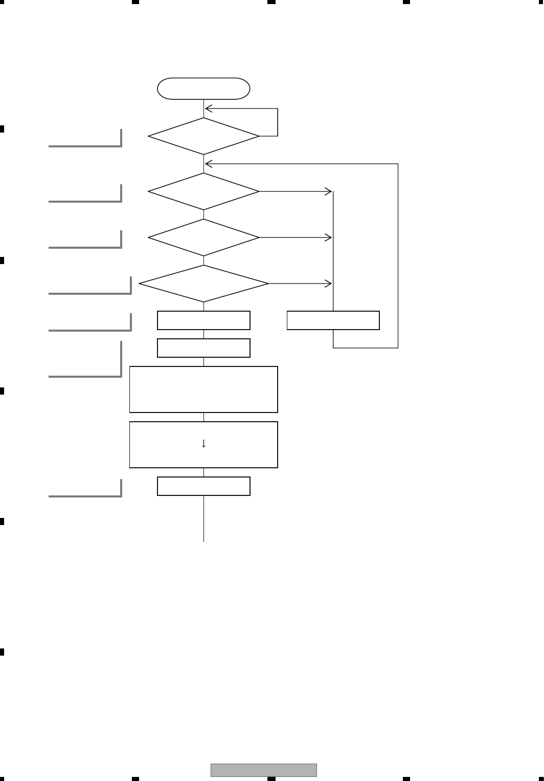
AVH-P4100DVD/XN/UC
36
1234
1234
C
D
F
A
B
E
5. DIAGNOSIS
5.1 OPERATIONAL FLOWCHART
SYSPW <- H
Source keys operartive
Source ON
Vdd = 3.3 V?
BSENS = L?
ASENS = L?
ASENBO <- H
VDCNT5,8 <- H
Starts
Communication
with Display microcomputer
Standby
Y
Y
Y
Vdd : pin 23
BSENS : pin8
ASENS : pin9
ASENBO : pin123
VDCNT5 : pin25
STANDBY : pin27
Y
STANDBY = H?
VDCNT8 : pin26
RESET
SYSPW : pin128
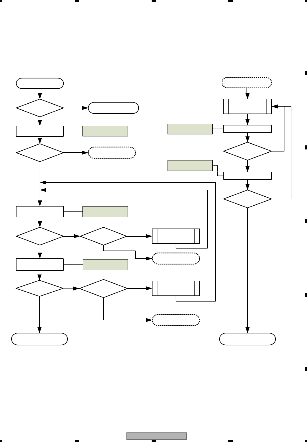
AVH-P4100DVD/XN/UC 37
5 678
5678
C
D
F
A
B
E
5.2 INSPECTION METHOD OF PICKUP UNIT
Disc to be used
CD-DA: TCD-782
DVD-Video: TDV-582
Execution method
START
Is it OK?
Is it OK?
Ckeck parts
other than PICK UP
PICK UP
cleaned?
Perform lens
cleaning
SKEW ADJ.
Is it OK?
LD current check
RF level check
RF level check
Yes
Error rate check
Finished
LD turned on? Check parts
No
Is it OK? PICK UP
cleaned?
Perform lens
cleaning
Error rate check
Is it OK?
Replace the PICK UP
Replace the PICK UP
Replace the PICK UP
Replace the PICK UP
Check point:
AS MAX check
Check point:
LD current check
Check point:
Error rate check
Yes
No
Yes
No
Yes
No
Yes
No
Yes
No
Yes
No
Yes
No
Check point:
AS MAX check
Check point:
Error rate check
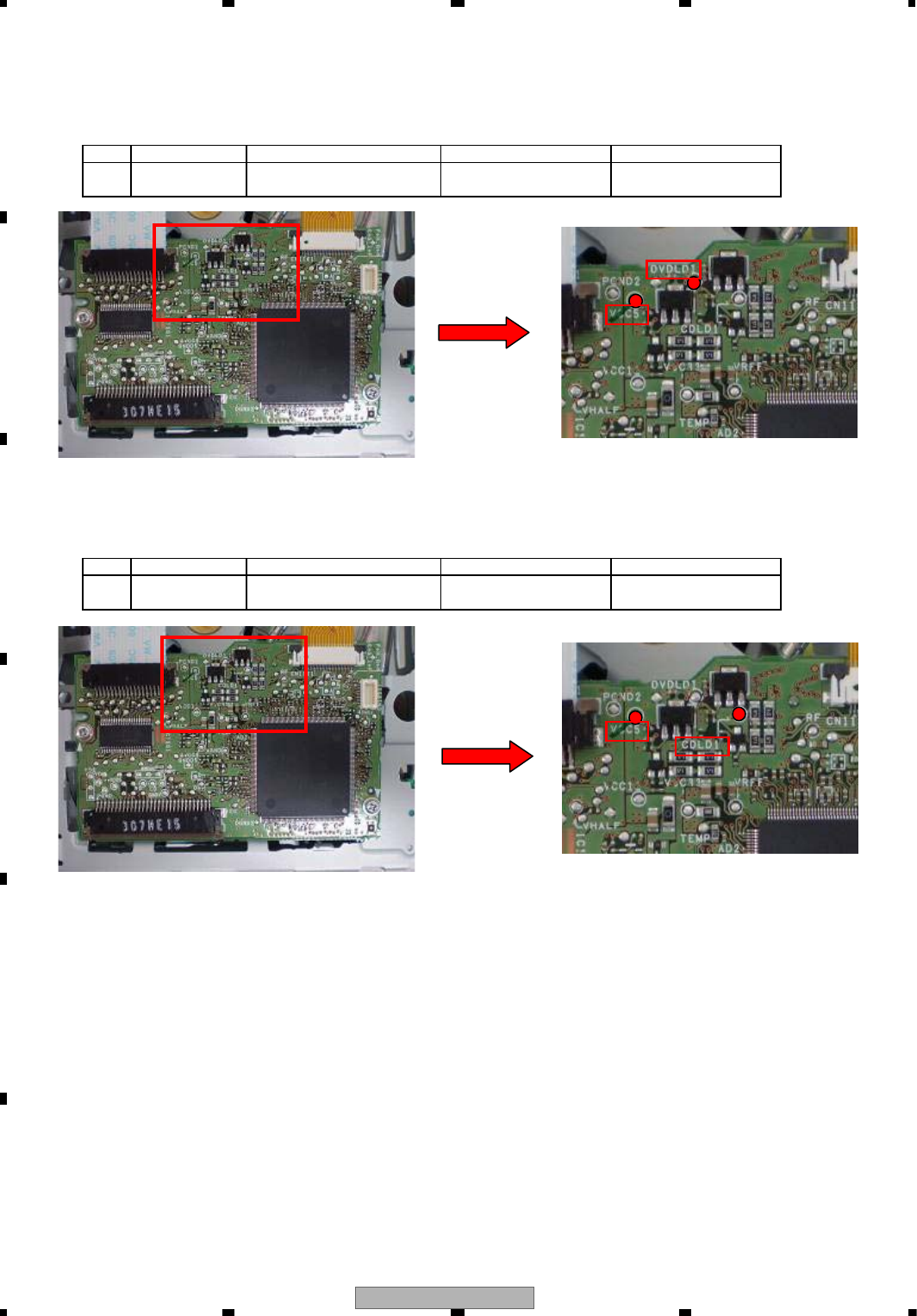
AVH-P4100DVD/XN/UC
38
1234
1234
C
D
F
A
B
E
LD current check
Check
Status: [Foucs closed] of TEST MODE
Notes: Please pay attention to the laser diode damage by static electricity.
Threshold
2 TCD-782 CDLD1-VCC5_3 60 - 360 (mV) 10 - 60 (mA)
NO. Disc Check Point
Check Point
DVDLD1-VCC5_3
NO.
1
Disc
GGV1025
Remarks: LD current
10 - 65 (mA)
Threshold
60 - 390 (mV)
Expansion
Expansion
Remarks: LD current
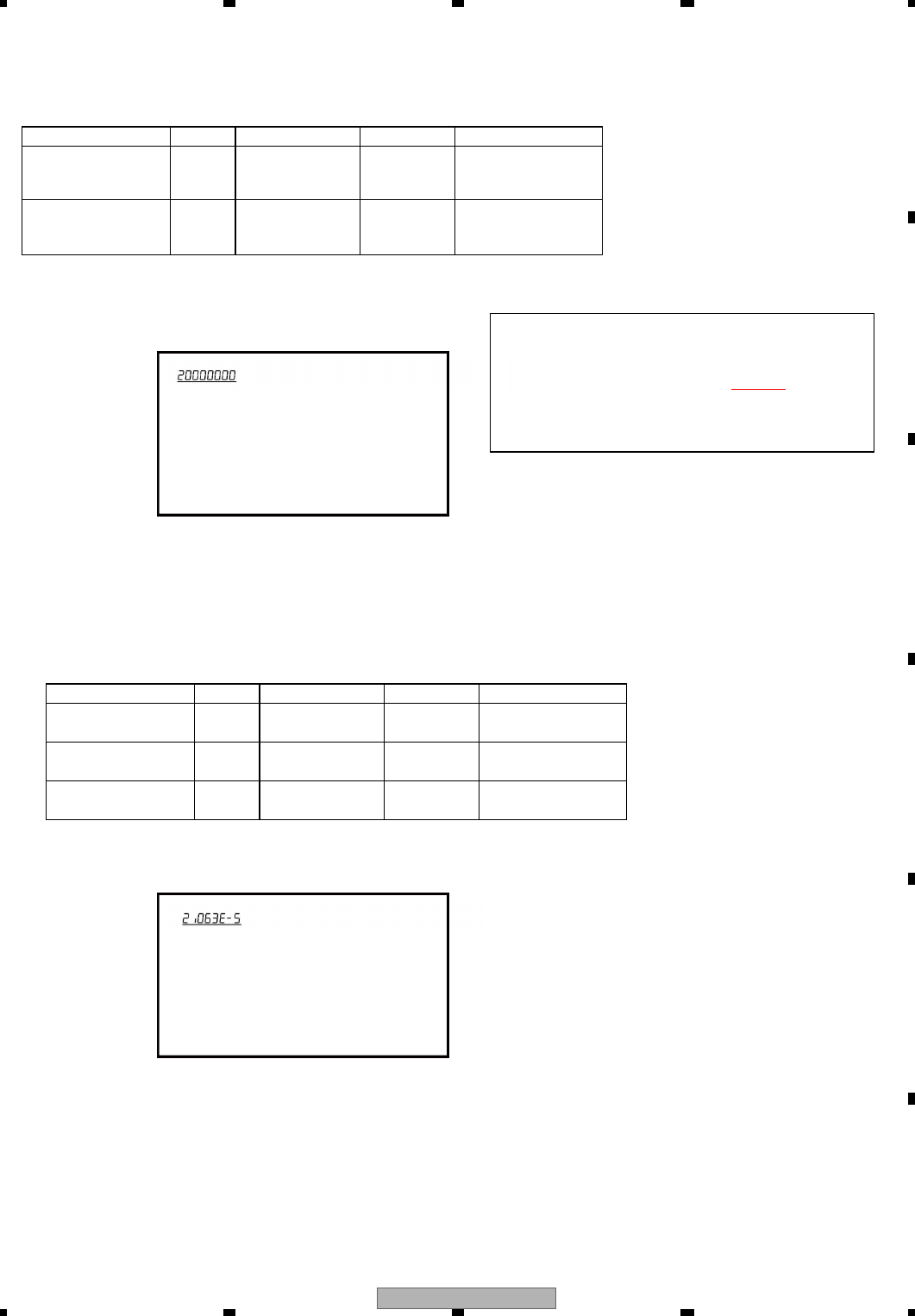
AVH-P4100DVD/XN/UC 39
5 678
5678
C
D
F
A
B
E
ASMAX check
ASMAX value shows the value of RF level.
Status: [Foucs closed] of TEST MODE
No. Disc Check Point Threshold Remarks:
8 digits value of
ASMAX more than
on display 0000 0B00
8 digits value of
ASMAX more than
on display 0000 0C00
Error rate check
Status: [Tracking Closed] of TEST MODE
No. Disc Check Point Threshold Remarks:
less than
1.000E-03
less than
1.000E-03
less than
2.500E-03
3 TCD-782 ID: HOME Position
2
GGV1025
ID: 200000
1
GGV1025
ID: 40000
1
GGV1025
Only four last digits are
displayed according to
the product.
2 TCD-782
Only four last digits is
displayed according to
the product.
In this case, the value is displayed for a split second.
When you tried to perform [FOCS CLOSE],
the display will charge automatically in the following order.
[1FFF0000]->[FEMAX]->[FE MIN]->[AS MAX]->
[ENV MAX]->[FE normal]->[Spindle gain]->
[TEMAX]->[TEMIN] ->[20000000]
Watch carefully the value of ASMAX.
Test mode display will not appear on the display of this product. Connect the rear monitor output to a monitor.
Test mode display will not appear on the display of this product. Connect the rear monitor output to a monitor.
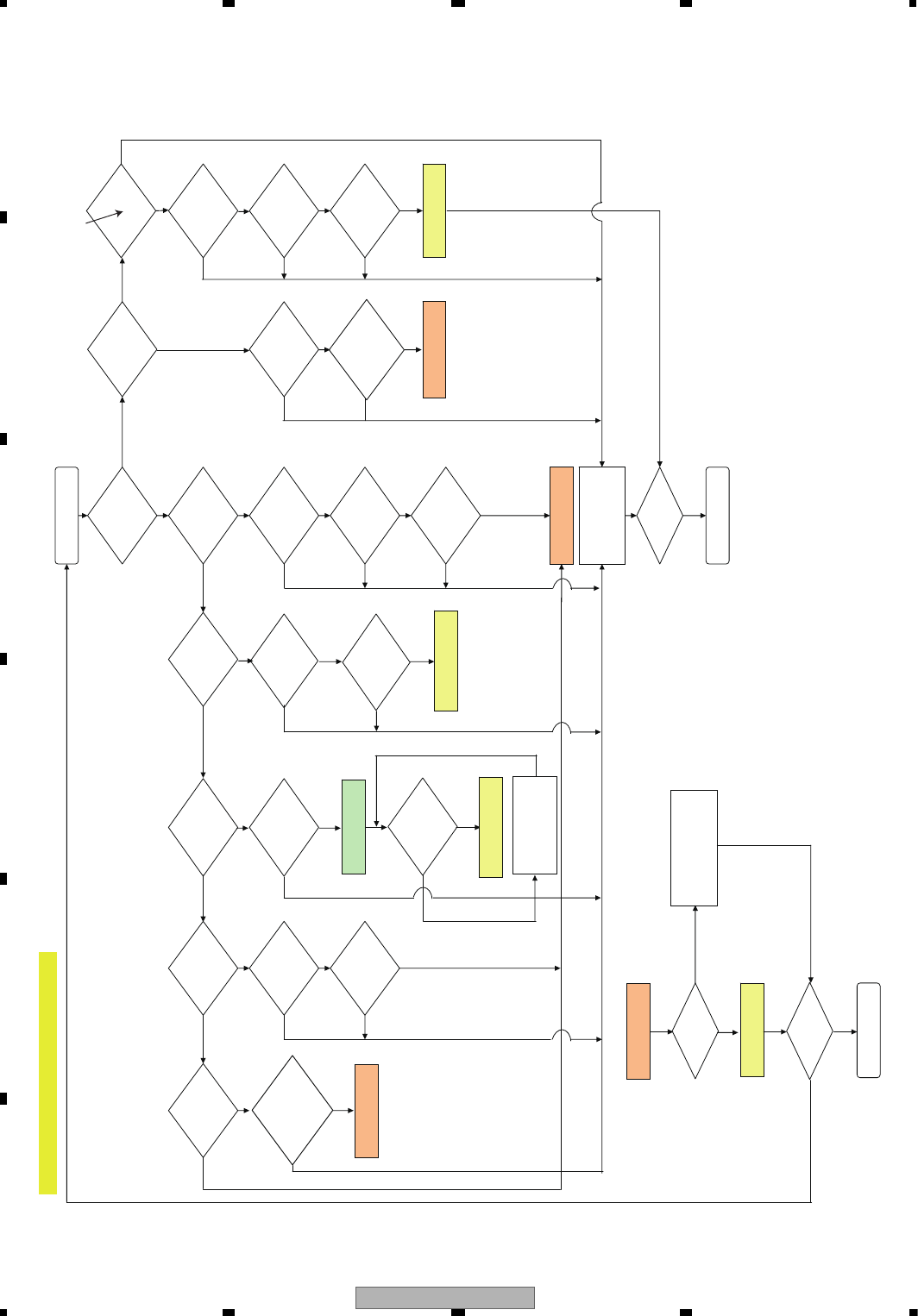
AVH-P4100DVD/XN/UC
40
1234
1234
C
D
F
A
B
E
5.3 DIAGNOSIS FLOWCHART
BACK END section flow
Standby
OK?
Execute
check 1.
Can the
playback
start?
NO
YES
YES
YES
YES
YES YES
YESYES
YE
S
YES
YES
YES
NO
NO
NO
NO
NO
YES
YES
YES
NO
YESYES
NO
START
END
END
YES
NO
NO
NO
NO
NO
YES
YES
NO
NO
NO
The product
is normal?(iPod
attestation IC)
YES
Product repair
YES
NO
NO
NO
NO
YES
NO
YES
YES
YES
NO
NO
YES
Does the
operation
take time?
Go to FE
section check.
Go to FE
section check.
Is the life of flash
memory OK?
Conduct check item 12.
Is the image
in error?
Is the video
circuit OK?
Execute check 11.
Is AVCC5
voltage OK?
Execute check 8.
Replace the unit.
Is VDD5(VCC33, VCC12)
power supply voltage OK?
Execute check 2.
Reset OK?
Execute check 3.
Is VSENS
OK?
Execute check 4.
Is 27 MHz
OK?
Execute check 5.
Is 48 MHz OK?
Execute check 13.
Replace the unit.
Replace the unit.
Replace the unit.
Go to FE
section check.
Go to the
product check.
Go to FE
section check.
Is VD8, VCC5
power supply
voltage OK?
Execute check 7.
Is SDRAM
IF OK?
Execute check 6.
Is the sound
in error?
Is the iPod play
in error?
Is the USB play
in error?
Is AVCC5
voltage OK?
Execute check 8.
Is DACCLK
normal?
Execute check 9.
Is the audio
circuit OK?
Execute check 10.
Repair the
defective part.
Normal?
Normal?
Is FE section
normal?
Go to FE related
repair process.
Is the iPod
circuit OK?
Execute check 14.
Is the USB
circuit OK?
Execute check 14.
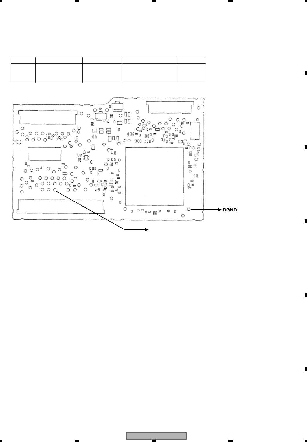
AVH-P4100DVD/XN/UC 41
5 678
5678
C
D
F
A
B
E
Check 1: Standby OK?
<Check> Check the voltage at the “STANBY” test point while the power is on.
Use the “DGND1” test point at the reference.
NO. Check point Module No. Specification value Unit
STANBY-DGND1 ALL VCC33 V-
0.6 V or more
V
Side A
1
Fig 1.1: STANBY check point
STANBY
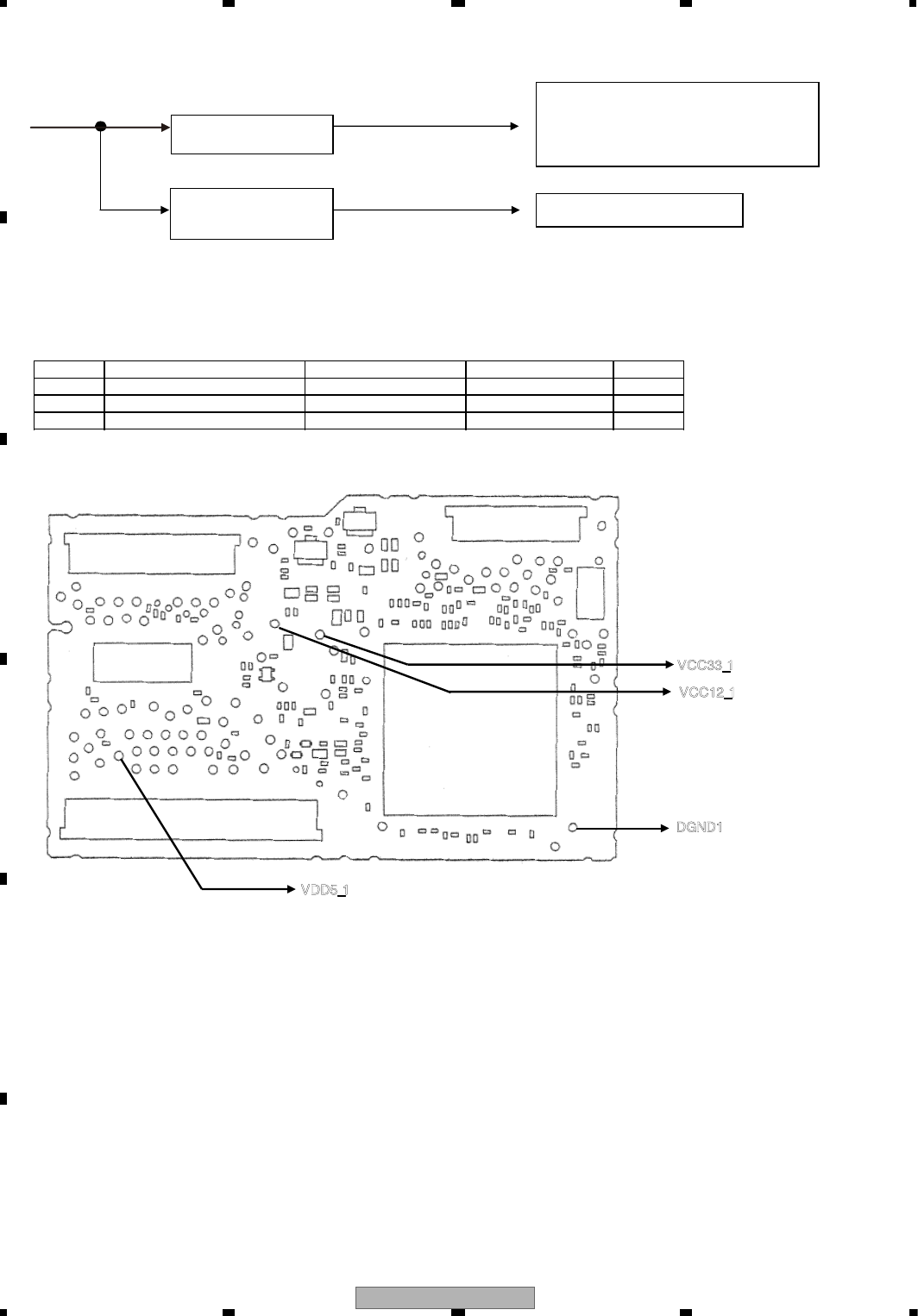
AVH-P4100DVD/XN/UC
42
1234
1234
C
D
F
A
B
E
VCC33 (= 3.3 V)
5DDV
VCC12 (= 1.2 V)
1VDD5_1 - DGND1
2VCC33_1 - DGND1
3VCC12_1 - DGND1
VDD5_1
DGND1
VCC12_1
VCC33_1
Check 2: Is VDD5 (VCC33, VCC12) power supply voltage OK?
Fig 2.1: Power supply configuration
IC1004
3.3 V output regulator
IC1005
DC/DC converter
1.2 V output
IC1501 DV5U power supply
IC1401 FLASH power supply (Data)
IC1402 FLASH power supply (Program)
IC1481 SDRAM power supply
IC1501 DV5U power supply
<Check> Check the voltage at the “VDD5_1, VCC33_1 and VCC12_1” test point while the power is on.
Use the “DGND1” test point at the reference.
Side A
NO. Check point Module No. Specification value Unit
Fig 2.2: VDD5, VCC33, VCC12 voltage check points
ALL
ALL
ALL
5.0 ± 0.4
3.3 ± 0.15
1.2 ± 0.12
V
V
V
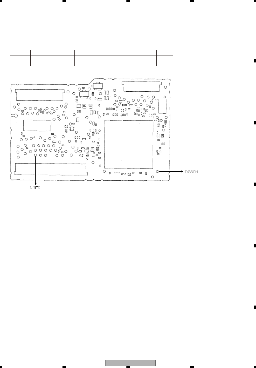
AVH-P4100DVD/XN/UC 43
5 678
5678
C
D
F
A
B
E
NRES
DGND1
Check 3: Reset OK?
NO. Check point Module No. Specification value Unit
1 XRES-DGND1 ALL VCC33 ×
0.7 or more
V
Side A
<Check> Check the voltage at the “XRES” test point while the power is on.
Use the “DGND1” test point at the reference.
Fig 3.1: RESET check point
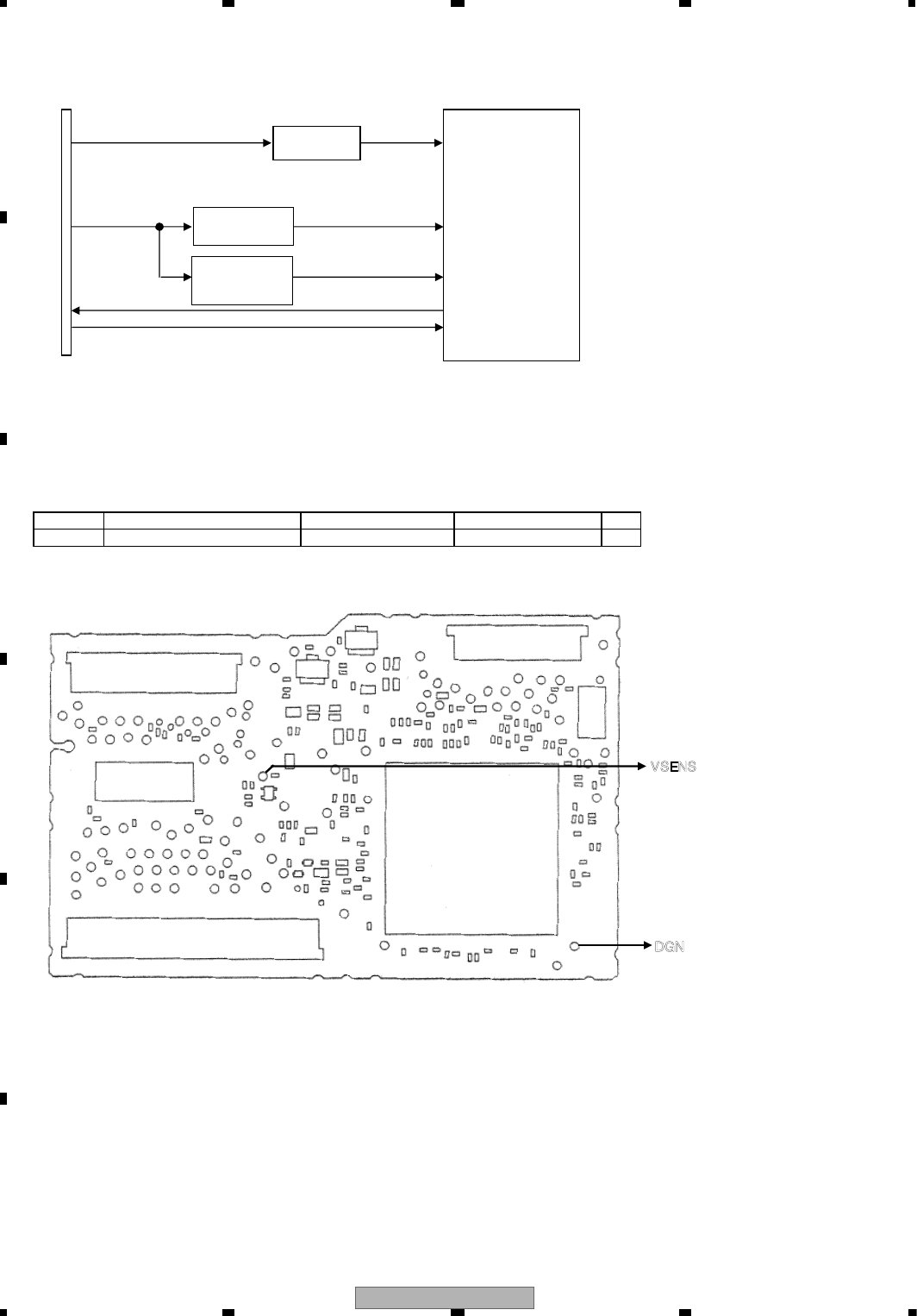
AVH-P4100DVD/XN/UC
44
1234
1234
C
D
F
A
B
E
CN1901
HOST I/F
SNESV8DV
33CCV5DDV
VCC12
STANBY
XRES
1 VSENS - DGND1 ALL 0.95 - 1.07 V
VD8 = 8.0 ± 0.4 V
IC1501
DV5U
IC1004
Regulator
IC1005
DC/DC
converter
VSENS
DGND1
Check 4: Is VSENS OK?
Fig 4.1: Power supply configuration and VSENS
<Check> Check the voltage at the “VSENS” test point while the power is on.
Use the “DGND1” test point at the reference.
NO. Check point
Side A
Module No. Specification value Unit
Fig 4.2: VSENS check point
R1004,
R1007
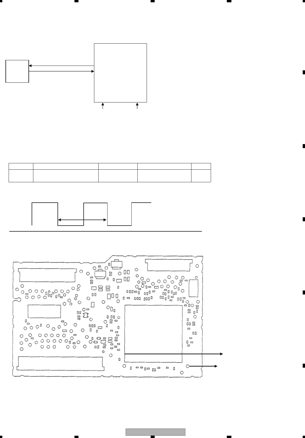
AVH-P4100DVD/XN/UC 45
5 678
5678
C
D
F
A
B
E
IC1501
DVD-LSI
X1501
27 MHz
crystal
VCC33 VCC12
Check 5: 27 MHz Normal?
<Outline> Each clock is created inside the IC1501 using the 27 MHz master crystal oscillator (X1501).
Fig 5.1: Clock configuration
<Check method> Turn the power on, and check with DGND being the reference.
In case of NG, check the applicable line, periphery of IC1501,
soldering of the peripheral components and defective components.
NO. Check point Module No. Specification value Unit
2 IC1501 169pin ALL 27 MHz
± 50 ppm ppm
GND
Fig 5.2: Clock specification value
Side A
Specification
value
Fig 5.3: 27 MHz check point
IC1501 158pin
DGND1
OSCO
OSCI

AVH-P4100DVD/XN/UC
46
1234
1234
C
D
F
A
B
E
MA0 - 11
MDQ0 - 15
MCK
XWE(NWE)
XCAS(NCAS)
XRAS(NRAS)
XCSM(NCSM)
DQM0
DQM1
BA0
BA1
IC
1480
SDRAM
IC1501
DV5U
Fig 6.1: SDRAM I/F
Check 6: Is SDRAM I/F OK?
<Outline> In order to secure the MPEG stream data as the buffer,
the capacity of communication I/F SDRAM between the LSI and the memory is 64Mbit.
Be careful as XCSM, XWE, XCAS and XRAS of IC1480 are called differently in IC1501,
namely NCSM, NWE, NCAS, NRAS.
AVH-P4100DVD/XN/UC 47
5 678
5678
C
D
F
A
B
E
1
2
3
4
5
6
7
8
9
10
11
12
13
14
15
16
17
18
19
20
21
22
23
24
25
26
27
28
29
30
31
32
33
34
35
36
37
MA0
MA1
MA2
MA3
MA4
MA5
MA6
MA7
MA8
MA9
MA10
MA11
MDQ0
MDQ1
MDQ2
MDQ3
MDQ4
MDQ5
MDQ6
MDQ7
MDQ8
MDQ9
MDQ10
MDQ11
MDQ12
MDQ13
MDQ14
MDQ15
MCK
XWE
XCAS
XRAS
XCSM
DQM0
DQM1
BA0
BA1
56 ohm ± 5 %
56 ohm ± 5 %
56 ohm ± 5 %
56 ohm ± 5 %
56 ohm ± 5 %
56 ohm ± 5 %
56 ohm ± 5 %
56 ohm ± 5 %
56 ohm ± 5 %
56 ohm ± 5 %
56 ohm ± 5 %
56 ohm ± 5 %
56 ohm ± 5 %
56 ohm ± 5 %
56 ohm ± 5 %
56 ohm ± 5 %
56 ohm ± 5 %
56 ohm ± 5 %
56 ohm ± 5 %
56 ohm ± 5 %
56 ohm ± 5 %
56 ohm ± 5 %
56 ohm ± 5 %
56 ohm ± 5 %
56 ohm ± 5 %
56 ohm ± 5 %
56 ohm ± 5 %
56 ohm ± 5 %
0.17 ohm or lower
56 ohm ± 5 %
56 ohm ± 5 %
56 ohm ± 5 %
56 ohm ± 5 %
56 ohm ± 5 %
56 ohm ± 5 %
56 ohm ± 5 %
56 ohm ± 5 %
IC1480 23pin
IC1480 24pin
IC1480 25pin
IC1480 29pin
IC1480 30pin
IC1480 31pin
IC1480 32pin
IC1480 33pin
IC1480 34pin
IC1480 33pin
IC1480 22pin
IC1480 35pin
IC1480 2pin
IC1480 4pin
IC1480 5pin
IC1480 7pin
IC1480 8pin
IC1480 10pin
IC1480 11pin
IC1480 13pin
IC1480 42pin
IC1480 44pin
IC1480 45pin
IC1480 47pin
IC1480 48pin
IC1480 50pin
IC1480 51pin
IC1480 53pin
IC1480 38pin
IC1480 16pin
IC1480 17pin
IC1480 18pin
IC1480 19pin
IC1480 15pin
IC1480 39pin
IC1480 20pin
IC1480 21pin
IC1501 201pin
IC1501 203pin
IC1501 207pin
IC1501 209pin
IC1501 208pin
IC1501 206pin
IC1501 202pin
IC1501 200pin
IC1501 198pin
IC1501 194pin
IC1501 199pin
IC1501 192pin
IC1501 160pin
IC1501 162pin
IC1501 164pin
IC1501 168pin
IC1501 170pin
IC1501 172pin
IC1501 176pin
IC1501 178pin
IC1501 177pin
IC1501 175pin
IC1501 171pin
IC1501 169pin
IC1501 167pin
IC1501 163pin
IC1501 161pin
IC1501 159pin
IC1501 183pin
IC1501 181pin
IC1501 188pin
IC1501 189pin
IC1501 190pin
IC1501 179pin
IC1501 180pin
IC1501 193pin
IC1501 197pin
<Check> Check the conductivity at “check point 1” and “check point 2” without power.
In case of NG, check the soldering and defective components throughout the
“output t input” of the applicable section.
NO. Signal name Check point 1 Check point 2 Specification value
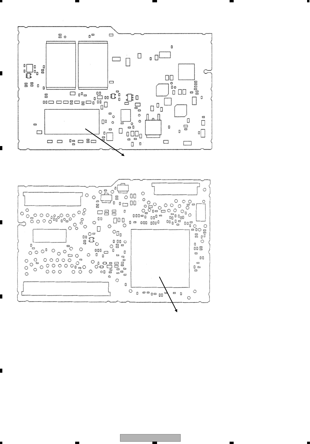
AVH-P4100DVD/XN/UC
48
1234
1234
C
D
F
A
B
E
Side B
Side A
Check point 1 (IC1480)
Check point 2 (IC1501)
Fig 6.2: SDRAM I/F check point
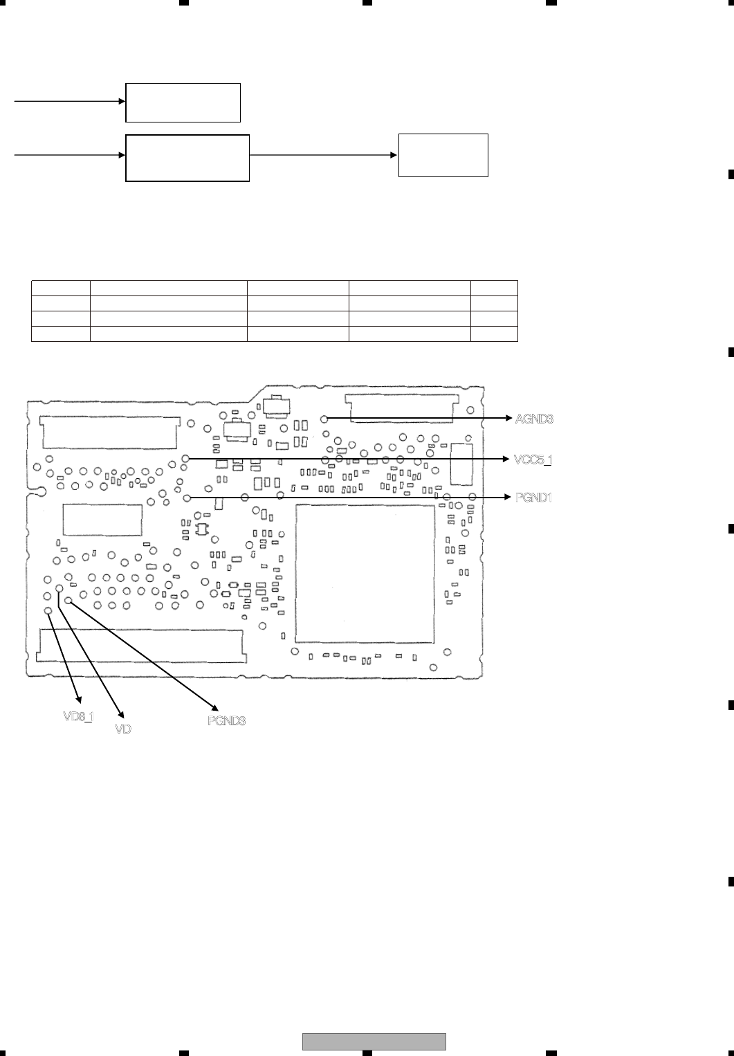
AVH-P4100DVD/XN/UC 49
5 678
5678
C
D
F
A
B
E
VD8_1
PGND3
VD
VD8_1
PGND1
VCC5_1
AGND3
Check 7: Is VD8, VCC5 power supply voltage OK?
F.E. driver system
IC1002
REG IC
for VCC 5 V.
Fig 7.1: Power supply configuration
Power supply
for PU
NO. Check point Module No. Specification value Unit
1
2
3
VD8_1 - PGND3
VD - PGND3
VCC5_1- AGND1
ALL
ALL
ALL
8.0 ± 0.4
8.0 ± 0.4
5.0 ± 0.1
V
V
V
Side A
<Check> Check the voltage at the “VD8_1, VD and VCC5_1” test point while the power is on.
Use the “PGND3 and AGND1” test point at the reference.
Fig 7.2: VD8, VCC5 voltage check points
VD8_2
VCC5 (= 5.0 V)
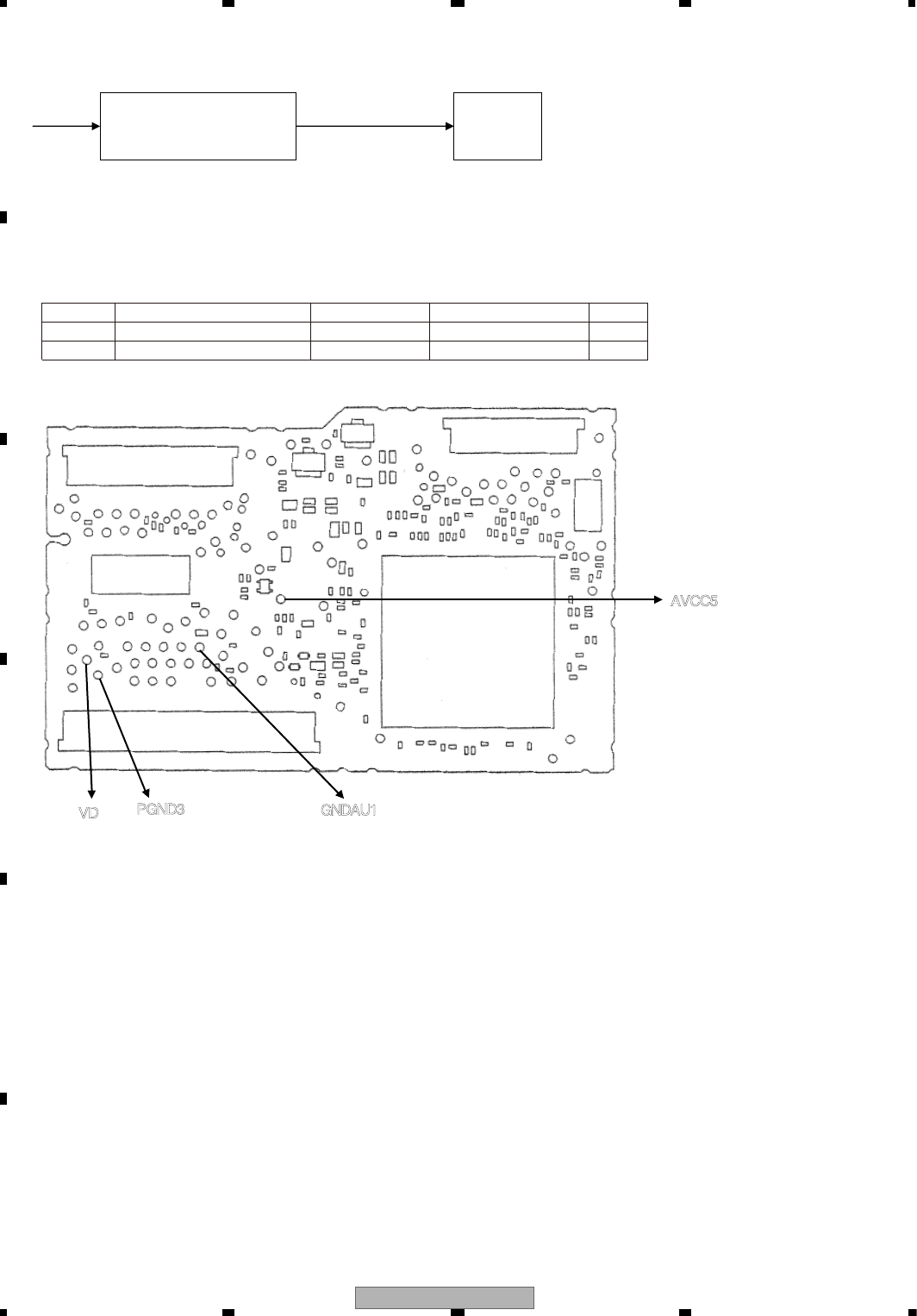
AVH-P4100DVD/XN/UC
50
1234
1234
C
D
F
A
B
E
DV IC1801
Audio-DAC
GNDAU1
PGND3
VD
AVCC5
Fig 8.2: VD8, AVCC5 voltage check points
Side A
Check 8: Is AVCC5 voltage OK?
Fig 8.1: Power supply configuration
IC1003
REG IC
for AVCC 5 V.
<Check> Playback DVD-REF-A1 TITLE 1 and check the voltage at the stylus.
Check with PGND and GNDAU being the reference.
NO. Check point
VD - PGND_3
AVCC5 - GNDAU1
Module No. Specification value Unit
1
2
ALL
ALL
8.0 ± 0.4
5.0 ± 0.1
V
V
AVCC5 (= 5.0 V)
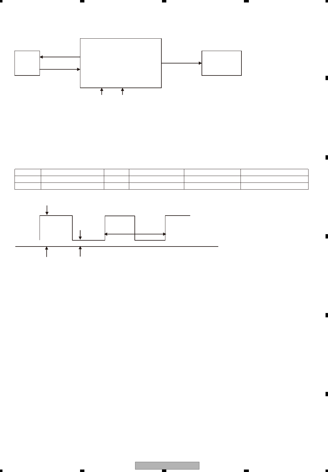
AVH-P4100DVD/XN/UC 51
5 678
5678
C
D
F
A
B
E
Fig 9.1: Clock configuration
Check 9: Is DACCLK normal?
<Outline> DACCLK for Audio-DAC is created by IC1501 using the 27 MHz master crystal oscillator (X1501).
DACCLK
<Check method>
DVD: DVD-REF-A1 TITLE 1
CD: Playback a normal CDDA.
Common to all DVD-V compatible modules.
Check with DGND being the reference.
In case of NG, check the applicable line, the periphery of IC1501, soldering of the peripheral components and
defective components.
IC1501
DVD-LSIX1501
27 MHz
crystal
IC1801
Audio-DAC
VCC33 VCC12
GND
Fig 9.2: Clock specification value
Specification
value 1
Specification
value 2
Specification
value 3
NO. Check point 1 (stylus) Media Specification value 1 Specification value 2 Specification value 3
1
2
DACCK
DACCK
DVD
CD
2.0 V~VCC33 V
2.0 V~VCC33 V
DGND~0.8 V
DGND~0.8 V
36.864 0 MHz ± 300 ppm
33.868 8 MHz ± 300 ppm
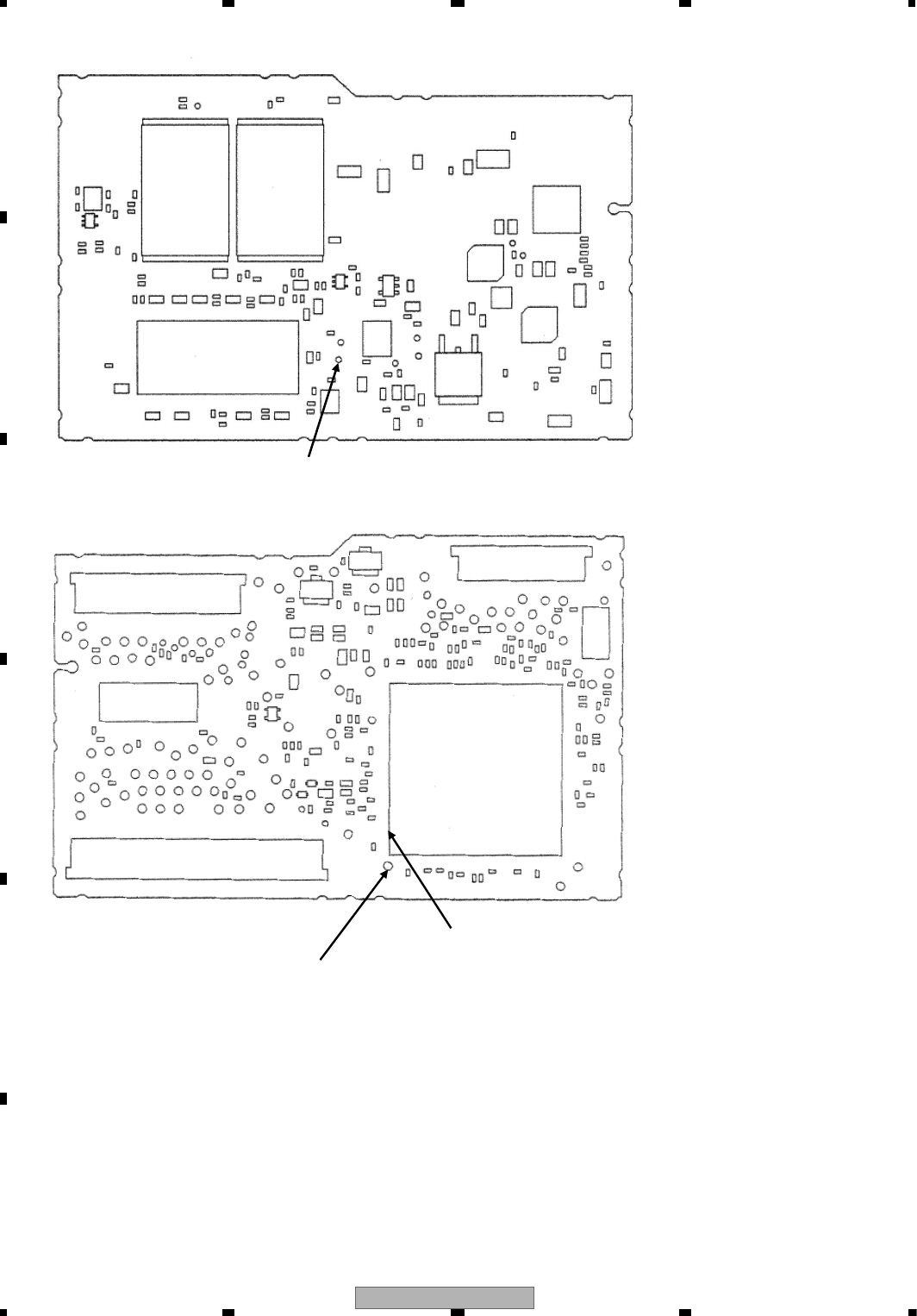
AVH-P4100DVD/XN/UC
52
1234
1234
C
D
F
A
B
E
DGND2
Side B
Side A
Fig 9.3: 27 MHz, DACCLK check point
Check point 1 (DACCK stylus)
Check point 2 (IC1501 148 pin)
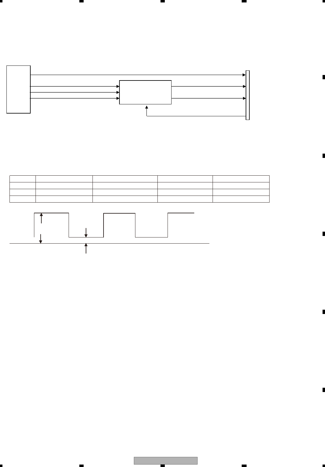
AVH-P4100DVD/XN/UC 53
5 678
5678
C
D
F
A
B
E
CN1901
HOST I/F
IECOUT
OLKCRL
ADOUT
ORKCRS
GNDAU
IC1801
Audio-DAC
IC1501
DVD-LSI
Fig 10.1: Audio circuit
Check 10: Is the audio circuit OK?
<Outline> The serial 3 lines digital output + DACCLK, output from DVD-LSI (IC1501), are converted to analog audio
signal at Audio-DAC (IC1801) and are output from the HOST I/F (CN1901).
Simultaneously, the analog MUTE signal is also output from DVD-LSI (IC1501) via the HOST I/F.
The digital audio signal (IECOUT), output from DVD-LSI (IC1501).
<Check method> Playback DVD-REF-A1 TITLE 2 CHAPTER 1 (48 k/16 bit 1 kHz 0 dB),
and check with DGND being the reference.
In case of NG, check the applicable line, periphery of major components as described in the above drawing,
soldering of the peripheral components and defective components.
NO. Check point 1 (stylus)
1
2
3
Specification value 1 Specification value 2 Reference waveform
ADOUT3
SRCK
LRCK
VCC33 V-0.6 V or higher
VCC33 V-0.6 V or higher
VCC33 V-0.6 V or higher
0.4 V or lower
0.4 V or lower
0.4 V or lower
Waveform 1
Waveform 2
Waveform 3
GND
Fig 10.2: Serial 3 lines specification value
Specification
value 1
Specification
value 2
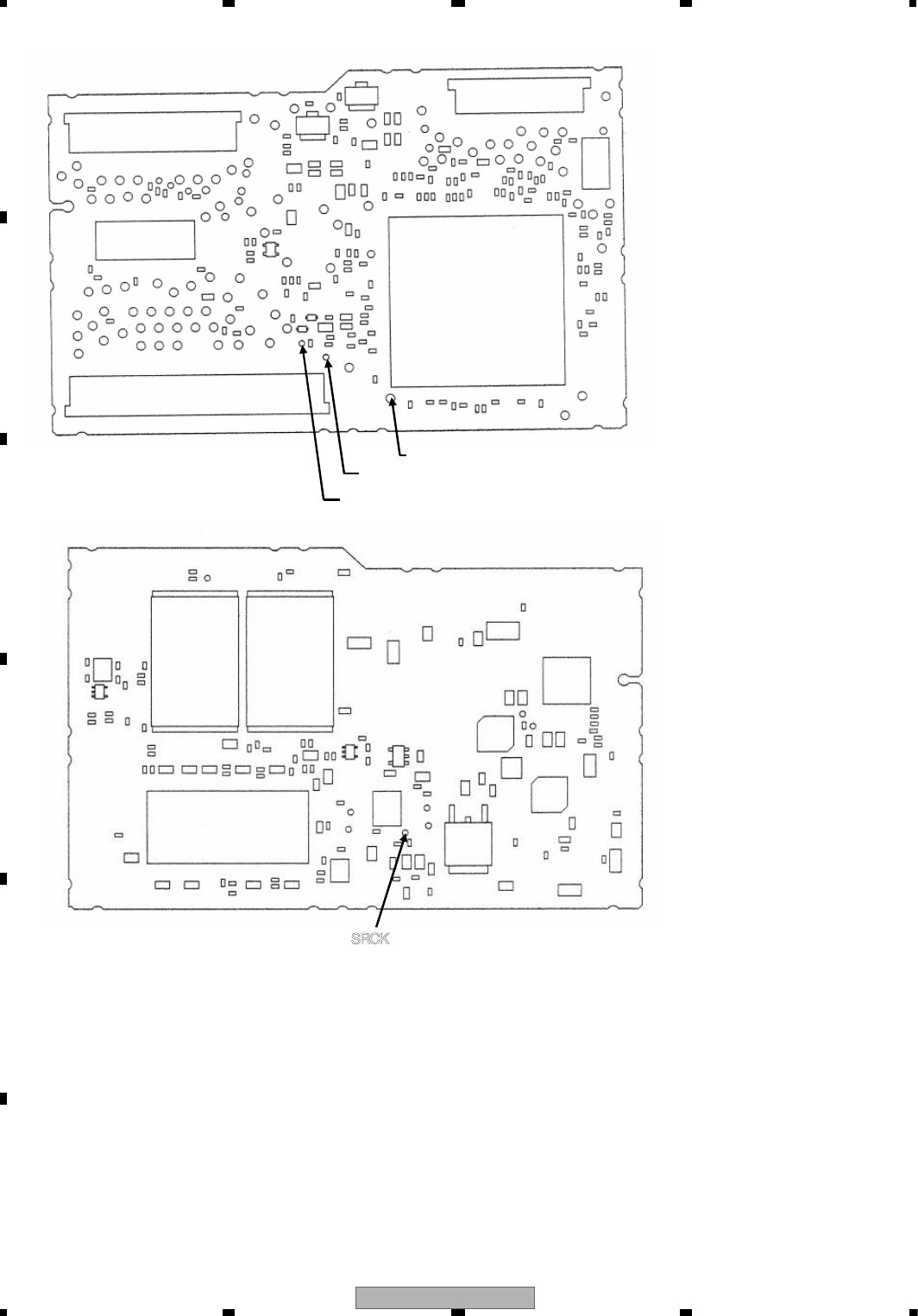
AVH-P4100DVD/XN/UC
54
1234
1234
C
D
F
A
B
E
SRCK
LRCK
ADOUT
DGND2
Fig 10.3: Serial 3 lines check points
Side A
Side B
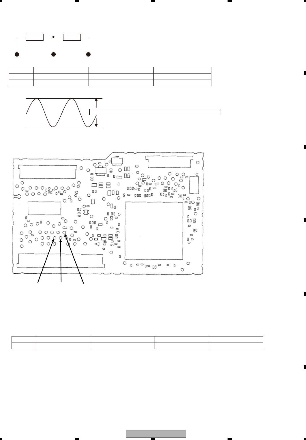
AVH-P4100DVD/XN/UC 55
5 678
5678
C
D
F
A
B
E
LO
RO GNDAU1
The following checks shall be conducted using the following measurement circuits with GNDAU1 being the reference.
NO.
4
5
Fig 10.4: Analog audio out (LO, RO) specification value.
Side A
Specification value is the root-mean-square value (rms).
Check point 1 (stylus)
1 400 ± 150 mV
1 400 ± 150 mV
Specification value (rms) Reference waveform
Waveform 4
Waveform 4
LO
RO
LO GNDAU1 RO
47 kohm 47 kohm
Fig 10.5: Analog audio out check point
Check with DGND being the reference.
NO. Check point 1 (stylus) Specification value 1 Specification value 2 Reference waveform
6 IEC VCC33 V-0.6 V or higher 0.4 V or lower Waveform 5
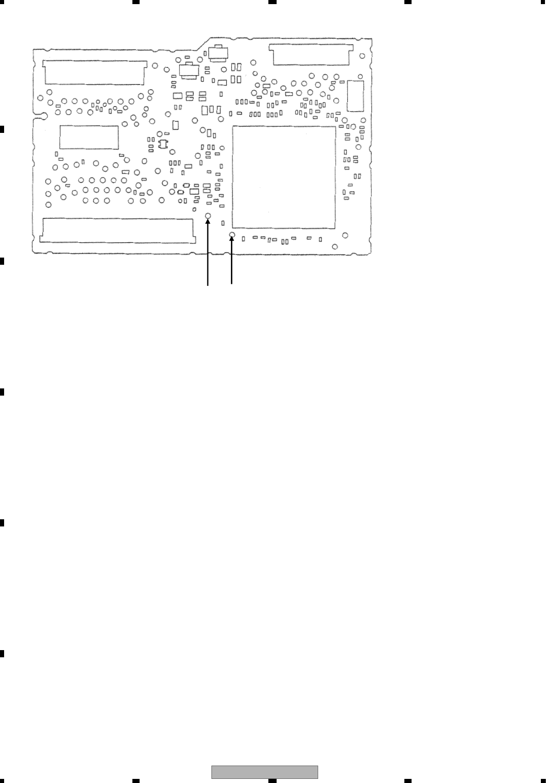
AVH-P4100DVD/XN/UC
56
1234
1234
C
D
F
A
B
E
IEC DGND2
Fig 10.6: Digital audio signal (IECOUT) check point
Side A
AVH-P4100DVD/XN/UC 57
5 678
5678
C
D
F
A
B
E
Check 11: Is the video circuit OK?
<Outline> Composite signal and component signal are output from DVD-LSI (IC1501), and are output from the
HOST I/F (CN1901) via a buffer circuit.
CN1901
HOST I/F
Composite COMPOSITE
Fig 11.1: Video circuit
<Checking method> Playback DVD-REF-A1 TITLE2 CHAPTER5 (WHITE 100%), and monitor COMPOSITE signal with
an oscilloscope with GNDV1 (stylus) being the reference. Set the trigger mode to “TV trigger” and
the trigger line to “150 line”.
IC1501
DVD_LSI
Video
DAC
section
NO.
Check point 1 (stylus)
Specification value Reference waveform
1 COMPOSITE 1 000 mVpp ± 5 % Waveform 6
In case of NG, check the applicable line, the periphery of the major components in the drawing above, soldering of the
peripheral components and defective components.
PEAK
COMPOSITE signal Reference
value
Color burst
Pedestal level
BOTTOM
Horizontal sync signal
Fig 11.2: Waveform for the case of composite white 100% output
AVH-P4100DVD/XN/UC
58
1234
1234
C
D
F
A
B
E
Side A
COMPOSITE GNDV
Fig 11.3: VIDEO signal check point

AVH-P4100DVD/XN/UC 59
5 678
5678
C
D
F
A
B
E
Check 12:How to judge whether the flash memory has reached its life or not.
If the reaction to user operation is slow or operation is slow in general, there is a possibility that the flash memory
has reached its life.
Make judgment regarding the flash memory life by looking at the display of the LD energizing time.
1.Let the LD energizing time displayed.
(Refer to the FE test mode for the method of displaying the LD energizing time.)
2.If the second digit from the left of the energizing time display is showing E,
such as “ E ”, it means that the flash memory has reached its life.
Example:
0E000BB8
AVH-P4100DVD/XN/UC
60
1234
1234
C
D
F
A
B
E
USB_CLOCK
IC1501
DVD-LSI
X1950
48 MHz
VCC33 VCC12
Check 13: 48 MHz Normal?
<Outline> Each clock is created inside the IC1501 using the 48 MHz master crystal oscillator (X1501).
Fig 13.1: Clock configuration
crystal
Fig 13.2: Clock specification value
<Check method> Turn the power on, and check with DGND1 being the reference.
In case of NG, check the applicable line, periphery of IC1501,
soldering of the peripheral components and defective components.
NO. Check point Module No. Specification value Unit
2 IC1501 50pin-DGND1 ALL 48 MHz
± 50 ppm ppm
GND
Specification
value
AVH-P4100DVD/XN/UC 61
5 678
5678
C
D
F
A
B
E
Side A
DGND1
IC1501 50pin
Fig 13.3: 48 MHz check point
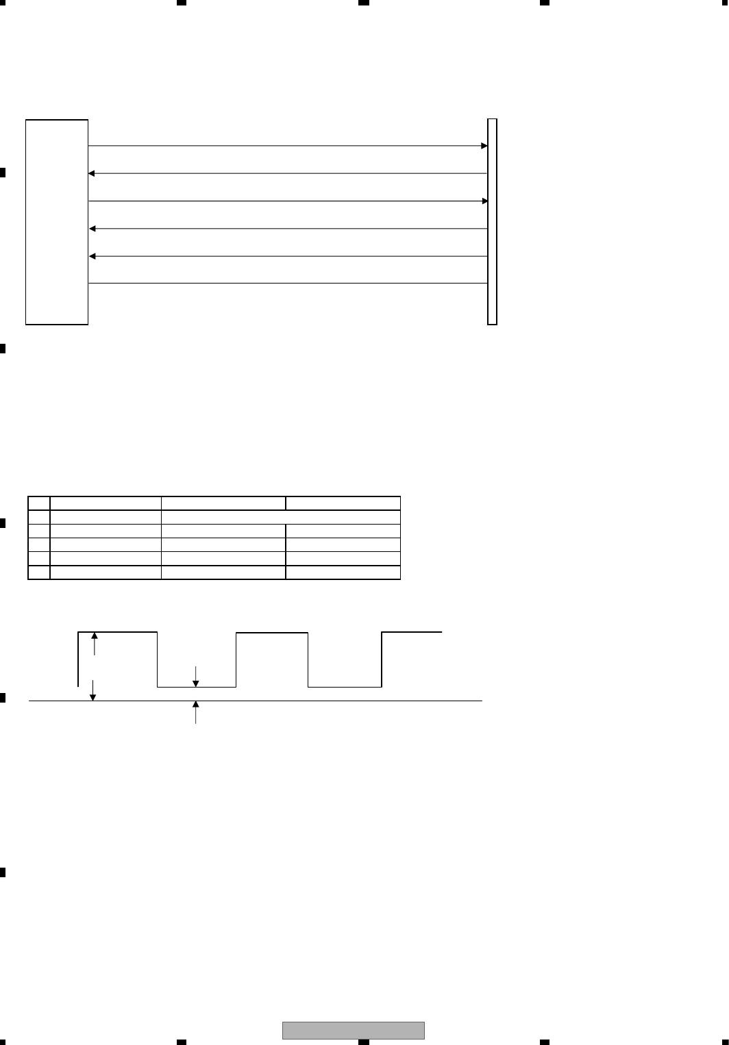
AVH-P4100DVD/XN/UC
62
1234
1234
C
D
F
A
B
E
CN1901
HOST I/F
No.
1 CP_RESET
2 SDATA VCC33*0.7or more VCC33*0.2 or less
VCC33*0.7or more VCC33*0.2 or less
VCC33*0.7or more VCC33*0.3 or less
VCC33*0.7or more VCC33*0.3 or less
3 SCLOCK
4 D+
5 D-
Fig. 14.2: USB Circuit Communication Wave
VCC33*0.7or more
IC1501
DVD-LSI
D-
D+
I2C_SCL
I2C_SDA
CP_RESE
Standard value 1
Standard value 1
Standard value 2
Standard value 2
DGND
Check 14: Is USB Circuit OK?
<Outline>
The data is transmitted through D+, D- and SDA of HOST I/F while playing USB/IPOD.
USB memory uses only D+ and D-, but IPOD uses SDA (DATA) and SCL (CLOCK)
in addition to D+ and D-.
Fig. 14-1: USB Circuit
<Check Method>
1.USB Memory: Play a song from USB memory and check D+ and D- with the DGND standards.
2.iPod: Connect iPod and check CP_RESET, SDA and SCL with the DGND standards until the pioneer log appears.
Play a song from iPod and check D+/D- with the DGND standards.
When it does not conform to the standards, check appropriate line, main parts shown in the above figure,
soldering of peripheral parts and malfunctions in parts.
Checking spot (stylus)
*Until the pioneer log appears after connecting the iPod
*Until the pioneer log appears after connecting the iPod
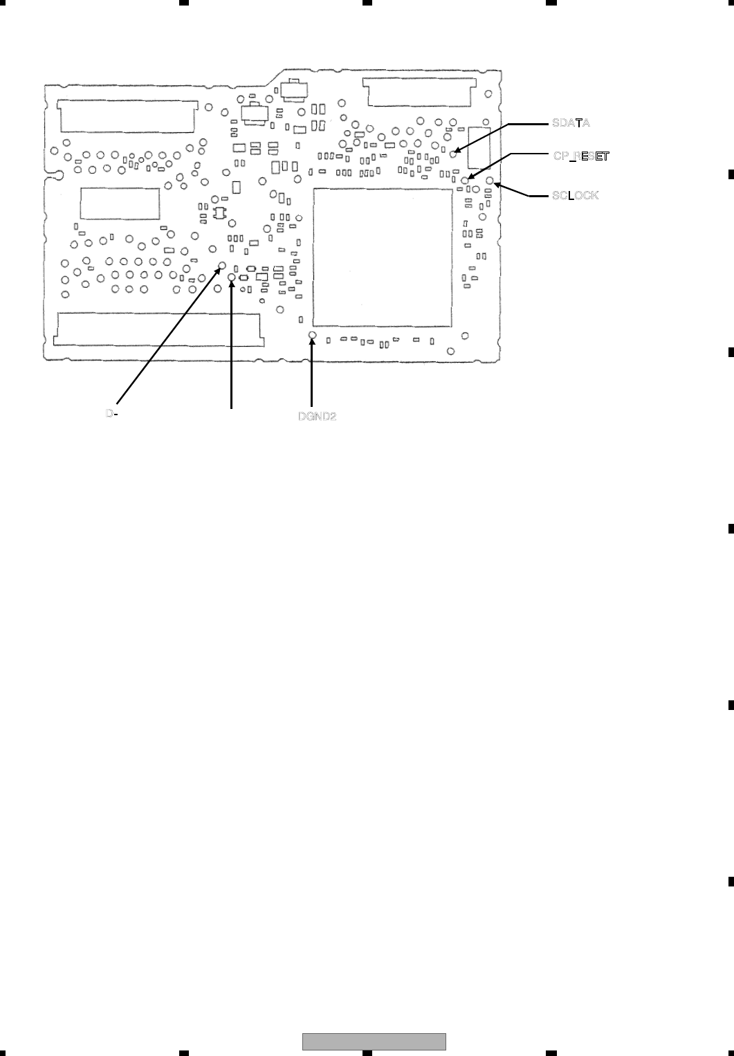
AVH-P4100DVD/XN/UC 63
5 678
5678
C
D
F
A
B
E
Side A
SCLOCK
SDATA
D-
CP_RESET
D+ DGND2
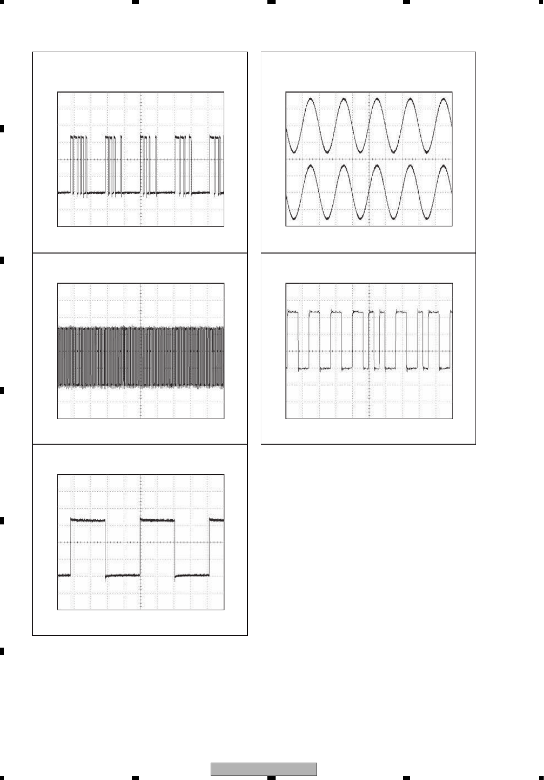
AVH-P4100DVD/XN/UC
64
1234
1234
C
D
F
A
B
E
AUDIO
Reference voltage: DGND2 1 V/div. 5 usec/div Reference voltage: GNDAU2 1 V/div. 500 usec/div
Reference voltage: DGND2 1 V/div. 5 usec/div Reference voltage: DGND2 1 V/div. 500 nsec/div
CH1:LRCK
CH1:SRCK
CH1:ADOUT3
CH1:LO
CH2:RO
CH1:IECOUT
Reference voltage: DGND2 1 V/div. 5 usec/div
G->
G->
->G->G
G->
G->
Waveform 1 Waveform 4
Waveform 2
Waveform 3
Waveform 5
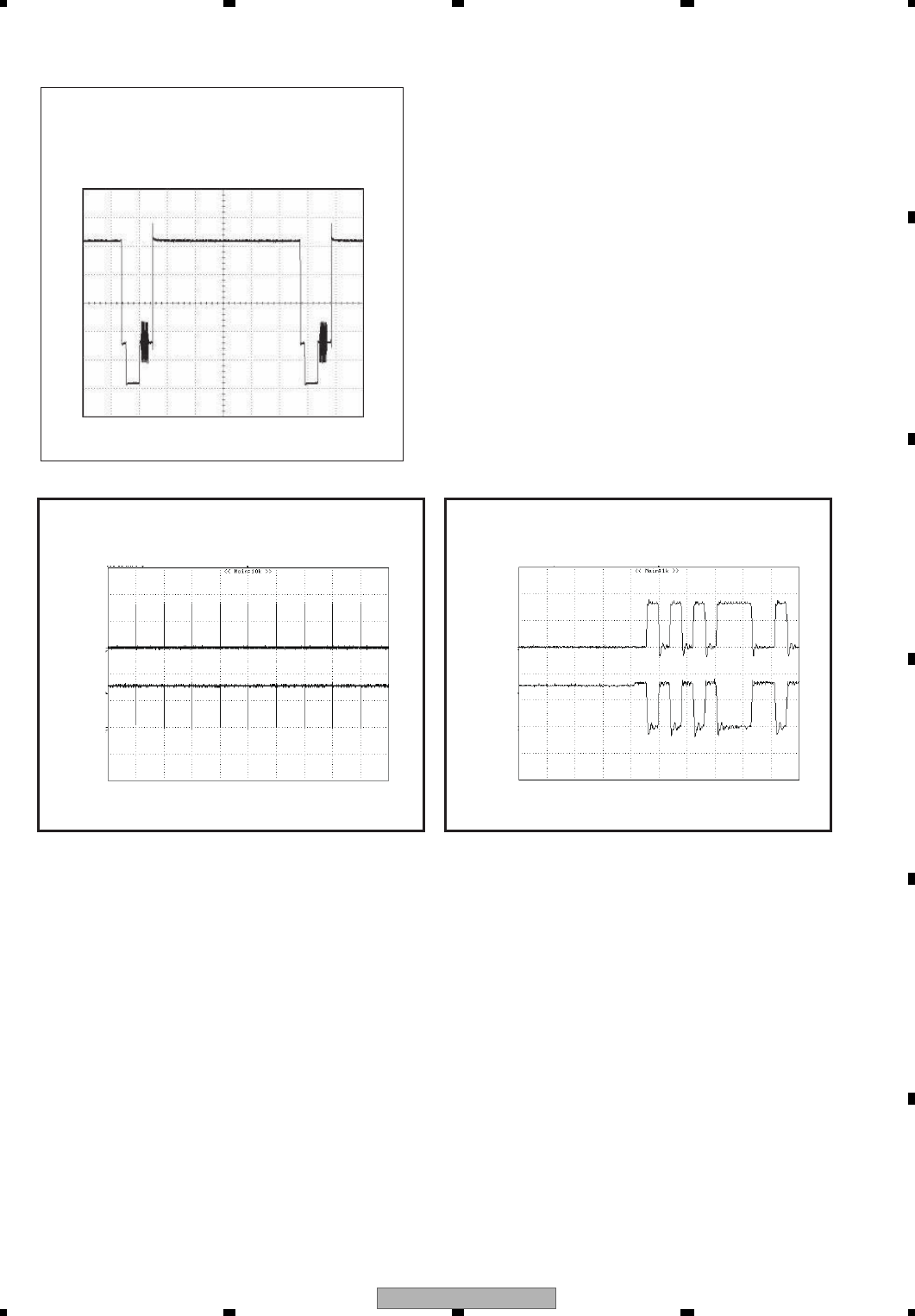
AVH-P4100DVD/XN/UC 65
5 678
5678
C
D
F
A
B
E
VIDEO
USB memory
USB memory USB memory
[WHITE 100IRE]
CH1:COMPO
Reference voltage: GNDV1 200 mV/div. 10 usec/div
-D-D
DNGDDNGD
+D+D
Waveform 6
Waveform 7 Waveform 8
Reference voltage:DGND 1 ms/div 2 V/div Reference voltage:DGND 200 ns/div 2 V/div
AVH-P4100DVD/XN/UC
66
1234
1234
C
D
F
A
B
E
iPod
-D-D
DNGDDNGD
+D+D
CP_RESET
DGND
SDA
NRES
iPod
SCL
iPod
iPodiPod
iPod
Waveform 9
Waveform 11
Waveform 13
Waveform 12
Waveform 10
Reference voltage:DGND 1 ms/div 2 V/div
Reference voltage:DGND 20 ms/div 1 V/div
Reference voltage:DGND 500 us/div 1 V/div
Reference voltage:DGND 2 ms/div 1 V/div
Reference voltage:DGND 200 ns/div 2 V/div
AVH-P4100DVD/XN/UC 67
5 678
5678
C
D
F
A
B
E
5.4 ERROR CODE LIST
Error status OSD *1 Disc
USB
(MSC)
USB
(iPod)
ACC
Off/On
Source
Off/On
Eject Play Key
NON-PLAYABLE DISC
INCOMPATIBLE DEVICE
UNPLAYABLE FILE
O
p
en 10h
X
-- ****
Read Error 0h299-20-RORRE
X
--
Focus Error(Focus Error
in mechanism set u
p)
h1209-20-RORRE X- - XXXX
XXXX
Surface Error h22E9-20-RORRE X- - XXXX
Address no
t
found(Invalid Track) ERROR-02-80 23h X- - XXXX
Spindle Lock ERROR-02-91 24h X- - XXXX
Carriage HOME ERROR-02-92 25h X- - XXXX
ID/SUBCODE Read Error ERROR-02-94 26h X- - XXXX
AV CHIP decode Error ERROR-02-9A 2Ah XX - XXXX
AV CHIP Recovery NG ERROR-02-9B 2Bh XXX XXXX
Error of PLAY BAC
K
Mode Status ERROR-02-9C 2Ch XX - XXXX
Disc Data Error ERROR-02-9D 2Dh X- - XXXX
THERMAL
PROTECTION IN MOTION
No Disc
(including Disc loading
and e
j
ectin
g)
40h X- - ****
Loading_Mecha Error 50h XXX X-X-
Communication fault attesting iPod
Communication fault attesting iPodh0606-20-RORRE
X
-
X
h1616-20-RORRE
X
-
X
iPod attestation retrying failure
iPod attestation time out
h2626-20-RORRE iPod attestation retrying failure
X
-
X
h3636-20-RORRE X-X --X-
--X-
--X-
--X-
h4646-20-RORRE --X --X-
--X-
Error setting iPod h5656-20-RORRE --
X
h6666-20-RORRE --X --X-
h7676-20-RORRE --X --X-
h8686-20-RORRE --X --X-
No songs error h96 --X --X-
iPod control forwarding/
Intarapta forwarding error hA6A6-20-RORRE --X --X-
Demand timeout
iPod's reproducing hB6B6-20-RORRE --X --X-
--X-
ERROR-02-6C --
X
Remote switch demand
timeout ERROR-02-6D --X --X-
--X-
--X-
PROTECTED DISC
NO ACCESSIBLE
DATA AVAILABL
DIFFERENT REGION DISC
NON-PLAYABLE DISC
ERROR-02-A0
X
--
XXXX
h1A1A-20-RORRE X- -
ERROR-02-A2
A
2h
X
--
XXXX
ERROR-02-A3
A
3h
X
--
XXXX
ERROR-02-A4
A
4h
X
--
XXXX
ERROR-02-A5
A
5h
X
--
XXXX
ERROR-02-A6
A
6h
X
--
XXXX
ERROR-02-A7
A
7h
X
--
XXXX
ERROR-02-A8
A
8h
X
--
XXXX
ERROR-02-A9
A
9h
X
--
XXXX
ERROR-02-AA
A
Ah
X
--
XXXX
Focus Error ERROR-02-AB
A
Bh
X
--
XXXX
Error of PLAY BAC
K
Mode Status h0B0B-20-RORRE X- - XXXX
Error of PLAY BAC
K
Mode Status h1B
C0h
1B-20-RORRE X- - XXXX
A
udio Propert
y
Timeou
t
Error *9 ERROR-02-C0 Audio property timeout error X- - XX X -
ERROR-02-D0 -X- --X-
CBW and CSW forwarding error
ERROR-02-D1 -
X
---
X
-
Audio class band securing failure
ERROR-02-D8 --
X
--
X
-
Audio class FS setting failure
ERROR-02-D9 --
X
--
X
-
Undefined Error ERROR-FF-FF
X
--
XXXX
--
--
00h USB device of format alone that
cannot be reproduced XX
30h X
70h --
X--
90h --X
Method of reset
Temp Error
(In Case of High
Tem
p
erature )
Region code Error NG
--
--
8*rorrEyeK7*MRPC Key Error for playback X--
X-
--
-- --
X-
Generation source
-
--
XX
h00rorrEaideM XXX X -
00h USB device that doesn't correspond XX-
X-
h07rorrEMRD X
(No display)
(No display)
(No display)
(No display)
A disc containing the unplayable
Format only
Door open error
Transfer start error
Focus error
Focus error during set up
(A focus has never been achieved
with that disc.)
Address not found.
Spindle lock NG
(the disc cannot rotate)
Carriage home NG
(The pick up tries to return to carriage
home, but it cannot go back and stopped.)
ID/SUBCODE Read Error (ID/SUBCODE
cannot be read due to scratch or stain.)
UART
*2 Meaning
AV CHIP decode NG
(AV chip cannot be decoded.)
AV CHIP recovery NG
Playback state error
(An error due to software bug.)
Disc Data NG
Disc has not been inserted.
(Including Load in process or
Eject in process.)
High temperature
(Playback is stopped because the pick up
temperature is 89 C or higher.)
Loading mechanism error
(The disc cannot be clamped.)
6Ch
6Dh
A0h
h39
D0h
FFh
D9h
D8h
D1h
DRM error (All music cannot be played
back due to DRM.)
DRM error (All music cannot be played
back due to DRM.)
Undefined error
iPod authentication data is abnormal
iPod authentication data is abnormal
REQUEST error
Failure in issuing the read command
L0 adjustment is NG.
L1 adjustment is NG
LD system NG
Gain adjustment system NG.
Gain determining system NG.
Servo initial setting related items NG.
Disc is not clamped yet.
Tracking system NG
Media setting system NG
JUMP over layers NG
Navigation command error
Retry over
REQUEST error
Failure in issuing read
command (chip dependent)
Adjustment of L0 is NG.
Adjustment of L1 is NG.
LD system NG
Gain adjustment system NG.
Gain determining system NG.
Servo initial setting related items NG.
Disc is not clamped yet.
Tracking system NG.
Media setting system NG.
XXXX
Error when iPod is connected/
It is generated STALL by the USB
communication
Demand timeout when
initial is communicated
Protocol version
non-correspondence
Timeout when protocol
version is judged
Remote switch error
iPod attestation time out
Error setting iPod
No songs error
iPod control forwarding/
Intarapta forwarding error
Demand timeout
iPod's reproducing
Remote switch demand
timeout
Error when iPod is connected/
It is generated STALL by the USB
communication
Demand timeout when
initial is communicated
Protocol version
non-correspondence
Timeout when protocol
version is judged
Remote switch error
Error when MCS is connected/
It is generated STALL by the USB
communication
CBW and CSW forwarding error
Audio class band securing failure
Audio class FS setting failure
Error when MCS is connected/
It is generated STALL by the USB
communication
Region code NG (Unable to be played back
due to incorrect mechanism region.)

AVH-P4100DVD/XN/UC
68
1234
1234
C
D
F
A
B
E
X: Cancel the error by operation. -: Error is not cancelled by operation. *: No setting
*1 A content displayed on OSD. As for the items having multiple display patterns, the upper row is for the Japanese version Full GUI, and the lower row is for
the Touch Panel model and Full GUI (English version).
*2 A parameter of UART command, such as “receipt error notice”, that the DVD mechanism transmits.
*3 CPPM(Content Protection for Prerecorded Media) : A copyright protection technique used in DVD-A. The protection is realized by using the keys recorded
on the media and the device key held by the player.
*4 DVD-A compatible model only.
When an error has occurred, only the audio output will be muted but playback operation will continue. Furthermore, acceptance of the user operation will be
the same as usual.
*5 AWM (Audio WaterMark): Electronic watermark. Information on the copyright owner or CCI (copy control information) are recorded so that illegally copied
discs can be identified.
*6 Notice as an error status will not be given
*7 CPRM(Content Protection for Recordable Media) : A copyright protection technique for digital contents used for re-writable DVD or memory card.
(DVD-VR model only)
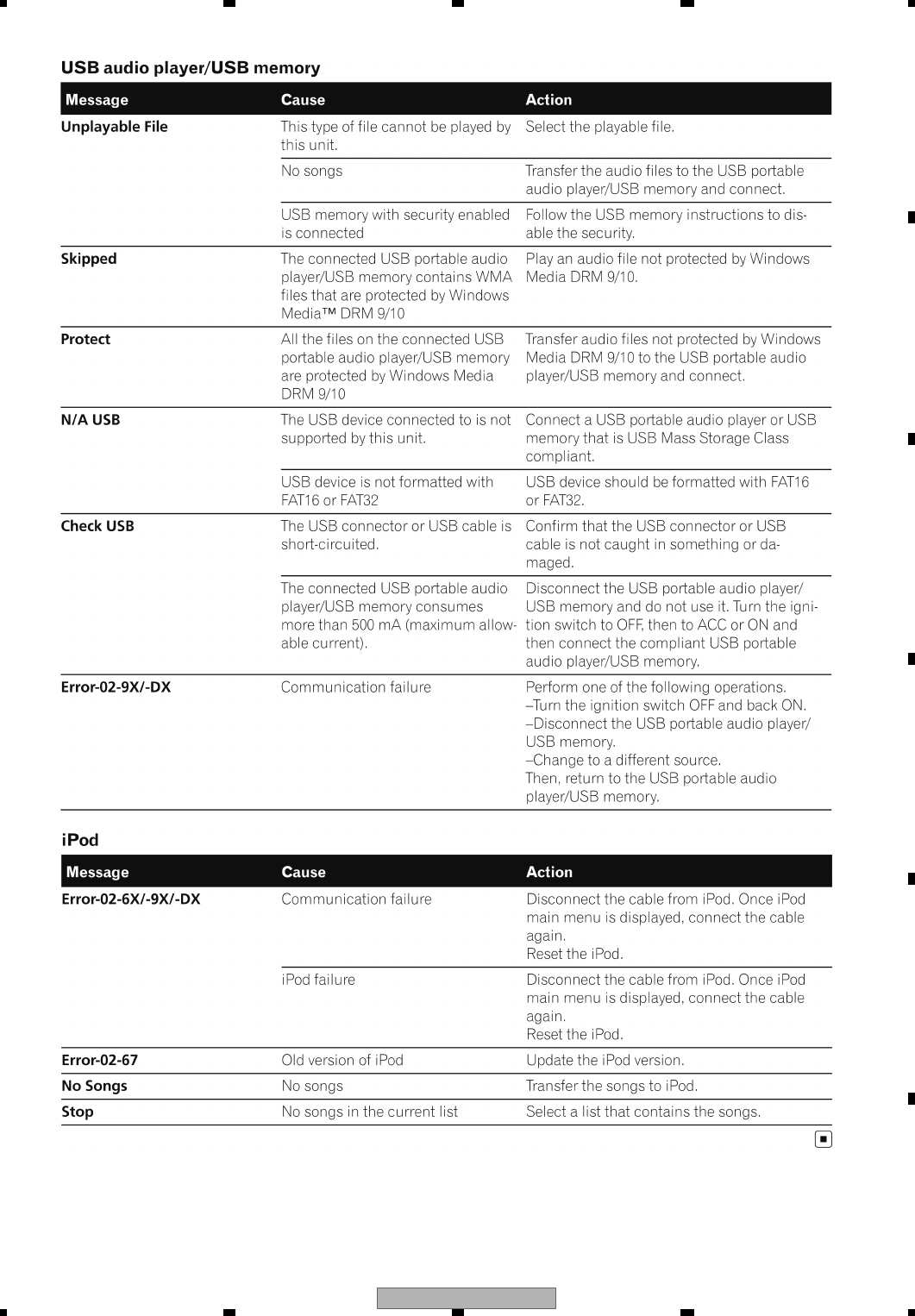
AVH-P4100DVD/XN/UC 69
5 678
5678
C
D
F
A
B
E
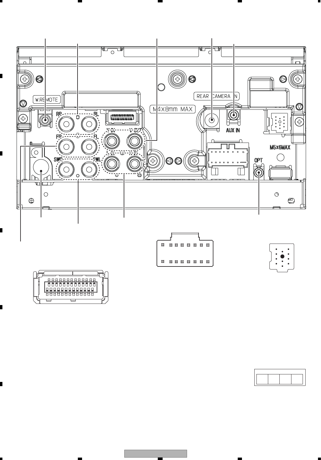
AVH-P4100DVD/XN/UC
70
1234
1234
C
D
F
A
B
E
5.5 CONNECTOR FUNCTION DESCRIPTION
1. FR-
2. RR-
3. FR+
4. RR+
5. FL-
6. RL-
7. FL+
8. RL+
11
10
9
8
7
6
5
4
3
2
1
IP-BUS INPUT
FRONT
OUTPUT
AUDIO
INPUT
ANTENNA
WIRED REMOTE
CONTROL
OPTICAL OUTPUT
135 7911 13 15
246 8
10 12 14 16
VIDEO
INPUT/OUTPUT
REAR
CAMERA IN
SUBWOOFER
OUTPUT
9. PARKING BRAKE
10. MUTE
11. B.REM
12. ILM
13. BGSENS
14. ACC
15. GND
16. B.UP
1. BUS+
2. BUSG
3. BUSLG
4. MAINTEST
5. BUS-
6. BUSRG
7. BUSL+
8. ASENBO
9. BUSR+
10. BUSR-
11. BUSL-
REAR
OUTPUT AUX IN
23
4
1
USB
1. USB5V
2. D-
3. D+
4. USBGND
2
1
26
25
1. CCR
2. CCG
3. CCB
4. CCSYNC
5. GNDSIG
6. DVDVBS
7. GNDDVD
8. YS
9. NC
10. CCAUL
11. CCAUR
12. GNDAU
13. ONSEI+
14. ONSEI-
15. REAUR
16. REAUL
17. GNDRAU
18. CCREM
19. DSEN
20. TVON
21. GION
22. MONON
23. VSW5
24. SYS_TO_NAVI
25. NAVI_TO_SYS
26. GNDD
RGB INPUT(UW5)
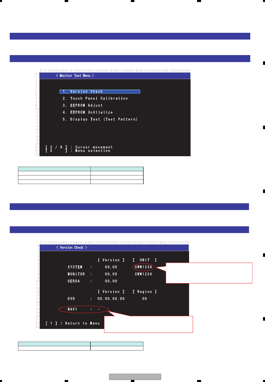
AVH-P4100DVD/XN/UC 71
5 678
5678
C
D
F
A
B
E
6. SERVICE MODE
6.1 MONITOR TEST MODE
[Method for Mode IN]
When the reset start is done while pushing MUTE and TRACK DOWN, it shifts to the monitor test mode.
[Display specifications]
[Method for Mode IN]
Choose "Version Check" among the monitor test mode menu screen.
[Display specifications]
"CONNECT" is indicated at the time of
the Navigation connection.
When 4 digits of read number is strange,
"---" is displayed.
ex) ---1x34
[Operation specification]
Operational description Remote controller key
Selection cursor up movement 2
Selection cursor down movement 8
Menu enter 5
[Operation specification]
Operational description Remote controller key
Return to test mode mene 1
1. Version Check
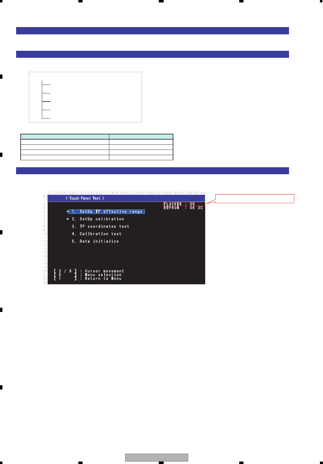
AVH-P4100DVD/XN/UC
72
1234
1234
C
D
F
A
B
E
[How to activate the touch panel test mode]
Choose "Touch Panel Calibration" among the monitor test mode menu screen.
[Menu types in the mode]
The calibration test mode consists of the following menus.
Top menu
[Description of the top menu]
[Display specification]
Conditions for lighting of the adjustment complete mark “ * ”.
Outermost circumference inspection :
In case the outermost circumference inspection has been completed normally.
16 points adjustment :
In case the calibration has been completed normally.
Conditions for the adjustment complete mark “ * ” to go out.
Outermost circumference inspection :
In case the outermost circumference inspection has never been performed.
In case the EEPROM initialization has been performed.
In case the adjustment value has been initialized.
16 points adjustment :
In case the 16 points adjustment has never been performed.
In case the EEPROM initialization has been performed.
In case the adjustment value has been initialized.
Data initialization
Outermost circumference inspection
16 points adjustment
Coordinate inspection
Calibration verification
Flicker initialized state
[Operation specification]
Operational description Remote controller key
Selection cursor up movement 2
Selection cursor down movement 8
Return to test mode mene 1
Menu enter 5
2. Touch Panel Calibration
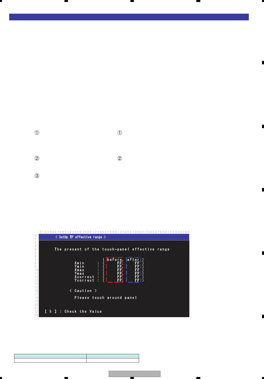
AVH-P4100DVD/XN/UC 73
5 678
5678
C
D
F
A
B
E
[Outermost circumference inspection]
[Outline]
Outermost circumference value of X and Y is obtained by tracing the outermost circumference of
the touch panel screen.
When exiting the menu screen by pressing 5 key, the captured value is stored in the EEPROM.
Furthermore, when storing the value, checking is made as to whether the value is within the range or not.
When the value is within the range.
Write the following value and adjustment information to the EEPROM, then “OK” is displayed.
1. The outermost value of X and Y(min/max) : 4 byte
2. The reference value for A/D correction of X,Y : 2 byte
3. Adjustment information(Adjustment OK) : 1 byte
When the value is within the range.
Write the following adjustment information to the EEPROM, then “NG” is displayed.
1. Adjustment information(Adjustment NG) : 1 byte
The initial value and the setting value allowable range are as follows.
<Before initial value> <After initial value>
Outermost value Outermost value
Xmin : 35h Xmin : 78h
Ymin : 3Fh Ymin : 78h
Xmax : F3h Xmax : B4h
Ymax : EAh Ymax : B4h
A/D correction value A/D correction value
X : 33h X : 00h
Y : 38h Y : 00h
Setting value allowable range
X direction Minimum value : 00h to 80h
Maximum value : 9Eh to FFh
Maximum value - Minimum value : more then 73h
Y direction Minimum value : 00h to 83h
Maximum value : 9Ah to FFh
Maximum value - Minimum value : more then 6Bh
[Display specifications]
Outermost circumference inspection in process
X/Y information of [MIN] and [MAX] of the outermost circumference are displayed.
[BEFOR] indicates the value stored in the EEPROM.
[AFTER] indicates MIN/MAX of the A/D value currently captured.
[Operation specification]
Operational description Remote controller key
Return to top mene 5
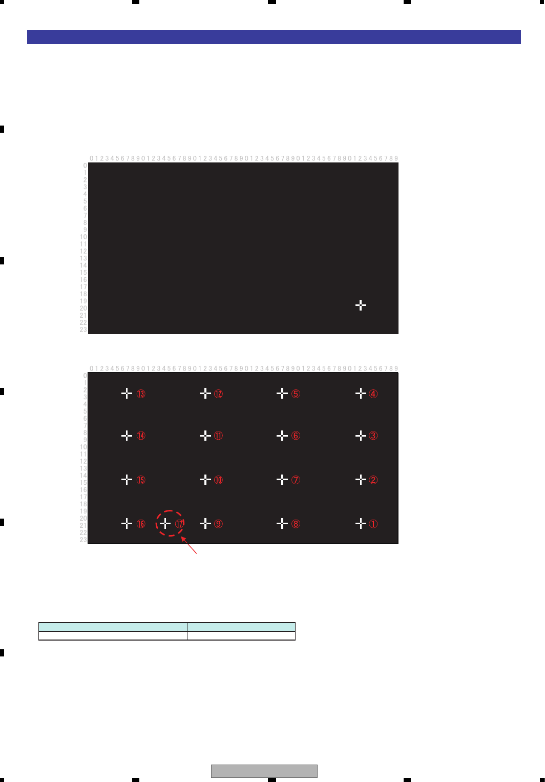
AVH-P4100DVD/XN/UC
74
1234
1234
C
D
F
A
B
E
[16 points adjustment]
[Outline]
When correctly touched, the cursor will disappear, and the next cursor will appear. Calibration is conducted
by repeating this process 16 times.
When the 17th point has been finally touched, setting information for the 16 points and the normal ending
information, total of 17 byte data, are written into the EEPROM, and the screen returns to the TOP menu.
[Display specifications]
16 points adjustment in process
Order of display of the locations to be pressed.
This point is intended to end the
calibration inspection, and therefore, the
corrected value of this point is not obtained.
[Operation specification]
Operational description Remote controller key
Return to top mene 5
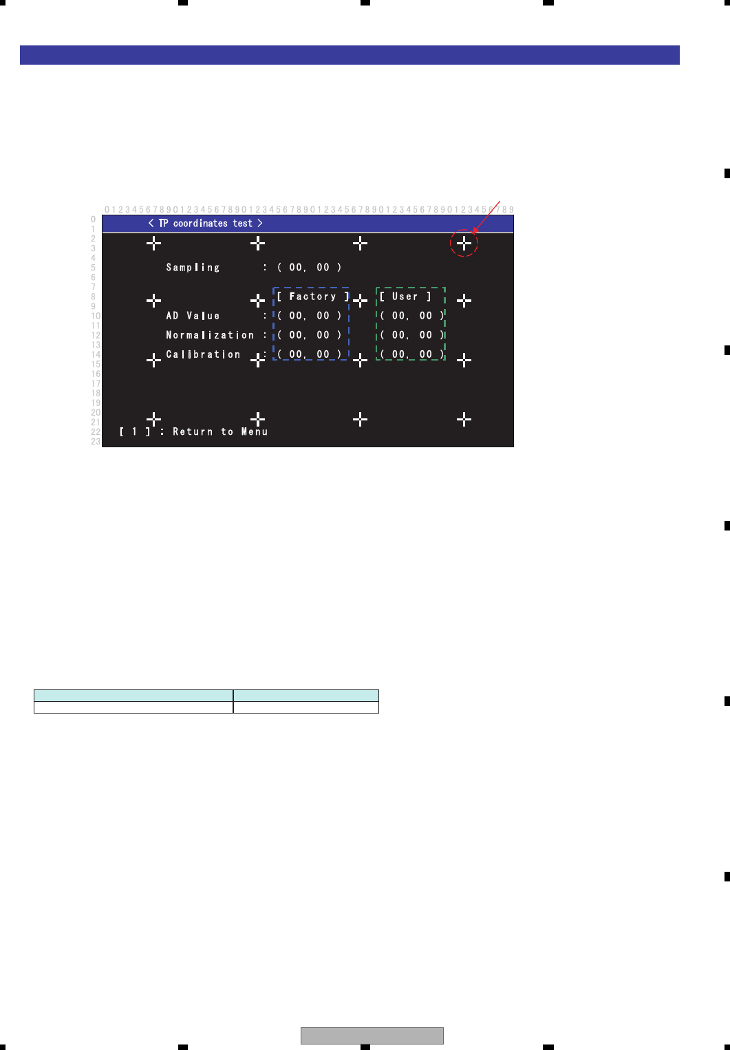
AVH-P4100DVD/XN/UC 75
5 678
5678
C
D
F
A
B
E
[Coordinate inspection]
[Outline]
The coordinate before correction and after correction at the time of pressing the touch panel are displayed for
coordinate verification.
Furthermore, the red "+" cursor can be moved by the key operaiont mentioned bellow, and the coordinate of
the cursor center is displayed.
[Display specifications] Fixed display
[Operation specification]
Operational description Remote controller key
Return to top mene 1
Each displayed coordinate is as follows.
The values under [Factory] are the corrected values in the Factory region and the values under [User] are
the corrected values in the User region.
• Sampling : A/D value (X direction, Y direction) of the pressed point is displayed.
• AD Value : The coordinate (X direction, Y direction) of the A/D value of the pressed point corrected by
the reference value for A/D correction is displayed.
• Normalization : The coordinate (X direction, Y direction) after normalizing the A/D corrected coordinate
within the effective range is displayed. (0~255)
• Calibration : The coordinate (X direction, Y direction) which is the result of adding the correction
by calibration to the normalized coordinate is displayed.
Movable "+" cursor is displayed in red.
16 calibration points are displayed in white.
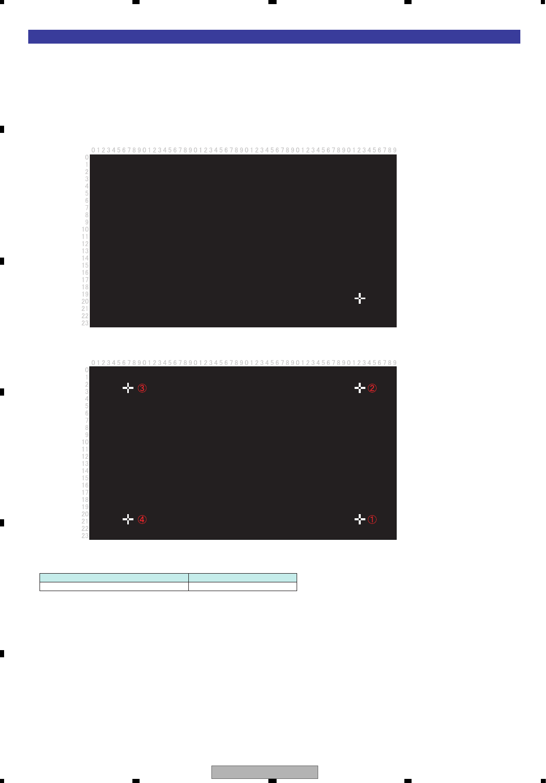
AVH-P4100DVD/XN/UC
76
1234
1234
C
D
F
A
B
E
[Calibration verification]
[Outline]
Touch the cursor “+” displayed on the screen. The correct touch will delete the cursor and another cursor
will be displayed. The incorrect touch will make the characters of cursor turn red.
Repeat this for 4 points, and “OK” is displayed upon the last press of 4th point.
[Display specifications]
The pushing order
confirming
[Operation specification]
Operational description Remote controller key
Return to top mene 1
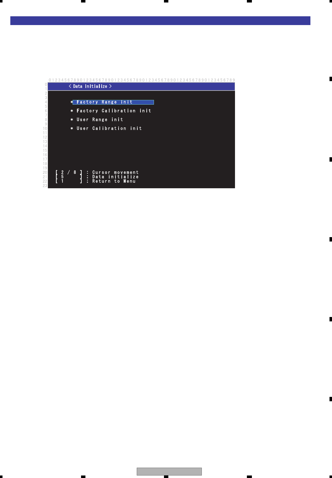
AVH-P4100DVD/XN/UC 77
5 678
5678
C
D
F
A
B
E
[Data initialization]
[Outline]
Result of outermost circumference inspection and of calibration inspection (corrected value) are returned to
their initial values.
As for the initialized items, the initial values are written into the EEPROM and the adjustment information
is cleared.
[Display specifications]
Conditions for the adjustment completion mark (*) to be lighted up.
(The mark will be lighted up if one of the multiple conditions is met.)
Outermost circumference inspection
When the outermost circumference inspection of the calibration for line has been completed normally.
16 point adjustment
When the 16 point adjustment of the calibration for line has been completed normally.
User outermost circumference inspection
When the user outermost circumference inspection of the calibration for line has been completed normally.
User 16 point adjustment
When the user 16 point adjustment of the calibration for line has been completed normally.
Conditions for the adjustment completion mark (*) to go out.
Outermost circumference inspection
When the above mentioned lighting conditions are not applicable.
When the adjusted value has been initialized (Data initialize).
When the EEPROM has been initialized.
16 point adjustment
When the above mentioned lighting conditions are not applicable.
When the adjusted value has been initialized (Data initialize).
When the EEPROM has been initialized.
User outermost circumference inspection
When the above mentioned lighting conditions are not applicable.
In case the outermost circumference inspection of the calibration for line or the 16-point adjustment is normally
terminated after normal termination of the outermost circumference inspection for user calibration.
When the adjusted value has been initialized (Data initialize).
When the EEPROM has been initialized.
User 16 point adjustment
When the above mentioned lighting conditions are not applicable.
In case the outermost circumference inspection of the calibration for line or the 16-point adjustment is normally
terminated after normal termination of the outermost circumference inspection for user calibration.
When the adjusted value has been initialized (Data initialize).
When the EEPROM has been initialized.
Refer to [Menu types in the mode].
[Operation specification]
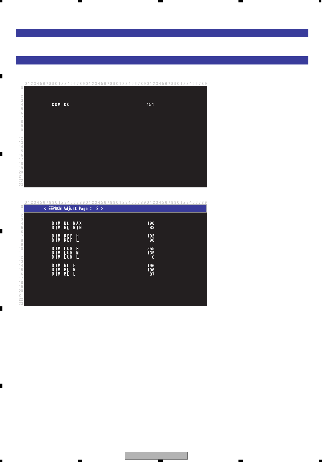
AVH-P4100DVD/XN/UC
78
1234
1234
C
D
F
A
B
E
[Method for Mode IN]
Choose "EEPROM Adjust" among the monitor test mode menu screen.
Flicker Adjust
[Display specifications]
Backlight output max value : 196
Backlight output min value : 83
Dimmer threshold value (high) : 192
Dimmer threshold value (low) : 96
Dimmer external light point (high) : 255
Dimmer external light point (medium) : 135
Dimmer external light point (low) : 0
Dimmer backlight point (high) : 196
Dimmer backlight point (medium) : 196
Dimmer backlight point (low) : 87
3. EEPROM Adjust
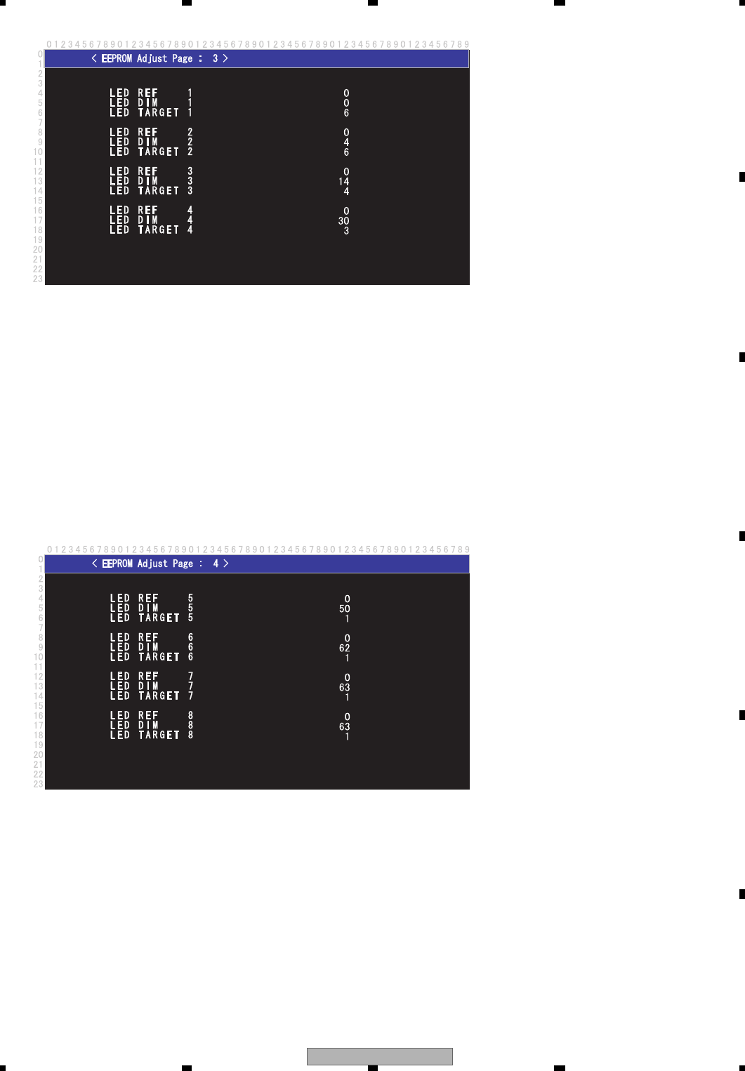
AVH-P4100DVD/XN/UC 79
5 678
5678
C
D
F
A
B
E
LCD protection value at High temperature (1) Temperature value : 0
LCD protection value at High temperature (1) Dimmer output : 0
LCD protection value at High temperature (1) Target arrival time : 6
LCD protection value at High temperature (2) Temperature value : 0
LCD protection value at High temperature (2) Dimmer output : 4
LCD protection value at High temperature (2) Target arrival time : 6
LCD protection value at High temperature (3) Temperature value : 0
LCD protection value at High temperature (3) Dimmer output : 14
LCD protection value at High temperature (3) Target arrival time : 4
LCD protection value at High temperature (4) Temperature value : 0
LCD protection value at High temperature (4) Dimmer output : 30
LCD protection value at High temperature (4) Target arrival time : 3
LCD protection value at High temperature (5) Temperature value : 0
LCD protection value at High temperature (5) Dimmer output : 50
LCD protection value at High temperature (5) Target arrival time : 1
LCD protection value at High temperature (6) Temperature value : 0
LCD protection value at High temperature (6) Dimmer output : 62
LCD protection value at High temperature (6) Target arrival time : 1
LCD protection value at High temperature (7) Temperature value : 0
LCD protection value at High temperature (7) Dimmer output : 63
LCD protection value at High temperature (7) Target arrival time : 1
LCD protection value at High temperature (8) Temperature value : 0
LCD protection value at High temperature (8) Dimmer output : 63
LCD protection value at High temperature (8) Target arrival time : 1
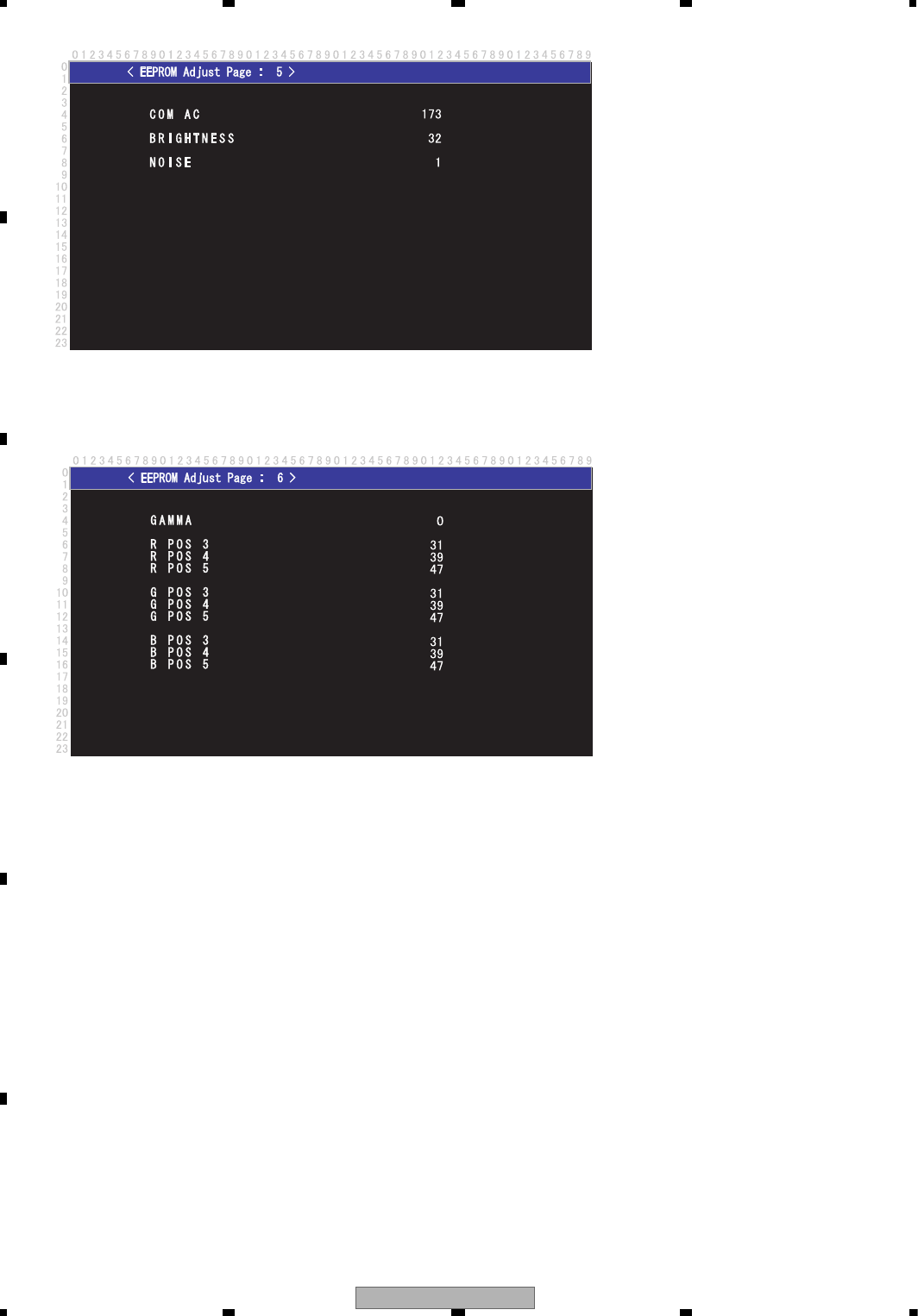
AVH-P4100DVD/XN/UC
80
1234
1234
C
D
F
A
B
E
Common inverted output amplitude adjusted value : 173
Brightness adjustment : 32
Noise shaping setting : 1
RGB gamma correction : 0
RGB gamma correction setting R polygonal line position setting arrangement [3] : 31
RGB gamma correction setting R polygonal line position setting arrangement [4] : 39
RGB gamma correction setting R polygonal line position setting arrangement [5] : 47
RGB gamma correction setting G polygonal line position setting arrangement [3] : 31
RGB gamma correction setting G polygonal line position setting arrangement [4] : 39
RGB gamma correction setting G polygonal line position setting arrangement [5] : 47
RGB gamma correction setting B polygonal line position setting arrangement [3] : 31
RGB gamma correction setting B polygonal line position setting arrangement [4] : 39
RGB gamma correction setting B polygonal line position setting arrangement [5] : 47
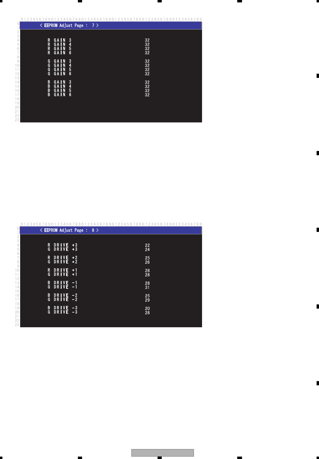
AVH-P4100DVD/XN/UC 81
5 678
5678
C
D
F
A
B
E
RGB gamma correction setting R gain arrangement [3] : 32
RGB gamma correction setting R gain arrangement [4] : 32
RGB gamma correction setting R gain arrangement [5] : 32
RGB gamma correction setting R gain arrangement [6] : 32
RGB gamma correction setting G gain arrangement [3] : 32
RGB gamma correction setting G gain arrangement [4] : 32
RGB gamma correction setting G gain arrangement [5] : 32
RGB gamma correction setting G gain arrangement [6] : 32
RGB gamma correction setting B gain arrangement [3] : 32
RGB gamma correction setting B gain arrangement [4] : 32
RGB gamma correction setting B gain arrangement [5] : 32
RGB gamma correction setting B gain arrangement [6] : 32
R drive adjustment +3 : 22
G drive adjustment +3 : 24
R drive adjustment +2 : 25
G drive adjustment +2 : 26
R drive adjustment +1 : 28
G drive adjustment +1 : 28
B drive adjustment +1 : 28
G drive adjustment +1 : 31
B drive adjustment +2 : 25
G drive adjustment +2 : 29
B drive adjustment +3 : 20
G drive adjustment +3 : 28
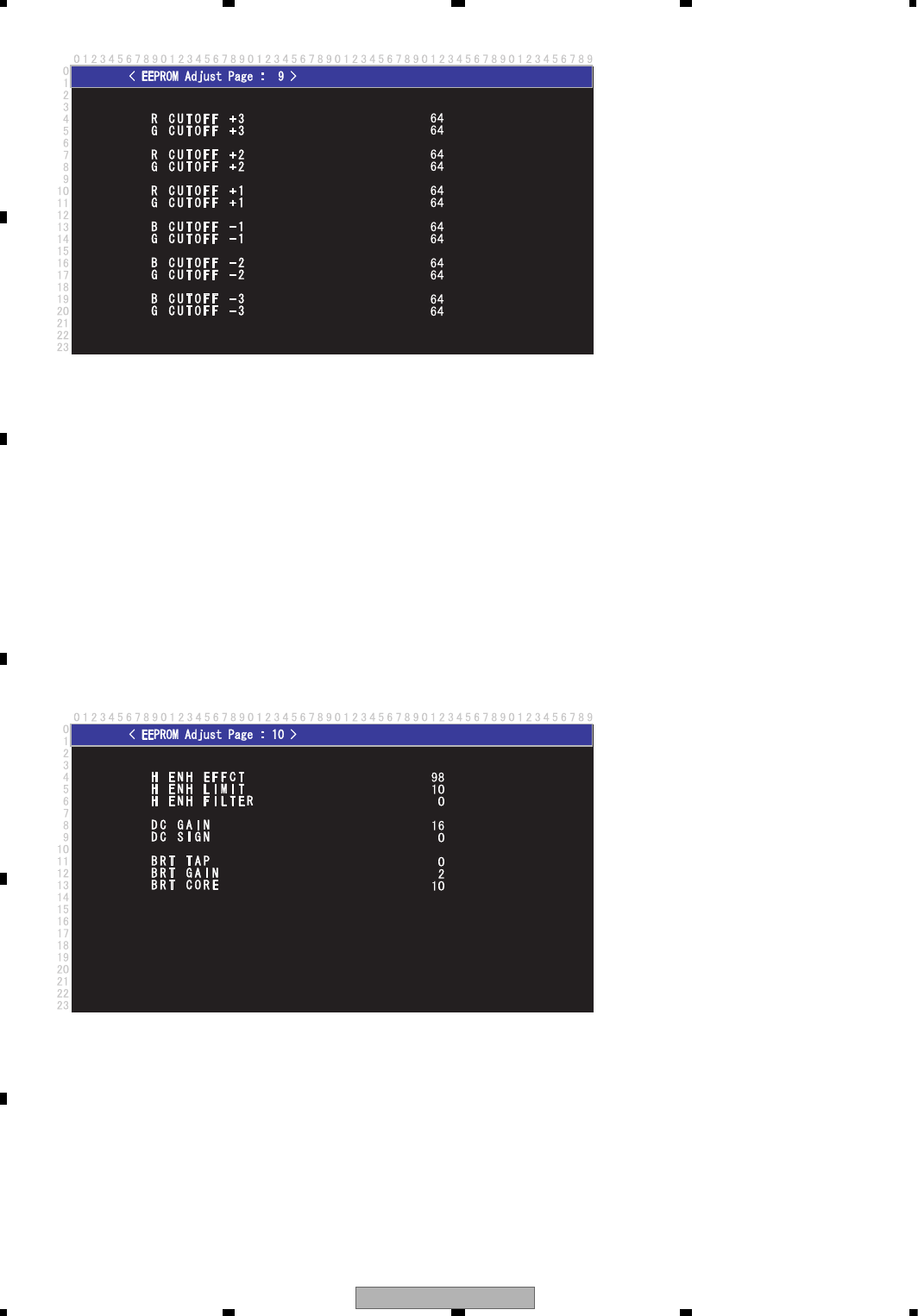
AVH-P4100DVD/XN/UC
82
1234
1234
C
D
F
A
B
E
R cutoff adjustment +3 : 64
G cutoff adjustment +3 : 64
R cutoff adjustment +2 : 64
G cutoff adjustment +2 : 64
R cutoff adjustment +1 : 64
G cutoff adjustment +1 : 64
B cutoff adjustment -1 : 64
G cutoff adjustment -1 : 64
B cutoff adjustment -2 : 64
G cutoff adjustment -2 : 64
B cutoff adjustment -3 : 64
G cutoff adjustment -3 : 64
Horizontal enhancer adjustment Correction effect adjustment : 98
Horizontal enhancer adjustment Limiter for both shots of the positive/negative side : 10
Horizontal enhancer adjustment Horizontal enhancer adjustment : 0
YUV DC transmission quantity correction setting Correction gain : 16
YUV DC transmission quantity correction setting DC transmission quantity correction polarity : 0
Brightness outline correction adjustment Correction tap select : 0
Brightness outline correction adjustment Correction gain : 2
Brightness outline correction adjustment Coring quantity : 10
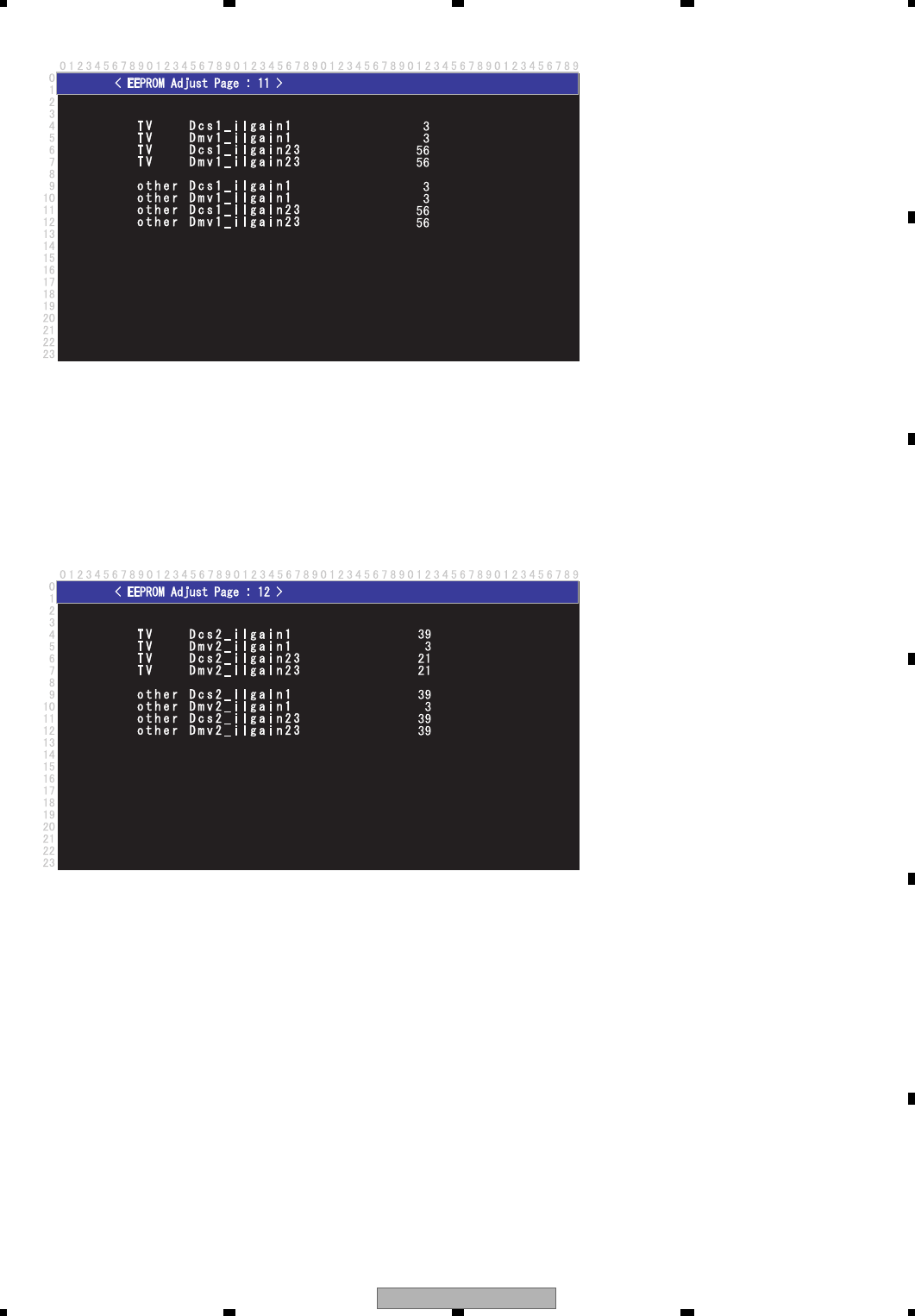
AVH-P4100DVD/XN/UC 83
5 678
5678
C
D
F
A
B
E
Synchronous separation Top curl adjustment (Strong electric field, TV) Dcs1_ilgain1 : 3
Synchronous separation Top curl adjustment (Strong electric field, TV) Dmv1_ilgain1 : 3
Synchronous separation Top curl adjustment (Strong electric field, TV) Dcs1_ilgain23 : 56
Synchronous separation Top curl adjustment (Strong electric field, TV) Dmv1_ilgain23 : 56
Synchronous separation Top curl adjustment (Strong electric field, Besides TV) Dcs1_ilgain1 : 3
Synchronous separation Top curl adjustment (Strong electric field, Besides TV) Dmv1_ilgain1 : 3
Synchronous separation Top curl adjustment (Strong electric field, Besides TV) Dcs1_ilgain23 : 56
Synchronous separation Top curl adjustment (Strong electric field, Besides TV) Dmv1_ilgain23 : 56
Synchronous separation Top curl adjustment (Weak electric field, TV) Dcs2_ilgain1 : 39
Synchronous separation Top curl adjustment (Weak electric field, TV) Dmv2_ilgain1 : 3
Synchronous separation Top curl adjustment (Weak electric field, TV) Dcs2_ilgain23 : 21
Synchronous separation Top curl adjustment (Weak electric field, TV) Dmv2_ilgain23 : 21
Synchronous separation Top curl adjustment (Weak electric field, Besides TV) Dcs2_ilgain1 : 39
Synchronous separation Top curl adjustment (Weak electric field, Besides TV) Dmv2_ilgain1 : 3
Synchronous separation Top curl adjustment (Weak electric field, Besides TV) Dcs2_ilgain23 : 39
Synchronous separation Top curl adjustment (Weak electric field, Besides TV) Dmv2_ilgain23 : 39
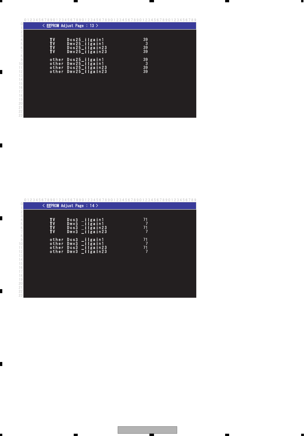
AVH-P4100DVD/XN/UC
84
1234
1234
C
D
F
A
B
E
Synchronous separation Top curl adjustment (Super-weak electric field, TV) Dcs25_ilgain1 : 39
Synchronous separation Top curl adjustment (Super-weak electric field, TV) Dmv25_ilgain1 : 3
Synchronous separation Top curl adjustment (Super-weak electric field, TV) Dcs25_ilgain23 : 39
Synchronous separation Top curl adjustment (Super-weak electric field, TV) Dmv25_ilgain23 : 39
Synchronous separation Top curl adjustment (Super-weak electric field, Besides TV) Dcs25_ilgain1 : 39
Synchronous separation Top curl adjustment (Super-weak electric field, Besides TV) Dmv25_ilgain1 : 3
Synchronous separation Top curl adjustment (Super-weak electric field, Besides TV) Dcs25_ilgain23 : 39
Synchronous separation Top curl adjustment (Super-weak electric field, Besides TV) Dmv25_ilgain23 : 39
Synchronous separation Top curl adjustment (Super-weak electric field, TV) Dcs3_ilgain1 : 71
Synchronous separation Top curl adjustment (Super-weak electric field, TV) Dmv3_ilgain1 : 7
Synchronous separation Top curl adjustment (Super-weak electric field, TV) Dcs3_ilgain23 : 71
Synchronous separation Top curl adjustment (Super-weak electric field, TV) Dmv3_ilgain23 : 7
Synchronous separation Top curl adjustment (Super-weak electric field, Besides TV) Dcs3_ilgain1 : 71
Synchronous separation Top curl adjustment (Super-weak electric field, Besides TV) Dmv3_ilgain1 : 7
Synchronous separation Top curl adjustment (Super-weak electric field, Besides TV) Dcs3_ilgain23 : 71
Synchronous separation Top curl adjustment (Super-weak electric field, Besides TV) Dmv3_ilgain23 : 7
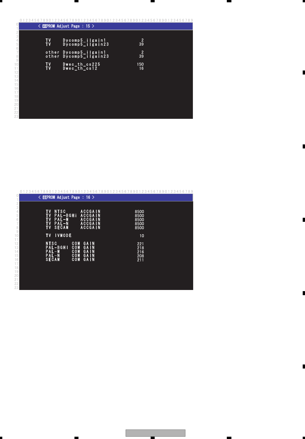
AVH-P4100DVD/XN/UC 85
5 678
5678
C
D
F
A
B
E
ACCGAIN setting (ulNT358_SYNC1_08) : 8500
ACCGAIN setting (ulPALBG_SYNC1_08) : 8500
ACCGAIN setting (ulPALM_SYNC1_08) : 8500
ACCGAIN setting (ulPALN_SYNC1_08) : 8500
ACCGAIN setting (ulSECAM_SYNC1_08) : 8500
IVMODE setting : 10
Com part Brightness gain (ulNT358_CMB1_20) : 221
Com part Brightness gain (ulPALBG_CMB1_20) : 218
Com part Brightness gain (ulPALBG_CMB1_21) : 216
Com part Brightness gain (ulPALBG_CMB1_22) : 208
Com part Brightness gain (ulPALBG_CMB1_23) : 211
Synchronous separation Top curl adjustment (Non signal, TV) Dycomp5_ilgain1 : 2
Synchronous separation Top curl adjustment (Non signal, TV) Dycomp5_ilgain23 : 39
Synchronous separation Top curl adjustment (Non signal, Besides TV) Dycomp5_ilgain1 : 2
Synchronous separation Top curl adjustment (Non signal, Besides TV) Dycomp5_ilg : 39
Electric field strength judgment value for TV Dwec_th_cs225 : 150
Electric field strength judgment value for Dwec_th_cs12 : 16
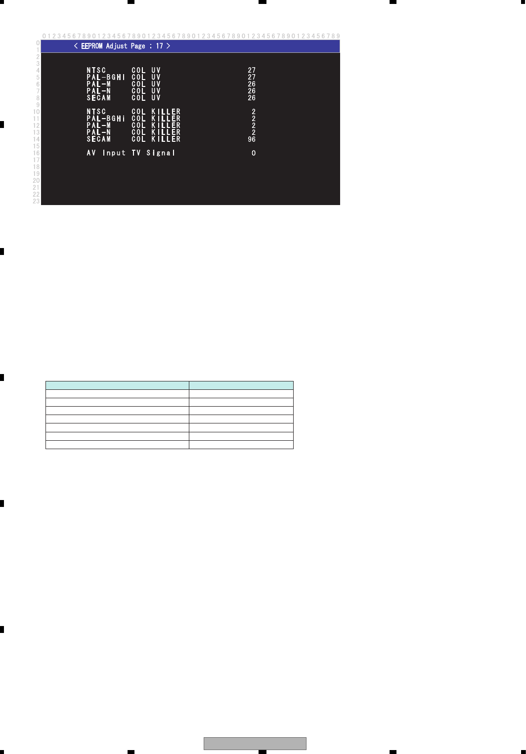
AVH-P4100DVD/XN/UC
86
1234
1234
C
D
F
A
B
E
Color demodulate part UV delay adjustment (ulNT358_AVICOL3_03) : 27
Color demodulate part UV delay adjustment (ulPALBG_AVICOL3_03) : 27
Color demodulate part UV delay adjustment (ulPALM_AVICOL3_03) : 26
Color demodulate part UV delay adjustment (ulPALN_AVICOL3_03) : 26
Color demodulate part UV delay adjustment (ulSECAM_AVICOL3_03) : 26
Color demodulate part Phase killer value (ulNT358_AVICOL1_09) : 2
Color demodulate part Phase killer value (ulPALBG_AVICOL1_09) : 2
Color demodulate part Phase killer value (ulPALM_AVICOL1_09) : 2
Color demodulate part Phase killer value (ulPALN_AVICOL1_09) : 2
Color demodulate part Phase killer value (ulSECAM_AVICOL1_09) : 96
AV input picture indication movement : 0
[Operation specification]
Operational description Remote controller key
Selection cursor up movement 2
Selection cursor down movement 8
Item content value up 6
Item content value down 4
Next menu page 9
Former menu page 7
Return to test mode mene 1
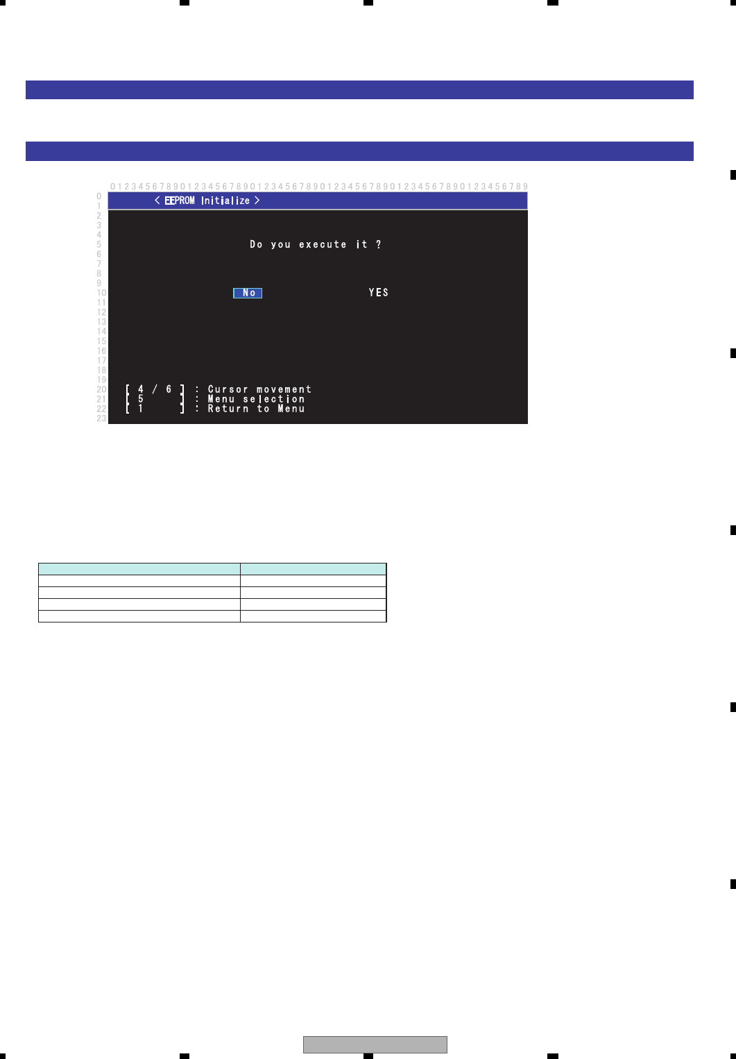
AVH-P4100DVD/XN/UC 87
5 678
5678
C
D
F
A
B
E
[Method for Mode IN]
Choose "EEPROM Initialize" among the monitor test mode menu screen.
[Display specifications]
Default of a cursor is the location of "No".
Choose "YES" and decide, initialize a setting value.
*) Don't turn off power while initializing.
When normally ends, "success" is displayed.
When will not end in four seconds, judged to be abnormal, "failure" is displayed.
[Operation specification]
Operational description Remote controller key
Selection cursor left movement 4
Selection cursor right movement 6
Return to test mode mene 1
Menu enter 5
4. EEPROM Initialize
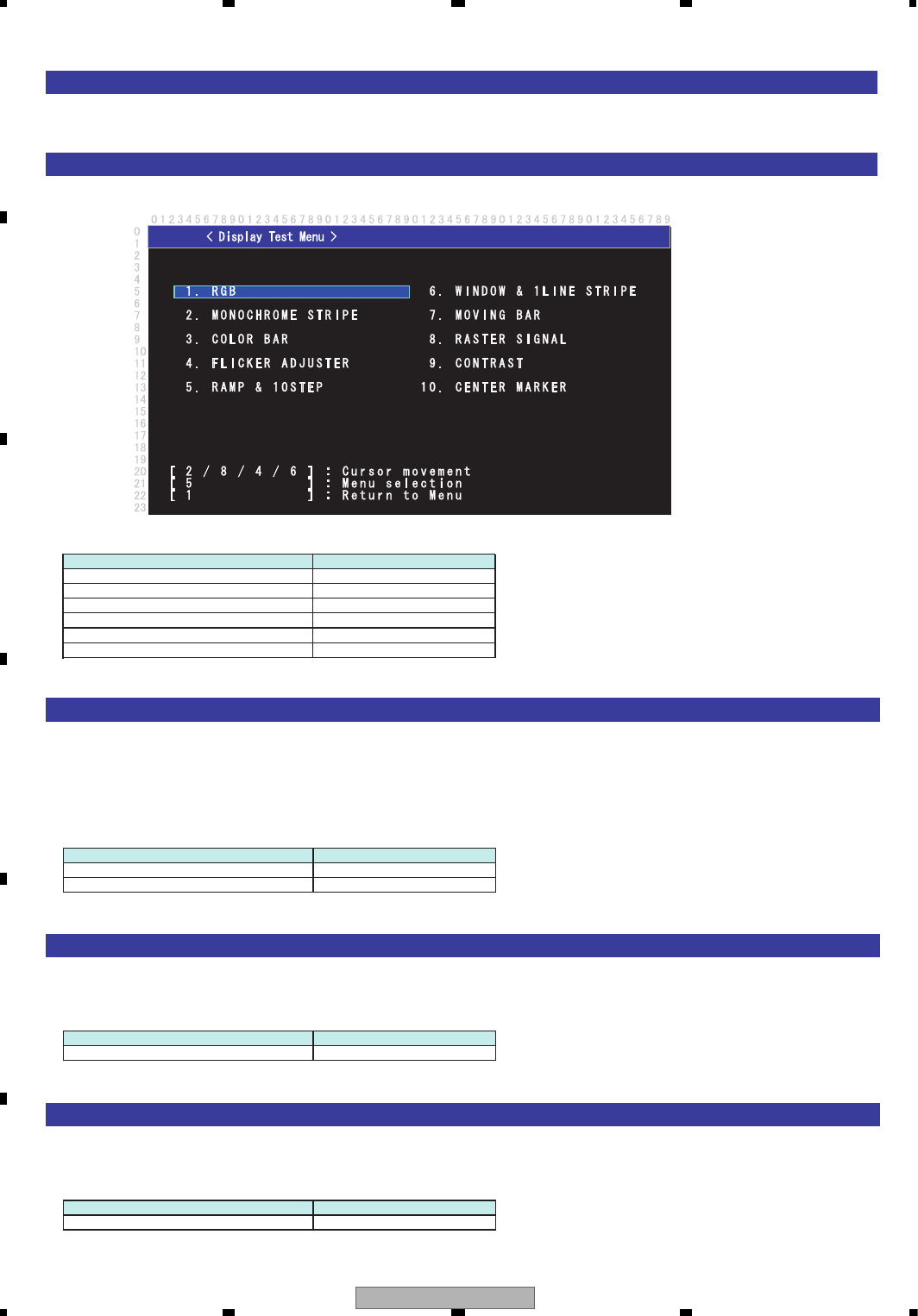
AVH-P4100DVD/XN/UC
88
1234
1234
C
D
F
A
B
E
[Method for Mode IN]
Choose "Display Test (Test Pattern)" among the monitor test mode menu screen.
[Display specifications]
5. Display Test (Test Pattern)
[Operation specification]
Operational description Remote controller key
Selection cursor up movement 2
Selection cursor down movement 8
Selection cursor left movement 4
Selection cursor right movement 6
Menu enter 5
Return to test mode mene 1
[RGB]
RGB is plotted in the following pattern:
R100% -> R50% -> G100% -> G50% -> B100% -> B50% -> BLACK -> GRAY -> WHITE -> C.Video 60Hz
-> C.Video 50Hz
(The display of the screen will be changed in 1 second.)
[Operation specification]
Operational description Remote controller key
Stop/Restart 5
Return to test mode mene 1
[MONOCHROME STRIPE]
Display of monochrome stripe signal (1dot Width)
[Operation specification]
Operational description Remote controller key
Return to test mode mene 1
[COLOR BAR]
Display of color bar signal
[Operation specification]
Operational description Remote controller key
Return to test mode mene 1
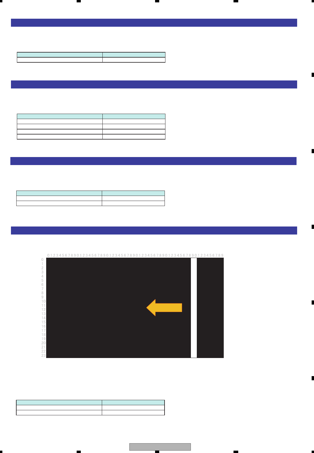
AVH-P4100DVD/XN/UC 89
5 678
5678
C
D
F
A
B
E
[FLICKER ADJUSTER]
Display of monochrome stripe signal of the flicker adjustment
[Operation specification]
Operational description Remote controller key
Return to test mode mene 1
[RAMP & 10STEP]
Display of step signal and signal for alpha blend check
[Operation specification]
Operational description Remote controller key
alpha blend rate up 2
alpha blend rate down 8
Next signal 5
Return to test mode mene 1
[WINDOW & 1LINE STRIPE]
Display of signal for video signal reply check
[Operation specification]
Operational description Remote controller key
Next signal 5
Return to test mode mene 1
[MOVING BAR]
A white vertical line indicates the signal which moves from the right to the left.
[Operation specification]
Operational description Remote controller key
Cycle1 -> 2 -> 3 -> stop -> 1 5
Return to test mode mene 1
Drift to the left
Cycle1 : 1 seconds
Cycle2 : 2 seconds
Cycle3 : 3 seconds
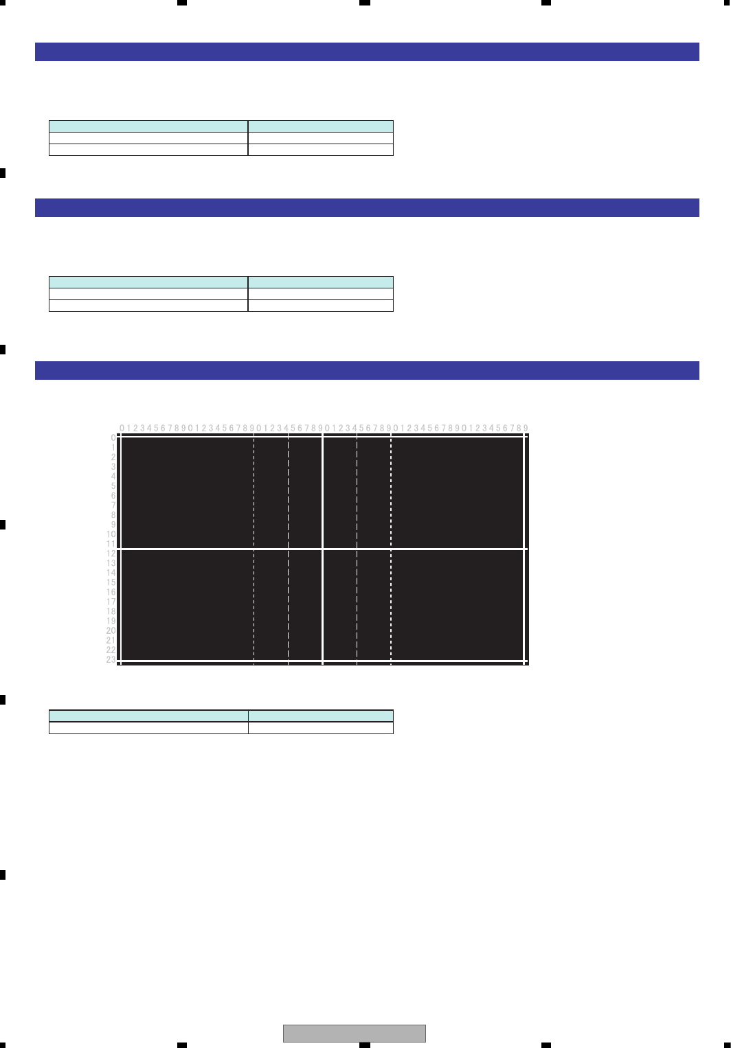
AVH-P4100DVD/XN/UC
90
1234
1234
C
D
F
A
B
E
[RASTER SIGNAL]
Display of signal for step confirmation
[Operation specification]
Operational description Remote controller key
Next signal 5
Return to test mode mene 1
[CONTRAST]
Display of Black/White signal
[Operation specification]
Operational description Remote controller key
Next signal 5
Return to test mode mene 1
[CENTER MARKER]
Display of signal for screen central location setting.
[Operation specification]
Operational description Remote controller key
Return to test mode mene 1
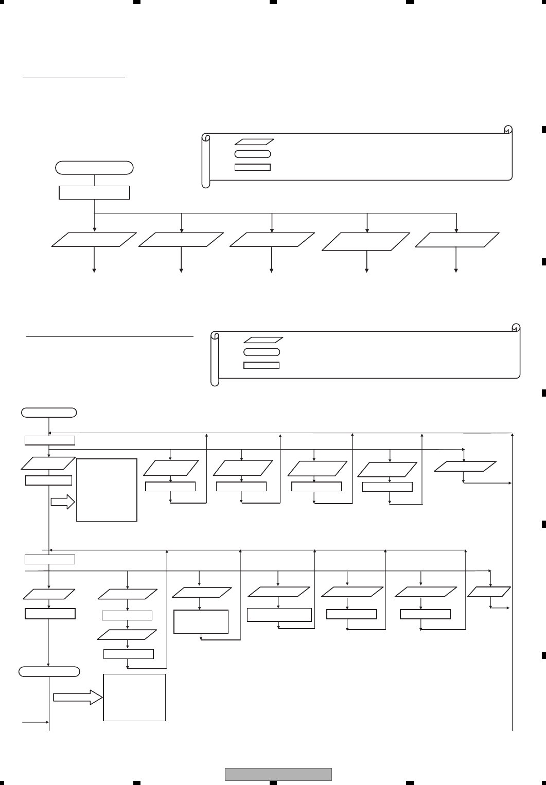
AVH-P4100DVD/XN/UC 91
5 678
5678
C
D
F
A
B
E
6.2 DVD TEST MODE
Image of the test mode.
[Note] Higher level 4 characters only. Lower level 4 characters are spaces.
)2()1(
Start of the test mode.
TEST
FE test selection EDC1 test selection
Hereafter, to FE test
mode image.
Hereafter, to EDC1
test mode image.
[Note] In order to move on to another test after selecting a test (FE/EDC1/EDC2), it is necessary to restart the DVD mechanism in the test mode.
(3)
EDC2 test selection
Hereafter, to EDC2
test mode image.
(4)
LD power on time
mode selection
Hereafter, to LD power on
time mode image.
(5)
Simple FE test mode
Hereafter, to simple
FE test mode.
Legend: … Key operation
… Operation state
… The content displayed on the DVD mechanism (video only)
8 characters data is sent to the product side (HOST) by UART communication.
Image of the front end test mode.
(2)
FE test mode
Disc type DVD1
layer
FE offset coefficient
TE offset coefficient
AS offset coefficient
ENV offset coefficient
TG offset coefficient
DBAL coefficient
VIN1 offset cancel value
VIN2 offset cancel value
VIN3 offset cancel value
VIN4 offset cancel value
VIN5 offset cancel value
Power on
0000 0000
0FFF 0000
0 x 00 0000
Legend: … Key operation
… Operation state
… The content displayed on the DVD mechanism (video only)
8 characters data is sent to the product side (HOST) by UART communication.
)5()4(
Disc type DVD2
layer Disc type CD
0000002000000010
Disc type CD-RW
0300 0000
EJECT
EJECT
[Note] If no action is taken for approximately 10 seconds after LD-ON, it will become LO-OFF automatically.
If F close is selected during LD-OFF, it will become an error.
During focus search (S character measurement mode), too, safety regulation applies if LD_OFF is not selected
within 10 seconds. Therefore, even if focus search is selected after LD-ON, it will become LD-OFF after 9 seconds.
In order to F close after focus search (S character measurement mode), set to Power_OFF first then power on again
before F close.
FEMAX level
FEMIN level
ASMAX level
ENVMAX level
FE normalization coefficient
Spindle gain coefficient
TEMAX level indication
TEMIN level indication
(2)
Focus close state
)2()1(
S curve
measurement
(2)
hcraesFesolcF
1A00 0000
F search
1100 0000
1FFF 0000
(3),(4)
CRG+/-
Activates while the key
is being pressed.
1B00 0000 : CRG+
1C00 0000 : CRG-
(5) (6)
LD-ON/OFF
When LO-ON: 1100 0000
When LD-OFF: 1000 000
CRG_HOME
1D00 0000
(8)
Power_OFF
(1) (3)
a b
1 x 00 0000
(7)
CRG_OUTSIDER
1E00 0000
[VOL-] + [TRACK UP] + Reset start
Switch position of the remote control unit.
[AVH mode]
(1)-(8) and EJECT is the key of remote control unit.
Test mode display will not appear on the display of this product. Connect the rear monitor output to a monitor.
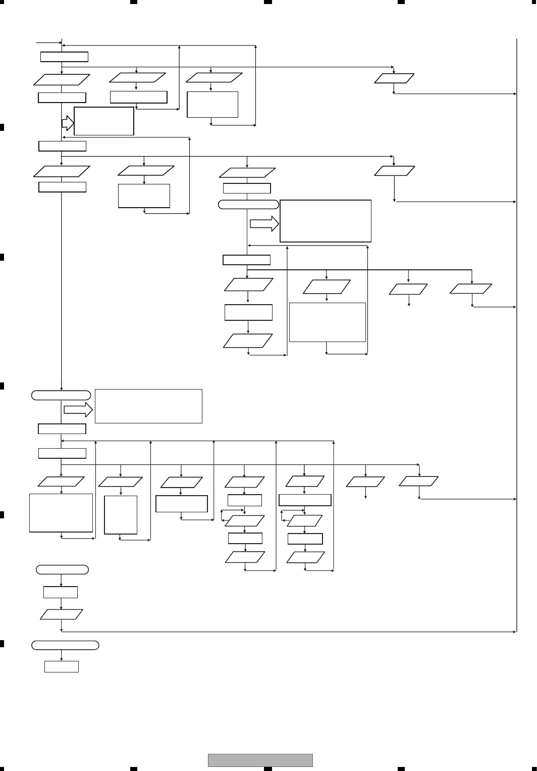
AVH-P4100DVD/XN/UC
92
1234
1234
C
D
F
A
B
E
(2)
(1) (2)
Tracking balance
TBAL coefficient (layer 0)
TBAL coefficient (layer 1)
TE normalization coefficient (layer 0)
TE normalization coefficient (layer 1)
Off track adjustment result
Focus Jump
When L0 layer: 2000 0000
When L1 layer: 2100 0000
2 x 00 0000
2FFF 0000
(3),(4)
CRG +/-
It operates while the key
is being pressed.
2B00 0000 : CRG+
2C00 0000 : CRG-
3000 0000
(8)
Power_OFF
(8)
Power_OFF
(5)
Performed including the tracking close processing.
FBAL coefficient (layer 0)
FBAL coefficient (layer 1)
Focus gain coefficient (layer 0)
Focus gain coefficient (layer 1)
Tracking gain coefficient (layer 0)
Tracking gain coefficient (layer 1)
AS normalization adjustment value (layer 0)
RF level value
3FFF 0000
Tracking close state
)2()1(
(1)
Error rate
measurement
Error rate
Focus gain coefficient (layer 0)
Focus gain coefficient (layer 1)
Tracking gain coefficient (layer 0)
Tracking gain coefficient (layer 1)
AS normalization adjustment value (layer 0)
RF level value
indication start
5000 0000
RF level is informed
every 500msec.
RF level value
indication end
)8()7(
To (2)
T.OPEN Power_OFF
)4(,)3()1(
Tracking close CRG +/-
It operates while the key
is being pressed.
3B00 0000 : CRG+
3C00 0000 : CRG-
3FFF 0000
a b
)2()1(
Tracking close state
Error rate
measurement
FBAL coefficient (layer 0)
FBAL coefficient (layer 1)
Focus gain coefficient (layer 0)
Focus gain coefficient (layer 1)
Tracking gain coefficient (layer 0)
Tracking gain coefficient (layer 1)
Playback speed
switching
4000 0000
4 x 00 0000
(5)
Error rate
Focus gain coefficient (layer 0)
Focus gain coefficient (layer 1)
Tracking gain coefficient (layer 0)
Tracking gain coefficient (layer 1)
AS normalization adjustment value (layer 0)
Focus Jump
DVDX1.3~
1.6CAV
CDX4CLV:
4x00 0000
When L0 layer: 4x00 0000
When L1 layer: 4x00 0000
(8)
Error display
Power_OFF
Error occurrence
L0 layer DVD X 1.3~1.6CAV, CD X 4CLV :4000 0000
L1 layer DVD X 1.3~1.6CAV :4100 0000
[Note] If an error occurs at Power_OFF, reset cannot be made. In such a case, it is necessary to turn the power off and start the test mode once again.
Error occurrence at Power_OFF
Error display
The number for designation of the track number shall be selected from the track numbers previously prepared.
Switch to cyclic by (3). Fix by (4).
For CD: Tracks 1, 4, 10, 11 and 32
For DVD: Tracks 1, 4, 10, 11, 32, 64 and 100
Change the method for ID address designation.
Designation of digit by command (1) and (2). UP/DOWN of numbers by command (3) and (4). Fix by command (5).
The higher 2 digits of the designated ID are the value showing the test state.
The lower 6 digits show the ID.
Example) If 300000 is desired to be designated as the ID, designated ID: 4A03 0000.
)8()7(
To (2)
T.OPEN Power_OFF
)4(,)3()6(
)3()4(-)1(
)5()5(
ID Search T.Jump+/-
4A00 0000 Jump+ : 4B00 0000
Jump- : 4C00 0000
ID designation
ID display
Track number
designation
Track number
indication
Search start Jump start
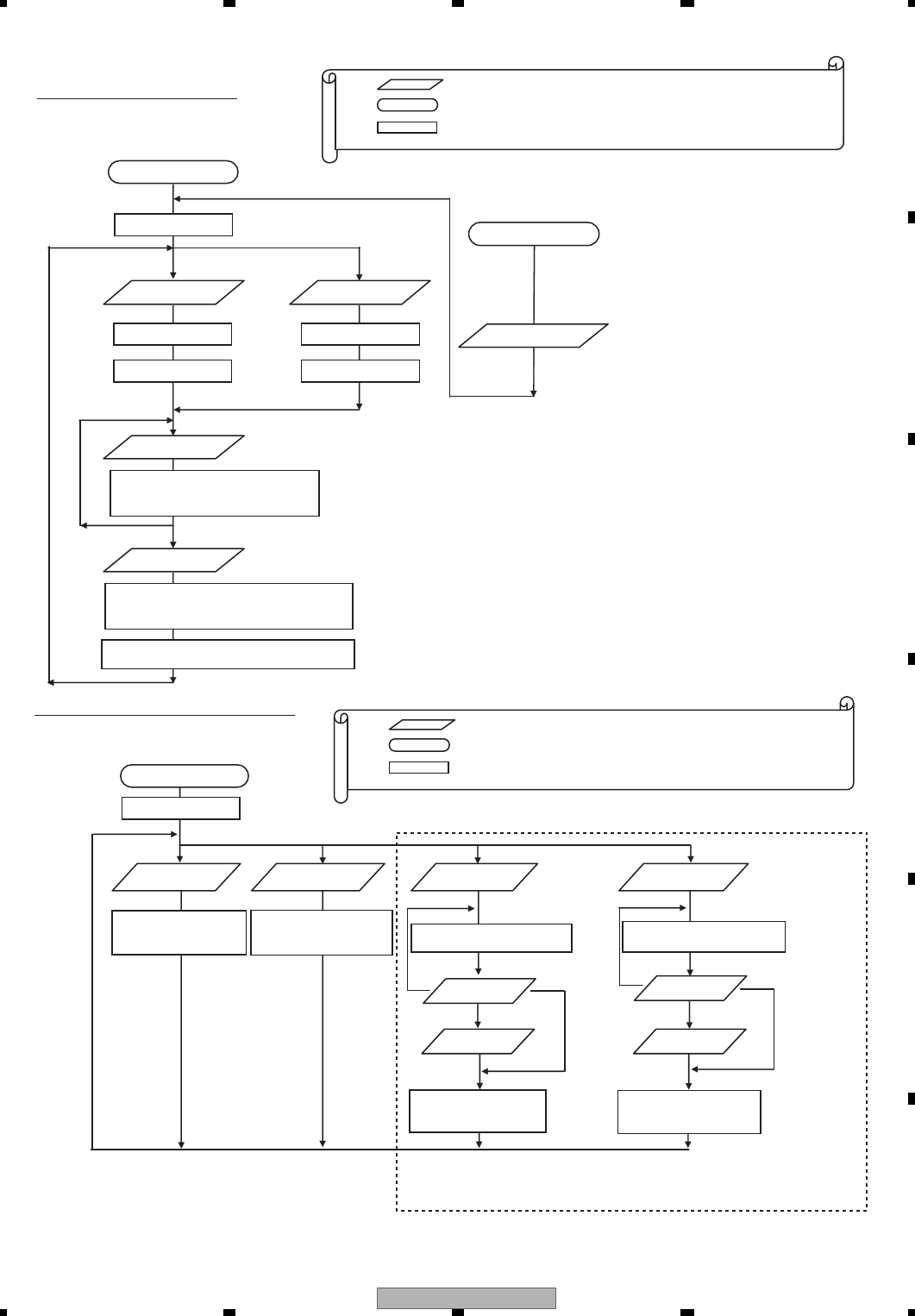
AVH-P4100DVD/XN/UC 93
5 678
5678
C
D
F
A
B
E
EDC. Image of the test mode
[Note] Image is the same for both EDC1 and EDC2.
(1) (2)
EDC1/2 test mode
0000 0000
Layer 0 selection Layer 1 selection
0000 0000 0100 0000
1003 0000 1103 0000
(5)
[Note] The display is updated at 0.5 seconds interval until 0/1 layer is selected or Eject is effected.
(1)-(4)
ID designation
EDC1/2 start
Layer 0: 10** ****
Layer 1: 11** ****
[Note] ** **** is the ID designation value
Layer 0: 20** ****
Layer 1: 21** ****
[Note] ** **** is the present ID designation value
**** ****
[Note] **** **** is the present ID designation value
Legend: … Key operation
… Operational state
… The content displayed on the DVD mechanism (video only)
8 characters data is sent to the product side (HOST) by UART communication.
[Note] Eject can be effected any time during the EDC test mode.
Eject
After completion of EJECT operation
EJECT operation
Test mode Eject
Image of the LD power on time mode.
LD power on time mode
0000 0000
CD LD power on
time indication
DVD LD power on
time indication
10** ****
[Note] ** **** is the CD LD
power on time.
20** ****
[Note] ** **** is the DVD LD
power on time.
(1) (2)
CD LD power on
time setting
Setting time
designation
30** ****
[Note] ** **** is the setting time.
Setting time
registration
DVD LD power on
time setting
Setting time
designation
40** ****
[Note] ** **** is the setting time.
(5) (6)
(1)-(4) (1)-(4)
(5) (5)
(8)
10** ****
[Note] ** **** is the CD LD
power on time.
Setting time
registration
(8)
20** ****
[Note] ** **** is the DVD LD
power on time.
[Note] If the power on time is 999999 hours or more, it is always reported as 999999 hours.
[Note] If the power on time is “*E** ****”, the value may not be correct due to the life of the flash memory.
[Method of setting time designation]
Designate the digit by command (1) and (2). UP/DOWN of numbers by command (3) and (4).
Fix by command (5). Cancel by command (8).
Legend: … Key operation
… Operational state
… The content displayed on the DVD mechanism (video only)
8 characters data is sent to the product side (HOST) by UART communication.
Not for service use
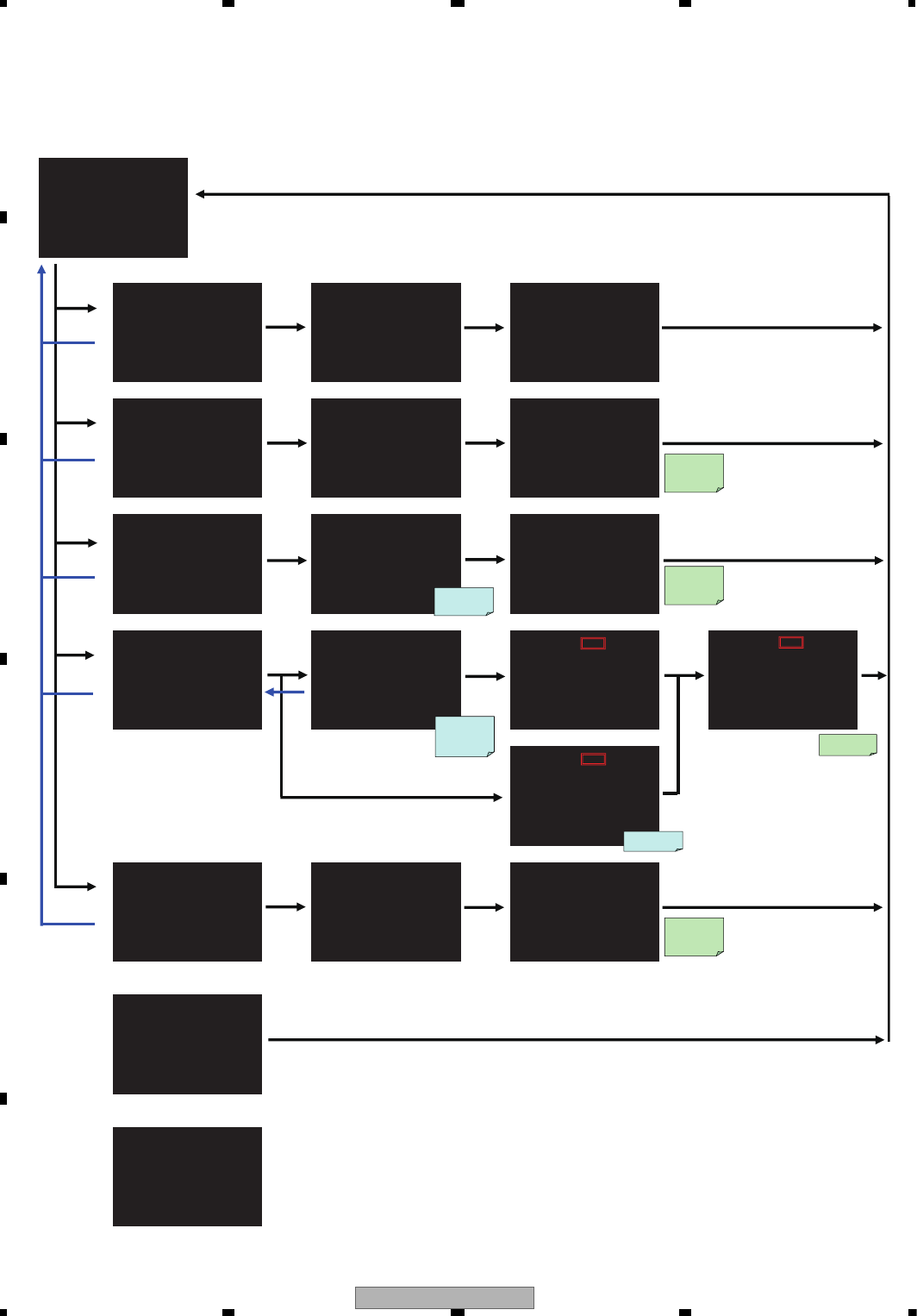
AVH-P4100DVD/XN/UC
94
1234
1234
C
D
F
A
B
E
The selection of the figure of each screen can be selected by "Key command for the test".
TEST MODE
1: LD ON
2: ASMAX
3: Skew Adjustment
4: Error Rate
5: CRG Move Outer
6: Eject
Please Input Number
NODLNODLNODL
1: DVD Single Layer 1: Power OFF
2: DVD Dual Layer
3: CD
4: CD-RW
5: Return
rebmuNtupnIesaelPgninnuRwoNrebmuNtupnIesaelP
XAMSAXAMSAXAMSA
1: DVD Single Layer 1: Power OFF
2: DVD Dual Layer
3: CD
4: CD-RW
5: Return ASMAX Level : 000000
rebmuNtupnI
esaelPgninnuRwoNrebmuNtupnIesaelP
tnemtsujdAwekStnemtsujdAwekStnemtsujdAwekS
1: DVD Single Layer 1: Power OFF
5: Return RF Level : 000000
rebmuNtupnIesaelPgninnuRwoNrebmuNtupnIesaelP
rennI-etaRrorrErennI-etaRrorrEetaRrorrEetaRrorrE
tnemerusaeMrennI:1reyaLelgniSDVD:1 1: Power OFF
2: Outer Measurement
tneme
rusaeM
elddiM:3DC:3
nruteR:5nruteR:5 Error Rate : 000000
NtupnI
es
aelPgninnuRwoNreb
m
uNtupnIesaelPrebmuNtupnIesaelP umber
*1 : The position in which
select was done is
displayed.
Error Rate
-
CD
DVD Inner
DVD Outer
DVD Middle
CD CD
Now Running
retuOevoMGRCretuOevoMGRCretuOevoMGRC
1: DVD Single Layer 1: Power OFF
2: DVD Dual Layer
3: CD
4: CD-RW
5: Return
rebmuNtupnIesaelPgninnuRwoNrebmuNtupnIesaelP
ERROR
1: Power OFF
Code : 00000000
Please Input Number
ERROR
Code : 00000000
Please Reset
1 select
2 select
3 select
4 select
select LD ON
Completion
select
ASMAX
value set
value set
select
RF Level
DVD select select
Error Rate
set select
select
select
select
select
ASMAX
Level display
Error Rate
display
RF Level
display
Update 500 msec.
*1
CD select
*1
*1
Search ID
0x00100000
Search ID
inner :
0x00040000
outer :
Search CRG
home position
5 Return select
5 Return select
5 Return select
5 Return select
5 Return
select
5 select
select select
CRG moves
to the most
outer
5 Return select
CRG Move
Completion
0 0020000
0
Simple test mode
<Flow chart>
<Error>
<Error : Power OFF>

AVH-P4100DVD/XN/UC 95
5 678
5678
C
D
F
A
B
E
6.3 DVD TOUCH PANEL TEST MODE
How to enter:
Reset with [VOL-] key and [TrackDOWN] key pressed.
How to unlock:
Product reset
Turning ACC ON
Summary:
It is for temporary analysis in services.
(For temporary analysis of user claim and etc. against DVD touch direct.)
(1)Display a frame border in the valid area as a button in the contents by OSD of DVD mecha on DVD-Video menu time.
(2)Display a cross-shape on the place user touched on touch direct display time by OSD of DVD mecha.
(3)Every time pressing "C (clear)" key on the remote controller, the color of the frame border and the cross-shape
above (1)(2) is changed (white -> red -> black -> clear -> white -> ... ).
Remarks:
The aim is as follows.
1.Display the available area of the disc button by OSD of MS5AVcode2.
->To clarify the true button position enables to judge the disc cause.
2.Display a cross-shape on the position that MS5AVcode2 thinks was pressed actually.
->To detect a gap in perception between HOST and mecha enables to judge the HOST cause.
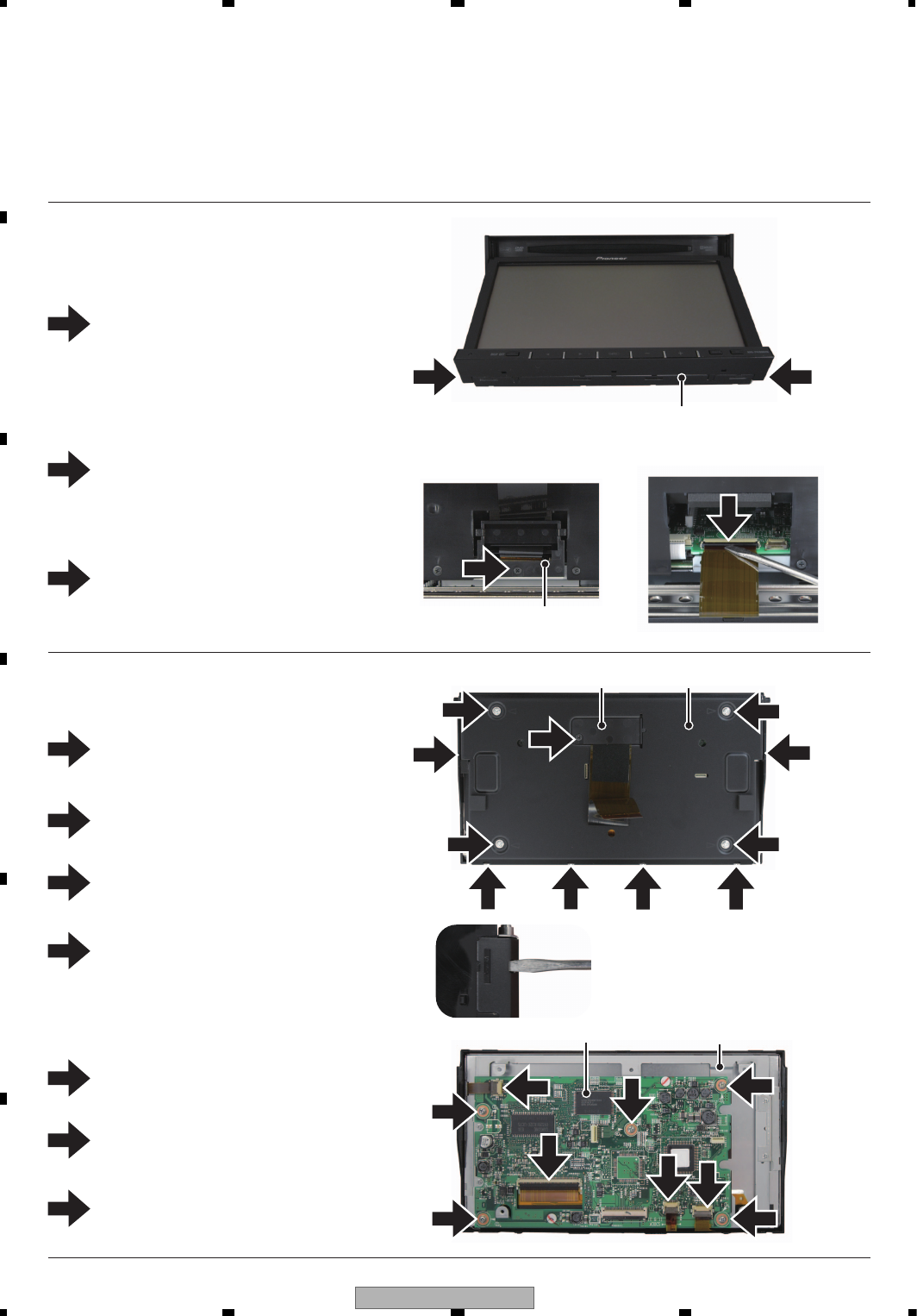
AVH-P4100DVD/XN/UC
96
1234
1234
C
D
F
A
B
E
7. DISASSEMBLY
1
2
1
2
- Removing the Monitor Assy (Fig.1, 2, 3)
Remove the two screws.(Fig.1)
Remove the screw
and then remove the Cover.(Fig.4)
Remove the two screws.(Fig.4)
1. Remove the Panel.
2. Remove the eight screws and then remove the Holder.
3. Remove the four screws and then remove the Left and Right Holder.
3
3
4
5
Remove the four hooks
and then remove the Case Unit.(Fig.4, 5)
6
7Remove the five screws
and then remove the Monitor Unit.
Disconnect the two cables
and then remove the LCD Assy.(Fig.6)
Disconnect the cable
and then remove the Monitor Assy.(Fig.3)
Remove the screw
and then remove the Cover.(Fig.2)
Remove the four screws.(Fig.4)
Disconnect the two cables.(Fig.6)
Please insert the driver from the hole
when it is difficult to remove the hook.
1 1
2
3
1
22
3
3
3
3
44
44
55
6
6
7
7
7
7
7
- Removing the Panel and Holder (not shown) (EW5, UW5)
Fig.1
- Removing the Monitor Unit (Fig.5)
Fig.3
Fig.5
Cover Fig.2
Fig.4
Fig.6
Cover Case Unit
Monitor Assy
LCD AssyMonitor Unit
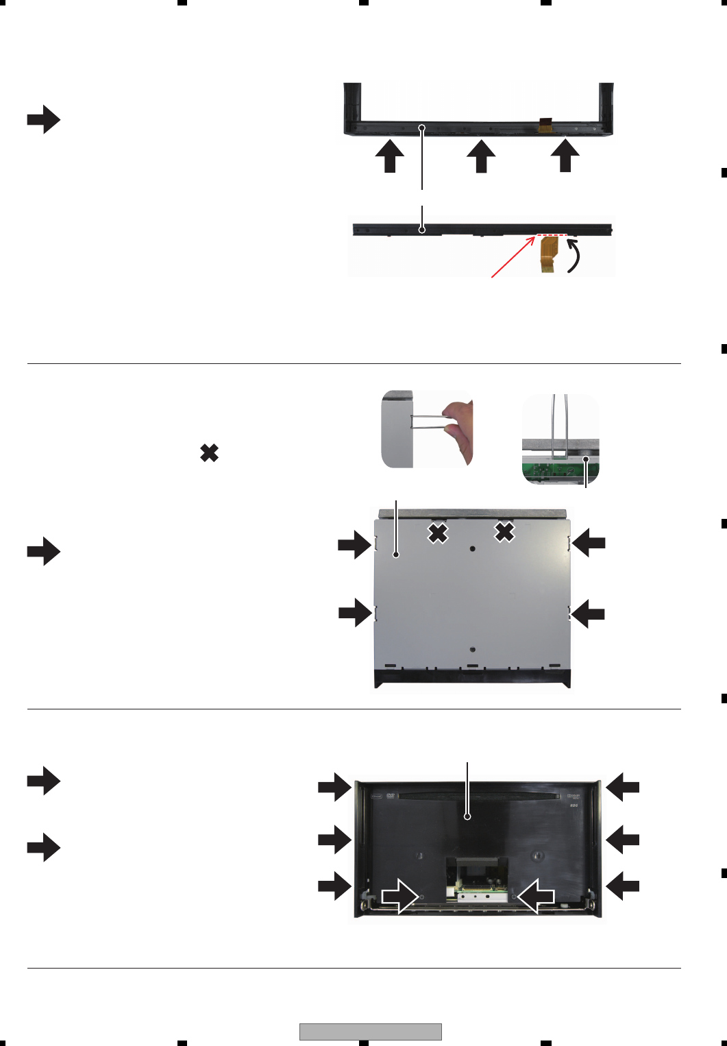
AVH-P4100DVD/XN/UC 97
5 678
5678
C
D
F
A
B
E
1
- Removing the Case (Fig.9, 10, 11)
Remove the four hooks with Tweezers
and then remove the Case.(Fig.11)
The hook is removed with Tweezers as shown in figure. (Fig.9)
Don’t remove from the hook of sign.(Fig.11)
Because the Holder may be deformed.(Fig.10)
- Removing the Keybord Unit (Fig.7, 8)
1
Attention when the Keyboard Unit are exchanged.(Fig.8)
• Bend the cable of a broken line part.
• Don’t bend it while rubbing right and left.
Remove the three hooks
and then remove the Keybord Unit.(Fig.7)
_ Refer to figure for how to bend the Cable.
_ Notes after exchanges.
The following items after the Keyboard Unit
are exchanged are checked.
• Lighting confirmation of all LED
• All switch operation confirmations
• Confirming the operation of the Remote Control Unit
- Removing the Panel Unit (Fig.12)
1
2
Remove the six screws.
Remove the two hooks
and then remove the Panel Unit.
1
1
1
1
111
1
1
1
1
11
2 2
Fig.9
Case
Fig.11
Fig.12
Fig.10
Holder
Fig.7
Fig.8
Keybord Unit
Panel Unit
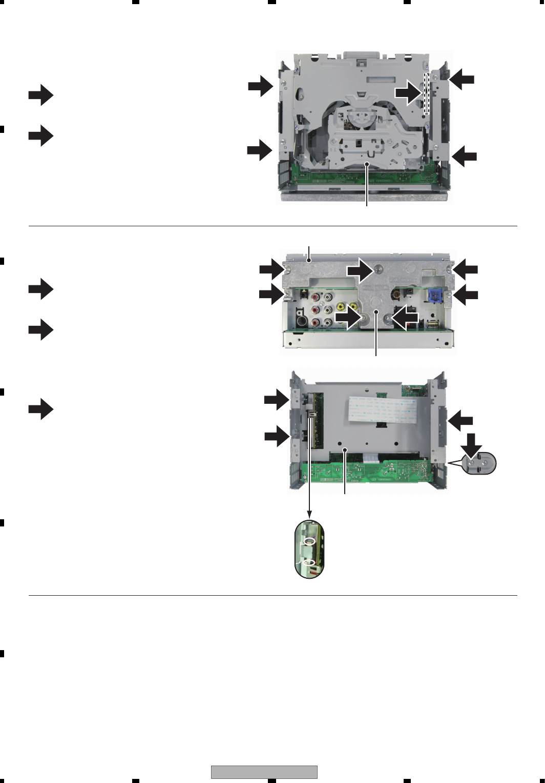
AVH-P4100DVD/XN/UC
98
1234
1234
C
D
F
A
B
E
1
2
Remove the four screws.
3
Disconnect the cable and then remove
the DVD Mechanism Module.
- Removing the DVD Mechanism Module (Fig.13)
- Removing the Chassis(Upper) (Fig.14, 15)
1Remove the two screws. (Fig.14)
2Remove the five screws
and then remove the Heat Sink. (Fig.14)
Remove the Holder. (Fig.14)
Remove the four screws
and then remove Chassis(Upper) while
holding both edges of the gasket. (Fig.15)
*If the gasket was damaged or lost,
replace it with the new one.
1
11
1
2
11
2
2
2
2
2
3
3
3
3
Fig.13
Fig.15
DVD Mechanism Module
Heat Sink
Holder
Fig.14
Chassis(Upper)
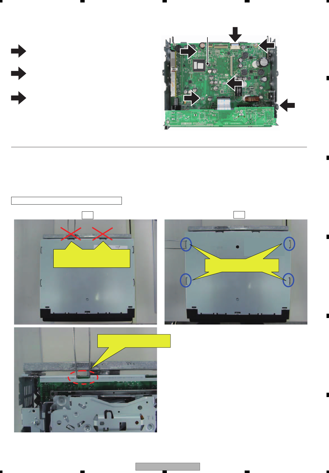
AVH-P4100DVD/XN/UC 99
5 678
5678
C
D
F
A
B
E
1
2
Remove the four screws
and then remove the Mother Unit.
3
Disconnect the cable.
Remove the screw.
1
2
3
3
3
3
- Removing the Mother Unit (Fig.16)
Fig.16
Mother Unit
NOTE: When you remove the top case
NG OK
Use these holes to remove the top
case.
REASON: The rear panel may be
deformed.
Don't put tweezers or something
into these holes to remove the top
case
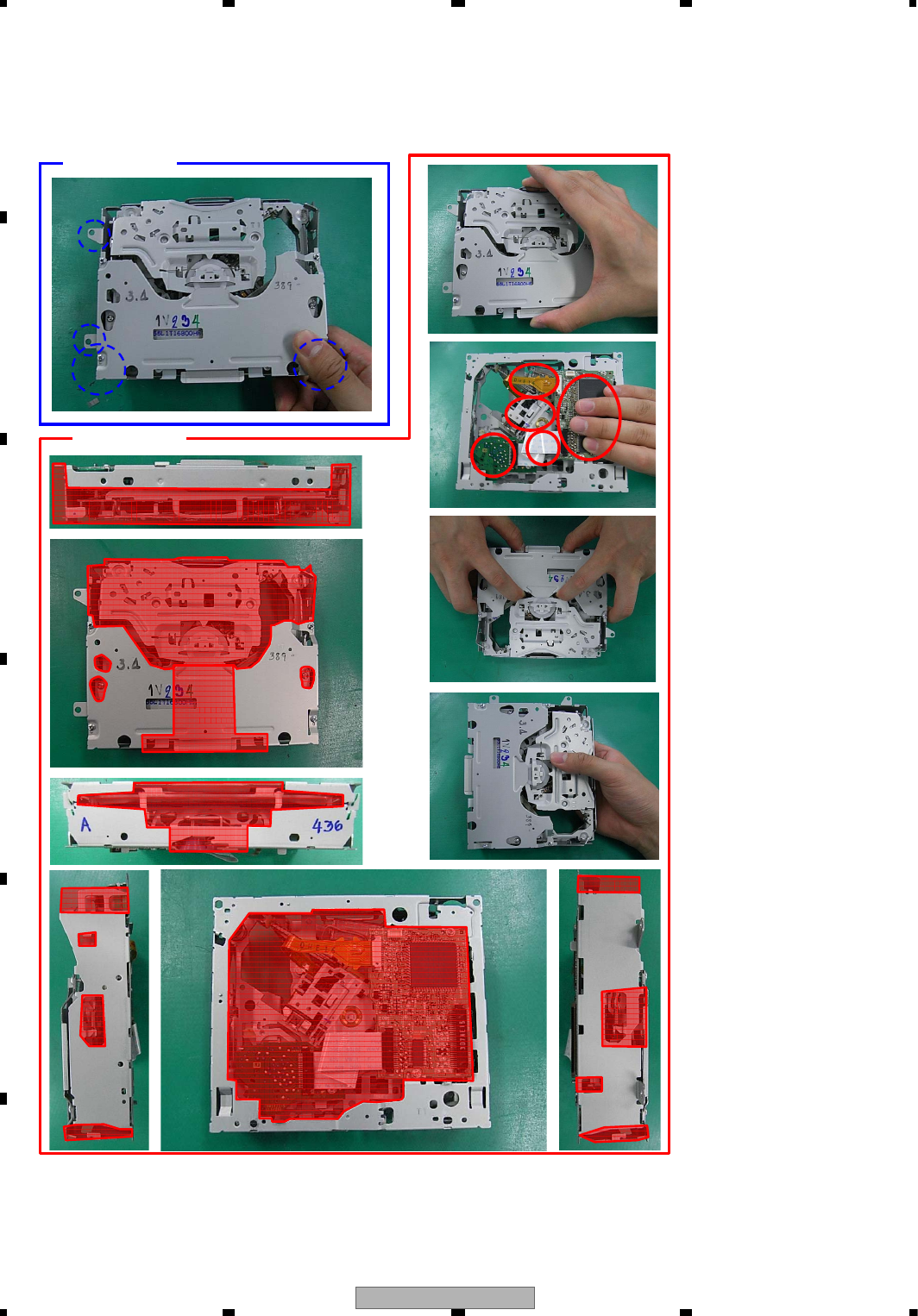
AVH-P4100DVD/XN/UC
100
1234
1234
C
D
F
A
B
E
1.Have a specified part.
Handling OK
Handling NG
How to have it
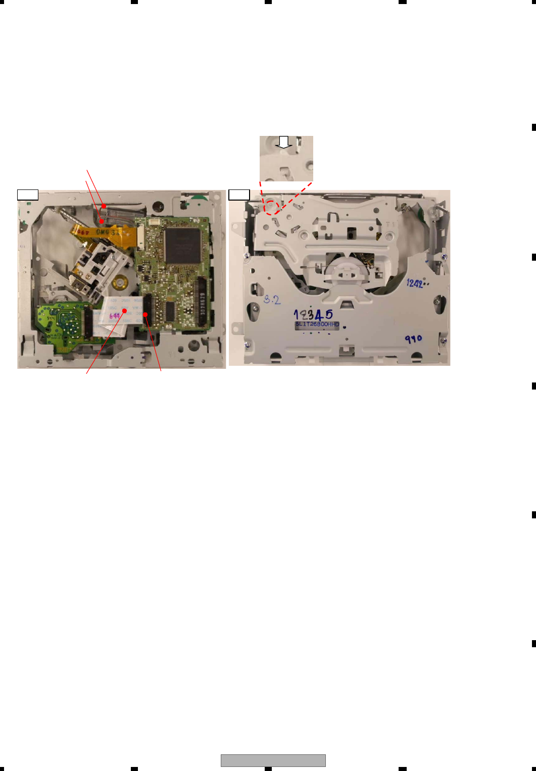
AVH-P4100DVD/XN/UC 101
5 678
5678
C
D
F
A
B
E
Connector (relay FFC)
Relay FFC
Fig. 1 Fig. 2
GND the brown line
4V to the gray line
Mecha Module_Bringing into the Clamp State with No Disc Loaded
1. Remove the relay FFC from the connector on the module PCB side (Fig. 1).
(Precaution) When it is difficult to apply 4V to the motor in procedure 2 below, remove the connector on the relay
PCB side, then remove the FFC, and remove the solder of the CRG motor lead and apply voltage to the lead.
2. Push the Disc detection arm while applying 4V to the CRG motor (Fig. 2)
By this action, the mecha moves to the clamp state and the PU moves to the outer periphery.
3. Stop the motor when the PU comes to the vicinity of the intermediate periphery.
(Precaution) If the PU goes to the outer most periphery, it idles.
It is not a problem, but please try not to let it idle as much as possible.
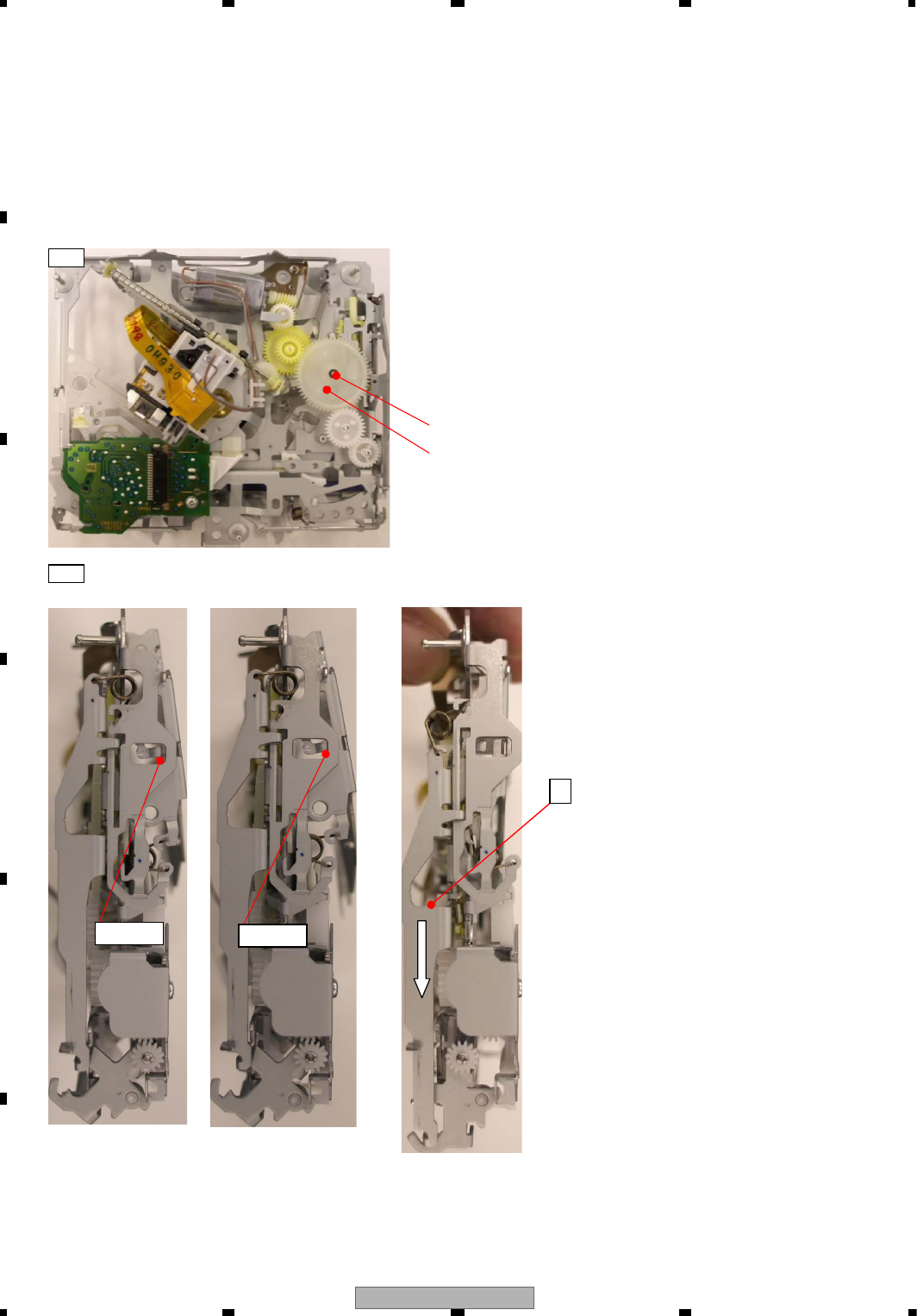
AVH-P4100DVD/XN/UC
102
1234
1234
C
D
F
A
B
E
T-case washer
Drive gear
Fig. 1
Fig. 2
b.Open-lock state
There is a
space There is
no space
c.Clamp state with no disc loaded
A
CRG Mecha_Bringing into the Clamp State with No Disc Loaded
1.Remove the T-case washer and then remove the drive gear. (Fig. 1)
2.Lift the clamp arm assy until it is in the state shown in Fig. 2_b (open-lock state).
3.Put your finger on the area A of Fig. 2_c and then slide it to the direction of the arrow (the direction of the playing state).
4.Push down the clamp arm.
(Precaution) When bringing the CRG mecha into the ejecting state again, install the drive gear after sliding the drive lever
and bringing it to the ejecting state, in order to prevent the cog of the pinion in the drive gear from chipping at the time of
its installation.
a.Ejecting state
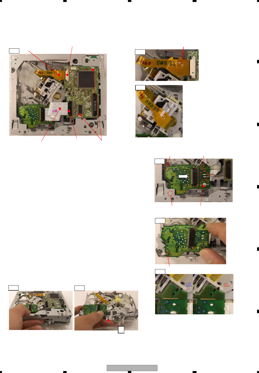
AVH-P4100DVD/XN/UC 103
5 678
5678
C
D
F
A
B
E
Connector (pick up FPC)
Connector
(Relay FFC)PCB clinch screw
Short-circuit
Fig.1
Fig. 2
Fig.3
Pick up FPC
Relay FFC
Fig. 4
Solder on the lead
Relay PCB clinch screw
Hook A
Hook B
Fig. 5
Hook B
Fig. 6
OK NG
Fig. 7 Fig. 8
A
Removing the Module PCB
1.Short-circuit two spots on the land of the pick up FPC. (Fig. 1)
2.Remove the pick up FPC and the relay FFC from the connector. (Fig. 2)
3.Temporarily attach the pick up FPC to the pick up rack. (Fig. 3)
(in order to prevent the damage to the pick up FPC)
4.Remove the two PCB clinch screws and then remove the module PCB. (Fig. 2)
Removing/Installing the Relay PCB
Removing)
1.Remove the relay FFC from the connector
(remove both sides so that the entire FFC will be removed). (Fig. 2)
2.Remove the solder on the lead for the CRG motor. (Fig. 4)
3.Remove the one relay PCB clinch screw. (Fig. 4)
4.Slide the relay PCB to the direction of the arrow and then remove
the relay PCB from the hook A and the hook B. (Fig. 4)
5.Turn the relay PCB over and then remove the SPDL motor FFC
from the connector.
Installing)
1.Check the mecha is in the ejecting state (disc-load suspended state).
When it is not in the ejecting state, apply 4V to the lead (motor) and
then bring it to the ejecting state (4V to the brown line and GND the gray line).
2.Fit the SPDL motor FFC to the connector (back of the relay PCB).
3.Hold the relay PCB so that it does not touch the SW knob as in Fig. 5.
4.Insert it into the hook B as it is a little off to the clockwise direction.
(Precaution) This is to prevent the SW knob from getting into the NG
position as in Fig. 6.
5.Push down the relay PCB lightly and then rotate it to the
counterclockwise direction.
It sets the relay PCB in the hook A and the positioning dowel.
(Precaution) Pay attention so the SW knob will not get onto the PU rack.
(Fig. 6)
6.As in the Figures, while supporting the location A with your fingers,
screw the relay PCB. (Fig. 7 / Fig. 8)
7.Solder the lead for the CRG motor.
8.Fit the relay FFC to the connector.
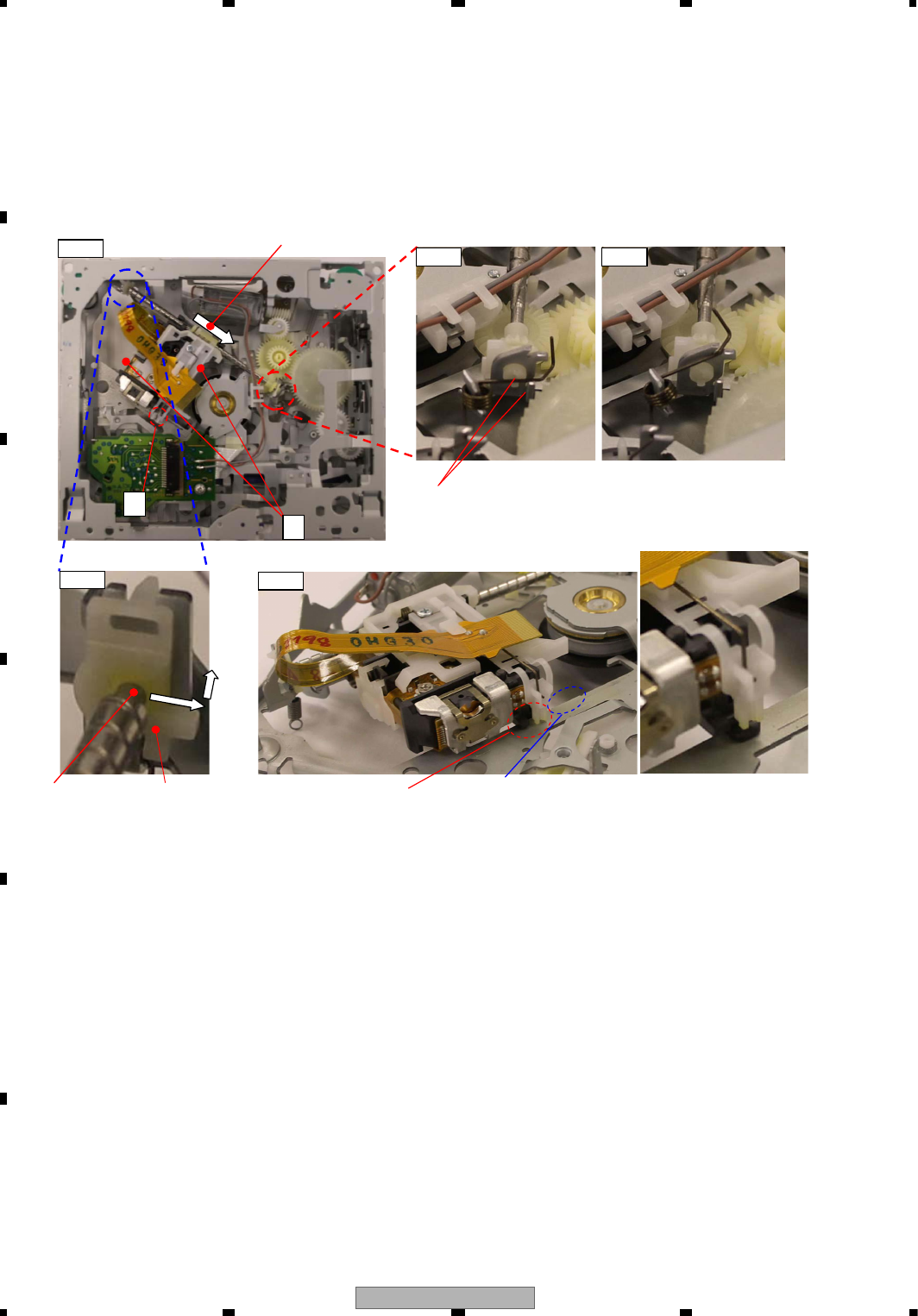
AVH-P4100DVD/XN/UC
104
1234
1234
C
D
F
A
B
E
Fig. 2a
Permanently hooked position Temporary hooked position
Fig. 2b
A
Slide to the direction of inner periphery
Fig. 1
Fig. 3
B
Fig.4
Regularly installed position Install avoiding the
area with blue broken
line (the connected
metal plate part)
The spring is installed under the resin flange and inside
the bended metal plate.
Outside holder
Back end of
the feed screw
Removing the PU Unit
1.Hook the feed screw biasing spring on the temporary hook (Fig. 2b). Be careful not to get injured by the tip of the spring.
2.Hold the PU at the location A in Fig. 1 and slide and scoot it to the direction of the inner periphery.
3.As in Fig. 3, shift the back end of the feed screw to the side and then to above and remove it from the outside holder.
4.Remove the tucking joint for the chassis at the location B and the PU unit by lifting them up without changing their
position and then remove the PU unit.
(Precaution) When installing the PU again, make sure to tuck the chassis in B and the PU unit (Fig. 4) first.
Moreover, do not forget to permanently hook the feed screw biasing spring (Fig. 2a).
Adjustments to the PU after its installation should be made according to the service manual.
Sending the PU to the outer periphery
1.Bring to the clamp state with no disc loaded according to the “Mecha Module_Bringing into the Clamp State with
No Disc Loaded” manual.
(Precaution) The relay FFC must be removed for certainty in order to prevent the IC damage.
2.Apply 1.5V to the CRG motor and then transfer the PU to the outer periphery.
(Precaution) Do not forget to reinstall the relay FFC after sending the PU to the outer periphery and take the
necessary measures.
[Installation NG]
The chassis is not tucked
between the PU case and the
PU rack.
AVH-P4100DVD/XN/UC 105
5 678
5678
C
D
F
A
B
E
8. EACH SETTING AND ADJUSTMENT
8.1 DVD ADJUSTMENT
1) Precautions
This product uses 5 V and 3.3 V as standard voltages.
The electrical potential that is the reference for signals,
is not GND, but VREF (approximately 2.2 V) and VHALF
(approximately 1.65 V) .
During product adjustments, if the reference voltage is
mistakenly taken as GND, and a grounding contact is
made, not only would it be impossible to measure the
accurate electrical potential, but also the servo motor
would malfunction, resulting in the application of a
strong impact on the pick up. The following precautionary
measures should be strictly adhered to, in order to
avoid such problems.
The reference voltage and GND should not be confused
when using the minus probe of a measurement device.
When an oscilloscope is being used special care should
be taken to make sure that the reference voltage is not
connected to the probe of ch1 (on the minus side),
while the probe of ch2 (on the minus side), is connected
to GND. Further, since the body frame of most measurement
devices have the same electrical potential as
the minus side of the probe, the body frame of the
measurement device should be set to floating ground.
If the reference voltage is connected to GND by
mistake, turn the regulator OFF immediately, or
turn the power OFF.
Remove the filters and wires used for measurements
only after the regulator has been turned OFF.
After the power supply is turned on, regulator ON the
following adjustment and measurement are promptly
done.
Whenever the product is in the test mode, the software
will not take any protective action. For this reason,
special care should be taken to make sure that no
mechanical or electrical shock could be applied to the
product when taking measurements in the test mode.
Whenever the EJECT key is pressed to eject the disk,
no other keys, other than the EJECT key, should be
pressed until the disk eject action has been completed.
Press the EJECT key only after the disk has stopped
completely.
If the product hangs up turn the power OFF immediately.
Laser didoes may be damaged, if the volume switch for
the laser power adjustment of the pick up unit, is turned.
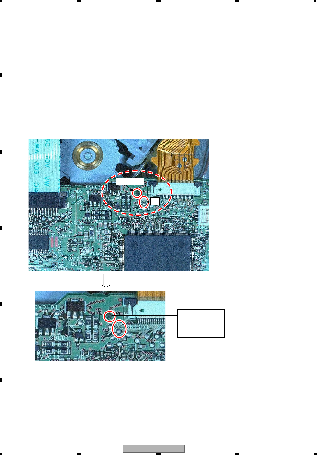
AVH-P4100DVD/XN/UC
106
1234
1234
C
D
F
A
B
E
Disc used:TDV-582
Measurement reference: AGND3
Measurement point: RF
Expansion
Oscilloscope
RF
AGND3
- SKEW adjustment
When one of the following replacements has taken place, SKEW adjustment for the pick up will be required.
(1) Replacement of the pick up unit
(2) Replacement of the spindle motor
(3) Replacement of the carriage chassis
(4) Replacement of the main shaft of the pick up unit
Measurement equipment and tools/jigs: Oscilloscope
Driver for SKEW adjustment -> Driver
Bond for fixing the SKEW -> GEM1033
Bond for resonance -> 1530 (1530 : produced by THREE BOND)
Bond for locking the screw -> 1401M (1401M : produced by THREE BOND)
Connection drawing
DVD core unit
Symptom in case the adjustment is not adequate: Worsening of the error rate 10
(Normally 10 or less.)
Large RF jitter
RF waveform distortion
Tracking drawing/Unstable servo
* Caution: Do not look into the laser light during adjustment.
-3
-4
RF
AGND3

AVH-P4100DVD/XN/UC 107
5 678
5678
C
D
F
A
B
E
TEST MODE
1: LD ON
2: ASMAX
3: Skew Adjustment
4: Error Rate
5: CRG Move Outer
6: Eject
Please Input Number
Skew Adjustment
Select “1: DVD Single Layer.”
Skew Adjustment
1: DVD Single Layer
5: Return
Please Input Number
There are two methods of making adjustment: a method of making adjustment through monitoring RF waves by the
oscilloscope (method 1) and a method of making adjustment through checking the numerical value of the RF level by
OSD (method 2).
Adjusting procedure is shown below, but regarding how to start the test mode and the operating procedure, please refer
to the clause on the service test mode.
Adjusting Procedure:
1. Install the pickup
(Refer to the removal of the pickup from the mecha unit.)
When handling the pickup, refer to the precautions on how to handle the PU listed below.
2. Method 1:
Connect the oscilloscope according to the AGND3 standards with reference to the connection diagram so that the RF
signals can be monitored.
Method 2:
The device does not need to be set. Proceed to the procedure 3.
3. Turn ON the power of the product.
4. Start the simplified FE test mode.
(Regarding how to start the test mode and the operating procedure, refer to the clause on the service test mode.)
5. Load the disc for adjustment (TDV582).
6. TEST MODE
Select “3: Skew Adjustment.”
Adjust the Skew using a driver while checking the RF value.
Refer to the following pages concerning the locations to make SKEW adjustment.
Method 1:
Slightly turn the skew adjusting screw A while checking the RF wave level by the oscilloscope and make
adjustment so the wave level would reach its maximum.
Next, slightly turn the skew adjusting screw B so the wave level would reach its maximum.
Slightly turn the skew adjusting screw A again so the wave level would reach its maximum.
(Make adjustment in the order of A->B->A and in the end complete adjustment by turning each screw
in the clockwise direction.)
Method 2:
Slightly turn the skew adjusting screw A while checking the value of the RF level through the OSD display so the wave
level would reach its maximum.
Next, slightly turn the skew adjusting screw B so the level would reach its maximum.
Slightly turn the skew adjusting screw A again so the level would reach its maximum.
(Make adjustment in the order of A->B->A and in the end complete adjustment by turning each screw in the
clockwise direction.)
AVH-P4100DVD/XN/UC
108
1234
1234
C
D
F
A
B
E
Skew Adjustment
1: Power OFF
RF Level : 000000
Please Input Number
Skew Adjustment
1: Power OFF
RF Level : 000000
Please Input Number
TEST MODE
1: LD ON
2: ASMAX
3: Skew Adjustment
4: Error Rate
5: CRG Move Outer
6: Eject
Please Input Number
TEST MODE
1: LD ON
2: ASMAX
3: Skew Adjustment
4: Error Rate
5: CRG Move Outer
6: Eject
Please Input Number
Switch arms
9. Skew Adjustment
Select “1: Power OFF.”
10. TEST MODE
Select “6: Eject.”
11. TEST MODE
Select “5: CRG Move Outer.”
12. In order to produce the clamping state with no disc loaded, slightly move the disc detection arm in the
counterclockwise direction while moving the switch arms outward.
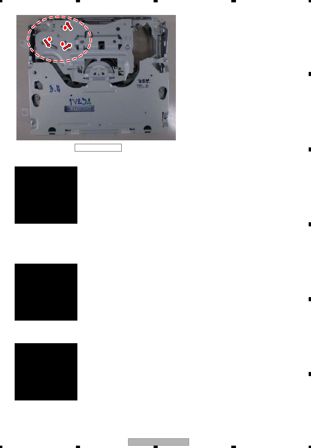
AVH-P4100DVD/XN/UC 109
5 678
5678
C
D
F
A
B
E
CRG Move Outer
1: DVD Single Layer
2: DVD Dual Layer
3: CD
4: CD-RW
5: Return
Please Input Number
CRG Move Outer
1: Power OFF
Please Input Number
TEST MODE
1: LD ON
2: ASMAX
3: Skew Adjustment
4: Error Rate
5: CRG Move Outer
6: Eject
Please Input Number
Disc Detection Arm
13. CRG Move Outer
Select “1: DVD Single Layer.”
The pickup moves to the outer periphery.
Apply the adhesive to fix the skew, the resonance adhesive and the screw lock.
Refer to the next page regarding the locations of adhesive joining.
14. CRG Move Outer
1: Power OFF
15. TEST MODE
Select “6: Eject.”
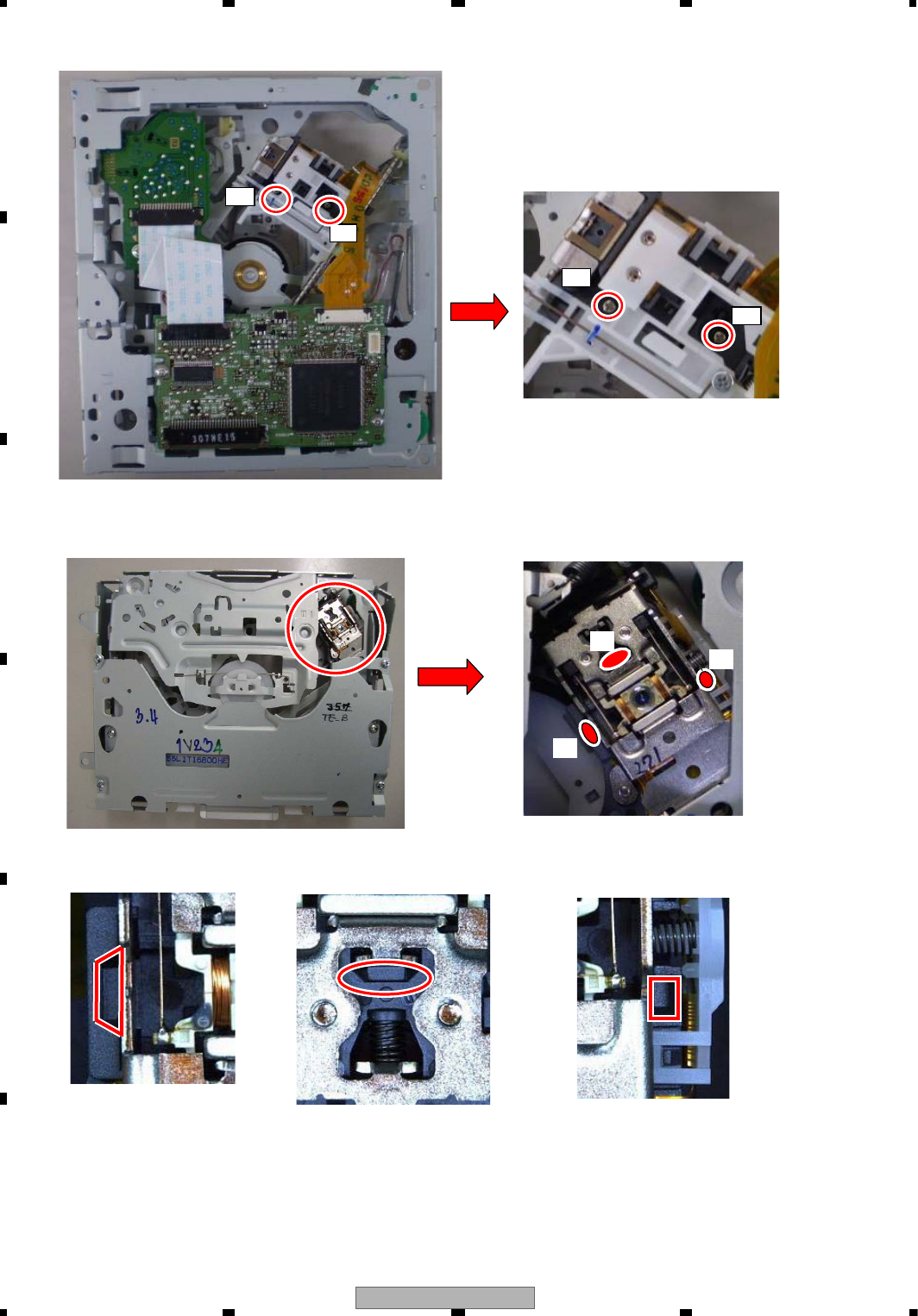
AVH-P4100DVD/XN/UC
110
1234
1234
C
D
F
A
B
E
A
B
A
B
1
12 3
Locations to make SKEW adjustment
Locations to adhere the SKEW 1,2,3: BOND QUICK MENDER
2
3
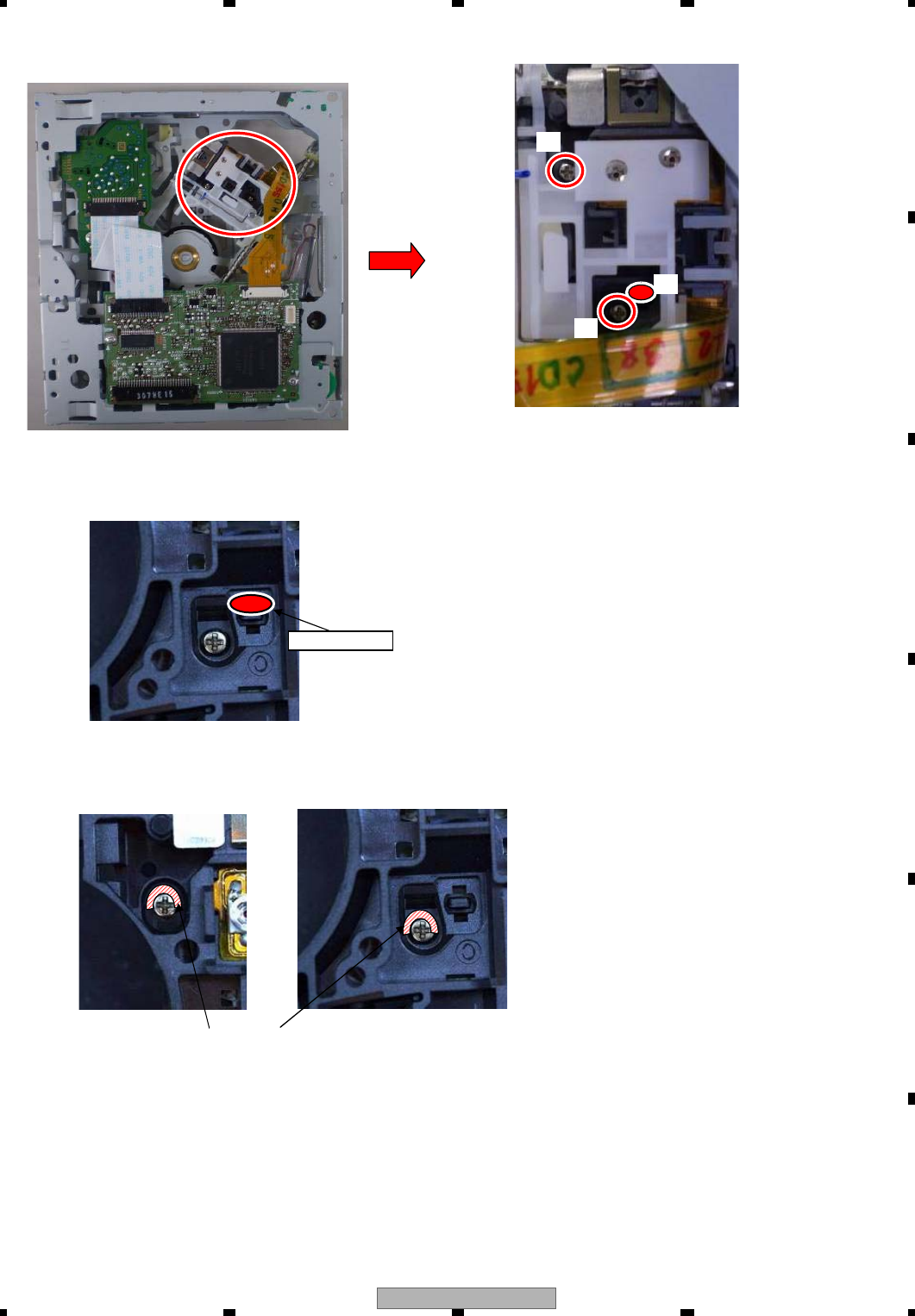
AVH-P4100DVD/XN/UC 111
5 678
5678
C
D
F
A
B
E
adhesive
Bond for resonance 4:Three Bond 1530
4
5
6
4
56
Bond for locking the screw 5,6 : Three Bond 1401M
Bond for locking the screw
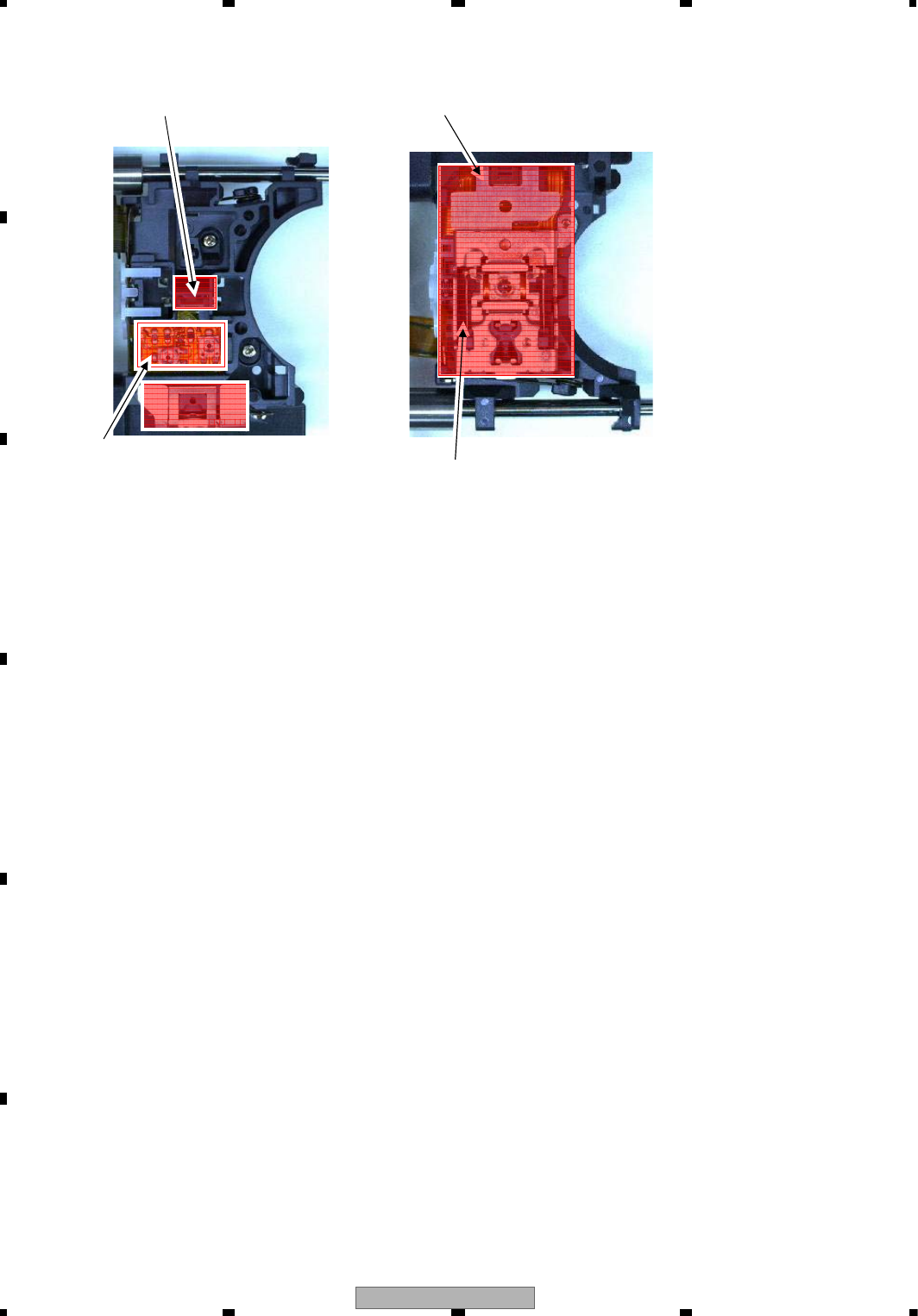
AVH-P4100DVD/XN/UC
112
1234
1234
C
D
F
A
B
E
Hologram (Beware of the static)
Do not touch the optical part
RF level adjusting part
Do not touch the spring
Precautions on handling the PU
*Precaution: Do not touch those shaded areas in the following figures.
.
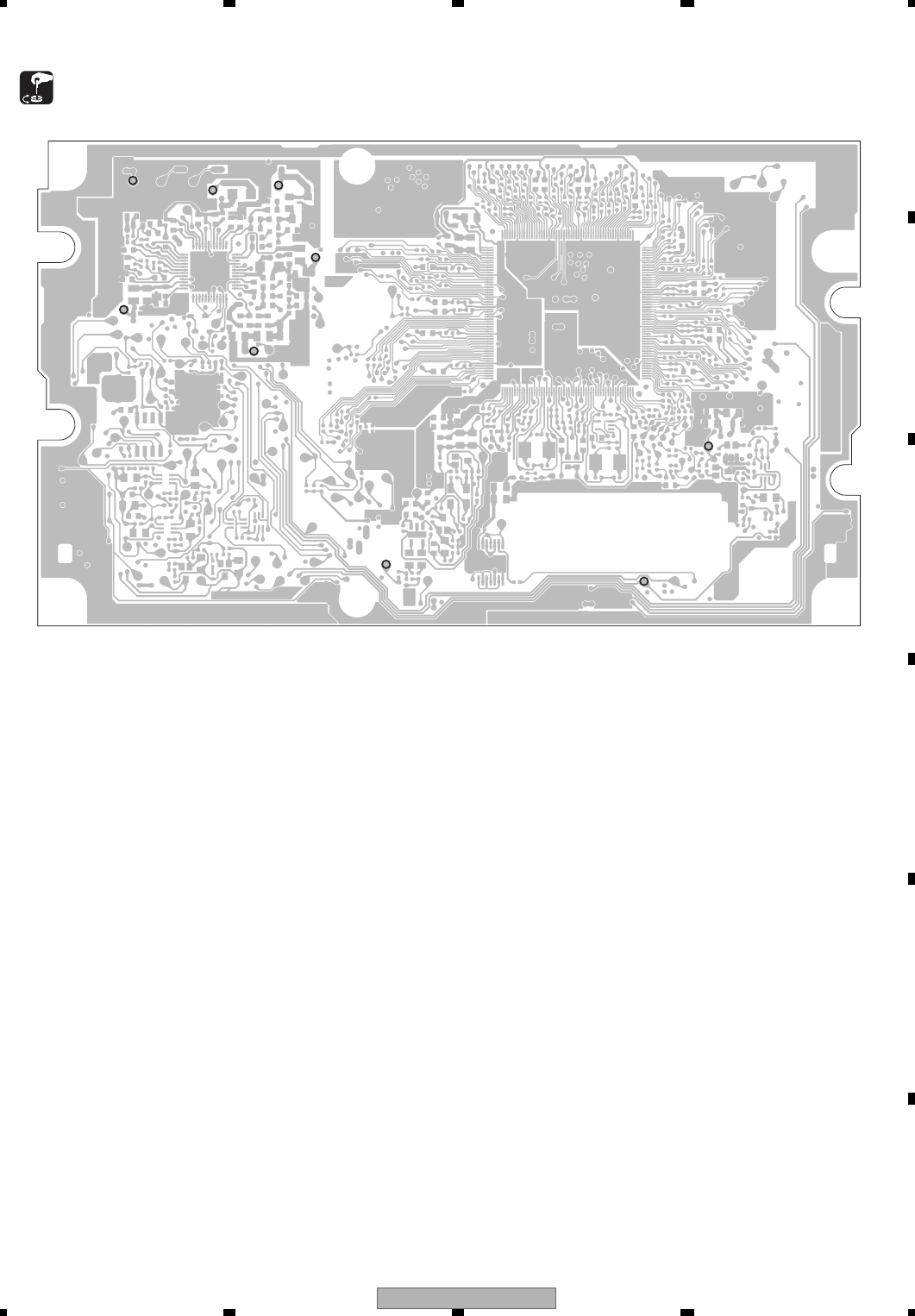
AVH-P4100DVD/XN/UC 113
5 678
5678
C
D
F
A
B
E
8.2 MONITOR UNIT ADJUSTMENT
- Adjustment Point
MONITOR UNIT(SIDE B)
PWRVI
VCC33
53V
8V
15V
-16V
COM
MONVBS
COMDC
AVH-P4100DVD/XN/UC
114
1234
1234
C
D
F
A
B
E
MONITOR UNIT ADJUSTMENT
NOTE:When shutting off the power supply of TC90A96BFGSING, be careful not to energize each IC terminal.
However , IIC lines(SDA and SCL) is not included in this case and it is possible to energize them with up 5 V.
No. Adustment item Input signal Measurement point
1 Check 3.3 V power TP:PWRVI TP:VCC33 -VCC33 = 3.3 ± 0.3 V
supply voltage to 14.4 V
2 Check 5.3 V power TP:PWRVI TP:53V -53V = 5.3 ± 0.3 V
supply voltage to 14.4 V
3 Check 8 V power TP:PWRVI TP:8V -8V = 8.0 ± 0.5 V
supply voltage to 14.4 V
4 Check 15 V power TP:PWRVI TP:15V -15V = 15.0 ± 0.2 V
supply voltage to 14.4 V
5
Check -16 V power
TP:PWRVI TP:-16V --16V = 16.35 ± 0.35 V
supply voltage to 14.4 V
6 Vcom amplifier No definition TP:COM - 5.80 ± 0.10 V Connect LCD panel for measurement
output amplitude
check
7 Tone voltage No definition 58pin of CN6001 -4.50 ± 0.30 V Connect LCD panel for measurement
amplitude
check V0
8 Tone voltage No definition 55pin of CN6001 -1.68 ± 0.20 V Connect LCD panel for measurement
amplitude
check V3
Adustment point Adustment Note
9 Tone voltage No definition 53pin of CN6001 - 0.121 ± 0.10 V Connect LCD panel for measurement
amplitude
adjustment V5
AVH-P4100DVD/XN/UC 115
5 678
5678
C
D
F
A
B
E
No. Adustment item Input signal Measurement point
51pin of CN6001 -
Adustment point Adustment Note
1.77 V ± 0.05 V
Tone voltage
amplitude
adjustment V7
10 No definition 1.262 ± 0.20 V Connect LCD panel for measurement
49pin of CN6001 -
Tone voltage
amplitude
adjustment V9
11 No definition 3.15 ± 0.20 V Connect LCD panel for measurement
48pin of CN6001 -
Tone voltage
amplitude
adjustment V10
12 No definition 3.43 ± 0.20 V Connect LCD panel for measurement
Screen -
Image check of
RGB signal
13 Input Color-bar
signal from
IC5702
-
DAC output -
Composite level
check
14 Input
composite
image 10-step
signal to
TP MONVBS
(2.0 Vpp ± 1%)
The amplitude of the 9-step
and the 0-step is
1.77 ± 0.05 V.
Screen -
Image check
15 Input
composite
image lamp
signal
(monochrome)
to TP MONVBS
Make sure that tone changes
smoothly, and there is no
colored area in the entire
display.
Execute to verify that IC5702 digital-out
is not bridged or "OPEN"ed.
Screen
Flicker adjustment
16 Output
black-white
50%
reverse signal
per 1 line
from IC5702
Adjust the flicker level to
minimum from all directions.
Adjustment point can be COM DC
off flicker adjustment mode.
TP COMDC
DC output

AVH-P4100DVD/XN/UC
116
1234
1234
C
D
F
A
B
E
8.3 PCL OUTPUT CONFIRMATION
- PCL output
In the normal operation mode (with the detachable panel installed, the ACC switched ON, the standby mode
cancelled), shift the TESTIN IC601(Pin 87) terminal to H.
The clock signal is output from the CLKOUT terminal IC601(Pin 62).
The frequency of the clock signal is 625 000 Hz that is one 32th of the fundamental frequency.
The clock signal should be 625 000 Hz (- 10 Hz, + 15 Hz).
If the clock signal out of the range, the X’tal (X601) should be replaced with new one.

AVH-P4100DVD/XN/UC 117
5 678
5678
C
D
F
A
B
E
9. EXPLODED VIEWS AND PARTS LIST
NOTES : Parts marked by " * " are generally unavailable because they are not in our Master Spare Parts List.
The > mark found on some component parts indicates the importance of the safety factor of the part.
Therefore, when replacing, be sure to use parts of identical designation.
Screw adjacent to mark on the product are used for disassembly.
For the applying amount of lubricants or glue, follow the instructions in this manual.
(In the case of no amount instructions,apply as you think it appropriate.)
""
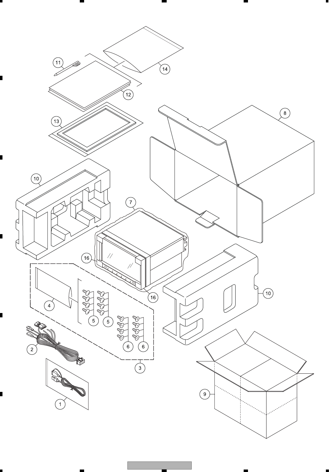
AVH-P4100DVD/XN/UC
118
1234
1234
C
D
F
A
B
E
9.1 PACKING(AVH-P4100DVD/XN/UC)
AVH-P4100DVD/XN/UC
AVH-P4100DVD/XN/UC 119
5 678
5678
C
D
F
A
B
E
PACKING(AVH-P4100DVD/XN/UC) SECTION PARTS LIST
Owner's Manual,Installation Manual
Mark No. Description Part No.
1 Cord Assy CDP1219
2 Cord Assy CDP1166
3 Screw Assy CEA2788
* 4 Polyethylene Bag CEG-127
5 Screw BMZ50P080FTC
6 Screw CMZ50P080FTC
7 Poly Bag CEG1402
8 Unit Box CHG6730
9 Contain Box CHL6730
10 Protector CHP3709
11 Pen CNV8969
12-1 Owner's Manual CRB2897
12-2 Owner's Manual CRB2898
12-3 Owner's Manual CRB2983
12-4 Installation Manual CRD4377
12-5 Caution Card CRP1387
* 16-6 Warranty Card CRY1276
13 Panel CNS9475
14 Polyethylene Bag CEG1426
15 •••••
16 Sheet CNN3089
Mark No. Description Part No.
Part No. Language
CRB2897 English
CRB2898 French
CRB2983 Spanish(Espanol)
CRD4377 English, French, Spanish(Espanol)
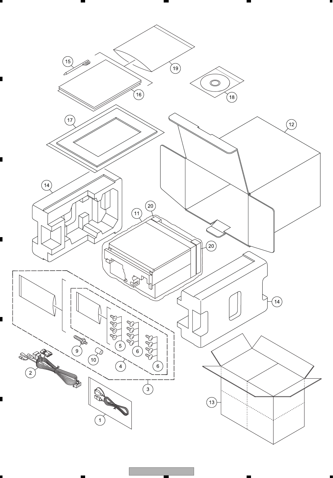
AVH-P4100DVD/XN/UC
120
1234
1234
C
D
F
A
B
E
9.2 PACKING(AVH-P4100DVD/XNEW5, XNUW5)
AVH-P4100DVD/XNEW5
AVH-P4100DVD/XNUW5
AVH-P4100DVD/XN/UC 121
5 678
5678
C
D
F
A
B
E
(1) PACKING(AVH-P4100DVD/XNEW5, XNUW5) SECTION PARTS LIST
(2) CONTRAST TABLE
AVH-P4100DVD/XNEW5 and AVH-P4100DVD/XNUW5 are constructed the same except for the following:
Owner's Manual,Installation Manual,Quick Start Guide
(3) CONTENTS OF CD-ROM (Operation Manual), CPJ1271
All operation manuals are supplied in PDF files by the CD-ROM. No printed papers are available.
Mark No. Description Part No.
1 Cord Assy CDP1040
2 Cord Assy CDP1167
* 3 Attachment Assy CEC1766
4 Screw Assy CEA9898
5 Screw CMZ50P080FTC
6 Screw BMZ50P080FTC
7 •••••
8 •••••
9 Screw CBA1650
10 Bush CNV3930
11 Poly Bag CEG1401
12 Unit Box See Contrast table(2)
13 Contain Box See Contrast table(2)
14 Protector CHP3708
15 Pen CNV8969
16-1 Installation Manual See Contrast table(2)
16-2 Quick Start Guide See Contrast table(2)
16-3 Quick Start Guide See Contrast table(2)
16-4 Owner's Manual See Contrast table(2)
16-5 Owner's Manual See Contrast table(2)
* 16-6 Caution Card See Contrast table(2)
* 16-7 Caution Card See Contrast table(2)
* 16-8 Passport See Contrast table(2)
16-9 Warranty Card CRY1279
17 Panel CNS9366
18 IM CD-ROM See Contrast table(2)
19 Polyethylene Bag CEG1426
20 Sheet CNN3089
Mark No. Description Part No.
Mark No. Description AVH-P4100DVD/XNEW5 AVH-P4100DVD/XNUW5
12 Unit Box CHG6728 CHG6729
13 Contain Box CHL6728 CHL6729
16-1 Installation Manual CRD4376 CRD4378
16-2 Quick Start Guide CRD4393 Not used
16-3 Quick Start Guide CRD4394 Not used
16-4 Owner's Manual Not used CRB2899
16-5 Owner's Manual Not used CRB2900
* 16-6 Caution Card CRP1389 Not used
* 16-7 Caution Card CRP1394 Not used
* 16-8 Passport CRY1268 Not used
18 IM CD-ROM CPJ1271 Not used
Part No. Language
CRD4393 English, Spanish(Espanol), German, French
CRD4394 Italian, Dutch
CRD4376 English, Spanish(Espanol), German, French, Italian, Dutch
CRB2899 English
CRB2900 Russian
CRD4378 English, Russian
Part No. Language
* CRB2878 English
* CRB2879 Spanish(Espanol)
* CRB2880 German
* CRB2881 French
* CRB2882 Italian
* CRB2883 Dutch
* CRB2884 Swedish
* CRB2885 Norwegian
* CRB2886 Finnish
* CRB2887 Danish
* CRB2888 Portuguese
* CRB2889 Greek
* CRB2890 Turkish
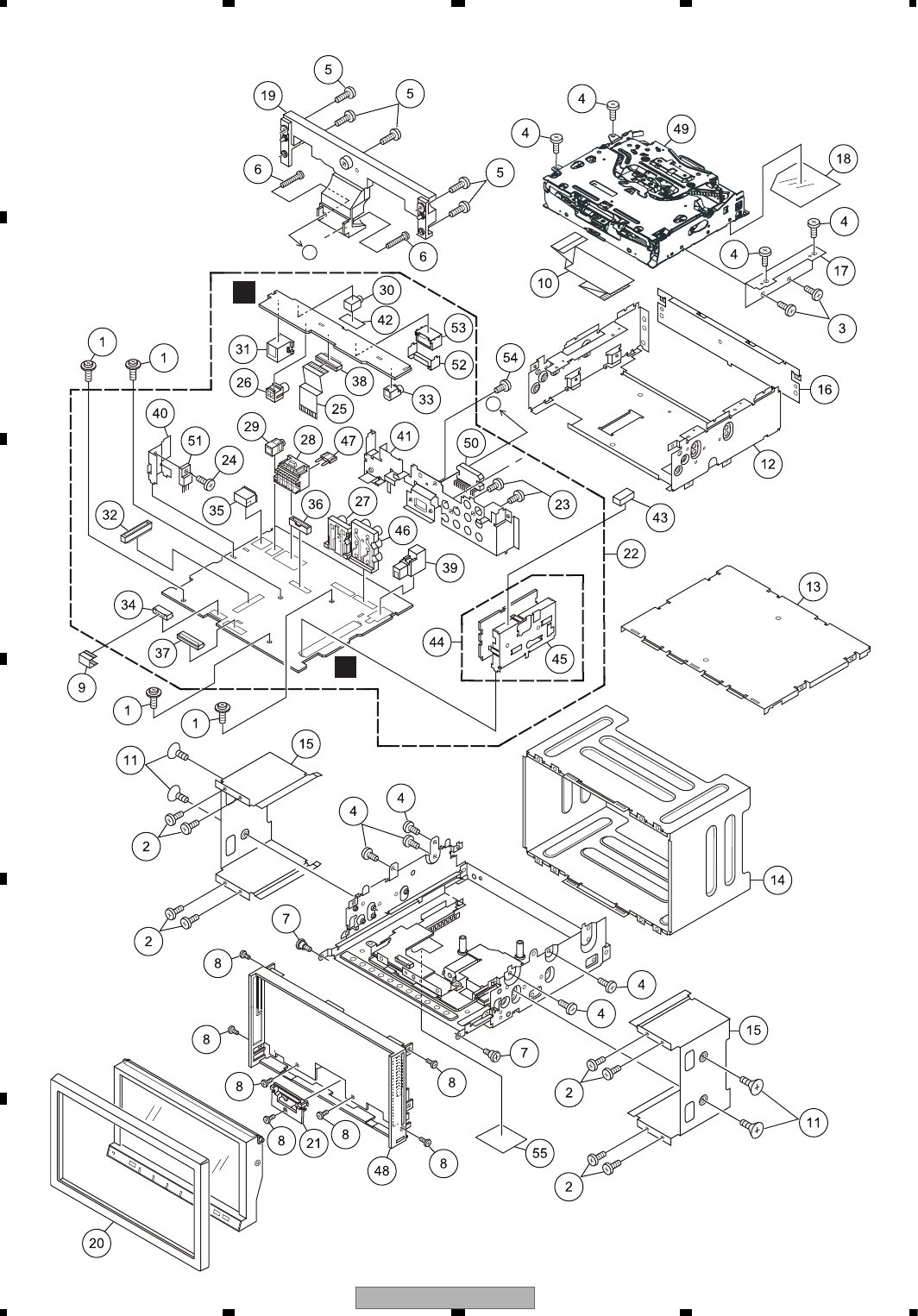
AVH-P4100DVD/XN/UC
122
1234
1234
C
D
F
A
B
E
9.3 EXTERIOR(1)
A
A
A
B
AVH-P4100DVD/XN/UC 123
5 678
5678
C
D
F
A
B
E
(1) EXTERIOR(1) SECTION PARTS LIST
(2) CONTRAST TABLE
AVH-P4100DVD/XN/UC, AVH-P4100DVD/XNEW5 and AVH-P4100DVD/XNUW5 are constructed the same except
for the following:
*If the gasket (No.43: CNN2782) was damaged or lost, replace it with the new one.
Mark No. Description Part No.
1 Screw ASZ26P050FTC
2 Screw See Contrast table(2)
3 Screw BMZ25P040FTB
4 Screw BSZ26P060FTC
5 Screw BSZ26P100FTC
6 Screw BSZ26P160FTC
7 Screw CBA1735
8 Screw(M2 x 3) CBA1877
9 FFC CDE8603
10 FFC CDE8746
11 Screw See Contrast table(2)
12 Chassis CNA3100
13 Case CNB3543
14 Holder See Contrast table(2)
15 Holder See Contrast table(2)
16 Holder CND4809
17 Holder CND4810
18 Insulator CNN2764
19 Heat Sink CNR1981
20 Panel See Contrast table(2)
21 Cover CNW1450
22 Mother Unit See Contrast table(2)
23 Screw BPZ26P080FTC
24 Screw BSZ26P060FTC
25 FFC CDE8747
26 Pin Jack(JA2003) CKB1065
27 Pin Jack(JA102) CKB1085
28 Plug(JA141) CKM1376
29 Jack(JA951) CKN1042
30 Jack(JA2002) CKN1077
31 Connector(JA2004) CKS3410
32 Connector(CN901) CKS3871
33 Connector(JA2001) CKS4124
34 Connector(CN801) CKS4178
35 Connector(CN522) CKS5669
36 Connector(CN121) CKS6051
37 Connector(CN501) CKS6062
38 Connector(CN2002) CKS6062
39 Antenna Jack(JA402) CKX1060
40 Holder CND4811
41 Holder See Contrast table(2)
42 Insulator CNN2307
43 Gasket CNN2782
44 FM/AM Tuner Unit(U401) See Contrast table(2)
45 Holder CND4324
46 Pin Jack(JA101) XKB7001
> 47 Fuse(10 A) YEK5001
48 Panel Unit See Contrast table(2)
49 DVD Mechanism Module(LS1) CXK6800
50 IC(IC181) PA2030A
51 IC(IC1061) NJM2388F84
52 Holder See Contrast table(2)
53 Connector(CN2001) See Contrast table(2)
54 Screw See Contrast table(2)
55 Sheet See Contrast table(2)
Mark No. Description Part No.
Mark No. Description
AVH-P4100DVD/XN/UC AVH-P4100DVD/XNEW5 AVH-P4100DVD/XNUW5
2 Screw Not used BMZ30P060FTC BMZ30P060FTC
11 Screw Not used CMZ50P080FTC CMZ50P080FTC
14 Holder Not used CND4337 CND4337
15 Holder Not used CND4338 CND4338
20 Panel Not used CNS9952 CNS9952
22 Mother Unit CWN3794 CWN3790 CWN3795
41 Holder CND4864 CND4864 CND4808
44
FM/AM Tuner Unit(U401)
CWE2098 CWE2097 CWE2097
48 Panel Unit CXE1738 CXE1736 CXE1736
52 Holder Not used Not used CND4814
53 Connector(CN2001) Not used Not used CKS4497
54 Screw Not used Not used BSZ26P060FTC
55 Sheet Not used CNN2947 CNN2947
AVH-P4100DVD/XN/UC
124
1234
1234
C
D
F
A
B
E
9.4 EXTERIOR(2)
A
A
E
F
EW5, UW5 UC
AVH-P4100DVD/XN/UC 125
5 678
5678
C
D
F
A
B
E
(1) EXTERIOR(2) SECTION PARTS LIST
(2) CONTRAST TABLE
AVH-P4100DVD/XN/UC, AVH-P4100DVD/XNEW5 and AVH-P4100DVD/XNUW5 are constructed the same except
for the following:
Mark No. Description Part No.
1 Screw(M2 x 3) CBA1877
2 Cover CNN2600
3 Cover CNN2601
4 Flexible PCB CNQ2709
5 Cover CNW1449
6 Touch Panel CSX1142
7 Button(RESET) CAI2199
* 8 Plate CNN2856
* 9 Grille See Contrast table(2)
10 Lighting Conductor CNW1445
11 Spacer CNW1446
12 Lighting Conductor CNW1458
* 13 Holder Unit CXE1268
14 Screw AMZ20P030FTC
15 Screw(M2 x 2) CBA1771
16 Holder CND4805
17 Holder CND4807
18 Insulator CNN2596
19 Insulator CNN2778
20 Monitor Unit See Contrast table(2)
21 Connector(CN5401) CKS5561
22 Connector(CN6101) CKS5561
23 Connector(CN5003) CKS5629
24 Connector(CN6001) CKS5773
25 Connector(CN5001) CKS5957
26 LCD CWX3691
27 Case Unit CXE1249
28 Cushion CNN1325
29 Screw IMS20P030FTC
30 Cord Assy CDP1167
31 Cap CNS1472
32 Resistor RS1/2PMF102J
* 33 Button Unit CXE1271
34 Spacer CNN3066
35 Spacer See Contrast table(2)
36 Keyboard Unit See Contrast table(2)
Mark No. Description Part No.
Mark No. Description
AVH-P4100DVD/XN/UC AVH-P4100DVD/XNEW5 AVH-P4100DVD/XNUW5
* 9 Grille CNS9812 CNS9812 CNS9665
20 Monitor Unit CWN3797 CWN3797 CWN3796
35 Spacer Not used Not used CNN2602
36 Keyboard Unit CWN3798 CWN3798 CWN3800
AVH-P4100DVD/XN/UC
126
1234
1234
C
D
F
A
B
E
9.5 EXTERIOR(3)
G
(A)
(B)
(C)
(A)
(A)
Spreads it
on the entire
gear
(A)
(A)
(A)
(A)
(A)
(A)
(A)
(A)
(B)
(C)
:
:
:
GEM1043
GEM1024
GEM1048

AVH-P4100DVD/XN/UC 127
5 678
5678
C
D
F
A
B
E
EXTERIOR(3) SECTION PARTS LIST
Mark No. Description Part No.
1 Drive Unit CXE1173
2 Screw AMZ26P030FTC
3 Screw BMZ26P030FTC
4 Screw(M2 x 2) CBA2129
5 Washer CBF1039
6 Screw EBA1049
7 Spring EBH1684
8 Spring EBL1031
9 Spring EBL1032
10 Slit board ENC1582
11 Bracket ENC1586
12 Insulator ENM1048
13 Spacer ENM1049
14 Insulator ENM1051
15 Arm(White) ENV1615
16 Gear ENV1616
17 Gear ENV1617
18 Gear ENV1618
19 Roller ENV1619
20 Rack ENV1620
21 Arm(Black) ENV1623
22 Frame Unit EXA1669
23 Motor Unit EXA1674
* 24 Chassis Unit EXA1687
25 Service PCB Assy EXX1058
26 Cord(White) EDC1024
27 Cord(Orange) EDC1025
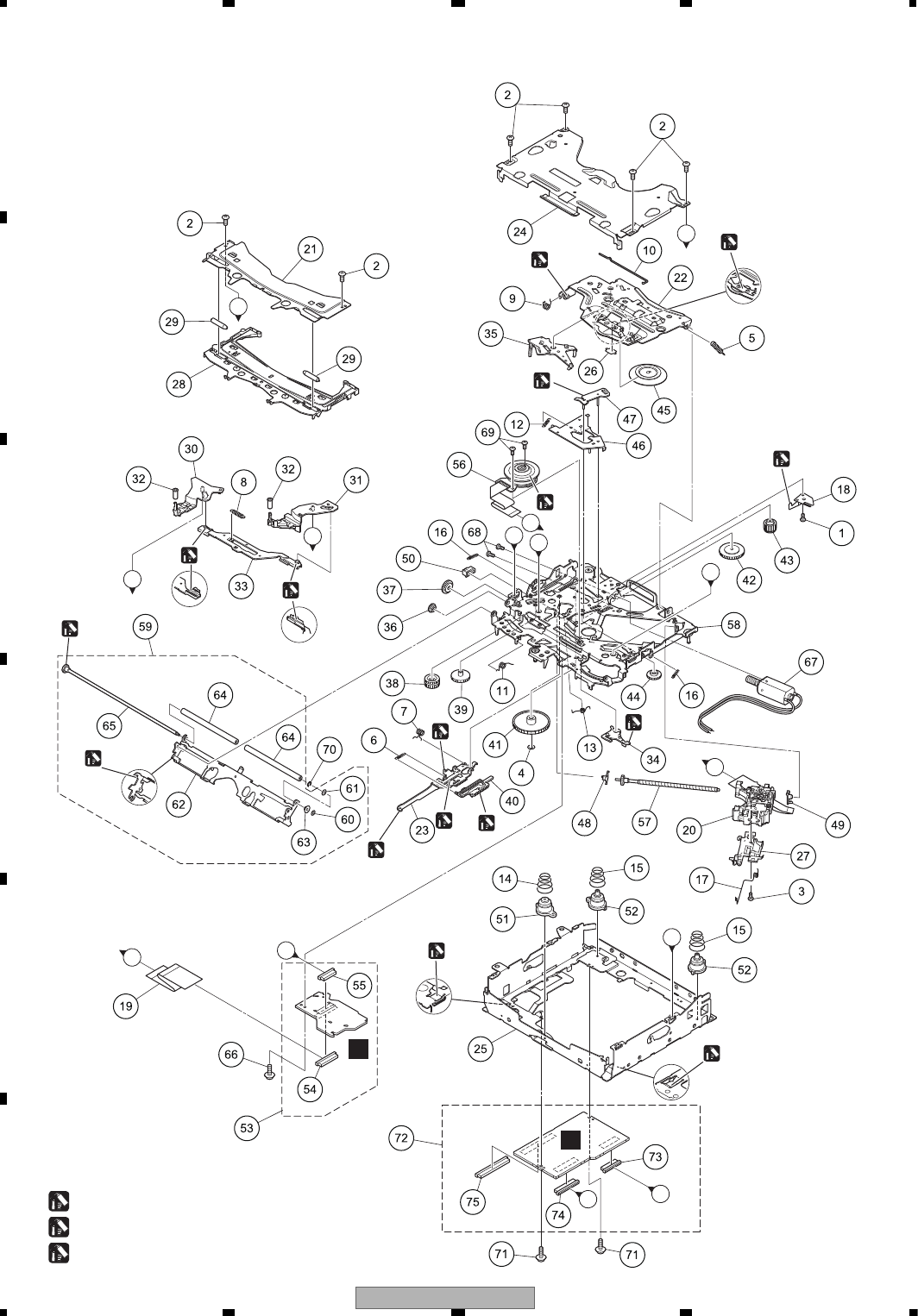
AVH-P4100DVD/XN/UC
128
1234
1234
C
D
F
A
B
E
9.6 DVD MECHANISM MODULE
A
C
D
D
F
E
C
B
A
B
E
G
F
G
C
D
(A) : GEM1045
(B) : GEM1038
(C) : GEM1024
(C)
(C)
(A)
(A)
(A)
(A)
(C)
(A)
(A)
(C)
(C)
(C)
(C)
(B)
(C)
(C)

AVH-P4100DVD/XN/UC 129
5 678
5678
C
D
F
A
B
E
DVD MECHANISM MODULE SECTION PARTS LIST
Mark No. Description Part No.
1 Screw BMZ20P020FTC
2 Screw BSZ20P040FTC
3 Screw(M2 x 4) CBA1835
4 Washer CBF1038
5 Spring CBH2860
6 Spring CBH3010
7 Spring CBH3011
8 Spring CBH3012
9 Spring CBH3013
10 Spring CBH3014
11 Spring CBH3015
12 Spring CBH3016
13 Spring CBH3017
14 Spring CBH3018
15 Spring CBH3019
16 Spring CBH3020
17 Spring CBH3030
18 Plate Spring CBL1797
19 Cable CDE8631
20 Service PU Unit CXX2398
21 Bracket CND4553
22 Arm CND4555
23 Lever CND4556
24 Frame CND4557
25 Frame CND4558
26 Sheet CNN2280
27 Rack CNW1170
28 Guide CNW1171
29 Roller CNW1172
30 Arm CNW1173
31 Arm CNW1174
32 Roller CNW1175
33 Lever CNW1176
34 Arm CNW1177
35 Arm CNW1178
36 Gear CNW1180
37 Gear CNW1181
38 Gear CNW1182
39 Gear CNW1183
40 Rack CNW1184
41 Gear CNW1185
42 Gear CNW1186
43 Gear CNW1187
44 Gear CNW1188
45 Clamper CNW1190
46 Arm CNW1191
47 Arm CNW1192
48 Holder CNW1193
49 Holder CNW1194
50 Holder CNW1195
51 Damper CNW1197
52 Damper CNW1198
* 53 Connect PCB Unit CWX3618
54 Connector(CN701) CKS6003
55 Connector(CN101) CKS6063
56 Motor Unit CXC4026
57 Screw Unit CXC8894
58 Chassis Unit CXC8895
59 Arm Assy CXC8896
60 Washer CBF1037
61 Washer CBF1038
62 Arm CND4554
63 Collar CNV6906
64 Roller CNW1196
65 Gear Unit CXC8893
66 Screw(M2 x 5) EBA1028
67 Motor EXM1050
68 Screw JFZ20P025FTC
69 Screw JGZ17P022FTC
70 Washer YE15FTC
71 Screw IMS20P030FTC
72 DVD Core Unit YWX5007
73 Connector(CN1101) CKS5775
74 Connector(CN1201) CKS6003
75 Connector(CN1901) CKS6025
Mark No. Description Part No.
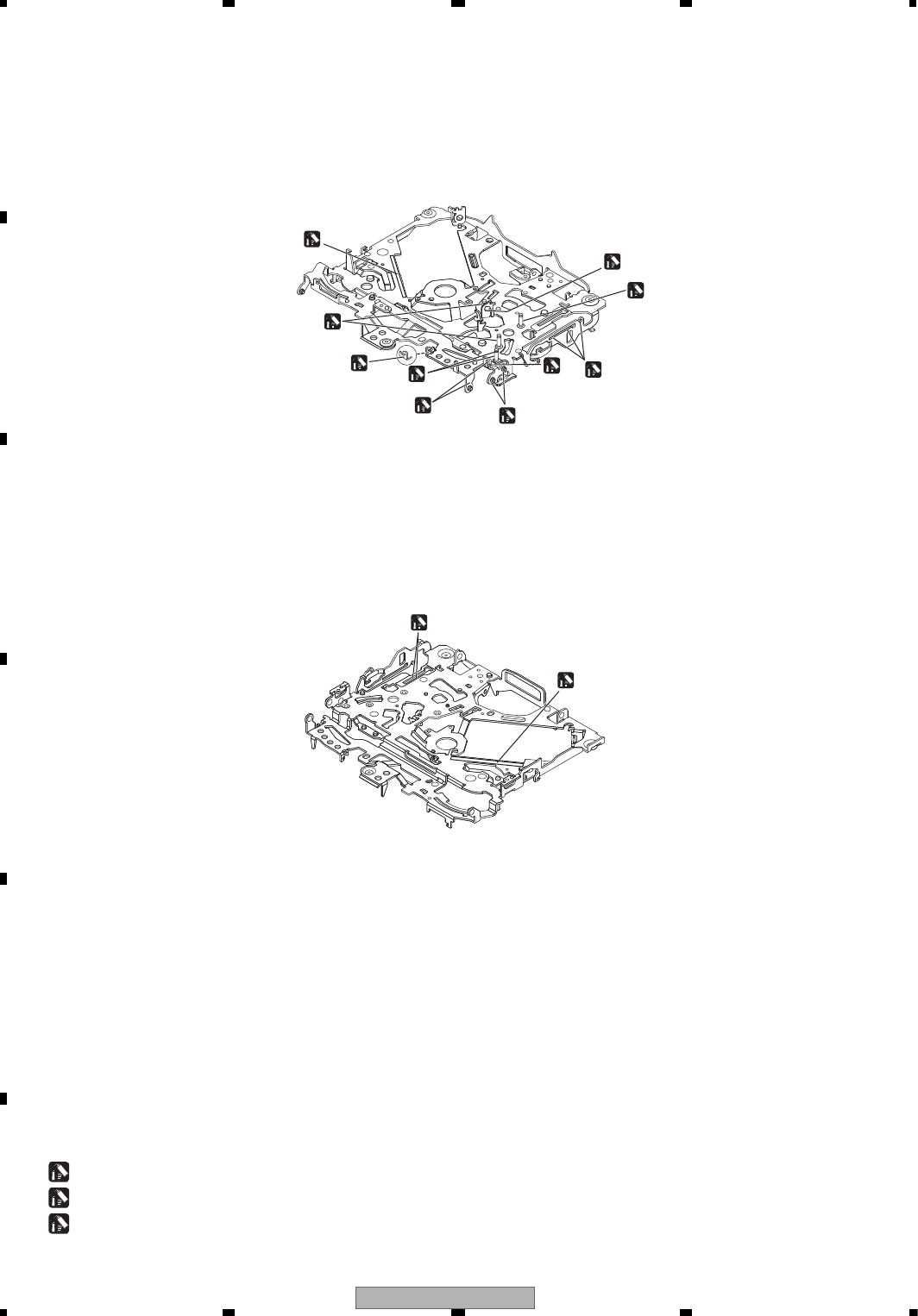
AVH-P4100DVD/XN/UC
130
1234
1234
C
D
F
A
B
E
(A) : GEM1045
(B) : GEM1038
(C) : GEM1024
(A)
(C)
(C)
(A)
(A)
(C)
(C)
(C)
(C)
(C)
(A)
(A)

AVH-P4100DVD/XN/UC 131
5 678
5678
C
D
F
A
B
E
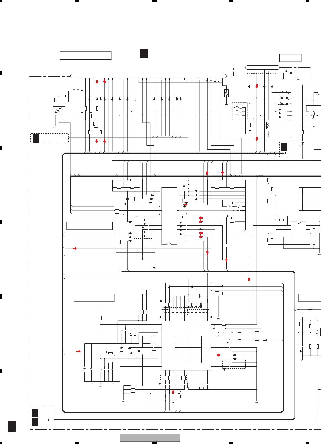
AVH-P4100DVD/XN/UC
132
1234
1234
C
D
F
A
B
E
10. SCHEMATIC DIAGRAM
10.1 MOTHER PCB(ANALOG)
Note: When ordering service parts, be sure to refer to " EXPLODED VIEWS AND PARTS LIST" or
"ELECTRICAL PARTS LIST".
1/4
A
PA_RL
PA_FR
EVSTB
EVSDT
PA_FL
PA_RR
LS_V
AVSCL
AVSDA
EVSCK
BUSL-
TUN_L
TUN_R
GNDBE2
RCA_SWR
RCA_SWL
LS_L
LS_R
RCA_RR
RCA_FR
RCA_RR
BUSR-
BUSR+
BUSL-
BUSL+
AUX_V
AUVGND
VCR_LGND
R_VOUT
BCAM_IN
VCR_V
VCR_VGND
ASENBO
VCR_L
AUX_R
VCR_RGND
AUAGND
VCR_R
AUX_L
BC_VGND
RCA_FL
RCA_RL
BUSL+
VCR_RGND
ONSEI-
TXNAVI
GUIDEON
TVON
ONSEI-
ONSEI+
GNDSIG
GNDSIG
RXNAVI
R_VOUT
VCR_R
ONSEI+
BUSR+
BUSR-
VCR_L
VCR_LGND
AUAGND
BUS-
BUS+
AUX_L
AUX_R
BCAM_IN
WIRED ANR
GNDSIG
ANG
ANB
CSYNC
GNDSIG
MAINTEST
WIREDAD
MONVBS
VCR_V
VCR_VGND
BC_VGND
AUX_V
AUVGND
CN121
GNDD
1
NAVI_TO_SYS
2
SYS_TO_NAVI
3
GUIDEON
4
TVON
5
NC
6
ONSEI-
7
ONSEI+
8
GNDAU
9
CCAUR
10
CCAUL
11
GNDSIG
12
CSYNC
13
GNDSIG
14
ANB
15
GNDSIG
16
ANG
17
GNDSIG
18
ANR
19
NC
20
WIRED
21
WIREDAD
22
GNDD
23
GNDV
24
BCAM_VGGND
25
BCAM_IN
26
AUXV
27
AUVGND
28
MAINTEST
29
AUXR
30
AUAGND
31
AUXL
32 BUSL-
33 BUSL+
34 GND
35
BUSR-
36
BUSR+
37
ASENSB0
38
BUS+
39
BUS-40
10u/10
C208
10u/10
C207
47u/16
C222
47u/16
C334
47u/16
C325
NM
C344
22u/16
C336
22u/16
C347
220u/4
C345
100u/6.3
C346
47u/16
C215
C342
C322
1u
C323
1u/10
C371
NM
C319 NM
C317 NM
C341
C339
C206
0.1u/10
C223
0.1u/10
C321
1u/10
C213 0.1u/10
C201
NM
C214 0.22u/6.3
C332 NM
C333 NM
C338
1u/10
C318 NM
C343
1u/10
C320 NM
C324
C340
C337
0.1u/10
C335 0.1u/10
C326 0.1u/10
C224 0.1u/10
C106
4.7u/10
C219
NM
C220
NM
C228 1u/10
C227
1u/10
C108
C203
NM
C329
C330
C327
C328
C209 1u/10
C226
NM
C218
NM
C211 1u/10
C212 1u/10
C202
1u/10
C210 NM
C205
1u/10
C204
1u/10
C308 0.1u/10
C307 0.1u/10
C306
0.1u
NM
C305
NM
C304 NM
C303 NM
C302 NM
C301 NM
C316
C315
C314
NM C313
C310
C312
C309
C311
NM
C110
0.1u/50
C109
C221
NM
C225
NM
C111
0.1u/50
C331 0.1u/10
D104
MALS068X
D105
MALS068X
D103
MALS068X
GNDV
GNDV
GNDA
GNDV
GNDA
GNDA
GN
GNDV
GNDD
GNDA
GNDA
GNDA
GNDV
GNDD
GNDA
GND
NM
IC202
OUT1
1
IN-1
2
IN+1
3
VEE
45
IN+2
6
IN-2
7
OUT2
8
VCC
IC201
PML018A
IN5-_L
1
IN5+_L
2
IN4+_L
3
IN4-_L
4
5
IN3_L
6
IN2_L
7
IN1_L
8
Vref
9
Vcc
10
Front_L
11
Rear_L
12
Pre/SW_L
13
Vp
14
Pref
15
PGND
16
Pre/SW_R
17
Rear_R
18
Front_R
19
DATA
20
CLK
21
STB
22
GND
23
IN1_R
24
IN2_R
25
IN3_R
26
IN4-_R
27
IN4+_R
28
IN5+_R
AN15887A
IC301
VCC1
1
BIAS1
2
GND1
3
L1-1
4
L1-2
5
R1-1
6
R1-2
7
L2-1
8
L2-2
9
VCC2
10
BIAS2
11 GND2
12
R2-1
13
R2-2
14
L3-1
15
L3-2
16
R3-1
17
R3-2
18
L4-1
19
L4-2
20
R4-1
21
R4-2
22
L5-1
23 L5-2
24
R5-1 25
R5-2 26
ROUT1 27
LOUT1 28
ROUT2 29
LOUT2 30
FB2 31
VOUT2 32
FB1 33
VOUT1 34
SDA
35
SCL
36
V1-1 37
V1-2 38
V2-1 39
V2-2 40
V3-1 41
V3-2 42
V4-1 43
V4-2 44
V5-1 45
V5-2 46
V6-1
47
V6-2
48
JA102
VCR_RG
1
VCR_RIN
2
VOUT_G
3
VOUT
4
VCR_LG
5
VCR_LIN
6
VCR_VG
7
VCR_VIN
8
JA
L201
2.2u
IMH23
Q105
C
1
B
2
E
3
C2 4
5
B1
6
E1
UMF23N
Q121
E1
1
B1
2
C2
3
E2
4
5
B2
6
C1
Q
R112
22k
R113
22k
R207 1k
R373
NM
R214
0
R323
NM
R222
NM
R217
NM
R218
NM
R225
NM
R324
NM
R208
0
R122
3.3k
R123
180
R204
1.6k
R211
2.7k
R127
22k
R121
5.6k
R128
1k
R205 1k
R224
NM
R223
NM
R124
180
R319 NM
R126
22k
R215
NM
R213
NM
R203
NM
R201
NM
R125 2.2k
R328
0
R322
100
R330
R306
R305
R316
R329
R312
100
R310 100
R303
R302
R301
R220
2.7k
R216
NM
R371
NM
R372
NM
R315 NM
R307
22k
R317
68
R318
4.7
R304
R313
R326 220
R314
22k
R206 1k
R311
100
R212
2.7k
R320 NM
R209
1.6k
R327
0
R115
75
R219
1.6k
R210
1.6k
R111
82
R309 NM
R129
1k
R308 0
R202
2.7k
R325 220
R321 NM
R221
0
TP109
TP104
TP102
TP108
TP106
TP105
TP107
TP103
BUP_1
EV12
SYS+B
SYS+B
SY
SYS+B
ANALOGBUS
AUX_EXT
NAVI_EXT
GNDA
GNDRF
GNDD
R378
0
C216 0.1u/16
D301
RB551V-30
D302
RB551V-30
P130
NM
12
P131
12
P132
12
miniSMDC075F/24
P102
12
miniSMDC075F/24
P121
12
uCOM BUS
mini
-
mini
VIDEO
VCR
4
3
VCR
5
AUDIO
2
6
1 LS1
E.VOL CAPTAIN6
MONITOR
14.4V
8.3V
12.2V
8.3V
8.3V
IP-BUS&NAVI&WIRED VCR IN
B.CAM x
-
-
-
NAVI GUIDE
1
TUNER
4
5
3
2 AV SEL
E.VOL INPUT
IP_BUS
LS1
AV SELECTOR
-
2
1
1
3
1
1
3
1
FOR SERVICE
3/4
A
2/4
A
3/4
A
3/4
A
BCN2002
E.VOL INPUT
FM(UC):-14.0 dBs
AM(UC):-24.0 dBs
FM(EW5):-10.0 dBs
AM(EW5):-20.0 dBs
IP-BUS: +2.2 dBs
AUX: +2.2 dBs
USB(AUX): +0.9 dBs
USB(LS1): +5.1 dBs
VCR: +2.2 dBs
DVD/CD: +5.1 dBs
VCR:+8.2 dBs
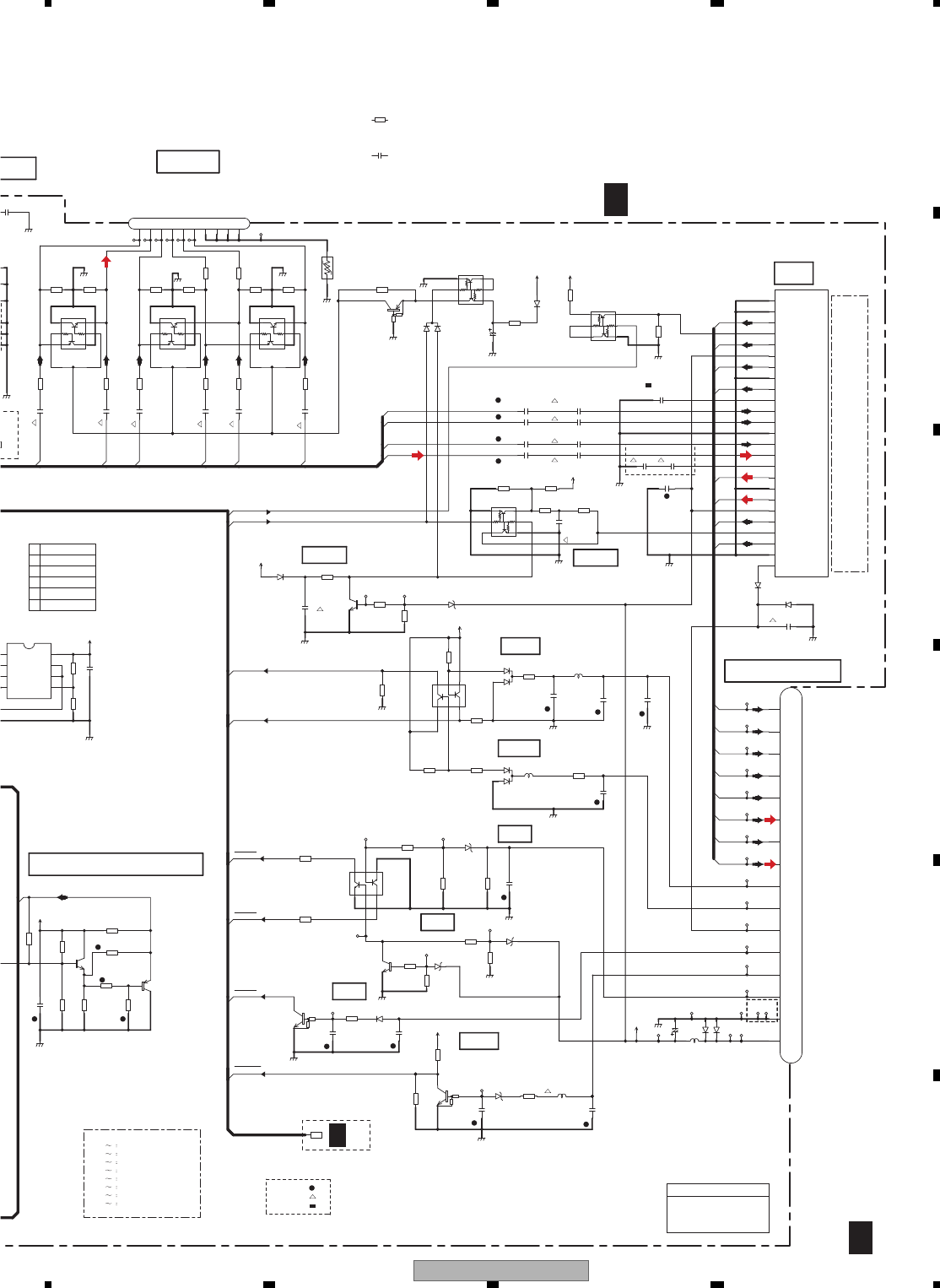
AVH-P4100DVD/XN/UC 133
5 678
5678
C
D
F
A
B
E
1/4
A
ISENS
SYSMUTE
SYSMUTE
PBSENS
TELMUTE
BGSENS
OFFMUTE
FR-
FR+
FL-
FL+
RL+
RL-
RR-
RR+
FR+
FR-
RR-
RR+
FL+
FL-
RL+
RL-
BSENS
ASENS
RCA_RR
RCA_RL
RCA_FR
RCA_FL
RCA_SWL
RCA_SWR
PA_FL
PA_FR
PA_RR
PA_RL
MONVBS
AMPPW
100u/16
C103
3300u/16 C141
C192
0.1u/50
C371
NM
C162
0.1u/50
C165
0.01u/50 C186
4.7u/10
C163
0.1u/50
C142
0.1u/50
C167
0.1u/50 C166
0.1u/50
C161
1u/10
C184
0.47u/16
C182
0.47u/16
C185
0.47u/16
C164
0.1u/50
C193
10u/35
C194
2.2u/16
C191
2.2u/16
C183
0.47u/16
C189
0.47u/16
C187
0.47u/16
C190
0.47u/16
C188
0.47u/16
C181
DCH1201-A
10u
C104
4.7u/10
C102
4.7u/10
C105
4.7u/10
C106
4.7u/10
C107
4.7u/10
C101
4.7u/10
C217
NM
C168
NM
C195
0.1u/50
C111
1u/50
D142
S1G-6904G2P
D181
MA111
D161
MA111
D102
MA111
D141
S1G-6904G2P
D183
S1G-6904G2P
D184
S1G-6904G2P
D164
DAN202U
D165
DAN202U
D101
DAN202U
D163
HZU7L(C3)
D166
UDZS5R6(B)
D162
HZU7L(A1)
D182
UDZS8R2(B)
X
X
X
GND
GNDD
GNDD
GNDD
GNDD
GNDD
GNDD
GND
GNDA
GND
GNDA
GNDD
GNDV
GND
GNDA
GNDA
GNDA
GNDA
GNDA
GNDA
GND
GNDA GNDA
GNDA
GNDA
NM
IC202
OUT1
1
IN-1
2
IN+1
3
VEE
45
IN+2
6
IN-2
7
OUT2
8
VCC
JA101
REAR_R
REAR_L
SW_R
SW_L
FRONT_R
FRONT_L
GND
GND
GND
GND
1
2
3
4
5
6
7
8
9
10
JA141
1
2
3
4
5
6
7
8
9
10
11
12
13
14
15
16
L162
2.2u
L161
2.2u
L163
CTF1295-A
DTC114EUA
Q161
DTC114EUA
Q164
DTA124EUA
Q102
N1XMU
261Q
E1
1
B1
2
C2
3
E2
4
5
B2
6
C1
UMD2N
Q103
2E 1
2B 2
1C 31E
4
51B
62C
UMH1N
Q182
E1 1
B1 2
C2 3E2
4
5B2
6C1
UMT1N
Q163
E1
1
B1
2
C2
3
E2
4
5
B2
6
C1
IMH23
Q101
C1
1
B2
2
E2
3
C2 4
5
B1
6
E1
IMH23
Q105
C1
1
B2
2
E2
3
C2 4
5
B1
6
E1
IMH23
Q104
C1
1
B2
2
E2
3
C2 4
5
B1
6
E1
Q371
NM
Q181
2SC4081(QRS)
NM
Q372
R117 0
R374
NM
R376
NM
R112
22k
R113
22k
R109
22k
R108
22k
R103
22k
R102
22k
R120
1k
R172
100k
R373
NM
R375
NM
R165
47k
R168
47k
R182
100k
R169
NM
R183
47k
R224
NM
R223
NM
R161
10k
R177
0
R178
0
R181
10k
R166
47k
R187
10k
R371
NM
R372
NM
R188
100
R176
15k
R101
82
R104
82
R162
47k
R173
4.7k
R105
NM
R175
10k
R170
47k
R185
1.5k
R186
68k
R163
10k
R184
68k
R107
82
R189
47k
R110
82
R164
100k
R111
82
R114
82
R167
47k
R171
4.7k
R118 0
R174
10k
TP170
TP171
TP164
TP159
TP173
TP156
TP157
TP162
TP155
TP158
TP161
OFFMUTE1
TP168
TP163
TP175
TP154
TP176
RCAGND
RCA_RR
RCA_RL
RCA_SWR
RCA_SWL
RCA_FR
RCA_FL
TP167
TP165
TP174
TP166
TP177
TP172
TP181
TP160
TP169
BUP_1
SYS+B
SYS+B
BUP_1
ACC33
SYS+B
SYS+B
SYS+B
ACC33
EXT
uCOMBUS
GNDA
L141
CTH1221-A
R378
0
UMD3N
Q183 E1
1
B1
2
C2
3
E2 4
5
B2
6
C1
R377
NM
IC181
PA2030A
TAB
1
PW-GND2
2
OUT2(-)
3
STBY
4
5OUT2(+)
6VCC2
7OUT1(-)
8PW-GND1
9OUT1(+)
10 RIPPLE
11 IN1
12 IN2
15 IN3
16 AC-GND
17 OUT3(+)
18 PW-GND3
19 OUT3(-)
20 VCC1
21 OUT4(+)
22 MUTE
23 OUT4(-)
24 PW-GND4
25 H-SW/VOS-DET
13 PRE-GND
14 IN4
GND1
GND2
TP178
GNDD
Q165
2SC4081(QRS)
R179
10k
R180
10k
D167
UDZ20(B)
TP179
miniSMDC075F/24
P101
1 2
8.PW.GND1
20.VCC3/4
AMPMUTE
2.PW.GND2
ASENS
10.SVR
25.B.REMOTE
PW CONNECTOR
18.PW.GND3
TELMUTE
4.STBY
7.RL-
6.VCC1/2
BSENS
15.RLIN
5.RR+
PBSENS
21.FR+
11.FLIN
23.FR-
13.S-GND
12.FRIN
22.MUTE
17.FL+
1.TAB
AMP
3.RR-
24.PW.GND4
9.RL+
16.ACGND
14.RRIN
ISENS
19.FL-
OFFMUTE
BGSENS
RCAOUT
P.B.
BGSENS
FR+
RR+
RL+
RL-
FL-
ILM
FR-
GND
B.UP
ACC
FL+
RR-
COM BUS
MONITOR VBS ADJUST
MUTE
B.REM
(CCG1236-A)
2125
3216
1608
CHIP SIZE LEGEND
CEAT332M16-P35
8.3V14.4V
8.3V
8.3V
3.3V
3.3V
14.4V
8.3V
R IN
NAVI GUIDE
1
TUNER
4
5
3
2 AV SEL
E.VOL INPUT
IP_BUS
LS1
201 E.VOL CAPTAIN6
141 PW CONNECTOR
161 SENS
301 AV SELECTER
101 RCAOUT MUTE&VCRIN
181 AMP
371 MONITOR VBS ADJUST
121 IP-BUS&NAVI&WIRED
SIDE_A
(D)
(D)
600uH
3/4
A
3/4
MOTHER PCB(ANALOG)
1/4
A
MOTHER UNIT
Consists of
MOTHER PCB
IF PCB
Symbol indicates a resistor.
No differentiation is made between chip resistors and
discrete resistors.
NOTE :
Symbol indicates a capacitor.
No differentiation is made between chip capacitors and
discrete capacitors.
NM : No Mount
FM(UC):+29.1 dBs
AM(UC):+19.1 dBs
FM(EW5):+33.1 dBs
AM(EW5):+23.1 dBs
IP-BUS:+35.3 dBs
AUX:+35.3 dBs
USB(AUX):+34.0 dBs
USB(LS1):+35.2 dBs
VCR:+35.3 dBs
DVD/CD:+35.2 dBs
FM(UC): +7.1 dBs
AM(UC): -2.9 dBs
FM(EW5):+11.1 dBs
AM(EW5): +1.1 dBs
IP-BUS:+13.3 dBs
AUX:+13.3 dBs
USB(AUX):+12.0 dBs
USB(LS1):+13.2 dBs
VCR:+13.3 dBs
DVD/CD:+13.2 dBs
dBs
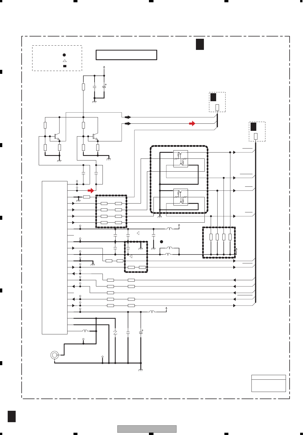
AVH-P4100DVD/XN/UC
134
1234
1234
C
D
F
A
B
E
10.2 MOTHER PCB(TUNER)
2/4
A
T_STUN
LDET
TUNCE2
TUNCK
TUNSL
S_TTUN
TUNCE
RCK
RDSLK
HSLK
RDT
TUN_R
TUN_L
GNDBE2
NM
C404
C401
NM
10u/6.3
C406
C409
0.01u/16
NM
C407
C410
NM
C411
NM
C403
0.01u/16
C402
NM
C405 0.01u/16
GNDD
GNDRF
GNDBE
GNDD
GNDRF
GNDRF
GNDBE
GNDBE
L401
22u
L405
NM
L402
1u
L404
CTF1379-A
L403
LCTAW1R0J3225
UMH1N
Q403
E1 1
B1 2
C2 3E2
4
5B2
6C1
UMH1N
Q404
E1 1
B1 2
C2 3E2
4
5B2
6C1
Q401
NM
Q402
NM
R412 680
R406 680
R419 22k
R411
680
R413 680
R402
NM
R420 22k
R421 22k
R415 680
R403
NM
R422 22k
R408 680
R416 680
R424
NM
R405
NM
R427 0
R428 0
R429
0
R430
0R431
0
R432 0
R433 0
R434 0
R435
0
R425
68k
R404
NM
R401
NM
R423
NM
R409
680
R414 680
R407 680
R410
1k
R426 0
TUN33
GNDRF
TUNCE2
TUNR
ANT
TUN8V
ROMVDD
TUNL
TUNCK
LDET
TUNCE1
TUNDGND
TUNDI
TUNSL
OSCGND
TUN33V
VDD33
SYS+B
SYS+B
U401
1
AM_ANT
2
RF_GND
3
FM_ANT
4
VCC
5
SL
6
CE2
7
WC
8
CE1
9
CK
10
DI
11
LDET
12
OSCGND
13
ROM_VDD
14
DO
15
DGND
16
COMP
17
VDD_3.3
18
RDS_CK
19
RDS_DATA
20
RDS_LOCK
21
RDS_HSLK
22
BEGND
23
Lch
24
Rch
P401
IMSA-6801-01Y901-T
TUNERBUS
ANALOGBUS
GNDBE
100u/10
C408
MAX.140mA
MAX.8mA
MAX.200mA
FM/AM TUNER UNIT
2125
3216
1608
CHIP SIZE LEGEND
EW5,UW5
EW5,UW5:CWE2097
UC:CWE2098
3.3V
8.4V
8.4V
3.3V
JA402
1
2
EW5,UW5
EW5,UW5
EW5,UW5
MOTHER PCB(TUNER)
2/4
A
MOTHER UNIT
Consists of
MOTHER PCB
IF PCB
1/4
A
3/4
A
FM(100%)(UC):-14.0 dBs
AM(30%)(UC):-24.0 dBs
FM(100%)(EW5):-10.0 dBs
AM(30%)(EW5):-20.0 dBs

AVH-P4100DVD/XN/UC 135
5 678
5678
C
D
F
A
B
E
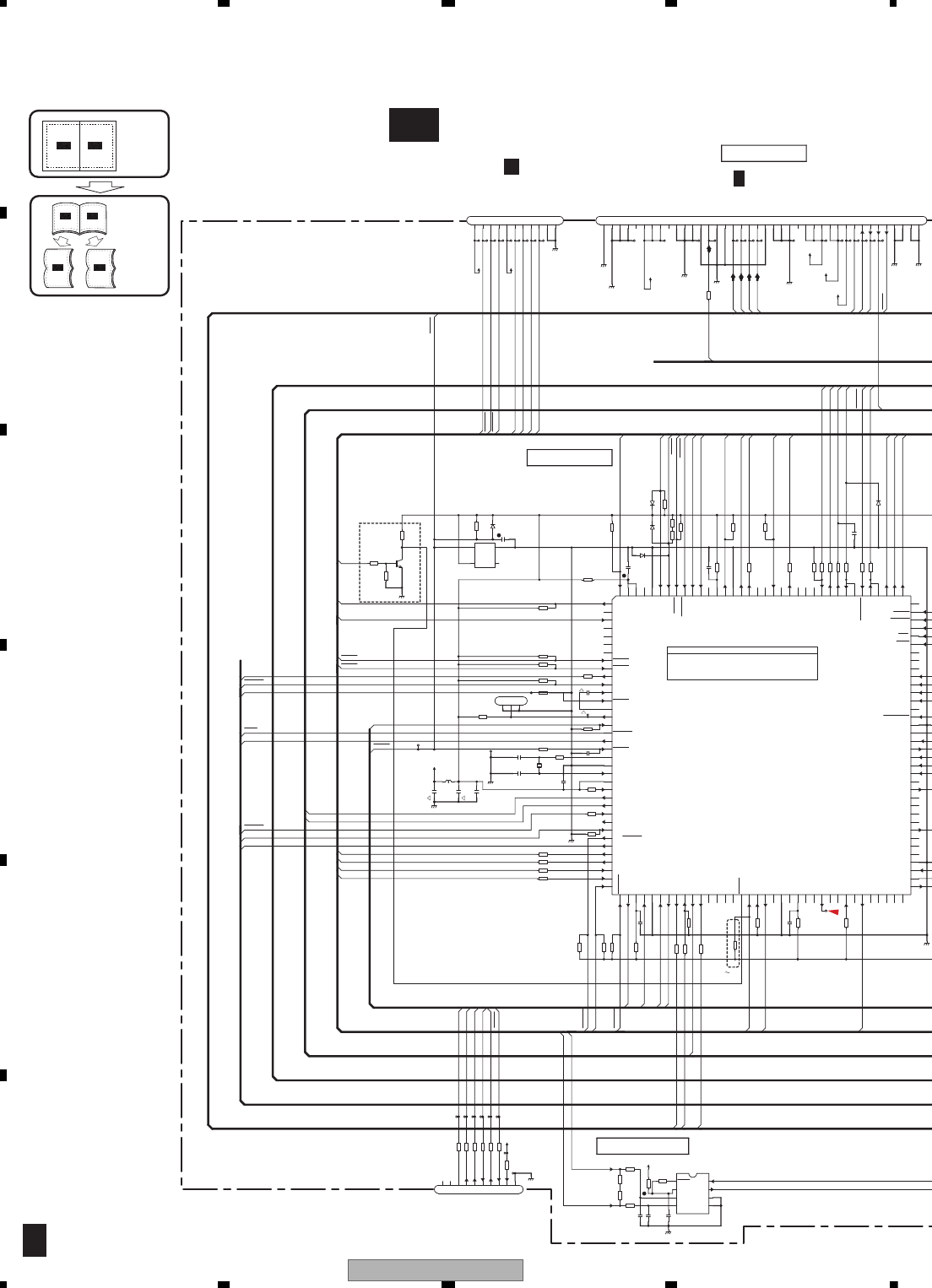
AVH-P4100DVD/XN/UC
136
1234
1234
C
D
F
A
B
E
10.3 MOTHER PCB(SYSTEM)(GUIDE PAGE)
A-a A-b
A-a A-b
A-b
A-a
Large size
SCH diagram
Guide page
Detailed page
3/4
A
A-a 3/4
TUNCE
MONVBS
HALFSW
HOMESW
OPENSW
PULSE1
PULSE0
MOT1
MOT0
BUS+
BUS-
TUNCE2
FLTXD
FLRXD
FLCLK
FLBUSY
N_G
RESET
CNVSS
FLRXD
FLTXD
FLBUSY
CNVSS
S_MTX
RESET
CSYNC1
M_SRX
EVSDT
EVSCK
EVSTB
AVSDA
S_MTX
M_SRX
HOMESW
OPENSW
PULSE0
PULSE1
SYSMUTE
AMPPW
SYSPW
BSENS
ASENS
IRQPW
MONIRST
TUNSL
PBSENS
ISENS
BGSENS
TELMUTE
FLPILM
GUIDEON
XRES
USBCNT
USBFLG
S_MSTX
STNDBY
MOT0
MOT1
MS_SRX
AVSCL
RESET
RESET
VDCNT5
VDCNT8
N_R
FLCLK
MONIRST
ASENBO
MAINTEST
N_B
TVON
AMUTE
MFLPW
S_TTUN
TUNCK
T_STUN
TXNAVI
RXNAVI
SWVDD
WIRED
WIREDAD
HALFSW
NM
CN601
1
2
3
4
5
6
7
8
9
01
CN801
1
2
3
4
5
6
7
8
9
10
11
C601
7p/50
C602
7p/50
C603
10u/6.3
C610
0.01u/16
C618
1u/10
C613
4.7u/10
C615
100p/50
C612
1000p/50
C611
0.01u/16
0
C
0.0
C607
0.01u/16
C606
1u/10
C751
1000p/50
C753
0.1u/10
C752
1000p/50
C605
1000p/50
C604
NM
D601
MA111
GND GNDD
GNDFL
GND
GNDV
GNDD
GNDD
GNDD
GNDD
GNDMP
GNDD
GNDD
GND
GNDD
GND
IC602
S-80827CNNB-B8M
OUT
1
VDD
2
NC
3
VSS
4
HA12241FP
IC751
DIN1 1
ROUT 2
DIN2 3
GND 45 BUS-
6BUS+
7VCC
8STBY
IC601
1
2
3
4
5
6
7
8
9
10
11
12
13
14
15
16
17
18
19
20
21
22
23
24
25
26
27
28
29
30
31
32
33
34
35
36
37
38
39
40
41
42
43
44
45
46
47
48
49
50
51
52
53
54
55
56
57
58
59
60
61
62
63
64
65
66
67
68
69
70
71
72
73
74
75
76
77
78
79
80
81
82
83
84
85
86
87
88
89
90
91
92
93
94
95
96
97
98
99
100
101
102
103
104
105
106
107
108
109
110
111
112
113
114
115
116
117
118
119
120
121
122
123
124
125
126
127
128
129
130
131
132
133
134
135
136
137
138
139
140
141
142
143
144
L601
2.2u
Q601
2SC4081(QRS)
R756 0
R754
100
R751
15
R752
47
R755
1k
R655
33k
R753
100
R602 0
R627
33k
R604
0
R605
0
R606
1k
R608 680
R610 680
R609 680
R612 1k
R618
100k
R619
100k
R620
100k
R607
100k
R641
100k
R622
100k
R674
47k
R621
10k
R601
0
R501
0
R617 4.7k
R613 NM
R628 NM
R629 NM
R623 1k
R625 100k
R626
0
R616 NM
R675
47k
R640
NM
R615 NM
R611 NM
R677
4.7k
R614 NM
R671 680
R670 680
R669
1k
R668
100k R667 1k
R665
100k
R663 0
R664 1.5k
R661 1k
R660 100k
R659 100k
R658 100
R657 680
R656 680
R654
100k
R653
100k
NM
R652
1k
R651
1.8k
R650
100k
R649
100k
R648 220
R647 220
R646
1.8k
R645
10k
TP601
TP603
MOT0
GNDP
MOT1
ILMB
PWRFL
CSYNC
N_B
N_G
N_R
PULSE0
PULSE1
OPENSW
TP502
MONIRST
S_MTX
HOMESW
PWRVI
GNDD
M_SRX
MONVBS
ACC33
TP
TP
TP
HALFSW
CLKOUT
MOTV
MOT5V
TP
VDD33
VD5
MOTV
DD5
VDD33
DD8
PWFL ACC33
PWVI
X601
CN501
1GNDILM
2GNDILM
3GNDSD
4GNDSD
5HDRST
6MFLPWR
7M_SRX
8S_MTX
9MONRST
10 ILMB
11 SWVDD33
12 SWVDD33
13 PWRVI
14 PWRVI
15 PWRVI
16 NC
17 GNDP
18 GNDP
19 GNDP
20 GNDRGB
21 NAVI_B
22 NAVI_G
23 NAVI_R
24 CCYNC
25 GNDRGB
26 GNDV
27 MONVBS
28 GNDV
29 GNDD
30 GNDD
31 GNDD
32 NC
33 PWRFL
34 PWRFL
35 PWRFL
36 NC
37 GNDFL
38 GNDFL
39 GNDFL
40 GNDILM
CN602 NM
1
2
3
VDD33
S_J
T_RESET
SCLK
J_S
GNDD1
CNVSS
BUSY
MFLPW
D604
NM
C619
100p/50
TP602
R662
0
D603
RB501V-40
D602
RB751V-40
D605
NM
POWER BUS
T_SCLK
GND
CNVSS
JTAG BUS
S_J
T_RESET
J_S
3.3V
TUNER BUS
SYSTEM MICOM
uCOM BUS
MONITOR UNIT
7.8V
8.1V
3.3V
IP-BUS DRIVER
MOTV
HALFSW
HOMESW
OPENSW
MOT5V
PULSE1
PULSE0
MOT1
MOT0
GND
GND
3.3V
RXIE
TXIE
5.1V
TUNSL
AVSCK
WIRED
NC
NC
AMPPW
VDCONT5
VDC0
AMUTE
USBCNT
USBFLG
MONIRST
NC
NC(SWVDD)
VDC1
NSD
CNVSS
BSENS
ASENS
STANDBY
TESTIN
TSI
TCK
TSO
AVSDATA
FLRXD
FLCLK
FLBUSY
TXLS1
RXLS1
XRESET
IRQPW
NC
FLEPM
TXNAVI
CLKOUT
TELMUTE
NC
FLCE
PBSENS
BGSENS
SYSPW
SYSMUTE
EVSDA
DDCCLK
EVSCK
EVSEL
MODEL3
MODEL2
MODEL1
MODEL0
HIOUTCLK
BEEP
NC
NC
NC
LDET
RCK
RDT
RDS57K
NC
NC
TUNPCE
TUNPCE2
NC
TUNPDI
TUNPCK
TUNPDO
NC
MOTPWR
NC
MOT0
MOT1
HALFSW
NC(OPENSW)
HOMESW
ISENS
NC
PULSE1
PULSE0
T_BUSY
RDSLK
WIREDAD
NC
FLPILM
NC
NC
NC
NC
NC
FLAPLESS
NC
NC
NC
NC
NC
NC
GUIDEON
VDCONT8
FLTXD
TXMON
RXMON
RXNAVI
RGBON
NC
NC
NC
NC
NC
NC
NC
NC
NC
NC
NC
NC
NC
NC
NC
ASENBO
MAINTET
NC
NC
NC
B,D G
L
MODEL2
UW5L
L
LH
MODEL0
LL
DELIVERY TO
L
L
L
MODEL3
L
UC
MODEL1
EW5L
15MHz
CSS1776
(RB551V-30)
VSS
VSS
VCC
VCC
VCC
VCC
VCC
VSS
VSS
VSS
VSS
AVSS
AVcc
VREF
VCC
RESET
XOUT
XIN
NMI
13.5V
R5F64167DFD-K
UW5
UC:PEG535A8
EW5,UW5:PEG534A8
G
CN101 CN5001
1/2
F
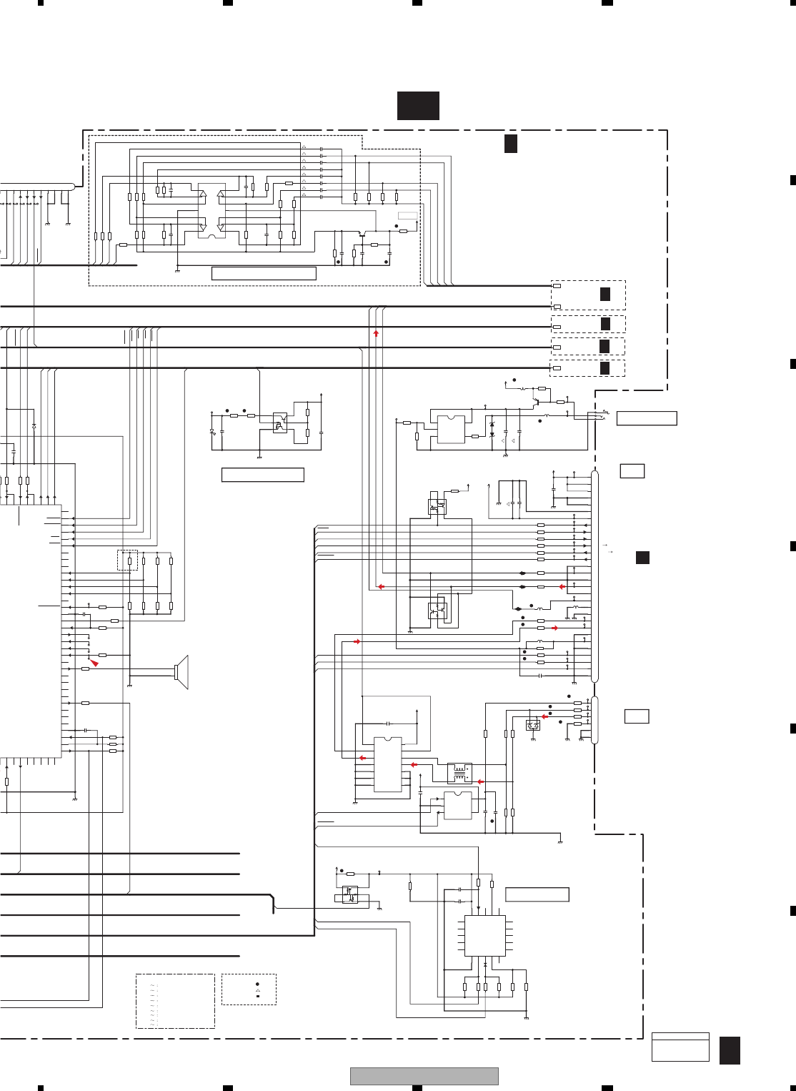
AVH-P4100DVD/XN/UC 137
5 678
5678
C
D
F
A
B
E
3/4
A
A-b 3/4
TUNCE
RDT
RDSLK
HSLK
PCK
PDT
XRES
IRQPW
S_MSTX
STNDBY
PRST
AMUTE
LS_R
LS_L
VDCNT5
RCK
LDET
TUNCE2
CSYNC1
N_R
N_G
N_B
CSYNC
ANR
ANG
FLPILM
DD5
MS_SRX
PCK
PDT
S_MTX
RESET
M_SRX
PRST
DDCCLK
EVSDT
EVSCK
EVSTB
FLPILM
MONIRST
ANB
GNDSIGGNDSIG
MFLPW
T_STUN
HIOUTCLK
VDCNT5
USBCNT
USBFLG
LS_V
CPV1062-A
BZ601
1
1
2
2
CN901
1
2
3
4
5
6
7
8
9
10
11
12
13
14
15
16
17
18
19
20
21
22
23
24
25
26
27
28
29
30
CN522
USB5V
D-
D+
USBGND
Shield1
Shield2
1
2
3
4
5
6
C787 10u/6.3
C521
1u/6.3
C782
1000p/50
C786 10u/6.3
C901
0.1u/10
C522
0.1u/10
C523
0.1u/10
C775 10u/6.3
C904
NM
C785 10u/6.3
C563
0.1u/10
C802
NM
C801
NM
C779 10u/6.3
C771
6p/50
C772
6p/50
C773
6p/50
C774
6p/50
C781
0.1u/16
C615
100p/50
C777 10u/6.3
C609
0.01u/16
C608
0.01u/16
C776 10u/6.3
C951
NM
C952
0.1u/10
C780
0.1u/16
C903
0.1u/10
SMLE12BC7T
D801
D951
MALS068X
D521
EMZC6.8N
1
2
3
GNDV
GND
GND
GND
GND GNDD
GNDA
GNDD
GNDD
GNDV
GNDD
GNDD
GNDDDC
GNDD
GNDD
GND
GNDD
GNDDDC
IC951
TC7SET08FUS1
INB
1
INA
2
GND
3OUTY 4
5
Vcc
IC771
NJM2138V
A_OUT
1
A_-IN
2
A_+IN
3
V+
4
5B_+IN
6B_-IN
7B_OUT
8
C_OUT
9
C_-IN
10
C_+IN
11
V-
12
D_+IN
13
D_-IN
14
D_OUT
IC522
TC7MBL6126SFK
1OE
1
A1
2
A2
3
A3
4
5A4
64OE
7GND 8
3OE
9
B4
10
B3
11
B2
12
B1
13
2OE
14
VCC
65
66
67
68
69
70
71
72
73
74
75
76
77
78
79
80
81
82
83
84
85
86
87
88
89
90
91
92
93
94
95
96
97
98
99
100
101
102
103
104
105
106
107
108
109
110
111
112
113
114
115
116
JA951
2
3
1
L521
CTF1713-A 12
34
L952
CTF1379-A
L951
CTF1389-A
UMD3N
Q902
E1 1
B1 2
C2 3E2
4
5B2
6C1
IMH23
Q901
C1 1
B2 2
E2 3C2
4
5B1
6E1
UMF5N
Q801
E1
1
B1
2
C2
3
E2
4
5
B2
6
C1
Q771
2SC4081(QRS)
R903
0
R563
1k
R564
NM
R909
470
R910
1k
R913
220
R952
47k
R912
220
R568
100k
R603
0
R676
NM
R562
100k
R609 680
R612 1k
R567
NM
R915
1k
R786
8.2k
R607
100k
R780
100
R782
100
R784
5.1k
R953
120
R951
0
R561
NM
R793
100
R794
NM
R795
NM
R796
NM
R797
NM
R777
22k
R773 22k
R783
22k
R787
22k
R775 22k
R776 22k
R778 22k
R788
22k
R779 22k
R791
22k
R790
22k
R774
22k
R772 22k R771 22k
R789
22k
R569
NM
R532 NM
R908 0
R907 0
R906 0
R905 0
R523 NM
R798
0
R623 1k
R624 0
R530 0
R639
100k
R529 0
R781
100
R803
10k
R804
3.3k
R524 0
R792
22k
R801
180
R802
180
R565
100
R566
100
R785
680
R914
220
R522 0
R525 0
R521 0
R526 0
R902
0
R911
220
R633
NM
R632
100k
R631
NM
R630
NM
R634
100k
R635
100k
R636
100k
R637
100k
R638
1k
R644
4.7k
R643
100k
R642
1k
USBD+
USBD-
USB5V1
CPRST
SDA
SCK
D+
D-
COMPOSIT
LOUT
ROUT
STANBY
LS1-SRX
S-LS1TX
IRQPWR
XRES
AMUTE
IECOUT
USBGR
TP561
ILMB
DD5_1
MONIRST
LED
VD8
VD5
S_MTX
M_SRX
ACC33
TP604
TP605
TP608
TP606
SPDIF
TP607
VD8
SYS+B
DD5
VD5
VDD33
ACC33
DD5
SYS+B
DD5
TUNERBUS
POWERBUS
NAVI_EXT
uCOMBUS
ANALOGBUS
1GNDILM
2GNDILM
3GNDSD
4GNDSD
5HDRST
6MFLPWR
7M_SRX
8S_MTX
9MONRST
10 ILMB
11 SWVDD33
C778 10u/6.3
GND
GND
2SA1576A(RS)
Q951
C2
B3
E1
R954
100k
R955
10k
341S2162
IC561
NC1
1
MODE1/SPI_nSS
2
NC2
3
nRESET
4
VCC
5
NC3
6
NC4
7
NC5
8NC6
9NC7
10
VSS
11
I2C_SCL/SPI_SIMO
12
I2C_SDA/SPI_SOMI
13
MODE0/SPI_CLK
14
NC8
15
NC9
16
NC10
17
NC11 18
NC12 19
NC13
20
L901
NM
MFLPW
D604
NM
C902
100p/25
R678
1k
IEC
TP951
R916 0
C564
1u/6.3
IC521
R5523N001B
EN
1
GND
2
FLG
3VIN 4
5
VOUT
R570
10k
C561
0.1u/10
L902
CTF1387-A
L903
UMD22N
Q561 E1
1
B1
2
C2
3
E2 4
5
B2
6
C1
MONITOR BUS
TUNER BUS
POWER BUS
POWER BUS
ANALOG BUS
IPOD CP IC
uCOM BUS
901 LS1
751 IP-BUS DRIVER
561 ipod CP
801 DRIVE UNIT
601 SYSTEM MICOM
521 USB I/F
501 MONITOR UNIT
TUNER BUS
2125
3216
1608
CHIP SIZE LEGEND
uCOM BUS 3.3V
5.2V
DGND
DGND
DGND
AGND
VDD5
CPRST
IECOUT
8.0V
VD
AGND
LS1 SRX
5.1V
XRES
STANBY
VGND
IRQPWR
PGND
PGND
SLS1TX
DGND
SCK
SDA
VD
D+
AGND
VD
ROUT
D-
COMPOSIT
LOUT
AMUTE
DGND
DVD&USB BUS
8.3V
5.2V
S/PDIF OUT
10/6R3
LS1
USB
RXIE
TXIE
JTAG BUS
MONITOR BUS
RGB VIDEO ISOLATOR
TESTIN
TSI
TCK
TSO
NC
NC
FLCE
EVSDA
DDCCLK
EVSCK
EVSEL
MODEL3
MODEL2
MODEL1
MODEL0
HIOUTCLK
BEEP
NC
NC
NC
LDET
RCK
RDT
RDS57K
NC
NC
TUNPCE
TUNPCE2
NC
TUNPDI
TUNPCK
NC
NAVI BUS
RDSLK
FLPILM
NC
FLAPLESS
NC
NC
NC
NC
771 RGB VIDEO ISOLATOR
951 S/PDIF OUT
INSERTION LED
NC
NC
NC
NC
NC
NC
NC
NC
(RB551V-30)
VCC
VCC
VSS
VSS
CTF1387-A
UW5
UW5
MOTHER PCB(SYSTEM)
3/4
A
MOTHER UNIT
Consists of
MOTHER PCB
IF PCB
1/4
A
2/4
A
4/4
A
1/4
A
C
CN1901
DVD/CD:+5.1 dBs
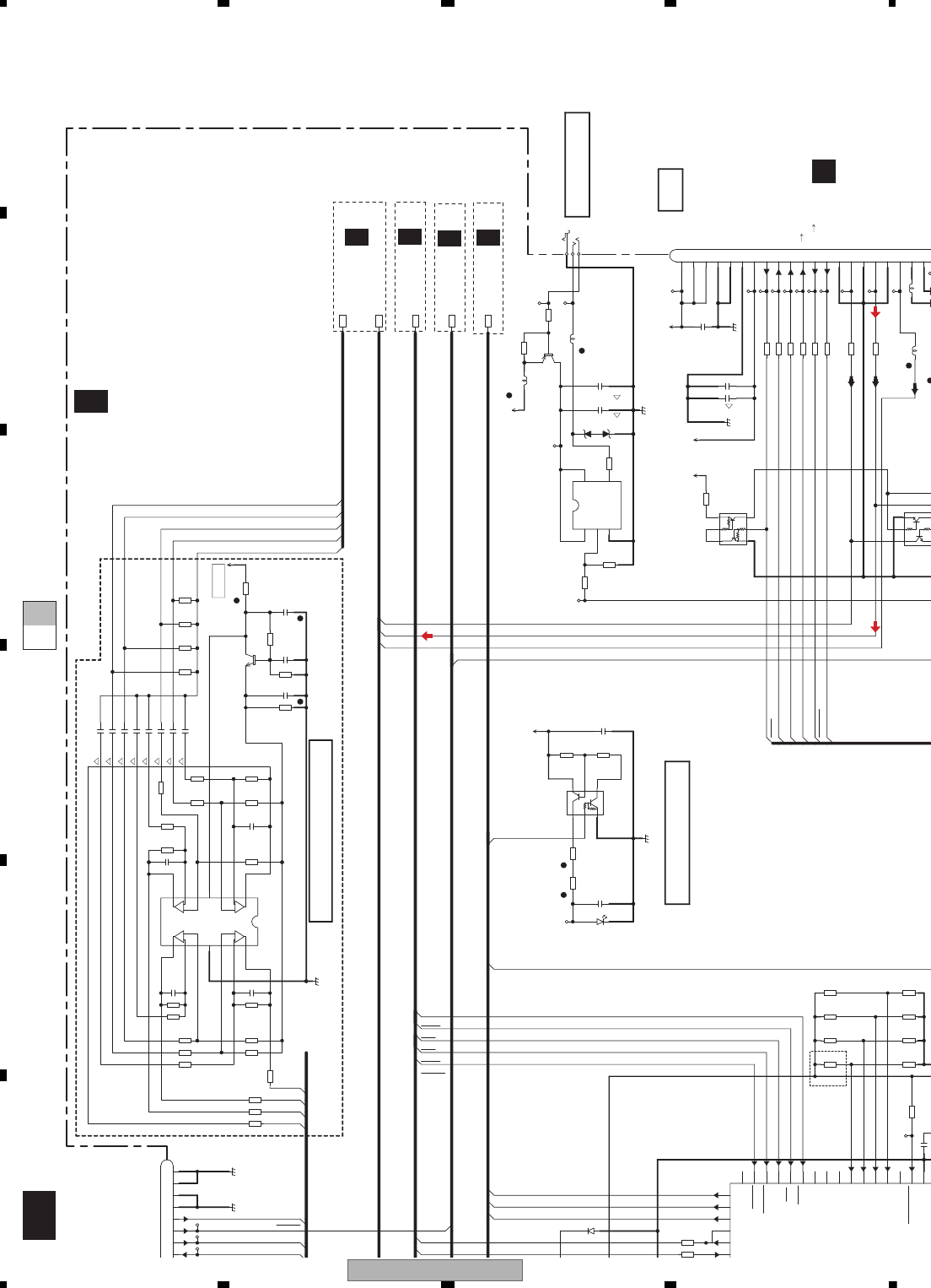
AVH-P4100DVD/XN/UC
138
1234
1234
C
D
F
A
B
E
A-a A-b
A-b 3/4
TUNCE
RDT
RDSLK
HSLK
XRES
IRQPW
S_MSTX
STNDBY
AMUTE
LS_R
LS_L
VDCNT5
RCK
LDET
CSYNC1
N_R
N_G
N_B
CSYNC
ANR
ANG
FLPILM
DD5
MS_SRX
S_MTX
RESET
M_SRX
EVSDT
EVSCK
EVSTB
ANB
GNDSIGGNDSIG
MFLPW
HIOUTCLK
LS_V
CN901
10
11
12
13
14
15
16
17
18
19
20
21
22
23
24
25
26
27
28
29
30
C787 10u/6.3
C782
1000p/50
C786 10u/6.3
C901
0.1u/10
C775 10u/6.3
C904
NM
C785 10u/6.3
C802
NM
C801
NM
C779 10u/6.3
C771
6p/50
C772
6p/50
C773
6p/50
C774
6p/50
C781
0.1u/16
p
C777 10u/6.3
C608
0.01u/16
C776 10u/6.3
C951
NM
C952
0.1u/10
C780
0.1u/16
C903
0.1u/10
SMLE12BC7T
D801
D951
MALS068X
GNDD
GNDD
GNDV
GNDDDC
GNDD
GND
GNDDDC
IC951
TC7SET08FUS1
INB
1
INA
2
GND
3OUTY 4
5
Vcc
IC771
NJM2138V
A_OUT
1
A_-IN
2
A_+IN
3
V+
4
5B_+IN
6B_-IN
7B_OUT
8
C_OUT
9
C_-IN
10
C_+IN
11
V-
12
D_+IN
13
D_-IN
14
D_OUT
92
93
94
95
96
97
98
99
100
101
102
103
104
105
106
107
108
109
110
111
112
113
JA951
2
3
1
L952
CTF1379-A
L951
CTF1389-A
UMD3N
Q902
E1 1
B1 2
C2 3E2
4
5B2
6C1
IMH23
Q901 C2
4
5B1
6E1
UMF5N
Q801
E1
1
B1
2
C2
3
E2
4
5
B2
6
C1
Q771
2SC4081(QRS)
R903
0
R909
470
R910
1k
R913
220
R952
47k
R912
220
1k
R915
1k
R786
8.2k
R780
100
R782
100
R784
5.1k
R953
120
R951
0
R793
100
R794
NM
R795
NM
R796
NM
R797
NM
R777
22k
R773 22k
R783
22k
R787
22k
R775 22k
R776 22k
R778 22k
R788
22k
R779 22k
R791
22k
R790
22k
R774
22k
R772 22k R771 22k
R789
22k
R907 0
R798
0
R623 1k
R781
100
R803
10k
R804
3.3k
R792
22k
R801
180
R802
180
R785
680
R914
220
R902
0
R911
220
R633
NM
R632
100k
R631
NM
R630
NM
R634
100k
R635
100k
R636
100k
R637
100k
R643
100k
D
COMPOSIT
LOUT
ROUT
STANBY
LS1-SRX
S-LS1TX
IRQPWR
XRES
AMUTE
IECOUT
DD5_1
LED
VD8
VD5
S_MTX
M_SRX
TP608
SPDIF
VD8
SYS+B
DD5
VD5
DD5
SYS+B
TUNERBUS
POWERBUS
NAVI_EXT
uCOMBUS
ANALOGBUS
1GNDILM
2GNDILM
3GNDSD
4GNDSD
5HDRST
6MFLPWR
7M_SRX
8S_MTX
C778 10u/6.3
2SA1576A(RS)
Q951
C2
B3
E1
R954
100k
R955
10k
MFLPW
D604
NM
R678
TP951
L902
CTF1387-A
L903
MONITOR BUS
TUNER BUS
POWER BUS
ANALOG BUS
uCOM BUS
AGND
VDD5
8.0V
VD
AGND
LS1 SRX
5.1V
XRES
STANBY
VGND
IRQPWR
PGND
PGND
SLS1TX
DGND
VD
AGND
VD
ROUT
COMPOSIT
LOUT
AMUTE
DGND
8.3V
5.2V
S/PDIF OUT
10/6R3
LS1
RGB VIDEO ISOLATOR
EVSDA
EVSCK
EVSEL
MODEL3
MODEL2
MODEL1
MODEL0
NC
NC
NC
LDET
RCK
RDT
RDS57K
NC
NC
TUNPCE
TUNPCE2
NAVI BUS
RDSLK
FLAPLESS
NC
INSERTION LED
(RB551V-30)
VSS
CTF1387-A
UW5
UW5
MOTHER PCB(SYSTEM)
3/4
A
1/4
A
2/4
A
4/4
A
1/4
A
C
CN1901
DVD/CD:+5.1 dBs
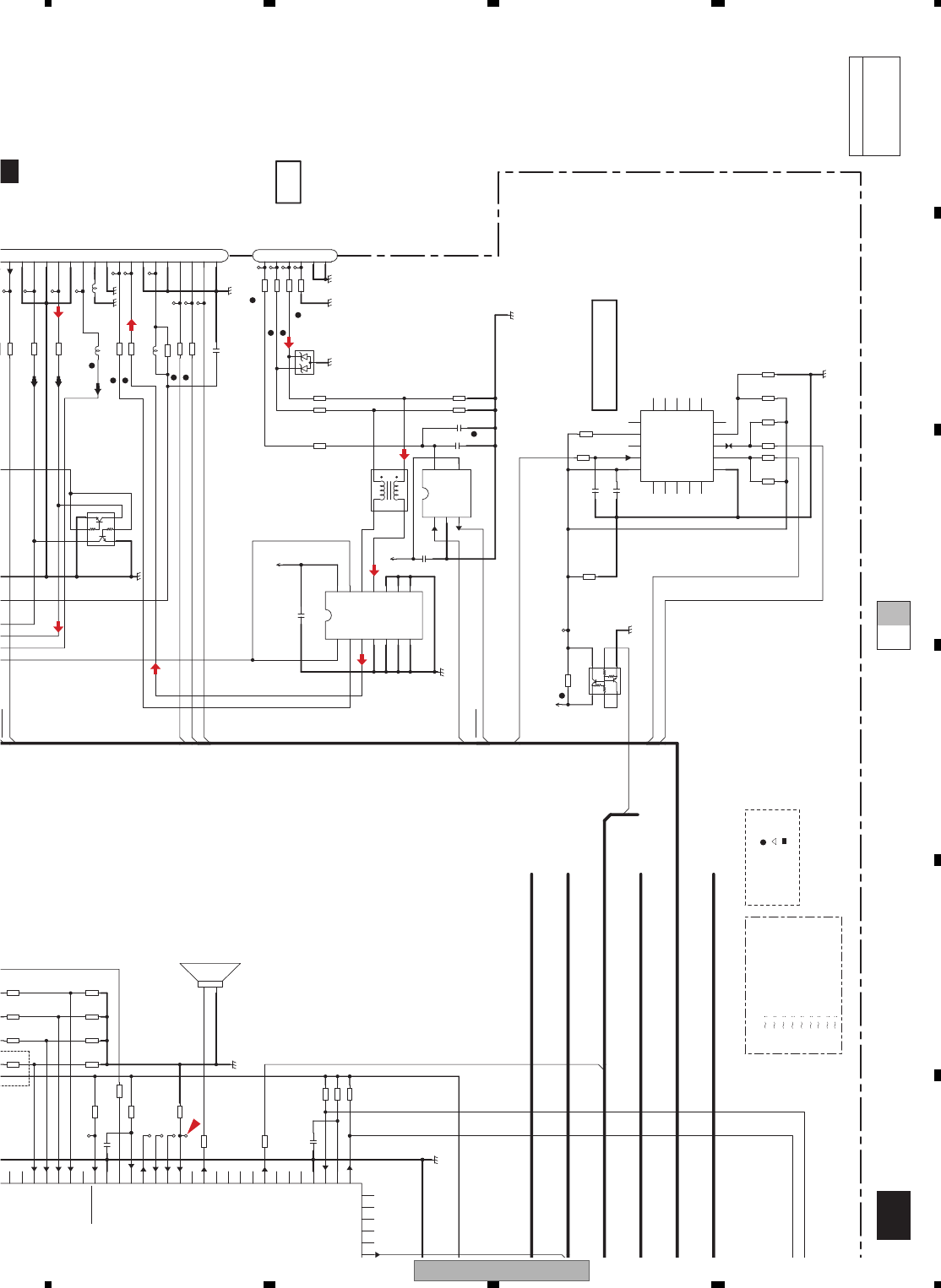
AVH-P4100DVD/XN/UC 139
5 678
5678
C
D
F
A
B
E
A-a A-b
A-b 3/4
PCK
PDT
STNDBY
PRST
PCK
PDT
PRST
DDCCLK
FLPILM
VDCNT5
USBCNT
USBFLG
CPV1062-A
BZ601
1
1
2
21
2
3
4
5
6
7
8
9
10
11
12
13
14
15
16
17
18
19
CN522
USB5V
D-
D+
USBGND
Shield1
Shield2
1
2
3
4
5
6
C521
1u/6.3
C522
0.1u/10
C523
0.1u/10
C563
0.1u/10
C609
0.01u/16
C608
0.01u/16
D521
EMZC6.8N
1
2
3
GNDV
GND
GND
GND
GND GNDD
GNDA
GNDD
GNDD
GNDD
GNDD
IC522
TC7MBL6126SFK
1OE
1
A1
2
A2
3
A3
4
5A4
64OE
7GND 8
3OE
9
B4
10
B3
11
B2
12
B1
13
2OE
14
VCC
68
69
70
71
72
73
74
75
76
77
78
79
80
81
82
83
84
85
86
87
88
89
90
91
92
93
94
95
96
97
98
99
100
101
L521
CTF1713-A 12
34
IMH23
Q901
C1 1
B2 2
E2 3C2
4
5B1
6E1
R903
0
R563
1k
R564
NM
R568
100k
R603
0
R676
NM
R562
100k
R567
NM
R561
NM
R569
NM
R532 NM
R908 0
R907 0
R906 0
R905 0
R523 NM
R624 0
R530 0
R639
100k
R529 0
R524 0
R565
100
R566
100
R914
220
R522 0
R525 0
R521 0
R526 0
R902
0
R633
NM
R632
100k
R631
NM
R630
NM
R634
100k
R635
100k
R636
100k
R637
100k
R638
1k
R644
4.7k
R643
100k
R642
1k
USBD+
USBD-
USB5V1
CPRST
SDA
SCK
D+
D-
COMPOSIT
LOUT
ROUT
STANBY
USBGR
TP561
TP604
TP605
TP608
TP606
TP607
VDD33
ACC33
DD5
GND
GND
341S2162
IC561
NC1
1
MODE1/SPI_nSS
2
NC2
3
nRESET
4
VCC
5
NC3
6
NC4
7
NC5
8NC6
9NC7
10
VSS
11
I2C_SCL/SPI_SIMO
12
I2C_SDA/SPI_SOMI
13
MODE0/SPI_CLK
14
NC8
15
NC9
16
NC10
17
NC11 18
NC12 19
NC13
20
L901
NM
C902
100p/25
R678
1k
IEC
R916 0
C564
1u/6.3
IC521
R5523N001B
EN
1
GND
2
FLG
3VIN 4
5
VOUT
R570
10k
C561
0.1u/10
L902
CTF1387-A
L903
UMD22N
Q561 E1
1
B1
2
C2
3
E2 4
5
B2
6
C1
POWER BUS
IPOD CP IC
901 LS1
751 IP-BUS DRIVER
561 ipod CP
801 DRIVE UNIT
601 SYSTEM MICOM
521 USB I/F
501 MONITOR UNIT
TUNER BUS
2125
3216
1608
CHIP SIZE LEGEND
uCOM BUS
3.3V
5.2V
DGND
DGND
DGND
AGND
CPRST
IECOUT
AGND
STANBY
VGND
DGND
SCK
SDA
D+
AGND
ROUT
D-
COMPOSIT
LOUT
DVD&USB BUS
USB
RXIE
TXIE
JTAG BUS
MONITOR BUS
TESTIN
TSI
TCK
TSO
NC
DDCCLK
MODEL3
MODEL2
MODEL1
MODEL0
HIOUTCLK
BEEP
NC
NC
FLPILM
NC
FLAPLESS
NC
NC
NC
NC
771 RGB VIDEO ISOLATOR
951 S/PDIF OUT
NC
NC
NC
NC
NC
NC
NC
NC
VCC
VCC
VSS
VSS
CTF1387-A
UW5
MOTHER UNIT
Consists of
MOTHER PCB
IF PCB
C
CN1901
DVD/CD:+5.1 dBs
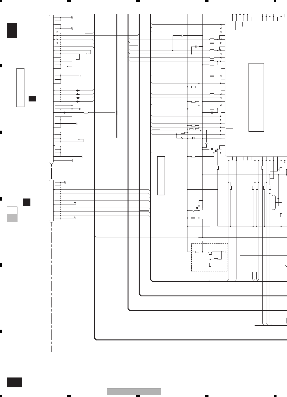
AVH-P4100DVD/XN/UC
140
1234
1234
C
D
F
A
B
E
A-bA-a
A-a 3/4
A-b 3/4
TUNCE
MONVBS
HALFSW
HOMESW
OPENSW
PULSE1
PULSE0
MOT1
MOT0
TUNCE2
N_G
CNVSS
S_MTX
RESET
CSYNC1
M_SRX
EVSDT
EVSCK
EVSTB
AVSDA
SYSMUTE
AMPPW
SYSPW
BSENS
ASENS
TUNSL
PBSENS
ISENS
BGSENS
TELMUTE
GUIDEON
XRES
USBCNT
USBFLG
AVSCL
RESET
N_R
MONIRST
ASENBO
MAINTEST
N_B
TVON
AMUTE
MFLPW
S_TTUN
TUNCK
T_STUN
WIRED
WIREDAD
CN801
1
2
3
4
5
6
7
8
9
10
11
C618
1u/10
C613
4.7u/10
C615
100p/50
C607
0.01u/16
C606
1u/10
D601
MA111
GND GNDD
GNDFL
GND
GNDV
GNDD
GNDMP
GNDD
GND
IC602
S-80827CNNB-B8M
OUT
1
VDD
2
NC
3
VSS
4
IC601
1
2
3
4
5
6
7
8
9
10
11
12
13
14
15
16
17 92
93
94
95
96
97
98
99
100
101
102
103
104
105
106
107
108
109
110
111
112
113
114
115
116
117
118
119
120
121
122
123
124
125
126
127
128
129
130
131
132
133
134
135
136
137
138
139
140
141
142
143
144
Q601
2SC4081(QRS)
R602 0
R608 680
R610 680
R609 680
R612 1k
R620
100k
R641
100k
R622
100k
R674
47k
R621
10k
R501
0
R617 4.7k
R623 1k
R626
0
R675
47k
R640
NM
R677
4.7k
R668
100k R667 1k
R665
100k
R663 0
R664 1.5k
R660 100k
R659 100k
R658 100
R654
100k
R652
1k
R651
1.8k
R646
1.8k
R645
10k
TP603
MOT0
GNDP
MOT1
ILMB
PWRFL
CSYNC
N_B
N_G
N_R
PULSE0
PULSE1
OPENSW
TP502
MONIRST
S_MTX
HOMESW
PWRVI
GNDD
M_SRX
MONVBS
ACC33
HALFSW
MOTV
MOT5V
VD5
MOTV
DD8
PWFL ACC33
PWVI
CN501
1GNDILM
2GNDILM
3GNDSD
4GNDSD
5HDRST
6MFLPWR
7M_SRX
8S_MTX
9MONRST
10 ILMB
11 SWVDD33
12 SWVDD33
13 PWRVI
14 PWRVI
15 PWRVI
16 NC
17 GNDP
18 GNDP
19 GNDP
20 GNDRGB
21 NAVI_B
22 NAVI_G
23 NAVI_R
24 CCYNC
25 GNDRGB
26 GNDV
27 MONVBS
28 GNDV
29 GNDD
30 GNDD
31 GNDD
32 NC
33 PWRFL
34 PWRFL
35 PWRFL
36 NC
37 GNDFL
38 GNDFL
39 GNDFL
40 GNDILM
CN602 NM
1
2
3
MFLPW
D604
NM
R662
0
D603
RB501V-40
D602
RB751V-40
D605
NM
POWER BUS
TUNER BUS
SYSTEM MICOM
uCOM BUS
MONITOR UNIT
7.8V
8.1V
3.3V
MOTV
HALFSW
HOMESW
OPENSW
MOT5V
PULSE1
PULSE0
MOT1
MOT0
GND
GND
TUNSL
AVSCK
WIRED
NC
NC
AMPPW
VDC0
AMUTE
USBCNT
USBFLG
NC
VDC1
NSD
CNVSS
BSENS
ASENS
AVSDATA
TELMUTE
PBSENS
BGSENS
SYSPW
SYSMUTE
EVSDA
EVSCK
EVSEL
MODEL3
MODEL2
MODEL1
MODEL0
NC
NC
NC
LDET
RCK
RDT
RDS57K
NC
NC
TUNPCE
TUNPCE2
NC
TUNPDI
TUNPCK
TUNPDO
NC
ISENS
NC
RDSLK
WIREDAD
NC
NC
NC
FLAPLESS
NC
NC
GUIDEON
NC
ASENBO
MAINTET
NC
NC
NC
L
MODEL2
UW5L
L
LH
MODEL0
LL
DELIVERY TO
L
L
L
MODEL3
L
UC
MODEL1
EW5L
(RB551V-30)
VSS
VSS
AVSS
AVcc
VREF
VCC
13.5V
UW5
G
CN101 CN5001
1/2
F
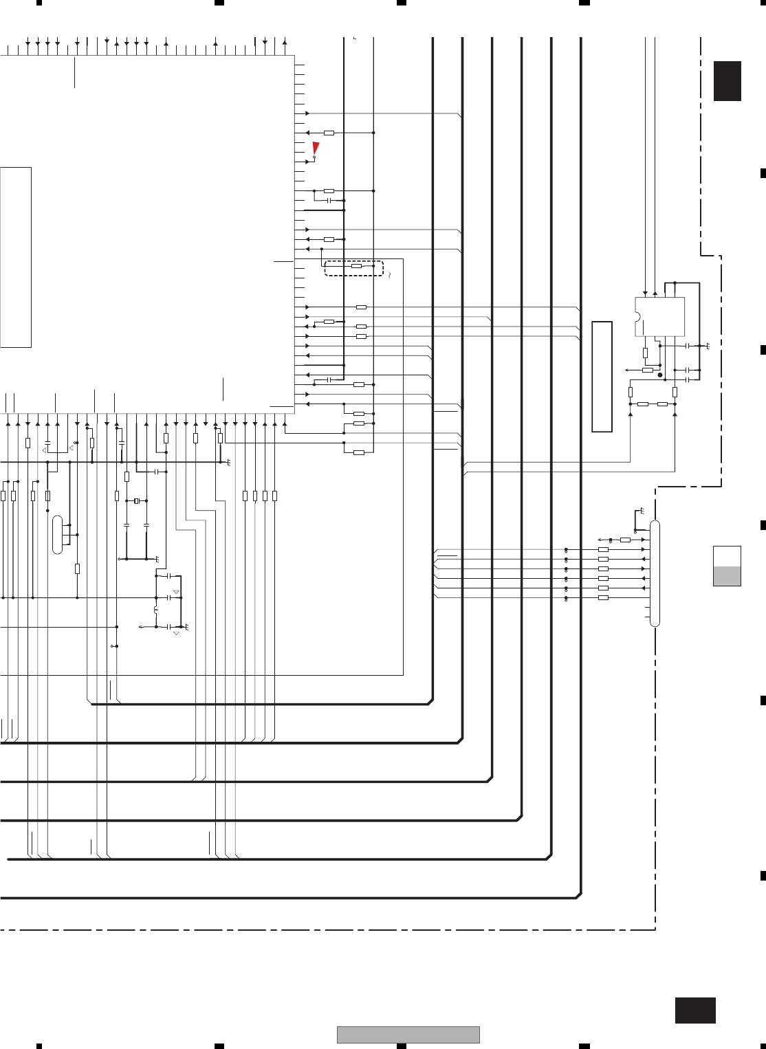
AVH-P4100DVD/XN/UC 141
5 678
5678
C
D
F
A
B
E
A-bA-a
A-a 3/4
A-b 3/4
BUS+
BUS-
FLTXD
FLRXD
FLCLK
FLBUSY
RESET
CNVSS
FLRXD
FLTXD
FLBUSY
CNVSS
S_MTX
M_SRX
HOMESW
OPENSW
PULSE0
PULSE1
BSENS
ASENS
IRQPW
MONIRST
FLPILM
XRES
USBCNT
USBFLG
S_MSTX
STNDBY
MOT0
MOT1
MS_SRX
RESET
VDCNT5
VDCNT8
FLCLK
AMUTE
TXNAVI
RXNAVI
SWVDD
HALFSW
NM
CN601
1
2
3
4
5
6
7
8
9
0
1
C601
7p/50
C602
7p/50
C603
10u/6.3
C610
0.01u/16
C613
4.7u/10
C612
1000p/50
C611
0.01u/16
C751
1000p/50
C753
0.1u/10
C752
1000p/50
C605
1000p/50
C604
NM
GNDD
GNDD
GNDD
GNDD
G
GNDD
HA12241FP
IC751
DIN1 1
ROUT 2
DIN2 3
GND 45 BUS-
6BUS+
7VCC
8STBY
IC601
8
9
10
11
12
13
14
15
16
17
18
19
20
21
22
23
24
25
26
27
28
29
30
31
32
33
34
35
36
37
38
39
40
41
42
43
44
45
46
47
48
49
50
51
52
53
54
55
56
57
58
59
60
61
62
63
64
65
66
67
68
69
70
71
72
73
74
75
76
77
78
79
80
81
82
83
84
85
86
87
88
89
90
91
92
93
94
95
96
97
98
99
100
101
L601
2.2u
R756 0
R754
100
R751
15
R752
47
R755
1k
R655
33k
R753
100
R627
33k
R604
0
R605
0
R606
1k
R618
100k
R619
100k
R607
100k
R601
0
R617 4.7k
R613 NM
R628 NM
R629 NM
R625 100k
R616 NM
R615 NM
R611 NM
R677
4.7k
R614 NM
R671 680
R670 680
R669
1k
R668
100k R667 1k
R661 1k
R660 100k
R659 100k
R657 680
R656 680
R654
100k
R653
100k
NM
R650
100k
R649
100k
R648 220
R647 220
TP601
TP603
CLKOUT
VDD33
DD5
VDD33
X601
CN602 NM
1
2
3
VDD33
S_J
T_RESET
SCLK
J_S
GNDD1
CNVSS
BUSY
C619
100p/50
TP602
T_SCLK
GND
CNVSS
JTAG BUS
S_J
T_RESET
J_S
3.3V
IP-BUS DRIVER
3.3V
RXIE
TXIE
5.1V
VDCONT5
VDC0
AMUTE
USBCNT
USBFLG
MONIRST
NC(SWVDD)
VDC1
NSD
CNVSS
BSENS
ASENS
STANDBY
TESTIN
TSI
TCK
TSO
FLRXD
FLCLK
FLBUSY
TXLS1
RXLS1
XRESET
IRQPW
NC
FLEPM
TXNAVI
CLKOUT
NC
FLCE
DDCCLK
MODEL3
MODEL2
MODEL1
MODEL0
HIOUTCLK
BEEP
NC
NC
NC
MOTPWR
MOT0
MOT1
HALFSW
NC(OPENSW)
HOMESW
PULSE1
PULSE0
T_BUSY
FLPILM
NC
NC
NC
NC
FLAPLESS
NC
NC
NC
NC
NC
VDCONT8
FLTXD
TXMON
RXMON
RXNAVI
RGBON
NC
NC
NC
NC
NC
NC
NC
NC
NC
NC
NC
NC
NC
NC
B,D G
L
UW5L
L
LH
LL
L
L
L
L
UC
EW5L
15MHz
CSS1776
VSS
VSS
VCC
VCC
VCC
VCC
VCC
VSS
VSS
VSS
RESET
XOUT
XIN
NMI
R5F64167DFD-K
UC:PEG535A8
EW5,UW5:PEG534A8
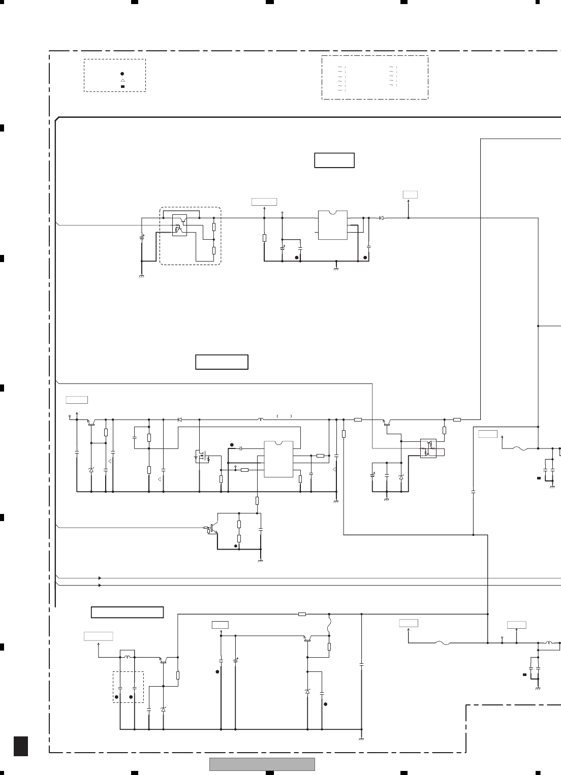
AVH-P4100DVD/XN/UC
142
1234
1234
C
D
F
A
B
E
10.4 MOTHER PCB(POWER SUPPLY)
4/4
A
SYSPW
HIOUTCLK
VDCNT8
SWVDD
VDCNT5
NM
C1401
CCH1477-A
C1341
C1226
10u/35
C1229
10u/35
C1403
1u/10
C1381
NM
C1383
NM
C1228
0.1u/10
C1227
0 1u/10
C1382
NM
C1342
1u/10
D1381
NM
GND
GNDD
GNDDDC
GNDHI
GNDDD
L1381
NM
CTH
L1209
NM
CTH1358-A-T
Q1381
NM
R1381
NM
R1401
NM
R1382
NM
R1128
NM
TP1401
TP1207
ACC33
DD8
MOT5V
MOTV VD8
VD5
DD5
D1341
HZU6R8(B2)
C1343
0.1u/16
C1128
NM
Q1122
NM
D1122
NM
R1127
NM
NM
Q1121
E1 1
B1 2
C2 3E2
4
5B2
6C1
NM
C1129
GND
IC1401
S-1112B33MC-L6S
VIN 1
VSS 2
ON/OFF 3
NC
4
5VOUT
R1149
NM
R1148
0
DTC143EUA
Q1143
R1145
5.1k
TP1142
R1146
300k
C1146
0.01u/16
R1150
11k
R1147
5.1k
D1142
RB551V-30
C1148
0.1u/16
C1147
CCG1222-A
4.7u
C1145
CCG1222-A
4.7u
R1141
680
TP1141
Q1141
2SC4081(QRS)
D1141
HZU13(B1)
EV12
C1141
0.1u/16
TK11840L
IC1141
EaIn 1
SCP 2
Vcc 3
BR/CTL 45 Out
6GND
7OSC
8FB
R1151
620
GNDHI
C1149
NM
C1144
270p/25
RSF014N03
Q1142
G
D
S
R1153
NM
R1152
0
R1154
0
L1141
ATH7061-A
C1143
NM
P1202
CEK1280-A
12
P1203
CEK1285-A
12
P1341
CEK1282-A
12
Q1341
2SD2153(VW)
R1343
220
R1144
910
NM
C1421
GNDD
R1422
NM
NM
Q1422
E1
1
B1
2
C2
3
E2
4
5
B2
6
C1
R1421
NM
C1142
0.1u/16
C1402
0.47u/10
D1401
RB551V-30
C1344
1000p/50
C1500
1000p/50
ACC33V
2125
3216
1608
CHIP SIZE LEGEND
3.3V
5.1V
5.1V
MOT5V & MOTV
8.1V
1121 HIOUT12V
1081 TUN3.3V
1061 SYS+B
1381 MOT5V
1201 DDC
1401 ACC33V
1021 PWVI,PWFL
1001 VDD33V 1341 MOTV
1500 VD5
HIOUT12V
(1.5A)
100uF/16V
14.1V
(2.5A)
(1.0A)
370kHz/416kHz
47uH
12.2V
NM
(NC)
4.8V
(D)(D)
1421 SWVDD33V
>
>
>
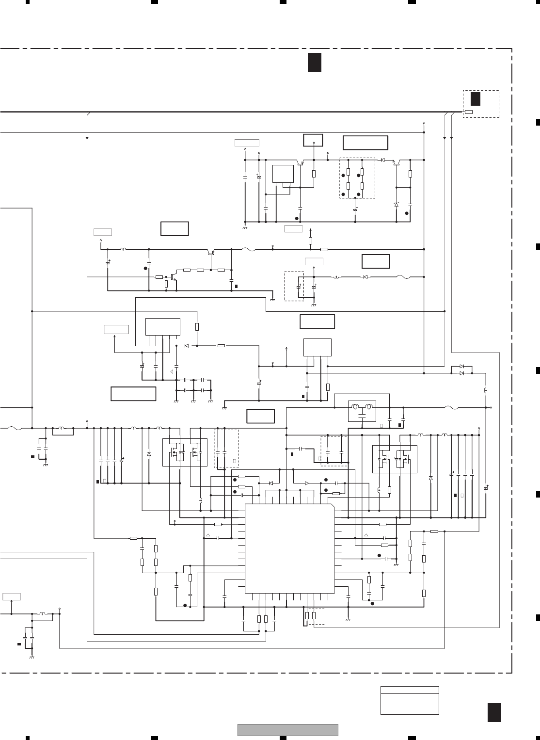
AVH-P4100DVD/XN/UC 143
5 678
5678
C
D
F
A
B
E
4/4
A
MFLPW
DDCCLK
SYSPW
22u/16
C1082
47u/6.3
C1002
4700u/16
C1201
330u/16
C1202
330u/16
C1203
100u/16
C1021
1000u/16
C1005
C1086
NM
C1084
4.7u/10
C1001
NM
C1061
1.0u/35
C1088
NM
C1206 NM
C1225 NM
C1226
10u/35
C1230
1.0u/35
C1229
10u/35
C1083
0.01u/16
C1085
NM
C1022
0.1u/50
C1003
0.01u/16
C1087
NM
4.7u/16
C1023
C1228
0.1u/10
C1227
0.1u/10
C1232
NM
C1214
CCG1223-A
C1233 NM
C1216 CCG1223-A
C1006
0.01u/50
C1212
1.0u/35
C1213
CCG1223-A
C1224 NM
C1204 NM
C1007
0.1u/50
C1205 NM
C1223 NM
D1002
S1G-6904G2P
D1081
S1G-6904G2P
D1206
RB551V-30
D1205
RB551V-30
D1203 NM
D1204
NM
D1021
S1G-6904G2P
D1201
RSX201L-30
D1202
RSX201L-30
D1001
UDZS18(B)
F1201 NM
3
2
1GNDD
GNDD
GNDFL
GNDMP
GNDRF
GNDDDC
GNDBE
GNDD
GNDDDC
GNDDDC
GNDDDC
S-812C33AUA-C2N
IC1001
1GND
2Vin
3Vout
NJM2886DL3-33
IC1081
1CONT
2VIN
3GND
4VOUT
5NC
BD9013KV
IC1201
OUTH2
1
BOOT2
2
CL2 3
N.C.1 4
VCCCL2 5
N.C.2 6
VCC 7
VCCCL1 8
N.C.3 9
CL1 10
BOOT1 11
OUTH1
12
SW1
13
DGND1
14
OUTL1
15
N.C.4
16
VREG5A
17
N.C.5
18
N.C.6
19
N.C.7
20
FB1
21
COMP1
22
SS1
23 N.C.8
24
N.C.9
25
EN1
26
EN2
27
N.C.10
28
N.C.11
29
GND
30
N.C.12
31
N.C.13
32
RT
33
SYNC
34 N.C.14
35 N.C.15
36
SS2
37
COMP2 38
FB2 39
N.C.16 40
EXTVCC 41
N.C.17 42
N.C.18 43
VREG5 44
N.C.19 45
OUTL2 46
DGND2
47
SW2
48
NJM2388F84
IC1061
1VIN
2VOUT
3GND
4
CONTROL
L1207
CTH1253-A
L1206
CTF1661-A
L1208
NM
CTH1358-A-T
L1209
NM
CTH1358-A-T
L1203
CTF1661-A
L1202
CTF1661-A L1204
CTH1253-A
L1205
CTF1661-A
L1201
CTH1253-A
Q1202
HAT2210RJ-TBB
S1
1
G1
2
S2
3
G2
4
D2-2
5
D2-1
6
D1-2
7
D1-1
8
Q1201
HAT2210RJ-TBB
S1
1
G1
2
S2
3
G2
4
D2-2
5
D2-1
6
D1-2
7
D1-1
8
Q1021
2SC4081(QRS)
Q1001
2SD1664(PQR)
2SB1132(QRS)
Q1022
R1207
6.8k
R1214
82k
R1025
0
R1024
NM
R1209
30k
R1023
10k
R1213
30k
R1208
10k
R1204
0
R1211
10(D)
R1219 0
R1220 0
R1218
0
R1206
47k
R1082
NM
R1210
10(D)
R1081
0
R1003
390
R1061
47k
R1215
1k
R1001
270
R1026
10k
R1027
10k
R1022
330
R1021
330
R1004
2.2
R1005
2.2
R1006
2.2
R1007
2.2
TP1021
TP1001
TP1206
TP1201
TP1205
TP1002
SYS+B
TP1202
7
PWVI
VDD33
PWFL
TUN33V
SYS+B
DD8
DD8
BUP_1
POWERBUS
R1202 82k
R1203
2.2
R1201 2.2
100u/10
C1081
L1021
DTL1100-A
L1022
CTH1262-A
1000u/16
C1024
TP1203
TP1003
C1207
330p/50
R1205
150
C1209
0.068u/50
C1208
150p/50
C1222
150p/50
R1217
33
C1219
0.068u/50
C1221
150p/50
22u/16
C1025
R1212
1k
C1234
NM
C1235
NM
C1218
100p/50
2SB1132(RS)
Q1002
P1021
CEK1280-A
12
P1022
CEK1283-A
12
P1202
CEK1280-A
12
C1231
0.01u/16
C1217
0.01u/16
P1201
CEK1344-A
12
R1216
9.1k
R1224
1k
R1225
10k
R1226
10k
C1210
C1220
C1215
0.033u/25
C1211
0.033u/25
PWFL
8V
PWVI
VDD33V
(22uH)
(1.0A)
TUN3.3V
SYS+B
DDC
7.8V
13.5V
3.3V
8.3V
3.3V
1V
(D)
(D)
(D)
(D)
(D)
(D)
(15uH)
(106/50)
5.1V
8.10V5.10V
(15uH)
LAYCHEM 4.0A
(15uH)
(ZL)
(ZL)
370kHz/416kHz
(106/50)
CEAT102M16-P30
100uH
SIDE_A
(1.75A)
(1.0A)
8.1V
3.3u/10
3.3u/10
UW5
3/4
A
MOTHER PCB(POWER SUPPLY)
4/4
A
>
>
>
>
MOTHER UNIT
Consists of
MOTHER PCB
IF PCB
The > mark found on some component parts indicates
the importance of the safety factor of the part.
Therefore, when replacing, be sure to use parts of
identical designation.
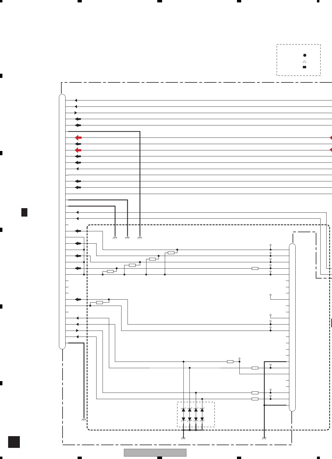
AVH-P4100DVD/XN/UC
144
1234
1234
C
D
F
A
B
E
10.5 IF PCB
B
GNDV GNDGNDD
D2004
MALS068X
D2005
D2006
GNDDGND
R2003
0
R2004
75
R2006
75
R2007
75
GNDD
R2001
75
R2008
NM
D2001
TP2024
TP2018
TP2025
TP2019
TP2020
TP2021
TP2015
TP2022
TP2016
TP2017
TP2023
TP2026
TP2030
R2005 470
R2009 470
R2010 1k
R2002 NM
CN2001
1
CCR
2
CCG
3
CCB
4CCSYNC
5GNDSIG
6DVDVBS
7GNDDVD
8YS
9NC
10 CCAUL
11 CCAUR
12 GNDAU
14 ONSEI-
15 REAUR
16 REAUL
17 GNDRAU
18 CCREM
19 DSEN
20 TVON
21 GION
22 MONON
23 VSW5
24 SYS_TO_NAVI
25 NAVI_TO_SYS
26 GNDD
13 ONSEI+
CN2002
1
BUS-
2
BUS+
3
ASENBO
4
BUSR+
5
BUSR-
6
GND
7
BUSL+
8
BUSL-
9
AUXL
10
AUAGND
11
AUXR
12
MAINTEST
13
AUVGND
14
AUXV
15
BCAM_IN
16
BCAM_VGGND
17
GNDV
18
GNDD
19
WIREDAD
20
WIRED
21
NC
22
ANR
23
GNDSIG
24
ANG
25
GNDSIG
26
ANB
27
GNDSIG
28
CSYNC
29
GNDSIG
30
CCAUL
31
CCAUR
32
GNDAU
33
ONSEI+
34
ONSEI-
35
NC
36
TVON
37
GUIDEON
38
SYS_TO_NAVI
39
NAVI_TO_SYS
40
GNDD
2125
CHIP SIZE LEGEND
3216
1608
CN121
1/4
A
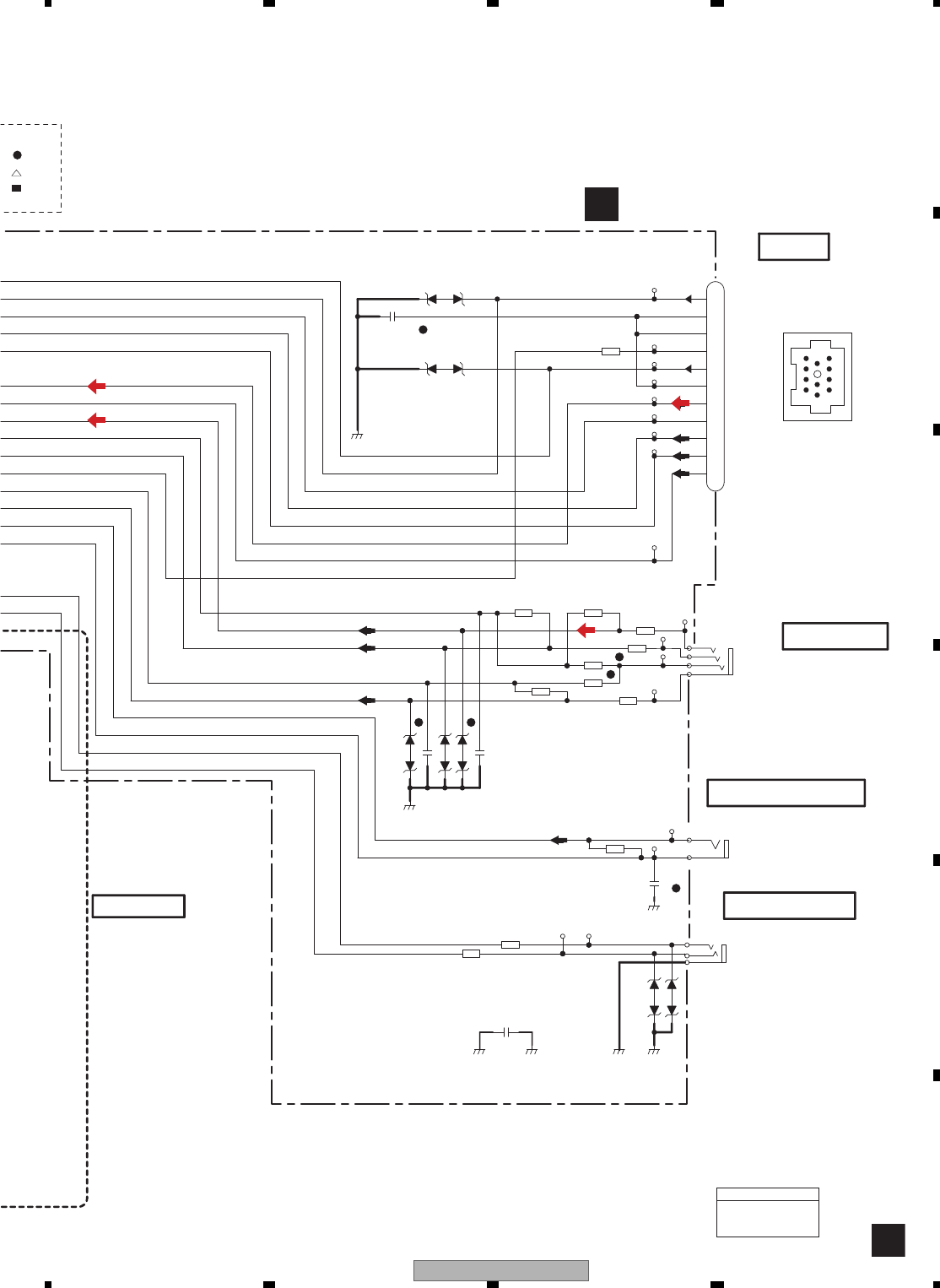
AVH-P4100DVD/XN/UC 145
5 678
5678
C
D
F
A
B
E
B
C2002
0.1u/50
GND
GNDD
R2011 1k
R2012 1k
JA2002
VIDEO
GND
AUXR
AUXL
11
22
33
44
C2001
0.1u/50
JA2003
2B.CAM_IN
1BCV_GND
R2018
75
GND
R2015 75
D2011
MALS068X
D2012
MALS068X
GND
D2009
D2010
MALS068X
GND
C2004
0.1u/50
D2003
MALS068X
C2003
0.1u/50
BUSL+
BUSR-
BUS-
ASENB
BUS+
BUSG
BUSR+
AUG
AUV
AUR
AUL
BCVG
BCAM
TP2002 TP2001
BUSL-
JA2001
2
3
1
R2014 22k
R2013
22k
JA2004
1BUS+
2BUSG
3BUSLG
4MAINTEST
5BUS-
6BUSRG
7BUSL+
8ASENBO
9BUSR+
10 BUSR-
11 BUSL-
R2019
1k
TP2029
D2002
MALS068X
AC
D2007
MALS068X
AC
CCR
CCG
CCB
CCSYNC
GNDSIG
DVDVBS
GNDDVD
YS
NC
CCAUL
CCAUR
GNDAU
ONSEI-
REAUR
REAUL
GNDRAU
CCREM
DSEN
TVON
GION
MONON
VSW5
SYS_TO_NAVI
NAVI_TO_SYS
GNDD
ONSEI+
R2021
0
R2020 0
R2022
GNDD GND
C2005
0.1u/50
R2017 0
R2016
0
LEGEND
GNDD
WIRED REMOTE
WIREDAD
WIRED
B.CAMERA INPUT
NAVI I/F
MINI JACK
IP BUS
UW5
BIF PCB
MOTHER UNIT
Consists of
MOTHER PCB
IF PCB
IP-BUS:+2.2 dBs
AUX:+2.2 dBs
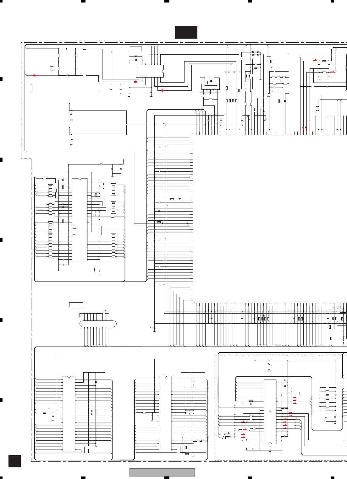
AVH-P4100DVD/XN/UC
146
1234
1234
C
D
F
A
B
E
10.6 DVD CORE UNIT(GUIDE PAGE)
C
C-a
A9
A4
A10
A5
A11
A6
A12
A7
A13
A8
A14
A15
D15
D7
D14
D6
D13
D5
D12
D4
D11
D3
D10
D2
D9
D1
D8
A3
A2
A1
XRD
A16
A5
A10
A4
A9
A1
A2
A3
A16A15
A14
A8
A13
A7
A12
A6
XRD
A11
A19
XWR1
A18
A17 A17
A19
A18
MDQ7
MDQ6
MDQ5
MDQ15
MDQ14
MA9
MA8
MA7
MA6
MA5
MA4
DQM0
XWE
XCAS
XRAS
XCSM
BA1
MA10
BA0
MA0
MA1
MA2
MA3
MCK
MA11
MDQ15
MDQ0
MDQ14
MDQ1
MDQ13
MDQ2
MDQ12
MDQ3
MDQ11
MDQ4
MDQ10
MDQ5
MDQ7
MDQ6
DQM1
DQM0
MDQ9
MDQ8
XWE
MA9
XRAS
BA0
XCAS
XCSM
MA7
MA0
MA1
MA10
MA8
BA1
MA6
MA3
MA5
MA4
MA2
A0
XCSF2
XRD
A16
XWR1
A19
A1
A17
A6
A3
A5
A2
A4
A7
FD
TD
XCSF1
D0
D8
D1
D9
D10
D2
D3
D4
D5
D11
D14
D13
D12
D7
D15
D4
D12
D5
D13
D6
D14
D7
D15
D10
D3
D11
D0
D8
D1
D9
D2
D6
A10
A8
A11
A9
LOUT
ROUT
SDODAC
SCKDAC
LTDAC
A12
IECOUT
A0
MA11
TRCDATA3
SCLOCK
TRCDATA0
TRCCLK
TRCDATA1
TRCST
TRCDATA2
SDATA
A0
COIL
COIL
COILW
HVM
HVP
HWM
HUP
HUM
HBM
MCK
COMPOSITE
XCSF2
FE1
FE2
EXTRG0
A15
A14
A13
A18
TEMP
DQM1
HWP
COILU
COILV
COILW
MD
LDIN TOM
FOP
FOM
TOP
CONT1
CONT2
FG
CRGDRV
HWP
HVM
HVP
HUM
HUP
HWM
HBM
HOM
XWR1
08E
NRES
NRES
TD
FD
STANDBY
MDQ13
MDQ9
MDQ10
MDQ11
MDQ12
MDQ8
MDQ1
MDQ3
MDQ2
MDQ4
MDQ0
A20
A20
D+
D-
D0
DGND3
DGND2
IEC
GNDD
GNDD
GNDA
GNDA
GNDD
GNDD
GND
GNDD
GNDD
GNDD
R1405
100K
R1503
1M
R1406
100K
R1402
100K
C1671
R1
C1672
R1
C1487
R1
C1481 R1
C1674
R1
C1480 R1
C1603
100P
C1482 R1
C1606
C1484 R1
C1509
R1
C1488
R1
C1602
100P
C1408
R1
C1403
R1
C1407
NM
C1402
NM
C1502
10
C1404
4R7
C1409
4R7
C1676
1
C1503 R1
VCC33
VCC12
VCC33
C1485
R1
C1504
R1
C1505
R1
C1506
R1
C1507
R1
C1508
R1
C1518 R1
C1519 R1
C1514
R1
C1511
R1
C1513 R1
C1516 R1
C1517 R1
C1515
R1
C1805
R1
PCM1753DBQ
IC1801
BCK
1
DATA
2
LRCK
3
DGND
4
5
NC
6
VCC
7
VOUTL
8
VOUTR
9
AGND
10
VCOM
11
ZEROR/ZEROA
12
ZEROL/NA
13
MD
14
MC
15
ML
16
SCK
2081C
7R4
GNDAU1
R1804
820
R1803
820
C1801
4R7
R1802
100K
C1804
1800P
R1801
100K
C1803
1800P
GNDAU
C1809
R1
GNDD
AVCC5
GNDAU
VCC33
C1501
10
GNDD
CN1951
1
2
3
4
5
6
7
8
9
1011
12
13
14
15
16
17
18
19
20
GNDD
VCC33
TEMP
PGND
GNDV
GNDD
R1954
15K
R1955
15K
C1601
R01
R1603
10K
R1517
10K
R1518
10K
C1673
R1
C1491 NM
C1492 NM
C1493 NM
C1494 NM
R1528
10K
R1529
10K
R1530
10K
R1531
10K
C1807
NM
R1217
1
R1218
1
R1213
1
R1214
1
R1215
1
R1216
1
PGND
PGND1PGND2
VHALF VHALF
VD8
PGND
100/16
C1201
FG
R1202 220
R1201 220
L1901
NM
11
2
2
3
344
D1902
NM
D1901
NM
GNDD
C1489
10
R1538
100K
R1542
10K
R1602
12K
R1601
12K
C1604
68P
C1605
68P
GNDD
VCC33
C1483 NM
C1486
NM
C1405
NM
R1212
270
AD2
ADOUT
CONT2
CONT1
CRGDRV
DACCK
FD1
LDIN
LRCK
LTDAC
MD1 MD2
SCKDAC
SDODAC
SRCK
TD1
XWR1
C1204
2200P
VC
GNDD5
R1403
NM
R1203
10K
R1204
15K
FOM2
FOP2
TOM2
TOP2
R1539
100K
R1501
1R2K
R1679
NM R1675
NM
R1673
NM
GNDD
R1505 100
R1506 100
R1507 100
L1904
C1490
R001
C1211
4R7
R1401
220
C1401
R01
R1950
240
R1951
240
C1512
10P
C1510
12P
C1203
NM
C1205
R1
C1207
R1
C1210
R1
C1209
R1
R1508
220
R1512
100
C1208
R01
C1525
NM
R1483
56
2
1
4
3
6
5
8
7
R1487
56
2
1
4
3
6
5
8
7
R1486
56
2
1
4
3
6
5
8
7
R1488
56
2
1
4
3
6
5
8
7
R1481
56
2
1
4
3
6
5
8
7
R1480
56
2
1
4
3
6
5
8
7
R1484
56
2
1
4
3
6
5
8
7
R1482
56
2
1
4
3
6
5
8
7
R1485
56
2
1
4
3
6
5
8
7
R1490
56
R1489
56
C1806
10
R1527
6R8K
R1546
6R8K
R1956
0R0
R1957
0R0
R1547
NM
R1409
NM
IC1201
BD8231EFV
1VC
2TKIN
3FCIN
4SLIN
5
SLOPOUT
6LDIN
7SPIN
8CTL1
9CTL2
10 GND1
11 TEST
12 FG
13 SPCNF
14 HB
15 HW-
16 HW+
17 HV-
18 HV+
19 HU-
20 HU+ 21
VM_S
22
BH
23
SPRNF
24
SPVM
25
SPGND
26
U
27
V
28
W
29
SLVM
30
PGND
31
SL/LDO+
32
SL/LDO-
33
FCO+
34
FCO-
35
TKO+
36
TKO- 37
AVM
38
PREVcc 39
PREGND 40
SUBGND
41
GND2
MN2DS0018MAUB
IC1501
EXDT1
1
EXDT9
2
EXDT2
3
EXDT10
4
VSS_1
5
VDD33_1
6
EXDT3
7
EXDT11
8
EXDT4
9
EXDT12
10
EXDT5
11
EXDT13
12
EXDT6
13
EXDT14
14
VSS_2
15
VDD33_2
16
EXDT7
17
EXDT15
18
VSS_3
19
VDD12_1
20
EXADR16
21
EXADT15
22
EXADT14
23
EXADT13
24
EXADT12
25
EXADT11
26
EXADT10
27
EXADT9
28
EXADT8
29
EXADR19
30
NEXWE
31
VSS_4
32
VDD33_3
33
EXADR18
34
EXADR17
35
EXADT7
36
EXADT6
37
EXADT5
38
EXADT4
39
EXADT3
40
EXADT2
41
EXADT1
42
VSS_5
43
VDD12_2
44
45
46
47
IRQPWR
48
49
USB CLOCK
50 VIN5 113
VIN6 114
115
116
VIN3 117
VIN4 118
VIN2 119
VIN1 120
VDSENS 121
TEMP 122
AD2 123
AD4 124
AVSSH 125
TD 126
FD 127
AVDDH 128
DAC3OUT 129
DAC2OUT 130
DAC1OUT 131
AVDDF 132
COMP1 133
VREF 134
IREF1 135
COMP2 136
AVSSF 137
COMPOSITE 138
DAC5OUT 139
AVSSE 140
AVDDE 141
AVDDG 142
AVSSG 143
LOUT 144
145
AVSSI
146
ROUT
147
AVDDI
148
DACCK
149
SRCK
150
LRCK
151
ADOUT
152
IECOUT
153
VSS_9
154
VDD33_6
155
OSCI
156
OSCO
157
VSS_10
158
VDD12_4
159
MDQ15
160
MDQ0
161
MDQ14
162
MDQ1
163
MDQ13
164
MDQ2
165
VSS_11
166 VDD33_7
167 MDQ12
168 MDQ3
169 MDQ11
170 MDQ4
171 MDQ10
172 MDQ5
173 VSS_12
174 VDD33_8
175 MDQ9
176 MDQ6
177 MDQ8
178 MDQ7
179 DQM0
180 DQM1
181 NWE
182 VSS_13
183 MCK
184 VDD33_9
185 MCKI
186 VSS_14
187 VDD12_5
188 NCAS
189 NRAS
190 NCSM
191
192 DQM3
193 BA0
194 MA9
195 VSS_15
196 VDD33_10
197 BA1
198 MA8
199 MA10
200 MA7
201 MA0
202 MA6
203 MA1
204 VSS_16
205 VDD33_11
206 MA5
207 MA2
208 MA4
209 MA3
210 VSS_17
211 VDD12_6
212 EXADT0
213 NEXCE
214 NEXOE
215 EXDT0
216
EXDT8
X1501
CSS1768
X1
1GND1 2
GND2
4X2 3
L1512
IC1480
K4S641632N-LC75
VDD1
1
DQ0
2
VDDQ1
3
DQ1
4
5DQ2
6VSSQ1
7DQ3
8DQ4
9VDDQ2
10 DQ5
11 DQ6
12 VSSQ2
13 DQ7
14 VDD2
15 LDQM
16 WE
17 CAS
18 RAS
19 CS
20 BA0
21 BA1
22 A10/AP
23 A0
24 A1
25 A2
26 A3
27 VDD3 28
VSS1
29
A4
30
A5
31
A6
32
A7
33
A8
34
A9
35
A11
36
N.C
37
CKE
38
CLK
39
UDQM
40
N.C/RFU
41
VSS2
42
DQ8
43
VDDQ3
44
DQ9
45
DQ10
46
VSSQ3
47
DQ11
48
DQ12
49
VDDQ4
50
DQ13
51
DQ14
52
VSSQ4
53
DQ15
54
VSS3
R1504
12
C1808
NM
IC1401
CWW1753
A15
1
A14
2
A13
3
A12
4
5A11
6A10
7A9
8A8
9A19
10 NC1
11 /WE
12 /RESET
13 NC2
14 NC3
15 RY_/BY
16 A18
17 A17
18 A7
19 A6
20 A5
21 A4
22 A3
23 A2
24 A1 25
A0
26
/CE
27
Vss1
28
/OE
29
DQ0
30
DQ8
31
DQ1
32
DQ9
33
DQ2
34
DQ10
35
DQ3
36
DQ11
37
Vcc
38
DQ4
39
DQ12
40
DQ5
41
DQ13
42
DQ6
43
DQ14
44
DQ7
45
DQ15_A-1
46
Vss2
47
/BYTE
48
A16
IC1402
CWW1754
A15
1
A14
2
A13
3
A12
4
5A11
6A10
7A9
8A8
9A19
10 NC1
11 /WE
12 /RESET
13 NC2
14 NC3
15 RY_/BY
16 A18
17 A17
18 A7
19 A6
20 A5
21 A4
22 A3
23 A2
24 A1 25
A0
26
/CE
27
Vss1
28
/OE
29
DQ0
30
DQ8
31
DQ1
32
DQ9
33
DQ2
34
DQ10
35
DQ3
36
DQ11
37
Vcc
38
DQ4
39
DQ12
40
DQ5
41
DQ13
42
DQ6
43
DQ14
44
DQ7
45
DQ15_A-1
46
Vss2
47
/BYTE
48
A16
R1511 0R0
R1670
10K
R1672
200
R1671
24K
R1674
30K
FLASH 16M
(2125)
(2125)
(2125)
FLASH 16M
(IEC/IPFLG)
SDRAM
(1608)
(2125)
(2125)
AUDIO 2CH ANALOG OUT
ADAC
(2125)
DEBUG
(2125)
CP_READY
I2C_SDA
I2C_SCL
08EJ
STANDBY
VIN8
VIN7
(3216)
27.000MHz
2
4
T
T
F
F
F
T
T
F
T
F
S
C
C
C
S
S
S
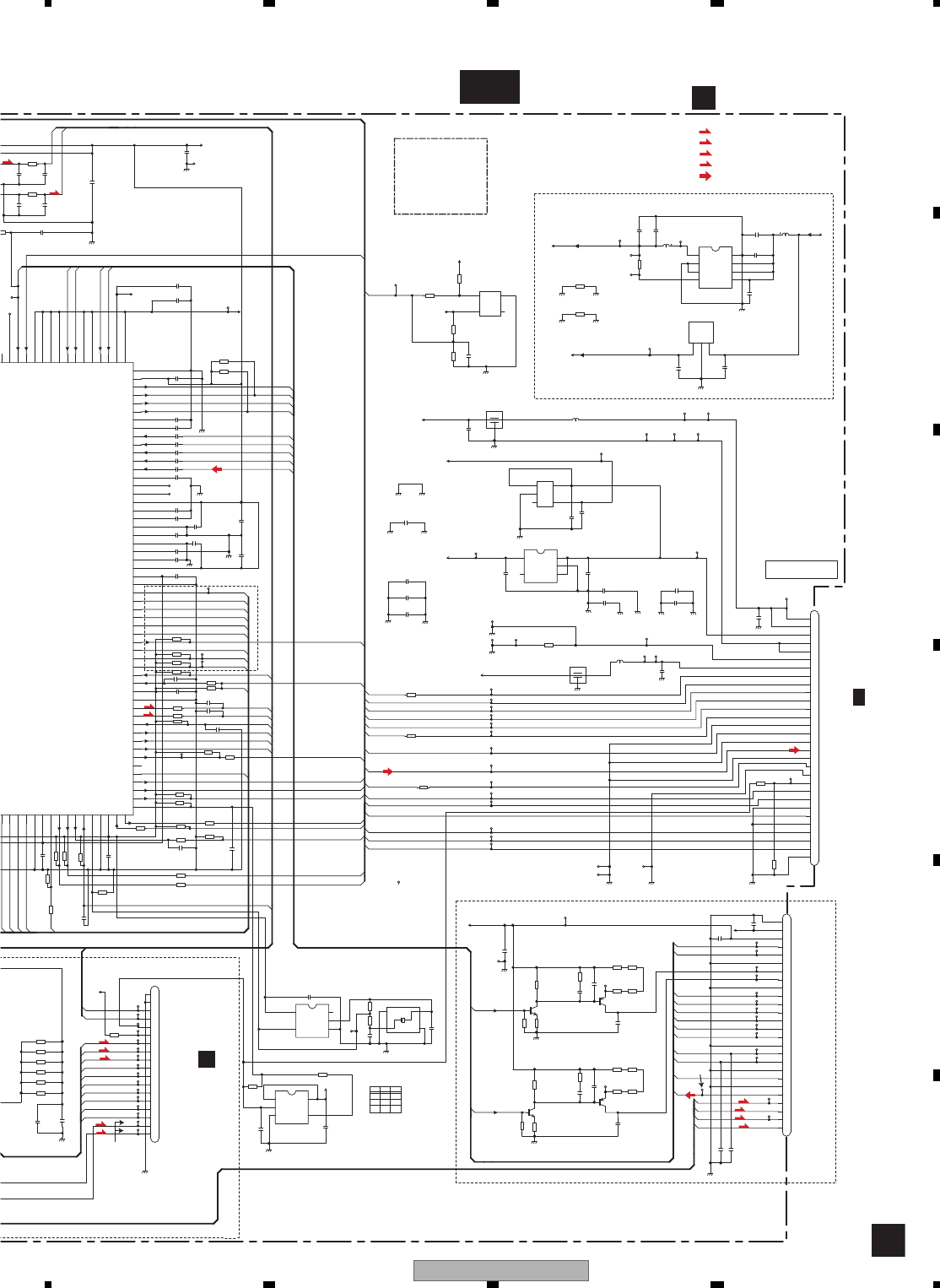
AVH-P4100DVD/XN/UC 147
5 678
5678
C
D
F
A
B
E
C
C-b
DVDMPD
FE1
A1
A3
A2
A4
SCLOCK
SDATA
TRCCLK
TRCDATA0
TRCDATA1
TRCDATA2
TRCDATA3
B
C
A
D
LPCO1
LPCO2
FD
TD
CDMPD
STANDBY
STSCOMN
SCKDAC
COILV
COILU
COILW
HVM
HVP
HWM
HUP
HUM
HBM
XCSF1
E+G_E+F
F+H_G+H
B
A
FE2
TEMP
RF
F+H_G+H
E+G_E+F
RF
CDMPD
CRGDRV
MD
FG
FE1
FE2
NRES
NRES
LTDAC
SDODAC
TOP
EXTRG0
TEMP
AMUTE
C
D
LDIN
CONT2
CONT1
CMDCOMN
VDSENS
VDSENS
HWP
FOM
FOP
HOME
NRES
IRQPWR
CMDCOMN
STSCOMN
ROUT
D-
D+
IECOUT
LOUT
AMUTE
08EJ
TRCST
TOM
I2C_SCL
I2C_SDA
CP_Reset
I2C_SCL
I2C_SDA
IRQPWR
COMPOSITE
HOME
08EJ
A20
CP_Reset
DVDMPD
DVDLD1
AGND3
VCC5_3
GNDA
GNDD
GNDA
GNDA
GNDA
GNDA
R1103
390
R1104
510
R1101 100K
C1106
R01
C1603
100P
C1606
R1
C1602
100P
VCC33
VCC5
Q1101
2SC4081
C1519 R1
C1520
R1
R1509 1K
R1510 1K
SDATA
SCLOCK
C1521 R1
C1622 R033
GNDA
C1620 R22
GNDA
C1624
R1
C1625
R1
C1621 R22
ANAMONI1
ANAMONI2
C1619 5600P
C1618 100P
C1616 R1
C1617 R1
GNDA
C1612 R1
C1614 R1
C1615 R1
C1613 R1
C1611 R1
C1610 R1
GNDA
C1609 R1
VREF
VREF
C1623
1
C1608
1
VHALF
R1232D121B
IC1005
PGND 1
VIN 2
VDD 3
CE 45 VOUT
6TEST
7AGND
8LX
L1004
FB12A
VCC12
C1010
2R2
C1011
1
R1002
100
VCC33-1
VCC33
VDD5
VCC12-1
FB12B
DDF
VCC33
IC1001
NM
OUT
1
VDD
2
NC
3
VSS
4
VSENS
VD8
GNDA
DGND1
PGND
PGND4
GNDV
NRES
VDD5
VD8_1
C1004
4R7
R1015
NM
AGND4
VCC5_1
EF1002
3
2
1
EF1001
3
2
1
PGND3
AGND1
VDD5_1
GNDAU GNDD
VDD5_2
GNDA
VCC5
GNDD
C1001
1
DGND4
PGND5
GNDD
AVCC5
RO
LO
VD8
AVCC5
C1522 R1
DVDLD0
CDLD0
R1604 1M
TEMP
PGND
GNDD
GNDD
VCC33
U-
HB+
HB-
W-
COM
COILU
V-
COP
U+
W+
V+
COILV
COILW
C1007
NM
C1006
NM
HOME
GNDD
R1017
NM
GND_DD
C1110
R01
VREF
C1108 R01
E+G_E+F
F+H_G+H
R1102 100K
GNDA
C1105 R1
R1106
560
Q1102
2SC4081
R1105
390
C1107
R01
CDLD1
DVDMPD
RF
C1601
R01
603
0K
CDMPD
C1523
R1
R1513 10K
08EJ
12EJ
IRQPWR
CMDCOMN
STSCOMN
STANBY
COMPOSITE
D+
D-
VD
C1526 R01
R1523 220
R1522 100K
R1519 1K
IC1006
NM
G
1
IN
2
GND
3OUT 4
5
VCC
VD8
GNDAU
GNDAU3
GNDV
GNDAU2
GNDD
C1015
R001
PGND
R1536
100K
R1537
100K
R1004
47K
R1007
6R8K
GNDD
VD8_2
R1011
NM
GND_DD
GND_DD
GND_DCON
GND_DCON
B
A
C
D
FE1
FE2
R1217
1
R1218
1
R1213
1
R1214
1
R1215
1
R1216
1
L1003
R1534
220
GNDD
C1016
R001
R1540 220
AGND2
GNDA
C1607
10
C1003 R1
AMUTE
R1525 10K
GNDD
R1952
1M
IC1951
TC7SZU04FU
NC 1
IN_A 2
GND 3
OUT_Y
4
5VCC
C1950
R1
R1542
10K
R1524 4R7K
48MHz
C1104
R1
R1602
12K
R1601
12K
C1604
68P
C1605
68P
R1514 18K
R1541 220
C1017
NM
R1526 10K
C1005
1
R1222
270
AD2
TRCST
R1026
NM
R1516 10K
R1300
0R0
VCC5
C1524
R047
C1302
NM
R1021
0R0
TOP1
FOP1
R1535
100K
CP_RESET
RESET
SDA
SCL
R1539
100K
NJM2885DL1-33
IC1004
1IN
2GND
3OUT
2SB1132
Q1104
2SB1132
Q1103
C1626
NM
C1627
NM
C1018
R1
L1902
L1903
C1211
4R7
GNDDPGND
C1019
R1
R1953
680
C1210
R1
C1528
470P
WAKEUP
R1019
100
R1025
100
R1027
100
C1529
NM
GNDAU
C1952
10P
C1951
10P
C1525
NM
C1527
NM
R1110
3R3
R1109
3R3
C1111
R22
C1109
R22
R1008
NM
R1001
NM
C1953
NM
C1954
47P
10
C1101
R1527
6R8K
R1546
6R8K
R1301
NM
R1547
NM
CN1901
1
2
3
4
5
6
7
8
9
10
11
12
13
14
15
16
17
18
19
20
21
22
23
24
25
26
27
28
29
30
CN1201
1
2
3
4
5
6
7
8
9
10
11
12
13
14
15
16
17
18
EXADT4
EXADT3
40
EXADT2
41
EXADT1
42
VSS_5
43
VDD12_2
44
45
46
47
IRQPWR
48
49
USB_CLOCK
50
VSS_6
51
VDD33_4
52
CMDCOMN
53 STSCOMN
54
12EJ
55
LTDAC 56
SDODAC 57
SCKDAC 58
XCSSR 59
P13 60
61
62
CONT1 63
CONT2 64
65
MD 66
CRGDRV 67
VSS_7 68
VDD33_5 69
NRES 70
FG 71
SCLOCK 72
SDATA 73
EXTRG0 74
EXTRG1 75
TRCCLK 76
TRCDATA0 77
TRCDATA1 78
TRCDATA2 79
TRCDATA3 80
TRCST 81
VSS_8 82
VDD12_3 83
AVDDD 84
PLFIL1 85
VREFH7 86
AVSSD 87
VREFL7 88
AVSSC 89
CCAPA 90
CDATA 91
AVDDC 92
ANAMONI1 93
ANAMONI2 94
RFINN 95
RFINP 96
VIN1RF 97
VIN2RF 98
VIN4RF 99
VIN3RF 100
VREFH5 101
VREFL5 102
DVDMPD 103
LPCO1 104
CDMPD 105
LPCO2
106
AVDDB
107
AVSSB
108
VREFH
109
VHALF 110
E+G_E+F 111
F+H_G+H 112
VIN5 113
VIN6 114
115
116
VIN3 117
VIN4 118
VIN2 119
VIN1 120
VDSENS 121
TEMP 122
AD2 123
AD4
IC1003
S-1200B50-M5
VIN 1
VSS 2
ON/OFF 3
NC
4
5VOUT
X1950
CSS1760
X1
1GND1 2
GND2
4X2 3
C1301
NM
CN1101
1
2
3
4
5
6
7
8
9
10
11
12
13
14
15
16
17
18
19
20
21
22
23
24
25
26
R1532
100
C1014
10
C1009
10
C1013
10
C1008
10
C1012
NM
R1543 180
R1544 180
R1533
NM
C1112
22
C1113
22
IC1002
S-1133B50-U5
NC
1
VSS
2
ON/OFF
3
VIN
4
5
VOUT
CP_READY
R1114
1R5
R1111
1R5
R1112
1R5
R1115
1R5
R1116
1R5
R1117
1R5
R1113
1R5
R1118
1R5
R1605 1M
GNDDGNDD
LPCO1
LPCO2
PU(DP10)
(1608)
(1608)
(1608*4)
(1608*4)
(1608)
DEBUG
MOTOR DRIVER
12cm(DSCSNS)
8cm
5.0-3.3&1.2 V DC/DC
VOLTAGE DETECT
(1608)
VD5
HOST I/F
AMUTE
ANALOG ROUT
(2125)
STANBY
(1608)
PGND
COMPOSIT
(3216)
HSTCMD
SLVSTS
PGND
XRESET
AGND
VD8
DGND
ANALOG LOUT
IRQPWR
VD8
AGND
VIDEO GND
AGND
D-
D+
DGND
COIL_U
HALL_V+
HALL_V-
HALL_U-
HALL_W+
GNDD
HALL_U+
COIL_V
HALL_W-
HALL_BIAS+
HALL_BIAS-
COIL_W
HOME
CRG/LE+
CRG/LE-
X
L
H
L
Z
GOUT
H
L
<TC7SZ126FU>
H
IN
VD8
F+
T-
LD GND
F-
FE2
B
A
T+
78LD
C
RF
78MDG
SW
65LD
E+G/E+F
GND
D
F+H/G+H
VCC
65MDG
FE1
:PU
1200->1299
1100->1199
:FLASH
:SDRAM
1480->1499
1850->1899
1670->1699 :DVN(BE)
:DVN(SYS)
:VIDEO
1900->1950
1500->1599
:AUDIO (DIGITAL)
1400->1449
1000->1049
1800->1849
1700->1749
:ACT+SPDL
:POWER SUPPLY
:OUTSIDE I/F
:AUDIO (ANALOG)
1600->1669 :DVN(FE)
1950->1999
(2125)
Vref
78MD
65MD
TEMP
TEMP GND
IECOUT
DGND
(1608)
(1608)
H
(1608)
LDIN
HOME
:USB
GNDD
(2125)
CP_Reset
CP_READY
I2C_SDA
I2C_SCL
08EJ
VIN8
VIN7
RESET
SDA
SCL
(3216)
(1608)
(1005)
WAKEUP
DGND
USB
48.000MHz
X:Don’t Care
Z:High Impedance
GNDD
C1021
680P
C1022
680P
GNDV
C1934
68P
CD
DVD
CDVD CORE UNIT
CN901
PICKUP UNIT (SERVICE)
D
CN701
3/4
A
1
3
FFOCUS SERVO LINE
TRACKING SERVO LINE
CARRIAGE SERVO LINE
SPINDLE SERVO LINE
RF SIGNAL
T
C
S
F
F
T
T
T
F
C
C
C
S
S
S
S
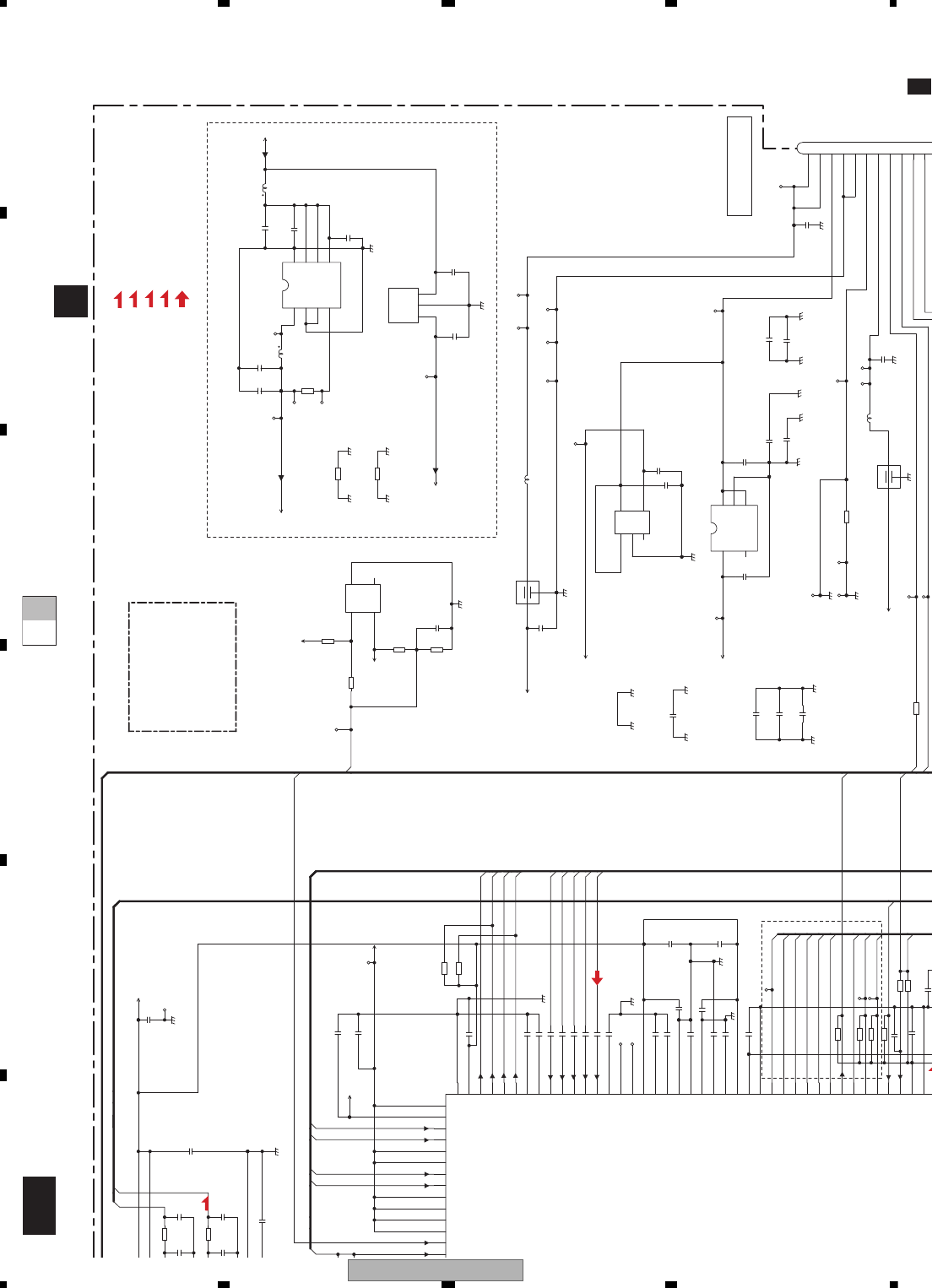
AVH-P4100DVD/XN/UC
148
1234
1234
C
D
F
A
B
E
C-a C-b
C-b
SCLOCK
SDATA
TRCCLK
TRCDATA0
TRCDATA1
TRCDATA2
TRCDATA3
B
C
A
D
LPCO1
LPCO2
FD
TD
CDMPD
F+H_G+H
E+G_E+F
RF
CRGDRV
FG
FE1
FE2
NRES
NRES
EXTRG0
TEMP
AMUTE
VDSENS
VDSENS
NRES
AMUTE
TRCST
DVDMPD
GNDA
GNDD
GNDA
C1603
100P
C1606
R1
C1602
100P
VCC33
R1509 1K
R1510 1K
SDATA
SCLOCK
C1521 R1
C1622 R033
GNDA
C1620 R22
GNDA
C1624
R1
C1625
R1
C1621 R22
ANAMONI1
ANAMONI2
C1619 5600P
C1618 100P
C1616 R1
C1617 R1
GNDA
C1612 R1
C1614 R1
C1615 R1
C1613 R1
C1611 R1
C1610 R1
GNDA
C1609 R1
VREF
VREF
C1623
1
C1608
1
VHALF
R1232D121B
IC1005
PGND 1
VIN 2
VDD 3
CE 45 VOUT
6TEST
7AGND
8LX
L1004
FB12A
VCC12
C1010
2R2
C1011
1
R1002
100
VCC33-1
VCC33
VDD5
VCC12-1
FB12B
DDF
VCC33
IC1001
NM
OUT
1
VDD
2
NC
3
VSS
4
VSENS
VD8
GNDA
DGND1
PGND
PGND4
GNDV
NRES
VDD5
VD8_1
C1004
4R7
R1015
NM
AGND4
VCC5_1
EF1002
3
2
1
EF1001
3
2
1
PGND3
AGND1
VDD5_1
GNDAU GNDD
VDD5_2
GNDA
VCC5
GNDD
C1001
1
DGND4
PGND5
GNDD
AVCC5
VD8
AVCC5
C1522 R1
R1604 1M
C1007
NM
C1006
NM
GNDD
R1017
NM
GND_DD
C1601
R01
C1523
R1
R1513 10K
VD
C1526 R01
R1523 220
R1522 100K
VD8
C1015
R001
PGND
R1004
47K
R1007
6R8K
GNDD
VD8_2
R1011
NM
GND_DD
GND_DD
GND_DCON
GND_DCON
L1003
GNDD
C1016
R001
AGND2
GNDA
C1607
10
C1003 R1
AMUTE
R1524 4R7K
R1602
12K
R1601
12K
C1604
68P
C1605
68P
C1017
NM
C1005
1
TRCST
R1516 10K
NJM2885DL1-33
IC1004
1IN
2GND
3OUT
C1626
NM
C1627
NM
C1018
R1
L1902
L1903
GNDDPGND
C1019
R1
R1019
100
GNDAU
R1008
NM
R1001
NM
C1953
NM
C1954
47P
CN1901
1
2
3
4
5
6
7
8
9
10
11
67
VSS_7 68
VDD33_5 69
NRES 70
FG 71
SCLOCK 72
SDATA 73
EXTRG0 74
EXTRG1 75
TRCCLK 76
TRCDATA0 77
TRCDATA1 78
TRCDATA2 79
TRCDATA3 80
TRCST 81
VSS_8 82
VDD12_3 83
AVDDD 84
PLFIL1 85
VREFH7 86
AVSSD 87
VREFL7 88
AVSSC 89
CCAPA 90
CDATA 91
AVDDC 92
ANAMONI1 93
ANAMONI2 94
RFINN 95
RFINP 96
VIN1RF 97
VIN2RF 98
VIN4RF 99
VIN3RF 100
VREFH5 101
VREFL5 102
DVDMPD 103
LPCO1 104
CDMPD 105
LPCO2
106
AVDDB
107
AVSSB
108
VREFH
109
VHALF 110
E+G_E+F 111
F+H_G+H 112
VIN5 113
VIN6 114
115
116
VIN3 117
VIN4 118
VIN2 119
VIN1 120
VDSENS 121
TEMP 122
IC1003
S-1200B50-M5
VIN 1
VSS 2
ON/OFF 3
NC
4
5VOUT
C1014
10
C1009
10
C1013
10
C1008
10
C1012
NM
IC1002
S-1133B50-U5
NC
1
VSS
2
ON/OFF
3
VIN
4
5
VOUT
R1605 1M
GNDDGNDD
(1608)
DEBUG
5.0-3.3&1.2 V DC/DC
VOLTAGE DETECT
(1608)
VD5
HOST I/F
AMUTE
(2125)
(1608)
PGND
(3216)
HSTCMD
PGND
XRESET
VD8
DGND
IRQPWR
VD8
VD8
:PU
1200->1299
1100->1199
:FLASH
:SDRAM
1480->1499
1850->1899
1670->1699 :DVN(BE)
:DVN(SYS)
:VIDEO
1900->1950
1500->1599
:AUDIO (DIGITAL)
1400->1449
1000->1049
1800->1849
1700->1749
:ACT+SPDL
:POWER SUPPLY
:OUTSIDE I/F
:AUDIO (ANALOG)
1600->1669 :DVN(FE)
1950->1999
(2125)
(1608)
(1608)
(1608)
:USB
(2125)
VIN8
VIN7
(1608)
(1005)
USB
GNDD
C1021
680P
C1022
680P
C1934
68P
C
DVD CORE UNIT
3/4
A
F
FOCUS SERVO LINE
TRACKING SERVO LINE
CARRIAGE SERVO LINE
SPINDLE SERVO LINE
RF SIGNAL
T
C
S
T
C
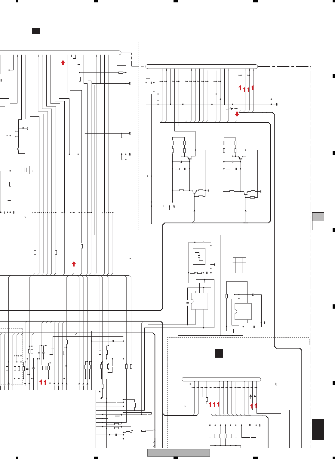
AVH-P4100DVD/XN/UC 149
5 678
5678
C
D
F
A
B
E
C-a C-b
C-b
DVDMPD
FE1
A1
A2
SCLOCK
SDATA
TRCCLK
STANDBY
STSCOMN
SCKDAC
COILV
COILU
COILW
HVM
HVP
HWM
HUP
HUM
HBM
XCSF1
E+G_E+F
F+H_G+H
B
A
FE2
TEMP
RF
CDMPD
CRGDRV
MD
FG
NRES
NRES
LTDAC
SDODAC
TOP
EXTRG0
AMUTE
C
D
LDIN
CONT2
CONT1
CMDCOMN
HWP
FOM
FOP
HOME
NRES
IRQPWR
CMDCOMN
STSCOMN
ROUT
D-
D+
IECOUT
LOUT
AMUTE
08EJ
TOM
I2C_SCL
I2C_SDA
CP_Reset
I2C_SCL
I2C_SDA
IRQPWR
COMPOSITE
HOME
08EJ
A20
CP_Reset
DVDLD1
AGND3
VCC5_3
GNDA
GNDD
GNDA
GNDA
GNDA
R1103
390
R1104
510
R1101 100K
C1106
R01
VCC5
Q1101
2SC4081
C1519 R1
C1520
R1
R1509 1K
R1510 1K
SDATA
SCLOCK
GNDA
NRES
VDD5
R1015
NM
AGND4
EF1002
3
2
1
AGND1
VDD5_1
VDD5_2
GNDD DGND4
GNDD
RO
LO
C1522 R1
DVDLD0
CDLD0
PGND
GNDD
GNDD
VCC33
U-
HB+
HB-
W-
COM
COILU
V-
COP
U+
W+
V+
COILV
COILW
HOME
C1110
R01
VREF
C1108 R01
E+G_E+F
F+H_G+H
R1102 100K
GNDA
C1105 R1
R1106
560
Q1102
2SC4081
R1105
390
C1107
R01
CDLD1
DVDMPD
RF
CDMPD
C1523
R1
R1513 10K
08EJ
12EJ
IRQPWR
CMDCOMN
STSCOMN
STANBY
COMPOSITE
D+
D-
C1526 R01
R1523 220
R1522 100K
R1519 1K
IC1006
NM
G
1
IN
2
GND
3OUT 4
5
VCC
GNDAU
GNDAU3
GNDV
GNDAU2
GNDD
PGND
R1536
100K
R1537
100K
B
A
C
D
FE1
FE2
R1217
1
R1218
1
R1213
1
R1214
1
R1215
1
R1216
1
R1534
220
GNDD
C1016
R001
R1540 220
AMUTE
R1525 10K
GNDD
R1952
1M
IC1951
TC7SZU04FU
NC 1
IN_A 2
GND 3
OUT_Y
4
5VCC
C1950
R1
R1542
10K
R1524 4R7K
48MHz
C1104
R1
R1514 18K
R1541 220
R1526 10K
R1222
270
R1026
NM
R1516 10K
R1300
0R0
VCC5
C1524
R047
C1302
NM
R1021
0R0
TOP1
FOP1
R1535
100K
CP_RESET
RESET
SDA
SCL
R1539
100K
2SB1132
Q1104
2SB1132
Q1103
L1903
C1211
4R7
R1953
680
C1210
R1
C1528
470P
WAKEUP
R1019
100
R1025
100
R1027
100
C1529
NM
C1952
10P
C1951
10P
C1525
NM
C1527
NM
R1110
3R3
R1109
3R3
C1111
R22
C1109
R22
10
C1101
R1527
6R8K
R1546
6R8K
R1301
NM
R1547
NM
2
3
4
5
6
7
8
9
10
11
12
13
14
15
16
17
18
19
20
21
22
23
24
25
26
27
28
29
30
CN1201
1
2
3
4
5
6
7
8
9
10
11
12
13
14
15
16
17
18
EXADT2
41
EXADT1
42
VSS_5
43
VDD12_2
44
45
46
47
IRQPWR
48
49
USB_CLOCK
50
VSS_6
51
VDD33_4
52
CMDCOMN
53 STSCOMN
54
12EJ
55
LTDAC 56
SDODAC 57
SCKDAC 58
XCSSR 59
P13 60
61
62
CONT1 63
CONT2 64
65
MD 66
CRGDRV 67
VSS_7 68
VDD33_5 69
NRES 70
FG 71
SCLOCK 72
SDATA 73
EXTRG0 74
EXTRG1 75
TRCCLK 76
TRCDATA0
X1950
CSS1760
X1
1GND1 2
GND2
4X2 3
C1301
NM
CN1101
1
2
3
4
5
6
7
8
9
10
11
12
13
14
15
16
17
18
19
20
21
22
23
24
25
26
R1532
100
R1543 180
R1544 180
R1533
NM
C1112
22
C1113
22
CP_READY
R1114
1R5
R1111
1R5
R1112
1R5
R1115
1R5
R1116
1R5
R1117
1R5
R1113
1R5
R1118
1R5
LPCO1
LPCO2
PU(DP10)
(1608)
(1608)
(1608*4)
(1608*4)
MOTOR DRIVER
12cm(DSCSNS)
8cm
VD5
AMUTE
ANALOG ROUT
STANBY
PGND
COMPOSIT
(3216)
HSTCMD
SLVSTS
PGND
XRESET
AGND
VD8
DGND
ANALOG LOUT
IRQPWR
AGND
VIDEO GND
AGND
D-
D+
DGND
COIL_U
HALL_V+
HALL_V-
HALL_U-
HALL_W+
GNDD
HALL_U+
COIL_V
HALL_W-
HALL_BIAS+
HALL_BIAS-
COIL_W
HOME
CRG/LE+
CRG/LE-
X
L
H
L
Z
G OUT
H
L
<TC7SZ126FU>
H
IN
VD8
F+
T-
LD GND
F-
FE2
B
A
T+
78LD
C
RF
78MDG
SW
65LD
E+G/E+F
GND
D
F+H/G+H
VCC
65MDG
FE1
Vref
78MD
65MD
TEMP
TEMP GND
IECOUT
DGND
H
LDIN
HOME
GNDD
CP_Reset
CP_READY
I2C_SDA
I2C_SCL
08EJ
RESET
SDA
SCL
(3216)
WAKEUP
DGND
48.000MHz
X:Don’t Care
Z:High Impedance
GNDV
CD
DVD
CN901
PICKUP UNIT (SERVICE)
D
CN701
3/4
A
1
3
F
F
T
T
C
C
C
S
S
S
S
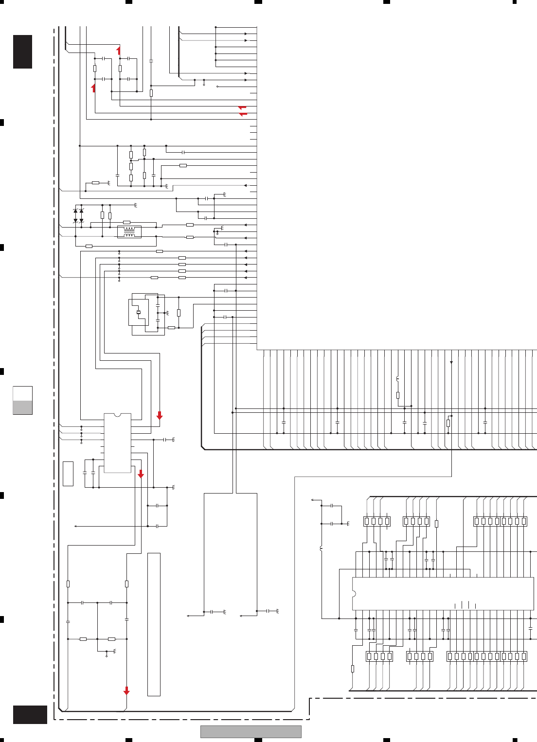
AVH-P4100DVD/XN/UC
150
1234
1234
C
D
F
A
B
E
C-bC-a
C-a
C-b
MDQ7
MDQ6
MDQ5
MDQ15
MDQ14
MA9
MA8
MA7
MA6
MA5
MA4
DQM0
XWE
XCAS
XRAS
XCSM
BA1
MA10
BA0
MA0
MA1
MA2
MA3
MCK
MA11
MDQ15
MDQ0
MDQ14
MDQ1
MDQ13
MDQ2
MDQ12
MDQ3
MDQ11
MDQ4
MDQ10
MDQ5
MDQ7
MDQ6
DQM1
DQM0
MDQ9
MDQ8
XWE
MA9
XRAS
BA0
XCAS
XCSM
MA7
MA0
MA1
MA10
MA8
BA1
MA6
FD
TD
LOUT
ROUT
SDODAC
SCKDAC
LTDAC
IECOUT
MA11
MCK
COMPOSITE
FE1
FE2
TEMP
DQM1
STANDBY
MDQ13
MDQ9
MDQ10
MDQ11
MDQ12
MDQ8
MDQ1
MDQ3
MDQ2
MDQ4
MDQ0
D+
D-
IEC
GNDA
GNDA
GNDD
GNDD
R1503
1M
C1671
R1
C1672
R1
C1487
R1
C1481 R1
C1674
R1
C1480 R1
C1603
100P
C1482 R1
C1484 R1
C1488
R1
C1602
100P
C1502
10
C1676
1
C1503 R1
VCC33
VCC12
C1485
R1
C1504
R1
C1505
R1
C1506
R1
C1507
R1
C1514
R1
C1511
R1
C1515
R1
C1805
R1
PCM1753DBQ
IC1801
BCK
1
DATA
2
LRCK
3
DGND
4
5
NC
6
VCC
7
VOUTL
8
VOUTR
9
AGND
10
VCOM
11
ZEROR/ZEROA
12
ZEROL/NA
13
MD
14
MC
15
ML
16
SCK
2081C
7R4
GNDAU1
R1804
820
R1803
820
C1801
4R7
R1802
100K
C1804
1800P
R1801
100K
C1803
1800P
GNDAU
C1809
R1
GNDD
AVCC5
GNDAU
VCC33
C1501
10
GNDD
TEMP
GNDV
GNDD
R1954
15K
R1955
15K
C1601
R01
R1603
10K
C1673
R1
C1491 NM
C1492 NM
C1493 NM
C1494 NM
C1807
NM
L1901
NM
11
2
2
3
344
D1902
NM
D1901
NM
GNDD
C1489
10
R1538
100K
R1602
12K
R1601
12K
C1604
68P
C1605
68P
C1483 NM
AD2
ADOUT
DACCK
LRCK
LTDAC
SCKDAC
SDODAC
SRCK
GNDD5
R1501
1R2K
R1679
NM R1675
NM
R1673
NM
GNDD
R1505 100
R1506 100
R1507 100
L1904
C1490
R001
R1950
240
R1951
240
C1512
10P
C1510
12P
R1508
220
R1512
100
R1483
56
2
1
4
3
6
5
8
7
R1487
56
2
1
4
3
6
5
8
7
R1486
56
2
1
4
3
6
5
8
7
R1488
56
2
1
4
3
6
5
8
7
R1481
56
2
1
4
3
6
5
8
7
R1480
56
2
1
4
3
6
5
8
7
R1484
56
2
1
4
3
6
5
8
7
R1482
56
2
1
4
3
6
5
8
7
R1485
56
2
1
4
3
6
5
8
7
R1490
56
R1489
56
C1806
10
R1956
0R0
R1957
0R0
MN2DS0018MAUB
IC1501
VIN6 114
115
116
VIN3 117
VIN4 118
VIN2 119
VIN1 120
VDSENS 121
TEMP 122
AD2 123
AD4 124
AVSSH 125
TD 126
FD 127
AVDDH 128
DAC3OUT 129
DAC2OUT 130
DAC1OUT 131
AVDDF 132
COMP1 133
VREF 134
IREF1 135
COMP2 136
AVSSF 137
COMPOSITE 138
DAC5OUT 139
AVSSE 140
AVDDE 141
AVDDG 142
AVSSG 143
LOUT 144
145
AVSSI
146
ROUT
147
AVDDI
148
DACCK
149
SRCK
150
LRCK
151
ADOUT
152
IECOUT
153
VSS_9
154
VDD33_6
155
OSCI
156
OSCO
157
VSS_10
158
VDD12_4
159
MDQ15
160
MDQ0
161
MDQ14
162
MDQ1
163
MDQ13
164
MDQ2
165
VSS_11
166 VDD33_7
167 MDQ12
168 MDQ3
169 MDQ11
170 MDQ4
171 MDQ10
172 MDQ5
173 VSS_12
174 VDD33_8
175 MDQ9
176 MDQ6
177 MDQ8
178 MDQ7
179 DQM0
180 DQM1
181 NWE
182 VSS_13
183 MCK
184 VDD33_9
185 MCKI
186 VSS_14
187 VDD12_5
188 NCAS
189 NRAS
190 NCSM
191
192 DQM3
193 BA0
194 MA9
195 VSS_15
196 VDD33_10
197 BA1
198 MA8
199 MA10
200 MA7
201 MA0
202 MA6
203 MA1
204
X1501
CSS1768
X1
1GND1 2
GND2
4X2 3
L1512
IC1480
VDD1
1
DQ0
2
VDDQ1
3
DQ1
4
5DQ2
6VSSQ1
7DQ3
8DQ4
9VDDQ2
10 DQ5
11 DQ6
12 VSSQ2
13 DQ7
14 VDD2
15 LDQM
16 WE
17 CAS
18 RAS
19 CS
20 BA0
21 BA1
22 A10/AP
23 A0
24 A1
25 A2
26 A3
27 VDD3 28
VSS1
29
A4
30
A5
31
A6
32
A7
33
A8
34
A9
35
A11
36
N.C
37
CKE
38
CLK
39
UDQM
40
N.C/RFU
41
VSS2
42
DQ8
43
VDDQ3
44
DQ9
45
DQ10
46
VSSQ3
47
DQ11
48
DQ12
49
VDDQ4
50
DQ13
51
DQ14
52
VSSQ4
53
DQ15
54
VSS3
R1504
12
C1808
NM
R1511 0R0
R1670
10K
R1672
200
R1671
24K
R1674
30K
(2125)
(IEC/IPFLG)
(1608)
(2125)
(2125)
AUDIO 2CH ANALOG OUT
ADAC
(2125)
(2125)
STANDBY
VIN8
VIN7
27.000MHz
T
F
T
F
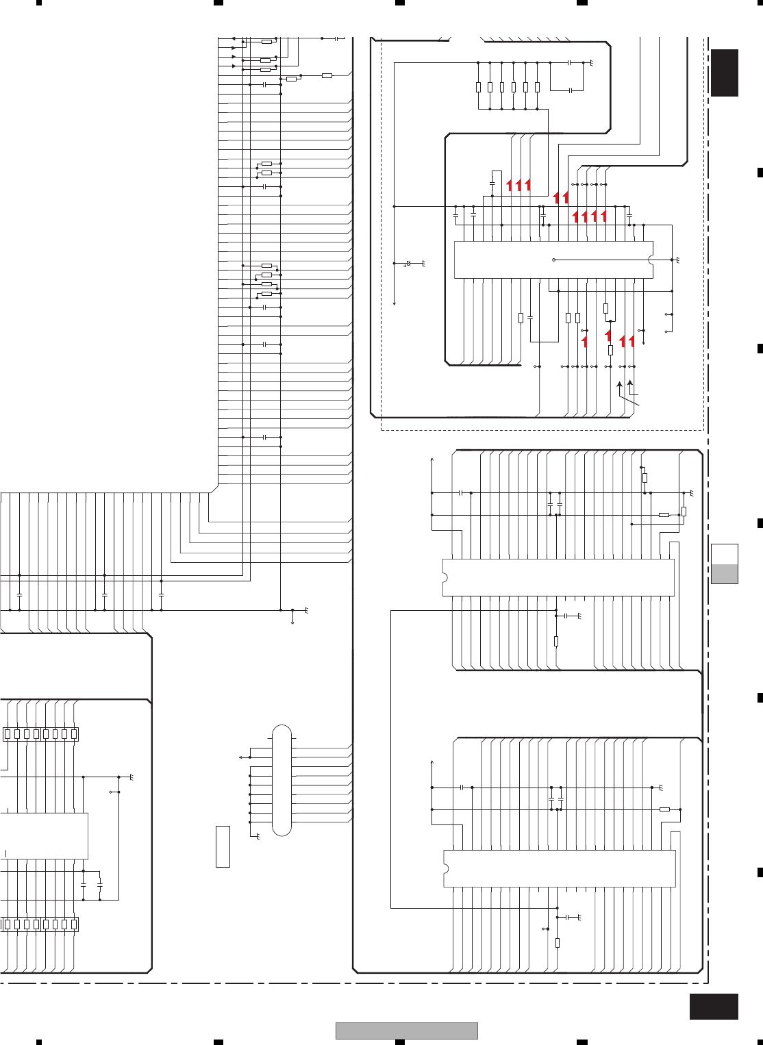
AVH-P4100DVD/XN/UC 151
5 678
5678
C
D
F
A
B
E
C-a
C-b
C-bC-a
A9
A4
A10
A5
A11
A6
A12
A7
A13
A8
A14
A15
D15
D7
D14
D6
D13
D5
D12
D4
D11
D3
D10
D2
D9
D1
D8
A3
A2
A1
XRD
A16
A5
A10
A4
A9
A1
A2
A3
A16A15
A14
A8
A13
A7
A12
A6
XRD
A11
A19
XWR1
A18
A17 A17
A19
A18
MA9
MA8
MA7
MA6
MA5
MA4
XCSM
BA1
MA10
BA0
MA0
MA1
MA2
MA3
MA11
MA7
MA0
MA1
MA10
MA8
BA1
MA6
MA3
MA5
MA4
MA2
A0
XCSF2
XRD
A16
XWR1
A19
A1
A17
A6
A3
A5
A2
A4
A7
XCSF1
D0
D8
D1
D9
D10
D2
D3
D4
D5
D11
D14
D13
D12
D7
D15
D4
D12
D5
D13
D6
D14
D7
D15
D10
D3
D11
D0
D8
D1
D9
D2
D6
A10
A8
A11
A9
A12
A0
TRCDATA3
SCLOCK
TRCDATA0
TRCCLK
TRCDATA1
TRCST
TRCDATA2
SDATA
A0
C
C
C
XCSF2
EXTRG0
A15
A14
A13
A18
DQM1
COILU
COILV
COILW
MD
LDIN TOM
FOP
FOM
TOP
CONT1
CONT2
FG
CRGDRV
HWP
HVM
HVP
HUM
HUP
HWM
HBM
XWR1
NRES
NRES
TD
FD
A20
A20
D0
DGND3
DGND2
GNDD
GNDD
GNDD
GNDD
GNDD
R1405
100K
R1406
100K
R1402
100K
C1509
R1
C1408
R1
C1403
R1
C1407
NM
C1402
NM
C1404
4R7
C1409
4R7
VCC33
C1485
R1
C1507
R1
C1508
R1
C1518 R1
C1519 R1
C1513 R1
C1516 R1
C1517 R1
CN1951
1
2
3
4
5
6
7
8
9
1011
12
13
14
15
16
17
18
19
20
GNDD
VCC33
PGND
R1517
10K
R1518
10K
R1528
10K
R1529
10K
R1530
10K
R1531
10K
R1217
1
R1218
1
R1213
1
R1214
1
R1215
1
R1216
1
PGND
PGND1PGND2
VHALF
VHALF
VD8
PGND
100/16
C1201
FG
R1202 220
R1201 220
R1542
GNDD
VCC33
C1486
NM
C1405
NM
R1212
270
CONT2
CONT1
CRGDRV
FD1
LDIN
MD1 MD2
TD1
XWR1
C1204
2200P
R1403
NM
R1203
10K
R1204
15K
FOM2
FOP2
TOM2
TOP2
R1539
100K
C1211
4R7
R1401
220
C1401
R01
C1203
NM
C1205
R1
C1207
R1
C1210
R1
C1209
R1
C1208
R01
C1525
R1483
56
2
1
4
3
6
5
8
7
R1487
56
2
1
4
3
6
5
8
7
R1488
56
2
1
4
3
6
5
8
7
R1484
56
2
1
4
3
6
5
8
7
1
8
R1527
6R8K
R1546
6R8K
R1547
NM
R1409
NM
IC1201
BD8231EFV
1VC
2TKIN
3FCIN
4SLIN
5
SLOPOUT
6LDIN
7SPIN
8CTL1
9CTL2
10 GND1
11 TEST
12 FG
13 SPCNF
14 HB
15 HW-
16 HW+
17 HV-
18 HV+
19 HU-
20 HU+ 21
VM_S
22
BH
23
SPRNF
24
SPVM
25
SPGND
26
U
27
V
28
W
29
SLVM
30
PGND
31
SL/LDO+
32
SL/LDO-
33
FCO+
34
FCO-
35
TKO+
36
TKO- 37
AVM
38
PREVcc 39
PREGND 40
SUBGND
41
GND2
EXDT1
1
EXDT9
2
EXDT2
3
EXDT10
4
VSS_1
5
VDD33_1
6
EXDT3
7
EXDT11
8
EXDT4
9
EXDT12
10
EXDT5
11
EXDT13
12
EXDT6
13
EXDT14
14
VSS_2
15
VDD33_2
16
EXDT7
17
EXDT15
18
VSS_3
19
VDD12_1
20
EXADR16
21
EXADT15
22
EXADT14
23
EXADT13
24
EXADT12
25
EXADT11
26
EXADT10
27
EXADT9
28
EXADT8
29
EXADR19
30
NEXWE
31
VSS_4
32
VDD33_3
33
EXADR18
34
EXADR17
35
EXADT7
36
EXADT6
37
EXADT5
38
EXADT4
39
EXADT3
40
EXADT2
41
EXADT1
42
VSS_5
43
VDD12_2
44
45
46
47
IRQPWR
48
49
MA9
195 VSS_15
196 VDD33_10
197 BA1
198 MA8
199 MA10
200 MA7
201 MA0
202 MA6
203 MA1
204 VSS_16
205 VDD33_11
206 MA5
207 MA2
208 MA4
209 MA3
210 VSS_17
211 VDD12_6
212 EXADT0
213 NEXCE
214 NEXOE
215 EXDT0
216
EXDT8
K4S641632N-LC75
19 CS
20 BA0
21 BA1
22 A10/AP
23 A0
24 A1
25 A2
26 A3
27 VDD3 28
VSS1
29
A4
30
A5
31
A6
32
A7
33
A8
34
A9
35
A11
36
N.C
IC1401
CWW1753
A15
1
A14
2
A13
3
A12
4
5A11
6A10
7A9
8A8
9A19
10 NC1
11 /WE
12 /RESET
13 NC2
14 NC3
15 RY_/BY
16 A18
17 A17
18 A7
19 A6
20 A5
21 A4
22 A3
23 A2
24 A1 25
A0
26
/CE
27
Vss1
28
/OE
29
DQ0
30
DQ8
31
DQ1
32
DQ9
33
DQ2
34
DQ10
35
DQ3
36
DQ11
37
Vcc
38
DQ4
39
DQ12
40
DQ5
41
DQ13
42
DQ6
43
DQ14
44
DQ7
45
DQ15_A-1
46
Vss2
47
/BYTE
48
A16
IC1402
CWW1754
A15
1
A14
2
A13
3
A12
4
5A11
6A10
7A9
8A8
9A19
10 NC1
11 /WE
12 /RESET
13 NC2
14 NC3
15 RY_/BY
16 A18
17 A17
18 A7
19 A6
20 A5
21 A4
22 A3
23 A2
24 A1 25
A0
26
/CE
27
Vss1
28
/OE
29
DQ0
30
DQ8
31
DQ1
32
DQ9
33
DQ2
34
DQ10
35
DQ3
36
DQ11
37
Vcc
38
DQ4
39
DQ12
40
DQ5
41
DQ13
42
DQ6
43
DQ14
44
DQ7
45
DQ15_A-1
46
Vss2
47
/BYTE
48
A16
FLASH 16M
(2125)
(2125)
FLASH 16M
SDRAM
DEBUG
CP_READY
I2C_SDA
I2C_SCL
08EJ
(3216)
2
4
T
T
F
F
F
T
S
C
C
C
S
S
S
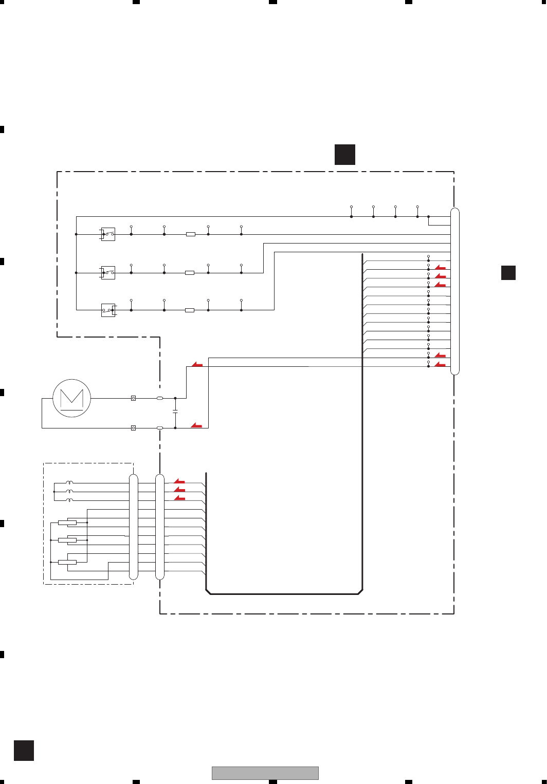
AVH-P4100DVD/XN/UC
152
1234
1234
C
D
F
A
B
E
10.7 CONNECT PCB
D
H+,H-,HU+,HU-,HV+,HV-,HW+,HW-,U,V,W
H+
W
U
V
HW+
HW-
HV+
HV-
HU+
HU-
H-
HV-
H+
HV+
HU-
HU+
HW-
HW+
H-
W
U
V
CN701
1CRG-
2CRG+
3HALL BIAS-
4HALL U-
5HALL U+
6HALL V-
7HALL V+
8HALL W-
9HALL W+
10 COIL V
11 COIL U
12 COIL W
13 HALL BIAS+
14 DSCSNS
15 8SNS
16 HOME
17 GND
18 GND
CSN1068-A
S101
1
2
34
CSN1068-A
S102
1
2
34
12
11
HOME
8SNS0
DSCSNS0
GND3 GND2 GND1
CRGM
CRGP
HM
HUM
HUP
HVM
HVP
HWM
HWP
V
U
W
HP
BR
1
GY
1
DSCSNS0_B
8SNS0_B
HOME_B
C101
0.1u/50
R101
100
R102
100
R103
100
GND_B
HOME1_BHOME1
8SNS1 8SNS1_B
DSCSNS1 DSCSNS1_B
CN101
1
V
2
U
3
W
4
H-
5
HW+
6
HW-
7
HU+
8
HU-
9
HV+
10
H+
11
HV-
1
2
3
4
5
6
7
8
9
10
11
CSN1068-A
S103
1
2
34
H3
H1
H2
M2
SPINDLE MOTOR
EXM1050
M1
LOAD/CRG MOTOR
CXC4026
HOME
8SNS
DSCSNS
DCONNECT PCB
C
CN1201
C
C
C
C
S
S
S
S
S
S

AVH-P4100DVD/XN/UC 153
5 678
5678
C
D
F
A
B
E
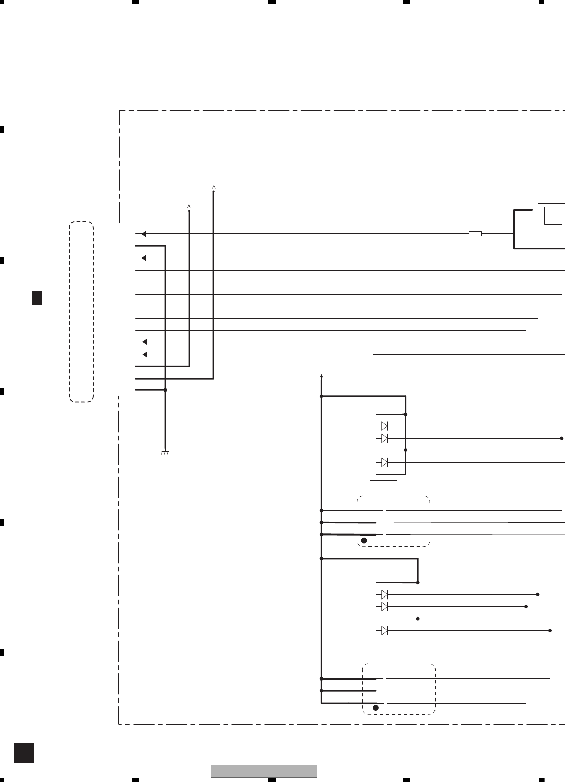
AVH-P4100DVD/XN/UC
154
1234
1234
C
D
F
A
B
E
10.8 KEYBOARD UNIT
E
KDT1
LEDR2 LEDR2
LEDG2 LEDG2
LEDB2 LEDB2
LEDB1
LEDB1
LEDG1
LEDG1
GNDKEY
GNDKEY
REM
ILMB
SWVDD33
KDT0
HDRST
LEDR1
LEDR1
ILMB
S
GNDKEY
SWVDD33
D3005
NSSM038A-6430
123456
D3002
NSSM038A-6430
123456
ILMB
U3001
RS-470
GND2 1
OUT 2
R3005
0
C3013 0.1u/16
C3012 0.1u/16
C3006 0.1u/16
C3007 0.1u/16
C3008 0.1u/16
C3014 0.1u/16
8.0V
1
2
3
4
5
6
7
8
9
10
11
12
13
14
CN5003
1/2
F
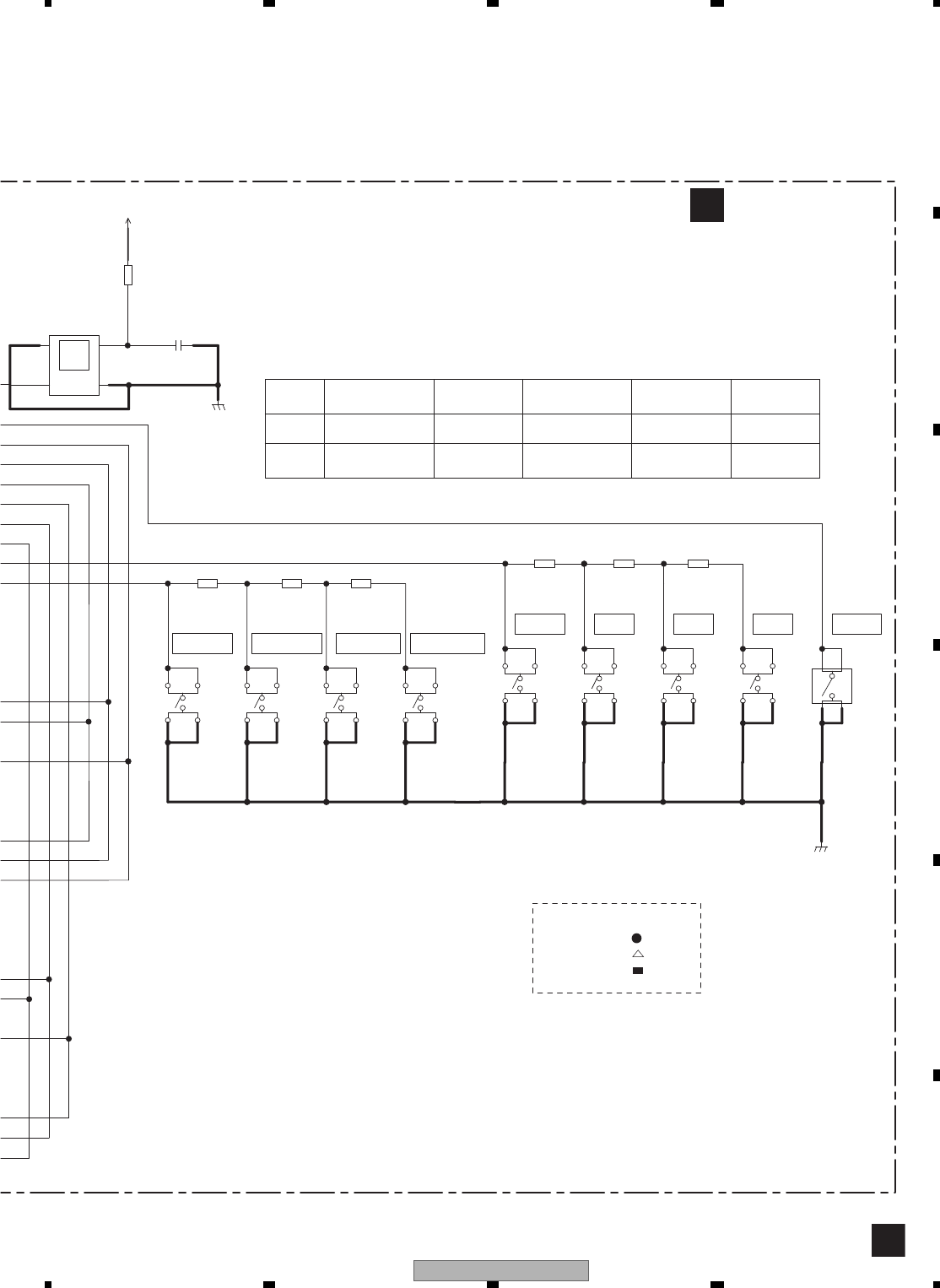
AVH-P4100DVD/XN/UC 155
5 678
5678
C
D
F
A
B
E
E
GNDKEY
R3011
10k
R3006
1.8k
R3009
10k
R3010
1.8k
SWVDD33
GNDKEY
VSG1020-A
S3001
1
2
34
VSG1020-A
S3002
1
2
34
VSG1020-A
S3003
1
2
34
VSG1020-A
S3008
1
2
34
VSG1020-A
S3006
1
2
34
VSG1020-A
S3007
1
2
34
VSG1020-A
S3009
1
2
34
VSG1020-A
S3004
1
2
34
CSG1155-A
S3005
1
2
3
4
U3001
RS-470
GND2 1
OUT 2GND1
3
VCC
4C3005
0.1u/50
R3007
3.9k
R3008
3.9k
R3001
47
CHIP SIZE LEGEND
2125
3216
1608
SOURCE
FORWARD REVERSE
DISP.OFF
EJECT MUTE VOL+ VOL- RESET
EJECT MUTE VOL+ x
VOL-
SOURCE FORWARD REVERSE DISP.OFF
KDT0
KDT1 x
0.0~0.5V 0.5~1.4V 1.4~2.2V 2.2~3.0V 3.0~3.3V
EKEYBOARD UNIT
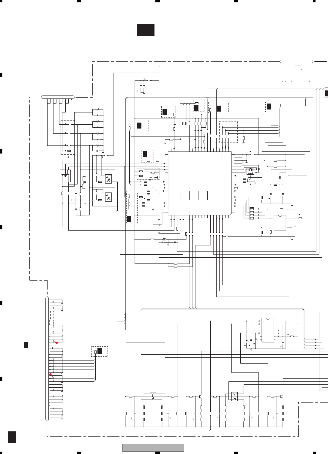
AVH-P4100DVD/XN/UC
156
1234
1234
C
D
F
A
B
E
10.9 MONITOR UNIT(uCOM)(GUIDE PAGE)
1/2
F
F-a 1/2
PNLVD
PNLXV
PNLYV
MFLPW
G_to_M
M_to_G
VADSCL
DIMMER
COMAC
COMDC
TOUCHAD
VADRES
ILMDT
ILMCK
MSRX
PNLADY
PNLADX
KDT1
KDT0
MFLPW
MSRX
NAVI_B
NAVI_G
NAVI_R
CSYNC
MONVBS
RSTOUT
HDRST
SMTX
MONRST
SMTX
REM
GRST
BLERR1
LEDB1
BLSYNC
TEMPSEN
VADSDA
TOOL0
TOOL1
MONRST
MONRST
FLMD0
ILMLD
PWCTL3
PWCTL2
PWCTL1
LEDR1
LEDG1
RED
LEDG2
LEDB2
BLUE
GREEN
LEDR2
REM
KDT0
KDT1
GNDV
HDRST
CN5401
1NC
2PLYV
3PLYV
4PLXV
5PLXV
6ADVX
7ADVX
8ADVY
9ADVY
10 NC
NM
CN5101
1TOOL0
2TOOL1
3RSTIN
4RSTOUT
5GND
6NC
7GND
8SWVDD
9SWVDD
10 FLMDO
CN5001
1
GNDILM
2
GNDFL
3
GNDFL
4
GNDFL
5
NC
6
PWRFL
7
PWRFL
8
PWRFL
9
NC
10
GNDD
11
GNDD
12
GNDD
13
GNDV
14
MONVBS
15
GNDV
16
GNDRGB
17
CSYNC
18
NAVI_R
19
NAVI_G
20
NAVI_B
21
GNDRGB
22
GNDP
23
GNDP
24
GNDP
25
NC
26
PWRVI
27
PWRVI
28
PWRVI
29
SWVDD33
30
SWVDD33
31
ILMB
32
MONRST
33
S_MTX
34
M_SRX
35
MFLPWR
36HDRST
37GNDOSD
38GNDOSD
39
GNDILM
40GNDILM
C5005
NM
C5006
NM
C5004
NM
C5407
1000p/50
C5409
1000p/50
C5408
1000p/50
C5405
0.1u/10
C5402
0.047u/10
C5406
1000p/50
C5404
1000p/50
C5403
1000p/50
C5401
0.047u/10
C5107
0.47u/10
C5108
0.01u/16
C5109
1u/10
C5110
0.1u/10
C5111
0.1u/10
C5105
0.1u/10
C5104
0.1u/10
C5103
0.1u/10
C5102
0.1u/10
C5101
10u/6.3
C5010
NM
C5009
NM
C5008
NM
C5106
0.1u/10
C5007
2.2u/10
C5003
NM
C5002
NM
C5001
NM
D5401
MA111
D5402
UDZS5R6(B)
D5403
UDZS5R6(B)
D5404
UDZS5R6(B)
D5405
UDZS5R6(B)
GNDP
GNDOSD
GNDOSD
GNDOSD
GNDOSD
GNDOSD
GNDOSD
GNDOSD
GNDOSD
GNDV
GNDRGB
GNDFL
GNDD
GNDOSD
GNDOSD
GNDOSD
GNDOSD
GNDILM
GNDOSD
GNDOSD
GNDOSD
GNDOSD
GNDILM
GNDOSD
GNDOSD
GNDOSD
S-93C56BD0I-J8
IC5102
CS
1
SK
2
DI
3
DO
45
GND
6
TEST
7
NC
8
VCC
IC5001
BH2227AFV
AO1
1
AO2
2
TESTMONI1
3
TESTMONI2
4
5AO3
6AO4
7NC1 8
NC2
9
VDD
10
CSB
11
CLK
12
DI
13
VFS
14
VSS
IC5101
NC 1
NC 2
EPRCE 3
EPRDO 4
EPRDI 5
EPRCK 6
NC 7
TOOL1 8
TOOL0 9
RESET 10
XT2 11
XT1 12
FLMD0 13
X2 14
X1 15
REGC 16
Vss0 17
Vss1 18
Vdd0 19
Vdd1
20
SCL 21
SDA 22
VADRES 23
NC 24
BLSYNC 25
NC 26
MVIPW 27
MFLPW 28
XRST 29
EPRST 30
EPRTEST 31
STEST 32
NC 33
PWCTL1 34
PWCTL2 35
PWCTL3 36
TESTIN 37
NC 38
FSEL 39
NC 40
NC
41
NC
42
(TBD)
43
PNLXV
44
PNLYV
45
PNLVD
46
NC
47
MODEL1
48
MODEL2
49
RXD1
50
TXD1
51
TXD0/TSO
52
RXD0/TSI
53
TSCK
54
NC
55
AVREF1
56
COMAC
57
COMDC
58
AVREF0
59
AVss
60
PNLADY
61
PNLADX
62
BLERR1
63
TEMPSEN
64
TOUCHAD
65
NC
66
KDT1
67
KDT0
68
NC
69
NC
70
NC
71
NC
72
NC
73
REMIN
74
DIMMER
75
ILMDT
76
ILMCK
77
ILMLD
78
NC
79
NC
80
L5401
CTF1473-A
L5101
CTF1635-A
Q5401
FMG12
1
155
44
2
233
UMX1N
Q5003
E1
1
B1
2
C2
3
E2
4
5
B2
6
C1
UMX1N
Q5001
E1
1
B1
2
C2
3
E2
4
5
B2
6
C1
UMF5N
Q5402
E1
1
B1
2
C2
3
E2
4
5
B2
6
C1
UMF5N
Q5403
E1
1
B1
2
C2
3
E2
4
5
B2
6
C1
Q5002
2SC4081(QR) Q5004
2SC4081(QR)
R5140
1k
2
1
4
36
5
8
7
R5404
0
R5407
1M
R5153
47k
R5152
47k
R5149
NM
R5148
100k
R5147
10k
R5146
10k
R5145
1k
R5144
47k
R5143
NM
R5142
100k
R5141
NM
R5137
47k
R5136
47k
R5133
47
R5132
47
R5126
100
R5139
47k
R5013
0
R5405
0
R5125
47k
R5411
10k
R5409 NM
R5101
47k
R5154
47k
R5408
1M
R5401
1k
R5413
10k
R5005
NM
R5010
NM
R5015
NM
R5020
NM
R5025
NM
R5030
NM
R5102
470
R5103
470
R5106
470
R5108
470
R5109
470
R5110
470
R5115
470
R5116
470
R5119
470
R5122
470
R5123
470
R5124
470
R5127
470
R5128
470
R5129
470 R5130
470
R5131
470
R5134
470
R5135
470
R5138
470
R5156
NM
R5104
0
R5105 0
R5120
0
R5111
4.7k
R5112
47k
R5113
4.7k
R5114
4.7k
R5117 47k
R5118
47k
R5121
47k
R5003
0
R5027
220
R5006
200
R5016
270
R5017
270
R5007
150
R5012
270 R5011
270
R5002
150
R5412
10k
R5155
47k
R5403
0
R5402
0
R5406
1k
R5151
0
R5150
0
R5107
0
R5031
0
R5028
0
R5026
220
R5023
0
R5018
0
R5008
0
R5019
10k
R5004
10k
R5024
10k
R5009
10k
R5014
10k
R5029
10k
R5410
10k
NM
TH5101
MtoG
TUOTSR
GtoM
NAVIG
CSYNC
MONVBS
ILMB
SWVDD33
GNDOSD
GNDRGB
GNDV
GNDP
GRST
PWRVI
GNDD
TSETRPE
VADRES
VADSDA
VADSCL
EPRCK
EPRDI
EPRDO
EPRCE
1
LOOT
0LOOT
RST
TSO
TP5102
MSRX
TSRPE
ADVX
TEMPSEN
PLYV
ADVY
NAVIB
MONRST
SMTX
MFLPW
HDRST
NAVIR
LESDD
GNDFL
GNDILM1
T
SE
TS
0DMLF
TESTIN
TSI
PLXV
PWRFL
TSCK
TP5101
PWRVI
PWRFL
ILMB
SWVDD33
SWVDD33
SWVDD33
X5101
VSS1186-A
1
2
3
DDCON
LEN2
VCOM
GER_M
MVIPW
ANALOG
PWCTL
M_VAD
R5001
200
R5021
220
R5022
220
20MHz
PLYV
ADVX
ADVY
PLXV
(RED) (GREEN) (BLUE)
RGB_LED DRIVER PART
TO TOUCH PANEL
MODEL1 H:VAD(IC5601) L:NO VAD(IC5601)
MODEL2 H:6.95inch L:5.8inch
PE5669A8
(RED) (GREEN) (BLUE)
F%
MODEL1 MODEL2
UW5
UC,EW5 L
HH
H
UPD78F1155AGC(A)
UW5
UW5
CN501
3/4
A
2/2
F
2/2
F
2/2
F
2/2
F2/2
F2/2
F
F
2/2
F
2/2
F
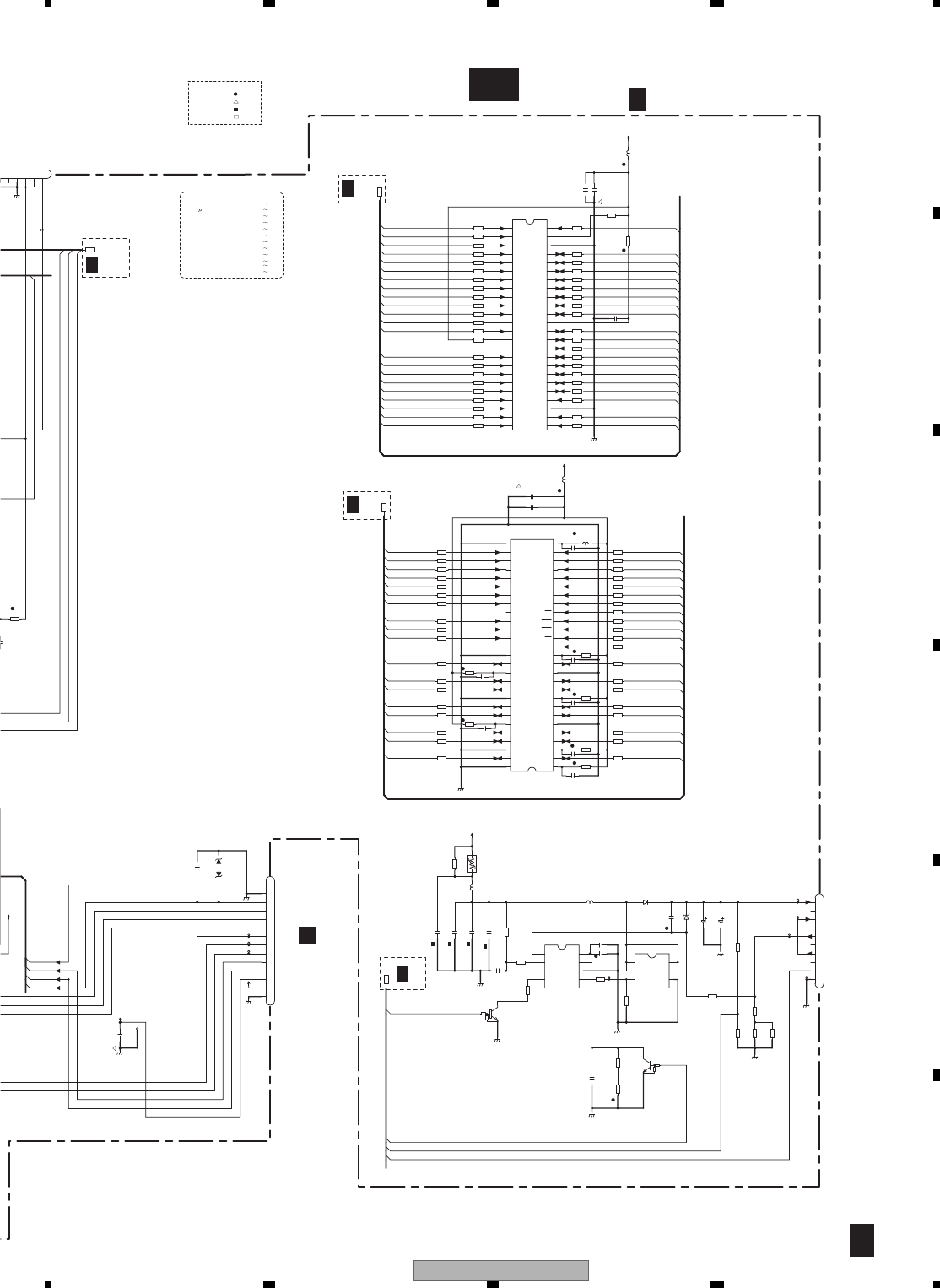
AVH-P4100DVD/XN/UC 157
5 678
5678
C
D
F
A
B
E
1/2
F
F-b 1/2
FAD_15
FAD_14
FAD_13
FAD_12
FAD_11
FAD_10
FAD_9
FAD_8
FAD_19
FAD_20
FRWE
GRST
FAD_21
FAD_18
FAD_17
FAD_7
FAD_6
FAD_5
FAD_4
FAD_3
FAD_2
FAD_1
FAD_16
FDATA_15
FDATA_7
FDATA_14
FDATA_6
FDATA_13
FDATA_5
FDATA_12
FDATA_4
FDATA_11
FDATA_3
FDATA_10
FDATA_2
FDATA_9
FDATA_1
FDATA_8
FDATA_0
FROE
FRCS
FAD_0
SDA_4
SDA_5
SDA_6
SDA_7
SDA_8
SDA_9
SDA_11
SDCKE
MEMCLK
SDM_1
SDD_8
SDD_9
SDD_10
SDD_11
SDD_12
SDD_13
SDD_14
SDD_15
SDA_3
SDA_2
SDA_1
SDA_0
SDA_10
SDBA_1
SDBA_0
SDCS
SDRAS
SDCAS
SDWE
SDM_0
SDD_7
SDD_6
SDD_5
SDD_4
SDD_3
SDD_2
SDD_1
SDD_0
DIMMER
BLERR1
LEDB1
TEMPSEN
MONRST
FLMD0
TEMPSEN
DIMMER
BLERR1
BLSYNC
LEDR1
LEDG1
REM
KDT0
KDT1
HDRST
5GND
6NC
7GND
8SWVDD
9SWVDD
10 FLMDO
CN6101
1A2+
2NC
3A1+
4NC
5A1-
6NC
7A2-
8NC
9TH
10 TH_G
CN5003
1GNDKEY
2SWVDD33
3ILMB
4KDT1
5KDT0
6LEDR2
7LEDG2
8LEDB2
9LEDR1
10 LEDG1
11 LEDB1
12 HDRST
13 GNDKEY
14 REM
10u/50
C6109
10u/50
C6108
C5305
0.1u/10
C5307
0.1u/10
C5309
0.1u/10
C5302
0.1u/10
C5201
NM
C6106
330p/50
C6101
10u/35
C6102
10u/35
C5308
0.1u/10
C6103
NM
C5304
0.1u/10
C5301
0.1u/10
C5203 0.1u/10
C5011
NM
C6104
10u/35
0.1u/10
C5202
4.7u/10
C5303
10u/6.3
C6107 NM
C6110
0.47u/10
C6105
0.1u/10
C6111
0.1u/50
C5017
NM
C5306
0.1u/10
D6102
UDZS36(B)
D5001
NM
GNDFL
GNDILM
GNDD
GNDD
OSD
GNDOSD
GNDFL
GNDILM
GNDFL
GNDFL
GNDFL
GNDILM
GNDFL
GNDOSD
SD
TK11840L
IC6101
EaIn
1
SCP
2
Vcc
3
BR/CTL
45
Out
6
GND
7
OSC
8
FB
IC5201
PEH208A8
A15
1
A14
2
A13
3
A12
4
5A11
6A10
7A9
8A8
9A19
10 A20
11 WE
12 RESET
13 A21
14 WP/ACC
15 RY/BY
16 A18
17 A17
18 A7
19 A6
20 A5
21 A4
22 A3
23 A2
24 A1 25
A0
26
CE
27
VSS1
28
OE
29
DQ0
30
DQ8
31
DQ1
32
DQ9
33
DQ2
34
DQ10
35
DQ3
36
DQ11
37
VCC
38
DQ4
39
DQ12
40
DQ5
41
DQ13
42
DQ6
43
DQ14
44
DQ7
45
DQ15/A-1
46
VSS2
47
BYTE
48
A16
IC5301
K4S281632K-UC75
VDD1
1
DQ0 2
VDDQ1 3
DQ1 4
5
DQ2
6
VSSQ1
7
DQ3
8
DQ4
9
VDDQ2
10
DQ5
11
DQ6
12
VSSQ2
13
DQ7
14
VDD2
15
LDQM
16
WE
17
CAS
18
RAS
19
CS
20
BA0
21
BA1
22
A10/AP
23
A0
24
A1
25
A2
26
A3
27
VDD3
28 VSS1
29 A4
30 A5
31 A6
32 A7
33 A8
34 A9
35 A11
36 N.C
37 CKE
38 CLK
39 UDQM
40 N.C/RFU
41 VSS2
42 DQ8
43 VDDQ3
44 DQ9
45 DQ10
46 VSSQ3
47 DQ11
48 DQ12
49 VDDQ4
50 DQ13
51 DQ14
52 VSSQ4
53 DQ15
54
VSS3
L6101
CTH1419-A
L6102
CTH1419-A
L5301
CTF1473-A
L5201
CTF1473-A
L5302
CTF1382-A
Q6102
CPH6424
D1
1
D2
2
G
3S4
5
D3
6
D4
DTC143EUA
Q6103
DTC143EUA
Q6101
R5334
0
R5336
0
R5327
0
R5329
0
R5337
0
R5330
0
R5331
0
R5333
0
R5328
0
R5335
0
R5318
82
R5311
82
R5316
82
R5314
82
R5317 82
R5315
82
R5305 0
R5306
0
R5310
0
R5304
0
R5307
0
R5309
0
R5303
0
R5308
0
R5301
0
R5302
0
R5244
1k
R5235
0
R5242
0
R5237
0
R5241
0
R5236
0
R6114
2k
R5240
0
R5243
0
R5238
0
R5233
0
R5234
0
R5239
0
R5229
0
R5232
0
R5231
0
R5230
0
R5226
0
R5228
0
R5227
0
R5225
0
R5224
0
R5214
1k
R5212
22
R5313
82
R6112
3.9k
R5332
0
R6103
620
R5312
82
R5322
0
R5201
0
R5202
0
R5203
0
R5204
0
R5205
0
R5206
0
R5208
0
R5211
0
R5209
0
R5207
0
R5210
0
R5213
0
R5222
0
R5218
0
R5220
0
R5219
0
R5216
0
R5215
0
R5217
0
R5223
0
R5221
0
R6101
NM
R5326
0
R5345
82
R5342
82
R5343
82
R5344
82
R5338
82
R5340
82
R5341
82
R5339
82
R6102
0
R5325
0
R5324 0
R5323 0
R5245
0
R5150
0
R6113
0
R6111
NM
R6110
5.6
R6109
2.7
R6106
1k
R6105
5.1k
R6104
0
LEDR2
LEDG2
GNDILM2
LEDB2
TP6101
A2+
A1+
GNDOSD2
A1-
0DMLF
ILMB
PWRFL
WVDD33
SWVDD33
GD33V
GD33V
INV_CONT
INV_CONT
G_SDRAM G_FROM
R5319
0
R5320
0
R6107
120k
R6108
10k
D6101
RB050L-60
miniSMDC075F/24
P6101
12
FLASH ROM
SD RAM
1608
2125
CHIP SIZE LEGEND
3216
3225
CON PART
5601
FLASH ROM PART
LCD PANELPART
5201
5401
6101
5501
5451C.VIDEO PART
TOUCH PANEL PART
5001
5701
5301SD RAM PART
6001
CONNECTOR PART
5101
DD-CON PART
BACKLIGHT PART
VIDEOA/D IC PART
GERDA IC PART
Basic oscillation frequency
360kHz
PWM (CONVERSION 478/528kHz)
7.8V
60mA setting
D
BACKLIGHT PART
TO KEYBOARD
TO BACKLIGHT
D%
D%
6151
3.3uH
3.3uH
E
MONITOR UNIT(uCOM)
1/2
F
2/2
F
2/2
F
2/2
F
2/2
F
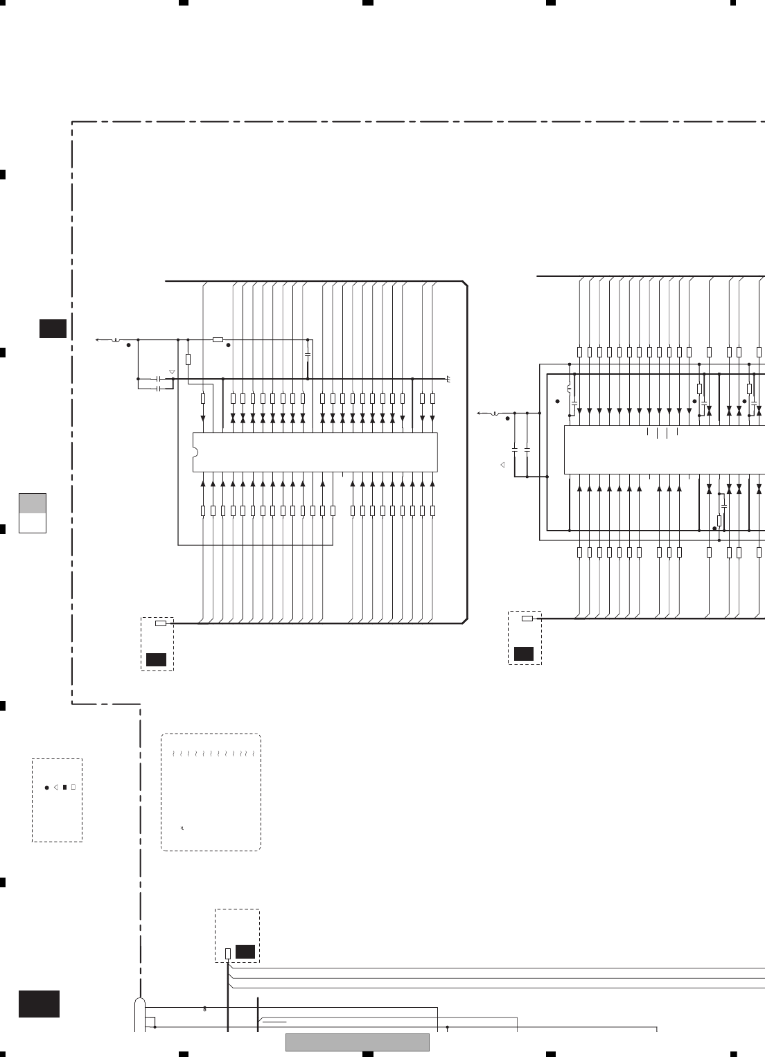
AVH-P4100DVD/XN/UC
158
1234
1234
C
D
F
A
B
E
F-a F-b
F-b 1/2
FAD_15
FAD_14
FAD_13
FAD_12
FAD_11
FAD_10
FAD_9
FAD_8
FAD_19
FAD_20
FRWE
GRST
FAD_21
FAD_18
FAD_17
FAD_7
FAD_6
FAD_5
FAD_4
FAD_3
FAD_2
FAD_1
FAD_16
FDATA_15
FDATA_7
FDATA_14
FDATA_6
FDATA_13
FDATA_5
FDATA_12
FDATA_4
FDATA_11
FDATA_3
FDATA_10
FDATA_2
FDATA_9
FDATA_1
FDATA_8
FDATA_0
FROE
FRCS
FAD_0
SDA_4
SDA_5
SDA_6
SDA_7
SDA_8
SDA_9
SDA_11
SDCKE
MEMCLK
SDM_1
SDD_8
SDD_9
SDD_10
SDD_11
SDD 12
SDA_3
SDA_2
SDA_1
SDA_0
SDA_10
SDBA_1
SDBA_0
SDCS
SDRAS
SDCAS
SDWE
SDM_0
SDD_7
SDD_6
SDD_5
SDD_4
SDD 3
DIMMER
BLERR1
TEMPSEN
MONRST
FLMD0
8SWVDD
9SWVDD
10 FLMDO
C5305
0.1u/10
C5307
C5201
NM
C5304
0.1u/10
C5301
0.1u/10
C5203 0.1u/10
C5202
4.7u/10
C5303
10u/6.3
C5306
0.1u/10
GNDD
IC5201
PEH208A8
A15
1
A14
2
A13
3
A12
4
5A11
6A10
7A9
8A8
9A19
10 A20
11 WE
12 RESET
13 A21
14 WP/ACC
15 RY/BY
16 A18
17 A17
18 A7
19 A6
20 A5
21 A4
22 A3
23 A2
24 A1 25
A0
26
CE
27
VSS1
28
OE
29
DQ0
30
DQ8
31
DQ1
32
DQ9
33
DQ2
34
DQ10
35
DQ3
36
DQ11
37
VCC
38
DQ4
39
DQ12
40
DQ5
41
DQ13
42
DQ6
43
DQ14
44
DQ7
45
DQ15/A-1
46
VSS2
47
BYTE
48
A16
IC5301
K4S281632K-UC75
8
DQ4
9
VDDQ2
10
DQ5
11
DQ6
12
VSSQ2
13
DQ7
14
VDD2
15
LDQM
16
WE
17
CAS
18
RAS
19
CS
20
BA0
21
BA1
22
A10/AP
23
A0
24
A1
25
A2
26
A3
27
VDD3
28 VSS1
29 A4
30 A5
31 A6
32 A7
33 A8
34 A9
35 A11
36 N.C
37 CKE
38 CLK
39 UDQM
40 N.C/RFU
41 VSS2
42 DQ8
43 VDDQ3
44 DQ9
45 DQ10
46 VSSQ3
47 DQ11
L5301
CTF1473-A
L5201
CTF1473-A
L5302
CTF1382-A
R5334
0
R5336
0
R5327
0
R5329
0
R5337
0
R5330
0
R5331
0
R5333
0
R5328
0
R5335
0
R5311
82
R5314
82
R5315
R5305 0
R5306
0
R5310
0
R5304
0
R5307
0
R5309
0
R5303
0
R5308
0
R5301
0
R5302
0
R5244
1k
R5235
0
R5242
0
R5237
0
R5241
0
R5236
0
R5240
0
R5243
0
R5238
0
R5233
0
R5234
0
R5239
0
R5229
0
R5232
0
R5231
0
R5230
0
R5226
0
R5228
0
R5227
0
R5225
0
R5224
0
R5214
1k
R5212
22
R5313
82
R5332
0
R5312
82
R5322
0
R5201
0
R5202
0
R5203
0
R5204
0
R5205
0
R5206
0
R5208
0
R5211
0
R5209
0
R5207
0
R5210
0
R5213
0
R5222
0
R5218
0
R5220
0
R5219
0
R5216
0
R5215
0
R5217
0
R5223
0
R5221
0
R5326
0
R5342
R5338
82
R5340
82
R5341
82
R5339
82
R5323 0
R5245
0
0DML
F
GD33V
GD33V
INV_CONT
G_SDRAM G_FROM
R5319
0
FLASH ROM
SD RAM
1608
2125
CHIP SIZE LEGEND
3216
3225
CON PART
5601
FLASH ROM PART
LCD PANELPART
5201
5401
6101
5501
5451C.VIDEO PART
TOUCH PANEL PART
5001
5701
5301SD RAM PART
6001
CONNECTOR PART
5101
DD-CON PART
BACKLIGHT PART
VIDEOA/D IC PART
GERDA IC PART
6151
MONITOR UNIT(uCOM)
1/2
F
2/2
F
2/2
F
2/2
F
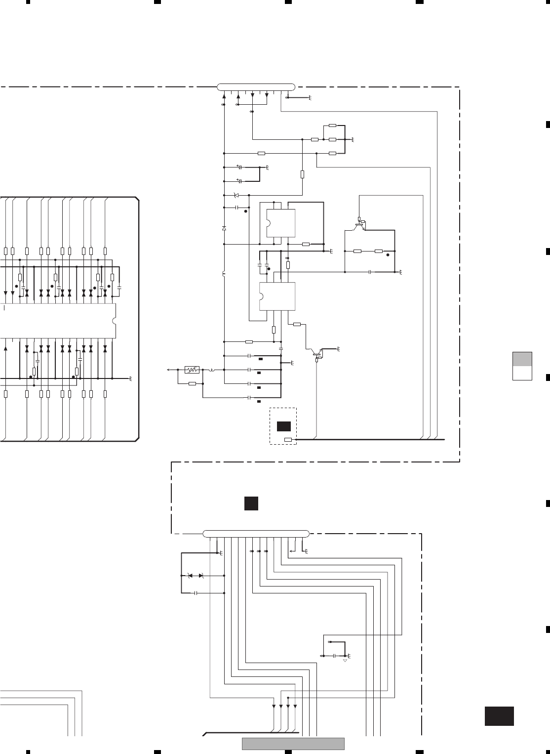
AVH-P4100DVD/XN/UC 159
5 678
5678
C
D
F
A
B
E
F-a F-b
F-b 1/2
SDM_1
SDD_8
SDD_9
SDD_10
SDD_11
SDD_12
SDD_13
SDD_14
SDD_15
SDWE
SDM_0
SDD_7
SDD_6
SDD_5
SDD_4
SDD_3
SDD_2
SDD_1
SDD_0
LEDB1
TEMPSEN
DIMMER
BLERR1
BLSYNC
LEDR1
LEDG1
REM
KDT0
KDT1
HDRST
CN6101
1A2+
2NC
3A1+
4NC
5A1-
6NC
7A2-
8NC
9TH
10 TH_G
CN5003
1GNDKEY
2SWVDD33
3ILMB
4KDT1
5KDT0
6LEDR2
7LEDG2
8LEDB2
9LEDR1
10 LEDG1
11 LEDB1
12 HDRST
13 GNDKEY
14 REM
10u/50
C6109
10u/50
C6108
C5307
0.1u/10
C5309
0.1u/10
C5302
0.1u/10
C6106
330p/50
C6101
10u/35
C6102
10u/35
C5308
0.1u/10
C6103
NM
C5301
0.1u/10
C5011
NM
C6104
10u/35
C6107 NM
C6110
0.47u/10
C6105
0.1u/10
C6111
0.1u/50
C5017
NM
C5306
0.1u/10
D6102
UDZS36(B)
D5001
NM
GNDFL
GNDILM
GNDD
GNDFL
GNDILM
GNDFL
GNDFL
GNDFL
GNDILM
GNDFL
GNDOSD
TK11840L
IC6101
EaIn
1
SCP
2
Vcc
3
BR/CTL
45
Out
6
GND
7
OSC
8
FB
VDD1
1
DQ0 2
VDDQ1 3
DQ1 4
5
DQ2
6
VSSQ1
7
DQ3
8
DQ4
9
VDDQ2
10
DQ5
11
DQ6
12
VSSQ2
13
DQ7
14
VDD2
15
LDQM
16
WE
1738
39 UDQM
40 N.C/RFU
41 VSS2
42 DQ8
43 VDDQ3
44 DQ9
45 DQ10
46 VSSQ3
47 DQ11
48 DQ12
49 VDDQ4
50 DQ13
51 DQ14
52 VSSQ4
53 DQ15
54
VSS3
L6101
CTH1419-A
L6102
CTH1419-A
Q6102
CPH6424
D1
1
D2
2
G
3S4
5
D3
6
D4
DTC143EUA
Q6103
DTC143EUA
Q6101
R5336
0
R5337
0
0
R5318
82
R5311
82
R5316
82
R5314
82
R5317 82
R5315
82
R5310
0
0
R6114
2k
R5313
82
R6112
3.9k
R6103
620
R5312
82
R5322
0
R6101
NM
R5345
82
R5342
82
R5343
82
R5344
82
R5338
82
R5340
82
R5341
82
R5339
82
R6102
0
R5325
0
R5324 0
R5323 0
R6113
0
R6111
NM
R6110
5.6
R6109
2.7
R6106
1k
R6105
5.1k
R6104
0
LEDR2
LEDG2
GNDILM2
LEDB2
TP6101
A2+
A1+
GNDOSD2
A1-
ILMB
PWRFL
3
SWVDD33
INV_CONT
R5319
0
R5320
0
R6107
120k
R6108
10k
D6101
RB050L-60
miniSMDC075F/24
P6101
12
Basic oscillation frequency
360kHz
PWM (CONVERSION 478/528kHz)
7.8V
60mA setting
D
BACKLIGHT PART
TO KEYBOARD
TO BACKLIGHT
D%
D%
3.3uH
3.3uH
E
2/2
F
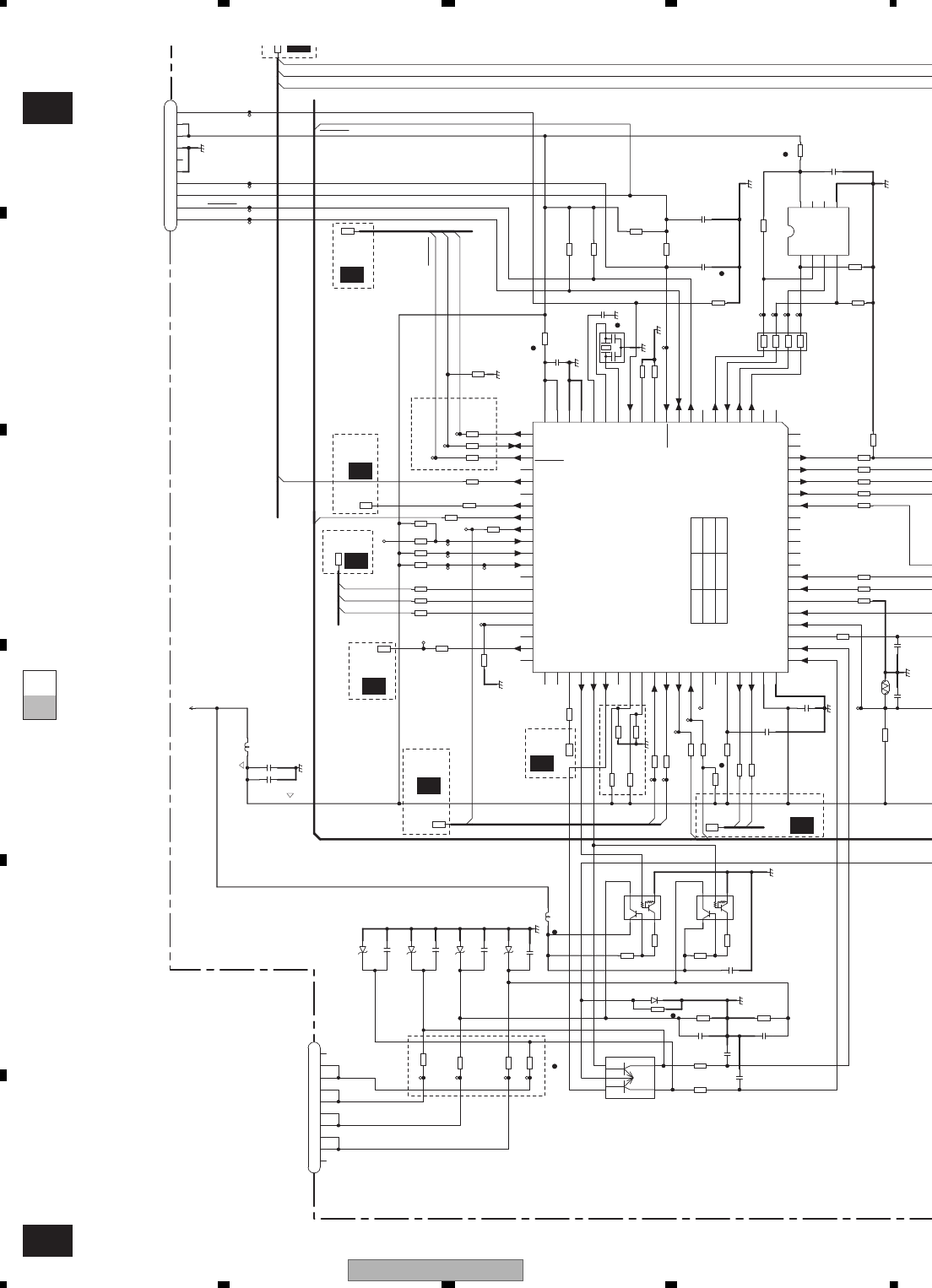
AVH-P4100DVD/XN/UC
160
1234
1234
C
D
F
A
B
E
F-bF-a
F-a 1/2
F-b 1/2
PNLVD
PNLXV
PNLYV
MFLPW
G_to_M
M_to_G
VADSCL
DIMMER
COMAC
COMDC
VADRES
ILMDT
ILMCK
MSRX
PNLADY
PNLADX
RSTOUT
SMTX
GRST
BLERR1
BLSYNC
TEMPSEN
VADSDA
TOOL0
TOOL1
MONRST
MONRST
FLMD0
ILMLD
PWCTL3
PWCTL2
PWCTL1
CN5401
1NC
2PLYV
3PLYV
4PLXV
5PLXV
6ADVX
7ADVX
8ADVY
9ADVY
10 NC
NM
CN5101
1TOOL0
2TOOL1
3RSTIN
4RSTOUT
5GND
6NC
7GND
8SWVDD
9SWVDD
10 FLMDO
C5407
1000p/50
C5409
1000p/50
C5408
1000p/50
C5405
0.1u/10
C5402
0.047u/10
C5406
1000p/50
C5404
1000p/50
C5403
1000p/50
C5401
0.047u/10
C5107
0.47u/10
C5108
0.01u/16
C5109
1u/10
C5110
0.1u/10
C5111
0.1u/10
C5105
0.1u/10
C5104
0.1u/10
C5103
0.1u/10
C5102
0.1u/10
C5101
10u/6.3
C5106
0.1u/10
D5401
MA111
D5402
UDZS5R6(B)
D5403
UDZS5R6(B)
D5404
UDZS5R6(B)
D5405
UDZS5R6(B)
GNDOSD
GNDOSD
GNDOSD
GNDOSD
GNDOSD
GNDOSD
GNDOSD
GNDOSD
GNDOSD
GNDOSD
GNDOSD
GNDOSD
GNDOSD
GNDOSD
GNDOSD
GNDOSD
S-93C56BD0I-J8
IC5102
CS
1
SK
2
DI
3
DO
45
GND
6
TEST
7
NC
8
VCC
IC5101
NC 1
NC 2
EPRCE 3
EPRDO 4
EPRDI 5
EPRCK 6
NC 7
TOOL1 8
TOOL0 9
RESET 10
XT2 11
XT1 12
FLMD0 13
X2 14
X1 15
REGC 16
Vss0 17
Vss1 18
Vdd0 19
Vdd1
20
SCL 21
SDA 22
VADRES 23
NC 24
BLSYNC 25
NC 26
MVIPW 27
MFLPW 28
XRST 29
EPRST 30
EPRTEST 31
STEST 32
NC 33
PWCTL1 34
PWCTL2 35
PWCTL3 36
TESTIN 37
NC 38
FSEL 39
NC 40
NC
41
NC
42
(TBD)
43
PNLXV
44
PNLYV
45
PNLVD
46
NC
47
MODEL1
48
MODEL2
49
RXD1
50
TXD1
51
TXD0/TSO
52
RXD0/TSI
53
TSCK
54
NC
55
AVREF1
56
COMAC
57
COMDC
58
AVREF0
59
AVss
60
PNLADY
61
PNLADX
62
BLERR1
63
TEMPSEN
64
TOUCHAD
65
NC
66
KDT1
67
KDT0
68
NC
69
NC
70
NC
71
NC
72
NC
73
REMIN
74
DIMMER
75
ILMDT
76
ILMCK
77
ILMLD
78
NC
79
NC
80
L5401
CTF1473-A
L5101
CTF1635-A
Q5401
FMG12
1
155
44
2
233
UMF5N
Q5402
E1
1
B1
2
C2
3
E2
4
5
B2
6
C1
UMF5N
Q5403
E1
1
B1
2
C2
3
E2
4
5
B2
6
C1
R5140
1k
2
1
4
36
5
8
7
R5404
0
R5407
1M
R5153
47k
R5152
47k
R5149
NM
R5148
100k
R5147
10k
R5146
10k
R5145
1k
R5144
47k
R5143
NM
R5142
100k
R5141
NM
R5137
47k
R5136
47k
R5133
47
R5132
47
R5126
100
R5139
47k
R5405
0
R5125
47k
R5411
10k
R5409 NM
R5101
47k
R5154
47k
R5408
1M
R5401
1k
R5413
10k R5102
470
R5103
470
R5106
470
R5108
470
R5109
470
R5110
470
R5115
470
R5116
470
R5119
470
R5122
470
R5123
470
R5124
470
R5127
470
R5128
470
R5129
470 R5130
470
R5131
470
R5134
470
R5135
470
R5138
470
R5156
NM
R5104
0
R5105 0
R5120
0
R5111
4.7k
R5112
47k
R5117 47k
R5118
47k
R5121
47k
R5412
10k
R5155
47k
R5403
0
R5402
0
R5406
1k
R5151
0
R5150
0
R5107
0
R5410
10k
NM
TH5101
MtoG
TUOTSR
GtoM
GRST
T
SETRPE
VADRES
VADSDA
VADSCL
EPRCK
EPRDI
EPRDO
EPRCE
1LOOT
0LOOT
RST
TSO
TP5102
TSRPE
ADVX
TEMPSEN
PLYV
ADVY
LESDD
T
SETS
0DML
F
TESTIN
TSI
PLXV
TSCK
TP5101
SWVDD33
X5101
VSS1186-A
1
2
3
DDCON
LEN2
VCOM
GER_M
MVIPW
PWCTL
M_VAD
20MHz
PLYV
ADVX
ADVY
PLXV
TO TOUCH PANEL
MODEL1 H:VAD(IC5601) L:NO VAD(IC5601)
MODEL2 H:6.95inch L:5.8inch
PE5669A8
F%
MODEL1 MODEL2
UW5
UC,EW5 L
HH
H
UPD78F1155AGC(A)
UW5
UW5
2/2
F
2/2
F
2/2
F
2/2
F
2/2
F
2/2
F
F
2/2
F
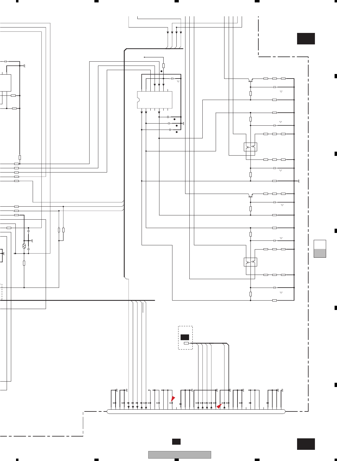
AVH-P4100DVD/XN/UC 161
5 678
5678
C
D
F
A
B
E
F-bF-a
F-a 1/2
F-b 1/2
TOUCHAD
ILMDT
ILMCK
PNLAD
PNLA
KDT1
KDT0
MFLPW
MSRX
NAVI_B
NAVI_G
NAVI_R
CSYNC
MONVBS
HDRST
SMTX
MONRST
REM
LEDB1
ILMLD
LEDR1
LEDG1
RED
LEDG2
LEDB2
BLUE
GREEN
LEDR2
REM
KDT0
KDT1
GNDV
HDRST
CN5001
1
GNDILM
2
GNDFL
3
GNDFL
4
GNDFL
5
NC
6
PWRFL
7
PWRFL
8
PWRFL
9
NC
10
GNDD
11
GNDD
12
GNDD
13
GNDV
14
MONVBS
15
GNDV
16
GNDRGB
17
CSYNC
18
NAVI_R
19
NAVI_G
20
NAVI_B
21
GNDRGB
22
GNDP
23
GNDP
24
GNDP
25
NC
26
PWRVI
27
PWRVI
28
PWRVI
29
SWVDD33
30
SWVDD33
31
ILMB
32
MONRST
33
S_MTX
34
M_SRX
35
MFLPWR
36HDRST
37GNDOSD
38GNDOSD
39
GNDILM
40GNDILM
C5005
NM
C5006
NM
C5004
NM
C5110
0.1u/10
C5111
0.1u/10
C5105
0.1u/10
C5010
NM
C5009
NM
C5008
NM
C5007
2.2u/10
C5003
NM
C5002
NM
C5001
NM
GNDP
GNDOSD
GNDOSD
GNDOSD
GNDV
GNDRGB
GNDFL
GNDD
GNDOSD
GNDILM
GNDILM
GNDOSD
GNDOSD
S-93C56BD0I-J8
DI
3
DO
45
GND
6
TEST
IC5001
BH2227AFV
AO1
1
AO2
2
TESTMONI1
3
TESTMONI2
4
5AO3
6AO4
7NC1 8
NC2
9
VDD
10
CSB
11
CLK
12
DI
13
VFS
14
VSS
UMX1N
Q5003
E1
1
B1
2
C2
3
E2
4
5
B2
6
C1
UMX1N
Q5001
E1
1
B1
2
C2
3
E2
4
5
B2
6
C1
Q5002
2SC4081(QR) Q5004
2SC4081(QR)
R5153
47k
R5152
47k
R5144
47k
R5143
NM
R5126
100
R5013
0
R5005
NM
R5010
NM
R5015
NM
R5020
NM
R5025
NM
R5030
NM
R5108
470
R5115
470
R5116
470
R5124
470
R5128
470
R5129
470
R5131
470
R5111
4.7k
R5113
4.7k
R5114
4.7k
R5003
0
R5027
220
R5006
200
R5016
270
R5017
270
R5007
150
R5012
270 R5011
270
R5002
150
R5031
0
R5028
0
R5026
220
R5023
0
R5018
0
R5008
0
R5019
10k
R5004
10k
R5024
10k
R5009
10k
R5014
10k
R5029
10k
NM
TH5101
NAVIG
CSYNC
MONVBS
ILMB
SWVDD33
GNDOSD
GNDRGB
GNDV
GNDP
PWRVI
GNDD
MSRX
TEMPSEN
NAVIB
MONRST
SMTX
MFLPW
HDRST
NAVIR
GNDFL
GNDILM1
PWRFL
PWRVI
PWRFL
ILMB
SWVDD33
SWVDD33
ANALOG
R5001
200
R5021
220
R5022
220
(RED) (GREEN) (BLUE)
RGB_LED DRIVER PART
(RED) (GREEN) (BLUE)
F%
CN501
3/4
A
2/2
F
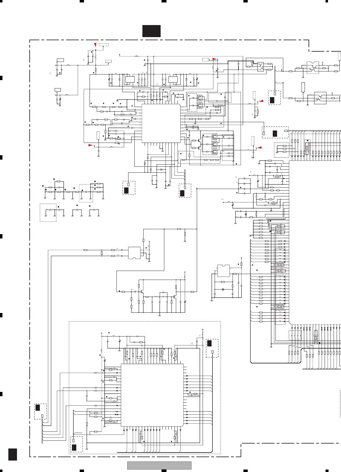
AVH-P4100DVD/XN/UC
162
1234
1234
C
D
F
A
B
E
10.10 MONITOR UNIT(MONITOR)(GUIDE PAGE)
2/2
F
F-a 2/2
LEN
EXTRG0
LCE
LCSY
LDEN
LHSY
LVSY
LCLK
LB0
LB1
LB2
LB3
LB4
LB5
LG0
LG1
LG2
LG3
LG4
LG5
LR0
LR1
LR5
LR4
LR3
SDD_15
SDD_14
SDD_13
SDD_12
SDD_11
SDD_10
SDD_9
SDD_8
SDM_1
SDCKE
DVVSY
DVHSY
DVCLK
DVR_0
DVR_1
DVR_2
DVR_3
DVR_4
DVR_5
DVG_0
DVG_1
DVG_2
DVG_3
DVG_4
DVG_5
DVVSY
DVHSY
DVCLK
DVR_5
DVR_4
DVR_3
DVR_2
DVR_1
DVR_0
DVG_5
DVG_4
DVG_3
DVG_2
DVG_1
DVG_0
DVB_5
DVB_4
DVB_3
DVB_2
DVB_0
DVB_1
NAVI_B
NAVI_G
NAVI_R
LR2
VADSCL
VADSDA
VADRES
PWCTL1
MONVBS
GNDV
PWCTL2
PWCTL3
PWCTL2
PWCTL3
CSYNC
CCH1586-A_Po
C5543
33u 10V
33u/10_Ta
C5460
47u/10_Ta
C5605
47u/10_Ta
C5611
CCH1440-A_Po
C5509 68u
6.3V
47u/10_Ta
C5713
47u/10_Ta
C5702
33u/10_Ta
C5503
C5538
4.7u/16
C5502
0.1u/10
C5519 0.01u/50
C5510
0.1u/50
C5520
0.1u/50
C5539
0.1u/50
C5530
0.1u/50
C5534
0.1u/50
C5541
0.1u/50
C5540
0.1u/50
C5542
0.1u/50
C5522
CCG1223-A
C5521
CCG1223-A
C5527
CCG1223-A
10u
C5537
0.01u/50
C5545
NM
C5454
0.1u/10
C5459
0.1u/10
C5507
0.1u/10
C5526
1000p/50
C5529
1000p/50
C5456
68p/50
C5457
5p/50
C5455
47p/50
C5458
47p/50
C5546
1u/16
C5544
0.1u/50
C5517
0.039u/50
C5516
0.039u/50
C5553
1u/16
C5552
1u/16
C5532 1u/16
C5531
1u/16
C5525
1u/16
C5535
4700p/50
C5706
NM
C5710
1u/6.3
C5711
1u/6.3
C5718 0.1u/10
C5715
0.1u/10
C5716
0.1u/10
C5726
0.1u/10
C5719
0.1u/10
C5714
68p/50
C5712
33p/50
C5717
0.01u/16
C5725
0.1u/10
C5727
0.1u/10
C5720
1u/6.3
C5721
1u/6.3
C5728
0.1u/10
C5729 0.1u/10
C5730 0.1u/10
C5723 1u/6.3
C5731 0.1u/10
C5734
1u/6.3
C5735
0.1u/10
C5528
0.01u/50
C5536
4700p/50
C5518
0.01u/50
C5613
0.082u/10
C5614
8200p/16
C5606 0.1u/10
C5616
0.1u/10
C5619
0.1u/10
C5610
0.1u/10
C5609
0.1u/10
C56080.1u/10
C5607
0.1u/10
C5612
0.1u/10
C5617
0.1u/10
C5615
0.1u/10
C5618
0.1u/10
C5620
0.1u/10
C5533
0.01u/50
C5736
C5732
1u/6.3
C5733
0.1u/10
C5722 1u/6.3
C5550
CCG1222-A 4.7u 25V
C5547
1u/25
C5551
NM
C5554
1u/25
C5555
1u/25
C5524
NM
C5556
1000p/50
C5724 1u/6.3
C5549
1u/16
C5548
1u/16
C5707
0.1u/10
C5513
DCH1201-A 10u 10V
C5505
DCH1201-A
10u 10V
C5501
DCH1201-A
10u 10V
C5451
10u/6.3
C5016
0.047u/25
C5014
NM
C5013
NM
C5012
1000p/50
C5453
10u/6.3
C5508
4700p/25
C5511
6800p/25
C5512 0.1u/16
C5514
0.033u/16
C5515 68p/50
C5523
NM
C5557
0.015u/16
C5558 27p/50
C5559
NM
C5601
1000p/50
C5602
0.1u/10
C5603
0.1u/10
C5604
0.1u/10
C5621
10u/6.3
C5708
10u/6.3
C5709
10u/6.3
C5701
12p/50
C5703
12p/50
C5504
1u/6.3
C5506
1u/6.3
C5018
NM
C5622
NM
C5452
10u/6.3
D5507
RB548W
1
2
3
D5503
RB548W
1
2
3
D5505
RB548W
1
2
3
D5506
RB548W
1
2
3
D5504
RB548W
1
2
3
D5509
NM
D5502
RB160M-30
D5510
NM
D5501
RSX201L-30
D5508
NM
D5511
NM
GNDP
GNDP
GNDP
GNDP
GNDP
GNDP
GNDP
GNDP
GNDP
GNDP
GNDP
GNDP
GNDP
GNDP
GNDP
GNDP
GNDP
GNDP
GNDP
GNDP
GNDV
AVAGND
GNDD
AVAGND
AVAGND
AVBGND
AVAGND
AVBGND
GNDRGB
AVAGND
GNDFL GND
GNDD
GNDRGB
GNDD
AVAGND
GNDILM
GNDD
GNDD
GNDD
GNDD
GNDRGB
GNDRGB
GNDD
GNDD
IC5701
TC7SHU04FUS1
NC
1
INA
2
GND0
3OUTY 4
5
Vcc
IC5451
NJM2505AF
Vout 1
GND 2
V+ 3
Vin
4
5VGND
BD6171KV
IC5501
NC1
1
OCPC2
2
VREGA 3
VS2 4
CL2 5
PVCC2 6
OUT2 7
LGND 8
VREGB 9
OVT1 10
PVCC1 11
CL1 12
VS1
13
OCPC1
14
FB1
15
INV1
16
SS1
17
FB2
18
INV2
19
SS2
20
VREF
21
OUT3
22
PVCC3
23
FB3
24
V03DET
25
V01DET
26
V02DET
27
V04DET
28 V05DET
29
SVBGND
30
GND
31
EN1
32
EN2
33
EN3
34
EN4
35 EN5
36
PVCC5 37
OUT5 38
FB5 39
PGND5 40
PVCC 41
VCC 42
FIN 43
RT 44
PGND4 45
FB4 46
OUT4
47
PVCC4
48
IC5601
AK5406XQ
GOUT6
1
GOUT5
2
GOUT4 3
GOUT3 4
GOUT2 5
GOUT1 6
GOUT0 7
NC1 8
NC2 9
DVSS1 10
DVDD1 11
BOUT7 12
BOUT6 13
BOUT5 14
BOUT4 15
BOUT3 16
BOUT2 17
BOUT1 18
BOUT0 19
NC3 20
NC4
21
DVSS2
22
DVDD2 23
CLAMP 24
AVSS1 25
TEST2 26
PVDD1 27
AVSS2 28
COAST 29
HSYNC 30
VSYNC 31
AVSS3 32
FLT 33
PVDD2 34
PVDD3 35
AVSS4 36
BIAS 37
TEST 38
AVDD1 39
AVSS5 40
AVSS6
41
AVDD2
42 BIN
43 AVSS7
44 AVDD3
45 AVDD4
46 AVSS8
47 GIN
48 SOGIN
49 AVSS9
50 AVDD5
51 AVDD6
52 AVSS10
53 RIN
54 A0
55 SCL
56 SDA
57 BYPASS
58 AVDD7
59 AVSS11
60
RESETN
61
VSYNCO
62 SONGOUT
63 HSYNCO
64 DTCLK
65 DVSS3
66 DVDD3
67 ROUT7
68 ROUT6
69 ROUT5
70 ROUT4
71 ROUT3
72 ROUT2
73 ROUT1
74 ROUT0
75 NC5
76 NC6
77 DVDD4
78 DVSS4
79 GOUT7
80
LCD_R_2
1
LCD_R_3
2
LCD_R_4
3
LCD_R_5
4
SDDATA_15
5
SDDATA_14
6
SDDATA_13
7
VSS_1
8
VDD3_1
9
SDDATA_12
10
SDDATA_11
11
SDDATA_10
12
SDDATA_9
13
SDDATA_8
14
SDM_1
15
SDCKE
16
MEMCLK
17
18 145
146
DVG_5
147
DVG_4
148
DVG_3
149
DVG_2
150
DVG_1
151
DVG_0
152
DVR_5
153
DVR_4
154
DVR_3
155
DVR_2
156
VSS_14
157
VDD3_12
158
DVR_1
159
DVR_0
160
DVCLK
161
DVHSY
162
DVVSY
163
IREF
164
VCMO
165
VREFH
166 VREFL
167 AVDD_1
168 AINP0
169 AINP1
170 AVSS_1
171 CLH
172 CLL
173 AVSS_2
174 DAOUT
175 AVDD_2
176 TSTIO
177 AVCLK
178 PMODE0
179 OSCXI
180 OSCXO
181 TSTCK
182 TSTC1
183 TSTC0
184 VDD_6
185 VSS_15
186 VDD3_13
187 MCKSL
188 LCDMUTE
189 GPIO_05
190 GPIO_04
191 LCDCE
192 LCDCSY
193 LCDDEN
194 LCDHSY
195 LCDVSY
196 LCDCLK
197 VDD3_14
198 VSS_16
199 VDD_7
200 LCDICLK
201 LCD_B_0
202 LCD_B_1
203 LCD_B_2
204 LCD_B_3
205 LCD_B_4
206 LCD_B_5
207 LCD_G_0
208 LCD_G_1
209 LCD_G_2
210 LCD_G_3
211 VDD3_15
212 VSS_17
213 LCD_G_4
214 LCD_G_5
215
LCD_R_0
216
LCD_R_1
L5602
CTF1473-A
L5601
CTF1473-A
L5454
0.1m
L5452
22u
L5501
CTH1250-A
L5504
CTF1635-A
L5508
CTF1635-A
L5510
DTL1096-A
L5451
CTF1379-A
L5603
CTF1635-A
L5702
CTF1635-A
L5502
CTH1249-A
L5505
DTL1136
L5703 NM
L5509
CTF1635-A
L5701
CTF1635-A
L5506
CTF1488-A
L5704
NM
L5507
CTH1318-A
L5453
27u
L5503
CTH1249-A
L5716
12
L5714
12
L5727
12
L5706
CTF1748-A
12
L5719
12
L5717
12
L5707
12
L5728
CTF1748-A
12
L5709
12
L5718
12
L5715
12
L5712
12
L5708
12
L5710
12
L5720
12
L5721
12
L5722
12
L5724
CTF1748-A
12
L5723
12
L5711
CTF1748-A
12
L5725
12
L5726
12
L5713
12
Q5562
UMZ1N
E1
1B1
2C2
3
E24
5
B26
C1
Q5561
UMX2N
E1
1
E2
2
B2
3
C2
4
5
B1
6
C1
RSQ035P03
Q5502
D1
1
D2
2
G
3
S
4
5
D3
6
D4
RSQ035P03
Q5501
D1
1
D2
2
G
3
S
4
5
D3
6
D4
Q5451
2SC4081(QRS)
Q5504
2SC4097(R)
2SA1576A(QRS)
Q5452
2SA1577(QR)
Q5503
R5790
0
R5784 0
R5748 0
R5747 0
R5746 0
R5745 0
R5744
0
R5704
0
R5620 0
R5619
0R5618
0
R5717
180
R5720
180
R5611
0
R5608 0
R5607 0
R5606 0
R5711
10k
R5532
0
R5530
220k
R5529
0
R5501
0
R5504
0
R5509
510
R5512
2.2k
R5526
47k
R5527
7.5k
R5723
180
R5919
10k
R5921
10k
R5920
10k
R5524
10k
R5808
R5468
NM
R5464
NM
R5452
NM
R5451
0
R5469
0
R5617
0
R5520
15
R5612 0
R5738
180
R5771
180
R5715
180
R5728
180
R5726
180
R5777
180
R5716
180
R5718
180
R5616
0
R5774
180
R5734
150
R5521
56k
R5602
47k
R5615
0
R5614
0
R5613
0
R5701
1M
R5702
22
R5705
100
R5706
1M
R5709
0
R5708
0
R5714
0
R5713
0
R5732
NM
R5733
22
R5731 22
R5739 12k
R5751
0
R5750
NM
R5749
0
R5775
150
R5772
150
R5783
150
R5781
150
R5785
68
R5796
68
R5794
68
R5798
68
R5788
68
R5792
68
R5800
68
R5786
68
R5805
150
R5793
150
R5787
150
R5799
150
R5801
150
R5791
150
R5789
150
R5795
150
R5803
150
R5797
150
R5804
150
R5802
150
R5806
68
R5604 0
R5605 0
R5621 2.2k
R5460
33k
R5525
3.3k
R5528
12k
R5710
10k
R5467
390
R5703
3.3k
R5505
200
R5724
180
R5737 270
R5736
270
R5735
270
R5533
15k
R5564
6.8k
R5741 7.5k
R5725
180
R5780
180
R5032
NM
R5033
0
R5034
NM
R5035
NM
R5453
100
R5743
6.2k
R5561
22k
R5562
22k
R5567
22k
R5566
22k
R5565
47k
R5563
4.7k
R5568
4.7k
R5518
22k
R5722
180
R5778
220
R5522
0
R5721
180
R5517
5.1k
R5508
200
R5454
100
R5519 15
R5609
6.8k
R5516
3k
R5513
3.3k
R5510
1k
R5727
180
R5511
200
R5506
10k
R5535
47
R5534
47
R5459
15k
R5466
2.7k
R5719
180
R5622
2.2k
R5462
680
R5463
470
R5707
470
R5610
2.7k
R5740
470
R5742
2.7k
R5623
2.2k
R5503
0
R5507
1k
R5514
0
R5523
62k
R5461
0
R5712
10k
R5502
6.8k
V33A
GD33V
15V
53V
8V
-16V
PWCTL3
TP5501
VCC33
DCG3
DCG1
DCG
DCG2
PWCT2
CVIDEO
VCC53V
V33A
VCC15V
V33A
VCC3.3V
V33A
VCCM16V
PWRVI
VCC8V
3.3V
VCC3.3V
VCC53V
VCC15V
VCC3.3V
V33A
GD33V
GD33V
GD33V
X5701
CSS1778-A
X5702
CSS1634-A
DDCON
VAD_GERDA
VAD_GERDA
PWCTL
MVIPW
ANALOG
M_VAD
PWCTL
R5455
0
C5015
0.1u/50
R5036 0
R5037 0
AVAGND
R5038
NM
R5039
NM
R5730 0
R5729
0
R5040 0
C5704
6p/50
C5705
6p/50
R5457
4.7k
R5458
6.8k
C5623
100p/50
10uH/0.61A
max100mA
V32
501
MAX2.0A
C.VIDEO
POWER SUPPLY
H:500kHz
L:454.5kHz
(D)
D%
(D)
(D)
(10u)
D% D%D%
D% D% D%
D%
10u
50V
D% D%
(D)
8.0V
15.0V
-16.3V
3.3V
D%
9.597MHz
33MHz
VIDEO_AD
(F)
(D)
0.8Vp-p(max1.0V)
(3528)
/
/
/
/
Discharge Part
+15V -16V
(3528)
(3528)
D%
5.3V
3.3V
3.3V
(2520) (2520)
(2520)
(2016)
(3216)
(2016)
(2016)
(2012)
18uH
10uH 68uH
UW5
UW5
UW5
UW5
UC,EW5
C5560
0.1u/16
R5515
10k
R5536
1k
IMZ4
Q5505
1
2
3
4
5
6
R5537
10k
R5538
10k
1/2
F
1/2
F
1/2
F1/2
F
1/2
F
1/2
F
1/2
F
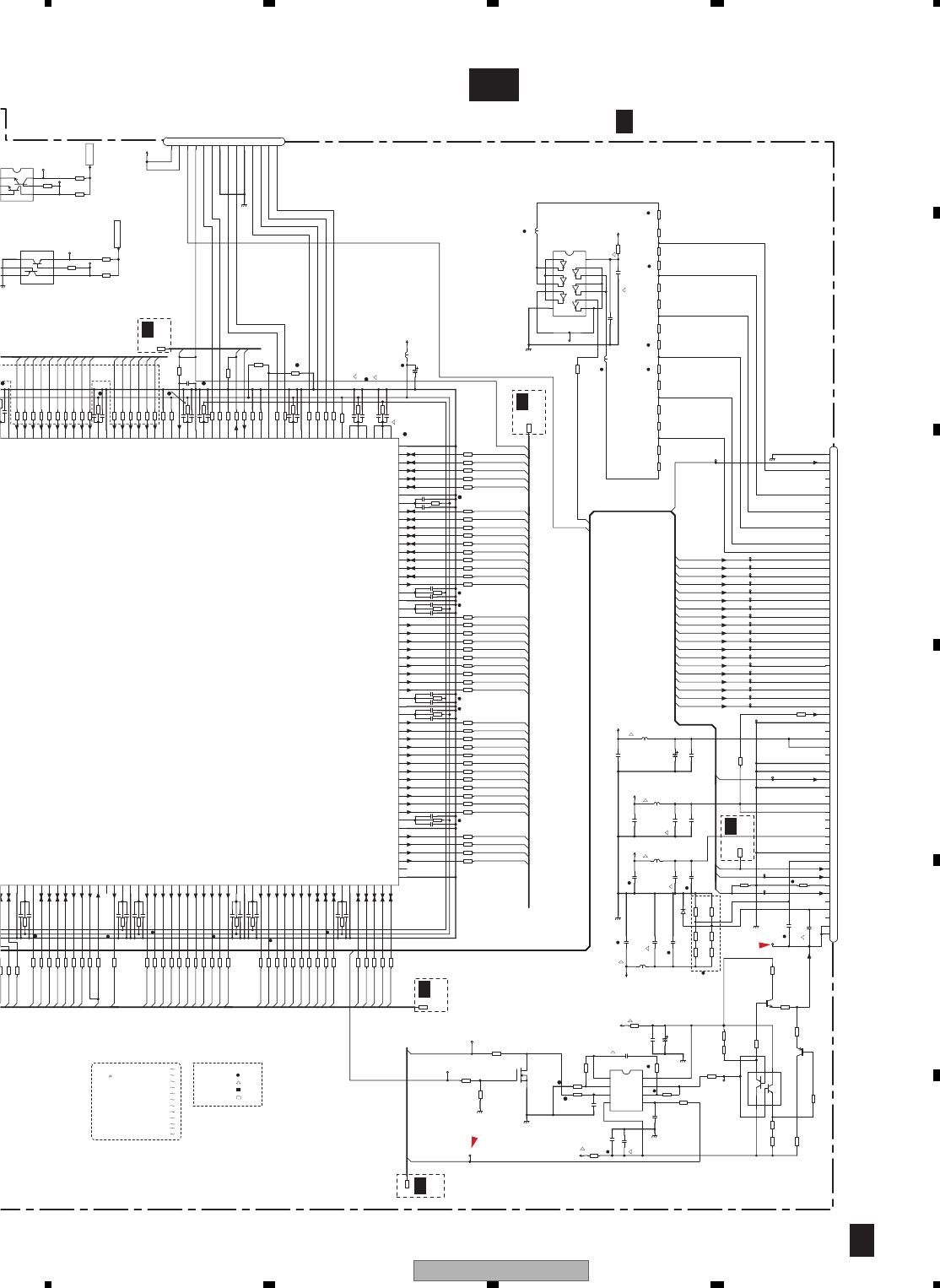
AVH-P4100DVD/XN/UC 163
5 678
5678
C
D
F
A
B
E
2/2
F
F-b 2/2
LCE
SDD_14
SDD_13
SDD_12
SDD_11
SDD_10
SDD_9
SDD_8
SDM_1
SDCKE
SDA_11
SDA_9
SDA_8
SDA_7
SDA_6
SDA_5
SDA_4
SDA_3
SDA_2
SDA_1
SDA_0
SDBA_1
SDBA_0
SDA_10
SDCS
SDRAS
SDCAS
SDWE
SDM_0
SDD_7
SDD_6
SDD_5
SDD_4
SDD_3
SDD_2
SDD_1
SDD_0
FAD_21
FAD_20
FAD_19
FAD_18
FAD_12
FAD_13
FAD_15
FAD_14
FAD_17
FAD_16
FAD_6
FAD_7
FAD_9
FAD_8
FAD_11
FAD_10
FAD_0
FAD_1
FAD_3
FAD_2
FAD_5
FAD_4
FROE
FDATA_15
FRWE
FRCS
FDATA_5
FDATA_6
FDATA_9
FDATA_7
FDATA_13
FDATA_14
FDATA_8
FDATA_12
FDATA_11
FDATA_10
FDATA_3
FDATA_4
FDATA_2
FDATA_1
FDATA_0
M_to_G
DVR_2
DVR_3
DVR_4
DVR_5
DVG_0
DVG_1
DVG_2
DVG_3
DVG_4
DVG_5
DVB_0
DVB_1
DVB_2
DVB_3
DVB_4
DVB_5
LB0
LB1
LB2
LB3
LB4
LB5
LG0
LG1
LG2
LG3
LG4
LG5
LR0
LR1
LR2
LR3
LR4
LR5
LCLK
LCSY
LDEN
LHSY
MEMCLK
TRCD1
TRCD1
EXTRG0
EXTRG0
TRCD0
TRCD0
TRCD2
TRCD2
TRCST TRCST
TRCCLK
TRCCLK
TRCD3
TRCD3
SDATA
SCLOCK
LEN
COMDC
LCE
COMAC
GRST
GRST
GRST
LVSY
G_to_M
NM
CN5701
1
2
3
4
5
6
7
8
9
10
11
12
13
14
CN6001
1VCOM
2 VCOM
3NC
4VEE
5NC
6 SPS
7 U/L
8 CLS
9 MODE
10 CS
11 GND
12 NC
13 VDD
14 NC
15 SPR
16 VCC
17 VSHD
18 NC
19 GND
20 CLD
21 GND
22 GND
23 NC
24 VSHA
25 VSHA
26 NC
27 GND
28 LBR
29 LS
30 R5
31 R4
32 R3
33 R2
34 R1
35 R0
36 G5
37 G4
38 G3
39 G2
40 G1
41 G0
42 B5
43 B4
44 B3
45 B2
46 B1
47 B0
48 V10
49 V9
50 NC
51 V7
52 NC
53 V5
54 NC
55 V3
56 NC
57 NC
58 V0
59 SPL
60 GND
47u/10_Ta
C5758
22u/16_Ta
C6156 22u/16_Ta
C6017
C6022
0.1u/10
C6015
0.1u/50
C6024
0.1u/50
C6023
0.1u/10
C6014
0.1u/10
C6013
0.1u/10
C6019
0.33u/50
C5734
1u/6.3
C5735
0.1u/10
C5738
1u/6.3
C5739
0.1u/10
C5741
0.1u/10
C5740
1u/6.3
C5752
1u/6.3
C5753
0.1u/10
C5770 0.1u/10
C5764 1u/6.3
C5769 0.1u/10
C5763 1u/6.3
C5767 0.1u/10
C5761 1u/6.3
C5766 0.1u/10
C5760 1u/6.3
C5765 0.1u/10
C5759 1u/6.3
C5762 1u/6.3
C5768 0.1u/10
C5757
0.1u/10
C5750
1u/6.3
C5751
0.1u/10
C5744
1u/6.3
C5745
0.1u/10
C5742
1u/6.3
C5743
0.1u/10
C5736
1u/6.3
C5737
0.1u/10
C5733
0.1u/10
C5748
1u/6.3
C5749
0.1u/10
C5747
0.1u/10
C5746
1u/6.3
C6010
0.1u/10
C6155
0.1u/10
C6154
CCG1222-A
4.7u
C6152
NM
C6026
1u/16
C6020
CCG1222-A
4.7u 25V
C6027
1u/25
C6012
DCH1201-A
10u 10V
C6018
DCH1201-A
10u 10V
C6016
0.1u/50
C6151
0.1u/50
C6025
0.1u/50
C5754
10u/6.3
C5755
10u/6.3
C5756
10u/6.3
C6158
4.7u/6.3
C5771
1000p/50
C6153
NM
D6001
NM
NDP
GNDD
GNDD
GNDD
GNDD
GNDD
GNDD
GNDD
GNDD
GNDD
NJM082BV
IC6151
A:OUT
1
A:-IN
2
A:+IN
3
V-
45
B:+IN
6
B:-IN
7
B:OUT
8
V+
IC6005
TC74VHCT04AFTS1
1A1
1Y2
2A3
2Y4
5
3A
6
3Y
7
GND 84Y
94A
105Y
115A
126Y
136A
14Vcc
MN103SE60PUB
IC5702
SDDATA_14
SDDATA_13
7
VSS_1
8
VDD3_1
9
SDDATA_12
10
SDDATA_11
11
SDDATA_10
12
SDDATA_9
13
SDDATA_8
14
SDM_1
15
SDCKE
16
MEMCLK
17
MIMCLK
18
SDAD_12
19
SDAD_11
20
VDD_1
21
VSS_2
22
VDD3_2
23
SDAD_9
24
SDAD_8
25
SDAD_7
26
SDAD_6
27
SDAD_5
28
SDAD_4
29
SDAD_3
30
SDAD_2
31
SDAD_1
32
SDAD_0
33
SDBA_1
34
VDD3_3
35
VSS_3
36
VDD_2
37
SDBA_0
38
SDAD_10
39
SDCS
40
SDRAS
41
SDCAS
42
SDWE
43
SDM_0
44
SDDATA_7
45
SDDATA_6
46
SDDATA_5
47
VDD3_4
48
VSS_4
49
SDDATA_4
50
SDDATA_3
51
SDDATA_2
52 SDDATA_1
53 SDDATA_0
54
VSS_5
55
FAD_22 56
FAD_21 57
FAD_20 58
FAD_19 59
FAD_18 60
VSS_6 61
VDD3_5 62
FAD_17 63
FAD_16 64
FAD_15 65
FAD_14 66
FAD_13 67
FAD_12 68
FAD_11 69
FAD_10 70
FAD_9 71
FAD_8 72
FAD_7 73
FAD_6 74
VDD3_6 75
VSS_7 76
VDD_3 77
FAD_5 78
FAD_4 79
FAD_3 80
FAD_2 81
FAD_1 82
FAD_0 83
FRWE 84
FRCS 85
FROE 86
FDATA_15 87
VDD3_7 88
VSS_8 89
VDD_4 90
FDATA_14 91
FDATA_13 92
FDATA_12 93
FDATA_11 94
FDATA_10 95
FDATA_9 96
FDATA_8 97
FDATA_7 98
FDATA_6 99
FDATA_5 100
VDD3_8 101
VSS_9 102
FDATA_4 103
FDATA_3 104
FDATA_2 105
FDATA_1
106
FDATA_0
107
VSS_10
108
VOUT_0
109
VOUT_1 110
VOUT_2 111
VDDP_0 112
VDDP_1 113
VDDP_2 114
RON 115
GPIO_08 116
GPIO_09 117
GPIO_10 118
GPIO_11 119
VSS_11 120
VDD3_9 121
SCLOCK 122
SDATA 123
DPSEL 124
GPIO_01 125
GPIO_00 126
RXD0 127
TXD0 128
GPIO_06 129
GPIO_02 130
GPIO_03 131
VDD_5 132
VSS_12 133
VDD3_10 134
XRST 135
INTR 136
GPIO_07 137
DVB_5 138
DVB_4 139
DVB_3 140
DVB_2 141
DVB_1 142
DVB_0 143
VSS_13 144
145
VDD3_11
146
DVG_5
147
DVG_4
148
DVG_3
149
DVG_2
150
DVG_1
151
DVG_0
152
DVR_5
153
DVR_4
154
DVR_3
155
DVR_2
156
VSS_14
VDD3_12
L5705
CTF1473-A
L6006
DTL1096-A
L6005
CTF1635-A
10u
L6008
DTL1096-A
L6001
CTF1306-A
L6007
CTF1635-A
Q5562
UMZ1N
E1
1B1
2C2
3
E24
5
B26
C1
Q5561
UMX2N
E1
E2
B2 C2
4
5
B1
6
C1
RUE003N02
Q6151
R5865 0
R5863
0
R5851 0
R5842
0
R5838
0
R5829 0
R5826 0
R5815
0
R5812
0
R5807 0
R5790
0
R5784 0
R6001
680
R6030
0
R5905
0
R5911
0
R5910
0
R5913
0
R5908
0
R5904
0
R5915
0
R5916
0
R5918
0
R5912
0
R5909
0
R5903
0
R5914
0
R5907
0
R5917
0
R5906
0
R5898
0
R5901
0
R5899
0
R5897
0
R5902
0
R5893
0
R5894
0
R5900
0
R5895
0
R5896
0
R5882
0
R5886
0
R5887
0
R5888
0
R5880
0
R5892
0
R5889
0
R5881
0
R5883
0
R5885
0
R5891
0
R5890
0
R5878
0
R5879
0
R5884
0
R5862
1k
R5861
68
R5866
68
R5870
68
R5857
68
R5867
68
R5871
68
R5868
68
R5859
68
R5847
150
R5844
150
R5852
150
R5845
150
R5849
150
R5843
10k
R5835
10k
R5841
10k
R5846
NM
R5833
NM
R5860
NM
R5858
NM
R5854
NM
R5848
NM
R5831
NM
R5856
NM
R5822
10k
R5820
10k
R5818
150
R5811
150
R5813
150
R5809
150
R5816
150
R5814
150
R5808
0
R5869 0
R6158
0
68
R5796
68
R5794
68
R5798
68
R5788
68
R5792
68
R5800
68
R5786
68
R5805
150
R5793
150
R5787
150
R5799
150
R5801
150
R5791
150
R5789
150
R5795
150
R5803
150
R5797
150
R5810
150
R5834
150
R5827
150
R5836
150
R5821
150
R5819
150
R5828
150
R5804
150
R5802
150
R5817
150
R5830
150
R5825
150
R5823
150
R5832
150
R5806
68
R6037
0
R5840
NM
R6156
10k
R6155
10k
R6044
5.1k
R6160
0
R6020
0
R6048
1.8k
R6046
4.7k
R6152
3.9k
R6019
56
R6032
82
R6022
0
R6018
39
R6017
47
R6015
82
R6013
160
R6012
18
R6011
10
R6010
0
R6161
15k
R5874 0
R5824
1k
R5569
6.8k
R5564
6.8k
R6016
12
R6014
15
R6026
1k
R5873 0
R5876 0
R5877 0
R5875 0
R6039
0
R6008
0
R6043
4.7k
R6045
5.6k
R6047
20k
R5565
47k
R5563
4.7k
R5570
47k
R5568
4.7k
R6025
100
R5853
82
R5850
10k
R6153
1k
R6154
1k
R6157
1k
R6159
NM
R5855
150
R5872 0
R6021
15
LB1
LB0
LCE2
LCSY
LHSY
LCLK
LDEN
LVSY
TP6003
GNDLCD
COM
LR5
LR3
DCG3
LR0
LR1
LG5
LR2
LR4
DCG1
DCG4
DCG2
LG0
LG3
LG2
LG4
LCE
LG1
COMAC
COMDC
LB5
LB3
LB2
LB4
VCCM16V
VCC15V
VCCM16V
VCC53V
VCCM16V
VCC8V
VCC53V
VCC15V
VCC3.3V
GD33V
GD33V
LEN2
G_SDRAM
GER_M
G_FROM
VCOM
R6151
3k
Q6001
UMZ1N
E11
B12
C23E2
4
5B2
6C1
Q6002
2SC4097(R)
C
2
B
3
E
1
R6038
NM
R6040
0
R6042
0
R6049
0
R6050
0
R6028
10k
R5837
1k
R5839
1k
R6027
33k
R6041
20
R6031
10
Q6003
2SA1577(Q)
R6029
0
R5752 47k
3216
1608
2125
CHIP SIZE LEGEND
GERDA
3225
/
(3528)
CON PART
5601
FLASH ROM PART
LCD PANELPART
5201
6001
CONNECTOR PART
SD RAM PART
5401
6101BACKLIGHT PART
5501
5451
5301
GERDA IC PART
DD-CON PART
VIDEOA/D IC PART
C.VIDEO PART
TOUCH PANELPART
5001
5701
5101
(3528)
ge Part
6V
D%
D%
D%
D%
D%
F%
D%
F%
D%
D%
F%
D%
D%
D%
TO LCD MODULE
D%
D%
VCOM PART
6151
L6004
CTF1306-A
UW5
MONITOR UNIT(MONITOR)
2/2
F
1/2
F
1/2
F
1/2
F
1/2
F
1/2
F
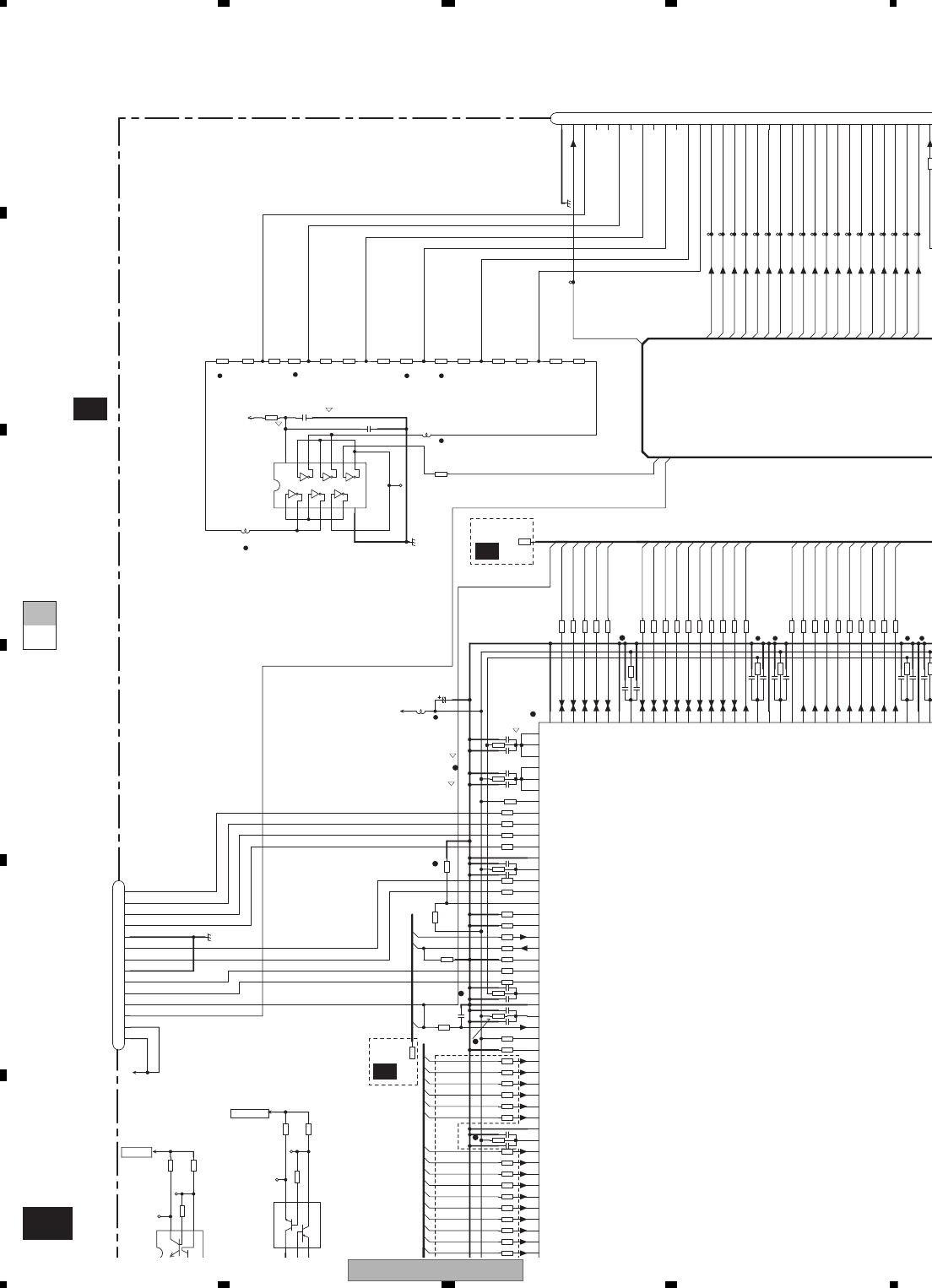
AVH-P4100DVD/XN/UC
164
1234
1234
C
D
F
A
B
E
F-a F-b
F-b 2/2
FAD_0
FAD_1
FAD_3
FAD_2
FAD_5
FAD_4
FROE
FDATA_15
FRWE
FRCS
FDATA_5
FDATA_6
FDATA_9
FDATA_7
FDATA_13
FDATA_14
FDATA_8
FDATA_12
FDATA_11
FDATA_10
FDATA_3
FDATA_4
FDATA_2
FDATA_1
FDATA_0
M_to_G
DVR_2
DVR_3
DVR_4
DVR_5
DVG_0
DVG_1
DVG_2
DVG_3
DVG_4
DVG_5
DVB_0
DVB_1
DVB_2
DVB_3
DVB_4
DVB_5
LB0
LB1
LB2
LB3
LB4
LB5
LG0
LG1
LG2
LG3
LG4
LG5
LR0
LR1
LR2
LR3
LR4
LR5
LCSY
LHSY
TRCD1
TRCD1
EXTRG0
EXTRG0
TRCD0
TRCD0
TRCD2
TRCD2
TRCST TRCST
TRCCLK
TRCCLK
TRCD3
TRCD3
SDATA
SCLOCK
LCE
GRST
GRST
GRST
G_to_M
NM
CN5701
1
2
3
4
5
6
7
8
9
10
11
12
13
14
CN6001
28 LBR
29 LS
30 R5
31 R4
32 R3
33 R2
34 R1
35 R0
36 G5
37 G4
38 G3
39 G2
40 G1
41 G0
42 B5
43 B4
44 B3
45 B2
46 B1
47 B0
48 V10
49 V9
50 NC
51 V7
52 NC
53 V5
54 NC
55 V3
56 NC
57 NC
58 V0
59 SPL
60 GND
47u/10_Ta
C5758
C5769 0.1u/10
C5763 1u/6.3
C5767 0.1u/10
C5761 1u/6.3
C5766 0.1u/10
C5760 1u/6.3
C5765 0.1u/10
C5759 1u/6.3
C5762 1u/6.3
C5768 0.1u/10
C5757
0.1u/10
C5750
1u/6.3
C5751
0.1u/10
C5744
1u/6.3
C5745
0.1u/10
C5742
1u/6.3
C5743
0.1u/10
C5736
1u/6.3
C5737
0.1u/10
C6010
0.1u/10
C6012
DCH1201-A
10u 10V
C5754
10u/6.3
C5755
10u/6.3
C5756
10u/6.3
C5771
1000p/50
GNDD
GNDD
GNDD
IC6005
TC74VHCT04AFTS1
1A1
1Y2
2A3
2Y4
5
3A
6
3Y
7
GND 84Y
94A
105Y
115A
126Y
136A
14Vcc
MN103SE60PUB
IC5702
VDD3 6 75
VSS_7 76
VDD_3 77
FAD_5 78
FAD_4 79
FAD_3 80
FAD_2 81
FAD_1 82
FAD_0 83
FRWE 84
FRCS 85
FROE 86
FDATA_15 87
VDD3_7 88
VSS_8 89
VDD_4 90
FDATA_14 91
FDATA_13 92
FDATA_12 93
FDATA_11 94
FDATA_10 95
FDATA_9 96
FDATA_8 97
FDATA_7 98
FDATA_6 99
FDATA_5 100
VDD3_8 101
VSS_9 102
FDATA_4 103
FDATA_3 104
FDATA_2 105
FDATA_1
106
FDATA_0
107
VSS_10
108
VOUT_0
109
VOUT_1 110
VOUT_2 111
VDDP_0 112
VDDP_1 113
VDDP_2 114
RON 115
GPIO_08 116
GPIO_09 117
GPIO_10 118
GPIO_11 119
VSS_11 120
VDD3_9 121
SCLOCK 122
SDATA 123
DPSEL 124
GPIO_01 125
GPIO_00 126
RXD0 127
TXD0 128
GPIO_06 129
GPIO_02 130
GPIO_03 131
VDD_5 132
VSS_12 133
VDD3_10 134
XRST 135
INTR 136
GPIO_07 137
DVB_5 138
DVB_4 139
DVB_3 140
DVB_2 141
DVB_1 142
DVB_0 143
VSS_13 144
145
VDD3_11
146
DVG_5
147
DVG_4
148
DVG_3
149
DVG_2
150
DVG_1
151
DVG_0
152
DVR_5
153
DVR_4
154
DVR_3
155
DVR_2
L5705
CTF1473-A
L6001
CTF1306-A
Q5562
UMZ1N
E1
1B1
2C2
3
24
5
26
1
5561
MX2N
C2
4
5
B1
6
C1
R5865 0
R5851 0
R5829 0
R5826 0
R5807 0
R6001
680
R5898
0
R5901
0
R5899
0
R5897
0
R5902
0
R5893
0
R5894
0
R5900
0
R5895
0
R5896
0
R5882
0
R5886
0
R5887
0
R5888
0
R5880
0
R5892
0
R5889
0
R5881
0
R5883
0
R5885
0
R5891
0
R5890
0
R5878
0
R5879
0
R5884
0
R5862
1k
R5843
10k
R5835
10k
R5841
10k
R5846
NM
R5833
NM
R5860
NM
R5858
NM
R5854
NM
R5848
NM
R5831
NM
R5856
NM
R5822
10k
R5820
10k
R5818
150
R5811
150
R5813
150
R5809
150
R5816
150
R5814
150
R5869 0
R5805
150
R5793
150
R5787
150
R5799
150
R5801
150
R5791
150
R5789
150
R5795
150
R5803
150
R5797
150
R6037
R5840
NM
R6020
0
R6019
56
R6032
82
R6022
0
R6018
39
R6017
47
R6015
82
R6013
160
R6012
18
R6011
10
R6010
0
R5874 0
R5824
1k
R5569
6.8k
R5564
6.8k
R6016
12
R6014
15
R5873 0
R5876 0
R5875 0
R6008
0
R5565
47k
R5563
4.7k
R5570
47k
R5568
4.7k
R5850
10k
R5872 0
R6021
15
LB1
LB0
LCE2
LCSY
LHSY
LR5
LR3
DCG3
LR0
LR1
LG5
LR2
LR4
DCG1
DCG4
DCG2
LG0
LG3
LG2
LG4
LG1
LB5
LB3
LB2
LB4
VCC15V
VCCM16V
VCC53V
GD33V
GD33V
GER_M
G_FROM
R5837
1k
R5839
1k
R5752 47k
GERDA
/
Part
D%
D%
D%
D%
F%
D%
F%
D%
D%
F%
D%
TO LCD MO
L6004
CTF1306-A
UW5
MONITOR UNIT(MONITOR)
2/2
F
1/2
F
1/2
F
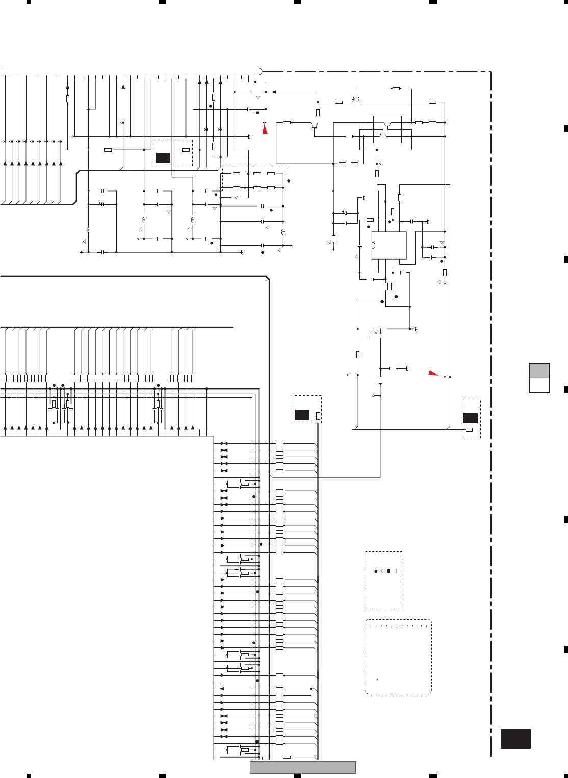
AVH-P4100DVD/XN/UC 165
5 678
5678
C
D
F
A
B
E
F-a F-b
F-b 2/2
LCE
SDD_13
SDD_12
SDD_11
SDD_10
SDD_9
SDD_8
SDM_1
SDCKE
SDA_11
SDA_9
SDA_8
SDA_7
SDA_6
SDA_5
SDA_4
SDA_3
SDA_2
SDA_1
SDA_0
SDBA_1
SDBA_0
SDA_10
SDCS
SDRAS
SDCAS
SDWE
SDM_0
SDD_7
SDD_6
SDD_5
SDD_4
SDD_3
SDD_2
SDD_1
SDD_0
FAD_21
FAD_20
FAD_19
FAD_18
FAD_12
FAD_13
FAD_15
FAD_14
FAD_17
FAD_16
FAD_6
FAD_7
FAD_9
FAD_8
FAD_11
FAD_10
FAD_0
FAD_1
FAD_3
FAD_2
FAD_5
FAD_4
FRWE LG4
LG5
LR0
LR1
LR2
LR3
LR4
LR5
LCLK
LCSY
LDEN
MEMCLK
LEN
COMDC
COMAC
LVSY
1VCOM
2 VCOM
3NC
4VEE
5NC
6 SPS
7 U/L
8 CLS
9 MODE
10 CS
11 GND
12 NC
13 VDD
14 NC
15 SPR
16 VCC
17 VSHD
18 NC
19 GND
20 CLD
21 GND
22 GND
23 NC
24 VSHA
25 VSHA
26 NC
27 GND
28 LBR
29 LS
30 R5
31 R4
32 R3
33 R2
34 R1
35 R0
36 G5
37 G4
G3
22u/16_Ta
C6156 22u/16_Ta
C6017
C6022
0.1u/10
C6015
0.1u/50
C6024
0.1u/50
C6023
0.1u/10
C6014
0.1u/10
C6013
0.1u/10
C6019
0.33u/50
1u/6.3
C5735
0.1u/10
C5738
1u/6.3
C5739
0.1u/10
C5741
0.1u/10
C5740
1u/6.3
C5752
1u/6.3
C5753
0.1u/10
C5770 0.1u/10
C5764 1u/6.3
C5769 0.1u/10
C5763 1u/6.3
C5762 1u/6.3
C5768 0.1u/10
C5748
1u/6.3
C5749
0.1u/10
C5747
0.1u/10
C5746
1u/6.3
C6155
0.1u/10
C6154
CCG1222-A
4.7u
C6152
NM
C6026
1u/16
C6020
CCG1222-A
4.7u 25V
C6027
1u/25
C6018
DCH1201-A
10u 10V
C6016
0.1u/50
C6151
0.1u/50
C6025
0.1u/50
C6158
4.7u/6.3
C6153
NM
D6001
NM
GNDD
GNDD
GNDD
GNDD
GNDD
GNDD
NJM082BV
IC6151
A:OUT
1
A:-IN
2
A:+IN
3
V-
45
B:+IN
6
B:-IN
7
B:OUT
8
V+
MN103SE60PUB
IC5702
VSS_1
8
VDD3_1
9
SDDATA_12
10
SDDATA_11
11
SDDATA_10
12
SDDATA_9
13
SDDATA_8
14
SDM_1
15
SDCKE
16
MEMCLK
17
MIMCLK
18
SDAD_12
19
SDAD_11
20
VDD_1
21
VSS_2
22
VDD3_2
23
SDAD_9
24
SDAD_8
25
SDAD_7
26
SDAD_6
27
SDAD_5
28
SDAD_4
29
SDAD_3
30
SDAD_2
31
SDAD_1
32
SDAD_0
33
SDBA_1
34
VDD3_3
35
VSS_3
36
VDD_2
37
SDBA_0
38
SDAD_10
39
SDCS
40
SDRAS
41
SDCAS
42
SDWE
43
SDM_0
44
SDDATA_7
45
SDDATA_6
46
SDDATA_5
47
VDD3_4
48
VSS_4
49
SDDATA_4
50
SDDATA_3
51
SDDATA_2
52 SDDATA_1
53 SDDATA_0
54
VSS_5
55
FAD_22 56
FAD_21 57
FAD_20 58
FAD_19 59
FAD_18 60
VSS_6 61
VDD3_5 62
FAD_17 63
FAD_16 64
FAD_15 65
FAD_14 66
FAD_13 67
FAD_12 68
FAD_11 69
FAD_10 70
FAD_9 71
FAD_8 72
FAD_7 73
FAD_6 74
VDD3_6 75
VSS_7 76
VDD_3 77
FAD_5 78
FAD_4 79
FAD_3 80
FAD_2 81
FAD_1 82
FAD_0 83
FRWE 84
L6006
DTL1096-A
L6005
CTF1635-A
10u
L6008
DTL1096-A
L6007
CTF1635-A
RUE003N02
Q6151
R5863
0
R5842
0
R5838
0
R5815
0
R5812
0
R5790
0
R6030
0
R5905
0
R5911
0
R5910
0
R5913
0
R5908
0
R5904
0
R5915
0
R5916
0
R5918
0
R5912
0
R5909
0
R5903
0
R5914
0
R5907
0
R5917
0
R5906
0
R5898
0
R5901
0
R5899
0
R5897
0
R5902
0
R5900
0
0
R5896
0
R5861
68
R5866
68
R5870
68
R5857
68
R5867
68
R5871
68
R5868
68
R5859
68
R5847
150
R5844
150
R5852
150
R5845
150
R5849
150
R5808
0
R6158
0
R5796
68
R5794
68
R5798
68
68
R5792
68
R5800
68
R5810
150
R5834
150
R5827
150
R5836
150
R5821
150
R5819
150
R5828
150
R5804
150
R5802
150
R5817
150
R5830
150
R5825
150
R5823
150
R5832
150
R5806
68
R6037
0
R6156
10k
R6155
10k
R6044
5.1k
R6160
0
R6048
1.8k
R6046
4.7k
R6152
3.9k
R6161
15k
R6026
1k
R5876 0
R5877 0
R6039
0
R6043
4.7k
R6045
5.6k
R6047
20k
R6025
100
R5853
82
R6153
1k
R6154
1k
R6157
1k
R6159
NM
R5855
150
R5872 0LCSY
LCLK
LDEN
LVSY
TP6003
GNDLCD
COM
LR5
LR3
LR0
LR1
LG5
LR2
LR4
LG4
LCE
COMAC
COMDC
VCCM16V
VCCM16V
VCC8V
VCC53V
VCC15V
VCC3.3V
LEN2
G_SDRAM
VCOM
R6151
3k
Q6001
UMZ1N
E11
B12
C23E2
4
5B2
6C1
Q6002
2SC4097(R)
C
2
B
3
E
1
R6038
NM
R6040
0
R6042
0
R6049
0
R6050
0
R6028
10k
R6027
33k
R6041
20
R6031
10
Q6003
2SA1577(Q)
R6029
0
3216
1608
2125
CHIP SIZE LEGEND
GERDA
3225
(3528)
CON PART
5601
FLASH ROM PART
LCD PANELPART
5201
6001
CONNECTOR PART
SD RAM PART
5401
6101BACKLIGHT PART
5501
5451
5301
GERDA IC PART
DD-CON PART
VIDEOA/D IC PART
C.VIDEO PART
TOUCH PANELPART
5001
5701
5101
(3528)
D%
D%
D%
TO LCD MODULE
D%
D%
VCOM PART
6151
1/2
F
1/2
F
1/2
F
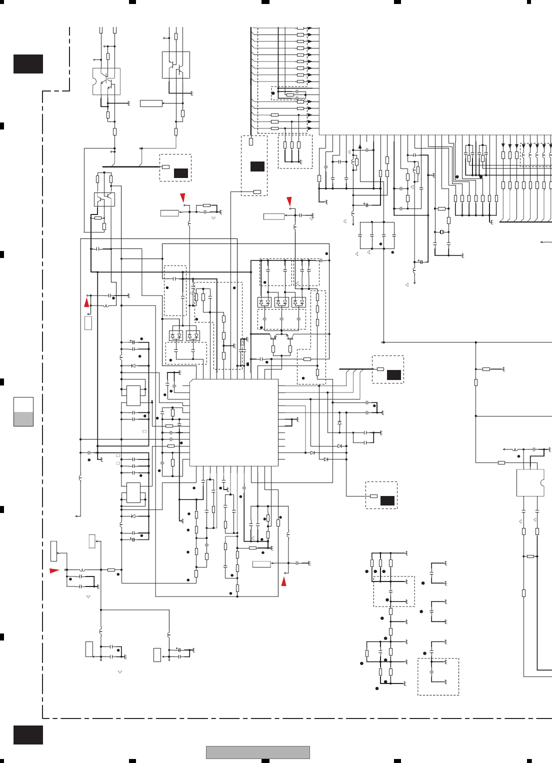
AVH-P4100DVD/XN/UC
166
1234
1234
C
D
F
A
B
E
F-bF-a
F-a 2/2
F-b 2/2
LEN
EXTRG0
LCE
LCSY
LDEN
LHSY
LVSY
LCLK
DVVSY
DVHSY
DVCLK
DVR_0
DVR_1
DVR_2
DVR_3
DVR_4
DVR_5
DVG_0
DVG_1
DVG_2
DVG_3
DVG_4
PWCTL1
PWCTL2
PWCTL3
PWCTL2
PWCTL3
CCH1586-A_Po
C5543
33u 10V
CCH1440-A_Po
C5509 68u
6.3V
47u/10_Ta
C5713
47u/10_Ta
C5702
33u/10_Ta
C5503
C5538
4.7u/16
C5502
0.1u/10
C5519 0.01u/50
C5510
0.1u/50
C5520
0.1u/50
C5539
0.1u/50
C5530
0.1u/50
C5534
0.1u/50
C5541
0.1u/50
C5540
0.1u/50
C5542
0.1u/50
C5522
CCG1223-A
C5521
CCG1223-A
C5527
CCG1223-A
10u
C5537
0.01u/50
C5545
NM
C5454
0.1u/10
C5507
0.1u/10
C5526
1000p/50
C5529
1000p/50
C5546
1u/16
C5544
0.1u/50
C5517
0.039u/50
C5516
0.039u/50
C5553
1u/16
C5552
1u/16
C5532 1u/16
C5531
1u/16
C5525
1u/16
C5535
4700p/50
C5710
1u/6.3
C5711
1u/6.3
C5718 0.1u/10
C5715
0.1u/10
C5716
0.1u/10
C5726
0.1u/10
C5719
0.1u/10
C5714
68p/50
C5712
33p/50
C5717
0.01u/16
C5725
0.1u/10
C5727
0.1u/10
C5720
1u/6.3
C5721
1u/6.3
C5728
0.1u/10
C5528
0.01u/50
C5536
4700p/50
C5518
0.01u/50
C5533
0.01u/50
C5732
1u/6.3
C5733
0.1u/10
C5550
CCG1222-A 4.7u 25V
C5547
1u/25
C5551
NM
C5554
1u/25
C5555
1u/25
C5524
NM
C5556
1000p/50
C5549
1u/16
C5548
1u/16
C5513
DCH1201-A 10u 10V
C5505
DCH1201-A
10u 10V
C5501
DCH1201-A
10u 10V
C5451
10u/6.3
C5016
0.047u/25
C5014
NM
C5013
NM
C5012
1000p/50
C5508
4700p/25
C5511
6800p/25
C5512 0.1u/16
C5514
0.033u/16
C5515 68p/50
C5523
NM
C5557
0.015u/16
C5558 27p/50
C5559
NM
C5708
10u/6.3
C5709
10u/6.3
C5504
1u/6.3
C5506
1u/6.3
C5018
NM
C5452
10u/6.3
D5507
RB548W
1
2
3
D5503
RB548W
1
2
3
D5505
RB548W
1
2
3
D5506
RB548W
1
2
3
D5504
RB548W
1
2
3
D5509
NM
D5502
RB160M-30
D5510
NM
D5501
RSX201L-30
D5508
NM
D5511
NM
GNDP
GNDP
GNDP
GNDP
GNDP
GNDP
GNDP
GNDP
GNDP
GNDP
GNDP
GNDP
GNDP
GNDP
GNDP
GNDP
GNDP
GNDP
GNDP
GNDP
GNDV
AVAGND
GNDD AVAGND
AVBGND
AVAGND
AVBGND
GNDRGB GNDFL GND
GNDRGB
GNDD
AVAGND
GNDILM
GNDD
GNDD
GNDD
GNDD
IC5451
NJM2505AF
Vout 1
GND 2
V+ 3
Vin
4
5VGND
BD6171KV
IC5501
NC1
1
OCPC2
2
VREGA 3
VS2 4
CL2 5
PVCC2 6
OUT2 7
LGND 8
VREGB 9
OVT1 10
PVCC1 11
CL1 12
VS1
13
OCPC1
14
FB1
15
INV1
16
SS1
17
FB2
18
INV2
19
SS2
20
VREF
21
OUT3
22
PVCC3
23
FB3
24
V03DET
25
V01DET
26
V02DET
27
V04DET
28 V05DET
29
SVBGND
30
GND
31
EN1
32
EN2
33
EN3
34
EN4
35 EN5
36
PVCC5 37
OUT5 38
FB5 39
PGND5 40
PVCC 41
VCC 42
FIN 43
RT 44
PGND4 45
FB4 46
OUT4
47
PVCC4
48
147
DVG 4
148
DVG_3
149
DVG_2
150
DVG_1
151
DVG_0
152
DVR_5
153
DVR_4
154
DVR_3
155
DVR_2
156
VSS_14
157
VDD3_12
158
DVR_1
159
DVR_0
160
DVCLK
161
DVHSY
162
DVVSY
163
IREF
164
VCMO
165
VREFH
166 VREFL
167 AVDD_1
168 AINP0
169 AINP1
170 AVSS_1
171 CLH
172 CLL
173 AVSS_2
174 DAOUT
175 AVDD_2
176 TSTIO
177 AVCLK
178 PMODE0
179 OSCXI
180 OSCXO
181 TSTCK
182 TSTC1
183 TSTC0
184 VDD_6
185 VSS_15
186 VDD3_13
187 MCKSL
188 LCDMUTE
189 GPIO_05
190 GPIO_04
191 LCDCE
192 LCDCSY
193 LCDDEN
194 LCDHSY
195 LCDVSY
196 LCDCLK
L5501
CTH1250-A
L5504
CTF1635-A
L5508
CTF1635-A
L5510
DTL1096-A
L5451
CTF1379-A
L5702
CTF1635-A
L5502
CTH1249-A
L5505
DTL1136
L5703 NM
L5509
CTF1635-A
L5701
CTF1635-A
L5506
CTF1488-A
L5704
NM
L5507
CTH1318-A
L5503
CTH1249-A
L5706
CTF1748-A
12
L5707
12
L5709
12
L5708
12
L5710
12
Q5562
UMZ1N
E1
1B1
2C2
3
E24
5
B26
C1
Q5561
UMX2N
E1
1
E2
2
B2
3
C2
4
5
B1
6
C1
RSQ035P03
Q5502
D1
1
D2
2
G
3
S
4
5
D3
6
D4
RSQ035P03
Q5501
D1
1
D2
2
G
3
S
4
5
D3
6
D4
Q5504
2SC4097(R)
2SA1577(QR)
Q5503
R5784 0
R5745 0
R5744
0
4
R5711
10k
R5532
0
R5530
220k
R5529
0
R5501
0
R5504
0
R5509
510
R5512
2.2k
R5526
47k
R5527
7.5k
R5919
10k
R5921
10k
R5920
10k
R5524
10k
R5468
NM
R5464
NM
R5452
NM
R5451
0
R5520
15
R5738
180
R5734
150
R5521
56k
R5705
100
R5706
1M
R5709
0
R5708
0
R5714
0
R5713
0
R5732
NM
R5733
22
R5731 22
R5739 12k
R5751
0
R5750
NM
R5749
0
R5775
150
R5772
150
R5783
150
R5781
150
R5793
150
R5787
150
R5799
150
R5801
150
R5791
150
R5789
150
R5795
150
R5803
150
R5797
150
R5525
3.3k
R5528
12k
R5710
10k
R5505
200
R5737 270
R5736
270
R5735
270
R5533
15k
R556
6.8k
R5741 7.5k
R5032
NM
R5033
0
R5034
NM
R5035
NM
R5453
100
R5743
6.2k
R5561
22k
R5562
22k
R5567
22k
R5566
22k
R556
47k
R5563
4.7k
R5568
4.7k
R5518
22k
R5778
220
R5522
0
R5517
5.1k
R5508
200
R5454
100
R5519 15
R5516
3k
R5513
3.3k
R5510
1k
R5511
200
R5506
10k
R5535
47
R5534
47
R5707
470
R5740
470
R5742
2.7k
R5503
0
R5507
1k
R5514
0
R5523
62k
R5461
0
R5712
10k
R5502
6.8k
V33A
GD33V
15V
53V
8V
-16V
PWCTL3
TP5501
VCC33
DCG3
DCG1
DCG2
PWCT2
CVIDEO
VCC53V
V33A
VCC3.3V
V33A
VCCM16V
PWRVI
VCC8V
3.3V
VCC53V
VCC15V
VCC3.3V
V33A
GD33V
GD33V
X5702
CSS1634-A
DDCON
VAD_GERDA
PWCTL
MVIPW
PWCTL
C5015
0.1u/50
R5036 0
R5037 0
AVAGND
R5038
NM
R5039
NM
R5730 0
R5729
0
R5040 0
C5704
6p/50
C5705
6p/50
10uH/0.61A
max100mA
V32
501
MAX2.0A POWER SUPPLY
H:500kHz
L:454.5kHz
(D)
D%
(D)
(D)
(10u)
D% D%D%
D% D% D%
D%
10u
50V
D% D%
(D)
8.0V
15.0V
-16.3V
3.3V
33MHz
(D)
0.8Vp-p(max1.0V)
(3528)
/
/
/
/
Discharge Part
+15V -16V
5.3V
3.3V
3.3V
(2016)
(3216)
(2016)
(2016)
(2012)
18uH
10uH 68uH
UW5
UW5
UW5
UC,EW5
C5560
0.1u/16
R5515
10k
R5536
1k
IMZ4
Q5505
1
2
3
4
5
6
R5537
10k
R5538
10k
1/2
F
1/2
F
1/2
F
1/2
F
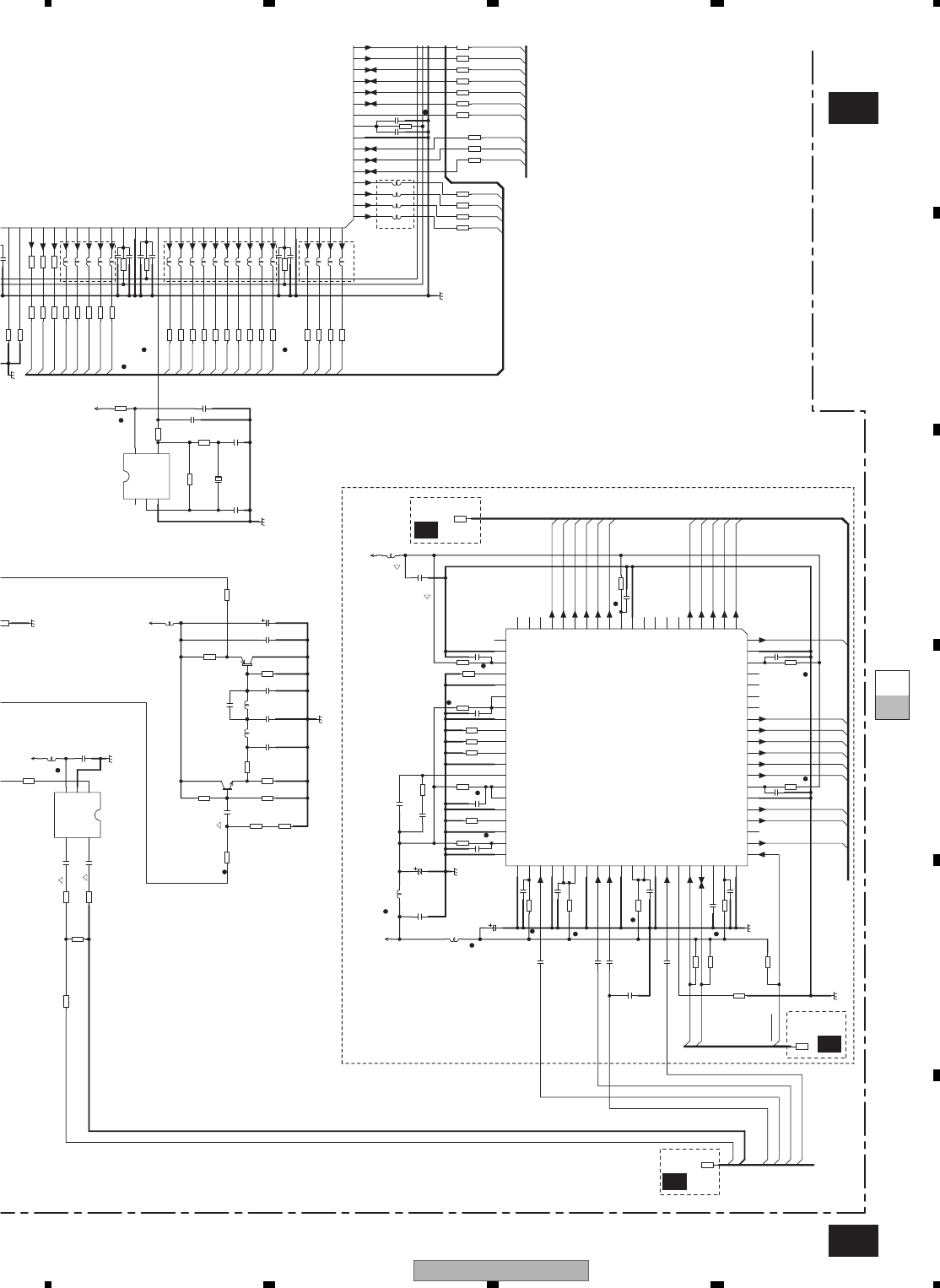
AVH-P4100DVD/XN/UC 167
5 678
5678
C
D
F
A
B
E
F-bF-a
F-a 2/2
F-b 2/2
LEN
EXTRG0
LCE
LCSY
LDEN
LHSY
LVSY
LCLK
LB0
LB1
LB2
LB3
LB4
LB5
LG0
LG1
LG2
LG3
LG4
LG5
LR0
LR1
LR5
LR4
LR3
SDD_15
SDD_14
SDD_13
SDD_12
SDD_11
SDD_10
SDD_9
SDD_8
SDM_1
SDCKE
DVVSY
DVHSY
DVCLK
DVR_5
DVR_4
DVR_3
DVR_2
DVR_1
DVR_0
DVG_5
DVG_4
DVG_3
DVG_2
DVG_1
DVG_0
DVB_5
DVB_4
DVB_3
DVB_2
DVB_0
DVB_1
NAVI_B
NAVI_G
NAVI_R
LR2
VADSCL
VADSDA
VADRES
MONVBS
GNDV
CSYNC
33u/10_Ta
C5460
47u/10_Ta
C5605
47u/10_Ta
C5611
C5454
0.1u/10
C5459
0.1u/10
C5456
68p/50
C5457
5p/50
C5455
47p/50
C5458
47p/50
C5706
NM
C5728
0.1u/10
C5729 0.1u/10
C5730 0.1u/10
C5723 1u/6.3
C5731 0.1u/10
C5734
1u/6.3
C5735
0.1u/10
C5613
0.082u/10
C5614
8200p/16
C5606 0.1u/10
C5616
0.1u/10
C5619
0.1u/10
C5610
0.1u/10
C5609
0.1u/10
C56080.1u/10
C5607
0.1u/10
C5612
0.1u/10
C5617
0.1u/10
C5615
0.1u/10
C5618
0.1u/10
C5620
0.1u/10
C5722 1u/6.3
C5724 1u/6.3
C5707
0.1u/10
C5451
10u/6.3
C5453
10u/6.3
C5601
1000p/50
C5602
0.1u/10
C5603
0.1u/10
C5604
0.1u/10
C5621
10u/6.3
C5701
12p/50
C5703
12p/50
C5622
NM
C5452
10u/6.3
AVAGND
AVAGND
AVAGND
GNDD
GNDD
GNDRGB
GNDRGB
GNDD
GNDD
IC5701
TC7SHU04FUS1
NC
1
INA
2
GND0
3OUTY 4
5
Vcc
IC5451
NJM2505AF
Vout 1
GND 2
V+ 3
Vin
4
5VGND
IC5601
AK5406XQ
GOUT6
1
GOUT5
2
GOUT4 3
GOUT3 4
GOUT2 5
GOUT1 6
GOUT0 7
NC1 8
NC2 9
DVSS1 10
DVDD1 11
BOUT7 12
BOUT6 13
BOUT5 14
BOUT4 15
BOUT3 16
BOUT2 17
BOUT1 18
BOUT0 19
NC3 20
NC4
21
DVSS2
22
DVDD2 23
CLAMP 24
AVSS1 25
TEST2 26
PVDD1 27
AVSS2 28
COAST 29
HSYNC 30
VSYNC 31
AVSS3 32
FLT 33
PVDD2 34
PVDD3 35
AVSS4 36
BIAS 37
TEST 38
AVDD1 39
AVSS5 40
AVSS6
41
AVDD2
42 BIN
43 AVSS7
44 AVDD3
45 AVDD4
46 AVSS8
47 GIN
48 SOGIN
49 AVSS9
50 AVDD5
51 AVDD6
52 AVSS10
53 RIN
54 A0
55 SCL
56 SDA
57 BYPASS
58 AVDD7
59 AVSS11
60
RESETN
61
VSYNCO
62 SONGOUT
63 HSYNCO
64 DTCLK
65 DVSS3
66 DVDD3
67 ROUT7
68 ROUT6
69 ROUT5
70 ROUT4
71 ROUT3
72 ROUT2
73 ROUT1
74 ROUT0
75 NC5
76 NC6
77 DVDD4
78 DVSS4
79 GOUT7
80
LCD_R_2
1
LCD_R_3
2
LCD_R_4
3
LCD_R_5
4
SDDATA_15
5
SDDATA_14
6
SDDATA_13
7
VSS_1
8
VDD3_1
9
SDDATA_12
10
SDDATA_11
11
SDDATA_10
12
SDDATA_9
13
SDDATA_8
14
SDM_1
15
SDCKE
16
_
187 MCKSL
188 LCDMUTE
189 GPIO_05
190 GPIO_04
191 LCDCE
192 LCDCSY
193 LCDDEN
194 LCDHSY
195 LCDVSY
196 LCDCLK
197 VDD3_14
198 VSS_16
199 VDD_7
200 LCDICLK
201 LCD_B_0
202 LCD_B_1
203 LCD_B_2
204 LCD_B_3
205 LCD_B_4
206 LCD_B_5
207 LCD_G_0
208 LCD_G_1
209 LCD_G_2
210 LCD_G_3
211 VDD3_15
212 VSS_17
213 LCD_G_4
214 LCD_G_5
215
LCD_R_0
216
LCD_R_1
L5602
CTF1473-A
L5601
CTF1473-A
L5454
0.1m
L5452
22u
L5451
CTF1379-A
L5603
CTF1635-A
L5453
27u
L5716
12
L5714
12
L5727
12
L5706
CTF1748-A
12
L5719
12
L5717
12
L5707
12
L5728
CTF1748-A
12
L5709
12
L5718
12
L5715
12
L5712
12
L5708
12
L5710
12
L5720
12
L5721
12
L5722
12
L5724
CTF1748-A
12
L5723
12
L5711
CTF1748-A
12
L5725
12
L5726
12
L5713
12
Q5451
2SC4081(QRS)
2SA1576A(QRS)
Q5452
R5790
0
R5748 0
R5747 0
R5746 0
0
R5704
0
R5620 0
R5619
0R5618
0
R5717
180
R5720
180
R5611
0
R5608 0
R5607 0
R5606 0
R5723
180
R546
NM
R5452
NM
R5451
0
R5469
0
R5617
0
R5612 0
R5738
180
R5771
180
R5715
180
R5728
180
R5726
180
R5777
180
R5716
180
R5718
180
R5616
0
R5774
180
R5734
150
R5602
47k
R5615
0
R5614
0
R5613
0
R5701
1M
R5702
22
R5714
0
R5713
0
R5732
NM
R5733
22
R5731 22
R5751
0
R5750
NM
R5749
0
R5785
68
R5796
68
R5794
68
R5798
68
R5788
68
R5792
68
R5800
68
R5786
68
R5804
150
R5802
150
R5604 0
R5605 0
R5621 2.2k
R5460
33k
R5467
390
R5703
3.3k
R5724
180
R5737 270
R5736
270
R5735
270
R5725
180
R5780
180
R5453
100
R5722
180
R5721
180
R5454
100
R5609
6.8k
R5727
180
R5459
15k
R5466
2.7k
R5719
180
R5622
2.2k
R5462
680
R5463
470
R5610
2.7k
R5623
2.2k
R5461
0
10k
VCC53V
V33A
VCC3.3V
GD33V
GD33V
X5701
CSS1778-A
VAD_GERDA
ANALOG
M_VAD
R5455
0
R5457
4.7k
R5458
6.8k
C5623
100p/50
C.VIDEO
D%
9.597MHz
VIDEO_AD
(F)
(3528)
(3528)
D%
(2520) (2520)
(2520)
UW5
1/2
F
1/2
F
1/2
F
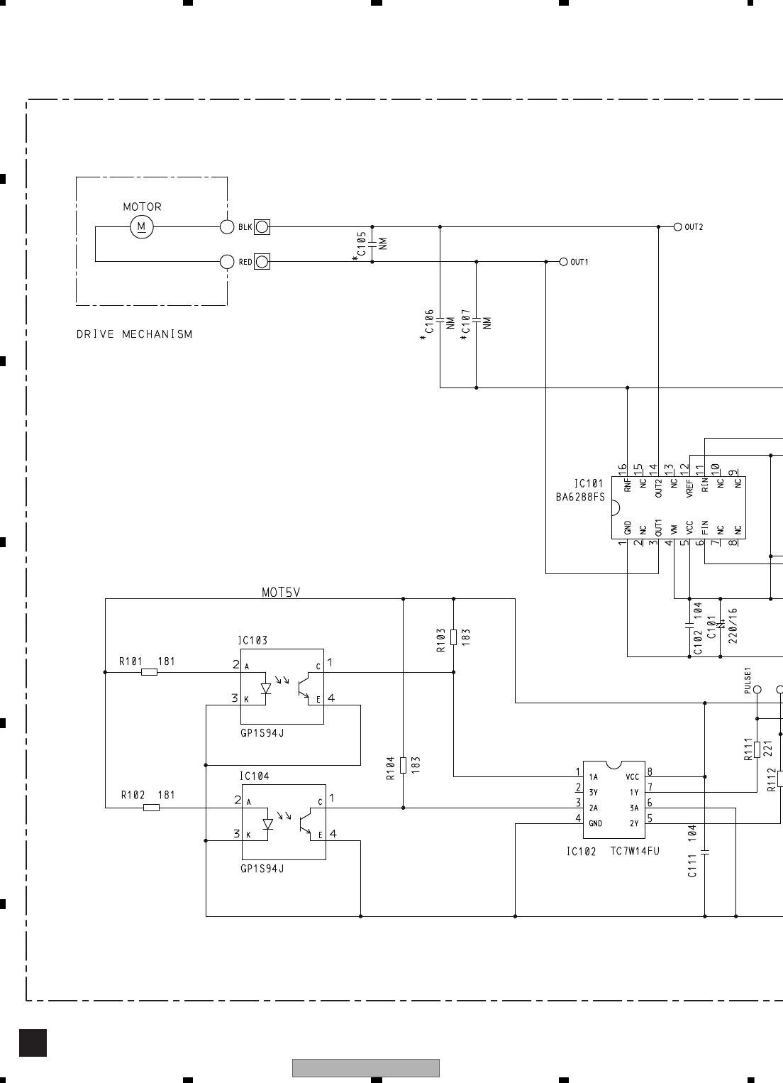
AVH-P4100DVD/XN/UC
168
1234
1234
C
D
F
A
B
E
10.11 SERVICE PCB ASSY
G
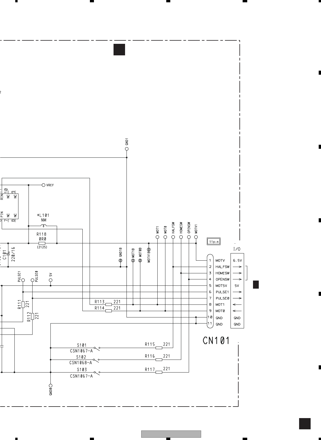
AVH-P4100DVD/XN/UC 169
5 678
5678
C
D
F
A
B
E
G
GSERVICE PCB ASSY
3/4
A
CN801
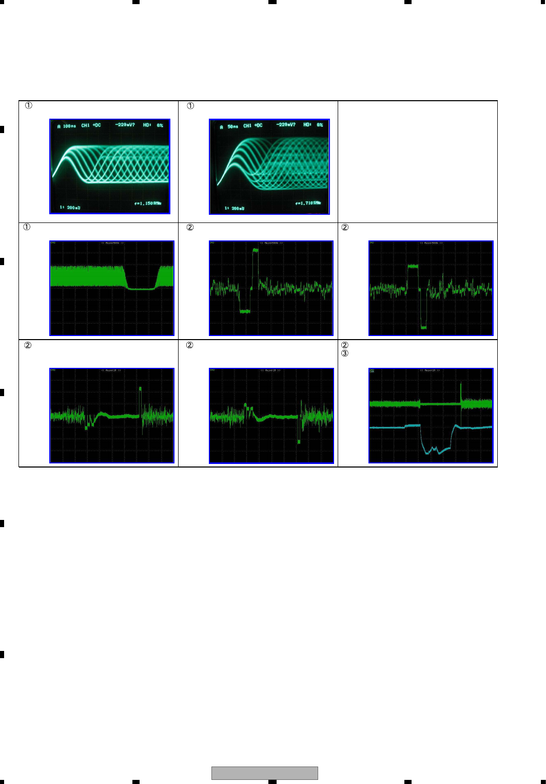
AVH-P4100DVD/XN/UC
170
1234
1234
C
D
F
A
B
E
10.12 WAVEFORMS
RF 0.2 V/div(AC) 100 ns/div
CDRF(x4CLV)
RF 0.2 V/div(AC) 50 ns/div
DVDRF(x1.3ZCAV)
RF 0.5 V/div 100 us/div
DVDRF(BD1mm)
TD1 0.2 V/div 100 us/div
Interval FWD(DVD)
TD1 0.2 V/div 100 us/div
Interval REV(DVD)
VHALF VHALF
2.2 V->
Traverse 1001FWD(short)(DVD)
VHALF
VHALF VHALF
0->
TD1 0.2 V/div 500 us/div
Multi 32FWD(DVD)
TD1 0.2 V/div 500 us/div
Multi 32REV(DVD)
CH1:TD1 0.5 V/div 10 ms/div
CH2:COP-COM 2.0 V/div 10 ms/div
- DVD CORE UNIT
Note:1. The encircled number denote measuring points in the circuit diagram.
2. Reference voltage: 1.65 V(TD1,FD1)(=VHALF)
2.2 V(RF)(=VREF)
In the waveform, it is seeing on the GND standard.
Offset of 1.65 V or 2.2 V is put in.
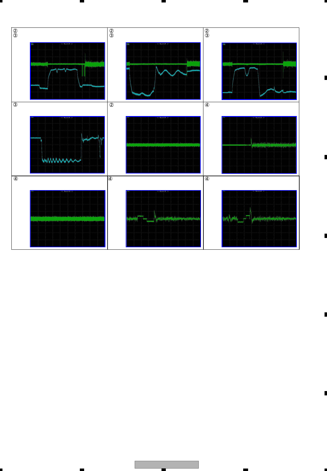
AVH-P4100DVD/XN/UC 171
5 678
5678
C
D
F
A
B
E
VHALF VHALF
VHALF
VHALF
VHALF VHALF
VHALF
VHALF
0->
0->
0->
0->
CH1:TD1 0.5 V/div 10 ms/div
CH2:COP-COM 2.0 V/div 10 ms/div
Traverse 1001REV(short)(DVD)
CH2:COP-COM 2.0 V/div 100 ms/div
ID search Inside -> Outside(DVD)
FD1 0.5 V/div 20 ms/div
Play FD(DVD)
FD1 0.5 V/div 500 us/div
Focus Jump L0 -> L1 FD1 0.5 V/div 500 us/div
Focus Jump L1 -> L0
TD1 0.5 V/div 100 ms/div
Play TD (DVD)
FD1 0.5 V/div 1 ms/div
Focus Close (DVD)
CH1:TD1 0.5 V/div 20 ms/div
CH2:COP-COM 2.0 V/div 20 ms/div
Traverse 5001FWD(long)(DVD)
CH1:TD1 0.5 V/div 20 ms/div
CH2:COP-COM 2.0 V/div 20 ms/div
Traverse 5001REV(long)(DVD)
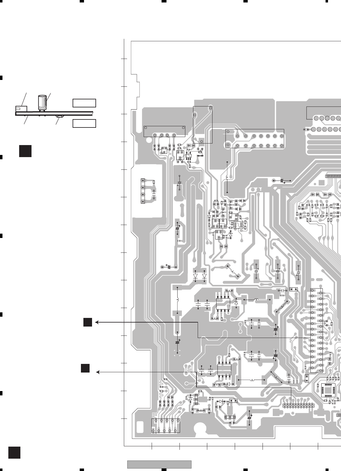
AVH-P4100DVD/XN/UC
172
1234
1234
C
D
F
A
B
E
11. PCB CONNECTION DIAGRAM
11.1 MOTHER PCB
A
AMOTHER PCB
Capacitor
Connector
P.C.Board Chip Part SIDE B
SIDE A
NOTE FOR PCB DIAGRAMS
1.The parts mounted on this PCB
include all necessary parts for
several destination.
For further information for
respective destinations, be sure
to check with the schematic dia-
gram.
2.Viewpoint of PCB diagrams
5151 25
2010 30
1
5
1
1 5
10
15
20
E
1
15
10
1 5 10
1
5
1
5
1
10
515
1
5
1
1 5 10
1
1
E
E
1 5
10
1
1
1
E
E
C1500
C1129
D951
P1341
C1141
IC561
C1143
Q1141
C1149
IC951
C1341 CN801
C1342
C1343
C1344
L1201
Q1341
L1202
L1203
L1204
L1205
L1206
L1207
L1208
L1209
D1141
R1141
D1341
R1343
C1381
C1382
C1383
Q1381
D1381
R1381
R1382
P1202
P1203
L902
L141
C1001
C1002
C1005
Q161
C1201
C1202
Q163
C1203
C1204
C1205
Q1201
C1206
Q1202
C1401
C1214
L161
L162
C1216
Q951
C1223
C1224
C1225
D1201
C1226
D1202
C1227
D1203
C1228
D1204
C1229
C1421
C1232
C1233
R904
L951
L952
R1210
R521
R1211
R522
R524
R525
R526
R527
R528
R529
R530
R534
R535
CN901
C1061
CN521
CN522
R161
JA141
R162 R165
R168
C901
C903
R170
C904
R171
R173
R174
C1081
R176
R5
R562
R563
R564
R565
R1061 C141
R566
C142
R567
R568
R569
R951
R952
R953
R954
L1141
R955
IC1061
R57
R771
R772
R773
R774
R775
R776
R777
R778
R779
C161
C162
C163
JA951
C165
C166
R780
C168
R781
R782
R783
R787
R788
R789
R790
C561
R791
R792
R793
C563
C564
C951
C952
C192
C771
L1381
C772
C773
C774
D521
C778C787
D161
D164
D165
10 20 30 40 50 60 70
X
140
130
120
110
100
90
80
70
60
50
40
30
20
10
0
YFRONT
P 1202 (A,61,57) Fuse 1 A CEK1280
P 1203 (A,66,24) Fuse 2.5 A CEK1285
>
>
CORD ASSY
S/PDIF OUT
C
CN1901
G
CN101
USB
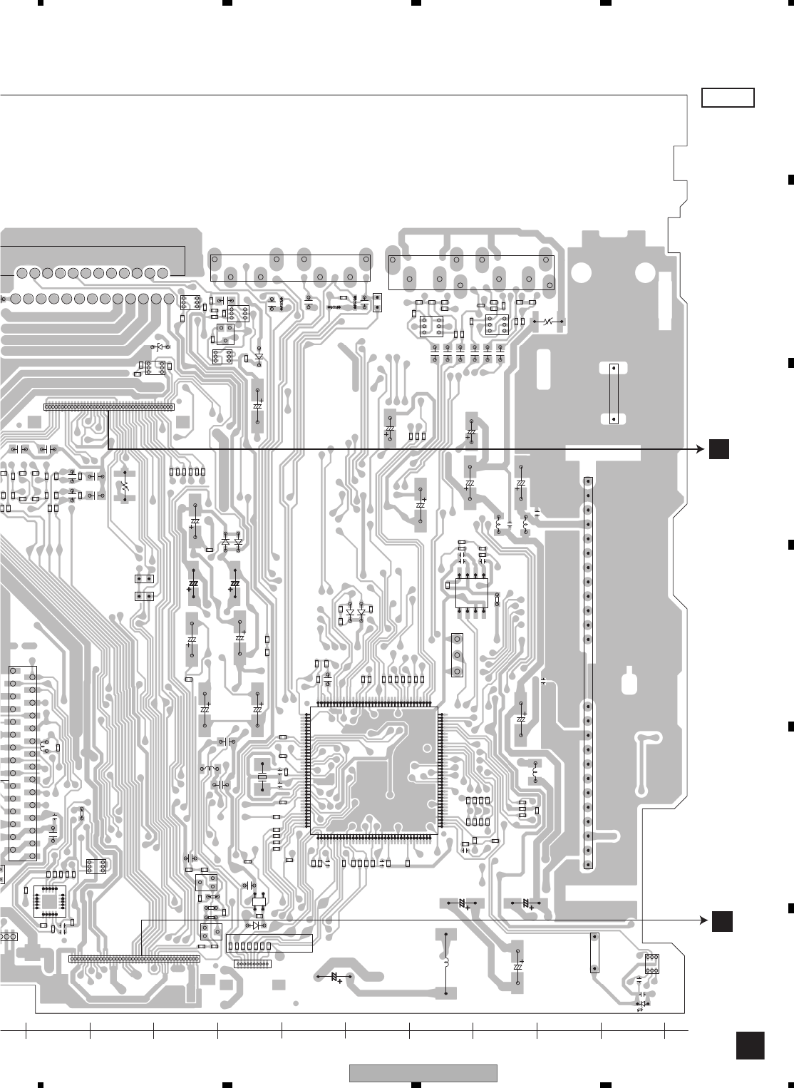
AVH-P4100DVD/XN/UC 173
5 678
5678
C
D
F
A
B
E
A
SIDE A
5151 25
2010 30
1 10
1
1
1
1 5
10
15
20
1
E
1
1 5 10 15 20 25 30 35
40 45 50 55 60 65 70
75
80859095
100105
110115120125130135140
1
1
1
1
5
1 5 10 15 20 25 30 35 40
15101520
10
E
E
1 5 10 15 20 25 30 35 40
1
1
51
1
5
10
1
1
1
1 5
10
15
20
25
1
1
R601
R602
R604
R605
R606
D182
R607
R608
R609
R419
R610
R611
R612
R613
R614
R420
R615
R421
R616
R422
JA402
R618
R619
IC751
P101
IC561
CN601
CN602
R620
R621
R622
R623
R624
IC181
R626
R627
R628
R629
C207
C208
R630
R631
R632
R633
R634
C404
R635
C405
R636
R637
C408
C215
P121
C601
C602
C603
C604
L1022
C606
R644
R645
C609
R646
C222
R647
R648
C224
C801
C802
P130
C610
P131
X601
C611
P132
R650
R651
R652
C618
R655
R656
R657
R661
R662
R663
R667
R668
R669
R670
R671
R676
Q101
Q102
Q103
Q104
BZ601
Q121
D601
D602
D603
D801
IC601
IC602
03
L902
R101
R102
R103
R104
R105
R107
R108
R109
R110
R111
R112
R113
R114
R115
C1021
R116
R117
R118
C1024
Q561
C1025
R119
R501
Q371
Q372
R120
JA101
R121
JA102
Q182
R122
Q183
R317
R123
R318
R124
R125
R126
R127
R128
R129
R327
R328
R904
CN501
U401
C101
CN121
C102
C103
C104
C105
C106
C107
C108
C109
C110
CN901
C325
1
C903
C904
R751
C1082
R752
R753
R754
R561
R755
R756
C1086
R562
R563
C334
R564
R371
R565
C336
R372
R566
R373
R567
R374
R568
R375
R569
R376
R377
R378
R184
R185
R186
R187
R570
R188
R189
C344
C345 C346
C347
R771
R772
R773
R774
R775
R776
R777
R778
R779
D102
D103
D104
D105
R780
R781
R782
R783
D301
D302
R788
R789
C751
C752
C753
C561
L201
R791
R792
R793
C563
C371
L402
C186
L403
Q801
L601
2
C771
C772
C778
C785
C786
C787
R205
R206
R207
70 80 90 100 110 120 130 140 150 160 170
ONT
FM/AM TUNER UNIT
B
CN2002
ANTENNA
RCA OUT
VCR IN
F
CN5001
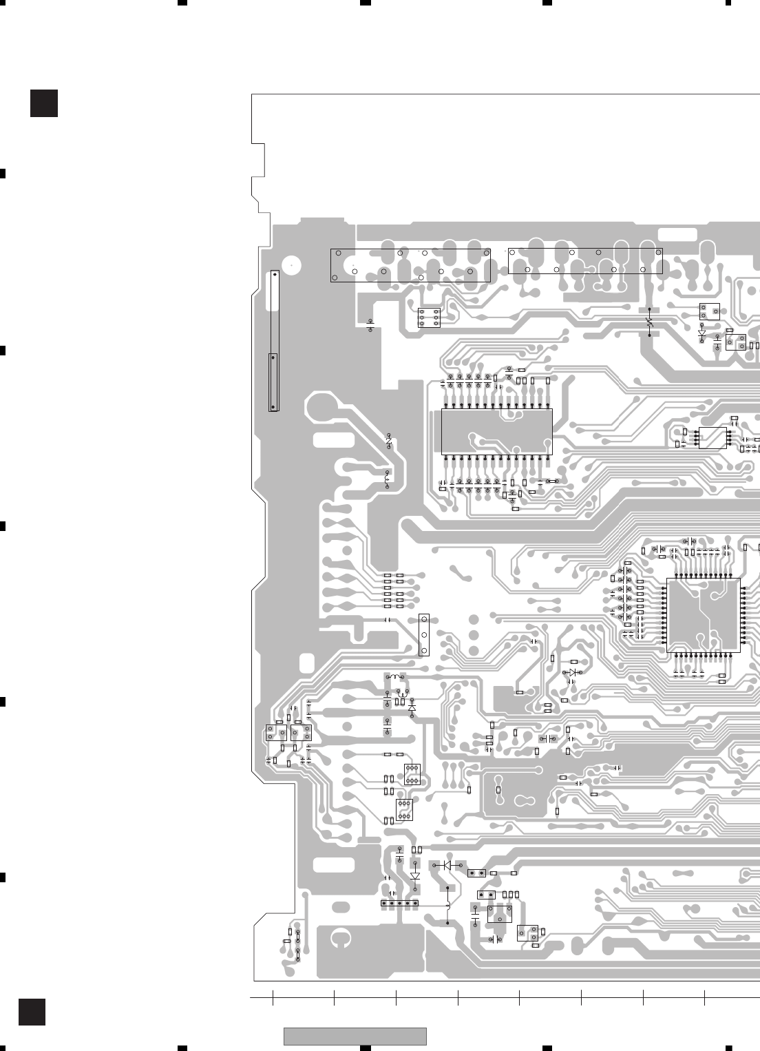
AVH-P4100DVD/XN/UC
174
1234
1234
C
D
F
A
B
E
A
AMOTHER PCB
170 160 150 140 130 120 110 100
1510
152025
1 5 10
15 20
25 30 35
40 45
1
1
1
1
5
E
E
E
E
15
E
R401
R402
R403
R404
R210
R405
R211
R406
R212
R407
R213
R408
R214
R409
R216
R2
R218
R219
R603
R410
R411
D181
R412
R413
R414
R220
R415
R221
R416
R222
R223
R224
R225
R801
R802
R803
R804
R617
R423 R424
R425
R426 R427 R428
R429
P102
R430
R431
R625
C201
R432
C202
R433
C203
R434
C204
R435
C205
C206
C209
C401
C402
C403
C210
C211
C406
C212
C407
C213
R638
C214
R639
C409
C216
C217
C218
C219
R640
C410
C411
L1021
C605
R642
R643
C607
C220
C608
C221
C223
R649
C225
C226
C227
C228
C612
C613
C615
R653
R654
C619
R658
R659
R660
R664
R665
R677
R678
Q105
D604
D605
IC201
IC202
P1021
P1022
R301
R302
R303
R304
R307
C1022
C1023
Q1021
Q1022
R310
R311
R312
R313
R314
R315
Q181
R319
R320
R321
R325
R326
R
D1021
R1021
R1022
R1023
R1024 R1025
R1026
R1027
R91
C111
P401
C305
C306
C307
C308
C309
C310
C311
C312
C313
C314 C31
C3
C317
C318
C319
C320
C321
C322
C323
C324
C326
C327
C328
C329
C1083
C1084
C330
C1085
C331
C332
C1087
C333
C1088
C335
C337
R181
R182
R183
C34
C34
C3
C3
D1081
R1081
D101
R1082
IC1081
Q401
Q402
Q403
Q404
C181
L401
L404
L405
IC301
R202
R204
R208
R209
1
1
1
1
P 1021 (B,137,20) Fuse 1 A CEK1280
P 1022 (B,136,17) Fuse 1.75 A CEK1283
P 1201 (B,19,46) Fuse 4 A CEK1344
>
>
>
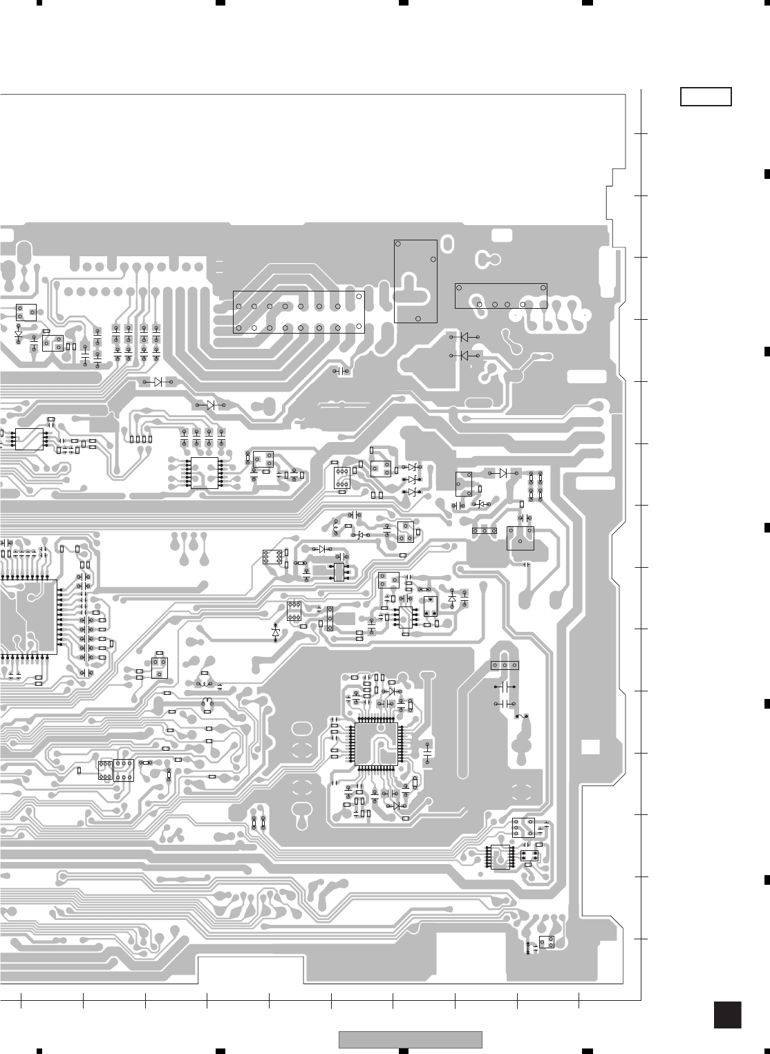
AVH-P4100DVD/XN/UC 175
5 678
5678
C
D
F
A
B
E
A
SIDE B
100 90 80 70 60 50 40 30
X
140
130
120
110
100
90
80
70
60
50
40
30
20
10
0
Y
20 10
1 5 10
15 20
30 35
40 45
25
1 5 10
30 35
40 45
1
1
1 5
10
1
E
1
1 5
10
1
1
1
5
1
E
E
E
1
5
E
E
1
1
1
1
E
E
E
R215
R217
R218
Q1121
Q1122
C1128
D181
D183
D184
R222
223
R225
C1142
C1144
C1145
Q1142
C1146
D1122
C1147
Q1143
C1148
R1127
R1128
IC771
C217
C218
C219
R641
D1142
C220
R1144
R1145
R1146
C226
R1147
R1148
R1149
IC1141
R1150
R1151
R1152
R1153
R1154
R674
R675
IC202
Q901
Q902
P1201
L901
L903
L521
C1003
Q1001
C1006
Q1002
C1007
Q162
Q164
Q165
C1207
C1208
C1209
C1402
C1403
C1210
R305
C1211
R306
C1212
C1213
R308
R309
C1215
L163
C1217
C1218
C1219
D1001
D1002
R310
R1001
R312
R1003
C1220
R1004
R315
Q181
C1221
R1005
R316
C1222
R1006
R1007
IC1001
D1205
R1201
D1206
R1202
R1203
R1204 R1205
R322
R1206
R323
R1207
R324
C1230
R1208
R901
D1401
R325
C1231
R1209
IC1201
Q1422
R326
R902
R903
C1234
C1235
R1401
Q771
R329
R905
R906
R907
R908
R909
R1212
R523
R1213
R330
R1214
IC1401
R1215
R1216
R1217
R1218
R910
R1219
R911
R912
R913
R914
R915
R916
R1220
C301
C302
R532
C303
R1224
C304
R1225
R1226
C307
R1421
R1422
C315
C316
C317
C318
C319
R163
R164
R166
R167
C320
321 R169
F1201
C902
R172
R175
C521
C522
R177
C523
C524
R178
R179
C332
C333
C335
C337
R180
C338
C339
R181
R182
R183
C340
C341
C342
C343
D101
C164
C167
R784
R785
R786
R794
Q601
R795
R796
R797
R798
C181
C182
C183
C184
C185
C187
C188
C189
IC301
C190
C191
C193
C194
C195
C775
D522
C776
D523
C777
C779
D141
D142
C780
C781
C782
IC521
IC522
D162
D163
R201
D166
D167
R203
1
1
1
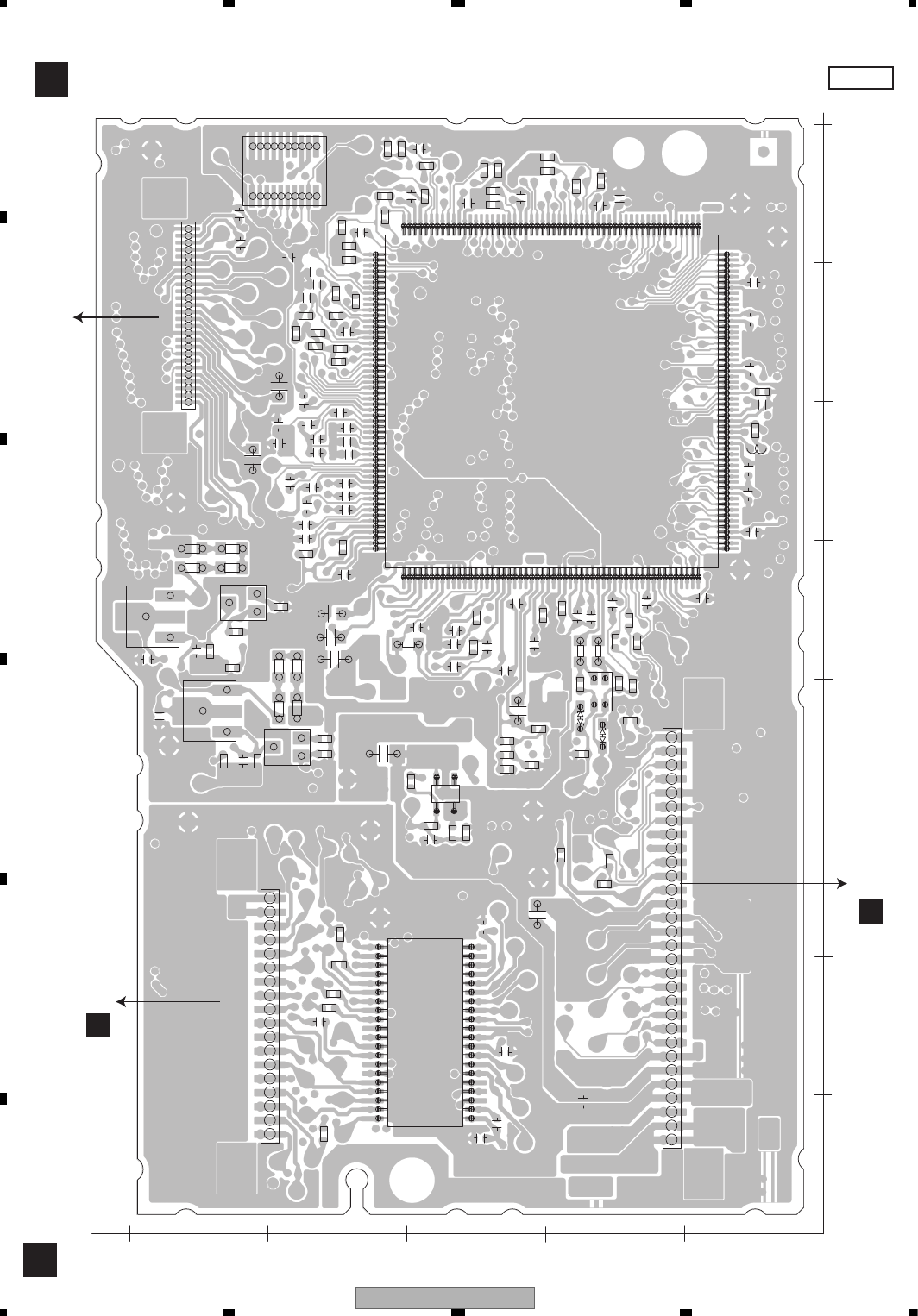
AVH-P4100DVD/XN/UC
176
1234
1234
C
D
F
A
B
E
11.2 DVD CORE UNIT
C
SIDE A
CDVD CORE UNIT
1 5 10 15 20 25 30
1 5 10 15 20 25 30 35 40 45 50
65 70 75 80 85 90 95 100 105
130 135 140 145 150 155 160
195 200 205 210 215
6055
125120115110
190
185
180175170
165
1510
1520
1 5 10 15
1
1 5 10 15 20
25303540
1
1 5 10 15 20 25
E
E
E
E
C1502
C1503
C1504
C1505
C1506 C1507 C1509
CN1901
R1101
C1511
R1102
R1103
C1514
R1104
C1515
R1105
C1516
R1106
C1517
C1518
C1519
R1109
C1520
R1110
C1521
R1111
C1522
R1112
C1523
R1113
C1524
R1114
R1115
C1526
R1116
R1117
C1528
R1118
C1529
R1505
R1506
R1507
R1508
R1509
IC1501
R1510
R1512
R1513
R1514
D1901
D1902
R1516
R1517
R1518
R1519
R1522
R1523
R1524
R1525
R1526
R1528
R1529
R1530R1531
R1533
R1534
CN1951
R1536
R1537
R1538
R1539
R1540
R1541
R1542
C1953
R1547
R1950
R1951
R1954
R1955
R1956
R1957
CN1201
C1203
C1204
C1205
C1207
C1208
C1018
C1019
C1022
C1601
C1602
C1603
C1604
R1001
C1605
C1606
C1607
R1004
C1608
C1609
R1007
R1008
IC1001
C1610
R1201
C1611
R1202
C1612
R1203
C1613
R1204
C1614
C1615
C1616
C1617
C1618
IC1201
C1619
C1620
C1621
C1622
R1212
C1623
C1624
R1021
C1625
C1626
C1627
R1601
R1026
R1602
R1603
R1027
R1604
R1605
L1512
L1901 C1671
C1672
C1673
C1674
C1676
R1670
R1671 R1672
R1673
R1674
R1675
R1679
CN1101
C1104
C1105
Q1101
Q1102
C1106
Q1103
C1107
C1108
Q1104
C1109 C1110
C1111
C1508
10 20 30 40 50 60 70 80
X
50
40
30
20
10
0
Y
PICKUP UNIT (SERVICE)
ACN901
DCN701
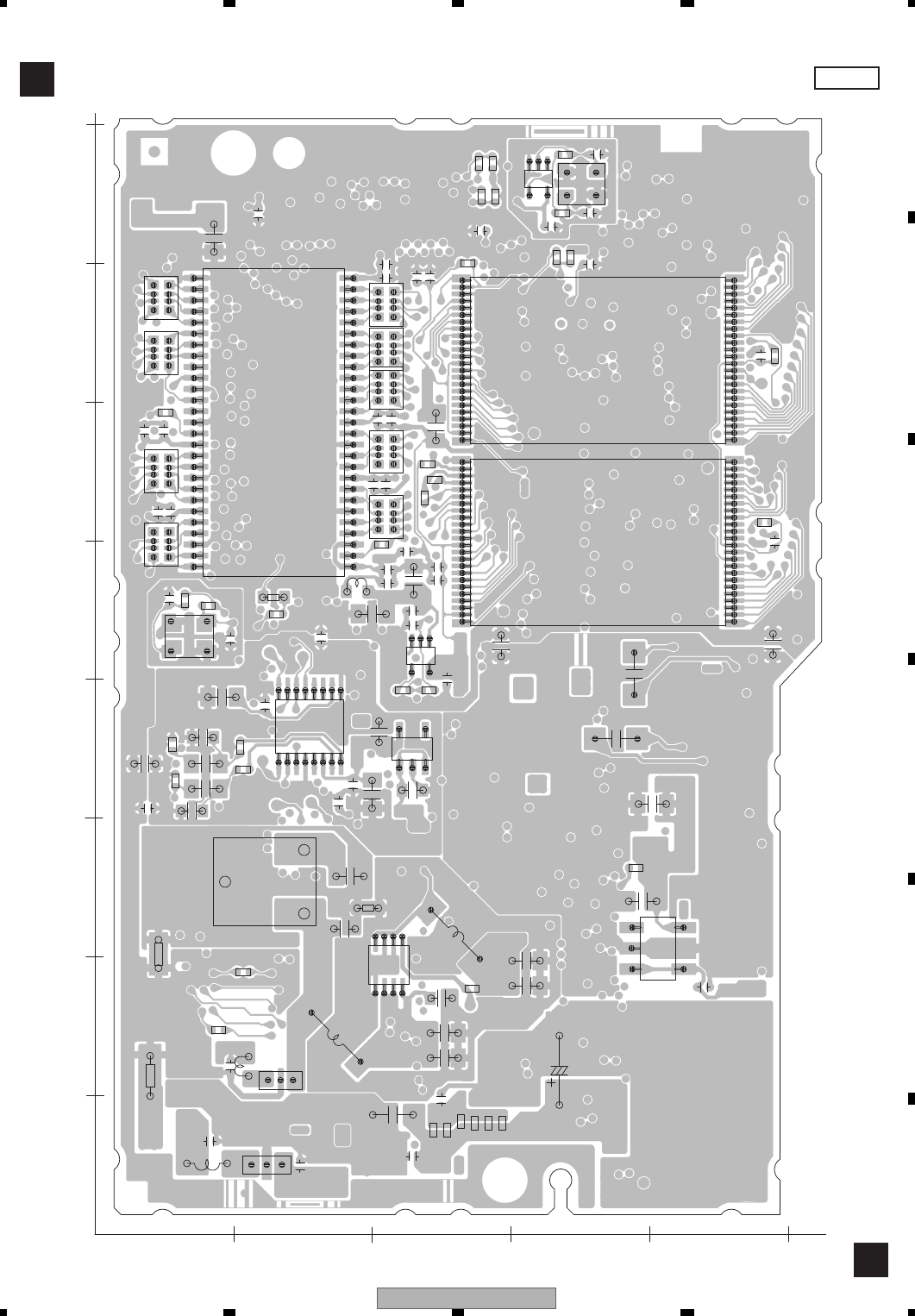
AVH-P4100DVD/XN/UC 177
5 678
5678
C
D
F
A
B
E
C
SIDE B
CDVD CORE UNIT
80 70 60 50 40 30 20 10
X
50
40
30
20
10
0
Y
1
1
1
5
1
1
1
1
1
5
1
5
10
15
20
25
30
35
40
45
1
5
10
15
20
25
30
35
40
45
1 5
1015
1
1 5 10 15 20 25
3035404550
C1501
C1510
C1512
C1513
R1300
R1301
C1525
C1527
R1501
R1503
R1504
L1003
L1004
R1511
EF1001
EF1002
C1934
R1527
R1532
R1535
C1950
C1951
C1952
R1543R1544
C1954
R1546
R1952 R1953
IC1951
C1001
C1003
C1004
C1005
C1006
C1007
C1008 C1009
C1201
C1010
C1011
C1012
C1013 C1014
C1209
C1015
C1016
C1017
C1401
C1402
C1403
C1404
C1210
C1405
C1211
C1407
C1408
C1409
C1021
X1501
R1002
C1802
IC1002
C1803
IC1003
C1804
IC1004
IC1005
C1805
C1806
IC1006
C1807
C1808
R1011
C1809
R1015
R1017
R1019
R1401
R1402
R1403
R1405
R1406
R1213
R1214
R1215
IC1401
R1409 R1216
IC1402
R1217
R1218
R1025
R1222
R1801 R1802
R1803
R1804
IC1801
L1902
L1903
L1904
X1950
C1480
C1481
C1482C1483
C1484
C1485
C1486
C1487
C1488
C1489
C1490
C1491
C1492
C1493
C1494
R1480
R1481
R1482
R1483R1484
R1485
R1486
R1487
R1488
IC1480
R1489
R1490
C1101
C1301
C1302
C1112 C1113
C1801
1
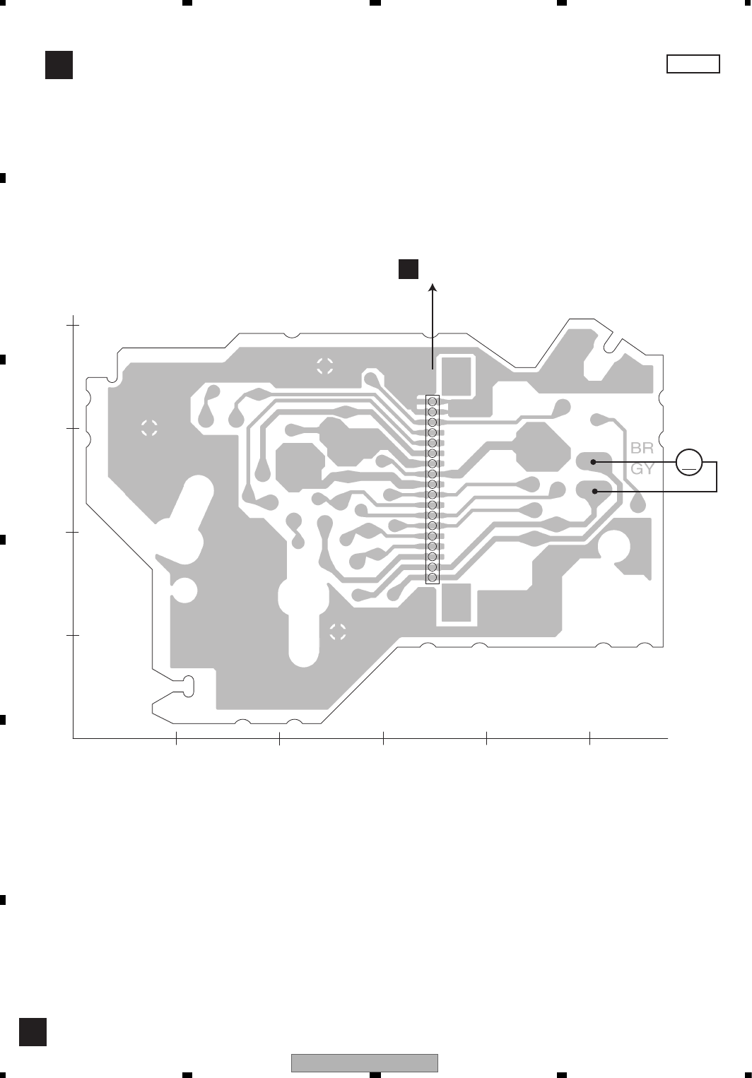
AVH-P4100DVD/XN/UC
178
1234
1234
C
D
F
A
B
E
11.3 CONNECT PCB
D
SIDE A
DCONNECT PCB
1 5 10 15
CN701
10 20 30 40 50
X
40
30
20
10
0
Y
M
M1
LOAD/CRG
MOTOR
CCN1201
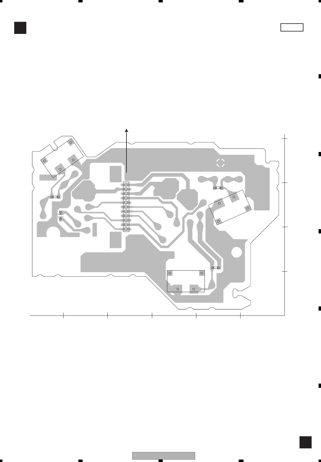
AVH-P4100DVD/XN/UC 179
5 678
5678
C
D
F
A
B
E
D
SIDE B
DCONNECT PCB
50 40 30 20 10
X
40
30
20
10
0
Y
1
1
1
1 5 10
R101
R102
R103
CN101
C101
S101
S102
S103
M2
SPINDLE MOTOR
HOME
8SNS
DSCSNS
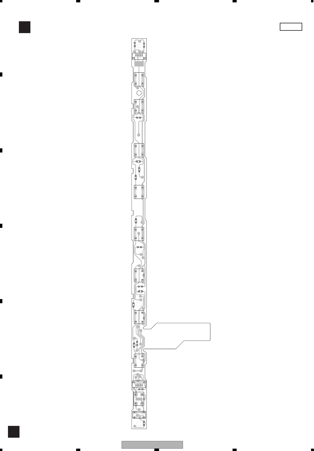
AVH-P4100DVD/XN/UC
180
1234
1234
C
D
F
A
B
E
11.4 KEYBOARD UNIT
E
SIDE A
EKEYBOARD UNIT
16
16
S3005 U3001
D3005
S3008 S3003 S3002 S3001 S3004 S3009 S3007 S3006
D3002
EJECT
MUTE
VOL+
VOL-
SRC/OFF
FORWARD
REVERSE
DISP OFFRESET
R3005
C3008
C3007
C3006
R3008
R3009
R3010
R3006
R3007
R3011
C3012
C3013
C3014
C3015
R3001
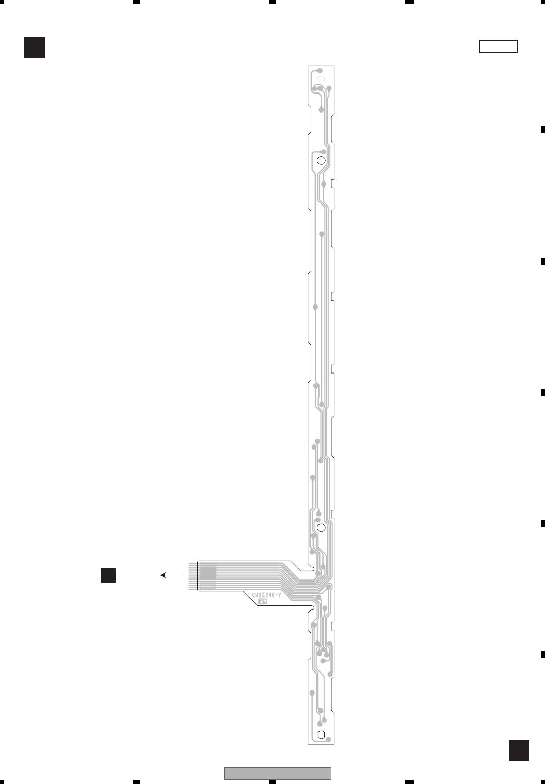
AVH-P4100DVD/XN/UC 181
5 678
5678
C
D
F
A
B
E
E
SIDE B
EKEYBOARD UNIT
FCN5003
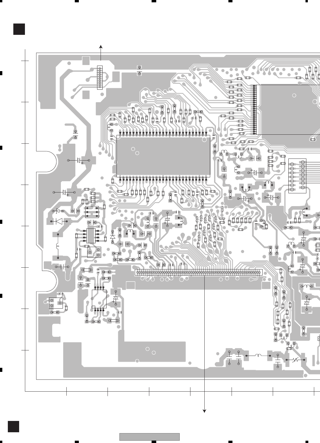
AVH-P4100DVD/XN/UC
182
1234
1234
C
D
F
A
B
E
11.5 MONITOR UNIT
F
FMONITOR UNIT
1
5
1
1510 15 20 25 30 35 40 45 50 55 60
1510 15 20 25
30
3540
45
50
1 10
E
5
1
E
1 5
10
1
5
1
5
10
15
20
R6104
R6105
R6106
R6107
R6108
R6109
IC6101
R6110
R6111
R6112
R6113
R6114
L6001
L6004
L6005
L6006
L6007
L5454
C6151
C6153
C6154
C6155
C6156
R6151 R6152
R6155
R6156
R6158
IC6151
R6160
C5201
C5202
C5013
C5016
C5018
C5605
R5201
C5611
R5202 R5203
C5613
R5204
C5614
R5205
R5206 R5207
R5208
IC5201
R5209
R5210
R5211
C56
C5622
R5212
R5213
R5214
R5215
R5216
R5217
R5218
R5219
R56
R5220
CN6001
R5221
R5222
R5223
R5032
R5033
R5034
L5301
R5611
R5229
R5036
L5302
R5037
R5613
R5615
R5616
R5618
R5231
R5233
R5235
R5237
R5239
C6013
R5240
C6014
L5701
C6015
L5702
L5703
C6017
C5460
C6018
R5820
L5705
C6019
R5822
C6022
C6023
L5710
C6024
L5711
D6001
L5712
C6026
L5713
C6027
L5714
L5715
L5716
L5717
L5718
L5719
R5835
L5720
R6010
R5840
R6011
R6012
R6013
R6014
R6015
R6016
R6017
R6018
R6019
R6020
R5850
R6021
R6022
L6101
L6102
R6032
R6043
R6044
R6045
R6046
R6047
R6048
R5894
R5895
R5897
C5301
C5302
C5303
C5304
C5305
C5306
C5307
C5308
C5309
CN5701
C5702
R5301
R5302
R5303
C5713
R5304
R5305
R5306
R5307
R5308
IC5301
R5309
P6101
R5310
R5311
R5312
R5313
R5314
C5725
R5315
R5316
R5317
R5318
R5319
L5201
R5320
R5708
R5709
CN6101
R5322
R5323
R5324
R5325
R5326
R5327
R5328
R5710
R5329
R5711
R5712
R5713
R5714
R5715
C6101
R5716
C6102
R5717
C6103
C6104
R5330
R5718
R5331
R5719
Q6101
C6105
R5332
C6106
Q6102
R5333
Q6103
C6107
R5334
C6108
L5601
R5335
C6109
L5602
R5336
L5603
R5337
R5338
R5720
R5339
R5721
R5722
R5723
C6110
R5724
C6111
R5340
R5341
R5342 R5343
R5344
R5920
R5345
R5921
R5730
C5758
D6101
D6102
R6101
R6102
R6103
10 20 30 40 50 60 70
X
80
70
60
50
40
30
20
10
0
Y
BACKLIGHT
LCD MODULE
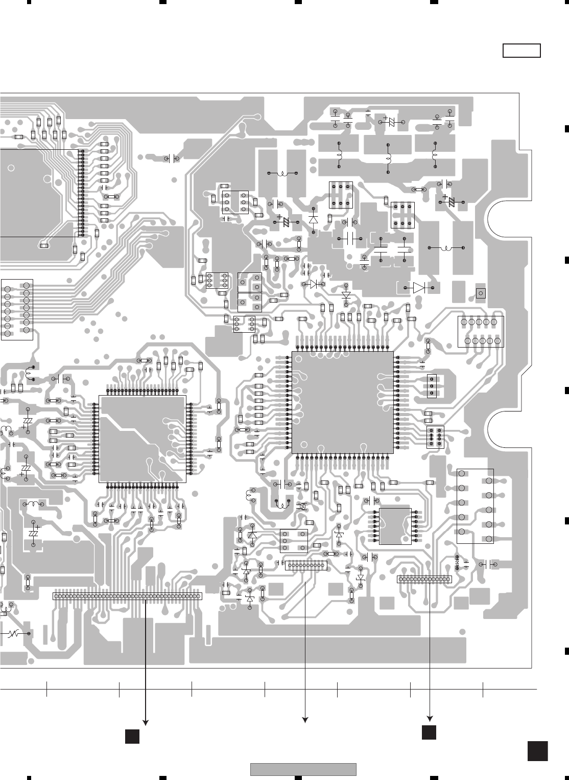
AVH-P4100DVD/XN/UC 183
5 678
5678
C
D
F
A
B
E
F
SIDE A
1 5 10 15 20 25 30 35 40
1 5 10 15 20
25 30 35 40
45 50 55 60
65 70 75 80
10
15 10
15
10
1 10
1
5
1 5
10
10
1 5
1
5
1
5
E E
1 5 10 15 20
25 30 35 40
45 50 55 60
65 70 75 80
1
1
1
25
30
35
40
45
1
1
R5561
R5562
R5563
R5564
R5565
L6001
R5566
R5567
R5568
R5569
R5570
L5454
R5795
R5797
R5799
CN5001
CN5003
CN5004
C5004
C5006
CN5401
X5101
C5203
C5011
C5014
C5017
018
C5401
C5402
C5403
C5404
Q5401
C5406
C5407
C5408
C5409
D5001
C5601
C5602
C5603
C5604
C5605
C5606
C5607 C5608 C5609
IC5001
C5610
C5611
C5612
C5613
C5614
C5615
C5616
C5617
C5618
D5401
C5619
IC5201
D5402
D5403
D5404
R5401
D5405
R5402
R5403
R5404
C5620
R5405
C5621
C5622
R5406
R5407
R5408
R5409
R5604
L5101
R5605
R5606
R5607
R5608
IC5601
R5609
R5224
R5801
R5225
R5226
R5033
R5803
R5227
34
R5610
R5228
R5611
R5805
R5229
R5612
R5613
R5614
R5615
R5616
R5617
R5618
R5230
R5619
R5231
R5232
R5233
R5234
L5501
R5235
L5502
R5236
L5503
R5237
R5238
R5620
L5505
R5239
TP5102
L5507
R5240
R5241
R5242
R5243
R5244
C5460
R5245
R6022
R6032
CN5101
C5101
C5102
C5103
C5104
C5105
C5106
C5111
C5501
CN5701
C5502
C5503
C5504
C5505
Q5501
Q5502
C5506
Q5503
Q5504
Q5505
C5509
C5510
R5101
R5102
R5103
R5104
R5105
R5106
R5107
R5108
C5519
R5109
IC5101
R5110
C5521
R5111
C5522
R5113
C5523
R5114
R5115
D5501
D5502
R5116
C5527
C5528
C5529
TH5101
R5501
P6101
R5503
D5508
R5120
R5122
R5123
R5124
R5125
D5511
R5127
R5128
R5129
C5539
R5514
R5515
R5130
R5131
R5519
R5132
R5133
C5543
R5135
L5401
R5138
R5520
R5522
R5523
R5140
R5141
5601
R5142
5602
C5553
L5603
R5146
R5147
C5559
R5534
R5535
R5536
R5537
R5538
C5560
R5920
R5151
R5921
R5153
R5154
Q5561
Q5562
R5156
R6101
70 80 90 100 110 120 130
ACN501 TOUCH PANEL E
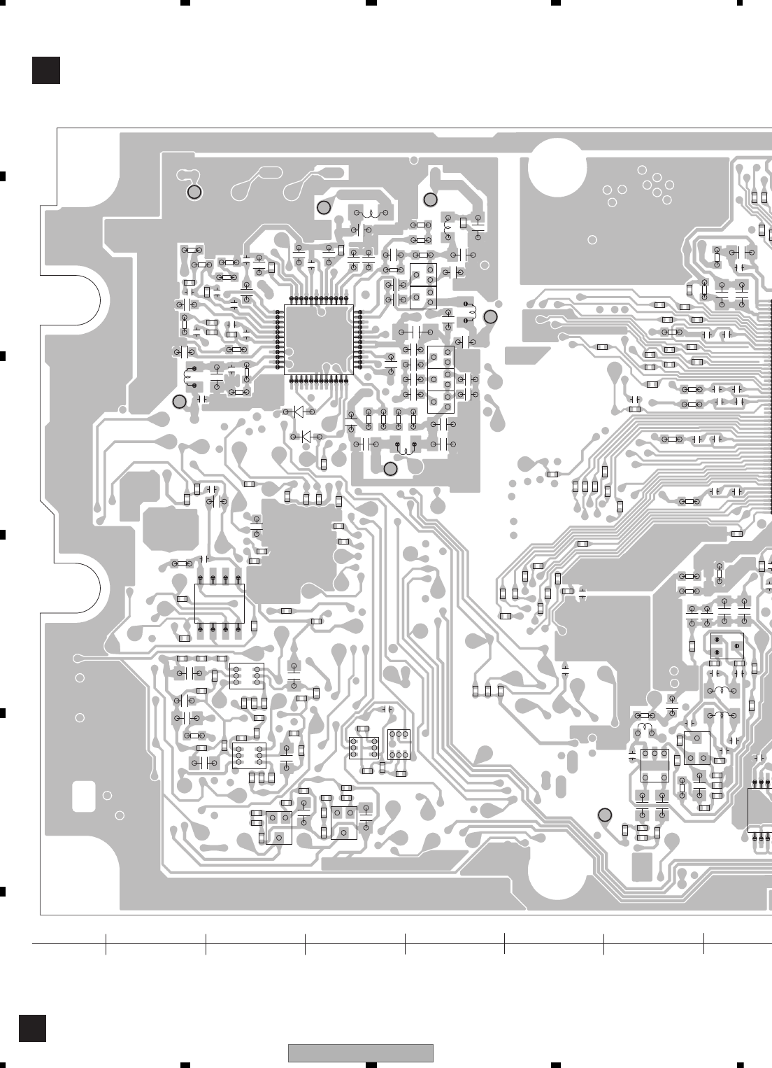
AVH-P4100DVD/XN/UC
184
1234
1234
C
D
F
A
B
E
F
FMONITOR UNIT
130 120 110 100 90 80 70
E
1
5
1
E
1
1
1
5
1 5 10
15 20
30 35
40 45
25
1
E
1
E
C5771
R5752
L5451
L5452
L5453
R5772
R5775
R5778
R5781
R5783
R5784
R5787
R5789
R5791
R5793
C5001
C5002
C5003
Q5001
C5005
Q5002
Q5003
C5007
Q5004
C5008
C5009
C5010
C5012
C5015
C5405
Q5402
Q5403
R5001
R5002
R5003
R5004
R5005
R5006
R5007
R5008
R5009
R5010
R5011
R5012
R5013
R5014
R5015
R5016
R5017
R5018
R5019
C5623
R5020
R5021
R5022R5023
R5024
R5025
R5602
R5026
R5027
R5028
R5410
R5411
R5029
R5412
R5413
R5030
R5031
R5035
R5807
R5038
R5039
R5809
R5040
C5451
R5811
C5452
C5453
R5813
L5504
C5454
R5814
R5621
Q5451 C5455
R5622
L5506
Q5452
C5456
R5816
R5623
C5457
L5508
C5458
C6010
R5818
L5509
C5459
L5510
R5824
R5826
R5829
R5831
R5833
R5837
R5451
R5839
R5452
R5453
R5454
R5455
IC6
R5457
R5458
IC5451
R5841
R5459
R5843
R5846 R5848
R5460
R5461
R5462
R5463
R5464
R5466
R5467
R5468
R5851
R546
R5854 R5856
R5858 R5860
R5862
R5865
R5869
R5873
R5878
R5879
R5881
R5882
C5107
C5108
C5109
C5110
C5507
C5508
C5511
C5512
C5513
C5514
C5708
C5515
C5709
C5516
C5517
C5518
IC5102
C5710
C5711
C5520
C5715
R5112
C
C5524
C5718
C5525
C5526
D5503
R5117
D5504
R5118
R5119
D5505
D5506
R5502
D5507
R5504
R5505
D5509
R5506
R5507
C5530
R5508
R5509
C5531
R5121
IC5501
C5532
C5533
D5510
C5534
C5535
C5536
R5126
C5537
C5538
R5510
R5511
R5512
R5513
R5516
C5732
R5517
C5733
R5518
C5540
C5541
C5542
C5736
C5737
R5134
C5544
C5545
C5546
R5136
R5137
C5547
C5548
C5549
R5521
R5139
R5524
R5525
R5526
C5742
R5527
C5743
R5528
C5550
C5744
R5529
C5551
C5745
C5552
R5143
R5144
C5554
C5555
R5145
C5556
C5557
R5148
R5530
C5558
R5149
R5919
R5532
R5533
C5750
R5729
C5751
R5150
C5754 C5755
R5152
C5756
C5757
R5155
R5739
PWRVI
VCC33
53V
8V
15V
-16V
MONVBS
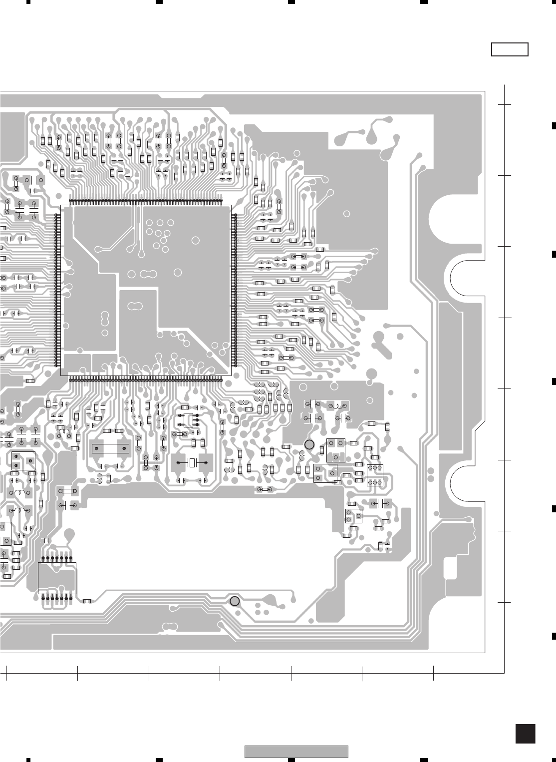
AVH-P4100DVD/XN/UC 185
5 678
5678
C
D
F
A
B
E
F
SIDE B
70 60 50 40 30 20 10
X
80
70
60
50
40
30
20
10
0
Y
1
1
E
1
5
1 5 10 15 20 25 30 35 40 45 50
55 60 65 70 75 80 85 90 95 100 105
110 115 120 125 130 135 140 145 150 155 160
165 170 175 180 185 190 195 200 205 210 215
1 5
E
1
E
E
R5740
C5768
R5741
C5769
R5742
R5743
R5744
R5745
R5746
R5747
R5748
C5770
R5749
R5750
R5751
L6008
L5452
L5453
C6152
Q6151
C6158
R5771
R5774
R5777
R5780
4
R5785
R5786
R5788
R6153
R6154
R5790
R5792
R6157
R5794
R6159
R5796
R5798
R6161
X5701
X5702
R5800
R5802
R5804
R5806
8
R5808
Q6001
Q6002
Q6003
R5040
R5810 R5812
5451 C5455
R5815
Q5452
C5456
5457
R5817
C5458
C6010
9
R5819
C6012
C6016
L5704
R5821
L5706
L5707
R5823
L5708
L5709
R582526 R5827
C6020
R5828
29
C6025
R5830
R6001
R5832
R5834
R5836
R5838
R6008
R5455
L5721
IC6005
L5722
L5723
L5724
R5458
L5725 L5726
R5842
L5727
5843
L5728
R5844
R5845
R5847
48
R5460
R5849
R5462
R5463
64
R5466
5467
R5468
R5469
R5852
R5853
R6025
R5855
R6026
856
R6027
R5857
R6028
R6029
R5859
R6030
R6031
R5861
R5863
R5865
R5866
R5867
R6037
R6038
R5868
R6039
R5869
R6040
R5870
R6041
R5871
R6042
R5872
R5873
R5874
R5875
R5876
R5877
R5878
R6049
R5879
R6050
R5880
R5881
R5882
R5883
R5884
R5885
R5886
R5887
R5888
R5889
R5890
R5891
R5892
R5893
R5896
R5898
R5899
C5701
C5703
C5704 C5705
C5706
C5707
C5708C5709
C5711 C5712
C5714
C5715
C5716
C5717
C5718
C5719
C5720
C5721
C5722
C5723
C5724
C5726
C5727
C5728
C5729
R5701
R5702
R5703
R5704
R5705
R5706
R5707 C5730
IC5701
C5731
IC5702
C5732 C5733
C5734
R5900
C5735
R5901
C5736
R5902
737
R5903
C5738
R5904
C5739
R5905
R5906 R5907
R5908 R5909
C5740
C5741
C5742 C5743
C5744
R5910
C5745
R5911
C5746
R5912
C5747
R5913
R5914
C5748
R5915
C5749
R5916
R5917
R5918
R5725
R5919
R5726
R5727
C5750
R5728
R5729
C5751
C5752
C5753
C5754 C5755
C5756
C5757
R5731
C5759
R5732
R5733
R5734
R5735
R5736
R5737
R5738
C5760
R5739
C5761
C5762
C5763
C5764
C5765
C5766
C5767
COM
COMDC
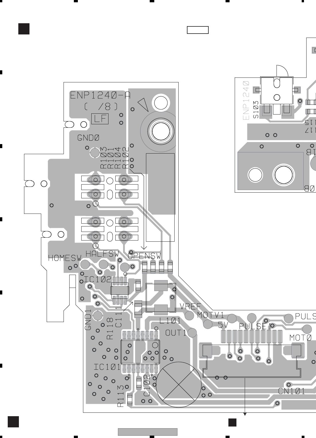
AVH-P4100DVD/XN/UC
186
1234
1234
C
D
F
A
B
E
11.6 SERVICE PCB ASSY
G
GSERVICE PCB ASSY SIDE A
ACN801
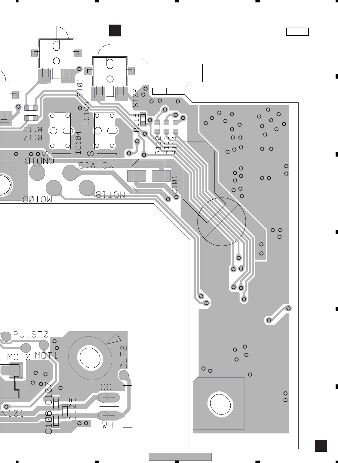
AVH-P4100DVD/XN/UC 187
5 678
5678
C
D
F
A
B
E
G
SERVICE PCB ASSY
GSIDE B
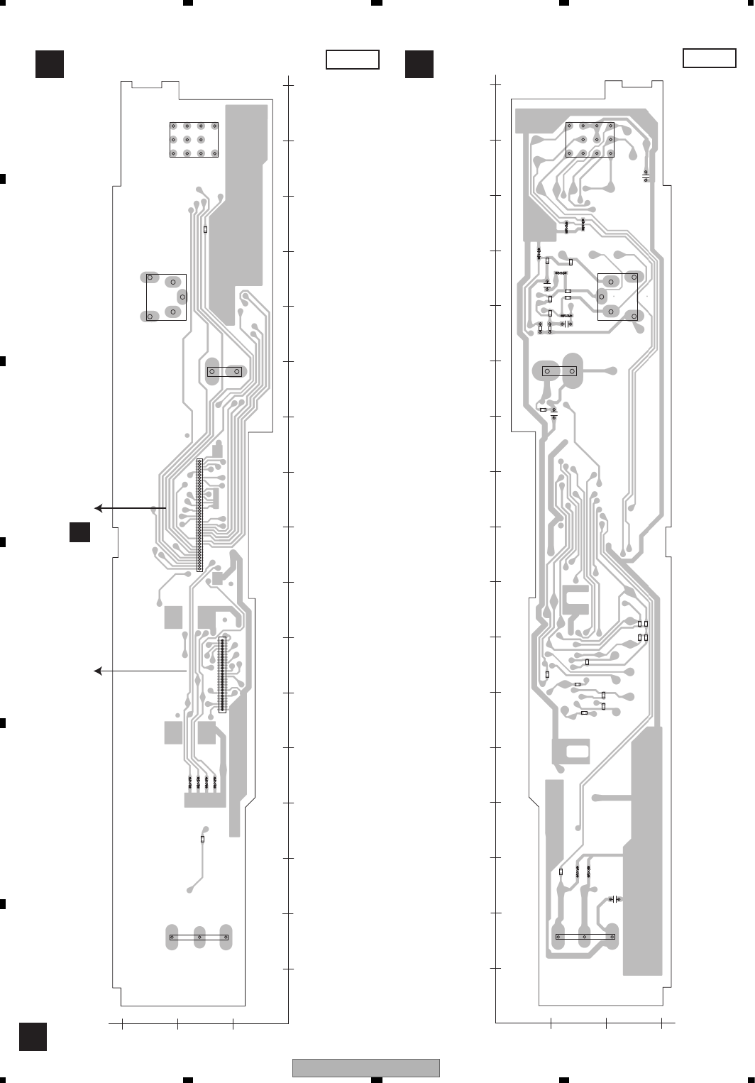
AVH-P4100DVD/XN/UC
188
1234
1234
C
D
F
A
B
E
11.7 IF PCB
B
SIDE B
SIDE A
BIF PCB BIF PCB
1
4
5
7
8
11
1 5 10 15 20 25
1 5 10 15 20 25 30 35 40
1
1
CN2001
CN2002
D2001
D2004
D2005
D2006
JA2001
JA2002
JA2003
JA2004
R2012 R2019
C2001
C2002
C2003
C2004
C2005
D2002
D2003
R2001
R2002
D2007 R2003
R2004
D2009
R2005
R2006 R2007
R2008
R2009
D2010
D2011
D2012
R2010
R2011
R2013
R2014
R2015
R2016
R2017
R2018
R2020
R2021
R2022
10 20 30 40 50 60 70 80 90 100 110 120 130 140 150
X
30
20
10
0
Y
160 170
170 160 150 140 130 120 110 100 90 80 70 60 50 40 30
X
30
20
10
0
Y
20 10
1
1
1
ACN121
IP-BUS
NAVI INTERFACE
WIRED REMOTE
B.CAM INPUT
MINIJACK

AVH-P4100DVD/XN/UC 189
5 678
5678
C
D
F
A
B
E
12. ELECTRICAL PARTS LIST
NOTE:
Parts whose parts numbers are omitted are subject to being not supplied.
The part numbers shown below indicate chip components.
Chip Resistor
RS1/_S___J,RS1/__S___J
Chip Capacitor (except for CQS.....)
CKS....., CCS....., CSZS.....
The > mark found on some component parts indicates the importance of the safety factor of the part.
Therefore, when replacing, be sure to use parts of identical designation.
Meaning of the figures and others in the parentheses in the parts list.
Example) IC 301 is on the point (face A, 91 of x-axis, and 111 of y-axis) of the corresponding
PC board.
IC 301 (A, 91, 111) IC NJM2068V
Circuit Symbol and No. Part No.
Unit Number : CWN3794(UC)
Unit Number : CWN3790(EW5)
Unit Number : CWN3795(UW5)
Unit Name : Mother Unit
Unit Number :
Unit Name : Keyboard Unit
Unit Number : CWN3797(UC,EW5)
Unit Number : CWN3796(UW5)
Unit Name : Monitor Unit
Unit Number : YWX5007
Unit Name : DVD Core Unit
Unit Number :
Unit Name : Connect PCB
Unit Number : EXX1058
Unit Name : Service PCB Assy
Mother Unit
Consists of
Mother PCB
IF PCB
AB
Unit Number : CWN3794(UC)
Unit Number : CWN3790(EW5)
Unit Number : CWN3795(UW5)
Unit Name : Mother Unit
MISCELLANEOUS
IC 181 (A,80,120) IC PA2030A
IC 201 (B,134,92) IC PML018A
IC 301 (B,100,62) IC AN15887A
IC 521 (B,19,28) IC R5523N001B
IC 522 (B,23,23) IC TC7MBL6126SFK
IC 561 (A,74,20) IC 341S2162
IC 601 (A,125,41) IC(UC) PEG535A8
(A,125,41) IC(EW5,UW5) PEG534A8
IC 602 (A,107,20) IC S-80827CNNB-B8M
IC 751 (A,140,68) IC HA12241FP
IC 771 (B,71,85) IC(UW5) NJM2138V
IC 951 (A,23,105) L-MOS And Gate TC7SET08FUS1
IC 1001 (B,20,74) IC S-812C33AUA-C2N
IC 1061 (A,7,88) IC NJM2388F84
IC 1081 (B,150,10) IC NJM2886DL3-33
IC 1141 (B,38,62) IC TK11840L
IC 1201 (B,43,41) IC BD9013KV
IC 1401 (B,49,69) Regulator IC S-1112B33MC-L6S
Q 101 (A,134,110) Transistor IMH23
Q 102 (A,101,109) Chip Digital Transistor DTA124EUA
Q 103 (A,101,105) Transistor UMD2N
Q 104 (A,144,110) Transistor IMH23
Q 105 (B,145,110) Transistor IMH23
Q 121 (A,90,104) Transistor UMF23N
Q 161 (A,33,80) Chip Transistor DTC114EUA
Q 162 (B,48,84) Transistor UMX1N
Q 163 (A,41,80) Transistor UMT1N
Q 164 (B,38,76) Chip Transistor DTC114EUA
Q 165 (B,42,86) Transistor 2SC4081
Q 181 (B,95,106) Transistor 2SC4081
Q 182 (A,103,112) Transistor UMH1N
Q 183 (A,96,114) Transistor UMD3N
Q 403 (B,149,30) Transistor(EW5,UW5) UMH1N
Q 404 (B,148,36) Transistor(EW5,UW5) UMH1N
Q 561 (A,81,26) Transistor UMD22N
Q 601 (B,78,54) Transistor(UW5) 2SC4081
Q 771 (B,61,87) Transistor(UW5) 2SC4081
Q 801 (A,168,10) Transistor UMF5N
Q 901 (B,84,37) Transistor IMH23
Q 902 (B,87,37) Transistor UMD3N
Q 951 (A,20,105) Transistor 2SA1576A
Q 1001 (B,30,83) Transistor 2SD1664
Q 1002 (B,25,74) Chip Transistor 2SB1132
Q 1021 (B,129,10) Transistor 2SC4081
Q 1022 (B,133,13) Chip Transistor 2SB1132
Circuit Symbol and No. Part No.

AVH-P4100DVD/XN/UC
190
1234
1234
C
D
F
A
B
E
Q 1141 (A,34,76) Transistor 2SC4081
Q 1142 (B,34,64) FET RSF014N03
Q 1143 (B,41,68) Digital Transistor DTC143EUA
Q 1201 (A,36,51) FET HAT2210RJ
Q 1202 (A,36,28) FET HAT2210RJ
Q 1341 (A,38,12) Transistor 2SD2153
D 101 (B,99,111) Diode DAN202U
D 102 (A,107,105) Diode MA111
D 103 (A,118,113) Diode MALS068X
D 104 (A,110,114) Diode MALS068X
D 105 (A,122,114) Diode MALS068X
D 141 (B,29,104) Diode S1G-6904G2P
D 142 (B,29,107) Diode S1G-6904G2P
D 161 (A,31,83) Diode MA111
D 162 (B,37,82) Diode HZU7L(A1)
D 163 (B,37,84) Diode HZU7L(C3)
D 164 (A,40,83) Diode DAN202U
D 165 (A,36,80) Diode DAN202U
D 166 (B,45,75) Diode UDZS5R6(B)
D 167 (B,37,86) Diode UDZS20(B)
D 181 (B,101,108) Diode MA111
D 182 (A,91,107) Diode UDZS8R2(B)
D 183 (B,78,100) Diode S1G-6904G2P
D 184 (B,70,96) Diode S1G-6904G2P
D 301 (A,101,76) Diode RB551V-30
D 302 (A,103,76) Diode RB551V-30
D 521 (A,15,107) Diode EMZC6.8N
D 601 (A,106,16) Diode MA111
D 602 (A,121,65) Diode RB751V-40
D 603 (A,123,65) Diode RB501V-40
D 801 (A,167,4) LED SMLE12BC7T
D 951 (A,28,105) Diode MALS068X
D 1001 (B,26,80) Diode UDZS18(B)
D 1002 (B,22,85) Diode S1G-6904G2P
D 1021 (B,142,21) Diode S1G-6904G2P
D 1081 (B,147,20) Diode S1G-6904G2P
D 1141 (A,39,76) Diode HZU13(B1)
D 1142 (B,31,65) Diode RB551V-30
D 1201 (A,29,61) Diode RSX201L-30
D 1202 (A,26,61) Diode RSX201L-30
D 1205 (B,40,50) Diode RB551V-30
D 1206 (B,40,31) Diode RB551V-30
D 1341 (A,35,16) Diode HZU6R8(B2)
D 1401 (B,52,73) Diode RB551V-30
D 2002 (B,144,13) Diode MALS068X
D 2003 (B,128,13) Diode MALS068X
D 2004 (A,44,16) Diode(UW5) MALS068X
D 2005 (A,44,18) Diode(UW5) MALS068X
D 2006 (A,44,13) Diode(UW5) MALS068X
D 2007 (B,145,16) Diode MALS068X
D 2009 (B,27,17) Diode MALS068X
D 2010 (B,27,15) Diode MALS068X
D 2011 (B,136,12) Diode MALS068X
D 2012 (B,139,8) Diode MALS068X
L 141 (A,37,97) Choke Coil 600 uH CTH1221
L 161 (A,36,84) Inductor LCTAW2R2J2520
L 162 (A,39,87) Inductor LCTAW2R2J2520
L 163 (B,49,76) Inductor CTF1295
L 201 (A,144,79) Inductor LCTAW2R2J2520
Circuit Symbol and No. Part No.
L 401 (B,152,84) Inductor LCTAW220J2520
L 402 (A,148,79) Chip Coil LCTAW1R0J2520
L 403 (A,150,40) Inductor LCTAW1R0J3225
L 404 (B,149,50) Inductor CTF1379
L 521 (B,18,23) Inductor CTF1713
L 601 (A,99,41) Inductor LCTAW2R2J2520
L 902 (A,73,44) Inductor CTF1387
L 903 (B,70,48) Inductor CTF1381
L 951 (A,28,107) Inductor CTF1389
L 952 (A,20,103) Inductor CTF1379
L 1021 (B,142,15) Inductor DTL1100
L 1022 (A,136,10) Inductor CTH1262
L 1141 (A,39,63) Inductor ATH7061
L 1201 (A,48,53) Inductor CTH1253
L 1202 (A,38,56) Inductor CTF1661
L 1203 (A,33,46) Inductor CTF1661
L 1204 (A,46,24) Inductor CTH1253
L 1205 (A,34,22) Inductor CTF1661
L 1206 (A,41,31) Inductor CTF1661
L 1207 (A,19,53) Inductor CTH1253
X 601 (A,107,40) Oscillator 15 MHz CSS1776
P 101 (A,152,111) Poly Switch MINISMDC075F/24
P 102 (B,109,109) Poly Switch MINISMDC075F/24
P 121 (A,86,85) Poly Switch MINISMDC075F/24
P 401 (B,151,90) Surge Protector IMSA-6801-01Y901
>P1021 (B,137,20) Fuse 1 A CEK1280
>P1022 (B,136,17) Fuse 1.75 A CEK1283
>P1201 (B,19,46) Fuse 4 A CEK1344
>P1202 (A,61,57) Fuse 1 A CEK1280
>P1203 (A,66,24) Fuse 2.5 A CEK1285
>P1341 (A,40,16) Fuse 1.5 A CEK1282
BZ601 (A,159,12) Buzzer CPV1062
U 401 (A,158,86) FM/AM Tuner Unit(UC) CWE2098
(A,158,86)
FM/AM Tuner Unit(EW5,UW5)
CWE2097
RESISTORS
R 101 (A,140,111) RS1/16SS820J
R 102 (A,143,113) RS1/16SS223J
R 103 (A,132,114) RS1/16SS223J
R 104 (A,131,112) RS1/16SS820J
R 107 (A,147,111) RS1/16SS820J
R 108 (A,147,114) RS1/16SS223J
R 109 (A,134,114) RS1/16SS223J
R 110 (A,137,109) RS1/16SS820J
R 111 (A,148,111) RS1/16SS820J
R 112 (A,149,114) RS1/16SS223J
R 113 (A,141,113) RS1/16SS223J
R 114 (A,138,109) RS1/16SS820J
R 115 (A,120,115) RS1/16SS750J
R 117 (A,136,114) RS1/16SS0R0J
R 118 (A,145,113) RS1/16SS0R0J
R 120 (A,105,105) RS1/16SS102J
R 121 (A,88,103) RS1/16SS562J
R 122 (A,88,104) RS1/16SS332J
R 123 (A,95,87) RS1/16SS181J
R 124 (A,98,87) RS1/16SS181J
R 125 (A,93,104) RS1/16SS222J
R 126 (A,97,87) RS1/16SS223J
R 127 (A,94,87) RS1/16SS223J
R 128 (A,96,87) RS1/16SS102J
Circuit Symbol and No. Part No.

AVH-P4100DVD/XN/UC 191
5 678
5678
C
D
F
A
B
E
R 129 (A,93,87) RS1/16SS102J
R 161 (A,31,80) RS1/16SS103J
R 162 (A,39,79) RS1/16SS473J
R 163 (B,43,82) RS1/16SS103J
R 164 (B,45,87) RS1/16SS104J
R 165 (A,44,79) RS1/16SS473J
R 166 (B,42,82) RS1/16SS473J
R 167 (B,46,86) RS1/16SS473J
R 168 (A,39,80) RS1/16SS473J
R 170 (A,42,83) RS1/16SS473J
R 171 (A,44,81) RS1/16SS472J
R 172 (B,39,72) RS1/16SS104J
R 173 (A,33,89) RS1/16SS472J
R 174 (A,39,84) RS1/16SS103J
R 175 (B,47,77) RS1/16SS103J
R 176 (A,35,88) RS1/16SS153J
R 177 (B,48,82) RS1/16SS0R0J
R 178 (B,50,87) RS1/16SS0R0J
R 179 (B,40,86) RS1/16SS103J
R 180 (B,44,89) RS1/16SS103J
R 181 (B,96,108) RS1/16SS103J
R 182 (B,93,106) RS1/16SS104J
R 183 (B,92,106) RS1/16SS473J
R 184 (A,101,112) RS1/16SS683J
R 185 (A,100,113) RS1/16SS152J
R 186 (A,100,112) RS1/16SS683J
R 187 (A,98,113) RS1/16SS103J
R 188 (A,99,114) RS1/16SS101J
R 189 (A,95,111) RS1/16SS473J
R 202 (B,130,100) RS1/16SS272J
R 204 (B,129,100) RS1/16SS162J
R 205 (A,132,93) RS1/16SS102J
R 206 (A,131,93) RS1/16SS102J
R 207 (A,130,93) RS1/16SS102J
R 208 (B,125,84) RS1/16S0R0J
R 209 (B,129,83) RS1/16SS162J
R 210 (B,128,100) RS1/16SS162J
R 211 (B,128,82) RS1/16SS272J
R 212 (B,126,100) RS1/16SS272J
R 214 (B,130,102) RS1/16SS0R0J
R 219 (B,131,83) RS1/16SS162J
R 220 (B,130,82) RS1/16SS272J
R 221 (B,131,79) RS1/16SS0R0J
R 301 (B,111,65) RS1/16SS101J
R 302 (B,111,64) RS1/16SS101J
R 303 (B,111,63) RS1/16SS101J
R 304 (B,111,62) RS1/16SS101J
R 305 (B,87,61) RS1/16SS101J
R 306 (B,87,60) RS1/16SS101J
R 307 (B,110,72) RS1/16SS223J
R 308 (B,87,55) RS1/16SS0R0J
R 310 (B,102,72) RS1/16SS101J
R 311 (B,111,67) RS1/16SS101J
R 312 (B,103,72) RS1/16SS101J
R 313 (B,111,66) RS1/16SS101J
R 314 (B,115,68) RS1/16SS223J
R 316 (B,89,70) RS1/16SS101J
R 317 (A,108,59) RS1/16SS680J
R 318 (A,108,61) RS1/16SS4R7J
R 322 (B,87,57) RS1/16SS101J
Circuit Symbol and No. Part No.
R 325 (B,97,51) RS1/16SS221J
R 326 (B,97,52) RS1/16SS221J
R 327 (A,96,55) RS1/16SS0R0J
R 328 (A,99,75) RS1/16SS0R0J
R 329 (B,90,70) RS1/16SS101J
R 330 (B,87,58) RS1/16SS101J
R 378 (A,100,13) RS1/16SS0R0J
R 406 (B,152,29) (EW5,UW5) RS1/16SS681J
R 407 (B,152,33) (EW5,UW5) RS1/16SS681J
R 408 (B,152,35) (EW5,UW5) RS1/16SS681J
R 409 (B,152,39) (EW5,UW5) RS1/16SS681J
R 410 (B,150,48) RS1/16SS102J
R 411 (B,152,63) (EW5,UW5) RS1/16SS681J
R 412 (B,152,64) RS1/16SS681J
R 413 (B,152,65) RS1/16SS681J
R 414 (B,152,66) RS1/16SS681J
R 415 (B,152,67) RS1/16SS681J
R 416 (B,152,68) RS1/16SS681J
R 419 (A,148,35) (EW5,UW5) RS1/16SS223J
R 420 (A,148,36) (EW5,UW5) RS1/16SS223J
R 421 (A,150,34) (EW5,UW5) RS1/16SS223J
R 422 (A,148,34) (EW5,UW5) RS1/16SS223J
R 425 (B,143,82) RS1/16SS683J
R 426 (B,151,29) (EW5,UW5) RS1/16SS0R0J
R 427 (B,151,33) (EW5,UW5) RS1/16SS0R0J
R 428 (B,151,35) (EW5,UW5) RS1/16SS0R0J
R 429 (B,150,39) (EW5,UW5) RS1/16SS0R0J
R 430 (B,149,48) RS1/16SS0R0J
R 431 (B,150,63) (EW5,UW5) RS1/16SS0R0J
R 432 (B,150,64) RS1/16SS0R0J
R 433 (B,150,65) RS1/16SS0R0J
R 434 (B,150,67) RS1/16SS0R0J
R 435 (B,150,68) RS1/16SS0R0J
R 501 (A,98,13) RS1/16SS0R0J
R 521 (A,18,108) RS1/16S0R0J
R 522 (A,11,108) RS1/16S0R0J
R 524 (A,15,24) RS1/16SS0R0J
R 525 (A,17,108) RS1/16S0R0J
R 526 (A,13,108) RS1/16S0R0J
R 529 (A,14,21) RS1/16SS0R0J
R 530 (A,14,20) RS1/16SS0R0J
R 562 (A,73,16) RS1/16SS104J
R 563 (A,74,16) RS1/16SS102J
R 565 (A,78,24) RS1/16SS101J
R 566 (A,75,24) RS1/16SS101J
R 568 (A,70,22) RS1/16SS1003F
R 570 (A,77,17) RS1/16SS103J
R 601 (A,111,40) RS1/16SS0R0J
R 602 (A,123,55) RS1/16SS0R0J
R 603 (B,135,41) RS1/16SS0R0J
R 604 (A,127,26) RS1/16SS0R0J
R 605 (A,116,26) RS1/16SS0R0J
R 606 (A,110,43) RS1/16SS102J
R 607 (A,130,26) RS1/16SS104J
R 608 (A,128,55) RS1/16SS681J
R 609 (A,130,55) RS1/16SS472J
R 610 (A,129,55) RS1/16SS681J
R 612 (A,131,55) RS1/16SS102J
R 617 (B,123,36) RS1/16SS472J
R 618 (A,110,36) RS1/16SS104J
Circuit Symbol and No. Part No.

AVH-P4100DVD/XN/UC
192
1234
1234
C
D
F
A
B
E
R 619 (A,124,26) RS1/16SS104J
R 620 (A,107,18) RS1/16SS104J
R 621 (A,119,64) RS1/16SS103J
R 622 (A,124,66) RS1/16SS104J
R 623 (A,132,55) RS1/16SS102J
R 624 (A,139,29) RS1/16SS0R0J
R 625 (B,124,30) (UW5) RS1/16SS104J
R 626 (A,117,57) RS1/16SS0R0J
R 627 (A,111,27) RS1/16SS333J
R 632 (A,142,36) (UW5) RS1/16SS104J
R 634 (A,140,33) RS1/16SS104J
R 635 (A,141,33) RS1/16SS104J
R 636 (A,142,33) RS1/16SS104J
R 637 (A,139,33) RS1/16SS104J
R 638 (B,138,34) RS1/16SS102J
R 639 (B,127,40) RS1/16SS104J
R 641 (B,81,52) (UW5) RS1/16SS104J
R 642 (B,134,34) RS1/16SS102J
R 643 (B,135,42) RS1/16SS104J
R 644 (A,140,30) RS1/16SS472J
R 645 (A,124,55) RS1/16SS103J
R 646 (A,116,57) RS1/16SS182J
R 647 (A,120,26) RS1/16SS221J
R 648 (A,122,26) RS1/16SS221J
R 649 (B,122,40) RS1/16SS104J
R 650 (A,121,26) RS1/16SS104J
R 651 (A,116,55) RS1/16SS182J
R 652 (A,126,55) RS1/16SS102J
R 654 (B,122,43) RS1/16SS104J
R 655 (A,115,26) RS1/16SS333J
R 656 (A,109,28) RS1/16SS681J
R 657 (A,109,29) RS1/16SS681J
R 658 (B,123,48) RS1/16SS101J
R 659 (B,126,47) RS1/16SS104J
R 660 (B,126,46) RS1/16SS104J
R 661 (A,123,26) RS1/16SS102J
R 662 (A,119,66) RS1/16SS0R0J
R 663 (A,127,55) RS1/16SS0R0J
R 664 (B,130,49) RS1/16SS1501D
R 665 (B,121,54) RS1/16SS104J
R 667 (A,110,46) RS1/16SS102J
R 668 (A,105,26) RS1/16SS104J
R 669 (A,109,33) RS1/16SS102J
R 670 (A,109,30) RS1/16SS681J
R 671 (A,109,31) RS1/16SS681J
R 674 (B,81,53) (UW5) RS1/16SS473J
R 675 (B,78,56) (UW5) RS1/16SS473J
R 677 (B,135,44) RS1/16SS472J
R 678 (B,131,43) RS1/16SS102J
R 751 (A,138,76) RS1/16SS150J
R 752 (A,142,75) RS1/16SS470J
R 753 (A,138,75) RS1/16SS101J
R 754 (A,142,74) RS1/16SS101J
R 755 (A,136,70) RS1/16SS102J
R 756 (A,144,67) RS1/16S0R0J
R 771 (A,73,87) (UW5) RS1/16SS472J
R 772 (A,73,84) (UW5) RS1/16SS472J
R 773 (A,67,87) (UW5) RS1/16SS472J
R 774 (A,70,83) (UW5) RS1/16SS472J
R 775 (A,72,87) (UW5) RS1/16SS472J
Circuit Symbol and No. Part No.
R 776 (A,72,83) (UW5) RS1/16SS472J
R 777 (A,75,87) (UW5) RS1/16SS472J
R 778 (A,75,84) (UW5) RS1/16SS472J
R 779 (A,79,84) (UW5) RS1/16SS472J
R 780 (A,66,82) (UW5) RS1/16SS101J
R 781 (A,67,82) (UW5) RS1/16SS101J
R 782 (A,74,82) (UW5) RS1/16SS101J
R 783 (A,79,87) (UW5) RS1/16SS472J
R 784 (B,57,85) (UW5) RS1/16SS512J
R 785 (B,55,85) (UW5) RS1/16SS681J
R 786 (B,61,85) (UW5) RS1/16SS822J
R 787 (A,63,86) (UW5) RS1/16SS472J
R 788 (A,70,87) (UW5) RS1/16SS472J
R 789 (A,68,87) (UW5) RS1/16SS472J
R 790 (A,63,84) (UW5) RS1/16SS472J
R 791 (A,67,84) (UW5) RS1/16SS472J
R 792 (A,68,84) (UW5) RS1/16SS472J
R 793 (A,75,82) (UW5) RS1/16SS101J
R 798 (B,64,88) (UW5) RS1/16S0R0J
R 801 (B,166,10) RS1/16S181J
R 802 (B,166,7) RS1/16S181J
R 803 (B,167,11) RS1/16SS103J
R 804 (B,168,9) RS1/16SS332J
R 902 (B,77,41) RS1/16SS0R0J
R 903 (B,75,39) RS1/16SS0R0J
R 905 (B,76,36) RS1/16S0R0J
R 906 (B,80,38) RS1/16S0R0J
R 907 (B,61,29) RS1/16S0R0J
R 908 (B,63,29) RS1/16S0R0J
R 909 (B,69,36) RS1/16SS471J
R 910 (B,77,50) RS1/16SS102J
R 911 (B,70,42) RS1/16SS221J
R 912 (B,76,47) RS1/16SS221J
R 913 (B,70,44) RS1/16SS221J
R 914 (B,76,44) RS1/16SS221J
R 915 (B,91,37) RS1/16SS102J
R 916 (B,71,53) RS1/16SS0R0J
R 951 (A,24,101) RS1/16SS0R0J
R 952 (A,24,103) RS1/16SS473J
R 953 (A,28,106) RS1/16SS121J
R 954 (A,20,108) RS1/16SS104J
R 955 (A,20,109) RS1/16SS103J
R 1001 (B,26,83) RS1/16SS271J
R 1003 (B,19,80) RS1/16SS391J
R 1004 (B,16,84) RS1/16S2R2J
R 1005 (B,16,82) RS1/16S2R2J
R 1006 (B,18,84) RS1/16S2R2J
R 1007 (B,18,82) RS1/16S2R2J
R 1021 (B,131,17) RS1/16SS331J
R 1022 (B,132,17) RS1/16SS331J
R 1023 (B,133,17) RS1/16SS103J
R 1025 (B,131,20) RS1/16SS0R0J
R 1026 (B,128,8) RS1/16SS103J
R 1027 (B,126,11) RS1/16SS103J
R 1061 (A,11,95) RS1/16SS473J
R 1081 (B,146,24) RS1/16SS0R0J
R 1141 (A,36,76) RS1/16SS681J
R 1144 (B,38,67) RS1/16SS9100D
R 1145 (B,33,61) RS1/16SS512J
R 1146 (B,40,65) RS1/16SS3003D
Circuit Symbol and No. Part No.

AVH-P4100DVD/XN/UC 193
5 678
5678
C
D
F
A
B
E
R 1147 (B,35,66) RS1/16S5101D
R 1148 (B,35,61) RS1/16SS0R0J
R 1150 (B,42,63) RS1/16SS1102D
R 1151 (B,38,59) RS1/16SS621J
R 1152 (B,46,58) RS1/16SS0R0J
R 1154 (B,38,66) RS1/16SS0R0J
R 1201 (B,38,29) RS1/16SS2R2J
R 1202 (B,50,40) RS1/16SS823J
R 1203 (B,40,51) RS1/16SS2R2J
R 1204 (B,46,52) RS1/16SS0R0J
R 1205 (B,44,51) RS1/16SS151J
R 1206 (B,43,52) RS1/16SS4702D
R 1207 (B,43,50) RS1/16SS6801D
R 1208 (B,44,50) RS1/16SS1002D
R 1209 (B,44,49) RS1/16SS303J
R 1210 (A,35,46) RS1/16SS10R0D
R 1211 (A,38,33) RS1/16SS10R0D
R 1212 (B,50,39) RS1/16SS102J
R 1213 (B,46,34) RS1/16SS303J
R 1214 (B,46,32) RS1/16SS8202D
R 1215 (B,45,32) RS1/16SS102J
R 1216 (B,44,30) RS1/16SS9101F
R 1217 (B,45,30) RS1/16SS330J
R 1218 (B,48,32) RS1/16SS0R0J
R 1219 (B,50,44) RS1/16SS0R0J
R 1220 (B,50,43) RS1/16SS0R0J
R 1224 (B,42,52) RS1/16SS102J
R 1225 (B,37,48) RS1/10SR103J
R 1226 (B,37,35) RS1/10SR103J
R 1343 (A,38,16) RS1/16SS221J
R 2001 (B,70,27) (UW5) RS1/16SS750J
R 2003 (B,65,17) (UW5) RS1/16SS0R0J
R 2004 (B,72,27) (UW5) RS1/16SS750J
R 2005 (B,57,20) (UW5) RS1/16SS471J
R 2006 (B,72,26) (UW5) RS1/16SS750J
R 2007 (B,70,26) (UW5) RS1/16SS750J
R 2009 (B,56,16) (UW5) RS1/16SS471J
R 2010 (B,59,20) (UW5) RS1/16SS102J
R 2011 (B,27,12) RS1/16SS102J
R 2012 (A,33,16) RS1/16SS102J
R 2013 (B,131,10) RS1/16SS223J
R 2014 (B,129,10) RS1/16SS223J
R 2015 (B,138,9) RS1/16SS750J
R 2016 (B,126,8) RS1/16S0R0J
R 2017 (B,126,10) RS1/16S0R0J
R 2018 (B,111,9) RS1/16SS750J
R 2019 (A,144,15) RS1/16SS102J
R 2020 (B,131,13) RS1/16SS0R0J
R 2021 (B,133,13) RS1/16SS0R0J
R 2022 (B,138,14) RS1/16SS0R0J
CAPACITORS
C 101 (A,140,106) CKSQYB475K10
C 102 (A,134,106) CKSQYB475K10
C 103 (A,106,98) CEVW101M16
C 104 (A,142,106) CKSQYB475K10
C 105 (A,136,106) CKSQYB475K10
C 106 (A,144,106) CKSQYB475K10
C 107 (A,138,106) CKSQYB475K10
Circuit Symbol and No. Part No.
C 108 (A,109,114) CKSRYB104K50
C 109 (A,114,114) CKSRYB104K50
C 110 (A,123,114) CKSRYB104K50
C 111 (B,154,109) CKSRYB104K50
C 141 (A,57,96) CEAT332M16
C 142 (A,43,89) CKSRYB104K50
C 161 (A,33,83) CKSRYB105K10
C 162 (A,33,85) CKSRYB104K50
C 163 (A,33,87) CKSRYB104K50
C 164 (B,41,76) CKSRYB104K50
C 165 (A,41,86) CKSRYB103K50
C 166 (A,37,88) CKSRYB104K50
C 167 (B,46,78) CKSRYB104K50
C 181 (B,98,106) 10 uF DCH1201
C 182 (B,78,104) CKSRYB474K16
C 183 (B,80,104) CKSRYB474K16
C 184 (B,85,104) CKSRYB474K16
C 185 (B,83,104) CKSRYB474K16
C 186 (A,101,114) CKSQYB475K10
C 187 (B,80,108) CKSQYB474K16
C 188 (B,78,108) CKSQYB474K16
C 189 (B,83,108) CKSQYB474K16
C 190 (B,85,108) CKSQYB474K16
C 191 (B,88,103) CKSQYB225K16
C 192 (A,66,114) CKSRYB104K50
C 193 (B,90,104) 10 uF CCG1236
C 194 (B,88,107) CKSQYB225K16
C 195 (B,49,102) CKSQYB104K50
C 202 (B,135,100) CKSRYB105K10
C 204 (B,140,100) CKSRYB105K10
C 205 (B,141,100) CKSRYB105K10
C 206 (B,143,99) CKSSYB104K10
C 207 (A,140,94) CEVW100M10
C 208 (A,127,94) CEVW100M10
C 209 (B,134,83) CKSRYB105K10
C 211 (B,138,83) CKSRYB105K10
C 212 (B,140,83) CKSRYB105K10
C 213 (B,141,83) CKSSYB104K10
C 214 (B,143,83) CKSSYB224K6R3
C 215 (A,132,82) CEVW470M16
C 216 (B,127,83) CKSSYB104K16
C 222 (A,140,86) CEVW470M16
C 223 (B,133,83) CKSSYB104K10
C 224 (A,146,79) CKSSYB104K10
C 227 (B,137,100) CKSRYB105K10
C 228 (B,135,83) CKSRYB105K10
C 307 (B,104,52) CKSSYB104K10
C 308 (B,105,52) CKSSYB104K10
C 309 (B,113,66) CKSRYB105K10
C 310 (B,113,63) CKSRYB105K10
C 312 (B,113,65) CKSRYB105K10
C 313 (B,113,62) CKSRYB105K10
C 315 (B,90,61) CKSRYB105K10
C 316 (B,90,60) CKSRYB105K10
C 321 (B,103,74) CKSRYB105K10
C 322 (B,113,69) CKSRYB105K10
C 323 (B,108,73) CKSRYB105K10
C 324 (B,113,68) CKSRYB105K10
C 325 (A,104,61) CEVW470M16
C 326 (B,105,72) CKSSYB104K10
Circuit Symbol and No. Part No.

AVH-P4100DVD/XN/UC
194
1234
1234
C
D
F
A
B
E
C 331 (B,105,71) CKSSYB104K10
C 334 (A,97,80) CEVW470M16
C 335 (B,97,73) CKSSYB104K10
C 336 (A,96,70) CEVW220M16
C 337 (B,97,72) CKSSYB104K10
C 338 (B,90,68) CKSRYB105K10
C 339 (B,90,67) CKSRYB105K10
C 340 (B,90,58) CKSRYB105K10
C 341 (B,90,57) CKSRYB105K10
C 342 (B,90,55) CKSRYB105K10
C 343 (B,90,53) CKSRYB105K10
C 345 (A,98,50) CEVW221M4
C 346 (A,106,50) CEVW101M6R3
C 347 (A,103,70) CEVW220M16
C 403 (B,164,46) CKSSYB103K16
C 405 (A,150,81) CKSSYB103K16
C 406 (B,152,44) CKSQYB106K6R3
C 408 (A,148,86) CEVW101M10
C 409 (B,164,40) CKSSYB103K16
C 521 (B,16,27) CKSSYB105K6R3
C 522 (B,15,28) CKSSYB104K10
C 523 (B,19,25) CKSSYB104K10
C 561 (A,76,15) CKSSYB104K10
C 563 (A,76,16) CKSSYB104K10
C 564 (A,17,18) CKSRYB105K6R3
C 601 (A,110,38) CCSSCH7R0D50
C 602 (A,110,40) CCSSCH7R0D50
C 603 (A,101,38) CKSQYB106K6R3
C 605 (B,114,37) CKSSYB102K50
C 606 (A,117,55) CKSRYB105K10
C 607 (B,122,51) CKSSYB103K16
C 608 (B,135,40) CKSSYB103K16
C 609 (A,139,28) CKSSYB103K16
C 610 (A,126,26) CKSSYB103K16
C 611 (A,117,26) CKSSYB103K16
C 612 (B,122,42) CKSSYB102K50
C 613 (B,126,42) CKSQYB475K10
C 615 (B,128,58) CCSSCH101J50
C 618 (A,105,23) CKSRYB105K10
C 619 (B,121,35) CCSSCH101J50
C 751 (A,138,74) CKSSYB102K50
C 752 (A,142,73) CKSSYB102K50
C 753 (A,138,73) CKSSYB104K10
C 771 (A,77,87) (UW5) CCSRCH6R0D50
C 772 (A,77,84) (UW5) CCSRCH6R0D50
C 773 (A,65,86) (UW5) CCSRCH6R0D50
C 774 (A,64,83) (UW5) CCSRCH6R0D50
C 775 (B,74,91) (UW5) CKSQYB106K6R3
C 776 (B,70,91) (UW5) CKSQYB106K6R3
C 777 (B,68,91) (UW5) CKSQYB106K6R3
C 778 (A,74,91) (UW5) CKSQYB106K6R3
C 779 (B,72,91) (UW5) CKSQYB106K6R3
C 780 (B,56,85) (UW5) CKSRYB104K16
C 781 (B,63,85) (UW5) CKSRYB104K16
C 782 (B,59,85) (UW5) CKSSYB102K50
C 785 (A,81,84) (UW5) CKSQYB106K6R3
C 786 (A,81,87) (UW5) CKSQYB106K6R3
C 787 (A,69,91) (UW5) CKSQYB106K6R3
C 901 (A,66,28) CKSSYB104K10
C 902 (B,68,51) CCSSCH101J50
Circuit Symbol and No. Part No.
C 903 (A,75,33) CKSSYB104K10
C 952 (A,23,107) CKSSYB104K10
C 1002 (A,19,79) CEVW470M6R3
C 1003 (B,19,70) CKSSYB103K16
C 1005 (A,16,65) CEAT102M16(P30)
C 1006 (B,19,78) CKSRYB103K50
C 1007 (B,30,80) CKSRYB104K50
C 1021 (A,147,10) CEVW101M16
C 1022 (B,134,9) CKSRYB104K50
C 1023 (B,137,13) CKSYB475K16
C 1024 (A,118,8) CEAT102M10(P30)
C 1025 (A,138,20) (UW5) CEVW220M16
C 1061 (A,11,91) CKSYB105K35
C 1081 (A,20,95) CEVW101M10
C 1082 (A,148,20) CEVW220M16
C 1083 (B,151,17) CKSSYB103K16
C 1084 (B,150,23) CKSQYB475K10
C 1141 (A,32,77) CKSSYB104K16
C 1142 (B,42,62) CKSSYB104K16
C 1144 (B,38,68) CCSSCH271J25
C 1145 (B,29,65) 4.7 uF CCG1222
C 1146 (B,41,65) CKSSYB103K16
C 1147 (B,44,60) 4.7 uF CCG1222
C 1148 (B,38,65) CKSRYB104K16
C 1201 (A,19,37) CEAT472M16(P30)
C 1202 (A,55,42) CEHAZL331M16(P30)
C 1203 (A,55,33) CEHAZL331M16(P30)
C 1207 (B,44,52) CCSSCH331J50
C 1208 (B,44,48) CCSSCH151J50
C 1209 (B,46,49) CKSRYB683K50
C 1210 (B,41,48) CKSQYB335K10
C 1211 (B,39,48) CKSRYB333K25
C 1212 (B,35,40) CKSYB105K35
C 1213 (B,22,51) 10 uF CCG1223
C 1214 (A,31,27) 10 uF CCG1223
C 1215 (B,38,34) CKSRYB333K25
C 1216 (A,30,51) 10 uF CCG1223
C 1217 (B,50,35) CKSSYB103K16
C 1218 (B,43,33) CCSRCH101J50
C 1219 (B,47,34) CKSRYB683K50
C 1220 (B,41,33) CKSQYB335K10
C 1221 (B,46,35) CCSSCH151J50
C 1222 (B,46,30) CCSSCH151J50
C 1226 (A,57,56) 10 uF CCG1236
C 1227 (A,57,54) CKSSYB104K10
C 1228 (A,61,23) CKSSYB104K10
C 1229 (A,60,24) 10 uF CCG1236
C 1230 (B,22,48) CKSYB105K35
C 1231 (B,47,49) CKSSYB103K16
C 1341 (A,45,10) 100 uF/16 V CCH1477
C 1342 (A,39,8) CKSRYB105K10
C 1343 (A,34,14) CKSRYB104K16
C 1344 (A,32,17) CKSSYB102K50
C 1402 (B,54,69) CKSRYB474K10
C 1403 (B,48,72) CKSRYB105K10
C 1500 (A,63,23) CKSSYB102K50
C 2001 (B,110,11) CKSRYB104K50
C 2002 (B,154,27) CKSRYB104K50
C 2003 (B,134,9) CKSRYB104K50
C 2004 (B,127,13) CKSRYB104K50
Circuit Symbol and No. Part No.

AVH-P4100DVD/XN/UC 195
5 678
5678
C
D
F
A
B
E
C 2005 (B,22,22) CKSRYB104K50
E
Unit Number : (UC,EW5)
Unit Number : (UW5)
Unit Name : Keyboard Unit
MISCELLANEOUS
D 3002 Chip LED NSSM038A-6430
D 3005 Chip LED NSSM038A-6430
S 3001 Switch(SOURCE) VSG1020
S 3002 Switch(FORWARD) VSG1020
S 3003 Switch(REVERSE) VSG1020
S 3004 Switch(VOL-) VSG1020
S 3005 Push Switch(RESET) CSG1155
S 3006 Switch(EJECT) VSG1020
S 3007 Switch(MUTE) VSG1020
S 3008 Switch(DISP.OFF) VSG1020
S 3009 Switch(VOL+) VSG1020
U 3001 Remote Receiver Unit RS-470
RESISTORS
R 3001 RS1/16S470J
R 3005 RS1/16S0R0J
R 3006 RS1/16S182J
R 3007 RS1/16S392J
R 3008 RS1/16S392J
R 3009 RS1/16S103J
R 3010 RS1/16S182J
R 3011 RS1/16S103J
CAPACITORS
C 3005 CKSRYB104K50
C 3006 CKSRYB104K16
C 3007 CKSRYB104K16
C 3008 CKSRYB104K16
C 3012 CKSRYB104K16
C 3013 CKSRYB104K16
C 3014 CKSRYB104K16
F
Unit Number : CWN3797(UC,EW5)
Unit Number : CWN3796(UW5)
Unit Name : Monitor Unit
MISCELLANEOUS
IC 5001 (A,118,22) IC BH2227AFV
IC 5101 (A,111,39) BLANK IC PE5669A8
IC 5102 (B,119,34) IC S-93C56BD0I-J8
IC 5201 (A,65,68) IC PEH208A8
IC 5301 (A,33,57) SDRAM(128 M) K4S281632K-UC75
IC 5451 (B,75,18) IC NJM2505AF
IC 5501 (B,109,61) IC BD6171KV
IC 5601 (A,83,34) IC(UW5) AK5406XQ
IC 5701 (B,44,36) Logic IC TC7SHU04FUS1
IC 5702 (B,50,54) IC MN103SE60PUB
IC 6005 (B,63,13) Logic IC TC74VHCT04AFTS1
Circuit Symbol and No. Part No.
IC 6101 (A,16,38) IC TK11840L
IC 6151 (A,18,22) IC NJM082BV
Q 5001 (B,116,19) Transistor UMX1N
Q 5002 (B,106,12) Transistor 2SC4081
Q 5003 (B,116,27) Transistor UMX1N
Q 5004 (B,113,12) Transistor 2SC4081
Q 5401 (A,104,20) Transistor FMG12
Q 5402 (B,104,20) Transistor UMF5N
Q 5403 (B,101,20) Transistor UMF5N
Q 5451 (B,71,20) Transistor 2SC4081
Q 5452 (B,68,30) Transistor 2SA1576A
Q 5501 (A,119,65) FET RSQ035P03
Q 5502 (A,110,68) FET RSQ035P03
Q 5503 (A,98,53) Transistor 2SA1577
Q 5504 (A,98,56) Transistor 2SC4097
Q 5505 (A,96,67) Transistor IMZ4
Q 5561 (A,93,56) Transistor UMX2N
Q 5562 (A,97,50) Transistor UMZ1N
Q 6001 (B,18,28) Transistor UMZ1N
Q 6002 (B,24,31) Transistor 2SC4097
Q 6003 (B,25,28) Transistor 2SA1577
Q 6101 (A,17,34) Digital Transistor DTC143EUA
Q 6102 (A,16,43) FET CPH6424
Q 6103 (A,7,21) Digital Transistor DTC143EUA
Q 6151 (B,21,22) FET RUE003N02
D 5401 (A,98,21) Diode MA111
D 5402 (A,113,15) Diode UDZS5R6(B)
D 5403 (A,110,21) Diode UDZS5R6(B)
D 5404 (A,98,12) Diode UDZS5R6(B)
D 5405 (A,97,16) Diode UDZS5R6(B)
D 5501 (A,121,55) Diode RSX201L-30
D 5502 (A,107,64) Diode RB160M-30
D 5503 (B,98,65) Diode RB548W
D 5504 (B,98,67) Diode RB548W
D 5505 (B,96,59) Diode RB548W
D 5506 (B,96,57) Diode RB548W
D 5507 (B,96,54) Diode RB548W
D 6101 (A,8,41) Diode RB050L-60
D 6102 (A,8,44) Diode UDZS36(B)
L 5101 (A,102,26) Inductor CTF1635
L 5201 (A,52,57) Inductor CTF1473
L 5301 (A,48,57) Inductor CTF1473
L 5302 (A,21,64) Inductor CTF1382
L 5401 (A,98,27) Inductor CTF1473
L 5451 (B,76,21) Inductor CTF1379
L 5452 (B,68,23) Inductor LCTAW220J2520
L 5453 (B,68,25) Chip Coil LCTAW270J2520
L 5454 (A,68,25) Inductor LCTAW101J2520
L 5501 (A,117,73) Choke Coil 18 uH CTH1250
L 5502 (A,110,73) Choke Coil 10 uH CTH1249
L 5503 (A,123,73) Choke Coil 10 uH CTH1249
L 5504 (B,121,57) Inductor CTF1635
L 5505 (A,125,61) Inductor DTL1136
L 5506 (B,103,73) Inductor CTF1488
L 5507 (A,102,71) Choke Coil 68 uH CTH1318
L 5508 (B,94,63) Inductor CTF1635
L 5509 (B,100,50) Inductor CTF1635
L 5510 (B,96,72) Inductor DTL1096
L 5601 (A,65,30) Inductor(UW5) CTF1473
L 5602 (A,64,35) Inductor(UW5) CTF1473
Circuit Symbol and No. Part No.

AVH-P4100DVD/XN/UC
196
1234
1234
C
D
F
A
B
E
L 5603 (A,68,43) Inductor(UW5) CTF1635
L 5701 (A,53,49) Inductor CTF1635
L 5702 (A,59,50) Inductor CTF1635
L 5705 (A,52,54) Inductor CTF1473
L 5706 (B,39,29) Inductor CTF1748
L 5707 (B,34,29) Inductor CTF1748
L 5708 (B,57,27) Inductor CTF1748
L 5709 (B,28,31) Inductor CTF1748
L 5710 (A,48,44) Inductor CTF1748
L 5711 (A,48,42) Inductor CTF1748
L 5712 (A,46,42) Inductor CTF1748
L 5713 (A,46,40) Inductor CTF1748
L 5714 (A,45,42) Inductor CTF1748
L 5715 (A,45,37) Inductor CTF1748
L 5716 (A,44,41) Inductor CTF1748
L 5717 (A,43,38) Inductor CTF1748
L 5718 (A,43,42) Inductor CTF1748
L 5719 (A,42,37) Inductor CTF1748
L 5720 (A,42,42) Inductor CTF1748
L 5721 (B,38,37) Inductor CTF1748
L 5722 (B,37,38) Inductor CTF1748
L 5723 (B,34,39) Inductor CTF1748
L 5724 (B,34,40) Inductor CTF1748
L 5725 (B,34,41) Inductor CTF1748
L 5726 (B,32,41) Inductor CTF1748
L 5727 (B,32,39) Inductor CTF1748
L 5728 (B,31,39) Inductor CTF1748
L 6001 (A,64,12) Inductor CTF1306
L 6004 (A,63,14) Inductor CTF1306
L 6005 (A,37,41) Inductor CTF1635
L 6006 (A,30,41) Inductor DTL1096
L 6007 (A,25,38) Inductor CTF1635
L 6008 (B,23,38) Inductor DTL1096
L 6101 (A,56,9) Choke Coil 3.3 uH CTH1419
L 6102 (A,8,35) Choke Coil 3.3 uH CTH1419
X 5101 (A,123,42)
Ceramic Resonator 20.000 MHz
VSS1186
X 5701 (B,44,30) Oscillator 9.597 MHz CSS1778
X 5702 (B,55,32) Radiator 33.000 MHz CSS1634
P 6101 (A,65,8) Poly Switch MINISMDC075F/24
RESISTORS
R 5001 (B,113,17) RS1/16SS201J
R 5002 (B,114,17) RS1/16SS151J
R 5003 (B,115,17) RS1/16SS0R0J
R 5004 (B,111,21) RS1/16SS103J
R 5006 (B,114,24) RS1/16SS201J
R 5007 (B,115,24) RS1/16SS151J
R 5008 (B,116,24) RS1/16SS0R0J
R 5009 (B,109,25) RS1/16SS103J
R 5011 (B,116,21) RS1/16SS271J
R 5012 (B,115,21) RS1/16SS271J
R 5013 (B,115,23) RS1/16SS0R0J
R 5014 (B,118,20) RS1/16SS103J
R 5016 (B,118,29) RS1/16SS271J
R 5017 (B,120,29) RS1/16SS271J
R 5018 (B,122,29) RS1/16SS0R0J
R 5019 (B,119,27) RS1/16SS103J
R 5021 (B,108,15) RS1/16SS221J
R 5022 (B,108,13) RS1/16SS221J
R 5023 (B,108,11) RS1/16SS0R0J
Circuit Symbol and No. Part No.
R 5024 (B,106,15) RS1/16SS103J
R 5026 (B,115,13) RS1/16SS221J
R 5027 (B,115,12) RS1/16SS221J
R 5028 (B,114,11) RS1/16SS0R0J
R 5029 (B,112,14) RS1/16SS103J
R 5031 (B,121,21) RS1/16S0R0J
R 5033 (A,67,15) RS1/16S0R0J
R 5036 (A,59,34) RS1/16S0R0J
R 5037 (A,61,34) RS1/16S0R0J
R 5040 (B,68,37) RS1/16S0R0J
R 5101 (A,97,37) RS1/16SS473J
R 5102 (A,98,34) RS1/16SS471J
R 5103 (A,98,33) RS1/16SS471J
R 5104 (A,99,40) RS1/16SS0R0J
R 5105 (A,99,39) RS1/16SS0R0J
R 5106 (A,99,37) RS1/16SS471J
R 5107 (A,97,36) RS1/16S0R0J
R 5108 (A,106,28) RS1/16SS471J
R 5109 (A,105,51) RS1/16SS471J
R 5110 (A,99,38) RS1/16SS471J
R 5111 (A,107,27) RS1/16SS4701D
R 5112 (B,107,44) RS1/16SS473J
R 5113 (A,110,25) RS1/16SS472J
R 5114 (A,110,27) RS1/16SS472J
R 5115 (A,108,28) RS1/16SS471J
R 5116 (A,111,27) RS1/16SS471J
R 5117 (B,109,45) RS1/16SS473J
R 5118 (B,110,45) RS1/16SS473J
R 5119 (B,116,46) RS1/16SS471J
R 5120 (A,111,51) RS1/16SS0R0J
R 5121 (B,112,45) RS1/16SS473J
R 5122 (A,112,51) RS1/16SS471J
R 5123 (A,113,51) RS1/16SS471J
R 5124 (A,113,28) RS1/16SS471J
R 5125 (A,99,42) (UW5) RS1/16SS473J
R 5126 (B,112,33) RS1/16SS101J
R 5127 (A,114,53) RS1/16SS471J
R 5128 (A,115,28) RS1/16SS471J
R 5129 (A,116,28) RS1/16SS471J
R 5130 (A,115,51) (UW5) RS1/16SS471J
R 5131 (A,118,28) RS1/16SS471J
R 5132 (A,117,51) (UW5) RS1/16SS470J
R 5133 (A,118,51) (UW5) RS1/16SS470J
R 5134 (B,108,48) RS1/16SS471J
R 5135 (A,108,52) RS1/16SS471J
R 5136 (B,114,39) RS1/16SS473J
R 5137 (B,115,38) RS1/16SS473J
R 5138 (A,109,52) RS1/16SS471J
R 5139 (B,107,42) (UC,EW5) RS1/16SS473J
R 5140 (A,123,35) RAB4CQ102J
R 5142 (A,120,51) RS1/16SS104J
R 5144 (B,122,31) RS1/16SS473J
R 5145 (B,121,46) RS1/16SS102J
R 5146 (A,122,38) RS1/16SS103J
R 5147 (A,122,37) RS1/16SS103J
R 5148 (B,122,45) RS1/16SS104J
R 5150 (B,122,38) RS1/16S0R0J
R 5151 (A,122,47) RS1/16S0R0J
R 5152 (B,109,32) RS1/16SS473J
R 5153 (A,123,28) RS1/16SS473J
Circuit Symbol and No. Part No.

AVH-P4100DVD/XN/UC 197
5 678
5678
C
D
F
A
B
E
R 5154 (A,99,41) RS1/16SS473J
R 5201 (A,52,76) RS1/16SS0R0J
R 5202 (A,49,75) RS1/16SS0R0J
R 5203 (A,52,74) RS1/16SS0R0J
R 5204 (A,50,74) RS1/16SS0R0J
R 5205 (A,52,73) RS1/16SS0R0J
R 5206 (A,50,72) RS1/16SS0R0J
R 5207 (A,52,72) RS1/16SS0R0J
R 5208 (A,50,71) RS1/16SS0R0J
R 5209 (A,52,70) RS1/16SS0R0J
R 5210 (A,50,70) RS1/16SS0R0J
R 5211 (A,54,76) RS1/16SS0R0J
R 5212 (A,53,60) RS1/16SS220J
R 5213 (A,52,69) RS1/16SS0R0J
R 5214 (A,50,60) RS1/16SS102J
R 5215 (A,52,68) RS1/16SS0R0J
R 5216 (A,50,67) RS1/16SS0R0J
R 5217 (A,48,67) RS1/16SS0R0J
R 5218 (A,50,66) RS1/16SS0R0J
R 5219 (A,52,65) RS1/16SS0R0J
R 5220 (A,52,64) RS1/16SS0R0J
R 5221 (A,52,63) RS1/16SS0R0J
R 5222 (A,52,62) RS1/16SS0R0J
R 5223 (A,50,61) RS1/16SS0R0J
R 5224 (A,78,75) RS1/16SS0R0J
R 5225 (A,72,76) RS1/16SS0R0J
R 5226 (A,78,73) RS1/16SS0R0J
R 5227 (A,72,78) RS1/16SS0R0J
R 5228 (A,78,72) RS1/16SS0R0J
R 5229 (A,71,76) RS1/16SS0R0J
R 5230 (A,78,71) RS1/16SS0R0J
R 5231 (A,70,78) RS1/16SS0R0J
R 5232 (A,78,70) RS1/16SS0R0J
R 5233 (A,70,76) RS1/16SS0R0J
R 5234 (A,78,66) RS1/16SS0R0J
R 5235 (A,69,78) RS1/16SS0R0J
R 5236 (A,78,65) RS1/16SS0R0J
R 5237 (A,68,76) RS1/16SS0R0J
R 5238 (A,78,64) RS1/16SS0R0J
R 5239 (A,66,76) RS1/16SS0R0J
R 5240 (A,70,61) RS1/16SS0R0J
R 5241 (A,77,63) RS1/16SS0R0J
R 5242 (A,74,60) RS1/16SS0R0J
R 5243 (A,75,59) RS1/16SS0R0J
R 5244 (A,78,74) RS1/16SS102J
R 5245 (A,79,68) RS1/16S0R0J
R 5301 (A,21,51) RS1/16SS0R0J
R 5302 (A,23,48) RS1/16SS0R0J
R 5303 (A,24,48) RS1/16SS0R0J
R 5304 (A,26,48) RS1/16SS0R0J
R 5305 (A,27,48) RS1/16SS0R0J
R 5306 (A,28,48) RS1/16SS0R0J
R 5307 (A,29,48) RS1/16SS0R0J
R 5308 (A,30,46) RS1/16SS0R0J
R 5309 (A,30,48) RS1/16SS0R0J
R 5310 (A,32,48) RS1/16SS0R0J
R 5311 (A,33,48) RS1/16SS820J
R 5312 (A,38,46) RS1/16SS820J
R 5313 (A,38,48) RS1/16SS820J
R 5314 (A,40,48) RS1/16SS820J
Circuit Symbol and No. Part No.
R 5315 (A,41,48) RS1/16SS820J
R 5316 (A,43,48) RS1/16SS820J
R 5317 (A,44,48) RS1/16SS820J
R 5318 (A,45,48) RS1/16SS820J
R 5319 (A,35,47) RS1/16S0R0J
R 5320 (A,43,45) RS1/16S0R0J
R 5322 (A,33,68) RS1/16S0R0J
R 5323 (A,36,68) RS1/16S0R0J
R 5324 (A,42,68) RS1/16S0R0J
R 5325 (A,46,59) RS1/16S0R0J
R 5326 (A,21,66) RS1/16SS0R0J
R 5327 (A,21,67) RS1/16SS0R0J
R 5328 (A,23,67) RS1/16SS0R0J
R 5329 (A,24,66) RS1/16SS0R0J
R 5330 (A,25,66) RS1/16SS0R0J
R 5331 (A,26,66) RS1/16SS0R0J
R 5332 (A,26,68) RS1/16SS0R0J
R 5333 (A,27,66) RS1/16SS0R0J
R 5334 (A,28,66) RS1/16SS0R0J
R 5335 (A,29,66) RS1/16SS0R0J
R 5336 (A,30,68) RS1/16SS0R0J
R 5337 (A,31,66) RS1/16SS0R0J
R 5338 (A,34,66) RS1/16SS820J
R 5339 (A,35,68) RS1/16SS820J
R 5340 (A,35,66) RS1/16SS820J
R 5341 (A,38,68) RS1/16SS820J
R 5342 (A,38,66) RS1/16SS820J
R 5343 (A,39,68) RS1/16SS820J
R 5344 (A,40,68) RS1/16SS820J
R 5345 (A,42,66) RS1/16SS820J
R 5401 (A,106,23) RS1/16SS102J
R 5402 (A,100,13) RS1/16S0R0J
R 5403 (A,99,16) RS1/16S0R0J
R 5404 (A,112,13) RS1/16S0R0J
R 5405 (A,109,19) RS1/16S0R0J
R 5406 (A,107,20) RS1/16SS102J
R 5407 (A,95,13) RS1/16SS105J
R 5408 (A,97,19) RS1/16SS105J
R 5410 (B,104,17) RS1/16SS103J
R 5411 (B,102,18) RS1/16SS103J
R 5412 (B,104,22) RS1/16SS103J
R 5413 (B,100,17) RS1/16SS103J
R 5451 (B,78,11) RS1/16SS0R0J
R 5453 (B,76,12) RS1/16SS101J
R 5454 (B,75,11) RS1/16SS101J
R 5455 (B,69,15) RS1/16SS0R0J
R 5457 (B,72,16) RS1/16S4701D
R 5458 (B,70,14) RS1/16SS6801D
R 5459 (B,72,20) RS1/16SS153J
R 5460 (B,69,16) RS1/16SS333J
R 5461 (B,73,18) RS1/16SS0R0J
R 5462 (B,69,17) RS1/16SS681J
R 5463 (B,68,18) RS1/16SS471J
R 5466 (B,66,28) RS1/16SS272J
R 5467 (B,69,28) RS1/16SS391J
R 5469 (B,65,28) RS1/16SS0R0J
R 5501 (A,104,59) RS1/16S0R0J
R 5502 (B,122,62) RS1/16S6801D
R 5503 (A,121,69) RS1/16S0R0J
R 5504 (B,121,70) RS1/16S0R0J
Circuit Symbol and No. Part No.

AVH-P4100DVD/XN/UC
198
1234
1234
C
D
F
A
B
E
R 5505 (B,119,62) RS1/16SS201J
R 5506 (B,120,68) RS1/16S1002D
R 5507 (B,117,60) RS1/16S1001D
R 5508 (B,119,61) RS1/16SS201J
R 5509 (B,117,55) RS1/16S5100D
R 5510 (B,118,67) RS1/16S1001D
R 5511 (B,122,66) RS1/16SS201J
R 5512 (B,116,57) RS1/16S2201D
R 5513 (B,118,68) RS1/16S3301D
R 5514 (A,100,59) RS1/16S0R0J
R 5515 (A,99,65) RS1/16SS103J
R 5516 (B,120,65) RS1/16SS302J
R 5517 (B,117,61) RS1/16SS512J
R 5518 (B,113,68) RS1/16SS223J
R 5519 (A,117,67) RS1/16SS150J
R 5520 (A,109,65) RS1/16SS150J
R 5521 (B,106,70) RS1/16SS563J
R 5522 (A,102,58) RS1/16S0R0J
R 5523 (A,105,61) RS1/16S6202D
R 5524 (B,104,53) RS1/16S1002D
R 5525 (B,98,72) RS1/16S3301D
R 5526 (B,102,53) RS1/16S4702D
R 5527 (B,101,53) RS1/16S7501D
R 5528 (B,98,71) RS1/16S1202D
R 5529 (B,99,53) RS1/16S0R0J
R 5530 (B,101,68) RS1/16S2203D
R 5532 (B,98,69) RS1/16S0R0J
R 5533 (B,94,72) RS1/16SS153J
R 5534 (A,101,53) RS1/16SS470J
R 5535 (A,103,54) RS1/16SS470J
R 5536 (A,99,67) RS1/16SS102J
R 5537 (A,93,67) RS1/16SS103J
R 5538 (A,94,69) RS1/16SS103J
R 5561 (A,95,53) RS1/16SS223J
R 5562 (A,94,54) RS1/16SS223J
R 5563 (A,91,56) RS1/16SS472J
R 5564 (A,90,56) RS1/16SS682J
R 5565 (A,91,59) RS1/16SS473J
R 5566 (A,102,51) RS1/16SS223J
R 5567 (A,95,51) RS1/16SS223J
R 5568 (A,100,50) RS1/16SS472J
R 5569 (A,99,48) RS1/16SS682J
R 5570 (A,100,48) RS1/16SS473J
R 5602 (B,84,35) (UW5) RS1/16SS473J
R 5604 (A,77,23) (UW5) RS1/16S0R0J
R 5605 (A,79,23) (UW5) RS1/16S0R0J
R 5606 (A,84,23) (UW5) RS1/16S0R0J
R 5607 (A,88,23) (UW5) RS1/16S0R0J
R 5608 (A,72,29) (UW5) RS1/16S0R0J
R 5609 (A,73,31) (UW5) RS1/16SS6801F
R 5610 (A,73,33) (UW5) RS1/16SS272J
R 5611 (A,71,31) (UW5) RS1/16S0R0J
R 5612 (A,94,34) (UW5) RS1/16S0R0J
R 5613 (A,71,34) (UW5) RS1/16SS0R0J
R 5614 (A,73,35) (UW5) RS1/16SS0R0J
R 5615 (A,71,35) (UW5) RS1/16SS0R0J
R 5616 (A,71,37) (UW5) RS1/16S0R0J
R 5617 (A,73,38) (UW5) RS1/16SS0R0J
R 5618 (A,71,40) (UW5) RS1/16S0R0J
R 5619 (A,94,39) (UW5) RS1/16S0R0J
Circuit Symbol and No. Part No.
R 5620 (A,83,45) (UW5) RS1/16S0R0J
R 5621 (B,90,25) (UW5) RS1/16SS222J
R 5622 (B,92,25) (UW5) RS1/16SS222J
R 5623 (B,93,25) (UW5) RS1/16SS222J
R 5701 (B,42,32) RS1/16SS105J
R 5702 (B,45,37) RS1/16SS220J
R 5703 (B,44,32) RS1/16SS332J
R 5704 (B,46,34) RS1/16S0R0J
R 5705 (B,54,34) RS1/16SS101J
R 5706 (B,56,34) RS1/16SS105J
R 5707 (B,57,36) RS1/16SS471J
R 5708 (A,54,41) RS1/16SS0R0J
R 5709 (A,53,41) RS1/16SS0R0J
R 5710 (A,52,41) RS1/16SS103J
R 5711 (A,52,39) RS1/16SS103J
R 5712 (A,51,41) RS1/16SS103J
R 5713 (A,49,41) RS1/16SS0R0J
R 5714 (A,50,41) RS1/16SS0R0J
R 5715 (A,48,41) RS1/16SS181J
R 5716 (A,47,40) RS1/16SS181J
R 5717 (A,47,37) RS1/16SS181J
R 5718 (A,46,38) RS1/16SS181J
R 5719 (A,46,36) RS1/16SS181J
R 5720 (A,44,40) RS1/16SS181J
R 5721 (A,44,37) RS1/16SS181J
R 5722 (A,42,40) RS1/16SS181J
R 5723 (A,42,35) RS1/16SS181J
R 5724 (A,41,40) RS1/16SS181J
R 5725 (B,38,36) RS1/16SS181J
R 5726 (B,36,37) RS1/16SS181J
R 5727 (B,34,37) RS1/16SS181J
R 5728 (B,33,37) RS1/16SS181J
R 5729 (B,62,35) RS1/16SS0R0J
R 5730 (A,58,40) RS1/16SS0R0J
R 5731 (B,33,31) RS1/16SS220J
R 5733 (B,16,35) RS1/16SS220J
R 5734 (B,39,30) RS1/16SS151J
R 5735 (B,33,29) RS1/16SS271J
R 5736 (B,56,27) RS1/16SS271J
R 5737 (B,29,29) RS1/16SS271J
R 5738 (B,36,29) RS1/16SS181J
R 5739 (B,64,38) RS1/16SS1202D
R 5740 (B,57,37) RS1/16SS471J
R 5741 (B,60,36) RS1/16SS752J
R 5742 (B,60,32) RS1/16SS272J
R 5743 (B,60,33) RS1/16SS622J
R 5744 (B,51,32) RS1/16S0R0J
R 5745 (B,50,30) RS1/16S0R0J
R 5746 (B,49,30) RS1/16S0R0J
R 5747 (B,48,32) RS1/16S0R0J
R 5748 (B,40,35) RS1/16S0R0J
R 5749 (B,34,31) RS1/16SS0R0J
R 5751 (B,19,35) RS1/16SS0R0J
R 5752 (B,85,47) RS1/16SS473J
R 5771 (B,33,39) RS1/16SS181J
R 5772 (B,85,37) (UW5) RS1/16SS151J
R 5774 (B,32,37) RS1/16SS181J
R 5775 (B,86,35) (UW5) RS1/16SS151J
R 5777 (B,31,37) RS1/16SS181J
R 5778 (B,86,34) (UW5) RS1/16SS221J
Circuit Symbol and No. Part No.

AVH-P4100DVD/XN/UC 199
5 678
5678
C
D
F
A
B
E
R 5780 (B,30,37) RS1/16SS181J
R 5781 (B,82,40) (UW5) RS1/16SS151J
R 5783 (B,87,38) (UW5) RS1/16SS151J
R 5784 (B,71,44) RS1/16S0R0J
R 5785 (B,34,42) RS1/16SS680J
R 5786 (B,31,43) RS1/16SS680J
R 5787 (B,88,37) (UW5) RS1/16SS151J
R 5788 (B,34,44) RS1/16SS680J
R 5789 (B,89,35) (UW5) RS1/16SS151J
R 5790 (B,31,44) RS1/16S0R0J
R 5791 (B,90,35) (UW5) RS1/16SS151J
R 5792 (B,30,46) RS1/16SS680J
R 5793 (B,90,33) (UW5) RS1/16SS151J
R 5794 (B,34,47) RS1/16SS680J
R 5795 (A,85,44) (UW5) RS1/16SS151J
R 5796 (B,30,47) RS1/16SS680J
R 5797 (A,86,45) (UW5) RS1/16SS151J
R 5798 (B,32,47) RS1/16SS680J
R 5799 (A,87,44) (UW5) RS1/16SS151J
R 5800 (B,28,47) RS1/16SS680J
R 5801 (A,88,45) (UW5) RS1/16SS151J
R 5802 (B,27,47) RS1/16SS151J
R 5803 (A,90,44) (UW5) RS1/16SS151J
R 5804 (B,26,46) RS1/16SS151J
R 5805 (A,91,44) (UW5) RS1/16SS151J
R 5806 (B,34,49) RS1/16SS680J
R 5807 (B,73,51) RS1/16S0R0J
R 5808 (B,34,50) RS1/16SS0R0J
R 5809 (B,78,44) (UW5) RS1/16SS151J
R 5810 (B,29,49) RS1/16SS151J
R 5811 (B,80,45) (UW5) RS1/16SS151J
R 5812 (B,26,50) RS1/16S0R0J
R 5813 (B,80,47) (UW5) RS1/16SS151J
R 5814 (B,81,46) (UW5) RS1/16SS151J
R 5815 (B,26,51) RS1/16S0R0J
R 5816 (B,82,46) (UW5) RS1/16SS151J
R 5817 (B,29,52) RS1/16SS151J
R 5818 (B,83,46) (UW5) RS1/16SS151J
R 5819 (B,24,50) RS1/16SS151J
R 5820 (A,59,55) RS1/16SS103J
R 5821 (B,27,53) RS1/16SS151J
R 5822 (A,62,55) RS1/16SS103J
R 5823 (B,34,53) RS1/16SS151J
R 5824 (B,77,54) RS1/16SS102J
R 5825 (B,26,54) RS1/16SS151J
R 5826 (B,71,54) RS1/16S0R0J
R 5827 (B,24,54) RS1/16SS151J
R 5828 (B,34,55) RS1/16SS151J
R 5829 (B,71,56) RS1/16S0R0J
R 5830 (B,31,55) RS1/16SS151J
R 5832 (B,29,55) RS1/16SS151J
R 5834 (B,25,57) RS1/16SS151J
R 5835 (A,59,56) RS1/16SS103J
R 5836 (B,26,57) RS1/16SS151J
R 5837 (B,75,58) RS1/16SS102J
R 5838 (B,29,57) RS1/16S0R0J
R 5839 (B,73,58) RS1/16SS102J
R 5841 (B,75,59) RS1/16SS103J
R 5842 (B,29,59) RS1/16S0R0J
R 5843 (B,71,58) RS1/16SS103J
Circuit Symbol and No. Part No.
R 5844 (B,26,60) RS1/16SS151J
R 5845 (B,27,62) RS1/16SS151J
R 5847 (B,28,60) RS1/16SS151J
R 5849 (B,28,62) RS1/16SS151J
R 5850 (A,59,57) RS1/16SS103J
R 5851 (B,73,61) RS1/16S0R0J
R 5852 (B,30,61) RS1/16SS151J
R 5853 (B,32,61) RS1/16SS820J
R 5855 (B,34,61) RS1/16SS151J
R 5857 (B,30,63) RS1/16SS680J
R 5859 (B,32,62) RS1/16SS680J
R 5861 (B,34,63) RS1/16SS680J
R 5862 (B,71,66) RS1/16SS102J
R 5863 (B,32,66) RS1/16S0R0J
R 5865 (B,70,66) RS1/16S0R0J
R 5866 (B,33,66) RS1/16SS680J
R 5867 (B,34,66) RS1/16SS680J
R 5868 (B,35,67) RS1/16SS680J
R 5869 (B,69,69) RS1/16S0R0J
R 5870 (B,34,68) RS1/16SS680J
R 5871 (B,35,69) RS1/16SS680J
R 5872 (B,49,75) RS1/16S0R0J
R 5873 (B,63,75) RS1/16S0R0J
R 5874 (B,56,75) RS1/16S0R0J
R 5875 (B,54,75) RS1/16S0R0J
R 5876 (B,47,75) RS1/16S0R0J
R 5877 (B,39,72) RS1/16S0R0J
R 5878 (B,64,72) RS1/16SS0R0J
R 5879 (B,63,71) RS1/16SS0R0J
R 5880 (B,62,70) RS1/16SS0R0J
R 5881 (B,65,75) RS1/16SS0R0J
R 5882 (B,64,75) RS1/16SS0R0J
R 5883 (B,61,73) RS1/16SS0R0J
R 5884 (B,61,75) RS1/16SS0R0J
R 5885 (B,60,73) RS1/16SS0R0J
R 5886 (B,60,75) RS1/16SS0R0J
R 5887 (B,59,73) RS1/16SS0R0J
R 5888 (B,59,75) RS1/16SS0R0J
R 5889 (B,58,73) RS1/16SS0R0J
R 5890 (B,57,75) RS1/16SS0R0J
R 5891 (B,56,72) RS1/16SS0R0J
R 5892 (B,55,70) RS1/16SS0R0J
R 5893 (B,52,70) RS1/16SS0R0J
R 5894 (A,59,58) RS1/16SS0R0J
R 5895 (A,55,60) RS1/16SS0R0J
R 5896 (B,53,73) RS1/16SS0R0J
R 5897 (A,52,59) RS1/16SS0R0J
R 5898 (B,52,75) RS1/16SS0R0J
R 5899 (B,51,75) RS1/16SS0R0J
R 5900 (B,51,72) RS1/16SS0R0J
R 5901 (B,50,72) RS1/16SS0R0J
R 5902 (B,50,74) RS1/16SS0R0J
R 5903 (B,46,75) RS1/16SS0R0J
R 5904 (B,46,70) RS1/16SS0R0J
R 5905 (B,46,73) RS1/16SS0R0J
R 5906 (B,45,71) RS1/16SS0R0J
R 5907 (B,45,73) RS1/16SS0R0J
R 5908 (B,44,71) RS1/16SS0R0J
R 5909 (B,43,73) RS1/16SS0R0J
R 5910 (B,42,71) RS1/16SS0R0J
Circuit Symbol and No. Part No.

AVH-P4100DVD/XN/UC
200
1234
1234
C
D
F
A
B
E
R 5911 (B,42,73) RS1/16SS0R0J
R 5912 (B,41,71) RS1/16SS0R0J
R 5913 (B,41,73) RS1/16SS0R0J
R 5914 (B,40,75) RS1/16SS0R0J
R 5915 (B,38,73) RS1/16SS0R0J
R 5916 (B,37,71) RS1/16SS0R0J
R 5917 (B,37,73) RS1/16SS0R0J
R 5918 (B,36,71) RS1/16SS0R0J
R 5919 (B,67,41) (UC,EW5) RS1/16SS103J
R 5920 (A,65,41) (UC,EW5) RS1/16SS103J
R 5921 (A,66,41) (UC,EW5) RS1/16SS103J
R 6001 (B,59,10) RS1/16SS681J
R 6008 (B,61,26) RS1/10S0R0J
R 6010 (A,61,15) RS1/16SS0R0J
R 6011 (A,61,13) RS1/16S10R0D
R 6012 (A,61,21) RS1/16SS18R0F
R 6013 (A,61,24) RS1/16S1600D
R 6014 (A,61,17) RS1/16SS15R0F
R 6015 (A,61,19) RS1/16SS82R0D
R 6016 (A,62,21) RS1/16SS12R0F
R 6017 (A,63,23) RS1/16S47R0D
R 6018 (A,63,19) RS1/16SS39R0D
R 6019 (A,63,16) RS1/16S56R0D
R 6020 (A,62,27) RS1/16SS0R0J
R 6021 (A,62,29) RS1/16SS15R0D
R 6022 (A,64,21) RS1/16SS0R0J
R 6025 (B,21,24) RS1/16SS101J
R 6026 (B,37,29) RS1/16SS102J
R 6027 (B,20,27) RS1/16SS333J
R 6028 (B,19,32) RS1/16SS103J
R 6029 (B,23,27) RS1/16SS0R0J
R 6030 (B,21,32) RS1/16SS0R0J
R 6031 (B,26,31) RS1/16SS100J
R 6032 (A,64,16) RS1/16SS82R0D
R 6037 (B,37,31) RS1/16SS0R0J
R 6039 (B,34,26) RS1/16S0R0J
R 6040 (B,20,29) RS1/16SS0R0J
R 6041 (B,28,29) RS1/16SS200J
R 6042 (B,20,28) RS1/16SS0R0J
R 6043 (A,30,32) RS1/16S4701D
R 6044 (A,28,33) RS1/16S5101D
R 6045 (A,25,32) RS1/16S5601D
R 6046 (A,22,33) RS1/16S4701D
R 6047 (A,23,38) RS1/16S2002D
R 6048 (A,22,32) RS1/16S1801D
R 6049 (B,22,28) RS1/16SS0R0J
R 6050 (B,18,30) RS1/16SS0R0J
R 6102 (A,12,33) RS1/16SS0R0J
R 6103 (A,15,35) RS1/16SS621J
R 6104 (A,10,20) RS1/16SS0R0J
R 6105 (A,19,45) RS1/16SS512J
R 6106 (A,14,46) RS1/16SS102J
R 6107 (A,15,49) RS1/16SS1203D
R 6108 (A,16,48) RS1/16SS1002D
R 6109 (A,15,46) RS1/16SS2R7J
R 6110 (A,16,46) RS1/16SS5R6J
R 6112 (A,7,19) RS1/16S3901D
R 6113 (A,19,37) RS1/16SS0R0J
R 6114 (A,12,38) RS1/16SS202J
R 6151 (A,15,18) RS1/16S3001D
Circuit Symbol and No. Part No.
R 6152 (A,17,17) RS1/16S3901D
R 6153 (B,17,18) RS1/16SS102J
R 6154 (B,17,21) RS1/16SS102J
R 6155 (A,20,29) RS1/16S1002D
R 6156 (A,20,27) RS1/16S1002D
R 6157 (B,21,20) RS1/16SS102J
R 6158 (A,15,29) RS1/10S0R0J
R 6160 (A,21,17) RS1/10S0R0J
R 6161 (B,18,20) RS1/16SS153J
CAPACITORS
C 5007 (B,122,23) CKSQYB225K10
C 5012 (B,82,35) (UW5) CKSSYB102K50
C 5015 (B,73,24) (UW5) CKSRYB104K50
C 5016 (A,12,62) CKSRYB473K25
C 5101 (A,102,28) CKSQYB106K6R3
C 5102 (A,100,30) CKSSYB104K10
C 5103 (A,99,35) CKSSYB104K10
C 5104 (A,100,32) CKSSYB104K10
C 5105 (A,105,25) CKSSYB104K10
C 5106 (A,122,45) CKSSYB104K10
C 5107 (B,115,42) CKSRYB474K10
C 5108 (B,119,46) CKSSYB103K16
C 5109 (B,119,44) CKSRYB105K10
C 5110 (B,120,39) CKSSYB104K10
C 5111 (A,105,28) CKSSYB104K10
C 5202 (A,56,56) CKSQYB475K10
C 5203 (A,78,69) CKSSYB104K10
C 5301 (A,36,48) CKSSYB104K10
C 5302 (A,42,48) CKSSYB104K10
C 5303 (A,48,53) CKSQYB106K6R3
C 5304 (A,47,56) CKSSYB104K10
C 5305 (A,21,61) CKSSYB104K10
C 5306 (A,32,66) CKSSYB104K10
C 5307 (A,37,65) CKSSYB104K10
C 5308 (A,41,66) CKSSYB104K10
C 5309 (A,46,62) CKSSYB104K10
C 5401 (A,97,24) CKSSYB473K10
C 5402 (A,102,17) CKSSYB473K10
C 5403 (A,95,14) CKSSYB102K50
C 5404 (A,96,19) CKSSYB102K50
C 5405 (B,102,24) CKSSYB104K10
C 5406 (A,96,16) CKSSYB102K50
C 5407 (A,111,16) CKSSYB102K50
C 5408 (A,112,19) CKSSYB102K50
C 5409 (A,96,13) CKSSYB102K50
C 5451 (B,76,14) CKSQYB106K6R3
C 5452 (B,74,14) CKSQYB106K6R3
C 5453 (B,70,16) CKSQYB106K6R3
C 5454 (B,77,19) CKSSYB104K10
C 5455 (B,68,19) CCSSCH470J50
C 5456 (B,67,20) CCSSCH680J50
C 5457 (B,69,27) CCSSCH5R0C50
C 5458 (B,66,27) CCSSCH470J50
C 5459 (B,71,22) CKSSYB104K10
C 5460 (A,68,21) CSZSR330M10
C 5501 (A,110,78) 10 uF DCH1201
C 5502 (A,114,79) CKSSYB104K10
C 5503 (A,117,78) CSZSR330M10
C 5504 (A,111,78) CKSRYB105K6R3
Circuit Symbol and No. Part No.

AVH-P4100DVD/XN/UC 201
5 678
5678
C
D
F
A
B
E
C 5505 (A,125,78) 10 uF DCH1201
C 5506 (A,124,78) CKSRYB105K6R3
C 5507 (B,120,55) CKSSYB104K10
C 5508 (B,121,61) CKSSYB472K25
C 5509 (A,126,67) 68 uF/6.3 V CCH1440
C 5510 (A,125,69) CKSRYB104K50
C 5511 (B,122,65) CKSSYB682K25
C 5512 (B,117,58) CKSSYB104K16
C 5513 (B,119,57) 10 uF DCH1201
C 5514 (B,117,62) CKSSYB333K16
C 5515 (B,117,64) CCSSCH680J50
C 5516 (B,122,64) CKSRYB393K50
C 5517 (B,122,59) CKSRYB393K50
C 5518 (B,116,65) CKSRYB103K50
C 5519 (A,114,59) CKSRYB103K50
C 5520 (B,115,68) CKSRYB104K50
C 5521 (A,119,60) 10 uF CCG1223
C 5522 (A,116,60) 10 uF CCG1223
C 5525 (B,111,69) CKSRYB105K16
C 5526 (B,109,68) CKSSYB102K50
C 5527 (A,112,62) 10 uF CCG1223
C 5528 (A,112,64) CKSRYB103K50
C 5529 (A,108,57) CKSSYB102K50
C 5530 (B,108,69) CKSRYB104K50
C 5531 (B,105,52) CKSRYB105K16
C 5532 (B,105,69) CKSRYB105K16
C 5533 (B,104,69) CKSRYB103K50
C 5534 (B,101,58) CKSRYB104K50
C 5535 (B,101,65) CKSRYB472K50
C 5536 (B,101,66) CKSRYB472K50
C 5537 (B,99,60) CKSRYB103K50
C 5538 (B,99,61) CKSYB475K16
C 5539 (A,101,67) CKSRYB104K50
C 5540 (B,99,58) CKSRYB104K50
C 5541 (B,99,57) CKSRYB104K50
C 5542 (B,99,55) CKSRYB104K50
C 5543 (A,103,64) 33 uF/10 V CCH1586
C 5544 (B,95,67) CKSRYB104K50
C 5546 (B,94,60) CKSRYB105K16
C 5547 (B,94,69) CKSQYB105K25
C 5548 (B,94,57) CKSRYB105K16
C 5549 (B,94,55) CKSRYB105K16
C 5550 (B,96,52) 4.7 uF CCG1222
C 5552 (B,96,63) CKSRYB105K16
C 5553 (A,100,61) CKSRYB105K16
C 5554 (B,104,50) CKSQYB105K25
C 5555 (B,93,72) CKSQYB105K25
C 5556 (B,116,69) CKSSYB102K50
C 5557 (B,119,65) CKSSYB153K16
C 5558 (B,116,61) CCSSCH270J50
C 5560 (A,95,65) CKSSYB104K16
C 5601 (A,83,25) (UW5) CKSSYB102K50
C 5602 (A,79,25) (UW5) CKSSYB104K10
C 5603 (A,82,25) (UW5) CKSSYB104K10
C 5604 (A,86,24) (UW5) CKSSYB104K10
C 5605 (A,67,30) (UW5) CSZSR470M10
C 5606 (A,87,25) (UW5) CKSSYB104K10
C 5607 (A,77,25) (UW5) CKSSYB104K10
C 5608 (A,80,25) (UW5) CKSSYB104K10
C 5609 (A,84,25) (UW5) CKSSYB104K10
Circuit Symbol and No. Part No.
C 5610 (A,88,25) (UW5) CKSSYB104K10
C 5611 (A,67,37) (UW5) CSZSR470M10
C 5612 (A,74,29) (UW5) CKSSYB104K10
C 5613 (A,71,32) (UW5) CKSSYB823K10
C 5614 (A,71,33) (UW5) CKSSYB822K16
C 5615 (A,73,32) (UW5) CKSSYB104K10
C 5616 (A,92,32) (UW5) CKSSYB104K10
C 5617 (A,74,37) (UW5) CKSSYB104K10
C 5618 (A,74,40) (UW5) CKSSYB104K10
C 5619 (A,92,38) (UW5) CKSSYB104K10
C 5620 (A,84,44) (UW5) CKSSYB104K10
C 5621 (A,72,43) (UW5) CKSQYB106K6R3
C 5623 (B,84,23) (UW5) CCSSCH101J50
C 5701 (B,42,27) CCSSCH120J50
C 5702 (A,53,47) CSZSR470M10
C 5703 (B,45,27) CCSSCH120J50
C 5704 (B,56,29) CCSSCH6R0D50
C 5705 (B,54,29) CCSSCH6R0D50
C 5707 (B,43,34) CKSSYB104K10
C 5708 (B,66,33) CKSQYB106K6R3
C 5709 (B,68,33) CKSQYB106K6R3
C 5710 (B,71,33) CKSRYB105K6R3
C 5711 (B,70,33) CKSRYB105K6R3
C 5712 (B,58,35) CCSSCH330J50
C 5713 (A,60,47) CSZSR470M10
C 5714 (B,58,37) CCSSCH680J50
C 5715 (B,63,36) CKSSYB104K10
C 5716 (B,62,36) CKSSYB104K10
C 5717 (B,56,37) CKSSYB103K16
C 5718 (B,63,38) CKSSYB104K10
C 5719 (B,62,38) CKSSYB104K10
C 5720 (B,53,37) CKSSYB105K6R3
C 5721 (B,52,36) CKSSYB105K6R3
C 5722 (B,48,38) CKSSYB105K6R3
C 5723 (B,48,35) CKSSYB105K6R3
C 5724 (B,40,37) CKSSYB105K6R3
C 5725 (A,56,41) CKSSYB104K10
C 5726 (B,61,35) CKSSYB104K10
C 5727 (B,53,38) CKSSYB104K10
C 5728 (B,51,35) CKSSYB104K10
C 5729 (B,48,37) CKSSYB104K10
C 5730 (B,48,36) CKSSYB104K10
C 5731 (B,40,38) CKSSYB104K10
C 5732 (B,69,45) CKSSYB105K6R3
C 5733 (B,67,45) CKSSYB104K10
C 5734 (B,33,45) CKSSYB105K6R3
C 5735 (B,34,45) CKSSYB104K10
C 5736 (B,69,51) CKSSYB105K6R3
C 5737 (B,71,51) CKSSYB104K10
C 5738 (B,28,51) CKSSYB105K6R3
C 5739 (B,29,51) CKSSYB104K10
C 5740 (B,31,51) CKSSYB105K6R3
C 5741 (B,32,51) CKSSYB104K10
C 5742 (B,68,54) CKSSYB105K6R3
C 5743 (B,66,54) CKSSYB104K10
C 5744 (B,69,56) CKSSYB105K6R3
C 5745 (B,67,56) CKSSYB104K10
C 5746 (B,33,57) CKSSYB105K6R3
C 5747 (B,34,57) CKSSYB104K10
C 5748 (B,32,58) CKSSYB105K6R3
Circuit Symbol and No. Part No.

AVH-P4100DVD/XN/UC
202
1234
1234
C
D
F
A
B
E
C 5749 (B,31,58) CKSSYB104K10
C 5750 (B,68,61) CKSSYB105K6R3
C 5751 (B,70,61) CKSSYB104K10
C 5752 (B,33,64) CKSSYB105K6R3
C 5753 (B,34,64) CKSSYB104K10
C 5754 (B,68,65) CKSQYB106K6R3
C 5755 (B,66,65) CKSQYB106K6R3
C 5756 (B,66,69) CKSQYB106K6R3
C 5757 (B,66,68) CKSSYB104K10
C 5758 (A,56,53) CSZSR470M10
C 5759 (B,61,70) CKSSYB105K6R3
C 5760 (B,55,72) CKSSYB105K6R3
C 5761 (B,53,70) CKSSYB105K6R3
C 5762 (B,48,72) CKSSYB105K6R3
C 5763 (B,47,72) CKSSYB105K6R3
C 5764 (B,40,70) CKSSYB105K6R3
C 5765 (B,60,70) CKSSYB104K10
C 5766 (B,54,70) CKSSYB104K10
C 5767 (B,54,72) CKSSYB104K10
C 5768 (B,49,70) CKSSYB104K10
C 5769 (B,48,70) CKSSYB104K10
C 5770 (B,39,70) CKSSYB104K10
C 5771 (B,77,55) CKSSYB102K50
C 6010 (B,64,19) CKSSYB104K10
C 6012 (B,61,24) 10 uF DCH1201
C 6013 (A,37,43) CKSSYB104K10
C 6014 (A,31,43) CKSSYB104K10
C 6015 (A,26,40) CKSRYB104K50
C 6016 (B,23,36) CKSRYB104K50
C 6017 (A,34,42) CSZSR220M16
C 6018 (A,32,41) 10 uF DCH1201
C 6019 (A,29,38) CKSQYB334K50
C 6020 (B,27,36) 4.7 uF CCG1222
C 6022 (A,38,31) CKSSYB104K10
C 6023 (A,35,31) CKSSYB104K10
C 6024 (A,33,31) CKSRYB104K50
C 6025 (B,27,38) CKSRYB104K50
C 6026 (A,28,35) CKSRYB105K16
C 6027 (A,24,36) CKSQYB105K25
C 6101 (A,61,7) 10 uF CCG1236
C 6102 (A,52,8) 10 uF CCG1236
C 6104 (A,9,30) 10 uF CCG1236
C 6105 (A,13,34) CKSSYB104K10
C 6106 (A,9,24) CCSSCH331J50
C 6108 (A,9,48) 10 uF/50 V CCH1922
C 6109 (A,13,56) 10 uF/50 V CCH1922
C 6110 (A,16,41) CKSRYB474K10
C 6111 (A,12,44) CKSRYB104K50
C 6151 (A,15,26) CKSRYB104K50
C 6154 (A,13,27) 4.7 uF CCG1222
C 6155 (A,23,19) CKSSYB104K10
C 6156 (A,22,23) CSZSR220M16
C 6158 (B,17,24) CKSQYB475K6R3
C
Unit Number : YWX5007
Unit Name : DVD Core Unit
MISCELLANEOUS
Circuit Symbol and No. Part No.
IC 1002 (B,21,41) Regulator IC S-1133B50-U5
IC 1003 (B,35,23) IC S-1200B50-M5
IC 1004 (B,25,11) IC NJM2885DL1-33
IC 1005 (B,19,21) IC R1232D121B
IC 1201 (A,15,29) IC BD8231EFV
*IC1401 (B,63,36) Flash ROM Unit CWW1753
*IC1402 (B,50,36) Flash ROM Unit CWW1754
IC 1480 (B,59,13) SDRAM(64M) K4S641632N-LC75
IC 1501 (A,60,20) IC MN2DS0018MAUB
IC 1801 (B,37,16) D/A Converter PCM1753DBQ
IC 1951 (B,76,32) Logic IC TC7SZU04FU
Q 1101 (A,35,39) Transistor 2SC4081
Q 1102 (A,46,42) Transistor 2SC4081
Q 1103 (A,38,45) Transistor 2SB1132
Q 1104 (A,45,49) Transistor 2SB1132
L 1003 (B,22,26) Inductor CTF1677
L 1004 (B,14,17) Inductor CTF1678
L 1512 (A,57,5) Inductor CTF1743
L 1902 (B,5,8) Inductor CTF1487
L 1903 (B,12,11) Inductor CTF1558
L 1904 (B,46,19) Inductor CTF1473
X 1501 (B,43,7) Oscillator 27.000 MHz CSS1768
X 1950 (B,76,35) Oscillator 48.000 MHz CSS1760
EF1001 (B,5,12) Chip EMI Filter DTF1106
EF1002 (B,11,13) Chip EMI Filter DTL1106
RESISTORS
R 1002 (B,18,27) RS1/16SS101J
R 1004 (A,29,27) RS1/16SS4702D
R 1007 (A,29,26) RS1/16SS6801D
R 1019 (B,15,9) RS1/16SS101J
R 1021 (A,27,15) RS1/16SS0R0J
R 1025 (B,19,11) RS1/16SS101J
R 1027 (A,27,19) RS1/16SS101J
R 1101 (A,35,36) RS1/16SS104J
R 1102 (A,43,42) RS1/16SS104J
R 1103 (A,34,41) RS1/16SS391J
R 1104 (A,36,36) RS1/16SS511J
R 1105 (A,42,44) RS1/16SS391J
R 1106 (A,45,39) RS1/16SS561J
R 1109 (A,34,43) RS1/16SS3R3J
R 1110 (A,41,43) RS1/16SS3R3J
R 1111 (A,38,39) RS1/10SR1R5J
R 1112 (A,38,38) RS1/10SR1R5J
R 1113 (A,49,46) RS1/10SR1R5J
R 1114 (A,48,46) RS1/10SR1R5J
R 1115 (A,41,38) RS1/10SR1R5J
R 1116 (A,41,39) RS1/10SR1R5J
R 1117 (A,48,43) RS1/10SR1R5J
R 1118 (A,49,43) RS1/10SR1R5J
R 1201 (A,16,36) RS1/16SS221J
R 1202 (A,17,35) RS1/16SS221J
R 1203 (A,22,35) RS1/16SS103J
R 1204 (A,19,35) RS1/16SS153J
R 1212 (A,7,36) RS1/16SS271J
R 1213 (B,8,29) RS1/16SS1R0J
R 1214 (B,8,27) RS1/16SS1R0J
R 1215 (B,8,28) RS1/16SS1R0J
R 1216 (B,8,24) RS1/16SS1R0J
Circuit Symbol and No. Part No.

AVH-P4100DVD/XN/UC 203
5 678
5678
C
D
F
A
B
E
R 1217 (B,8,25) RS1/16SS1R0J
R 1218 (B,8,26) RS1/16SS1R0J
R 1222 (B,26,39) RS1/16SS271J
R 1300 (B,39,24) RS1/16SS0R0J
R 1401 (B,63,49) RS1/16SS221J
R 1402 (B,70,27) RS1/16SS104J
R 1405 (B,56,24) RS1/16SS104J
R 1406 (B,54,25) RS1/16SS104J
R 1480 (B,52,21) RAB4CQ560J
R 1481 (B,56,21) RAB4CQ560J
R 1482 (B,61,21) RAB4CQ560J
R 1483 (B,64,21) RAB4CQ560J
R 1484 (B,67,21) RAB4CQ560J
R 1485 (B,50,5) RAB4CQ560J
R 1486 (B,55,5) RAB4CQ560J
R 1487 (B,64,5) RAB4CQ560J
R 1488 (B,68,5) RAB4CQ560J
R 1489 (B,59,5) RS1/16SS560J
R 1490 (B,50,21) RS1/16SS560J
R 1501 (B,46,7) RS1/16SS122J
R 1503 (B,45,8) RS1/16SS105J
R 1504 (B,45,13) RS1/16SS120J
R 1505 (A,43,13) RS1/16SS101J
R 1506 (A,37,14) RS1/16SS101J
R 1507 (A,44,14) RS1/16SS101J
R 1508 (A,43,15) RS1/16SS221J
R 1509 (A,63,35) RS1/16SS102J
R 1510 (A,64,35) RS1/16SS102J
R 1511 (B,46,13) RS1/16S0R0J
R 1512 (A,58,5) RS1/16SS101J
R 1513 (A,66,35) RS1/16SS103J
R 1514 (A,68,35) RS1/16SS183J
R 1516 (A,65,36) RS1/16SS103J
R 1517 (A,76,16) RS1/16SS103J
R 1518 (A,74,24) RS1/16SS103J
R 1519 (A,70,34) RS1/16SS102J
R 1522 (A,65,38) RS1/16SS104J
R 1523 (A,66,37) RS1/16SS221J
R 1524 (A,64,37) RS1/16SS472J
R 1525 (A,71,34) RS1/16SS103J
R 1526 (A,67,34) RS1/16SS103J
R 1527 (B,77,29) RS1/16SS682J
R 1528 (A,78,20) RS1/16SS103J
R 1529 (A,76,18) RS1/16SS103J
R 1530 (A,77,20) RS1/16SS103J
R 1531 (A,75,24) RS1/16SS103J
R 1532 (B,70,33) RS1/16SS101J
R 1534 (A,78,30) RS1/16SS221J
R 1535 (B,70,34) RS1/16SS104J
R 1536 (A,78,31) RS1/16SS104J
R 1537 (A,73,35) RS1/16SS104J
R 1538 (A,61,4) RS1/16SS104J
R 1539 (A,77,23) RS1/16SS104J
R 1540 (A,73,32) RS1/16SS221J
R 1541 (A,75,32) RS1/16SS221J
R 1542 (A,77,29) RS1/16SS103J
R 1543 (B,75,28) RS1/16SS181J
R 1544 (B,77,28) RS1/16SS181J
R 1546 (B,75,29) RS1/16SS682J
R 1601 (A,42,25) RS1/16SS123J
Circuit Symbol and No. Part No.
R 1602 (A,44,25) RS1/16SS123J
R 1603 (A,43,30) RN1/16SE1002D
R 1604 (A,50,35) RS1/16SS105J
R 1605 (A,49,37) RS1/16SS105J
R 1670 (A,34,21) RS1/16SS1002D
R 1671 (A,36,21) RS1/16SS2402D
R 1672 (A,45,19) RS1/16SS2000D
R 1674 (A,45,20) RS1/16SS3002D
R 1801 (B,35,6) RS1/16SS104J
R 1802 (B,33,6) RS1/16SS104J
R 1803 (B,35,11) RS1/16SS821J
R 1804 (B,34,11) RS1/16SS821J
R 1950 (A,42,16) RS1/16S24R0F
R 1951 (A,42,18) RS1/16S24R0F
R 1952 (B,78,34) RS1/16SS105J
R 1953 (B,74,34) RS1/16SS681J
R 1954 (A,35,17) RS1/16SS153J
R 1955 (A,40,14) RS1/16SS153J
R 1956 (A,40,18) RS1/16SS0R0J
R 1957 (A,40,15) RS1/16SS0R0J
CAPACITORS
C 1001 (B,36,21) CKSRYB105K10
C 1003 (B,18,44) CKSSYB104K16
C 1004 (B,24,40) CKSQYB475K10
C 1005 (B,32,23) CKSRYB105K16
C 1008 (B,20,31) 10 uF DCH1201
C 1009 (B,18,31) 10 uF DCH1201
C 1010 (B,26,18) CKSQYB225K10
C 1011 (B,22,18) CKSRYB105K10
C 1013 (B,15,25) 10 uF DCH1201
C 1014 (B,13,25) 10 uF DCH1201
C 1015 (B,7,8) CKSSYB102K50
C 1016 (B,12,10) CKSSYB102K50
C 1018 (A,28,28) CKSSYB104K10
C 1019 (A,10,17) CKSSYB104K10
C 1021 (B,34,4) CCSRCH681J50
C 1022 (A,23,21) CCSRCH681J50
C 1101 (B,31,40) 10 uF DCH1201
C 1104 (A,34,42) CKSSYB104K10
C 1105 (A,42,45) CKSSYB104K10
C 1106 (A,37,48) CKSSYB103K16
C 1107 (A,41,49) CKSSYB103K16
C 1108 (A,74,42) CKSSYB103K16
C 1109 (A,56,41) CKSRYB224K10
C 1110 (A,71,42) CKSSYB103K16
C 1111 (A,61,39) CKSRYB224K10
C 1112 (B,40,39) 22 uF CCG1178
C 1113 (B,36,38) 22 uF CCG1178
C 1201 (B,12,34) CEVW101M16
C 1204 (A,8,24) CKSSYB222K50
C 1205 (A,13,23) CKSSYB104K16
C 1207 (A,22,25) CKSSYB104K16
C 1208 (A,15,36) CKSSYB103K16
C 1209 (B,10,25) CKSSYB104K16
C 1210 (B,6,23) CKSSYB104K16
C 1211 (B,9,22) CKSYB475K16
C 1401 (B,63,48) CKSSYB103K16
C 1403 (B,69,23) CKSSYB104K10
Circuit Symbol and No. Part No.

AVH-P4100DVD/XN/UC
204
1234
1234
C
D
F
A
B
E
C 1404 (B,58,25) CKSQYB475K6R3
C 1408 (B,47,25) CKSSYB104K10
C 1409 (B,47,23) CKSQYB475K6R3
C 1480 (B,47,21) CKSSYB104K10
C 1481 (B,49,23) CKSSYB104K10
C 1482 (B,54,21) CKSSYB104K10
C 1484 (B,59,20) CKSSYB104K10
C 1485 (B,69,21) CKSSYB104K10
C 1487 (B,58,4) CKSSYB104K10
C 1488 (B,52,5) CKSSYB104K10
C 1489 (B,45,20) CKSQYB106K6R3
C 1490 (B,45,23) CKSSYB102K50
C 1501 (B,72,9) CKSQYB106K6R3
C 1502 (A,35,32) CKSQYB106K6R3
C 1503 (A,60,4) CKSSYB104K10
C 1504 (A,51,5) CKSSYB104K10
C 1505 (A,53,5) CKSSYB104K10
C 1506 (A,55,5) CKSSYB104K10
C 1507 (A,62,5) CKSSYB104K10
C 1508 (A,66,5) CKSSYB104K10
C 1509 (A,69,5) CKSSYB104K10
C 1510 (B,46,5) CCSSCH120J50
C 1511 (A,46,9) CKSSYB104K10
C 1512 (B,43,10) CCSSCH100D50
C 1513 (B,74,12) CKSSYB104K10
C 1514 (A,46,13) CKSSYB104K10
C 1515 (A,45,15) CKSSYB104K10
C 1516 (A,75,15) CKSSYB104K10
C 1517 (A,74,16) CKSSYB104K10
C 1518 (A,75,22) CKSSYB104K10
C 1519 (A,74,26) CKSSYB104K10
C 1520 (A,75,30) CKSSYB104K10
C 1521 (A,60,37) CKSSYB104K10
C 1522 (A,65,34) CKSSYB104K10
C 1523 (A,68,37) CKSSYB104K10
C 1524 (A,69,37) CKSSYB473K10
C 1526 (A,68,37) CKSSYB103K16
C 1528 (A,78,29) CCSSCH471J16
C 1601 (A,44,29) CKSSYB103K16
C 1602 (A,42,24) CCSSCH101J50
C 1603 (A,44,27) CCSSCH101J50
C 1604 (A,41,27) CCSSCH680J50
C 1605 (A,43,27) CCSSCH680J50
C 1606 (A,41,23) CKSSYB104K10
C 1607 (A,41,35) CKSQYB106K6R3
C 1608 (A,43,36) CKSRYB105K10
C 1609 (A,48,35) CKSSYB104K10
C 1610 (A,50,37) CKSSYB104K10
C 1611 (A,51,37) CKSSYB104K10
C 1612 (A,52,34) CKSSYB104K10
C 1613 (A,52,37) CKSSYB104K10
C 1614 (A,53,34) CKSSYB104K10
C 1615 (A,54,34) CKSSYB104K10
C 1616 (A,54,37) CKSSYB104K10
C 1617 (A,54,38) CKSSYB104K10
C 1618 (A,56,34) CCSSCH101J50
C 1619 (A,57,34) CKSSYB562K25
C 1620 (A,58,34) CKSSYB224K6R3
C 1621 (A,57,37) CKSSYB224K6R3
C 1622 (A,59,35) CKSSYB333K16
Circuit Symbol and No. Part No.
C 1623 (A,45,35) CKSRYB105K10
C 1624 (A,58,37) CKSSYB104K10
C 1625 (A,56,37) CKSSYB104K10
C 1671 (A,44,17) CKSSYB104K10
C 1672 (A,45,18) CKSSYB104K10
C 1673 (A,45,22) CKSSYB104K10
C 1674 (A,43,21) CKSSYB104K10
C 1676 (A,38,22) CKSRYB105K10
C 1801 (B,34,8) CKSQYB475K6R3
C 1802 (B,32,8) CKSQYB475K6R3
C 1803 (B,36,8) CCSRCH182J50
C 1804 (B,31,7) CCSRCH182J50
C 1805 (B,32,19) CKSSYB104K10
C 1806 (B,39,9) 10 uF DCH1201
C 1809 (B,43,16) CKSSYB104K10
C 1934 (B,42,29) CCSRCH680J50
C 1950 (B,73,33) CKSSYB104K10
C 1951 (B,74,36) CCSSCH100D50
C 1952 (B,78,36) CCSSCH100D50
C 1954 (B,43,49) CCSRCH470J50
D
Unit Number :
Unit Name : Connect PCB
MISCELLANEOUS
S 101 (B,51,37) Switch(HOME) CSN1068
S 102 (B,12,23) Switch(DSCSNS) CSN1068
S 103 (B,22,10) Switch(8SNS) CSN1068
R 101 (B,52,27) RS1/16S101J
R 102 (B,15,29) RS1/16S101J
R 103 (B,16,11) RS1/16S101J
C 101 (B,51,23) CKSRYB104K50
G
Unit Number : EXX1058
Unit Name : Service PCB Assy
IC 101 IC BA6288FS
IC 102 IC TC7W14FU
IC 103 Photo Interruptor GP1S94J
IC 104 Photo Interruptor GP1S94J
S 101 Switch CSN1067
S 102 Switch CSN1068
S 103 Switch CSN1067
R 101 RS1/16S181J
R 102 RS1/16S181J
R 103 RS1/16S183J
R 104 RS1/16S183J
R 113 RS1/16S221J
R 118 RS1/10S0R0J
C 101 CEVW220M16
C 102 CKSRYB104K16
C 111 CKSRYB104K16
Miscellaneous Parts List
Pickup Unit(Service) CXX2398
M 1 Motor Unit(LOAD/CRG) CXC4026
M 2 Motor(SPINDLE) EXM1050
Circuit Symbol and No. Part No.
