Application Kit TC2X7 V1.0 Manual V10
User Manual:
Open the PDF directly: View PDF ![]() .
.
Page Count: 49
- Trademarks
- Table of Contents
- List of Figures
- List of Tables
- 1 Introduction
- 2 Application Kit Features
- 3 Application Kit Information
- 3.1 Power Supply
- 3.1.1 Power via supply connector (X101)
- 3.1.2 Power via Micro USB (BU301)
- 3.1.3 Multi Voltage Safety Micro Processor Supply TLF35584QV
- 3.2 Real Time Clock
- 3.3 XGA Display
- 3.3.1 Write a display register
- 3.3.2 Read a display register
- 3.3.3 Touch controller
- 3.4 Micro SD card
- 3.5 LEDs
- 3.6 Clock
- 3.7 USB Connector
- 3.7.1 Serial Connection to PC
- 3.7.2 miniWiggler JDS
- 3.8 Beeper
- 3.9 MultiCAN
- 3.10 LIN
- 3.11 Ethernet
- 3.12 Core current measurement
- 3.13 Other peripherals
- 3.14 Toggle LED’s
- 3.15 Debug System
- 3.15.1 OCDS1
- 4 Signal Description
- 5 Connector Pin Assignment
- 6 Schematic and Layout
- A
- B
- C
- D
- E
- F
- H
- I
- L
- M
- O
- P
- R
- S
- T
- U
- W
- X

User’s Manual
V 1.0 2015-04
Microcontrollers
32-Bit
Microcontroller
Application Kit TC2X7
Hardware: APPLICATION KIT TC2X7 V1.X
Hardware Manual
Application Kit TC2x7 Hardware Manual downloaded by Myoungho Sunwoo (Hanyang University) at 11 Mar 2016 05:10

Edition 2015-04
Published by
Infineon Technologies AG
81726 Munich, Germany
© 2015 Infineon Technologies AG
All Rights Reserved.
Legal Disclaimer
The information given in this document shall in no event be regarded as a guarantee of conditions or
characteristics. With respect to any examples or hints given herein, any typical values stated herein and/or any
information regarding the application of the device, Infineon Technologies hereby disclaims any and all warranties
and liabilities of any kind, including without limitation, warranties of non-infringement of intellectual property rights
of any third party.
Information
For further information on technology, delivery terms and conditions and prices, please contact the nearest
Infineon Technologies Office (www.infineon.com).
Warnings
Due to technical requirements, components may contain dangerous substances. For information on the types in
question, please contact the nearest Infineon Technologies Office.
Infineon Technologies components may be used in life-support devices or systems only with the express written
approval of Infineon Technologies, if a failure of such components can reasonably be expected to cause the failure
of that life-support device or system or to affect the safety or effectiveness of that device or system. Life support
devices or systems are intended to be implanted in the human body or to support and/or maintain and sustain
and/or protect human life. If they fail, it is reasonable to assume that the health of the user or other persons may
be endangered.
Application Kit TC2x7 Hardware Manual downloaded by Myoungho Sunwoo (Hanyang University) at 11 Mar 2016 05:10

User’s Manual
V 1.0 2015-04
Microcontrollers
32-Bit
Microcontroller
Application Kit TC2X7
Hardware: APPLICATION KIT TC2X7 V1.X
Hardware Manual
Application Kit TC2x7 Hardware Manual downloaded by Myoungho Sunwoo (Hanyang University) at 11 Mar 2016 05:10
Application Kit TC2X7
Hardware Manual
User’s Manual V 1.0, 2015-04
Trademarks
TriCore® is a trademark of Infineon Technologies AG.
Application Kit TC2X7 User’s Manual
Revision History: V 1.0 2015-04
Previous Versions: V0.1
Page Subjects (major changes since last revision)
all changed to V1.0
–
–
We Listen to Your Comments
Any information within this document that you feel is wrong, unclear or missing at all?
Your feedback will help us to continuously improve the quality of this document.
Please send your proposal (including a reference to this document) to:
mcdocu.comments@infineon.com
Application Kit TC2x7 Hardware Manual downloaded by Myoungho Sunwoo (Hanyang University) at 11 Mar 2016 05:10

User’s Manual L-1 V 1.0, 2015-04
Application Kit TC2X7
Hardware Manual
1Introduction . . . . . . . . . . . . . . . . . . . . . . . . . . . . . . . . . . . . . . . . . . . . . . 1-1
2 Application Kit Features . . . . . . . . . . . . . . . . . . . . . . . . . . . . . . . . . . . . 2-1
2.1 Summary of Features . . . . . . . . . . . . . . . . . . . . . . . . . . . . . . . . . . . . . . . 2-1
2.2 Block Diagram . . . . . . . . . . . . . . . . . . . . . . . . . . . . . . . . . . . . . . . . . . . . . 2-3
2.3 Placement . . . . . . . . . . . . . . . . . . . . . . . . . . . . . . . . . . . . . . . . . . . . . . . . 2-4
3 Application Kit Information . . . . . . . . . . . . . . . . . . . . . . . . . . . . . . . . . . 3-1
3.1 Power Supply . . . . . . . . . . . . . . . . . . . . . . . . . . . . . . . . . . . . . . . . . . . . . . 3-1
3.1.1 Power via supply connector (X101) . . . . . . . . . . . . . . . . . . . . . . . . . . . 3-1
3.1.2 Power via Micro USB (BU301) . . . . . . . . . . . . . . . . . . . . . . . . . . . . . . 3-1
3.1.3 Multi Voltage Safety Micro Processor Supply TLF35584QV . . . . . . . . 3-1
3.2 Real Time Clock . . . . . . . . . . . . . . . . . . . . . . . . . . . . . . . . . . . . . . . . . . . 3-2
3.3 XGA Display . . . . . . . . . . . . . . . . . . . . . . . . . . . . . . . . . . . . . . . . . . . . . . 3-2
3.3.1 Write a display register . . . . . . . . . . . . . . . . . . . . . . . . . . . . . . . . . . . . 3-3
3.3.2 Read a display register . . . . . . . . . . . . . . . . . . . . . . . . . . . . . . . . . . . . 3-3
3.3.3 Touch controller . . . . . . . . . . . . . . . . . . . . . . . . . . . . . . . . . . . . . . . . . . 3-4
3.4 Micro SD card . . . . . . . . . . . . . . . . . . . . . . . . . . . . . . . . . . . . . . . . . . . . . 3-4
3.5 LEDs . . . . . . . . . . . . . . . . . . . . . . . . . . . . . . . . . . . . . . . . . . . . . . . . . . . . 3-4
3.6 Clock . . . . . . . . . . . . . . . . . . . . . . . . . . . . . . . . . . . . . . . . . . . . . . . . . . . . 3-5
3.7 USB Connector . . . . . . . . . . . . . . . . . . . . . . . . . . . . . . . . . . . . . . . . . . . . 3-5
3.7.1 Serial Connection to PC . . . . . . . . . . . . . . . . . . . . . . . . . . . . . . . . . . . 3-5
3.7.2 miniWiggler JDS . . . . . . . . . . . . . . . . . . . . . . . . . . . . . . . . . . . . . . . . . 3-5
3.8 Beeper . . . . . . . . . . . . . . . . . . . . . . . . . . . . . . . . . . . . . . . . . . . . . . . . . . . 3-5
3.9 MultiCAN . . . . . . . . . . . . . . . . . . . . . . . . . . . . . . . . . . . . . . . . . . . . . . . . . 3-6
3.10 LIN . . . . . . . . . . . . . . . . . . . . . . . . . . . . . . . . . . . . . . . . . . . . . . . . . . . . . . 3-6
3.11 Ethernet . . . . . . . . . . . . . . . . . . . . . . . . . . . . . . . . . . . . . . . . . . . . . . . . . . 3-6
3.12 Core current measurement . . . . . . . . . . . . . . . . . . . . . . . . . . . . . . . . . . . 3-6
3.13 Other peripherals . . . . . . . . . . . . . . . . . . . . . . . . . . . . . . . . . . . . . . . . . . . 3-6
3.14 Toggle LED’s . . . . . . . . . . . . . . . . . . . . . . . . . . . . . . . . . . . . . . . . . . . . . . 3-6
3.15 Debug System . . . . . . . . . . . . . . . . . . . . . . . . . . . . . . . . . . . . . . . . . . . . . 3-7
3.15.1 OCDS1 . . . . . . . . . . . . . . . . . . . . . . . . . . . . . . . . . . . . . . . . . . . . . . . . 3-7
4 Signal Description . . . . . . . . . . . . . . . . . . . . . . . . . . . . . . . . . . . . . . . . . 4-1
5 Connector Pin Assignment . . . . . . . . . . . . . . . . . . . . . . . . . . . . . . . . . . 5-1
5.1 IO Connectors TC237 . . . . . . . . . . . . . . . . . . . . . . . . . . . . . . . . . . . . . . . 5-1
5.2 IO Connectors TC267, TC277, TC297 . . . . . . . . . . . . . . . . . . . . . . . . . . 5-2
5.3 Power connector pinout . . . . . . . . . . . . . . . . . . . . . . . . . . . . . . . . . . . . . . 5-2
5.4 USB connector pinout . . . . . . . . . . . . . . . . . . . . . . . . . . . . . . . . . . . . . . . 5-3
5.5 CAN connector pinout . . . . . . . . . . . . . . . . . . . . . . . . . . . . . . . . . . . . . . . 5-3
5.6 LIN connector pinout . . . . . . . . . . . . . . . . . . . . . . . . . . . . . . . . . . . . . . . . 5-4
Table of Contents
Application Kit TC2x7 Hardware Manual downloaded by Myoungho Sunwoo (Hanyang University) at 11 Mar 2016 05:10

User’s Manual L-2 V 1.0, 2015-04
Application Kit TC2X7
Hardware Manual
5.7 OCDS connector pinout . . . . . . . . . . . . . . . . . . . . . . . . . . . . . . . . . . . . . . 5-4
5.8 Ethernet Connector . . . . . . . . . . . . . . . . . . . . . . . . . . . . . . . . . . . . . . . . . 5-5
5.9 DAP connector pinout . . . . . . . . . . . . . . . . . . . . . . . . . . . . . . . . . . . . . . . 5-5
6 Schematic and Layout . . . . . . . . . . . . . . . . . . . . . . . . . . . . . . . . . . . . . . 6-1
6.1 Schematic . . . . . . . . . . . . . . . . . . . . . . . . . . . . . . . . . . . . . . . . . . . . . . . . 6-1
6.1.1 Known problems/differences . . . . . . . . . . . . . . . . . . . . . . . . . . . . . . . . 6-1
6.2 Layout . . . . . . . . . . . . . . . . . . . . . . . . . . . . . . . . . . . . . . . . . . . . . . . . . . . 6-6
6.3 Layout with Dimensioning . . . . . . . . . . . . . . . . . . . . . . . . . . . . . . . . . . . . 6-8
Application Kit TC2x7 Hardware Manual downloaded by Myoungho Sunwoo (Hanyang University) at 11 Mar 2016 05:10

User’s Manual L-3 V 1.0, 2015-04
Application Kit TC2X7
Hardware Manual
Figure 2-1 Application Kit TC2X7 Block Schematic . . . . . . . . . . . . . . . . . . . . . . 2-3
Figure 2-2 Applcation Kit TC2X7 V1.X Top Placement. . . . . . . . . . . . . . . . . . . . 2-4
Figure 2-3 Applcation Kit TC2X7 V1.X Bottom Placement . . . . . . . . . . . . . . . . . 2-5
Figure 5-1 IO Connectors TC237- Pinout . . . . . . . . . . . . . . . . . . . . . . . . . . . . . . 5-1
Figure 5-2 IO Connectors TC267, TC277, TC297 - Pinout . . . . . . . . . . . . . . . . . 5-2
Figure 5-3 Power connector pinout . . . . . . . . . . . . . . . . . . . . . . . . . . . . . . . . . . . 5-2
Figure 5-4 USB connector Pinout . . . . . . . . . . . . . . . . . . . . . . . . . . . . . . . . . . . . 5-3
Figure 5-5 CAN connector pinout (IDC10) . . . . . . . . . . . . . . . . . . . . . . . . . . . . . 5-3
Figure 5-6 LIN connector pinout (IDC10) . . . . . . . . . . . . . . . . . . . . . . . . . . . . . . 5-4
Figure 5-7 OCDS connector pinout (IDC16) . . . . . . . . . . . . . . . . . . . . . . . . . . . . 5-4
Figure 5-8 Ethernet connector pinout (RJ45) . . . . . . . . . . . . . . . . . . . . . . . . . . . 5-5
Figure 5-9 DAP connector pinout (FTSH10) . . . . . . . . . . . . . . . . . . . . . . . . . . . . 5-5
Figure 6-1 Schematic - Project . . . . . . . . . . . . . . . . . . . . . . . . . . . . . . . . . . . . . . 6-2
Figure 6-2 Schematic - CPU and Power Supply . . . . . . . . . . . . . . . . . . . . . . . . . 6-3
Figure 6-3 Schematic - Peripherals. . . . . . . . . . . . . . . . . . . . . . . . . . . . . . . . . . . 6-4
Figure 6-4 Schematic - miniWiggler JDS and OCDS1 . . . . . . . . . . . . . . . . . . . . 6-5
Figure 6-5 Component Plot Top Layer . . . . . . . . . . . . . . . . . . . . . . . . . . . . . . . . 6-6
Figure 6-6 Component Plot Bottom Layer. . . . . . . . . . . . . . . . . . . . . . . . . . . . . . 6-7
Figure 6-7 Dimensioning (mm) . . . . . . . . . . . . . . . . . . . . . . . . . . . . . . . . . . . . . . 6-8
Figure 6-8 Dimensioning (mil) . . . . . . . . . . . . . . . . . . . . . . . . . . . . . . . . . . . . . . . 6-9
List of Figures
Application Kit TC2x7 Hardware Manual downloaded by Myoungho Sunwoo (Hanyang University) at 11 Mar 2016 05:10

User’s Manual L-4 V 1.0, 2015-04
Application Kit TC2X7
Hardware Manual
Application Kit TC2x7 Hardware Manual downloaded by Myoungho Sunwoo (Hanyang University) at 11 Mar 2016 05:10

User’s Manual L-5 V 1.0, 2015-04
Application Kit TC2X7
Hardware Manual
Table 4-1 Power Signals . . . . . . . . . . . . . . . . . . . . . . . . . . . . . . . . . . . . . . . . . . 4-1
Table 4-2 Reset Signals. . . . . . . . . . . . . . . . . . . . . . . . . . . . . . . . . . . . . . . . . . . 4-1
Table 4-3 Interrupt Signals. . . . . . . . . . . . . . . . . . . . . . . . . . . . . . . . . . . . . . . . . 4-1
Table 4-4 Clock Signals . . . . . . . . . . . . . . . . . . . . . . . . . . . . . . . . . . . . . . . . . . . 4-2
Table 4-5 Debug Signals . . . . . . . . . . . . . . . . . . . . . . . . . . . . . . . . . . . . . . . . . . 4-2
Table 4-6 Peripheral Signals . . . . . . . . . . . . . . . . . . . . . . . . . . . . . . . . . . . . . . . 4-2
List of Tables
Application Kit TC2x7 Hardware Manual downloaded by Myoungho Sunwoo (Hanyang University) at 11 Mar 2016 05:10

User’s Manual L-6 V 1.0, 2015-04
Application Kit TC2X7
Hardware Manual
Application Kit TC2x7 Hardware Manual downloaded by Myoungho Sunwoo (Hanyang University) at 11 Mar 2016 05:10

Application Kit TC2X7
Hardware Manual
User’s Manual -7 V 1.0, 2015-04
Application Kit TC2x7 Hardware Manual downloaded by Myoungho Sunwoo (Hanyang University) at 11 Mar 2016 05:10

Application Kit TC2X7
Hardware Manual
Introduction
User’s Manual 1-1 V 1.0, 2015-04
1 Introduction
We congratulate you on your purchase of the TriCore Evaluation Board. This kit is a
versatile tool, providing quick access to the capabilities of TriCore's powerful
architecture.
Applications can be developed easily. The Application Kit is equipped with a variety of
peripherals for connection to the environment. There is also an interface for the On Chip
Debugging Features.
The Application Kit allows easily the development of TriCore applications with the
corresponding tools.
Subsequently, the applications can be downloaded and can be tested with the powerful
debugger software.
This Application Kit Hardware Manual familiarizes you with the TriCore Evaluation Board
and guides you through the initial configuration of the Application Kit.
For detailed technical information about the TC2X7 (e.g. TC237, TC267, TC277, TC297)
please refer to the User Manual of the device.
Application Kit TC2x7 Hardware Manual downloaded by Myoungho Sunwoo (Hanyang University) at 11 Mar 2016 05:10

Application Kit TC2X7
Hardware Manual
Introduction
User’s Manual 1-2 V 1.0, 2015-04
Application Kit TC2x7 Hardware Manual downloaded by Myoungho Sunwoo (Hanyang University) at 11 Mar 2016 05:10

Application Kit TC2X7
Hardware Manual
Application Kit Features
User’s Manual 2-1 V 1.0, 2015-04
2 Application Kit Features
2.1 Summary of Features
– Infineon’s TC2X7 (TC237, TC267, TC277, TC297) Controller in LFBGA-292
Package
– LCD XGA Display 320x240
– SD card slot (mini SD)
– High Speed CAN Transceivers
– USB to UART bridge
– Ethernet Gigabit PHY (if Ethernet supported by assembled CPU)
– LIN Transceiver
– Crystal 20MHz (default) or External Clock
– USB miniWiggler JDS for easy debugging
– 4 Low Power Status LEDs
– RTC with alarm
– Acoustic beeper
– 100mm x 100mm
Connectors
The Application Kit TC2X7 offers a wide variety of connectors:
– Standard power connector
– Micro USB connector for ASC Interface (ASC0) and miniWiggler
– RJ45 connector for Ethernet (if Ethernet supported by assembled CPU)
– 16-pin header for JTAG interface (OCDS)
– 10-pin header for DAP
– 10pin (2x5) Header for LIN Transceiver (LIN)
– 10pin (2x5) Header for CAN High Speed Transceiver (CAN0)
– two 40-pin connectors with I/O signals
– mini SD card slot
Components
– Infineon’s Multi Voltage Safety Micro Processor Supply TLF35584QV
– LED to validate power supply (5V or 3,3Volt)
– LED indicating RESET (ESR0) active state
– LED indicating activ miniWiggler JDS
– LED switched via DAS software
– Infineon’s High Speed CAN-Transceiver TLE 7250 GVIO
– Infineon’s LIN-Transceiver TLE 7259-3GE
– QSPI Real-Time Clock/Calendar with SRAM and unique MAC Id MCP79511 (only
with TC237)
Application Kit TC2x7 Hardware Manual downloaded by Myoungho Sunwoo (Hanyang University) at 11 Mar 2016 05:10

Application Kit TC2X7
Hardware Manual
Application Kit Features
User’s Manual 2-2 V 1.0, 2015-04
– I2C Real-Time Clock/Calendar with SRAM and unique MAC Id MCP79411 (not
with TC237)
– USB to UART bridge FT2232HL (FTDI)
– Single Port Gigabit Ethernet PHY PEF7071 (LANTIQ, if Ethernet supported by
assembled CPU)
– Touch screen controller ADS7843
– 4 general purpose LEDs
– Reset switch
– Wake switch
– Xilinx CPLD XC9572XL
Application Kit TC2x7 Hardware Manual downloaded by Myoungho Sunwoo (Hanyang University) at 11 Mar 2016 05:10
Application Kit TC2X7
Hardware Manual
Application Kit Features
User’s Manual 2-3 V 1.0, 2015-04
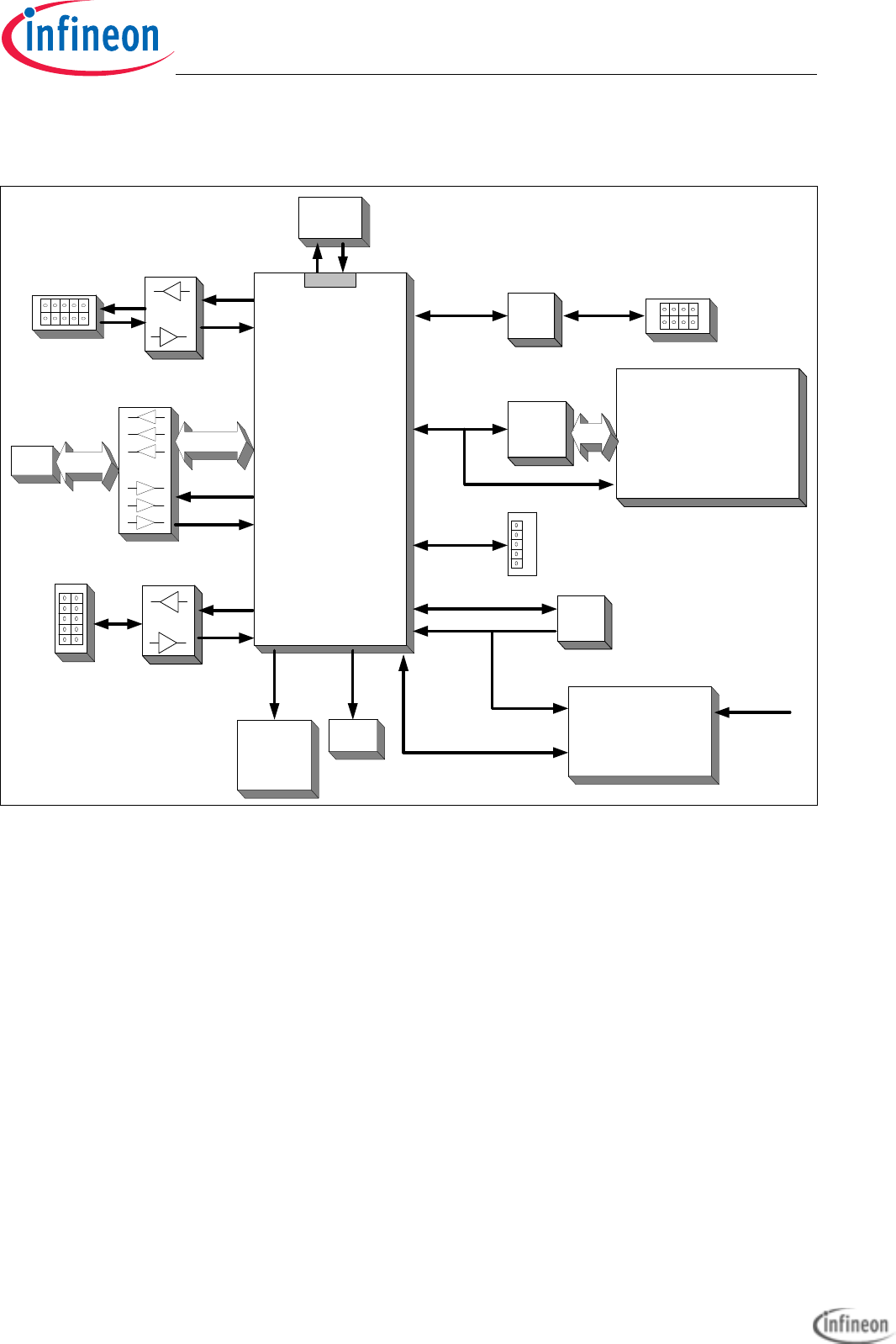
2.2 Block Diagram
Figure 2-1 Application Kit TC2X7 Block Schematic
Micro
USB miniWiggler
OCDS1
USB
XTAL
CAN
Transceiver
TxCAN0
RxCAN0 TC2X7
(TC237,
TC267,
TC277,
TC297)
TriCore
CPU
PLL
CAN0
TX0
RX0
4 LED’s
(P13.0 up to
P13.3)
Multi Voltage Safety Micro
Processor Supply
TLF35584QV
RMII PHY Twisted Pair
RJ45
LIN
LIN
Transceiver
TX1
RX1
Micro
SD Card
QSPI0 Serial to
Parallel
converter
XGA Display
320x240
with touch
QSPI1
Acoustic
Beeper
P33.0
RTC
QSPI3 or I2C
P33.7
WAKEUP
WAKE
QSPI2
QSPI2
Application Kit TC2x7 Hardware Manual downloaded by Myoungho Sunwoo (Hanyang University) at 11 Mar 2016 05:10
Application Kit TC2X7
Hardware Manual
Application Kit Features
User’s Manual 2-4 V 1.0, 2015-04
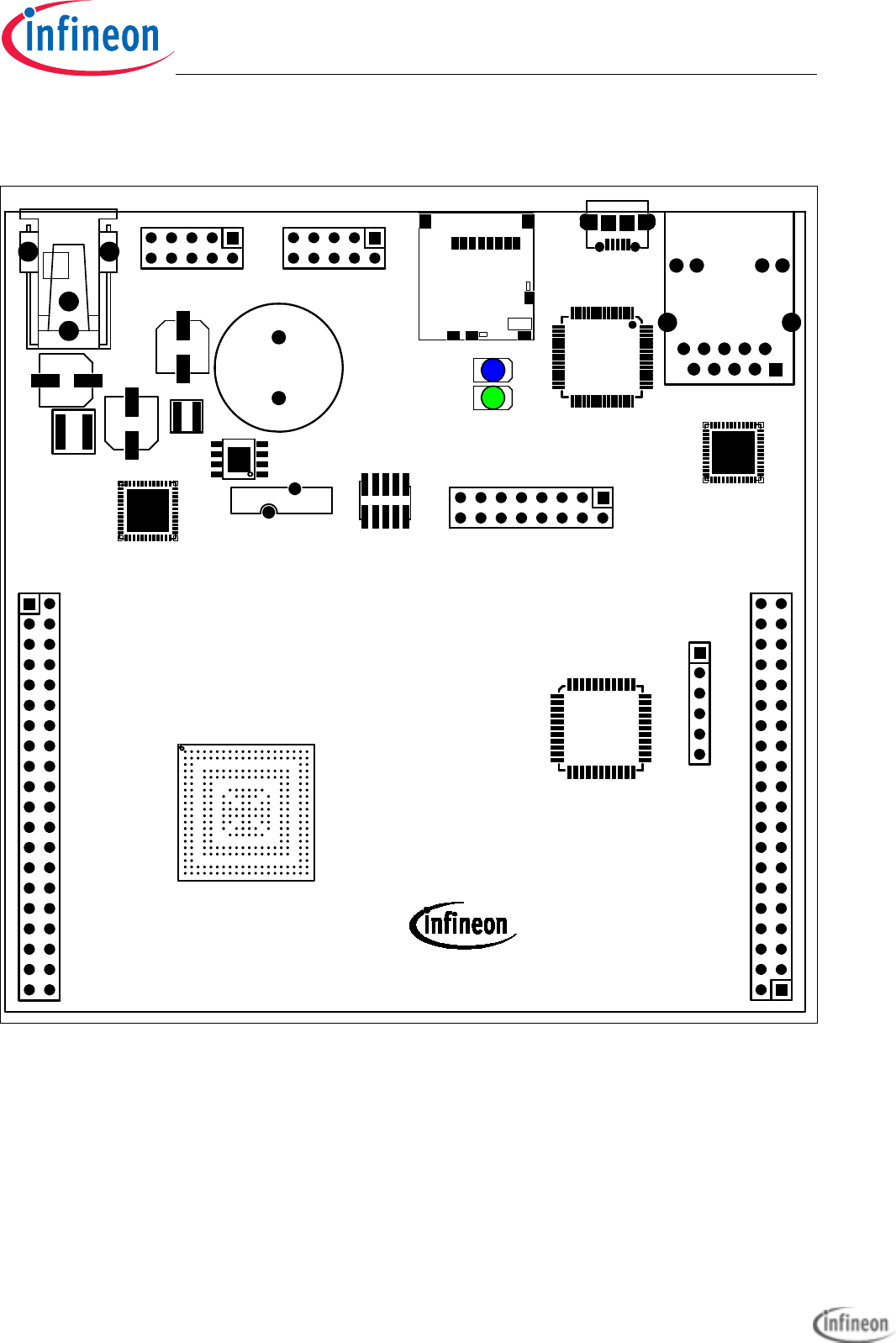
2.3 Placement
Figure 2-2 Applcation Kit TC2X7 V1.X Top Placement
DAP 1
1
1
APPLICATION KIT TC2X7 V1.X
CAN0
POWER
+5,5V...+40V
1
1
L1
RUN
1
ETH
LIN
ACT
JTAG
1
1
INFINEON
USB
SDCARD
TECHNOLOGIES AG
U101
U103
X302
X202
F
X205
X103
X102
X101
U102
+
LS101
L102
L101
C114
C107
X301
X201
U301
D302
BU301
D301
C209
U203
X203
F
X204
U201
-
+
BT101
Application Kit TC2x7 Hardware Manual downloaded by Myoungho Sunwoo (Hanyang University) at 11 Mar 2016 05:10
Application Kit TC2X7
Hardware Manual
Application Kit Features
User’s Manual 2-5 V 1.0, 2015-04
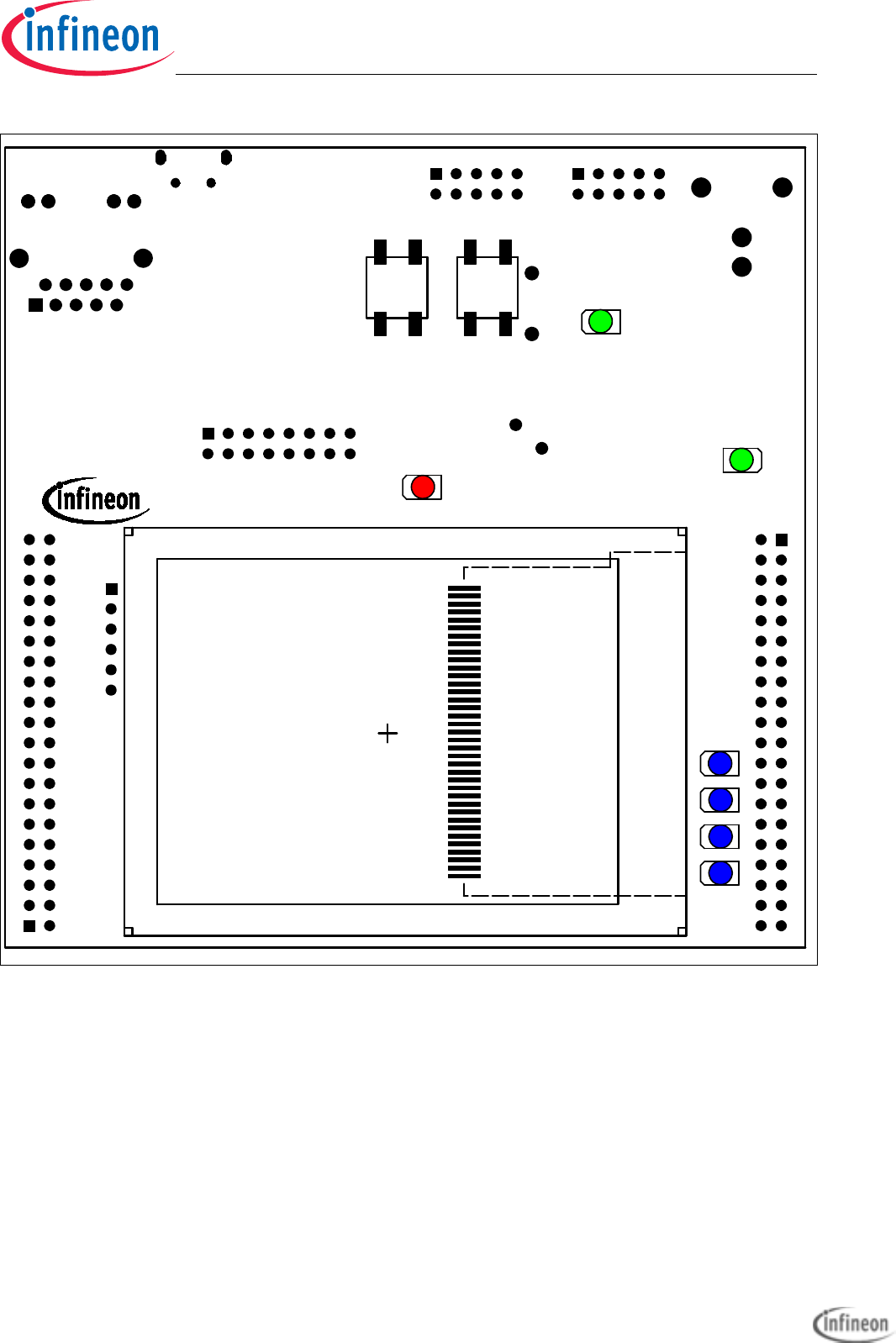
Figure 2-3 Applcation Kit TC2X7 V1.X Bottom Placement
SS2
L4
WAKE
V_UC
/PORST
P13.3
P13.0
P13.1
P13.2
ESR0
1
LCD201
D104
S102
S101
D110 D109 D108 D107
D106
D105
Application Kit TC2x7 Hardware Manual downloaded by Myoungho Sunwoo (Hanyang University) at 11 Mar 2016 05:10

Application Kit TC2X7
Hardware Manual
Application Kit Features
User’s Manual 2-6 V 1.0, 2015-04
Application Kit TC2x7 Hardware Manual downloaded by Myoungho Sunwoo (Hanyang University) at 11 Mar 2016 05:10

Application Kit TC2X7
Hardware Manual
Application Kit Information
User’s Manual 3-1 V 1.0, 2015-04
3 Application Kit Information
3.1 Power Supply
The microcontroller needs 3 different supply voltages. This voltages are generated via
Infineon’s Multi Voltage Safety Micro Processor Supply TLF35584QV (+3,3V and +5V
volt for ADC and CAN) and via the microcontroller itself (+1,3V).
Applying a stable supply voltage causes the power on reset after a short period. The
LED' (V_UC) indicate the status of the cpu voltage.
The board can be powered directly by USB or by the power connector. In case that the
voltage on the power connector is higher than the 5V from the USB then the board is
powered by power connector.
A manual power on reset is executed by pressing the reset button.
3.1.1 Power via supply connector (X101)
The Board has to be connected to a +5,5V to +40V DC power supply.
A supply with 6V and 500mA is sufficient. The pinout for the supply connector is shown
in Figure 5-3. There can be used any standard power pack with a connector where the
positive line is surrounded by the ground line.
3.1.2 Power via Micro USB (BU301)
The Board can also be powered by the Micro USB connector. The power consumption
of the board is approx. 400mA with TC237. Other CPUs like TC297 has a higher
consumption. Use an USB port which can deliver 500mA (USB 2.0) or better 900mA
(USB 3.0). Most USB hubs are not able to drive more than 100mA and can’t be used.
Also it is possible to power the board with a cellular battery charger which has 5V output
and use Micro USB for connecting.
The pinout for the USB connector is shown in Figure 5-4.
3.1.3 Multi Voltage Safety Micro Processor Supply TLF35584QV
The board has assembled the Safety Micro Processor Supply with the following
Features:
• High efficient multi voltage power supply chip
• Serial step up and step down pre regulator for wide input voltage range from 3.0 to
40 V with full performance and low over all power loss
• Low drop post regulator 5.0V/200mA for communication supply (named LDO_Com)
• Low drop post regulator 3.3 V/600 mA (VS2) or 5.0V/600mA (VS1) for μC supply
(named LDO_μC)
Application Kit TC2x7 Hardware Manual downloaded by Myoungho Sunwoo (Hanyang University) at 11 Mar 2016 05:10

Application Kit TC2X7
Hardware Manual
Application Kit Information
User’s Manual 3-2 V 1.0, 2015-04
• Provides enable, sync out signal and voltage monitoring (inside device to be added
to reset function) for an optional external post regulator for core supply (not used)
• Voltage reference 5.0 V +/- 1% for ADC supply, 150 mA current capability (named
Volt_Ref)
• Two trackers for sensor supply following voltage reference 150 mA current capability
each (named Tracker 1 and Tracker 2, not used)
• Standby regulator 3.3 V/10 mA (VS2) or 5.0 V/10 mA (VS1) (named LDO_Stby)
• Independent voltage monitoring block with reset function
• Configurable functional and window watchdog
• 16-bit SPI
• Safe state control with two safe state signals with programmable delay
• Input voltage monitoring (over voltage switch off)
• Green Product (RoHS compliant)
• ISO26262 compliant
• AEC Qualified
The TLF35584 is connected to the CPU via QSPI2 and use QSPI2_SLSO1 (P14.2) as
chip select. Via this spi connection the power supply will be configured (Watchdog,
device states and soon).
For more information see the data sheet of TLF35584. Because the TC237 is a 3,3V
devices we use the 3,3V version of the TLF35584 (VS2). All other CPUs are working with
5V and we use the 5,0V version of the TLF35584 (VS1).
3.2 Real Time Clock
The board is equipped with a RTC MCP79511 (if with TC237) or MCP79411 (if with all
other CPUs) from Microchip. The device is powered from the standby voltage of the
TLF35584 and is also powered when the TLF35584 is switched to standby mode. For
backup when the TLF35584 is not powered then there is a small battery to hold the value
inside the RTC. The MCP79511 is connected to the microcontroller via QSPI3, the
MCP79411 is connected to the microcontroller via I2C on P15.4/P15.5. The RTC can
trigger an SCU_REQ8 (P33.7) interrupt (activ high) with the alarms. Also an alarm from
the RTC will wake-up (switch on) the board if the board is powered and the supply is
switched off.
The MCP79511/MCP79411 contains also an unique ID in the format EUI-48. This id can
be used as mac id for ethernet if the assembled CPU support ethernet.
For more information about the RTC please see the datasheet of
MCP79511/MCP79411.
3.3 XGA Display
The board has an XGA Display with a resolution of 320x240. The display has an ILI9341
display controller. Please see the datasheet of the display controller for the register of
Application Kit TC2x7 Hardware Manual downloaded by Myoungho Sunwoo (Hanyang University) at 11 Mar 2016 05:10

Application Kit TC2X7
Hardware Manual
Application Kit Information
User’s Manual 3-3 V 1.0, 2015-04
the controller. The display is connected to the the microcontroller via an SPI to Parallel
converter (U201).
The SPI to Parallel converter is based on a statemachine. This state machine is clocked
with the clock of SPI, here SCLK0 (P20.11). Each rising edge of P20.11 will change the
state of statemachine. When SLSO08 (P20.6) is not low then the state machine will go
always in the idle state with a valid clock edge.
3.3.1 Write a display register
A single write to any register can be done by a 32 bit transfer of SPI. Make sure that the
SLSO08 is low during this 32 bit. Bit 31 must be transfered first.
Bit 31 must be 0, this will be indicate a write access.
Bit 30 must be 0, this will be indicate a single access.
Bit 29...Bit 22 is the 8 bit register number which will be written
Bit 21...Bit 6 is the 16bit value which will be written
Bit 5...Bit 0 are dummy bits which are used to execute the write.
To speedup the writing (e.g. write to ram of display controller) it is possible to make a
endless transfer. This is done by this:
first 10 bit transfer
Bit 9 must be 0, this will be indicate a write access.
Bit 8 must be 1, this will be indicate an endless transfer.
Bit 7...Bit 0 is the 8 bit register number which will be written
Now you need to transfer only 16bit values for the registers. With the first 16 bit value
there is no action on the display. With the second value transfer is a write to the register
started. This means after the last value you must make a dummy transfer to write the last
value.
The endless mode can only be leave by a rising edge of SCLK0 with SLSO08 set to high.
This can be done by a dummy transfer to any other chip select or by a transfer from the
touch controller.
3.3.2 Read a display register
A single read from any register can be done by a 32 bit transfer of SPI. Make sure that
the SLSO08 is low during the complete transfer.
first transfer has 16 bit:
Bit 15 must be 1, this will be indicate a read access.
Bit 14 must be 0, this will be indicate a single access.
Bit 13...Bit 7 is the 8 bit register number which will be read
Bit 5...Bit 0 are dummy bits to setup the register number.
Application Kit TC2x7 Hardware Manual downloaded by Myoungho Sunwoo (Hanyang University) at 11 Mar 2016 05:10

Application Kit TC2X7
Hardware Manual
Application Kit Information
User’s Manual 3-4 V 1.0, 2015-04
second transfer must have 26 bits:
Bit 25...Bit 16 are dummy bits which are needed to readout the register value
Bit 15...Bit 0 are dummy bits to transfer the readed value.
To speedup the reading (e.g. reading from ram of display controller) it is possible to make
a endless transfer. This is done by this:
first 16 bit transfer:
first transfer has 16 bit:
Bit 15 must be 1, this will be indicate a read access.
Bit 14 must be 1, this will be indicate an endless access.
Bit 13...Bit 7 is the 8 bit register number which will be read
Bit 5...Bit 0 are dummy bits to setup the register number.
second 10 bit transfer:
Bit 9...Bit 0are dummy bits which are needed to readout the register value
Now you need to transfer only 16bit values for the registers. With the each 16 bit transfer
you get a value. With the last transfer you have dummy read which you don’t get the
result.
The endless mode can only be leave by a rising edge of SCLK0 with SLSO08 set to high.
This can be done by a dummy transfer to any other chip select or by a transfer from the
touch controller.
3.3.3 Touch controller
The touch of display is connected to an Touch controller ADS7843. This controller is
connected via the QSPI0 and SLSO9 to the microcontroller. For more information about
the delivered values from the touch controller please see the datasheet of ADS7348.
3.4 Micro SD card
The board has a slot to use the board with an micro SD card. The card will be used in
SPI mode only. The SD is connectred to QSPI1 with chip select 9 (P10.5) of QSPI1.
Please see additional literature how to use a SD card in SPI mode.
3.5 LEDs
There are 8 LEDs on board:
– D107 up to D110 (blue) -> toogle LEDs connected to P13.0 ... P13.3
– D106 ESR0 (red) -> RESET LED indicate the reset state of the board
– D105 V_UC (green) -> V_UC power supply indication
– D104 SS2 (green) -> safe state signal 2 of TLF35584
– D302 ACT (green) -> on board miniWiggler JDS is ACTIV
Application Kit TC2x7 Hardware Manual downloaded by Myoungho Sunwoo (Hanyang University) at 11 Mar 2016 05:10

Application Kit TC2X7
Hardware Manual
Application Kit Information
User’s Manual 3-5 V 1.0, 2015-04
– D301 RUN (blue) -> Debug RUN mode (switched by DAS Server)
3.6 Clock
On the board is a fixed crystal wiith 20MHz assembled. You can change this by replacing
Y101 (soldered).
3.7 USB Connector
The USB connector is used for connection to a PC. Via the USB it is possible to power
the board, using the ASCLIN0 as serial connection via USB and Debugging via DAS. For
the pinout of USB socket see Figure 5-4.
NOTE: Before connecting the board to the PC, make sure that the actual DAS software
is installed on the PC. For actual DAS software please contact your local FAE.
The software can also be found on the
DAS website
3.7.1 Serial Connection to PC
After the first connection of USB to a PC the needed driver will be installed automatically.
During this there will be created a new COM port on PC. This COM port can be used to
communicate with the board via ASC0 of the device (e.g. bootstrap loader).
3.7.2 miniWiggler JDS
The miniWiggler JDS is a low cost debug tool which allows you access to the JTAG of
the device. Make sure that you have the latest DAS release. Debugging is possible via
the DAS Server ‘UDAS‘. Please contact your prefered debug vendor for support of DAS.
If you have connected the board to the PC and there runs the DAS server, then a working
connection is visible via the green ACTIV LED.
The status RUN LED is switched on/off through the DAS Server, depending on the used
debugger (client).
IMPORTANT: Make sure that there is no or a tristated connection on X301 (OCDS1) if
the ACTIV LED is on.
3.8 Beeper
The board has an electro-acoustic transducer which can be used for an acoustic output.
The transducer is connected to pin P33.0 and needs a 2048Hz frequency.
Application Kit TC2x7 Hardware Manual downloaded by Myoungho Sunwoo (Hanyang University) at 11 Mar 2016 05:10

Application Kit TC2X7
Hardware Manual
Application Kit Information
User’s Manual 3-6 V 1.0, 2015-04
3.9 MultiCAN
On the board is oneCAN transceiver connected to the MultiCAN on TC2X7 node 0. The
transceiver is connected to an IDC10 plug. For the pinout of IDC10 plug see Figure 5-5.
You can use a IDC female connector with crimpconnector, flat cable and SUB-D 9 plug
with crimpconnector to have a 1:1 adapter to SUB-D 9.
3.10 LIN
On the board is one LIN transceiver connected to the ASCLIN1 on TC2X7. The
transceiver are connected to one IDC10 plug. For the pinout of IDC10 plug see
Figure 5-6. You can use a IDC female connector with crimpconnector, flat cable and
SUB-D 9 plug with crimpconnector to have a 1:1 adapter to SUB-D 9.
3.11 Ethernet
The Application Kit provide a RJ45 connector (X204) for twisted pair ethernet
connections.The board use a Lantiq Giagabit PHY PEF7071 as physical interface
device.
Note: The parts for ethernet are not assemled if the assembled CPU (TC237L) don’t
support ethernet.
For more information about the ethernet modul see TC2X7 User’s Manual, about the
PHY see the PEF7071 datasheet. For the pinout of RJ45 see Figure 5-8.
3.12 Core current measurement
It is possible to measure the core (+1,3V) current with two ADC pins of the CPU. This
can be done by synchronous measurement of AN5 and AN17 with TC237. For all other
CPUs this can be done by synchronous measurement of AN6 and AN22. The pins are
connected togheter by an 50mOhm resistor. The current can be calculated by the
following formula:
Icore = (VAN10 - VAN22) / 0,05. To get an valid result the measurement must be done
synchronous.
3.13 Other peripherals
For all other peripherals there are no special plugs on the board. Many of the peripheral
signals are available on the two standard connectors X102 and X103. See “Connector
Pin Assignment” on Page 5-1.
3.14 Toggle LED’s
Port 13 pin 0 up to pin 3 are connected to single LED’s (D107... D110) and can be
controlled by Software. This status LED’s are low active.
Application Kit TC2x7 Hardware Manual downloaded by Myoungho Sunwoo (Hanyang University) at 11 Mar 2016 05:10

Application Kit TC2X7
Hardware Manual
Application Kit Information
User’s Manual 3-7 V 1.0, 2015-04
3.15 Debug System
3.15.1 OCDS1
The OCDS1 signals are connected to the IDC16 plug (X301). They work with the port
supply of +3.3V. For pinout of the connector see Figure 5-7. You can connect any
debugger to this connector.
f you connect a debug hardware make sure that the miniWiggler JDS (see “miniWiggler
JDS” on Page 3-5) is not activ (ACTIV LED is off).
If the ACTIV LED is on, then stop the active DAS Server ’UDAS’ and/or remove the USB
connection to the PC.
Application Kit TC2x7 Hardware Manual downloaded by Myoungho Sunwoo (Hanyang University) at 11 Mar 2016 05:10

Application Kit TC2X7
Hardware Manual
Application Kit Information
User’s Manual 3-8 V 1.0, 2015-04
Application Kit TC2x7 Hardware Manual downloaded by Myoungho Sunwoo (Hanyang University) at 11 Mar 2016 05:10
Application Kit TC2X7
Hardware Manual
Signal Description
User’s Manual 4-1 V 1.0, 2015-04
4 Signal Description
For more information about the signals please see the user manuals for TC2X7 and/or
the schematics of the board.
Table 4-1 Power Signals
Short Name Description
VCC_IN Supply Input (5,5V...50V(40V))
VIN Input voltage of power supply device
GND Ground
VDD Core Supply Voltage (1,3V)
V_UC Port Supply Voltage (5V or 3,3V)
VSSOSC Oscillator Ground
VSSM ADC Analog Part Ground
VDDM ADC Analog Part Supply Voltage (VREF_5V or 3,3V)
VAGND1 ADC Reference Ground 1
VAREF1 ADC Reference Voltage 1 (VREF_5V or 3,3V)
VAGND2 ADC Reference Ground 2
VAREF2 ADC Reference Voltage 2 (VREF_5V or 3,3V)
VDD_FT Supply Voltage FT2232HL device (3,3V)
VDD_USB USB Supply Voltage (5V)
Table 4-2 Reset Signals
Short Name Description
/PORST Power On Reset
/ESR0 External Service Request 0 (Hardware Reset)
/ESR1 External Service Request 1 (Non Maskable Interrupt)
Table 4-3 Interrupt Signals
Short Name Description
REQ1 / P15.8 External Trigger Input 1
REQ3 / P10.3 External Trigger Input 3
REQ5 / P10.8 External Trigger Input 5
REQ8 / P33.7 External Trigger Input 8 (RTC alarm activ)
Application Kit TC2x7 Hardware Manual downloaded by Myoungho Sunwoo (Hanyang University) at 11 Mar 2016 05:10
Application Kit TC2X7
Hardware Manual
Signal Description
User’s Manual 4-2 V 1.0, 2015-04
REQ9 / P20.0 External Trigger Input 9(Touch acttiv)
REQ11 / P20.9 External Trigger Input 11 (MD Interrupt)
Table 4-4 Clock Signals
Short Name Description
XTAL1 Crystal Oscillator Input
XTAL2 Crystal Oscillator Output
Table 4-5 Debug Signals
Short Name Description
/TRST Test Reset
TCK / DAP0 Test Clock / Device Access Pin 0
TMS / DAP1 Test Mode Select / Device Access Pin 1
TDI / P21.6 Test Data Input
TDO / P21.7 Test Data Output
/TESTMODE / P20.2 Test Mode Select Input
Table 4-6 Peripheral Signals
Short Name Description
P14.1 Receive Data ASCLIN0
P14.0 Transmit Data ASCLIN0
P15.1 Receive Data ASCLIN1
P15.0 Transmit Data ASCLIN1
SCLK0 / P20.11 Clock Line SSC0
MRST0A / P20.12 Master Receive / Slave Transmit QSPI0
MTSR0 / P20.14 Master Transmit / Slave Receive QSPI0
SLSO08 / P20.6 Slave Select Output 8 (QSPI0)
SLSO09 / P20.3 Slave Select Output 9 (QSPI0)
SCLK1 / P10.2 Clock Line QSPI1
MRST1A / P10.1 Master Receive / Slave Transmit QSPI1
MTSR1 / P10.3 Master Transmit / Slave Receive QSPI1
SLSO19 / P10.5 Slave Select Output 9 (QSPI1)
SCLK2 / P15.3 Clock Line QSPI2
Table 4-3 Interrupt Signals
Application Kit TC2x7 Hardware Manual downloaded by Myoungho Sunwoo (Hanyang University) at 11 Mar 2016 05:10
Application Kit TC2X7
Hardware Manual
Signal Description
User’s Manual 4-3 V 1.0, 2015-04
MRST2B / P15.7 Master Receive / Slave Transmit QSPI2
MTSR2 / P15.5 Master Transmit / Slave Receive QSPI2
SLSO21 / P14.2 Slave Select Output 1 (QSPI2)
SCLK3 / P22.3 Clock Line QSPI3
MRST3E / P22.1 Master Receive / Slave Transmit QSPI3
MTSR3 / P22.0 Master Transmit / Slave Receive QSPI3
SLSO313 / P23.1 Slave Select Output 13 (QSPI3)
P15.4 I2C Clock (not with TC237)
P15.5 I2C Data (not with TC237)
P20.8 CAN Transmitter Output 0
P20.7 CAN Receiver Input 0
P21.2 Ethernet MDC
P21.3 Ethernet MDIO
P11.2 Ethernet TXD1
P11.3 Ethernet TXD0
P11.6 Ethernet TXEN
P11.9 Ethernet RXD1
P11.10 Ethernet RXD0
P11.11 Ethernet CRSDIV
P11.12 Ethernet REFCLK
ANx Analog Input x for all TC2X7
ANx(y) Analog Input y for TC237 and Analog Input x for all others
P33.0 Beeper output (2048Hz)
P13[0...3] On board LED’s
Table 4-6 Peripheral Signals
Application Kit TC2x7 Hardware Manual downloaded by Myoungho Sunwoo (Hanyang University) at 11 Mar 2016 05:10

Application Kit TC2X7
Hardware Manual
Signal Description
User’s Manual 4-4 V 1.0, 2015-04
Application Kit TC2x7 Hardware Manual downloaded by Myoungho Sunwoo (Hanyang University) at 11 Mar 2016 05:10

Application Kit TC2X7
Hardware Manual
Connector Pin Assignment
User’s Manual 5-1 V 1.0, 2015-04
5 Connector Pin Assignment
The Application Kit will be shipped with two 40 pin male (plug) connectors on top layer
with a standard grid of 2,54mm.
5.1 IO Connectors TC237
Figure 5-1 IO Connectors TC237- Pinout
VCC_IN 1 2 V_UC (+3V3) VCC_IN 1 2 V_UC (+3V3)
GND 3 4 GND GND 3 4 GND
AN10 5 6 AN9 P33.10 5 6 P33.9
AN16 7 8 AN15 P14,8 7 8 P14.7
AN3 9 10 AN2 P14,6 9 10 P10.6
AN11112AN0 1112P11.8
P33.5 13 14 P33.4 P02.0 13 14 P02.1
P33.3 15 16 P33.2 P02.2 15 16 P02.3
P33.1 17 18 P33.12 P02.4 17 18 P02.5
P33.8 19 20 P33.6 P02.6 19 20 P02.7
P34.0 21 22 P34.1 P02.8 21 22 P00.0
P34.2 23 24 P34.3 P00.1 23 24 P00.2
P22.4 25 26 P33.11 P00.3 25 26 P00.4
P22.0 27 28 P22.1 P00.5 27 28 P00.6
P22.2 29 30 P22.3 P00.7 29 30 P00.8
P15.2 31 32 P15.3 P00.9 31 32 P21.4
P15.4 33 34 P15.5 P21.5 33 34 P00.12
P15.6 35 36 P15.7 AN21 35 36 AN20
P20, 9 37 38 P20. 10 AN17 37 38 AN13
P14.4 39 40 P14.5 AN11 39 40 AN12
X102 X103
Application Kit TC2x7 Hardware Manual downloaded by Myoungho Sunwoo (Hanyang University) at 11 Mar 2016 05:10
Application Kit TC2X7
Hardware Manual
Connector Pin Assignment
User’s Manual 5-2 V 1.0, 2015-04
5.2 IO Connectors TC267, TC277, TC297
5.3 Power connector pinout
Figure 5-2 IO Connectors TC267, TC277, TC297 - Pinout
Figure 5-3 Power connector pinout
VCC_IN 1 2 V_UC (+5V) VCC_IN 1 2 V_UC (+5V)
GND 3 4 GND GND 3 4 GND
AN21 5 6 AN20 P33.10 5 6 P33.9
AN33 7 8 AN32 P14,8 7 8 P14.7
AN3 9 10 AN2 P14,6 9 10 P10.6
AN81112AN0 P10.71112P10.4
P33.5 1314 P33.4 P02.0 1314 P02.1
P33.3 1516 P33.2 P02.2 1516 P02.3
P33.1 17 18 P33.12 P02.4 17 18 P02.5
P33.8 1920 P33.6 P02.6 1920 P02.7
P23.0 2122 P23.1 P02.8 2122 P00.0
P23.2 2324 P23.3 P00.1 2324 P00.2
P23.4 25 26 P33.11 P00.3 25 26 P00.4
P22.0 2728 P22.1 P00.5 2728 P00.6
P22.2 2930 P22.3 P00.7 2930 P00.8
P15.2 3132 P15.3 P00.9 3132 P00.10
P15.4 33 34 P15.5 P00.11 33 34 P00.12
P15.6 35 36 P15.7 AN45 35 36 AN44
P20,9 3738 P20.10 AN17 3738 AN16
P14.4 39 40 P14.5 AN25 39 40 AN24
X102 X103
+5,5V…+40V
GND
Application Kit TC2x7 Hardware Manual downloaded by Myoungho Sunwoo (Hanyang University) at 11 Mar 2016 05:10

Application Kit TC2X7
Hardware Manual
Connector Pin Assignment
User’s Manual 5-3 V 1.0, 2015-04
5.4 USB connector pinout
5.5 CAN connector pinout
Figure 5-4 USB connector Pinout
Figure 5-5 CAN connector pinout (IDC10)
D+
D-
VCC
GND
ID
2468
GND
CANH
CANL
13579
1
0
GND
Application Kit TC2x7 Hardware Manual downloaded by Myoungho Sunwoo (Hanyang University) at 11 Mar 2016 05:10

Application Kit TC2X7
Hardware Manual
Connector Pin Assignment
User’s Manual 5-4 V 1.0, 2015-04
5.6 LIN connector pinout
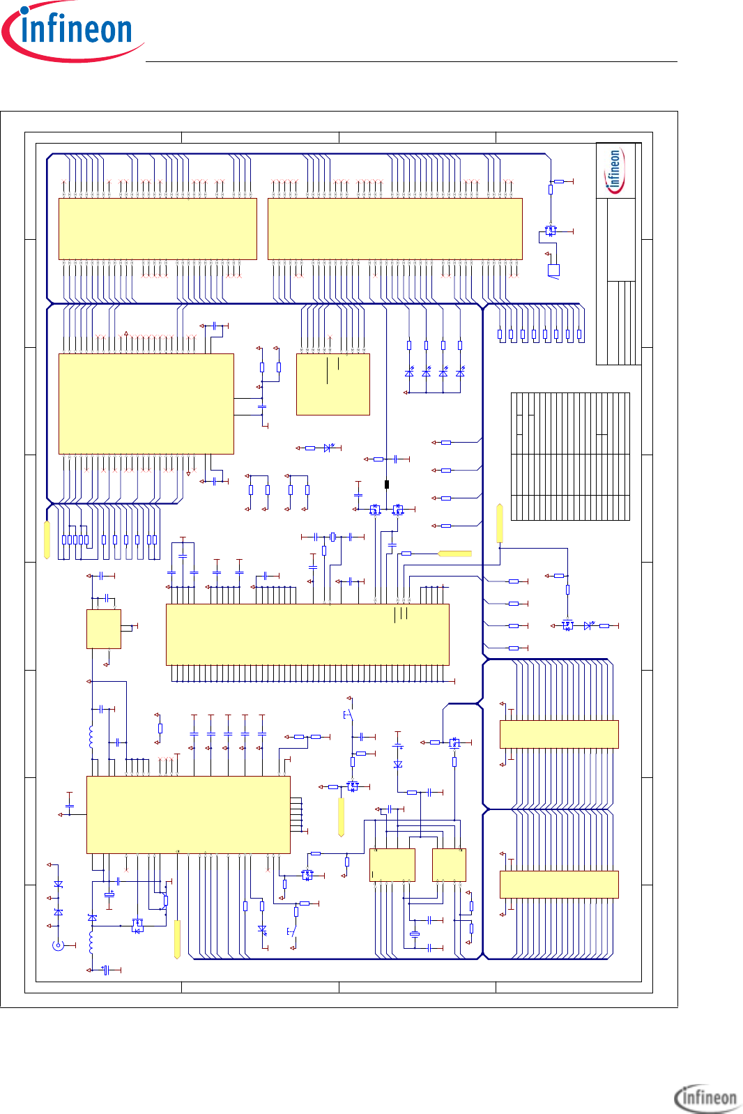
5.7 OCDS connector pinout
Figure 5-6 LIN connector pinout (IDC10)
Figure 5-7 OCDS connector pinout (IDC16)
2468
GND
BUS
VIN opt
13579
1
0
GND
TDO
2468
13579
10 12 14 16
11 13 15
TDI
/TRST
TCK
/BRKIN
TMS
GND
GND
/PORST
/BRKOUT
GND
VDDP3
Application Kit TC2x7 Hardware Manual downloaded by Myoungho Sunwoo (Hanyang University) at 11 Mar 2016 05:10
Application Kit TC2X7
Hardware Manual
Connector Pin Assignment
User’s Manual 5-5 V 1.0, 2015-04
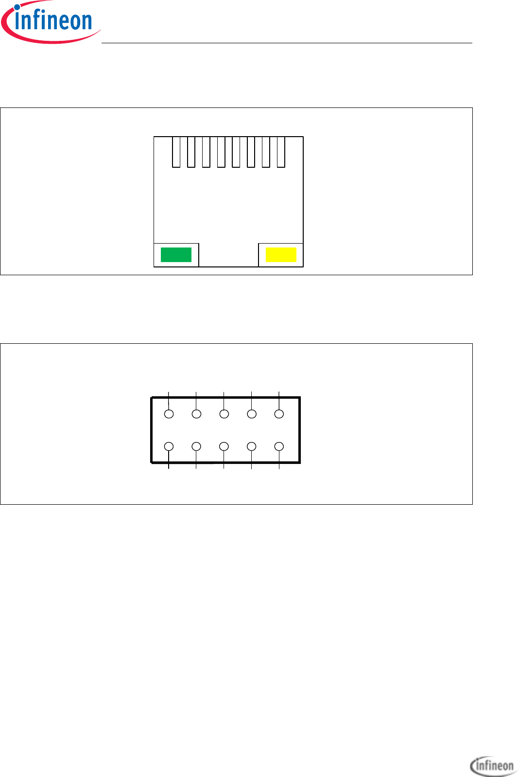
5.8 Ethernet Connector
5.9 DAP connector pinout
Figure 5-8 Ethernet connector pinout (RJ45)
Figure 5-9 DAP connector pinout (FTSH10)
J2
J1
J3
J4
J5
J6
J7
J8
DAP0
2468
13579
10
USR1_IO
/PORST
USR0_IO
DAP1
GND
GND
Key
GND
VDDP3
Application Kit TC2x7 Hardware Manual downloaded by Myoungho Sunwoo (Hanyang University) at 11 Mar 2016 05:10

Application Kit TC2X7
Hardware Manual
Connector Pin Assignment
User’s Manual 5-6 V 1.0, 2015-04
Application Kit TC2x7 Hardware Manual downloaded by Myoungho Sunwoo (Hanyang University) at 11 Mar 2016 05:10

Application Kit TC2X7
Hardware Manual
Schematic and Layout
User’s Manual 6-1 V 1.0, 2015-04
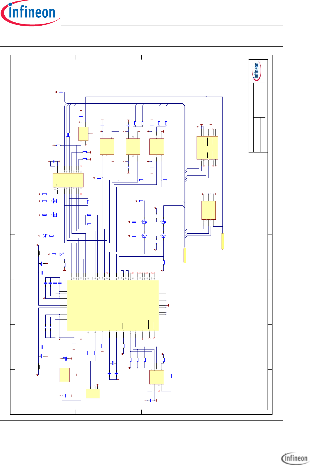
6 Schematic and Layout
6.1 Schematic
6.1.1 Known problems/differences
On board version V1.0 are the resistors R147, R148 and R337 assembled via wire wrap.
All other components are identically.
Application Kit TC2x7 Hardware Manual downloaded by Myoungho Sunwoo (Hanyang University) at 11 Mar 2016 05:10

Application Kit TC2X7
Hardware Manual
Schematic and Layout
User’s Manual 6-2 V 1.0, 2015-04
Figure 6-1 Schematic - Project
1
1
2
2
3
3
4
4
5
5
6
6
7
7
8
8
D D
C C
B B
A A
4Infineon Technologies AG
ATV MC AC E PDA
Am Campeon 1-12
D-85579 Neubiberg
Tel.: +49-89-234-0
4
4/9/2015
Number:
Date:
Sheet: of
Application Kit TC2X7 Project Overview
1.1Revision:
G:\Technical_Sup port\TriCore\TriBoard\EDA_DXP\Applica tion Kit\Ap pl Kit TC2X7\Appl Kit TC2X7 V1.X\Appl Kit TC2X7 V11.prj
File:
PORT[00..34]
/ESR0
/PORST
CPU and Power Supply
CPU_supply.sch
PORT[00..34]
/ESR0
On Board Peripherals
Peripherals.sch
PORT[00..34]
/PORST
MiniWiggler and DAP
OCDS.sch
/ESR0
PORT[00..34]
/PORST
Application Kit TC2x7 Hardware Manual downloaded by Myoungho Sunwoo (Hanyang University) at 11 Mar 2016 05:10
Application Kit TC2X7
Hardware Manual
Schematic and Layout
User’s Manual 6-3 V 1.0, 2015-04
Figure 6-2 Schematic - CPU and Power Supply
1
1
2
2
3
3
4
4
5
5
6
6
7
7
8
8
D D
C C
B B
A A
1Infineon Technologies AG
ATV MC AC E PDA
Am Campeon 1-12
D-85579 Neubiberg
Tel.: +49-89-234-0
4
4/9/2015
Number:
Date:
Sheet: of
Application Kit TC2X7 CPU and Power Supply
1.1Revision:
G:\Technical_Sup port\TriCore\TriBoard\EDA_DXP\Applica tion Kit\Ap pl Kit TC2X7\Appl Kit TC2X7 V1.X\CPU_supply.sch
File:
VDD / VDDSB G8
ESR1 G16
ESR0 F16
PORST G17
VEXT (VDDP3) A2
VDDOSC3 N20
VDD G13
VGATE1N (VCAP0) Y17
VDDOSC N19
P32.2 (VCAP1) Y18
XTAL1 M20
XTAL2 M19
VSSOSC L20
VDD / VDDSB H7
VDD H14
VDD N14
VDD P13
VDD N7
VDD P8
VEXT (VDDP3) B3
VEXT (VDDP3) W20
VEXT (VDDP3) V19
VEVRSB (VDDP3) T11
VDDP3 A19
VDDP3 B18
VDDFL3 (VDDP3) D16
VDDFL3 (VDDP3) E15
VFLEX (VDDP3) D5
VSS
B2
VSS
D4
VSS
E5
VSS
T16
VSS
U17
VSS
W19
VSS
Y20
VSS
A20
VSS
B19
VSS
D17
VSS
E16
VSS / AGBT_TXN P10
VSS / AGBT_TXP P11
VSS
P12
VSS
N9
VSS
P9
VSS
N10
VSS
N11
VSS
N12
VSS
M7
VSS
M8
VSS
M10
VSS
M11
VSS
M13
VSS
M14
VSS / AGBT_CLKN L7
VSS
L8
VSS
L9
VSS
L10
VSS
L11
VSS
L12
VSS
L13
VSS / AGBT_ERR L14
VSS / AGBT_CLKP K7
VSS
K8
VSS
K9
VSS
K10 VSS
K11 VSS
K12 VSS
K13
NC / VDDPSB K14
VSS
J7 VSS
J8 VSS
J10 VSS
J11 VSS
J13 VSS
J14 VSS
H9 VSS
H10 VSS
H11 VSS
H12 VSS
G9 VSS
G10 VSS
G11 VSS
G12
VGATE1P (NC) W17
U101A
TC2X7
+3V3
VDD
CB101
100n CB102
100n
CB103
100n
GND
VDD
VAREF1
VDDM
CB110
1μF
GND
CB111
100n
GND
CB108
330n
GND
CB107
330n
GND
CB106
1μF
GND
GND
R101
0R
C102
10pF
C101
10pF
12
Y101
20MHz
GND
GND
P33.8
P33.9P33.10
P33.11
R116
4K7
1
2
X101
POWER
VCC_IN
D101
MSS2P2
C114
100μF/40V CB112
100n
GND
GND
V_PREREGVIN
GND
VIN
QST
SW1 43
WDI
16
QST 5
VS1
45
WAK
4
RSH
47
PG1 41
VS2
44
VST
2
ENA
3
AG1
6
SW2 42
FRE
24
ROT
17
INT
18
SDO
13
SCL
14
QUC 30
QCO 31
SYN 19
QT1 33
QT2 32
VCI 26
SEC 23
EVC 21
SCS
15
ERR
20
BSG
1RSL
48
STU
25
DRG
46
GND
HS
SDI
12
SS1
11
SS2
10
QVR 29
AG2
7
AG3
8
AG4
28
AGS
9
TM 22
GST 27
PG2 40
FB1 34
FB2 35
FB3 36
FB4 37
FB5 38
AG5
39
U102
*
VREF_5V
+5V
S102
WAKE
R102
680R
S101
RESET
GND
R104
4K7 R105
10K
C115
4,7μF/10V
GNDGND
V_UC
R103
1K
V_UC
GND
GND
C108
1μF/10V
GND
C113
4,7μF/10V
GND
V_UC
QT1
QT2
/ESR0
GND
R115
100K
/PORST
GND
X1
1
VCC 10
SCK
8
VSS 5
SI
6
MFP 9
X2
2VBAT 3
CS
4
SO
7
U104
*
1 2
Y102
32.768Hz
C103
10pF
C104
12pF
GND GND
CB114
100n
R113
10K
V_UC
1
3
5
7
9
11
13
15
2
4
6
8
10
12
14
16
17
19
21
23
25
27
29
18
20
22
24
26
28
30
31 32
33 34
35 36
37 38
39 40
X102
CON2X20
1
3
5
7
9
11
13
15
2
4
6
8
10
12
14
16
17
19
21
23
25
27
29
18
20
22
24
26
28
30
31 32
33 34
35 36
37 38
39 40
X103
CON2X20
R119
*
GND
V_UC
D105
LP T67K
GND
R118
220R
R117
10K
V_UC
1
32
Q106
BSS138N
D106
LS T67K
1
32
Q103
BSS138N
PORT[00..34]
/PORST
R111
10K
R112
10K
/ESR1
P02.0 P02.1
P02.2 P02.3
P02.4 P02.5
P02.6 P02.7
P02.8 P00.0
P00.1 P00.2
P00.3 P00.4
P00.5 P00.6
P00.7 P00.8
P00.9
V_UCVCC_IN
P00.12
AN4 5 (21)
AN21(10)
AN4 4 (20)
AN20(9)
AN8(1)
AN2 5 (11)
GND
P22.3P22.2
P22.1P22.0
P23.1
P15.7P15.6
P33.5
P10.5
P15.2
GND
V_UCVCC_IN
GNDGND
P14.8
P14.6
P14.5
P14.2
P20.10P20.9
P33.6 +1
-2
LS101
BRT1615P-06
+5V
GND
R121
10K
R123
4R7_opt
R122
4R7
VREF_5V
AN2 4 (12)
GND
P10.6
P14.6
R134
10K_opt
1
32
Q107
BSS138N
GND
1
3 2
Q105
BSS83P
GND
BT101
BR-1225/VCN
C116
*
P14.4
P14.3
P14.2
P33.1
P33.2P33.3
P33.4
P23.0 P23.1
P23.2 P23.3
P23.4
P10.6
P10.4
P00.10
P00.11
P10.7
C106
22μF/10V
C109
4,7μF/10V
C110
4,7μF/10V
C111
4,7μF/10V
C112
4,7μF/10V
GND
GND
+3V3 R124
0R
QST
R110
100K
GND
R114
10K
P33.8
P33.12
P33.7
R125
0R_opt
VREF_5V
+3V3
R131
10K_opt
R132
10K_opt
R141
2K2
GND
V_UC V_UC
1
32
Q102
BSS138N
D102
SS26
VDD_USB
L101
XAL5050-223MEB
L102
XAL4030-472MEC
R130
*
4
3
1,2,5,6
Q101
BSL606SN
C107
47μF/40V
GND
GND
GND
D103
SS22
VIN
GND
P14.3
GND
R142
2K2_opt
R127
opt
R128
0R
GND
+5V
CB113
100n
R129
470R
D104
LP T67K
GND
13 D111
BAT54
R136
1K
C118
100pF
GND
P15.3
P15.6
P15.7
P14.7
P15.3
P15.5P15.4
R137
10K
P22.3
P22.0
P22.1
R138
1K
P33.9
R139
2K2
GND
V_UC
+3V3
CB104
1μF
CB105
100n
VDD
C105
*
GND
1
65
Q104A
*
3
24
Q104B
*
GND
V_UC
L103
*
C120
*GND
GND
GND
Q1
GND
6
SENSE/ADJ 2
BYP 4
IN
8
EN
5
GND
HS
U103
*
GND
V_UC C119
*
C117
*
+3V3
GND
R120
*
V_UC +3V3
U101
U102
TC237 TC267
TLF35584QVVS2 TLF35584QVVS1
U103 NA TLS203B0EJV33
R120 0R NA
C116 1μF NA
C117 NA 10nF
C119 NA 10μF
Q104 NA BSL215C
L103 NA LTF3020T-4R7N
C120 4,7μF 10μF
C105 10μF 22μF
R130 330mR 330mR
R119 680R 1K5
V_UC +3,3V +5V
P11.6 D9
P11.9 A9
P11.3 B10
P11.11 A8
P11.12 B8
P11.10 B9
P11.2 A10
P02.0
B1
P02.1
C2
P02.2
C1
P02.3
D2
P02.4
D1
P02.5
E2
P00.4
J1
P00.5
J2
P00.12
L2
P00.9
K2
P00.3
H2
P00.0
G1
P10.6 / HWCFG5 A4
P13.1 A12
P13.0 B12
P13.3 A11
P10.1 B7
P13.2 B11
P10.5 / HWCFG4 B5
P10.2 A5
P10.3 A6
P00.2
H1 P00.1
G2
P11.8 (NC) E7
P00.8
K4 P00.7
K1 P00.6
J4
P02.6
E1
P02.7
F2
P02.8
F1
P11.4 (NC) D10
P11.0 (NC) E10
P11.1 (NC) E9
P11.5 (NC) D8
P11.7 (NC) E8
P11.13 (NC) E6
P11.14 (NC) D7
P11.15 (NC) D6
P12.0 (NC) E12
P12.1 (NC) E11
P10.4 (NC) B6
P10.0 (NC) A7
P10.7 (NC) A3
P10.8 (NC) B4
P00.10 (NC)
K5
P00.11 (NC)
L1
P02.9 (NC)
E4
P02.10 (NC)
F5
P02.11 (NC)
F4
P01.3 (NC)
G5
P01.4 (NC)
G4
P01.5 (NC)
H5
P01.6 (NC)
H4
P01.7 (NC)
J5
U101B
TC2X7
P15.3
B17 P15.2
C19
P15.5
E14
P20.10
E19
P20.14
C20
P14.1
A15 P14.0
B16
P15.1
A18 P15.0
B20
P20.11
E20
P20.12
D19
P20.13
D20
P20.8
F20
P20.9
E17
P15.4
A17
P20.3
G20
P20.6
F17
P33.5 Y12
P20.7
F19
P21.3
J19 P21.2
K19
P33.7 Y13
P22.3
R19
P33.8 W14
P33.9 Y14
P33.10 W15
P21.4
K20
P33.11 Y15
P21.5
J20
P20.0
H20
P22.0
P20
P22.1
P19
P22.2
R20
P15.8
D14 P15.7
D15 P15.6
A16
P33.12 W16
P23.1 U19
P33.4 W12
P33.6 W13
P14.7
D13
P33.3 Y11
P22.4 (NC)
P16
P14.8
A13
P33.1 Y10
P33.0 W10
P33.2 W11
P33.13 (NC) Y16
P23.0 (NC) V20
P23.2 (NC) U20
P23.4 (NC) T20
P23.3 (NC) T19
P20.1 (NC)
G19
P32.3 (NC) Y19
P32.4 (NC) W18
P32.5 (NC) T15
P32.6 (NC) U15
P32.7 (NC) U16
P23.5 (NC) T17
P23.6 (NC) R17
P23.7 (NC) R16
P33.14 (NC) T14
P33.15 (NC) U14
P21.0 (NC)
K17
P21.1 (NC)
J17
P22.5 (NC)
P17
P22.6 (NC)
N16
P22.7 (NC) N17
P22.8 (NC) M16
P22.9 (NC) M17
P22.10 (NC) L16
P22.11 (NC) L17
P14.9 (NC)
D12
P14.10 (NC)
D11
P34.3 (NC) U12
P34.2 (NC) T12
P34.4 (NC) T13
P34.5 (NC) U13
P34.1 (NC) U11
U101C
TC2X7
P10.1
P33.12
P00.0
AN1 (P34.0)
U10
AN2 (AN0 / P40.0)
W9
AN2 7 (AN13 / P41.1) V1
AN5 (AN1 / P40.1)
Y9
AN8 (AN2 / P40.2)
W8
AN1 0 (AN3 / P40.3)
Y8
AN1 1 (AN4 / P40.4)
W7
AN1 3 (AN5 / P40.5)
W6
AN1 6 (AN6 / P40.6)
W5
AN1 8 (AN7 / P40.7)
W4
AN2 0 (AN9 / P40.9)
Y3
AN2 1 (AN10 / P40.10)
Y2
AN3 7 (AN18 / P41.6) P2
AN3 9 (AN19 / P41.7) P1
AN4 4 (AN20 / P41.8) N1
AN4 5 (AN21 / P41.9) N2
VAGND1 (VAGND) Y7
VAREF1 (VAREF) Y6
VDDM
Y5
VSSM
Y4
AN2 8 (AN14 / P41.2) U2
AN2 9 (AN15 / P41.3) U1
AN3 3 (AN16 / P41.4) R1
AN3 5 (AN17 / P41.5) R2
AN4 6 (AN22 / P41.10) M1
AN4 7 (AN23 / P41.11) M2
AN1 9 (AN8 / P40.8)
W3
AN2 5 (AN11 / P40.11) W1
AN2 6 (AN12 / P41.0) V2
VAGND2 / NC (NC)
T2 VAREF2 / NC (NC)
T1
AN0 (NC)
T10
AN3 (NC)
U9
AN4 (NC)
T9
AN6 (NC)
T8
AN7 (NC)
U8
AN9 (NC)
U7
AN1 2 (NC)
T7
AN1 4 (NC)
U6
AN1 5 (NC)
T6
AN2 2 (NC)
T5
AN1 7 (NC)
U5
AN2 3 (NC)
R5
AN2 4 (NC) W2
AN3 0 (NC) T4
AN3 1 (NC) R4
AN3 2 (NC) P4
AN3 4 (NC) P5
AN3 6 (NC) N4
AN3 8 (NC) N5
AN4 0 (AN49/NC) M5
AN4 1 (AN48/NC) M4
AN4 2 (NC) L5
AN4 3 (NC) L4
U101D
TC2X7
AN2 5 (11)AN1
VAREF2
CB109
*
GND
VAREF1
TRST L19
TCK / DAP0 J16
TMS / DAP1 K16
P21.6 / TDI H17
P21.7 / TDO / DAP2 H16
P20.2 / TESTMODE H19
P14.3 / HWCFG3_BMI B14
P14.4 / HWCFG6_HIGHZ B15
P14.2 / HWCFG2_EVR13 E13
P14.5 / HWCFG1_EVR33 A14
P14.6 / HWCFG0_DCLDO B13
U101E
TC2X7
P21.6
P21.7
DAP1
DAP0
/TRST
P33.0
/ESR1
/ESR0
/PORST
V_UC
/PORST
/PORST
P14.5
R140
2K2
GND
V_UC
P14.4
GND
R143
2K2_opt
R133
10K_opt
P14.3
V_UC
V_UC R106
*
R107
*
R108
*
R109
*
D107
LB T673
D108
LB T673
D109
LB T673
D110
LB T673
P13.3
P13.2
P13.1
P13.0
R106-109 100R 470R
R126 NA 4R7
AN2 0 (9)
AN21(10) AN45(21)
AN4 4 (20)
AN8(2)
AN2(0)
AN2 7 (13)
AN2 6 (12)
AN3 3 (16)
AN17(14) AN16(13)
AN3
AN0
P00.10
P00.11
P21.5
P21.4
P10.4
P11.8
P23.0
AN1
P23.1
P34.1
P23.2
P34.2
P23.3
P34.3
P23.4
P22.4
R135
4R7_opt
R126
*
VREF_5V
+3V3
VAREF2
AN1 6 (6)
AN0
AN32(15)AN33(16)
AN2
R144
*
AN17(14)
AN2 8 (14)
AN3
R151
*
AN8 (2)
AN2
AN5(1)
AN1 0 (3)
AN3 2 (15)
AN2 9 (15)
AN2 4 (12)
AN2 7 (13)
AN2 6 (12)
AN1 6 (6)
AN1 7 (14)
AN2 8 (14)
AN3 2 (15)
AN2 9 (15)
AN2 4 (12)
TC277 TC297
250mR
NA
NA
0R NA
0R
R150
*
AN0
R145
*
AN8 (1)
R152
*AN5 (1)
R153
*
AN3
R154
*
R155
*
R156
*
AN2 (0)
AN1 0 (3)
R157
*
R146
*
AN1 6 (13)
P00.1
P00.2
P00.3
P00.4
P00.5
P00.6
P00.7
P00.8
P00.9
P00.12
P02.0
P02.1
P02.2
P02.3
P02.4
P02.5
P02.6
P02.7
P02.8
P14.0
P14.1
P14.7
P14.8
P15.0
P15.1
P15.2
P15.3
P15.4
P15.5
P15.6
P15.7
P15.8
P14.2
P14.3
P14.4
P14.5
P14.6
P20.0
P20.6
P20.7
P20.8
P20.9
P20.10
P20.11
P20.12
P20.13
P20.14
P20.3
P21.2
P21.3
P21.4
P21.5
P22.0
P22.1
P22.2
P22.3
P33.0
P33.1
P33.2
P33.3
P33.4
P33.5
P33.6
P33.7
P33.8
P33.9
P33.10
P33.11
P23.1
P13.0
P13.1
P13.2
P13.3
P11.12
P11.11
P11.10
P11.9
P11.6
P11.3
P11.2
P10.2
P10.3
P10.5
P10.6
R158
*
R159
*
R160
*
R161
*
R162
*
R163
*
R164
*
R165
*
P10.4
P11.8
P00.11
P00.10
P23.0
P23.2
P23.3
P23.4
P34.1
P34.2
P34.3
P22.4
R150-165
R144-146
XTAL2
XTAL1
P10.7
GND
CB109 NA 1μFNA
R166
0R05
VDD
VDD
AN6(5)
AN6(5)
AN6 (5)
X1
1
VCC 8
SCL
6VSS 4
SDA
5MFP 7
X2
2VBAT 3
U105
*
P15.5
P15.4
QST
QST
MFP
MFP
VBAT
U104
MCP79411-I/MSNAU105
NAMCP79511-I/MS
R147
2K
V_UC R148
2K
V_UC
Application Kit TC2x7 Hardware Manual downloaded by Myoungho Sunwoo (Hanyang University) at 11 Mar 2016 05:10

Application Kit TC2X7
Hardware Manual
Schematic and Layout
User’s Manual 6-4 V 1.0, 2015-04
Figure 6-3 Schematic - Peripherals
1
1
2
2
3
3
4
4
5
5
6
6
7
7
8
8
D D
C C
B B
A A
2Infineon Technologies AG
ATV MC AC E PDA
Am Campeon 1-12
D-85579 Neubiberg
Tel.: +49-89-234-0
4
4/9/2015
Number:
Date:
Sheet: of
Application Kit TC2X7 Peripherals
1.1Revision:
G:\Technical_Sup port\TriCore\TriBoard\EDA_DXP\Applica tion Kit\Ap pl Kit TC2X7\Appl Kit TC2X7 V1.X\Peripherals.sch
File:
+5V
R248
0R
GND
R246
120R
R245
0R
R247
0R GND 2
RXD 4
CANH
7
TXD 1
VCC 3
CANL
6
INH
8
VIO
5
U206
TLE7250GVIO
R244
0R
V_UC
1
3
5
7
9
2
4
6
8
10
X202
CAN0
GND
PORT[00..34]
CB221
100n
GND
PORT[00..34]
GND
R242
0R
R240
1K
CB220
100n
GND
C209
22μF/40V
GND
P15.0
P15.1
R243
10K
V_UC
1
3
2
D201
BAT54-04
1
3
5
7
9
2
4
6
8
10
X203
LIN1
R241
10K
VIN
R239
0R_opt
GND
GND
V_UC
VIN
VS
CLKOUT 46
VDDP
2
LED0
24
LED1
23
LED2
22
XTAL1 36
XTAL2 37
EPAD
HS TMS 20
TPIAN
27 TPIAP
26
MDIO 42
REGO
39
TDI 18
TCK 19
MDINT 47
MDC 41
TX_CLK / REFCLK 9
RSTN 16
TDO 21
PEF7071 SDA 44
SCL 43
TXD0 14
TXD1 12
TXD2 11
TXD3 10
RXD0 5
RXD1 4
RXD2 3
RXD3 1
RX_CTL / CRS_DV 48
TX_CTL / TX_EN 15
RX_CLK 6
TPIBN
29 TPIBP
28
TPICN
32 TPICP
31
TPIDN
34 TPIDP
33
VDDP
7
VDDC
8
VDDX
13
VDDL
17
VDDH
25 VDDH
30 VDDH
35
VDDR
38
VDDC
40
VDDP
45
U203
PEF7071
99
22
44
33
55
66
88
LYK LYK
LYA LYA
LGA LGA
LGK LGK
SHIELD S
77
SC 10
C1
X204
RJ45
GND
L201
4,7μ/0,5A
C202
22μF
C203
330pF
GND GND
+3V3
SDA 5
WP
7VCC 8
SCL 6
GND 4
A2
3
A0
1
A1
2
U204
AT24C02AN-10SJ-2.7_opt
Shield
GND GND
R220
11K
C206
opt
GND
GND
+3V3
+3V3
GND
CB219
100n_opt
GND GND
R223
100R
R224
100R
R225
16K
R226
16K
R219
5R1
C207
opt
C208
opt
R221
3K3
R222
11K
GND
R217
opt
C204
33pF
C205
33pF
GND
GND
R232
100R R233
100R
R234
100R
P11.2
P11.3
P11.6
P11.12
P11.9
P11.10
P11.11
P21.3
P20.9
EN 2
INH
8
BUS
6TXD 4
WK 3
RXD 1
VS
7GND 5
U205
TLE7259-3GE
R230
10K
V_UC
R231
0R
R231...R234 NEXT TO CPU
R227
100R
C210
1n
GND
P20.7
P20.8
13
Y201
NX3225SA-25MHz
TPIA_P
TPIA_N
TPIB_P
TPIB_N
TPIC_P
TPIC_N
TPID_P
TPID_N
CB208
100n
CB209
100n
CB210
100n
CB211
100n
CB212
100n
CB213
100n
CB214
100n
CB215
100n
+3V3
GND
+1V
+1V
CB216
100n
CB217
100n
CB218
100n
GND
R237
0R
DB1
1
DB2
2
DB3
3
DB4
4
GND
5
VCC
6
CS
7
RS
8
WR
9
RD
10
IM0
11
X+
12
Y+
13
X-
14
Y-
15
LEDA
16
LEDK4
17
LEDK3
18
LEDK2
19
LEDK1
20
N.C.
21
DB5
22
RST
31
VCI
32
VCC
33
GND
34
DB10
23
DB11
24
DB12
25
DB13
26
DB14
27
DB15
28
DB16
29
DB17
30
DB6
35
DB7
36
DB8
37
LCD201
ELT240320ATP
D15
D0
D1
D2
D3
D4
D5
D6
D7
D8
D9
D10
D11
D12
D13
D14
1
32
Q201
BSS138N
GND
GND
+3V3
+3V3
+3V3
/CS_TFT
/WR
/RD
R208
10K
R207
470R
GND
R201
1K_opt
R202
0R
+3V3
GND
X+
Y+
X-
Y-
+3V3
GND
VCC
1
BUSY
13
PENIRQ
11
X+ 2
GND 6
VCC
10
Y+ 3
X- 4
Y- 5
IN3 7
IN4 8
VREF 9
DOUT
12 DIN
14
CS
15
DCLK
16
U202
ADS7843E
CB205
100n
C201
10uF
CB204
100n
GND
V_UC
GNDGND
X+
Y+
X-
Y-
P20.3
P20.11
P20.14
P20.12
R203
22R
R204
22RR205
22R
R206
22R
CB206
100n
GND
RS
IO1
40
IO2
41
IO3
42
IO4/GCK1
43
IO5/GCK2
44
IO6/GCK3
1
IO7
2
IO8
3
IO9
5
IO10
6
IO11
7
IO12
8
IO13
12
IO14
13
IO15
14
IO16
16
IO17
18
IO18 19
IO19 20
IO20 21
VCCIO 26
TDI
9
TMS
10
IO0
39
TCK
11
TDO
24
IO33 38
GND 25
IO32 37
IO31/GTS1 36
IO30/GTS2 34
IO29/GSR 33
IO28 32
IO27 31
IO26 30
IO25 29
IO24 28
IO23 27
IO22 23
IO21 22
VCCINT 35
VCCINT 15
GND 17
GND 4
U201
XC9572XL-10VQ44I
V_UC
CB201
100n
CB202
100n
CB203
100n
+3V3
GND
/ESR0_3V
P20.11
P20.14
P20.12
/LCD16
P20.6
D15
D7
D8
D9
D10
D11
D12
D13
D14
D6
D5
D4
D3
D2
D1
D0
/RD
/WR
RS
/CS_TFT
1
3
2
4
5
6
X201
PROG_opt
+3V3
GND
/LCD16
/LCD16
/ESR0
/ESR0_3V
/ESR0_3V
/ESR0_3V
1
3
2
4
5
6
7
8
COM
CD
S
X205
MICRO-SD
GND
VDD_SD
GND
R249
680R
C211
10uF
GND
+3V3
R218
0R
GND
R228
100R
R229
100R
R235
0R
/ESR0_3V
P10.5
P10.2
P10.3
P10.1
MRST_SD
/CS_SD
MTSR_SD
SCLK_SD
MRST_SD
/CS_SD
MTSR_SD
SCLK_SD
P15.8
/CD_SD
/CD_SD
R238
0R
P20.13
R250
4R7
P21.2
P20.0
VS
+3V3
2
61
Q202A
BSD235N
5
34
Q202B
BSD235N
GND
GND
R210
10K
R211
10K
+3V3
R209
10K
/ESR0
NOT WITH TC237L (except ADAS device)
Application Kit TC2x7 Hardware Manual downloaded by Myoungho Sunwoo (Hanyang University) at 11 Mar 2016 05:10
Application Kit TC2X7
Hardware Manual
Schematic and Layout
User’s Manual 6-5 V 1.0, 2015-04
Figure 6-4 Schematic - miniWiggler JDS and OCDS1
1
1
2
2
3
3
4
4
5
5
6
6
7
7
8
8
D D
C C
B B
A A
3Infineon Technologies AG
ATV MC AC E PDA
Am Campeon 1-12
D-85579 Neubiberg
Tel.: +49-89-234-0
4
4/9/2015
Number:
Date:
Sheet: of
Application Kit TC2X7 OCDS and OnBoard Wiggler
1.1Revision:
G:\Technical_Sup port\TriCore\TriBoard\EDA_DXP\Applica tion Kit\Ap pl Kit TC2X7\Appl Kit TC2X7 V1.X\OCDS.sch
File:
TMS
1
TDO
3
CPUCLOCK
5
TDI
7
TRST
9
TCK
11
BRKIN
13
N.C.
15
VCC 2
GND 4
GND 6
PORST 8
BRKOUT 10
GND 12
OCDSE 14
KEY 16
X301
OCDS1
+3V3
GND
DAP0
DAP1
/TRST
GND
/PORST
PORT[00..34]
/PORST
PORT[00..34]
EECS
63
EECLK
62
EEDATA
61
TEST
13
SUSPEND
36
OSCI
2
DM
7
GND
1
VREGOUT
49
RESET
14
AGND
10
OSCO
3
DP
8
REF
6
GND
5
VREGIN
50
GND
11
VCCIO 20
GND
15
VCCIO 31
ADBUS0 16
ADBUS1 17
ADBUS2 18
ADBUS3 19
ADBUS4 21
ADBUS5 22
ADBUS6 23
ADBUS7 24
ACBUS0 26
ACBUS1 27
ACBUS2 28
BDBUS0 38
BCBUS0 48
BDBUS1 39
BCBUS1 52
BDBUS2 40
BCBUS2 53
BDBUS3 41
BDBUS4 43
BDBUS5 44
BDBUS6 45
BDBUS7 46
ACBUS3 29
ACBUS4 30
ACBUS5 32
ACBUS6 33
ACBUS7 34
BCBUS3 54
BCBUS4 55
BCBUS5 57
BCBUS6 58
BCBUS7 59
GND
25
GND
35
GND
47
GND
51
PWREN
60
VCORE 64
VCORE 12
VCORE 37
VCCIO 42
VCCIO 56
VPLL 9
VPHY 4
U301
FT2232HL
VBUS 1
D+ 3
D- 2
ID 4
GND 5
BU301
Micro USB
GND
R302
27R
R303
27R
R304
12K/1%
C306
3,3uF
VDD_FT
L301
MMZ1608R300A
CB301
100n
GND
R301
1K
CB303
100n
CB302
100n
CB304
100n
C301
10μ/6V
GND
VDD_FT
R305
10K
R307
opt
R306
2K2
CB306
100n
R308
1K_opt
CB307
100n
GND
+3V3
ADBUS0
ADBUS1
ADBUS2
ADBUS3
ADBUS4
ADBUS5
ADBUS6
ADBUS7
ACBUS0
ACBUS1
ACBUS3
R309
10K
+3V3
TMS
/TRST
DAP0
USR0
/RESET
D301
LB T673
R311
100R
VDD_FT
/PORST
ADBUS0
ADBUS1
ADBUS2
ADBUS3
ADBUS4
ADBUS6
/TRST_IN
ACBUS1
ACBUS5
BDBUS0
BDBUS1
USR8
GND
P14.0
R320
1K
V_UC
DAP1
TDI
/TRST
DAP0
DAP1
P14.1
P14.0
BDBUS0
BDBUS1
CB309
100n
R312
680R
D302
LP T67K
VDD_FT
VDD_FT R314
1K
R316
10K
R318
10K
R317
10K
R319
10K
VDD_FT V_UC
VDD_FT V_UC
R315
10K
+3V3
R310
10K
VDD_FT
R321
opt
R322
opt
GND GND
GND
GND
13
Y301
NX3225SA-12MHz
C304
8pF
C305
8pF
VDD_FT
GND
GND
R324
10K
VDD_FT
GND
VDD_FT
VDD_FT
R325
10K
OUT 3
GND
2
IN
1
U305
TLE4274GSV33
GND
GND
CB311
100n
CB310
100n
CB312
100n
GND
GND
C302
4u7/6V
GND
CB305
100n
VDD_FT
GND
L302
MMZ1608R300A
C303
4u7/6V
GND
CB313
100n
GND
GND
VDD_FT
VDD_FT
+1V8
/OE
1VCC 5
A
2
GND
3Y4
U304
74LVC1G125
CB308
100n
GND
VDD_FT
GND
ACBUS4
ADBUS1
ADBUS2
R326
10K
VDD_FT
CB315
100n
CB314
100n
GND
VDD_FT +3V3
GND
R327
4K7
GND
ADBUS2
ACBUS3
DIR
5
VCCA
1VCCB 6
A
3
GND 2
B4
U306
SN74LVC1T45DBV
DIR
5
VCCA
1VCCB 6
A
3
GND 2
B4
U307
SN74LVC1T45DBV
CB317
100n
CB316
100n
VDD_FT +3V3
GND
R328
4K7
GND
GND
ACBUS5
GND
ADBUS1
ACBUS5
ACBUS5
ACBUS4
P21.7
P21.7
P21.6
P21.6
ACBUS7
ACBUS7
ACBUS7
ACBUS3
R313
10K
R329
0R_optR330
0R_opt
ACBUS4
ORG 6
DNC
7
VCC
8CS 1
GND
5
Q
4
CLK 2
D3
U302
93LC46B-I/SN
G
1
1A1
21Y1 18
1A2
41Y2 16
1A3
61Y3 14
1A4
81Y4 12
VCC 20
GND 10
2Y1 9
2Y2 7
2Y3 5
2Y4 3
G
19
2A1
11
2A2
13
2A3
15
2A4
17
U303
SN74AHC244PW
R336
0R
P21.6
R335
0R
P21.7
R332
0R_opt
R323
0R_opt
FOR USING WIGGLER WITH JTAG:
Assemble R329-R332 and R308
Remove R333-R336
2
61
Q301A
BSD235N
5
3 4
Q301B
BSD235N
2
61
Q302A
BSD235N
5
3 4
Q302B
BSD235N
2
61
Q303A
BSD235N
5
3 4
Q303B
BSD235N
VDD_USB
/PORST
R333
10K
+3V3
/TRST
R333 only needed for HOT Attach via DAP
R331
0R_opt
R334
0R
ACBUS2
VREF 1
GND 3
GND 5
KEY 7
GND 9
DAP1
2
DAP0
4
USER1
8USER0
6
RESET
10
X302
DAP
+3V3
DAP0
/TRST
DAP1
P21.7
/PORST
GND
N.C.
1
VCC 5
A
2
GND
3
Y4
U308 SN74LVC1G07DCK
CB318
100n
GND
GND
+3V3
R337
10K
+3V3
Application Kit TC2x7 Hardware Manual downloaded by Myoungho Sunwoo (Hanyang University) at 11 Mar 2016 05:10
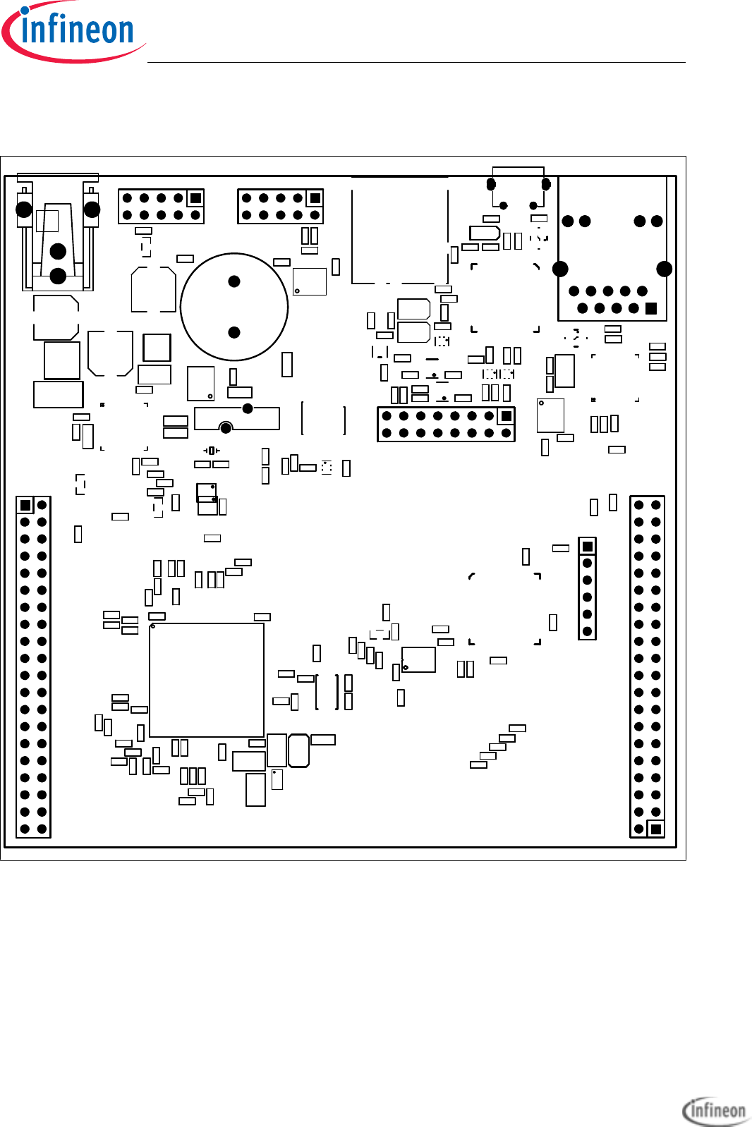
Application Kit TC2X7
Hardware Manual
Schematic and Layout
User’s Manual 6-6 V 1.0, 2015-04
6.2 Layout
Figure 6-5 Component Plot Top Layer
U101
R135
R133
CB105
U308
U103
R165
R164
R163
R162
R161
R160
R159
R158
R157
R156
R155
R154
R153
R152
R151
R150
R146
R145
R144
R143
R140
R126
Q202
CB318
CB109
CB104
C119
R138
R142
R141
R132
X302
R131
X202
R209
R230
Y102
Y101
F
X205
X103
X102
X101
U102
R218
R125
R124
R123
R122
R120
R117
R116
R114
R113
R112
R111
R109 R108
R107 R106
R103
R102
R101
Q201
Q106
+
LS101
L102
L101
CB201
CB114
CB112
CB106
CB107
CB108
CB111
CB110
CB103
CB102
CB101
C116
C114
C108
C110
C109
C107
C106
C104 C103
C102
C101
CB202
U202
X301
X201 R228
R249
R229
CB204
R207
R206
C201
R202
U206
R203
CB205
R246
R201
CB206
R247
R245
R244
R248
CB302
R302
R303
R310
R315
R316
R317
R318
R319
R314
R320
R312
Q301
Q302
Q303
Y301
U301
R308
CB301
R301
D302
L301
BU301
R311
C302
CB305
R323
D301
CB314
CB315
CB316
CB317
R313
R327
R328
R336
U306
U307
C209
C203
D201
L201
R208
R210
R239
R241
R219
R220
R221
R222
R225
R226
R231
R232
R233
R234
R227
U203
U204
X203
F
X204
Y201
R211
R205
R204
CB203
U201
C117
U104
-
+
BT101
Q107
R134
R130
R115
R127
R128
CB113
Q104
L103
C120
C105 R166
U105
R147
R148
R337
Application Kit TC2x7 Hardware Manual downloaded by Myoungho Sunwoo (Hanyang University) at 11 Mar 2016 05:10
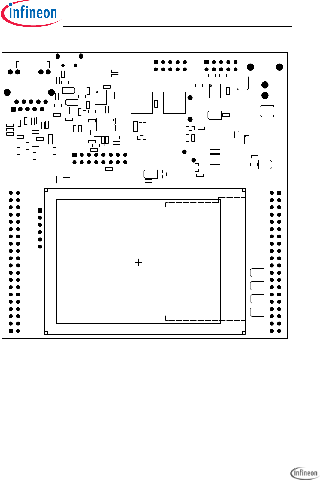
Application Kit TC2X7
Hardware Manual
Schematic and Layout
User’s Manual 6-7 V 1.0, 2015-04
Figure 6-6 Component Plot Bottom Layer
1
LCD201
R139
R129 D104
C111
R237
S102
S101
R121
R119
R118
R110
R105
R104
Q103
Q102
Q101
D110 D109 D108 D107
D106
D105
D101
C115
C113
C112
R235
C211
CB221
R238
CB304
CB306
R305
R306
U302
R307
CB303
CB307
CB308
CB309
R309
C306
U303
U304
R321
R322
C304
C305
CB310
CB311
CB312
R324
R325
C301
R304
C303
CB313
L302
U305
R326
R329
R330
R331
R334
R335
R332
C202
C206
C207
C208
C204
C205
C210
CB220
CB219
R240
R242
R243
R224
R223
R217
U205
CB208
CB209
CB210
CB211
CB212
CB213
CB214
CB215
CB216
CB217
CB218
D102
D103
R250
R333
Q105 C118
D111
R136
R137
Application Kit TC2x7 Hardware Manual downloaded by Myoungho Sunwoo (Hanyang University) at 11 Mar 2016 05:10
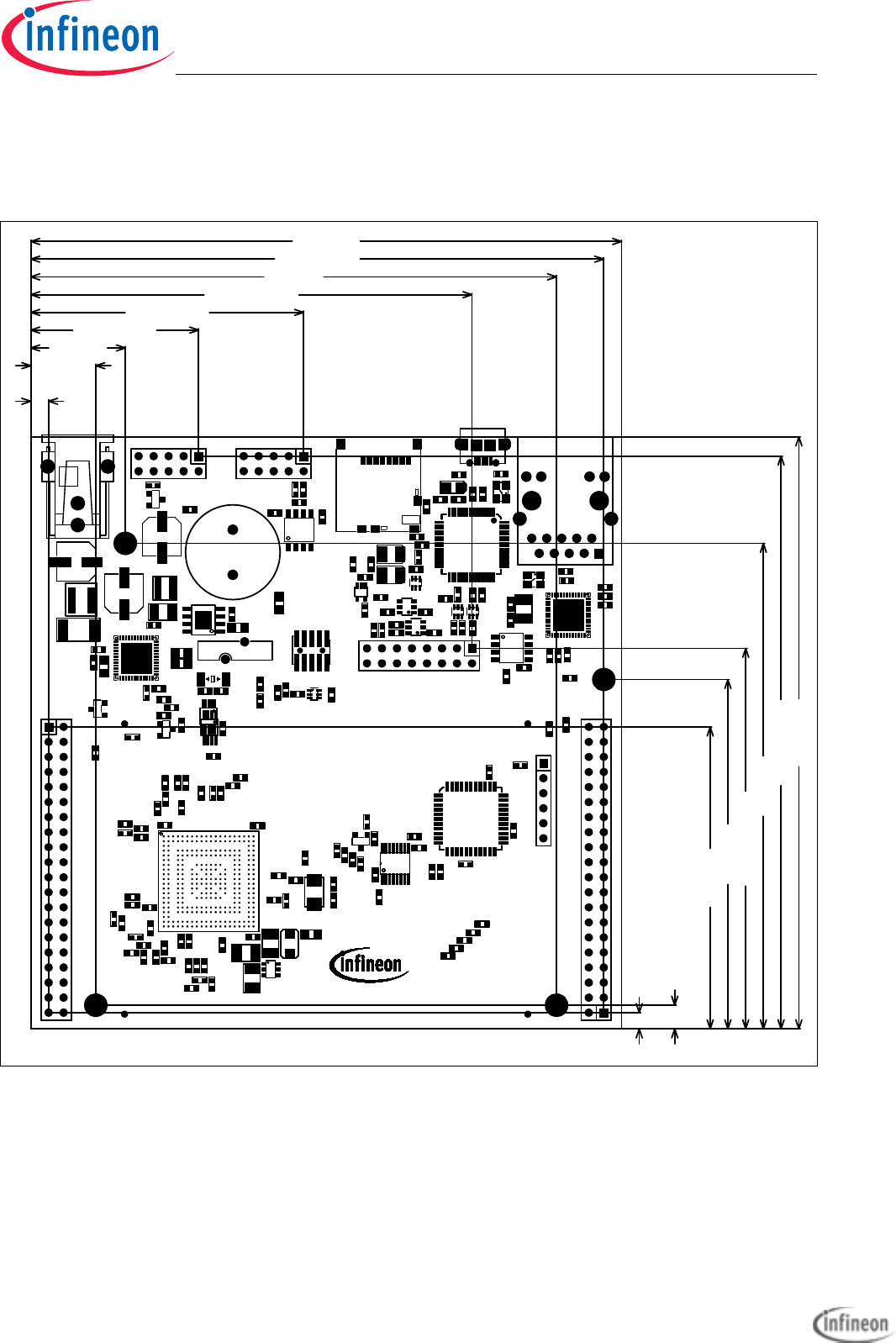
Application Kit TC2X7
Hardware Manual
Schematic and Layout
User’s Manual 6-8 V 1.0, 2015-04
6.3 Layout with Dimensioning
The following dimensions should be used for development of extension boards.
Figure 6-7 Dimensioning (mm)
DAP 1
1
1
APPLICATION KIT TC2X7 V1.X
CAN0
POWER
+5,5V...+40V
1
1
L1
RUN
1
ETH
LIN
ACT
JTAG
1
1
INFINEON
USB
SDCARD
TECHNOLOGIES AG
16 (mm)
11 (mm)
89 (mm)
59 (mm)
82 (mm)
4 (mm)
51 (mm)
96.99 (mm)
28.41 (mm)
46.19 (mm)
100 (mm)
3.01 (mm)
2.74 (mm)
96.72 (mm)
100 (mm)
64.262 (mm)
74.676 (mm)
U101
R135
R133
CB105
U308
U103
R165
R164
R163
R162
R161
R160
R159
R158
R157
R156
R155
R154
R153
R152
R151
R150
R146
R145
R144
R143
R140
R126
Q202
CB318
CB109
CB104
C119
R138
R142
R141
R132
X302
R131
X202
R209
R230
Y102
Y101
F
X205
X103
X102
X101
U102
R218
R125
R124
R123
R122
R120
R117
R116
R114
R113
R112
R111
R109 R108
R107 R106
R103
R102
R101
Q201
Q106
+
LS101
L102
L101
CB201
CB114
CB112
CB106
CB107
CB108
CB111
CB110
CB103
CB102
CB101
C116
C114
C108
C110
C109
C107
C106
C104 C103
C102
C101
CB202
U202
X301
X201 R228
R249
R229
CB204
R207
R206
C201
R202
U206
R203
CB205
R246
R201
CB206
R247
R245
R244
R248
CB302
R302
R303
R310
R315
R316
R317
R318
R319
R314
R320
R312
Q301
Q302
Q303
Y301
U301
R308
CB301
R301
D302
L301
BU301
R311
C302
CB305
R323
D301
CB314
CB315
CB316
CB317
R313
R327
R328
R336
U306
U307
C209
C203
D201
L201
R208
R210
R239
R241
R219
R220
R221
R222
R225
R226
R231
R232
R233
R234
R227
U203
U204
X203
F
X204
Y201
R211
R205
R204
CB203
U201
C117
U104
-
+
BT101
Q107
R134
R130
R115
R127
R128
CB113
Q104
L103
C120
C105 R166
U105
R147
R148
R337
Application Kit TC2x7 Hardware Manual downloaded by Myoungho Sunwoo (Hanyang University) at 11 Mar 2016 05:10
Application Kit TC2X7
Hardware Manual
Schematic and Layout
User’s Manual 6-9 V 1.0, 2015-04
Figure 6-8 Dimensioning (mil)
TECHNOLOGIES AG
SDCARD
USB
INFINEON
1
1
JTAG
ACT
LIN
ETH
1
RUN
L1
1
1
+5,5V...+40V
POWER
CAN0
APPLICATION KIT TC2X7 V1.X 1
1
1
DAP
2940 (mil)
2530 (mil)
3937.008 (mil)
3807.874 (mil)
107.874 (mil)
118.504 (mil)
3937.008 (mil)
1818.504 (mil)
1118.504 (mil)
3818.504 (mil)
2007.874 (mil)
157.48 (mil)
3228.347 (mil)
2322.835 (mil)
3503.937 (mil)
433.071 (mil)
629.921 (mil)
R337
R148
R147 U105
R166
C105
C120
L103
Q104
CB113
R128
R127
R115
R130
R134 Q107
+
-
BT101
U104
C117
U201
CB203
R204 R205
R211
Y201
F
X204
X203
U204
U203
R227
R234
R233
R232
R231
R226
R225
R222
R221
R220
R219
R241
R239
R210
R208
L201
D201
C203
C209
U307
U306
R336
R328
R327
R313
CB317 CB316
CB315 CB314
D301
R323
CB305
C302
R311
BU301
L301
D302
R301
CB301
R308
U301
Y301
Q303
Q302
Q301
R312
R320
R314
R319
R318
R317 R316
R315
R310
R303
R302
CB302
R248
R244
R245 R247
CB206
R201
R246
CB205
R203
U206
R202
C201
R206
R207
CB204
R229
R249
R228
X201
X301
U202
CB202
C101 C102
C103
C104
C106
C107
C109
C110
C108
C114
C116
CB101
CB102
CB103
CB110
CB111
CB108
CB107
CB106
CB112
CB114
CB201
L101
L102
+
LS101
Q106
Q201
R101
R102
R103
R106
R107
R108
R109
R111
R112
R113
R114
R116
R117
R120
R122
R123
R124
R125
R218
U102
X101
X102
X103
F
X205
Y101
Y102
R230
R209
X202
R131
X302
R132
R141
R142
R138
C119
CB104
CB109
CB318
Q202
R126
R140
R143
R144
R145
R146
R150
R151
R152
R153
R154
R155
R156
R157
R158
R159
R160
R161
R162
R163
R164
R165
U103
U308
CB105
R133
R135
U101
Application Kit TC2x7 Hardware Manual downloaded by Myoungho Sunwoo (Hanyang University) at 11 Mar 2016 05:10

User’s Manual L-1 V 1.0, 2015-04
Application Kit TC2X7
Hardware Manual
A
ACTIV LED 3-5
B
Beeper 3-5
C
CAN connector pinout 5-3
Clock 3-5
Clock Signals 4-2
Connector Pin Assignment 5-1
Core current measurement 3-6
crystal 3-5
D
DAP connector pinout 5-5
Debug Signals 4-2
Debug System 3-7
Dimensioning 6-8
E
Ethernet 3-6
Ethernet Connector 5-5
F
Flexray Pinout 5-3
H
HSCT socket pinout 5-4
I
Interrupt Signals 4-1
L
Layout 6-6
LEDs 3-4
LIN 3-6
LIN connector pinout 5-4
M
manual power on reset 3-1
Micro SD card 3-4
miniWiggler JDS 3-5
Multi Voltage Safety Micro Processor Sup-
ply 3-1
MultiCAN 3-6
O
OCDS connector pinout 5-4
OCDS1 3-7
Other peripherals 3-6
P
Peripheral Signals 4-2
Power connector pinout 5-2
power on reset 3-1
Power Signals 4-1
power supply 3-1
Power via Micro USB 3-1
Power via supply connector 3-1
R
Read a display register 3-3
Real Time Clock 3-2
Reset Signals 4-1
RUN LED 3-5
S
Schematic 6-1
Schematic and Layout 6-1
Serial Connection to PC 3-5
Signal Description 4-1
status LED 3-6
Supply 3-1
T
Toggle LED’s 3-6
Touch controller 3-4
Keyword Index
Application Kit TC2x7 Hardware Manual downloaded by Myoungho Sunwoo (Hanyang University) at 11 Mar 2016 05:10


