ASTRO Series/Astro Digital Spectra & Plus W3 W4 W5 W7 W9 Control Heads Service Manual 6881096C77 O
User Manual: -ASTRO Series/Astro Digital Spectra & Digital Spectra Plus W3 W4 W5 W7 W9 control heads service manual 6881096C77-O
Open the PDF directly: View PDF ![]() .
.
Page Count: 126 [warning: Documents this large are best viewed by clicking the View PDF Link!]
- Front Cover
- Forward
- Table of Contents
- Foreword ii
- Commercial Warranty xi
- Chapter 1 Introduction 1-1
- Chapter 2 Basic Maintenance 2-1
- Chapter 3 Theory of Operation 3-1
- Chapter 4 Test Equipment and Service Aids 4-1
- Chapter 5 Troubleshooting 5-1
- Chapter 6 Radio Connectors 6-1
- Chapter 7 Exploded Views and Parts Lists 7-1
- Chapter 8 Schematics, Overlays, and Parts Lists 8-1
- Appendix A Replacement Parts Ordering A-1
- Index Index-1
- Chapter 1 Introduction
- Chapter 2 Basic Maintenance
- Chapter 3 Theory of Operation
- 3.1 W3 Control Head
- 3.2 W4, W5, and W7 Control Heads
- 3.2.1 Power Switch/Ignition
- 3.2.2 Voltage Regulator
- 3.2.3 Microcomputer
- 3.2.4 Interface Circuitry
- 3.2.5 Reset
- 3.2.6 Bus Busy
- 3.2.7 Serial Bus Data
- 3.2.8 Push-To-Talk (PTT)
- 3.2.9 Hang-Up Button (HUB)
- 3.2.10 Ignition Sense Circuitry
- 3.2.11 Keypad Scan
- 3.2.12 Vacuum Fluorescent (VF) Voltage Converter Circuitry
- 3.2.13 Vacuum Fluorescent Display Driver IC
- 3.2.14 Vacuum Fluorescent Display
- 3.2.15 Backlight LEDs
- 3.3 W9 Control Head
- 3.4 Vehicle Interface Port (VIP)
- Chapter 4 Test Equipment and Service Aids
- Chapter 5 Troubleshooting
- 5.1 Required Tools and Supplies
- 5.2 Troubleshooting Waveforms
- 5.3 Replacing the Vacuum Fluorescent Display (W4, W5, and W7 Control Heads)
- 5.4 Replacing the Remote Back-Housing Interface Board
- 5.5 Replacing the Remote Interconnect Board
- 5.6 Replacing the Control-Head Board
- 5.7 Final Reassembly–W3 Control Head
- 5.8 Troubleshooting Charts
- Chapter 6 Radio Connectors
- Chapter 7 Exploded Views and Parts Lists
- Chapter 8 Schematics, Overlays, and Parts Lists
- Appendix A Replacement Parts Ordering
- Index
- Back Cover
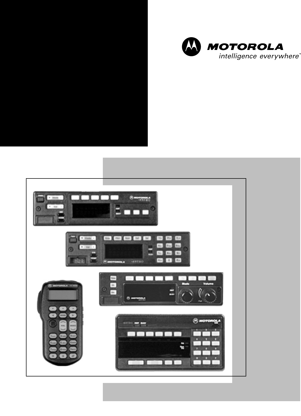
ASTRO® Digital Spectra®
and Digital Spectra Plus
Mobile Radios
W3 / W4 / W5 / W7/ W9
Control Head Models
Service Manual

i
Title Page ASTRO® Digital Spectra®
and Digital Spectra Plus
Mobile Radios
W3/W4/W5/W7/W9
Control Head Models
Service Manual
Motorola, Inc.
8000 West Sunrise Boulevard
Fort Lauderdale, Florida 33322 6881096C77-O

ii
Foreword
This manual covers the ASTRO® Digital Spectra® and Digital Spectra Plus control heads (Models W3, W4, W5, W7, and
W9), unless otherwise specified. This manual provides sufficient information to enable qualified service shop technicians to
troubleshoot and repair ASTRO® Digital Spectra® and Digital Spectra Plus control heads to the component level.
For details on radio operation, refer to the applicable manuals available separately. A list of related publications is provided
in the section, “Related Publications,” on page ix.
Product Safety and RF Exposure Compliance
ATTENTION!
The radio that comes with this control head is restricted to occupational use only to satisfy FCC RF
energy exposure requirements. Before using this product, read the RF energy awareness information
and operating instructions in the Product Safety and RF Exposure booklet enclosed with your radio
(Motorola Publication part number 68P81095C99) to ensure compliance with RF energy exposure
limits.
For a list of Motorola-approved antennas, batteries, and other accessories, visit the following web site
which lists approved accessories: http://www.motorola.com/cgiss/index.shtml
Manual Revisions
Changes which occur after this manual is printed are described in FMRs (Florida Manual Revisions). These FMRs provide
complete replacement pages for all added, changed, and deleted items. To obtain FMRs, contact the Radio Parts Services
Division (refer to “Appendix A, Replacement Parts Ordering”).
Computer Software Copyrights
The Motorola products described in this manual may include copyrighted Motorola computer programs stored in
semiconductor memories or other media. Laws in the United States and other countries preserve for Motorola certain
exclusive rights for copyrighted computer programs, including, but not limited to, the exclusive right to copy or reproduce in
any form the copyrighted computer program. Accordingly, any copyrighted Motorola computer programs contained in the
Motorola products described in this manual may not be copied, reproduced, modified, reverse-engineered, or distributed in
any manner without the express written permission of Motorola. Furthermore, the purchase of Motorola products shall not
be deemed to grant either directly or by implication, estoppel, or otherwise, any license under the copyrights, patents or
patent applications of Motorola, except for the normal non-exclusive license to use that arises by operation of law in the
sale of a product.
Document Copyrights
No duplication or distribution of this document or any portion thereof shall take place without the express written permission
of Motorola. No part of this manual may be reproduced, distributed, or transmitted in any form or by any means, electronic
or mechanical, for any purpose without the express written permission of Motorola.
Disclaimer
The information in this document is carefully examined, and is believed to be entirely reliable. However, no responsibility is
assumed for inaccuracies. Furthermore, Motorola reserves the right to make changes to any products herein to improve
readability, function, or design. Motorola does not assume any liability arising out of the applications or use of any product
or circuit described herein; nor does it cover any license under its patent rights nor the rights of others.
Trademarks
MOTOROLA, the Stylized M logo, ASTRO, and Spectra are registered in the US Patent & Trademark Office. All other
product or service names are the property of their respective owners.
© Motorola, Inc. 2003.
CAUTION: Before using this product, read the operating instruc-
tions for safe usage contained in the Product Safety and RF Expo-
sure booklet enclosed with your radio.
!
C a u t i o n

Table of Contents iii
6881096C77-O September 26, 2003
Table of Contents
Foreword.........................................................................................................ii
Product Safety and RF Exposure Compliance............................................................................................ii
Manual Revisions ........................................................................................................................................ii
Computer Software Copyrights ...................................................................................................................ii
Document Copyrights..................................................................................................................................ii
Disclaimer....................................................................................................................................................ii
Trademarks .................................................................................................................................................ii
Commercial Warranty ...................................................................................xi
Limited Warranty ........................................................................................................................................xi
MOTOROLA COMMUNICATION PRODUCTS................................................................................xi
I. What This Warranty Covers And For How Long .....................................................................xi
II. General Provisions.................................................................................................................xi
III. State Law Rights ..................................................................................................................xii
IV. How To Get Warranty Service .............................................................................................xii
V. What This Warranty Does Not Cover....................................................................................xii
VI. Patent And Software Provisions ......................................................................................... xiii
VII. Governing Law................................................................................................................... xiii
Chapter 1 Introduction ......................................................................... 1-1
1.1 Notations Used in This Manual...................................................................................................... 1-1
1.2 Control Head Features .................................................................................................................. 1-2
1.3 Control Heads................................................................................................................................ 1-2
1.3.1 W3 Control Head .............................................................................................................. 1-2
1.3.1.1 W3 Controls............................................................................................................. 1-3
1.3.2 W4, W5, W7, and W9 Control Heads ............................................................................... 1-4
1.3.2.1 W4, W5, W7, and W9 Controls................................................................................ 1-6
Chapter 2 Basic Maintenance.............................................................. 2-1
2.1 Inspection ...................................................................................................................................... 2-1
2.2 Cleaning......................................................................................................................................... 2-1
2.2.1 Cleaning External Plastic Surfaces................................................................................... 2-1
2.2.2 Cleaning Internal Circuit Boards and Components........................................................... 2-1
2.3 Handling Precautions..................................................................................................................... 2-2
Chapter 3 Theory of Operation............................................................ 3-1
3.1 W3 Control Head ........................................................................................................................... 3-1
3.1.1 SB9600 Serial Bus Interface............................................................................................. 3-1
3.1.2 Display Circuit................................................................................................................... 3-1
3.1.3 Keypad Side Keys and Top Keys ..................................................................................... 3-2
3.1.4 Microphone Preamplifier and PTT .................................................................................... 3-2

iv Table of Contents
September 26, 2003 6881096C77-O
3.1.5 On-/Off-Hook Control ........................................................................................................3-3
3.1.6 Backlight Circuit ................................................................................................................3-3
3.1.7 Power Supply....................................................................................................................3-3
3.1.8 Status LEDs......................................................................................................................3-3
3.1.9 Jumper Selection ..............................................................................................................3-3
3.1.10 Power On/Off ....................................................................................................................3-4
3.1.11 Miscellaneous Functions...................................................................................................3-4
3.2 W4, W5, and W7 Control Heads....................................................................................................3-4
3.2.1 Power Switch/Ignition........................................................................................................3-4
3.2.2 Voltage Regulator .............................................................................................................3-5
3.2.3 Microcomputer ..................................................................................................................3-5
3.2.4 Interface Circuitry..............................................................................................................3-5
3.2.5 Reset................................................................................................................................. 3-6
3.2.6 Bus Busy...........................................................................................................................3-6
3.2.7 Serial Bus Data.................................................................................................................3-6
3.2.8 Push-To-Talk (PTT) ..........................................................................................................3-7
3.2.9 Hang-Up Button (HUB) .....................................................................................................3-7
3.2.10 Ignition Sense Circuitry.....................................................................................................3-7
3.2.11 Keypad Scan.....................................................................................................................3-7
3.2.12 Vacuum Fluorescent (VF) Voltage Converter Circuitry.....................................................3-7
3.2.13 Vacuum Fluorescent Display Driver IC.............................................................................3-8
3.2.14 Vacuum Fluorescent Display ............................................................................................3-8
3.2.15 Backlight LEDs..................................................................................................................3-8
3.3 W9 Control Head ...........................................................................................................................3-8
3.3.1 Display ..............................................................................................................................3-8
3.3.2 W9 Controls and Indicators...............................................................................................3-9
3.3.3 Control Board....................................................................................................................3-9
3.3.3.1 Microprocessor ........................................................................................................3-9
3.3.3.2 Watchdog Timer.......................................................................................................3-9
3.3.3.3 Bus Transceiver.....................................................................................................3-10
3.3.3.4 Vacuum Fluorescent Voltage Converter................................................................3-10
3.3.3.5 Vehicle Interface Ports...........................................................................................3-10
3.3.3.6 Power Supply.........................................................................................................3-10
3.3.3.7 Ignition Sense Circuits ...........................................................................................3-10
3.3.3.8 EEPROM Write-Protect Circuit ..............................................................................3-11
3.3.4 Display Board..................................................................................................................3-11
3.3.4.1 VF Display..............................................................................................................3-11
3.3.4.2 VF Display Driver ...................................................................................................3-11
3.3.4.3 Status LEDs...........................................................................................................3-11
3.3.4.4 Backlight LEDs.......................................................................................................3-11
3.3.5 Default Jumper Settings..................................................................................................3-11
3.4 Vehicle Interface Port (VIP) .........................................................................................................3-12
3.4.1 W4, W5, and W7 Control Heads..................................................................................... 3-12
3.4.1.1 VIP Output Connections ........................................................................................3-12
3.4.1.1.1 Dash-Mount Installations ................................................................................3-12
3.4.1.1.2 Remote-Mount Installations ............................................................................ 3-13
3.4.1.2 VIP Input Connections (Remote-Mount Only)........................................................ 3-13
3.4.2 W9 Control Heads...........................................................................................................3-14
3.4.2.1 VIP Output Connections ........................................................................................3-14
3.4.2.2 VIP Input Connections ...........................................................................................3-14
Chapter 4 Test Equipment and Service Aids ..................................... 4-1

Table of Contents v
6881096C77-O September 26, 2003
4.1 Recommended Test Equipment and Service Aids ........................................................................ 4-1
Chapter 5 Troubleshooting................................................................. 5-1
5.1 Required Tools and Supplies......................................................................................................... 5-1
5.2 Troubleshooting Waveforms.......................................................................................................... 5-2
5.2.1 ASTRO Digital Spectra Waveforms.................................................................................. 5-2
5.3 Replacing the Vacuum Fluorescent Display (W4, W5, and W7 Control Heads) ........................... 5-5
5.3.1 Removing the Display.......................................................................................................5-5
5.3.2 Installing the Display......................................................................................................... 5-5
5.4 Replacing the Remote Back-Housing Interface Board .................................................................. 5-5
5.4.1 W4, W5, and W7 Control Heads....................................................................................... 5-5
5.5 Replacing the Remote Interconnect Board.................................................................................... 5-6
5.5.1 Low-/Mid-Power Radios.................................................................................................... 5-6
5.5.2 High-Power Radios........................................................................................................... 5-6
5.6 Replacing the Control-Head Board................................................................................................ 5-7
5.6.1 W3 Control Heads ............................................................................................................ 5-7
5.6.2 W4, W5, and W7 Control Heads....................................................................................... 5-8
5.6.3 W9 Control Heads .......................................................................................................... 5-10
5.7 Final Reassembly–W3 Control Head........................................................................................... 5-11
5.8 Troubleshooting Charts ............................................................................................................... 5-12
Chapter 6 Radio Connectors ............................................................... 6-1
6.1 Radio Connectors.......................................................................................................................... 6-2
6.2 Radio Connector Locations ........................................................................................................... 6-3
6.3 Extender Cable (P501) .................................................................................................................. 6-4
6.4 Control-Head Cabling Diagram...................................................................................................... 6-4
Chapter 7 Exploded Views and Parts Lists........................................ 7-1
7.1 Model W3 Hand-Held Control Head Exploded View ..................................................................... 7-2
7.2 W4 Rotary Control Head Exploded View...................................................................................... 7-3
7.3 W5 and W7 Pushbutton Control Head Exploded View................................................................. 7-4
7.4 W9 Pushbutton Control Head Exploded View .............................................................................. 7-5
7.5 HMN1080A, HMN1061A, HMN1079A Microphone Exploded View .............................................. 7-6
7.6 Small Pushbutton Parts ................................................................................................................. 7-7
7.7 Large Pushbutton Parts................................................................................................................. 7-7
Chapter 8 Schematics, Overlays, and Parts Lists............................. 8-1
8.1 List of Schematics, Component Location Diagrams, and Parts Lists ............................................ 8-1
Appendix A Replacement Parts Ordering..............................................A-1
A.1 Basic Ordering Information............................................................................................................A-1
A.2 Motorola Online .............................................................................................................................A-1
A.3 Mail Orders ....................................................................................................................................A-1
A.4 Telephone Orders..........................................................................................................................A-2

vi Table of Contents
September 26, 2003 6881096C77-O
A.5 Fax Orders.....................................................................................................................................A-2
A.6 Parts Identification .........................................................................................................................A-2
A.7 Product Customer Service.............................................................................................................A-2
Index.....................................................................................................Index-1

List of Figures vii
6881096C77-O September 26, 2003
List of Figures
Figure 1-1. Typical W3 Hand-Held Control Head....................................................................................1-3
Figure 1-2. Typical W4 Rotary Control Head........................................................................................... 1-4
Figure 1-3. Typical W5 Pushbutton Control Head...................................................................................1-4
Figure 1-4. Typical W7 Pushbutton Control Head...................................................................................1-5
Figure 1-5. Typical W9 Pushbutton Control Head...................................................................................1-5
Figure 3-1. Astro Spectra Control Head Block Diagram.......................................................................... 3-4
Figure 3-2. Cabling Interconnect Diagram for Dash Mount................................................................... 3-13
Figure 3-3. Cabling Interconnect Diagram for Remote Mount............................................................... 3-13
Figure 5-1. Replacing the Vacuum Fluorescent Display ......................................................................... 5-5
Figure 5-2. Model W4 Rotary Control Head Assembly Screw and Snap Sequence............................... 5-8
Figure 5-3. Models W5 and W7 Pushbutton Control Head Assembly Screw Sequence ........................ 5-8
Figure 5-4. W9 Control Head Control Board and Display Board........................................................... 5-10
Figure 6-1. J0103 Remote-Mount Control Head Connector.................................................................... 6-2
Figure 6-2. J5 Control Cable for Remote-Mount Control Head............................................................... 6-2
Figure 6-3. J6 Radio Operations Connector............................................................................................ 6-2
Figure 6-4. J2 Rear Accessory Connector .............................................................................................. 6-2
Figure 6-5. P104 Microphone Jack ......................................................................................................... 6-2
Figure 6-6. Dash-Mount Radio Connector Locations.............................................................................. 6-3
Figure 6-7. Remote-Mount Radio Connector Locations.......................................................................... 6-3
Figure 6-8. Command Board Connector Locations................................................................................. 6-3
Figure 6-9. VOCON Board Connector Locations .................................................................................... 6-3
Figure 6-10. P501 Extender Cable............................................................................................................ 6-4
Figure 6-11. Control-Head Cabling Diagram............................................................................................. 6-4
Figure 7-1. W3 Hand-Held Control Head Exploded View ....................................................................... 7-2
Figure 7-2. W4 Rotary Control Head Exploded View .............................................................................. 7-3
Figure 7-3. W5 and W7 Pushbutton Control Head Exploded View......................................................... 7-4
Figure 7-4. W9 Pushbutton Control Head Exploded View ...................................................................... 7-5
Figure 7-5. HMN1080A, HMN1061A, HMN1079A Microphone Exploded View...................................... 7-6

viii Related Publications
September 26, 2003 6881096C77-O
List of Tables
Table 1-1. ASTRO Digital Spectra/Spectra Plus Basic Features ...........................................................1-2
Table 1-2. 12-Button Keypad (W7 and W9) ...........................................................................................1-7
Table 3-1. W3 Jumper Selection............................................................................................................ 3-3
Table 3-2. Types of Operations..............................................................................................................3-4
Table 3-3. Serial Data Bus Logic............................................................................................................3-6
Table 3-4. PTT Logic States...................................................................................................................3-7
Table 3-5. HUB Logic States..................................................................................................................3-7
Table 3-6. Standard Jumper Configurations......................................................................................... 3-11
Table 3-7. VIP Output Connections .....................................................................................................3-14
Table 3-8. VIP Input Connections ........................................................................................................3-14
Table 4-1. Recommended Motorola Test Equipment and Service Aids.................................................4-1
Table 5-1. Required Tools and Supplies ................................................................................................5-1
Table 7-1. Exploded Views.....................................................................................................................7-1
Table 7-2. W3 Hand-Held Control Head Exploded View Parts List........................................................7-2
Table 7-3. Model W4 Rotary Control Head Parts List ............................................................................7-3
Table 7-4. W5 and W7 Pushbutton Control Head Parts List..................................................................7-4
Table 7-5. W9 Pushbutton Control Head Parts List ..............................................................................7-5
Table 7-6. HMN1080A, HMN1061A, HMN1079A Microphone Parts List...............................................7-6
Table 7-7. Small Pushbutton Parts List..................................................................................................7-7
Table 7-8. Large Pushbutton Parts List..................................................................................................7-7

List of Tables ix
6881096C77-O September 26, 2003
Related Publications
ASTRO Digital Spectra and Digital Spectra Plus Model W3 User’s Guide..................................6881090C61
ASTRO Digital Spectra and Digital Spectra Plus Models W4, W5, W7, and W9 User’s Guide ..6881090C62
ASTRO Digital Spectra Hand-Held Control Head User’s Guide (Model W3) ..............................6881073C25
ASTRO Digital Spectra (Model W4, W5, W7, and W9) User’s Guide..........................................6881074C80
ASTRO Digital Spectra and Digital Spectra Plus Mobile Radios Detailed Service Manual .........6881076C25
ASTRO Digital Spectra Mobile Radios Dual Control Head Radio System Service Manual.........6881091C78
ASTRO Spectra and Digital Spectra FM Two-Way Mobile Radios Installation Manual ...............6881070C85
ASTRO Spectra Motorcycle Radios Supplemental Installation Manual...................................... 6880103W01
CPS Programming Installation Guide..........................................................................................6881095C44
KVL 3000 User’s Manual............................................................................................................. 6881131E16

xList of Tables
September 26, 2003 6881096C77-O
Notes
6881096C77-O September 26, 2003
Commercial Warranty xi
Commercial Warranty
Limited Warranty
MOTOROLA COMMUNICATION PRODUCTS
I. What This Warranty Covers And For How Long
MOTOROLA INC. (“MOTOROLA”) warrants the MOTOROLA manufactured Communication
Products listed below (“Product”) against defects in material and workmanship under normal use and
service for a period of time from the date of purchase as scheduled below:
Motorola, at its option, will at no charge either repair the Product (with new or reconditioned parts),
replace it (with a new or reconditioned Product), or refund the purchase price of the Product during
the warranty period provided it is returned in accordance with the terms of this warranty. Replaced
parts or boards are warranted for the balance of the original applicable warranty period. All replaced
parts of Product shall become the property of MOTOROLA.
This express limited warranty is extended by MOTOROLA to the original end user purchaser only
and is not assignable or transferable to any other party. This is the complete warranty for the Product
manufactured by MOTOROLA. MOTOROLA assumes no obligations or liability for additions or
modifications to this warranty unless made in writing and signed by an officer of MOTOROLA.
Unless made in a separate agreement between MOTOROLA and the original end user purchaser,
MOTOROLA does not warrant the installation, maintenance or service of the Product.
MOTOROLA cannot be responsible in any way for any ancillary equipment not furnished by
MOTOROLA which is attached to or used in connection with the Product, or for operation of the
Product with any ancillary equipment, and all such equipment is expressly excluded from this
warranty. Because each system which may use the Product is unique, MOTOROLA disclaims
liability for range, coverage, or operation of the system as a whole under this warranty.
II. General Provisions
This warranty sets forth the full extent of MOTOROLA'S responsibilities regarding the Product.
Repair, replacement or refund of the purchase price, at MOTOROLA's option, is the exclusive
remedy. THIS WARRANTY IS GIVEN IN LIEU OF ALL OTHER EXPRESS WARRANTIES. IMPLIED
WARRANTIES, INCLUDING WITHOUT LIMITATION, IMPLIED WARRANTIES OF
MERCHANTABILITY AND FITNESS FOR A PARTICULAR PURPOSE, ARE LIMITED TO THE
DURATION OF THIS LIMITED WARRANTY. IN NO EVENT SHALL MOTOROLA BE LIABLE FOR
DAMAGES IN EXCESS OF THE PURCHASE PRICE OF THE PRODUCT, FOR ANY LOSS OF
USE, LOSS OF TIME, INCONVENIENCE, COMMERCIAL LOSS, LOST PROFITS OR SAVINGS
OR OTHER INCIDENTAL, SPECIAL OR CONSEQUENTIAL DAMAGES ARISING OUT OF THE
USE OR INABILITY TO USE SUCH PRODUCT, TO THE FULL EXTENT SUCH MAY BE
DISCLAIMED BY LAW.
ASTRO Digital Spectra and Digital Spectra
Plus Units One (1) Year
Product Accessories One (1) Year

September 26, 2003 6881096C77-O
xii Commercial Warranty
III. State Law Rights
SOME STATES DO NOT ALLOW THE EXCLUSION OR LIMITATION OF INCIDENTAL OR
CONSEQUENTIAL DAMAGES OR LIMITATION ON HOW LONG AN IMPLIED WARRANTY
LASTS, SO THE ABOVE LIMITATION OR EXCLUSIONS MAY NOT APPLY.
This warranty gives specific legal rights, and there may be other rights which may vary from state to
state.
IV. How To Get Warranty Service
You must provide proof of purchase (bearing the date of purchase and Product item serial number)
in order to receive warranty service and, also, deliver or send the Product item, transportation and
insurance prepaid, to an authorized warranty service location. Warranty service will be provided by
Motorola through one of its authorized warranty service locations. If you first contact the company
which sold you the Product, it can facilitate your obtaining warranty service. You can also call
Motorola at 1-888-567-7347 US/Canada.
V. What This Warranty Does Not Cover
A. Defects or damage resulting from use of the Product in other than its normal and customary
manner.
B. Defects or damage from misuse, accident, water, or neglect.
C. Defects or damage from improper testing, operation, maintenance, installation, alteration,
modification, or adjustment.
D. Breakage or damage to antennas unless caused directly by defects in material workmanship.
E. A Product subjected to unauthorized Product modifications, disassemblies or repairs (includ-
ing, without limitation, the addition to the Product of non-Motorola supplied equipment) which
adversely affect performance of the Product or interfere with Motorola’s normal warranty
inspection and testing of the Product to verify any warranty claim.
F. Product which has had the serial number removed or made illegible.
G. Rechargeable batteries if:
- any of the seals on the battery enclosure of cells are broken or show evidence of tamper-
ing.
- the damage or defect is caused by charging or using the battery in equipment or service
other than the Product for which it is specified.
H. Freight costs to the repair depot.
I. A Product which, due to illegal or unauthorized alteration of the software/firmware in the Prod-
uct, does not function in accordance with MOTOROLA’s published specifications or the FCC
type acceptance labeling in effect for the Product at the time the Product was initially distrib-
uted from MOTOROLA.
J. Scratches or other cosmetic damage to Product surfaces that does not affect the operation of
the Product.
K. Normal and customary wear and tear.

6881096C77-O September 26, 2003
Commercial Warranty xiii
VI. Patent And Software Provisions
MOTOROLA will defend, at its own expense, any suit brought against the end user purchaser to the
extent that it is based on a claim that the Product or parts infringe a United States patent, and
MOTOROLA will pay those costs and damages finally awarded against the end user purchaser in
any such suit which are attributable to any such claim, but such defense and payments are
conditioned on the following:
A. that MOTOROLA will be notified promptly in writing by such purchaser of any notice of such
claim;
B. that MOTOROLA will have sole control of the defense of such suit and all negotiations for its
settlement or compromise; and
C. should the Product or parts become, or in MOTOROLA’s opinion be likely to become, the
subject of a claim of infringement of a United States patent, that such purchaser will permit
MOTOROLA, at its option and expense, either to procure for such purchaser the right to con-
tinue using the Product or parts or to replace or modify the same so that it becomes nonin-
fringing or to grant such purchaser a credit for the Product or parts as depreciated and accept
its return. The depreciation will be an equal amount per year over the lifetime of the Product
or parts as established by MOTOROLA.
MOTOROLA will have no liability with respect to any claim of patent infringement which is based
upon the combination of the Product or parts furnished hereunder with software, apparatus or
devices not furnished by MOTOROLA, nor will MOTOROLA have any liability for the use of ancillary
equipment or software not furnished by MOTOROLA which is attached to or used in connection with
the Product. The foregoing states the entire liability of MOTOROLA with respect to infringement of
patents by the Product or any parts thereof.
Laws in the United States and other countries preserve for MOTOROLA certain exclusive rights for
copyrighted MOTOROLA software such as the exclusive rights to reproduce in copies and distribute
copies of such Motorola software. MOTOROLA software may be used in only the Product in which
the software was originally embodied and such software in such Product may not be replaced,
copied, distributed, modified in any way, or used to produce any derivative thereof. No other use
including, without limitation, alteration, modification, reproduction, distribution, or reverse
engineering of such MOTOROLA software or exercise of rights in such MOTOROLA software is
permitted. No license is granted by implication, estoppel or otherwise under MOTOROLA patent
rights or copyrights.
VII. Governing Law
This Warranty is governed by the laws of the State of Illinois, USA.

September 26, 2003 6881096C77-O
Notes
xiv Commercial Warranty
Chapter 1 Introduction
ASTRO Digital Spectra and Digital Spectra Plus control heads are available in five radio models:
W3, W4, W5, W7, and W9. This chapter describes the control heads used with these radios.
1.1 Notations Used in This Manual
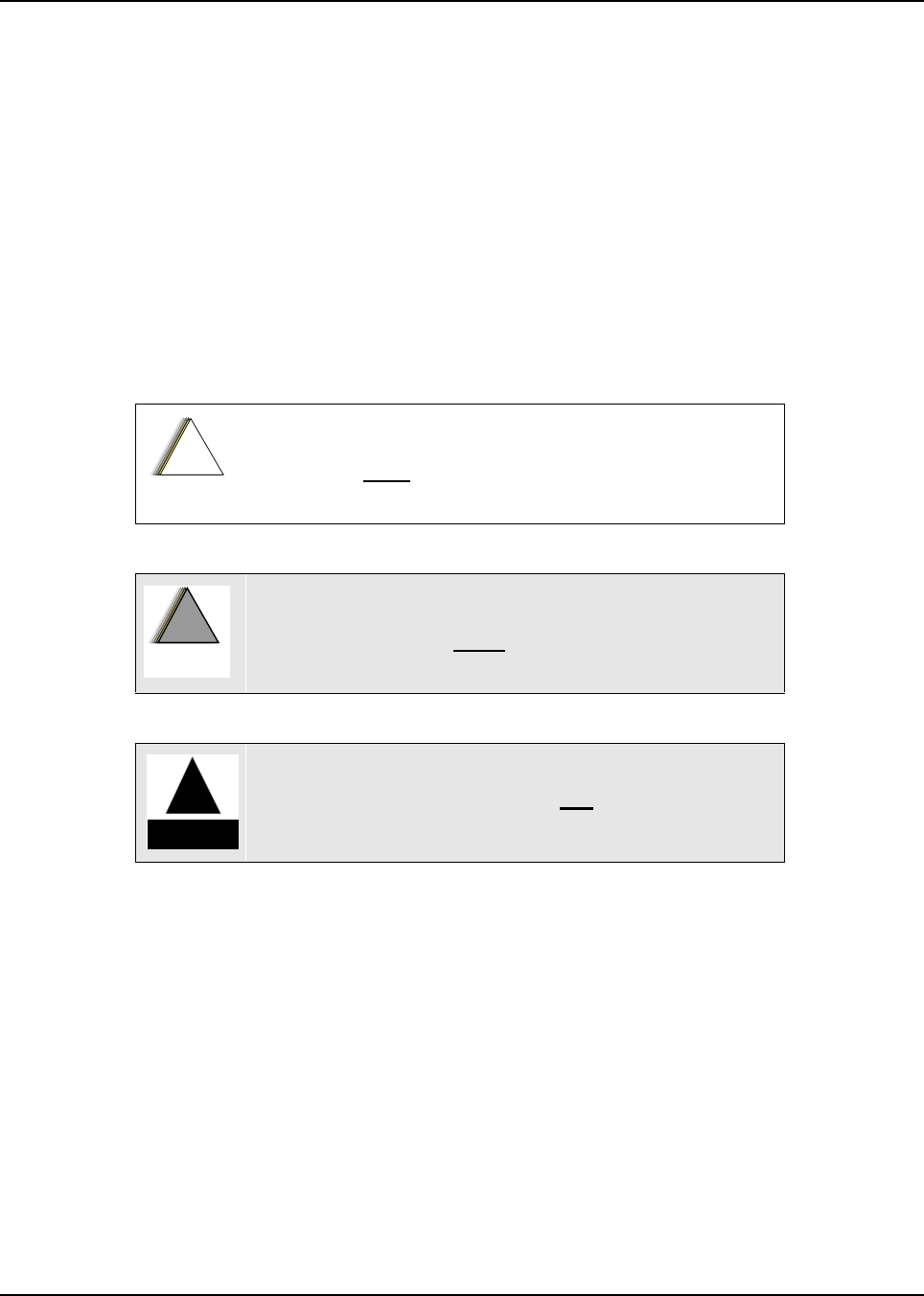
Throughout the text in this publication, you will notice the use of note, caution, warning, and danger
notations. These notations are used to emphasize that safety hazards exist, and care must be taken
and observed.
NOTE: An operational procedure, practice, or condition that is essential to emphasize.
CAUTION indicates a potentially hazardous situation which, if
not avoided, might result in equipment damage.
WARNING indicates a potentially hazardous situation
which, if not avoided, could result in death or injury.
DANGER indicates an imminently hazardous
situation which, if not avoided, will result in death or
injury.
!
C a u t i o n
!
W A R N I N G
!
D A N G E R
!

September 26, 2003 6881096C77-O
1-2 Introduction: Control Head Features
1.2 Control Head Features
The table below outlines the basic features of the five control heads covered in this manual.
1.3 Control Heads
The control heads used with ASTRO Digital Spectra and Digital Spectra Plus radios have
microprocessor circuitry that operates the standard and optional features built into the system. The
control-head design allows for installation in even the smallest of vehicles. The control head may be
field-programmed to add options or alter the information stored in certain areas of its electronic
memory.
The following sections describe the control head used by each of the five models.
1.3.1 W3 Control Head
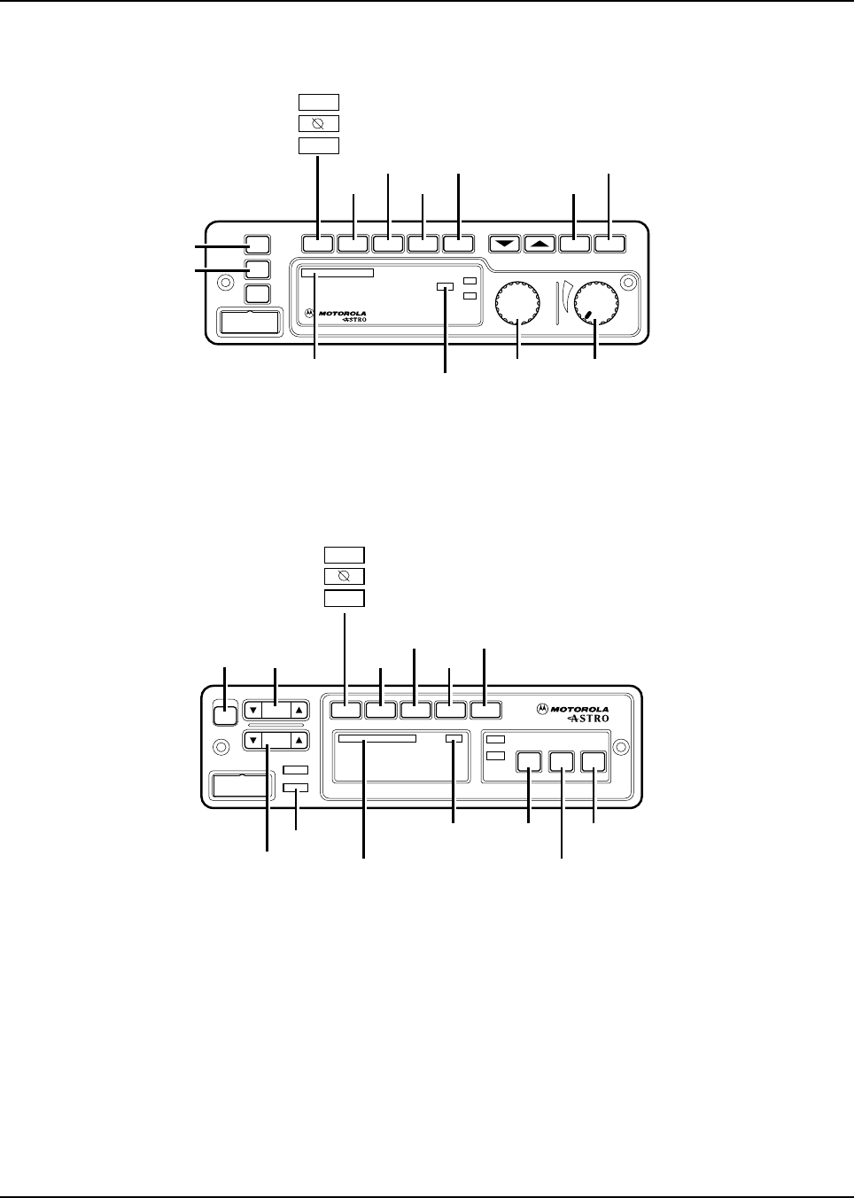
The W3 Hand-Held Control Head (HHCH) is shown below. THe HHCH has been designed as an
alternative to the standard radio control-head approach. It can emulate most radio control-head
functions, including LCD display, volume control, power On/Off, and mode. The HHCH can either
replace the radio control head or be used in dual-control applications, either in conjunction with a
radio control head or another HHCH.
Table 1-1. ASTRO Digital Spectra/Spectra Plus Basic Features
Feature W3 W4 W5 W7 W9
Display 2 line/
14 characters
Liquid-Crystal
Display (LCD)
with 8 Status
Annunciators
1 line/
8 characters
Vacuum
Fluorescent
Display
1 line/
8 characters
Vacuum
Fluorescent
Display
1 line/
8 characters
Vacuum
Fluorescent
Display
1 line/
11 characters
Vacuum
Fluorescent
Display
Mode &
Volume
Controls
Rocker Switches Rotary Mode &
Volume Controls Rocker Switch
Mode & Volume
Controls
Rocker Switch
Mode & Volume
Controls
Rocker Switch
Mode & Volume
Controls
Numeric
Keypad Yes No No Yes Yes
Channel
Capability
(Digital
Spectra)
255 128 128 255 255
Channel
Capability
(Digital
Spectra Plus)
512 128 128 512 512
Remote Mount Available Available Available Available Available
Dash Mount Available Available Available Available Not Available
6881096C77-O September 26, 2003
Introduction: Control Heads 1-3
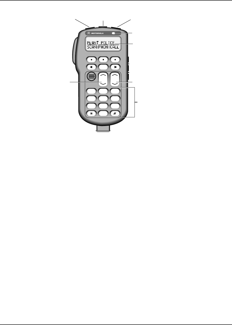
Figure 1-1. Typical W3 Hand-Held Control Head
1.3.1.1 W3 Controls
On/Off Button (T1): Turns the radio on and off. Can be used as an additional programmable button if the
on/off function is not used.
Orange Programmable Button (T2): Programmed at the factory for emergency use. Field
programmable by a qualified radio technician.
Programmable Button (T3): Field programmable by a qualified radio technician.
LED Indicator: Green/red light-emitting diode. Indicates operating status.
Display: 2-line by 14-character display. Provides visual information about many radio features.
Keypad. Provides control of, and data interface with, many features.
Programmable Side Button 1 (S1): Field programmable by a qualified radio technician.
Programmable Side Button 2 (S2): Field programmable by a qualified radio technician.
Programmable Side Button 3 (S3): Field programmable by a qualified radio technician.
Mode Control: Used for selecting modes and programming menus.
Volume Control: Used for selecting volume level, editing names, and making certain radio adjustments.
Push-To-Talk (PTT) Button: Engages the transmitter.
MODE
HOME
2ABC1QZ 3DEF
4GHI 5JKL 6MNO
7PRS 8TUV 9WXY
0
VOL
Side Button 1 (S1)
Side Button 2 (S2)
Side Button 3 (S3)
On/Off
Button
(T1)
Push-To-Talk
(PTT) Switch
LED
Indicator
Alphanumeric
Keypad
Volume
Control Mode Control
Orange Programmable
Button
(T2)
Programmable
Button
(T3)
Display
Button
September 26, 2003 6881096C77-O
1-4 Introduction: Control Heads
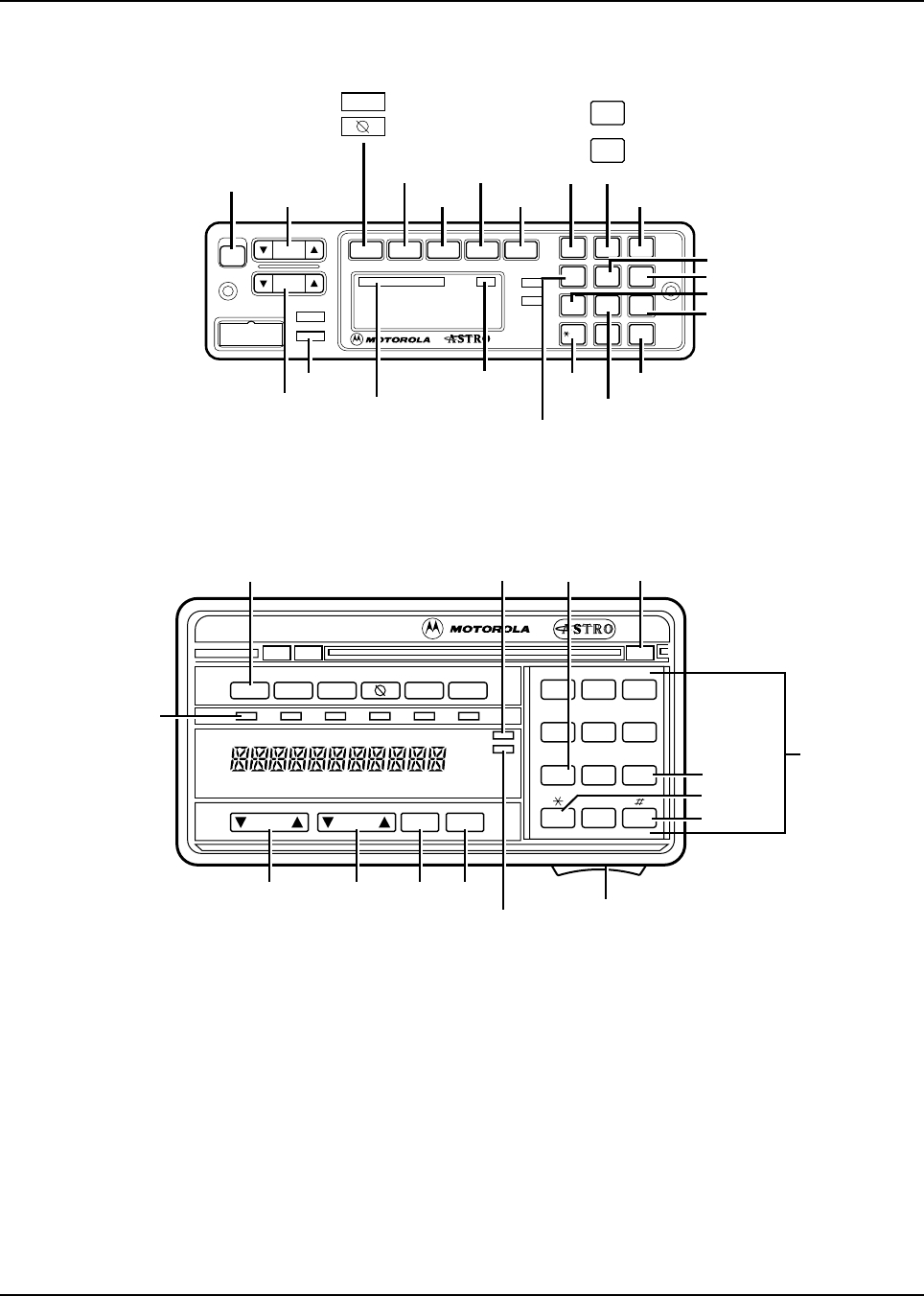
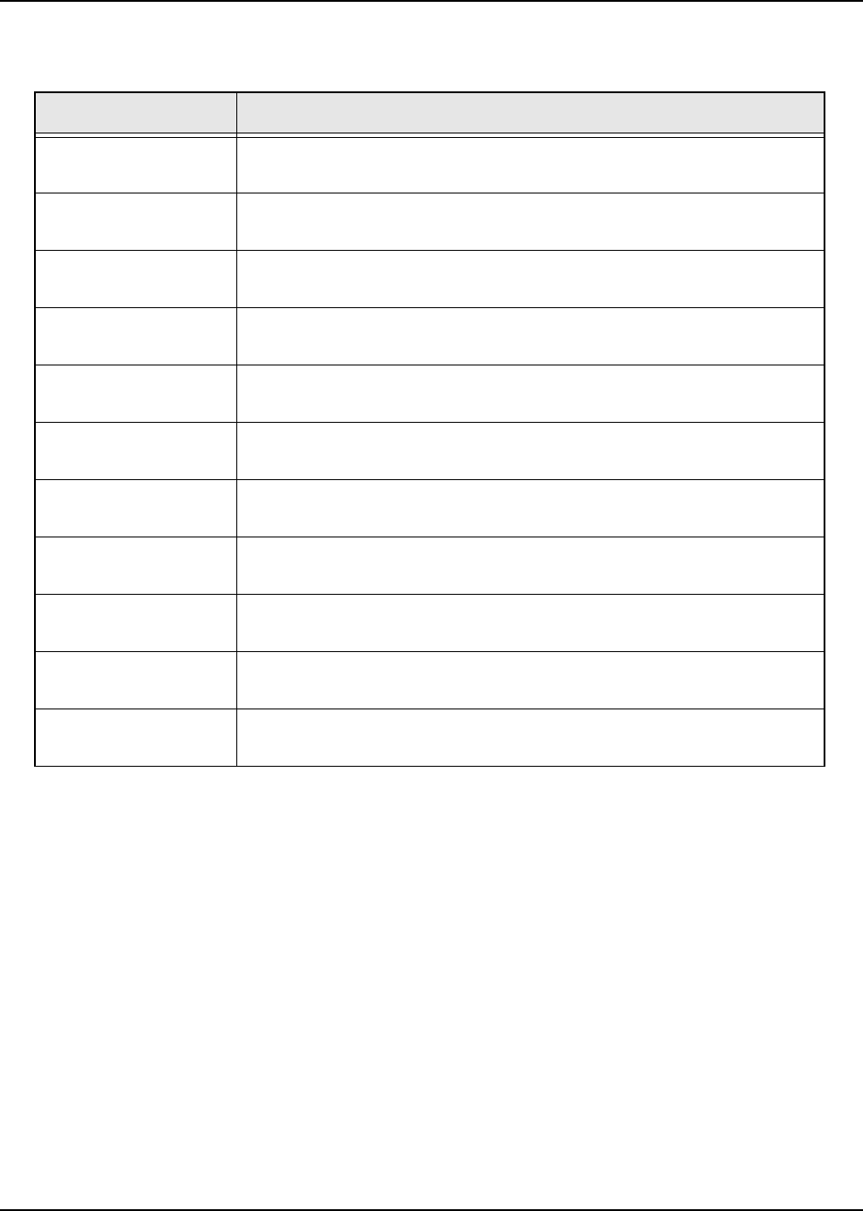
1.3.2 W4, W5, W7, and W9 Control Heads
Figure 1-2. Typical W4 Rotary Control Head
Figure 1-3. Typical W5 Pushbutton Control Head
PHONE
PAGE
or
SECURE
or
EMERGENCY
Page
Emer
CALL DIRECT
XMIT
BUSY
Mode Volume
Pwr
Phon Call SelScan
Mic
Home
Dim
H/L
Dir Mon
SCAN SELECT MONITOR
MODE
KNOB POWER ON/OFF/
VOLUME KNOB
HOME
HORN/
LIGHTS
PRIORITY/
NON-PRIORITY
INDICATORS DIRECT
INDICATOR
Mode
Vol
Mic
Phon Call Sel
H/L Mon Dir
PWR
Scan
XMIT
BUSY
DIM
HOME
MODE
POWER
ON/OFF
PAGE
or
SECURE
or
EMERGENCY
Page
Emer
PHONE
SCAN
CALL
SELECT
VOLUME PRIORITY/
NON-PRIORITY
INDICATORS
DIRECT
INDICATOR HORN/
LIGHTS
MONITOR
DIRECT
HOME
6881096C77-O September 26, 2003
Introduction: Control Heads 1-5
Figure 1-4. Typical W7 Pushbutton Control Head
Figure 1-5. Typical W9 Pushbutton Control Head
POWER
ON/OFF
2
2Pge
or
SITE
LOCK
MESSAGE
REPROGRAM
DIRECT
O
#
Del Rcl
Mode
Vol
Mic
Phon Call Sel
PWR
Scan
XMIT
BUSY
DIM
HOME
1
Ste
23
Lck
4
Sts
5
Rpg
6
Msg
7
H/L
8
Mon
9
Dir
MODE
EMERGENCY
or
SECURE
Emer
PHONE
SCAN
CALL
SELECT
PAGE
VOLUME
DIRECT
INDICATOR DELETE
RECALL
MONITOR
STATUS
HORN/LIGHTS
HOME
PRIORITY/
NON-PRIORITY
INDICATORS
XMIT BUSY
Call
ScanEmer
DIM
Pri
Non
Pri
123
456
789
Mode Vol Sel Home
Phon H/L
Rcl Sql Del
Dir
Sts Msg
VOLUME
ROCKER
MODE
ROCKER SELECT HOME
KEYPAD
RECALL
DELETE
DIMMER
CONTROL
PRIORITY
INDICATOR
FUNCTION
BUTTON
NON-PRIORITY
INDICATOR
FUNCTION
ON/OFF
INDICATORS
* Optional buttons (included but not installed or programmed)
MESSAGE*
POWER
SWITCH
STATUS*
0

September 26, 2003 6881096C77-O
1-6 Introduction: Control Heads
1.3.2.1 W4, W5, W7, and W9 Controls
Power Switch (PWR): Turns the radio and its accessories on or off. The Power switch is part of the
rotary volume knob on the W4 model, a push-type switch on the W5 and W7 models, and a slide switch
on the right-hand bottom surface of the W9 model.
Mode Switch: Used for selecting modes and programming menus. The Mode switch is a rotary switch
on the W4 model and a rocker switch on the W5, W7, and W9 models. Press the right side of the rocker
switch to increase the mode number and the left side to decrease the mode number. Press and hold the
switch to scroll the mode number up or down. The mode names appear in the display window.
Volume Switch: Used for selecting the volume level, editing names, and making certain radio
adjustments. The Volume switch is a rotary switch on the W4 model and a rocker switch on the W5, W7,
and W9 models. On the pushbutton models, pressing and releasing the Volume switch checks the
volume setting. Your display will show “VOLUME_ _” and a number value (0-15). Pressing and holding
the left side decreases the volume. The number value scrolls up or down to your desired level. The
Volume rocker switch also controls the volume level of the public address (PA) and external radio
speaker (Ex Rd) options when they are enabled. The display window shows “PA VOL _ _” when public
address is on and the Volume rocker switch is pressed.
Dim Button: Used to control the brightness of the display and button backlighting. When you turn on the
system, the display comes on at the brightness level it was on before the system was last turned off.
Press the DIM button once to reduce the brightness of the display to medium level and twice for low
brightness level. Press the DIM button a third time to turn the display and button backlighting off. This is
called the “surveillance” mode.
Home Button: Used for restoring preprogrammed mode, establishing programmed mode, selecting
programming entries, etc. Press the Home button to go to the radio’s preprogrammed “home” mode. On
the W7 models, you can use the Home button instead of the Mode switch to change modes. Hold the
Home button until a beep sounds to enter the configuration state. The display shows an entry prompt.
Use the keypad to enter your new mode choice and press the Home button again. Your mode is now
changed without scrolling.
Select Button: Used to configure radio options.
Option Buttons: Used for turning options on and off, such as Phone, Scan, Emergency Call, and
Secure.
Display: The vacuum fluorescent (VF) display’s primary function is to display mode numbers, mode
names, volume level, and the status of options. It also functions as an on-off indicator for the entire
system and plays an integral role in the operator’s reconfiguration of options. The display is 8 characters
on W4, W5, and W7 models and 11 characters on the W9 model.
XMIT and BUSY Indicators: The XMIT indicator lights when the radio is transmitting. The BUSY
indicator lights when the selected channel is busy.
Scan Indicators: When scan operation detects activity on a non-priority (NON-PRI) channel, the NON-
PRI indicator light comes on. Activity on a second priority channel causes the priority (PRI) indicator to
light. First priority channel activity causes PRI to flash.
12-Button Keypad (W7 and W9): Used to change the status of options and for entering numbers.
Several keys serve multiple functions. The following buttons can be programmed to W7 and W9 control
heads. The table below describes the buttons preinstalled on the W7 model. (See the ASTRO Digital
Spectra or Digital Spectra Plus User’s Guide for a complete description of keypad operation.)
6881096C77-O September 26, 2003
Introduction: Control Heads 1-7
Table 1-2. 12-Button Keypad (W7 and W9)
Key Description
#1 key
Site (STE)
Forces the radio to scan for a new site when the automatic multiple-site select
(AMSS) feature for wide-area coverage is in use.
#2 Key
Page (2 or 2Pge)
Initiates a Call Alert page or enters Call ID list programming.
#3 key
Lock (Lck)
Locks the radio onto the current site when the AMSS feature is in use.
#4 key
Status (Sts)
Used alone or in conjunction with other keypad buttons and the Sel button to
send a status transmission, indicating a predetermined condition change.
#5 key
Regroup (Rpg)
Requests a change in the radio’s talkgroup assignment when the dynamic
regrouping feature is used.
#6 key
Message (Msg)
Used alone or in conjunction with other keypad buttons and the Sel button to
transmit a message, indicating a response or temporary condition.
#7 key
Horn/Lights (H/L)
Selects/enables radio external alarms.
#8 key
Monitor (Mon)
Monitors the radio for channel traffic.
#9 key
Direct/Simplex (Dir)
Used for talkaround (mobile-to-mobile) conversations.
* key
Recall (Rcl)
Reviews modes in scan and phone lists.
# key
Delete (Del)
Used when editing stored lists.

September 26, 2003 6881096C77-O
1-8 Introduction: Control Heads
Notes
Chapter 2 Basic Maintenance
This chapter describes inspection, cleaning, and handling precautions for the control heads. Each of
these topics provides information vital to the successful operation and maintenance of your radio.
2.1 Inspection
Check that the external surfaces of the control head are clean, and that all external controls and
switches are functional. A detailed inspection of the interior electronic circuitry is not needed.
2.2 Cleaning
The following procedures describe the recommended cleaning agents and the methods to be used
when cleaning the external and internal surfaces of the control head. These surfaces should be
cleaned whenever a periodic visual inspection reveals the presence of smudges, grease, and/or
grime. Internal surfaces should be cleaned only when the control head is disassembled for servicing
or repair.
The only recommended agent for cleaning the external control head surfaces is a 0.5% solution of a
mild dishwashing detergent in water. The only factory recommended liquid for cleaning the printed
circuit boards and their components is isopropyl alcohol (70% by volume).
2.2.1 Cleaning External Plastic Surfaces
The detergent-water solution should be applied sparingly with a stiff, non-metallic, short-bristled
brush to work all loose dirt away from the control head. A soft, absorbent, lint-free cloth or tissue
should be used to remove the solution and dry the control head. Make sure that no water remains
entrapped near the connectors, cracks, or crevices.
2.2.2 Cleaning Internal Circuit Boards and Components
Isopropyl alcohol may be applied with a stiff, non-metallic, short-bristled brush to dislodge embedded
or caked materials located in hard-to-reach areas.
Alcohol is a high-wetting liquid and can carry contamination into unwanted places if an excessive
quantity is used. Make sure that controls or tunable components are not soaked with the liquid. Do
not use high-pressure air to hasten the drying process, since this could cause the liquid to puddle
and collect in unwanted places.
Upon completion of the cleaning process, use a soft, absorbent, lint-free cloth to dry the area.
NOTE: Always use a fresh supply of alcohol and a clean container to prevent contamination by
dissolved material (from previous usage).
The effects of certain chemicals and their vapors can have
harmful results on certain plastics. Aerosol sprays, tuner
cleaners, and other chemicals should be avoided.
!
C a u t i o n

September 26, 2003 6881096C77-O
2-2 Basic Maintenance: Handling Precautions
2.3 Handling Precautions
Complementary metal-oxide semiconductor (CMOS) devices, and other high-technology devices,
are used in this family of radios. While the attributes of these devices are many, their characteristics
make them susceptible to damage by electrostatic discharge (ESD) or high-voltage charges.
Damage can be latent, resulting in failures occurring weeks or months later. Therefore, special
precautions must be taken to prevent device damage during disassembly, troubleshooting, and
repair. Handling precautions are mandatory for this radio, and are especially important in low-
humidity conditions. DO NOT attempt to disassemble the radio without observing the following
handling precautions:
• Eliminate static generators (plastics, Styrofoam, etc.) in the work area.
• Remove nylon or double-knit polyester jackets, roll up long sleeves, and remove or tie back
loose-hanging neckties.
• Store and transport all static-sensitive devices in ESD-protective containers.
• Disconnect all power from the unit before ESD-sensitive components are removed or inserted
unless otherwise noted.
• Use a static-safeguarded workstation through the use of an anti-static kit (Motorola part number
01-80386A82). This kit includes a wrist strap, two ground cords, a static-control table mat and a
static-control floor mat.
NOTE:Be sure that the table and floor mats are properly grounded.
When these items are not readily available, observing the following techniques will minimize the
chance of damage:
- If a static-sensitive device is to be temporarily set down, use a conductive surface for place-
ment of the device.
- Make skin contact with a conductive work surface first and maintain this contact when the
device is set down or picked up.
- Always wear a conductive wrist strap when servicing this equipment. The Motorola part
number for a replacement wrist strap that connects to the table mat is 42-80385A59
Components used in this equipment can be damaged by
accumulated static charge. Avoid unnecessary handling.
When handling devices, use a group strap, conductive
benches, and floor mats to ensure that a static charge does
not develop on component terminals. Always pick up
components by the body when possible, avoiding the
electrical terminals. Exposed connections should be shorted
together via conductive foam when not in use.
Use grounded equipment when performing tests. DO NOT
connect components to or disconnect components from test
equipment while power is applied.
!
C a u t i o n

Chapter 3 Theory of Operation
This chapter describes the operational theory of the control heads for the W3, W4, W5, W7, and W9
radio models. It includes vehicular interface port (VIP) information.
3.1 W3 Control Head
The W3 Hand-Held Control Head (HHCH) contains the U3 microcomputer, which runs on a 4 MHz
clock and performs the following basic functions:
• SB9600 data encode and decode for communication to host radio.
• Liquid-crystal display (LCD) drive comprising two rows of 14 dot-matrix characters plus
10 annunciators.
• Scans a 22-key keypad.
• Scans three side keys and three top keys.
• Determines what type of radio is connected from the bus data and selects either portable or
mobile/vehicle adaptor (VA) modes.
• Scans the PTT switch.
• Provides display drive and programmable adjustment for display contrast.
• Provides display and keypad backlight control.
• Activates the red PTT LED and yellow status LED as required.
• Provides remote keying of the microphone via the SB9600 serial bus as required.
• Detects off-hook/on-hook conditions in mobile/VA mode.
• Provides SPI serial communications to U8 for serial-to-parallel output expansion, U12 for
parallel-to-serial input compression, U14 for analog-to-serial input compression, and option
connector J2.
3.1.1 SB9600 Serial Bus Interface
The serial interface circuit, comprising transistors Q1, Q2, and Q8, and comparator U2, provides an
interface between the microphone/message and a host radio for two-way SB9600 serial bus
communications. This is necessary to control the radio from the HHCH and have radio status
messages displayed on the HHCH. The interface circuit performs the following functions:
• Buffering of the input and output data by Q1 and U2 to improve isolation and drive capability.
• Conversion of balanced to unbalanced SB9600 data input to SB96 bus interface by Q1, U2.
• Bidirectional busy control through U3-20, -21, and -41 to J 1-3. U320 and -21 are paralleled to
provide increased drive capability.
3.1.2 Display Circuit
The display is a liquid-crystal display (LCD) and comprises two rows of 14 dot-matrix characters and
10 annunciators. The display circuit consists of sections involving character generation, backplane
drive, negative voltage generation, temperature compensation, and contrast control. A 200 kHz clock
is derived from U4-25, which also supplies U14.

September 26, 2003 6881096C77-O
3-2 Theory of Operation: W3 Control Head
Operation of the circuit is complex; a brief description is detailed below:
• Display data exits U3-5/12 as eight bits of parallel data. This data addresses a character
look-up table in LCD driver/controller U4. This provides the relevant segment output data from
U4, as well as LCD drivers U5, U6, and U7, to activate the relevant display dots that form the
characters as defined in the look-up table.
• The LCD is multiplexed with eight backplanes that are driven separately by U4-47 to -54. Each
backplane is driven sequentially, one after the other, by a stepped a.c. voltage of between
approximately -2 volts and +5 volts. LCD dots are displayed when a maximum or minimum of
one of the backplane drives coincides with a minimum or maximum, respectively, of the
relevant segment drive voltage.
• Negative voltage generation necessary for correct operation of the display is derived from a
timed clock output from U3-38. This is fed to a voltage doubler comprising C21, C22, and D30.
The d.c. output of the doubler is fed to voltage divider R16 to R20. This divider provides evenly
spaced voltage increments from approximately -2 volts to +5 volts, which are then fed to U4,
U5, U6, and U7 to form the stepped backplane and segment drive voltages.
• Temperature compensation is provided by U3 and U14 in conjunction with D32. This diode
provides a temperature-dependent voltage to analog input pin 1 of A/D converter U14. This is
sent as serial data input to U3-34, where it is compared to a reference in U3. The amount of
deviation from this reference determines the duty cycle of the output drive voltage from U3-38.
This results in a change to the drive voltage across C22, which is fed to analog input pin 6 of
U14 via voltage divider R26 and R2, which is then fed to U3 as serial data. U3 checks this
voltage for accuracy, using the temperature-dependent voltage at U14-1 as a reference, and
corrects the drive duty cycle accordingly.
• Contrast control is achieved by adjusting the display drive duty cycle U3-38 by either keypad
control or radio programming via the SB9600 bus. U3 contains a reference that presets the
drive duty cycle to an average value when first connected to a new radio. Adjustment of the
contrast setting will set up a new reference, which will be retained by the radio in EEPROM for
future use so that the new setting will be retained if the microphone is turned off.
3.1.3 Keypad Side Keys and Top Keys
The HHCH keypad is configured as a matrix of five columns by six rows. The keyboard is scanned
by taking each column output low in turn (each one 1 ms) and reading the corresponding row inputs
through the data input latch, U10. After all five columns have been scanned, the row data is then
decoded to see which keys, if any, are pressed. The HHCH then waits for debounce until the keypad
is scanned again. The keypad is scanned every 25 ms. If the same key is still pressed, the key
register value is determined from a key table. If the SB9600 serial bus is not busy, a serial-bus
"BUTCTL" message transmission is initiated. The same process also applies when a key is
released.
3.1.4 Microphone Preamplifier and PTT
PTT is achieved by activating switch S1. This places a ground on the microphone pre-amplifier
circuit, comprising Q6 and associated components, and effectively turns it on. Activation of S7 also
places a low on U10-6 input, which is passed on to U3 and transmitted as an SB9600 message back
to the radio. When this message is received by the radio, (if required) an SB9600 message is sent
back to the microphone and detected by U3, and the PTT LED is activated through U8. However,
illumination of the PTT LED is under radio control and is therefore dependent upon radio
programming. Q7 is also connected across the PTT line. Its purpose is to remotely enable the
microphone pre-amplifier through a received SB9600 serial-bus message, as required.

6881096C77-O September 26, 2003
Theory of Operation: W3 Control Head 3-3
Microphone cartridge M1 contains a capacitive transducer coupled to a FET amplifier. Microphone
audio is obtained from the output of MI and fed to Q6-b via C28, which provides either 0dB of gain in
portable mode or 20dB in mobile mode, during transmit. This gain change is achieved by the action
of Q5, which is turned on in mobile mode only, and bypasses R71. (Note that this gain is with respect
to a radio input impedance of 2k.Ω for portables and 600Ω for mobiles.)
3.1.5 On-/Off-Hook Control
The on-/off-hook control circuit comprises U8 and Hall switch U9. This circuit is only active in mobile
mode, during which the output at U8-6 and -7 is driven high by U3. This provides supply volts for U9,
the output of which still remains in its normally high state, provided that the microphone is off-hook.
During the on-hook condition, when the microphone is retained in its hang-up bracket, a magnet in
the hang-up bracket activates the Hall switch, which in turn pulls U9-3 low. This is detected by U3,
which then sends an appropriate SB9600 message back to the radio. When the microphone is
removed from the hang-up bracket, U9-3 returns high, causing U3 to send another SB9600 message
back to the radio.
3.1.6 Backlight Circuit
The backlight circuit comprises U3, U15, Q3, Q4, and LEDs D3 to D17. U3 enables the backlights,
as required, by placing a low at U3-16. This, in turn, turns on Q3 and Q4, causing the LEDs to turn
on. The action of D35 and R34 provides a constant current source for the LEDs over a supply
voltage range of 5.5 to 17 volts. U15 provides current balance between the individual pairs of LEDs,
and R34 controls the total current to about 60 mA.
3.1.7 Power Supply
The power supply consists of a 5-volt linear regulator, U1, which provides the necessary 5-volt
supply for all of the digital circuits. It has a low drop-out voltage to enable operation from an input
voltage of about 5 volts up to 17 volts. This regulator also contains internal current-Iimiting
protection, which will normally protect against damage from short-circuit faults. In addition, current is
supplied directly from the unregulated input to the backlight LEDs for power dissipation reasons.
3.1.8 Status LEDs
D22 is provided as a status LED for programmable radio functions. It is activated by an SB9600
message from the radio which is detected by U3, resulting in a high at U8-2 and -3. In addition, the
PTT LED, D21, can provide flashing radio status messages and can also be activated at the same
time as D22.
3.1.9 Jumper Selection
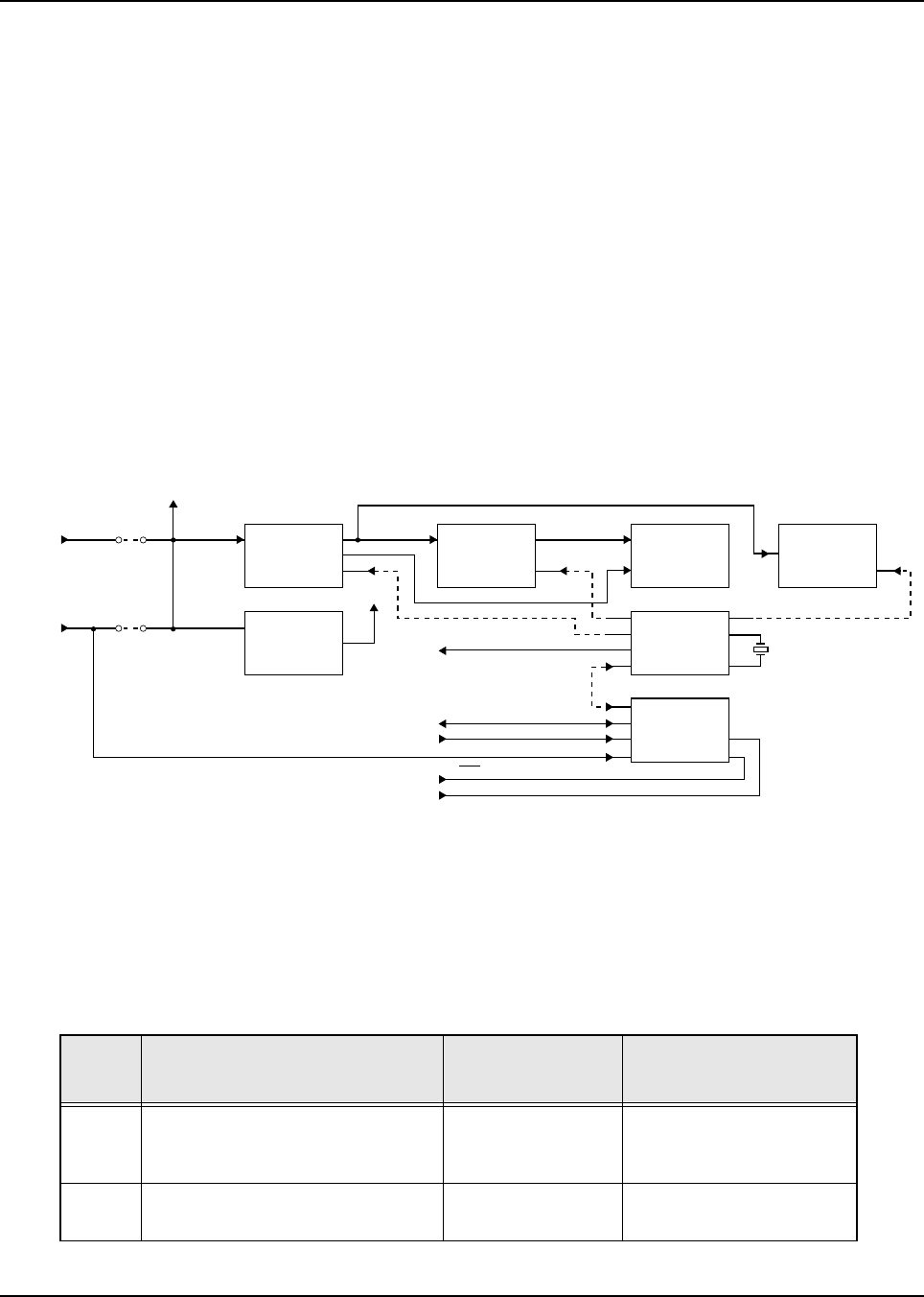
The only jumpers that may normally be installed are JU10, JU11, and JU12. When these jumpers are
installed, the ground provided is passed on to U3. These jumpers indicate whether a speaker is
installed in the unit, the SB9600 serial-bus device address, and single- or dual-control head control,
as defined in the table below.
Table 3-1. W3 Jumper Selection
Jumper IN OUT
JU10 Internal Speaker No internal speaker
JU11 SB9600 address = 6 BS9600 address = 5
JU12 Dual control Single control
September 26, 2003 6881096C77-O
3-4 Theory of Operation: W4, W5, and W7 Control Heads
3.1.10 Power On/Off
The HHCH has the ability to turn a host radio on or off by activating S6, which then places a
momentary logic low on the Mic Hi line. This is detected by appropriate circuitry in the host radio,
which then reverses the power on/off state of the radio. Since the microphone power is supplied by a
switched Opt B+ line from the radio, the microphone power on/off state follows that of the radio.
3.1.11 Miscellaneous Functions
If TP1 contacts are momentarily shorted or certain key combinations are pressed simultaneously, the
HHCH is placed in its test mode to carry out various diagnostic checks.
Transient protection diodes D24, D25, D37, D38, and D39 provide electrostatic transient protection
for sensitive components within the HHCH by preventing voltages from going outside the specified
ranges for these components.
3.2 W4, W5, and W7 Control Heads
The following pages describe the operational theory of the components of the W4, W5, and W7
control heads. Refer to Figure 3-1 for the control-head components.
Figure 3-1. Astro Spectra Control Head Block Diagram
3.2.1 Power Switch/Ignition
For dash-mounted radios, a pushbutton On/Off switch (S1) (or rotary knob on the W4 control head)
on the front panel controls power to the radio and accessories. In addition to this switch, you can wire
the vehicle’s ignition and add or remove control-head jumpers to further control radio operation.
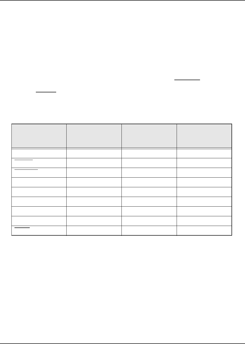
Table 3-2. Types of Operations
Type How it Operates Control Head
Jumper/Status Ignition Wiring
1 RECEIVE and TRANSMIT enabled
via control head ON/OFF switch
(ignition has no effect).
JU1OUT; JU2/IN Connect ignition cable to
“Battery Hot” at fuse block.
2 RECEIVE and TRANSMIT enabled
only when ignition switch is ON. JU1/OUT; JU2/IN Connect ignition cable to
“Ignition” at fuse block.
VOLTAGE
CONVERTER
CIRCUITRY
5 VOLT
REGULATOR
U45
(U3, Q50, T60)
A+/IGN
13.8V 37 VDC
+5 VDC
JU1
JU2
12
12
A+
IGNITION
U101
VF DRIVER
IC VACUUM
FLUORESCENT
DISPLAY
U102
34 VDC
2.5 VAC
VIP OUTPUTS
U1
U4
MICRO-
COMPUTER
INTERFACE
AND
WATCHDOG
TIMER IC
SERIAL DATA BUS
VIP INPUTS
IGNITION SENSE
PTT SENSE
HUB SENSE
BACKLIGHT
LEDS
1
2
4.0 MHz
Y1

6881096C77-O September 26, 2003
Theory of Operation: W4, W5, and W7 Control Heads 3-5
The ignition cable is the fused wire attached to the accessory connector. The control head is shipped
with jumper JU1 OUT and jumper JU2 IN. The three options are:
1. Connect the ignition cable to “Battery Hot” on the fuse block to TRANSMIT and RECEIVE via
the front panel pushbutton On/Off switch, regardless of the ignition setting.
OR
2. Connect the ignition cable to “Ignition” at the fuse block to disable TRANSMIT and RECEIVE
except when the ignition is on. This method is more convenient because you need only to
switch off your ignition; the radio will not drain your car’s battery when you leave the radio
switch on.
3. To allow receive via front panel On/Offf, but inhibit transit when the ignition is off, control head
jumpers and radio software settings must be changed. Follow the disassembly procedures in
Chapter 5 to remove the control head PC board from its housing, and then locate JU1 and
JU2 using the board overlays in Chapter 8. Carefully unsolder JU2 from the board and solder
it in a JU1. Change the “ignition switch” field in CPS (Radio Wide/Advanced) or RSS (F4/F3/
F3/F3) to “TX inhibit.”
For remote mounted radios, the same options of operation are available to the customer. The fused
GREEN wire coming from the control-head end of the interconnect cable is connected to “Battery
Hot.” The ignition cable is the fused ORANGE wire also coming from the interconnect cable. The
control head is shipped with jumper JU1 OUT and JU2 IN. Configured this way, connections to the
ignition cable are made following options (1) or (2) above.
3.2.2 Voltage Regulator
Switch B+ is applied to U45, a 5-volt regulator. C45 and C58 filter SWB+ and the 5-volt line to ensure
U45 operated properly. CR90 protects against accidental reverse-polarity connections during
installation. The 5-volt supply operates the microcomputer circuitry, interface circuitry, vacuum
fluorescent (VF) driver U101, and comparator U3.
3.2.3 Microcomputer
The microcomputer, U1, operates on the 5-volt supply and is filtered by L1. A resonator, Y1,
oscillates at 4 MHz to provide a stable clock for microcomputer timing. U1 handles all communication
with the radio command board over the serial bus, scans the keyboard for button presses, and
generates the display information needed by the VF driver (U101) to drive the VF display (U102).
3.2.4 Interface Circuitry
The bulk of the interface circuitry is contained in bipolar, custom IC, U4. This IC includes watchdog
timer circuits, serial-bus communication drive circuits, and input buffer circuits to protect
microprocessor U1.
3 RECEIVE enabled by control head
ON/OFF switch; TRANSIT enabled
only when ignition switch is ON.
JU1 IN; JU2 OUT Connect ignition cable to
“ignition” at fuse block.
Enable “TX inhibit” ignition
switch setting in RSS or
CPS.
Table 3-2. Types of Operations (Continued)
Type How it Operates Control Head
Jumper/Status Ignition Wiring
September 26, 2003 6881096C77-O
3-6 Theory of Operation: W4, W5, and W7 Control Heads
3.2.5 Reset
On initial power-up, the RESET line to U1-1 is held low by U4 for approximately 120 milliseconds
before going high. This resets U1 and starts it operating properly. Then, a pulse train generated at
U1-38 sends tickle pulses to the watchdog timer circuitry in U4 and sends a STROBE signal to the
VF display driver, U101. Capacitor C6 charges to about 3.3 volts and triggers a reset as described
above. Any time a reset occurs, U4-9 goes high, causing radio circuitry in the command board to
also reset. Should radio circuitry initiate the reset, pin 23 of the control unit PC board connector is
forced high, triggering the same events described above. The control head can reset the radio
command board, and vice-versa, via the reset line. See Table 3-3.
3.2.6 Bus Busy
The control head prepares to send data on the serial bus when U-15 (BUSY OUT) goes low, causing
U4-10 to go high. This signals the radio command board that the control head has data to send.
U4-11 (BUSY IN) goes low whenever U4-10 goes high. This informs the control-head microcomputer
that the serial bus is in use. See Table 3-3.
3.2.7 Serial Bus Data
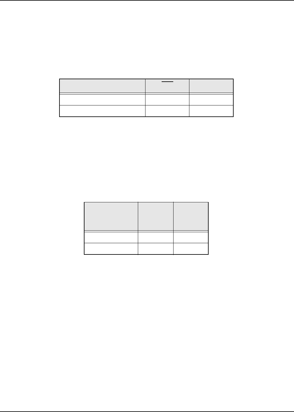
See Table 3-3 for Serial Data Bus Logic. Two lines, BUS+ and BUS-, send data between the control
head and the radio command board. Under the normal condition of inactivity, BUS+ is high and BUS-
is low. This is the “inactive state” on the serial bus. When the two lines invert (BUS+ goes low, BUS-
goes high), the serial bus is in the “active state.”
The control head uses the TX DATA line (U1-33) to send data over the serial bus. When TX DATA
goes low, the bus is placed in the active state by U4; when TX DATA goes high, the bus returns to
the inactive state.
Data is sent to the microcomputer on the RX DATA line (U1-32). Whenever the serial bus is in the
active state, RX DATA is low. An inactive state on the bus causes RX DATA to go high.
Table 3-3. Serial Data Bus Logic
Data Line No Bus Activity
(Normal
Receiving Data)
Bus Activity
(Sending or
Receiving Data)
In Reset*
Busy Low High Low
BUSY IN High Low High
BUSY OUT High Low* High
BUS+ High Low and High High
BUS- Low High and Low Low
TX DATA High Low and High** High
RX DATA High Low and High High
RESET Low Low High
RESET High High Low
* Bus activity will occur immediately after a reset.
** Sending only.
6881096C77-O September 26, 2003
Theory of Operation: W4, W5, and W7 Control Heads 3-7
3.2.8 Push-To-Talk (PTT)
The PTT line from the microphone keys the transmitter. This line (U4-37) is normally biased at
5 volts, but goes to DIG GND when the microphone PTT button is pressed. This causes the PTT line
(U1-21) to go high. The transmit command is then sent over the serial bus to the radio command
board. Releasing the PTT reverses this process. There is no PTT hardware connection from the
control head to the radio command board. See Table 3-4.
3.2.9 Hang-Up Button (HUB)
The control head senses when the microphone is off-hook by monitoring the HUB line from the
microphone. When the microphone is on-hook, the HUB line (U4-31) is connected to ground, placing
a high on the inverted HUB line (U1-20) and sending the on-hook command over the serial bus.
When the microphone is off-hook, U4-31 biases to 5 volts, reversing the process and sending the off-
hook command over the serial bus. See Table 3-5.
3.2.10 Ignition Sense Circuitry
Ignition sense voltage is sensed by U4-28. When this voltage is high, U4-29 goes low, resulting in
U1-39 going low, and sending the “ignition-on” command over the serial bus. When the ignition
voltage drops off, the process is reversed.
3.2.11 Keypad Scan
U1 scans the keypad switches for a button press by sending out periodic low-going pulses in
sequence on pins 8 through 12. Keypad sense lines connect back to U1 on pins 13 through 17.
Resistors R120 through R124 ensure that the sense lines are high until a key is pressed. When a
button is pressed, keypad contacts close, allowing the low-going pulse to return to the
microcomputer on the appropriate sense line. This informs U1 that a particular button was pressed.
3.2.12 Vacuum Fluorescent (VF) Voltage Converter Circuitry
Voltage for the VF display is generated by a fixed-frequency, variable duty-cycle controlled, flyback
voltage converter. The switching frequency is about 210 kHz. One half of U3, pins 5-7, forms a
210 kHz sawtooth oscillator. The sawtooth waveform is produced at U3-6 and is applied to pin 3 of
the other half of U3. This portion of U3 is a duty-cycle controlled comparator.
Table 3-4. PTT Logic States
Microphone Push-to-Talk PTT PTT
PRESSED Low High
RELEASED High Low
Table 3-5. HUB Logic States
Microphone
Hang-Up
Button HUB Line Inverted
HUB
ON-HOOK Low High
OFF-HOOK High Low

September 26, 2003 6881096C77-O
3-8 Theory of Operation: W9 Control Head
U1-6 controls the entire voltage converter. During startup, U1-6 pulls to ground, biasing U3-2 to
about 1.85 volts via R51 and R52. U3-1 and R61 then begin to switch Q50 on and off at a 210 kHz
rate. This allows current to flow through T60, building a magnetic field, then collapsing it. When the
field collapses, the back EMF (flyback) forward biases CR51 and charges C52 (after a few cycles) to
about 37 volts, causing zener diode VR50 to conduct. The high voltage is regulated by the effect that
VR50 has on the bias voltage at U3-2. If the high-voltage supply increases, VR50 pulls U3-2 higher
in voltage resulting in a decreased duty-cycle for Q50 (the switching frequency remains constant;
only the duty-cycle of on-time versus off-time decreases). Less power is up-converted to C52 when
the duty cycle decreases; hence, regulation is maintained.
The voltage converter also produces an a.c. filament voltage for the VF display across T60 pins 4
and 6. R101 drops this voltage to approximately 2.4 Vrms. This a.c. voltage rides on a positive d.c.
offset due to R50, depending on brightness. The positive offset allows a VF display grid to be
reverse-biased with respect to the filament when that particular grid is supposed to be shut off. This
prevents “character ghosting.” Display dimming is exclusively controlled by multiplexing information
sent from U1 to the VF driver IC, U101. Display dimming has no effect on the voltage converter
circuitry except in the OFF mode. In this mode, U1-6 goes high, resulting in U3-2 going to +5 volts.
This keeps U3-1 low and Q50 turned off. The high-voltage supply drops to about 12 volts and the a.c.
filament voltage drops to zero, shutting off the display.
3.2.13 Vacuum Fluorescent Display Driver IC
The VF driver IC, U101, receives data directly from the microcomputer for multiplexing the VF
display. All of the grid and anode driver lines from U101 are either at, or about, 34 volts (ON) or
ground (OFF).
3.2.14 Vacuum Fluorescent Display
The VF display is an 8-character, 14-segment device. Anodes are the actual phosphorescent
segments, and grids are the wire-mesh structures located over each character. Multiplexing allows
character generation with a minimum of interconnecting lines between display and driver. Anodes
and grids operate at, or about, 34 volts when ON and are at zero when OFF. The filament operates
on ac at about 2.4 Vrms, with current flow at 100 mA through the filament. The d.c. current flowing
from anodes and grids to the filament and through R50 to ground increases filament voltage by up to
5 Vdc.
3.2.15 Backlight LEDs
Most buttons on the control head are backlit by ten LEDs for easy night-time viewing. In medium and
low brightness level settings, U1-19 goes high, turning on Q131 and causing a fixed current to flow
through the LEDs.
In the OFF mode and the maximum brightness mode, U1-19 goes low, turning off Q131 and the
LEDs. Microprocessor U1 does not duty-cycle change the brightness level of the backlighting LEDs.
3.3 W9 Control Head
The W9 control head has solid-state microprocessor circuitry that operates the standard and optional
features built into the system. The control-head design allows installation in even the smallest of
down-sized vehicles.
3.3.1 Display
The control head has an 11-character alphanumeric VF display for indicating the following:
• Zone/Mode names
• Squelch level

6881096C77-O September 26, 2003
Theory of Operation: W9 Control Head 3-9
• Volume level
•Status codes
• Message codes
• Telephone numbers
• Identification numbers
• Alarm displays
• Option status
3.3.2 W9 Controls and Indicators
The W9 control head 12-button keypad contains traditional alphanumeric keys. These keys double
as function keys for options. Six ON/OFF option buttons and indicator lights above the display
window tell whether these options are on or off. All buttons are backlit to allow operation in low-light
conditions.
Other indicators include BUSY, XMIT, Pri, and Non-Pri. The BUSY indicator lights when activity is
detected on the channel. The XMIT (transmit) indicator lights when you are transmitting. The Non-Pri
(non-priority) or Pri (priority) indicators light when activity occurs during scanning. If the detected
activity is in the non-priority mode, the Non-Pri indicator lights. If the activity is in the priority mode,
the Pri indicator lights (steady on for second priority mode, and flashing for first priority mode).
3.3.3 Control Board
NOTE: Refer to the W9 control head foldout block diagram and schematic diagram for the following
discussion.
The control board's microprocessor unit (MPU) communicates on the serial bus, receives and
interprets keypad data, and controls the volume. The MPU (U2) sends data to a driver to control the
display and sends data to turn the LEDs on or off. The control board has a watchdog timer that
senses the need for a system reset. The vehicle interface ports are also controlled on this board.
3.3.3.1 Microprocessor
The MPU operates in expanded bus mode with internal Read-Only Memory (ROM) active. The clock
frequency is 7.9488 MHz, which results in an internal operating frequency of 1987 kHz. The limited
number of I/O ports is augmented by using a serial-to-parallel shift register (U6) to scan the keypad
and to switch the VIP drivers Q71, Q72, and Q73.
3.3.3.2 Watchdog Timer
The watchdog timer is on the serial input/output integrated circuit (SIOIC) U4. On system power-up,
capacitor C6 pulls U4, pin 43, high while the RESET output at pin 4 goes low, and the
microprocessor resets.
As C6 charges, the voltage on U4, pin 43, drops, causing the output to go high and the
microprocessor to start operating. At this point, the bias on U4, pin 43, shifts toward positive, causing
the voltage to begin to rise, eventually causing another reset cycle. A high on U4, pin 9, (RESET
input) also initiates a reset.
When the microprocessor operates correctly, the microprocessor sends "tickle" pulses to U4-2.
These pulses tickle the watchdog timer and keep the voltage on U4, pin 43, low enough to prevent
reset. If the tickle pulses stop for more than 250 ms, the reset cycle repeats.
The watchdog timer can be disabled by shorting U4, pin 43, to ground.

September 26, 2003 6881096C77-O
3-10 Theory of Operation: W9 Control Head
3.3.3.3 Bus Transceiver
The serial bus transceiver is on SIOIC U4. The timer on SIOIC U4, pins 10, 16, and 17, connects to
the external bus. Pins 11, 13, 19, and 20 connect to MPO 2. These pins act as a serial-
communication buffer.
3.3.3.4 Vacuum Fluorescent Voltage Converter
Voltage for the vacuum fluorescent (VF) display filaments is generated by a fixed-frequency,
variable-duty-cycle-driven, flyback voltage converter. Dual Comparator U3B, with resistors R56
through R60, form a triangle-wave generator that has an output swing between 1.5 and 3.2 volts at a
frequency of 160 kHz. The output of this triangle goes to U3A-3, where it is compared to a feedback
signal on U3A-2. The d.c. feedback signal comes from the voltage converter output through diode
CR51 and is regulated by VR50 to 43 volts. The U3A output voltage increases or decreases as its
input voltage rises or falls. Consequently, the duty cycle seen at the gate of MOSFET transistor Q50
varies inversely with the triangle output voltage. The output of Q50, varying at 160 kHz, is applied to
the primary of transformer T60, pins 1 and 3. The secondary of T60, pins 4 and 6, supplies 3.5 Vac
for the VF display (U102) filaments.
3.3.3.5 Vehicle Interface Ports
The control-head connector, P103, provides connections for three vehicle interface port (VIP) inputs
and three VIP outputs.
The three VIP inputs enter the control head at P103, pins 4, 3, and 37. Zener diodes YR10, YR9, and
YR8 limit the input voltages to 15 volts. VIP input 2 can be strapped through jumper JU11 to provide
various control functions connected to P103, pins 41, 43, and 44. The three inputs are connected to
SIOIC U4 at pins 25, 22, and 35. The input signals are buffered in U4 and are output on pins 24, 21,
and 36. From U4, the signals are fed through 10K resistors R44, R14, and R15 to the MPU, U2. The
MPU directs the signals as required by programming.
Programmable switches on the control head are connected through J101, pins 11, 10, 9, 8, and 7
(KRl through KRS, respectively) to CPU U2, pins 49, 44, 46, 48, and 50. The other contacts of the
switches are connected through J101, pins 14, 15, 16, 17, and 19 (KSl through KSS), to CMOS shift
register U6, pins 4, 5, 6, 7, and 14.
Shift register U6 outputs, pins 13, 12, and 11, go to Darlington transistors Q71, Q72, and Q73. These
three transistors drive the VIP outputs (up to 300 mA each) through control-head connector PI03,
pins 2, 1, and 34. Primarily, these transistors control external relays. VIP outputs 1 and 2 are
connected to jumpers JU12 and JU13 to provide control functions connected to P103, pins 28 and
29. VIP output 1 can also be connected through JU22 to MIC-PTT, pin 24.
3.3.3.6 Power Supply
The +5-volt power supply U46 is a three-terminal regulator IC that regulates the 12-volt SWB+ down
to +5 volts for the digital logic circuits. The regulated +5 volts enters the control-head PC board
through connector J101, pin 4.
3.3.3.7 Ignition Sense Circuits
SIOIC U4 senses the vehicle ignition’s state through its pin 28, disabling transmit when the ignition is
off. For negative-ground systems, the orange lead is typically connected to +l2 volts. For more
information, see the cable kit section in the Detailed Service Manual 68P80102W61.
NOTE: Q40 supplies an inverting path for positive-ground ignition service.

6881096C77-O September 26, 2003
Theory of Operation: W9 Control Head 3-11
3.3.3.8 EEPROM Write-Protect Circuit
Transistors Q161, Q162, and associated circuitry guard against inadvertently writing into the
EEPROM U5 by inhibiting the Write Enable input. The circuitry guarantees the EEPROM is protected
during reset and when shift register U6 is not in the proper programming state.
3.3.4 Display Board
The display board contains the main operator interface points of the system, including the vacuum
fluorescent display, the status indicator LEDs, and the user keypad.
NOTE: Refer to the foldout schematic diagram of the display board for this discussion.
3.3.4.1 VF Display
The (VF) display is an 11-digit, 14-segment display that needs two separate voltages to operate, The
anode and grids use +43 volts to accelerate electrons from the cathode, and the filament uses 3.5
vac at 80 mA. These voltages are obtained from the VF voltage converter on the controller board.
3.3.4.2 VF Display Driver
VF display driver U101 receives 14-segment display data, digit enable data, and indicator state data
from the microprocessor on the controller circuit board. This data is clocked using CLOCK (pin 23)
and DATA-IN (pin 43) lines, then framed using LATCH-ENABLE (pin 24) and STROBE (pin 21) to
control brightness. The 32-bit data frame is updated every millisecond so that a coherent display is
maintained and totally updated every 11 ms.
3.3.4.3 Status LEDs
Status LEDs CR111 through CR120 are driven by the display driver as though they were decimal
points on the VF display. Level-shifting transistors are required for this since the display driver uses
43 volts for control signals.
3.3.4.4 Backlight LEDs
The same signal (VF-CONTROL) that turns the VF voltage converter on and off also operates the
backlight LEDs. Transistor Q134 supplies base current to the individual driver transistors. The driver
transistors act as current sources to the LEDs. Backlight LEDs CR131 through CR134 are
connected to thermistor RT133 via Q132. This circuit allows more current to flow through these LEDs
at room temperature and reduces current as the temperature rises.
3.3.5 Default Jumper Settings
The factory installs jumpers in each control head according to customer-ordered options. See Table
3-6 for the standard jumper configurations. See the diagrams on the foldout pages for other
configurations.
Table 3-6. Standard Jumper Configurations
Jumper Number Normally
JU1 IN
JU2 OUT
JU3 IN
JU4 OUT
September 26, 2003 6881096C77-O
3-12 Theory of Operation: Vehicle Interface Port (VIP)
3.4 Vehicle Interface Port (VIP)
The vehicle interface port (VIP) allows the control head to control outside circuits in the vehicle and
to receive inputs from outside the control head. This results in greater flexibility and ease of
installation when interfacing to other systems in the vehicle. There are up to three VIP outputs that
can be used for relay control. There are also up to three VIP inputs that can accept input from
switches, etc.
3.4.1 W4, W5, and W7 Control Heads
The VIP outputs are controlled by microcomputer U1 pins 26, 27, and 28. A high level causes the
associated transistors Q71-73 to conduct up to 300 mA of current to ground. Primarily, these
transistors control external relays. The relay coil is connected between the VIP output pin and
SWB+. See the installation manual for connection details.
The VIP input lines connect to U4, pins 22, 25, and 35. U4 acts as an inverting stage, passing the
VIP input signals to U1, pins 29-31, to be read by the microcomputer. VIP inputs normally connect to
ground via a normally open or normally closed switch.
3.4.1.1 VIP Output Connections
3.4.1.1.1 Dash-Mount Installations
Two VIP outputs are available in dash-mount installations. VIP OUT 1 is on pin 12 of the rear
accessory connector; VIP OUT 2 is on pin 3. These connections are used to control relays. Connect
one terminal of the relay coil to SWB+ (Rear Accessory Connector pin 4). Connect the other relay
coil terminal to one of the VIP outputs. See the installation manual for the horn and lights connection.
JU5 IN
JU7 IN
JU8 OUT
JU9 OUT
JU10 OUT
JU11 OUT
JU12 OUT
JU13 OUT
JU16 OUT
JU17 OUT
JU18 IN
JU19 IN
JU20 IN
JU21 OUT
JU22 OUT
Table 3-6. Standard Jumper Configurations (Continued)
Jumper Number Normally
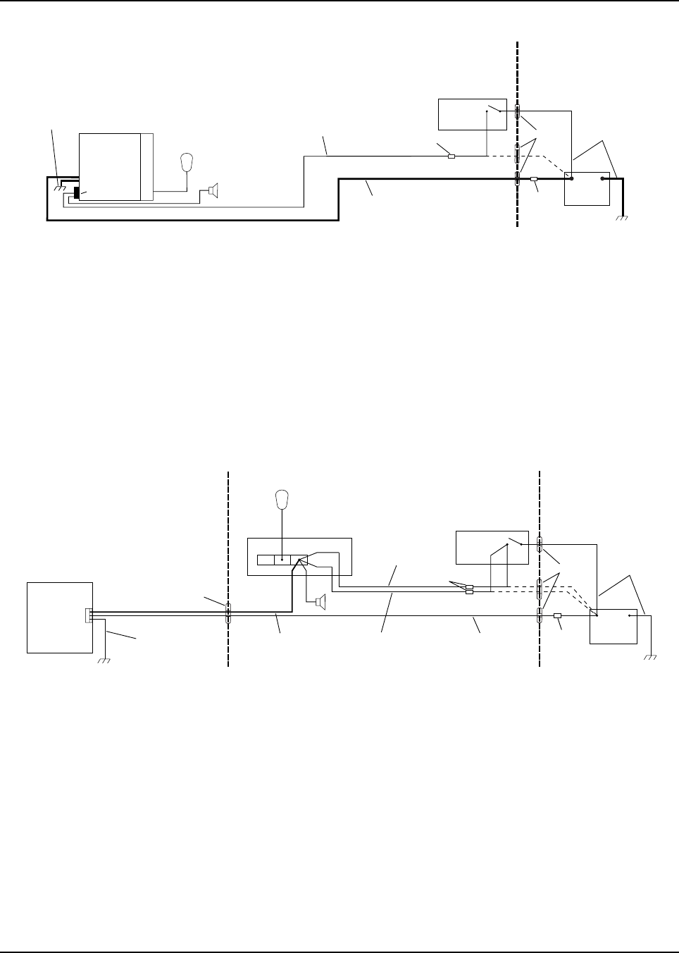
6881096C77-O September 26, 2003
Theory of Operation: Vehicle Interface Port (VIP) 3-13
Figure 3-2. Cabling Interconnect Diagram for Dash Mount
3.4.1.1.2 Remote-Mount Installations
VIP outputs function exactly the same in remote-mount installations as the dash mount. However,
three VIP outputs are available at the remote-mount accessory cable connector. VIP OUT 1 is on pin
12, VIP OUT 2 is on pin 3, and VIP OUT 3 is on pin 15.
Figure 3-3. Cabling Interconnect Diagram for Remote Mount
3.4.1.2 VIP Input Connections (Remote-Mount Only)
Three VIP input lines are also available in remote-mount installations. VIP IN 1 is on pin 14, VIP IN 2
is on pin 10, and VIP 3 is on pin 9. These connections are used to accept input from switches or
other circuits in the vehicle. The VIPs are biased at about 5 volts, and to be activated the inputs are
switched to ground. Normally, a switch is connected from a VIP input line to ground. The switch can
be normally open or normally closed, depending on VIP programming and the particular function
being performed.
RADIO COMPARTMENT = OPERATOR COMPARTMENT VEHICLE BATTERY
COMPARTMENT
A good chassis connection via the black primary
power cable is essential for radio operation and
to prevent damage to the radio and cable kit.
Connection to the vehicle frame is desirable.
VEHICLE
BATTERY
15A OR 20A
FUSE
PART OF
VEHICLE
WIRING
VEHICLE
IGNITION SWITCH
ON/ACC
GROMMET
RADIO POWER CABLE
(RED/BATTERY HOT)
RADIO IGNITION
CABLE (thin RED)
SPEAKER
3A OR 4A FUSE
MICROPHONE
RADIO POWER CABLE (BLK/GROUND)
RADIO
(-)
(+)
CAUTION
MAEPF-27646-O
Rear connector
CH SEE NOTE
NOTE:
Caution: if you choose to connect the radio’s IGNITION line directly to the car’s battery, excess use of the radio when the car’s ignition is not running (i.e. alternator running)
could result in a slow discharge of the car’s battery. This configuration allows the radio to operate with the car’s ignition switch ON or OFF.
If the radio’s IGNITION line is wired to the car’s ignition switch, the radio will only function when the car’s ignition switch is turned ON.
RADIO COMPARTMENT OPERATOR COMPARTMENT VEHICLE BATTERY
COMPARTMENT
A good chassis connection via
the black primary power cable
is essential for radio operation
and to prevent damage to the
radio and cable kit. Connection
to the vehicle frame is desirable.
VEHICLE
BATTERY
15A OR 20A
FUSE
PART OF
VEHICLE
WIRING
VEHICLE
IGNITION SWITCH
ON/ACC
GROMMET
GROMMET SEE NOTE
RADIO POWER CABLE
(RED/BATTERY HOT)
RECEIVER
CONTROL
CABLE (GRN)
RADIO CONTROL
CABLE (BLK/MULTI-
CONDUCTOR)
SPEAKER
TRANSMITTER
CONTROL
CABLE (ORG)
4.0A FUSE
MICROPHONE
VIP
MIC
RADIO (ORG)
(GRN)
RADIO
POWER CABLE
(BLK/GROUND)
RADIO (-)
(+)
CAUTION
NOTE:
The orange and green power cables connect to either the vehicle battery or the ignition switch. Connect the green cable directly to the battery. The receiver operates
when the control head is on. Connect the orange cable to the ignition switch. The transmitter operates only when the ignition switch is on. Alternate connections:
Connecting both green and orange cables to the battery allows the control head to turn the receiver and transmitter on or off. Connecting both green and orange cables
to the ignition switch allows the ignition switch to turn the receiver and transmitter on or off. (Alternator whine and other noise problems may occur. Isolate the green
cable with a Motorola relay, part #59-00813674.)
MAEPF-27616-O
September 26, 2003 6881096C77-O
3-14 Theory of Operation: Vehicle Interface Port (VIP)
3.4.2 W9 Control Heads
The VIPs allow the W9 control head to operate outside circuits and to receive inputs from outside the
control head. There are three VIP outputs that are used for relay control. There are also three VIP
inputs that accept inputs from switches. See the cable kit section for typical connections of VIP input
switches and VIP output relays.
3.4.2.1 VIP Output Connections
The VIP output pins are located on the back of the control head below the area labeled VIP. These
connections are used to control relays. One end of the relay should be connected to switched B+,
while the other side is connected to a software-controlled on/off switch inside the control head. The
relay can be normally On or normally Off depending on how the VIP outputs are configured. The
control-head connector P103 pins that are connected to the external relays are listed in Table 3-7.
The function of the VIP outputs can be defined by field programming of the control head. Typical
applications for VIP outputs are external horn/lights alarm and horn-ring transfer relay control.
3.4.2.2 VIP Input Connections
The VIP input pins are located on the back of the control head below the area labeled VIP. These
connections accept inputs from switches. One side of the switch is connected to ground while the
other side is connected to a buffered input to the control head. The switch can be normally closed or
normally open, depending on how the VIP inputs are configured. The control head provides three
VIP input connections. The control-head connector P103 pins that are connected to the external
switches are listed in Table 3-8.
The function of the VIP inputs is defined by field programming of the control head. Typical
applications for the VIP inputs are for a foot switch or a horn ring switch.
Table 3-7. VIP Output Connections
VIP Output
No. Switched
B+ Pin No. VIP Output
Pin No. Default Function Is Changed
with Field Programmer
1 18 2 Horn Relay (Alarm)
2 19 1 Light Relay (Alarm)
3 35 34 Siren-Horn Transfer
Table 3-8. VIP Input Connections
VIP Input
No. Switched
B+ Pin No. VIP Output
Pin No. Default Function Is Changed
with Field Programmer
1 20 4 Siren; Horn Ring
2 21 3 Emergency (if option is present)
33637None

Chapter 4 Test Equipment and Service Aids
4.1 Recommended Test Equipment and Service Aids
The list of equipment contained in Table 4-1includes most of the standard test equipment required for
servicing Motorola control heads. The Characteristics column is included so that equivalent
equipment can be substituted; however, when no information is provided in this column, the specific
Motorola model listed is either a unique item or no substitution is recommended.
Table 4-1. Recommended Motorola Test Equipment and Service Aids
Motorola
Model Number Description Characteristics Application
6032A*DC power supply
(Agilent) 0-20 Vdc, 0-50 A current-limited Bench supply for 13.8 Vdc
FLUKE 87*Digital Multimeter True RMS metering, 200 kHz
frequency counter, 32-segment
bar graph with backlit display
Recommended for AC/DC
voltage and current
measurements
54622A*Oscilloscope (Agilent) Two-channel, 100 MHz
bandwidth, 200 MSa/s sample
rate, 2 MB memory/channel
Waveform Measurements
3080369B99
(dash mount)
3080369B97
(remote mount)
Extender Cable—
Allows operation of
control head while
extended from radio
Control head troubleshooting
* or equivalent

September 26, 2003 6881096C77-O
Notes
4-2 Test Equipment and Service Aids: Recommended Test Equipment and Service Aids
Chapter 5 Troubleshooting
This chapter, along with the theory of operation in Chapter 3 and the schematics, overlays, and parts
lists in Chapter 8, will aid you in troubleshooting a malfunctioning ASTRO Digital Spectra or Digital
Spectra Plus control head. If the board is severely damaged or otherwise non-repairable, refer to the
board replacement instructions in the section, “Replacing the Control Head Board” on page 5-7.
NOTE: To access W9 control-head boards for troubleshooting, remove them from the plastic housing
using the procedure on page 5-10. To access W4, W5, and W7 control-head boards, use a
control-head extender cable and the procedure on page 5-8. (Refer to the chapter,
“Recommended Test Equipment and Service Aids” on page 4-1 for the appropriate Motorola
test equipment and service aids part numbers.)
5.1 Required Tools and Supplies
Table 5-1lists the tools and supplies needed for basic troubleshooting.
Table 5-1. Required Tools and Supplies
Tools and Supplies
Small, flat-blade screwdriver
2.5 mm hex-key driver
Torx® T8, T10, and T15 drivers
3.0 mm Allen wrench
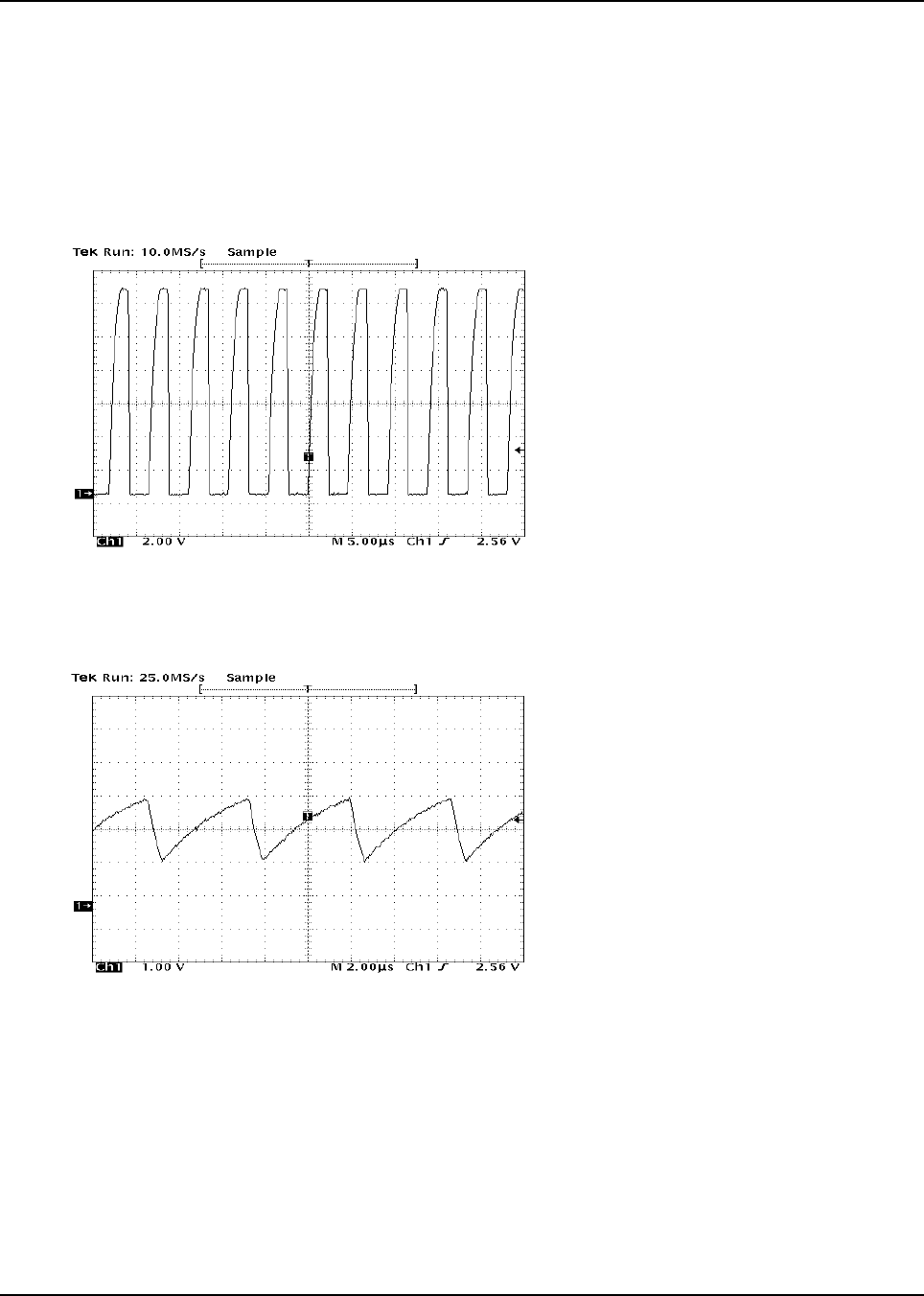
September 26, 2003 6881096C77-O
5-2 Troubleshooting: Troubleshooting Waveforms
5.2 Troubleshooting Waveforms
This section contains images of waveforms that might be useful in verifying operation of certain parts
of the circuitry. These waveforms are for reference only; the actual data depicted will vary depending
upon the operating conditions.
5.2.1 ASTRO Digital Spectra Waveforms
Waveform W1: Oscillator Out, U4 Pin 42
Waveform W2: Sawtooth Oscillator: U3 Pin 3
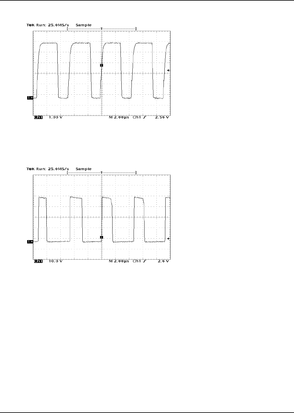
6881096C77-O September 26, 2003
Troubleshooting: Troubleshooting Waveforms 5-3
Waveform W3: U3 Output: U3 pin 1 (output to Q50)
Waveform W4: Q50 Drain
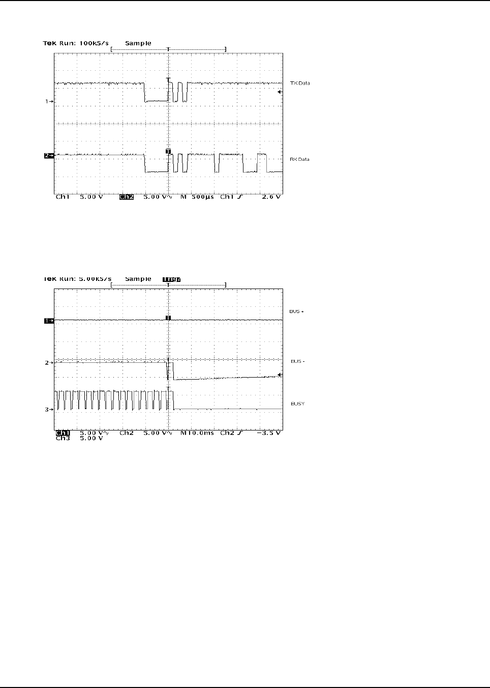
September 26, 2003 6881096C77-O
5-4 Troubleshooting: Troubleshooting Waveforms
Waveform W5: Transmit / Receive Data: U4 pins 19 and 20
Waveform W6: Serial Bus lines: U1 pins 17, 16, 10
NOTE: Serial bus data can be seen during power up and button presses.
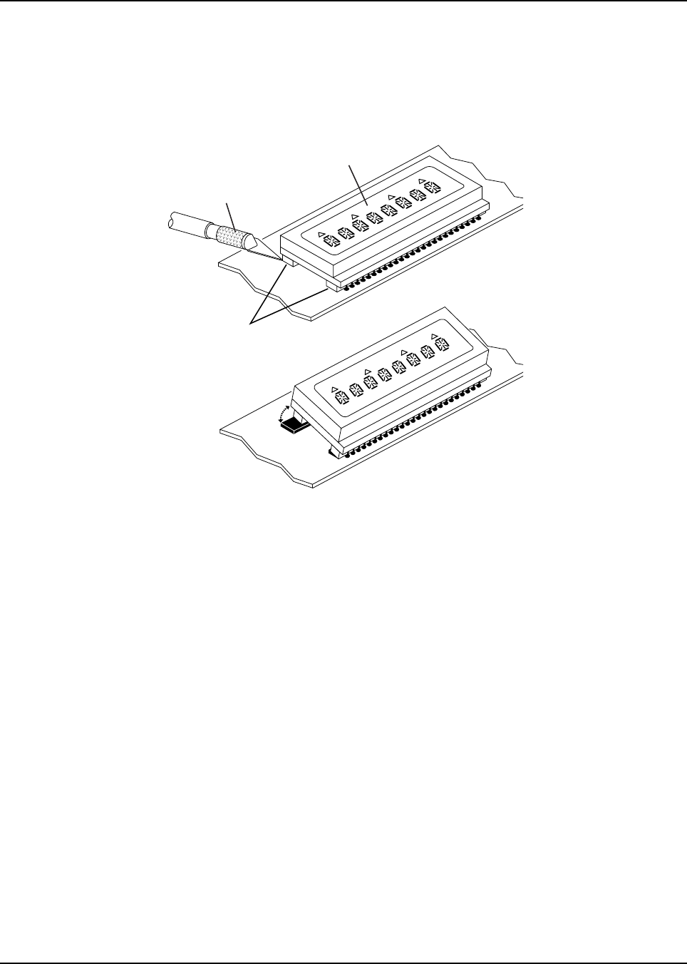
6881096C77-O September 26, 2003
Troubleshooting: Replacing the Vacuum Fluorescent Display (W4, W5, and W7 Control Heads) 5-5
5.3 Replacing the Vacuum Fluorescent Display (W4, W5, and W7
Control Heads)
5.3.1 Removing the Display
1. Figure 5-1 below, Detail A, shows the removal procedure. Cut through the shock pad located
opposite the side of the display with the soldered leads.
Figure 5-1. Replacing the Vacuum Fluorescent Display
2. Wear finger protection to prevent cutting your fingers on the sharp edges of the glass. Pull up
on the edge of the display (see Figure 5-1 above, Detail B), bending the solder leads. Then
cut through the remaining shock pad.
3. Unsolder the leads from the PC board to remove the display. Use organic solvent to remove
the remaining shock pad and adhesive residue from the board.
5.3.2 Installing the Display
1. Apply the adhesive-backed shock pads to the new display. Carefully align the solder leads
and insert the display into the PC board.
2. Solder the leads of the new display to the PC board. Do not reuse the old display.
5.4 Replacing the Remote Back-Housing Interface Board
5.4.1 W4, W5, and W7 Control Heads
1. Unplug the microphone.
2. Disconnect the control cable from the control head on remote models.
3. Remove the two front-panel screws using a 2.5 mm hex-key driver.
4. Grasp the front panel firmly, and carefully unplug the control-head assembly from the radio or
remote control-head back housing.
5. Remove the two remote back-housing interface attachment screws.
6. Remove the remote control-head interface board from the remote control-head back housing.
PRI
PRI NDIR
PRI
PRI NDIR
DETAIL A
DETAIL B
KNIFE
SHOCK
PAD
DISPLAY
September 26, 2003 6881096C77-O
5-6 Troubleshooting: Replacing the Remote Interconnect Board
7. Before installing a new Interface PC board (P/N 0105950T92), check to ensure that all
gaskets are in place. Gasket (P/N 3205197X01) fits the perimeter of the plastic housing on
the bottom surface, and is placed against the sealing rim in back housing. Gasket (P/N
3205198X01) fits inside the pin-out area on bottom of plastic housing. Gasket (P/N
3205082E90) O-rings (2) fit into recessed areas around the bottom of the screw clearance
holes.
8. Attach the new interface PC board to the back housing with the two screws: torqued to
6-8 in.-lbs.
9. Reassemble the back housing to the front housing with the two screws: torqued to 4-6 in.-lbs.
5.5 Replacing the Remote Interconnect Board
5.5.1 Low-/Mid-Power Radios
1. Remove the two front panel screws using a 2.5 mm hex-key driver.
2. Grasp the front panel firmly, and carefully unplug it from the radio.
3. Remove the three screws that hold the remote interconnect board to the front panel using a
Torx T10 driver.
4. Install the new remote interconnect board onto the front panel, and replace the screws.
Torque the screws to 6-8 in.-lbs.
5. Reassemble the front panel into the radio and replace the screws.
6. Torque the screws to 4-6 in.-lbs.
5.5.2 High-Power Radios
1. Use a Torx T15 driver to remove the two screws in the radio top cover and then remove the
radio top cover.
2. Remove the ribbon cable (38-conductor) from between the command board and the
interconnect board by first disconnecting the cable at the command board side and then at
the interconnect board.
3. Disengage the retaining wire on the back of the interconnect board at the chassis side.
4. Use the radio key to unlatch the radio handle, and use a Torx T15 driver to remove the two
interconnect board screws that are inside the handle.
5. Turn the radio upside down and use a Torx T15 driver to remove the four bottom-cover
screws. Remove the bottom cover.
6. Remove the RF-board shield and unplug the coaxial cable that comes up from the other side
of the radio. Move the end of the coaxial cable out from behind the interconnect board.
Take care to avoid misalignment of connector pins.
Take care to avoid misalignment of connector pins. Remove the
radio top cover to allow visual inspection during connector alignment.
!
C a u t i o n
!
C a u t i o n

6881096C77-O September 26, 2003
Troubleshooting: Replacing the Control-Head Board 5-7
7. Pull the retaining wire up into position so that the interconnect board can be slid back away
from the front of the radio, and then up and out from the radio chassis.
8. Remove the rubber gasket from the front of the interconnect board by pulling it up and over
the D-connectors.
9. Gently pry each of the arms on the interconnect board spacer so that the snap feature on the
arms can be slid past the interconnect board.
10. Place the interconnect board spacer onto the new interconnect board, making sure that each
arm is aligned in the proper slot and snaps securely into place.
11. Replace the rubber gasket, retaining wire, coaxial cable, bottom cover (torque four screws to
6-8 in.-lbs), and interconnect board screws (torque two screws to 10-12 in.-lbs).
12. Turn the radio top side up and re-insert the ribbon cable (38-conductor) by first connecting the
command board side and then the interconnect board side. This cable is connected to two
38-pin connectors. The cable is keyed so that the cable fits only in the correct position.
13. Fold the ribbon cable down flat. Replace the top cover and torque the two screws to 6-8 in.-
lbs. These screws are self-tapping and caution should be used so that the screws properly
enter the previously cut threads.
5.6 Replacing the Control-Head Board
5.6.1 W3 Control Heads
NOTE: Numbers shown in brackets in the following procedure refer to item numbers in Figure 7-1,
“W3 Hand-Held Control Head Exploded View,” on page 7-2, and in Table 7-2, “W3 Hand-Held
Control Head Exploded View Parts List,” on page 7-2.
1. Remove the strain-relief boot (part of cable assembly [15]) from the housing assembly [7] by
applying downward pressure on the boot and pulling it away from the control head until they
are completely separated.
2. Carefully remove the rubber seal (part of cable assembly [15]) from the housing assembly [7]
opening.
NOTE:Take care to avoid damaging this seal.
3. Using a small screwdriver, remove the seal support wedge [14] from the control head.
4. Using a small screwdriver to depress the telco lever, remove the telco connector (part of
cable assembly [15]) from the control head, and pull the cable assembly away from the
housing (like a telephone jack).
5. Remove the rear-cover assembly [2] from the control head.
6. Locate the recesses in the lower portion of the housing on both sides of the rear-cover’s snap
features and, prying the snaps until the two parts separate, remove the rear cover from the
unit.
7. Remove the two snap retainers [4] from between the circuit board [5] and the housing
assembly [7].
8. Disconnect the microphone assembly [8] connector from the circuit board [5].
9. Carefully remove the microphone cable assembly from the keypad [6].
10. Carefully pry the housing’s snap features from the circuit board [5].
NOTE:Be careful to avoid damaging circuit-board components.
There are seven snaps locking the circuit board to the housing. As the snap features are
deflected, push the circuit board upward, using the keypad, to release the circuit board from
the snap features.
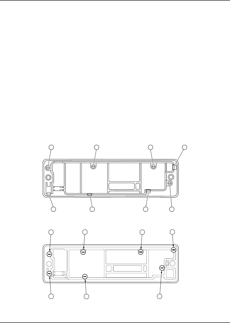
September 26, 2003 6881096C77-O
5-8 Troubleshooting: Replacing the Control-Head Board
11. Remove the circuit-board assembly from the housing.
12. Remove the keypad [6] from the housing assembly [7].
5.6.2 W4, W5, and W7 Control Heads
NOTE: For the following procedure, refer to Chapter 7: Exploded Views and Parts Lists, beginning
on page 7-1, for the exploded view and associated parts list applicable to the model being
disassembled.
1. Unplug the microphone.
2. Remove the two front-panel screws using a 2.5 mm hex-key driver.
3. Disconnect the control cable on remote models.
4. Grasp the front panel firmly, and carefully unplug the control-head assembly from the radio or
remote control-head back housing.
5. Lay the control head face down on a clean, flat surface, being careful not to scratch or mar
the display.
6. Using a Torx T10 driver, remove the control-head screws:
- W4 Control Head: four screws [callouts 5-8], as shown in Figure 5-2.
The W4 control head has, in addition to the screws, four snap features [callouts 1-4], which
are shown in Figure 5-2.
- W5 and W7 Control Heads: seven screws, as shown in Figure 5-3.
Figure 5-2. Model W4 Rotary Control Head Assembly Screw and Snap Sequence
Figure 5-3. Models W5 and W7 Pushbutton Control Head Assembly Screw Sequence
7 1
58
3
42 6
416
2
5
3
7
6881096C77-O September 26, 2003
Troubleshooting: Replacing the Control-Head Board 5-9
7. Carefully separate the PC board, internal spacer, and elastomer keypad assembly from the
front panel.
- On rotary control-head models, care must be taken not to damage the flex circuit when
separating the printed circuit board from the front housing. Do not disturb the buttons in the
front panel.
- On rotary control-head models, the flex circuit must also be unplugged.
8. On rotary control-head models, desolder the XMIT and BUSY LED before removing the
elastomer keypad.
9. Remove the elastomer keypad from the PC board.
NOTE:Before you unsnap the PC board, note that the board slips under a hook on the right
and snaps on the left. This will facilitate the assembly.
10. Remove the PC board from the internal spacer. The PC board snaps into and out of the
spacer.
11. To reassemble, snap the PC board into the internal spacer. Before you press the elastomer
keypad into the board, make sure that the conductive pads in the board and the elastomer
keypad are clean and free of any foreign material.
12. On rotary control head models, solder the XMIT and Busy LEDs onto the PC board.
NOTE:On rotary control head models, the flex circuit must be connected to the PC board
prior to attaching the PC board to the spacer.
13. Install the PC board internal spacer and elastomer keypad assembly into the front panel.
Replace the screws and torque them to 6-8 in.-lbs.
14. Do one of the following:
- For dash-mounted radios, plug the interconnect board into the radio, and then plug in the
control-head assembly and fasten it with the two front-panel screws (torqued to 4-6 in.-lbs).
- For remote-mount control heads, replace the front panel into the remote control-head back
housing, make sure the gasket is in place, and then torque the screws to 4-6 in.-lbs.
Replace any plugs and cables on the rear of the control head.
Take care to avoid misalignment of connector pins. On dash mount
radios, remove the radio top cover to allow visual inspection during
connector alignment.
!
C a u t i o n
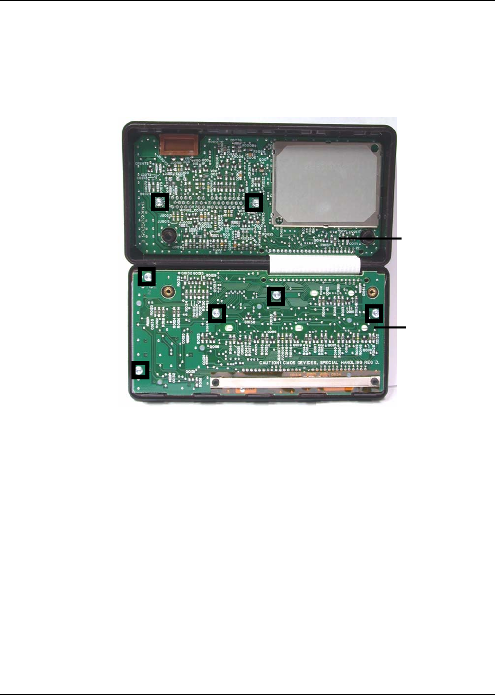
September 26, 2003 6881096C77-O
5-10 Troubleshooting: Replacing the Control-Head Board
5.6.3 W9 Control Heads
NOTE: Before disassembling the W9 control head, note the location of the labeled buttons.
NOTE: Refer to Figure 7-4, “W9 Pushbutton Control Head Exploded View,” on page 7-5 and
Table 7-5, “W9 Pushbutton Control Head Parts List,” on page 7-5 for the callout numbers in
this section.
Figure 5-4. W9 Control Head Control Board and Display Board
1. Using a Torx T15 driver, remove the two 30 mm machine screws [29] from the back housing
[31] of the control head.
2. Fold the front housing [41] over so that the front housing is face down and the back housing is
on your working surface with the flex cable [18] attached.
3. Using a Torx T10 driver, remove the five 8 mm self-tapping screws [17] from the Display
Board Kit [37], the two 10 mm captive screws [12] with the leaf assembly spring [11], and the
two 16 mm tapping screws [38] from the control PC board.
4. Remove the Command Board Kit [36] from the back housing and the Display Board Kit [37]
from the front housing.
5. Remove the elastomer keypad [7], ON/OFF switch gasket [34], the “D” Connector Gasket
[33], the solder-side shield [16], and the component-side shield [19] from the PC boards.
Control Board
Display Board
16 mnm self-tapping screws
(2)
8 mnm self-tapping screws
(5)

6881096C77-O September 26, 2003
Troubleshooting: Final Reassembly–W3 Control Head 5-11
6. Install the new PC board with the elastomer keypad, the ON/OFF switch gasket, the “D”
Connector Gasket, the “D” Connector O-ring, the solder-side shield, and the component-side
shield in the appropriate locations.
7. Reassemble the Command Board Kit [36] into the back housing [31], making sure that the
power switch is in the proper location and then replace the two tapping screws [38], torquing
them to 6-8 in.-lbs.
8. Reassemble the Display Board Kit [37] into the front housing [41], making sure that the
elastomer keypad [7] is in the proper location.
9. Replace the captive screws [12] and the leaf assembly spring [11] in the front housing, and
then torque them to 6-8 in.-lbs.
NOTE:Before assembling the leaf assembly spring, ensure that the insulator [10] on the
board is present. Also ensure that the leaf assembly spring and captive screws are
aligned properly to prevent stripping the front housing screw bosses.
10. Close the assembly by replacing the front housing [41] and the two screws in the back
housing [31]. Torque the screws to 6-8 in.-lbs.
5.7 Final Reassembly–W3 Control Head
When reassembling the control head, make sure the microphone pins are properly inserted through
the elastomeric keypad. Also make sure the elastomeric keypad inserts are secured to the PC board.
NOTE: Numbers shown in parentheses in the following procedure refer to item numbers in
Table 7-2, “W3 Hand-Held Control Head Exploded View Parts List,” on page 7-2.
1. To reassemble the housing assembly [7]:
A. Insert the transmit indicator [11] into the housing. Ensure that the top surface of the
lightpipe is below the label recess of the housing.
B. Attach the nameplate label [13] to the front of the housing. Ensure that the label is
securely attached.
C. Install the PTT actuator [9] into the housing. Ensure that its lip is seated in the grove in the
housing.
D. Install the PTT lever [10] and the PTT boot [12] into the housing. Ensure that the lever is
seated in its nest and the boot is located properly in the recesses in the housing.
E. Install the keypad [6] into the housing. Ensure that all of the keys are located in the correct
openings in the housing.
2. Install the microphone assembly [8] into the keypad. Ensure that the front surface of the
cartridge is located up against the keypad membrane.
NOTE:The membrane is the rain seal and is very sensitive to puncture by sharp objects.
3. Connect the microphone cable connector to the mating location on the circuit board [5].
Be careful to not bend the tabs on the shields when removing
them and align them carefully when replacing the shields.
When working with chips and SOT (small-outline transistor)
parts, use extreme caution when heating. Never reuse a chip
or SOT part; always replace with the correct Motorola part.
!
C a u t i o n

September 26, 2003 6881096C77-O
5-12 Troubleshooting: Troubleshooting Charts
4. Install the circuit board [5] into the housing assembly [7] as follows:
A. Hold the housing assembly so that its key openings face downward and its top faces away
from you.
B. Pivot the circuit board’s display down under the retention features in the housing and
rotate the board downward, ensuring that the board is positioned between the snap
features. Ensure that the microphone assembly’s [8] wire passes through the opening in
the circuit board.
C. Press downward firmly on the board until the seven snap features lock the board into
place.
5. Install the two snap retainers [4] between the circuit board and the side wall of the housing
assembly [7], one on each side.
6. Install the main seal [3] onto the rear cover assembly [2], placing the seal under the retainer
features around the perimeter of the cover.
7. Install the rear cover assembly [2] onto the housing assembly [7].
Starting at the top of the cover, pivot the cover toward the housing and squeeze the two
halves together until the snap features at the lower end of the rear cover engage the
housing’s features and snap closed.
8. Insert the cable assembly’s [15] telco connector into the opening in the bottom of the housing,
and ensure that it is correctly oriented.
9. Press the telco connector in place until it snaps in (like a phone plug).
10. Place the seal-support wedge [14] into the housing’s opening, orienting it so that its long
portion is under the telco connector lever, and then push until it is properly seated.
11. Push the rubber seal (part of the cable assembly [15]) into the housing’s opening and ensure
that it is properly seated.
NOTE:This seal must be inserted completely into the housing to ensure the rain seal.
12. Push the strain-relief boot (part of the cable assembly [15]) into the housing and ensure that it
is properly seated.
13. Insert the kit label [1] into the recess on the rear cover, and ensure that it is securely attached.
5.8 Troubleshooting Charts
This section contains detailed troubleshooting flowcharts. These charts should be used as a guide in
determining the problem areas. They are not a substitute for knowledge of circuit operation and
astute troubleshooting techniques. It is advisable to refer to the related detailed circuit descriptions in
the theory section prior to troubleshooting a radio.
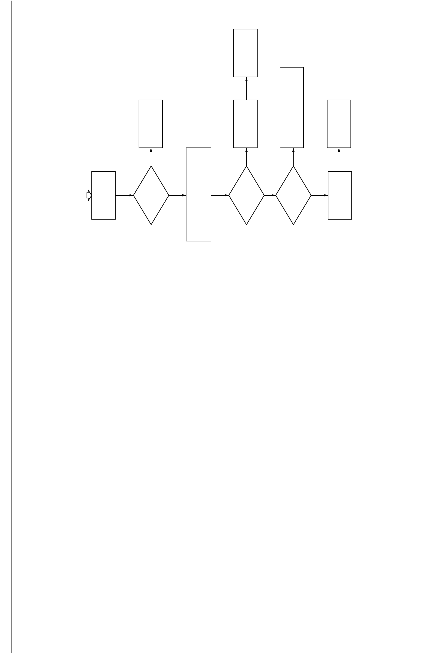
Troubleshooting 5-13
6881096C77-O September 26, 2003
Figure 5-5. W4 Control Head (Sheet 1 of 2)
START
Check U45
(+5V Reg.)
Repair
Is
+5V OK
?
With no buttons pressed, check U1
pins 8-11 for activity.
Activity
on all pins
?
(8-11)
Activity
on one pin
only
?
No activity
at all
Check U1 for
proper operation
and repair
Check that pin for a shorted button
closure somewhere on the line.
Check return lines (U1 pins 13-15).
Check R120-R122.
Press buttons and
check return lines
(U1 pins 13-17).
Check R120-R124
Repair
MAEPF-22619-A
CONTROL UNIT POWERS UP
PROPERLY BUT BUTTON PRESSES
DO NOT WORK.
YES
YES
NO
YES
NO
NO
NO
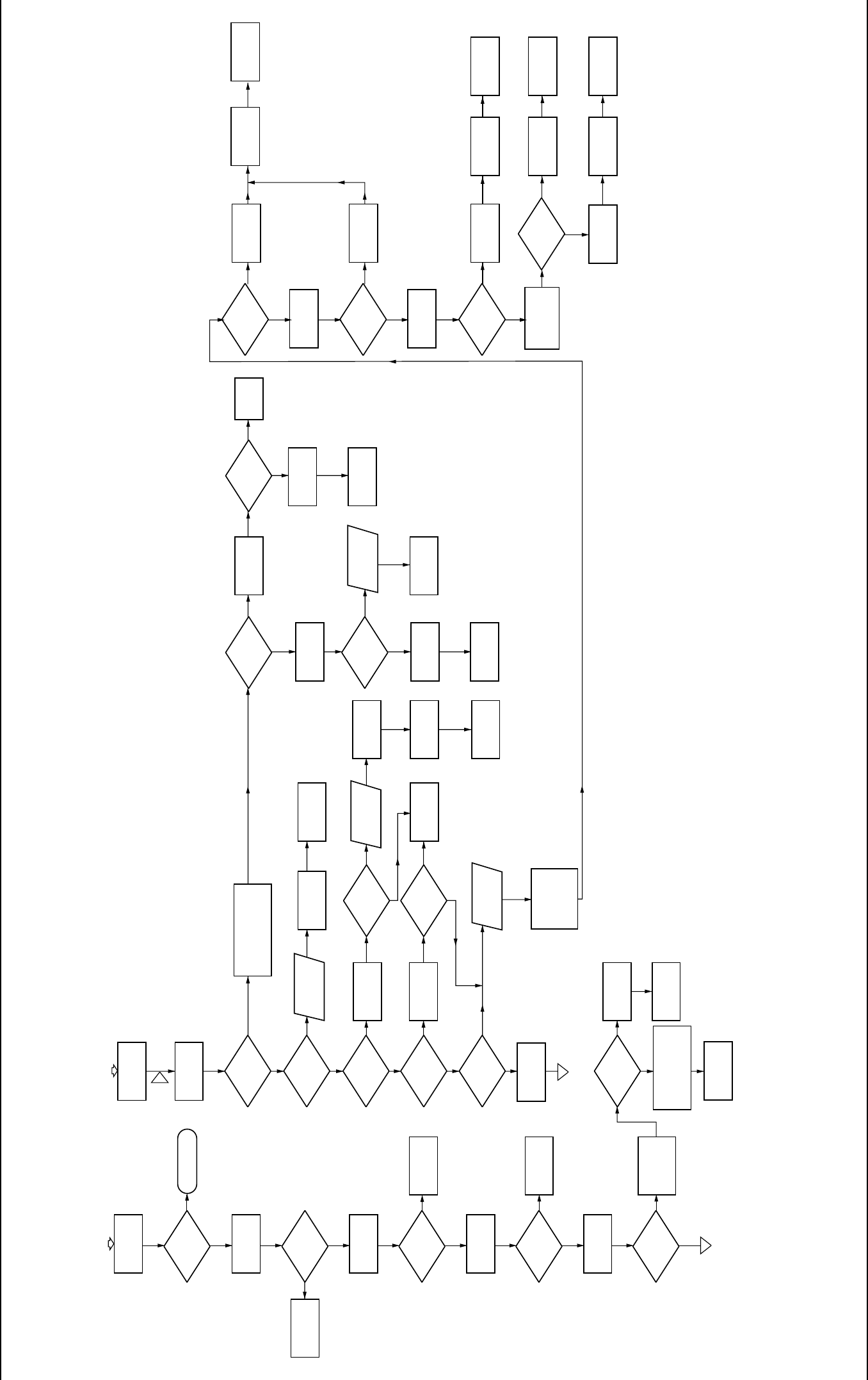
5-14 Troubleshooting
September 26, 2003 6881096C77-O
Figure 5-6. W4 Control Head (Sheet 2 of 2)
A
A
CR50 is
Probably Open
Check
U101-1
Voltage
Is
Voltage
33 to 39V
?
Is
Voltage
over 40V
?
Is
Voltage
20 to 25V
?
Is
Voltage
11 to 14V
?
Choose the
closest voltage
range and
proceed
Is
Reset Line
OK
?
Check U1: U4: Y1 for proper
operation. U1-1 must go
low momentarily after
power up, then stay high
to properly initialize U1
Repair and
Return to
Start
CR50 is
probably open
Remove VF
Display
Check T60
pins 1, 2, 3
continuity
Check
C52
Check U4 and
cabling for source
of problem
Repair and
Return to
Start
START
VERY BRIGHT DISPLAY
VARIES WITH SUPPLY VOLTAGE
Check VF Display
Filament Voltage with an
AC voltmeter between pins
1 and 25 of VF Display. The
voltage should be 2 to 3 Vrms
Check R51, R52,
C51, C52
and repair
OK
?
Is
C52 OK
?
Possible sawtooth
oscillator problem
Remove VF
Display
Observe waveform
at U3-3. Compare
with
Waveform W2
in section 5.8
Return
To
Start
CR51 is probably
open
Remove VF
Display
Repair and
Return to
Start
Q50 may have
been overstressed
during failure
Replace Q50
Check CR51,
Q50 and
Repair
Return
To
Start
Check VF Display
Filament
For Open
Return
To
Start
Check R101, T60
and
Repair
Is
Filament
Open
?
Is
Voltage
Correct
?
Check R50
and T60
pins 4, 5, 6
for continuity
Remove VF
Display and
Replace
Return
To
Start
OK
?
Check U101
and U1 for
proper
operation
Repair and
Return to
Start
Is
waveform
correct
?
Check DC voltage
on U3-2. It should
be 1.5 to 2.0 VDC
Is
voltage
correct
?
Check U3-1
Waveform W3
in section 5.8
Is
waveform
present
?
Check Q50 drain.
Compare to
Waveform W5 in
section 5.8
Check U3, C54,
R56-R60
and Repair
Q50 may have been
overstressed
during failure.
Replace Q50
Return
To
Start
Check R52,
R51, C51
and Repair
Check U3,
R61, Q50,
and Repair
Q50 may have been
overstressed during
failure. Replace Q50
Return
To
Start
Return
To
Start
Return
To
Start
Is
waveform
present
?
Check R61,
Replace Q50
Check T60
and Repair
Q50 may have been
overstressed during
failure. Replace Q50
Turn Power on
with Control Head
connected to radio
Is
display at proper
brightness
level
?
Check for SWB+
voltage on Control
Head PC Board
Is
SWB+ On
?
Check U45
(+5V REG)
Is
+5V OK
?
Check L50,
R55
Continuity
OK
?
Check
U1-6
Is
Voltage
Low
?
No Problem
END
Repair and
Return to
Start
Repair and
Return to
Start
Check Reset
line to see if it is
being held high
by radio
malfunction
A
START
NO DISPLAY OR
VERY DIM DISPLAY
Check SW1, J102,
P102 and Repair:
Return to Start
NO
YES
NO
YES
YES
NO
NO
YES
MAEPF-22618-O
NO
YES
NO
YES
YES
NO
YES
NO
NO
YES
YES
YES
YES
YES
YES
NO
NO
NO
NO
NO
NO
YES
YES
NO
YES
NO
YES
NO
YES
NO
YES
NO
Is
Voltage
below 10V
?
Repair and
Return to
Start

Chapter 6 Radio Connectors
This chapter contains the ASTRO Digital Spectra and Digital Spectra Plus connector locations.
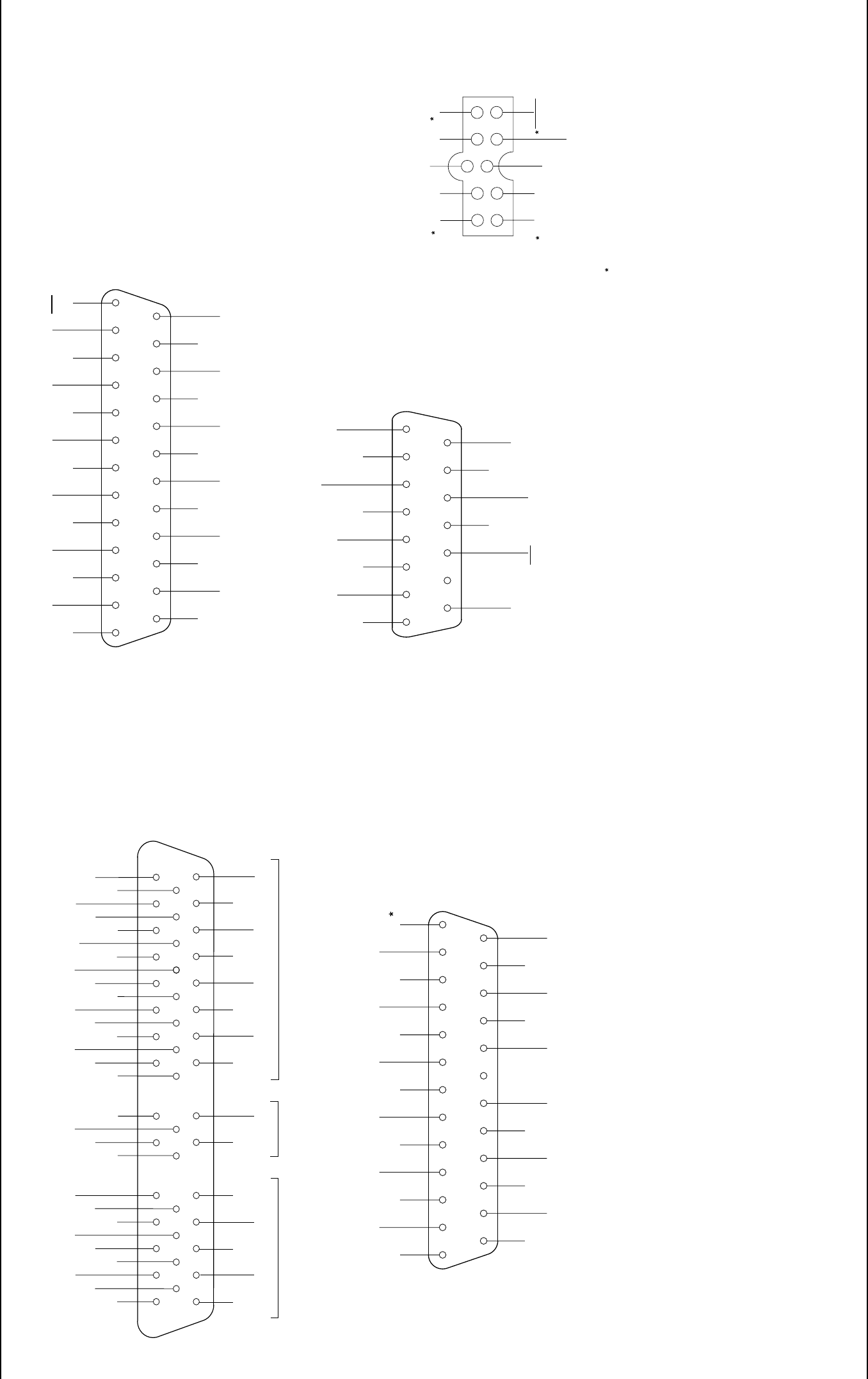
6-2 Radio Connectors: Radio Connectors
September 26, 2003 6881096C77-O
6.1 Radio Connectors
Figure 6-1. J0103 Remote-Mount Control Head Connector
Figure 6-2. J5 Control Cable for Remote-Mount Control Head
Figure 6-3. J6 Radio Operations Connector
Figure 6-4. J2 Rear Accessory Connector
Figure 6-5. P104 Microphone Jack
12345 13
12
11
108
714 15 16 17
48 4940 4134 43 4435 36 37 38 45 46 47 50
VIP 2
OUT
VIP 1
OUT
VIP 2
IN
VIP 1
IN
DATA
OUT
MIC
LO
MIC
HI
SPKR
LO
SPKR
LO
MIC
HI
MIC
LO BATT -
VF
SENSE
1 IGN +
ANALOG
GND
BUS +
SWB + DIG
GND
PTT/HUB
REF
PTT
RESET
EMGCY BATT +
(A+)
BATT -
VF
SENSE
2
IGN -
BUSY
SWB +
DIG
GND
SPARE
-1
SPARE
-2
29
28
27
26 30 31 32
18 19 20 21 23 24 33
VIP 3
OUT
SWB +
DIG
GND
VIP 3
IN
CLOCK HUB
SWB +
SPKR
HI NC BATT + DIG
GND
BUSSPKR
HI NC NC
RADIO
MIC
VIP
MAEPF-21670-A
EMER
MIC
HI ANA
GND TX
AUD FLT
AUDIO (FILT-AUD
SHLD)
MIC
LO DET
AUD RX
AUDIO BUS + IGN
RESET
B+
BUSY
SPKR
LO SWB +
SPKR
HI DIG
GND BUS -
123456
13 12 11 10 9 8 7
14
1516
1718192021
2223
24
25
MAEPF-23798-O
(PTT )
BUS
SHLD A +
RESET SPARE-2
SPARE-1
RSSI
EMER
MIC
HI ANA
GND TX
AUD FLT
AUD NC FIL AUD
SHLD
MIC
LO DET
AUD RX
AUD BUS + IGN PTT/
VIP IN 1
SPKR
HI BUSY BUS
SHIELD RESET
SPKR
LO SWB + A + DIG
GND
SPARE
2SPARE
1
RSSI/
VIP IN 2
BUS -
123456
13 12 11 10 9 8 7
14
15
16
1718192021
2223
24
25
MAEPF-21669-A
DIG
GND SPKR
HI EMER
SPKR
LO NOTE 1
IGNITION
VIP OUT 2
NOTE 1
SWB+
PTT/
TX-RS232
BUSY
12345687
9
1011
12131415
MAEPF-23799-O
VRS TX/
CTS-RS232
MIC HI/RESET/
RTS-RS232
BUS+ VIP OUT 1
NOTE1
DISC. AUD/
RX-RS232
BUS-
FUNCTIONAL ONLY IN DASH-MOUNT
CONFIGURATION. N.C. IN REMOTE-MOUNT
CONFIGURATION.
NOTES:
1.
GND
DIG
GND MIC
LO
PTT/
PROGRAM
RESET
9
10
7
8
5
6
MAEPF-23800-A
PROG
RX
DATA
SWB+
PINS 1, 2, 9, AND 10 ARE NO CONNECTIONS (NC)
ON P104 OF A REMOTE-MOUNT CONTROL HEAD.
DETAIL SHOWN FROM
CONTROL HEAP FRONT VIEW
(MALE PIN VIEW)
Vpp
1
2
3
4
HUB/
BUSY
KEYFAIL/
PROG
TX DATA
MIC HI/
PROG
RX/TX ENABLE
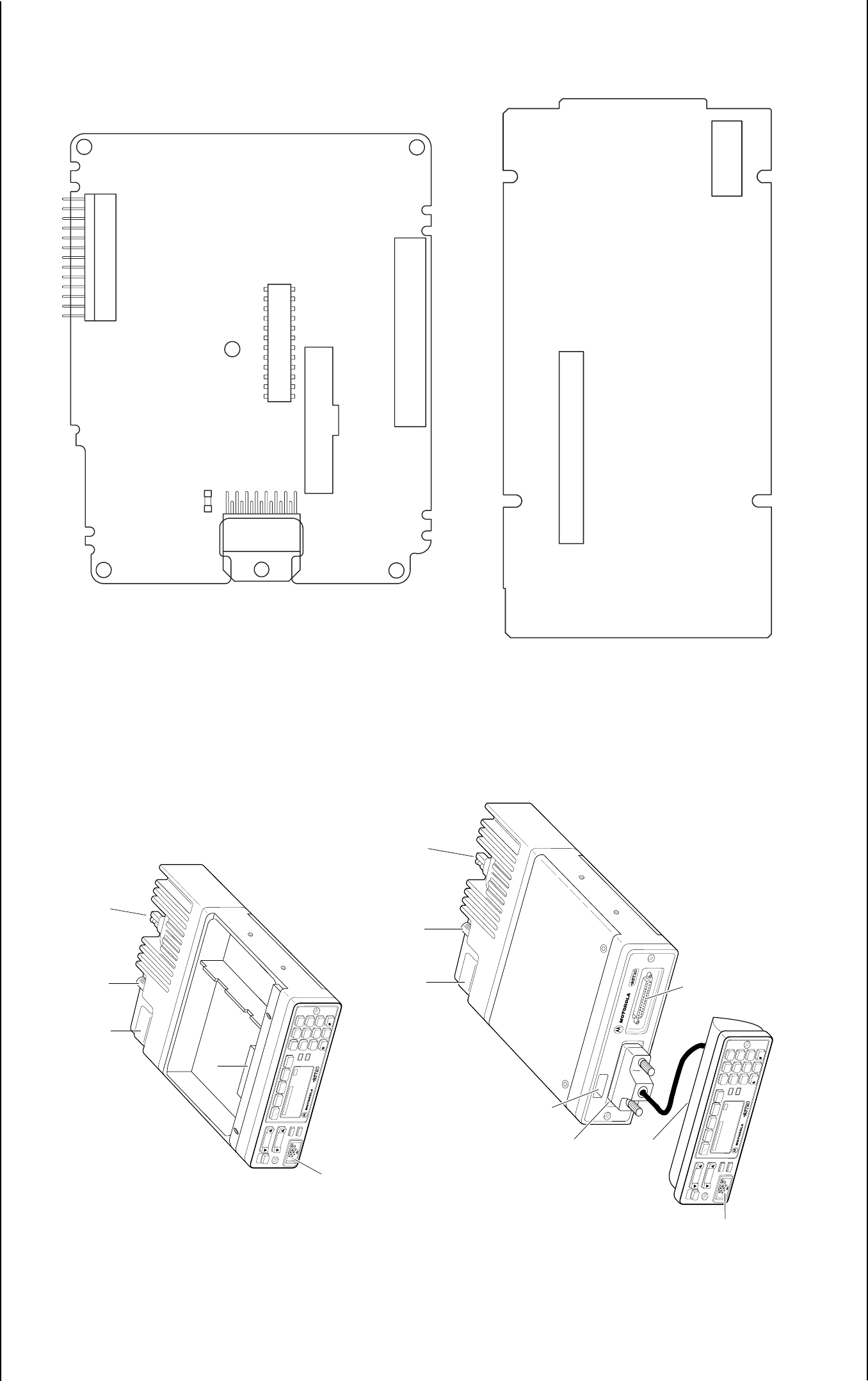
Radio Connectors: Radio Connector Locations 6-3
6881096C77-O September 26, 2003
6.2 Radio Connector Locations
Figure 6-6. Dash-Mount Radio Connector Locations
Figure 6-7. Remote-Mount Radio Connector Locations
Figure 6-8. Command Board Connector Locations
Figure 6-9. VOCON Board Connector Locations
MAEPF-24496-O
0
PWR
Mode Scan
Phon Sel
Call
Vol
DIM
HOME
XMIT
BUSY
123
456
789
0
Sts Msg
H/L MonDir
RclDel
DASH-MOUNT RADIO
J2 ANTENNA PWR
P502
P104
MAEPF-24497-A
0
PWR
ModeScan
PhonSel
Call
Vol
DIM
HOME
XMIT
BUSY
123
456
789
0
Sts Msg
H/L Mon Dir
Rcl Del
J2
J5
P506
REMOTE-MOUNT
CONTROL HEAD
REMOTE-MOUNT
RADIO
J6
J0103
P104
ANTENNA PWR
COMMAND BOARD
(VIEWED FROM SIDE 1)
P503
F500
U450
15
24 19
16
J500
2
50
49 1
25
30
P501
P502
1
38 29
10
20
19
13
12
14 13
12 11
10 9
8
3
65
4
21
7
1
214
13 25
26
VOCON BOARD
(VIEWED FROM SIDE 2)
49
50 J501
25
24
J801
2
1
1
2
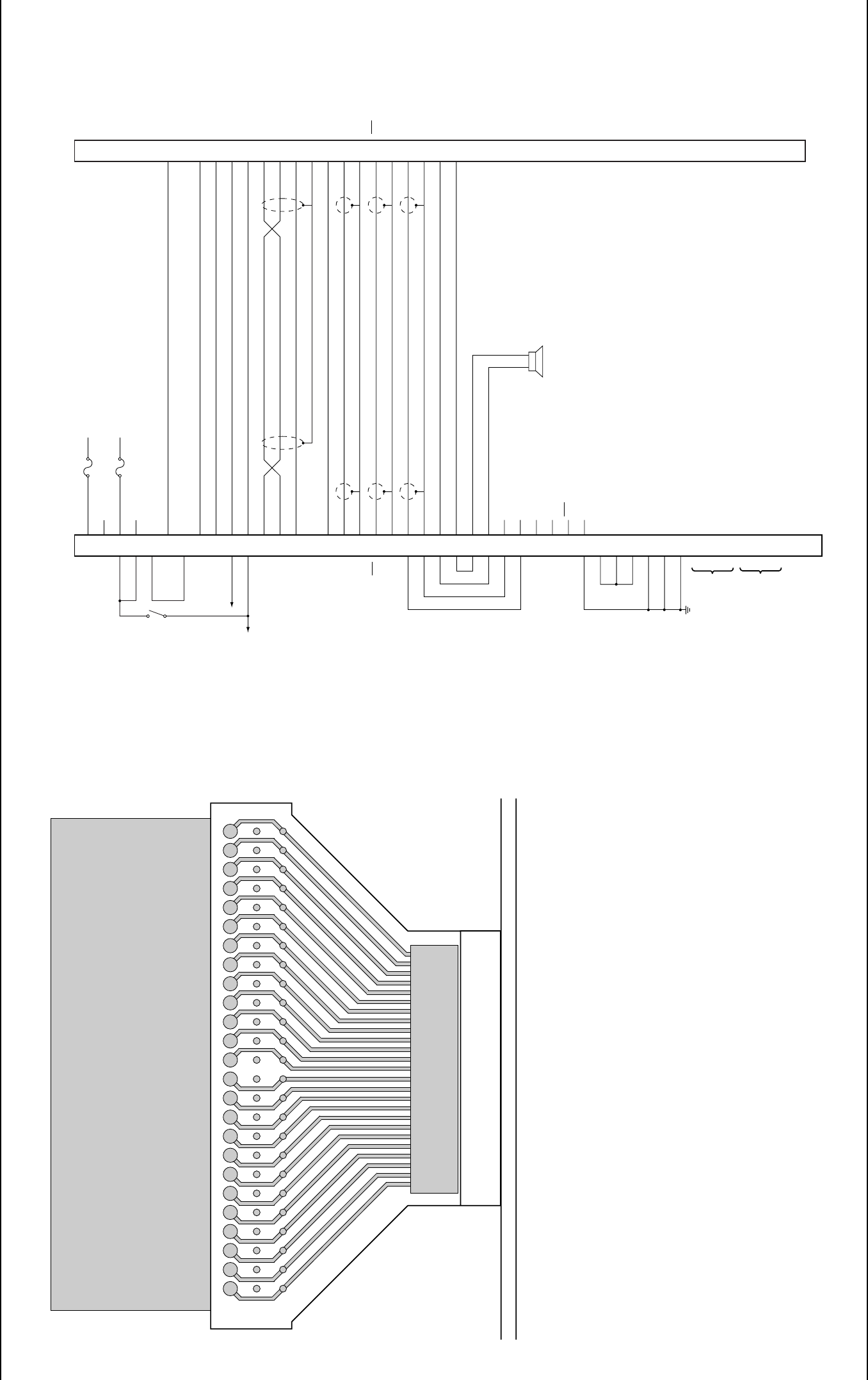
6-4 Radio Connectors: Extender Cable (P501)
September 26, 2003 6881096C77-O
6.3 Extender Cable (P501)
Figure 6-10. P501 Extender Cable
6.4 Control-Head Cabling Diagram
Figure 6-11. Control-Head Cabling Diagram
151719 131197531212325272931333537394143454749
16
18
20 14 12 10 8642
22
2426
2830
32
3436
38
404244
46
4850
P501
EXTENDER
CABLE
(3080370E06)
(FACING TOWARD
CONTROL HEAD)
J501
COMMAND BOARD
P1001
SPARE 2
EMERGENCY
SPARE 1
DIG GND
SWB+
BUS +
BUS -
BUSY
BUS SHIELD
RESET
DET AUDIO
ANA GND
PTT
MIC HI
MIC LO
SPKR HI
SPKR LO
A+
RSSI
RX AUDIO
RED
VIO
BRN
BLU
YEL
WHT
BLK
BLK/RED
BARE
BLK/ORG
BLK/BRN
SHIELD
BLK/GRN
SHIELD
BLK/YEL
SHIELD
ORG
GRN
CONTROL HEAD
ORG
GRN
NC
NC
MIC LO
MIC HI
SWB+
HUB
PTT
PTT/HUB REF
SWB+
SWB+
SWB+
DIG GND
DIG GND
DIG GND
(DATA IN)
(STROBE)
(CLOCK)
(DATA OUT)
BUS +
BUS -
BUSY
RESET
DET AUDIO
ANA GND
PTT
IGN+
IGN-
BATT+
BATT+
BATT-
SPARE 2
BATT-
EMERGENCY
SPARE 1
BLK/GRN
BLK/ORG
DIG GRD
SWB+
P5
RADIO
15
32
47
30
31
29
14
27
28
49
48
17
50
33
26
45
16
46
12
13
44
11
10
43
7
8
41
40
24
23
18
19
3
20
21
36
4
3
37
2
1
34
38
5
SPEAKER
17
13
16
18
22
5
14
23
21
19
9
0
1
12
11
25
24
20
15
7
1
2
3
1
2
3
VIP IN
VIP OUT
Chapter 7 Exploded Views and Parts Lists
This chapter contains the exploded views and associated parts lists for each of the ASTRO Digital Spectra and Digital Spectra Plus control heads. Tables containing pushbutton parts lists are also included.
Table 7-1. Exploded Views
Fig # Description Page #
Figure 7-1 W3 Hand-Held Control Head Exploded View 7-2
Figure 7-2 W4 Rotary Control Head Exploded View 7-3
Figure 7-3 W5 and W7 Pushbutton Control Head Exploded View 7-4
Figure 7-4 W9 Pushbutton Control Head Exploded View 7-5
Figure 7-5 HMN1080A, HMN1061A, HMN1079A Microphone Exploded View 7-6
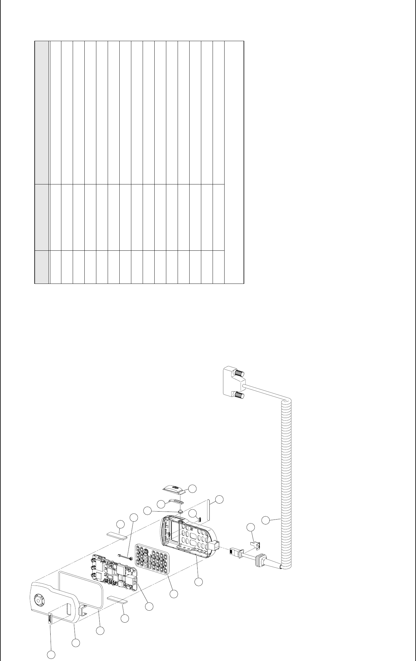
September 26, 2003 6881096C77-O
7-2 Exploded Views and Parts Lists: Model W3 Hand-Held Control Head Exploded View
7.1 Model W3 Hand-Held Control Head Exploded View
Figure 7-1. W3 Hand-Held Control Head Exploded View
2
1
3
4
5
6
7
8
4
15
14
10
9
12
11
13
Table 7-2. W3 Hand-Held Control Head Exploded View Parts List
Item No. Motorola Part No. Description
1 Not available LABEL
2 0105955T26 ASSEMBLY, Rear Cover
3 3205082E93 SEAL, Main
4 4205343Y01 RETAINER, Snap (Qty 2)
5 0102707D81 BOARD, SB9600 Circuit
6 7505832X01 KEYPAD (Part of Item 7)
7 0102707D86 ASSEMBLY, Housing (Includes Items 6 and 9 thru 13)
8 0102708D08 ASSEMBLY, Microphone
9 7505618V02 ACTUATOR, PTT (Part of Item 7)
10 4505850X01 LEVER, PTT (Part of Item 7)
11 3205839X01 INDICATOR, Transmit (Part of Item 7)
12 3805835X01 BOOT, PTT (Part of Item 7)
13 3305409X17 LABEL (Part of Item 7)
14 3205274V01 WEDGE, Seal Support
15 HKN6095_ ASSEMBLY, Cable
Note: _ = The latest version kit. When ordering, refer to your specific kit for
this suffix letter.
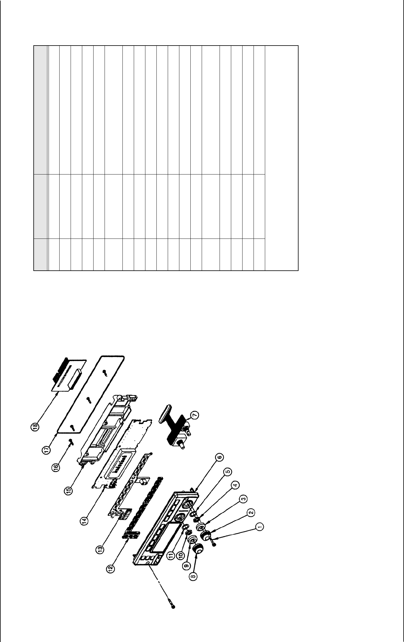
Exploded Views and Parts Lists: W4 Rotary Control Head Exploded View 7-3
6881096C77-O September 26, 2003
7.2 W4 Rotary Control Head Exploded View
Figure 7-2. W4 Rotary Control Head Exploded View
Table 7-3. Model W4 Rotary Control Head Parts List
Item No. Motorola Part No. Description
1 0380077M01 SCREW, Control Head Mounting (Qty 2)
2 3602113Z05 KNOB, Volume Control
3 3205805V01 GASKET, W4 Shaft (Qty 2)
4 0284218M01 NUT, Volume Switch
5 0484219M01 LOCKWASHER, Volume Switch
6 1502117Z07 or
1502117Z08 HOUSING, Front Cover (Mobile)
HOUSING, Front Cover (Motorcycle)
7 0102709J83 ASSEMBLY, Volume and Rotary Switch
8 3602113Z03 KNOB, Mode Control
9 3205805V01 GASKET, W4 Shaft (Qty 2)
10 0284218M02 NUT, Mode Switch
11 0484219M02 LOCKWASHER, Mode Switch
12 6105129X01 LIGHTPIPE
13 7505128X01 KEYPAD
14 AAHN4045_ or
PMLN4019_ ASSEMBLY, Circuit Board (Mobile)
ASSEMBLY, Circuit Board (Motorcycle)
15 4302112Z02 SPACER, Internal
16 0310945A14 SCREW, Machine (Qty 4)
17 3280289L02 GASKET, Housing
18 HLN6401_ ASSEMBLY, Circuit Board Interconnect
Notes: _ = The latest version kit. When ordering, refer to your specific kit
for this suffix letter.
The HKN4356_ Radio Cable is used to remote mount the W4
Control Head.
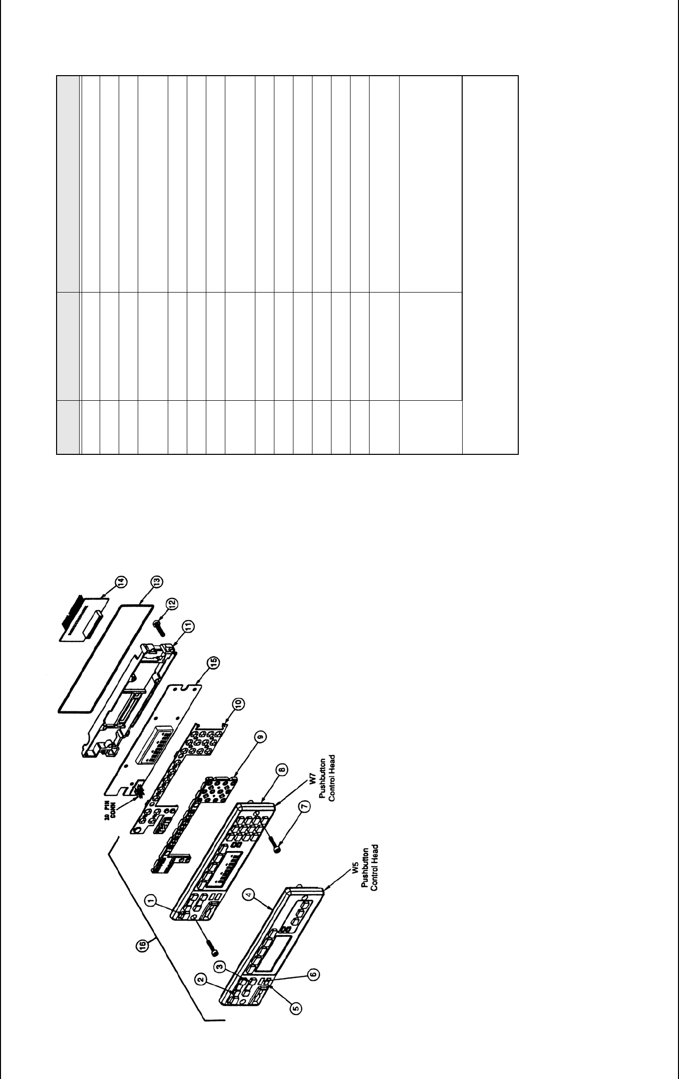
September 26, 2003 6881096C77-O
7-4 Exploded Views and Parts Lists: W5 and W7 Pushbutton Control Head Exploded View
7.3 W5 and W7 Pushbutton Control Head Exploded View
Figure 7-3. W5 and W7 Pushbutton Control Head Exploded View
Table 7-4. W5 and W7 Pushbutton Control Head Parts List
Item No. Motorola Part No. Description
1 3880227M04 SWITCH, On/Off Cap
2 3880009P01 SWITCH, Mode Rocker
3 3880009P02 SWITCH, Volume Rocker
4 1580020S17 or
1580020S19 HOUSING, W5 Front Cover (Mobile)
HOUSING, W5 Front Cover (Motorcycle)
5 3880092J05 PUSHBUTTON, HOME
6 3880092J05 PUSHBUTTON, DIM
7 0380077M01 SCREW, (Qty 2)
8 1580020S16 or
1580020S18 HOUSING, W7 Front Cover (Mobile)
HOUSING, W7 Front Cover (Motorcycle)
9 6180017S01 LIGHTPIPE
10 7580012S03 KEYPAD
11 4380019S02 SPACER, Internal Frame
12 0310945A14 SCREW, Tapping (Qty 7)
13 3280289L02 GASKET, Housing
14 HLN6401_ BOARD, Interconnect
15 HLN6396_ or
HLN6563_ BOARD, Control Head (Mobile)
BOARD, Control Head (Motorcycle)
16 0180049S09 or
0180049S11 or
0180049S08 or
0180049S10
ASSEMBLY, W5 Front Cover (Mobile)
ASSEMBLY, W5 Front Cover (Motorcycle)
ASSEMBLY, W7 Front Cover (Mobile)
ASSEMBLY, W7 Front Cover (Motorcycle)
Item 16 includes items 1, 2, 3, 4 or 8, 5, 6, 9, and 10
Notes: _ = The latest version kit. When ordering, refer to your specific kit
for this suffix letter.
The HKN4356_ Radio Cable is used to remote mount the W5 and
W7 Control Head.
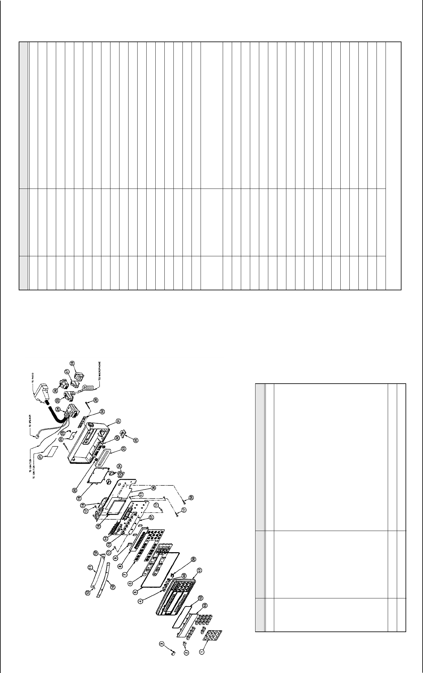
Exploded Views and Parts Lists: W9 Pushbutton Control Head Exploded View 7-5
6881096C77-O September 26, 2003
7.4 W9 Pushbutton Control Head Exploded View
Figure 7-4. W9 Pushbutton Control Head Exploded View
Table 7-5. W9 Pushbutton Control Head Parts List
Item No. Motorola Part No. Description
1 1380087J01 ESCUTCHEON
2 HLN5083_
HLN5091_
HLN5066_
HLN5256_
HLN5074_
HLN5268_
HLN5259_
HLN5258_
HLN5090_
HLN5072_
HLN5257_
HLN5076_
HLN5085_
HLN5078_
HLN5087_
HLN5079_
HLN5095_
BUTTON, Emergency
BUTTON, Dir
BUTTON, Scan
BUTTON, Srch
BUTTON, Call
BUTTON, Page
BUTTON, RPGM
BUTTON, Site
BUTTON, PHON
BUTTON, H/L
BUTTON, Lock
BUTTON, RCL
BUTTON, SQL
BUTTON, Del
BUTTON, Home
BUTTON, Sel
BUTTON, Blank
3 3880253K01 PLUG
4 3880195P03 SWITCH, Mode Rocker
5 3205145X01 GASKET, Internal Frame
6 6105126X01 LIGHTPIPE, Keypad
7 7505127X01 KEYPAD
8 7280242J01 DISPLAY, VF
9 7580094M05 PAD, Shock (Qty 3)
10 1405410X01 INSULATOR
11 4180042S01 SPRING, Leaf Assy
12 0380041S01 SCREW, Captive (Qty 4)
13 6180026R02 SPACER, LED (8-Position)
14 6180027R02 SPACER, LED (2-Position)
16 2680190P02 SHIELD, Solder Side (Includes two 1480269K01 insulators)
17 0310945A11 SCREW, Tapping (Qty 5)
18 3080034K01 CABLE, Flex
19 2680190P02 SHIELD, Component Side
20 3205082E90 O-RING "D" Connector (Qty 2)
21 3380178M01 NAMEPLATE
22 0784323C01 BRACKET, Strain Relief
23 0310908A18 SCREW, Machine
24 HKN4356_ CABLE, Radio
25 HMN1050_ or
HMN1080_ or
HMN1061_
KIT, Microphone
26 1580221J01 HOUSING, VIP Connector (Optional)
27 7502118Z01 COVER, Rubber Dust (MIC)
28 7502118Z02 COVER, Rubber Dust (VIP)
29 0310908A33 SCREW, Machine (Qty 2)
30 3205198X01 GASKET, Face
31 1505199X01 HOUSING, Back
32 2805778W01 CONNECTOR, Mini "D" 50 Contact
33 3205143X01 GASKET, "D" Connector
34 3205143X01 GASKET, On/Off Switch
35 3880128J01 KEY, On/Off
36 HCN4046_ BOARD KIT, Command (includes Display Board)
37 HCN4046_ BOARD KIT, Display (includes Command Board)
38 0310945A14 SCREW, Tapping (Qty 2)
39 3880092J05 KEY, Blank
40 3880195P02 SWITCH, Volume Rocker
41 1505125X09 HOUSING, Front
42 3205144X01 GASKET, Lens
43 6105146X01 LENS, VF Display
Note: _ = The latest version kit. When ordering, refer to your specific kit for this suffix
letter.
Table 7-5. W9 Pushbutton Control Head Parts List (Continued)
Item No. Motorola Part No. Description
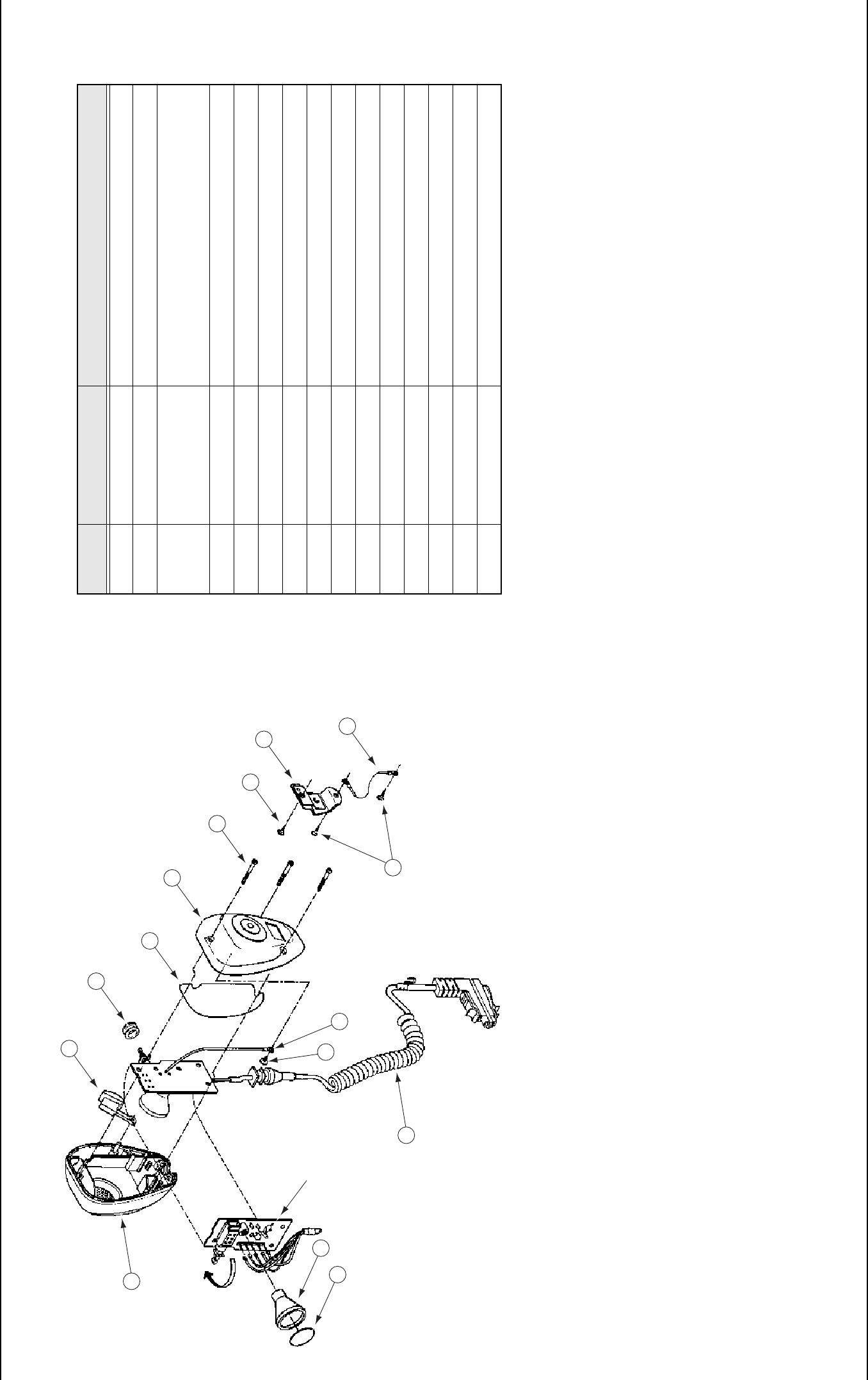
7-6 Exploded Views and Parts Lists: HMN1080A, HMN1061A, HMN1079A Microphone Exploded View
September 26, 2003 6881096C77-O
7.5 HMN1080A, HMN1061A, HMN1079A Microphone Exploded View
Figure 7-5. HMN1080A, HMN1061A, HMN1079A Microphone Exploded View
4
2
1
15
8
9
3
10
13
14
12
11
7
MICROPHONE
BOARD
MAEPF-27700-O
5
6
Table 7-6. HMN1080A, HMN1061A, HMN1079A Microphone Parts List
Item No. Motorola Part No. Description
1 1580127D05 Microphone Front Housing
2 3880144D05 Microphone PTT Button
3 3080223J05 or
3080210P01 or
3080223J01
HMN1080A Coiled 6 Cond
HMN1079A Coiled 6 Cond
HMN1061A Coiled 6 Cond
4 0580221K01 PTT Switch Grommet
5 0310943M09 Tapping Screw (3 x 0.5 x 6)
6 3080206L01 PCB to Mic Weight Wire
7 3280058H03 Housing Gasket
8 0180750T91 Microphone Rear Housing
9 0380076E04 Hi-lo Metric Screw
10 0312002C01 Screw, Self-drilling, 6-20 x 1/2”
11 3580089D01 Microphone Felt Baffle
12 0580148D01 Microphone Grommet
13 0180743T91 Hangup Clip
14 0180750T52 Ground Wire
15 0300138015 Screw, Self-drilling, 8-18 x 1/2”
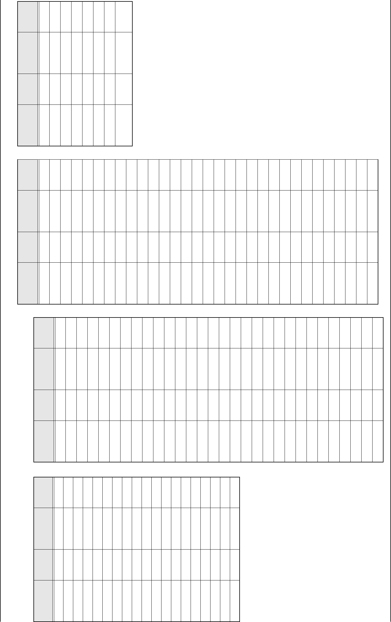
Exploded Views and Parts Lists: Small Pushbutton Parts 7-7
6881096C77-O September 26, 2003
7.6 Small Pushbutton Parts 7.7 Large Pushbutton Parts
Table 7-7. Small Pushbutton Parts List
Part Number Graphic
Legend Part Number Graphic
Legend
3805671X02 1 3805671X21 9wxy
3805671X03 2 3805671X22 * Rcl
3805671X04 3 3805671X23 #Del
3805671X05 4 3805671X24 1Ste
3805671X06 5 3805671X25 2Pge
3805671X07 6 3805671X26 3Lck
3805671X08 7 3805671X27 4Sts
3805671X09 8 3805671X28 5Rpg
3805671X10 9 3805671X29 6Msg
3805671X11 0 3805671X30 7H/L
3805671X12 * 3805671X31 8Mon
3805671X13 # 3805671X32 9Dir
3805671X14 2abc 3805671X33 Mon
3805671X15 3def 3805671X34 H/L
3805671X16 4ghi 3805671X35 DIR
3805671X17 5jkl 3805671X36 Urg
3805671X18 6mno 3805671X37 RTT
3805671X19 7prs 3805671X38 Home
3805671X20 8tuv 3805671X39 Dim
Table 7-8. Large Pushbutton Parts List
Part Number Graphic
Legend Part Number Graphic
Legend
3805672X01 - - 3805672X10 H/L
3805672X02 MPL 3805672X11 Sts
3805672X03 Scan 3805672X12 Call
3805672X04 DVP 3805672X13 Msg
3805672X05 PA 3805672X14 Rcl
3805672X06 Sirn 3805672X15 Mode
3805672X07 Wail 3805672X16 ExRd
3805672X08 Hi/Lo 3805672X17 Del
3805672X09 Man 3805672X18 Sel
3805672X19 Mon 3805672X52 Emer
3805672X20 DTMF 3805672X53 Stdy
3805672X21 Yelp 3805672X54 ECC
3805672X22 MVS 3805672X55 Rptr
3805672X23 Play 3805672X56 State
3805672X24 Rply 3805672X57 Reg
3805672X25 Rcrd 3805672X58 AirHn
3805672X26 Emer 3805672X59 TB Scn
3805672X27 Ext 3805672X60 SCC
3805672X28 F/R 3805672X61 Srch
3805672X29 Alt 3805672X62 Lock
3805672X30 Tel 3805672X63 Page
3805672X31 Sql 3805672X64 Rear
3805672X32 DES 3805672X65 Xfer
3805672X33 Txt 3805672X66 ST
3805672X34 Indv 3805672X67 VHF
3805672X35 Pvt 3805672X68 UHF
3805672X36 Site 3805672X69 Aux
3805672X37 AA 3805672X70 QC II
3805672X38 Sub 3805672X71 Mute
3805672X39 Home 3805672X72 Pri
3805672X40 Menu 3805672X73 Blu
3805672X41 Rpgm 3805672X74 Div
3805672X42 Step 3805672X75 RTT
3805672X43 3805672X76 Send
3805672X44 Phon 3805672X77 Front
3805672X45 Dir 3805672X78 Bid
3805672X46 Text 3805672X79 ZONE
3805672X47 Rvw 3805672X80 TRBL
3805672X48 Sec 3805672X81 OVHD
3805672X49 Ø 3805672X82 UNGD
3805672X50 L/S 3805672X83 RSSI
3805672X51 S/S 3805672X84 VRS
3805672X85 A/B 3805669X12 ETrp
3805672X86 Chan 3805669X13 LvTe
3805672X87 PRTT 3805669X14 ArTe
3805672X88 RtRn 3805669X15 LvGg
3805672X89 Emp# 3805669X16 ArGg
3805672X90 Pass 3805669X17 P/in
3805672X91 Cir 3805669X18 P/out
3805672X92 URG 3805669X19 Serv
3805672X93 A 3805669X20 0/S
3805672X94 B 3805669X21 Rev
3805672X95 C 3805669X22 Stby
3805672X96 D 3805669X23 Sts 1
3805672X97 E 3805669X24 Sts 2
3805672X98 F 3805669X25 Sts 3
3805672X99 G 3805669X26 Sts 4
3805669X01 K 3805669X27 Sts 5
3805669X02 L 3805669X28 Sts 6
3805669X03 T/Z 3805669X29 Sts 7
3805669X04 30 3805669X30 Sts 8
Table 7-8. Large Pushbutton Parts List (Continued)
Part Number Graphic
Legend Part Number Graphic
Legend
3805669X05 Entr 3805669X31 Drvr
3805669X06 M/WT 3805669X32 Bdg#
3805669X07 MAck 3805669X33 LnBI
3805669X08 Time 3805669X34 RtBl
3805669X09 SRun 3805669X35 LnRn
3805669X10 ERun 3805669X36 s
3805669X11 STrp 3805669X37 t
3800028M01
“Emer Housing”
3800029M01
“Emer Plunger”
Table 7-8. Large Pushbutton Parts List (Continued)
Part Number Graphic
Legend Part Number Graphic
Legend

7-8 Exploded Views and Parts Lists: Large Pushbutton Parts
September 26, 2003 6881096C77-O
Notes
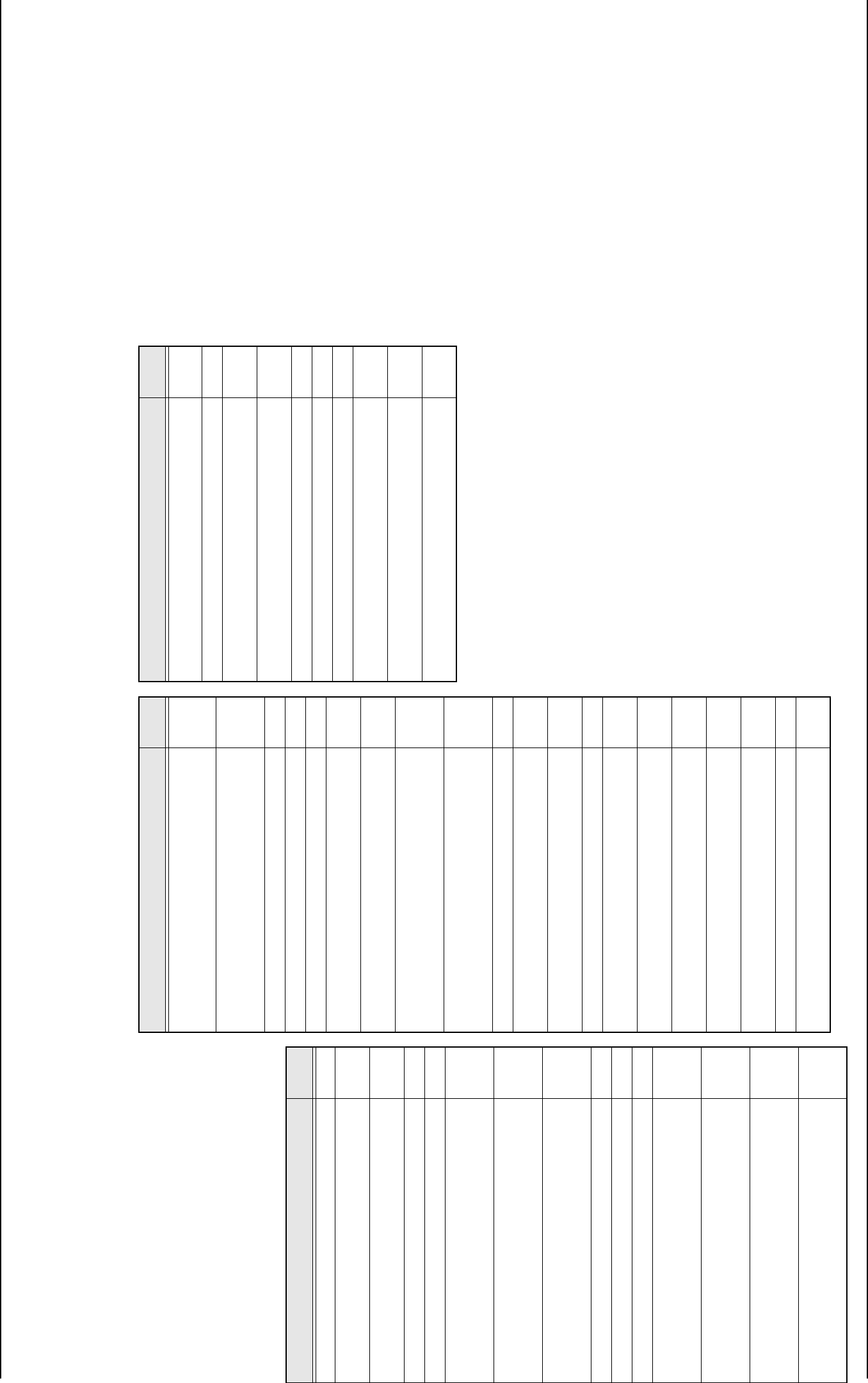
Schematics, Overlays, and Parts Lists: List of Schematics, Component Location Diagrams, and Parts Lists 8-1
6881096C77-O September 26, 2003
Chapter 8 Schematics, Overlays, and Parts Lists
8.1 List of Schematics, Component
Location Diagrams, and Parts
Lists
The following table lists the schematics,
component location diagrams, and parts lists
contained in this chapter.
Table 8-1. List of Schematics, Component Location
Diagrams, and Parts Lists
Figure Title Page
HMN4044E W3 Control Head Schematic 8-2
HMN4044E W3 Control Head Component Location
Diagram 8-3
HMN4044E W3 Control Head Component Location
Diagram 8-4
HMN4044E Parts List 8-5
HKN6096B Remote “Y” Cable Wiring Diagram 8-6
AAHN4045F/G (Standard), HLN4071A/B (Rear),
PMLN4019C/D (Motorcycle) W4 Control Head
Schematic (Sheet 1 of 2)
8-7
AAHN4045F/G (Standard), HLN4071A/B (Rear),
PMLN4019C/D (Motorcycle) W4 Control Head
Schematic (Sheet 2 of 2)
8-8
AAHN4045 (Standard), HLN4071 (Rear), PMLN4019
(Motorcycle) W4 Control Head Component Location
Diagram
8-9
AAHN4045G Standard Parts List 8-10
HCN4071B Rear Parts List 8-12
PMLN4019D Motorcycle Parts List 8-14
HLN6396F/G/H (Standard), HLN6814A/B/C (Rear),
HLN6563B/C/D (Motorcycle) W5/W7 Control Head
Schematic (Sheet 1 of 2)
8-16
HLN6396F/G/H (Standard),HLN6814A/B/C (Rear),
HLN6563B/C/D (Motorcycle) W5/W7 Control Head
Schematic (Sheet 2 of 2)
8-17
HLN6396F/G (Standard), HLN6814A/B (Rear),
HLN6563B/C (Motorcycle) W5/W7 Control Head
Component Location Diagram (Viewed from Side 1)
8-18
HLN6396F/G (Standard), HLN6814A/B (Rear),
HLN6563B/C (Motorcycle) W5/W7 Control Head
Component Location Diagram (Viewed from Side 2)
8-18
HLN6396H_HLN6814C_HLN6563C W5/W7 Control
Head Component Location Diagram (Viewed from
Side 1)
8-19
HLN6396H_HLN6814C_HLN6563C W5/W7 Control
Head Component Location Diagram (Viewed from
Side 2)
8-19
HLN6396H Standard Parts List 8-20
HLN6814C Rear Parts List 8-22
HLN6563D Motorcycle Parts List 8-24
HCN1078J (Standard), HCN1121D (Rear) W9
Control Head Schematic (Side 1 of 2) 8-26
HCN1078J (Standard), HCN1121D (Rear) W9
Control Head Schematic (Side 2 of 2) 8-27
HCN1078J (Standard), HCN1121D (Rear) W9
Control Head Component Location Diagram (Viewed
from Side 1)
8-28
HCN1078J (Standard), HCN1121D (Rear) W9
Control Head Component Location Diagram (Viewed
from Side 2)
8-29
HCN1078J (Standard), HCN1121D (Rear) Parts List 8-30
W4, W5, and W7 Control Head Low-/Mid-Power
Interconnection Diagram 8-33
W4, W5, and W7 High Power Interconnection
Diagram 8-34
W5 and W7 Control Head Interface Board Schematic 8-35
HLN6432D W5/W7 Control Head Interface Board
Component Location Diagram 8-36
HLN6401A Control Head Interconnect Board, (Dash-
Mount) 8-37
HLN6486D/E High Power Standard Interconnect
Board 8-38
HLN6486D/E High-Power Interconnect Board
(Viewed from Side 1) 8-39
HLN6486D/E High-Power Interconnect Board
(Viewed from Side 2) 8-39
HLN6486E Standard Interconnect Parts List 8-40
HLN6574E W3 Control Head High-Power
Interconnect Board Schematic Design 8-41
Table 8-1. List of Schematics, Component Location
Diagrams, and Parts Lists (Continued)
Figure Title Page
HLN6574E W3 High Power Interconnect Board
Component Location Diagrams 8-42
HLN6574E W3 High-Power Interconnect Parts List 8-43
HLN6459D, HLN6344E, and HLN6365E Low-Power
Interconnect Board Schematic 8-45
HLN6459D, HLN6344E, and HLN6365 Low-Power
Interconnect Component Location Diagram 8-46
HLN6459D W3 Low-Power Interconnect Parts List 8-47
HLN6365E Motorcycle Interconnect Parts List 8-49
HLN6344E Standard Interconnect Parts List 8-50
HMN1080A, HMN1061A, HMN1079A Microphone
Board Overlay 8-51
HMN1080A, HMN1061A, HMN1079A Microphone
Schematic 8-51
HMN1080A, HMN1061A, HMN1079A Microphone
Parts List 8-51
Table 8-1. List of Schematics, Component Location
Diagrams, and Parts Lists (Continued)
Figure Title Page
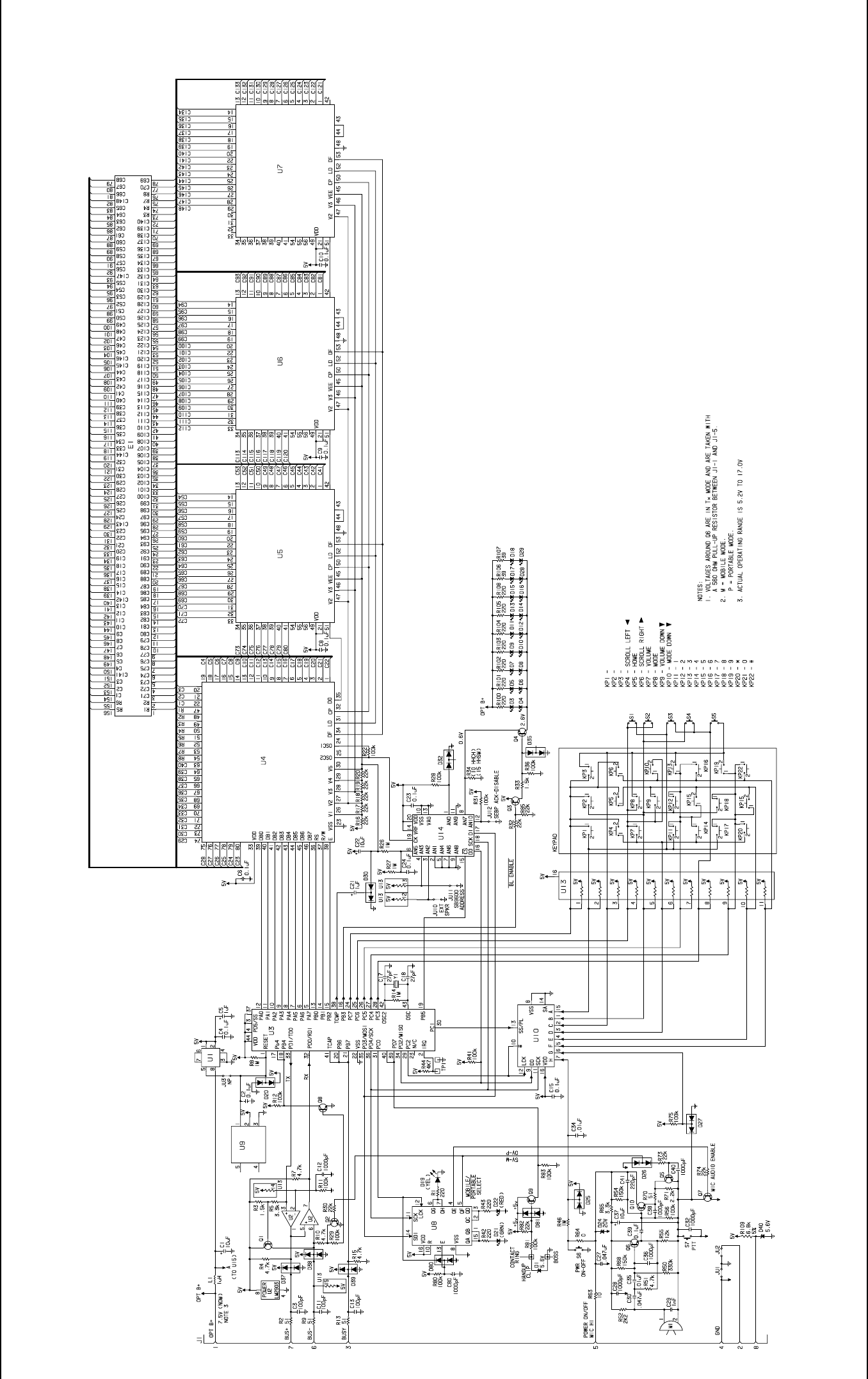
8-2 Schematics, Overlays, and Parts Lists: List of Schematics, Component Location Diagrams, and Parts Lists
September 26, 2003 6881096C77-O
Figure 8-1. HMN4044E W3 Control Head Schematic
(For reference only - board is not field-repairable)
63B81084C78-O
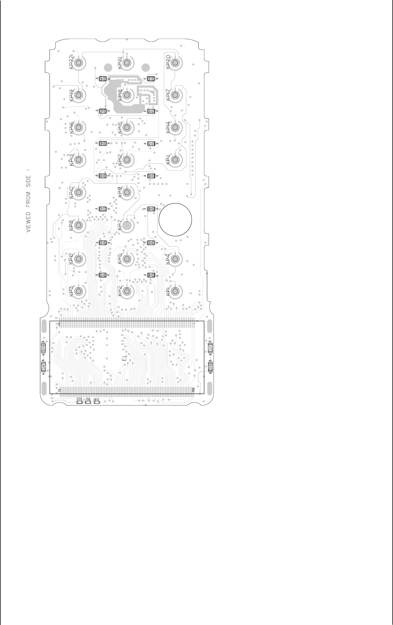
Schematics, Overlays, and Parts Lists: List of Schematics, Component Location Diagrams, and Parts Lists 8-3
6881096C77-O September 26, 2003
Figure 8-2. HMN4044E W3 Control Head Component Location Diagram
MAEPF-25560-O
(Viewed from Side 1)
(For reference only - board is not field-repairable)
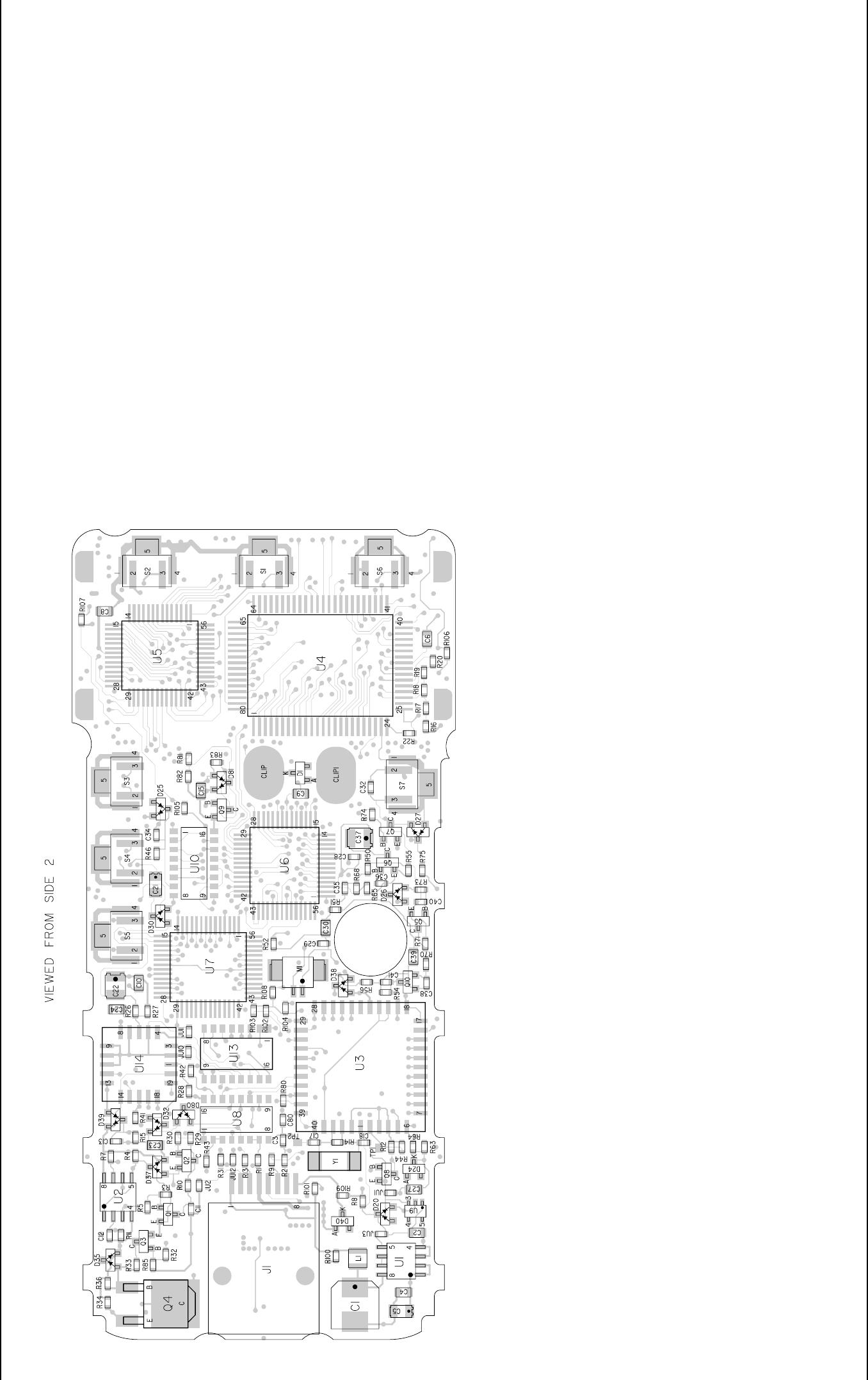
8-4 Schematics, Overlays, and Parts Lists: List of Schematics, Component Location Diagrams, and Parts Lists
September 26, 2003 6881096C77-O
Figure 8-3. HMN4044E W3 Control Head Component Location Diagram
MAEPF-25561-O
(Viewed from Side 2)
(For reference only - board is not field-repairable)
Schematics, Overlays, and Parts Lists: List of Schematics, Component Location Diagrams, and Parts Lists 8-5
6881096C77-O September 26, 2003
HMN4044E Parts List
(For reference only - board is not field-repairable)
ITEM MOTOROLA
PART
NUMBER DESCRIPTION
C1 2380090M24 10µF ± 20%; 50V
C2 2113743A19 0.1µF
C3 2113740F51 100pF
C4 2113743A19 0.1µF
C5 2311049A07 1µF ± 1%; 16V
C6 2113743A19 0.1µF
C8-C10 2113743A19 0.1µF
C11 2113740F51 100pF
C12 2113741F25 1000pF
C13 2113740F51 100pF
C15 2113743A19 0.1µF
C17-C18 2113740F37 27pF
C21 2311049A07 1µF ± 1%; 16V
C22 2311049A57 10µF ±1%;
C23 2113743A19 0.1µF
C24 2113743A19 0.1µF
C27 2113741A61 .047µF
C28-C29 2113741F25 1000pF
C30 2113741A61 .047µF
C32 2113741F25 1000pF
C34-C35 2113741F49 .010µF
C36 2113741F25 1000pF
C37 2311049A57 10µF ±1%; 16V
C38 2113741F25 1000pF
C39 2113743A19 0.1µF
C40 2113741F25 1000pF
C41 2113740F59 220pF
C80 2113741F25 1000pF
D1 4813830A15 Zener; 5.6V
D3-D16 4805729G75 LED Green
D17-D18 4805729G85 LED Green
D19 4805729G82 LED Yellow
D21 4805729G83 LED Green
D22 4805729G81 LED Red
D24 4880140L25 20V
D25-D27 4813833C05 Dual; 70V
D28-D29 4805729G85 LED Green
D30 4813833C05 Dual; 70V
D32 4813833C05 Dual; 70V
D35 4813833C05 Dual; 70V
D37-D39 4813833C05 Dual; 70V
D80-D81 4813833C05 Dual; 70V
J1 0984875T03 Jack
L1 2480140E01 1.2µH
P1 2809926G01 Header
Q1 4805128M12 SOT
Q2 4880214G02 MMBT 3904
Q3 4805128M12 SOT
Q4 4805780V01
Q5-Q8 4880214G02 MMBT 3904
Q9 4805128M12 SOT
Q10 4880214G02 MMBT 3904
R1 0662057A33 220
R2 0662057A18 51
R3 0662057A53 1.5k
R4 0662057A65 4.7k
R5 0662057A61 3.3k
R7 0662057A65 4.7k
R8 0662057A75 12k
R9 0662057A18 51
R10 0662057A65 4.7k
R11-R12 0662057A97 100k
R13 0662057A18 51
R14 0662057A97 100k
R15 0662057A65 4.7k
ITEM MOTOROLA
PART
NUMBER DESCRIPTION
R16-R20 0662057A81 22k
R22 0662057A97 100k
R26-R27 0662057B22 1M
R28-R29 0662057A97 100k
R30 0662057A81 22k
R31 0662057A97 100k
R32 0662057A81 22k
R33 0662057A53 1.5k
R34 0662057A01 10
R36 0662057A97 100k
R41 0662057A97 100k
R42-R43 0662057A33 220
R44 0662057A65 4.7k
R46 0662057B22 1M
R50 0662057B10 330k
R51 0662057A65 4.7k
R52 0662057A57 2.2k
R54 0662057B02 150k
R55 0662057A75 12k
R56 0662057A97 100k
R63 0662057A01 10
R64 0662057B47 0
R65 0662057A61 3.3k
R68 0662057B02 150k
R70 0662057A15 39
R71 0662057A57 2.2k
R73-R74 0662057A81 22k
R75 0662057A53 1.5k
R80-R81 0662057A97 100k
R82 0662057A81 22k
R83 0662057A97 100k
R100-R105 0662057A33 220
R106-R107 0662057A15 39
ITEM MOTOROLA
PART
NUMBER DESCRIPTION
R108 0662057A33 220
R109 0662057A69 6.8k
S1-S7 4005840X01
U1 5105469E65 Voltage Regulator
U2 5105663U34 IC Comparator
U3 5113802A07 IC Comparator µP
U4 5102074D01 LDC
U5-U7 5102074D01 Driver
U8 5113805A75 8-Bit Shift Register
U9 5105625U63 IC Voltage Detector
U10 5113805A74 Shift Register
U13 0604267J01 In-line Resistor Package
U14 5102073D01 Analog/Digital Converter
Y1 4880065M01 Resonator; 4.0 MHz
ITEM MOTOROLA
PART
NUMBER DESCRIPTION
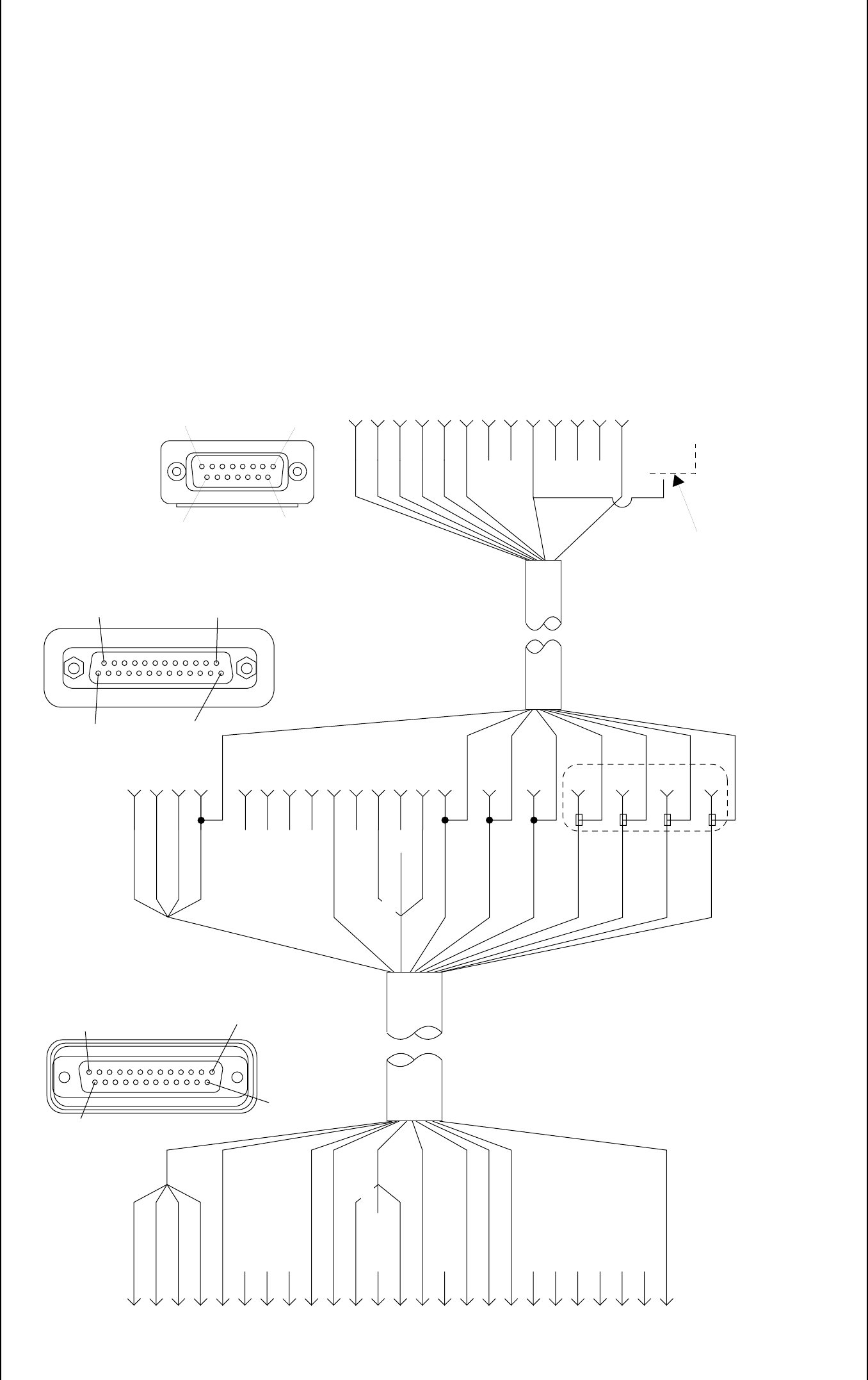
8-6 Schematics, Overlays, and Parts Lists: List of Schematics, Component Location Diagrams, and Parts Lists
September 26, 2003 6881096C77-O
Figure 8-4. HKN6096B Remote “Y” Cable Wiring Diagram
WHT/BLUE
5WHT/BLUE 5
J1
J2
P1
YELLOW/BLK
14 YELLOW/RED
23 DRAIN
18 WHT/BLK
17 NC
15 NC
19 NC
20 GRAY
4ORANGE
3YELLOW/GRN
ORANGE/BLUE
ORANGE/BLUE
12 NC
10 DRAIN
11 BLACK
22 NC
21 GREEN
13 BROWN
25 RED
24 NC
6NC
PIN 1
PIN 1
PIN 8
PIN 15
PIN 9
PIN 1
PIN 13
PIN 13
PIN 14
PIN 14
PIN 25
PIN 25
9NC
1
YELLOW/BLK 14
YELLOW/RED 23
DRAIN 18
NC 19
NC 1
NC 6
NC 10
GRAY 4
NC 2
YELLOW/GRN 12
NC 21
DRAIN 11
BLACK 22
ORANGE 5
BLACK 4
YELLOW 12
GREEN 2
BROWN 6
RED 7
NC 14
NC 11
GRAY 8
NC 10
NC 9
NC 1
WHT/BLK
CONNECTOR
METAL SHROUD
SOLDER WIRE
SECURELY
IN POSITION
3
BROWN 25
RED 24
NC
2NC
7NC
8YELLOW
8GREEN
WHT/BLK
ORANGE
YELLOW
MAEPF-25562-O
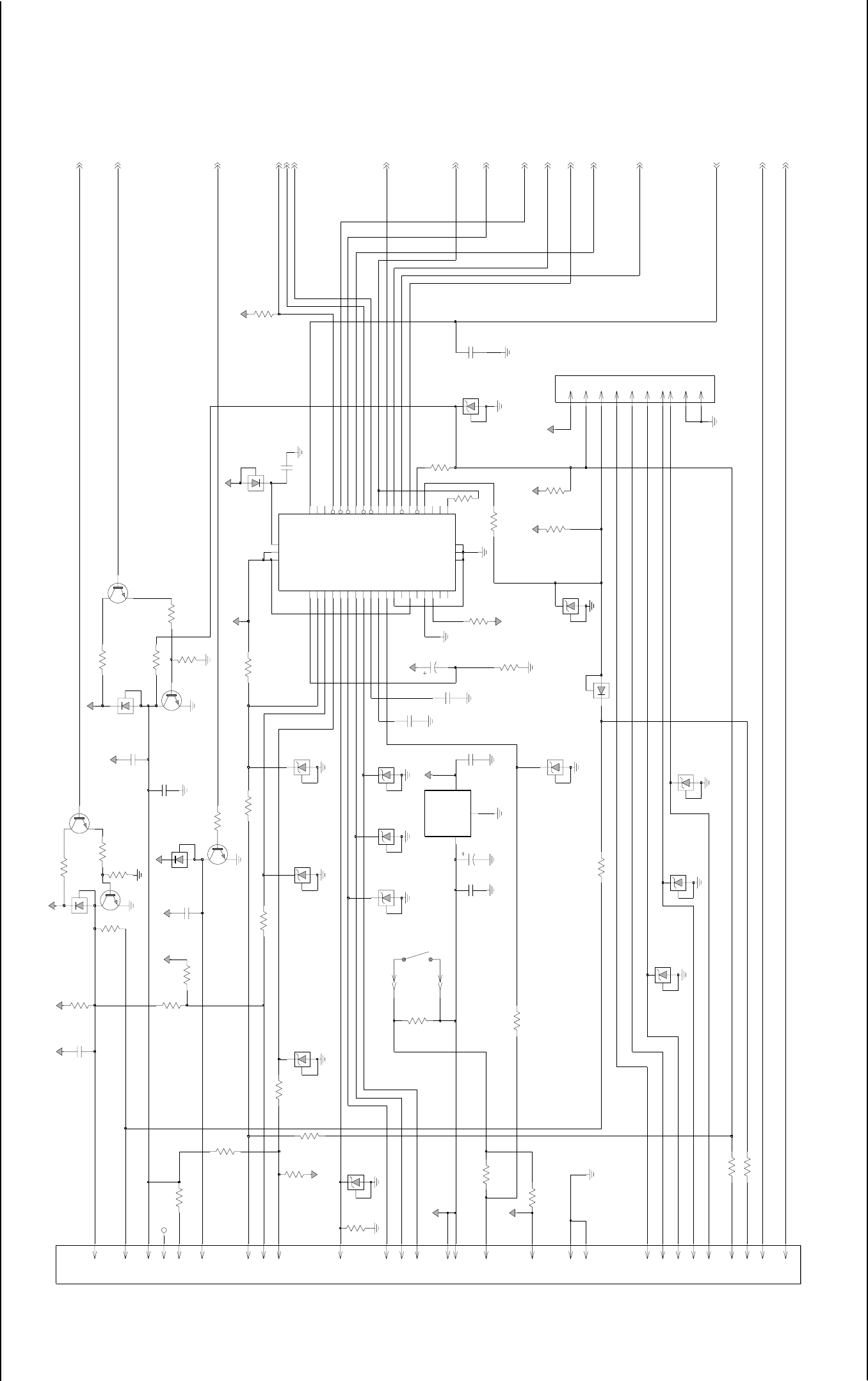
Schematics, Overlays, and Parts Lists: List of Schematics, Component Location Diagrams, and Parts Lists 8-7
6881096C77-O September 26, 2003
Figure 8-5. AAHN4045F/G (Standard), HLN4071A/B (Rear), PMLN4019C/D (Motorcycle) W4 Control Head Schematic (Sheet 1 of 2)
BUSY_IN*
BUSY_OUT*
IGN*
VIP_IN_3*
A+
0.1uF
C48
CR55
J2
JU20
STROBE
J1
HUB_INV
PTT
VIP_IN_2*
RESET*
TX_DATA
RX_DATA
470pF
+5V
VIP_IN_1*
R98*
C41
R25
47K
100K
R34
47K
R74
100K
+5V
4.7K
R177
JU18*
VIP_OUT_2
R77
Q75
470
R76
Q74
470
R80
100K
CR73
CR72
1uF
R79
CR71
C6
470
CR76
SP-2_VF-SENSE-2
SP-1_VF-SENSE-1
+5V
4.7K
R176
VIP_OUT_3
JU8*
SWB+
VIP_OUT_1
JU4*
SWB+
33K
R73
0.1uF
Q72
SWB+
C82
470pF
C175
JU14*
470
SWB+
R71
Q71
SWB+
470pF
JU12*
+5V
C176
+5V
R1*
+5V
4.7K
R175
10K
NC
JU9*
JU6*
R174
JU13*
SWB+
4.7K
VR3
Q73
15V
VR4
15V
R31
VR20
15V
47K
15V VR22
15V
VR21
JU5
18
JU3
SWB+
SWB+
470pF
C174
26
8
14
19
1MEG
7
R10
+5V
10K
+5V
R99
JU15*
C7
.01uF
.01uF
C1
10K
R81
16
17
10K
R87
R84
15
10K
15V15V
VR9VR8 VR10
15V
10
1
5
9
8
2
6
7
4
15V
3
VR2VR1
15V15V
VR7
23
MIC HI
GND
GND
A+
IGN
SWB+
SWB+
BUS+
BUS-
BUSY
RESET
VIP IN 3
VIP IN 2
VIP IN 1
VIPOUT 3
KEY SLOT
VIPOUT2
VIPOUT1
P103
SERIAL I/O
P104
R7
SW1
4
5
2. PART USAGE MAY VARY WITH APPLICATION. REFER TO PARTS LIST FOR USAGE INFORMATION.
1. ALL RESISTANCE IS IN OHMS. ALL CAPACITANCE IN PICO-FARADS UNLESS NOTED OTHERWISE.
NOTES:
S.NET-KID
S.NET-KEY
S.NET-WE
MIC LO
MIC HI
HUB
PTT
SP-2/VF-SENSE-2
SP-1/VF-SENSE-1
HUB
PTT
S.NET-KID
S.NET-KEY
S.NET-WE
MIC LO
17 BUS_POS
BUS_NEG
16
BUSY_OUT* 13
BUSY_IN* 11
BUSY
10
A+/IGN 39
U4
SP1
SP2
(NOTE 2) ROTARY
14
IGN* 29
IGN
28
HUB_POL
32
HUB_INV 30
34 GND2
5GND1
GND
1
41
15
33
26
27
40
8
38
+5V_REG 3
6
+5V
42
23
18
12
25
TX_DATA 19
RX_DATA 20
RES_HUB 31
RESET_FILTR
7
RESET* 4
9RESET
PTT* 37
PTT
WDT_TICKLE 2
WDT_IN_T_CAP
44 VIP_IN_3* 36
VIP_IN_2* 21
VIP_IN_1* 2435 VIP_IN_3
VIP_IN_2
22 VIP_IN_1
SC74487F
WDT_T_CAP
43
U45
OUT 3
IN
1
GND
2
MC78M05
1
2
24
28
20
21
9
27
3
13
C45
10uF
470pF
C57 .01uF
C58
5
6
+5V
JU1*
11
JU2*
VR5
15V
12
4
A+
22
SWB+
25
10
10K
R9* VR6
15V
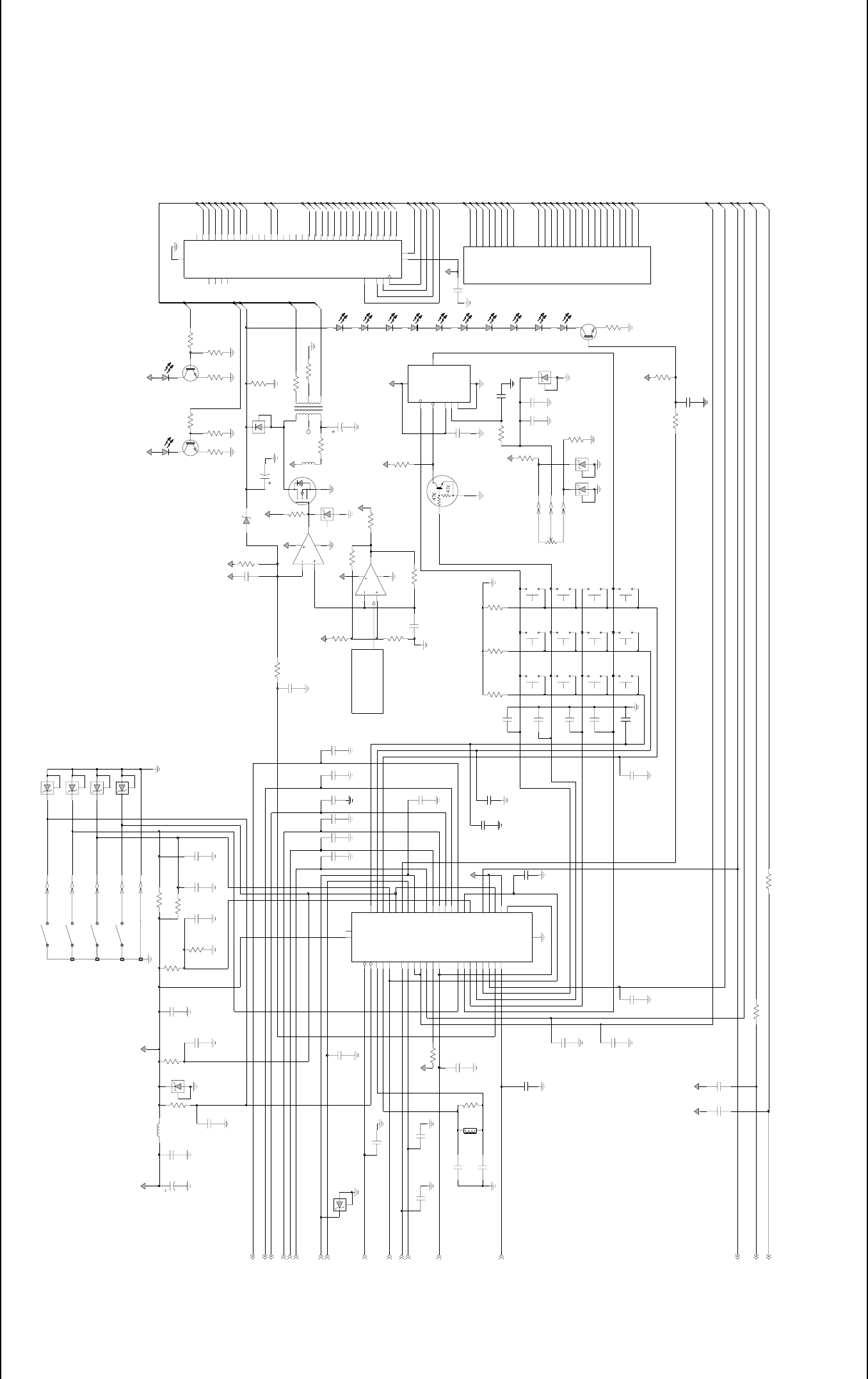
8-8 Schematics, Overlays, and Parts Lists: List of Schematics, Component Location Diagrams, and Parts Lists
September 26, 2003 6881096C77-O
Figure 8-6. AAHN4045F/G (Standard), HLN4071A/B (Rear), PMLN4019C/D (Motorcycle) W4 Control Head Schematic (Sheet 2 of 2)
C23
C50
10uF
DATA_IN
LTCH_ENBL
SP-2_VF-SENSE-2
STROBE
STROBE
G8
P0
BUS3(32:1)
SP-1_VF-SENSE-1
IGN*
VIP_OUT_2
VIP_OUT_3
VIP_OUT_1
PTT
R131
10K
WITH POWER APPLIED.
3.
2. PART USAGE MAY VARY WITH APPLICATION. REFER TO PARTS LIST FOR USAGE INFORMATION.
1. ALL RESISTANCE IS IN OHMS. ALL CAPACITANCE IN PICO-FARADS UNLESS NOTED OTHERWISE. BUSY XMIT
D
G
S
WARNING!
(RED)(YELLOW)
U102
2
3
VOLUME
R7
SW1
ROTARY
SWITCH
ROTARY
P001
P001
P001
P001
P001
1
2
3
5
SW2
1
DAMAGE TO THE CIRCUIT
U1 PINS 3,18,23,40 ARE NOT CONNECTED WITHMC68HC05C8A
NOTES:
MAY OCCUR.
MICROPROCESSOR
DO NOT PROBE U3 PIN 5
C40
470pF
3
470pF
C39
10
13
4
26
27
1000uF
C53
C18*
CR137
32
11
16
10K
R52
22K
ZU
SWITCH
+5V
NC
1
R200
33K 18
1
2
3
4
5
6
+5V
R56
Q9 34
2
24 LTCH_ENBL
VCC1
44 VDISP
1
77J03
T60
Q30 5
4
Q31
Q32 3
Q4 39
Q5 38
37
Q6
Q7 36
Q8 35
Q23 13
12
Q24
Q25 11
Q26 10
Q27 9
8
Q28
Q29 7
Q3 40
25
Q16
20
Q17
Q18 19
Q19 17
41
Q2
16
Q20
Q21 15
Q22 14
NC4
29
42
Q1
Q10 33
Q11 32
Q12 31
30
Q13
Q14 27
Q15 26
STROBE
21
CLK
23
DATA_IN
43
GND 22
6NC1
NC2
18 NC3
28
10V
U101
UCQ5818EPF
470pF
VR24
470pF
C30
C141
470pF
C17
CR136
3
36V
VR50
JU17*
JU16
CR131
CR132
CR133
CR134
C19*
22
19
20
32
10K
15
16
R140
C16*
8
C15*
VR31
10V
C44*
J7
J8
J9
J6
J5
VR32
10V
J4
VR33
10V
R123
R8
+5V
10K
+5V
100
30
29
100
R6
0.1uF
28
C81
C140
470pF
Q76
VSS
22
1
J3
CLOCK
36
37 WDT_TKL
IGN*
39
RESET*
1
BUSY_IN
41
STROBE 38
VDD 44
4
VIP_OUT_2 27
26
VIP_OUT_1
BUSY_IN 25
24
RX_DATA
32
TX_DATA
33
DATA_IN
34
DATA_IN
35
PB4 17
19
BKLT
HUB 20
PTT 21
VIP_IN_3 31
VIP_IN_2 30
VIP_IN_1 29
VIP_OUT_3 28
PA4
8
7LTCH_ENBL
HV_CNTRL
6
BUSY_OUT
5
PB0 13
PB1 14
PB2 15
PB3 16
23
+5V_FIL 40
OSC1
43
OSC2
42
PA0
12
PA1
11
PA2
10
PA3
9
MC68HC705C8A
U1
2IRQ*
3
+5V_FIL
18
CR51
U3A
LM2903
2
3
1
8
4
470pF
C2
10K
R92
10V
VR25
C46 C21
470pF
R115
1uF
22K
R51
1K
GND
4
3W+
2
VCC 8
VREF
5
U2
63A81
CLK
7
CS*
1DOUT6
C90
470pF470pF
C91
470pF
C92 JU19 470pF
C93
10K
R93 R91
10K
10K
R90
R28
10K
10V
VR29
VR28
10V
10V
VR27
J10
VR30
10V
R59
+5V_FIL
560
SWITCH
DIM
+5V
SWITCH
MON
7
2
33K
R113
+5V_FIL
25
12
R55
+5V
12
Q111
R29
25
6
CR135
100K
1K
R61
R114
33K
470pF
C54
DVP/EMER
SWITCH
DIR
SWITCH
ZD
SWITCH
PHON
SWITCH
SWB+
C25*
C29
470pF
SWB+
5
470pF
C30
R5
4.7K
R30
31
27
1000uF
C55
1MEG
2
CR139
15
1
SWITCH
SCAN
CR140
C12*
470pF
C38
C10*
+5V
CR111
Q50
13
CR112
C24*
14
9.107uH
L50
9.107uH
L1
30pF
C20
470pF
+5V
.01uF
C42
PN 6
24
PO
C36
470pF
2
PF
PG 5
PH 20
PI 22
PJ 7
PK 4
PL 21
PM 19
G6 11
G7 10
G8 9
PA 3
23
PB
PC 18
PD 8
PE 13
32M01
VF DISPLAY
1
F1
25
F2
G1 17
G2 16
G3 15
G4 14
G5 12
18
17
+5V
21
SWITCH
CALL
100K
R121R120
100K
SWITCH
HOME
SWITCH
Y1
SEL
470pF
C28
FREQ=4MHz
24
22
21
20
SWB+
SWB+
23
SWB+
+5V
4.7K
R2
+5V
10
C22
30pF
C11*
R116
1K
12
Q112
470pF
C37
C51
9
31
30
26
9
28
14
C101*
C43
0.1uF
R57
47K
24
R112
100K
8
100K
R111
C14*
19
6
7
10uF
5
7
8
4
+5V
C52
H/L
U3B
LM2903
6
SWITCH
17
23
10V
VR26
R50
560
4
5
R101
12
C9*
1.5K
R60
Q131
+5V_FIL
33K
R58
10
CR138
29
11
+5V
470pF
C33
470pF
C32
470pF
C34
470pF
R122
100K
C35
G2
G1
R
Y
PB
PF
PA
PK
PG
PN
PJ
PO
DATA_IN
CLK
STROBE
CLOCK
BUSY_IN*
VIP_IN_2*
BKLT
RX_DATA
TX_DATA
VIP_IN_1*
VIP_IN_3*
VDISP
LTCH_ENBL
PD
PE
PM
PH
PC
PL
G8
G7
G6
PI
G5
G4
G3
HUB_INV
BUSY_OUT*
G7
G6
G5
G4
G3
G2
G1
G8
F2
F1
Y
R
VDISP
RESET*
PB
P0
F2
PI
PL
PH
PM
PC
PE
PD
PJ
PN
PG
PK
PA
PF
F1
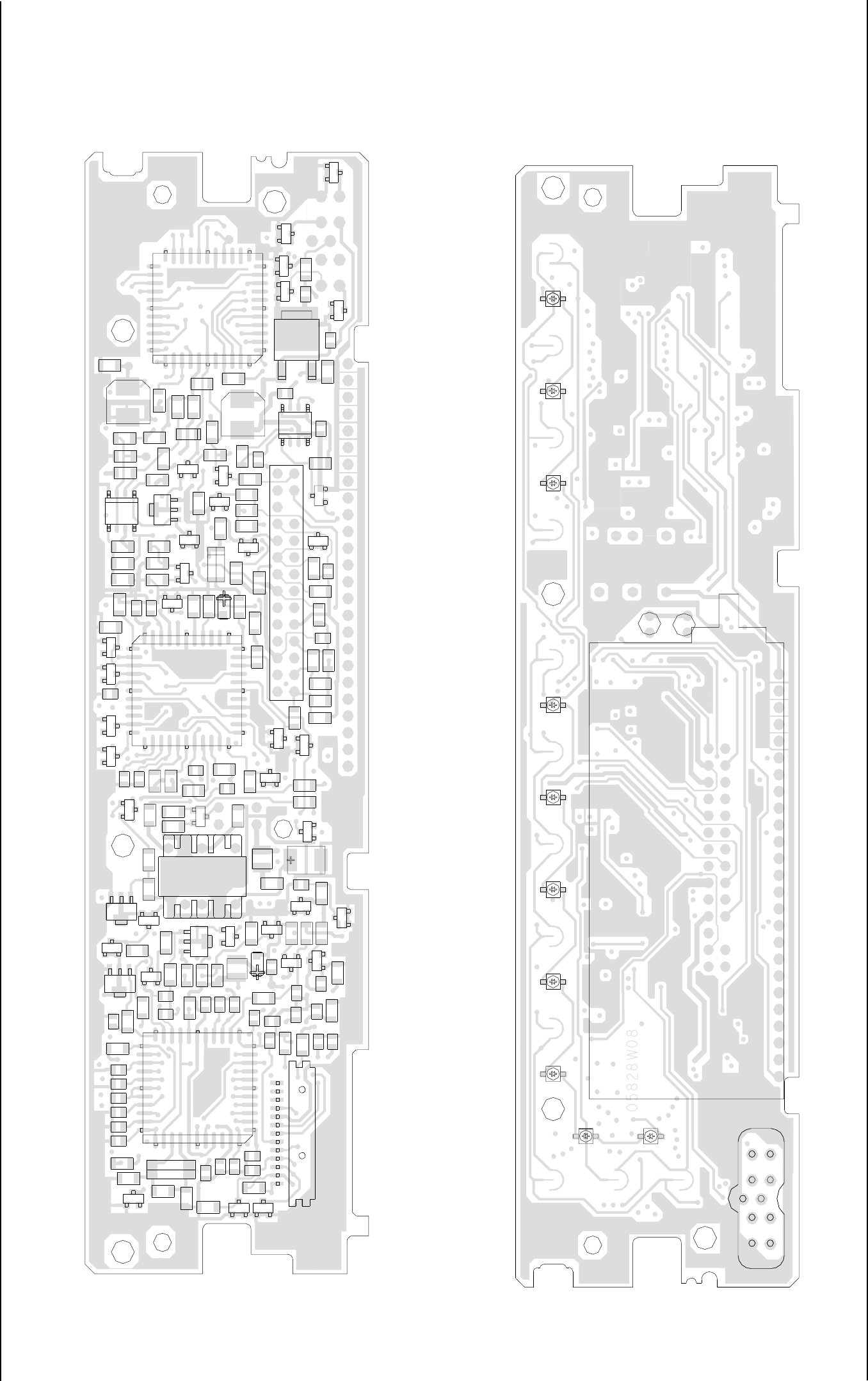
Schematics, Overlays, and Parts Lists: List of Schematics, Component Location Diagrams, and Parts Lists 8-9
6881096C77-O September 26, 2003
Figure 8-7. AAHN4045 (Standard), HLN4071 (Rear), PMLN4019 (Motorcycle) W4 Control Head Component Location Diagram
C23
VR33
JU20
C140
C39
VR31
C43
Y1
R30
VR32
C22
R29
C9
C41
C40
C38
C20
C15
R98
Q73
R79
CR73
CR71
Q71
Q75
C11
C10 C29
JU16
Q131
CR138
CR137
CR136
CR135
CR134
CR139 CR140
CR133
CR132
CR131
VR30
R55 C90
VR25
R111
JU2
JU6
R174
R176
C174
JU13
VR23
R123
C35
R2
R176
R177
JU18
R81
JU3
VR10
CR51
R51
C54
R60
R200
R59
R61
R58
R56
R57 R116
R114
VR9
R9
R112
VR26
R34
VR50
VR5
C176
JU15
C44
C18
CR55
R99
R113
R115
L50
C17
C37
C34
R73
C12
R77
Q72
R28
R92
R121
R80
R74 R76 R101
Q74
Q111
R50
R25
R90
C50 VR29 VR24
R87
JU9
R1
JU12 C82
C175
Q76 C57
U2
C45
C58
U45
C57
VR21
C80 JU4
VR22 VR3 VR4
VR20
VR8
JU8
R84
C14
C19
VR2 VR1 VR7 VR6
C1
C83
C16
C7
R10
C6
C48 C53
Q112
JU1
R122
Q50
U3
R52
JU14
C101
C51
R5
C52
R140
C141
CR76
CR90
C55
JU5
R31
JU17
R91
VR27
VR28
R120
C91
R71
R93
C2
C24
C25
C30
R8
R6
C32
C33 JU19
C93
C28 C36
L1
C46
C21
R131
C42
CR72
C92
7
6
1
1
17
U1
P1
P104
40
39 29
28
18
T60
U4
U102
U101
7
6
1
17
40
39
29
28
18
11
1
1
1
A
A
AA
AA
A
K
K
2
2
3
3
3
4
4
4
4
5
5
5
6
6
7
7
8
8
8
910111213
13 14 1
28272524232221201918171615
7
6
1
17
40
39 29
28
18
9
18
7
5
6
3
4
1
2
P103
CR111
CR112
A
A
A
A
A
A
A
A
A
A
A
K
K
K
K
K
K
K
K
K
K
K
A
A
A
A
A
A
A
A
A
S
E
E
E
E
E
EEE
D
B
B
B
B
B
BB
B
G
C
C
C
C
C
CC
C
K
K
K
K
K
K
K
K
K
A
K
K
K
KKK
A
K
12 3 4 5 6 78 91011121314 2524232221201918171615
HOME
DIM
H/L OPT1 OPT2 OPT3 OPT4 SEL ZD ZU DIR MON
SIDE 1
SIDE 2
8-10 Schematics, Overlays, and Parts Lists: List of Schematics, Component Location Diagrams, and Parts Lists
September 26, 2003 6881096C77-O
AAHN4045G Standard Parts List
ITEM MOTOROLA
PART
NUMBER DESCRIPTION
C1 2113741N45 CAP CHIP CL2 X7R 10% 10000
C10 2113741M13 CAP CHIP CL2 X7R 10% 470
C101 2113740B65 CAP CHIP REEL CL1 +/-30 470
C11 2113741M13 CAP CHIP CL2 X7R 10% 470
C12 2113741M13 CAP CHIP CL2 X7R 10% 470
C14 2113741M13 CAP CHIP CL2 X7R 10% 470
C140 2113741M13 CAP CHIP CL2 X7R 10% 470
C141 2113741M13 CAP CHIP CL2 X7R 10% 470
C15 2113741M13 CAP CHIP CL2 X7R 10% 470
C16 2113741M13 CAP CHIP CL2 X7R 10% 470
C17 2113741M13 CAP CHIP CL2 X7R 10% 470
C174 2113741M13 CAP CHIP CL2 X7R 10% 470
C175 2113741M13 CAP CHIP CL2 X7R 10% 470
C176 2113741M13 CAP CHIP CL2 X7R 10% 470
C18 2113741M13 CAP CHIP CL2 X7R 10% 470
C19 2113741M13 CAP CHIP CL2 X7R 10% 470
C2 2113741M13 CAP CHIP CL2 X7R 10% 470
C20 2113741M13 CAP CHIP CL2 X7R 10% 470
C21 2113741M13 CAP CHIP CL2 X7R 10% 470
C22 2113740B36 CAP CHIP REEL CL1 +/-30 30
C23 2113740B36 CAP CHIP REEL CL1 +/-30 30
C24 2113741M13 CAP CHIP CL2 X7R 10% 470
C25 2113741M13 CAP CHIP CL2 X7R 10% 470
C28 2113741M13 CAP CHIP CL2 X7R 10% 470
C29 2113741M13 CAP CHIP CL2 X7R 10% 470
C30 2113741M13 CAP CHIP CL2 X7R 10% 470
C32 2113741M13 CAP CHIP CL2 X7R 10% 470
C33 2113741M13 CAP CHIP CL2 X7R 10% 470
C34 2113741M13 CAP CHIP CL2 X7R 10% 470
C35 2113741M13 CAP CHIP CL2 X7R 10% 470
C36 2113741M13 CAP CHIP CL2 X7R 10% 470
C37 2113741M13 CAP CHIP CL2 X7R 10% 470
C38 2113741M13 CAP CHIP CL2 X7R 10% 470
C39 2113741M13 CAP CHIP CL2 X7R 10% 470
C40 2113741M13 CAP CHIP CL2 X7R 10% 470
C41 2113741M13 CAP CHIP CL2 X7R 10% 470
C42 2113741N45 CAP CHIP CL2 X7R 10% 10000
C43 2113741N69 CAP CHIP CL2 X7R 10%
100000
C44 2113741M13 CAP CHIP CL2 X7R 10% 470
C45 2380090M24 CAP ALU 10 20 50V SURF MT
C46 2311049A37 CAP TANT CHIP 1 20 20
C48 2113741N69 CAP CHIP CL2 X7R 10%
100000
C50 2311049A95 CAP TANT CHIP 10 UF 25V
10%
C51 2113741N21 CAP CHIP CL2 X7R 10% 1000
C52 2380090M24 CAP ALU 10 20 50V SURF MT
C53 2113741N21 CAP CHIP CL2 X7R 10% 1000
C54 2113740B65 CAP CHIP REEL CL1 +/-30 470
C55 2113741N21 CAP CHIP CL2 X7R 10% 1000
C57 2113741M13 CAP CHIP CL2 X7R 10% 470
C58 2113741N45 CAP CHIP CL2 X7R 10% 10000
C6 2311049A37 CAP TANT CHIP 1 20 20
C7 2113741N45 CAP CHIP CL2 X7R 10% 10000
C80 NOTPLACED 64AM DUMMY PART NUMBER
C81 2113743A19 CAP CHIP .100 UF 10% X7R
C82 NOTPLACED 64AM DUMMY PART NUMBER
C83 2113743A19 CAP CHIP .100 UF 10% X7R
C9 2113741M13 CAP CHIP CL2 X7R 10% 470
C90 2113741M13 CAP CHIP CL2 X7R 10% 470
C91 2113741M13 CAP CHIP CL2 X7R 10% 470
C92 2113741M13 CAP CHIP CL2 X7R 10% 470
C93 2113741M13 CAP CHIP CL2 X7R 10% 470
CR0076 4813833C09 DIODE GEN PURP .1A 100V
‘DX’
CR111 4880026P01 DIODE LED RED
ITEM MOTOROLA
PART
NUMBER DESCRIPTION
CR112 4880026P02 DIODE LED YELLOW
CR131 4880052R03 DIODE LIGHT EMITTING GRN
CR132 4880052R03 DIODE LIGHT EMITTING GRN
CR133 4880052R03 DIODE LIGHT EMITTING GRN
CR134 4880052R03 DIODE LIGHT EMITTING GRN
CR135 4880052R03 DIODE LIGHT EMITTING GRN
CR136 4880052R03 DIODE LIGHT EMITTING GRN
CR137 4880052R03 DIODE LIGHT EMITTING GRN
CR138 4880052R03 DIODE LIGHT EMITTING GRN
CR139 4880052R03 DIODE LIGHT EMITTING GRN
CR140 4880052R03 DIODE LIGHT EMITTING GRN
CR51 4813833C09 DIODE GEN PURP .1A 100V
‘DX’
CR55 4813833C09 DIODE GEN PURP .1A 100V
‘DX’
CR71 4813833C09 DIODE GEN PURP .1A 100V
‘DX’
CR72 4813833C09 DIODE GEN PURP .1A 100V
‘DX’
CR73 4813833C09 DIODE GEN PURP .1A 100V
‘DX’
CR90 4882960R02 DIODE RECT 48R82960R01 A/P
JU1 NOTPLACED 64AM DUMMY PART NUMBER
JU12 NOTPLACED 64AM DUMMY PART NUMBER
JU13 NOTPLACED 64AM DUMMY PART NUMBER
JU14 NOTPLACED 64AM DUMMY PART NUMBER
JU15 NOTPLACED 64AM DUMMY PART NUMBER
JU16 0611077A01 RES CHIP JUMPER
JU17 NOTPLACED 64AM DUMMY PART NUMBER
JU18 NOTPLACED 64AM DUMMY PART NUMBER
JU19 NOTPLACED 64AM DUMMY PART NUMBER
JU2 0611077A01 RES CHIP JUMPER
JU20 NOTPLACED 64AM DUMMY PART NUMBER
JU3 0611077A01 RES CHIP JUMPER
JU4 NOTPLACED 64AM DUMMY PART NUMBER
JU5 0611077A01 RES CHIP JUMPER
ITEM MOTOROLA
PART
NUMBER DESCRIPTION
JU6 NOTPLACED 64AM DUMMY PART NUMBER
JU8 NOTPLACED 64AM DUMMY PART NUMBER
JU9 NOTPLACED 64AM DUMMY PART NUMBER
L1 2480140E16 INDUCTOR CHIP 10UH
L50 2480140E16 INDUCTOR CHIP 10UH
P001 0905573P02 SKT 13 POSTN
P103 2880102M07 PLUG VERTICAL 28 POSITION
P104 2880068M01 HEADER MIC
Q111 4813824A10 TSTR NPN 40V .2A GEN PURP
Q112 4813824A10 TSTR NPN 40V .2A GEN PURP
Q131 4813824A10 TSTR NPN 40V .2A GEN PURP
Q50 4880053M03 TSTR N/CH SOT 89 200V B ST
84
Q71 4880053M02 TSTR NPN MXT2222A
Q72 4880053M02 TSTR NPN MXT2222A
Q73 4880053M02 TSTR NPN MXT2222A
Q74 4813824A10 TSTR NPN 40V .2A GEN PURP
Q75 4813824A10 TSTR NPN 40V .2A GEN PURP
Q76 4880048M01 TSTR NPN DIG 47K/47K
R1 NOTPLACED 64AM DUMMY PART NUMBER
R10 0611077B47 RES CHIP 1 MEG 5 1/8W
R101 0611077A28 RES CHIP 12 5 1/8W
R111 0611077B23 RES CHIP 100K 5 1/8W
R112 0611077B23 RES CHIP 100K 5 1/8W
R113 0611077B11 RES CHIP 33K 5 1/8W
R114 0611077B11 RES CHIP 33K 5 1/8W
R115 0611077A74 RES CHIP 1000 5 1/8
R116 0611077A74 RES CHIP 1000 5 1/8
R120 0611077B23 RES CHIP 100K 5 1/8W
R121 0611077B23 RES CHIP 100K 5 1/8W
R122 0611077B23 RES CHIP 100K 5 1/8W
R123 0611077A98 RES CHIP 10K 5 1/8W
R131 0611077A68 RES CHIP 560 5 1/8W
R140 0611077A98 RES CHIP 10K 5 1/8W
ITEM MOTOROLA
PART
NUMBER DESCRIPTION

Schematics, Overlays, and Parts Lists: List of Schematics, Component Location Diagrams, and Parts Lists 8-11
6881096C77-O September 26, 2003
R174 0611077A90 RES CHIP 4700 5 1/8
R175 0611077A90 RES CHIP 4700 5 1/8
R176 0611077A90 RES CHIP 4700 5 1/8
R177 0611077A90 RES CHIP 4700 5 1/8
R2 0611077A90 RES CHIP 4700 5 1/8
R200 0611077B07 RES CHIP 22K 5 1/8W
R25 0611077B15 RES CHIP 47K 5 1/8W
R28 0611077A98 RES CHIP 10K 5 1/8W
R29 0611077B23 RES CHIP 100K 5 1/8W
R30 0611077B47 RES CHIP 1 MEG 5 1/8W
R31 0611077B15 RES CHIP 47K 5 1/8W
R34 0611077B15 RES CHIP 47K 5 1/8W
R5 0611077A90 RES CHIP 4700 5 1/8
R50 0611077A68 RES CHIP 560 5 1/8W
R51 0611077B07 RES CHIP 22K 5 1/8W
R52 0611077A98 RES CHIP 10K 5 1/8W
R55 0611077A28 RES CHIP 12 5 1/8W
R56 0611077B11 RES CHIP 33K 5 1/8W
R57 0611077B15 RES CHIP 47K 5 1/8W
R58 0611077B11 RES CHIP 33K 5 1/8W
R59 0611077A98 RES CHIP 10K 5 1/8W
R6 0611077A50 RES CHIP 100 5 1/8W
R60 0611077A78 RES CHIP 1500 5 1/8
R61 0611077A74 RES CHIP 1000 5 1/8
R71 0611077A66 RES CHIP 470 5 1/8W
R73 0611077B11 RES CHIP 33K 5 1/8W
R74 0611077B23 RES CHIP 100K 5 1/8W
R76 0611077A66 RES CHIP 470 5 1/8W
R77 0611077A66 RES CHIP 470 5 1/8W
R79 0611077A66 RES CHIP 470 5 1/8W
R8 0611077A50 RES CHIP 100 5 1/8W
R80 0611077B23 RES CHIP 100K 5 1/8W
R81 0611077A98 RES CHIP 10K 5 1/8W
ITEM MOTOROLA
PART
NUMBER DESCRIPTION
R84 0611077A98 RES CHIP 10K 5 1/8W
R87 0611077A98 RES CHIP 10K 5 1/8W
R9 NOTPLACED 64AM DUMMY PART NUMBER
R90 0611077A98 RES CHIP 10K 5 1/8W
R91 0611077A98 RES CHIP 10K 5 1/8W
R92 0611077A98 RES CHIP 10K 5 1/8W
R93 0611077A98 RES CHIP 10K 5 1/8W
R98 NOTPLACED 64AM DUMMY PART NUMBER
R99 0611077A98 RES CHIP 10K 5 1/8W
T60 2580277J03 XFMR VLTG CONVERSION
U1 0104002J91 PRGMD MICROP ASSEM
U101 5180236C05 IC VF DRVR SN75518FN
U102 7280032M01 DSPLY VF 14 SEG 8 CHAR
BLUGRN
U2 5185963A81 MODE 8-BIT SER I/O
TLCO831DR
U3 5113820A02 IC DUAL SING SPLY LO PWR
2903
U4 5180057S04 “IC CUST SER I/O 13”” REEL”
U45 5113816G04 IC +5V REG 78M05
VR1 4813830A28 DIODE 15V 5% 225MW
MMBZ5245B_
VR10 4813830A28 DIODE 15V 5% 225MW
MMBZ5245B_
VR2 4813830A28 DIODE 15V 5% 225MW
MMBZ5245B_
VR20 4813830A28 DIODE 15V 5% 225MW
MMBZ5245B_
VR21 4813830A28 DIODE 15V 5% 225MW
MMBZ5245B_
VR22 4813830A28 DIODE 15V 5% 225MW
MMBZ5245B_
VR23 NOTPLACED 64AM DUMMY PART NUMBER
VR24 4813830A23 DIODE 10V 5% 225MW
MMBZ5240B_
VR25 4813830A23 DIODE 10V 5% 225MW
MMBZ5240B_
VR26 4813830A23 DIODE 10V 5% 225MW
MMBZ5240B_
ITEM MOTOROLA
PART
NUMBER DESCRIPTION
VR27 4813830A23 DIODE 10V 5% 225MW
MMBZ5240B_
VR28 4813830A23 DIODE 10V 5% 225MW
MMBZ5240B_
VR29 4813830A23 DIODE 10V 5% 225MW
MMBZ5240B_
VR3 4813830A28 DIODE 15V 5% 225MW
MMBZ5245B_
VR30 4813830A23 DIODE 10V 5% 225MW
MMBZ5240B_
VR31 4813830A23 DIODE 10V 5% 225MW
MMBZ5240B_
VR32 4813830A23 DIODE 10V 5% 225MW
MMBZ5240B_
VR33 4813830A23 DIODE 10V 5% 225MW
MMBZ5240B_
VR4 4813830A28 DIODE 15V 5% 225MW
MMBZ5245B_
VR5 4813830A28 DIODE 15V 5% 225MW
MMBZ5245B_
VR50 4813830C41 DIODE 36V ‘M3’ MMSZ5258BT1
VR6 4813830A28 DIODE 15V 5% 225MW
MMBZ5245B_
VR7 4813830A28 DIODE 15V 5% 225MW
MMBZ5245B_
VR8 4813830A28 DIODE 15V 5% 225MW
MMBZ5245B_
VR9 4813830A28 DIODE 15V 5% 225MW
MMBZ5245B_
Y1 4880065M01 RESONTR CERAMIC 4.00 MHZ
ITEM MOTOROLA
PART
NUMBER DESCRIPTION

8-12 Schematics, Overlays, and Parts Lists: List of Schematics, Component Location Diagrams, and Parts Lists
September 26, 2003 6881096C77-O
HCN4071B Rear Parts List
ITEM MOTOROLA
PART
NUMBER DESCRIPTION
C1 2113741N45 CAP CHIP CL2 X7R 10% 10000
C10 2113741M13 CAP CHIP CL2 X7R 10% 470
C101 2113740B65 CAP CHIP REEL CL1 +/-30 470
C11 2113741M13 CAP CHIP CL2 X7R 10% 470
C12 2113741M13 CAP CHIP CL2 X7R 10% 470
C14 2113741M13 CAP CHIP CL2 X7R 10% 470
C140 2113741M13 CAP CHIP CL2 X7R 10% 470
C141 2113741M13 CAP CHIP CL2 X7R 10% 470
C15 2113741M13 CAP CHIP CL2 X7R 10% 470
C16 2113741M13 CAP CHIP CL2 X7R 10% 470
C17 2113741M13 CAP CHIP CL2 X7R 10% 470
C174 2113741M13 CAP CHIP CL2 X7R 10% 470
C175 2113741M13 CAP CHIP CL2 X7R 10% 470
C176 2113741M13 CAP CHIP CL2 X7R 10% 470
C18 2113741M13 CAP CHIP CL2 X7R 10% 470
C19 2113741M13 CAP CHIP CL2 X7R 10% 470
C2 2113741M13 CAP CHIP CL2 X7R 10% 470
C20 2113741M13 CAP CHIP CL2 X7R 10% 470
C21 2113741M13 CAP CHIP CL2 X7R 10% 470
C22 2113740B36 CAP CHIP REEL CL1 +/-30 30
C23 2113740B36 CAP CHIP REEL CL1 +/-30 30
C24 2113741M13 CAP CHIP CL2 X7R 10% 470
C25 2113741M13 CAP CHIP CL2 X7R 10% 470
C28 2113741M13 CAP CHIP CL2 X7R 10% 470
C29 2113741M13 CAP CHIP CL2 X7R 10% 470
C30 2113741M13 CAP CHIP CL2 X7R 10% 470
C32 2113741M13 CAP CHIP CL2 X7R 10% 470
C33 2113741M13 CAP CHIP CL2 X7R 10% 470
C34 2113741M13 CAP CHIP CL2 X7R 10% 470
C35 2113741M13 CAP CHIP CL2 X7R 10% 470
C36 2113741M13 CAP CHIP CL2 X7R 10% 470
C37 2113741M13 CAP CHIP CL2 X7R 10% 470
C38 2113741M13 CAP CHIP CL2 X7R 10% 470
C39 2113741M13 CAP CHIP CL2 X7R 10% 470
C40 2113741M13 CAP CHIP CL2 X7R 10% 470
C41 2113741M13 CAP CHIP CL2 X7R 10% 470
C42 2113741N45 CAP CHIP CL2 X7R 10% 10000
C43 2113741N69 CAP CHIP CL2 X7R 10%
100000
C44 2113741M13 CAP CHIP CL2 X7R 10% 470
C45 2380090M24 CAP ALU 10 20 50V SURF MT
C46 2311049A37 CAP TANT CHIP 1 20 20
C48 2113741N69 CAP CHIP CL2 X7R 10%
100000
C50 2311049A95 CAP TANT CHIP 10 UF 25V
10%
C51 2113741N21 CAP CHIP CL2 X7R 10% 1000
C52 2380090M24 CAP ALU 10 20 50V SURF MT
C53 2113741N21 CAP CHIP CL2 X7R 10% 1000
C54 2113740B65 CAP CHIP REEL CL1 +/-30 470
C55 2113741N21 CAP CHIP CL2 X7R 10% 1000
C57 2113741M13 CAP CHIP CL2 X7R 10% 470
C58 2113741N45 CAP CHIP CL2 X7R 10% 10000
C6 2311049A37 CAP TANT CHIP 1 20 20
C7 2113741N45 CAP CHIP CL2 X7R 10% 10000
C80 NOTPLACED 64AM DUMMY PART NUMBER
C81 2113743A19 CAP CHIP .100 UF 10% X7R
C82 NOTPLACED 64AM DUMMY PART NUMBER
C83 2113743A19 CAP CHIP .100 UF 10% X7R
C9 2113741M13 CAP CHIP CL2 X7R 10% 470
C90 2113741M13 CAP CHIP CL2 X7R 10% 470
C91 2113741M13 CAP CHIP CL2 X7R 10% 470
C92 2113741M13 CAP CHIP CL2 X7R 10% 470
C93 2113741M13 CAP CHIP CL2 X7R 10% 470
CR0076 4813833C09 DIODE GEN PURP .1A 100V
‘DX’
CR111 4880026P01 DIODE LED RED
ITEM MOTOROLA
PART
NUMBER DESCRIPTION
CR112 4880026P02 DIODE LED YELLOW
CR131 4880052R03 DIODE LIGHT EMITTING GRN
CR132 4880052R03 DIODE LIGHT EMITTING GRN
CR133 4880052R03 DIODE LIGHT EMITTING GRN
CR134 4880052R03 DIODE LIGHT EMITTING GRN
CR135 4880052R03 DIODE LIGHT EMITTING GRN
CR136 4880052R03 DIODE LIGHT EMITTING GRN
CR137 4880052R03 DIODE LIGHT EMITTING GRN
CR138 4880052R03 DIODE LIGHT EMITTING GRN
CR139 4880052R03 DIODE LIGHT EMITTING GRN
CR140 4880052R03 DIODE LIGHT EMITTING GRN
CR51 4813833C09 DIODE GEN PURP .1A 100V
‘DX’
CR55 4813833C09 DIODE GEN PURP .1A 100V
‘DX’
CR71 4813833C09 DIODE GEN PURP .1A 100V
‘DX’
CR72 4813833C09 DIODE GEN PURP .1A 100V
‘DX’
CR73 4813833C09 DIODE GEN PURP .1A 100V
‘DX’
CR90 4882960R02 DIODE RECT 48R82960R01 A/P
JU1 0611077A01 RES CHIP JUMPER
JU12 NOTPLACED 64AM DUMMY PART NUMBER
JU13 NOTPLACED 64AM DUMMY PART NUMBER
JU14 NOTPLACED 64AM DUMMY PART NUMBER
JU15 NOTPLACED 64AM DUMMY PART NUMBER
JU16 0611077A01 RES CHIP JUMPER
JU17 NOTPLACED 64AM DUMMY PART NUMBER
JU18 NOTPLACED 64AM DUMMY PART NUMBER
JU19 0611077A01 RES CHIP JUMPER
JU2 0611077A01 RES CHIP JUMPER
JU20 0611077A01 RES CHIP JUMPER
JU3 0611077A01 RES CHIP JUMPER
JU4 NOTPLACED 64AM DUMMY PART NUMBER
JU5 0611077A01 RES CHIP JUMPER
ITEM MOTOROLA
PART
NUMBER DESCRIPTION
JU6 NOTPLACED 64AM DUMMY PART NUMBER
JU8 NOTPLACED 64AM DUMMY PART NUMBER
JU9 NOTPLACED 64AM DUMMY PART NUMBER
L1 2480140E16 INDUCTOR CHIP 10UH
L50 2480140E16 INDUCTOR CHIP 10UH
P001 0905573P02 SKT 13 POSTN
P103 2880102M07 PLUG VERTICAL 28 POSITION
P104 2880068M01 HEADER MIC
Q111 4813824A10 TSTR NPN 40V .2A GEN PURP
Q112 4813824A10 TSTR NPN 40V .2A GEN PURP
Q131 4813824A10 TSTR NPN 40V .2A GEN PURP
Q50 4880053M03 TSTR N/CH SOT 89 200V B ST
84
Q71 4880053M02 TSTR NPN MXT2222A
Q72 4880053M02 TSTR NPN MXT2222A
Q73 4880053M02 TSTR NPN MXT2222A
Q74 4813824A10 TSTR NPN 40V .2A GEN PURP
Q75 4813824A10 TSTR NPN 40V .2A GEN PURP
Q76 4880048M01 TSTR NPN DIG 47K/47K
R1 NOTPLACED 64AM DUMMY PART NUMBER
R10 0611077B47 RES CHIP 1 MEG 5 1/8W
R101 0611077A28 RES CHIP 12 5 1/8W
R111 0611077B23 RES CHIP 100K 5 1/8W
R112 0611077B23 RES CHIP 100K 5 1/8W
R113 0611077B11 RES CHIP 33K 5 1/8W
R114 0611077B11 RES CHIP 33K 5 1/8W
R115 0611077A74 RES CHIP 1000 5 1/8
R116 0611077A74 RES CHIP 1000 5 1/8
R120 0611077B23 RES CHIP 100K 5 1/8W
R121 0611077B23 RES CHIP 100K 5 1/8W
R122 0611077B23 RES CHIP 100K 5 1/8W
R123 0611077A98 RES CHIP 10K 5 1/8W
R131 0611077A68 RES CHIP 560 5 1/8W
R140 0611077A98 RES CHIP 10K 5 1/8W
ITEM MOTOROLA
PART
NUMBER DESCRIPTION
Schematics, Overlays, and Parts Lists: List of Schematics, Component Location Diagrams, and Parts Lists 8-13
6881096C77-O September 26, 2003
R174 0611077A90 RES CHIP 4700 5 1/8
R175 0611077A90 RES CHIP 4700 5 1/8
R176 0611077A90 RES CHIP 4700 5 1/8
R177 0611077A90 RES CHIP 4700 5 1/8
R2 0611077A90 RES CHIP 4700 5 1/8
R200 0611077B07 RES CHIP 22K 5 1/8W
R25 0611077B15 RES CHIP 47K 5 1/8W
R28 0611077A98 RES CHIP 10K 5 1/8W
R29 0611077B23 RES CHIP 100K 5 1/8W
R30 0611077B47 RES CHIP 1 MEG 5 1/8W
R31 0611077B15 RES CHIP 47K 5 1/8W
R34 0611077B15 RES CHIP 47K 5 1/8W
R5 0611077A90 RES CHIP 4700 5 1/8
R50 0611077A68 RES CHIP 560 5 1/8W
R51 0611077B07 RES CHIP 22K 5 1/8W
R52 0611077A98 RES CHIP 10K 5 1/8W
R55 0611077A28 RES CHIP 12 5 1/8W
R56 0611077B11 RES CHIP 33K 5 1/8W
R57 0611077B15 RES CHIP 47K 5 1/8W
R58 0611077B11 RES CHIP 33K 5 1/8W
R59 0611077A98 RES CHIP 10K 5 1/8W
R6 0611077A50 RES CHIP 100 5 1/8W
R60 0611077A78 RES CHIP 1500 5 1/8
R61 0611077A74 RES CHIP 1000 5 1/8
R71 0611077A66 RES CHIP 470 5 1/8W
R73 0611077B11 RES CHIP 33K 5 1/8W
R74 0611077B23 RES CHIP 100K 5 1/8W
R76 0611077A66 RES CHIP 470 5 1/8W
R77 0611077A66 RES CHIP 470 5 1/8W
R79 0611077A66 RES CHIP 470 5 1/8W
R8 0611077A50 RES CHIP 100 5 1/8W
R80 0611077B23 RES CHIP 100K 5 1/8W
R81 0611077A98 RES CHIP 10K 5 1/8W
ITEM MOTOROLA
PART
NUMBER DESCRIPTION
R84 0611077A98 RES CHIP 10K 5 1/8W
R87 0611077A98 RES CHIP 10K 5 1/8W
R9 NOTPLACED 64AM DUMMY PART NUMBER
R90 0611077A98 RES CHIP 10K 5 1/8W
R91 0611077A98 RES CHIP 10K 5 1/8W
R92 0611077A98 RES CHIP 10K 5 1/8W
R93 0611077A98 RES CHIP 10K 5 1/8W
R98 NOTPLACED 64AM DUMMY PART NUMBER
R99 0611077A98 RES CHIP 10K 5 1/8W
T60 2580277J03 XFMR VLTG CONVERSION
U1 0104002J91 PRGMD MICROP ASSEM
U101 5180236C05 IC VF DRVR SN75518FN
U102 7280032M01 DSPLY VF 14 SEG 8 CHAR
BLUGRN
U2 5185963A81 MODE 8-BIT SER I/O
TLCO831DR
U3 5113820A02 IC DUAL SING SPLY LO PWR
2903
U4 5180057S04 “IC CUST SER I/O 13”” REEL”
U45 5113816G04 IC +5V REG 78M05
VR1 4813830A28 DIODE 15V 5% 225MW
MMBZ5245B_
VR10 4813830A28 DIODE 15V 5% 225MW
MMBZ5245B_
VR2 4813830A28 DIODE 15V 5% 225MW
MMBZ5245B_
VR20 4813830A28 DIODE 15V 5% 225MW
MMBZ5245B_
VR21 4813830A28 DIODE 15V 5% 225MW
MMBZ5245B_
VR22 4813830A28 DIODE 15V 5% 225MW
MMBZ5245B_
VR23 NOTPLACED 64AM DUMMY PART NUMBER
VR24 4813830A23 DIODE 10V 5% 225MW
MMBZ5240B_
VR25 4813830A23 DIODE 10V 5% 225MW
MMBZ5240B_
VR26 4813830A23 DIODE 10V 5% 225MW
MMBZ5240B_
ITEM MOTOROLA
PART
NUMBER DESCRIPTION
VR27 4813830A23 DIODE 10V 5% 225MW
MMBZ5240B_
VR28 4813830A23 DIODE 10V 5% 225MW
MMBZ5240B_
VR29 4813830A23 DIODE 10V 5% 225MW
MMBZ5240B_
VR3 4813830A28 DIODE 15V 5% 225MW
MMBZ5245B_
VR30 4813830A23 DIODE 10V 5% 225MW
MMBZ5240B_
VR31 4813830A23 DIODE 10V 5% 225MW
MMBZ5240B_
VR32 4813830A23 DIODE 10V 5% 225MW
MMBZ5240B_
VR33 4813830A23 DIODE 10V 5% 225MW
MMBZ5240B_
VR4 4813830A28 DIODE 15V 5% 225MW
MMBZ5245B_
VR5 4813830A28 DIODE 15V 5% 225MW
MMBZ5245B_
VR50 4813830C41 DIODE 36V ‘M3’ MMSZ5258BT1
VR6 4813830A28 DIODE 15V 5% 225MW
MMBZ5245B_
VR7 4813830A28 DIODE 15V 5% 225MW
MMBZ5245B_
VR8 4813830A28 DIODE 15V 5% 225MW
MMBZ5245B_
VR9 4813830A28 DIODE 15V 5% 225MW
MMBZ5245B_
Y1 4880065M01 RESONTR CERAMIC 4.00 MHZ
ITEM MOTOROLA
PART
NUMBER DESCRIPTION
8-14 Schematics, Overlays, and Parts Lists: List of Schematics, Component Location Diagrams, and Parts Lists
September 26, 2003 6881096C77-O
PMLN4019D Motorcycle Parts List
ITEM MOTOROLA
PART
NUMBER DESCRIPTION
C1 2113741N45 CAP CHIP CL2 X7R 10% 10000
C10 2113741M13 CAP CHIP CL2 X7R 10% 470
C101 2113740B65 CAP CHIP REEL CL1 +/-30 470
C11 2113741M13 CAP CHIP CL2 X7R 10% 470
C12 2113741M13 CAP CHIP CL2 X7R 10% 470
C14 2113741M13 CAP CHIP CL2 X7R 10% 470
C140 2113741M13 CAP CHIP CL2 X7R 10% 470
C141 2113741M13 CAP CHIP CL2 X7R 10% 470
C15 2113741M13 CAP CHIP CL2 X7R 10% 470
C16 2113741M13 CAP CHIP CL2 X7R 10% 470
C17 2113741M13 CAP CHIP CL2 X7R 10% 470
C174 2113741M13 CAP CHIP CL2 X7R 10% 470
C175 2113741M13 CAP CHIP CL2 X7R 10% 470
C176 2113741M13 CAP CHIP CL2 X7R 10% 470
C18 2113741M13 CAP CHIP CL2 X7R 10% 470
C19 2113741M13 CAP CHIP CL2 X7R 10% 470
C2 2113741M13 CAP CHIP CL2 X7R 10% 470
C20 2113741M13 CAP CHIP CL2 X7R 10% 470
C21 2113741M13 CAP CHIP CL2 X7R 10% 470
C22 2113740B36 CAP CHIP REEL CL1 +/-30 30
C23 2113740B36 CAP CHIP REEL CL1 +/-30 30
C24 2113741M13 CAP CHIP CL2 X7R 10% 470
C25 2113741M13 CAP CHIP CL2 X7R 10% 470
C28 2113741M13 CAP CHIP CL2 X7R 10% 470
C29 2113741M13 CAP CHIP CL2 X7R 10% 470
C30 2113741M13 CAP CHIP CL2 X7R 10% 470
C32 2113741M13 CAP CHIP CL2 X7R 10% 470
C33 2113741M13 CAP CHIP CL2 X7R 10% 470
C34 2113741M13 CAP CHIP CL2 X7R 10% 470
C35 2113741M13 CAP CHIP CL2 X7R 10% 470
C36 2113741M13 CAP CHIP CL2 X7R 10% 470
C37 2113741M13 CAP CHIP CL2 X7R 10% 470
C38 2113741M13 CAP CHIP CL2 X7R 10% 470
C39 2113741M13 CAP CHIP CL2 X7R 10% 470
C40 2113741M13 CAP CHIP CL2 X7R 10% 470
C41 2113741M13 CAP CHIP CL2 X7R 10% 470
C42 2113741N45 CAP CHIP CL2 X7R 10% 10000
C43 2113741N69 CAP CHIP CL2 X7R 10%
100000
C44 2113741M13 CAP CHIP CL2 X7R 10% 470
C45 2380090M24 CAP ALU 10 20 50V SURF MT
C46 2311049A37 CAP TANT CHIP 1 20 20
C48 2113741N69 CAP CHIP CL2 X7R 10%
100000
C50 2311049A95 CAP TANT CHIP 10 UF 25V
10%
C51 2113741N21 CAP CHIP CL2 X7R 10% 1000
C52 2380090M24 CAP ALU 10 20 50V SURF MT
C53 2113741N21 CAP CHIP CL2 X7R 10% 1000
C54 2113740B65 CAP CHIP REEL CL1 +/-30 470
C55 2113741N21 CAP CHIP CL2 X7R 10% 1000
C57 2113741M13 CAP CHIP CL2 X7R 10% 470
C58 2113741N45 CAP CHIP CL2 X7R 10% 10000
C6 2311049A37 CAP TANT CHIP 1 20 20
C7 2113741N45 CAP CHIP CL2 X7R 10% 10000
C80 NOTPLACED 64AM DUMMY PART NUMBER
C81 2113743A19 CAP CHIP .100 UF 10% X7R
C82 2113741N69 CAP CHIP CL2 X7R 10%
100000
C83 2113743A19 CAP CHIP .100 UF 10% X7R
C9 2113741M13 CAP CHIP CL2 X7R 10% 470
C90 2113741M13 CAP CHIP CL2 X7R 10% 470
C91 2113741M13 CAP CHIP CL2 X7R 10% 470
C92 2113741M13 CAP CHIP CL2 X7R 10% 470
C93 2113741M13 CAP CHIP CL2 X7R 10% 470
CR0076 4813833C09 DIODE GEN PURP .1A 100V
‘DX’
CR111 4880026P01 DIODE LED RED
ITEM MOTOROLA
PART
NUMBER DESCRIPTION
CR112 4880026P02 DIODE LED YELLOW
CR131 4880052R03 DIODE LIGHT EMITTING GRN
CR132 4880052R03 DIODE LIGHT EMITTING GRN
CR133 4880052R03 DIODE LIGHT EMITTING GRN
CR134 4880052R03 DIODE LIGHT EMITTING GRN
CR135 4880052R03 DIODE LIGHT EMITTING GRN
CR136 4880052R03 DIODE LIGHT EMITTING GRN
CR137 4880052R03 DIODE LIGHT EMITTING GRN
CR138 4880052R03 DIODE LIGHT EMITTING GRN
CR139 4880052R03 DIODE LIGHT EMITTING GRN
CR140 4880052R03 DIODE LIGHT EMITTING GRN
CR51 4813833C09 DIODE GEN PURP .1A 100V
‘DX’
CR55 4813833C09 DIODE GEN PURP .1A 100V
‘DX’
CR71 4813833C09 DIODE GEN PURP .1A 100V
‘DX’
CR72 NOTPLACED 64AM DUMMY PART NUMBER
CR73 4813833C09 DIODE GEN PURP .1A 100V
‘DX’
CR90 4882960R02 DIODE RECT 48R82960R01 A/P
JU1 0611077A01 RES CHIP JUMPER
JU12 NOTPLACED 64AM DUMMY PART NUMBER
JU13 NOTPLACED 64AM DUMMY PART NUMBER
JU14 0611077A01 RES CHIP JUMPER
JU15 NOTPLACED 64AM DUMMY PART NUMBER
JU16 NOTPLACED 64AM DUMMY PART NUMBER
JU17 0611077A01 RES CHIP JUMPER
JU18 0611077A01 RES CHIP JUMPER
JU19 NOTPLACED 64AM DUMMY PART NUMBER
JU2 NOTPLACED 64AM DUMMY PART NUMBER
JU20 NOTPLACED 64AM DUMMY PART NUMBER
JU3 0611077A01 RES CHIP JUMPER
JU4 NOTPLACED 64AM DUMMY PART NUMBER
JU5 0611077A01 RES CHIP JUMPER
ITEM MOTOROLA
PART
NUMBER DESCRIPTION
JU6 0611077A01 RES CHIP JUMPER
JU8 NOTPLACED 64AM DUMMY PART NUMBER
JU9 NOTPLACED 64AM DUMMY PART NUMBER
L1 2480140E16 INDUCTOR CHIP 10UH
L50 2480140E16 INDUCTOR CHIP 10UH
P001 0905573P02 SKT 13 POSTN
P103 2880102M07 PLUG VERTICAL 28 POSITION
P104 2880068M01 HEADER MIC
Q111 4813824A10 TSTR NPN 40V .2A GEN PURP
Q112 4813824A10 TSTR NPN 40V .2A GEN PURP
Q131 4813824A10 TSTR NPN 40V .2A GEN PURP
Q50 4880053M03 TSTR N/CH SOT 89 200V B ST
84
Q71 4880053M02 TSTR NPN MXT2222A
Q72 NOTPLACED 64AM DUMMY PART NUMBER
Q73 4880053M02 TSTR NPN MXT2222A
Q74 4813824A10 TSTR NPN 40V .2A GEN PURP
Q75 4813824A10 TSTR NPN 40V .2A GEN PURP
Q76 4880048M01 TSTR NPN DIG 47K/47K
R1 NOTPLACED 64AM DUMMY PART NUMBER
R10 0611077B47 RES CHIP 1 MEG 5 1/8W
R101 0611077A28 RES CHIP 12 5 1/8W
R111 0611077B23 RES CHIP 100K 5 1/8W
R112 0611077B23 RES CHIP 100K 5 1/8W
R113 0611077B11 RES CHIP 33K 5 1/8W
R114 0611077B11 RES CHIP 33K 5 1/8W
R115 0611077A74 RES CHIP 1000 5 1/8
R116 0611077A74 RES CHIP 1000 5 1/8
R120 0611077B23 RES CHIP 100K 5 1/8W
R121 0611077B23 RES CHIP 100K 5 1/8W
R122 0611077B23 RES CHIP 100K 5 1/8W
R123 0611077A98 RES CHIP 10K 5 1/8W
R131 0611077A68 RES CHIP 560 5 1/8W
R140 0611077A98 RES CHIP 10K 5 1/8W
ITEM MOTOROLA
PART
NUMBER DESCRIPTION

Schematics, Overlays, and Parts Lists: List of Schematics, Component Location Diagrams, and Parts Lists 8-15
6881096C77-O September 26, 2003
R174 0611077A90 RES CHIP 4700 5 1/8
R175 0611077A90 RES CHIP 4700 5 1/8
R176 0611077A90 RES CHIP 4700 5 1/8
R177 0611077A90 RES CHIP 4700 5 1/8
R2 0611077A90 RES CHIP 4700 5 1/8
R200 0611077B07 RES CHIP 22K 5 1/8W
R25 0611077B15 RES CHIP 47K 5 1/8W
R28 0611077A98 RES CHIP 10K 5 1/8W
R29 0611077B23 RES CHIP 100K 5 1/8W
R30 0611077B47 RES CHIP 1 MEG 5 1/8W
R31 0611077B15 RES CHIP 47K 5 1/8W
R34 0611077B15 RES CHIP 47K 5 1/8W
R5 0611077A90 RES CHIP 4700 5 1/8
R50 0611077A68 RES CHIP 560 5 1/8W
R51 0611077B07 RES CHIP 22K 5 1/8W
R52 0611077A98 RES CHIP 10K 5 1/8W
R55 0611077A28 RES CHIP 12 5 1/8W
R56 0611077B11 RES CHIP 33K 5 1/8W
R57 0611077B15 RES CHIP 47K 5 1/8W
R58 0611077B11 RES CHIP 33K 5 1/8W
R59 0611077A98 RES CHIP 10K 5 1/8W
R6 0611077A50 RES CHIP 100 5 1/8W
R60 0611077A78 RES CHIP 1500 5 1/8
R61 0611077A74 RES CHIP 1000 5 1/8
R71 0611077A66 RES CHIP 470 5 1/8W
R73 0611077B11 RES CHIP 33K 5 1/8W
R74 0611077B23 RES CHIP 100K 5 1/8W
R76 0611077A66 RES CHIP 470 5 1/8W
R77 0611077A66 RES CHIP 470 5 1/8W
R79 0611077A66 RES CHIP 470 5 1/8W
R8 0611077A50 RES CHIP 100 5 1/8W
R80 0611077B23 RES CHIP 100K 5 1/8W
R81 NOTPLACED 64AM DUMMY PART NUMBER
ITEM MOTOROLA
PART
NUMBER DESCRIPTION
R84 0611077A98 RES CHIP 10K 5 1/8W
R87 0611077A98 RES CHIP 10K 5 1/8W
R9 NOTPLACED 64AM DUMMY PART NUMBER
R90 0611077A98 RES CHIP 10K 5 1/8W
R91 0611077A98 RES CHIP 10K 5 1/8W
R92 0611077A98 RES CHIP 10K 5 1/8W
R93 0611077A98 RES CHIP 10K 5 1/8W
R98 NOTPLACED 64AM DUMMY PART NUMBER
R99 0611077A98 RES CHIP 10K 5 1/8W
T60 2580277J03 XFMR VLTG CONVERSION
U1 0104002J91 PRGMD MICROP ASSEM
U101 5180236C05 IC VF DRVR SN75518FN
U102 7280032M01 DSPLY VF 14 SEG 8 CHAR
BLUGRN
U2 5185963A81 MODE 8-BIT SER I/O
TLCO831DR
U3 5113820A02 IC DUAL SING SPLY LO PWR
2903
U4 5180057S04 “IC CUST SER I/O 13”” REEL”
U45 5113816G04 IC +5V REG 78M05
VR1 4813830A28 DIODE 15V 5% 225MW
MMBZ5245B_
VR10 4813830A28 DIODE 15V 5% 225MW
MMBZ5245B_
VR2 4813830A28 DIODE 15V 5% 225MW
MMBZ5245B_
VR20 4813830A28 DIODE 15V 5% 225MW
MMBZ5245B_
VR21 4813830A28 DIODE 15V 5% 225MW
MMBZ5245B_
VR22 4813830A28 DIODE 15V 5% 225MW
MMBZ5245B_
VR23 NOTPLACED 64AM DUMMY PART NUMBER
VR24 4813830A23 DIODE 10V 5% 225MW
MMBZ5240B_
VR25 4813830A23 DIODE 10V 5% 225MW
MMBZ5240B_
VR26 4813830A23 DIODE 10V 5% 225MW
MMBZ5240B_
ITEM MOTOROLA
PART
NUMBER DESCRIPTION
VR27 4813830A23 DIODE 10V 5% 225MW
MMBZ5240B_
VR28 4813830A23 DIODE 10V 5% 225MW
MMBZ5240B_
VR29 4813830A23 DIODE 10V 5% 225MW
MMBZ5240B_
VR3 4813830A28 DIODE 15V 5% 225MW
MMBZ5245B_
VR30 4813830A23 DIODE 10V 5% 225MW
MMBZ5240B_
VR31 4813830A23 DIODE 10V 5% 225MW
MMBZ5240B_
VR32 4813830A23 DIODE 10V 5% 225MW
MMBZ5240B_
VR33 4813830A23 DIODE 10V 5% 225MW
MMBZ5240B_
VR4 4813830A28 DIODE 15V 5% 225MW
MMBZ5245B_
VR5 4813830A28 DIODE 15V 5% 225MW
MMBZ5245B_
VR50 4813830C41 DIODE 36V ‘M3’ MMSZ5258BT1
VR6 4813830A28 DIODE 15V 5% 225MW
MMBZ5245B_
VR7 4813830A28 DIODE 15V 5% 225MW
MMBZ5245B_
VR8 4813830A28 DIODE 15V 5% 225MW
MMBZ5245B_
VR9 4813830A28 DIODE 15V 5% 225MW
MMBZ5245B_
Y1 4880065M01 RESONTR CERAMIC 4.00 MHZ
ITEM MOTOROLA
PART
NUMBER DESCRIPTION
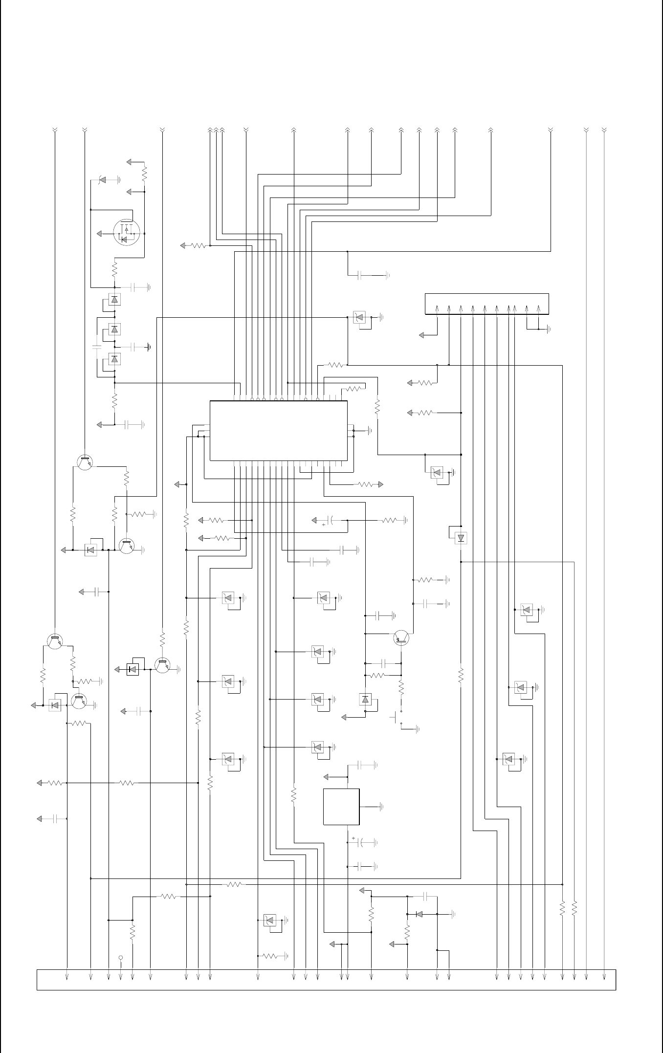
8-16 Schematics, Overlays, and Parts Lists: List of Schematics, Component Location Diagrams, and Parts Lists
September 26, 2003 6881096C77-O
Figure 8-8. HLN6396F/G/H (Standard), HLN6814A/B/C (Rear), HLN6563B/C/D (Motorcycle) W5/W7 Control Head Schematic (Sheet 1 of 2)
VIP IN 1
KEY SLOT
2. PART USAGE MAY VARY WITH APPLICATION. REFER TO PARTS LIST FOR USAGE INFORMATION.
SERIAL I/O
NOTES:
BUS-
RESET
VIP IN 3
MIC HI S.NET-WE
PTT
VIP IN 2
GND
S.NET-KID
SWB+
GND
VIPOUT1
S.NET-KEY
P103
MIC LO
VIPOUT 3
1. ALL RESISTANCE IS IN OHMS. ALL CAPACITANCE IN PICO-FARADS UNLESS NOTED OTHERWISE.
A+
SWB+
G
S
D
VIPOUT2
S.NET-WE
BUSY
IGN
BUS+
SWB+
S.NET-KID
S.NET-KEY
P104
MIC HI
MIC LO
HUB
PTT
HUB
SP-1_VF-SENSE-1
SP-2_VF-SENSE-2
Q71
SWB+
470pF
C176
CR90
VR5
15V
SWB+ A+_IGN
15V
VR3
10K
R6
JU2
CR52
8
7
SWB+
3
0.1uF
C174
470pF
+5V
C47 SWB+
C6
1.5uF
6
3
5
13
11
4
C7
.01uF
470pF
C41
47K
R34
+5V
4.7K
R177
CR76
VR4
C4
.01uF
15V
R87
10K
CR71
Q73
+5V
+5V
C175
470pF
22
23
10
12
25
2
15
JU4*
10K
A+
R200*
R99
1MEG
47K
R31
4.7K
R176
VIP_IN_3* 36
WDT_IN_T_CAP
44
WDT_TICKLE 2
WDT_T_CAP
43
+5V
RES_HUB 31
RX_DATA 20
TX_DATA 19
VIP_IN_1
25
VIP_IN_2
22
35 VIP_IN_3 VIP_IN_1* 24
VIP_IN_2* 21
OSC_OUT
6
+5V
+5V_REG 3
PTT 38
PTT* 37
9RESET
RESET* 4
7RESET_FILTR
40
27
26
33
15
12
18
23
42
5GND1
34 GND2
HUB_INV 30
HUB_POL
32 IGN
28
IGN* 29
14
8
39
BUSY
10 BUSY_IN* 11
BUSY_OUT* 13
BUS_NEG
16
17 BUS_POS
41
EXT_OSC_IN
GND
1
SC74487F
U4
A+/IGN
R98*
100K
+5V
JU8*
10uF
C45
7
17
16
VR10
A+_IGN
15V
9
C5
0.1uF
Q52
22K
R3
CR53
C3
.01uF
CR54
JU15*
1MEG
R4 36V
VR11
4
6
CR55
A+_IGN
A+
33K
R74
JU1*
JU3
SWB+
R175
4.7K
SWB+
1K
R8
CR73
470pF
C57
10K
R84
R81
10K
33K
R73
R7
10K
.01uF
C1
R71
470
VR2
15V
JU5
15V
VR1
NC
C48
0.1uF
C8
.01uF
SWB+
PWR
SWITCH
15V
VR20
15V
VR21
VR22
15V
14
26
19
JU9*
JU13*
1
Q74
10
5
R77
470
R76
470
33K
R75
JU18*
470
R72
U45
GND
2
IN
1OUT 3
+5V
+5V
C58
.01uF
MC78M05
JU7*
15V
8
VR9
18
R1*
10K
C43
0.1uF
15V
VR6R9
10K
SWB+
4.7K
R174
JU14*
15V
VR8
C56
470pF
+5V
Q75
JU6*
47K
R25
SWB+
CR72
15V
VR7
Q72 Q51
A+
JU12*
1
24
2
9
28
21
20
VIP_OUT_1
STROBE
EXT_OSC_IN
VIP_IN_3*
BUSY_OUT*
IGN*
TX_DATA
RX_DATA
BUSY_IN*
RESET*
HUB_INV
PTT
VIP_IN_2*
VIP_IN_1*
SP-1_VF-SENSE-1
SP-2_VF-SENSE-2
27
VIP_OUT_3
VIP_OUT_2
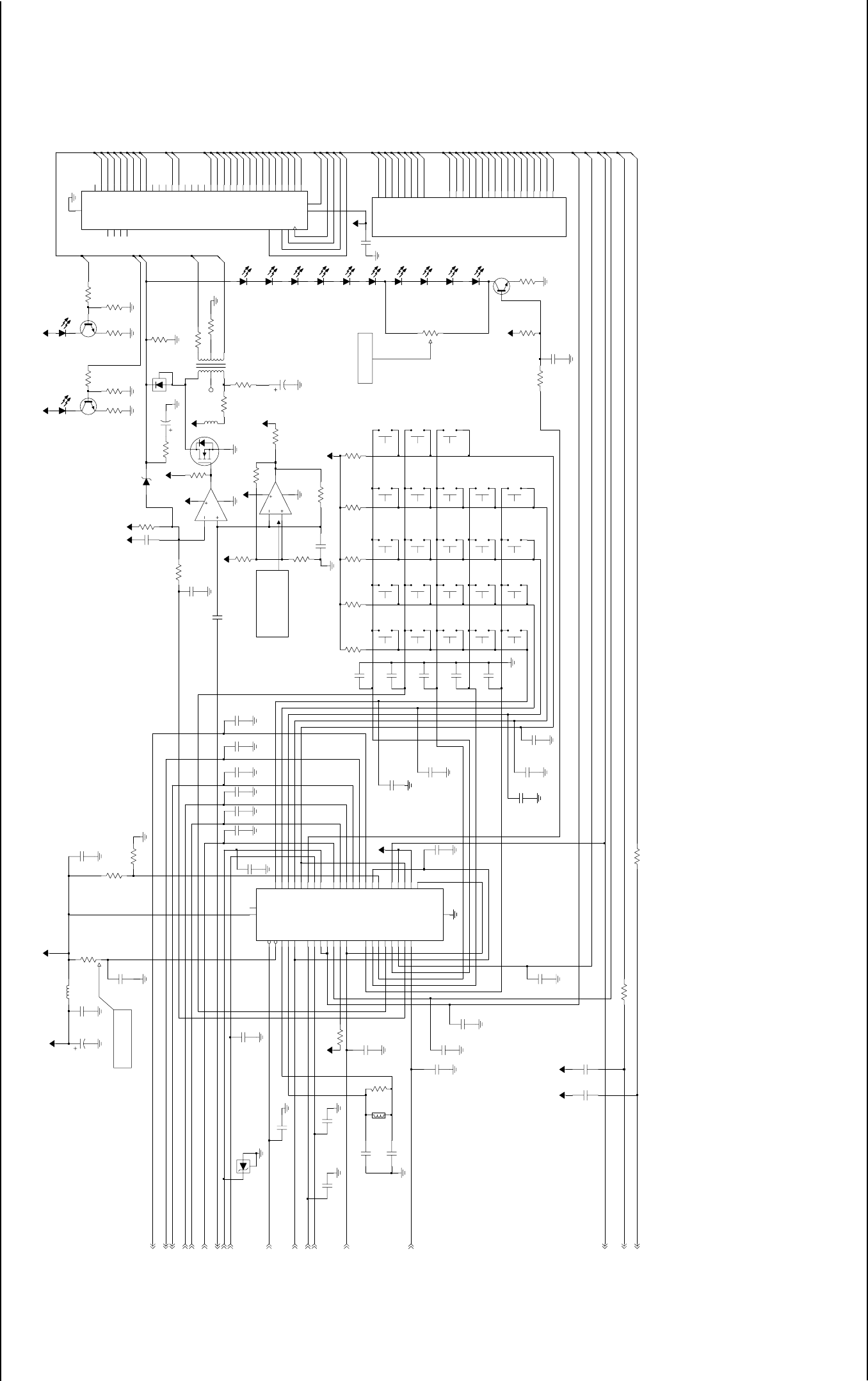
Schematics, Overlays, and Parts Lists: List of Schematics, Component Location Diagrams, and Parts Lists 8-17
6881096C77-O September 26, 2003
Figure 8-9. HLN6396F/G/H (Standard),HLN6814A/B/C (Rear), HLN6563B/C/D (Motorcycle) W5/W7 Control Head Schematic (Sheet 2 of 2)
G
S
WARNING!
(RED)(YELLOW)
VF DISPLAY
DAMAGE TO THE CIRCUIT
DIAGNOSTIC TEST
DO NOT PROBE U3 PIN 5
MAY OCCUR.
WITH POWER APPLIED.
SHORT TO GND. FOR
SHORT TO DISABLE
KEYPAD BACKLIGHT
NOTES:
1. ALL RESISTANCE IS IN OHMS. ALL CAPACITANCE IN PICO-FARADS UNLESS NOTED OTHERWISE.
2. PART USAGE MAY VARY WITH APPLICATION. REFER TO PARTS LIST FOR USAGE INFORMATION.
BUSY XMIT
D
3.U1 PINS 3,18,23,40 ARE NOT CONNECTED WITH MC68HC05C8A MICROPROCESSOR.
PN 6
24
PO
C36
470pF
PF
PG 5
PH 20
PI 22
PJ 7
PK 4
PL 21
PM 19
G6 11
G7 10
G8 9
PA 3
23
PB
PC 18
PD 8
PE 13
2
U102
1
F1
25
F2
G1 17
G2 16
G3 15
G4 14
G5 12
CR112
32M01
C23
30
13
30pF
C20
470pF
R57
47K
R29
470pF
C31
44
4
VSS
22
100K
34
DATA_IN
35
CLOCK
36
37 WDT_TKL
IGN*
39
RESET*
1
BUSY_IN*
41
STROBE 38
VDD
VIP_OUT_3 28
VIP_OUT_2 27
26
VIP_OUT_1
BUSY_IN 25
24
RX_DATA
32
TX_DATA
33
DATA_IN
15
PB3 16
PB4 17
19
BKLT
INV_HUB 20
PTT 21
VIP_IN_3 31
VIP_IN_2 30
VIP_IN_1 29
PA3
9
PA4
8
7LTCH_ENBL
HV_CNTRL
6
BUSY_OUT*
5
PB0 13
PB1 14
PB2
+5V_FIL 18
23
IGN* 40
OSC1
43
OSC2
42
PA0
12
PA1
11
PA2
10
SWB+SWB+
MC68HC705C8A
U1
2IRQ*
3
470pF
C54
C32
470pF
470pF
C33
470pF
C34
4
26
C35
470pF
470pF
C30
100K
R122R121
100K
CR133
CR134
19
18
17
CR51
30
26
Q111
C12*
JU100*
25
12
100K
JU17*
R112
JU16
4.7K
SWB+
R131
R5
100K
+5V
560
R123 R124
100K
12
+5V
+5V
C52
10uF
NC
13
29
11
HOME
SWITCH
10
14
+5V
470pF
C38
C18*
C40
470pF
22K
R51
R114
33K
VR24
10V
7
2
+5V
1
1K
+5V
28
Q112
R116
470pF
C37
12
31
3
1
8
4
32
31
15
16
C101*
21
20
16
U3-1
LM2903
2
C42*
22
1uF
C46
27
2
+5V_FIL
1
R181
22K
12
C26
470pF
.01uF
SWB+
DIM
SWITCH
C19*
C51
C17
C14*
470pF
CR132
CR131
C24*
14
C55
R52
1000uF
CR136
10K
100K
C10*
9.107uH
L50
R120
C39
24
1
470pF
470pF
C2
R178
10K
470pF
10
L1
9.107uH
R2
+5V
C27
1.5K
R60
4.7K
9
28
C50
10uF
33K
R113
24
1K
R115
8
100K
R111
Y1
6
7
470pF
C28
FREQ=4MHz
6
12
12
R180
SWITCH
VU
12
SEL
SWITCH
U3-2
LM2903
6
5
7
8
4
VR50
25
+5V_FIL
17
23
5
36V
4
5
R101
12
15
1000uF
C53
C16*
C15*
CR139
CR140
560
18
3
9
R50
CR135
+5V
CR138
6.8K
R61
2
SWITCH
MD
12
MU
SWITCH
12
OPT2
SWITCH
1
1
2
3
4
5
6
23
77J03
T60
R182
12
+5V
C29
470pF
10
R56
33K
C44*
30pF
+5V
8
C22
11
+5V_FIL
C11*
34
2
24 LTCH_ENBL
VCC1
44
VDISP
1
CR137
5
4
Q31
Q32 3
Q4 39
Q5 38
Q6 37
Q7 36
Q8 35
Q9
13
12
Q24
Q25 11
Q26 10
Q27 9
Q28 8
Q29 7
Q3 40
Q30
25
20
Q17
Q18 19
Q19 17
41
Q2
16
Q20
Q21 15
Q22 14
Q23
29
42
Q1
Q10 33
Q11 32
Q12 31
30
Q13
Q14 27
Q15 26
Q16
STROBE
21
23 CLK
DATA_IN
43
GND 22
6NC1
NC2
18 NC3
28 NC4
12
27
29
U101
UCQ5818EPF
SWITCH
OPT4
12
SWITCH
OPT3
SWB+
R55
1MEG
R30
+5V
12
R59
22
C25*
10K
C21
3
0.1uF
C13
470pF
C9*
JU19
Q131
R58
1K
20
33K
R28
CR111
Q50
12
19
32
21
S7
12
SWITCH
S8
12
SWITCH
S6
12
SWITCH
12
SWITCH
S1
SWITCH
S4
12
SWITCH
S3
2
SWITCH
S5
12
SWITCH
12
SWITCH
S2
1
SWITCH
STAR
12
PND
2
SWITCH
OPT1
12
SWITCH
12
SWITCH
VD
1
SWITCH
S0
12
S9
G5
G4
G3
G2
G1
R
Y
PB
PF
PA
PK
PG
PN
PJ
PO
DATA_IN
CLK
STROBE
VIP_IN_1*
VIP_IN_2*
VIP_OUT_3
SP-1_VF-SENSE-1
EXT_OSC_IN
HUB_INV
PTT
STROBE
CLOCK
RX_DATA
TX_DATA
VIP_IN_3*
SP-2_VF-SENSE-2
G8
P0
VDISP
LTCH_ENBL
PD
PE
PM
PH
PC
PL
G8
G7
G6
PI
BUS3(32:1)
VDISP
IGN*
RESET*
DATA_IN
BUSY_IN*
LTCH_ENBL
VIP_OUT_1
VIP_OUT_2
BKLT
STROBE
BUSY_OUT*
G7
G6
G5
G4
G3
G2
G1
G8
F2
F1
Y
R
PB
P0
F2
PI
PL
PH
PM
PC
PE
PD
PJ
PN
PG
PK
PA
PF
F1
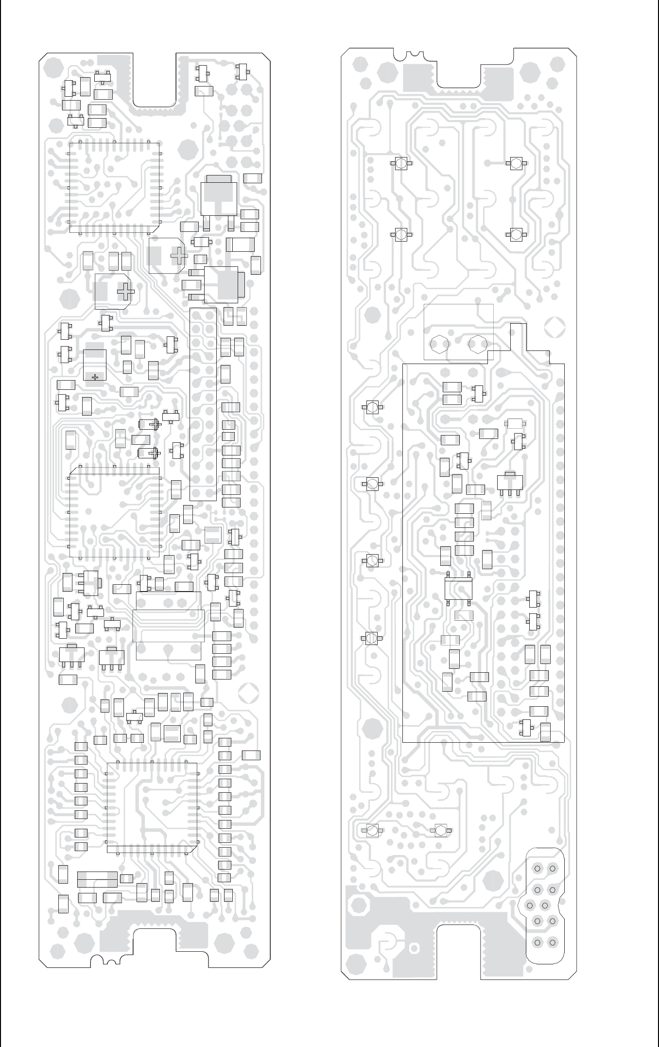
8-18 Schematics, Overlays, and Parts Lists: List of Schematics, Component Location Diagrams, and Parts Lists
September 26, 2003 6881096C77-O
Figure 8-10. HLN6396F/G (Standard), HLN6814A/B (Rear), HLN6563B/C (Motorcycle) W5/W7 Control Head Component Location Diagram (Viewed from Side 1)
Figure 8-11. HLN6396F/G (Standard), HLN6814A/B (Rear), HLN6563B/C (Motorcycle) W5/W7 Control Head Component Location Diagram (Viewed from Side 2)
JU100 R29
C39
C9
C41
C40
C38
C20
C19
C15
C44
C14
C11
C10
Q74
C24
C21
R123
C23 R30
C18 Y1
R122
R124
R121
R120
C35
C34
C33
C32
C31
C30
C29
C28
C27
C26
C22
C2
C16 C42
R28
C37
C17
7
7
6
6
1
1
17
17
U1
40
40
39
39
29
29
28
28
18
18
1234567891011121314
1234567891011121314
28272625
25
24
24
23
23
22
22
21
21
20
20
19
19
18
18
17
17
16
16
15
15
T60
U4 U101
Q51
U45
C45
C52
C50
JU17
R131
C39R
R25
R87
JU6
R174
R1
JU12
JU13
C175
C174
CR90
JU7
JU1
R31
R4
R3
C5
C4
C8
CR52
CR54
R34
C58
VR11
C57
CR55 C46
C6
R200
R182
R99
R8 JU15
CR71
Q71
CR72
R72
Q73
R73
VR4
VR3
C3
CR53
JU2
R177
R2
C53
R9
VR6
C47
JU18
R7
C176
R81
C1
VR10 VR1 VR2
VR7
C7
VR21
C48
R55
JU8
L50
VR8
VR9
VR5
C43
C56
Q52
Q72
R75
R77
CR73
Q75
R175
JU16
Q131
R50
R98
C25
C36
L1
R178
JU19
R71
R76
R74
C12
R176
R180
R181
C101
7
6
1
17
40
39 29
28
18
1
2
3
6
5
4
R113
R111
R115
R116
Q50
R59
R60
R58
JU4
R101
JU3
R56
R61
R51
C51
VR50
R6
*#
VR22
VR20
C55
CR76
JU14
JU5
R5
PWR
MD MU
VUVD
DIM
HOME
OPT1 OPT2 OPT3 OPT4 SEL
C54
R57
P104
U3
JU9
C13
R52
R114
R112
Q112
CR51
Q111
CR111
CR112
12 3 4 5 6 78 91011121314
28 27 26 25 24 23 22 21 20 19 18 17 16 15
1
1
2
23
3
4
45
5
6
6
7
7
8
89
9
10
10 11 12 13 14 2524232221201918171615
CR138
CR139
CR140
CR137
CR136
CR135
CR134
CR133
CR131
CR132
123
456
789
0
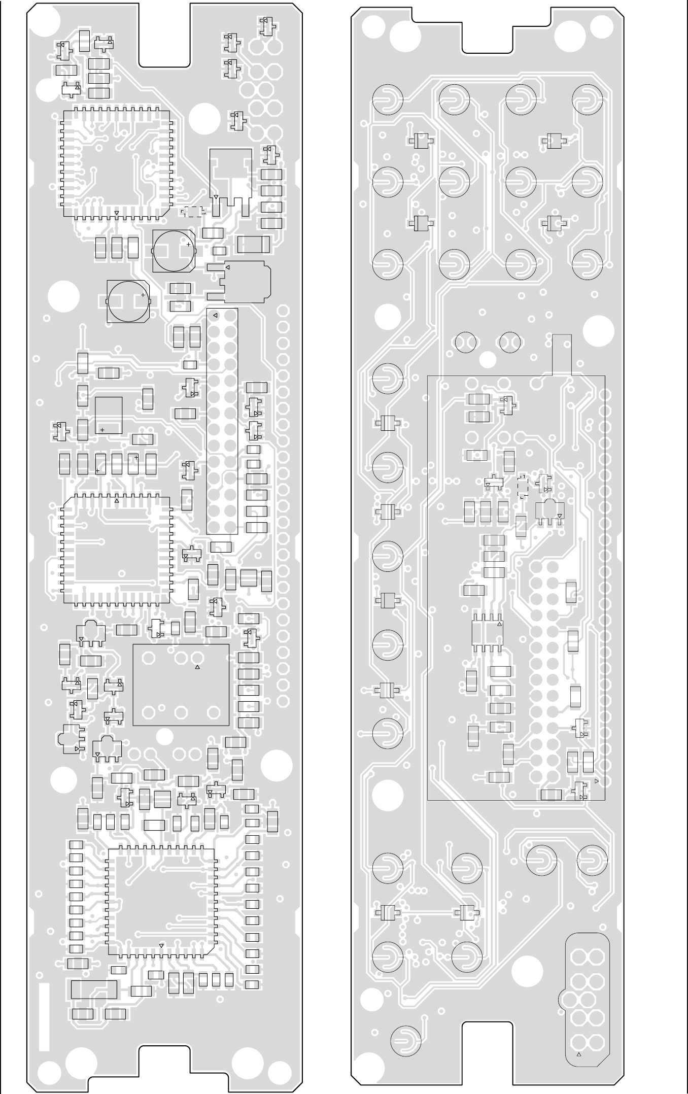
Schematics, Overlays, and Parts Lists: List of Schematics, Component Location Diagrams, and Parts Lists 8-19
6881096C77-O September 26, 2003
Figure 8-12. HLN6396H_HLN6814C_HLN6563C W5/W7 Control Head Component Location Diagram (Viewed from Side 1)
Figure 8-13. HLN6396H_HLN6814C_HLN6563C W5/W7 Control Head Component Location Diagram (Viewed from Side 2)
C1
C2
C3
C4
C5
C6
C7
C8
C17
C10*
C101*
C11*
C12*
C14*
C15*
C16* C18*
C19*
C20
C21
C22
C23
C26
C27
C28
C29
C24*
C25*
C30
C31
C32
C33
C34
C35
C36
C37
C38
C39
C40
C41
C43
C45
C46
C47
C48
C42*
C44*
C50
C52
C53
C56
C57
C58
C174
C175
C176
C9*
CR52 CR53
CR54
CR55
CR71 CR72
CR73
CR90
JU2
JU1*
JU16
JU19
JU100*
JU12*
JU13*
JU15*
JU17*
JU18*
JU6*
JU7*
JU8*
L1
L50
15
14
28
P103
Q51
Q52
Q71
Q72
Q73
Q74
Q75
Q131
R2
R3
R4
R7
R8
R9
R1*
R25
R28
R29
R200*
R30
R31
R34R50
R55
R71
R72
R73
R74
R75
R76
R77
R81
R84
R87
R99
R120
R121
R122
R123
R124
R131
R174
R175
R176
R177
R178
R180
R181
R182
R98*
4
5
63
2
1
T60
6
40
39 29
28
18
17
7
1U1
1
6
7
17
18
28
29 39
40
U4
3
2
1
U45
1
6
717
18
28
29
39
40
U101
VR1
VR2
VR3 VR4
VR5
VR6
VR8
VR9
VR10
VR11
VR20
VR21
VR22
VR24
Y1
8480251R07
C13
C51
C54
C55
CR51
CR76
CR111
CR112
CR131 CR132
CR133
CR134
CR135
CR136
CR137
CR138
CR139
CR140
DIM
HOME
JU3
JU5
JU14* JU4* JU9*
MD MU OPT1 OPT2 OPT3 OPT4
3
5
6
7
8
4
2
9
10
P104
PND
PWR
Q50
Q111
Q112
R5
R6
R51
R52
R56
R57 R58
R59
R60
R61
R101
R111
R112
R113
R114
R115
R116
S0
S1 S2 S3
S4 S5 S6
S7 S8 S9
SEL
STAR
1
4
5
8
U3
25
U102
VD
VR7
VR50
VU

8-20 Schematics, Overlays, and Parts Lists: List of Schematics, Component Location Diagrams, and Parts Lists
September 26, 2003 6881096C77-O
HLN6396H Standard Parts List
ITEM MOTOROLA
PART
NUMBER DESCRIPTION
C0053 2113741N21 CAP CHIP CL2 X7R 10% 1000
C0055 2113741N21 CAP CHIP CL2 X7R 10% 1000
C1 2113741N45 CAP CHIP CL2 X7R 10% 10000
C10 NOTPLACED 64AM DUMMY PART NUMBER
C101 NOTPLACED 64AM DUMMY PART NUMBER
C11 NOTPLACED 64AM DUMMY PART NUMBER
C12 NOTPLACED 64AM DUMMY PART NUMBER
C13 2113741N69 CAP CHIP CL2 X7R 10%
100000
C14 NOTPLACED 64AM DUMMY PART NUMBER
C15 NOTPLACED 64AM DUMMY PART NUMBER
C16 NOTPLACED 64AM DUMMY PART NUMBER
C17 2113741M13 CAP CHIP CL2 X7R 10% 470
C174 2113741M13 CAP CHIP CL2 X7R 10% 470
C175 2113741M13 CAP CHIP CL2 X7R 10% 470
C176 2113741M13 CAP CHIP CL2 X7R 10% 470
C18 NOTPLACED 64AM DUMMY PART NUMBER
C19 NOTPLACED 64AM DUMMY PART NUMBER
C2 2113741M13 CAP CHIP CL2 X7R 10% 470
C20 2113741M13 CAP CHIP CL2 X7R 10% 470
C21 2113741M13 CAP CHIP CL2 X7R 10% 470
C22 2113740B36 CAP CHIP REEL CL1 +/-30 30
C23 2113740B36 CAP CHIP REEL CL1 +/-30 30
C24 NOTPLACED 64AM DUMMY PART NUMBER
C25 NOTPLACED 64AM DUMMY PART NUMBER
C26 2113741M13 CAP CHIP CL2 X7R 10% 470
C27 2113741M13 CAP CHIP CL2 X7R 10% 470
C28 2113741M13 CAP CHIP CL2 X7R 10% 470
C29 2113741M13 CAP CHIP CL2 X7R 10% 470
C3 2113741N45 CAP CHIP CL2 X7R 10% 10000
C30 2113741M13 CAP CHIP CL2 X7R 10% 470
C31 2113741M13 CAP CHIP CL2 X7R 10% 470
C32 2113741M13 CAP CHIP CL2 X7R 10% 470
C33 2113741M13 CAP CHIP CL2 X7R 10% 470
C34 2113741M13 CAP CHIP CL2 X7R 10% 470
C35 2113741M13 CAP CHIP CL2 X7R 10% 470
C36 2113741M13 CAP CHIP CL2 X7R 10% 470
C37 2113741M13 CAP CHIP CL2 X7R 10% 470
C38 2113741M13 CAP CHIP CL2 X7R 10% 470
C39 2113741M13 CAP CHIP CL2 X7R 10% 470
C4 2113741N45 CAP CHIP CL2 X7R 10% 10000
C40 2113741M13 CAP CHIP CL2 X7R 10% 470
C41 2113741M13 CAP CHIP CL2 X7R 10% 470
C42 NOTPLACED 64AM DUMMY PART NUMBER
C43 2113741N69 CAP CHIP CL2 X7R 10%
100000
C44 NOTPLACED 64AM DUMMY PART NUMBER
C45 2380090M24 CAP ALU 10 20 50V SURF MT
C46 2311049A37 CAP TANT CHIP 1 20 20
C47 2113741N69 CAP CHIP CL2 X7R 10%
100000
C48 2113741N69 CAP CHIP CL2 X7R 10%
100000
C5 2113741N69 CAP CHIP CL2 X7R 10%
100000
C50 2311049A95 CAP TANT CHIP 10 UF 25V
10%
C51 2113741N45 CAP CHIP CL2 X7R 10% 10000
C52 2380090M24 CAP ALU 10 20 50V SURF MT
C54 2113740B65 CAP CHIP REEL CL1 +/-30 470
C56 2113741M13 CAP CHIP CL2 X7R 10% 470
C57 2113741M13 CAP CHIP CL2 X7R 10% 470
C58 2113741N45 CAP CHIP CL2 X7R 10% 10000
C6 2311049A38 CAP TANT CHIP 1.5 10 16
C7 2113741N45 CAP CHIP CL2 X7R 10% 10000
C8 2113741N45 CAP CHIP CL2 X7R 10% 10000
C9 NOTPLACED 64AM DUMMY PART NUMBER
CR111 4880026P01 DIODE LED RED
CR112 4880026P02 DIODE LED YELLOW
ITEM MOTOROLA
PART
NUMBER DESCRIPTION
CR131 4880052R03 DIODE LIGHT EMITTING GRN
CR132 4880052R03 DIODE LIGHT EMITTING GRN
CR133 4880052R03 DIODE LIGHT EMITTING GRN
CR134 4880052R03 DIODE LIGHT EMITTING GRN
CR135 4880052R03 DIODE LIGHT EMITTING GRN
CR136 4880052R03 DIODE LIGHT EMITTING GRN
CR137 4880052R03 DIODE LIGHT EMITTING GRN
CR138 4880052R03 DIODE LIGHT EMITTING GRN
CR139 4880052R03 DIODE LIGHT EMITTING GRN
CR140 4880052R03 DIODE LIGHT EMITTING GRN
CR51 4811058B11 DIODE 48S11058A11 A/P
CR52 4811058B11 DIODE 48S11058A11 A/P
CR53 4811058B11 DIODE 48S11058A11 A/P
CR54 4811058B11 DIODE 48S11058A11 A/P
CR55 4811058B11 DIODE 48S11058A11 A/P
CR71 4811058B11 DIODE 48S11058A11 A/P
CR72 4811058B11 DIODE 48S11058A11 A/P
CR73 4811058B11 DIODE 48S11058A11 A/P
CR76 4811058B11 DIODE 48S11058A11 A/P
CR90 4882960R02 DIODE RECT 48R82960R01 A/P
JU0003 0611077A01 RES CHIP JUMPER
JU0005 0611077A01 RES CHIP JUMPER
JU0016 0611077A01 RES CHIP JUMPER
JU0017 NOTPLACED 64AM DUMMY PART NUMBER
JU1 NOTPLACED 64AM DUMMY PART NUMBER
JU100 NOTPLACED 64AM DUMMY PART NUMBER
JU12 NOTPLACED 64AM DUMMY PART NUMBER
JU13 NOTPLACED 64AM DUMMY PART NUMBER
JU14 NOTPLACED 64AM DUMMY PART NUMBER
JU15 NOTPLACED 64AM DUMMY PART NUMBER
JU18 NOTPLACED 64AM DUMMY PART NUMBER
JU19 NOTPLACED 64AM DUMMY PART NUMBER
JU2 0611077A01 RES CHIP JUMPER
ITEM MOTOROLA
PART
NUMBER DESCRIPTION
JU4 NOTPLACED 64AM DUMMY PART NUMBER
JU6 NOTPLACED 64AM DUMMY PART NUMBER
JU7 NOTPLACED 64AM DUMMY PART NUMBER
JU8 NOTPLACED 64AM DUMMY PART NUMBER
JU9 NOTPLACED 64AM DUMMY PART NUMBER
L1 2480140E16 INDUCTOR CHIP 10UH
L50 2480140E16 INDUCTOR CHIP 10UH
MP0103 4380290L01 SPACER LED
MP0106 5480004N01 LABEL BARCODE
P0103 2880102M07 PLUG VERTICAL 28 POSITION
P0104 2880068M01 HEADER MIC
Q111 4880141L02 TSTR NPN SOT23 LO PROFILE
TAPE
Q112 4880141L02 TSTR NPN SOT23 LO PROFILE
TAPE
Q131 4880141L02 TSTR NPN SOT23 LO PROFILE
TAPE
Q50 4880053M03 TSTR N/CH SOT 89 200V B ST
84
Q51 4813821A30 MOSFET N-CH 60V 15A
Q52 4880141L01 TSTR PNP SOT23 LO PROFILE
TAPE
Q71 4880053M02 TSTR NPN MXT2222A
Q72 4880053M02 TSTR NPN MXT2222A
Q73 4880053M02 TSTR NPN MXT2222A
Q74 4880141L02 TSTR NPN SOT23 LO PROFILE
TAPE
Q75 4880141L02 TSTR NPN SOT23 LO PROFILE
TAPE
R0002 0611077A90 RES CHIP 4700 5 1/8
R0005 0611077A90 RES CHIP 4700 5 1/8
R1 NOTPLACED 64AM DUMMY PART NUMBER
R101 0611077A28 RES CHIP 12 5 1/8W
R111 0611077B23 RES CHIP 100K 5 1/8W
R112 0611077B23 RES CHIP 100K 5 1/8W
R113 0611077B11 RES CHIP 33K 5 1/8W
ITEM MOTOROLA
PART
NUMBER DESCRIPTION
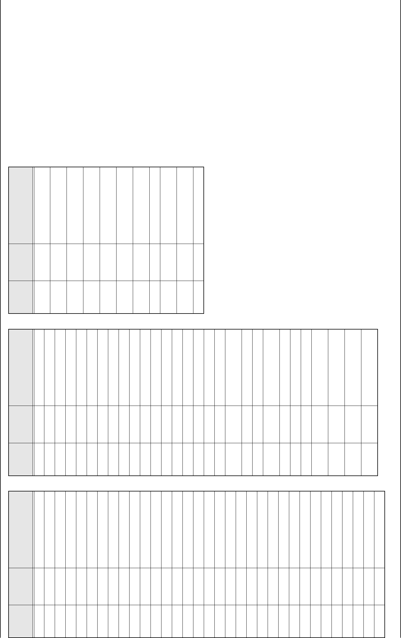
Schematics, Overlays, and Parts Lists: List of Schematics, Component Location Diagrams, and Parts Lists 8-21
6881096C77-O September 26, 2003
R114 0611077B11 RES CHIP 33K 5 1/8W
R115 0611077A74 RES CHIP 1000 5 1/8
R116 0611077A74 RES CHIP 1000 5 1/8
R120 0611077B23 RES CHIP 100K 5 1/8W
R121 0611077B23 RES CHIP 100K 5 1/8W
R122 0611077B23 RES CHIP 100K 5 1/8W
R123 0611077B23 RES CHIP 100K 5 1/8W
R124 0611077B23 RES CHIP 100K 5 1/8W
R131 0611077A68 RES CHIP 560 5 1/8W
R174 0611077A90 RES CHIP 4700 5 1/8
R175 0611077A90 RES CHIP 4700 5 1/8
R176 0611077A90 RES CHIP 4700 5 1/8
R177 0611077A90 RES CHIP 4700 5 1/8
R178 0611077A98 RES CHIP 10K 5 1/8W
R180 0611077A28 RES CHIP 12 5 1/8W
R181 0611077B07 RES CHIP 22K 5 1/8W
R182 0611077A28 RES CHIP 12 5 1/8W
R200 0611077B47 RES CHIP 1 MEG 5 1/8W
R25 0611077B15 RES CHIP 47K 5 1/8W
R28 0611077A74 RES CHIP 1000 5 1/8
R29 0611077B23 RES CHIP 100K 5 1/8W
R3 0611077B07 RES CHIP 22K 5 1/8W
R30 0611077B47 RES CHIP 1 MEG 5 1/8W
R31 0611077B15 RES CHIP 47K 5 1/8W
R34 0611077B15 RES CHIP 47K 5 1/8W
R4 0611077B47 RES CHIP 1 MEG 5 1/8W
R50 0611077A68 RES CHIP 560 5 1/8W
R51 0611077B07 RES CHIP 22K 5 1/8W
R52 0611077A98 RES CHIP 10K 5 1/8W
R55 0611077A28 RES CHIP 12 5 1/8W
R56 0611077B11 RES CHIP 33K 5 1/8W
R57 0611077B15 RES CHIP 47K 5 1/8W
R58 0611077B11 RES CHIP 33K 5 1/8W
ITEM MOTOROLA
PART
NUMBER DESCRIPTION
R59 0611077A98 RES CHIP 10K 5 1/8W
R6 0611077A98 RES CHIP 10K 5 1/8W
R60 0611077A78 RES CHIP 1500 5 1/8
R61 0611077A94 RES CHIP 6.8K 5 1/8
R7 0611077A98 RES CHIP 10K 5 1/8W
R71 0611077A66 RES CHIP 470 5 1/8W
R72 0611077A66 RES CHIP 470 5 1/8W
R73 0611077B11 RES CHIP 33K 5 1/8W
R74 0611077B11 RES CHIP 33K 5 1/8W
R75 0611077B11 RES CHIP 33K 5 1/8W
R76 0611077A66 RES CHIP 470 5 1/8W
R77 0611077A66 RES CHIP 470 5 1/8W
R8 0611077A74 RES CHIP 1000 5 1/8
R81 0611077A98 RES CHIP 10K 5 1/8W
R87 0611077A98 RES CHIP 10K 5 1/8W
R9 0611077A98 RES CHIP 10K 5 1/8W
R98 NOTPLACED 64AM DUMMY PART NUMBER
R99 0611077A98 RES CHIP 10K 5 1/8W
U0102 7280032M01 DSPLY VF 14 SEG 8 CHAR
BLUGRN
U1 0104002J91 PRGMD MICROP ASSEM
U101 5180236C05 IC VF DRVR SN75518FN
U3 5113820A02 IC DUAL SING SPLY LO PWR
2903
U4 5180057S04 “IC CUST SER I/O 13”” REEL”
U45 5113816G04 IC +5V REG 78M05
VR0011 4813830C41 DIODE 36V ‘M3’ MMSZ5258BT1
VR08 4813830A28 DIODE 15V 5% 225MW
MMBZ5245B_
VR09 4813830A28 DIODE 15V 5% 225MW
MMBZ5245B_
VR1 4813830A28 DIODE 15V 5% 225MW
MMBZ5245B_
VR10 4813830A28 DIODE 15V 5% 225MW
MMBZ5245B_
ITEM MOTOROLA
PART
NUMBER DESCRIPTION
VR2 4813830A28 DIODE 15V 5% 225MW
MMBZ5245B_
VR20 4813830A28 DIODE 15V 5% 225MW
MMBZ5245B_
VR21 4813830A28 DIODE 15V 5% 225MW
MMBZ5245B_
VR22 4813830A28 DIODE 15V 5% 225MW
MMBZ5245B_
VR3 4813830A28 DIODE 15V 5% 225MW
MMBZ5245B_
VR4 4813830A28 DIODE 15V 5% 225MW
MMBZ5245B_
VR5 4813830A28 DIODE 15V 5% 225MW
MMBZ5245B_
VR50 4813830C41 DIODE 36V ‘M3’ MMSZ5258BT1
VR6 4813830A28 DIODE 15V 5% 225MW
MMBZ5245B_
VR7 4813830A28 DIODE 15V 5% 225MW
MMBZ5245B_
Y1 4880065M01 RESONTR CERAMIC 4.00 MHZ
ITEM MOTOROLA
PART
NUMBER DESCRIPTION
8-22 Schematics, Overlays, and Parts Lists: List of Schematics, Component Location Diagrams, and Parts Lists
September 26, 2003 6881096C77-O
HLN6814C Rear Parts List
ITEM MOTOROLA
PART
NUMBER DESCRIPTION
C0053 2113741N21 CAP CHIP CL2 X7R 10% 1000
C0055 2113741N21 CAP CHIP CL2 X7R 10% 1000
C1 2113741N45 CAP CHIP CL2 X7R 10% 10000
C10 NOTPLACED 64AM DUMMY PART NUMBER
C101 NOTPLACED 64AM DUMMY PART NUMBER
C11 NOTPLACED 64AM DUMMY PART NUMBER
C12 NOTPLACED 64AM DUMMY PART NUMBER
C13 NOTPLACED 64AM DUMMY PART NUMBER
C14 NOTPLACED 64AM DUMMY PART NUMBER
C15 NOTPLACED 64AM DUMMY PART NUMBER
C16 NOTPLACED 64AM DUMMY PART NUMBER
C17 2113741M13 CAP CHIP CL2 X7R 10% 470
C174 2113741M13 CAP CHIP CL2 X7R 10% 470
C175 2113741M13 CAP CHIP CL2 X7R 10% 470
C176 2113741M13 CAP CHIP CL2 X7R 10% 470
C18 NOTPLACED 64AM DUMMY PART NUMBER
C19 NOTPLACED 64AM DUMMY PART NUMBER
C2 2113741M13 CAP CHIP CL2 X7R 10% 470
C20 2113741M13 CAP CHIP CL2 X7R 10% 470
C21 2113741M13 CAP CHIP CL2 X7R 10% 470
C22 2113740B36 CAP CHIP REEL CL1 +/-30 30
C23 2113740B36 CAP CHIP REEL CL1 +/-30 30
C24 NOTPLACED 64AM DUMMY PART NUMBER
C25 NOTPLACED 64AM DUMMY PART NUMBER
C26 2113741M13 CAP CHIP CL2 X7R 10% 470
C27 2113741M13 CAP CHIP CL2 X7R 10% 470
C28 2113741M13 CAP CHIP CL2 X7R 10% 470
C29 2113741M13 CAP CHIP CL2 X7R 10% 470
C3 NOTPLACED 64AM DUMMY PART NUMBER
C30 2113741M13 CAP CHIP CL2 X7R 10% 470
C31 2113741M13 CAP CHIP CL2 X7R 10% 470
C32 2113741M13 CAP CHIP CL2 X7R 10% 470
C33 2113741M13 CAP CHIP CL2 X7R 10% 470
C34 2113741M13 CAP CHIP CL2 X7R 10% 470
C35 2113741M13 CAP CHIP CL2 X7R 10% 470
C36 2113741M13 CAP CHIP CL2 X7R 10% 470
C37 2113741M13 CAP CHIP CL2 X7R 10% 470
C38 2113741M13 CAP CHIP CL2 X7R 10% 470
C39 2113741M13 CAP CHIP CL2 X7R 10% 470
C4 NOTPLACED 64AM DUMMY PART NUMBER
C40 2113741M13 CAP CHIP CL2 X7R 10% 470
C41 2113741M13 CAP CHIP CL2 X7R 10% 470
C42 NOTPLACED 64AM DUMMY PART NUMBER
C43 NOTPLACED 64AM DUMMY PART NUMBER
C44 NOTPLACED 64AM DUMMY PART NUMBER
C45 2380090M24 CAP ALU 10 20 50V SURF MT
C46 2311049A37 CAP TANT CHIP 1 20 20
C47 2113741N69 CAP CHIP CL2 X7R 10%
100000
C48 NOTPLACED 64AM DUMMY PART NUMBER
C5 NOTPLACED 64AM DUMMY PART NUMBER
C50 2311049A95 CAP TANT CHIP 10 UF 25V
10%
C51 2113741N45 CAP CHIP CL2 X7R 10% 10000
C52 2380090M24 CAP ALU 10 20 50V SURF MT
C54 2113740B65 CAP CHIP REEL CL1 +/-30 470
C56 NOTPLACED 64AM DUMMY PART NUMBER
C57 2113741M13 CAP CHIP CL2 X7R 10% 470
C58 2113741N45 CAP CHIP CL2 X7R 10% 10000
C6 2311049A38 CAP TANT CHIP 1.5 10 16
C7 2113741N45 CAP CHIP CL2 X7R 10% 10000
C8 NOTPLACED 64AM DUMMY PART NUMBER
C9 NOTPLACED 64AM DUMMY PART NUMBER
CR111 4880026P01 DIODE LED RED
CR112 4880026P02 DIODE LED YELLOW
CR131 4880052R03 DIODE LIGHT EMITTING GRN
ITEM MOTOROLA
PART
NUMBER DESCRIPTION
CR132 4880052R03 DIODE LIGHT EMITTING GRN
CR133 4880052R03 DIODE LIGHT EMITTING GRN
CR134 4880052R03 DIODE LIGHT EMITTING GRN
CR135 4880052R03 DIODE LIGHT EMITTING GRN
CR136 4880052R03 DIODE LIGHT EMITTING GRN
CR137 4880052R03 DIODE LIGHT EMITTING GRN
CR138 4880052R03 DIODE LIGHT EMITTING GRN
CR139 4880052R03 DIODE LIGHT EMITTING GRN
CR140 4880052R03 DIODE LIGHT EMITTING GRN
CR51 4811058B11 DIODE 48S11058A11 A/P
CR52 NOTPLACED 64AM DUMMY PART NUMBER
CR53 NOTPLACED 64AM DUMMY PART NUMBER
CR54 NOTPLACED 64AM DUMMY PART NUMBER
CR55 4811058B11 DIODE 48S11058A11 A/P
CR71 4811058B11 DIODE 48S11058A11 A/P
CR72 4811058B11 DIODE 48S11058A11 A/P
CR73 4811058B11 DIODE 48S11058A11 A/P
CR76 4811058B11 DIODE 48S11058A11 A/P
CR90 NOTPLACED 64AM DUMMY PART NUMBER
JU0003 0611077A01 RES CHIP JUMPER
JU0005 0611077A01 RES CHIP JUMPER
JU0016 0611077A01 RES CHIP JUMPER
JU0017 NOTPLACED 64AM DUMMY PART NUMBER
JU1 0611077A01 RES CHIP JUMPER
JU100 NOTPLACED 64AM DUMMY PART NUMBER
JU12 NOTPLACED 64AM DUMMY PART NUMBER
JU13 NOTPLACED 64AM DUMMY PART NUMBER
JU14 NOTPLACED 64AM DUMMY PART NUMBER
JU15 NOTPLACED 64AM DUMMY PART NUMBER
JU18 NOTPLACED 64AM DUMMY PART NUMBER
JU19 0611077A01 RES CHIP JUMPER
JU2 NOTPLACED 64AM DUMMY PART NUMBER
JU4 NOTPLACED 64AM DUMMY PART NUMBER
ITEM MOTOROLA
PART
NUMBER DESCRIPTION
JU6 NOTPLACED 64AM DUMMY PART NUMBER
JU7 0611077A01 RES CHIP JUMPER
JU8 NOTPLACED 64AM DUMMY PART NUMBER
JU9 NOTPLACED 64AM DUMMY PART NUMBER
L1 2480140E16 INDUCTOR CHIP 10UH
L50 2480140E16 INDUCTOR CHIP 10UH
MP0101 7580094M05 “SHOCK PAD, VF”
MP0102 7580094M05 “SHOCK PAD, VF”
MP0103 7580094M05 “SHOCK PAD, VF”
MP0106 5480004N01 LABEL BARCODE
P0103 2880102M07 PLUG VERTICAL 28 POSITION
P0104 2880068M01 HEADER MIC
Q111 4880141L02 TSTR NPN SOT23 LO PRO-
FILE TAPE
Q112 4880141L02 TSTR NPN SOT23 LO PRO-
FILE TAPE
Q131 4880141L02 TSTR NPN SOT23 LO PRO-
FILE TAPE
Q50 4880053M03 TSTR N/CH SOT 89 200V B ST
84
Q51 NOTPLACED 64AM DUMMY PART NUMBER
Q52 NOTPLACED 64AM DUMMY PART NUMBER
Q71 4880053M02 TSTR NPN MXT2222A
Q72 4880053M02 TSTR NPN MXT2222A
Q73 4880053M02 TSTR NPN MXT2222A
Q74 4880141L02 TSTR NPN SOT23 LO PRO-
FILE TAPE
Q75 4880141L02 TSTR NPN SOT23 LO PRO-
FILE TAPE
R0002 0611077A90 RES CHIP 4700 5 1/8
R0005 0611077A90 RES CHIP 4700 5 1/8
R1 NOTPLACED 64AM DUMMY PART NUMBER
R101 0611077A28 RES CHIP 12 5 1/8W
R111 0611077B23 RES CHIP 100K 5 1/8W
R112 0611077B23 RES CHIP 100K 5 1/8W
R113 0611077B11 RES CHIP 33K 5 1/8W
ITEM MOTOROLA
PART
NUMBER DESCRIPTION
Schematics, Overlays, and Parts Lists: List of Schematics, Component Location Diagrams, and Parts Lists 8-23
6881096C77-O September 26, 2003
R114 0611077B11 RES CHIP 33K 5 1/8W
R115 0611077A74 RES CHIP 1000 5 1/8
R116 0611077A74 RES CHIP 1000 5 1/8
R120 0611077B23 RES CHIP 100K 5 1/8W
R121 0611077B23 RES CHIP 100K 5 1/8W
R122 0611077B23 RES CHIP 100K 5 1/8W
R123 0611077B23 RES CHIP 100K 5 1/8W
R124 0611077B23 RES CHIP 100K 5 1/8W
R131 0611077A68 RES CHIP 560 5 1/8W
R174 0611077A90 RES CHIP 4700 5 1/8
R175 0611077A90 RES CHIP 4700 5 1/8
R176 0611077A90 RES CHIP 4700 5 1/8
R177 0611077A90 RES CHIP 4700 5 1/8
R178 0611077A98 RES CHIP 10K 5 1/8W
R180 0611077A28 RES CHIP 12 5 1/8W
R181 0611077B07 RES CHIP 22K 5 1/8W
R182 0611077A28 RES CHIP 12 5 1/8W
R200 0611077B47 RES CHIP 1 MEG 5 1/8W
R25 NOTPLACED 64AM DUMMY PART NUMBER
R28 0611077A74 RES CHIP 1000 5 1/8
R29 0611077B23 RES CHIP 100K 5 1/8W
R3 NOTPLACED 64AM DUMMY PART NUMBER
R30 0611077B47 RES CHIP 1 MEG 5 1/8W
R31 0611077B15 RES CHIP 47K 5 1/8W
R34 0611077B15 RES CHIP 47K 5 1/8W
R4 NOTPLACED 64AM DUMMY PART NUMBER
R50 0611077A68 RES CHIP 560 5 1/8W
R51 0611077B07 RES CHIP 22K 5 1/8W
R52 0611077A98 RES CHIP 10K 5 1/8W
R55 0611077A28 RES CHIP 12 5 1/8W
R56 0611077B11 RES CHIP 33K 5 1/8W
R57 0611077B15 RES CHIP 47K 5 1/8W
R58 0611077B11 RES CHIP 33K 5 1/8W
ITEM MOTOROLA
PART
NUMBER DESCRIPTION
R59 0611077A98 RES CHIP 10K 5 1/8W
R6 NOTPLACED 64AM DUMMY PART NUMBER
R60 0611077A78 RES CHIP 1500 5 1/8
R61 0611077A94 RES CHIP 6.8K 5 1/8
R7 NOTPLACED 64AM DUMMY PART NUMBER
R71 0611077A66 RES CHIP 470 5 1/8W
R72 0611077A66 RES CHIP 470 5 1/8W
R73 0611077B11 RES CHIP 33K 5 1/8W
R74 0611077B11 RES CHIP 33K 5 1/8W
R75 0611077B11 RES CHIP 33K 5 1/8W
R76 0611077A66 RES CHIP 470 5 1/8W
R77 0611077A66 RES CHIP 470 5 1/8W
R8 NOTPLACED 64AM DUMMY PART NUMBER
R81 0611077A98 RES CHIP 10K 5 1/8W
R84 NOTPLACED 64AM DUMMY PART NUMBER
R87 0611077A98 RES CHIP 10K 5 1/8W
R9 0611077A98 RES CHIP 10K 5 1/8W
R98 NOTPLACED 64AM DUMMY PART NUMBER
R99 0611077A98 RES CHIP 10K 5 1/8W
T60 2580277J03 XFMR VLTG CONVERSION
U0102 7280032M01 DSPLY VF 14 SEG 8 CHAR
BLUGRN
U1 0104002J91 PRGMD MICROP ASSEM
U101 5180236C05 IC VF DRVR SN75518FN
U3 5113820A02 IC DUAL SING SPLY LO PWR
2903
U4 5180057S04 “IC CUST SER I/O 13”” REEL”
U45 5113816G04 IC +5V REG 78M05
VR0011 NOTPLACED 64AM DUMMY PART NUMBER
VR1 4813830A28 DIODE 15V 5% 225MW
MMBZ5245B_
VR10 4813830A28 DIODE 15V 5% 225MW
MMBZ5245B_
VR2 4813830A28 DIODE 15V 5% 225MW
MMBZ5245B_
ITEM MOTOROLA
PART
NUMBER DESCRIPTION
VR20 4813830A28 DIODE 15V 5% 225MW
MMBZ5245B_
VR21 4813830A28 DIODE 15V 5% 225MW
MMBZ5245B_
VR22 4813830A28 DIODE 15V 5% 225MW
MMBZ5245B_
VR3 4813830A28 DIODE 15V 5% 225MW
MMBZ5245B_
VR4 4813830A28 DIODE 15V 5% 225MW
MMBZ5245B_
VR5 NOTPLACED 64AM DUMMY PART NUMBER
VR50 4813830C41 DIODE 36V ‘M3’
MMSZ5258BT1
VR6 4813830A28 DIODE 15V 5% 225MW
MMBZ5245B_
VR7 4813830A28 DIODE 15V 5% 225MW
MMBZ5245B_
VR8 4813830A28 DIODE 15V 5% 225MW
MMBZ5245B_
VR9 4813830A28 DIODE 15V 5% 225MW
MMBZ5245B_
Y1 4880065M01 RESONTR CERAMIC 4.00 MHZ
ITEM MOTOROLA
PART
NUMBER DESCRIPTION
8-24 Schematics, Overlays, and Parts Lists: List of Schematics, Component Location Diagrams, and Parts Lists
September 26, 2003 6881096C77-O
HLN6563D Motorcycle Parts List
ITEM MOTOROLA
PART
NUMBER DESCRIPTION
C0053 2113741N21 CAP CHIP CL2 X7R 10% 1000
C0055 2113741N21 CAP CHIP CL2 X7R 10% 1000
C1 2113741N45 CAP CHIP CL2 X7R 10% 10000
C10 NOTPLACED 64AM DUMMY PART NUMBER
C101 NOTPLACED 64AM DUMMY PART NUMBER
C11 NOTPLACED 64AM DUMMY PART NUMBER
C12 NOTPLACED 64AM DUMMY PART NUMBER
C13 2113741N69 CAP CHIP CL2 X7R 10%
100000
C14 NOTPLACED 64AM DUMMY PART NUMBER
C15 NOTPLACED 64AM DUMMY PART NUMBER
C16 NOTPLACED 64AM DUMMY PART NUMBER
C17 2113741M13 CAP CHIP CL2 X7R 10% 470
C174 2113741M13 CAP CHIP CL2 X7R 10% 470
C175 2113741M13 CAP CHIP CL2 X7R 10% 470
C176 2113741M13 CAP CHIP CL2 X7R 10% 470
C18 NOTPLACED 64AM DUMMY PART NUMBER
C19 NOTPLACED 64AM DUMMY PART NUMBER
C2 2113741M13 CAP CHIP CL2 X7R 10% 470
C20 2113741M13 CAP CHIP CL2 X7R 10% 470
C21 2113741M13 CAP CHIP CL2 X7R 10% 470
C22 2113740B36 CAP CHIP REEL CL1 +/-30 30
C23 2113740B36 CAP CHIP REEL CL1 +/-30 30
C24 NOTPLACED 64AM DUMMY PART NUMBER
C25 NOTPLACED 64AM DUMMY PART NUMBER
C26 2113741M13 CAP CHIP CL2 X7R 10% 470
C27 2113741M13 CAP CHIP CL2 X7R 10% 470
C28 2113741M13 CAP CHIP CL2 X7R 10% 470
C29 2113741M13 CAP CHIP CL2 X7R 10% 470
C3 2113741N45 CAP CHIP CL2 X7R 10% 10000
C30 2113741M13 CAP CHIP CL2 X7R 10% 470
C31 2113741M13 CAP CHIP CL2 X7R 10% 470
C32 2113741M13 CAP CHIP CL2 X7R 10% 470
C33 2113741M13 CAP CHIP CL2 X7R 10% 470
C34 2113741M13 CAP CHIP CL2 X7R 10% 470
C35 2113741M13 CAP CHIP CL2 X7R 10% 470
C36 2113741M13 CAP CHIP CL2 X7R 10% 470
C37 2113741M13 CAP CHIP CL2 X7R 10% 470
C38 2113741M13 CAP CHIP CL2 X7R 10% 470
C39 2113741M13 CAP CHIP CL2 X7R 10% 470
C4 2113741N45 CAP CHIP CL2 X7R 10% 10000
C40 2113741M13 CAP CHIP CL2 X7R 10% 470
C41 2113741M13 CAP CHIP CL2 X7R 10% 470
C42 NOTPLACED 64AM DUMMY PART NUMBER
C43 2113741N69 CAP CHIP CL2 X7R 10%
100000
C44 NOTPLACED 64AM DUMMY PART NUMBER
C45 2380090M24 CAP ALU 10 20 50V SURF MT
C46 2311049A37 CAP TANT CHIP 1 20 20
C47 2113741N69 CAP CHIP CL2 X7R 10%
100000
C48 2113741N69 CAP CHIP CL2 X7R 10%
100000
C5 2113741N69 CAP CHIP CL2 X7R 10%
100000
C50 2311049A95 CAP TANT CHIP 10 UF 25V
10%
C51 NOTPLACED 64AM DUMMY PART NUMBER
C52 2380090M24 CAP ALU 10 20 50V SURF MT
C54 2113740B65 CAP CHIP REEL CL1 +/-30 470
C56 2113741M13 CAP CHIP CL2 X7R 10% 470
C57 2113741M13 CAP CHIP CL2 X7R 10% 470
C58 2113741N45 CAP CHIP CL2 X7R 10% 10000
C6 2311049A38 CAP TANT CHIP 1.5 10 16
C7 2113741N45 CAP CHIP CL2 X7R 10% 10000
C8 2113741N45 CAP CHIP CL2 X7R 10% 10000
C9 NOTPLACED 64AM DUMMY PART NUMBER
CR111 4880026P01 DIODE LED RED
CR112 4880026P02 DIODE LED YELLOW
ITEM MOTOROLA
PART
NUMBER DESCRIPTION
CR131 4880052R03 DIODE LIGHT EMITTING GRN
CR132 4880052R03 DIODE LIGHT EMITTING GRN
CR133 4880052R03 DIODE LIGHT EMITTING GRN
CR134 4880052R03 DIODE LIGHT EMITTING GRN
CR135 4880052R03 DIODE LIGHT EMITTING GRN
CR136 4880052R03 DIODE LIGHT EMITTING GRN
CR137 4880052R03 DIODE LIGHT EMITTING GRN
CR138 4880052R03 DIODE LIGHT EMITTING GRN
CR139 4880052R03 DIODE LIGHT EMITTING GRN
CR140 4880052R03 DIODE LIGHT EMITTING GRN
CR51 4811058B11 DIODE 48S11058A11 A/P
CR52 4811058B11 DIODE 48S11058A11 A/P
CR53 4811058B11 DIODE 48S11058A11 A/P
CR54 4811058B11 DIODE 48S11058A11 A/P
CR55 4811058B11 DIODE 48S11058A11 A/P
CR71 4811058B11 DIODE 48S11058A11 A/P
CR72 NOTPLACED 64AM DUMMY PART NUMBER
CR73 4811058B11 DIODE 48S11058A11 A/P
CR76 4811058B11 DIODE 48S11058A11 A/P
CR90 4882960R02 DIODE RECT 48R82960R01 A/P
E0001 8480251R06 BD CKT CTRL HD
JU0003 NOTPLACED 64AM DUMMY PART NUMBER
JU0005 NOTPLACED 64AM DUMMY PART NUMBER
JU0016 NOTPLACED 64AM DUMMY PART NUMBER
JU0017 0611077A01 RES CHIP JUMPER
JU1 0611077A01 RES CHIP JUMPER
JU100 NOTPLACED 64AM DUMMY PART NUMBER
JU12 NOTPLACED 64AM DUMMY PART NUMBER
JU13 NOTPLACED 64AM DUMMY PART NUMBER
JU14 0611077A01 RES CHIP JUMPER
JU15 NOTPLACED 64AM DUMMY PART NUMBER
JU18 0611077A01 RES CHIP JUMPER
JU19 NOTPLACED 64AM DUMMY PART NUMBER
ITEM MOTOROLA
PART
NUMBER DESCRIPTION
JU2 NOTPLACED 64AM DUMMY PART NUMBER
JU4 NOTPLACED 64AM DUMMY PART NUMBER
JU6 0611077A01 RES CHIP JUMPER
JU7 NOTPLACED 64AM DUMMY PART NUMBER
JU8 NOTPLACED 64AM DUMMY PART NUMBER
JU9 NOTPLACED 64AM DUMMY PART NUMBER
L1 2480140E16 INDUCTOR CHIP 10UH
L50 2480140E16 INDUCTOR CHIP 10UH
MP0101 7580094M05 “SHOCK PAD, VF”
MP0102 7580094M05 “SHOCK PAD, VF”
MP0103 7580094M05 “SHOCK PAD, VF”
MP0106 5480004N01 LABEL BARCODE
P0103 2880102M07 PLUG VERTICAL 28 POSITION
P0104 2880068M01 HEADER MIC
Q111 4880141L02 TSTR NPN SOT23 LO PROFILE
TAPE
Q112 4880141L02 TSTR NPN SOT23 LO PROFILE
TAPE
Q131 4880141L02 TSTR NPN SOT23 LO PROFILE
TAPE
Q50 4880053M03 TSTR N/CH SOT 89 200V B ST
84
Q51 4813821A30 MOSFET N-CH 60V 15A
Q52 4880141L01 TSTR PNP SOT23 LO PROFILE
TAPE
Q71 4880053M02 TSTR NPN MXT2222A
Q72 NOTPLACED 64AM DUMMY PART NUMBER
Q73 4880053M02 TSTR NPN MXT2222A
Q74 4880141L02 TSTR NPN SOT23 LO PROFILE
TAPE
Q75 4880141L02 TSTR NPN SOT23 LO PROFILE
TAPE
R0002 0611077A90 RES CHIP 4700 5 1/8
R0005 0611077A90 RES CHIP 4700 5 1/8
R1 NOTPLACED 64AM DUMMY PART NUMBER
R101 0611077A28 RES CHIP 12 5 1/8W
ITEM MOTOROLA
PART
NUMBER DESCRIPTION
Schematics, Overlays, and Parts Lists: List of Schematics, Component Location Diagrams, and Parts Lists 8-25
6881096C77-O September 26, 2003
R111 0611077B23 RES CHIP 100K 5 1/8W
R112 0611077B23 RES CHIP 100K 5 1/8W
R113 0611077B11 RES CHIP 33K 5 1/8W
R114 0611077B11 RES CHIP 33K 5 1/8W
R115 0611077A74 RES CHIP 1000 5 1/8
R116 0611077A74 RES CHIP 1000 5 1/8
R120 0611077B23 RES CHIP 100K 5 1/8W
R121 0611077B23 RES CHIP 100K 5 1/8W
R122 0611077B23 RES CHIP 100K 5 1/8W
R123 0611077B23 RES CHIP 100K 5 1/8W
R124 0611077B23 RES CHIP 100K 5 1/8W
R131 0611077A68 RES CHIP 560 5 1/8W
R174 0611077A90 RES CHIP 4700 5 1/8
R175 0611077A90 RES CHIP 4700 5 1/8
R176 0611077A90 RES CHIP 4700 5 1/8
R177 0611077A90 RES CHIP 4700 5 1/8
R178 0611077A98 RES CHIP 10K 5 1/8W
R180 0611077A28 RES CHIP 12 5 1/8W
R181 0611077B07 RES CHIP 22K 5 1/8W
R182 0611077A28 RES CHIP 12 5 1/8W
R200 0611077B47 RES CHIP 1 MEG 5 1/8W
R25 0611077B15 RES CHIP 47K 5 1/8W
R28 0611077A74 RES CHIP 1000 5 1/8
R29 0611077B23 RES CHIP 100K 5 1/8W
R3 0611077B07 RES CHIP 22K 5 1/8W
R30 0611077B47 RES CHIP 1 MEG 5 1/8W
R31 0611077B15 RES CHIP 47K 5 1/8W
R34 0611077B15 RES CHIP 47K 5 1/8W
R4 0611077B47 RES CHIP 1 MEG 5 1/8W
R50 0611077A68 RES CHIP 560 5 1/8W
R51 0611077B07 RES CHIP 22K 5 1/8W
R52 0611077A98 RES CHIP 10K 5 1/8W
R55 0611077A28 RES CHIP 12 5 1/8W
ITEM MOTOROLA
PART
NUMBER DESCRIPTION
R56 0611077B11 RES CHIP 33K 5 1/8W
R57 0611077B15 RES CHIP 47K 5 1/8W
R58 0611077B11 RES CHIP 33K 5 1/8W
R59 0611077A98 RES CHIP 10K 5 1/8W
R6 0611077A98 RES CHIP 10K 5 1/8W
R60 0611077A78 RES CHIP 1500 5 1/8
R61 0611077A94 RES CHIP 6.8K 5 1/8
R7 0611077A98 RES CHIP 10K 5 1/8W
R71 0611077A66 RES CHIP 470 5 1/8W
R72 0611077A66 RES CHIP 470 5 1/8W
R73 0611077B11 RES CHIP 33K 5 1/8W
R74 0611077B11 RES CHIP 33K 5 1/8W
R75 0611077B11 RES CHIP 33K 5 1/8W
R76 0611077A66 RES CHIP 470 5 1/8W
R77 0611077A66 RES CHIP 470 5 1/8W
R8 0611077A74 RES CHIP 1000 5 1/8
R81 NOTPLACED 64AM DUMMY PART NUMBER
R84 NOTPLACED 64AM DUMMY PART NUMBER
R87 0611077A98 RES CHIP 10K 5 1/8W
R9 0611077A98 RES CHIP 10K 5 1/8W
R98 NOTPLACED 64AM DUMMY PART NUMBER
R99 0611077A98 RES CHIP 10K 5 1/8W
U0102 7280032M01 DSPLY VF 14 SEG 8 CHAR
BLUGRN
U1 0104002J91 PRGMD MICROP ASSEM
U101 5180236C05 IC VF DRVR SN75518FN
U3 5113820A02 IC DUAL SING SPLY LO PWR
2903
U4 5180057S04 “IC CUST SER I/O 13”” REEL”
U45 5113816G04 IC +5V REG 78M05
VR1 4813830A28 DIODE 15V 5% 225MW
MMBZ5245B_
VR10 4813830A28 DIODE 15V 5% 225MW
MMBZ5245B_
VR11 4813830C41 DIODE 36V ‘M3’ MMSZ5258BT1
ITEM MOTOROLA
PART
NUMBER DESCRIPTION
VR2 4813830A28 DIODE 15V 5% 225MW
MMBZ5245B_
VR20 4813830A28 DIODE 15V 5% 225MW
MMBZ5245B_
VR21 4813830A28 DIODE 15V 5% 225MW
MMBZ5245B_
VR22 4813830A28 DIODE 15V 5% 225MW
MMBZ5245B_
VR3 4813830A28 DIODE 15V 5% 225MW
MMBZ5245B_
VR4 4813830A28 DIODE 15V 5% 225MW
MMBZ5245B_
VR5 4813830A28 DIODE 15V 5% 225MW
MMBZ5245B_
VR50 4813830C41 DIODE 36V ‘M3’ MMSZ5258BT1
VR6 4813830A28 DIODE 15V 5% 225MW
MMBZ5245B_
VR7 4813830A28 DIODE 15V 5% 225MW
MMBZ5245B_
VR8 4813830A28 DIODE 15V 5% 225MW
MMBZ5245B_
VR9 4813830A28 DIODE 15V 5% 225MW
MMBZ5245B_
Y1 4880065M01 RESONTR CERAMIC 4.00 MHZ
ITEM MOTOROLA
PART
NUMBER DESCRIPTION
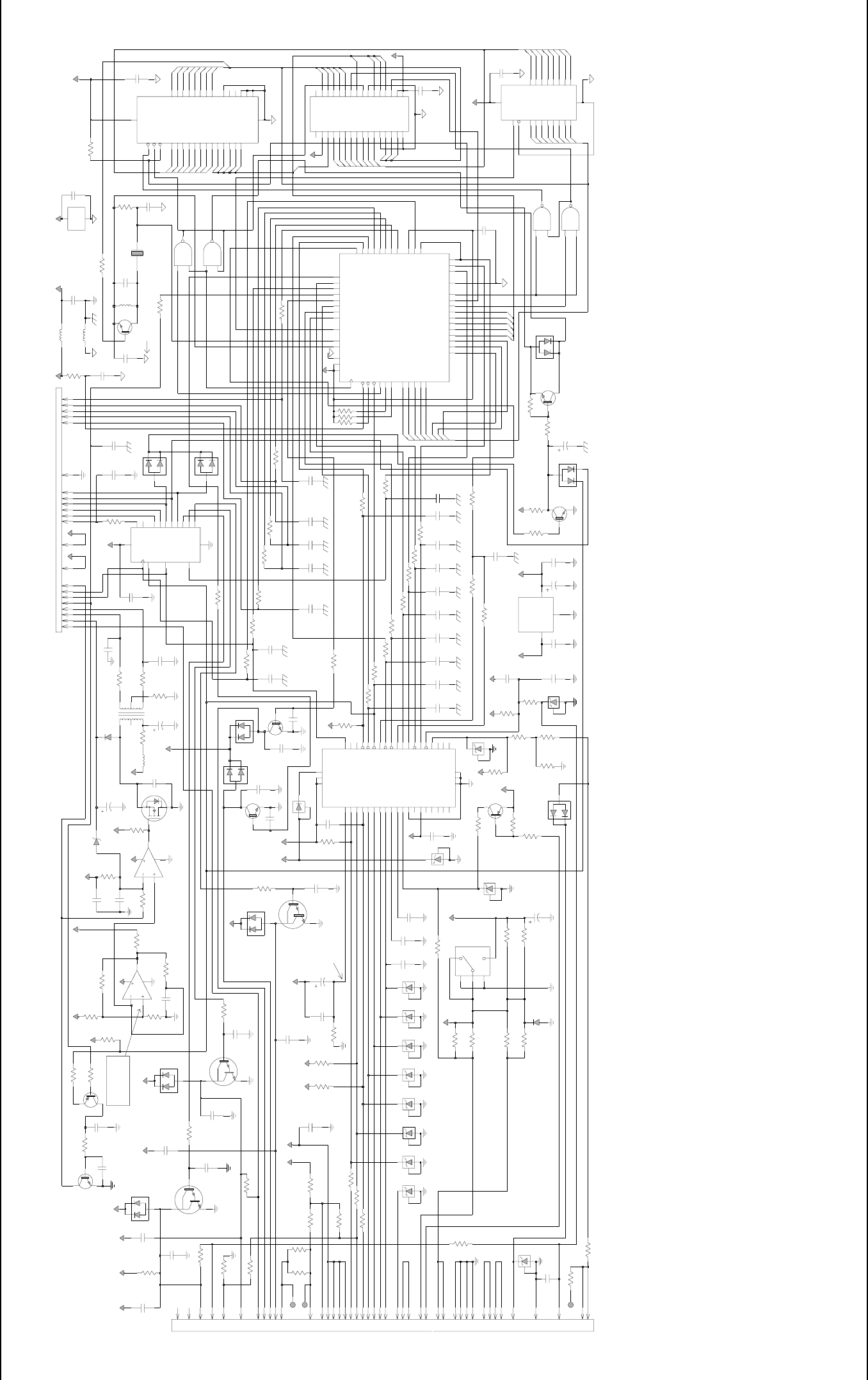
8-26 Schematics, Overlays, and Parts Lists: List of Schematics, Component Location Diagrams, and Parts Lists
September 26, 2003 6881096C77-O
Figure 8-14. HCN1078J (Standard), HCN1121D (Rear) W9 Control Head Schematic (Side 1 of 2)
KR4
BUSY
BUS-
CONNECTOR
BUS+
FIL_2
OR DAMAGE TO THE
SPEAKER-LO
BATT-
KR1
DATA(7:0)
3.) ASTERISK (*) INDICATES PARTS NOT NORMALLY PLACED IN STANDARD CONFIGURATION
J101
KS1
KR3
HEAD
VIP-OUT-1
VF-CONTROL
GROUND
VIP-IN-1
SPARE-1
DO NOT PROBE U3 PIN
SPARE-2
SHORT TO GROUND TO
NC
MIC-HUB
VIP-OUT-2
SPARE-2
NOTE: Q40 USED FOR POSITIVE GROUND
IGNITION SERVICE 5 VOLT
1.) ALL RESISTANCE IS IN OHMS. ALL CAPACITANCE IN PICO-FARADS UNLESS NOTED OTHERWISE.
DATA(7:0)
DATA(7:0)
DISABLE WATCH-DOG TIMER
CLOCK
NC
ADDRESS (8:12)
DATA(7:0)
EMERGENCY
DATA
KS3
KS2
DEK-CLOCK
DEK-DATA-OUT
VIP-OUT-3
VIP-OUT-1
STROBE
(GREEN)
MIC-PTT
A+
REGISTER
FLEX CABLE
2.) PART USAGE MAY VARY WITH APPLICATION. REFER TO PARTS LIST FOR USAGE INFORMATION.
SWB+
DIGITAL GROUND
VIP-OUT-2
VIP-OUT-3
EEPROM
CIRCUITRY MAY OCCUR.
LATCH
LATCH
ADDRESS (7:0)
+43V
SPEAKER-HI
MIC-SWB+
SHIFT
GROUND
5 WITH POWER APPLIED
CONTROL
WARNING!
IGN+
VIP-IN-3
VIP-IN-2
MICROPROCESSOR
PTT/HUB-REF
KR5
PROM
P103
NC
(ORANGE)
KR2
SERIAL I/0
IGN-
ADDRESS (8:12)
NOTES:
KS4
KS5
REGULATOR
RESET
FIL_1
MIC-LO
MIC-HI
5.1
36
VR6
15V
R55
1
23
Q74
3
JU3
0
18
Q171
10K
R161
MC78M05
U46
2
GND
1IN 3
OUT
U8
PWR_GND
7
GND
14
VCC
2
12
10K
R163
1K
R38
1uF
C165
C207
4
31
15
470pF
470pF
C276
C206
470pF
+5V_FIL
43
45
SWB+
L2
9.107uH
.01uF
C53
C16
470pF
1615
R41
10K
A4
8A3
9A2
Q161
A8
3A12
30
A13 31
+5V_FIL 32
+5V_FIL
4A7
5A6
6A5
7
D6 22
D7 23
CE* 24
A10 25
OE* 26
GND
27
A11 28
A9 29
D1
15 D2
16 GND
17
NC 18
D3 19
D4
2+5V_FIL
20
D5 21
U7
SOCKET
1NC
10 A1
11 A0
12 GND
13 D0
14
15pF
C22
0
JU19
10K
R84
5
CR164
3
1
2
10K
R20
VR11
15V
C277
470pF
5.1
R53
L1
9.107uH
C275
41
470pF
0
7
10K
R0165
JU5
0
JU16*
11
35
VR2
470pF
12
15V
10K
C18
C173
470pF
+5V
R19
C7
.01uF
10K
R81
JU21*
44
0
R27
10K
C12
15V
VR3
Q71
1
2
3
470pF
10uF
CR161
3
1
2
C52
1uF
17
NC1 26
NC2 30
NC3
NC4 12
2
RDY_BUSY*
32
VCC
16
VSS
C46
19
D4 20
D5
D6 21
22
D7
23 EN_CE
25 EN_OE
31 EN_WE
NC 1
5A6
4A7
29 A8
28 A9
13
D0 14
D1 15
D2
18
D3
10 A1
24 A10
27 A11
3A12
9A2
8A3
7A4
6A5
9
+5V_FIL
U5
AT28HC64
11 A0
A2 12
A3 9
A4 6
A5 5
A6 2
A7
20
VCC
D5
4D6
3D7
11 EN_LE
1EN_OE
10
GND
19
A0 16
A1 15
18 D0
17 D1
14 D2
13 D3
8D4
7
R25
MC74HC373
U10
47K
100K
R5
15V
10
10K
R13
VR5
SWB+
5
JU20
0
R16
+5V
13
10K
470pF
C73
49
47K
R99
SWB+
470pF
T60
77J03
1
2
3
4
5
6
C39
10K
10K
R74
6
SWB+
R59
R18
10K
Q162
10K
470pF
C75
R15
+5V
C54
470pF
+5V
12
7.9488MHz
21
26
C45
Y1
7160
C274
10uF
+5V_FIL
+5V_FIL
470pF
48
22K
R6
C28
470pF
30
+5V
9
470pF
C272
10K
R183
43V
C170
0.1uF
L23
VR50
470pF
22uH
1
2
3
4
5
6
7
C72
470pF
C26
0
CR74
CR75
CR90
JU4*
0
14
R40
1K
32
C63
0.1uF
15V
VR10
0
JU23*
10K
R28
4.7K
R8
9.107uH
L50
C50
10uF
40
U8B
MC74HC00
5
4
6
1011
R29
10K
R57
33K
.01uF
C51
U3B
LM2903
6
5
7
8
4
R56
6.8K
33K
+5V_FIL
SWB+
R60
R24
15V
VR8
10K
R44
33K
+5V
6
5
4
3
2
1
0
47K
R34
470pF
C14
+5V
7
11
+5V
+5V
8
+5V
47
0
JU12*
SWB+ 470pF
13
12
11
C41
Q170
+5V
MC74HC00
U8C
R87
14
10K
470pF
+5V
20
33K
C202
3
A+_IGN
R0058
470pF
C20
R50
470pF
C174
R98
470
C29
10K
470pF 470pF
+5V
C30
R173
4.7K
22K
R181
15V
VR1
JU11*
0
5
CR72
C271
470pF
0.1uF
C61
C171
470pF
R31
24
47K
50
C64
0.1uF
Q23
1
3
2
+5V
+5V
SWB+
R71
33K
2
3
1
8
4
C176
470pF
U3A
LM2903
470pF
C38
C66
0.1uF
19
R75
10K
5.1
R54
33
+5V+5V
1318
2
12
1K
R39
2
+5V
1K
R35
21
19
470pF
C19
C6
470pF
C21
SWB+
1.5uF
0
JU17*
28
33K
R72
+5V_FIL
37
PTH-1
3
+5V SWB+
PTH-3
CR162
3
1
2
C13
+5V
R14
470pF 470pF
10K
C273
470pF
C44
R166
2.2K
1MEG
A+_IGN
Q72
1
2
3
R200
C65
0.1uF
22K
R51
C67
0.1uF
2.2K
10K
R164
0
R172
C62
0.1uF
Q73
1
2
3
1K
R61 Q50
S(3)
G(2)
D(1)
38
C56
10
1
2
3
.01uF
C1
.01uF
MC74HC00
U8D
33K
R73
0
0
1
2
3
4
5
6
7
470pF
JU2*
15V
SWB+
C47
+5V
VR9
470pF
C57
1K
R37
8
+5V
20
7
R12
17 1K
46
R171
47K R170
100K
MC74HC00
9
10
8
27
U8A
470pF
C246
CR71
0
470pF
C15
JU24*
SWB+
34
PTH-2
16
15V
VR7
33K
R22
8
4
0
JU9*
1VSS
18 XIRQ
8
XTAL
0
JU10*
KR4
KR5 50
RESET*
17
STRA_AS 4
STRB_R_W*
6
26
VDD 52
VRH 51
VRL
PD4_SCK
25
PD5_SS*
43
PE0_AN0
45
VIP_IN_1
VIP_IN_2 47
49
KR1 44
KR2 46
KR3
48
PC4_A4_D4
PC5_A5_D5
14
15 PC6_A6_D6
PC7_A7_D7
16
20 RX_DATA
21 TX_DATA
22 PD2_MISO
PD3_MOSI 23
24
PB4_A12
37 PB5_A13
36 PB6_A14
35 PB7_A15
9PC0_A0_D0
10 PC1_A1_D1
11 PC2_A2_D2
12 PC3_A3_D3
13
STROBE
LATCH 29
28
BUSY_OUT*
27
DEK_DATA-OUT
42 PB0_A8
41 PB1_A9
40 PB2_A10
39 PB3_A11
38
EXTAL
19 IRQ
3MODA_LIR*
2MODB_VSTBY
34
PTT
33
VIP_IN_3 32
BUSY_IN* 31
DEK_CLOCK
30
MC68HC11A1
U2
5CLK_E
7
0
470pF
C40
C74
7
6
5
4
3
2
1
R17
1
470pF
R30
10K
CR55
10K
+5V
47K
R43
789
VR4
15V
7
6
5
4
3
2
1
0
CR51
47K
R182
R21
11
Q75
C23
1MEG
29
4.7pF
SWB+
470pF
C76
JU22*
0
VR12
15V
11
12pF
C24
5
R52
JU13*
0
17
10
10K
8
470pF
C279
3
4
5
6
7
C278
470pF
R1
10K
0
1
2
CR73
10K
R23
0
JU18
9
C27
470pF
C17
R7
4.7K
SWB+
470pF
2264
C71
470pF
470pF
C37
C175
470pF
1
JU1
0
Q40
OFF
1
ON
3
CR76
S1
SWITCH
G1
4
G2
5
2
IN
VR514
15V
12
12
Q7
11
Q8
9
DATA
10
QS*
2SER_DAT_IN
1LATCH
VDD
16
15 EN_OE
8
GND
4
Q1
5
Q2
Q3 6
7
Q4
14
Q5
Q6 13
MC1409B
U6
3CLK
1K
R33
10
SWB+
10K
R26
22
35 VIP_IN_3 24
VIP_IN_1*
21
VIP_IN_2*
36
VIP_IN_3*
44 WDT_IN_T_CAP
2
WDT_TICKLE
43 WDT_T_CAP
37
9RESET
4
RESET*
7RESET_FILTR
31
RES_HUB
RX_DATA 20
19
TX_DATA
25 VIP_IN_1
VIP_IN_2
15
12
NC7 18
NC8 23
NC9
42
OSC_OUT
6
POS5V
3
POS5_REG
38
PTT
PTT*
28
29
IGN*
14 NC
8NC1
40 NC2
NC3
27
26 NC4
33 NC5
NC6
16
17 BUS+
41
EXT_OSC_IN
1GND
5GND
34 GND
30
HUB_INV
32 HUB_POL
IGN
SC74487F
U4
39
APOS
BUSY
10
11
BUSY_IN*
13
BUSY_OUT*
BUS-
CR163
3
12
R10
220
R32
21
DATA(7:0)
47K
ADDRESS(8:12)
ADDRESS(7:0)
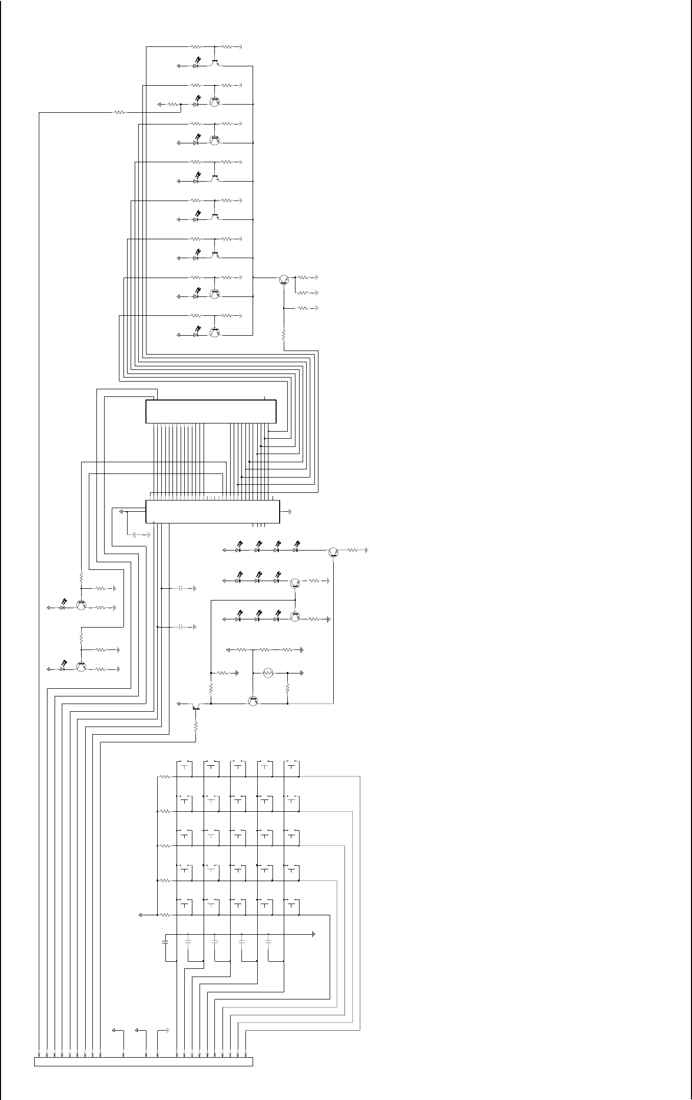
Schematics, Overlays, and Parts Lists: List of Schematics, Component Location Diagrams, and Parts Lists 8-27
6881096C77-O September 26, 2003
Figure 8-15. HCN1078J (Standard), HCN1121D (Rear) W9 Control Head Schematic (Side 2 of 2)
(RED)
XMIT
(YEL)
BUSY
VF_CONTROL
GRID
ANODE
1
P101
34 5
OPT4 MU SEL
KS3
KR5
+5V
9
ANODE
ANODE
ANODE
IS IN PICOFARADS UNLESS NOTED OTHERWISE.
2.) ASTERISK (*) DENOTES UN-USED PART PER THIS
1.) ALL RESISTANCE IS IN OHMS. CAPACITANCE
SPARE_2
KS5
KS4
KS1
GRID
GRID
ANODE
ANODE
ANODE
KR3
KR4
CLOCK
VU HOME 0
SWB+
DATA_IN
ANODE
ANODE
ANODE
APPLICATION.
GRID
ANODE
VF DRIVER
GRID
GRID
GRID
NOTES:
GRID
GND
LATCH
STROBE
+43V
FILAMENT 1
FILAMENT 2
STAR PND OPT6
2
KR1
KS2
KR2
67
OPT3 MD DIM 8
OPT5OPT2
VDOPT1
VF DISPLAY
FLEX CABLE
ANODE
ANODE
ANODE
GRID
GRID
GRID
CR134
22
19
4
6
SWB+
SWB+
20
100K
Q134
CR112
R112 Q111
1.5K
R150
5
10K
C55
0.1uF
R132
S111
12
27
SWB+
R137
SWB+
CR113
10K
R142
Q115
16
CR111
17
SWB+SWB+SWB+
100K
R124
Q133
Q131
R116
1K
470pF
C139
S105
12
2
S101
12
1.5K
S102
1
10K
R154
R144
Q117
12
S110
12
CR116
10
S126
CR120
11
12
1
2
S123 S127
12
S131
CR118
220
R158
R138
220 220
+5V
S124
12
R131
9
SWB+
1.5K
100K
RT133
R115
+5V
R134
SWB+
1K33K 33K
R113
R111
R114
R141
10K
100K
Q114
R155
10K
R145
1.5K
Q118 Q119
8
7
14
Q9 34
SERIAL_OUT 2
24 LATCH
+5V
44
+43V
1
15
Q30 5
Q31 4
Q32 3
Q4 39
Q5 38
Q6 37
Q7 36
Q8 35
Q23 13
Q24 12
Q25 11
Q26 10
Q27 9
Q28 8
Q29 7
Q3 40
Q16 25
Q17 20
Q18 19
Q19 17
Q2 41
Q20 16
Q21 15
Q22 14
NC4
29
Q1 42
Q10 33
Q11 32
Q12 31
Q13 30
Q14 27
Q15 26
U101
STROBE
21 CLK
23
DATA_IN
43
GND
22
NC1
6
NC2
18
NC3
28
S109
12
UCQ5818EPF
100K
R121
100K
R120
12
S125
12
12
S122 S136
12
S134
12
S100
12
S104
12
S103
R136
2.2K
C141
470pF
S106
12
JU8
0
0
JU7
+5V
R148*
0
C135
470pF
SWB+
+5V
21
18
12
3K
25 L
18 M
9N
27
NC
13
15 G5
14 G6
13 G7
12 G8
10 G9
21 H
26 I
11 J
28
FILAMENT 2
5G
23 G1
6G10
7G11
22 G2
19 G3
17 G4
U102
2A
4B
20 C
16 D
8E
24 F
1
FILAMENT 1
12
PR-483-05
S121
1
2
S133
CR137
SWB+
CR135
CR136 Q133
CR140
CR131
CR138
S108
12
S107
12
1.5K
R157
SWB+
10K
R147
Q120
1.5K
R156
R146
CR119
CR114
10K
R151
1.5K
12
Q132
SWB+
S135
Q112
Q130
10K
R129
R130
R123
100K
4.7K
100K
R122
R153
1.5K
R143
10K
CR132
SWB+
R135
6.8K
CR133
CR117
33K
220
R159
Q110
R149
2.2K
R139
+5V
S132
12
2
3
C134
1
C133
470pF
470pF
C132
470pF
470pF
C131
10K
R140
Q113
CR115
Q116
R152
1.5K
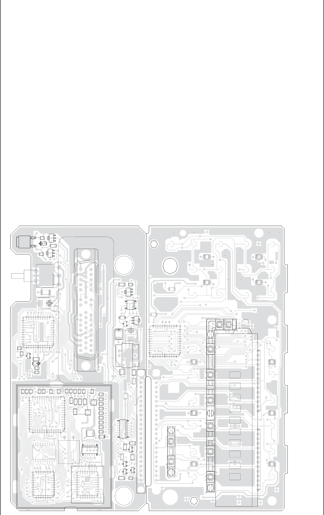
8-28 Schematics, Overlays, and Parts Lists: List of Schematics, Component Location Diagrams, and Parts Lists
September 26, 2003 6881096C77-O
Figure 8-16. HCN1078J (Standard), HCN1121D (Rear) W9 Control Head Component Location Diagram (Viewed from Side 1)
U5 U10 U2
Y1
U7 U8 L23 L1
U4
C45
U46
P103
Q73
S1
Q72
C50
Q71
U3
T60
C52
Q50
S123
U102
U101
S121 S122 S124
S133 S134 S135
S131 S136
S108S107
S110 S100 S111
S109
S127
S102
S106S105S104
S103
S101
S126
S125
U6
VR51
C47
C20
C19
C16
C12
C21
C74
C17
C18
C15
C13
C44
R20
C14
R19
R16
L2
R37
C276
C64
L50
C56
C278
R54
CR51
Q170
R172
C170
R163
CR161
CR162
CR111 CR112
CR136 CR137 CR135
CR113 CR115 CR117 CR119 CR118 CR120
CR114
CR116
CR138
CR139 CR140
CR133
CR132
CR131 CR134
S132
114 15 28
CR163
C165
R12
C29
C30
C39
C40
C41
C28
C75
C26
C27
R38
C38
R173
C207
C206
C6
R200
C277
CR90
C275
C46
C274
R72
R71
C271
VR50
RT133
C55
110 87 543211121314151617
33 2829303132 2627
50 4546474849 4344 4041 3738 36 3435
2021 18192324
K
A
B
K
K
A
A
6
6
G DS
5
58
4
4
1
1
1
1
1
1
1
2
2
2
2
3
3
3
CE BCE
BCE
K
AC
BE
K
A
K
A
8
916
7
7
7
8
8
14
1
4
513
14
20
21
21
33
3446
47
29
30
1
1
1
1
4
513
14
20
10
11
20
20
2129
30
17
18
28
2939
40
6
7
1
17
18
28
2939
40
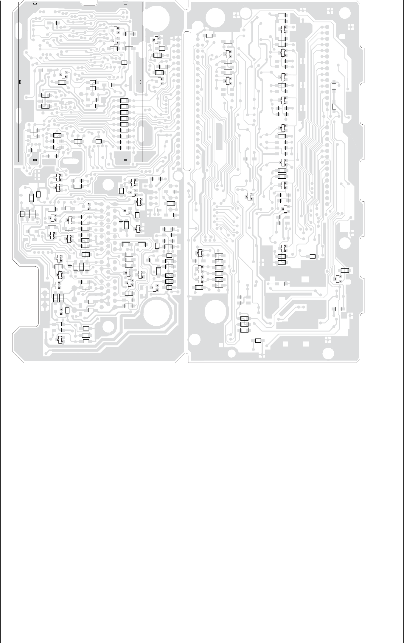
Schematics, Overlays, and Parts Lists: List of Schematics, Component Location Diagrams, and Parts Lists 8-29
6881096C77-O September 26, 2003
Figure 8-17. HCN1078J (Standard), HCN1121D (Rear) W9 Control Head Component Location Diagram (Viewed from Side 2)
R29
R28
R27
R26
R75
R30
R41
R40
R39
C66
R21
C24
C23 R23
C62
C63
R33
R35
C61
R14
R44
R13
R99
C1
R43
R22
R25
JU19
JU18
JU23
JU6
JU5
JU1
C202
JU13
JU12
JU22
C67
JU21
JU20
R10
JU17
R60
R1
C71
R134
R120
C135
R153
C139
R131
C132
R143
R141
R151
R147
R157
R145
R155
JU7
JU8
R146
R156
R138
R144
R154
R142
R152
R140
R150
R149
R148
R115
R113
R111
R116
R114
R112
C141
R158
R159
R124
R121
R122
R123
C133
R135
R136
R137
R130
R139
R129
R132
R56
R58
R57
C54
R61
R51
C51
R52
C53
C57
C174
C73
R73
C72
C272 C273
CR72 CR73
C176
R87
JU10
JU9
VR8
VR10 VR9
VR4
VR6 Q40
VR1
R31
R84
JU11
JU3
VR3 VR12
CR76
C175
JU2
JU4 VR7
VR11
C173
VR2
CR75 Q75
Q161
Q171
Q162
Q23
Q74
CR74
C7
VR5
R6
R8
C76
R98
CR164
C279
C246
R59
CR71
Q132 Q133 Q134
Q116
Q131
Q130
Q120
Q114
Q118 Q119 Q117
C131 C134
Q115 Q113 Q110
Q111
Q112
R81
R24 R34
R5
R7
R32
R183C37
R17
R74
R15
R18
R182
R181
R55
R50
R53
R161
R170
R171
C171
R166
C65
R165 R164
C22
C
BE
C
A
AA
KK
K
BE
C
BE
C
BE
C
BE
C
BE
C
BE
C
BE
C
BE
C
BE
C
BE
C
BE
C
BE
C
BE
C
BE
C
BE
C
BE
C
BE
C
BE
C
BE
C
BE
C
BE
C
BE
AA
K
AA
KAA
K
AA
A
K
KK
AA
K
AA
K
A
A
K
AA
K
AA
K
AA
K
AA
K
A
KK
A
KK
A
KK
A
KK
A
KK
11087543211121314151617
3328 29 30 31 3226 27
5045 46 47 48 4943 4440 4137 383634 35
20 2118 19 23 24
8-30 Schematics, Overlays, and Parts Lists: List of Schematics, Component Location Diagrams, and Parts Lists
September 26, 2003 6881096C77-O
HCN1078J (Standard), HCN1121D (Rear) Parts List
ITEM MOTOROLA
PART
NUMBER DESCRIPTION
C1 2113741N45 CAP CHIP CL2 X7R 10% 10000
C12 2113741M13 CAP CHIP CL2 X7R 10% 470
C13 2113741M13 CAP CHIP CL2 X7R 10% 470
C131 2113740B65 CAP CHIP REEL CL1 +/-30 470
C132 2113740B65 CAP CHIP REEL CL1 +/-30 470
C133 2113740B65 CAP CHIP REEL CL1 +/-30 470
C134 2113740B65 CAP CHIP REEL CL1 +/-30 470
C135 2113740B65 CAP CHIP REEL CL1 +/-30 470
C139 2113740B65 CAP CHIP REEL CL1 +/-30 470
C14 2113741M13 CAP CHIP CL2 X7R 10% 470
C141 2113740B65 CAP CHIP REEL CL1 +/-30 470
C15 2113741M13 CAP CHIP CL2 X7R 10% 470
C16 2113741M13 CAP CHIP CL2 X7R 10% 470
C165 2311049A37 CAP TANT CHIP 1 20 20
C17 2113741M13 CAP CHIP CL2 X7R 10% 470
C170 2113741N69 CAP CHIP CL2 X7R 10%
100000
C171 2113740B65 CAP CHIP REEL CL1 +/-30 470
C173 2113740B65 CAP CHIP REEL CL1 +/-30 470
C174 2113740B65 CAP CHIP REEL CL1 +/-30 470
C175 2113740B65 CAP CHIP REEL CL1 +/-30 470
C176 2113740B65 CAP CHIP REEL CL1 +/-30 470
C18 2113741M13 CAP CHIP CL2 X7R 10% 470
C19 2113741M13 CAP CHIP CL2 X7R 10% 470
C20 2113741M13 CAP CHIP CL2 X7R 10% 470
C202 2113740B65 CAP CHIP REEL CL1 +/-30 470
C206 2113741M13 CAP CHIP CL2 X7R 10% 470
C207 2113741M13 CAP CHIP CL2 X7R 10% 470
C21 2113741M13 CAP CHIP CL2 X7R 10% 470
C22 2113740B29 CAP CHIP REEL CL1 +/-30 15
C23 2113740B17 CAP CHIP REEL CL1 +/-30 4.7
C24 2113740B27 CAP CHIP REEL CL1 +/-30 12
C246 2113740B65 CAP CHIP REEL CL1 +/-30 470
C26 2113741M13 CAP CHIP CL2 X7R 10% 470
C27 2113741M13 CAP CHIP CL2 X7R 10% 470
C271 2113741M13 CAP CHIP CL2 X7R 10% 470
C272 2113740B65 CAP CHIP REEL CL1 +/-30 470
C273 2113740B65 CAP CHIP REEL CL1 +/-30 470
C274 2113741M13 CAP CHIP CL2 X7R 10% 470
C275 2113741M13 CAP CHIP CL2 X7R 10% 470
C277 2113741M13 CAP CHIP CL2 X7R 10% 470
C278 2113740B65 CAP CHIP REEL CL1 +/-30 470
C279 2113740B65 CAP CHIP REEL CL1 +/-30 470
C28 2113741M13 CAP CHIP CL2 X7R 10% 470
C29 2113741M13 CAP CHIP CL2 X7R 10% 470
C30 2113741M13 CAP CHIP CL2 X7R 10% 470
C300 2113741M13 CAP CHIP CL2 X7R 10% 470
C301 2113741M13 CAP CHIP CL2 X7R 10% 470
C37 2113740B65 CAP CHIP REEL CL1 +/-30 470
C38 2113741M13 CAP CHIP CL2 X7R 10% 470
C39 2113741M13 CAP CHIP CL2 X7R 10% 470
C40 2113741M13 CAP CHIP CL2 X7R 10% 470
C41 2113741M13 CAP CHIP CL2 X7R 10% 470
C44 2113741M13 CAP CHIP CL2 X7R 10% 470
C45 2380090M24 CAP ALU 10 20 50V SURF MT
C46 2311049A37 CAP TANT CHIP 1 20 20
C47 2113741M13 CAP CHIP CL2 X7R 10% 470
C50 2311049J27 CAP TANT CHIP 10 10 25
C51 2113741N45 CAP CHIP CL2 X7R 10% 10000
C52 2380090M24 CAP ALU 10 20 50V SURF MT
C53 2113741N45 CAP CHIP CL2 X7R 10% 10000
C54 2113740B65 CAP CHIP REEL CL1 +/-30 470
C55 2113741N69 CAP CHIP CL2 X7R 10%
100000
C56 2113741N45 CAP CHIP CL2 X7R 10% 10000
C57 2113740B65 CAP CHIP REEL CL1 +/-30 470
C6 2311049A38 CAP TANT CHIP 1.5 10 16
ITEM MOTOROLA
PART
NUMBER DESCRIPTION
C61 2113741N69 CAP CHIP CL2 X7R 10%
100000
C62 2113741N69 CAP CHIP CL2 X7R 10%
100000
C63 2113741N69 CAP CHIP CL2 X7R 10%
100000
C64 2113741N69 CAP CHIP CL2 X7R 10%
100000
C65 2113741N69 CAP CHIP CL2 X7R 10%
100000
C66 2113741N69 CAP CHIP CL2 X7R 10%
100000
C67 2113741N69 CAP CHIP CL2 X7R 10%
100000
C7 2113741N45 CAP CHIP CL2 X7R 10% 10000
C71 2113740B65 CAP CHIP REEL CL1 +/-30 470
C72 2113740B65 CAP CHIP REEL CL1 +/-30 470
C73 2113740B65 CAP CHIP REEL CL1 +/-30 470
C74 2113741M13 CAP CHIP CL2 X7R 10% 470
C75 2113741M13 CAP CHIP CL2 X7R 10% 470
C76 2113740B65 CAP CHIP REEL CL1 +/-30 470
CR111 4880052R01 DIODE LIGHT EMITTING RED
CR112 4880052R02 DIODE LIGHT EMITTING YEL
CR113 4880052R01 DIODE LIGHT EMITTING RED
CR114 4880052R01 DIODE LIGHT EMITTING RED
CR115 4880052R01 DIODE LIGHT EMITTING RED
CR116 4880052R02 DIODE LIGHT EMITTING YEL
CR117 4880052R01 DIODE LIGHT EMITTING RED
CR118 4880052R01 DIODE LIGHT EMITTING RED
CR119 4880052R01 DIODE LIGHT EMITTING RED
CR120 4880052R01 DIODE LIGHT EMITTING RED
CR131 4880052R03 DIODE LIGHT EMITTING GRN
CR132 4880052R03 DIODE LIGHT EMITTING GRN
CR133 4880052R03 DIODE LIGHT EMITTING GRN
CR134 4880052R03 DIODE LIGHT EMITTING GRN
CR135 4880052R03 DIODE LIGHT EMITTING GRN
ITEM MOTOROLA
PART
NUMBER DESCRIPTION
CR136 4880052R03 DIODE LIGHT EMITTING GRN
CR137 4880052R03 DIODE LIGHT EMITTING GRN
CR138 4880052R03 DIODE LIGHT EMITTING GRN
CR139 4880052R03 DIODE LIGHT EMITTING GRN
CR140 4880052R03 DIODE LIGHT EMITTING GRN
CR161 4880236E08 DIODE DUAL SOT 23
CR162 4880236E08 DIODE DUAL SOT 23
CR163 4880236E08 DIODE DUAL SOT 23
CR164 4880236E08 DIODE DUAL SOT 23
CR51 4813833C09 DIODE GEN PURP .1A 100V
‘DX’
CR71 4880236E08 DIODE DUAL SOT 23
CR72 4880236E08 DIODE DUAL SOT 23
CR73 4880236E08 DIODE DUAL SOT 23
CR74 4880236E08 DIODE DUAL SOT 23
CR75 4880236E08 DIODE DUAL SOT 23
CR76 4880236E08 DIODE DUAL SOT 23
CR90 4882960R02 DIODE RECT 48R82960R01 A/P
JU1 0611077A01 RES CHIP JUMPER
JU18 0611077A01 RES CHIP JUMPER
JU19 0611077A01 RES CHIP JUMPER
JU20 0611077A01 RES CHIP JUMPER
JU23 0611077A01 RES CHIP JUMPER
JU3 0611077A01 RES CHIP JUMPER
JU5 0611077A01 RES CHIP JUMPER
JU7 0611077A01 RES CHIP JUMPER
L1 2480140E16 INDUCTOR CHIP 10UH
L2 2480140E16 INDUCTOR CHIP 10UH
L23 2480289M16 COIL IF 22UH 1611 CS 223
L50 2480140E16 INDUCTOR CHIP 10UH
P7 0980049R01 SOCKET PLCC 32 PIN
Q110 4880141L02 TSTR NPN SOT23 LO PROFILE
TAPE
Q110 4880141L04 TSTR NPN SOT23 LO PROFILE
TAPE
ITEM MOTOROLA
PART
NUMBER DESCRIPTION
Schematics, Overlays, and Parts Lists: List of Schematics, Component Location Diagrams, and Parts Lists 8-31
6881096C77-O September 26, 2003
Q111 4880141L02 TSTR NPN SOT23 LO PROFILE
TAPE
Q112 4880141L02 TSTR NPN SOT23 LO PROFILE
TAPE
Q113 4880141L02 TSTR NPN SOT23 LO PROFILE
TAPE
Q114 4880141L02 TSTR NPN SOT23 LO PROFILE
TAPE
Q115 4880141L02 TSTR NPN SOT23 LO PROFILE
TAPE
Q116 4880141L02 TSTR NPN SOT23 LO PROFILE
TAPE
Q117 4880141L02 TSTR NPN SOT23 LO PROFILE
TAPE
Q118 4880141L02 TSTR NPN SOT23 LO PROFILE
TAPE
Q119 4880141L02 TSTR NPN SOT23 LO PROFILE
TAPE
Q120 4880141L02 TSTR NPN SOT23 LO PROFILE
TAPE
Q130 4880141L02 TSTR NPN SOT23 LO PROFILE
TAPE
Q131 4880141L02 TSTR NPN SOT23 LO PROFILE
TAPE
Q132 4880141L02 TSTR NPN SOT23 LO PROFILE
TAPE
Q133 4880141L02 TSTR NPN SOT23 LO PROFILE
TAPE
Q134 4880141L01 TSTR PNP SOT23 LO PROFILE
TAPE
Q161 4880141L02 TSTR NPN SOT23 LO PROFILE
TAPE
Q162 4880141L02 TSTR NPN SOT23 LO PROFILE
TAPE
Q170 4880141L01 TSTR PNP SOT23 LO PROFILE
TAPE
Q171 4880141L02 TSTR NPN SOT23 LO PROFILE
TAPE
Q23 4880141L02 TSTR NPN SOT23 LO PROFILE
TAPE
Q40 4880141L01 TSTR PNP SOT23 LO PROFILE
TAPE
ITEM MOTOROLA
PART
NUMBER DESCRIPTION
Q50 4880053M03 TSTR N/CH SOT 89 200V B ST
84
Q71 4880052M01 TSTR NPN DRLNGTN MXTA27
Q72 4880052M01 TSTR NPN DRLNGTN MXTA27
Q73 4880052M01 TSTR NPN DRLNGTN MXTA27
Q74 4880141L04 TSTR NPN SOT23 LO PROFILE
TAPE
Q75 4880141L04 TSTR NPN SOT23 LO PROFILE
TAPE
R1 0611077A98 RES CHIP 10K 5 1/8W
R10 0611077A58 RES CHIP 220 5 1/8W
R111 0611077B23 RES CHIP 100K 5 1/8W
R112 0611077B23 RES CHIP 100K 5 1/8W
R113 0611077B11 RES CHIP 33K 5 1/8W
R114 0611077B11 RES CHIP 33K 5 1/8W
R115 0611077A74 RES CHIP 1000 5 1/8
R116 0611077A74 RES CHIP 1000 5 1/8
R12 0611077A74 RES CHIP 1000 5 1/8
R120 0611077B23 RES CHIP 100K 5 1/8W
R121 0611077B23 RES CHIP 100K 5 1/8W
R122 0611077B23 RES CHIP 100K 5 1/8W
R123 0611077B23 RES CHIP 100K 5 1/8W
R124 0611077B23 RES CHIP 100K 5 1/8W
R129 0611077A98 RES CHIP 10K 5 1/8W
R13 0611077A98 RES CHIP 10K 5 1/8W
R130 0611077A90 RES CHIP 4700 5 1/8
R131 0611077A58 RES CHIP 220 5 1/8W
R132 0611077A98 RES CHIP 10K 5 1/8W
R134 0611077A78 RES CHIP 1500 5 1/8
R135 0611077A94 RES CHIP 6800 5 1/8
R136 0611077A82 RES CHIP 2200 5 1/8
R137 0611077A36 RES CHIP 27 5 1/8W
R138 0611077A58 RES CHIP 220 5 1/8W
R139 0611077A82 RES CHIP 2200 5 1/8
R14 0611077A98 RES CHIP 10K 5 1/8W
ITEM MOTOROLA
PART
NUMBER DESCRIPTION
R140 0611077A98 RES CHIP 10K 5 1/8W
R141 0611077A98 RES CHIP 10K 5 1/8W
R142 0611077A98 RES CHIP 10K 5 1/8W
R143 0611077A98 RES CHIP 10K 5 1/8W
R144 0611077A98 RES CHIP 10K 5 1/8W
R145 0611077A98 RES CHIP 10K 5 1/8W
R146 0611077A98 RES CHIP 10K 5 1/8W
R147 0611077A98 RES CHIP 10K 5 1/8W
R149 0611077B11 RES CHIP 33K 5 1/8W
R15 0611077A98 RES CHIP 10K 5 1/8W
R150 0611077A78 RES CHIP 1500 5 1/8
R151 0611077A78 RES CHIP 1500 5 1/8
R152 0611077A78 RES CHIP 1500 5 1/8
R153 0611077A82 RES CHIP 2200 5 1/8
R154 0611077A78 RES CHIP 1500 5 1/8
R155 0611077A78 RES CHIP 1500 5 1/8
R156 0611077A78 RES CHIP 1500 5 1/8
R157 0611077A78 RES CHIP 1500 5 1/8
R158 0611077A58 RES CHIP 220 5 1/8W
R159 0611077A58 RES CHIP 220 5 1/8W
R16 0611077A98 RES CHIP 10K 5 1/8W
R161 0611077A98 RES CHIP 10K 5 1/8W
R163 0611077A98 RES CHIP 10K 5 1/8W
R164 0611077A98 RES CHIP 10K 5 1/8W
R165 0611077A98 RES CHIP 10K 5 1/8W
R166 0611077A82 RES CHIP 2200 5 1/8
R17 0611077A98 RES CHIP 10K 5 1/8W
R170 0611077B23 RES CHIP 100K 5 1/8W
R171 0611077B15 RES CHIP 47K 5 1/8W
R172 0611077A82 RES CHIP 2200 5 1/8
R173 0611077A90 RES CHIP 4700 5 1/8
R18 0611077A98 RES CHIP 10K 5 1/8W
R181 0611077B07 RES CHIP 22K 5 1/8W
ITEM MOTOROLA
PART
NUMBER DESCRIPTION
R182 0611077B15 RES CHIP 47K 5 1/8W
R183 0611077A98 RES CHIP 10K 5 1/8W
R19 0611077A98 RES CHIP 10K 5 1/8W
R20 0611077A98 RES CHIP 10K 5 1/8W
R200 0611077B47 RES CHIP 1 MEG 5 1/8W
R21 0611077B47 RES CHIP 1 MEG 5 1/8W
R22 0611077B11 RES CHIP 33K 5 1/8W
R23 0611077A98 RES CHIP 10K 5 1/8W
R24 0611077B11 RES CHIP 33K 5 1/8W
R25 0611077B15 RES CHIP 47K 5 1/8W
R26 0611077A98 RES CHIP 10K 5 1/8W
R27 0611077A98 RES CHIP 10K 5 1/8W
R28 0611077A98 RES CHIP 10K 5 1/8W
R29 0611077A98 RES CHIP 10K 5 1/8W
R30 0611077A98 RES CHIP 10K 5 1/8W
R31 0611077B15 RES CHIP 47K 5 1/8W
R32 0611077B15 RES CHIP 47K 5 1/8W
R33 0611077A74 RES CHIP 1000 5 1/8
R34 0611077B15 RES CHIP 47K 5 1/8W
R35 0611077A74 RES CHIP 1000 5 1/8
R37 0611077A74 RES CHIP 1000 5 1/8
R38 0611077A74 RES CHIP 1000 5 1/8
R39 0611077A98 RES CHIP 10K 5 1/8W
R40 0611077A74 RES CHIP 1000 5 1/8
R41 0611077A98 RES CHIP 10K 5 1/8W
R43 0611077B15 RES CHIP 47K 5 1/8W
R44 0611077A98 RES CHIP 10K 5 1/8W
R5 0611077B23 RES CHIP 100K 5 1/8W
R50 0611077A66 RES CHIP 470 5 1/8W
R51 0611077B07 RES CHIP 22K 5 1/8W
R52 0611077A98 RES CHIP 10K 5 1/8W
R53 0611077A19 RES CHIP 5.1 5 1/8W
R54 0611077A19 RES CHIP 5.1 5 1/8W
ITEM MOTOROLA
PART
NUMBER DESCRIPTION
8-32 Schematics, Overlays, and Parts Lists: List of Schematics, Component Location Diagrams, and Parts Lists
September 26, 2003 6881096C77-O
R55 0611077A28 RES CHIP 12 5 1/8W
R56 0611077B11 RES CHIP 33K 5 1/8W
R57 0611077B11 RES CHIP 33K 5 1/8W
R58 0611077B11 RES CHIP 33K 5 1/8W
R59 0611077A98 RES CHIP 10K 5 1/8W
R6 0611077B07 RES CHIP 22K 5 1/8W
R60 0611077A94 RES CHIP 6800 5 1/8
R61 0611077A74 RES CHIP 1000 5 1/8
R7 0611077A90 RES CHIP 4700 5 1/8
R71 0611077B11 RES CHIP 33K 5 1/8W
R72 0611077B11 RES CHIP 33K 5 1/8W
R73 0611077B11 RES CHIP 33K 5 1/8W
R74 0611077A98 RES CHIP 10K 5 1/8W
R75 0611077A98 RES CHIP 10K 5 1/8W
R8 0611077A90 RES CHIP 4700 5 1/8
R81 0611077A98 RES CHIP 10K 5 1/8W
R84 0611077A98 RES CHIP 10K 5 1/8W
R87 0611077A98 RES CHIP 10K 5 1/8W
R98 0611077A98 RES CHIP 10K 5 1/8W
R99 0611077B15 RES CHIP 47K 5 1/8W
RT133 0680149M02 THERMISTOR CHIP 100K OHM
U10 5180177M02 WIDE BODY SOLC OCTAL
LATCH
U101 5180236C05 IC VF DRVR SN75518FN
U102 7280242J01 DISPLAY VF
U2 5113802A01
(HCN1078
only)
IC 68HC11 W/SCI SPI A/D 512
U3 5113820A02 IC DUAL SING SPLY LO PWR
2903
U4 5180057S04 “IC CUST SER I/O 13”” REEL”
U46 5113816G04 IC +5V REG 78M05
U5 5197014A10 IC SPECTRA MEMORY BD
U6 5184704M54 IC CMOS REGISTER
U7 Not Available IC PROM
ITEM MOTOROLA
PART
NUMBER DESCRIPTION
U8 5180177M03 QUAD NAND GATE
VR1 4813830A28 DIODE 15V 5% 225MW
MMBZ5245B_
VR10 4813830A28 DIODE 15V 5% 225MW
MMBZ5245B_
VR11 4813830A28 DIODE 15V 5% 225MW
MMBZ5245B_
VR12 4813832C28 ZENER BPLR 15V FOR ESD
SOT23
VR2 4813830A28 DIODE 15V 5% 225MW
MMBZ5245B_
VR3 4813830A28 DIODE 15V 5% 225MW
MMBZ5245B_
VR4 4813832C28 ZENER BPLR 15V FOR ESD
SOT23
VR5 4813830A28 DIODE 15V 5% 225MW
MMBZ5245B_
VR50 4813830C43 DIODE 43V ‘M5’ MMSZ5260BT1
VR514 4813830A28 DIODE 15V 5% 225MW
MMBZ5245B_
VR6 4813830A28 DIODE 15V 5% 225MW
MMBZ5245B_
VR7 4813830A28 DIODE 15V 5% 225MW
MMBZ5245B_
VR8 4813830A28 DIODE 15V 5% 225MW
MMBZ5245B_
VR9 4813830A28 DIODE 15V 5% 225MW
MMBZ5245B_
ITEM MOTOROLA
PART
NUMBER DESCRIPTION
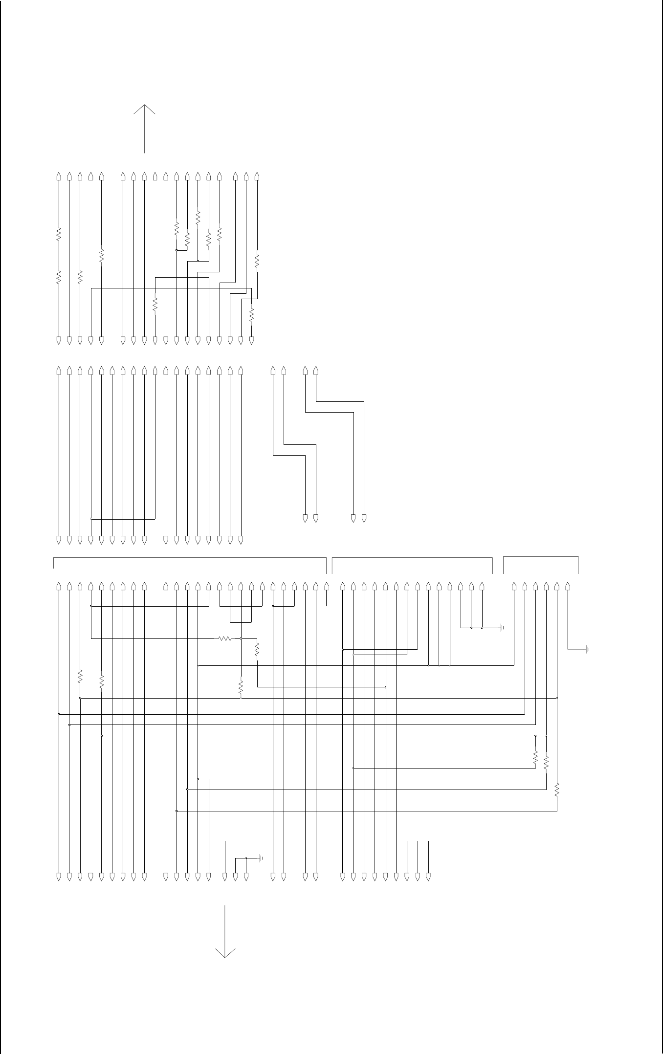
Schematics, Overlays, and Parts Lists: List of Schematics, Component Location Diagrams, and Parts Lists 8-33
6881096C77-O September 26, 2003
Figure 8-18. W4, W5, and W7 Control Head Low-/Mid-Power Interconnection Diagram
21
4624 PTT
BUSY
BUS -
BUS +
SPARE 1
SPARE 2
RESET
SW B+
3
37
4
38
5
2
19
18
A+
VF SENSE 1
1
CABLE SIDE
VF SENSE 2 VF SENSE 2
2
NC
VIP-OUT-1
VIP-OUT-2
VIP-OUT-3/DEK-STROBE
VIP-IN-1
VIP-IN-2
VIP-IN-3/DEK-DATA-IN
VF SENSE 1
IGNITION
B+/A+
2FIL AUD SHLD
MIC HI
MIC LO
HUB
19 VIP-OUT-2/DEK-DATA-OUT
VIP-OUT-3/DEK-STROBE
14
17 VIP-IN-1
VIP-IN-2
16
VIP-IN-3/DEK-DATA-IN
15
DIG-GND
DIG-GND
DIG-GND
W4/W5/W7
20
36
SNET-KEY
SNET-KID
SNET-WE
9
20
21
12
SWB+
SHIELD GND
EMER
30
14
31
32
1
34
40
24
23
26
6
13
GND
GND
KEY SLOT
VIP SECTION MIC SECTION
RADIO SECTION
RADIO SIDE
11
CONTROL HEAD SIDE
17
10
22
2623 RESET
28
29
SPARE 1
DEK-DATA-OUT
DEK-CLOCK
SWB+
SWB+
SWB+ 35
VIP-OUT-1/DEK-CLOCK
18
10
27
MIC LO
15
11
475
SW B+
B+/A+
IGNITION
16
49
REMOTE CONTROL HEAD INTERCONNCECT BOARD
25
CONTROL HEAD SIDE
MICROPOHONE HI (BLK/YEL)
12 MIC HI
DETECTED AUDIO
ANALOG GROUND
PTT/VIP IN 1
12
MICROPOHONE LO (SHIELD)
DETECTED AUDIO (BLK/BRN)
MIC-HI
MIC-LO
PTT
EMERG/HUB
PTT/HUB-REF
8
41
7
SPARE 1 (BROWN)
13
45
16
46
33
50
17
26
28
29
48
49
50
SPARE 2 (RED)
SW B+ (YELLOW)
DIGITAL GROUND (BLUE)
SPEAKER LO (GREEN)
SPEAKER HI (ORANGE)
EMERGENCY (VIOLET)
SPEAKER HI (BLK/ORG)
SPEAKER LO (BLK/GRN)
B+ (GREEN)
IGNITION (ORANGE)
SPARE 2
8
7
484
11
44
43
10
1
23
14
5
21
19
16
17
22
18
24
18
12
11
9
10
23
14
5
21
19
16
DETECTED AUDIO (SHIELD/ANALOG GROUND)
SP 1 (BLK/GRN)
SP 1 (SHIELD)
BUSY (BLK/RED)
BUS - (BLACK)
BUS + (WHITE)
BUS SHIELD (BARE)
RESET (BLK/ORG)
45
27
3
28
3325 BUSY
MIC HI
MIC LO
HUB
PTT
BUS -
BUS +
SPEAKER LO
SPEAKER HI
EMERGENCY
SPARE 1
VIP OUT 1
SPARE 2
VIP OUT 2
27
17
31
34
44
27
43
10
47
15
11
9
25 PIN REMOTE
CONNECTOR (P2)
6
7
13
NC
24
17
9
22
25
NC
11
14
TO COMMAND BOARD
NC
NC
NC
NC
22
SPEAKER LO
1
3
BUSY
P2
SPEAKER HI
EMERGENCY
SWB+
COMMAND BOARD
CONNECTOR (P502)
REMOTE RADIO INTERCONNECT BOARD (LOW/MID POWER)
REMOTE CONTROL HEAD CABLE
12
13
BUS -
BUS +
BUS SHIELD
RESET
SPARE 1
SPARE 2
SWB+
18
24
25
13
DIGITAL GROUND
P9
P1
35
13
1
2
E1
E2
NC NC
TO W4/W5/ W 7 CONTROL HEAD
JU1002
R608
JU1004
JU614
JU1008
JU1001
JU1005
JU1006
JU604
JU1003
JU1007
JU513
JU650
JU512
JU631 JU632
JU12
JU601
JU609
JU615
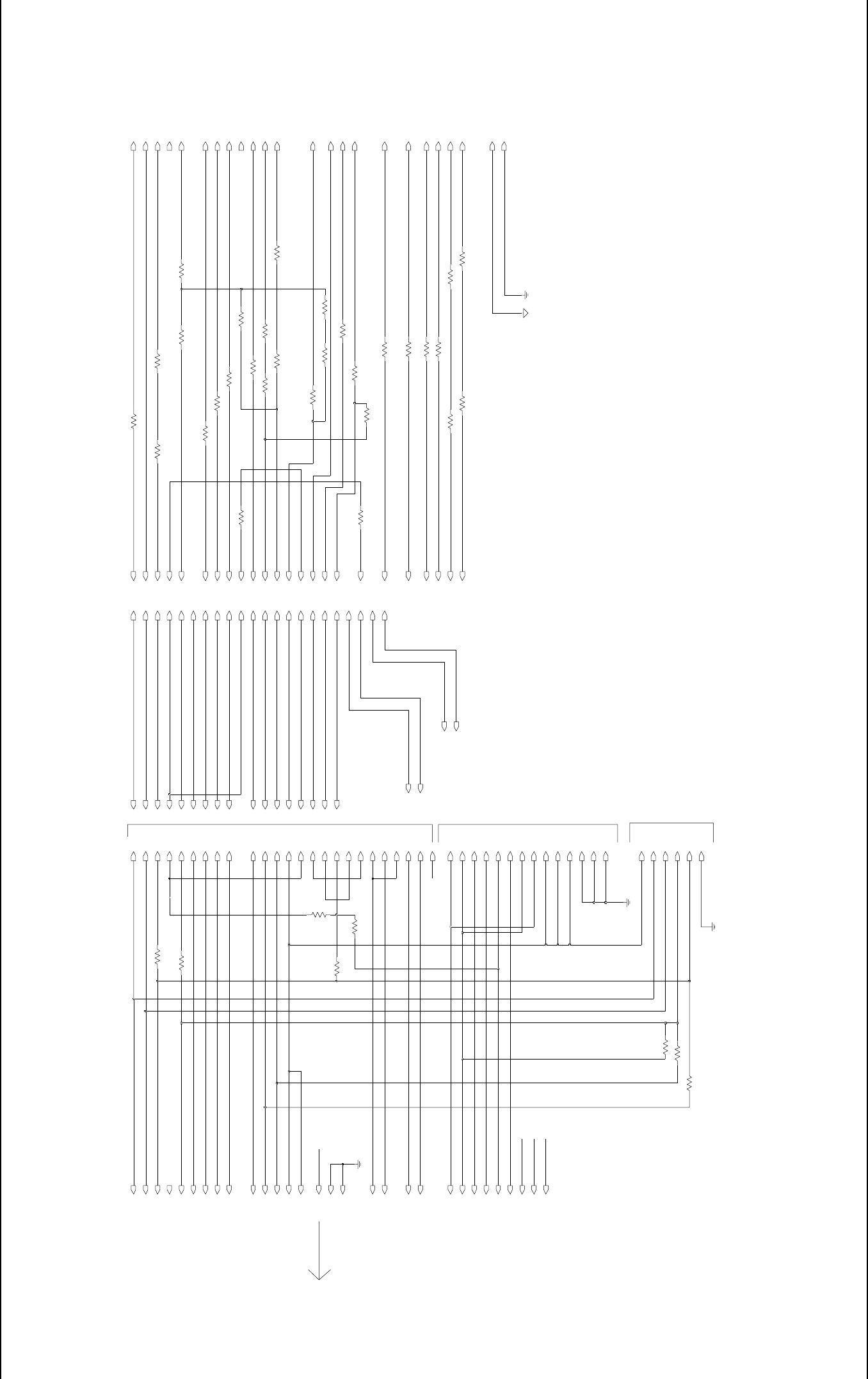
8-34 Schematics, Overlays, and Parts Lists: List of Schematics, Component Location Diagrams, and Parts Lists
September 26, 2003 6881096C77-O
Figure 8-19. W4, W5, and W7 High Power Interconnection Diagram
35
IGN 21
3IGN
RSSI/VOL 2
15 RSSI/VOL (A2)
RX-AUDIO 8
7RX-AUDIO
TX-AUDIO 12
8TX-AUDIO
FLT-AUDIO 5
6FLT_AUDIO
16
VIP-IN-3/DEK-DATA-IN
FIL AUD SHLD
MIC HI
MIC LO
HUB
17 VIP-IN-1
EMERGENCY
VIP-IN-2
HUB
PTT
BUS -
BUS +
50
SPARE 2 (RED)
SW B+ (YELLOW)
DIGITAL GROUND (BLUE)
SPEAKER LO (GREEN)
SPEAKER HI (ORANGE)
EMERGENCY (VIOLET)
SPEAKER HI (BLK/ORG)
SPEAKER LO (BLK/GRN)
B+ (GREEN)
IGNITION (ORANGE)
44
27
43
10
SPARE 2
NCNC
31
25 PIN REMOTE
CONNECTOR (P2)
6
7
13
2
E1
E2
SPARE 2
13
1
25
NC
11
14
27
12
11
9
10
23
14
5
21
19
16
SPEAKER HI
EMERGENCY
SWB+
COMMAND BOARD
CONNECTOR (P502)
24
25
13
DIGITAL GROUND
BUS -
BUS +
BUS SHIELD
SPEAKER LO
SPEAKER HI
17
SPARE 1
34
17
22
18
24
25
CONTROL HEAD SIDE
MICROPOHONE HI (BLK/YEL)
12 MIC HI
DETECTED AUDIO
ANALOG GROUND
PTT
12
MICROPOHONE LO (SHIELD)
DETECTED AUDIO (BLK/BRN)
DETECTED AUDIO (SHIELD/ANALOG GROUND)
SP 1 (BLK/GRN)
SP 1 (SHIELD)
BUSY (BLK/RED)
REMOTE RADIO INTERCONNECT BOARD (HIGH POWER)
REMOTE CONTROL HEAD CABLE
12
13
45
27
3
28
RESET
SPARE 1
BUSY
SWB+
18
28
29
48
49
11
CONTROL HEAD SIDE
17
10
22
2623 RESET
28
29
SPARE 1
SPARE 2
8
7
48
47
15
11
9
10
1
23
NC
24
21
9
22
IGNITION
16
49
REMOTE CONTROL HEAD INTERCONNCECT BOARD
W4/W5/W7
20
36
SNET-KEY
SNET-KID
SNET-WE
9
20
21
12
SWB+
MIC-HI
MIC-LO
PTT
EMERG/HUB
BUS - (BLACK)
BUS + (WHITE)
BUS SHIELD (BARE)
RESET (BLK/ORG)
SPARE 1 (BROWN)
13
45
16
3325
50
MIC HI
MIC LO
VIP SECTION MIC SECTION
RADIO SECTION
RADIO SIDE
CABLE SIDE
VF SENSE 2 VF SENSE 2
2
NC
VIP-OUT-1
VIP-OUT-2
VIP-OUT-3/DEK-STROBE
VIP-IN-1
VIP-IN-2
VIP-IN-3/DEK-DATA-IN
DEK-DATA-OUT
DEK-CLOCK
SWB+
SWB+
4
11
44
43
10
27
MIC LO
15
14
5
5
19
16
15
DIG-GND
DIG-GND
DIG-GND
21
4624 PTT
BUSY
BUS -
BUS +
SPARE 1
SPARE 2
RESET
SW B+
SHIELD GND
EMER
30
14
PTT/HUB-REF
8
41
7
40
24
23
26
46
33
GND
17
26
22
SPEAKER LO
1
3
3
37
4
38
5
2
19
18
A+
VF SENSE 1
1VF SENSE 1
IGNITION
B+/A+
2
SWB+ 35
VIP-OUT-1/DEK-CLOCK
18
19 VIP-OUT-2/DEK-DATA-OUT
VIP-OUT-3/DEK-STROBE
14
11
47
KEY SLOT
SW B+
B+/A+
A+ 30
20 A+
RESET
BUSY
BUS -
BUS +
10
28
ANA-GND
DIG-GND
19.6V
PTT
MIC HI
MIC LO
TO W4/W5/W7 CONTROL HEAD
BUSY
31
32
1
34
NC
NC
NC
NC
6
13 GND
JU643
JU636
JU601
JU609
JU642
JU1004
JU644
JU641
JU1001
JU608
JU607
JU662
JU606
JU663
JU659
JU616
JU1003
JU1007
JU640
JU653
JU632
JU657JU633
JU614JU645
JU639
JU655
JU1002
JU615
JU650 JU646
JU1006
JU1008
JU604
JU1005
JU638
JU637
JU630
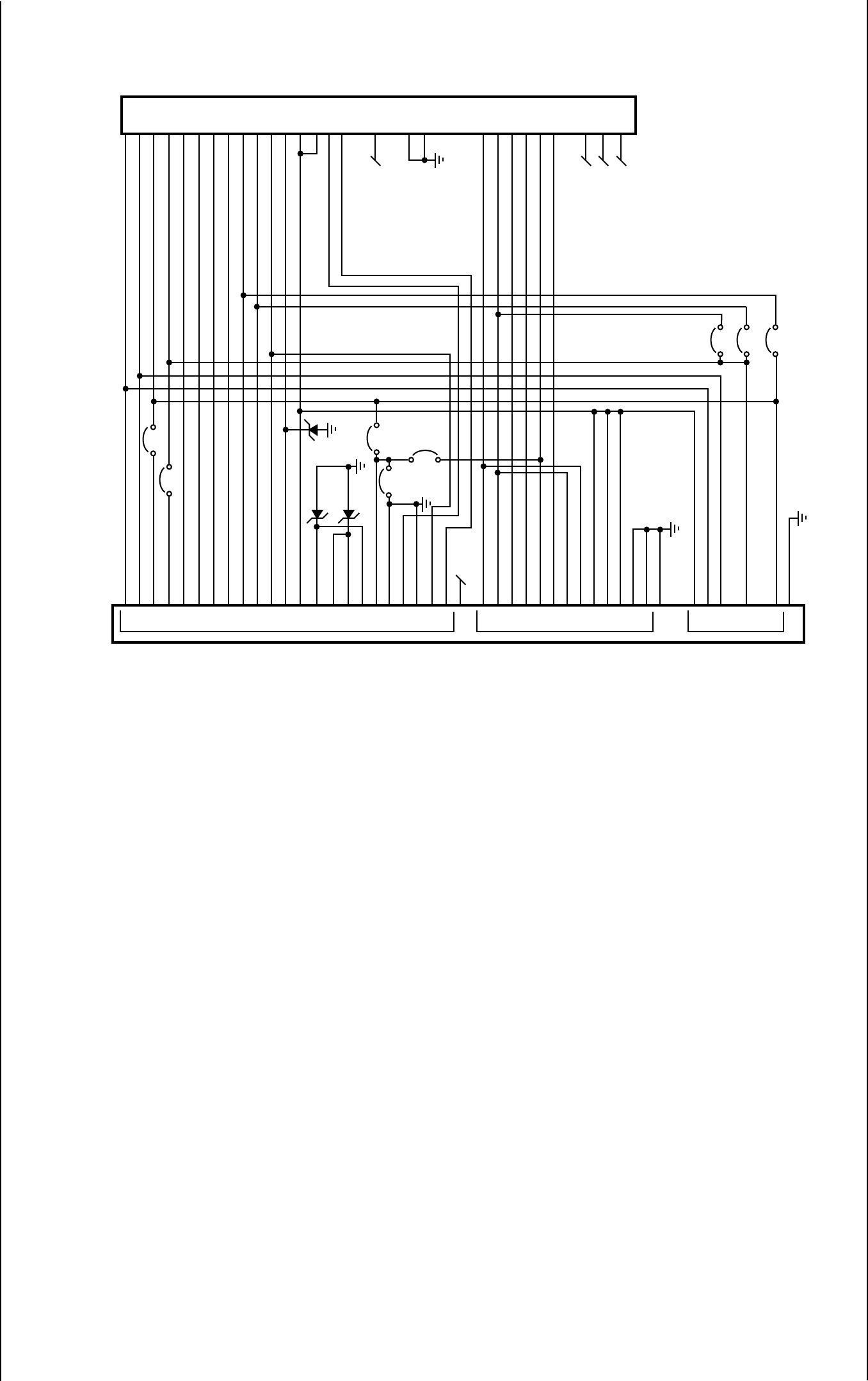
Schematics, Overlays, and Parts Lists: List of Schematics, Component Location Diagrams, and Parts Lists 8-35
6881096C77-O September 26, 2003
Figure 8-20. W5 and W7 Control Head Interface Board Schematic
33 BUSY
46 PTT
12 MIC-HI
13 MIC-L0
45 HUB
9000 CABLE
INTERFACE CONN.
P0100
HLN6432D W5/W7
CONTROL HEAD INTERFACE BOARD
MAEPF-23570-A
CONTROL HEAD
CONNECTOR
J0103
MIC-HI 27
MIC-LO 3
HUB 28
JU1005* PTT 24
JU1006* BUSY 25
17 BUS+ BUS+ 22
50 BUS BUS 10
26 RESET RESET 23
28 SPARE 1 SPARE 1 8
29 SPARE 2 SPARE 2 7
47 A+ A+ 5
15 IGN IGN 11
48 SWB+ SWB+ 4
12
11 SPKR LO
44 SPKR HI
43 SPKR HI
10 SPKR LO
27 EMERGENCY
VR1003**
VR1001
VR1002
15V
15V VF SENSE 1 1
VF SENSE 2 2
JU1001*
16 SHIELD GND
14 VF SENSE 1 JU1008
49 DIGITAL GND
30 A+
31 VF SENSE 2
32
JU1007
26
KEY SLOT
6
13
GND
GND
2 VIP-OUT-1 VIP-OUT-1/DEK-CLOCK 18
1 VIP-OUT-2 VIP-OUT-2/DEK-DATA-OUT 19
34 VIP-OUT-3/DEK-STROBE VIP-OUT-3/DEK-STROBE 14
4 VIP-IN-1 VIP-IN-1 17
3 VIP-IN-2 VIP-IN-2 16
37 VIP-IN-3/DEK-DATA-IN VIP-IN-3/DEK-DATA-IN 15
5 DEK-DATA-OUT
38 DEK-CLOCK
18 SWB+
19 SWB+
35 SWB+
20 DIG-GND
21 DIG-GND
36 DIG-GND
9
SNET-KEY
20
SNET-KID
21
SNET-WE
* = PARTS NOT PLACED
** = 0105950T92 ONLY
41 SWB+
8 MIC-HI
7 MIC-LO
24 PTT
40 EMERG/HUB
23 PTT/HUB-REF
JU1002*
JU1003*
JU1004*
MIC SECTION VIP SECTION RADIO SECTION
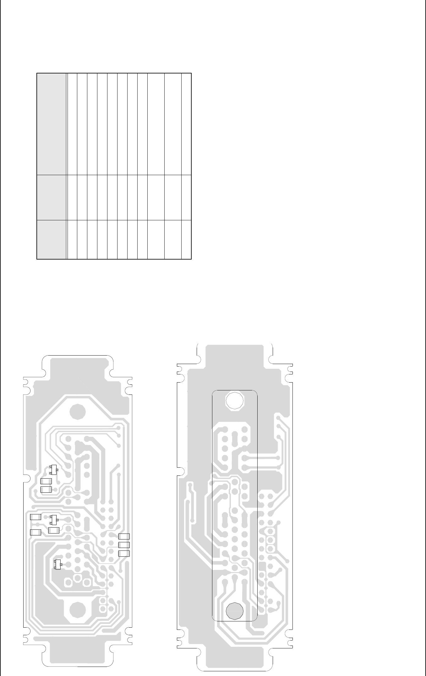
8-36 Schematics, Overlays, and Parts Lists: List of Schematics, Component Location Diagrams, and Parts Lists
September 26, 2003 6881096C77-O
Figure 8-21. HLN6432D W5/W7 Control Head Interface Board Component Location Diagram
JU1002
JU1003
JU1006
VR1003
JU1004 JU1005
VR1001 VR1002
JU1007
JU1008
JU1001
HLN6432D W5/W7 Parts List
Item Motorola
Part
Number Description
JU1001 NOTPLACED 64AM DUMMY PART NUMBER
JU1002 NOTPLACED 64AM DUMMY PART NUMBER
JU1003 NOTPLACED 64AM DUMMY PART NUMBER
JU1004 NOTPLACED 64AM DUMMY PART NUMBER
JU1005 NOTPLACED 64AM DUMMY PART NUMBER
JU1006 NOTPLACED 64AM DUMMY PART NUMBER
JU1007 0611077A01 RES CHIP JUMPER
JU1008 0611077A01 RES CHIP JUMPER
VR1001 4813830A28 DIODE 15V 5% 225MW
MMBZ5245B_
VR1002 4813830A28 DIODE 15V 5% 225MW
MMBZ5245B_
VR1003 NOTPLACED 64AM DUMMY PART NUMBER
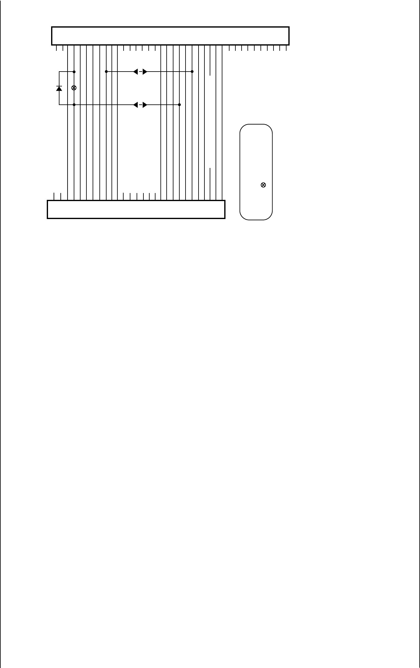
Schematics, Overlays, and Parts Lists: List of Schematics, Component Location Diagrams, and Parts Lists 8-37
6881096C77-O September 26, 2003
Figure 8-22. HLN6401A Control Head Interconnect Board, (Dash-Mount)
1
2
3
4
5
6
7
8
9
10
11
12
13
14
15
16
17
18
19
20
21
22
23
24
25
26
27
28
NC
NC
MIC-LOW NC
NC
J103 P502
HLN6401A
CONTROL HEAD INTERCONNECT BOARD
(Dash Mount)
MAEPF-23575-O
1
3
7
31
30
28
27
14
23
22
21
4
5
8
10
12
13
18
17
16
15
25
11
2
9
32
6
29
19
20
24
26
33
34
35
36
37
38
NC
NC
NC
NC
NC
NC
NC
NC
NC
NC
NC
NC
NC
NC
NC
NC
KEYED-SLOT
KEYED-SLOT
NC
NC
NC
NC
NC
NC
NOTE
CR10
JU11
NOTE
JU10
NOTE
SWB+
A+
DIG-GND
SPARE-2
SPARE-1
SERIAL BUS RESET
BUS-
IGN
VIP-OUT-1
VIP-OUT-2
S.NET_KID/PROG-VPP
S.NET_WE/PROG-RXD
BUS+
S.NET_KEY/PROG-TXD
MIC PTT/PROG-RESET
BUSY
MIC-HI/PROG-MOD-CONTROL
HUB/PROG BUSY
NOTE: NOT COMPATIBLE WITH
SPECTRA E JU10, JU11, CR10 INSTALLED
FOR AVL OPTION.
TRACE CUT ONLY WHEN
CR10 INSTALLED.
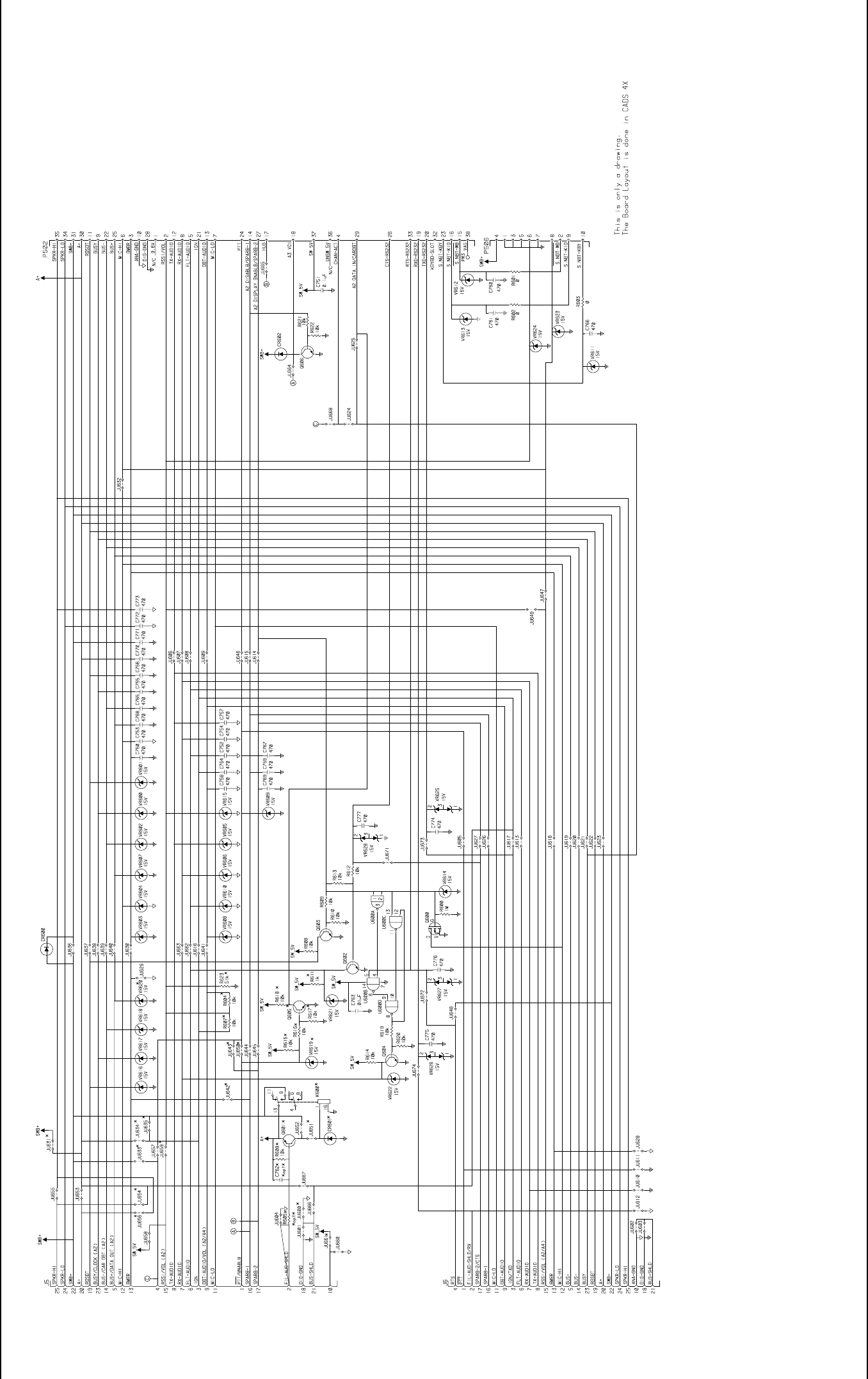
8-38 Schematics, Overlays, and Parts Lists: List of Schematics, Component Location Diagrams, and Parts Lists
September 26, 2003 6881096C77-O
Figure 8-23. HLN6486D/E High Power Standard Interconnect Board
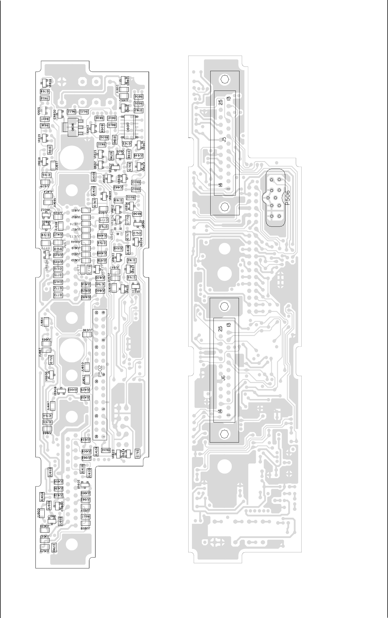
Schematics, Overlays, and Parts Lists: List of Schematics, Component Location Diagrams, and Parts Lists 8-39
6881096C77-O September 26, 2003
Figure 8-24. HLN6486D/E High-Power Interconnect Board (Viewed from Side 1)
Figure 8-25. HLN6486D/E High-Power Interconnect Board (Viewed from Side 2)
13
24
5
6
7
8
9
10
8-40 Schematics, Overlays, and Parts Lists: List of Schematics, Component Location Diagrams, and Parts Lists
September 26, 2003 6881096C77-O
HLN6486E Standard Interconnect Parts List
ITEM MOTOROLA
PART
NUMBER DESCRIPTION
C750 2113740B49 CAP CHIP REEL CL1 +/-30 100
C751 2113741N69 CAP CHIP CL2 X7R 10%
100000
C752 2113740B49 CAP CHIP REEL CL1 +/-30 100
C754 2113740B49 CAP CHIP REEL CL1 +/-30 100
C755 2113740B49 CAP CHIP REEL CL1 +/-30 100
C756 2113740B49 CAP CHIP REEL CL1 +/-30 100
C757 2113740B49 CAP CHIP REEL CL1 +/-30 100
C763 2113741N45 CAP CHIP CL2 X7R 10% 10000
C764 2113740B49 CAP CHIP REEL CL1 +/-30 100
C765 2113740B49 CAP CHIP REEL CL1 +/-30 100
C768 2113740B49 CAP CHIP REEL CL1 +/-30 100
C770 2113740B49 CAP CHIP REEL CL1 +/-30 100
C771 2113740B49 CAP CHIP REEL CL1 +/-30 100
C772 2113740B49 CAP CHIP REEL CL1 +/-30 100
C773 2113740B49 CAP CHIP REEL CL1 +/-30 100
C774 2113740B65 CAP CHIP REEL CL1 +/-30 470
C775 2113740B65 CAP CHIP REEL CL1 +/-30 470
C776 2113740B65 CAP CHIP REEL CL1 +/-30 470
C777 2113740B65 CAP CHIP REEL CL1 +/-30 470
H0001 0300139581 SCR MCH 4-40X5/16 PHLPAN
STL
H0002 0300139581 SCR MCH 4-40X5/16 PHLPAN
STL
H0003 0300139581 SCR MCH 4-40X5/16 PHLPAN
STL
H0004 0300139581 SCR MCH 4-40X5/16 PHLPAN
STL
J0005 0980159P02 CONNECTOR 25-PIN
J0006 0980159P02 CONNECTOR 25-PIN
JU601 0611077A01 RES CHIP JUMPER
JU604 0611077A01 RES CHIP JUMPER
JU606 0611077A01 RES CHIP JUMPER
JU607 0611077A01 RES CHIP JUMPER
JU608 0611077A01 RES CHIP JUMPER
JU609 0611077A01 RES CHIP JUMPER
JU613 0611077A01 RES CHIP JUMPER
JU618 0611077A01 RES CHIP JUMPER
JU619 0611077A01 RES CHIP JUMPER
JU620 0611077A01 RES CHIP JUMPER
JU621 0611077A01 RES CHIP JUMPER
JU622 0611077A01 RES CHIP JUMPER
JU623 0611077A01 RES CHIP JUMPER
JU626 0611077A01 RES CHIP JUMPER
JU629 0611077A01 RES CHIP JUMPER
JU630 0611077A01 RES CHIP JUMPER
JU632 0611077A01 RES CHIP JUMPER
JU636 0611077A01 RES CHIP JUMPER
JU637 0611077A01 RES CHIP JUMPER
JU638 0611077A01 RES CHIP JUMPER
JU639 0611077A01 RES CHIP JUMPER
JU640 0611077A01 RES CHIP JUMPER
JU644 0611077A01 RES CHIP JUMPER
JU645 0611077A01 RES CHIP JUMPER
JU646 0611077A01 RES CHIP JUMPER
JU652 0611077A01 RES CHIP JUMPER
JU653 0611077A01 RES CHIP JUMPER
JU655 0611077A01 RES CHIP JUMPER
JU657 0611077A01 RES CHIP JUMPER
JU658 0611077A01 RES CHIP JUMPER
JU662 0611077A01 RES CHIP JUMPER
JU664 0611077A01 RES CHIP JUMPER
JU665 0611077A01 RES CHIP JUMPER
JU666 0611077A01 RES CHIP JUMPER
JU671 0611077A01 RES CHIP JUMPER
JU672 0611077A01 RES CHIP JUMPER
JU673 0611077A01 RES CHIP JUMPER
JU674 0611077A01 RES CHIP JUMPER
ITEM MOTOROLA
PART
NUMBER DESCRIPTION
P0502 2880267M04 PLUG RIGHT ANGLE HDR 38
POS
P0506 2880068M01 HEADER MIC
R601 0611077A01 RES CHIP JUMPER
R602 0611077A01 RES CHIP JUMPER
R603 0611077A01 RES CHIP JUMPER
R614 0611077A98 RES CHIP 10K 5 1/8W
VR600 4813830A28 DIODE 15V 5% 225MW
MMBZ5245B_
VR601 4813830A28 DIODE 15V 5% 225MW
MMBZ5245B_
VR602 4813830A28 DIODE 15V 5% 225MW
MMBZ5245B_
VR603 4813830A28 DIODE 15V 5% 225MW
MMBZ5245B_
VR604 4813830A28 DIODE 15V 5% 225MW
MMBZ5245B_
VR605 4813830A28 DIODE 15V 5% 225MW
MMBZ5245B_
VR606 4813830A28 DIODE 15V 5% 225MW
MMBZ5245B_
VR610 4813830A28 DIODE 15V 5% 225MW
MMBZ5245B_
VR611 4813830A28 DIODE 15V 5% 225MW
MMBZ5245B_
VR612 4813830A28 DIODE 15V 5% 225MW
MMBZ5245B_
VR613 4813830A28 DIODE 15V 5% 225MW
MMBZ5245B_
VR615 4813830A28 DIODE 15V 5% 225MW
MMBZ5245B_
VR616 4813830A28 DIODE 15V 5% 225MW
MMBZ5245B_
VR617 4813830A28 DIODE 15V 5% 225MW
MMBZ5245B_
VR618 4813830A28 DIODE 15V 5% 225MW
MMBZ5245B_
VR623 4813830A28 DIODE 15V 5% 225MW
MMBZ5245B_
VR624 4813830A28 DIODE 15V 5% 225MW
MMBZ5245B_
ITEM MOTOROLA
PART
NUMBER DESCRIPTION
VR625 4813832C28 ZENER BPLR 15V FOR ESD
SOT23
VR626 4813832C28 ZENER BPLR 15V FOR ESD
SOT23
VR627 4813832C28 ZENER BPLR 15V FOR ESD
SOT23
VR628 4813832C28 ZENER BPLR 15V FOR ESD
SOT23
ITEM MOTOROLA
PART
NUMBER DESCRIPTION
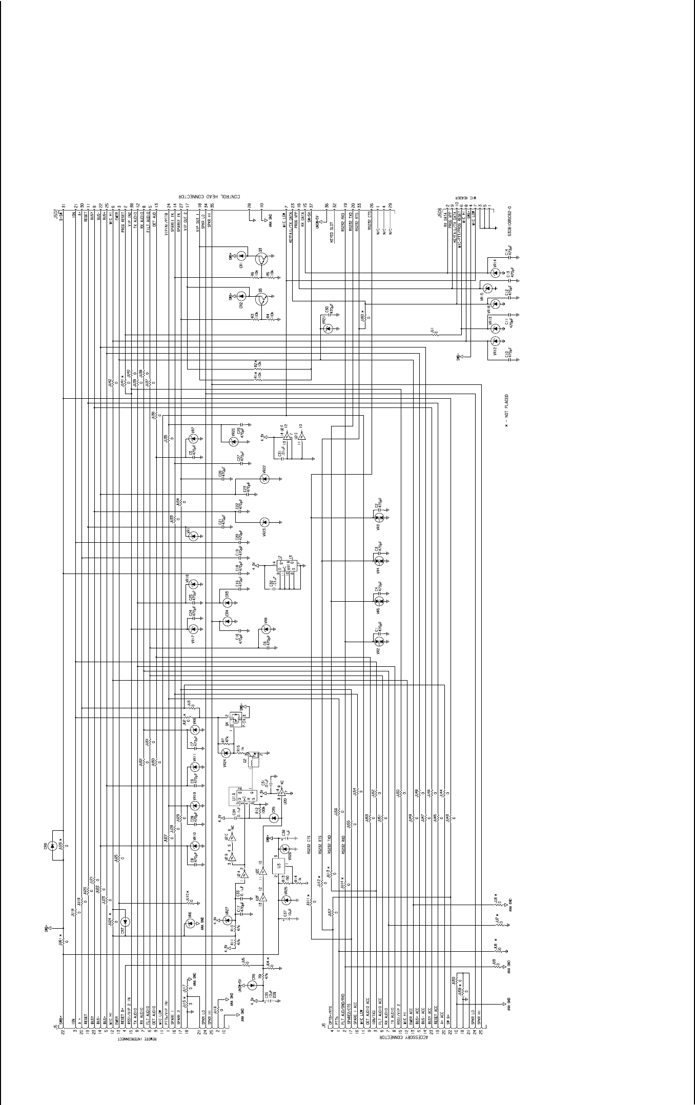
Schematics, Overlays, and Parts Lists: List of Schematics, Component Location Diagrams, and Parts Lists 8-41
6881096C77-O September 26, 2003
Figure 8-26. HLN6574E W3 Control Head High-Power Interconnect Board Schematic Design
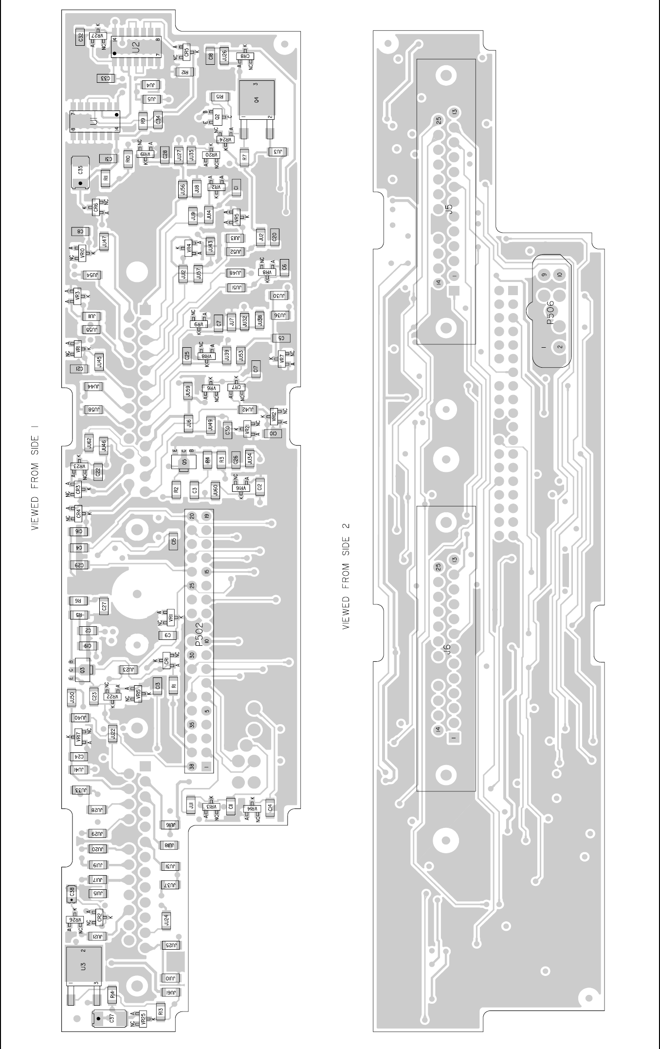
8-42 Schematics, Overlays, and Parts Lists: List of Schematics, Component Location Diagrams, and Parts Lists
September 26, 2003 6881096C77-O
Figure 8-27. HLN6574E W3 High Power Interconnect Board Component Location Diagrams
MAEPF-25697-O
MAEPF-25698-O
Schematics, Overlays, and Parts Lists: List of Schematics, Component Location Diagrams, and Parts Lists 8-43
6881096C77-O September 26, 2003
HLN6574E W3 High-Power Interconnect Parts List
ITEM MOTOROLA
PART
NUMBER DESCRIPTION
C1 2113740B65 CAP CHIP REEL CL1 +/-30 470
C10 2113740B65 CAP CHIP REEL CL1 +/-30 470
C11 2113740B65 CAP CHIP REEL CL1 +/-30 470
C12 2113740B65 CAP CHIP REEL CL1 +/-30 470
C13 2113740B65 CAP CHIP REEL CL1 +/-30 470
C14 2113740B65 CAP CHIP REEL CL1 +/-30 470
C15 2113740B49 CAP CHIP REEL CL1 +/-30 100
C16 2113740B49 CAP CHIP REEL CL1 +/-30 100
C17 2113740B49 CAP CHIP REEL CL1 +/-30 100
C18 2113740B49 CAP CHIP REEL CL1 +/-30 100
C19 2113740B49 CAP CHIP REEL CL1 +/-30 100
C2 2113740B65 CAP CHIP REEL CL1 +/-30 470
C20 2113740B49 CAP CHIP REEL CL1 +/-30 100
C21 2113740B49 CAP CHIP REEL CL1 +/-30 100
C22 2113740B49 CAP CHIP REEL CL1 +/-30 100
C23 2113740B49 CAP CHIP REEL CL1 +/-30 100
C24 2113740B49 CAP CHIP REEL CL1 +/-30 100
C25 2113740B49 CAP CHIP REEL CL1 +/-30 100
C26 2113740B65 CAP CHIP REEL CL1 +/-30 470
C27 2113740B65 CAP CHIP REEL CL1 +/-30 470
C28 2113740B65 CAP CHIP REEL CL1 +/-30 470
C29 2113740B65 CAP CHIP REEL CL1 +/-30 470
C3 2113740B65 CAP CHIP REEL CL1 +/-30 470
C30 2113740B65 CAP CHIP REEL CL1 +/-30 470
C31 2113741N45 CAP CHIP CL2 X7R 10% 10000
C32 2113741N45 CAP CHIP CL2 X7R 10% 10000
C33 2113741N69 CAP CHIP CL2 X7R 10%
100000
C34 2113741N69 CAP CHIP CL2 X7R 10%
100000
C35 2311049J26 CAP TANT CHIP 10 20 16
C37 2311049J26 CAP TANT CHIP 10 20 16
C38 2311049A37 CAP TANT CHIP 1 20 20
C4 2113740B65 CAP CHIP REEL CL1 +/-30 470
C5 2113740B49 CAP CHIP REEL CL1 +/-30 100
C6 2113740B49 CAP CHIP REEL CL1 +/-30 100
C7 2113740B49 CAP CHIP REEL CL1 +/-30 100
C8 2113740B49 CAP CHIP REEL CL1 +/-30 100
C9 2113740B49 CAP CHIP REEL CL1 +/-30 100
CR1 4813833C10 DIODE GEN PUR 70V
MMBD6050
CR2 4813833C10 DIODE GEN PUR 70V
MMBD6050
CR3 4813833C10 DIODE GEN PUR 70V
MMBD6050
CR4 4813833C10 DIODE GEN PUR 70V
MMBD6050
CR5 4813833C10 DIODE GEN PUR 70V
MMBD6050
CR6 4813833C10 DIODE GEN PUR 70V
MMBD6050
CR7 4813833C10 DIODE GEN PUR 70V
MMBD6050
CR8 NOTPLACED 64AM DUMMY PART NUMBER
H0001 0300139581 SCR MCH 4-40X5/16 PHLPAN
STL
H0002 0300139581 SCR MCH 4-40X5/16 PHLPAN
STL
H0003 0300139581 SCR MCH 4-40X5/16 PHLPAN
STL
H0004 0300139581 SCR MCH 4-40X5/16 PHLPAN
STL
HU3 NOTPLACED 64AM DUMMY PART NUMBER
J5 0980159P02 CONNECTOR 25-PIN
J6 0980159P02 CONNECTOR 25-PIN
JU1 0611077A01 RES CHIP JUMPER
JU10 NOTPLACED 64AM DUMMY PART NUMBER
JU11 0611077A01 RES CHIP JUMPER
JU12 0611077A01 RES CHIP JUMPER
JU13 0611077A01 RES CHIP JUMPER
JU14 0611077A01 RES CHIP JUMPER
ITEM MOTOROLA
PART
NUMBER DESCRIPTION
JU15 NOTPLACED 64AM DUMMY PART NUMBER
JU16 0611077A01 RES CHIP JUMPER
JU17 0611077A01 RES CHIP JUMPER
JU18 0611077A01 RES CHIP JUMPER
JU19 0611077A01 RES CHIP JUMPER
JU2 0611077A01 RES CHIP JUMPER
JU20 0611077A01 RES CHIP JUMPER
JU21 0611077A01 RES CHIP JUMPER
JU22 0611077A01 RES CHIP JUMPER
JU23 0611077A01 RES CHIP JUMPER
JU24 NOTPLACED 64AM DUMMY PART NUMBER
JU25 0611077A01 RES CHIP JUMPER
JU26 0611077A01 RES CHIP JUMPER
JU27 0611077A01 RES CHIP JUMPER
JU28 0611077A01 RES CHIP JUMPER
JU29 0611077A01 RES CHIP JUMPER
JU30 0611077A01 RES CHIP JUMPER
JU31 0611077A01 RES CHIP JUMPER
JU32 0611077A01 RES CHIP JUMPER
JU33 0611077A01 RES CHIP JUMPER
JU34 0611077A01 RES CHIP JUMPER
JU35 0611077A01 RES CHIP JUMPER
JU36 0611077A01 RES CHIP JUMPER
JU37 0611077A01 RES CHIP JUMPER
JU38 0611077A01 RES CHIP JUMPER
JU39 0611077A01 RES CHIP JUMPER
JU4 2113741N69 CAP CHIP CL2 X7R 10%
100000
JU40 0611077A01 RES CHIP JUMPER
JU41 NOTPLACED 64AM DUMMY PART NUMBER
JU42 0611077A01 RES CHIP JUMPER
JU43 0611077A01 RES CHIP JUMPER
JU44 0611077A01 RES CHIP JUMPER
JU45 0611077A01 RES CHIP JUMPER
ITEM MOTOROLA
PART
NUMBER DESCRIPTION
JU46 0611077A01 RES CHIP JUMPER
JU47 0611077A01 RES CHIP JUMPER
JU48 0611077A01 RES CHIP JUMPER
JU49 0611077A01 RES CHIP JUMPER
JU5 0611077A74 RES CHIP 1000 5 1/8
JU50 0611077A01 RES CHIP JUMPER
JU51 0611077A01 RES CHIP JUMPER
JU52 NOTPLACED 64AM DUMMY PART NUMBER
JU53 0611077A01 RES CHIP JUMPER
JU54 0611077A01 RES CHIP JUMPER
JU55 NOTPLACED 64AM DUMMY PART NUMBER
JU56 0611077A01 RES CHIP JUMPER
JU57 NOTPLACED 64AM DUMMY PART NUMBER
JU58 NOTPLACED 64AM DUMMY PART NUMBER
JU59 0611077A01 RES CHIP JUMPER
JU6 NOTPLACED 64AM DUMMY PART NUMBER
JU60 NOTPLACED 64AM DUMMY PART NUMBER
JU61 NOTPLACED 64AM DUMMY PART NUMBER
JU62 0611077A01 RES CHIP JUMPER
JU7 NOTPLACED 64AM DUMMY PART NUMBER
JU8 NOTPLACED 64AM DUMMY PART NUMBER
JU9 NOTPLACED 64AM DUMMY PART NUMBER
P502 2880267M04 PLUG RIGHT ANGLE HDR 38
POS
P506 2880068M01 HEADER MIC
Q2 4880048M01 TSTR NPN DIG 47K/47K
Q3 4880052M01 TSTR NPN DRLNGTN MXTA27
Q4 4813821A32 TSTR P-CH PWR FET 60V 5A
Q5 4880052M01 TSTR NPN DRLNGTN MXTA27
R1 NOTPLACED 64AM DUMMY PART NUMBER
R10 0611077B15 RES CHIP 47K 5 1/8W
R11 0611077B15 RES CHIP 47K 5 1/8W
R12 0611077B23 RES CHIP 100K 5 1/8W
R13 0611077A54 RES CHIP 150 5 1/8W
ITEM MOTOROLA
PART
NUMBER DESCRIPTION
8-44 Schematics, Overlays, and Parts Lists: List of Schematics, Component Location Diagrams, and Parts Lists
September 26, 2003 6881096C77-O
R14 0611077A74 RES CHIP 1000 5 1/8
R15 0611077A74 RES CHIP 1000 5 1/8
R2 NOTPLACED 64AM DUMMY PART NUMBER
R3 0611077A98 RES CHIP 10K 5 1/8W
R4 0611077A98 RES CHIP 10K 5 1/8W
R5 0611077A98 RES CHIP 10K 5 1/8W
R6 0611077A98 RES CHIP 10K 5 1/8W
R7 0611077B15 RES CHIP 47K 5 1/8W
R9 0611077B15 RES CHIP 47K 5 1/8W
U1 5113806A05 IC FLIP-FLOP,DUAL D
U2 5113806A37 IC SCHMITT TRIGGER,HEX
U3 5113816A19 IC ADJ LO DROPOUT POS
REG .8A
VR1 4813830A28 DIODE 15V 5% 225MW
MMBZ5245B_
VR10 4813830A28 DIODE 15V 5% 225MW
MMBZ5245B_
VR11 4813830A28 DIODE 15V 5% 225MW
MMBZ5245B_
VR12 4813830A28 DIODE 15V 5% 225MW
MMBZ5245B_
VR13 4813830A28 DIODE 15V 5% 225MW
MMBZ5245B_
VR14 4813830A28 DIODE 15V 5% 225MW
MMBZ5245B_
VR15 4813830A28 DIODE 15V 5% 225MW
MMBZ5245B_
VR16 4813830A28 DIODE 15V 5% 225MW
MMBZ5245B_
VR17 4813830A28 DIODE 15V 5% 225MW
MMBZ5245B_
VR18 4813830A28 DIODE 15V 5% 225MW
MMBZ5245B_
VR19 4813830A28 DIODE 15V 5% 225MW
MMBZ5245B_
VR2 4813832C28 ZENER BPLR 15V FOR ESD
SOT23
VR20 4813830A28 DIODE 15V 5% 225MW
MMBZ5245B_
ITEM MOTOROLA
PART
NUMBER DESCRIPTION
VR21 4813830A28 DIODE 15V 5% 225MW
MMBZ5245B_
VR22 4813830A28 DIODE 15V 5% 225MW
MMBZ5245B_
VR23 4813830A28 DIODE 15V 5% 225MW
MMBZ5245B_
VR24 4813830A28 DIODE 15V 5% 225MW
MMBZ5245B_
VR25 4813830A28 DIODE 15V 5% 225MW
MMBZ5245B_
VR26 4880140L23 DIODE SOT ZENER 18V
TAPE&REEL
VR27 4813830A28 DIODE 15V 5% 225MW
MMBZ5245B_
VR3 4813832C28 ZENER BPLR 15V FOR ESD
SOT23
VR4 4813832C28 ZENER BPLR 15V FOR ESD
SOT23
VR5 4813832C28 ZENER BPLR 15V FOR ESD
SOT23
VR6 4813830A28 DIODE 15V 5% 225MW
MMBZ5245B_
VR7 4813830A28 DIODE 15V 5% 225MW
MMBZ5245B_
VR8 4813830A28 DIODE 15V 5% 225MW
MMBZ5245B_
VR9 4813830A28 DIODE 15V 5% 225MW
MMBZ5245B_
ITEM MOTOROLA
PART
NUMBER DESCRIPTION
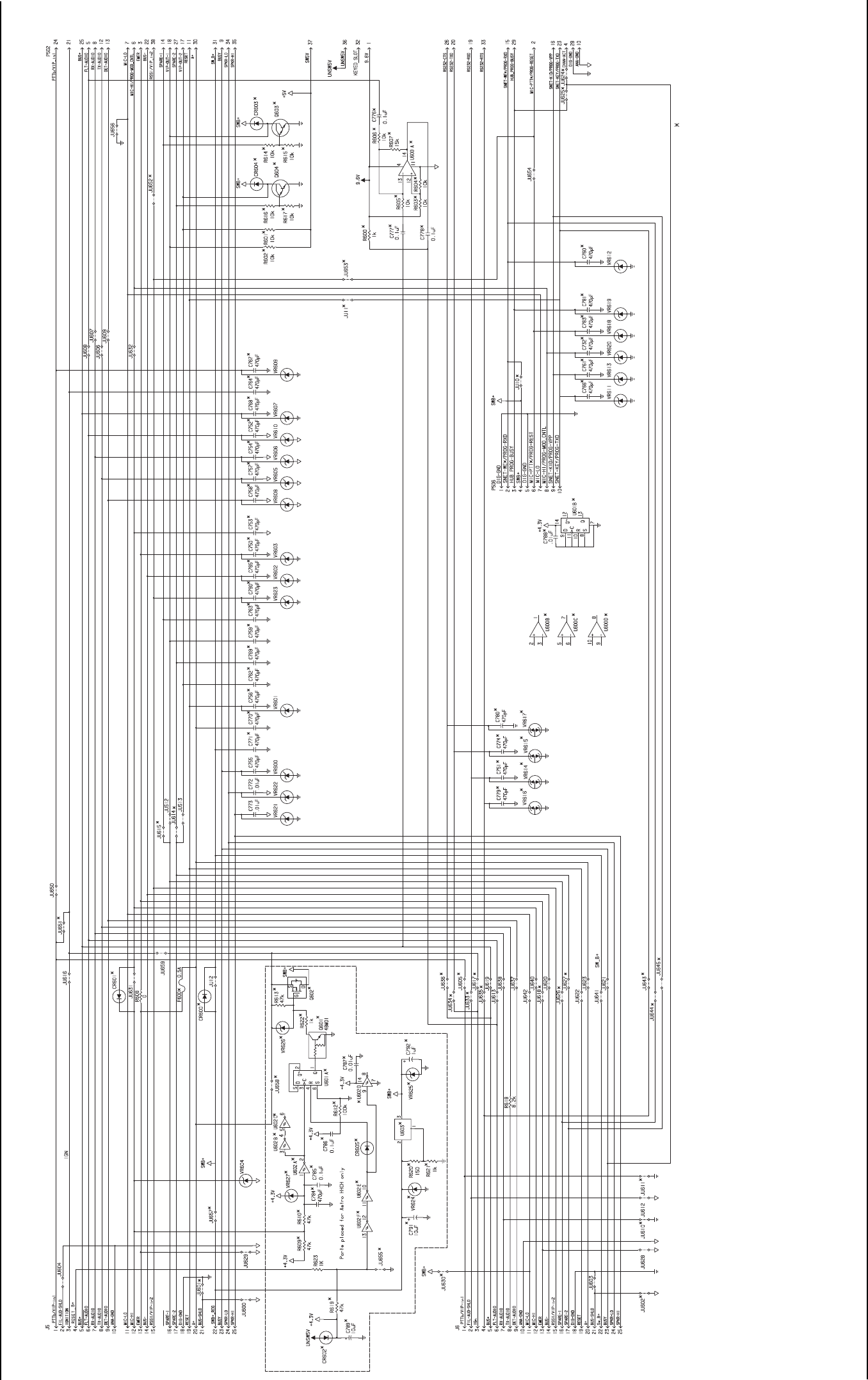
Schematics, Overlays, and Parts Lists: List of Schematics, Component Location Diagrams, and Parts Lists 8-45
6881096C77-O September 26, 2003
Figure 8-28. HLN6459D, HLN6344E, and HLN6365E Low-Power Interconnect Board Schematic
- NOT PLACED
MAEPF-27094-O
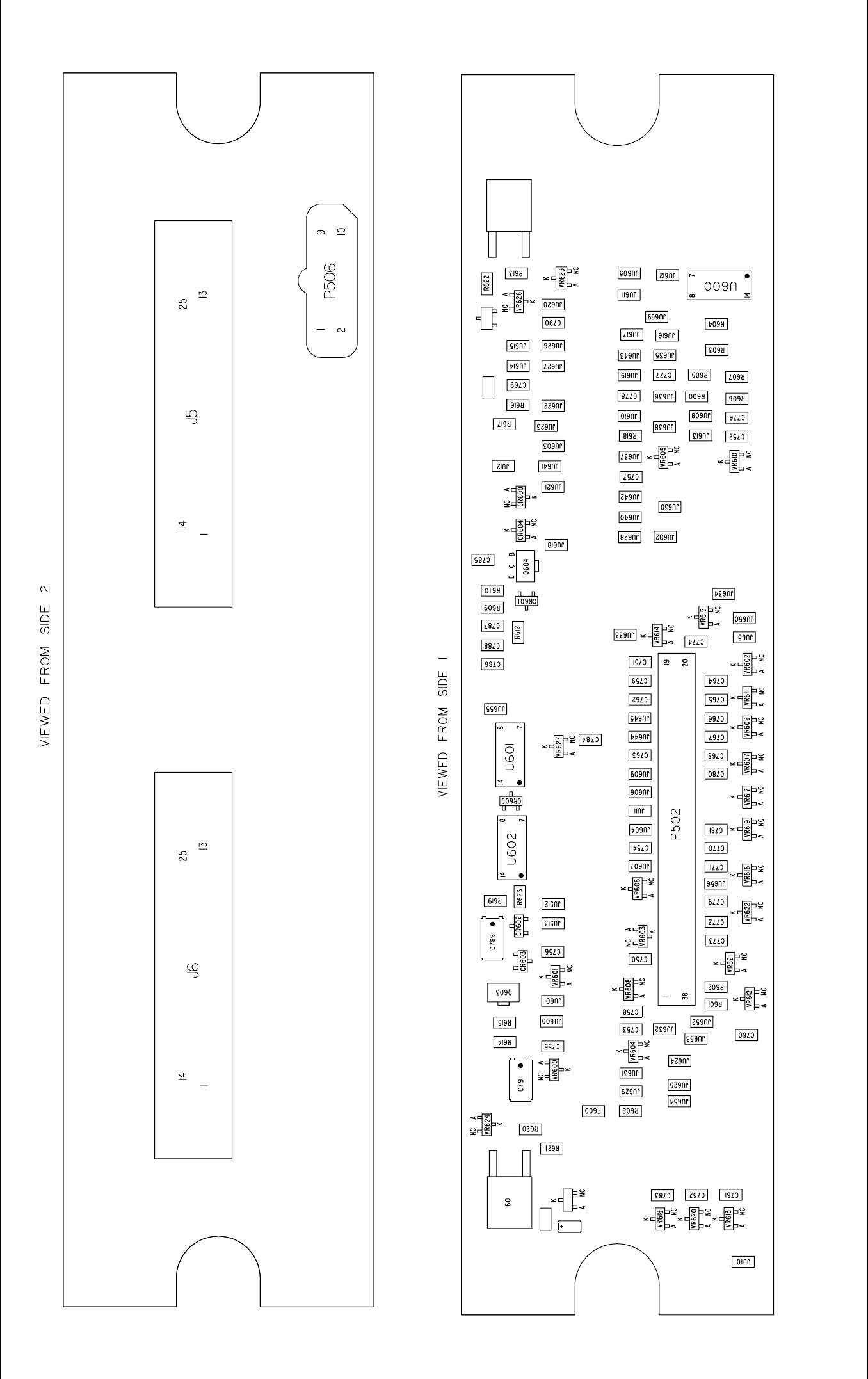
8-46 Schematics, Overlays, and Parts Lists: List of Schematics, Component Location Diagrams, and Parts Lists
September 26, 2003 6881096C77-O
Figure 8-29. HLN6459D, HLN6344E, and HLN6365 Low-Power Interconnect Component Location Diagram
MAEPF-27093-O
MAEPF-27703-O
1
3
2
E
B
C
Q60I
JU658
Q602
2
I
3
I
2
3
I
I
I
22
I2
3
3
3
3
23
I
U
JU657
C792
VR625
Schematics, Overlays, and Parts Lists: List of Schematics, Component Location Diagrams, and Parts Lists 8-47
6881096C77-O September 26, 2003
HLN6459D W3 Low-Power Interconnect Parts List
ITEM MOTOROLA
PART
NUMBER DESCRIPTION
C732 2113740B65 CAP CHIP REEL CL1 +/-30 470
C750 2113740B65 CAP CHIP REEL CL1 +/-30 470
C751 2113740B65 CAP CHIP REEL CL1 +/-30 470
C752 2113740B65 CAP CHIP REEL CL1 +/-30 470
C753 2113740B65 CAP CHIP REEL CL1 +/-30 470
C754 2113740B65 CAP CHIP REEL CL1 +/-30 470
C755 2113740B65 CAP CHIP REEL CL1 +/-30 470
C756 2113740B65 CAP CHIP REEL CL1 +/-30 470
C757 2113740B65 CAP CHIP REEL CL1 +/-30 470
C758 2113740B65 CAP CHIP REEL CL1 +/-30 470
C759 2113740B65 CAP CHIP REEL CL1 +/-30 470
C760 2113740B65 CAP CHIP REEL CL1 +/-30 470
C761 2113740B65 CAP CHIP REEL CL1 +/-30 470
C762 2113740B65 CAP CHIP REEL CL1 +/-30 470
C763 2113740B65 CAP CHIP REEL CL1 +/-30 470
C764 2113740B65 CAP CHIP REEL CL1 +/-30 470
C765 2113740B65 CAP CHIP REEL CL1 +/-30 470
C766 2113740B65 CAP CHIP REEL CL1 +/-30 470
C767 2113740B65 CAP CHIP REEL CL1 +/-30 470
C768 2113740B65 CAP CHIP REEL CL1 +/-30 470
C769 2113740B65 CAP CHIP REEL CL1 +/-30 470
C770 2113740B65 CAP CHIP REEL CL1 +/-30 470
C771 2113740B65 CAP CHIP REEL CL1 +/-30 470
C772 2113740B65 CAP CHIP REEL CL1 +/-30 470
C773 2113740B65 CAP CHIP REEL CL1 +/-30 470
C774 2113740B65 CAP CHIP REEL CL1 +/-30 470
C776 NOTPLACED 64AM DUMMY PART NUMBER
C777 NOTPLACED 64AM DUMMY PART NUMBER
C778 NOTPLACED 64AM DUMMY PART NUMBER
C779 2113740B65 CAP CHIP REEL CL1 +/-30 470
C780 2113740B65 CAP CHIP REEL CL1 +/-30 470
C781 2113740B65 CAP CHIP REEL CL1 +/-30 470
C783 2113740B65 CAP CHIP REEL CL1 +/-30 470
C784 2113740B65 CAP CHIP REEL CL1 +/-30 470
C785 2113741N69 CAP CHIP CL2 X7R 10%
100000
C786 2113741N69 CAP CHIP CL2 X7R 10%
100000
C787 2113741N45 CAP CHIP CL2 X7R 10% 10000
C788 2113741N45 CAP CHIP CL2 X7R 10% 10000
C789 2311049J26 CAP TANT CHIP 10 20 16
C790 2113740B65 CAP CHIP REEL CL1 +/-30 470
C791 2311049J26 CAP TANT CHIP 10 20 16
C792 2311049A37 CAP TANT CHIP 1 20 20
CR600 4813833C10 DIODE GEN PUR 70V
MMBD6050
CR601 4813833C10 DIODE GEN PUR 70V
MMBD6050
CR602 4813833C10 DIODE GEN PUR 70V
MMBD6050
CR603 4813833C10 DIODE GEN PUR 70V
MMBD6050
CR604 4813833C10 DIODE GEN PUR 70V
MMBD6050
CR605 4813833C10 DIODE GEN PUR 70V
MMBD6050
F600 NOTPLACED 64AM DUMMY PART NUMBER
HD001 0300139581 SCR MCH 4-40X5/16 PHLPAN
STL
HD002 0300139581 SCR MCH 4-40X5/16 PHLPAN
STL
HD003 0300139581 SCR MCH 4-40X5/16 PHLPAN
STL
HD004 0300139581 SCR MCH 4-40X5/16 PHLPAN
STL
J5 0980159P02 CONNECTOR 25-PIN
J6 0980159P02 CONNECTOR 25-PIN
JU10 NOTPLACED 64AM DUMMY PART NUMBER
JU11 NOTPLACED 64AM DUMMY PART NUMBER
JU12 NOTPLACED 64AM DUMMY PART NUMBER
JU512 NOTPLACED 64AM DUMMY PART NUMBER
ITEM MOTOROLA
PART
NUMBER DESCRIPTION
JU513 NOTPLACED 64AM DUMMY PART NUMBER
JU600 0611077A01 RES CHIP JUMPER
JU601 NOTPLACED 64AM DUMMY PART NUMBER
JU602 0611077A01 RES CHIP JUMPER
JU603 NOTPLACED 64AM DUMMY PART NUMBER
JU604 0611077A01 RES CHIP JUMPER
JU605 NOTPLACED 64AM DUMMY PART NUMBER
JU606 0611077A01 RES CHIP JUMPER
JU607 0611077A01 RES CHIP JUMPER
JU608 0611077A01 RES CHIP JUMPER
JU609 0611077A01 RES CHIP JUMPER
JU610 NOTPLACED 64AM DUMMY PART NUMBER
JU611 NOTPLACED 64AM DUMMY PART NUMBER
JU612 0611077A01 RES CHIP JUMPER
JU613 NOTPLACED 64AM DUMMY PART NUMBER
JU614 0611077A01 RES CHIP JUMPER
JU615 0611077A01 RES CHIP JUMPER
JU616 0611077A01 RES CHIP JUMPER
JU617 NOTPLACED 64AM DUMMY PART NUMBER
JU618 0611077A01 RES CHIP JUMPER
JU619 0611077A01 RES CHIP JUMPER
JU620 0611077A01 RES CHIP JUMPER
JU621 0611077A01 RES CHIP JUMPER
JU622 0611077A01 RES CHIP JUMPER
JU623 0611077A01 RES CHIP JUMPER
JU624 NOTPLACED 64AM DUMMY PART NUMBER
JU625 NOTPLACED 64AM DUMMY PART NUMBER
JU626 0611077A01 RES CHIP JUMPER
JU627 0611077A01 RES CHIP JUMPER
JU628 NOTPLACED 64AM DUMMY PART NUMBER
JU629 NOTPLACED 64AM DUMMY PART NUMBER
JU630 NOTPLACED 64AM DUMMY PART NUMBER
JU631 NOTPLACED 64AM DUMMY PART NUMBER
ITEM MOTOROLA
PART
NUMBER DESCRIPTION
JU632 0611077A01 RES CHIP JUMPER
JU633 NOTPLACED 64AM DUMMY PART NUMBER
JU634 NOTPLACED 64AM DUMMY PART NUMBER
JU635 NOTPLACED 64AM DUMMY PART NUMBER
JU636 NOTPLACED 64AM DUMMY PART NUMBER
JU637 0611077A01 RES CHIP JUMPER
JU638 0611077A01 RES CHIP JUMPER
JU640 0611077A01 RES CHIP JUMPER
JU641 0611077A01 RES CHIP JUMPER
JU642 0611077A01 RES CHIP JUMPER
JU643 NOTPLACED 64AM DUMMY PART NUMBER
JU644 NOTPLACED 64AM DUMMY PART NUMBER
JU645 NOTPLACED 64AM DUMMY PART NUMBER
JU650 0611077A01 RES CHIP JUMPER
JU651 NOTPLACED 64AM DUMMY PART NUMBER
JU652 0611077A01 RES CHIP JUMPER
JU653 NOTPLACED 64AM DUMMY PART NUMBER
JU654 0611077A01 RES CHIP JUMPER
JU655 2113741N69 CAP CHIP CL2 X7R 10%
100000
JU656 0611077A01 RES CHIP JUMPER
JU657 NOTPLACED 64AM DUMMY PART NUMBER
JU658 NOTPLACED 64AM DUMMY PART NUMBER
JU659 0611077A01 RES CHIP JUMPER
P502 2880102M09 PLUG VERTICAL 38 POSITION
P506 2880068M01 HEADER MIC
Q601 4880048M01 TSTR NPN DIG 47K/47K
Q602 4813821A32 TSTR P-CH PWR FET 60V 5A
Q603 4880052M01 TSTR NPN DRLNGTN MXTA27
Q604 4880052M01 TSTR NPN DRLNGTN MXTA27
R600 NOTPLACED 64AM DUMMY PART NUMBER
R601 NOTPLACED 64AM DUMMY PART NUMBER
R602 NOTPLACED 64AM DUMMY PART NUMBER
R603 NOTPLACED 64AM DUMMY PART NUMBER
ITEM MOTOROLA
PART
NUMBER DESCRIPTION
8-48 Schematics, Overlays, and Parts Lists: List of Schematics, Component Location Diagrams, and Parts Lists
September 26, 2003 6881096C77-O
R604 NOTPLACED 64AM DUMMY PART NUMBER
R605 NOTPLACED 64AM DUMMY PART NUMBER
R606 NOTPLACED 64AM DUMMY PART NUMBER
R607 NOTPLACED 64AM DUMMY PART NUMBER
R608 0611077A01 RES CHIP JUMPER
R609 0611077B15 RES CHIP 47K 5 1/8W
R610 0611077B15 RES CHIP 47K 5 1/8W
R612 0611077B23 RES CHIP 100K 5 1/8W
R613 0611077B15 RES CHIP 47K 5 1/8W
R614 0611077A98 RES CHIP 10K 5 1/8W
R615 0611077A98 RES CHIP 10K 5 1/8W
R616 0611077A98 RES CHIP 10K 5 1/8W
R617 0611077A98 RES CHIP 10K 5 1/8W
R618 0611077A96 RES CHIP 8200 5 1/8
R619 0611077B15 RES CHIP 47K 5 1/8W
R620 0611077A54 RES CHIP 150 5 1/8W
R621 0611077A74 RES CHIP 1000 5 1/8
R622 0611077A74 RES CHIP 1000 5 1/8
R623 0611077A74 RES CHIP 1000 5 1/8
U600 NOTPLACED 64AM DUMMY PART NUMBER
U601 5113806A05 IC FLIP-FLOP,DUAL D
U602 5113806A37 IC SCHMITT TRIGGER,HEX
U603 5113816A19 IC ADJ LO DROPOUT POS
REG .8A
VR600 4813830A28 DIODE 15V 5% 225MW
MMBZ5245B_
VR601 4813830A28 DIODE 15V 5% 225MW
MMBZ5245B_
VR602 4813830A28 DIODE 15V 5% 225MW
MMBZ5245B_
VR603 4813830A28 DIODE 15V 5% 225MW
MMBZ5245B_
VR604 4813830A28 DIODE 15V 5% 225MW
MMBZ5245B_
VR605 4813830A28 DIODE 15V 5% 225MW
MMBZ5245B_
ITEM MOTOROLA
PART
NUMBER DESCRIPTION
VR606 4813830A28 DIODE 15V 5% 225MW
MMBZ5245B_
VR607 4813830A28 DIODE 15V 5% 225MW
MMBZ5245B_
VR608 4813830A28 DIODE 15V 5% 225MW
MMBZ5245B_
VR609 4813830A28 DIODE 15V 5% 225MW
MMBZ5245B_
VR610 4813830A28 DIODE 15V 5% 225MW
MMBZ5245B_
VR611 4813830A28 DIODE 15V 5% 225MW
MMBZ5245B_
VR612 4813830A28 DIODE 15V 5% 225MW
MMBZ5245B_
VR613 4813830A28 DIODE 15V 5% 225MW
MMBZ5245B_
VR614 4813832C28 ZENER BPLR 15V FOR ESD
SOT23
VR615 4813832C28 ZENER BPLR 15V FOR ESD
SOT23
VR616 4813832C28 ZENER BPLR 15V FOR ESD
SOT23
VR617 4813832C28 ZENER BPLR 15V FOR ESD
SOT23
VR618 4813830A28 DIODE 15V 5% 225MW
MMBZ5245B_
VR619 4813830A28 DIODE 15V 5% 225MW
MMBZ5245B_
VR620 4813830A28 DIODE 15V 5% 225MW
MMBZ5245B_
VR621 4813830A28 DIODE 15V 5% 225MW
MMBZ5245B_
VR622 4813830A28 DIODE 15V 5% 225MW
MMBZ5245B_
VR623 4813830A28 DIODE 15V 5% 225MW
MMBZ5245B_
VR624 4813830A28 DIODE 15V 5% 225MW
MMBZ5245B_
VR625 4880140L23 DIODE SOT ZENER 18V
TAPE&REEL
VR626 4813830A28 DIODE 15V 5% 225MW
MMBZ5245B_
VR627 NOTPLACED 64AM DUMMY PART NUMBER
ITEM MOTOROLA
PART
NUMBER DESCRIPTION
Schematics, Overlays, and Parts Lists: List of Schematics, Component Location Diagrams, and Parts Lists 8-49
6881096C77-O September 26, 2003
HLN6365E Motorcycle Interconnect Parts List
ITEM MOTOROLA
PART
NUMBER DESCRIPTION
C754 2113740B65 CAP CHIP REEL CL1 +/-30 470
C755 2113740B65 CAP CHIP REEL CL1 +/-30 470
C772 2113741N45 CAP CHIP CL2 X7R 10% 10000
C773 2113741N45 CAP CHIP CL2 X7R 10% 10000
GS1 4205747Z01 CLIP GRND
GS2 4205747Z01 CLIP GRND
J5 0980159P02 CONNECTOR 25-PIN
JU12 0611077A01 RES CHIP JUMPER
JU512 0611077A01 RES CHIP JUMPER
JU513 0611077A01 RES CHIP JUMPER
JU600 0611077A01 RES CHIP JUMPER
JU601 0611077A01 RES CHIP JUMPER
JU603 0611077A01 RES CHIP JUMPER
JU604 0611077A01 RES CHIP JUMPER
JU606 0611077A01 RES CHIP JUMPER
JU607 0611077A01 RES CHIP JUMPER
JU608 0611077A01 RES CHIP JUMPER
JU609 0611077A01 RES CHIP JUMPER
JU612 0611077A01 RES CHIP JUMPER
JU613 0611077A01 RES CHIP JUMPER
JU619 0611077A01 RES CHIP JUMPER
JU620 0611077A01 RES CHIP JUMPER
JU621 0611077A01 RES CHIP JUMPER
JU622 0611077A01 RES CHIP JUMPER
JU623 0611077A01 RES CHIP JUMPER
JU631 0611077A01 RES CHIP JUMPER
JU632 0611077A01 RES CHIP JUMPER
JU637 0611077A01 RES CHIP JUMPER
JU638 0611077A01 RES CHIP JUMPER
JU640 0611077A01 RES CHIP JUMPER
JU641 0611077A01 RES CHIP JUMPER
JU642 0611077A01 RES CHIP JUMPER
JU651 0611077A01 RES CHIP JUMPER
JU654 0611077A01 RES CHIP JUMPER
JU656 0611077A01 RES CHIP JUMPER
JU657 0611077A01 RES CHIP JUMPER
JU659 0611077A01 RES CHIP JUMPER
P502 2880102M09 PLUG VERTICAL 38 POSITION
P506 2880068M01 HEADER MIC
R608 0611077A74 RES CHIP 1000 5 1/8
R618 0611077A96 RES CHIP 8200 5 1/8
VR600 4813830A28 DIODE 15V 5% 225MW
MMBZ5245B_
VR601 4813830A28 DIODE 15V 5% 225MW
MMBZ5245B_
VR602 4813830A28 DIODE 15V 5% 225MW
MMBZ5245B_
VR603 4813830A28 DIODE 15V 5% 225MW
MMBZ5245B_
VR604 4813830A28 DIODE 15V 5% 225MW
MMBZ5245B_
VR605 4813830A28 DIODE 15V 5% 225MW
MMBZ5245B_
VR606 4813830A28 DIODE 15V 5% 225MW
MMBZ5245B_
VR607 4813830A28 DIODE 15V 5% 225MW
MMBZ5245B_
VR608 4813830A28 DIODE 15V 5% 225MW
MMBZ5245B_
VR609 4813830A28 DIODE 15V 5% 225MW
MMBZ5245B_
VR610 4813830A28 DIODE 15V 5% 225MW
MMBZ5245B_
VR611 4813830A28 DIODE 15V 5% 225MW
MMBZ5245B_
VR612 4813830A28 DIODE 15V 5% 225MW
MMBZ5245B_
VR613 4813830A28 DIODE 15V 5% 225MW
MMBZ5245B_
VR618 4813830A28 DIODE 15V 5% 225MW
MMBZ5245B_
ITEM MOTOROLA
PART
NUMBER DESCRIPTION
VR619 4813830A28 DIODE 15V 5% 225MW
MMBZ5245B_
VR620 4813830A28 DIODE 15V 5% 225MW
MMBZ5245B_
VR621 4813830A28 DIODE 15V 5% 225MW
MMBZ5245B_
VR622 4813830A28 DIODE 15V 5% 225MW
MMBZ5245B_
ITEM MOTOROLA
PART
NUMBER DESCRIPTION
8-50 Schematics, Overlays, and Parts Lists: List of Schematics, Component Location Diagrams, and Parts Lists
September 26, 2003 6881096C77-O
HLN6344E Standard Interconnect Parts List
ITEM MOTOROLA
PART
NUMBER DESCRIPTION
C754 2113740B65 CAP CHIP REEL CL1 +/-30 470
C755 2113740B65 CAP CHIP REEL CL1 +/-30 470
C772 2113741N45 CAP CHIP CL2 X7R 10% 10000
C773 2113741N45 CAP CHIP CL2 X7R 10% 10000
J5 0980159P02 CONNECTOR 25-PIN
J6 0980159P02 CONNECTOR 25-PIN
JU12 0611077A01 RES CHIP JUMPER
JU512 0611077A01 RES CHIP JUMPER
JU513 0611077A01 RES CHIP JUMPER
JU600 0611077A01 RES CHIP JUMPER
JU601 0611077A01 RES CHIP JUMPER
JU603 0611077A01 RES CHIP JUMPER
JU604 0611077A01 RES CHIP JUMPER
JU606 0611077A01 RES CHIP JUMPER
JU607 0611077A01 RES CHIP JUMPER
JU608 0611077A01 RES CHIP JUMPER
JU609 0611077A01 RES CHIP JUMPER
JU612 0611077A01 RES CHIP JUMPER
JU613 0611077A01 RES CHIP JUMPER
JU619 0611077A01 RES CHIP JUMPER
JU620 0611077A01 RES CHIP JUMPER
JU621 0611077A01 RES CHIP JUMPER
JU622 0611077A01 RES CHIP JUMPER
JU623 0611077A01 RES CHIP JUMPER
JU628 0611077A01 RES CHIP JUMPER
JU629 0611077A01 RES CHIP JUMPER
JU631 0611077A01 RES CHIP JUMPER
JU632 0611077A01 RES CHIP JUMPER
JU637 0611077A01 RES CHIP JUMPER
JU638 0611077A01 RES CHIP JUMPER
JU640 0611077A01 RES CHIP JUMPER
JU641 0611077A01 RES CHIP JUMPER
JU642 0611077A01 RES CHIP JUMPER
JU650 0611077A01 RES CHIP JUMPER
JU654 0611077A01 RES CHIP JUMPER
JU656 0611077A01 RES CHIP JUMPER
JU657 0611077A01 RES CHIP JUMPER
JU659 0611077A01 RES CHIP JUMPER
P502 2880102M09 PLUG VERTICAL 38 POSITION
P506 2880068M01 HEADER MIC
R608 0611077A01 RES CHIP JUMPER
R618 0611077A96 RES CHIP 8200 5 1/8
VR600 4813830A28 DIODE 15V 5% 225MW
MMBZ5245B_
VR601 4813830A28 DIODE 15V 5% 225MW
MMBZ5245B_
VR602 4813830A28 DIODE 15V 5% 225MW
MMBZ5245B_
VR603 4813830A28 DIODE 15V 5% 225MW
MMBZ5245B_
VR604 4813830A28 DIODE 15V 5% 225MW
MMBZ5245B_
VR605 4813830A28 DIODE 15V 5% 225MW
MMBZ5245B_
VR606 4813830A28 DIODE 15V 5% 225MW
MMBZ5245B_
VR607 4813830A28 DIODE 15V 5% 225MW
MMBZ5245B_
VR608 4813830A28 DIODE 15V 5% 225MW
MMBZ5245B_
VR609 4813830A28 DIODE 15V 5% 225MW
MMBZ5245B_
VR610 4813830A28 DIODE 15V 5% 225MW
MMBZ5245B_
VR611 4813830A28 DIODE 15V 5% 225MW
MMBZ5245B_
VR612 4813830A28 DIODE 15V 5% 225MW
MMBZ5245B_
VR613 4813830A28 DIODE 15V 5% 225MW
MMBZ5245B_
VR618 4813830A28 DIODE 15V 5% 225MW
MMBZ5245B_
ITEM MOTOROLA
PART
NUMBER DESCRIPTION
VR619 4813830A28 DIODE 15V 5% 225MW
MMBZ5245B_
VR620 4813830A28 DIODE 15V 5% 225MW
MMBZ5245B_
VR621 4813830A28 DIODE 15V 5% 225MW
MMBZ5245B_
VR622 4813830A28 DIODE 15V 5% 225MW
MMBZ5245B_
ITEM MOTOROLA
PART
NUMBER DESCRIPTION
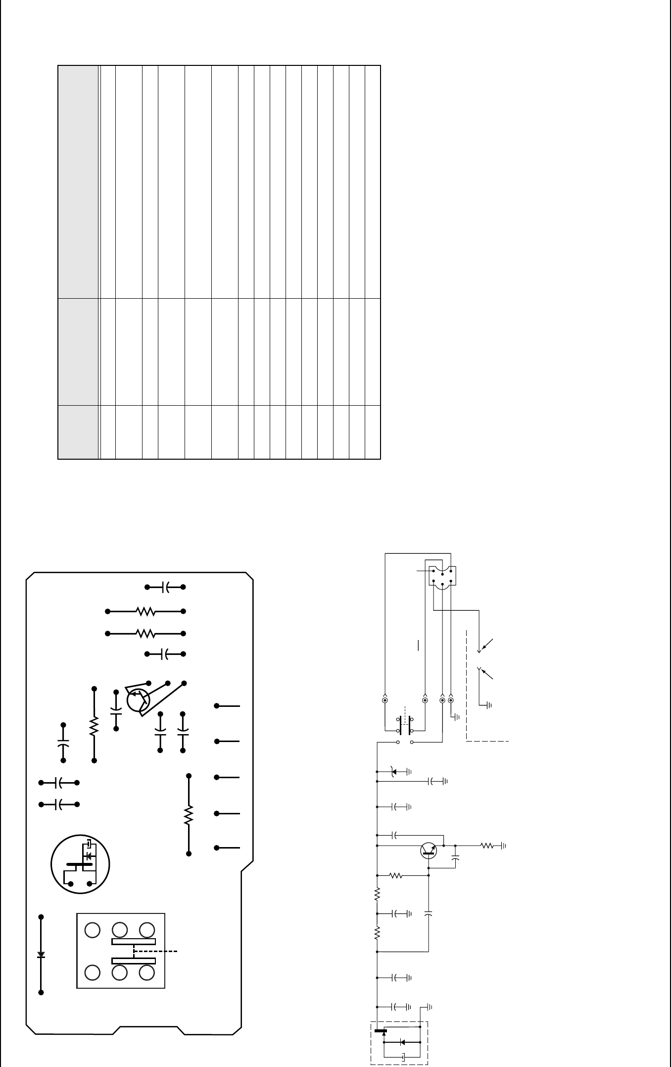
Schematics, Overlays, and Parts Lists: List of Schematics, Component Location Diagrams, and Parts Lists 8-51
6881096C77-O September 26, 2003
Figure 8-30. HMN1080A, HMN1061A, HMN1079A Microphone Board Overlay
Figure 8-31. HMN1080A, HMN1061A, HMN1079A Microphone Schematic
ic
++
GRN BLK
R1306 C1307
C1308
Q1302
C1306
R1303
C1302
C1301
R1305
C1305
R1302
C1309
C1304
CR1301
MK1301
S1301
BLU WHT RED
MAEPF-27698-O
VR1301
12V S1301
PUSH TO TALK
C1308
0.27
C1304
10
C1302
0.001
C1301
27pF
MK1301
C1307
0.001
R1306
56
R1302
2.2K
R1303
1K
R1305
100K
C1306
36pF
C1305
0.22
Q1302
M8208
C1309
62pF
(VEHICLE
CHASSIS
GROUND) MIC
HANG-UP
CLIP
MIC
HANG-UP
STUD
H.U.B. (BLU)
MIC HI (RED)
PTT (GRN)
DIG GND (WHT)
MIC LO (BLK)
MICROPHONE
CONNECTOR J104
(DETAIL SHOWN
FROM CONNECTOR
FRONT VIEW)
N.C.
+
MAEPF-27699-O
HMN1080A, HMN1061A, HMN1079A Microphone Parts List
ITEM MOTOROLA
PART
NUMBER DESCRIPTION
C1301 2111038H35 CAP 27pF 50V
C1302,
C1307 2111039B13 CAP 1000 50V
C1304 2311048C10 CAP 10 50V
C1305 0811051A15
0811051A11 CAP .22 63V (HMN1080A & HMN1079A only)
CAP .047 63V (HMN1061A only)
C1306 2182133G39
2111038P50 CAP 36 500V (HMN1080A & HMN1079A only)
CAP 220 50V (HMN1061A only)
C1308 2382397D25
0811051A14 CAP .27pF 20V (HMN1080A & HMN1079A only)
CAP .15 63V (HMN1061A only)
C1309 2111014H44 CAP 62pF 100V
CR1301 4811034A36 12V Zener
MK1301 5080258E06 ELECTRET MIC CTRG
Q1302 4811043C05 NPN
R1302 0611009C57 RES 2200 1/4
R1303 0611009C49 RES 1000 1/4
R1305 0611009C97 RES 100K 1/4
R1306 0611009C19 RES 56 5 1/4
S1301 4080065E02 SW MOMENTARY

8-52 Schematics, Overlays, and Parts Lists: List of Schematics, Component Location Diagrams, and Parts Lists
September 26, 2003 6881096C77-O
Notes

Appendix A Replacement Parts Ordering
A.1 Basic Ordering Information
When ordering replacement parts or equipment information, the complete identification number
should be included. This applies to all components, kits, and chassis. If the component part number
is not known, the order should include the number of the chassis or kit of which it is a part, and
sufficient description of the desired component to identify it.
Crystal orders should specify the crystal type number, crystal and carrier frequency, and the model
number in which the part is used.
The ASTRO Digital Spectra/Digital Spectra Plus Mobile Radios Control Head Manual (Motorola
publication part number 6881096C77) includes complete parts lists and parts numbers.
A.2 Motorola Online
Motorola Online users can access our online catalog at
https://www.motorola.com/businessonline
To register for online access:
• Domestic customers: please call 800-814-0601 (U.S. and Canada).
• International customers: please go to https://www.motorola.com/businessonline and click on
“Sign Up Now.”
A.3 Mail Orders
Send written orders to the following addresses:
*The Radio Products Services Division (RPSD) was formerly known as the Customer Care and Services
Division (CCSD) and/or the Accessories and Aftermarket Division (AAD).
Replacement Parts/
Test Equipment/Manuals/
Crystal Service Items:
Motorola Inc.
Radio Products Services Division*
Attention: Order Processing
2200 Galvin Drive
Elgin, IL 60123
U.S.A.
Federal Government Orders:
Motorola Inc.
U.S. Federal Government
Markets Division
Attention: Order Processing
7230 Parkway Drive
Landover, MD 21076
U.S.A.
International Orders:
Motorola Inc.
Radio Products Services Division*
Attention: Order Processing
2200 Galvin Drive
Elgin, IL 60123
U.S.A.

September 26, 2003 6881096C77-O
A-2 Replacement Parts Ordering: Telephone Orders
A.4 Telephone Orders
Radio Products Services Division*
(United States and Canada)
7:00 AM to 7:00 PM (Central Standard Time)
Monday through Friday (Chicago, U.S.A.)
1-800-422-4210
1-847-538-8023 (International Orders)
U.S. Federal Government Markets Division (USFGMD)
1-800-826-1913 Federal Government Parts - Credit Cards Only
8:30 AM to 5:00 PM (Eastern Standard Time)
A.5 Fax Orders
Radio Products Services Division*
(United States and Canada)
1-800-622-6210
1-847-576-3023 (International)
USFGMD
(Federal Government Orders)
1-800-526-8641 (For Parts and Equipment Purchase Orders)
A.6 Parts Identification
Radio Products Services Division*
(United States and Canada)
1-800-422-4210, menu 3
A.7 Product Customer Service
Customer Response Center
(Non-technical Issues)
1-800-247-2346
FAX:1-800-247-2347
*The Radio Products Services Division (RPSD) was formerly known as the Customer Care and Services
Division (CCSD) and/or the Accessories and Aftermarket Division (AAD).

Index-1
6881096C77-O September 26, 2003
Index Index
C
cable, P501 extender 6-4
cautions 1-1
charts, troubleshooting 5-12
cleaning
circuit boards 2-1
components 2-1
external surfaces 2-1
component location diagrams 8-1
control heads
cabling 6-4
Model W3 1-2
Models W4, W5, W7, W9 1-4
overview 1-2
replacing 5-7
Model W3 5-7
Model W4, W5, W7 5-8
Model W9 5-10
vehicle interface port (VIP) 3-12
controls
Model W3 1-3
Model W4, W5, W7, W9 1-6
copyrights
computer software ii
document ii
E
extender cable, P501 6-4
H
handling precautions 2-2
J
jumper configurations 3-11
M
maintenance
cleaning 2-1
inspection 2-1
manual
notations 1-1
revisions ii
Microphone
exploded view 7-6
parts list 7-6
Model W3
backlight circuit 3-3
display circuit 3-1
exploded view 7-2
final reassembly 5-11
jumper selection 3-3
keypad side keys and top keys 3-2
microphone preamplifier and PTT 3-2
On/0ff hook control 3-3
operation 3-1
parts list 7-2
power On/Off 3-4
power supply 3-3
replacing the control head 5-7
SB9600 Serial Bus Interface 3-1
status LEDs 3-3
Model W9
control board 3-9
bus transceiver 3-10
EEPROM write-protect circuit 3-11
ignition sense circuits 3-10
microprocessor 3-9
power supply 3-10
vacuum fluorescent voltage converter 3-10
vehicle interface ports 3-10
watchdog timer 3-9
controls and indicators 3-9
default jumper settings 3-11
display 3-8
display board 3-11
backlight LEDs 3-11
status LEDs 3-11
vacuum fluorescent display 3-11
vacuum fluorescent display driver 3-11
exploded view 7-5
operation 3-8
parts list 7-5
replacing the control head 5-10
vehicle interface port (VIP) 3-14
Models W4, W5, W7
backlight LEDs 3-8
bus busy 3-6
hang-up button (HUB) 3-7
ignition sense circuitry 3-7
interface circuitry 3-5
keypad scan 3-7
microcomputer 3-5
Model W4 exploded view 7-3
Model W4 parts list 7-3
Models W5, W7 exploded view 7-4
Models W5, W7 parts list 7-4
operation 3-4
power switch/ignition 3-4
push-to-talk (PTT) 3-7
replacing the control head 5-8
replacing the remote back housing
interface board 5-5
replacing the vacuum fluorescent display 5-5
reset 3-6
serial bus data 3-6
vacuum fluorescent display 3-8
vacuum fluorescent display driver IC 3-8
vacuum fluorescent voltage converter circuitry 3-7
vehicle interface port 3-12
voltage regulator 3-5
N
notations 1-1

Index-2
September 26, 2003 6881096C77-O
P
parts list 8-1
large pushbutton parts 7-7
Microphone 7-6
Model W3 7-2
Model W4 7-3
Model W5 7-4
Model W7 7-4
Model W9 7-5
small pushbutton parts 7-7
parts, ordering replacement A-1
product safety information ii
PTT (push-to-talk) 3-7
R
reassembly, final 5-11
Model W3 5-11
remote back housing interface board, replacing 5-5
remote interconnect board, replacing 5-6
replacement parts, ordering A-1
replacing
control head 5-7
remote back housing interface board 5-5
remote interconnect board 5-6
vacuum fluorescent display 5-5
RF exposure compliance information ii
S
schematics 8-1
Serial Bus Data 3-6
T
test equipment and service aids 4-1
trademark information ii
troubleshooting 5-1
charts 5-12
final reassembly 5-11
replacing the control head 5-7
replacing the remote back housing
interface board 5-5
replacing the remote interconnect board 5-6
replacing the vacuum fluorescent display 5-5
tools and supplies 5-1
waveforms 5-2
V
vacuum fluorescent display, replacing 5-5
vehicle interface port (VIP) 3-12
Model W4, W5, W7 3-12
VIP input connections 3-13
VIP output connections 3-12
Model W9 3-14
VIP input connections 3-14
VIP output connections 3-14
VIP output connections
dash-mount installations 3-12
remote-mount installations 3-13
W
warranty xi
waveforms
troubleshooting 5-2

6881096C77-O
*6881096C77*
MOTOROLA, the Stylized M Logo, ASTRO, and Spectra are
registered in the U.S. Patent and Trademark Office. All other
product or service names are the property of their respective owners.
© Motorola, Inc. 2003
All rights reserved. Printed in U.S.A.
Motorola, Inc.
8000 West Sunrise Boulevard
Ft. Lauderdale, FL 33322