Atari 2600 TIA Technical Manual Text
User Manual:
Open the PDF directly: View PDF ![]() .
.
Page Count: 38
TIA lA
TrJ-EV:SIOK INTERFACE ADAPTOH (MODEL lA)
GJ:NtR>.L DSSCP.IPTXON
The TIAIA is an HOS integrated circuit designed to inter-
face between an eight (8) bit microprocessor and atelevision
video ibodulator and to convert eight (8) bit parallel data into
serial outputs for the color, Ivuninosity ,and composite syT\C
required by avideo modulator.
This circuit operates on a•line by line" basis, always
oiitputing the saine infonnation every television line unless new
data is written into it by the microprocessor.
Ahardware sync counter produces horizontal sync timing
independent of the microprocessor.
Vertical sync timing is supplied
to this circuit by the microprocessor and combined into composite
sync. Horizontal position counters are used to trigger the serial
output of five (5) horizontally moveable objects; two players,
two*niissiles;anc aball. The XLicroprocessor can add or sub-
tract from these position counters to move these objects right
or left.
The microprocessor determines all vertical position and
motion by vritinc zeros or ones into object registers before
each appropriate horizontal line.
Kails, clouds and other seldom moved objects are produced
bv alow resolution data register called the playfield register.
Afifteen (15) bit collision register detects all fifteen
Dossible two object collisions between these six (6) objects
"(five moveable and one playfield) •This collision register
can be read and reset by the microprocessor. Six input ports
are also provided on this chip that can be read by the j&icro-
processor. These input ports and the collision register are
the only chip addresses that can be read by the microprocessor.
All other addresses are vuitire only.
Color luminosity registers are included that can be pro-
graimned by the microprocessor with eight (8) luminosity and
fifteen (15) color values. Adigital phase shifter is included
on this chip to provide asingle color output with fifteen (15)
phase angles
.
Two (2) independent audio generating circuits are included,
each with programmable frequency, noise content, and volume
control registers.
DKTAIL DESCRIPTION
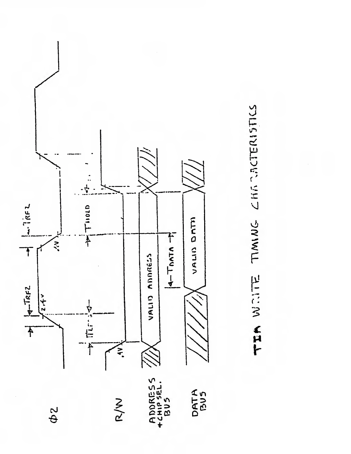
1, Data and addressinc
Aecisters on this chip are addressed by the micro-
processor as part of its overall RAM-ROM iaeDor%* space.
The attached taJDle of read-write addresses svinMri^es
the addressable functions. There are no registers
that are both read and write. Some addresses how-
ever are both read and write, with write data 50ing
into one register and read data returning fron a
different register.
If the read-write line is low, the data bits indicated
in this table will be written into the addressed
write locotion when the^2 clock goes from high to
lew. Soae registers arc eight bits wide, sose only
one bit, ar some (strobes) have no bits, perforitdng
only control functions (such as resets) when their
address is written.
If the read-write line is high, the addressed location
can be read by the niicroprocessor on data lines 6and
7while the<t2* clock is high.
The addresses given in the table refer only tc the
six (6) real address lines. If any of the four (4)
chip select lines a.re used for addressinc,
the addresses aust be stoaified accordingly.
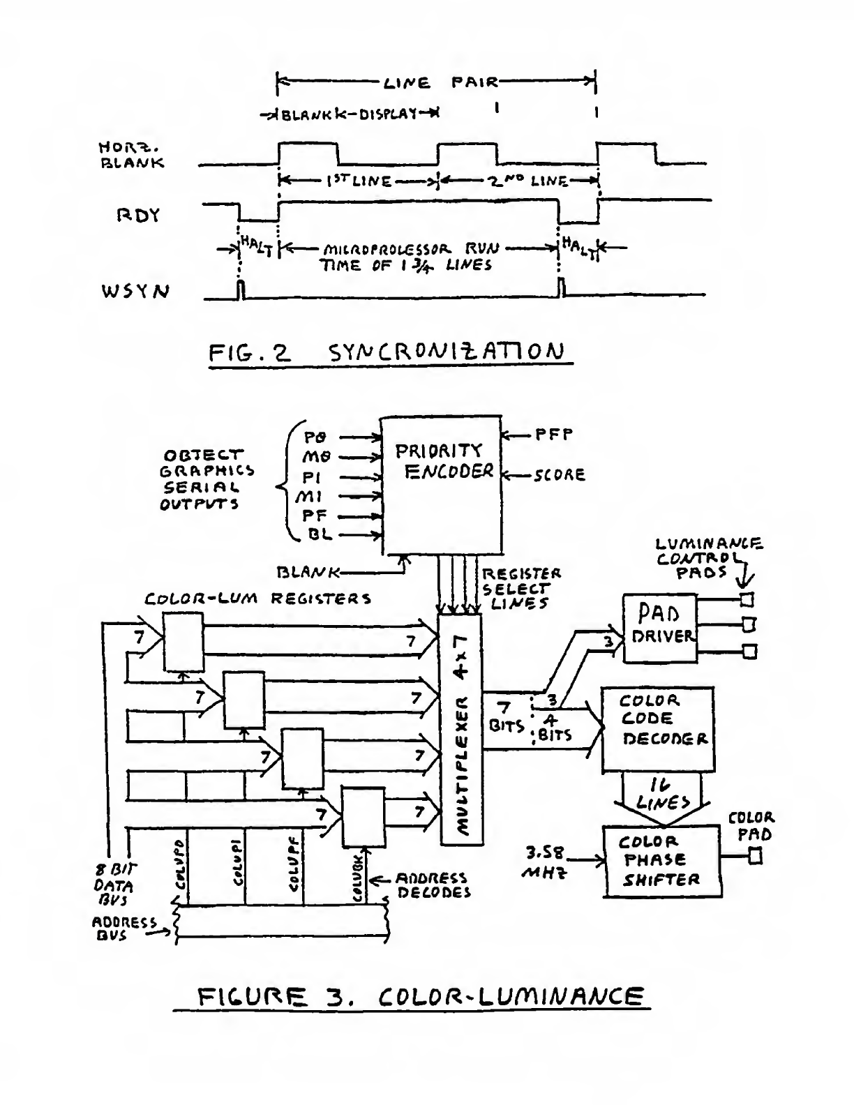
Syncronization
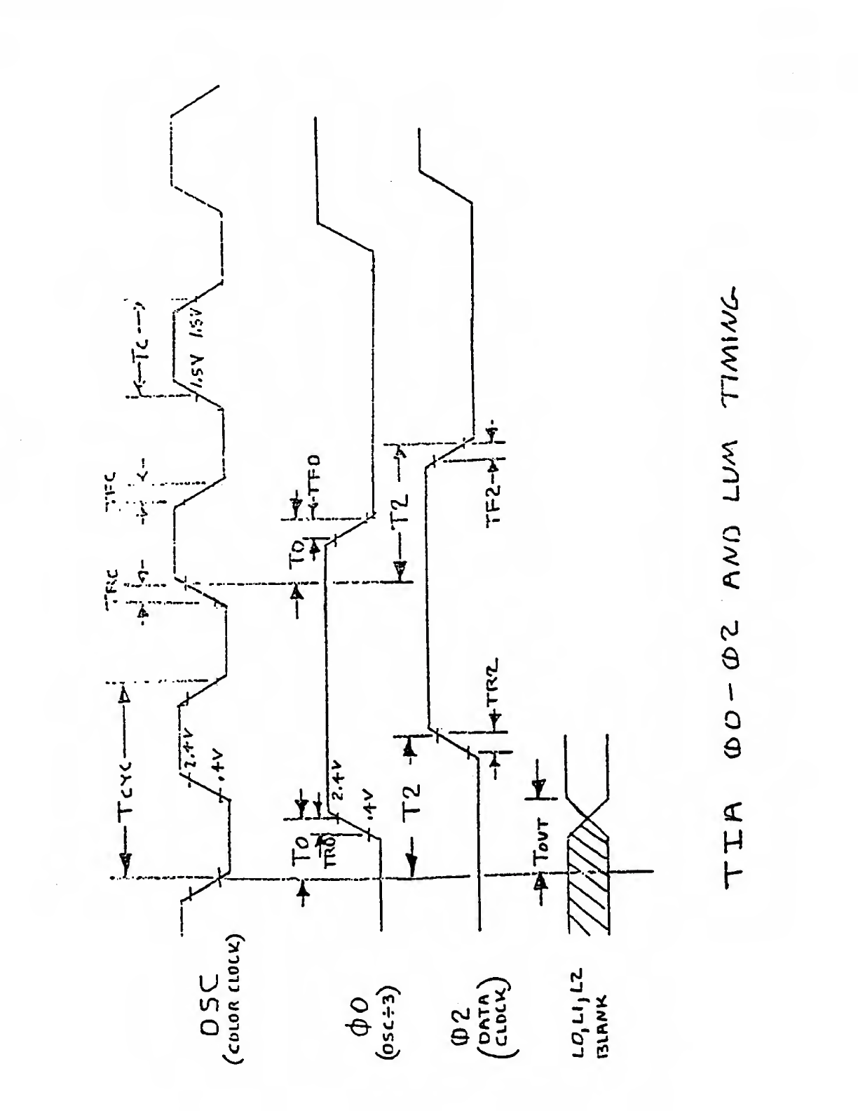
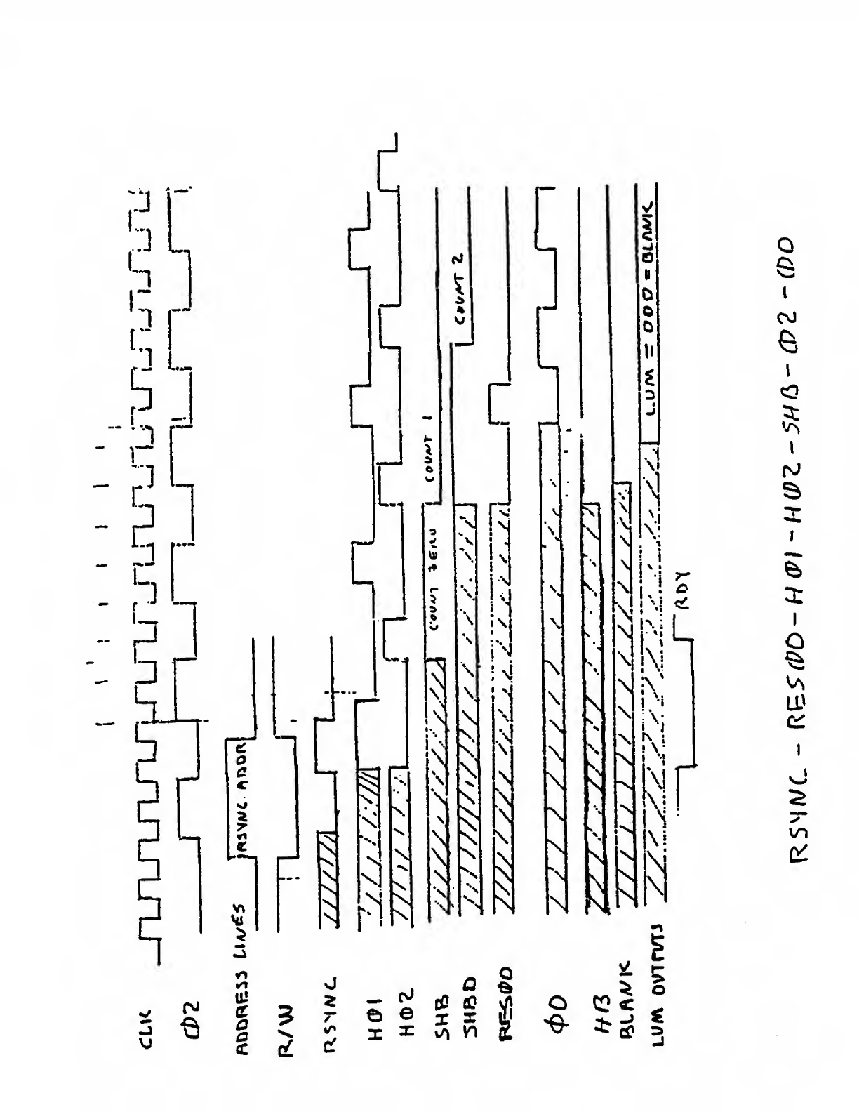
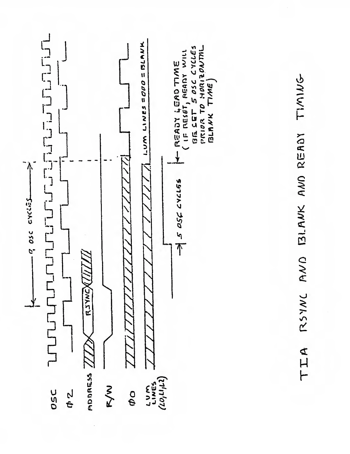
A. Eori2ontal Tixing
Ahardware cour*ter on this chip produces all )jori-
zontal tiri ng (such as sync, blanK, burst) indepen-
dent of the microprocessor. This counter is 4riv€ih«
from a^ external 3.58 MHZ oscillator and has a
total co\ant of 228, Blank is decoded as 68 counts
and sync and color burst as 16 counts.
B. Vertical Timing
There are one bit, addressable registers on this
chip for vertical sync and vertical blanK. The
timing for these functions is established by
the microprocessor by writing zero or one into
these bits. (VSYNC, VBLANK)
C. Composite Syne
Borizontal sync and the output of the vertical
sync bit are combined together to produce com-
posite sync. This composite sync signal drives
achip output pad to an external composite video
resistor network*
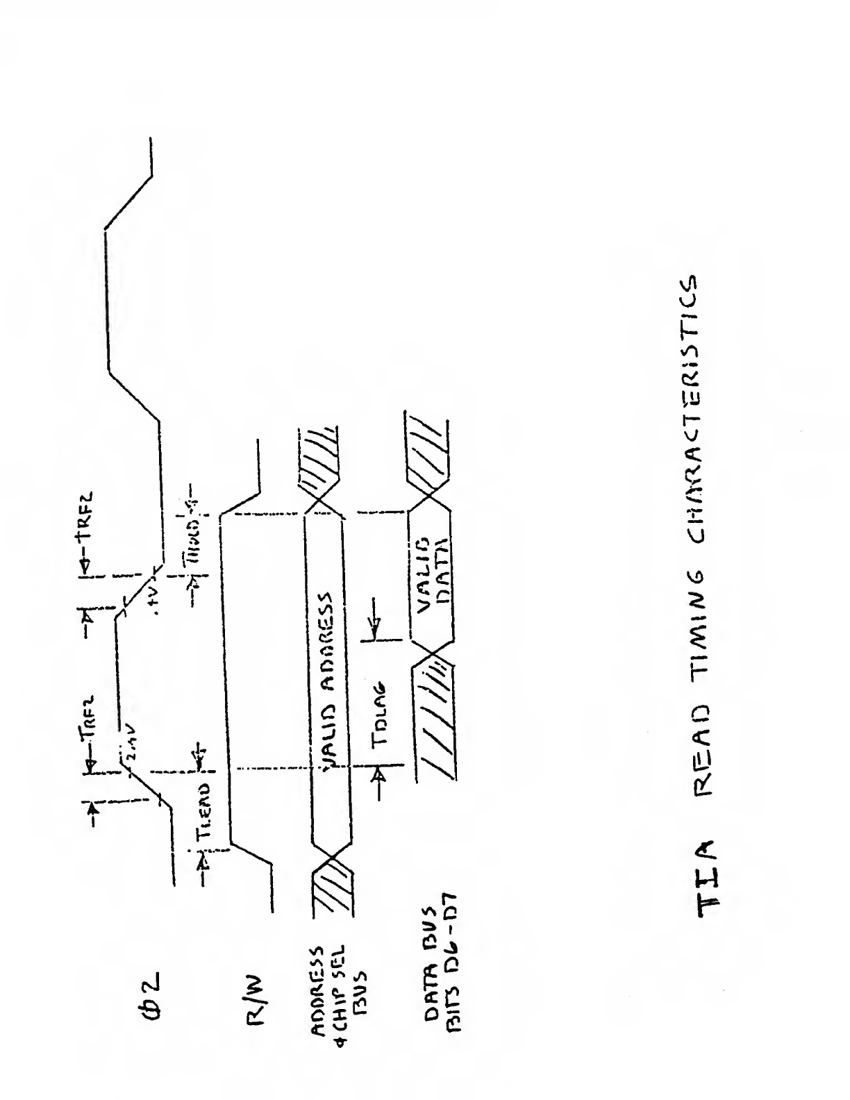
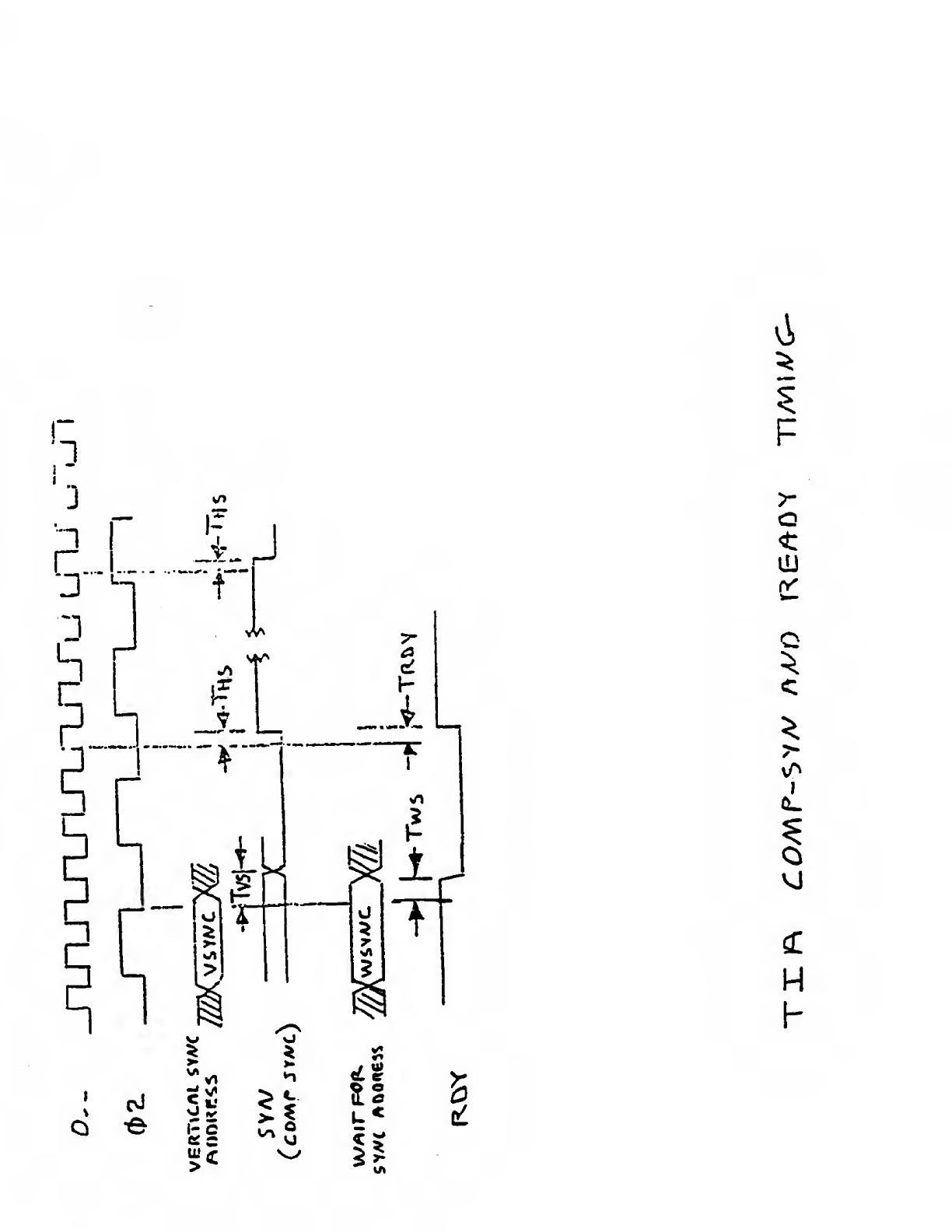
D. Microprocessor Synchronization
The. 3. 58 MHZ oscillator also clocks adivide by
three counter on this chip whose output (1.X9 MHZ)
is buffered to drive an output pad called iO*
This pad provides the input phase zero clock to
the microprocessor which then produces the system CZ
clock (1.19 MHZ).
Software pvogra:n loops require different lengths
of time to run depending on branch decisions
made within the prograa\. Additional synchronization
(Shown in Figure 2) is, therefore, required be-
tween the software and hardware. This is done
with Aone bit latch called KSTOC (wait for sync).
Khen the microprocessor finishes aroutine such
as loadino regii?ters for ahorizontal line, or
comouting'new'vertical locations during vertical
blank, it cAn address WSYNC, setting this latch
high. When- this latch is high, it drives an
output pad to zero connected to the nicroprocessor
ready line (KDY) .Azero on this line causes
the microprocessor to halt and wait. As shown in
ficure 2jWSYNC latch is autoir^tically resez to zero
by'the leading edge of the next horizontal blank
tiining signal, releasing the ?i>y line, allowing
the microprocessor to begin its conput&tior. and
register writing for this horizontal television
line or line pair.
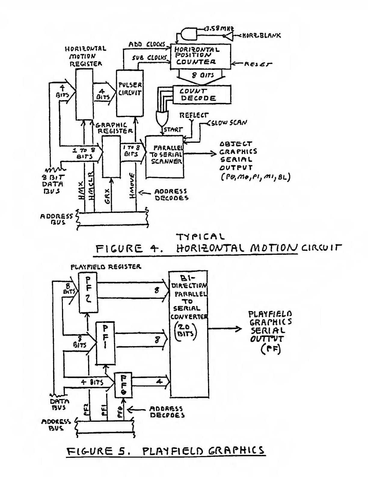
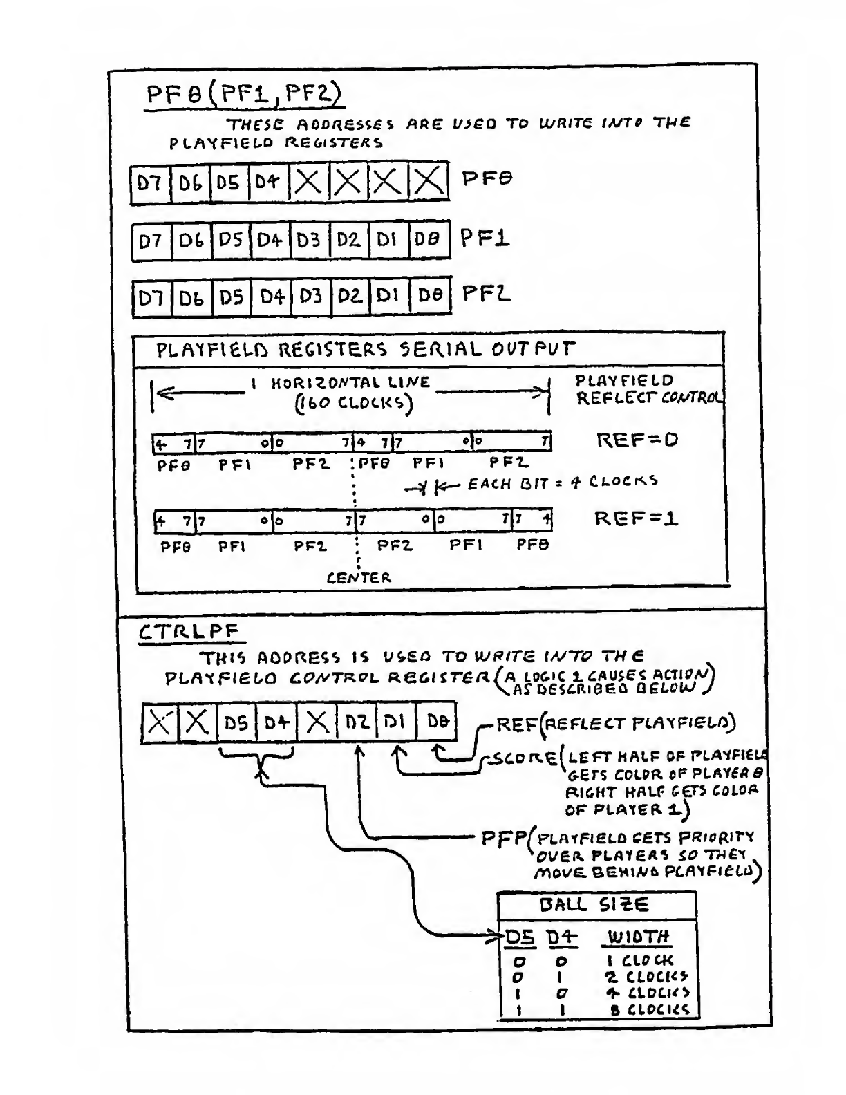
vfield crachics Register
Description
Objects, (such as walls, clouds, and score) which
are not recuired to move, are written into a20
bit register called the playfield register. This
reoister (Figure 5) is loaded from the data bus
bv'three separate write addresses (PFO, PFl, PF2)
.
Playfield may be loaded at any time. To clear
the playfield, zeros must be written into all
three addresses.
Normal Serial Output
The playfield reoister is automatically scanned
(and converted to serial output) by abi-direct- _
ional shift register clocked at arate which spreacs
the twenty (20) bits out over the left half of
ahorizontal line. This scanning is initiated
by the end of horizontal blank (left edge of tele-
vision screen) .Normally the same scan is then
repeated, duplicating the same twenty (20) bit
sequence over the right half of the horizontal
line.
Reflected Serial. Output
Arelected playfield may be requested by writing
aone into bit zero of the playf ield control re-
gister (CTRLPF) •When this bit is true the
scanning shift register will scan the opposite
direction during the right half of the hori-
zontal line, reversing the twenty (20) bit sequence.
p. Timing Constraints
tven though the playfield bytes (PFO, PFl, PF2)
&ay be written at any tiae, if one of then is
changed while being serially scanned, part of
the new value nay both show up on the television
horizontal line.
4•Eojrizon tal Position Counters
•D_e_scription
The plavfield is a'fijced* t./aphics register,
always starting its serial output when triggered
by the becinning of each television line.
This chip'also includes five "moveable" graphics
recisters, whose serial outputs are triggered
by' five separate horizontal position counters
every tice these coiinters pass through zero
count* These position counters «re clocXed
continuously during the unblanke portion of
every horizontal line and their counr length
is exactly ecual to the normal nusiber of clocks
supplied to the-n during this tisve. They will
therefore pass throxigh zero at the sane time
du ing each horizontal television line and the
triogered outputs will have no horizontal
motion. Atypical horizontal counter is shown
in ficure 4.
If extra clocks are supplied to these counters
(or normal clocks s'orpressed) the zero crossing
time will shift and he object will have moved
left (extra clocks) or right (fewer Clocks)
*
Sor.e position counters have extra decodes
(in addition to azero decode) to trigger multiple
copies of the same object across ahorizontal
line*
All position counters can be reset to zero count
by the microprocessor at any tijne, by awrite
instruction to the reset addresses (RESBL, RESMO,
RESHl, RESPOr RESPl) .If reset occurs during
horizontal blank, the object will appear at
the left side of the televisioa screea^. Pro-
perly timed resets may position an object,
at any horizontal location consistent with the
microprocessor cycle time*
B:. .r.Ball Position Counter
The ball position counter has only the zero
crossing decode and therefore cannot trigcer
multiple copies o£ the ball graphics.
C* Play erPosition Counters
Each player position counter has three decodes
in addition to the zero crossing decode. Th*se
decodes are controlled by bits 0,1,2 of the
rainher size control registers (NUSIZO, KU5I21) ,
and trigger 1,2, or 3copies of the player
{at various spacings) across ahorizontal line
as shown on page "^O .These sasie control bits
are used for the Hecodes on the aissile position
counter, insuring an equal number of players
and cissiles.
D. 'Missije Position Counters
Missile position counters are identical to
player positon counters except that they have
another* type of reset in addition to the pre-
viously discussed horizontal position reset.
These extra reset addresses RESHPl)
write data bit 1into aone bit register vbose
output is used to position the missile (horizon-
tally) directly on top of its corresponding
player, and to disable the missile serial out-
put.
£, Horizontal Motion Recisters
A. General Description
There sure five write only registers on this
chip that contain the horizontal motion values
for each of the five moving objects. Atypical
horizontal motion register is shewn in figure
4. .The data bus (bits4 through? )is written
into these addresses (KMPO, HKPl, HMMO,
Hml, HMBL) to load these registers with motion
values. These registers supply extra (or
fewer) clocks to the horizontal position counters
only when commanded to do so by an HMOVZ
address from the microprocessor. These re-
gisters cay all be cleared to zero (no mc.ionl
sijaultaneously by an HMCLR command
from the microprocessor, or individually by
loading zeros into each register*
These registers are each foxir bits in length
and may be loaded with positive (left notion)
,
negative (right motion) or zero (no motion)
values. Negative values are represented
in twos complement format.
D. Tij .Lng Constraints
These registers nay be loaded or cleared atalxaost
any tine. The ro.Dtion. values they contain will
be used only when aji EHOVT conixand is addressed,
£md then all five notion values will be used
simultaneously into all five horizontal position
counters once* The only tixcdng constraint on
this operation involves the EHOVE conniand.
The EKOVE cotocand must be located in the nicro-
processor progr^.'a imcdiately after await
for sync (WSYKC) cor^sand. This insures that
the EHOVE operation begins at the leading edge
of horizont9».l blainJ:, stnd has the full blaiiX
tine to supply extra or fever clocks to the
horizontal* position counters* Ibese reglsttrs should
not bt aodifled for at least 26 CoLiputer cycles after the
^* HovingObjectGraphi cs Registers EH?ve cotriar*d.
A. General Descript ion
There are five graphics registers for noving
objects on this chip. These graphics registers
are loaded (written) in parallel by the niicro-
processor and like the playfield register
are scanned and converted to serial output,
CnliXe the playfield register, which is always
scanned beginning at the left side of each hori-
zontal line, moving object graphics registers
are scanned only when triggered by astart
decode fron their horizontal position counter.
Atyoical craohics register is shows in figure
4
'
B. Missile Graphics
The graphics registers for both nissiles are
identical and very simple. They each consist
of aone bit register called nissile enable
(EKAMOi ENAMI) .This graphics bit is scanned
(outputed) only when triggered by its corre-
sponding position counter. There are control
bits (bits AfS, of NUSIZO, KUSI21) that can
stretch this single graphics bit out over
widths of 1, 2, 4, or 8clocks of horizontal
line tine. (A full line is 160 clocks!
.
C. Player Graphics
The graphics registers for both players are
identical and are rather conplex. They each
consist of eight bit parallel, registers (GRPO,
GRPl) and abi-directional parallel to serial
scan coujiter that converts the parallel data
into serial output.
Aone bit control register (RZFPO, KEFPl) ce-
terniines the direction (reflection) of the
parallel to serial scan, outputicg either
D7 throuch DO, or DO through D7, This allows
reflection (horizontal flipping) of player
serial graphics data without having to flip
tl^e microprocessor data.
The clocJc into the scan counter caii be controlled
(three bits of KUSIZO and NUSIZl) to slow
the scan rate and stretch the eight bits of
serial Graphics out over widths of 5, 16,
or 32 clocks of horizontal line time* These
sajse control bits are used in the player-^
missile motion counters to control multiple
copies, so only three player widths (scan
rates) are available.
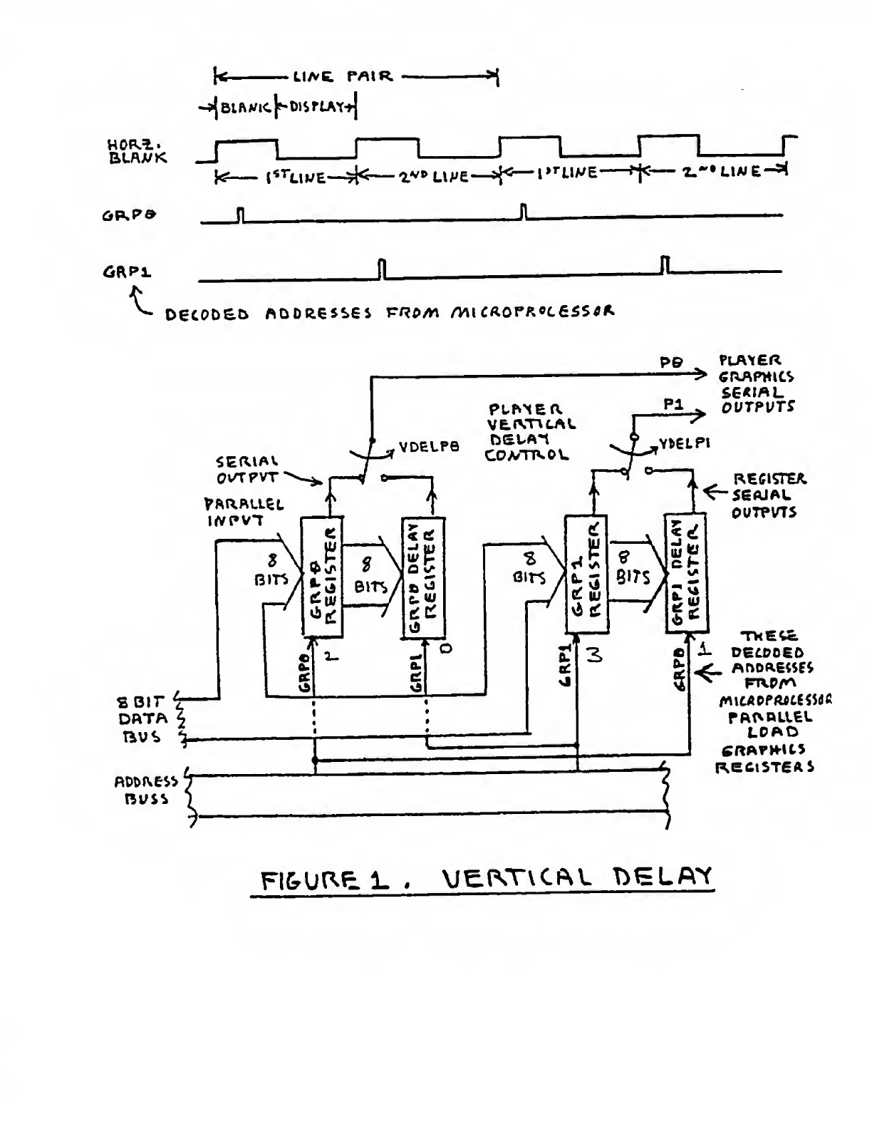
Vertical Delav ,
Each of the player graphics registers actually
consists of two 8bit .pjiraliel registers.
The first (GRPO, GRPl) is loaded (written)
fron the microprocessor 8bit data bus. The
second is autoinatically loaded from the cut-
out of the first. The reason for this is a
complex subject called vertical delay.
Alarge aioount of microprocessor tiae is re*
quired to generate player, missile and play-
field graphics (table look up, mas)cing,
con;parisons,-ect.) and load these into this
chip's registers. For most game programs this
tijoe is just too lajrge to fit into one horizontal
line time. In fact for most games it will
barely fit into two line times (127 microseconds)
.
Therefore, individual graphics registers are
loaded (written) every two lines, arid used
twice for serial output between loads.
This type of programming will obviously licit
the vertical height resolution of objects
to multiples of two lines. It also will
limit the resolution of vertical motion to
two lines jumps.
Nothing can be done about the vertical
heioht resolution; however, vertical motion
can'be resolved to asingle line by addition
of asecond graphics register that is auto-
matically parallel loaded from the output
of the first, one line time after the first
was loaded from the data bus. This second graphics
reoister output is therefore always delayed
vertically by one line. Acontrol bit called
vertical delay (VDELO, VDELl) selects which
of these two registers is to be used for
serial output. If this control bit is set
by the microprocessor between picture franes
the object will be moved ^dcvn (delayed) by
one line ouxinc the next frame.
In most prograjrming applications player
graphics and player 1graphics are loaded
(written) alternately, during the blanX time
just prior to each line as shown in (figure 1)
.
Since GPJ^O and GHPl addresses from the micro-
processor alternate, they are delayed by
one line from each other. The GRPO address
decode can therefore be used to load the de-
layed graphics register for player 1, and
GRPl likewise to load the delayed graphics
register for player 0. The two vertical de-
lay bats (VDELO, VBELl) then select delayed
or'undelayed registers for player ana
player 1as serial outputs,
^•Ball Graphics
The ball graphics register is almost identical
to the r;issiie graphics register. It also
consist?, of asingle enable bit (EJiASL) whose
output is triggered by the ball position counter.
It also has two control bits (bits 4, 5of
CTRLPF) that can stretch this single graphics
bit out over widths of 1, 2, 4, or 8clocks
of horizontal line time.
Unlike the missile graphics, however, the
ball graphics register has capability for
vertical delay similar to the player graphics,
Asecond graphics (enable) bit is alternately
loaded from the output of the first, one
line after the first was loaded from the data
bus. Aball vertical delay bit {VDZLBD se-
lects which of these two graphics bits is
used for the ball serial output. The first
graphics bit (ENABL) should be loaded during the
sane horizontal blank tiroe as player. (GRPO), be
cause GrlPl is used to* load the second enable
bit from the output of the first on alternate
lines.
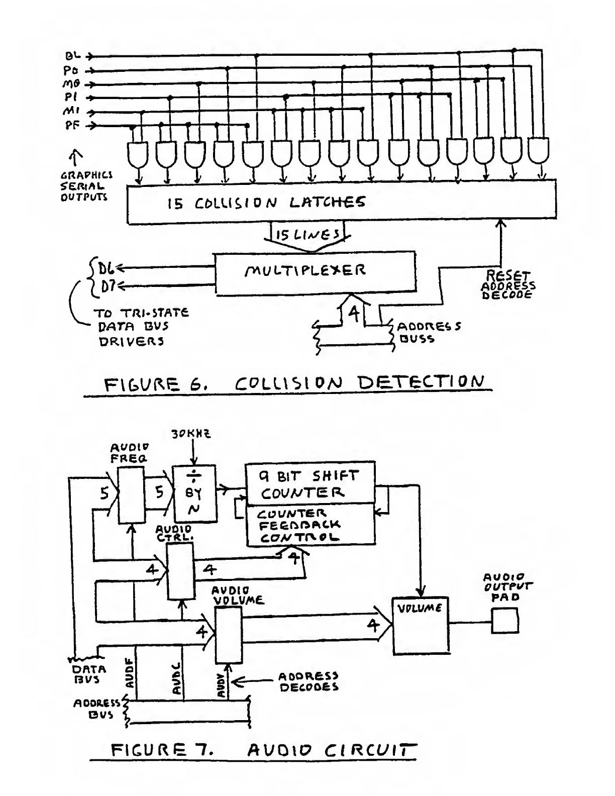
7*Collision Detection I/at'ches
A. Definitions
The serial outputs from all the graphics re-
gisters represent real time horizontal location
of objects on the television screen. ^If any
of these outputs occur at the same time,
they vill overlap (colHde) on the screen. There are six objects
generated on this chip -'five noving and playfield ellowing
fifteen possible tvo object collisions. These overlaps (collisions)
are detected by fifteen "and" gates whenever they occur, aftd
are stored in fifteen individual latch register bits, as shown in figur
£.
E•^e.^din'oCollision:-
The laicroprocessor can read these fifteen collision bits on
d^ta lines 6and 7by addressing the:n tvo at atime. This
could be done at any time but is usually done between frames
{curing vertical blank) after all possible collisions have serially
occured.
C. Reset
All collision bits are reset simultaneously by the microprocessor
using the reset address CXCLR. This is usually done near the
end of vertical blsnW, after collisions have been tested.
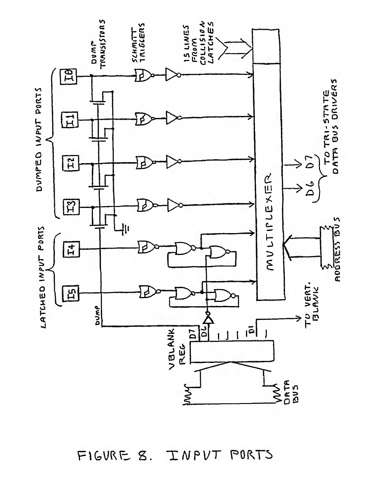
Input ports
A. General Description
There are 6input ports on this chip whose logic state r.ay be
read on data line 7with read addresses INPTO through 1NPT5.
These 6ports are divided into two types, "dumped" and ''latched'
.
See figure 6.
B, DurToed Input Ports '.10 through 13)
Thes- ii input ports are normally used to read paddle position from
an external potentiometer-capacitor circuit. In order to discharge
these capacitors each of these input ports has alarge transistor,
vhich may be turned on grounding the input ports) by writing into
bit 7of the register VBLAS'K. Vhen this control bit is cleared the
potentimeters begin to recharge the capacitors and the microprocessor
measures the time requirfed to detect alogic 1at each input por^.
long as bit 7of register VBLASX is zero, these four ports
are general purpose high inpedance input ports. When this bit is a
1these ports are grounded.
C. Latched Input ports (14, 15)
These two input ports have latches which can be enabled or disabled
by writing into bit 6of register VBLAKK.
When disabled, these latches are removed from the circuit coropletly
and these ports become two general purpose input ports, whose
present logic state can be read directly by the microprocessor.
When enabled, these latches will store negative zero logic level)
signals appearing on these tvo input ports, and the input por^
addresses will read the latches instead of the input ports.
latched Input Ports (lA, 15) *continued
Vhen first enabled these latches vill remain positive as
long as the input ports remain positive (logic one;. A
zero input port signal vill clear alatch value to zero,
where it vill remsin (even after the port returns positive 5
until disabled. Both latches cay be sirultaneously
disabled by writing azero into bit $of register VBLANK.
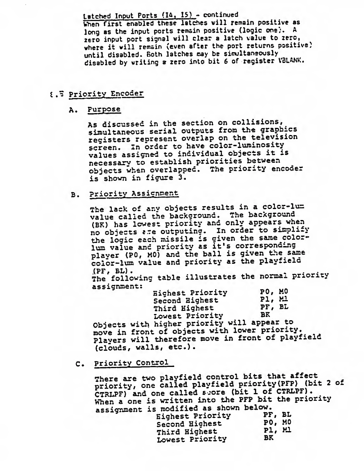
iPriority Encoder
A. Purpose
As discussed in the section on collisions,
simultaneous serial outputs from the graphics
registers reoresent overlap on the television
screen. In order to have color-luminosity
values assigned to individual objects it is
necessarv ro establish priorities between
objects when overlapped. The priority encoder
is shown in figure 3*
B. Priority Assicnnent
The lack of any objects results in acolor-lu=
value called the backorounc. The background
(BK) has lowest priority and only appears when
no objects e.re outputing. In order to sinpli^y
the logic each missile is given the sane color-
luB value and priority as it's corresponding
plaver (PO, MO) and the ball is given the sane
color-lum value and priority as the playfield
(PF /BXi) .
The 'following table illustrates the normal priority
assignment: ^«
Hichest Priority PO, KO
Second Highest Pl# Ml
Third Highest PF, BL
Lowest Priority BK
Objects with higher priority will appear to
move in front of objects with lower priority.
Players will therefore move in front of playfielc
(clouds, walls, etc.).
C, priority Control
There are two playfield control bits that affect
priority, one called playfield priority (PFP) (bit 2o*
CTRLPF) and one called s.:ore (bit 1of CTBLPF)
.
When aone is written into the PFP bit the priority
assignment is modified as shown below.
Highest Priority PF, BL
Second Hiohest PO, MO
Third Highest Pi/ Ml
Lowest Priority BK
Players will then move behind playfield (clouds
i
vail Ietc.)
.
When aone is written into the score control
bit, the playfield is forced to take the color-
lura of player in the left half of the screen
and player 1in the right half of the screen.
This is* used when displaying score and identifi-es
the score with the correct player.
The prioritv enco der produces 4register select
lines (shown in figure 3) that arc mutnally
exclusive. These 4lines select either bach-
groxind, p' ayer 0, player 1or playfield, and
only one' of" them can be true at atime.
5•Co1oLumin^.r.ce l^egisters
A,Description
There are four registers (shown in figure 3) that
contain color-lum codes* Tour bits of color
code and three bits of luainance code may be
written into each of these registers (COLUPO,
COL0P1, COLUPF, COLUBK> by the microprocessor
at any tirse. These co!es (representing 16 color
values and 8luminance values) are given in
the Detailed Address List.
3. Multiplexing
The serial graphics output from all six objects
is examined by" the priority encoder which
activates one of the four select lines into
a4X7multiplexer. This multiplexer (shown
in figure 3) then selects one of the four color
luE registers as a7line output. Three
of these lines are binary coded luminosity and
go directly to chip output pads. The other
four lines go to the color phase shifter.
10. Color Phase Shifter
This portion of the chip (shown in figure 3) produces
areference color output (color burst) during hori-
zontal hl&Tik and then during the unblanked portion
of the line it produces acolor output shifted
in phase with respect to the color burst.- The
The amount of phase shift determines the color and
is selected by the four color code lines from the
Color-lum multiplexer. Binary code selects no
color. Code 1selects gold (same phase as color
burst) .Codes 2(0010) through 15 (1111) shift
the phase from zero through almost 360 degrees
allowing selection of 15 total colors around the
television color wheel.
Ay Uo.\Circuits
Two audio circuits are incorporated on this chip*
Thev are identical and completely independent, al-
though their outputs could be combined externally
into one speaker. Each audio circuit consists of
parts described below, and in figure 7.
A. Frecuency Select
Clock pulses (at apprcy.iffiately 30 KHZJ fron
the horizontal sync coxinter pass through a
•divide by N" circuit which is controlled
bv the output code from afive bit frequency
register (AUDF) .This register can be loaded
(written) by the rucroprocessor at any tiae,
and causes the 30 KHZ clocks to be divided
bv 1(code 00000) through 32. (code 11111)
.
This produces pulses that are digitally ad-
justable froa approxinately 30 KHZ to 1KE2
and are used to clock the noise- tone generator.
B. Noise-Tone Generator
This circuit contains anine bit shift counter
which nay be controlled by the ouput code frczi
afour bit audio control register (AUDC)
,
and is clocked by the frequency select circuit.
The control register can be loaded by the mcro-
processor at any time, and selects different
shift counter feedback taps and count lengths
to produce avariety of noise and tone qualities.
C. Voluce Select
The shift counter ouput is used to drive the
audio output pad through four driver transistors
that graduated in size. Each transistor
is twice as large as the previous one and
is enabled by one bit frora the audio volune
register (AUDV) .This audio volume register^
nay be loaded by the microprocessor at any tine.
As binary codes through 15 are loaded, the
pad drive transistors are enabled in abinary
sequence. The shift counter output therefore
can pull down on the audio ouput pad with 16
selectable impedance levels.
JnJL
JL
JLr
1A
0UTPVT5
J1IL
Ho^-^. I\t'\r
RLAWK
i»"*'uv£ —-z-"* uwn—^
Li
;TIME OF 13/^ UMe& :
'*
vjsxN _ji 1! n
FIG. ZSX^CROVliflTTOAJ
LUmilVAVCPs.
i7»
DATA
fkOOtKBSS
5^
u
i
/
X
cot; //Tea
5
REFtecr
TO SERIAL CftAPHICS
£)yTPVT
PlCURt TOPICAL
r
T
_VP
F
I
4- Bits
DPiTA
nv5
P
F
sFABRUEL
TO
SERIAL
FlG-l/Re5. PLAMFieLD GAMmCS
Pi
ourPim
TO Tni*STAT£
RfeSfcT
I—^A0or\e<»5
FBea V
»
J)
CTRL.
qBIT SHIFT
AVDIO
VOLV/^£
1
PAD
FICUtXGl. AUDIO CfRCl/lT*
VI
vj C
-C-
-J oJW
i/\ c; -J
VJ "J
Ii>-{>
IL!
5;°
r
c
(2
tli
c:
a
o
a:
OCD
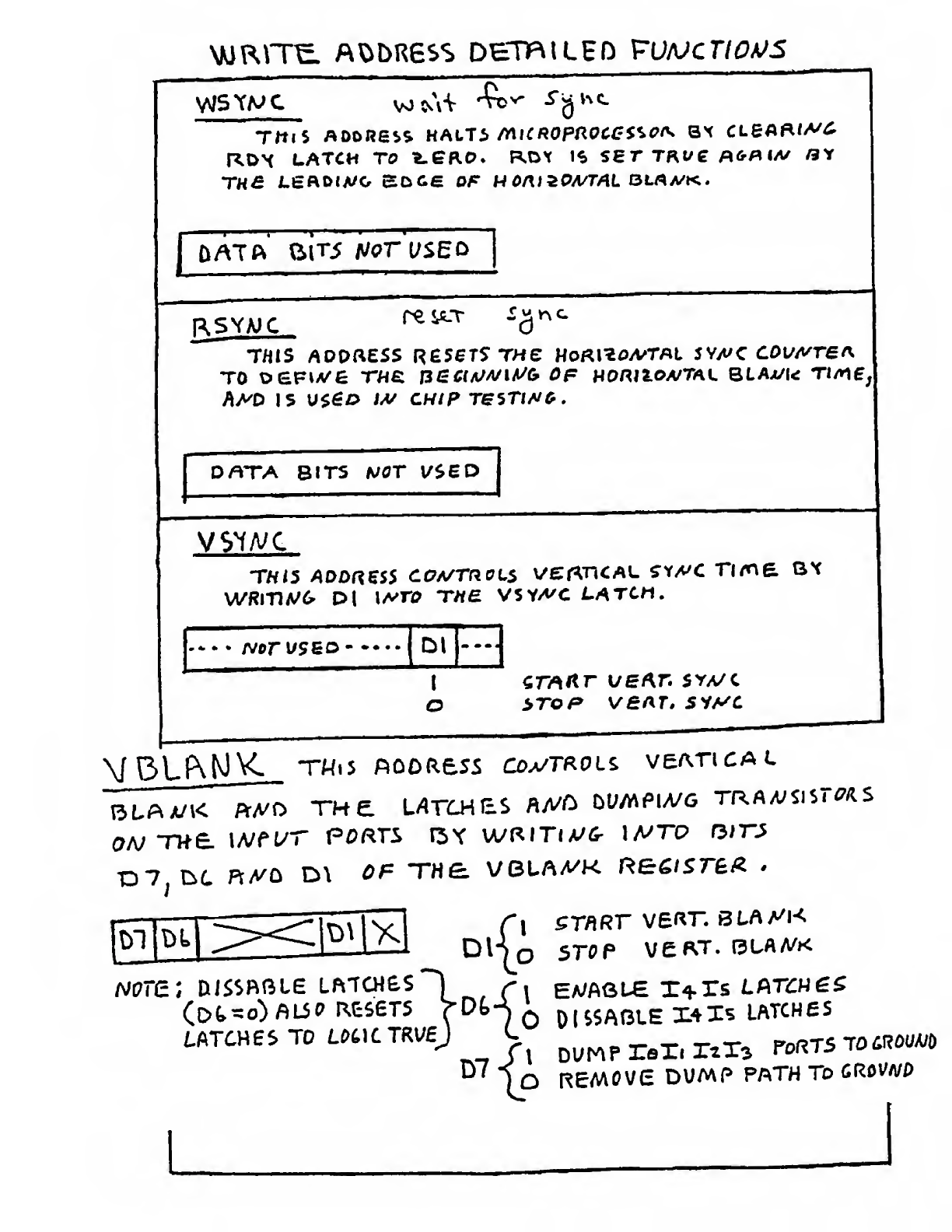
A0DR6SS DHTBILED \^UAJCTIOA^S
KOX LATCH TO Ife-eaO. ROX 16 SET TKl/C /^frflW /3Y
[DAT ft BIT5 A/or USED
T/ilS /^DPftESS Resets THC Hoftl^i)A'TAL 5YyWC COV/vr€A
OaTA BITS A/OT v/seD
VS^A/C
T«i5 >^o0f?ess <:t7A/^rRe7i,5 vetKncAL fftA'C rirae Gx
Dl
I
a>ro/» VfiAn SYA^il
V\3l.(\M\C_ TMiS A00R£5S a>VTRC?LS VEATlCAt
a/v "me. lA/ft/r ports tsy u/t^iTiA/^ lA^rc? oir^
TD7^ DC D\
STflRF VERT. BLAA/K
DHo STOP VCRT. fSLAA/K
/vpre: dissbblg Lft'TCH£S~1 ^, ea/aql^ x+rs latchcs
Cd -o) Ali presets rt>t A^dl^aole X4 is latch e
s
LATCHES TO L«>t.CTRV£j L^^^^^ 3-^^, ^-.^^ PoRT5 TOdWUA/D
IOREMOVE DUMP PATH To CROVWP
I
PFe(PFl,PF2.)
THr5£ aooaes'^a^ flfte u^eo to u/ritc ia/tc rye
D7 05 XXK PF©
D7 Of, PS D4- DS D2. Dl Dd PFi
|di Dt> 05 D4- D3 Dl
i
PFL
PLAtFiei-ri REGISTERS SERIAL OUTPUT
1^ «HOftl^OA'TAl. LIA/E ^1
1"^ gbO CLOCKS)
|V 1|7 o|o 7i* 7|7 •!«> T
•_^ j«— BACH an sfClocks
|4- 7|7 «|£> 7|7 0|0 T7 R\=F=JL
PFe PPi PPi ;PPZ PFI PFe
f
CTR.LPF
TKi^ AOORE^s IS u&eo TO ff/re uyro th£
D5 '3
'Vers COLPR OP PLrtVfA s
OP PLAxeR a.)
DAU- 61
O1^CLOCU>
t1SC10CU<.
^$
Twesf Aoofiess^s cd/jtrol the /yum^BR b/zd
OP FLAY£n$ Bd/O /y?n$/L£5 ^
Dl 09
r
Missile, site
o
t
1I
WIDTH
ICLOCK
4- CLOCKS
01 DQ
ODD
OI
OIO
O1t
IO
rt
IIo
(It
(160 CLOCKS
Hi
81
TWO CCW£S
T\UC COPIES
3coFte^
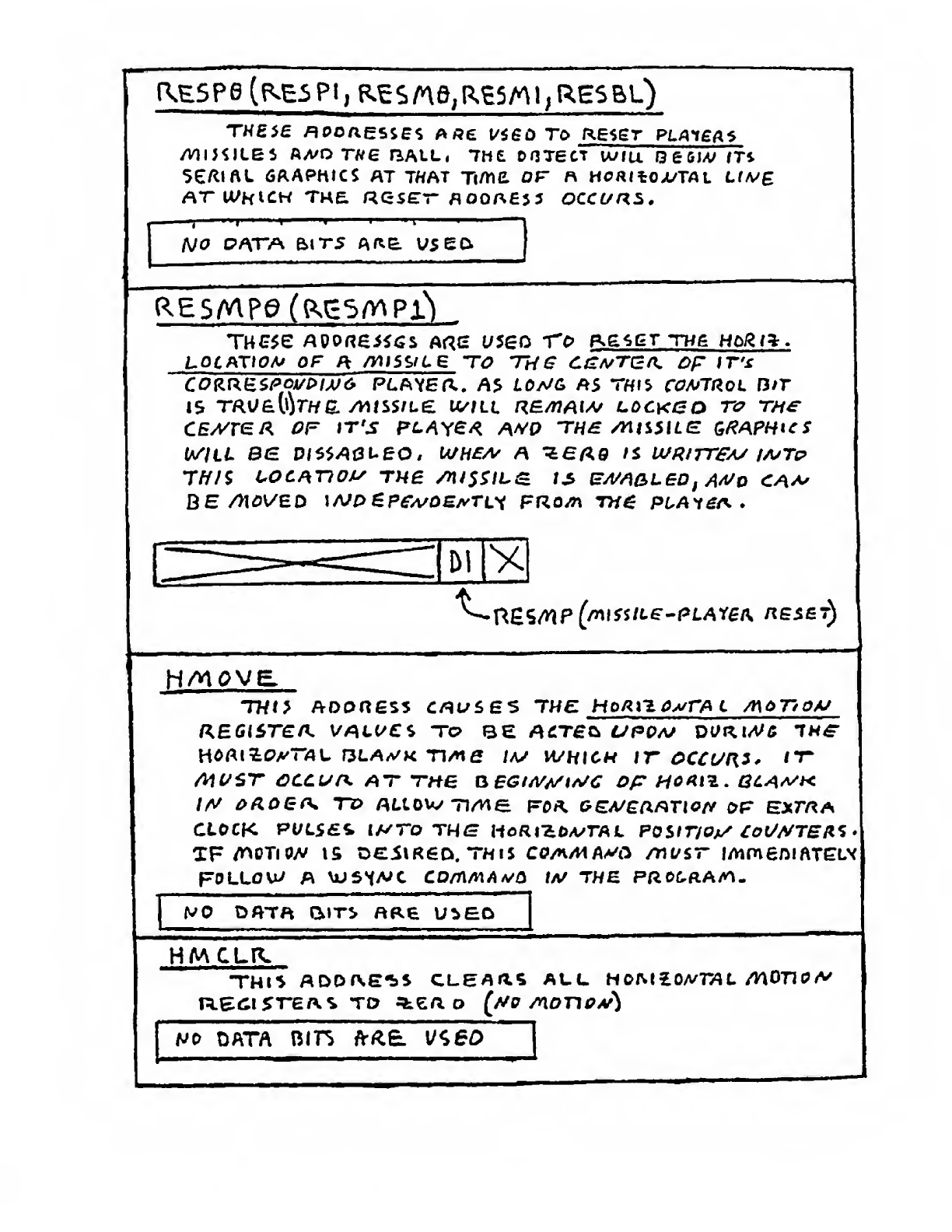
fVES P6(Pi)SA\ 5; Rg5 1;RES BL)
TH£5e flPOAESSes fiRE UiGO TO RE^gT PLA*t£a^
Se/ttftt fiAAPHtCS AT THAT Tl/HC Of RH<?RltOX/TAL Lf/V/g
A/a DATA aiT5 AftE. VSEO.
aESMpa(psgs/Y^pf)
C0RReS/30i/p/>i;<> PLAYED* /V5 /.Oa/G AS T«I5 CO^ltKoL mx
jffn Locanou rue /nis^iL^ e^/^aLeo, a^o ca^
BE /nOVBO \A/PBpeA^OB/^TL^ PROyn TH^ P£.AY£A .
77/i> ADDnes5 c/quses thc Ho/ti^i^^rA c/m^T/qa/
(KEGiSTEiK VfikLUC% TO BE A£T£0 UPOA/ X>\)tKlA^& TH^
CCCUfK AT THE aeCiA^Mt/^C OP HO^t^> QCA^^
//V TO AUowTi/ne ocA/ea/^rio// op extra
CLOCK PUCS£4 l//ro TH^ iicRt-^OA/TAL FOStTiOjj^ Coi/ATTEH^ *
XF A^OTlOiV 15 OCStRGD. THIS CO/KM(KMa musT lAimenfatCLx
FOLLOW AX4J5^A»C CDMAl/lvO WTHE PROC^ftAA^-
DATa aiTi ARE U>£0
HMCLR.
THt^ ADOf\e*»S CLEAaS ALL HOt^X^ONTAL /Y\OT\0
VL^c\%T^K% TO o(//p /norip^vi
fjo DATA Rtn fr^E y^eD
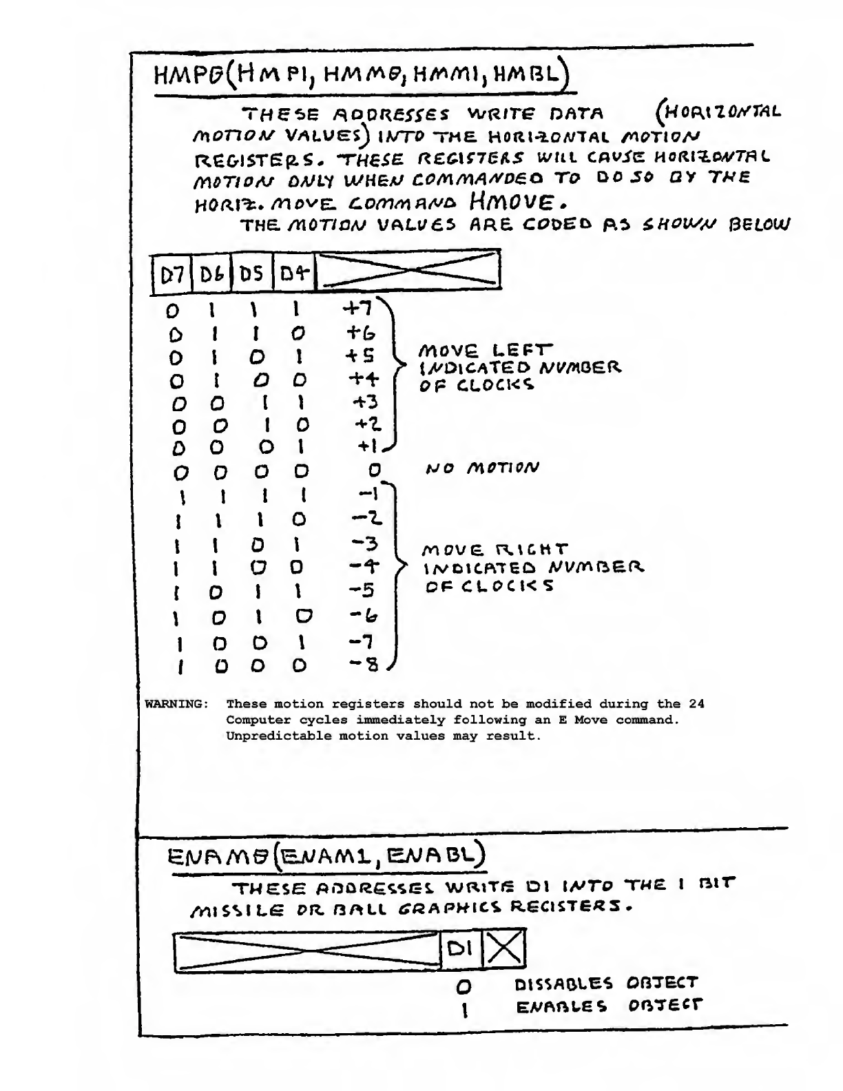
HMP(?(H/v\Pl, HMAVgj HAWAI I) HMBl)
moTiOA/ Q/JVi WHajJ co/AmA/^oea to ooso ay TA/e
THa/MOT/XSA/ VALl/dS ARE C£7Deo f:^^* ^HOl^A/ BBLCUJ
D7
-1
DS
u1
1I
11
1I
t
I
f
1
I^MOVE LEPT"
n
wDp CLOCK*;
nnIt
t
nO11
DI+1
J
oo
\1!1
1II
II\AlOVG. n.\CMT
11o
r11-5 OP CUOCK S
o»o-i?
1oDI-T
1O o -3 J
WARNING: These motion registers should not be modified during the 24
Computer cycles immediately following an EMove command.
Unpredictable motion values may result.
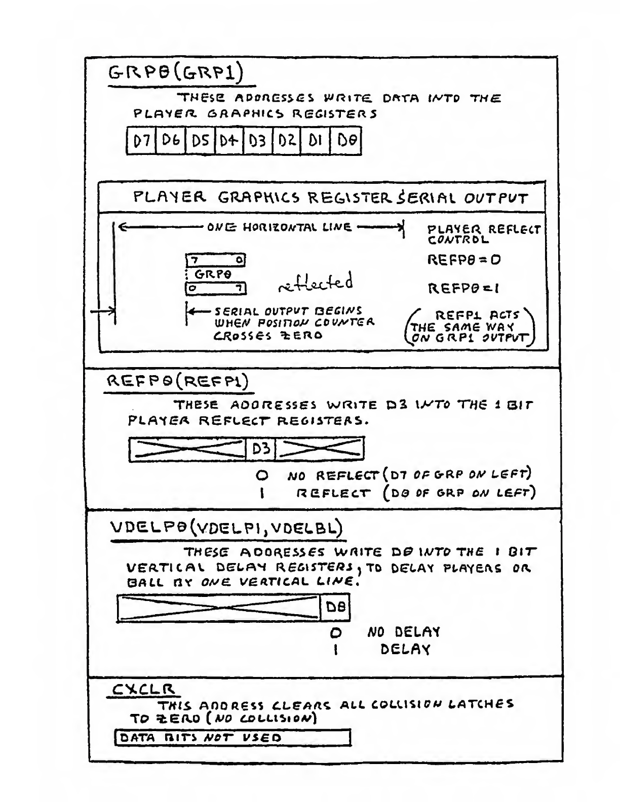
THese ^\oon(is^a% wntre. d^ta tA^ro ths
Pt-Rvea ^sAAPHic*> R.e{;i5Tef^5
07 Ob DS t)4- Ii3 02. b\
PLANER. GRftPUVCS REG\S7ER. ieR\ftL OUTPUT
€OWE HORIZO//TAt. UW6 ——JpLflVEr^ REFLeCT
U
—
sstitnL OUTPUT aeetA/s /ncppi rc7<\
1ttfMe/f po%motJ covATSA /^j^g 5^^e ^^^^ \
THESE Aoorcesses write i>^rc^ ttis iQ)r
OA/0 RCPLeCr (d7 £)P CrRP <?V L^f^r)
VDeLP©(YDELPl,VD6LBL)
NO DELAY
THIS. AOOResS CLPA/l^ ALL COLUSIt?V tATCHfS
IDATA air& /vgT- vsao I
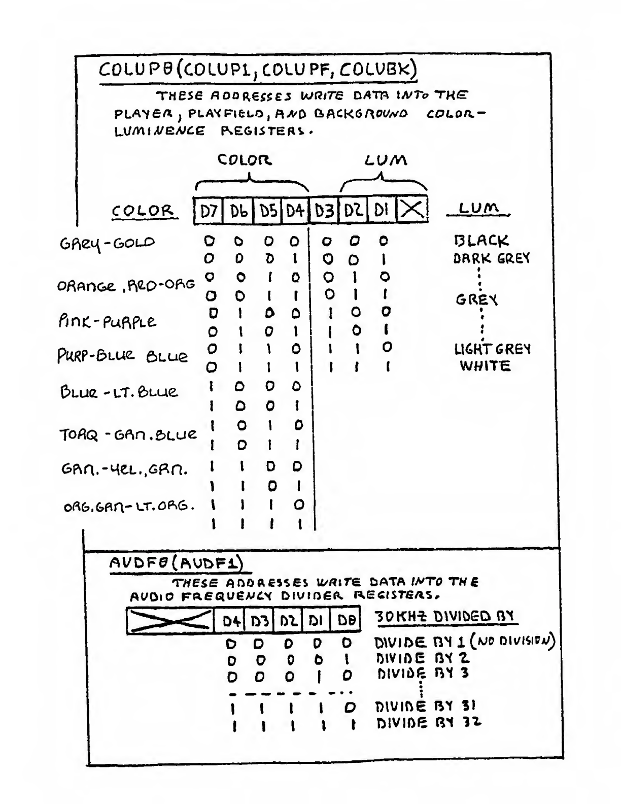
CQLUPg(COLUPljCDLUPF;COLUBk)
These flooa€5$£j lAjQtre dato ia^t^th^
COLOR D7 D4- b3
o
D\\
Q[1o
OIIt1
D1I
I\11
I\1I
1\I1t(
c
I
I
II
ID
\II
I\1
I\ I I
LU/n
I
«
f
WHITE
Twese Anoftessas u/*?ir6 data /A'Tarw^
0^ 0*4 DI
DD
t1
1
1I11o
11I1
DWmE 1(wo DluiMPv)
DlVH>e 3X
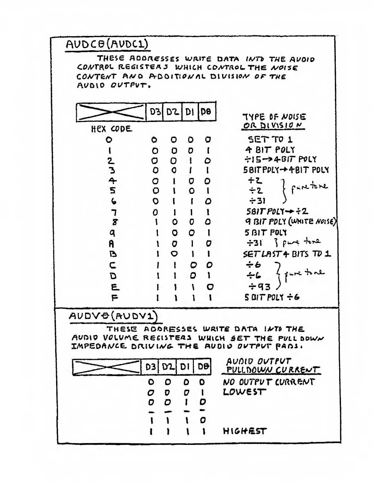
AUDCe(AUDCL)
Twese Aoonesses ujt^tre data /vrt toe auoiq
CO//TROL tL6<>t^T€AJ IVHICH CDA^TAOt. THE A^C?f5C
0^
Hex cof>^
o
I
2.
5
a
lb
c
D
O
O
o
o
o
1
I
\
I
I
I
1
I
o
o
I
I
I
I
o
I
1
\
\
D
I
I
I
I
I
I
o
\
I
o
I
D
I
o
I
o
I
I
I
o
I
o
SET TO i
SBirPPW-^^-BlT POLN
•5-31 )
S£TiJ)ST^ BITS TPi.
THESE AOOKFSSe^ U/RITfi DATA IX^TA THfi.
/^VOtO UV^\£ ReClSTEAi U/UtCH ^ET THS Pt/Lt D0l4/>/
I/HPEOAA/tC DaJUtV^;^ TK6 AUOIO PAOI.
D3 01
tJO 0\)T?VT tVR^^f^T
aC7 I
1
1II
1\I1
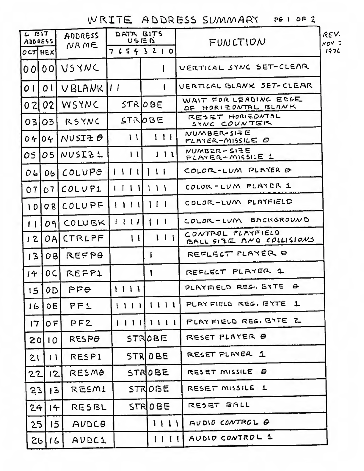
\A/R.ITE Ali DRESS SUMf^AAR^ pc- »c»f a
ADDRESS
OCT HEX
ADDRESS U9r= ri
7CS^i2. i
00 00
IIVBLPlWK //
OZ 02 BE
03 03
0^ b^v 11I
05 05 I\1\I
0(a\ Ob coL\JPe I\fI11
1
07 07 COLUPL 1IM1\\
10 08 COLUPF 1II\II 1
fI01 COLU MM/
/ZOA
|3> OB
CTRLPF IIBFVUL A/^Q COLL\<^\Oy^^
OC
15 OD MM PLPiYPiHuD RHS-. &XTE a-
)(5 OE PF 1MM MM PLH^ P^GlCs ^"^G-* TSYTE a.
17 OF
20l 10
PFZ I11)MIP'LFsY F\euO RES. BtTE 2_
B.^<>eT PLAYER, e
Zl nR£SP1 5TR QBE
^7- \7, STR OBE RESET mvssite B
STR OBE RESer AM<>5IL£ L
Z4 1^ RE5BL SrR OBE
15 15 MM
AUDCl Mil f\vx>\v coA'TRai- a.
U/RHTf AP0RE55 5L^/i14l/^R^ PC- *2. OF Z
IoctIhex 7tS^32. 1
Fu/u ctic?a;
Z7 17 t11M
3^ 12 AUDFl f1IM
3I\^ AUDVO I 1 M
3Z IAftUD VI \\\\
33112,
Gr P.Pi
35 ID
3fc IE
37 \F
^0 20 HmP9 1(11 HOR ^DWTBL m£>rir7/V PL/\Y^fl &
^1 \z\ H/APl hill
^2- ^^
+3 1^
4^ 2-V HM SL 1IH
45 2S VD6LP©
VDELPl
^7 27 VOELRL VEi^-nCftU DEtAX BALL
50 28 AetjET All55aE TD PLPtlEd &
RSSmPi RESET" M^SStUE 1TD FLAYER L
52 2A
S3 2B H/V\CLR 57W0BE
CLEAR CZ?i.HSl£7A/ Z-ATdKE^
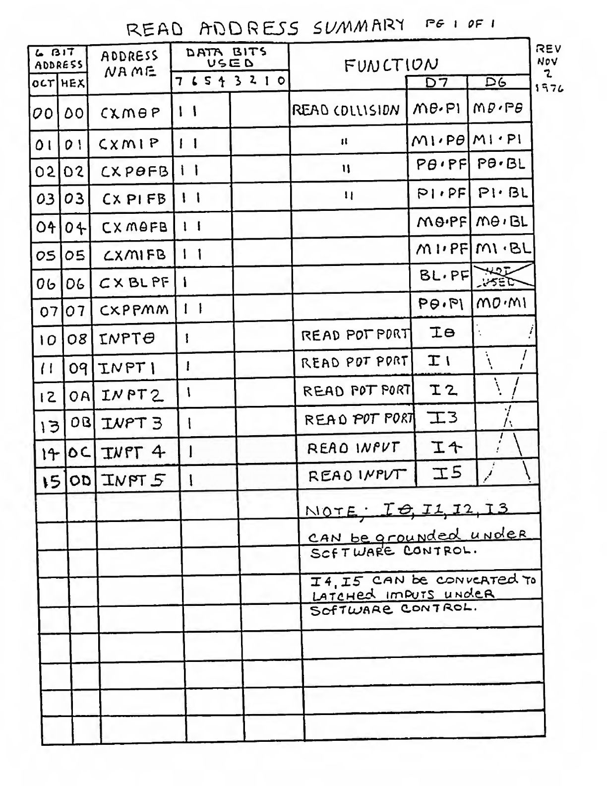
READ BUMMhR'i (=6- iof i
^irt jp Q^
?AC:v: -;.i^ODD-?j^ OGc<<4:
3:i!^"|34^^ 33"" |32'" |3lT mW'jSBl ffrflS^'
Ibah} J7JJ/ii/J-^UJJ IJ-A
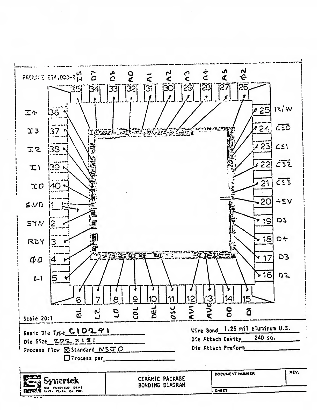
Bisic Die Tvra C> yO^^ \
!Die Si2e_?:PJ3=.?_Ll.i
'Process How ^St anda rd A/ S",0
rpocess per
Wire Sand roil elumlnum U^. S^
Die Attach Cavlt v2^0 SQ-
Die Attich Preform _
j^SiVicrtek CERAMIC PACKAGE
BONDING DIAGRAK
OOCUMEhT NUWtCft REV.
Sheet
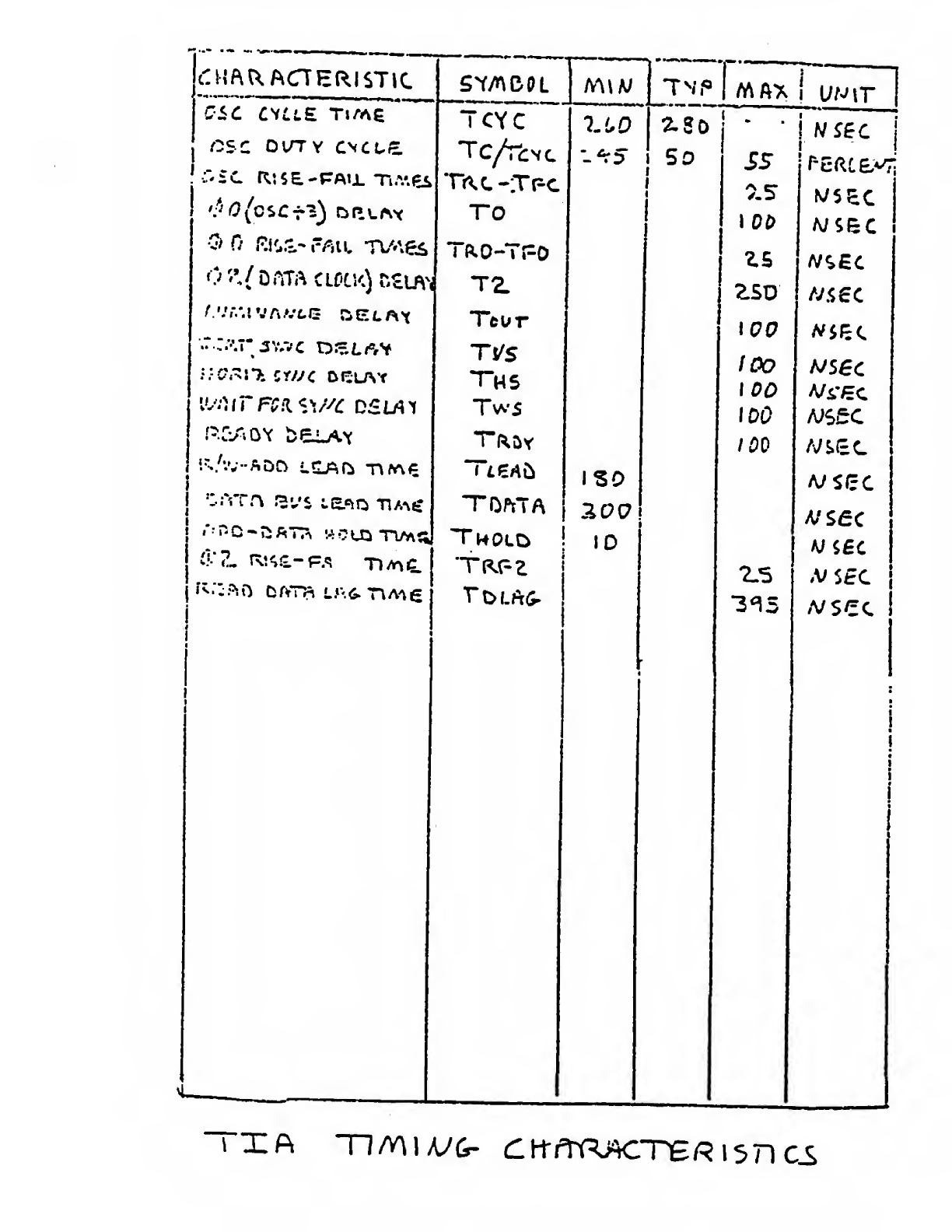
CSC OlTTY CNCte
t> '1/ DnTA CLf'CK) r.£u=\\
NWh)
TCYC
Trvc -iTpc
TO
Tcur
Tw5
TOPrTA
"TkOLD !
1^5
TN .^ IMAX 1U^^IT
2.S0 j
-
SS
So
ISO
2C?C7
ID
IC7C7
100
2.5
3^5
A/ sec
J
1
i:
c:
r
L.
3
vj
L
c
JN
193
M
N.
-V.
2
r
c:
L/il
I.
N
\
\
\
N
Q
tS CO
IX
^vn
si
V
\
l\
t
!*.
1"i
l\
N
\
c
i:
.
\
\
\
\
\
\
\
\
\
\
\
\
\
*
i
!^
SHU
IN
\
\
n'
N
N
•••;
\i
Q
e
^.
I
I
Q
I
•J
V
>
o
<
1
.-J
J
1
1.
r.
.J
h
in
e
e
C
c
J
\
\
\
\
\
\
\
\
\l
s
c
e
II
Q
11
•\
(I
2
N
s.
\
\
\
\
\
\
\
\
\
\
\
\
\
oa'
U-
S^
^J
u! J
C3 G
J.
•J
vj
>
T
li!
c
flC
1
£2
o
M
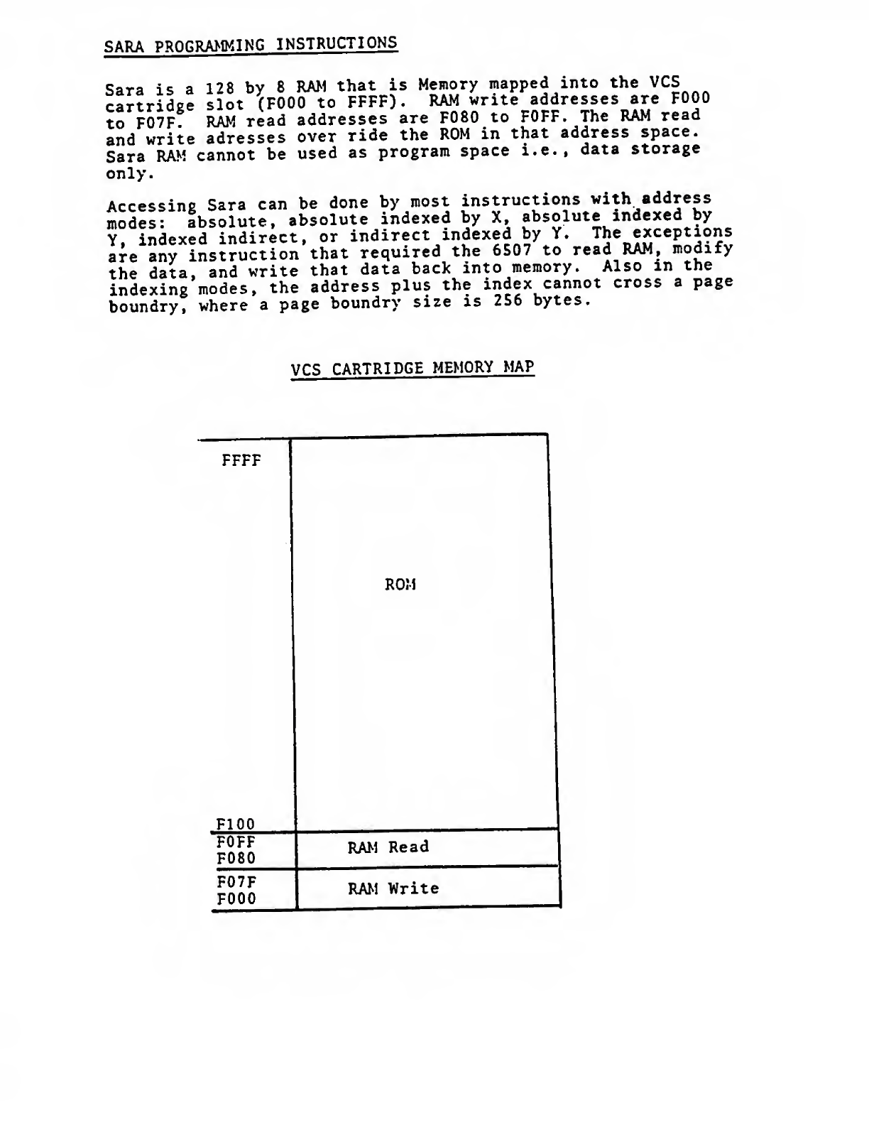
SARA PPnnRAMMING INSTRUCTIONS
Sara is a128 by 8RAM that is Memory mapped into the VCS
cartridee slot (FOOD to FFFF) .RAM write addresses are FOOD
to F07F RAM read addresses are F080 to FOFF. The RAM read
and write adresses over ride the ROM in that address space.
Sara RAM cannot be used as program space i.e.. data storage
only.
Accessing Sara can be done by most instructions with, address
modes: absolute, absolute indexed by X^^solute indexed by
Y, indexed indirect, or indirect indexed by Y. The exceptions
are any instruction that required the 6507 to read RAM, modify
the data, and write that data back into memory. Also in the
indexing modes, the address plus the index cannot cross apage
boundry, where apage boundry size is 256 bytes.
VCS CARTRIDGE MEMORY MAP
FFFF
FlOO
ROM
FOFF
F080 RAM Read
F07F
FOOO RAM Write
