BVM D14H1U_Maintenance Manual BVMD14H1
User Manual: BVMD14H1
Open the PDF directly: View PDF ![]() .
.
Page Count: 158 [warning: Documents this large are best viewed by clicking the View PDF Link!]
- Cover
- Table of Contents
- 1. Operating Instructions
- 2. Service Informations
- 2-1. Circuit Boards Location
- 2-2-1. Cabinet and Rear Panel Removal
- 2-2-2. How To Open The B Board
- 2-2-3. Bezel Complete Assy Removal
- 2-2-4. HA, HB and HC Boards Removal (D14H5)
- 2-2-5. YA, YB and YC Boards Removal
- 2-2-6. G Board Removal
- 2-2-7. BX Board (BKM-129X) Removal and Check
- 2-2-8. T Board Removal
- 2-2-9. M Block Assy (MA and MB Boards) Removal
- 2-2-10. Picture Tube Removal
- 2-1. Circuit Boards Location
- 3. Set-Up Adjustments
- 4. Safety Related Adjustments
- 5. Circuit Adjustments
- 6. Circuit Descriptions
- 7. Semiconductors
- 8. Exploded Views
- 9. Electrical Parts List
- 10. Block Diagrams
- 11. Diagrams

MAINTENANCE MANUAL
1st Edition
Serial No. 2000001 and Higher (ALL MODELS)
TRINITRON® COLOR VIDEO MONITOR
BVM-D14H1U
BVM-D14H5U
CHASSIS NO. SCC-G09D-A
CHASSIS NO. SCC-G09E-A
BVM-D14H1E
BVM-D14H5E
BVM-D14H1A
BVM-D14H5A
CHASSIS NO. SCC-G10B-A
CHASSIS NO. SCC-G10C-A
CHASSIS NO. SCC-P31A-A
CHASSIS NO. SCC-P31B-A
! WARNING
This manual is intended for qualified service personnel only.
To reduce the risk of electric shock, fire or injury, do not perform any servicing other than that
contained in the operating instructions unless you are qualified to do so. Refer all servicing to
qualified service personnel.
! WARNUNG
Die Anleitung ist nur für qualifiziertes Fachpersonal bestimmt.
Alle Wartungsarbeiten dürfen nur von qualifiziertem Fachpersonal ausgeführt werden. Um die
Gefahr eines elektrischen Schlages, Feuergefahr und Verletzungen zu vermeiden, sind bei
Wartungsarbeiten strikt die Angaben in der Anleitung zu befolgen. Andere als die angegeben
Wartungsarbeiten dürfen nur von Personen ausgeführt werden, die eine spezielle Befähigung
dazu besitzen.
! AVERTISSEMENT
Ce manual est destiné uniquement aux personnes compétentes en charge de l’entretien. Afin
de réduire les risques de décharge électrique, d’incendie ou de blessure n’effectuer que les
réparations indiquées dans le mode d’emploi à moins d’être qualifié pour en effectuer d’autres.
Pour toute réparation faire appel à une personne compétente uniquement.
WARNING!!
AN INSULATED TRANSFORMER SHOULD BE USED DURING
ANY SERVICE TO AVOID POSSIBLE SHOCK HAZARD, BE-
CAUSE OF LIVE CHASSIS.
THE CHASSIS OF THIS RECEIVER IS DIRECTLY CONNECTED
TO THE AC POWER LINE.
SAFETY-RELATED COMPONENT WARNING !!
COMPONENTS IDENTIFIED BY A ! MARK ON THE SCHEMATIC
DIAGRAMS, EXPLODED VIEWS AND IN THE PARTS LIST ARE
CRITICAL TO SAFE OPERATION. REPLACE THESE COMPO-
NENTS WITH SONY PARTS WHOSE PART NUMBERS APPEAR
AS SHOWN IN THIS MANUAL OR IN SUPPLEMENTS PUB-
LISHED BY SONY. CIRCUIT ADJUSTMENTS THAT ARE CRITI-
CAL TO SAFE OPERATION ARE IDENTIFIED IN THIS MANUAL.
FOLLOW THESE PROCEDURES WHENEVER CRITICAL COM-
PONENTS ARE REPLACED OR IMPROPER OPERATION IS
SUSPECTED.
ATTENTION!!
AFIN D’ÉVITER TOUT RISQUE D’ÉLECTROCUTION
PROVENANT D’UN CHÂSSIS SOUS TENSION, UN
TRANSFORMATEUR D’ISOLEMENT DOIT ETRE UTILISÉ LORS
DE TOUT DÉPANNAGE.
LE CHÂSSIS DE CE RÉCEPTEUR EST DIRECTEMENT
RACCORDÉ Á L’ALIMENTATION SECTEUR.
ATTENTION AUX COMPOSANTS RELATIFS Á LA
SÉCURITÉ!!
LES COMPOSANTS IDENTIFIÉS PAR UNE MAPQUE ! SUR
LES SCHÉMAS DE PRINCIPE, LES VUES EXPLOSÉES ET LES
LISTES DE PIECES SONT D’UNE IMPORTANCE CRITIQUE
POUR LA SÉCURITÉ DU FONCTIONNEMENT. NE LES
REMPLACER QUE PAR DES COMPOSANTS SONY DONT LE
NUMÉRO DE PIÈCE EST INDIQUÉ DANS LE PRÉSENT MANUEL
OU DANS DES SUPPLÉMENTS PUBLIÉS PAR SONY. LES
RÉGLAGES DE CIRCUIT DONT L’IMPORTANCE EST CRITIQUE
POUR LA SÉCURITÉ DU FONCTIONNEMENT SONT
IDENTIFIÉS DANS LE PRÉSENT MANUEL. SUIVRE CES
PROCÉDURES LORS DE CHAQUE REMPLACEMENT DE
COMPOSANTS CRITIQUES, OU LORSQU’UN MAUVAIS
FONCTIONNEMENT EST SUSPECTÉ.
1
BVM-D14H1U/D14H5U/D14H1E/D14H5E/D14H1A/D14H5A
Table of Contents
1. Operating Instructions
BVM-D9H1J/D9H1U/D9H1E/D9H1A/D9H5J/D9H5U/D9H5E/D9H5A
D14H1J/D14H1U/D14H1E/D14H1A/D14H5J/D14H5U/D14H5E/D14H5A
.....................................................................................................................1-1
2. Service Informations
2-1. Circuit Boards Location ..............................................................................2-1
2-2-1. Cabinet and Rear Panel Removal ............................................... 2-2
2-2-2. How To Open The B Board .......................................................2-3
2-2-3. Bezel Complete Assy Removal .................................................. 2-3
2-2-4. HA, HB and HC Boards Removal (D14H5) ..............................2-4
2-2-5. YA, YB and YC Boards Removal .............................................2-5
2-2-6. G Board Removal ....................................................................... 2-5
2-2-7. BX Board (BKM-129X) Removal and Check ...........................2-6
2-2-8. T Board Removal ....................................................................... 2-7
2-2-9. M Block Assy (MA and MB Boards) Removal ......................... 2-8
2-2-10. Picture Tube Removal ................................................................2-9
3. Set-Up Adjustments
3-1. Set-Up Adjustment When CRT is Replaced ...............................................3-1
[Focus Adjustment] ..................................................................................... 3-3
[Landing Adjustment] .................................................................................3-5
[H Blanking Adjustment] ............................................................................3-6
[V Blanking Adjustment] ............................................................................3-7
[Linearity Adjustment] ................................................................................ 3-8
[Convergence Adjustment] .......................................................................3-10
[Static Convergence Adjustment] .............................................................3-10
[Dynamic Convergence Adjustment]........................................................3-11
[G2 Adjustment]........................................................................................ 3-11
[White Balance Adjustment] .....................................................................3-12
4. Safety Related Adjustments
+B (135 V) Voltage Check ........................................................ 4-2
High Voltage Regulator Check ..................................................4-2
High Voltage Hold-Down Check ...............................................4-3
Beam Current Protector Check .................................................. 4-3
2BVM-D14H1U/D14H5U/D14H1E/D14H5E/D14H1A/D14H5A
5. Circuit Adjustments
5-1. B Board Adjustments ..................................................................................5-1
1. RGB Signal Adjustment.............................................................5-2
2. 15k YPBPR SMPTE (709) Signal Adjustment..........................5-3
3. 15k YPBPR SMPTE (601) Signal Adjustment..........................5-5
4. 15k YPBPR BETACAM SETUP 0 (601) Signal Adjustment ...5-6
5. 15k YPBPR BETACAM SETUP 7.5 (601) Signal Adjustment 5-7
6. 33k YPBPR SMPTE (709) Signal Adjustment..........................5-8
6. Circuit Descriptions
6-1. G Board .......................................................................................................6-1
6-2. G1 Board .....................................................................................................6-4
6-3. B Board .......................................................................................................6-4
6-4. C Board .......................................................................................................6-6
6-5. MA Board.................................................................................................... 6-6
6-6. MB Board ....................................................................................................6-6
7. Semiconductors ............................................................. 7-1
8. Exploded Views
8-1. Bezel, Cabinet .............................................................................................8-1
8-2. M Block, Signal Block ................................................................................8-2
8-3. Picture Tube, Chassis ..................................................................................8-3
9. Electrical Parts List ........................................................ 9-1
10. Block Diagrams
Overall (1/2) .............................................................................................. 10-1
Overall (2/2) .............................................................................................. 10-2
B (1/2), BX, B1, B2 ..................................................................................10-3
B (2/2), C...................................................................................................10-4
G (1/2) .......................................................................................................10-5
G (2/2), G1 ................................................................................................ 10-6
MA, MB .................................................................................................... 10-7
HA, HB, HC ..............................................................................................10-8
3
BVM-D14H1U/D14H5U/D14H1E/D14H5E/D14H1A/D14H5A
11. Diagrams
11-1. Frame Schematic Diagrams ...................................................................... 11-2
11-2. Schematic Diagrams and Printed Wiring Boards......................................11-3
Schematic Diagrams
BX (1/2) .................................................................................................. 11-4
BX (2/2) .................................................................................................. 11-5
B (1/4) ..................................................................................................11-7
B (2/4) ..................................................................................................11-8
B (3/4) ..................................................................................................11-9
B (4/4) ................................................................................................ 11-10
B1 ................................................................................................11-12
B2 ................................................................................................11-13
C ................................................................................................11-14
G (1/3) ................................................................................................11-17
G (2/3) ................................................................................................11-18
G (3/3) ................................................................................................11-19
G1 ................................................................................................11-21
HA ................................................................................................11-23
HB ................................................................................................11-24
HC, HD ................................................................................................11-26
MA ................................................................................................11-29
MB ................................................................................................11-31
YA, YB, YC..........................................................................................11-32
T ................................................................................................11-33
Printed Wiring Boards
BX ..................................................................................................11-3
B ..................................................................................................11-6
B1 ................................................................................................11-12
B2 ................................................................................................11-13
C ................................................................................................11-14
G ................................................................................................11-15
G1 ................................................................................................11-21
HA ................................................................................................11-22
HB ................................................................................................11-24
HC ................................................................................................11-25
HD ................................................................................................11-26
MA ................................................................................................11-28
MB ................................................................................................11-30
YA, YB, YC..........................................................................................11-32
T ................................................................................................11-33

4BVM-D14H1U/D14H5U/D14H1E/D14H5E/D14H1A/D14H5A
1-1
BVM-D14H1U/D14H5U/D14H1E/D14H5E/D14H1A/D14H5A
Section 1
Operating Instructions
OPERATION MANUAL
[Japanese/English]
1st Edition
Serial No. 2000001 and Higher
TRINITRON
®
COLOR VIDEO MONITOR
BVM-D9H1J/D9H1U/D9H1E/D9H1A
BVM-D9H5J/D9H5U/D9H5E/D9H5A
BVM-D14H1J/D14H1U/D14H1E/D14H1A
BVM-D14H5J/D14H5U/D14H5E/D14H5A
This section is extracted from
operation manual.
1-2 BVM-D14H1U/D14H5U/D14H1E/D14H5E/D14H1A/D14H5A
WARNING
To prevent fire or shock hazard, do not
expose the unit to rain or moisture.
To avoid electrical shock, do not open the
cabinet. Refer servicing to qualified
personnel only.
AVERTISSEMENT
Afin d’éviter tout risque d’incendie ou d’électrocution, ne pas
exposer cet appareil à la pluie ou à l’humidité.
Afin d’écarter tout risque d’électrocution, garder le coffret
fermé. Ne confier l’entretien de l’appareil qu’à un personnel
qualifié.
WARNUNG
Um Feuergefahr und die Gefahr eines elektrischen SchIages
zu vermeiden, darf das Gerät weder Regen noch
Feuchtigkeit ausgesetzt werden.
Um einen elektrischen Schlag zu vermeiden, darf das
Gehäuse nicht geöffnet werden. Überlassen Sie
Wartungsarbeiten stets nur einem Fachmann.
ADVERTENCIA
Para evitar incendios o el riesgo de electrocución, no
exponga la unidad a la lluvia ni a la humedad.
Para evitar descargas eléctricas, no abra la unidad. En caso
de avería, solicite los servicios de personal cualificado.
ATTENZIONE
Per evitare incendi o cortocircuiti, l’apparecchio non deve
essere esposto alla pioggia o all’umidità.
Per evitare scosse elettriche, non aprite l’apparecchio. Per
le riparazioni rivolgetevi solo a personale qualificato.
CAUTION:
Danger of explosion if battery is incorrectly replaced.
Replace only with the same or equivalent type recommended
by the manufacturer. Discard used batteries according to the
manufacturer’s instructions.
ATTENTION
Il y a un risque d’explosion si la pile est mal insérée.
Remplacer la pile uniquement par une pile de même type ou
de type équivalent recommandé par le fabricant. Jeter les
piles usées conformément aux instructions du fabricant.
VORSICHT:
Es besteht Explosionsgefahr, wenn die Batterie inkorrekt
eingelegt wird.
Es darf nur eine identische oder eine vom Hersteller
empfohlene Batterie des gleichen Typs eingesetzt werden.
Entladene Batterien sind nach den Anweisungen des
Herstellers zu entsorgen.
PRECAUCION
Peligro de explosión en caso de haberse instalado
incorrectamente la betería.
Cambie sólo por una del mismo tipo o especificaciones
equivalentes, de entre las recomendadas por el fabricante.
Las baterías viejas se deben eliminar siguiendo las
instrucciones del fabricante.
ATTENZIONE:
Pericolo di esplosione se la pila viene sostituita
scorrettamente.
Sostituirla solo con un’altra uguale o di un tipo equivalente
consigliato dal fabbricante. Gettare via le pile usate secondo
le istruzioni del fabbricante.
Note
The socket-outlet should be installed near the equipment and
be easily accessible.
Remarque
La prise doit être près de l’appareil et facile d’accès.
Hinweis
Zur Trennung vom Netz ist der Netzstecker aus der
Steckdose zu ziehen, welche sich in der Nähe des Gerätes
befinden muß und leicht zugänglich sein soll.
Nota
La toma mural debe estar instalada cerca del equipo y debe
accederse a ésta con facilidad.
Nota
La presa di corrente deve essere situata vicino
all’apparecchio e deve essere facilmente accessibile.
For customers in the USA
(BVM-D9H1U/D9H5U, BVM-D14H1U/D14H5U)
This equipment has been tested and found to comply with
the limits for a Class A digital device, pursuant to Part 15 of
the FCC Rules. These limits are designed to provide
reasonable protection against harmful interference when the
equipment is operated in a commercial environment. This
equipment generates, uses, and can radiate radio frequency
energy and, if not installed and used in accordance with the
instruction manual, may cause harmful interference to radio
communications. Operation of this equipment in a residential
area is likely to cause harmful interference in which case the
user will be required to correct the interference at his own
expense.
You are cautioned that any changes or modifications not
expressly approved in this manual could void your authority
to operate this equipment.
The shielded interface cable recommended in this manual
must be used with this equipment in order to comply with the
limits for a digital device pursuant to Subpart B of Part 15 of
FCC Rules.
Für Kunden in Deutschland
Entsorgungshinweis: Bitte werfen Sie nur entladene
Batterien in die Sammelboxen beim Handel oder den
Kommunen. Entladen sind Batterien in der Regel dann,
wenn das Gerät abschaltet und signalisiert “Batterie leer”
oder nach längerer Gebrauchsdauer der Batterien “nicht
mehr einwandfrei funktioniert”. Um sicherzugehen, kleben
Sie die Batteriepole z.B. mit einem Klebestreifen ab oder
geben Sie die Batterien einzeln in einen Plastikbeutel.
Voor de klanten in Nederland
Bij dit produkt zijn batterijen geleverd.
Wanneer deze leeg zijn, moet u ze niet
weggooien maar inleveren als KCA.
• Dit apparaat bevat een Li-ion batterij voor memory back-up.
• De batterij voor memory back-up is vastgesoldeerd op de
MA printplaat BT1.
• Raadpleeg uw leverancier over de verwijdering van de
batterij op het moment dat u het apparaat bij einde
levensduur afdankt.
• Gooi de batterij niet weg, maar lever hem in als KCA.
För kunderna i Sverige
Apparaten ma kun tilkoples jordet stikkontakt
For kunder i Norge
Apparatet må kun tilkoples jordet stikkontakt
For the customers in Europe
(BVM-D9H1E/D9H1A/D9H5E/D9H5A, BVM-D14H1E/
D14H1A/D14H5E/D14H5A)
This product with the CE marking complies with both the
EMC Directive (89/336/EEC) and the Low Voltage Directive
(73/23/EEC) issued by the Commission of the European
Community.
Compliance with these directives implies conformity to the
following European standards:
• EN60950: Product Safety
• EN55103-1: Electromagnetic Interference (Emission)
• EN55103-2: Electromagnetic Susceptibility (Immunity)
This product is intended for use in the following
Electromagnetic Environment(s):
E1 (residential), E2 (commercial and light industrial), E3
(urban outdoors) and E4 (controlled EMC environment, ex.
TV studio).
Pour les clients européens
(BVM-D9H1E/D9H1A/D9H5E/D9H5A, BVM-D14H1E/
D14H1A/D14H5E/D14H5A)
Ce produit portant la marque CE est conforme à la fois à la
Directive sur la compatibilité électromagnétique (EMC) (89/
336/CEE) et à la Directive sur les basses tensions (73/23/
CEE) émises par la Commission de la Communauté
européenne.
La conformité à ces directives implique la conformité aux
normes européennes suivantes:
• EN60950: Sécurité des produits
• EN55103-1: Interférences électromagnétiques (émission)
• EN55103-2: Sensibilité électromagnétique (immunité)
Ce produit est prévu pour être utilisé dans les
environnements électromagnétiques suivants:
E1 (résidentiel), E2 (commercial et industrie légère), E3
(urbain extérieur) et E4 (environnement EMC contrôlé ex.
studio de télévision).
Für Kunden in Europa
(BVM-D9H1E/D9H1A/D9H5E/D9H5A, BVM-D14H1E/
D14H1A/D14H5E/D14H5A)
Dieses Produkt besitzt die CE-Kennzeichnung und erfüllt
sowohl die EMV-Direktive (89/336/EEC) als auch die
Direktive Niederspannung (73/23/EEC) der EG-
Kommission.
Die Erfüllung dieser Direktiven bedeutet Konformität für die
folgenden Europäischen Normen:
• EN60950: Produktsicherheit
• EN55103-1: Elektromagnetische Interferenz (Emission)
• EN55103-2: Elektromagnetische Empfindlichkeit
(Immunität)
Dieses Produkt ist für den Einsatz unter folgenden
elektromagnetischen Bedingungen ausgelegt:
E1 (Wohnbereich), E2 (kommerzieller und in beschränktem
Maße industrieller Bereich), E3 (Stadtbereich im Freien) und
E4 (kontrollierter EMV-Bereich, z.B. Fernsehstudio)
English

1-3
BVM-D14H1U/D14H5U/D14H1E/D14H5E/D14H1A/D14H5A
ATTENTION - When the product is installed in a rack:
a) Elevated operating ambient temperature
If installed in a closed or multi-unit rack assembly, the
operating ambient temperature of the rack environment
may be greater than room ambient. Therefore,
consideration should be given to installing the equipment
in an environment compatible with the manufacture’s
maximum rated ambient temperature (Tmra: 0°C to 35°C
(32°F to 95°F)).
b) Reduced air flow
Installation of the equipment in a rack should be such that
the amount of air flow required for safe operation of the
equipment is not compromised.
c) Mechanical loading
Mounting of the equipment in the rack should be such
that a hazardous condition is not achieved due to uneven
mechanical loading.
d) Circuit overloading
Consideration should be given to the connection of the
equipment to the supply circuit and the effect that
overloading of circuits might have on overcurrent
protection and supply wiring.
Appropriate consideration of equipment nameplate
ratings should be used when addressing this concern.
e) Reliable earthing
Reliable earthing of rack-mounted equipment should be
maintained. Particular attention should be given to supply
connections other than direct connections to the branch
circuit (e.g., use of power strips).
f) Gap keeping
Upper and lower gap of rack-mounted equipment should
be kept at least 44 mm (1
3
⁄
4
inches).
For the customers in the United Kingdom
(BVM-D9H1E/D9H1A/D9H5E/D9H5A, BVM-D14H1E/
D14H1A/D14H5E/D14H5A)
WARNING
THIS APPARATUS MUST BE EARTHED
IMPORTANT
The wires in this mains lead are coloured in accordance with
the following code:
Green-and-yellow: Earth
Blue: Neutral
Brown: Live
As the colours of the wires in the mains lead of this
apparatus may not correspond with the coloured markings
identifying the terminals in your plug proceed as follows:
The wire which is coloured green-and-yellow must be
connected to the terminal in the plug which is marked by the
letter E or by the safety earth symbol Y or coloured green or
green-and-yellow.
The wire which is coloured blue must be connected to the
terminal which is marked with the letter N or coloured black.
The wire which is coloured brown must be connected to the
terminal which is marked with the letter L or coloured red.
Ensure that your equipment is connected correctly - if you
are in any doubt consult a qualified electrician.
Achtung - bei Installation des Geräts in einem Gestell:
a) Erhöhte Umgebungstemperatur bei Betrieb
Wird das Gerät in einem geschlossenen Gestell oder
einem Gestell mit mehreren anderen Geräten installiert,
kann die Umgebungstemperatur um das Gestell höher
sein als die normale Umgebungstemperatur im Raum.
Achten Sie daher bitte besonders darauf, das Gerät in
einer Umgebung zu installieren, in der die Temperatur
nicht über die vom Hersteller angegebene
Umgebungstemperatur von 0 bis
35 °C (32 °F bis 95 °F) ansteigt (Tmra).
b) Reduzierte Belüftung
Das Gerät muß so im Gestell installiert werden, daß eine
Belüftung gewährleistet ist, die für den sicheren Betrieb
des Geräts erforderlich ist.
c) Mechanische Belastung
Das Gerät muß so im Gestell installiert werden, daß nicht
durch eine ungleichmäßige mechanische Belastung
Unfallgefahr entsteht.
d) Überlastung der Stromkreise
Der Anschluß des Geräts an das Versorgungsnetz
erfordert sorgfältige Planung. Bitte beachten Sie
insbesondere die Auswirkungen, die eine Überlastung
der Stromkreise im Hinblick auf den
Überspannungsschutz und die physischen Komponenten
des Versorgungsnetzes haben kann.
Beachten Sie in diesem Zusammenhang unbedingt die
Angaben auf dem Typenschild am Gerät.
e) Zuverlässige Erdung
Geräte, die in einem Gestell installiert werden, benötigen
eine zuverlässige Erdung. Achten Sie insbesondere auf
Anschlüsse an das Versorgungsnetz, die nicht direkt an
einen Abzweigstromkreis, sondern indirekt, zum Beispiel
über Verlängerungskabel, erfolgen.
f) Erforderliche Abstände
Halten Sie zur Ober- und Unterseite eines in einem
Gestell installierten Geräts einen Abstand von 44 mm
(1
3
/
4
inches) ein.
1
(E)
Table of Contents
Chapter 1
Overview
Chapter 2
Menu
(Continued)
Precautions ........................................................................................ 3(E)
Overview............................................................................................ 4(E)
Features .....................................................................................4(E)
Options ......................................................................................5(E)
Location and Function of Parts ....................................................... 7(E)
BVM-D9H1U/D9H1E/D9H1A/D9H5U/D9H5E/D9H5A Front
Panel...................................................................................7(E)
BVM-D9H1U/D9H1E/D9H1A/D9H5U/D9H5E/D9H5A Rear
Panel.................................................................................12(E)
BVM-D14H1U/D14H1E/D14H1A/D14H5U/D14H5E/D14H5A
Front Panel .......................................................................16(E)
BVM-D14H1U/D14H1E/D14H1A/D14H5U/D14H5E/D14H5A
Rear Panel ........................................................................21(E)
Installation of the 4:3 Mask ........................................................... 24(E)
BVM-D9H1U/D9H1E/D9H1A/
D9H5U/D9H5E/D9H5A ..................................................24(E)
BVM-D14H1U/D14H1E/D14H1A/
D14H5U/D14H5E/D14H5A ............................................24(E)
Basic Menu Operations .................................................................. 25(E)
Menu Operation Buttons .........................................................25(E)
Displaying the Menus..............................................................26(E)
Menu Operation.......................................................................26(E)
ADDRESS Menu ....................................................................29(E)
Menu Structure............................................................................... 30(E)
APreset Adjustment of the Picture Level Control Knobs
— CONTROL PRESET ADJ Menu ..................................... 31(E)
Overview .................................................................................31(E)
Structure of the CONTROL PRESET ADJ Menu ..................31(E)
Setting Lists in the CONTROL PRESET ADJ Menu.............31(E)
BAdjusting the Color Temperature
— COLOR TEMP ADJ Menu ............................................... 33(E)
Overview .................................................................................33(E)
Structure of the COLOR TEMP ADJ Menu ...........................33(E)
Setting Lists in the COLOR TEMP ADJ Menu ......................34(E)
C Setting the Input Configuration
— INPUT CONFIG Menu...................................................... 35(E)
Overview .................................................................................35(E)
Structure of the INPUT CONFIG Menu .................................35(E)
Setting Lists in the INPUT CONFIG Menu............................36(E)
DAssigning the Remote Control Functions
— REMOTE Menu ................................................................. 37(E)
Overview .................................................................................37(E)
Structure of the REMOTE Menu ............................................37(E)
Setting Lists of the REMOTE Menu.......................................38(E)
1-4 BVM-D14H1U/D14H5U/D14H1E/D14H5E/D14H1A/D14H5A
Table of contens
2
(E)
Chapter 2
Menu
Chapter 3
Appendix
ESetting the Power-Up Conditions and Data about the Screen
Display — SYSTEM CONFIG Menu.................................... 39(E)
Overview .................................................................................39(E)
Structure of the SYSTEM CONFIG Menu .............................40(E)
Setting Lists of the SYSTEM CONFIG Menu........................40(E)
FDisplaying Information About the Monitor
— STATUS Menu ................................................................... 42(E)
Overview .................................................................................42(E)
Structure of the STATUS Menu..............................................42(E)
Setting Lists of the STATUS Menu ........................................42(E)
GAdjusting the Position, Size and Geometry of the Picture
— ALIGNMENT Menu.......................................................... 43(E)
Overview .................................................................................43(E)
Structure of the ALIGNMENT Menu .....................................43(E)
Setting Lists of the ALIGNMENT Menu ...............................43(E)
Selecting the Monitor to Control — ADDRESS Menu ............... 45(E)
Overview .................................................................................45(E)
Displaying the ADDRESS Menu ............................................45(E)
Cancelling the Remote Control Mode.....................................46(E)
Exiting the ADDRESS Menu..................................................46(E)
Short-cut Function in the ADDRESS Menu ...........................46(E)
Specifications................................................................................... 47(E)
Available Signal Format..........................................................53(E)
Connection Cable Specifications
for Color Temperature Probes..........................................54(E)
Menu Index ..................................................................................... 56(E)
Menu Configuration ....................................................................... 58(E)
3
(E)
Chapter 1 Overview
Precautions
On safety
• Operate the unit only with a power source as
specified in “Specifications” section.
• The nameplate indicating operating voltage, power
consumption, etc., is located at the rear.
• Should any solid object or liquid fall into the cabinet,
unplug the unit and have it checked by qualified
personnel before operating it any further.
• Do not drop or place heavy objects on the power
cord. If the power cord is damaged, turn off the
power immediately. It is dangerous to use the unit
with a damaged power cord.
• Unplug the unit from the wall outlet if it is not to be
used for several days or more.
• Disconnect the power cord from the AC outlet by
grasping the plug, not by pulling the cord.
• The socket-outlet shall be installed near the
equipment and shall be easily accessible.
• Use the supplied AC adaptor for the BVM-D9H1U/
D9H1E/D9H1A/D9H5U/D9H5E/D9H5A models
only. It is dangerous to use the AC adaptor for
models other than these.
On installation
• Allow adequate air circulation to prevent internal heat
build-up.
Do not place the unit on surfaces (rugs, blankets, etc.)
or near materials (curtains, draperies) that may block
the ventilation holes.
• Do not install the unit in a location near heat sources
such as radiators or air ducts, or in a place subject to
direct sunlight, excessive dust, mechanical vibration
or shock.
On mounting the rack
When the monitor is mounted on the rack, the
proximity of other equipment or a decrease in air
circulation may cause heat to build up inside the
monitor. Therefore, when mounting the monitor on
the rack, ensure there is an adequate opening for
ventilation or install a fan. The following operating
conditions are needed:
Temperature: 0°C to 35°C (32°F to 95°F),
Optimum temperature: 20°C to 30°C (68°F to 86°F)
On the battery (BVM-D9H1U/D9H1E/D9H1A/
D9H5U/D9H5E/D9H5A only)
The MAIN POWER switch is not supplied with the
above models. Therefore, when the power is turned
off with a battery installed, the monitor is set to
standby mode and a small amount of power is
consumed. When the monitor is not used for a long
period, remove the battery.
On cleaning
To keep the unit looking brand-new, periodically clean
it with a mild detergent solution. Never use strong
solvents such as thinner or benzine, or abrasive
cleansers since they will damage the cabinet. As a
safety precaution, unplug the unit before cleaning it.
On repacking
Do not throw away the carton and packing materials.
They make an ideal container which to transport the
unit.
If you have any questions about this unit, contact your
authorized Sony dealer.
On magnetism
• Do not place the unit near any objects or pieces of
equipment which generate magnetism, such as
magnets, speakers, electric clocks, toys using
magnets, health appliances, etc. Magnetism will
cause picture bounce, oscillations or picture
discoloration.
• Also, the picture may become fuzzy or the colors
may not reproduce correctly due to earth magnetism.
This depends on direction that the unit is installed.
This is not equipment failure. In such a case, simply
degauss the unit.
On the CRT
• Dust accumulates on the CRT easily. Clean the CRT
when necessary with a soft cloth.
The surface of the CRT is easily scratched; therefore,
do not rub or touch the surface of the CRT
unnecessarily since this may result in a scratched
picture tube.
• If you touch the surface of the CRT, you may feel a
weak electrical shock. This is simply static electricity
that is generated on the surface of the CRT. It will not
affect the human body.
On using as the monitor for 4:3 signals
The 16:9 mask is installed at the factory. When the
display is set to the 4:3 aspect ratio, the upper and
lower portions of the display are masked and you
cannot view the upper and lower portions of the
picture. Therefore, when you want to display the
picture in 4:3 aspect ratio, install the supplied 4:3
mask.
Chapter 1 Overview

1-5
BVM-D14H1U/D14H5U/D14H1E/D14H5E/D14H1A/D14H5A
4
(E)
Chapter 1 Overview
Overview
The BVM-D9H1U/D9H1E/D9H1A/D9H5U/D9H5E/
D9H5A are 9 -inch Trinitoron®1) Color Monitors. The
BVM-D14H1U/D14H1E/D14H1A/D14H5U/D14H5E/
D14H5A are 14-inch2) Trinitoron® Color Monitors.
Features
Multiformat
The monitor supports the principal format (480I/480P/
720P/1080I) for the digital broadcasts, NTSC and PAL
color systems, and a wide variety of signals3) whose
horizontal frequency is between 15 kHz and 45 kHz.
High resolution picture tube
The HR Trinitron picture tube produces a clear, high
resolution image.
Separate control unit (BVM-D9H1U/D9H1E/
D9H1A/D14H1U/D14H1E/D14H1A)
Using a separate control unit reduces the space needed
for the equipment.
The monitor is controlled by a separate control unit,
such as an optional BKM-10R/11R Monitor Control
Unit or by daisy chain connections.
Controlling monitor groups
Up to 32 monitors can be controlled from one control
unit by the RS-485 serial remote connections. You can
control individual monitors or monitor groups simply
by entering monitor address or group numbers. You
can also execute the same operation on all connected
monitors, or put all connected monitors into the same
setup and adjustment state.
1) Trinitron® is a registered trademark of Sony Corporation.
2) 9-inch and 14-inch refer to the CRT size of the monitor.
For effective picture size, see “Specifications” on page 47(E).
3) For details on the signal format, see “Available Signal Format” on page
53(E).
........................................................................................................................................................................................................
Model
BVM-D9H1U/
D9H1E/D9H1A/
D9H5U/D9H5E/
D9H5A
BVM-D14H1U/
D14H1E/D14H1A/
D14H5U/D14H5E/
D14H5A
Resolution at the
center of the picture
450 TV lines (4:3)
340 TV lines (16:9)
800 TV lines (4:3)
600 TV lines (16:9)
Aperture
grille pitch
0.25 mm
0.25 mm
Auto chroma phase and white balance
functions
The chroma and phase of the decoder are
automatically adjusted with the auto chroma phase
function and the color temperature is automatically
adjusted with the auto white balance function by using
the BKM-14L Auto Setup Probe, etc.
4:3 area marker
It is possible to check the 4:3 aspect area in the 16:9
picture by displaying the 4:3 marker.
Expandable input capability
You can obtain HD SDI signals, D1 SDI signals,
NTSC/PAL signals or YPBPR/RGB signals by
installing the optional input adaptors at the rear of the
monitor. The input connector configuration can be
easily modified and up to three adaptors can be
installed. The BKM-129X Analog Component Input
Adaptor is installed at SLOT 1 at the factory.
Stable color temperature
The beam current feedback circuit maintains a constant
color temperature over long periods of time.
Blue-only mode convenient for monitoring
noise
All three CRT cathodes can be driven with a blue
signal, producing a monochrome display. This mode is
convenient for chroma and phase adjustment, and for
monitoring VTR noise.
5
(E)
Chapter 1 Overview
Other features
• The monitor’s various functions and operating
conditions can be set with on-screen menus.
• Has both RS-485 serial remote and relay contact
parallel remote control connectors.
• H delay and V delay functions for simultaneous
checking of the horizontal and vertical
synchronization signals. VITS (Vertical Interval Test
Signal) checking is also possible.
• Auto and manual degaussing.
• The monitor may be mounted in an EIA-standard 19-
inch rack, using an optional MB-520 (for 9-inch
monitor) or BKM-30E14/31E14 (for 14-inch
monitor) Rack Mount Kit.
• The appearance of the monitor can be changed to
16:9 or 4:3 display by the replacement of a mask.
• Operable by using a Sony lithium ion battery (BP-
L60/L90A) or DC 12 V external power source.
(BVM-D9H1U/D9H1E/D9H1A/D9H5U/D9H5E/
D9H5A only)
• Built-in audio reproduce circuit and speaker. (BVM-
D9H5U/D9H5E/D9H5A only)
Options
For external control
BKM-10R Monitor Control Unit
A controller for the BVM-D9H/D14H series video
monitors, allowing you to control multiple monitors
from one control unit.
BKM-11R Monitor Control Unit
A controller for the BVM-D9H/D14H and other BVM/
HDM series video monitors, allowing you to control
multiple monitors from one control unit.
BKM-14L Auto Setup Probe
A probe, allowing the automatic adjustment of this
monitor’s color temperature.
For installation
MB-520 Mounting Bracket
Mounting bracket to mount one or two BVM-D9H1U/
D9H1E/D9H1A/D9H5U/D9H5E/D9H5A in a 19-inch
EIA standard rack.
MB-519 Mounting Panel
Panel for the BVM-D9H1U/D9H1E/D9H1A to fill up
the space created when mounting a video monitor to a
rack with the MB-520 mounting bracket.
MB-509 Mounting Panel
Panel for the BVM-D9H5U/D9H5E/D9H5A to fill up
the space created when mounting a video monitor to a
rack with the MB-520 mounting bracket.
BKM-30E14 Rack Mount Kit
Rack mount kit for mounting the BVM-D14H5U/
D14H5E/D14H5A in an EIA standard 19-inch rack.
BKM-31E14 Rack Mount Kit
Rack mount kit for mounting the BVM-D14H1U/
D14H1E/D14H1A in an EIA standard 19-inch rack.
Others
VF-508 Monitor ENG Kit
Kit that includes a light intercepting hood which is
mounted on the front of a monitor, and a connector
protector which is mounted on the rear.
Input adaptors
The input connector panel is configured by sliding the
optional input adaptor into the input option slot at the
rear of the monitor. Up to three adaptors can be
installed to the monitor.
The input signal type for each connector of the adaptor
is set with the INPUT CONFIG menu, in accordance
with the configuration of the connector panel.
Note
When installing the adaptor, be sure to perform the
necessary input signal setup with the INPUT CONFIG
menu. If the setup is not performed, the adaptors may
not function correctly.
For information about the INPUT CONFIG menu, see “[C]
Setting the Input Configuration — INPUT CONFIG Menu”
on page 35(E).
1-6 BVM-D14H1U/D14H5U/D14H1E/D14H5E/D14H1A/D14H5A
6
(E)
Chapter 1 Overview
Overview
BKM-120D SDI 4:2:2 Input Adaptor
Includes a decoder for serial digital component signals.
D1 SDI input/output connectors for two serial digital
channels and active loop-through output connectors.
BKM-127W NTSC/PAL Input Adaptor
Includes decoders for analog composite NTSC and
PAL signals. Input/output connectors for two analog
channels and one YC channel.
BKM-129X Analog Component Input Adaptor
Includes input/output connectors for one analog
channel and EXT SYNC input/output connectors.
The BKM-129X is mounted to the monitor at the
factory.
BKM-142HD HD SDI Input Adaptor
Includes a decoder for HD serial digital signals and
input/output connectors for two serial digital signal
channels and monitor output connector.
Notes
• The BKM-142HD uses two input option slots.
• The signal from MONITOR OUT connector does not
satisfy the ON-LINE signal specifications.
7
(E)
Chapter 1 Overview
Location and Function of Parts
BVM-D9H1U/D9H1E/D9H1A/D9H5U/D9H5E/D9H5A Front Panel
For the BVM-D14H1U/D14H1E/D14H1A/D14H5U/D14H5E/D14H5A, see pages 16(E) to 20(E).
BVM-D9H1U/D9H1E/D9H1A
BVM-D9H5U/D9H5E/D9H5A
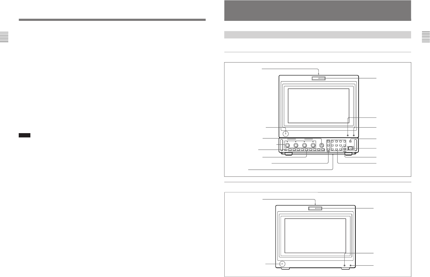
1 Tally lamp
2 STANDBY lamp
3 POWER lamp
4 DEGAUSS button
5 POWER switch
6 Ent button
7 Numeric keypad
8 Carrying handle
9 OPTION connector
0 VOLUME control
qa MANUAL adjustment knobs
qs SHIFT button
qd Function buttons
qf Menu operation buttons
qg Stand
1 Tally lamp
2 STANDBY lamp
3 POWER lamp
8 Carrying handle
9 OPTION connector
1-7
BVM-D14H1U/D14H5U/D14H1E/D14H5E/D14H1A/D14H5A
8
(E)
Chapter 1 Overview
This manual explains the location and function of parts
and controls of the BVM-D9H5U/D9H5E/D9H5A.
The explanation also applies to the optional BKM-
10R/11R Monitor Control Unit.
1 Tally lamp
With factory settings, the tally lamp lights as follows
when the pins of the PARALLEL REMOTE [1]
connector on the rear panel are shorted:
– in red, when pins No.3 and No.9 are shorted.
– in green, when pins No.4 and No.9 are shorted.
– in amber, when pins No.3, No.4 and No.9 are
shorted.
The tally lamp lights as follows when the pins of the
PARALLEL REMOTE [2] connector on the rear panel
are shorted:
– in red, when pins No.3 and No.5 are shorted.
– in green, when pins No.4 and No.5 are shorted.
– in amber, when pins No.3, No.4 and No.5 are
shorted.
By changing the setting in the REMOTE menu,
different pins on the remote connector can be used to
control the tally lamp.
For information about the REMOTE menu, see “[D]
Assigning the Remote Control Functions
— REMOTE Menu” on page 37(E).
2 STANDBY lamp
Lights when the monitor is in standby mode. The
monitor will be in standby mode under the following
conditions:
• The AC adaptor or battery is attached to the monitor
when the STANDBY MODE menu of the SYSTEM
CONFIG menu is set to ON.
• The monitor is changed from operation mode to
standby mode by external control.
For information about the SYSTEM CONFIG menu, see
“[E] Setting the Power-Up Conditions and Data about the
Screen Display — SYSTEM CONFIG Menu” on page
39(E).
3 POWER lamp
Lights when the monitor is put into operation mode
from standby mode (see STANDBY lamp 2) by
pressing the POWER switch 5.
Note
When the STANDBY lamp 2 is blinking, the monitor
cannot be put into operation mode (internal data
initialization is taking place). Wait until the
STANDBY lamp 2 is steadily lit.
4 DEGAUSS button
Press to degauss the CRT (every time the monitor is
turned on, the CRT is degaussed automatically). To
degauss again, wait for more than five minutes.
5 POWER switch
Press to turn on/off the monitor. By setting with the
ADDRESS menu, it is possible to turn on/off the
power of the specified monitors only, or of all
monitors at the same time.
For information about the ADDRESS menu, see “Selecting
the Monitor to Control — ADDRESS Menu” on page 45(E).
6 Ent button
Use to confirm the items, values and characters
entered.
7 Numeric keypad
Use to designate the channel number for the input
signal to be monitored, or to enter the setting values
with the menus.
8 Carrying handle
Pull out to use for carrying the monitor.
9 OPTION connector
Used to connect the BKM-11R Monitor Control Unit
or Auto Setup Probe (BKM-14L, etc.)
0 VOLUME control
Adjusts the volume of the audio signals from the
equipment connected to the AUDIO IN jacks at the
rear of the monitor.
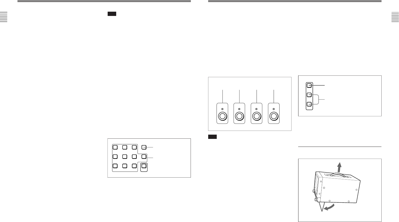
Numeric buttons
Del button: Deletes the
values and characters
entered.
1 2 3 Del
4560
789
Ent
Location and Function of Parts
9
(E)
Chapter 1 Overview
!¡ MANUAL adjustment knobs
Each press of one of these knobs turns the knob’s
green LED on or off. When the corresponding knob is
on (lit), it is possible to manually adjust the contrast,
brightness, chroma and phase by turning the
corresponding knobs. The PHASE knob is also used to
select the items or enter the setting values with the
menus. It is possible to set the preset value for each
adjusting item with the CONTROL PRESET ADJ
menu.
For Information about the CONTROL PRESET ADJ menu,
see “ [A] Preset Adjustment of the Picture Level Control
Knobs — CONTROL PRESET ADJ menu” on page 31(E).
Note
The PHASE and CHROMA knobs may not be
adjusted due to the signals. However, these knobs are
used for selecting the items or entering the setting
values with the menus.
!™ SHIFT button
Press to select one of the two functions designated to
the function buttons !£.
Each time the SHIFT button is pressed, the LED turns
on (SHIFT ON: lits in umber) and off (SHIFT OFF.)
SHIFT OFF: The functions indicated above the
function buttons can be used (the LED of the
function button lits in green.)
SHIFT ON: The functions indicated below the
function buttons can be used (the LED of the
function button lits in amber.)
CONTRAST
knob
BRIGHT
knob
CHROMA
knob
PHASE
knob
PHASE CHROMA BRIGHT CONTRAST
!£ Function buttons
Change the operation conditions for the monitor.
Each time the button is pressed, the LED turns on and
turns off, and the operation conditions are changed.
Each button has two functions. Select one of the two
functions by pressing the SHIFT button !™. When the
SHIFT button is set to ON, the LED lights in umber,
and when the SHIFT button is set to OFF, the LED of
each button lights in green.
For the functions of the function buttons in case of SHIFT
OFF and SHIFT ON, see pages 10(E) and 11(E).
!¢ Menu operation buttons
For more information about menu operation, see “Basic
Menu Operations” on page 25(E).
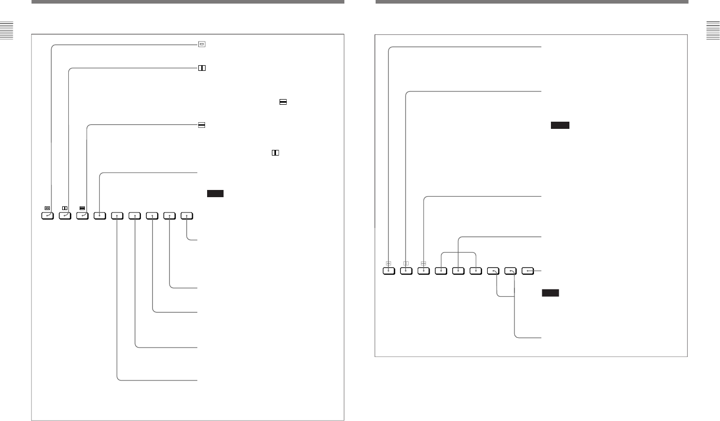
qg Stand
Pull out to use.
Using the Carrying Handle and Stand
MENU button: Press to display the monitor
menus.
UP/DOWN buttons: Press to select the
items and setting values.
MENU
UP
DOWN
Pull up.
Pull out toward front side.
1-8 BVM-D14H1U/D14H5U/D14H1E/D14H5E/D14H1A/D14H5A
10
(E)
Chapter 1 Overview
Location and Function of Parts
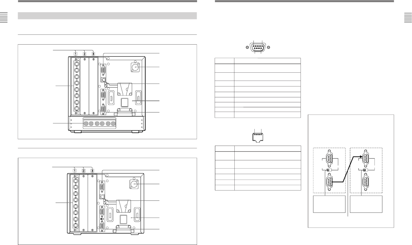
(Underscan) button: When this button is pushed in (ON),
the picture is underscanned by 3%, and four ends of the
raster is displayed on the screen.
(H delay) button: When this button is pushed in (ON), the
picture moves horizontally, and a horizontal sync signal
appears approximately one quarter in the left edge of the
screen.
• The brightness of the picture increases automatically, and it
makes it easy to check the sync part.
• If it is pressed together with the button, a pulse cross
picture is displayed.
(V delay) button: When this button is pushed in (ON), the
picture moves vertically, and a vertical sync signal appears
approximately in the center of the screen.
• The brightness of the picture increases automatically, and it
makes it easy to check the sync part.
• If it is pressed together with button, a pulse cross
picture is displayed.
MONO button: When this button is pushed in (ON), a
monochrome picture is displayed. When the buttons is off,
the monitor switches automatically color mode.
Notes
• The MONO button does not function with the RGB signal
input.
• When the NTSC or PAL color signals are received and
color burst signals are not input, the monitor does not
switch to color mode.
ADDRESS button: When this button is pushed in (ON), the
ADDRESS menu appears on the screen. By using the
ADDRESS menu, operation conditions for multiple monitors
are set.
For more information about the ADDRESS menu, see
“Selecting the Monitor to Control — ADDRESS Menu” on
page 45(E).
F2 button: When this button is pushed in (ON), you can access
directly the MANUAL menu of the level 1 of the COLOR TEMP
ADJ menu, if the short-cut function is assigned to this button.
F1 button: When this button is pushed in (ON), the characters
disappear from the monitor on the MANUAL menu of the level 1
of the CONTROL PRESET ADJ menu, the MANUAL menu of the
level 1 of the COLOR TEMP ADJ menu, and the ALIGNMENT
menu.
COMB button: This button does not function with this monitor.
However, when the BKM-127W NTSC/PAL Input Adaptor
(optional) is installed and the NTSC or PAL color signals are
received, the monitor can be used with the comb filter turned on.
APT (aperture) button: When this button is pushed in (ON), the
frequency response can be modified. The degree of
modification is set with the menu. (When RGB signals are
input, the button does not function.)
Function buttons in SHIFT OFF mode (LEDs of function buttons in green)
16:9 SYNC R G B
MONO APT COMB
F3
F1
F4
F2
MARKER
ADDRESS
B ONLY
11
(E)
Chapter 1 Overview
Function buttons in SHIFT ON mode (LEDs of function buttons in amber)
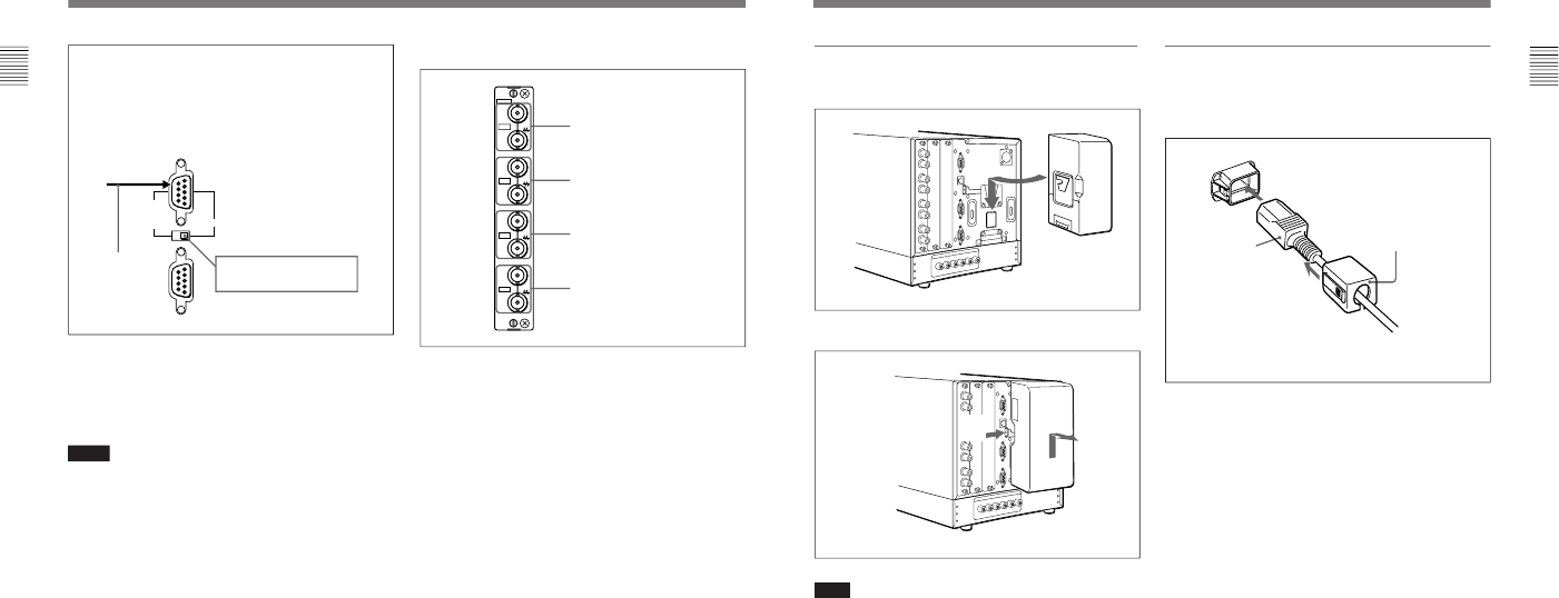
16:9 button: When this button is pushed in (ON), the aspect
ratio changes to 16:9, and when set to OFF, the aspect
ratio changes to 4:3.
The aspect ratio is fixed to 16:9 when the signal other than
4:3 signal format is input. For details, see “Available
Signal Format” on page 53(E).
SYNC button: When this button is pushed in (ON), the
monitor synchronizes to the sync signal input to the SYNC
connectors on the BKM-129X (EXT SYNC). When set to
OFF, it synchronizes to the sync signal included in the
signals being monitored (INT SYNC).
Notes
• When INT SYNC is selected, use a component including
a sync signal on the Y signal, and use RGB signal
including a sync signal on the G signal.
• When the BKM-129X is not installed to the monitor or
serial digital signals are monitored, INT SYNC is
automatically selected. You cannot select EXT SYNC.
B ONLY (blue only) button: When this button is pushed in
(ON), red and green signals are cut, and only the blue
signal is displayed as a monochrome picture. It makes it
easy to adjust CHROMA and PHASE, and to check VTR
noise.
R/G/B buttons: When these buttons are pushed in (ON),
R(red), G(green), and B(blue) beams are cut respectively.
MARKER button: When this button is pushed in (ON), a 4:3
marker is displayed and it is possible to check the 4:3 aspect
area in the 16:9 picture.
Note
The 4:3 marker is not displayed when the signals of the 4:3
aspect ratio are monitored or the monitor is in H/V delay mode
F3/F4 buttons: For future expansion.
16:9 SYNC R G B
MONO APT COMB
F3
F1
F4
F2
MARKER
ADDRESS
B ONLY
1-9
BVM-D14H1U/D14H5U/D14H1E/D14H5E/D14H1A/D14H5A
12
(E)
Chapter 1 Overview
BVM-D9H1U/D9H1E/D9H1A/D9H5U/D9H5E/D9H5A Rear Panel
For the BVM-D14H1U/D14H1E/D14H1A/D14H5U/D14H5E/D14H5A, see pages 21(E) to 23(E).
BVM-D9H5U/D9H5E/D9H5A
BVM-D9H1U/D9H1E/D9H1A
Location and Function of Parts
1 PARALLEL REMOTE
1/2 connectors
2 DC 12V IN jack
3 EJECT button
4 AC adaptor/battery
attachment place
5 SERIAL REMOTE
connectors
6 Input option slots
7 Analog input/output
connectors
8 AUDIO IN/OUT
(input/output) jacks
1 PARALLEL REMOTE
1/2 connectors
2 DC 12V IN jack
3 EJECT button
4 AC adaptor/battery
attachment place
5 SERIAL REMOTE
connectors and SERIAL
REMOTE/CTRL UNIT
select switch
6 Input option slots
7 Analog input/output
connectors
13
(E)
Chapter 1 Overview
1 PARALLEL REMOTE1/2 connectors
(1: female, D-sub 9-pin, 2: modular connector)
Form a parallel switch and controls the monitor
externally. The pin assignment and factory setting
function assigned to each pin are given below.
1: D-sub 9-pin
15
96
2: modular connector
1 6
All pin function assignments can be changed with the
REMOTE menu.
For information about the REMOTE menu, see “ [D]
Assigning the Remote Control Functions — REMOTE
Menu” on page 37(E).
To switch each function between on and off or
between enable and disable, change pin connections in
the following way.
ON or enabled: Short each pin and pin 9 together for
D-sub 9-pin.
Short each pin and pin 5 together for modular
connector.
OFF or disabled: Leave each pin open.
Pin number
1Set input signal channel 1 (numeric keypad
function)
2Set input signal channel 2 (numeric keypad
function)
3 Set red tally lamp on or off
4 Set green tally lamp on or off
5 Select sync signal (SYNC button function)
6 Set underscan on or off
7 Set a 16:9 aspect ratio on or off
8
Functions
Set the 4:3 area marker display on or off
9GND
Pin number
1Set input signal channel 1 (numeric keypad
function)
2Set input signal channel 2 (numeric keypad
function)
3 Set red tally lamp on or off
4 Set green tally lamp on or off
5 GND
6 Set underscan on or off
Functions
2 DC 12V IN jack (XLR-type, 4-pin)
Connects the DC 12V external power source to use the
monitor.
3 EJECT button
While sliding this button, remove the AC adaptor or
battery.
4 AC adaptor/battery attachment place
Attach the AC adaptor or battery.
5 SERIAL REMOTE connectors (female, D-sub 9-
pin), and SERIAL REMOTE/CTRL UNIT select
switch (BVM-D9H1U/D9H1E/D9H1A only)
These are RS-485 serial interface connectors, used for
connecting two or more BVM-xxE/F/G, BVM-xxD
and HDM-xxE series monitors. The IN and OUT
connectors form a loop-through connection.
BVM-D9H1U/D9H1E/D9H1A only: The SERIAL
REMOTE/CTRL UNIT select switch is set to SERIAL
REMOTE at the factory.
(continued)
For connecting the monitor (used for daisy
chain connections)
Connect two monitors using a cable with D-sub 9-
pin plugs such as an RCC-5G (not supplied) as
follows:
SERIAL
REMOTE
IN
SERIAL
REMOTE
OUT
CTRL UNIT
SERIAL
REMOTE
IN
SERIAL
REMOTE
OUT
CTRL UNIT
Monitor 1
BVM-D9H1U/
D9H1E/D9H1A:
Set to SERIAL
REMOTE.
Monitor 2
BVM-D9H1U/
D9H1E/D9H1A:
Set to SERIAL
REMOTE.
Cable with D-sub 9-pin plugs
(not supplied)
1-10 BVM-D14H1U/D14H5U/D14H1E/D14H5E/D14H1A/D14H5A
14
(E)
Chapter 1 Overview
6 Input option slots (three slots)
The monitor may be fitted with optional input adaptors
up to three.
The BKM-129X is installed to the monitor at the
factory.
Notes
• The BKM-142HD uses two input option slots.
• Each adaptor can also be installed into SLOT 1.
Install any adaptor to SLOT 1.
Location and Function of Parts
For connecting the BKM-10R Monitor
Control Unit
Connect the monitor and control unit using a cable
with D-sub 9-pin plugs such as an RCC-5G (not
supplied) as follows:
SERIAL
REMOTE
IN CTRL UNIT
BVM-D9H1U/D9H1E/D9H1A:
Set to CTRL UNIT.
Cable with D-sub
9-pin plugs
(not supplied)
Y/G connectors (BNC)
P
B
/B connectors (BNC)
P
R
/R connectors (BNC)
SYNC connectors (BNC)
129X
IN
OUT
IN
OUT
IN
OUT
IN
OUT
ANALOG
Y/G
P
B
/B
P
R
/R
SYNC
7 Analog input/output connectors (BKM-129X)
RGB signals or component signals (Y/PB/PR) can be
fed in the IN connectors. The type of signal applied to
each connector is set with the INPUT CONFIG menu.
The OUT connectors are used for loop-through output
of the input signal.
For information about the INPUT CONFIG menu, see “ [C]
Setting the Input Configuration — INPUT CONFIG Menu”
on page 35(E).
8 AUDIO IN/OUT (input/output) jacks (BVM-
D9H5U/D9H5E/D9H5A only)
Connects to the audio output jacks of the VCR or
microphone amplifier. The monitor is equipped with
three input and output jacks. You can obtain the loop-
through output from the OUT jacks.
15
(E)
Chapter 1 Overview
Connecting the AC power cord
Attach the AC adaptor to the monitor, and then
connect the supplied AC power cord.
Attach the AC plug holder to the AC power cord, and
connect it to the AC IN connector so that the cord does not
come loose.
AC plug holder (supplied)
AC power cord
(supplied)
Attaching the AC adaptor or battery
Attaching
Removing the AC adaptor or battery
Note
Use the supplied AC adaptor for the BVM-D9H1U/
D9H1E/D9H1A/D9H5U/D9H5E/D9H5A models
only. It is dangerous to use the AC adaptor for models
other than these.
21
1-11
BVM-D14H1U/D14H5U/D14H1E/D14H5E/D14H1A/D14H5A
16
(E)
Chapter 1 Overview
Location and Function of Parts
BVM-D14H1U/D14H1E/D14H1A/D14H5U/D14H5E/D14H5A Front Panel
BVM-D14H5U/D14H5E/D14H5A
BVM-D14H1U/D14H1E/D14H1A
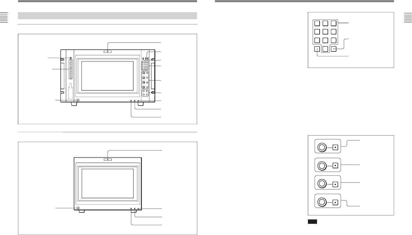
1 Tally lamp
2 POWER switch
3 DEGAUSS button
4 Numeric keypad
5 MANUAL adjustment
buttons and knobs
6 Menu operation buttons
7 POWER lamp
8 STANDBY lamp
9 OVER LOAD lamp
0 SHIFT button
qa Function buttons
qs OPTION connector
1 Tally lamp
7 POWER lamp
8 STANDBY lamp
9 OVER LOAD lamp
qs OPTION connector
17
(E)
Chapter 1 Overview
This manual explains the location and function of parts
and controls of the BVM-D14H5U/D14H5E/D14H5A.
The explanation also applies to the optional BKM-
10R/11R Monitor Control Unit.
1 Tally lamp
With factory settings, the tally lamp lights as follows
when the pins of the PARALLEL REMOTE [1]
connector on the rear panel are shorted:
– in red, when pins No.3 and No.9 are shorted.
– in green, when pins No.4 and No.9 are shorted.
– in amber, when pins No.3, No.4 and No.9 are
shorted.
The tally lamp lights as follows when the pins of the
PARALLEL REMOTE [2] connector on the rear panel
are shorted:
– in red, when pins No.3 and No.5 are shorted.
– in green, when pins No.4 and No.5 are shorted.
– in amber, when pins No.3, No.4 and No.5 are
shorted.
By changing the setting in the REMOTE menu,
different pins on the remote connector can be used to
control the tally lamp.
For information about the REMOTE menu, see “[D]
Assigning the Remote Control Functions
— REMOTE Menu” on page 37(E).
2 POWER switch
Press to turn on/off the monitor. By setting with the
ADDRESS menu, it is possible to turn on/off the
power of the specified monitors only, or of all
monitors at the same time.
For information about the ADDRESS menu, see “Selecting
the Monitor to Control — ADDRESS Menu” on page 45(E).
3 DEGAUSS button
Press to degauss the CRT (every time the monitor is
turned on, the CRT is degaussed automatically). To
degauss again, wait for more than five minutes.
4 Numeric keypad
Use to designate the channel number for the input
signal to be monitored, or to enter the setting values
with the menus.
5 MANUAL adjustment buttons and knobs
Each press of one of these buttons turns the button’s
green LED on or off. When the corresponding button
is on (lit), it is possible to manually adjust the contrast,
brightness, chroma and phase by turning the
corresponding knobs. The PHASE knob is also used to
enter the setting values with the menus. It is possible to
set the preset value for each adjusting item with the
CONTROL PRESET ADJ menu.
For Information about the CONTROL PRESET ADJ menu,
see “ [A] Preset Adjustment of the Picture Level Control
Knobs — CONTROL PRESET ADJ menu” on page 31(E).
Note
The PHASE and CHROMA knobs may not be
adjusted due to the signals. However, these knobs are
used for selecting the items or entering the setting
values with the menus. (continued)
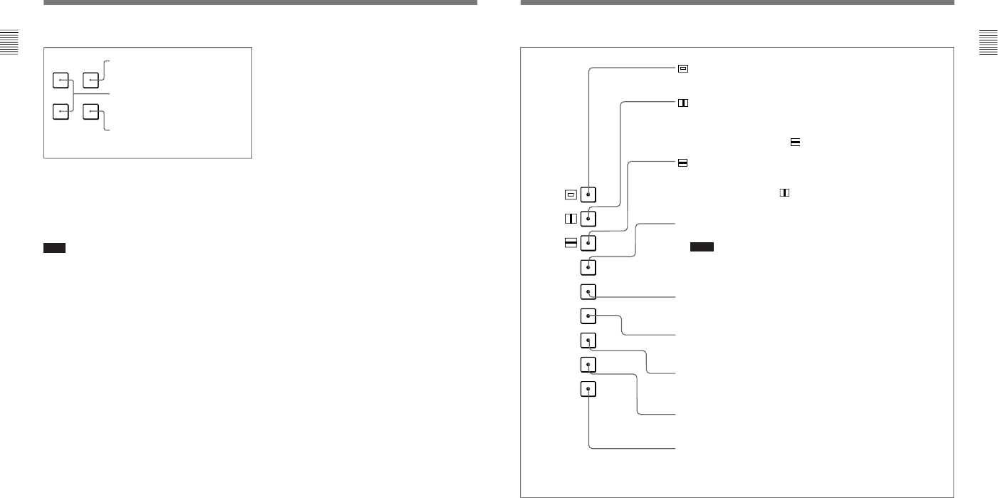
Numeric buttons
Ent button: Confirms the
values and characters entered
(ENTER button of the menu
operation buttons 6 has the
same function).
Del button: Deletes the values
and characters entered.
INPUT
123
Del
456
0
789
Ent
PHASE
CHROMA
BRIGHT
CONTRAST MANUAL
CONTRAST button
and knob
BRIGHT button
and knob
CHROMA button
and knob
PHASE button
and knob
1-12 BVM-D14H1U/D14H5U/D14H1E/D14H5E/D14H1A/D14H5A
18
(E)
Chapter 1 Overview
Location and Function of Parts
6 Menu operation buttons
For more information about menu operation, see “Basic
Menu Operations” on page 25(E).
7 POWER lamp
Lights when the monitor is put into operation mode
from standby mode (see STANDBY lamp 8) by
pressing the POWER switch 2.
Note
When the STANDBY lamp 8 is blinking, the monitor
cannot be put into operation mode (internal data
initialization is taking place). Wait until the
STANDBY lamp 8 is steadily lit.
8 STANDBY lamp
Lights when the monitor is in standby mode. The
monitor will be in standby mode under the following
conditions:
• The MAIN POWER switch (on the rear panel) is
turned on when the STANDBY MODE menu of the
SYSTEM CONFIG menu is set to ON (the
STANDBY lamp will blink for a few moments after
the switch is turned on, then will light).
• The monitor is changed from operation mode to
standby mode by external control.
For information about the SYSTEM CONFIG menu, see
“[E] Setting the Power-Up Conditions and Data about the
Screen Display — SYSTEM CONFIG Menu” on page
39(E).
9 OVER LOAD lamp
Lights when some malfunction has occured.
When the OVER LOAD lamp is lit, consult your
nearest Sony service facilities.
MENU button: Press to display the monitor
menus.
ENTER button: Press to confirm the items
and values entered (Ent button on the
numeric keypad 4 has the same function).
UP/DOWN buttons: Press to select the
items and setting values.
UP MENU
DOWN ENTER
0 SHIFT button
Press to select one of the two functions designated to
the function buttons !¡.
Each time the SHIFT button is pressed, the LED turns
on (SHIFT ON: lits in umber) and off (SHIFT OFF.)
SHIFT OFF: The functions indicated above the
function buttons can be used (the LED of the
function button lits in green.)
SHIFT ON: The functions indicated below the
function buttons can be used (the LED of the
function button lits in amber.)
!¡ Function buttons
Change the operation conditions for the monitor.
Each time the button is pressed, the LED turns on and
turns off, and the operation conditions are changed.
Each button has two functions. Select one of the two
functions by pressing the SHIFT button 0. When the
SHIFT button is set to ON, the LED lights in umber,
and when the SHIFT button is set to OFF, the LED of
each button lights in green.
For the functions of the function buttons in case of SHIFT
OFF and SHIFT ON, see pages 19(E) and 20(E).
!™ OPTION connector
Used to connect the BKM-11R Monitor Control Unit
or Auto Setup Probe (BKM-14L, etc.)
19
(E)
Chapter 1 Overview
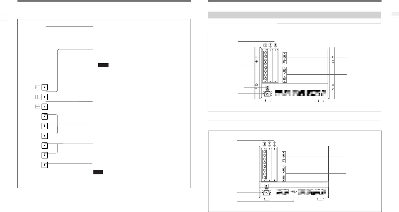
(Underscan) button: When this button is pushed in (ON), the picture is
underscanned by 3%, and four ends of the raster is displayed on the screen.
(H delay) button: When this button is pushed in (ON), the picture moves
horizontally, and a horizontal sync signal appears approximately one quarter in the
left edge of the screen.
• The brightness of the picture increases automatically, and it makes it easy to check
the sync part.
• If it is pressed together with the button, a pulse cross picture is displayed.
(V delay) button: When this button is pushed in (ON), the picture moves vertically,
and a vertical sync signal appears approximately in the center of the screen.
• The brightness of the picture increases automatically, and it makes it easy to check
the sync part.
• If it is pressed together with button, a pulse cross picture is displayed.
MONO button: When this button is pushed in (ON), a monochrome picture is displayed.
When the buttons is off, the monitor switches automatically color mode.
Notes
• The MONO button does not function with the RGB signal input.
• When the NTSC or PAL color signals are received and color burst signals are not
input, the monitor does not switch to color mode.
APT (aperture) button: When this button is pushed in (ON), the frequency response
can be modified. The degree of modification is set with the menu. (When RGB
signals are input, the button does not function.)
COMB button: This button does not function with this monitor.
However, when the BKM-127W NTSC/PAL Input Adaptor (optional) is installed and the
NTSC or PAL color signals are received, the monitor can be used with the comb filter
turned on.
F1 button: When this button is pushed in (ON), the characters disappear from the
monitor on the MANUAL menu of the level 1 of the CONTROL PRESET ADJ menu, the
MANUAL menu of the level 1 of the COLOR TEMP ADJ menu, and the ALIGNMENT
menu.
F2 button: When this button is pushed in (ON), you can access directly the MANUAL
menu of the level 1 of the COLOR TEMP ADJ menu, if the short-cut function is assigned
to this button.
ADDRESS button: When this button is pushed in (ON), the ADDRESS menu appears
on the screen. By using the ADDRESS menu, operation conditions for multiple
monitors are set.
For more information about the ADDRESS menu, see “Selecting the Monitor to
Control — ADDRESS Menu” on page 45(E).
Function buttons in SHIFT OFF mode (LEDs of function buttons in green)
MONO
APT
COMB
F1
F2
ADDRESS
16 : 9
SYNC
BLUE
ONLY
R
G
B
F3
F4
MARKER
1-13
BVM-D14H1U/D14H5U/D14H1E/D14H5E/D14H1A/D14H5A
20
(E)
Chapter 1 Overview
Location and Function of Parts
Function buttons in SHIFT ON mode (LEDs of function buttons in amber)
16:9 button: When this button is pushed in (ON), the aspect ratio changes to
16:9, and when set to OFF, the aspect ratio changes to 4:3.
The aspect ratio is fixed to 16:9 when the signal other than 4:3 signal
format is input. For details, see “Available Signal Format” on page 53(E).
SYNC button: When this button is pushed in (ON), the monitor synchronizes
to the sync signal input to the SYNC connectors on the BKM-129X (EXT
SYNC). When set to OFF, it synchronizes to the sync signal included in
the signals being monitored (INT SYNC).
Notes
• When INT SYNC is selected, use a component including a sync signal
on the Y signal, and use RGB signal including a sync signal on the G
signal.
• When the BKM-129X is not installed to the monitor or serial digital
signals are monitored, INT SYNC is automatically selected. You cannot
select EXT SYNC.
BLUE ONLY button: When this button is pushed in (ON), red and green
signals are cut, and only the blue signal is displayed as a monochrome
picture. It makes it easy to adjust CHROMA and PHASE, and to check
VTR noise.
R/G/B buttons: When these buttons are pushed in (ON), R(red), G(green),
and B(blue) beams are cut respectively.
F3/F4 buttons: For future expansion.
MARKER button: When this button is pushed in (ON), a 4:3 marker is
displayed and it is possible to check the 4:3 aspect area in the 16:9 picture.
Note
The 4:3 marker is not displayed when the signals of the 4:3 aspect ratio are
monitored or the monitor is in H/V delay mode
MONO
APT
COMB
F1
F2
ADDRESS
16 : 9
SYNC
BLUE
ONLY
R
G
B
F3
F4
MARKER
21
(E)
Chapter 1 Overview
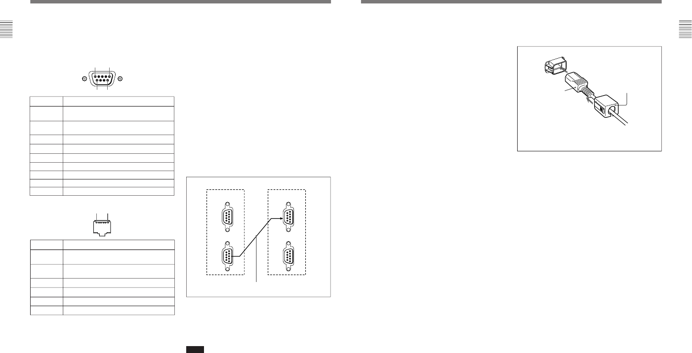
BVM-D14H1U/D14H1E/D14H1A/D14H5U/D14H5E/D14H5A Rear Panel
BVM-D14H5U/D14H5E/D14H5A
BVM-D14H1U/D14H1E/D14H1A
1 PARALLEL REMOTE
1/2 connectors
2 SERIAL REMOTE
connectors
3 Input option slots
4 Analog input/output
connectors
5 MAIN POWER switch
6 AC IN connector
1 PARALLEL REMOTE
1/2 connectors
2 SERIAL REMOTE
connectors
3 Input option slots
4 Analog input/output
connectors
5 MAIN POWER switch
6 AC IN connector
7 CONTROL UNIT
connector
(continued)
1-14 BVM-D14H1U/D14H5U/D14H1E/D14H5E/D14H1A/D14H5A
22
(E)
Chapter 1 Overview
Location and Function of Parts
1 PARALLEL REMOTE1/2 connectors
(1: female, D-sub 9-pin, 2: modular connector)
Form a parallel switch and controls the monitor
externally. The pin assignment and factory setting
function assigned to each pin are given below.
1: D-sub 9-pin
15
96
2: modular connector
1 6
All pin function assignments can be changed with the
REMOTE menu.
For information about the REMOTE menu, see “ [D]
Assigning the Remote Control Functions — REMOTE
Menu” on page 37(E).
Pin number
1Set input signal channel 1 (numeric keypad
function)
2Set input signal channel 2 (numeric keypad
function)
3 Set red tally lamp on or off
4 Set green tally lamp on or off
5 Select sync signal (SYNC button function)
6 Set underscan on or off
7 Set a 16:9 aspect ratio on or off
8
Functions
Set the 4:3 area marker display on or off
9GND
Pin number
1Set input signal channel 1 (numeric keypad
function)
2Set input signal channel 2 (numeric keypad
function)
3 Set red tally lamp on or off
4 Set green tally lamp on or off
5 GND
6 Set underscan on or off
Functions
Cable with D-sub 9-pin plugs
(not supplied)
Monitor 1 Monitor 2
IN
SERIAL
REMOTE SERIAL
REMOTE
OUT
IN
OUT
To switch each function between on and off or
between enable and disable, change pin connections in
the following way.
ON or enabled: Short each pin and pin 9 together for
D-sub 9-pin.
Short each pin and pin 5 together for modular
connector.
OFF or disabled: Leave each pin open.
2 SERIAL REMOTE connectors
(female, D-sub 9-pin)
These are RS-485 serial interface connectors, used for
connecting two or more BVM-xxE/F/G, BVM-xxD
and HDM-xxE series monitors.
The IN and OUT connectors form a loop-through
connection.
Connect two monitors using a cable with D-sub 9-pin
plugs such as an RCC-5G (not supplied) as shown in
the figure on the next page.
3 Input option slots (three slots)
The monitor may be fitted with optional input adaptors
up to three.
The BKM-129X is installed to the monitor at the
factory.
Notes
• The BKM-142HD uses two input option slots.
• Each adaptor can also be installed into SLOT 1.
Install any adaptor to SLOT 1.
23
(E)
Chapter 1 Overview
6 AC IN connector (3-pin)
Connects the monitor to an AC power source, via the
supplied AC power cord.
7 CONTROL UNIT connector (female, D-sub 9-
pin) (BVM-D14H1U/D14H1E/D14H1A only)
Connects a monitor control unit such as the BKM-10R
using a cable with D-sub 9-pin plugs such as an RCC-
5G (not supplied).
4 Analog input/output connectors (BKM-129X)
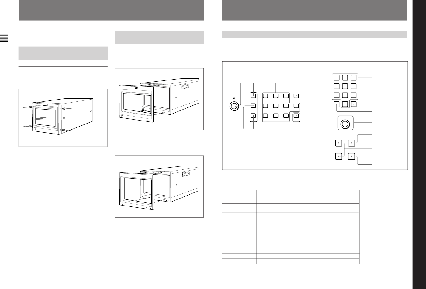
1-15
BVM-D14H1U/D14H5U/D14H1E/D14H5E/D14H1A/D14H5A
24
(E)
Chapter 1 Overview
Installation of the 4:3 Mask
When the aspect ratio is switched from 16:9 to 4:3,
replace the 16:9 mask with the supplied 4:3 mask.
BVM-D9H1U/D9H1E/D9H1A/
D9H5U/D9H5E/D9H5A
Installing the 4:3 mask
1
Remove four screws from both sides of the monitor
and then remove the16:9 mask.
2
Install the 4:3 mask (supplied) and fix both sides
with four screws.
Replacing the 16:9 mask
Remove the 4:3 mask and replace the 16:9 mask using
the same procedures as those for installing the 4:3
mask.
BVM-D14H1U/D14H1E/D14H1A/
D14H5U/D14H5E/D14H5A
Installing the 4:3 mask
1
Remove the 16:9 mask.
2
Install the 4:3 mask (supplied).
1Attach the lower portion of the mask.
2Attach the upper portion of the mask by
pressing it until the click.
Replacing the 16:9 mask
Remove the 4:3 mask and replace the 16:9 mask using
the same procedures as those for installing the 4:3
mask.
25
(E)
Chapter 2 Menu
Basic Menu Operations
Menu Operation Buttons
Button Function
UP button Moves the cursor upward. In setting mode, increases the setting
and adjustment values.
DOWN button Moves the cursor downward. In setting mode, decreases the
setting and adjustment values.
The menus are operated using the menu operation
buttons on the front panel of the monitor or BKM-
10R/11R Monitor Control Unit.
The functions of the menu operation buttons are
described below.
MENU button Displays the Menus. Goes back to the menu of the upper level
(on the Main Menu, goes back to the normal picture).
ENTER button/ Executes the items selected and settings.
Ent button
PHASE knob By turning this knob clockwise, the cursor moves upward. In
setting mode, increases the setting and adjustment values (has
the same function as UP button).
By turning this knob counterclockwise, the cursor moves
downward. In setting mode, decreases the setting and
adjustment values (has the same function as DOWN button).
1 2 3 Del
4560
789
Ent
PHASE
MENU
UP
DOWN
UP MENU
DOWN ENTER
INPUT
123
Del
456
0
789
Ent
PHASE
Buttons on the BVM-D9H5U/D9H5E/D9H5A
PHASE
knob MENU button Numeric keypad Del button
UP
button DOWN button Ent button
Buttons on the BVM-D14H5U/D14H5E/D14H5A
Numeric keypad
Ent button
Del button
PHASE knob
MENU button
UP/DOWN buttons
ENTER button
Numeric keypad Enters the numerical values.
Del button Deletes the values and characters entered.
Chapter 2 Menu
1-16 BVM-D14H1U/D14H5U/D14H1E/D14H5E/D14H1A/D14H5A
26
(E)
Chapter 2 Menu
Basic Menu Operations
Displaying the Menus
Press the MENU button.
The menu list is displayed on the screen.
CONTROL PRESET ADJ...
MENU
COLOR TEMP ADJ...
INPUT CONFIG...
REMOTE...
SYSTEM CONFIG...
STATUS...
ALIGNMENT...
p
Menu List
When you select one item on the main menu, the level
1 menu corresponding to the selected item on the main
menu appears.
For information about the items on the main menu, see
“Menu Structure” on page 30(E).
Note
Menu settings that cannot be changed are displayed in
blue.
About menu numbers
For purposes of explanation in this manual, each menu
is preceded by menu numbers. The alphabet
determines the classification of menus on the Menu
List (Main Menu), and the numbers determine the
level and the order. These menu numbers are not
shown on the screen.
e.g. A135
Note
Only the menus which require explanation are
preceded by menu numbers. Thus, the menu number is
counted without menus which do not require
explanation.
Menu Operation
Follow the steps described below to display the menu
and perform the adjustment or setup you wish.
1
Press the MENU button.
The Menu List is displayed.
2
Using the UP/DOWN buttons or PHASE knob,
move the cursor to the desired item. (Example:
select the INPUT CONFIG menu by pressing the
DOWN button.)
3
Press the ENTER button or Ent button.
The Level 1 of the selected menu is displayed.
Cursor
Menu List
CONTROL PRESET ADJ...
MENU
COLOR TEMP ADJ...
INPUT CONFIG...
REMOTE...
SYSTEM CONFIG...
STATUS...
ALIGNMENT...
p
(continued)
Indicates the CONTROL PRESET ADJ menu
Indicates the first menu in Level 1
Indicates the third menu in Level 2
Indicates the fifth menu in Level 3
HC 1
INPUT CONFIG(1/2) ↓
FORMAT... YPBPR
SLOTNOSLOT1
INPUTNO1
EXT SYNC SLOT SLOT1
AUDIO INPUT ---
COLOR TEMP STD
APERTURE VALUE ---
CHANNEL NAME... PROG
p
↓
B
B
B
B
B
B
B
A
B
C
D
E
F
G
27
(E)
Chapter 2 Menu
4
Repeat steps 2 and 3 until the desired menu is
displayed.
For more information about setting and
adjustments, see below.
To abort menu operation
Press the MENU button. The menu of the upper level
is displayed.
The setting or adjustment being performed is canceled,
and data loading or saving is aborted.
If “NG” or “ERROR” appears during menu
operation
Press the MENU button to return to the menu in use.
Enters
numerical
values.
[ ↓ ] indicates that
the menu
continues onto
next page.
[ ↑ ] indicates that
the menu is
continued from
previous page.
Selects from
various options.
Indicates that
this item has
sub-list. Thus,
you can go to
the lower level.
HC 1
INPUT CONFIG(1/2) ↓
FORMAT... YPBPR
SLOTNOSLOT1
INPUTNO1
EXT SYNC SLOT SLOT1
AUDIO INPUT ---
COLOR TEMP STD
APERTURE VALUE ---
CHANNEL NAME... PROG
p
↓
Choosing one of two or more selections
Selecting in setting mode
1
Using the UP/DOWN buttons or PHASE knob,
move the cursor to the desired item and press the
ENTER or Ent button.
The selected item is displayed in yellow text and
set to setting mode.
2
Using the UP/DOWN buttons or PHASE knob,
change the setting.
3
Press the ENTER or Ent button.
The setting is confirmed (The item is displayed in
white text again).
Selecting from the setting list
1
Using the UP/DOWN buttons or PHASE knob, move
the cursor to the desired item in the setting list.
2
Press the ENTER or Ent button.
The display returns to the menu of the upper level,
and the selected setting is executed.
HC 1
CHANNEL NAME
PROG
EDIT
CAM
VTR
NEW NAME
p
HC 1
INPUT CONFIG(1/2) ↓
FORMAT... YPBPR
SLOTNOSLOT1
INPUTNO1
EXT SYNC SLOT SLOT1
AUDIO INPUT ---
COLOR TEMP STD
APERTURE VALUE 100
CHANNEL NAME... PROG
p
↓

1-17
BVM-D14H1U/D14H5U/D14H1E/D14H5E/D14H1A/D14H5A
28
(E)
Chapter 2 Menu
Basic Menu Operations
Entering a numerical value
1
Using the UP/DOWN buttons or PHASE knob,
move the cursor to the desired item and press the
ENTER or Ent button.
The selected item is displayed in yellow text and
set to setting mode.
2
Set the value in one of the following three ways:
• Enter the value directly using the numeric keypad
and press the ENTER or Ent button
• Select the value using the UP/DOWN buttons
• Select the value using the PHASE knob
3
Press the ENTER or Ent button.
The setting is confirmed (The item is displayed in
white text again).
Entering characters
1
Display the setting menu and set the cursor to
NEW NAME using the UP/DOWN buttons or
PHASE knob.
HC 1
INPUT CONFIG(1/2) ↓
FORMAT... YPBPR
SLOTNOSLOT1
INPUTNO1
EXT SYNC SLOT SLOT1
AUDIO INPUT ---
COLOR TEMP STD
APERTURE VALUE 100
CHANNEL NAME... PROG
p
↓
HC 1
CHANNEL NAME
PROG
EDIT
CAM
VTR
NEW NAME
p
2
Press the ENTER or Ent button.
“?” is displayed in yellow. The “?” indicates the
position where character input is possible.
3
Select the character you wish to enter using the
UP/DOWN buttons or PHASE knob.
When you press the UP button, or turn the PHASE
knob clockwise, the characters and symbols appear
in the order shown below.
A B .............Y Z 0 1 ...............8 9 ( , ) : ; .
- + / & (space) ?
If you press the UP/DOWN button or turn the
PHASE knob counterclockwise, the characters and
symbols appear in the reverse order described
above.
4
Press the ENTER or Ent button.
The selected character is entered.
5
Repeat steps 3 and 4 until all the characters are
entered, then press the ENTER or Ent button.
The selected characters are confirmed, and the
display returns to the menu of the previous level.
To correct the entered character
Press the Del button on the numeric keypad. The
character on the left side of the “?”(in yellow) is
deleted.
HC 1
CHANNEL NAME
PROG
EDIT
CAM
VTR
NEW NAME
?
p
HC 1
CHANNEL NAME
PROG
EDIT
CAM
VTR
NEW NAME
C?
p
29
(E)
Chapter 2 Menu
ADDRESS Menu
In addition to the menus displayed on the menu list, the
ADDRESS menu is provided. This ADDRESS menu is
used to select the monitor or the monitor group, so that
when several monitors are connected together via
serial remote ports, the control panel can select which
monitor to control.
To display or exit the ADDRESS menu, press the
ADDRESS button. The method of choosing menu
items and changing settings is the same as with the
other menus.
For information about the ADDRESS menu, see “Selecting
the Monitor to Control —ADDRESS Menu” on page 45(E).
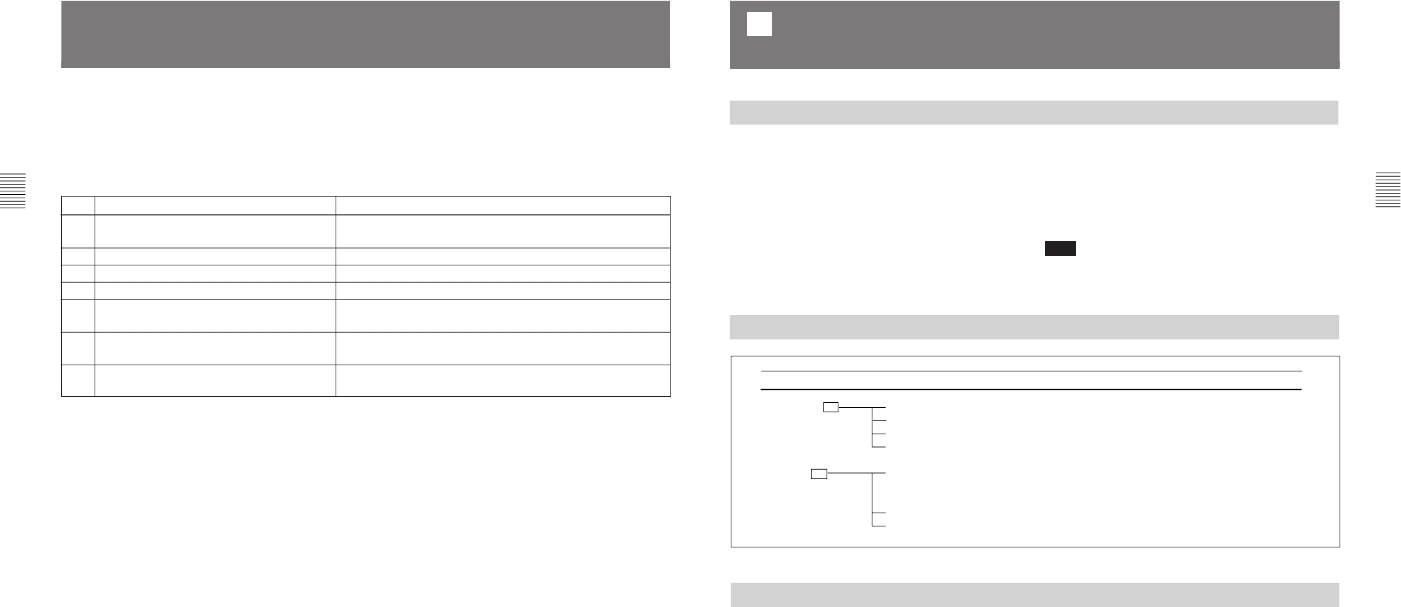
1-18 BVM-D14H1U/D14H5U/D14H1E/D14H5E/D14H1A/D14H5A
30
(E)
Chapter 2 Menu
Menu Structure
Menus consist of one to three levels.
Detailed information on the levels of menus is
described at the top of explanation of each menu.
Main Menu Functions
ACONTROL PRESET ADJ menu Sets the preset values for the input signal’s chroma, contrast,
phase, and brightness. (page 31(E))
BCOLOR TEMP ADJ menu Sets the color temperature. (page 33(E))
CINPUT CONFIG menu Sets the input channel. (page 35(E))
DREMOTE menu Sets the remote control functionality. (page 37(E))
ESYSTEM CONFIG menu Sets the power-up conditions and data about the screen display.
(page 39(E))
FSTATUS menu Displays the information about the monitor or options installed in
the monitor. (page 42(E))
GALIGNMENT menu Adjusts the position, size and geometry of the picture. (page
43(E))
31
(E)
Chapter 2 Menu
MANUAL A1
AUTO A2
CHROMA
PHASE
CONTRAST
BRIGHT
FULL FIELD WHITE 100%
8COLOR BAR 100%
8COLOR BAR 75%
SMPTE COLOR BAR
EIA COLOR BAR
The preliminary adjustments of chroma, phase,
contrast and brightness are carried out with the
CONTROL PRESET ADJ menu to set the preset
values to the knobs for the above-mentioned
adjustments.
Preset values can be set in the following two ways:
• Adjustment with the MANUAL adjustment knobs
(MANUAL menu)
• Automatic adjustment (AUTO menu)
An external color bar signal is necessary.
Note
After installing the optional board, carry out AUTO
adjustment.
This section explains the setting lists displayed in the
menu.
How to read the setting lists
• For purposes of explanation, each setting list is
preceded by a menu number. These numbers are not
displayed on the screen.
For more information about the menu number, see “About
menu numbers” on page 26(E).
Overview
• The arrow mark (÷) refers you to another setting list
that appears after you make the setting, or to an
operation that is carried out as a result of the setting.
When there is no arrow mark, the menu does not have
any sub-list.
Setting Lists in the CONTROL PRESET ADJ Menu
Structure of the CONTROL PRESET ADJ Menu
A Preset Adjustment of the Picture Level Control
Knobs — CONTROL PRESET ADJ Menu
Level 1 Level 2
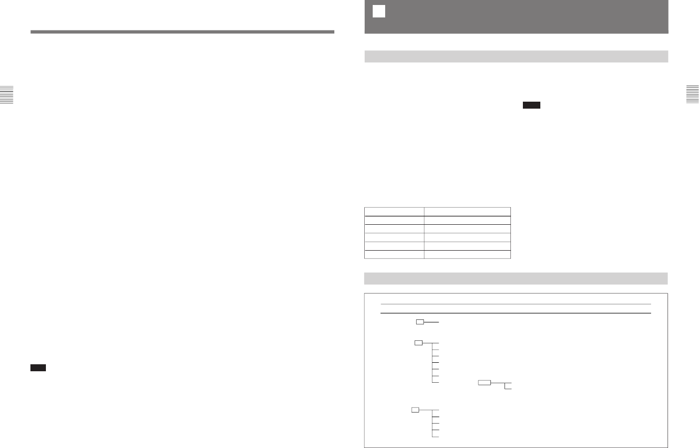
1-19
BVM-D14H1U/D14H5U/D14H1E/D14H5E/D14H1A/D14H5A
32
(E)
Chapter 2 Menu
[A] CONTROL PRESET ADJ menu
Select the setting method.
MANUAL... : Set with the MANUAL adjustment
knobs. ÷[A1]
AUTO... : Set by automatic adjustment. ÷[A2]
[A1] MANUAL menu
Adjust values by turning the CHROMA, PHASE,
CONTRAST, and/or BRIGHT knobs. After the
adjustment, press the ENTER or Ent button to confirm
the adjusted values.
The setting value is 0 to 200.
CHROMA: xxx
PHASE: xxx
CONTRAST: xxx
BRIGHT: xxx
When you want to erase characters from the screen
while adjusting manually
Press the [F1] button. The characters disappear. To
display characters, press the [F1] button again.
To reset the setting to the default
Press the corresponding MANUAL adjustment button
(BVM-D14H5U/D14H5E/D14H5A) or knob (BVM-
D9H5U/D9H5E/D9H5A.) The adjusted value is reset
to 100 (default).
[A2] AUTO menu
You can adjust the CHROMA and PHASE levels
automatically. Input the color bar signals to the board
to be adjusted and select the required color bar signals.
÷Adjustment is carried out.
8COLOR BAR 100%: 100% full-field 8-color bar
(white, yellow, cyan, green. magenta, red, blue,
black)
8COLOR BAR 75%: 75% full-field color bar (with
100% white signal)
SMPTE COLOR BAR: SMPTE standard color bar
EIA COLOR BAR: EIA standard color bar
Note
When you execute the AUTO menu, SYNC button
should be set to OFF (INT SYNC).
EXT SYNC will cause an error abortion of auto
adjustment procedure.
A Preset Adjustment of the Picture Level Control Knobs — CONTROL PRESET ADJ Menu
33
(E)
Chapter 2 Menu
Overview
Manufacturer Probe Model Name
SONY BKM-14L (no cable required)
GRASEBY SLS 9400
MINOLTA CA-100
PHILIPS PM 5639
THOMA TF6
B Adjusting the Color Temperature
— COLOR TEMP ADJ Menu
The monitor can memorize the data for up to three
color temperatures (STD, COL1, COL2.) The data for
each color temperature is adjusted with the COLOR
TEMP ADJ menu. The data of the color temperature
selected in the INPUT CONFIG menu is adjusted.
Color temperature adjustment can be made in the
following three ways:
• Knob adjustment (MANUAL menu)
You can adjust the color temperature with the bias
and gain knobs.
• Automatic adjustment using a probe
(PROBE menu)
You can use the following probes for automatic
adjustment of color temperature. Except for the Sony
BKM-14L, a cable is required to connect the color
analyzer to the monitor.
For more information about the cable specification required
and about the connection, see “Connection Cable
Specifications for Color Temperature Probes” on page
54(E).
Notes
• The CRT size of the BVM-D9H1U/D9H1E/D9H1A/
D9H5U/D9H5E/D9H5A is small. So, when a probe
other than the Sony BKM-14L is used, use the probe
closely to the CRT screen.
• After the color temperature is adjusted by automatic
adjustment, carry out the AUTO adjustment of the
CONTROL PRESET ADJ menu (AUTO CHROMA
PHASE adjustment.)
• Copying other color temperature data (COPY
menu)
You can copy the memorized color temperature data
(STD/COL1/COL2/D65/D93.) Use the factory
setting value or the adjusted value as an original
value to shorten the adjustment time.
MANUAL B1
COPY B3 STD
COL1
COL2
D65
D93
ADJUST
D65
D93
START
PROBE
X
Y
LOW LIGHT (20 IRE)
HIGH LIGHT (100 IRE)
LOAD REF VALUE B21
@@@
PROBE B2
Structure of the COLOR TEMP ADJ Menu
Level 1 Level 2 Level 3

1-20 BVM-D14H1U/D14H5U/D14H1E/D14H5E/D14H1A/D14H5A
34
(E)
Chapter 2 Menu
Setting Lists in the COLOR TEMP ADJ Menu
This section explains the setting lists displayed in the
menu.
How to read the setting lists
• For purposes of explanation, each setting list is
preceded by a menu number. These numbers are not
displayed on the screen.
For more information about the menu number, see “About
menu numbers” on page 26(E).
• The arrow mark (÷) refers you to another setting list
that appears after you make the setting, or to an
operation that is carried out as a result of the setting.
When there is no arrow mark, the menu does not have
any sub-list.
[B] COLOR TEMP ADJ menu
Select the adjustment method.
MANUAL... : Set with the MANUAL adjustment
knob. ÷[B1]
PROBE... : Set using a probe. ÷[B2]
COPY... : Copy data from elsewhere. ÷[B3]
[B1] MANUAL menu
Adjust the gain and bias with the MANUAL
adjustment knob.
ADJUST... : Adjust the gain and bias. To shift
between gain adjustment and bias adjustment,
press UP/DOWN buttons. Use appropriate knobs
in each adjustment as described below. After the
adjustment, press the ENTER or Ent button to
confirm the adjusted values.
RED: CONTRAST KNOB (Adjust the R gain or
bias with the CONTRAST knob.)
GREEN: BRIGHT KNOB (Adjust the G gain or
bias with the BRIGHT knob.)
BLUE: CHROMA KNOB (Adjust the B gain or
bias with the CHROMA knob.)
LUMINANCE: PHASE KNOB (Adjust
luminance with the PHASE knob.)
To reset RED/GREEN/BLUE to the value
before adjustment
When you are adjusting the gain or bias using the
MANUAL adjustment knobs, you can reset the
setting to the one before adjustment by pressing the
corresponding MANUAL adjustment button
(BVM-D14H5U/D14H5E/D14H5A) or knob
(BVM-D9H5U/D9H5E/D9H5A).
To reset all of settings at the same time, press the
PHASE button or knob.
Note
You cannot reset the setting after you press the
ENTER or Ent button.
To access the MANUAL menu directly
When the [F2] button is assigned as the short-cut key
to the MANUAL menu, you can directly access the
MANUAL menu that corresponds to the color
temperature setting (STD/COL1/COL2) set to the
image on the screen.
For details of how to assign the short-cut key, see “ [E]
Setting the Power-Up Conditions and Data about the Screen
Display — SYSTEM CONFIG Menu” on page 39(E).
[B2] PROBE menu
Select the probe for color temperature adjustment.
START: Start adjustment.
PROBE: Select the probe.
X: Enter the x coordinate.
Y: Enter the y coordinate.
LOW LIGHT (20IRE): Enter the luminance (cd/m2)
for low light.
HIGH LIGHT (100IRE): Enter the luminance (cd/
m2) for high light.
LOAD REF VALUE: Select the standard settings of
the x and y coordinates. ÷[B21]
[B21] LOAD REF VALUE
Select one of the followings:
D65: Use D65 setting (x and y coordinates and
standard luminance).
D93: Use D93 setting (x and y coordinates and
standard luminance).
[B3] COPY menu
Select one of followings: ÷ The current data, which is
used for adjusting, is copied.
STD: Copy STD data (factory setting: D65).
COL1: Copy COL 1 data (factory setting: D93).
COL2: Copy COL 2 data (factory setting: D65).
D65: Copy the color temperature of D65.
D93: Copy the color temperature of D93.
Note
The current data which is used for adjusting (selected
in the INPUT CONFIG menu) is displayed in blue
letters and you can not select it.
B Adjusting the Color Temperature — COLOR TEMP ADJ Menu
35
(E)
Chapter 2 Menu
You can set up to nine input channels.
Data pertaining to the input signals are set with the
INPUT CONFIG menu.
When a channel number (1 to 9) is entered with the
numeric keypad, it is then possible to set which input
connector on the rear panel will be assigned to that
channel number, and select the type of signal that will
be connected.
Assigning slot and connector numbers
Set which input connector on which slot will be
assigned to the current channel.
Assigning the signal type and format
The signal type and format which can be assigned to
each channel number vary, depending on what
adaptors are installed in the rear panel.
Overview
C
Setting the Input Configuration
— INPUT CONFIG Menu
To assign D1 serial digital signals
Serial digital signals can be assigned to the slot where
the BKM-120D is installed.
To assign analog composite signals
Analog composite signals can be assigned to the slot
where the BKM-127W is installed.
To assign HD serial digital signals
HD serial digital signals can be assigned to the slots
where the BKM-142HD is installed.
To assign analog component or RGB signals
Analog component or RGB signals can be assigned to
the slot where BKM-129X is installed.
INPUT CONFIG (1/2)
CH x
FORMAT C1
SLOT NO
INPUT NO
EXT SYNC SLOT
AUDIO INPUT
COLOR TEMP
APERTURE VALUE
CHANNEL NAME C 2
INPUT CONFIG (2/2)
CH x
1125/60I SYSTEM
H PHASE
MARKER PHASE
MARKER WIDTH
NTSC SET UP
YPBPR MATRIX
VCR MODE
YPBPR
RGB
NTSC, PAL
D1-SDI
HD-SDI
PROG
EDIT
CAM
VTR
NEW NAME
Structure of the INPUT CONFIG Menu
Level 1 Level 2

1-21
BVM-D14H1U/D14H5U/D14H1E/D14H5E/D14H1A/D14H5A
36
(E)
Chapter 2 Menu
This section explains the setting lists displayed in the
menu.
How to read the setting lists
• For purposes of explanation, each setting list is
preceded by a menu number. These numbers are not
displayed on the screen.
For more information about the menu number, see “About
menu numbers” on page 26(E).
• The arrow mark (÷) refers you to another setting list
that appears after you make the setting, or to an
operation that is carried out as a result of the setting.
When there is no arrow mark, the menu does not have
any sub-list.
[C] (1/2) INPUT CONFIG (1/2) menu
Set input signal data for each channel.
CH x: Current channel is indicated. To change the
channel, enter a channel number with the numeric
keypad. The settings below will be stored as
information of this channel.
FORMAT... : Select the input signal type. ÷[C1]
SLOT NO: Select the slot number.
INPUT NO: Select the input connector number.
EXT SYNC SLOT: Select the slot when the external
sync signal is used.
AUDIO INPUT (BVM-D9H5U/D9H5E/D9H5A
only): Select the audio input number.
COLOR TEMP: Select the color temperature.
APERTURE VALUE: Enter the aperture adjustment
value (0 to 200).
CHANNEL NAME: Give the channel a name.
÷[C2]
[C] (2/2) INPUT CONFIG (2/2) menu
Set input signal data for each channel.
CH x: Current channel is indicated. To change the
channel, enter a channel number with the numeric
keypad. The settings below will be stored as
information of this channel.
1125/60I SYSTEM: Select the number of active
scanning lines per frame for 1125/60I input
signals. When the HD SDI signal is input, the
number of active scanning lines is selected
automatically.
1035: The active scanning lines are 1035 lines.
1080: The active scanning lines are 1080 lines
Setting Lists in the INPUT CONFIG Menu
H PHASE: Set the horizontal picture position (–128 to
+127).
MARKER PHASE: Set the 4:3 marker position.
MARKER WIDTH: Set the 4:3 marker width.
NTSC SET UP: Set the setup level when the BKM-
127W is installed. SETUP 7.5 or 0.
YPBPR MATRIX: Select the matrix when YPBPR
signals of the signal format 480/60I or 480/60P
(TV lines 525) are input.
VCR MODE: Compensate for a distorted picture
when the input signals from the VCR are not
typical. This mode is effective when the signal
formats 480/60I or 575/50I are input.
ON: Operates when the signal formats 480/60I or
575/50I are input.
OFF:Does not operate.
[C1] FORMAT menu
Select the signal format.
YPBPR: Select the component signals when the
BKM-129X is installed. SPMTE, BETACAM 7.5
or 0.
RGB: Select when the BKM-129X is installed.
NTSC, PAL: Selects when the BKM-127W is
installed.
D1-SDI: Select when the BKM-120D is installed.
HD-SDI: Select when the BKM-142D is installed.
[C2] CHANNEL NAME menu
Give the channel a name. Enter a name after a preset
one or a new one.
PROG: Program signal.
EDIT: Signal from an editor.
CAM: Camera signal.
VTR: Signal from a VTR.
NEW NAME: Enter a new name. (Up to 20 characters
can be entered and up to six characters from the
head of the name are displayed in the INPUT
CONFIG menu ([C] 1/2).)
C Setting the Input Configuration — INPUT CONFIG Menu
37
(E)
Chapter 2 Menu
SERIAL REMOTE D1
MONITOR ADDRESS
GROUP ADDRESS
PARALLEL REMOTE
PARALLEL REMOTE CONFIG D2 1 PIN D21
2 PIN
3 PIN
4 PIN
5 PIN
6 PIN
7 PIN
8 PIN
CH D211 (1/2)
R OFF D211 (2/2)
The remote control functions are set with the
REMOTE menu. With this monitor, both serial remote
control (SERIAL REMOTE) and parallel remote
control (PARALLEL REMOTE) are possible.
• Settings for the serial remote control (SERIAL
REMOTE)
An address number (MONITOR ADDRESS) and
group number (GROUP ADDRESS) can be assigned
to the monitor connected to the SERIAL REMOTE
connector.
• ON/OFF setting for the parallel remote control
(PARALLEL REMOTE)
• Settings for the parallel remote control
(PARALLEL REMOTE)
Functions can be assigned to the pins of the
PARALLEL REMOTE connector.
Priority order of the remote control functions
It is possible to simultaneously use the BKM-10R/11R
Monitor Control Unit, SERIAL REMOTE, and
PARALLEL REMOTE for control, but commands
from PARALLEL REMOTE have priority. Therefore,
it is impossible for the BKM-10R/11R or SERIAL
REMOTE to change items set by PARALLEL
REMOTE.
There is no priority order between commands from
SERIAL REMOTE and the BKM-10R/11R control
panel.
PARALLEL REMOTE 1 and 2 are connected
parallel inside the unit, therefore, there is no priority
order between them.
About monitor address and group numbers
It is possible to control up to 32 monitors connected
via serial remote connector (using the SERIAL
REMOTE connector). By giving each monitor a
monitor address and group number, it is possible to
control just a specific monitor or monitor group.
With the SERIAL REMOTE menu, each monitor can
be set with a monitor address and group number,
between 1 and 99.
The ADDRESS menu is used to control the monitors
which are connected by the serial remote connectors.
For information about the ADDRESS menu, see “Selecting
the Monitor to Control — ADDRESS Menu” on page 45(E).
Note
The address number must differ from one monitor to
another. If two or more monitors have the same
address number, an operation error occurs.
Overview
Structure of the REMOTE Menu
Level 1 Level 2 Level 3
D
Assigning the Remote Control Functions
— REMOTE Menu

1-22 BVM-D14H1U/D14H5U/D14H1E/D14H5E/D14H1A/D14H5A
38
(E)
Chapter 2 Menu
Setting Lists of the REMOTE Menu
This section explains the setting lists displayed in the
menu.
How to read the setting lists
• For purposes of explanation, each setting list is
preceded by a menu number. These numbers are not
displayed on the screen.
For more information about the menu number, see “About
menu numbers” on page 26(E).
• The arrow mark (÷) refers you to another setting list
that appears after you make the setting, or to an
operation that is carried out as a result of the setting.
When there is no arrow mark, the menu does not have
any sub-list.
[D] REMOTE menu
Select the type of remote control.
SERIAL REMOTE : Set the address and group
number of the monitor controlled via the SERIAL
REMOTE connector. ÷[D1]
PARALLEL REMOTE: Select whether parallel
remote control will be used or not (ON or OFF.)
PARALLEL REMOTE CONFIG : Set the pin
assignments for the PARALLEL REMOTE
connector. ÷[D2]
[D1] SERIAL REMOTE menu
Set the monitor address and group number.
MONITOR ADDRESS: Enter a number.
GROUP ADDRESS: Enter a number.
[D2] PARALLEL REMOTE CONFIG menu
Select the PARALLEL REMOTE connector pins for
which you want to change the function. The factory
settings for each pin are given below. ÷[D211]
PINs 1 to 4, and PIN 6 of the PARALLEL REMOTE
1 and 2 are common settings.
1 PIN: CH01
2 PIN: CH02
3 PIN: TALLY RED
4 PIN: TALLY GREEN
5 PIN: EXT SYNC (PARALLEL REMOTE [1])
GND (PARALLEL REMOTE [2])
6 PIN: UNDERSCAN
7 PIN: 16:9
8 PIN: 4:3 MARKER
Note
PINs 1 to 4, and PIN 6 of the PARALLEL REMOTE
1 and 2 are connected inside the unit, therefore
different functions cannot be assigned to those pins.
[D211] (1/2) 1-8 PIN menu (1/2)
Assign a function to the selected pin.
CH: Select a channel number. Enter the desired
channel number with the numeric keypad.
----: Set to unused.
UNDER SCAN: Set underscan on or off.
16:9: Set a 16:9 aspect ratio on or off.
H DELAY: Set the horizontal sync display on or off.
V DELAY: Set the vertical sync display on or off.
EXT SYNC: Set the synchronization to external sync
signals enabled or disabled.
APERTURE: Set the correction of frequency
characteristics enabled or disabled.
MONO: Set monochrome display on or off.
BLUE ONLY: Set the blue signal pictures display
(monochrome) on or off.
[D211] (2/2) 1-8 PIN menu (2/2)
Assign a function to the selected pin.
R OFF: Set cutting red beams enabled or disabled.
G OFF: Set cutting green beams enabled or disabled.
B OFF: Set cutting blue beams enabled or disabled.
4:3 MARKER: Set the 4:3 marker display on or off.
CAPTION VISION: Set Caption Vision on or off.
TALLY RED: Set tally red on or off.
TALLY GREEN: Set tally green on or off.
DEGAUSS: Set degaussing on or off.
POWER OFF: Set the monitor power on or off.
For the pin assignment, see “PARALLEL REMOTE 1/2
connectors” in the Location and Function of Parts on page
13(E) for BVM-D9H1U/D9H1E/D9H1A/D9H5U/D9H5E/
D9H5A or page 22(E) for BVM-D14H1U/D14H1E/
D14H1A/D14H5U/D14H5E/D14H5A.
D Assigning the Remote Control Functions — REMOTE Menu
39
(E)
Chapter 2 Menu
Overview
The SYSTEM CONFIG menu is displayed on the two
pages.
The SYSTEM CONFIG (1/2) menu is used for the
following settings:
•Power-up condition (STANDBY MODE menu)
This menu sets the condition of the monitor when the
MAIN POWER switch on the rear panel is switched
on (BVM-D14H1U/D14H1E/D14H1A/D14H5U/
D14H5E/D14H5A) or when the battery is installed
(BVM-D9H1U/D9H1E/D9H1A/D9H5U/D9H5E/
D9H5A.)
•Power-up input channel (DEFAULT CH menu)
This menu sets the power-up input channel.
•Time from power-up until degauss (DEGAUSS
DELAY menu)
If several monitors are turned on at the same time and
all start degaussing at the same time, there will be a
very large current draw on the power supply for a few
moments. To prevent this, the delay time between
power-up and degaussing can be set for each monitor
independently.
•Setting of the contrast and brightness after
adjusting the white balance (CONT/BRT HOLD
menu)
Selects if the adjusted contrast and brightness are
retained or they are reset to the center values, when
the color temperature is adjusted in the COLOR
TEMP ADJ menu.
•Assigning shortcut to the COLOR TEMP ADJ
menu to the [F2] key (COL TEMP SHORT-CUT
menu)
Assigns the shortcut to the MANUAL menu of the
COLOR TEMP ADJ menu to the [F2] key. This
allows you to jump directly to the MANUAL menu
corresponding to the color temperature set to the
currently displayed image (STD/COL 1/COL 2.)
• Auto color control (ACC SW menu) (when using
the BKM-127W)
Selects if the ACC (Auto Color Control) circuit is
turned on or off.
•Selecting the monitor to copy the original data
(CONFIG COPY menu)
Setting data of the INPUT CONFIG and SYSTEM
CONFIG (except the DEGAUSS DELAY data)
menus can be copied from the serial connected
monitor.
The SYSTEM CONFIG (2/2) menu is used for the
following settings:
• Display mode and position of the signal format
(FORMAT DISPLAY and POSITION menus)
• Display mode and position of the channel number
(CH NO and POSITION menus)
• Display mode and position of the channel name
(CH NAME and POSITION menus)
• Display mode of the caption (CAPTION menu)
• Maintenance (MAINTENANCE menu)
This is for a service qualified personnel.
E
Setting the Power-Up Conditions and Data about
the Screen Display — SYSTEM CONFIG Menu

1-23
BVM-D14H1U/D14H5U/D14H1E/D14H5E/D14H1A/D14H5A
40
(E)
Chapter 2 Menu
SYSTEM CONFIG (1/2)
@
STANDBY MODE
@
DEFAULT CH
@
DEGAUSS DELAY
@
CONT/BRT HOLD
@
COL TEMP SHORT-CUT
@
ACC SW
@
CONFIG COPY E1
SYSTEM CONFIG (2/2)
@
FORMAT DISPLAY E2
@
POSITION
@
CH NO E3
@
POSITION
@
CH NAME E4
@
POSITION
@
CAPTION E5
@
MAINTENANCE
LAST
CH x
MONITOR ADDRESS E11
ENTER PASSWORD
Structure of the SYSTEM CONFIG Menu
Level 1 Level 2
Setting Lists of the SYSTEM CONFIG Menu
This section explains the setting lists displayed in the
menu.
How to read the setting lists
• For purposes of explanation, each setting list is
preceded by a menu number. These numbers are not
displayed on the screen.
For more information about the menu number, see “About
menu numbers” on page 26(E).
• The arrow mark (÷) refers you to another setting list
that appears after you make the setting, or to an
operation that is carried out as a result of the setting.
When there is no arrow mark, the menu does not have
any sub-list.
• The factory setting is shown in the brackets.
[E] (1/2) SYSTEM CONFIG (1/2) menu
Set each of the following items.
STANDBY MODE: Select the power-up condition
when the MAIN POWER switch is turned on
(BVM-D14H1U/D14H1E/D14H1A/D14H5U/
D14H5E/D14H5A) or when the battery is installed
(BVM-D9H1U/D9H1E/D9H1A/D9H5U/D9H5E/
D9H5A.)
ON: Standby mode
[OFF]: Operation mode
DEFAULT CH: Select the power-up input channel
(LAST or CH x).
[LAST]: Set the channel to the channel that was
selected at the time the power was last turned
off.
CH x: Set the channel to a specific channel
number.
DEGAUSS DELAY: Set the time between power-up
and the beginning of degaussing. Enter the desired
time (in seconds, 0 to 255).
ESetting the Power-Up Conditions and Data about the Screen Display — SYSTEM CONFIG Menu
41
(E)
Chapter 2 Menu
CONT/BRT HOLD: Select the contrast and
brightness settings to the center or adjusted value
after adjusting the white balance or auto
adjustment of CONTROL PRESET ADJ (OFF or
ON).
ON: The contrast and brightness are set to the
value before adjusting.
[OFF]: The contrast and brightness are set to the
center value (100) after adjusting.
COL TEMP SHORT-CUT: Assign the shortcut
function to the MANUAL menu of the COLOR
TEMP ADJ menu to [F2] key (OFF or F2).
F2: Assigns the shortcut to the MANUAL menu
of the COLOR TEMP ADJ menu.
[OFF]: Does not assign the shortcut to the
MANUAL menu of the COLOR TEMP ADJ
menu.
ACC SW: Set the automatic color control switch (OFF
or ON).
CONFIG COPY...: Copy setting data of the INPUT
CONFIG and SYSTEM CONFIG (except the
DEGAUSS DELAY data) menus from the serial
connected BVM-D9H/D14H monitor. ÷[E11]
[E11] MONITOR ADDRESS menu
Set the address number of the monitor to be copied.
[E] (2/2) SYSTEM CONFIG (2/2) menu
Select items to be displayed on the screen.
FORMAT DISPLAY: Select the display mode of the
signal format. ÷[E2] (2/2)
POSITION: Select the display position of the
signal format. ÷[E2] (2/2)
CH NO: Select the display mode of the channel
number. ÷[E3] (2/2)
POSITION: Select the display position of the
channel number. ÷[E3] (2/2)
CH NAME: Select the display mode of the channel
name. ÷[E4] (2/2)
POSITION: Select the display position of the
channel name. ÷[E4] (2/2)
CAPTION: Select the caption display mode.
÷[E5] (2/2)
MAINTENANCE...: Menu for service personnel.
[E2] (2/2) FORMAT DISPLAY and POSITION
menus
FORMAT DISPLAY menu
Select the display mode of the signal format.
[AUTO]: Disappears after displayed for a while.
ON: Displayed.
OFF: Not displayed.
POSITION menu
Select the display position.
[BOTTOM LEFT]
BOTTOM CENTER
BOTTOM RIGHT
TOP LEFT
TOP CENTER
TOP RIGHT
[E3] (2/2) CH NO and POSITION menus
CH NO menu
Select the display mode of the channel number.
[AUTO]: Disappears after displayed for a while.
ON: Displayed.
OFF: Not displayed.
POSITION menu
Select the display position.
BOTTOM LEFT
BOTTOM CENTER
[BOTTOM RIGHT]
TOP LEFT
TOP CENTER
TOP RIGHT
[E4] (2/2) CH NAME and POSITION menus
CH NAME menu
Select the display mode of the channel name.
[AUTO]: Disappears after displayed for a while.
ON: Displayed.
OFF: Not displayed.
POSITION menu
Select the display position.
BOTTOM LEFT
BOTTOM CENTER
BOTTOM RIGHT
[TOP LEFT]
TOP CENTER
TOP RIGHT
[E5] (2/2) CAPTION menu
Select the caption display mode.
[OFF]: Not displayed
CAPTION 1: Displayed in CAPTION 1 mode.
CAPTION 2: Displayed in CAPTION 2 mode.
TEXT 1: Displayed in TEXT 1 mode.
TEXT 2: Displayed in TEXT 2 mode.

1-24 BVM-D14H1U/D14H5U/D14H1E/D14H5E/D14H1A/D14H5A
42
(E)
Chapter 2 Menu
STATUS (1/2) F1
STATUS (2/2) F2
SLOT 1 F3
MODEL NAME
SERIAL NO
The STATUS menu is used to view general data about
the monitor and information about signals assigned to
the slots in the rear panel.
The following information is displayed on the two
pages of the STATUS menu.
Overview
Structure of the STATUS Menu
Setting Lists of the STATUS Menu
This section explains the setting lists displayed in the
menu.
How to read the setting lists
• For purposes of explanation, each setting list is
preceded by a menu number. These numbers are not
displayed on the screen.
For more information about the menu number, see “About
menu numbers” on page 26(E).
• The arrow mark (÷) refers you to another setting
list that appears after you make the setting, or to an
operation that is carried out as a result of the setting.
When there is no arrow mark, the menu does not
have any sub-list.
[F] STATUS menu
Select the STATUS menu 1/2 or 2/2. ÷[F1]
[F1] STATUS (1/2) menu
Data about the current channel is displayed.
CH: channel number
SL: slot number
IN: input connector number
FORMAT: format of the input signal
NAME: channel name
[F2] STATUS (2/2) menu
Data about the monitor is displayed at the upper half of
the display.
MODEL NAME: model name
SERIAL NO: serial number
OPERATION TIME: operation time (in hours)
SOFTWARE VERSION: software version
Data about the input adaptors installed into the
respective slots in the rear panel is displayed at the
lower half of the display.
When the BKM-129X is installed in SLOT 1, the
following is displayed. When any optional boards are
not installed, EMPTY is displayed for SLOT 2 and
SLOT 3.
SLOT1: COMPONENT ÷[F3]
SLOT2: EMPTY ÷[F3]
SLOT3: EMPTY ÷[F3]
[F3] SLOT 1 to 3 menu
Select the desired slot. Data about the optional board
installed in the selected slot is displayed.
MODEL NAME: Model name of that optional board
SERIAL NO: Serial number of that circuit board
F
Displaying Information About the Monitor
— STATUS Menu
• Data about the current channel (STATUS menu
(1/2))
• Data about the monitor in use and data about the
input adaptors installed into the slots on the rear
panel (STATUS menu (2/2))
Level 1 Level 2
43
(E)
Chapter 2 Menu
The ALIGNMENT menu is used for adjusting the
position, size and geometry of the picture.
Overview
Setting Lists of the ALIGNMENT Menu
This section explains the setting lists displayed in the
menu.
How to read the setting lists
• For purposes of explanation, each setting list is
preceded by a menu number. These numbers are not
displayed on the screen.
For more information about the menu number, see “About
menu numbers” on page 26(E).
G
Adjusting the Position, Size and Geometry of
the Picture — ALIGNMENT Menu
Level 1
Structure of the ALIGNMENT Menu
V SIZE
V CENTER
H SIZE
H PHASE
H PIN
H KEY
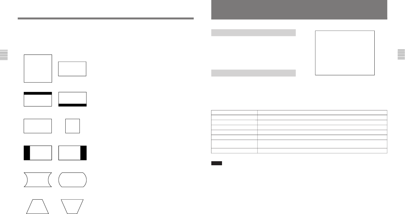
1-25
BVM-D14H1U/D14H5U/D14H1E/D14H5E/D14H1A/D14H5A
44
(E)
Chapter 2 Menu
[G] ALIGNMENT menu
Adjust the position, size or geometry of the picture
with the UP and DOWN buttons or PHASE knob.
V SIZE: Adjust the height of the picture.
V CENTER: Adjust the vertical picture position.
H SIZE: Adjust the width of the picture.
H PHASE: Adjust the horizontal picture position.
H PIN: Correct side pincushion distortion.
H KEY: Correct trapezoid distortion.
(continued)
GAdjusting the Position, Size and Geometry of the Picture — ALIGNMENT Menu
45
(E)
Chapter 2 Menu
DISPLAY GROUP ADDRESS
---
ADDRESS
SINGLE **
GROUP**
ALL
ALL POWER ON
ALL POWER OFF
DISPLAY MONITOR ADDRESS
*
*
ADDRESS Menu
Overview
When multiple monitors are connected by a serial
remote connection, the ADDRESS menu is used to
choose whether one particular monitor or monitor
group will be controlled, or whether operations are to
be performed on all monitors together.
Displaying the ADDRESS Menu
Press the ADDRESS button.
The ADDRESS menu is displayed on the screen.
By pressing the ENTER or Ent button after selecting
the item, serial remote operation becomes activated.
Settings made with the menu items are as follows:
Item
SINGLE
GROUP
ALL
ALL POWER ON
ALL POWER OFF
DISPLAY MONITOR ADDRESS
DISPLAY GROUP ADDRESS
Function
Controls only a specified monitor. Enter the monitor address number.
Controls only a specified monitor group. Enter the group address number.
Controls all monitors.
Turns all connected monitors on.
Turns all connected monitors off.
When this item is selected, each connected monitor displays its monitor address on its
screen.
When this item is selected, each connected monitor displays its group address on its screen.
Notes
• To remotely control monitors connected in serial,
MONITOR ADDRESS or GROUP ADDRESS of
monitors should be correctly set in the REMOTE
menu.
For details of the REMOTE menu, see “[D] Assigning the
Remote Control Functions – REMOTE Menu” on page
37(E).
- In GROUP or ALL mode, the LEDs of the
function buttons will not light with controlled
from the menu. (LEDs light only when you press
the function button.)
- In GROUP or ALL mode, LEDs of controlled
monitor will light as follows.
Selecting the Monitor to Control
— ADDRESS Menu
•In case of SHIFT OFF before remote control
operation: LEDs light in green when the SHIFT
button is remotely set to OFF.
For details, see “SHIFT button” on page10(E) for BVM-
D9H5U/D9H5E/D9H5A or on page 19(E) for BVM-
D14H5U/D14H5E/D14H5A.
•In case of SHIFT ON before remote control
operation: LEDs light in amber when the SHIFT
button is remotely set to ON.
For details, see “SHIFT button” on page11(E) for BVM-
D9H5U/D9H5E/D9H5A or on page 20(E) for BVM-
D14H5U/D14H5E/D14H5A.

1-26 BVM-D14H1U/D14H5U/D14H1E/D14H5E/D14H1A/D14H5A
46
(E)
Chapter 2 Menu
Cancelling the Remote Control
Mode
To cancel the remote control mode, press the
ADDRESS button.
Exiting the ADDRESS Menu
To exit the ADDRESS menu, press the ADDRESS
button or the MENU button.
Short-cut Function in the
ADDRESS Menu
When selecting the monitor, short-cut function will
enable to select the target monitor without using the
items in the ADDRESS menu. The operation
procedure is as follows.
To select the monitor in the SINGLE mode
1
Press the ADDRESS button.
2
Press the address number of the target monitor.
Press one digit address number on the numeric
keypad when it is from 1 to 9.
Press three digits address number (press 0 button
and then press the two-digit address number) when
it is from 10 to 99.
To select the monitors in the GROUP mode
1
Press the ADDRESS button.
2
Press the F1 button.
3
Press the group number of the target monitor.
Press one digit group address number when it is
from 1 to 9.
Press three digits group address number (press 0
button and then press the two-digit group number)
when it is from 10 to 99.
To select all the monitors in the ALL mode
1
Press the ADDRESS button.
2
Press the F2 button.
Selecting the Monitor to Control — ADDRESS Menu
47
(E)
Chapter 3 Appendix
Nominal chromaticity coordinates:
EBU phosphor
Dimensions (w/h/d)
BVM-D9H1U/D9H1E/D9H1A:
approx. 217 × 174 × 364.5mm
(8 5/8 × 6 7/8 × 14 3/8 inches)
when the AC adaptor is installed:
approx. 217 × 174 × 419.5mm
(8 5/8 × 6 7/8 × 16 5/8 inches)
BVM-D9H5U/D9H5E/D9H5A:
approx. 217 × 218 × 364.5mm
(8 5/8 × 8 5/8 × 14 3/8 inches)
when the AC adaptor is installed:
approx. 217 × 218 × 419.5mm
(8 5/8 × 8 5/8 × 16 5/8 inches)
BVM-D14H1U/D14H1E/D14H1A:
approx. 346 × 280 × 519mm
(13 5/8 × 11 1/8 × 20 1/2 inches)
BVM-D14H5U/D14H5E/D14H5A:
approx. 482 × 280 × 519mm
(19 × 11 1/8 × 20 1/2 inches)
Specifications
General
System 15.625 kHz – 45 kHz
(For details, see “Available Signal
Format” on page 53(E).)
CRT
BVM-D9H1U/D9H1E/D9H1A/D9H5U/D9H5E/
D9H5A HR Trinitron, 4:3 aspect ratio
Aperture grille pitch: 0.25 mm
90 degree deflection, 21.6 mm
diameter in-line gun
Effective picture size with 16:9
aspect ratio:
155.4 × 87.4 mm (6 1/8 × 3 1/2
inches) (w/h)
178 mm (7 inches) (diagonal size)
Effective picture size with 4:3
aspect ratio:
155.4 × 115 mm (6 1/8 × 4 5/8
inches) (w/h)
190.7 mm (7 1/2 inches) (diagonal
size)
CRT protection: EHT (extremely
high tension) protection type
Warm-up time: approx. 30 minutes
Anode voltage: 15 kV with no
beam current
BVM-D14H1U/D14H1E/D14H1A/D14H5U/
D14H5E/D14H5A
HR Trinitron, 4:3 aspect ratio
Aperture grille pitch: 0.25 mm
90 degree deflection, 29.4 mm
diameter in-line gun
Effective picture size with 16:9
aspect ratio:
267.5 × 150.5 mm (10 5/8 × 6
inches) (w/h)
306.9 mm (12 1/8 inches)
(diagonal size)
Effective picture size with 4:3
aspect ratio:
267.5 × 200.6 mm (10 5/8 × 8
inches) (w/h)
331.6 mm (13 1/8 inches)
(diagonal size)
CRT protection: EHT (extremely
high tension) protection type
Warm-up time: approx. 30 minutes
Anode voltage: 23 kV with no
beam current
xy
R 0.640 0.330
G 0.290 0.600
B 0.150 0.060
Chapter 3 Appendix
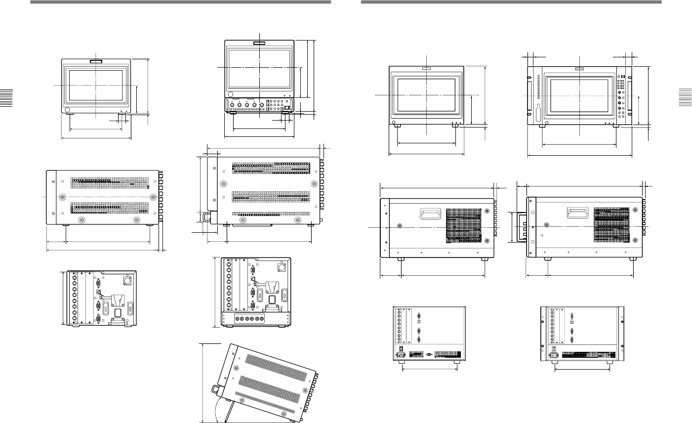
1-27
BVM-D14H1U/D14H5U/D14H1E/D14H5E/D14H1A/D14H5A
48
(E)
Chapter 3 Appendix
174.5 (6 7/8)
31 (1 1/4)
263 (10 3/8)
60 (2 3/8)
45.5
(1 13/16)
352.5 (14) 12 (1/2)
30 (1 3/16)
BVM-D9H5U/D9H5E/D9H5A
Unit: mm (inches)
Front
Side
Rear
When using stand
Specifications
170 (6
3
/
4
)
210 (8
3
/
8
)
8
(
11
/
32
)
5
(
7
/
32
)
85 (3
3
/
8
)
217 (8
5
/
8
)
163 (6
1
/
2
)
∅20
(
13
/
16
)
218 (8
5
/
8
)
170 (6
3
/
4
)
3.5 (
5
/
32
)
85 (3
3
/
8
)
217 (8
5
/
8
)
163 (6
1
/
2
)
∅22 (
7
/
8
)
352.5 (14)
263 (10
3
/
8
)
60 (2
3
/
8
)12
(
1
/
2
)
162 (6 1/2)
302 (12)
18°
Dimensional drawing
BVM-D9H1U/D9H1E/D9H1A
Unit: mm (inches)
Front
Side
Rear
49
(E)
Chapter 3 Appendix
370
90
500
43
130
12
265 (10
1
/
2
)
15
(
19
/
32
)
131.5 (5
1
/
4
)
482 (19)
28
(1
1
/
8
)
340 (13
1
/
2
)
28
(1
1
/
8
)
265 (10
1
/
2
)
15
(
19
/
32
)
131.5 (5
1
/
4
)
346 (13
5
/
8
)
260 (10
1
/
4
)
370
90
500 12
260 (10
1
/
4
)
340 (13
1
/
2
)
BVM-D14H1U/D14H1E/D14H1A
Unit: mm (inches)
Front
Side
Rear
BVM-D14H5U/D14H5E/D14H5A
Unit: mm (inches)
Front
Side
Rear

1-28 BVM-D14H1U/D14H5U/D14H1E/D14H5E/D14H1A/D14H5A
50
(E)
Chapter 3 Appendix
Specifications
Power requirements
BVM-D9H1U/D9H1E/D9H1A/
D9H5U/D9H5E/D9H5A:
AC 100 to 240 V, 50/60 Hz, DC
12V+5 V
-1
BVM-D14H1U/D14H1E/D14H1A/
D14H5U/D14H5E/D14H5A:
AC 100 to 240 V, 50/60 Hz
Input/output connectors
Video input/output BNC type × 3 (with loop-through
outputs, 75-ohm automatic
termination)
R/G/B: 1 Vp-p ±6 dB, positive,
high impedance
Y: 1 Vp-p ±6 dB, high impedance
P
B
/P
R
: 0.7 Vp-p ±6 dB, high
impedance
Sync input/output BNC type × 1 (with loop-through
output, 75-ohm automatic
termination)
Composite sync: 0.3 to 8 Vp-p,
positive/negative tri-level sync
signal input or negative bi-level
sync signal input, high impedance
Return loss More than 40 dB (10 MHz, with
75-ohm termination)
Remote control OPTION: Mini-DIN 8-pin × 1
CONTROL UNIT:
D-sub 9-pin × 1 (BVM-D9H1U/
D9H1E/D9H1A1), BVM-
D14H1U/D14H1E/D14H1A
only)
PARALLEL REMOTE 1:
D-sub 9-pin × 1
PARALLEL REMOTE 2:
Modular connector 6-pin
SERIAL REMOTE: D-sub 9-pin ×
21) (with loop-through output)
Audio input (BVM-D9H5U/D9H5E/D9H5A only)
Phono jack × 3 (with loop-through
output)
................................................................................................................................................................................................................................................
1)BVM-D9H1U/D9H1E/D9H1A is swithced to REMOTE
or CTRL UNIT with the select switch.
Mass BVM-D9H1U/D9H1E/D9H1A:
approx. 8.1 kg (17 lb 14 oz)
when the AC adaptor is installed:
approx. 8.9 kg (19 lb 10 oz)
BVM-D9H5U/D9H5E/D9H5A:
approx. 9.3 kg (20 lb 8 oz)
when the AC adaptor is installed:
approx. 10.1 kg (22 lb 4 oz)
BVM-D14H1U/D14H1E/D14H1A:
approx. 21 kg (46 lb 5 oz)
BVM-D14H5U/D14H5E/D14H5A:
approx. 23 kg (50 lb 11 oz)
Power consumption
BVM-D9H1U/D9H1E/D9H1A/
D9H5U/D9H5E/D9H5A:
85 W max. (an optional BKM-
142HD or BKM-120D is
installed)
60 W typical (the supplied analog
component input adaptor is
installed)
BVM-D14H1U/D14H1E/D14H1A/
D14H5U/D14H5E/D14H5A:
115 W max. (an optional BKM-
142HD or BKM-120D is
installed)
100 W typical (the supplied
analog component input adaptor
is installed)
Peak inrush current(1) Power ON, current probe
method: 80 A (240 V) (BVM-
D9H1U/D9H1E/D9H1A/
D9H5U/D9H5E/D9H5A),
45 A (240 V) (BVM-D14H1U/
D14H1E/D14H1A/D14H5U/
D14H5E/D14H5A)
(2) Hot switching inrush current,
measured in accordance with
European standard
EN55103-1: 10 A (230 V)
(BVM-D9H1U/D9H1E/D9H1A/
D9H5U/D9H5E/D9H5A),
20 A (230 V) (BVM-D14H1U/
D14H1E/D14H1A/D14H5U/
D14H5E/D14H5A)
51
(E)
Chapter 3 Appendix
.............................................................................................................................................................................................................................................
2) The aperture cannot be compensated for RGB input signals.
Video signal
Frequency response
575/50I, 480/60I component inputs
BVM-D9H1U/D9H1E/D9H1A/
D9H5U/D9H5E/D9H5A/
D14H1U/D14H1E/D14H1A/
D14H5U/D14H5E/D14H5A:
50Hz to 10MHz (0 dB/–3 dB)
Models other than the above or
RGB inputs
BVM-D9H1U/D9H1E/D9H1A/
D9H5U/D9H5E/D9H5A:
48 Hz to 17 MHz, (1 dB/ –3 dB)
BVM-D14H1U/D14H1E/
D14H1A/D14H5U/D14H5E/
D14H5A:
48 Hz to 24 MHz, (0 dB/ –3 dB)
Aperture compensation2)
OFF: 0 dB
ON: 2 dB to 6 dB
575/50I, 480/60I inputs: 5 MHz
Input other than the above: 16 MHz
Picture performance
Normal scan 5% overscan of CRT effective
screen area (adjustable range
greater than ±15%)
Underscan 3% underscan of CRT effective
screen area (adjustable range
greater than ±15%)
Linearity Within a central area bounded by a
circle with a diameter equal to the
picture height, less than 1.0 % of
the picture height, and outside the
same area, about 2.0 % of the
picture height
Color temperature D93, D65 (adjustable to other color
temperatures)
Convergence error Within a central area bounded by a
circle with a diameter equal to the
picture height.
Less than 0.4 mm with a central
area bounded by a circle and less
than 0.7 mm at any other point.
Standard luminescence
120 cd/m2 (at standard 1 Vp-p
100% white signal)
Raster size stabilityLess than 1% of picture height (at
120 cd/m2 peak luminescence, 10
to 90% APL)
Resolution (at screen center, 120 cd/m2 luminescence)
BVM-D9H1U/D9H1E/D9H1A/
D9H5U/D9H5E/D9H5A:
340 TV lines (16:9)
450 TV lines (4:3)
BVM-D14H1U/D14H1E/D14H1A/
D14H5U/D14H5E/D14H5A:
600 TV lines (16:9)
800 TV lines (4:3)
Operating conditions
Temperature 0°C to 35°C (32°F to 95°F)
Optimum temperature
20°C to 30°C (68°F to 86°F)
Humidity 0% to 90% (no condensation)
Pressure 700 hPa to 1060 hPa
Storage and transport conditions
Temperature –10°C to 40°C (14°F to 104°F)
Humidity 0% to 90%
Pressure 700 hPa to 1060 hPa

1-29
BVM-D14H1U/D14H5U/D14H1E/D14H5E/D14H1A/D14H5A
52
(E)
Chapter 3 Appendix
Specifications
Accessories supplied
AC power cord (1)
AC adaptor (1) (BVM-D9H1U/D9H1E/D9H1A/
D9H5U/D9H5E/D9H5A only)
AC plug holder (1)
Tally plate (1)
4:3 mask (1)
Operation manual (1)
Acquired safety regulations
UL1950, CSA950
FCC Class A, IC Class A
DHHS, DNHW
TÜV (EN60950), PTB
CE-Marking, C-tick Mark
Design and specifications are subject to change
without notice.
53
(E)
Chapter 3 Appendix
Available Signal Format
575/50I (*PAL) 625 575 25 2:1 interlace 16:9/4:3 ITU 601
480/60I (*NTSC) 525 483 30 2:1 interlace 16:9/4:3 ITU 601
575/50P 625 575 50 Progressive 16:9/4:3 –
480/60P 525 483 60 Progressive 16:9/4:3 SMPTE 293M
1080/48I 1125 1080 24 2:1 interlace 16:9 –
1080/50I 1125 1080 25 2:1 interlace 16:9 SMPTE 294M
1035/60I 1125 1035 30 2:1 interlace 16:9 BTA S-001B
1080/60I 1125 1080 30 2:1 interlace 16:9 SMPTE 274M/BTA S-001B
720/60P 750 720 60 Progressive 16:9 SMPTE 296M
System Total lines
per frame ** Frame
rate (Hz) Scanning format Aspect Standard
* Available when the optional adaptor is installed.
** Also compatible with 1/1.001.
Active
lines per
frame
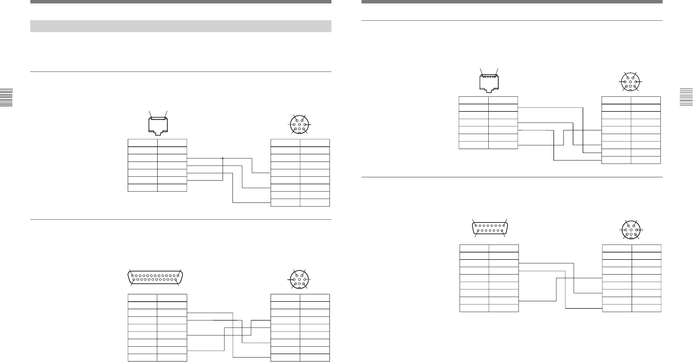
1-30 BVM-D14H1U/D14H5U/D14H1E/D14H5E/D14H1A/D14H5A
54
(E)
Chapter 3 Appendix
Specifications
Connection Cable Specifications for Color Temperature Probes
Special cables are required to connect color
temperature probes other than the Sony BKM-14L to
the monitor.
The following diagrams show specifications and pin
assignments for the required cables.
Connection cable for GRASEBY SLS 9400 probe
Modular connector Mini DIN 8-pin connector
(male)
N.C.
GND
RXD
TXD
GND
N.C.
1
2
3
4
5
6
NC
NC
RTS
GND
N.C.
TXD
+5V
RXD
1
2
3
4
5
6
7
8
16 1
2
3
6
8
5
Connection cable for MINOLTA CA-100 probe
D-sub 25-pin connector Mini DIN 8-pin connector
(male) (male)
Signal Pin Number Signal Pin Number
Signal Pin Number Signal Pin Number
N.C.
TXD
RXD
RTS
CTS
N.C.
GND
N.C.
1
2
3
4
5
6
7
8 to 25
NC
NC
RTS
GND
N.C.
TXD
+5V
RXD
1
2
3
4
5
6
7
8
1
2
3
6
8
5
113
14 25
55
(E)
Chapter 3 Appendix
Connection cable for PHILIPS PM 5639 probe (corresponds to PHILIPS PM 5639/64
cable)
Modular connector Mini DIN 8-pin connector
(male)
+5V
N.C.
RXD
TXD
N.C.
GND
1
2
3
4
5
6
NC
NC
RTS
GND
N.C.
TXD
+5V
RXD
1
2
3
4
5
6
7
8
16 1
2
3
6
8
5
Connection cable for THOMA TF6 probe
D-sub 15-pin connector (female) Mini DIN 8-pin connector (male)
Signal Pin Number Signal Pin Number
Signal Pin Number Signal Pin Number
N.C.
RXD
TXD
N.C.
N.C.
N.C.
GND
N.C.
1
2
3
4
5
6
7
8 to 15
NC
NC
RTS
GND
N.C.
TXD
+5V
RXD
1
2
3
4
5
6
7
8
18
915
1
2
3
6
8
5

1-31
BVM-D14H1U/D14H5U/D14H1E/D14H5E/D14H1A/D14H5A
56
(E)
Chapter 3 Appendix
Menu Index
The menu index shows the menu items provided with
this monitor in alphabetical order. For you reference,
each menu item is followed by the page of this manual
on which the item is explained, its menu number, and
the Main Menu that the item belongs to.
Menu Item Page Menu number Main menu
A ACC SW 41(E) – SYSTEM CONFIG menu
ADDRESS 45(E) – ADDRESS menu
ADJUST 34(E) – COLOR TEMP ADJ menu
ALIGNMENT 44(E) [G] ALIGNMENT menu
APERTURE VALUE 36(E) – INPUT CONFIG menu
AUDIO INPUT 36(E) – INPUT CONFIG menu
AUTO 32(E) [A2] CONTROL PRESET ADJ menu
B BRIGHT 32(E) – CONTROL PRESET ADJ menu
C CAM 36(E) – INPUT CONFIG menu
CAPTION 41(E) [E5] SYSTEM CONFIG menu
CH 38(E) [D211] REMOTE menu
40(E) – SYSTEM CONFIG menu
CH NAME 41(E) [E4] SYSTEM CONFIG menu
CH NO 41(E) [E3] SYSTEM CONFIG menu
CHANNEL NAME 36(E) [C2] INPUT CONFIG menu
CHROMA 32(E) – CONTROL PRESET ADJ menu
COL TEMP SHORT-CUT 41(E) – SYSTEM CONFIG menu
COL1 34(E) – COLOR TEMP ADJ menu
COL2 34(E) – COLOR TEMP ADJ menu
COLOR TEMP 36(E) – INPUT CONFIG menu
COLOR TEMP ADJ 33(E) [B] COLOR TEMP ADJ menu
CONFIG COPY 41(E) [E1] SYSTEM CONFIG menu
CONT/BRT HOLD 41(E) – SYSTEM CONFIG menu
CONTRAST 32(E) – CONTROL PRESET ADJ menu
CONTROL PRESET ADJ 31(E) [A] CONTROL PRESET ADJ menu
COPY 34(E) [B3] COLOR TEMP ADJ menu
D D1-SDI 36(E) – INPUT CONFIG menu
D65 34(E) – COLOR TEMP ADJ menu
D93 34(E) – COLOR TEMP ADJ menu
DEFAULT CH 40(E) – SYSTEM CONFIG menu
DEGAUSS DELAY 40(E) – SYSTEM CONFIG menu
E EDIT 36(E) – INPUT CONFIG menu
EIA COLOR BAR 32(E) – CONTROL PRESET ADJ menu
ENTER PASSWORD 40(E) – SYSTEM CONFIG menu
EXT SYNC SLOT 36(E) – INPUT CONFIG menu
F FORMAT 36(E) [C1] INPUT CONFIG menu
FORMAT DISPLAY 41(E) [E2] SYSTEM CONFIG menu
FULL FIELD WHITE 100 % 31(E) – CONTROL PRESET ADJ menu
G GROUP ADDRESS 38(E) – REMOTE menu
H H KEY 44(E) – ALIGNMENT menu
H SIZE 44(E) – ALIGNMENT menu
H PHASE 36(E) – INPUT CONFIG menu
44(E) – ALIGNMENT menu
H PIN 44(E) – ALIGNMENT menu
HD-SDI 36(E) – INPUT CONFIG menu
HIGH LIGHT 34(E) – COLOR TEMP ADJ menu
I INPUT CONFIG 35(E) [C] INPUT CONFIG menu
INPUT NO 36(E) – INPUT CONFIG menu
L LAST 40(E) – SYSTEM CONFIG menu
LOAD REF VALUE 34(E) [B21] COLOR TEMP ADJ menu
LOW LIGHT 34(E) – COLOR TEMP ADJ menu
57
(E)
Chapter 3 Appendix
Menu Item Page Menu number Main menu
M MAINTENANCE 40(E) [E5] SYSTEM CONFIG menu
MANUAL 32(E) [A1] CONTROL PRESET ADJ menu
34(E) [B1] COLOR TEMP ADJ menu
MARKER PHASE 36(E) – INPUT CONFIG menu
MARKER WIDTH 36(E) – INPUT CONFIG menu
MODEL NAME 42(E) – STATUS menu
MONITOR ADDRESS 38(E) – REMOTE menu
41(E) [E11] SYSTEM CONFIG menu
N NEW NAME 36(E) – INPUT CONFIG menu
NTSC, PAL 36(E) – INPUT CONFIG menu
NTSC SET UP 36(E) – INPUT CONFIG menu
P PARALLEL REMOTE 38(E) – REMOTE menu
PARALLEL REMOTE CONFIG 38(E) [D2] REMOTE menu
PHASE 32(E) – CONTROL PRESET ADJ menu
POSITION 41(E) – SYSTEM CONFIG menu
PROBE 34(E) – COLOR TEMP ADJ menu
PROG 36(E) – INPUT CONFIG menu
R REMOTE 37(E) [D] REMOTE menu
RGB 35(E) – INPUT CONFIG menu
R OFF 38(E) [D211] REMOTE menu
S SERIAL NO 42(E) – STATUS menu
SERIAL REMOTE 38(E) [D1] REMOTE menu
SLOT 1 42(E) [F3] STATUS menu
SLOT NO 36(E) – INPUT CONFIG menu
SMPTE COLOR BAR 32(E) – CONTROL PRESET ADJ menu
STANDBY MODE 40(E) – SYSTEM CONFIG menu
START 34(E) – COLOR TEMP ADJ menu
STATUS 42(E) [F] STATUS menu
STD 34(E) – COLOR TEMP ADJ menu
SYSTEM CONFIG 39(E) [E] SYSTEM CONFIG menu
V V CENTER 44(E) – ALIGNMENT menu
V SIZE 44(E) – ALIGNMENT menu
VTR 36(E) – INPUT CONFIG menu
X X 34(E) – COLOR TEMP ADJ menu
Y Y 34(E) – COLOR TEMP ADJ menu
YPBPR 36(E) – INPUT CONFIG menu
YPBPR MATRIX 36(E) – INPUT CONFIG menu
1 1125/60I SYSTEM 36(E) – INPUT CONFIG menu
1 PIN 38(E) [D21] REMOTE menu
2 2 PIN 38(E) – REMOTE menu
3 3 PIN 38(E) – REMOTE menu
4 4 PIN 38(E) – REMOTE menu
5 5 PIN 38(E) – REMOTE menu
6 6 PIN 38(E) – REMOTE menu
7 7 PIN 38(E) – REMOTE menu
8 8COLOR BAR 100% 32(E) – CONTROL PRESET ADJ menu
8COLOR BAR 75% 32(E) – CONTROL PRESET ADJ menu
8 PIN 38(E) – REMOTE menu
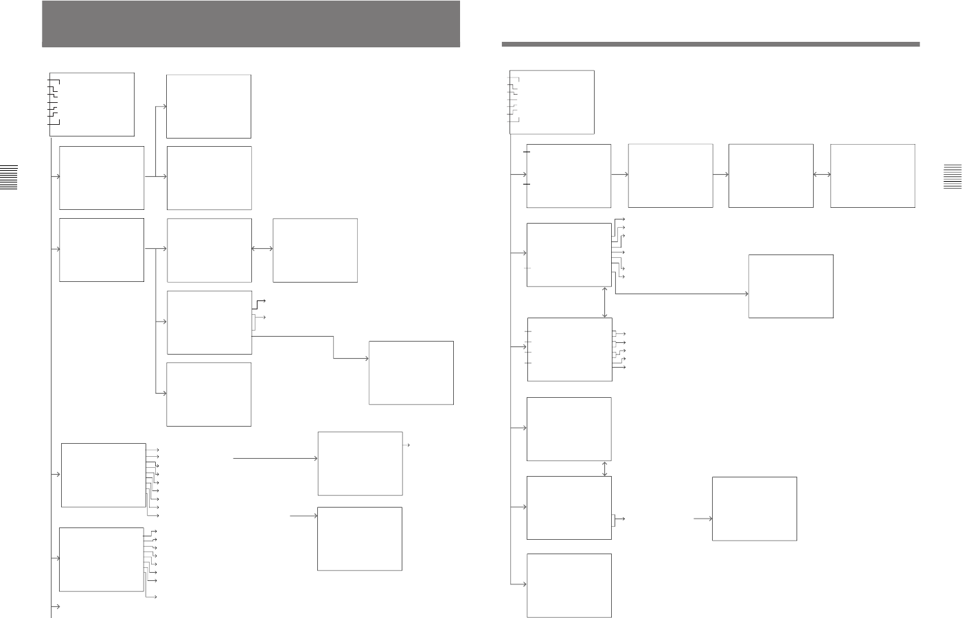
1-32 BVM-D14H1U/D14H5U/D14H1E/D14H5E/D14H1A/D14H5A
58
(E)
Chapter 3 Appendix
A1
AA2
B
C(1/2)
C(2/2)
B1(1/2)
B2
B3
B21
C1
C2
B1(2/2)
MAIN MENU
Set by automatic adjustment (using the
color bar signal)
Set input signal data for each channel.
:Current channel is indicated.
:Select the input signal type.
:Select the slot number.
:Select the input connector number.
:Select the slot when the external sync signal is used.
:Select the audio input number (BVM-D9H5 only)
:Select the color temperature.
:Enter the aperture adjustment value.
:Give the channel name. (Select in the “C2” menu)
Set the preset value with the
adjustment knobs.
D (next page)
:Select the level of
YPBPR signals.
:Current channel is indicated.
:Select the number of active scanning lines per frame.
:Set the holizontal picture position.
:Set the 4:3 marker position.
:Set the 4:3 marker width.
:Set the NTSC setup level when the BKM-127W is installed.
:Select the matrix when YPBPR signals of the signal formats
480/60I or 480/60P are input.
:Select ON to compensate for a distorted picture when the input
signals from the VCR are not typical. (Effective only when the
signal formats 480/60I or 575/50I are input.)
You can copy the color temperature
data.
Menu Configuration
CONTROL PRESET ADJ...
MENU
COLOR TEMP ADJ...
INPUT CONFIG...
REMOTE...
SYSTEM CONFIG...
STATUS...
ALIGNMENT...
p
A
B
C
D
E
F
G
CHROMA:100CONTRAST:100
PHASE :100BRIGHT :100
MANUAL
TO CANCEL :MENU KEY
TO CONFIRM:ENTER KEY
MANU AL...
CONTROL PRESET ADJ
AUTO...
p
AUTO
FULL FIELD WHITE 100%
8COLOR BAR 100%
8COLOR BAR 75%
SMPTE OLOR BAR
EIA COLOR BAR
C
p
STD
COLOR TEMP ADJ
MANUAL
PROBE...
COPY...
p
TS D
ADJUST ↓
RED :CONTRAST KNOB
GREEN :BRIGHT KNOB
BLUE :CHROMA KNOB
LUMINANCE :PHASE KNOB
TO CANCEL :MENU KEY
TO CONFIRM :ENTER KEY
↓
AIN
:0500 G:0500 R:0500
G
B
TS D
ADJUST ↓
↓
IAS
:0500 G:0500 R:0500
B
B
STD
PROBE
START
PROBEBKM-14L
X0.313
Y 0.329
LOWLIG T ( 20IRE) 2.7
HIGHLIGHT(100IRE) 120
LOADREFVALUE...
H
p
STD
COPY FROM
STD
COL1
COL2
D65
D93
p
REF VALUE
D65
D93
p
HC 1
FORMAT
YPBPRSMPTE
RGB
NTSC,PAL
D1-SDI
HD-SDI
p
HC 1
CHANNEL NAME
PROG
EDIT
CAM
VTR
NEW NAME
p
HC 1
INPUT CONFIG(1/2) ↓
FORMAT... YPBPR
SLOT NOSLOT1
INPUTNO1
EXT SY NC SL OT SLOT1
AUDIO INPUT 1
COLOR TEMP STD
APERTURE VALUE 100
CHANNEL NAME... PROG
p
↓
HC 1
INPUT CONFIG(2/2) ↓
1125/60I SYSTEM 1080I
HPHASE 000
MARKER PHASE 000
MARKER WIDTH 000
NTSC SETUP 7.5
YPBPR MATRIX 60I
VCR MODE OFF
p
↓
Select the probe for color temperature adjustment.
:Select the probe (BKM-14L, SLS 9400, CA-100, TF6,
or PM 5639)
:Confirm/Change x, y value on the Chromaticity
Coordinate and luminance
59
(E)
Chapter 3 Appendix
D
F/F1
F2
G
E1
E2
E3
E4
E5
D1
D2
E(1/2)
E(2/2)
D21 D211(1/2) D211(2/2)
E11
F3
:Data about the installed
optional board is displayed.
:Select the display mode of the signal format and display position.
:Select the display mode of the channel number and display position.
:Select the display mode of the channel name and display position.
:Select the caption display mode.
:For qualified service personnel
:Select the power-up condition.
:Select the power-up input channel.
:Set the time between power-up and the
beginning of degaussing.
:Select the CONT/BRT settings in the
COLOR TEMP ADJ.
:Set the short-cut function to the F2 key.
:Set the automatic color control.
You can copy the INPUT
CONFIG menu and SYSTEM
CONFIG menu (except
DEGAUSS DELAY) from the
monitor which you assign the
address No.
MAIN MENU
Use for adjusting the position, size
and geometry of the picture.
CONTROL PRESET ADJ...
MENU
COLOR TEMP ADJ...
INPUT CONFIG...
REMOTE...
SYSTEM CONFIG...
STATUS...
ALIGNMENT...
p
A
B
C
D
E
F
G
ES RIAL REMOTE
REMOTE
MONITOR ADDRESS 001
GROUP ADDRESS 001
ARALLEL REMOTE OFF
ARALLEL REMOTE CONFIG.
p
P
P
REMOTE CONFIG
1PIN...CH1
2PIN...CH2
3PIN...TALLYRED
4PIN...TALLY GREEN
5PIN...EXTSYNC
6PIN...UNDERSCAN
7PIN...16:9
8PIN...4:3MARKER
p
PIN... ↓
CH 01
----
UNDER SCAN
16:9
H DELAY
VDELAY
EXT SYNC
APERTURE
p
↓
M ONO
B LUE ONLY
1
PIN... ↓
R OFF
G OFF
B OFF
4:3 MARKER
CAPTIONVISION
TALLY RED
TALLY GREEN
DEGAUSS
p
↓
P OWERO FF
1
YSTEM CONFIG(1/2) ↓
STANDBY MODE OFF
DEFAULTCH...LAST
DEGUSS DELAY 000
CONT/BRT HOLD OFF
COL TEMP SHORT-CUT OFF
ACC SWON
CONFIG COPY...
p
↓
S
YSTEM CONFIG(2/2) ↓
FORMAT DISPLAY AUTO
POSITION BOTTOM LEFT
CHNOAUTO
POSI TION TOP RIGHT
CH AMEAUTO
POSITION TOP LEFT
CAPTIONOFF
MAINTENANCE...
p
↓
S
N
COPY FROM
MONITOR ADDRESS 001
p
9 1 1 YPBPR
H SL IN FORMAT NAME
STATUS (1/ 2)
1 1 1 YPBPR PROG
2 2 1 NTSC PAL
3 3 2 D1-SDI
4 1 1 YPBPR
5 2 NTSC,PAL
6 2 1 NTSC,PAL
7 1 1 YPBPR
8 3 1 D1-SDI
2
C
↓
↓
STATUS (2/2)
ODEL NAME BVM-D9H5U
ERIALNO2001234
PERATION TIME 000123H
OFTWARE VERSI N 1.00
SLOT1 COMPONENT
SLOT2 NTSC,PAL
SLOT3 D1-SDI
O
M
S
O
S
↓
↓
p
LOT1 COMPONENT
ODEL NAME BKM-129X
ERIALNO9071501
S
M
S
ALIGNMENT
VSIZE 00
V CENTER 00
HSIZE00
HPHASE 00
HPIN 00
HKEY00
p
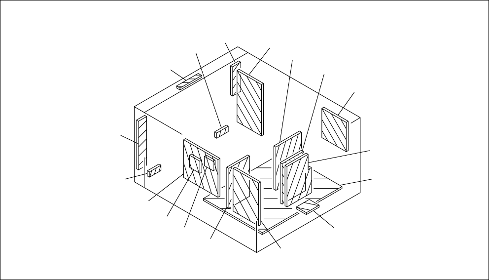
2-1
BVM-D14H1U/D14H5U/D14H1E/D14H5E/D14H1A/D14H5A
Section 2
Service Informations
2-1. Circuit Boards Location
C
G
G1
MA
BX
T
MB
HC
(D14H5)
HB
(D14H5)
HA
(D14H5)
HD
(D14H1)
B2
B1
B
YB
YA
YC
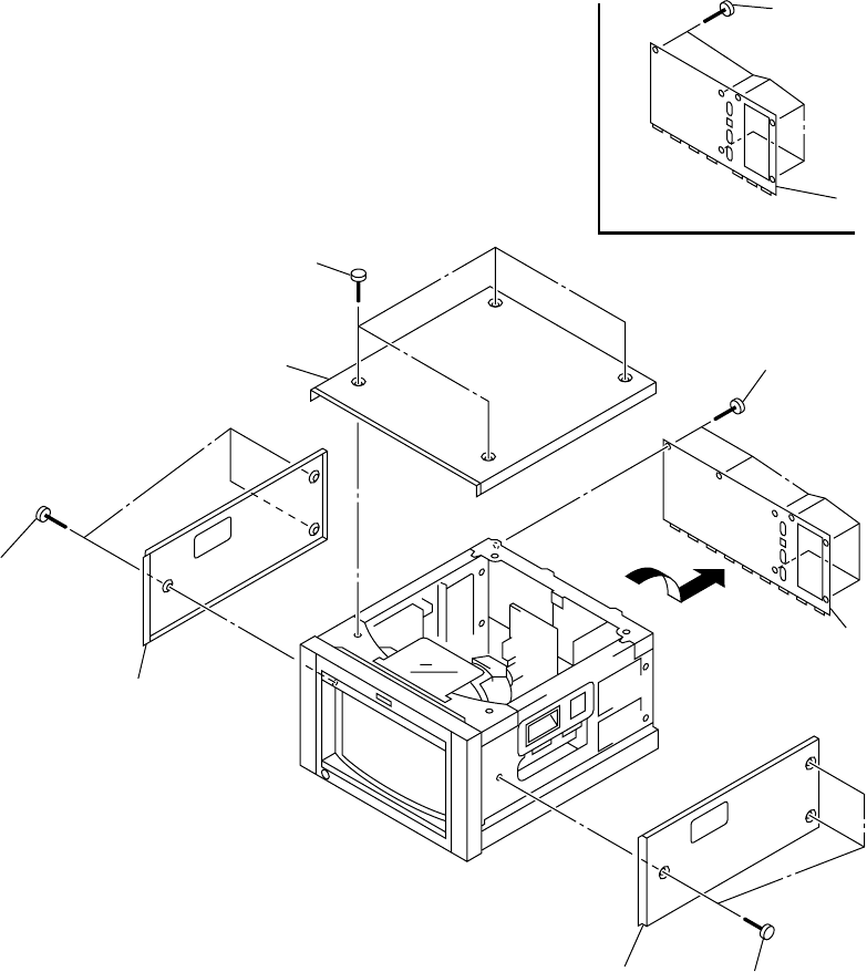
2-2 BVM-D14H1U/D14H5U/D14H1E/D14H5E/D14H1A/D14H5A
2-2-1. Cabinet and Rear Panel Removal
D14H1
7 Six screws
(+BVTT 3 × 6)
7 Seven screws
(+BVTT 3 × 6)
8 Rear panel
(Upper)
8 Rear panel
(Upper)
1 Three screws
(Case screw OS)
3 Three screws
(Case screw OS)
5 Four screws
(Case screw OS)
2 Cabinet (R)
4 Cabinet (L)
6 Cabinet (Upper)
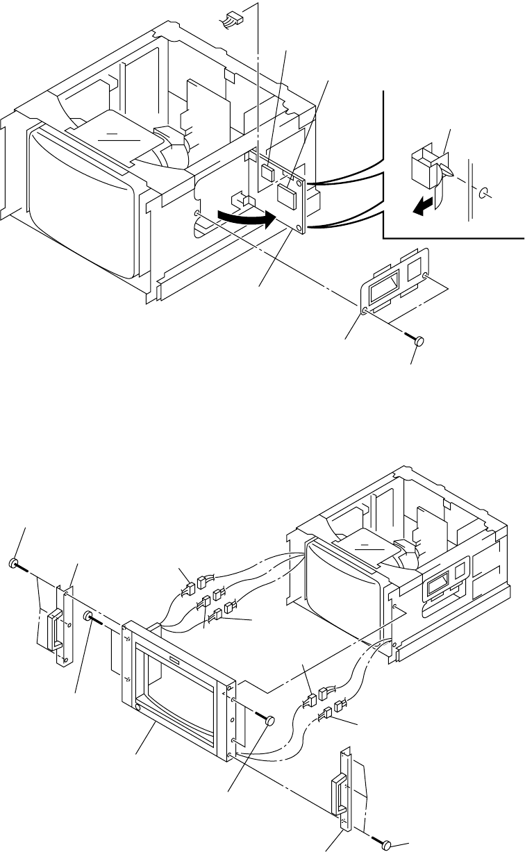
2-3
BVM-D14H1U/D14H5U/D14H1E/D14H5E/D14H1A/D14H5A
2-2-2. How To Open The B Board
2-2-3. Bezel Complete Assy Removal
(1) D14H5
1 Two screws
(+P 4 × 8)
2 Handle plate
4 B board
3 Two PWB holders
B1 board
B2 board
CN301
1 Three screws
(+PSW 4 × 14)
2 Handle assy Connector
(16P)
Connector
(9P)
Connector
(8P) Connector
(16P)
Connector
(7P)
5 Two screws
(+B 4 × 8)
6 Two screws
(+B 4 × 8)
4 Handle assy
3 Three screws
(+PSW 4 × 14)
7 Bezel complete assy
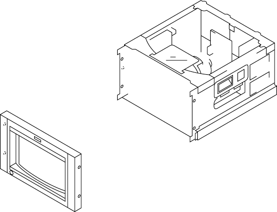
2-4 BVM-D14H1U/D14H5U/D14H1E/D14H5E/D14H1A/D14H5A
(2) D14H1
2-2-4. HA, HB and HC Boards Removal (D14H5)
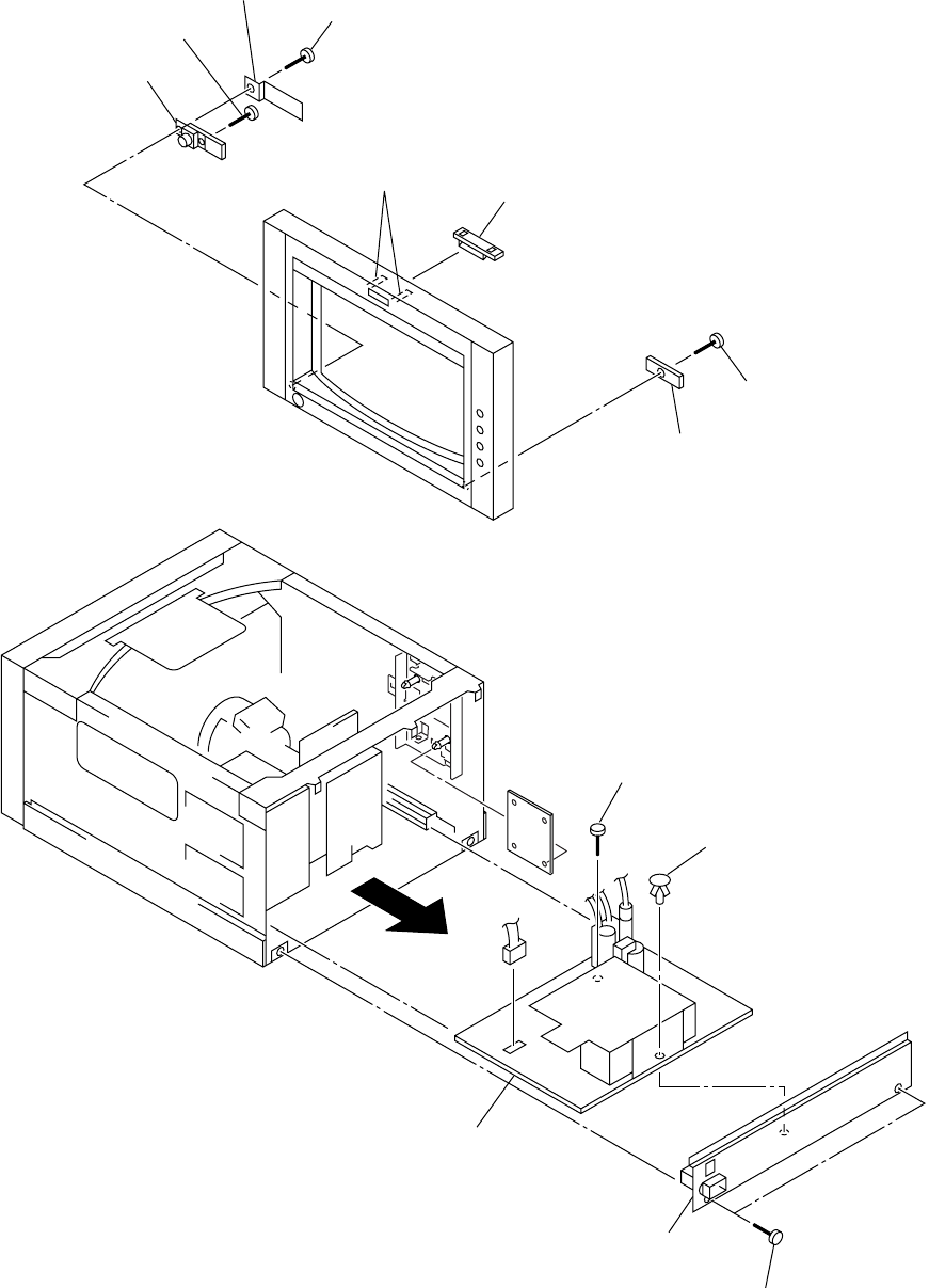
2-5
BVM-D14H1U/D14H5U/D14H1E/D14H5E/D14H1A/D14H5A
2-2-5. YA, YB and YC Boards Removal
2-2-6. G Board Removal
5 Screw
(+BVTP 3 × 10)
3 Screw
(+BVTP 3 × 10)
1 Two claws 2 YA board
6 YC insulator
8 YC board
7 Screw
(+BVTP 3 × 10)
4 YB board
4 Screw
(+PSW 3 × 12)
2 Rivet
5 G board
3 Rear panel (Lower)
1 Tow screws
(+PSW 4 × 8)
CN601
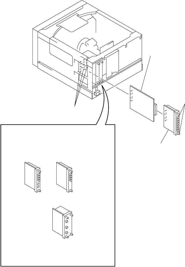
2-6 BVM-D14H1U/D14H5U/D14H1E/D14H5E/D14H1A/D14H5A
2-2-7. BX Board (BKM-129X) Removal and Check
3 Z COMPL
(Part No. : A-1394-977-A)
∗ Insert the Z COMPL
into the slot and insert
the BX board (BKM-129X)
into the connector on the
Z COMPL.
1 Loosen two
stopper screws.
2 Remove BX board
(BKM-129X).
Three slots
BKM-127W BKM-120D
BKM-142HD
∗ In case the interface board of option is attached,
connect it to the Z COMPL in the same way.
Note : The interface board can be attached to all slots.
But, left side slot should be always used.
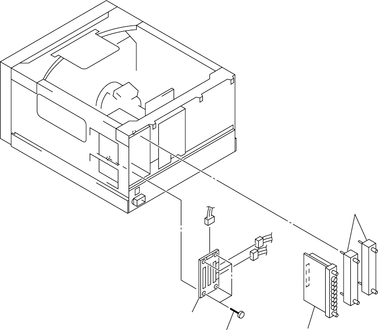
2-7
BVM-D14H1U/D14H5U/D14H1E/D14H5E/D14H1A/D14H5A
2-2-8. T Board Removal
3 Four screws
(+BVTT 3 × 6)
4 T board
CN801
CN805
CN806
2 BX board (BKM-129X)
1 Two blank panel assy
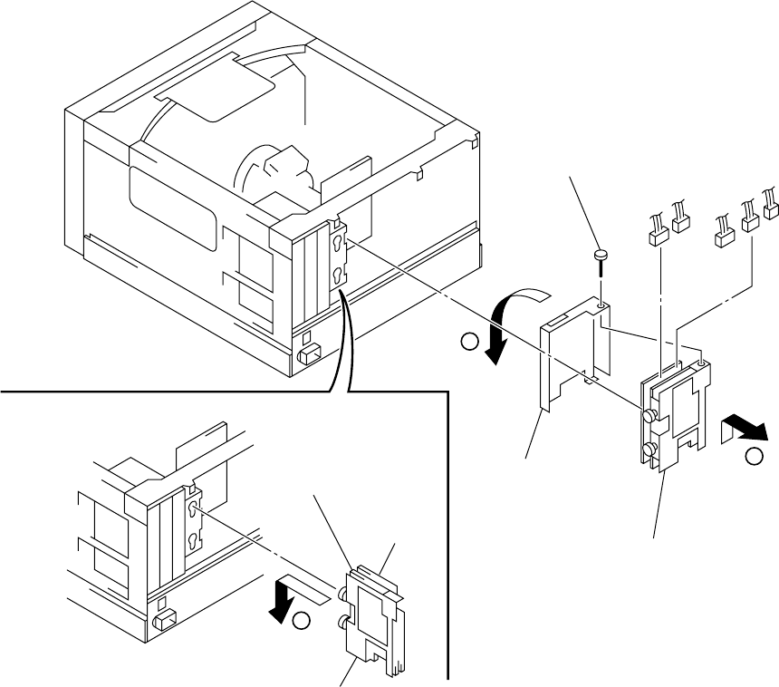
2-8 BVM-D14H1U/D14H5U/D14H1E/D14H5E/D14H1A/D14H5A
2-2-9. M Block Assy (MA and MB Boards) Removal
B
A
C
2 Screw
(+BVTT 3 × 6)
CN101 CN103
CN1100
CN1105
CN1106
3 Remove MA shield
in the arrow B direction.
1 Remove M block assy
in the arrow A direction.
4 Hang M block assy
in the arrow C direction.
MB board
MA board
SERVICE POSITION
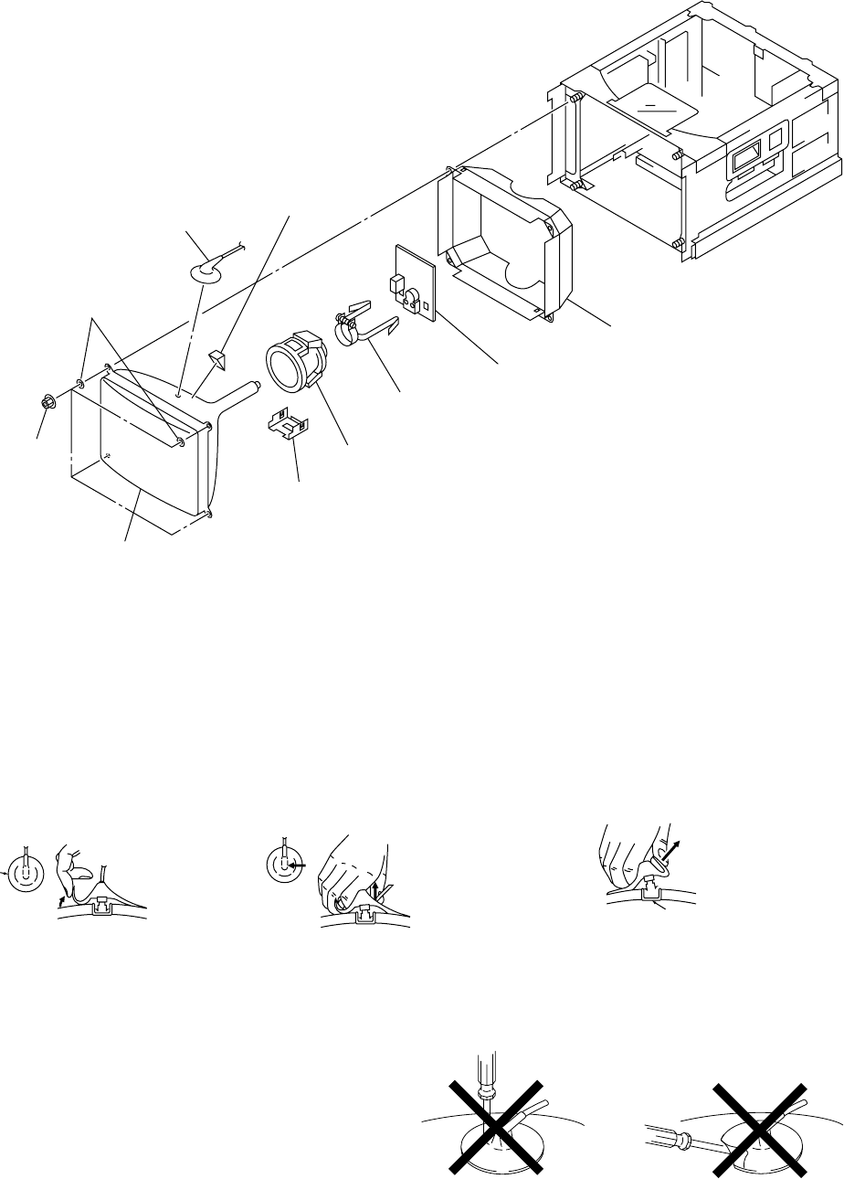
2-9
BVM-D14H1U/D14H5U/D14H1E/D14H5E/D14H1A/D14H5A
2-2-10. Picture Tube Removal
1 Anode cap
4 Two position
washer
3 Four flange nut
(M5)
DY spacer
9 Picture tube shield assy
2 C board
6 C board band
7 Deflection yoke
8 DY shield
5 Picture tube
(1) Turn up one side of the rubber cap in the
direction indicated by arrow a.(2) Using a thumb, pull up the rubber cap
firmly in the direction indicated by
arrow b.
(3) When one side of the rubber cap is
separated from the anode button, the
anode-cap can be removed by turning
up the rubber cap and pulling up it in the
direction of the arrow c.
• REMOVAL OF ANODE CAP
Note: To eliminate electric shock hazard, when replacing the picture tube, short-circuit the anode of the picture tube and the
high-voltage terminal of anode cap to the picture tube shield or carbon painted on the picture tube, after removing the anode.
• Removal Procedure
• Handling Precautions
(1) Do not scratch the surface of anode cap with a sharp object.
(2) Do not press the rubber so hard that it damages the inside of
anode caps. A shatter-hook terminal is built into the rubber.
(3) Do not turn the foot of the rubber over.
The shatter-hook terminal will stick out or damage the rubber.
a
a
b
b
c
Anode button

2-10 BVM-D14H1U/D14H5U/D14H1E/D14H5E/D14H1A/D14H5A
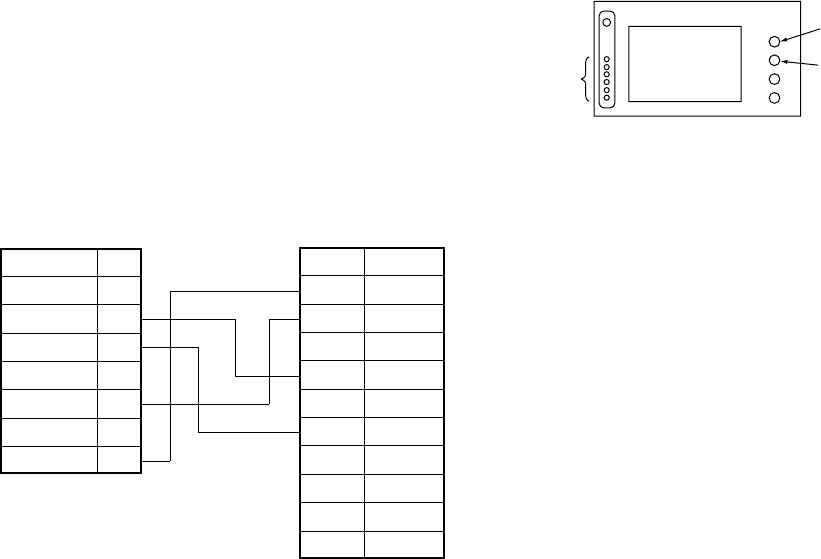
3-1
BVM-D14H1U/D14H5U/D14H1E/D14H5E/D14H1A/D14H5A
Section 3
Set-Up Adjustments
3-1. Set-Up Adjustment When CRT is
Replaced
This section describes the adjustments to be performed
when the CRT is replaced.
[Preparations]
..
..
.Required tools and measuring instruments
1. Signal generator
YPB/YPR signal generator
..
..
.1080/60i (1125) : SMPTE 274M standard/
BTA S-001 standard
..
..
.1035/60i (1125) : BTA S-001 standard
..
..
.720/60p : SMPTE 296M standard
..
..
.480/60p (525P) : SMPTE 293M standard
..
..
.480/60i (525) : ITU601
..
..
.1080/48i (1125) : —
..
..
.1080/50i (1125) : SMPTE 274M standard
..
..
.720/50p : —
..
..
.575/50p (625P) : —
..
..
.575/50i (625) : ITU601
NTSC analog composite signal generator
HD SDI signal generator
D1 SDI signal generator
2. BKM-127W (NTSC/PAL input adapter)
3. BKM-142HD (HD SDI input adapter)
4. BKM-120D (D1 SDI input adapter)
5. Oscilloscope
6. Luminance meter
7. Color analyzer (Minolta CA-100)
8. Cable of the following specifications to connect the
RS-232C terminal of the CA-100 and the OPTION
terminal of the monitor.
1
2
3
4
5
6
7
8
9 – 19
20
21 – 25
FG
TXD
RXD
RTS
CTS
NC
GND
NC
NC
DTR
NC
1
2
3
4
5
6
7
8
H SYNC
V SYNC
RTS
GND
NC
TXD
+5V
RXD
CA-100 RS-232C connector side
D Sub 25-pin (male)
HDM option connector side
Mini DIN 8-pin
..
..
.Setting the INPUT CONFIGURATION menu
Set the INPUT CONFIGURATION menu of the SETUP
menu as shown below unless otherwise specified.
FORMAT................................YPBPR
SLOT NO................................ 1
INPUT NO .............................. 1
SYNC MODE ......................... INT
APEARTURE VALUE .......... 100
CHANNEL NAME ................PROG
COLOR TEMP .......................STD
H PHASE ................................000
MARKER PHASE.................. 000
MARKER WIDTH .................000
..
..
.Operate the SYSTEM CONFIG menu as follows.
Use the SYSTEM menu to select ALL SYSTEM with the
RE-LOAD FACTORY DATA, and execute it.
BVM-D14H1/D14H5 control panel
SHIFT button
Function
buttons
CONTRAST VR
BRIGHT VR
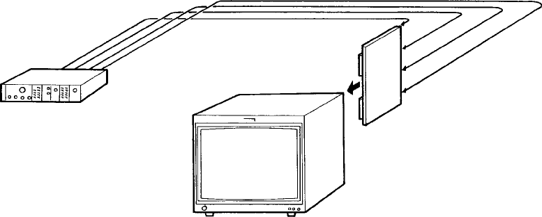
3-2 BVM-D14H1U/D14H5U/D14H1E/D14H5E/D14H1A/D14H5A
..
..
.Connection diagram
SLOT No. 1
Component signal generator
BKM-129X
BVM-D14H1U/D14H5U/D14H1E/D14H5E/D14H1A/D14H5A
Y/G terminal
PB/B terminal
PR/R terminal
SYNC terminal
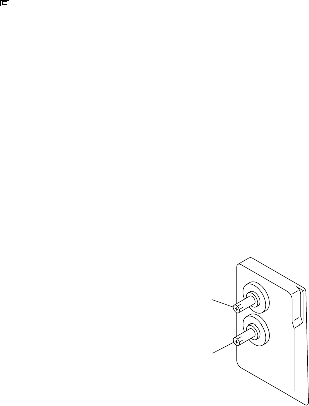
3-3
BVM-D14H1U/D14H5U/D14H1E/D14H5E/D14H1A/D14H5A
Note: If the uniformity is extremely poor, compromise
so that the FOCUS AMP is not adjusted to the
best focus but is adjusted to obtain the reason-
able uniformity and good focus at the same
time.
12. Copy the adjustment data that is obtained in step 11 to
the MODE11, MODE12, MODE14 and MODE25 to
MODE28 in this order.
13. Connect the 720/60p cross-hatch signal to the ANA-
LOG Y/G input connector.
14. Adjust the following DF adjustment data until the
thickness of the cross-hatch lines at the corners of
picture have the same thickness as those in the center
of screen.
FOCUS AMP
FOCUS KEY
Note: If the uniformity is extremely poor, compromise
so that the FOCUS AMP is not adjusted to the
best focus but is adjusted to obtain the reason-
able uniformity and good focus at the same
time.
15. Copy the adjustment data that is obtained in step 14 to
the MODE6, MODE19 and MODE20 in this order.
Fig. 1-1
[Focus Adjustment]
1. Connect the 1080/60i cross-hatch signal (see note) to
the ANALOG Y/G input connector.
Note: This is the 1125 (1080) cross-hatch signal.
2. Press the SHIFT button to set the SHIFT OFF. [The
LED (orange) on top of the button turns off.] Press the
UNDER SCAN button ( ) to its OFF position to
select the normal mode. [The green LED turns on.]
3. Set the initial (default) value to the following DF
adjustment data.
FOCUS AMP : 27
FOCUS KEY : 07
Note: This menu is located in the directory under the
DEFLECTION menu of the MAINTENANCE menu.
4. Adjust the FOUCS 1 control (horizontal focus adjust-
ment) and the FOUCS 2 control (vertical focus
adjustment) until the center of the screen has the
optimum focus.
5. Connect the 1080/60i monoscope signal to the ANA-
LOG Y/G input connector.
6. Check that the horizontal resolution higher than the
specifications can be recognized.
Specifications: 600 TV lines or more
7. Connect the 1080/60i cross-hatch signal to the ANA-
LOG Y/G input connector.
8. Adjust the following DF adjustment data until the
thickness of the cross-hatch lines at the corners of
picture have the same thickness as those in the center
of screen.
FOCUS AMP
FOCUS KEY
Note: If the uniformity is extremely poor, compromise
so that the FOCUS AMP is not adjusted to the
best focus but is adjusted to obtain the reason-
able uniformity and good focus at the same
time.
9. Copy the adjustment data that is obtained in step 8 to
the MODE2 to MODE4, MODE7 to MODE10,
MODE15 to MODE18, MODE21 to MODE24,
MODE29 to MODE32 in this order.
10. Connect the 480/60i cross-hatch signal (see note) to
the ANALOG Y/G input connector.
Note: NTSC cross-hatch signal
11. Adjust the following DF adjustment data until the
thickness of the cross-hatch lines at the corners of
picture have the same thickness as those in the center
of screen.
FOCUS AMP
FOCUS KEY
FOCUS 1
FOCUS 2
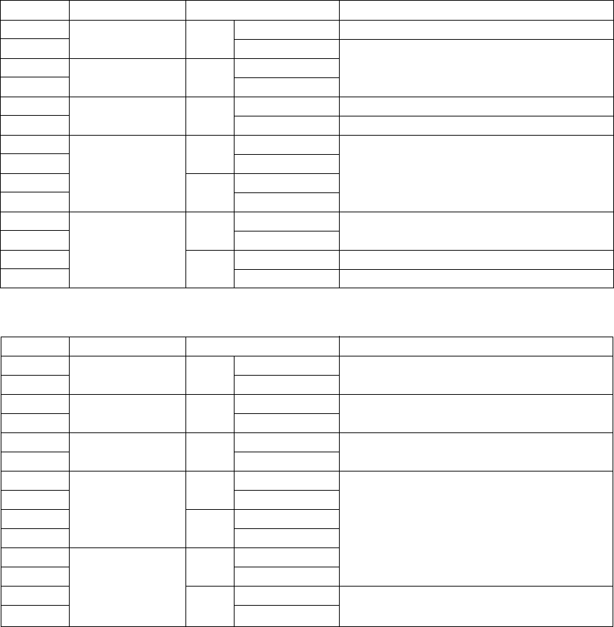
3-4 BVM-D14H1U/D14H5U/D14H1E/D14H5E/D14H1A/D14H5A
Mode
MODE1
MODE2
MODE3
MODE4
MODE5
MODE6
MODE7
MODE8
MODE9
MODE10
MODE11
MODE12
MODE13
MODE14
Signal format
1080/60i 16 : 9
(1125)
1035/60i 16 : 9
(1125)
720/60p 16 : 9
480/60p 16 : 9
(525)
4 : 3
480/60i 16 : 9
(525)
4 : 3
Screen mode
NORMAL
UNDER SCAN
NORMAL
UNDER SCAN
NORMAL
UNDER SCAN
NORMAL
UNDER SCAN
NORMAL
UNDER SCAN
NORMAL
UNDER SCAN
NORMAL
UNDER SCAN
Mode
MODE15
MODE16
MODE17
MODE18
MODE19
MODE20
MODE21
MODE22
MODE23
MODE24
MODE25
MODE26
MODE27
MODE28
Signal format
1080/48i 16 : 9
(1125)
1080/50i 16 : 9
(1125)
720/50p 16 : 9
575/50P 16 : 9
(625)
4 : 3
575/50i 16 : 9
(625)
4 : 3
Screen mode
NORMAL
UNDER SCAN
NORMAL
UNDER SCAN
NORMAL
UNDER SCAN
NORMAL
UNDER SCAN
NORMAL
UNDER SCAN
NORMAL
UNDER SCAN
NORMAL
UNDER SCAN
Adjustment procedure
Perform the adjustment of step 1 to step 8.
Copy the MODE 1 data.
Perform the adjustment of step 10 to step 11.
Copy the MODE 5 data.
Copy the MODE 1 data.
Copy the MODE 13 data.
Perform the adjustment of step 10 to step 11.
Copy the MODE 13 data.
Adjustment procedure
Copy the MODE 1 data.
Copy the MODE 1 data.
Copy the MODE 5 data.
Copy the MODE 1 data.
Copy the MODE 13 data.
(1) 60 Hz system
(2) 50 Hz system
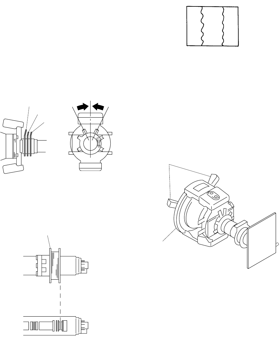
3-5
BVM-D14H1U/D14H5U/D14H1E/D14H5E/D14H1A/D14H5A
Red Green Blue
[Landing Adjustment]
1. Connect the 480/60i entire-white signal (see note) to
the ANALOG Y/G input connector.
Note: This is the NTSC entire-white signal.
2. Press the SHIFT button to ON. [The LED (orange) on
top of the button turns on.]
3. Press the 16:9 button to the OFF position to set the 4:3
mode. [The LED (orange) on top of the button turns
off.]
4. Direct the CRT screen toward east (or west). Press the
DEGAUSS button.
5. Set the Purity knob in the mechanical center.
Fig. 1-2
6. Push the DY (deflection yoke) to the front as far as it
can go.
7. Fix the neck assembly in the position as shown in Fig.
1-3.
Fig. 1-3
8. Change the screen display to all green only as follows.
[While the SFHIT is ON (the orange LED on the
SHIFT button turns on), press the R and B button to
ON. (The orange LED on the SHIFT button turns on.)]
9. Adjust the Purity knob until green comes to the center
of the display as shown in Fig. 1-4.
Fig. 1-4
10. Move back the DY so that the entire screen shows the
green only.
11. Connect the 480/60i cross-hatch signal (see note) to
the ANALOG Y/G input connector.
Note: This is the NTSC cross-hatch signal.
12. Adjust the DY inclination. After DY inclination
adjustment is complete, tighten the DY fixing screw.
13. Fix the deflection yoke (DY) using the three DY
spacers.
Fig. 1-5
..
..
.Final adjustment
When the adjustment is complete, check that mis-
landing (landing error) does not occur even when the
monitor is directed in all directions of east, west, south
and north.
Neck assy
DY spacers
Deflection yoke (DY)
Purity
6-pole
4-pole
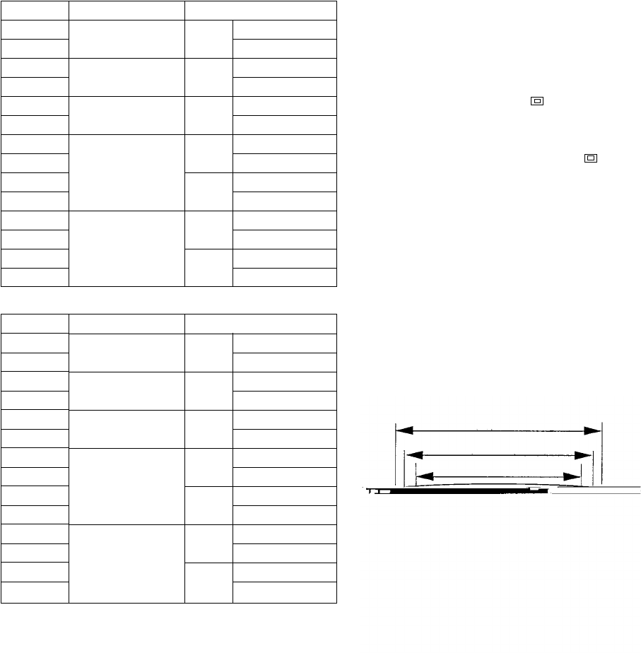
3-6 BVM-D14H1U/D14H5U/D14H1E/D14H5E/D14H1A/D14H5A
Mode
MODE1
MODE2
MODE3
MODE4
MODE5
MODE6
MODE7
MODE8
MODE9
MODE10
MODE11
MODE12
MODE13
MODE14
Signal format
1080/60i 16 : 9
(1125)
1035/60i 16 : 9
(1125)
720/60p 16 : 9
480/60p 16 : 9
(525)
4 : 3
480/60i 16 : 9
(525)
4 : 3
Screen mode
NORMAL
UNDER SCAN
NORMAL
UNDER SCAN
NORMAL
UNDER SCAN
NORMAL
UNDER SCAN
NORMAL
UNDER SCAN
NORMAL
UNDER SCAN
NORMAL
UNDER SCAN
Mode
MODE15
MODE16
MODE17
MODE18
MODE19
MODE20
MODE21
MODE22
MODE23
MODE24
MODE25
MODE26
MODE27
MODE28
Signal format
1080/48i 16 : 9
(1125)
1080/50i 16 : 9
(1125)
720/50p 16 : 9
575/50P 16 : 9
(625)
4 : 3
575/50i 16 : 9
(625)
4 : 3
Screen mode
NORMAL
UNDER SCAN
NORMAL
UNDER SCAN
NORMAL
UNDER SCAN
NORMAL
UNDER SCAN
NORMAL
UNDER SCAN
NORMAL
UNDER SCAN
NORMAL
UNDER SCAN
60 Hz system
50 Hz system
Fig. 1-6
Effective screen area
Signal display area
Deflection area (raster area)
H CENTER
A = B
H PHASE
C = D
AB
CD
2. Increase the brightness by adjusting the BRIGHT con-
trol so that blanking becomes visible on screen.
Note: The following adjustment menus are located in
the directory under the DEFLECTION menu of
the MAINTENANCE menu.
H BLK LEFT H CENT
H BLK RIGHT H PHASE
H SIZE
[H Blanking Adjustment]
..
..
.Preparation
1. Connect the monoscope signal of the signal formats
that are shown in the following table, to the ANA-
LOG Y/G input connector. Perform the H blanking
adjustment in the respective screen modes using the
respective signal formats.
..
..
.H. Blanking Adjustment
1. Press the SHIFT button to ON. [The LED (orange) on
top of the button turns on.]
2. To select the 4:3 mode of the adjustment, press the
16:9 OFF button [to turn off the LED (orange)] to
select the 4:3 mode.
To select the 16:9 mode of the adjustment, press the
16:9 ON button [to turn on the LED (orange)] to select
the 16:9 mode.
3. Press the SHIFT button to OFF. [The LED (orange)
on top of the button turns off.]
4. To select the NORMAL mode of adjustment, press the
UNDER SCAN button ( ) to its OFF position to
select the normal mode. [The green LED turns off.]
To select the UNDER SCAN mode of adjustment,
press the UNDER SCAN button ( ) to its ON
position to select the under scan mode. [The green
LED turns on.]
5. Set the following adjustment data to adjustment points
as shown below.
H BLK LEFT : 255
H BLK RIGHT : 0
6. Adjust the H SIZE data so that the entire raster area is
visible on screen.
7. Adjust the H CENTER data so that the raster is
position just in the center of the screen (so that A = B).
(Fig. 1-6)
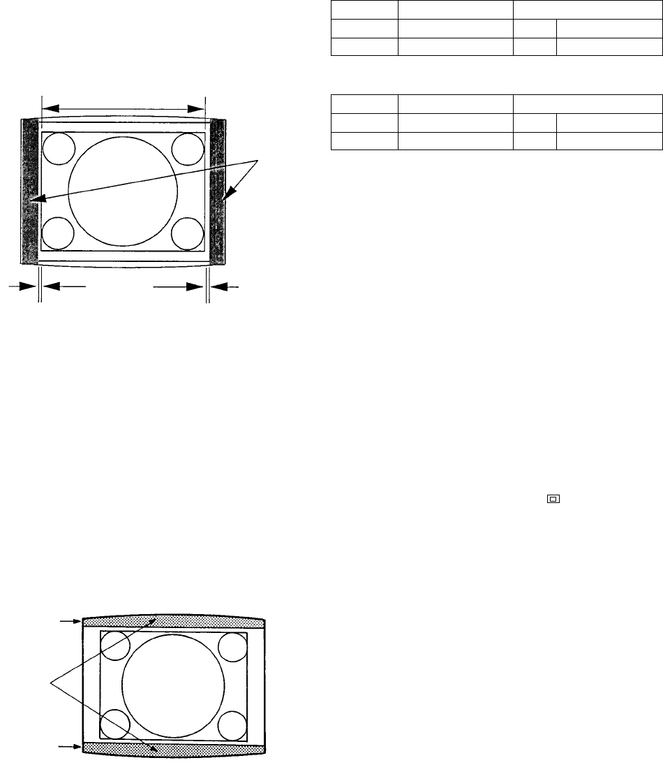
3-7
BVM-D14H1U/D14H5U/D14H1E/D14H5E/D14H1A/D14H5A
H BLK
8. Adjust the H PHASE data so that the monoscope
picture is positioned just in the center of the raster (so
that C = D).
9. Adjust the H BLK RIGHT data so that the horizontal
blanking is positioned 0 to 2 mm outside the right end
of the monoscope signal display area. (Fig. 1-7)
10. Adjust the H BLK LEFT data so that the horizontal
blanking is position 0 to 2 mm outside the left end of
the monoscope signal display area. (Fig. 1-7)
11. Return the H SIZE data to the original data size.
Fig. 1-7
[V Blanking Adjustment]
..
..
.Preparation
1. Connect the monoscope signal of the signal formats
that are shown in the following table, to the ANALOG
Y/G input connector. Perform the V blanking adjust-
ment in the respective screen modes using the respec-
tive signal formats.
60 Hz system
50 Hz system
2. Increase the brightness by adjusting the BRIGHT
control so that blanking becomes visible on screen.
Note: The following adjustment menus are located in
the directory under the DEFLECTION menu of
the MAINTENANCE menu.
V BLK TOP
V BLK BOTTOM
V SIZE
V CENT
..
..
.V Blanking Adjustment
1. Press the SHIFT button to ON. [The LED (orange) on
top of the button turns on.]
2. Press the 16:9 OFF button [to turn off the LED
(orange)] to select the 4:3 mode.
3. Press the SHIFT button to OFF. [The LED (orange)
on top of the button turns off.]
4. Press the UNDER SCAN button ( ) to its ON
position to select the under scan mode. [The green
LED turns on.]
5. Adjust the V SIZE data so that the 5% over-scan is
obtained.
6. Take note of the present V CENT data. After noting
present V CENT data, adjust V CENT so that the top
of the raster becomes visible.
7. Adjust the V BLK TOP data so that the vertical
blanking on top of the screen is positioned as closest as
possible to the signal display area.
8. Adjust V CENT so that the bottom of the raster
becomes visible.
9. Adjust the V BLK BOTTOM data so that the vertical
blanking on bottom of the screen is positioned as
closest as possible to the signal display area.
10. Return the V CENT data to the original data.
Signal display area
H BLK WIDTH H BLK PHASE
2 to 3 mm
V BLK TOP
V BLK
V BLK
BOTTOM
Fig. 1-8
Mode
MODE9
MODE13
Signal format
480/60p (525) 4 : 3
480/60i (525) 4 : 3
Screen mode
NORMAL
NORMAL
Mode
MODE23
MODE27
Signal format
575/50p (625) 4 : 3
575/50i (625) 4 : 3
Screen mode
NORMAL
NORMAL
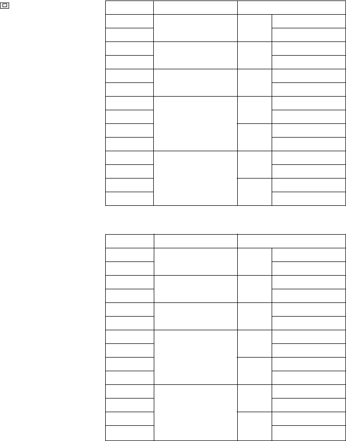
3-8 BVM-D14H1U/D14H5U/D14H1E/D14H5E/D14H1A/D14H5A
MODE
MODE1
MODE2
MODE3
MODE4
MODE5
MODE6
MODE7
MODE8
MODE9
MODE10
MODE11
MODE12
MODE13
MODE14
Signal format
1080/60i 16 : 9
(1125)
1035/60i 16 : 9
(1125)
720/60p 16 : 9
480/60p 16 : 9
(525)
4 : 3
480/60i 16 : 9
(525)
4 : 3
Screen mode
NORMAL
UNDER SCAN
NORMAL
UNDER SCAN
NORMAL
UNDER SCAN
NORMAL
UNDER SCAN
NORMAL
UNDER SCAN
NORMAL
UNDER SCAN
NORMAL
UNDER SCAN
MODE
MODE15
MODE16
MODE17
MODE18
MODE19
MODE20
MODE21
MODE22
MODE23
MODE24
MODE25
MODE26
MODE27
MODE28
Signal format
1080/48i 16 : 9
(1125)
1080/50i 16 : 9
(1125)
720/50p 16 : 9
575/50P 16 : 9
(625)
4 : 3
575/50i 16 : 9
(625)
4 : 3
Screen mode
NORMAL
UNDER SCAN
NORMAL
UNDER SCAN
NORMAL
UNDER SCAN
NORMAL
UNDER SCAN
NORMAL
UNDER SCAN
NORMAL
UNDER SCAN
NORMAL
UNDER SCAN
[Linearity Adjustment]
..
..
.Linearity Adjustment (1)
1. Connect the 1080/60i (1125) cross-hatch signal to the
ANALOG Y/G input connector.
2. Press the SHIFT button to ON. [The LED (orange) on
top of the button turns on.]
3. Press the 16:9 ON button [to turn on the LED (or-
ange)] to select the 16:9 mode.
4. Press the SHIFT button to OFF. [The LED (orange)
on top of the button turns off.]
5. Press the UNDER SCAN button ( ) to its OFF
position to select the normal mode. [The green LED
turns off.]
6. Check that the picture is not slanted, that there are no
top and bottom PIN distortion and horizontal trapezoi-
dal distortion.
Slanted picture:
Adjust inclination of the DY.
Horizontal PIN distortion:
Adjust upper and lower neck twist of the DY.
Horizontal trapezoidal distortion:
Adjust TLV adjustment control of the DY.
(Be careful that the TLV adjustment can
deteriorate the convergence.)
..
..
.Linearity Adjustment (2)
Note 1) Connect the monoscope signal or the cross-
hatch signal having the following signal formats
as shown in the table below, to the ANALOG Y/
G input connector. Perform the linearity
adjustment (2) in the respective screen modes
using the respective signal formats.
60 Hz system
50 Hz system
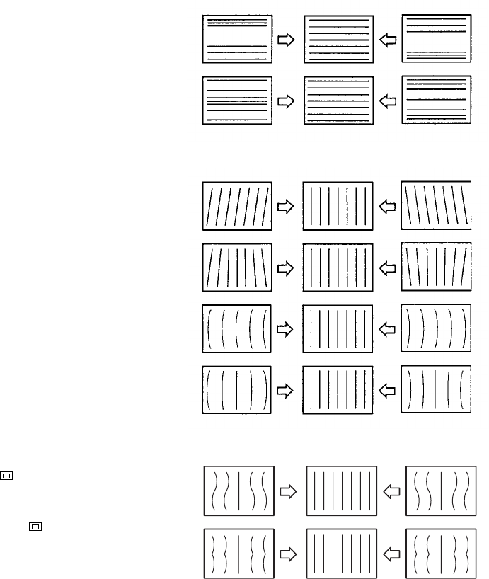
3-9
BVM-D14H1U/D14H5U/D14H1E/D14H5E/D14H1A/D14H5A
Note 2) The following adjustment menus are located in
the directory under the DEFLECTION menu of
the MAINTENANCE menu.
H SIZE
H CENTER
H KEY BAL
H KEY
H PIN BAL
H PIN
H COR S
H COR PIN
H PIN
V SIZE
V CENTER
V LIN AMP
V LIN BAL
1. Connect the monoscope signal to the ANALOG Y/G in-
put connector.
2. Press the SHIFT button to ON. [The LED (orange) on
top of the button turns on.]
3. To adjust the 4:3 mode of adjustment, press the 16:9
OFF button [to turn off the LED (orange)] to select the
4:3 mode.
4. Press the SHIFT button to OFF. [The LED (orange) on
top of the button turns off.]
5. To select the NORMAL mode of adjustment, press the
UNDER SCAN button ( ) to its OFF position to select
the normal mode. [The green LED turns off.]
To select the UNDER SCAN mode of adjustment, press
the UNDER SCAN button ( ) to its ON position to
select the under scan mode. [The green LED turns on.]
6. Adjust the H CENTER data so that the horizontal center
of the picture comes to the horizontal center of the
screen.
7. Adjust the V CENTER data so that the vertical center of
the picture comes to the vertical center of the screen.
8. Connect the cross-hatch signal to the ANALOG Y/G in-
put connector.
9. Adjust the respective V SIZE, V LIN BAL, V LIN AMP
and H SIZE data so that the optimum picture is obtained
as shown in Fig. 1-9.
Note: Do not adjust the V SIZE data when adjusting the
MODEs 9, 13, 23 and 27.
10. Adjust the horizontal trapezoidal distortion and hori-
zontal PIN distortion on both sides of picture using the
H KEY BAL, H KEY, H PIN BAL and H PIN data re-
spectively as shown in Fig. 1-10.
11. Adjust the corner “S” distortion and the corner PIN
distortion on both sides of picture using the H CORS
and H COR PIN data respectively as shown in Fig. 1-
11.
12. Repeat the above-described steps of the linearity
adjustment(2) until the optimum horizontal linearity
and vertical linearity are obtained.
Fig. 1-9
V LIN BAL
V LIN AMP
H KEY
BAL
H PIN
BAL
H KEY
H PIN
Fig. 1-10
Fig. 1-11
H COR S
H COR PIN
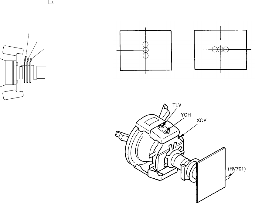
3-10 BVM-D14H1U/D14H5U/D14H1E/D14H5E/D14H1A/D14H5A
Fig. 1-14
R
G
B
R G B
[Static Convergence Adjustment]
..
..
.Horizontal Static Convergence Adjustment
1. Adjust RV701 (H. STAT) on the C board so that the
red dots and the green dots are correctly converged.
2. When the blue dot is mis-converged with respect to the
red and green dots, implement the HMC (horizontal
misconvergence) correction by adjusting the 4-pole
magnet and the 6-pole magnet of the DY.
..
..
.Vertical Static Convergence Adjustment
1. Implement the VMC (vertical misconvergence)
correction by adjusting the 4-pole magnet and the 6-
pole magnet of the DY.
Fig. 1-13
[Convergence Adjustment]
..
..
.Preparation
1. Connect the 480/60p cross-hatch signal to the ANA-
LOG Y/G input connector.
2. Press the SHIFT button to ON. [The LED (orange) on
top of the button turns on.]
3. Press the 16:9 OFF button [to turn off the LED
(orange)] to select the 4:3 mode.
4. Press the SHIFT button to set the SHIFT OFF. [The
LED (orange) on top of the button turns off.]
5. Press the UNDER SCAN button ( ) to its OFF
position to select the NORMAL mode of adjustment.
[The green LED turns off.]
Fig. 1-12
Purity
6-pole
4-pole
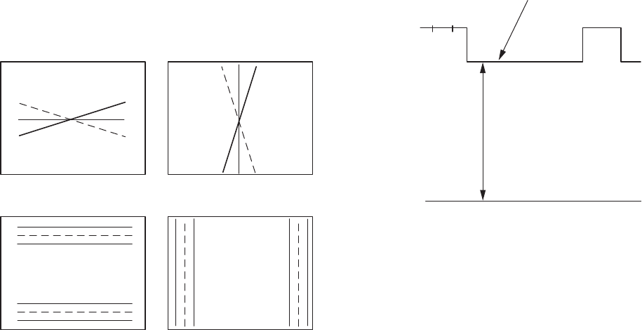
3-11
BVM-D14H1U/D14H5U/D14H1E/D14H5E/D14H1A/D14H5A
[Dynamic Convergence Adjustment]
1. Minimize the vertical misconvergence in the left-most
end of the center of a screen and in the right-most end
of the center of a screen by adjusting the DY correc-
tion reactor XCV as shown in Fig. 1-15.
2. Minimize the vertical misconvergence in the top of a
screen and in the bottom of a screen by adjusting the
DY correction reactor YCH as shown in Fig. 1-15.
3. Minimize the vertical misconvergence in the top of a
screen and in the bottom of a screen by adjusting the
DY correction reactor TLV as shown in Fig. 1-15.
4. Minimize the vertical misconvergence in the left-most
end of the center of a screen and in the right-most end
of the center of a screen by adjusting the DY correc-
tion reactor TLH as shown in Fig. 1-15.
Fig. 1-15
[G2 Adjustment]
1. Connect the 480/60i entire black signal to the ANA-
LOG Y/G input connector.
2. Connect an oscilloscope probe one after another to the
C board R-cathode (TP701), G-cathode (TP702) then
B-cathode (TP703) to measure the DC voltage at their
respective pedestal portion.
3. Connect an oscilloscope to the cathode whose DC
voltage of the respective pedestal portion has the
highest DC voltage.
4. Adjust RV702 on the C board so that the DC voltage
of the respective pedestal portion is 125 ±3 V.
Fig. 1-16
XCV YCH
TLV TLH
B
G
R
R
B
G
B
R
RGB BGR
G
R
BR
G
RB
B
Pedestal
125±3(V
DC
)
0(V
DC
)
3-12 BVM-D14H1U/D14H5U/D14H1E/D14H5E/D14H1A/D14H5A
x y y (cd/m2)
D65 0.313 0.329 2.7
0.313 0.329 120
D93 0.283 0.297 2.7
0.283 0.297 120
CRT drive voltage CRT drive voltage
Chromaticity coordinate Chromaticity coordinate
Data transmission
2. Preparation for Adjustment
2.1 Connect the 480/60i (525) WINDOW signal to the
ANALOG Y/G input connector.
2.2 Connect the RS-232C connector of a color analyzer
CA-100 with the OPTION connector of a monitor
using the cable that is shown by section “3-1. Set-Up
Adjustment When CRT is Replaced - Required tools
and measuring instruments, item 8”.
2.3 Set up the CA-100 as described below. Attach the
measurement probe of the CA-100 to the center of the
CRT screen.
Display mode xyY mode
Baud rate 9600
3. White Balance Adjustment
3.1 White Balance Adjustment (1)
1. Press the SHIFT ON button [to turn on the LED (orange)
on top of the SHIFT button]. Press the 16:9 ON button
[to turn on the LED (orange)] to select the 16:9 mode.
2. Press the MONO ON button to select the B/W mode.
[The green LED turns on.]
3. Select MAINTENANCE menu of the SYSTEM
CONFIG menu.
4. Select VIDEO menu of the MAINTENANCE menu.
5. Take note of the SUB CONTRAST data. Then set 100
to the SUB CONTRAST data.
6. Select SYSTEM/COLOR TEMP menu of the MAIN-
TENANCE menu.
7. Select D93 of the SYSTEM/COLOR TEMP menu. Then
cover the entire CRT screen surface with a black blind cloth.
Select the MANUAL adjustment item and adjust the white
balance until the following value is obtained.
x = 0.283
y = 0.297
8. Select D65 of the SYSTEM/COLOR TEMP menu.
Then cover the entire CRT screen surface with a thick
black blind cloth. Select the MANUAL adjustment
item and adjust the white balance until the following
value is obtained.
x = 0.313
y = 0.329
9. Select the SYSTEM/COLOR TEMP/COPY/OTHER
VALUE menu.
10. After selecting the STD item of the COLOR TEMP menu,
select D93. Copy the D93 color temperature data to STD.
11. After selecting the COLOR1 item of the COLOR
TEMP menu, select D65. Copy the D65 color temper-
ature data to COLOR1.
12. After selecting the COLOR2 item of the COLOR
TEMP menu, select D93. Copy the D93 color temper-
ature data to COLOR2.
13. Select VIDEO menu of the MAINTENANCE menu.
14. Return the SUB CONTRAST data to the original data.
15. Press the MONO button to the OFF position to cancel
the B/W mode. [The green LED turns off.]
[White Balance Adjustment]
1. Outline of the white balance adjustment and calibra-
tion of the color analyzer that is used for the white
balance adjustment are described first.
1,1 The parameter that converts the RGB drive voltage of
a CRT to the chromaticity coordinate is acquired.
This monitor has the copy function of the color temperature
data between two or more monitors.
However, the CRT drive voltage are unique in every
monitor because it is different depending on each CRT.
Therefore, the same color temperature cannot be obtained in
multiple monitors even though the same drive voltage is
given to them. It means that the data that is used to copy the
color temperature, must be the xyY chromaticity coordinate
or similar data that does not depend on each CRT, unlike the
CRT drive that depends on each CRT.
When the D93 MANUAL adjustment is implemented using
the MAINTENANCE/SYSTEM/COLOR TEMP menu of
the SYSTEM CONFIG menu, the parameter that converts
the CRT drive voltage to the chromaticity coordinate is
created while the adjustment is implemented. This parame-
ter is used when copying the color temperature data to other
monitors as shown.
Fig. 1-17
1.2 D65 color temperature adjustment
1.3 Copying the color temperature data to the STD color
temperature, COLOR1 color temperature and COL-
OR2 color temperature.
..
..
.On calibration of the color analyzer
When color temperature of any monitor is measured by
two or more color analyzers, these color analyzers show
different measurement values even though the object of
measurement is the same. Also the measurement value
of color analyzer changes as time elapses.
Therefore, any color analyzer must be calibrated so that
it shows the correct measurement value of the following
chromaticity coordinate before using the analyzer.
3-13
BVM-D14H1U/D14H5U/D14H1E/D14H5E/D14H1A/D14H5A
3.2 Sub Contrast Adjustment
1. Connect the 480/60i (525) 100 IRE WINDOW signal
to the ANALOG Y/G input connector.
2. Attach the luminance meter to the center of the CRT screen.
3. Select STD using the COLOR TEMP menu of the
INPUT CONFIG menu.
4. Select MAINTENANCE menu of the SYSTEM
CONFIG menu.
5. Select SUB CONTRAST menu of the VIDEO menu.
6. Press the SHIFT ON button [to turn on the LED
(orange) on top of the SHIFT button]. Press the 16:9
OFF button [to turn off the LED (orange)] to select the
4:3 mode.
7. Press the SHIFT OFF button [to turn off the LED
(orange) on top of the SHIFT button].
Press the UNDER SCAN button ( ) to its ON
position to select the under scan mode. [The green
LED turns off.]
8. Adjust SUB CONTRAST so that luminance becomes
120 cd/m2.
9. Press the SHIFT ON button [to turn on the LED
(orange) on top of the SHIFT button]. Press the 16:9
ON button [to turn on the LED (orange)] to select the
16:9 mode.
10. Adjust SUB CONTRAST so that luminance becomes
120 cd/m2.
11. Press the SHIFT OFF button [to turn off the LED
(orange) on top of the SHIFT button].
Press the UNDER SCAN button ( ) to its ON
position to select the under scan mode. [The green
LED turns off.]
12. Adjust SUB CONTRAST so that luminance becomes
120 cd/m2.
13. Press the UNDER SCAN button ( ) to its ON
position to select the under scan mode. [The green
LED turns off.]
14. Press the SHIFT ON button [to turn on the LED
(orange) on top of the SHIFT button]. Press the 16:9
OFF button [to turn off the LED (orange)] to select the
4:3 mode.
15. Connect the 1080/60i 100 IRE WINDOW signal to the
ANALOG Y/G input connector.
16. Adjust SUB CONTRAST so that luminance becomes
120 cd/m2.
17. Press the SHIFT OFF button [to turn off the LED
(orange) on top of the SHIFT button].
Press the UNDER SCAN button ( ) to its ON
position to select the under scan mode. [The green
LED turns off.]
18. Adjust SUB CONTRAST so that luminance becomes
120 cd/m2.
19. Press the UNDER SCAN button ( ) to its OFF
position to select the normal mode. [The green LED
turns on.]
20. Connect the 480/60p (525P) 100 IRE WINDOW
signal to the ANALOG Y/G input connector.
21. Press the SHIFT ON button [to turn on the LED
(orange) on top of the SHIFT button]. Press the 16:9
OFF button [to turn off the LED (orange)] to select the
4:3 mode.
22. Press the SHIFT OFF button [to turn off the LED
(orange) on top of the SHIFT button].
Press the UNDER SCAN button ( ) to its OFF
position to select the normal mode. [The green LED
turns on.]
23. Adjust SUB CONTRAST so that luminance becomes
120 cd/m2.
24. Press the UNDER SCAN button ( ) to its OFF
position to select the normal mode. [The green LED
turns on.]
25. Adjust SUB CONTRAST so that luminance becomes
120 cd/m2.
26. Press the UNDER SCAN button ( ) to its OFF
position to select the normal mode. [The green LED
turns on.]
3.3 White Balance Adjustment (2)
1. Connect the 480/60i (525) 20 IRE WINDOW color
difference signal to the ANALOG Y/G input connec-
tor.
2. Select STD using the COLOR TEMP menu of the
INPUT CONFIG menu.
3. Select MAINTENANCE menu of the SYSTEM
CONFIG menu.
4. Select the VIDEO menu.
5. Increase the CHROMA control to its maximum.
6. Adjust white balance by adjusting the PR/R BLACK
and PB/B BLACK menus of the VIDEO menu.
x = 0.283
y = 0.297
3-14 BVM-D14H1U/D14H5U/D14H1E/D14H5E/D14H1A/D14H5A
3.6 White Balance Adjustment (5)
1. Turn off the main POWER switch.
2. Insert the BKM-120D into the SLOT 2.
3. Connect the D1-SDI 20 IRE WINDOW signal to the
BKM-120D.
4. Turn on the main POWER switch.
5. Select D1-SDI using the FORMAT menu of the
INPUT CONFIG menu.
6. Select MAINTENANCE menu of the SYSTEM
CONFIG menu.
7. Select the VIDEO menu.
8. Increase the CHROMA control to its maximum.
9. Adjust white balance by adjusting the PR/R BLACK
and PB/B BLACK menus of the VIDEO menu.
x = 0.283
y = 0.297
3.7 White Balance Adjustment (6)
1. Turn off the main POWER switch.
2. Insert the BKM-127W into the SLOT 2.
3. Connect the NTSC 20 IRE WINDOW signal to the
BKM-127W.
4. Turn on the main POWER switch.
5. Select NTSC, PAL using the FORMAT menu of the
INPUT CONFIG menu.
6. Select MAINTENANCE menu of the SYSTEM
CONFIG menu.
7. Select the VIDEO menu.
8. Increase the CHROMA control to its maximum.
9. Adjust white balance by adjusting the PR/R BLACK
and PB/B BLACK menus of the VIDEO menu.
x = 0.283
y = 0.297
3.4 White Balance Adjustment (3)
1. Connect the 1080/60i (1125) 20 IRE WINDOW color
difference signal to the ANALOG Y/G input connec-
tor.
2. Select STD using the COLOR TEMP menu of the
INPUT CONFIG menu.
3. Select MAINTENANCE menu of the SYSTEM
CONFIG menu.
4. Select the VIDEO menu.
5. Increase the CHROMA control to its maximum.
6. Adjust white balance by adjusting the PR/R BLACK
and PB/B BLACK menus of the VIDEO menu.
x = 0.283
y = 0.297
3.5 White Balance Adjustment (4)
1. Turn off the main POWER switch.
2. Insert the BKM-142HD into the SLOT 2.
3. Connect the HD-SDI 20 IRE WINDOW signal to the
BKM-142HD.
4. Turn on the main POWER switch.
5. Select HD-SDI using the FORMAT menu of the
INPUT CONFIG menu.
6. Select MAINTENANCE menu of the SYSTEM
CONFIG menu.
7. Select the VIDEO menu.
8. Increase the CHROMA control to its maximum.
9. Adjust white balance by adjusting the PR/R BLACK
and PB/B BLACK menus of the VIDEO menu.
x = 0.283
y = 0.297

4-1
BVM-D14H1U/D14H5U/D14H1E/D14H5E/D14H1A/D14H5A
Section 4
Safety Related Adjustments
This section describes the adjustment procedure that is
required when the safety related parts are replaced.
[Preparation]
..
..
.Required tools and measuring equipment
1. Signal generator
YPB/YPR signal generator
..
..
.1080/60i (1125) : SMPTE 274M standard
..
..
.480/60i (525) : ITU601 (Refer to page 1-29)
2. Electrostatic voltmeter: Singer ESH-27X or ESH-23X
or equivalent
3. Digital voltmeter
4. 200 kΩ variable resistor
5. 20 kΩ variable resistor
6. Ammeter
..
..
.Set the INPUT CONFIGURATION menu
Set the INPUT CONFIGURATION menu of the SETUP
menu as shown below unless otherwise specified.
FORMAT................................ YPBPR
SLOT NO................................ 1
INPUT NO .............................. 1
SYNC MODE ......................... INT
APEARTURE VALUE .......... 100
CHANNEL NAME ................ PROG
COLOR TEMP ....................... STD
H PHASE ................................ 000
MARKER PHASE.................. 000
MARKER WIDTH ................. 000
SLOT No. 1
Component signal generator
Y/G terminal
PB/B terminal
PR/R terminal
SYNC terminal
BVM-D14H1U/D14H5U/D14H1E/D14H5E/D14H1A/D14H5A
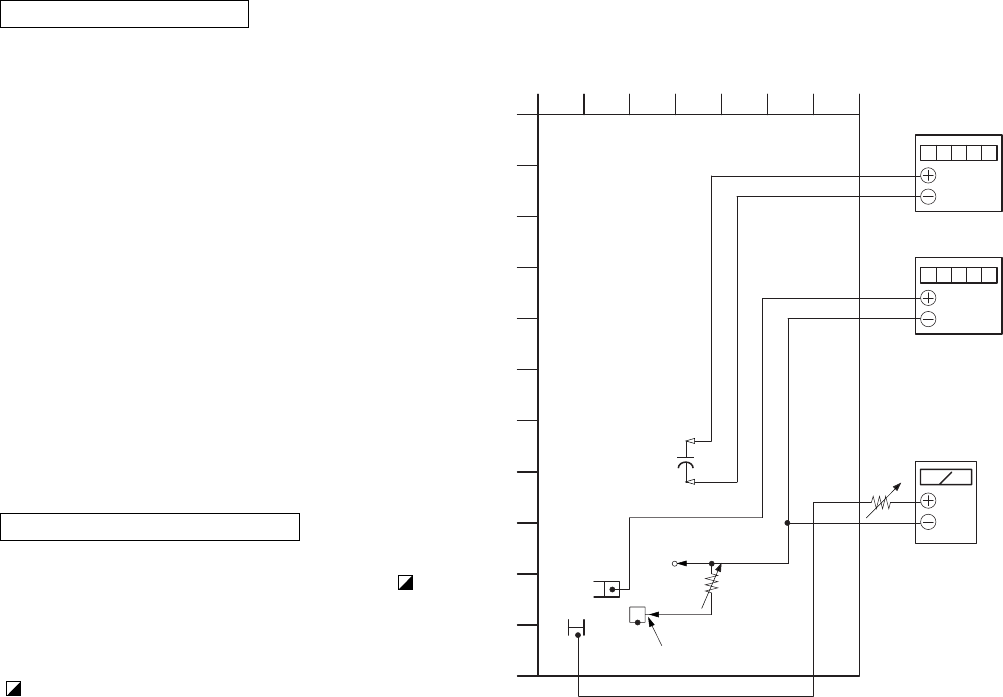
4-2 BVM-D14H1U/D14H5U/D14H1E/D14H5E/D14H1A/D14H5A
+B (135 V) Voltage Check
1. Connect a digital voltmeter across C645 on the G
board.
2. Turn on the main power.
3. Connect the 1080/60i 100 IRE signal (see note) to
input connector.
Note: 1125 (1080) 100 IRE signal
4. Push the BRIGHTNESS and CONTRAST buttons to
their MANUAL positions (to turn the green LEDs on
the buttons.)
5. Set the BRIGHTNESS and CONTRAST buttons to
their MAX positions.
6. Check that the following DC voltage appears.
135.0 ± 0.8 V
7. Turn off the main power.
8. Disconnect the digital voltmeter.
High Voltage Regulator Check
When the following parts (the parts to which the mark
is attached on the schematic diagram) are replaced, be sure
to perform the following checks.
G board ....... IC515, IC519, IC520, T502, R1509,
R1514, R1576, R1577, R592, R593,
R599
1. Turn off the main power.
2. Connect an electrostatic voltmeter to the anode cap of
CRT tube.
..
..
.Electrostatic voltmeter: It must have already been
calibrated to have the input impedance of 2 x 10⁹ Ω
or more. Singer ESH-27X or ESH-23X or equiva-
lent
3. Turn on the main power.
4. Connect the 1080/60i monoscope signal (see note) to
input connector.
Note: 1125 (1080) monoscope signal
5. Push the BRIGHTNESS and CONTRAST buttons to
their MANUAL positions (to turn the green LEDs on
the buttons.)
6. Set the BRIGHTNESS and CONTRAST buttons to
their mechanical center positions.
7. Check that the following high voltage appears.
22.5 ± 1.0 kV
8. Turn off the main power.
9. Disconnect the electrostatic voltmeter.
[Connection]
G board (Side B)
1234567
A
B
C
D
E
F
G
H
I
J
K
Digital
voltmeter
Digital
voltmeter
Ammeter
20kΩ
200kΩ
GND
R1522
D512
IC523-Pin 2
C645

4-3
BVM-D14H1U/D14H5U/D14H1E/D14H5E/D14H1A/D14H5A
Beam Current Protector Check
When the following parts (the parts to which the mark
is attached on the schematic diagram) are replaced, be sure
to perform the following checks.
G board ....... IC507, IC517, IC523, Q520, D507,
D535, T502, R1516, R1517, R1518,
R1521, R1522, R1523, R1566, R1569,
R512, R562, R576, R578, R579, R580,
R586
1. Turn off the main power.
2. Connect a DC ammeter and a 20 kΩ variable resistor
in series between the junction point of R1522 and
R1523, and GND on the G board
[The junction point of R1522 and R1523 is the
positive (+) side. Adjust the 20 kΩ variable resistor to
its maximum resistance beforehand.]
3. Turn on the main power.
4. Connect the 480/60i entire black signal (see note) to
input connector.
Note: NTSC entire black signal
5. Push the BRIGHTNESS and CONTRAST buttons to
their MANUAL positions (to turn the green LEDs on
the buttons.)
6. Set the BRIGHTNESS and CONTRAST buttons to
their mechanical center positions.
7. Confirm that the raster disappears from the CRT
screen when the DC ammeter reaches the following
value as the 20 kΩ variable resistor is turned to
decrease its resistance value gradually.
1600 µA
8. Turn off the main power.
9. Remove a 20 kΩ variable resistor and a DC ammeter.
High Voltage Hold-Down Check
When the following parts (the parts to which the mark
is attached on the schematic diagram) are replaced, be sure
to perform the following checks.
G board ...... IC514, IC507, IC523, Q520, D506,
D513, D535, T502, R553, R560, R561,
R569, R575, R597, R1566, R512
1. Turn off the main power.
2. Connect a digital voltmeter between D513 cathode and
GND of G board.
3. Connect a 200 kΩ variable resistor between IC523
pin-2 and GND of the G board.
[Adjust the 200 kΩ variable resistor to its maximum
resistance value.]
5. Connect the 480/60i entire black signal (see note) to
input connector.
Note: NTSC entire black signal
6. Push the BRIGHTNESS and CONTRAST buttons to
their MANUAL positions (to turn the green LEDs on
the buttons.)
7. Set the BRIGHTNESS and CONTRAST buttons to
their MIN positions.
8. Confirm that the raster disappears from the CRT
screen when the DC voltage at D513 cathode reaches
the following voltage as the 200 kΩ variable resistor is
turned to decrease its resistance value gradually.
25.5 ± 1.0 V
9. Turn off the main power.
10. Remove the 200 kΩ variable resistor that is connected
to IC523 pin-2.
11. Turn on the main power.
12. Confirm that the DC voltage at D513 cathode is as
follows.
20.0 ± 1.5 V
13. Connect the 480/60i entire white signal to input
connector.
14. Set the BRIGHTNESS and CONTRAST buttons to
their MAXIMUM positions.
15. Confirm that the DC voltage at TP505 is as follows.
22.0 ± 2.0 V
16. Disconnect the digital voltmeter.

4-4 BVM-D14H1U/D14H5U/D14H1E/D14H5E/D14H1A/D14H5A
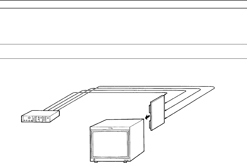
5-1
BVM-D14H1U/D14H5U/D14H1E/D14H5E/D14H1A/D14H5A
Section 5
Circuit Adjustments
5-1. B Board Adjustments
This section describes the following adjustments that are
required when the parts are replaced or maintenance is
performed in the B board.
1. RGB signal adjustment
2. 15k YPBPR SMPTE (709) signal adjustment
3. 15k YPBPR SMPTE (601) signal adjustment
4. 15k YPBPR BETACAM SETUP 0 (601) signal
adjustment
5. 15k YPBPR BETACAM SETUP 7.5 (601) signal
adjustment
6. 33k YPBPR SMPTE (709) Signal Adjustment
Control Settings
..
..
.Set the INPUT CONFIGURATION menu of the SETUP
menu as shown below.
FRMAT ............... YPBPR
SLOT NOT ......... 1
INPUT NOT........ 1
.Set “128” to the CHROMA data using the CHROMA
control knob.
.Perform the following operaion using the SYSTEM
CONFIG menu.
Select the B BOARD using the RE-LOAD FACTORY
DATA of the SYSTEM menu.
Equipment Required
Name Main Specifications Model Name
Signal generator 15 kHz/60 Hz RGB VG-854 or equivalent
15 kHz/60 Hz YPBPR SMPTE (709)
15 kHz/60 Hz YPBPR SMPTE (601)
15 kHz/60 Hz YPBPR BETACAM SETUP 7.5 (601)
33 kHz/60 Hz YPBPR SMPTE (709)
Oscilloscope Frequency: DC to 150 MHz or more TEKTORONIX 2445A
Dual trace or equivalent
Connection (1)
SLOT No. 1
Component signal generator
Y/G terminal
PB/B terminal
PR/R terminal
SYNC terminal
BKM-129X
BVM-D14H1U/D14H5U/D114H1E/D14H5E/D14H1A/D14H5A
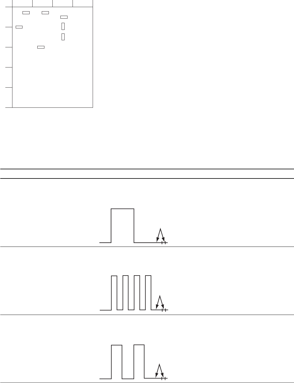
5-2 BVM-D14H1U/D14H5U/D14H1E/D14H5E/D14H1A/D14H5A
Connection (2)
Adjustment Procedure
1. RGB Signal Adjustment
Status During Adjustment Specifications Adjustment Point
Step 1 Adjust the GREEN waveforms to have Use the adjustment menu Y/G BLACK
..
..
.Input the 15 kHz/60 Hz the same amplitude at TP302. (40H) that is located under the directory
RGB 100% color bar signal. Level difference: 0 ±10 mV of the VIDEO menu of the
..
..
.Use the FORMAT item of the MAINTENANCE menu.
INPUT CONFIG menu to select RGB.
..
..
.Connect an oscilloscope to TP302.
Step 2 Make flat the pedestal portion of the Use the adjustment menu PB/B BLACK
..
..
.Connect an oscilloscope to TP303. BLUE waveform at TP303. (30H) that is located under the directory
Level difference: 0 ±10 mV of the VIDEO menu of the
MAINTENANCE menu.
Step 3 Make flat the pedestal portion of the Use the adjustment menu PR/R BLACK
..
..
.Connect an oscilloscope to TP304. RED waveform at TP304. (20H) that is located under the directory
Level difference: 0 ±10 mV of the VIDEO menu of the
MAINTENANCE menu.
ABCD
1
2
3
4
5
TP301
TP302 TP303 TP1302
TP1301
TP1300
TP304
B board -side A-
Make flat
Make flat
Make flat
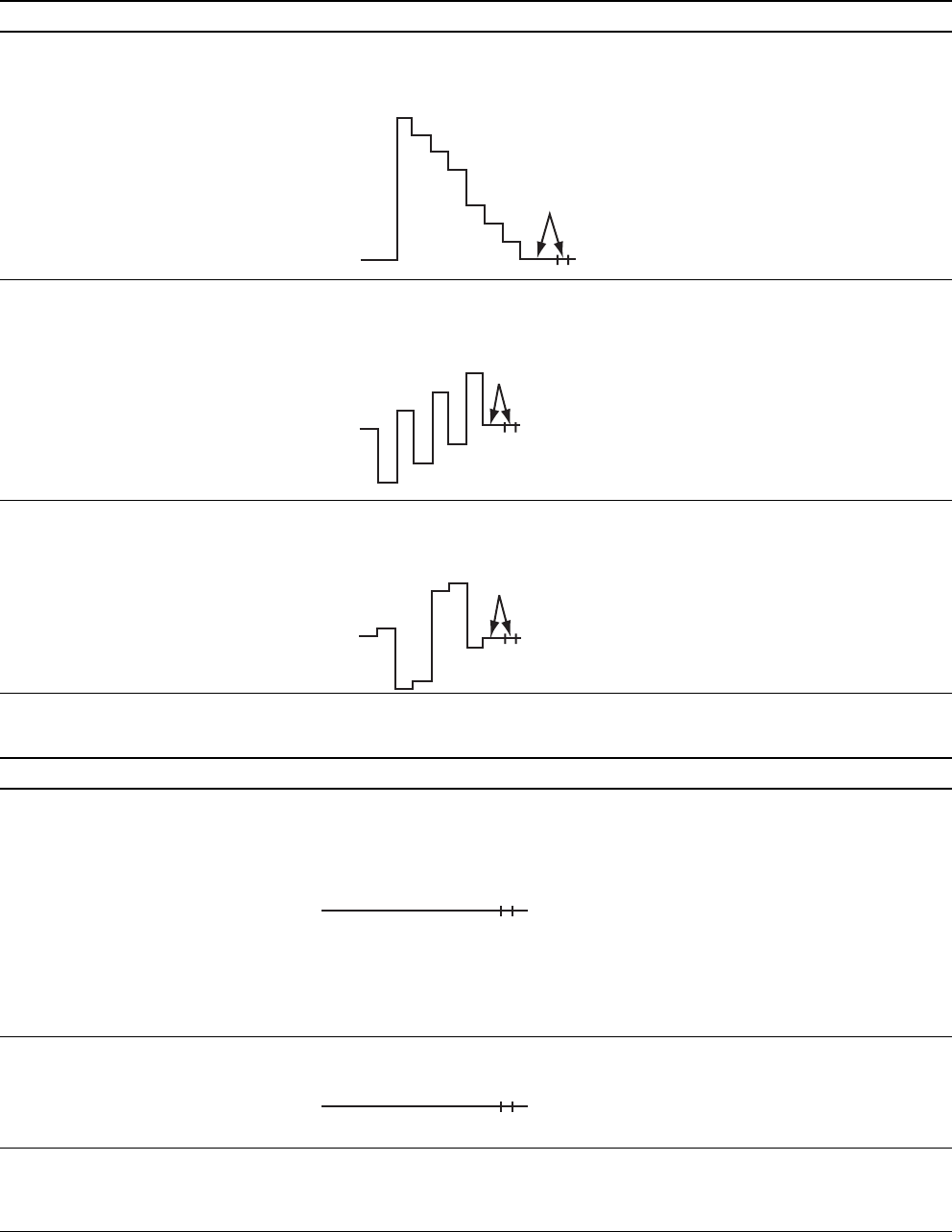
5-3
BVM-D14H1U/D14H5U/D14H1E/D14H5E/D14H1A/D14H5A
2. 15k YPBPR SMPTE (709) Signal Adjustment
2-1. BLACK Level Adjustment
Status During Adjustment Specifications Adjustment Point
Step 1 Make flat the pedestal portion of the Use the adjustment menu Y/G BLACK
..
..
.Input the 15 kHz/60 Hz YPBPR Y-signal waveform at TP302. (41H) that is located under the directory
SMPTE (709) 100% color bar signal. Level difference: 0 ± 10 mV of the VIDEO menu of the
..
..
.Use the FORMAT item of the INPUT MAINTENANCE menu.
CONFIG menu to select YPBPR SMPTE.
Set 709 for YPBPR MATRIX.
..
..
.Connect an oscilloscope to TP302.
Step 2 Make flat the pedestal portion of the Use the adjustment menu PB/B BLACK
..
..
.Connect an oscilloscope to TP303. PB waveform at TP303. (32H) that is located under the directory
Level difference: 0 ± 10 mV of the VIDEO menu of the
MAINTENANCE menu.
Step 3 Make flat the pedestal portion of the Use the adjustment menu PR/R BLACK
..
..
.Connect an oscilloscope to TP304. PR waveform at TP304. (22H) that is located under the directory
Level difference: 0 ± 10 mV of the VIDEO menu of the
MAINTENANCE menu.
2-2. CHROMA Leak Adjustment
Status During Adjustment Specifications Adjustment Point
Step 1 Make flat the PB waveform at TP303. Use the adjustment menu CHROMA PB
..
..
.Input the 15 kHz/60 Hz YPBPR Level difference: 0 ± 20 mV (11H) that is located under the directory
SMPTE (709) 100% color bar signal. of the VIDEO menu of the
..
..
.Use the FORMAT item of the INPUT MAINTENANCE menu.
CONFIG menu to select YPBPR SMPTE.
Set 709 for YPBPR MATRIX.
..
..
.Use the CHROMA knob to set
“0” to the CHROMA data.
..
..
.Connect an oscilloscope to TP303.
Step 2 Make flat the PR waveform at TP304. Use the adjustment menu CHROMA PR
..
..
.Connect an oscilloscope to TP304. Level difference: 0 ± 20 mV (10H) that is located under the directory
of the VIDEO menu of the
MAINTENANCE menu.
Step 3
..
..
.Set “128” to the CHROMA data
using the CHROMA control knob.
Make flat
Make flat
Make flat
Make the signal amplitude as flat as possible.
Make the signal amplitude as flat as possible.
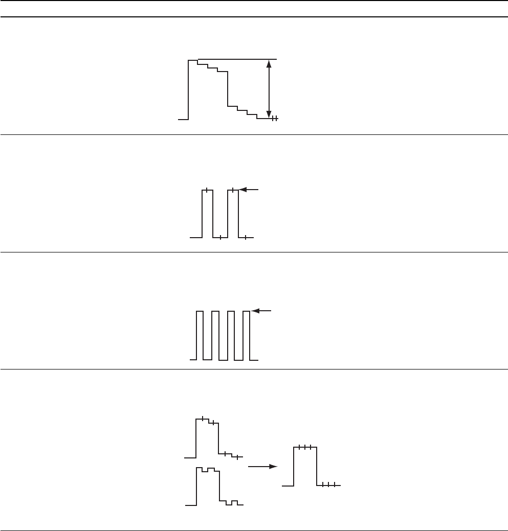
5-4 BVM-D14H1U/D14H5U/D14H1E/D14H5E/D14H1A/D14H5A
2-3. MATRIX Adjustment
Status During Adjustment Specifications Adjustment Point
Step 1 GREEN waveform amplitude at TP1301: Use the adjustment menu Y LEVEL
..
..
.Input the 15 kHz/60 Hz YPBPR 560 ± 20 mVp-p (50H) that is located under the directory
SMPTE (709) 100% color bar signal. of the VIDEO menu of the
..
..
.Use the FORMAT item of the INPUT MAINTENANCE menu.
CONFIG menu to select YPBPR SMPTE.
Set 709 for YPBPR MATRIX.
..
..
.Connect an oscilloscope to TP1301.
Step 2 Adjust the RED waveforms to have Use the adjustment menu PR LEVEL
..
..
.Connect an oscilloscope to TP1300. the same amplitude at TP1300. (60H) that is located under the directory
Level difference: 0 ± 20 mV of the VIDEO menu of the
MAINTENANCE menu.
Step 3 Adjust the BLUE waveforms to have Use the adjustment menu PB LEVEL
..
..
.Connect an oscilloscope to TP1302. the same amplitude at TP1302. (80H) that is located under the directory
Level difference: 0 ± 20 mV of the VIDEO menu of the
MAINTENANCE menu.
Step 4 Make flat the GREEN waveform at TP1301 Use the adjustment menu G-Y/R (70H)
..
..
.Connect an oscilloscope to TP1301. Level difference: 0 ± 20 mV and G-Y/B (90H) that is located under
the directory of the VIDEO menu of
the MAINTENANCE menu.
Adjust for the
same amplitude
560±20mVp-p
Adjust for the
same amplitude
G-Y/R variable
G-Y/B variable
Make the portions flat

5-5
BVM-D14H1U/D14H5U/D14H1E/D14H5E/D14H1A/D14H5A
3. 15k YPBPR SMPTE (601) Signal Adjustment
Status During Adjustment Specifications Adjustment Point
Step 1 GREEN waveform amplitude at TP1301: Use the adjustment menu Y LEVEL
..
..
.Input the 15 kHz/60 Hz YPBPR 560 ± 20 mVp-p (51H) that is located under the directory
SMPTE (601) 100% color bar signal. of the VIDEO menu of the
..
..
.Use the FORMAT item of the INPUT MAINTENANCE menu.
CONFIG menu to select YPBPR SMPTE.
Set 601 for YPBPR MATRIX.
..
..
.Connect an oscilloscope to TP1301.
Step 2 Adjust the RED waveforms to have Use the adjustment menu PR LEVEL
..
..
.Connect an oscilloscope to TP1300. the same amplitude at TP1300. (62H) that is located under the directory
Level difference: 0 ± 20 mV of the VIDEO menu of the
MAINTENANCE menu.
Step 3 Adjust the BLUE waveforms to have Use the adjustment menu PB LEVEL
..
..
.Connect an oscilloscope to TP1302 the same amplitude at TP1302. (82H) that is located under the directory
Level difference: 0 ± 20 mV of the VIDEO menu of the
MAINTENANCE menu.
Step 4 Make flat the GREEN waveform at TP1301 : Use the adjustment menu G-Y/R (71H)
..
..
.Connect an oscilloscope to TP1301. Level difference: 0 ± 20 mV and G-Y/B (91H) that is located under the
directory of the VIDEO menu of the
MAINTENANCE menu.
Adjust for the
same amplitude
560±20mVp-p
Adjust for the
same amplitude
G-Y/R variable
G-Y/B variable
Make the portions flat
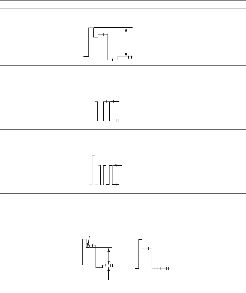
5-6 BVM-D14H1U/D14H5U/D14H1E/D14H5E/D14H1A/D14H5A
4. 15k YPBPR BETACAM SETUP 0 (601) Signal Adjustment
Status During Adjustment Specifications Adjustment Point
Step 1 GREEN waveform amplitude at TP1301: Use the adjustment menu Y LEVEL
..
..
.Input the 15 kHz/60 Hz YPBPR BETACAM 560 ± 20 mVp-p (52H) that is located under the directory
SETUP 0 (601) 75% color bar signal. of the VIDEO menu of the
..
..
.Use the FORMAT item of the INPUT MAINTENANCE menu.
CONFIG menu to select YPBPR BETA 0.
..
..
.Connect an oscilloscope to TP1301.
Step 2 Adjust the RED waveforms to have Use the adjustment menu PR LEVEL
..
..
.Connect an oscilloscope to TP1300. the same amplitude at TP1300. (64H) that is located under the directory
Level difference: 0 ± 20 mV of the VIDEO menu of the
MAINTENANCE menu.
Step 3 Adjust the BLUE waveforms to have Use the adjustment menu PB LEVEL
..
..
.Connect an oscilloscope to TP1302. the same amplitude at TP1302. (84H) that is located under the directory
Level difference: 0 ± 20 mV of the VIDEO menu of the
MAINTENANCE menu.
Step 4 Make flat the GREEN waveform at TP1301. Use the adjustment menu G-Y/R (72H)
..
..
.Connect an oscilloscope to TP1301. Amplitude between YELLOW and pedestal: and G-Y/B (92H) that is located under the
420 ± 20 mVp-p directory of the VIDEO menu of the
Make flat the waveform: Level difference: MAINTENANCE menu.
0 ± 20 mV
560±20mVp-p
Adjust for the
same amplitude
Adjust for the
same amplitude.
420±20mVp-p
Pedestal
Yellow
Make the
portions flat
G-Y/R variableG-Y/B variable
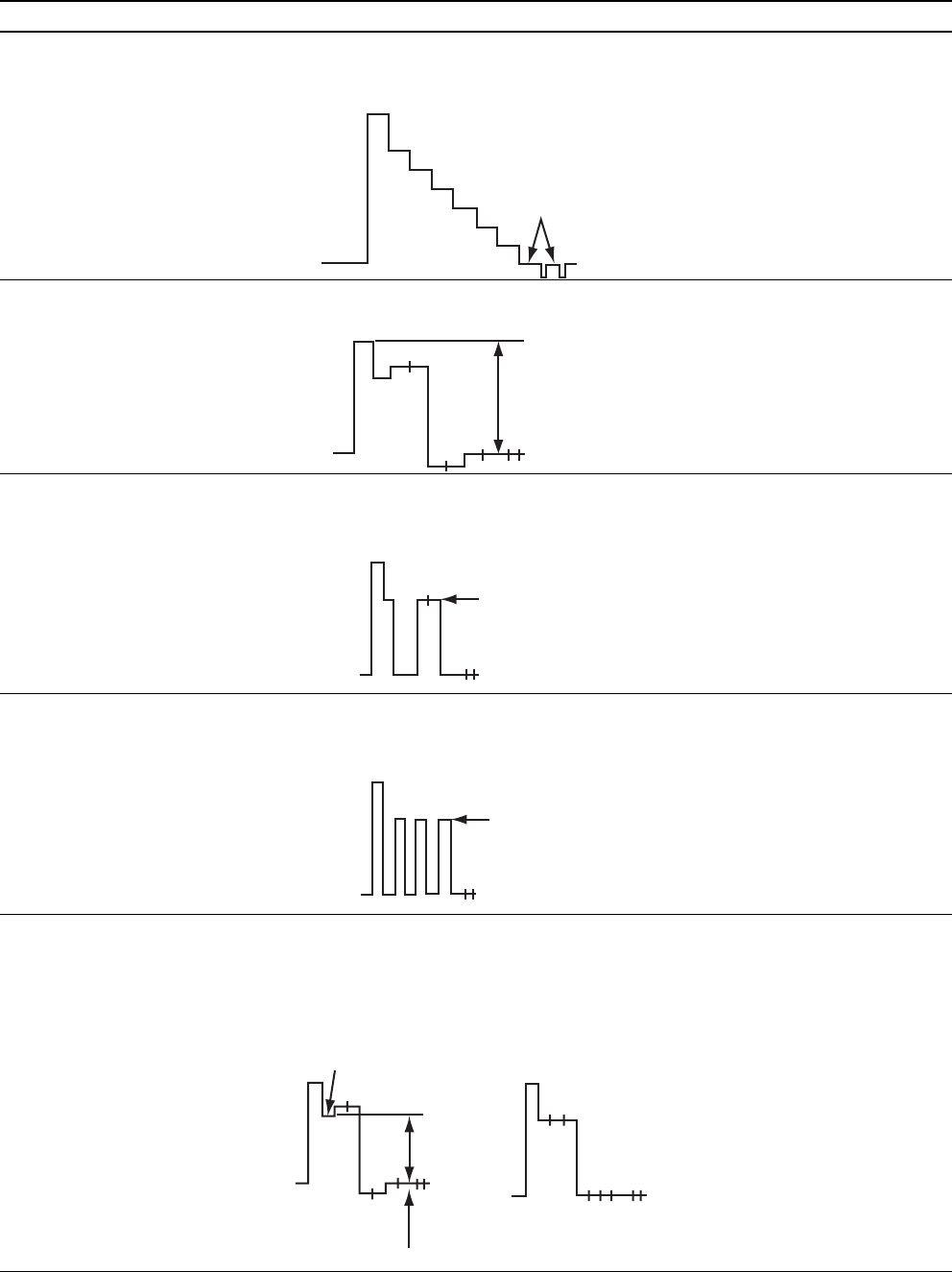
5-7
BVM-D14H1U/D14H5U/D14H1E/D14H5E/D14H1A/D14H5A
5. 15k YPBPR BETACAM SETUP 7.5 (601) Signal Adjustment
Status During Adjustment Specifications Adjustment Point
Step 1 Make flat the pedestal portion of the Use the adjustment menu Y/G BLACK
..
..
.Input the 15 kHz/60 Hz YPBPR Y-signal waveform at TP302. (42H) that is located under the directory
BETACAM SETUP 7.5 (601) Level difference: 0 ± 10 mV of the VIDEO menu of the
75% color bar signal. MAINTENANCE menu.
..
..
.Use the FORMAT item of the INPUT
CONFIG menu to select YPBPR BETA 7.5.
..
..
.Connect an oscilloscope to TP302.
Step 2 GREEN waveform amplitude at TP1301: Use the adjustment menu Y LEVEL
..
..
.Connect an oscilloscope to TP1301. 560 ± 20 mVp-p (53H) that is located under the directory
of the VIDEO menu of the
MAINTENANCE menu.
Step 3 Adjust the RED waveforms to have Use the adjustment menu PR LEVEL
..
..
.Connect an oscilloscope to TP1300. the same amplitude at TP1300. (65H) that is located under the directory
Level difference: 0 ± 20 mV of the VIDEO menu of the
MAINTENANCE menu.
Step 4 Adjust the BLUE waveforms to have Use the adjustment menu PB LEVEL
..
..
.Connect an oscilloscope to TP1302. the same amplitude at TP1302. (85H) that is located under the directory
Level difference: 0 ± 20 mV of the VIDEO menu of the
MAINTENANCE menu.
Step 5 Make flat the GREEN waveform at TP1301. Use the adjustment menu G-Y/R (73H)
..
..
.Connect an oscilloscope to TP1301. Amplitude between YELLOW and pedestal: and G-Y/B (93H) that is located under the
420 ± 20 mVp-p directory of the VIDEO menu of the
Make flat the waveform: MAINTENANCE menu.
Level difference: 0 ± 20 mV
Adjust for the
same amplitude
560±20mVp-p
Adjust for the
same amplitude
Adjust for the
same amplitude
420±20mVp-p
Pedestal
Yellow
Make the
portions flat.
G-Y/R variableG-Y/B variable
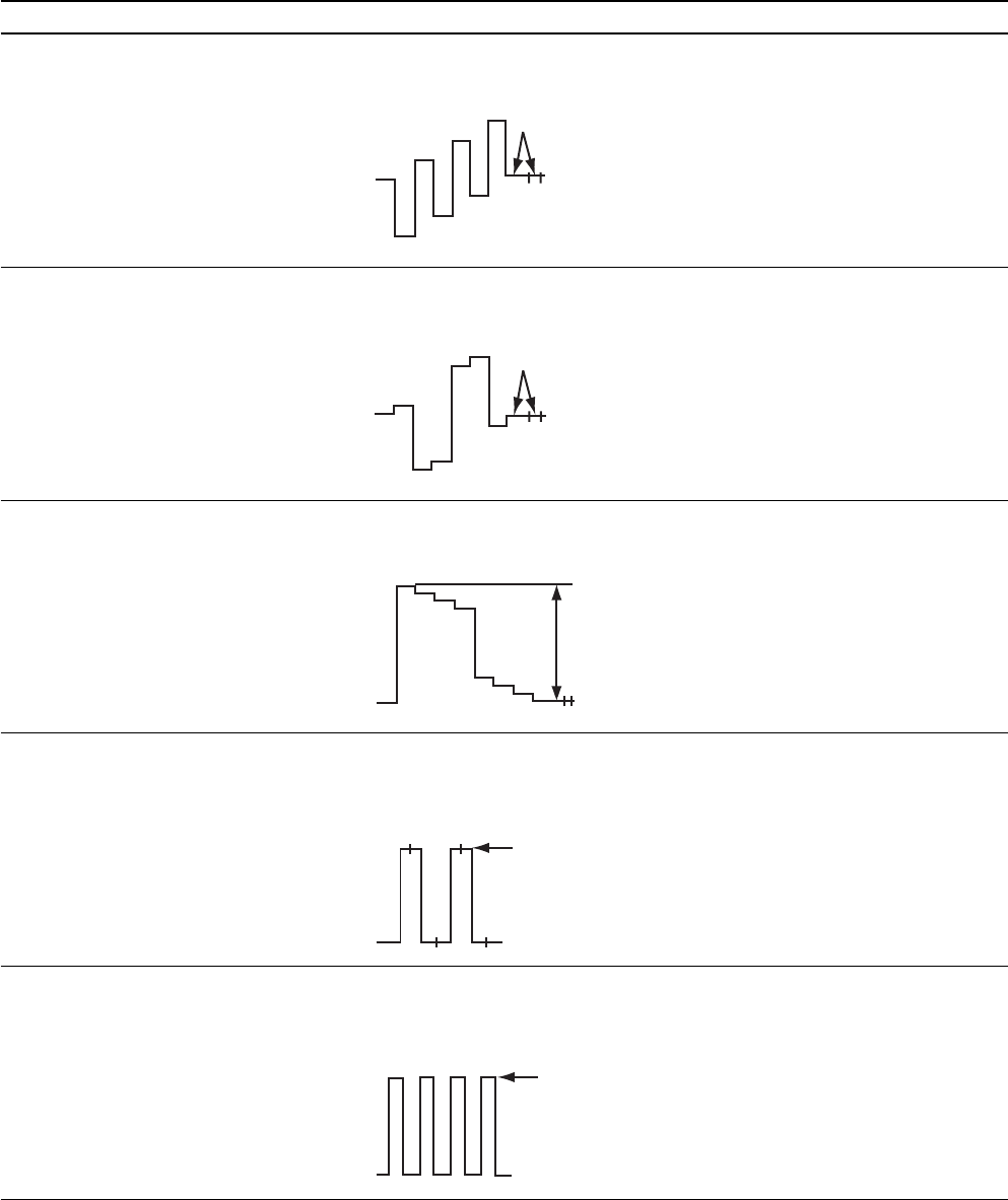
5-8 BVM-D14H1U/D14H5U/D14H1E/D14H5E/D14H1A/D14H5A
6. 33k YPBPR SMPTE (709) Signal Adjustment
Status During Adjustment Specifications Adjustment Point
Step 1 Make flat the PB waveform at TP303. Use the adjustment menu PB/B BLACK
..
..
.Input the 33 kHz/60 Hz YPBPR Level difference: 0 ± 10 mV (33H) that is located under the directory
SMPTE (709) 100% color bar signal. of the VIDEO menu of the
..
..
.Use the FORMAT item of the INPUT MAINTENANCE menu.
CONFIG menu to select YPBPR SMPTE.
..
..
.Connect an oscilloscope to TP303.
Step 2 Make flat the PR waveform at TP304. Use the adjustment menu PR/R BLACK
..
..
.Connect an oscilloscope to TP304. Level difference: 0 ± 10 mV (23H) that is located under the directory
of the VIDEO menu of the
MAINTENANCE menu.
Step 3 Check amplitude of the GREEN waveform
..
..
.Connect an oscilloscope to TP1301. at TP1301: 560 ± 20 mVp-p
Step 4 Adjust the RED waveforms to have Use the adjustment menu PR LEVEL
..
..
.Connect an oscilloscope to TP1300. the same amplitude at TP1300. (61H) that is located under the directory
Level difference: 0 ± 20 mV of the VIDEO menu of the
MAINTENANCE menu.
Step 5 Adjust the BLUE waveforms to have Use the adjustment menu PB LEVEL
..
..
.Connect an oscilloscope to TP1302. the same amplitude at TP1302. (81H) that is located under the directory
Level difference: 0 ± 20 mV of the VIDEO menu of the
MAINTENANCE menu.
Make the
portions flat
Make the
portions flat
560±20mVp-p
Adjust for the
same amplitude.
Adjust for the
same amplitude.
6-1
BVM-D14H1U/D14H5U/D14H1E/D14H5E/D14H1A/D14H5A
Section 6
Circuit Descriptions
This section describes the circuit operations of the follow-
ing boards used in the BVM-D14H1J/D14H5J.
6-1. G board
6-2. G1 board
6-3. B board
6-4. C board
6-5. MA board
6-6. MB board
6-1. G Board
Power Supply Circuit
Power supply of this monitor consists of the following two
switching regulators.
1. The power factor improvement regulator that is used to
comply with the power supply high frequency harmon-
ics regulations.
2. The main regulator that supplies the power to the
signal system, the deflection circuit and high voltage
circuit.
1. Power Factor Improvement Circuit
The power factor improvement block
The power factor improvement circuit of this monitor uses
the active filter IC module (IC601) of the current-threshold
type boost-chopper system to comply with the power
supply high frequency harmonics regulations.
The power factor improvement circuit consists of IC601,
T603 and C615.
IC601 is a module IC in which the control IC, the switch-
ing FET, the boost diode and input/output voltage detectors
are built in.
Basic operation of the power factor improvement block is
as follows. When the POWER signal (IC508 pin-1 output)
goes “LOW” and the Vcc power is supplied to IC601, the
FET inside the module IC601 is turned on and an electric
current starts to flow in the primary winding of T603 and
the FET. This current increases with the slope of Vin
(rms)/L where L is the primary side inductance of T603.
This FET current is monitored by the source current
detection resistor that is connected between pin-4 and pin-
7 of IC601. When this FET current reaches the set value
that is specified by the multiplier inside the control IC, the
FET is turned off. Then an electric current flows through
the boost diode where the current decreases with the slope
of -(Vd - Vin (rms))/L. When this current reaches 0, the
FET is turned on.
The current-threshold operation is thus realized by the
above described circuit operations. (Vd: Voltage across
C615. Vin: Input voltage to power supply)
In other words, the circuit operations that are described, are
performed as one-operation-cycle all the time while the
power is on. When you observe the circuit operations as
described above, during only the half-wave period of
commercial power line frequency, you will notice that ON/
OFF timing of the FET is controlled by the control IC so
that the envelope of the peak values of the choke current is
proportional to the half-wave of the sine waveform of the
power line frequency. As the result of this control,
waveform of the input voltage and that of the output
voltage become similar so that the power factor is im-
proved. At the same time, the voltage Vd across C615
becomes higher than the peak value of the input voltage to
the power circuit. The voltage Vd is set to about 380 V
regardless of the input voltage to the power circuit.
This circuit does not operate during the standby mode.
When this circuit is not operating, the voltage Vd becomes
almost equal to the peak value of the input voltage to the
power supply circuit.
2. Main Regulator
The separately excited current composite resonance system
is used for the main regulator. The main regulator consists
mainly of IC602, IC610, T605, C629, C631 and the
secondary side rectifier circuit of T605. IC602 is a
multiple chip module in which the four chips of the control
block, the FET drive block and the switching FET block
(high side and low side) are connected by bonding wire
inside the IC. IC210 has the following circuit configura-
tion. A half-bridge rectifier is constructed by the two FET
switches, the two capacitors C629 and C631, and the
transformer T605 for the input voltage Vd. The secondary
side of the transformer has the half wave rectifiers and full
wave rectifiers for each output lines.
IC602 receives the control signal from IC610 that performs
the constant voltage control over the +135 V line through
the isolator PH603. The control signal changes the
oscillating frequency of IC602 so that the constant voltage
control is realized.
The secondary side of T605 generates not only +135 V but
also +160 V, +15 V, _15 V, +6 V, _6 V powers and the
heater voltage that are required by the respective circuits.
The +15 V, _15 V, +6 V, _6 V powers are regulated to
+12 V, _12 V, +5 V, _5 V powers by the three-terminal
regulators respectively so that these powers are supplied to
each circuit board.
6-2 BVM-D14H1U/D14H5U/D14H1E/D14H5E/D14H1A/D14H5A
3. Over-Voltage Protection and Over-Current
Protection Circuit
The +135 V voltage line of the main power supply has the
over-voltage protection circuit and the over-current
protection circuit that protect the power supply circuit and
the loads when an abnormality occurs in the respective
loads and in the voltage feedback system.
When an over-current occurs, the latch circuit consisting of
Q616 and Q617 is turned on so that the VCC power to
IC601 and IC602 is turned off through the isolator PH604
to stop operation of the main power supply circuit.
This protection circuit is released when the input power to
the main power supply circuit is turned off once or when
the standby mode is selected.
Deflection and High Voltage Circuit
1. Sync Signal and Deflection Signal Processing
Circuit
The horizontal and vertical sync signals that are input from
CN501 (pins-1/-2) are sent to the H/V DELAY timing
circuit consisting of IC510, IC522, IC509 and IC526. The
H/V DELAY timing circuit outputs the sync signals that
have the same phase as those of the input signal during
normal operation. However, during the H/V DELAY
mode, it outputs the delayed sync signals to which delay is
given by IC509 and IC510. The output sync signals are
processed of the waveforms by IC503 and are sent to the
deflection signal processor IC507.
The deflection signal processor IC507 outputs the various
signals that are required for deflection, such as horizontal
drive circuit, parabola signal for dynamic focusing,
parabola signal for picture distortion correction, vertical
drive signal and H/V blanking signals. The output signals
are controlled directly by the microprocessor in the MA
board through I2C bus.
The horizontal free-running frequency is set for about 18
kHz. The pull-in range of the input signal frequency is
from 15 kHz to 45 kHz.
The deflection signal processor IC507 has the built-in
protector for X-ray protection. When its pin-15 is raised to
8 V or higher, the X-ray protection circuit starts working to
stop the horizontal and vertical outputs. The X-ray
protector circuit can be reset by turning off the main power
once then back on, or by entering the standby mode.
There can be a case that the monitor receives the non-
standard TV signal such as the output signal from VTR. In
order to reduce the skew effect on screen caused by
irregular timing of the input sync signal, the PLL circuit
inside the IC507 is stopped during the vertical blanking
period.
This function is effective when the horizontal frequency of
the input signal is 15 kHz (NTSC and PAL).
Because this circuit produces an ill effect when the stan-
dard TV signal is input, use or not-use of this circuit can be
selected from the on-screen menu.
2. PWM Control Circuit for +B Power Voltages
for Horizontal Deflection and of High Voltage
The PWM control circuit for +B power voltage consists of
IC515 and its peripheral circuit. The horizontal drive
signal that is output from IC507 pin-21 is used as the
PWM trigger signal.
The PWM control for horizontal deflection system is
performed by inputting the deflection distortion correction
signal that is output from IC507 pin-31 to which the H.
size control DC voltage super-imposed, to IC515 pin-8.
On the other hand, the horizontal signal that is fed back
from the horizontal output circuit is inputted to IC515 pin-
7. These two input signals are compared and the error
signal between them, that is the PWM control signal is
output from IC515 pin-11. The PWM control output
signal is sent to the +B regulator circuit consisting of
Q2503 and its peripheral circuit that control the H. size and
the deflection distortion correction.
The PWM control for the high voltage circuit is performed
by inputting the reference signal generated by IC519, to
IC515 pin-16 that is compared with the FBT high voltage
detected voltage that is input to IC515 pin-17. The error
signal between them, that is the PWM control signal is
output from IC515 pin-13. The PWM control output
signal is sent to the +B regulator circuit consisting of Q514
and its peripheral circuit that control the high voltage to be
supplied to CRT.
The PWM control signal that is output from IC515 re-
ceives the DTC (Dead Time Control) in order to protect
the horizontal output circuit and the high voltage output
circuit from damage caused by the sharp change of fre-
quency of the input video signal. The DTC circuit works
as follows. When frequency of the input sync signal is
changed, the unlock signal that is output from IC507 pin-
37 is sent to IC507 pin-6 as the DTC signal input via the
switches Q523 and Q504, so that the PWM is controlled to
decrease the +B regulator output voltages to be supplied to
the horizontal and high voltage systems.
3. Horizontal Output Circuit
The horizontal drive signal that is output form IC507 pin-
21 is amplified by the horizontal drive circuit consisting of
Q2501, Q2502, Q2505 and their peripheral circuit. The
horizontal drive signal then drives T2502 (HDT) and
Q2508 (H. OUT). The H. pulse is induced by the reso-
nance between the capacitors C2528, C2530, C2531 and
theH. winding impedance.
6-3
BVM-D14H1U/D14H5U/D14H1E/D14H5E/D14H1A/D14H5A
The H. pulse is voltage-divided, wave-shaped by IC2501
and its peripheral circuit, and is sent to IC507 pin-6, the B
board and the MA board.
Amplitude of the horizontal deflection current is detected
by T2503, Q2513 and their peripheral circuit. The detect-
ed amplitude is fed back to the PWM control circuit.
Multiple S-shape correction capacitors are prepared, and
are selected by Q2514, Q2515, Q2516, Q2517, Q2518 and
Q2519. The S-shape correction capacitors are switched at
the following three points of horizontal frequencies:
Horizontal frequency of 15 kHz, H. frequency in the range
of 27 to 33.75 kHz and H. frequency in the range of 37 to
45 kHz. The horizontal linearity correction coils are
switched by the relay RY2501 when the H. frequency of
15 kHz is input.
The H. centering circuit consists of IC2502, IC2504 and
Q2504. The H. center position is controlled by amplifying
the H. CENT. DC signal that is supplied from IC508 (D/A)
and by super-imposing the DC current to the horizontal
deflection current. As to the power supply for IC2504, the
secondary winding of T2501 (HOT) is used so that a
floating power supply is realized.
4. Vertical Output Circuit
The vertical output circuit consists of IC2503 and its
peripheral circuit.
The vertical output signal is generated by inputting the V.
drive signal that is output form IC507 pin-29, to IC2503
pin-1 where it is amplified. The V. center position is
controlled by inputting the V. DC signal that is supplied
from IC507 pin-28, to IC2503 pin-7. The vertical deflec-
tion amplitude and the vertical center position are con-
trolled by IC507.
The vertical feedback pulse is generated by wave-shaping
the V. flyback pulse with R2570, R2571 and D2520, and
by inputting it to IC507 pin-30.
5. High Voltage Output Circuit
The HV drive signal that is output from IC515 pin-23 is
sent to the high voltage output circuit consisting of Q506,
Q507, Q513 (HV. OUT) and their peripheral circuit where
the flyback pulse is generated by resonance. The flyback
pulse is not only supplied to T502 (FBT) but also rectified,
smoothed out by D520 and C578 so that the rectified high
voltage is supplied to the C board as the G2 voltage.
Amplitude of the high voltage is voltage-divided by the
high voltage resistors inside the FBT, and is output from
T502 pin-14. The detected output of the high voltage is
again voltage-divided by IC520, R1509, R1576 and R1577
so that it is sent to the PWM control signal as the high
voltage feedback voltage.
6. Dynamic Focus Output Circuit
The H. focus signal that is output from IC507 pin-17 is
amplified by the H. focus amplifier consisting of Q510,
Q511, Q512 and the peripheral circuit. The H. focus signal
then drives T501 (DFT) where it is amplified to about 500
V and is supplied to T502 pin-17. The H. focus signal
interferes with the white balance reference pulse inside the
CRT and produces an ill effect. In order to prevent
occurrence of the ill effect, the H. focus signal is of a
constant voltage is used during the vertical blanking period
instead of the H. parabola signal. This switching is
performed by IC516, IC524 and the peripheral circuit.
The V. focus signal that is output from IC507 pin-32 is
amplified by the V. focus amplifier consisting of Q517,
Q518 and the peripheral circuit. The V. focus signal is
amplified to about 200 V and is supplied to T502 pin-18.
7. H/V Blanking Circuit
The H/V blanking circuit consists of IC501, IC527, IC509
and the peripheral circuit. Timing of the H. blanking
signal is determined by the timing reference signal. The H.
SAW signal that is output from IC507 pin-16 is used as the
timing reference signal for the H. blanking. IC501 deter-
mines the start position of the H. blanking and IC509
determines the end position of the H. blanking.
The V. blanking circuit consists of IC502, IC528, IC510
and the peripheral circuit. The V. SAW signal that is
output from IC507 pin-29 is used as the timing reference
signal for the V. blanking. IC502 determines the start
position of the V. blanking and IC510 determines the end
position of the V. blanking.
Timing control of the H/V blanking signal is performed
using the control voltage that is output from IC512 (DA).
8. Protector Circuit
The H/V protector circuit consists of IC523, IC514 and the
peripheral circuit. When the voltage that appears at T502
pin-6 (FBT tertiary winding) exceeds the reference voltage
that is set by IC514, the internal protector circuit of IC507
is started up through D506. The operating point of the H/
V protector circuit is set at about 27 kV of the high voltage
output.
The ik protector circuit consists of IC517, IC523 and the
peripheral circuit. The ABL current value is detected by
R1521, R1522 and R1523. When the detected current
value exceeds the reference voltage that is set by IC517,
the internal protector circuit of IC507 is started up through
D507. The operating point of the ik protector circuit is set
at about 1500 µA of the ABL current.
6-4 BVM-D14H1U/D14H5U/D14H1E/D14H5E/D14H1A/D14H5A
6-2. G1 Board
The G1 board is the standby regulator circuit that supplies
the standby power (STBY5V) for the control system
devices (such as CPU).
The standby regulator consists mainly of IC601, IC1602,
PH601, T1601 and D1606. IC1601 has the built-in
switching FET, the PWM controller and protection circuit.
The control terminal of IC1601 receives the control signal
from IC1602 that performs the constant voltage control
over the STBY5V line through the isolator PH601. The
internal FET inside IC1601 is PWM-switched by the
control signal so that the STBY5V output from the second-
ary winding of T1601 is stabilized.
1. Over-Voltage Protection and Over-Current
Protection Circuit
The STBY5V line of the standby power supply have the
over-voltage protection circuit that protects the power
supply and the loads when an abnormality occurs in the
voltage feedback system.
When the over-voltage is detected, the “LOW” signal is set
to the control terminal of the latch circuit through the
isolator PH602 so that the power supply is stopped by the
latch circuit consisting of Q606 and Q607.
This protection circuit is released wen the input power is
turned off that discharges the C615 voltage of the G board.
When an over-current is detected in the STBY5V line, the
micro-fuse F1603 blows.
6-3. B Board
1. Clamp Circuit (1)
The signal that is selected by the option board is input to
CN301.
IC300 (1/3) (analog switch) is turned ON by the Y-CLP-P
pulse. As a result, the pedestal voltage of the Y/G signal is
sampled-and-held. In IC303, the sampled-and-held voltage
and the reference voltage (Y/G BLACK voltage) are
compared so that the error voltage is used to control the
bias current of the Y/G signal clamp amplifier (Q300 to
Q302) so that the pedestal voltage of the Y/G signal is
clamped to a fixed voltage.
The same clamp operation is performed for the PB/B and
PR/R signals but the C-CLP-P pulse is used as the clamp
pulse.
2. Matrix Circuit
The Y, R-Y and B-Y signals are converted to the R, G and
B signals by the matrix circuit in the Y/PB/PR signal is
being input.
IC306 is the Y-level adjustment amplifier. IC307 and
IC308 are the chroma level adjustment amplifier. The R-
signal is generated by adding the Y-signal to the R-Y
signal that has passed IC400 (PR gain control amplifier).
The Y-signal is generated by adding the R-Y signal that
has passed IC400 (PR gain control amplifier), the B-Y
signal that has passed IC401 (PB gain control amplifier)
and the Y-signal that is inverted and amplified by Q463.
The B-signal is generated by adding the Y-signal to the B-
Y signal that has passed IC401 (PB gain control amplifier).
3. RGB Selector Switch
IC1300 (1/3), IC1302 (1/3) and IC1303 (1/3) are the
selector switch selecting either the RGB signal or the
YPBPR signal (matrix circuit). Output of the selector
switch is R, G and B signals.
4. Clamp Circuit (2)
The R-signal is sampled-and-held by the timing pulse of
the deflection system.
IC1305 compares the sampled R-signal with the reference
signal. The error voltage controls the DC bias of the R-
signal amplifier (Q1300 to Q1302) so that the pedestal
level is kept to a constant DC level all the time. The same
clamp operation is performed in the G and B signals in the
same way.
6-5
BVM-D14H1U/D14H5U/D14H1E/D14H5E/D14H1A/D14H5A
5. OSD Insertion Circuit
The on-screen display of the R-signal is realized by
inserting the OSD blanking with IC1300 (2/3) and by
inserting the OSD with IC1304 (1/3). The WINDOW
signal that is used during the AUTO W/B adjustment is
created by the character generator, and uses the same
signal line in the same way for character display. The
same insertion operation is performed in the G and B
signals in the same way.
6. CUT-OFF Circuit
CUT-OFF of the R-signal is performed by IC1304 (2/3, 3/
3). The same cut-off operation is performed in the G and
B signals in the same way.
7. CXA1739 Peripheral Circuit
The RGB signal is input during the normal operation and
the color difference signal is input during the blue-only
mode.
(The B-signal is input to the Y input connector.)
CXA1739 has the built-in auto cut-off loop. The auto cut-
off reference pulse is inserted into every H. period in the
order of R, G then B channels at the end of the V. BLKG
period (during the 3H period immediately after the rise-up
of the V. pulse that is supplied to pin-18) in the output
signal from CXA1739. The return pulse of the reference
pulse is buffered by Q1402 and input to IC1401 pin-25.
The return pulse that is input to pin-25 is compared with
the BIAS control voltage by the voltage comparator. The
error signal from the comparator is used to shift the DC
output voltage until the return pulse agrees with the
adjustment voltage. This circuit operation is performed to
prevent the changing of the cut-off level caused by the drift
of CRT or of the drive circuit.
Q1431 to Q1434 in the R-signal output circuit remove the
smear that occurs inside the IC.
The same circuit operation is performed in the G-channel
and the B-channel too.
8. ABL Circuit
The ABL circuit consists of Q1460 for ABL and Q1461
for BRT ABL.
The ABL voltage from the deflection block is input the
respective emitters of Q1460 and Q1461. The voltage-
divided DC voltage of the ABL signal is input the respec-
tive bases of Q1460 and Q1461. Their collectors are
connected to IC1401 pin-46 (PIC CONT) and pin-7 (BRT
CONT) respectively. When these transistors are turned on,
the ABL operation can be performed by decreasing their
respective control voltages.
9. AUTO CHROMA PHASE
The signals that are output from IC1401 are selected by
IC2380. Only the sample pulse portion of the selected
signal is sampled by IC2381 and is compared with the
output by IC2382. The error signal from the comparator is
fed back to DAC through IC2383 and automatically
controls the PB LEVEL or the R LEVEL until the output
agrees with the sampled level.
10. B1 Board
The B1 board is an aperture correction circuit.
The aperture correction performs the frequency compensa-
tion at 5 MHz when the input signal is 480/60i and 575/
501 with DL400/DL401. It performs the frequency
compensation at 16 MHz when any other signals are input.
DL404 and DL405 are the delay lines that corrects the
delay amount of the Y-signal. The PB and PR signals are
corrected of their delay amounts by DL501, DL502,
DL503 and DL504.
Amount of compensation can be varied by 2 to 6 dB when
the APT is ON using the aperture correction amplifier.
11. Sync Separator Circuit/B2 Board
The sync separator circuit consists of the sync AGC circuit
and the B2 board.
Either the input sync signal in the mode of 480/60i and
575/501 or that in any other modes, is selected by IC3301
(2/3), (3/3), Q3302 and Q3303. The sync signal is separat-
ed by the SYNC AGC circuit of Q3304 to Q3319.
Either INT sync or EXT sync is selected by IC3301.
In the B2 board, the equalizing pulses are extracted by
IC3901, the H. sync pulse is separated by the H. SYNC
SEP. circuit consisting of IC3904, IC3905, IC3906,
IC3907 and the V. sync pulse is separated by the V. SYNC
SEP. circuit consisting of Q3905, Q3907, Q3908.
The switch IC3902 is the selector switch that selects either
the internal sync separator output or the already separated
H. and V. sync signals that are input when the SDI signal
is used.
6-6 BVM-D14H1U/D14H5U/D14H1E/D14H5E/D14H1A/D14H5A
6-6. MB Board
1. Character Display and Internal Signal
Generator
IC1107 is the character generator IC such as menu charac-
ters. IC1110 generates the 4:3 marker and the various
signals for automatic adjustments.
Outputs of the two IC are mixed by IC1100 and is output.
2. Serial Communication Driver
IC1105 is the communication controller for the serial
remote control. It performs the transmission and reception
of the serial remote communication together with the RS-
485 driver of IC1103 and IC1106.
IC1108 (communication controller) and IC1109 (RS-232
driver) performs the transmission and reception of the
OPTION terminals.
3. Parallel Remote Control
IC1112 reads out the status of the parallel remote terminal
and transfers it to the CPU in the MA board.
6-4. C Board
The C board circuit is the CRT drive circuit.
The R-signal that is input to CN702 is amplified by about
25 dB and inverted by the cascaded amplifier consisting of
Q730, Q732 and Q733, and is sent to the cathode.
This amplifier has the frequency compensation characteris-
tics (peaking characteristics) by R733, C730, C776, R746
and L730. Q702 is the auto cut-off circuit that allows to
flow the output pulse through R704 via Q735 when Q702
is ON.
The reference pulse that is current-to-voltage converted by
R704, is input to IC1401 pin-25 through a buffer in the B
board in order to activate the auto cut-off circuit.
The above-described circuit operations are applied to the
G-signal and B-signal.
6-5. MA Board
1. System Control
IC106 (system control CPU) controls the monitor in
accordance with the program that is installed in IC108
(flash EEPROM). The program in IC108 can be re-written
by the boot loader program in IC106. Various settings are
saved in the SRAM (IC111) that is backed up by battery.
2. Internal Bus inside Monitor
Most blocks of the deflection circuits and the signal
circuits are controlled by the I2C bus that is driven by
IC103 (5/6), (6/6). The I2C bus is controlled of its opera-
tion by controlling the general purpose port of IC106 by
software.
IC112 is an expansion I/O unit that is used to control the
internal bus and the TALLY LED.
3. Connection to Options
The respective option boards are controlled by IC101 (1/4),
(2/4), (3/4), IC103 (1/6), (2/6), (3/6), (4/6) and IC104. The
data communication with the option slot bus uses the
strobe/hand-shake method using the SLOT ID signal. Data
is transferred by MISO/MOSI/SCLK. The MISO/MOSI/
SCLK signal is also used for communication between the
MA board and the MB board.
IC112 is the RS-422 driver that establishes communication
to read the key data or knob information of the internal
controller or the control unit and to turn on/off the LED.
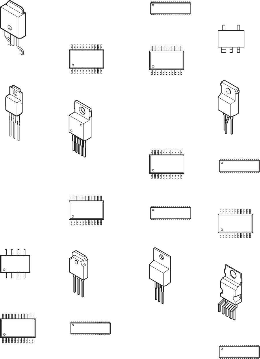
7-1
BVM-D14H1U/D14H5U/D14H1E/D14H5E/D14H1A/D14H5A
Section 7
Semiconductors
IC
BA05FP-E2
VccGND
OUT
BA05T
BA12T
VCC
GND
OUT
CXA1211M
CXA1521M
LM358D
LM393PS
LTC490CS8
M24C02-MN6T
MAX490ECSA
MM1026BFB
TC4W53FU
TC7W00FU
TC7W08F
TC7W32FU
TC7W74FU
TL082
UPC4558G2
X25040SI
TOP VIEW
14
5
8
CXA1544M-T6
NJU3716M-T2
112
24 13
TOP VIEW
CXA1875AM-T4
MAX202CSE
MAX3100CEE-TG068
MC14053BF
MC74HC4053F
MC74HC4538AF
TC74HC4053AFT (EL)
TC74HC4538AF
18
16 9
TOP VIEW
LA6500-FA
5
1
LC35256DM-70-TLM
MB90096PF-178
MB90096PF-G-127-BND-ER
114
28 15
TOP VIEW
LM2990T-5.0
123
M62399FP-TE2
TOP VIEW
110
20 11
MB89613R-651
TOP VIEW
132
64 33
MBM29F400BC-90FP
122
44 23
TOP VIEW
MC74HC00AFEL
MC74HC08AF
MC74HC589AFEL
TC74HC30AF
TC74VHC02F
TC74VHC04F
TC74VHC125F
TC74VHC138F
TC74VHC14F
17
14 8
TOP VIEW
MC74HC175FEL
TOP VIEW
18
16 9
NJM7912FA
12
3
SC7S02F
TC-4S30F
TC4S11F
TC4S71F
TC7S08F
TC7S14F
1
TOP VIEW
SE-135N
1
23
SN74HC05ANS
TOP VIEW
17
14 8
TC74VHC244F
TC74VHC574F
110
20 11
TOP VIEW
TDA8172
7
1
TDA9106
TOP VIEW
121
42 22
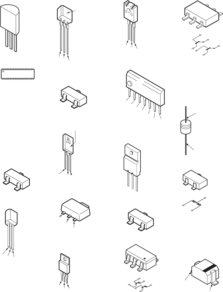
7-2 BVM-D14H1U/D14H5U/D14H1E/D14H5E/D14H1A/D14H5A
TL431CLP
UPC1093J
Z8622812PSC
TOP VIEW
19
18 10
2SA1037AK-T146-QR
2SA1037AK-T146-R
2SA1330-06
2SA1462-T1Y33
2SA1462-Y33
2SC1623-L5L6
2SC3326N-A
2SC3392-5-TB
2SC3545-T43
DTA114EKA-T146
DTA114GKAT146
DTA143ESA-TP
DTA144EKA-T146
DTC114EK
DTC114GKA
DTC114EKA-T146
E
B
C
2SA1091-0
2SC2362K-G
ECB
2SA1175-HFE
2SC2785-HFE
LETTER SIDE
ECB
2SA1221-K
2SB734-34
2SD774-34
E
B
C
2SA1381-E
2SC3503-DE
LETTER SIDE
EB
2SB1132-P
2SD1834
E
B
C
2SC3746
2SC5450-CA
2SD982
BCE
2SC3950-D
ECB
2SC4686A
G1 S1 NC
S2
G2 D2
D1
2SK2350
2SK2655-01R-F165
GDS
2SK520K44K45-T1B
D
S
G
IMT2
1
2
3
45
6
1
2
3
45
6
IMX2-T109
5
6
4
1
32
3
21
456
1SS119-25
D1N20R
HZS9.1NB2
RD18ESB1
RD27ESB2
RD5.1ESB3
RD6.2ESB2
RD6.8SB2-T1
CATHODE
ANODE
1SS226
1
2
3
1
2
3
1SS352
RD12ESB2
RD13SB2
RD15SB1
RD3.3SB
RD30SB-T1
RD4.7SB2
RD6.2SB
CATHODE
ANODE
IC, TRANSISTOR
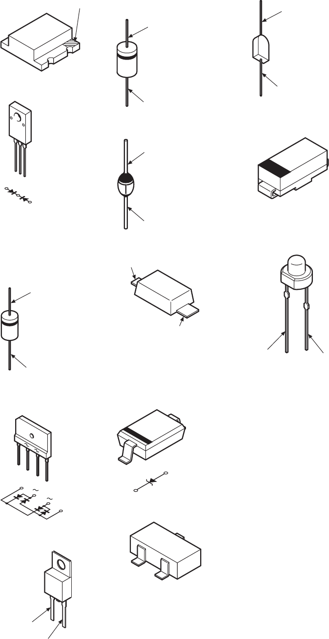
7-3
BVM-D14H1U/D14H5U/D14H1E/D14H5E/D14H1A/D14H5A
CL-155Y/PG-CD
CATHODE
D10SC9M
12
3
123
D1NL20U-TR
D1NL40-TA2
ERA91-02
ERD38-06
RH-1A
S2L20UF
CATHODE
ANODE
D4SB60L
+
–
+–
DD54SCLS-YCC-11
CATHODE
ANODE
EL1Z
GP08D
RGP02-17EL-6433
CATHODE
ANODE
FE3D
CATHODE
ANODE
MA111-(K8).S0
CATHODE
ANODE
RD10SB1
RD10SB3-T1
RD12SB-T1
RD12SB1-T1
RD5.6SB2
RD7.5SB1-T1
1
2
1
2
RD22M-B
CATHODE
ANODE
NC
RM11C
CATHODE
ANODE
SC311-6-TE12RA
SC802-04
ANODE
CATHODE
SLR-325DCT31
SLR-325MCT31
SLR-325VCT31
CATHODE
ANODE
DIODE

7-4 BVM-D14H1U/D14H5U/D14H1E/D14H5E/D14H1A/D14H5A
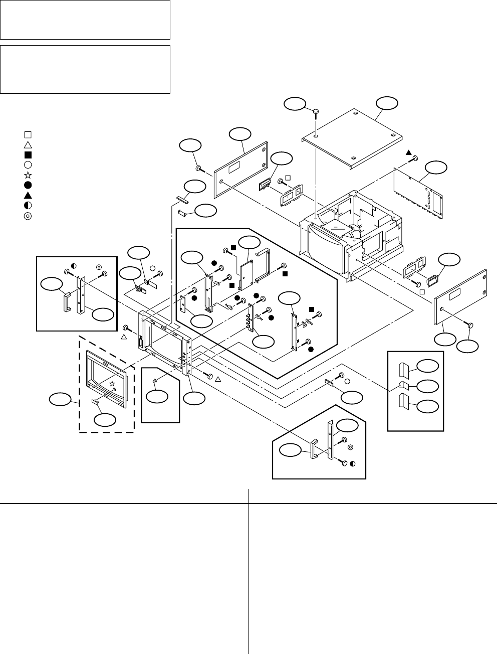
8-1
BVM-D14H1U/D14H5U/D14H1E/D14H5E/D14H1A/D14H5A
Section 8
Exploded Views
Ref.No. Part No. Description RemarkRef.No. Part No. Description Remark
8-1. BEZEL, CABINET
CABINET
1 X-4037-285-1 MASK (16:9) ASSY 2
2*3-718-322-02 EMBLEM, SONY
3 X-4037-278-1 BEZEL ASSY (D14H5)
X-4033-145-1 BEZEL ASSY (D14H1)
4 4-050-851-01 KNOB, CONTROL (D14H5)
5*A-1372-664-A HA MOUNT (D14H5)
6*4-050-925-04 BRACKET (RIGHT), BEZEL (D14H5)
7*A-1372-665-A HB MOUNT (D14H5)
8*4-050-924-04 BRACKET (LEFT), BEZEL (D14H5)
9*A-1375-185-A HC COMPL (D14H5)
10 *4-337-212-11 HANDLE (D14H5)
11 4-050-922-01 BASE, HANDLE (D14H5)
12 *A-1373-742-A YB MOUNT (D14H5)
*A-1373-717-A YB MOUNT (D14H1)
13 *A-1373-716-A YA MOUNT
14 *4-050-876-01 PLATE, LIGHT INTERCEPTION
15 *A-1373-743-A YC MOUNT (D14H5)
*A-1373-718-A YC MOUNT (D14H1)
16 *4-061-920-01 INSULATOR, YC
17 4-043-825-01 HANDLE
18 *4-073-226-01 CABINET (R)
19 *4-073-227-01 CABINET (L)
20 4-050-931-01 CABINET (UPPER) (D14H5)
4-050-967-01 CABINET(UPPER) (D14H1)
21 4-063-969-01 SCREW (OS), CASE, CLAW
22 *4-073-201-01 PANEL (UPPER), REAR (D14H5)
*4-073-228-01 PANEL (UPPER),REAR (D14H1)
23 *X-4033-276-1 GUARD ASSY,HARNESS(L) (D14H1)
24 *X-4033-277-1 GUARD ASSY,HARNESS(S) (D14H1)
((
(
(
• Items marked “ * ” are not stocked since they are seldom required
for routine service. Some delay should be anticipated when order-
ing these items.
• Items with no part number and no description are not stocked be-
cause they are seldom required for routine service.
• The construction parts of an assembled part are indicated with a
collation number in the remarks column.
The components identified marked ! are
critical for safety.
Replace only with the part number specified.
Les composants identifiés par la marque !
sont critiques pour la sécurité.
Ne les remplacer que par une pièce portant
le numéro spécifié.
NOTE :
(
: 7-682-161-01 +P 4x8
: 7-682-561-09 +B 4x8
: 7-682-947-01 +PSW 3x6
: 7-685-647-79 +BVTP 3x10
: 7-624-200-01 NUT, PUSH 1.5
: 7-685-648-79 +BVTP 3x12
: 7-685-871-09 +BVTT 3x6
: 7-682-963-09 +PSW 4x14
: 7-628-000-04 +PS 5x14
D14H5
D14H5
D14H5
D14H5
D14H1
1
2
3
4
5
6
7
8
9
10
10
11
11
12
13
14
15
16
17
17
18
19
20
21
21
21
22
23
23
24
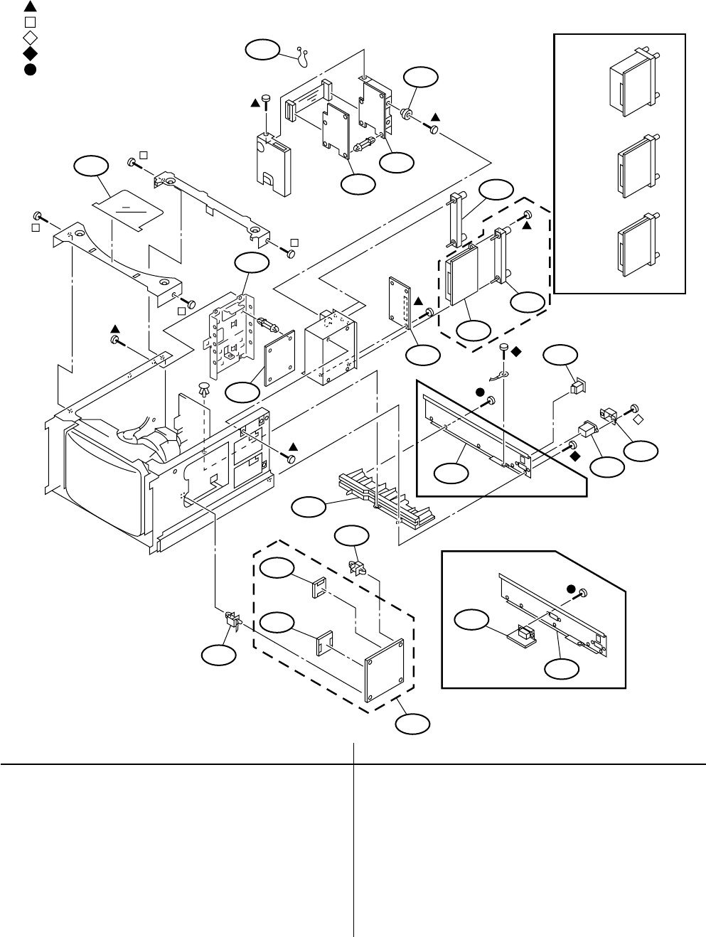
8-2 BVM-D14H1U/D14H5U/D14H1E/D14H5E/D14H1A/D14H5A
BLOCK
8-2. M BLOCK, SIGNAL BLOCK
Ref.No. Part No. Description RemarkRef.No. Part No. Description Remark
51 *A-1136-014-A B COMPL 52,53
52 *A-1131-464-A B2 MOUNT
53 *A-1131-463-A B1 MOUNT
54 *3-703-141-00 HOLDER, PWB
55 *4-353-620-11 HINGE, PC BOARD
56 *4-073-208-01 PANEL (LOWER), REAR (D14H5)
*4-073-232-01 PANEL(LOWER),REAR (D14H1)
57 *A-1372-136-A HD MOUNT (D14H1)
58 !1-762-300-11 SWITCH, AC POWER SEESAW
59 !1-251-382-11 INLET, AC 3P(WITH NOISE FILTER)
60 2-990-241-02 HOLDER (A), PLUG
61 *A-1306-572-A MA COMPL
62 *A-1306-571-A MB COMPL
63 *4-073-210-01 COLLAR
64 *A-1390-942-A T MOUNT
65 *X-4037-166-1 PANEL ASSY, BLANK
66 *A-1136-013-A BX COMPL
67 *X-4037-154-1 PANEL ASSY, CONNECTOR
68 *4-050-913-02 INSULATOR (ANODE)
69 *4-074-026-01 HOLDER,G PWB
70 3-701-417-02 PURSE LOCK (11 DIA.)
71 *4-074-027-01 BRACKET, G1
72 *A-1316-504-A G1 COMPL
(
D14H1
D14H5
OPTION
BKM-
142HD
BKM-
127W
BKM-
120D
BKM-129X
: 7-685-871-09 +BVTT 3x6
: 7-682-950-01 +PSW 3x12
: 7-682-950-09 +PSW 3x12
: 7-682-961-09 +PSW 4x8
: 7-685-648-79 +BVTP 3x12
51
52
53
54
55
56
56
57
58
59
60
61
71
62
63
64
72
65
66
67
68
69
70
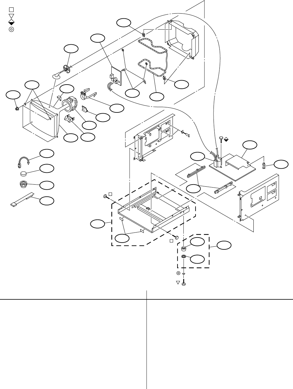
8-3
BVM-D14H1U/D14H5U/D14H1E/D14H5E/D14H1A/D14H5A
CHASSIS
8-3. PICTURE TUBE, CHASSIS
Ref.No. Part No. Description RemarkRef.No. Part No. Description Remark
101 4-306-034-00 NUT,(B) (M5), FLANGE
102 4-348-567-00 WASHER, CRT POSITION
103 !8-738-335-05 PICTURE TUBE M34LHF20X (For USA)
!8-738-333-05 PICTURE TUBE M34LHF21X
(For AEP,AUS)
104 !1-451-508-11 DEFLECTION YOKE
105 4-053-410-02 SHIELD, DY
106 X-2105-533-1 PLATE ASSY, CORRECTION, TLH
107 4-050-492-01 SPACER, DY
108 *4-047-349-01 HOLDER, HV CABLE
109 *A-1331-883-A C MOUNT
110 4-303-774-03 SPRING
111 !1-411-660-21 COIL, DEMAGNETIC
112 4-395-824-01 HOLDER, DEGAUSSING COIL
113 *4-382-050-01 BAND, C PC BOARD
114 *A-1316-456-A G COMPL 115
115 !X-4560-177-1 TRANSFORMER ASSY,FLYBACK
(NX-4141/J1A4)
116 *4-073-218-01 GUIDE, PWB
117 *X-4037-279-1 CHASSIS ASSY, BOTTOM (D14H5)118
117 *X-4037-288-1 CHASSIS ASSY,BOTTOM (D14H1)
118 3-840-486-02 CUSHION, SPEAKER
119 X-4033-117-1 FOOT ASSY 120,121
120 X-4836-202-9 FOOT
121 *3-668-845-01 CUSHION, LEG
122 4-308-870-00 CLIP,LEAD WIRE
123 1-452-032-00 MAGNET,DISC (10MMφ)
124 1-452-094-00 MAGNET,ROTATABLE DISK:15MMφ
125 4-051-735-22 PIECE A(75), CONV. CORRECT
127 *3-687-542-41 SPACER, PC BOARD SPACE
(
: 7-682-161-01 +P 4x8
: 7-682-564-09 +B 4x14
: 7-682-950-01 +PSW 3x12
: 7-688-004-02 W 4
101
102
103
104
105
106
107
108
109
110 111
112
112
113
114
115
116
117
118
119
120
121
122
123
124
125
127

8-4 BVM-D14H1U/D14H5U/D14H1E/D14H5E/D14H1A/D14H5A
9-1
BVM-D14H1U/D14H5U/D14H1E/D14H5E/D14H1A/D14H5A
Ref.No. Part No. Description RemarkRef.No. Part No. Description Remark
Ref.No. Part No. Description RemarkRef.No. Part No. Description Remark
Section 9
Electrical Parts List
*A-1136-014-A B COMPL
*********
Including B1 and B2 MOUNT
<CAPACITOR>
C300 1-163-031-11 CERAMIC CHIP 0.01µF 50V
C301 1-163-031-11 CERAMIC CHIP 0.01µF 50V
C304 1-104-760-11 CERAMIC CHIP 0.047µF 10% 50V
C305 1-163-021-91 CERAMIC CHIP 0.01µF 10% 50V
C306 1-163-031-11 CERAMIC CHIP 0.01µF 50V
C307 1-164-505-11 CERAMIC CHIP 2.2µF 16V
C308 1-115-152-11 ELECT CHIP 22µF 20% 6.3V
C309 1-163-031-11 CERAMIC CHIP 0.01µF 50V
C310 1-163-031-11 CERAMIC CHIP 0.01µF 50V
C311 1-163-031-11 CERAMIC CHIP 0.01µF 50V
C312 1-126-390-11 ELECT CHIP 22µF 20% 6.3V
C332 1-104-760-11 CERAMIC CHIP 0.047µF 10% 50V
C333 1-163-021-91 CERAMIC CHIP 0.01µF 10% 50V
C334 1-163-031-11 CERAMIC CHIP 0.01µF 50V
C335 1-164-505-11 CERAMIC CHIP 2.2µF 16V
C336 1-163-031-11 CERAMIC CHIP 0.01µF 50V
C337 1-163-031-11 CERAMIC CHIP 0.01µF 50V
C338 1-115-152-11 ELECT CHIP 22µF 20% 6.3V
C339 1-164-505-11 CERAMIC CHIP 2.2µF 16V
C340 1-163-031-11 CERAMIC CHIP 0.01µF 50V
C341 1-163-031-11 CERAMIC CHIP 0.01µF 50V
C367 1-104-760-11 CERAMIC CHIP 0.047µF 10% 50V
C368 1-163-021-91 CERAMIC CHIP 0.01µF 10% 50V
C369 1-163-031-11 CERAMIC CHIP 0.01µF 50V
C370 1-164-505-11 CERAMIC CHIP 2.2µF 16V
C371 1-163-031-11 CERAMIC CHIP 0.01µF 50V
C372 1-163-031-11 CERAMIC CHIP 0.01µF 50V
C373 1-115-152-11 ELECT CHIP 22µF 20% 6.3V
C374 1-164-505-11 CERAMIC CHIP 2.2µF 16V
C375 1-163-031-11 CERAMIC CHIP 0.01µF 50V
C376 1-163-031-11 CERAMIC CHIP 0.01µF 50V
C377 1-126-396-11 ELECT CHIP 47µF 20% 16V
C378 1-126-396-11 ELECT CHIP 47µF 20% 16V
C386 1-126-916-11 ELECT 1000µF 20% 6.3V
C387 1-126-916-11 ELECT 1000µF 20% 6.3V
C450 1-126-394-11 ELECT CHIP 10µF 20% 16V
C451 1-163-031-11 CERAMIC CHIP 0.01µF 50V
C452 1-163-031-11 CERAMIC CHIP 0.01µF 50V
C454 1-126-396-11 ELECT CHIP 47µF 20% 16V
C460 1-126-390-11 ELECT CHIP 22µF 20% 6.3V
C461 1-126-390-11 ELECT CHIP 22µF 20% 6.3V
C462 1-163-031-11 CERAMIC CHIP 0.01µF 50V
C463 1-163-031-11 CERAMIC CHIP 0.01µF 50V
C464 1-163-031-11 CERAMIC CHIP 0.01µF 50V
C465 1-126-394-11 ELECT CHIP 10µF 20% 16V
C466 1-126-394-11 ELECT CHIP 10µF 20% 16V
C467 1-163-031-11 CERAMIC CHIP 0.01µF 50V
C468 1-163-031-11 CERAMIC CHIP 0.01µF 50V
C485 1-126-390-11 ELECT CHIP 22µF 20% 6.3V
C486 1-126-390-11 ELECT CHIP 22µF 20% 6.3V
C487 1-163-031-11 CERAMIC CHIP 0.01µF 50V
C488 1-163-031-11 CERAMIC CHIP 0.01µF 50V
C489 1-163-031-11 CERAMIC CHIP 0.01µF 50V
C490 1-126-394-11 ELECT CHIP 10µF 20% 16V
C491 1-163-031-11 CERAMIC CHIP 0.01µF 50V
C492 1-163-031-11 CERAMIC CHIP 0.01µF 50V
C494 1-126-396-11 ELECT CHIP 47µF 20% 16V
C1300 1-163-031-11 CERAMIC CHIP 0.01µF 50V
C1301 1-163-031-11 CERAMIC CHIP 0.01µF 50V
C1302 1-163-087-00 CERAMIC CHIP 4PF 0.25PF 50V
C1304 1-104-760-11 CERAMIC CHIP 0.047µF 10% 50V
C1305 1-163-021-91 CERAMIC CHIP 0.01µF 10% 50V
C1306 1-109-982-11 CERAMIC CHIP 1µF 10% 10V
C1307 1-163-031-11 CERAMIC CHIP 0.01µF 50V
C1308 1-163-031-11 CERAMIC CHIP 0.01µF 50V
C1309 1-164-505-11 CERAMIC CHIP 2.2µF 16V
C1310 1-164-346-11 CERAMIC CHIP 1µF 16V
C1320 1-163-031-11 CERAMIC CHIP 0.01µF 50V
C1321 1-163-031-11 CERAMIC CHIP 0.01µF 50V
C1322 1-163-091-00 CERAMIC CHIP 8PF 0.25PF 50V
C1324 1-104-760-11 CERAMIC CHIP 0.047µF 10% 50V
C1325 1-163-021-91 CERAMIC CHIP 0.01µF 10% 50V
C1326 1-163-031-11 CERAMIC CHIP 0.01µF 50V
C1327 1-163-031-11 CERAMIC CHIP 0.01µF 50V
C1330 1-164-346-11 CERAMIC CHIP 1µF 16V
C1340 1-163-031-11 CERAMIC CHIP 0.01µF 50V
C1341 1-163-031-11 CERAMIC CHIP 0.01µF 50V
C1342 1-163-086-00 CERAMIC CHIP 3PF 0.25PF 50V
C1344 1-104-760-11 CERAMIC CHIP 0.047µF 10% 50V
C1345 1-163-021-91 CERAMIC CHIP 0.01µF 10% 50V
C1346 1-163-031-11 CERAMIC CHIP 0.01µF 50V
C1347 1-163-031-11 CERAMIC CHIP 0.01µF 50V
C1348 1-163-251-11 CERAMIC CHIP 100PF 5% 50V
C1350 1-164-346-11 CERAMIC CHIP 1µF 16V
C1400 1-163-035-00 CERAMIC CHIP 0.047µF 50V
B
NOTE :
• Items marked “ * ” are not stocked since they are seldom required
for routine service. Some delay should be anticipated when ordering
these items.
• Due to standardization, replacements in the parts list may be
different from the parts specified in the diagrams or the components
used on the set.
RESISTORS
• All resistors are in ohms.
• F: nonflammable
• METAL: Metal-film resistor
• METAL OXIDE: Metal oxide-film resistor
The components identified marked ! are
critical for safety.
Replace only with the part number specified.
Les composants identifiés par la marque !
sont critiques pour la sécurité.
Ne les remplacer que par une pièce portant
le numéro spécifié.

9-2 BVM-D14H1U/D14H5U/D14H1E/D14H5E/D14H1A/D14H5A
Ref.No. Part No. Description RemarkRef.No. Part No. Description Remark
C1401 1-163-035-00 CERAMIC CHIP 0.047µF 50V
C1402 1-163-035-00 CERAMIC CHIP 0.047µF 50V
C1404 1-163-031-11 CERAMIC CHIP 0.01µF 50V
C1405 1-163-035-00 CERAMIC CHIP 0.047µF 50V
C1406 1-163-809-11 CERAMIC CHIP 0.047µF 10% 25V
C1407 1-163-809-11 CERAMIC CHIP 0.047µF 10% 25V
C1408 1-163-809-11 CERAMIC CHIP 0.047µF 10% 25V
C1409 1-164-489-11 CERAMIC CHIP 0.22µF 10% 16V
C1410 1-164-004-11 CERAMIC CHIP 0.1µF 10% 25V
C1411 1-164-004-11 CERAMIC CHIP 0.1µF 10% 25V
C1412 1-164-004-11 CERAMIC CHIP 0.1µF 10% 25V
C1413 1-163-251-11 CERAMIC CHIP 100PF 5% 50V
C1414 1-163-275-11 CERAMIC CHIP 0.001µF 5% 50V
C1415 1-163-038-91 CERAMIC CHIP 0.1µF 25V
C1416 1-164-004-11 CERAMIC CHIP 0.1µF 10% 25V
C1417 1-164-004-11 CERAMIC CHIP 0.1µF 10% 25V
C1418 1-164-004-11 CERAMIC CHIP 0.1µF 10% 25V
C1419 1-163-251-11 CERAMIC CHIP 100PF 5% 50V
C1420 1-163-275-11 CERAMIC CHIP 0.001µF 5% 50V
C1421 1-163-038-91 CERAMIC CHIP 0.1µF 25V
C1422 1-164-004-11 CERAMIC CHIP 0.1µF 10% 25V
C1423 1-164-004-11 CERAMIC CHIP 0.1µF 10% 25V
C1424 1-163-251-11 CERAMIC CHIP 100PF 5% 50V
C1425 1-163-275-11 CERAMIC CHIP 0.001µF 5% 50V
C1426 1-163-038-91 CERAMIC CHIP 0.1µF 25V
C1427 1-163-038-91 CERAMIC CHIP 0.1µF 25V
C1428 1-164-004-11 CERAMIC CHIP 0.1µF 10% 25V
C1429 1-163-038-91 CERAMIC CHIP 0.1µF 25V
C1431 1-163-251-11 CERAMIC CHIP 100PF 5% 50V
C1450 1-163-031-11 CERAMIC CHIP 0.01µF 50V
C1451 1-163-251-11 CERAMIC CHIP 100PF 5% 50V
C1460 1-164-005-11 CERAMIC CHIP 0.47µF 25V
C1461 1-163-031-11 CERAMIC CHIP 0.01µF 50V
C1462 1-163-031-11 CERAMIC CHIP 0.01µF 50V
C1464 1-164-005-11 CERAMIC CHIP 0.47µF 25V
C1465 1-163-031-11 CERAMIC CHIP 0.01µF 50V
C1466 1-163-031-11 CERAMIC CHIP 0.01µF 50V
C1467 1-126-935-11 ELECT 470µF 20% 16V
C1468 1-126-396-11 ELECT CHIP 47µF 20% 16V
C1469 1-126-396-11 ELECT CHIP 47µF 20% 16V
C2300 1-163-222-11 CERAMIC CHIP 5PF 0.25PF 50V
C2310 1-126-396-11 ELECT CHIP 47µF 20% 16V
C2311 1-163-031-11 CERAMIC CHIP 0.01µF 50V
C2315 1-163-224-11 CERAMIC CHIP 7PF 0.5PF 50V
C2330 1-163-092-00 CERAMIC CHIP 9PF 0.25PF 50V
C2351 1-163-031-11 CERAMIC CHIP 0.01µF 50V
C2352 1-163-031-11 CERAMIC CHIP 0.01µF 50V
C2353 1-163-031-11 CERAMIC CHIP 0.01µF 50V
C2361 1-126-396-11 ELECT CHIP 47µF 20% 16V
C2362 1-163-031-11 CERAMIC CHIP 0.01µF 50V
C2363 1-126-396-11 ELECT CHIP 47µF 20% 16V
C2364 1-163-031-11 CERAMIC CHIP 0.01µF 50V
C2383 1-163-031-11 CERAMIC CHIP 0.01µF 50V
C2384 1-163-009-11 CERAMIC CHIP 0.001µF 10% 50V
C2385 1-163-009-11 CERAMIC CHIP 0.001µF 10% 50V
C2386 1-163-031-11 CERAMIC CHIP 0.01µF 50V
C2387 1-163-031-11 CERAMIC CHIP 0.01µF 50V
C2388 1-163-031-11 CERAMIC CHIP 0.01µF 50V
C2389 1-163-031-11 CERAMIC CHIP 0.01µF 50V
C2390 1-163-031-11 CERAMIC CHIP 0.01µF 50V
C3301 1-126-394-11 ELECT CHIP 10µF 20% 16V
C3302 1-163-251-11 CERAMIC CHIP 100PF 5% 50V
C3303 1-163-251-11 CERAMIC CHIP 100PF 5% 50V
C3304 1-163-257-11 CERAMIC CHIP 180PF 5% 50V
C3305 1-163-251-11 CERAMIC CHIP 100PF 5% 50V
C3306 1-163-257-11 CERAMIC CHIP 180PF 5% 50V
C3307 1-163-251-11 CERAMIC CHIP 100PF 5% 50V
C3308 1-164-346-11 CERAMIC CHIP 1µF 16V
C3309 1-126-390-11 ELECT CHIP 22µF 20% 6.3V
C3311 1-163-038-91 CERAMIC CHIP 0.1µF 25V
C3312 1-163-038-91 CERAMIC CHIP 0.1µF 25V
C3313 1-163-263-11 CERAMIC CHIP 330PF 5% 50V
C3314 1-163-038-91 CERAMIC CHIP 0.1µF 25V
C3316 1-163-038-91 CERAMIC CHIP 0.1µF 25V
C3332 1-163-031-11 CERAMIC CHIP 0.01µF 50V
C3333 1-163-031-11 CERAMIC CHIP 0.01µF 50V
C3339 1-163-038-91 CERAMIC CHIP 0.1µF 25V
C3341 1-163-251-11 CERAMIC CHIP 100PF 5% 50V
C3342 1-163-251-11 CERAMIC CHIP 100PF 5% 50V
C3344 1-164-004-11 CERAMIC CHIP 0.1µF 10% 25V
C3350 1-164-005-11 CERAMIC CHIP 0.47µF 25V
C3402 1-163-031-11 CERAMIC CHIP 0.01µF 50V
C3403 1-163-031-11 CERAMIC CHIP 0.01µF 50V
C3405 1-163-038-91 CERAMIC CHIP 0.1µF 25V
C3406 1-164-182-11 CERAMIC CHIP 0.0033µF 10% 50V
C3407 1-164-344-11 CERAMIC CHIP 0.068µF 10% 25V
C3408 1-126-394-11 ELECT CHIP 10µF 20% 16V
C3410 1-164-004-11 CERAMIC CHIP 0.1µF 10% 25V
C3411 1-163-259-91 CERAMIC CHIP 220PF 5% 50V
C3412 1-164-004-11 CERAMIC CHIP 0.1µF 10% 25V
C3432 1-163-035-00 CERAMIC CHIP 0.047µF 50V
C3433 1-163-031-11 CERAMIC CHIP 0.01µF 50V
C4300 1-163-031-11 CERAMIC CHIP 0.01µF 50V
C4302 1-163-031-11 CERAMIC CHIP 0.01µF 50V
C4303 1-163-031-11 CERAMIC CHIP 0.01µF 50V
C4350 1-163-031-11 CERAMIC CHIP 0.01µF 50V
C4351 1-163-031-11 CERAMIC CHIP 0.01µF 50V
C4352 1-163-031-11 CERAMIC CHIP 0.01µF 50V
C4353 1-163-031-11 CERAMIC CHIP 0.01µF 50V
C4354 1-163-031-11 CERAMIC CHIP 0.01µF 50V
C4355 1-126-396-11 ELECT CHIP 47µF 20% 16V
<CONNECTOR>
CN301 1-764-334-11 PLUG, CONNECTOR 11P
CN302 *1-564-509-11 PLUG, CONNECTOR 6P
CN303 *1-564-510-11 PLUG, CONNECTOR 7P
CN304 *1-564-513-11 PLUG, CONNECTOR 10P
CN307 *1-564-512-11 PLUG, CONNECTOR 9P
CN308 *1-564-512-11 PLUG, CONNECTOR 9P
CN411 *1-506-611-11 PIN, CONNECTOR 8P
CN412 *1-506-611-11 PIN, CONNECTOR 8P
CN421 *1-779-070-21 PIN, CONNECTOR 12P
CN422 *1-779-070-21 PIN, CONNECTOR 12P
<DIODE>
D1400 8-719-073-01 DIODE MA111-(K8).S0
D1401 8-719-073-01 DIODE MA111-(K8).S0
D1402 8-719-073-01 DIODE MA111-(K8).S0
D1403 8-719-073-01 DIODE MA111-(K8).S0
D1404 8-719-037-17 DIODE RD10SB3-T1
D3301 8-719-016-74 DIODE 1SS352
D3302 8-719-016-74 DIODE 1SS352
D3307 8-719-800-76 DIODE 1SS226
D3308 8-719-800-76 DIODE 1SS226
D4401 8-719-158-09 DIODE RD4.7SB2
B

9-3
BVM-D14H1U/D14H5U/D14H1E/D14H5E/D14H1A/D14H5A
Ref.No. Part No. Description RemarkRef.No. Part No. Description Remark
<IC>
IC300 8-759-011-65 IC MC74HC4053F
IC301 8-759-011-65 IC MC74HC4053F
IC302 8-759-011-65 IC MC74HC4053F
IC303 8-759-981-48 IC TL082M
IC304 8-759-981-48 IC TL082M
IC305 8-759-981-48 IC TL082M
IC306 8-752-054-80 IC CXA1521M
IC307 8-752-054-80 IC CXA1521M
IC308 8-752-054-80 IC CXA1521M
IC400 8-752-053-21 IC CXA1211M
IC401 8-752-053-21 IC CXA1211M
IC1300 8-759-011-65 IC MC74HC4053F
IC1302 8-759-011-65 IC MC74HC4053F
IC1303 8-759-011-65 IC MC74HC4053F
IC1304 8-759-011-65 IC MC74HC4053F
IC1305 8-759-981-48 IC TL082M
IC1306 8-759-981-48 IC TL082M
IC1307 8-759-981-48 IC TL082M
IC1308 8-759-011-65 IC MC74HC4053F
IC1309 8-759-011-65 IC MC74HC4053F
IC1400 8-759-038-15 IC MC74HC4538AF
IC1401 8-752-067-05 IC CXA1739S
IC2380 8-759-523-02 IC TC74HC4053AFT(EL)
IC2381 8-759-523-02 IC TC74HC4053AFT(EL)
IC2382 8-759-988-13 IC LM393PS
IC2383 8-759-083-94 IC TC7W74FU
IC3301 8-759-523-02 IC TC74HC4053AFT(EL)
IC3400 8-759-424-13 IC MC74HC00AFEL
IC3401 8-759-032-14 IC MC74HC08AF
IC3403 8-759-328-12 IC Z8622812PSC
IC3404 8-759-527-74 IC M24C02-MN6T
IC3406 8-759-084-79 IC TC7S14F
IC3407 8-759-242-76 IC TC7W08F
IC4300 8-752-072-94 IC CXA1875AM-T4
IC4301 8-752-072-94 IC CXA1875AM-T4
IC4302 8-752-072-94 IC CXA1875AM-T4
IC4350 8-752-072-94 IC CXA1875AM-T4
IC4351 8-759-482-47 IC M62399FP-TE2
IC4352 8-759-482-47 IC M62399FP-TE2
<COIL>
L300 1-406-665-11 CHOKE 100µH
<TRANSISTOR>
Q300 8-729-112-65 TRANSISTOR 2SA1462-Y33
Q301 8-729-107-31 TRANSISTOR 2SC3545-T43
Q302 8-729-920-59 TRANSISTOR IMX2-T109
Q303 8-729-107-31 TRANSISTOR 2SC3545-T43
Q304 8-729-107-31 TRANSISTOR 2SC3545-T43
Q330 8-729-112-65 TRANSISTOR 2SA1462-Y33
Q331 8-729-107-31 TRANSISTOR 2SC3545-T43
Q332 8-729-920-59 TRANSISTOR IMX2-T109
Q333 8-729-107-31 TRANSISTOR 2SC3545-T43
Q334 8-729-107-31 TRANSISTOR 2SC3545-T43
Q365 8-729-112-65 TRANSISTOR 2SA1462-Y33
Q366 8-729-107-31 TRANSISTOR 2SC3545-T43
Q367 8-729-920-59 TRANSISTOR IMX2-T109
Q368 8-729-107-31 TRANSISTOR 2SC3545-T43
Q369 8-729-107-31 TRANSISTOR 2SC3545-T43
Q450 8-729-120-28 TRANSISTOR 2SC1623-L5L6
Q451 8-729-107-31 TRANSISTOR 2SC3545-T43
Q452 8-729-107-31 TRANSISTOR 2SC3545-T43
Q453 8-729-112-65 TRANSISTOR 2SA1462-T1Y33
Q460 8-729-112-65 TRANSISTOR 2SA1462-Y33
Q461 8-729-107-31 TRANSISTOR 2SC3545-T43
Q462 8-729-120-28 TRANSISTOR 2SC1623-L5L6
Q463 8-729-107-31 TRANSISTOR 2SC3545-T43
Q464 8-729-107-31 TRANSISTOR 2SC3545-T43
Q465 8-729-026-50 TRANSISTOR 2SA1037AK-T146-QR
Q466 8-729-026-50 TRANSISTOR 2SA1037AK-T146-QR
Q485 8-729-120-28 TRANSISTOR 2SC1623-L5L6
Q486 8-729-107-31 TRANSISTOR 2SC3545-T43
Q487 8-729-107-31 TRANSISTOR 2SC3545-T43
Q1300 8-729-112-65 TRANSISTOR 2SA1462-Y33
Q1301 8-729-107-31 TRANSISTOR 2SC3545-T43
Q1302 8-729-120-28 TRANSISTOR 2SC1623-L5L6
Q1303 8-729-120-28 TRANSISTOR 2SC1623-L5L6
Q1304 8-729-120-28 TRANSISTOR 2SC1623-L5L6
Q1305 8-729-026-50 TRANSISTOR 2SA1037AK-T146-QR
Q1320 8-729-112-65 TRANSISTOR 2SA1462-Y33
Q1321 8-729-107-31 TRANSISTOR 2SC3545-T43
Q1322 8-729-120-28 TRANSISTOR 2SC1623-L5L6
Q1323 8-729-120-28 TRANSISTOR 2SC1623-L5L6
Q1340 8-729-112-65 TRANSISTOR 2SA1462-Y33
Q1341 8-729-107-31 TRANSISTOR 2SC3545-T43
Q1342 8-729-120-28 TRANSISTOR 2SC1623-L5L6
Q1343 8-729-120-28 TRANSISTOR 2SC1623-L5L6
Q1400 1-801-806-11 TRANSISTOR DTC144EKA-T146
Q1401 8-729-120-28 TRANSISTOR 2SC1623-L5L6
Q1402 8-729-026-50 TRANSISTOR 2SA1037AK-T146-QR
Q1410 8-729-112-65 TRANSISTOR 2SA1462-Y33
Q1411 8-729-120-28 TRANSISTOR 2SC1623-L5L6
Q1412 8-729-112-65 TRANSISTOR 2SA1462-Y33
Q1413 8-729-107-31 TRANSISTOR 2SC3545-T43
Q1414 8-729-120-28 TRANSISTOR 2SC1623-L5L6
Q1420 8-729-112-65 TRANSISTOR 2SA1462-Y33
Q1421 8-729-120-28 TRANSISTOR 2SC1623-L5L6
Q1422 8-729-112-65 TRANSISTOR 2SA1462-Y33
Q1423 8-729-107-31 TRANSISTOR 2SC3545-T43
Q1424 8-729-120-28 TRANSISTOR 2SC1623-L5L6
Q1430 8-729-112-65 TRANSISTOR 2SA1462-Y33
Q1431 8-729-120-28 TRANSISTOR 2SC1623-L5L6
Q1432 8-729-112-65 TRANSISTOR 2SA1462-Y33
Q1433 8-729-107-31 TRANSISTOR 2SC3545-T43
Q1434 8-729-120-28 TRANSISTOR 2SC1623-L5L6
Q1460 8-729-120-28 TRANSISTOR 2SC1623-L5L6
Q1461 8-729-120-28 TRANSISTOR 2SC1623-L5L6
Q1462 1-801-806-11 TRANSISTOR DTC144EKA-T146
Q1463 8-729-900-53 TRANSISTOR DTC114EK
Q2300 8-729-112-65 TRANSISTOR 2SA1462-Y33
Q2301 8-729-107-31 TRANSISTOR 2SC3545-T43
Q2302 8-729-112-65 TRANSISTOR 2SA1462-Y33
Q2303 8-729-112-65 TRANSISTOR 2SA1462-Y33
Q2315 8-729-112-65 TRANSISTOR 2SA1462-Y33
Q2316 8-729-107-31 TRANSISTOR 2SC3545-T43
Q2317 8-729-112-65 TRANSISTOR 2SA1462-Y33
Q2318 8-729-112-65 TRANSISTOR 2SA1462-Y33
Q2330 8-729-112-65 TRANSISTOR 2SA1462-Y33
Q2331 8-729-107-31 TRANSISTOR 2SC3545-T43
Q2332 8-729-112-65 TRANSISTOR 2SA1462-Y33
Q2333 8-729-112-65 TRANSISTOR 2SA1462-Y33
Q2380 8-729-120-28 TRANSISTOR 2SC1623-L5L6
Q2381 8-729-120-28 TRANSISTOR 2SC1623-L5L6
Q2382 8-729-120-28 TRANSISTOR 2SC1623-L5L6
Q2383 8-729-120-28 TRANSISTOR 2SC1623-L5L6
Q3301 8-729-026-50 TRANSISTOR 2SA1037AK-T146-QR
Q3302 8-729-026-50 TRANSISTOR 2SA1037AK-T146-QR
B

9-4 BVM-D14H1U/D14H5U/D14H1E/D14H5E/D14H1A/D14H5A
Ref.No. Part No. Description RemarkRef.No. Part No. Description Remark
Q3303 8-729-026-50 TRANSISTOR 2SA1037AK-T146-QR
Q3304 8-729-920-59 TRANSISTOR IMX2-T109
Q3305 8-729-920-59 TRANSISTOR IMX2-T109
Q3306 8-729-120-28 TRANSISTOR 2SC1623-L5L6
Q3307 8-729-026-50 TRANSISTOR 2SA1037AK-T146-QR
Q3308 8-729-107-31 TRANSISTOR 2SC3545-T43
Q3309 8-729-120-28 TRANSISTOR 2SC1623-L5L6
Q3310 8-729-925-42 TRANSISTOR IMT2
Q3311 8-729-120-28 TRANSISTOR 2SC1623-L5L6
Q3312 8-729-026-50 TRANSISTOR 2SA1037AK-T146-QR
Q3313 8-729-120-28 TRANSISTOR 2SC1623-L5L6
Q3314 8-729-920-59 TRANSISTOR IMX2-T109
Q3315 8-729-112-65 TRANSISTOR 2SA1462-Y33
Q3316 8-729-120-28 TRANSISTOR 2SC1623-L5L6
Q3317 8-729-925-42 TRANSISTOR IMT2
Q3318 8-729-026-50 TRANSISTOR 2SA1037AK-T146-QR
Q3319 8-729-120-28 TRANSISTOR 2SC1623-L5L6
Q3402 1-801-806-11 TRANSISTOR DTC144EKA-T146
<RESISTOR>
R300 1-216-049-91 RES,CHIP 1K 5% 1/10W
R301 1-216-025-91 RES,CHIP 100 5% 1/10W
R302 1-216-657-11 METAL CHIP 1.8K 0.50% 1/10W
R303 1-216-663-11 METAL CHIP 3.3K 0.50% 1/10W
R305 1-216-651-11 METAL CHIP 1K 0.50% 1/10W
R306 1-216-025-91 RES,CHIP 100 5% 1/10W
R307 1-216-653-11 METAL CHIP 1.2K 0.50% 1/10W
R308 1-216-025-91 RES,CHIP 100 5% 1/10W
R309 1-216-049-91 RES,CHIP 1K 5% 1/10W
R310 1-216-049-91 RES,CHIP 1K 5% 1/10W
R311 1-216-029-00 RES,CHIP 150 5% 1/10W
R312 1-216-675-91 METAL CHIP 10K 0.50% 1/10W
R313 1-218-776-11 METAL CHIP 1M 0.50% 1/10W
R314 1-216-675-91 METAL CHIP 10K 0.50% 1/10W
R315 1-218-764-11 METAL CHIP 330K 0.50% 1/10W
R316 1-216-033-00 RES,CHIP 220 5% 1/10W
R317 1-216-025-91 RES,CHIP 100 5% 1/10W
R318 1-216-053-00 RES,CHIP 1.5K 5% 1/10W
R319 1-216-685-11 METAL CHIP 27K 0.50% 1/10W
R320 1-216-679-11 METAL CHIP 15K 0.50% 1/10W
R321 1-216-089-91 RES,CHIP 47K 5% 1/10W
R322 1-216-681-11 METAL CHIP 18K 0.50% 1/10W
R323 1-216-025-91 RES,CHIP 100 5% 1/10W
R324 1-216-057-00 RES,CHIP 2.2K 5% 1/10W
R325 1-216-037-00 RES,CHIP 330 5% 1/10W
R330 1-216-049-91 RES,CHIP 1K 5% 1/10W
R331 1-216-025-91 RES,CHIP 100 5% 1/10W
R332 1-216-657-11 METAL CHIP 1.8K 0.50% 1/10W
R333 1-216-663-11 METAL CHIP 3.3K 0.50% 1/10W
R335 1-216-651-11 METAL CHIP 1K 0.50% 1/10W
R336 1-216-025-91 RES,CHIP 100 5% 1/10W
R337 1-216-653-11 METAL CHIP 1.2K 0.50% 1/10W
R338 1-216-025-91 RES,CHIP 100 5% 1/10W
R339 1-216-049-91 RES,CHIP 1K 5% 1/10W
R340 1-216-049-91 RES,CHIP 1K 5% 1/10W
R341 1-216-025-91 RES,CHIP 100 5% 1/10W
R342 1-216-675-91 METAL CHIP 10K 0.50% 1/10W
R343 1-218-776-11 METAL CHIP 1M 0.50% 1/10W
R344 1-216-675-91 METAL CHIP 10K 0.50% 1/10W
R345 1-218-770-11 METAL CHIP 560K 0.50% 1/10W
R346 1-216-033-00 RES,CHIP 220 5% 1/10W
R347 1-216-025-91 RES,CHIP 100 5% 1/10W
R348 1-216-053-00 RES,CHIP 1.5K 5% 1/10W
R349 1-216-683-11 METAL CHIP 22K 0.50% 1/10W
R350 1-218-759-11 METAL CHIP 200K 0.50% 1/10W
R351 1-216-693-11 METAL CHIP 56K 0.50% 1/10W
R353 1-216-089-91 RES,CHIP 47K 5% 1/10W
R354 1-216-025-91 RES,CHIP 100 5% 1/10W
R355 1-216-057-91 RES,CHIP 2.2K 5% 1/10W
R356 1-216-033-00 RES,CHIP 220 5% 1/10W
R365 1-216-049-91 RES,CHIP 1K 5% 1/10W
R366 1-216-025-91 RES,CHIP 100 5% 1/10W
R367 1-216-657-11 METAL CHIP 1.8K 0.50% 1/10W
R368 1-216-663-11 METAL CHIP 3.3K 0.50% 1/10W
R370 1-216-651-11 METAL CHIP 1K 0.50% 1/10W
R371 1-216-025-91 RES,CHIP 100 5% 1/10W
R372 1-216-653-11 METAL CHIP 1.2K 0.50% 1/10W
R373 1-216-025-91 RES,CHIP 100 5% 1/10W
R374 1-216-049-91 RES,CHIP 1K 5% 1/10W
R375 1-216-049-91 RES,CHIP 1K 5% 1/10W
R376 1-216-025-91 RES,CHIP 100 5% 1/10W
R377 1-216-675-91 METAL CHIP 10K 0.50% 1/10W
R378 1-218-776-11 METAL CHIP 1M 0.50% 1/10W
R379 1-216-675-91 METAL CHIP 10K 0.50% 1/10W
R380 1-218-770-11 METAL CHIP 560K 0.50% 1/10W
R381 1-216-033-00 RES,CHIP 220 5% 1/10W
R382 1-216-025-91 RES,CHIP 100 5% 1/10W
R383 1-216-053-00 RES,CHIP 1.5K 5% 1/10W
R384 1-216-683-11 METAL CHIP 22K 0.50% 1/10W
R385 1-218-759-11 METAL CHIP 200K 0.50% 1/10W
R386 1-216-693-11 METAL CHIP 56K 0.50% 1/10W
R388 1-216-089-91 RES,CHIP 47K 5% 1/10W
R389 1-216-025-91 RES,CHIP 100 5% 1/10W
R390 1-216-057-00 RES,CHIP 2.2K 5% 1/10W
R391 1-216-033-00 RES,CHIP 220 5% 1/10W
R450 1-216-025-91 RES,CHIP 100 5% 1/10W
R451 1-216-049-91 RES,CHIP 1K 5% 1/10W
R452 1-216-647-11 METAL CHIP 680 0.50% 1/10W
R453 1-216-649-11 METAL CHIP 820 0.50% 1/10W
R454 1-216-645-11 METAL CHIP 560 0.50% 1/10W
R455 1-216-647-11 METAL CHIP 680 0.50% 1/10W
R456 1-216-065-91 RES,CHIP 4.7K 5% 1/10W
R457 1-216-029-91 RES,CHIP 150 5% 1/10W
R458 1-216-025-91 RES,CHIP 100 5% 1/10W
R459 1-216-057-00 RES,CHIP 2.2K 5% 1/10W
R460 1-216-671-11 METAL CHIP 6.8K 0.50% 1/10W
R461 1-216-667-11 METAL CHIP 4.7K 0.50% 1/10W
R462 1-216-671-11 METAL CHIP 6.8K 0.50% 1/10W
R463 1-216-667-11 METAL CHIP 4.7K 0.50% 1/10W
R464 1-216-660-11 METAL CHIP 2.4K 0.50% 1/10W
R465 1-216-668-11 METAL CHIP 5.1K 0.50% 1/10W
R466 1-216-663-11 METAL CHIP 3.3K 0.50% 1/10W
R467 1-216-649-11 METAL CHIP 820 0.50% 1/10W
R468 1-216-045-00 RES,CHIP 680 5% 1/10W
R469 1-216-045-00 RES,CHIP 680 5% 1/10W
R470 1-216-651-11 METAL CHIP 1K 0.50% 1/10W
R471 1-216-061-00 RES,CHIP 3.3K 5% 1/10W
R472 1-216-025-91 RES,CHIP 100 5% 1/10W
R473 1-216-049-91 RES,CHIP 1K 5% 1/10W
R474 1-216-647-11 METAL CHIP 680 0.50% 1/10W
R475 1-216-647-11 METAL CHIP 680 0.50% 1/10W
R476 1-216-647-11 METAL CHIP 680 0.50% 1/10W
R477 1-216-645-11 METAL CHIP 560 0.50% 1/10W
R478 1-216-065-91 RES,CHIP 4.7K 5% 1/10W
R479 1-216-065-91 RES,CHIP 4.7K 5% 1/10W
R480 1-216-025-91 RES,CHIP 100 5% 1/10W
R481 1-216-057-00 RES,CHIP 2.2K 5% 1/10W
R482 1-216-025-91 RES,CHIP 100 5% 1/10W
R483 1-216-645-11 METAL CHIP 560 0.50% 1/10W
R484 1-216-013-91 RES,CHIP 33 5% 1/10W
B

9-5
BVM-D14H1U/D14H5U/D14H1E/D14H5E/D14H1A/D14H5A
Ref.No. Part No. Description RemarkRef.No. Part No. Description Remark
R485 1-216-671-11 METAL CHIP 6.8K 0.50% 1/10W
R486 1-216-661-11 METAL CHIP 2.7K 0.50% 1/10W
R487 1-216-671-11 METAL CHIP 6.8K 0.50% 1/10W
R488 1-216-667-11 METAL CHIP 4.7K 0.50% 1/10W
R489 1-216-025-91 RES,CHIP 100 5% 1/10W
R490 1-216-049-91 RES,CHIP 1K 5% 1/10W
R491 1-216-647-11 METAL CHIP 680 0.50% 1/10W
R492 1-216-647-11 METAL CHIP 680 0.50% 1/10W
R493 1-216-647-11 METAL CHIP 680 0.50% 1/10W
R494 1-216-645-11 METAL CHIP 560 0.50% 1/10W
R495 1-216-065-91 RES,CHIP 4.7K 5% 1/10W
R497 1-216-025-91 RES,CHIP 100 5% 1/10W
R498 1-216-057-00 RES,CHIP 2.2K 5% 1/10W
R499 1-216-029-91 RES,CHIP 150 5% 1/10W
R1300 1-216-025-91 RES,CHIP 100 5% 1/10W
R1301 1-216-663-11 METAL CHIP 3.3K 0.50% 1/10W
R1302 1-216-657-11 METAL CHIP 1.8K 0.50% 1/10W
R1303 1-216-651-11 METAL CHIP 1K 0.50% 1/10W
R1305 1-216-025-91 RES,CHIP 100 5% 1/10W
R1306 1-216-653-11 METAL CHIP 1.2K 0.50% 1/10W
R1307 1-216-025-91 RES,CHIP 100 5% 1/10W
R1308 1-216-049-91 RES,CHIP 1K 5% 1/10W
R1309 1-218-776-11 METAL CHIP 1M 0.50% 1/10W
R1310 1-216-675-91 METAL CHIP 10K 0.50% 1/10W
R1311 1-216-073-00 RES,CHIP 10K 5% 1/10W
R1312 1-216-073-00 RES,CHIP 10K 5% 1/10W
R1313 1-216-025-91 RES,CHIP 100 5% 1/10W
R1314 1-216-057-00 RES,CHIP 2.2K 5% 1/10W
R1315 1-216-295-91 SHORT 0
R1316 1-216-675-91 METAL CHIP 10K 0.50% 1/10W
R1317 1-216-689-11 METAL CHIP 39K 0.50% 1/10W
R1318 1-216-065-91 RES,CHIP 4.7K 5% 1/10W
R1319 1-216-065-91 RES,CHIP 4.7K 5% 1/10W
R1320 1-216-025-91 RES,CHIP 100 5% 1/10W
R1321 1-216-663-11 METAL CHIP 3.3K 0.50% 1/10W
R1322 1-216-657-11 METAL CHIP 1.8K 0.50% 1/10W
R1323 1-216-651-11 METAL CHIP 1K 0.50% 1/10W
R1325 1-216-025-91 RES,CHIP 100 5% 1/10W
R1326 1-216-653-11 METAL CHIP 1.2K 0.50% 1/10W
R1327 1-216-025-91 RES,CHIP 100 5% 1/10W
R1328 1-216-049-91 RES,CHIP 1K 5% 1/10W
R1329 1-218-776-11 METAL CHIP 1M 0.50% 1/10W
R1330 1-216-675-91 METAL CHIP 10K 0.50% 1/10W
R1331 1-216-025-91 RES,CHIP 100 5% 1/10W
R1332 1-216-057-00 RES,CHIP 2.2K 5% 1/10W
R1333 1-216-295-91 SHORT 0
R1334 1-216-073-00 RES,CHIP 10K 5% 1/10W
R1335 1-216-073-00 RES,CHIP 10K 5% 1/10W
R1340 1-216-025-91 RES,CHIP 100 5% 1/10W
R1341 1-216-663-11 METAL CHIP 3.3K 0.50% 1/10W
R1342 1-216-657-11 METAL CHIP 1.8K 0.50% 1/10W
R1343 1-216-651-11 METAL CHIP 1K 0.50% 1/10W
R1345 1-216-025-91 RES,CHIP 100 5% 1/10W
R1346 1-216-653-11 METAL CHIP 1.2K 0.50% 1/10W
R1347 1-216-025-91 RES,CHIP 100 5% 1/10W
R1348 1-216-049-91 RES,CHIP 1K 5% 1/10W
R1349 1-218-776-11 METAL CHIP 1M 0.50% 1/10W
R1350 1-216-675-91 METAL CHIP 10K 0.50% 1/10W
R1351 1-216-025-91 RES,CHIP 100 5% 1/10W
R1352 1-216-057-00 RES,CHIP 2.2K 5% 1/10W
R1353 1-216-295-91 SHORT 0
R1354 1-216-685-11 METAL CHIP 27K 0.50% 1/10W
R1355 1-216-691-11 METAL CHIP 47K 0.50% 1/10W
R1357 1-216-073-00 RES,CHIP 10K 5% 1/10W
R1358 1-216-073-00 RES,CHIP 10K 5% 1/10W
R1400 1-216-025-91 RES,CHIP 100 5% 1/10W
R1401 1-216-295-91 SHORT 0
R1402 1-216-073-00 RES,CHIP 10K 5% 1/10W
R1405 1-216-025-91 RES,CHIP 100 5% 1/10W
R1406 1-216-025-91 RES,CHIP 100 5% 1/10W
R1407 1-216-025-91 RES,CHIP 100 5% 1/10W
R1408 1-216-049-91 RES,CHIP 1K 5% 1/10W
R1409 1-216-049-91 RES,CHIP 1K 5% 1/10W
R1410 1-216-025-91 RES,CHIP 100 5% 1/10W
R1411 1-216-085-00 RES,CHIP 33K 5% 1/10W
R1412 1-216-089-91 RES,CHIP 47K 5% 1/10W
R1413 1-216-085-00 RES,CHIP 33K 5% 1/10W
R1414 1-216-085-00 RES,CHIP 33K 5% 1/10W
R1415 1-216-113-00 RES,CHIP 470K 5% 1/10W
R1416 1-216-025-91 RES,CHIP 100 5% 1/10W
R1417 1-216-063-91 RES,CHIP 3.9K 5% 1/10W
R1418 1-216-049-91 RES,CHIP 1K 5% 1/10W
R1419 1-216-073-00 RES,CHIP 10K 5% 1/10W
R1420 1-216-095-00 RES,CHIP 82K 5% 1/10W
R1421 1-216-041-00 RES,CHIP 470 5% 1/10W
R1422 1-216-049-91 RES,CHIP 1K 5% 1/10W
R1423 1-216-041-00 RES,CHIP 470 5% 1/10W
R1424 1-216-049-91 RES,CHIP 1K 5% 1/10W
R1425 1-216-065-91 RES,CHIP 4.7K 5% 1/10W
R1426 1-216-025-91 RES,CHIP 100 5% 1/10W
R1427 1-216-063-91 RES,CHIP 3.9K 5% 1/10W
R1428 1-216-049-91 RES,CHIP 1K 5% 1/10W
R1429 1-216-073-00 RES,CHIP 10K 5% 1/10W
R1430 1-216-095-00 RES,CHIP 82K 5% 1/10W
R1431 1-216-041-00 RES,CHIP 470 5% 1/10W
R1432 1-216-049-91 RES,CHIP 1K 5% 1/10W
R1433 1-216-041-00 RES,CHIP 470 5% 1/10W
R1434 1-216-049-91 RES,CHIP 1K 5% 1/10W
R1435 1-216-065-91 RES,CHIP 4.7K 5% 1/10W
R1436 1-216-025-91 RES,CHIP 100 5% 1/10W
R1437 1-216-063-91 RES,CHIP 3.9K 5% 1/10W
R1438 1-216-049-91 RES,CHIP 1K 5% 1/10W
R1439 1-216-073-00 RES,CHIP 10K 5% 1/10W
R1440 1-216-095-00 RES,CHIP 82K 5% 1/10W
R1441 1-216-041-00 RES,CHIP 470 5% 1/10W
R1442 1-216-049-91 RES,CHIP 1K 5% 1/10W
R1443 1-216-041-00 RES,CHIP 470 5% 1/10W
R1444 1-216-049-91 RES,CHIP 1K 5% 1/10W
R1445 1-216-065-91 RES,CHIP 4.7K 5% 1/10W
R1446 1-216-097-91 RES,CHIP 100K 5% 1/10W
R1447 1-216-097-91 RES,CHIP 100K 5% 1/10W
R1450 1-216-675-91 METAL CHIP 10K 0.50% 1/10W
R1451 1-216-089-91 RES,CHIP 47K 5% 1/10W
R1452 1-216-687-11 METAL CHIP 33K 0.50% 1/10W
R1453 1-216-687-11 METAL CHIP 33K 0.50% 1/10W
R1454 1-216-687-11 METAL CHIP 33K 0.50% 1/10W
R1455 1-216-085-00 RES,CHIP 33K 5% 1/10W
R1456 1-216-085-00 RES,CHIP 33K 5% 1/10W
R1457 1-216-085-00 RES,CHIP 33K 5% 1/10W
R1460 1-216-113-00 RES,CHIP 470K 5% 1/10W
R1461 1-216-085-00 RES,CHIP 33K 5% 1/10W
R1464 1-216-689-11 METAL CHIP 39K 0.50% 1/10W
R1466 1-216-113-00 RES,CHIP 470K 5% 1/10W
R1467 1-216-083-00 RES,CHIP 27K 5% 1/10W
R1469 1-216-667-11 METAL CHIP 4.7K 0.50% 1/10W
R1470 1-216-671-11 METAL CHIP 6.8K 0.50% 1/10W
R1471 1-216-689-11 METAL CHIP 39K 0.50% 1/10W
R1472 1-218-768-11 METAL CHIP 470K 0.50% 1/10W
R1473 1-216-073-00 RES,CHIP 10K 5% 1/10W
R1480 1-216-069-00 RES,CHIP 6.8K 5% 1/10W
B

9-6 BVM-D14H1U/D14H5U/D14H1E/D14H5E/D14H1A/D14H5A
Ref.No. Part No. Description RemarkRef.No. Part No. Description Remark
R1481 1-216-065-91 RES,CHIP 4.7K 5% 1/10W
R1482 1-216-061-00 RES,CHIP 3.3K 5% 1/10W
R1483 1-216-089-91 RES,CHIP 47K 5% 1/10W
R1484 1-216-085-00 RES,CHIP 33K 5% 1/10W
R1485 1-216-073-00 RES,CHIP 10K 5% 1/10W
R2300 1-216-025-91 RES,CHIP 100 5% 1/10W
R2301 1-216-065-91 RES,CHIP 4.7K 5% 1/10W
R2302 1-216-009-91 RES,CHIP 22 5% 1/10W
R2303 1-216-035-00 RES,CHIP 270 5% 1/10W
R2304 1-216-645-11 METAL CHIP 560 0.50% 1/10W
R2305 1-216-643-11 METAL CHIP 470 0.50% 1/10W
R2307 1-216-025-91 RES,CHIP 100 5% 1/10W
R2308 1-216-055-00 RES,CHIP 1.8K 5% 1/10W
R2309 1-216-025-91 RES,CHIP 100 5% 1/10W
R2310 1-216-049-91 RES,CHIP 1K 5% 1/10W
R2313 1-216-295-91 RES,CHIP 0
R2314 1-216-615-91 METAL CHIP 33 0.5% 1/10W
R2315 1-216-025-91 RES,CHIP 100 5% 1/10W
R2316 1-216-065-91 RES,CHIP 4.7K 5% 1/10W
R2317 1-216-009-91 RES,CHIP 22 5% 1/10W
R2318 1-216-035-00 RES,CHIP 270 5% 1/10W
R2319 1-216-645-11 METAL CHIP 560 0.50% 1/10W
R2320 1-216-643-11 METAL CHIP 470 0.50% 1/10W
R2322 1-216-025-91 RES,CHIP 100 5% 1/10W
R2323 1-216-055-00 RES,CHIP 1.8K 5% 1/10W
R2324 1-216-025-91 RES,CHIP 100 5% 1/10W
R2325 1-216-049-91 RES,CHIP 1K 5% 1/10W
R2327 1-216-295-91 RES,CHIP 0
R2329 1-216-615-91 METAL CHIP 33 0.5% 1/10W
R2330 1-216-025-91 RES,CHIP 100 5% 1/10W
R2331 1-216-065-91 RES,CHIP 4.7K 5% 1/10W
R2332 1-216-009-91 RES,CHIP 22 5% 1/10W
R2333 1-216-035-00 RES,CHIP 270 5% 1/10W
R2334 1-216-645-11 METAL CHIP 560 0.50% 1/10W
R2335 1-216-643-11 METAL CHIP 470 0.50% 1/10W
R2337 1-216-025-91 RES,CHIP 100 5% 1/10W
R2338 1-216-055-00 RES,CHIP 1.8K 5% 1/10W
R2339 1-216-025-91 RES,CHIP 100 5% 1/10W
R2340 1-216-049-91 RES,CHIP 1K 5% 1/10W
R2342 1-216-295-91 RES,CHIP 0
R2344 1-216-615-91 METAL CHIP 33 0.5% 1/10W
R2380 1-216-025-91 RES,CHIP 100 5% 1/10W
R2381 1-216-057-00 RES,CHIP 2.2K 5% 1/10W
R2382 1-216-025-91 RES,CHIP 100 5% 1/10W
R2383 1-216-057-00 RES,CHIP 2.2K 5% 1/10W
R2384 1-216-025-91 RES,CHIP 100 5% 1/10W
R2385 1-216-057-00 RES,CHIP 2.2K 5% 1/10W
R2386 1-216-025-91 RES,CHIP 100 5% 1/10W
R2387 1-216-057-00 RES,CHIP 2.2K 5% 1/10W
R2388 1-216-073-00 RES,CHIP 10K 5% 1/10W
R2389 1-216-073-00 RES,CHIP 10K 5% 1/10W
R2390 1-216-057-00 RES,CHIP 2.2K 5% 1/10W
R2391 1-216-073-00 RES,CHIP 10K 5% 1/10W
R2392 1-216-073-00 RES,CHIP 10K 5% 1/10W
R2393 1-216-057-00 RES,CHIP 2.2K 5% 1/10W
R3299 1-216-025-91 RES,CHIP 100 5% 1/10W
R3300 1-216-025-91 RES,CHIP 100 5% 1/10W
R3301 1-216-053-00 RES,CHIP 1.5K 5% 1/10W
R3302 1-216-079-00 RES,CHIP 18K 5% 1/10W
R3303 1-216-091-00 RES,CHIP 56K 5% 1/10W
R3304 1-216-013-00 RES,CHIP 33 5% 1/10W
R3305 1-216-013-00 RES,CHIP 33 5% 1/10W
R3306 1-216-013-00 RES,CHIP 33 5% 1/10W
R3307 1-216-049-91 RES,CHIP 1K 5% 1/10W
R3308 1-216-049-91 RES,CHIP 1K 5% 1/10W
R3309 1-216-049-91 RES,CHIP 1K 5% 1/10W
R3310 1-216-057-00 RES,CHIP 2.2K 5% 1/10W
R3311 1-216-057-00 RES,CHIP 2.2K 5% 1/10W
R3312 1-216-049-91 RES,CHIP 1K 5% 1/10W
R3313 1-216-063-91 RES,CHIP 3.9K 5% 1/10W
R3314 1-216-053-00 RES,CHIP 1.5K 5% 1/10W
R3315 1-216-065-91 RES,CHIP 4.7K 5% 1/10W
R3316 1-216-687-11 METAL CHIP 33K 0.50% 1/10W
R3317 1-216-663-11 METAL CHIP 3.3K 0.50% 1/10W
R3318 1-216-651-11 METAL CHIP 1K 0.50% 1/10W
R3319 1-216-083-00 RES,CHIP 27K 5% 1/10W
R3320 1-216-037-00 RES,CHIP 330 5% 1/10W
R3321 1-216-679-11 METAL CHIP 15K 0.50% 1/10W
R3322 1-216-097-91 RES,CHIP 100K 5% 1/10W
R3323 1-216-659-11 METAL CHIP 2.2K 0.50% 1/10W
R3324 1-216-655-11 METAL CHIP 1.5K 0.50% 1/10W
R3325 1-216-041-00 RES,CHIP 470 5% 1/10W
R3326 1-216-029-00 RES,CHIP 150 5% 1/10W
R3327 1-216-111-00 RES,CHIP 390K 5% 1/10W
R3328 1-216-659-11 METAL CHIP 2.2K 0.50% 1/10W
R3329 1-216-681-11 METAL CHIP 18K 0.50% 1/10W
R3330 1-216-676-11 METAL CHIP 11K 0.50% 1/10W
R3331 1-216-059-00 RES,CHIP 2.7K 5% 1/10W
R3332 1-216-075-00 RES,CHIP 12K 5% 1/10W
R3333 1-216-669-11 METAL CHIP 5.6K 0.50% 1/10W
R3334 1-216-659-11 METAL CHIP 2.2K 0.50% 1/10W
R3335 1-216-659-11 METAL CHIP 2.2K 0.50% 1/10W
R3336 1-216-640-11 METAL CHIP 360 0.50% 1/10W
R3337 1-216-069-00 RES,CHIP 6.8K 5% 1/10W
R3338 1-216-057-00 RES,CHIP 2.2K 5% 1/10W
R3339 1-216-037-00 RES,CHIP 330 5% 1/10W
R3340 1-216-693-11 METAL CHIP 56K 0.50% 1/10W
R3341 1-218-768-11 METAL CHIP 470K 0.50% 1/10W
R3342 1-216-097-91 RES,CHIP 100K 5% 1/10W
R3343 1-216-696-11 METAL CHIP 75K 0.50% 1/10W
R3344 1-216-661-11 METAL CHIP 2.7K 0.50% 1/10W
R3345 1-216-073-00 RES,CHIP 10K 5% 1/10W
R3346 1-216-099-00 RES,CHIP 120K 5% 1/10W
R3347 1-216-687-11 METAL CHIP 33K 0.50% 1/10W
R3381 1-216-683-11 METAL CHIP 22K 0.50% 1/10W
R3382 1-216-031-00 RES,CHIP 180 5% 1/10W
R3385 1-216-049-91 RES,CHIP 1K 5% 1/10W
R3400 1-216-097-91 RES,CHIP 100K 5% 1/10W
R3401 1-216-097-91 RES,CHIP 100K 5% 1/10W
R3402 1-216-097-91 RES,CHIP 100K 5% 1/10W
R3403 1-216-097-91 RES,CHIP 100K 5% 1/10W
R3410 1-216-049-91 RES,CHIP 1K 5% 1/10W
R3411 1-216-025-91 RES,CHIP 100 5% 1/10W
R3412 1-216-025-91 RES,CHIP 100 5% 1/10W
R3413 1-216-025-91 RES,CHIP 100 5% 1/10W
R3414 1-216-049-91 RES,CHIP 1K 5% 1/10W
R3416 1-216-049-91 RES,CHIP 1K 5% 1/10W
R3417 1-216-049-91 RES,CHIP 1K 5% 1/10W
R3418 1-216-069-00 RES,CHIP 6.8K 5% 1/10W
R3419 1-216-049-91 RES,CHIP 1K 5% 1/10W
R3421 1-216-025-91 RES,CHIP 100 5% 1/10W
R3422 1-216-025-91 RES,CHIP 100 5% 1/10W
R3423 1-216-025-91 RES,CHIP 100 5% 1/10W
R3424 1-216-073-00 RES,CHIP 10K 5% 1/10W
R3425 1-216-073-00 RES,CHIP 10K 5% 1/10W
R3426 1-216-025-91 RES,CHIP 100 5% 1/10W
R3427 1-216-025-91 RES,CHIP 100 5% 1/10W
R3428 1-216-025-91 RES,CHIP 100 5% 1/10W
R3429 1-216-025-91 RES,CHIP 100 5% 1/10W
R3430 1-216-049-91 RES,CHIP 1K 5% 1/10W
B

9-7
BVM-D14H1U/D14H5U/D14H1E/D14H5E/D14H1A/D14H5A
Ref.No. Part No. Description RemarkRef.No. Part No. Description Remark
R3431 1-216-295-91 SHORT 0
R3433 1-216-025-91 RES,CHIP 100 5% 1/10W
R3434 1-216-025-91 RES,CHIP 100 5% 1/10W
R4300 1-216-073-00 RES,CHIP 10K 5% 1/10W
R4301 1-216-073-00 RES,CHIP 10K 5% 1/10W
R4302 1-216-073-00 RES,CHIP 10K 5% 1/10W
R4303 1-216-073-00 RES,CHIP 10K 5% 1/10W
R4304 1-216-033-00 RES,CHIP 220 5% 1/10W
R4305 1-216-033-00 RES,CHIP 220 5% 1/10W
R4306 1-216-073-00 RES,CHIP 10K 5% 1/10W
R4307 1-216-073-00 RES,CHIP 10K 5% 1/10W
R4308 1-216-073-00 RES,CHIP 10K 5% 1/10W
R4309 1-216-073-00 RES,CHIP 10K 5% 1/10W
R4310 1-216-033-00 RES,CHIP 220 5% 1/10W
R4311 1-216-033-00 RES,CHIP 220 5% 1/10W
R4312 1-216-073-00 RES,CHIP 10K 5% 1/10W
R4313 1-216-073-00 RES,CHIP 10K 5% 1/10W
R4314 1-216-073-00 RES,CHIP 10K 5% 1/10W
R4315 1-216-049-91 RES,CHIP 1K 5% 1/10W
R4316 1-216-033-00 RES,CHIP 220 5% 1/10W
R4317 1-216-033-00 RES,CHIP 220 5% 1/10W
R4320 1-216-057-00 RES,CHIP 2.2K 5% 1/10W
R4417 1-216-073-00 RES,CHIP 10K 5% 1/10W
R4420 1-216-033-00 RES,CHIP 220 5% 1/10W
R4423 1-216-073-00 RES,CHIP 10K 5% 1/10W
R4426 1-216-033-00 RES,CHIP 220 5% 1/10W
R4434 1-216-049-91 RES,CHIP 1K 5% 1/10W
R4435 1-216-073-00 RES,CHIP 10K 5% 1/10W
R4436 1-216-677-11 METAL CHIP 12K 0.50% 1/10W
R4437 1-216-668-11 METAL CHIP 5.1K 0.50% 1/10W
R4438 1-216-073-00 RES,CHIP 10K 5% 1/10W
R4439 1-216-073-00 RES,CHIP 10K 5% 1/10W
R4440 1-216-073-00 RES,CHIP 10K 5% 1/10W
R4441 1-216-073-00 RES,CHIP 10K 5% 1/10W
R4442 1-216-073-00 RES,CHIP 10K 5% 1/10W
R4443 1-216-033-00 RES,CHIP 220 5% 1/10W
R4444 1-216-033-00 RES,CHIP 220 5% 1/10W
R4445 1-216-071-00 RES,CHIP 8.2K 5% 1/10W
R4446 1-216-131-11 RES,CHIP 2.7M 5% 1/10W
R4447 1-216-071-00 RES,CHIP 8.2K 5% 1/10W
R4448 1-216-071-00 RES,CHIP 8.2K 5% 1/10W
R4449 1-216-131-11 RES,CHIP 2.7M 5% 1/10W
R4450 1-216-131-11 RES,CHIP 2.7M 5% 1/10W
R4451 1-216-071-00 RES,CHIP 8.2K 5% 1/10W
R4452 1-216-131-11 RES,CHIP 2.7M 5% 1/10W
R4453 1-216-073-00 RES,CHIP 10K 5% 1/10W
R4454 1-216-033-00 RES,CHIP 220 5% 1/10W
R4455 1-216-033-00 RES,CHIP 220 5% 1/10W
R4456 1-216-073-00 RES,CHIP 10K 5% 1/10W
R4457 1-216-071-00 RES,CHIP 8.2K 5% 1/10W
R4458 1-216-061-00 RES,CHIP 3.3K 5% 1/10W
R4459 1-216-131-11 RES,CHIP 2.7M 5% 1/10W
R4460 1-216-057-00 RES,CHIP 2.2K 5% 1/10W
R4461 1-216-071-00 RES,CHIP 8.2K 5% 1/10W
R4462 1-216-131-11 RES,CHIP 2.7M 5% 1/10W
R4471 1-216-025-91 RES,CHIP 100 5% 1/10W
R4472 1-216-025-91 RES,CHIP 100 5% 1/10W
****************************************************************
*A-1131-463-A B1 MOUNT
***********
<CAPACITOR>
C401 1-126-396-11 ELECT CHIP 47µF 20% 16V
C402 1-126-396-11 ELECT CHIP 47µF 20% 16V
C403 1-163-031-11 CERAMIC CHIP 0.01µF 50V
C404 1-163-031-11 CERAMIC CHIP 0.01µF 50V
C407 1-163-038-91 CERAMIC CHIP 0.1µF 25V
C410 1-163-038-91 CERAMIC CHIP 0.1µF 25V
C411 1-165-319-11 CERAMIC CHIP 0.1µF 50V
C412 1-163-031-11 CERAMIC CHIP 0.01µF 50V
C502 1-163-031-11 CERAMIC CHIP 0.01µF 50V
C503 1-163-031-11 CERAMIC CHIP 0.01µF 50V
<CONNECTOR>
CN401 *1-568-015-11 SOCKET, CONNECTOR 8P
CN402 *1-568-015-11 SOCKET, CONNECTOR 8P
<DELAY LINE>
DL400 1-411-450-11 DELAY LINE
DL401 1-411-450-11 DELAY LINE
DL402 1-234-455-21 DELAY LINE
DL403 1-234-455-21 DELAY LINE
DL404 1-411-451-11 DELAY LINE
DL405 1-234-456-21 DELAY LINE
DL501 1-402-770-11 DELAY LINE
DL502 1-416-476-21 DELAY LINE
DL503 1-402-770-11 DELAY LINE
DL504 1-416-476-21 DELAY LINE
<IC>
IC410 8-759-011-65 IC MC74HC4053F
IC450 8-752-053-21 IC CXA1211M
IC501 8-759-011-65 IC MC74HC4053F
<TRANSISTOR>
Q400 8-729-120-28 TRANSISTOR 2SC1623-L5L6
Q401 8-729-120-28 TRANSISTOR 2SC1623-L5L6
Q402 8-729-120-28 TRANSISTOR 2SC1623-L5L6
Q403 8-729-120-28 TRANSISTOR 2SC1623-L5L6
Q404 8-729-026-50 TRANSISTOR 2SA1037AK-T146-QR
Q405 8-729-112-65 TRANSISTOR 2SA1462-T1Y33
Q406 8-729-112-65 TRANSISTOR 2SA1462-T1Y33
Q407 8-729-112-65 TRANSISTOR 2SA1462-T1Y33
Q408 8-729-107-31 TRANSISTOR 2SC3545-T43
Q409 8-729-107-31 TRANSISTOR 2SC3545-T43
Q410 1-801-806-11 TRANSISTOR DTC144EKA-T146
Q411 8-729-120-28 TRANSISTOR 2SC1623-L5L6
Q412 8-729-107-31 TRANSISTOR 2SC3545-T43
Q413 8-729-120-28 TRANSISTOR 2SC1623-L5L6
Q414 8-729-107-31 TRANSISTOR 2SC3545-T43
Q501 8-729-026-50 TRANSISTOR 2SA1037AK-T146-QR
Q502 8-729-107-31 TRANSISTOR 2SC3545-T43
Q503 8-729-112-65 TRANSISTOR 2SA1462-T1Y33
Q504 8-729-026-50 TRANSISTOR 2SA1037AK-T146-QR
Q505 8-729-107-31 TRANSISTOR 2SC3545-T43
Q506 8-729-112-65 TRANSISTOR 2SA1462-T1Y33
Q511 8-729-120-28 TRANSISTOR 2SC1623-L5L6
Q512 8-729-107-31 TRANSISTOR 2SC3545-T43
Q513 8-729-112-65 TRANSISTOR 2SA1462-T1Y33
Q514 8-729-107-31 TRANSISTOR 2SC3545-T43
B1B

9-8 BVM-D14H1U/D14H5U/D14H1E/D14H5E/D14H1A/D14H5A
Ref.No. Part No. Description RemarkRef.No. Part No. Description Remark
Q515 8-729-120-28 TRANSISTOR 2SC1623-L5L6
Q516 8-729-107-31 TRANSISTOR 2SC3545-T43
Q517 8-729-112-65 TRANSISTOR 2SA1462-T1Y33
Q518 8-729-107-31 TRANSISTOR 2SC3545-T43
<RESISTOR>
R400 1-216-025-91 RES,CHIP 100 5% 1/10W
R401 1-216-057-00 RES,CHIP 2.2K 5% 1/10W
R402 1-216-651-11 METAL CHIP 1K 0.50% 1/10W
R403 1-216-025-91 RES,CHIP 100 5% 1/10W
R404 1-216-057-00 RES,CHIP 2.2K 5% 1/10W
R405 1-216-651-11 METAL CHIP 1K 0.50% 1/10W
R406 1-216-025-91 RES,CHIP 100 5% 1/10W
R407 1-216-057-00 RES,CHIP 2.2K 5% 1/10W
R408 1-216-057-00 RES,CHIP 2.2K 5% 1/10W
R409 1-216-089-91 RES,CHIP 47K 5% 1/10W
R410 1-216-025-91 RES,CHIP 100 5% 1/10W
R411 1-216-057-00 RES,CHIP 2.2K 5% 1/10W
R412 1-216-643-11 METAL CHIP 470 0.50% 1/10W
R413 1-216-025-91 RES,CHIP 100 5% 1/10W
R414 1-216-057-00 RES,CHIP 2.2K 5% 1/10W
R415 1-216-643-11 METAL CHIP 470 0.50% 1/10W
R416 1-216-025-91 RES,CHIP 100 5% 1/10W
R417 1-216-057-00 RES,CHIP 2.2K 5% 1/10W
R418 1-216-057-00 RES,CHIP 2.2K 5% 1/10W
R419 1-216-085-00 RES,CHIP 33K 5% 1/10W
R420 1-216-025-91 RES,CHIP 100 5% 1/10W
R421 1-216-651-11 METAL CHIP 1K 0.50% 1/10W
R422 1-216-025-91 RES,CHIP 100 5% 1/10W
R423 1-216-025-91 RES,CHIP 100 5% 1/10W
R424 1-216-643-11 METAL CHIP 470 0.50% 1/10W
R425 1-216-643-11 METAL CHIP 470 0.50% 1/10W
R426 1-216-025-91 RES,CHIP 100 5% 1/10W
R427 1-216-651-11 METAL CHIP 1K 0.50% 1/10W
R428 1-216-057-00 RES,CHIP 2.2K 5% 1/10W
R429 1-216-057-00 RES,CHIP 2.2K 5% 1/10W
R430 1-216-025-91 RES,CHIP 100 5% 1/10W
R431 1-216-025-91 RES,CHIP 100 5% 1/10W
R432 1-216-061-00 RES,CHIP 3.3K 5% 1/10W
R433 1-216-075-00 RES,CHIP 12K 5% 1/10W
R434 1-216-065-91 RES,CHIP 4.7K 5% 1/10W
R435 1-216-051-00 RES,CHIP 1.2K 5% 1/10W
R436 1-216-065-91 RES,CHIP 4.7K 5% 1/10W
R437 1-216-057-00 RES,CHIP 2.2K 5% 1/10W
R438 1-216-073-00 RES,CHIP 10K 5% 1/10W
R439 1-216-057-00 RES,CHIP 2.2K 5% 1/10W
R440 1-216-049-91 RES,CHIP 1K 5% 1/10W
R441 1-216-295-91 SHORT 0
R442 1-216-025-91 RES,CHIP 100 5% 1/10W
R443 1-216-025-91 RES,CHIP 100 5% 1/10W
R444 1-216-025-91 RES,CHIP 100 5% 1/10W
R501 1-216-025-91 RES,CHIP 100 5% 1/10W
R502 1-216-057-00 RES,CHIP 2.2K 5% 1/10W
R503 1-216-651-11 METAL CHIP 1K 0.50% 1/10W
R504 1-216-651-11 METAL CHIP 1K 0.50% 1/10W
R505 1-216-025-91 RES,CHIP 100 5% 1/10W
R506 1-216-025-91 RES,CHIP 100 5% 1/10W
R507 1-216-057-00 RES,CHIP 2.2K 5% 1/10W
R508 1-216-025-91 RES,CHIP 100 5% 1/10W
R509 1-216-037-00 RES,CHIP 330 5% 1/10W
R510 1-216-631-11 METAL CHIP 150 0.50% 1/10W
R511 1-216-631-11 METAL CHIP 150 0.50% 1/10W
R512 1-216-025-91 RES,CHIP 100 5% 1/10W
R513 1-216-025-91 RES,CHIP 100 5% 1/10W
R514 1-216-057-00 RES,CHIP 2.2K 5% 1/10W
R515 1-216-651-11 METAL CHIP 1K 0.50% 1/10W
R516 1-216-651-11 METAL CHIP 1K 0.50% 1/10W
R517 1-216-025-91 RES,CHIP 100 5% 1/10W
R518 1-216-025-91 RES,CHIP 100 5% 1/10W
R519 1-216-057-00 RES,CHIP 2.2K 5% 1/10W
R520 1-216-025-91 RES,CHIP 100 5% 1/10W
R521 1-216-037-00 RES,CHIP 330 5% 1/10W
R522 1-216-631-11 METAL CHIP 150 0.50% 1/10W
R523 1-216-631-11 METAL CHIP 150 0.50% 1/10W
R524 1-216-025-91 RES,CHIP 100 5% 1/10W
R531 1-216-057-00 RES,CHIP 2.2K 5% 1/10W
R532 1-216-057-00 RES,CHIP 2.2K 5% 1/10W
R533 1-216-061-00 RES,CHIP 3.3K 5% 1/10W
R534 1-216-069-00 RES,CHIP 6.8K 5% 1/10W
R535 1-216-057-00 RES,CHIP 2.2K 5% 1/10W
R536 1-216-057-00 RES,CHIP 2.2K 5% 1/10W
R537 1-216-025-91 RES,CHIP 100 5% 1/10W
R538 1-216-051-00 RES,CHIP 1.2K 5% 1/10W
R541 1-216-057-00 RES,CHIP 2.2K 5% 1/10W
R542 1-216-057-00 RES,CHIP 2.2K 5% 1/10W
R543 1-216-061-00 RES,CHIP 3.3K 5% 1/10W
R544 1-216-069-00 RES,CHIP 6.8K 5% 1/10W
R545 1-216-057-00 RES,CHIP 2.2K 5% 1/10W
R546 1-216-057-00 RES,CHIP 2.2K 5% 1/10W
R547 1-216-025-91 RES,CHIP 100 5% 1/10W
R548 1-216-051-00 RES,CHIP 1.2K 5% 1/10W
****************************************************************
*A-1131-464-A B2 MOUNT
***********
<CAPACITOR>
C3901 1-163-031-11 CERAMIC CHIP 0.01µF 50V
C3902 1-164-161-11 CERAMIC CHIP 0.0022µF 10% 50V
C3903 1-163-133-00 CERAMIC CHIP 470PF 5% 50V
C3904 1-163-017-00 CERAMIC CHIP 0.0047µF 10% 50V
C3905 1-163-009-11 CERAMIC CHIP 0.001µF 10% 50V
C3906 1-163-251-11 CERAMIC CHIP 100PF 5% 50V
C3907 1-163-133-00 CERAMIC CHIP 470PF 5% 50V
C3908 1-164-346-11 CERAMIC CHIP 1µF 16V
C3909 1-163-259-91 CERAMIC CHIP 220PF 5% 50V
C3910 1-163-031-11 CERAMIC CHIP 0.01µF 50V
C3912 1-163-127-00 CERAMIC CHIP 270PF 5% 50V
C3913 1-163-031-11 CERAMIC CHIP 0.01µF 50V
C3914 1-163-031-11 CERAMIC CHIP 0.01µF 50V
C3915 1-163-259-91 CERAMIC CHIP 220PF 5% 50V
C3916 1-163-031-11 CERAMIC CHIP 0.01µF 50V
C3917 1-163-031-11 CERAMIC CHIP 0.01µF 50V
C3918 1-163-031-11 CERAMIC CHIP 0.01µF 50V
C3919 1-163-031-11 CERAMIC CHIP 0.01µF 50V
C3920 1-163-031-11 CERAMIC CHIP 0.01µF 50V
C3921 1-164-489-11 CERAMIC CHIP 0.22µF 10% 16V
C3922 1-164-489-11 CERAMIC CHIP 0.22µF 10% 16V
C3923 1-163-031-11 CERAMIC CHIP 0.01µF 50V
C3924 1-163-031-11 CERAMIC CHIP 0.01µF 50V
<CONNECTOR>
CN3901 *1-573-896-11 SOCKET, CONNECTOR 12P
CN3902 *1-573-896-11 SOCKET, CONNECTOR 12P
B1 B2

9-9
BVM-D14H1U/D14H5U/D14H1E/D14H5E/D14H1A/D14H5A
Ref.No. Part No. Description RemarkRef.No. Part No. Description Remark
<DIODE>
D3901 8-719-016-74 DIODE 1SS352
D3902 8-719-016-74 DIODE 1SS352
D3903 8-719-016-74 DIODE 1SS352
D3904 8-719-016-74 DIODE 1SS352
<IC>
IC3901 8-759-239-34 IC TC74HC4538AF
IC3902 8-759-523-02 IC TC74HC4053AFT(EL)
IC3904 8-759-239-34 IC TC74HC4538AF
IC3905 8-759-100-96 IC UPC4558G2
IC3906 8-759-234-20 IC TC7S08F
IC3907 8-759-035-90 IC SC7S02F
IC3908 8-759-082-61 IC TC4W53FU
<TRANSISTOR>
Q3901 8-729-027-38 TRANSISTOR DTA144EKA-T146
Q3902 8-729-027-38 TRANSISTOR DTA144EKA-T146
Q3903 8-729-026-50 TRANSISTOR 2SA1037AK-T146-QR
Q3905 8-729-026-50 TRANSISTOR 2SA1037AK-T146-QR
Q3906 8-729-027-38 TRANSISTOR DTA144EKA-T146
Q3907 8-729-120-28 TRANSISTOR 2SC1623-L5L6
Q3908 8-729-026-50 TRANSISTOR 2SA1037AK-T146-QR
Q3909 8-729-026-50 TRANSISTOR 2SA1037AK-T146-QR
Q3910 8-729-026-50 TRANSISTOR 2SA1037AK-T146-QR
Q3911 1-801-806-11 TRANSISTOR DTC144EKA-T146
Q3912 8-729-202-38 TRANSISTOR 2SC3326N-A
Q3913 8-729-202-38 TRANSISTOR 2SC3326N-A
Q3914 8-729-120-28 TRANSISTOR 2SC1623-L5L6
Q3915 8-729-026-50 TRANSISTOR 2SA1037AK-T146-QR
Q3916 8-729-120-28 TRANSISTOR 2SC1623-L5L6
<RESISTOR>
R3901 1-216-025-91 RES,CHIP 100 5% 1/10W
R3902 1-216-025-91 RES,CHIP 100 5% 1/10W
R3903 1-216-659-11 METAL CHIP 2.2K 0.50% 1/10W
R3904 1-216-025-91 RES,CHIP 100 5% 1/10W
R3905 1-218-754-11 METAL CHIP 120K 0.50% 1/10W
R3906 1-216-659-11 METAL CHIP 2.2K 0.50% 1/10W
R3907 1-218-754-11 METAL CHIP 120K 0.50% 1/10W
R3908 1-216-059-00 RES,CHIP 2.7K 5% 1/10W
R3909 1-216-659-11 METAL CHIP 2.2K 0.50% 1/10W
R3910 1-216-699-91 METAL CHIP 100K 0.50% 1/10W
R3912 1-216-057-00 RES,CHIP 2.2K 5% 1/10W
R3913 1-216-655-11 METAL CHIP 1.5K 0.50% 1/10W
R3914 1-216-025-91 RES,CHIP 100 5% 1/10W
R3915 1-216-674-11 METAL CHIP 9.1K 0.50% 1/10W
R3916 1-216-025-91 RES,CHIP 100 5% 1/10W
R3917 1-216-097-91 RES,CHIP 100K 5% 1/10W
R3918 1-216-049-91 RES,CHIP 1K 5% 1/10W
R3919 1-216-065-91 RES,CHIP 4.7K 5% 1/10W
R3920 1-216-049-91 RES,CHIP 1K 5% 1/10W
R3922 1-216-689-11 METAL CHIP 39K 0.50% 1/10W
R3923 1-216-025-91 RES,CHIP 100 5% 1/10W
R3924 1-216-681-11 METAL CHIP 18K 0.50% 1/10W
R3925 1-216-697-91 METAL CHIP 82K 0.50% 1/10W
R3926 1-216-049-91 RES,CHIP 1K 5% 1/10W
R3927 1-216-699-91 METAL CHIP 100K 0.50% 1/10W
R3928 1-216-025-91 RES,CHIP 100 5% 1/10W
R3929 1-216-681-11 METAL CHIP 18K 0.50% 1/10W
R3930 1-216-675-91 METAL CHIP 10K 0.50% 1/10W
R3931 1-216-049-91 RES,CHIP 1K 5% 1/10W
R3932 1-216-653-11 METAL CHIP 1.2K 0.50% 1/10W
R3933 1-216-651-11 METAL CHIP 1K 0.50% 1/10W
R3934 1-216-025-91 RES,CHIP 100 5% 1/10W
R3935 1-216-049-91 RES,CHIP 1K 5% 1/10W
R3936 1-216-097-91 RES,CHIP 100K 5% 1/10W
R3937 1-216-025-91 RES,CHIP 100 5% 1/10W
R3938 1-216-073-00 RES,CHIP 10K 5% 1/10W
R3939 1-216-097-91 RES,CHIP 100K 5% 1/10W
R3940 1-216-073-00 RES,CHIP 10K 5% 1/10W
R3941 1-216-049-91 RES,CHIP 1K 5% 1/10W
R3942 1-216-081-00 RES,CHIP 22K 5% 1/10W
R3943 1-216-055-00 RES,CHIP 1.8K 5% 1/10W
R3944 1-216-049-91 RES,CHIP 1K 5% 1/10W
R3945 1-216-079-00 RES,CHIP 18K 5% 1/10W
R3946 1-216-059-00 RES,CHIP 2.7K 5% 1/10W
R3947 1-216-089-91 RES,CHIP 47K 5% 1/10W
R3948 1-216-295-91 SHORT 0
****************************************************************
*A-1136-013-A BX COMPL
***********
<CAPACITOR>
C010 1-128-526-11 ELECT 100µF 20% 16V
C011 1-163-038-91 CERAMIC CHIP 0.1µF 25V
C012 1-128-526-11 ELECT 100µF 20% 16V
C013 1-163-038-91 CERAMIC CHIP 0.1µF 25V
C014 1-128-526-11 ELECT 100µF 20% 16V
C015 1-163-038-91 CERAMIC CHIP 0.1µF 25V
C016 1-163-038-91 CERAMIC CHIP 0.1µF 25V
C017 1-163-038-91 CERAMIC CHIP 0.1µF 25V
C018 1-163-038-91 CERAMIC CHIP 0.1µF 25V
C019 1-163-038-91 CERAMIC CHIP 0.1µF 25V
C020 1-163-038-91 CERAMIC CHIP 0.1µF 25V
C021 1-163-038-91 CERAMIC CHIP 0.1µF 25V
C022 1-163-038-91 CERAMIC CHIP 0.1µF 25V
C050 1-128-526-11 ELECT 100µF 20% 16V
C051 1-163-038-91 CERAMIC CHIP 0.1µF 25V
C052 1-128-526-11 ELECT 100µF 20% 16V
C053 1-163-038-91 CERAMIC CHIP 0.1µF 25V
C054 1-128-526-11 ELECT 100µF 20% 16V
C055 1-163-038-91 CERAMIC CHIP 0.1µF 25V
C056 1-163-038-91 CERAMIC CHIP 0.1µF 25V
C057 1-163-038-91 CERAMIC CHIP 0.1µF 25V
C058 1-163-038-91 CERAMIC CHIP 0.1µF 25V
C059 1-163-038-91 CERAMIC CHIP 0.1µF 25V
C060 1-163-038-91 CERAMIC CHIP 0.1µF 25V
C061 1-163-038-91 CERAMIC CHIP 0.1µF 25V
C062 1-163-038-91 CERAMIC CHIP 0.1µF 25V
C101 1-163-227-11 CERAMIC CHIP 10PF 0.5PF 50V
C102 1-163-235-11 CERAMIC CHIP 22PF 5% 50V
C103 1-107-701-11 ELECT 47µF 20% 16V
C104 1-107-725-11 CERAMIC CHIP 0.1µF 10% 16V
C106 1-163-021-91 CERAMIC CHIP 0.01µF 10% 50V
C201 1-163-227-11 CERAMIC CHIP 10PF 0.5PF 50V
C202 1-163-235-11 CERAMIC CHIP 22PF 5% 50V
C203 1-107-701-11 ELECT 47µF 20% 16V
C204 1-107-725-11 CERAMIC CHIP 0.1µF 10% 16V
C206 1-163-021-91 CERAMIC CHIP 0.01µF 10% 50V
C301 1-163-227-11 CERAMIC CHIP 10PF 0.5PF 50V
C302 1-163-235-11 CERAMIC CHIP 22PF 5% 50V
C303 1-107-701-11 ELECT 47µF 20% 16V
C304 1-107-725-11 CERAMIC CHIP 0.1µF 10% 16V
BXB2

9-10 BVM-D14H1U/D14H5U/D14H1E/D14H5E/D14H1A/D14H5A
Ref.No. Part No. Description RemarkRef.No. Part No. Description Remark
C306 1-163-021-91 CERAMIC CHIP 0.01µF 10% 50V
C401 1-163-091-00 CERAMIC CHIP 8PF 0.25PF 50V
C402 1-163-235-11 CERAMIC CHIP 22PF 5% 50V
C403 1-107-701-11 ELECT 47µF 20% 16V
C404 1-107-725-11 CERAMIC CHIP 0.1µF 10% 16V
C501 1-128-526-11 ELECT 100µF 20% 16V
C502 1-163-038-91 CERAMIC CHIP 0.1µF 25V
C503 1-163-038-91 CERAMIC CHIP 0.1µF 25V
<CONNECTOR>
CN001 *1-774-523-11 PIN, CONNECTOR (PC BOARD) 64P
<DIODE>
D101 8-719-073-01 DIODE MA111-(K8).S0
D102 8-719-073-01 DIODE MA111-(K8).S0
D201 8-719-073-01 DIODE MA111-(K8).S0
D202 8-719-073-01 DIODE MA111-(K8).S0
D301 8-719-073-01 DIODE MA111-(K8).S0
D302 8-719-073-01 DIODE MA111-(K8).S0
D401 8-719-073-01 DIODE MA111-(K8).S0
D402 8-719-073-01 DIODE MA111-(K8).S0
D501 8-719-158-19 DIODE RD6.2SB
<FILTER>
FL501 1-239-183-11 FILTER, EMI
FL502 1-239-480-11 FILTER, EMI
FL503 1-239-480-11 FILTER, EMI
<IC>
IC010 8-759-460-74 IC BA05FP-E2
IC050 8-759-539-89 IC LM2990SX-5.0
IC501 8-759-594-41 IC MB89613R-651
IC502 8-759-186-44 IC TC74VHC125F
IC503 8-759-156-54 IC X25040SI
<TRANSISTOR>
Q101 8-729-112-65 TRANSISTOR 2SA1462-Y33
Q102 8-729-027-38 TRANSISTOR DTA144EKA-T146
Q103 8-729-107-31 TRANSISTOR 2SC3545-T43
Q201 8-729-112-65 TRANSISTOR 2SA1462-Y33
Q202 8-729-027-38 TRANSISTOR DTA144EKA-T146
Q203 8-729-107-31 TRANSISTOR 2SC3545-T43
Q301 8-729-112-65 TRANSISTOR 2SA1462-Y33
Q302 8-729-027-38 TRANSISTOR DTA144EKA-T146
Q303 8-729-107-31 TRANSISTOR 2SC3545-T43
Q401 8-729-120-28 TRANSISTOR 2SC1623-L5L6
Q402 1-801-806-11 TRANSISTOR DTC144EKA-T146
Q403 8-729-026-49 TRANSISTOR 2SA1037AK-T146-R
Q404 8-729-027-38 TRANSISTOR DTA144EKA-T146
Q501 1-801-806-11 TRANSISTOR DTC144EKA-T146
<RESISTOR>
R101 1-214-837-11 METAL 75 1% 1/2W
R102 1-216-089-91 RES,CHIP 47K 5% 1/10W
R103 1-216-025-91 RES,CHIP 100 5% 1/10W
R104 1-216-057-00 RES,CHIP 2.2K 5% 1/10W
R105 1-216-097-91 RES,CHIP 100K 5% 1/10W
R106 1-216-009-91 RES,CHIP 22 5% 1/10W
R107 1-216-025-91 RES,CHIP 100 5% 1/10W
R108 1-216-097-91 RES,CHIP 100K 5% 1/10W
R109 1-216-013-00 RES,CHIP 33 5% 1/10W
R201 1-214-837-11 METAL 75 1% 1/2W
R202 1-216-089-91 RES,CHIP 47K 5% 1/10W
R203 1-216-025-91 RES,CHIP 100 5% 1/10W
R204 1-216-057-00 RES,CHIP 2.2K 5% 1/10W
R205 1-216-097-91 RES,CHIP 100K 5% 1/10W
R206 1-216-009-91 RES,CHIP 22 5% 1/10W
R207 1-216-025-91 RES,CHIP 100 5% 1/10W
R208 1-216-097-91 RES,CHIP 100K 5% 1/10W
R209 1-216-013-00 RES,CHIP 33 5% 1/10W
R301 1-214-837-11 METAL 75 1% 1/2W
R302 1-216-089-91 RES,CHIP 47K 5% 1/10W
R303 1-216-025-91 RES,CHIP 100 5% 1/10W
R304 1-216-057-00 RES,CHIP 2.2K 5% 1/10W
R305 1-216-097-91 RES,CHIP 100K 5% 1/10W
R306 1-216-009-91 RES,CHIP 22 5% 1/10W
R307 1-216-025-91 RES,CHIP 100 5% 1/10W
R308 1-216-097-91 RES,CHIP 100K 5% 1/10W
R309 1-216-013-00 RES,CHIP 33 5% 1/10W
R401 1-214-837-11 METAL 75 1% 1/2W
R402 1-216-089-91 RES,CHIP 47K 5% 1/10W
R403 1-216-049-91 RES,CHIP 1K 5% 1/10W
R404 1-216-097-91 RES,CHIP 100K 5% 1/10W
R405 1-216-057-00 RES,CHIP 2.2K 5% 1/10W
R406 1-216-009-91 RES,CHIP 22 5% 1/10W
R407 1-216-025-91 RES,CHIP 100 5% 1/10W
R408 1-216-097-91 RES,CHIP 100K 5% 1/10W
R409 1-216-013-00 RES,CHIP 33 5% 1/10W
R410 1-216-097-91 RES,CHIP 100K 5% 1/10W
R501 1-216-097-91 RES,CHIP 100K 5% 1/10W
R502 1-216-025-91 RES,CHIP 100 5% 1/10W
R503 1-216-025-91 RES,CHIP 100 5% 1/10W
R504 1-216-097-91 RES,CHIP 100K 5% 1/10W
R505 1-216-025-91 RES,CHIP 100 5% 1/10W
R506 1-216-097-91 RES,CHIP 100K 5% 1/10W
R507 1-216-025-91 RES,CHIP 100 5% 1/10W
R508 1-216-097-91 RES,CHIP 100K 5% 1/10W
R509 1-216-097-91 RES,CHIP 100K 5% 1/10W
R510 1-216-097-91 RES,CHIP 100K 5% 1/10W
R511 1-216-097-91 RES,CHIP 100K 5% 1/10W
R512 1-216-097-91 RES,CHIP 100K 5% 1/10W
R513 1-216-097-91 RES,CHIP 100K 5% 1/10W
R514 1-216-097-91 RES,CHIP 100K 5% 1/10W
R515 1-216-097-91 RES,CHIP 100K 5% 1/10W
R516 1-216-065-91 RES,CHIP 4.7K 5% 1/10W
R517 1-216-097-91 RES,CHIP 100K 5% 1/10W
R518 1-216-097-91 RES,CHIP 100K 5% 1/10W
<TERMINAL BOARD >
TB001 1-694-601-11 TERMINAL BOARD ASSY, I/O
<TEST PIN>
TP001 *1-537-864-11 PIN, POST
TP010 *1-537-864-11 PIN, POST
<CRYSTAL>
X501 1-578-689-21 VIBRATOR ( 8 MHz)
****************************************************************
BX

9-11
BVM-D14H1U/D14H5U/D14H1E/D14H5E/D14H1A/D14H5A
Ref.No. Part No. Description RemarkRef.No. Part No. Description Remark
*A-1331-883-A C MOUNT
**********
4-373-933-01 SHEET (TRANSISTOR), BN
4-382-854-11 SCREW (M3X10), P, SW (+)
<CAPACITOR>
C701 1-107-963-11 ELECT 33µF 20% 250V
C702 1-162-116-00 CERAMIC 680PF 10% 2KV
C703 1-136-627-11 FILM 0.022µF 3% 1KV
C704 1-162-114-00 CERAMIC 4700PF 2KV
C730 1-102-110-00 CERAMIC 220PF 10% 50V
C731 1-107-888-11 ELECT 47µF 20% 25V
C732 1-163-031-11 CERAMIC CHIP 0.01µF 50V
C733 1-163-031-11 CERAMIC CHIP 0.01µF 50V
C734 1-107-963-11 ELECT 33µF 20% 250V
C735 1-102-050-00 CERAMIC 0.01µF 99% 500V
C750 1-102-110-00 CERAMIC 220PF 10% 50V
C751 1-107-888-11 ELECT 47µF 20% 25V
C752 1-163-031-11 CERAMIC CHIP 0.01µF 50V
C753 1-163-031-11 CERAMIC CHIP 0.01µF 50V
C754 1-107-963-11 ELECT 33µF 20% 250V
C755 1-102-050-00 CERAMIC 0.01µF 99% 500V
C770 1-102-110-00 CERAMIC 220PF 10% 50V
C771 1-107-888-11 ELECT 47µF 20% 25V
C772 1-163-031-11 CERAMIC CHIP 0.01µF 50V
C773 1-163-031-11 CERAMIC CHIP 0.01µF 50V
C774 1-107-963-11 ELECT 33µF 20% 250V
C775 1-102-050-00 CERAMIC 0.01µF 99% 500V
C777 1-102-514-11 CERAMIC 22PF 5% 50V
C778 1-102-518-11 CERAMIC 33PF 5% 50V
<CONNECTOR>
CN701 *1-691-096-11 PIN, CONNECTOR (PC BOARD) 8P
CN702 *1-564-525-11 PLUG, CONNECTOR 10P
CN703 1-695-915-11 TAB (CONTACT)
<DIODE>
D730 8-719-073-01 DIODE MA111-(K8).S0
D731 8-719-073-01 DIODE MA111-(K8).S0
D732 8-719-073-01 DIODE MA111-(K8).S0
D733 8-719-073-01 DIODE MA111-(K8).S0
D734 8-719-073-01 DIODE MA111-(K8).S0
D735 8-719-073-01 DIODE MA111-(K8).S0
D736 8-719-073-01 DIODE MA111-(K8).S0
D737 8-719-073-01 DIODE MA111-(K8).S0
D738 8-719-157-72 DIODE RD22M-B
D750 8-719-073-01 DIODE MA111-(K8).S0
D751 8-719-073-01 DIODE MA111-(K8).S0
D752 8-719-073-01 DIODE MA111-(K8).S0
D753 8-719-073-01 DIODE MA111-(K8).S0
D754 8-719-073-01 DIODE MA111-(K8).S0
D755 8-719-073-01 DIODE MA111-(K8).S0
D756 8-719-073-01 DIODE MA111-(K8).S0
D757 8-719-073-01 DIODE MA111-(K8).S0
D758 8-719-157-72 DIODE RD22M-B
D770 8-719-073-01 DIODE MA111-(K8).S0
D771 8-719-073-01 DIODE MA111-(K8).S0
D772 8-719-073-01 DIODE MA111-(K8).S0
D773 8-719-073-01 DIODE MA111-(K8).S0
D774 8-719-073-01 DIODE MA111-(K8).S0
D775 8-719-073-01 DIODE MA111-(K8).S0
D776 8-719-073-01 DIODE MA111-(K8).S0
D777 8-719-073-01 DIODE MA111-(K8).S0
D778 8-719-157-72 DIODE RD22M-B
<SOCKET>
J701 !1-251-116-11 SOCKET, CRT
<COIL>
L701 1-412-532-11 INDUCTOR 39µH
L730 1-408-597-31 INDUCTOR 3.3µH
L750 1-408-597-31 INDUCTOR 3.3µH
L770 1-408-597-31 INDUCTOR 3.3µH
<TRANSISTOR>
Q701 8-729-903-68 TRANSISTOR 2SD982
Q730 8-729-809-22 TRANSISTOR 2SC3950-D
Q731 8-729-821-02 TRANSISTOR 2SC3503-DE
Q732 8-729-801-88 TRANSISTOR 2SA1381-E
Q733 8-729-821-02 TRANSISTOR 2SC3503-DE
Q734 8-729-033-31 TRANSISTOR 2SK520K44K45-T1B
Q735 8-729-105-08 TRANSISTOR 2SA1330-06
Q750 8-729-809-22 TRANSISTOR 2SC3950-D
Q751 8-729-821-02 TRANSISTOR 2SC3503-DE
Q752 8-729-801-88 TRANSISTOR 2SA1381-E
Q753 8-729-821-02 TRANSISTOR 2SC3503-DE
Q754 8-729-033-31 TRANSISTOR 2SK520K44K45-T1B
Q755 8-729-105-08 TRANSISTOR 2SA1330-06
Q770 8-729-809-22 TRANSISTOR 2SC3950-D
Q771 8-729-821-02 TRANSISTOR 2SC3503-DE
Q772 8-729-801-88 TRANSISTOR 2SA1381-E
Q773 8-729-821-02 TRANSISTOR 2SC3503-DE
Q774 8-729-033-31 TRANSISTOR 2SK520K44K45-T1B
Q775 8-729-105-08 TRANSISTOR 2SA1330-06
<RESISTOR>
R701 1-249-383-11 CARBON 1.5 5% 1/4W F
R702 1-249-428-11 CARBON 8.2K 5% 1/4W F
R703 1-216-017-91 RES,CHIP 47 5% 1/10W
R704 1-216-097-91 RES,CHIP 100K 5% 1/10W
R705 1-216-073-00 RES,CHIP 10K 5% 1/10W
R706 1-216-065-91 RES,CHIP 4.7K 5% 1/10W
R707 1-219-752-11 CARBON 100K 5% 1/2W
R708 1-220-824-11 CARBON 270K 5% 1/2W
R731 1-216-025-91 RES,CHIP 100 5% 1/10W
R732 1-214-844-81 METAL 150 1% 1/2W
R733 1-215-381-00 METAL 22 1% 1/4W
R734 1-219-688-11 METAL 2.7K 1% 10W
R735 1-216-017-91 RES,CHIP 47 5% 1/10W
R736 1-216-017-91 RES,CHIP 47 5% 1/10W
R737 1-215-892-11 METAL OXIDE 1K 5% 2W F
R738 1-216-013-00 RES,CHIP 33 5% 1/10W
R739 1-216-013-00 RES,CHIP 33 5% 1/10W
R741 1-216-689-11 RES,CHIP 39K 5% 1/10W
R742 1-216-085-00 RES,CHIP 33K 5% 1/10W
R743 1-216-085-00 RES,CHIP 33K 5% 1/10W
R744 1-216-033-00 RES,CHIP 220 5% 1/10W
R745 1-219-744-11 CARBON 220 5% 1/2W
R746 1-219-747-91 CARBON 2.2K 5% 1/2W
R751 1-216-025-91 RES,CHIP 100 5% 1/10W
R752 1-214-844-81 METAL 150 1% 1/2W
R753 1-215-381-00 METAL 22 1% 1/4W
R754 1-219-688-11 METAL 2.7K 1% 10W
R755 1-216-017-91 RES,CHIP 47 5% 1/10W
C

9-12 BVM-D14H1U/D14H5U/D14H1E/D14H5E/D14H1A/D14H5A
Ref.No. Part No. Description RemarkRef.No. Part No. Description Remark
R756 1-216-017-91 RES,CHIP 47 5% 1/10W
R757 1-215-892-11 METAL OXIDE 1K 5% 2W F
R758 1-216-013-00 RES,CHIP 33 5% 1/10W
R759 1-216-013-00 RES,CHIP 33 5% 1/10W
R761 1-216-689-11 RES,CHIP 39K 5% 1/10W
R762 1-216-085-00 RES,CHIP 33K 5% 1/10W
R763 1-216-085-00 RES,CHIP 33K 5% 1/10W
R764 1-216-033-00 RES,CHIP 220 5% 1/10W
R765 1-219-744-11 CARBON 220 5% 1/2W
R766 1-219-747-91 CARBON 2.2K 5% 1/2W
R771 1-216-025-91 RES,CHIP 100 5% 1/10W
R772 1-214-844-81 METAL 150 1% 1/2W
R773 1-215-381-00 METAL 22 1% 1/4W
R774 1-219-688-11 METAL 2.7K 1% 10W
R775 1-216-017-91 RES,CHIP 47 5% 1/10W
R776 1-216-017-91 RES,CHIP 47 5% 1/10W
R777 1-215-892-11 METAL OXIDE 1K 5% 2W F
R778 1-216-013-00 RES,CHIP 33 5% 1/10W
R779 1-216-013-00 RES,CHIP 33 5% 1/10W
R781 1-216-689-11 RES,CHIP 39K 5% 1/10W
R782 1-216-085-00 RES,CHIP 33K 5% 1/10W
R783 1-216-085-00 RES,CHIP 33K 5% 1/10W
R784 1-216-033-00 RES,CHIP 220 5% 1/10W
R785 1-219-744-11 CARBON 220 5% 1/2W
R786 1-219-747-91 CARBON 2.2K 5% 1/2W
R788 1-202-816-11 SOLID 68K 10% 1/2W
<VARIABLE RESISTOR>
RV701 !1-241-714-11 RES, ADJ, METAL FILM 110M
RV702 1-230-641-11 RES, ADJ, METAL GLAZE 2.2M
<SPARK GAP>
SG701 1-519-422-11 GAP, SPARK
SG702 1-519-422-11 GAP, SPARK
SG703 1-519-422-11 GAP, SPARK
SG704 1-519-422-11 GAP, SPARK
SG705 1-519-422-11 GAP, SPARK
****************************************************************
*A-1316-456-A G COMPL
**********
!1-473-159-21 CAP ASSY, HIGH-VOLTAGE
1-533-223-11 CLIP, FUSE
1-900-249-01 LEAD ASSY, FOCUS
!2-371-561-00 BUSHING (P), INSULATING
!4-061-191-01 SHEET, INSULATE
4-382-854-01 SCREW (M3X8), P, SW (+)
7-682-949-09 SCREW +PSW 3X10
<CAPACITOR>
C501 1-163-275-11 CERAMIC CHIP 0.001µF 5% 50V
C502 1-163-251-11 CERAMIC CHIP 100PF 5% 50V
C503 1-107-889-11 ELECT 220µF 20% 25V
C504 1-163-031-11 CERAMIC CHIP 0.01µF 50V
C505 1-107-561-11 FILM CHIP 0.01µF 5% 50V
C507 1-107-889-11 ELECT 220µF 20% 25V
C508 1-163-017-00 CERAMIC CHIP 0.0047µF 10% 50V
C509 1-163-275-11 CERAMIC CHIP 0.001µF 5% 50V
C510 1-115-565-11 CERAMIC CHIP 2.2µF 10% 10V
C511 1-163-021-91 CERAMIC CHIP 0.01µF 10% 50V
C512 1-126-964-11 ELECT 10µF 20% 50V
C513 1-126-968-11 ELECT 100µF 20% 50V
C514 1-163-017-00 CERAMIC CHIP 0.0047µF 10% 50V
C515 1-163-021-91 CERAMIC CHIP 0.01µF 10% 50V
C516 1-126-959-11 ELECT 0.47µF 20% 50V
C517 1-163-037-11 CERAMIC CHIP 0.022µF 10% 50V
C518 1-126-967-11 ELECT 47µF 20% 50V
C519 1-163-021-91 CERAMIC CHIP 0.01µF 10% 50V
C520 1-163-009-11 CERAMIC CHIP 0.001µF 10% 50V
C521 1-164-222-11 CERAMIC CHIP 0.22µF 25V
C522 1-164-346-11 CERAMIC CHIP 1µF 16V
C523 1-163-139-00 CERAMIC CHIP 820PF 5% 50V
C524 1-163-021-91 CERAMIC CHIP 0.01µF 10% 50V
C525 1-164-489-11 CERAMIC CHIP 0.22µF 10% 16V
C526 1-107-823-11 CERAMIC CHIP 0.47µF 10% 16V
C527 1-126-968-11 ELECT 100µF 20% 50V
C528 1-163-031-11 CERAMIC CHIP 0.01µF 50V
C529 1-163-021-91 CERAMIC CHIP 0.01µF 10% 50V
C530 1-126-968-11 ELECT 100µF 20% 50V
C531 1-164-344-11 CERAMIC CHIP 0.068µF 10% 25V
C534 1-124-234-00 ELECT 22µF 20% 16V
C536 1-126-967-11 ELECT 47µF 20% 50V
C537 1-163-038-91 CERAMIC CHIP 0.1µF 25V
C538 1-102-119-00 CERAMIC 0.0015µF 10% 50V
C539 1-163-023-00 CERAMIC CHIP 0.015µF 10% 50V
C546 1-163-031-11 CERAMIC CHIP 0.01µF 50V
C547 1-164-161-11 CERAMIC CHIP 0.0022µF 10% 50V
C548 1-126-967-11 ELECT 47µF 20% 50V
C549 1-126-964-11 ELECT 10µF 20% 50V
C550 1-163-021-91 CERAMIC CHIP 0.01µF 10% 50V
C551 1-163-021-91 CERAMIC CHIP 0.01µF 10% 50V
C552 1-126-964-11 ELECT 10µF 20% 50V
C553 1-163-021-91 CERAMIC CHIP 0.01µF 10% 50V
C554 1-126-960-11 ELECT 1µF 20% 50V
C555 1-163-038-91 CERAMIC CHIP 0.1µF 25V
C556 1-163-021-91 CERAMIC CHIP 0.01µF 10% 50V
C557 1-163-021-91 CERAMIC CHIP 0.01µF 10% 50V
C558 1-126-964-11 ELECT 10µF 20% 50V
C559 1-163-021-91 CERAMIC CHIP 0.01µF 10% 50V
C560 1-126-960-11 ELECT 1µF 20% 50V
C561 1-163-001-11 CERAMIC CHIP 220PF 10% 50V
C562 1-107-725-11 CERAMIC CHIP 0.1µF 10% 16V
C563 1-163-037-11 CERAMIC CHIP 0.022µF 10% 50V
C564 1-163-031-11 CERAMIC CHIP 0.01µF 50V
C565 1-164-004-11 CERAMIC CHIP 0.1µF 10% 25V
C566 1-163-093-00 CERAMIC CHIP 10PF 5% 50V
C567 1-163-021-91 CERAMIC CHIP 0.01µF 10% 50V
C568 1-106-383-00 MYLAR 0.047µF 10% 200V
C569 1-102-820-00 CERAMIC 330PF 5% 50V
C570 1-123-024-21 ELECT 33µF 160V
C571 1-162-116-00 CERAMIC 680PF 10% 2KV
C573 1-136-044-00 FILM 0.0017µF 3% 1.6KV
C574 1-107-682-11 CERAMIC CHIP 1µF 10% 16V
C575 1-102-030-00 CERAMIC 330PF 10% 500V
C576 1-136-541-11 FILM 1.5µF 5% 200V
C577 1-137-417-11 MYLAR 0.0047µF 10% 200V
C578 1-162-114-00 CERAMIC 0.0047µF 2KV
C581 1-163-021-91 CERAMIC CHIP 0.01µF 10% 50V
C582 1-163-021-91 CERAMIC CHIP 0.01µF 10% 50V
C585 1-126-968-11 ELECT 100µF 20% 50V
C587 1-107-725-11 CERAMIC CHIP 0.1µF 10% 16V
C588 1-163-031-11 CERAMIC CHIP 0.01µF 50V
C589 1-107-364-11 MYLAR 0.01µF 10% 200V
C590 1-107-364-11 MYLAR 0.01µF 10% 200V
C591 1-163-031-11 CERAMIC CHIP 0.01µF 50V
C592 1-163-031-11 CERAMIC CHIP 0.01µF 50V
C G

9-13
BVM-D14H1U/D14H5U/D14H1E/D14H5E/D14H1A/D14H5A
Ref.No. Part No. Description RemarkRef.No. Part No. Description Remark
C593 1-163-031-11 CERAMIC CHIP 0.01µF 50V
C594 1-163-031-11 CERAMIC CHIP 0.01µF 50V
C595 1-104-652-11 ELECT 470µF 20% 10V
C596 1-163-031-11 CERAMIC CHIP 0.01µF 50V
C598 1-107-877-11 ELECT 1000µF 20% 10V
C599 1-163-031-11 CERAMIC CHIP 0.01µF 50V
C602 !1-113-889-11 CERAMIC 1000PF 20% 250V
C603 1-164-004-11 CERAMIC CHIP 0.1µF 10% 25V
C604 !1-107-533-11 MYLAR 1µF 20% 250V
C606 !1-113-926-11 CERAMIC 0.0047µF250V
C607 !1-113-926-11 CERAMIC 0.0047µF250V
C608 !1-113-889-11 CERAMIC 1000PF 20% 250V
C609 1-163-021-91 CERAMIC CHIP 0.01µF 10% 50V
C610 1-107-910-11 ELECT 100µF 20% 50V
C611 1-137-479-11 MYLAR 1µF 10% 400V
C612 1-107-906-11 ELECT 10µF 20% 50V
C613 1-136-175-11 FILM 0.68µF 5% 50V
C614 1-107-909-11 ELECT 47µF 20% 50V
C615 1-117-752-11 ELECT(BLOCK) 330µF 20% 450V
C616 1-163-021-91 CERAMIC CHIP 0.01µF 10% 50V
C617 1-107-906-11 ELECT 10µF 20% 50V
C621 1-107-905-11 ELECT 4.7µF 20% 50V
C623 1-137-399-11 MYLAR 0.1µF5%100V
C624 1-130-029-00 FILM 8200PF 2% 50V
C625 1-107-906-11 ELECT 10µF 20% 50V
C627 1-107-910-11 ELECT 100µF 20% 50V
C629 1-119-867-11 MYLAR 0.047µF 3% 1KV
C631 1-119-867-11 MYLAR 0.047µF 3% 1KV
C636 1-107-890-11 ELECT 2200µF 20% 25V
C637 1-111-171-31 ELECT 220µF 20% 100V
C638 1-111-171-31 ELECT 220µF 20% 100V
C640 1-107-911-11 ELECT 220µF 20% 50V
C641 1-107-890-11 ELECT 2200µF 20% 25V
C642 1-107-890-11 ELECT 2200µF 20% 25V
C643 1-107-890-11 ELECT 2200µF 20% 25V
C644 1-107-890-11 ELECT 2200µF 20% 25V
C645 1-107-960-11 ELECT 4.7µF 20% 200V
C648 1-107-962-11 ELECT 22µF 20% 250V
C649 1-107-914-11 ELECT 1000µF 20% 25V
C650 1-107-914-11 ELECT 1000µF 20% 25V
C651 1-107-914-11 ELECT 1000µF 20% 25V
C652 1-107-914-11 ELECT 1000µF 20% 25V
C653 1-107-906-11 ELECT 10µF 20% 50V
C654 1-107-906-11 ELECT 10µF 20% 50V
C661 1-107-906-11 ELECT 10µF 20% 50V
C662 1-107-888-11 ELECT 47µF 20% 25V
C663 1-107-888-11 ELECT 47µF 20% 25V
C664 1-107-888-11 ELECT 47µF 20% 25V
C665 1-107-888-11 ELECT 47µF 20% 25V
C666 1-107-906-11 ELECT 10µF 20% 50V
C667 1-163-021-91 CERAMIC CHIP 0.01µF 10% 50V
C669 1-163-021-91 CERAMIC CHIP 0.01µF 10% 50V
C670 1-107-907-11 ELECT 22µF 20% 50V
C671 1-163-021-91 CERAMIC CHIP 0.01µF 10% 50V
C674 1-102-973-00 CERAMIC 100PF 5% 50V
C675 1-163-009-11 CERAMIC CHIP 0.001µF 10% 50V
C676 1-163-009-11 CERAMIC CHIP 0.001µF 10% 50V
C677 1-163-009-11 CERAMIC CHIP 0.001µF 10% 50V
C678 1-163-009-11 CERAMIC CHIP 0.001µF 10% 50V
C679 1-163-009-11 CERAMIC CHIP 0.001µF 10% 50V
C680 1-163-009-11 CERAMIC CHIP 0.001µF 10% 50V
C681 1-163-009-11 CERAMIC CHIP 0.001µF 10% 50V
C682 1-163-009-11 CERAMIC CHIP 0.001µF 10% 50V
C683 1-162-318-11 CERAMIC 0.001µF 10% 500V
C684 1-162-318-11 CERAMIC 0.001µF 10% 500V
C685 1-162-318-11 CERAMIC 0.001µF 10% 500V
C687 1-104-665-11 ELECT 100µF 20% 10V
C688 1-102-129-00 CERAMIC 0.01µF 10% 50V
C689 1-104-652-11 ELECT 470µF 20% 10V
C690 1-104-652-11 ELECT 470µF 20% 10V
C1500 1-163-031-11 CERAMIC CHIP 0.01µF 50V
C1503 1-163-133-00 CERAMIC CHIP 470PF 5% 50V
C1505 1-104-555-11 FILM CHIP 0.022µF 5% 16V
C1506 1-163-021-91 CERAMIC CHIP 0.01µF 10% 50V
C1507 1-163-021-91 CERAMIC CHIP 0.01µF 10% 50V
C1508 1-107-823-11 CERAMIC CHIP 0.47µF 10% 16V
C1511 1-163-038-91 CERAMIC CHIP 0.1µF 25V
C1512 1-163-031-11 CERAMIC CHIP 0.01µF 50V
C1513 1-163-031-11 CERAMIC CHIP 0.01µF 50V
C1514 1-163-031-11 CERAMIC CHIP 0.01µF 50V
C1515 1-163-227-11 CERAMIC CHIP 10PF 0.5PF 50V
C1516 1-163-038-91 CERAMIC CHIP 0.1µF 25V
C1517 1-163-031-11 CERAMIC CHIP 0.01µF 50V
C1518 1-163-031-11 CERAMIC CHIP 0.01µF 50V
C1519 1-163-031-11 CERAMIC CHIP 0.01µF 50V
C1520 1-163-009-11 CERAMIC CHIP 0.001uF 10% 50V
C1521 1-163-809-11 CERAMIC CHIP 0.047µF 10% 25V
C1522 1-107-682-11 CERAMIC CHIP 1µF 10% 16V
C1523 1-107-823-11 CERAMIC CHIP 0.47µF 10% 16V
C1524 1-107-823-11 CERAMIC CHIP 0.47µF 10% 16V
C1525 1-163-021-91 CERAMIC CHIP 0.01µF 10% 50V
C1526 1-163-009-11 CERAMIC CHIP 0.001µF 10% 50V
C1527 1-163-227-11 CERAMIC CHIP 10PF 0.5PF 50V
C1528 1-126-935-11 ELECT 470µF 20% 6.3V
C1530 1-163-005-11 CERAMIC CHIP 470PF 10% 50V
C1531 1-163-005-11 CERAMIC CHIP 470PF 10% 50V
C1532 1-104-664-11 ELECT 47µF 20% 16V
C1533 1-163-021-91 CERAMIC CHIP 0.01µF 10% 50V
C1534 1-163-021-91 CERAMIC CHIP 0.01µF 10% 50V
C1535 1-163-038-91 CERAMIC CHIP 0.1µF 25V
C1536 1-163-009-11 CERAMIC CHIP 0.001µF 10% 50V
C1537 1-163-021-91 CERAMIC CHIP 0.01µF 10% 50V
C1538 1-163-009-11 CERAMIC CHIP 0.001µF 10% 50V
C1539 1-126-964-11 ELECT 10µF 20% 50V
C1540 1-126-964-11 ELECT 10µF 20% 50V
C1541 1-126-963-11 ELECT 4.7µF 20% 50V
C2501 1-163-021-91 CERAMIC CHIP 0.01µF 10% 50V
C2502 1-162-558-11 CERAMIC 100PF 10% 2KV
C2503 1-126-968-11 ELECT 100µF 20% 50V
C2504 1-164-004-11 CERAMIC CHIP 0.1µF 10% 25V
C2505 1-163-021-91 CERAMIC CHIP 0.01µF 10% 50V
C2506 1-106-383-00 MYLAR 0.047µF 10% 200V
C2507 1-163-021-91 CERAMIC CHIP 0.01µF 10% 50V
C2508 1-123-024-21 ELECT 33µF 160V
C2509 1-163-021-91 CERAMIC CHIP 0.01µF 10% 50V
C2510 1-126-972-11 ELECT 1000µF 20% 50V
C2511 1-126-972-11 ELECT 1000µF 20% 50V
C2512 1-102-820-00 CERAMIC 330PF 5% 50V
C2513 1-126-968-11 ELECT 100µF 20% 50V
C2514 1-162-558-11 CERAMIC 100PF 10% 2KV
C2515 1-130-061-91 FILM 0.0015µF 5% 630V
C2516 1-106-220-00 MYLAR 0.1µF 10% 100V
C2518 1-137-194-81 MYLAR 0.47µF 5% 50V
C2519 1-163-037-11 CERAMIC CHIP 0.022µF 10% 50V
C2520 1-136-155-00 MYLAR 0.015µF 5% 50V
C2521 1-107-914-11 ELECT 1000µF 20% 50V
C2522 1-106-351-00 MYLAR 0.0022µF 99% 200V
C2523 1-126-767-11 ELECT 1000µF 20% 16V
C2524 1-126-767-11 ELECT 1000µF 20% 16V
C2528 1-136-044-00 FILM 0.0017µF 3% 1.6KV
G

9-14 BVM-D14H1U/D14H5U/D14H1E/D14H5E/D14H1A/D14H5A
Ref.No. Part No. Description RemarkRef.No. Part No. Description Remark
C2529 1-107-962-11 ELECT 22µF 20% 250V
C2530 1-136-044-00 FILM 0.0017µF 3% 1.6KV
C2531 1-162-115-00 CERAMIC 330PF 10% 2KV
C2532 1-109-844-11 FILM 0.68µF 5% 250V
C2533 1-115-521-11 FILM 0.82µF 5% 250V
C2534 1-163-021-91 CERAMIC CHIP 0.01µF 10% 50V
C2536 1-117-677-11 FILM 3.3µF 5% 250V
C2537 1-104-760-11 CERAMIC CHIP 0.047µF 10% 50V
C2538 1-164-004-11 CERAMIC CHIP 0.1µF 10% 25V
C2539 1-164-346-11 CERAMIC CHIP 1µF 16V
C2541 1-107-957-11 ELECT 1µF 20% 250V
C2542 1-162-115-00 CERAMIC 330PF 10% 2KV
C2543 1-117-677-11 FILM 3.3µF 5% 250V
C2544 1-117-214-11 CERAMIC 0.001 10% 2KV
<CONNECTOR>
CN501 *1-564-515-11 PLUG, CONNECTOR 12P
CN502 *1-564-510-11 PLUG, CONNECTOR 7P
CN601 *1-766-241-11 PIN, CONNECTOR (PC BOARD) 3P
CN602 *1-695-561-11 PIN, CONNECTOR (PC BOARD) 7P
CN603 *1-691-960-11 PIN, CONNECTOR (PC BOARD) 3P
CN604 *1-691-096-11 PIN, CONNECTOR (PC BOARD) 8P
CN605 *1-564-509-11 PLUG, CONNECTOR 6P
CN606 *1-564-511-11 PLUG, CONNECTOR 8P
CN607 *1-691-291-11 PIN, CONNECTOR 5P
CN608 *9-910-999-31 H TYPE BASE POST
CN2501 *1-568-536-11 PLUG (MINIATURE DY) 6P
<DIODE>
D501 8-719-073-01 DIODE MA111-(K8).S0
D502 8-719-073-01 DIODE MA111-(K8).S0
D503 8-719-073-01 DIODE MA111-(K8).S0
D504 8-719-158-56 DIODE RD15SB1
D505 8-719-037-23 DIODE RD12SB1-T1
D506 8-719-073-01 DIODE MA111-(K8).S0
D507 8-719-073-01 DIODE MA111-(K8).S0
D509 8-719-073-01 DIODE MA111-(K8).S0
D511 8-719-073-01 DIODE MA111-(K8).S0
D512 8-719-073-01 DIODE MA111-(K8).S0
D513 8-719-302-43 DIODE EL1Z
D514 8-719-073-01 DIODE MA111-(K8).S0
D515 8-719-073-01 DIODE MA111-(K8).S0
D516 8-719-929-15 DIODE HZS9.1NB2
D517 8-719-037-23 DIODE RD12SB1-T1
D518 8-719-988-11 DIODE FE3D
D519 8-719-988-11 DIODE FE3D
D520 8-719-028-72 DIODE RGP02-17EL-6433
D524 8-719-110-31 DIODE RD12ESB2
D525 8-719-073-01 DIODE MA111-(K8).S0
D528 8-719-073-01 DIODE MA111-(K8).S0
D529 8-719-073-01 DIODE MA111-(K8).S0
D530 8-719-073-01 DIODE MA111-(K8).S0
D531 8-719-073-01 DIODE MA111-(K8).S0
D532 8-719-073-01 DIODE MA111-(K8).S0
D533 8-719-073-01 DIODE MA111-(K8).S0
D534 8-719-073-01 DIODE MA111-(K8).S0
D535 8-719-073-01 DIODE MA111-(K8).S0
D536 8-719-073-01 DIODE MA111-(K8).S0
D537 8-719-158-40 DIODE RD10SB1
D538 8-719-158-53 DIODE RD13SB2
D539 8-719-158-53 DIODE RD13SB2
D540 8-719-033-53 DIODE RD6.8SB2-T1
D541 8-719-033-53 DIODE RD6.8SB2-T1
D601 8-719-073-01 DIODE MA111-(K8).S0
D602 !8-719-510-53 DIODE D4SB60L
D603 8-719-037-54 DIODE RD30SB-T1
D604 8-719-028-72 DIODE RGP02-17EL-6433
D605 8-719-110-31 DIODE RD12ESB2
D606 8-719-911-19 DIODE 1SS119-25
D607 8-719-073-01 DIODE MA111-(K8).S0
D608 8-719-110-67 DIODE RD27ESB2
D609 8-719-073-01 DIODE MA111-(K8).S0
D612 8-719-989-76 DIODE SC802-04
D614 8-719-989-21 DIODE SC311-6-TE12RA
D617 8-719-037-23 DIODE RD12SB1-T1
D619 8-719-073-01 DIODE MA111-(K8).S0
D620 8-719-073-01 DIODE MA111-(K8).S0
D622 8-719-027-43 DIODE S2L20UF
D623 8-719-050-18 DIODE D4SBL20U
D624 8-719-052-91 DIODE D4SBS4-F
D625 8-719-052-91 DIODE D4SBS4-F
D626 8-719-052-90 DIODE D1NL40-TA2
D627 8-719-110-48 DIODE RD18ESB1
D630 8-719-073-01 DIODE MA111-(K8).S0
D633 8-719-073-01 DIODE MA111-(K8).S0
D634 8-719-109-93 DIODE RD6.2ESB2
D635 8-719-304-63 DIODE RM11C
D636 8-719-989-21 DIODE SC311-6-TE12RA
D637 8-719-510-48 DIODE D1N20R
D638 8-719-037-06 DIODE RD7.5SB1-T1
D639 8-719-073-01 DIODE MA111-(K8).S0
D640 8-719-157-94 DIODE RD3.3SB
D2501 8-719-036-96 DIODE RD5.6SB2
D2502 8-719-929-15 DIODE HZS9.1NB2
D2503 8-719-036-96 DIODE RD5.6SB2
D2504 8-719-908-03 DIODE GP08D
D2506 8-719-939-07 DIODE ERD38-06
D2507 8-719-911-19 DIODE 1SS119-25
D2508 8-719-988-11 DIODE FE3D
D2509 8-719-988-11 DIODE FE3D
D2510 8-719-300-76 DIODE RH-1A
D2511 8-719-075-44 DIODE DD54SCLS-YCC-11
D2512 8-719-911-19 DIODE 1SS119-25
D2513 8-719-908-03 DIODE GP08D
D2514 8-719-951-30 DIODE ERA91-02
D2515 8-719-158-17 DIODE RD5.6SB2
D2520 8-719-989-21 DIODE SC311-6-TE12RA
<FERRITE BEAD>
FB501 1-410-397-21 FERRITE 1.1µH
FB502 1-410-397-21 FERRITE 1.1µH
FB606 1-410-397-21 FERRITE 1.1µH
FB2501 1-410-397-21 FERRITE 1.1µH
FB2503 1-410-397-21 FERRITE 1.1µH
<IC>
IC501 8-759-981-48 IC TL082M
IC502 8-759-981-48 IC TL082M
IC503 8-759-239-34 IC TC74HC4538AF
IC506 8-759-981-48 IC TL082M
IC507 8-759-593-29 IC TDA9106
IC508 8-752-072-94 IC CXA1875AM-T4
IC509 8-759-239-34 IC TC74HC4538AF
IC510 8-759-239-34 IC TC74HC4538AF
IC512 8-752-072-94 IC CXA1875AM-T4
IC514 8-759-198-31 IC µPC1093J
IC515 8-759-158-82 IC CXA1544M-T6
IC516 8-759-009-07 IC MC14053BF
G

9-15
BVM-D14H1U/D14H5U/D14H1E/D14H5E/D14H1A/D14H5A
Ref.No. Part No. Description RemarkRef.No. Part No. Description Remark
IC517 8-759-198-31 IC µPC1093J
IC519 !8-759-198-31 IC µPC1093J
IC520 8-759-998-98 IC LM358D
IC522 8-759-231-30 IC TC-4S30F
IC523 8-759-988-13 IC LM393PS
IC524 8-759-424-31 IC MC74HC175FEL
IC526 8-759-231-30 IC TC-4S30F
IC527 8-759-209-69 IC TC4S11F
IC528 8-759-082-55 IC TC7W00FU
IC529 8-759-239-34 IC TC74HC4538AF
IC601 8-749-015-27 IC MZ1540
IC602 8-749-013-78 IC MCR5102
IC606 8-759-394-35 IC BA12T
IC607 8-759-701-88 IC NJM7912FA
IC608 8-759-450-47 IC BA05T
IC609 8-759-247-67 IC LM2990T-5.0
IC610 8-749-920-61 IC SE-135N
IC2501 8-759-209-90 IC TC4S71F
IC2502 8-759-100-96 IC UPC4558G2
IC2503 8-759-980-58 IC TDA8172
IC2504 8-759-803-42 IC LA6500-FA
<COIL>
L501 1-410-482-31 INDUCTOR 100µH
L502 1-412-533-21 INDUCTOR 47µH
L503 1-412-525-31 INDUCTOR 10µH
L601 1-406-976-11 INDUCTOR 68µH
L603 1-412-529-11 INDUCTOR 22µH
L604 1-412-529-11 INDUCTOR 22µH
L605 1-412-529-11 INDUCTOR 22µH
L606 1-412-529-11 INDUCTOR 22µH
L607 1-406-663-21 INDUCTOR 47µH
L608 1-406-663-21 INDUCTOR 47µH
L609 1-410-397-21 FERRITE 1.1µH
L610 1-410-397-21 FERRITE 1.1µH
L613 1-412-533-21 INDUCTOR 47µH
L614 1-412-533-21 INDUCTOR 47µH
L615 1-412-533-21 INDUCTOR 47µH
L616 1-412-533-21 INDUCTOR 47µH
L617 1-412-533-21 INDUCTOR 47µH
L2501 1-459-111-00 INDUCTOR 10mH
L2502 1-410-682-31 INDUCTOR 470µH
L2503 1-411-667-11 COIL, HORIZONTAL LINEARITY
L2504 1-411-667-11 COIL, HORIZONTAL LINEARITY
L2505 1-412-552-11 INDUCTOR 2.2mH
L2506 1-414-493-41 INDUCTOR 4.7mH
L2507 1-406-671-11 INDUCTOR 1mH
<NEON LAMP>
NL501 1-519-526-11 LAMP, NEON
<PHOTO COUPLER >
PH603 8-749-010-64 PHOTO COUPLER PC123F2
PH604 8-749-010-64 PHOTO COUPLER PC123F2
<TRANSISTOR>
Q501 8-729-925-42 TRANSISTOR IMT2
Q504 8-729-027-23 TRANSISTOR DTA114EKA-T146
Q505 8-729-026-49 TRANSISTOR 2SA1037AK-T146-R
Q506 8-729-019-85 TRANSISTOR 2SC3392-5-TB
Q507 8-729-026-50 TRANSISTOR 2SA1037AK-T146-QR
Q508 8-729-026-49 TRANSISTOR 2SA1037AK-T146-R
Q509 8-729-120-28 TRANSISTOR 2SC1623-L5L6
Q510 8-729-140-96 TRANSISTOR 2SD774-34
Q511 8-729-140-96 TRANSISTOR 2SD774-34
Q512 8-729-140-97 TRANSISTOR 2SB734-34
Q513 8-729-044-21 TRANSISTOR 2SK2655-01R-F165
Q514 8-729-015-28 TRANSISTOR IRFI9630GS
Q517 8-729-018-03 TRANSISTOR 2SC4686A
Q518 8-729-018-03 TRANSISTOR 2SC4686A
Q520 8-729-900-53 TRANSISTOR DTC114EK
Q521 8-729-120-28 TRANSISTOR 2SC1623-L5L6
Q523 1-801-806-11 TRANSISTOR DTC144EKA-T146
Q524 1-801-806-11 TRANSISTOR DTC144EKA-T146
Q525 8-729-027-38 TRANSISTOR DTA144EKA-T146
Q529 1-801-806-11 TRANSISTOR DTC144EKA-T146
Q530 1-801-806-11 TRANSISTOR DTC144EKA-T146
Q531 1-801-806-11 TRANSISTOR DTC144EKA-T146
Q532 1-801-806-11 TRANSISTOR DTC144EKA-T146
Q533 8-729-026-49 TRANSISTOR 2SA1037AK-T146-R
Q534 8-729-027-38 TRANSISTOR DTA144EKA-T146
Q535 8-729-120-28 TRANSISTOR 2SC1623
Q536 8-729-027-38 TRANSISTOR DTA144EKA
Q601 8-729-120-28 TRANSISTOR 2SC1623-L5L6
Q602 8-729-119-78 TRANSISTOR 2SC2785-HFE
Q603 8-729-120-28 TRANSISTOR 2SC1623-L5L6
Q604 8-729-033-26 TRANSISTOR DTA114GKAT146
Q605 8-729-029-47 TRANSISTOR DTA143ESA-TP
Q608 8-729-029-47 TRANSISTOR DTA143ESA-TP
Q609 8-729-900-53 TRANSISTOR DTC114EK
Q611 8-729-033-25 TRANSISTOR DTC114GKA
Q612 8-729-033-26 TRANSISTOR DTA114GKAT146
Q613 8-729-027-23 TRANSISTOR DTA114EKA-T146
Q614 8-729-200-17 TRANSISTOR 2SA1091-O
Q615 8-729-120-28 TRANSISTOR 2SC1623-L5L6
Q616 8-729-033-25 TRANSISTOR DTC114GKA
Q617 8-729-033-26 TRANSISTOR DTA114GKAT146
Q618 1-801-806-11 TRANSISTOR DTC144EKA-T146
Q619 8-729-027-38 TRANSISTOR DTA144EKA-T146
Q620 1-801-806-11 TRANSISTOR DTC144EKA-T146
Q621 8-729-900-53 TRANSISTOR DTC114EK
Q622 1-801-806-11 TRANSISTOR DTC144EKA-T146
Q2501 8-729-119-78 TRANSISTOR 2SC2785-HFE
Q2502 8-729-119-76 TRANSISTOR 2SA1175-HFE
Q2503 8-729-015-28 TRANSISTOR IRFI9630GS
Q2504 8-729-800-32 TRANSISTOR 2SC2362K-G
Q2505 8-729-820-73 TRANSISTOR 2SC3746
Q2508 8-729-049-47 TRANSISTOR 2SC5450-CA
Q2511 8-729-122-13 TRANSISTOR 2SA1221-K
Q2512 1-801-806-11 TRANSISTOR DTC144EKA-T146
Q2513 8-729-119-76 TRANSISTOR 2SA1175-HFE
Q2514 8-729-034-60 TRANSISTOR 2SK2350
Q2515 1-801-806-11 TRANSISTOR DTC144EKA-T146
Q2518 8-729-034-60 TRANSISTOR 2SK2350
Q2519 1-801-806-11 TRANSISTOR DTC144EKA-T146
<RESISTOR>
R501 1-216-651-11 METAL CHIP 1K 0.50% 1/10W
R502 1-216-683-11 METAL CHIP 22K 0.50% 1/10W
R503 1-216-073-00 RES,CHIP 10K 5% 1/10W
R504 1-216-073-00 RES,CHIP 10K 5% 1/10W
R505 1-216-085-00 RES,CHIP 33K 5% 1/10W
R506 1-216-081-00 RES,CHIP 22K 5% 1/10W
R507 1-216-073-00 RES,CHIP 10K 5% 1/10W
R508 1-216-045-00 RES,CHIP 680 5% 1/10W
R509 1-216-073-00 RES,CHIP 10K 5% 1/10W
R510 1-216-677-11 METAL CHIP 12K 0.50% 1/10W
G

9-16 BVM-D14H1U/D14H5U/D14H1E/D14H5E/D14H1A/D14H5A
Ref.No. Part No. Description RemarkRef.No. Part No. Description Remark
R511 1-216-069-00 RES,CHIP 6.8K 5% 1/10W
R512 1-216-073-00 RES,CHIP 10K 5% 1/10W
R513 1-216-049-91 RES,CHIP 1K 5% 1/10W
R514 1-216-073-00 RES,CHIP 10K 5% 1/10W
R515 1-216-001-00 RES,CHIP 10 5% 1/10W
R517 1-216-073-00 RES,CHIP 10K 5% 1/10W
R518 1-216-073-00 RES,CHIP 10K 5% 1/10W
R519 1-216-674-11 METAL CHIP 9.1K 0.50% 1/10W
R520 1-216-077-91 RES,CHIP 15K 5% 1/10W
R521 1-216-059-00 RES,CHIP 2.7K 5% 1/10W
R522 1-216-073-00 RES,CHIP 10K 5% 1/10W
R523 1-216-073-00 RES,CHIP 10K 5% 1/10W
R524 1-216-025-91 RES,CHIP 100 5% 1/10W
R525 1-216-077-91 RES,CHIP 15K 5% 1/10W
R526 1-216-041-00 RES,CHIP 470 5% 1/10W
R527 1-216-049-91 RES,CHIP 1K 5% 1/10W
R528 1-216-073-00 RES,CHIP 10K 5% 1/10W
R529 1-216-041-00 RES,CHIP 470 5% 1/10W
R531 1-216-105-91 RES,CHIP 220K 5% 1/10W
R540 1-216-075-00 RES,CHIP 12K 5% 1/10W
R542 1-216-025-91 RES,CHIP 100 5% 1/10W
R543 1-216-085-00 RES,CHIP 33K 5% 1/10W
R544 1-216-077-91 RES,CHIP 15K 5% 1/10W
R545 1-216-685-11 METAL CHIP 27K 0.50% 1/10W
R546 1-216-673-11 METAL CHIP 8.2K 0.50% 1/10W
R547 1-216-073-00 RES,CHIP 10K 5% 1/10W
R548 1-216-049-91 RES,CHIP 1K 5% 1/10W
R549 1-216-065-91 RES,CHIP 4.7K 5% 1/10W
R550 1-216-025-91 RES,CHIP 100 5% 1/10W
R551 1-216-049-91 RES,CHIP 1K 5% 1/10W
R552 1-216-089-91 RES,CHIP 47K 5% 1/10W
R553 1-216-643-11 METAL CHIP 470 0.50% 1/10W
R554 1-216-009-91 RES,CHIP 22 5% 1/10W
R555 1-216-025-91 RES,CHIP 100 5% 1/10W
R556 1-216-001-00 RES,CHIP 10 5% 1/10W
R559 1-216-073-00 RES,CHIP 10K 5% 1/10W
R560 1-216-675-91 METAL CHIP 10K 0.50% 1/10W
R561 1-216-675-91 METAL CHIP 10K 0.50% 1/10W
R562 1-216-643-11 METAL CHIP 470 0.50% 1/10W
R564 1-216-049-91 RES,CHIP 1K 5% 1/10W
R565 1-216-009-91 RES,CHIP 22 5% 1/10W
R566 1-216-049-91 RES,CHIP 1K 5% 1/10W
R567 1-216-083-00 RES,CHIP 27K 5% 1/10W
R569 1-216-683-11 METAL CHIP 22K 0.50% 1/10W
R570 1-216-051-00 RES,CHIP 1.2K 5% 1/10W
R571 1-216-073-00 RES,CHIP 10K 5% 1/10W
R572 1-216-057-00 RES,CHIP 2.2K 5% 1/10W
R573 1-216-105-91 RES,CHIP 220K 5% 1/10W
R574 1-216-069-00 RES,CHIP 6.8K 5% 1/10W
R575 1-216-698-11 METAL CHIP 91K 0.50% 1/10W
R576 1-216-663-11 METAL CHIP 3.3K 0.50% 1/10W
R577 1-216-065-91 RES,CHIP 4.7K 5% 1/10W
R578 1-216-675-91 METAL CHIP 10K 0.50% 1/10W
R579 1-216-675-91 METAL CHIP 10K 0.50% 1/10W
R580 1-216-663-11 METAL CHIP 3.3K 0.50% 1/10W
R581 1-216-685-11 METAL CHIP 27K 0.50% 1/10W
R582 1-216-683-11 METAL CHIP 22K 0.50% 1/10W
R583 1-216-063-91 RES,CHIP 3.9K 5% 1/10W
R584 1-216-053-00 RES,CHIP 1.5K 5% 1/10W
R585 1-216-097-91 RES,CHIP 100K 5% 1/10W
R586 1-249-429-11 CARBON 10K 5% 1/4W
R588 1-249-405-11 CARBON 100 5% 1/4W F
R589 1-208-610-11 METAL OXIDE 2M 5% 1W
R590 1-216-035-00 RES,CHIP 270 5% 1/10W
R591 1-216-073-00 RES,CHIP 10K 5% 1/10W
R592 1-216-049-91 RES,CHIP 1K 5% 1/10W
R593 1-216-081-00 RES,CHIP 22K 5% 1/10W
R594 1-216-073-00 RES,CHIP 10K 5% 1/10W
R595 1-216-069-00 RES,CHIP 6.8K 5% 1/10W
R596 1-216-001-00 RES,CHIP 10 5% 1/10W
R597 1-247-688-11 CARBON 10 5% 1/4W F
R599 1-216-065-91 RES,CHIP 4.7K 5% 1/10W
R601 1-216-073-00 RES,CHIP 10K 5% 1/10W
R602 !1-202-844-00 SOLID 330K 20% 1/2W
R603 1-260-081-11 CARBON 33 5% 1/2W
R604 1-215-887-00 METAL OXIDE 150 5% 2W F
R605 1-216-097-91 RES,CHIP 100K 5% 1/10W
R606 1-240-251-11 CMT,MELF 6.8 5% 10W
R607 1-216-095-00 RES,CHIP 82K 5% 1/10W
R608 1-216-073-00 RES,CHIP 10K 5% 1/10W
R609 1-216-065-91 RES,CHIP 4.7K 5% 1/10W
R610 1-216-049-91 RES,CHIP 1K 5% 1/10W
R611 1-207-615-00 METAL 0.33 10% 2W
R612 1-216-089-91 RES,CHIP 47K 5% 1/10W
R613 1-207-615-00 METAL 0.33 10% 2W
R614 1-216-073-00 RES,CHIP 10K 5% 1/10W
R615 1-215-485-00 METAL 470K 1% 1/4W
R616 1-215-485-00 METAL 470K 1% 1/4W
R617 1-215-485-00 METAL 470K 1% 1/4W
R618 1-216-677-11 METAL CHIP 12K 0.50% 1/10W
R619 1-216-657-11 METAL CHIP 1.8K 0.50% 1/10W
R620 1-216-675-91 METAL CHIP 10K 0.50% 1/10W
R621 1-216-363-00 METAL OXIDE 0.33 5% 2W F
R622 1-216-363-00 METAL OXIDE 0.33 5% 2W F
R623 1-260-135-11 CARBON 1M 5% 1/2W
R624 1-249-401-11 CARBON 47 5% 1/4W F
R626 1-260-135-11 CARBON 1M 5% 1/2W
R627 1-202-933-61 FUSIBLE 0.1 10% 1/2W F
R628 1-249-401-11 CARBON 47 5% 1/4W F
R631 1-216-651-11 METAL CHIP 1K 0.50% 1/10W
R635 1-260-135-11 CARBON 1M 5% 1/2W
R636 1-260-135-11 CARBON 1M 5% 1/2W
R638 1-216-081-00 RES,CHIP 22K 5% 1/10W
R641 1-216-041-00 RES,CHIP 470 5% 1/10W
R642 1-202-933-61 FUSIBLE 0.1 10% 1/2W F
R643 1-202-933-61 FUSIBLE 0.1 10% 1/2W F
R644 1-202-933-61 FUSIBLE 0.1 10% 1/2W F
R645 1-202-933-61 FUSIBLE 0.1 10% 1/2W F
R651 1-216-097-91 RES,CHIP 100K 5% 1/10W
R652 1-215-481-00 METAL 330K 1% 1/4W
R653 1-216-691-11 METAL CHIP 47K 0.50% 1/10W
R654 1-216-049-91 RES,CHIP 1K 5% 1/10W
R657 1-216-041-00 RES,CHIP 470 5% 1/10W
R658 1-216-101-00 RES,CHIP 150K 5% 1/10W
R659 1-216-049-91 RES,CHIP 1K 5% 1/10W
R661 1-216-653-11 METAL CHIP 1.2K 0.50% 1/10W
R662 1-215-483-00 METAL 390K 1% 1/4W
R664 1-215-473-00 METAL 150K 1% 1/4W
R665 1-216-675-91 METAL CHIP 10K 0.50% 1/10W
R666 1-216-386-11 METAL OXIDE 0.56 5% 3W F
R667 1-216-073-00 RES,CHIP 10K 5% 1/10W
R668 1-247-895-91 CARBON 470K 5% 1/4W
R669 1-216-049-91 RES,CHIP 1K 5% 1/10W
R672 1-202-933-61 FUSIBLE 0.1 10% 1/2W F
R677 1-216-089-91 RES,CHIP 47K 5% 1/10W
R678 1-216-073-00 RES,CHIP 10K 5% 1/10W
R679 !1-202-727-00 SOLID 4.7M 20% 1/2W
R680 !1-202-727-00 SOLID 4.7M 20% 1/2W
R682 1-202-933-61 FUSIBLE 0.1 10% 1/2W F
R683 1-202-933-61 FUSIBLE 0.1 10% 1/2W F
G

9-17
BVM-D14H1U/D14H5U/D14H1E/D14H5E/D14H1A/D14H5A
Ref.No. Part No. Description RemarkRef.No. Part No. Description Remark
R684 1-216-081-00 RES,CHIP 22K 5% 1/10W
R685 1-216-081-00 RES,CHIP 22K 5% 1/10W
R686 1-216-065-91 RES,CHIP 4.7K 5% 1/10W
R1502 1-215-911-11 METAL OXIDE 100 5% 3W F
R1505 1-249-397-11 CARBON 22 5% 1/4W F
R1506 1-249-417-11 CARBON 1K 5% 1/4W
R1507 1-249-401-11 CARBON 47 5% 1/4W F
R1508 1-249-397-11 CARBON 22 5% 1/4W F
R1509 !1-216-675-91 METAL CHIP 10K 0.50% 1/10W
R1512 1-216-081-00 RES,CHIP 22K 5% 1/10W
R1514 1-216-073-00 RES,CHIP 10K 5% 1/10W
R1515 1-216-093-91 RES,CHIP 68K 5% 1/10W
R1516 1-216-667-11 METAL CHIP 4.7K 0.50% 1/10W
R1517 1-216-667-11 METAL CHIP 4.7K 0.50% 1/10W
R1518 1-216-673-11 METAL CHIP 8.2K 0.50% 1/10W
R1519 1-208-610-11 METAL OXIDE 2M 5% 1W
R1520 1-208-612-11 METAL OXIDE 10M 5% 1W
R1521 1-216-667-11 METAL CHIP 4.7K 0.5% 1/10W
R1522 1-216-667-11 METAL CHIP 4.7K 0.5% 1/10W
R1523 1-216-669-11 METAL CHIP 5.6K 0.5% 1/10W
R1524 1-202-830-00 SOLID 10K 20% 1/2W
R1525 1-216-073-00 RES,CHIP 10K 5% 1/10W
R1526 1-216-073-00 RES,CHIP 10K 5% 1/10W
R1532 1-216-679-11 METAL CHIP 15K 0.50% 1/10W
R1533 1-216-673-11 METAL CHIP 8.2K 0.50% 1/10W
R1534 1-216-693-11 METAL CHIP 56K 0.50% 1/10W
R1535 1-218-754-11 METAL CHIP 120K 0.50% 1/10W
R1541 1-216-073-00 RES,CHIP 10K 5% 1/10W
R1544 1-216-073-00 RES,CHIP 10K 5% 1/10W
R1545 1-216-113-00 RES,CHIP 470K 5% 1/10W
R1546 1-249-443-11 CARBON 0.47 5% 1/4W F
R1547 1-216-667-11 RES,CHIP 4.7K 0.5% 1/10W
R1548 1-216-049-91 RES,CHIP 1K 5% 1/10W
R1549 1-216-687-11 METAL CHIP 33K 0.50% 1/10W
R1550 1-216-687-11 METAL CHIP 33K 0.50% 1/10W
R1551 1-216-049-91 RES,CHIP 1K 5% 1/10W
R1552 1-216-089-91 RES,CHIP 47K 5% 1/10W
R1553 1-216-065-91 RES,CHIP 4.7K 5% 1/10W
R1554 1-216-049-91 RES,CHIP 1K 5% 1/10W
R1555 1-216-057-00 RES,CHIP 2.2K 5% 1/10W
R1556 1-216-675-91 METAL CHIP 10K 0.50% 1/10W
R1557 1-216-699-91 METAL CHIP 100K 0.50% 1/10W
R1558 1-218-776-11 METAL CHIP 1M 0.50% 1/10W
R1559 1-216-049-91 RES,CHIP 1K 5% 1/10W
R1560 1-216-693-11 METAL CHIP 56K 0.50% 1/10W
R1561 1-216-695-11 METAL CHIP 68K 0.50% 1/10W
R1562 1-216-049-91 RES,CHIP 1K 5% 1/10W
R1563 1-216-089-91 RES,CHIP 47K 5% 1/10W
R1566 1-216-081-00 RES,CHIP 22K 5% 1/10W
R1567 1-216-097-91 RES,CHIP 100K 5% 1/10W
R1568 1-216-089-91 RES,CHIP 47K 5% 1/10W
R1569 1-216-669-11 RES,CHIP 5.6K 0.5% 1/10W
R1570 1-216-085-00 RES,CHIP 33K 5% 1/10W
R1571 1-216-097-91 RES,CHIP 100K 5% 1/10W
R1572 1-216-073-00 RES,CHIP 10K 5% 1/10W
R1573 1-216-121-91 RES,CHIP 1M 5% 1/10W
R1574 1-216-073-00 RES,CHIP 10K 5% 1/10W
R1575 1-216-067-00 RES,CHIP 5.6K 5% 1/10W
R1576 1-216-627-11 METAL CHIP 100 0.50% 1/10W
R1577 !1-216-668-11 METAL CHIP 5.1K 0.50% 1/10W
R1578 1-216-093-91 RES,CHIP 68K 5% 1/10W
R1579 1-216-693-11 METAL CHIP 56K 0.50% 1/10W
R1580 1-216-685-11 METAL CHIP 27K 0.50% 1/10W
R1581 1-216-061-00 RES,CHIP 3.3K 5% 1/10W
R1582 1-216-073-00 RES,CHIP 10K 5% 1/10W
R1583 1-216-097-91 RES,CHIP 100K 5% 1/10W
R1584 1-216-679-11 METAL CHIP 15K 0.50% 1/10W
R1585 1-216-693-11 METAL CHIP 56K 0.5% 1/10W
R1586 1-216-675-91 METAL CHIP 10K 0.5% 1/10W
R1587 1-216-687-11 METAL CHIP 33K 0.5% 1/10W
R1588 1-216-691-11 METAL CHIP 47K 0.5% 1/10W
R1589 1-216-699-11 METAL CHIP 100K 0.5% 1/10W
R1590 1-216-699-11 METAL CHIP 100K 0.5% 1/10W
R2501 1-216-037-00 RES,CHIP 330 5% 1/10W
R2502 1-249-449-11 CARBON 1.5 5% 1/4W F
R2503 1-216-675-91 METAL CHIP 10K 0.50% 1/10W
R2504 1-249-449-11 CARBON 1.5 5% 1/4W F
R2505 1-249-443-11 CARBON 0.47 5% 1/4W F
R2506 1-260-308-11 CARBON 22 5% 1/2W
R2509 1-216-073-00 RES,CHIP 10K 5% 1/10W
R2510 1-216-059-00 RES,CHIP 2.7K 5% 1/10W
R2512 1-216-073-00 RES,CHIP 10K 5% 1/10W
R2513 1-216-069-00 RES,CHIP 6.8K 5% 1/10W
R2514 1-216-065-91 RES,CHIP 4.7K 5% 1/10W
R2517 1-216-025-91 RES,CHIP 100 5% 1/10W
R2518 1-249-383-11 CARBON 1.5 5% 1/4W
R2519 1-216-073-00 RES,CHIP 10K 5% 1/10W
R2520 1-216-453-00 METAL OXIDE 270 5% 2W F
R2521 1-216-373-11 METAL OXIDE 2.2 5% 2W F
R2522 1-216-065-91 RES,CHIP 4.7K 5% 1/10W
R2523 1-216-373-11 METAL OXIDE 2.2 5% 2W F
R2524 1-216-073-00 RES,CHIP 10K 5% 1/10W
R2525 1-216-017-91 RES,CHIP 47 5% 1/10W
R2526 1-216-057-00 RES,CHIP 2.2K 5% 1/10W
R2527 1-260-288-11 CARBON 0.47 5% 1/2W F
R2528 1-260-288-11 CARBON 0.47 5% 1/2W F
R2529 1-216-448-11 METAL OXIDE 39 5% 2W F
R2530 1-249-476-11 CARBON 1.5 5% 1/2W F
R2531 1-216-081-00 RES,CHIP 22K 5% 1/10W
R2538 1-215-907-11 METAL OXIDE 22 5% 3W F
R2539 1-215-907-11 METAL OXIDE 22 5% 3W F
R2540 1-215-907-11 METAL OXIDE 22 5% 3W F
R2545 1-216-073-00 RES,CHIP 10K 5% 1/10W
R2546 1-216-073-00 RES,CHIP 10K 5% 1/10W
R2547 1-216-448-11 METAL OXIDE 39 5% 2W F
R2548 1-216-073-00 RES,CHIP 10K 5% 1/10W
R2549 1-216-073-00 RES,CHIP 10K 5% 1/10W
R2550 1-216-097-91 RES,CHIP 100K 5% 1/10W
R2551 1-215-862-11 METAL OXIDE 68 5% 1W F
R2552 1-216-097-91 RES,CHIP 100K 5% 1/10W
R2554 1-215-886-11 METAL OXIDE 100 5% 2W F
R2556 1-216-073-00 RES,CHIP 10K 5% 1/10W
R2557 1-215-912-11 METAL OXIDE 150 5% 3W F
R2558 1-216-097-91 RES,CHIP 100K 5% 1/10W
R2559 1-216-065-91 RES,CHIP 4.7K 5% 1/10W
R2560 1-249-393-11 CARBON 10 5% 1/4W F
R2561 1-216-053-00 RES,CHIP 1.5K 5% 1/10W
R2562 1-216-081-00 RES,CHIP 22K 5% 1/10W
R2563 1-216-057-00 RES,CHIP 2.2K 5% 1/10W
R2564 1-216-369-00 METAL OXIDE 1 5% 2W F
R2565 1-216-025-91 RES,CHIP 100 5% 1/10W
R2570 1-216-077-91 RES,CHIP 15K 5% 1/10W
R2571 1-216-065-91 RES,CHIP 4.7K 5% 1/10W
R2572 1-215-905-11 METAL OXIDE 10 5% 3W F
R2574 1-215-908-00 METAL OXIDE 33 5% 3W F
R2575 1-216-452-11 METAL OXIDE 180 5% 2W F
<RELAY>
RY601 !1-515-738-11 RELAY
RY602 1-755-018-11 RELAY
RY2501 1-755-167-11 RELAY, AC POWER
G
9-18 BVM-D14H1U/D14H5U/D14H1E/D14H5E/D14H1A/D14H5A
Ref.No. Part No. Description RemarkRef.No. Part No. Description Remark
<TRANSFORMER>
T501 1-424-555-11 TRANSFORMER, FERRITE (DFT)
T502 !X-4560-177-1 TRANSFORMER ASSY, FLYBACK
NX-4141/J1A4
T503 1-423-855-11 TRANSFORMER, FERRITE (HRT)
T602 !1-423-333-11 TRANSFORMER, LINE FILTER (LFT)
T603 1-416-913-11 INDUCTOR 0µH
T605 1-435-285-11 CONVERTER
T2501 1-437-207-11 TRANSFORMER, FERRITE (HOT)
T2502 1-423-853-11 TRANSFORMER, FERRITE (HDT)
T2503 1-431-443-11 TRANSFORMER, FERRITE (HST)
<THERMISTOR>
TH501 1-807-973-11 THERMISTOR
THP601!1-808-059-31 THERMISTOR, POSITIVE
<VARISTOR>
VDR601!1-810-622-11 VARISTOR
VDR602!1-801-073-31 VARISTOR TNR14V471K660
****************************************************************
*A-1316-504-A G1 COMPL
***********
<CAPACITOR>
C1601 1-104-665-11 ELECT 100µF 20% 10V
C1602 1-164-004-11 CERAMIC CHIP 0.1µF 10% 25V
C1603 1-107-906-11 ELECT 10µF 20% 50V
C1604 1-107-911-11 ELECT 220µF 20% 50V
C1605 1-107-888-11 ELECT 47µF 20% 25V
C1606 1-163-021-91 CERAMIC CHIP 0.01µF 10% 50V
C1607 1-107-880-11 ELECT 4700µF 20% 10V
C1608 1-107-880-11 ELECT 4700µF 20% 10V
C1609 1-164-004-11 CERAMIC CHIP 0.1µF 10% 25V
C1610 1-107-906-11 ELECT 10µF 20% 50V
C1611 1-128-339-11 ELECT 2200µF 20% 10V
<CONNECTOR>
CN1601 *1-691-292-11 CONNECTOR 3P
CN1602 *1-779-370-11 CONNECTOR 3P
<DIODE>
D1601 8-719-033-53 DIODE RD6.8SB2-T1
D1602 8-719-033-53 DIODE RD6.8SB2-T1
D1603 8-719-989-21 DIODE SC311-6-TE12RA
D1604 8-719-066-51 DIODE P6KE170AG23
D1605 8-719-063-73 DIODE D1NL20U-TR
D1606 8-719-510-41 DIODE D10SC9M
D1607 8-719-109-86 DIODE RD5.1ESB3
< FUSE >
F1603 !1-533-987-11 FUSE (5A/125V)
< FERRITE BEAD >
FB1601 1-410-397-21 FERRITE 1.1µH
< IC >
IC1601 8-759-490-02 IC TOP224Y-BB
IC1602 8-759-140-85 IC µPC1093J
< COIL >
L1601 1-411-799-11 COMMON MODE CHOKE 7µH
L1602 1-406-975-21 CHOKE 47µH
<PHOTO COUPLER>
PH601 8-749-010-64 PHOTO COUPLER PC123F2
PH602 8-749-010-64 PHOTO COUPLER PC123F2
<TRANSISTOR>
Q1601 8-729-033-26 TRANSISTOR DTA114GKAT146
Q1602 8-729-033-25 TRANSISTOR DTC114GKA
Q1603 8-729-033-25 TRANSISTOR DTC114GKA
<RESISTOR>
R1601 1-216-017-91 RES,CHIP 47 5% 1/10W
R1602 1-249-387-11 CARBON 3.3 5% 1/4W F
R1603 1-216-073-00 RES,CHIP 10K 5% 1/10W
R1604 1-216-009-91 RES,CHIP 22 5% 1/10W
R1605 1-216-057-00 RES,CHIP 2.2K 5% 1/10W
R1606 1-216-049-91 RES,CHIP 1K 5% 1/10W
R1607 1-216-035-00 RES,CHIP 270 5% 1/10W
R1608 1-216-667-11 METAL CHIP 4.7K 0.50% 1/10W
R1609 1-216-667-11 METAL CHIP 4.7K 0.50% 1/10W
R1610 1-216-049-91 RES,CHIP 1K 5% 1/10W
R1611 1-216-001-00 RES,CHIP 10 5% 1/10W
R1612 1-216-675-91 METAL CHIP 10K 0.50% 1/10W
R1613 1-216-659-11 METAL CHIP 2.2K 0.50% 1/10W
<TRANSFORMER>
T1601 1-435-184-11 TRANSFORMER, CONVERTER
****************************************************************
*A-1372-664-A HA MOUNT (D14H5)
********************
<CAPACITOR>
C201 1-126-206-11 ELECT CHIP 100µF 20% 6.3V
C202 1-126-206-11 ELECT CHIP 100µF 20% 6.3V
C203 1-126-206-11 ELECT CHIP 100µF 20% 6.3V
C204 1-126-206-11 ELECT CHIP 100µF 20% 6.3V
C205 1-126-206-11 ELECT CHIP 100µF 20% 6.3V
C206 1-126-206-11 ELECT CHIP 100µF 20% 6.3V
C207 1-126-206-11 ELECT CHIP 100µF 20% 6.3V
C211 1-163-031-11 CERAMIC CHIP 0.01µF 50V
C212 1-163-031-11 CERAMIC CHIP 0.01µF 50V
C213 1-163-031-11 CERAMIC CHIP 0.01µF 50V
C214 1-163-031-11 CERAMIC CHIP 0.01µF 50V
C215 1-163-031-11 CERAMIC CHIP 0.01µF 50V
C216 1-163-031-11 CERAMIC CHIP 0.01µF 50V
C217 1-163-031-11 CERAMIC CHIP 0.01µF 50V
C301 1-163-031-11 CERAMIC CHIP 0.01µF 50V
C302 1-163-031-11 CERAMIC CHIP 0.01µF 50V
C303 1-163-031-11 CERAMIC CHIP 0.01µF 50V
C304 1-163-031-11 CERAMIC CHIP 0.01µF 50V
G1G HA

9-19
BVM-D14H1U/D14H5U/D14H1E/D14H5E/D14H1A/D14H5A
Ref.No. Part No. Description RemarkRef.No. Part No. Description Remark
C305 1-163-031-11 CERAMIC CHIP 0.01µF 50V
C306 1-163-031-11 CERAMIC CHIP 0.01µF 50V
C307 1-163-031-11 CERAMIC CHIP 0.01µF 50V
C308 1-163-031-11 CERAMIC CHIP 0.01µF 50V
<CONNECTOR>
CN201 *1-564-005-11 PIN, CONNECTOR 6P
CN202 *1-564-009-11 PIN, CONNECTOR 10P
<DIODE>
D201 8-719-073-01 DIODE MA111-(K8).S0
D202 8-719-073-01 DIODE MA111-(K8).S0
D203 8-719-073-01 DIODE MA111-(K8).S0
D204 8-719-073-01 DIODE MA111-(K8).S0
D205 8-719-073-01 DIODE MA111-(K8).S0
D206 8-719-073-01 DIODE MA111-(K8).S0
D207 8-719-073-01 DIODE MA111-(K8).S0
D208 8-719-073-01 DIODE MA111-(K8).S0
D209 8-719-073-01 DIODE MA111-(K8).S0
D210 8-719-073-01 DIODE MA111-(K8).S0
D211 8-719-073-01 DIODE MA111-(K8).S0
D212 8-719-073-01 DIODE MA111-(K8).S0
D213 8-719-073-01 DIODE MA111-(K8).S0
D214 8-719-073-01 DIODE MA111-(K8).S0
D215 8-719-073-01 DIODE MA111-(K8).S0
D216 8-719-073-01 DIODE MA111-(K8).S0
D217 8-719-073-01 DIODE MA111-(K8).S0
D218 8-719-073-01 DIODE MA111-(K8).S0
D219 8-719-073-01 DIODE MA111-(K8).S0
D220 8-719-073-01 DIODE MA111-(K8).S0
D221 8-719-073-01 DIODE MA111-(K8).S0
D222 8-719-073-01 DIODE MA111-(K8).S0
D223 8-719-987-45 DIODE CL-155Y/PG-CD
D224 8-719-987-45 DIODE CL-155Y/PG-CD
D225 8-719-987-45 DIODE CL-155Y/PG-CD
D226 8-719-987-45 DIODE CL-155Y/PG-CD
D231 8-719-158-19 DIODE RD6.2SB
<IC>
IC201 8-759-342-19 IC NJU3716M-T2
IC202 8-759-342-19 IC NJU3716M-T2
<TRANSISTOR>
Q201 1-801-806-11 TRANSISTOR DTC144EKA-T146
Q202 8-729-921-12 TRANSISTOR 2SD1834
Q203 8-729-921-12 TRANSISTOR 2SD1834
<RESISTOR>
R201 1-216-043-91 RES,CHIP 560 5% 1/10W
R202 1-216-043-91 RES,CHIP 560 5% 1/10W
R203 1-216-043-91 RES,CHIP 560 5% 1/10W
R204 1-216-043-91 RES,CHIP 560 5% 1/10W
R205 1-216-097-91 RES,CHIP 100K 5% 1/10W
R206 1-216-049-91 RES,CHIP 1K 5% 1/10W
R207 1-216-049-91 RES,CHIP 1K 5% 1/10W
R208 1-216-065-91 RES,CHIP 4.7K 5% 1/10W
R209 1-216-049-91 RES,CHIP 1K 5% 1/10W
R210 1-216-097-91 RES,CHIP 100K 5% 1/10W
R211 1-216-085-00 RES,CHIP 33K 5% 1/10W
R212 1-216-095-00 RES,CHIP 82K 5% 1/10W
R213 1-216-085-00 RES,CHIP 33K 5% 1/10W
R214 1-216-095-00 RES,CHIP 82K 5% 1/10W
R215 1-216-089-91 RES,CHIP 47K 5% 1/10W
R216 1-216-089-91 RES,CHIP 47K 5% 1/10W
R217 1-216-089-91 RES,CHIP 47K 5% 1/10W
R301 1-216-065-91 RES,CHIP 4.7K 5% 1/10W
R302 1-216-065-91 RES,CHIP 4.7K 5% 1/10W
R303 1-216-065-91 RES,CHIP 4.7K 5% 1/10W
R304 1-216-065-91 RES,CHIP 4.7K 5% 1/10W
R305 1-216-065-91 RES,CHIP 4.7K 5% 1/10W
R306 1-216-065-91 RES,CHIP 4.7K 5% 1/10W
R307 1-216-065-91 RES,CHIP 4.7K 5% 1/10W
R308 1-216-065-91 RES,CHIP 4.7K 5% 1/10W
<SWITCH>
S201 1-692-037-31 SWITCH, KEY BOARD (POWER)
S202 1-692-037-31 SWITCH, KEY BOARD (DEGAUSS)
S203 1-692-037-31 SWITCH, KEY BOARD (NUM-1)
S204 1-692-037-31 SWITCH, KEY BOARD (NUM-2)
S205 1-692-037-31 SWITCH, KEY BOARD (NUM-3)
S206 1-692-037-31 SWITCH, KEY BOARD (NUM-0)
S207 1-692-037-31 SWITCH, KEY BOARD (NUM-4)
S208 1-692-037-31 SWITCH, KEY BOARD (NUM-5)
S209 1-692-037-31 SWITCH, KEY BOARD (NUM-6)
S210 1-692-037-31 SWITCH, KEY BOARD (NUM-CLEAR)
S211 1-692-037-31 SWITCH, KEY BOARD (NUM-7)
S212 1-692-037-31 SWITCH, KEY BOARD (NUM-8)
S213 1-692-037-31 SWITCH, KEY BOARD (NUM-9)
S214 1-692-037-31 SWITCH, KEY BOARD (NUM-ENTER)
S215 1-692-037-31 SWITCH, KEY BOARD (ENCODER 0)
S216 1-692-037-31 SWITCH, KEY BOARD (ENCODER 1)
S217 1-692-037-31 SWITCH, KEY BOARD (ENCODER 2)
S218 1-692-037-31 SWITCH, KEY BOARD (ENCODER 3)
S219 1-692-037-31 SWITCH, KEY BOARD (MENU)
S220 1-692-037-31 SWITCH, KEY BOARD (ENTER)
S221 1-692-037-31 SWITCH, KEY BOARD (UP)
S222 1-692-037-31 SWITCH, KEY BOARD (DOWN)
S231 1-473-469-11 ENCODER, ROTARY (CONTRAST)
S232 1-473-469-11 ENCODER, ROTARY (BRIGHT)
S233 1-473-469-11 ENCODER, ROTARY (CHROMA)
S234 1-473-469-11 ENCODER, ROTARY (PHASE)
****************************************************************
*A-1372-665-A HB MOUNT (D14H5)
*******************
<CAPACITOR>
C101 1-126-391-11 ELECT CHIP 47µF 20% 6.3V
C102 1-126-391-11 ELECT CHIP 47µF 20% 6.3V
C111 1-163-031-11 CERAMIC CHIP 0.01µF 50V
C112 1-163-031-11 CERAMIC CHIP 0.01µF 50V
C113 1-163-031-11 CERAMIC CHIP 0.01µF 50V
<CONNECTOR>
CN101 1-506-471-11 PIN, CONNECTOR 6P
HBHA

9-20 BVM-D14H1U/D14H5U/D14H1E/D14H5E/D14H1A/D14H5A
Ref.No. Part No. Description RemarkRef.No. Part No. Description Remark
<DIODE>
D101 8-719-073-01 DIODE MA111-(K8).S0
D102 8-719-073-01 DIODE MA111-(K8).S0
D103 8-719-073-01 DIODE MA111-(K8).S0
D104 8-719-073-01 DIODE MA111-(K8).S0
D105 8-719-073-01 DIODE MA111-(K8).S0
D106 8-719-073-01 DIODE MA111-(K8).S0
D107 8-719-073-01 DIODE MA111-(K8).S0
D108 8-719-073-01 DIODE MA111-(K8).S0
D109 8-719-073-01 DIODE MA111-(K8).S0
D110 8-719-073-01 DIODE MA111-(K8).S0
D111 8-719-158-19 DIODE RD6.2SB
D121 8-719-987-45 DIODE CL-155Y/PG-CD
D122 8-719-987-45 DIODE CL-155Y/PG-CD
D123 8-719-987-45 DIODE CL-155Y/PG-CD
D124 8-719-987-45 DIODE CL-155Y/PG-CD
D125 8-719-987-45 DIODE CL-155Y/PG-CD
D126 8-719-987-45 DIODE CL-155Y/PG-CD
D127 8-719-987-45 DIODE CL-155Y/PG-CD
D128 8-719-987-45 DIODE CL-155Y/PG-CD
D129 8-719-987-45 DIODE CL-155Y/PG-CD
D130 8-719-987-45 DIODE CL-155Y/PG-CD
<IC>
IC101 8-759-342-19 IC NJU3716M-T2
IC102 8-759-342-19 IC NJU3716M-T2
<TRANSISTOR>
Q101 8-729-921-12 TRANSISTOR 2SD1834
Q102 8-729-921-12 TRANSISTOR 2SD1834
Q103 1-801-806-11 TRANSISTOR DTC144EKA-T146
<RESISTOR>
R101 1-216-043-91 RES,CHIP 560 5% 1/10W
R102 1-216-043-91 RES,CHIP 560 5% 1/10W
R103 1-216-043-91 RES,CHIP 560 5% 1/10W
R104 1-216-043-91 RES,CHIP 560 5% 1/10W
R105 1-216-043-91 RES,CHIP 560 5% 1/10W
R106 1-216-043-91 RES,CHIP 560 5% 1/10W
R107 1-216-043-91 RES,CHIP 560 5% 1/10W
R108 1-216-043-91 RES,CHIP 560 5% 1/10W
R109 1-216-043-91 RES,CHIP 560 5% 1/10W
R110 1-216-043-91 RES,CHIP 560 5% 1/10W
R112 1-216-097-91 RES,CHIP 100K 5% 1/10W
R113 1-216-049-91 RES,CHIP 1K 5% 1/10W
R114 1-216-049-91 RES,CHIP 1K 5% 1/10W
R115 1-216-049-91 RES,CHIP 1K 5% 1/10W
R116 1-216-097-91 RES,CHIP 100K 5% 1/10W
R117 1-216-065-91 RES,CHIP 4.7K 5% 1/10W
R121 1-216-085-00 RES,CHIP 33K 5% 1/10W
R122 1-216-095-00 RES,CHIP 82K 5% 1/10W
R123 1-216-085-00 RES,CHIP 33K 5% 1/10W
R124 1-216-095-00 RES,CHIP 82K 5% 1/10W
R125 1-216-089-91 RES,CHIP 47K 5% 1/10W
R126 1-216-089-91 RES,CHIP 47K 5% 1/10W
R127 1-216-089-91 RES,CHIP 47K 5% 1/10W
<SWITCH>
S101 1-692-037-31 SWITCH, KEY BOARD (SHIFT)
S102 1-692-037-31 SWITCH, KEY BOARD (/16.9)
S103 1-692-037-31 SWITCH, KEY BOARD (/SYNC)
S104 1-692-037-31 SWITCH, KEY BOARD (BLUE ONLY)
S105 1-692-037-31 SWITCH, KEY BOARD (MON/R)
S106 1-692-037-31 SWITCH, KEY BOARD (APT/G)
S107 1-692-037-31 SWITCH, KEY BOARD (COMB/B)
S108 1-692-037-31 SWITCH, KEY BOARD (F1/F3)
S109 1-692-037-31 SWITCH, KEY BOARD (F2/F4)
S110 1-692-037-31 SWITCH, KEY BOARD
(ADDRESS/MAKER)
****************************************************************
*A-1375-185-A HC COMPL (D14H5)
*******************
1-540-044-11 SOCKET, IC
<CAPACITOR>
C1 1-163-227-11 CERAMIC CHIP 10PF 0.5PF 50V
C2 1-163-227-11 CERAMIC CHIP 10PF 0.5PF 50V
C4 1-163-031-11 CERAMIC CHIP 0.01µF 50V
C50 1-163-031-11 CERAMIC CHIP 0.01µF 50V
C52 1-163-031-11 CERAMIC CHIP 0.01µF 50V
C53 1-163-031-11 CERAMIC CHIP 0.01µF 50V
C54 1-163-031-11 CERAMIC CHIP 0.01µF 50V
C55 1-163-031-11 CERAMIC CHIP 0.01µF 50V
C56 1-163-031-11 CERAMIC CHIP 0.01µF 50V
C57 1-163-031-11 CERAMIC CHIP 0.01µF 50V
C58 1-163-031-11 CERAMIC CHIP 0.01µF 50V
C59 1-163-031-11 CERAMIC CHIP 0.01µF 50V
C60 1-163-031-11 CERAMIC CHIP 0.01µF 50V
C61 1-163-031-11 CERAMIC CHIP 0.01µF 50V
C62 1-163-031-11 CERAMIC CHIP 0.01µF 50V
C63 1-163-031-11 CERAMIC CHIP 0.01µF 50V
C64 1-163-031-11 CERAMIC CHIP 0.01µF 50V
C65 1-163-031-11 CERAMIC CHIP 0.01µF 50V
C67 1-163-031-11 CERAMIC CHIP 0.01µF 50V
C68 1-163-031-11 CERAMIC CHIP 0.01µF 50V
C81 1-126-206-11 ELECT CHIP 100µF 20% 6.3V
C82 1-124-635-00 ELECT 220µF 20% 6.3V
C83 1-126-206-11 ELECT CHIP 100µF 20% 6.3V
C84 1-126-206-11 ELECT CHIP 100µF 20% 6.3V
C85 1-126-206-11 ELECT CHIP 100µF 20% 6.3V
C86 1-126-206-11 ELECT CHIP 100µF 20% 6.3V
C87 1-126-206-11 ELECT CHIP 100µF 20% 6.3V
C89 1-126-206-11 ELECT CHIP 100µF 20% 6.3V
<CONNECTOR>
CN2 1-506-474-11 PIN, CONNECTOR 9P
CN3 *1-564-009-11 PIN, CONNECTOR 10P
CN4 *1-564-005-11 PIN, CONNECTOR 6P
CN5 1-506-471-11 PIN, CONNECTOR 6P
<DIODE>
D1 8-719-158-19 DIODE RD6.2SB
D2 8-719-158-19 DIODE RD6.2SB
D3 8-719-158-19 DIODE RD6.2SB
D4 8-719-158-19 DIODE RD6.2SB
D5 8-719-158-19 DIODE RD6.2SB
D6 8-719-158-19 DIODE RD6.2SB
D7 8-719-158-19 DIODE RD6.2SB
D8 8-719-158-19 DIODE RD6.2SB
HCHB

9-21
BVM-D14H1U/D14H5U/D14H1E/D14H5E/D14H1A/D14H5A
Ref.No. Part No. Description RemarkRef.No. Part No. Description Remark
<FILTER>
FL1 1-239-183-11 FILTER, EMI
FL2 1-239-183-11 FILTER, EMI
FL3 1-239-183-11 FILTER, EMI
FL4 1-239-183-11 FILTER, EMI
FL5 1-236-071-11 ENCAPSULATED COMPONENT
FL6 1-236-071-11 ENCAPSULATED COMPONENT
FL7 1-239-183-11 FILTER, EMI
FL8 1-239-183-11 FILTER, EMI
FL9 1-239-183-11 FILTER, EMI
FL10 1-239-183-11 FILTER, EMI
FL11 1-236-071-11 ENCAPSULATED COMPONENT
FL12 1-239-183-11 FILTER, EMI
FL13 1-239-183-11 FILTER, EMI
FL14 1-239-183-11 FILTER, EMI
FL15 1-239-183-11 FILTER, EMI
FL16 1-236-071-11 ENCAPSULATED COMPONENT
<IC>
IC2 8-759-991-19 IC PST529CMT
IC3 8-759-186-47 IC TC74VHC138F
IC9 8-759-186-30 IC TC74VHC14F
IC10 8-759-186-30 IC TC74VHC14F
IC11 8-759-175-27 IC TC74VHC574F
IC12 8-759-174-16 IC TC74VHC244F
IC13 8-759-289-43 IC LTC490CS8
<CHIP CONDUCTOR>
JR2 1-216-296-91 SHORT 0
<COIL>
L2 1-412-537-31 INDUCTOR 100µH
<RESISTOR>
R1 1-216-073-00 RES,CHIP 10K 5% 1/10W
R2 1-216-295-91 SHORT 0
R3 1-216-073-00 RES,CHIP 10K 5% 1/10W
R4 1-216-073-00 RES,CHIP 10K 5% 1/10W
R5 1-216-073-00 RES,CHIP 10K 5% 1/10W
R6 1-216-073-00 RES,CHIP 10K 5% 1/10W
R7 1-216-097-91 RES,CHIP 100K 5% 1/10W
R12 1-216-073-00 RES,CHIP 10K 5% 1/10W
R13 1-216-073-00 RES,CHIP 10K 5% 1/10W
R14 1-216-049-91 RES,CHIP 1K 5% 1/10W
R15 1-216-049-91 RES,CHIP 1K 5% 1/10W
R16 1-216-073-00 RES,CHIP 10K 5% 1/10W
R19 1-216-073-00 RES,CHIP 10K 5% 1/10W
R20 1-216-073-00 RES,CHIP 10K 5% 1/10W
R21 1-216-049-91 RES,CHIP 1K 5% 1/10W
R22 1-216-049-91 RES,CHIP 1K 5% 1/10W
R23 1-216-049-91 RES,CHIP 1K 5% 1/10W
R24 1-216-049-91 RES,CHIP 1K 5% 1/10W
R25 1-216-049-91 RES,CHIP 1K 5% 1/10W
R26 1-216-049-91 RES,CHIP 1K 5% 1/10W
R27 1-216-049-91 RES,CHIP 1K 5% 1/10W
R28 1-216-049-91 RES,CHIP 1K 5% 1/10W
R41 1-216-073-00 RES,CHIP 10K 5% 1/10W
R42 1-216-073-00 RES,CHIP 10K 5% 1/10W
R43 1-216-073-00 RES,CHIP 10K 5% 1/10W
R44 1-216-073-00 RES,CHIP 10K 5% 1/10W
R50 1-216-097-91 RES,CHIP 100K 5% 1/10W
R60 1-216-089-91 RES,CHIP 47K 5% 1/10W
R61 1-216-089-91 RES,CHIP 47K 5% 1/10W
R62 1-216-089-91 RES,CHIP 47K 5% 1/10W
R63 1-216-089-91 RES,CHIP 47K 5% 1/10W
R64 1-216-089-91 RES,CHIP 47K 5% 1/10W
R65 1-216-089-91 RES,CHIP 47K 5% 1/10W
R66 1-216-089-91 RES,CHIP 47K 5% 1/10W
R67 1-216-089-91 RES,CHIP 47K 5% 1/10W
R68 1-216-097-91 RES,CHIP 100K 5% 1/10W
R70 1-216-097-91 RES,CHIP 100K 5% 1/10W
R71 1-216-097-91 RES,CHIP 100K 5% 1/10W
R72 1-216-097-91 RES,CHIP 100K 5% 1/10W
R73 1-216-097-91 RES,CHIP 100K 5% 1/10W
R74 1-216-097-91 RES,CHIP 100K 5% 1/10W
R75 1-216-097-91 RES,CHIP 100K 5% 1/10W
R76 1-216-097-91 RES,CHIP 100K 5% 1/10W
R77 1-216-097-91 RES,CHIP 100K 5% 1/10W
R78 1-216-097-91 RES,CHIP 100K 5% 1/10W
R79 1-216-097-91 RES,CHIP 100K 5% 1/10W
R80 1-216-097-91 RES,CHIP 100K 5% 1/10W
R81 1-216-097-91 RES,CHIP 100K 5% 1/10W
R82 1-216-097-91 RES,CHIP 100K 5% 1/10W
R83 1-216-097-91 RES,CHIP 100K 5% 1/10W
R84 1-216-097-91 RES,CHIP 100K 5% 1/10W
R85 1-216-097-91 RES,CHIP 100K 5% 1/10W
R86 1-216-097-91 RES,CHIP 100K 5% 1/10W
R87 1-216-097-91 RES,CHIP 100K 5% 1/10W
R88 1-216-097-91 RES,CHIP 100K 5% 1/10W
R89 1-216-097-91 RES,CHIP 100K 5% 1/10W
R90 1-216-097-91 RES,CHIP 100K 5% 1/10W
R91 1-216-097-91 RES,CHIP 100K 5% 1/10W
R92 1-216-097-91 RES,CHIP 100K 5% 1/10W
R93 1-216-097-91 RES,CHIP 100K 5% 1/10W
R94 1-216-097-91 RES,CHIP 100K 5% 1/10W
<CRYSTAL>
X1 1-767-892-21 VIBRATOR, CRYSTAL (20 MHz)
****************************************************************
*A-1372-136-A HD MOUNT (D14H1)
*******************
<CONNECTOR>
CN101 1-565-269-11 SOCKET, CONNECTOR (D-DUB,L) 9P
CN102 1-506-474-11 PIN, CONNECTOR 9P
<DIODE>
D101 8-719-037-00 DIODE RD6.2SB2-T1
D102 8-719-037-00 DIODE RD6.2SB2-T1
D103 8-719-037-00 DIODE RD6.2SB2-T1
D104 8-719-037-00 DIODE RD6.2SB2-T1
D105 8-719-037-00 DIODE RD6.2SB2-T1
****************************************************************
HC HD

9-22 BVM-D14H1U/D14H5U/D14H1E/D14H5E/D14H1A/D14H5A
Ref.No. Part No. Description RemarkRef.No. Part No. Description Remark
*A-1306-572-A MA COMPL
************
1-540-222-11 SOCKET, IC (PCC PACKAGE) 84P
1-550-104-11 HOLDER, BATTERY
BATTERY, LITHIUM CR2025
<CAPACITOR>
C101 1-163-031-11 CERAMIC CHIP 0.01µF 50V
C102 1-126-392-11 ELECT CHIP 100µF 20% 6.3V
C103 1-126-392-11 ELECT CHIP 100µF 20% 6.3V
C104 1-163-031-11 CERAMIC CHIP 0.01µF 50V
C105 1-163-235-11 CERAMIC CHIP 22PF 5% 50V
C106 1-163-227-11 CERAMIC CHIP 10PF 0.5PF 50V
C108 1-126-392-11 ELECT CHIP 100µF 20% 6.3V
C109 1-126-392-11 ELECT CHIP 100µF 20% 6.3V
C110 1-163-031-11 CERAMIC CHIP 0.01µF 50V
C111 1-126-392-11 ELECT CHIP 100µF 20% 6.3V
C112 1-126-392-11 ELECT CHIP 100µF 20% 6.3V
C113 1-163-031-11 CERAMIC CHIP 0.01µF 50V
C114 1-163-031-11 CERAMIC CHIP 0.01µF 50V
C115 1-163-031-11 CERAMIC CHIP 0.01µF 50V
C116 1-126-392-11 ELECT CHIP 100µF 20% 6.3V
C117 1-163-031-11 CERAMIC CHIP 0.01µF 50V
C118 1-126-392-11 ELECT CHIP 100µF 20% 6.3V
C119 1-163-031-11 CERAMIC CHIP 0.01µF 50V
C120 1-163-031-11 CERAMIC CHIP 0.01µF 50V
C121 1-126-392-11 ELECT CHIP 100µF 20% 6.3V
C122 1-126-392-11 ELECT CHIP 100µF 20% 6.3V
C123 1-163-031-11 CERAMIC CHIP 0.01µF 50V
C124 1-163-031-11 CERAMIC CHIP 0.01µF 50V
C125 1-126-392-11 ELECT CHIP 100µF 20% 6.3V
C126 1-163-031-11 CERAMIC CHIP 0.01µF 50V
C127 1-163-031-11 CERAMIC CHIP 0.01µF 50V
C128 1-126-392-11 ELECT CHIP 100µF 20% 6.3V
C129 1-126-392-11 ELECT CHIP 100µF 20% 6.3V
C130 1-163-031-11 CERAMIC CHIP 0.01µF 50V
C131 1-163-031-11 CERAMIC CHIP 0.01µF 50V
C132 1-126-392-11 ELECT CHIP 100µF 20% 6.3V
C133 1-126-392-11 ELECT CHIP 100µF 20% 6.3V
C134 1-163-031-11 CERAMIC CHIP 0.01µF 50V
C135 1-163-031-11 CERAMIC CHIP 0.01µF 50V
C136 1-126-392-11 ELECT CHIP 100µF 20% 6.3V
C137 1-163-031-11 CERAMIC CHIP 0.01µF 50V
C139 1-163-031-11 CERAMIC CHIP 0.01µF 50V
C140 1-163-031-11 CERAMIC CHIP 0.01µF 50V
C141 1-163-031-11 CERAMIC CHIP 0.01µF 50V
C142 1-163-031-11 CERAMIC CHIP 0.01µF 50V
C144 1-163-031-11 CERAMIC CHIP 0.01µF 50V
C145 1-163-031-11 CERAMIC CHIP 0.01µF 50V
C147 1-163-031-11 CERAMIC CHIP 0.01µF 50V
C148 1-163-031-11 CERAMIC CHIP 0.01µF 50V
C149 1-126-392-11 ELECT CHIP 100µF 20% 6.3V
C150 1-163-031-11 CERAMIC CHIP 0.01µF 50V
C151 1-163-031-11 CERAMIC CHIP 0.01µF 50V
C153 1-163-031-11 CERAMIC CHIP 0.01µF 50V
C154 1-163-031-11 CERAMIC CHIP 0.01µF 50V
C159 1-126-392-11 ELECT CHIP 100µF 20% 6.3V
C160 1-163-031-11 CERAMIC CHIP 0.01µF 50V
C161 1-163-031-11 CERAMIC CHIP 0.01µF 50V
C162 1-163-031-11 CERAMIC CHIP 0.01µF 50V
C163 1-126-392-11 ELECT CHIP 100µF 20% 6.3V
C164 1-163-031-11 CERAMIC CHIP 0.01µF 50V
C165 1-126-400-11 ELECT CHIP 22µF 20% 35V
C166 1-126-392-11 ELECT CHIP 100µF 20% 6.3V
C168 1-126-392-11 ELECT CHIP 100µF 20% 6.3V
C169 1-163-031-11 CERAMIC CHIP 0.01µF 50V
C171 1-163-031-11 CERAMIC CHIP 0.01µF 50V
C172 1-126-392-11 ELECT CHIP 100µF 20% 6.3V
<CONNECTOR>
CN101 *1-564-525-11 PLUG, CONNECTOR 10P
CN102 *1-793-722-11 PIN, CONNECTOR (PC BOARD) 50P
CN103 *1-564-522-11 PLUG, CONNECTOR 7P
CN105 *1-564-524-11 PLUG, CONNECTOR 9P
<DIODE>
D101 8-719-158-19 DIODE RD6.2SB
D102 8-719-158-19 DIODE RD6.2SB
D103 8-719-158-19 DIODE RD6.2SB
D104 8-719-158-19 DIODE RD6.2SB
D109 8-719-158-19 DIODE RD6.2SB
<FILTER>
FL103 1-239-183-11 FILTER, EMI
FL104 1-239-183-11 FILTER, EMI
FL105 1-239-183-11 FILTER, EMI
FL107 1-239-183-11 FILTER, EMI
FL108 1-239-183-11 FILTER, EMI
FL109 1-239-183-11 FILTER, EMI
FL110 1-239-183-11 FILTER, EMI
FL111 1-239-183-11 FILTER, EMI
FL112 1-239-183-11 FILTER, EMI
FL113 1-239-183-11 FILTER, EMI
FL114 1-236-071-11 ENCAPSULATED COMPONENT
FL115 1-236-071-11 ENCAPSULATED COMPONENT
FL117 1-236-071-11 ENCAPSULATED COMPONENT
FL120 1-239-183-11 FILTER, EMI
FL123 1-239-183-11 FILTER, EMI
FL124 1-239-183-11 FILTER, EMI
<IC>
IC101 8-759-186-44 IC TC74VHC125F
IC102 8-759-082-59 IC TC7W32FU
IC103 8-759-925-75 IC SN74HC05ANS
IC104 8-759-239-98 IC TC74HC30AF
IC106 8-759-644-13 IC HD6435368AX06M
IC107 8-759-081-44 IC TC74VHC04F
IC108 8-759-553-93 IC MBM29F400BC-90PF
IC109 8-759-186-47 IC TC74VHC138F
IC110 8-759-346-07 IC MM1026BFB
IC111 8-759-497-29 IC LC35256DM-70-TLM
IC112 8-752-381-84 IC CXD1095BQ
IC113 8-759-575-91 IC MAX490ECSA
<CHIP CONDUCTOR>
JR101 1-216-295-91 SHORT 0
JR102 1-216-295-91 CONDUCTOR,CHIP 0
JR103 1-216-097-91 RES,CHIP 100K 5% 1/10W
<COIL>
L101 1-412-537-31 INDUCTOR 100µH
MA

9-23
BVM-D14H1U/D14H5U/D14H1E/D14H5E/D14H1A/D14H5A
Ref.No. Part No. Description RemarkRef.No. Part No. Description Remark
<TRANSISTOR>
Q102 8-729-027-38 TRANSISTOR DTA144EKA-T146
Q103 1-801-806-11 TRANSISTOR DTC144EKA-T146
Q104 1-801-806-11 TRANSISTOR DTC144EKA-T146
Q105 8-729-903-46 TRANSISTOR 2SB1132-P
Q106 8-729-903-46 TRANSISTOR 2SB1132-P
<RESISTOR>
R101 1-216-097-91 RES,CHIP 100K 5% 1/10W
R102 1-216-097-91 RES,CHIP 100K 5% 1/10W
R103 1-216-025-91 RES,CHIP 100 5% 1/10W
R104 1-216-025-91 RES,CHIP 100 5% 1/10W
R105 1-216-097-91 RES,CHIP 100K 5% 1/10W
R106 1-216-097-91 RES,CHIP 100K 5% 1/10W
R107 1-216-097-91 RES,CHIP 100K 5% 1/10W
R108 1-216-097-91 RES,CHIP 100K 5% 1/10W
R109 1-216-097-91 RES,CHIP 100K 5% 1/10W
R110 1-216-097-91 RES,CHIP 100K 5% 1/10W
R111 1-216-097-91 RES,CHIP 100K 5% 1/10W
R112 1-216-097-91 RES,CHIP 100K 5% 1/10W
R113 1-216-025-91 RES,CHIP 100 5% 1/10W
R115 1-216-025-91 RES,CHIP 100 5% 1/10W
R116 1-216-025-91 RES,CHIP 100 5% 1/10W
R117 1-216-025-91 RES,CHIP 100 5% 1/10W
R118 1-216-097-91 RES,CHIP 100K 5% 1/10W
R119 1-216-097-91 RES,CHIP 100K 5% 1/10W
R120 1-216-025-91 RES,CHIP 100 5% 1/10W
R121 1-216-097-91 RES,CHIP 100K 5% 1/10W
R122 1-216-025-91 RES,CHIP 100 5% 1/10W
R123 1-216-121-91 RES,CHIP 1M 5% 1/10W
R124 1-216-025-91 RES,CHIP 100 5% 1/10W
R125 1-216-065-91 RES,CHIP 4.7K 5% 1/10W
R126 1-216-025-91 RES,CHIP 100 5% 1/10W
R127 1-216-065-91 RES,CHIP 4.7K 5% 1/10W
R128 1-216-097-91 RES,CHIP 100K 5% 1/10W
R129 1-216-097-91 RES,CHIP 100K 5% 1/10W
R130 1-216-049-91 RES,CHIP 1K 5% 1/10W
R131 1-216-049-91 RES,CHIP 1K 5% 1/10W
R132 1-216-097-91 RES,CHIP 100K 5% 1/10W
R133 1-216-049-91 RES,CHIP 1K 5% 1/10W
R134 1-216-049-91 RES,CHIP 1K 5% 1/10W
R135 1-216-073-00 RES,CHIP 10K 5% 1/10W
R136 1-216-073-00 RES,CHIP 10K 5% 1/10W
R137 1-216-073-00 RES,CHIP 10K 5% 1/10W
R138 1-216-097-91 RES,CHIP 100K 5% 1/10W
R139 1-216-049-91 RES,CHIP 1K 5% 1/10W
R140 1-216-097-91 RES,CHIP 100K 5% 1/10W
R141 1-216-049-91 RES,CHIP 1K 5% 1/10W
R142 1-216-097-91 RES,CHIP 100K 5% 1/10W
R143 1-216-049-91 RES,CHIP 1K 5% 1/10W
R144 1-216-097-91 RES,CHIP 100K 5% 1/10W
R145 1-216-049-91 RES,CHIP 1K 5% 1/10W
R146 1-216-097-91 RES,CHIP 100K 5% 1/10W
R147 1-216-049-91 RES,CHIP 1K 5% 1/10W
R148 1-216-097-91 RES,CHIP 100K 5% 1/10W
R150 1-216-097-91 RES,CHIP 100K 5% 1/10W
R151 1-216-097-91 RES,CHIP 100K 5% 1/10W
R152 1-216-073-00 RES,CHIP 10K 5% 1/10W
R153 1-216-073-00 RES,CHIP 10K 5% 1/10W
R154 1-216-097-91 RES,CHIP 100K 5% 1/10W
R155 1-216-097-91 RES,CHIP 100K 5% 1/10W
R156 1-216-097-91 RES,CHIP 100K 5% 1/10W
R157 1-216-097-91 RES,CHIP 100K 5% 1/10W
R158 1-216-073-00 RES,CHIP 10K 5% 1/10W
R159 1-216-049-91 RES,CHIP 1K 5% 1/10W
R160 1-216-073-00 RES,CHIP 10K 5% 1/10W
R161 1-216-097-91 RES,CHIP 100K 5% 1/10W
R162 1-216-097-91 RES,CHIP 100K 5% 1/10W
R163 1-216-097-91 RES,CHIP 100K 5% 1/10W
R164 1-216-097-91 RES,CHIP 100K 5% 1/10W
R165 1-216-097-91 RES,CHIP 100K 5% 1/10W
R166 1-216-025-91 RES,CHIP 100 5% 1/10W
R167 1-216-097-91 RES,CHIP 100K 5% 1/10W
R168 1-216-025-91 RES,CHIP 100 5% 1/10W
R169 1-216-097-91 RES,CHIP 100K 5% 1/10W
R170 1-216-025-91 RES,CHIP 100 5% 1/10W
R171 1-216-025-91 RES,CHIP 100 5% 1/10W
R172 1-216-053-00 RES,CHIP 1.5K 5% 1/10W
R173 1-216-025-91 RES,CHIP 100 5% 1/10W
R178 1-216-053-00 RES,CHIP 1.5K 5% 1/10W
R179 1-216-047-91 RES,CHIP 820 5% 1/10W
R180 1-216-073-00 RES,CHIP 10K 5% 1/10W
R181 1-216-025-91 RES,CHIP 100 5% 1/10W
R182 1-216-025-91 RES,CHIP 100 5% 1/10W
R183 1-216-073-00 RES,CHIP 10K 5% 1/10W
R184 1-216-025-91 RES,CHIP 100 5% 1/10W
R185 1-216-025-91 RES,CHIP 100 5% 1/10W
R186 1-216-025-91 RES,CHIP 100 5% 1/10W
R187 1-216-025-91 RES,CHIP 100 5% 1/10W
R188 1-216-025-91 RES,CHIP 100 5% 1/10W
R189 1-216-025-91 RES,CHIP 100 5% 1/10W
R190 1-216-033-00 RES,CHIP 220 5% 1/10W
R191 1-216-033-00 RES,CHIP 220 5% 1/10W
R192 1-216-097-91 RES,CHIP 100K 5% 1/10W
R193 1-216-033-00 RES,CHIP 220 5% 1/10W
R194 1-216-033-00 RES,CHIP 220 5% 1/10W
R195 1-216-033-00 RES,CHIP 220 5% 1/10W
R196 1-216-073-00 RES,CHIP 10K 5% 1/10W
R197 1-216-073-00 RES,CHIP 10K 5% 1/10W
R198 1-216-097-91 RES,CHIP 100K 5% 1/10W
<THERMISTOR>
THP101 1-771-075-21 THERMISTOR, POSITIVE
THP102 1-771-075-21 THERMISTOR, POSITIVE
<TEST PIN>
TP110 *1-537-864-11 PIN, POST
TP111 *1-537-864-11 PIN, POST
TP112 *1-537-864-11 PIN, POST
TP113 *1-537-864-11 PIN, POST
TP114 *1-537-864-11 PIN, POST
<CRYSTAL>
X1011-767-892-21 VIBRATOR, CRYSTAL (20 MHz)
****************************************************************
*A-1306-571-A MB COMPL
************
7-432-114-11 SCREW LOCK
<CAPACITOR>
C1100 1-126-206-11 ELECT CHIP 100µF 20% 6.3V
C1101 1-165-319-11 CERAMIC CHIP 0.1µF 50V
C1102 1-126-206-11 ELECT CHIP 100µF 20% 6.3V
MBMA

9-24 BVM-D14H1U/D14H5U/D14H1E/D14H5E/D14H1A/D14H5A
Ref.No. Part No. Description RemarkRef.No. Part No. Description Remark
C1103 1-165-319-11 CERAMIC CHIP 0.1µF 50V
C1104 1-163-031-11 CERAMIC CHIP 0.01µF 50V
C1105 1-163-031-11 CERAMIC CHIP 0.01µF 50V
C1106 1-126-206-11 ELECT CHIP 100µF 20% 6.3V
C1107 1-126-206-11 ELECT CHIP 100µF 20% 6.3V
C1108 1-163-233-11 CERAMIC CHIP 18PF 5% 50V
C1109 1-163-031-11 CERAMIC CHIP 0.01µF 50V
C1110 1-163-231-11 CERAMIC CHIP 15PF 5% 50V
C1111 1-126-206-11 ELECT CHIP 100µF 20% 6.3V
C1112 1-163-031-11 CERAMIC CHIP 0.01µF 50V
C1114 1-163-031-11 CERAMIC CHIP 0.01µF 50V
C1115 1-126-206-11 ELECT CHIP 100µF 20% 6.3V
C1116 1-163-031-11 CERAMIC CHIP 0.01µF 50V
C1117 1-126-206-11 ELECT CHIP 100µF 20% 6.3V
C1118 1-163-021-91 CERAMIC CHIP 0.01µF 10% 50V
C1119 1-107-682-11 CERAMIC CHIP 1µF 10% 16V
C1120 1-163-031-11 CERAMIC CHIP 0.01µF 50V
C1121 1-126-206-11 ELECT CHIP 100µF 20% 6.3V
C1122 1-165-319-11 CERAMIC CHIP 0.1µF 50V
C1123 1-163-031-11 CERAMIC CHIP 0.01µF 50V
C1124 1-165-319-11 CERAMIC CHIP 0.1µF 50V
C1125 1-126-206-11 ELECT CHIP 100µF 20% 6.3V
C1126 1-165-319-11 CERAMIC CHIP 0.1µF 50V
C1127 1-126-206-11 ELECT CHIP 100µF 20% 6.3V
C1128 1-165-319-11 CERAMIC CHIP 0.1µF 50V
C1129 1-126-206-11 ELECT CHIP 100µF 20% 6.3V
C1130 1-126-206-11 ELECT CHIP 100µF 20% 6.3V
C1131 1-163-031-11 CERAMIC CHIP 0.01µF 50V
C1132 1-165-319-11 CERAMIC CHIP 0.1µF 50V
C1133 1-165-319-11 CERAMIC CHIP 0.1µF 50V
C1134 1-165-319-11 CERAMIC CHIP 0.1µF 50V
C1135 1-163-021-91 CERAMIC CHIP 0.01µF 10% 50V
C1136 1-107-682-11 CERAMIC CHIP 1µF 10% 16V
C1137 1-165-319-11 CERAMIC CHIP 0.1µF 50V
C1138 1-165-319-11 CERAMIC CHIP 0.1µF 50V
C1139 1-165-319-11 CERAMIC CHIP 0.1µF 50V
C1140 1-165-319-11 CERAMIC CHIP 0.1µF 50V
C1141 1-163-031-11 CERAMIC CHIP 0.01µF 50V
C1142 1-126-206-11 ELECT CHIP 100µF 20% 6.3V
C1143 1-163-031-11 CERAMIC CHIP 0.01µF 50V
C1144 1-163-031-11 CERAMIC CHIP 0.01µF 50V
C1145 1-126-206-11 ELECT CHIP 100µF 20% 6.3V
C1146 1-163-031-11 CERAMIC CHIP 0.01µF 50V
C1147 1-163-031-11 CERAMIC CHIP 0.01µF 50V
C1148 1-163-031-11 CERAMIC CHIP 0.01µF 50V
C1149 1-163-031-11 CERAMIC CHIP 0.01µF 50V
C1150 1-126-206-11 ELECT CHIP 100µF 20% 6.3V
C1151 1-163-031-11 CERAMIC CHIP 0.01µF 50V
C1152 1-163-031-11 CERAMIC CHIP 0.01µF 50V
C1153 1-163-031-11 CERAMIC CHIP 0.01µF 50V
C1154 1-163-031-11 CERAMIC CHIP 0.01µF 50V
C1156 1-163-031-11 CERAMIC CHIP 0.01µF 50V
C1157 1-126-206-11 ELECT CHIP 100µF 20% 6.3V
C1158 1-163-031-11 CERAMIC CHIP 0.01µF 50V
C1159 1-126-206-11 ELECT CHIP 100µF 20% 6.3V
C1160 1-163-021-91 CERAMIC CHIP 0.01µF 10% 50V
C1161 1-163-021-91 CERAMIC CHIP 0.01µF 10% 50V
C1162 1-164-690-91 CERAMIC CHIP 0.0022µF 5% 50V
C1180 1-163-243-11 CERAMIC CHIP 47PF 5% 50V
<CONNECTOR>
CN1100 *1-564-524-11 PLUG, CONNECTOR 9P
CN1101 *1-564-527-11 PLUG, CONNECTOR 12P
CN1102 *1-793-722-11 PIN, CONNECTOR (PC BOARD) 50P
CN1103 1-695-581-21 CONNECTOR, D SUB
CN1104 1-695-581-21 CONNECTOR, D SUB
CN1105 *1-564-524-11 PLUG, CONNECTOR 9P
CN1106 *1-564-522-11 PLUG, CONNECTOR 7P
CN1107 1-695-581-21 CONNECTOR, D SUB
CN1109 1-793-721-11 JACK, MODULAR
<DIODE>
D1100 8-719-158-19 DIODE RD6.2SB
D1101 8-719-158-19 DIODE RD6.2SB
D1102 8-719-158-19 DIODE RD6.2SB
D1103 8-719-158-19 DIODE RD6.2SB
D1104 8-719-037-22 DIODE RD12SB-T1
D1105 8-719-037-22 DIODE RD12SB-T1
D1106 8-719-037-22 DIODE RD12SB-T1
D1107 8-719-037-22 DIODE RD12SB-T1
D1108 8-719-037-22 DIODE RD12SB-T1
D1109 8-719-037-22 DIODE RD12SB-T1
D1110 8-719-158-19 DIODE RD6.2SB
D1111 8-719-158-19 DIODE RD6.2SB
D1112 8-719-158-19 DIODE RD6.2SB
D1113 8-719-158-19 DIODE RD6.2SB
D1114 8-719-158-19 DIODE RD6.2SB
D1115 8-719-158-19 DIODE RD6.2SB
D1116 8-719-158-19 DIODE RD6.2SB
D1117 8-719-158-19 DIODE RD6.2SB
D1118 8-719-158-19 DIODE RD6.2SB
<FILTER>
FL1100 1-239-183-11 FILTER, EMI
FL1101 1-239-183-11 FILTER, EMI
FL1102 1-239-183-11 FILTER, EMI
FL1103 1-239-183-11 FILTER, EMI
FL1108 1-239-183-11 FILTER, EMI
FL1109 1-239-183-11 FILTER, EMI
FL1110 1-239-183-11 FILTER, EMI
FL1111 1-239-183-11 FILTER, EMI
FL1112 1-239-183-11 FILTER, EMI
FL1113 1-239-183-11 FILTER, EMI
FL1114 1-239-183-11 FILTER, EMI
FL1115 1-239-183-11 FILTER, EMI
FL1116 1-239-183-11 FILTER, EMI
FL1117 1-239-183-11 FILTER, EMI
FL1118 1-239-183-11 FILTER, EMI
FL1119 1-239-183-11 FILTER, EMI
FL1120 1-239-183-11 FILTER, EMI
FL1121 1-239-183-11 FILTER, EMI
<IC>
IC1100 8-759-186-26 IC TC74VHC02F
IC1101 8-759-186-44 IC TC74VHC125F
IC1102 8-759-081-44 IC TC74VHC04F
IC1103 8-759-397-01 IC MAX487CSA-TE2
IC1104 8-759-186-30 IC TC74VHC14F
IC1105 8-759-594-45 IC MAX3100CEE-TG068
IC1106 8-759-397-01 IC MAX487CSA-TE2
IC1107 8-759-522-14 IC MB90096PF-G-127-BND-ER
IC1108 8-759-594-45 IC MAX3100CEE-TG068
IC1109 8-759-252-59 IC MAX202CSE
IC1110 8-759-594-46 IC MB90096PF-178
IC1112 8-759-454-11 IC MC74HC589AFEL
MB

9-25
BVM-D14H1U/D14H5U/D14H1E/D14H5E/D14H1A/D14H5A
Ref.No. Part No. Description RemarkRef.No. Part No. Description Remark
<COIL>
L1100 1-412-537-31 INDUCTOR 100µH
L1101 1-412-537-31 INDUCTOR 100µH
L1102 1-412-537-31 INDUCTOR 100µH
<RESISTOR>
R1100 1-216-025-91 RES,CHIP 100 5% 1/10W
R1101 1-216-025-91 RES,CHIP 100 5% 1/10W
R1102 1-216-025-91 RES,CHIP 100 5% 1/10W
R1103 1-216-025-91 RES,CHIP 100 5% 1/10W
R1104 1-216-025-91 RES,CHIP 100 5% 1/10W
R1106 1-216-025-91 RES,CHIP 100 5% 1/10W
R1107 1-216-025-91 RES,CHIP 100 5% 1/10W
R1108 1-216-077-91 RES,CHIP 15K 5% 1/10W
R1109 1-216-025-91 RES,CHIP 100 5% 1/10W
R1110 1-216-025-91 RES,CHIP 100 5% 1/10W
R1111 1-216-025-91 RES,CHIP 100 5% 1/10W
R1112 1-216-025-91 RES,CHIP 100 5% 1/10W
R1113 1-216-097-91 RES,CHIP 100K 5% 1/10W
R1114 1-216-025-91 RES,CHIP 100 5% 1/10W
R1115 1-216-025-91 RES,CHIP 100 5% 1/10W
R1117 1-216-121-91 RES,CHIP 1M 5% 1/10W
R1118 1-216-077-91 RES,CHIP 15K 5% 1/10W
R1119 1-216-025-91 RES,CHIP 100 5% 1/10W
R1120 1-216-097-91 RES,CHIP 100K 5% 1/10W
R1121 1-216-097-91 RES,CHIP 100K 5% 1/10W
R1122 1-216-097-91 RES,CHIP 100K 5% 1/10W
R1123 1-216-097-91 RES,CHIP 100K 5% 1/10W
R1125 1-216-097-91 RES,CHIP 100K 5% 1/10W
R1126 1-216-097-91 RES,CHIP 100K 5% 1/10W
R1127 1-216-097-91 RES,CHIP 100K 5% 1/10W
R1128 1-216-097-91 RES,CHIP 100K 5% 1/10W
R1130 1-216-089-91 RES,CHIP 47K 5% 1/10W
R1131 1-216-097-91 RES,CHIP 100K 5% 1/10W
R1132 1-216-097-91 RES,CHIP 100K 5% 1/10W
R1133 1-216-089-91 RES,CHIP 47K 5% 1/10W
R1136 1-216-089-91 RES,CHIP 47K 5% 1/10W
R1137 1-216-295-91 SHORT 0
R1138 1-216-625-11 METAL CHIP 82 0.50% 1/10W
R1140 1-216-638-11 METAL CHIP 300 0.50% 1/10W
R1141 1-216-073-00 RES,CHIP 10K 5% 1/10W
R1142 1-216-073-00 RES,CHIP 10K 5% 1/10W
R1143 1-216-073-00 RES,CHIP 10K 5% 1/10W
R1144 1-216-073-00 RES,CHIP 10K 5% 1/10W
R1145 1-216-089-91 RES,CHIP 47K 5% 1/10W
R1147 1-216-295-91 SHORT 0
R1148 1-216-625-11 METAL CHIP 82 0.50% 1/10W
R1149 1-216-638-11 METAL CHIP 300 0.50% 1/10W
R1151 1-216-049-91 RES,CHIP 1K 5% 1/10W
R1152 1-216-049-91 RES,CHIP 1K 5% 1/10W
R1153 1-216-049-91 RES,CHIP 1K 5% 1/10W
R1154 1-216-049-91 RES,CHIP 1K 5% 1/10W
R1155 1-216-049-91 RES,CHIP 1K 5% 1/10W
R1156 1-216-049-91 RES,CHIP 1K 5% 1/10W
R1157 1-216-049-91 RES,CHIP 1K 5% 1/10W
R1158 1-216-097-91 RES,CHIP 100K 5% 1/10W
R1159 1-216-049-91 RES,CHIP 1K 5% 1/10W
R1160 1-216-097-91 RES,CHIP 100K 5% 1/10W
R1161 1-216-097-91 RES,CHIP 100K 5% 1/10W
R1162 1-216-097-91 RES,CHIP 100K 5% 1/10W
R1163 1-216-097-91 RES,CHIP 100K 5% 1/10W
R1164 1-216-097-91 RES,CHIP 100K 5% 1/10W
R1165 1-216-097-91 RES,CHIP 100K 5% 1/10W
R1166 1-216-097-91 RES,CHIP 100K 5% 1/10W
R1167 1-216-089-91 RES,CHIP 47K 5% 1/10W
R1170 1-216-065-91 RES,CHIP 4.7K 5% 1/10W
R1171 1-216-065-91 RES,CHIP 4.7K 5% 1/10W
R1172 1-216-089-91 RES,CHIP 47K 5% 1/10W
R1173 1-216-089-91 RES,CHIP 47K 5% 1/10W
R1174 1-216-097-91 RES,CHIP 100K 5% 1/10W
R1175 1-216-097-91 RES,CHIP 100K 5% 1/10W
R1176 1-216-097-91 RES,CHIP 100K 5% 1/10W
R1177 1-216-097-91 RES,CHIP 100K 5% 1/10W
R1180 1-216-065-91 RES,CHIP 4.7K 5% 1/10W
R1181 1-216-097-91 RES,CHIP 100K 5% 1/10W
R1182 1-216-025-91 RES,CHIP 100 5% 1/10W
R1183 1-216-025-91 RES,CHIP 100 5% 1/10W
R1184 1-216-025-91 RES,CHIP 100 5% 1/10W
R1185 1-216-025-91 RES,CHIP 100 5% 1/10W
R1186 1-216-295-91 SHORT 0
R1187 1-216-295-91 SHORT 0
R1188 1-216-295-91 SHORT 0
R1189 1-216-295-91 SHORT 0
<THERMISTOR>
TH1100 1-533-817-21 THERMISTOR
<TEST PIN>
TP1100 *1-537-864-11 PIN, POST
TP1101 *1-537-864-11 PIN, POST
TP1102 *1-537-864-11 PIN, POST
TP1103 *1-537-864-11 PIN, POST
TP1104 *1-537-864-11 PIN, POST
TP1106 *1-537-864-11 PIN, POST
TP1107 *1-537-864-11 PIN, POST
TP1108 *1-537-864-11 PIN, POST
TP1109 *1-537-864-11 PIN, POST
TP1110 *1-537-864-11 PIN, POST
TP1111 *1-537-864-11 PIN, POST
TP1112 *1-537-864-11 PIN, POST
TP1113 *1-537-864-11 PIN, POST
<CRYSTAL>
X1100 1-767-280-21 VIBRATOR, CRYSTAL (3.6864 MHz)
****************************************************************
*A-1390-942-A T MOUNT
**********
<CONNECTOR>
CN801 *1-564-526-11 PLUG, CONNECTOR 11P
CN802 1-774-525-11 SOCKET, CONNECTOR 64P
CN803 1-774-525-11 SOCKET, CONNECTOR 64P
CN804 1-774-525-11 SOCKET, CONNECTOR 64P
CN805 *1-564-523-11 PLUG, CONNECTOR 8P
CN806 *1-564-525-11 PLUG, CONNECTOR 10P
****************************************************************
MB T
9-26 BVM-D14H1U/D14H5U/D14H1E/D14H5E/D14H1A/D14H5A
Ref.No. Part No. Description RemarkRef.No. Part No. Description Remark
*A-1373-716-A YA MOUNT
***********
<CONNECTOR>
CN901 *1-564-719-11 PIN, CONNECTOR (SMALL TYPE) 3P
<DIODE>
D901 8-719-064-11 DIODE SPR-325MVW
D902 8-719-064-11 DIODE SPR-325MVW
D903 8-719-064-11 DIODE SPR-325MVW
D904 8-719-064-11 DIODE SPR-325MVW
D905 8-719-064-11 DIODE SPR-325MVW
<RESISTOR>
R901 1-216-049-11 RES,CHIP 1K 5% 1/10W
R902 1-216-049-11 RES,CHIP 1K 5% 1/10W
R903 1-216-049-11 RES,CHIP 1K 5% 1/10W
R904 1-216-049-11 RES,CHIP 1K 5% 1/10W
R905 1-216-049-11 RES,CHIP 1K 5% 1/10W
R906 1-216-049-11 RES,CHIP 1K 5% 1/10W
R907 1-216-049-11 RES,CHIP 1K 5% 1/10W
R908 1-216-049-11 RES,CHIP 1K 5% 1/10W
R909 1-216-049-11 RES,CHIP 1K 5% 1/10W
R910 1-216-049-11 RES,CHIP 1K 5% 1/10W
****************************************************************
*A-1373-717-A YB MOUNT (D14H1)
*******************
*A-1373-742-A YB MOUNT (D14H5)
*******************
<DIODE>
D921 8-719-061-96 DIODE SLR-325DCT31
D922 8-719-053-43 DIODE SLR-325VCT31
D923 8-719-060-27 DIODE SLR-325MCT31
****************************************************************
*A-1373-718-A YC MOUNT (D14H1)
*******************
*A-1373-743-A YC MOUNT (D14H5)
*******************
<CONNECTOR>
CN931 *1-564-724-11 PIN, CONNECTOR (SMALL TYPE) 8P
CN932 1-774-533-11 SOCKET, SMALL TYPE DIN (8P)
<DIODE>
D931 8-719-037-22 DIODE RD12SB-T1
D932 8-719-037-22 DIODE RD12SB-T1
D933 8-719-037-22 DIODE RD12SB-T1
D934 8-719-037-22 DIODE RD12SB-T1
D935 8-719-158-19 DIODE RD6.2SB
D936 8-719-037-22 DIODE RD12SB-T1
D937 8-719-037-22 DIODE RD12SB-T1
<CHIP CONDUCTOR>
JR931 1-216-295-91 SHORT 0
JR932 1-216-295-91 SHORT 0
****************************************************************
ACCESSORIES
**************
!1-534-827-14 CORD, POWER 10A/125V (For US)
3-170-078-01 HOLDER (B), PLUG (POWER CORD)
3-867-938-01 MANUAL, OPERATION
(JAPANESE/ENGLISH)
4-051-743-01 PLATE, TALLY
X-4037-287-1 MASK (4:3) ASSY
YB YCYA
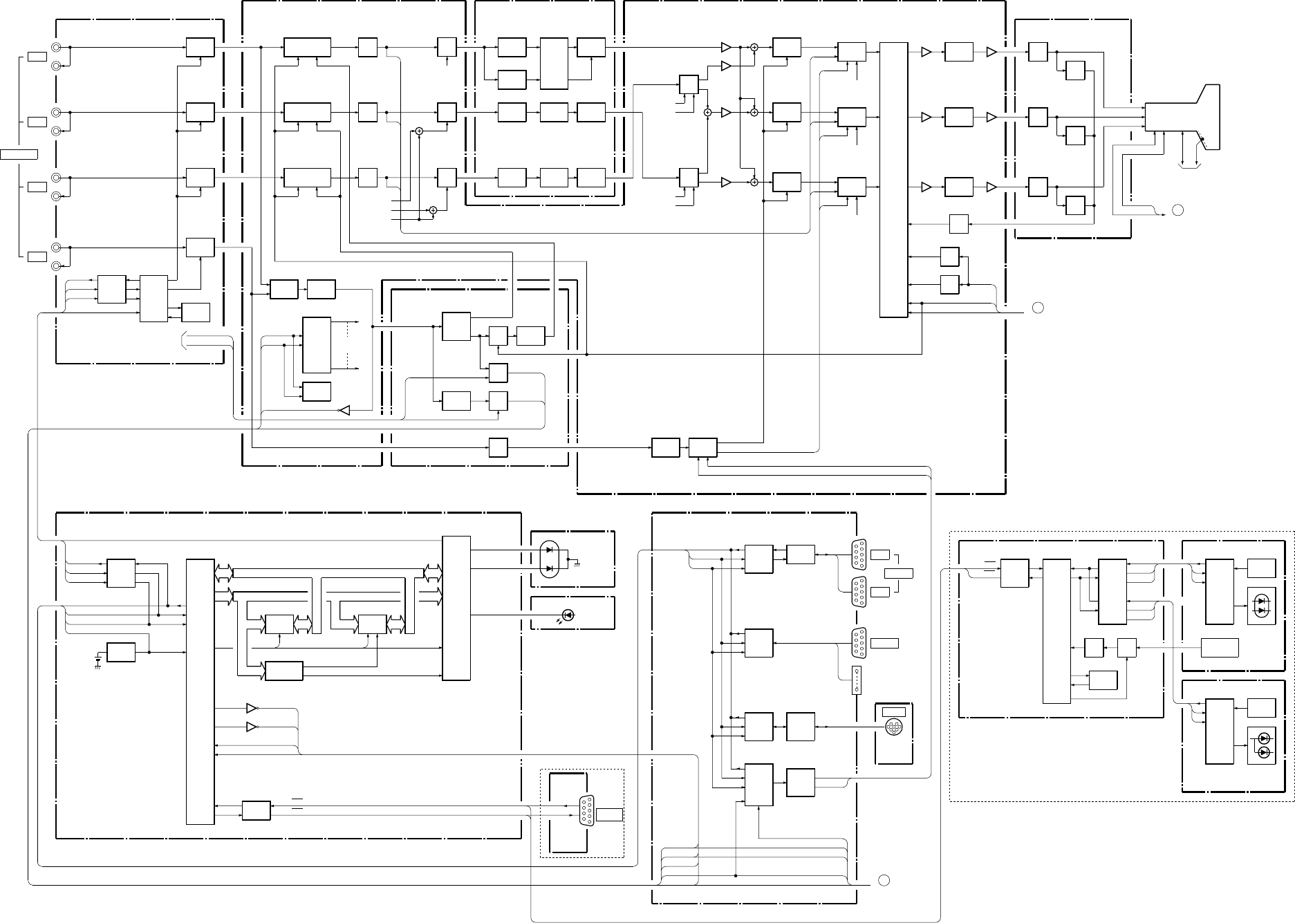
10-1
BVM-D14H1U/D14H5U/D14H1E/D14H5E/D14H1A/D14H5A 10-1
Section 10
Block Diagrams
Overall (1/2)
Overall (1/2)
Overall (1/2)Overall (1/2)
Y/G
BX
PB/B
PR/R
SYNC
IC502
BUFF
MISO
MOSI
SCLK
RESET
SUB
CPU
IC501
IC503
EEPROM
D/A
CONV CONTROL
SIGNAL
ANALOG I/O
Y/G CLAMP
PULSE INSERT
IC300,303
Q300-302
PB/B CLAMP
PULSE INSERT
IC301,304
Q330-332
PR/R CLAMP
PULSE INSERT
IC302,305
Q365-367
G
B
R
G1
(FBT)
V901
PICTURE TUBE
HV
H1,2
C
FV1,2
IC3404
EEPROM
Y/G
BUFF
Q101,102
PB/B
BUFF
Q201,203
PR/R
BUFF
Q301,303
SYNC
BUFF
Q401,403
OPTION V SYNC
H SYNC
BUFF
Q303
G
Q333
H BLK
Q368
BUFF B
R
BUFF
Y
AMP
IC306
PB
AMP
IC307
PR
AMP
IC308
SDA
CHROMA PR
Y LEVEL
CHROMA PB
CHROMA
DELAY
B
Q404,405,411,412
DL404,405
DELAY
Q400-403,413,414
DL400-403
DELAY
Q501,503,515,516
DL501,502
DELAY
Q504,506,511,512
DL503,504
SELECT
IC410
SELECT
IC501
SELECT
IC501
Y
BUFF/AMP
Q406-409
PB
BUFF/AMP
Q502,517,518
PR
BUFF/AMP
Q505,513,514
B1
PR
AMP
R
CLAMP
IC1300,1305
Q1300-1302
IC400
PR LEVEL
G-Y/R
PB
AMP
IC401
PB LEVEL
G-Y/B
G
CLAMP
IC1302,1306
Q1320-1322
B
CLAMP
IC1303,1307
Q1340-1342
CUT OFF
SWITCH
IC401
CUT OFF R
OSD R
R
CUT OFF
SWITCH
IC1308
CUT OFF G
OSD G
G
CUT OFF
SWITCH
IC1309
CUT OFF B
OSD B
R
RGB
MATRIX
IC1304
R
CLAMP
Q1431-1434
G
CLAMP
Q1421-1424
B
CLAMP
Q1411-1414
PIC
ABL
Q1460
BRT
ABL
Q1460
H BLK
V BLK
IK
BUFF
Q1402
R
OUT
Q730-734
IK
BUFF
Q735
G
OUT
Q750-754
IK
BUFF
Q755
B
OUT
Q770-774
IK
BUFF
Q775
G1
H1,2
2
G BOARD
ABL
1
G BOARD
Y CLP P
C CLP P
SYNC
SEP SYNC
AGC
Q3304-3319
IC3301
Q3301-3303
SDA
SCL
COMP SYNC SEP IC3406
IC4300-4302
IC4350-4352
H SYNC
SEP
IC3901
COMP SYNC SEP CLAMP
PULSE
GEN
SW
IC3902 IC3904
SW
IC3902
V SYNC
SEP
Q3905,3907
SW
IC3902 V SYNC SEP
H SYNC SEP
B2
H SYNC
V SYNC
H BLK
SW
IC3908
COMP SYNC VIDEO
IC101
BUFF
MISO
MOSI
SCLK MAIN
CPU
IC106
IC110
RESET
BAT1
LITHUM
BATTERY
D0-7
A0-19
PROGRAM
ROM
IC108
A0-17 D0-7 SRAM
IC111
A0-14 D0-7
RD/WR
ADDRESS
SELECTOR
IC109
A15-18
A0-2
D0-7
PARALLEL
I/O
IC112
HD
CN101
CONTORL
UNIT
RS422
DRIVER
IC113
RS485
CONTROL RS485
REM1
IC1103,1106
YC
OPTION
REMOTE1
CN1104
OUT
CN1103
IN
D921-923
YB
YA
OSD
IC1107,1110
DECODER
CAPTION BUFFER
IC3403 IC3400,3401
IC3407 BLK P
OSD R/G/B
RESET
RESET
MISO
MOSI
SCLK
IC103
IC103 SCL
COMP SYNC
V SYNC
RXD/RXD
TXD/TXD
MA
MB
TALLY(G)
TALLY(R)
D901-905
PROT/
STANDBY/
POWER
OSD R/G/B
OSD BLK
D14H1 MODEL
MISO
MOSI
SCLK
IC1105
REMOTE2
CN1107
REM2
DRIVER
IC1112
CN1109
MODULAR
RS232C
CONTROL
IC1108
RS232C
I/F
IC1109
OSD
DRIVER
IC1100
V SYNC
OSD BLK
OSD R/G/B
H SYNC
COMP SYNC
SCL
SDA
V SYNC
H SYNC
SCL
SDA
3
G BOARD
RS422
DRIVER
IC13
MAIN
CPU
IC1
BUS
SHIFT
IC12
BUFF
IC11
INV
IC9,10
ADDRESS
DECODER
IC3
RXD/RXD
TXD/TXD
MISO
MOSI
SCLK
MISO
MOSI
SCLK
HC
S/P
CONV
IC201,202
ENCODER
S231-234
MATRIX
SW
S201-222
D223-226
D121-130
HA
S/P
CONV
IC101,102
MATRIX
SW
S101-110
HB
D14H5 MODEL
AFC
(BKM-129X)
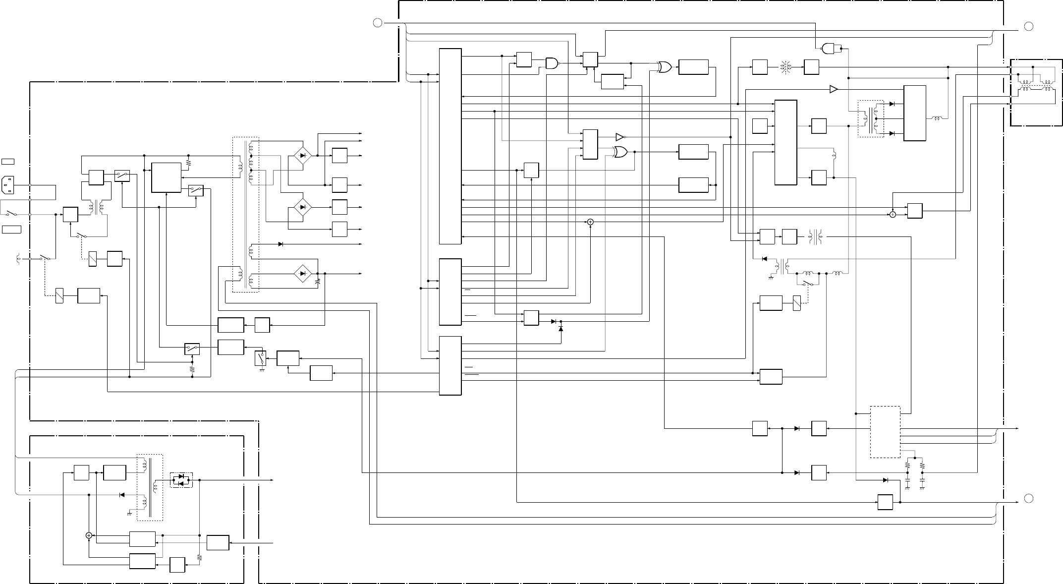
10-2 BVM-D14H1U/D14H5U/D14H1E/D14H5E/D14H1A/D14H5A
10-2
Overall (2/2)Overall (2/2)
Overall (2/2)
Overall (2/2)
AC IN
S901
POWER
DGC
D624
±15V RECT
T603
PFCT
AC
RECT
D602
PFC
CONT
IC601 Q605 MAIN
SWITCHING
+12V
REG
IC602
Q608
T605
PIT
IC606
IC607
D625
±6V RECT IC608
IC609
D623
±B RECT
+B
REG
IC610PH603
PFC & MAIN
ON/OFF
ISORATOR
PH604
Q615
Q609
+15V
+5V
-5V
+B
T1601
SRT
D1606
STBY 5V
STBY 5V
REG
IC1602
PH601
5V SENSE
D1605
STBY 5V
SW
IC1601
SW
Q1601
OVP
FEED BACK
ISORATOR
PH602
SDA
SCL
MB BOARD
DY
3
DEGAUS
DRIVE
Q601,619
RY602
RY601
RELAY
DRIVE
Q602
-15V
-12V
+12V
D626 +160V
-12V
REG
+5V
REG
-5V
REG
SW
Q611-613
Q620-622
POWER
ON /OFF
Q618 HV PROT
DGC SW
H2
H1
POWER
+B
FEED BACK
ISORATOR
SW
Q1603
CTL
FEED BACK
ISORATOR
DC IN
+18V
DC IN
+18V
G
G1
H SYNC
V SYNC
DEF
CONTROL
IC507
D/A
CONV
IC512
Q2503
PWM
H
BLK
IC501
H FOCAP IC527
H BLK
H BLK
SYNC
IC509
IC506,Q501
DELAY
IC526 H SYNC
PULSE GEN
IC503(1/2)
HV IN
H OUT COL
H LOCK
H FOC
V BLK
SYNC
IC510
V SYNC
PULSE GEN
IC503(2/2)
PLL
PULSE GEN
IC529
IC502
IC528
IC522
V BLK
CONT
V FOC
PLL INH
V SYNC IN
VDC OUT
V OUT
EW OUT
X RAY
H BLK(F)
V BLK(B)
H BLK(R0
4:3/16:9
50/60
H SIZE Q524,529-531
SW
1125/50
D/A
CONV
IC508 H DL
V DL
H CENT
15K
33.75K
H
DRIVE
Q2505 T2502
HDT H
OUT
Q2508
IC2502
HV
REG
Q519
PWM
CONT
IC515 T2501
HOT
T501
DFT
HV
OUT
Q513
T503
HRT
H CENTER
AMP
IC2501
L2501
HCC
V
OUT
IC2503
IC516
SW DF
AMP
Q509-512
T2503
CURRENT L2504
HLC L2503
HLC
RELAY
SW
Q2511 RY2501
S-CAP
ON/OFF
Q2514,2515
Q2518,2519
T502
FBT
HV
PROT
IC514,523 HV
FV1
FV2
G2
AMP
Q517,518
IK
PROT
IC517,523
HV
PROT
Q520
ABL
1
B BOARD
V BLK
H BLK
2
C BOARD
HV
FV1
FV2
G2
H1
H2
PICTURE
TUBE
H DY+
H DY-
V DY+
V DY-
IC2501
AFC
AC 100-240V
50/60Hz
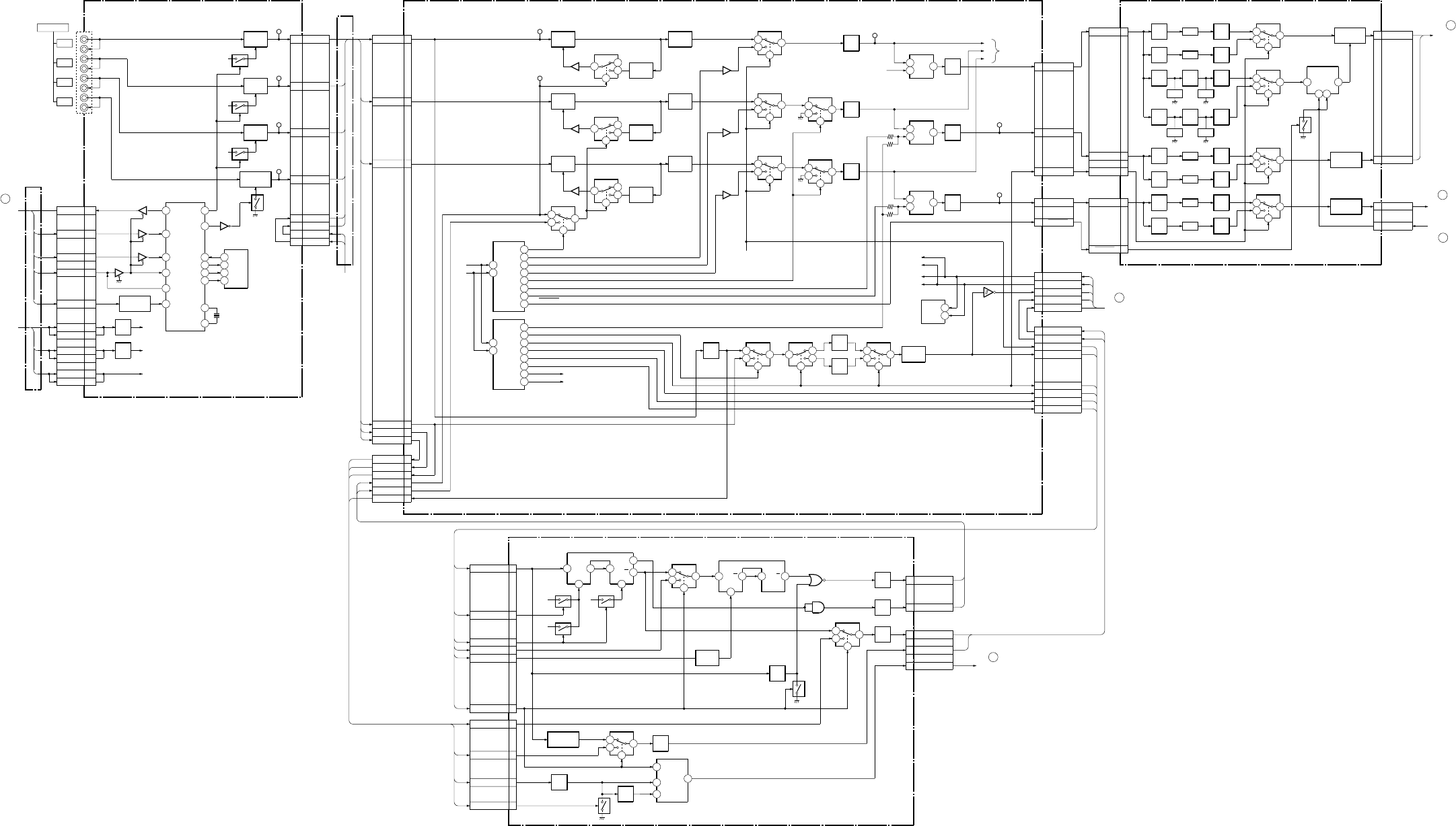
10-3
BVM-D14H1U/D14H5U/D14H1E/D14H5E/D14H1A/D14H5A 10-3
B (1/2) /BX, B1, B2B (1/2), BX, B1, B2
Signal Select
B Block (1/2)
Signal Select, Sub CPU
BX Block
Signal Amp
B1 Block
H/V, Sync Generator
B2 Block
B Block (1/2)
BX Block
B1 Block
B2 Block
X501
Y/G
ANALOG I/O
PB/B
PR/P
SYNC
TB001
14
11
12
13
IC300
TP300
Y/G AMP
Q300,301
IC303
CLAMP57 4
9
5
3
IC300
BX
Y/G BUFF
Q101,103
Q102
+5V
TP101
PB/B BUFF
Q201,203
Q202
+5V
TP201
PR/R BUFF
Q301,303
Q302
+5V
TP301
SYNC BUFF
Q401,403
TP401
MISO B27 2
31
IC501
SUB CPU
5V
REG
12 13
11
IC502
IC502
9108
IC502
546
IC502
MOSI A28
SCLK B28
SLOT1 ID A31
RESET B26
+6V A7
+6V B7
RESET SW
Q501
+5V
IC502
IC010
-5V
REG
-6V A6
-6V B6 -5V
IC050
STBY 5V A29
STBY 5V B29 5V-2
CN001(1/2)
T
MA BOARD
CN101
OPTION
SO2
1
SI2
2
SCLK2
64
INT0
14
SLOT ID
63
RSTX
19
48
BX OE
47
EXT SYNC OE
53SI1 52SO1 51SCLK1 50EECS
Q404
SO
2SI
5SCK
6CS0
1
IC503
EEPROM
23
X1
22X0
Q402
Y/G OUT
B12 CN001(2/2) T
PB/B OUT
B14
PR/R OUT
B16
CS OUT
B22
HS OUT
A21 VS OUT
B21 VS IN
B20 HS IN
A20
OPTION
()
SIGNAL SELECT
SUB CPU B(1/2) (SIGNAL SELECT)
CLAMP
Q302(2/2)
CLAMP
Q302(1/2) 31
IC303
CLAMP
14
11
13
12
IC301
PB/B AMP
Q330,331
IC304
CLAMP57 4
9
5
3
IC301
CLAMP
Q332(2/2)
CLAMP
Q332(1/2) 31
IC304
CLAMP
14
11
13
12
IC302
PR/R AMP
Q365,366
IC305
CLAMP57 4
9
5
3
IC302
CLAMP
Q367(2/2)
CLAMP
Q367(1/2) 31
IC305
CLAMP
15
2
110
IC301
BUFF
Q303
TP302
5
1
3Y
AMP
IC306
BUFF
Q333
BUFF
Q304
5
1
3PB
AMP
IC307
BUFF
Q334
15
2
110
IC302
BUFF
Q368
5
1
3PR
AMP
IC308
BUFF
Q369
TP303
TP304
G
B
RTO (2/2)
15
2
110
IC300
TP301
SDA 14
15
1
3
4
5
2
6
7
9
D/A
CONV
IC4300
SCL
CLP P SW
Y/G BLACK
PB/B BLACK
PR/R BLACK
CHROMA/PB
CHROMA/PR
APER SW
MONO
H BLK (2/2)
14
15
7
2
9
10
3
1
5
4
D/A
CONV
IC4302
CHROMA
EXT SYNC SEL
DAC2 (2/2)
H SYNC SEP1
CLP P DLY
SDI SEL
H SYNC SEP2
Y LEVEL (2/2)
1
3
Y/G
PB/B
CN301
5PR/R
9
COMP SYNC
4
5
39
IC3301
15 2
1
10
IC3301
BUFF
Q3301 14
12
13 11
IC3301 BUFF
Q3302
BUFF
Q3303
SYNC
AGC
Q3304-3319
SUB PIC (2/2)
7
H SYNC 8
V SYNC
CN421 6V SYNC 7H SYNC 5COMP SYNC 10Y CLP P 11C CLP P 8CAPTION Y
Y
7
PB
3
CN411(1/2)
PR
1CN412(1/3)
COMP SYNC SEP
12
CN422(1/2)
H SYNC SEP1
2H SYNC SEP2
3CLP P DLY
4SDI SEL
5
H BLK
7
4
2
H SYNC SEP
9V SYNC SEP
8
V SYNC SEP
3H SYNC SEP
2COMP SYNC SEP
1SCL
5SDA
6
IC3406
5
SDA 6SCL
SDA
SCL
EEPROM
IC3404
MB BOARD
CN1100
Q3901
+5V
15
2
110
IC3902
CLAMP
DELAY
CONTROL
12
V SYNC SEP
Q3905,3907
B2(H/V SYNC GENERATOR)
COMP SYNC SEP
CN3902 (1/2) CK
12 10
Q
14
CxRx CK
47
Q
2
CxRx
6Q
IC3901
H SYNC SEP
Q3902
+5V
Q3906
+5V
IC3905
Q3909
CK
12 9
Q
14
CxRx CK
47
Q
IC3904
CLAMP PULSE GEN
BUFF
Q3910 Q3911
2
14
BUFF
Q3903
4
5
39
IC3902
BUFF
Q3913
BUFF
Q3912
2
14
IC3906
IC3907
3H SYNC SEP2
2H SYNC SEP1 7H BLK 4CLP P DLY
5SDI SEL
14
12
13 11
IC3902
7H SYNC
CN3901 (1/2)
BUFF
Q3916
BUFF
Q3908
BUFF
Q3914
6V SYNC
5COMP SYNC
8CAPTION Y
5
7
6
1
Q3915
SWITCH
IC3908
10 Y CLP P
CN3901 (2/2)
11 C CLP P
9H SYNC SEP
8V SYNC SEP
10 VIDEO
CN3902 (2/2)
B BOARD (2/2)
CN422(2/2)
SDA(2/2)
SCL(2/2)
H SYNC SEP1
1
APER SW
4
4
5
39
IC410
B1(SIGNAL AMP)
7BUFF
Q405 DL405 BUFF
Q412
BUFF
Q404 DL404 BUFF
Q411
BUFF
Q402 BUFF
Q403 BUFF
Q414
DL402 DL403
BUFF
Q400 BUFF
Q401 BUFF
Q413
DL400 DL401
14
12
13 11
IC410
14
12
13 11
IC501
BUFF
Q503 DL502 BUFF
Q516
BUFF
Q501 DL501 BUFF
Q515
1
4
5
39
IC501
BUFF
Q506 DL504 BUFF
Q512
BUFF
Q504 DL503 BUFF
Q511
3
Y BUFF/AMP
Q406-409
7
6
PB BUFF/AMP
Q502,517,518
IC450
GAIN CONT
Q410
PR BUFF/AMP
Q505,513,514
Y
6
PB4
PR2
CN401(2/2)
CN402(2/2)
Y
PB
H SYNC SEP1
1
4
PR
APER SW
CN308
CN401(1/2)
CN402(1/2)
APER5
B BOARD(2/2)
CN412(2/3)
B BOARD(2/2)
CN411(2/2)
2
3
A
E
C
B BOARD(2/2)
CN412(3/3)
D
B
F
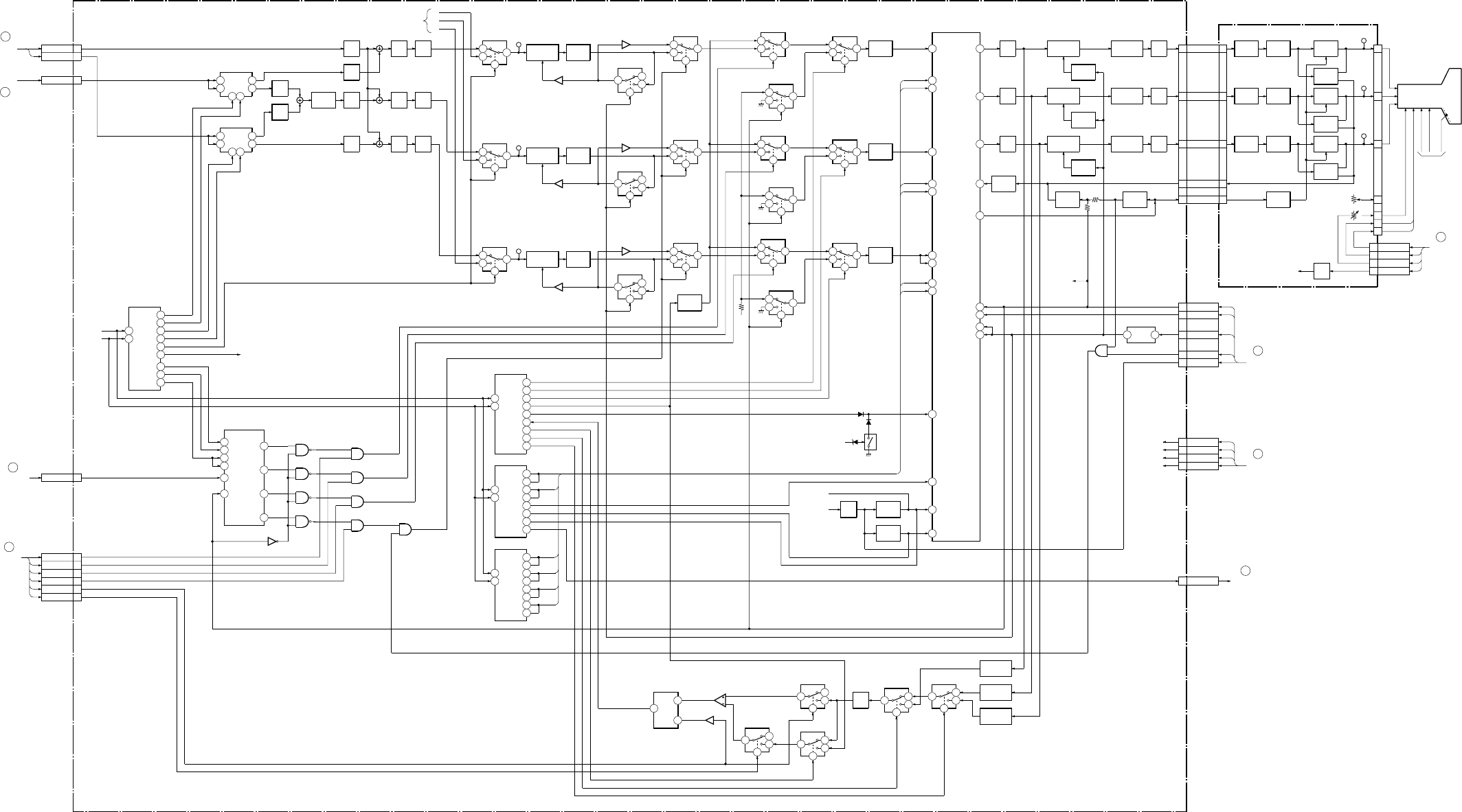
10-4 BVM-D14H1U/D14H5U/D14H1E/D14H5E/D14H1A/D14H5A
10-4
B (2/2), CB (2/2), C
Signal Select, RGB Matrix
B Block (2/2)
RGB Out
C Block
B Block (2/2)
C Block
Y6
BUFF
Q465
1
726
3
5
PR
AMP
IC400
CN411(2/2)
1
726
3
5
PB
AMP
IC401
BUFF
Q466
AMP
Q460,461 BUFF
Q462 AMP
Q463 BUFF
Q464
BUFF
Q450
AMP
Q451 BUFF
Q452
BUFF
Q453
BUFF
Q485 AMP
Q486 BUFF
Q487
PR 2
CN412(2/3)
R AMP
Q1300,1301
IC1305
CLAMP31 4
9
5
3
IC1300
CLAMP
Q1302
14
12
13 11
IC1300 IC1300 IC1305
CLAMP75 15
2
110
IC1300
14
12
13 11
IC1304
B1 BOARD
CN401(2/2)
B1 BOARD
CN402(2/2)
15
2
110
IC1304
R BUFF
Q1303
4
5
39
IC1304
G AMP
Q1320,1321
IC1306
CLAMP31 4
9
5
3
IC1302
CLAMP
Q1322
14
12
13 11
IC1302 IC1301 IC1306
CLAMP75 15
2
110
IC1302
14
12
13 11
IC1308
15
2
110
IC1308
G BUFF
Q1322
4
5
39
IC1308
B AMP
Q1340,1341
IC1307
CLAMP31 4
9
5
3
IC1303
CLAMP
Q1342
14
12
13 11
IC1303 IC1302 IC1307
CLAMP75 15
2
110
IC1303
14
12
13 11
IC1309
15
2
110
IC1309
B BUFF
Q1343
4
5
39
IC1309
R
G
B
FROM(1/2)
DC ADJ
Q1304,1305
41
R OUT
IC401
RGB MATRIX
BUFF
Q1431-1433
R IN
10
G C/O
33
G GAIN
G IN
11
G DRV
32
G BIAS
B C/O
27
B GAIN
B IN
12
B DRV
26
B BIAS
Y IN
3
MUTE
21
PIC
46
+12V Q1463
PIC ABL
Q1460
SW
Q1462
BRT ABL
Q1461 BRT CNT
7
SUB PIC(1/2)
DAC2(1/2)
VIDEO 10
CN422(2/2)
SDA(1/2) 14
15
6
5
3
4
7
1
2
9
D/A
CONV
IC4301
SCL(1/2)
PR LEVEL
G-Y/R
G-Y/B
PB LEVEL
RGB SW
CAP CT
CAP L1/L2
Y LEVEL (1/2)
10 CAP ON/OFF
3
2
6
7
14
15
13
5
4
12
D/A
CONV
IC4351 R GAIN
R BIAS
BRT DAC
PIC DAC
APER
B/O
3
2
12
3
4
5
6
7
14
15
D/A
CONV
IC4352 G GAIN
G BIAS
B BIAS
B GAIN
14
15
9
6
7
3
10
1
5
4
D/A
CONV
IC4350 CUT OFF R
CUT OFF G
CUT OFF B
DC ADJ
S/DC SEL
R SEL
GB SEL
2ACP
MUTE
R C/O
38
R GAIN R DRV
44
R BIAS
YS
16
-5V
B2 BOARD
CN3902(2/2)
15 2
1
10
IC2380
IC3403
CAPTION DECODER
L1/L2
17 C/T
18 ON/OFF
1RESET
2
CV1
11
HP
8
6G
5R 13
12 11
13
12 11
Q3402
10
98
IC3400
5
46
IC3400
2
13
IC3400
7
B
3
BOX
10
98
5
46
2
13
IC3400
IC3401
IC3401
IC3401
IC3401
OSD R
OSD G
OSD B
BUFF
Q1430
CLAMP
Q1434
AMP
Q2300-2302 BUFF
Q2303
22
V BLK
36
G OUT BUFF
Q1421-1423
BUFF
Q1420
CLAMP
Q1424
AMP
Q2315-2317 BUFF
Q2318
30
B OUT BUFF
Q1411-1413
BUFF
Q1410
CLAMP
Q1414
AMP
Q2330-2322 BUFF
Q2333
IK BUFF
Q1402
41R OUT
IK MASK
Q1401 IK MASK
Q1400
20
HP 18
VP
R OUT2
G OUT4
B OUT6
IK RTN10
VP1
CN304
H BLK
1CN303
V BLK
6
12
A2
Q2
10
IC1400
MONO-MULTI
23CLP2 24CLP1 AFC PLS
4
VD BLK
7ABL
2
1
2
7IC3407
5
63
IC3407
ACP R BUFF
Q2382
ACP R BUFF
Q2381
ACP R BUFF
Q2380
45
3
9
IC2381
15 2
1
10
IC2381
14 12
13
11
IC2380
BUFF
Q2383
14 12
13
11
IC2381
6
5
7
12
IC2382
SAMPLING
IC2382
SAMPLING
2
D
1
CK
Q
5
IC2383
LATCH
OSD R 1
CN307
MB BOARD
CN1105 OSD G 2
OSD B 3
OSD BLK 4
S PULSE1 6
S PULSE2 8
STBY 5V
1CN302
ST 5V
+5V
3+5V
-5V
4-5V
+12V
5+12V G BOARD
CN605
G BOARD
CN502
CN702
BUFF
Q732,733 R SW
Q734
IK DET
Q735
TP701
BUFF
Q752,753 G SW
Q754
IK DET
Q755
TP702
BUFF
Q772,773 B SW
Q774
IK DET
Q775
TP703
VP BUFF
Q702
12
10
8
13
(FBT)
V901
PICTURE TUBE
G2
H1,2
F1
F2
HV
9
5
6
RV701
G2
H1
H2
8H2
7H1
1G2
3 160V
CN701
RV702
G BOARD
CN604
REG
Q701
+B
B()
SIGNAL SELECT
RGB MATRIX
(2/2)
C
(RGB OUT)
BLK P
CN412(3/3) B1 BOARD
CN402(2/2)
APER
5
2
4
6
10
1
C
PB 4
B
F
G
D
I
H
J
R AMP
Q730,731
G AMP
Q750,751
B AMP
Q770,771
H BLK
(1/2)
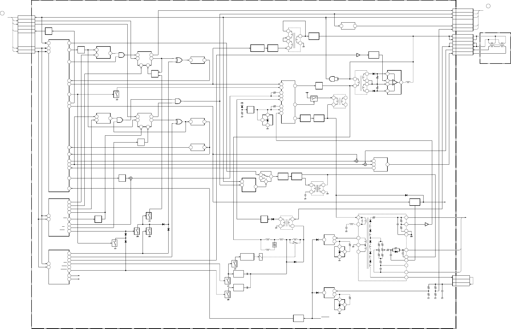
10-5
BVM-D14H1U/D14H5U/D14H1E/D14H5E/D14H1A/D14H5A 10-5
G (1/2)G (1/2)
H/V OSC, Dynamic Focus
G Block (1/2)
G Block (1/2)
7
1
2
8
5
AFC
CN501
H SYNC
V SYNC
V TIM
SDA 4
SCL
CN1101
MB BOARD
H FLY
6
SDA
41 SCL
40
IC507
HV OSC
17
H FOC
2
67
H BLK
CONT
IC501
A2
12 B1
510
Q2
2
Q1
14
CX2 CX1
IC509
H BLK SYNC
2
14
IC527
DELAY
IC506,Q501
71
24
IC526
22
H BLK
38HV IN 21H OUT COL
37
H LOCK
B1
56
Q1
IC503(1/2)
H SYNC
PULSE GEN
Q504
Q523
28
VDC OUT
32V FOC
2
57
V BLK
CONT
IC502
A2
12 B1
59Q2
2
Q1
14
CX2 CX1
IC510
V BLK SYNC
71
24
IC522
B2
11 10
Q2
IC503(2/2)
V SYNC
PULSE GEN
3
PLL INH Q1
64
A1
33
V SYNC IN
BUFF
Q521
29V OUT 30V FLY
31EW OUT
15
XRAY
5
H BLK(R)
IC512
D/A CONV
SDA
14 SCL
15
4
H BLK(F)
7
V BLK(B) 6
V BLK(T)
3
H SIZE 1
50/60 2
1125/50
9
VDL
IC508
D/A CONV
SDA
14 SCL
15
10
HDL
7
HCENT
4
33.75K 5
31.5K 6
15K
1
POWER 2
DGC POWER (2/2)
DGC (2/2)
D530
Q524
Q530
Q531
D529
D531
D532
Q529
SW
Q533
1
3
2
+15V
TIN
3DTC
6
INT-
8INT+
7
FB1
9
INT-
16 INT+
17
FB2
15
IC515
PWM CONT
11
OUT1
13
OUT2
23
DRV BUFF
Q506,507
H SENTER
BIAS
Q2504
31
IC2502
12
9
1
4
T2501
HOT
10
5
2
1
3
4
1H DY+
CN2501
2H DY+
3H DY-
4H DY-
5V DY+
6V DY- DY
+B
10
9
2
5
T503
HRT
Q514
PWM
Q2503
11
IC2504
H CENTER AMP
IC2501 1
2
4L2501
HCC
1
4
T2502
HDT
2
3
H DRIVE
Q2505
8
5
BUFF
Q2501,2502
H OUT
Q2508
1H BLK
CN502
6V BLK
4AFC
7VD BLK
2ABL
B2
11 10
Q2
IC529(1/2)
V BLK PULSE GEN
CN303
B BOARD
+VIN
7
IC2503
V OUT
-VIN
1PUMP UP
35OUT
CK
9D1
4Q4 15
F.F 4
5
39
IC516
DF AMP
Q509-512
1
5
11
8
T501
DFT
1
3
2
FV2
HV
PROT 6
2
1HV
14
13
FV
16
7
15
T502
FBT
5
IK DET
1
IK DET
3
CN503
IC514
IC523
2
3
1
D506
HV PROT
11
FV
17
18
FV1
13
1
3
2
IK
PROT
IC517
IC523
5
6
7
D507
IK PROT
HV PROT (2/2)
HV PROT
Q520
BUFF
Q2513
RELAY SW
Q2511
S-CAP
ON/OFF
Q2514
Q2515
S-CAP
ON/OFF
Q2518
Q2519
Q2512
1
2
5
3
L2506
L2507
L2503
HLC L2504
HLC
RY2501
T2503
CURRENT
D2514
D2512 C BOARD
PICTURE TUBE
G2 AMP
Q517,518
D520
G2 (2/2)
G()
H/V OSC
DYNAMIC FOCUS
(1/2)
H
IC524
L
BUFF
Q525
23
V BUC
BUFF
Q535
16
H FOCAP
DELAY
Q532
10
4:3/16:9 SW
Q534
BUFF
Q505,508
IC520
HV REG
IC529(2/2)
PLL
PULSE GEN
IC519
HV REG
HV OUT
Q513
6
53
IC528
2
17
IC528
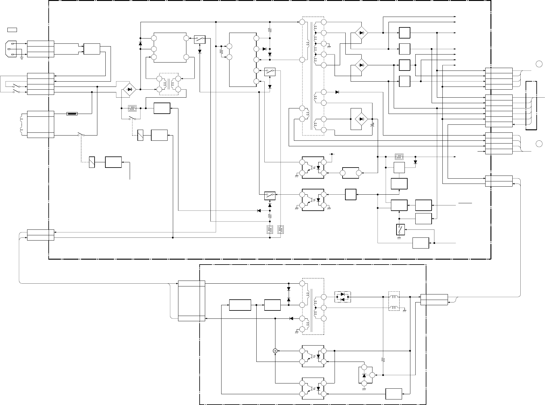
10-6 BVM-D14H1U/D14H5U/D14H1E/D14H5E/D14H1A/D14H5A
10-6
G (2/2), G1G (2/2), G1
Main Regulator
G Block (2/2)
Main Regulator
G1 Block
G Block (2/2)
G1 Block
LIVE 3
+B
REG
G
(MAIN REG)
NEUTRAL 1
LIVE
CN603
3
17
CN601
1
5
AC L IN
AC L IN
AC L OUT
AC L OUT
S901
POWER
DGC
THP601
LINE
FILTER
T602
RY602
LATCH
Q603,604
DEGAUS
DRIVE
Q601,619
RY601
RELAY
DRIVE
Q602
9
3
10
13
9
VCC
DRA IN
1
AC SENSE
3
CATHODE
10
5L SENSE
IC601
POWER FACTOR CONT
T603
PFCT
Q605
VD
1
RESET
3
18
VB
15
VC2
19
VS
14
VC1
7
RT
IC602
MAIN SWITCHING
Q608 2
418
17
16
T605
PIT
D624
±15V RECT
13
12
D625
±6V RECT
21
4
3
1
2
+15V
IC610
PH603
+B FEED BACK
PROT
Q615
4
3
1
2
PH604
RFC & MAIN ON/OFF
5
3
T1601
SRT
10
9
8
1
4
5V
CONTROL
SW
Q1601,1602
IC1601 D1603
D1605
D1606
4
3
1
2
PH601
CTL FEED BACK
3
2
1
5V OVP
COMP
Q1603
4
3
1
2
PH602
OVP FEED BACK
Q609
T
CN302
B BOARD
OPTION
D602
AC RECT
1DGC
3DGC
DGC SW (1/2)
D609
+12V
REG
15
14
IC606
-12V
REG
IC607
+5V
REG
IC608
-5V
REG
IC609
D626
D623
+B RECT
11
10
8
7
D620
D633
IC1602
STBY 5V
REG
O.C.P
Q614
LATCH
Q616,617
LATCH
Q611,612 PROT
Q613
PROT
Q621,622
POWER
ON/OFF
Q618
Q620
HV PROT (1/2)
+B (1/2)
POWER (1/2)
+15V
-15V
+12V
-12V
+5V
-5V
G2 (1/2)
5
-6V
+6V
STBY +5V
STBY +5V
+12V
+5V
-5V
+12V
-12V
5V SENSE
3
4
1
5
4
7
6
2
1
3
7
8
1G2
H2
+160V
H1
CN605
CN606
CN604
CN701
C BOARD
(2/2)
D635
J
I
D1604 L1601
5
3
DC IN
18V
CN601
5
DC IN
CN607
3
18V
5V SENSE
2STBY +5V
1
CN608
ST 5V
STBY +5V
15V SENSE
2
CN1602
G1
AC IN
AC 100-240V
50/60Hz
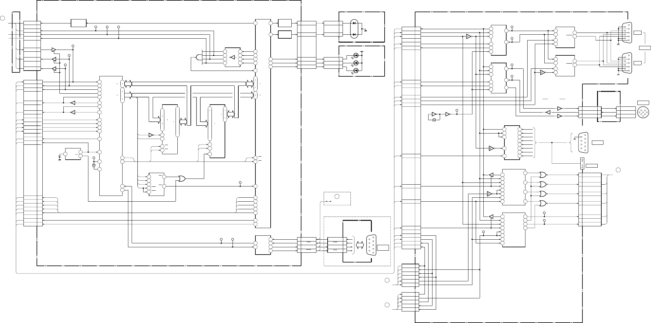
10-7
BVM-D14H1U/D14H5U/D14H1E/D14H5E/D14H1A/D14H5A 10-7
MA, MBMA, MB
Main CPU, Parallel I/O
MA Block
Remote Control OSD
MB Block
MA Block
MB Block
T
CN101
BAT
42
RST 5
CS
BAT1
LITHIUM
BATTERY
IC110
RESET
564
IC10189 10
IC101
231
IC101
OPTION
IC106
MAIN CPU
EXTAL
84
XTAL
1
RXD1
81 TXD1
80 SCK1
82 SCK2
79
RESET
21
25
32
33
40
43
54
.
D0
D7
A0
A19
D0-7
A0-19
13 12
IC107
19
21
24
.
26
.
28
.
15
17
.
.
31
11
4
42
.
34
.
3
.
30
.
.
IC108
PROGRAM ROM
CE
12
OE
14 WE
43
A0
A16 D0
D7
RD
WR
A0-17
A18
D0-7
10
3
25
.
24
.
21
.
23
.
11
13
15
19
.
2
.
26
.
1
.
A0-14
IC111
SRAM
CE
20
OE
22 WE
27
RD
WR
A0
A14
D0-7
D0
D7
15
WR 14
RD WR
RD
IC109
ADDRESS
SELECTOR
2
17
IC102
A0
113
Y2
A15
A1
2
A16
A2
3
A17
CS2
4
A18
CS3
5
12Y3
30
32
35
39
.
46
48 A0
A2
D0
D7
D0-7
A0-2
IC112
PARALLEL I/O
CS
45
PC0
11 PC5
16 PC1
12
RXD
7RXD
2TXD
3TXD
8
2
3
8
7
5
6
RS422
DRIVE
YA
1
2
3
+5V
D921
D922
D923
YB
STANDBY
POWER
PROT
CN421
7
2
3
CN102
8
TXD
TXD
RXD
RXD
1
6
95
HD
A0-2
CN101
CONTORL
UNIT
PA0
54
SLAVE CPU
RESET
MA )
(
MAIN CPU
PARALLEL I/O
4
MOSI 5
SCLK 6
MISO
10
SLOT3
9
SLOT2 8
SLOT1
3
RESET
CN001
BX BOARD
A10
MISO B10
MOSI A11
SCLK
CN102
TP101
TP102
TP103
Q102
TP105 TP106 TP107
12 13
IC103
A13
SDA
10 11
IC103
A12
SDA
A5
IRQ REM1 B5
IRQ OPT A3
H SYNC A4
V SYNC
A14
M/S SEL B15
SIO RESET
PHAI
3
BREQ
6P11/E
4
BACK
5
IRQ1
9IRQ0
8P75
61 P73
59
P91
76
78RXD2 77TXD2
TP104
X101
20MHz
A17
3
A19
A-1
IC104
SLOT
RECEIVER 1
2
3
4
86
4
2
8
5
3
1
9
IC103
SLOT
DRIVER
PB1
3PB0
64 PB3
5PB2
4
PE0
49
TP116 TP115 CN105
IC113
44
43
RD
WR RD
WR
TP117
PC2
13 PC3
14
PA6
62 PA7
63
CS REM2
CS REM1
CS OPT
CS OSD1
CS OSD2
CS REM2
CS REM1
CS OPT
CS OSD1
CS OSD2
B6
A7
B7
B8
A9
B14
SLAVE TX
CS REM2
CS REM1
CS OPT
CS OSD1
CS OSD2
A15
MASTER TX
LED DRIVE
Q104,106
29
PD7
21
PD1
LED DRIVE
Q103,105 2 TALLY(G)
CN103
3 TALLY(R)
2TALLY(G)
3TALLY(R)
D901-905
CN901
4
5
6STANDBY
POWER
PROT
24
PD4 28
PD6 27
PD5
D14H1 MODEL
CN1102
MOSI
SCLK
12
IC1102 13 12
IC1102
X1100
3.6864MHz
CS REM1
IRQ REM1
6
5
IC1103
RS485 REM1
DI
4RO
1
DE
3RE
2
6
DO/RI 7
DO/RI
IC1106
RS485 REM1
DI
4RO
1
DE
3RE
2
6
DO/RI 7
DO/RI
MASTER/
SLAVE SW
10 7
IC1109
11 14
98
YC
CN1106 TXD
5RXD
7RTS2
OPTION
5
9
61REMOTE1
CN1104
OUT
CN1103
IN
5
9
61
B10
A11
B6
A5
IC1104
MISO A10
TP1100
D OUT
2D IN
1SCLK
3
CS
4IRQ
6X1
10
15
TX
14RX
TP1103
TP1102
IC1105
RS485 CONT
8
9
IC1104
RS232 I/F
D OUT
2D IN
1SCLK
3
CS
4IRQ
6X1
10
15
TX
14
RX
TP1106
TP1107
IC1108
RS232C CONT
13
RTS
IC1112
REMOTE2 DRIVE
QH
9LATCH
12 LOAD
13
SCLK
11
OE
10
15
A1
B2
C3
D4
E5
F6
G7
H
4
3
IC1104
REM1
REM2
REM3
REM4
REM5
REM6
REM7
REM8
9810
IC1101
IC1107
OSD
TRE
23 SIN
25 SCLK
24 CS
26 DOCKI
8H SYNC
12 V SYNC
13 RESET
5
IC1110
OSD
TRE
23 SIN
25 SCLK
24 CS
26 DOCKI
8H SYNC
12 V SYNC
13 RESET
5
12
13
IC1104
231
IC1101
TP1101
19
R OUT
CS OPT B7
IRQ OPT B5
SLAVE TX B14
MASTER TX A15
M/S SEL A14
CS REM2 A7
CS OSD1 B8
SIO RESET B15
CS OSD2 A9
SDA A13
SCL A12
COMP SYNC A3
V SYNC A4
V SYNC 2
H SYNC 1
SCL 4
SDA 5
AFC 7
VTIM 8
CN1101
V SYNC 3
H SYNC 2
SCL 1
SDA 5
6
COMP SYNC
CN1100
G BOARD
CN501
B BOARD
CN308
IC1100
64
5
18G OUT IC1100
910
8
20
B OUT IC1100
31
2
16
VOB1 IC1100
12 13
11
19
R OUT 18
G OUT 20
B OUT 17
I OUT
TP1108
TP1109
6
8
3
CN931 TXD
RXD
RTS
6
8
3
CN931 CN932
CN1107
REMOTE1
5
9
61
CN1109
MODULAR
1
2
OSD R
OSD G
CN1105
3OSD B
4OSD BLK
8SAMPL PLS2
6SAMPL PLS1
B BOARD
CN307
MB )
(
REMOTE CONTROL
OSD
HC BOARD
CN2
D14H5 MODEL
E
K
L
G
A
OPTION
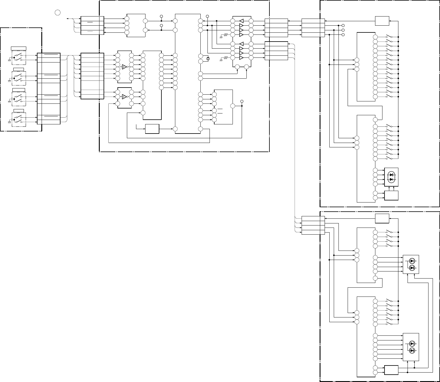
10-8 BVM-D14H1U/D14H5U/D14H1E/D14H5E/D14H1A/D14H5A
10-8
HA, HB, HC BVM-D14H5BVM-D14H5 HA, HB, HC
HA Block
HB Block
HC Block
Switch
HA Block
Serial to Parallel Converter
HB Block
Main CPU
HC Block
HA
LED SW
Q202,203
(1/2)
S231
CONTRAST CN202
S232
BRIGHT
S233
CHROMA
S234
PHASE
ENCODER 3
10
9ENCODER 3
ENCODER 2
8
7ENCODER 2
ENCODER 1
6
5ENCODER 1
ENCODER 0
4
3ENCODER 0
3
4
5
6
7
8
9
10
EN 3A
EN 3B
CN3
EN 2A
EN 2B
EN 1A
EN 1B
EN 0A
EN 0B
5
3
1
9
11
13
6
4
2
8
10
12
IC9
5
36
4
IC10
11 10
RESET
IC11
BUFFER
D7
2D6
3D5
4D4
5D3
6D2
7
D1
8D0
9
CLK
11
OE
1
IC2+12V
D7
64 D6
63 D5
62 D4
61 D3
60 D2
59 D1
58 D0
57
19
Q7 18
Q6 17
Q5 16
Q4 15
Q3 14
Q2 13
Q1 12
Q0
TXD1
28
3
DIN
DOUT
6DOUT
5RIN
7R IN
82
ROUT RXD1
29
TP3
IC13
RS422 DRIVE
CN2 3RXD 9
RXD 7TXD 2
TXD
MA BOARD
CN105 TP4
IC1
MAIN CPU
26
RXD0 25
TXD0 27
SCK0
TP5
16
6
8
2
4
14
12
18
IC12
BUS SHIFT
5 MISO
4 MOSI
3 SCLK
6CE2
CN5
5
13
11
17
15
7
9
3
5 MISO
4 MOSI
3 SCLK
6 CE1
CN4
20
TMCI1
1 19
ENA ENB
21
TMO1
53
A3 52
A4 51
A5
50A6 34
IOS 49
A7
RES
R37
RD
A
1B
2C
3
G2A
4G2B
5G1
6
15Y0
TP6
IC3
HC
5
MISO 4MOSI 3SCLK 6CE2
CN201
TP204
TP203
TP202
SW OUT
Q201
CLK
14 STB
15 DATA
13
11
P1 S201
10
P2 S202
9
P3 S203
8
P4 S204
7
P5 S205
5
P6 S206
4
P7 S207
3
P8 S208
2
P9 S209
1
P10 S210
23
P11 S211
22
P12 S212
21P13 S213
20P14 S214
POWER
DEGAUSS
NUM-1
NUM-2
NUM-3
NUM-0
NUM-4
NUM-5
NUM-6
NUM-CLEAR
NUM-7
NUM-8
NUM-9
NUM-ENTER
CLK
14 STB
15
DATA
13
11
P1 10P2 S215
9P3 S216
8P4 S217
7P5 S218
5P6 S219
4
P7 S220
3
P8 S221
2
P9
S222
1P10 23P11 22P12
19P15 17
P16
ENCODER 0
MENU
ENTER
UP
DOWN
ENCODER 1
ENCODER 2
ENCODER 3
12
SO
D223-226
HA (2/2)
LED SW
Q101,102
5MISO 4MOSI 3SCLK 6CE1
CN202 SW OUT
Q103
CLK
14 STB
15
DATA
13
11P1 S107
10
P2 S108
9
P3 S109
8
P4 S110
2P9 1P10 23P11 22P12
COMB/B
F1/F3
F2/F4
ADD/MARKER
CLK
14 STB
15
DATA
13
11P1 10P2 S101
9P3 S102
8P4 S103
7
P5 S104
5
P6 S105
S106
19
P15 17
P16
SHIFT
MONO/R
APT/G
10:9
SYNC
B ONLY
12
SO
HB
D127-130
2
P9 1P10 23P11 22P12
D121-126
21P13 20P14
K
ADDRESS
DECODER
IC201
S/P CONV
IC202
S/P CONV
IC101
S/P CONV
IC102
S/P CONV
9
10 X1
11-1
BVM-D14H1U/D14H5U/D14H1E/D14H5E/D14H1A/D14H5A 11-1
2
3
4
5
1
A BCDEFGH
Section 11
Diagrams
Note:
• Parts marked “ * ” differ according to the model/destination. Refer
to the mount table for each function.
• The parts marked “ # ” on schematic diagrams are not mounted.
• All capacitors are in µF unless otherwise noted. pF: µµF 50WV or
less are not indicated except for electrolytics.
• All electrolytics are in 50 V unless otherwise specified.
• : fusible resistor
• : nonflammable resistor
• ∆: internal component
• : panel designation and adjustment for repair
• Caution when replacing chip parts
New parts must be attached after removal of the chip.
Be careful not to heat the minus side of a tantalum capacitor,
because it is easily damaged by the heat.
Reference information
RESISTOR RN : METAL FILM
RC : SOLID
FPRD : NONFLAMMABLE CARBON
FUSE : NONFLAMMABLE FUSIBLE
RS : NONFLAMMABLE METAL OXIDE
RB : NONFLAMMABLE CEMENT
RW : NONFLAMMABLE WIREWOUND
: ADJUSTMENT RESISTOR
COIL LF-8L : MICRO INDUCTOR
CAPACITOR TA : TANTALUM
PS : STYROL
PP : POLYPROPYLENE
PT : MYLAR
MPS : METALIZED POLYESTER
MPP : METALIZED POLYPROPYLENE
ALB : BIPOLAR
ALT : HIGH TEMPERATURE
ALR : HIGH RIPPLE
• The components marked in this schematic diagram have been
carefully factory-selected for each set in order to satisfy regulations
regarding X-ray radiation.
• When replacing components marked , make the necessary
adjustments indicated. If results do not meet the specified value,
change the component marked and repeat the adjustment until
the specified value is achieved.
• When replacing a part shown in the table below, be sure to perform
the related adjustment.
[Measuring conditions, voltage and waveform]
• A voltage value is the reference value between the measurement
point and the earth, when the RGB color bar signal is received
(digital multi-meter used: 10 M ohms/V DC).
• Unit of voltage is V (volt).
•: B+line
: B– line
• Voltage variations may occur due to normal production tolerances.
• RGB color bar signal.
• Circled numbers indicate the reference waveform.
•: Signal path.
Les composants identifiés par la marque !
sont critiques pour la sécurité.
Ne les remplacer que par une pièce portant
le numéro spécifié.
The components identified marked ! are
critical for safety.
Replace only with the part number specified.
NOTE:
The circuit indicated as shown on the left contains
high voltages of over 600 Vp-p. Take care to avoid
electric shock during inspection or repair work.
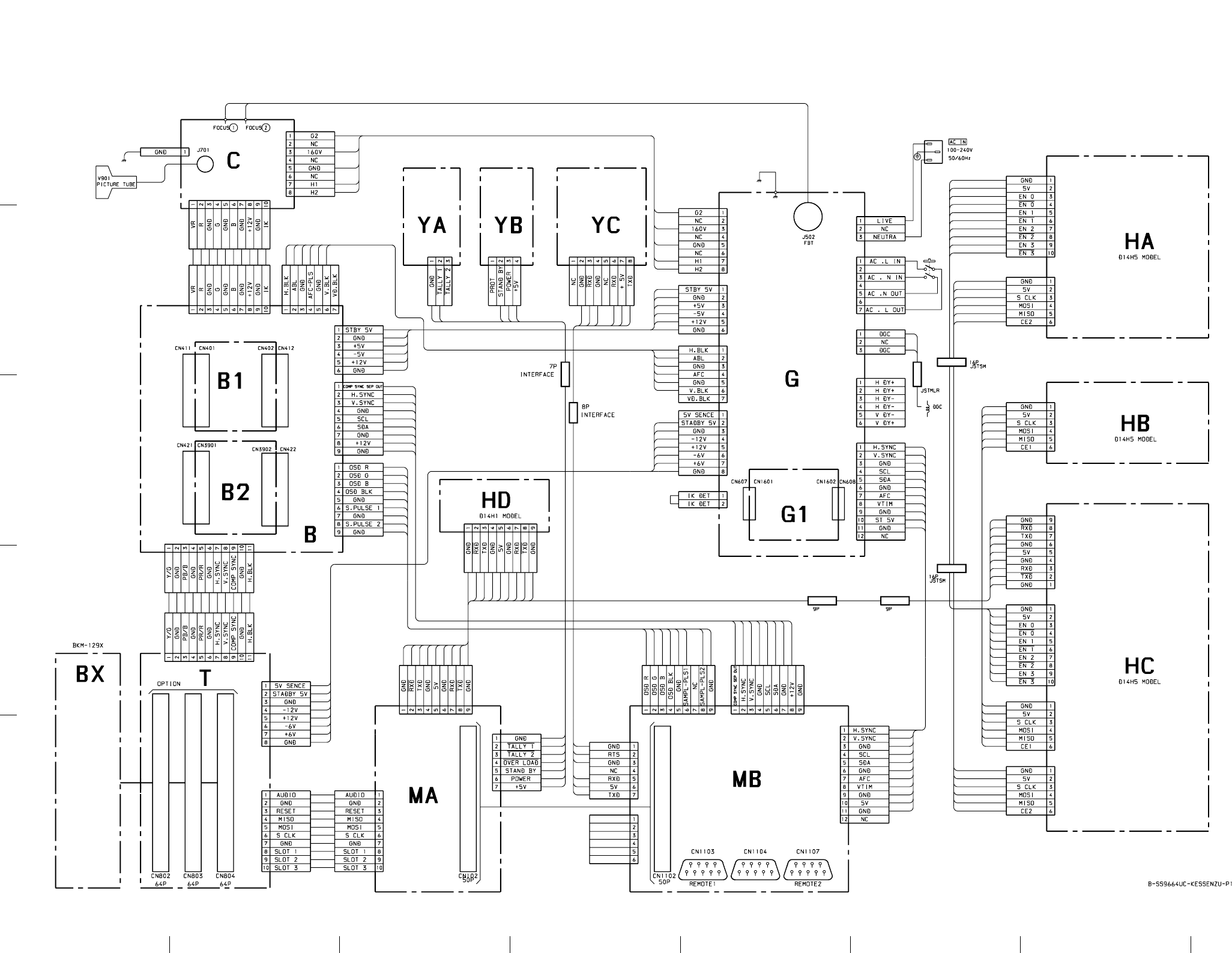
11-2 BVM-D14H1U/D14H5U/D14H1E/D14H5E/D14H1A/D14H5A
11-2
2
3
4
5
ABCDEFGH
1
11-1. Frame Schematic Diagrams
FrameFrame
CN301
CN801
CN805
CN806 CN101
CN105 CN1105
CN1101
CN5
CN4
CN3
CN2
CN201
CN202
CN606
CN501
CN2501
CN101
CN702
CN701
CN703
CN304
CN308
CN302
CN307
CN103
CN901 CN921
CN1106
CN1109
CN604
CN605
CN503
CN601
CN603
CN602
CN1100
CN1
CN931
CN303
CN502
11P
WHT
S-MICRO
8P
WHT-(L)
S-MICRO
8P
WHT-(L)
S-MICRO
10P
WHT-(L)
S-MICRO
10P
WHT-(L)
S-MICRO
9P
WHT-(L)
S-MICRO
9P
WHT-(L)
S-MICRO
12P
WHT-(L)
S-MICRO
6P
WHT
ELCO
6P
WHT
ELCO
10P
WHT
ELCO
9P
WHT
ELCO
6P
WHT
ELCO
10P
WHT
ELCO
8P
WHT
S-MICRO
12P
WHT
S-MICRO
6P
WHT
MINI
6P
YEL
ELCO
10P
WHY-L
:S-MICRO
8P
:VH
FASTEN
10P
WHT
S-MICRO
9P
RED
S-MICRO
6P
RED
S-MICRO
9P
WHT
S-MICRO
7P
RED
S-MICRO
3P
WHT-L
PH
4P
BOARD IN
7P
BLK-(L)
S-MICRO
6P
8P
WHT
:VH
6P
RED
S-MICRO
2P
WHT
S-MICRO
3P
WHT
:MINI
3P
WHT
:VH
7P
WHT
:VH
9P
RED-(L)
S-MICRO
9P
WHT-(L)
ELCO
8P
WHT
:PH
7P
WHT
S-MICRO
7P
WHT
S-MICRO
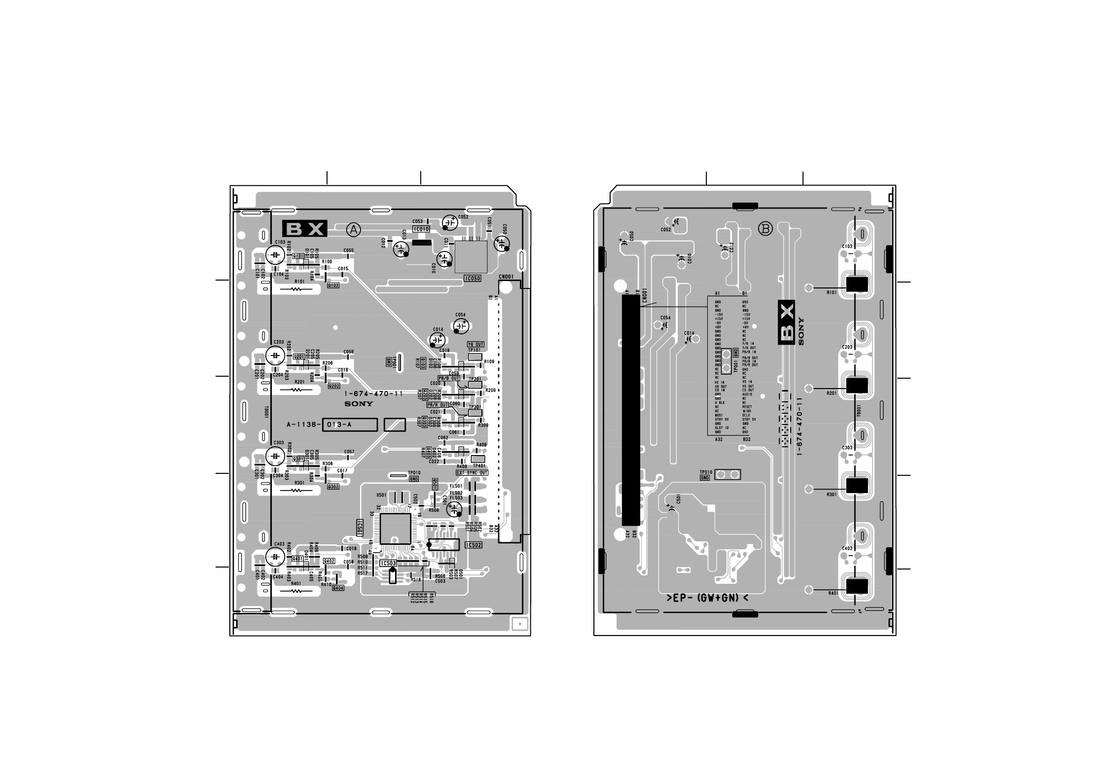
11-3
BVM-D14H1U/D14H5U/D14H1E/D14H5E/D14H1A/D14H5A 11-3
2
3
4
5
1
A BCDEFGH
BXBX
11-2. Schematic Diagrams and Printed Wiring Boards
A
1
2
3
4
5
BC
CBA
1
2
3
4
5
BX BOARD
BX –A SIDE–
SUFFIX: -11 BX –B SIDE–
SUFFIX: -11
[BX BOARD]
* : B SIDE
D101 A-1
D102 C-2
D201 A-2
D202 C-3
D301 A-3
D302 C-3
D401 A-4
D402 C-3
D501 C-5
IC010 B-1
IC050 C-1
IC501 B-4
IC502 C-4
IC503 B-5
Q101 A-1
Q102 B-2
Q103 C-2
Q201 A-2
Q202 B-3
Q203 C-3
Q301 A-3
Q302 B-4
Q303 C-3
Q401 A-4
Q402 B-4
Q403 C-3
Q404 B-5
Q501 C-4
TP001 B-2
TP010 B-4
TP101 C-2
TP201 C-3
TP301 C-3
TP401 C-3
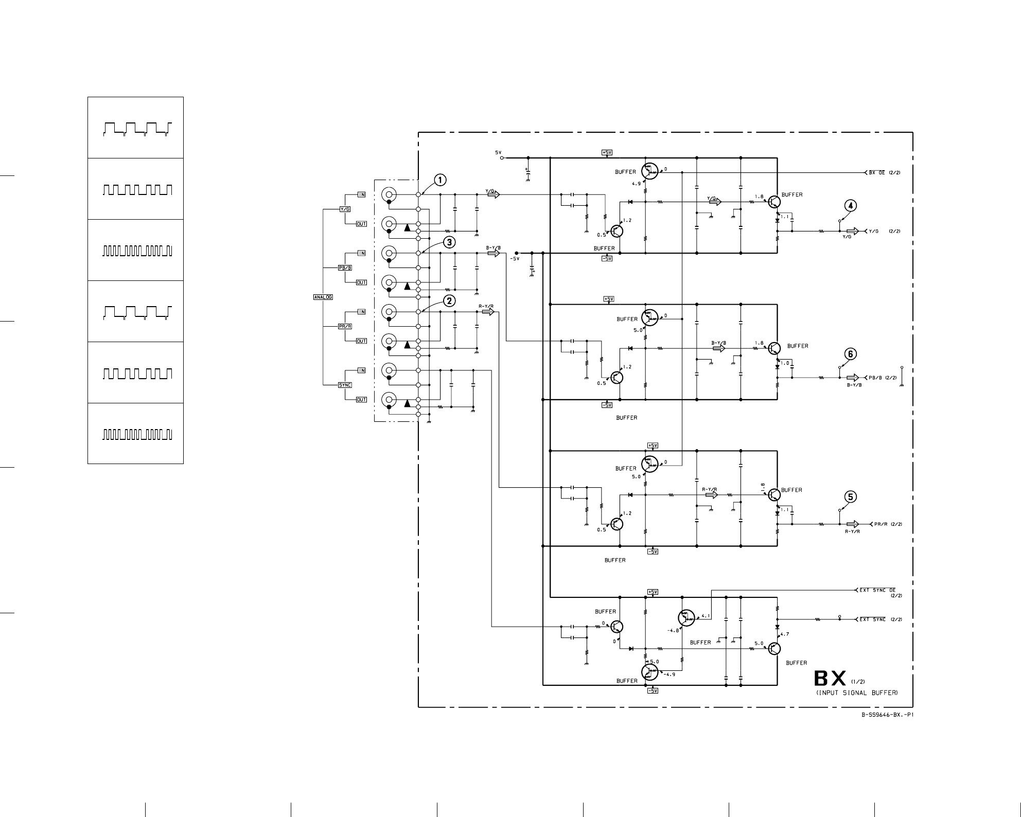
11-4 BVM-D14H1U/D14H5U/D14H1E/D14H5E/D14H1A/D14H5A
11-4
2
3
4
5
ABCDEFGH
1
BX (1/2)BX (1/2)
2.0Vp-p (H)
1.4Vp-p (H)
1.4Vp-p (H)
4
0.9Vp-p (H)
0.6Vp-p (H)
0.6Vp-p (H)
1
2
3
5
6
BX BOARD WAVEFORMS
R102
R202
R302
R103
R203
R303
D101
D102
D201
D202
D301
D302
Q202
Q302
R402
R403
R109
R108
R209
R208
R309
R308
Q101
Q102
Q103
Q203
Q303
Q301
Q201
TP101
TP201
TP301
TP401
C104
C203
C204
C303
C304
R104
R105
R106 R107
R204
R205
R206 R207
R304
R305
R306
R307
C403
C404
TP010
R404
R406
R407
R408
Q401
Q402
Q404
D401
D402
R410
C062
C022
R409
C061
C021
C057
C017
C018
C058
C056 C060
C016 C020
C059C055
C015 C019
C103
C014
C054
C201
C301
C101
C401
Q403
C106
C206
C306
R101
R201
R30 1
R401
R405
C102
C202
C30 2
C402
TB001
100
16V
:HT
0.1
25V
F:CHIP
0.1
25V
F:CHIP
0.1
25V
F:CHIP
0.1
25V
F:CHIP
0.1
25V
F:CHIP
0.1
25V
F:CHIP
0.1
25V
F:CHIP
0.1
25V
F:CHIP
100
16V
:HT
0.1
25V
F:CHIP
0.1
25V
F:CHIP
0.1
25V
F:CHIP
0.1
25V
F:CHIP
0.1
25V
F:CHIP
0.1
25V
F:CHIP
0.1
25V
F:CHIP
0.1
25V
F:CHIP
10p
CH:CHIP
47
16V
:BP
0.1
16V
B:CHIP 0.01
B:CHIP
10p
CH:CHIP
47
16V
:BP
0.1
16V
B:CHIP 0.01
B:CHIP
10p
CH:CHIP
47
16V
:BP
0.1
16V
B:CHIP 0.01
B:CHIP
8p
CH:CHIP
47
16V
:BP
0.1
16V
B:CHIP
2SA146 2
DTA144 EKA
2SC354 5
2SA146 2
DTA144 EKA
2SC354 5
2SA146 2
DTA144 EKA
2SC354 5
2SC241 2K
DTC144 EKA
2SA103 7AK
DTA144 EKA
47k
:CHIP
100
:CHIP
2.2k
:CHIP
100k
:CHIP
22
:CHIP 100
:CHIP
100k
:CHIP
33
:CHIP
47k
:CHIP
100
:CHIP 2.2k
:CHIP
100k
:CHIP
22
:CHIP 100
:CHIP
100k
:CHIP
33
:CHIP
47k
:CHIP
100
:CHIP 2.2k
:CHIP
100k
:CHIP
22
:CHIP
100
:CHIP
100k
:CHIP
33
:CHIP
47k
:CHIP
1k
:CHIP
100k
:CHIP
22
:CHIP
100
:CHIP
100k
:CHIP 33
:CHIP
100k
:CHIP
75
1/2W
:RN
75
1/2W
:RN
75
1/2 W
:RN-CP
75
1/2W
:RN
MA111
MA111
MA111
MA111
MA111
MA111
MA111
MA111
2.2k :CHIP
22p
CH:CHIP
22p
CH:CHIP
22p
CH:CHI P
22p
CH:CHIP
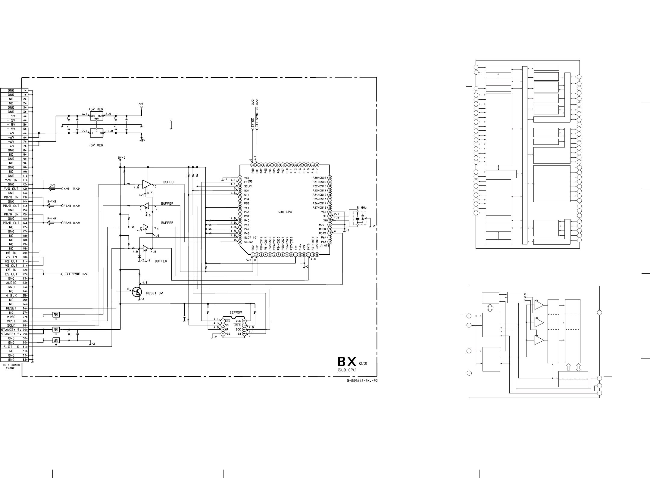
11-5
BVM-D14H1U/D14H5U/D14H1E/D14H5E/D14H1A/D14H5A 11-5
2
3
4
5
1
A BCDEFGH
BX (2/2)BX (2/2)
MB89613R-651 (IC501)
X25040S (IC503)
8
1
5
7
6
4
3
X DECODE
LOGIC 512 BYTE
ARRAY
STATUS
REGISTER WRITE
PROJECT
LOGIC
COMMAND
DECODE
AND
CONTROL
LOGIC
Y DECODE
DATA REGISTER
WRITE
CONTROL
AND
TIMING
LOGIC
32
64
32
32X32
32X32
64X32
48
2
CS
SO
WP
VSS
VCC
HOLD
SCK
SI
28
27
26
24
23
22
21
20
OSC
CLOCK CONTROL
RESET(WDT)
C-MOS I/O PORT
C-MOS I/O PORT
I/O PORT
C-MOS OUT PORT
EXT. BUS INTERFACE
RAM
ROM
TIME BASE TIMER
8 BIT
PMW TIMER
PULSE WIDTH
COUNT TIMER
16 BIT
TIMER COUNTER
8 BIT
SERIAL 1
8BIT
SERIAL 2
BUZZER OUT
I/O PORT
OPEN DRAIN
EXT. INTERRUPUT
OPEN DRAIN
OUT PORT
CPU
F MC-8L
2
X0
X1
RST
49
48
47
46
45
44
43
42
41
40
39
38
37
36
35
34
P00/AD0
P01/AD1
P02/AD2
P03/AD3
P04/AD4
P05/AD5
P06/AD6
P07/AD7
P10/A08
P11/A09
P12/A10
P13/A11
P14/A12
P15/A13
P16/A14
P17/A15
MOD0
MOD1
29
30
31
32
P27/ALE
P26/RD
P25/WR
P24/CLK
P23/RDY
P22/HRQ
P21/HAK
INTERNAL BUS
59
58
57
56
55
54
52
51
50
53
33
P20/BUFC
P37/PTO
P36/WTO
VCC
P35/PWC
P34/EC
P33/SI1
P32/SO1
P31/SCK1
P30
VSS
1
2
3
64
63
62
61
60
P47/S12
P46/SO2
P45/SCK2
P44/BZ
P43
P42
P41
P40
4
5
6
7
8
9
10
11
12
13
14
15
16
17
18
19
P50
P51
P52
P53
P54
P55
P56
P57
VCC
N.C.
VSS
P60/INT0
P61/INT1
P62/INT2
P63/INT3
P64
8 BIT
FL501
FL502
FL503
Q501
R508
R506 R507
D501
R504
R505
R503
R501
R502
R517 R518
X501
C502
R511 R510 R509
R516
C010 C012 C013C011 IC010
TP001
IC503
C501
IC502(1/4)
IC502(2/4)
IC502(3/4)
IC502(4/4)
C050 C051
IC050
C052 C053
C503
R513
R512
R514
R515
IC501
CN001
100
16V
:HT
0.1
25V
F:CHIP
100
16V
:HT
0.1
25V
F:CHIP
100
16V
:HT
0.1
25V
F:CHIP
100
16V
:HT
0.1
25V
F:CHIP
100
16V
:HT
0.1
25V
F:CHIP
0.1
25V
F:CHIP
RD6.2SB
BA05FP
LM2990CX
TC74VHC125F
TC74VHC125F
TC74VHC125F
TC74VHC125F
X25040S
DTC144EKA
100k
:CHIP
100
:CHIP
100
:CHIP
100k
:CHIP
100
:CHIP
100k
:CHIP 100
:CHIP
100k
:CHIP
100k
:CHIP
100k
:CHIP
100k
:CHIP
4.7k
:CHIP
100k
:CHIP
100k
:CHIP
100k :CHIP
100k :CHIP
100k :CHIP
100k :CHIP
MB89613R-651
64P
14 8
9
7
10
2
3
1
1112
1
6
5
4
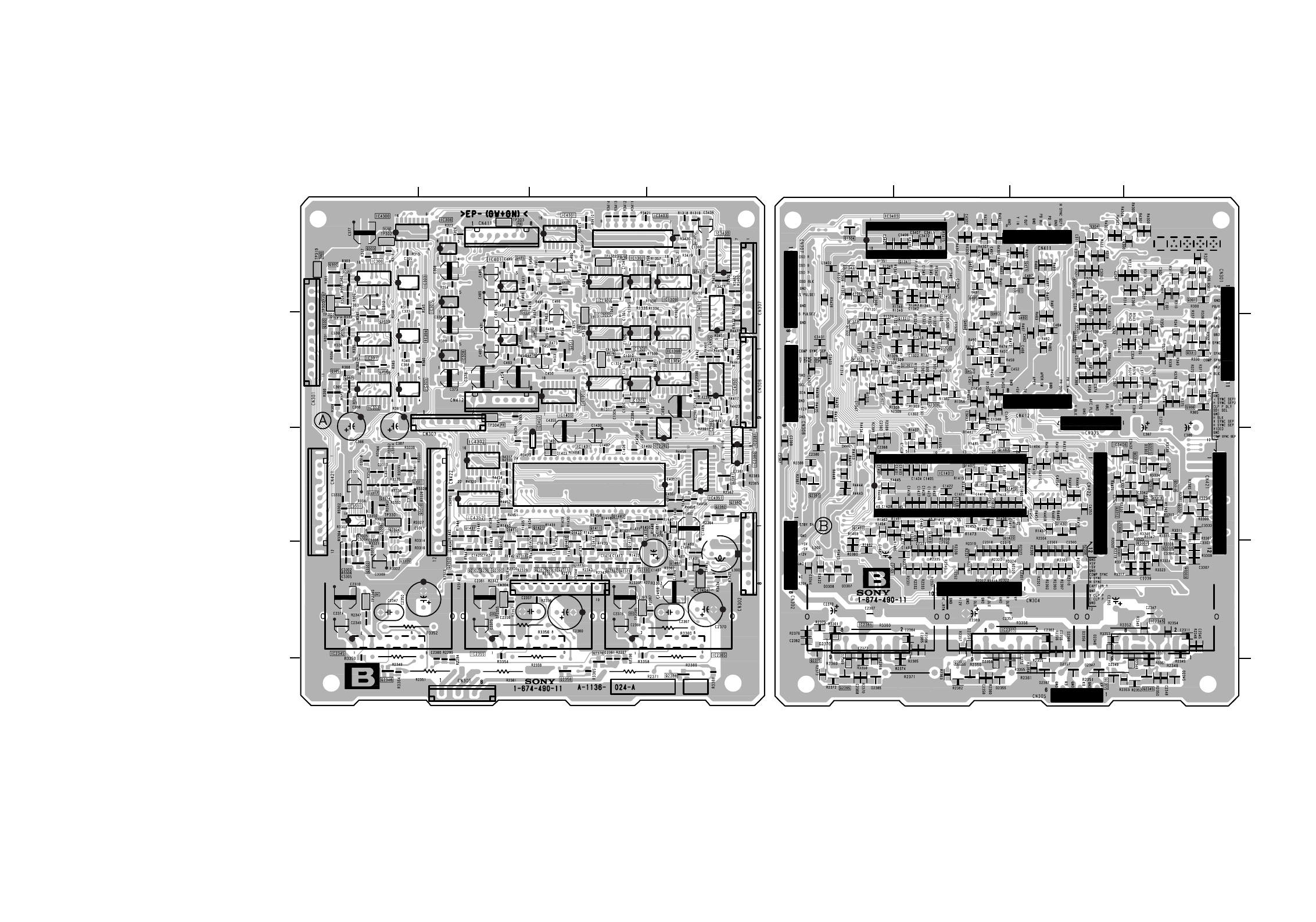
11-6 BVM-D14H1U/D14H5U/D14H1E/D14H5E/D14H1A/D14H5A
11-6
2
3
4
5
ABCDEFGH
1
BB
B BOARD
B –A SIDE–
SUFFIX: -11 B –B SIDE–
SUFFIX: -11
[B BOARD]
* : B SIDE
D1400 C-3
D1401 D-4
D1402 D-3
D1403 C-3
D1404 *B-3
D1405 *C-3
D2345 *A-5
D2346 *B-4
D2347 *B-5
D2348 *A-5
D2349 *B-5
D2355 *C-5
D2356 *B-4
D2357 *B-5
D2358 *C-5
D2359 *C-4
D2365 *D-5
D2366 *B-4
D2367 *B-5
D2369 *D-5
D2370 *D-4
D3301 *B-4
D3302 *A-3
D3307 *D-4
D3308 *D-4
D4401 *D-3
IC300 A-1
IC301 A-2
IC302 A-2
IC303 A-1
IC304 A-2
IC305 A-2
IC306 B-1
IC307 B-1
IC308 B-2
IC400 B-2
IC401 B-1
IC1300 C-2
IC1302 C-2
IC1303 C-1
IC1304 D-2
IC1305 C-2
IC1306 C-2
IC1307 C-1
IC1308 D-2
IC1309 D-1
IC1400 C-2
IC1401 *C-3
IC2345 A-4
IC2355 B-4
IC2365 D-4
IC2380 D-3
IC2381 D-3
IC2382 D-3
IC2383 D-2
IC3301 A-3
IC3400 D-1
IC3401 D-1
IC3403 D-1
IC3404 D-4
IC3405 D-2
IC3406 *B-3
IC3407 C-2
IC4300 A-1
IC4301 C-1
IC4302 B-3
IC4350 D-2
IC4351 D-3
IC4352 B-3
Q300 A-1
Q301 *A-1
Q302 A-1
Q303 A-1
Q304 *B-1
Q330 A-2
Q331 *A-2
Q332 A-2
Q333 A-2
Q334 *B-1
Q365 A-2
Q366 *A-2
Q367 A-2
Q368 A-2
Q369 *B-2
Q450 B-2
Q451
Q452 *C-2
Q453 *B-1
Q460 *B-1
Q461 *B-1
Q462 B-2
Q463 *C-1
Q464 *C-2
Q465 B-2
Q466 *C-1
Q485 B-1
Q486 C-1
Q487 *C-1
Q1300 *C-2
Q1301 *C-2
Q1302 *D-2
Q1303 *D-2
Q1304 *D-1
Q1305 D-1
Q1320 *C-2
Q1321 *C-2
Q1322 *D-2
Q1323 *D-2
Q1340 *C-1
Q1341 *C-1
Q1342 *D-1
Q1343 *D-1
Q1400 *C-3
Q1401 C-3
Q1402 *C-3
Q1410 *C-3
Q1411 C-3
Q1412 C-4
Q1413 C-3
Q1414 C-4
Q1420 *C-3
Q1421 C-3
Q1422 C-4
Q1423 C-3
Q1424 C-4
Q1430 *B-3
Q1431 B-3
Q1432 B-4
Q1433 B-3
Q1434 B-4
Q1460 *D-3
Q1461 D-4
Q1462 C-3
Q1463 *C-3
Q2300 B-4
Q2301 B-4
Q2302 B-4
Q2303 B-4
Q2315 C-4
Q2316 C-4
Q2317 C-4
Q2318 B-4
Q2330 D-4
Q2331 C-4
Q2332 C-4
Q2333 C-4
Q2345 *A-5
Q2346 A-4
Q2355 *C-5
Q2356 C-5
Q2365 *D-5
Q2366 D-5
Q2375 *D-5
Q2376 C-4
Q2377 *B-5
Q2380 D-3
Q2381 D-3
Q2382 D-3
Q2383 *D-3
Q3301 *A-3
Q3302 A-4
Q3303 *A-4
Q3304 A-3
Q3305 A-4
Q3306 A-3
Q3307 *A-4
Q3308 *A-4
Q3309 *B-3
Q3310 A-3
Q3311 A-3
Q3312 *B-3
Q3313 *A-3
Q3314 A-3
Q3315 *A-3
Q3316 *A-3
Q3317 A-3
Q3318 *A-3
Q3319 *A-3
Q3402 D-1
TP300 A-1
TP301 A-1
TP302 A-1
TP303 B-1
TP304 B-2
TP310 A-1
TP1300 C-2
TP1301 C-2
TP1302 C-1
TP2345 A-4
TP2355 B-4
TP2365 C-4
TP3301 A-3
ABCD
1
2
3
4
5
5
4
3
2
1
ABCD
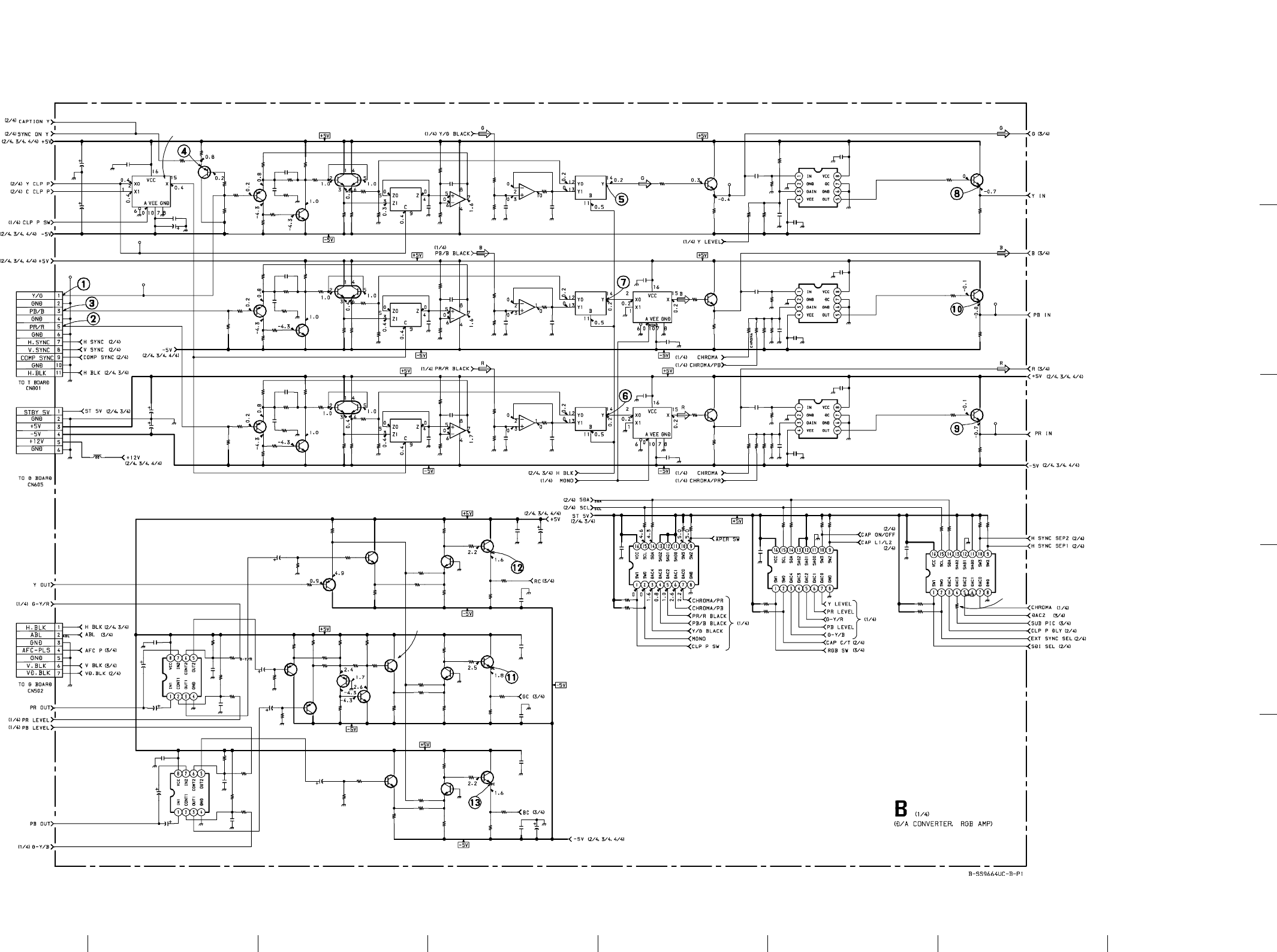
11-7
BVM-D14H1U/D14H5U/D14H1E/D14H5E/D14H1A/D14H5A 11-7
2
3
4
5
1
A BCDEFGH
B (1/4)B (1/4)
R300
R301
R306
R307
R308
R309
R316
R317
R319 R320
R321
R323
R324
R354
R347
R346
R339
R338
R337
R336
R331
R330
R365
R366
R371
R372
R373
R374 R375
R340
R381
R382 R389
C301
C4300 C4302
Q300
R302
R303
C302 R304
R305
C303
Q301
Q302
R310
C304
R312
R313 C305
R314
R315
C306
C309
C310
C311
Q330
R332
R333
C330
C331
Q331
Q332
C332
R342
R343 C333
R344
C334
C336
C337
C338
R353
C340
C341
Q365
R367
R368
C365
R370
C366
Q366
Q367
C367
R377
R378 C368
R379
C369
C371
C372
R388
C375
C376
IC306
IC307
IC308
R450
R455
R458
R459
R463
R470 R480
R481
R488
R489 R497
R498
C451
C452
C462
R460
R461
R462
R467
R471
R472
R476 C467
C468
Q450 Q451
IC400
C460
C461
Q460
Q461
Q462
Q463
Q486
Q485
IC401
C485
C486
C487
R485
R493 C491
C492
IC4300
R4300
R4301
R4302R4303
R4304R4305
R4306
R4307
R4308R4309R4310R4311
C463
C464
C488
C489
C370
C307
C335
C308
CN301
C387
C373
IC4301
R4312
R4313
R4314
C377
C378
C4303
R4316
R4317
C300
C386
R311
R341
R376
R348
R318
R383
R322
R349
R384
R350
R385
R351
R386
R352
R387
R486
R464
R465
CN302
R4320
R4315
R325
R356
R391
C454
C494
TP300
TP301
TP302
TP303
TP304
TP310
C374
C339
C465
Q3301
R3300
R3301
R3299
C312
R380
R345
R487
R456
R478
R479
R495
C450
R452
R474
R475
R491
R492
R473
R490
C466
C490
R451
R466
R454
R477
R494
R482
R483
R453
L300
Q453
Q465
Q466
R355
R390
R334
R369
R468 R469
R335
CN303
Q452
Q464
Q487
R457
R484
R499
Q303
Q333
Q368
Q304
Q334
Q369
IC4302
IC300
IC300
IC303
IC301
IC301
IC304
IC302
IC302
IC305
IC301
IC302
IC300
IC303
IC304
IC305
2SC3545
CLAMP
2SC3545
CLAMP
2SC3545
CLAMP
2SA1462
CLAMP
IMX2
CLAMP
0.047
B:CHIP
0.01
B:CHIP
2SA1462
CLAMP
IMX2
CLAMP
0.047
B:CHIP
0.01
B:CHIP
2SA1462
CLAMP
IMX2
CLAMP
0.047
B:CHIP
0.01
B:CHIP
0.01
F:CHIP 0.01
F:CHIP
1k
:CHIP
100
:CHIP
3.3k
:RN-CP
1.8k
:RN-CP
1k
:RN-CP
100
:CHIP
1.2k
:RN-CP
100
:CHIP
1k
:CHIP
1M
:RN-CP
10k
:RN-CP
100
:CHIP
100
:CHIP
100
:CHIP
10k
:RN-CP
1M
:RN-CP
1k
:CHIP
100
:CHIP
1.2k
:RN-CP
100
:CHIP
1.8k
:RN-CP
3.3k
:RN-CP
100
:CHIP
1k
:CHIP
1k
:CHIP
100
:CHIP
3.3k
:RN-CP
1.8k
:RN-CP
1k
:RN-CP
100
:CHIP
1.2k
:RN-CP
100
:CHIP
1k
:CHIP 1k
:CHIP
1k
:CHIP
1k
:CHIP
1M
:RN-CP
10k
:RN-CP
100
:CHIP
TL082CPS
CLAMP
TL082CPS
CLAMP
TL082CPS
CLAMP
TL082CPS
CLAMP
TL082CPS
CLAMP
TL082CPS
CLAMP
CXA1875AM-T4
D/A CONVERTER
10k
:CHIP
10k
:CHIP
10k
:CHIP
10k
:CHIP
220
:CHIP
220
:CHIP
10k
:CHIP
10k
:CHIP
10k
:CHIP
10k
:CHIP
220
:CHIP
220
:CHIP
0.01
F:CHIP
0.01
F:CHIP
0.01
F:CHIP
0.01
F:CHIP
0.01
F:CHIP
0.01
F:CHIP
0.01
F:CHIP
0.01
F:CHIP
22
6.3V
:BP-CP
0.01
F:CHIP
0.01
F:CHIP
0.01
F:CHIP
0.01
F:CHIP
0.01
F:CHIP 0.01
F:CHIP
0.01
F:CHIP
0.01
F:CHIP
0.01
F:CHIP
22
6.3V
:HT-CP
22
6.3V
:HT-CP
0.01
F:CHIP
0.01
F:CHIP
0.01
F:CHIP
22
6.3V
:HT-CP
22
6.3V
:HT-CP
0.01
F:CHIP 0.01
F:CHIP
0.01
F:CHIP
MC74HC4053FEL
SWITCH
MC74HC4053FEL
SWITCH
MC74HC4053FEL
SWITCH
MC74HC4053FEL
SWITCH
MC74HC4053FEL
SWITCH
MC74HC4053FEL
SWITCH
MC74HC4053FEL
SWITCH
MC74HC4053FEL
SWITCH
MC74HC4053FEL
SWITCH
CXA1521M
Y AMP
CXA1521M
PB AMP
CXA1521M
PR AMP
CXA1211M
PB AMP
CXA1211M
PR AMP
2SC2412K
BUFFER
2SC3545
AMP
2SA1462
AMP
2SC3545
AMP
2SC2412K
BUFFER
2SC3545
AMP
2SC2412K
BUFFER
2SC3545
AMP
10k
:RN-CP
330k
:RN-CP 220
:CHIP
27k
:RN-CP 15k
:RN-CP
47k
:CHIP
2.2k
:CHIP
10k
:RN-CP
220
:CHIP 47k
:CHIP
100
:CHIP
10k
:RN-CP
220
:CHIP 47k
:CHIP
100
:CHIP
100
:CHIP
680
:RN-CP
100
:CHIP
2.2k
:CHIP
6.8k
:RN-CP
4.7k
:RN-CP
6.8k
:RN-CP
4.7k
:RN-CP
820
:RN-CP
1k
:RN-CP
3.3k
:CHIP
100
:CHIP
680
:RN-CP 100
:CHIP
2.2k
:CHIP
6.8k
:RN-CP
4.7k
:RN-CP 100
:CHIP
680
:RN-CP 100
:CHIP
2.2k
:CHIP
2.2
F:CHIP
2.2
F:CHIP
2.2
F:CHIP
0.01
F:CHIP
0.01
F:CHIP
0.01
F:CHIP
0.01
F:CHIP
22
6.3V
:BP-CP
11P
WHT
:S-MICRO
22
6.3V
:BP-CP
1000
6.3V
CXA1875AM-T4
D/A CONVERTER
10k
:CHIP
10k
:CHIP
10k
:CHIP
47
16V
:HT-CP
47
16V
:HT-CP
0.01
F:CHIP
220
:CHIP
220
:CHIP
0.01
F:CHIP
1000
6.3V
150 :CHIP
100 :CHIP
100 :CHIP
1.5k
:CHIP
1.5k
:CHIP
1.5k
:CHIP
18k
:RN-CP
22k
:RN-CP
22k
:RN-CP
200k
:RN-CP
220k
:RN-CP
56k
:RN-CP
56k
:RN-CP
#
#
2.7k
:RN-CP
2.4k
:RN-CP
5.1k
:RN-CP
6P
RED
:S-MICRO
#
CH:CHIP
# CH:CHIP
#
CH:CHIP
# CH:CHIP
#
CH:CHIP
# CH:CHIP
#
:RN-CP
2.2k
:CHIP
1k
:CHIP
330
:CHIP
220
:CHIP
220
:CHIP
47
16V
:HT-CP
47
16V
:HT-CP
2.2
16V
F:CHIP
2.2
16V
F:CHIP
2SA1037K
100
:CHIP
1.5k
:CHIP
6.3V
:HT-CP
10
16V
:HT-CP
100
:CHIP
560k
:RN-CP
560k
:RN-CP
6.8k :RN-CP
4.7k
:CHIP
4.7k
:CHIP
4.7k
:CHIP
10
16V
:HT-CP
680
:RN-CP
680
:RN-CP
680
:RN-CP
680
:RN-CP
680
:RN-CP
1k
:CHIP
1k
:CHIP
10
16V
:HT-CP
10
16V
:HT-CP
1k
:CHIP
3.3k
:RN-CP
4.7k
:CHIP
560
:RN-CP
560
:RN-CP
560
:RN-CP
100
:CHIP
560
:RN-CP
820
:RN-CP
2SA1462
BUFFER
2SA1037K
BUFFER
2SA1037K
BUFFER
2.2k
:CHIP
2.2k
:CHIP
# :RN-CP
# :RN-CP
680
:CHIP 680
:CHIP
1k :RN-CP
7P WHT :S-MICRO
2SC3545
BUFFER
2SC3545
BUFFER
2SC3545
BUFFER
150
33
150
2SC3545
BUFFER
2SC3545
BUFFER
2SC3545
BUFFER
2SC3545
BUFFER
2SC3545
BUFFER
2SC3545
BUFFER
CXA1875AM-T4
D/A CONVERTER
22µ
100µH
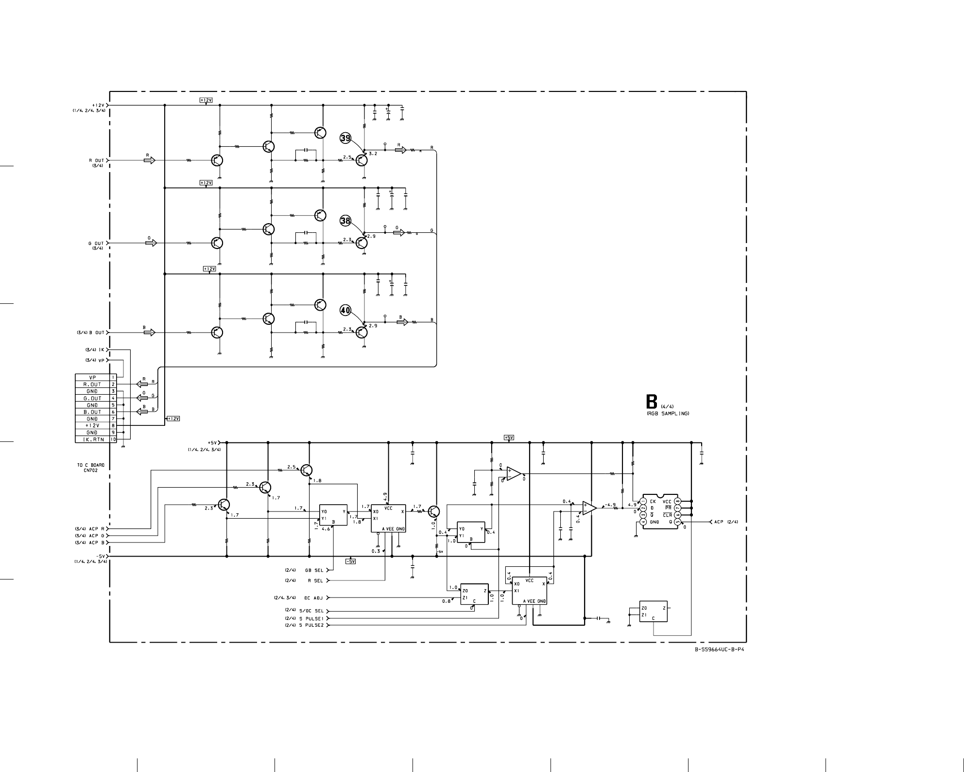
11-8 BVM-D14H1U/D14H5U/D14H1E/D14H5E/D14H1A/D14H5A
11-8
2
3
4
5
ABCDEFGH
1
B (2/4)B (2/4)
IC2383
R2386
R2387
IC2382(2/2)
R2388
R2389
R2391
R2390
R2392
R2393
R2384
R2382
R2380
C2383
C2389
C2388
C2386
C2387
C2390
CN304
R2381 R2383 R2385
Q2380
Q2381
Q2382
IC2380(1/3)
IC2380(2/3)
IC2380(3/3)
Q2383
IC2381(2/3)
IC2381(1/3)
IC2381(3/3)
IC2382(1/2)
C2385
C2384
TP2345
TP2355
TP2365
R2300
R2301 R2302
R2303
R2307
R2304 R2305 R2308
R2309
R2310
R2315
R2316
R2317
R2318
R2322
R2319 R2320
R2323
R2324
R2325
R2330
R2331
R2332
R2333
R2337
R2334
R2335 R2338
R2339
R2340
C2300
C2353
C2352
C2351
C2363
C2361
C2310
C2362
C2364
Q2301
Q2300
Q2316
Q2315
Q2330
Q2331
Q2302
Q2303
R2314
C2315
Q2317
Q2318
R2329
Q2332
Q2333
R2344
C2330
C2311
TC7W74FU
LATCH
LM393PS-E20
SAMPLING
100
:CHIP
100
:CHIP
100
:CHIP
0.01
F:CHIP
100
:CHIP
2.2k
:CHIP
10k
:CHIP
10k
:CHIP
2.2k
:CHIP
10k
:CHIP
10k
:CHIP
2.2k
:CHIP
0.01
F:CHIP
0.01
F:CHIP
0.01
F:CHIP
0.01
F:CHIP
0.01
F:CHIP
10P
WHT
:S-MICRO
2.2k
:CHIP 2.2k
:CHIP 2.2k
:CHIP
2SC2412K
BUFFER
2SC2412K
BUFFER
2SC2412K
BUFFER
MC74HC4053AFT
SWITCH
MC74HC4053AFT
SWITCH
MC74HC4053AFT
SWITCH
2SC2412K
BUFFER
MC74HC4053AFT
SWITCH
MC74HC4053AFT
SWITCH
MC74HC4053AFT
SWITCH
LM393PS-E20
SAMPLING
B:CHIP
B:CHIP
100
:CHIP
4.7k
:CHIP 22
:CHIP
270
:CHIP
100
:CHIP
560
:RN-CP 470
:RN-CP 1.8k
:CHIP
100
:CHIP
1k
:CHIP
100
:CHIP
4.7k
:CHIP
22
:CHIP
270
:CHIP 100
:CHIP
560
:RN-CP
470
:RN-CP 1.8k
:CHIP
100
:CHIP
1k
:CHIP
100
:CHIP
4.7k
:CHIP
22
:CHIP
270
:CHIP 100
:CHIP
560
:RN-CP
470
:RN-CP 1.8k
:CHIP
100
:CHIP
1k
:CHIP
5p
CH:CP
0.01
F:CHIP
0.01
F:CHIP
0.01
F:CHIP
47
16V
:HT-CP
47
16V
:HT-CP
47
16V
:HT-CP
0.01
F:CHIP
0.01
F:CHIP
2SC3454
2SA1462
2SC3545
2SA1462
2SA1462
2SC3545
2SA1462
2SA1462
33
:CHIP
7pF
CH:CHIP
2SA1642
2SA1642
33
:CHIP
2SA1462
2SA1462
33
:CHIP
9p
CH:CHIP
0.01
F:CHIP
0.001µF
0.001µF
2
1
10
15
12
13
6117 8
14
2
1
15
10
3
21
5
3
9
412
13
16
6117 8
14
5
64
7
8
5
3
4
9
16
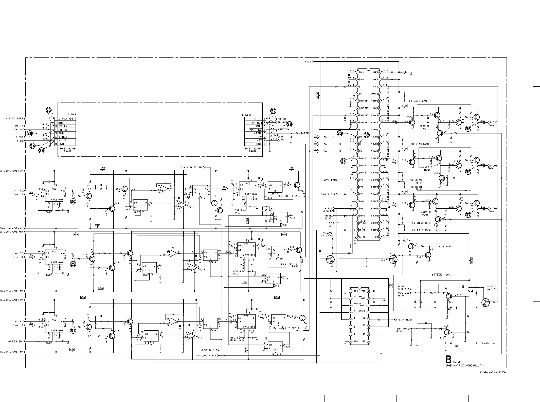
11-9
BVM-D14H1U/D14H5U/D14H1E/D14H5E/D14H1A/D14H5A 11-9
2
3
4
5
1
A BCDEFGH
B (3/4)B (3/4)
C1300
C1301
R1300
Q1300
R1305
Q1301
R1306
R1307
Q1302
R1308
C1304
C1305
C1307
C1308
R1313
Q1303
R1314
C1320
C1321
R1320
Q1320
R1325 Q1321
R1326
R1327
Q1322
R1328
C1324
C1325
R1331
R1332
C1340
C1341
R1340
Q1340
R1345 Q1341
R1346
R1347
Q1342
R1348 C1344
C1345
R1351
Q1343
R1352
R1301
R1302
R1303
R1309
R1310
R1321
R1322
R1323
R1329
R1330
R1341
R1342
C1343
R1349
R1350
Q1400
C1400
C1401
C1404
C1419
C1424
R1400
R1405
R1406
R1407
R1408
R1409
R1410
R1411 R1415
R1416
R1418 R1419
R1421
R1424
R1425
R1426 R1428 R1429 R1431
R1434
R1435
R1436
R1438
R1439 R1441
R1444
R1445
R1446
R1447
R1451
C1450
Q1402
C1461
C1462 R1461
C1465
C1466
R1467
D1400
D1402
D1401
C1409
C1429
C1460
C1464
C1427
C1426
C1415
IC1401
R1315
C1309
R1316
R1317
R1333
R1353
C1346
C1347
C1326
C1327
Q1323
C1413
C1421
C1451
R1450
R1440
R1430
R1420
R1412
C1406
C1407
C1408
R1460
R1466
C1467
C1348
CN412
CN411
R1413
R1414
R1464
R1452
R1453
R1454
R1481
R1480
C1468
C1469
R1473
R1484 R1483
TP1300
TP1301
TP1302
D1403
D1404
R1401
R1485
R1311
R1334
R1335
R1357
C1306
R1312
R1318
R1319
R1343
R1344
R1358
R1354
R1355
C1405
R1455
R1456
R1457
R1472
R1482
Q1431
Q1434
Q1424
Q1411
Q1414
Q1463
IC1400
Q1460
Q1461
Q1304
Q1305
Q1462
R1402
C1410
C1411
C1412
C1416
C1417
C1418
C1422
C1423
C1428
Q1421
C1402
C1425
C1420
C1414
Q1401
R1469
R1470
C1302
C1322
C1342
C1310
C1330
C1350
C1431
R1423
R1433
R1443
Q1433
R1442
Q1423
R1432
Q1413
R1422
R1471
Q1430
Q1432
Q1422
Q1420
Q1410
Q1412
R1437
R1427
R1417
IC1300
IC1300
IC1302
IC1302
IC1303
IC1303
IC1302
IC1303
IC1300
IC1305
IC1306
IC1307
IC1304 IC1304
IC1304
IC1308
IC1308
IC1308
IC1309
IC1309
IC1309
IC1305
IC1306
IC1307
2SC3545
CLAMP
100
:CHIP
2SC3545
CLAMP
100
:CHIP
2SC3545
CLAMP
100
:CHIP
100
:CHIP
2SA1462
CLAMP 100
:CHIP
1.2k
:RN-CP
100
:CHIP
1k
:CHIP
0.047
B:CHIP
0.01
B:CHIP
2SC2412K
BUFFER
100
:CHIP
2SA1462
CLAMP
100
:CHIP
1.2k
:RN-CP
100
:CHIP
1k
:CHIP
0.047
B:CHIP
0.01
B:CHIP
100
:CHIP
2SA1462
CLAMP
100
:CHIP
1.2k
:RN-CP
100
:CHIP
1k
:CHIP
0.047
B:CHIP
0.01
B:CHIP
2SC2412K
BUFFER
2SC2412K
CLAMP
2SC2412K
CLAMP
2SC2412K
CLAMP
0.01
F:CHIP
0.01
F:CHIP
0.01
F:CHIP
0.01
F:CHIP
0.01
F:CHIP
0.01
F:CHIP
0.01
F:CHIP
0.01
F:CHIP
TL082CPS
CLAMP
TL082CPS
CLAMP
TL082CPS
CLAMP
3.3k
:RN-CP
1.8k
:RN-CP
1k
:RN-CP
1M
:RN-CP
10k
:RN-CP
3.3k
:RN-CP
1.8k
:RN-CP
1k
:RN-CP
1M
:RN-CP
10k
:RN-CP
3.3k
:RN-CP
1.8k
:RN-CP
1M
:RN-CP
10k
:RN-CP
0.01
F:CHIP
0.047
F:CHIP
0.047
F:CHIP
0.01
F:CHIP
100p
CH:CHIP
100p
CH:CHIP
0.01
F:CHIP
0.01
F:CHIP
0.01
F:CHIP
0.01
F:CHIP
MC74HC4053FEL
SWITCH
MC74HC4053FEL
SWITCH
MC74HC4053FEL
SWITCH
MC74HC4053FEL
SWITCH
MC74HC4053FEL
SWITCH
MC74HC4053FEL
SWITCH
DTC144EKA
IK-MASK
2SA1037K
IK-BUFFER
2.2k
:CHIP
2.2k
:CHIP
2.2k
:CHIP
100
:CHIP
100
:CHIP
100
:CHIP
100
:CHIP
1k
:CHIP
1k
:CHIP
100
:CHIP
33k
:CHIP 470k
:CHIP
100
:CHIP
1k
:CHIP 10k
:CHIP
470
:CHIP
1k
:CHIP
4.7k
:CHIP
100
:CHIP
1k
:CHIP 10k
:CHIP 470
:CHIP
1k
:CHIP
4.7k
:CHIP
100
:CHIP
1k
:CHIP
10k
:CHIP 470
:CHIP
1k
:CHIP
4.7k
:CHIP
100k
:CHIP
100k
:CHIP
47k
:CHIP
33k
:CHIP
27k
:CHIP
0.22
16V
B:CHIP
0.1
25V
F:CHIP
0.1
25V
F:CHIP
0.47
25V
F:CHIP
0.47
25V
F:CHIP
MA111
MA111
MA111
0.1
25V
F:CHIP
0.1
25V
F:CHIP
CXA1739S
RGB-MATRIX
2SC2412K
BUFFER
MC74HC4053FEL
SWITCH
MC74HC4053FEL
SWITCH
MC74HC4053FEL
SWITCH
TL082CPS
CLAMP
TL082CPS
CLAMP
TL082CPS
CLAMP
MC74HC4053FEL
SWITCH
MC74HC4053FEL
SWITCH
MC74HC4053FEL
SWITCH
MC74HC4053FEL
SWITCH
MC74HC4053FEL
SWITCH
MC74HC4053FEL
SWITCH
MC74HC4053FEL
SWITCH
MC74HC4053FEL
SWITCH
MC74HC4053FEL
SWITCH
0
:CHIP
10k
:RN-CP
39k
:RN-CP
0
:CHIP
0
:CHIP
2.2
16V
F:CHIP
0.01
F:CHIP
0.01
F:CHIP
0.01
F:CHIP
0.01
F:CHIP
100p
CH:CHIP
100p
CH:CHIP
10k
:RN-CP
82k
:CHIP
82k
:CHIP
82k
:CHIP
0.047 25V B:CHIP
0.047 25V B:CHIP
0.047 25V B:CHIP
47k
:CHIP
470k
:CHIP
470k
:CHIP
0.1
25V
F:CHIP
470
16V
100p
CH:CHIP
#
CH:CHIP
8P 8P
33k
:CHIP
33k
:CHIP
39k
:RN-CP
33k
:RN-CP
33k
:RN-CP
33k
:RN-CP
6.8k
:CHIP
4.7k
:CHIP 47
16V
:HT-CP
47
16V
:HT-CP
10k
:CHIP
47k
:CHIP
33k
:CHIP
MA111
RD10SB3
10k
:CHIP
10k
:CHIP
10k
:CHIP
10k
:CHIP
10k
:CHIP
0
:CHIP
1
10V
B:CHIP
10k :CHIP
4.7k
:CHIP
4.7k
:CHIP
1k :RN-CP
# :RN-CP
10k :CHIP
27k
:RN-CP
47k
:RN-CP
0.047
F:CHIP
33k
:CHIP
33k
:CHIP
33k
:CHIP
470k
:RN-CP
3.3k
:CHIP
2SC2412K
BUFFER
2SC2412K
CLAMP
2SC2412K
CLAMP
2SC2412K
BUFFER
2SC2412K
CLAMP
DTC114EKA
SWITCH
MC74HC4538AFEL
MONO MULTI
2SC2412K
PIC ABL
2SC2412K
BRT ABL
2SC2412K
BUFFER
2SA1037K
BUFFER
DTC144EKA
SWITCH
10k
:CHIP
0.1
25V
B:CHIP
0.1
25V
B:CHIP
0.1
25V
B:CHIP
0.1
25V
B:CHIP
0.1
25V
B:CHIP
0.1
25V
B:CHIP
0.1
25V
B:CHIP
0.1
25V
B:CHIP
0.1
25V
B:CHIP
2SC2412K
BUFFER
0.047
50V
B:CHIP
CH:CHIP
CH:CHIP
CH:CHIP
2SC2412K
IK-BLK
1.2k
:RN-CP
10k
:RN-CP
4p CH:CHIP
8p CH:CHIP
3p CH:CHIP
1/16V
1/16V
1/16V
100p
470
:CHIP
470
:CHIP
470
:CHIP
2SC3545
BUFFER
1k
:CHIP
2SC3545
BUFFER
1k
:CHIP
2SC3545
BUFFER
1k
:CHIP
39k
:RN-CP
2SA1462
BUFFER
2SA1462
BUFFER
2SA1462
BUFFER
2SA1462
BUFFER
2SA1462
BUFFER
2SA1462
BUFFER
3.9k
:CHIP
3.9k
:CHIP
3.9k
:CHIP
0.001µF
0.001µF
0.001µF
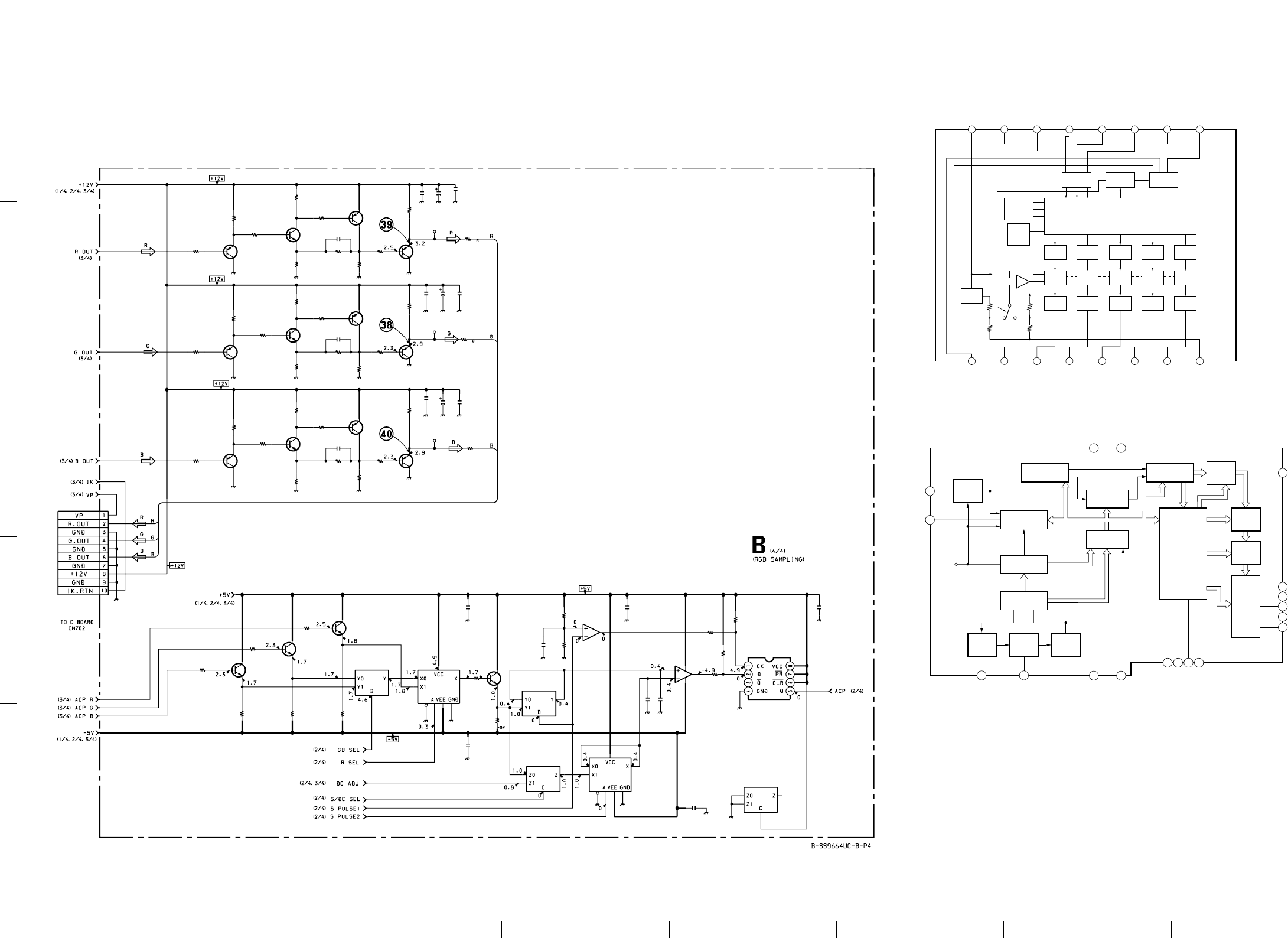
11-10 BVM-D14H1U/D14H5U/D14H1E/D14H5E/D14H1A/D14H5A
11-10
2
3
4
5
ABCDEFGH
1
B (4/4)B (4/4)
CXA1875AM (IC4300, 4301, 4302, 4350)
Z8622812PSC (IC3403)
LATCH
DAC
AMP
LATCH
DAC
AMP
LATCH
DAC
AMP
LATCH
DAC
AMP
LATCH
DAC
AMP
+
–
VCC
REG
I2C DECODER
LEVEL
CONVERTER
LEVEL
CONVERTER LEVEL
CONVERTER
LATCH
POWER
ON
RESET
OPEN COLLECTOR
3 6
25 81 4 7
SW1
SW0
DAC4
DAC3
DAC2
DAC1
DAC0
GND
14 11
15 12 916 13 10
VCC
SCL
SDA
SAD2
SAD1
SAD0
SW3
SW2
CLAMP
SLICE LEVEL
VDD
(DIGITAL)
COMP SYNC
PFD
DOT CLK
LOOP
FIL
DATA SLICER DATA MOD
XFR BUF
CHAR
ROW
DISPLAY
RAM
OUTPUT
LOGIC
LOOP
FILTER
PHOSE/
FREQ
DET VCO
DATA RECOVERY
COMMAND
PROCESSOR
AND
DECODER
CONTROL
SYNC SLICER
HORIZONTAL
COUNTER
VERTICAL CTR
AND CONTROL
DATA CLK
RECOVERY
TIMING LOGIC
11
12
1514 VDD
(ANALOG)
VSS
(DIGITAL) 109
VSS
(ANALOG)
2
NRESET
DCLK
SLICED DATA
8 13
LOCK
7
B
4
LUM
3
17116 18
BOX
LNG/SCK
CT/SDA
DONF/SEN
NSIN
6
G5
R
IC2383
R2386
R2387
IC2382(2/2)
R2388
R2389
R2391
R2390
R2392
R2393
R2384
R2382
R2380
C2383
C2389
C2388
C2386
C2387
C2390
CN304
R2381 R2383 R2385
Q2380
Q2381
Q2382
IC2380(1/3)
IC2380(2/3)
IC2380(3/3)
Q2383
IC2381(2/3)
IC2381(1/3)
IC2381(3/3)
IC2382(1/2)
C2385
C2384
TP2345
TP2355
TP2365
R2300
R2301 R2302
R2303
R2307
R2304 R2305 R2308
R2309
R2310
R2315
R2316
R2317
R2318
R2322
R2319 R2320
R2323
R2324
R2325
R2330
R2331
R2332
R2333
R2337
R2334
R2335 R2338
R2339
R2340
C2300
C2353
C2352
C2351
C2363
C2361
C2310
C2362
C2364
Q2301
Q2300
Q2316
Q2315
Q2330
Q2331
Q2302
Q2303
R2314
C2315
Q2317
Q2318
R2329
Q2332
Q2333
R2344
C2330
C2311
TC7W74FU
LATCH
LM393PS-E20
SAMPLING
100
:CHIP
100
:CHIP
100
:CHIP
0.01
F:CHIP
100
:CHIP
2.2k
:CHIP
10k
:CHIP
10k
:CHIP
2.2k
:CHIP
10k
:CHIP
10k
:CHIP
2.2k
:CHIP
0.01
F:CHIP
0.01
F:CHIP
0.01
F:CHIP
0.01
F:CHIP
0.01
F:CHIP
10P
WHT
:S-MICRO
2.2k
:CHIP 2.2k
:CHIP 2.2k
:CHIP
2SC2412K
BUFFER
2SC2412K
BUFFER
2SC2412K
BUFFER
MC74HC4053AFT
SWITCH
MC74HC4053AFT
SWITCH
MC74HC4053AFT
SWITCH
2SC2412K
BUFFER
MC74HC4053AFT
SWITCH
MC74HC4053AFT
SWITCH
MC74HC4053AFT
SWITCH
LM393PS-E20
SAMPLING
B:CHIP
B:CHIP
100
:CHIP
4.7k
:CHIP 22
:CHIP
270
:CHIP
100
:CHIP
560
:RN-CP 470
:RN-CP 1.8k
:CHIP
100
:CHIP
1k
:CHIP
100
:CHIP
4.7k
:CHIP
22
:CHIP
270
:CHIP 100
:CHIP
560
:RN-CP
470
:RN-CP 1.8k
:CHIP
100
:CHIP
1k
:CHIP
100
:CHIP
4.7k
:CHIP
22
:CHIP
270
:CHIP 100
:CHIP
560
:RN-CP
470
:RN-CP 1.8k
:CHIP
100
:CHIP
1k
:CHIP
5p
CH:CP
0.01
F:CHIP
0.01
F:CHIP
0.01
F:CHIP
47
16V
:HT-CP
47
16V
:HT-CP
47
16V
:HT-CP
0.01
F:CHIP
0.01
F:CHIP
2SC3454
2SA1462
2SC3545
2SA1462
2SA1462
2SC3545
2SA1462
2SA1462
33
:CHIP
7pF
CH:CHIP
2SA1642
2SA1642
33
:CHIP
2SA1462
2SA1462
33
:CHIP
9p
CH:CHIP
0.01
F:CHIP
0.001µF
0.001µF
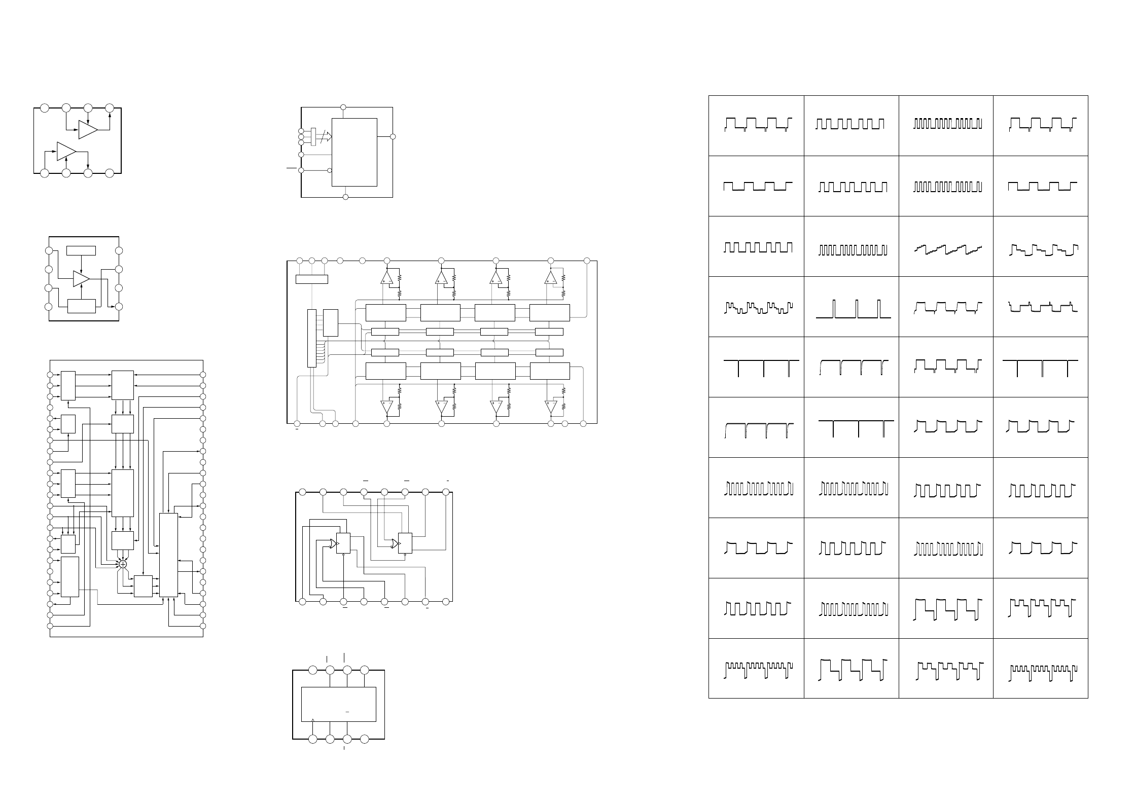
11-11
BVM-D14H1U/D14H5U/D14H1E/D14H5E/D14H1A/D14H5A 11-11
2
3
4
5
1
A BCDEFGH
BB
0.90Vp-p (H) 0.60Vp-p (H) 0.60Vp-p (H)
4
0.90Vp-p (H)
0.55Vp-p (H) 0.55Vp-p (H)
123
56
B BOARD WAVEFORMS
7
0.55Vp-p (H) 0.90Vp-p (H)
0.82Vp-p (H)
8
90
0.85Vp-p (H) 1.3Vp-p (H) 1.5Vp-p (H)
!¡ !™
!£
1.5Vp-p (H) 5.0Vp-p (H) 1.6Vp-p (H)
!¢ !∞ !§
1.4Vp-p (H)
4.2Vp-p (V) 4.0Vp-p (H)
!¶ !• !ª
1.8Vp-p (H) 4.0Vp-p (V)
4.0Vp-p (H)
@º
@¡ @™
4.2Vp-p (V) 0.80Vp-p (H) 0.80Vp-p (H)
@£ @¢
@∞
0.90Vp-p (H) 0.50Vp-p (H) 0.80Vp-p (H)
@§ @¶ @•
0.50Vp-p (H)
1.1Vp-p (H) 0.5Vp-p (H)
@ª #º
0.5Vp-p (H) 1.4Vp-p (H)
#¡ #™
0.65Vp-p (H) 0.70Vp-p (H)
#£ #¢
2.4Vp-p (H) 2.2Vp-p (H)
#∞ #§
2.1Vp-p (H) 4Vp-p (H)
#¶ #•
3.4Vp-p (H) 3.0Vp-p (H)
#ª $º
CXA1211M (IC400, 401)
IN 1
123 4
876 5
VCA 1
VCA 2
CONT 1 OUT 1 GND
Vcc IN 2 CONT 2 OUT 2
CXA1521M (IC306, 307, 308)
IN 1
2
3
4
8
7
6
5
GCA
Vcc
DC CONT
REGULATOR
GND
OUT
GAIN-CONT
DC-CONT
GND
GAIN
CONT
V
EE
148
2
3
4
5
6
7
8
9
10
11
12
13
14
15
16
17
18
19
20
21
22
23
24
CLAMP
SHP
AMP
CLAMP
SHP
AMP
PULSE
GENERATOR
VIDEO
SW
MATRIX
AXIS SW
HUE & COLOR
PROCESS
PIC
GAMMA
CONTROL
AUTOMATIC
CUTOFF
CONTROL
PROCESS
47
46
45
44
43
42
41
39
38
36
35
34
33
32
31
30
28
27
26
25
29
37
40
R-Y HUE
b-Y
Y
GND 1
SH OUT
SH CONT
BRIGHT
SH IN
AXIS
R IN
G IN
B IN
OSD R
OSD G
OSD B
YS
YM
VP
GND 2
HP
MUTE
V BLK
CLP 2
CLP 1
COLOR
PIC
GAMMA
R DRIVE
V
CC
R V
CC
R OUT
R GND
R S/H
R C/O
G V
CC
G OUT
G GND
G S/H
G C/O
G DRIVE
B V
CC
B OUT
B GND
B S/H
B C/O
B DRIVE
IK
CXA1739S (IC1401)
M24C02-MN6T (IC3404)
3
E0
E1
E2
2 k BIT
EEPROM
SDA
WC
SCL
VSS
VCC
1
8
7
2
3
6
5
4
M62399FP-TE2 (IC4351, 4352)
8BIT LATCH
8BIT
UPPER DIGITS
SEGMENT R-2R
8BIT LATCH
8BIT
UPPER DIGITS
SEGMENT R-2R
8BIT LATCH
8BIT
UPPER DIGITS
SEGMENT R-2R
8BIT LATCH
8BIT
UPPER DIGITS
SEGMENT R-2R
8BIT LATCH
8BIT
UPPER DIGITS
SEGMENT R-2R
8BIT LATCH
8BIT
UPPER DIGITS
SEGMENT R-2R
8BIT LATCH
8BIT
UPPER DIGITS
SEGMENT R-2R
8BIT LATCH
8BIT
UPPER DIGITS
SEGMENT R-2R
ADDRESS
DECODER
I C BUS TRANCEAVER
2
CHIP SELECT
19
CS0 CS1 CS2
20
R
1
SCL
2
SDA
3
VREFL
8
A05
4
A06
5
A07
6
A08
7
GND
10
VREFU1
9
18
VDD
17
A04
15
A03
14
A02
13
A01
12
VCC
16
VREFU2
11
6
CLR
7
PR
8
VCC
5
Q
RSQ
3
Q
2
D
4
GND
1
CK
QDC
TC7W74FU (IC2383)
16 15 14 13 12 11 10 9
1 2 3 4 5 6 7 8
1-C 1-CR 1-RD 1-CK 1-CK 1-Q 1-Q GND
VDD 2-C 2-CR 2-RD 2-CK 2-CR 2-Q 2-Q
MC74HC4538AFEL (IC1400)
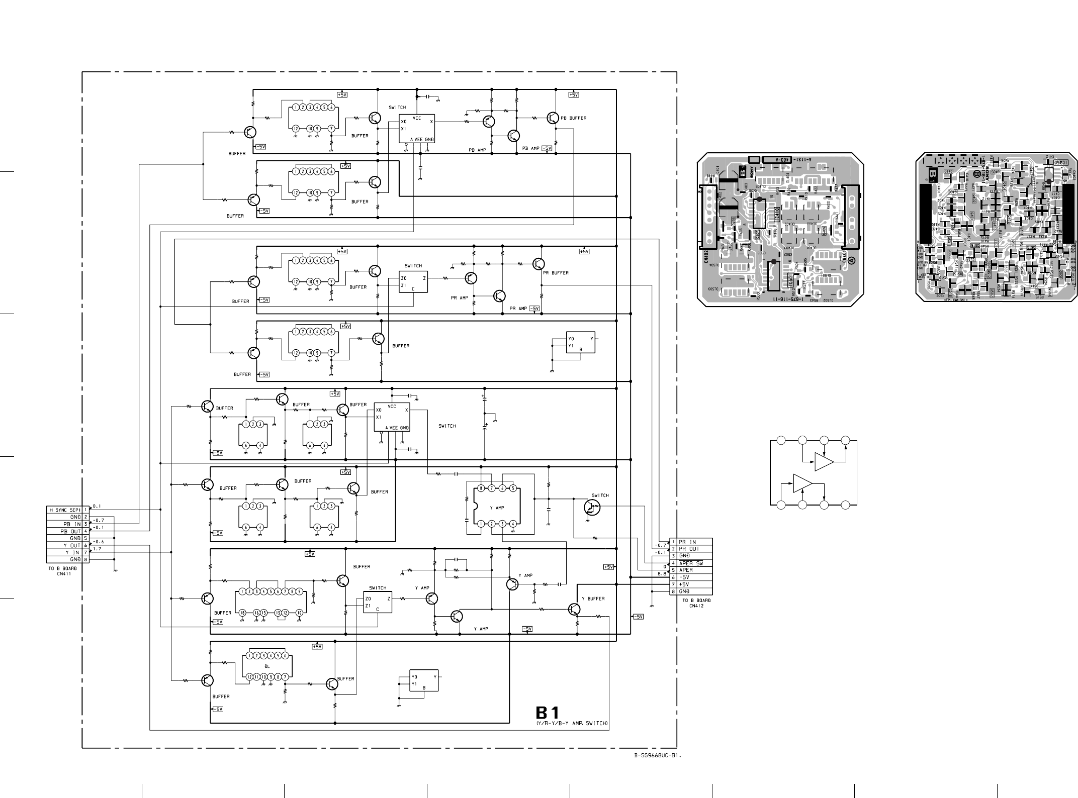
11-12 BVM-D14H1U/D14H5U/D14H1E/D14H5E/D14H1A/D14H5A
11-12
2
3
4
5
ABCDEFGH
1
B1B1
B1 BOARD
B1 –A SIDE–
SUFFIX: -11 B1 –B SIDE–
SUFFIX: -11
CXA1211M (IC450)
IN 1
123 4
876 5
VCA 1
VCA 2
CONT 1 OUT 1 GND
Vcc IN 2 CONT 2 OUT 2
R401
R403
R404
R406
R410
R411
R400
R413
R414
R416
R420 R421
R422
R423
R426
R427
R428
R429
R431
R432
R435
R436
R438
R439
R442
C403
C404
C407
Q400 Q401
Q402
Q403
DL400 DL401
DL404
C401
C402
R412
R415
R424
R425
C502
C503
R501
R502
R504
R503
R505
R506
R507
R508 R510
DL502
R511
R512
R513
R514
R515
R516
R517
R518
R519
R520
R522 DL504
R523
R524
IC501(1/3)
IC501(2/3)
IC410(1/3)
IC410(3/3)
IC410(2/3)
R402
R405
R509
R521
R443
R444
C411
C412
Q410
IC450
C410
Q404
Q411
Q412
Q506
Q505
Q501
Q503
Q502
Q413
Q414
R433
Q408
Q407
Q405
Q406
R407
R408
R417
R418
Q515
R541
Q516
R542
Q517 Q518
R543 R544 R545
R546
R547
R548
Q511
Q512
R531
R532
R533 R534 R535
R536 R537
R538
R409
R419
R430
R440
R441
Q513
Q514
R437
R434
DL403
DL402
DL405
Q409
DL503
DL501
Q504
IC501(3/3)
CN401
CN402
2.2k
:CHIP
100
:CHIP
2.2k
:CHIP
100
:CHIP
100
:CHIP
2.2k
:CHIP
100
:CHIP
100
:CHIP
2.2k
:CHIP
100
:CHIP
100
:CHIP
100
:CHIP
100
:CHIP 100
:CHIP
2.2k
:CHIP
2.2k
:CHIP
100
:CHIP
3.3k
:CHIP
1.2k
:CHIP
4.7k
:CHIP
10k
:CHIP
2.2k
:CHIP
100
:CHIP
0.01
F:CHIP
0.01
F:CHIP
0.1
25V
F:CHIP
2SC2412K 2SC2412K
2SC2412K
2SC2412K
0.01
F:CHIP
0.01
F:CHIP
100
:CHIP
2.2k
:CHIP 100
:CHIP
100
:CHIP
2.2k
:CHIP
100
:CHIP
100
:CHIP
100
:CHIP
2.2k
:CHIP 100
:CHIP 100
:CHIP
2.2k
:CHIP
100
:CHIP
100
:CHIP
470
:RN-CP
470
:RN-CP
1k
:RN-CP
470
:RN-CP
470
:RN-CP
1k
:RN-CP
1k
:CHIP
1k
:CHIP
150
:CHIP
150
:CHIP
1k
:RN-CP
1k
:RN-CP
150
:RN-CP
150
:RN-CP
MC74HC4053FEL
MC74HC4053FEL
MC74HC4053FEL
MC74HC4053FEL
MC74HC4053FEL
1k
:RN-CP
1k
:RN-CP
330
:CHIP
330
:CHIP
47
16V
:HF-CP
47
16V
:HF-CP
12k
:CHIP
0.1
F:CHIP
0.1
F:CHIP
0.01
F:CHIP
CXA1211M
2SA1037
2SC3545
DTC144EK
2SC2412K
2SC3545
2SC2412K
2SC3545
2SA1037K
2SC3545
2SC3545
100
:CHIP
100
:CHIP
2.2k
:CHIP
2.2k
:CHIP
2.2k
:CHIP
2.2k
:CHIP
2SC2412K
2.2k
:CHIP
2SC3545
2.2k
:CHIP
2SC3545
3.3k
:CHIP
6.8k
:CHIP
2.2k
:CHIP
2.2k
:CHIP 100
:CHIP
1.2k
:CHIP
2SC2412K
2SC3545
2.2k
:CHIP
2.2k
:CHIP
3.3k
:CHIP 6.8k
:CHIP
2.2k
:CHIP
2.2k
:CHIP 100
:CHIP
1.2k
:CHIP
2SA1462
2SA1462
2SA1462
2SA1462
2SA1462
2SA1462
47k
:CHIP
33k
:CHIP
100
:CHIP 1k
:CHIP
0
:CHIP
2SA1462
2SC3545
2.2k :CHIP
4.7k :CHIP
2SC3545
2SA1037AK
MC74HC4053FEL
8P
:B-TP-B
8P
:B-TO-B
16
14
6117 8
12
13
5
3
9
4
12
13
67811
16
14
5
3
9
4
2
1
10
15
2
1
10
15
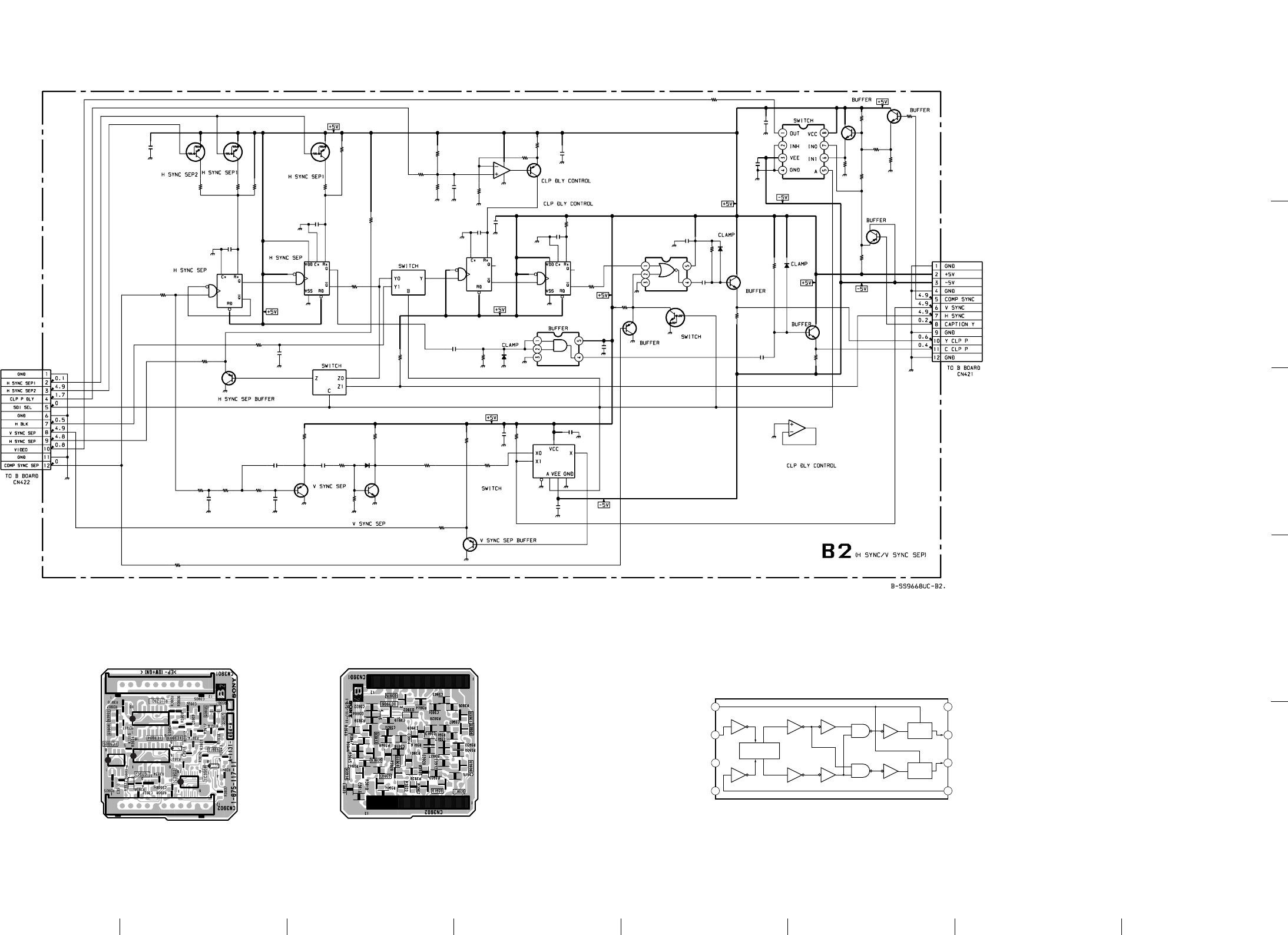
11-13
BVM-D14H1U/D14H5U/D14H1E/D14H5E/D14H1A/D14H5A 11-13
2
3
4
5
1
A BCDEFGH
B2B2
TC4W53FU (IC3908)
1
2
3
4 5
6
7
8
COMMON
INH
VEE CH1
A
CH0
VDD
VSS
LOGIC LEVEL
CONVERTOR
OUT IN
C
OUT IN
C
B2 BOARD
B2 –A SIDE–
SUFFIX: -11 B2 –B SIDE–
SUFFIX: -11
0.0022µH
0.0047µH
C3901
C3903
C3906
C3907
C3908
C3909
C3910
C3912 C3913
C3914
C3915
C3916
C3917
C3918
C3919
C3920
C3921
C3922
C3923
C3924
D3901
D3902
D3903
D3904
Q3901 Q3902
Q3903
Q3905
Q3906
Q3907
Q3908
Q3909
Q3910
Q3911
Q3912
Q3913
IC3902(1/3)
IC3902(2/3)
IC3902(3/3)
IC3905(1/2)
IC3905(2/2
R3901
R3902
R3904
R3905
R3906
R3907
R3908
R3909
R3910
R3912
R3913
R3914
R3915
R3916
R3917
R3918
R3919
R3920
R3922
R3923
R3924
R3925
R3926
R3927
R3928
R3929
R3930
R3931
R3932
R3933
R3934
R3935
R3936
R3937
R3938
R3939
R3940
R3948
IC3901(1/2)
IC3901(2/2)
IC3904(2/2)
IC3904(1/2)
IC3908
IC3907
R3903
C3902
C3904
C3905
CN3902
IC3906
DTA144EKA
82k
:RN-CP
1.2k
:RN-CP
DTA144EKA
1.5k
:RN-CP
9.1k
:RN-CP
2SA1037K
0.01
F:CHIP
220p
CH:CHIP
2SC3326N
0.22
16V
B:CHIP
2SC3326N
220p
CH:CHIP
0.22
16V
B:CHIP
100
:CHIP
1
16V
F:CHIP
2SA1037K
2SC2412K
2SA1037K
2.7k
:CHIP
0.01
F:CHIP
TC74HC4053AFT
0.01
F:CHIP
0.01
F:CHIP
NJM4558M-TE2
0.01
F:CHIP
0.01
F:CHIP
100
:CHIP
0.01
F:CHIP
470p
CH:CHIP
470p
CH:CHIP
2SA1037K
1k
:CHIP
39k
:RN-CP
100k
:RN-CP
18k
:RN-CP
10k
:RN-CP
100k
:CHIP
1SS352
18k
:RN-CP
1SS352
100k
:CHIP
1SS352
10k
:CHIP
10k
:CHIP
2.2k
:RN-CP 2.2k
:RN-CP
2.2k
:CHIP 1k
:CHIP
100
:CHIP
100k
:CHIP
1SS352
4.7k
:CHIP
100p
CH:CHIP
0.01
F:CHIP
0.01
F:CHIP
0.01
F:CHIP
0.01
F:CHIP
1k
:CHIP
1k
:CHIP
TC74HC4053AFT
TC74HC4053AFT
NJM4558M-T
E
100
:CHIP
100
:CHIP
100
:CHIP
100
:CHIP
100
:CHIP
100
:CHIP
DTA144EKA
100k
:RN-CP
120k
:RN-CP
120k
:RN-CP
1k
:RN-CP
270p
CH:CHIP
2SA1037K
DTC144EKA
1k
:CHIP
0
:CHIP
TC74HC4538AF-TP2
TC74HC4538AF-TP2
TC74HC4538AF-TP2
TC74HC4538AF-TP2
TC4W53
F
TC7S02F
3.9k
:RN-CP
B:CHIP
B:CHIP
B:CHIP
12P
BOTB
TC750F
0.001µH
11
12
15 14
10
9
13
5
4
16 1 2
6
7
83
2
1
10
15
11
12
15 14
10
9
13
6
5
87
4
5
4
83
7
6
19 12
3
21
16
6117 8
12
13
14
45
3
9
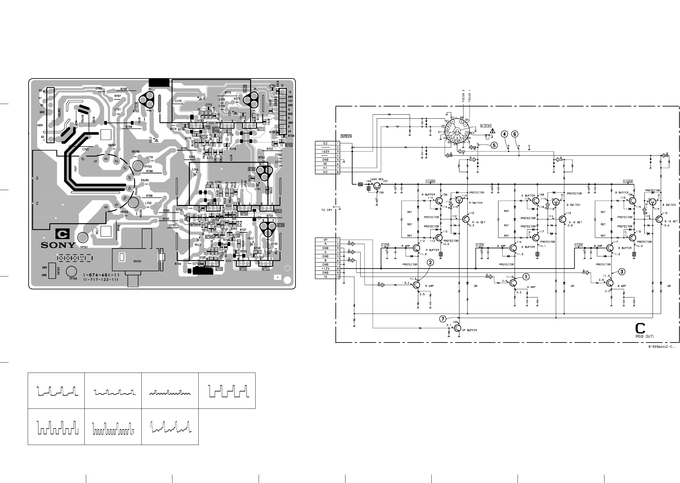
11-14 BVM-D14H1U/D14H5U/D14H1E/D14H5E/D14H1A/D14H5A
11-14
2
3
4
5
ABCDEFGH
1
CC
0.1Vp-p (H) 0.1Vp-p (H) 0.1Vp-p (H)
123
C BOARD WAVEFORMS
C BOARD
C –B SIDE–
SUFFIX: -11
4
56Vp-p (H)
61Vp-p (H)
5
54Vp-p (H)
6 7
55Vp-p (H)
TP701 TP702 TP703 TP700
R734
R737
R740 R754
R757
R774
R777
R780
SG702
Q734 Q774
D736
CN702
Q701
Q730
Q731
Q732
Q733
Q735
Q702
Q750
Q751 Q752
Q753
Q755
Q770
Q771 Q772
Q773
Q775
C702
SG701
R707 C703
J701
R745
SG703 SG704
R765
SG705
R785
R701
R702
C701
C734 C735 C754 C755 C774 C775
D733
D732
D731
D730
D734
D735
D737
D750
D751
D752
D753
D755
D754
D756
D757
D770
D771
D772
D773
D775
D774
D776
D778
D777
D758
D738
C731 C732 C751 C752 C771 C772
C773
C753
C733
R703
R705
R706
R731
R742
R743
R744
R751
R762
R763 R764 R771
R782
R783 R784
R779
R778
R776
R775
R759
R758
R756
R755
R739
R738
R736
R735
R781
R761
R741
R732
R752 R772
L701
RV702
CN701
CN703
C730
C770
R788
RV701
R766
R786
R708
R746
R704
R787
Q754
C704
L730 L750
L770
R733 R753
C750 C777
R773
C778
33
250V
:HT
680p
2kV
B
0.022
1kV
:PP
47
25V
:HT
0.01
50V
F:CHIP
0.01
50V
F:CHIP
33
250V
:HT
0.01
500V
E
47
25V
:HT
0.01
50V
F:CHIP
0.01
50V
F:CHIP
33
250V
:HT
0.01
500V
E
47
25V
:HT
0.01
50V
F:CHIP
0.01
50V
F:CHIP
33
250V
:HT
0.01
500V
E
10P
WHT-L
:S-MICRO
RD22M-T1B3 RD22M-T1B3 RD22M-T1B3
2SD982
2SC1654
2SC3503-E
2SA1381-E
2SC3503-E
2SK520
2SA1330
2SC3503-E 2SA1381-E
2SC3503-E
2SA1330
2SC3503-E 2SA1381-E
2SC3503-E
2SK520
2SA1330
1.5
1/4W
:FPRD
8.2k
1/4W
:FPRD
47
1/10W
:CHIP
10k
1/10W
:CHIP
4.7k
1/10W
:CHIP
100k
1/2W
:RC
100
1/10W
:CHIP
150
1/2W
:RN
2.7k
10W
:RN
47
1/10W
:CHIP
47
1/10W
:CHIP
1k
2W
:RS
33
1/10W
:CHIP
33
1/10W
:CHIP
5MM
39k
1/10W
:CHIP
33k
1/10W
:CHIP
33k
1/10W
:CHIP
220
1/10W
:CHIP
220
1/2W
:RC
100
1/10W
:CHIP
150
1/2W
:RN
2.7k
10W
:RN
47
1/10W
:CHIP
47
1/10W
:CHIP
1k
2W
:RS
33
1/10W
:CHIP
33
1/10W
:CHIP
39k
1/10W
:CHIP
33k
1/10W
:CHIP
33k
1/10W
:CHIP
220
1/10W
:CHIP
220
1/2W
:RC
100
1/10W
:CHIP
150
1/2W
:RN
2.7k
10W
:RN
47
1/10W
:CHIP
47
1/10W
:CHIP
1k
2W
:RS
33
1/10W
:CHIP
33
1/10W
:CHIP
5MM
39k
1/10W
:CHIP
33k
1/10W
:CHIP
33k
1/10W
:CHIP
220
1/10W
:CHIP
220
1/2W
:RC
2SC3950-E 2SC3950-E 2SC3950-E
220p
B
220p
B
8P
:VH
MA111-TX
MA111-TX
MA111-TX
MA111-TX
MA111-TX
MA111-TX
MA111-TX
MA111-TX
MA111-TX
MA111-TX
MA111-TX
MA111-TX
MA111-TX
MA111-TX
MA111-TX
MA111-TX
MA111-TX
MA111-TX
MA111-TX
MA111-TX
MA111-TX
MA111-TX
MA111-TX
MA111-TX
68k 1/2W :RC
110M
2.2M
100
:CHIP
270k
1/2W
:RC
2.2k
1/2W
:RC
2.2k
1/2W
:RC
2.2k
1/2W
:RC
7.5JW
2SK520
0.0047
2kV
:EL0606 :EL0606
:EL0606
22
1/4W
:RN
22
1/4W
:RN
220p
:CH 22p
22
1/4W
:RN
33p
:CH
39µH
3.3µH 3.3µH
3.3µH
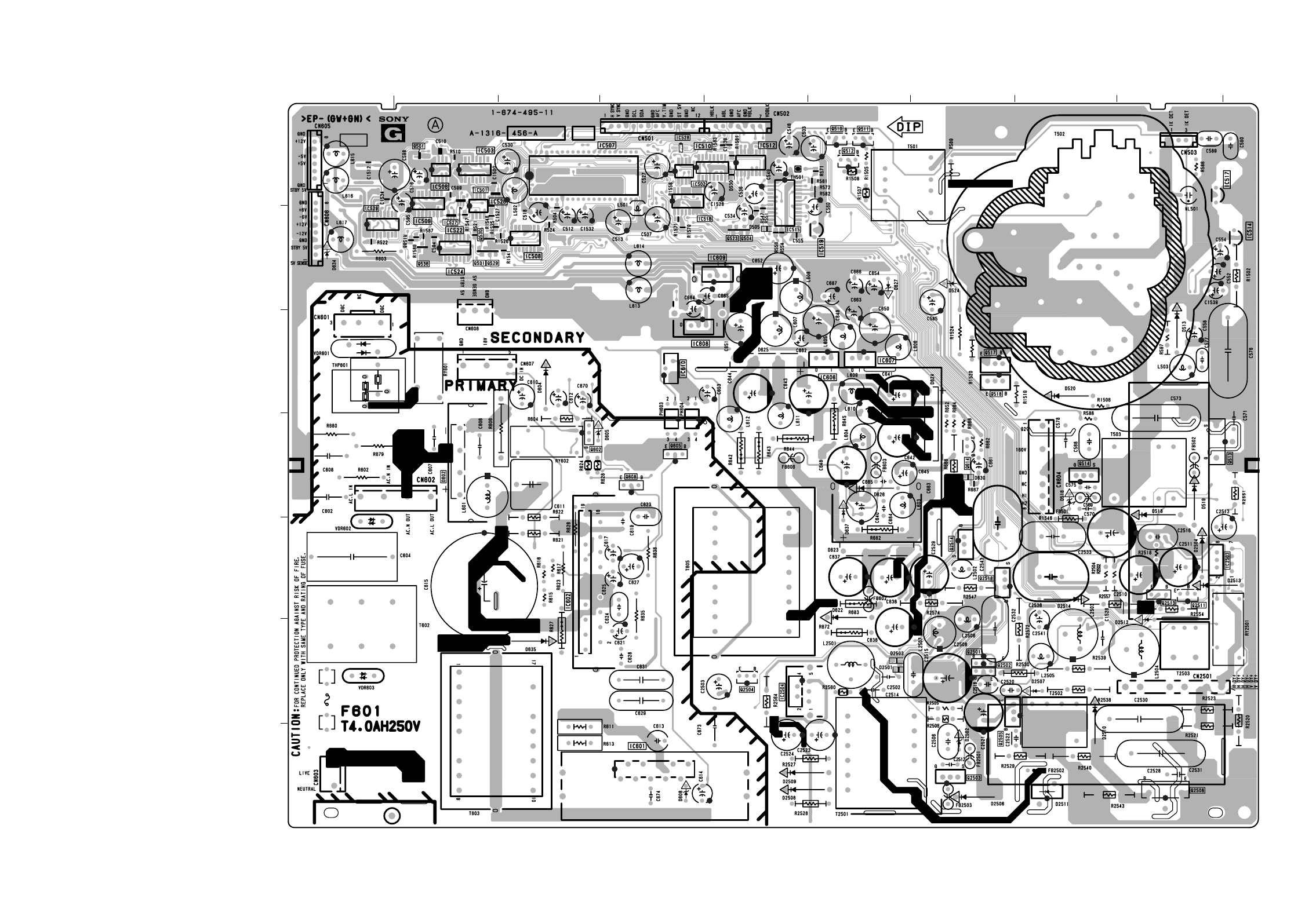
11-15
BVM-D14H1U/D14H5U/D14H1E/D14H5E/D14H1A/D14H5A 11-15
2
3
4
5
1
A BCDEFGH
GG
G BOARD
G –A SIDE–
SUFFIX: -11
[G BOARD]
* : B-SIDE
D2501 F-6
D2502 G-7
D2503 F-6
D2504 J-5
D2506 G-7
D2507 H-6
D2508 E-7
D2509 E-7
D2510 H-7
D2511 H-7
D2512 J-6
D2513 K-5
D2514 H-5
D2515 *E-6
D2520 *J-5
D501 *E-2
D502 *E-2
D503 *E-2
D504 *E-2
D505 E-2
D506 *J-3
D507 *J-2
D508 *J-2
D509 *J-2
D510 *J-2
D511 *J-2
D512 *J-2
D513 J-3
D514 *K-4
D515 *F-1
D516 H-4
D517 *F-2
D518 J-4
D519 J-4
D520 H-3
D524 G-2
D525 *G-3
D529 *C-1
D530 E-1
D531 *C-2
D532 *C-2
D533 *B-2
D534 *D-1
D535 *F-2
D536 *C-1
D537 *F-2
D538 *C-1
D539 *C-2
D540 *B-1
D601 *B-3
D602 B-4
D603 *C-3
D604 C-3
D605 C-4
D607 *C-4
D608 D-7
D609 *D-4
D612 *C-4
D614 *D-5
D617 *D-5
D619 *D-4
D620 *D-4
D622 F-5
D623 F-5
D624 G-4
D625 D-3
D626 F-4
D627 F-2
D633 *C-3
D634 A-2
D635 C-6
D636 *D-5
D637 F-4
D638 *E-2
D639 *F-2
D640 *F-2
IC2501 *F-6
IC2502 *E-6
IC2503 K-5
IC2504 E-6
IC501 B-1
IC502 D-1
IC503 B-1
IC506 B-1
IC507 C-1
IC508 C-2
IC509 B-2
IC510 E-1
IC512 E-1
IC514 K-2
IC515 E-1
IC516 D-1
IC517 K-1
IC519 F-2
IC520 *G-2
IC522 B-1
IC523 *J-2
IC524 B-2
IC526 B-1
IC527 B-2
IC528 D-1
IC529 A-2
IC601 D-7
IC602 C-5
IC606 F-3
IC607 F-3
IC608 D-3
IC609 E-2
IC610 D-3
Q2501 G-6
Q2502 G-6
Q2503 G-7
Q2504 E-6
Q2505 G-6
Q2508 J-7
Q2511 J-5
Q2513 J-5
Q2514 G-5
Q2515 *G-5
Q2518 G-5
Q2519 *G-5
Q501 B-1
Q504 E-2
Q505 *F-1
Q506 *J-4
Q507 *K-4
Q508 *F-1
Q509 *F-1
Q510 F-1
Q511 F-1
Q512 F-1
Q513 K-4
Q514 H-4
Q517 G-3
Q518 G-3
Q520 *C-1
Q521 *D-2
Q523 E-2
Q524 *C-1
Q525 *D-1
Q529 B-2
Q530 B-2
Q531 B-2
Q532 *E-1
Q533 *F-2
Q534 *E-1
Q535 *C-1
Q536 B-2
Q601 *A-2
Q602 C-4
Q603 *C-3
Q604 *C-3
Q605 D-4
Q608 D-4
Q609 *D-4
Q611 *F-2
Q612 *F-2
Q613 *F-2
Q614 G-4
Q615 *D-3
Q616 *F-2
Q617 *F-2
Q618 *D-2
Q619 *A-2
Q620 *F-2
Q621 *F-2
Q622 *E-2
A
1
2
3
4
5
6
7
BCDEF GH JK

11-16 BVM-D14H1U/D14H5U/D14H1E/D14H5E/D14H1A/D14H5A
11-16
2
3
4
5
ABCDEFGH
1
GG
G –B SIDE–
SUFFIX: -11
1
2
3
4
5
6
7
ABCDEFGHJK
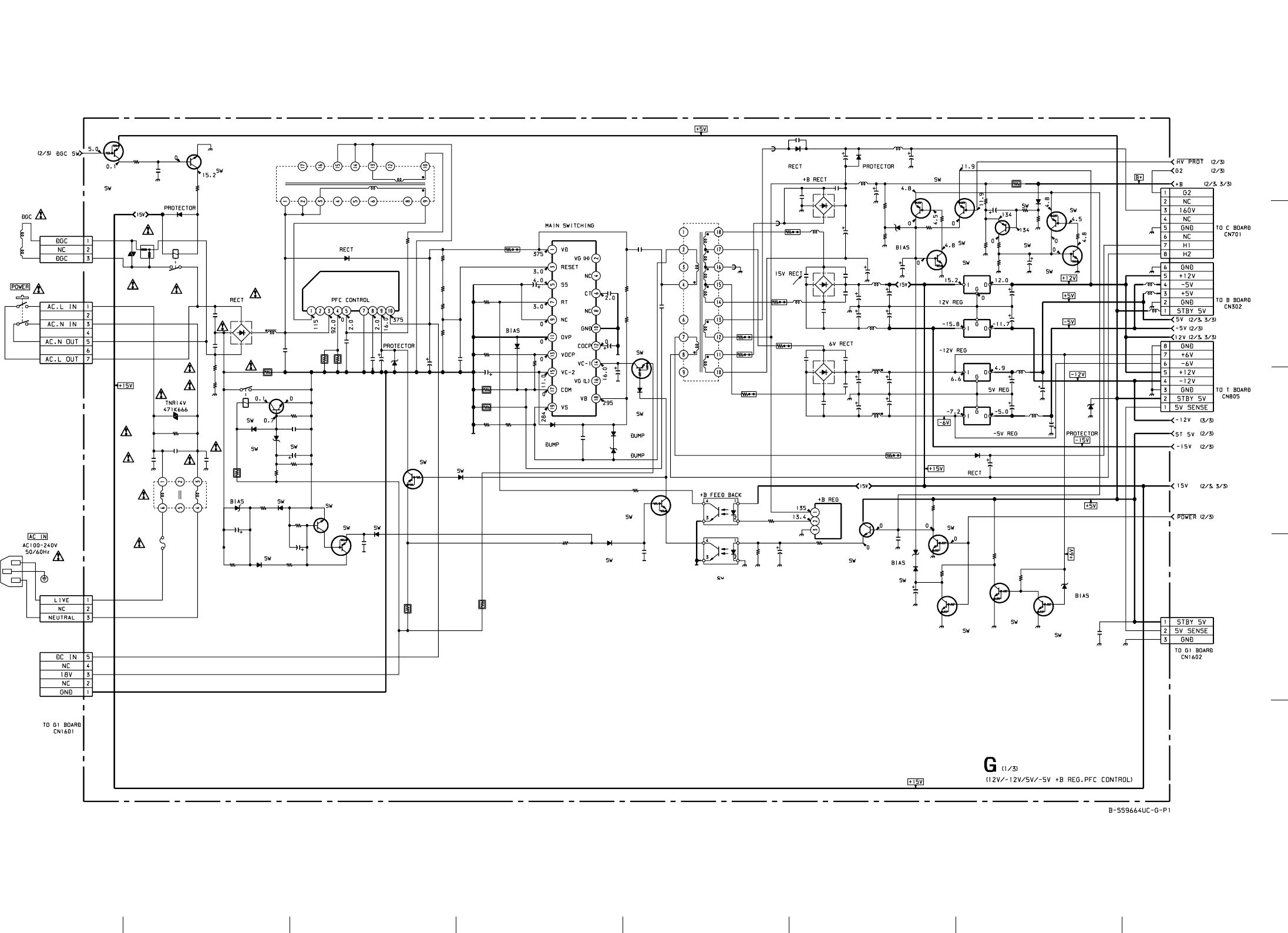
11-17
BVM-D14H1U/D14H5U/D14H1E/D14H5E/D14H1A/D14H5A 11-17
2
3
4
5
1
A BCDEFGH
G (1/3)G (1/3)
R601
CN602
R615
R616
Q614
R620
C616
R623
C610
C641
C642
C644
C645
C662
C663
C664
C665
R626
R631
R635
R636
R641
R651
R654
R659
R666
R667
R669
C603
D602
D604
D608
D609
D619
D620
D622
D624
D625
D626
D630
IC602
IC608
IC609
IC610
PH603
PH604
Q611
Q612
Q616
Q617
R627
R642
R643
R644
R645
C604
C606
C607
C612
C637
C638
C653
C661
L601
L603
L604
L605
L606
Q604
R602
THP601
R606
R652
R664
R662
C667
CN603
Q609
C629
C631
R638
D623
C640
R672 C636
C614
IC607
T602
C611 R611
R613
C609
R608
Q602
C670
R677
R605
R607 R612
R610
D603 D607
C671
D633
R617
R618
D612
D614
Q615
Q603
C669
R668
VDR601
VDR602
R653
R661
R665
Q601
C654 C666
D605
Q605
Q608
CN601
R604 R609
R679
R680
D634
Q619
R678
R657
T605
T603
IC601
D635
C674
R614 Q613
C617
C621
C625
R619
R621
R622
C675
C676
C677
C678
C679
C680
C681
C682
C685
C683
C684
FB603 C648
D636
D617
R682
R683
D637
D640
D639
C687
R685
R686
Q620
Q621
Q622
R684
D638
Q618
R624 R628
RY601
L609
L610
C649
C650
C651
C652
IC606
FB606
C643
CN607
CN608
L613
L614
L615
RY602
C613
D601
C623
R658
R603
CN606
D627
C602
C608
CN604
CN605
L616
L617
C624
C627
L607
L608
F601
D606
C690
C689
C688
C615
FB602
470k
:RN
470k
:RN
10k
:CHIP
10k
:RN-CP
100k
:CHIP
470 :CHIP
1k
:RN-CP
0.1
25V
B:CHIP
1
250V
0.0047
250V
0.0047
250V
100
:HT
10
:HT
0.01
B:CHIP
220
100V
:HR
220
100V
:HR
2200
25V
:HT
2200
25V
:HT
2200
25V
:HT
4.7
200V
:HT
10
:HT
10
:HT
47
25V
:HT
47
25V
:HT
47
25V
:HT
47
25V
:HT
D4SB60L
RGP02-17
RD27ESB2
S2L20UF
D4SBS4
D4SBS4
D1NL40-TA
MCR5102
BA05T
LM2990
SE135
PC123FY2
PC123FY2
DTA114GKA
DTC114GKA
DTA114GKA
2SA1091
DTC114GKA
DTA114GKA
330k
1/2W
:RC 1M
1/2W 1M
1/2W
0.1
1/2W
:RF
1M
1/2W
1M
1/2W
0.1
1/2W
:RF
0.1
1/2W
:RF
0.1
1/2W
:RF
0.1
1/2W
:RF
1k
:CHIP
1k
:CHIP
0.56 3W :RS
10k
:CHIP
1k
:CHIP
0.01
B:CHIP
7P
MA111
MA111
MA111
MA111
3P
WHT
:VH
6.8
10W
:RB
22k
:CHIP
D4SBL20U
2200
25V
:HT
NJM7912FA
470k
:RN
12k
:RN-CP
0.01
B:CHIP
1
400V
47
:HT
0.0047
1kV
:PP
0.0047
1kV
:PP
220
:HT
22
:HT
0.01
B:CHIP
RD30SB MA111
SC802-04
SC311-06
MA111
2SC3311A
DTC114EKA
100k
:CHIP
82k
:CHIP
10k
:CHIP
1k
:CHIP
0.33
2W
:RB
47k
:CHIP
0.33
2W
:RB
330k
:RN
390k
:RN 150k
:RN
0.1
1/2W
:RF
47k
:CHIP
LFT
2SC2412K
2SC2412K
0.01
B:CHIP
47k
:RN-CP
1.2k
:RN-CP
10k
:RN-CP
470k
10
:HT 10
:HT
3P
WHT
:MINI
RD12ESB2
2SC2412K
DTA143ESA
DTA143ESA
150
2W
:RS 4.7k
:CHIP
RD6.2ESB
4.7M
1/2W
:RC
4.7M
1/2W
:RC
DTA144EKA
10k
:CHIP
470
:CHIP
10k
:CHIP
100p
CH
RM11A
MZ1540
DTA114EKA
1.8k
:RN-CP
0.33
2W
:RS
0.33
2W
:RS
10
:HT
4.7
:HT
10
:HT
22
250V
:HT
0.001
B:CHIP
0.001
B:CHIP
0.001
B:CHIP
0.001
B:CHIP
0.001
B:CHIP
0.001
B:CHIP
0.001
B:CHIP
0.001
B:CHIP
0.001
500V
B
0.001
500V
B
0.001 500V B
5MMJW
RD12SB1
DTC144EKA
47
:FPRD
47
:FPRD
1000
25V
:HT
1000
25V
:HT
1000
25V
:HT
1000
25V
:HT
100
10V
SC311-06
DIN20R
RD7.5SB1
MA111
RD3.3SB1
1.1UH
BA12T
DTC144EKA
DTC114EKA
DTC144EKA
0.1
1/2W
:RF
0.1
1/2W
:RF
22k
:CHIP
22k
:CHIP
4.7k
:CHIP
2200
25V
:HT
PFC
5P
WHT
:VH
3P
WHT
:VH
0.68
:MPS
MA111
0.1
100V
:PT
150k
:CHIP
33
1/2W
8P
WHT
:S-MICRO
RD18ESB1
1000pF
250V
E
1000pF
250V
E
8P
:VH
6P
RED
:S-MICRO
8200pF
:PP
:HT
4A
250V
1SS119
470
10V
470
10V
0.01
330
450V
5MMJW
68µH
100µF
1.1µH
1.1µH
22µH
22µH
22µH
22µH
47µH
47µH
47µ
47µ
47µ
47µ
47µ
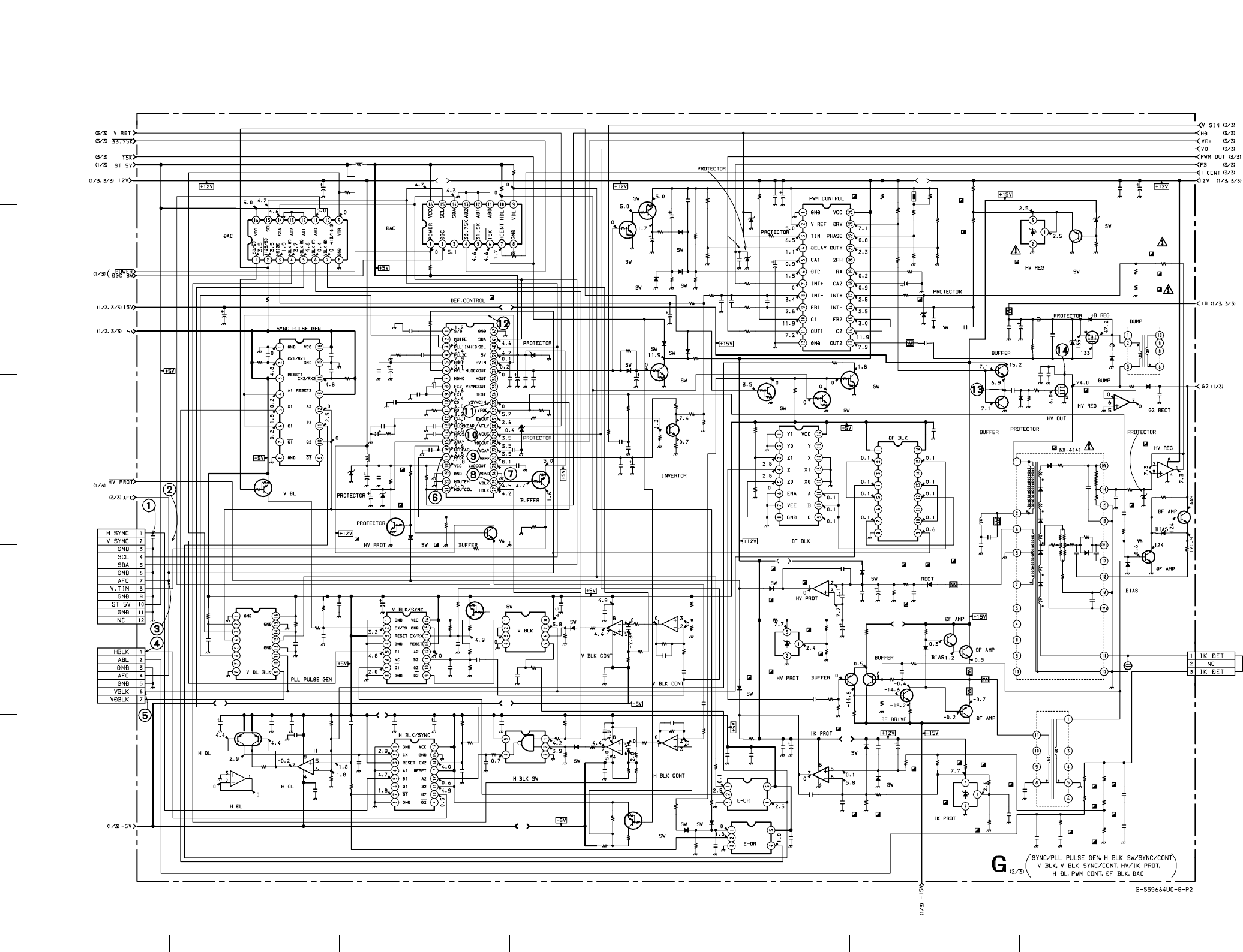
11-18 BVM-D14H1U/D14H5U/D14H1E/D14H5E/D14H1A/D14H5A
11-18
2
3
4
5
ABCDEFGH
1
G (2/3)G (2/3)
R501
R502
C503
C504
C505
C507
R523
R528
IC508
R524
Q501
R505 R511
R517
C520
C536
R540C534
D501 R542 D503 R544
R554
C546
C548
D504
D505
R556
R572
R567
R565
R593
C585
C581
D519
D518
C575
C570
C568 C569
R596
D514
R594
C565
IC516
C528
C531
D506
C555
Q508
R570
R595
R574
R584
R585
Q509 R590
D515
Q510
Q511
Q512
D507
T501
Q518
D528
Q517
D525
TH501 R577
R571
R581
R583
R591 R582
Q507
Q513
R597
D513
C564
D509
C557
C553
R560
R553
C551
R562
C556 C559
R579
C567
D511
D512
R586
C582
D524
R1502
R1506
R1507
R1508
R1512
R1514
R1524
R1525
R1526
C591
C592
C537
C562
C566
C571
C574
C576
C578
C577
C589
C590
L503
Q505
C552
C554
C558
C560
C573
C593
R555
R575
D520
CN501
C518
C530
C527
C513
C519 R515
C514
C508
C515
R512
R518
C529
C1506
R503
R548
R529
R527 R526
C524
C1503
R1505
C512
C517
C521
NL501
Q523
Q521
R547
IC510
IC512
L501
Q506
D517
R1544
Q524
R566
C550
C594
IC524
C596
C599
IC526 C1500
Q525
IC522
Q504
R504
R508
R546
C501
D530
R509
Q529
Q530
Q531
R521
R1545
R1541
R510
C588
C598
FB501
FB502
R588
R1563
D534 R1562
C1519
C1518
R1561
R1559
C1516
C1517
R1555
C1515 IC527
R1554
D533
R1552 C1513
C1512 R1548
R1553
C1511
R1551
C595
C1521 C1522
R1518
R1516
R1517
C1514
Q520
R569
R564
R559
R1567
C1524
R1568
C1508
C549
C1525
T503
C539 R552 C563
C561
R573
C1526
R1534
R1535
R1571
R1573
C1528
C1531
C1530
D529
R1574
D536
C1532
R599
Q533
D537
R1575
R1509
R1576
R1577
D538
D539
D540
C525
R589
R1546
R514
R1578
C1533
C502
R1579
C1534
CN502
R520
R506
R525
C523
R1558
R1560
C1505
R1581
R1580
R1582 C1535 C1536 R1583
C1537
R1584
Q532
R531
R1532
R1533
R1547
R1549 R1550
C1527
R1590
C1538
R550
R1586
R1585
R1587
R1588
C1539
R522
L502
Q535
R1556
IC528
IC529
R1521
R1522
R1523
R1569
R580
R578
R576
IC517
R561
IC514
IC519
IC515
IC507
Q534
IC509
Q536
IC503
CN503
C1507
C547
R1519
D541
C511
C522
R507 R592
R1520
R1515
C587
D535
D502
R551
D532
D531
Q514D516
R519
C509
R549
C1520
C516
C510
R1589
C1541
C538
T502
C526
C1540
R543
R545
C1523
R1557
R1566
R513
R1570
IC523
IC502
IC506
IC501
IC523
IC520
IC520
IC502
IC506
IC501
220
25V
:HT
0.01
F:CHIP
0.01
:PPS-CP
220
25V
:HT
0.001
B:CHIP
0.068
B:CHIP
22
16V
0.01
F:CHIP
47
0.1
25V
F:CHIP
330p 330p
500V
B
0.01
B:CHIP 100
IMT2
2SC2412K
1k
:RN-CP
22k
:RN-CP
33k
:CHIP 6.8k
:CHIP 10k
:CHIP
10k
:CHIP
100 :CHIP
10k
:CHIP
12k
:CHIP
100
:CHIP 15k
:CHIP
22
:CHIP
10
:CHIP
22
:CHIP
27k
:CHIP
1.2k
:CHIP
2.2k
:CHIP
6.8k
:CHIP
1.5k
:CHIP
100k
:CHIP
270
:CHIP
22k
:CHIP
10k
:CHIP
6.8k
:CHIP
10
:CHIP
1k
47
:FPRD
100
3W
:RS
22
:FPRD
22k
:CHIP
10k
1/2W
:RC
2SA1338
10k
:CHIP 27k
:RN-CP
22k
:RN-CP
3.9k
:CHIP
0.01
F:CHIP
47
0.01
B:CHIP
0.01
B:CHIP
0.01
B:CHIP
0.01
B:CHIP
0.01
B:CHIP
0.01
F:CHIP
0.1
25V
B:CHIP
0.01
B:CHIP
0.01
B:CHIP
0.01
F:CHIP
0.01
F:CHIP
RD15SB1
RD12SB1
FE3DL-6488
FE3DL-6488
RD12ESB2
MC14053BF
LM358
2SD774
2SD774
2SB734
470
:RN-CP
10k
:RN-CP
470
:RN-CP
4.7k
:CHIP
10k
:RN-CP
10k
10k
:CHIP
10
1/4W
:FPRD
10k
:CHIP
10k
:CHIP
10k
:CHIP
DFT
3K
0.1
25V
F:CHIP
10
1
10
1
1
16V
B
10p
SL:CHIP
680p
2kV
1
16V
B
1.5
200V
0.0047
2kV
0.01
200V
:PT
0.01
200V
:PT
MA111 MA111
MA111
MA111
MA111
MA111
MA111
MA111
MA111
MA111
MA111
0.0017
1.6kV
:PP
0.01
F:CHIP
0.0047
200V
CXA1875AM
2SK2655
0.047
200V
33
160V
100 :CHIP
91k
:RN-CP
RGP02
LM393PS
LM393PS
10k
:CHIP
0.0047 B:CHIP
10
100
0.0047
B:CHIP
0.01
B:CHIP
0.022
B:CHIP
47
0.01
B:CHIP
0.22
F:CHIP
0.01
B:CHIP 100
0.01
B:CHIP
100
470p
CH:CHIP
0.01
B:CHIP
12P
WHT
:S-MICRO
TL082CPS
2SC4686
2SC4686
2SC2412K
DTC144EK
10k :CHIP
10k
:CHIP
10
:CHIP
10k
:CHIP
470
:CHIP
1k
:CHIP
470
:CHIP
1k :CHIP
22
:FPRD
TC74HC4538AF
CXA1875AM
2SC1037AK
2SC1037AK
2SC3392
RD12SB1
1k
:CHIP
RGP10G
DTC144EKA
10k
:CHIP
0.01
B:CHIP
680
:CHIP
8.2k
:RN-CP
0.001
CH:CHIP
0.01
F:CHIP
0.01
F:CHIP
0.01
F:CHIP
0.01
F:CHIP
TC4530F
MC74HC175FEL
TC4530F
DTA114EKA
DTA144EKA
10k
:CHIP
MA111
DTC144EKA
DTC144EKA
DTC144EKA
10k
:CHIP
2.7k
:CHIP
10k
:CHIP
470k
:CHIP
0.01
F:CHIP
1000
10V
:HT 12k
RN:CHIP
1.1UH
1.1UH100
1/4W
:FPRD
1k
:CHIP
470
10V
:HT
22k
:RN-CP
1k
:CHIP
0.1
25V
B:CHIP
0.01
F:CHIP
0.01
F:CHIP
0.01 F:CHIP
10p
CH:CHIP
0.1
25V
B:CHIP
0.01
F:CHIP
0.01
F:CHIP
0.01
F:CHIP
0.047
25V
B:CHIP
1
16V
B:CHIP
MA111
MA111
TS082CPS
TS082CPS
TC4S11F
DTC114EK
4.7k
:RN-CP
4.7k
:RN-CP
8.2k
:RN-CP
1k
:CHIP
47k
:CHIP
4.7k
:CHIP
1k
:CHIP
2.2k
:CHIP
1k
:CHIP
68k
:RN-CP
1k
:CHIP
47k
:CHIP
0.47
16V
B:CHIP
10
HRT
0.015
25V
B:CHIP
47k
:CHIP
0.022
25V
B:CHIP
220p
B:CHIP
220k
:CHIP
120k
:RN-CP
0.47
B:CHIP
0.01
B:CHIP
0.001
B:CHIP
470
6.3V
:HT
470p
B:CHIP
470p
B:CHIP
10k
:CHIP
56k
:RN-CP
100k
:CHIP
47k
:CHIP
100k
:CHIP
1M
:CHIP
MA111
4.7k
:CHIP
47
16V
MA111
RD10SB1
2SA1037K
10k
:RN-CP
10k
:CHIP
5.6k
:CHIP
100
:RN-CP
5.1k
:RN-CP
0.22
B:CHIP
2M
1W
:RN
0.01
B:CHIP
RD13SB2
RD13SB2
10k
:CHIP
0.47
1/4W
:FPRD
68k
:CHIP
7P
WHT
:S-MICRO
0.01
B:CHIP
TL082CPS
TL082CPS
56k
:RN-CP
100p
CH:CHIP
15k
:CHIP
22k
:CHIP
15k
:CHIP
820p
CH:CHIP
RD6.8ESB2
1M
:RN-CP
56k
:RN-CP
0.022
:PPS-CP 3.3k
:CHIP
27k
:RN-CP
10k
:CHIP 0.1
25V
B:CHIP 0.001
B:CHIP 100k
:CHIP
0.01
B:CHIP
15k
:RN-CP
DTA144EKA
220k
:CHIP
15k
:RN-CP
8.2k
:RN-CP 4.7k
:RN-CP
33k
:RN-CP 33k
:RN-CP
10p
CH:CHIP
100k
:RN-CP
0.001
B:CHIP
100 :CHIP
10k
:RN-CP
56k
:RN-CP
33k
:RN-CP
47k
:RN-CP
10
10k
:CHIP
2SC2412K
10k
:RN-CP
TC7W00F
TC74HC4538
4.7k
:RN-CP
4.7k
:RN-CP
5.6k
:RN-CP
5.6k
:RN-CP
3.3k
:RN-CP
10k
:RN-CP
3.3k
:RN-CP
10k
:RN-CP
CXA1544M
LM358
TDA9106
DTA144EKA
TC74HC4538AF
DTA144EKA
TC74HC4538AF
3P
WHT
:S-MICRO
0.01 B:CHIP
0.0022
B:CHIP
2M 1W :RN
RD6.8ESB2
0.01
B:CHIP
1
16V
F:CHIP
10k :CHIP 1k :CHIP
10M 1W :RN
68k :CHIP
1 16V B
MA111
MA111
1k :CHIP
TL082CPS
MA111
MA111
IRFI9630GSRD9.1ESB2
9.1k
:RN-CP
0.001
CH:CHIP
4.7k
:CHIP
0.001
CH:CHIP
0.47
2.2
16V
F:CHIP
100k
:RN-CP
4.7 50V
0.0015
FBT
0.47
B:CHIP
10/50V
33k
:CHIP
27k
:RN-CP
0.47
B:CHIP
100k
:RN-CP
22k
:CHIP
1k :CHIP
33k
:CHIP
12V
12V 12V
5V
15V
15V
-5V
12V
-5V-5V
47µ
100µ
µPC1093J
µPC1093J
µPC1093J
10µ
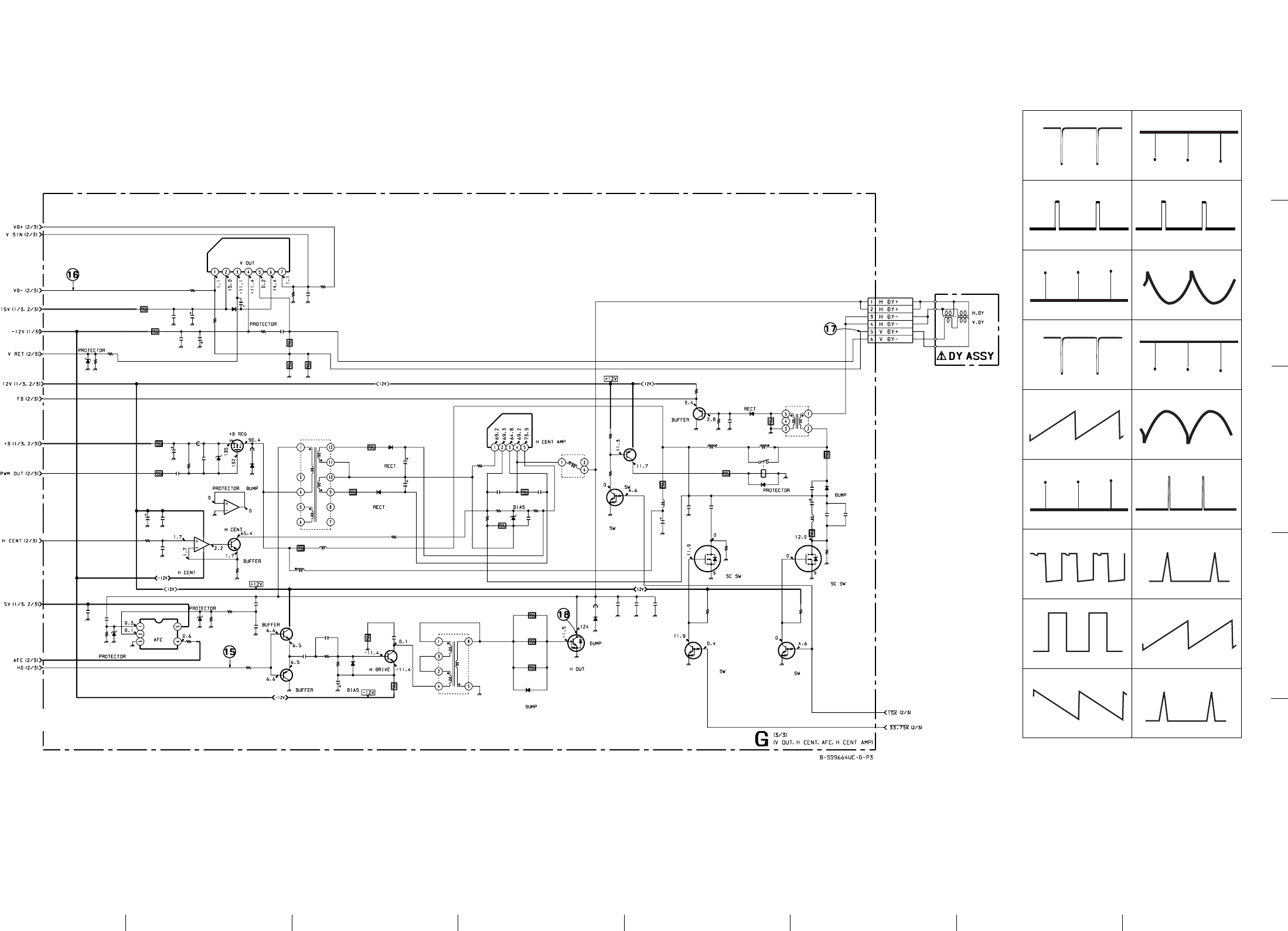
11-19
BVM-D14H1U/D14H5U/D14H1E/D14H5E/D14H1A/D14H5A 11-19
2
3
4
5
1
A BCDEFGH
G (3/3)G (3/3)
4.0Vp-p (H) 4.0Vp-p (V)
4.7Vp-p (H)
4
4.9Vp-p (H)
4.9Vp-p (V) 1.5Vp-p (H)
1 2
3
56
G BOARD WAVEFORMS
4.8Vp-p (H)
7
5.0Vp-p (V)
8
2.8Vp-p (V)
9
1.4Vp-p (V)
0
4.9Vp-p (V)
!¡
4.9Vp-p (H)
!™
1.2Vp-p (H)
!£
500Vp-p (H)
!¢
10Vp-p (H)
!∞
2.8Vp-p (V)
!§
1.3Vp-p (V)
!¶
940Vp-p (H)
!•
T2503
R2502 C2507 C2510
C2511
R2524
C2512
Q2503
C2503
Q2501
Q2502
T2501
T2502
Q2512
Q2511
Q2513
Q2515 Q2519
CN2501
L2503 L2504
RY2501
Q2518
Q2514
C2505
C2509
C2515
C2518
C2520
C2521
C2523
C2524
R2503
R2504
R2505
R2506
R2517
R2518 R2520
R2526
R2527
R2528
R2529
R2530
R2545
R2546
R2548
R2549
R2550
R2556
R2557
IC2503
D2507
D2512
C2501
IC2501
C2502
C2504
C2506
C2508
C2514
C2516
C2519
C2531
D2506
D2508
D2509
D2510
D2514
FB2502
Q2505
IC2502(1/2)
Q2504
R2519
R2531
IC2504
R2559
R2560
R2561
R2562 R2563
C2538
C2539
R2521 R2523
R2565
R2501
R2513
L2501
R2570
R2571
C2537
R2510
R2552
R2558
R2512
R2525
R2547
C2534
R2538
R2539
R2540
L2507
FB2503
FB2501
C2529
L2502
D2511
Q2508
R2509
R2514
R2522
R2554
R2551
C2541
R2572
R2574
C2528 C2530
L2505
L2506
D2502
C2532 C2533
C2536 C2543
D2501
D2503
D2520
IC2502(2/2)
D2515
C2544
D2504
D2513
C2522
R2564
C2513
0.0015
630V
:PP
100
0.01
B:CHIP
0.01
B:CHIP
0.01
B:CHIP
1000
1000
330p
0.47
:MPS
0.015
:MPS
1000
:HT
1000
16V
1000
16V
1SS119
1SS119
2SC3311A
DTC144EKA
2SA1309A
DTC144EKA DTC144EKA
10k
:RN-CP
100
:CHIP
2.2k
:CHIP
270
2W
:RS
39
2W
:RS
10k
:CHIP
10k
:CHIP
10k
:CHIP
10k
:CHIP
100k
:CHIP
10k
:CHIP 10k
:CHIP
150
3W
:RS
0.01
B:CHIP
HLC HLC
2SA1309
IRFI9630
2SA1221
1.5
1/4W
:FPRD
1.5
1/4W
:FPRD
0.47
1/4W
:FPRD
1.5
0.47
1/2W
:FPRD
0.47
1/2W
:FPRD
1.5
1/2W
:FPRD
HOT
HDT
100p
2kV
B
0.1
25V
B:CHIP
33
160V
100p
2kV
0.1
100V
:PT
330p
2kV
6P
WHT
:VH
ERD38-06
FE3DL-6488
FE3DL-6488
RH-1AV1
ERA91-02
JW
2SC3746
0.047
200V
:PT
0.022
B:CHIP
TC4S71F
22
1/2W
:FPRD
10k
:CHIP
22k
:CHIP
2.2
2W
:RS
2.2
2W
:RS
330
:CHIP
6.8k
:CHIP
0.1
B:CHIP
1
16V
F:CHIP
NJM4558M
LA6500
HCC
2SC2362KG
2SK2350
2SK2350
4.7k
:CHIP
10
:FPRD
1.5k
:CHIP
22k
:CHIP 2.2k
:CHIP
100
:CHIP
15k
:CHIP
4.7k
:CHIP
0.047
B:CHIP
2.7k
:CHIP
0.01
B:CHIP
22
3W
:RS
22
3W
:RS
22
3W
:RS
10k
:CHIP
47
:CHIP
39
2W
:RS
100k
:CHIP 100k
:CHIP
1mH
1.1UH 1.1UH
22
250V
:HT
:EL0606
DD54SCLS
10k
:CHIP
4.7k
:CHIP
100
2W
:RS
10
3W
:RS
1
250V
:HT
4.7k
:CHIP
68
1W
:RS
33
3W
:RS
TDA8172
2SC5450-CA
0.0017
1.6kV
:PP
2.2mH
:EL0606
4.7mmH
RD9.1ESB2
0.0017
1.6kV
:PP
0.68
250V
:PP 0.82
250V
:PP 3.3
250V
:PP
3.3
250V
:PP
RD5.6SB2
RD5.6SB2
RD6.8SB
NJM4558M
RD5.6SB2
0.001
2kV
GP08D
GP08D
0.0022
200V
:PT
1
2W
:RS
100
470µH
6
57
3
21
8
4
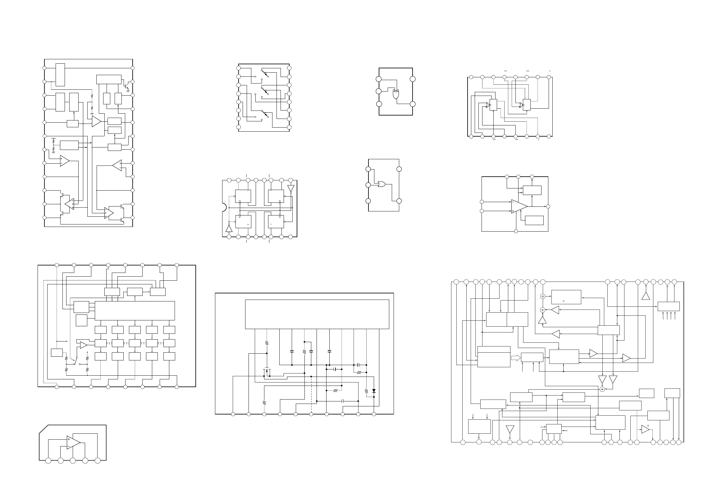
11-20 BVM-D14H1U/D14H5U/D14H1E/D14H5E/D14H1A/D14H5A
11-20
2
3
4
5
ABCDEFGH
1
GG
CXA1544M (IC515)
1
2
V
REF
3
4
5
6
7
8
9
10
11
12
DELAY GEN
COMP EDGE DETECT
(SELECT)
AGC
OUTPUT START
START (V
CC
> 9V)
STOP (V
CC
<
6V)
GND
V
CC
GEN
24
23
22
21
20
19
18
17
16
15
14
13
PHASE
CONT
DUTY
CONT
AGC
WIND
COMPARATOR
V
REF
T IN
DELAY ADJ
CAGC 1
DTC
IN 1(+)
IN 1(-)
FB 1
CORRECTOR 1
OUT 1
P. GND
DRIVE OUT
PHASE ADJ
DUTY ADJ
RAGC
RAGC 2
IN 2(+)
IN 2(-)
FB 2
CORRECTOR 2
OUT 2
V
CC
CXA1875AM (IC508, 512)
LA6500 (IC2504)
2 4 51 3
+–
V
EE
OUT V
CC
MC14053BF (IC516)
1
2
3
4
5
6
7
8
B1
B0
C.COM
CO
INH
VEE
VSS
VDD
B.COM
A.COM
A1
A0
A
B
C
C1
9
10
11
12
13
14
15
16
OPEN
OPEN
OPEN
MC74HC175FEL (IC524)
9
10
111213
141516
87654321
QQ
D
CKCLR
QQ
DCK
CLR
QQ
D
CK
CLR
Q
Q
D
CK
CLR
VCC
4Q1Q
1Q
1D
2D
2Q
2Q
GND
CLEAR
4Q
4D
3D
3Q
3Q
CLOCK
MZ1540 (IC601)
10987654321
1110987654321
CathodeComparator
Output VccGNDDrainDrain Gate Input
Voltage
Sensing
Source Zero
Current
Sensing
TC4S30F (IC522, 526)
GND
V
DD
1
2
3
5
4
TC4S71F (IC2501)
1
2
3
5
4
VDDIN B
IN A
VSS OUT X
TC74HC4538/4538AF
(IC503, 509, 510, 529)
16 15 14 13 12 11 10 9
1 2 3 4 5 6 7 8
1-C 1-CR 1-RD 1-CK 1-CK 1-Q 1-Q GND
VDD 2-C 2-CR 2-RD 2-CK 2-CR 2-Q 2-Q
TDA8172 (IC2503)
VCC
2
OUTPUT
STAGE
SUPPLY
6FLYBAK GEN
3
FLYBAK
GENERATOR
POWER
AMPLIFIER OUTPUT
5
TERMINAL
PROTECTION
GND
4
INVERTING IN 1
NON INVERT IN 7
TDA9106 (IC507)
7 BITS
6 BITS
VPOS
7 BITS VAMP
7 BITS
6 BITS6 BITS
2
X
SPIN BAL
6 BITS
KEY BAL
6 BITS
H-FLY
VREF SAFE FREQ.
2 BITS
AMP&KEYST
10
8 9 11 1312 14
1764
235
X
X
LOCK/UNLOCK
IDENTIFICATION
PHASE
COMPARATOR
VCC
SYNC INPUT
SELECT
(2 BITS)
SYNC
PROCESSOR
RESET GENERATOR
IC INTERFACE
2
PHASE/FREQUENCY
COMPARATOR
H-PHASE(7 BITS)
H-SAWTOOTH
GENERATOR
H-DUTY
(5 BITS)
SAFETY
PROCESSOR
HOUT
BUFFER
BLANKING
GENERATOR
CORNER
CORRECTION
(2 6 BITS)
PHASE
SHIFTER
16 17 18 2019 2115
23
42 41 40 39 38 37 36 35 34 33 32 31 30 29 28 27 26 25 24 22
VREF
S AND C
CORRECTION
GEOMETRY
TRACKING
2
X
2
X
VERTICAL
OSCILLATOR
RAMP GENERATOR
2
X
MOIRE
PROCESSOR
(5 BITS)
VSYNC
FREE RUNNING
5 BITS
2
X
VFLY
VSYNC
HFLY
LOCK
S/G
MOIRE
PLL1INHIB
PLL2C
HREF
HFLY
HGND
FC2
FC1
C0
R0
PLL1F
HLOCKCAP
HPOS
XRAY
HFOCUSCAP
HFOCUS
VCC
GND
HOUTEM
HOUTCOL
GND
SDA
SCL
5V
H/HVIN
HLOCKOUT
HOUT
VSYNCOUT
TEST
VSYNCIN
VFOCUS
EWOUT
VFLY
VOUT
VDCOUT
VCAP
VREF
VAGCCAP
VGND
VBLKOUT
HBLKOUT
2 5 BITS
LATCH
DAC
AMP
LATCH
DAC
AMP
LATCH
DAC
AMP
LATCH
DAC
AMP
LATCH
DAC
AMP
+
–
VCC
REG
I2C DECODER
LEVEL
CONVERTER
LEVEL
CONVERTER LEVEL
CONVERTER
LATCH
POWER
ON
RESET
OPEN COLLECTOR
3 6
25 81 4 7
SW1
SW0
DAC4
DAC3
DAC2
DAC1
DAC0
GND
14 11
15 12 916 13 10
VCC
SCL
SDA
SAD2
SAD1
SAD0
SW3
SW2
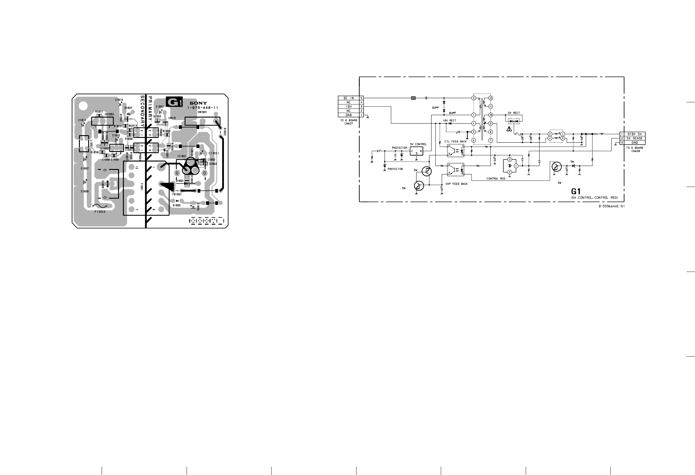
11-21
BVM-D14H1U/D14H5U/D14H1E/D14H5E/D14H1A/D14H5A 11-21
2
3
4
5
1
A BCDEFGH
G1G1
G1 BOARD
G1 –B SIDE–
SUFFIX: -11
PH601
PH602
R1601
R1603
R1605
R1606
R1608
R1609
R1610 R1611
R1612
R1613
C1601 C1602
C1603
C1604
C1605
C1606
C1607 C1608
C1609
C1610
C1611
Q1601
Q1602
Q1603
IC1601
IC1602
T1601
D1601
D1602
D1606
D1607
R1602
F1603
D1603
CN1601
CN1602
L1601
D1605
D1604
FB1601
R1607
L1602
R1604
47
25V
:HT
4700
10V
:HT
0.01
B:CHIP
4700
10V
:HT
47
:CHIP 10k
:CHIP
2.2k
:CHIP
1k
:CHIP 0.1
25V
B:CHIP
1k
:CHIP
220
:HT 10
:CHIP
4.7k
:RN-CP
4.7k
:RN-CP
2.2k
:RN-CP
10k
:RN-CP
10
:HT
2200
10V
:HT
10
:HT
0.1
25V
B:CHIP
RD6.8ESB2
RD6.8SB2
SC311-06 D10SC9M
RD5.1ESB3
TOP224Y-BB
PC123FY2
PC123FY2
DTA114GKA
DTC114GKA
DTC114GKA
3.3
:FPRD
SRT
5P
WHT
:VH
100
10V
3P
WHT-L
:VH
5A
125V
COIL
D1NL20U
P6KE170
270
:CHIP
22
:CHIP
47 H
µ
µPC1093J-T
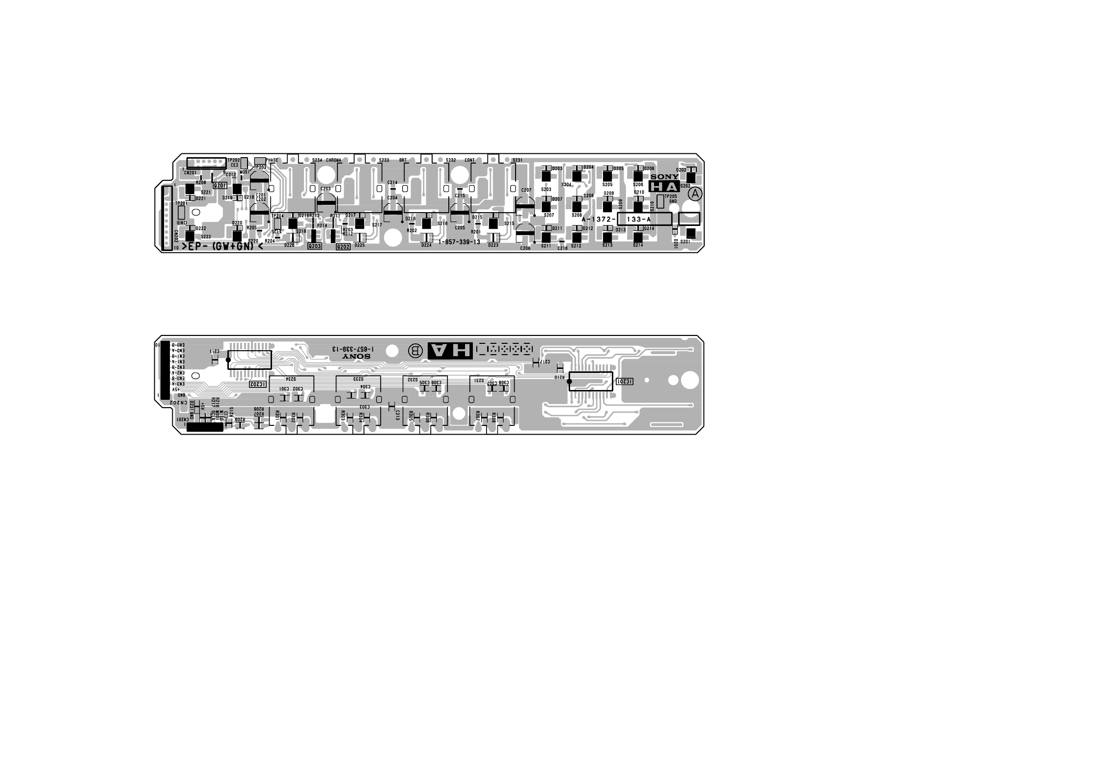
11-22 BVM-D14H1U/D14H5U/D14H1E/D14H5E/D14H1A/D14H5A
11-22
2
3
4
5
ABCDEFGH
1
HAHA
HA BOARD
HA –A SIDE–
SUFFIX: -13
HA –B SIDE–
SUFFIX: -13
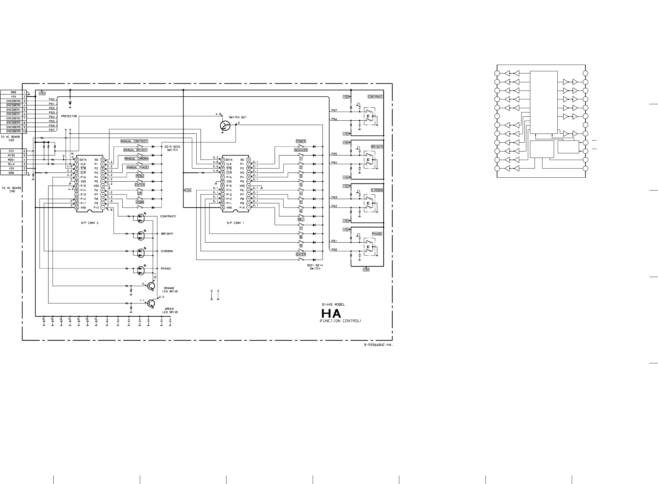
11-23
BVM-D14H1U/D14H5U/D14H1E/D14H5E/D14H1A/D14H5A 11-23
2
3
4
5
1
A BCDEFGH
HAHA
NJU3716M (IC201, 202)
P7
P8
P9
P10
P11
Vss
P12
P13
P14
P15
P16
SO
V
DD
P6
P5
P4
P3
P2
P1
CLR
STB
CLK
DATA
1
2
3
4
5
6
7
8
9
10
11
12
24
23
22
21
20
19
18
17
16
15
14
13
LATCH
SHIFT
REGISTER CONTROL
C201 C202 C203 C204 C205 C206 C207 C211 C212 C213 C214 C215 C216
C217
S232
S233
S234
C308
C307
C306
C305
C304
C303
C302
C301
IC201IC202
S231
R205
R204
R210
R211
R212
R213
R214
R215
R301
R302
R303
R304
R305
R306
R307
R308
D201
D202
D203
D204
D205
D206
D207
D208
D209
D210
D211
D212
D213
D214
D215
D217
D218
D219
D220
D221
D222
S201
S202
S203
S204
S205
S206
S207
S208
S209
S210
S211
S212
S213
S214
S215
S216
S217
S218
S219
S220
S221
S222
TP201 TP205
TP203TP202
D216
D223
D224
D225
D226
Q202
Q203
R203
R202
R216 R208
R207
TP204
CN201
CN202
D231 Q201
R209
R217
R206
R201
CL-155Y/PG
CL-155Y/PG
CL-155Y/PG
CL-155Y/PG
6.3V 6.3V 6.3V 6.3V 6.3V 6.3V 6.3V
0.01
F:CHIP 0.01
F:CHIP 0.01
F:CHIP 0.01
F:CHIP 0.01
F:CHIP 0.01
F:CHIP
0.01
F:CHIP
0.01
F:CHIP
0.01
F:CHIP
0.01
F:CHIP
0.01
F:CHIP
0.01
F:CHIP
0.01
F:CHIP
0.01
F:CHIP
0.01
F:CHIP
MA111
MA111
MA111
MA111
MA111
MA111
MA111
MA111
MA111
MA111
MA111
MA111
MA111
MA111
MA111
MA111
MA111
MA111
MA111
MA111
MA111
MA111
NJU3716MNJU3716M
2SD1834
2SD1834
560
:CHIP
560
:CHIP
560
:CHIP
100k
:CHIP
1k
:CHIP
4.7k
:CHIP
100k
:CHIP
33k
:CHIP
82k
:CHIP
33k
:CHIP
82k
:CHIP
47k
:CHIP
47k
:CHIP
4.7k
:CHIP
4.7k
:CHIP
4.7k
:CHIP
4.7k
:CHIP
4.7k
:CHIP
4.7k
:CHIP
4.7k
:CHIP
4.7k
:CHIP
6P
WHT
:S-MICRO
10P
WHT
:S-MICRO
RD6.2SB DTC144EKA
1k :CHIP
47k :CHIP
1k :CHIP
560 :CHIP
100µF
100µF 100µF 100µF 100µF 100µF 100µF
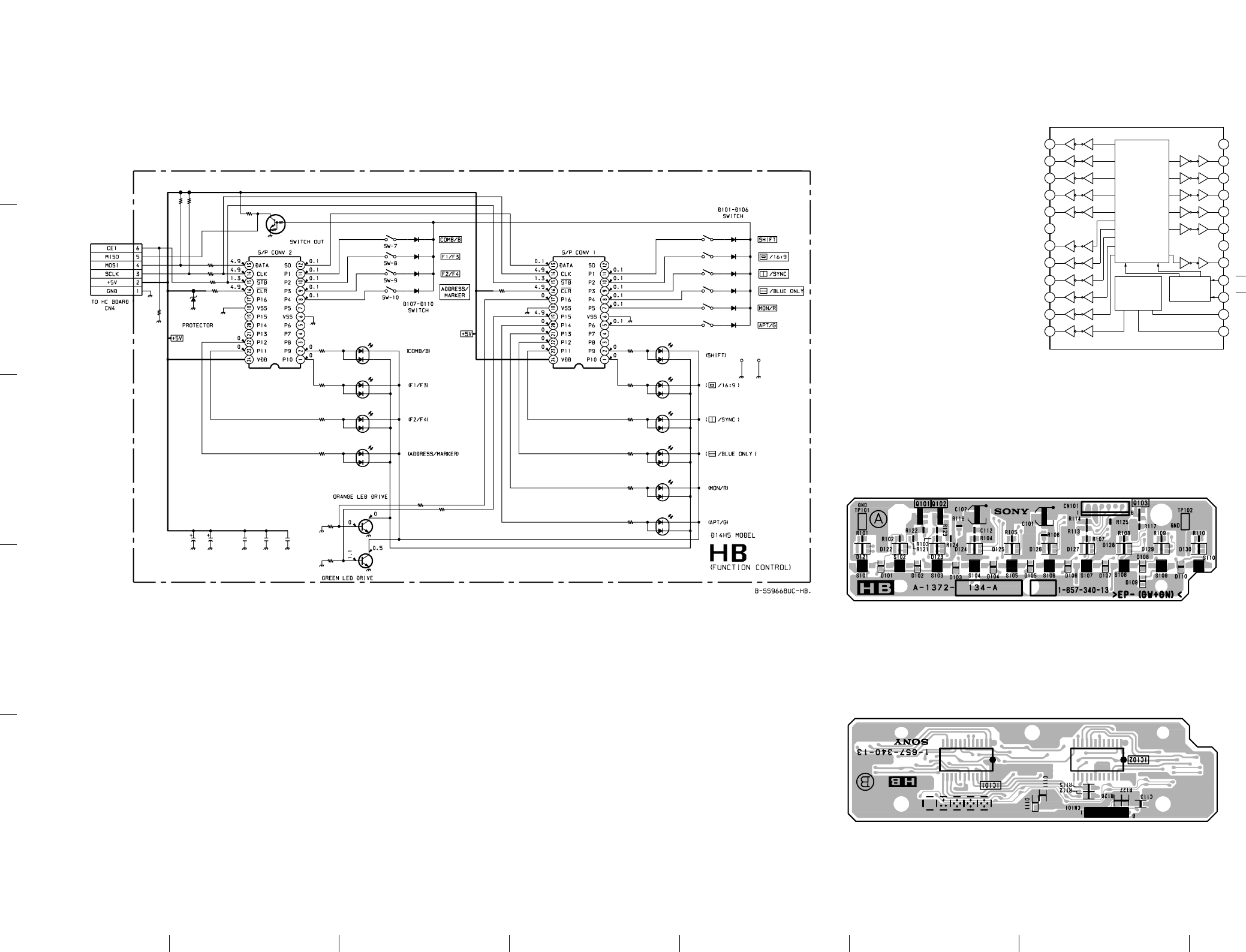
11-24 BVM-D14H1U/D14H5U/D14H1E/D14H5E/D14H1A/D14H5A
11-24
2
3
4
5
ABCDEFGH
1
HBHB
NJU3716M (IC101, 102)
P7
P8
P9
P10
P11
Vss
P12
P13
P14
P15
P16
SO
V
DD
P6
P5
P4
P3
P2
P1
CLR
STB
CLK
DATA
1
2
3
4
5
6
7
8
9
10
11
12
24
23
22
21
20
19
18
17
16
15
14
13
LATCH
SHIFT
REGISTER CONTROL
HB –A SIDE–
SUFFIX: -13
HB –B SIDE–
SUFFIX: -13
HB BOARD
R125
R126
R127
D121
D122
D123
D124
D125
D126
D107
D108
D109
D110
D101
D102
D103
D104
D105
D106
R101
R102
R103
R104
R105
R106
R107
R108
R109
R110
R112
R113
R114
R115
R116
R117
R121
R122 R123
R124
S101
S102
S103
S104
S105
S106
S107
S108
S109
S110
TP101 TP102
C111 C112 C113
Q101
Q102
D127
D128
D130
D129
C101 C102
IC101IC102
CN101
Q103
D111
0.01
F:CHIP 0.01
F:CHIP 0.01
F:CHIP
MA111
MA111
MA111
MA111
MA111
MA111
MA111
MA111
MA111
MA111
CL-155Y/PG
CL-155Y/PG
CL-155Y/PG
CL-155Y/PG
CL-155Y/PG
CL-155Y/PG
CL-155Y/PG
CL-155Y/PG
CL-155Y/PG
CL-155Y/PG
NJU3716MNJU3716M
2SD1834
2SD1834
560
:CHIP
560
:CHIP
560
:CHIP
560
:CHIP
560
:CHIP
560
:CHIP
560
:CHIP
560
:CHIP
560
:CHIP
560
:CHIP
100k
:CHIP
1k :CHIP
1k :CHIP
1k
:CHIP
100k :CHIP
4.7k
:CHIP
33k
:CHIP
82k
:CHIP 33k :CHIP
82k
:CHIP
47k
:CHIP
47k
:CHIP
47k
:CHIP
6P
RED
:S-MICRO DTC144EKA
RD6.2SB
47µF 47µF
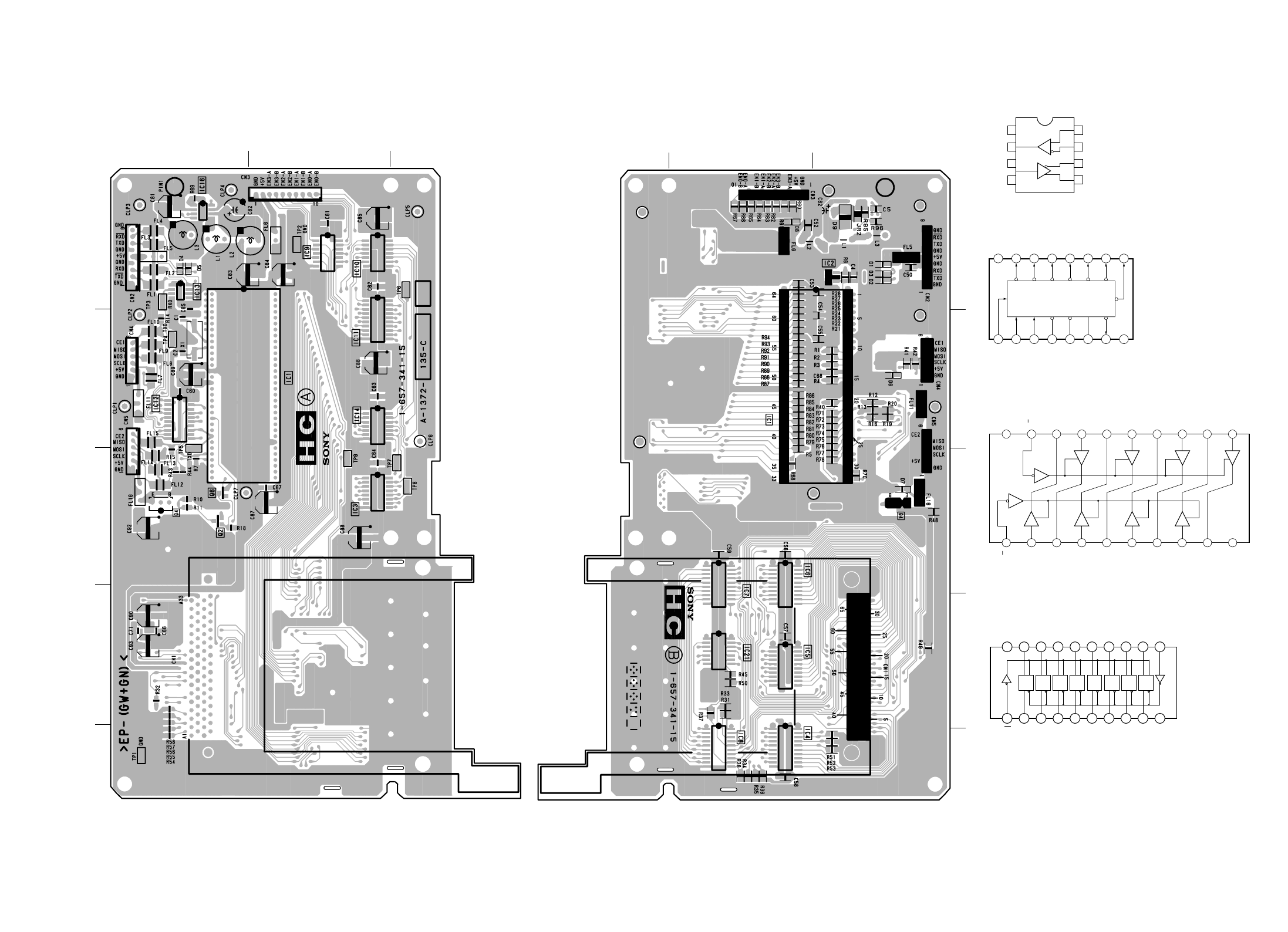
11-25
BVM-D14H1U/D14H5U/D14H1E/D14H5E/D14H1A/D14H5A 11-25
2
3
4
5
1
A BCDEFGH
HC, HDHC, HD
LTC490CS8 (IC13)
R
OUT
D
IN
1
2
3
4
8
7
6
5
A
IN
B
IN
Z
OUT
Y
OUT
V
DD
GND
D
R
TC74VHC138F (EL) (IC3)
131516 1214 11 10 9
421 53 6 7 8
Vcc Y0 Y1 Y2 Y3 Y5 T6Y4
BA CG2A G2B G1 GNDY7
Y0 Y1 Y2 Y3 Y4 Y5
BCG2A G2B G1 Y7
AY6
TC74VHC244F (EL) (IC12)
20 19 18 17 16 15 14 13 12 11
1 2 3 4 5 6 7 8 9 10
1G
1A1
2Y4
1A2
2Y3
1A3
2Y2
1A4
2Y1
GND 2A4
1Y4
2A3
1Y3
2A3
1Y2
2A4
1Y1
2G
Vcc
TC74VHC574F (EL) (IC11)
20 1119 18 17 16 15 14 13 12
1 1023456789
Vcc 1Q 2Q 3Q 4Q 5Q 6Q 7Q CLK8Q
OC 1D 2D 3D 4D 5D 6D 7D GND8D
Q OE
D CK Q OE
D CK Q OE
D CK Q OE
D CK Q OE
D CK Q OE
D CK Q OE
D CK Q OE
D CK
A
1
2
3
4
5
BC
A
1
2
3
4
5
BC
HC BOARD
HC –A SIDE–
SUFFIX: -15 HC –B SIDE–
SUFFIX: -15
[HC BOARD]
* : B SIDE
D1 *A-1
D2 *A-1
D3 *A-1
D4 A-1
D5 A-1
D6 *A-2
D7 *A-3
D8 *A-2
D9 A-1
IC1 B-2
IC2 A-1
IC3 B-3
IC4 *B-5
IC5 *B-4
IC6 *B-3
IC7 *B-3
IC8 *B-5
IC9 B-1
IC10 B-1
IC11 B-2
IC13 A-1
IC14 B-2
IC21 *B-4
Q4 A-3
TP2 A-1
TP3 A-1
TP4 A-2
TP6 C-1
TP7 C-3
TP8 C-3
TP9 B-3
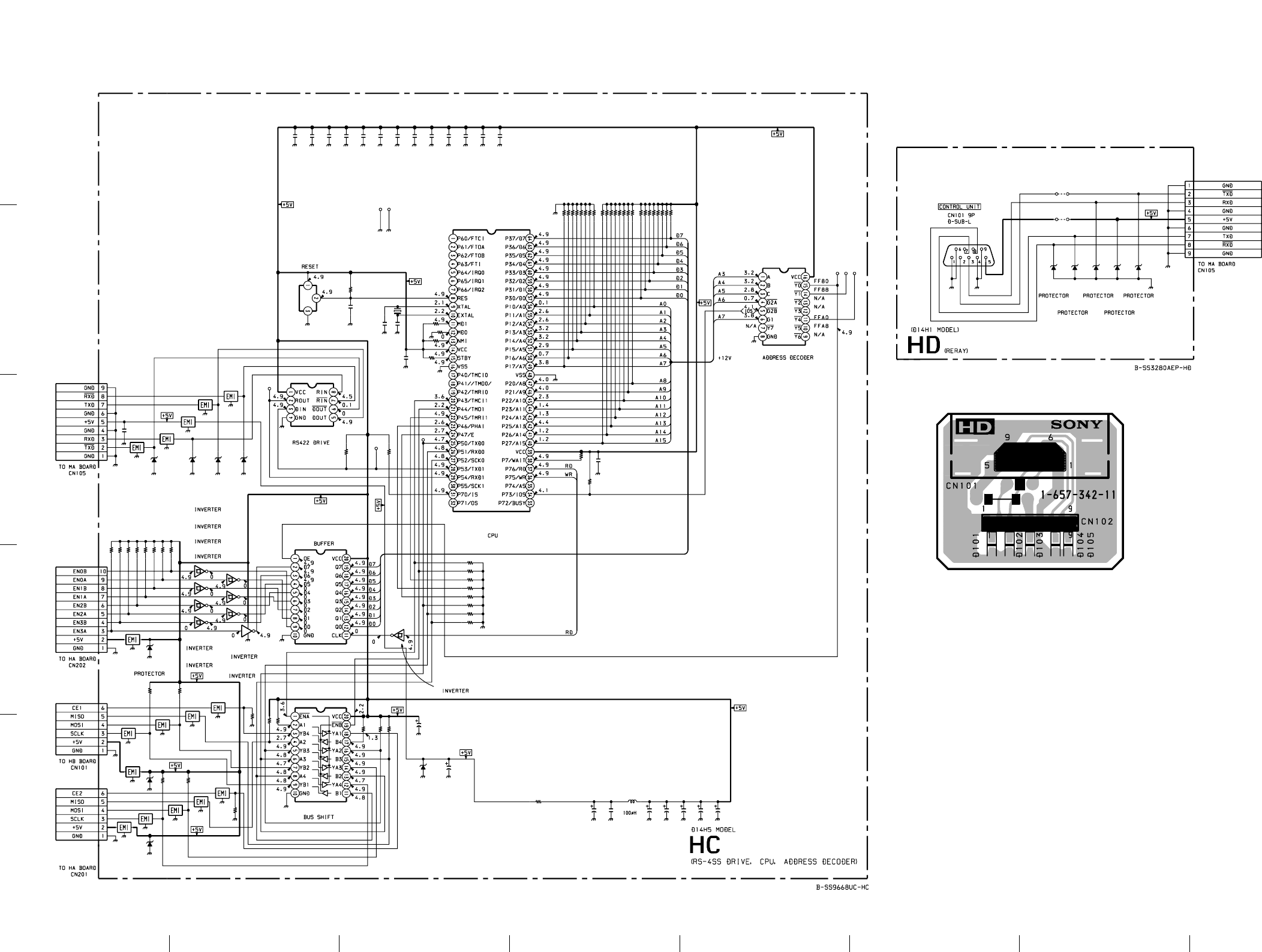
11-26 BVM-D14H1U/D14H5U/D14H1E/D14H5E/D14H1A/D14H5A
11-26
2
3
4
5
ABCDEFGH
1
HC, HDHC, HD
HD –B SIDE–
SUFFIX: -11
CN3
CN2
IC2
R6
R2
R4
R12R20
R41
R42
R13
R16
R19
R43
R44
R21
R22
R23 R25
R24 R26
R27
R28
TP1 TP2
TP3
TP4 TP5
C52
C67
C65
C64
C63
C62
C61
C60
C59
C58
C4
C68
C1
C2
C50
C57
C56
C55
C54
C53
C83 C84 C85 C86 C87C81
C89
R3
R87
R88
R89
R90
R91
R92
R93
R94
R75
R76
R77
R79
R86
R82 R84
R85
R80
R81 R83
IC12
IC11
FL1
FL2
FL5
FL4
FL3
FL6
FL12 FL13
FL14
FL15
FL16
FL7
FL8
FL9
FL10
FL11
C82
CN4
CN5
R7
R68
R70
R71
R72
R73
R74
R78
D1
D3
D4
D5
D6
D7
D8
IC9(1/6)
IC9(6/ 6)
IC9(2/6)
IC9(3/ 6)
IC9(5/6)
IC9(4/ 6)
IC13
X1
R14
R15
JR2
L2
IC3
IC10(1/6)
IC10(2 /6)
IC10(5 /6)
R5
IC1
R1
R60
R61
R62
R63
R64
R65
R66
R67
D2
220
6.3V
10pF
CH:CHIP
10pF
CH:CHIP
0.01
F:CHIP
0.01
F:CHIP
0.01
F:CHIP
0.01
F:CHIP
0.01
F:CHIP 0.01
F:CHIP
0.01
F:CHIP 0.01
F:CHIP
0.01
F:CHIP 0.01
F:CHIP
0.01
F:CHIP 0.01
F:CHIP
0.01
F:CHIP 0.01
F:CHIP
0.01
F:CHIP 0.01
F:CHIP
0.01
F:CHIP
0.01
F:CHIP
100
6.3V
AL-CP
100
6.3V
AL-CP
100
6.3V
AL-CP
100
6.3V
AL-CP
100
6.3V
AL-CP
100
6.3V
AL-CP
100
6.3V
AL-CP
9P
10P
6P
WHT
:S-MICRO
6P
RED
:S-MICRO
RD6.2SB-T1
RD6.2SB-T1
RD6.2SB-T1
RD6.2SB-T1
RD6.2SB-T1
RD6.2SB-T1
RD6.2SB-T1
PST529 C
TC74VHC14F(EL)
TC74VHC14F(EL)
TC74VHC14F(EL)
TC74VHC14F(EL)
TC74VHC14F(EL)
TC74VHC14F(EL)
TC74VH C574F( EL)
TC74VH C244F( EL)
LTC490 CS8
0
:CHIP
10k
:CHIP 10k
:CHIP
10k
:CHIP
100k
:CHIP
10k
:CHIP
10k
:CHIP
10k
:CHIP
10k
:CHIP
10k
:CHIP
1k
:CHIP
1k
:CH
IP
1k
:CHIP
1k
:CHIP
1k
:CHIP
1k
:CHIP
1k
:CHIP
1k
:CHIP
10k
:CHIP
10k
:CHIP
10k
:CHIP
10k
:CHIP
100k
:CHIP
100k
:CHIP
100k
:CHIP100k
:CHIP
100k
:CHIP100k
:CHIP
100k
:CHIP
100k
:CHIP
100k
:CHIP
100k
:CHIP
100k
:CHIP
100k
:CHIP
100k
:CHIP
100k
:CHIP
100k
:CHIP
100k
:CHIP
100k
:CHIP
100k
:CHIP
100k
:CHIP
100k
:CHIP
100k
:CHIP
100k
:CHIP
100k
:CHIP
100k
:CHIP
100
k
:CHIP
100k
:CH
IP
1k
:CHIP
1k
:CHIP
0
:CHIP
TC74VH C138F(
TC74VHC14F(EL)
TC74VHC14F(EL)
TC74VHC14F(EL)
10k :CHIP
HD6473 258-P1 0
10k
:CHIP
47k
:CHIP
47k
:CHIP
47k
:CHIP
47k
:CHIP
47k
:CHIP
47k
:CHIP
47k
:CHIP
47k
:CHIP
RD6.2SB-T1
CN102
D101
D103
D102
D104
D105
JW1
JW2
9P
RD6.2SB
RD6.2SB
RD6.2SB
RD6.2SB
RD6.2SB
(5)
(10)
CN102
D101
D103
D102
D104
D105
JW1
JW2
9P
RD6.2SB
RD6.2SB
RD6.2SB
RD6.2SB
RD6.2SB
(5)
(10)
CN102
D101
D103
D102
D104
D105
JW1
JW2
9P
RD6.2SB
RD6.2SB
RD6.2SB
RD6.2SB
RD6.2SB
(5)
(10)
CN102
D101
D103
D102
D104
D105
JW1
JW2
9P
RD6.2SB
RD6.2SB
RD6.2SB
RD6.2SB
RD6.2SB
(5)
(10)
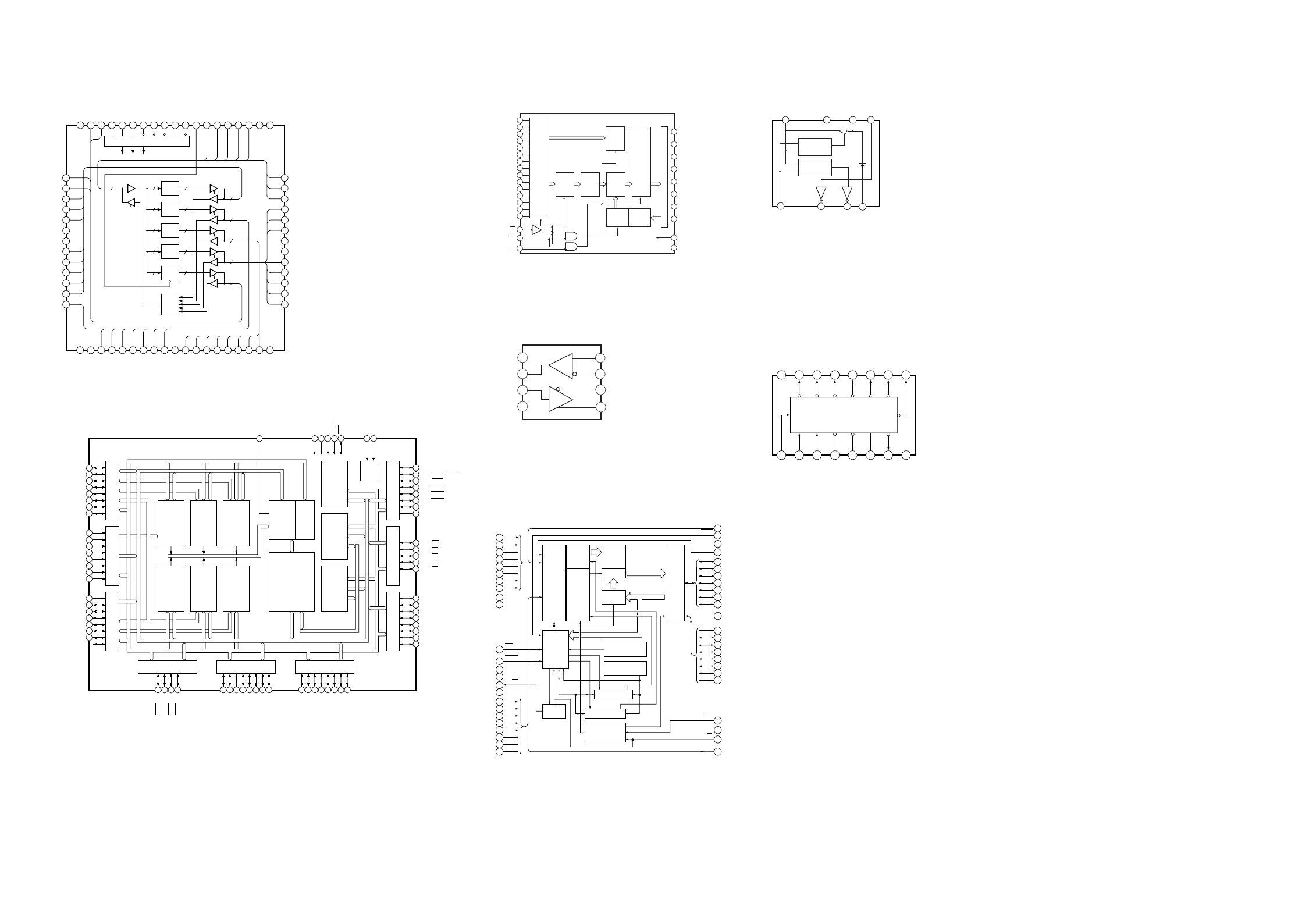
11-27
BVM-D14H1U/D14H5U/D14H1E/D14H5E/D14H1A/D14H5A 11-27
2
3
4
5
1
A BCDEFGH
MAMA
CXD1095BQ (IC112)
LATCH
CONTROL
50
51 49 48 47 46 45 44 43 42 41 40 39 38 37 36 35 34 33
NC
PX1
PX0
A2
A1
A0
CS
RD
WR
GND
RST
CLR
D7
D6
D5
D4
D3
NC
NC
LATCH
LATCH
LATCH
LATCH
DATA
SELECT
2
1345 6 7 8910 11 12 13 14 15 16 17 18
NC
NC
PB1
PB2
PB3
PB4
PB5
PB6
PB7
GND
PC0
PC1
PC2
PC3
PC4
PC5
PC6
PC7
NC
PX2 52
53
54
55
56
57
58
60
61
62
63
64
59
PX3
PA0
PA1
PA2
GND
V
DD
PA3
PA4
PA5
PA6
PA7
PB0
D2
32
31
30
29
28
27
26
24
23
22
21
20
25
D1
D0
PD7
PD6
PD5
V
DD
GND
PD4
PD3
PD2
PD1
PD0
19
88
8
8
8
8
8
8
8
8
8
8
8
8
8
8
HD6435368AX06M (IC106)
LC35256DM-70-TLM (IC111)
VCC
OE
CE
GND
WE
ADDRESS
BUFFER
INPUT
DATA
BUFFER
CONTROL
INPUT
DATA
COLUMN
I/O
CIRCUIT
COLUMN
DECODER
OUTPUT
DATA
BUFFER
MEMORY
ARRAY
CELL
LOW
DECODER
14
28
27
22
A13
A8
A9
A11
A10
A14
A12
A7
A6
A5
A4
A3
A2
A1
A0
1
2
3
4
5
6
7
8
9
10
26
25
24
23
21
20
I/O8
I/O7
I/O6
I/O5
I/O4
I/O2
I/O3
I/O1
11
12
13
15
16
17
18
19
MAX490ECSA (IC113)
A
B
Z
Y
VCC
RO
DI
GND 5
7
8
6
1
4
2
3
R
D
TC74VHC138F (FL) (IC109)
CONTROL
CIRCUIT LOW VCC
DETECTOR CIRCUIT
WRITE/ERASE
PULSE TIMER
ERASE CIRCUIT
RY/BY
BUFFER
CHIP ENABLE/
OUTPUT ENABLE
CIRCUIT
I/O
BUFFER
DATA
LATCH
ADDRESS
LATCH Y
DECODER
4,194,304
CELL
MATRIX
Y GATE
WRITE CIRCUIT
23
24 25
26
27
28
29
30
31
32
33
34
35
36
37
38
39
40
41
42
43
44
DQ3
DQ11
VCC
DQ4
DQ12
DQ5
DQ13
DQ7
DQ14
DQ6
DQ10
DQ2
DQ9
DQ1
DQ8
DQ0
GND
CE
OE
1
2
3
4
5
6
7
8
9
10
20
19
18
17
16
15
14
13
12
11
21
22
A8
A9
A15
A14
A13
A12
A11
NC
RY/BY
WE
A7
A6
A4
A5
NC
NC
RESET
NC
47
48
45
46
A3
A2
A1
A17
A10
NC
X
DECODER
A16
BYTE
GND
DQ15/A–1
A0
STB
STB
MBM29F400BC-90PF (IC108)
OPEN
COLLECTOR VBAT
CSVOUT
VCC
DIODE
GND
DETECT
DETECT
12 3 4
5
6
78
CS
3.3V
4.2V
MM102BFB (IC110)
131516 1214 11 10 9
421 53 6 7 8
Vcc Y0 Y1 Y2 Y3 Y5 T6Y4
BA CG2A G2B G1 GNDY7
Y0 Y1 Y2 Y3 Y4 Y5
BCG2A G2B G1 Y7
AY6
P9 /SCK
P9 /RXD
P9 /TXD
P9 /SCK /PW
P9 /RXD /PW
P9 /TXD /PW
P9 /FTOA
P9 /FTOA
7
6
5
1
0
3
2
1
3
2
PORT 9PORT 8
P8 /AN
P8 /AN
P8 /AN
P8 /AN
P8 /AN
P8 /AN
P8 /AN
P8 /AN
7
6
5
4
3
2
1
0
7
6
5
4
3
2
1
0
PORT 7
P7 /FTOA
P7 /FTOB /FTCI
P7 /FTOB /FTCI
P7 /FTOB /FTCI
P7 /FTI /TMRI
P7 /FTI
P7 /FTI
P7 /TMCI
1
3
2
1
2
1
7
3
2
1
3
2
1
0
10-BIT
A/D CONVERTER
(x8 CHANNEL)
PWM TIMER
(x3 CHANNEL)
SERIAL
COMMUNICATION
INTERFACE
(x2 CHANNEL)
WATCHDOG
TIMER
16-BIT FREE
RUNNING TIMER
(x3 CHANNEL)
8-BIT
TIMER
DATA
TRANSFER
CONTROLLER
INTERRUPT
CONTROLLER
CPU
32k BYTE (H8 / 534)
PROM / MASK OM RAM
2k BYTE
62k BYTE (H8 / 536)
WAIT
STATE
CONTROLLER
CLOCK
OSC
PORT 3 PORT 2 PORT 1
3
4
5
6
PORT 6 PORT 4PORT 5
P6 /IRO /A
P6 /PW /IRQ /A
P6 /PW /IRQ /A
P6 /PW /IRQ /A
0216
1317
2418
3519
1
2
3
P5 /A
P5 /A
P5 /A
P5 /A
P5 /A
P5 /A
P5 /A
P5 /A
80
91
210
113
124
135
146
157
P4 /A
0
P4 /A
1
P4 /A
2
P4 /A
3
P4 /A
4
P4 /A
5
P4 /A
6
P4 /A
77
6
5
4
3
2
1
0
P1 /TMO
P1 /IRQ /ADTRG
P1 /IRQ
P1 /WAIT
P1 /BREQ
P1 /BACK
P1 /E
P1 /Ø
7
6
5
4
3
2
1
0
1
0
P2 /WR
P2 /RD
P2 /DS
P2 /R/W
P2 /AS
0
1
2
3
4
P3 /D
P3 /D
P3 /D
P3 /D
P3 /D
P3 /D
P3 /D
P3 /D
0
1
2
3
4
5
6
77
6
5
4
3
2
1
0
MD
MD
MD
STBY
RES
XTAL
EXTAL
2
1
NMI
ADDRESS BUS
DATA BUS (HIGH ORDER)
DATA BUS (LOW ORDER)
2
2
2
4
3
2
1
1
1
0
68
67
66
65
64
63
62
61
59
58
57
56
55
54
53
52
50
49
48
47
46
45
44
38 39 40 41 30 31 32 33 34 35 36 37 21 22 23 24 25 26 27 28
13
14
15
16
17
18
19
20
80
1
2
3
4
72
73
74
75
76
77
78
79
697010967811
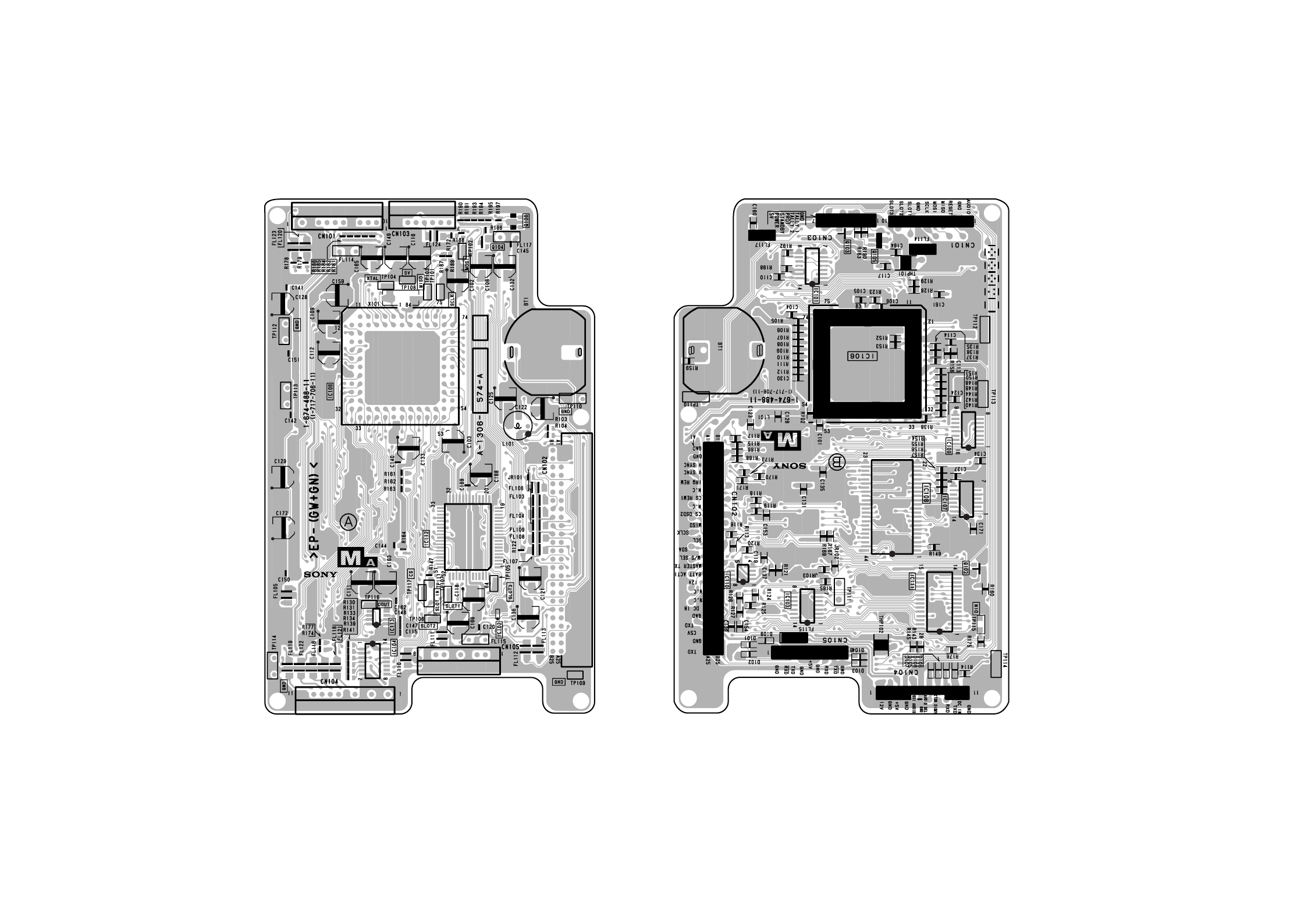
11-28 BVM-D14H1U/D14H5U/D14H1E/D14H5E/D14H1A/D14H5A
11-28
2
3
4
5
ABCDEFGH
1
MAMA
MA BOARD
MA –A SIDE–
SUFFIX: -11 MA –B SIDE–
SUFFIX: -11
[MA BOARD]
* : B SIDE
D101 C-4
D102 C-4
D103 *B-4
D104 *B-4
D105 *A-5
D106 *A-5
D107 *A-5
D108 *A-5
D109 C-4
IC101 *B-1
IC102 C-4
IC103 *B-4
IC104 *A-4
IC106 B-2
IC107 *A-3
IC108 *A-3
IC109 *A-3
IC110 *C-3
IC111 *A-4
IC112 B-3
IC113 A-4
Q102 *A-4
Q103 *B-1
Q104 C-1
Q105 *B-1
Q106 C-1
TP101 B-1
TP102 B-1
TP103 B-1
TP104 B-1
TP105 B-4
TP106 B-4
TP107 B-4
TP108 B-1
TP109 C-5
TP110 C-2
TP111 B-4
TP112 A-2
TP113 A-2
TP114 A-5
TP115 *A-5
TP116 A-4
TP117 B-4
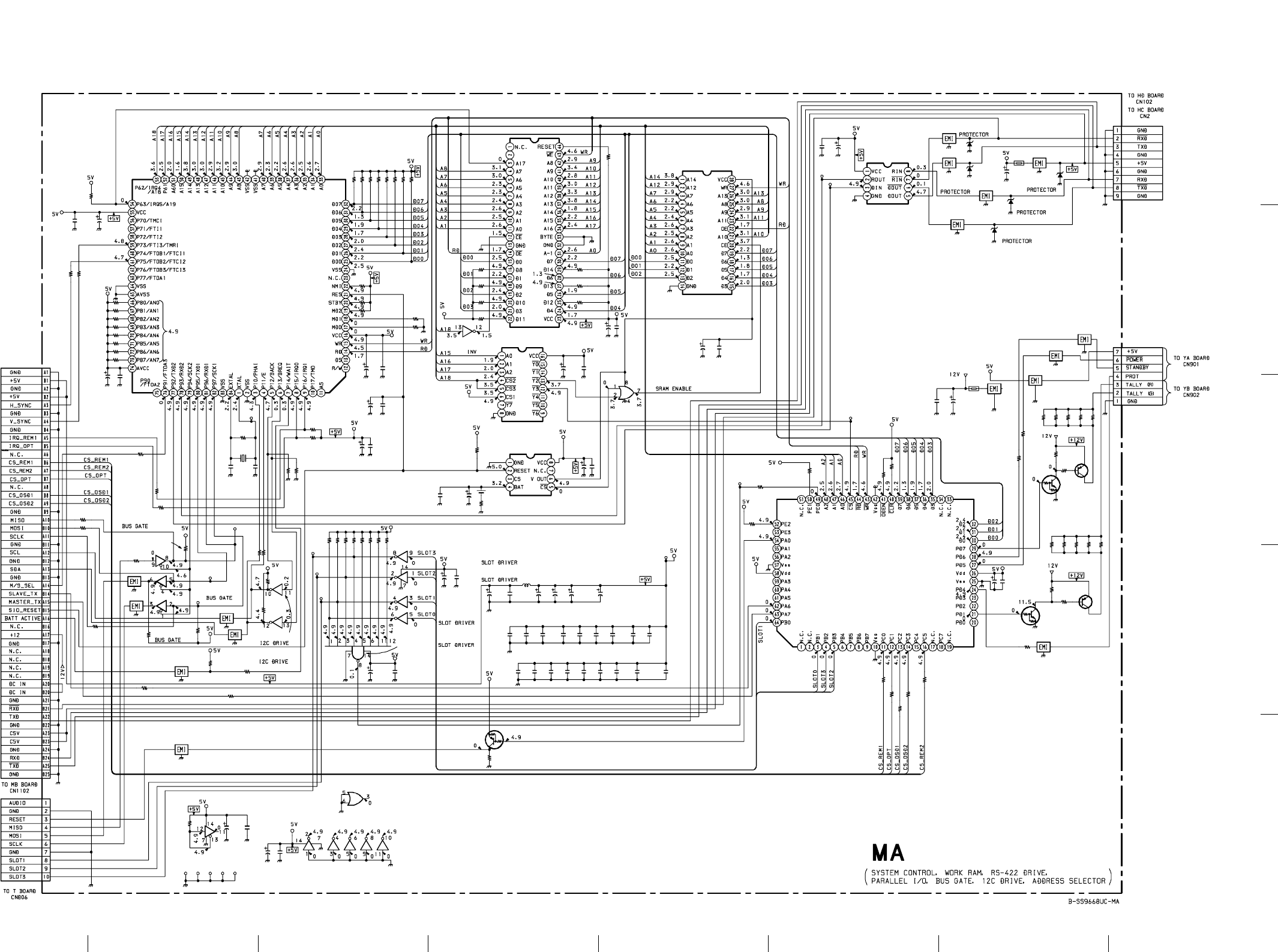
11-29
BVM-D14H1U/D14H5U/D14H1E/D14H5E/D14H1A/D14H5A 11-29
2
3
4
5
1
A BCDEFGH
MAMA
R102
R103 R104
C101
C102
C103
C104
R113
FL104
R115
FL105
R117
R118
TP101
R119
FL107
TP102
R121 R122
FL108
FL109
C105
TP103
R123
TP104
C106
R124 R126
R128
R129
TP105
TP106
TP107
C108
R138
C109
R140
C110
C112
R142
C113
R144
C114
C115
R146
R148
R150
R151
R152
R153
C116 C117
C118
C119
C120
C121
R158
R160
C122
C123 L101
C124
C125
C126
C127
C128
C129
C130
C131
C132
C133
C134
C135
C136
C137
C139
C140
C141
C142
C144
C145
C147
C148
C149
C150
C151
C153
C154
C159
TP108
C160
C161
TP111
R165
TP115
TP116
TP117
R167
R169
R173
C164
THP101
FL114
C168 C169
FL117
FL120
FL123
C171
C172
IC109
C111
X101
C162 C163
TP112 TP113 TP114TP109 TP110
R159
R125
R127
C166
THP102
FL110
FL111
FL112
FL113
R188
R189
R198
FL115
CN103
R147
Q102
R157
R156
R155
R196
R197
R183
R180
R178
R179
C165
Q104
Q106
Q103
Q105
IC111
IC112
IC110
IC108
IC106
IC113
R112
R111
R110
R109
R107
R108
R106
R105
R187
R120R116
R130
R154
R163
R162
R161
D101
D102
D104
D103
D109
CN105
R136
R135
R145
CN102
CN101
R137
R101
R132
R172
R181
FL124
R182 R184 R185 R186
R190 R191 R193 R194
R195
JR101
FL103
BT1
JR103
R131
R133
R134
R139
R141
R143
IC104
R164
R166
R168
R170
R171
R192
IC102
IC107
IC103
IC103
IC103
IC103
IC103
IC103
IC107
IC101
IC101
IC101
IC102
IC107
IC107
IC107
IC107
IC101
0.01
F:CHIP
0.01
F:CHIP
10k
:CHIP
100k
:CHIP
1M
:CHIP
10k
:CHIP
100k
:CHIP
100k
:CHIP
100
6.3V
:HT-CP
100
6.3V
:HT-CP
10k
:CHIP
10k
:CHIP
22p
CH:CHIP
10p
CH:CHIP
100
6.3V
:HT-CP
0.01
F:CHIP
0.01
F:CHIP
100
6.3V
:HT-CP
100
6.3V
:HT-CP
100
6.3V
:HT-CP
100
6.3V
:HT-CP
0.01
F:CHIP
0.01
F:CHIP 0.01
F:CHIP 0.01
F:CHIP 0.01
F:CHIP 0.01
F:CHIP 0.01
F:CHIP 0.01
F:CHIP
0.01
F:CHIP 0.01
F:CHIP 0.01
F:CHIP 0.01
F:CHIP 0.01
F:CHIP
100
6.3V
:HT-CP
100
6.3V
:HT-CP
100
6.3V
:HT-CP
100
6.3V
:HT-CP
100
6.3V
:HT-CP
0.01
F:CHIP
0.01
F:CHIP
0.01
F:CHIP
0.01
F:CHIP
100
6.3V
:HT-CP
100k
:CHIP
100
6.3V
:HT-CP
100k
:CHIP
100
6.3V
:HT-CP
100
6.3V
:HT-CP
0.01
F:CHIP
0.01
F:CHIP
100
:CHIP
100
:CHIP
TC74VHC138F(EL)
ADDRESS SELECTOR
100
6.3V
:HT-CP
0.01
F:CHIP
100
6.3V
:HT-CP
100
6.3V
:HT-CP
0.01
F:CHIP
0.01
F:CHIP 100
6.3V
:HT-CP
0.01
F:CHIP
100
6.3V
:HT-CP
0.01
F:CHIP
0.01
F:CHIP
0.01
F:CHIP
0.01
F:CHIP
0.01
F:CHIP
0.01
F:CHIP
0.01
F:CHIP
0.01
F:CHIP
0.01
F:CHIP
100
6.3V
:HT-CP
100k
:CHIP
100
:CHIP 100
:CHIP
100
:CHIP
100
:CHIP
100k
:CHIP
100k
:CHIP
100
:CHIP
4.7k
:CHIP
100
:CHIP
4.7k
:CHIP
100k
:CHIP
100k
:CHIP
100k
:CHIP
100k
:CHIP
100k
:CHIP
100k
:CHIP
100k
:CHIP
100k
:CHIP
1k
:CHIP
100k
:CHIP
100
:CHIP
100
:CHIP
100
:CHIP
100k
:CHIP
7P
RED:L
:S-MICRO
DTA144EKA-T146
SLAVE CPU RESET
100k
:CHIP
100k
:CHIP
100k
:CHIP
1.5k
:CHIP
820
:CHIP
22
35V
:HT-CP
1k
:CHIP 10k
:CHIP
10k
:CHIP
10k
:CHIP
10k
:CHIP
DTC144EKA
INV
2SB1132-T100
LED DRIVE
DTC144EKA
INV
2SB1132-T100
LED DRIVE
LC35256DM-70-TLM
WORK RAM
CXD1095BQ
PARALLEL I/O
MM1026BFB
RESET
MBM29F400BC-90PF
PROGRAM ROM
HD6435368AX06M
SYSTEM CONTROL
TC7W32FU(TE12R)
TC7W32FU(TE12R)
SN74HC05ANSR
SN74HC05ANSR
SN74HC05ANSR
SN74HC05ANSR
SN74HC05ANSR
SN74HC05ANSR
TC74VHC04F(EL)
TC74VHC04F(EL)
TC74VHC04F(EL)
TC74VHC04F(EL)
TC74VHC04F(EL)
TC74VHC125F
TC74VHC125F
TC74VHC125F
MAX490ECSA
RS422 DRIVE
20.0MHz
100k:CHIP
100k:CHIP
100k:CHIP
100k:CHIP
100k:CHIP
100k:CHIP
100k:CHIP
100k:CHIP
100 :CHIP
TC74VHC125F
100 :CHIP100 :CHIP
1k
:CHIP
100k
:CHIP
100k :CHIP
100k :CHIP
100k :CHIP
RD6.2SB-T1
RD6.2SB-T1
RD6.2SB-T1
RD6.2SB-T1
RD6.2SB
9P
10k :CHIP
10k :CHIP
1k :CHIP
TC74VHC04F(EL)
50P
10P
10k :CHIP
100k
:CHIP
100k
:CHIP
1.5k
:CHIP
820
:CHIP
820
:CHIP 820
:CHIP 820
:CHIP 820
:CHIP
820 820 820 820
820
0
:CHIP
CR2025
100K :CHIP
1k
:CHIP
1k
:CHIP
1k
:CHIP
1k
:CHIP
1k
:CHIP
1k
:CHIP
TC74HC30AF(EL)
SLOT RECEIVER
100k
:CHIP
100
:CHIP
100
:CHIP
100
:CHIP
100
:CHIP
100k
:CHIP
100µH
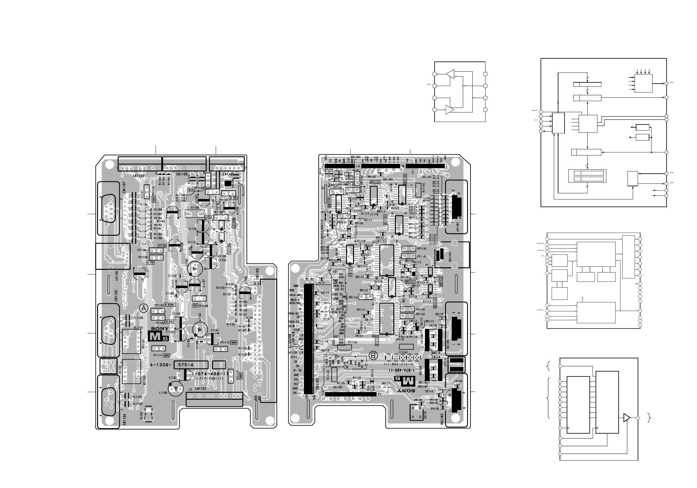
11-30 BVM-D14H1U/D14H5U/D14H1E/D14H5E/D14H1A/D14H5A
11-30
2
3
4
5
ABCDEFGH
1
MBMB
MAX3100CEE (IC1105, 1108)MAX487ECSA (IC1103, 1106)
A
B
C
D
E
F
G
H
LCK
SCK
SS/PL
OE
SA
Serial
Data
Input
Parallel
Data
Inputs
QH Serial
Data
Output
Shift
Register
Input
Latch
9
14
15
1
2
3
4
5
6
7
12
11
13
10
MC74HC589AFEL (IC1112)
MB90096PF-127/G-178 (IC1107, 1110)
8
7
1
2
34
5
24
25
26
27
28
19
20
21
22
23
14
15
16
17
18
9
10
11
12
13
6
BOUT
ROUT
GOUT
IOUT
VOB1
VOB2
DOCKO
FH
GND
VCO GND
VCO GNC
DISP
VSYNC
EVEN
RESET
CS
SIN
SCLK
TRE
DOCKI
HSYNC
CPOUT
VCOIN
DISPLAY CONTROL
FONT
ROM
(32FIGURE 16LINE)
DOT CLOCK
DISPLAY
OUTPUT
CONTROL
DOT CLOCK
GENERATOR
(PLL CIRLOIT)
(16KByte)
COMMAND
TABLE ROM
COMMAND
TABLE ROM
CONTROL
SERIAL
INPUT
CONTROL
DISPLAY
MEMORY
VRAM TEST
VCC
V3V
AV3V
AVCC
MB BOARD
MB –A SIDE–
SUFFIX: -11 MB –B SIDE–
SUFFIX: -11
[MB BOARD]
* : B SIDE
D1100 *A-3
D1101 *A-3
D1102 *A-4
D1103 *A-5
D1104 *C-1
D1105 *C-1
D1106 *C-1
D1107 *C-1
D1108 *C-1
D1109 *C-1
D1110 *A-2
D1111 *A-2
D1112 *A-2
D1113 *A-2
D1114 *A-2
D1115 *A-2
D1116 *A-1
D1117 *A-1
D1118 *C-1
IC1100 *B-1
IC1101 *A-1
IC1102 *B-1
IC1103 *A-3
IC1104 *B-3
IC1105 C-2
IC1106 *A-2
IC1107 *B-2
IC1108 C-2
IC1109 *C-1
IC1110 *B-3
IC1112 *B-2
TP1100 C-2
TP1101 B-3
TP1102 B-3
TP1103 B-2
TP1104 B-2
TP1106 B-1
TP1107 C-1
TP1108 C-2
TP1109 B-3
TP1110 C-2
TP1111 B-4
TP1112 C-4
TP1113 C-4
5
4
3
2
1
ABC
A
1
2
3
4
5
BC
X1
X2
DOUT
BAUD-RATE
GENERATOR
SPI
INTERFACE BAUD-RATE
GENERATOR
DIN
SCLK
CS B0
Pt TX-SHIFT REGISTER
START/STOP-
BIT DETECT
D0t–D7t
RX-SHIFT REGISTER
D0r–D7r
SHDN
FE
RA
B1
B2
B3
RX
TX
9
Pt TX-BUFFER REGISTER
9
Pr RX-BUFFER REGISTER
Pr
Pr
RX-BUFFER REGISTER
9
9
I / O
CTS
RTS
VCC
ACTIVITY
DETECT
GND
RA/FE
(MASKS)
PrRT
IRQ
INTERRUPT
LOGIC
TRANSMIT-DONE (TM)
DATA-RECEIVED (RM)
PARITY (PM)
FRAMING ERROR (RAM)/
RECEIVE ACTIVITY
(SOURCES)
7
1
4
3
2
8
16
13
11
14
9
10
15
6
1
2
3
4
RO
RE
DE
DI
8
R
D
7
6
5
VCC
B
A
GND
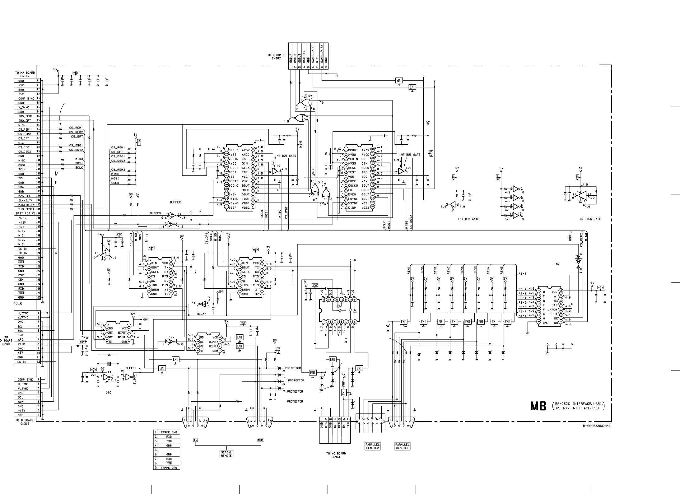
11-31
BVM-D14H1U/D14H5U/D14H1E/D14H5E/D14H1A/D14H5A 11-31
2
3
4
5
1
A BCDEFGH
MBMB
R1100
R1101
R1102
R1103
R1104
R1106
R1107
R1108
R1110
R1111
R1112
C1101
C1102
C1103
C1104
C1105
C1106
R1114
C1107
R1115
C1108
R1117
C1109
R1119
C1110
C1111
R1120
R1121
R1122
R1123
R1125
R1126
R1127
R1128
R1130
R1131 R1132
C1112
C1114
FL1100
C1115
FL1101
R1133
C1116 C1117
R1136
FL1102
FL1103
R1141
R1142
C1120 C1121
R1143
R1144
C1122
R1145
C1123
C1124
C1125
C1126
C1127
C1128
C1129
FL1108
IC1109
D1104
D1105
FL1109
D1106
D1107
TH1100
TP1106
D1108
D1109
TP1107
FL1111
C1139
C1140
D1110
C1141
R1151
R1152
FL1114
C1142
R1153
R1154
R1155
R1156
C1143
R1157
C1144
R1158
R1159
D1111
FL1115
C1145
C1146
R1160
D1112
FL1116
C1147
R1161
D1113
FL1117
C1148
R1162
D1114
FL1118
C1149
R1163
C1150
D1115
FL1119
C1151
R1164
D1116
FL1120
C1153
R1165
D1117
FL1121
C1154
R1166
C1157
C1159
C1152
C1156
C1158
IC1103
TP1100
TP1101
TP1102
TP1103
TP1104
TP1108
TP1109
TP1110
C1132
C1133
C1134
C1137
C1138
FL1110
FL1112
FL1113
R1113
R1137
TP1111TP1112TP1113
C1119
C1136
IC1112
L1100
L1101
L1102
IC1106
X1100
R1173
R1172
R1170
R1171
C1180
R1181
R1180
C1100
R1174
R1175
R1176
R1177
CN1107
CN1104
CN1103
CN1106
CN1105
R1167
CN1100
CN1101
R1109
C1161
R1140R1138 R1148 R1149
C1118
C1135
CN1102
IC1110
IC1107
IC1105
IC1108
C1160
C1130
R1186 R1187
R1188 R1189
D1103
D1102
D1101
D1100
R1183 R1182
R1184
R1185
D1118
R1118
C1162
CN1109
C1131
R1147
IC1101
IC1101
IC1101
IC1102
IC1102
IC1104
IC1104
IC1104
IC1104
IC1104
IC1104
IC1102
IC1102
IC1102
IC1102
IC1100
IC1101
IC1100
IC1100
IC1100
10k
:CHIP
10k
:CHIP
10k
:CHIP
10k
:CHIP
MAX202CSE-TE2
RS232C INTERFACE
RD12SB
PROTECTOR
RD12SB
PROTECTOR
RD12SB
PROTECTOR
RD12SB
PROTECTOR
18p
CH:CHIP
15p
CH:CHIP
1M
:CHIP
RD12SB
PROTECTOR
RD12SB
PROTECTOR
0.1
F:CHIP
0.1
F:CHIP
0.1
F:CHIP
0.1
F:CHIP
0.1
F:CHIP
TC74VHCU04F(EL)
TC74VHCU04F(EL)
TC74VHCU04F(EL)
TC74VHCU04F(EL)
100
6.3V
:AL-CP
0.1
F:CHIP
100
6.3V
:AL-CP
0.1
F:CHIP
0.01
F:CHIP
0.01
F:CHIP
100
6.3V
:AL-CP
100
6.3V
:AL-CP
0.01
F:CHIP 100
6.3V
:AL-CP
0.01
F:CHIP
0.01
F:CHIP 100
6.3V
:AL-CP
0.01
F:CHIP 100
6.3V
:AL-CP
1.0
B:CHIP
0.01
F:CHIP 100
6.3V
:AL-CP
0.1
F:CHIP
0.01
F:CHIP
0.1
F:CHIP
100
6.3V
:AL-CP
0.1
F:CHIP
100
6.3V
:AL-CP
0.1
F:CHIP
100
6.3V
:AL-CP
1.0
B:CHIP
0.1
F:CHIP
0.1
F:CHIP
0.01
F:CHIP
100
6.3V
:AL-CP
0.01
F:CHIP
0.01
F:CHIP
100
6.3V
:AL-CP
0.01
F:CHIP 0.01
F:CHIP 0.01
F:CHIP 0.01
F:CHIP
100
6.3V
:AL-CP
0.01
F:CHIP
0.01
F:CHIP
0.01
F:CHIP 0.01
F:CHIP
0.01
F:CHIP 100
6.3V
:AL-CP
0.01
F:CHIP 100
6.3V
:AL-CP
47p
CH:CHIP
RD6.2SB
PROTECTOR
RD6.2SB
PROTECTOR
RD6.2SB
PROTECTOR
RD6.2SB
PROTECTOR
RD6.2SB
PROTECTOR
RD6.2SB
PROTECTOR
RD6.2SB
PROTECTOR
RD6.2SB
PROTECTOR
MAX487ECSA
RS485 INTERFACE
TC74VHC14F(EL)
TC74VHC14F(EL)
TC74VHC14F(EL)
TC74VHC14F(EL)
TC74VHC14F(EL)
MAX487ECSA
RS485 INTERFACE
MC74HC589AFEL
REMOTE2 DRIVER
100 :CHIP
100 :CHIP
100 :CHIP
100 :CHIP
100 :CHIP
100 :CHIP
100 :CHIP
100 :CHIP
100 :CHIP
100 :CHIP
100 :CHIP
100k
:CHIP
100
:CHIP
100
:CHIP
100
:CHIP
100k :CHIP
100k :CHIP
100k:CHIP
100k:CHIP
100k :CHIP
100k:CHIP
100k:CHIP
100k :CHIP
47k
:CHIP
100k
:CHIP 100k
:CHIP
47k
:CHIP 47k
:CHIP
0
:CHIP
47k
:CHIP
1k
:CHIP
1k
:CHIP
1k
:CHIP
1k
:CHIP
1k
:CHIP
1k
:CHIP
1k
:CHIP
100k
:CHIP
1k
:CHIP
100k
:CHIP 100k
:CHIP 100k
:CHIP 100k
:CHIP 100k
:CHIP 100k
:CHIP 100k
:CHIP
4.7k
:CHIP
4.7k
:CHIP
47k
:CHIP
47k
:CHIP
100k
:CHIP
100k
:CHIP
100k
:CHIP
100k
:CHIP
4.7k
:CHIP
100k
:CHIP
3.6864MHz
9P
9P
9P
9P
WHT
:S-MICRO
12P
WHT
:S-MICRO
9P
RED
:S-MICRO
7P
47k
:CHIP
100 :CHIP
0.01
B:CHIP
300
:RN-CP
82
:RN-CP 82
:RN-CP 300
:RN-CP
50P
0.01
B:CHIP
0.01
B:CHIP
TC74VHC125F(EL)
TC74VHC125F(EL)
TC74VHC125F(EL)
TC74VHC125F(EL)
MB90096PF-G-178
OSD
TC74VHC02F
MIX
TC74VHC02F
MIX
TC74VHC02F
MIX
TC74VHC02F
MIX
MB90096PF-127
OSD
MAX3100CEE
UART
MAX3100CEE
UART
0.01
B:CHIP
TC74VHCU04F(EL)
TC74VHCU04F(EL)
TC74VHC14F(EL)
100
6.3V
:AL-CP
00
00
RD6.2SB-T1
RD6.2SB-T1
RD6.2SB-T1
RD6.2SB-T1
100 100
100
100
RD6.2SB
PROTECTOR
15k
:CHIP
0.0022
6P
0.01
F:CHIP
0
:CHIP
100µH
100µH
100µH
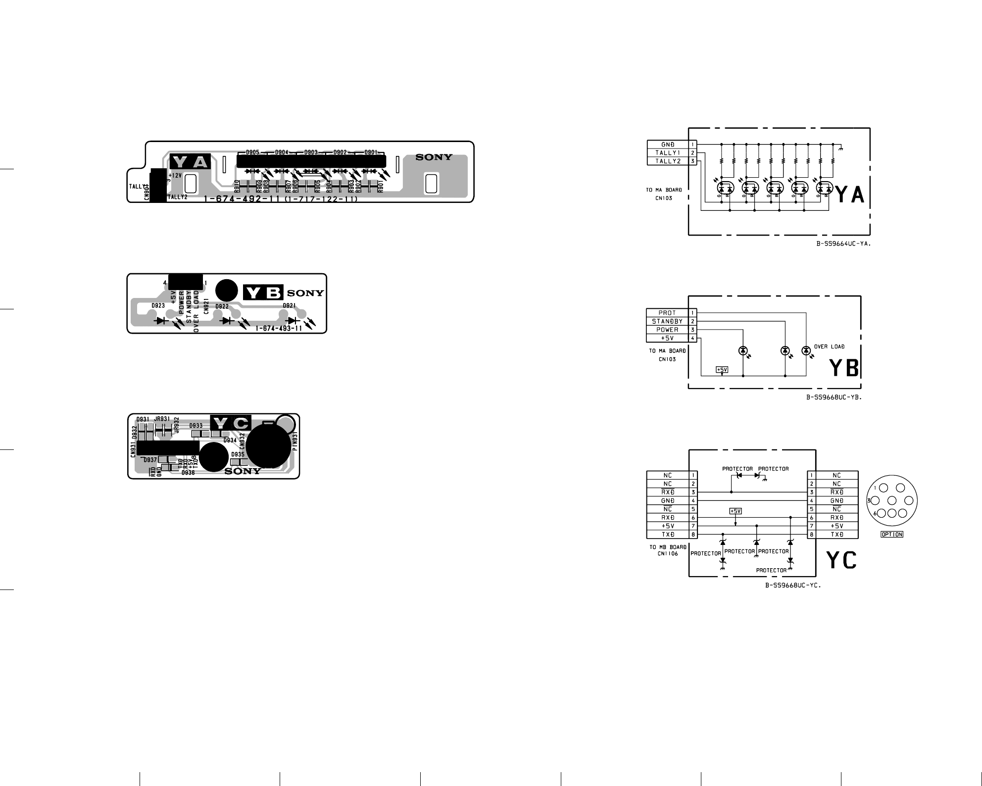
11-32 BVM-D14H1U/D14H5U/D14H1E/D14H5E/D14H1A/D14H5A
11-32
2
3
4
5
ABCDEFGH
1
YA, YB, YCYA, YB, YC
YA –B SIDE–
SUFFIX: -11
YB –B SIDE–
SUFFIX: -11
YC –B SIDE–
SUFFIX: -11
D921
CN921
D923
D922
SLR-325DCT31
6P
SLR-325MCT31
POWER
SLR-325VCT31
STANDBY
CN932
CN931
D935
D937
D931 D932
D933
D934
D936
8P
8P
6.2SB
RD12SB
RD12SB
RD12SB RD12SB
RD12SB
RD12SB
D901 D902 D903 D904 D905
CN901
R901 R902 R903 R904 R905 R906 R907 R908 R909 R910
SPR-325MVW
TALLY IND SPR-325MVW
TALLY IND SPR-325MVW
TALLY IND SPR-325MVW
TALLY IND SPR-325MVW
TALLY IND
3P
WHT
PH
1k
:CHIP 1k
:CHIP 1k
:CHIP 1k
:CHIP 1k
:CHIP 1k
:CHIP 1k
:CHIP 1k
:CHIP 1k
:CHIP 1k
:CHIP
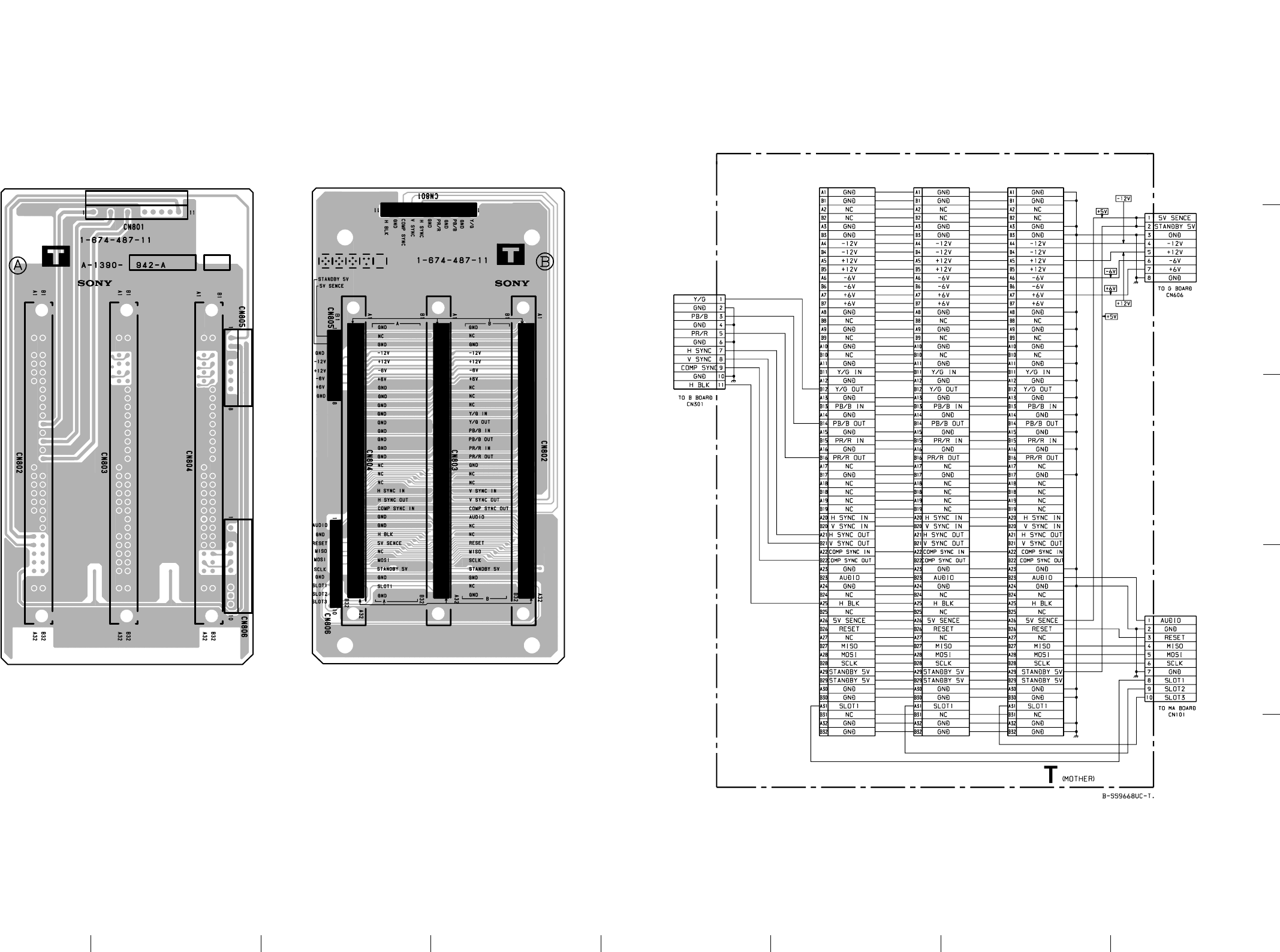
11-33
BVM-D14H1U/D14H5U/D14H1E/D14H5E/D14H1A/D14H5A 11-33
2
3
4
5
1
A BCDEFGH
TT
T BOARD
T –A SIDE–
SUFFIX: -11 T –B SIDE–
SUFFIX: -11
CN802 CN803 CN804
CN801
CN805
CN806
64P
WHT 64P
WHT 64P
WHT
11P
WHT(-L)
:S-MICRO
8P
WHT(-L)
:S-MICRO
10P
WHT(-L)
:S-MICRO

11-34 BVM-D14H1U/D14H5U/D14H1E/D14H5E/D14H1A/D14H5A
11-34
2
3
4
5
ABCDEFGH
1
The material contained in this manual consists of
information that is the property of Sony Corporation.
Sony Corporation expressly prohibits the duplication of
any portion of this manual or the use thereof for any
purpose other than the operation or maintenance of the
equipment described in this manual without the express
written permission of Sony Corporation.
Le matériel contenu dans ce manuel consiste en
informations qui sont la propriété de Sony Corporation.
Sony Corporation interdit formellement la copie de
quelque partie que ce soit de ce manuel ou son emploi
pour tout autre but que des opérations ou entretiens de
l’équipement à moins d’une permission écrite de Sony
Corporation.
Das in dieser Anleitung enthaltene Material besteht aus
Informationen, die Eigentum der Sony Corporation sind.
Die Sony Corporation untersagt ausdrücklich die
Vervielfältigung jeglicher Teile dieser Anleitung oder den
Gebrauch derselben für irgendeinen anderen Zweck als
die Bedienung oder Wartung der in dieser Anleitung
beschriebenen Ausrüstung ohne ausdrückliche
schriftliche Erlaubnis der Sony Corporation.
Sony Corporation
Broadcasting & Professional Systems Company9-929-659-01
English
99JS16033-1
Printed in Japan
©1999.10