CCS_2719_2P2S_Feb82 CCS 2719 2P2S Feb82
CCS_2719_2P2S_Feb82 CCS_2719_2P2S_Feb82
User Manual: CCS_2719_2P2S_Feb82
Open the PDF directly: View PDF ![]() .
.
Page Count: 67
MODEL.2719
2 PARALLEL 1 2
SERIAL
1/0
INTERFACE
.
Reference
Manual
11-,
CaHfoniia
Computer
Systems·
42000096-01
CCS
MODEL
2719
2 PARALLEL / 2 SERIAL
I/O
INTERFACE
Reference
Manual
Rev
B
Manual
#42000095-01
Copyright
1981
California
Computer
Systems
250
Caribbean
Drive
Sunnyvale
CA
94086
Copyright
1981
by
California
Computer
Systems.
All
rights
reserved.
No
part
of
this
publication
may
be
reproduced
in
any
form
or
by
any
means
without
express
permission
of
California
Computer
Systems.
The
information
contained
in
this
manual
is
believed
to
be
correct
at
the
time
of
publication.
However,
CCS
assumes
no
liability
resulting
from
the
use
of
this
publication.
Publication
History:
Revision
A
printed
December
1981
Revision
B
printed
February
1982
Z-80
M
is
a
trademark
of
Zilog,
Inc.
CP/M
M
is
a
trademark
of
Digital
Research,
Inc.
OASIS m
is
a
trademark
of
Phase
One,
Inc.

TABLE
OF
CONTENTS
CHAPTER 1 INTRODUCTION
1.1
GENERAL
DESCRIPTION
.........................•
1-1
1.2
USING
THIS
MANUAL
............................
1-2
1 . 3
SPECIFICAT
IONS
...............................
1-
3
1.4
2719
BLOCK
DIAGRAM
.............•.............
1-4
CHAPTER 2 CONFIGURING
THE
2719
2.1
2.2
2.3
2.4
2.5
2.6
2.7
2.8
2.9
2.10
BASE
ADDRESS
JUMPERS
....•...•............••..
2-1
INTERRUPT
MODE
AND
PRIORITY
CONFIGURATION
.•.•
2-4
2.2.1
Mode 0
Configuration
....••••••.•.••...
2-4
2 . 2 . 2 Mode 1
Configuration
..................
2-4
2.2.3
Mode 2
Configuration
.......•••..•.•...
2-5
SERIAL INTERFACES
..................•..•......
2-7
2.3.1
Synchronous
Conversion
...•.•..•.....•.
2-7
2.3.2
DCE/DTE
Conversion
....••...•.....•..•.
2-7
2.3.3
Non-Standard
Handshaking
...•....•..•..
2-7
2.3.4
Baud
Rate
Source
Jumpers
.•.••..••.....
2-9
2 . 3
.5
Protective
Ground
...........•••.•..•..
2-9
PARALLEL INTERFACE CONFIGURATION
......••....
2-10
2.4.1
Buffer
Direction
Jumpers
•.........•••
2-10
2.4.2
Buffer
Enable
Jumpers
...•......•...•.
2-10
2.4.3
Reversing
Interface
Polarities
•.•..•.
2-10
THE
RESET JUMPER
......................•....•
2-11
INTERRUPT
ACKNOWLEDGE
WAITS
.................
2-11
CLOCK
PHASE
.................................
2-11
DATA
LATCH
ENABLING
AND
DISABLING
...........
2-12
BAUD
RATES
IN
2
MHZ
SYSTEMS
.................
2-12
OPERATION
IN
6
MHZ
SYSTEMS
...•.....••..•.•..
2-12
CHAPTER 3
PROGRAMMING
INFORMATION
3.1
3.2
3.3
3.4
PORT
RELATIVE ADDRESSES
...........••......•..
DART
2719-UNIQUE
PROGRAMMING
.......•.•.......
CTC
2719-UNIQUE
PROGRAMMING
......••.•..•.....
PROGRAMMING
THE
PIA
.........................
.
3.4.1
3.4.2
~.4.3
PIA
Command
Registers
.......••........
PIA
Data
Direction
Registers
.........
.
PIA
Initialization
.............•......
3-1
3-2
3-3
3-4
3-5
3-7
3-7
CHAPTER
4
HARDWARE
DESIGN
4.1
THE
PlAIS
........................•...........
4-1
4 • 2
THE
DART
......•....••...•...•..•..•......•••.
4-
2
4 • 3
THE
eTC
.......•.......•....•.••..............
4-
3
4.4
ADDRESS
AND
CONTROL
LOGIC
....•...............
4-6
4.5
INTERRUPT LOGIC
..............................
4-7
4.6
DATA
BUFFERING
AND
LATCHING
..................
4-9
APPENDIX A TECHNICAL
INFORMATION
A.l
USER-REPLACEABLE
PARTS
.......................
A-2
A.2
SERIAL
CONNECTOR
PINOUTS
.....................
A-4
A.3
PARALLEL
CONNECTOR
PINOUTS
...................
A-4
A.4
RS-232-C
CONNECTOR
PINOUTS
...................
A-5
A.5
BUS
CONNECTOR
PINOUTS
........•...............
A-6
A.6
SCHEMATIC/LOGIC
DIAGRAM
....•.•..•....•..•....
A-7
APPENDIX B
SAMPLE
DRIVERS
B
.1
CP/M DRIVER
.".................................
B-2
B.2
OASIS DRIVER
..•............•.................
B-8

CHAPTER
1
INTRODUCTION
1.1
GENERAL
DESCRIPTION
The
CCS
Model
2719
is
capable
of
interfacing
a
wide
variety
of
peripheral
equipment
to
Z-80-based
CPUs.
Software
and
hardware
options
give
a
high
degree
of
flexibility
to
the
2719
1s
two
serial
and
two
parallel
I/O
ports.
The
serial
ports
are
controlled
by
a
Z-80
DART
(Dual
Asynchronous
Receiver/Transmitter),
which
handles
asynchronous
serial
data
transfers
in
all
common
formats.
Baud
rates
up
to
11S.2K
are
available.
The
parallel
ports,
each
controlled
by
a
6821
PIA
(peripheral
Interface
Adapter),
are
designed
to
implement
Centronics
interfaces,
but
each
may
also
be
used
as
two
unidirectional
8-bit
ports
with
2-line
handshaking
or
as
one
unidirectional
16-bit
port.
The
2719
fully
supports
the
three
Z-80
interrupt
modes
for
all
ports.
Separate
headers
allow
the
user
to
select
the
Mode 0
or
Mode 2
interrupt
priority
level
and
the
devices
which
will
directly
control
the
INT*
line
for
Mode 1
and
Mode 2
interrupts.
(In
Mode 0
the
INT*
line
is
controlled
by
the
system1s
Interrupt
Controller.)
The
2719
also
supports
CCSls
fast
Mode 2
Interrupt
Daisy
Chain
Look-Ahead
Scheme
as
implemented
in
CCS
Systems
300/400.
Though
designed
especially
for
use
with
CCS
Systems
300/400,
the
2719
is
compatible
with
CCS
System
2210
as
well
as
with
a
majority
of
the
Z-80-based
S-100
systems
presently
available.
The
base
address
of
the
I/O
ports
is
jumper-selectable.
Clock
phase,
Interrupt-Acknowledge
wait,
and
reset
options
allow
the
user
to
meet
the
special
conditions
of
specific
systems.
1-2
INTRODUCTION
1.2
USING THIS
MANUAL
This
manual
is
intended
to
provide
information
required
by
system
integraters,
troubleshooters,
and
programmers.
Chapter
2
deals
with
board
configuration,
including
hardware-configured
serial
and
parallel
interface
options.
Chapter
3
discusses
the
2719-unique
programming
requirements
of
the
DART
and
CTC
and
provides
complete
programming
instructions
for
the
PIAs.
Chapter
4
presents
a
detailed
discussion
of
the
hardware
design
of
the
2719,
and
is
intended
to
be
read
in
conjunction
with
frequent
references
to
the
Schematic/Logic
Diagram
included,
along
with
various
technical
illustrations
and
tables,
in
Appendix
A.
Sample
drivers
for
the
serial
and
parallel
port
drivers
for
CP/M
and
OASIS
operating
systems
are
provided
in
Appendix
B.

INTRODUCTION
1.3
SPECIFICATIONS
I/O
INTERFACES
SERIAL:
Two
Asynchronous
Ports
Meet
EIA
RS-232-C
Standard,
Full
or
Partial
Primary
Channel
Synchronous
Capability
(SIO/0
Plug-Compatible)
Easy
DCE-to-DTE
Reconfiguration
Non-Standard
Handshaking
Options
Programmable
(Z-80
CTC)
or
External
Baud
Rates
PARALLEL:
Two
Centronics-Type
Ports
Hardware
and
Software
Reconfiguration
Options
Port
Buffers
Disabled
When
Cable
Disconnected
SYSTEM
INTERFACE
POWER
S-100:
Complies
with
IEEE
Task
696.l/D2
Supports
All
Three
Z-80
Interrupt
Modes
Supports
CCS's
Mode 2
Interrupt
Extended
Daisy
Chain
Look-Ahead
Scheme
Jumper-Selectable
Board
Base
Address
Full
Buffering
of
Bus-Driving
Outputs,
Schmitt-Trigger
Bus
Receiver
Inputs
+8
Volts
Regul'ated
On-Board
to
+5
Volts
+16
Volts
Regulated
On-Board
to
+12
Volts
-16
Volts
Regulated
On-Board
to
-12
Volts
Consumption:
Heat
Burden:
.75
Amps
at
+8
Volts
.05
Amps
at
+16
Volts
.05
Amps
at
-16
Volts
110
gram-calories/minute
.45
BTU/minute
ENVIRONMENTAL
REQUIREMENTS
Temperature:
Humidity:
o
to
70
C.
(32
to
155
F.)
Up
to
90%
Non-Condensing
1-3
1-4
INTRODUCTION
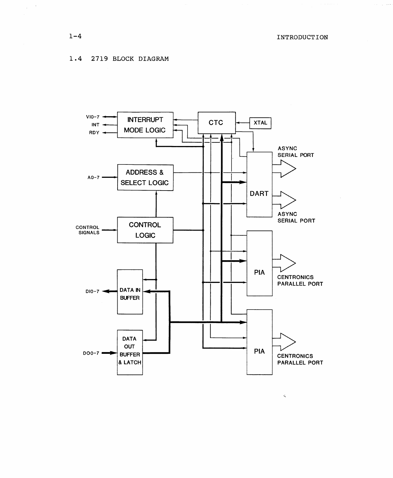
1.4
2719
BLOCK
DIAGRAM
V10-7
-----
INT-
ROY
-
AO-7
----+
INTERRUPT
ru
CTC
H XTAL I
MODE LOGIC
Il
-'"=.J
r='-
I
~
ASYNC
SERIAL
PORT
~
ADDRESS &
SELECT LOGIC
~I--:I-l
DART
~
CONTROL _
SIGNALS
CONTROL
LOGIC
010-7
~
DATA
IN
J.,..~.--
....
BUFFER
DATA
~
OUT
000-7
~
BUFFER
J----
..
& LATCH
PIA
PIA
ASYNC
SERIAL
PORT
~
CENTRONICS
PARALLEL
PORT
CENTRONICS
PARALLEL
PORT
CHAPTER
2
CONFIGURING
THE
2719
The
2719,
while
designed
to
be
flexible,
has
also
been
designed
to
require
as
little
configuration
as
possible
in
its
primary
environment,
CCS
Systems
300/400.
When
the
2719
is
added
to
a
System
300/400,
only
the
1M2
Header
and
Protective
Ground
Jumper
require
configuration.
All
other
headers
and
jumpers
are
shipped
configured
for
a
System
300/400.
However,
if
the
2719
is
used
in
a
CCS
System
2210
or
a
non-CCS
system,
additional
configuration
will
be
required.
This
chapter
includes
configuration
instructions
for
all
board
options.
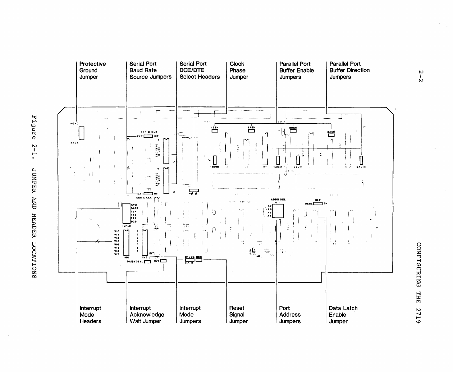
Jumper
and
header
locations
are
shown
in
Figure
2-1.
Table
2-2
briefly
defines
each
option.
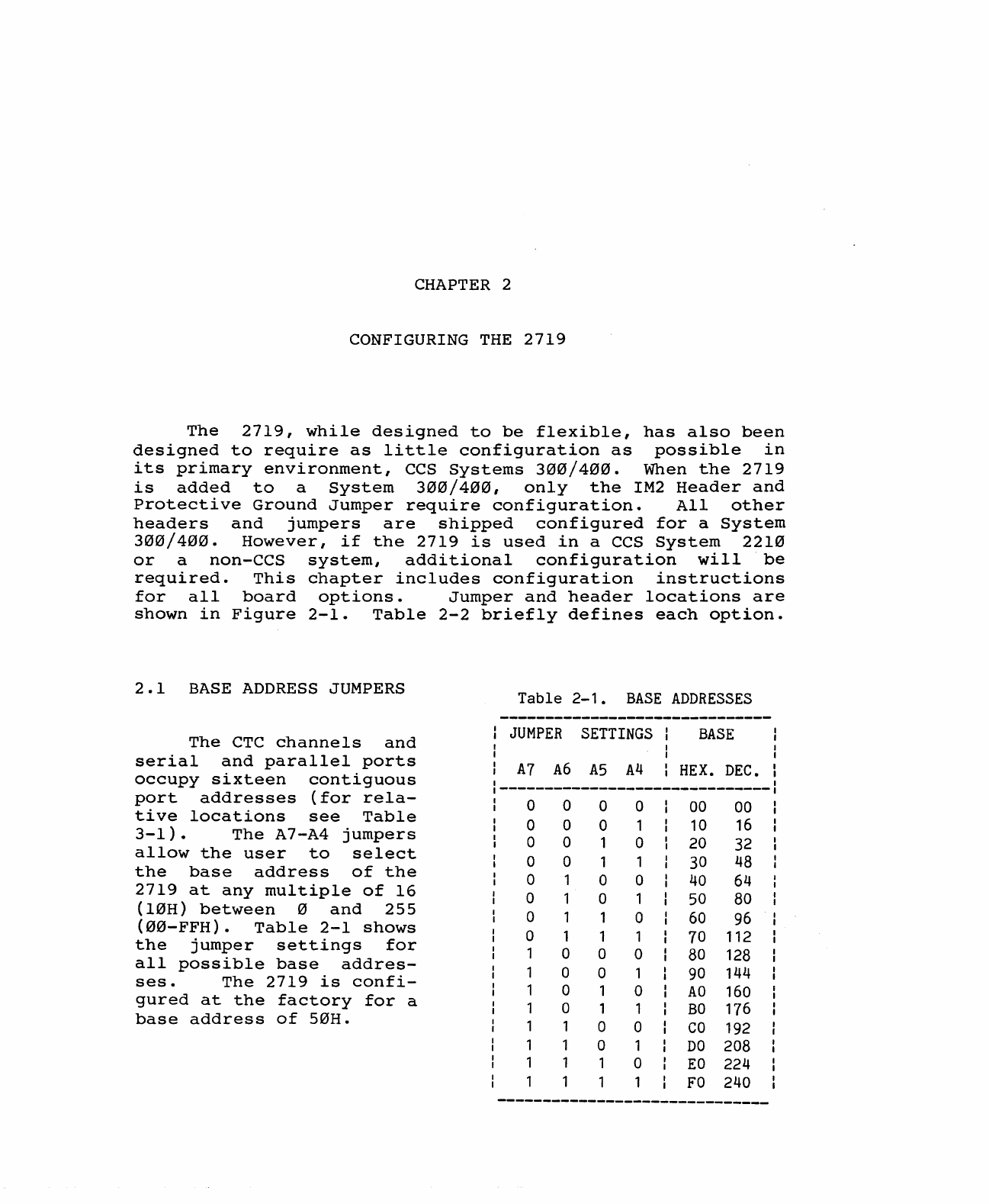
2.1
BASE
ADDRESS
JUMPERS
Table
2-1.
BASE
ADDRESSES
------------------------------
The
CTC
channels
and
JUMPER
SETTINGS
BASE
serial
and
parallel
ports
A7 A6
A5 A4
HEX.
DEC.
occupy
sixteen
contiguous
------------------------------
port
addresses
(for
rela-
0 0 0 0
00 00
tive
locations
see
Table
0 0 0 1
10
16
3-1)
.
The
A7-A4
jumpers
0 0 1 0 20 32
allow
the
user
to
select
0 0 1 1 30
48
the
base
address
of
the
0 1 0 0
40
64
2719
at
any
multiple
of
16
0 1 0 1 50 80
(10H)
between
0
and
255
0 1 1 0
60
96
(00-FFH)
.
Table
2-1
shows
0 1 1 1 70 112
the
jumper
settings
for
1 0 0 0
80
128
all
possible
base
addres-
1 0 0 1
90
144
sese
The
2719
is
confi-
1 0 1 0
AO
160
gured
at
the
factory
for
a 1 0 1 1
BO
176
base
address
of
50H.
1 1 0 0
CO
192
1 1 0 1
DO
208
1 1 1 0
EO
224
1 1 1 1
FO
240
------------------------------
I':tj
1-'-
1O
C
t;
CD
N
I
.....
Y
C
::s:
"'0
I:lj
::0
~
Z
0
::r::
trJ
~
0
trJ
:::0
L'1
0
()
~
8
H
0
Z
CJ)
POND
SOND
Protective
Ground
Jumper
0
I
Serial
Port
Baud
Rate
Source
Jumpers
r
SER
B
CLK
EXT
c::::J
INT
oT
~
(')(1)
'"'"
0:11
;;:111
oT
~
,..r,
~:::
0:11
;;:Joo
"
EXTc::::J
INT
SER A
CLK
i'lf
,..---,..------'
DART
i '
"DcTC
' '
:~:
I I
i
P2A
,
P2B
'.
VI1
1
VI2
~----I-:"---
VI3
VI4
VIS
vie
VI7
INT;
C
VIO
I~M1'2
~
M
IMO
1M
2
~~------,
DAIBYDSBL
D
RDYCJ
Serial
Port
DCE/DTE
Select Headers
1BEN
CJ
1BDIR
c::::J
-II "
'J
{l
I'
j
IMODE
RES
c::::JCJ
0,1
2
Clock
Phase
Jumper
1AEN
D
,.
.J
1
Parallel
Port
Buffer
Enable
Jumpers
'"
I.
'" 1
O
' I 0
~
I
I,
II
1
ADIR
~';
2BDIR
,
-l
C 1
~
U r
ADDR
SEL
DLE
DSBL
c::::J
EN
A7001
lAS
A5
A4
1
,
_____
______________
______________
______________
_
__________
~r
Interrupt
Mode
Headers
Interrupt
Acknowledge
Wait
Jumper
Interrupt
Mode
Jumpers
Reset
Signal
Jumper
Port
Address
Jumpers
Parallel
Port
Buffer
Direction
Jumpers
2AEN
CJ
L , o
.,,;
2ADIR
Data
Latch
Enable
Jumper
CONFIGURING
THE
2719
2-3
:
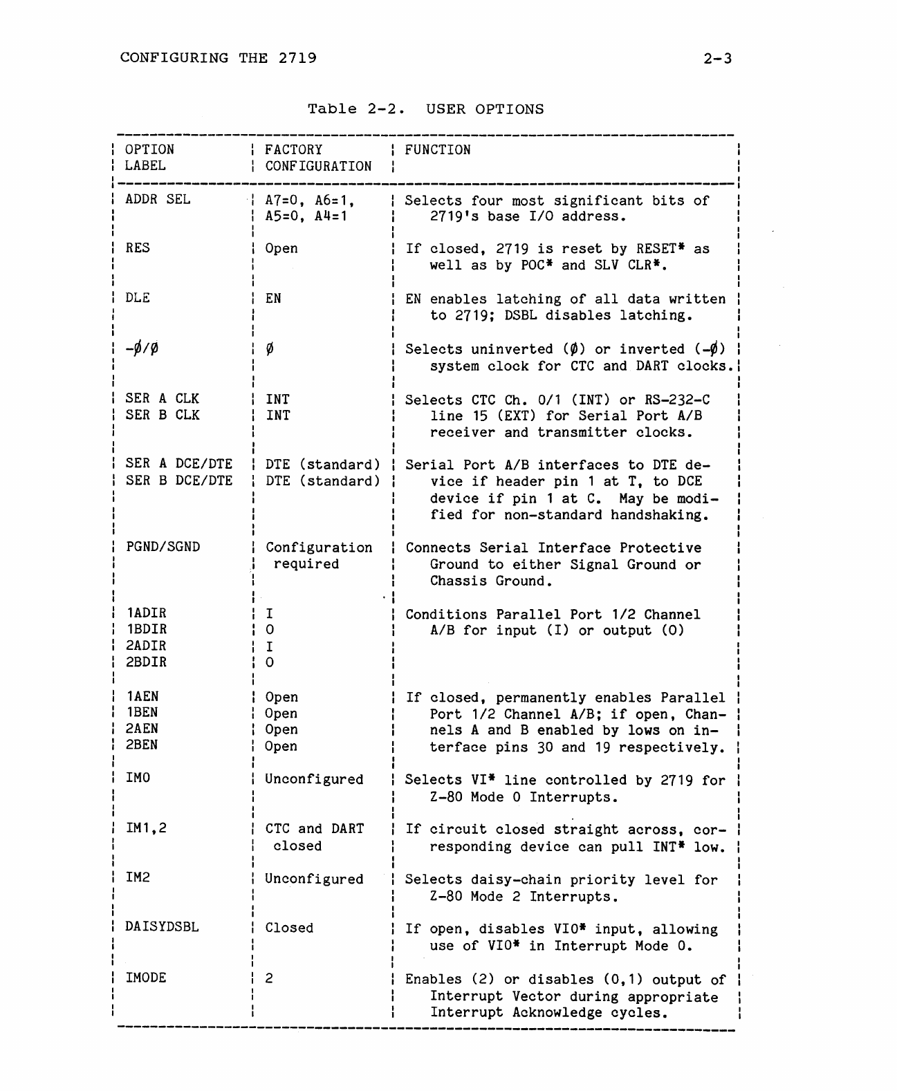
OPTION
:
LABEL
Table
2-2.
USER
OPTIONS
:
FACTORY
:
FUNCTION
:
CONFIGURATION
,---------------------------------------------------------------------------
ADDR
SEL
RES
DLE
-¢/f/J
SER
A
CLK
SER
B
CLK
SER
A
DCE/DTE
SER
B
DCE/DTE
PGND/SGND
1ADIR
1BDIR
2ADIR
2BDIR
1AEN
1BEN
2AEN
2BEN
IMO
IM1,2
1M2
DAISYDSBL
IMODE
A7=0,
A6=1,
A5=0,
A4=1
Open
EN
INT
INT
DTE
(standard)
DTE
(standard)
Configuration
required
I
o
I
o
Open
Open
Open
Open
Unconfigured
CTC
and
DART
closed
Unconfigured
Closed
2
Selects
four
most
significant
bits
of
2719's
base
I/O
address.
If
closed,
2719
is
reset
by
RESET*
as
well
as
by
POC*
and
SLY
CLR*.
EN
enables
latching
of
all
data
written
to
2719;
DSBL
disables
latching.
Selects
uninverted
(~)
or
inverted
(-~)
system
clock
for
CTC
and
DART
clocks.
Selects
CTC
Ch.
0/1 (INT)
or
RS-232-C
line
15
(EXT)
for
Serial
Port
A/B
receiver
and
transmitter
clocks.
Serial
Port
A/B
interfaces
to
DTE
de-
vice
if
header
pin
1
at
T,
to
DCE
device
if
pin
1
at
C.
May
be modi-
fied
for
non-standard
handshaking.
Connects
Serial
Interface
Protective
Ground
to
either
Signal
Ground
or
Chassis
Ground.
Conditions
Parallel
Port
1/2
Channel
AlB
for
input
(I)
or
output
(0)
If
closed,
permanently
enables
Parallel
Port
1/2
Channel A/B;
if
open,
Chan-
nels
A and B
enabled
by lows
on
in-
terface
pins
30
and
19
respectively.
Selects
VI*
line
controlled
by 2719
for
Z-80
Mode
0
Interrupts.
If
circuit
closed
straight
across,
cor-
responding
device
can
pull
INT*
low.
Selects
daisy-chain
priority
level
for
Z-80
Mode
2
Interrupts.
If
open,
disables
VIO*
input,
allowing
use
of
VIO*
in
Interrupt
Mode
O.
Enables
(2)
or
disables
(0,1)
output
of
Interrupt
Vector
during
appropriate
Interrupt
Acknowledge
cycles.
---------------------------------------------------------------------------
2-4
CONFIGURING
THE
2719
2.2
INTERRUPT
MODE
AND
PRIORITY
CONFIGURATION
Three
header
areas
and
two
jumpers
allow
you
to
tailor
2719
interrupts
to
a
particular
system.
If
the
system
uses
an
interrupt
controller,
you
will
need
to
configure
the
2719
for
Mode 0
interrupts.
If
the
system
does
not
implement
vectored
interrupts,
you
will
need
to
configure
for
Mode
1,
in
which
an
interrupt
causes
an
automatic
restart
at
location
0038H.
If
the
system
supports
the
powerful
Mode 2
Interrupt
Daisy
Chain,
as
CCS
Systems
300/400
do,
you
should
configure
for
Mode
2.
The
three
header
areas
are
labelled
IM0, 1M2,
and
IMl,2
in
accordance
with
the
interrupt
modes
to
which
they
apply.
IMl,2
is
a
2x6
pad
matrix,
hardwired
for
the
standard
configuration,
which
may
be
altered
by
the
installation
of
jumper
wires
or
header
pins
and
shorting
plugs.
IM0
and
1M2
are
socketed
2x8
headers.'
The
Interrupt
Mode (IMODE)
and
Daisy
Chain
Disable
(DAISYDSBL)
Jumpers
are
hardwired
for
Mode
2
and
must
be
reconfigured
for
Mode 0
or
Mode
1.
2.2.1
Mode 0
Configuration
The
first
task
in
configuring
for
Mode 0
is
to
reconfigure
the
IMODE
jumper,
cutting
the
trace
labelled
2
and
installing
a
jumper
in
the
0,1
position.
Next,
cut
the
CTC
and
DART
traces
of
the
IMl,2
Jumpers
and
the
DAISYDSBL
trace.
Finally,
install
the
16
pin
DIP
header
in
the
IM0
socket
and
wire
the
header
cover
to
select
the
VI*
line
by
which
each
device
will
assert
its
interrupt.
Remember
that
the
lower
the
number
of
the
VI*
line,
the
higher
the
interrupt
priority.
The
pins
corresponding
to
the
VI*
lines
are
labelled
0
through
7;
the
six
interrupt
signal
pins
are
labelled
C, D,
lA,
IB,
2A,
and
2B.
Pins
9
and
16
are
not
used.
More
than
one
interrupt
line
may
be
tied
to
one
VI*
line;
it
will
then
be
up
to
the
interrupt
service
routine
called
when
that
VI*
line
is
asserted
to
determine
which
device
generated
the
interrupt.
2.2.2
Mode 1
Configuration
Configuring
for
Mode 1
involves:
1)
leaving
the
IM0
and
1M2
Headers
unconfigured;
2)
reconfiguring
the
IMODE
Jumper
by
cutting
the
trace
labelled
2
and
installing
a
jumper
in
the
0/1
position;
3)
cutting
the
DAISYDSBL
trace;
and
4)
either
leaving
the
IMl,2
Jumpers
as
they
are
or
installing
jumpers,
CONFIGURING
THE
2719
2-5
depending
on
whether
or
not
parallel
port
interrupts
are
to
be
handled
through
the
CTC.
If
they
are
(see
Chapter
3
for
an
explanation
of
how
this
is
done),
the
IM1,2
Jumpers
should
be
left
as
they
are.
If
parallel
port
interrupts
are
to
be
asserted
directly
by
the
parallel
ports,
jumpers
should
be
installed
in
positions
PIA,
PIB,
P2A,
and
P2B.
2.2.3
Mode 2
Configuration
The
Z-80
Mode 2
Interrupt
Daisy
Chain,
when
extended
beyond
four
peripheral
devices,
requires
look-ahead
logic
to
ensure
that
all
devices
are
properly
informed
of
higher-priority
interrupts
within
the
allotted
time.
CCS
Systems
200,
300,
and
400
implement
a
unique
look-ahead
scheme
in
which:
1)
each
board
participating
in
the
daisy
chain
asserts
its
interrupt
priority
by
forcing
a
given
vectored
Interrupt
bus
line
low;
and
2)
a
board
is
prevented
from
interrupting
when
a
lower-numbered
VI*
line
is
low.
Thus
there
are
nine
interrupt
priority
levels,
0-8;
the
priority
0
board
controls
VI0*
and
senses
no
VI*
lines,
while
the
priority
8
board
senses
all
VI*
lines
and
controls
none.
The
1M2
Header
allows
the
user
to
select
the
interrupt
priority
level
of
the
2719
by
selecting
which
VI*
line(s)
the
board
will
be
sensitive
to
and
which
VI*
line
it
will
pull
low.
System
300/400
interrupt
priorities
may
be
determined
at
the
system
implementer's
discretion,
depending
on
system
components
and
application.
However,
the
priority
scheme
shown
below
should
be
appropriate
for
the
majority
of
systems.
The
System
Processor
is
hardwired
for
Level
0;
it
is
the
only
board
whose'priority
is
fixed.
Level
0:
2820
System
Processor
Level
1 :
2805
Wallclock/Terminator
Level
2:
2830
Six-Channel
Serial
I/O
---->
Level
3 :
2719
2
Parallel/2
Serial
I/O
Level
4:
2831
Arithmetic
Processor
Level
5:
2833
GPIB
Interface
Level
7:
2822
Floppy
Disk
Controller
Level
8:
2832
Hard
Di~k
Controller
Note
that
gaps
are
allowed
in
the
priority
structure;
thus,
it
is
not
necessary
to
reconfigure
a
level
3
board
to
level
2
if
there
is
no
level
2
board
in
the
system.
However,
no
priority
level
may
be
occupied
by
more
than
one
board.

2-6
CONFIGURING
THE
2719
Figure
2-2.
1M2
HEADER
CONFIGURATION
LEVEL
1
LEVEL
2
LEVEL
3
1 1 0 0 1 0 0
2 2 2
0-
3 3 3
4 4 4
5 5 5
6 6 6
7 7 7
INT INT INT
LEVEL
4
LEVEL
5
LEVEL
6
1 0 0 1 0 0 1 0 0
2 0 0 2 0 0 2 0 0
3 0 0 3 0 0 3 0 0
4 N 4 0 0 4 0 0
5 5 N 5 0 0
6 o 0 6 6
~
7 o 0 7 o 0 7
0 INT 0 INT INT
LEVEL
7
LEVEL
8
1 0 0 1 0 0
2 0 0 2 0 0
3 0 0 3 0 0
4 0 0 4 0 0
5 0 0 5 0 0
6 0 0 6 0 0
7
~
7 0 0
INT 0 0 INT
CONFIGURING
THE
2719
2-7
To
configure
the
1M2
Header,
determine
the
priority
level,
then:
1)
tie
all
lower-numbered
left-column
pins
straight
across;
and
2)
tie
the
pin
corresponding
to
the
2719's
priority
level
to
pin
9,
labeled
INT.
Note
that
the
lowest
level
to
which
the
2719
may
be
assigned
is
1:
the
board
is
hardwired
to
sense
the
VI0*
line,
which
is
reserved
as
the
2820
System
Processor's
priority-assertion
line.
Figure
2-2
shows
configuration
of
1M2
for
all
priority
levels.
2.3
SERIAL INTERFACES
2.3.1
Synchronous
Conversion
To
convert
the
2719
serial
communications,
simply
remove
the
it
with
a
Z-80
SIO/0
(neither
the
plug-compatible
with
the
DART).
with
the
board.
2.3.2
DCE/DTE
Conversion
ports
for
synchronous
Z-80
DART
(U3)
and
replace
SIO/l
nor
the
SIO/2
is
The
SIO/0
is
not
supplied
Each
serial
port
interface
includes
a
16-pin
DIP
header
with
cover
for
selecting
whether
the
port-will
interfac~
to
a
DTE
(Data
Terminal
Equipment)
or
DCE
(Data
Communication
Equipment)
device.
Since
most
peripherals
act
as
DTE,
the
2719
is
shipped
configured
to
interface
to
DTE
devices.
To
reconfigure
a
port
to
interface
to
a
DCE
device,
simply
turn
the
port's
DCE/DTE
header
so
that
instead
of
having
pin
1
in
pin
1
of
the
socket
(labeled
T),
pin
1
is
in
pin
9
of
the
socket
(labeled
C).
2.3.3
Non-Standard
Handshaking
Some
devices
using
the
RS-232-C
interface,
especially
printers,
use
non-standard
handshaking.
To
interface
such
a
device,
you
will
need
to
reconfigure
a DCE/DTE
Header
according
to
the
requirements
of
the
peripheral.
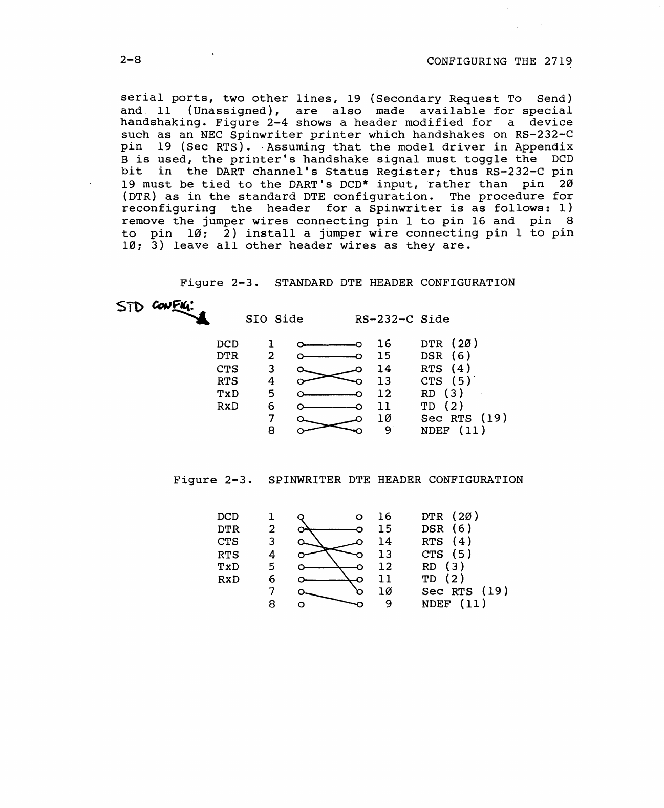
Figure
2-3
shows
the
header
pinouts
and
the
standard
DTE
wiring.
Note
that,
besides
the
RS-232-C
lines
normally
used
by
the
2719's
2-8
CONFIGURING
THE
2719
serial
ports,
two
other
lines,
19
(Secondary
Request
To
Send)
and
11
(Unassigned),
are
also
made
available
for
special
handshaking.
Figure
2-4
shows
a
header
modified
for
a
device
such
as
an
NEC
Spinwriter
printer
which
handshakes
on
RS-232-C
pin
19
(Sec
RTS).
-Assuming
that
the
model
driver
in
Appendix
B
is
used,
the
printer's
handshake
signal
must
toggle
the
DCD
bit
in
the
DART
channel's
Status
Register;
thus
RS-232-C
pin
19
must
be
tied
to
the
DART's
DCD*
input,
rather
than
pin
20
(DTR)
as
in
the
standard
DTE
configuration.
The
procedure
for
reconfiguring
the
header
for
a
Spinwriter
is
as
follows:
1)
remove
the
jumper
wires
connecting
pin
1
to
pin
16
and
pin
8
to
pin
10;
2)
install
a
jumper
wire
connecting
pin
1
to
pin
10;
3)
leave
all
other
header
wires
as
they
are.
Figure
2-3.
STANDARD
DTE
HEADER
CONFIGURATION
Sit>
t:w~
SIO
Side
RS-232-C
Side
DCD
1 0 0
16
DTR
(20)
DTR
2 0 0
15
DSR
(6)
CTS 3
><
14
RTS
(4
)
RTS
4
13
CTS
(5
)"
'TxD
5 0 0
12
RD
(3)
RxD
6 0 0
11
TD
(2)
7
><
10
Sec
RTS
(19)
8 9
NDEF
(11)
Figure
2-3.
SPINWRITER
DTE
HEADER
CONFIGURATION
DCD
DTR
CTS
RTS
TxD
RxD
1
2
3
4
5
6
7
8
16
15
14
13
12
11
10
9
DTR
(20)
DSR
(6)
RTS
(4)
CTS
(5)
RD
(3)
TD
(2)
Sec
RTS
(19)
NDEF
(11)
CONFIGURING
THE
2719
2-9
2.3.4
Baud
Rate
Source
Jumpers
If
you
plan
to
use
a
DART
channel
to
interface
a
DCE
device,
you
may
want
that
channel's
baud
rate
clock
to
be
supplied
by
the
DCE
device.
The
Channel
A
and
B
Baud
Rate
Source
Jumpers,
labeled
SER A
CLK
and
SER B CLK,
allow
each
DART
channel's
clocks
to
be
controlled
by
either
the
CTC
or
RS-232-C
li~e
15,
TSEC(DCE),
from
the
peripheral.
The
jumpers
are
hardwired
in
the
INT
position,
selecting
the
internal
(CTC)
baud
rate
sources.
To
select
the
external
(peripheral)
baud
rate
source,
cut
the
INT
trace
and
install
a
jumper
wire
in
the
EXT
position
of
the
appropriate
Baud
Rate
Source
Jumper.
[Please
note
that
because
DART
pins
RxCA
and
TxCA
are
together
on
the
PC
Board,
the
Channel
A
Receiver
transmitter
Clocks
cannot
be
separately
controlled.]
2.3.5
Protective
Ground
tied
and
Protective
Ground
is
defined
as
the
supply
current
return
path,
not
a
signal
current
return
path.
It
is
intended
to
equalize
the
voltage
potential
of
the
terminal
and
the
mainframe,
and
should
be
implemented
whenever
the
terminal
and
the
mainframe
are
connected
to
different
power
sources
which
may
have
different
ground
potentials.
If
both
serial
terminals
interfaced
through
the
2719
are
to
be
connected
to
the
same
outlet
as
the
mainframe,
the
protective
ground
feature
need
not
be
implemented.
At
the
upper
left
corner
of
the
board
are
two
jumper
pads
labeled
PGND
and
SGND.
These
allow
the
user
to
select
one
of
two
implementations
of
the
RS-232-C
Protective
Ground
signals
for
both
ports.
The
recommended
implementation
is
to
run
a
green
wire
from
the
PGND
pad
to
the
mainframe
chassis,
with
an
alligator
clip
or
other
convenient
method
for
connection.
This
conforms
to
the
RS-232
design
specifications,
ensuring
that
terminal
and
mainframe
have
the
same
potentials.
Use
this
method
with
CCS-supplied
terminals.
Some
terminals,
however,
tie
Protective
Ground
and
Signal
Ground
together
or
use
the
Protective
Ground
as
the
Signal
Ground.
If
you
are
using
such
a
terminal
with
the
2719,
you
will
need
to
install
a
100
ohm,
1/2
Watt
resistor
(as
per
EIA
standard
RS-422-A)
between
the
PGND
and
SGND
pads.
2-10
CONFIGURING
THE
2719
2.4
PARALLEL
INTERFACE
CONFIGURATION
2.4.1
Buffer
Direction
Jumpers
Bidirectional
buffers
are
used
on
the
four
parallel
port
data
channels.
The
direction
of
data
flow
is
determined
by
the
Parallel
Port
Buffer
Direction
Jumpers
lADIR,
lBDIR,
2ADIR,
and
2BDIR,
which
are
hardwired
for
the
standard
Centronics-type
interface
configuration.
Channel
B
of
each
port
(Centronics
data
bus)
is
hardwired
in
the
0
position
for
output;
Channel
A
of
each
port
(Centronics
status
bus)
is
hardwired
in
the
I
position
for
input.
To
change
the
direction
of
a
buffer,
cut
the
existing
trace
and
~nstall
a
jumper
wire
in
the
opposite
position.
[Please
note
that
while
each
channel
may
be
used
for
either
input·
or
output,
the
characteristics
of
the
PIA
handshaking
signals
make
Channel
B
more
suited
for
output
and
Channel
A
more
suited
for
input.]
2.4.2
Buffer
Enable
Jumpers
The
parallel
interfaces
are
designed
so
that
lows
on
interface
lines
30
and
19
enable
the
Channel
A
and
Channel
B
interface
buffers
respectively;
otherwise
the
enable
inputs
to
the
buffers
are
pulled
high.
Thus,
the
buffers
will
not
be
enabled
unless
the
interface
cable
is
connected.
On
the
Centronics
interface
lines
30
and
19
are
defined
as
ground
lines.
However,
some
Centronics-type
peripherals
may
not
support
the
lines
as
defined.
If
this
is
the
case,
or
if
the
interface
is
used
in
a
non-Centronics
configuration
and
the
peripheral
does
not
assert
inter£ace
lines
30
and
19
low,
jumper
wires
must
be
installed
between
the
appropriate
Buffer
Enable
Jumper
pads
to
permanently
enable
the
buffers.
The
four
Buffer
Enable
Jumpers
are
labeled
lAEN, lBEN, 2AEN,
and
2BEN.
2.4.3
Reversing
Interface
Polarities
The
parallel
port
buffers
were
selected
to
support
the
Centronics
interface
polarities:
positive
logic
data
and
negative
logic
handshaking.
However,
pin-compatible
buffers
may
be
substituted
for
the
buffers
used
on
the
parallel
ports
CONFIGURING
THE
2719
2-11
if
positive-logic
handshaking
or
negative-logic
data
are
required.
For
negative-logic
data,
replace
the
appropriate
8104/8304
with
an
8103/8303;
for
positive-logic
handshaking,
replace
the
appropriate
74LS367A
with
a
74LS368A.
2.5
THE
RESET
JUMPER
If
the
2719
is
used
in
a
system
which
does
not
automatically
assert
SLVCLR*
when
RESET*
is
asserted,
a
jumper
must
be
installed
between
the
pads
labelled
RES.
This
is
necessary
primarily
when
the
board
is
used
in
Cromemco
systems.
It
is
not
necessary
with
CCS
systems.
If
you
are
uncertain
about
whether
the
Reset
Jumper
is
required,
consult
the
system
documentation;
if
you
remain
uncertain,
call
the
system
manufacturer.
2.6
INTERRUPT
ACKNOWLEDGE
WAITS
If
the
2719
is
used
with
a
CCS
2810
CPU, a
wait
state
is
required
in
all
Interrupt
Acknowledge
cycles
to
ensure
that
the
CTC
has
time
to
put
its
vector
on
the
bus
before
the
CPU
tries
to
read
it.
To
enable
Interrupt
Acknowledge
wait
states,
install
a
jumper
wire
between
the
pads
labeled
ROY.
This
jumper
is
not
required
if
the
2719
is
used
in
a
System
300/400.
If
the
2719
is
used
in
a
non-CCS
system,
this
jumper
mayor
may
not
be
required;
experiment,
and
install
the
jumper
if
necessary.
2.7
CLOCK
PHASE
In
some
systems,
including
the
CCS
2210
(with
the
2810
CPU
board),
the
system
clock
on
bus
pin
24
and
the
CPU
clock
are
of
opposite
phase.
Z-80
devices
in
a
system
must
all
have
clocks
of
the
same
phase
to
work
together.
The
Clock
Phase
Jumper
allows
the
user
to
invert
the
phase
of
the
system
clock
signal
used
on
the
2719
as
necessary.
If
the
2719
is
used
in
a
CCS
System
300/400
or
any
other
system
in
which
the
bus
clock
is
in
phase
with
the
processor
clock,
set
the
Clock
Phase
Jumper
to
the
rightmost
(0)
position.
If
the
2719
is
used
in
a
system
(including
the
CCS
System
2210)
featuring
the
CCS
2810
CPU
board
or
any
other
system
in
which
the
bus
clock
and
processor
clock
are
of
opposite
phase,
set
the
Clock
Phase
Jumper
to
the
leftmost
(-0)
position.

2-12
CONFIGURING
THE
2719
2.8
DATA
LATCH
ENABLING
AND
DISABLING
The
OLE
jumper
has
been
included
on
the
2719
to
allow
disabling
of
the
Data
Out
Latch.
The
jumper
is
hardwired
in
the
EN
position,
which
is
required
if
the
2719
is
used
with
a
CCS
2810
CPU. When
the
2719
is
used
in
a
System
300/400,
the
jumper
may
be
in
either
the
EN
or
DSBL
position.
However,
some
CPU's
may
require
that
data
corning
onto
the
board
not
be
latched.
If
you
are
using
a
non-CCS
CPU,
experiment,
then
disable
the
latching
by
cutting
the
EN
trace
and
installing
a
jumper
wire
in
the
DSBL
position
if
the
2719
cannot
accept
latched
data
from
your
CPU.
2.9
BAUD
RATES
IN
2
MHZ
SYSTEMS
The
CTC
cannot
accept
a CLK/TRG
input
whose
frequency
is
greater
than
half
the
system
clock
frequency.
Thus,
if
you
use
the
2719
in
a 2
MHz
system,
you
must
replace
the
1.8432
MHz
crystal
pack
in
the
lower
right
corner
of
the
board
with
a
74LS74
dual
flip-flop.
The
crystal
pack
is
not
socketed;
you
will
need
to
unsolder
its
four
pins
and
remove
the
solder
from
the
other
pads
before
installing
the
74LS74.
(If
you
install
the
74LS74,
then
at
a
later
date
install
the
2719
in
a 4
MHz
system,
you
need
not
replace
the
crystal
pack
unless
you
want
to
be
able
to
select
baud
rates
greater
than
9600.)
Note
that
installation
of
a
74LS74
will
necessitate
changes
to
the
serial
port
drivers
if
they
have
been
written
for
the
2719
with
the
crystal
pack.
See
Section
3.3.
2.10
OPERATION
IN
6MHZ
SYSTEMS
To
use
"the
2719
in
a 6
MHz
system,
you
must
replace
four
chips:
the
Z-80A
CTC
with
a
Z-80B
CTC;
the
Z-80A
DART
with
a
Z-80B
DART
(or
Z-80B
SIO/0
for
synchronous
capability);
and
both
6821
PIAs
with
68B2l
PIAs.
Some
2719
boards
may
be
shipped
with
68B2l's,
in
which
case
replace
ment
of
the
PIAs
will
not
be
necessary;
check
the
chips
(not
the
silkscreen
labels)
before
replacing
the
PIAs.
Baud
rate
programming
will
not
change
if
the
CTC
is
used
in
the
co~nter
mode
with
the
1.8432
MHz
crystal
pack.
In
the
timer
mode
or
with
a
74LS74
installed
instead
of
the
crystal
pack,
multiply
the
4
MHz
values
in
Table
3-3
by
1.5
(75
baud
will
not
be
available).
CHAPTER
3
PROGRAMMING
INFORMATION
This
section
is
provided
for
those
who
wish
to
write
their
own
drivers
for
the
2719's
serial
and/or
parallel
ports.
Full
instructions
for
programming"the
PIAs
are
given,
as
they
may
not
be
readily
available.
programming
options
for
the
Z-80
SIO
and
CTC
are
quite
elaborate,
and
are
not
given
in
this
manual.
Complete
instructions
are
given
in
the
Z-80
Family
Programming
Reference
Manual
included
in
CCS
System
300/400
documentation
packages
or
available
separately
from
CCS,
as
well
as
in
a
variety
of
other
publications,
a
few
of
which
are
listed
below.
Only
the
programming
limitations
and
requirements
stemming
from
the
implementation
of
the
SIO
and
CTC
on
the
2T19
are
treated
in
this
chapter.
AN
INTRODUCTION
TO
MICROCOMPUTERS,
Osborne
and
Associates,
Inc.
(Berkeley,
CA:
1978).
ZILOG
MICRCOMPUTER
COMPONENTS
DATA
BOOK,
Zilog,
Inc.
(Cupertino,
CA:
1980).
MOSTEK
MICROCOMPUTER
DATA
BOOK,
Mostek
Corporation
(Carollton,
TX:
1979).
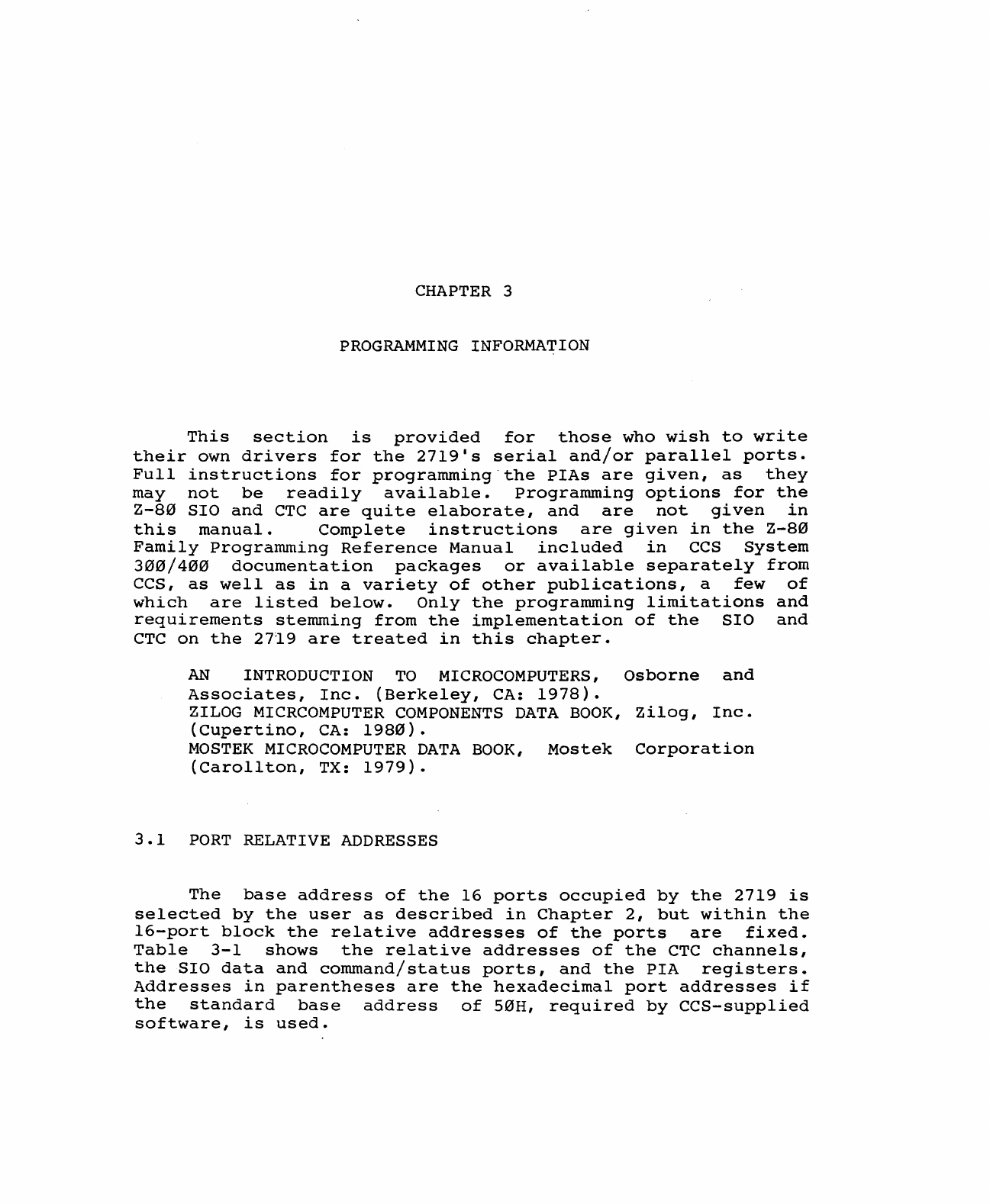
3.1
PORT
RELATIVE
ADDRESSES
The
base
address
of
the
16
ports
occupied
by
the
2719
is
selected
by
the
user
as
described
in
Chapter
2,
but
within
the
l6-port
block
the
relative
addresses
of
the
ports
are
fixed.
Table
3-1
shows
the
relative
addresses
of
the
CTC
channels,
the
SIO
data
and
command/status
ports,
and
the
PIA
registers.
Addresses
in
parentheses
are
the
hexadecimal
port
addresses
if
the
standard
base
address
of
50H,
required
by
CCS-supplied
software,
is
used.
3-2
PROGRAMMING
INFORMATION
Table
3-1.
PORT
RELATIVE
ADDRESSES
-----------------------------------------------------------
1 CTC:
CHANNEL
0
CHANNEL
1
CHANNEL
2
CHANNEL
3
1
Base
(50)
Base+l
(51)
Base+2
(52)
Base+3
(53)
1
1-----------------------------------------------------------1
1
DART:
A
DATA
A
COMMAND
B
DATA
B
COMr~D
1
1
Base+4
(54)
Base+5
(55)
Base+6
(56)
Base+7
(57)
1
1-----------------------------------------------------------1
1
PIAl:
A DATA/DIR B DATA/DIR A
CONTROL
B
CONTROL
1
1
Base+8
(58)
Base+9
(59)
Base+A
(SA)
Base+B
(5B)
1
1-----------------------------------------------------------1
1
PIA2:
A DATA/DIR B DATA/DIR A
CONTROL
B
CONTROL
1
1
Base+C
(5C)
Base+D
(5D)
Base+E
(5E)
Base+F
(SF)
1
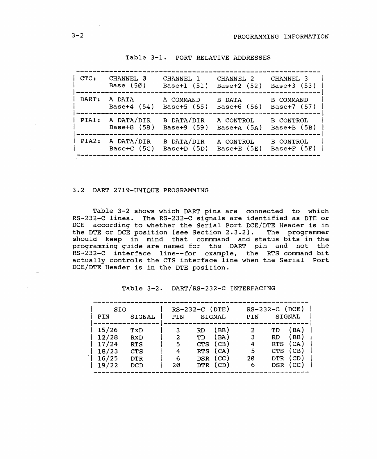
3.2
DART
2719-UNIQUE
PROGRAMMING
Table
3-2
shows
which
DART
pins
are
connected
to
which
RS-232-C
lines.
The
RS-232-C
signals
are
identified
as
DTE
or
DCE
according
to
whether
the
Serial
Port
DCE/DTE
Header
is
in
the
DTE
or
DCE
position
(see
Section
2.3.2).
The
programmer
should
keep
in
mind
that
commmand
and
status
bits
in
the
programming
guide
are
named
for
the
DART
pin
and
not
the
RS-232-C
interface
line--for
example,
the
RTS
command
bit
actually
controls
the
CTS
interface
line
when
the
Serial
Port
DCE/DTE
Header
is
in
the
DTE
position.
Table
3-2.
DART/RS-232-C
INTERFACING
SIO
1
RS-232-C
(DTE)
RS-232-C
(DCE) 1
1 PIN SIGNAL I PIN SIGNAL
PIN
SIGNAL 1
1----------------1-----------------------------------1
1
15/26
TxD 1 3
RD
(BB) 2
TD
(BA) 1
1
12/28
RxD
1 2
TD
(BA) 3
RD
(BB) 1
1
17/24
RTS
1 5
CTS
(CB) 4
RTS
{cAl
1
1
18/23
CTS
1 4
RTS
{cAl
5
CTS
(CB) 1
-I
16/25
DTR
1 6
DSR
(CC) 20
DTR
(CD) 1
I
19/22
DCD
1
20
DTR
(CD) 6
DSR
(CC) 1

PROGRAMMING
INFORMATION
3-3
Programming
limitations
of
the
DART
are
listed
below.
They
result
from
the
fact
that
pins
W/RDYA*, W/RDYB*,
RIA*,
and
RIB*
are
not
connected
on
the
PC
Board.
1.
Bit
7
of
Command
Register
I
(Wait/Ready
Enable)
should
be
0.
Bits
6
and
5
are
don't-care
bits.
2.
Bit
4
of
Status
Register
0
will
always
be
low.
This
will
not
affect
External
Status
Interrupts.
3.3
CTC
2719-UNIQUE
PROGRAMMING
The
CTC
on
the
2719
is
used
to
provide
programmable
clock
signals
for
the
DART
and
to
generate
Mode 2
interrupts
for
the
PIAs.
In
the
factory
configuration,
Channel
0
provides
the
clocks
for
Serial
Port
A,
Channel
1
provides
the
clocks
for
Serial
Port
B,
Channel
2
interrupts
for
PIAl,
and
Channel
3
interrupts
for
PIA2.
Please
note
that,
for
each
serial
port,
both
the
Receiver
Clock
and
the
Transmitter
Clock
are
controlled
by
the
same
CTC
signal
and
therefore
cannot
be
independently
programmed.
The
specific
programming
requirements
for
the
CTC
on
the
2719
are
listed
below.
1.
Channels
0
and
1,
which
determine
the
serial
port
baud
rates,
may
be
programmed
in
either
the
counter
mode
or
the
timer
mode.
Interrupts
should
be
disabled.
Table
3-3
shows
programming
options
for
common
baud
rates.
2.
If
Mode 2
interrupts
from
the
PIAs
are
desired,
Channels
2
and
3
must
be
progran~ed
in
the
counter
mode
with
interrupts
enabled,
rising
edges
counted,
and
a
time
constant
of
1.
Thus
the
two
bytes
sent
after
the
interrupt
vector
to
initialize
Channel
2
or
3
are
D7H
followed
by
0lH.

3-4
PROGRAMMING
INFORMATION
Table
3-3.
TIME
CONSTANTS
FOR
COMMON
BAUD
RATES
TIME
CONSTANTS
---------
----------------------------------------
BAUD
RATE
75
110
134.5
150
300
600
1200
2400
4800
7200
9600
19.2K
38.4K
57.6K
115.2K
CRYSTAL
4
MHZ
C T
192
96
48
24
16
12
6
3
2
1
208
142
116
104
52
26
13
FLIP-FLOP
2
MHZ
C T
104
52
26
13
104
71
58
52
26
13
4
MHZ
C T
208
104
52
26
17
13
208
142
116
104
52
26
13
C =
Counter
Mode (Command
Byte
= 47H)
T =
Timer
Mode,
Prescaler
of
16
(Command =
07H)
DART
Clock
Rate
is
assumed
to
be
16x
3.4
PROGRAMMING
THE
PIA
Each
PIA
has
six
accessible
(read
and
write)
registers:
two
Data
Registers,
two
Data
Direction
Registers,
and
two
Command
Registers.
Register
selection
is
determined
by
two
Register
Select
inputs
(RS0,
RS1)
controlled
by
A0
and
Al
and
by
Bit
2
of
the
Command
Register.
Table
3-4
shows
how
each
register
is
selected.
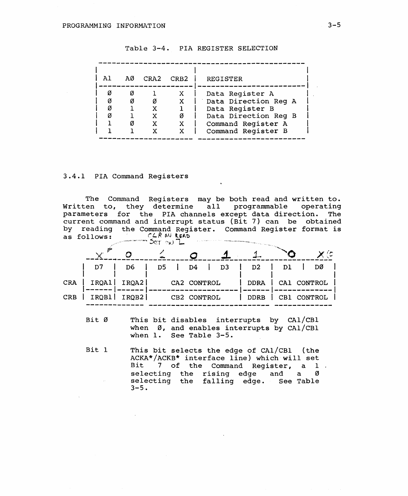
PROGRAt'1MING
INFORMATION
3-5
Table
3-4.
PIA
REGISTER SELECTION
I 1 I
1
Al
A0
CRA2
CRB2
1 REGISTER 1
1---------------------1------------------------1
I 0 0 1 X 1
Data
Register
A I
1 0 0 0
xl'
Data
Direction
Reg A 1
1 0 1
XII
Data
Register
B 1
1 0 1 X 0 I
Data
Direction
Reg B I
1 1 0 X X 1 Command
Register
A 1
1 1 1 X X 1 Command
Register
B 1
---------------------
------------------------
3.4.1
PIA
Command
Registers
The
Command
Registers
may
be
both
read
and
written
to.
Written
to,
they
determine
all
programmable
operating
parameters
for
the
PIA
channels
except
data
direction.
The
current
command
and
interrupt
status
(Bit
7)
can
be
obtained
by
reading
the
Command
Register.
Command
Register
format
is
as
follows:
.'
r L R
61J
t"At>
,
.......
'
......
"
..
"'>~'-
..•
r.~'"'
.:5<::·'r
"~'i\J
~
'
..
'
...
'.--
...
~
..•
- . "
..
,
".
--2{~~-~p
_______
~
_____
~
_____
~_~
___
~
___
~::~
____
~J?
1
D7
1
D6
I
D5
I
D4
I
D3
I
D2
I
Dl
I
D0
1
1 1 I I I I
CRA
1
IRQAll
IRQA21
CA2
CONTROL
I
DDRA
1 CAl
CONTROL
I
1------1------1--------------------1------1-------------I
CRB
1
IRQBll
IRQB21
CB2
CONTROL
I
DDRB
I CBl
CONTROL
I
Bit
0
Bit
1
This
bit
disables
interrupts
by
CAl/CBl
when
0,
and
enables
interrupts
by
CAl/CBl
when
1.
See
Table
3-5.
This
bit
selects
the
edge
of
CAl/CBl
(the
ACKA*/ACKB*
interface
line)
which
will
set
Bit
7
of
the
Command
Register,
a 1 .
selecting
the
rising
edge
and
a 0
selecting
the
falling
edge.
See
Table
3-5.
3-6
PROGRAMMING
INFORMATION
Table
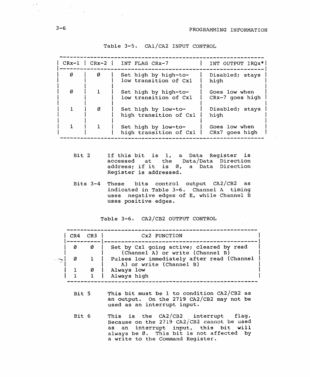
3-5.
CAl/CA2
INPUT
CONTROL
------------------------------------------------------------
CRx-l
I
CRx-2
lINT
FLAG
CRx-7
lINT
OUTPUT
IRQx*
------------------------------------------------------------
o 0
Set
high
by
high-to-
I
Disabled:
stays
low
transition
of
Cxl
1
high
I
o 1
Set
high
by
high-to-
I
Goes
low
when
low
transition
of
Cxl
I
CRx-7
goes
high
I
1 0
Set
high
by
low-to-
1
Disabled:
stays
high
transition
of
Cxl
1
high
I
1 1
Set
high
by
low-to-
1
Goes
low
when
high
transition
of
Cxl
1 CRx7
goes
high
Bit
2
If
this
bit
is
1,
a
Data
Register
is
accessed
at
the
Data/Data
Direction
address:
if
it
is
0,
a
Data
Direction
Register
is
addressed.
Bits
3-4
These
bits
control
output
CA2/CB2
as
indicated
in
Table
3-6.
Channel
A
timing
uses
negative
edges
of
E,
while
Channel
B
uses
positive
edges.
Table
3-6.
CA2/CB2
OUTPUT
CONTROL
1
CR4
CR3
I Cx2 FUNCTION 1
1----------1---------------------------------------------I
1 0 0 1
Set
by
exl
going
active:
cleared
by
read
1
1 I
(Channel
A)
or
write
(Channel
B) I
~I
0 1 I
Pulses
low
immediately
after
read
(Channell
.'
1 1 A)
or
write
(Channel
B) I
I 1 0 1
Always
low
1
1 1 1 I
Always
high
I
Bit
5
Bit
6
This
bit
must
be
1
to
condition
CA2/CB2
as
an
output.
On
the
2719
CA2/CB2 may
not
be
used
as
an
interrupt
input.
This
is
the
CA2/CB2
interrupt
flag.
Because
on
the
2719
CA2/CB2
cannot
be
used
as
an
interrupt
input,
this
bit
will
always
be
0.
This
bit
is
not
affected
by
a
write
to
the
Command
Register.
PROGRAMMING
INFORMATION
Bit
7
This
is
the
CAllcBl
interrupt
flag.
When
this
bit
is
1,
IRQA*/IRQB*
has
been
asserted
by
the
appropriate
transition
of
CAl/cBl.
This
bit
is
cleared
when
the
channel1s
Data
Register
is
read
and
is
not
affected
by
a
write
to
the
Command
Register.
3.4.2
PIA
Data
Direction
Registers
3-7
Bits
0-7
of
the
Data
Direction
Register
control
the
direction
of
data
lines
0-7
respectively.
If
a
bit
is
0,
the
corresponding
data
line
is
an
input;
if
a
bit
is
1,
the
corresponding
data
line
is
an
output.
A
Data
Direction
Register
can
be
accessed
only
if
Bit
2
of
the
Command
Register
for
the
same
channel
is
0.
Because
of
the
way
the
PIA
data
lines
are
buffered
on
the
2719,
ALL
BITS
OF
A
CHANNEL
MUST
BE
PROGRAMMED
FOR
THE
SAME
DIRECTION
and
the
data
direction
programmed
for
a
channel
must
agree
with
the
setting
of
the
corresponding
Parallel
Port
Data
Direction
Jumper
as
described
in
Section
2.4.1.
3.4.3
PIA
INITIALIZATION:
CENTRONICS
CONFIGURATION
The
following
sequence
initializes
a
parallel
port
in
the
standard
Centronics
configuration.
a.
Output
00H
to
both
Ch.
A
and
Ch.
B
Control
Ports
to
select
DDR.
b.
Output
to
Data/Dir
Ports
(00H
to
Ch.
A
and
0FFH
to
Ch.
B)
to
select
direction.
c.
Output
2CH
(or
2DH
for
interrupts)
to
both
Ch.
A
and
Ch.
B
Control
Ports
to
set
the
PIA
mode.
d.
Input
from
both
Ch.
A
and
Ch.
B
Data/Dir
Ports
to
clear
the
status
bits.
CHAPTER
4
HARDWARE
DESIGN
Two
6821
PIAs
and
a
Z-80
DART
provide
the
two
parallel
and
two
serial
ports
of
the
2719.
Most
of
the
interface
functions
are
provided
by
these
three
chips.
A
Z-80
CTC
is
employed
to
generate
baud
rate
clocks
for
the
two
DART
channels
and
Mode 2
interrupts
for
the
two
PIAs.
Additional
logic
supports
interrupt
capability
in
all
three
Z-80
modes,
addresses
and
controls
the
CTC,
DART,
and
PIAs,
and
controls
data
buffering.
Thus
the
2719
can
be
divided
into
six
functional
elements:
the
PIAs,
the
DART,
the
CTC,
the
interrupt
logic,
the
address/control
logic,
and
data
buffering.
Each
element
is
separately
described
below.
4.1
THE
PIA'S
Each
6821
PIA
provides
two
parallel
data
channels,
programmable
for
input
or
output
on
a
bit-by-bit
basis,
with
programmable
two-line
handshaking
for
each
channel.
programming
options
are
discussed
in
Chapter
3.
PIA
inputs
and
outputs
are
defined
in
Table
4-1.
For
additional
information
see
a
6821
data
sheet.
Each
PIA
data
channel
is
buffered
by
an
8304
bi-directional
driver/receiver,
the
direction
of
data
flow
being
jumper-selectable
but
pre-configured
for
Channel
A
as
input
and
Channel
B
as
output.
The
A
and
B
data
buffers
are
enabled
by
lows
on
interface
lines
30
and
19
respectively,
or
may
be
permanently
enabled
by
the
installation
of
a
jumper.
Handshaking
is
determined
to
consist
of
one
input
(CA1/CB1)
and
one
output
(CA2/CB2)
by
the
buffers
on
the
handshake
lines.
The
on-board
reset
signal
is
buffered
onto
the
parallel
interface
to
provide
a
reset
signal
for
the
peripheral.
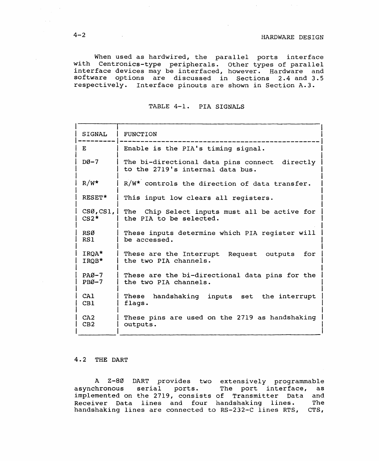
4-2
HARDWARE
DESIGN
When
used
as
hardwired,
the
parallel
ports
interface
with
Centronics-type
peripherals.
Other
types
of
parallel
interface
devices
may
be
interfaced,
however.
Hardware
and
software
options
are
discussed
in
Sections
2.4
and
3.5
respectively.
Interface
pinouts
are
shown
in
Section
A.3.
TABLE
4-1.
PIA
SIGNALS
1
SIGNAL
FUNCTION
1
---------
------------------------------------------------1
E
Enable
is
the
PIAls
timing
signal.
1
D0-7
R/W*
RESET*
CS0,CSl,
CS2*
RS0
RSI
IRQA*
IRQB*
PA0-7
PB0-7
CAl
CBl
CA2
CB2
The
bi-directional
data
pins
connect
directly
to
the
2719
1s
internal
data
bus.
R/W*
controls
the
direction
of
data
transfer.
This
input
low
clears
all
registers.
The
Chip
Select
inputs
must
all
be
active
for
the
PIA
to
be
selected.
These
inputs
determine
which
PIA
register
will
be
accessed.
These
are
the
Interrupt
Request
outputs
for
the
two
PIA
channels.
These
are
the
bi-directional
data
pins
for
the
the
two
PIA
channels.
These
handshaking
inputs
set
the
interrupt
flags.
These
pins
are
used
on
the
2719
as
handshaking
outputs.
4.2
THE
DART
A
Z-80
DART
provides
two
extensively
programmable
asynchronous
serial
ports.
The
port
interface,
as
implemented
on
the
2719,
consists
of
Transmitter
Data
and
Receiver
Data
lines
and
four
handshaking
lines.
The
handshaking
lines
are
connected
to
RS-232-C
lines
RTS, CTS,

HARDWARE
DESIGN
4-3
DTR,
and
DSR,
as
indicated
in
Table
3-2,
the
Serial
Interface
Headers
allowing
configuration
of
the
interface
as
either
DCE
or
DTE,
as
well
as
allowing
for
non-standard
handshaking
using
lines
19
or
11.
Table
4-2
defines
the
DART
inputs
and
outputs.
4.3
THE
CTC
The
Z-80
CTC
consists
of
four
separately
programmable
counter/timer
circuits.
Each
circuit
includes
a
downcounter,
a
time
constant
register,
and
a
prescaler.
In
the
timer
mode,
the
downcounter
is
loaded
with
the
programmed
time
constant,
then
decremented
with
every
16
or
256
pulses
of
the
4
MHz
system
clock
(depending
on
the
prescaler
selected).
In
the
counter
mode,
the
downcounter
is
loaded
with
the
time
constant,
then
decremented
with
every
pulse
of
the
channel's
CLK/TRG
input,
the
prescaler
having
no
effect.
Channels
0-2
have
ZC/TO
(Zero
Count/Time
Out)
outputs
that
pulse
high
when
the
downcounters
reach
zero;
all
four
channels
can
be
programmed
to
interrupt
when
their
downcounters
reach
zero.
In
addition,
downcounter
contents
can
be
read
from
the
channel
address
without
disturbing
the
counting.
Table
4-3
defines
the
CTC
inputs
and
outputs.
On
the
2719,
CTC
Channels
0
and
1
are
used
to
supply
the
DART
Channel
A
and
Channel
B
clocks
respectively,
while
Channels
2
and
3
are
used
to
bring
the
PIA
interrupts
into
the
Z-80
Mode 2
Interrupt
Daisy
Chain.
Channels
0
and
1
thus
may
be
programmed
in
either
the
counter
or
timer
mode,
as
described
in
Section
3.3.
The
CLK/TRG
inputs
of
Channels
o
and
1
are
controlled
by
a
1.8432
MHz
crystal.
(Note
that
jumpers
allow
each
DART
channel's
transmitter
and
receiver
clocks
to
be
controlled
by
RS-232-C
line
15
if
the
DART
channel
functions
as
the
DTE
device
and
the
user
desires
the
baud
rate
to
be
controlled
by
the
DCE
device.)
Whenever
either
of
the
PIAl
interrupt
request
outputs
IRQA*
and
IRQB*
goes
low,
the
CLK/TRG
input
to
CTC
Channel
2
goes
high.
The
CLK/TRG
input
to
Channel
3
is
similarly
controlled
by
the
PIA2
interrupt
request
outputs.
If
these
channels
are
programmed
in
the
counter
mode
as
described
in
Section
3.3,
the
CTC
will
generate
the
actual
interrupt
request
whenever
a
PIA
signals
that
it
wants
one.
In
Interrupt
Mode
2,
this
means
that
an
Interrupt
vector
pointing
to
the
appropriate
PIA
service
routine
can
be
gated
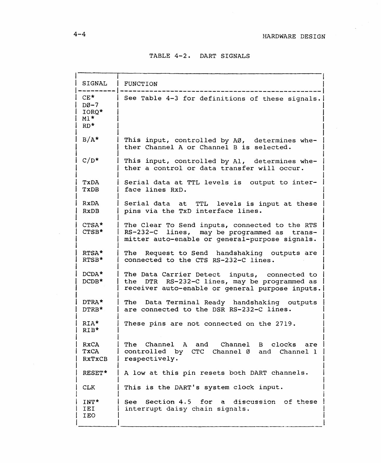
4-4
HARDWARE
DESIGN
TABLE
4-2.
DART
SIGNALS
I
I SIGNAL I
FUNCTION
1---------
------------------------------------------------
I CE*
See
Table
4-3
for
definitions
of
these
signals.
D0-7
IORQ*
MI*
RD*
B/A*
C/D*
TxDA
TxDB
RxDA
RxDB
CTSA*
CTSB*
RTSA*
RTSB*
DCDA*
DCDB*
DTRA*
DTRB*
RIA*
RIB*
RxCA
TxCA
RxTxCB
RESET*
CLK
INT*
lEI
lEO
This
input,
controlled
by
A0,
determines
whe-
ther
Channel
A
or
Channel
B
is
selected.
This
input,
controlled
by
AI,
determines
whe-
ther
a
control
or
data
transfer
will
occur.
Serial
data
at
TTL
levels
is
output
to
inter-
face
lines
RxD.
Serial
data
at
TTL
levels
is
input
at
these
pins
via
the
TxD
interface
lines.
The
Clear
To
Send
inputs,
connected
to
the
RTS
RS-232-C
lines,
may
be
programmed
as
trans-
mitter
auto-enable
or
general-purpose
signals.
The
Request
to
Send
handshaking
outputs
are
connected
to
the
CTS
RS-232-C
lines.
The
Data
Carrier
Detect
inputs,
connected
to
the
DTR
RS-232-C
lines,
may
be
programmed
as
receiver
auto-enable
or
general
purpose
inputs.
The
Data
Terminal
Ready
handshaking
outputs
are
connected
to
the
DSR
RS-232-C
lines.
These
pins
are
not
connected
on
the
2719.
The
Channel
A
controlled
by
respectively.
and
CTC
Channel
Channel
IZJ
B
clocks
are
and
Channel
1
A
low
at
this
pin
resets
both
DART
channels.
This
is
the
DART's
system
clock
input.
See
Section
4.5
for
a
discussion
of
these
interrupt
daisy
chain
signals.

HARDWARE
DESIGN
4-5
TABLE
4-3.
CTC
SIGNALS
I
SIGNAL 1
FUNCTION
---------1------------------------------------------------
CE*
I
Chip
Enable
is
controlled
by
the
address
1
decode
circuitry.
1
RD*
I
The
Read
input
determines
the
direction
of
I
data
transfer.
IORQ*
The
I/O
Request
input
enables
data
transfer.
Ml*
.Both
Ml*
and
IORQ*
low
indicates
an
Interrupt
CS0,CSl
CLK/TRG
0-3
ZC/TO
0-2
D0-7
RESET*
CLK
INT*
lEI
lEO
Acknowledge
cycle.
The
Channel
CTC
channels.
Select
inputs
select
one
of
four
They
are
controlled
by
A0-Al.
The
Clock/Trigger
inputs
control
downcounter
decrementing
in
counter
mode.
CLK/TRG0-l
are
controlled
by
the
crystal
or
the
system
clock
divided
by
two.
CLK/TRG2-3
are
controlled
by
the
PIA
IRQ*
outputs.
The
Zero
Count/Timeout
pins
pulse
high
when
the
downcounters
reach
zero.
ZC/T00-l
control
:
the
DART
receiver
and
transmitter
clocks.
The
bi-directional
data
pins
connect
directly
to
the
2719
internal
data
bus.
Reset
low
terminates
downcounting,
disables
interrupts,
and
tri-states
D0-D7.
This
is
the
CTC's
system
clock
input.
See
Section
4.5
for
a
discussion
of
these
interrupt
daisy
chain
signals.
4-6
HARDWARE
DESIGN
onto
the
bus
during
the
Interrupt
Acknowledge
cycle.
The
IM0
and
IMl,2
Headers
allow
direct
assertion
of
PIA
interrupt
requests
in
Interrupt
Modes
0
and
1,
in
which.
the,
special
interrupt
capabilities
of
a
Z-80
device
are
not
required.
4.4
ADDRESS
AND
CONTROL
LOGIC
During
I/O
cycles,
A7-A0
carry
the
I/O
port
address,
selecting
one
of
256
I/O
ports.
Each
of
the
four
major
components
of
the
2719
(the
DART,
the
CTC,
and
the
t~o
PIAs)
occupies
four
ports.
The
2719
is
designed
so
that
the
ports'
of
the
four
devices
occupy
absolute
locations
relative
to
each
other
in
any
l6-port
block
whose
base
is
a
multiple
of
16.
For
an
on-board
device
to
be
selected,
A7-A4
must
match
the
settings
of
the
Base
Address
Jumpers,
either
sINP
or
sOUT
must
be
active,
and
sINTA
must
be
inactive.
When
these
conditions
are
met,
the
internal
signal
BDSEL
(Board
Select)
goes
active.
BDSEL
is
the
CS0
input
to
each
PIA
and
is
input
to
the
CTC
and
DART
Select
Gates
(U10a
and
b),
the
outputs
of
which
control
the
CTC
and
DART
Chip
Enable
inputs.
When
BDSEL
is
active,
A3
and
A2
determine
which
device
is
enabled,
control'ling
PIA
inputs
CSI
and
CS2*
and
being
input
to
the
CTC
and
DART
Select
Gates.
Table
4-4
shows
the
states
of
A3
and
A2
required
to
enable
the
various
chips.
Table
4-4.
CHIP SELECTION
I
A3
A2
I CHIP SELECTED I
\--------1---------------1
I 0 0 1
CTC
1
I 0 1 1
DART
I
I 1 0 I
PIAl
1
1 1 1 I
PIA2
I
Except
for
the
Enable
inputs
to
the
PIAs,
the
rest
of
the
control
logic
for
the
four
devices
is
relatively
straightforward.
The
R/W*
inputs
to
the
PI
As
are
controlled
directly
by
pWR*,
while
the
RD*
(essentially
R*/W)
inputs
to
the
DART
and
CTC
are
low
when
pDBIN
is
active
during
non-Interrupt-Acknowledge
cycles
and
high
at
all
other
times.
CTC
and
DART
inputs
MI*
and
eLK
are
controlled
HARDWARE
DESIGN
4-7
directly
by
the
sMl
and
02
bus
lines1
IORQ*
is
active
when
'one
of
SINTA,
sINP,
or
sOUT
is
active.
The
Enable
inputs
to
the
PIAs
are
required
to
be
active
for
166
nanoseconds
during
read
-
and
write
operations,
but
need
not
be
synchronized
to
'the
system
clock.
On
the
2719
they
are
a.ctive
whenever
either
pWR*
or
pDBIN
is
active.
With
a 4
MHz
or,
slower
system
clock,
Enable
pulses
of
adequate
duration
are
guaranteed.
The
2719
is
wired
so
that
the
CTC,
the
DART,
and
the
PIAs
are
all
reset
when
either
of
bus
signals
POC*
or
SLVCLR*
goes
active.
The
IEEE
standards
for
the
8-100
bus
specify
that
SLVCLR*
should
be
asserted
whenever
RESET*
is
asserted.
SLVCLR*,
when
asserted
by
RESET*,
is
removed
sli-ghtly
before
RESET*
to
ensure
that
bus
slaves
finish
the
reset
before'
the
bus
master
comes
up.
Thus
it
is
advantageous
for
a
peripheral
board
to
be
reset
by
SLVCLR*
if
possible.
However,
in
some
systems
SLVCLR*
is
not
automatically
asserted
when
RESET*
is
asserted.
When
the
2719
is
used
in
such
systems
it
will
be
necessary
to
install
a
jumper
between
the
pads
labelled
RES
to
cause
the
2719
to
be
reset
directly
by
RESET*
active.
4.5
INTERRUPT LOGIC
The
Z-80
CPU
is
capable
of
three
modes
of
maskable
interrupt
response,
the
mode
in
which
the
CPU
operates
at
a
given
time
being
determined
by
software.
The
three
modes
are
defined
in
the
CPU
section
of
the
Z-80
Family
Programming
Reference
Manual.
Mode 0
is
the
8080
interrupt
mode,
which
requires
that
an
interrupt
controller
be
part
of
the
system.
An
interrupting
device
asserts
one
of
the
VI*
lines,
which
is
sensed
by
the
Interrupt
Controller;
the
Interrupt
Controller
then
asserts
INT*
and
puts
out
the
programmed
instruction
(usually
a
restart
or
call).
In
Mode
1
the
interrupting
device
asserts
INT*
directly,
causing
the
CPU
to
execute
a
restart
at
location
0038H.
In
Mode
2,
the
special
Z-80
mode,
the
highest-priority
interrupting
device
puts
the
vector
for
its
interrupt
service
routine
onto
the
bus
during
the
Interrupt
Acknowledge
cycle.
In
support
of
Mode 2
interrupts,
the
Z-80
peripherals
have
lEI
and
lEO
(Interrupt
Enable
In
and
Out)
pins
which
allow
them
to
be
linked
in
a
hardware-prioritizing
interrupt
daisy
chain.
The
highest-priority
device's
lEO
is
connected
to
the
next-highest-priority
device's
lEI.
If
a
device's
lEI
input
is
high,
it
may
generate
an
interrupt
request
by
forcing
INT*
low.
A
device's
lEO
output
is
forced
low
if
4-8
HARDWARE
DESIGN
either
its
lEI
pin
or
its
INT*
pin
is
low.
Thus
a
device
generating
an
interrupt
request
disables
the
interrupt
request
logic
of
all
lower-priority
devices
in
the
daisy
chain.
Higher-priority
devices
are
unaffected,
however,
and
may
interrupt
at
any
time,
providing
that
CPU
interrupts
are
enabled.
If
more
than
four
devices
are
connected
in
a
simple
daisy
chain,
a
low-priority
interrupt
request
may
not
be
disqualified
by
a
higher-priority
interrupt
request
soon
enough
to
prevent
the
low-priority
device
from
thinking
its
interrupt
is
being
acknowledged
and
outputting
its
interrupt
vector.
The
2719
supports
an
extended
Z-80
Mode 2
Interrupt
Daisy
Chain
with
a
look-ahead
scheme
implemented
on
all
CCS
System
300/400
peripheral
boards.
The
VI*
bus
lines
are
used
to
prioritize
the
boards
participating
in
the
chain.
Each
board's
look-ahead
logic
guarantees
that
an
interrupt
request
by
an
on-board
device
or
by
a
device
on
a
higher-priority
board
will
be
passed
on
to
lower-priority
boards
rapidly
enough
to
be
recognized
before
the
interrupt
is
acknowledged,
preventing
two
devices
from
putting
their
interrupt
vectors
on
the
bus
at
the
same
time.
On
the
2719,
if
the
DART
requests
an
interrupt,
the
CTC
is
prevented
from
interrupting
by
the
normal
chip-to-chip
lEI-lEO
daisy
chain.
An
interrupt
by
a
higher-priority
board
does
not
ripple
through
the
DART,
however;
the
interrupt
request
logic
of
both
the
DART
and
the
CTC
is
immediately
disabled
when
the
2719
interrupt
logic
senses
any
higher-priority
VI*
line
going
low.
Whenever
an
on-board
device
interrupts
or
the
2719
senses
a
higher-
priority
VI*
line
low,
the
2719
forces
its
priority-assertion
VI*
line
low
to
immediately
disable
lower-priority
boards.
The
particular
VI*
lines
the
2719
senses
and
the
VI*
line
it
asserts
are
determined
by
the
configuration
of
the
1M2
Header
(see
Section
2.2.3).
In
some
environments
it
will
be
desirable
for
the
2719
to
generate
Mode 0
or
Mode 1
interrupts.
The
Mode 0
Header
allows
the
user
to
select
which
VI*
line
each
on-board
device
will
use
to
communicate
its
interrupt
request
to
the
Interrupt
Controller.
The
Mode
1,2
Header
allows
each
device
to
directly
assert
INT*.
Configuration
instructions
for
the
interrupt
headers
are
given
in
Section
2.2.
In
some
systems,
including
those
using
a
CCS
2810
CPU,
a
wait
may
be
required
during
Interrupt
Acknowledge
cycles
to
ensure
that
the
eTC
has
time
to
get
its
interrupt
vector
onto
the
bus.
For
this
reason,
jumper-enabled
circuitry
has
been
provided
to
force
bus
line
RDY
low
while
pSYNC
is
active
during
Interrupt
Acknowledge
cycles
in
which
the
2719
has
the
highest-priority
interrupt
pending.
HARDWARE
DESIGN
4-9
4.6
DATA
BUFFERING
AND
LATCHING
All
system
bus
inputs
and
outputs
are
fully
buffered,
as
are
the
serial
and
parallel
port
interface
lines.
Hysteresis
drivers
and
receivers
are
used
for
system
bus
interfacing,
ensuring
minimum
noise
on
the
bus.
No
load
of
more
than
one
Low-Power
Schottky
TTL
level
is
placed
on
any
system
bus
input.
INT*
and
VI*
line
drivers
are
open-collector.
Serial
port
interface
drivers
and
receivers
meet
EIA
RS-232-C
specifications.
Except
for
the
parallel
port
buffers,
discussed
in
Section
4.1,
and
the
Data
In
Buffer,
all
buffers
are
permanently
enabled.
The
Data
In
Buffer
and
Data
Out
Latch
(described
below)
are
alternately
tri-stated
except
during
Interrupt
Acknowledge
cycles.
The
Data
Out
Latch
is
always
disabled
during
Interrupt
Acknowledge
cycles.
The
Data
In
..
Buffer
is
enabled
during
Interrupt
Acknowledge
cycles
if
the
board
is
configured
for
Mode 2
interrupts
and
the
2719
has
the
highest-priority
request
pending:
this
is
necessary
to
allow
the
Interrupt
Vector
onto
the
bus.
However,
in
Interrupt
Mode 0
or
1
it
is
necessary
to
keep
the
Interrupt
vector
off
the
bus.
If
the
IMS
Jumper
is
wired
for
the
0/1
position,
the
Data
In
Buffer
is
disabled
during
all
Interrupt
Acknowledge
cycles.
In
all
non-Interrupt-
Acknowledge
cycles,
the
Data
Out
Latch
is
disabled
and
the
Data
In
Buffer
enabled
for
the
duration
of
pDBIN
active
when
the
board
is
addressed
during
an
I/O
Read
cycle:
otherwise
the
Data
In
Buffer
is
tri-stated
and
the
Data
Out
Latch
is
enabled.
The
Data
Out
Latch
has
been
included
to
defeat
the
multiplexing
of
status
and
data
on
the
DO
lines
by
the
CCS
2810
CPU,
thus
allowing
the
2719
tol
be
used
in
the
CCS
System
2210.
The
CTC
cannot
handle
the
2810's
multiplexed
status
and
data.
When
bus
signal
sOUT
goes
inactive,
the
data
is
latched
(provided
that
the
latching
signal
is
not
jumper-disabled)
until
one
of
three
things
occurs:
1)
sINTA
goes
active:
2)
an
I/O
Read
cycle
occurs,
enabling
the
Data
In
Buffer:
or
3)
another
I/O
Write
cycle
occurs,
with
sOUT
going
active,
gating
new
data
onto
the
bus.
Because
the
CTC's
RD*
input
is
always
low
unless
pDBIN
is
active
and
sINTA
is
inactive,
the
CTC
may
read
valid
data
for
as
long
as
it
is
enabled
during
an
I/O
Write
cycle.
When a
device
has
interrupted,
it
monitors
the
data
bus
during
all
instruction
fetches,
looking
for
the
RETI
instruction
which
signals
that
servicing
of
the
interrupt
has
been
completed
and
that
lower-priority
interrupts
may
now
be
asserted.
To
ensure
proper
monitoring
of
the
CPU
instruction
fetches
by
the
2719,
the
CPU
must
internally

4-10
HARDWARE
DESIGN
connect
the
DI
and
DO
buses.
This
is
necessary
because,
while
the
RETI
instruction
is
input
to
the
CPU
on
the
Dr
lines,
the
2719
looks
for
RETI
on
the
DO
lines.
The
CCS
2820
System
Processor
Board
meets
this
requirement
as
long
as
no
other
board
asserts
DODSB
during
instruction
fetch
cycles.
APPENDIX
A
TECHNICAL
INFORlvIATION

A-2
TECHNICAL INFORMATION
A.l
USER-REPLACEABLE PARTS
QTY
REF
Integrated
Circuits
1
1
2
3
1
2
1
3
1
1
4
1
1
1
3
2
1
1
2
1
1
1
U3
U6
U16,17
U24,28,29
U23
U26,30
U22
U27,31,33
U21
U20
U7,9,10,12
U19
U28
U25
U5,14,15
U4,13
Ul
U2
U8,11
U32
U18
Yl
Capacitors
13
6
Cl,7-12,14-19
C2-6,13
Resistors
2
3
Rl,2
Zl-3
DESCRIPTION
Z-80A
DART
Z-80A
CTC
6821
PIA
74LS136
quad
EX-OR
74LS13
dual
4-in
NAND
74LS240
oct
buffers,
inv
74LS08
quad
2-in
AND
74LS244
octal
buffers
74LS02
quad
2-in
NOR
74LS00
quad
2-in
NAND
8304B
transceiver
7407
hex
buffer,
OC
74LS10
tri
3-in
NAND
74LSl1
tri
3-in
AND
75150
line
driver
75154
line
receiver
79L12
-12V
regulator
78L12
+12V
regulator
74LS367A
hex
drivers,
74LS373
octal
D
latches
LM323K +5 V
regulator
Oscillator,
1.8432
MHz
.1uf
Mono,
50VDC,
20%
4.7uf
Tant,
35VDC,
20%
2.7K
ohm,
1/4
Watt,
5%
SIP
Network,
2.7K
x 7
CCS
PART
if:
48200119-01
48200084-01
48200076-01
48200021-01
48200120-01
48200034-01
48200006-01
48200035-01
48200002-01
48200001-01
48200068-01
48200051-01
48200008-01
48200125-01
48200055-01
48200056-01
48200115-01
48200127-01
48200039-01
48200041-01
48200107-01
48200118-01
15900001-01
15500003-01
47000023-01
47400002-01
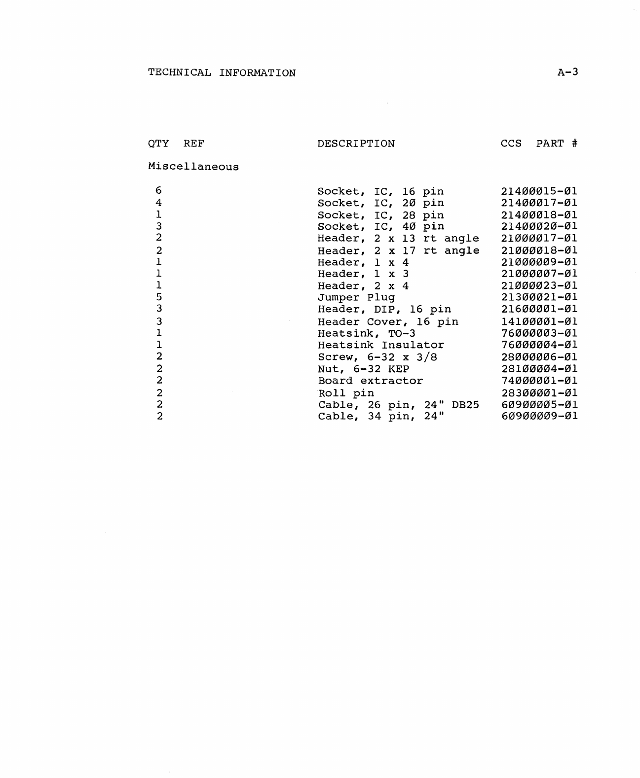
TECHNICAL INFORMATION
QTY
REF
Miscellaneous
6
4
1
3
2
2
1
1
1
5
3
3
1
1
2
2
2
2
2
2
DESCRIPTION
Socket,
Ie,
16
pin
Socket,
IC,
20
pin
Socket,
IC,
28
pin
Socket,
IC,
40
pin
Header,
2 x
13
rt
angle
Header,
2 x
17
rt
angle
Header,
1 x 4
Header,
1 x 3
Header,
2 x 4
Jumper
Plug
Header,
DIP,
16
pin
Header
Cover,
16
pin
Heatsink,
TO-3
Heatsink
Insulator
Screw,
6-32
x
3/8
Nut,
6-32
KEP
Board
extractor
Roll
pin
Cable,
26
pin,
24"
DB25
Cable,
34
pin,
2411
A-3
CCS PART #
21400015-01
21400017-01
21400018-01
21400020-01
21000017-01
21000018-01
21000009-01
21000007-01
21000023-01
21300021-01
21600001-01
14100001-01
76000003-01
76000004-01
28000006-01
28100004-01
74000001-01
28300001-01
60900005-01
60900009-01
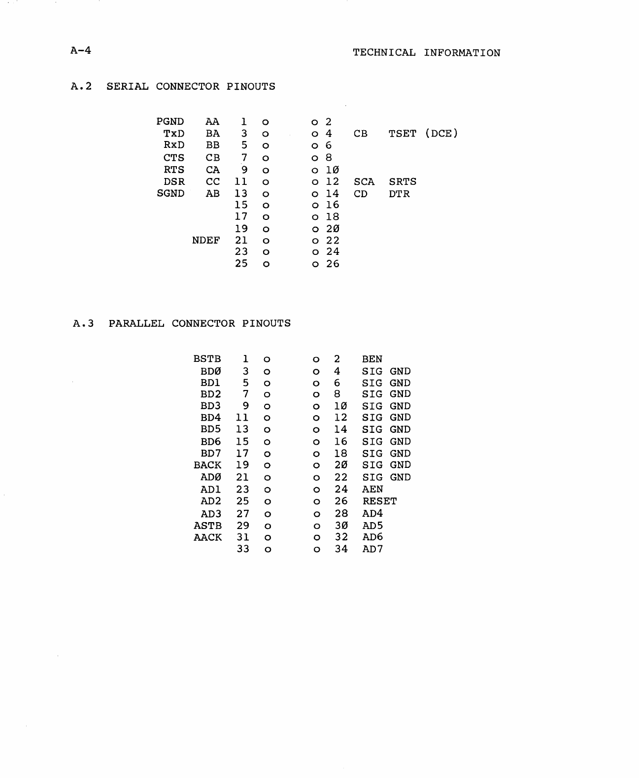
A-4
TECHNICAL
INFORMATION
A.2
SERIAL
CONNECTOR
PINOUTS
PGND
AA
1 0 0 2
TxD
BA
3 0 0 4
CB
TSET (DCE)
RxD
BB
5 0 0 6
CTS
CB
7 0 0 8
RTS
CA
9 0 0
10
DSR
CC
11
0 0
12
SCA
SRTS
SGND
AB
13
0 0
14
CD
DTR
15
0 0
16
17
0 o
18
19
0 o
20
NDEF
21 0 o
22
23
0 0
24
25 0 0
26
A.3
PARALLEL
CONNECTOR
PINOUTS
BSTB
1 0 0 2
BEN
BD0
3 0 0 4
SIG
GND
BDI 5 0 0 6
SIG
GND
BD2
7 0 0 8
SIG
GND
BD3
9 0 0
10
SIG
GND
BD4
11
0 0
12
SIG
GND
BD5
13
0 0
14
SIG
GND
BD6
15
0 0
16
SIG
GND
BD7
17
0 0
18
SIG
GND
BACK
19
0 0
20
SIG
GND
AD0
21 0 0 22
SIG
GND
ADI
23
0 0
24
AEN
AD2
25 0 0
26
RESET
AD3
27 0 0
28
AD4
ASTB
29 0 0
30
ADS
AACK
31
0 0
32
AD6
33 0 0
34
AD7
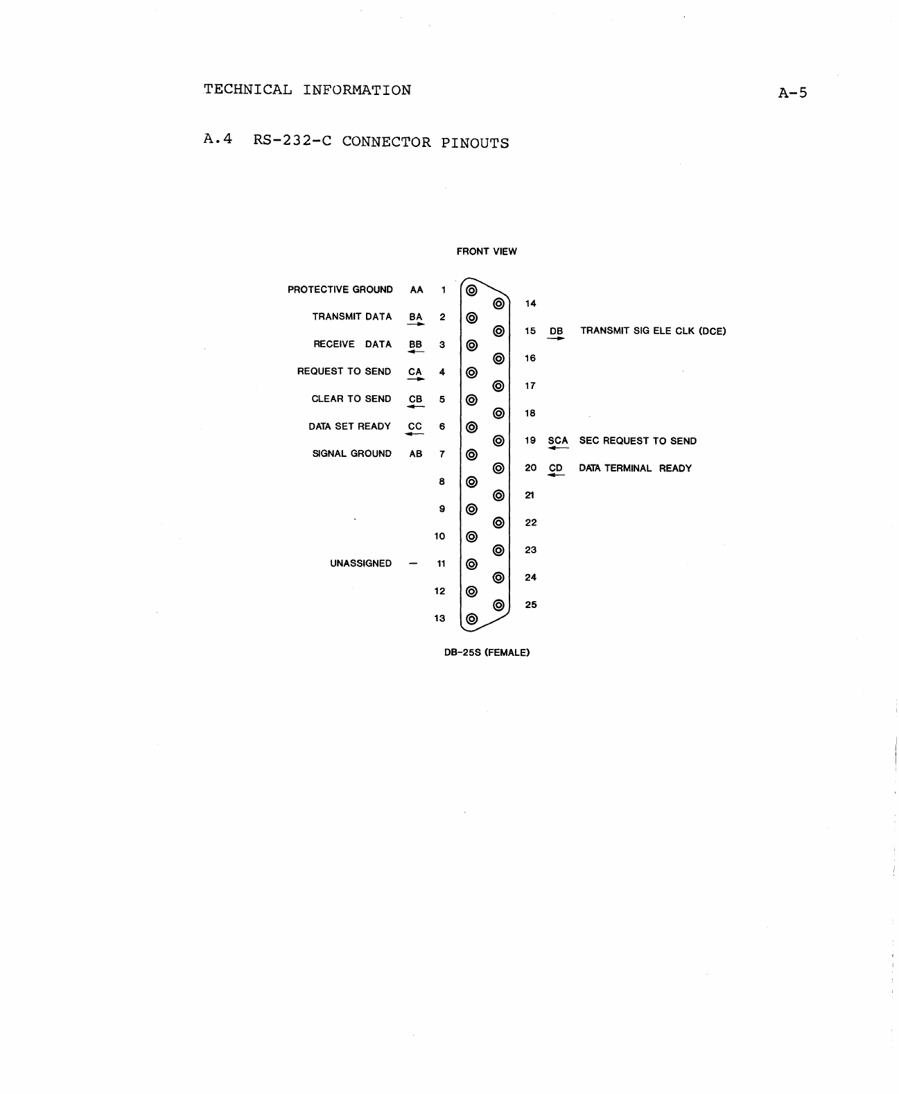
TECHNICAL INFORMATION
A-5
A.4
RS-232-C
CONNECTOR
PINOUTS
FRONT VIEW
PROTECTIVE
GROUND
AA @ @ 14
TRANSMIT DATA BA 2 @
-@ 15 DB TRANSMIT
SIG
ElE
ClK
(DCE)
-
RECEIVE DATA BB 3 @
-@
16
REQUEST TO SEND CA 4 @
-@
17
CLEAR TO SEND CB 5 @
-@ 18
DATA
SET READY
CC
6 @
--
@
19
SCA SEC REQUEST TO SEND
--
SIGNAL GROUND AB 7 @ @
20
CD
DATA
TERMINAL READY
-
8 @ @
21
9 @ @
22
10 @ @
23
UNASSIGNED
11
@
@)
24
12
@) @)
25
13
@)
DB-25S
(FEMALE)
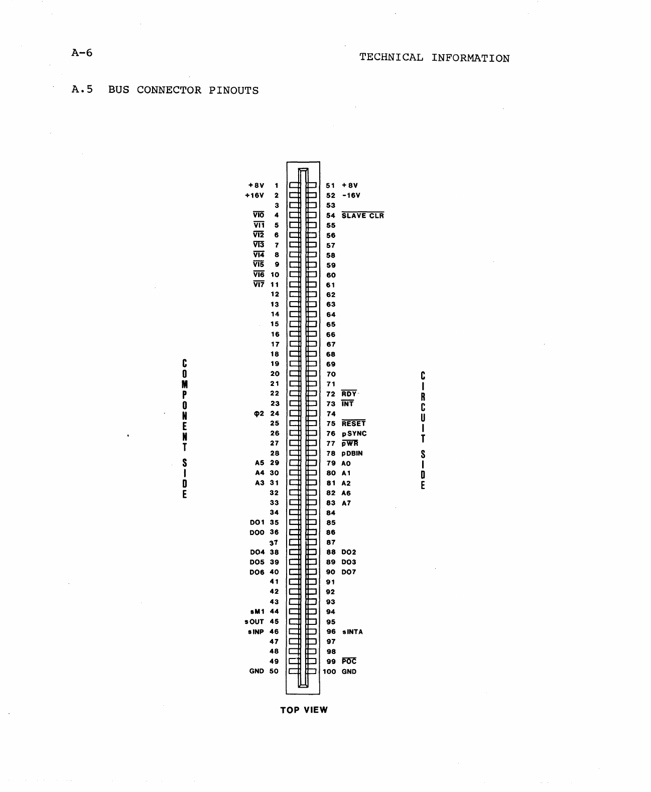
A-6
TECHNICAL
INFORMATION
A.5
BUS
CONNECTOR
PINOUTS
+8V
1
51
+8V
+16V 2
52
-16V
3
53
ViO
4
54
SLAVE
CLR
Vi1
5
55
Vi2
6
56
VI3
7
57
Vi4
8
58
ViS
9
59
ViS
10
60
Vi7
11
61
12
62
13
63
14
64
15
65
16
66
17
67
18
68
C
19
69
0
20
70
C
M
21
71 I
P
22
72
iiDv'. R
0
23
73
iNT C
N
CP2
24
74
U
E
25
75
RESET I
N
26
76
pSYNC T
T
27
77
pWR
28
78
pOBIN
S
S
A5
29
79
AO
I
I
A4
30
80
A1
0
0
A3
31
81
A2
E
E
32
82
A6
33
83
A7
34
84
001
35
85
000
36
86
31
87
004
38
88
002
005
39
89
003
006
40
90
007
41
91
42
92
43
93
sM1
44
94
sOUT
45
95
slNP
46
96
slNTA
47
97
48
98
49
99
~
GNO
50
100
GNO
TOP
VIEW

TECHNICAL INFORMATION
A-7
A.6
SCHEMATIC/LOGIC
DIAGRAM
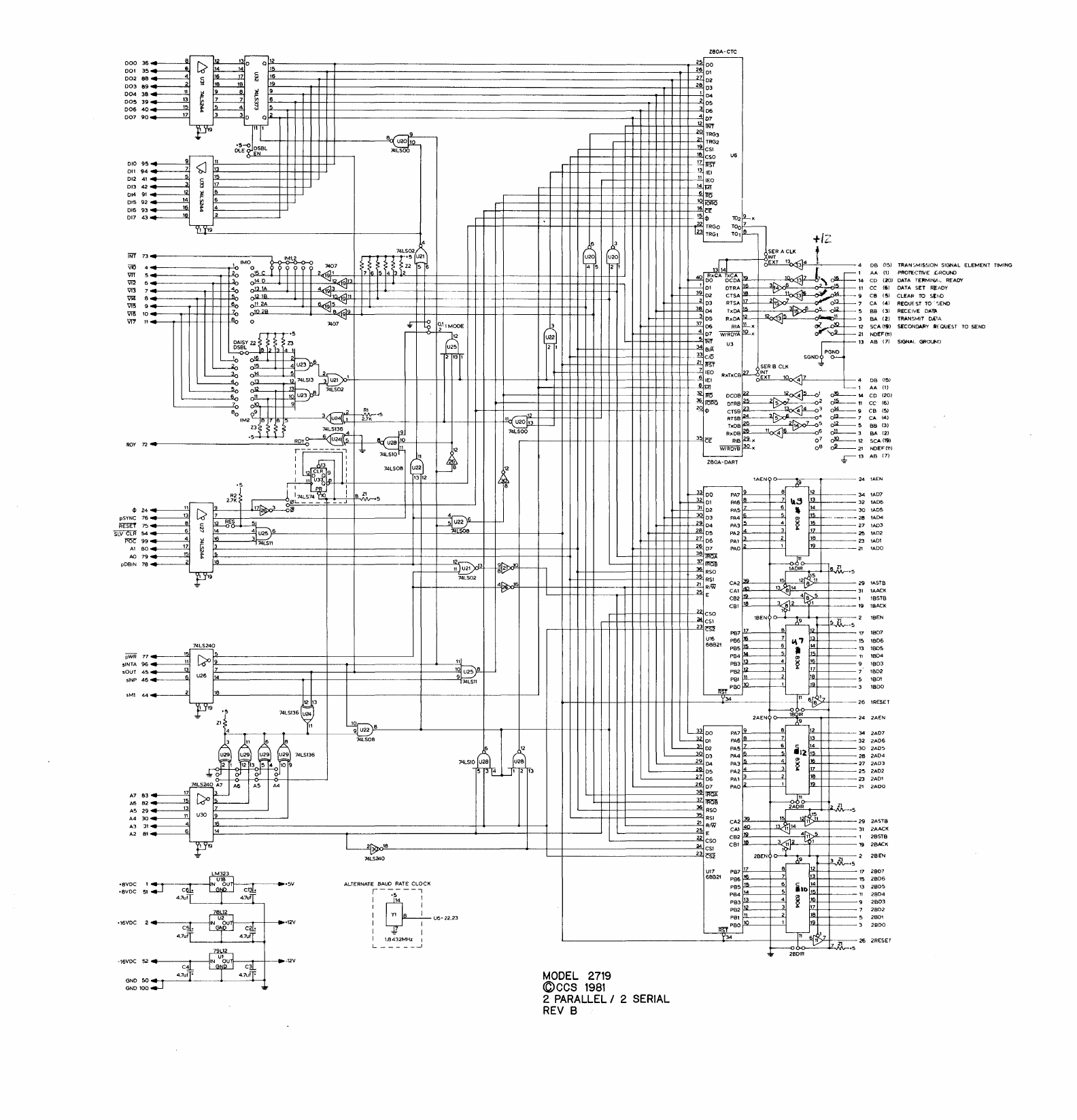
ZBOA-CTC
000
36~~~~f'2~--------~
________________________________________________________________
~~2~5~
00'
35~
L-6
~
c
'5
26
0,
002
Be
_~
c
iJ2.------Jz
id
'6
27
02
003
B9~
!lI
~
'9
2B03
~~:
~:~
~
:t=::j
~
:
~:
D06
40
'5
t
~
~
5 3 D6
007
90
17
~
D Q 2 4
07
II
L
'--+H-f--I-I-+_+------"B'<;(ciU20r,;:;-
:;
~~
~~g~~
~
'9
CSI
,
19
.---
~:~
::~
<Q
fl';~-------+-+H-++f---J
012
4'
_----2
f"'5~
____
_t_+_+4-+~
013
42
_--2
§
1"'7------_t_+_+4-'
014
9'
_----'1
~
128--
___
-+-H...J
~:!
:~
~
~
p!--------+-I
017
43
_----1l!
1-"2
_____
-1
4
rl-t----t-~-I--+_+_+__+_+_f_!':2.lB
CSO
U6
rl-t--I-----I--t-l--+_+--+-++-+--
-
!Z.
RSf
g lEI
r--+_+-1I-+_+H_+++_.!!i"
'EO
r--+_~r+-+_1~~H-f-+-1I_+_+~~'4m
r-----+_+___+_~~t-~+-+_+_+-~~k+-~·~·-~~
rl------t-~~~-I--t-t---+_+·-~~-~·~~+-~~,~
r--r1------+-+_+_+_+-t~~t-+4-1--+_+_+__+_+_~-~~
r+_1-r----_1~~H_+_+_+_+_1_+4_H_++-1~+·~~
ro2~x
....
.---
+/2-
iNi'
.-.-.--.-~;-
~7~..--L:~2~
~
VIO
---------..--2'<>'
11'01\5 C ? ?
T~
2
~~7
\
fd
1.1/
2 5 i
U20
45
U20
2 1
22
TRGO
T00Ff17:
123_TRGI
TO"B.
SER
ACLK
t
.-.
___
_t_--o
'NT
I T
~
4
DB
(15)
TRANSMISSION
SIGNAL
ELEMENT
TIMING
: 6 -
3;'4
0 I
""'~"-A-9;"3;j~7:~~:r~l~~2==t1=j=====1:t-l--_---I--+---_--=--_-+-+-4_H-f-+-1I_+-f___J
Vi3
:---
4'3
lA
4-'19'3
"l
j
40
~
19
10.~'
I.
oI§...
--
I
AA
(1) PROTECTIVE
LROUNO
~~
~~
~~~~
12.
,~
6
~'.'\
-,~
-
~~
~~
:~)
~:~~
~~~M:;O;EAD'f
~-~
02
CTSA
'"
V"
-,,-
~~
-9
CB
(!!o)
CLEAR
TO
SEND
2
03
RTSA
1L-
~
7
3~
~.y:L
--
CA
(.)
REQUEST
TO·
SEND
ViII
_ I 5
'2
IB
-.:.::
lcuglf!1'''~_+-+----
__
-+_+--I---
171!1
9 _ 6
o-'!l.'
,;r.2A'------
__
4-.+--I"!.6'9
'5
'"
~-++-l-----'3!!l.je
D4
TxDA
~
~
-
BB
(3)
RECEIvE
OA1Jl.
.--fo
~+_+4-+---"I3
05
RxOA
1L-
~
::...."
3
BA
(2)
TRANSMIT
O,(lA
•
~
0.1
,
MODE
r 3
+-+_+_-H~+_-,,37'-lD6
RIA
!Lx
<:il.
,~-
12
SCA
(19)
SECONDARy
R'OUEST
TO
SEN~
Vl1!
10
;
0
10
28
-.:.::
819lJl!-19f-J>------I-+-I----I-++-+l----+++-HI-+--i
VT'1
"
~7
DAISY
22
rrr.r-~5
OSBL
:
fa
r2
f3
; 4 ,
.'6-
I
21--..
'5
41u23 6
14 5
oJnL-_-.-~'2
74LS13
,2 3
U25
+--+-++_~+-~-H_t_+_+----4-++--""I34
B/A
U3
PGNO
'21
5m
D~I--
13
AB
(7)
SIGNAL
GROUND
~'3
,
+--+-++-+_+_+_------l-++_~+-I--
- .
~
C/O
SGNO
-0:::-.
2 ~2
U22
1-++~_+++_-!!.j4
07
W/ROYA!lL~
7~1--
21
NOEF(~)
+-+_+_-H-++_+--__+_+_~-+----H_+__"_'_12'
rn
SER
B
CLK
-
~
U21)o!-'
+-----I-I1---I-+f---<4++-+-1---+--4++-1-+++-++--1-+++-1-+++--£l~
:~~
RXTXCB~
~T
10
4~7
____
+_-
DB
CIS)
AA
(I)
74LS02 B m
~--~--~~~4-~+-~+4~+-I-tl
~~
+-+------t-_+_-H-++_+----4-++__t__+_~_+
...
+---+---+
~~
20
<I>
."
.'2
9
11-
U28
fll,'~'---+--I-~
'---
012----
14
CD
(20)
~
CC
(6)
~
CB(5)
012---
CA
(4)
012---
BB
(3)
oIL--
3
SA
(2)
~'2
SCA(9)
dL--21
NOEF(11)
'2
~
12
"
3
74LS10
r "
a~
74LS08
U22
~
8
~'3
AB
(7)
Z80A-OART
I
'2
~LRQ
9
=J_
>----
05 I
11
U3'bLetR---+-'-I__+_----~~'3+'-2
-+
__
-'
,----
lAEN I;)
o---tl,9,--------
~
DO
PA71"-9-~-6"l
~'2-+-
__
_ lA07
----R
0'
PA6
7
\\3
f!"34---
32
r-
2.~~
~~~4LS74PL..::~
....
---;.-I"-8""Z11\r-!5
PSYN~
~:
4-
__
,''-!j~
[j
fL~___,;=-+_----.:I7~-----+_-_+----..J
4
REm
75
_~
c
1l"2,---<:,R,EcS>--4---25L..
~22
JL-
f--
~
f--~f-----2!
D2
PA5
7
6,
~'4~
___
30
lADS
~-++_+---'=:'-"-l9
~~
:~~
;
~
I-"!-'-+-f--_--_-_-_--
~~
lAD3
SLY
CLR
54
6
t:l
1"'4'-------4'4;lU25
)26'-----_+--+-----_++-l-~---'~~.!!L.---+-I--+_-I----f
~
99
_~
01
>'!'16'-------"-t;:;74LS;-;:"
+-+-+-+_I-+---"~"'1~
~:
::~
3 :
fl':~4---
~
lA02
:
~~4---~
~
~1!---------------+---+----------H-+-------+-+-~~-+-~1-+4
+--+-t-+_~_+_+_2""_16
07
PAO
fL---f----'-l'
1lJ,9iL+
___
21
IAOO
-+_+------.!',2!..i1,~
.lJ,2~~,.J3
3.
~69
2'''.JCd'4--+-'
L--f--I-H_+~_+~3"51J;
::
'--::1';::-
18
pDBIN
76_~
r
~
~
at:>'"
H_+---+-r+-+-~-++--""-I36
RSO
r',,,,,AO,,,,
IR
'--o-.-4----f-2.,ili
Z
'\r-05
74LS02
41:::.-
'6
H-++_--~~_+_+_I-++_+---'3""j5
RSI
",39"--_+---,,,!'5k-,--,1'92r§B:'>"~''----+--
__
29
lASTB
H-4_----+---+~t:7~I2I--4_I-I++-1_++------.--I--l-+f_j-+++-~~
:/W
~:l
f9:'.I---i---!'l'3(i
~~
'4
4~
5
31
lAACK
CBI
,..
3---B1
2
t::(f3:::,:.L-+---:
9
;=!~:
~~-+---+_I-+~_t_+_I___'~"'I~~~
lBENQ o--f
.....
-t-~o___f_____c~--
2
18EN
r-_+_~-++_+_+_+__~~_+_+4-+--+_+---'2~3~
ffi7~17'--~~~8~"f--~·S
U16
PB6~
7
~,
n
;~
~::
66821 PBS
1~
6
5•
14,
13
lB05
P84
I""L-_~~
11
IB04
P83
13
43
~
1-";6,+-+_--
9
IB03
PB2
1-"'2'---~~_".f
lB02
PB(
~
2
1"'6,+-+_--
IBD!
1m'
PBD
'.12
----
3
lBDO
~'3
H+~f--+_+H_+4_H-f-+-lf--+------<'i'i,-,,34,,-----~--~-
-
-T
~'---------
26
lRESET
-'
19
z,
If":'---_~-__._-74t--LS--'3-6-l
__
~-,
_+--
__
'~~..::UJ22/~6'-----
.....
-----l--..---+---+-f-j-++-+--+~
---ll
DO
PA71"-9_2A-EN~:--6:.-lL.!!'IB",0i:"--f"'-2,---:1:~~-----
::::
3 " 6
_~
74LS08
~
01
PA61"'6_~~"-17
f"13'-++_---
32 2AD6
U29 U29
U29 U29
74LS'36 ;
~6
j
~
~
~~
PA5
f2-7
__
~:~
.'2
f!!::4+--
2,
'2'3
S.
(0 9 74LS'0
U28 U28
29
D4
::~
1"--_ _+__-4'4
~
~,
~~
~:~~
..!.-
<>' <>'
<>'
<>'
5 3 4 , 2'
13
28
OS
PA21"---I----"I
3
li:
f!1"_++_--
25
2A02
1
19
~O
5~~:
96:
~~
Do""!------------+----+---------'
,,1
s~~:
:!
!---=---';
U26
''':L-
_______
---1_+-+_-l---------+---:;t.'~t=iU;;_;;2~-
----!II!
r
'J4LS11
51'011
44
4------.!
'8
~
A7
A6
A5
A4
:~
~~
=:~
~~===~~=~~
!=~=:=
~
2AOO
A7
83
-----.!Z
f"-.....:L.J
'-+-+-+-I_+------~3""leim:lA
--::-r;;::-
~
82_~
~~
Lf+~~----------~37~
~
--f4'
U30
1"-9,-
________
-'
L~~~~_t~t~i~;~~~~~~~~~~~~-=:
=~~
,J..---'2c<oA""0IR"--2rk-1-'-S-+-I'Yi
Z
,,,1
~.oS
A3
3'4---"1
lb
'----------'21':!-iR/W
~~~1":"---+--(3.:=;~1,--,-,,4-""'2CJ--"
~~
~:~~
A2
8'
4--_
6
"l
'4
L-
______
---'~=iS
~SO
CB2
19
"J
dr;rS
,
2BSTB
,
19
L-----'2"l1~:~,..~--------------+--+_-f-------------il'!.j24
CSI
CB'
18
3~2
L1'S'i
19
2BACK
=
~a40
'--+----------------'2~3
CS2
2BENQ
o-_'
.....
__
~o___t_____~-
2 2BEN
B
~
'2
----1v&.-os
LM323
U1B
-6VOC
+8VDC
5:::r--
CoN
OUTI----C-13.--o----1~OSV
4.7U~
__
-4--_4_7u_'f
>----,
7BL12
016VOC
2
4---
IN
U'1:,UrI--o---t-------
o'2V
c4
CSo
4.7UL...---,-
__
4._71i
___
f
..
~'6VOC
52
4---_..__--\1
7
12
U1
GNO
50
....
r---
......
--
.....
----+--.
GNO
100
ALTERNATE
BAUD
RATE
CLOCK
[-----,
:
0-+0~4
:
I
YI
I U6- 22.23
1 I
1
.;
I
1 1.6432MHz I
L
_____
-I
U17
PB7
f!1'7'----~.2.f
17 2B07
68B21 PBS 16
7'3
'S
2B06
PBS
15
6 C
'4
13
280S
PB4
f""4'----t--"'lS
I'D
fl"'~~~--
PB3
~'3_--l~4'-1
~
f!lI~74--+---9
2B03
PB2
~'2
__
~-"l3
7
2802
PBl
fll"----t-£f2
18
S 2801
PBO
f"'10'---t--'-l,,9
3
2BOO
~
----r;-
L-
_______________
-+=
r34"----
__
---+
__
+~
---.!!j6r,;(,z..f---=--- 26 2RESET
V 7
Z1
-S
MODEL
2719
©CCS
1981
2
PARALLEL
/ 2
SERIAL
REV
B
F
2BOIR
APPENDIX B
SAMPLE
DRIVERS
Drivers
for
the
2719
parallel
and
serial
ports
will
be
included
with
future
releases
of
CP/M
with
the
CCS
System
2210
and
OASIS
with
the
CCS
Systems
300
and
400.
If
your
operating
system
does
not
include
drivers
for
the
2719,
you
will
need
to
add
them.
The
sample
drivers
that
follow
may
be
used
as
they
are
or
modified
as
desired.
For
instructions
on
adding
the
drivers
to
your
operating
systems,
see
the
relevant
operating
system
documentation.
For
CP/M
on
the
System
300
or
400,
see
the
System
300
or
System
400
CP/M
Supplementary
Manual;
for
OASIS,
see
Phase
One1s
Macro
Assembler
Language
Reference
Manual.
Please
note
that
the
ORG
addresses
used
in
the
sample
driver
listings
were
chosen
for
assembly
purposes
and
are
not
the
addresses
at
which
your
drivers
will
reside.
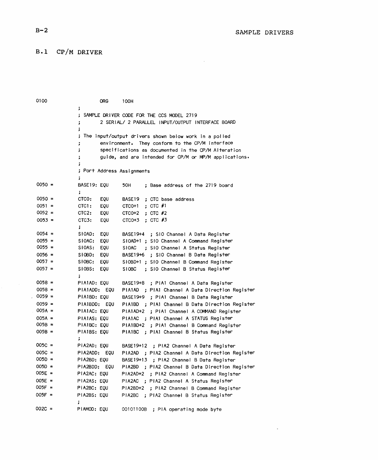
B-2
SAMPLE
DRIVERS
B.l
CP/M DRIVER
0100
0050 =
0050 =
0051
=
0052
=
0053 =
0054
0055
0055
0056
0057
0057
=
0058 =
0058
=
0059 =
0059
=
005A
=
005A
=
005B
=
005B
=
005C
=
005C
=
0050 =
0050
005E
005E
005F
005F
002C
ORG
100H
SAMPLE
DRIVER
CODE
FOR
THE
CCS
MODEL
2719
2
SERIAL/
2
PARALLEL
INPUT/OUTPUT
INTERFACE
BOARD
The
input/output
drivers
shown
below
work
in
a pol led
environment.
They
conform
to
the
CP/M
interface
specifications
as documented
in
the
CP/M
Alteration
guide,
and
are
intended for
CP/M
or
MP/M
applications.
Port
Address Assignments
BASE19:
EQU
CTCO:
EQU
CTC1:
EQU
CTC2:
EQU
CTC3:
EQU
SIOAD:
EQU
SIOAC:
EQU
SIOAS:
EQU
SlooD:
EQU
SIOBC:
EQU
SlOBS:
EQU
PIA1AD:
EQU
PIA1ADD:
EQU
PIA1BD:
EQU
PIA1BDD:
EQU
PIA1AC:
EQU
PIA1AS:
EQU
PIA1BC:
EQU
PIA1BS:
EQU
PIA2AD:
EQU
PIA2ADD:
EQU
PIA2BD:
EQU
PIA2BDD:
EQU
PIA2AC:
EQU
PIA2AS:
EQU
PIA2BC:
EQU
PIA2BS:
EQU
PIAMOD:
EQU
50H
BASE19
CTCO+l
CTCO+2
CTCO+3
Base address
of
the
2719
board
CTC
base address
CTC
#1
CTC
#2
CTC
#3
BASEl
9+4
i
SIO
Channel A Data
Register
SIOAD+l
i
SIO
Channel A
Command
Register
SIOAC
SIO
Channel A
Status
Register
BASEl9+6
SIOBD+l
SIOBC
i
SIO
Channel B Data
Register
SIO
Channel B
Command
Register
SIO
Channel B
Status
Register
BASEl
9+8
j
PIAl
Channel A Data
Register
PIA1AD
;
PIAl
Channel A Data
Direction
Register
BASE
1
9+9
j
PIAl
Channel B Data
Register
PIA1BD
;
PIAl
Channel B
Data.
Direction
Register
PIA1AD+2
j
PIAl
Channel A
COMMAND
Register
PIA1AC
;
PIAl
Channel A
STATUS
Register
PIA1BD+2
i
PIAl
Channel B
Command
Register
PIA1BC
i
PIAl
Channel B
Status
Register
BASE19+12
;
PIA2
Channel A Data
Register
PIA2AD
j
PIA2
Channel A Data
Direction
Register
BASE19+13
i
PIA2
Channel B Data
Register
PIA2BD
j
PIA2
Channel B Data
Direction
Register
PIA2AD+2
;
PIA2
Channel A
Command
Register
PIA2AC
;
PIA2
Channel A
Status
Register
PIA2BD+2
;
PIA2
Channel B
Command
Register
PIA2BC
i
PIA2
Channel B
Status
Register
001011008 j
PIA
operating
mode
byte
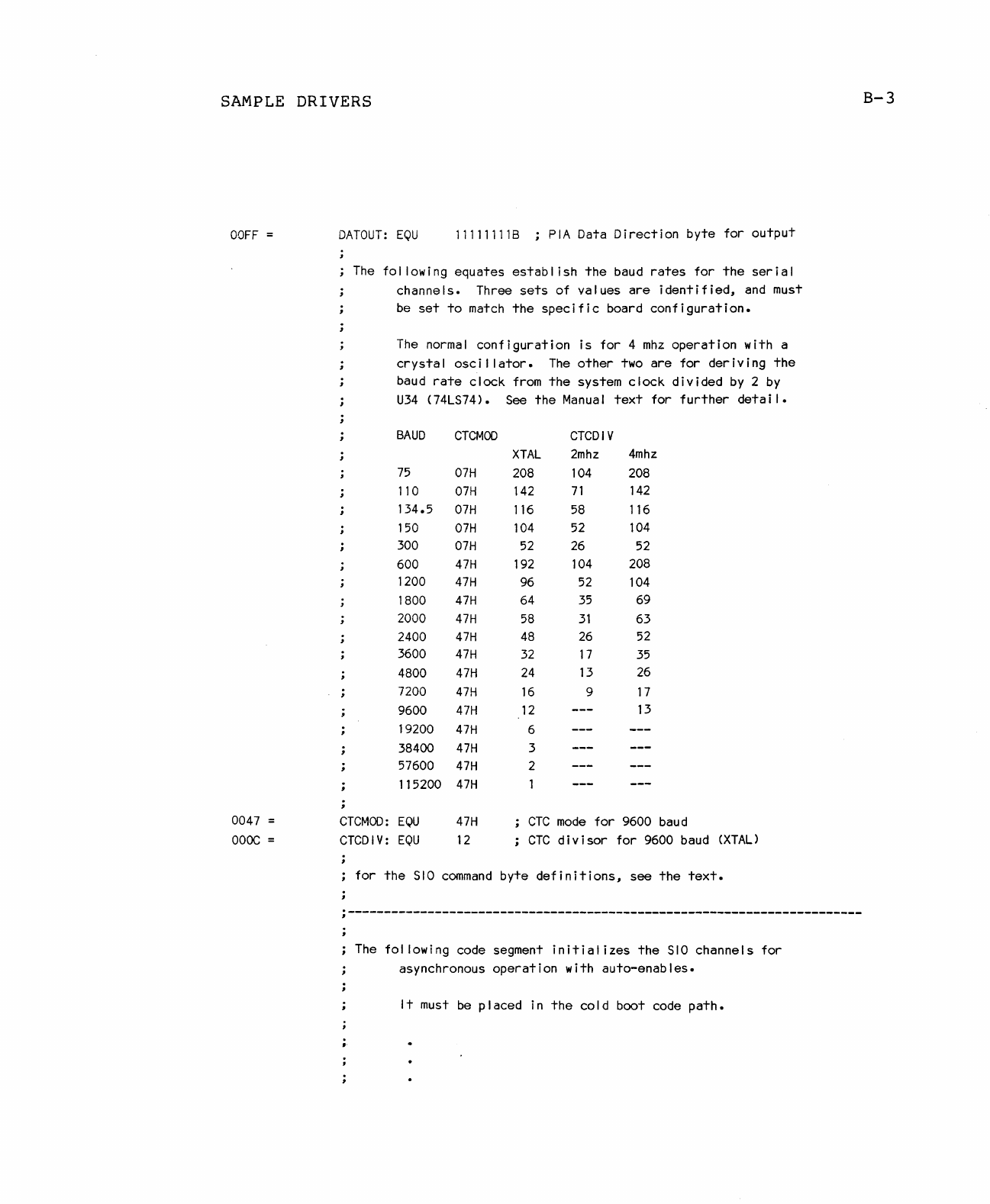
SAMPLE
DRIVERS
OOFF
0047
OOOC
DATOUT:
EQU
11111111B ;
PIA
Data
Direction
byte
for
output
The
fol lowing
equates
establ
ish
the
baud
rates
for
the
serial
channels.
Three
sets
of
values
are
identified,
and must
be
set
to
match
the
specific
board
configuration.
The
normal
configuration
is
for
4
mhz
operation
with a
crystal
oscillator.
The
other
two
are
for
deriving
the
baud
rate
clock
from
the
system
clock
divided
by
2
by
U34
(74LS74). See
the
Manual
text
for
further
detail.
BAUD
CTCMOO
75
07H
110
07H
134.5
07H
150
07H
300
07H
600
47H
1200
47H
1800
47H
2000
47H
2400
47H
3600
47H
4800
47H
7200
47H
9600
47H
XTAL
208
142
116
104
52
192
96
64
58
48
32
24
16
12
19200
47H
6
38400
47H
3
57600
47H
2
115200
47H
1
CTCDIV
2mhz
104
71
58
52
26
104
52
35
31
26
17
13
9
4mhz
208
142
116
104
52
208
104
69
63
52
35
26
17
13
CTCMOD:
EQU
CTCDIV:
EQU
47H
12
CTC
mode
for
9600 baud
CTC
divisor
for
9600 baud
(XTAL)
;
for
the
SIO
command
byte
definitions,
see
the
text.
;-----------------------------------------------------------------------
The
fol lowing code segment
initializes
the
510
channels
for
asynchronous
operation
with
auto-enables.
It
must
be
placed
in
the
cold
boot code
path.
8-3
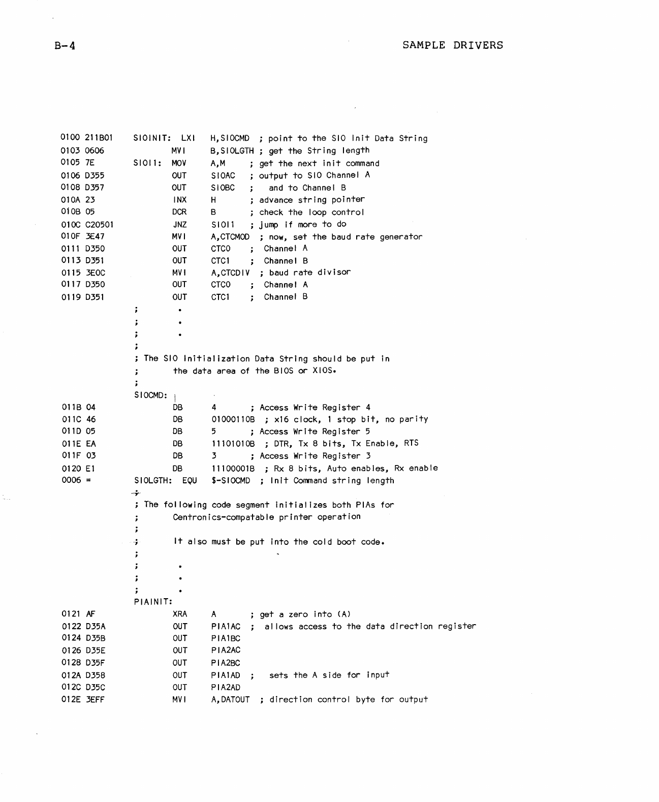
8-4
0100
211BOl
0103 0606
0105
7E
0106
D355
0108
D357
010A
23
010B
05
010C
C20501
OlOF
3E47
0111
D350
0113
D351
0115
3EOC
0117
D350
0119
D351
011B
04
011C
46
011D
05
011E
EA
011F
03
0120
El
0006 =
0121
AF
0122
D35A
0124
D35B
0126
D35E
0128
D35F
012A
D358
012C
D35C
012E
3EFF
SAMPLE
DRIVERS
SIOINIT:
LXI
H,SIOCMD
;
point
to
the
SIO
Init
Data
String
MVI
B,SIOLGTH
;
get
the
String
length
SIOll :
MeV
A,M
get
the
next
init
command
OUT
SIOAC
output
to
SIO
Channel A
OUT
SIOBC
and
to
Channel B
INX
H advance
string
pointer
DCR
B check
the
loop
control
JNZ
SIOll
jump
if
more
to
do
MVI
A,CTCMOD
;
now,
set
the
baud
rate
generator
OUT
CTCO
Channel A
OUT
CTCl
Channel B
MVI
A,CTCDIV
i baud
rate
divisor
OUT
CTCO
Channel A
OUT
CTCl
Channel B
The
SIO
Initialization
Data
String
should be
put
in
the
data
area
of
the
BIOS
or
XIOS.
SIOCMD:
I
DB
4 ; Access Write
Register
4
DB
01000110B
i x16
clock,
1
stop
bit,
no
parity
DB
5 i Access Write
Register
5
DB
11101010B
i
DTR,
Tx
8
bits,
Tx
Enable,
RTS
DB
3 Access Write
Register
3
DB
11100001B
;
Rx
8
bits,
Auto
enables,
Rx
enable
SIOLGTH:
EQU
$-SIOCMD
;
Init
Command
string
length
~,r
The
fol lowing code segment
initializes
both
PIAs
for
Centronics-compatable
printer
operation
-j
It
also
must be
put
into
the
cold
boot code.
PIAINIT:
XRA
A
get
a
zero
into
(A)
OUT
PIA
lAC
al
lows
access
to
the
data
direction
register
OUT
PIA1BC
OUT
PIA2AC
OUT
PIA2BC
OUT
PIA1AD
sets
the
A
side
for input
OUT
PIA2AD
MVI
A,DATOUT
direction
control
byte
for
output
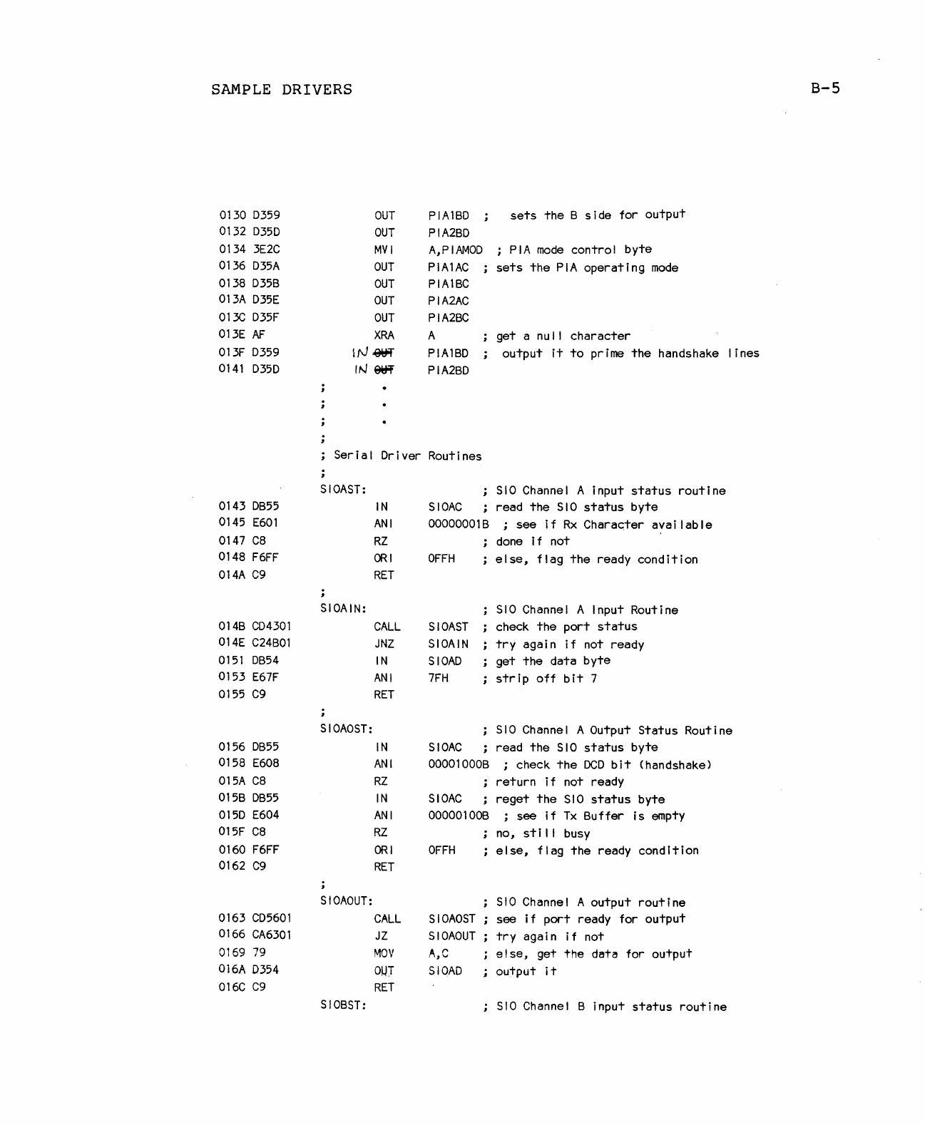
SAMPLE
DRIVERS
8-5
0130
0359
OUT
PIA1BO
sets
the
B
side
for
output
0132
0350
OUT
PIA2BO
0134
3E2C
MVI
A,PIAMOO
PIA
mode
control
byte
0136
035A
OUT
PIA
lAC
sets
the
PIA
operating
mode
0138
035B
OUT
PIA1BC
013A
035E
OUT
PIA2AC
013C
035F
OUT
PIA2BC
013E
AF
XRA
A
get
a
nul
I
character
013F
0359 I
rJ
.@ijif
PIA1BO
output
it
to
prime
the
handshake
lines
0141
0350
IN
9ijo'f
PIA2BO
Serial
Driver Routines
SIOAST:
;
SIO
Channel A input
status
routine
0143
OB55
IN
SIOAC
; read
the
SIO
status
byte
0145
E601
ANI
00000001B
;
see
if
Rx
Character
avai
lable
0147
C8
RZ
done
if
not
0148
F6FF
ORI
OFFH
;
else,
flag
the
ready
condition
014A
C9
RET
SIOAIN:
SIO
Channel A Input Routine
014B
C04301
CALL
SIOAST
check
the
port
status
014E
C24BOl
JNZ
SIOAIN
try
again
if
not ready
0151
OB54
IN
SIOAO
get
the
data
byte
0153
E67F
ANI
7FH
strip
off
bit
7
0155
C9
RET
SIOAOST:
;
SIO
Channel A Output
Status
Routine
0156
OB55
IN
SIOAC
; read
the
SIO
status
byte
0158
E608
ANI
00001000B
; check
the
DCO
bit
(handshake)
015A
C8
RZ
;
return
if
not ready
015B
OB55
IN
SIOAC
;
reget
the
SIO
status
byte
015D
E604
ANI
000001008 ; see
if
Tx
Buffer
is
empty
015F
C8
RZ
no,
stili
busy
0160
F6FF
ORI
OFFH
else,
flag
the
ready
condition
0162
C9
RET
SIOAOUT:
SIO
Channel A
output
routine
0163
C05601
CALL
SIOAOST
see
if
port
ready
for
output
0166
CA6301
JZ
SIOAOUT
try
again
if
not
0169
79
MaV
A,e
else,
get
the
data
for
output
016A
0354
OUT
SIOAO
output
it
016C
C9
RET
SIOBST:
SIO
Channel B input
status
routine
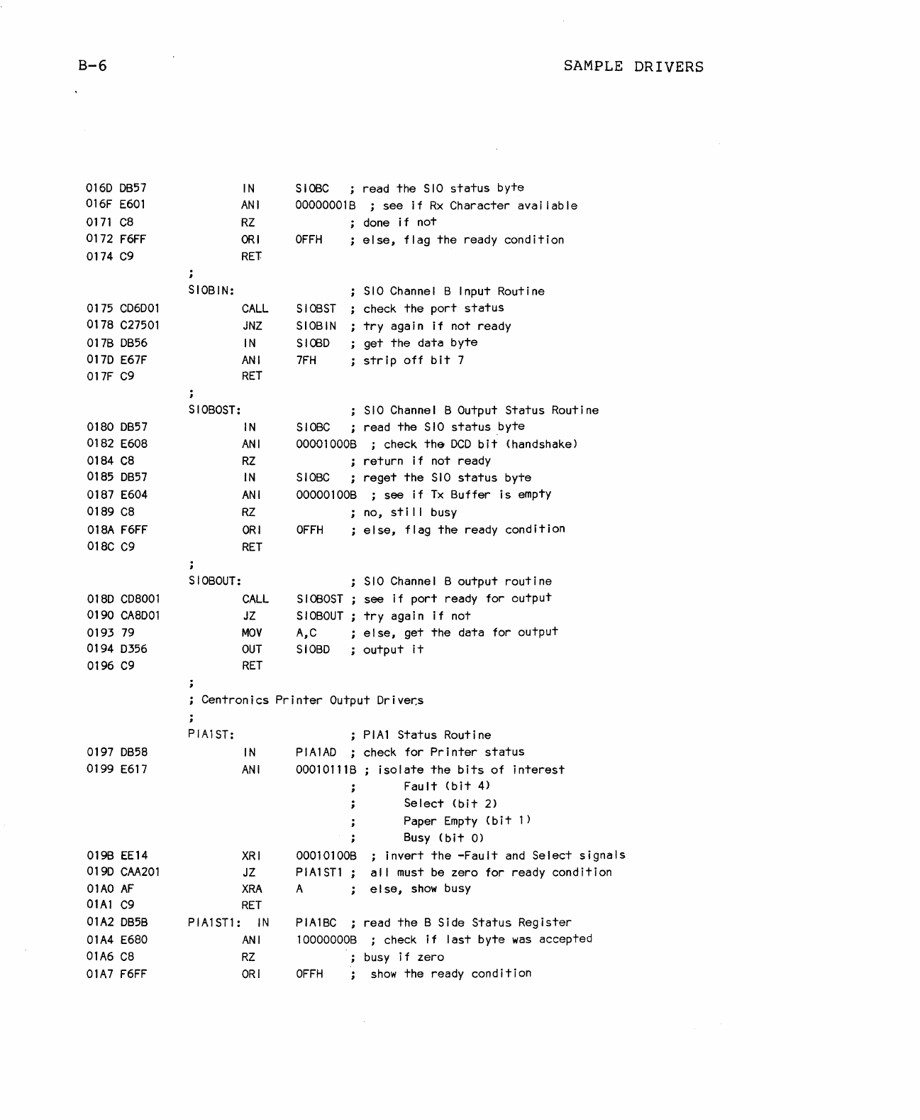
8-6
0160 0057
016F
E601
0171
C8
0172
F6FF
IN
ANI
RZ
ORI
SAMPLE
DRIVERS
SIOBC
read
the
SIO
status
byte
00000001B ;
see
if
Rx
Character
avai
lable
done
if
not
OFFH
else,
flag
the
ready
condition
0174
C9
RET
0175
C06001
0178
C27501
017B
OB56
0170
E67F
017F
C9
0180
OB57
0182
E608
0184
C8
0185
OB57
0187
E604
0189
C8
018A
F6FF
018C
C9
0180
C08001
0190
CA8001
0193
79
0194 0356
0196
C9
0197
OB58
0199
E617
0198
EE14
0190
CAA201
01AO
AF
01Al
C9
01A2
OB5B
01A4
E680
01A6
C8
01A7
F6FF
SIOBIN:
SIO
Channel B Input Routine
SIOBOST:
SIOBOUT:
CALL
JNZ
IN
ANI
RET
IN
ANI
RZ
IN
ANI
RZ
ORI
RET
CALL
JZ
MOV
OUT
RET
SI08ST
SIOBIN
SIOOO
7FH
check
the
port
status
try
again
if
not ready
get
the
data
byte
str
i p
off
bit
7
SIO
Channel B Output
Status
Routine
SIOBC
read
the
SIO
status
byte
00001000B ; check
the
OCO
bit
(handshake)
return
if
not ready
SIOBC
reget
the
SIO
status
byte
00000100B ;
see
if
Tx
Buffer
is
empty
no,
still
busy
OFFH
else,
flag
the
ready
condition
SIO
Channel B
output
routine
SIOBOST
see
if
port
ready
for
output
SIOBOUT
A,C
SIOBO
try
again
if
not
else,
get
the
data
for
output
output
it
Centronics
Printer
Output Oriver.s
PIA1ST:
IN
ANI
XRI
JZ
XRA
RET
PIAl
ST1:
IN
ANI
RZ
ORI
PIA1AO
00010111B
PIAl
Status
Routine
check
for
Printer
status
isolate
the
bits
of
interest
Fault
(bit
4)
Select
(bit
2)
Paper
Empty
(bit
1)
Busy
(bit
0)
00010100B
invert
the
-Fault
and
Select
signals
PIA1STl
al I must be
zero
for
ready
condition
A
else,
show
busy
PIA1BC
read
the
B Side
Status
Register
10000000B
i check
if
last
byte
was
accepted
busy
if
zero
OFFH
show
the
ready
condition
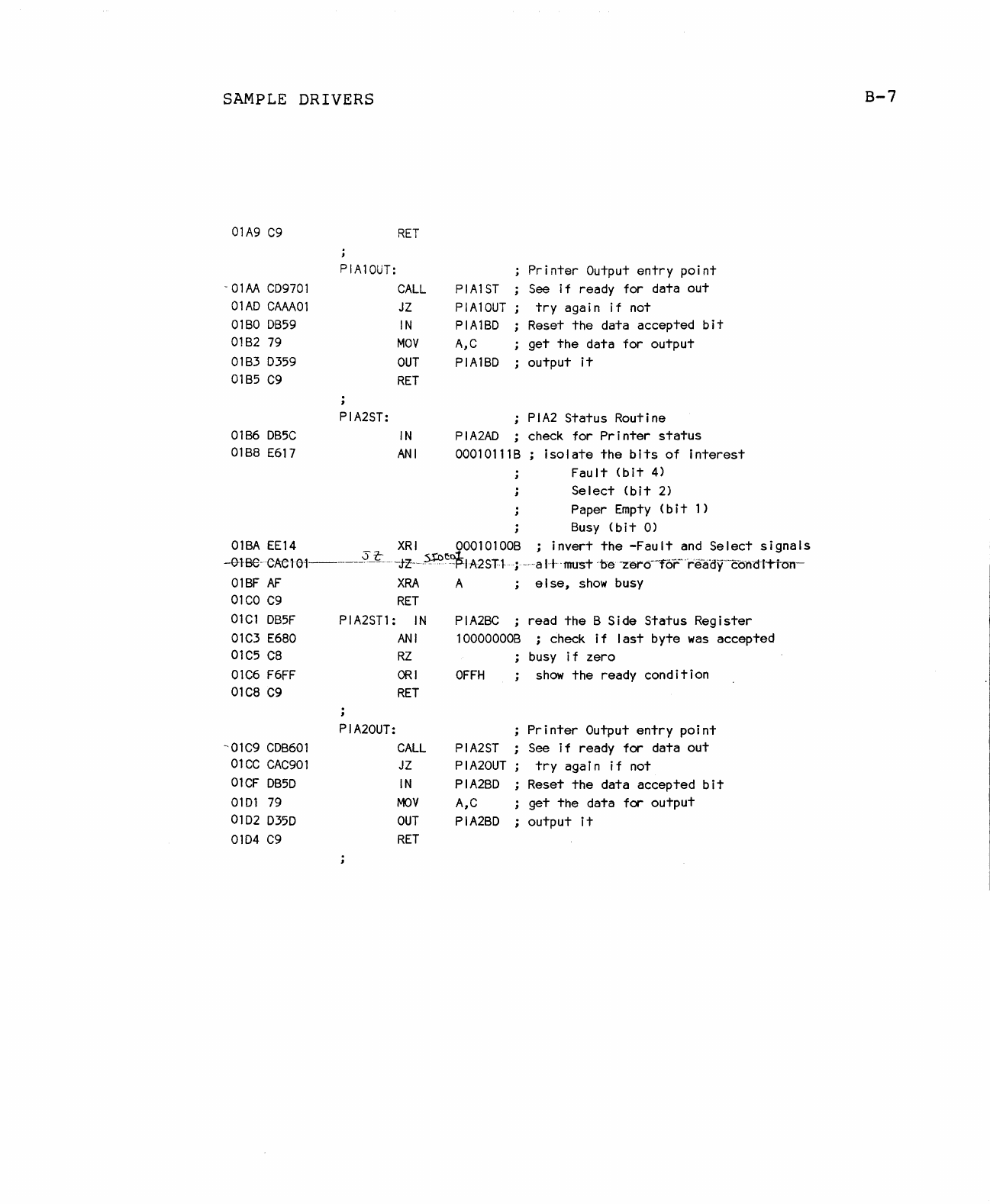
SAMPLE
DRIVERS
01A9
C9
-01M
CD9701
01AD
CAAAOl
01BO
0859
01B2
79
01B3
0359
0185
C9
0186
DB5C
01B8
E617
PIA10UT:
PIA2ST:
RET
CALL
JZ
IN
MOV
OUT
RET
IN
ANI
PIA1ST
PIAl
OUT
PIA1BD
A,C
PIA1BD
Printer
Output
entry
point
See
if
ready for data
out
try
again
if
not
Reset
the
data accepted
bit
get
the
data
for
output
output
it
;
PIA2
Status
Routine
PIA2AD
; check
for
Printer
status
00010111B
isolate
the
bits
of
interest
Fault
(bit
4)
Select
(bit
2)
Paper
Empty
(bit
1)
Busy
(bit
0)
OlBA
EE14
XRI
00010100B
invert
the
-Fault
and
Select
signals
-o-lse-cAe10l---------~t----;tz---~:P.:>~$:IA2ST_t
-i---a '-+--musToe
-Zercfror--rEfaeW-'-condfTTOn-
OlBF
AF
XRA
A
else,
show
busy
OlCO
C9
RET
OlCl
DB5F
PIA2STl
:
IN
PIA2BC
read
the
B Side
Status
Register
01C3
E680
ANI
10000000B
i check
if
last
byte
was
accepted
01C5
C8
RZ
busy
if
zero
01C6
F6FF
ORI
OFFH
show
the
ready
condition
01C8
C9
RET
PIA20UT:
Printer
Output
entry
point
~01C9
CDB601
CALL
PIA2ST
See
if
ready
for
data
out
OlCC
CAC901
JZ
PIA20UT
try
again
if
not
OlCF
OB5D
IN
PIA2BO
Reset
the
data
accepted
bit
OlDl
79
MOV
A,C
get
the
data
for
output
01D2
0350
OUT
PIA2BD
output
it
0104
C9
RET
B-7
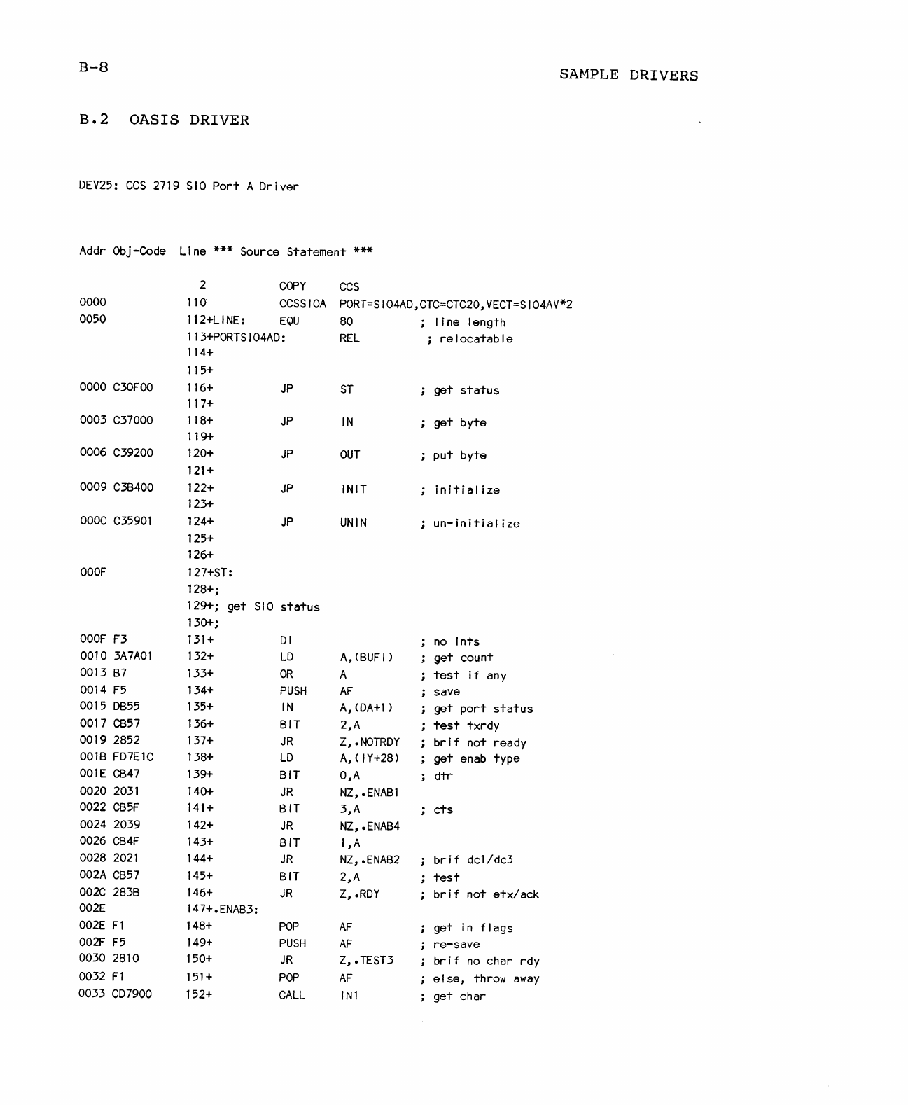
B-8
SAMPLE
DRIVERS
B.2
OASIS DRIVER
DEV25:
CCS
2719
SIO
Port
A
Driver
Addr
Obj-Code Line *** Source Statement ***
2 copy
CCS
0000
0050
110
112+LlNE:
CCSSIOA
PORT=SI04AO,CTC=CTC20,VECT=SI04AV*2
0000
C30FOO
0003
C37000
0006
C39200
0009
C3B400
OOOC
C35901
OOOF
OOOF
F3
0010
3A7A01
0013
B7
0014
F5
0015
DB55
0017
CB57
0019 2852
001B
FD7E1C
001E
CB47
0020
2031
0022
CB5F
0024 2039
0026
CB4F
0028
2021
002A
CB57
002C
283B
002E
002E
Fl
002F
F5
0030 2810
0032 Fl
0033
C07900
EQU
80
i
line
length
113+PORTSI04AD:
114+
115+
116+
117+
118+
119+
120+
121+
122+
123+
124+
125+
126+
127+ST:
128+;
JP
JP
JP
JP
JP
129+;
get
SIO
status
130+;
131+
01
132+
LD
133+
134+
135+
136+
137+
138+
139+
140+
141+
142+
143+
144+
145+
146+
147+.ENAB3:
148+
149+
150+
151+
152+
OR
PUSH
IN
BIT
JR
LD
BIT
JR
BIT
JR
BIT
JR
BIT
JR
POP
PUSH
JR
POP
CALL
REL
ST
IN
OUT
INIT
UNIN
A,(BUFI)
A
AF
A,
CDA+l
)
2,A
Z,
.NOTRDY
A,(IY+28)
O,A
NZ,.ENAB1
3,A
NZ,.ENAB4
l,A
NZ,.ENAB2
2,A
Z,.ROY
AF
AF
Z,.TEST3
AF
INl
;
relocatable
get
status
get
byte
put
byte
initial
ize
un-initialize
no
ints
get
count
test
if
any
save
get
port
status
test
txrdy
brif
not ready
get
enab
type
dtr
cts
brif
dc1/dc3
test
brif
not
etx/ack
get
in
flags
re-save
brif
no
char
rdy
else,
throwaway
get
char
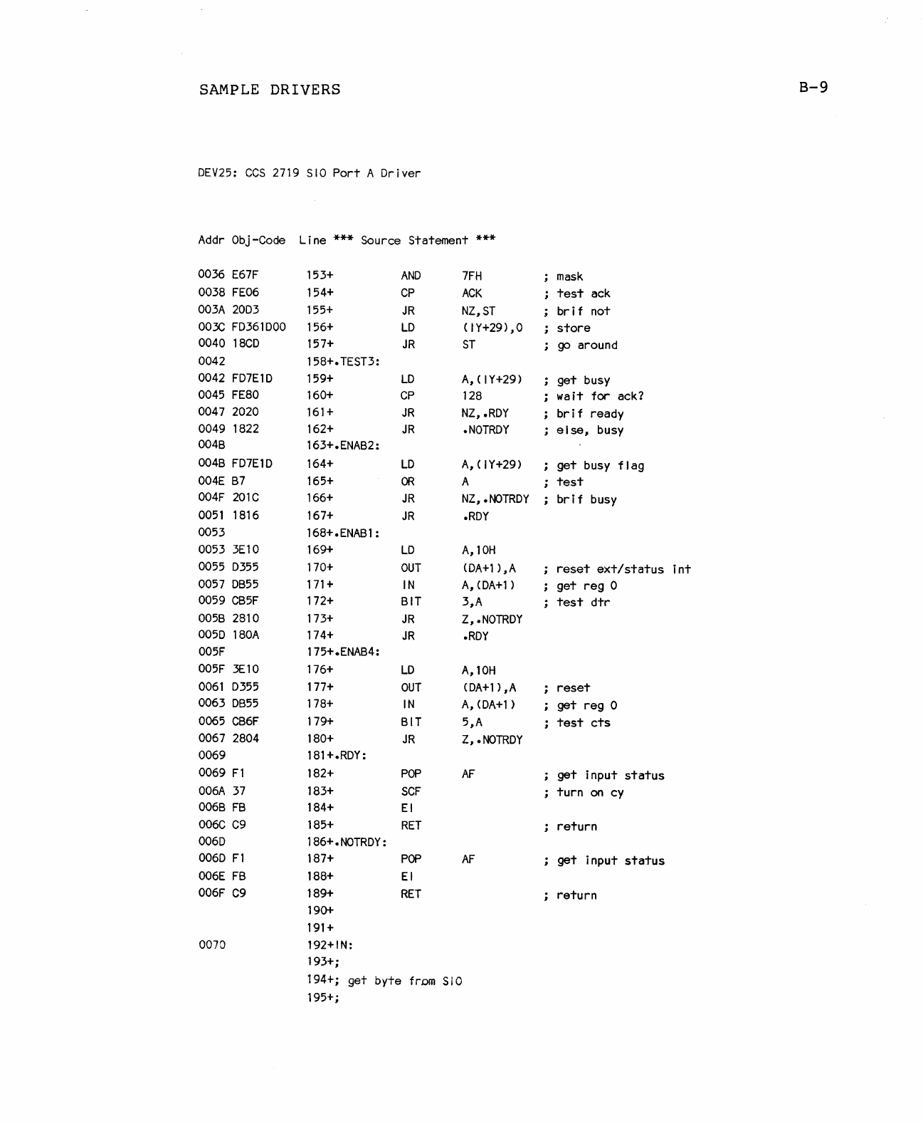
SAMPLE
DRIVERS
8-9
DEV25:
CCS
2719
510
Port
A
Driver
Addr
Obj-Code Line *** Source Statement ***
0036
E67F
153+
AND
7FH
mask
0038
FE06
154+
CP
ACK
test
ack
003A
2003
155+
JR
NZ~ST
bri
f
not
003C
F0361000
156+
LO
( I
Y+29)
~
0
store
0040
18CO
157+
JR
ST
go around
0042 158+.TEST3:
0042
F07E10
159+
LO
A~
(IY+29)
get
busy
0045
FE80
160+
CP
128
wait
for
ack?
0047 2020
161+
JR
NZ~.ROY
brif
ready
0049
1822
162+
JR
•
NOTROY
else,
busy
004B
163+.ENAB2:
0048
F07E10
164+
LO
A~(IY+29)
get
busy
flag
004E
87
165+
OR
A
test
004F
201C
166+
JR
NZ~.NOTROY
brif
busy
0051
1816
167+
JR
.ROY
0053
168+.ENAB1
:
0053
3E10
169+
LO
A~10H
0055 0355
170+
OUT
<DA+1
),A
reset
ext/status
int
0057
OB55
171+
IN
A,
CDA+1
)
get
reg
0
0059
CB5F
172+
BIT
3,A
test
dtr
005B
2810
173+
JR
Z,.NOTROY
0050
180A
174+
JR
.ROY
005F
175+.ENA84:
005F
3E10
176+
LO
A,10H
0061
0355
177+
OUT
CDA+1
)
,A
reset
0063 0855
178+
IN
A~
CDA+1
)
get
reg
0
0065
CB6F
179+
BIT
5~A
test
cts
0067 2804
180+
JR
Z~.NOTROY
0069
181+.ROY:
0069
F1
182+
POP
AF
get
input
status
006A
37
183+
SCF
turn
on
cy
006B
FB
184+
EI
006C
C9
185+
RET
return
0060
186+.NOTROY:
0060
F1
187+
POP
AF
get
input
status
006E
FB
188+
EI
006F
C9
189+
RET
return
190+
191+
0070 192+IN:
193+;
194+;
get
byte
from
SIO
195+;
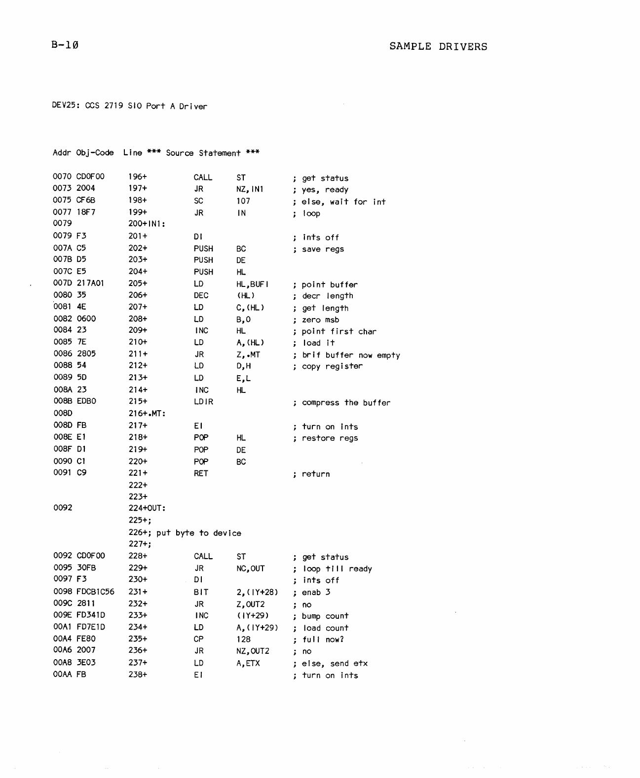
8-10
SAMPLE
DRIVERS
OEV25:
CCS
2719
SIO
Port
A
Oriver
Addr
Obj-Code Line *** Source
Statement
***
0070
COOFOO
196+
CALL
ST
get
status
0073 2004
197+
JR
NZ,IN1
yes,
ready
0075
CF6B
198+
SC
107
else,
wait
for
int
0077
18F7
199+
JR
IN
loop
0079
200+IN1
:
0079
F3
201+
01
ints
off
007A
C5
202+
PUSH
BC
save
regs
007B
05
203+
PUSH
OE
007C
E5
204+
PUSH
HL
0070
217A01
205+
LO
HL,BUFI
point
buffer
0080
35
206+
OEC
(HU
decr length
'0081
4E
207+
LO
C,
(HL>
get
length
0082 0600
208+
LO
B,O
zero
msb
0084 23
209+
INC
HL
point
first
char
0085
7E
210+
LO
A,
(HL>
load
it
0086 2805 211+
JR
Z,
.MT
brif
buffer
now
empty
0088
54
212+
LO
O,H
copy
register
0089 50 213+
LO
E,L
008A
23
214+
INC
HL
008B
EOBO
215+
LOIR
compress
the
buffer
0080
216+.MT:
0080
FB
217+
EI
turn
on
ints
008E
E1
218+
POP
HL
restore
regs
008F
01
219+
POP
OE
0090
Cl
220+
POP
BC
0091
C9
221+
RET
return
222+
223+
0092
224+0UT:
225+;
226+;
put
byte
to
device
227+;
0092
COOFOO
228+
CALL
ST
get
status
0095
30FB
229+
JR
NC,OUT
loop
ti
II
ready
0097
F3
230+
01
ints
off
0098
FOCB1C56
231+
BIT
2, (IY+28) enab 3
009C
2811
232+
JR
Z,OUT2
no
009E
F03410
233+
INC
(
IY+29)
bump
count
OOAl
F07E10
234+
LO
A,(IY+29) load count
00A4
FE80
235+
CP
128
fu
II
now?
00A6
2007
236+
JR
NZ,OUT2
no
00A8
3E03
237+
LO
A,ETX
else,
send
etx
OOM
FB
238+
EI
turn
on
ints
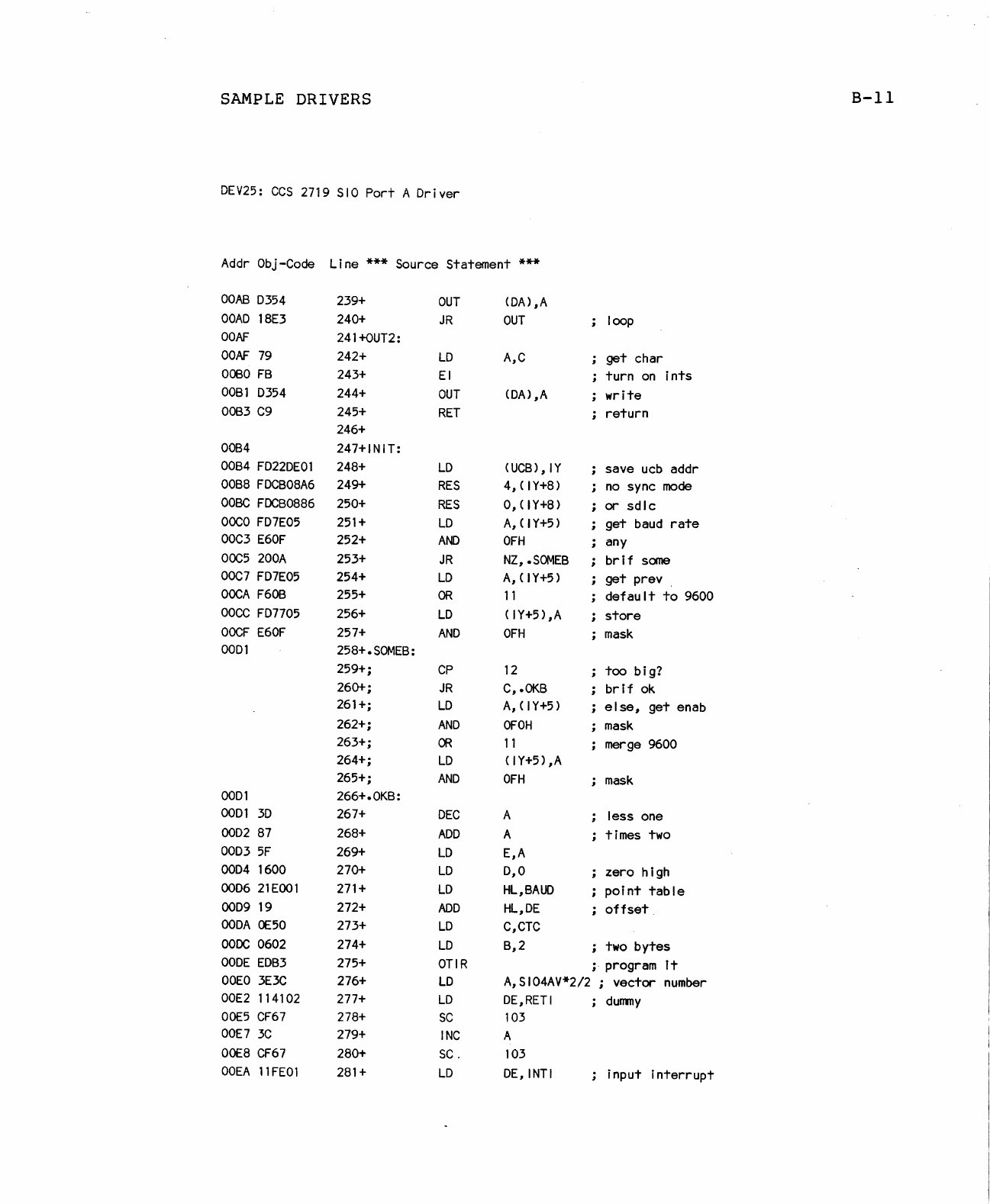
SAMPLE
DRIVERS
8-11
DEV25:
CCS
27i9
SIO
Port
A Driver
Addr
Obj-Code
Li
ne
*** Source Statement
***
OOAB
D354
239+
OUT
COA)
,A
OOAD
18E3
240+
JR
OUT
loop
OOPF
241+OUT2:
OOPF
79
242+
LD
A,C
get
char
0080
FB
243+
EI
turn
on
ints
00B1
0354
244+
OUT
COA)
,A
write
0083
C9
245+
RET
return
246+
00B4
247+INIT:
00B4
FD22DE01
248+
LD
(UCB),IY
save
ucb
addr
00B8
FDCB08A6
249+
RES
4, ( I
Y+8)
no
sync
mode
OOBC
FDCB0886
250+
RES
0,(IY+8)
or
sdlc
OOCO
FD7E05
251+
LD
A,(IY+5)
get
baud
rate
00C3
E60F
252+
AND
OFH
any
OOC5
200A
253+
JR
NZ,.SOMEB
brif
some
00C7
FD7E05
254+
LD
A,
(IY+5)
get
prev
OOCA
F608
255+
OR
11
default
to
9600
OOCC
FD7705
256+
LD
( I
Y+5)
,A
store
OOCF
E60F
257+
AND
OFH
mask
0001
258+.SOMEB:
259+;
CP
12
too
big?
260+;
JR
C,
.OKB
brlf
ok
261+;
LD
A,
(IY+5)
else,
get
enab
262+;
AND
OFOH
mask
263+;
OR
11
merge 9600
264+;
LD
( I
Y+5)
,A
265+;
AND
OFH
mask
0001
266+.0KB:
0001
3D
267+
DEC
A
less
one
0002
87
268+
ADD
A times two
0003
5F
269+
LD
E,A
0004
1600
270+
LD
0,0
zero
high
0006
21E001
271+
LD
HL,BAUO
point
table
0009
19
272+
ADD
HL,OE
offset.
OOOA
0E50
273+
LD
C,CTC
OODC
0602
274+
LD
B,2
two
bytes
OODE
EOB3
275+
OTIR
program
It
OOEO
3E3C
276+
LD
A,SI04AV*2/2 ;
vector
number
00E2
114102
277+
LD
DE,RETI
;
durrmy
00E5
CF67
278+
SC
103
OOE7
3C
279+
INC
A
00£8
CF67
280+
SC.
103
OOEA
11FE01
281+
LD
DE,
INTI
input
interrupt
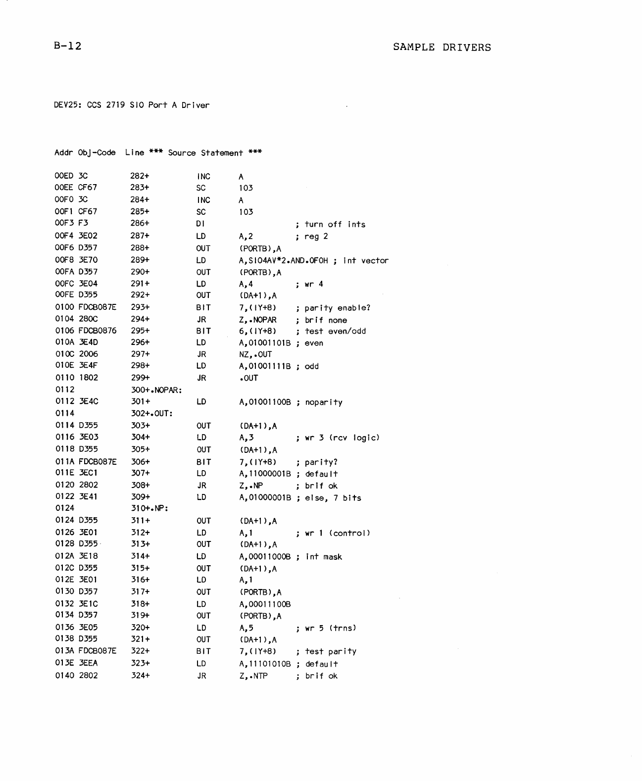
8-12
SAMPLE
DRIVERS
DEV25:
CCS
2719
SIO
Port
A
Driver
Addr
Obj-Code Line *** Source
Statement
***
OOED
3C
282+
INC
A
OOEE
CF67
283+
SC
103
OOFO
3C
284+
INC
A
00F1
CF67
285+
SC
103
00F3
F3
286+
DI
turn
off
ints
OOF4
3E02
287+
LD
A,2
reg
2
00F6
D357
288+
OUT
(PORTB)
,A
OOF8
3E70
289+
LD
A,SI04AV*2.AND.OFOH
int
vector
OOFA
D357
290+
OUT
(PORTB)
,A
OOFC
3E04
291+
LD
A,4
wr
4
OOFE
D355
292+
OUT
<DA+l
),A
0100
FDCB087E
293+
BIT
7,(IY+8)
parity
enable?
0104
280C
294+
JR
Z,.NOPAR
br i f none
0106
FOCB0876
295+
BIT
6,(IY+8)
test
even/odd
010A
3E40
296+
LD
A,01001101B even
OlOG
2006
297+
JR
NZ,.OUT
OlOE
3E4F
298+
LO
A,01001111B
odd
0110 1802
299+
JR
.OUT
0112 300+.
NOP
AR
:
01123E4C 301+
LO
A,01001100B
noparlty
0114 302+.0UT:
0114 0355 303+
OUT
<DA+1
),A
01163E03
304+
LO
A,3
wr
3
(rcv
logic)
0118 0355
305+
OUT
<DA+1
),A
011A
FDCB087E
306+
BIT
7,
( I
Y+8)
parity?
011E
3ECl
307+
LO
A,11000001B defau
It
0120 2802
308+
JR
Z,
.NP
brl
f
ok
01223E41
309+
LD
A,01000001B
else,
7
bits
0124 310+.NP:
0124
D355
311+
OUT
<DA+l
),A
0126
3EOl
312+
LO
A,
1
wr
1
(control)
0128 0355, 313+
OUT
<DA+l
)
,A
012A
3E18
314+
LO
A,0001100OB
int
mask
012C
D355
315+
OUT
<DA+l
),A
012E
3EOl
316+
LO
A,l
0130 0357
317+
OUT
(PORTB)
,A
0132
3EIC
318+
LD
A,0001110OB
0134 0357
319+
OUT
(PORTB)
,A
0136
3E05
320+
LO
A,5
wr
5
(trns)
0138 0355 321+
OUT
<DA+l
),A
013A
FOCB087E
322+
BIT
7,(IY+8)
test
parity
013E
3EEA
323+
LD
A,11101010B
default
0140
2802
324+
JR
Z,
.NTP
brif
ok
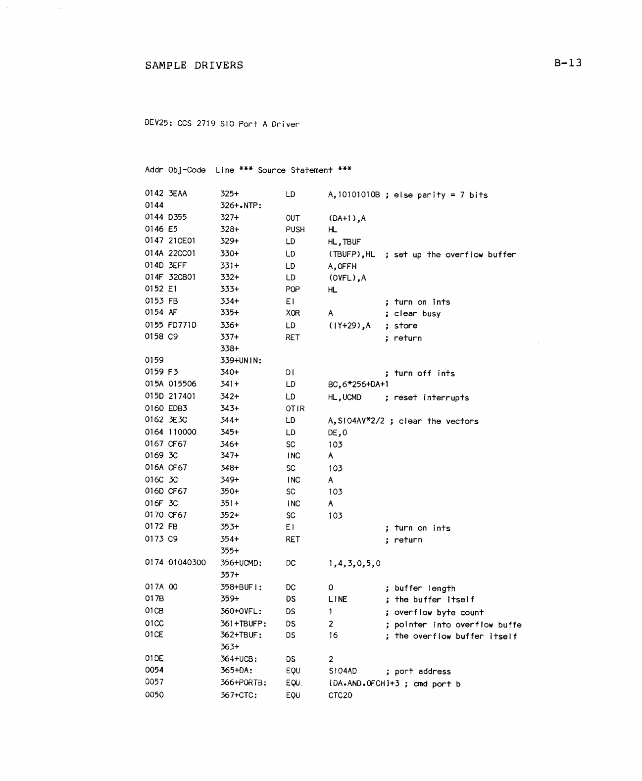
SAMPLE
DRIVERS
OEV25:
CCS
2719
SIO
Port
A
Driver
Addr
Obj-Code Line *** Source Statement ***
0142
3EAA
0144
0144 0355
0146
E5
0147
21CEOl
014A
22CCOl
0140
3EFF
014F
32CBOl
0152
El
0153
FB
0154
AF
0155
F0771D
0158
C9
0159
0159
F3
015A
015506
0150
217401
325+
326+.NTP:
327+
328+
329+
330+
331+
332+
333+
334+
335+
336+
337+
338+
339+UNIN:
340+
341+
342+
0160
EOB3
343+
0162
3E3C
344+
0164 110000
345+
0167
CF67
346+
0169
3C
347+
016A CF67
348+
016C
3C
349+
0160
CF67
350+
016F
3C
351+
0170
CF67
352+
0172
FB
353+
0173
C9
354+
355+
0174 01040300
356+UCMO:
357+
017A
00
017B
01CB
01CC
01CE
OlOE
0054
0057
0050
358+BUF
I:
359+
360+OVFL:
361+TBUFP:
362+TBUF:
363+
364+UCB:
365+DA:
366+PORTB:
367+CTC:
LO
OUT
PUSH
LO
LO
LO
LO
POP
EI
XOR
LO
RET
01
LO
LO
OTIR
LO
LO
SC
INC
SC
INC
SC
INC
SC
EI
RET
OC
OC
OS
OS
OS
OS
OS
EQU
EQU.
EQU
A,1010l010B
else
parity
7
bits
<DA+l
),A
HL
HL,TBUF
(TBUFP),HL
A,OFFH
COVFU
,A
HL
A
(IY+29)
,A
BC,6*256+0A+1
set
up
the
overflow
buffer
turn
on
ints
clear
busy
store
return
turn
off
i
nts
HL,UCMO
reset
interrupts
A,SI04AV*2/2 ;
clear
the
vectors
OE,O
103
A
103
A
103
A
103
1,4,3,0,5,0
o
LINE
1
2
16
2
turn
on
ints
return
buffer
length
the
buffer
itself
overflow
byte
count
pointer
into
overflow
buffe
the
overflow
buffer
itself
SI04AD
;
port
address
[OA.ANO.OFCH]+3
;
cmd
port
b
CTC20
8-13
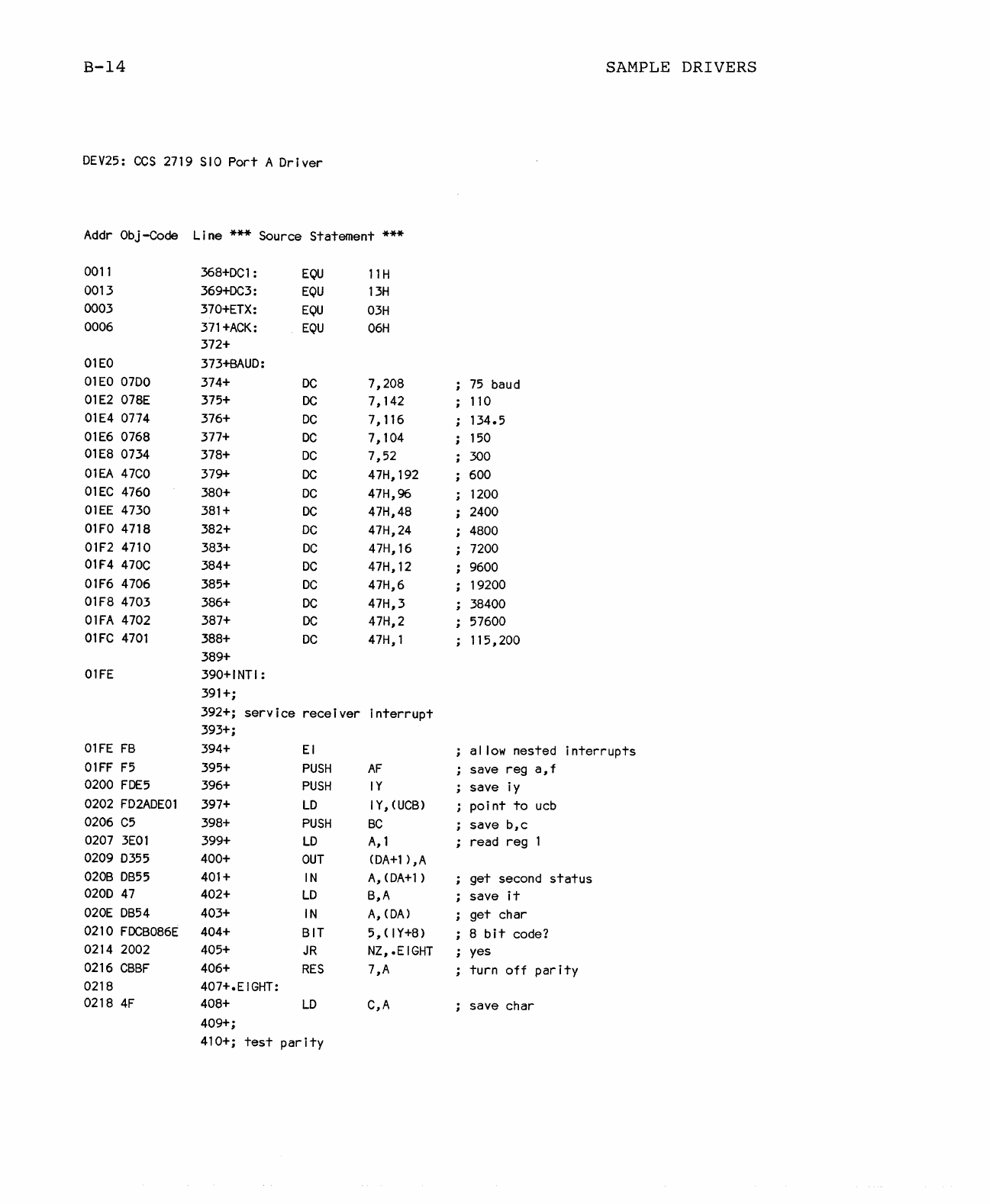
B-14
SAMPLE
DRIVERS
DEV25:
CCS
2719 510
Port
A
Driver
Addr
Obj-Code Line
***
Source Statement
***
0011
368+DCl
:
EQU
l1H
0013
369+DC3:
EQU
13H
0003
370+ETX:
EQU
03H
0006
371+ACK:
EQU
06H
372+
OlEO
373+BAUD:
OlEO
07DO
374+
DC
7,208
75
baud
01E2
078E
375+
DC
7,142
110
01E4
0774 376+
DC
7,116 134.5
01E6
0768
377+
DC
7,104
150
01E8
0734 378+
DC
7,52
300
OlEA
47CO
379+
DC
47H,192 600
01EC
4760 380+
DC
47H,96 1200
01EE
4730 381+
DC
47H,48 2400
01FO
4718 382+
DC
47H,24 4800
01F2
4710 383+
DC
47H,16 7200
01F4
470C
384+
DC
47H,12 9600
01F6
4706 385+
DC
47H,6 19200
01F8 4703 386+
DC
47H,3 38400
01FA
4702 387+
DC
47H,2 57600
01FC
4701
388+
DC
47H,1
115,200
389+
01FE
390+INTI
:
391+;
392+;
service
receIver
interrupt
393+;
01FE
FB
394+
EI
a I
low
nested
interrupts
01FF
F5
395+
PUSH
AF
save
reg
a,f
0200
FDE5
396+
PUSH
IY
save
iy
0202
FD2ADEOl
397+
LD
I
Y,
WCB)
point
to
ucb
0206
C5
398+
PUSH
BC
save
b,c
0207
3EOl
399+
LD
A,l
read
reg
0209
D355
400+
OUT
CDA+l
),A
020B
DB55
401+
IN
A,
CDA+l
)
get
second
status
020D
47
402+
LD
B,A
save
it
020E
DB54
403+
IN
A,
CDA)
get
char
0210
FDCB086E
404+
BIT
5,
(IY+8) 8
bit
code?
0214 2002
405+
JR
NZ,
.E I
GHT
yes
0216
CBBF
406+
RES
7,A
turn
off
par
i
ty
0218 407+.EIGHT:
0218
4F
408+
LD
C,A
save
char
409+;
410+;
test
parity
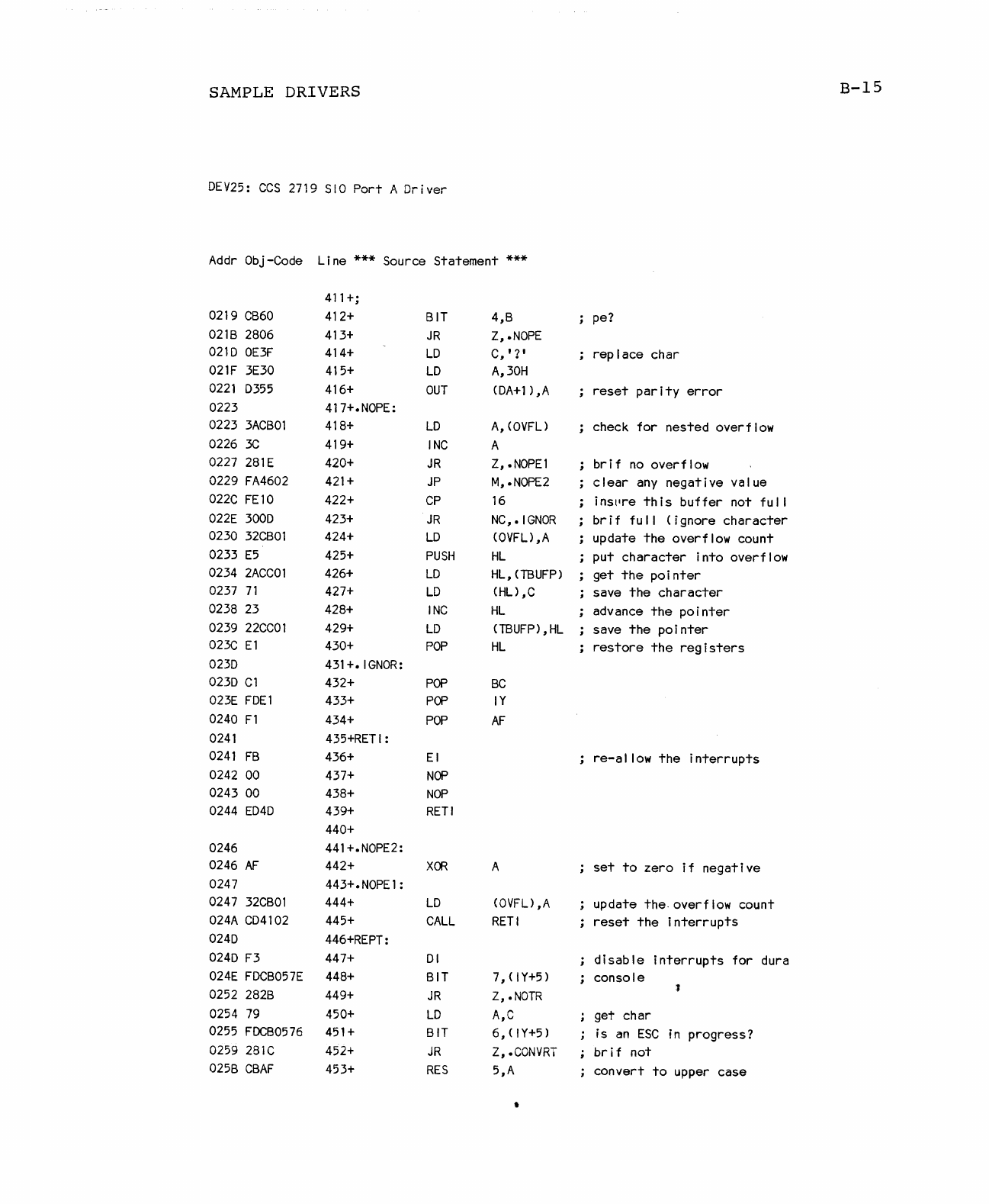
SAMPLE
DRIVERS
DEV25:
CCS
2719
SIO
Port
A Driver
Addr
Obj-Code Line *** Source Statement ***
0219
CB60
021B
2806
0210
OE3F
021F
3E30
0221
0355
0223
0223
3ACB01
0226
3C
0227
281E
0229
FA4602
022C
FE10
022E
3000
0230
32CB01
0233
E5
0234
2ACC01
0237
71
0238
23
0239
22CC01
023C
E1
0230
0230
C1
023E
FOE1
0240
F1
0241
0241
FB
0242
00
0243
00
0244
E040
411
+;
412+
413+
414+
415+
416+
417+.NOPE:
418+
419+
420+
421+
422+
423+
424+
425+
426+
427+
428+
429+
430+
431+.IGNOR:
432+
433+
434+
435+RETI:
436+
437+
438+
439+
440+
441+.NOPE2:
BIT
JR
LO
LO
OUT
LO
INC
JR
JP
CP
JR
LO
PUSH
LO
LO
INC
LO
POP
POP
POP
POP
EI
NOP
NOP
RETI
0246
0246
AF
0247
442+
XOR
443+.
NOPE
1 :
0247
32CB01
024A
C04102
0240
444+
LO
445+
CALL
446+REPT:
0240
F3
447+
024E
FDCB057E
448+
0252
282B
449+
0254
79
450+
0255
FDCB0576
451+
0259
281C
452+
025B
CBAF
453+
01
BIT
JR
LO
BIT
JR
RES
4,B
Z,
.NOPE
C,'
l'
A,30H
<DA+1
),A
A,
{OVFU
A
Z,.NOPE1
M,.NOPE2
16
NC,. I
GNOR
{OVFU
,A
HL
HL,
(TBUFP)
(HU
,C
HL
(TBUFP),HL
HL
BC
IY
AF
A
{OVFU
,A
RETI
7,
( I
Y+5)
Z,.NOTR
A,C
6,
( I
Y+5)
Z,.CONVRT
5,A
•
pe?
replace
char
reset
parity
error
check
for
nested
overflow
brif
no
overflow
clear
any
negative
value
i nSllre
th
is
buffer
not
fu
I I
brif
full
(ignore
character
update
the
overflow count
put
character
into
overflow
get
the
pointer
save
the
character
advance
the
pointer
save
the
pointer
restore
the
registers
re-al
low
the
interrupts
set
to
zero
if
negative
update
the.
overflow count
reset
the
interrupts
disable
interrupts
for
dura
console
get
char
is
an
ESC
in
progress?
br i f not
convert
to
upper
case
B-15
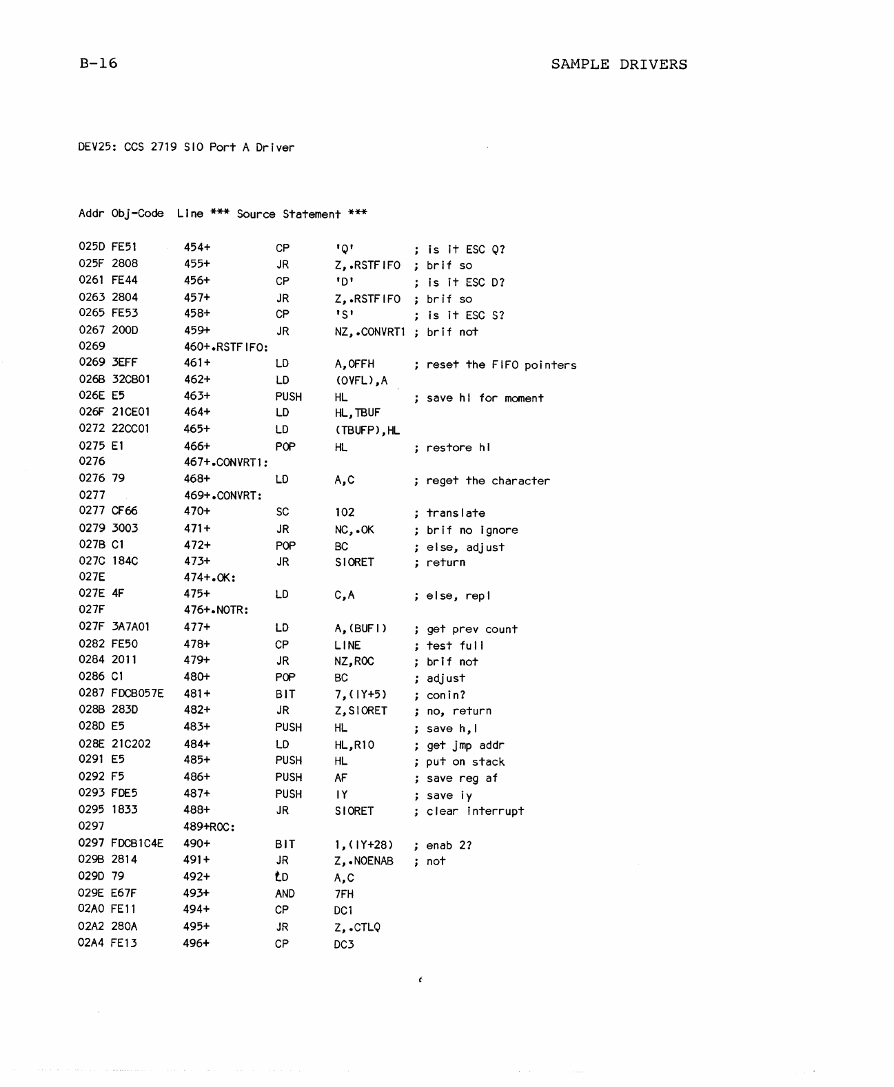
B-16
SAMPLE
DRIVERS
DEV25:
CCS
2719
SIO
Port
A Driver
Addr
Obj-Code Line *** Source Statement ***
025D
FE51
454+
CP
'Q'
is
it
ESC
Q?
025F
2808
455+
JR
Z,.RSTFIFO
bri
f so
0261
FE44
456+
CP
'D'
is
it
ESC
D?
0263 2804
457+
JR
Z,
.RSTF
IFO
br
if
so
0265
FE53
458+
CP
IS'
is
it
ESC
S?
0267
200D
459+
JR
NZ,
.CONVRTl
brif
not
0269 460+.RSTFIFO:
0269
3EFF
461+
LD
A,OFFH
reset
the
FIFO
pointers
0268
32CBOl
462+
LD
<OVFU
,A
026E
E5
463+
PUSH
HL
save hi
for
moment
026F
21CEOl
464+
LD
HL,TBUF
0272
22CCOl
465+
LD
(TBUFP)
,HL
0275
El
466+
POP
HL
restore
hi
0276
467+.CONVRTl
:
0276
79
468+
LD
A,C
reget
the
character
0277
469+.CONVRT:
0277
CF66
470+
SC
102
translate
0279 3003
471+
JR
NC,.OK
br i f
no
Ignore
027B
Cl
472+
POP
BC
else,
adj
ust
027C
184C
473+
JR
SIORET
return
027E
474+.OK:
027E
4F
475+
LD
C,A
else,
rep I
027F
476+.
NOTR:
027F
3A7AOl
477+
LD
A,(BUFI)
get
prev count
0282
FE50
478+
CP
LINE
test
fu
II
0284
2011
479+
JR
NZ,ROC
bri
f not
0286
Cl
480+
POP
BC
adjust
0287
FDCB057E
481+
BIT
7,(IY+5) conln?
028B
283D
482+
JR
Z,SIORET
no,
return
028D
E5
483+
PUSH
HL
save h, I
028E
21C202
484+
LD
HL,Rl0
get
jmp
addr
0291
E5
485+
PUSH
HL
put
on
stack
0292
F5
486+
PUSH
AF
save reg
af
0293
F0E5
487+
PUSH
IY
save iy
0295
1833
488+
JR
SIORET
clear
interrupt
0297
489+ROC:
0297
FDCB1C4E
490+
BIT
1, (IY+28) enab
2?
029B
2814
491+
JR
Z,.NOENAB
not
029D
79
492+ tD
A,C
029E
E67F
493+
AND
7FH
02AO
FEll 494+
CP
DCl
02A2
280A
495+
JR
Z,.CTLQ
02A4
FEl3 496+
CP
DC3

SAMPLE
DRIVERS
OEV25:
CCS
2719
SIO
Port
A
Driver
Addr
Obj-Code Line *** Source Statement ***
02A6
2009
02A8
02A8
C1
02A9
F07710
02AC
181C
02AE
02AE
AF
02AF
18F7
02B1
02B1
79
02B2
Cl
02B3
02B3
05
02B4
E5
02B5
217A01
02B8
34
02B9
5E
02BA
1600
02BC
19
02BO
77
02BE
E1
02BF
01
02CO
1808
02C2
02C2
C5
02C3
OE07
02C5
C09200
02C8
C1
02C9
El
02CA
02CA
3ACB01
02CD
3D
02CE
32C801
02Dl
FAF002
02D4
C5
0205
D5
02D6
E5
02D7
21CFOl
02DA
llCEOl
02DD
010FOO
02EO
1A
02E1
EDBO
02E3
2ACCOl
497+
498+.CTLS:
JR
499+
POP
500+
LD
501+
JR
502+.CTLQ:
503+
XOR
504+
JR
505+.NOENAB:
506+
LD
507+
POP
508+R2:
509+
PUSH
510+
511+
512+
513+
514+
515+
516+
517+
518+
519+
520+R10:
PUSH
LD
INC
LO
LD
ADD
LD
POP
POP
JR
521+
PUSH
522+
LO
523+
CALL
524+
POP
525+
POP
526+SIORET:
527+
LO
528+
DEC
529+
LD
530+
JP
531+
PUSH
532+
533+
534+
535+
536+
537+
538+
539+
PUSH
PUSH
LD
LD
LD
LD
LOIR
LD
NZ,.NOENAB
BC
(I Y+29),A
SIORET
A
.CTLS
A,C
BC
DE
HL
HL,BUF
I
(HU
E,
(HU
D,O
HL,OE
(HU,A
HL
DE
SIORET
BC
C,7
OUT
BC
HL
A,
(QVFU
A
(QVFU
,A
M,SIORETl
BC
DE
HL
HL,TBUF+l
OE,TBUF
BC,15
A,
<DE)
HL,
(TBUFP)
set
the
busy
sw
reset
turn
off
busy
sw
get
this
char
adj
ust
stack
saye
de and hi
regs
point
buffer
incr
count
load
it
zero
high
point
next
store
the
character
restore
regs
return
save
b,c
get
be I I code
write
the
bell
restore
b,c
restore
h,
I
see
if
overflow
occurred
update
the
character
count
brif
no
overflow
else,
empty
the
overflow
squeeze
the
buffer
down
byte
count
get
the
next
character
do
the
squeeze
update
the
pointer
B-17
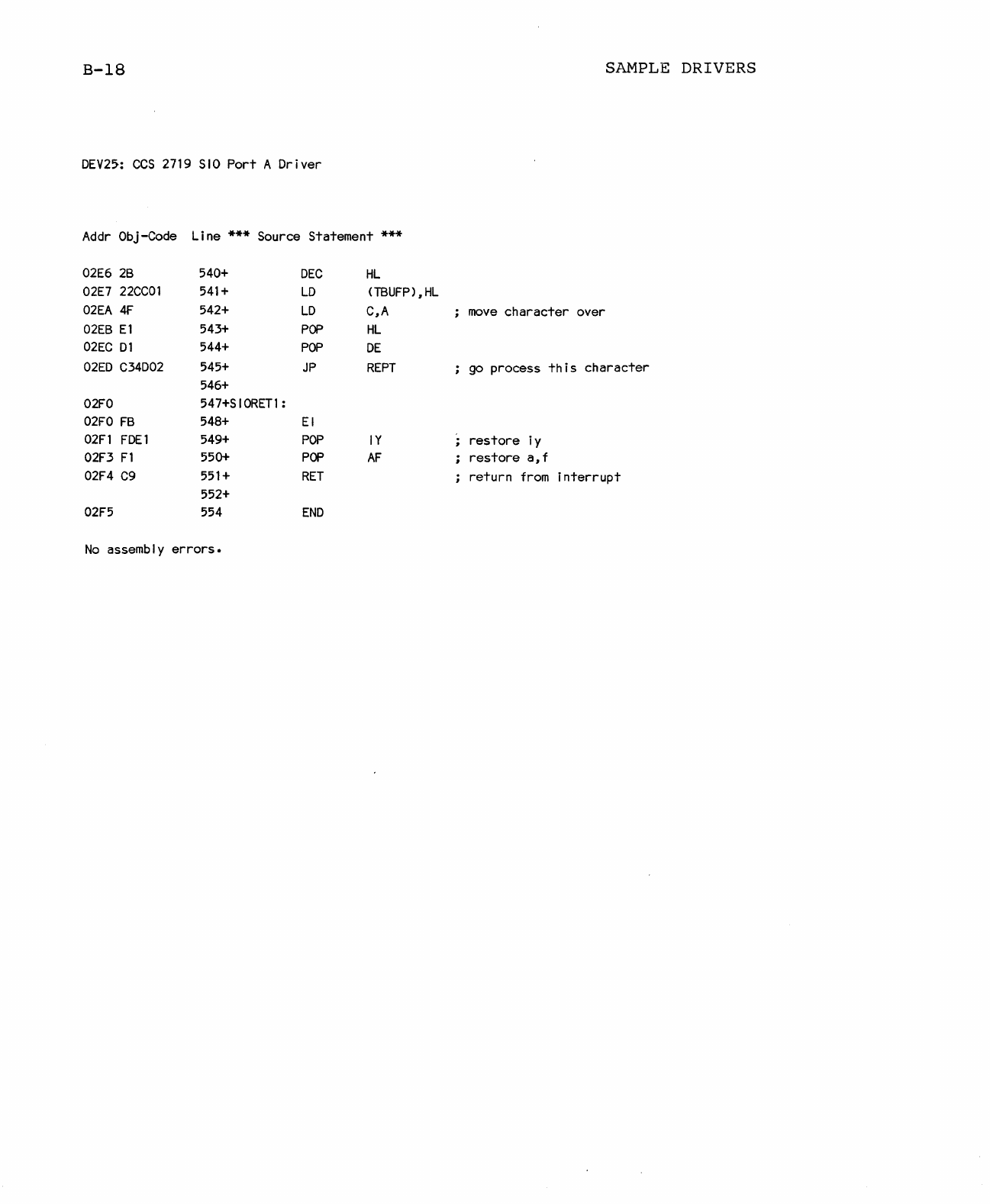
B-18
SAMPLE
DRIVERS
DEV25:
CCS
2719 510
Port
A
Driver
Addr
Obj
-Code Line *** Source Statement ***
02E6
2B
540+
DEC
HL
02E7
22CC01
541+
LD
(TBUFP),HL
02EA
4F
542+
LD
C~A
move
character
over
02EB
E1
543+
POP
HL
02EC
D1
544+
POP
DE
02ED
C34D02
545+
JP
REPT
go
process
this
character
546+
02F0
547+S
I
ORET1
:
02FO
FB
548+
EI
02Fl
FDE1
549+
POP
IY
restore
iy
02F3
F1
550+
POP
AF
restore
a~f
02F4
C9
551+
RET
return
from
interrupt
552+
02F5
554
END
No
assembly
errors.
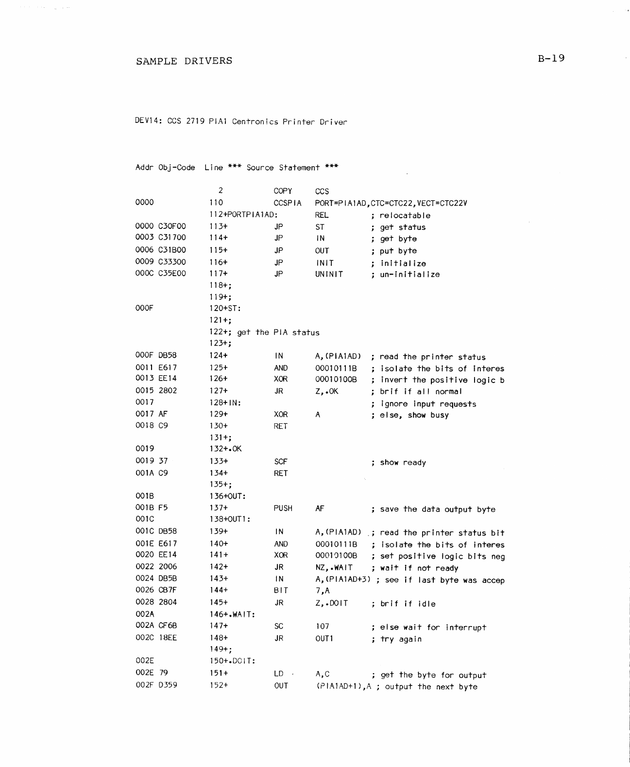
SAMPLE
DRIVERS
DEV14:
CCS
2719 PIAl
Centronics
Printer
Driver
Addr
Obj-Code
0000
0000
C30FOO
0003
C31700
0006
C31BOO
0009 C33300
OOOC
C35EOO
OOOF
OOOF
DB58
0011
E617
0013
EE14
0015 2802
0017
0017
AF
0018
C9
0019
0019
37
OOlA
C9
001B
001B
F5
OOlC
OOlC
DB58
001E
E617
0020
EE14
0022 2006
0024
DB5B
0026
CB7F
0028 2804
002A
002A
CF6B
002C
18EE
002E
002E
79
002F
D359
Line *** Source
Statement
***
COpy
CCS
2
110
CCSPIA
PORT=PIA1AD,CTC=CTC22,VECT=CTC22V
112+PORTPIA1AD:
113+
JP
114+
115+
116+
117+
118+;
119+;
120+ST:
121
+;
JP
JP
JP
JP
REL
ST
IN
OUT
IN
IT
UNINIT
relocatable
get
status
get
byte
put
byte
in
Iti
a Ii
ze
un- in
it
i a I I
ze
122+;
get
the
PIA
status
123+;
124+
125+
126+
127+
128+IN:
129+
130+
131+;
132+.
OK
133+
134+
135+;
136+OUT:
137+
138+OUT1
:
139+
140+
141+
142+
143+
144+
145+
146+.WAIT:
147+
148+
149+;
150+.DOIT:
151+
152+
IN
AND
XOR
JR
XOR
RET
SCF
RET
PUSH
IN
AND
XOR
JR
IN
BIT
JR
SC
JR
LD
OUT
A,(PIA1AD)
00010111B
00010100B
Z,.OK
A
AF
read
the
printer
status
isolate
the
bits
of
Interes
invert
the
positive
logic
b
brif
if
al
I normal
ignore
input
requests
else,
show
busy
show
ready
save
the
data
output
byte
A,(PIA1AD)
.,
read
the
printer
status
bit
00010111B
Isolate
the
bits
of
interes
00010100B
set
positive
logic
bits
neg
NZ,.WAIT
wait
if
not
ready
A,(PIA1AD+3) ;
see
if
last
byte
was
accep
7,A
Z,.DOIT
107
oun
br
if
if
idle
else
wait
for
interrupt
try
again
A,C
;
get
the
byte
for
output
(PIA1AD+ll,A;
output
the
next
byte
B-19
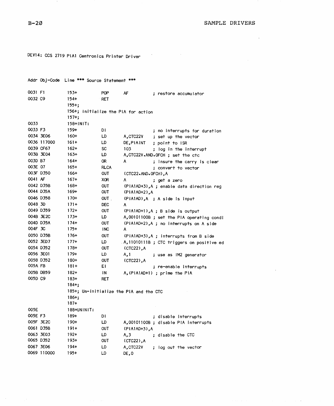
B-20
SAMPLE
DRIVERS
DEV14:
CCS
2719 PIAl
Centronics
Printer
Driver
Addr
ObJ-Code Line *** Source Statement ***
0031
F1
0032
C9
0033
0033
F3
0034
3E06
0036 117000
0039
CF67
0038
3E04
003D
87
003E
07
003F
D350
0041
AF
0042
D358
0044
D35A
0046
D358
0048
3D
0049
D359
0048
3E2C
004D
D35A
004F
3C
0050
D358
0052
3ED7
0054
D352
0056
3EOl
0058
D352
005A
F8
0058
D859
005D
C9
005E
005E
F3
005F
3E2C
0061
D358
0063
3E03
0065
D352
0067
3E06
0069 110000
153+
154+
155+;
POP
RET
AF
restore
accumulator
156+;
Initial
ize
the
PIA
for
action
157+;
158+INIT:
159+
160+
161+
162+
163+
164+
165+
166+
167+
168+
169+
170+
171+
172+
173+
174+
175+
176+
177+
178+
179+
180+
181+
182+
183+
184+;
DI
LD
LD
SC
LD
OR
RLCA
OUT
XOR
OUT
OUT
OUT.
DEC
OUT
LD
OUT
INC
OUT
LD
OUT
LD
OUT
EI
IN
RET
no
interrupts
for
duration
A,CTC22V
set
up
the
vector
DE,PIAINT
point
to
ISR
103
log in
the
interrupt
A,CTC22V.AND.OFCH
;
set
the
ctc
A ;
insure
the
carry
is
clear
;
convert
to
vector
(CTC22.AND.OFCH),A
A ;
get
a
zero
(PIA1AD+3),A
;
enable
data
direction
reg
(P
I A 1
AD+
2 ) , A
(PIA1AD),A
; A
side
is
input
A
(PIA1AD+1),A; 8
side
is
output
A,001011008 ;
set
the
PIA
operating
condi
CPIA1AD+2),A
no
interrupts
on
A
side
A
(PIA1AD+3),A
.A,110101118
(CTC22),A
A,
1
(CTC22),A
interrupts
from
8
side
CTC
triggers
on
positive
ed
use
as
1M2
generator
re-enable
interrupts
A,CPIA1AD+1)
; prime
the
PIA
185+;
Un-initialize
the
PIA
and
the
CTC
186+;
187+
188+UNINIT:
189+
190+
191+
192+
193+
194+
195+
DI
LD
OUT
LD
OUT
LD
LD
disable
interrupts
A,00101100B
disable
PIA
interrupts
(PIA1AD+3),A
A,3
disable
the
CTC
(CTC22)
,A
A,CTC22V
log
out
the
vector
DE,O

SAMPLE
DRIVERS
B-21
DEV14:
CCS
2719 PIAl
Centronics
Printer
Driver
Addr
Obj-Code
Li
ne
*** Source
Statement
***
006C
CF67
196+
SC
103
unschedule
006E
FB
197+
EI
006F
C9
198+
RET
199+;
200+;
Interrupt
service
routine
201+;
202+
0070 203+PIAINT:
0070
FB
204+
EI
; al
low
nested
interrupts
0071
F5
205+
PUSH
AF
; save
the
accumulator
0072
DB59
206+
IN
A,(PIA1AD+1)
;
clear
the
interrupt
flag
0074
F1
207+
POP
AF
restore
the
accumulator
0075
ED4D
208+
RETI
; done
0077 209
END
No
assembly
errors.
