CM Series/CM Radios Detailed Service Manual 6866545D30 O
User Manual: -CM Series/CM Radios Detailed service manual 6866545D30-O
Open the PDF directly: View PDF ![]() .
.
Page Count: 390 [warning: Documents this large are best viewed by clicking the View PDF Link!]

Commercial Series
CM Radios
Detailed Service Manual
6866545D30-O

ii

WLS EMEA Publications Department, Jays Close, Viables Industrial Estate, Basingstoke, Hampshire, RG22 4PD, UK.
Issue : December 2003 iii
Commercial Series
CM Radios
Detailed Service Manual
6866545D30-O
Contents
Section 1 Service Maintainability
Section 2 Controlhead Service Information
Section 3 UHF2 Service Information
Section 4 VHF2 Service Information
Section 5 Midband Service Information
Section 6 UHF2 High Power Service Information
Section 7 VHF2 High Power Service Information

iv

Commercial Series
CM Radios
Service Maintainability
Issue: December 2003

ii
Computer Software Copyrights
The Motorola products described in this manual may include copyrighted Motorola computer programs stored
in semiconductor memories or other media. Laws in the United States and other countries preserve for
Motorola certain exclusive rights for copyrighted computer programs, including the exclusive right to copy or
reproduce in any form, the copyrighted computer program. Accordingly, any copyrighted Motorola computer
programs contained in the Motorola products described in this manual may not be copied or reproduced in
any manner without the express written permission of Motorola. Furthermore, the purchase of Motorola
products shall not be deemed to grant, either directly or by implication, estoppel or otherwise, any license
under the copyrights, patents or patent applications of Motorola, except for the normal non-exclusive
royalty-free license to use that arises by operation of law in the sale of a product.

iii
Table of Contents
Chapter 1 INTRODUCTION
1.0 Scope of Manual..................................................................................................1-1
2.0 Warranty and Service Support.............................................................................1-1
2.1 Warranty Period and Return Instructions .......................................................1-1
2.2 After Warranty Period.....................................................................................1-1
2.3 European Radio Support Centre (ERSC).......................................................1-2
2.4 Parts Identification and Ordering ....................................................................1-2
2.5 EMEA Test Equipment Support......................................................................1-2
2.6 Technical Support...........................................................................................1-3
2.7 Related Documents ........................................................................................1-3
3.0 Radio Model Information......................................................................................1-4
Chapter 2 MAINTENANCE
1.0 Introduction ..........................................................................................................2-1
2.0 Preventive Maintenance ......................................................................................2-1
2.1 Inspection .......................................................................................................2-1
2.2 Cleaning .........................................................................................................2-1
3.0 Safe Handling of CMOS and LDMOS..................................................................2-2
4.0 General Repair Procedures and Techniques.......................................................2-2
5.0 Notes For All Schematics and Circuit Boards ......................................................2-5
Chapter 3 SERVICE AIDS
1.0 Recommended Test Tools...................................................................................3-1
2.0 Test Equipment....................................................................................................3-2

iv

v
SAFETY INFORMATION
Read this information before using your radio.
PRODUCT SAFETY AND RF EXPOSURE FOR MOBILE TWO-WAY RADIOS
INSTALLED IN VEHICLES OR AS FIXED SITE CONTROL STATIONS.
This document provides information and instructions for the safe and efficient operation of Motorola
Mobile Two-Way Radios. The information provided in this document supersedes information
contained in user guides published prior to February 2002.
COMPLIANCE WITH RF ENERGY EXPOSURE STANDARDS
Note:This Radio is intended for use in occupational/controlled applications, where users have been
made aware of the potential for exposure and can exercise control over their exposure. This radio
device is NOT authorized for general population, consumer or similar use.
This user safety booklet includes useful information about RF exposure and helpful instructions on
how to control your RF exposures.
Your Motorola radio is designed and tested to comply with a number of national and international
standards and guidelines regarding human exposure to radio frequency electromagnetic energy. This
radio complies with IEEE and ICNIRP exposure limits for occupational/controlled RF exposure
environments at usage factors of up to 50% talk–50% listen. In terms of measuring RF energy for
compliance with the IEEE/ICNIRP exposure guidelines, your radio radiates measurable RF energy
only while it is transmitting (during talking), not when it is receiving (listening) or in standby mode.
Your Motorola two-way radio complies with the following RF energy exposure
standards and guidelines:
●United States Federal Communications Commission, Code of Federal Regulations; 47 CFR part 2
sub-part J
●American National Standards Institute (ANSI) / Institute of Electrical and Electronic Engineers
(IEEE) C95. 1-1992
●Institute of Electrical and Electronic Engineers (IEEE) C95.1-1999 Edition
●International Commission on Non-Ionizing Radiation Protection (ICNIRP) 1998
●Ministry of Health (Canada) Safety Code 6. Limits of Human Exposure to Radiofrequency Electro-
magnetic Fields in the Frequency Range from 3 kHz to 300 GHz, 1999
●Australian Communications Authority Radiocommunications (Electromagnetic Radiation - Human
Exposure) Standard 2001
●ANATEL, Brasil Regulatory Authority, Resolution 256 (April 11, 2001) “additional requirements for
SMR, cellular and PCS product certification.”
vi
COMPLIANCE AND CONTROL GUIDELINES AND OPERATING INSTRUCTIONS FOR
MOBILE TWO-WAY RADIOS INSTALLED IN VEHICLES
To control your exposure and ensure compliance with the occupational/controlled environment
exposure limits, always adhere to the following procedures:
●To transmit (talk), push the Push-To-Talk (PTT) button; to receive, release the PTT button. Transmit
only when people outside the vehicle are at least the minimum lateral distance away from a properly
installed, externally-mounted antenna. Table 1 lists the minimum distance for bystanders in an
uncontrolled environment from the transmitting antenna at several different ranges of rated radio
power for mobile radios installed in a vehicle..
●Install mobile antennas at the centre of the roof and centre of the trunk deck. These mobile installa-
tion guidelines are limited to metal body vehicles. The antenna installation must additionally be in
accordance with:
a. The requirements of the antenna manufacturer/supplier
b. Instructions in the Radio Installation Manual.
●Use only Motorola-approved supplied or replacement antenna. Use of non–Motorola - approved
antennas, modifications, or attachments could damage the radio and may violate IEEE/ICNIRP regu-
lations. For a list of Motorola-approved antennas please see your dealer. Your nearest dealer can
be found at the following web site :
http://www.motorola.com/cgiss/emea/dealerlocator.html
For additional information on exposure requirements or other training information, visit
http://www.motorola.com/rfhealth.
COMPLIANCE AND CONTROL GUIDELINES AND OPERATING INSTRUCTIONS FOR
MOBILE TWO-WAY RADIOS INSTALLED AS FIXED SITE CONTROL STATIONS
If mobile radio equipment is installed at a fixed location and operated as a control station or as a fixed
unit, the antenna installation must comply with the following requirements in order to ensure optimal
performance and compliance with the RF energy exposure in the standards and guidelines listed
above:
●The antenna must be mounted outside the building on the roof or a tower if at all possible.
●As with all fixed site antenna installations, it is the responsibility of the licensee to manage the site in
accordance with applicable regulatory requirements and may require additional compliance actions
such as site survey measurements, signage, and site access restrictions in order to insure that
exposure limits are not exceeded.
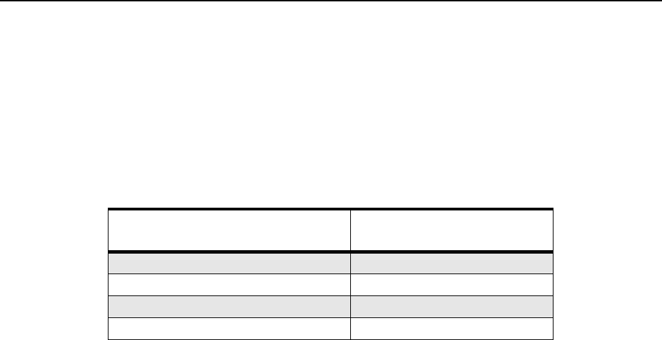
Table 1: Rated Power and Distance
Rated Power of Vehicle-Installed
Mobile Two-Way Radio
Minimum Distance from
Transmitting Antenna
Less than 7Watts 20 cm (8 Inches)
7 to 15 Watts 30.5 cm (1 Foot)
16 to 50 Watts 61 cm (2 Feet)
51 to 110 Watts 91.5 cm (3 Feet)

vii
ELECTROMAGNETIC INTERFERENCE/COMPATIBILITY
NOTE: Nearly every electronic device is susceptible to electromagnetic interference (EMI) if
inadequately shielded, designed or otherwise configured for electromagnetic compatibility. It may be
necessary to conduct compatibility testing to determine if any electronic equipment used in or around
vehicles or near fixed site antenna is sensitive to external RF energy or if any procedures need to be
followed to eliminate or mitigate the potential for interaction between the radio transmitter and the
equipment or device.
Facilities
To avoid electromagnetic interference and/or compatibility conflicts, turn off your radio in any
facility where posted notices instruct you to do so. Hospitals or health care facilities may be
using equipment that is sensitive to external RF energy.
Vehicles
To avoid possible interaction between the radio transmitter and any vehicle electronic control
modules, for example, ABS, engine, or transmission controls, the radio should be installed only by an
experienced installer and that the following precautions be used when installing the radio:
1. Refer to the manufacturer’s instructions or other technical bulletins or recommendations on radio installation.
2. Before installing the radio, determine the location of the electronic control modules and their harnesses in
the vehicle.
3. Route all radio wiring, including the antenna transmission line, as far away as possible from the electronic
control units and associated wiring.
Driver Safety
Check the laws and regulations on the use of radios in the area where you drive. Always obey them.
When using your radio while driving, please:
●Give full attention to driving and to the road.
●Pull off the road and park before making or answering a call if driving conditions so require.
OPERATIONAL WARNINGS
For Vehicles With An Air Bag
Do not mount or place a mobile radio in the area over an air bag or in the air bag deployment area. Air
bags inflate with great force. If a radio is placed in the air bag deployment area and the air bag
inflates, the radio may be propelled with great force and cause serious injury to occupants of the
vehicle.
Potentially Explosive Atmospheres
Turn off your radio prior to entering any area with a potentially explosive atmosphere. Sparks in a
potentially explosive atmosphere can cause an explosion or fire resulting in bodily injury or even
death.
The areas with potentially explosive atmospheres referred to above include fuelling areas such as
below decks on boats, fuel or chemical transfer or storage facilities, areas where the air contains
chemicals or particles, such as grain, dust or metal powders. Areas with potentially explosive
atmospheres are often but not always posted.
Blasting Caps And Areas
To avoid possible interference with blasting operations, turn off your radio when you are near
electrical blasting caps, in a blasting area, or in areas posted:
"Turn off two-way radio". Obey all signs and instructions.

viii
For radios installed in vehicles fueled by liquefied petroleum gas, refer to the (U.S.) National Fire
Protection Association standard, NFPA 58, for storage, handling, and/or container information. For a
copy of the LP-gas standard, NFPA 58, contact the National Fire Protection Association, One Battery
Park, Quincy, MA.

Chapter 1
INTRODUCTION
1.0 Scope of Manual
This manual is intended for use by service technicians familiar with similar types of equipment. It
contains service information required for the equipment described and is current as of the printing
date. Changes which occur after the printing date may be incorporated by a complete Manual
revision or alternatively as additions.
2.0 Warranty and Service Support
Motorola offers long term support for its products. This support includes full exchange and/or repair
of the product during the warranty period, and service/ repair or spare parts support out of warranty.
Any "return for exchange" or "return for repair" by an authorised Motorola Dealer must be
accompanied by a Warranty Claim Form. Warranty Claim Forms are obtained by contacting an
Authorised Motorola Dealer.
2.1 Warranty Period and Return Instructions
The terms and conditions of warranty are defined fully in the Motorola Dealer or Distributor or
Reseller contract. These conditions may change from time to time and the following notes are for
guidance purposes only.
In instances where the product is covered under a "return for replacement" or "return for repair"
warranty, a check of the product should be performed prior to shipping the unit back to Motorola.
This is to ensure that the product has been correctly programmed or has not been subjected to
damage outside the terms of the warranty.
Prior to shipping any radio back to the appropriate Motorola warranty depot, please contact
Customer Resources (Please see page 2 and page 3 in this Chapter). All returns must be
accompanied by a Warranty Claim Form, available from your Customer Services representative.
Products should be shipped back in the original packaging, or correctly packaged to ensure no
damage occurs in transit.
2.2 After Warranty Period
After the Warranty period, Motorola continues to support its products in two ways.
1. Motorola's Radio Aftermarket and Accessory Division (AAD) offers a repair service to both
end users and dealers at competitive prices.
2. AAD supplies individual parts and modules that can be purchased by dealers who are
technically capable of performing fault analysis and repair.
NOTE Before operating or testing these units, please read the Safety Information Section in the
front of this manual.

1-2 INTRODUCTION
2.3 European Radio Support Centre (ERSC)
The ERSC Customer Information Desk is available through the following service numbers:
Austria: 08 00 29 75 41 Italy: 80 08 77 387
Belgium: 08 00 72 471 Luxemburg: 08 00 23 27
Denmark: 80 88 05 72 Netherlands: 08 00 22 45 13
Finland: 08 00 11 49 910 Norway: 80 01 11 15
France: 08 00 90 30 90 Portugal: 08 00 84 95 70
Germany: 08 00 18 75 240 Spain: 90 09 84 902
Greece: 00 80 04 91 29 020 Sweden: 02 07 94 307
UK : 08 00 96 90 95 Switzerland: 08 00 55 30 82
Ireland: 18 00 55 50 21 Iceland: 80 08 147
Or dial the European Repair and Service Centre:
Tel: +49 30 6686 1555
Please use these numbers for repair enquiries only.
2.4 Piece Parts
Some replacement parts, spare parts, and/or product information can be ordered directly. If a
complete Motorola part number is assigned to the part, it is available from Motorola Radio
Aftermarket and Accessory Division (AAD). If no part number is assigned, the part is not normally
available from Motorola. If the part number is appended with an asterisk, the part is serviceable by
Motorola Depot only. If a parts list is not included, this generally means that no user-serviceable
parts are available for that kit or assembly.
All part orders should be directed to :
Motorola GmbH
Customer Care
AM Borsigturm 130
13507 Berlin
Germany.
2.5 EMEA Test Equipment Support
Information related to support and service of Motorola Test Equipment is available via Motorola
Online (Extranet), through the Customer Care organisation of Motorola’s local area representation
or by calling the the European Repair and Service Centre: Tel: +49 30 6686 1555

Warranty and Service Support 1-3
2.6 Technical Support
Motorola Product Services is available to assist the dealer/distributors in resolving any malfunctions
which may be encountered.
UK/Ireland - Richard Russell
Telephone: +44 (0) 1256 488 082
Fax: +44 01256 488 080
Email: BRR001@email.mot.com
Central/East Europe - Siggy Punzenberger
Telephone: +49 (0) 6128 70 2342
Fax: +49 (0) 6128 95 1096
Email: TFG003@email.mot.com
Scandinavia
Telephone: +46 8 735 9282
Fax: +46 8 735 9280
Email: C14749@email.mot.com
Germany -Customer Connect Team
Telephone: +49 (0) 6128 70 2248
Fax: +49 (0) 6128 95 1082
Email: cgiss.emea@europe.mot.com
France - Lionel Lhermitte
Telephone: +33 1 6929 5722
Fax: +33 1 6929 5904
Email: TXE037@email.mot.com
Italy - Ugo Gentile
Telephone: +39 0 2822 0325
Fax: +39 0 2822 0334
Email: C13864@email.mot.com
Africa & Middle East - Armand Roy
Telephone: +33 1 6929 5715
Fax: +33 1 6929 5778
Email: armand.roy@Motorola.com
2.7 Related Documents
The following documents are directly related to the use and maintainability of this product.
Title Language Part Number
CM Series Product Manual English GMLN1062_
German GMLN1063_
French GMLN1064_
Italian GMLN1065_
Spanish GMLN1066_
Russian GMLN1067_
1-4 INTRODUCTION
3.0 Radio Model Information
The model number and serial number are located on a label attached to the back of your radio. You
can determine the RF output power, frequency band, protocols, and physical packages. The
example below shows one mobile radio model number and its specific characteristics.
Table 1-1 Radio Model Number (Example: MDM50FNC9AN2_N)
Type of
Unit
Model
Series
Freq.
Band
Power
Level
Physical
Packages
Channel
Spacing Protocol Feature
Level
Model
Revision
Model
Package
MD M 50 F
Midband
(66-
88MHz)
J
VHF1
(136-
162MHz)
K
VHF2
(146-
174MHz)
N
1-25W
C
CM140
CM340
9
Program-
mable
AA
Conven-
tional
MDC
1
RF
Connector :
Mini-UHF
AN
Q
UHF1
(403-
430MHz)
P
25-40W
F
CM160
CM360
AN
5 Tone
2
RF
Connector :
BNC
R
UHF2
(438-
470MHz)
Q
25-45W
S
UHF3
(465-
495MHz)
MD = Motorola Internal Use
M = Mobile

Chapter 2
MAINTENANCE
1.0 Introduction
This chapter of the manual describes:
■preventive maintenance
■safe handling of CMOS devices
■repair procedures and techniques
2.0 Preventive Maintenance
The radios do not require a scheduled preventive maintenance program; however, periodic visual
inspection and cleaning is recommended.
2.1 Inspection
Check that the external surfaces of the radio are clean, and that all external controls and switches
are functional. It is not recommended to inspect the interior electronic circuitry.
2.2 Cleaning
The following procedures describe the recommended cleaning agents and the methods to be
used when cleaning the external and internal surfaces of the radio. External surfaces include the
front cover, housing assembly, and battery case. These surfaces should be cleaned whenever a
periodic visual inspection reveals the presence of smudges, grease, and/or grime.
The only recommended agent for cleaning the external radio surfaces is a 0.5% solution of a mild
dishwashing detergent in water. The only factory recommended liquid for cleaning the printed
circuit boards and their components is isopropyl alcohol (70% by volume).
1. Cleaning External Plastic Surfaces
The detergent-water solution should be applied sparingly with a stiff, non-metallic, short-
bristled brush to work all loose dirt away from the radio. A soft, absorbent, lintless cloth or
tissue should be used to remove the solution and dry the radio. Make sure that no water
remains entrapped near the connectors, cracks, or crevices.
2. Cleaning Internal Circuit Boards and Components
Isopropyl alcohol may be applied with a stiff, non-metallic, short-bristled brush to dislodge
embedded or caked materials located in hard-to-reach areas. The brush stroke should
direct the dislodged material out and away from the inside of the radio. Make sure that
controls or tunable components are not soaked with alcohol. Do not use high-pressure
air to hasten the drying process since this could cause the liquid to collect in unwanted
places. Upon completion of the cleaning process, use a soft, absorbent, lintless cloth to
dry the area. Do not brush or apply any isopropyl alcohol to the frame, front cover, or
back cover.
NOTE Internal surfaces should be cleaned only when the radio is disassembled for servicing or
repair.
CAUTION: The effects of certain chemicals and their vapors can have harmful results on
certain plastics. Aerosol sprays, tuner cleaners, and other chemicals should be avoided.
!

2-2 MAINTENANCE
3.0 Safe Handling of CMOS and LDMOS
Complementary metal-oxide semiconductor (CMOS) devices are used in this family of radios.
CMOS characteristics make them susceptible to damage by electrostatic or high voltage
charges. Damage can be latent, resulting in failures occurring weeks or months later. Therefore,
special precautions must be taken to prevent device damage during disassembly,
troubleshooting, and repair.
Handling precautions are mandatory for CMOS circuits and are especially important in low
humidity conditions. DO NOT attempt to disassemble the radio without first referring to the CMOS
CAUTION paragraph in the Disassembly and Reassembly section of the manual.
4.0 General Repair Procedures and Techniques
IC Pre-Baking
No pre-baking of components is required in the repair of this product.
Parts Replacement and Substitution
When damaged parts are replaced, identical parts should be used. If the identical replacement
component is not locally available, check the parts list for the proper Motorola part number and
order the component from the nearest Motorola Communications parts center listed in the “Piece
Parts” section of this manual.
Rigid Circuit Boards
The family of radios uses bonded, multi-layer, printed circuit boards. Since the inner layers are
not accessible, some special considerations are required when soldering and unsoldering
components. The through-plated holes may interconnect multiple layers of the printed circuit.
Therefore, care should be exercised to avoid pulling the plated circuit out of the hole.
When soldering near the 18-pin and 40-pin connectors:
■avoid accidentally getting solder in the connector.
■be careful not to form solder bridges between the connector pins
■closely examine your work for shorts due to solder bridges.
NOTE Always use a fresh supply of alcohol and a clean container to prevent contamination by
dissolved material (from previous usage).

General Repair Procedures and Techniques 2-3
Chip Components
Use either the RLN4062 Hot-Air Repair Station or the Motorola 0180381B45 Repair Station for
chip component replacement. When using the 0180381B45 Repair Station, select the TJ-65 mini-
thermojet hand piece. On either unit, adjust the temperature control to 370 °C (700 °F), and
adjust the airflow to a minimum setting. Airflow can vary due to component density.
■To remove a chip component:
1. Use a hot-air hand piece and position the nozzle of the hand piece approximately 0.3 cm
(1/8") above the component to be removed.
2. Begin applying the hot air. Once the solder reflows, remove the component using a pair
of tweezers.
3. Using a solder wick and a soldering iron or a power desoldering station, remove the
excess solder from the pads.
■To replace a chip component using a soldering iron:
1. Select the appropriate micro-tipped soldering iron and apply fresh solder to one of the
solder pads.
2. Using a pair of tweezers, position the new chip component in place while heating the
fresh solder.
3. Once solder wicks onto the new component, remove the heat from the solder.
4. Heat the remaining pad with the soldering iron and apply solder until it wicks to the
component. If necessary, touch up the first side. All solder joints should be smooth and
shiny.
■To replace a chip component using hot air:
1. Use the hot-air hand piece and reflow the solder on the solder pads to smooth it.
2. Apply a drop of solder paste flux to each pad.
3. Using a pair of tweezers, position the new component in place.
4. Position the hot-air hand piece approximately 0.3 cm (1/8” ) above the component and
begin applying heat.
5. Once the solder wicks to the component, remove the heat and inspect the repair. All
joints should be smooth and shiny.

2-4 MAINTENANCE
Shields
Removing and replacing shields will be done with the R1070 station with the temperature control
set to approximately 215°C (415°F) [230°C (445°F) maximum].
■To remove the shield:
1. Place the circuit board in the R1070 circuit board holder.
2. Select the proper heat focus head and attach it to the heater chimney.
3. Add solder paste flux around the base of the shield.
4. Position the shield under the heat-focus head.
5. Lower the vacuum tip and attach it to the shield by turning on the vacuum pump.
6. Lower the focus head until it is approximately 0.3 cm (1/8”) above the shield.
7. Turn on the heater and wait until the shield lifts off the circuit board.
8. Once the shield is off, turn off the heat, grab the part with a pair of tweezers, and turn off
the vacuum pump.
9. Remove the circuit board from the R1070 circuit board holder.
■To replace the shield:
1. Add solder to the shield if necessary, using a micro-tipped soldering iron.
2. Next, rub the soldering iron tip along the edge of the shield to smooth out any excess
solder. Use solder wick and a soldering iron to remove excess solder from the solder
pads on the circuit board.
3. Place the circuit board back in the R1070 circuit board holder.
4. Place the shield on the circuit board using a pair of tweezers.
5. Position the heat-focus head over the shield and lower it to approximately 0.3 cm (1/8”)
above the shield.
6. Turn on the heater and wait for the solder to reflow.
7. Once complete, turn off the heat, raise the heat-focus head and wait approximately one
minute for the part to cool.
8. Remove the circuit board and inspect the repair. No cleaning should be necessary.

Notes For All Schematics and Circuit Boards 2-5
5.0 Notes For All Schematics and Circuit Boards
* Component is frequency sensitive. Refer to the Electrical Parts List for value and usage.
1. Unless otherwise stated, resistances are in Ohms (k = 1000), and capacitances are in picofarads
(pF) or microfarads (µF).
2. DC voltages are measured from point indicated to chassis ground using a Motorola DC
multimeter or equivalent. Transmitter measurements should be made with a 1.2 µH choke in
series with the voltage probe to prevent circuit loading.
3. Interconnect Tie Point Legend:
Signal Name Signal Description
16_8MHz 16.8MHz Reference Frequency from Synthesizer to ASFIC
3V 3V RF regulator
5V 5V RF regulator
5V_CH Optional 5V for Control Head
9V Regulated 9.3V Supply Voltage
9R 9V to enable RX_INJ when RX_EN is active
ASFIC_CS ASFIC Chip Select
B+ 13.8V Supply Voltage
BATT_SENSE Battery Voltage Sense Line
BOOT_EN_IN_CH Boot Mode Select
BW_SEL Select BW (12.5 KHz, 25 KHz)
CH_ACT Channel Activity Indicator Signal (Fast Squelch)
COMM_DATA_SEL_CH Display Driver Command/ Data Select
D3_V3 Regulated 3.3V supply voltage for Voice Storage
DEMOD Audio Output Signal from the Receiver IC
DETECTOR_AUDIO_SEND_BRD Flat Audio to Option Board
DISPLAY_CS_CH Control Head Chip Select
EMERGENCY_ACCES_CONN Emergency line to switch on the radio voltage regulators
EMERGENCY_SENSE Emergency sense to µP
EXTERNAL_MIC_AUDIO ACCES_CONN External (from accessory connector) microphone input
F1200 Interrupt line from ASFIC CMP
FILT_SW_B+ Switched 13.8 V supply voltage
FLAT_TX_AUDIO_INPUT_ACCESS_CONN Flat TX input from accessory connector
HANDSE RX_AUDIO_CH Handset Audio Output
HOOK_CH Hang-up switch input
HSIO High Speed Clock In / Data Out
IGNITION Ignition Line to switch on he radio’s voltage regulator
KEYPAD_COL_CH Keypad Matrix Column
LOC_DIST Enable Attenuator for RX line
LSIO Low Speed Clock In / Data Out
MIC_AUDIO_CH Microphone Input

2-6 MAINTENANCE
MIC_PTT_CH Microphone PTT Input
MOD_IN Modulation Signal from ASFIC
MOD_OUT Modulation Signal to the Synthesizer
ONOFF_SENSE On off sense switch
OPT_DATA_R_OPRD DATA/Ready Request from Option Board
OPT_EN_OPBD Option Board Chip Select
PA_BIAS PA Control bias voltage
PA_CURRENT Not used
POST_LIMITER_TX
AUDIO_RETURN_OPT_BRD
Flat TX Input from Option Board
PROG x IN ACC y General Purpose Input x accessory connector Pin y
PROG x INOUT ACC y General Purpose Input/Output x accessory connector Pin y
PROG x OUT ACC y General Purpose Input x accessory connector Pin y
PWR_SET PA Power Control Voltage
RESET Reset Line
RSSI Received Signal Strength Indicator
RX RX signal
RX AUD RTN Option Board Input/Output of Receiver Audio Path
RX_AUDIO_OUTPUT_ACCESS_CONN Flat or filtered audio to accessory connector
RX_EN Enable Receiving
RX_INJ RF signal from VCO into the Receiver
SCI_CH Bi-directional serial communication line
SHIFT_R_CS SPI Chip select for the Control Head
SPI_CLK Serial peripheral interface bus CLOCK
SPI_MISO Serial peripheral interface bus data IN
SPI_MOSI Serial peripheral interface bus data OUT
SPKR- Negative Audio PA Speaker Output
SPKR- Negative Audio PA Speaker Output
SPKR+ Positive Audio PA Speaker Output
SQ_DET Squelch Detect Signal
SYNTH_CS Synth Chip Select
SYNTH_LOCK µP Clock Lock Signal
TX AUDIO_RETURN_OPT_BRD Option Board Output to Transmit Audio Path
TX AUDIO_SEND_OPT_BRD Microphone Audio to Option Board
TX_INJ RF signal from the VCO to transmitter PA
TX_EN Enable transmitting
UNMUTED RX_AUDIO_SEND_OPT_BRD Unmuted filtered audio to option board
uP_CLK µP Clock signal
VoL_INDIRECT Volume Pot Input
VOX Voice operated transmit level

Notes For All Schematics and Circuit Boards 2-7
VS AUDIO_SEL Switch signal to Enable option board audio output signal
VS GAIN_SEL Voice Storage Gain Select line
VS_MIC Voice Storage Audio Signal to microphone path
VS_INT Voice Storage Interrupt line
VS_RAC Voice storage Row Address Clock Signal
VSTBY 3.3 V supply for µP when the radio is switched off

2-8 MAINTENANCE

Chapter 3
SERVICE AIDS
1.0 Recommended Test Tools
Table 3.1 lists the service aids recommended for working on the radio. While all of these items are
available from Motorola, most are standard workshop equipment items, and any equivalent item
capable of the same performance may be substituted for the item listed.
Table 3-1 Service Aids
Motorola Part
No. Description Application
RLN4460_ Portable Test Set Enables connection to audio/accessory jack.
Allows switching for radio testing.
GMVN5034_ Customer Programming
Software (CPS) and Tuner
CDROM (MDC)
Programs customer options and channel data.
Tunes hardware parameters, front end,
power, deviation etc.
GMVN5033_ Customer Programming
Software (CPS) and Tuner
CDROM (5-Tone)
Programs customer options and channel data.
Tunes hardware parameters, front end,
power, deviation etc.
RKN4081_ Programming Cable with
Internal RIB
Includes radio interface box (RIB) capability.
FKN8096_ Data/Flash Adapter Key Used with RKN4081 (10 to 8 pin adapter for
front Telco connector with Data/Flash switch).
RKN4083_ Mobile Programming/Test Cable Connects radio to RIB (RLN4008_).via rear
accessory connector
FKN8113_ Adapter Cable Used with RKN4083 (20 to 16 pin adapter for
rear accessory connector).
GTF374_ Program Cable Connects RIB to Radio microphone input.
RLN4008_ Radio Interface Box Enables communications between radio and
computer’s serial communications adapter.
HLN8027_ Mini UHF to BNC Adaptor Adapts radio antenna port to BNC cabling of
test equipment.
GPN6133_ Power Supply Provides the radio with power when bench
testing.
EPN4040_ Wall-Mounted Power Supply Used to supply power to the RIB (UK).
EPN4041_ Wall-Mounted Power Supply Used to supply power to the RIB (Euro).
8180384N64 Housing Eliminator (25W) Test Fixture used to bench test the radio pcb.
3080369B71 Computer Interface Cable Connects the RIB to the Computer (25-pin).

3-2 SERVICE AIDS
3080369B72 Computer Interface Cable Connects the RIB to the Computer (9-pin)
(Use for IBM PC AT - other IBM models use
the B71 cable above).
6686119B01 Removal Tool Assists in the removal of radio control head.
6680334F39 Hex Tool Assists in the removal of antenna connector.
WADN4055A Portable Soldering Station Digitally controlled soldering iron.
6604008K01 0.4mm Replacement Tip For WADN4055A Soldering iron.
6604008K01 0.8mm Replacement Tip For WADN4055A Soldering iron.
0180386A82 Anti-static Grounding Kit Used for all radio assembly/disassembly
procedures.
6684253C72 Straight Prober
6680384A98 Brush
1010041A86 Solder (RMA type) 63/37, 0.5mm diameter, 1lb. spool.
Table 3-1 Service Aids
Motorola Part
No. Description Application

Test Equipment 3-3
2.0 Test Equipment
Table 3-2 lists test equipment required to service the radio and other two-way radios.
Table 3-2 Recommended Test Equipment
Motorola Part
No. Description Characteristics Application
R2600_NT Comms System
Analyzer (non MPT)
This monitor will
substitute for items with
an asterisk *
Frequency/deviation meter
and signal generator for wide-
range troubleshooting and
alignment
*R1072_ Digital Multimeter AC/DC voltage and current
measurements
*R1377_ AC Voltmeter 100 µV to 300 V,
5Hz-1MHz,
10 Megohm input
impedance
Audio voltage
measurements
WADN4133 Delay
Oscilloscope
2 Channel 40 MHz
bandwidth,
5 mV/cm - 20 V/cm
Waveform measurements
R1440_
0180305F17
0180305F31
0180305F40
RLN4610_
T1013_
Wattmeter,
Plug-in Elements
Plug-in Elements
Plug-in Elements
Carry case
RF Dummy Load
Thruline 50-Ohm,
±5% accuracy
10W, 25 - 60 MHz
10W, 100 - 250 MHz
10W, 200 - 500 MHz
Wattmeter and
6 elements
Transmitter power output
measurements
S1339_ RF Millivolt Meter 100mV to 3 VRF,
10 kHz to 1.2 GHz
RF level measurements
R1011_/220V 220V Power
Supply
0-40V, 0-40A Programmable

3-4 SERVICE AIDS

Commercial Series
CM Radios
Controlhead
Service Information
Issue: December 2003

ii
Computer Software Copyrights
The Motorola products described in this manual may include copyrighted Motorola computer programs stored
in semiconductor memories or other media. Laws in the United States and other countries preserve for
Motorola certain exclusive rights for copyrighted computer programs, including the exclusive right to copy or
reproduce in any form, the copyrighted computer program. Accordingly, any copyrighted Motorola computer
programs contained in the Motorola products described in this manual may not be copied or reproduced in
any manner without the express written permission of Motorola. Furthermore, the purchase of Motorola
products shall not be deemed to grant, either directly or by implication, estoppel or otherwise, any license
under the copyrights, patents or patent applications of Motorola, except for the normal non-exclusive royalty-
free license to use that arises by operation of law in the sale of a product.

iii
Table of Contents
Chapter 1 MODEL OVERVIEW
1.0 CM140/CM340 Models ........................................................................................1-1
2.0 CM160/CM360 Models ........................................................................................1-1
Chapter 2 THEORY OF OPERATION
1.0 Introduction ..........................................................................................................2-1
2.0 Controlhead Model for CM140 and CM340 .........................................................2-1
2.1 Power Supplies...............................................................................................2-1
2.2 Power On / Off................................................................................................2-1
2.3 Microprocessor Circuit....................................................................................2-1
2.4 SBEP Serial Interface.....................................................................................2-1
2.5 Keypad Keys ..................................................................................................2-1
2.6 Status LED and Back Light Circuit..................................................................2-3
2.7 Microphone Connector Signals ......................................................................2-3
2.8 Speaker ..........................................................................................................2-4
2.9 Electrostatic Transient Protection...................................................................2-4
3.0 Controlhead Model for CM160 andCM360 ..........................................................2-4
3.1 Power Supplies...............................................................................................2-4
3.2 Power On / Off................................................................................................2-4
3.3 Microprocessor Circuit....................................................................................2-5
3.4 SBEP Serial Interface.....................................................................................2-5
3.5 Keypad Keys ..................................................................................................2-6
3.6 Status LED and Back Light Circuit..................................................................2-6
3.7 Liquid Crystal Display (LCD) ..........................................................................2-6
3.8 Microphone Connector Signals ......................................................................2-6
3.9 Speaker ..........................................................................................................2-7
3.10 Electrostatic Transient Protection ...................................................................2-8
Chapter 3 TROUBLESHOOTING CHARTS
1.0 Troubleshooting Chart for Controlhead CM140/340 ...........................................3-1
1.1 On/Off ............................................................................................................3-1
1.2 Microprocessor ..............................................................................................3-2
2.0 Troubleshooting Chart for Controlhead CM160/360 ............................................3-3
2.1 On/Off ............................................................................................................3-3
2.2 Microprocessor ..............................................................................................3-4
2.3 Display ...........................................................................................................3-5
2.4 Backlight ........................................................................................................3-6

iv
Chapter 4 CONTROLHEAD PCB/SCHEMATICS/PARTS LISTS
1.0 Allocation of Schematics and Circuit Boards .......................................................4-1
2.0 Controlhead CM140/340 - PCB 8488998U01 Schematics..................................4-3
2.1 Controlhead PCB 8488998U01 - Parts List....................................................4-5
3.0 Controlhead CM160/360 - PCB 8489714U01 Schematics .................................4-6
3.1 Controlhead PCB 8489714U01 - Parts List ...................................................4-8
Chapter 1
OVERVIEW
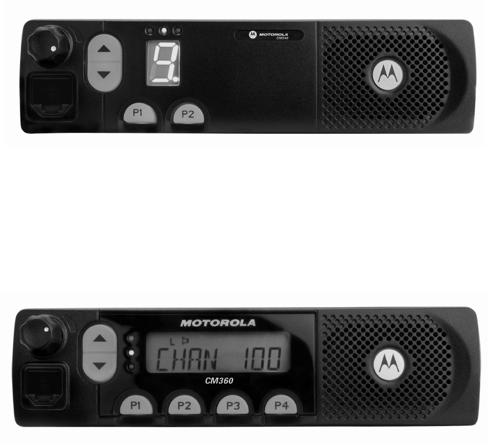
1.0 CM140/CM340Models
The Controlhead contains the internal speaker, the on/off/volume knob, the microphone connector,
several buttons to operate the radio, three indicator Light Emitting Diodes (LED) to inform the user
about the radio status, and a single character 7-segment display for numeric information e.g.
channel number.
2.0 CM160/CM360Models
The Controlhead contains the internal speaker, the on/off/volume knob, the microphone connector,
several buttons to operate the radio, three indicator Light Emitting Diodes (LED) to inform the user
about the radio status, and an 8 character Liquid Crystal Display (LCD) for alpha - numerical
information e.g. channel number or call address name.

1-2 OVERVIEW
Chapter 2
THEORY OF OPERATION
1.0 Introduction
This Chapter provides a detailed theory of operation for the Controlhead circuits. For details of the
trouble shooting refer to the related chapter in this section.
2.0 Controlhead Model for CM140 and CM340
The controlhead contains the internal speaker, the on/off/volume knob, the microphone connector,
several buttons to operate the radio and three indicator Light Emitting Diodes (LED) to inform the
user about the radio status and a 7-segment display for numeric information.
2.1 Power Supplies
The power supply to the control head is taken from the host radio’s 9.3V via connector J803-9, The
9.3V is used for the LEDs and back light, the 5V is used for the LCD driver and level shifter. The
stabilized 3V is used for the other parts.
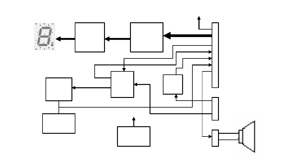
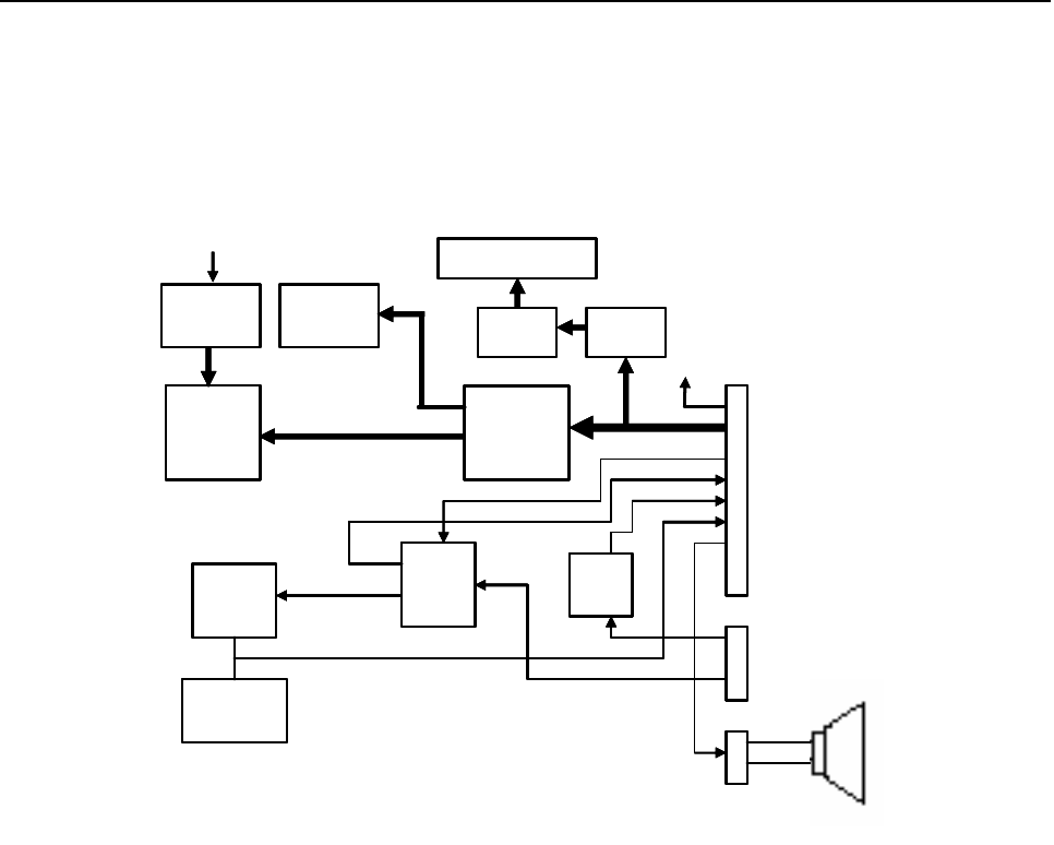
2.2 SPI Interface
The host radio (master) communicates with the control head through its SPI bus. Three lines are
connected to the shift register (U801):SPI clock (J803-17), SPI MOSI (J803-16) and shift register
chip select (J803-15).
Shift
Register
BCD To
7-segment
Mux.
Control
Keypads
DTMF
Resistors
PTT
circuit
2pinspeaker
connector
7-segment
display
9.3V
Keypad
Backlight
9.3VRow/Column
Control line
Boot_res / SCI
DTMF
Row/Column
Boot_res (DTMF-
Column)/ SCI
(DTMF-Row)
Shift
Register
BCD To
7-segment
Mux.
Control
Keypads
DTMF
Resistors
PTT
circuit
2pinspeaker
connector
7-segment
display
9.3V
Keypad
Backlight
9.3VRow/Column
Control line
Boot_res / SCI
DTMF
Row/Column
Boot_res (DTMF-
Column)/ SCI
(DTMF-Row)

2-2 THEORY OF OPERATION
When the host radio needs to send date to the shift register, the radio asserts the shift register chip
select and the data is loaded to the shift register. For example, the host radio sends data to change
display channel or change LED status.
2.3 Keypad Keys
The control head keypad is a four-key design. All keys are configured as two analog lines read by
µP. The voltage on the analog lines varies between 0V and 3.3 V depending on which key is
pressed. If no key is pressed, the voltage at both lines is 3.3V. The key configuration can be thought
of as a matrix where the two lines represent one row and one column. Each line is connected to a
resistive divider powered by 3.3V. If a button is pressed, it will connect one specific resistor of each
divider line to ground level and thereby reduce the voltages on the analog lines. The voltages of the
lines are A/D converted inside the µP (ports PE 6 - 7) and specify the pressed button. To determine
which key is pressed, the voltage of both lines must be considered.
The same analog lines also support a keypad microphone. A microphone key press is processed in
the same manner like a control head key press.
2.4 Status LED’s and Back Light Circuit
All indicator LEDs (red, yellow, and green) are driven by current sources. To change the LED status
the host radio sends a data message to the control head shift register via the SPI bus. The control
head shift register determines the LED status from the received data and switches the LEDs on or
off via Q5-Q7.
The back light for the keypad is always on. The back light current for the keypad is drawn from the
9.3 V source and controlled by two current sources. The LED current is determined by the resistor
at the emitter of the respective current source transistor.
2.5 Microphone Connector Signals
The MIC_PTT line (J802-3) is grounded when the PTT button on the microphone is pressed. When
released, this line is pulled to 9.3V by R805. Two transistor stages (Q802, Q801 and associated
parts) are used to level shift between 9.3V and 3.3V required for the uP while keeping the same
sense (active low for PTT pressed).
Two of the mic socket lines (J802-2,7) have dual functions depending on the type of microphone or
SCI lead connected. An electronic switch (U803) is used to switch these two lines between mic
keypad operation or SCI operation. The switch (mux) is controlled by the uP through J803-20 with
level shifting (and inversion) provided by transistor Q812. When MUX_CTRL (J803-20) is low the
electronic switch is in the mic keypad mode. The mic socket (J802) pin 2 is connected to the keypad
row line that goes to J803-13 and pin 7 is connected to the keypad column line that goes to J803-12.
When MUX_CTRL (J803-20) is high the electronic switch is in the SCI mode. The mic socket (J802
pin 2) is connected to the SCI line that goes to J803-4 and pin 7 is connected to the BOOT_RES line
that goes to J803-11.
The HOOK line (J802-6) is used to inform the uP which type of microphone or SCI lead is connected
to the microphone socket. The voltage of the HOOK line is monitored by the uP (port PE0,
MIC_SENSE) through a resistor divider on the main board. When the HOOK line is grounded (on
hook condition) or floating (2.8V nominal), the uP sets the mux (U803) for keypad operation to allow
the use of microphones with a keypad. When the HOOK line is connected to 9.3V, the uP sets the
mux for SCI operation. This mode is also used to select low cost mic operation where the gain of the
microphone path is increased (on the main board) to compensate for not having a pre-amp in the low
cost mic.

Controlhead Model for CM140 and CM340 2-3
If the BOOT_RES (J802-7) line is connected to >5V (e.g. 9.3V) at turn-on, the uP will start in boot
mode instead of normal operation. This mode is used to programme new firmware into the FLASH
memory (U404 mainboard).
2.6 Speaker
The controlhead contains a speaker for the receiver audio. The receiver audio signal from the
differential audio output of the audio amplifier located on the radio’s controller is fed via connector
J803-1, 2 to the speaker connector P801 pin 1 and pin 2. The speaker is connected to the speaker
connector P801. The controlhead speaker can be disconnected if an external speaker, connected on
the accessory connector, is used.
2.7 Electrostatic Transient Protection
Electrostatic transient protection is provided for the sensitive components in the controlhead by
diodes VR801, VR802, VR803 and VR804. The diodes limit any transient voltages to tolerable
levels. The associated capacitors provide Radio Frequency Interference (RFI) protection.
2-4 THEORY OF OPERATION
3.0 Controlhead Model for CM160 and CM360
The controlhead contains the internal speaker, the on/off/volume knob, the microphone connector,
several buttons to operate the radio, three indicator Light Emitting Diodes (LED) to inform the user
about the radio status, and an 8 character Liquid Crystal Display (LCD) for alpha - numerical
information e.g. channel number or call address name.
3.1 Power Supplies
The power supply to the control head is taken from the host radio’s 9.3V via connector J103-9, The
9.3V is used for the LEDs and back light, the 5V is used for the LCD driver (U3) and level shifter
(U4). The stabilized 3V is used for the other parts.
3.2 SPI Interface
The host radio (master) communicates with the control head through its SPI bus. Three lines are
connected to the shift register (U8):SPI clock (J103-17), SPI MOSI (J103-16), shift register chip
select (J103-15) and LCD driver chip select (J103-18).
When the host radio needs to send date to the shift register, the radio asserts the shift register chip
select and the data is loaded to the shift register. For example, the host radio sends data to change
display channel or change LED status.
8pinJACK
connector
9.3V LCD
Shift
Register
Backlight
Control
Mux.
Control
Keypads
Keypad
Resistors
PTT
circuit
2-pin speaker
connector
9.3V
LED
Indicators
Row/Column
Control line
Boot_Res / SCI
DTMF
Row/Column
Boot_Res (DTMF-
Column)/ SCI
(DTMF-Row)
Level
Shifter
LCD
Driver
LED
Backlight
8pinJACK
connector
9.3V LCD
Shift
Register
Backlight
Control
Mux.
Control
Keypads
Keypad
Resistors
PTT
circuit
2-pin speaker
connector
9.3V
LED
Indicators
Row/Column
Control line
Boot_Res / SCI
DTMF
Row/Column
Boot_Res (DTMF-
Column)/ SCI
(DTMF-Row)
Level
Shifter
LCD
Driver
LED
Backlight

Controlhead Model for CM160 and CM360 2-5
3.3 Keypad Keys
The control head keypad is a four-key design. All keys are configured as two analog lines read by
µP. The voltage on the analog lines varies between 0V and 3.3 V depending on which key is
pressed. If no key is pressed, the voltage at both lines is 3.3V. The key configuration can be thought
of as a matrix where the two lines represent one row and one column. Each line is connected to a
resistive divider powered by 3.3V. If a button is pressed, it will connect one specific resistor of each
divider line to ground level and thereby reduce the voltages on the analog lines. The voltages of the
lines are A/D converted inside the µP (ports PE 6 - 7) and specify the pressed button. To determine
which key is pressed, the voltage of both lines must be considered.
The same analog lines also support a keypad microphone. A microphone key press is processed in
the same manner like a control head key press.
3.4 LCD Driver
The LCD (36 x 4 segemnts) is controlled by U3. It has an on onboard clock controlled by R28
(typically 20kHz measured on pin 2). U3 is operated from the 5V supply and is controlled over the
SPI bus (SPI_CLK J103-17, SPI_MOSI J103-16, LCD chip select J103-18). Chip select is active low.
U2 is used to provide level shifting between the 3.3V logic from the uP and the 5V required by U3.
3.5 Status LED’s and Back Light Circuit
All indicator LEDs (red, yellow, and green) are driven by current sources. To change the LED status
the host radio sends a data message to the control head shift register via the SPI bus. The control
head shift register determines the LED status from the received data and switches the LEDs on or
off via Q8-Q10.
Backlighting for the LCD and keys is provided by a matrix of 21 LEDs arranged in 7 columns of 3
rows. The LEDs are driven from a constant current circuit (Q12, U1 and associated parts). There are
4 levels of baclight: off, low, medium and high, which are controlled by two outputs (pins 15, 1) from
the shift register (U8). The current is controlled by transistor Q12. The op amp U1 monitors the
current by measuring the voltage drop across R26, R27 and adjusting the bias of Q12 to achieve the
required level as set by the combined shift register o/ps. When in the off state, Q11 is also turned on
to clamp the base of Q12 so as to force it off. This ensures that the LEDs are fully off. Q11 is
controlled by pin 3 of the shift register U8.
3.6 Microphone Connector Signals
The MIC_PTT line (J102-3) is grounded when the PTT button on the microphone is pressed. When
released, this line is pulled to 9.3V by R33. Two transistor stages (Q14, Q13 and associated parts)
are used to level shift between 9.3V and 3.3V required for the uP while keeping the same sense
(active low for PTT pressed).
Two of the mic socket lines (J102-2, 7) have dual functions depending on which type of microphone
or SCI lead that is connected. An electronic switch (U41) is used to switch these two lines between
mic keypad operation or SCI operation. The switch (mux) is controlled by the uP through J103-20
with level shifting (and inversion) provided by transistor Q41. When MUX_CTRL (103-20) is low the
electronic switch is in the mic keypad mode. The mic socket (J102) pin 2 is connected to the keypad
row line that goes to J103-13 and pin 7 is connected to the keypad column line that goes to 103-12.
When MUX_CTRL (103-20) is high the electronic switch is in the SCI mode. The mic socket (J102
pin 2) is connected to the SCI line that goes to J103-4 and pin 7 is connected to the BOOT_RES line
that goes to J103-11.

2-6 THEORY OF OPERATION
The HOOK line (J102-6) is used to inform the uP which type of microphone or SCI lead is connected
to the microphone socket. The voltage of the HOOK line is monitored by the uP (port PE0,
MIC_SENSE) through a resistor divider on the main board. When the HOOK line is grounded (on
hook condition) or floating (2.8V nominal), the uP sets the mux (U8) for keypad operation to allow the
use of microphones with a keypad. When the HOOK line is connected to 9.3V, the uP sets the mux
for SCI operation. This mode is also used to select low cost mic operation where the gain of the
microphone path is increased (on the main board) to compensate for not having a pre-amp in the low
cost mic.
If the BOOT_RES (J102-7) line is connected to >5V (e.g. 9.3V) at turn-on then the uP will start in
boot mode instead of normal operation. This mode is used to programme new firmware into the
FLASH memory (U404 mainboard).
3.7 Speaker
The controlhead contains a speaker for the receiver audio. The receiver audio signal from the
differential audio output of the audio amplifier located on the radio’s controller is fed via connector
J103-1, 2 to the speaker connector P101 pin 1 and pin 2. The speaker is connected to the speaker
connector P101. The controlhead speaker can be disconnected if an external speaker, connected on
the accessory connector, is used.
3.8 Electrostatic Transient Protection
Electrostatic transient protection is provided for the sensitive components in the controlhead by
diodes VR1 - VR4. The diodes limit any transient voltages to tolerable levels. The associated
capacitors provide Radio Frequency Interference (RFI) protection.
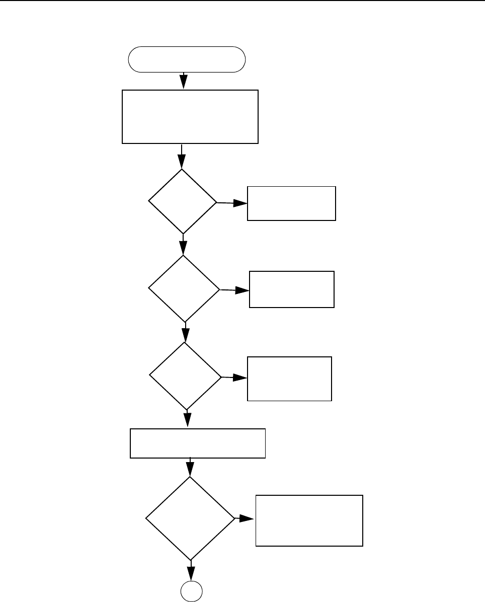
Chapter 3
TROUBLESHOOTING CHARTS
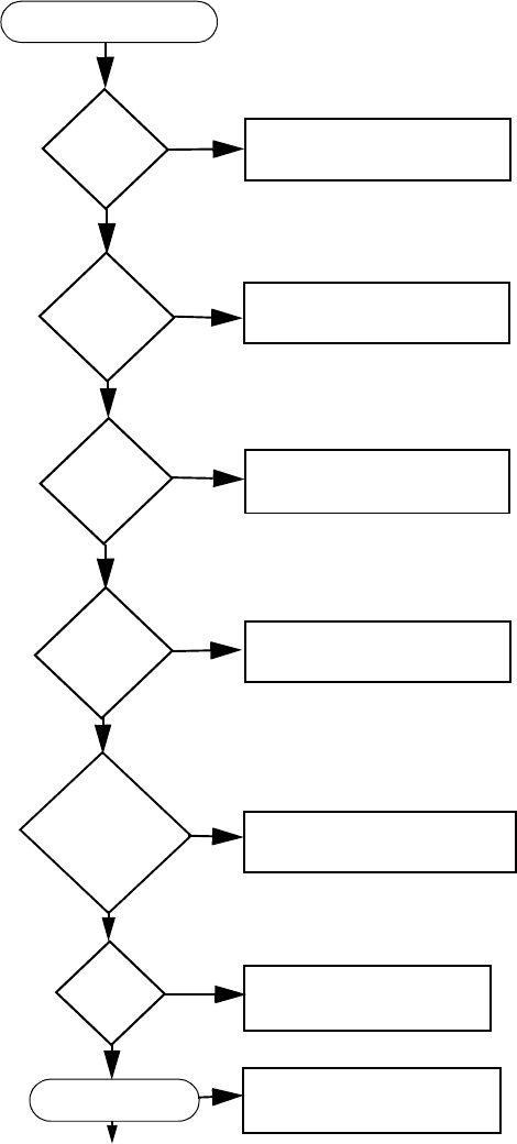
1.0 Controlhead CM140/CM340 Troubleshooting Chart
1.1 Control Head Failure
Back light
OK ?
Check 9.3V on
R808, R809
No
Control Head Check
Power-up
Alert Tone
OK ?
Check Speaker
Connection
No
Power-up
Red LED
Flash ?
Check
D801, Q806, U801
No
Channel
Display
OK?
Check
DS801, U801, U802
No
Up/Down
P1 and P2
Alert Tone
Buttons OK?
Check R845, R846
R810, R811
No
EXT
PTT
OK ?
Check Q801, Q802
No
Communication Ok
Check Q803, Q812
Control Head is OK
YES
YES
YES
YES
YES
YES
No
3-2 TROUBLESHOOTING CHARTS
1.2 Button/Tones Select Error (Page 1 of 2)
No
Check Voltage Levels on
TP401 (Keypad Col)
and TP402 (Keypad Row)
(see table on next page)
Right
Voltage
Up Key
No
Check R846, R811
on Control Head
Right
Voltage
on Down Key
?
Check Control Head
connectivity continuity
and R429, R430, D401
(main board)
Connect DTMF Mic
to TELCO Connector
YES
Button/Tones Check
Check R845, R810
on Control Head
Right
Voltage
on P1/P2
Keys ?
Is there
0.75 Vdc on
MIC_SENSE
R429, on radio
Check R813, R814
on Control Head
?
A
YES
No
YES
No

Controlhead CM140/CM340 Troubleshooting Chart 3-3
1.3 Button/Tones Select Error (Page 2 of 2)
Key_Col
Voltage
(TP401)
Key_Column Voltage TP401
0.008 V 0.675 V 1.346 V 1.997 V 2.650 V 3.300 V
0.008 V Up
0.675 V 1 2 3
1.346 V 4 5 6 7
1.997 V 8 9 0 *
2.650 V # C B A
3.300 V Down Left Key
P1
Right Key
P2 Idle
Key_Row Voltage TP402
No
Right
Voltage
on DTMF keys
?
Replace
Q812
YES
Button/Tones Keys
Okay
A
Does Q812
on Control Head
operates well
?
Replace U803
on Control Head
YES
No
3-4 TROUBLESHOOTING CHARTS
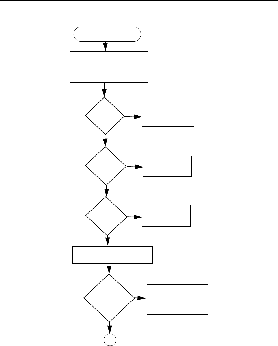
2.0 Controlhead CM160/CM360 Troubleshooting Chart
2.1 Control Head Failure
Back light
OK ?
Check 9.3V on
Q12, U1 and associated
parts and U8
No
Control Head Check
Power-up
Alert Tone
OK ?
Check Speaker
Connection
No
Indicator
LED’S
OK ?
Check
Q8-Q10, U8 and 9.3V
No
Display
OK?
Check LCD
connections, U3 for 5V,
Osc. pins 1 & 2 activity
SCI thru via U4
No
Up/Down
P1 and P2
Alert Tone
Buttons
OK?
Check keypad resistors
No
EXT
PTT
OK ? Check Q13, Q802
No
Communication Ok
Check Q803, Q14 and
associated parts
Control Head is OK
YES
YES
YES
YES
YES
YES
No
Controlhead CM160/CM360 Troubleshooting Chart 3-5
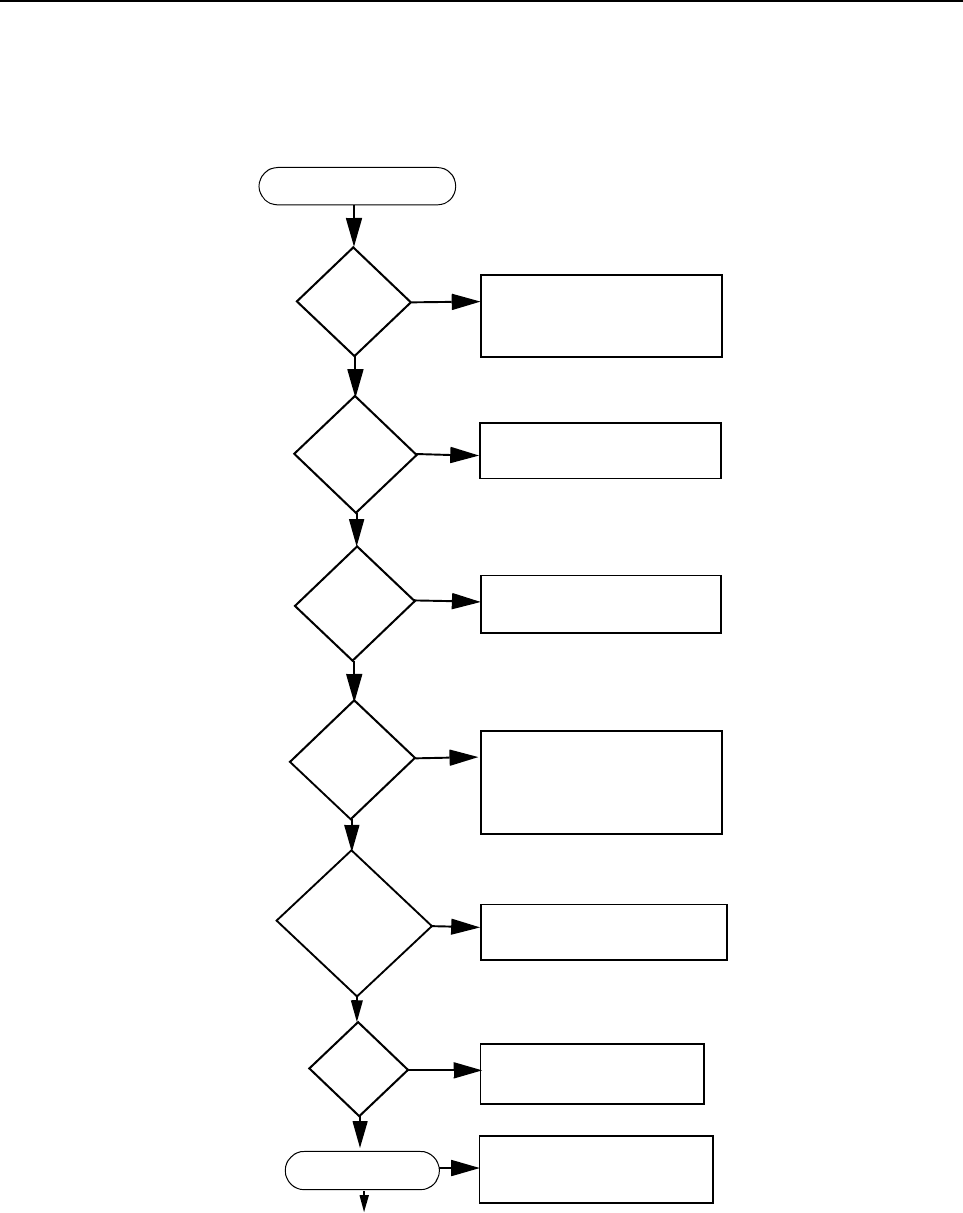
2.2 Button/Tones Select Error (Page 1 of 2)
No
Check Voltage Levels on
TP401 (Keypad Col)
and TP402 (Keypad Row)
(see table on next page)
Right
Voltage
Up Key?
No
Check R13, R45
on Control Head
Right
Voltage
on Down
Key?
Check Control Head
connectivity continuity
and R429, R430, D401
(Main Board)
Connect DTMF Mic
to TELCO Connector
YES
Button/Tones Check
Check R12, R49
on Control Head
Right
Voltage
on P1-P4
Keys ?
Is there
0.75 Vdc on
MIC_SENSE
R429, on radio
Check R31, R29
R51, R11
on Control Head
A
YES
No
YES
No
3-6 TROUBLESHOOTING CHARTS
2.3 Button/Tones Select Error (Page 2 of 2)
Key_Col
Voltage
(TP401)
Key_Column Voltage TP401
0.008 V 0.675 V 1.346 V 1.997 V 2.650 V 3.300 V
0.008 V Up
0.675 V 1 2 3
1.346 V 4 5 6 7
1.997 V 8 9 0 *
2.650 V # C B A
3.300 V Down Left Key
P1
Right Key
P2 P3 P4 Idle
Key_Row Voltage TP402
No
Right
Voltage
on DTMF keys
?
Replace
Q41
YES
Button/Tones Keys
Okay
A
Does Q41
on Control Head
operates well
?
Replace U8
on Control Head
YES
No

Chapter 4
CONTROLHEAD PCB / SCHEMATICS / PARTS LISTS
1.0 Allocation of Schematics and Circuit Boards
Table 4-1 Controlhead Diagrams and Parts Lists
PCB :
Controlhead CM140/CM340
8488998U01 Main Board Top Side
8488998U01 Main Board Bottom Side
Page 4-3
Page 4-3
SCHEMATICS
Sheet 1 of 1 Page 4-4
Parts List
8488998U01 Page 4-5
Table 4-2 Controlhead Diagrams and Parts Lists
PCB :
Controlhead CM160/CM360
8489714U01 Main Board Top Side
8489714U01 Main Board Bottom Side
Page 4-6
Page 4-6
SCHEMATICS
Sheet 1 of 1 Page 4-7
Parts List
8489714U01 Page 4-8

4-2 CONTROLHEAD PCB / SCHEMATICS / PARTS LISTS
THIS PAGE INTENTIONALLY LEFT BLANK
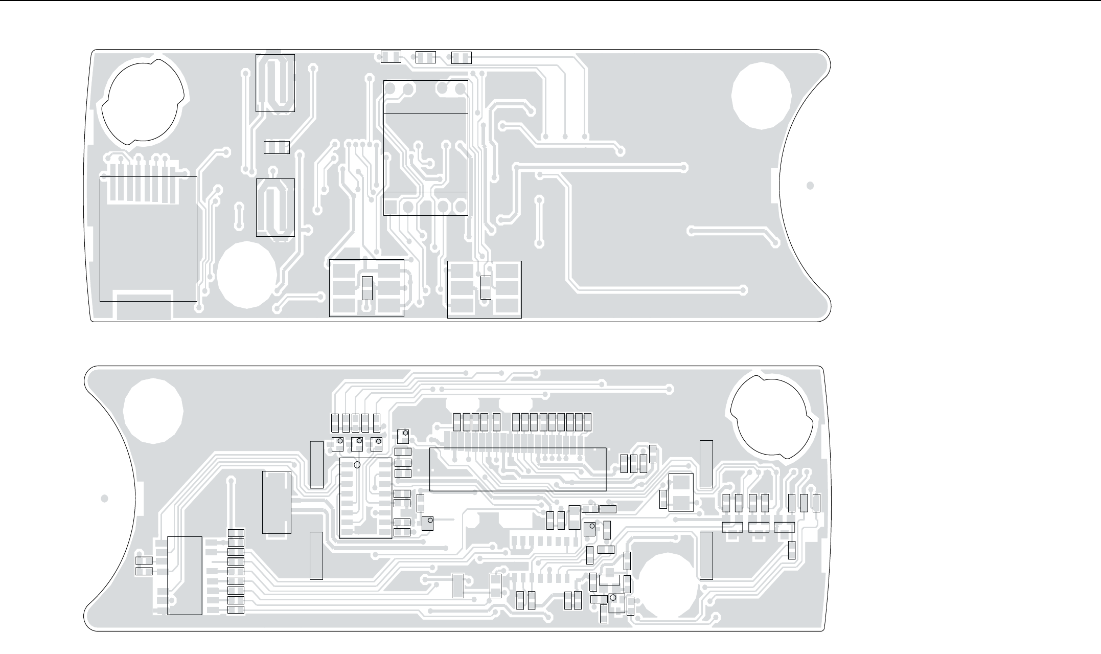
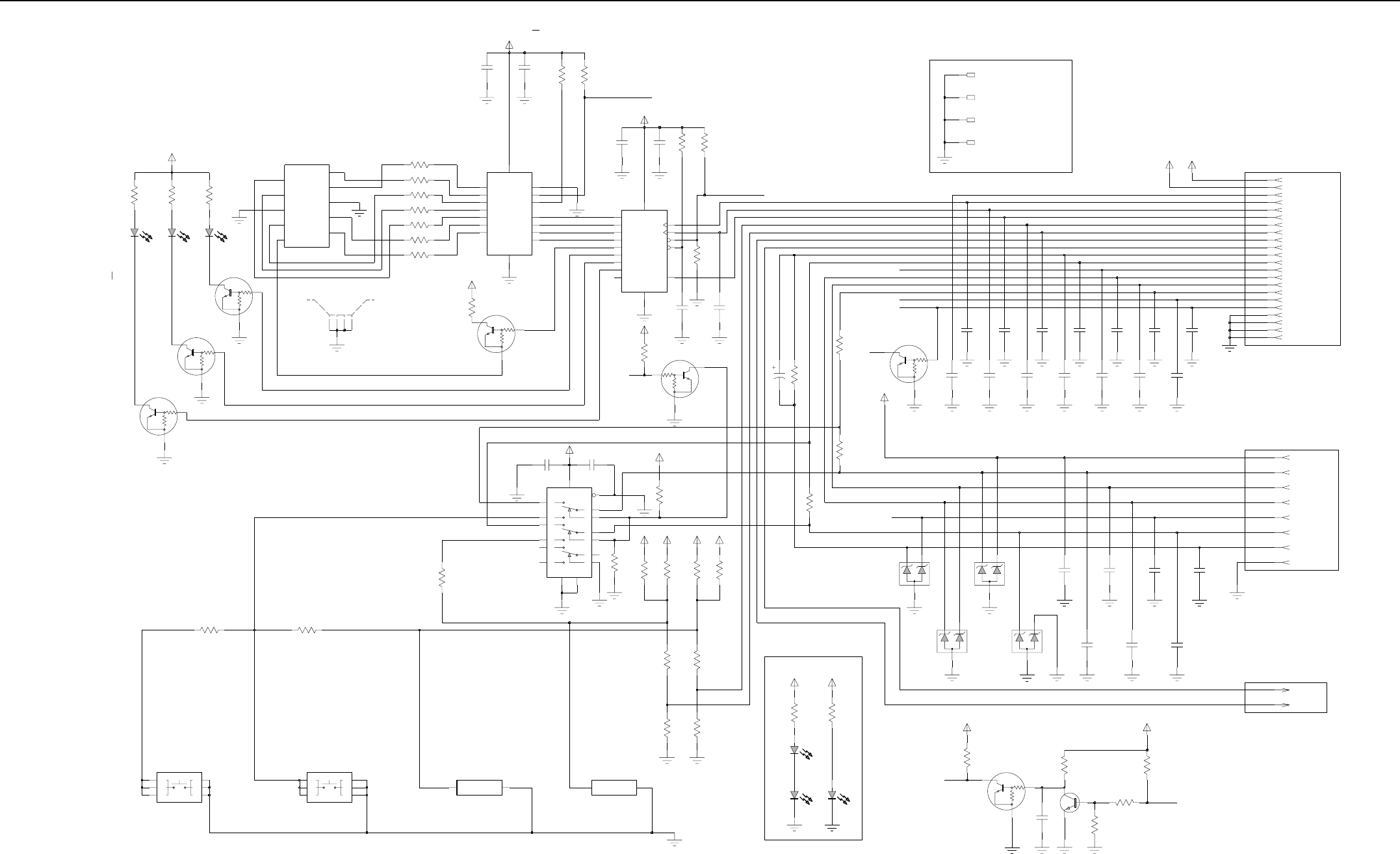
Controlhead CM140/CM340 - PCB 8488998U01 / Schematics 4-3
2.0 Controlhead CM140/CM340 - PCB 8488998U01 / Schematics
SHOWN FROM SIDE 1
D801
S801
D805
J802
D804
SH1
DS801
S802
J805
J804
D806
D802 D803
1
1
111 1
1
1
M801
8488998u01_p3
SHOWN FROM SIDE 2
C801
C802
C803
C804
C805
C806
C807
C808
C809
C810
C811
C812
C813
C814
C815
C816
C817
C818
C819
C820
C821
C822
C823
C824
C825
C826
C827
C832
C833
C834
C836
M802
M803
M804
P801
Q802
Q803
Q804 Q805 Q806
Q811
Q812
R801
R802
R803 R804
R805
R806
R807
R808
R809
R810
R811
R813
R816
R818
R819
R820
R821
R822
R823
R824
R825
R826
R827
R829
R830
R831
R832
R833
R834
R839
R840
R841
R842
R843
R844
R845
R846
R847
R848
R849
R850
U801
VR802VR803 VR804
Q801
R842
J803
Controlhead CM140/CM340
PCB 8488998U01
Top Side
Bottom Side
4-4 Controlhead CM140/CM340 - PCB 8488998U01 / Schematics
DNP
Change to 1% Change to 1%
COL
ROW
COL
DNP
DNPDNP
DNP
DNP
UP
DOWN
DNP
DNP
DNP
ROW
Change to 1%
Change to 1%
Change to 1%
Place under the 7-segment
MIC. PTT
MIC. AUDIO
SPI_MOSI
HOOK
RX. AUDIO
SPKR-
SPKR+
SPKR-
SPKR+
KEY_ROW
KEY_COL
COM/DATA_SEL
SPI_CLK
SH_R_CS
DISP_CS
DIS_RES
BOOT_RES
BOOT_RES
DNP
F1
F2
DNP
RED LED
GREEN LED
YELLOW LED
DNPDNP DNP
THESE ARE THE
ESD PROTECTION
MAIN BOARD CONNECTOR
MICROPHONE CONNECTOR
SPEAKER CONNECTOR
HOOK
9.3 V
MIC. AUDIO
MIC. PTT
SCI
RX. AUDIO
KEYPAD BACKLIGHT
CONTACTS (SPRINGS)
SCI
J803-22
220.p
R845
51.K
R846
VR803
G2
J803-21 G1
J803-10 18
10
BI J803-18
19
J803-19
6
J803-6
J803-4
1
4
J803-1
J803-13 13
17
J803-17
7
9
J803-9
J803-7
12
DISPL_CS
J803-12
20
J803-20
J803-8 8
CH_PTT J803-5 5
3
J803-3
J803-11 11
J803-15
OE
TELCO_PTT
CH_PTT
TELCO_PTT
COMM_CATH_2
ANODE_B
ANODE_A
HDSP-513G
15
16
S802
4
S801
6
C6
5C5
C4
2
J803-16
R809
3.3K
J803-2
D3_3V
SH1
4
3
2
1
SHIELD
0.
PIN2 2
R850
CONTACT
13K
PIN2 2
PIN1
1
J804
CONTACT
R848
PIN1
1
J805
10.K
R849
R844
10.K
R847
D3_3V D3_3V
51.K
10.K
C836
9_3V
R843
10.K
Q812
9_3V
Q811
10.K
22.K
R840
R842
22.K
R839
9_3V9_3V
R832
20.K20.K
R831
R841
C833
100n
10.K
0.
0.
R834
100n
R833
13 X1
MC14053B
3
C832
C9
B10
11
Z1
Z0
5
Z4
Y1
1
Y0
2
Y15
X0
12
X14
VEE
7
VCC 16
GND
8
EN 6
1M804
A
U803
C834
1M803
22.n
1M801
C817
1M802
20.
VDD 16
LT 3
LE 5
G
VR804 220.p
C2
11
C1 2
BI 4
B2
U802
VSS
8
14 F
15 E
9D2
10
D1 6
C824
12
B1 1
A2
13
A1 7
MC14511BFEL
220.p
C826
220.p
220.p 220.p
C818C816
220.p
C819 C821
220.p
C820
220.p
220.p
C822
C803
220.p
C801
220.p
C805
220.p 220.p 220.p
C809C807 C811
220.p
C813
220.p
220.p
C814
220.p
C812
220.p
C810C806
220.p
C808
220.p 220.p
220.p
9_3VD3_3V
9_3V
C804
9_3V
9_3V
9_3V
9_3V
D3_3V
D3_3V
C802
9_3V D3_3V
33.
33.
R827
33.
R825
R826
R824
R823
R822
33.
33.
33.
33.
R821
1n
C823
10.K
Q802 47.K
R807
R806
10.K
R805
47.K
47.K R804
Q801
R803
680.
R802
R820
680.
3C3
2
C2
1C1
TOUCH_SW_MARLIN
3C3
2
C2
1C1
TOUCH_SW_MARLIN
6
C6
5C5
4
C4
10u
0.
C815
R830
R810
470.
HSMG-C670
D806
R808
300.
0.
R801
HSMG-C670
D804
1
J802-1
5
J802-5
2
J802-2
4
J802-4
3
J802-3
7
J802-7
6
J802-6
8
J802-8
DS801
COMM_CATH_1
ANODE_G
ANODE_F
ANODE_E
ANODE_DP
ANODE_D
ANODE_C
OE
DISPL_CS
BI
R811
0.
22K
R813 R816
D801
13K
D802
HSMH-C670
D803
HSMY-C670
Q804
HSMG-C670
Q805
Q806
1
P801-1
2
P801-2
R818 R819
3.9K
C825
680.
CLK_L 12
U801
100n
Q4
4Q3
3Q2
2Q1
1Q0
15
GND
8
EN_OE 13
CLK_S 11
VCC 16
SEROUT
9SERIN 14
RESET 10
Q7
7Q6
6Q5
5
MC74HC595A
C827
100n 10.K
R829
Q803
20.0
VR802
VR801
20.0
20.0
HSMG-C670
14
J803-14
D805
10K
47K
47K
10K
47K
10K
47K
10K
47K
10K
47K
10K
47K
73B02964C39-O
10K
Controlhead CM140/CM340 Schematic
Controlhead CM140/CM340 - PCB 8488998U01 / Schematics 4-5
2.1 Controlhead PCB 8488998U01 Parts
List
Circuit
Ref Motorola
Part No Description
C802 2113740F59 CAP CHIP REEL CL13
C804 2113740F59 CAP CHIP REEL CL13
C805 2113740F39 CAP CHIP REEL CL1+/-30 33
C806 2113740F39 CAP CHIP REEL CL1+/-30 33
C808 2113740F59 CAP CHIP REEL CL13
C809 2113740F39 CAP CHIP REEL CL1+/-30 33
C810 2113740F39 CAP CHIP REEL CL1+/-30 33
C811 2113740F59 CAP CHIP REEL CL13
C812 2113740F39 CAP CHIP REEL CL1+/-30 33
C813 2113740F59 CAP CHIP REEL CL13
C814 2113740F59 CAP CHIP REEL CL13
C816 2113740F39 CAP CHIP REEL CL1+/-30 33
C817 2113740F39 CAP CHIP REEL CL1+/-30 33
C818 2113740F39 CAP CHIP REEL CL1+/-30 33
C819 2113740F39 CAP CHIP REEL CL1+/-30 33
C820 2113740F39 CAP CHIP REEL CL1+/-30 33
C821 2113740F29 CAP CHIP REEL CL1+/-30 12
C822 2113740F39 CAP CHIP REEL CL1+/-30 33
C823 2113743K15 CER CHIP CAP .100uF
C824 2113740F59 CAP CHIP REEL CL13
C825 2113743K15 CER CHIP CAP .100uF
C826 2113740F59 CAP CHIP REEL CL13
C827 2113743K15 CER CHIP CAP .100uF
C832 2113743K15 CER CHIP CAP .100uF
C833 2113743K15 CER CHIP CAP .100uF
C834 2113743E07 CER CHIP CAP .022uF
C836 2113740F59 CAP CHIP REEL CL13
D801 4805729G74 LED SMT RED HP
D802 4805729G73 LED SMT YEL HP
D803 4805729G75 LED SMT GREEN HP
D804 4805729G75 LED SMT GREEN HP
D805 4805729G75 LED SMT GREEN HP
D806 4805729G75 LED SMT GREEN HP
DS801 5180353L02 7-SEGMENT DISPLAY
J802 0908353Y02 MODULAR 8-PIN STR
J803 0989241U02 FLEX 20-PIN 1mmTOP NON
M801 7588823L03 PAD GROUNFD LCD
M802 7588823L03 PAD GROUNFD LCD
M803 7588823L03 PAD GROUNFD LCD
M804 7588823L03 PAD GROUNFD LCD
P801 2809926G01 CONN 1.25MM 2PIN SURMT
Q801 4809940E02 TSTR NPN DIG DTC114YE
Q802 4813824A10 TSTR NPN 40V .2A GEN P
Q803 4809940E02 TSTR NPN DIG DTC114YE
Q804 4809940E02 TSTR NPN DIG DTC114YE
Q805 4809940E02 TSTR NPN DIG DTC114YE
Q806 4809940E02 TSTR NPN DIG DTC114YE
Q811 4809940E02 TSTR NPN DIG DTC114YE
Q812 4809940E02 TSTR NPN DIG DTC114YE
R801 0662057A01 CHIP RES 10 OHMS 5%
R802 0662057A61 CHIP RES 330 OHMS 5%
R803 0662057A89 CHIP RES 47K OHMS 5%
R804 0662057A89 CHIP RES 47K OHMS 5%
R805 0662057A73 CHIP RES 10K OHMS 5%
R806 0662057A89 CHIP RES 47K OHMS 5%
R807 0662057A73 CHIP RES 10K OHMS 5%
R808 0662057A36 CHIP RES 300 OHMS 5%
R809 0662057A45 CHIP RES 680 OHMS 5%
R810 0662057B47 CHIP RES 0 OHMS +0.5
R811 0662057B47 CHIP RES 0 OHMS +0.5
R813 0662057D08 CHIP RES 22K OHMS 5%
R816 0662057D03 CHIP RES 13K OHMS 5%
R818 0662057A63 CHIP RES 3900 OHMS 5%
R819 0662057A45 CHIP RES 680 OHMS 5%
R820 0662057A45 CHIP RES 680 OHMS 5%
R821 0662057A13 CHIP RES 33 OHMS 5%
R822 0662057A13 CHIP RES 33 OHMS 5%
R823 0662057A13 CHIP RES 33 OHMS 5%
R824 0662057A13 CHIP RES 33 OHMS 5%
R825 0662057A13 CHIP RES 33 OHMS 5%
R826 0662057A13 CHIP RES 33 OHMS 5%
R827 0662057A13 CHIP RES 33 OHMS 5%
R829 0662057A73 CHIP RES 10K OHMS 5%
Circuit
Ref Motorola
Part No Description
R830 0662057A41 CHIP RES 470 OHMS 5%
R841 0662057A73 CHIP RES 10K OHMS 5%
R842 0662057A73 CHIP RES 10K OHMS 5%
R843 0662057A73 CHIP RES 10K OHMS 5%
R844 0662057A73 CHIP RES 10K OHMS 5%
R845 0662057A90 CHIP RES 51K OHMS 5%
R846 0662057A90 CHIP RES 51K OHMS 5%
R849 0662057D03 CHIP RES 13K OHMS 5%
Circuit
Ref Motorola
Part No Description
4-6 Controlhead CM160/CM360 - PCB 8489714U01 / Schematics
3.0 Controlhead CM160/CM360 - PCB 8489714U01 / Schematics
C40
4
3
2
1Q12
R19
R26
R27
R20
R24
14
58
U1
C11
C26
Q11
C17
R18
C35 C36
2
P101
C19
C23
14
58
U18
C21
C22
R11
M4
12
24
37
48
U3
M3
R28 R39
R6
R7
R8
R9
C18
C30
C32
C33
R30
C16
C20
C25 R10
R15
C39
R29
R51
7
8
14
U2
1
J103
C4
C8
C27
C38
C44
C45
C46
C47
C48
C49
C50
C51
C52
C53
C54
C55
C24
R13
R25
R44
R45
R46
R21
R22
R23
Q8 Q9 Q10
16
1
8
9
U8 C7
C15
R14
R40
C1
C14
C58
R16
R17
R31
R54
R3
C56
M2
Q41
R41
16
18
9
U41
C2
C3
C5
C29
C34
C42
R42
R43
C6
VR1VR2 VR3 VR4
C43
Q13
Q14
R33
R37
R38
M1
C41
R12
R34
R35
R36
R48
R49
R50
8
7
5
6
3
2
1
4
9
J102
1S6
D2
1
S5
D4
1
S3
D26
1
S4
D9
1
S1
D20
1
S2
D10
D18
D19
D3
D14
D17
D24
D27
D5
D8
D11
D15
D16
D21
DS1
D12
D13
D22
D23
D25
Controlhead CM160/CM360 PCB
8489714U01
Top Side
Bottom Side
Controlhead CM160/CM360 - PCB 8489714U01 / Schematics 4-7
10K
47K
10K
47K
10K
47K
10K
47K
10K
47K
10K
47K
9.3 V
F1
+
F2
MIC. AUDIO
MIC. PTT
KEY_ROW
KEY_COL
SPI_CLK
-
SPEAKER CONNECTOR
HOOK
MICROPHONE CONNECTOR
MAIN BOARD CONNECTOR
ESD CONTACTS
DIS_RES
DISP_CS
COM/DATA_SEL
SH_R_CS
BOOT_RES
BOOT_RES
SCI
MIC. PTT
SPKR+
SPKR-
UP
DOWN
SPI_MOSI
HOOK
RX. AUDIO
SCI
SPKR+
SPKR-
MIC. AUDIO
F4 F3
RX. AUDIO
0.1uF
C22
Y1C
ZA 14
ZB 15
ZC 4
C23
1000pF
VDD 16
VEE
7
VSS
8
YOA
12
Y0B
2
Y0C
5
13 Y1A
Y1B
1
3
U41
HEF4053B
EN 6
11
SA
SB 10
9
SC
R13
51K
D12
HSMG-C670
D3_3V
19
HSMG-C670
D10
J102-88
J103-19
10
J102-77
C43
J103-10
470pF
C54
0.1uF
R36
47K
HSMG-C670
9_3V
R28
D25
P101-22
680K
51K
R12
R27
10
R7
10K
HSMG-C670
D17
DNF
C5
5C6 6
10K
R34
S2
C1
1C2 2
C3
3C4 4
D23
HSMG-C670
TOUCH_SW
DNF
D14
HSMG-C670
0
R9
MC74HCT04A
U2-6
13 12
12
DNF
C4
1000pF
4
C4
5C5 6
C6
DNF
TOUCH_SW
S6
TOUCH_SW
S3
1C1 2
C2
3C3
10K
R8
DNF
U2-5
MC74HCT04A
11 10
DNF
HSMG-C670
D8
C29
DNF
1000pF
8
DNF
0
R10
U2-4
MC74HCT04A
9
680
DNF
R20
10K
6
C6
9_3V
R23
1C1 C2 2
3C3 4
C4
5C5
D2
HSMG-C670
TOUCH_SW
DNF
S1
1K
R18
10K
R15
100pF
DNF
DNF
J103-1313
C33
220pF
C53
DNF
C35
M3
6
D3_3V
DNF
1000pF
C30
9_3V
J102-6
DNF
100pF
D19
HSMH-C670
12
5V_IN
DNF
C20
2.2uF Q41
J103-12
2.2uF
MC74HCT04A
U2-2
34
C19
J103-1111
9_3V
HSMG-C670
D9
DNF
1000pF
C27
D18
HSMY-C670
DNF
1000pF
C41
4
47K
R38
2
3
1
8
4
9_3V
J102-4
4
V3
5
VDD
7
VREG
16
VSS 6
U1-1
LM2904
SEG4 21
SEG5 22
SEG6 23
SEG7 24
SEG8 25
26
SEG9
9SI
V1
3
V2
42
43
SEG26
SEG27 44
SEG28 45
SEG29 46
SEG3 20
SEG30 47
48
SEG31
35
SEG19 36
SEG2 19
SEG20 37
SEG21 38
SEG22 39
SEG23 40
SEG24 41
SEG25
SEG10 28
SEG11
SEG12 29
SEG13 30
SEG14 31
SEG15 32
SEG16 33
SEG17 34
SEG18
COM2 14
COM3 15
CS
10
C_D
11
OSC1
1OSC2
2
SEG0 17
SEG1 18
27
S1D15100
U3
CK
8
COM0 12
COM1 13
20V
VR3
VR2
20V
VR1
10uF
C1
DNF
20V
Q5
5
Q6
6
Q7
7
RESET 10
SERIN 14
SEROUT
9
VCC 16
CLK_S 11
EN_OE 13
GND
8
Q0
15
Q1
1
Q2
2
3Q3
Q4
4
U8
MC74HC595A
CLK_L 12
DNF
22K
R46
R44
R45
0
J102-55
DNF
20K
3
J103-21G1
R54
13K
J102-3
10K
R39
220pF
DNF
C55
J103-1818
DNF
10K
R6
R29
22K
DNF
C47
220pF
47K
R37
R30
10K
DNF
3
J103-88
130K
J103-3
D4
HSMG-C670
R11
M2 M4
220pF
C46
220pF
DNF
DNF
9_3V
C45
D16
HSMG-C670
R35
D24
HSMG-C670
0
R43 3.3K
R41
DNF
DNF
S5
TOUCH_SW
21
10K
J103-1515
D3_3V
9_3V
1000pF
C24
Q8
9_3V
C32
D3_3V
D3_3V
5V_CH
DNF
100pF
0.1uF
5
7
8
4
9_3V 9_3V
9_3V
DNF
C14
U1-2
LM2904 6
C17
5V_CH
M1
J103-44
DNF
1000pF
1
J103-66
Q9
J103-1
C5
R50
22K
470pF
0
R49
DNF
R48
20K
R42
0
DNF
C48
DNF
DNF
C50
9_3V
220pF
J103-55
470pF
R33
10K
0.1uF
C56
MC74HCT04A
U2-3
56
HSMG-C670
D15
Q10
10K
R19
5V_CH
C3
470pF
9_3V
470pF
43K
R51
C2
C18
HSMG-C670
D21
PWR_GND
U2-7
GND
7
VCC
14
0.1uF
J103-99
C36
1000pF
R40
DNF
220pF
C44
DNF
10K
C3
3C4 4
C5
5C6 6
9_3V
DNF
S4
TOUCH_SW
C1
1C2 2
C16
0.1uF
DNF
J103-1717
J103-77
1000pF
C42
1000pF
DNF
C38
3.9K
R24
R21
C25
5V_IN
2.2K
DNF
1000pF
Q12
J102-11
Q13
J103-2020
Q14
R16
27K
HSMG-C670
D5
HSMG-C670
D13
0
R25
9_3V
9_3V VR4
20V
470pF
C49
R31
13K
DNF
4.7uF
C21
DNF
C51
220pF
D20
HSMG-C670
R17
13K
D27
HSMG-C670HSMG-C670
D26
1000pF
C34
DNF
SEG8
13
SEG9
14
680
R22
SEG29
34
SEG3
8
SEG30
35
SEG31
36
SEG4
9
SEG5
10
SEG6
11
SEG7
12
SEG21
26
SEG22
27
SEG23
28
SEG24
29
SEG25
30
31 SEG26
SEG27
32
SEG28
33
SEG14
19
SEG15
20
SEG16
21
SEG17
22
SEG18
23
SEG19
24
SEG2
7
SEG20
25
COM2 3
COM3 4
SEG0
5
SEG1
6
SEG10
15
SEG11
16
SEG12
17
SEG13
18
DNF
LCD_36PIN
DS1
COM0 1
COM1 2
R14
10K
0.1uF
C15
D3_3V
C7
1000pF
16
J102-22
1000pF
C39
J103-16
Q11
DNF
0.1uF
C11
12
1
J103-22G2
U2-1
MC74HCT04A
C40
P101-1
J103-22
DNF
1000pF
J103-1414
9_3V
HSMG-C670
D3
C8
1000pF
9_3V
HSMG-C670
D22
SHUTDOWN
3
1000pF
C6
DNF
LP2951C
5V_TAP 6
5
ERRORFEEDBACK
7
GND
4
INPUT
8OUTPUT 1
SENSE 2
9_3V
DNF
U18
HSMG-C670
D11
C26
1000pF
C58
.022uF
10
470pF
C52
R3
SI
CS
MUX_CTL
ROW
COL
10
R26
TELCO_PTT
CS
CK
MUX_CTL
CH_PTT
CH_PTT
TELCO_PTT
CK
SI
Controlhead CM160/CM360 Schematic
Controlhead CM160/CM360 - PCB 8489714U01 / Schematics 4-8
3.1 Controlhead PCB 8489714U01 Parts
List
Circuit
Ref Motorola
Part No Description
C1 NOTPLACED CAP, 10uF
C2 2113740F67 CAP, 470pF
C3 2113740F67 CAP, 470pF
C4 2113740F12 CAP CHIP REEL CL1 +/-30 12
C5 2113740F67 CAP, 470pF
C6 2113740F12 CAP CHIP REEL CL1 +/-30 12
C7 2113741F25 CAP, 1000pF
C8 2113741F25 CAP, 1000pF
C11 2113743K15 CAP, 0.1uF
C14 NOTPLACED CAP, 0.1uF
C15 2113743K15 CAP, 0.1uF
C16 2113743K15 CAP, 0.1uF
C17 NOTPLACED CAP, 1000pF
C18 2113743K15 CAP, 0.1uF
C19 2113743F18 CAP, 2.2uF
C20 NOTPLACED CAP, 2.2uF
C21 NOTPLACED CAPP, 4.7uF
C22 2113743K15 CAP, 0.1uF
C23 2113741F25 CAP, 1000pF
C24 2113741F25 CAP, 1000pF
C25 NOTPLACED CAP, 1000pF
C26 2113741F25 CAP, 1000pF
C27 2113740F12 CAP CHIP REEL CL1 +/-30 12
C29 2113740F12 CAP CHIP REEL CL1 +/-30 12
C30 NOTPLACED CAP, 100pF
C32 NOTPLACED CAP, 100pF
C33 NOTPLACED CAP, 100pF
C34 2113740F12 CAP CHIP REEL CL1 +/-30 12
C35 NOTPLACED CAP, 1000pF
C36 NOTPLACED CAP, 1000pF
C38 NOTPLACED CAP, 1000pF
C39 NOTPLACED CAP, 1000pF
C40 NOTPLACED CAP, 1000pF
C41 NOTPLACED CAP, 1000pF
C42 2113740F12 CAP CHIP REEL CL1 +/-30 12
C43 2113743K15 CAP, 0.1uF
C44 NOTPLACED CAP, 220pF
C45 NOTPLACED CAP, 220pF
C46 NOTPLACED CAP, 220pF
C47 NOTPLACED CAP, 220pF
C48 NOTPLACED CAP, 220pF
C49 2113740F67 CAP, 470pF
C50 2113740F67 CAP, 470pF
C51 2113740F12 CAP CHIP REEL CL1 +/-30 12
C52 2113740F67 CAP, 470pF
C53 2113740F12 CAP CHIP REEL CL1 +/-30 12
C54 2113740F67 CAP, 470pF
C55 NOTPLACED CAP, 220pF
C56 2113743K15 CAP, 0.1uF
C58 2113743E07 CAP, .022uF
D2 4805729G75 HSMG-C670
D3 4805729G75 HSMG-C670
D4 4805729G75 HSMG-C670
D5 4805729G75 HSMG-C670
D8 4805729G75 HSMG-C670
D9 4805729G75 HSMG-C670
D10 4805729G75 HSMG-C670
D11 4805729G75 HSMG-C670
D12 4805729G75 HSMG-C670
D13 4805729G75 HSMG-C670
D14 4805729G75 HSMG-C670
D15 4805729G75 HSMG-C670
D16 4805729G75 HSMG-C670
D17 4805729G75 HSMG-C670
D18 4805729G73 HSMY-C670
D19 4805729G74 HSMH-C670
D20 4805729G75 HSMG-C670
D21 4805729G75 HSMG-C670
D22 4805729G75 HSMG-C670
D23 4805729G75 HSMG-C670
D24 4805729G75 HSMG-C670
D25 4805729G75 HSMG-C670
D26 4805729G75 HSMG-C670
D27 4805729G75 HSMG-C670
DS1 NOTPLACED LCD_36PIN
Circuit
Ref Motorola
Part No Description
J102 0908353Y02 CONN_J
J103 0989241U02 CONN_J
M1 7588823L03 CONTACT
M2 7588823L03 CONTACT
M3 7588823L03 CONTACT
M4 7588823L03 CONTACT
P101 2809926G01 CONN_P
Q8 4809940E02 DTC114YE
Q9 4809940E02 DTC114YE
Q10 4809940E02 DTC114YE
Q11 4809940E02 DTC114YE
Q12 4813824B01 PZT2222A
Q13 4809940E02 DTC114YE
Q14 4813824A10 MMBT3904
Q41 4809940E02 DTC114YE
R3 0662057A01 RES, 10
R6 NOTPLACED RES, 10K
R7 NOTPLACED RES, 10K
R8 NOTPLACED RES, 10K
R9 0662057B47 RES, 0
R10 NOTPLACED RES, 0
R11 0662057B01 RES, 130K
R12 0662057A90 RES, 51K
R13 0662057A90 RES, 51K
R14 0662057A73 RES, 10K
R15 NOTPLACED RES, 10K
R16 0662057A83 RES, 27K
R17 0662057A76 RES, 13K
R18 0662057A49 RES, 1K
R19 0662057A73 RES, 10K
R20 NOTPLACED RES, 10K
R21 0662057A63 RES, 3.9K
R22 0662057A45 RES, 680
R23 0662057A45 RES, 680
R24 0662057A57 RES, 2.2K
R25 0662057B47 RES, 0
R26 0662057A01 RES, 10
R27 0662057A01 RES, 10
R28 0662057B18 RES, 680K
Circuit
Ref Motorola
Part No Description
R29 0662057A81 RES, 22K
R30 NOTPLACED RES, 10K
R31 0662057A76 RES, 13K
R33 0662057A73 RES, 10K
R34 0662057A73 RES, 10K
R35 0662057A61 RES, 3.3K
R36 0662057A89 RES, 47K
R37 0662057A89 RES, 47K
R38 0662057A89 RES, 47K
R39 0662057A73 RES, 10K
R40 0662057A73 RES, 10K
R41 0662057A73 RES, 10K
R42 NOTPLACED RES, 0
R43 NOTPLACED RES, 0
R44 NOTPLACED RES, 20K
R45 0662057B47 RES, 0
R46 NOTPLACED RES, 22K
R48 NOTPLACED RES, 20K
R49 0662057B47 RES, 0
R50 NOTPLACED RES, 22K
R51 0662057A88 RES, 43K
R54 0662057A76 RES, 13K
S1 NOTPLACED TOUCH_SW
S2 NOTPLACED TOUCH_SW
S3 NOTPLACED TOUCH_SW
S4 NOTPLACED TOUCH_SW
S5 NOTPLACED TOUCH_SW
S6 NOTPLACED TOUCH_SW
U1 5113818A01 LM2904
U2 5113805A05 MC74HCT04A
U3 5102109U01 S1D15100
U8 5113805A75 MC74HC595A
U18 NOTPLACED LP2951C
U41 5184704M60 HEF4053B
VR1 4813830A75 MMBZ20VAL
VR2 4813830A75 MMBZ20VAL
VR3 4813830A75 MMBZ20VAL
VR4 4813830A75 MMBZ20VAL
Circuit
Ref Motorola
Part No Description

Commercial Series
CM Radios
UHF2 (438-470MHz)
Service Information
Issue: December 2003

ii
Computer Software Copyrights
The Motorola products described in this manual may include copyrighted Motorola computer programs stored
in semiconductor memories or other media. Laws in the United States and other countries preserve for
Motorola certain exclusive rights for copyrighted computer programs, including the exclusive right to copy or
reproduce in any form, the copyrighted computer program. Accordingly, any copyrighted Motorola computer
programs contained in the Motorola products described in this manual may not be copied or reproduced in
any manner without the express written permission of Motorola. Furthermore, the purchase of Motorola
products shall not be deemed to grant, either directly or by implication, estoppel or otherwise, any license
under the copyrights, patents or patent applications of Motorola, except for the normal non-exclusive royalty-
free license to use that arises by operation of law in the sale of a product.

iii
Table of Contents
Chapter 1 MODEL CHART AND TECHNICAL SPECIFICATIONS
1.0 CM140/CM340/CM160/CM360 Model Chart .......................................................1-1
2.0 Technical Specifications ......................................................................................1-2
Chapter 2 THEORY OF OPERATION
1.0 Introduction ..........................................................................................................2-1
2.0 UHF (438-470MHz) Receiver .............................................................................2-1
2.1 Receiver Front-End .......................................................................................2-1
2.2 Receiver Back-End.........................................................................................2-2
3.0 UHF (438-470MHz) Transmitter Power Amplifier ...............................................2-2
3.1 First Power Controller Stage...........................................................................2-2
3.2 Power Controlled Driver Stage .......................................................................2-3
3.3 Final Stage......................................................................................................2-3
3.4 Directional Coupler.........................................................................................2-3
3.5 Antenna Switch...............................................................................................2-3
3.6 Harmonic Filter ...............................................................................................2-4
3.7 Power Control.................................................................................................2-4
4.0 UHF (438-470MHz) Frequency Synthesis ..........................................................2-4
4.1 Reference Oscillator.......................................................................................2-4
4.2 Fractional-N Synthesizer ................................................................................2-5
4.3 Voltage Controlled Oscillator (VCO) ...............................................................2-6
4.4 Synthesizer Operation....................................................................................2-7
5.0 Controller Theory of Operation ............................................................................2-8
5.1 Radio Power Distribution ................................................................................2-8
5.2 Protection Devices........................................................................................2-10
5.3 Automatic On/Off ..........................................................................................2-10
5.4 Microprocessor Clock Synthesiser ...............................................................2-11
5.5 Serial Peripheral Interface (SPI)...................................................................2-12
5.6 SBEP Serial Interface...................................................................................2-12
5.7 General Purpose I/O.....................................................................................2-12
5.8 Normal Microprocessor Operation................................................................2-13
5.9 Static Random Access Memory....................................................................2-14
6.0 Control Board Audio and Signalling Circuits ......................................................2-14
6.1 Audio Signalling Filter IC and Compander (ASFIC CMP) ............................2-14
7.0 Transmit Audio Circuits......................................................................................2-15
7.1 Microphone Input Path .................................................................................2-15
7.2 PTT Sensing and TX Audio Processing .......................................................2-16

iv
8.0 Transmit Signalling Circuits ...............................................................................2-17
8.1 Sub-Audio Data (PL/DPL) ............................................................................2-17
8.2 High Speed Data .......................................................................................... 2-18
8.3 Dual Tone Multiple Frequency (DTMF) Data ...............................................2-18
9.0 Receive Audio Circuits....................................................................................... 2-19
9.1 Squelch Detect ............................................................................................. 2-19
9.2 Audio Processing and Digital Volume Control.............................................. 2-20
9.3 Audio Amplification Speaker (+) Speaker (-) ................................................2-20
9.4 Handset Audio.............................................................................................. 2-21
9.5 Filtered Audio and Flat Audio .......................................................................2-21
10.0 Receive Audio Circuits .....................................................................................2-21
10.1 Sub-Audio Data (PL/DPL) and High Speed Data Decoder ..........................2-21
10.2 Alert Tone Circuits........................................................................................ 2-22
Chapter 3 TROUBLESHOOTING CHARTS
1.0 Troubleshooting Flow Chart for Receiver RF (Sheet 1 of 2)................................3-2
1.1 Troubleshooting Flow Chart for Receiver (Sheet 2 of 2) ................................3-3
2.0 Troubleshooting Flow Chart for 25W Transmitter (Sheet 1 of 3) .......................3-4
2.1 Troubleshooting Flow Chart for 25W Transmitter (Sheet 2 of 3) ...................3-5
2.2 Troubleshooting Flow Chart for 25W Transmitter (Sheet 3 of 3).................... 3-6
3.0 Troubleshooting Flow Chart for Synthesizer .......................................................3-7
4.0 Troubleshooting Flow Chart for VCO...................................................................3-8
5.0 Troubleshooting Flow Chart for DC Supply (Sheet 1 of 2) ..................................3-9
5.1 Troubleshooting Flow Chart for DC Supply (Sheet 2 of 2) ...........................3-10
Chapter 4 UHF PCB/SCHEMATICS/PARTS LISTS
1.0 Allocation of Schematics and Circuit Boards .......................................................4-1
1.1 UHF2 and Controller Circuits .........................................................................4-1
2.0 UHF2 1-25W PCB 8488978U01 (Rev. D) / Schematics......................................4-3
2.1 UHF2 1-25W PCB 8488978U01 (Rev. D) Parts List ....................................4-19

Chapter 1
MODEL CHART AND TECHNICAL SPECIFICATIONS
1.0 CM140/CM340/CM160/CM360 Model Chart
CM Series UHF2 438-470MHz
Model Description
MDM50RNC9AA2_N CM140 438-470 MHz 1-25W 8-Ch
MDM50RNC9AN2_N CM340 438-470 MHz 1-25W 10-Ch
MDM50RNF9AA2_N CM160 438-470 MHz 1-25W 64-Ch
MDM50RNF9AN2_N CM360 438-470 MHz 1-25W 100-Ch
Item Description
X FUE1021_ S. Tanapa UHF2 25W 8 Ch BNC
X PMUE2019_ S. Tanapa UHF2 25W 10 Ch BNC
X PMUE1999_ S. Tanapa UHF2 25W 64 Ch BNC
X PMUE2021_ S. Tanapa UHF2 25W 100 Ch BNC
X X FCN6288_ Control Head
X X FCN5523_ Control Head
XXXX HKN4137_ Battery Power Cable
X
X
X
X
RMN50188_
HMN3596_
Mag One Microphone
Compact Microphone
XXXX GLN7324_ Low Profile Trunnion
X X X X 6866546D02_ RTTE Leaflet
XXXX 6866537D37_ Safety Leaflet
XFLE1621AS Servicing Kit CM140
X PMUE2041AS Servicing Kit CM340
X PMUE2027AS Servicing Kit CM160
X PMUE2043AS Servicing Kit CM360
X = Indicates one of each is required
1-2 MODEL CHART AND TECHNICAL SPECIFICATIONS
2.0 Technical Specifications
Data is specified for +25°C unless otherwise stated.
General
Specification UHF2
Frequency Range: 438-470 MHz
Frequency Stability
(-30°C to +60°C, 25°C Ref.)
±2 PPM
Channel Capacity: CM140 - 8
CM340 - 10
CM160 - 64
CM360 - 100
Channel Spacing: 12.5/20/25 kHz
Power Output: 1-25W
Power Supply: 13.2Vdc (10.8 - 15.6 Vdc) negative vehicle ground
Dimensions (L X W X H) 118mm X 169mm X 44mm
Weight:
Low power (1-25W) 1.02 Kg
Operating Temperature -30 to 60 o C
Storage temperature -40 to 80o C
Shock and Vibration Meets MIL-STD 810-C,D&E and TIA/EIA 603
Dust Meets MIL-STD 810-C,D&E and TIA/EIA 603
Humidity Meets MIL-STD 810-C,D&E and TIA/EIA 603
Technical Specifications 1-3
*Availability subject to the laws and regulations of individual countries.
Transmitter
Specification UHF2
Frequency Stability: +/- 2.5ppm
Modulation Limiting: ±2.5 kHz @ 12.5 kHz
±4.0 kHz @ 20 kHz
±5.0 kHz @ 20/25 kHz
Current Drain Transmit: 8A (25W)
FM Hum and Noise: -35 dB@12.5 kHz
-40 dB@ 20/25 kHz
Conducted/Radiated
Emissions:
-36 dBm < 1 GHz
-30 dBm > 1 GHz
Adjacent Channel Power -60dB @12.5,
-70dB @ 20/25kHz
Audio Response:
( 300 to 3000Hz) +1, -3dB
Audio Distortion:
@ 1000 Hz, 60%
Rated Maximum Deviation:
3% Typical
Receiver
Specification UHF2
Sensitivity (12dBSINAD): (ETS) 0.35µV (12.5kHz) 0.30µV (25kHz) Typical
Intermodulation : (ETS) >65dB
Adjacent Channel
Selectivity: (ETS)
70 dB @ 25 kHz
60 dB @ 12.5 kHz
Spurious Rejection: (ETS) 70 dB
Rated Audio: (ETS) (Extended audio with 4 Ohm
speaker)
4W Internal , 13W External
Audio Distortion @ Rated Audio: 3% Typical
Hum and Noise: -35 dB @ 12.5 kHz
-40 dB @ 20/25 kHz
Audio Response:
( 300 to 3000Hz) +1, -3dB
Conducted Spurious
Emission per FCC Part 15:
-57 dBm <1 GHz
-47 dBm >1 GHz

1-4 MODEL CHART AND TECHNICAL SPECIFICATIONS

Chapter 2
THEORY OF OPERATION
1.0 Introduction
This Chapter provides a detailed theory of operation for the UHF circuits in the radio. Details of the
theory of operation and trouble shooting for the the associated Controller circuits are included in this
Section of the manual.
2.0 UHF (438-470MHz) Receiver
2.1 Receiver Front-End
The received signal is applied to the radio’s antenna input connector and routed through the
harmonic filter and antenna switch. The insertion loss of the harmonic filter/antenna switch is less
than 1 dB. The signal is routed to the first filter (4-pole), which has an insertion loss of 2 dB typically.
The output of the filter is matched to the base of the LNA (Q303) that provides a 16 dB gain and a
noise figure of better than 2 dB. Current source Q301 is used to maintain the collector current of
Q303. Diode CR301 protects Q303 by clamping excessive input signals. Q303 output is applied to
the second filter (3-pole) which has an insertion loss of 1.5 dB. In Distance mode, Q304 turns on and
causes D305 to conduct, thus bypassing C322 and R337. In Local mode, the signal is routed
through C322 and R337, thus inserting 7 dB attenuation. Since the attenuator is located after the RF
amplifier, the receiver sensitivity is reduced only by 6 dB, while the overall third order input intercept
is raised.
The first mixer is a passive, double-balanced type, consisting of T300, T301 and U302. This mixer
provides all of the necessary rejection of the half-IF spurious response. High-side injection at +15
dBm is delivered to the first mixer. The mixer output is then connected to a duplex network which
matches its output to the XTAL filter input (FL300) at the IF frequency of 44.85 MHz. The duplex
network terminates into a 50 ohm resistor (R340) at all other frequencies.
Figure 2-1 UHF Receiver Block Diagram
Mixer Xtal Filter
Controller
Front Filter
Antenna
First LO
2nd LO Xtal Osc
25kHzFilter
IF Amp
Second Filter 4- Pole
25kHzFilter
12.5kHzFilter
Phase Shift
Element
IFIC
LNA

2-2 THEORY OF OPERATION
2.2 Receiver Back End
The IF signal from the crystal filter enters the IF amplifier which provides 20 dB of gain and feeds
the IF IC at pin 1. The first IF signal at 44.85 MHz mixes with the second local oscillator (LO) at
44.395 MHz to produce the second IF at 455 kHz. The second LO uses the external crystal Y301.
The second IF signal is amplified and filtered by two external ceramic filters (FL303/FL302 for
12.5KHz channel spacing and FL304/FL301 for 25KHz channel spacing). The IF IC demodulates
the signal by means of a quadrature detector and feeds the detected audio (via pin 7) to the audio
processing circuits. At IF IC pin 5, an RSSI signal is available with a dynamic range of 70 dB.
3.0 UHF Transmitter Power Amplifier (438-470 MHz)
The radio’s 25W PA is a three-stage amplifier used to amplify the output from the VCOBIC to the
radio transmit level. All three stages utilize LDMOS technology. The gain of the first stage (U101) is
adjustable and controlled by pin 7 of U103-2 via U103-3. It is followed by an LDMOS stage Q105
and LDMOS final stage Q100.
Figure 2-2 UHF Transmitter Block Diagram
Devices U101, Q105 and Q100 are surface mounted. A metal clip ensures good thermal contact
between both the driver and final stage, and the chassis.
3.1 First Power Controller Stage
The first stage (U101) is a 20dB gain integrated circuit containing two LDMOS FET amplifier stages.
It amplifies the RF signal from the VCO (TX_INJ). The output power of stage U101 is controlled by a
DC voltage applied to pin 1 from the op-amp U103-3, pin 8. The control voltage simultaneously
varies the bias of two FET stages within U101. This biasing point determines the overall gain of
U101 and therefore its output drive level to Q105, which in turn controls the output power of the
Loop
Pin Diode
Antenna
Switch RF Jack
Antenna
Harmonic
Filter
Coupler
PA-Final
Stage
From VCO
Controlled
Stage
Bias
Temperature
Sense
SPI BUS
ASFIC_CMP
PA
PWR
SET
PA
Driver
Controller
U103-2
Forward

UHF Transmitter Power Amplifier (438-470 MHz) 2-3
PA.Op-amp U103-3 monitors the drain current of U101 via resistor R122 and adjusts the bias
voltage of U101.
In receive mode, the DC voltage from RX_EN line turns on Q101, which in turn switches off the
biasing voltage to U101.
3.2 Power Controlled Driver Stage
The next stage is an LDMOS device (Q105) which provides a gain of 12dB. This device requires a
positive gate bias and a quiescent current flow for proper operation. The bias is set during transmit
mode by the drain current control op-amp U102-1, and fed to the gate of Q105 via the resistive
network R175, R147.
Op-amp U102-1 monitors the drain current of Q105 via resistors R126-8 and adjusts the bias
voltage of Q105.
In receive mode the DC voltage from RX_EN line turns on Q102, which in turn switches off the
biasing voltage to Q105.
3.3 Final Stage
The final stage is an LDMOS device (Q100) providing a gain of 12dB. This device also requires a
positive gate bias and a quiescent current flow for proper operation. The voltage of the line PA_BIAS
is set in transmit mode by the ASFIC and fed to the gate of Q100 via the resistive network R134,
R131. This bias voltage is tuned in the factory. If the transistor is replaced, the bias voltage must be
tuned using the Tuner. Care must be taken not to damage the device by exceeding the maximum
allowed bias voltage. The device’s drain current is drawn directly from the radio’s DC supply voltage
input, B+, via L117 and L115.
A matching network consisting of C1004-5, C1008, C1021: and two striplines, transforms the
impedance to 50 ohms and feeds the directional coupler.
3.4 Directional Coupler
The directional Coupler is a microstrip printed circuit, which couples a small amount of the forward
power of the RF power from Q100.The coupled signal is rectified to an output power which is
proportional to the DC voltage rectified by diode D105; and the resulting DC voltage is routed to the
power control section to ensure that the forward power out of the radio is held to a constant value.
3.5 Antenna Switch
The antenna switch utilizes the existing dc feed (B+) to the last stage device (Q100). The basic
operation is to have both PIN diodes (D103, D104) turned on during key-up by forward biasing
them. This is achieved by pulling down the voltage at the cathode end of D104 to around 12.4V
(0.7V drop across each diode). The current through the diodes needs to be set around 100 mA to
fully open the transmit path through resistor R108. Q106 is a current source controlled by Q103
which is turned on in Tx mode by TX_EN. VR102 ensures that the voltage at resistor R107 never
exceeds 5.6V.

2-4 THEORY OF OPERATION
3.6 Harmonic Filter
Inductors L111 and L113 along with capacitors C1011, C1023, C1020 and C1016 form a low-pass
filter to attenuate harmonic energy coming from the transmitter. Resistor R150 along with L126
drains any electrostatic charges that might otherwise build up on the antenna. The harmonic filter
also prevents high level RF signals above the receiver passband from reaching the receiver circuits
to improve spurious response rejection.
3.7 Power Control
The output power is regulated by using a forward power detection control loop. A directional coupler
samples a portion of the forward and reflected RF power. The forward sampled RF is rectified by
diode D105, and the resulting DC voltage is routed to the operational amplifier U100. The error
output current is then routed to an integrator, and converted into the control voltage. This voltage
controls the bias of the pre-driver (U101 and driver (Q105) stages. The output power level is set by
way of a DAC, PWR_SET, in the audio processing IC (U504) which acts at the forward power
control loop reference.
The sampled reflected power is rectified by diode D107,The resulting DC voltage is amplified by an
operational amplifier U100 and routed to the summing junction. This detector protects the final stage
Q100 from reflected power by increasing the error current. The temperature sensor protects the
final stage Q100 from overheating by increasing the error current. A thermistor RT100 measures the
final stage Q100 temperature. The voltage divider output is routed to an operational amplifier U103
and then goes to the summing junction. The Zener Diode VR101 keeps the loop control voltage
below 5.6V and eliminates the DC current from the 9.3 regulator U501.
Two local loops for the Pre Driver (U101) and for the Driver (Q105) are used in order to stabilize the
current for each stage.
In Rx mode, the two transistors Q101 and Q102 go to saturation and shut down the transmitter by
applying ground to the Pre Driver U101 and for the Driver Q105 control.
4.0 UHF (438-470MHz) Frequency Synthesis
The synthesizer consists of a reference oscillator (Y201), low voltage Fractional-N (LVFRAC-N)
synthesizer (U200), and a voltage controlled oscillator (VCO) (U201).
4.1 Reference Oscillator
The reference oscillator is a crystal (Y201) controlled Colpitts oscillator and has a frequency of
16.8MHz. The oscillator transistor and start-up circuit are located in the LVFRAC-N (U200) while the
oscillator feedback capacitors, crystal, and tuning varactors are external. An analog-to-digital (A/D)
converter internal to the LVFRAC-N (U200) and controlled by the microprocessor via SPI sets the
voltage at the warp output of U200 pin 25. This sets the frequency of the oscillator. Consequently,
the output of the crystal Y201 is applied to U200 pin 23.
The method of temperature compensation is to apply an inverse Bechmann voltage curve, which
matches the crystal’s Bechmann curve to a varactor that constantly shifts the oscillator back on
frequency. The crystal vendor characterizes the crystal over a specified temperature range and
codes this information into a bar code that is printed on the crystal package. In production, this
crystal code is read via a 2-dimensional bar code reader and the parameters are saved.

UHF (438-470MHz) Frequency Synthesis 2-5
This oscillator is temperature compensated to an accuracy of +/-2.5 PPM from -30 to 60 degrees C.
The temperature compensation scheme is implemented by an algorithm that uses five crystal
parameters (four characterize the inverse Bechmann voltage curve and one for frequency accuracy
of the reference oscillator at 25 degrees C). This algorithm is implemented by the LVFRAC-N (U200)
at the power up of the radio.
TCXO Y200, along with its corresponding circuitry R204, R205, R210, and C2053, are not placed as
the temperature compensated crystal proved to be reliable.
4.2 Fractional-N Synthesizer
The LVFRAC-N U200 consists of a pre-scaler, programmable loop divider, control divider logic,
phase detector, charge pump, A/D converter for low frequency digital modulation, balanced
attenuator used to balance the high and low frequency analog modulation, 13V positive voltage
multiplier, serial interface for control, and a super filter for the regulated 5 volts.
Figure 2-3 UHF Synthesizer Block Diagram
A voltage of 5V applied to the super filter input (U200, pin 30) supplies an output voltage of 4.5Vdc
(VSF) at U200, pin 28. This supplies 4.5 V to the VCO Buffer IC U201.
To generate a high voltage to supply the phase detector (charge pump) output stage at pin VCP
(U200, pin 47) while using a low voltage 3.3Vdc supply, a 13V positive voltage multiplier is used
(D200, D201, and capacitors C2024, 2025, 2026, 2055, 2027, 2001).
Output lock (U200, pin 4) provides information about the lock status of the synthesizer loop. A high
level at this output indicates a stable loop. A 16.8 MHz reference frequency is provided at U200, pin
19.
DATA
CLK
CEX
MODIN
VCC, DC5V
XTAL1
XTAL2
WARP
PREIN
VCP
REFERENCE
OSCILLATOR
VOLTAGE
MULTIPLIER
DATA (U403 PIN 100)
CLOCK (U403 PIN 1)
CSX (U403 PIN 2)
MOD IN (U501 PIN 40)
+5V (U503 PIN 1)
7
8
9
10
13, 30
23
24
25
32
47
VMULT2 VMULT1
BIAS1
SFOUT
AUX3
AUX4
IADAPT
IOUT
GND
FREFOUT
LOCK 4
19
6, 22, 33, 44
43
45
3
2
28
14 15
40
FILTERED 5V
STEERING
LOCK (U403 PIN 56)
PRESCALER IN
FREF (U504 PIN 34)
39
BIAS2
41
48
5, 20, 34, 36
+5V (U503 PIN 1)
AUX1
VDD, DC5V MODOUT
U200
LOW VOLTAGE
FRACTIONAL-N
SYNTHESIZER
AUX2 1 (NU)
BWSELECT
VCO Bias
TRB
To IF
Section
TX RF INJECTION
(1ST STAGE OF PA)
LO RF INJECTION
VOLTAGE
CONTROLLED
OSCILLATOR
LINE
LOOP
FILTER

2-6 THEORY OF OPERATION
4.3 Voltage Controlled Oscillator (VCO)
The Voltage Controlled Oscillator (VCO) consists of the VCO/Buffer IC (VCOBIC, U201), the TX and
RX tank circuits, the external RX buffer stages, and the modulation circuitry.
Figure 2-4 UHF VCO Block Diagram
The VCOBIC together with the LVFRAC-N (U200) generate the required frequencies in both
transmit and receive modes. The TRB line (U201, pin 19) determines which VCO and buffer is
enabled (high being TX output at pin 10, low being RX output at pin 8). A sample of the signal from
the enabled output is routed from U201, pin 12 (PRESC_OUT), via a low pass filter to U200, pin 32
(PREIN).
A steering line voltage between 3.0V and 10.0V at varactor D204 tunes the TX VCO through the
frequency range of 438-470MHz, and at D203 tunes the RX VCO through the frequency range of
393.15-425.15MHz.
The external RX amplifier is used to increase the output from U201, pin 9 from 3-4 dBm to the
required 15dBm for proper mixer operation. In TX mode, the modulation signal from the LVFRAC-N
(U200, pin 41) is applied to the VCO by way of the modulation circuit D205, R212, R211, C2073.
Presc
RX
TX
Buffers
Q200 Low Pass
Filter
Attenuator
Pin8
Pin14
Pin10
(U200 Pin28)
VCC Buffers
TX RF Injection
U200 Pin 32
AUX3 (U200 Pin 2)
Prescaler Out
Pin 12Pin 19
Pin 20
TX/RX/BS
Switching Network
U201
VCOBIC
Rx
Active Bias
Tx
Active Bias
Pin2
Rx-I adjust
Pin1
Tx-I adjust
Pins 9,11,17
Pin18
Vsens
Circuit
Pin15
Pin16
RX VCO
Circuit
TX VCO
Circuit
RX Tank
TX Tank
Pin7
Vcc-Superfilter
Collector/RF in
Pin4
Pin5
Pin6
RX
TX
(U200 Pin 28)
Rx-SW
Tx-SW
Vcc-Logic
(U200 Pin 28)
Steer Line
Voltage
(VCTRL)
Pin13
Pin3
TRB IN
LO RF INJECTION

UHF (438-470MHz) Frequency Synthesis 2-7
4.4 Synthesizer Operation
The synthesizer consists of a low voltage FRAC-N IC (LVFRAC-N), reference oscillator, charge
pump circuits, loop filter circuit, and DC supply. The output signal (PRESC_OUT) of the VCOBIC
(U201, pin 12) is fed to the PREIN, pin 32 of U200 via a low pass filter which attenuates harmonics
and provides a correct input level to the LVFRAC-N in order to close the synthesizer loop.
The pre-scaler in the synthesizer (U200) is a dual modulus pre-scaler with selectable divider ratios.
The divider ratio of the pre-scaler is controlled by the loop divider, which in turn receives its inputs
via the SPI. The output of the pre-scaler is applied to the loop divider. The output of the loop divider
is connected to the phase detector, which compares the loop divider’s output signal with the
reference signal. The reference signal is generated by dividing down the signal of the reference
oscillator (Y201).
The output signal of the phase detector is a pulsed dc signal that is routed to the charge pump. The
charge pump outputs a current from U200, pin 43 (IOUT). The loop filter (consisting of R224, R217,
R234, C2074, C2075, C2077, C2078, C2079, C2080, C2028, and L205) transforms this current into
a voltage that is applied the varactor diodes D203 and D204 for RX and TX respectively. The output
frequency is determined by this control voltage. The current can be set to a value fixed in the
LVFRAC-N or to a value determined by the currents flowing into BIAS 1 (U200, pin 40) or BIAS 2
(U200, pin 39). The currents are set by the value of R200 or R206 respectively. The selection of the
three different bias sources is done by software programming.
To modulate the synthesizer loop, a two-spot modulation method is utilized via the MODIN (U200,
pin 10) input of the LVFRAC-N. The audio signal is applied to both the A/D converter (low frequency
path) and the balance attenuator (high frequency path). The A/D converter converts the low
frequency analog modulating signal into a digital code which is applied to the loop divider, thereby
causing the carrier to deviate. The balance attenuator is used to adjust the VCO’s deviation
sensitivity to high frequency modulating signals. The output of the balance attenuator is presented
at the MODOUT port of the LVFRAC-N (U200,pin 41) and connected to the VCO modulation
varactor D205.

2-8 THEORY OF OPERATION
5.0 Controller Theory of Operation
This section provides a detailed theory of operation for the radio and its components. The main
radio is a single-board design, consisting of the transmitter, receiver, and controller circuits. A
control head is connected by an extension cable. The control head contains LED indicators, a
microphone connector, buttons, and speaker.
In addition to the power cable and antenna cable, an accessory cable can be attached to a
connector on the rear of the radio. The accessory cable enables you to connect accessories to the
radio, such as an external speaker, emergency switch, foot-operated PTT, and ignition sensing, etc.
Figure 2-5 Controller Block Diagram
5.1 Radio Power Distribution
Voltage distribution is provided by five separate devices:
■U514 P-cH FET - Batt + (Ext_SWB+)
■U501 LM2941T - 9.3V
■U503 LP2951CM - 5V
■U508 MC 33269DTRK - 3.3V
■U510 LP2986ILDX - 3.3V Digital
External
Microphone
Internal
Microphone
External
Speaker
Internal
Speaker
SCI to
Control Head
Audio
PA
Audio/Signaling
Architecture
To Synthesizer
Mod
Out
16.8 MHz
Reference Clock
from Synthesizer
Disc Audio
To R F S ec ti on SPI
Digital
Architecture
µP Clock
3.3V
Regulator
RAM
EEPROM
FLASH
HC11FL0
ASFIC_CMP
Accessory &
Connector
Handset
.

Controller Theory of Operation 2-9
The DC voltage applied to connector P2 supplies power directly to the following circuitry:
■Electronic on/off control
■RF power amplifier
■12 volts P-cH FET -U514
■9.3 volt regulator
■Audio PA
Figure 2-6 DC Power Distribution Block Diagram
Regulator U501 is used to generate the 9.3 volts required by some audio circuits, the RF circuitry
and power control circuitry. Input and output capacitors are used to reduce high frequency noise.
Resistors R5001 / R5081 set the output voltage of the regulator. This regulator output is
electronically enabled by a 0 volt signal on pin 2. Q502, Q505 and R5038 are used to disable the
regulator when the radio is turned off.
Voltage regulator U510 provides 3.3 volts for the digital circuitry. Operating voltage is from the
regulated 9.3V supply. Input and output capacitors are used to reduce high frequency noise and
provide proper operation during battery transients. U510 provides a reset output that goes to 0 volts
if the regulator output goes below 3.1 volts. This is used to reset the controller to prevent improper
operation.
Voltage regulator U508 provides 3.3V for the RF circuits and ASFIC_CMP. Input and output
capacitors are used to reduce the high frequency noise and provide proper operation during battery
transients.
U501
9.3V Regulator
FET
P-CH
On/Off
Control
500mA
SW_Filt_B+
Acces Conn
Audio PA_Soutdown
Power Loop Op_Amp
Auto
On/Off
Switch
Control
Ignition B+
RF_PA
Audio_PA
Antenna Switch
Power Control
Filt_B+
Ferrite Bit
Control Head
Mic Connector
Mic Bias
9V, 5mA
Keypad
7_Seg
Bed
to
7-Seg
Shift
Reg
3.2V
72mA
9.3V
65mA
Status LEDs
7_Seg
DOT
Back
light
On/Off
Control
11-16.6V
0.9A 0.85A
U503
5V RF Regulator
U508
3.3V RF Reg
U510
3.3V D Reg
Reset
Rx_Amp
PA_Pre-driver
PA D river
500mA
LVFRAC_N
IF_Amp
ASFIC_CMP
IFIC
RX Cct
micro P
RAM
Flash
EEPROM
90mA
25mA50mA45mA
9.3V
45mA
9.3V
75mA
9.3V
162mA

2-10 THEORY OF OPERATION
Voltage regulator U503 provides 5V for the RF circuits. Input and output capacitors are used to
reduce the high frequency noise and provide proper operation during battery transients.
VSTBY is used only for CM360 5-tone radios.
The voltage VSTBY, which is derived directly from the supply voltage by components R5103 and
VR502, is used to buffer the internal RAM. Capacitor C5120 allows the battery voltage to be
disconnected for a couple of seconds without losing RAM parameters. Dual diode D501 prevents
radio circuitry from discharging this capacitor. When the supply voltage is applied to the radio,
C5120 is charged via R5103 and D501.
5.2 Protection Devices
Diode VR500 acts as protection against ESD, wrong polarity of the supply voltage, and load dump.
VR692 - VR699 are for ESD protection.
5.3 Automatic On/Off
The radio can be switched ON in any one of the following three ways:
■On/Off switch. (No Ignition Mode)
■Ignition and On/Off switch (Ignition Mode)
■Emergency
5.3.1 No Ignition Mode
When the radio is connected to the car battery for the first time, Q500 will be in saturation, Q503 will
cut-off, Filt_B+ will pass through R5073, D500, and S5010-pin 6 (On/Off switch). When S5010 is
ON, Filt_B+ will pass through S5010-pin5, D511, R5069, R5037 and base of Q505 and move Q505
into saturation. This pulls U501-pin2 through R5038, D502 to 0.2V and turns On U514 and U501
9.3V regulator which supplies voltage to all other regulators and consequently turns the radio on,
When U504 (ASFIC_CMP) gets 3.3V, GCB2 goes to 3.3V and holds Q505 in saturation, for soft turn
off.
5.3.2 Ignition Mode
When ignition is connected for the first time, it will force high current through Q500 collector, This
will move Q500 out of saturation and consequently Q503 will cut-off. S5010 pin 6 will get ignition
voltage through R601 (for load dump), R610, (R610 & C678 are for ESD protection), VR501,
R5074, and D500. When S5010 is ON, Filt_B+ passes through S5010-pin 5, D511, R5069, R5037
and base of Q505 and inserts Q505 into saturation. This pulls U501-pin 2 through R5038, D502 to
0.2V and turns on U514 and U501 9.3V regulator which supply voltage to all other regulators and
turns the radio on, When U504 (ASFIC_CMP) get 3.3V supply, GCB2 goes to 3.3V and holds Q505
in saturation state to allow soft turn off,
When ignition is off Q500, Q503 will stay at the same state so S5010 pin 6 will get 0V from Ignition,
Q504 goes from Sat to Cut, ONOFF_SENSE goes to 3.3V and it indicates to the radio to soft turn
itself by changing GCB2 to ‘0’ after de registration if necessary.

Controller Theory of Operation 2-11
5.3.3 Emergency Mode
The emergency switch (P1 pin 9), when engaged, grounds the base of Q506 via EMERGENCY
_ACCES_CONN. This switches Q506 to off and consequently resistor R5020 pulls the collector of
Q506 and the base of Q506 to levels above 2 volts. Transistor Q502 switches on and pulls U501
pin2 to ground level, thus turning ON the radio. When the emergency switch is released R5030 pulls
the base of Q506 up to 0.6 volts. This causes the collector of transistor Q506 to go low (0.2V),
thereby switching Q502 to off.
While the radio is switched on, the µP monitors the voltage at the emergency input on the accessory
connector via U403-pin 62. Three different conditions are distinguished: no emergency kit is
connected, emergency kit connected (unpressed), and emergency press.
If no emergency switch is connected or the connection to the emergency switch is broken, the
resistive divider R5030 / R5049 will set the voltage to about 3.14 volts (indicates no emergency kit
found via EMERGENCY_SENSE line). If an emergency switch is connected, a resistor to ground
within the emergency switch will reduce the voltage on EMERGENCY _SENSE line, and indicate to
the µP that the emergency switch is operational. An engaged emergency switch pulls line
EMERGENCY _SENSE line to ground level. Diode VR503 limits the voltage to protect the µP input.
While EMERGENCY _ACCES_CONN is low, the µP starts execution, reads that the emergency
input is active through the voltage level of µP pin 64, and sets the DC POWER ON output of the
ASFIC CMP pin 13 to a logic high. This high will keep Q505 in saturation for soft turn off.
5.4 Microprocessor Clock Synthesiser
The clock source for the µP system is generated by the ASFIC CMP (U504). Upon power-up the
synthesizer IC (FRAC-N) generates a 16.8 MHz waveform that is routed from the RF section to the
ASFIC CMP pin 34. For the main board controller the ASFIC CMP uses 16.8 MHz as a reference
input clock signal for its internal synthesizer. The ASFIC CMP, in addition to audio circuitry, has a
programmable synthesizer which can generate a synthesized signal ranging from 1200Hz to
32.769MHz in 1200Hz steps.
When power is first applied, the ASFIC CMP will generate its default 3.6864MHz CMOS square
wave UP CLK (on U504 pin 28) and this is routed to the µP (U403 pin 90). After the µP starts
operation, it reprograms the ASFIC CMP clock synthesizer to a higher UP CLK frequency (usually
7.3728 or 14.7456 MHz) and continues operation.
The ASFIC CMP may be reprogrammed to change the clock synthesizer frequencies at various
times depending on the software features that are executing. In addition, the clock frequency of the
synthesizer is changed in small amounts if there is a possibility of harmonics of the clock source
interfering with the desired radio receive frequency.
The ASFIC CMP synthesizer loop uses C5025, C5024 and R5033 to set the switching time and jitter
of the clock output. If the synthesizer cannot generate the required clock frequency it will switch
back to its default 3.6864MHz output.
Because the ASFIC CMP synthesizer and the µP system will not operate without the 16.8 MHz
reference clock it (and the voltage regulators) should be checked first when debugging the system.

2-12 THEORY OF OPERATION
5.5 Serial Peripheral Interface (SPI)
The µP communicates to many of the IC’s through its SPI port. This port consists of SPI TRANSMIT
DATA (MOSI) (U403-pin100), SPI RECEIVE DATA (MISO) (U403-pin 99), SPI CLK (U0403-pin1)
and chip select lines going to the various IC’s, connected on the SPI PORT (BUS). This BUS is a
synchronous bus, in that the timing clock signal CLK is sent while SPI data (SPI TRANSMIT DATA
or SPI RECEIVE DATA) is sent. Therefore, whenever there is activity on either SPI TRANSMIT
DATA or SPI RECEIVE DATA there should be a uniform signal on CLK. The SPI TRANSMIT DATA
is used to send serial from a µP to a device, and SPI RECEIVE DATA is used to send data from a
device to a µP.
There are two IC’s on the SPI BUS, ASFIC CMP (U504 pin 22)), and EEPROM (U400). In the RF
sections there is one IC on the SPI BUS, the FRAC-N Synthesizer. The chip select line CSX from
U403 pin 2 is shared by the ASFIC CMP and FRAC-N Synthesizer. Each of these IC’s check the
SPI data and when the sent address information matches the IC’s address, the following data is
processed.
When the µP needs to program any of these Is it brings the chip select line CSX to a logic “0” and
then sends the proper data and clock signals. The amount of data sent to the various IC’s are
different; e.g., the ASFIC CMP can receive up to 19 bytes (152 bits). After the data has been sent
the chip select line is returned to logic “1”.
5.6 SBEP Serial Interface
The SBEP serial interface allows the radio to communicate with the Customer Programming
Software (CPS), or the Universal Tuner via the Radio Interface Box (RIB) or the cable with internal
RIB. This interface connects to the SCI pin via control head connector (J2-pin 17) and to the
accessory connector P1-6 and comprises BUS+. The line is bi-directional, meaning that either the
radio or the RIB can drive the line. The µP sends serial data and it reads serial data via pin 97.
Whenever the µP detects activity on the BUS+ line, it starts communication.
5.7 General Purpose Input/Output
The controller provides six general purpose lines (PROG I/O) available on the accessory connector
P1 to interface to external options. Lines PROG IN 3 and 6 are inputs, PROG OUT 4 is an output
and PROG IN OUT 8, 12 and 14 are bi-directional. The software and the hardware configuration of
the radio model define the function of each port.
■PROG IN 3 can be used as external PTT input, or others, set by the CPS. The µP reads this
port via pin 72 and Q412.
■PROG OUT 4 can be used as external alarm output, set by the CPS. Transistor Q401 is
controlled by the µP (U403 pin 55)
■PROG IN 6 can be used as normal input, set by the CPS. The µP reads this port via pin 73
and Q411. This pin is also used to communicate with the RIB if resistor R421 is placed.
■DIG IN OUT 8,12,14 are bi-directional and use the same circuit configuration. Each port uses
an output Q416, Q404, Q405 controlled by µP pins 52, 53, 54. The input ports are read
through µP pins 74, 76, 77; using Q409, Q410, Q411

Controller Theory of Operation 2-13
5.8 Normal Microprocessor Operation
For this radio, the µP is configured to operate in one of two modes, expanded and bootstrap. In
expanded mode the µP uses external memory devices to operate, whereas in bootstrap operation
the µP uses only its internal memory. In normal operation of the radio the µP is operating in
expanded mode as described below.
During normal operation, the µP (U403) is operating in expanded mode and has access to 3
external memory devices; U400 (EEPROM), U402 (SRAM), U404 (Flash). Also, within the µP there
are 3 Kilobytes of internal RAM, as well as logic to select external memory devices.
The external EEPROM (U400) space contains the information in the radio which is customer
specific, referred to as the codeplug. This information consists of items such as: 1) what band the
radio operates in, 2) what frequencies are assigned to what channel, and 3) tuning information.
The external SRAM (U402) as well as the µP’s own internal RAM space are used for temporary
calculations required by the software during execution. All of the data stored in both of these
locations is lost when the radio powers off.
The µP provides an address bus of 16 address lines (ADDR 0 - ADDR 15), and a data bus of 8 data
lines (DATA 0 - DATA 7). There are also 3 control lines; CSPROG (U403-38) to chip select U404-pin
30 (FLASH), CSGP2 (U403-pin 41) to chip select U404-pin 20 (SRAM) and PG7_R_W (U403-pin 4)
to select whether to read or to write. The external EEPROM (U400-pin1).
When the µP is functioning normally, the address and data lines should be toggling at CMOS logic
levels. Specifically, the logic high levels should be between 3.1 and 3.3V, and the logic low levels
should be between 0 and 0.2V. No other intermediate levels should be observed, and the rise and
fall times should be <30ns.
The low-order address lines (ADDR 0 - ADDR 7) and the data lines (DATA 0-DATA 7) should be
toggling at a high rate, e.g., you should set your oscilloscope sweep to 1us/div. or faster to observe
individual pulses. High speed CMOS transitions should also be observed on the µP control lines.
On the µP the lines XIRQ (U403-pin 48), MODA LIR (U403-pin 58), MODB VSTPY (U403-pin 57)
and RESET (U403-pin 94) should be high at all times during normal operation. Whenever a data or
address line becomes open or shorted to an adjacent line, a common symptom is that the RESET
line goes low periodically, with the period being in the order of 20ms. In the case of shorted lines you
may also detect the line periodically at an intermediate level, i.e. around 2.5V when two shorted
lines attempt to drive to opposite rails.
The MODA LIR (U403-pin 58) and MODB VSTPY (U403-pin 57) inputs to the µP must be at a logic
“1” for it to start executing correctly. After the µP starts execution it will periodically pulse these lines
to determine the desired operating mode. While the Central Processing Unit (CPU) is running,
MODA LIR is an open-drain CMOS output which goes low whenever the µP begins a new
instruction. An instruction typically requires 2-4 external bus cycles, or memory fetches.
There are eight analog-to-digital coverter ports (A/D) on U403 labelled within the device block as
PEO-PE7. These lines sense the voltage level ranging from 0 to 3.3V of the input line and convert
that level to a number ranging from 0 to 255 which is read by the software to take appropriate action.

2-14 THEORY OF OPERATION
5.9 Static Random Access Memory (SRAM)
The SRAM (U402) contains temporary radio calculations or parameters that can change very
frequently, and which are generated and stored by the software during its normal operation. The
information is lost when the radio is turned off.
The device allows an unlimited number of write cycles. SRAM accesses are indicated by the CS
signal U402 (which comes from U403-CSGP2) going low. U402 is commonly referred to as the
external RAM as opposed to the internal RAM which is the 3 Kilobytes of RAM which is part of the
68HC11FL0. Both RAM spaces serve the purpose. However, the internal RAM is used for the
calculated values which are accessed most often.
Capacitor C402 and C411 serves to filter out any AC noise which may ride on +3.3 V at U402
6.0 Control Board Audio and Signalling Circuits
6.1 Audio Signalling Filter IC and Compander (ASFIC CMP)
The ASFIC CMP (U504) used in the controller has the following four functions:
1. RX/TX audio shaping, i.e. filtering, amplification, attenuation
2. RX/TX signaling, PL/DPL/HST/MDC
3. Squelch detection
4. µP clock signal generation
The ASFIC CMP is programmable through the SPI BUS (U504 pins-20/21/22), normally receiving
19 bytes. This programming sets up various paths within the ASFIC CMP to route audio and/or
signaling signals through the appropriate filtering, gain and attenuator blocks. The ASFIC CMP also
has 6 General Control Bits GCB0-5 which are CMOS level outputs and used for the following:
■GCBO - BW Select
■GCBI - switches the audio PA On/Off
■GCB2 - DC Power On switches the voltage regulator (and the radio) on and off
■GCB3 - Control on MUX U509 pin 9 to select between Low Cost Mic path to STD Mic Path
■GCB4 - Control on MUX U509 pin 11 to select between Flat RX path to filtered RX path on the
accessory connector.
■GCB5 - Control on MUX U509 pin 10 to select between Flat TX path mute and Flat TX path

Transmit Audio Circuits 2-15
7.0 Transmit Audio Circuits
Figure 2-7 Transmit Audio Paths
7.1 Microphone Input Path
The radio supports 2 distinct microphone paths known as internal (from control head J2-15) and
external mic (from accessory connector P1-2) and an auxiliary path (FLAT TX AUDIO, from
accessory connector P1-5). The microphones used for the radio require a DC biasing voltage
provided by a resistive network.
The two microphone audio input paths enter the ASFIC CMP at U504-pin 48 (external mic) and
U504-pin 46 (internal mic). The microphone is plugged into the radio control head and connected to
the audio DC via J2-pin 15. The signal is then routed via C5045 to MUX U509 that select between
two paths with different gain to support Low Cost Mic (Mic with out amplifier in it) and Standard Mic.
7.1.1 Low Cost Microphone
Hook Pin is shorted to Pin 1(9.3V) inside the Low Cost Mic, This routes 9.3V to R429, and creates
2.6V on MIC_SENSE (u.P U403-67) by Voltage Divider R429/R430. U403 senses this voltage and
sends command to ASFIC_CMP U504 to get GCB3 = ‘0’. The audio signal is routed from C5045 via
U509-5 (Z0), R5072, U507, R5026, C5091, R5014 via C5046 to U504- 46 int. mic (C5046 100nF
creates a159Hz pole with U504- 46 int mic impedance of 16Kohm).
MIC
IN
MOD IN TO
RF
SECTION
(SYNTHESIZER)
36
44
40
P1
ACCESSORY
CONNECTOR
J2
CONTROL HEAD
CONNECTOR
MIC
EXT MIC
FLAT TX
AUDIO
42
5
48
46
15
2
24kOhms
FILTERS AND
PREEMPHASIS
HS SUMMER
SPLATTER
FILTER
LS SUMMER
LIMITER
ATTENUATOR
VCO
ATN
TX RTN
TX SND
MIC
INT
AUX
TX
ASFIC_CMP
U504
U509
MIC
EXT
FLAT TX
AUDIO MUTE
GCB3
MUX
35
U509
MUX
GCB5
38

2-16 THEORY OF OPERATION
7.1.2 Standard Microphone
Hook Pin is shorted to the hook mic inside the standard Mic, If the mic is out off hook, 3.3V is routed
to R429 via R458, D401, and it create 0.7V on MIC_SENSE (u.P U403-67) by Voltage Divider
R429/R430. U403 senses this voltage and sends command to ASFIC_CMP U504 to get GCB3 =‘1’.
The audio signal is routed from C5045 via U509-3 (Z1), R5072, U507, R5026, C5091, R5014 via
C5046 to U504- 46 int mic (C5046 100nF create a159Hz pole with U504- 46 int mic impedance of
16Kohm). 9.3VDC is routed via R5077, R5075 to J2-15, It create 4.65V with Mic Impedance. C5010
supplies AC Ground to create AC impedance of 510 Ohms via R5075. and Filter 9.3V DC mic bias
supply.
Note: The audio signal at U504-pin 46 should be approximately 12mV for 1.5kHz or 3kHz of
deviation with 12.5kHz or 25kHz channel spacing.
The external microphone signal enters the radio on accessory connector P1 pin 2 and is routed via
line EXT MIC to R5054. R5078 and R5076 provide the 9.3Vdc bias. Resistive divider R5054/ R5070
divide the input signal by 5.5 and provide input protection for the CMOS amplifier input. R5076 and
C5009 provide a 510 ohm AC path to ground that sets the input impedance for the microphone and
determines the gain based on the emitter resistor in the microphone’s amplifier circuit.
C5047 serves as a DC blocking capacitor. The audio signal at U504-pin 48 should be approximately
14mV for 1.5kHz or 3kHz of deviation with 12.5kHz or 25kHz channel spacing.
The FLAT TX AUDIO signal from accessory connector P1-pin 5 is fed to the ASFIC CMP (U504 pin
42 through U509 pin 2 to U509 pin 15 via U506 OP-AMP circuit and C5057.
The ASFIC has an internal AGC that can control the gain in the mic audio path. The AGC can be
disabled / enabled by the µP. Another feature that can be enabled or disabled in the ASFIC is the
VOX. This circuit, along with Capacitor C5023 at U504-pin 7, provides a DC voltage that can allow
the µP to detect microphone audio. The ASFIC can also be programmed to route the microphone
audio to the speaker for public address operation.
7.2 PTT Sensing and TX Audio Processing
Internal microphone PTT is sensed by µP U403 pin 71. Radio transmits when this pin is “0” and
selects inside the ASFIC_ CMP U504 internal Mic path. When the internal Mic PTT is “0” then
external Mic PTT is grounded via D402. External Mic PTT is sensed by U403 pin 72 via Q412
circuits. The radio transmits when this pin is “0” and selects inside the ASFIC _CMP U504 External
Mic path.
Inside the ASFIC CMP, the mic audio is filtered to eliminate frequency components outside the 300-
3000Hz voice band, and pre-emphasized if pre-emphasis is enabled. The signal is then limited to
prevent the transmitter from over deviating. The limited mic audio is then routed through a summer,
which is used to add in signaling data, and then to a splatter filter to eliminate high frequency
spectral components that could be generated by the limiter. The audio is then routed to an
attenuator, which is tuned in the factory or the field to set the proper amount of FM deviation. The
TX audio emerges from the ASFIC CMP at U504-pin 40 MOD IN, at which point it is routed to the
RF section.

Transmit Signalling Circuits 2-17
8.0 Transmit Signalling Circuits
Figure 2-8 Transmit Signalling Path
From a hardware point of view, there are 3 types of signaling:
■Sub-audible data (PL / DPL / Connect Tone) that gets summed with transmit voice or
signaling,
■DTMF data for telephone communication in trunked and conventional systems, and
■Audible signaling including MDC and high-speed trunking.
Note: All three types are supported by the hardware while the radio software determines which
signaling type is available.
8.1 Sub-Audio Data (PL/DPL)
Sub-audible data implies signaling whose bandwidth is below 300Hz. PL and DPL waveforms are
used for conventional operation and connect tones for trunked voice channel operation. The
trunking connect tone is simply a PL tone at a higher deviation level than PL in a conventional
system. Although it is referred to as “sub-audible data”, the actual frequency spectrum of these
waveforms may be as high as 250 Hz, which is audible to the human ear. However, the radio
receiver filters out any audio below 300Hz, so these tones are never heard in the actual system.
Only one type of sub-audible data can be generated by U504 (ASFIC CMP) at any one time. The
process is as follows, using the SPI BUS, the µP programs the ASFIC CMP to set up the proper low-
speed data deviation and select the PL or DPL filters. The µP then generates a square wave which
strobes the ASFIC PL / DPL encode input LSIO U504-pin 18 at twelve times the desired data rate.
For example, for a PL frequency of 103Hz, the frequency of the square wave would be 1236Hz.
This drives a tone generator inside U504 which generates a staircase approximation to a PL sine
wave or DPL data pattern. This internal waveform is then low-pass filtered and summed with voice
or data. The resulting summed waveform then appears on U504-pin 40 (MOD IN), where it is sent to
the RF board as previously described for transmit audio. A trunking connect tone would be
generated in the same manner as a PL tone.
19
18
40
MOD IN
TO RF
SECTION
(SYNTHESIZER)
80
44 HIGH SPEED
CLOCK IN
(HSIO)
LOW SPEED
CLOCK IN
(LSIO)
ASFIC_CMP U504
MICRO
CONTROLLER
U403
HS
SUMMER
5-3-2 STATE
ENCODER
DTMF
ENCODER
SPLATTER
FILTER
PL
ENCODER
LS
SUMMER
ATTENUATOR
85
82
SPI
BUS

2-18 THEORY OF OPERATION
8.2 High Speed Data
High speed data refers to the 3600 baud data waveforms, known as Inbound Signaling Words
(ISWs) used in a trunking system for high speed communication between the central controller and
the radio. To generate an ISW, the µP first programs the ASFIC CMP (U504) to the proper filter and
gain settings. It then begins strobing U504-pin 19 (HSIO) with a pulse when the data is supposed to
change states. U504’s 5-3-2 State Encoder (which is in a 2-state mode) is then fed to the post-
limiter summer block and then the splatter filter. From that point it is routed through the modulation
attenuator and then out of the ASFIC CMP to the RF board. MDC is generated in much the same
way as trunking ISW. However, in some cases these signals may also pass through a data pre-
emphasis block in the ASFIC CMP. Also these signaling schemes are based on sending a
combination of 1200 Hz and 1800 Hz tones only. Microphone audio is muted during high speed data
signaling.
8.3 Dual Tone Multiple Frequency (DTMF) Data
DTMF data is a dual tone waveform used during phone interconnect operation. It is the same type
of tones which are heard when using a “Touch Tone” telephone.
There are seven frequencies, with four in the low group (697, 770, 852, 941Hz) and three in the high
group (1209, 1336, 1477Hz). The high-group tone is generated by the µP (U403-46) strobing U504-
19 at six times the tone frequency for tones less than 1440Hz or twice the frequency for tones
greater than 1440Hz. The low group tone is generated by the ASFIC CMP, controlled by the µP via
SPI bus. Inside U504 the low-group and high-group tones are summed (with the amplitude of the
high group tone being approximately 2 dB greater than that of the low group tone) and then pre-
emphasized before being routed to the summer and splatter filter. The DTMF waveform then follows
the same path as was described for high-speed data.

Receive Audio Circuits 2-19
9.0 Receive Audio Circuits
Figure 2-9 Receive Audio Paths
9.1 Squelch Detect
The radio’s RF circuits are constantly producing an output at the discriminator (IF IC). This signal
(DISC AUDIO) is routed to the ASFIC CMP’s squelch detect circuitry input DISC (U504-pin 2). All of
the squelch detect circuitry is contained within the ASFIC CMP. Therefore from a user’s point of
view, DISC AUDIO enters the ASFIC CMP, and the ASFIC CMP produces two CMOS logic outputs
based on the result. They are CH ACT (U504-16) and SQ DET (U504-17).
The squelch signal entering the ASFIC CMP is amplified, filtered, attenuated, and rectified. It is then
sent to a comparator to produce an active high signal on CH ACT. A squelch tail circuit is used to
produce SQ DET (U504-17) from CH ACT. The state of CH ACT and SQ DET is high (logic “1”)
when carrier is detected, otherwise low (logic “0”).
CH ACT is routed to the µP pin 84 while SQ DET is routed to the µP pin 83.
SQ DET is used to determine all audio mute / unmute decisions except for Conventional Scan. In
this case CH ACT is a pre-indicator as it occurs slightly faster than SQ DET.
FLT RX AUDIO
P1
11
16
1EXTERNAL
SPEAKER
INTERNAL
SPEAKER
ACCESSORY
CONNECTOR
CONTROL HEAD
CONNECTOR
HANDSET
AUDIO
18
20
19
J2
INT
SPKR-
SPKR +
SPKR -
1
9
2
U509
4110
INT
SPKR+
4
6
DISC
ASFIC_CMP
U504
AUDIO
PA
U502
VOLUME
ATTEN.
FILTER AND
DEEMPHASIS
17
MICRO
CONTROLLER
U403
80
FROM
RF
SECTION
(IF IC) LIMITER, RECTIFIER
FILTER, COMPARATOR
SQ DET
SQUELCH
CIRCUIT
16
PL FILTER
LIMITER
CH ACT
AUX RX
43
18
LS IO
U IO AUDIO
83
84
39
URX OUT
DISC
AUDIO
37
85
GCB4
MUTE
GCB1
14
U505

2-20 THEORY OF OPERATION
9.2 Audio Processing and Digital Volume Control
The receiver audio signal (DISC AUDIO) enters the controller section from the IF IC where it is.DC
coupled to ASFIC CMP via the DISC input U504-pin 2. The signal is then applied to both the audio
and the PL/DPL paths
The audio path has a programmable amplifier, whose setting is based on the channel bandwidth
being received, an LPF filter to remove any frequency components above 3000Hz, and a HPF to
strip off any sub-audible data below 300Hz. Next, the recovered audio passes through a de-
emphasis filter (if it is enabled to compensate for Pre-emphasis which is used to reduce the effects
of FM noise). The IC then passes the audio through the 8-bit programmable attenuator whose level
is set depending on the value of the volume control. Finally the filtered audio signal passes through
an output buffer within the ASFIC CMP. The audio signal exits the ASFIC CMP at AUDIO output
(U504 pin 41).
The µP programs the attenuator, using the SPI BUS, based on the volume setting. The minimum /
maximum settings of the attenuator are set by codeplug parameters.
Since sub-audible signaling is summed with voice information on transmit, it must be separated
from the voice information before processing. Any sub-audible signaling enters the ASFIC CMP
from the IF IC at DISC U504-2. Once inside, it goes through the PL/DPL path. The signal first
passes through one of the two low-pass filters, either the PL low-pass filter or the DPL/LST low-pass
filter. Either signal is then filtered and goes through a limiter and exits the ASFIC CMP at LSIO
(U504-pin 18). At this point, the signal will appear as a square wave version of the sub-audible
signal which the radio received. The µP U403 pin 80 will decode the signal directly to determine if it
is the tone / code which is currently active on that mode.
9.3 Audio Amplification Speaker (+) Speaker (-)
The output of the ASFIC CMP’s digital volume pot, U504-pin 41 is routed through DC blocking
capacitor C5049 to the audio PA (U502 pin 1 and 9).
The audio power amplifier has one inverted and one non-inverted output that produces the
differential audio output SPK+/SPK- (U502 pins 4 and 6)
The audio PA is enabled via the ASFIC CMP (U504-GCB1). When the base of Q501 is low, the
transistor is off and U502-pin 8 is high, using pull up resistor R5041, and the audio PA is ON. The
voltage at U502-pin 8 must be above 8.5Vdc to properly enable the device.
If the voltage is between 3.3 and 6.4V, the device will be active but has its input (U502-pins 1/9) off.
This is a mute condition which is used to prevent an audio pop when the PA is enabled.
The SPK+ and SPK- outputs of the audio PA have a DC bias which varies proportionately with B+
(U502- pin 7). B+ of 11V yields a DC offset of 5V, and B+ of 17V yields a DC offset of 8.5V. If either
of these lines is shorted to ground, it is possible that the audio PA will be damaged. SPK+ and SPK-
are routed to the accessory connector (P1-pin 1 and 16) and to the control head (connector J2-pins
19 and 20).

Receive Signalling Circuits 2-21
9.4 Handset Audio
Certain handheld accessories have a speaker within them which require a different voltage level
than that provided by U502. For these devices HANDSET AUDIO is available at control head
connector J2 pin18.
The received audio from the output of the ASFIC CMP’s digital volume attenuator is routed to U505
pin 2 where it is amplified. This signal is routed from the output of the op-amp U505 to J2-pin 18.
From the control head, the signal is sent directly to the microphone jack.
9.5 Filtered Audio and Flat Audio
The ASFIC CMP output audio at U504-pin 39 is filtered and de-emphasized, but has not gone
through the digital volume attenuator. From ASFIC CMP U504-pin 39 the signal is routed via R5034
through gate U509-pin 12 and AC coupled to U505-pin 6. The gate controlled by ASFIC CMP port
GCB4 selects between the filtered audio signal from the ASFIC CMP pin 39 (URXOUT) or the
unfiltered (flat) audio signal from the ASFIC CMP pin 10 (UIO). Resistors R5034 and R5021
determine the gain of op-amp UU505-pin 6 for the filtered audio while R5032 and R5021 determine
the gain for the flat Audio. The output of U505-pin 7 is then routed to P1 pin 11 via DC blocking
capacitor C5003. Note that any volume adjustment of the signal on this path must be done by the
accessory.
10.0 Receive Signalling Circuits
Figure 2-10 Receive Signalling Paths
10.1 Sub-Audio Data (PL/DPL) and High Speed Data Decoder
The ASFIC CMP (U504) is used to filter and limit all received data. The data enters the ASFIC CMP
at input DISC (U504 pin 2). Inside U504 the data is filtered according to data type (HS or LS), then it
is limited to a 0-3.3V digital level. The MDC and trunking high speed data appear at U504-pin 19,
where it connects to the µP U403 pin 80.
DET AUDIO
DISCRIMINATOR AUDIO
FROM RF SECTION
(IF IC)
19
18
25
2
82
80
DISC
PLCAP2
LSIO
HSIO
DATA FILTER
AND DEEMPHASIS LIMITER
FILTER LIMITER
ASFIC_CMP
U504
MICRO
CONTROLLER
U403
85
44
8
PLEAP

2-22 THEORY OF OPERATION
The low speed limited data output (PL, DPL, and trunking LS) appears at U504-pin18, where it
connects to the µP U403-pin 80.
The low speed data is read by the µP at twice the frequency of the sampling waveform; a latch
configuration in the ASFIC CMP stores one bit every clock cycle. The external capacitors C5028,
and C5026 set the low frequency pole for a zero crossings detector in the limiters for PL and HS
data. The hysteresis of these limiters is programmed based on the type of received data.
10.2 Alert Tone Circuits
When the software determines that it needs to give the operator an audible feedback (for a good
key press, or for a bad key press), or radio status (trunked system busy, phone call, circuit failures),
it sends an alert tone to the speaker. It does so by sending SPI BUS data to U504 which sets up the
audio path to the speaker for alert tones. The alert tone itself can be generated in one of two ways:
internally by the ASFIC CMP, or externally using the µP and the ASFIC CMP.
The allowable internal alert tones are 304, 608, 911, and 1823Hz. In this case a code contained
within the SPI BUS load to the ASFIC CMP sets up the path and determines the tone frequency,
and at what volume level to generate the tone. (It does not have to be related to the voice volume
setting.)
For external alert tones, the µP can generate any tone within the 100-3000Hz audio band. This is
accomplished by the µP generating a square wave which enters the ASFIC CMP at U504 pin 19.
Inside the ASFIC CMP this signal is routed to the alert tone generator.
The output of the generator is summed into the audio chain just after the RX audio de-emphasis
block. Inside U504, the tone is amplified and filtered, then passed through the 8-bit digital volume
attenuator, which is typically loaded with a special value for alert tone audio. The tone exits at U504-
pin 41 and is routed to the audio PA like receive audio.
Chapter 3
TROUBLESHOOTING CHARTS
This section contains detailed troubleshooting flowcharts. These charts should be used as a guide in
determining the problem areas. They are not a substitute for knowledge of circuit operation and
astute troubleshooting techniques. It is advisable to refer to the related detailed circuit descriptions
in the theory of operation sections prior to troubleshooting a radio.
Most troubleshooting charts end up by pointing to an IC to replace. It is not always noted, but it is
good practice to verify supplies and grounds to the affected IC and to trace continuity to the
malfunctioning signal and related circuitry before replacing any IC. For instance, if a clock signal is
not available at a destination, continuity from the source IC should be checked before replacing the
source IC.

3-2 TROUBLESHOOTING CHARTS
1.0 Troubleshooting Flow Chart for Receiver RF (Sheet 1 of 2)
Problem in 12 KHz and
25 KHz channel spacing
9V on
R310 (LNA)
OK
?
Check
RX_EN
No
Go to
DC Section
Yes
RX_EN
ON ?
No
Check Q306, Q300
and U403
Yes
START
LOC_DIST
ON?
Check Q304, D305
and U403
LO
POWER
OK ?
Go to SYN
Section
Yes
Yes
No
No
Go
to A
Yes
3 V
to U301
Okay ?
No
Check
LOC_DIST
Go to
DC Section
Yes
Check D301-304
Replace IF Filters( FL304, FL301)
If problem in 25 KHz spacing
Check
TPI
Check 5V
on R337
5V
(IF AMP)
OK ?
Go to
DC Section
Yes
No
Check 3V
on R339

Troubleshooting Flow Chart for Receiver RF (Sheet 1 of 2) 3-3
1.1 Troubleshooting Flow Chart for Receiver (Sheet 2 of 2)
3V
(IFIC -Vcc)
OK ?
Installation
OK ?
Yes
Yes
No
No
A
From
Check visually
all receiver
components
installation ?
Inject - 40dBm (CW)
to RF connector
Check Power on
C335
RF
Power
> -28 dBM?
Yes
No
Check Power on
C337
Go to
DC Section
Check
the component
Antenna to Mixer
circuitry problem
Replace
Q303, Q301
Check passive
components
RF
Power
> -28 dBM?
Yes
No
Replace
Q305, Q300, U302
Check passive
components
Check Y301
44.395 MHz
Y301
OK
?
Yes
No
Replace Q302, Y300
Check D301 - 304
Replace Y301
3V to
U301
OK?
Yes
No
Replace U300
Go to DC Section
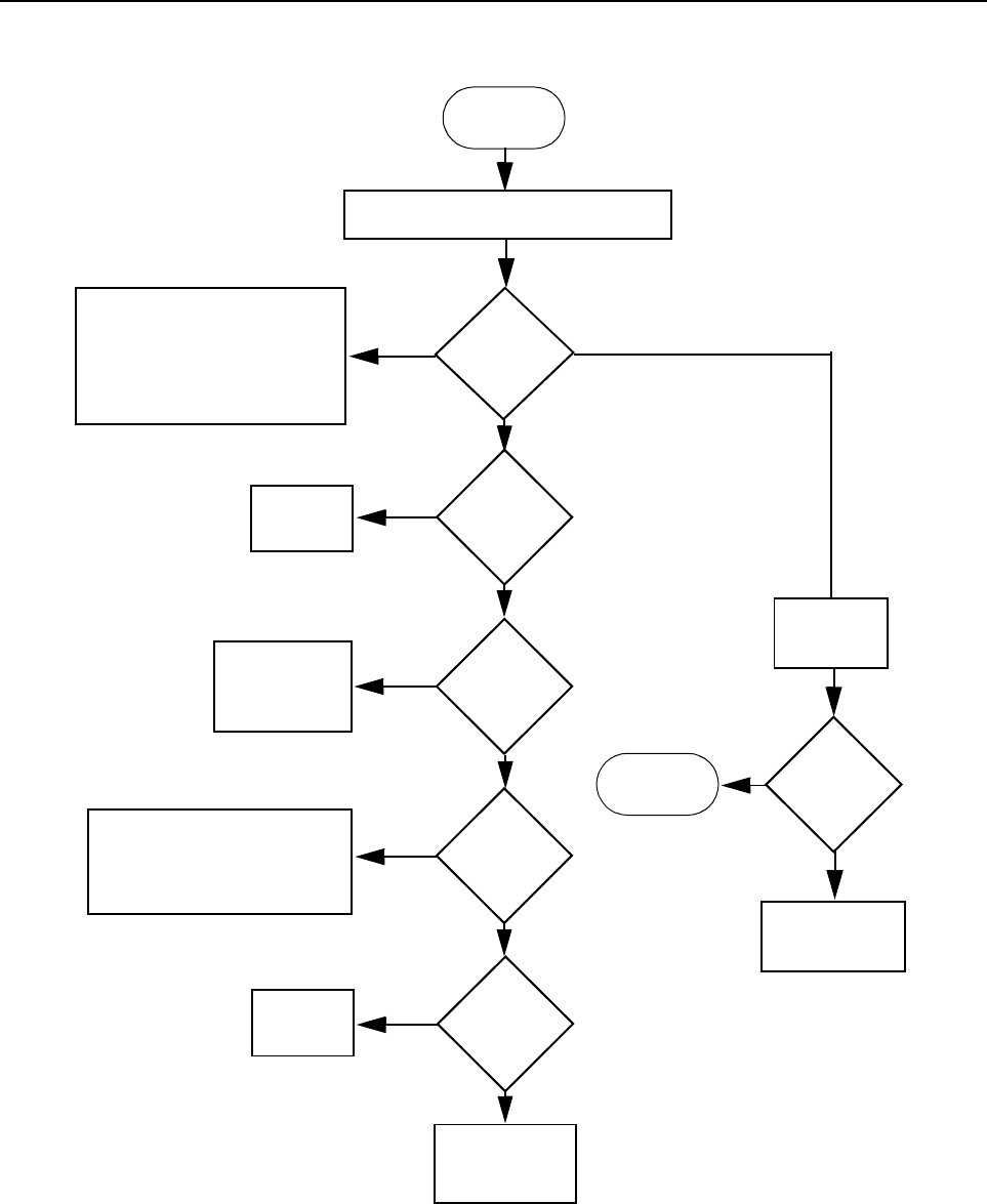
3-4 TROUBLESHOOTING CHARTS
2.0 Troubleshooting Flow Chart for 25W Transmitter (Sheet 1 of 3)
START
Yes
No
Check components between
Q100 and RF output,
Antenna Switch D104, D103,
VR102 and Q106
Before replacing Q100.
No or too low power when keyed
Current
increase when
keyed?
Check power settings, tuning
& components between U103
Pin 3 and ASFIC Pin 6 before
replacing ASFIC
Control
Voltage at
TP150
>1.6V?
Check PA
Stages
>1A
Voltage U103
pin 5 =
4.7V?
U103 Pin 3
<2.6Vdc
PA Bias
Voltage@R134
>2Vdc
Check 9.3V
Regulator
U501, R180 &
R181
Yes
Yes
No
No
Yes
Check
U103
Check Forward
Power Sense
Circuit
No
Short U100
Pin 3 to
ground
Voltage at
TP150 rises?
Check PA
Stages
Check Forward
Power Sense
Circuit
Yes
No
>800mA & <1A
<800mA
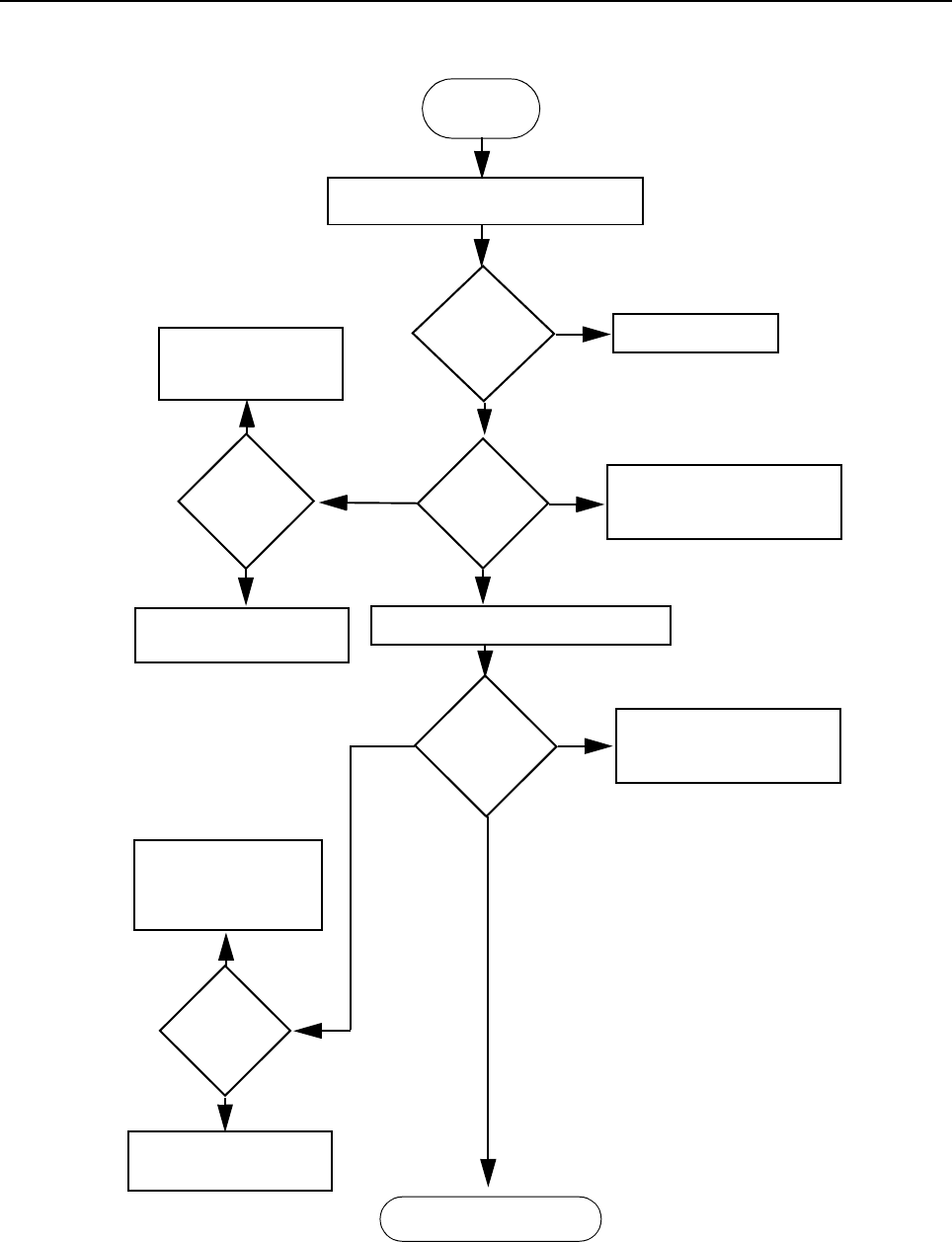
Troubleshooting Flow Chart for 25W Transmitter (Sheet 1 of 3) 3-5
2.1 Troubleshooting Flow Chart for 25W Transmitter (Sheet 2 of 3)
Yes
>3V
Check Q102, R139,
R155, R166, R126-
R128, R169, R138,
R175, R147
Check PA
Stages
No or too low power when keyed
DC
Voltage
at Q101 & Q102
base=0?
DC
Voltage
at U103
Pin 8
Check U403
Check resistive network at
Pin 9 and 10 of U103
before replacing U101
Measure DC Voltage at U102 Pin 1
Pin 1
Voltage
Check resistive network at
Pin 2 & 3 of U102 before
replacing Q105
Check Final PA Stages
DC
Voltage
U102 Pin 3 =
8.7V
Check U102 before re-
placing Q105
DC
Voltage at
U103 Pin
10=8.9V
Check Q101, Q102,
R153, R136, R165,
R122, R168 & R137
Check U103 before re-
placing U101
No
No
Yes
>4.5V
3.5 to 4.5V
2-3V
Yes
No
<3.5V
<2V
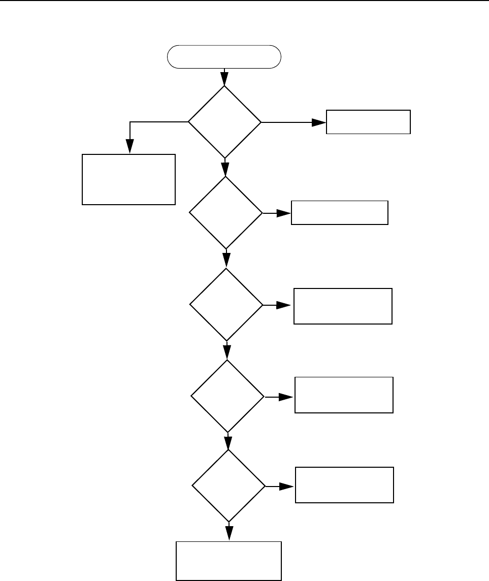
3-6 TROUBLESHOOTING CHARTS
2.2 Troubleshooting Flow Chart for 25W Transmitter (Sheet 3 of 3)
No
Yes
Yes
No
Check Final PA Stage
PA_Bias
Voltage at
R134
RF Voltage
after C1044
>100mV?
Voltage
across R122
>50mV?
RF Voltage
Q105 gate
>250mV?
RF Voltage
Q100 gate
>3V?
Check components
between Q100 &
antenna connector
Replace Q100
Check FGU
Check components
between C1044 &
C1117
Check components
between C1117 &
Q105
Check components
between Q105 &
Q100
No
No
Yes
Yes
2-3V
Supply Voltage
Check Bias Tuning,
R134, R131 & R106
before replacing
ASFIC U504
<2V
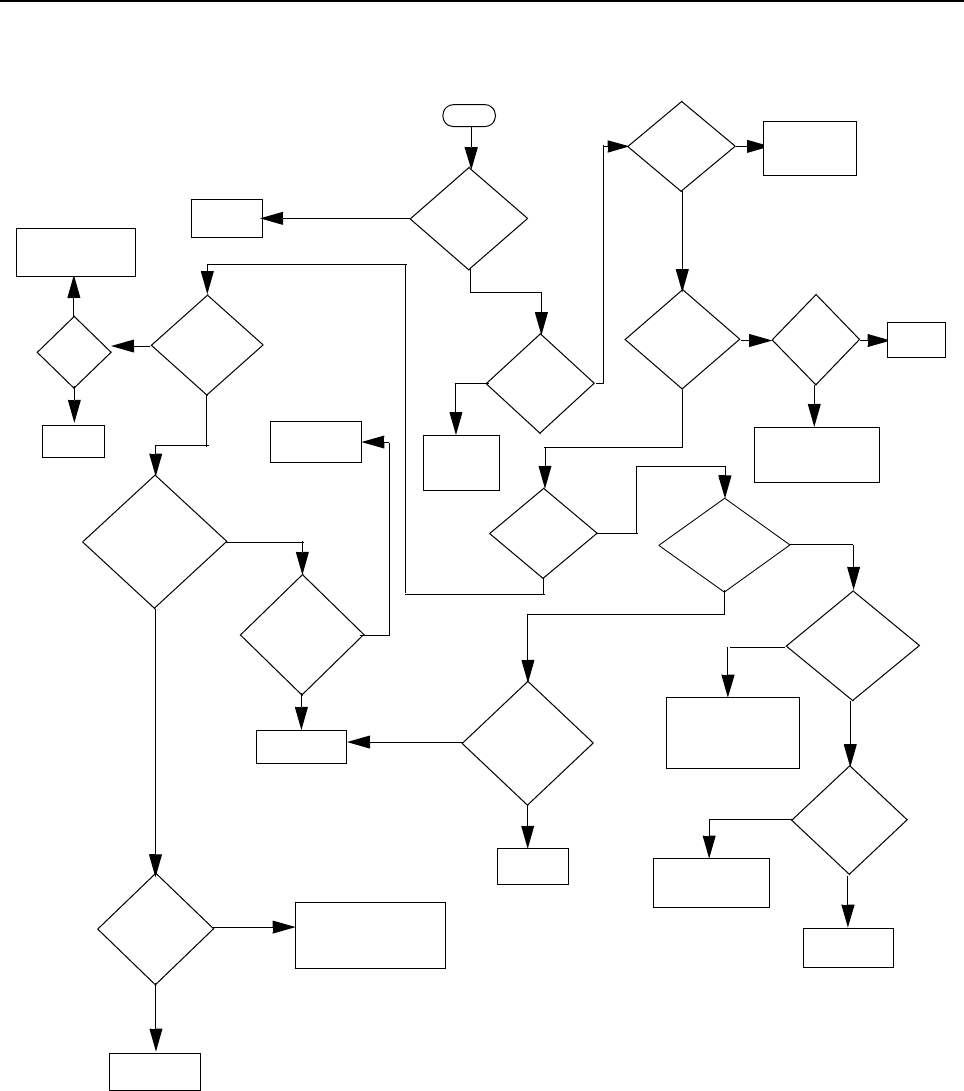
Troubleshooting Flow Chart for Synthesizer 3-7
3.0 Troubleshooting Flow Chart for Synthesizer
5V
at pin 6 of
D200
Is
information
from mP U403
correct
?
Is
U200 Pin 47
at = 13VDC
?
Is
U201 Pin 19
<40 mVDC in RX &
>4.5 VDC in TX?
(at VCO section)
?
Start
Visual
check of the
Board
OK?
Correct
Problem
Check 5V
Regulator
U503
+5V
at U200
Pin’s
13 & 30
?
Is
16.8MHz
Signal at U200
Pin 19
?
Check
Y201 and associated
Parts
Are
signals
at Pin’s 14 &15
of U200
?
Check
R228 Check R201
Is
U200
Pin 2 >4.5 VDC in
Tx & <40 mVDC
in Rx
?
Replace U200
Remove
Shorts
Is
there a short
between Pin 47 and
Pins 14 & 15 of
U200
?
Is
RF level at
U200 Pin 32
-12 < x <-25
dBm
?
Replace U200
Are
Waveforms
at Pins 14 & 15
triangular
?
Do
Pins 7,8 & 9
of U200 toggle
when channel is
changed?
Check programming
lines between
U403 and U200
Pins 7,8 & 9
Replace U200
Check uP U403
Troubleshooting
Chart
NO
YES
NO
YES
NO
YES
NO
NO
NO
YES
YES
YES
NO
YES
YES
YES
NO
NO
NO
NO
YES
NO
YES
YES
Check D200, D201,
C2026, C2025, &
C2027
5V
at U200
pins 5, 20, 34
& 36
C h e c k 5 V
Regulator
U503
Is
16.8MHz
signal at
U200 Pin
23?
Replace
U200
YES
NO
NO
YES
NO
YES
If C2052, R208,C2067,
C2068, L210 are OK, then
see VCO
troubleshooting chart

3-8 TROUBLESHOOTING CHARTS
4.0 Troubleshooting Flow Chart for VCO
Are Q200
Base at 2.4V
Collector at 4.5V
Emitter at 1.7V
Are U201 Pins
13 at 4.4V
15 at 1.1V
10 at 4.5V
16 at 1.9V
Low or no RF Signal
at TP1
Visual check
of board
OK?
35mV DC at
U201 Pin 19
NO
YES
at base of Q200
NO
NO
NO
YES
YES
YES
Low or no RF Signal
at input to PA
4.8V DC at
U201 Pin 19
Is RF available
at C2060
YES
YES
YES
YES
NO
NO
NO
NO
NO
Audio =180mVRMS
at “-” Side of
4.5VDC
at D205
If R211 and R12 are OK,
then replace D205
Replace R211
Replace R212
NO
NO
YES
YES
If parts between
R109 & U201 Pin10
are OK, replace U201
TX VCO
RX VCO
Correct
Problem
Visual check
of board
OK?
Check runner
between U200 Pin 2
and U201 Pin 19
Is RF available Replace U201
If all parts associated
with the pins are OK,
replace Q200
If all parts from collector
of Q200 to TP1 are
OK, replace Q200
Power OK but
no modulation
Check parts to pre-driver
If all parts
associated
with the pins
are OK,
replace U201
YES YES
Make sure Synthesizer is
working correctly and runner
between U200 Pin 28 and
U201 Pin 14 & and is OK
4.5V DC
OK ?
OK? OK?
D205
at U201 Pin 14 & 18
4.5V DC
OK ?
at U201 Pin 14&18
NO

Troubleshooting Flow Chart for DC Supply (1 of 2) 3-9
5.0 Troubleshooting Flow Chart for DC Supply (1 of 2)
Since the failure of a critical voltage supply might cause the radio to automatically power down,
supply voltages should first be probed with a multimeter. If all the board voltages are absent, then
the voltage test point should be retested using a rising-edge-triggered oscilloscope. If the voltage is
still absent, then another voltage should be tested using the oscilloscope. If that voltage is present,
then the original voltage supply in question is defective and requires investigation of associated
circuitry.
Check VDC on
C5008
V=3.3V
?
Check Voltage on
C5043
No
Go to D3_3V
Yes
9v<V<9.8v
?
Go to Start
No
Replace U508
Yes
3V
Check VDC on
C5006
V=5V
?
Check Voltage on
C5042
No
Go to 3V
Yes
9v<V<9.8v
?
Go to Start
No
Replace U503
Yes
5V

3-10 TROUBLESHOOTING CHARTS
5.1 Troubleshooting Flow Chart for DC Supply (2 of 2)
Check VDC on
C5007
V=3.3V
?
Check Voltage on
C5041
No
Go to Digital Section
Yes
9v<V<9.8v
?
Go to Start
No
Replace U510
Yes
D3_3V

Chapter 4
UHF2 PCB/ SCHEMATICS/ PARTS LISTS
1.0 Allocation of Schematics and Circuit Boards
1.1 UHF2 and Controller Circuits
The UHF circuits are contained on the printed circuit board (PCB) which also contains the Controller
circuits. This Chapter shows the schematics for both the UHF circuits and the Controller circuits. The
PCB component layouts and the Parts Lists in this Chapter show both the Controller and UHF circuit
components. The UHF and Controller schematics and the related PCB and parts list are shown in
the tables below.
Table 4-1 UHF2 1-25W Diagrams and Parts Lists
PCB :
8488978U01- D Main Board Top Side
8488978U01- D Main Board Bottom Side
Page 4-4
Page 4-5
SCHEMATICS
Main Circuit
Transmitter
Synthesiser and VCO
Receiver Front and Back End
DC and Audio Ccts
Microprocessor and Controller Ccts
Power Control Cct
Page 4-6/Page 4-7
Page 4-8/Page 4-9
Page 4-10/Page 4-11
Page 4-12/Page 4-13
Page 4-14/Page 4-15
Page 4-16/Page 4-17
Page 4-18
Parts List
8488978U01- D Page 4-19
Controller version is T1

4-2 UHF2 PCB/ SCHEMATICS/ PARTS LISTS
THIS PAGE INTENTIONALLY LEFT BLANK

UHF2 1-25W PCB 8488978U01 (rev. D) / Schematics 4-3
2.0 UHF2 1-25W PCB 8488978U01 (rev. D) / Schematics
9V
COMP_B+
DET_VFWD
FILT_SW_B+
INTEGRATOR
PA_BIAS
PWR_SET
RX
RX_EN
TX_EN
TX_INJ
SHEET 1 OF 8
73D02968C74-O
9V
COMP_B+
DET_VFWD
FILT_SW_B+
INTEGRATOR
PA_BIAS
PWR_SET
RX
RX_EN
TX_EN
TX_INJ
MAIN
COMPARTMENT
UHF2 Interconnection between Main Board and
Power Amplifier Compartment
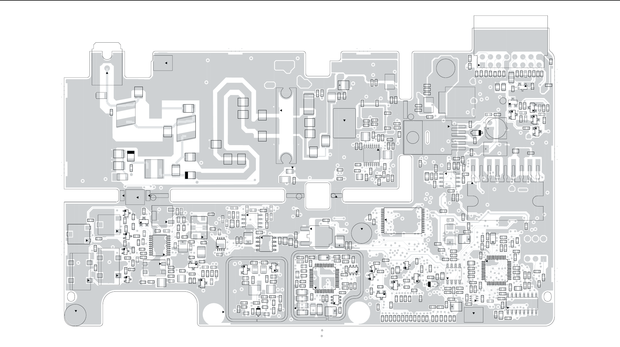
4-4 UHF2 1-25W PCB 8488978U01 (rev. D) / Schematics
C301
C302
C303
C304 C305
C306
C307
C308
C309
C310
C311
C312
C313
C314
C315
C316
C317
C318
C319
C320
C322
C336
C337
C359
C360
C361
C362
C364
C365
C369
C371
C402
C406
C411
C414
C418
C490
C602
C603
C604
C605
C606
C607
C608
C609
C610
C611
C612
C613
C614
C615
C616
C617
C618
C619
C620
C621
C622
C623
C624
C625
C626
C627
C628
C629
C630
C631
C632
C633
C662
C678
C1001
C1004
C1005
C1006
C1007
C1008
C1009
C1010
C1011
C1012
C1013
C1014
C1016
C1020
C1021
C1023
C1026
C1031
C1033
C1034
C1037
C1038
C1039
C1041
C1042
C1044
C1052
C1057
C1063
C1064
C1065
C1074
C1082
C1084
C1087
C1088
C1097
C1098
C1099
C1100
C1104
C1108
C1113
C1114
C1115
C1116
C1117
C1118
C1119
C1122
C1123
C1124
C1125
C1129
C1131
C1151
C1152
C1153
C1154
C1155
C1156
C1263
C1264
C2001
C2002 C2004
C2012
C2013
C2014
C2016
C2024
C2025
C2026
C2027
C2028
C2030
C2033
C2036
C2052
C2055
C2056
C2057
C2058
C2059
C2061
C2062
C2063
C2064
C2066
C2067
C2068
C2069
C2073
C2074
C2075
C2077
C2078
C2079
C2080
C2081
C5001
C5003
C5005
C5006 C5008
C5010
C5011
C5012
C5013
C5014
C5015
C5016
C5018
C5019
C5020
C5021
C5022
C5023
C5024
C5025
C5026
C5027
C5028 C5029
C5030
C5032
C5033
C5034
C5035
C5038
C5042
C5043
C5044
C5046
C5047
C5048
C5050
C5051
C5052
C5053
C5054
C5056
C5057
C5059
C5062
C5064
C5066
C5068
C5070
C5071
C5074
C5076
C5078
C5079
C5080
C5081
C5087
C5088
C5089
C5090
C5095
C5096
C5100
C5101
C5102
C5103
C5110
C5111
C5113
C5114 C5115
C5116 C5117
C5118
2
CR300
D103
D104
D200
D201
2D203
2
D204
D205
D301
D302
D303
D304
2
D400
2D401
2D500
D502
2D513
2
3
4
5
6
FL300
FL301
FL302
4
32
FL303
4
32
FL304
O
J11
L103
L104
L105
L107
L108
L111
L113
L114
L119
L120
L122
L126
L203 L204
L205
L206 L207
L210
L211 L213
L214 L215
L303
L305
L315
M1 M2
M3
M4
M5
1
M6
1
M9
1
M100
M101
M102
M103 M104
M105 M106
M107
O
M108
O
M109
O
M110
1
P1
8
7
1
3
4
6
25
Q100
2
Q302
2
Q305
Q400
Q407
Q414
2Q415
2
Q500
2Q503
R106
R109
R148
R150
R151
R159
R171
R173
R174
R178
R179
R182
R200
R202
R206
R208
R211
R212
R217
R221
R222
R224 R225
R226
R228
R232
R233
R234
R302
R303
R304
R305
R306
R307
R308
R309
R311
R312
R313
R314
R315
R316
R317
R318
R319
R320
R321
R322
R323
R324
R325
R327
R328
R329
R332
R333
R335
R337
R339
R406
R428
R429
R430
R431
R439
R440
R441
R444
R445
R450
R451
R458
R459
R461
R462
R472
R473
R601
R602
R610
R5000
R5001
R5009
R5010
R5011
R5019
R5021
R5022
R5024
R5031
R5032
R5033
R5034
R5038
R5039
R5040
R5043
R5044
R5045
R5046
R5047
R5048
R5050
R5052
R5053
R5054
R5055
R5056
R5057
R5063
R5064
R5065
R5066
R5067
R5068
R5070
R5071
R5073
R5074
R5075
R5077
R5079
R5080
R5081 R5082 R5083
R5084
R5085
R5086
R5087
R5089
R5092
R5093
R5094
R5095
R5096
R5097
R5098
R5099 R5100
RT100
1
SH200
1
SH202
TP3
1
16
8
9
U101
1
37 25
13
U200
11
1
20
10
U300 4
58
U301
22 21
8
7
1U402
1
45
8
U500
5
2
3
4
U501
19
U502
1
45
8
U503
137
25
13
U504
14
58
U505
1
45
8
U506
3
2
1
U508
16
1
8
9
U509
U515
VR500 2
VR501
VR504
2
VR693
2
Y300
4
3
2
Y301
SHOWN FROM SIDE 1 OL 79B02969C76-O
OL 79B02969C78-O
UHF2 (438-470MHz) 1-25W 8488978U01 (rev. D)
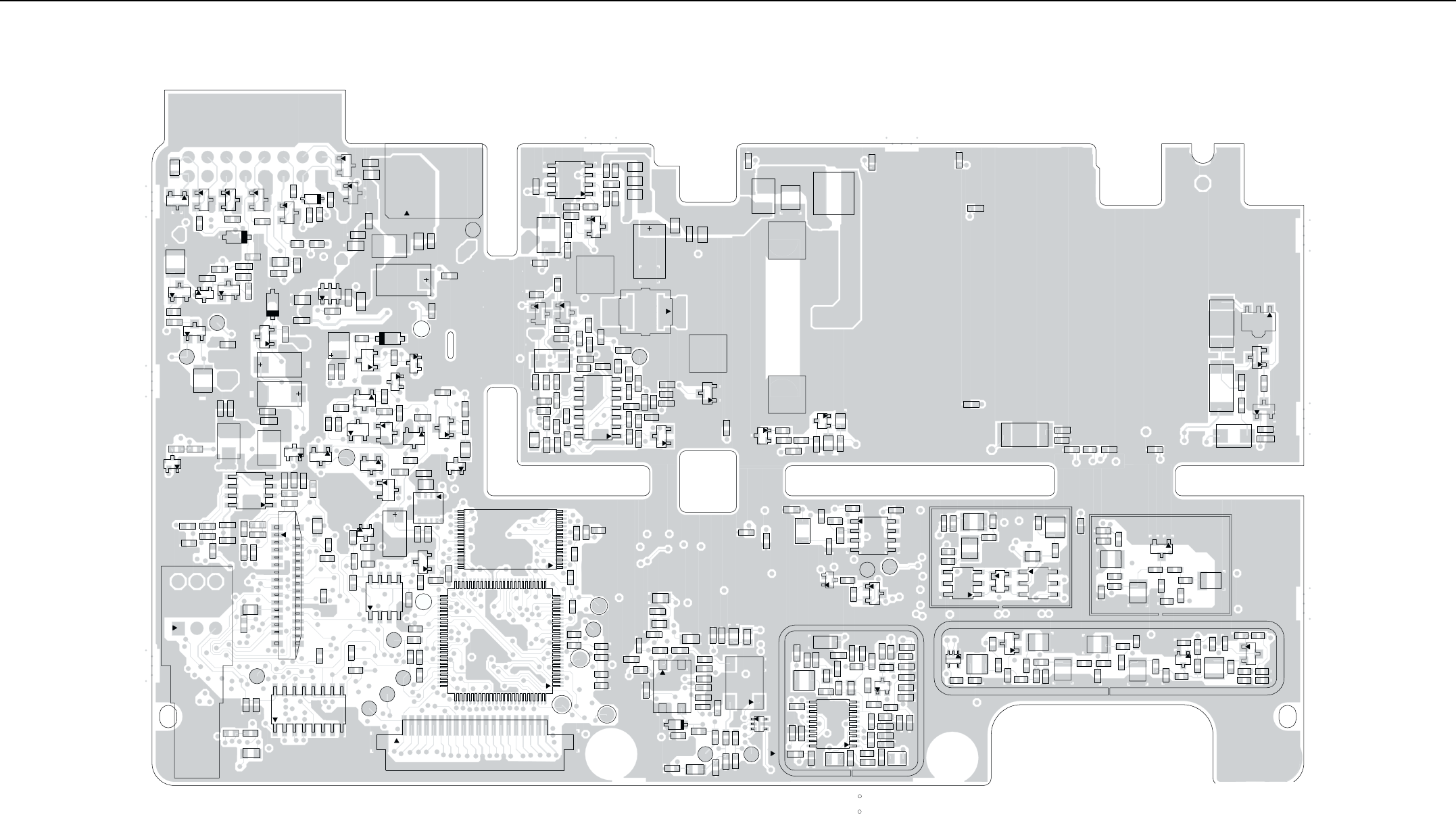
UHF2 1-25W PCB 8488978U01 (rev. D) / Schematics 4-5
C300
C321
C323
C324
C325
C326
C327
C328
C329
C330
C331
C332
C333
C334
C335
C338
C339
C340
C341
C342
C343
C344
C345
C346
C347
C348
C349
C350
C351
C353
C354
C355
C356
C357
C358
C366
C367
C368
C370
C400
C401
C403
C404
C405
C407
C408
C410
C412
C413
C415
C416
C417
C421
C422
C423
C1000
C1002
C1027
C1028
C1029
C1032
C1035
C1036
C1040
C1043
C1045
C1046
C1047
C1050
C1051
C1053
C1054
C1059
C1060
C1061
C1062
C1066
C1067
C1070
C1071
C1072
C1073
C1075
C1076
C1077
C1078
C1079
C1080
C1081
C1083
C1085
C1086
C1089
C1090
C1091
C1092
C1093
C1096
C1101
C1103
C1106
C1107
C1109
C1110
C1111
C1112
C1121
C1126
C1127 C1128
C1130
C1132
C1260
C1261
C2000
C2003
C2005
C2006
C2007
C2008
C2009
C2010
C2011
C2015
C2017
C2018
C2019
C2020
C2021
C2022
C2023
C2029
C2031
C2032
C2034
C2035
C2037
C2038
C2039
C2040
C2041
C2042
C2043
C2044
C2045
C2046
C2047
C2048
C2049
C2050
C2051
C2053
C2054
C2060
C2065
C2070
C2071
C2072
C2076
C2129
C2198
C5000
C5002
C5007
C5009
C5017
C5031
C5036
C5037
C5039
C5040
C5041
C5045
C5049
C5055
C5058
C5060
C5061
C5063
C5065
C5067
C5069
C5072
C5073
C5075
C5077
C5082
C5083
C5084
C5085
C5086
C5091
C5092
C5094
C5097
C5098
C5099
C5104
C5119
C5120
2
CR301
2
D100
2
D102
D105
D106
D202
2
D305
D402
2
D501
2
D511
1J2
29 28
2
29 30
32 31
J3
L100
L101
L115
L117
L118
L121
L200
L201
L202
L208
L209
L212
L216
L217
L300
L301
L302
L304
L306
L307
L308
L309
L310
L311
L312
L313
L314
L500
L501
L502
M111
M112
M113
M114
1P2P2
2
Q101
2
Q102
2
Q103
1
23
Q105
Q106
Q106
Q200
Q201
Q300
2Q301
Q303
Q304
2
Q306
2
Q401
Q403
Q404
Q405
Q408
Q409
Q410
Q411
Q412
Q413
Q416
2
Q417
Q501
Q502
Q504
2
Q505 2
Q506
R103 R104
R107
R108
R117
R118
R119
R122
R126
R127
R128
R130
R131
R134
R135
R136
R137
R138
R139
R140
R141
R142
R143
R145
R147
R149
R153
R155
R156
R157
R158
R160
R161
R165
R166
R167
R168
R169
R170
R172
R175
R180
R181
R183
R185
R186
R201
R203
R204
R205
R207
R209
R210
R213
R214
R215
R216
R218
R219
R220
R223
R227
R229
R230
R231
R235
R300
R301
R310
R326
R330
R331
R334
R336
R338
R340
R345
R346
R347
R401
R402
R403 R404
R405
R407
R414 R415
R421
R422
R423
R424
R425
R426
R427
R432
R433
R434
R435
R436
R438
R442
R443
R453
R454
R455
R456 R457
R460
R463
R466
R467
R468
R469
R470
R471
R600
R603
R604
R615
R5002
R5008 R5013
R5014
R5016
R5020 R5023
R5025
R5026
R5027
R5028
R5029
R5030
R5035
R5036
R5037
R5041
R5042
R5049
R5051
R5058
R5059
R5060
R5061
R5062
R5069
R5072
R5076
R5078
R5088
R5103
1
6
54
3
2
S5010
1
SH201
SH300
SH301
SH302
6
4
3
T300
6
43
T301
TP1
TP2
TP4
TP150
TP200
TP201
TP400
TP401
TP402
TP403
TP404
TP405
TP406
TP407
TP408
TP409
TP410
TP425
TP425
TP500
TP555
TP556
1
45
8
U100
1
4
5
8
U102
87
1
14
U103
11
1
20
10
U201
U302U302
14
58
U400
1
76 51
26
U403
32
17 16
1
16
1
8
9
U405
1
4
5
8
U507
U510
U514
2
VR101
2
VR102
2
VR400
VR401
2
VR402
VR502
VR503
2
VR692
2VR694
2VR695
2VR696
2VR697
2VR698
2
VR699
Y200
4
3
2
Y201
SHOWN FROM SIDE 2 OL 79B02969C77-O
OL 79B02969C79-O
U404
UHF2 (438-470MHz) 1-25W 8488978U01 (rev. D)
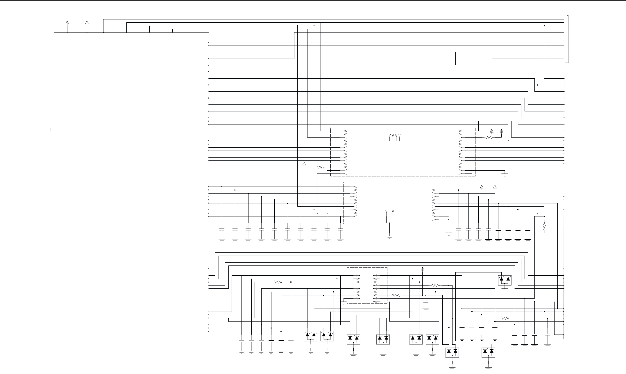
4-6 UHF2 1-25W PCB 8488978U01 (rev. D) / Schematics
Accessory Connector
Control Head Connector
NC
Place capacitors near J2 Place capacitors near J2
Place capacitors near J2
Place capacitors near J2
ELP ONLY
NC ELP ONLY
NC ELP ONLY
NCELP ONLY
Internal spkr+ jumper
DNPJ3 -
DNPDNP
DNP
DIGITAL
Option Board
Keypad/Display
Accessory Connector
EXT_ALARM_OUT
EXT_MIC_PTT
PROG_IN
PROG_I/O
PROG_I/O
PROG_I/O
TO DC & AUDIO
TO SHEET 2
220
TX AUDIO SEND
DETECTOR AUDIO SEND
TX AUDIO RETURN
UNMUTED RX AUDIO SEND
POST-LIMITER FLAT TX AUDIO RETURN
RX AUDIO RETURN
RESET
DIGITAL 3.3 VOLT SUPPLY
GND
ANALOG 3 VOLT SUPPLY
BACKLIGHT
GND
EXTERNAL_ MIC
VOICE STORAGE AUDIO SELECT
OPTION BOARD ENABLE
DATA READY/REQUEST
SERIAL CLOCK
SERIAL DATA RETURN
SERIAL DATA SEND
PUSH TO TALK
DISPLAY DRIVER CHIP SELECT
KEYPAD ROW
KEYPAD COLUMN
DISPLAY_DRIVER_COMMAND/DATA_SEL
VOICE STORAGE INT
VOICE STORAGE RAC
VOICE STORAGE CS
VOICE STORAGE GAIN SELECT
DISPLAY_DRIVER_CS_EN
SHIFT_REG_CS
DISPLAY_DRIVER_COMMAND/DATA_SEL
KEYPAD_COLUMN
KEYPAD_ROW
SCI_PROGRAMMING
BOOT/RESET
SPI_MOSI
MIC_PTT
HOOK
9.3V
D3_3V
HANDSET_RX_AUDIO
MIC_AUDIO
SPKR-
SPKR+
DISPLAY_DRIVER_RESET
SPI_CLK
GND
GND
Option Board Connector
28 Pins Connector
DNP
33.
P1-1
D3_3V
J3-23
23 J3-9
9
VS_GAIN_SEL
VSTBY
3V
0.0
R602
9V
0.
R603
0.
R604
J2-4
4
J2-2
2
19
J2-11
11 J2-14
14
15 J2-20
20 J2-19
J2-7
7J2-18
18 J2-15
J2-22
G2
J2-12
12
17
J2-5 5
J2-16 16
J2-13 13
J2-21
G1
J2-9 9
J2-8 8
J2-17
J2-6 6
J2-3 3
J2-10 10
J2-1
30
J3-31 31
J3-32 32
10
FILT_SW_B+
D3_3V
D3_3V
1
5
J3-5
J3-29 29
J3-30
10
J3-10
13
J3-13
J3-19 18
J3-18
8
J3-8
25
16
J3-16 17
J3-17
2
J3-2
J3-20
20 J3-11
11
15
J3-15
J3-27
27
6
J3-6 J3-28
22 J3-22
1
J3-1
24
28 J3-26
26 J3-24
1n
7
J3-7
J3-14
14
3
J3-3
4J3-4
0.
R600
19
J3-12
12 J3-21
21
VR692
20.0
J3-25
OPT_DATA_R_OPBD
OPT_EN_OPBD
HOOK_CH
MIC_PTT_CH
RESET
SHIFT_R_CS
VOL_INDIRECT
ONOFF_SENSE
EMERGENCY_SENSE
VOX
BATT_SENSE
BOOT_EN_IN_CH
VS_INT
VS_RAC
VS_CS
VS_AUDIO_SEL
FILT_SW_B+
CH_ACT
ASFIC_CS
SYNTH_LOCK
SYNTH_CS
RSSI
uP_CLK
F1200
SQ_DET
LSIO
HSIO
DISPLAY_CS_CH
COMM_DATA_SEL_CH
KEYPAD_COL_CH
KEYPAD_ROW_CH
SCI_CH
PROG_O-ACC_C_4
PROG_I-ACC_C_3
PROG_IO-ACC_C_14
PROG_I-ACC_C_6
PROG_IO-ACC_C_8
PROG_IO-ACC_C_12
RX_EN
LOC_DIST
TX_EN SPI_MOSISPI_CLK SPI_MISO
D3_3V
20.0
VR692
100.
330.0
R601
9V
R615
C678
100.n
33.
VR693
C662
R610
1n
1n
C633 C632 C631
1n
C630
1n
C629
1n 1n
C628
1n
1n
C626C627
1n 1n
C625
C624
1n
1n
C622
C623
1n 1n
C621 C620
1n
1n
C618 C619
1n1n
C617C616
1n 1n
C614 C615
1n1n
C613C612C611
1n1n
C610
1n
1n
C609C608C607
1n
1n
C606
1n1n
C605C604C603
1n
C602
1n
VR698
20.0 VR694
20.0 20.0
20.0
VR697
VR699
VR695
20.0
VR696
P1-7 7
P1-13
13
P1-10
P1-14 14
8
P1-12 12
P1-9
9
P1-8
P1-6 6
P1-4 4
P1-3 3
P1-15
15
FILT_SW_B+
5P1-11
11
2
P1-5
1P1-16
16 P1-2
DNP
UHF2 (438-470MHz) Main Circuit (Sht 1 of 2)
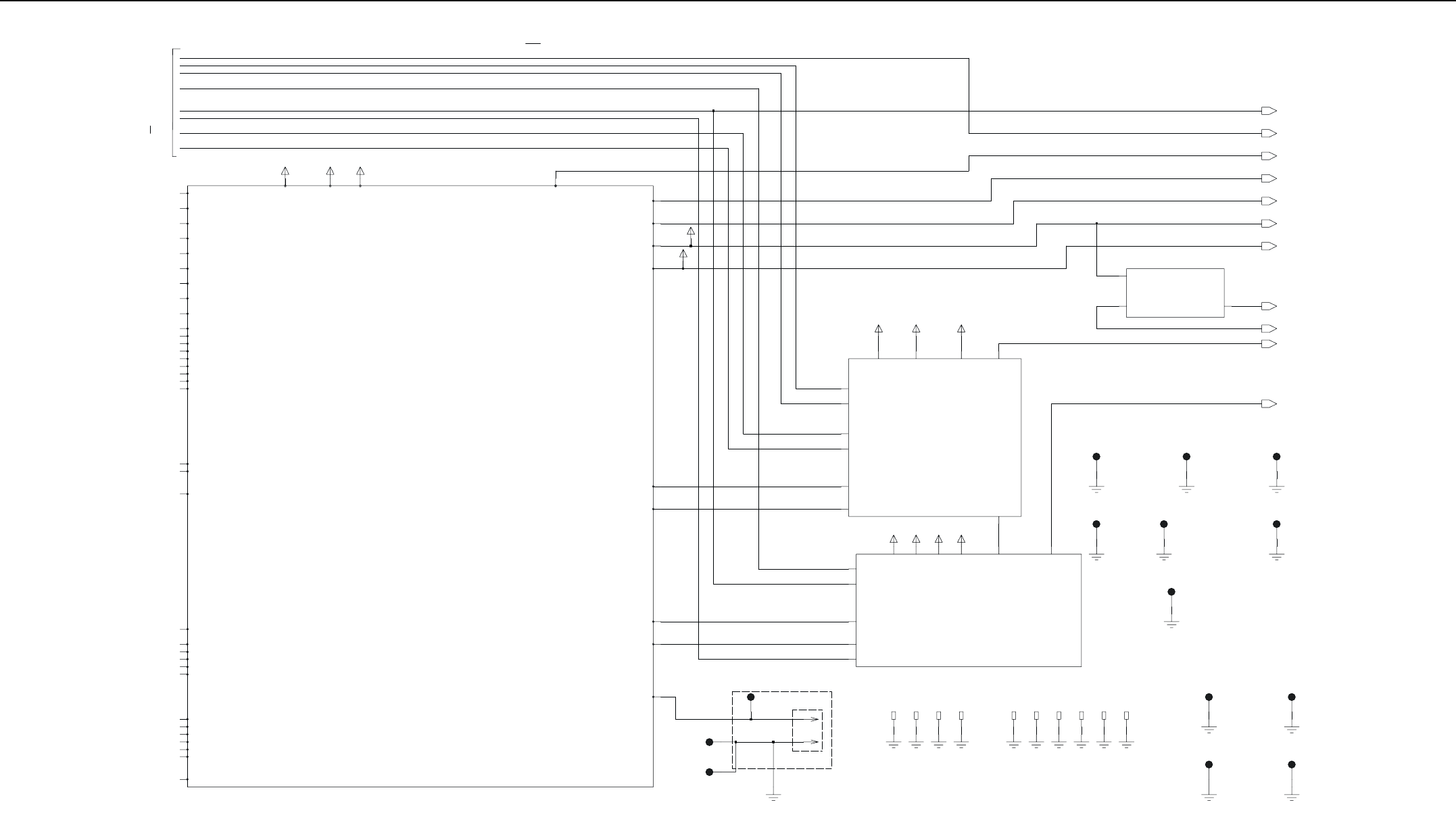
UHF2 1-25W PCB 8488978U01 (rev. D) / Schematics 4-7
MOD_OUT
16.8MHz
SPI_CLK
SPI_MOSI
MIC_AUDIO_CH
HANDSET_RX_AUDIO_CH
VS_AUDIO_SEL
RESET
uP_CLK
F1200
HSIO
LSIO
SQ_DET
CH_ACT
ASFIC_CS
EXTERNAL_MIC_AUDIO_ACCESS_CONN
B+
3V
BW_SEL
D3_3V 5V
PWR_SET
DEMOD
SPKR+
SPKR-
5V_CH
VS_MIC
RX_AUDIO_RETURN_OPT_BRD
POST_LIMITER_FLAT_TX_AUDIO_RETURN_OPT_BRD
TX_AUDIO_RETURN_OPT_BRD
UNMUTED_RX_AUDIO_SEND_OPT_BRD
PA_BIAS
HOLES FOR PA SHIELD
PEDS FOR GND CONTACTS
(SOURCE)
(SOURCE)
DC & AUDIO
CONTACTS FOR PA CLIP
DC Connector
(SOURCE)
(SOURCE) (SOURCE) (SOURCE)
SHEET 4 OF 8
73D02968C74-O
BOARD HOLES
DETECTOR_AUDIO_SEND_OPT_BRD
TX_AUDIO_SEND_OPT_BRD
VSTBY
VOL_INDIRECT
BATT_SENSE
EMERGENCY_ACCES_CONN
VOX
EMERGENCY_SENSE
COMP_B+
FILT_SW_B+
9V
ONOFF_SENSE
IGNITION
RX_AUDIO_OUTPUT_ACCESS_CONN
FLAT_TX_AUDIO_INPUT_ACCESS_CONN
PLTD_HOLE1_4X1_8
M102
1
GND
TEST_POINT
TX_INJ
3V5V
9R 9V
BW_SEL
DEMOD
LOC_DIST
RSSI
RX
RX_EN
RX_INJ
9R
1
M111
TO SHEET 1
DET_VFWD
INTEGRATOR
COMP_B+
FILT_SW_B+
9V
PWR_SET
PA_BIAS
DET_VFWD
FILT_SW_B+
INTEGRATOR
PLTD_HOLE1_4X1_8
M101
FILT_SW_B+
9V
1
GND
SYNTH_CS
SYNTH_LOCK
3V5V
16.8MHz
3V5V 9R
MOD_IN RX_INJ
SPI_CLK
SPI_MOSI
PLTD_HOLE3_5x7_0
M1
1
GND
PLTD_HOLE3_5x7_0
M3
M107
1
PLTD_HOLE3_5x7_0_TRIMMED
M8
1
GND
M108
1
1
M109
1
M110
1
P2-2
2
GND
1
M5
PLTD_HOLE3_5x7_0_TRIMMED
GND
1
P2-1
M113
1
M9
PLTD_NUT
1
M114
1
9V5V9R
M112
M106
1
5V
D3_3V3V
VCC
M105
1
GND
1
PLTD_HOLE3_5x7_0_TRIMMED
M4
1
GND
PLTD_HOLE3_5x6_0_TRIMMED
M2
1
GND
M7
PLTD_HOLE3_5x7_0_TRIMMED
M104
PLTD_HOLE1_4X1_8
GND
1
TP3 1
TP2
TEST_POINT
1
1
GND
M103
PLTD_HOLE1_4X1_8
GND
1
RX
TX_EN
TX_INJ
RX_EN
FGU
POWER CONTROL
RX
UHF2 (438-470MHz) Main Circuit (Sht 2 of 2)
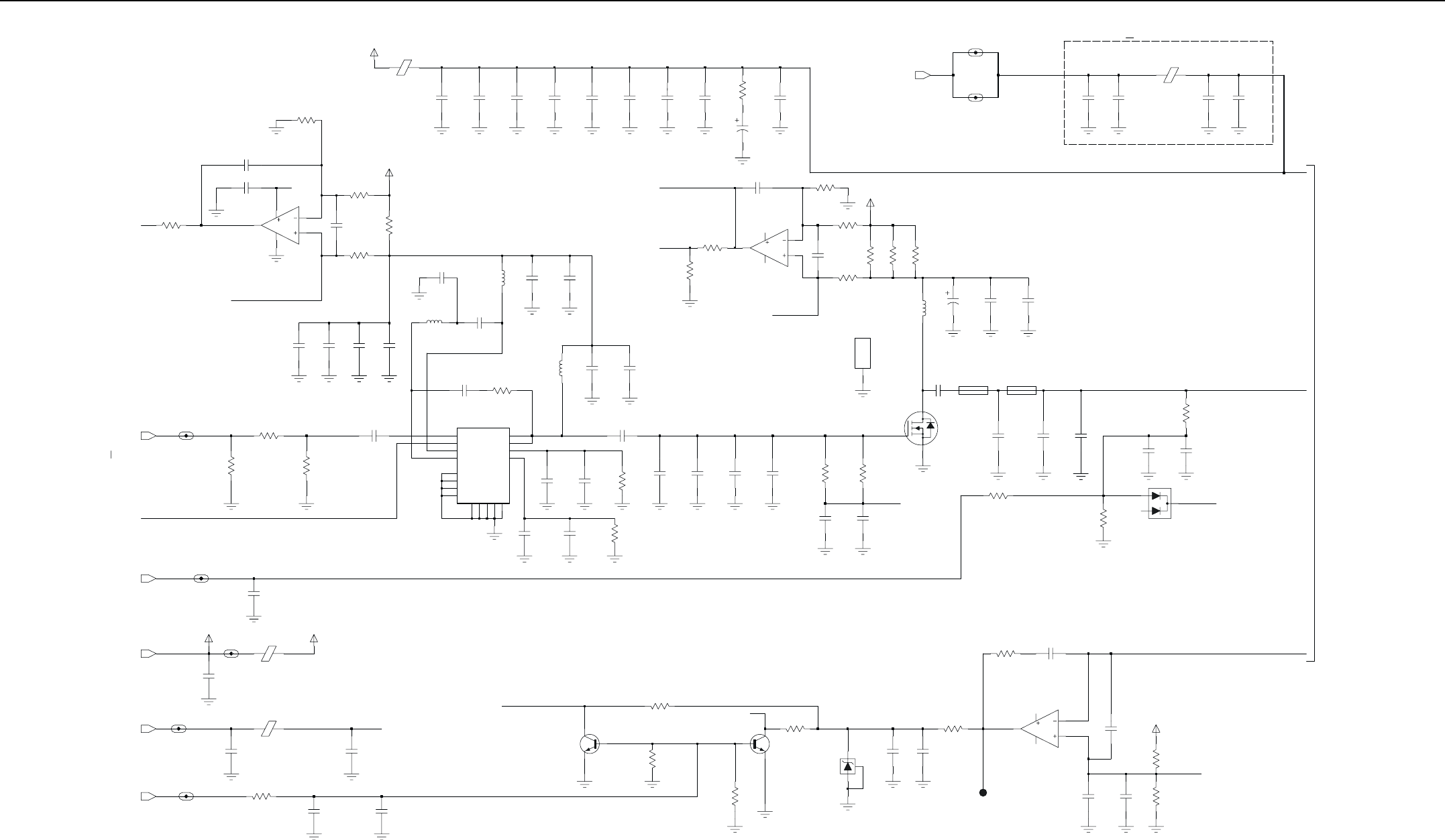
4-8 UHF2 1-25W PCB 8488978U01 (rev. D) / Schematics
120.p
100n
120.p
DNP
DNP
PLACED NEAR R122
PLACED NEAR CHIP’s PIN
DNP
TO SHEET 2
FILT_SW_B+
FLT_9V
9V
TX_INJ
COMP_B+
C1027
C1103
C1061
22n
1019447
L119
PA_FILT_B+
R136
36.K
R168
C1053 180.p
C1001
4.7
FLT_9V
V_CTRL_PREDRIVER
1.0u
IF109
R165
2.4K
FILT_SW_B+
C1126
L122
1.542*4 0.8*25
MRF1513’s Thermal pad
(SOURCE)
DNP
V_CNTRL
DNP
MRF 1518
Place inside of the PA compartment
DNP DNP
100n
C1028
R170
R167
510.
C1036
2.2K
FLT_9V
22n
47.K
R181
47.K
R131
R180
100.K
2.7K
R134
R137
39.K
C1104
33.n
C1014
39.p
120.p
C1033
C1044
10.n
IF105
1
39.p
C1116
1019447
L121
C1115
39.p
R166
2.7K
36.K
R138
10.K
Q102
R155
R153
10.K
Q101
6.8
VR101
IF104
1
120.p
10u
33n
15.000
L118
1019447
R109
120.p
C1054
C1057
120.p
D100
2.7K
R147
R175
560.
R128
1.
R127
1. 1.
R126
1.n
C1040
FLT_9V
39.K
R139
R169
2.K
C1107
120.p39.p
C1106
C1012
9.1p
Q105
R158
6.8K
C1043
120.p
22n
C1032
120.p
VD1
14 VG1 2
VG2 3
C1042
NC1
8
NC2
9
NC3
10
NC4
15
RFIN
16 RFOUT1 6
RFOUT2 7
VCNTRL
1
17 EP
G2
11
GND1
4
GND2
5
GND3
12
GND4
13
30C65
U101
8
4
11
C1039
6
5
7
4
11
MC3303
U103
9
10
U102
LM2904
2
3
1
8
4
MC3303
U103
C1072 120.p
C1070
300
R173 R174
4.22n
300
470.p
C1041 R171
560.
C1119
120.p
C1117
C1031
30.p
3.3n
L104
6.8p
C1118 56.n
18.n
L105
L107
11.030n
R178
51. 51.
R179
51.
R106
2.2K
R122
POS
1
FILT_SW_B+_PA
1019447
L100
M100
HEATSINK
6.8K
R159
C1038
22n
C1029
100n
C1066
120.p
120.p
C1065
22n
C1037C1064
120.p
C1063
120.p
120.p
C1062
C1060
120.p
C1111
39.p
R130
0.
C1074
C1263
1.n
120.p
TP150
TEST_POINT
1
C1261
120.p 10.n
C1260
C1151
24.p
30.p
C1156
C1152
15.p
C1153
11.p
C1154
18.p 4.3p
C1155
39.p
C1129
R182
10.K
C1264
C1100
120.p
C1099
1
IF103
1
120.p
IF108
1
IF107
1
R186
5.1
39.p
C1092
C1089
120.p
C1000
120.p
C1112
39.p
39.p
C1086
C1109
39.p39.p
C1110
39.p
IF106
1
C1084
VCNTR1
VCNTR1
VCNTR2
VCNTR2
VCNTR3
V_CTRL_DRIVER
VCNTR3
RX_EN
FILT_SW_B+_PA
V_CTRL_DRIVER
V_CTRL_PREDRIVER
PA_BIAS
V_REF_OPAMP
UHF2 (438-470MHz) Transmitter (Sht 1 of 2)
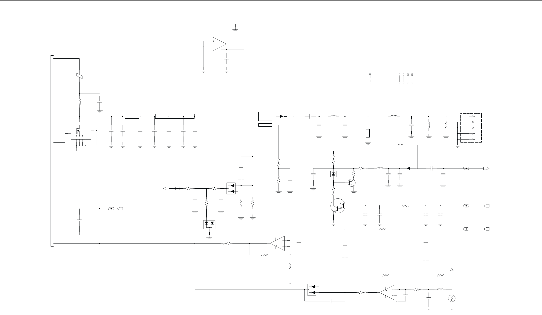
UHF2 1-25W PCB 8488978U01 (rev. D) / Schematics 4-9
LM2904
U102
L117
1019447
Antenna Connector
390.n
7.5 width 2.032
Coupler
PA’s Temp. Sensor
DNP
DNP
TO SHEET 1
SHEET 2 OF 8
73D02968C74-O
Current sense protection (option)
DNP
FILT_SW_B+_PA
PA_FILT_B+
PWR_SE
T
L126
120.p
C1035
RT100
C1004
27.p
L115
18.n
1
J11-1
120.
C1081
INTEGRATOR
DET_VFWD
IF110
1
39.p
IF111
1
10K
R150
Q106
5.6
VR102
470.
R172
D104
D103
C1121
5.6p
C1021
9.1p
C1007C1009
120.p
S2
S3
S4
22.p
Q100
D
G
GND1
GND2
S1
C1008
8.2p12.p
C1013
1.u
L103
FLT_9V
47.0K
R151
5.6K
120.p
C1052
120.p
C1051
R135
43.K
R145
22.K
C1050
120.p
3
1
4
11
D102
R143
U103
MC3303
2
22.K
R142
22.K
R148
22.K
22.K
R149
C1076
13.p
10.K
R156
C1059
D106
120.p
3.3K
R161
3.3K
R160
C1101
20.p
D105
100.
R119
R118
100.
L108
390.0n
L114
18.n
L113
17.n
L111
17.n
47.p
C1108
R108
51.000
R107
51.000
6.8p
C1016
C1010
30.p 30.p
C1006
39.p
C1011
C1026
6.2p
9.1p
C1023
3.3p
C1020
R103
120.p
C1079
39.p
C1091
100.
10K
R183
C1080
R185
39.p
C1078
39.p 39.p
C1077
R157
Q103
56.K
C1130
R104
39.p
470.
12
14
4
11
C1073
120.p
6
5
7
8
4
U103
MC3303
13
C1067
120.p
C1002
100.p
IF101
1
10.n
C1047
IF100
1
IF102
1
G2
J11-4 G1
J11-2 2
J11-3 3
J11-5
36.p
C1005
RX
V_forward
V_REF_OPAMP
TX_EN
CONTACTS FOR PA CLIP
M4
PLTD_HOLE3_5x7_0_TRIMMED
GND
1
1
M114
1
1
M113
M111
1
M112
UHF2 (438-470MHz) Transmitter (Sht 2 of 2)
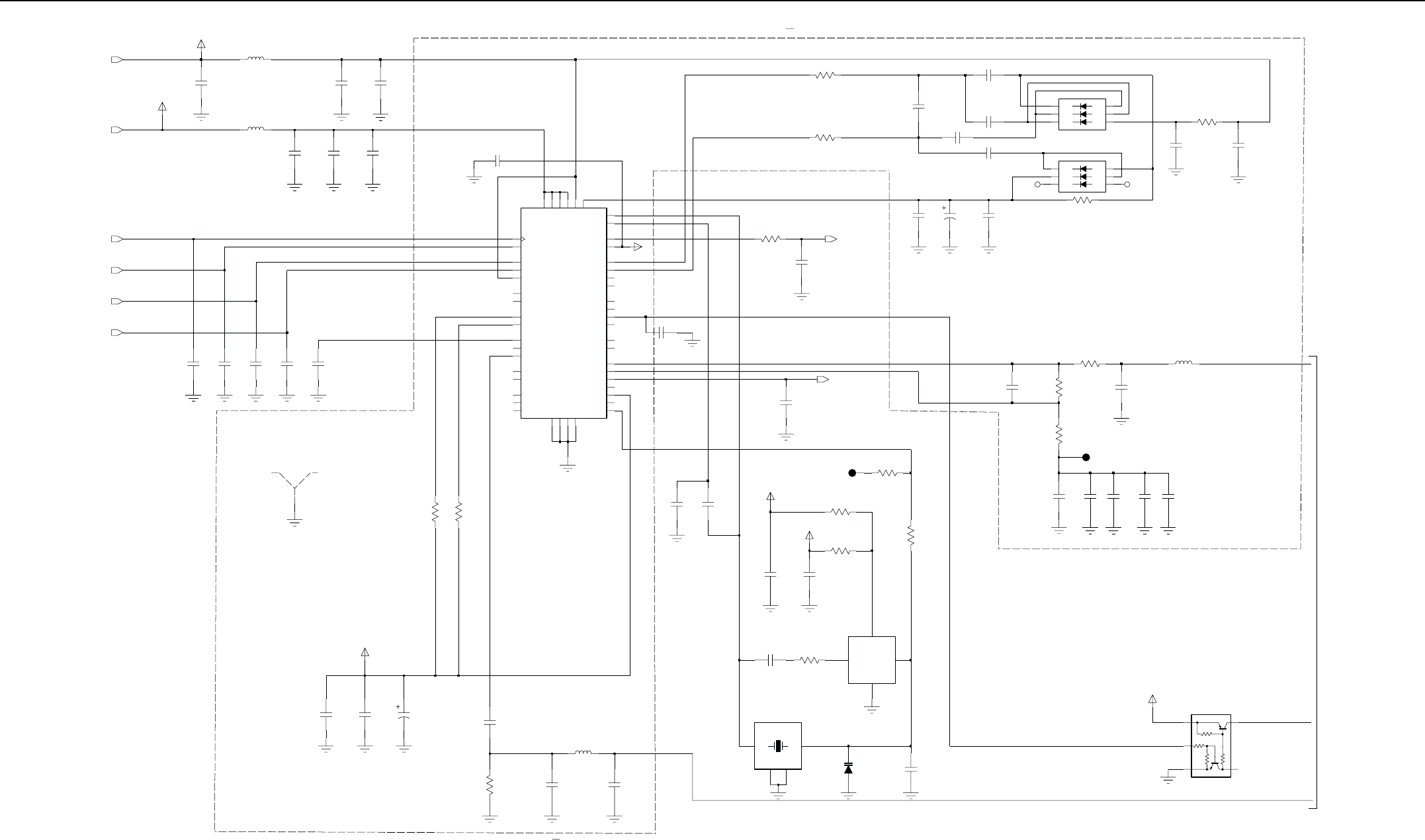
4-10 UHF2 1-25W PCB 8488978U01 (rev. D) / Schematics
U200
FRACN_63A27
XTAL2 24
XTAL1 23
WARP 25
13
VRO
VMULT4 11
VMULT3 12
34
VMULT2 14
VMULT1 15
VCP 47
VBPASS
21
TEST2 38
TEST1 37
SFOUT
V_SF
5V
5V
VCO_MOD
46
ADAPTSW
BIAS1
40
AVDD 20
AUX4 3
AUX3 2
R209
100.K
AUX2 1
AUX1 48
AGND
22
DVDD 36
DGND
6
DATA
7
CLK
8
D201
CEX
9
CCOMP
42
BIAS2
39
17
MODOUT 41
MODIN
10
4
LOCK
IOUT 43
INDMULT 16
IADAPT
5.1p
C2067
45
FREFOUT 19
PRE_GND
33
PREIN
32
5
PD_VDD
PD_GND
44
NC3
31 NC2
29
DNP
DNP
DNP
DNP
DNP
DNP
DNP
TO SHEET 2
NC1 28
SFIN
30
SFCAP
26
SFBASE
27
REFSEL
18
PVREF
35
SYNTH_LOCK
PRE_VDD
120.p
C2050
120.p
0.1uF
C2053
R210
C2017
GND
3OUT
VCC
4
1
VCON
100.K 16.8MHz
Y200
45J68
2
0.
R202
0.1uF
120.p
C2016
C2006
C2036
C2005
2.2uF
2.2uF
1.n
C2198
120.p
V_SF
C2129
1
Q201
TEST_POINT
TP200
1
TP201
TEST_POINT
C2080
100.n 100.n 100.n
C2079 C2078
100.n
C2077
51.
R208
R200
100.K
C2002
120.p
C2033
4.7uF
C2014
0.1uF
1.5K
R224
R206
120.K
R207
150.K
C2074
100.n
C2013
0.1uF
1.3K
R217
39.
L205
R234
1uH
120.p
C2045C2046
A1
A2
A3
K1
K2
K3
120.p
K3
D200
A1
A2
A3
K1
K2
120.p
C2052
C2051
220p 62.00p
2GND
4GND1
3
OUT
1IN
C2054
D202
Y201
14R06
FREQ
NC NC
C2034
2.7p
C2072
120.p
C2075
C2001
4.7uF
100.n
2.2uF
C2004
120.p
C2035
C2049
120.p
100.
R229
22p
C2055
C2015
0.1uF
R226
150.
150.
R225
R228
100.
120.p
C2048
C2027
10n
10n
C2026
C2025
10n
C2024
10n
10n
C2023
2.2n
C2028
390nH
L200
2.2uF
C2000
390nH
L217
33n
120.p
C2047
L210
5.1p
C2068
3V
0.
R205
0.
R204
1
C2020
100n
SH200
SHIELD
3V
SPI_MOSI
SPI_CLK
MOD_IN
5V
3V
SYNTH_CS
16.8MHZ
UHF2 (438-470MHz) Synthesiser and VCO (Sht 1 of 2)
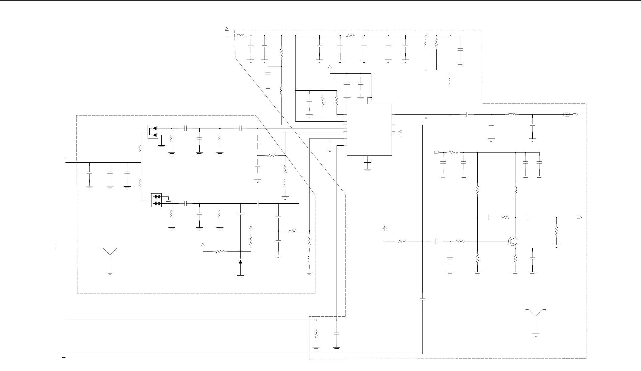
UHF2 1-25W PCB 8488978U01 (rev. D) / Schematics 4-11
VCO Shield
VCOBIC Shield
DNP
DNP DNP
DNP
DNP
73D02968C74-O
TO SHEET 1
SHEE 5 OF 8
IF200
10.K
V_SF
TX_INJ
RX_INJ
9R
1
120.p
C2081
R201
100.n
C2076
C2042
120.p
C2041
120.p 120.p
C2071
C2040
1
12.p
SHIELD
SH202
1
SH201
SHIELD
C2039
C2038
120.p
120.p
150.n
L204
L203
150.n
R223
220.
100n
C2003C2037
120.p
0.
R203
3.3p
C2044
C2019
120.p120.p
C2018
V_SFV_SF
R230
75.
R220
510.
VCO_MOD
V_SF
C2043
6.8p
NC
0.1uF
C2012
10n
NC
L202
C2022
680nH
2.4p
0.1uF
C2011
C2069
C2066
1.2p
2.7K
R216
2.7K
R215
6.2p
C2065
120.p
100.0n
L213
C2032
C2063
8.200p
4.7K
R214 L212
33n
R227
82.
R219
820.
C2031
1n
R213
1
3
2
4.7K
BFS540
Q200
100n
C2010
6.2p
C2064
L211
100.0n
L216
18.n
C2070
12.p
680nH
L201
3.9n
C2030
L207
7.80n
C2059
L215
47nH
5.1p
C2073
1.p
5.1p
C2058
C2062
12p
120.p
C2029
R233
220.
R222
47.
R212
47.K
6.8K
R211
1.K
R218
L206
12.5n
L214
R235
47nH
18.
47.
R232
R221
220.
1.n
C2021
C2057
5.1p
C2056
12p
C2061
5.1p
15p
C2060
100n
C2009 C2008
0.1uF
C2007
0.1uF
L209
100.0n
100.0n
L208
51.
R231
D205
D204
VCC_LOGIC
D203
SUPER_FLTR
19 TRB_IN
16 TX_BASE
15 TX_EMITTER
1TX_IADJ 10
TX_OUT
13
TX_SWITCH
14
VCC_BUFFERS 18
GND_FLAG
GND_LOGIC
17
12
PRESC_OUT
5RX_BASE
6RX_EMITTER
2RX_IADJ 8
RX_OUT
7
RX_SWITCH
3
50U54
U201
4COLL_RFIN
20 FLIP_IN
11 GND_BUFFERS
9
UHF2 (438-470MHz) Synthesiser and VCO (Sht 2 of 2)
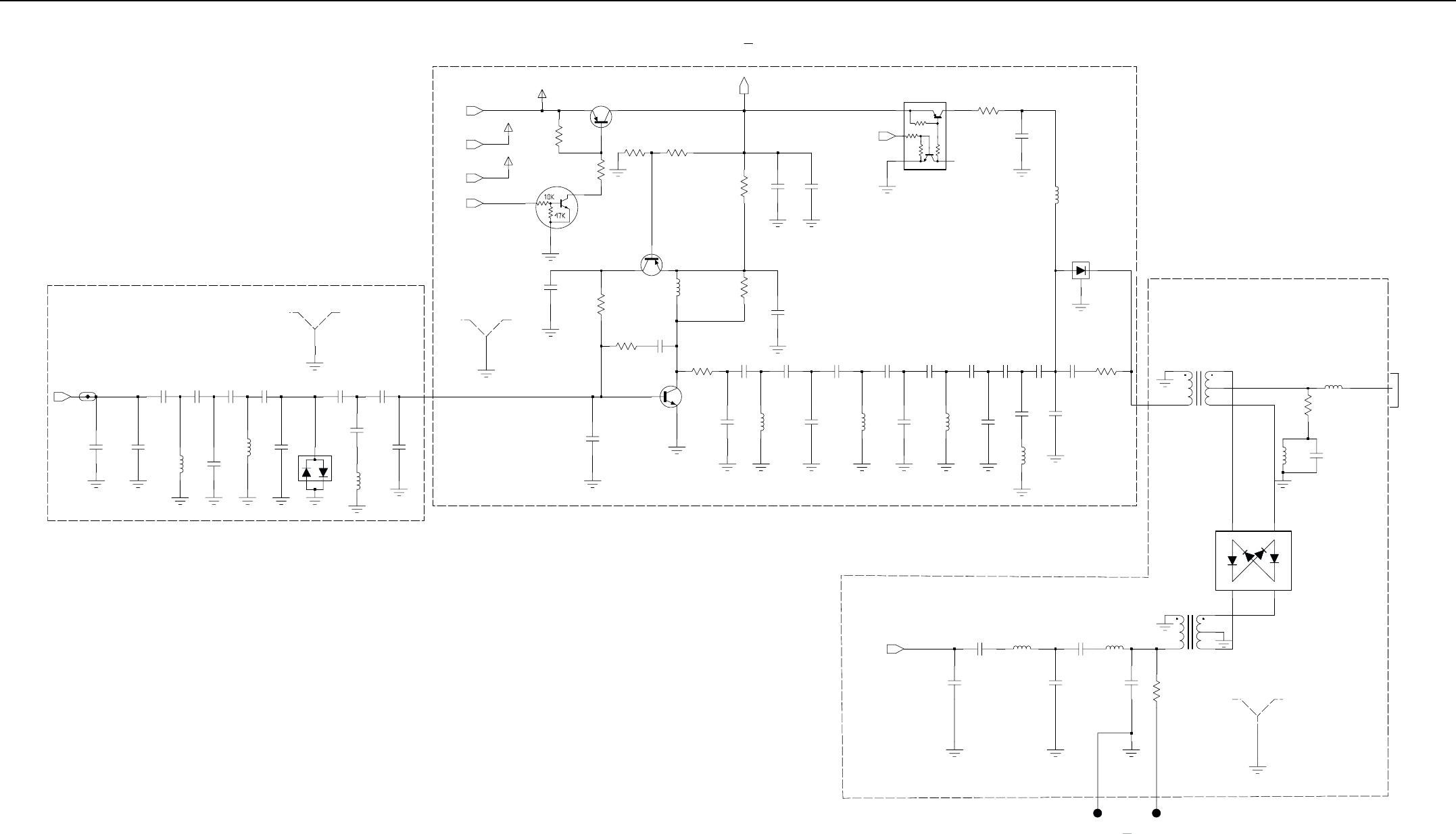
4-12 UHF2 1-25W PCB 8488978U01 (rev. D) / Schematics
MIXER SHIELD
DNP
DNP
DNP
DNP
DNP
TO SHEET 2
FRONT-END SHIELD
51.p
3V
5V
9V
RX_EN
LOC_DIST
470.0n
IF300
1
TP1
1
5.6p
C1121
TEST_POINT
TP4
1
TEST_POINT
Q300
Q306
R346
R345
10.K
10.K
Q304
18.08n
L314
10.p
C330
12.p
C333
10.p
C335
C329
36.p
C348
3.3p
C344
A2
A4
K1
K3
3.6p
U302
24.p
C370
120.p 120.p
C325
R301
C324
SH301
SHIELD
1
470.
SH302
1
SHIELD
SH300
1
C342
4.7p
SHIELD
R347
15.
C328
43.p
L308
18.08n
L307
18.08n
C356
15.p
C367
8.200p
10.p
C366
4.7p
C341
8.2p
C368
100.
R338
330p
C327
150.n
L304
C321
120.p
430.
R334
3.6p
C347
3V
5V
9V
D305
18.08n
L313
L312
18.08n
L311
18.08n
L310
18.08n
L309
18.08n
L300
18.08n
L302
150.n 82p
C354
R340
51.
XFMR
T301
4
6
3
1
2
4
6
3
1
2
T300
XFMR
36.p
C358
220.
R336
10.p
C332
3.6p
C343
C331
10.p
C346
4.3p
C355
39.p
Q303
BFS540
1n
100n
C351
C323
2.7K
R326
C350
120.p
Q301
10.K
R300 R310
15.K
120.p
C349
R331
100.
820.
C326
22.n
150.n
R330
L301
C357
36.p
C353
82.p
CR301
20.p
C334
3.9p
C345
10.p
C338
C340
2.4p
2.4p
C339
C300
L306
RX
9R
RX_INJ
UHF2 (438-470MHz) Receiver Front and Back End (Sht 1 of 2)
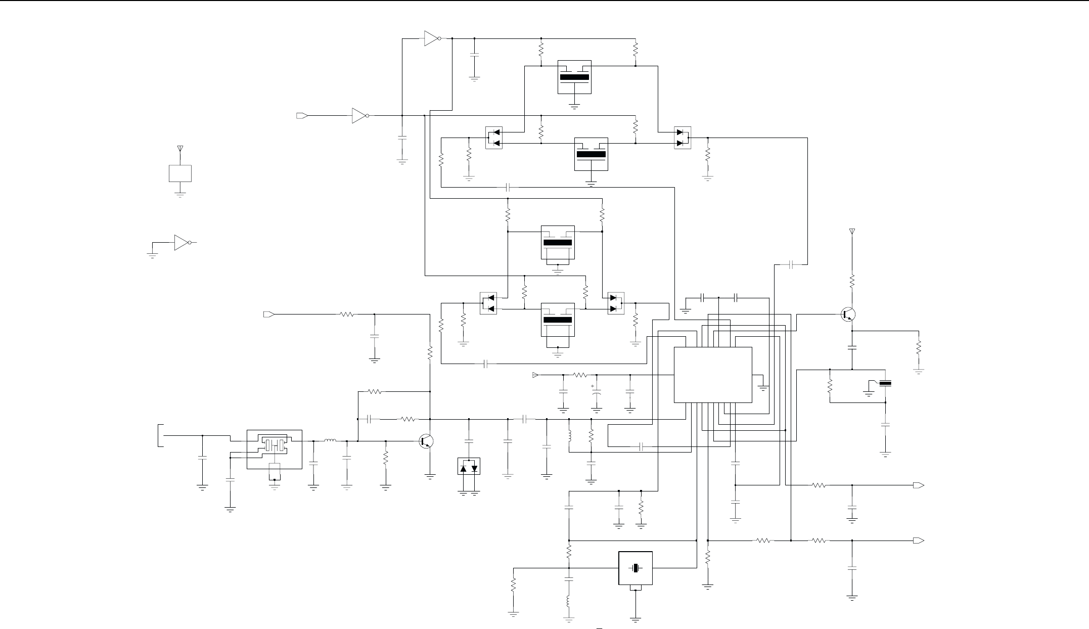
UHF2 1-25W PCB 8488978U01 (rev. D) / Schematics 4-13
73D02968C74-O
SHEET 6 OF 8
Check if it is 3v or another value
NU
NU
NU
DNP
DNP DNP
TO SHEET 1
22.p
BW_SEL
5V
L315
27nH
0.
C359
R303
33p
30p
C361
R311
4OSCOUT 3
QUADIN
10
RFIN
1
RFIN_DEC
2
RSSIOUT 5
RSSI_FEED
9
VCC
6
15.K
16
IFAMP_DEC1
19 IFAMP_DEC2 17
LIMIN
14 LIMOUT 11
LIM_DEC1 13
LIM_DEC2
12
MIXOUT 20
OSCIN
AUDIOOUT 8
AUDIO_FEED
7
GND 15
IFAMPIN
18 IFAMPOUT
1
GND2
4
IN
3OUT 6
U300
SA616
FLTR_44.85M
FREQ
CC1
2
CC2
5
GND1
20.K
FL300
100.
3V
R308
R337
13.K
R312
33.K
R304
R333
560.
C365
22p
C364
22p
L305
1.2u
C320
0.1uF
0.1uF
C319
0.1uF
C318
0.1uF
C317
1OUT 2
0.1uF
C316
1
CFWC455D
FL304
3
GND1
GND2
4
IN
45B02
Y300
455KHz
3
2
130.0p
C302
06B09
Y301
2GND
4GND1
3OUT 1
IN
0.
R302
44.395MHz
12.K
R319
3.3K
R325
D304 D303
12.K
R318
R307
20.K
R317
12.K
U301
35
3V
U301
GND
4
VCC
8
3V
TC7W04F
FL303
GND1
3
4GND2
IN
1OUT 2
PWR_GND
CFWC455G
C315
C314
100n
TC7W04F
62
100n
TC7W04F
17
U301
U301
C313
100n
C312
2.4K
100n
R327
20.K
R306
R305
20.K
R316
12.K
R315
12.K
R314
12.K
3.3K
R324
D302
3
GND
1IN 2
OUT
D301
3
GND
1IN 2
OUT
FL302
FLTR
FL301
FLTR
100n
C311 C310
100n
R328
1.2K
R329
1.8K
390.
R335
Q302
C309
100n
12.K
C322
R313
8.2K
4.7n
R321 680.
R332
10.K
R320
51.
R339
100n
10.0u
C301
C308
100n
C307
R309C360
30p 15.K
C306
4.7K
100n
R323
L303
1.2u
C371
C337
2.7p
6.8p
CR300
100n
C303
100n
C305
Q305
C304
100n 4.7K
R322
C369
8.2p
C336
C362
9.1p
DEMOD
RSSI
UHF2 (438-470MHz) Receiver Front and Back End (Sht 2 of 2)
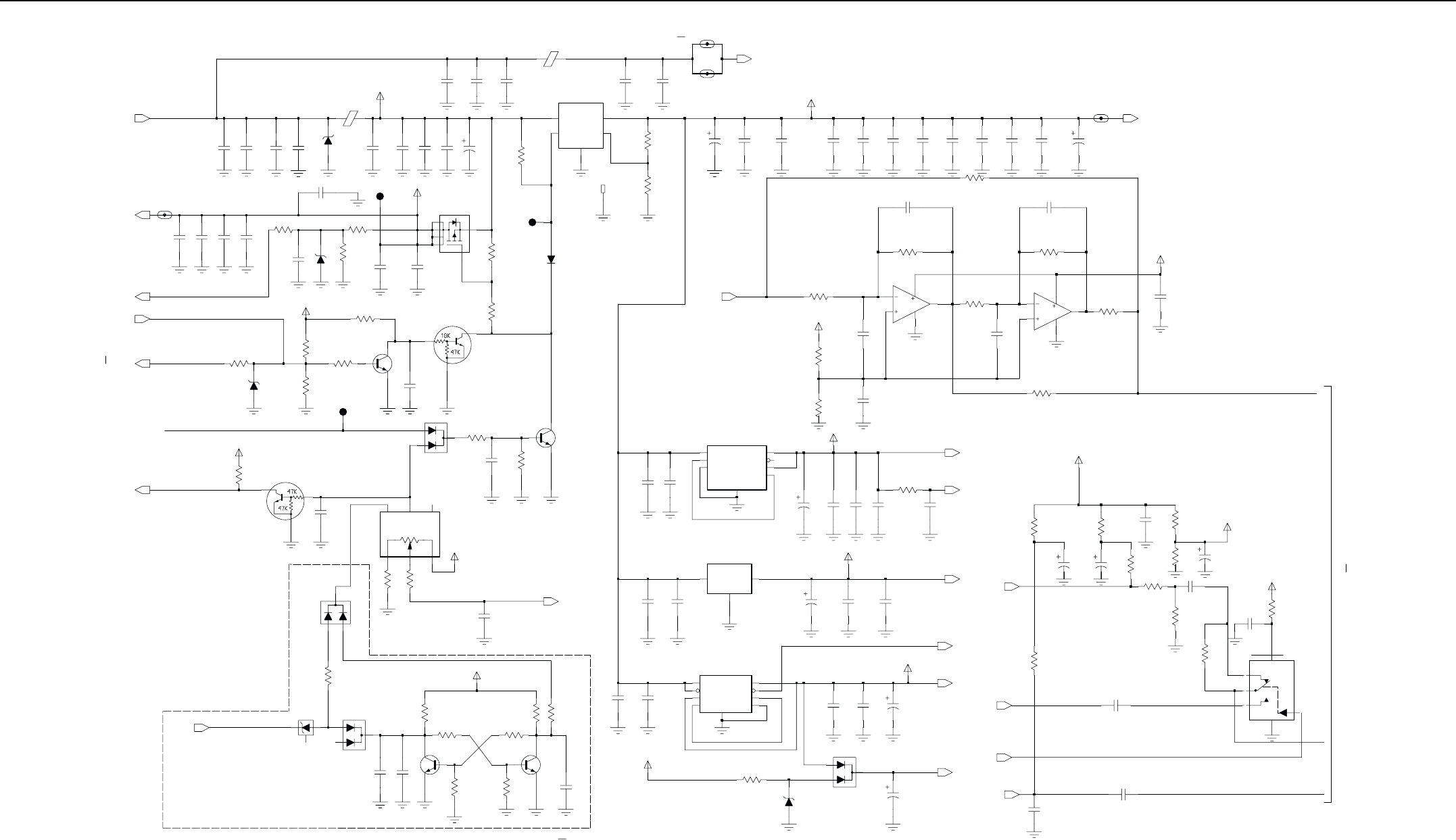
4-14 UHF2 1-25W PCB 8488978U01 (rev. D) / Schematics
9V
COMP_B+
B+
BATT_SENSE
DNP
VAG=4.5v
3.3V to IFIC, ASFIC
3.3V RF REGULATOR
3.3v digital
DNP
DNP
DNP
TO SHEET 2
DNP
DNP
DNP
DNP
DNP
DNP
DNP
1.n
220.p
C5113
100n
C5017
C5120
47u
C5066
120.p
VSTBY
VS_MIC
VS_AUDIO_SEL
5V_CH
DC_POWER_ON
10.0u
C5006
C5070
120.p
10.0u
C5008
C1034
150.K
R5020
R5053
L500
10.K
R5052
1.K
R5001
C1085
39.p
C5000
1n
HIGH
16
5
4
2
1.u
C5045
1019447
DNP
USE NLAS4599
On /Off for ATE
Come from Pin GCB2 of ASFIC
3.3v Digital REGULATOR
For mid_band
DNP DNP
Smart Fuse Circuit
SOURCE
Place near uP
Volume
Audio
Indirect
SOURCE
DNP
1%
5V TO LVFRACN
SOURCE
9.3V
5V RF Regulator
DNP
DNP
DNP
DNP
DNP
DNP
DNP
DNP
DNP
DNP IN MARLIN
DNP IN MARLIN+
SOURCE
DNP
1%
Spacer for TO-220
POWER SUPPLY 9.3V SOURCE
C1128
39.p
D3_3V
3V
5V
100n
C5018
R5077
M6
IF504
1
300.
120.p
C1113
39.p
C1097
39.p
C1088
IF502
1
39.p
C1114
C1098
IF503
1
120.p
1019447
L120
FILT_B+
22.n
C5085
120.p
C5083C5060
100.n
C5005
R5081
6.34K
100.u
33.K
R5038
1u
C5042
7
GND
4
INPUT
8OUTPUT 1
SENSE 2
SHUTDOWN
3
LP2951C
U503
5V_TAP 6
ERROR 5
FEEDBACK
510.
510.
R5076
R5075
100.
R5078
Q505
100n
2.2K
R5071
C5035
10.0u
D3_3V
10.0u
C5010
C5011
C5009
10.0u
100.
9
NC
OUTPUT5
SENSE
6SHUTDOWN
8
3TAP
R5079
LP2986ILDX
U510
7
ERROR
FEEDBACK2
1
GND
INPUT
4
FILT_SW_B+
Q506
S5010
50.K
SWITCH
LOW
3
100n
9V
C5015
C5016
100n
C5068
120.p
47u
C5007
120.p
C5065
C5064
C5069
120.p
120.p
FILT_B+
1.K
R5073
D500
D513
3V
NO
6
2
VPOS
C5102
100n
MAX4599EXT
U515
COM
5
3GND
IN 1
NC
4
D502
R5028
100.K
R5029
100.K
10.K
R5037
C5094
220.p
220.p
R5069
C5092
10.K
R5089 R5085
1.M1.M
R5082
51.K 270.K
R5083
TP556
1
TP500
TEST_POINT
1
TP555
TEST_POINT
1
TEST_POINT
0.
R5047
1.n
C5111
220.p
C5096C5095
220.p
C5074
9V
VAG
120.p
OUT 2
100n
C5047
U508
MC33269D
GND
1
IN
3
C5041
2.2u
C5043
0.
1u
R5084
C1127
100.u
C1125
39.p 39.p
C1123 C1124
39.p39.p
C1122
C1087
39.p
10.M
39.p
R5002
C5040
100.n
C5063
C5039
100.n
100.n
1.K
R5074
FILT_B+
R5096
100.n
C5103
100.K
R5095
200.K
R5094
1.M
R5093
220.K
R5092
100.K
R5099
100.K
U500
6
5
7
8
4
LM2904
U500
2
3
1
8
4
LM2904
C5104
5V
10.u
16.p
6.8p
C5115 C5117
100n
C5118
R5100
1.M
5V
0.
R5097
0.
R5098
1.u
C5114
C5116
220.p
47.K
R5035
C5110
D3_3V
Q504
5.1
VR501
100.n
C5038
100.K
R5039
FILT_B+
R5048
24.K
Q500
Q503
IF505
1
28.0
VR500
10.u
C5119
24.K
3.9
R5103
VR502
D501
3.3
VR504
Q502
3.3
VR503
R5050
13.K
D511
62.K
R5031
C5037
100.n
R5062
10.K
R5049
15.K
33.K
R5030
47.K
R5036
U514
C5062
0.
100.n
R5000
C5001
10.u
R5054
10.K
R5070
2.2K
120.p
C5071
100n
C5019
10.K
C1132
39.p
C1096
39.p
LM2941T
U501
1
ADJ
3GND
2ON_OFF
4VIN 5
VOUT
22.n
C5086
C5084
120.p100.n
C5061
1n
C5067
ONOFF_SENSE
EMERGENCY_SENSE
EMERGENCY_ACCES_CONN
RESET
IGNITION
FILT_SW_B+
DEMOD
VOL_INDIRECT EXTERNAL_MIC_AUDIO_ACCESS_CONN
MIC_AUDIO_CH
3V
D3_3V
5V
DNP
DNP
DNP
UHF2 (438-470MHz) DC and Audio Circuits (Sht 1 of 2)
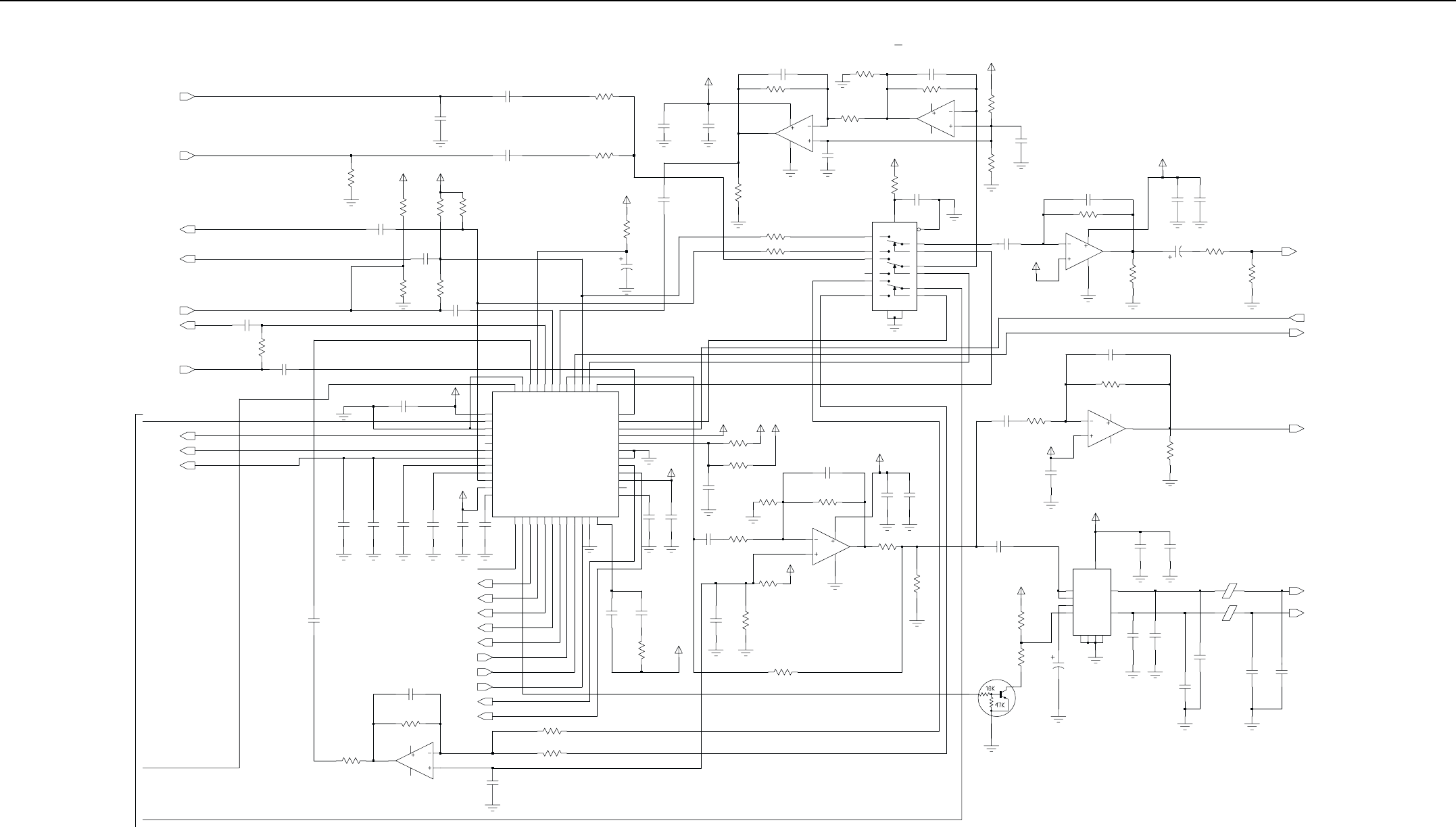
UHF2 1-25W PCB 8488978U01 (rev. D) / Schematics 4-15
C5023
100n
SPKR-
SPKR+
100n
C5034
R5016
1.M
12.K
24.K
100n
120.p
C5080
R5088
0.
200K
36K
1K
120P
TO SHEET 1
DNP
DNP
DNP
DNP
DNP
DNP
DNP
DNP
DNP
DNP
DNP
DNP
DNP
DNP
DNP
DNP
DNP
DNP
73D02968C74-O
SHEET 7 OF 8
C5002
Q501
LM2904 6
5
7
8
4
47u
LM2904
6
5
7
8
4
U506
1
8
4
U505
LM2904
2
3
1
8
4
U505
LM2904
U506
2
3
C5054
100n
C5053
100n
C5052
30.K
R5040
100n
C5051
100n R5042
100n
C5025
3V
C5024
82.p
100.K
C5089
R5022
10.K
R5058
C5003
47u
R5009
0.
R5025
U507
LM2904 6
5
7
8
4
100.K
100n
C5032
100n
C5031
24.K
R5046
3
1
8
4
33.K
R5045
LM2904
U507
2
C5030
100n
100n
C5057
C5050
100n
R5034
47.K
R5032
C5088
82.p
R5021
9V
9V
VAG
VAG
100.K
R5065
6.2K
R5014
0.
R5013
0.
C5036
270.K
R5027
3V
100.n 10.K
R5061
10.K
33.K
R5060
R5026
4.7K
R5072
2.2u
C5014
R5044
24.K
R5043
3V
24.K
1.u
8.2K
R5063
C5055
R5023
100.K
3V
3V
C5027
100n
10.K
R5057
R5056
10.K
R5059
C5058
100n
100.K
10.K
R5087
560.
R5086
1.n
C5101
220.p220.p
C5100
220.p
C5098
C5099
C5097
220.p
C5091
82.p
C5082
120.p
C5081
120.p
3V
R5008
0.
C5044
1u
3V
3V
3V
100n
C5029
C5028
100n
1019447
L502
B+
3V
OUT2
3RR
7
VCC
1019447
L501
2
5GND2
10 GND3
11 GND4
9INV
8M_SS
1NINV
4
OUT1
6
TDA1519C
U502
GND1
100.K
C5056
R5024
FILT_SW_B+
1.u
8.2K
R5064
R5080
10.
120.p
C5073
120.p
C5072
R5033
47.K
C5026
100n
100.n
C5021
R5041
24.K
R5051
3V 5V
3V
0.
R5011
R5010
0. 1n
100n
C5075
9V
C5033
100n
C5048
C5020
Y15
2Y0
Y1
1
4
Z
Z0
5
3Z1
100n
B
C9
6
EN
GND
8VCC 16
7VEE
X14
X0
12
X1
13
MC14053B
U509
11
A
10
C5059
22n
C5046
100n
VDDA
1
VDDCP 32
VDDD 33
VDDDAC
11
VDDRC 45
VDDSYN 27
7VOX
RXSND 39
SQCAP
12
SQDET
17
SQIN
9SYN 28
TXRTN 36
44
TXSND
UIO
10
LSIO
18
MICEXT 48
MICINT 46
MOD 40
NC 26
PLCAP
8
PLCAP2 25
RXRTN 43
GCB5 38
GNDA
3
GNDD 31
GNDDO 30
GNDRC 47
GNDSYN
23
19 HSIO
LCAP
24
DATA
22
DISC
2
F1200 29
GCB0
15
14 GCB1
GCB2
13
35
GCB3
GCB4 37
AUXTN 42
CHACT
16
21 CLK
CLK168 34
20 CSX
DACG
6DACR
5DACU
4
U504
41
AUDIO
C5087
30C53
C5049
100n
10.K
R5055
R5019
C5013
1u
C5022
100n
C5012
4.7u
R5066
6.2K
R5067
R5068
6.2K
82.p
C5090
120.p
C5076
120.p
C5077
C5078
1.n
C5079
120.p
POST_LIMITER_FLAT_TX_AUDIO_RETURN_OPT_BRD
TX_AUDIO_RETURN_OPT_BRD
RX_AUDIO_OUTPUT_ACCESS_CONN
TX_AUDIO_SEND_OPT_BRD
FLAT_TX_AUDIO_INPUT_ACCESS_CONN
RX_AUDIO_RETURN_OPT_BRD
UNMUTED_RX_AUDIO_SEND_OPT_BRD
DETECTOR_AUDIO_SEND_OPT_BRD
CH_ACT
SPI_CLK
16.8MHz
ASFIC_CS
PWR_SET
PA_BIAS
SPI_MOSI
F1200
BW_SEL
AUDIO_PA_EN
DC_POWER_ON
FLAT_OR_DEEMPH_RX_AUD_SEL
FLAT_TX_AUDIO_MUTE
HSIO
LSIO
MOD_OU
T
SQ_DET
uP_CLK
VOX
HANDSET_RX_AUDIO_CH
UHF2 (438-470MHz) DC and Audio Circuits (Sht 2 of 2
)
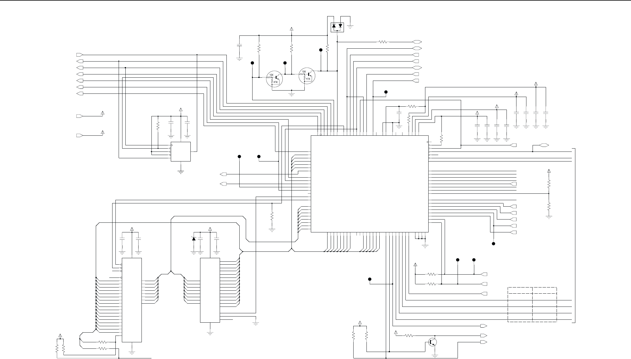
4-16 UHF2 1-25W PCB 8488978U01 (rev. D) / Schematics
DNP
TO SHEET 2
SPI_CLK
SPI_MOSI
SPI_MISO
PLACE NEAR U402
DNP
DNP
PROVIDE WIRED OR OPERATION ON CSPROG
DO NOT CONNECT THIS CS IN ORDER TO
DNP
SPI_CLK
SPI_MOSI
SPI_CLK
uP_CLK
OPT_DATA_R_OPBD
LSIO
F1200
HSIO
SQ_DET
CH_ACT
A(9)
A(10)
A(11)
A(12)
A(13)
A(8)
D(0)
D(1)
D(2)
D(3)
D(4)
D(5)
D(6)
D(7)
SPI_MISO
SPI_MOSI
D3_3V
D3_3V
ASFIC_CS
EE_CS
SYNTH_CS
DISPLAY_CS_CH
SHIFT_R_CS
MARLIN MARLIN+
PROG_OUT-ALARM_4 VS_INT
PROG_IO-P8_O VS_CS
PROG_IO-P12_O
DNP
DNP
SHIFT_REGN_CS
PROG_IO-P14_O VS_RAC
R473
100.K
100.K
R472
100n
C400
120.p
C401
10.K
R438
19
OE 22
VDD
28
VSS
14
WE 27
D3_3V
D3_3V
D3_3V
20
D1
11
D2
12
D3
13
D4
15
D5
16
D6
17
D7
18
D8
8
A3 7
A4 6
A5 5
A6 4
A7 3
A8 25
A9 24
CS
A0 10
A1 9
A10 21
A11 23
A12 2
A13 26
A14 1
A2
U402
SRM2B256
1CS
7HOLD
6SCK
5SI
2
SO
8
VCC
4
VSS
WP
3
U400
X25128-2.7
VRH 68
VRL
13 VSS
40 VSSL
87 VSSR
XFC 93
48
XIRQ
91
XTAL
PJ5 77
PJ6 78
PJ7
94
RESET
12
VDD
39
VDDL 88
VDDR
92
VDDSYN
69
PI5
50 PI6
49 PI7
71
PJ0_CSGP3 72
PJ1_CSGP4 73
PJ2 74
PJ3 75
PJ4 76
PH5_CSGP1
41 PH6_CSGP2
38 PH7_CSPROG
56 PI0
55 PI1
54 PI2
53 PI3
52 PI4
51
PG5_XA18
5PG6_AS
4
PG7_R_W
47 PH0_PW1
46 PH1_PW2
45 PH2_PW3
44 PH3_PW4
43 PH4_CSIO
42
PF6_ADDR6
22 PF7_ADDR7
29 PFO_ADDR0
6PG0_XA13
16 PG1_XA14
20 PG2_XA15
19 PG3_XA16
17 PG4_XA17
18
62
PE6_AN6 61
PE7_AN7 60
28 PF1_ADDR1
27 PF2_ADDR2
26 PF3_ADDR3
25 PF4_ADDR4
24 PF5_ADDR5
23
PD4_SCK 2
PD5_SS
PD6_LVIN 3
PE0_AN0 67
PE1_AN1 66
PE2_AN2 65
PE3_AN3 64
PE4_AN4 63
PE5_AN5
PC4_DATA4
35 PC5_DATA5
36 PC6_DATA6
37 PC7_DATA7
97
PD0_RXD 98
PD1_TXD 99
PD2_MISO 100
PD3_MOSI 1
PB5_ADDR13
8PB6_ADDR14
7PB7_ADDR15
14 PBO_ADDR8
30 PC0_DATA0
31 PC1_DATA1
32 PC2_DATA2
33 PC3_DATA3
34
PA4_OC4_OC1 84
PA5_OC3_OC1 85
PA6_OC2_OC1 86
PA7_PA1_OC1
10 PB1_ADDR9
11 PB2_ADDR10
9PB3_ADDR11
21 PB4_ADDR12
15
IRQ
LVOUT 95
58
MODA_LIR 57
MODB_VSTBY
79
PA0_IC3 80
PA1_IC2 81
PA2_IC1 82
PA3_IC4_OC5_OC1 83
U403
MC68HC11FL0
59
AVDD
70 AVSS
89
ECLK
90
EXTAL
96
C413
120.p
C405
100n
100.K
R425
C404
100n
120.p 100n
C412
D3_3V
C403
120.p
C411 C402
10.K
R439
100n
D3_3V
R462
51.
D400
R424
100.K
100.K
R423
R415 0.
R414 0.
FILT_SW_B+
120.p
D3_3V
C408
100n
C416
D3_3V
120.p
C415
100n
C407
120.p
C414
100n
C406
R463
D3_3V
10.K Q417
C410
100n 10.K
R451 R450
10.K
Q400
Q407
4.3
VR401
I_O6 28
29
I_O7
RESET
9
VCC
8
EN_WE
7
GND
24
I_O0 21
I_O1 22
I_O2 23
I_O3 25
I_O4 26
I_O5 27
A4
16
A5
15
A6
14
A7
13
A8
3
A9
2
EN_CE
30
EN_OE
32
A12
12
A13
4
A14
5
A15
11
A16
10
6A17
A2
18
A3
17
AT49LV002N_70VI
U404
A0
20
A1
19
A10
31
A11
1
3.3K
R443
D3_3V
100.K
D3_3V
R428
R427
100.K 100.K
R426
1
R471
10.
1
TEST_POINT
TP410
1
TEST_POINT
TP403
TEST_POINT
TP404
1
TP406
TEST_POINT
1
TP425
TEST_POINT
1
D3_3V
1
TP401
TEST_POINT
1
TEST_POINT
TP407
D3_3V
TEST_POINT
TP402
R442
10.K
10.K
R441
TP400
TEST_POINT
1
D(5)
D(6)
D(7)
A18_RES
A(0:18)
D(0:7)
RESET
TEST_POINT
TP409
1
A(12)
A(13)
A(14)
A(15)
A(16)
A(2)
A(3)
A(4)
A(5)
A(6)
A(7)
A(8)
A(9)
R_W
D(0)
D(1)
D(2)
D(3)
D(4)
SCI_CH
FILT_SW_B+
TX_EN
A(17)
A18_RES
A(18)
A(0)
A(1)
A(10)
A(11)
A(5)
A(6)
A(7)
A(8)
A(9)
D(0)
D(1)
D(2)
D(3)
D(4)
D(5)
D(6)
D(7)
R_W
D3_3V
MIC_PTT
ACCESS_PTT
PROG_IN-P6_I
PROG_IO-P8_I
ONOFF_SENSE
PROG_IO-P12_I
PROG_IO-P14_I
A(0)
A(1)
A(10)
A(11)
A(12)
A(13)
A(14)
A(2)
A(3)
A(4)
ASFIC_CS
MIC_SENSE
VOL_INDIRECT
BATT_SENSE
EMERGENCY_SENSE
RSSI
VOX
KEYPAD_COL_CH
KEYPAD_ROW_CH
A(1)
A(2)
A(3)
A(4)
A(5)
A(6)
A(7)
A(0)
SHIFT_R_CS
A(14)
A(15)
A(16)
A(17)
A(18)
COMM_DATA_SEL_CH
R_W
SYNTH_CS
LOC_DIST
DISPLAY_CS_CH
SYNTH_LOCK
OPT_EN_OPBD
RX_EN
UHF2 (438-470MHz) Microprocessor and Controller Circuits (Sht 1 of 2)
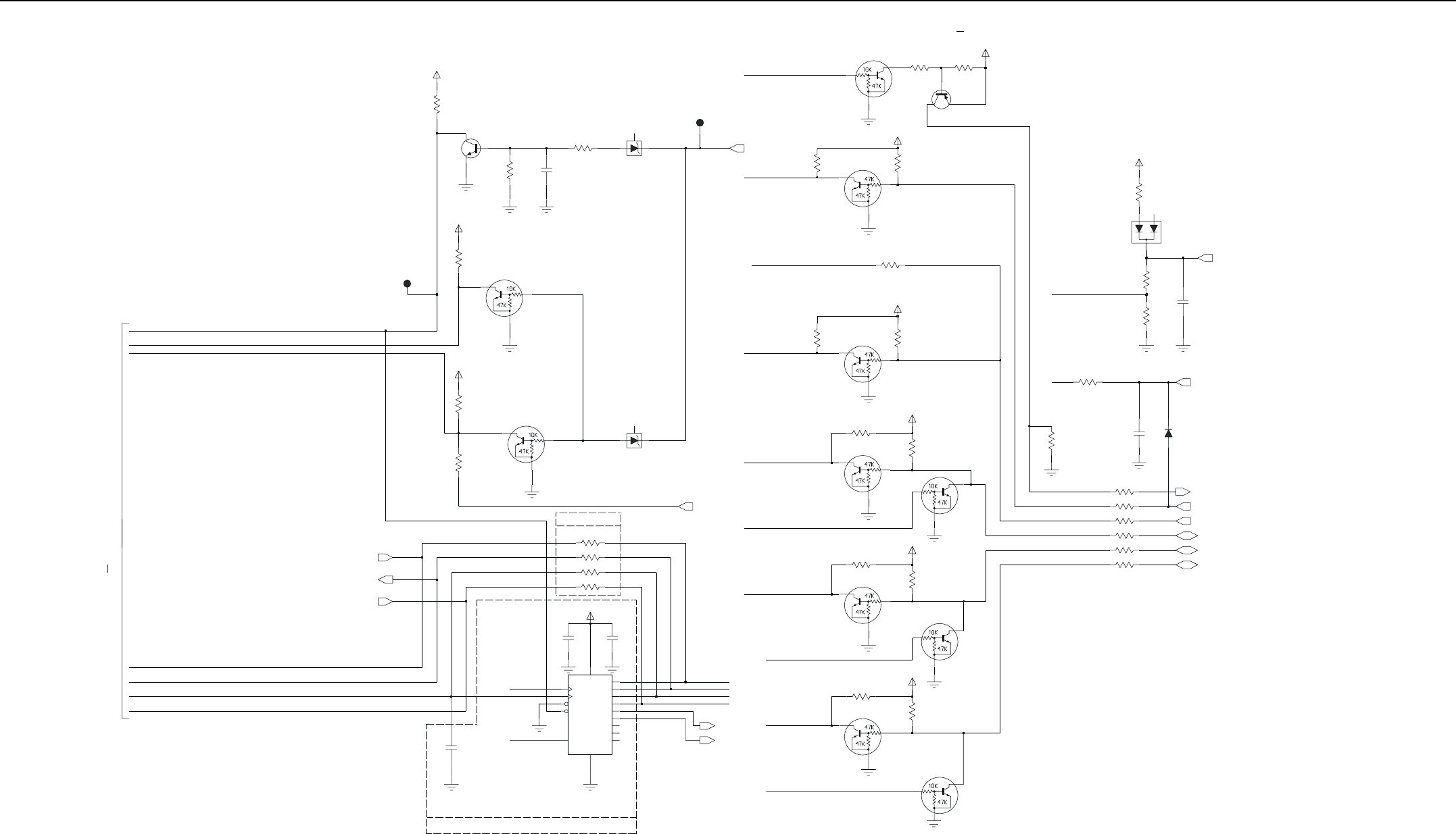
UHF2 1-25W PCB 8488978U01 (rev. D) / Schematics 4-17
D3_3V
DNP
DNP
SHEET 8 OF 8
73D02968C74-O
DNP
R458
3.3K
VR400
VSTBY
C417
120.p
VR402
3.30
R402 0.
Q401
DNP
DNP
DNP IN MARLIN
TO SHEET 1
DNP IN MARLIN+ PROG_IN
PROG_I/O
PROG_I/O
PROG_I/O
EXT_ALARM_OUT
EXT_MIC_PTT
22.n
C421
120.p
C423
100n
C422
D3_3V
TEST_POINT
TP408
1
R470
10.K
TP405
TEST_POINT
1
47.K
R459
0.
R407
R406 0.
R436
33.K R457
3.3K
14 SERIN 9
SEROUT
16
VCC
D3_3V
1
Q1 2
Q2 3
Q3 4
Q4 5
Q5 6
Q6 7
Q7
10 RESET
MC74HC595A
U405
12 CLK_L
11 CLK_S
13 EN_OE
8
GND
15
Q0
0.
R469
0.
0.
R467
R468
R466 0.
D3_3V
C490
1.u
10.K
R422
R431
10.K
R430
39.K
R429
100.K
D401
220.
R421
R461
220.
120.p
C418
D3_3V
6.80
10.K
R445
10.K
R444
Q415
D3_3V
Q414
Q413
D402
Q405
Q404
Q416
Q403 2.7K
R401 R460
1.5K
FILT_SW_B+
10.K
R440
Q412
R405 0.
33.K
R435 R456
D3_3V
3.3KQ411
33.K
D3_3V
R434
3.3K
R455
Q410
R404 0.
D3_3V
0.
R403
R433
R454
3.3K
33.K
Q409
D3_3V
3.3K
33.K
R432
R453
Q408
PROG_OUT-ALARM_4
HOOK_CH
MIC_PTT_CH
BOOT_EN_IN_CH
MIC_PTT
MIC_SENSE
SCI_CH
PROG_OUT-ALARM_4
PROG_IO-P8_O
PROG_IO-P12_O
PROG_IO-P14_O
SPI_CLK
VS_AUDIO_SEL
VS_GAIN_SEL
SPI_MOSI
PROG_I-ACC_C_3
PROG_O-ACC_C_4
PROG_I-ACC_C_6
PROG_IO-ACC_C_8
PROG_IO-ACC_C_12
PROG_IO-ACC_C_14
PROG_IO-P14_I
PROG_IO-P14_O
PROG_IO-P12_I
PROG_IO-P12_O
PROG_IO-P8_I
PROG_IO-P8_O
PROG_IN-P6_I
ACCESS_PTT
VS_INT
VS_CS
VS_RAC
UHF2 (438-470MHz) Microprocessor and Controller Circuits (Sht 2 of 2)
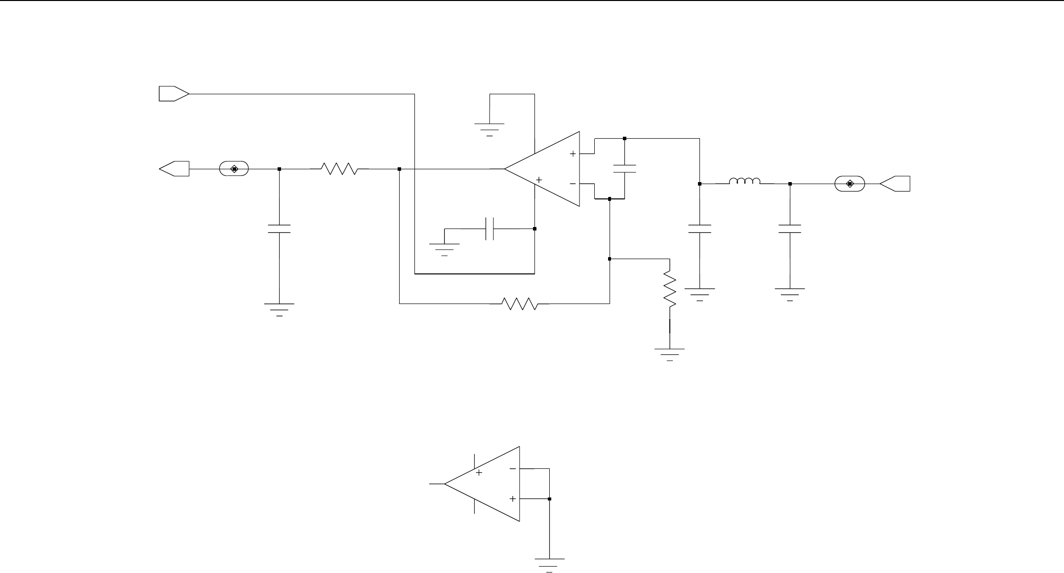
4-18 UHF2 1-25W PCB 8488978U01 (rev. D) / Schematics
LM2904
U100
6
5
IF701
1
7
8
4
SHEET 3 OF 8
73D02968C74-O
IF700
1
39.p
C1082
39.p
C1075
U100
LM2904
2
3
1
8
4
C1071
120.p
15K
R117
22.K
R141
R140
27.K
C1046
120.p
120.p
C1045
DET_VFWD
INTEGRATOR
FILT_SW_B+
L101
1.u
UHF2 (438-470MHz) Power Control Circuit
UHF2 1-25W PCB 8488978U01 (rev. D) / Schematics 4-19
2.1 UHF2 PCB 8488978U01 (rev. D) Parts List
1-25W
Circuit
Ref.
Motorola
Part No. Description
C1000 2113740F53 CAP CHIP REEL CL1 +/-30 120
C1001 2311049A08 KEMET CAPS
C1002 2111078B42 CAP CHIP RF 100 5 NPO 100V
C1004 2111078B25 CAP ALT E32
C1005 2111078B31 CHIP CAP 36PF +- 5%
C1006 2111078B27 CAP CHIP RF 30 5 NPO 100V
C1007 NOT PLACED GCAM DUMMY PART NUMBER
C1008 2111078B15 CAP CHIP RF 12 5 NPO 100V
C1009 NOT PLACED GCAM DUMMY PART NUMBER
C1010 2111078B27 CAP CHIP RF 30 5 NPO 100V
C1011 2111078B32 CAP ALT E12
C1012 2111078B12 CAP CHIP RF 9.1 .5 NPO 100V
C1013 NOT PLACED GCAM DUMMY PART NUMBER
C1014 2111078B38 CAP CHIP RF 68 5 NPO 100V
C1016 2111078B09 CAP ALT E17
C1020 2111078B01 CAP CHIP RF 3.3 .25 NPO 100V
C1021 2111078B12 CAP CHIP RF 9.1 .5 NPO 100V
C1023 2111078B12 CAP CHIP RF 9.1 .5 NPO 100V
C1026 2111078B08 CAP CHIP RF 6.2 .25NPO 100V
C1027 2311049A45 CAP TANT CHIP 10 10 35
C1028 2113743K15 CER CHIP CAP .100UF
C1029 2113743K15 CER CHIP CAP .100UF
C1031 2113741F37 CAP CHIP CL2 X7R REEL 3300
C1032 2113743E07 CER CHIP CAP .022UF
C1033 2113741F49 CAP CHIP CL2 X7R REEL 10000
C1034 2113740F41 CAP CHIP REEL CL1 +/-30 39
C1035 2113740F53 CAP CHIP REEL CL1 +/-30 120
C1036 2113743E07 CER CHIP CAP .022UF
C1037 2113743E07 CER CHIP CAP .022UF
C1038 NOT PLACED GCAM DUMMY PART NUMBER
C1039 2113743E07 CER CHIP CAP .022UF
C1040 2113741F25 CAP CHIP CL2 X7R REEL 1000
C1041 2113740F67 CAP CHIP CL1 +/-30 470 5%
C1042 2113740F53 CAP CHIP REEL CL1 +/-30 120
C1043 2113740F53 CAP CHIP REEL CL1 +/-30 120
C1044 2113740F53 CAP CHIP REEL CL1 +/-30 120
C1045 2113740F53 CAP CHIP REEL CL1 +/-30 120
C1046 2113740F53 CAP CHIP REEL CL1 +/-30 120
C1047 2113743E20 CAP CHIP. 10 UF 10%
C1050 2113740F53 CAP CHIP REEL CL1 +/-30 120
C1051 2113740F53 CAP CHIP REEL CL1 +/-30 120
C1052 2113740F53 CAP CHIP REEL CL1 +/-30 120
C1053 2113740F57 CAP CHIP REEL CL1 +/-30 180
C1054 2113740F53 CAP CHIP REEL CL1 +/-30 120
C1057 2113740F53 CAP CHIP REEL CL1 +/-30 120
C1059 2113740F53 CAP CHIP REEL CL1 +/-30 120
C1060 NOT PLACED GCAM DUMMY PART NUMBER
C1061 NOT PLACED GCAM DUMMY PART NUMBER
C1062 2113740F53 CAP CHIP REEL CL1 +/-30 120
C1063 2113740F53 CAP CHIP REEL CL1 +/-30 120
C1064 2113740F53 CAP CHIP REEL CL1 +/-30 120
C1065 2113740F53 CAP CHIP REEL CL1 +/-30 120
C1066 2113740F53 CAP CHIP REEL CL1 +/-30 120
C1067 2113740F53 CAP CHIP REEL CL1 +/-30 120
C1070 2113740F53 CAP CHIP REEL CL1 +/-30 120
C1071 2113740F53 CAP CHIP REEL CL1 +/-30 120
C1072 2113740F53 CAP CHIP REEL CL1 +/-30 120
C1073 2113740F53 CAP CHIP REEL CL1 +/-30 120
C1074 2113740F53 CAP CHIP REEL CL1 +/-30 120
C1075 2113740F41 CAP CHIP REEL CL1 +/-30 39
C1076 2113740F30 CAP CHIP REEL CL1+/-30 13
Circuit
Ref.
Motorola
Part No. Description
C1077 2113740F41 CAP CHIP REEL CL1 +/-30 39
C1078 2113740F41 CAP CHIP REEL CL1 +/-30 39
C1079 2113740F53 CAP CHIP REEL CL1 +/-30 120
C1080 2113740F41 CAP CHIP REEL CL1 +/-30 39
C1081 NOT PLACED GCAM DUMMY PART NUMBER
C1082 NOT PLACED GCAM DUMMY PART NUMBER
C1083 2113740F41 CAP CHIP REEL CL1 +/-30 39
C1084 2113740F41 CAP CHIP REEL CL1 +/-30 39
C1085 2113740F41 CAP CHIP REEL CL1 +/-30 39
C1086 2113740F41 CAP CHIP REEL CL1 +/-30 39
C1087 2113740F41 CAP CHIP REEL CL1 +/-30 39
C1088 2113740F41 CAP CHIP REEL CL1 +/-30 39
C1089 2113740F53 CAP CHIP REEL CL1 +/-30 120
C1090 NOT PLACED GCAM DUMMY PART NUMBER
C1091 NOT PLACED GCAM DUMMY PART NUMBER
C1092 NOT PLACED GCAM DUMMY PART NUMBER
C1093 NOT PLACED GCAM DUMMY PART NUMBER
C1096 2113740F41 CAP CHIP REEL CL1 +/-30 39
C1097 2113740F41 CAP CHIP REEL CL1 +/-30 39
C1098 2113740F53 CAP CHIP REEL CL1 +/-30 120
C1099 2113740F53 CAP CHIP REEL CL1 +/-30 120
C1100 2113740F53 CAP CHIP REEL CL1 +/-30 120
C1101 2113740F34 CAP CHIP REEL CL1 +/-30 20
C1103 2113741A57 CAP CHIP 33K +-5%
(2160521A31)
C1104 2113928A02 CAP CERAMIC CHIP .47UF
C1106 2113740F41 CAP CHIP REEL CL1 +/-30 39
C1107 2113740F53 CAP CHIP REEL CL1 +/-30 120
C1108 2113740F43 CAP CHIP REEL CL1 +/-30 47
C1109 2113740F41 CAP CHIP REEL CL1 +/-30 39
C1110 2113740F41 CAP CHIP REEL CL1 +/-30 39
C1111 2113740F41 CAP CHIP REEL CL1 +/-30 39
Circuit
Ref.
Motorola
Part No. Description
C1112 2113740F41 CAP CHIP REEL CL1 +/-30 39
C1113 2113740F53 CAP CHIP REEL CL1 +/-30 120
C1114 2113740F41 CAP CHIP REEL CL1 +/-30 39
C1115 2113740F41 CAP CHIP REEL CL1 +/-30 39
C1116 2113740F41 CAP CHIP REEL CL1 +/-30 39
C1117 2113741F25 CAP CHIP CL2 X7R REEL 1000
C1118 2113740F23 CAP CHIP REEL CL1 +/-30 6.8
C1119 2113740F53 CAP CHIP REEL CL1 +/-30 120
C1121 2113740F21 CAP CHIP REEL CL1+/-30 5.6
C1122 2113740F41 CAP CHIP REEL CL1 +/-30 39
C1123 2113740F41 CAP CHIP REEL CL1 +/-30 39
C1124 2113740F41 CAP CHIP REEL CL1 +/-30 39
C1125 2113740F41 CAP CHIP REEL CL1 +/-30 39
C1126 2113740F53 CAP CHIP REEL CL1 +/-30 120
C1127 2360567A03 CAP TANTALUM
C1128 2113740F41 CAP CHIP REEL CL1 +/-30 39
C1129 2113740F41 CAP CHIP REEL CL1 +/-30 39
C1130 2113740F41 CAP CHIP REEL CL1 +/-30 39
C1131 NOT PLACED GCAM DUMMY PART NUMBER
C1132 2113740F41 CAP CHIP REEL CL1 +/-30 39
C1151 NOT PLACED GCAM DUMMY PART NUMBER
C1152 NOT PLACED GCAM DUMMY PART NUMBER
C1153 2113740F28 CAP CHIP REEL CL1 +/-30 11
C1154 2113740F33 CAP CHIP REEL CL1 +/-30 18
C1155 NOT PLACED GCAM DUMMY PART NUMBER
C1156 2111078B23 CAP ALT E37
C1260 2113741F49 CAP CHIP CL2 X7R REEL 10000
C1261 2113740F53 CAP CHIP REEL CL1 +/-30 120
C1263 2113741F25 CAP CHIP CL2 X7R REEL 1000
C1264 2113743K15 CER CHIP CAP .100UF
C2000 2113743F18 CAP CHIP 2.2 UF 16V +80-20%
C2001 2311049J11 CAPACITOR TANT 10% 4.7UF
Circuit
Ref.
Motorola
Part No. Description
4-20 UHF2 1-25W PCB 8488978U01 (rev. D) / Schematics
C2002 2311049A72 CAP TANT CHIP 10.0UF 10%
10V
C2003 2113743K15 CER CHIP CAP .100UF
C2004 2113743F18 CAP CHIP 2.2 UF 16V +80-20%
C2005 2113743F18 CAP CHIP 2.2 UF 16V +80-20%
C2006 2113743F18 CAP CHIP 2.2 UF 16V +80-20%
C2007 2113743E20 CAP CHIP. 10 UF 10%
C2008 2113743E20 CAP CHIP. 10 UF 10%
C2009 2113743E20 CAP CHIP. 10 UF 10%
C2010 2113743E20 CAP CHIP. 10 UF 10%
C2011 2113743E20 CAP CHIP. 10 UF 10%
C2012 NOT PLACED GCAM DUMMY PART NUMBER
C2013 2113743E20 CAP CHIP. 10 UF 10%
C2014 2113743E20 CAP CHIP. 10 UF 10%
C2015 2113743E20 CAP CHIP. 10 UF 10%
C2016 2113743E20 CAP CHIP. 10 UF 10%
C2017 2113743E20 CAP CHIP. 10 UF 10%
C2018 2113740F53 CAP CHIP REEL CL1 +/-30 120
C2019 2113740F53 CAP CHIP REEL CL1 +/-30 120
C2020 2113743E20 CAP CHIP. 10 UF 10%
C2021 2113741F25 CAP CHIP CL2 X7R REEL 1000
C2022 2113741F49 CAP CHIP CL2 X7R REEL 10000
C2023 2113741F49 CAP CHIP CL2 X7R REEL 10000
C2024 2113741F49 CAP CHIP CL2 X7R REEL 10000
C2025 2113741F49 CAP CHIP CL2 X7R REEL 10000
C2026 2113741F49 CAP CHIP CL2 X7R REEL 10000
C2027 2113741F49 CAP CHIP CL2 X7R REEL 10000
C2028 2113741F33 CAP CHIP CL2 X7R REEL 2200
C2029 2113740F53 CAP CHIP REEL CL1 +/-30 120
C2030 2113741F39 CAP CHIP CL2 XTR REEL 3900
C2031 NOT PLACED GCAM DUMMY PART NUMBER
C2032 2113740F53 CAP CHIP REEL CL1 +/-30 120
Circuit
Ref.
Motorola
Part No. Description
C2033 2113740F53 CAP CHIP REEL CL1 +/-30 120
C2034 2113740F53 CAP CHIP REEL CL1 +/-30 120
C2035 2113740F53 CAP CHIP REEL CL1 +/-30 120
C2036 2113740F53 CAP CHIP REEL CL1 +/-30 120
C2037 2113740F53 CAP CHIP REEL CL1 +/-30 120
C2038 2113740F53 CAP CHIP REEL CL1 +/-30 120
C2039 2113740F53 CAP CHIP REEL CL1 +/-30 120
C2040 2113740F53 CAP CHIP REEL CL1 +/-30 120
C2041 2113740F53 CAP CHIP REEL CL1 +/-30 120
C2042 2113740F53 CAP CHIP REEL CL1 +/-30 120
C2043 2113740L14 CAP CER CHIP 6.8PF +-0.1PF
C2044 NOT PLACED GCAM DUMMY PART NUMBER
C2045 2113740F53 CAP CHIP REEL CL1 +/-30 120
C2046 2113740F53 CAP CHIP REEL CL1 +/-30 120
C2047 2113740F53 CAP CHIP REEL CL1 +/-30 120
C2048 2113740F53 CAP CHIP REEL CL1 +/-30 120
C2049 NOT PLACED GCAM DUMMY PART NUMBER
C2050 2113740F53 CAP CHIP REEL CL1 +/-30 120
C2051 2113740F59 CAP CHIP REEL CL1 +/-30 220
C2052 2113740F53 CAP CHIP REEL CL1 +/-30 120
C2053 NOT PLACED GCAM DUMMY PART NUMBER
C2054 2113740L37 CAP 62.0 PF 50V 2.0%
C2055 2113740F35 CAP CHIP REEL CL1 +/-30 22
C2056 2113740F20 CAP CHIP REEL CL1 +/-30 5.1
C2057 2113740F20 CAP CHIP REEL CL1 +/-30 5.1
C2058 2113740F20 CAP CHIP REEL CL1 +/-30 5.1
C2059 2113740F20 CAP CHIP REEL CL1 +/-30 5.1
C2060 2113740F31 CAP CHIP REEL CL1 +/-30 15
C2061 2113740F29 CAP CHIP REEL CL1 +/-30 12
C2062 2113740F29 CAP CHIP REEL CL1 +/-30 12
C2063 2113740L16 CAP CER CHIP 8.2 PF+-0.1PF
C2064 2113740L13 CAP CER CHIP 6.2 PF+-0.1PF
Circuit
Ref.
Motorola
Part No. Description
C2065 2113740F53 CAP CHIP REEL CL1 +/-30 120
C2066 2113740L03 CAP CER CHIP 2.4PF +-0.1PF
C2067 2113740F20 CAP CHIP REEL CL1 +/-30 5.1
C2068 2113740F20 CAP CHIP REEL CL1 +/-30 5.1
C2069 2113740F05 CAP CHIP REEL CL1 +/-30 1.2
C2070 2113740L13 CAP CER CHIP 6.2 PF+-0.1PF
C2071 2113740L13 CAP CER CHIP 6.2 PF+-0.1PF
C2072 2113740L04 CAP CER CHIP 2.7 PF +-0.1PF
C2073 2113740F03 CAP CHIP REEL CL1 +/-30 1.0
C2074 2109720D14 CAP CER CHIP LOW DIST
0.1UF
C2075 2109720D14 CAP CER CHIP LOW DIST
0.1UF
C2076 NOT PLACED GCAM DUMMY PART NUMBER
C2077 2109720D14 CAP CER CHIP LOW DIST
0.1UF
C2078 2109720D14 CAP CER CHIP LOW DIST
0.1UF
C2079 2109720D14 CAP CER CHIP LOW DIST
0.1UF
C2080 2109720D14 CAP CER CHIP LOW DIST
0.1UF
C2081 2113740F53 CAP CHIP REEL CL1 +/-30 120
C2129 2113740F53 CAP CHIP REEL CL1 +/-30 120
C2198 2113741F25 CAP CHIP CL2 X7R REEL 1000
C300 NOT PLACED GCAM DUMMY PART NUMBER
C301 2311049A57 CAP TANT CHIP A/P 10UF 10%
16V
C302 2113740F54 CAP CHIP REEL CL1+/-30 130
C303 2113743K15 CER CHIP CAP .100UF
C304 2113743E20 CAP CHIP. 10 UF 10%
C305 2113743E20 CAP CHIP. 10 UF 10%
C306 2113743E20 CAP CHIP. 10 UF 10%
C307 2113743E20 CAP CHIP. 10 UF 10%
Circuit
Ref.
Motorola
Part No. Description
C308 2113743E20 CAP CHIP. 10 UF 10%
C309 2113743E20 CAP CHIP. 10 UF 10%
C310 2113743E20 CAP CHIP. 10 UF 10%
C311 2113743E20 CAP CHIP. 10 UF 10%
C312 2113743E20 CAP CHIP. 10 UF 10%
C313 2113743E20 CAP CHIP. 10 UF 10%
C314 2113743E20 CAP CHIP. 10 UF 10%
C315 2113743E20 CAP CHIP. 10 UF 10%
C316 2113743E20 CAP CHIP. 10 UF 10%
C317 2113743E20 CAP CHIP. 10 UF 10%
C318 2113743E20 CAP CHIP. 10 UF 10%
C319 2113743E20 CAP CHIP. 10 UF 10%
C320 2113743E20 CAP CHIP. 10 UF 10%
C321 2113740F53 CAP CHIP REEL CL1 +/-30 120
C322 2113741F41 CAP CHIP CL2 X7R REEL 4700
C323 2113741F25 CAP CHIP CL2 X7R REEL 1000
C324 2113740F53 CAP CHIP REEL CL1 +/-30 120
C325 2113740F53 CAP CHIP REEL CL1 +/-30 120
C326 2113743E07 CER CHIP CAP .022UF
C327 2113741F13 CAP CHIP CL2 X7R REEL 330
C328 2113740F42 CAP CHIP REEL CL1 +/-30 43
C329 2113740L31 CAP 36.0 PF 50V 2.0 %
C330 2113740L18 CAP CER CHIP 10.0 PF +/-.25PF
C331 2113740L18 CAP CER CHIP 10.0 PF +/-.25PF
C332 2113740L18 CAP CER CHIP 10.0 PF +/-.25PF
C333 2113740L20 CAP 12.0 PF 50V 2.0 %
C334 2113740L25 CAP CER CHIP 20.0 PF +/-.25PF
C335 2113740L18 CAP CER CHIP 10.0 PF +/-.25PF
C336 2113740L17 CAP CER CHIP 9.1 PF+-0.1PF
C337 2113740L14 CAP CER CHIP 6.8PF +-0.1PF
C338 2113740L18 CAP CER CHIP 10.0 PF +/-.25PF
C339 2113740L03 CAP CER CHIP 2.4PF +-0.1PF
Circuit
Ref.
Motorola
Part No. Description
UHF2 1-25W PCB 8488978U01 (rev. D) / Schematics 4-21
C340 2113740L03 CAP CER CHIP 2.4PF +-0.1PF
C341 2113740F19 CAP CHIP REEL CL1 +/-30 4.7
C342 2113740F19 CAP CHIP REEL CL1 +/-30 4.7
C343 2113740L07 CAP CER CHIP 3.6PF +-0.1PF
C344 2113740L07 CAP CER CHIP 3.6PF +-0.1PF
C345 2113740L08 CAP CER CHIP 3.9 PF+/-0.1PF
C346 2113740L09 CAP CER CHIP 4.3 PF +-0.1PF
C347 2113740L07 CAP CER CHIP 3.6PF +-0.1PF
C348 2113740L06 CAP CER CHIP 3.3 PF+/-0.1PF
C349 2113740F53 CAP CHIP REEL CL1 +/-30 120
C350 2113740F53 CAP CHIP REEL CL1 +/-30 120
C351 2113743E20 CAP CHIP. 10 UF 10%
C353 NOT PLACED GCAM DUMMY PART NUMBER
C354 2113740F49 CAP CHIP REEL CL1 +/-30 82
C355 NOT PLACED GCAM DUMMY PART NUMBER
C356 2113740L22 CAP 15.0 PF 50V 2.0 %
C357 NOT PLACED GCAM DUMMY PART NUMBER
C358 NOT PLACED GCAM DUMMY PART NUMBER
C359 2113740F39 CAP CHIP REEL CL1 +/-30 33
C360 2113740F38 CAP CHIP REEL CL1 +/-30 30
C361 NOT PLACED GCAM DUMMY PART NUMBER
C362 2113740F35 CAP CHIP REEL CL1 +/-30 22
C364 NOT PLACED GCAM DUMMY PART NUMBER
C365 NOT PLACED GCAM DUMMY PART NUMBER
C366 2113740L18 CAP CER CHIP 10.0 PF +/-.25PF
C367 2113740L16 CAP CER CHIP 8.2 PF+-0.1PF
C368 2113740F25 CAP CHIP REEL CL1+/-30 8.2
C369 2113740F25 CAP CHIP REEL CL1+/-30 8.2
C370 2113740L27 CAP 24.0 PF 50V 2.0 %
C371 NOT PLACED GCAM DUMMY PART NUMBER
C400 2113740F53 CAP CHIP REEL CL1 +/-30 120
C401 2113743K15 CER CHIP CAP .100UF
Circuit
Ref.
Motorola
Part No. Description
C402 NOT PLACED GCAM DUMMY PART NUMBER
C403 2113743K15 CER CHIP CAP .100UF
C404 2113743K15 CER CHIP CAP .100UF
C405 2113743K15 CER CHIP CAP .100UF
C406 2113743K15 CER CHIP CAP .100UF
C407 2113743K15 CER CHIP CAP .100UF
C408 2113743K15 CER CHIP CAP .100UF
C410 2113743K15 CER CHIP CAP .100UF
C411 NOT PLACED GCAM DUMMY PART NUMBER
C412 2113740F53 CAP CHIP REEL CL1 +/-30 120
C413 2113740F53 CAP CHIP REEL CL1 +/-30 120
C414 2113740F53 CAP CHIP REEL CL1 +/-30 120
C415 2113740F53 CAP CHIP REEL CL1 +/-30 120
C416 2113740F53 CAP CHIP REEL CL1 +/-30 120
C417 2113740F53 CAP CHIP REEL CL1 +/-30 120
C418 2113740F53 CAP CHIP REEL CL1 +/-30 120
C421 2113743E07 CER CHIP CAP .022UF
C422 2113740F53 CAP CHIP REEL CL1 +/-30 120
C423 2113743K15 CER CHIP CAP .100UF
C490 NOT PLACED GCAM DUMMY PART NUMBER
C5000 2113741F25 CAP CHIP CL2 X7R REEL 1000
C5001 2389289U01 10UF 50V 20% ALUMINUM SMD
C5002 2311049A99 CAP TANT CHIP 47 UF 10V 20%
C5003 2311049A99 CAP TANT CHIP 47 UF 10V 20%
C5005 2360567A03 CAP TANTALUM
C5006 2311049A57 CAP TANT CHIP A/P 10UF 10%
16V
C5007 2311049A99 CAP TANT CHIP 47 UF 10V 20%
C5008 2311049A57 CAP TANT CHIP A/P 10UF 10%
16V
C5009 2311049A57 CAP TANT CHIP A/P 10UF 10%
16V
Circuit
Ref.
Motorola
Part No. Description
C5010 2311049A57 CAP TANT CHIP A/P 10UF 10%
16V
C5011 2311049A57 CAP TANT CHIP A/P 10UF 10%
16V
C5012 2311049A56 CAP TAN CHIP A/P 4.7 20 10
C5013 2113928P04 CAP CER CHIP 1.0UF 20% 6.3V
C5014 NOT PLACED GCAM DUMMY PART NUMBER
C5015 2113743K15 CER CHIP CAP .100UF
C5016 2113743K15 CER CHIP CAP .100UF
C5017 2113743K15 CER CHIP CAP .100UF
C5018 2113743K15 CER CHIP CAP .100UF
C5019 2113743K15 CER CHIP CAP .100UF
C5020 2113743K15 CER CHIP CAP .100UF
C5021 2113741M69 CAP CHIP CLS2 100000 PF 20V
10
C5022 2113743K15 CER CHIP CAP .100UF
C5023 2113743K15 CER CHIP CAP .100UF
C5024 2113743K15 CER CHIP CAP .100UF
C5025 2113743K15 CER CHIP CAP .100UF
C5026 2113743K15 CER CHIP CAP .100UF
C5027 2113743K15 CER CHIP CAP .100UF
C5028 2113743K15 CER CHIP CAP .100UF
C5029 2113743K15 CER CHIP CAP .100UF
C5030 2113743K15 CER CHIP CAP .100UF
C5031 2113743K15 CER CHIP CAP .100UF
C5032 2113743K15 CER CHIP CAP .100UF
C5033 2113743K15 CER CHIP CAP .100UF
C5034 2113743K15 CER CHIP CAP .100UF
C5035 2113743K15 CER CHIP CAP .100UF
C5036 2113743K15 CER CHIP CAP .100UF
C5037 2113743K15 CER CHIP CAP .100UF
C5038 2113743K15 CER CHIP CAP .100UF
C5039 NOT PLACED GCAM DUMMY PART NUMBER
Circuit
Ref.
Motorola
Part No. Description
C5040 NOT PLACED GCAM DUMMY PART NUMBER
C5041 2113743F18 CAP CHIP 2.2 UF 16V +80-20%
C5042 2113743F16 CAP CHIP 1.0UF 16V+80-20%
C5043 2113743F16 CAP CHIP 1.0UF 16V+80-20%
C5044 2113928C04 CAP CER CHIP 4.7UF
6.3V10%0805
C5045 2113743F16 CAP CHIP 1.0UF 16V+80-20%
C5046 2113743E20 CAP CHIP. 10 UF 10%
C5047 2113743E20 CAP CHIP. 10 UF 10%
C5048 2113743E20 CAP CHIP. 10 UF 10%
C5049 2113743E20 CAP CHIP. 10 UF 10%
C5050 2113743E20 CAP CHIP. 10 UF 10%
C5051 2113743E20 CAP CHIP. 10 UF 10%
(CM160/CM360)
C5052 2113743E20 CAP CHIP. 10 UF 10%
C5053 2113743E20 CAP CHIP. 10 UF 10%
(CM160/CM360)
C5054 2113743E20 CAP CHIP. 10 UF 10%
(CM160/CM360)
C5055 2113928C04 CAP CER CHIP 4.7UF
6.3V10%0805
C5056 2113928C04 CAP CER CHIP 4.7UF
6.3V10%0805 (CM160/CM360)
C5057 2113928C04 CAP CER CHIP 4.7UF
6.3V10%0805
C5058 NOT PLACED GCAM DUMMY PART NUMBER
C5059 2113743E07 CER CHIP CAP .022UF
C5060 2113741M69 CAP CHIP CLS2 100000 PF 20V
10
C5061 2113741M69 CAP CHIP CLS2 100000 PF 20V
10
C5062 2113741M69 CAP CHIP CLS2 100000 PF 20V
10
C5063 2113741M69 CAP CHIP CLS2 100000 PF 20V
10
C5064 2113740F53 CAP CHIP REEL CL1 +/-30 120
Circuit
Ref.
Motorola
Part No. Description
4-22 UHF2 1-25W PCB 8488978U01 (rev. D) / Schematics
C5065 2113740F53 CAP CHIP REEL CL1 +/-30 120
C5066 2113740F53 CAP CHIP REEL CL1 +/-30 120
C5067 2113741F25 CAP CHIP CL2 X7R REEL 1000
C5068 2113740F53 CAP CHIP REEL CL1 +/-30 120
C5069 2113740F53 CAP CHIP REEL CL1 +/-30 120
C5070 2113740F53 CAP CHIP REEL CL1 +/-30 120
C5071 2113741F25 CAP CHIP CL2 X7R REEL 1000
C5072 2113740F53 CAP CHIP REEL CL1 +/-30 120
C5073 2113740F53 CAP CHIP REEL CL1 +/-30 120
C5074 2113740F53 CAP CHIP REEL CL1 +/-30 120
C5075 NOT PLACED GCAM DUMMY PART NUMBER
C5076 2113740F53 CAP CHIP REEL CL1 +/-30 120
C5077 2113740F53 CAP CHIP REEL CL1 +/-30 120
C5078 2113741F25 CAP CHIP CL2 X7R REEL 1000
C5079 2113740F53 CAP CHIP REEL CL1 +/-30 120
C5080 2113740F53 CAP CHIP REEL CL1 +/-30 120
C5081 2113740F53 CAP CHIP REEL CL1 +/-30 120
C5082 2113740F53 CAP CHIP REEL CL1 +/-30 120
C5083 2113740F53 CAP CHIP REEL CL1 +/-30 120
C5084 2113740F53 CAP CHIP REEL CL1 +/-30 120
C5085 2113741A53 CAP CHIP CL2 X7R REEL 22000
C5086 2113741A53 CAP CHIP CL2 X7R REEL 22000
C5087 2113740F53 CAP CHIP REEL CL1 +/-30 120
C5088 2113740F49 CAP CHIP REEL CL1 +/-30 82
C5089 2113740F49 CAP CHIP REEL CL1 +/-30 82
C5090 2113740F49 CAP CHIP REEL CL1 +/-30 82
C5091 2113740F49 CAP CHIP REEL CL1 +/-30 82
C5092 2113740F59 CAP CHIP REEL CL1 +/-30 220
C5094 2113740F59 CAP CHIP REEL CL1 +/-30 220
C5095 2113740F59 CAP CHIP REEL CL1 +/-30 220
C5096 2113740F59 CAP CHIP REEL CL1 +/-30 220
C5097 2113740F59 CAP CHIP REEL CL1 +/-30 220
Circuit
Ref.
Motorola
Part No. Description
C5098 2113740F59 CAP CHIP REEL CL1 +/-30 220
C5099 2113740F59 CAP CHIP REEL CL1 +/-30 220
C5100 2113740F59 CAP CHIP REEL CL1 +/-30 220
C5101 2113741F25 CAP CHIP CL2 X7R REEL 1000
(CM160/CM360)
C5102 2113743E20 CAP CHIP. 10 UF 10%
(CM160/CM360)
C5103 2113743K15 CER CHIP CAP .100UF
(CM160/CM360)
C5104 NOT PLACED GCAM DUMMY PART NUMBER
C5110 2113741F25 CAP CHIP CL2 X7R REEL 1000
C5111 2113741F25 CAP CHIP CL2 X7R REEL 1000
C5113 NOT PLACED GCAM DUMMY PART NUMBER
C5114 NOT PLACED GCAM DUMMY PART NUMBER
C5115 NOT PLACED GCAM DUMMY PART NUMBER
C5116 NOT PLACED GCAM DUMMY PART NUMBER
C5117 NOT PLACED GCAM DUMMY PART NUMBER
C5118 NOT PLACED GCAM DUMMY PART NUMBER
C5119 2113743H14 CAP CHIP 10.0 UF 16V +80-20%
C5120 2311049A99 CAP TANT CHIP 47UF 10
(CM340/CM360)
C602 2113740F41 CAP CHIP REEL CL1 +/-30 39
C603 2113740F41 CAP CHIP REEL CL1 +/-30 39
C604 2113740F41 CAP CHIP REEL CL1 +/-30 39
C605 2113740F41 CAP CHIP REEL CL1 +/-30 39
C606 2113740F41 CAP CHIP REEL CL1 +/-30 39
C607 2113740F41 CAP CHIP REEL CL1 +/-30 39
C608 NOT PLACED GCAM DUMMY PART NUMBER
C609 NOT PLACED GCAM DUMMY PART NUMBER
C610 2113740F41 CAP CHIP REEL CL1 +/-30 39
C611 2113740F41 CAP CHIP REEL CL1 +/-30 39
C612 2113740F41 CAP CHIP REEL CL1 +/-30 39
C613 2113740F41 CAP CHIP REEL CL1 +/-30 39
Circuit
Ref.
Motorola
Part No. Description
C614 2113740F41 CAP CHIP REEL CL1 +/-30 39
C615 2113740F41 CAP CHIP REEL CL1 +/-30 39
C616 2113740F41 CAP CHIP REEL CL1 +/-30 39
C617 2113740F41 CAP CHIP REEL CL1 +/-30 39
C618 2113740F41 CAP CHIP REEL CL1 +/-30 39
C619 NOT PLACED GCAM DUMMY PART NUMBER
C620 2113740F41 CAP CHIP REEL CL1 +/-30 39
C621 2113740F41 CAP CHIP REEL CL1 +/-30 39
C622 2113740F41 CAP CHIP REEL CL1 +/-30 39
C623 2113740F41 CAP CHIP REEL CL1 +/-30 39
C624 2113740F41 CAP CHIP REEL CL1 +/-30 39
C625 2113740F41 CAP CHIP REEL CL1 +/-30 39
C626 2113740F41 CAP CHIP REEL CL1 +/-30 39
C627 2113740F41 CAP CHIP REEL CL1 +/-30 39
C628 2113740F41 CAP CHIP REEL CL1 +/-30 39
C629 2113740F41 CAP CHIP REEL CL1 +/-30 39
C630 2113740F41 CAP CHIP REEL CL1 +/-30 39
C631 2113740F41 CAP CHIP REEL CL1 +/-30 39
C632 2113740F41 CAP CHIP REEL CL1 +/-30 39
C633 2113740F41 CAP CHIP REEL CL1 +/-30 39
C662 2113740F41 CAP CHIP REEL CL1 +/-30 39
C678 2113741M69 CAP CHIP CLS2 100000 PF 20V
10
CR300 4880154K03 SOT MMBD353 RH DIODE
DUAL SCHT
CR301 4880154K03 SOT MMBD353 RH DIODE
DUAL SCHT
D100 NOT PLACED GCAM DUMMY PART NUMBER
D102 4813833C02 DIODE DUAL 70V ‘5B’ COMM
CATH
D103 4802482J02 PIN DIODE SMD
D104 4802482J02 PIN DIODE SMD
D105 4805218N57 DIODE DUAL
Circuit
Ref.
Motorola
Part No. Description
D106 4805218N57 DIODE DUAL
D200 4802233J09 DIODE TRIPLE SOT25-RH
D201 4802233J09 DIODE TRIPLE SOT25-RH
D202 4862824C03 DIODE VARACTOR
D203 4805649Q13 DIODE VCTR ISV 228
D204 4805649Q13 DIODE VCTR ISV 228
D205 4862824C01 DIODE VARACTOR
D301 4802245J97 Band Switchind Diode, Rohm
DAN
D302 4802245J97 Band Switchind Diode, Rohm
DAN
D303 4802245J97 Band Switchind Diode, Rohm
DAN
D304 4802245J97 Band Switchind Diode, Rohm
DAN
D305 4880142L01 SOT MMBV109 RH
D400 4813833C07 DIODE DUAL 100V ‘5C’ SERIES
D401 4813833C02 DIODE DUAL 70V ‘5B’ COMM
CATH
D402 4809948D42 DIODE SCHOTTKY RB751V-40
(CM140/CM160)
D500 4813833C02 DIODE DUAL 70V ‘5B’ COMM
CATH
D501 4813833C02 DIODE DUAL 70V ‘5B’ COMM
CATH (CM340/CM360)
D502 4813825A23 DIODE, DISCRETE SPECIALS
VAR&P
D511 4813833C02 DIODE DUAL 70V ‘5B’ COMM
CATH
D513 4813833C02 DIODE DUAL 70V ‘5B’ COMM
CATH
FL300 9180022M11 XTAL FILTER 44.85MHZ
FL301 9180468V06 SMD455KHZ 4 ELEMENT CER
FLTR
FL302 9180468V04 SMD455KHZ 4 ELEMENT CER
FLTR
Circuit
Ref.
Motorola
Part No. Description
UHF2 1-25W PCB 8488978U01 (rev. D) / Schematics 4-23
FL303 9180469V03 SMD455KHZ 6 ELEMENT CER
FLTR
FL304 9180469V06 SMD455KHZ 6 ELEMENT CER
FLTR
J11 2889309U01 MINI-UHF PCB R.A
J2 0989241U02 FLEX 20PIN 1MM TOP NON ZIF
J3 0986615Z01 CONN,ZIF,F,28CONT,,TIN,,,CBL
(CM160/CM360)
L100 7686135U02 FLTR,EMI
L101 2462587T30 IND CHIP 1000NH 5% LOW PRO
L103 2462587T30 IND CHIP 1000NH 5% LOW PRO
L104 2462587N50 CHIP IND 56 NH 5%
L105 2462587N44 CHIP IND 18 NH 5%
L107 2460591B04 COIL AIR WOUND INDUC 11.03
L108 2462587T22 IND. CHIP 390NH 5% LOW PRO
L111 2460592A01 COIL AW 2 TURN 17 NH
L113 2460592A01 COIL AW 2 TURN 17 NH
L114 2485873L01 ENCAPSULATED AIR WOUND
COIL
L115 2485873L01 ENCAPSULATED AIR WOUND
COIL
L117 7686135U02 FLTR,EMI
L118 7686135U02 FLTR,EMI
L119 7686135U02 FLTR,EMI
L120 7686135U02 FLTR,EMI
L121 7686135U02 FLTR,EMI
L122 2460591A01 COIL AIR WOUND INDUC 4.22
L126 2462587T22 IND. CHIP 390NH 5% LOW PRO
L200 2462587Q42 IND CHIP 390NH 10%
L201 2462587V44 IND CHIP 680 NH 10%
L202 2462587V44 IND CHIP 680 NH 10%
L203 2462587V36 CHIP IND 150NH 5% 0805
L204 2462587V36 CHIP IND 150NH 5% 0805
L205 2462587Q47 IND CHIP 1000 NH 10%
Circuit
Ref.
Motorola
Part No. Description
L206 2484562T11 COIL SURF MNT AIR WOUND
L207 2413923C12 IND CHIP 7.8 NH 2%
L208 2413926N24 IND CER CHIP 100.0 NH 5%
L209 2413926N24 IND CER CHIP 100.0 NH 5%
L210 2413926N18 IND CER CHIP 33.0 NH 5%
L211 2413926N24 IND CER CHIP 100.0 NH 5%
L212 2413926N18 IND CER CHIP 33.0 NH 5%
L213 2413926N24 IND CER CHIP 100.0 NH 5%
L214 2413926H20 IND CHIP 47.0 NH 5%
L215 2413926H20 IND CHIP 47.0 NH 5%
L216 2462587N44 CHIP IND 18 NH 5%
L217 2462587Q42 IND CHIP 390NH 10%
L300 2460591C35 COIL AIR WOUND INDUC 18.08
L301 2462587N55 CHIP IND 150 NH 5%
L302 2462587N55 CHIP IND 150 NH 5%
L303 2462587X69 IND CHIP LO-PRO 1200 NH 5%
L304 2462587N55 CHIP IND 150 NH 5%
L305 2483411T74 INDUCTOR CHIP SHIELDED
L306 2413926K31 IND CER CHIP 470.0 NH 5%
L307 2460591C35 COIL AIR WOUND INDUC 18.08
L308 2460591C35 COIL AIR WOUND INDUC 18.08
L309 2460591C35 COIL AIR WOUND INDUC 18.08
L310 2460591C35 COIL AIR WOUND INDUC 18.08
L311 2460591C35 COIL AIR WOUND INDUC 18.08
L312 2460591C35 COIL AIR WOUND INDUC 18.08
L313 2460591C35 COIL AIR WOUND INDUC 18.08
L314 2460591C35 COIL AIR WOUND INDUC 18.08
L315 NOT PLACED GCAM DUMMY PART NUMBER
L500 7686135U02 FLTR,EMI
L501 7686135U02 FLTR,EMI
L502 7686135U02 FLTR,EMI
M100 2686201B01 HEAT SPREADER WM
Circuit
Ref.
Motorola
Part No. Description
M105 7588823L03 PAD GROUND LCD
M106 7588823L03 PAD GROUND LCD
M107 7588823L03 PAD GROUND LCD
M108 7588823L04 PAD GROUND LCD
M109 7588823L04 PAD GROUND LCD
M110 7588823L04 PAD GROUND LCD
M111 3985994A01 CONTACT, PCB SPEAKER
M112 3985994A01 CONTACT, PCB SPEAKER
M113 3985994A01 CONTACT, PCB SPEAKER
M114 3985994A01 CONTACT, PCB SPEAKER
M9 0289511U01 NUTS
P1 2804503J01 CONNECTOR,ACCY 16 PIN
P2 NOT PLACED GCAM DUMMY PART NUMBER
PCB 8488978U01 MARLIN UHF
Q100 4886163B01 LDMOS SMT 35W 520MH 12V
Q101 4813824A10 TSTR NPN 40V .2A GEN PURP
Q102 4813824A10 TSTR NPN 40V .2A GEN PURP
Q103 4813824A06 XSTR NPN 30V DARLINGTON
Q105 4886212B01 LDMOS PWR TSTR MRF1518
Q106 4805128M27 SOT TRANS
Q200 4802245J95 BJT, NPN TRANSISTOR
Q201 4809939C04 TSTR DUAL PNP/NPN UMC3
Q300 4809940E02 TSTR DIG NPN DTC114YE
Q301 4813824A17 XSTR PNP40V .2A GENPB=100-
300
Q302 4813824A10 TSTR NPN 40V .2A GEN PURP
Q303 4802245J95 BJT, NPN TRANSISTOR
Q304 4809939C04 TSTR DUAL PNP/NPN UMC3
Q305 4802197J95 RF TRANSISTOR PBR941
Q306 4813824A17 XSTR PNP40V .2A GENPB=100-
300
Q400 4809940E02 TSTR DIG NPN DTC114YE
Circuit
Ref.
Motorola
Part No. Description
Q401 4880141L03 QSTR PNP SOT23 LO PROFILE
TAPE
Q403 4809940E02 TSTR DIG NPN DTC114YE
Q404 4809940E02 TSTR DIG NPN DTC114YE
Q405 4809940E02 TSTR DIG NPN DTC114YE
Q407 4809940E02 TSTR DIG NPN DTC114YE
Q408 4880048M01 TSTR NPN DIG 47K/47K
Q409 4880048M01 TSTR NPN DIG 47K/47K
Q410 4880048M01 TSTR NPN DIG 47K/47K
Q411 4880048M01 TSTR NPN DIG 47K/47K
Q412 4880048M01 TSTR NPN DIG 47K/47K
Q413 4809940E02 TSTR DIG NPN DTC114YE
Q414 4809940E02 TSTR DIG NPN DTC114YE
Q415 NOT PLACED GCAM DUMMY PART NUMBER
Q416 4809940E02 TSTR DIG NPN DTC114YE
Q417 4813824A10 TSTR NPN 40V .2A GEN PURP
Q500 4813824A10 TSTR NPN 40V .2A GEN PURP
Q501 4809940E02 TSTR DIG NPN DTC114YE
Q502 4809940E02 TSTR DIG NPN DTC114YE
Q503 4813824A10 TSTR NPN 40V .2A GEN PURP
Q504 4880048M01 TSTR NPN DIG 47K/47K
Q505 4813824A10 TSTR NPN 40V .2A GEN PURP
Q506 4813824A10 TSTR NPN 40V .2A GEN PURP
R103 0683962T51 RES CHIP 120 5-1
R104 0662057A41 CHIP RES 470 OHMS 5%
R106 0680194M18 RES 51 OHMS 5% 1W
R107 0680194M18 RES 51 OHMS 5% 1W
R108 0680194M18 RES 51 OHMS 5% 1W
R109 0662057A14 RES CHIP 36 OHM 5 1/8W
R117 0662057P02 RES. CHIP 15K 1% 30X60
R118 0662057C51 CHIP RES 100 OHMS 5%
R119 0662057C51 CHIP RES 100 OHMS 5%
Circuit
Ref.
Motorola
Part No. Description
4-24 UHF2 1-25W PCB 8488978U01 (rev. D) / Schematics
R122 0662057C19 CHIP RES 4.7 OHMS 5%
R126 0662057C03 CHIP RES 1.0 OHMS 5%
R127 0662057C03 CHIP RES 1.0 OHMS 5%
R128 0662057C03 CHIP RES 1.0 OHMS 5%
R130 0662057B47 CHIP RES 0 OHMS +-.050
OHMS
R131 0662057A97 CHIP RES 100K OHMS 5%
R134 0662057A59 CHIP RES 2700 OHMS 5%
R135 0662057A88 CHIP RES 43K OHMS 5%
R136 0662057A86 CHIP RES 36K OHMS 5%
R137 0662057A87 CHIP RES 39K OHMS 5%
R138 0662057A86 CHIP RES 36K OHMS 5%
R139 0662057A87 CHIP RES 39K OHMS 5%
R140 0662057A83 CHIP RES 27K OHMS 5%
R141 0662057A81 CHIP RES 22K OHMS 5%
R142 0662057A81 CHIP RES 22K OHMS 5%
R143 0662057A81 CHIP RES 22K OHMS 5%
R145 0662057A81 CHIP RES 22K OHMS 5%
R147 0662057A59 CHIP RES 2700 OHMS 5%
R148 0662057A81 CHIP RES 22K OHMS 5%
R149 0662057A81 CHIP RES 22K OHMS 5%
R150 0662057A73 CHIP RES 10K OHMS 5%
R151 0662057A67 CHIP RES 5600 OHMS 5%
R153 0662057A73 CHIP RES 10K OHMS 5%
R155 0662057A73 CHIP RES 10K OHMS 5%
R156 0662057A73 CHIP RES 10K OHMS 5%
R157 0662057A91 CHIP RES 56K OHMS 5%
R158 0662057A69 RES CHIP 6800 OHM 5 1/8W
R159 NOT PLACED GCAM DUMMY PART NUMBER
R160 0662057A61 CHIP RES 3300 OHMS 5%
R161 0662057A61 CHIP RES 3300 OHMS 5%
R165 0662057A58 CHIP RES 2400 OHMS 5%
Circuit
Ref.
Motorola
Part No. Description
R166 0662057A59 CHIP RES 2700 OHMS 5%
R167 0662057A57 CHIP RES 2200 OHMS 5%
R168 0662057A57 CHIP RES 2200 OHMS 5%
R169 0662057A56 CHIP RES 2000 OHMS 5%
R170 0662057A42 CHIP RES 510 OHMS 5%
R171 0662057A43 CHIP RES 560 OHMS 5%
R172 0662057A41 CHIP RES 470 OHMS 5%
R173 0662057A29 CHIP RES 150 OHMS 5%
R174 0662057A29 CHIP RES 150 OHMS 5%
R175 0662057A43 CHIP RES 560 OHMS 5%
R178 0662057A18 CHIP RES 51 OHMS 5%
R179 0662057A18 CHIP RES 51 OHMS 5%
R180 0660082A89 RES CHIP 47K OHMS 1% 1/16W
R181 0660082A89 RES CHIP 47K OHMS 1% 1/16W
R182 0662057A73 CHIP RES 10K OHMS 5%
R183 0662057A25 CHIP RES 100 OHMS 5%
R185 0662057A73 CHIP RES 10K OHMS 5%
R186 0662057C20 CHIP RES 5.1 OHMS 5%
R200 0662057A97 CHIP RES 100K OHMS 5%
R201 0662057A73 CHIP RES 10K OHMS 5%
R202 NOT PLACED GCAM DUMMY PART NUMBER
R203 0662057B47 CHIP RES 0 OHMS +-.050
OHMS
R204 NOT PLACED GCAM DUMMY PART NUMBER
R205 NOT PLACED GCAM DUMMY PART NUMBER
R206 0662057A99 CHIP RES 120K OHMS 5%
R207 0662057B02 CHIP RES 150K OHMS 5%
R208 0662057A18 CHIP RES 51 OHMS 5%
R209 0662057A97 CHIP RES 100K OHMS 5%
R210 NOT PLACED GCAM DUMMY PART NUMBER
R211 0662057A69 RES CHIP 6800 OHM 5 1/8W
R212 0662057A89 CHIP RES 47K OHMS 5%
Circuit
Ref.
Motorola
Part No. Description
R213 0662057A65 CHIP RES 4700 OHMS 5%
R214 0662057A65 CHIP RES 4700 OHMS 5%
R215 0662057A62 CHIP RES 3600 OHMS 5%
R216 0662057A59 CHIP RES 2700 OHMS 5%
R217 0662057A52 CHIP RES 1300OHMS 5%05
R218 0662057A49 CHIP RES 1000 OHMS 5%
R219 NOT PLACED GCAM DUMMY PART NUMBER
R220 0662057A42 CHIP RES 510 OHMS 5%
R221 0662057A33 CHIP RES 220 OHMS 5%
R222 0662057A33 CHIP RES 220 OHMS 5%
R223 0662057A33 CHIP RES 220 OHMS 5%
R224 0662057A53 CHIP RES 1500 OHMS 5%
R225 0662057A29 CHIP RES 150 OHMS 5%
R226 0662057A29 CHIP RES 150 OHMS 5%
R227 0662057A23 CHIP RES 82 OHMS 5%
R228 0662057A25 CHIP RES 100 OHMS 5%
R229 0662057A25 CHIP RES 100 OHMS 5%
R230 0662057A22 CHIP RES 75 OHMS 5%
R231 0662057A18 CHIP RES 51 OHMS 5%
R232 0662057A17 RES CHIP 47 OHMS 5%
R233 0662057A17 RES CHIP 47 OHMS 5%
R234 0662057A15 CHIP RES 39 OHMS 5%
R235 0662057A07 CHIP RES 18 OHMS 5%
R300 0662057A73 CHIP RES 10K OHMS 5%
R301 0662057A41 CHIP RES 470 OHMS 5%
R302 0662057B47 CHIP RES 0 OHMS +-.050
OHMS
R303 0662057B47 CHIP RES 0 OHMS +-.050
OHMS
R304 0662057A85 CHIP RES 33K OHM 5%
R305 0662057A80 CHIP RES 20K OHMS 5%
R306 0662057A80 CHIP RES 20K OHMS 5%
R307 0662057A80 CHIP RES 20K OHMS 5%
Circuit
Ref.
Motorola
Part No. Description
R308 0662057A80 CHIP RES 20K OHMS 5%
R309 0662057A77 CHIP RES 15K OHMS 5%
R310 0662057A77 CHIP RES 15K OHMS 5%
R311 NOT PLACED GCAM DUMMY PART NUMBER
R312 0662057A76 CHIP RES 13K OHMS 5%
R313 0662057A75 CHIP RES 12K OHMS 5%
R314 0662057A75 CHIP RES 12K OHMS 5%
R315 0662057A75 CHIP RES 12K OHMS 5%
R316 0662057A75 CHIP RES 12K OHMS 5%
R317 0662057A75 CHIP RES 12K OHMS 5%
R318 0662057A75 CHIP RES 12K OHMS 5%
R319 0662057A75 CHIP RES 12K OHMS 5%
R320 0662057A73 CHIP RES 10K OHMS 5%
R321 0662057A71 CHIP RES 8200 OHMS 5%
R322 0662057A65 CHIP RES 4700 OHMS 5%
R323 0662057A65 CHIP RES 4700 OHMS 5%
R324 0662057A61 CHIP RES 3300 OHMS 5%
R325 0662057A61 CHIP RES 3300 OHMS 5%
R326 0662057A59 CHIP RES 2700 OHMS 5%
R327 0662057A58 CHIP RES 2400 OHMS 5%
R328 0662057A55 CHIP RES 1800 OHM 5%
R329 0662057A51 CHIP RES 1200 OHMS 5%
R330 0662057A47 CHIP RES 820 OHMS 5%
R331 0662057A25 CHIP RES 100 OHMS 5%
R332 0662057A45 CHIP RES 680 OHMS 5%
R333 0662057A43 CHIP RES 560 OHMS 5%
R334 0662057A40 CHIP RES 430 OHMS 5%
R335 0662057A39 CHIP RES 390 OHMS 5%
R336 0662057A33 CHIP RES 220 OHMS 5%
R337 0662057A25 CHIP RES 100 OHMS 5%
R338 0662057A25 CHIP RES 100 OHMS 5%
R339 0662057A18 CHIP RES 51 OHMS 5%
Circuit
Ref.
Motorola
Part No. Description
UHF2 1-25W PCB 8488978U01 (rev. D) / Schematics 4-25
R340 0662057A18 CHIP RES 51 OHMS 5%
R345 0662057A73 CHIP RES 10K OHMS 5%
R346 0662057A73 CHIP RES 10K OHMS 5%
R347 0662057A05 CHIP RES 15 OHMS 5%
R401 0662057C85 CHIP RES 2700 OHMS 5%
R402 0662057B47 CHIP RES 0 OHMS +-.050
OHMS
R403 0662057B47 CHIP RES 0 OHMS +-.050
OHMS
R404 0662057B47 CHIP RES 0 OHMS +-.050
OHMS
R405 0662057B47 CHIP RES 0 OHMS +-.050
OHMS
R406 0662057B47 CHIP RES 0 OHMS +-.050
OHMS
R407 0662057B47 CHIP RES 0 OHMS +-.050
OHMS
R414 0662057B47 CHIP RES 0 OHMS +-.050
OHMS
R415 0662057B47 CHIP RES 0 OHMS +-.050
OHMS (CM340/CM360)
R421 0662057A33 CHIP RES 220 OHMS 5%
R422 0662057A73 CHIP RES 10K OHMS 5%
(CM140/CM160)
R423 NOT PLACED GCAM DUMMY PART NUMBER
R424 NOT PLACED GCAM DUMMY PART NUMBER
R425 0662057A97 CHIP RES 100K OHMS 5%
R426 0662057A97 CHIP RES 100K OHMS 5%
(CM140/CM160)
R427 NOT PLACED GCAM DUMMY PART NUMBER
R428 0662057A97 CHIP RES 100K OHMS 5%
R429 0662057A97 CHIP RES 100K OHMS 5%
R430 0662057A87 CHIP RES 39K OHMS 5%
R431 NOT PLACED GCAM DUMMY PART NUMBER
R432 0662057A85 CHIP RES 33K OHM 5%
R433 0662057A85 CHIP RES 33K OHM 5%
Circuit
Ref.
Motorola
Part No. Description
R434 0662057A85 CHIP RES 33K OHM 5%
R435 0662057A85 CHIP RES 33K OHM 5%
R436 0662057A85 CHIP RES 33K OHM 5%
R438 0662057A73 CHIP RES 10K OHMS 5%
R439 0662057A73 CHIP RES 10K OHMS 5%
R440 0662057A73 CHIP RES 10K OHMS 5%
R441 0662057A73 CHIP RES 10K OHMS 5%
R442 0662057A73 CHIP RES 10K OHMS 5%
R443 0662057A61 CHIP RES 3300 OHMS 5%
R444 0662057A73 CHIP RES 10K OHMS 5%
R445 0662057A73 CHIP RES 10K OHMS 5%
R450 0662057A73 CHIP RES 10K OHMS 5%
R451 0662057A73 CHIP RES 10K OHMS 5%
R453 0662057A61 CHIP RES 3300 OHMS 5%
R454 0662057A61 CHIP RES 3300 OHMS 5%
R455 0662057A61 CHIP RES 3300 OHMS 5%
R456 0662057A61 CHIP RES 3300 OHMS 5%
R457 0662057A61 CHIP RES 3300 OHMS 5%
R458 0662057A61 CHIP RES 3300 OHMS 5%
R459 NOT PLACED GCAM DUMMY PART NUMBER
R460 0662057A53 CHIP RES 1500 OHMS 5%
R461 0662057A33 CHIP RES 220 OHMS 5%
R462 0662057A18 CHIP RES 51 OHMS 5%
R463 0662057A73 CHIP RES 10K OHMS 5%
R466 NOT PLACED GCAM DUMMY PART NUMBER
R467 NOT PLACED GCAM DUMMY PART NUMBER
R468 NOT PLACED GCAM DUMMY PART NUMBER
R469 NOT PLACED GCAM DUMMY PART NUMBER
R470 0662057A73 CHIP RES 10K OHMS 5%
(CM340/CM360)
R471 0662057A01 CHIP RES 10 OHMS 5%
R472 NOT PLACED GCAM DUMMY PART NUMBER
Circuit
Ref.
Motorola
Part No. Description
R473 NOT PLACED GCAM DUMMY PART NUMBER
R5000 0662057B47 CHIP RES 0 OHMS +-.050
OHMS
R5001 0662057T68 RES CHIP 1.0K 1% 30*60
R5002 0662057C01 CHIP RES 0 OHMS .050 OHMS
(CM160/CM360)
R5008 0662057B47 CHIP RES 0 OHMS +-.050
OHMS
R5009 0662057B47 CHIP RES 0 OHMS +-.050
OHMS
R5010 0662057B47 CHIP RES 0 OHMS +-.050
OHMS
R5011 NOT PLACED GCAM DUMMY PART NUMBER
R5013 NOT PLACED GCAM DUMMY PART NUMBER
R5014 0662057B47 CHIP RES 0 OHMS +-.050
OHMS
R5016 NOT PLACED GCAM DUMMY PART NUMBER
R5019 0662057B05 CHIP RES 200K OHMS 5%
R5020 0662057B02 CHIP RES 150K OHMS 5%
R5021 0662057A97 CHIP RES 100K OHMS 5%
R5022 0662057A97 CHIP RES 100K OHMS 5%
R5023 0662057A97 CHIP RES 100K OHMS 5%
R5024 0662057A97 CHIP RES 100K OHMS 5%
(CM160/CM360)
R5025 0662057A97 CHIP RES 100K OHMS 5%
R5026 0662057A85 CHIP RES 33K OHM 5%
R5027 0662057B08 CHIP RES 270K OHMS 5%
R5028 0662057A97 CHIP RES 100K OHMS 5%
R5029 0662057A97 CHIP RES 100K OHMS 5%
R5030 0662057A85 CHIP RES 33K OHM 5%
R5031 0662057A92 CHIP RES 62K OHMS 5%
R5032 0662057A89 CHIP RES 47K OHMS 5%
R5033 0662057A89 CHIP RES 47K OHMS 5%
R5034 0662057A86 CHIP RES 36K OHMS 5%
Circuit
Ref.
Motorola
Part No. Description
R5035 0662057A89 CHIP RES 47K OHMS 5%
R5036 0662057A89 CHIP RES 47K OHMS 5%
R5037 0662057A73 CHIP RES 10K OHMS 5%
R5038 0662057A85 CHIP RES 33K OHM 5%
R5039 0662057A97 CHIP RES 100K OHMS 5%
R5040 0662057A84 CHIP RES 30K OHMS 5%
R5041 0662057A82 CHIP RES 24K OHMS 5%
R5042 0662057A82 CHIP RES 24K OHMS 5%
R5043 0662057A82 CHIP RES 24K OHMS 5%
R5044 0662057A82 CHIP RES 24K OHMS 5%
R5045 0662057A85 CHIP RES 33K OHM 5%
R5046 0662057A82 CHIP RES 24K OHMS 5%
R5047 0662057B47 CHIP RES 0 OHMS +-.050
OHMS (CM140/CM340)
R5048 0662057A82 CHIP RES 24K OHMS 5%
R5049 0662057A77 CHIP RES 15K OHMS 5%
R5050 0662057A76 CHIP RES 13K OHMS 5%
R5051 0662057A75 CHIP RES 12K OHMS 5%
R5052 0662057A73 CHIP RES 10K OHMS 5%
R5053 0662057A73 CHIP RES 10K OHMS 5%
R5054 0662057A73 CHIP RES 10K OHMS 5%
R5055 0662057A73 CHIP RES 10K OHMS 5%
R5056 0662057A73 CHIP RES 10K OHMS 5%
R5057 0662057A73 CHIP RES 10K OHMS 5%
R5058 NOT PLACED GCAM DUMMY PART NUMBER
R5059 NOT PLACED GCAM DUMMY PART NUMBER
R5060 0662057A73 CHIP RES 10K OHMS 5%
R5061 0662057A73 CHIP RES 10K OHMS 5%
R5062 0662057A73 CHIP RES 10K OHMS 5%
R5063 NOT PLACED GCAM DUMMY PART NUMBER
R5064 NOT PLACED GCAM DUMMY PART NUMBER
R5065 0662057A68 CHIP RES 6200 OHMS 5%
Circuit
Ref.
Motorola
Part No. Description
4-26 UHF2 1-25W PCB 8488978U01 (rev. D) / Schematics
R5066 0662057A49 CHIP RES 1000 OHMS 5%
R5067 NOT PLACED GCAM DUMMY PART NUMBER
R5068 NOT PLACED GCAM DUMMY PART NUMBER
R5069 0662057A73 CHIP RES 10K OHMS 5%
R5070 0662057A57 CHIP RES 2200 OHMS 5%
R5071 0662057A57 CHIP RES 2200 OHMS 5%
R5072 0662057A65 CHIP RES 4700 OHMS 5%
R5073 0662057A49 CHIP RES 1000 OHMS 5%
R5074 0662057A49 CHIP RES 1000 OHMS 5%
R5075 0662057A42 CHIP RES 510 OHMS 5%
R5076 0662057A42 CHIP RES 510 OHMS 5%
R5077 0662057A36 CHIP RES 300 OHMS 5%
R5078 0662057A25 CHIP RES 100 OHMS 5%
R5079 0662057A25 CHIP RES 100 OHMS 5%
R5080 0662057A01 CHIP RES 10 OHMS 5%
R5081 0613952D78 CER CHIP RES 6340 OHM 1%
0603
R5082 0662057A90 CHIP RES 51K OHMS 5%
R5083 0662057B08 CHIP RES 270K OHMS 5%
R5084 0662057B47 CHIP RES 0 OHMS +-.050
OHMS (CM160/CM360)
R5085 NOT PLACED GCAM DUMMY PART NUMBER
R5086 0662057A43 CHIP RES 560 OHMS 5%
R5087 0662057A97 CHIP RES 100K OHMS 5%
R5088 0662057B47 CHIP RES 0 OHMS +-.050
OHMS
R5089 NOT PLACED GCAM DUMMY PART NUMBER
R5092 NOT PLACED GCAM DUMMY PART NUMBER
R5093 NOT PLACED GCAM DUMMY PART NUMBER
R5094 NOT PLACED GCAM DUMMY PART NUMBER
R5095 NOT PLACED GCAM DUMMY PART NUMBER
R5096 NOT PLACED GCAM DUMMY PART NUMBER
Circuit
Ref.
Motorola
Part No. Description
R5097 0662057B47 CHIP RES 0 OHMS +-.050
OHMS
R5098 NOT PLACED GCAM DUMMY PART NUMBER
R5099 NOT PLACED GCAM DUMMY PART NUMBER
R5100 NOT PLACED GCAM DUMMY PART NUMBER
R5103 0662057A82 CHIP RES 24K OHMS 5%
(CM340/CM360)
R600 0662057C01 CHIP RES 0 OHMS .050 OHMS
R601 0611077A62 RES CHIP 330 5 1/8W
R602 0662057B47 CHIP RES 0 OHMS +-.050
OHMS
R603 0662057C01 CHIP RES 0 OHMS .050 OHMS
R604 0662057C01 CHIP RES 0 OHMS .050 OHMS
R610 0662057C59 CHIP RES 220 OHMS 5%
R615 0662057A25 CHIP RES 100 OHMS 5%
RT100 0680361L01 THERMISTOR 47KOHM
S5010 1889288U01 POTENTIOMETER W/SWITCH
VOLUME
SH200 2689590U01 VCO SHIELD
SH201 2689589U01 VCO SHIELD
SH202 2689589U01 VCO SHIELD
SH300 2689591U01 MIXER SHIELD
SH301 2689593U01 FRONT ENA SHIELD
SH302 2689591U01 MIXER SHIELD
T300 2580541Z01 BALUN TRANSFORMER
T301 2580541Z01 BALUN TRANSFORMER
U100 5113818A01 IC LOW COST SING SPLY
LM2904DR
U101 5185130C65 IC VHF/UHF/800 MHZ LDMOS
DRIVE
U102 5113818A01 IC LOW COST SING SPLY
LM2904DR
U103 5113819A04 IC QD OP AMP GEN PURP
MC3303D
Circuit
Ref.
Motorola
Part No. Description
U200 5185963A27 IC TESTED AT25016 48 PIN
GFP
U201 5105750U54 IC PKG DIE VCO BUFFER
U300 5186144B01 FM IF IC SA616
U301 5109522E10 IC 3-INV LMOS TC7W04FU
U302 4808612Y05 CROSSOVER QUAD DIODE
SMS3928-0
U400 5102463J64 16KX8 SPI SERIAL EEPROM
U402 5102463J36 32KX8 STATIC RAM
(CM340/CM360)
U403 5102226J56 68HC11FLO_PASS5 100P IN
TQFP
U404 5189233U02 FLASH 2MEG AT49LV002N-70VI
(CM140/CM160)
U404 5189233U21 FLASH 4MEG AT49LV040N-70VI
(CM340/CM360)
U405 5113805A75 IC 8 BIT SER TO PAR/PAR
HC595
U500 NOT PLACED GCAM DUMMY PART NUMBER
U501 0104016J81 9V REGULATOR ASSEMBLY
U502 5102463J95 AUDIO PA TDA1519C
U503 5105469E65 IC VLTG REGLTR
U504 5185130C53 IC ASFIC_CMP_R1
U505 5113818A01 IC LOW COST SING SPLY
LM2904DR
U506 5113818A01 IC LOW COST SING SPLY
LM2904DR
U507 5113818A01 IC LOW COST SING SPLY
LM2904DR
U508 5113816A30 IC 3.3V LOW DROPOUT POS.
REG.
U509 5113806A20 IC MUX/DEMUX TRIPLE 2-
CHNL
U510 5104187K94 IC LP2986ILDX-3.3 VLTG REG
U514 4802393L66 MOSFET P-CH
U515 5162852A59 IC CMOS ANALOG SWITCH
SPDT (CM360/CM160)
Circuit
Ref.
Motorola
Part No. Description
VR101 4813830A18 DIODE 6.8V 5%
225MWMMBZ5235B_
VR102 4813830A15 TSTR 5.6V 5% 20MA 225MW
VR400 NOT PLACED GCAM DUMMY PART NUMBER
VR401 NOT PLACED GCAM DUMMY PART NUMBER
VR402 4813830A09 DIODE 3.3V 5% 225MW
MMBZ5226B
VR500 4813832C77 TRANS SUP. 24V HIGH PWR
VR501 4813830A14 DIODE 5.1V 5% 225MW
MMBZ5231B_
VR502 4813830G09 DIODE 3.3V 5% ‘CK’ 500MW
_4684 (CM340/CM360)
VR503 4813830G09 DIODE 3.3V 5% ‘CK’ 500MW
_4684
VR504 4813830G09 DIODE 3.3V 5% ‘CK’ 500MW
_4684
VR692 4813830A75 DIODE DUAL COM ANODE
VR693 4813830A77 DIODE DL ZENER TVS 33V 1.0A
VR694 4813830A75 DIODE DUAL COM ANODE
VR695 4813830A77 DIODE DL ZENER TVS 33V 1.0A
VR696 4813830A75 DIODE DUAL COM ANODE
VR697 4813830A75 DIODE DUAL COM ANODE
VR698 4813830A75 DIODE DUAL COM ANODE
VR699 4813830A75 DIODE DUAL COM ANODE
Y200 NOT PLACED GCAM DUMMY PART NUMBER
Y201 4880114R06 CRYSTAL 16.8MHZ
Y300 9186145B02 CER.DISCR. CDBCA455CX36-
TC
Y301 4880606B09 2ND OSC XTAL 44.395 MHZ
0786637Z01 SPRT,REINFORCEMENT,CRS
Circuit
Ref.
Motorola
Part No. Description

Commercial Series
CM Radios
VHF2 (146-174MHz)
Service Information
Issue: December 2003

ii
Computer Software Copyrights
The Motorola products described in this manual may include copyrighted Motorola computer programs stored
in semiconductor memories or other media. Laws in the United States and other countries preserve for
Motorola certain exclusive rights for copyrighted computer programs, including the exclusive right to copy or
reproduce in any form, the copyrighted computer program. Accordingly, any copyrighted Motorola computer
programs contained in the Motorola products described in this manual may not be copied or reproduced in
any manner without the express written permission of Motorola. Furthermore, the purchase of Motorola
products shall not be deemed to grant, either directly or by implication, estoppel or otherwise, any license
under the copyrights, patents or patent applications of Motorola, except for the normal non-exclusive royalty-
free license to use that arises by operation of law in the sale of a product.

iii
Table of Contents
Chapter 1 MODEL CHART AND TECHNICAL SPECIFICATIONS
1.0 CM140/CM340/CM160/CM360 Model Chart .......................................................1-1
2.0 Technical Specifications ......................................................................................1-2
Chapter 2 THEORY OF OPERATION
1.0 Introduction ..........................................................................................................2-1
2.0 VHF (146-174MHz) Receiver..............................................................................2-1
2.1 Receiver Front-End .......................................................................................2-1
2.2 Receiver Back-End.........................................................................................2-2
3.0 VHF (146-174MHz) Transmitter Power Amplifier ...............................................2-2
3.1 First Power Controller Stage...........................................................................2-2
3.2 Power Controlled Driver Stage .......................................................................2-3
3.3 Final Stage......................................................................................................2-3
3.4 Directional Coupler.........................................................................................2-3
3.5 Antenna Switch...............................................................................................2-3
3.6 Harmonic Filter ...............................................................................................2-4
3.7 Power Control.................................................................................................2-4
4.0 VHF (146-174MHz) Frequency Synthesis ..........................................................2-4
4.1 Reference Oscillator.......................................................................................2-4
4.2 Fractional-N Synthesizer ................................................................................2-5
4.3 Voltage Controlled Oscillator (VCO) ...............................................................2-6
4.4 Synthesizer Operation....................................................................................2-7
5.0 Controller Theory of Operation ............................................................................2-8
5.1 Radio Power Distribution ................................................................................2-8
5.2 Protection Devices........................................................................................2-10
5.3 Automatic On/Off ..........................................................................................2-10
5.4 Microprocessor Clock Synthesiser ...............................................................2-11
5.5 Serial Peripheral Interface (SPI)...................................................................2-12
5.6 SBEP Serial Interface...................................................................................2-12
5.7 General Purpose I/O.....................................................................................2-12
5.8 Normal Microprocessor Operation................................................................2-13
5.9 Static Random Access Memory....................................................................2-14
6.0 Control Board Audio and Signalling Circuits ......................................................2-14
6.1 Audio Signalling Filter IC and Compander (ASFIC CMP) ............................2-14
7.0 Transmit Audio Circuits......................................................................................2-15
7.1 Microphone Input Path .................................................................................2-15
7.2 PTT Sensing and TX Audio Processing .......................................................2-16

iv
8.0 Transmit Signalling Circuits ...............................................................................2-17
8.1 Sub-Audio Data (PL/DPL) ............................................................................2-17
8.2 High Speed Data .......................................................................................... 2-18
8.3 Dual Tone Multiple Frequency (DTMF) Data ...............................................2-18
9.0 Receive Audio Circuits....................................................................................... 2-19
9.1 Squelch Detect ............................................................................................. 2-19
9.2 Audio Processing and Digital Volume Control.............................................. 2-20
9.3 Audio Amplification Speaker (+) Speaker (-) ................................................2-20
9.4 Handset Audio.............................................................................................. 2-21
9.5 Filtered Audio and Flat Audio .......................................................................2-21
10.0 Receive Audio Circuits .....................................................................................2-21
10.1 Sub-Audio Data (PL/DPL) and High Speed Data Decoder ..........................2-21
10.2 Alert Tone Circuits........................................................................................ 2-22
Chapter 3 TROUBLESHOOTING CHARTS
1.0 Troubleshooting Flow Chart for Receiver RF (Sheet 1 of 2)................................3-2
1.1 Troubleshooting Flow Chart for Receiver (Sheet 2 of 2) ................................3-3
2.0 Troubleshooting Flow Chart for 25W Transmitter (Sheet 1 of 3) ........................3-4
2.1 Troubleshooting Flow Chart for 25W Transmitter (Sheet 2 of 3)...................3-5
2.2 Troubleshooting Flow Chart for 25W Transmitter (Sheet 3 of 3)...................3-6
3.0 Troubleshooting Flow Chart for Synthesizer .......................................................3-7
4.0 Troubleshooting Flow Chart for VCO...................................................................3-8
5.0 Troubleshooting Flow Chart for DC Supply (Sheet 1 of 2) ..................................3-9
5.1 Troubleshooting Flow Chart for DC Supply (Sheet 2 of 2) ...........................3-10
Chapter 4 VHF PCB/SCHEMATICS/PARTS LISTS
1.0 Allocation of Schematics and Circuit Boards .......................................................4-1
1.1 VHF2 and Controller Circuits..........................................................................4-1
2.0 VHF2 1-25W PCB 8488977U01 (Rev. C) / Schematics ......................................4-3
2.1 VHF2 1-25W PCB 8488977U01 (Rev. C) Parts List ....................................4-19
Chapter 1
MODEL CHART AND TECHNICAL SPECIFICATIONS
1.0 CM140/CM340/CM160/CM360 Model Chart
CM Series VHF2 146-174MHz
Model Description
MDM50KNC9AA2_N CM140 146-174 MHz 1-25W 8-Ch
MDM50KNC9AN2_N CM340 146-174 MHz 1-25W 10-Ch
MDM50KNF9AA2_N CM160 146-174 MHz 1-25W 64-Ch
MDM50KNF9AN2_N CM360 146-174 MHz 1-25W 100-Ch
Item Description
X FUD1183_ S. Tanapa VHF2 25W 8 Ch BNC
X PMUD1879_ S. Tanapa VHF2 25W 10 Ch BNC
X PMUD1874_ S. Tanapa VHF2 25W 64 Ch BNC
X PMUD1881_ S. Tanapa VHF2 25W 100 Ch BNC
X X FCN6288_ Control Head
X X FCN5523_ Control Head
XXXX HKN4137_ Battery Power Cable
X
X
X
X
RMN50188_
HMN3596_
Mag One Microphone
Compact Microphone
XXXX GLN7324_ Low Profile Trunnion
X X X X 6866546D02_ RTTE Leaflet
XXXX 6866537D37_ Safety Leaflet
XFLD1934AS Servicing Kit CM140
X PMUD1889AS Servicing Kit CM340
X PMUD1883AS Servicing Kit CM160
X PMUD1891AS Servicing Kit CM360
X = Indicates one of each is required

1-2 MODEL CHART AND TECHNICAL SPECIFICATIONS
2.0 Technical Specifications
Data is specified for +25°C unless otherwise stated.
General
Specification VHF2
Frequency Range: 146-174 MHz
Frequency Stability
(-30°C to +60°C, 25°C Ref.)
±2 PPM
Channel Capacity: CM140 - 8
CM340 - 10
CM160 - 64
CM360 - 100
Channel Spacing: 12.5/20/25 kHz
Power Output: 1-25W
Power Supply: 13.2Vdc (10.8 - 15.6 Vdc) negative vehicle ground
Dimensions (L X W X H) 118mm X 169mm X 44mm
Weight:
Low power (1-25W) 1.02 Kg
Operating Temperature -30 to 60 o C
Storage temperature -40 to 80o C
Shock and Vibration Meets MIL-STD 810-C,D&E and TIA/EIA 603
Dust Meets MIL-STD 810-C,D&E and TIA/EIA 603
Humidity Meets MIL-STD 810-C,D&E and TIA/EIA 603

Technical Specifications 1-3
*Availability subject to the laws and regulations of individual countries.
Transmitter
Specification VHF2
Frequency Stability: +/- 2.5ppm
Modulation Limiting: ±2.5 kHz @ 12.5 kHz
±4.0 kHz @ 20 kHz
±5.0 kHz @ 20/25 kHz
Current Drain Transmit: 7A (25W)
FM Hum and Noise: -40 dB@12.5 kHz
-45 dB@ 20/25 kHz
Conducted/Radiated
Emissions:
-36 dBm < 1 GHz
-30 dBm > 1 GHz
Adjacent Channel Power -60dB @12.5,
-70dB @ 20/25kHz
Audio Response:
( 300 to 3000Hz) +1, -3dB
Audio Distortion:
@ 1000 Hz, 60%
Rated Maximum Deviation:
3% Typical
Receiver
Specification VHF2
Sensitivity (12dBSINAD): (ETS) 0.35µV (12.5kHz) 0.30µV (25kHz) Typical
Intermodulation : (ETS) >65dB
Adjacent Channel
Selectivity: (ETS)
75 dB @ 25 kHz
65 dB @ 12.5 kHz
Spurious Rejection: (ETS) 75 dB
Rated Audio: (ETS) (Extended audio with 4 Ohm
speaker)
4W Internal , 13W External
Audio Distortion @ Rated Audio: 3% Typical
Hum and Noise: -40 dB @ 12.5 kHz
-45 dB @ 20/25 kHz
Audio Response:
( 300 to 3000Hz) +1, -3dB
Conducted Spurious
Emission per FCC Part 15:
-57 dBm <1 GHz
-47 dBm >1 GHz

1-4 MODEL CHART AND TECHNICAL SPECIFICATIONS
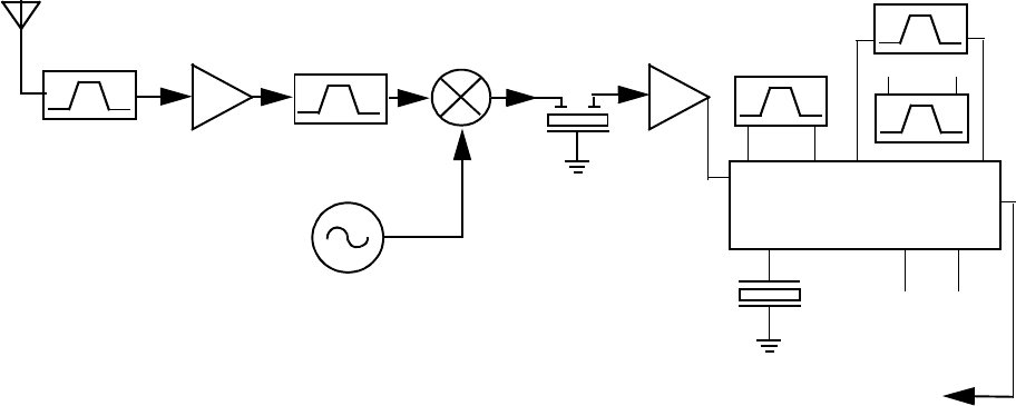
Chapter 2
THEORY OF OPERATION
1.0 Introduction
This Chapter provides a detailed theory of operation for the VHF circuits in the radio. Details of the
theory of operation and trouble shooting for the the associated Controller circuits are included in this
Section of the manual.
2.0 VHF (146-174MHz) Receiver
2.1 Receiver Front-End
The received signal is applied to the radio’s antenna input connector and routed through the
harmonic filter and antenna switch. The insertion loss of the harmonic filter/antenna switch is less
than 1 dB. The signal is routed to the first filter (4-pole), which has an insertion loss of 2 dB typically.
The output of the filter is matched to the base of the LNA (Q303) that provides a 16 dB gain and a
noise figure of better than 2 dB. Current source Q301 is used to maintain the collector current of
Q303. Diode CR301 protects Q303 by clamping excessive input signals. Q303 output is applied to
the second filter (3-pole) which has an insertion loss of 1.5 dB. In Distance mode, Q304 turns on and
causes D305 to conduct, thus bypassing C322 and R337. In Local mode, the signal is routed
through C322 and R337, thus inserting 7 dB attenuation. Since the attenuator is located after the RF
amplifier, the receiver sensitivity is reduced only by 6 dB, while the overall third order input intercept
is raised.
The first mixer is a passive, double-balanced type, consisting of T300, T301 and U302. This mixer
provides all of the necessary rejection of the half-IF spurious response. High-side injection at +15
dBm is delivered to the first mixer. The mixer output is then connected to a duplex network which
matches its output to the XTAL filter input (FL300) at the IF frequency of 44.85 MHz. The duplex
network terminates into a 50 ohm resistor (R340) at all other frequencies.
Figure 2-1 VHF Receiver Block Diagram
Mixer Xtal Filter
Controller
Front Filter
Antenna
First LO
2nd LO Xtal Osc
25kHzFilter
IF Amp
Second Filter 4- Pole
25kHzFilter
12.5kHzFilter
Phase Shift
Element
IFIC
LNA

2-2 THEORY OF OPERATION
2.2 Receiver Back End
The IF signal from the crystal filter enters the IF amplifier which provides 20 dB of gain and feeds
the IF IC at pin 1. The first IF signal at 44.85 MHz mixes with the second local oscillator (LO) at
44.395 MHz to produce the second IF at 455 kHz. The second LO uses the external crystal Y301.
The second IF signal is amplified and filtered by two external ceramic filters (FL303/FL302 for
12.5KHz channel spacing and FL304/FL301 for 25KHz channel spacing). The IF IC demodulates
the signal by means of a quadrature detector and feeds the detected audio (via pin 7) to the audio
processing circuits. At IF IC pin 5, an RSSI signal is available with a dynamic range of 70 dB.
3.0 VHF Transmitter Power Amplifier (146-174 MHz)
The radio’s 25W PA is a three-stage amplifier used to amplify the output from the TX_INJ to the
antenna port. All three stages utilize LDMOS technology. The gain of the first stage (U101)and the
second stage (Q105) is adjustable and is controlled by pin 7 of U103-2 via U103-3 and U102-1. It is
followed by an LDMOS final stage Q100.
Figure 2-2 VHF Transmitter Block Diagram
Devices U101, Q105 and Q100 are surface mounted. A metal clip ensures good thermal contact
between both the driver and final stage, and the chassis.
3.1 First Power Controller Stage
The first stage (U101) is a 20dB gain integrated circuit containing two LDMOS FET amplifier stages.
It amplifies the RF signal from the VCO (TX_INJ). The output power of stage U101 is controlled by a
DC voltage applied to pin 1 from the op-amp U103-3, pin 8. The control voltage simultaneously
varies the bias of two FET stages within U101. This biasing point determines the overall gain of
U101 and therefore its output drive level to Q105, which in turn controls the output power of the PA.
Loop
Pin Diode
Antenna
Switch RF Jack
Antenna
Harmonic
Filter
Coupler
PA-Final
Stage
From VCO (TX_INJ)
Controlled
Stage
Bias
Temperature
Sense
SPI BUS
ASFIC_CMP
PA
PWR
SET
PA
Driver
Controller
U103-2
Forward

VHF Transmitter Power Amplifier (146-174 MHz) 2-3
Op-amp U103-3 monitors the drain current of U101 via resistor R122 and adjusts the bias voltage of
U101.
In receive mode, the DC voltage from RX_EN line turns on Q101, which in turn switches off the
biasing voltage to U101.
3.2 Power Controlled Driver Stage
The next stage is an LDMOS device (Q105) which provides a gain of 12dB. This device requires a
positive gate bias and a quiescent current flow for proper operation. The bias is set during transmit
mode by the drain current control op-amp U102-1, and fed to the gate of Q105 via the resistive
network.
Op-amp U102-1 monitors the drain current of Q105 via resistors R126-7 and adjusts the bias
voltage of Q105 so that the current remains constant.
In receive mode the DC voltage from RX_EN line turns on Q102, which in turn switches off the
biasing voltage to Q105.
3.3 Final Stage
The final stage is an LDMOS device (Q100) providing a gain of 12dB. This device also requires a
positive gate bias and a quiescent current flow for proper operation. The voltage of the line PA_BIAS
is set in transmit mode by the ASFIC and fed to the gate of Q100 via the resistive network R134,
R131. This bias voltage is tuned in the factory. If the transistor is replaced, the bias voltage must be
tuned using the Tuner. Care must be taken not to damage the device by exceeding the maximum
allowed bias voltage. The device’s drain current is drawn directly from the radio’s DC supply voltage
input, B+, via L117 and L115.
A matching network consisting of C1004-5, C1008-9, C1021, C1013, C1019, L116: and two
striplines, transforms the impedance to 50 ohms and feeds the directional coupler.
3.4 Bi-Directional Coupler
The bi-directional Coupler is a microstrip printed circuit, which couples a small amount of the
forward and reverse power of the RF power from Q100.The coupled signal is rectified to an output
power which is proportional to the DC voltage rectified by diode D105; and the resulting DC voltage
is routed to the power control section to ensure that the forward power out of the radio is held to a
constant value.
3.5 Antenna Switch
The antenna switch utilizes the existing dc feed (B+) to the last stage device (Q100). The basic
operation is to have both PIN diodes (D103, D104) turned on during key-up by forward biasing
them. This is achieved by pulling down the voltage at the cathode end of D104 to around 12.4V
(0.7V drop across each diode). The current through the diodes needs to be set around 100 mA to
fully open the transmit path through resistor R108. Q106 is a current source controlled by Q103
which is turned on in Tx mode by TX_EN. VR102 ensures that the voltage at resistor R107 never
exceeds 5.6V.

2-4 THEORY OF OPERATION
3.6 Harmonic Filter
Inductors L111, L112 and L113 along with capacitors C1011, C1024, C1025, C1022, C1020, C1016,
C1017 and C1026 form a low-pass filter to attenuate harmonic energy coming from the transmitter.
Resistor R150 along with L126 drains any electrostatic charges that might otherwise build up on the
antenna. The harmonic filter also prevents high level RF signals above the receiver passband from
reaching the receiver circuits to improve spurious response rejection.
3.7 Power Control
The output power is regulated by using a forward power detection control loop. A directional coupler
samples a portion of the forward and reflected RF power. The forward sampled RF is rectified by
diode D105, and the resulting DC voltage is routed to the operational amplifier U100. The error
output current is then routed to an integrator, and converted into the control voltage. This voltage
controls the bias of the pre-driver (U101) and driver (Q105) stages. The output power level is set by
way of a DAC, PWR_SET, in the audio processing IC (U504), which acts at the forward power
control loop reference.
The sampled reflected power is rectified by diode D107,The resulting DC voltage is amplified by an
operational amplifier U100 and routed to the summing junction. This detector protects the final stage
Q100 from reflected power by increasing the error current. The temperature sensor protects the
final stage Q100 from overheating by increasing the error current. A thermistor RT100 measures the
final stage Q100 temperature. The voltage divider output is routed to an operational amplifier U103
and then goes to the summing junction. The Zener Diode VR101 keeps the loop control voltage
below 5.6V and eliminates the DC current from the 9.3 regulator U501.
Two local loops for the Pre Driver (U101) and for the Driver (Q105) are used in order to stabilize the
current for each stage.
In Rx mode, the two transistors Q101 and Q102 go to saturation and shut down the transmitter by
applying ground to the Pre Driver U101 and for the Driver Q105 control.
4.0 VHF (146-174MHz) Frequency Synthesis
The synthesizer consists of a reference oscillator (Y201), low voltage Fractional-N (LVFRAC-N)
synthesizer (U200), and a voltage controlled oscillator (VCO) (U201).
4.1 Reference Oscillator
The reference oscillator is a crystal (Y201) controlled Colpitts oscillator and has a frequency of
16.8MHz. The oscillator transistor and start-up circuit are located in the LVFRAC-N (U200) while the
oscillator feedback capacitors, crystal, and tuning varactors are external. An analog-to-digital (A/D)
converter internal to the LVFRAC-N (U200) and controlled by the microprocessor via SPI sets the
voltage at the warp output of U200 pin 25. This sets the frequency of the oscillator. Consequently,
the output of the crystal Y201 is applied to U200 pin 23.
The method of temperature compensation is to apply an inverse Bechmann voltage curve, which
matches the crystal’s Bechmann curve to a varactor that constantly shifts the oscillator back on
frequency. The crystal vendor characterizes the crystal over a specified temperature range and
codes this information into a bar code that is printed on the crystal package. In production, this
crystal code is read via a 2-dimensional bar code reader and the parameters are saved.
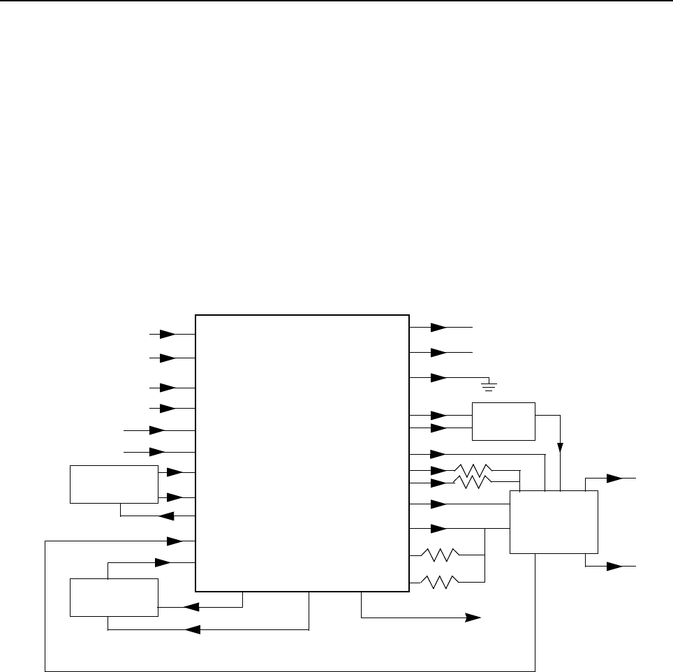
VHF (146-174MHz) Frequency Synthesis 2-5
This oscillator is temperature compensated to an accuracy of +/-2.5 PPM from -30 to 60 degrees C.
The temperature compensation scheme is implemented by an algorithm that uses five crystal
parameters (four characterize the inverse Bechmann voltage curve and one for frequency accuracy
of the reference oscillator at 25 degrees C). This algorithm is implemented by the LVFRAC-N (U200)
at the power up of the radio.
TCXO Y200, along with its corresponding circuitry R204, R205, R210, and C2053, are not placed as
the temperature compensated crystal proved to be reliable.
4.2 Fractional-N Synthesizer
The LVFRAC-N U200 consists of a pre-scaler, programmable loop divider, control divider logic,
phase detector, charge pump, A/D converter for low frequency digital modulation, balanced
attenuator used to balance the high and low frequency analog modulation, 13V positive voltage
multiplier, serial interface for control, and a super filter for the regulated 5 volts.
Figure 2-3 VHF Synthesizer Block Diagram
A voltage of 5V applied to the super filter input (U200, pin 30) supplies an output voltage of 4.5Vdc
(VSF) at U200, pin 28. This supplies 4.5 V to the VCO Buffer IC U201.
To generate a high voltage to supply the phase detector (charge pump) output stage at pin VCP
(U200, pin 47) while using a low voltage 3.3Vdc supply, a 13V positive voltage multiplier is used
(D200, D201, and capacitors C2024, 2025, 2026, 2055, 2027, 2001).
Output lock (U200, pin 4) provides information about the lock status of the synthesizer loop. A high
level at this output indicates a stable loop. A 16.8 MHz reference frequency is provided at U200, pin
19.
DATA
CLK
CEX
MODIN
VCC, DC5V
XTAL1
XTAL2
WARP
PREIN
VCP
REFERENCE
OSCILLATOR
VOLTAGE
MULTIPLIER
DATA (U403 PIN 100)
CLOCK (U403 PIN 1)
CSX (U403 PIN 2)
MOD IN (U501 PIN 40)
+5V (U503 PIN 1)
7
8
9
10
13, 30
23
24
25
32
47
VMULT2 VMULT1
BIAS1
SFOUT
AUX3
AUX4
IADAPT
IOUT
GND
FREFOUT
LOCK 4
19
6, 22, 33, 44
43
45
3
2
28
14 15
40
FILTERED 5V
STEERING
LOCK (U403 PIN 56)
PRESCALER IN
FREF (U504 PIN 34)
39
BIAS2
41
48
5, 20, 34, 36
+5V (U503 PIN 1)
AUX1
VDD, DC5V MODOUT
U200
LOW VOLTAGE
FRACTIONAL-N
SYNTHESIZER
AUX2 1
BWSELECT
VCO Bias
TRB
To IF
Section
TX RF INJECTION
(1ST STAGE OF PA)
LO RF INJECTION
VOLTAGE
CONTROLLED
OSCILLATOR
LINE
LOOP
FILTER

2-6 THEORY OF OPERATION
4.3 Voltage Controlled Oscillator (VCO)
The Voltage Controlled Oscillator (VCO) consists of the VCO/Buffer IC (VCOBIC, U201), the TX and
RX tank circuits, the external RX amplifier, and the modulation circuitry.
Figure 2-4 VHF VCO Block Diagram
The VCOBIC together with the LVFRAC-N (U200) generate the required frequencies in both
transmit and receive modes. The TRB line (U201, pin 19) determines which VCO and buffer is
enabled (high being TX output at pin 10, low being RX output at pin 8). A sample of the signal from
the enabled output is routed from U201, pin 12 (PRESC_OUT), via a low pass filter to U200, pin 32
(PREIN).
A steering line voltage between 3.0V and 10.0V at varactor D204 tunes the TX VCO through the
frequency range of 146-174MHz, and at D203 tunes the RX VCO through the frequency range of
190-219MHz.
The external RX amplifier is used to increase the output from U201, pin 9 from 3-4 dBm to the
required 15dBm for proper mixer operation. In TX mode, the modulation signal from the LVFRAC-N
(U200, pin 41) is applied to the VCO by way of the modulation circuit D205, R212, R211, C2073.
Presc
RX
TX
Q200 Low Pass
Filter
Attenuator
Pin8
Pin14
Pin10
(U200 Pin28)
VCC Buffers
TX RF Injection
U200 Pin 32
AUX3 (U200 Pin 2)
Prescaler Out
Pin 12Pin 19
Pin 20
TX/RX/BS
Switching Network
U201
VCOBIC
Rx
Active Bias
Tx
Active Bias
Pin2
Rx-I adjust
Pin1
Tx-I adjust
Pins 9,11,17
Pin18
Vsens
Circuit
Pin15
Pin16
RX VCO
Circuit
TX VCO
Circuit
RX Tank
TX Tank
Pin7
Vcc-Superfilter
Collector/RF in
Pin4
Pin5
Pin6
RX
TX
(U200 Pin 28)
Rx-SW
Tx-SW
Vcc-Logic
(U200 Pin 28)
Steer Line
Voltage
(VCTRL)
Pin13
Pin3
TRB IN
LO RF INJECTION
Buffer

VHF (146-174MHz) Frequency Synthesis 2-7
4.4 Synthesizer Operation
The synthesizer consists of a low voltage FRAC-N IC (LVFRAC-N), reference oscillator, charge
pump circuits, loop filter circuit, and DC supply. The output signal (PRESC_OUT) of the VCOBIC
(U201, pin 12) is fed to the PREIN, pin 32 of U200 via a low pass filter which attenuates harmonics
and provides a correct input level to the LVFRAC-N in order to close the synthesizer loop.
The pre-scaler in the synthesizer (U200) is a dual modulus pre-scaler with selectable divider ratios.
The divider ratio of the pre-scaler is controlled by the loop divider, which in turn receives its inputs
via the SPI. The output of the pre-scaler is applied to the loop divider. The output of the loop divider
is connected to the phase detector, which compares the loop divider’s output signal with the
reference signal. The reference signal is generated by dividing down the signal of the reference
oscillator (Y201).
The output signal of the phase detector is a pulsed dc signal that is routed to the charge pump. The
charge pump outputs a current from U200, pin 43 (IOUT). The loop filter (consisting of R224, R217,
R234, C2074, C2075, C2077, C2078, C2079, C2080, C2028, and L205) transforms this current into
a voltage that is applied the varactor diodes D203 and D204 for RX and TX respectively. The output
frequency is determined by this control voltage. The current can be set to a value fixed in the
LVFRAC-N or to a value determined by the currents flowing into BIAS 1 (U200, pin 40) or BIAS 2
(U200, pin 39). The currents are set by the value of R200 or R206 respectively. The selection of the
three different bias sources is done by software programming.
To modulate the synthesizer loop, a two-spot modulation method is utilized via the MODIN (U200,
pin 10) input of the LVFRAC-N. The audio signal is applied to both the A/D converter (low frequency
path) and the balance attenuator (high frequency path). The A/D converter converts the low
frequency analog modulating signal into a digital code which is applied to the loop divider, thereby
causing the carrier to deviate. The balance attenuator is used to adjust the VCO’s deviation
sensitivity to high frequency modulating signals. The output of the balance attenuator is presented
at the MODOUT port of the LVFRAC-N (U200,pin 41) and connected to the VCO modulation
varactor D205.

2-8 THEORY OF OPERATION
5.0 Controller Theory of Operation
This section provides a detailed theory of operation for the radio and its components. The main
radio is a single-board design, consisting of the transmitter, receiver, and controller circuits. A
control head is connected by an extension cable. The control head contains LED indicators, a
microphone connector, buttons, and speaker.
In addition to the power cable and antenna cable, an accessory cable can be attached to a
connector on the rear of the radio. The accessory cable enables you to connect accessories to the
radio, such as an external speaker, emergency switch, foot-operated PTT, and ignition sensing, etc.
Figure 2-5 Controller Block Diagram
5.1 Radio Power Distribution
Voltage distribution is provided by five separate devices:
■U514 P-cH FET - Batt + (Ext_SWB+)
■U501 LM2941T - 9.3V
■U503 LP2951CM - 5V
■U508 MC 33269DTRK - 3.3V
■U510 LP2986ILDX - 3.3V Digital
External
Microphone
Internal
Microphone
External
Speaker
Internal
Speaker
SCI to
Control Head
Audio
PA
Audio/Signaling
Architecture
To Synthesizer
Mod
Out
16.8 MHz
Reference Clock
from Synthesizer
Disc Audio
To R F S ec ti on SPI
Digital
Architecture
µP Clock
3.3V
Regulator
RAM
EEPROM
FLASH
HC11FL0
ASFIC_CMP
Accessory &
Connector
Handset
.

Controller Theory of Operation 2-9
The DC voltage applied to connector P2 supplies power directly to the following circuitry:
■Electronic on/off control
■RF power amplifier
■12 volts P-cH FET -U514
■9.3 volt regulator
■Audio PA
Figure 2-6 DC Power Distribution Block Diagram
Regulator U501 is used to generate the 9.3 volts required by some audio circuits, the RF circuitry
and power control circuitry. Input and output capacitors are used to reduce high frequency noise.
Resistors R5001 / R5081 set the output voltage of the regulator. This regulator output is
electronically enabled by a 0 volt signal on pin 2. Q502, Q505 and R5038 are used to disable the
regulator when the radio is turned off.
Voltage regulator U510 provides 3.3 volts for the digital circuitry. Operating voltage is from the
regulated 9.3V supply. Input and output capacitors are used to reduce high frequency noise and
provide proper operation during battery transients. U510 provides a reset output that goes to 0 volts
if the regulator output goes below 3.1 volts. This is used to reset the controller to prevent improper
operation.
Voltage regulator U508 provides 3.3V for the RF circuits and ASFIC_CMP. Input and output
capacitors are used to reduce the high frequency noise and provide proper operation during battery
transients.
U501
9.3V Regulator
FET
P-CH
On/Off
Control
500mA
SW_Filt_B+
Acces Conn
Audio PA_Soutdown
Power Loop Op_Amp
Auto
On/Off
Switch
Control
Ignition B+
RF_PA
Audio_PA
Antenna Switch
Power Control
Filt_B+
Ferrite Bit
Control Head
Mic Connector
Mic Bias
9V, 5mA
Keypad
7_Seg
Bed
to
7-Seg
Shift
Reg
3.2V
72mA
9.3V
65mA
Status LEDs
7_Seg
DOT
Back
light
On/Off
Control
11-16.6V
0.9A 0.85A
U503
5V RF Regulator
U508
3.3V RF Reg
U510
3.3V D Reg
Reset
Rx_Amp
PA_Pre-driver
PA D river
500mA
LVFRAC_N
IF_Amp
ASFIC_CMP
IFIC
RX Cct
micro P
RAM
Flash
EEPROM
90mA
25mA50mA45mA
9.3V
45mA
9.3V
75mA
9.3V
162mA

2-10 THEORY OF OPERATION
Voltage regulator U503 provides 5V for the RF circuits. Input and output capacitors are used to
reduce the high frequency noise and provide proper operation during battery transients.
VSTBY is used only for CM360 5-tone radios.
The voltage VSTBY, which is derived directly from the supply voltage by components R5103 and
VR502, is used to buffer the internal RAM. Capacitor C5120 allows the battery voltage to be
disconnected for a couple of seconds without losing RAM parameters. Dual diode D501 prevents
radio circuitry from discharging this capacitor. When the supply voltage is applied to the radio,
C5120 is charged via R5103 and D501.
5.2 Protection Devices
Diode VR500 acts as protection against ESD, wrong polarity of the supply voltage, and load dump.
VR692 - VR699 are for ESD protection.
5.3 Automatic On/Off
The radio can be switched ON in any one of the following three ways:
■On/Off switch. (No Ignition Mode)
■Ignition and On/Off switch (Ignition Mode)
■Emergency
5.3.1 No Ignition Mode
When the radio is connected to the car battery for the first time, Q500 will be in saturation, Q503 will
cut-off, Filt_B+ will pass through R5073, D500, and S5010-pin 6 (On/Off switch). When S5010 is
ON, Filt_B+ will pass through S5010-pin5, D511, R5069, R5037 and base of Q505 and move Q505
into saturation. This pulls U501-pin2 through R5038, D502 to 0.2V and turns On U514 and U501
9.3V regulator which supplies voltage to all other regulators and consequently turns the radio on,
When U504 (ASFIC_CMP) gets 3.3V, GCB2 goes to 3.3V and holds Q505 in saturation, for soft turn
off.
5.3.2 Ignition Mode
When ignition is connected for the first time, it will force high current through Q500 collector, This
will move Q500 out of saturation and consequently Q503 will cut-off. S5010 pin 6 will get ignition
voltage through R601 (for load dump), R610, (R610 & C678 are for ESD protection), VR501,
R5074, and D500. When S5010 is ON, Filt_B+ passes through S5010-pin 5, D511, R5069, R5037
and base of Q505 and inserts Q505 into saturation. This pulls U501-pin 2 through R5038, D502 to
0.2V and turns on U514 and U501 9.3V regulator which supply voltage to all other regulators and
turns the radio on, When U504 (ASFIC_CMP) get 3.3V supply, GCB2 goes to 3.3V and holds Q505
in saturation state to allow soft turn off,
When ignition is off Q500, Q503 will stay at the same state so S5010 pin 6 will get 0V from Ignition,
Q504 goes from Sat to Cut, ONOFF_SENSE goes to 3.3V and it indicates to the radio to soft turn
itself by changing GCB2 to ‘0’ after de registration if necessary.

Controller Theory of Operation 2-11
5.3.3 Emergency Mode
The emergency switch (P1 pin 9), when engaged, grounds the base of Q506 via EMERGENCY
_ACCES_CONN. This switches Q506 to off and consequently resistor R5020 pulls the collector of
Q506 and the base of Q506 to levels above 2 volts. Transistor Q502 switches on and pulls U501
pin2 to ground level, thus turning ON the radio. When the emergency switch is released R5030 pulls
the base of Q506 up to 0.6 volts. This causes the collector of transistor Q506 to go low (0.2V),
thereby switching Q502 to off.
While the radio is switched on, the µP monitors the voltage at the emergency input on the accessory
connector via U403-pin 62. Three different conditions are distinguished: no emergency kit is
connected, emergency kit connected (unpressed), and emergency press.
If no emergency switch is connected or the connection to the emergency switch is broken, the
resistive divider R5030 / R5049 will set the voltage to about 3.14 volts (indicates no emergency kit
found via EMERGENCY_SENSE line). If an emergency switch is connected, a resistor to ground
within the emergency switch will reduce the voltage on EMERGENCY _SENSE line, and indicate to
the µP that the emergency switch is operational. An engaged emergency switch pulls line
EMERGENCY _SENSE line to ground level. Diode VR503 limits the voltage to protect the µP input.
While EMERGENCY _ACCES_CONN is low, the µP starts execution, reads that the emergency
input is active through the voltage level of µP pin 64, and sets the DC POWER ON output of the
ASFIC CMP pin 13 to a logic high. This high will keep Q505 in saturation for soft turn off.
5.4 Microprocessor Clock Synthesiser
The clock source for the µP system is generated by the ASFIC CMP (U504). Upon power-up the
synthesizer IC (FRAC-N) generates a 16.8 MHz waveform that is routed from the RF section to the
ASFIC CMP pin 34. For the main board controller the ASFIC CMP uses 16.8 MHz as a reference
input clock signal for its internal synthesizer. The ASFIC CMP, in addition to audio circuitry, has a
programmable synthesizer which can generate a synthesized signal ranging from 1200Hz to
32.769MHz in 1200Hz steps.
When power is first applied, the ASFIC CMP will generate its default 3.6864MHz CMOS square
wave UP CLK (on U504 pin 28) and this is routed to the µP (U403 pin 90). After the µP starts
operation, it reprograms the ASFIC CMP clock synthesizer to a higher UP CLK frequency (usually
7.3728 or 14.7456 MHz) and continues operation.
The ASFIC CMP may be reprogrammed to change the clock synthesizer frequencies at various
times depending on the software features that are executing. In addition, the clock frequency of the
synthesizer is changed in small amounts if there is a possibility of harmonics of the clock source
interfering with the desired radio receive frequency.
The ASFIC CMP synthesizer loop uses C5025, C5024 and R5033 to set the switching time and jitter
of the clock output. If the synthesizer cannot generate the required clock frequency it will switch
back to its default 3.6864MHz output.
Because the ASFIC CMP synthesizer and the µP system will not operate without the 16.8 MHz
reference clock it (and the voltage regulators) should be checked first when debugging the system.

2-12 THEORY OF OPERATION
5.5 Serial Peripheral Interface (SPI)
The µP communicates to many of the IC’s through its SPI port. This port consists of SPI TRANSMIT
DATA (MOSI) (U403-pin100), SPI RECEIVE DATA (MISO) (U403-pin 99), SPI CLK (U0403-pin1)
and chip select lines going to the various IC’s, connected on the SPI PORT (BUS). This BUS is a
synchronous bus, in that the timing clock signal CLK is sent while SPI data (SPI TRANSMIT DATA
or SPI RECEIVE DATA) is sent. Therefore, whenever there is activity on either SPI TRANSMIT
DATA or SPI RECEIVE DATA there should be a uniform signal on CLK. The SPI TRANSMIT DATA
is used to send serial from a µP to a device, and SPI RECEIVE DATA is used to send data from a
device to a µP.
There are two IC’s on the SPI BUS, ASFIC CMP (U504 pin 22)), and EEPROM (U400). In the RF
sections there is one IC on the SPI BUS, the FRAC-N Synthesizer. The chip select line CSX from
U403 pin 2 is shared by the ASFIC CMP and FRAC-N Synthesizer. Each of these IC’s check the
SPI data and when the sent address information matches the IC’s address, the following data is
processed.
When the µP needs to program any of these Is it brings the chip select line CSX to a logic “0” and
then sends the proper data and clock signals. The amount of data sent to the various IC’s are
different; e.g., the ASFIC CMP can receive up to 19 bytes (152 bits). After the data has been sent
the chip select line is returned to logic “1”.
5.6 SBEP Serial Interface
The SBEP serial interface allows the radio to communicate with the Customer Programming
Software (CPS), or the Universal Tuner via the Radio Interface Box (RIB) or the cable with internal
RIB. This interface connects to the SCI pin via control head connector (J2-pin 17) and to the
accessory connector P1-6 and comprises BUS+. The line is bi-directional, meaning that either the
radio or the RIB can drive the line. The µP sends serial data and it reads serial data via pin 97.
Whenever the µP detects activity on the BUS+ line, it starts communication.
5.7 General Purpose Input/Output
The controller provides six general purpose lines (PROG I/O) available on the accessory connector
P1 to interface to external options. Lines PROG IN 3 and 6 are inputs, PROG OUT 4 is an output
and PROG IN OUT 8, 12 and 14 are bi-directional. The software and the hardware configuration of
the radio model define the function of each port.
■PROG IN 3 can be used as external PTT input, or others, set by the CPS. The µP reads this
port via pin 72 and Q412.
■PROG OUT 4 can be used as external alarm output, set by the CPS. Transistor Q401 is
controlled by the µP (U403 pin 55)
■PROG IN 6 can be used as normal input, set by the CPS. The µP reads this port via pin 73
and Q411. This pin is also used to communicate with the RIB if resistor R421 is placed.
■DIG IN OUT 8,12,14 are bi-directional and use the same circuit configuration. Each port uses
an output Q416, Q404, Q405 controlled by µP pins 52, 53, 54. The input ports are read
through µP pins 74, 76, 77; using Q409, Q410, Q411

Controller Theory of Operation 2-13
5.8 Normal Microprocessor Operation
For this radio, the µP is configured to operate in one of two modes, expanded and bootstrap. In
expanded mode the µP uses external memory devices to operate, whereas in bootstrap operation
the µP uses only its internal memory. In normal operation of the radio the µP is operating in
expanded mode as described below.
During normal operation, the µP (U403) is operating in expanded mode and has access to 3
external memory devices; U400 (EEPROM), U402 (SRAM), U404 (Flash). Also, within the µP there
are 3 Kilobytes of internal RAM, as well as logic to select external memory devices.
The external EEPROM (U400) space contains the information in the radio which is customer
specific, referred to as the codeplug. This information consists of items such as: 1) what band the
radio operates in, 2) what frequencies are assigned to what channel, and 3) tuning information.
The external SRAM (U402) as well as the µP’s own internal RAM space are used for temporary
calculations required by the software during execution. All of the data stored in both of these
locations is lost when the radio powers off.
The µP provides an address bus of 16 address lines (ADDR 0 - ADDR 15), and a data bus of 8 data
lines (DATA 0 - DATA 7). There are also 3 control lines; CSPROG (U403-38) to chip select U404-pin
30 (FLASH), CSGP2 (U403-pin 41) to chip select U404-pin 20 (SRAM) and PG7_R_W (U403-pin 4)
to select whether to read or to write. The external EEPROM (U400-pin1).
When the µP is functioning normally, the address and data lines should be toggling at CMOS logic
levels. Specifically, the logic high levels should be between 3.1 and 3.3V, and the logic low levels
should be between 0 and 0.2V. No other intermediate levels should be observed, and the rise and
fall times should be <30ns.
The low-order address lines (ADDR 0 - ADDR 7) and the data lines (DATA 0-DATA 7) should be
toggling at a high rate, e.g., you should set your oscilloscope sweep to 1us/div. or faster to observe
individual pulses. High speed CMOS transitions should also be observed on the µP control lines.
On the µP the lines XIRQ (U403-pin 48), MODA LIR (U403-pin 58), MODB VSTPY (U403-pin 57)
and RESET (U403-pin 94) should be high at all times during normal operation. Whenever a data or
address line becomes open or shorted to an adjacent line, a common symptom is that the RESET
line goes low periodically, with the period being in the order of 20ms. In the case of shorted lines you
may also detect the line periodically at an intermediate level, i.e. around 2.5V when two shorted
lines attempt to drive to opposite rails.
The MODA LIR (U403-pin 58) and MODB VSTPY (U403-pin 57) inputs to the µP must be at a logic
“1” for it to start executing correctly. After the µP starts execution it will periodically pulse these lines
to determine the desired operating mode. While the Central Processing Unit (CPU) is running,
MODA LIR is an open-drain CMOS output which goes low whenever the µP begins a new
instruction. An instruction typically requires 2-4 external bus cycles, or memory fetches.
There are eight analog-to-digital coverter ports (A/D) on U403 labelled within the device block as
PEO-PE7. These lines sense the voltage level ranging from 0 to 3.3V of the input line and convert
that level to a number ranging from 0 to 255 which is read by the software to take appropriate action.

2-14 THEORY OF OPERATION
5.9 Static Random Access Memory (SRAM)
The SRAM (U402) contains temporary radio calculations or parameters that can change very
frequently, and which are generated and stored by the software during its normal operation. The
information is lost when the radio is turned off.
The device allows an unlimited number of write cycles. SRAM accesses are indicated by the CS
signal U402 (which comes from U403-CSGP2) going low. U402 is commonly referred to as the
external RAM as opposed to the internal RAM which is the 3 Kilobytes of RAM which is part of the
68HC11FL0. Both RAM spaces serve the purpose. However, the internal RAM is used for the
calculated values which are accessed most often.
Capacitor C402 and C411 serves to filter out any AC noise which may ride on +3.3 V at U402
6.0 Control Board Audio and Signalling Circuits
6.1 Audio Signalling Filter IC and Compander (ASFIC CMP)
The ASFIC CMP (U504) used in the controller has the following four functions:
1. RX/TX audio shaping, i.e. filtering, amplification, attenuation
2. RX/TX signaling, PL/DPL/HST/MDC
3. Squelch detection
4. µP clock signal generation
The ASFIC CMP is programmable through the SPI BUS (U504 pins-20/21/22), normally receiving
19 bytes. This programming sets up various paths within the ASFIC CMP to route audio and/or
signaling signals through the appropriate filtering, gain and attenuator blocks. The ASFIC CMP also
has 6 General Control Bits GCB0-5 which are CMOS level outputs and used for the following:
■GCBO - BW Select
■GCBI - switches the audio PA On/Off
■GCB2 - DC Power On switches the voltage regulator (and the radio) on and off
■GCB3 - Control on MUX U509 pin 9 to select between Low Cost Mic path to STD Mic Path
■GCB4 - Control on MUX U509 pin 11 to select between Flat RX path to filtered RX path on the
accessory connector.
■GCB5 - Control on MUX U509 pin 10 to select between Flat TX path mute and Flat TX path

Transmit Audio Circuits 2-15
7.0 Transmit Audio Circuits
Figure 2-7 Transmit Audio Paths
7.1 Microphone Input Path
The radio supports 2 distinct microphone paths known as internal (from control head J2-15) and
external mic (from accessory connector P1-2) and an auxiliary path (FLAT TX AUDIO, from
accessory connector P1-5). The microphones used for the radio require a DC biasing voltage
provided by a resistive network.
The two microphone audio input paths enter the ASFIC CMP at U504-pin 48 (external mic) and
U504-pin 46 (internal mic). The microphone is plugged into the radio control head and connected to
the audio DC via J2-pin 15. The signal is then routed via C5045 to MUX U509 that select between
two paths with different gain to support Low Cost Mic (Mic with out amplifier in it) and Standard Mic.
7.1.1 Low Cost Microphone
Hook Pin is shorted to Pin 1(9.3V) inside the Low Cost Mic, This routes 9.3V to R429, and creates
2.6V on MIC_SENSE (u.P U403-67) by Voltage Divider R429/R430. U403 senses this voltage and
sends command to ASFIC_CMP U504 to get GCB3 = ‘0’. The audio signal is routed from C5045 via
U509-5 (Z0), R5072, U507, R5026, C5091, R5014 via C5046 to U504- 46 int. mic (C5046 100nF
creates a159Hz pole with U504- 46 int mic impedance of 16Kohm).
MIC
IN
MOD IN TO
RF
SECTION
(SYNTHESIZER)
36
44
40
P1
ACCESSORY
CONNECTOR
J2
CONTROL HEAD
CONNECTOR
MIC
EXT MIC
FLAT TX
AUDIO
42
5
48
46
15
2
24kOhms
FILTERS AND
PREEMPHASIS
HS SUMMER
SPLATTER
FILTER
LS SUMMER
LIMITER
ATTENUATOR
VCO
ATN
TX RTN
TX SND
MIC
INT
AUX
TX
ASFIC_CMP
U504
U509
MIC
EXT
FLAT TX
AUDIO MUTE
GCB3
MUX
35
U509
MUX
GCB5
38

2-16 THEORY OF OPERATION
7.1.2 Standard Microphone
Hook Pin is shorted to the hook mic inside the standard Mic, If the mic is out off hook, 3.3V is routed
to R429 via R458, D401, and it create 0.7V on MIC_SENSE (u.P U403-67) by Voltage Divider
R429/R430. U403 senses this voltage and sends command to ASFIC_CMP U504 to get GCB3 =‘1’.
The audio signal is routed from C5045 via U509-3 (Z1), R5072, U507, R5026, C5091, R5014 via
C5046 to U504- 46 int mic (C5046 100nF create a159Hz pole with U504- 46 int mic impedance of
16Kohm). 9.3VDC is routed via R5077, R5075 to J2-15, It create 4.65V with Mic Impedance. C5010
supplies AC Ground to create AC impedance of 510 Ohms via R5075. and Filter 9.3V DC mic bias
supply.
Note: The audio signal at U504-pin 46 should be approximately 12mV for 1.5kHz or 3kHz of
deviation with 12.5kHz or 25kHz channel spacing.
The external microphone signal enters the radio on accessory connector P1 pin 2 and is routed via
line EXT MIC to R5054. R5078 and R5076 provide the 9.3Vdc bias. Resistive divider R5054/ R5070
divide the input signal by 5.5 and provide input protection for the CMOS amplifier input. R5076 and
C5009 provide a 510 ohm AC path to ground that sets the input impedance for the microphone and
determines the gain based on the emitter resistor in the microphone’s amplifier circuit.
C5047 serves as a DC blocking capacitor. The audio signal at U504-pin 48 should be approximately
14mV for 1.5kHz or 3kHz of deviation with 12.5kHz or 25kHz channel spacing.
The FLAT TX AUDIO signal from accessory connector P1-pin 5 is fed to the ASFIC CMP (U504 pin
42 through U509 pin 2 to U509 pin 15 via U506 OP-AMP circuit and C5057.
The ASFIC has an internal AGC that can control the gain in the mic audio path. The AGC can be
disabled / enabled by the µP. Another feature that can be enabled or disabled in the ASFIC is the
VOX. This circuit, along with Capacitor C5023 at U504-pin 7, provides a DC voltage that can allow
the µP to detect microphone audio. The ASFIC can also be programmed to route the microphone
audio to the speaker for public address operation.
7.2 PTT Sensing and TX Audio Processing
Internal microphone PTT is sensed by µP U403 pin 71. Radio transmits when this pin is “0” and
selects inside the ASFIC_ CMP U504 internal Mic path. When the internal Mic PTT is “0” then
external Mic PTT is grounded via D402. External Mic PTT is sensed by U403 pin 72 via Q412
circuits. The radio transmits when this pin is “0” and selects inside the ASFIC _CMP U504 External
Mic path.
Inside the ASFIC CMP, the mic audio is filtered to eliminate frequency components outside the 300-
3000Hz voice band, and pre-emphasized if pre-emphasis is enabled. The signal is then limited to
prevent the transmitter from over deviating. The limited mic audio is then routed through a summer,
which is used to add in signaling data, and then to a splatter filter to eliminate high frequency
spectral components that could be generated by the limiter. The audio is then routed to an
attenuator, which is tuned in the factory or the field to set the proper amount of FM deviation. The
TX audio emerges from the ASFIC CMP at U504-pin 40 MOD IN, at which point it is routed to the
RF section.
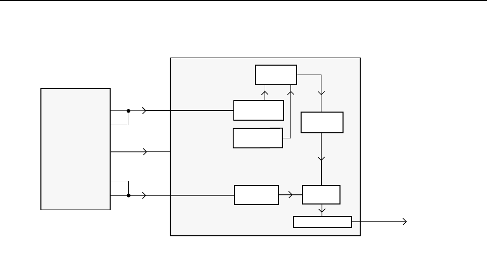
Transmit Signalling Circuits 2-17
8.0 Transmit Signalling Circuits
Figure 2-8 Transmit Signalling Path
From a hardware point of view, there are 3 types of signaling:
■Sub-audible data (PL / DPL / Connect Tone) that gets summed with transmit voice or
signaling,
■DTMF data for telephone communication in trunked and conventional systems, and
■Audible signaling including MDC and high-speed trunking.
Note: All three types are supported by the hardware while the radio software determines which
signaling type is available.
8.1 Sub-Audio Data (PL/DPL)
Sub-audible data implies signaling whose bandwidth is below 300Hz. PL and DPL waveforms are
used for conventional operation and connect tones for trunked voice channel operation. The
trunking connect tone is simply a PL tone at a higher deviation level than PL in a conventional
system. Although it is referred to as “sub-audible data”, the actual frequency spectrum of these
waveforms may be as high as 250 Hz, which is audible to the human ear. However, the radio
receiver filters out any audio below 300Hz, so these tones are never heard in the actual system.
Only one type of sub-audible data can be generated by U504 (ASFIC CMP) at any one time. The
process is as follows, using the SPI BUS, the µP programs the ASFIC CMP to set up the proper low-
speed data deviation and select the PL or DPL filters. The µP then generates a square wave which
strobes the ASFIC PL / DPL encode input LSIO U504-pin 18 at twelve times the desired data rate.
For example, for a PL frequency of 103Hz, the frequency of the square wave would be 1236Hz.
This drives a tone generator inside U504 which generates a staircase approximation to a PL sine
wave or DPL data pattern. This internal waveform is then low-pass filtered and summed with voice
or data. The resulting summed waveform then appears on U504-pin 40 (MOD IN), where it is sent to
the RF board as previously described for transmit audio. A trunking connect tone would be
generated in the same manner as a PL tone.
19
18
40
MOD IN
TO RF
SECTION
(SYNTHESIZER)
80
44 HIGH SPEED
CLOCK IN
(HSIO)
LOW SPEED
CLOCK IN
(LSIO)
ASFIC_CMP U504
MICRO
CONTROLLER
U403
HS
SUMMER
5-3-2 STATE
ENCODER
DTMF
ENCODER
SPLATTER
FILTER
PL
ENCODER
LS
SUMMER
ATTENUATOR
85
82
SPI
BUS

2-18 THEORY OF OPERATION
8.2 High Speed Data
High speed data refers to the 3600 baud data waveforms, known as Inbound Signaling Words
(ISWs) used in a trunking system for high speed communication between the central controller and
the radio. To generate an ISW, the µP first programs the ASFIC CMP (U504) to the proper filter and
gain settings. It then begins strobing U504-pin 19 (HSIO) with a pulse when the data is supposed to
change states. U504’s 5-3-2 State Encoder (which is in a 2-state mode) is then fed to the post-
limiter summer block and then the splatter filter. From that point it is routed through the modulation
attenuator and then out of the ASFIC CMP to the RF board. MDC is generated in much the same
way as trunking ISW. However, in some cases these signals may also pass through a data pre-
emphasis block in the ASFIC CMP. Also these signaling schemes are based on sending a
combination of 1200 Hz and 1800 Hz tones only. Microphone audio is muted during high speed data
signaling.
8.3 Dual Tone Multiple Frequency (DTMF) Data
DTMF data is a dual tone waveform used during phone interconnect operation. It is the same type
of tones which are heard when using a “Touch Tone” telephone.
There are seven frequencies, with four in the low group (697, 770, 852, 941Hz) and three in the high
group (1209, 1336, 1477Hz). The high-group tone is generated by the µP (U403-46) strobing U504-
19 at six times the tone frequency for tones less than 1440Hz or twice the frequency for tones
greater than 1440Hz. The low group tone is generated by the ASFIC CMP, controlled by the µP via
SPI bus. Inside U504 the low-group and high-group tones are summed (with the amplitude of the
high group tone being approximately 2 dB greater than that of the low group tone) and then pre-
emphasized before being routed to the summer and splatter filter. The DTMF waveform then follows
the same path as was described for high-speed data.

Receive Audio Circuits 2-19
9.0 Receive Audio Circuits
Figure 2-9 Receive Audio Paths
9.1 Squelch Detect
The radio’s RF circuits are constantly producing an output at the discriminator (IF IC). This signal
(DISC AUDIO) is routed to the ASFIC CMP’s squelch detect circuitry input DISC (U504-pin 2). All of
the squelch detect circuitry is contained within the ASFIC CMP. Therefore from a user’s point of
view, DISC AUDIO enters the ASFIC CMP, and the ASFIC CMP produces two CMOS logic outputs
based on the result. They are CH ACT (U504-16) and SQ DET (U504-17).
The squelch signal entering the ASFIC CMP is amplified, filtered, attenuated, and rectified. It is then
sent to a comparator to produce an active high signal on CH ACT. A squelch tail circuit is used to
produce SQ DET (U504-17) from CH ACT. The state of CH ACT and SQ DET is high (logic “1”)
when carrier is detected, otherwise low (logic “0”).
CH ACT is routed to the µP pin 84 while SQ DET is routed to the µP pin 83.
SQ DET is used to determine all audio mute / unmute decisions except for Conventional Scan. In
this case CH ACT is a pre-indicator as it occurs slightly faster than SQ DET.
FLT RX AUDIO
P1
11
16
1EXTERNAL
SPEAKER
INTERNAL
SPEAKER
ACCESSORY
CONNECTOR
CONTROL HEAD
CONNECTOR
HANDSET
AUDIO
18
20
19
J2
INT
SPKR-
SPKR +
SPKR -
1
9
2
U509
4110
INT
SPKR+
4
6
DISC
ASFIC_CMP
U504
AUDIO
PA
U502
VOLUME
ATTEN.
FILTER AND
DEEMPHASIS
17
MICRO
CONTROLLER
U403
80
FROM
RF
SECTION
(IF IC) LIMITER, RECTIFIER
FILTER, COMPARATOR
SQ DET
SQUELCH
CIRCUIT
16
PL FILTER
LIMITER
CH ACT
AUX RX
43
18
LS IO
U IO AUDIO
83
84
39
URX OUT
DISC
AUDIO
37
85
GCB4
MUTE
GCB1
14
U505

2-20 THEORY OF OPERATION
9.2 Audio Processing and Digital Volume Control
The receiver audio signal (DISC AUDIO) enters the controller section from the IF IC where it is.DC
coupled to ASFIC CMP via the DISC input U504-pin 2. The signal is then applied to both the audio
and the PL/DPL paths
The audio path has a programmable amplifier, whose setting is based on the channel bandwidth
being received, an LPF filter to remove any frequency components above 3000Hz, and a HPF to
strip off any sub-audible data below 300Hz. Next, the recovered audio passes through a de-
emphasis filter (if it is enabled to compensate for Pre-emphasis which is used to reduce the effects
of FM noise). The IC then passes the audio through the 8-bit programmable attenuator whose level
is set depending on the value of the volume control. Finally the filtered audio signal passes through
an output buffer within the ASFIC CMP. The audio signal exits the ASFIC CMP at AUDIO output
(U504 pin 41).
The µP programs the attenuator, using the SPI BUS, based on the volume setting. The minimum /
maximum settings of the attenuator are set by codeplug parameters.
Since sub-audible signaling is summed with voice information on transmit, it must be separated
from the voice information before processing. Any sub-audible signaling enters the ASFIC CMP
from the IF IC at DISC U504-2. Once inside, it goes through the PL/DPL path. The signal first
passes through one of the two low-pass filters, either the PL low-pass filter or the DPL/LST low-pass
filter. Either signal is then filtered and goes through a limiter and exits the ASFIC CMP at LSIO
(U504-pin 18). At this point, the signal will appear as a square wave version of the sub-audible
signal which the radio received. The µP U403 pin 80 will decode the signal directly to determine if it
is the tone / code which is currently active on that mode.
9.3 Audio Amplification Speaker (+) Speaker (-)
The output of the ASFIC CMP’s digital volume pot, U504-pin 41 is routed through DC blocking
capacitor C5049 to the audio PA (U502 pin 1 and 9).
The audio power amplifier has one inverted and one non-inverted output that produces the
differential audio output SPK+/SPK- (U502 pins 4 and 6)
The audio PA is enabled via the ASFIC CMP (U504-GCB1). When the base of Q501 is low, the
transistor is off and U502-pin 8 is high, using pull up resistor R5041, and the audio PA is ON. The
voltage at U502-pin 8 must be above 8.5Vdc to properly enable the device.
If the voltage is between 3.3 and 6.4V, the device will be active but has its input (U502-pins 1/9) off.
This is a mute condition which is used to prevent an audio pop when the PA is enabled.
The SPK+ and SPK- outputs of the audio PA have a DC bias which varies proportionately with B+
(U502- pin 7). B+ of 11V yields a DC offset of 5V, and B+ of 17V yields a DC offset of 8.5V. If either
of these lines is shorted to ground, it is possible that the audio PA will be damaged. SPK+ and SPK-
are routed to the accessory connector (P1-pin 1 and 16) and to the control head (connector J2-pins
19 and 20).
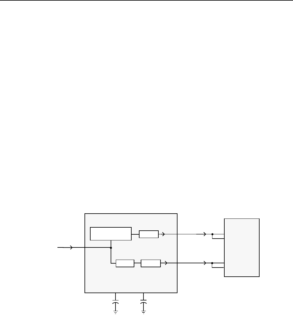
Receive Signalling Circuits 2-21
9.4 Handset Audio
Certain handheld accessories have a speaker within them which require a different voltage level
than that provided by U502. For these devices HANDSET AUDIO is available at control head
connector J2 pin18.
The received audio from the output of the ASFIC CMP’s digital volume attenuator is routed to U505
pin 2 where it is amplified. This signal is routed from the output of the op-amp U505 to J2-pin 18.
From the control head, the signal is sent directly to the microphone jack.
9.5 Filtered Audio and Flat Audio
The ASFIC CMP output audio at U504-pin 39 is filtered and de-emphasized, but has not gone
through the digital volume attenuator. From ASFIC CMP U504-pin 39 the signal is routed via R5034
through gate U509-pin 12 and AC coupled to U505-pin 6. The gate controlled by ASFIC CMP port
GCB4 selects between the filtered audio signal from the ASFIC CMP pin 39 (URXOUT) or the
unfiltered (flat) audio signal from the ASFIC CMP pin 10 (UIO). Resistors R5034 and R5021
determine the gain of op-amp UU505-pin 6 for the filtered audio while R5032 and R5021 determine
the gain for the flat Audio. The output of U505-pin 7 is then routed to P1 pin 11 via DC blocking
capacitor C5003. Note that any volume adjustment of the signal on this path must be done by the
accessory.
10.0 Receive Signalling Circuits
Figure 2-10 Receive Signalling Paths
10.1 Sub-Audio Data (PL/DPL) and High Speed Data Decoder
The ASFIC CMP (U504) is used to filter and limit all received data. The data enters the ASFIC CMP
at input DISC (U504 pin 2). Inside U504 the data is filtered according to data type (HS or LS), then it
is limited to a 0-3.3V digital level. The MDC and trunking high speed data appear at U504-pin 19,
where it connects to the µP U403 pin 80.
DET AUDIO
DISCRIMINATOR AUDIO
FROM RF SECTION
(IF IC)
19
18
25
2
82
80
DISC
PLCAP2
LSIO
HSIO
DATA FILTER
AND DEEMPHASIS LIMITER
FILTER LIMITER
ASFIC_CMP
U504
MICRO
CONTROLLER
U403
85
44
8
PLEAP

2-22 THEORY OF OPERATION
The low speed limited data output (PL, DPL, and trunking LS) appears at U504-pin18, where it
connects to the µP U403-pin 80.
The low speed data is read by the µP at twice the frequency of the sampling waveform; a latch
configuration in the ASFIC CMP stores one bit every clock cycle. The external capacitors C5028,
and C5026 set the low frequency pole for a zero crossings detector in the limiters for PL and HS
data. The hysteresis of these limiters is programmed based on the type of received data.
10.2 Alert Tone Circuits
When the software determines that it needs to give the operator an audible feedback (for a good
key press, or for a bad key press), or radio status (trunked system busy, phone call, circuit failures),
it sends an alert tone to the speaker. It does so by sending SPI BUS data to U504 which sets up the
audio path to the speaker for alert tones. The alert tone itself can be generated in one of two ways:
internally by the ASFIC CMP, or externally using the µP and the ASFIC CMP.
The allowable internal alert tones are 304, 608, 911, and 1823Hz. In this case a code contained
within the SPI BUS load to the ASFIC CMP sets up the path and determines the tone frequency,
and at what volume level to generate the tone. (It does not have to be related to the voice volume
setting.)
For external alert tones, the µP can generate any tone within the 100-3000Hz audio band. This is
accomplished by the µP generating a square wave which enters the ASFIC CMP at U504 pin 19.
Inside the ASFIC CMP this signal is routed to the alert tone generator.
The output of the generator is summed into the audio chain just after the RX audio de-emphasis
block. Inside U504, the tone is amplified and filtered, then passed through the 8-bit digital volume
attenuator, which is typically loaded with a special value for alert tone audio. The tone exits at U504-
pin 41 and is routed to the audio PA like receive audio.
Chapter 3
TROUBLESHOOTING CHARTS
This section contains detailed troubleshooting flowcharts. These charts should be used as a guide in
determining the problem areas. They are not a substitute for knowledge of circuit operation and
astute troubleshooting techniques. It is advisable to refer to the related detailed circuit descriptions
in the theory of operation sections prior to troubleshooting a radio.
Most troubleshooting charts end up by pointing to an IC to replace. It is not always noted, but it is
good practice to verify supplies and grounds to the affected IC and to trace continuity to the
malfunctioning signal and related circuitry before replacing any IC. For instance, if a clock signal is
not available at a destination, continuity from the source IC should be checked before replacing the
source IC.
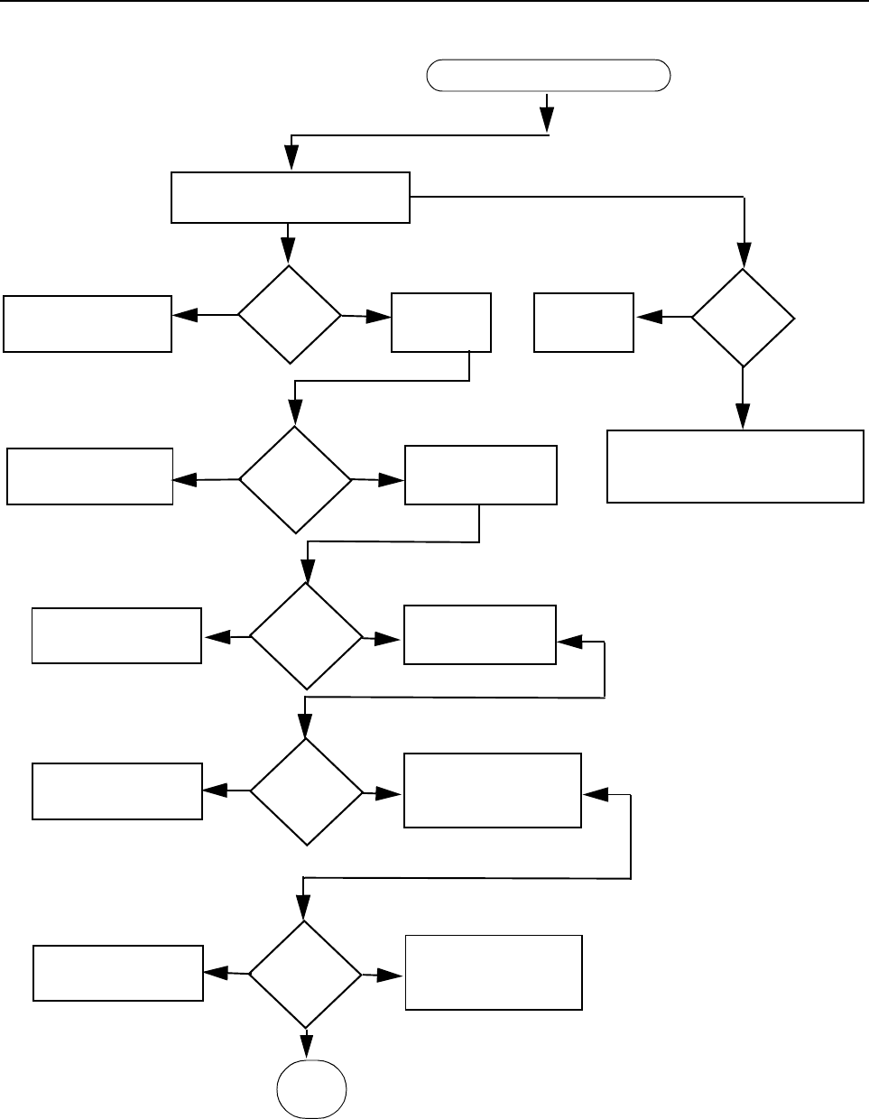
3-2 TROUBLESHOOTING CHARTS
1.0 Troubleshooting Flow Chart for Receiver RF (Sheet 1 of 2)
Problem in 12 KHz and
25 KHz channel spacing
9V on
R310 (LNA)
OK?
Check
RX_EN
No
Go to
DC Section
Yes
RX_EN
ON ?
No
Check Q306, Q300
and U403
Yes
START
LOC_DIST
ON?
Check Q304, D305
and U403
LO
POWER
OK ?
Go to SYN
Section
Yes
Yes
No
No
Go
to A
Yes
3 V
to U301
Okay ?
No
Check
LOC_DIST
Go to
DC Section
Yes
Check D301-304
Replace IF Filters( FL304, FL301)
If problem in 25 KHz spacing
Check
TPI
Check 5V
on R336
5V
(IF AMP)
OK ?
Go to
DC Section
Yes
No
Check 3V
on R339
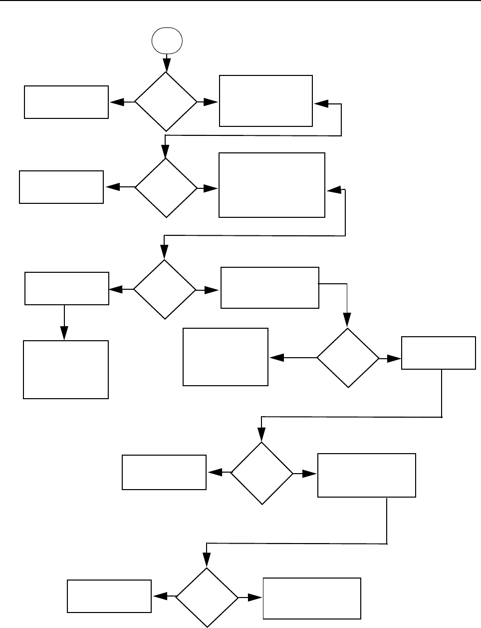
Troubleshooting Flow Chart for Receiver RF (Sheet 1 of 2) 3-3
1.1 Troubleshooting Flow Chart for Receiver (Sheet 2 of 2)
3V
(IFIC -Vcc)
OK ?
Installation
OK ?
Yes
Yes
No
No
A
From
Check visually
all receiver
components
installation ?
Inject - 40dBm (CW)
to RF connector
Check Power on
C332
RF
Power
> -28 dBM?
Yes
No
Check Power on
C336
Go to
DC Section
Check
the component
Antenna to Mixer
circuitry problem
Replace
Q303, Q301
Check passive
components
RF
Power
> -28 dBM?
Yes
No
Replace
Q305, Q300, U302
Check passive
components
Check Y301
44.395 MHz
Y301
OK?
Yes
No
Replace Q302, Y300
Check D301 - 304
Replace Y301
3V to
U301
OK?
Yes
No
Replace U300
Go to DC Section
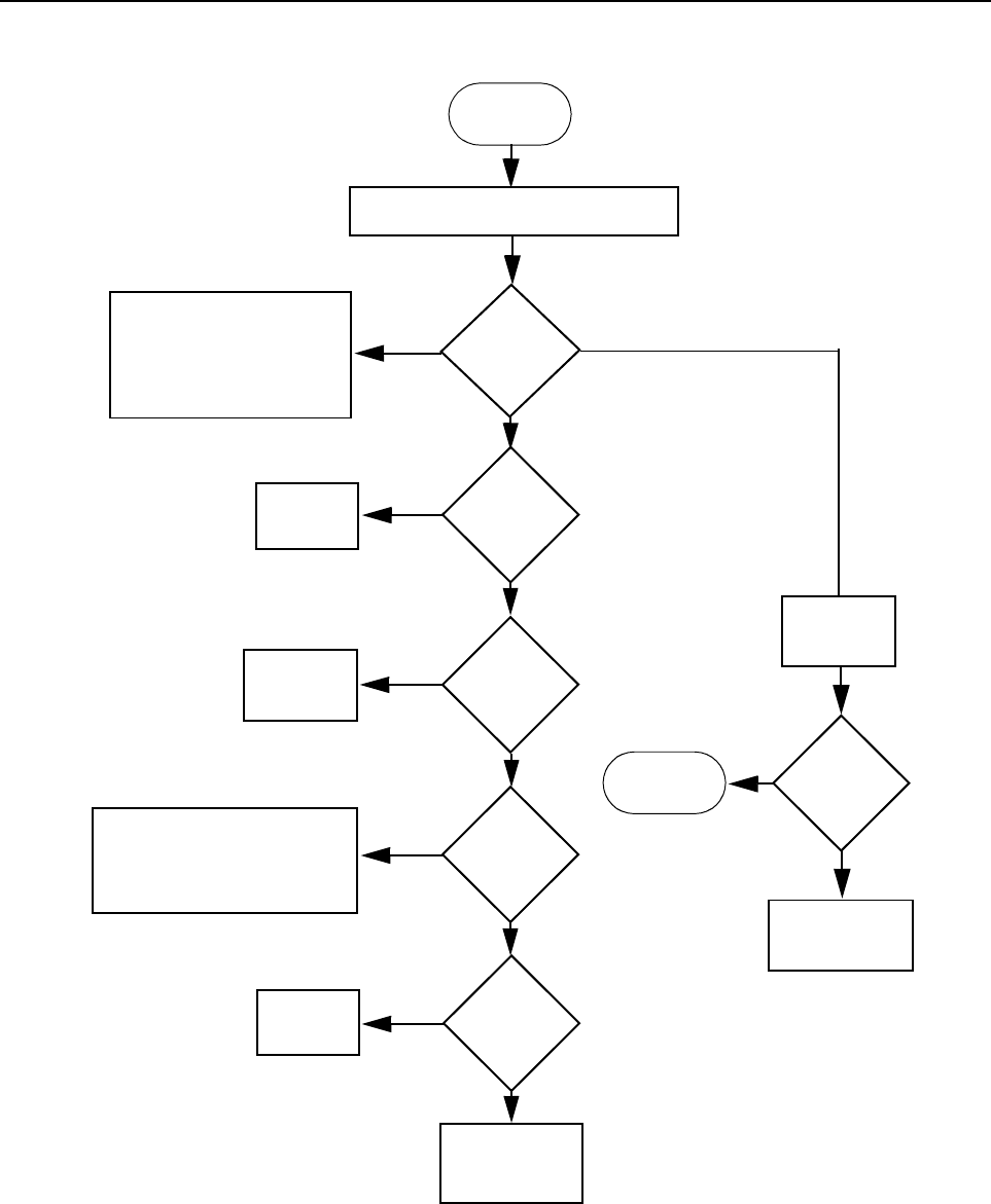
3-4 TROUBLESHOOTING CHARTS
2.0 Troubleshooting Flow Chart for 25W Transmitter (Sheet 1 of 3)
START
Yes
No
Check components between
Q100 and RF output,
Antenna Switch D104,
D103, VR102 and Q106 be-
fore replacing Q100
No or too low power when keyed
Current
increase when
keyed?
Check power settings, tuning
& components between U103
Pin 3 and ASFIC Pin 6 before
replacing ASFIC
Control
Voltage at
TP150
=1.5V?
Check PA
Stages
>1.0A
Voltage U103
pin 5 =
4.7V?
U103 Pin 3
<2.6V
U100 Pin 3
>2Vdc
Check 9.3V
Regulator
U501
Yes
Yes
No
No
Yes
Check
U103
Check forward
Power Sense
Circuit
No
Short U100
Pin 3 to
ground
Voltage at
TP150 rises?
Check PA
Stages
Check Forward
Power Sense
Circuit
Yes
No
>430mA & <1.0A
<500mA
>1.5V
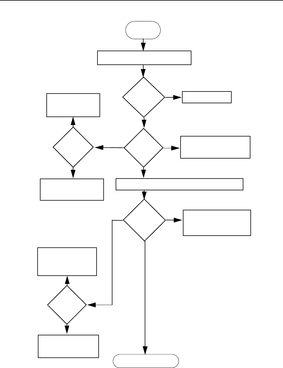
Troubleshooting Flow Chart for 25W Transmitter (Sheet 1 of 3) 3-5
2.1 Troubleshooting Flow Chart for 25W Transmitter (Sheet 2 of 3)
Yes
<2V
Check Q102, R139,
R155, R166, R126,
R127, R169, R138,
R175, R147
Check PA
Stages
No or too low power when keyed
DC
Voltage
at Q101 & Q102
base=0?
DC
Voltage
at U103
Pin 8
Check U403
Check resistive network at
Pin 9 and 10 of U103
before replacing U101
Measure DC Voltage at U102 Pin 1 2.3V
Pin 1
Voltage
at U102
Check resistance network
at pin 1, 2, 3 of U102 before
replacing Q105
Check Final PA Stages
U102 Pin 3 =
8.8V
Check U102 before re-
placing Q105
DC
Voltage at
U103 Pin
10=8.8V
Check Q101,
R153,R136, R165,
R122, R168, R137
Check U103 and Resistive
Network at Pin 10 of U103
before replacing U101
No
No
Yes
>5V
2-5V
2-3V
Yes
No
<2V
>3V
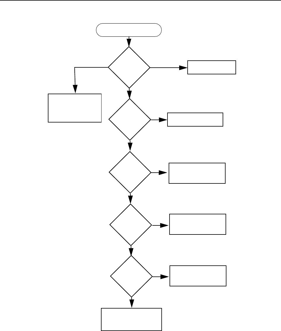
3-6 TROUBLESHOOTING CHARTS
2.2 Troubleshooting Flow Chart for 25W Transmitter (Sheet 3 of 3)
No
Yes
Yes
No
Check Final PA Stage
PA_Bias
Voltage at
R134
2.1V
RF Voltage
after C1044 -
>100mV?
Voltage
across R122
>50mV?
RF Voltage
Q105 gate
>100mV?
RF Voltage
Q100 gate
>1.5V?
Check components
between Q100 &
antenna connector
Replace Q100
Check FGU
Check components
between C1044 &
C1117
Check components
between C1117 &
Q105
Check components
between Q105 &
Q100
No
No
Yes
Yes
2-3V
Supply Voltage
Check Bias Tuning
R134, R131, R106
before replacing
ASFIC U504
<2V
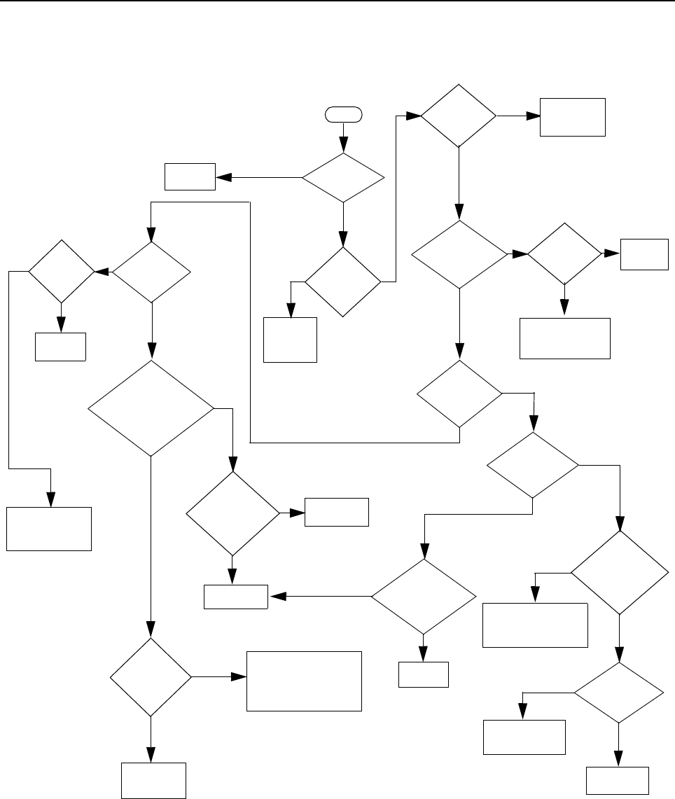
Troubleshooting Flow Chart for Synthesizer 3-7
3.0 Troubleshooting Flow Chart for Synthesizer
+5V at
U200 Pins
13 & 30?
5V
at pin 6 of
D200
Is information
from µP U403
correct?
Is U200
Pin 47
= 13VDC?
Is U201 Pin 19
<40 mVDC in RX &
>4.5 VDC in TX?
(at VCO section)
Start
Visual
check of the
Board OK?
Correct
Problem
Check 5V
Regulator
U503
Is 16.8MHz
Signal at
U200 Pin 19?
Check
Y201 and associated
parts
Are signals
at Pins 14 &
15 of U200?
Check
R228
Check R201
Is U200 pin 2
>4.5 VDC in Tx &
<40 mVDC in Rx
Replace U200
Remove
Shorts
Is there a short
between Pin 47 and
Pins 14 & 15 of
U200?
Is RF level at
U200 Pin 32
-12 < x <-25
dBm?
Replace
U200
If C2052, R208, C2067
C2068. C210, are OK, then
see VCO
troubleshooting chart
Are Waveforms
at Pins 14 & 15
triangular?
Do Pins
7,8 & 9 of
U200 toggle
when channel is
changed?
Check programming
lines between U403
and U200 Pins 7,8 & 9
Replace U200
Check µP U403
Troubleshooting
Chart
No
Yes
No
Yes
No
Yes
No
No
No
Yes
Yes
Yes
No
Yes
Yes
Yes
No
No
No
No
Yes
No
Yes
Yes
Check D200, D201,
C2026, C2025,
C2024 & C2027
5V at
U200 pins 5,
20, 34 & 36
C h e c k 5 V
Regulator
U503
Is
16.8MHz
signal at
U200 pin
23?
Replace
U200
Yes
No
No
Yes
No
Yes

3-8 TROUBLESHOOTING CHARTS
4.0 Troubleshooting Flow Chart for VCO
Are Q200
Base at 2.4V
Collector at 4.5V
Emitter at 1.7V
Are U201 Pins
13 at 4.4V
15 at 1.1V
10 at 4.5V
16 at 1.9V
Low or no RF Signal
at TP1
Visual check
of board
OK?
35mV DC at
U201 Pin 19
NO
YES
at base of Q200
NO
NO
NO
NO
YES
YES
YES
YES
Low or no RF Signal
at input to PA
5V DC at U201
Pin 14 & 18 OK?
4.8V DC at
U201 Pin 19
Is RF available
at C2060
YES
YES
YES
YES
YES
NO
NO
NO
NO
NO
Audio =180mVrms
at “+” side of
D205
2.5VDC
at D205
If R211 is Ok,
replace D205
Replace R211
Replace R212
NO
NO
YES
YES
TX VCO
RX VCO
Correct
Problem
Visual check
of board
OK?
Make sure U508 is working
correctly and runner
between U508 Pin 1 and
U201 Pin 14 & 18 is OK
Check runner
between U200 Pin 2
and U201 Pin 19
Is RF available
If all parts from U200 Pin 8
to Base of Q200 are OK,
replace U200
Check parts between
TP1 and Q200
Power OK but
no modulation
Check Transmiiter
Pre Driver
If all parts
associated
with the pins
are OK,
replace U201
4.5V DC at
U201 Pin 3 OK?
YES
NO 4.5V DC at
U201 Pin 3 OK?
YES
NO
Make sure Synthesizer is
working correctly and runner
between U200 Pin 28 and
U201 Pin 3 is OK
3.3 DC at U201
Pin 14 & 18 OK?
OK? OK?
If all parts associated
with the pins are OK
If L216, C2071, C2070,
C2060 are okay
replace U201
Check 9V at R230
YES

Troubleshooting Flow Chart for DC Supply (1 of 2) 3-9
5.0 Troubleshooting Flow Chart for DC Supply (1 of 2)
Since the failure of a critical voltage supply might cause the radio to automatically power down,
supply voltages should first be probed with a multimeter. If all the board voltages are absent, then
the voltage test point should be retested using a rising-edge-triggered oscilloscope. If the voltage is
still absent, then another voltage should be tested using the oscilloscope. If that voltage is present,
then the original voltage supply in question is defective and requires investigation of associated
circuitry.
Check VDC on
C5008
V=3.3V
?
Check Voltage on
C5043
No
Go to D3_3V
Yes
9v<V<9.8v
?
Go to Start
No
Replace U508
Yes
3V
Check VDC on
C5006
V=5V
?
Check Voltage on
C5042
No
Go to 3V
Yes
9v<V<9.8v
?
Go to Start
No
Replace U503
Yes
5V

3-10 TROUBLESHOOTING CHARTS
5.1 Troubleshooting Flow Chart for DC Supply (2 of 2)
Check VDC on
C5007
V=3.3V
?
Check Voltage on
C5041
No
Go to Digital Section
Yes
9v<V<9.8v
?
Go to Start
No
Replace U510
Yes
D3_3V

Chapter 4
VHF2 PCB/ SCHEMATICS/ PARTS LISTS
1.0 Allocation of Schematics and Circuit Boards
1.1 VHF2 and Controller Circuits
The VHF circuits are contained on the printed circuit board (PCB) which also contains the Controller
circuits. This Chapter shows the schematics for both the VHF circuits and the Controller circuits. The
PCB component layouts and the Parts Lists in this Chapter show both the Controller and VHF circuit
components. The VHF and Controller schematics and the related PCB and parts list are shown in
the tables below.
Table 4-1 VHF2 1-25W Diagrams and Parts Lists
PCB :
8488977U01-C Main Board Top Side
8488977U01-C Main Board Bottom Side
Page 4-4
Page 4-5
SCHEMATICS
Main Circuit
Transmitter
Synthesiser and VCO
Receiver Front and Back End
DC and Audio Ccts
Microprocessor and Controller Ccts
Power Control Cct
Page 4-6/Page 4-7
Page 4-8/Page 4-9
Page 4-10/Page 4-11
Page 4-12/Page 4-13
Page 4-14/Page 4-15
Page 4-16/Page 4-17
Page 4-18
Parts List
8488977U01-C Page 4-19
Controller version is T1

4-2 VHF2 PCB/ SCHEMATICS/ PARTS LISTS
THIS PAGE INTENTIONALLY LEFT BLANK
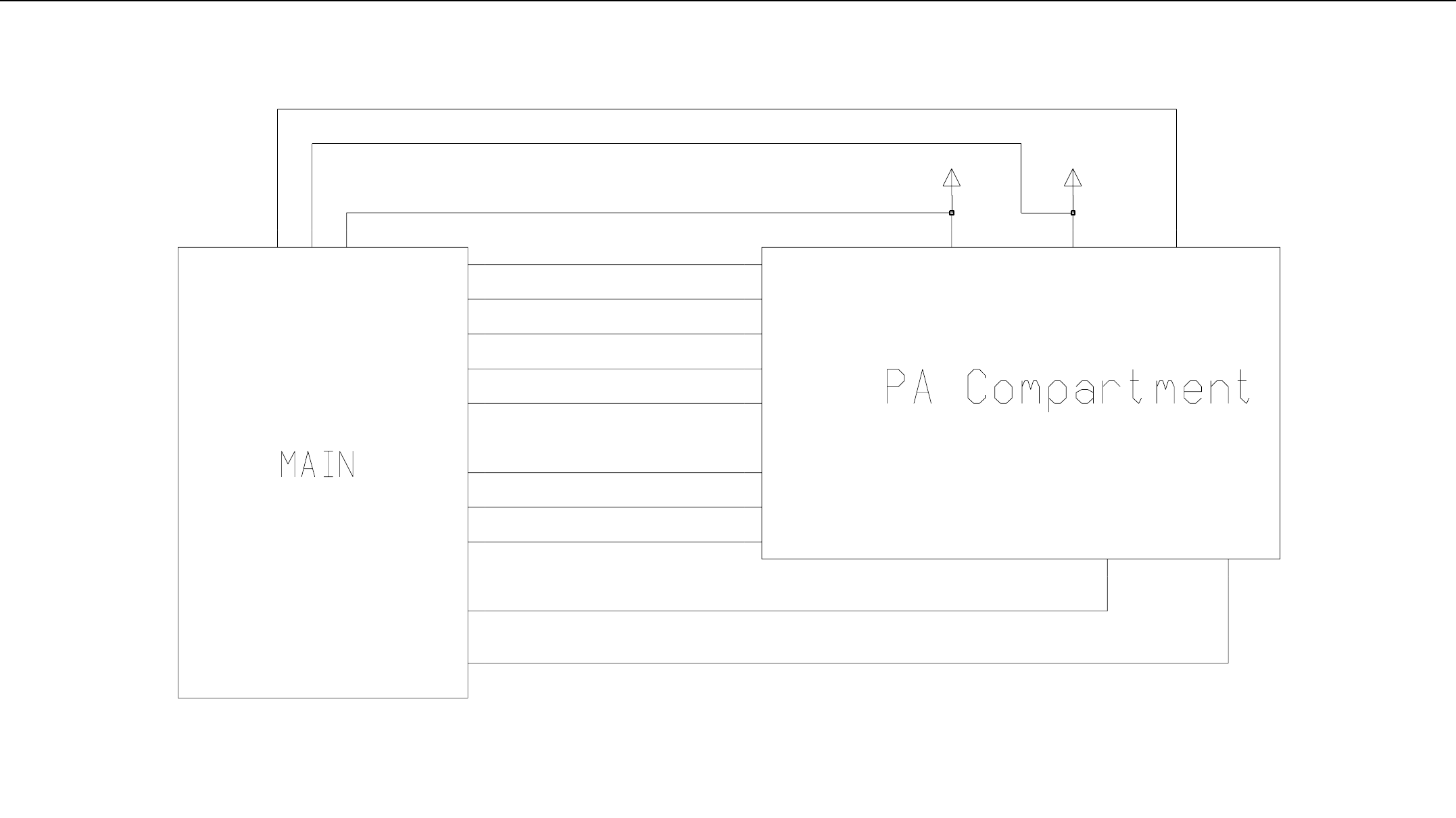
VHF2 1-25W PCB 8488977U01 (rev. C) / Schematics 4-3
2.0 VHF2 1-25W PCB 8488977U01 (rev. C) / Schematics
73D02968C63-0
SHEET 1 OF 8
TX_EN
TX_INJ
9V COMP_B+
DET_VFWD
DET_VRVS
FILT_SW_B+
INTEGRATOR
PA_BIAS
PA_CURRENT
PWR_SET
RX
RX_EN
TX_EN
TX_INJ
9V FILT_SW_B+
9V
COMP_B+
DET-VFWD
DET_VRVS
FILT_SW_B+
INTEGRATOR
PA_BIAS
PA_CURRENT
PWR_SET
RX
RX_EN
VHF2 Interconnection between Main Board and Power Amplifier Compartment
4-4 VHF2 1-25W PCB 8488977U01 (rev. C) / Schematics
SHOWN FROM SIDE 1
C301
C302
C303
C304 C305
C306
C307
C308
C309
C310
C311
C312
C313
C314
C315
C316
C317
C318
C319
C320
C322
C335
C336
C352
C353
C356
C357
C359
C360
C364
C367
C402
C406
C411
C414
C418
C490
C602
C603
C604
C605
C606
C607
C608
C609
C610
C611
C612
C613
C614
C615
C617
C618
C619
C620
C621
C622
C623
C624
C625
C626
C627
C628
C629
C630
C631
C632
C633
C662
C678
C1001
C1004C1005
C1007
C1008 C1009
C1011
C1012
C1013
C1014
C1015
C1016 C1017
C1018
C1019
C1020
C1021
C1022
C1023
C1024
C1030
C1031
C1033
C1034
C1037
C1039
C1041
C1044
C1047
C1049
C1052
C1057
C1063
C1064
C1065
C1068
C1069
C1074
C1076
C1082
C1087
C1088
C1097
C1098
C1099
C1100
C1104
C1105
C1113
C1114
C1115
C1116
C1117
C1118
C1119
C1120
C1122
C1123
C1124
C1125
C2001
C2002 C2004
C2012
C2013
C2014
C2016
C2024
C2025
C2026
C2027
C2028
C2030
C2033
C2036
C2052
C2055
C2056
C2057
C2058
C2059
C2061 C2062
C2063
C2064
C2066
C2067
C2068
C2069
C2073
C2074
C2075
C2077
C2078
C2079
C2080
C5001
C5003
C5005
C5006
C5008
C5010
C5011
C5012
C5013
C5014
C5015
C5016
C5018
C5019
C5020
C5021
C5022
C5023
C5024
C5025
C5026
C5027
C5028
C5029
C5030
C5032
C5033
C5034
C5035
C5038
C5042
C5043
C5044
C5046
C5047
C5048
C5050
C5051
C5052
C5053
C5054
C5056
C5057
C5059
C5062
C5064
C5066
C5068
C5070
C5071
C5074
C5076
C5078
C5079
C5080
C5081
C5087
C5088
C5089
C5090
C5095
C5096
C5100
C5101
C5102
C5103
C5110
C5111
CR300
D101
D104
D200
D201
D203
D204
D205
D301
D302
D303
D304
D400
D401
D500
D502
D513
FL300
FL301
FL302
FL303
FL304
J11
L102
L103
L104
L105
L106
L107
L111
L112
L116
L119
L120
L122
L126
L203
L204
L205
L206 L207
L210
L211 L213
L214
L215
L301
L304
L315
M1
M2
M3
M4
M5
M6
M7
M8
M9
M100
M101
M102
M103 M104
M105 M106
M107
O
M108
O
M109
O
M110
P1
Q100
Q302
Q305
Q400
Q407
Q414
Q415
Q500
Q503
R101
R102
R105
R106
R107
R108
R109
R123
R124
R125
R146
R148
R150
R151
R171
R173
R174
R176
R178
R179
R200
R202
R206
R208
R211
R212
R217
R221
R222
R224
R225
R226
R228
R232
R233
R234
R302
R303
R304
R305
R306
R307
R308
R309
R311
R312
R313
R314
R315
R316
R317
R318
R319
R320
R321
R322
R323
R324
R325
R326
R328
R329
R331
R332
R334
R336
R338
R406
R428
R429
R430
R431
R439
R440
R441
R444
R445
R450
R451
R458
R459
R461
R462
R472
R473
R601
R610
R5000
R5001
R5009
R5010
R5011
R5019
R5021
R5022
R5024
R5031
R5032
R5033
R5034
R5038
R5039
R5040
R5043
R5044
R5045
R5046
R5047
R5048
R5050
R5052
R5053
R5054
R5055
R5056
R5057
R5063
R5064
R5065
R5066
R5067
R5068
R5070
R5071
R5073
R5074
R5075
R5077
R5079
R5080
R5081
R5082
R5083
R5084
R5085
R5086
R5087
R5089
RT100
SH200
SH202
TP3
U101
U200
U300 U301
U402
U501
U502
U503
U504
U505
U506
U508
U509
U515
VR101
VR401
VR500 VR501
VR504
VR693
Y300
Y301
C616
O
O
VHF2 (146-174MHz) 1-25W 8488977U01 (rev. C)
VHF2 1-25W PCB 8488977U01 (rev. C) / Schematics 4-5
SHOWN FROM SIDE 2
C300
C321
C323
C324
C325
C326
C327
C328
C329
C330
C331
C332
C333
C334
C337
C338
C339
C340
C341
C342
C343
C344
C345
C346
C347
C348
C349
C350
C351
C354
C355
C361
C362
C363
C365
C366
C400
C401
C403
C404
C405
C407
C408
C410
C412
C413
C415
C416
C417
C421
C422
C423
C1000
C1002
C1003
C1006
C1010
C1025
C1027
C1028
C1029
C1032
C1035
C1036
C1038
C1040
C1042
C1043
C1045
C1046
C1048
C1050
C1051C1053
C1054
C1055
C1056
C1058
C1059
C1060
C1061
C1062
C1066
C1067
C1070
C1071
C1072
C1073
C1075
C1077
C1078
C1079
C1080
C1081
C1083
C1084
C1085
C1086
C1089
C1090
C1091
C1092
C1093
C1094
C1095
C1101
C1102
C1103
C1106
C1107
C1108
C1109
C1110
C1112
C1121
C1126
C1127
C1128
C1129
C1130
C1131
C2000
C2003
C2005
C2006
C2007
C2008
C2009
C2010
C2011
C2015
C2017
C2018
C2019
C2020
C2021
C2022
C2023
C2029
C2031
C2032
C2034
C2035
C2037
C2038
C2039
C2040
C2041
C2042
C2043
C2044
C2045
C2046
C2047
C2048
C2049
C2050
C2051
C2053
C2054
C2060
C2065
C2070
C2071
C2072
C2076
C5000
C5002
C5007
C5009
C5017
C5031
C5036
C5037
C5039
C5040
C5041
C5045
C5049
C5055
C5058
C5060
C5061
C5063
C5065
C5067
C5069
C5072
C5073
C5075
C5077
C5082
C5083
C5084
C5085
C5086
C5091
C5092
C5094
C5097
C5098
C5099
C5104
C5113
C5114
C5115
C5116
C5117
C5118
C5119
C5120
CR301
D100
D102
D103
D105
D106
D107
D108
D202
D305
D402
D501
D511
J2
J3
L100
L101
L108
L109
L110
L113
L114
L115
L117
L118
L121
L200
L201
L202
L208
L209
L212
L216
L217
L302 L303
L305
L306
L307
L312
L313 L314
L500
L501
L502
M111
M112
M113
M114
P2
Q101Q102
Q103
Q105
Q106
Q200
Q300
Q301
Q303
Q304
Q306
Q401
Q403
Q404
Q405
Q408
Q409
Q410
Q411
Q412
Q413
Q416
Q417
Q501
Q502
Q504
Q505
Q506
R103
R104
R110
R111
R112
R113
R114
R115
R116
R117
R118
R119
R120
R121
R122
R126
R127
R130
R131
R132
R134
R135
R136
R137
R138
R139
R140
R141
R142
R143
R144
R145
R147
R149
R153
R155
R156
R157
R158
R159
R160
R161
R162
R163
R164
R165
R166
R167
R168
R169
R170
R172
R175
R177
R180
R181
R182
R185
R186
R201
R203
R204
R205
R207
R209
R210
R213
R214
R215
R216
R218
R219
R220
R223
R227
R229
R230
R231
R235
R300
R301
R310
R327
R330
R333
R335
R337
R339
R340
R341
R342
R343
R344
R345R346
R401
R402
R403 R404
R405
R407
R414 R415
R421
R422
R423
R424
R425
R426
R427
R432
R433
R434
R435
R436
R438
R442
R443
R453
R454
R455
R456 R457
R460
R463
R466
R467
R468
R469
R470
R471
R600
R615
R5002
R5008 R5013
R5014
R5016
R5020 R5023
R5025
R5026
R5027
R5028
R5029
R5030
R5035
R5036
R5037
R5041
R5042
R5049
R5051
R5058
R5059
R5060
R5061
R5062
R5069
R5072
R5076
R5078
R5088
R5092
R5093
R5094
R5095
R5096
R5097
R5098
R5099
R5100
R5101
R5102
R5103
S5010
SH201
SH300
SH301
SH302
T300
T301
TP1
TP2
TP4
TP150
TP200
TP201
TP400
TP401
TP402
TP403
TP404
TP405
TP406
TP407
TP408
TP409
TP410
TP425
TP500
TP555
TP556
U100
U102
U103
U201
U302
U400
U404
U405
U500
U507
U510
U514
VR102
VR400
2VR402
VR502
VR503
VR692
VR694
VR695
VR696
VR697
VR698
VR699
Y200
Y201
L300 L308
L309
L310
L311
U403
VHF2 (146-174MHz) 1-25W 8488977U01 (rev. C)
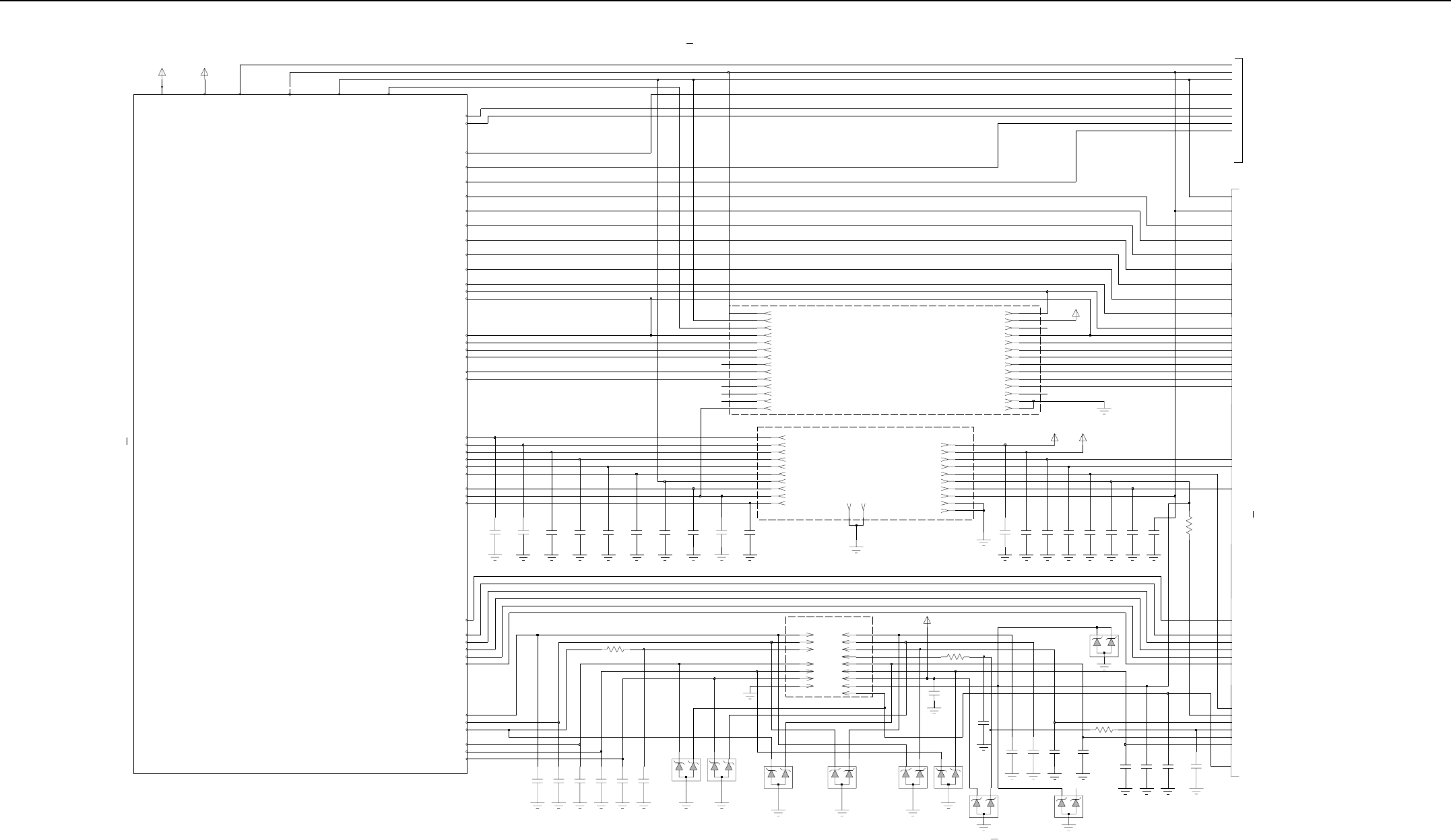
4-6 VHF2 1-25W PCB 8488977U01 (rev. C) / Schematics
Option Board Connector
Accessory Connector
Control Head Connector
28 pins connector
TX AUDIO SEND
DETECTOR AUDIO SEND
TX AUDIO RETURN
UNMUTED RX AUDIO SEND
POST-LIMITER FLATTX AUDIO RETURN
RX AUDIO RETURN
OPTION BOARD ENABLE
DATA READY/REQUEST
RESET
DIGITAL 3.3 VOLT SUPPLY
GND
VOICE STORAGE INT
GND
EXTERNAL MIC
ANALOG 3 VOLT SUPPLY
SERIAL CLOCK
SERIAL DATA RETURN
SERIAL DATA SEND
PUSH TO TALK
DISPLAY DRIVER CHIP SELECT
NCBACKLIGHT
KEYPAD ROW
KEYPAD COLUMN
DISPLAY_DRIVER_CS_EN
SHIFT_REG_CS
DISPLAY_DRIVER_COMMAND/DATA_SEL
KEYPAD_COLUMN
KEYPAD_ROW
SCI_PROGRAMMING
MIC_PTT
HOOK
9.3V
D3_3V
HANDSET_RX_AUDIO
MIC_AUDIO
INT_SPKR-
INT_SPKR+
BOOT/RESET DISPLAY_DRIVER_RESET
SPI_CLK
GND
GND
SPI_MOSI
Place capacitors near J2 Place capacitors near J2
Place capacitors near J2
Place capacitors near J2
ELP ONLY
NC ELP ONLY
NCELP ONLY
DISPLAY_DRIVER_COMMAND/DATA_SELNCELP ONLY
NCELP ONLY
NCELP ONLY
Internal spkr+ jumper
VOICE STORAGE RAC
VOICE STORAGE CS
VOICE STORAGE GAIN SELECT
VOICE STORAGE AUDIO SELECT
DNPJ3 -
DNPDNP
DNP
DIGITAL
Option Board
Keypad/Display
Accessory Connector
EXT_ALARM_OUT
EXT_MIC_PTT
PROG_IN
PROG_I/O
PROG_I/O
PROG_I/O
TO DC & AUDIO
TO SHEET 2
VOX
BATT_SENSE
BOOT_EN_IN_CH
VS_INT
VS_RAC
VS_CS
VS_AUDIO_SEL
VS_GAIN_SEL
VSTBY
LSIO
HSIO
DISPLAY_CS_CH
COMM_DATA_SEL_CH
KEYPAD_COL_CH
KEYPAD_ROW_CH
SCI_CH
OPT_DATA_R_OPBD
OPT_EN_OPBD
HOOK_CH
MIC_PTT_CH
RESET
SHIFT_R_CS
VOL_INDIRECT
ONOFF_SENSE
EMERGENCY_SENSE
RX_EN
LOC_DIST
TX_EN SPI_MOSISPI_CLK SPI_MISO
D3_3V
FILT_SW_B+
CH_ACT
ASFIC_CS
SYNTH_LOCK
SYNTH_CS
RSSI
uP_CLK
F1200
SQ_DET
220.
PROG_O-ACC_C_4
PROG_I-ACC_C_3
PROG_IO-ACC_C_14
PROG_I-ACC_C_6
PROG_IO-ACC_C_8
PROG_IO-ACC_C_12
R610
100. 20.0
VR692
9V
R615
330.0
R601
C678
100.n
23
J3-26 26
J3-25
25
R600
J3-28 28
J3-23
9
0.
18
J3-7
7
J3-9
J3-27 27
J3-18
33.
VR693
1n
C662
C633
1n 1n
C632 C631
1n
C630
1n
C629
1n
C628
1n
C627
1n 1n
C625C626
C624
1n 1n
1n
C623
1n
C622 C621
1n 1n
C620
C619
1n
C618
1n 1n1n
C617C615 C616
1n1n
C614C613
1n
C612
1n
C611
1n
C610
1n
C609
1n
C608
1n
1n
C607
1n
C606
1n1n
C605
1n
C604C603
1n
C602
6
J3-22 22
J3-24 24
2J3-4
4J3-6
3J3-5
5J3-2
J3-15
15
J3-1
1J3-3
J3-11 11
J3-10 10
J3-8
8
J3-20
20
J3-16 16
J3-19 19
J3-21 21
12
J3-13 13
J3-14 14
J3-17
17
J3-12
20.0
VR692
20.0
VR698
20.0
VR694
20.0
VR699
20.0
VR697 VR696
20.0
VR695
G2
20.0
J2-2
2
J2-21
G1
J2-22
J2-16 16
J2-13 13
J2-17 17
J2-5 5
3
J2-9 9
J2-8 8
J2-1 1
J2-6 6
J2-3
J2-14
14
J2-4
4
19
J2-10 10
J2-11
11
J2-15
15 J2-20
20 J2-19
J2-7
7J2-18
18
10
FILT_SW_B+
D3_3V
D3_3V
J2-12
12
P1-13
13
P1-10
P1-7 7
12
P1-14 14
P1-8 8
P1-12
6
P1-9
9
P1-3 3
P1-6
FILT_SW_B+
P1-4 4
11
P1-15
15
P1-5
5P1-11
16 P1-2
2
P1-1
1P1-16
D3_3V
VHF2 (146-174MHz) Main Circuit (Sht 1 of 2)
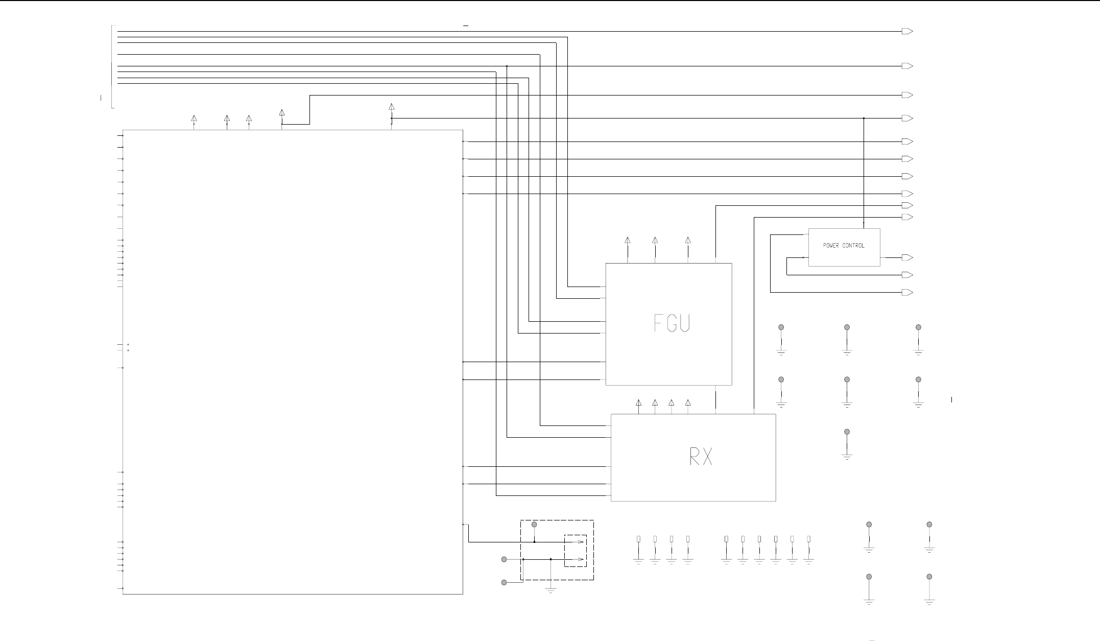
VHF2 1-25W PCB 8488977U01 (rev. C) / Schematics 4-7
DC Connector
DC & AUDIO
TO SHEET 1
PEDS FOR GND CONTACTSCONTACTS FOR PA CLIP
73D02968C63-0
SHEET4OF8
9R
SPI_MOSI
SPI_CLK
ASFIC_CS
RX_AUDIO_RETURN_OPT_BRD
CH_ACT
5V
uP_CLK
F1200
HSIO
LSIO
3V
VS_MIC
PWR_SET
GND
1
9V5V
DET-VFWD
1
GND
1
GND
3V
PLTD_HOLE3_5x7_0_TRIMMED
M7
1
GND
TP3
TEST_POINT
1
FILT_SW_B+
9V
P2-1
1
M110
P2-2
2
D3_3V 5V
1
M112
GND
16.8MHz
3V5V 9R
MOD_IN RX_INJ
SPI_CLK
SPI_MOSI
SYNTH_CS
SYNTH_LOCK
TX_INJ
BOARD HOLES
(SOURCE) (SOURCE)
(SOURCE)
(SOURCE)
(SOURCE)
(SOURCE)
VSTBY
SPKR+
MOD_OUT
EMERGENCY_ACCES_CONN
DET_VRVS
PA_CURRENT
FILT_SW_B+
HOLES FOR PA SHIELD
9V
SPKR-
RESET
VS_AUDIO_SEL
HANDSET_RX_AUDIO_CH
MIC_AUDIO_CH
TX_AUDIO_SEND_OPT_BRD
DETECTOR_AUDIO_SEND_OPT_BRD
UNMUTED_RX_AUDIO_SEND_OPT_BRD
TX_AUDIO_RETURN_OPT_BRD
POST_LIMITER_FLAT_TX_AUDIO_RETURN_OPT_BRD
D3_3V
16.8MHz
VOL_INDIRECT
BATT_SENSE
SQ_DET
VOX
EMERGENCY_SENSE
ONOFF_SENSE
IGNITION
5V_CH
COMP_B+
PA_BIAS
PWR_SET
B+
BW_SEL
DEMOD
FLAT_TX_AUDIO_INPUT_ACCESS_CONN
RX_AUDIO_OUTPUT_ACCESS_CONN
EXTERNAL_MIC_AUDIO_ACCESS_CONN
FILT_SW_B+
GND
1
M102
PLTD_HOLE1_4X1_8
GND
1
PLTD_HOLE1_4X1_8
M103
M4
PLTD_HOLE3_5x7_0_TRIMMED
GND
1
M101
PLTD_HOLE1_4X1_8
1
M106
1
M107
PLTD_HOLE1_4X1_8
M104
1
GND
M105
1
M108
1
GND
1
M109
M3
PLTD_HOLE3_5x7_0
GND
1
M2
PLTD_HOLE3_5x6_0_TRIMMED
1
PLTD_HOLE3_5x7_0_TRIMMED
M5
1
M111
1
PLTD_NUT
M9
3V
DET_VFWD
INTEGRATOR
5V
1
M1
PLTD_HOLE3_5x7_0
GND
1
M8
PLTD_HOLE3_5x7_0_TRIMMED
1
VCC
3V5V
9R 9V
BW_SEL
DEMOD
LOC_DIST
RSSI
RX
RX_EN
RX_INJ
1
TEST_POINT
TP2
M113
1
M114
DET_VRVS
FILT_SW_B+
COMP_B+
PA_CURRENT
RX
TX_INJ
9V
RX_EN
TX_EN
INTEGRATOR
PA_BIAS
9R
VHF2 (146-174MHz) Main Circuit (Sht 2 of 2)
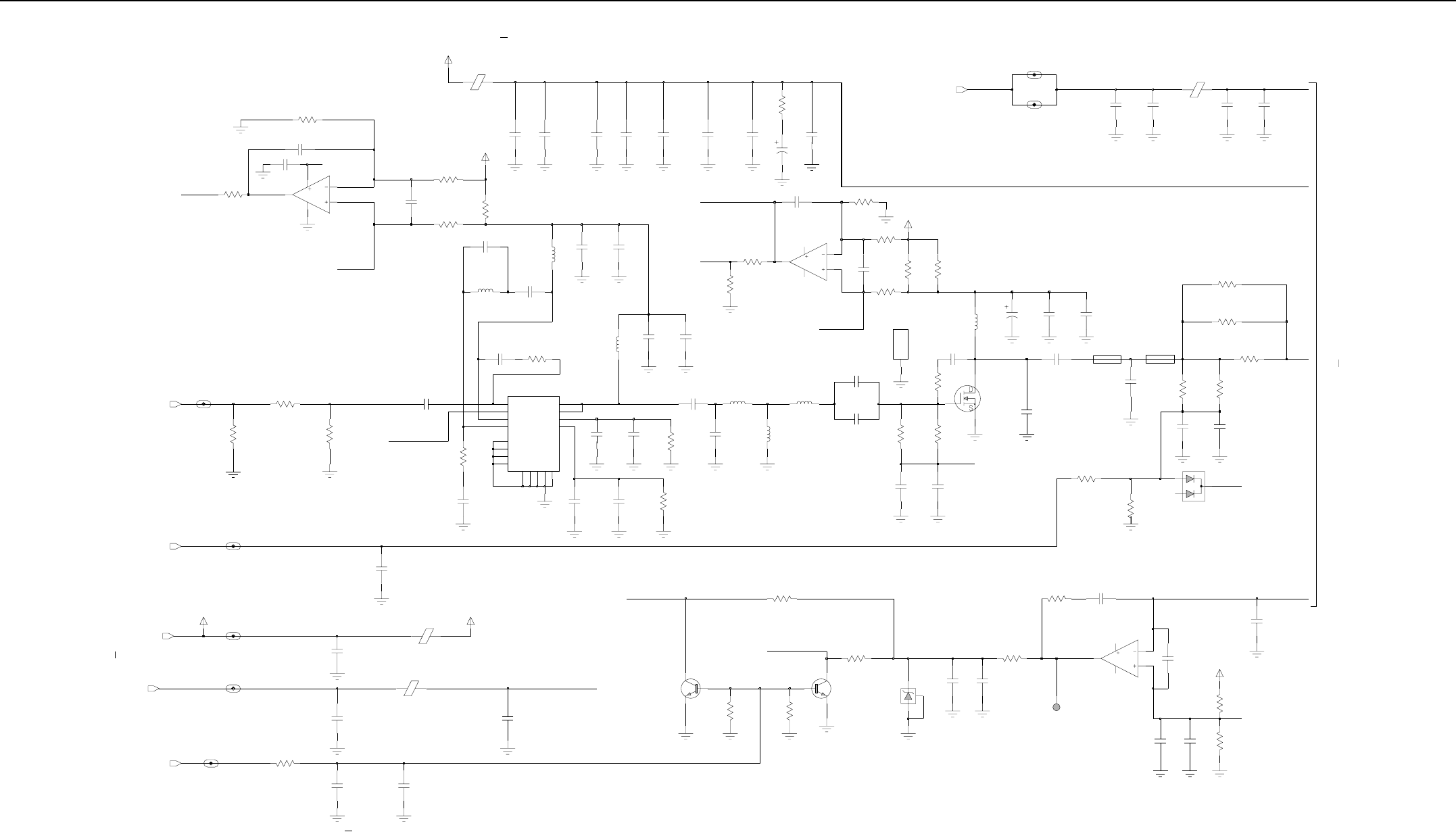
4-8 VHF2 1-25W PCB 8488977U01 (rev. C) / Schematics
120.
R102
10u
MRF1513’s Thermal pad
DNP DNP
DNP
(SOURCE)
0.8*251.542*4
TO SHEET 2
V_CNTRL
DNP
DNP
1n
1019447
V_CTRL_PREDRIVER
RX_ENRX_EN
9V
FILT_SW_B+
PA_BIAS
COMP_B+
TX_INJ
Q105
22n
22n
1
IF110
R182
10.K
C1089
1019447
C1039
1
TP150
TEST_POINT
L110
12.0n
22.K
L121
FLT_9V
C1069
DNP
1019447
1n
1n
C1068
1n
C1070
C1029
C1066
100n
1n
C1103
33n
C1120
33p
C1117
47p
33p
C1119
C1118
33p
C1031
22n
L105
68.n
L104
68.n
L107
4.22n
51.0
R105
51.0
R123
R106
2.7
1n
C1062
C1061
1n
FILT_SW_B+_PA
1n
C1060
1n
C1063
1n
C1037C1064
C1081
11
0.
R130
3
1
8
4
U103
MC3303 6
5
7
4
LM2904
U102
2
1n
C1072
C1065
1n
2.7
R125
R124
2.7
R181
47.K
C1036
22n
FLT_9V
R180
47.K
R134
47.K
R131
100.K
HEATSINK
M100
1POS
C1038 R159
5.6K
R186
5.1
1n
C1043
22n
C1032
1n
C1053
5.6K
R158
14 VD1 2
VG1 3
VG2
C1027
8NC1
9NC2
10 NC3
15 NC4
16 RFIN 6
RFOUT1 7
RFOUT2
1VCNTRL
EP
17
11 G2
4GND1
5GND2
12 GND3
13 GND4
U101
30C65
56.00p
C1014
1n
C1044
C1033
22n
10n
C1104
1n
C1042
2.2K
R168
R137
2.4K
R165
39.K
39.K
R136
C1028
100n
510.
R170
2.2K
R167
4.7
R122
IF107
L118
220.p
L122
C1126
R109
13.85n
15.000
220.p
C1129
IF106
1n
C1109
FILT_SW_B+
1n
220.p
C1092
C1086
1n
1n
C1100
L100
C1099
1n
9
10
8
4
11
22n
U103
MC3303
VR101
5.6
R127
1.1.
R126
C1040
2.2n
R139
39.K
R169
FLT_9V
2.2K
2.4K
R166
R138
39.K
R175
220.
R155
10.K
Q102
10.K
R153
Q101
1n
C1074
470
R171
IF108
300
L119
1019447
R173 R174
300
C1041
1n
R176
100
220.p
C1112 C1110
220.p
C1030
22n
IF105
IF109
1n
R147
C1057
C1001
C1105
470p
1.u
R179
36.36.
R178
7.66n
L109
27n
L106
220.p
C1084
IF104
1n
C1054
D100
220.p
220.p
PA_FILT_B+
C1116
220.p
C1000
C1115
C1012
56.00p
C1015
47.00p
470p
C1107C1106
470p
VCNTR1
VCNTR1
VCNTR2
VCNTR2
V_CTRL_DRIVER
VCNTR3
FILT_SW_B+_PA
V_CTRL_DRIVER
V_CTRL_PREDRIVER
FLT_9V
VCNTR3
V_REF_OPAMP
VHF2 (146-174MHz) Transmitter (Sht 1 of 2)
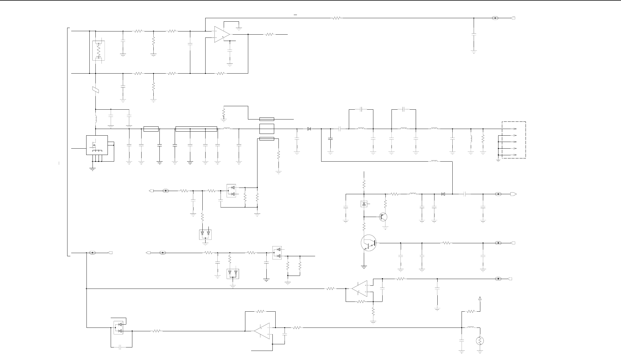
VHF2 1-25W PCB 8488977U01 (rev. C) / Schematics 4-9
PWR_SET
Final_cur_sense
PA_FILT_B+
TX_EN
PA_CURRENT
FILT_SW_B+_PA
TO SHEET 1
73D02968C63-0
DNP
DNP
DNP
DNP
DNP
DNP
DNP
DNPDNP
Place near both sides of PA shields
DNP
DNP
PA’s Temp. Sensor
Coupler
width 2.032
7.5
SHEET 2 OF 8
1.2u
RX
R172
C1013
13.p
C1008
120.00p
C1004
150.p
C1005
L126
J11-5
G2
S3
S4
GND1
GND2
S2
S1
V_forward
10.p
C1007 C1021
18.0n
L116
C1009
100.p100.p
L115
18.0n
150.p
G
56.p
D
C1121
C1019
V_reverse
Final_cur_sense
V_REF_OPAMP
DET_VFWD
INTEGRATOR
V_reverse
6.8p
DET_VRVS
Q100
D103
D104
1
1019447
L117
IF113
1
IF111
1
IF102
IF112
IF101
1
IF103
1
J11-4
G1
J11-2
2
IF100
J11-1
1
J11-3
3
R5102
Q103
100.
100.
R5101
220.p
C1095
220.p
C1130
1n
C1091
1n
C1080
C1079
1n
1n
C1077
56.K
1n
R157
C1073
U103
MC3303
11
4
14
12
13
LM2904
U102
4
8
7
5
6
C1067
1n
470.0p
C1003
C1059
C1002
470.0p
R156
1n
10.K
R116
10.K
R185
1n
C1058
10.K
22.K
R149
C1056
1n
R177
100.K
R112
R132
100.
100.K
R114
10.K
R115
10.K
R113
10.K
R111
1.K
R110
1.K
C1055
1n
R148
R101
22.K
0.
U103
11
4
1
3
2
120.
MC3303
FLT_9V
R104
47.0K
RT100
L103
1.u
5.6K
1n
R151
1n C1052
43.K
R135
C1051
22.K
R145
1n
C1050
D102
3.3K
D108
R163
3.3K
R162
D107
C1102
100.p
R121
100. 100.
R120
R143
22.K
22.K
3.3K
R142
D106
3.3K
R161
C1101
R160 D105
100.p
R119
100.
R118
100.
22.p
C1017
L114
1.20u
L113
L108
L112
48.0n
48.0n
48.0n48.0n
68.p
L111
51.000
R108
C1108
51.000
R107
C1016
33.p
C1006C1010
100.p 150.p
C1011
C1018
16.00p
68.p
C1023
20.p 6.8p
C1022
12.p
C1020
R103
C1025
4.7p
120.
4.7p
C1024
C1035
22n
10.K
Q106
R150
470.
VR102
5.6
VHF2 (146-174MHz) Transmitter (Sht 2 of 2)
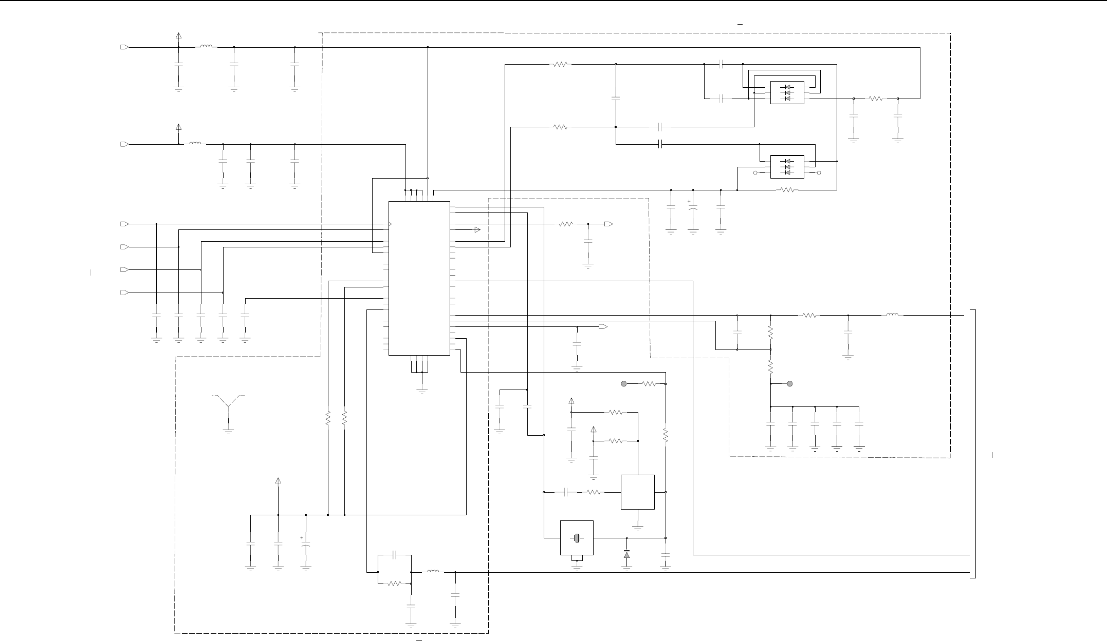
4-10 VHF2 1-25W PCB 8488977U01 (rev. C) / Schematics
4
1
VCON
46
ADAPTSW
AVDD 20
AUX4 3
AUX3 2
AUX2 1
AUX1 48
2.7p
AGND
22
DVDD 36
DGND
6
DATA
3V
3V
7
C2005
CLK
8
CEX
9
CCOMP
42
BIAS2
39 BIAS1
40
NC1
MODOUT 41
MODIN
10
C2053
100p
4
1
LOCK
IOUT 43
INDMULT 16
IADAPT 45
FREFOUT 19
PRE_GND
33
PREIN
32
5
PD_VDD
PD_GND
44
NC3
31 NC2
TP201
TEST_POINT
29
17 SFOUT
SFIN
30
SFCAP
26
SFBASE
27
REFSEL
18
PVREF
35
PRE_VDD 34
VMULT2 14
VMULT1 15
VCP 47
VBPASS
21
TEST2 38
TEST1 37
28
100.n
U200
FRACN_63A27
XTAL2 24
XTAL1 23
C2020
100n
WARP 25
1TP200
TEST_POINT
1
13
VRO
VMULT4 11
VMULT3 12
DNP
DNP
DNP
DNP
DNP
DNP DNP
TO SHEET 2
100.n
C2080 C2079 C2078
100.n 100.n
C2077
0.
R205
0.
R204
SH200
SHIELD
2.2uF
100.K
R209
C2049
470p
1n
C2035
220p 62.0p
C2051
2GND
4GND1
3
OUT
1IN
C2054
D202
Y201
14R06
FREQ
C2072
NC NC
390nH
L217
470p
C2047
470p
C2046 C2045
150.K
470p
200.K
R206R200
4.7uF
C2002
1n
C2033
0.1uF
C2014
1.5K
R224
100p
V_SF
5V
5V
VCO_MOD
C2052
470p
C2050
Y200
45J68
2
GND
3OUT
VCC
R202
16.8MHz
0.
C2016
0.1uF
C2036
1n
2.2uF
C2006
R225
R228
100.
150.
C2048
470p
C2027
10n
C2026
10n
10n
C2025
10n
C2024
C2023
10n
2.2n
C2028
390nH
L200
2.2uF
C2000 C2034
C2001
4.7uF
1n
100.n
C2075
100.K
2.2uF
C2004
R208
C2067
8.2p
R229
100.
22p
C2055
C2015
0.1uF
R226
150.
R207
150.K
C2074
100.n
0.1uF
1.3K
R217
C2013
39.
R234
1uH
L205
100nH
L210
6.8p
A1
A2
A3
K1
K2
K3
C2068
D200
D201
A1
A2
A3
K1
K2
K3
0.1uF
C2017
100.K
R210
3V
16.8MHZ
SYNTH_LOCK
SPI_MOSI
SPI_CLK
MOD_IN
5V
SYNTH_CS
VHF2 (146-174MHz) Synthesiser and VCO (Sht 1 of 2)
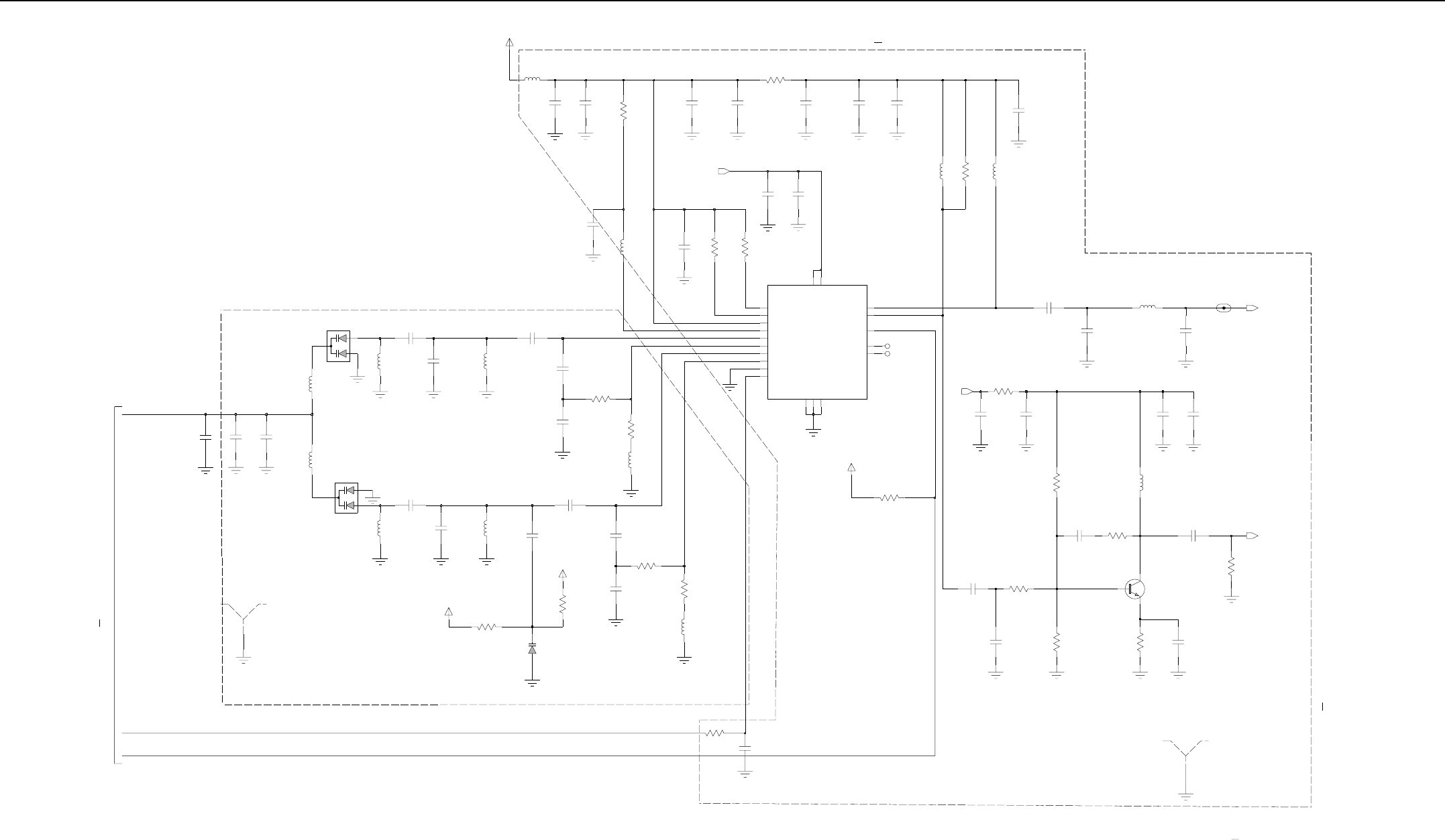
VHF2 1-25W PCB 8488977U01 (rev. C) / Schematics 4-11
73D02968C63-0
SHEET5OF8
VCO Shield
VCOBIC Shield
DNP
TO SHEET 1
DNP
DNP
DNP
RX_INJ
3V
TX_INJ
IF200
1n
C2037
C2040
C2012
8.2p 47.0n
L207
30.K
C2038
1n
1
TRB_IN
19
TX_BASE
16
TX_EMITTER
15
TX_IADJ
1TX_OUT 10
TX_SWITCH 13
VCC_BUFFERS 14
VCC_LOGIC 1817 GND_LOGIC
PRESC_OUT 12
RX_BASE
5
RX_EMITTER
6
RX_IADJ
2RX_OUT 8
RX_SWITCH 7
SUPER_FLTR
3
U201
50U54
COLL_RFIN
4
FLIP_IN
20
GND_BUFFERS
11 GND_FLAG
9
L204
680nH
680nH
L203
220.
R223
C2003
100n
39.p
1.n
1
C2071
SH202
SHIELD
1
SHIELD
SH201
C2039
5.6p
1n
R216
3.9K
C2069
10p
R215
4.7K
C2065
1n
C2032
L213
100nH
15.p
C2063 R214
100nH
L212
4.7K
R227
R219
100.
820.
100.n
C2076
R211
47.K
R218
1.K
33.0n
L206
L214
47nH
R235
18.
R221
R232
47.
220.
C2021
10n
18p
C2057
C2061
12p
C2056
18p
0.
R203
3.3p
C2044
100n
C2019
R230
C2018
100n
V_SF
V_SF
V_SF
100.
R220
VCO_MOD
510.
1.n1.n
C2042 C2041
C2022
NC
NC
680nH
10n
0.1uF
L202
C2066
C2011
1n
C2031
4.7K
1
3
2
R213
C2010
Q200
BFS540
100n
0.
R201
C2064
10.p
100nH
L211
47.0n
L216
39.p
C2070
L201
680nH
47nH
L215
C2059
18p
1.p
C2073 C2058
18p
C2062
12p
1n
C2029
R222
220.
R233
47.
R212
C2060
15p
C2009
100n 0.1uF
C2008
0.1uF
C2007
100nH
L209 L208
100nH
R231
51.
D205
D204
D203
6.8p
C2043
0.1uF
C2030
3.9n
9R
VHF2 (146-174MHz) Synthesiser and VCO (Sht 2 of 2)
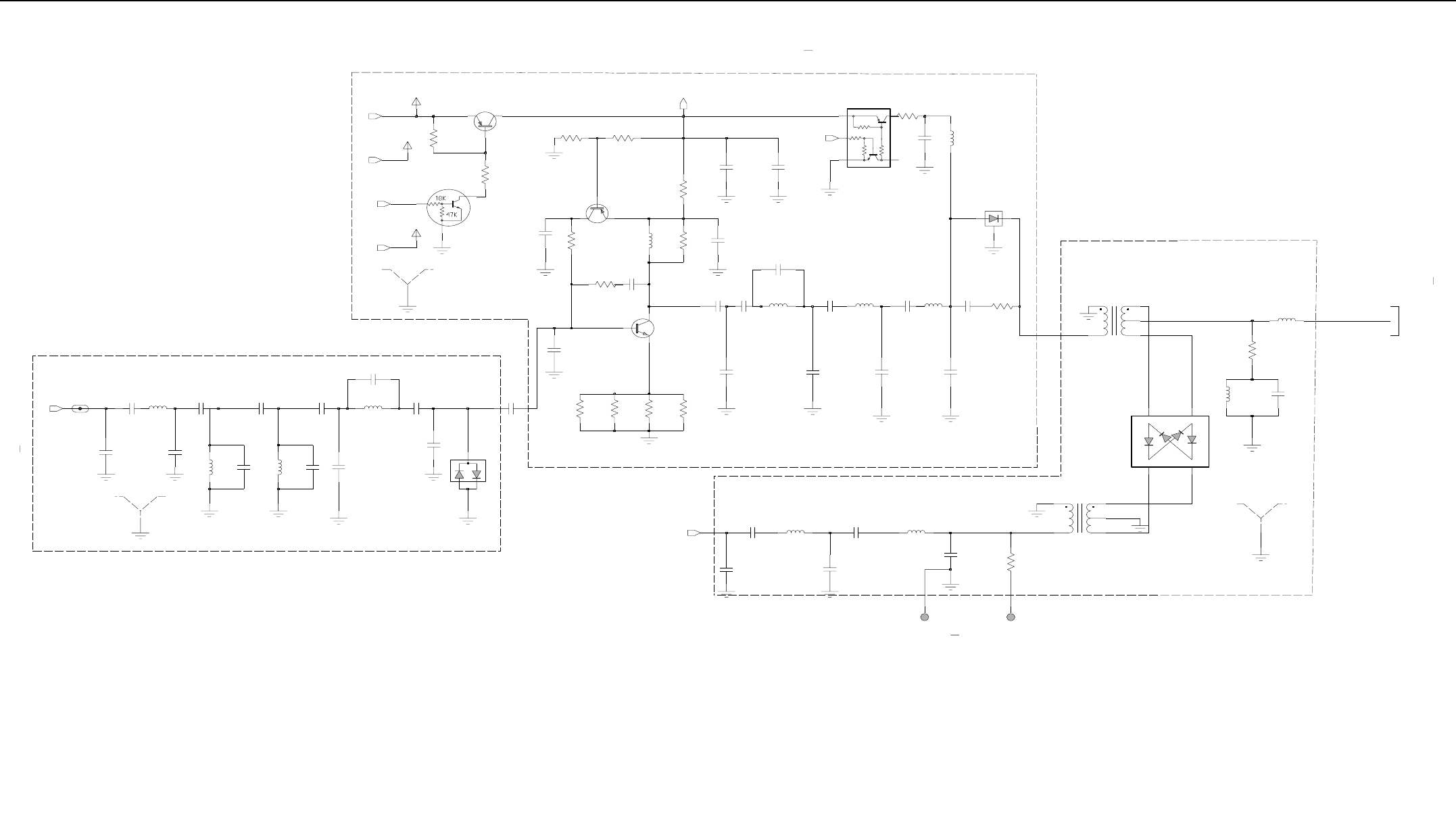
4-12 VHF2 1-25W PCB 8488977U01 (rev. C) / Schematics
1
TEST_POINT
1
IF300
TP4
1
TEST_POINT
TP1
Q306 Q304
R346
10.K
10.K
R345
Q300
C351
K3
K1
A4
A2
U302
36.p
C327
180.p
C337
1.n
C326
1.n
10.
R343 R344
10.10.
470.
R301
R342
SH301
1
SHIELD
SHIELD
1
SH300
SH302
1
SHIELD
3.3p
L314
33.47n
C366
1n
C325
12p
C363
L313
33.47n
L312
33.47n
39p
C362
C348
C361
18p
18p
C344
C345
82p
82p
C332
100.
R337
330p
L302
10n 1.2u
R333
430.
C321
C343
82.p
D305
9V
5V
L311
3V
33.47n33.47n 33.47n
L310
33.47n
L309
L308
33.47n
L307
33.47n
L300
150.n
L306
82p
51.
R340
C342
2
1
3
T301
2
1
3
6
4
XFMR
XFMR
R335
6
4
T300
36.p
220.
C350C334
91.p
56.p
91.p
C333
C346C339
100.p
C347
39.p
10.
R341
BFS540
Q303
470.p
C331
2.4K
1n
C324
470.p
C330
R327
9R
RX
5V
3V
RX_INJ
470.0n
LOC_DIST
RX_EN
9V
C300
L305
120.p
51.p
C338
C354
30.p
C340
82.p
C365
30.p5.6p
C355
82.p
C341
C323
CR301
1.n
C349
36.p
L303
1.2u
R330
1.K 470.p
51.
FRONT-END SHIELD
C328
R339
470.p
C329
15.K
MIXER SHIELD
DNP
DNP
DNP
DNP
DNP
TO SHEET 2
R300 R310
Q301
10.K
VHF2 (146-174MHz) Receiver Front and Back End (Sht 1 of 2)
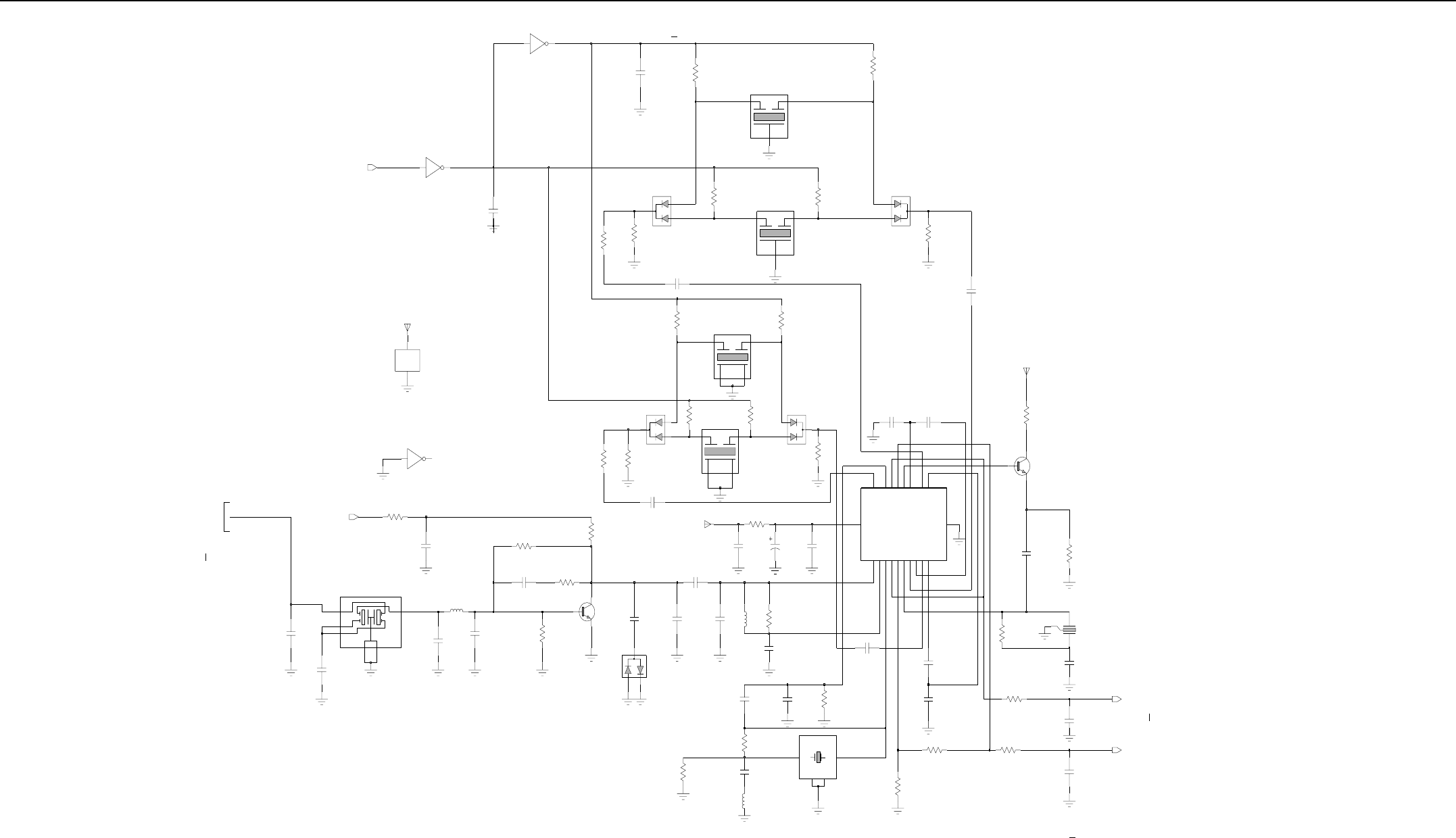
VHF2 1-25W PCB 8488977U01 (rev. C) / Schematics 4-13
VCC
6
RSSI_FEED
9RSSIOUT 5
U300
SA616
8
AUDIOOUT
LIMOUT 11
LIMIN
14
IFAMP_DEC2 17
IFAMP_DEC1
19
16
C356
15.K
IFAMPOUTIFAMPIN
18
GND 15
FREQ
OUT 6
IN
3
GND2
4
GND1
1
AUDIO_FEED
7
RFIN_DEC
2RFIN
1
QUADIN
L315
10
OSCOUT 34 OSCIN
MIXOUT 20
LIM_DEC2
12 LIM_DEC1 13
0.
27nH
C352
R303
30p
33p
R311
FLTR_44.85M
R308
20.K
3V
CC2
5
CC1
2
FL300
R336
100.
13.K
R312
R304
33.K
R332
560.
C360
22p
L304
22p
1.2u
C359
0.1uF
C319
0.1uF
C320
C318
0.1uF
C317
0.1uF
C316
0.1uF
CFWC455D
OUT 2
IN
1
GND2
4
3
GND1
FL304
45B02
Y300
12
3
455KHz
130.0p
44.395MHz
C302
06B09
0.
Y301
IN 13 OUT
4GND1
2GND
R302
R319
R325
3.3K
12.K
D304 D303
R318
12.K
R307
20.K
R317
12.K
3V
PWR_GND
U301
53
TC7W04F
3V
FL303
2
OUTIN
1
4GND2
GND1
3
CFWC455G
5V
U301
VCC
8
GND
4
100n
C315
26
U301
C314
100n
BW_SEL
TC7W04F
71
U301
TC7W04F
C313
C312
100n
R326
2.4K
100n
20.K
20.K
R305
R306
12.K
R316
12.K
R315
R314
3.3K 12.K
R324
D302
FLTR
1IN
3
GND
FL302
D301
FLTR
2
OUT
1IN
3
GND
FL301
2
OUT
100n
C311
100n
C310
1.2K
R329
1.8K
R328
Q302
390.
R334
C309
R313
12.K
100n
RSSI
C322
4.7n
8.2K
R331
680.
R321
DEMOD
R338
10.K
R320
C301
10.0u
51.
C357
22.p
C335
9.1p
8.2p
C364
4.7K
R322
C304
100n
Q305
C305
100n
C303
100n
CR300
C336
6.8p
C367
2.7p 1.2u
L301
4.7K
R323
C306
100n
30p
C353
15.K
R309
C307
100n
DNP
NU
NU
NU
Check if it is 3v or another value
TO SHEET 1
C308
SHEET 6 OF 8
73D02968C63-0
DNPDNP
100n
VHF2 (146-174MHz) Receiver Front and Back End (Sht 2 of 2)
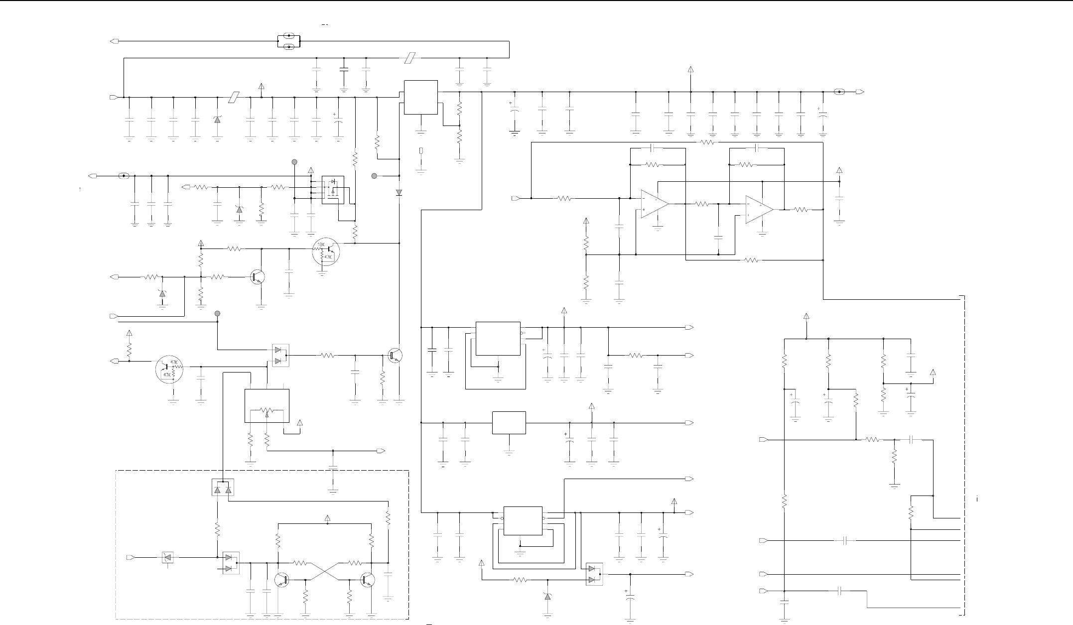
4-14 VHF2 1-25W PCB 8488977U01 (rev. C) / Schematics
R5103
M6
DNP
DNP
DNP
Indirect
Audio
Volume
Place near uP
SOURCE
Smart Fuse Circuit
DNP
DNP For mid_band
spacer for TO-220
On/Off for ATE
DNP DNP
DNP IN MARLIN +
DNP
DNP
DNP
DNP
DNP
DNP
DNP
DNP
DNP
DNP DNP
100.n
C5063
10.K
R5054
L500
IF500
1
FILT_SW_B+
TP555
TEST_POINT
1
10.0u
FILT_SW_B+
9V
COMP_B+
B+
100.n
3V
D3_3V
5V
1n
5V
3V
D3_3V
MIC_AUDIO_CH
VOL_INDIRECT
EXTERNAL_MIC_AUDIO_ACCESS_CONN
DEMOD
RESET
DC_POWER_ON
EMERGENCY_ACCES_CONN
EMERGENCY_SENSE
ONOFF_SENSE
IGNITION
100.p
Q503
28.0
VR500
R5085
1019447L120
510.
DNP
3.3V to IFIC, ASFIC
TO SHEET 2
DNP
DNP
DNP
DNP
DNP
DNP
DNP
POWER SUPPLY
VAG=4.5v
3.3V RF REGULATOR
3.3v digital
3.3v Digital REGULATOR
9.3V
SOURCE
SOURCE
5V TO LVFRACN
1%
1%
5V RF Regulator
9.3V
SOURCE
SOURCE
BATT_SENSE
5V_CH
VS_MIC
VSTBY VS_AUDIO_SEL
R5076
510.
R5075
R5078
9V
100.
R5071
2.2K
100n
C5047
2.2K
R5070
1n
C5067 100n
C5015
1n
C5065
C5066
1n
C5064
1n
57R01
IF502
1
9V
C1127
100.u
C1125
220.p220.p
C1124
220.p
C1123C1122
220.p220.p
C1034
100.n
C5061
C5000
1n
47.K
R5036
VR504
3.3
FILT_B+
3.3
VR503
13.K
D511
R5050
R5031
62.K
C5008
IF503
1
C1088
IF501
220.p
C1114
1n
C1098
220.p
C5094
C5096
220.p220.p
C5095
R5069
10.K
R5037
10.K
10.M
R5002
300.
C5071
R5077
1n
C5019
100n
R5053
R5052
10.K
10.K
C1087
1n
FILT_B+
C5038
R5039
100.K
C5011
10.0u
10.0u
C5010 C5009
10.0u
100.
R5079
C5039
100.n
4
NC 9
5
OUTPUT
6SENSE
8SHUTDOWN
TAP
3
LP2986ILDX
ERROR 7
2
FEEDBACK
GND
1
INPUT
MC33269D
1GND
3IN 2
OUT
U510
U508
2.2u
C5041
1u
C5043
1u
C5042
FILT_B+
C1097
1n
47u
C5120
D501
24.K
3.9
VR502
220.p
1.u
C5114
C5116
220.p
C5113
R5096
100.K
R5095
200.K
1.M
220.K
R5094
R5093 R5099
100.K
6
5
7
8
4
R5092
100.K
2
3
1
8
4
LM2904
U500
TEST_POINT
TP556
1
LM2904
U500
100.n
C5040
FILT_B+
R5074
1.K
1.K
R5073
D500
D513
VR501
5.1
1n
C5070C5018
100n
47u
C5007C5069C5017
1n100n
C5006
10.0u 1n
C5016 C5068
220.p
100n
C1113
220.p
C5092
TEST_POINT
TP500
1
220.p
C1128
1n
C1085
Q502
Q504
R5035
47.K
Q505
D3_3V
100n
C5035
1n
C5074
Q500
R5029
R5038
33.K
100.K
R5028
100.K
VOUT 5
U514
U501
LM2941T
ADJ 1
GND
3
ON_OFF
2
VIN
4
C5062
100.n
R5000
0.
22.n
C5086
C5084
R5049
15.K
33.K
R5030
Q506
1.u
C5045
C5085
22.n
100.p
C5083
100.n
R5020
C5060
C5119
D3_3V
150.K
10.u
10.u
C5104
6.8p
C5115
5V
C5117
16.p
5V
100n
C5118
R5100
1.M
0.
R5098
0.
R5097
24.K
R5048
1.M
R5089
1.M
R5082
51.K R5083
270.K
0.
D502
R5047
1.n
C5111
1.n
C5110
C5102
100n
C5037
100.n
R5062
10.K
C5005
100.u
R5081
6.34K
R5001
C5001
10.u
1.K
6
5
4
2
SWITCH
S5010
50.K
3
LOW
1HIGH
ERROR
7FEEDBACK
4
GND
8INPUT 1
OUTPUT
2
SENSE
3SHUTDOWN
LP2951C
U503
6
5V_TAP
5
VHF2 (146-174MHz) DC and Audio Circuits (Sht 1 of 2)
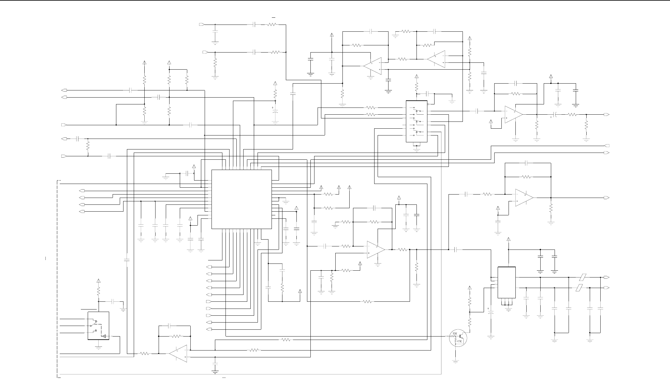
VHF2 1-25W PCB 8488977U01 (rev. C) / Schematics 4-15
C5072
1n
C5073
200K
36K
1K
DNP
120p
SPKR+
HANDSET_RX_AUDIO_CH
R5086
VDDDAC
11
VDDRC 45
VDDSYN 27
VOX
7
3V
FILT_SW_B+
POST_LIMITER_FLAT_TX_AUDIO_RETURN_OPT_BRD
SPKR-
0.
R5088
3V
30C53
U504
R5066
9V
VAG
VAG
C5033
100n
3V
C5027
1019447
L502
100n
C5032 C5088
L501
6.2K
R5065
1.n
C5076
DNP
DNP
TO SHEET 1
SHEET7OF8
73D02968C63-0
DNP
DNP
DNP
DNP
USE NLAS4599
DNP IN MARLIN
DNP IN MARLIN
DNP IN MARLIN
DNP
DNP
DNP
DNP
DNP
DNP
DNP
AUDIO
DNP
DNPDNP
DNP
R5024
100.K
1019447
82.p
C5090 R5068
6.2K
R5067
6.2K
0.
R5014
R5013
0.
270.K
R5027
100.n
C5036
SQIN
9SYN 28
TXRTN 36
TXSND 44
UIO
10
VDDA
1
VDDCP 32
VDDD 33
MOD
NC 26
PLCAP
8
25
PLCAP2
RXRTN 43
RXSND 39
SQCAP
12
SQDET
17
GNDDO
GNDRC 47
GNDSYN
23
HSIO
19
LCAP
24
LSIO
18
MICEXT 48
MICINT 46
40
GCB0
15
14 GCB1
GCB2
13
GCB3 35
GCB4 37
GCB5 38
GNDA
3
GNDD 31
30
CLK168 34
20 CSX
DACG
6DACR
5DACU
4
DATA
22
DISC
2
F1200 29
AUDIO 41
AUXTN 42
CHACT
16
21 CLK
C5046
100n
X0
12
13 X1
Y15
Y0
2
1Y1
Z4
Z0
5
3Z1
11
A
B10
C9
EN 6
8GND
VCC 16
VEE
7
X14
22n
U509
MC14053B
C5059
C5101
1.n
C5100
220.p220.p
C5099
100.K
R5087
560.
R5084
0.
100n
C5103
5
COM
GND
3
1
IN
4NC
6
NO
VPOS 2
3V
100n
MAX4599EXT
U515
C5023 C5013
1u
C5012
100n
C5022
4.7u
10.
R5080
1n
C5056
100.n
R5064
8.2K24.K
R5044 R5063
3V
24.K
R5043
8.2K
C5055
1.u
100.K
R5023
100n
30.K
R5040
C5026
100n
R5033
47.K
100n
C5025
C5024
100n
R5016
9V
1.M
C5058
100n
10.K
R5059
10.K
R5058
47u
C5003
100.K
R5025
R5009
0.
LM2904 6
5
7
8
4
U507
R5021
82.p
100.K
100n
C5028
NINV
4
OUT1
6
OUT2
3RR
7
VCC
9V
B+
3V
2GND1
5GND2
10 GND3
11 GND4
9INV
8M_SS
1
TDA1519C
U502
100n
C5052
100n
C5051
24.K
R5042
C5050
100n
R5034
R5032 56.K
R5057
10.K
10.K
R5056
82.p
C5089
6
5
7
8
4
R5022
100.K
U505
6
5
7
8
4
U506
LM2904
U505
LM2904
2
3
1
8
4
LM2904
U506
LM2904 2
3
1
8
4
100n
C5054
100n
C5053
220.p 220.p
C5098C5097
C5091
82.p
1.n
C5082
1.n
C5080
C5081
1.n
1.n
C5079
C5078
1.n
1.n
3V
C5077
24.K
R5041
12.K
R5051
Q501
47u
C5002
C5087
R5019
10.K
R5055
100n
C5049
C5048
100n
100n
C5020
10.K
R5061
R5060
10.K
R5026
33.K
R5072
4.7K
100nC5014
2.2u
5V
C5034
R5011
0.
3V
R5010
3V
1n
0.
3V
C5075
100n
C5031
R5046
24.K
33.K
R5045
2
3
1
8
4
LM2904
U507
C5057
100n
C5030
100n
3V
R5008
0.
1u
C5044
3V
3V
100n
C5029
C5021
100.n
TX_AUDIO_RETURN_OPT_BRD
16.8MHz
RX_AUDIO_OUTPUT_ACCESS_CONN
TX_AUDIO_SEND_OPT_BRD
RX_AUDIO_RETURN_OPT_BRD
UNMUTED_RX_AUDIO_SEND_OPT_BRD
DETECTOR_AUDIO_SEND_OPT_BRD
FLAT_TX_AUDIO_INPUT_ACCESS_CONN
CH_ACT
SPI_CLK
ASFIC_CS
PWR_SET
PA_CURRENT
PA_BIAS
SPI_MOSI
F1200
BW_SEL
DC_POWER_ON
FLAT_OR_DEEMPH_RX_AUD_SEL
HSIO
LSIO
MOD_OUT
SQ_DET
uP_CLK
VOX
VHF2 (146-174MHz) DC and Audio Circuits (Sht 2 of 2)
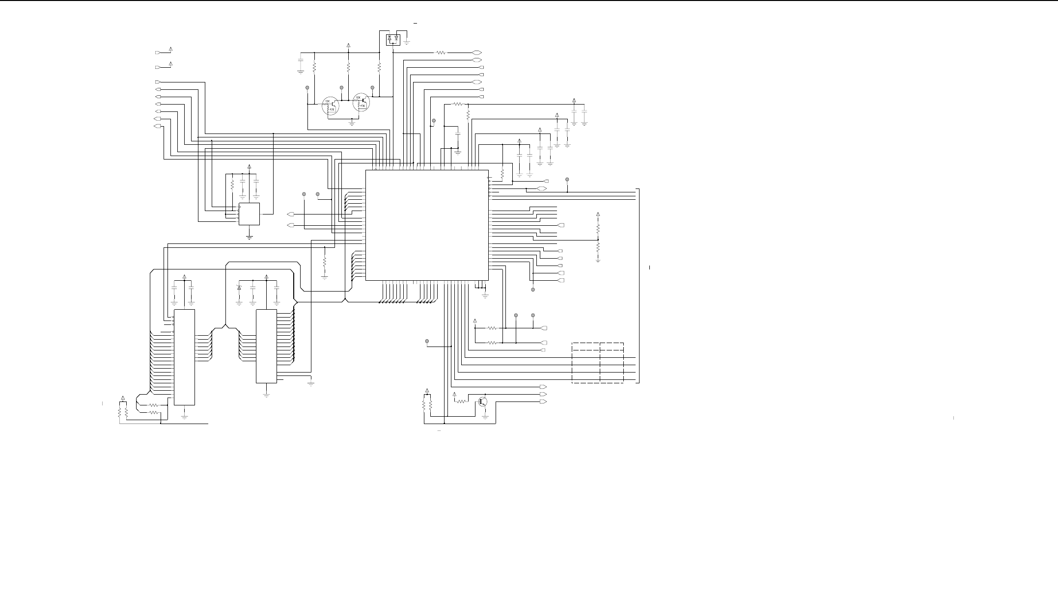
4-16 VHF2 1-25W PCB 8488977U01 (rev. C) / Schematics
DNP
DNP
DO NOT CONNECTTHIS CS IN ORDER TO
PROVIDEWIRED OR OPERATION ON CSPROG
DNP
DNP
SPI_MOSI
SPI_MISO
SPI_CLK
ASFIC_CS
DISPLAY_CS_CH
SYNTH_CS
EE_CS
SHIFT_R_CS
MARLIN MARLIN+
VS_INT
PROG_OUT-ALARM_4
VS_CS
PROG_IO-P8_O
PROG_IO-P12_O SHIFT_REGN_CS
PROG_IO-P14_O VS_RAC
TO SHEET 2
DNP
DNP
13 VSS
U403
94
RESET
78
PJ7
MC68HC11FL0
91
XTAL
48
XIRQ
XFC 93
87 VSSR
40 VSSL
71
PJ0_CSGP3
49 PI7 68
VRL
69
VRH
92
VDDSYN
88
VDDR
39
VDDL
12
VDD
56 PI0
38 PH7_CSPROG
77
PJ6
76
PJ5
75
PJ4
74
PJ3
73
PJ2
72
PJ1_CSGP4
PH1_PW2
47 PH0_PW1
4
50 PI6
51 PI5
52 PI4
53 PI3
54 PI2
55 PI1
16 PG1_XA14
6PG0_XA13
29
41 PH6_CSGP2
42 PH5_CSGP1
43 PH4_CSIO
44 PH3_PW4
45 PH2_PW3
46
27 PF2_ADDR2
28 PF1_ADDR1
PE7_AN7
PG7_R_W
5PG6_AS
18 PG5_XA18
17 PG4_XA17
19 PG3_XA16
20 PG2_XA15
PE1_AN1 66
PE0_AN0 67
PD6_LVIN
PFO_ADDR0
22 PF7_ADDR7
23 PF6_ADDR6
24 PF5_ADDR5
25 PF4_ADDR4
26 PF3_ADDR3 97
PD0_RXD
37 PC7_DATA7
60
PE6_AN6 61
PE5_AN5 62
PE4_AN4 63
PE3_AN3 64
PE2_AN2 65
PC1_DATA1
30
14 PBO_ADDR8
3
2
PD5_SS
1
PD4_SCK
100
PD3_MOSI
99
PD2_MISO
98
PD1_TXD
11 PB2_ADDR10
10 PB1_ADDR9
86
PA7_PA1_OC1
36 PC6_DATA6
35 PC5_DATA5
34 PC4_DATA4
33 PC3_DATA3
32 PC2_DATA2
31 PC0_DATA0
58
MODA_LIR
LVOUT 95
96
IRQ
90
EXTAL
89
ECLK
70 AVSS
59
AVDD
85
PA6_OC2_OC1
84
PA5_OC3_OC1
83
PA4_OC4_OC1
82
PA3_IC4_OC5_OC1
81
PA2_IC1
80
PA1_IC2
79
PA0_IC3
57
MODB_VSTBY
7PB7_ADDR15
8PB6_ADDR14
ACCESS_PTT
A18_RES
PROG_IN-P6_I
PROG_IO-P8_I
PROG_IO-P14_I
PROG_IO-P12_I
SHIFT_R_CS
SHIFT_R_CS
MIC_PTT
MIC_SENSE
TX_EN
15 PB5_ADDR13
21 PB4_ADDR12
9PB3_ADDR11
100.K
D3_3V
100.K
R473
R471
10.
R472
TEST_POINT
TP408
1
TEST_POINT
TP402
1
TEST_POINT
TP407
1
TEST_POINT
TP425
1
TEST_POINT
TP401
1
1
TEST_POINT
TP400
1
TP410
1
TP404
TEST_POINT
1
TEST_POINT
TP409
1
TEST_POINT
TP406
1
TEST_POINT
Q417
TEST_POINT
TP403
R463
10.K
100n
C410
10.K
R451 R450
10.K
Q400
VR401
Q407
D3_3V
4.3
28
29
I_O7
RESET
9
VCC
8
7
GND
24
I_O0 21
I_O1 22
I_O2 23
I_O3 25
I_O4 26
I_O5 27
I_O6
16
A5
15
A6
14
A7
13
A8
3
A9
2
EN_CE
30
EN_OE
32
EN_WE
12
A13
4
A14
5
A15
11
A16
10
6A17
A2
18
A3
17
A4
U404
A0
20
A1
19
A10
31
A11
1
A12
3.3K
R443
D3_3V
AT49LV002N_70VI
R442
10.K
10.K
R441
R428
100.K
100.K
D3_3V
R427
100.K
R426 0.
R415
0.
FILT_SW_B+
R414
D3_3V
C416
1n 100n
D3_3V
C408
1n
C415
100n
C407
C414
D3_3V
C406
1n
D3_3V
100n
C413
1n 100n
C405
100.K
R425
C404
100n
C412
1n 100n
C403 C411
D3_3V
100n1n
R439
C402
10.K
R462
51.
D400
D3_3V
R424
100.K
D3_3V
100.K
R423
C400
1n 100n
C401
10.K
R438
D8
19
OE 22
VDD
28
VSS
14
WE 27
D3_3V
D3_3V
D3_3V
CS 20
D1
11
D2
12
D3
13
D4
15
D5
16
D6
17
D7
18
A2 8
A3 7
A4 6
A5 5
A6 4
A7 3
A8 25
A9 24
A0 10
A1 9
A10 21
A11 23
A12 2
A13 26
A14 1
3
U402
SRM2B256
1CS
7HOLD
6SCK
5SI
2
SO
8
VCC
4
VSS
WP
U400
X25128-2.7
R_W
R_W
D3_3V
SCI_CH
FILT_SW_B+
R_W
A18_RES
SPI_CLK
SPI_CLK
ASFIC_CS
ASFIC_CS
EE_CS
EE_CS
EMERGENCY_SENSE
RSSI
VOX
KEYPAD_COL_CH
KEYPAD_ROW_CH
COMM_DATA_SEL_CH
SYNTH_CS
SYNTH_CS
LOC_DIST
DISPLAY_CS_CH
DISPLAY_CS_CH
SYNTH_LOCK
OPT_EN_OPBD
RX_EN
ONOFF_SENSE
VOL_INDIRECT
BATT_SENSE
RESET
A(6)
A(5)
A(4)
A(3)
A(2)
A(1)
A(0)
uP_CLK
OPT_DATA_R_OPBD
LSIO
F1200
HSIO
SQ_DET
CH_ACT
SPI_MISO
SPI_MISO
SPI_MISO
SPI_MOSI
SPI_MOSI
SPI_MOSI
SPI_CLK
A(5)
A(4)
A(3)
A(2)
A(1)
A(0)
A(15)
A(16)
A(18)
A(17)
A(14)
A(13)
A(12)
A(11)
A(10)
A(9)
A(8)
A(7)
D(4)
D(3)
D(2)
D(1)
D(0)
D(7)
D(6)
D(5)
D(4)
D(3)
D(2)
D(1)
D(0)
A(14)
A(13)
A(12)
A(11)
A(10)
A(9)
A(8)
A(7)
A(6)
A(0:18)
A(8)
A(9)
A(10)
A(11)
A(12)
A(13)
A(0)
A(1)
A(2)
A(3)
A(4)
A(5)
A(6)
A(7)
A(14)
A(15)
A(16)
A(17)
A(18)
D(0:7)
D(0)
D(1)
D(2)
D(3)
D(4)
D(5)
D(6)
D(7)
D(7)
D(6)
D(5)
VHF2 (146-174MHz) Microprocessor and Controller Circuits (Sht 1 of 2)
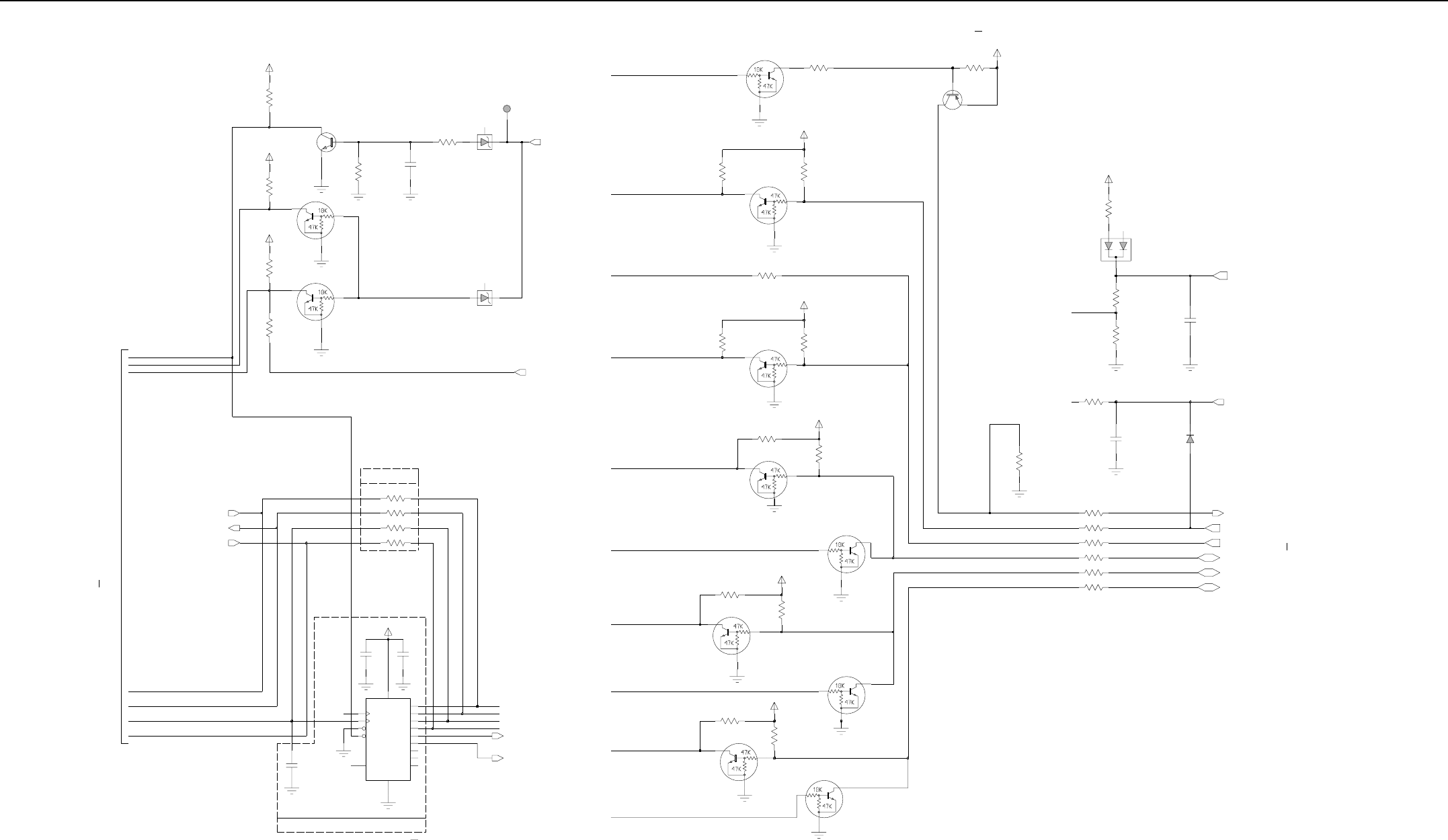
VHF2 1-25W PCB 8488977U01 (rev. C) / Schematics 4-17
PROG_IN
PROG_I/O
PROG_I/O
PROG_I/O
EXT_ALARM_OUT
EXT_MIC_PTT
DNP IN MARLIN+
DNP IN MARLIN
DNP
DNP
DNP
DNP
DNP
DNP
73D02968C63-0
SHEET 8 OF 8
TO SHEET 1
VSTBY
R470
10.K
TEST_POINT
TP405
1
R431
10.K
R459
47.K
22.n
C421
1n
C422
100n
C423
10 RESET
14 SERIN 9
SEROUT
16
VCC
D3_3V
15
Q0 1
Q1 2
Q2 3
Q3 4
Q4 5
Q5 6
Q6 7
Q7
MC74HC595A
U405
12 CLK_L
11 CLK_S
13 EN_OE
8
GND
0.
R469
R467
R468 0.
0.
R466 0.
C490
1.u
10.K
D3_3V
R422
39.K
R430
100.K
R429
D401
R421
220.
220.
R461
1n
D3_3V
C418
3.3K
R458
D3_3V
1n
C417
3.30
VR402
VR400
6.80
10.K
R445
R444
D3_3V
10.K
Q415
Q414
Q413
D402
Q405
Q404
Q416
Q403
R401
2.7K
R460
FILT_SW_B+
1.5K
R440
10.K
Q401
R407 0.
0.
R406
33.K
R436
D3_3V
3.3K
R457
Q412
0.
R405
R435
33.K
R456
3.3K
D3_3V
D3_3V
Q411
33.K
R434
3.3K
R455
Q410
0.
R404
R403 0.
33.K
D3_3V
R433
3.3K
R454
Q409
D3_3V
R432
33.K
R453
Q408 3.3K
0.
R402
PROG_OUT-ALARM_4
HOOK_CH
MIC_PTT_CH
BOOT_EN_IN_CH
MIC_PTT
MIC_SENSE
SCI_CH
PROG_OUT-ALARM_4
PROG_IO-P8_O
PROG_IO-P12_O
PROG_IO-P14_O
VS_AUDIO_SEL
VS_GAIN_SEL
SPI_MOSI
SPI_CLK
PROG_I-ACC_C_3
PROG_O-ACC_C_4
PROG_I-ACC_C_6
PROG_IO-ACC_C_8
PROG_IO-ACC_C_12
PROG_IO-ACC_C_14
PROG_IO-P14_I
PROG_IO-P14_O
PROG_IO-P12_I
PROG_IO-P12_O
PROG_IO-P8_I
PROG_IO-P8_O
PROG_IN-P6_I
ACCESS_PTT
VS_INT
VS_CS
VS_RAC
VHF2 (146-174MHz) Microprocessor and Controller Circuits (Sht 2 of 2)
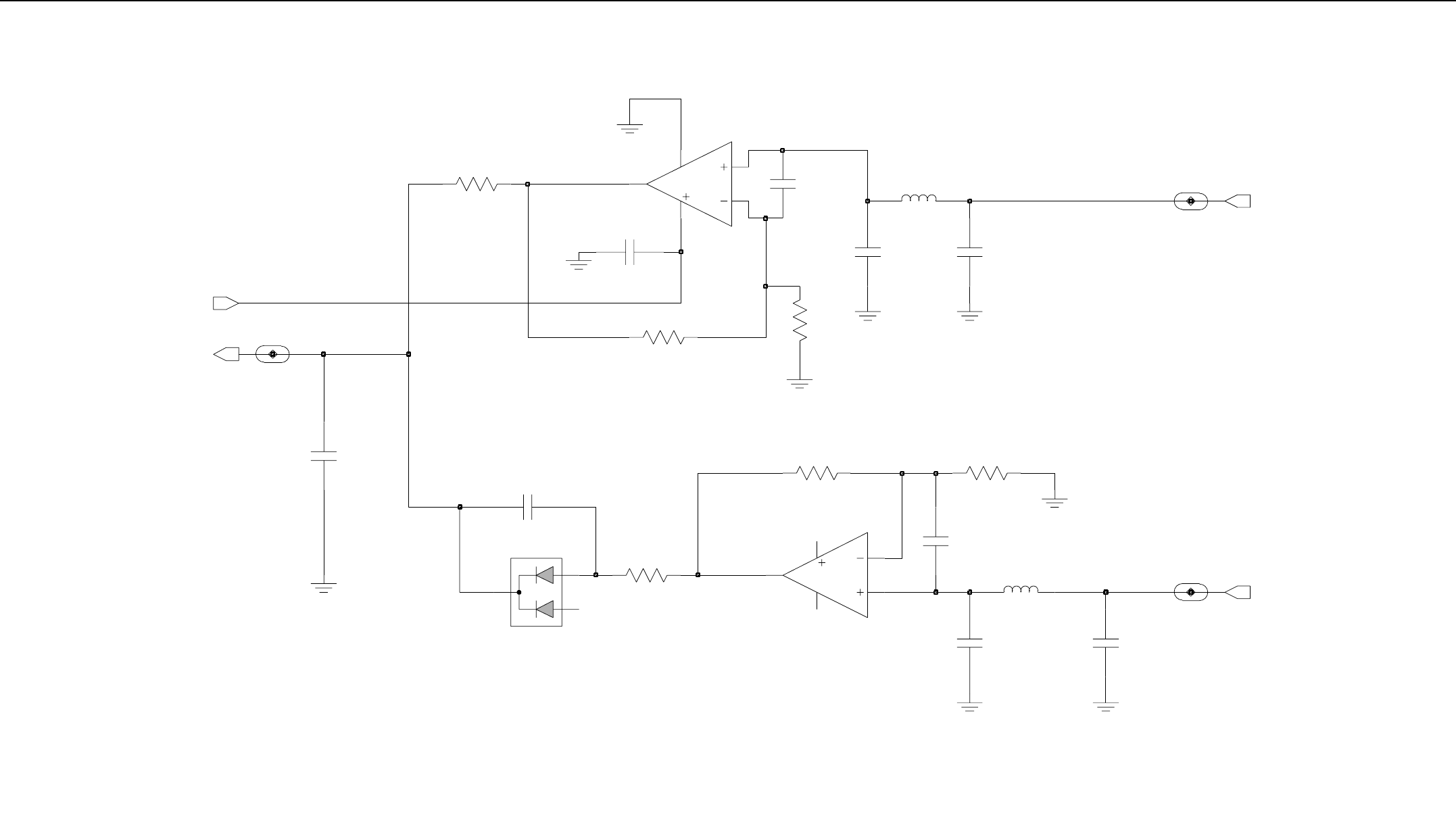
4-18 VHF2 1-25W PCB 8488977U01 (rev. C) / Schematics
IF701
1
DET_VRVS
FILT_SW_B+
INTEGRATOR
DET_VFWD
1n
DNP
73D02968C63-0
SHEET 3 OF 8
L102
C1047
1.u
15K
R117
R141
22.K
22.K
R140
1n
C1046
C1045
1n
1.u
L101
C1082
IF702
1
1n
1n
IF700
C1076
7
8
4
C1075
1n
3
1
8
4
U100
LM2904 6
5
U100
LM2904
2
C1071
1n
R146
22.K
1n
C1049
D101
R164
10.K
22.K
R144
1n
C1048
VHF2 (146-174MHz) Power Control Circuit
VHF2 1-25W PCB 8488977U01 (rev. C) / Schematics 4-19
2.1 VHF2 PCB 8488977U01 (rev. C) Parts List
1-25W
Circuit
Ref.
Motorola
Part No. Description
C1000 2113740F59 CAP CHIP REEL CL1 +/-30 220
C1001 2311049A08 KEMET CAPS
C1002 2111078B59 CHIP CAP RF 470 5 NPO 100V
C1003 2111078B59 CHIP CAP RF 470 5 NPO 100V
C1004 2111078B47 CAP CHIP RF 150 5 NP O 100V
C1005 2111078B47 CAP CHIP RF 150 5 NP O 100V
C1006 2111078B47 CAP CHIP RF 150 5 NP O 100V
C1007 NOT PLACED GCAM DUMMY PART NUMBER
C1008 2111078B42 CAP CHIP RF 100 5 NPO 100V
C1009 2111078B42 CAP CHIP RF 100 5 NPO 100V
C1010 2111078B42 CAP CHIP RF 100 5 NPO 100V
C1011 2111078B38 CAP CHIP RF 68 5 NPO 100V
C1012 2111078B36 CAP CHIP RF 56 5 NPO 100V
C1013 2111078B36 CAP CHIP RF 56 5 NPO 100V
C1014 NOT PLACED GCAM DUMMY PART NUMBER
C1015 2111078B34 CAP CHIP RF 47 5 NPO 100V
C1016 2111078B29 CAP CHIP RF 33 5 NPO 100V
C1017 2111078B22 CAP CHIP RF 22 5 NPO 100V
C1018 NOT PLACED GCAM DUMMY PART NUMBER
C1019 2111078B16 CAP CHIP RF 13 5 NPO 100V
C1020 2111078B15 CAP CHIP RF 12 5 NPO 100V
C1021 2111078B13 CAP ALT E16
C1022 2111078B09 CAP ALT E17
C1023 2111078B21 CAP ALT E35
C1024 2111078B05 CAP ALT E19
C1025 2111078B05 CAP ALT E19
C1027 2311049A45 CAP TANT CHIP 10 10 35
C1028 2113743K15 CER CHIP CAP .100UF
C1029 2113743K15 CER CHIP CAP .100UF
C1030 2113743E07 CER CHIP CAP .022UF
C1031 2113743E07 CER CHIP CAP .022UF
C1032 2113743E07 CER CHIP CAP .022UF
C1033 2113743E07 CER CHIP CAP .022UF
C1034 2113740F59 CAP CHIP REEL CL1 +/-30 220
C1035 2113743E07 CER CHIP CAP .022UF
C1036 2113743E07 CER CHIP CAP .022UF
C1037 2113743E07 CER CHIP CAP .022UF
C1038 NOT PLACED GCAM DUMMY PART NUMBER
C1039 2113743E07 CER CHIP CAP .022UF
C1040 2113741F33 CAP CHIP CL2 X7R REEL 2200
C1041 2113741F25 CAP CHIP CL2 X7R REEL 1000
C1042 2113741F25 CAP CHIP CL2 X7R REEL 1000
C1043 2113741F25 CAP CHIP CL2 X7R REEL 1000
C1044 2113741F25 CAP CHIP CL2 X7R REEL 1000
C1045 2113741F25 CAP CHIP CL2 X7R REEL 1000
C1046 2113741F25 CAP CHIP CL2 X7R REEL 1000
C1047 2113743K17 CAP CHIP .330 UF +80-20% 16V
C1048 2113741F25 CAP CHIP CL2 X7R REEL 1000
C1049 2113741F25 CAP CHIP CL2 X7R REEL 1000
C1050 2113741F25 CAP CHIP CL2 X7R REEL 1000
C1051 2113741F25 CAP CHIP CL2 X7R REEL 1000
C1052 2113741F25 CAP CHIP CL2 X7R REEL 1000
C1053 2113741F25 CAP CHIP CL2 X7R REEL 1000
C1054 2113741F25 CAP CHIP CL2 X7R REEL 1000
C1055 2113741F25 CAP CHIP CL2 X7R REEL 1000
C1056 2113741F25 CAP CHIP CL2 X7R REEL 1000
C1057 2113741F25 CAP CHIP CL2 X7R REEL 1000
C1058 2113741F25 CAP CHIP CL2 X7R REEL 1000
C1059 2113741F25 CAP CHIP CL2 X7R REEL 1000
C1060 2113741F25 CAP CHIP CL2 X7R REEL 1000
C1061 2113741F25 CAP CHIP CL2 X7R REEL 1000
Circuit
Ref.
Motorola
Part No. Description
C1062 2113741F25 CAP CHIP CL2 X7R REEL 1000
C1063 2113741F25 CAP CHIP CL2 X7R REEL 1000
C1064 2113741F25 CAP CHIP CL2 X7R REEL 1000
C1065 2113741F25 CAP CHIP CL2 X7R REEL 1000
C1066 2113741F25 CAP CHIP CL2 X7R REEL 1000
C1067 2113741F25 CAP CHIP CL2 X7R REEL 1000
C1068 2113741F25 CAP CHIP CL2 X7R REEL 1000
C1069 2113741F25 CAP CHIP CL2 X7R REEL 1000
C1070 2113741F25 CAP CHIP CL2 X7R REEL 1000
C1071 2113741F25 CAP CHIP CL2 X7R REEL 1000
C1072 2113741F25 CAP CHIP CL2 X7R REEL 1000
C1073 2113741F25 CAP CHIP CL2 X7R REEL 1000
C1074 2113741F25 CAP CHIP CL2 X7R REEL 1000
C1075 2113741F25 CAP CHIP CL2 X7R REEL 1000
C1076 2113741F25 CAP CHIP CL2 X7R REEL 1000
C1077 2113741F25 CAP CHIP CL2 X7R REEL 1000
C1078 2113740F59 CAP CHIP REEL CL1 +/-30 220
C1079 2113741F25 CAP CHIP CL2 X7R REEL 1000
C1080 2113741F25 CAP CHIP CL2 X7R REEL 1000
C1081 NOT PLACED GCAM DUMMY PART NUMBER
C1082 NOT PLACED GCAM DUMMY PART NUMBER
C1083 2113741F25 CAP CHIP CL2 X7R REEL 1000
C1084 2113740F59 CAP CHIP REEL CL1 +/-30 220
C1085 2113741F25 CAP CHIP CL2 X7R REEL 1000
C1086 2113741F25 CAP CHIP CL2 X7R REEL 1000
C1087 2113741F25 CAP CHIP CL2 X7R REEL 1000
C1088 2113741F25 CAP CHIP CL2 X7R REEL 1000
C1089 2113741F25 CAP CHIP CL2 X7R REEL 1000
C1090 NOT PLACED GCAM DUMMY PART NUMBER
C1091 NOT PLACED GCAM DUMMY PART NUMBER
C1092 NOT PLACED GCAM DUMMY PART NUMBER
C1093 NOT PLACED GCAM DUMMY PART NUMBER
Circuit
Ref.
Motorola
Part No. Description
C1094 NOT PLACED GCAM DUMMY PART NUMBER
C1095 NOT PLACED GCAM DUMMY PART NUMBER
C1097 2113741F25 CAP CHIP CL2 X7R REEL 1000
C1098 2113741F25 CAP CHIP CL2 X7R REEL 1000
C1099 2113741F25 CAP CHIP CL2 X7R REEL 1000
C1100 2113741F25 CAP CHIP CL2 X7R REEL 1000
C1101 2113740F51 CAP CHIP REEL CL1 +/-30 100
C1102 2113740F51 CAP CHIP REEL CL1 +/-30 100
C1103 2113741A57 CAP CHIP 33K +-5%
(2160521A31)
C1104 2113741A53 CAP CHIP CL2 X7R REEL 22000
C1105 2113740F67 CAP CHIP CL1 +/-30 470 5%
C1106 2113740F67 CAP CHIP CL1 +/-30 470 5%
C1107 2113740F67 CAP CHIP CL1 +/-30 470 5%
C1108 2113740F47 CAP CHIP REEL CL1 +/-30 68
C1109 2113740F59 CAP CHIP REEL CL1 +/-30 220
C1110 2113740F59 CAP CHIP REEL CL1 +/-30 220
C1112 2113740F59 CAP CHIP REEL CL1 +/-30 220
C1113 2113740F59 CAP CHIP REEL CL1 +/-30 220
C1114 2113740F59 CAP CHIP REEL CL1 +/-30 220
C1115 2113740F59 CAP CHIP REEL CL1 +/-30 220
C1116 2113740F59 CAP CHIP REEL CL1 +/-30 220
C1117 2113740F43 CAP CHIP REEL CL1 +/-30 47
C1118 2113740F39 CAP CHIP REEL CL1 +/-30 33
C1119 2113740F39 CAP CHIP REEL CL1 +/-30 33
C1120 2113740F39 CAP CHIP REEL CL1 +/-30 33
C1121 NOT PLACED GCAM DUMMY PART NUMBER
C1122 2113740F59 CAP CHIP REEL CL1 +/-30 220
C1123 2113740F59 CAP CHIP REEL CL1 +/-30 220
C1124 2113740F59 CAP CHIP REEL CL1 +/-30 220
C1125 2113740F59 CAP CHIP REEL CL1 +/-30 220
C1126 2113740F59 CAP CHIP REEL CL1 +/-30 220
Circuit
Ref.
Motorola
Part No. Description
4-20 VHF2 1-25W PCB 8488977U01 (rev. C) / Schematics
C1127 2360567A03 CAP TANTALUM
C1128 2113740F59 CAP CHIP REEL CL1 +/-30 220
C1129 2113740F59 CAP CHIP REEL CL1 +/-30 220
C1130 2113740F59 CAP CHIP REEL CL1 +/-30 220
C1131 NOT PLACED GCAM DUMMY PART NUMBER
C2000 2113743F18 CAP CHIP 2.2 UF 16V +80-20%
C2001 2311049J11 CAPACITOR TANT 10% 4.7UF
C2002 2311049A56 CAP TAN CHIP A/P 4.7 20 10
C2003 2113743K15 CER CHIP CAP .100UF
C2004 2113743F18 CAP CHIP 2.2 UF 16V +80-20%
C2005 2113743F18 CAP CHIP 2.2 UF 16V +80-20%
C2006 2113743F18 CAP CHIP 2.2 UF 16V +80-20%
C2007 2113743E20 CAP CHIP. 10 UF 10%
C2008 2113743E20 CAP CHIP. 10 UF 10%
C2009 2113743E20 CAP CHIP. 10 UF 10%
C2010 2113743E20 CAP CHIP. 10 UF 10%
C2011 2113743E20 CAP CHIP. 10 UF 10%
C2012 NOT PLACED GCAM DUMMY PART NUMBER
C2013 2113743E20 CAP CHIP. 10 UF 10%
C2014 2113743E20 CAP CHIP. 10 UF 10%
C2015 2113743E20 CAP CHIP. 10 UF 10%
C2016 2113743E20 CAP CHIP. 10 UF 10%
C2017 2113743E20 CAP CHIP. 10 UF 10%
C2018 2113743E20 CAP CHIP. 10 UF 10%
C2019 2113743E20 CAP CHIP. 10 UF 10%
C2020 2113743E20 CAP CHIP. 10 UF 10%
C2021 2113741F49 CAP CHIP CL2 X7R REEL 10000
C2022 2113741F49 CAP CHIP CL2 X7R REEL 10000
C2023 2113741F49 CAP CHIP CL2 X7R REEL 10000
C2024 2113741F49 CAP CHIP CL2 X7R REEL 10000
C2025 2113741F49 CAP CHIP CL2 X7R REEL 10000
C2026 2113741F49 CAP CHIP CL2 X7R REEL 10000
Circuit
Ref.
Motorola
Part No. Description
C2027 2113741F49 CAP CHIP CL2 X7R REEL 10000
C2028 2113741F33 CAP CHIP CL2 X7R REEL 2200
C2029 2113741F25 CAP CHIP CL2 X7R REEL 1000
C2030 2113741F39 CAP CHIP CL2 XTR REEL 3900
C2031 NOT PLACED GCAM DUMMY PART NUMBER
C2032 2113741F25 CAP CHIP CL2 X7R REEL 1000
C2033 2113741F25 CAP CHIP CL2 X7R REEL 1000
C2034 2113741F25 CAP CHIP CL2 X7R REEL 1000
C2035 2113741F25 CAP CHIP CL2 X7R REEL 1000
C2036 2113741F25 CAP CHIP CL2 X7R REEL 1000
C2037 2113741F25 CAP CHIP CL2 X7R REEL 1000
C2038 2113741F25 CAP CHIP CL2 X7R REEL 1000
C2039 2113741F25 CAP CHIP CL2 X7R REEL 1000
C2040 2113741F25 CAP CHIP CL2 X7R REEL 1000
C2041 2113741F25 CAP CHIP CL2 X7R REEL 1000
C2042 2113741F25 CAP CHIP CL2 X7R REEL 1000
C2043 2113740L14 CAP CER CHIP 6.8PF +-0.1PF
C2044 2113740L06 CAP CER CHIP 3.3 PF+/-0.1PF
C2045 2113740F67 CAP CHIP CL1 +/-30 470 5%
C2046 2113740F67 CAP CHIP CL1 +/-30 470 5%
C2047 2113740F67 CAP CHIP CL1 +/-30 470 5%
C2048 2113740F67 CAP CHIP CL1 +/-30 470 5%
C2049 NOT PLACED GCAM DUMMY PART NUMBER
C2050 2113740F67 CAP CHIP CL1 +/-30 470 5%
C2051 2113740F59 CAP CHIP REEL CL1 +/-30 220
C2052 2113740F67 CAP CHIP CL1 +/-30 470 5%
C2053 NOT PLACED GCAM DUMMY PART NUMBER
C2054 2113740L37 CAP 62.0 PF 50V 2.0%
C2055 2113740F35 CAP CHIP REEL CL1 +/-30 22
C2056 2113740F33 CAP CHIP REEL CL1 +/-30 18
C2057 2113740F33 CAP CHIP REEL CL1 +/-30 18
C2058 2113740F33 CAP CHIP REEL CL1 +/-30 18
Circuit
Ref.
Motorola
Part No. Description
C2059 2113740F33 CAP CHIP REEL CL1 +/-30 18
C2060 2113740F31 CAP CHIP REEL CL1 +/-30 15
C2061 2113740F29 CAP CHIP REEL CL1 +/-30 12
C2062 2113740F29 CAP CHIP REEL CL1 +/-30 12
C2063 2113740L22 CAP 15.0 PF 50V 2.0 %
C2064 2113740F32 CAP CHIP REEL CL1 +/-30 16
C2065 2113740F27 CAP CHIP REEL CL1 +/-30 10
C2066 2113740L16 CAP CER CHIP 8.2 PF+-0.1PF
C2067 2113740F25 CAP CHIP REEL CL1+/-30 8.2
C2068 2113740F23 CAP CHIP REEL CL1 +/-30 6.8
C2069 2113740L12 CAP CER CHIP 5.6PF +-0.1PF
C2070 2113740F41 CAP CHIP REEL CL1 +/-30 39
C2071 2113740F41 CAP CHIP REEL CL1 +/-30 39
C2072 2113740L04 CAP CER CHIP 2.7 PF +-0.1PF
C2073 2113740F03 CAP CHIP REEL CL1 +/-30 1.0
C2074 2109720D14 CAP CER CHIP LOW DIST
0.1UF
C2075 2109720D14 CAP CER CHIP LOW DIST
0.1UF
C2076 NOT PLACED GCAM DUMMY PART NUMBER
C2077 2109720D14 CAP CER CHIP LOW DIST
0.1UF
C2078 2109720D14 CAP CER CHIP LOW DIST
0.1UF
C2079 2109720D14 CAP CER CHIP LOW DIST
0.1UF
C2080 2109720D14 CAP CER CHIP LOW DIST
0.1UF
C2081 2113740F67 CAP CHIP CL1 +/-30 470 5%
C300 2113740F44 CAP CHIP REEL CL1 +/-30 51
C301 2311049A57 CAP TANT CHIP A/P 10UF 10%
16V
C302 2113740F54 CAP CHIP REEL CL1+/-30 130
C303 2113743K15 CER CHIP CAP .100UF
C304 2113743E20 CAP CHIP. 10 UF 10%
Circuit
Ref.
Motorola
Part No. Description
C305 2113743E20 CAP CHIP. 10 UF 10%
C306 2113743E20 CAP CHIP. 10 UF 10%
C307 2113743E20 CAP CHIP. 10 UF 10%
C308 2113743E20 CAP CHIP. 10 UF 10%
C309 2113743E20 CAP CHIP. 10 UF 10%
C310 2113743E20 CAP CHIP. 10 UF 10%
C311 2113743E20 CAP CHIP. 10 UF 10%
C312 2113743E20 CAP CHIP. 10 UF 10%
C313 2113743E20 CAP CHIP. 10 UF 10%
C314 2113743E20 CAP CHIP. 10 UF 10%
C315 2113743E20 CAP CHIP. 10 UF 10%
C316 2113743E20 CAP CHIP. 10 UF 10%
C317 2113743E20 CAP CHIP. 10 UF 10%
C318 2113743E20 CAP CHIP. 10 UF 10%
C319 2113743E20 CAP CHIP. 10 UF 10%
C320 2113743E20 CAP CHIP. 10 UF 10%
C321 2113741F49 CAP CHIP CL2 X7R REEL 10000
C322 2113741F41 CAP CHIP CL2 X7R REEL 4700
C323 2113741F25 CAP CHIP CL2 X7R REEL 1000
C324 2113741F25 CAP CHIP CL2 X7R REEL 1000
C325 2113741F25 CAP CHIP CL2 X7R REEL 1000
C326 2113741F25 CAP CHIP CL2 X7R REEL 1000
C327 2113741F25 CAP CHIP CL2 X7R REEL 1000
C328 2113740F67 CAP CHIP CL1 +/-30 470 5%
C329 2113740F67 CAP CHIP CL1 +/-30 470 5%
C330 2113740F67 CAP CHIP CL1 +/-30 470 5%
C331 2113740F67 CAP CHIP CL1 +/-30 470 5%
C332 2113741F13 CAP CHIP CL2 X7R REEL 330
C333 2113740L41 CAP 91.0 PF 50V 2.0 %
C334 2113740L41 CAP 91.0 PF 50V 2.0 %
C335 2113740L17 CAP CER CHIP 9.1 PF+-0.1PF
C336 2113740L14 CAP CER CHIP 6.8PF +-0.1PF
Circuit
Ref.
Motorola
Part No. Description
VHF2 1-25W PCB 8488977U01 (rev. C) / Schematics 4-21
C337 2113740F57 CAP CHIP REEL CL1 +/-30 180
C338 2113740F53 CAP CHIP REEL CL1 +/-30 120
C339 2113740F51 CAP CHIP REEL CL1 +/-30 100
C340 2113740F49 CAP CHIP REEL CL1 +/-30 82
C341 2113740F49 CAP CHIP REEL CL1 +/-30 82
C342 2113740F49 CAP CHIP REEL CL1 +/-30 82
C343 2113740F49 CAP CHIP REEL CL1 +/-30 82
C344 NOT PLACED GCAM DUMMY PART NUMBER
C345 NOT PLACED GCAM DUMMY PART NUMBER
C346 2113740F45 CAP CHIP REEL CL1+/-30 56
C347 2113740F41 CAP CHIP REEL CL1 +/-30 39
C348 2113740F41 CAP CHIP REEL CL1 +/-30 39
C349 NOT PLACED GCAM DUMMY PART NUMBER
C350 2113740F40 CAP CHIP REEL CL1 +/-30 36
C351 2113740F40 CAP CHIP REEL CL1 +/-30 36
C352 2113740F39 CAP CHIP REEL CL1 +/-30 33
C353 2113740F38 CAP CHIP REEL CL1 +/-30 30
C354 2113740F38 CAP CHIP REEL CL1 +/-30 30
C355 2113740F38 CAP CHIP REEL CL1 +/-30 30
C356 NOT PLACED GCAM DUMMY PART NUMBER
C357 2113740F35 CAP CHIP REEL CL1 +/-30 22
C359 NOT PLACED GCAM DUMMY PART NUMBER
C360 NOT PLACED GCAM DUMMY PART NUMBER
C361 2113740F33 CAP CHIP REEL CL1 +/-30 18
C362 2113740F33 CAP CHIP REEL CL1 +/-30 18
C363 NOT PLACED GCAM DUMMY PART NUMBER
C364 2113740F25 CAP CHIP REEL CL1+/-30 8.2
C365 2113740F21 CAP CHIP REEL CL1+/-30 5.6
C366 NOT PLACED GCAM DUMMY PART NUMBER
C367 NOT PLACED GCAM DUMMY PART NUMBER
C400 2113741F25 CAP CHIP CL2 X7R REEL 1000
C401 2113743K15 CER CHIP CAP .100UF
Circuit
Ref.
Motorola
Part No. Description
C402 2113743K15 CER CHIP CAP .100UF
C403 2113743K15 CER CHIP CAP .100UF
C404 2113743K15 CER CHIP CAP .100UF
C405 2113743K15 CER CHIP CAP .100UF
C406 2113743K15 CER CHIP CAP .100UF
C407 2113743K15 CER CHIP CAP .100UF
C408 2113743K15 CER CHIP CAP .100UF
C410 2113743K15 CER CHIP CAP .100UF
C411 2113741F25 CAP CHIP CL2 X7R REEL 1000
C412 2113741F25 CAP CHIP CL2 X7R REEL 1000
C413 2113741F25 CAP CHIP CL2 X7R REEL 1000
C414 2113741F25 CAP CHIP CL2 X7R REEL 1000
C415 2113741F25 CAP CHIP CL2 X7R REEL 1000
C416 2113741F25 CAP CHIP CL2 X7R REEL 1000
C417 2113741F25 CAP CHIP CL2 X7R REEL 1000
C418 2113741F25 CAP CHIP CL2 X7R REEL 1000
C421 2113743E07 CER CHIP CAP .022UF
C422 2113741F25 CAP CHIP CL2 X7R REEL 1000
C423 2113743K15 CER CHIP CAP .100UF
C490 NOT PLACED GCAM DUMMY PART NUMBER
C5000 2113741F25 CAP CHIP CL2 X7R REEL 1000
C5001 2389289U01 10UF 50V 20% ALUMINUM SMD
C5002 2311049A99 CAP TANT CHIP 47 UF 10V 20%
C5003 2311049A99 CAP TANT CHIP 47 UF 10V 20%
C5005 2360567A03 CAP TANTALUM
C5006 2311049A57 CAP TANT CHIP A/P 10UF 10%
16V
C5007 2311049A99 CAP TANT CHIP 47 UF 10V 20%
C5008 2311049A57 CAP TANT CHIP A/P 10UF 10%
16V
C5009 2311049A57 CAP TANT CHIP A/P 10UF 10%
16V
C5010 2311049A57 CAP TANT CHIP A/P 10UF 10%
16V
Circuit
Ref.
Motorola
Part No. Description
C5011 2311049A57 CAP TANT CHIP A/P 10UF 10%
16V
C5012 2311049A56 CAP TAN CHIP A/P 4.7 20 10
C5013 2113928P04 CAP CER CHIP 1.0UF 20% 6.3V
C5014 NOT PLACED GCAM DUMMY PART NUMBER
C5015 2113743K15 CER CHIP CAP .100UF
C5016 2113743K15 CER CHIP CAP .100UF
C5017 2113743K15 CER CHIP CAP .100UF
C5018 2113743K15 CER CHIP CAP .100UF
C5019 2113743K15 CER CHIP CAP .100UF
C5020 2113743K15 CER CHIP CAP .100UF
C5021 2113741M69 CAP CHIP CLS2 100000 PF 20V
10
C5022 2113743K15 CER CHIP CAP .100UF
C5023 2113743K15 CER CHIP CAP .100UF
C5024 2113743K15 CER CHIP CAP .100UF
C5025 2113743K15 CER CHIP CAP .100UF
C5026 2113743K15 CER CHIP CAP .100UF
C5027 2113743K15 CER CHIP CAP .100UF
C5028 2113743K15 CER CHIP CAP .100UF
C5029 2113743K15 CER CHIP CAP .100UF
C5030 2113743K15 CER CHIP CAP .100UF
C5031 2113743K15 CER CHIP CAP .100UF
C5032 2113743K15 CER CHIP CAP .100UF
C5033 2113743K15 CER CHIP CAP .100UF
C5034 2113743K15 CER CHIP CAP .100UF
C5035 2113743K15 CER CHIP CAP .100UF
C5036 2113743K15 CER CHIP CAP .100UF
C5037 2113743K15 CER CHIP CAP .100UF
C5038 2113743K15 CER CHIP CAP .100UF
C5039 NOT PLACED GCAM DUMMY PART NUMBER
C5040 NOT PLACED GCAM DUMMY PART NUMBER
C5041 2113743F18 CAP CHIP 2.2 UF 16V +80-20%
Circuit
Ref.
Motorola
Part No. Description
C5042 2113743F16 CAP CHIP 1.0UF 16V+80-20%
C5043 2113743F16 CAP CHIP 1.0UF 16V+80-20%
C5044 2113928C04 CAP CER CHIP 4.7UF
6.3V10%0805
C5045 2113743F16 CAP CHIP 1.0UF 16V+80-20%
C5046 2113743E20 CAP CHIP. 10 UF 10%
C5047 2113743E20 CAP CHIP. 10 UF 10%
C5048 2113743E20 CAP CHIP. 10 UF 10%
C5049 2113743E20 CAP CHIP. 10 UF 10%
C5050 2113743E20 CAP CHIP. 10 UF 10%
C5051 2113743E20 CAP CHIP. 10 UF 10%
(CM160/CM360)
C5052 2113743E20 CAP CHIP. 10 UF 10%
C5053 2113743E20 CAP CHIP. 10 UF 10%
(CM160/CM360)
C5054 2113743E20 CAP CHIP. 10 UF 10%
(CM160/CM360)
C5055 2113928C04 CAP CER CHIP 4.7UF
6.3V10%0805
C5056 2113928C04 CAP CER CHIP 4.7UF
6.3V10%0805
C5057 2113928C04 CAP CER CHIP 4.7UF
6.3V10%0805
C5058 NOT PLACED GCAM DUMMY PART NUMBER
C5059 2113743E07 CER CHIP CAP .022UF
C5060 2113741M69 CAP CHIP CLS2 100000 PF 20V
10
C5061 2113741M69 CAP CHIP CLS2 100000 PF 20V
10
C5062 2113741M69 CAP CHIP CLS2 100000 PF 20V
10
C5063 2113741M69 CAP CHIP CLS2 100000 PF 20V
10
C5064 2113741F25 CAP CHIP CL2 X7R REEL 1000
C5065 2113741F25 CAP CHIP CL2 X7R REEL 1000
C5066 2113741F25 CAP CHIP CL2 X7R REEL 1000
C5067 2113741F25 CAP CHIP CL2 X7R REEL 1000
Circuit
Ref.
Motorola
Part No. Description
4-22 VHF2 1-25W PCB 8488977U01 (rev. C) / Schematics
C5068 2113741F25 CAP CHIP CL2 X7R REEL 1000
C5069 2113741F25 CAP CHIP CL2 X7R REEL 1000
C5070 2113741F25 CAP CHIP CL2 X7R REEL 1000
C5071 2113741F25 CAP CHIP CL2 X7R REEL 1000
C5072 2113741F25 CAP CHIP CL2 X7R REEL 1000
C5073 2113741F25 CAP CHIP CL2 X7R REEL 1000
C5074 2113741F25 CAP CHIP CL2 X7R REEL 1000
C5075 NOT PLACED GCAM DUMMY PART NUMBER
C5076 2113741F25 CAP CHIP CL2 X7R REEL 1000
C5077 2113741F25 CAP CHIP CL2 X7R REEL 1000
C5078 2113741F25 CAP CHIP CL2 X7R REEL 1000
C5079 2113741F25 CAP CHIP CL2 X7R REEL 1000
C5080 2113741F25 CAP CHIP CL2 X7R REEL 1000
C5081 2113741F25 CAP CHIP CL2 X7R REEL 1000
C5082 2113741F25 CAP CHIP CL2 X7R REEL 1000
C5083 2113740F51 CAP CHIP REEL CL1 +/-30 100
C5084 2113740F51 CAP CHIP REEL CL1 +/-30 100
C5085 2113741A53 CAP CHIP CL2 X7R REEL 22000
C5086 2113741A53 CAP CHIP CL2 X7R REEL 22000
C5087 2113740F53 CAP CHIP REEL CL1 +/-30 120
C5088 2113740F49 CAP CHIP REEL CL1 +/-30 82
C5089 2113740F49 CAP CHIP REEL CL1 +/-30 82
C5090 2113740F49 CAP CHIP REEL CL1 +/-30 82
C5091 2113740F49 CAP CHIP REEL CL1 +/-30 82
C5092 2113740F59 CAP CHIP REEL CL1 +/-30 220
C5094 2113740F59 CAP CHIP REEL CL1 +/-30 220
C5095 2113740F59 CAP CHIP REEL CL1 +/-30 220
C5096 2113740F59 CAP CHIP REEL CL1 +/-30 220
C5097 2113740F59 CAP CHIP REEL CL1 +/-30 220
C5098 2113740F59 CAP CHIP REEL CL1 +/-30 220
C5099 2113740F59 CAP CHIP REEL CL1 +/-30 220
C5100 2113740F59 CAP CHIP REEL CL1 +/-30 220
Circuit
Ref.
Motorola
Part No. Description
C5101 2113741F25 CAP CHIP CL2 X7R REEL 1000
(CM160/CM360)
C5102 2113743E20 CAP CHIP. 10 UF 10%
(CM160/CM360)
C5103 2113743K15 CER CHIP CAP .100UF
(CM160/CM360)
C5104 NOT PLACED GCAM DUMMY PART NUMBER
C5110 2113741F25 CAP CHIP CL2 X7R REEL 1000
C5111 2113741F25 CAP CHIP CL2 X7R REEL 1000
C5113 NOT PLACED GCAM DUMMY PART NUMBER
C5114 2113743F16 CAP CHIP 1.0UF 16V+80-20%
C5115 NOT PLACED GCAM DUMMY PART NUMBER
C5116 NOT PLACED GCAM DUMMY PART NUMBER
C5117 NOT PLACED GCAM DUMMY PART NUMBER
C5118 2113743E20 CAP CHIP. 10 UF 10%
C5119 2113743H14 CAP CHIP 10.0 UF 16V +80-20%
C5120 3211049A99 CAP TANT CHIP 47 UF 10
(CM340/CM360)
C5121 2113741F25 CAP CHIP CL2 X7R REEL 1000
C602 2113741F25 CAP CHIP CL2 X7R REEL 1000
C603 2113741F25 CAP CHIP CL2 X7R REEL 1000
C604 2113741F25 CAP CHIP CL2 X7R REEL 1000
C605 2113741F25 CAP CHIP CL2 X7R REEL 1000
C606 2113741F25 CAP CHIP CL2 X7R REEL 1000
C607 2113741F25 CAP CHIP CL2 X7R REEL 1000
C608 NOT PLACED GCAM DUMMY PART NUMBER
C609 NOT PLACED GCAM DUMMY PART NUMBER
C610 2113741F25 CAP CHIP CL2 X7R REEL 1000
C611 2113741F25 CAP CHIP CL2 X7R REEL 1000
C612 2113741F25 CAP CHIP CL2 X7R REEL 1000
C613 2113741F25 CAP CHIP CL2 X7R REEL 1000
C614 2113741F25 CAP CHIP CL2 X7R REEL 1000
C615 2113741F25 CAP CHIP CL2 X7R REEL 1000
C616 2113741F25 CAP CHIP CL2 X7R REEL 1000
Circuit
Ref.
Motorola
Part No. Description
C617 2113741F25 CAP CHIP CL2 X7R REEL 1000
C618 2113741F25 CAP CHIP CL2 X7R REEL 1000
C619 NOT PLACED GCAM DUMMY PART NUMBER
C620 2113741F25 CAP CHIP CL2 X7R REEL 1000
C621 2113741F25 CAP CHIP CL2 X7R REEL 1000
C622 2113741F25 CAP CHIP CL2 X7R REEL 1000
C623 2113741F25 CAP CHIP CL2 X7R REEL 1000
C624 2113741F25 CAP CHIP CL2 X7R REEL 1000
C625 2113741F25 CAP CHIP CL2 X7R REEL 1000
C626 2113741F25 CAP CHIP CL2 X7R REEL 1000
C627 2113741F25 CAP CHIP CL2 X7R REEL 1000
C628 2113741F25 CAP CHIP CL2 X7R REEL 1000
C629 2113741F25 CAP CHIP CL2 X7R REEL 1000
C630 2113741F25 CAP CHIP CL2 X7R REEL 1000
C631 2113741F25 CAP CHIP CL2 X7R REEL 1000
C632 2113741F25 CAP CHIP CL2 X7R REEL 1000
C633 2113741F25 CAP CHIP CL2 X7R REEL 1000
C662 2113741F25 CAP CHIP CL2 X7R REEL 1000
C678 2113741M69 CAP CHIP CLS2 100000 PF 20V
10
CR300 4880154K03 SOT MMBD353 RH DIODE
DUAL SCHT
CR301 4880154K03 SOT MMBD353 RH DIODE
DUAL SCHT
D100 NOT PLACED GCAM DUMMY PART NUMBER
D101 4813833C02 DIODE DUAL 70V ‘5B’ COMM
CATH
D102 4813833C02 DIODE DUAL 70V ‘5B’ COMM
CATH
D103 4802482J02 PIN DIODE SMD
D104 4802482J02 PIN DIODE SMD
D105 4805218N57 DIODE DUAL
D106 4805218N57 DIODE DUAL
D107 4805218N57 DIODE DUAL
Circuit
Ref.
Motorola
Part No. Description
D108 4805218N57 DIODE DUAL
D200 4802233J09 DIODE TRIPLE SOT25-RH
D201 4802233J09 DIODE TRIPLE SOT25-RH
D202 4862824C03 DIODE VARACTOR
D203 4805649Q13 DIODE VCTR ISV 228
D204 4805649Q13 DIODE VCTR ISV 228
D205 4862824C01 DIODE VARACTOR
D301 4802245J97 Band Switchind Diode, Rohm
DAN
D302 4802245J97 Band Switchind Diode, Rohm
DAN
D303 4802245J97 Band Switchind Diode, Rohm
DAN
D304 4802245J97 Band Switchind Diode, Rohm
DAN
D305 4880142L01 SOT MMBV109 RH
D400 4813833C07 DIODE DUAL 100V ‘5C’ SERIES
D401 4813833C02 DIODE DUAL 70V ‘5B’ COMM
CATH
D402 4809948D42 DIODE SCHOTTKY RB751V-40
(CM140/CM160)
D500 4813833C02 DIODE DUAL 70V ‘5B’ COMM
CATH
D501 4813833C02 DIODE DUAL 70V ‘5B’ COMM
CATH (CM340/CM360)
D502 4813825A23 DIODE, DISCRETE SPECIALS
VAR&P
D511 4813833C02 DIODE DUAL 70V ‘5B’ COMM
CATH
D513 4813833C02 DIODE DUAL 70V ‘5B’ COMM
CATH
FL300 9180022M11 XTAL FILTER 44.85MHZ
FL301 9180468V06 SMD455KHZ 4 ELEMENT CER
FLTR
FL302 9180468V04 SMD455KHZ 4 ELEMENT CER
FLTR
FL303 9180469V03 SMD455KHZ 6 ELEMENT CER
FLTR
Circuit
Ref.
Motorola
Part No. Description
VHF2 1-25W PCB 8488977U01 (rev. C) / Schematics 4-23
FL304 9180469V06 SMD455KHZ 6 ELEMENT CER
FLTR
J11 2889309U01 MINI-UHF PCB R.A
J2 0989241U02 FLEX 20PIN 1MM TOP NON ZIF
J3 0986615Z01 CONN,ZIF,F,28CONT,,TIN,,,CBL
(CM160/CM360))
L100 2484657R01 INDUCTOR BEAD CHIP
L101 2462587T30 IND CHIP 1000NH 5% LOW PRO
L102 2462587T30 IND CHIP 1000NH 5% LOW PRO
L103 2462587T30 IND CHIP 1000NH 5% LOW PRO
L104 2462587T13 IND CHIP 68NH 5% LOW PRO
L105 2462587T13 IND CHIP 68NH 5% LOW PRO
L106 2460591A11 COIL AIR WOUND INDUC 7.66
L107 2460591A01 COIL AIR WOUND INDUC 4.22
L108 2462587X69 IND CHIP LO-PRO 1200 NH 5%
L109 NOT PLACED GCAM DUMMY PART NUMBER
L110 2462587N42 CHIP IND 12 NH 5%
L111 2485873L05 ENCAPSULATED AIR WOUND
48NH
L112 2485873L05 ENCAPSULATED AIR WOUND
48NH
L113 2485873L05 ENCAPSULATED AIR WOUND
48NH
L114 2485873L05 ENCAPSULATED AIR WOUND
48NH
L115 2485873L01 ENCAPSULATED AIR WOUND
COIL
L116 2485873L01 ENCAPSULATED AIR WOUND
COIL
L117 2484657R01 INDUCTOR BEAD CHIP
L118 2484657R01 INDUCTOR BEAD CHIP
L119 2484657R01 INDUCTOR BEAD CHIP
L120 2484657R01 INDUCTOR BEAD CHIP
L121 2484657R01 INDUCTOR BEAD CHIP
L122 2460591C23 COIL AIR WOUND INDUC 13.85
Circuit
Ref.
Motorola
Part No. Description
L126 2462587X69 IND CHIP LO-PRO 1200 NH 5%
L200 2462587Q42 IND CHIP 390NH 10%
L201 2462587V44 IND CHIP 680 NH 10%
L202 2462587V44 IND CHIP 680 NH 10%
L203 2462587V44 IND CHIP 680 NH 10%
L204 2462587V44 IND CHIP 680 NH 10%
L205 2462587Q47 IND CHIP 1000 NH 10%
L206 2413923C05 IND CHIP 33 NH 2%
L207 2413923C07 IND CHIP 47 NH 2%
L208 2413926N24 IND CER CHIP 100.0 NH 5%
L209 2413926N24 IND CER CHIP 100.0 NH 5%
L210 2413926N24 IND CER CHIP 100.0 NH 5%
L211 2413926N24 IND CER CHIP 100.0 NH 5%
L212 2413926N24 IND CER CHIP 100.0 NH 5%
L213 2413926N24 IND CER CHIP 100.0 NH 5%
L214 2413926H20 IND CHIP 47.0 NH 5%
L215 2413926H20 IND CHIP 47.0 NH 5%
L216 2413926H20 IND CHIP 47.0 NH 5%
L217 2462587Q42 IND CHIP 390NH 10%
L300 2460591G24 COIL AIR WOUND INDUC 33.47
L301 2462587X69 IND CHIP LO-PRO 1200 NH 5%
L302 2462587X69 IND CHIP LO-PRO 1200 NH 5%
L303 2462587N69 CHIP IND 1200 NH 5%
L304 2483411T74 INDUCTOR CHIP SHIELDED
L305 2413926K31 IND CER CHIP 470.0 NH 5%
L306 2462587N55 CHIP IND 150 NH 5%
L307 2460591G24 COIL AIR WOUND INDUC 33.47
L308 2460591G24 COIL AIR WOUND INDUC 33.47
L309 2460591G24 COIL AIR WOUND INDUC 33.47
L310 2460591G24 COIL AIR WOUND INDUC 33.47
L311 2460591G24 COIL AIR WOUND INDUC 33.47
L312 2460591G24 COIL AIR WOUND INDUC 33.47
Circuit
Ref.
Motorola
Part No. Description
L313 2460591G24 COIL AIR WOUND INDUC 33.47
L314 2460591G24 COIL AIR WOUND INDUC 33.47
L315 NOT PLACED GCAM DUMMY PART NUMBER
L500 2484657R01 INDUCTOR BEAD CHIP
L501 2484657R01 INDUCTOR BEAD CHIP
L502 2484657R01 INDUCTOR BEAD CHIP
M100 2686201B01 HEAT SPREADER WM
M105 7588823L03 PAD GROUND LCD
M106 7588823L03 PAD GROUND LCD
M107 7588823L03 PAD GROUND LCD
M108 7588823L04 PAD GROUND LCD
M109 7588823L04 PAD GROUND LCD
M110 7588823L04 PAD GROUND LCD
M111 3985994A01 CONTACT, PCB SPEAKER
M112 3985994A01 CONTACT, PCB SPEAKER
M113 3985994A01 CONTACT, PCB SPEAKER
M114 3985994A01 CONTACT, PCB SPEAKER
M9 0289511U01 NUTS
P1 2804503J01 CONNECTOR,ACCY 16 PIN
P2 NOT PLACED GCAM DUMMY PART NUMBER
PCB 8488977U01 MARLIN VHF
Q100 4886163B01 LDMOS SMT 35W 520MH 12V
Q101 4813824A10 TSTR NPN 40V .2A GEN PURP
Q102 4813824A10 TSTR NPN 40V .2A GEN PURP
Q103 4813824A06 XSTR NPN 30V DARLINGTON
Q105 4813828A11 TSTR 520 MHZ 3W, 12.5V RF
LDMO
Q106 4805128M27 SOT TRANS
Q200 4802245J95 BJT, NPN TRANSISTOR
Q300 4809940E02 TSTR DIG NPN DTC114YE
Q301 4813824A17 XSTR PNP40V .2A GENPB=100-
300
Q302 4813824A10 TSTR NPN 40V .2A GEN PURP
Circuit
Ref.
Motorola
Part No. Description
Q303 4802245J95 BJT, NPN TRANSISTOR
Q304 4809939C04 TSTR DUAL PNP/NPN UMC3
Q305 4802197J95 RF TRANSISTOR PBR941
Q306 4813824A17 XSTR PNP40V .2A GENPB=100-
300
Q400 4809940E02 TSTR DIG NPN DTC114YE
Q401 4880141L03 QSTR PNP SOT23 LO PROFILE
TAPE
Q403 4809940E02 TSTR DIG NPN DTC114YE
Q404 4809940E02 TSTR DIG NPN DTC114YE
Q405 4809940E02 TSTR DIG NPN DTC114YE
Q407 4809940E02 TSTR DIG NPN DTC114YE
Q408 4880048M01 TSTR NPN DIG 47K/47K
Q409 4880048M01 TSTR NPN DIG 47K/47K
Q410 4880048M01 TSTR NPN DIG 47K/47K
Q411 4880048M01 TSTR NPN DIG 47K/47K
Q412 4880048M01 TSTR NPN DIG 47K/47K
Q413 4809940E02 TSTR DIG NPN DTC114YE
Q414 4809940E02 TSTR DIG NPN DTC114YE
Q415 NOT PLACED GCAM DUMMY PART NUMBER
Q416 4809940E02 TSTR DIG NPN DTC114YE
Q417 4813824A10 TSTR NPN 40V .2A GEN PURP
Q500 4813824A10 TSTR NPN 40V .2A GEN PURP
Q501 4809940E02 TSTR DIG NPN DTC114YE
Q502 4809940E02 TSTR DIG NPN DTC114YE
Q503 4813824A10 TSTR NPN 40V .2A GEN PURP
Q504 4880048M01 TSTR NPN DIG 47K/47K
Q505 4813824A10 TSTR NPN 40V .2A GEN PURP
Q506 4813824A10 TSTR NPN 40V .2A GEN PURP
R101 NOT PLACED GCAM DUMMY PART NUMBER
R102 0683962T51 RES CHIP 120 5-1
R103 0683962T51 RES CHIP 120 5-1
R104 0683962T51 RES CHIP 120 5-1
Circuit
Ref.
Motorola
Part No. Description
4-24 VHF2 1-25W PCB 8488977U01 (rev. C) / Schematics
R105 0680194M18 RES 51 OHMS 5% 1W
R106 0680194M18 RES 51 OHMS 5% 1W
R107 0680194M18 RES 51 OHMS 5% 1W
R108 0680194M18 RES 51 OHMS 5% 1W
R109 0662057A05 CHIP RES 15 OHMS 5%
R110 NOT PLACED GCAM DUMMY PART NUMBER
R111 NOT PLACED GCAM DUMMY PART NUMBER
R112 0662057P95 RES CHIP 100.0K 1% 30X60
R113 0662057P10 RES CHIP 10.0K 1% 30X60
R114 0662057P10 RES CHIP 10.0K 1% 30X60
R115 0662057P10 RES CHIP 10.0K 1% 30X60
R116 0662057P10 RES CHIP 10.0K 1% 30X60
R117 0662057P02 RES. CHIP 15K 1% 30X60
R118 0662057C51 CHIP RES 100 OHMS 5%
R119 0662057C51 CHIP RES 100 OHMS 5%
R120 0662057C51 CHIP RES 100 OHMS 5%
R121 0662057C51 CHIP RES 100 OHMS 5%
R122 0662057C19 CHIP RES 4.7 OHMS 5%
R123 0662057C13 CHIP RES 2.7 OHMS 5%
R124 0662057C13 CHIP RES 2.7 OHMS 5%
R125 0662057C13 CHIP RES 2.7 OHMS 5%
R126 0662057C03 CHIP RES 1.0 OHMS 5%
R127 0662057C03 CHIP RES 1.0 OHMS 5%
R130 0662057B47 CHIP RES 0 OHMS +-.050
OHMS
R131 0662057A97 CHIP RES 100K OHMS 5%
R132 NOT PLACED GCAM DUMMY PART NUMBER
R134 0662057A89 CHIP RES 47K OHMS 5%
R135 0662057A88 CHIP RES 43K OHMS 5%
R136 0662057A87 CHIP RES 39K OHMS 5%
R137 0662057A87 CHIP RES 39K OHMS 5%
R138 0662057A87 CHIP RES 39K OHMS 5%
Circuit
Ref.
Motorola
Part No. Description
R139 0662057A87 CHIP RES 39K OHMS 5%
R140 0662057A81 CHIP RES 22K OHMS 5%
R141 0662057A81 CHIP RES 22K OHMS 5%
R142 0662057A81 CHIP RES 22K OHMS 5%
R143 0662057A81 CHIP RES 22K OHMS 5%
R144 0662057A81 CHIP RES 22K OHMS 5%
R145 0662057A81 CHIP RES 22K OHMS 5%
R146 0662057A81 CHIP RES 22K OHMS 5%
R147 0662057A81 CHIP RES 22K OHMS 5%
R148 0662057A81 CHIP RES 22K OHMS 5%
R149 0662057A81 CHIP RES 22K OHMS 5%
R150 0662057A73 CHIP RES 10K OHMS 5%
R151 0662057A67 CHIP RES 5600 OHMS 5%
R153 0662057A73 CHIP RES 10K OHMS 5%
R155 0662057A73 CHIP RES 10K OHMS 5%
R156 0662057A73 CHIP RES 10K OHMS 5%
R157 0662057A91 CHIP RES 56K OHMS 5%
R158 0662057A67 CHIP RES 5600 OHMS 5%
R159 NOT PLACED GCAM DUMMY PART NUMBER
R160 0662057A61 CHIP RES 3300 OHMS 5%
R161 0662057A61 CHIP RES 3300 OHMS 5%
R162 0662057A61 CHIP RES 3300 OHMS 5%
R163 0662057A61 CHIP RES 3300 OHMS 5%
R164 0662057A73 CHIP RES 10K OHMS 5%
R165 0662057A58 CHIP RES 2400 OHMS 5%
R166 0662057A58 CHIP RES 2400 OHMS 5%
R167 0662057A57 CHIP RES 2200 OHMS 5%
R168 0662057A57 CHIP RES 2200 OHMS 5%
R169 0662057A57 CHIP RES 2200 OHMS 5%
R170 0662057A42 CHIP RES 510 OHMS 5%
R171 0662057A41 CHIP RES 470 OHMS 5%
R172 0662057A41 CHIP RES 470 OHMS 5%
Circuit
Ref.
Motorola
Part No. Description
R173 0662057A36 CHIP RES 300 OHMS 5%
R174 0662057A36 CHIP RES 300 OHMS 5%
R175 0662057A33 CHIP RES 220 OHMS 5%
R176 0662057A25 CHIP RES 100 OHMS 5%
R177 NOT PLACED GCAM DUMMY PART NUMBER
R178 0662057A14 RES CHIP 36 OHM 5 1/8W
R179 0662057A14 RES CHIP 36 OHM 5 1/8W
R180 0660082A89 RES CHIP 47K OHMS 1% 1/16W
R181 0660082A89 RES CHIP 47K OHMS 1% 1/16W
R182 0662057A73 CHIP RES 10K OHMS 5%
R185 0662057A73 CHIP RES 10K OHMS 5%
R186 0662057C20 CHIP RES 5.1 OHMS 5%
R200 0662057A99 CHIP RES 120K OHMS 5%
R201 0662057B47 CHIP RES 0 OHMS +-.050
OHMS
R202 NOT PLACED GCAM DUMMY PART NUMBER
R203 0662057B47 CHIP RES 0 OHMS +-.050
OHMS
R204 NOT PLACED GCAM DUMMY PART NUMBER
R205 NOT PLACED GCAM DUMMY PART NUMBER
R206 0662057B02 CHIP RES 150K OHMS 5%
R207 0662057B02 CHIP RES 150K OHMS 5%
R208 0662057A18 CHIP RES 51 OHMS 5%
R209 0662057A97 CHIP RES 100K OHMS 5%
R210 NOT PLACED GCAM DUMMY PART NUMBER
R211 0662057A89 CHIP RES 47K OHMS 5%
R212 0662057A84 CHIP RES 30K OHMS 5%
R213 0662057A65 CHIP RES 4700 OHMS 5%
R214 0662057A65 CHIP RES 4700 OHMS 5%
R215 0662057A65 CHIP RES 4700 OHMS 5%
R216 0662057A63 CHIP RES 3900 OHMS 5%
R217 0662057A52 CHIP RES 1300OHMS 5%05
R218 0662057A49 CHIP RES 1000 OHMS 5%
Circuit
Ref.
Motorola
Part No. Description
R219 NOT PLACED GCAM DUMMY PART NUMBER
R220 0662057A42 CHIP RES 510 OHMS 5%
R221 0662057A33 CHIP RES 220 OHMS 5%
R222 0662057A33 CHIP RES 220 OHMS 5%
R223 0662057A33 CHIP RES 220 OHMS 5%
R224 0662057A53 CHIP RES 1500 OHMS 5%
R225 0662057A29 CHIP RES 150 OHMS 5%
R226 0662057A29 CHIP RES 150 OHMS 5%
R227 0662057A25 CHIP RES 100 OHMS 5%
R228 0662057A25 CHIP RES 100 OHMS 5%
R229 0662057A25 CHIP RES 100 OHMS 5%
R230 0662057A25 CHIP RES 100 OHMS 5%
R231 0662057A18 CHIP RES 51 OHMS 5%
R232 0662057A17 RES CHIP 47 OHMS 5%
R233 0662057A17 RES CHIP 47 OHMS 5%
R234 0662057A15 CHIP RES 39 OHMS 5%
R235 0662057A07 CHIP RES 18 OHMS 5%
R300 0662057A73 CHIP RES 10K OHMS 5%
R301 0662057A41 CHIP RES 470 OHMS 5%
R302 0662057B47 CHIP RES 0 OHMS +-.050
OHMS
R303 0662057B47 CHIP RES 0 OHMS +-.050
OHMS
R304 0662057A85 CHIP RES 33K OHM 5%
R305 0662057A80 CHIP RES 20K OHMS 5%
R306 0662057A80 CHIP RES 20K OHMS 5%
R307 0662057A80 CHIP RES 20K OHMS 5%
R308 0662057A80 CHIP RES 20K OHMS 5%
R309 0662057A77 CHIP RES 15K OHMS 5%
R310 0662057A77 CHIP RES 15K OHMS 5%
R311 NOT PLACED GCAM DUMMY PART NUMBER
R312 0662057A76 CHIP RES 13K OHMS 5%
R313 0662057A75 CHIP RES 12K OHMS 5%
Circuit
Ref.
Motorola
Part No. Description
VHF2 1-25W PCB 8488977U01 (rev. C) / Schematics 4-25
R314 0662057A75 CHIP RES 12K OHMS 5%
R315 0662057A75 CHIP RES 12K OHMS 5%
R316 0662057A75 CHIP RES 12K OHMS 5%
R317 0662057A75 CHIP RES 12K OHMS 5%
R318 0662057A75 CHIP RES 12K OHMS 5%
R319 0662057A75 CHIP RES 12K OHMS 5%
R320 0662057A73 CHIP RES 10K OHMS 5%
R321 0662057A71 CHIP RES 8200 OHMS 5%
R322 0662057A65 CHIP RES 4700 OHMS 5%
R323 0662057A65 CHIP RES 4700 OHMS 5%
R324 0662057A61 CHIP RES 3300 OHMS 5%
R325 0662057A61 CHIP RES 3300 OHMS 5%
R326 0662057A58 CHIP RES 2400 OHMS 5%
R327 0662057A58 CHIP RES 2400 OHMS 5%
R328 0662057A55 CHIP RES 1800 OHM 5%
R329 0662057A51 CHIP RES 1200 OHMS 5%
R330 0662057A49 CHIP RES 1000 OHMS 5%
R331 0662057A45 CHIP RES 680 OHMS 5%
R332 0662057A43 CHIP RES 560 OHMS 5%
R333 0662057A40 CHIP RES 430 OHMS 5%
R334 0662057A39 CHIP RES 390 OHMS 5%
R335 0662057A33 CHIP RES 220 OHMS 5%
R336 0662057A25 CHIP RES 100 OHMS 5%
R337 0662057A25 CHIP RES 100 OHMS 5%
R338 0662057A18 CHIP RES 51 OHMS 5%
R339 0662057A18 CHIP RES 51 OHMS 5%
R340 0662057A18 CHIP RES 51 OHMS 5%
R341 0662057A01 CHIP RES 10 OHMS 5%
R342 0662057A01 CHIP RES 10 OHMS 5%
R343 0662057A01 CHIP RES 10 OHMS 5%
R344 0662057A01 CHIP RES 10 OHMS 5%
R345 0662057A73 CHIP RES 10K OHMS 5%
Circuit
Ref.
Motorola
Part No. Description
R346 0662057A73 CHIP RES 10K OHMS 5%
R401 0662057C85 CHIP RES 2700 OHMS 5%
R402 0662057B47 CHIP RES 0 OHMS +-.050
OHMS
R403 0662057B47 CHIP RES 0 OHMS +-.050
OHMS
R404 0662057B47 CHIP RES 0 OHMS +-.050
OHMS
R405 0662057B47 CHIP RES 0 OHMS +-.050
OHMS
R406 0662057B47 CHIP RES 0 OHMS +-.050
OHMS
R407 0662057B47 CHIP RES 0 OHMS +-.050
OHMS
R414 0662057B47 CHIP RES 0 OHMS +-.050
OHMS
R415 0662057B47 CHIP RES 0 OHMS +-.050
OHMS (CM340/CM360)
R421 0662057A33 CHIP RES 220 OHMS 5%
R422 0662057A73 CHIP RES 10K OHMS 5%
(CM140/CM160)
R423 NOT PLACED GCAM DUMMY PART NUMBER
R424 NOT PLACED GCAM DUMMY PART NUMBER
R425 0662057A97 CHIP RES 100K OHMS 5%
R426 0662057A97 CHIP RES 100K OHMS 5%
(CM140/CM160)
R427 NOT PLACED GCAM DUMMY PART NUMBER
R428 0662057A97 CHIP RES 100K OHMS 5%
R429 0662057A97 CHIP RES 100K OHMS 5%
R430 0662057A87 CHIP RES 39K OHMS 5%
R431 NOT PLACED GCAM DUMMY PART NUMBER
R432 0662057A85 CHIP RES 33K OHM 5%
R433 0662057A85 CHIP RES 33K OHM 5%
R434 0662057A85 CHIP RES 33K OHM 5%
R435 0662057A85 CHIP RES 33K OHM 5%
R436 0662057A85 CHIP RES 33K OHM 5%
Circuit
Ref.
Motorola
Part No. Description
R438 0662057A73 CHIP RES 10K OHMS 5%
R439 0662057A73 CHIP RES 10K OHMS 5%
R440 0662057A73 CHIP RES 10K OHMS 5%
R441 0662057A73 CHIP RES 10K OHMS 5%
R442 0662057A73 CHIP RES 10K OHMS 5%
R443 0662057A61 CHIP RES 3300 OHMS 5%
R444 0662057A73 CHIP RES 10K OHMS 5%
R445 0662057A73 CHIP RES 10K OHMS 5%
R450 0662057A73 CHIP RES 10K OHMS 5%
R451 0662057A73 CHIP RES 10K OHMS 5%
R453 0662057A61 CHIP RES 3300 OHMS 5%
R454 0662057A61 CHIP RES 3300 OHMS 5%
R455 0662057A61 CHIP RES 3300 OHMS 5%
R456 0662057A61 CHIP RES 3300 OHMS 5%
R457 0662057A61 CHIP RES 3300 OHMS 5%
R458 0662057A61 CHIP RES 3300 OHMS 5%
R459 NOT PLACED GCAM DUMMY PART NUMBER
R460 0662057A53 CHIP RES 1500 OHMS 5%
R461 0662057A33 CHIP RES 220 OHMS 5%
R462 0662057A18 CHIP RES 51 OHMS 5%
R463 0662057A73 CHIP RES 10K OHMS 5%
R466 NOT PLACED GCAM DUMMY PART NUMBER
R467 NOT PLACED GCAM DUMMY PART NUMBER
R468 NOT PLACED GCAM DUMMY PART NUMBER
R469 NOT PLACED GCAM DUMMY PART NUMBER
R470 0662057A73 CHIP RES 10K OHMS 5%
(CM340/CM360)
R471 0662057A01 CHIP RES 10 OHMS 5%
R472 NOT PLACED GCAM DUMMY PART NUMBER
R473 NOT PLACED GCAM DUMMY PART NUMBER
R5000 0662057B47 CHIP RES 0 OHMS +-.050
OHMS
R5001 0662057T68 RES CHIP 1.0K 1% 30*60
Circuit
Ref.
Motorola
Part No. Description
R5002 0662057C01 CHIP RES 0 OHMS .050 OHMS
(CM160/CM360)
R5008 0662057B47 CHIP RES 0 OHMS +-.050
OHMS
R5009 0662057B47 CHIP RES 0 OHMS +-.050
OHMS
R5010 0662057B47 CHIP RES 0 OHMS +-.050
OHMS
R5011 NOT PLACED GCAM DUMMY PART NUMBER
R5013 NOT PLACED GCAM DUMMY PART NUMBER
R5014 0662057B47 CHIP RES 0 OHMS +-.050
OHMS
R5016 NOT PLACED GCAM DUMMY PART NUMBER
R5019 0662057B05 CHIP RES 200K OHMS 5%
R5020 0662057B02 CHIP RES 150K OHMS 5%
R5021 0662057A97 CHIP RES 100K OHMS 5%
R5022 0662057A97 CHIP RES 100K OHMS 5%
R5023 0662057A97 CHIP RES 100K OHMS 5%
R5024 0662057A97 CHIP RES 100K OHMS 5%
(CM160/CM360)
R5025 0662057A97 CHIP RES 100K OHMS 5%
R5026 0662057A85 CHIP RES 33K OHM 5%
R5027 0662057B08 CHIP RES 270K OHMS 5%
R5028 0662057A97 CHIP RES 100K OHMS 5%
R5029 0662057A97 CHIP RES 100K OHMS 5%
R5030 0662057A85 CHIP RES 33K OHM 5%
R5031 0662057A92 CHIP RES 62K OHMS 5%
R5032 0662057A89 CHIP RES 47K OHMS 5%
R5033 0662057A89 CHIP RES 47K OHMS 5%
R5034 0662057A86 CHIP RES 36K OHMS 5%
R5035 0662057A89 CHIP RES 47K OHMS 5%
R5036 0662057A89 CHIP RES 47K OHMS 5%
R5037 0662057A73 CHIP RES 10K OHMS 5%
R5038 0662057A85 CHIP RES 33K OHM 5%
Circuit
Ref.
Motorola
Part No. Description
4-26 VHF2 1-25W PCB 8488977U01 (rev. C) / Schematics
R5039 0662057A97 CHIP RES 100K OHMS 5%
R5040 0662057A84 CHIP RES 30K OHMS 5%
R5041 0662057A82 CHIP RES 24K OHMS 5%
R5042 0662057A82 CHIP RES 24K OHMS 5%
R5043 0662057A82 CHIP RES 24K OHMS 5%
R5044 0662057A82 CHIP RES 24K OHMS 5%
R5045 0662057A85 CHIP RES 33K OHM 5%
R5046 0662057A82 CHIP RES 24K OHMS 5%
R5047 0662057B47 CHIP RES 0 OHMS +-.050
OHMS (CM140/CM340)
R5048 0662057A82 CHIP RES 24K OHMS 5%
R5049 0662057A77 CHIP RES 15K OHMS 5%
R5050 0662057A76 CHIP RES 13K OHMS 5%
R5051 0662057A75 CHIP RES 12K OHMS 5%
R5052 0662057A73 CHIP RES 10K OHMS 5%
R5053 0662057A73 CHIP RES 10K OHMS 5%
R5054 0662057A73 CHIP RES 10K OHMS 5%
R5055 0662057A73 CHIP RES 10K OHMS 5%
R5056 0662057A73 CHIP RES 10K OHMS 5%
R5057 0662057A73 CHIP RES 10K OHMS 5%
R5058 NOT PLACED GCAM DUMMY PART NUMBER
R5059 NOT PLACED GCAM DUMMY PART NUMBER
R5060 0662057A73 CHIP RES 10K OHMS 5%
R5061 0662057A73 CHIP RES 10K OHMS 5%
R5062 0662057A73 CHIP RES 10K OHMS 5%
R5063 NOT PLACED GCAM DUMMY PART NUMBER
R5064 NOT PLACED GCAM DUMMY PART NUMBER
R5065 0662057A68 CHIP RES 6200 OHMS 5%
R5066 0662057A49 CHIP RES 1000 OHMS 5%
R5067 NOT PLACED GCAM DUMMY PART NUMBER
R5068 NOT PLACED GCAM DUMMY PART NUMBER
R5069 0662057A73 CHIP RES 10K OHMS 5%
Circuit
Ref.
Motorola
Part No. Description
R5070 0662057A57 CHIP RES 2200 OHMS 5%
R5071 0662057A57 CHIP RES 2200 OHMS 5%
R5072 0662057A65 CHIP RES 4700 OHMS 5%
R5073 0662057A49 CHIP RES 1000 OHMS 5%
R5074 0662057A49 CHIP RES 1000 OHMS 5%
R5075 0662057A42 CHIP RES 510 OHMS 5%
R5076 0662057A42 CHIP RES 510 OHMS 5%
R5077 0662057A36 CHIP RES 300 OHMS 5%
R5078 0662057A25 CHIP RES 100 OHMS 5%
R5079 0662057A25 CHIP RES 100 OHMS 5%
R5080 0662057A01 CHIP RES 10 OHMS 5%
R5081 0613952D78 CER CHIP RES 6340 OHM 1%
0603
R5082 0662057A90 CHIP RES 51K OHMS 5%
R5083 0662057B08 CHIP RES 270K OHMS 5%
R5084 0662057B47 CHIP RES 0 OHMS +-.050
OHMS (CM160/CM360)
R5085 NOT PLACED GCAM DUMMY PART NUMBER
R5086 0662057A43 CHIP RES 560 OHMS 5%
R5087 0662057A97 CHIP RES 100K OHMS 5%
R5088 0662057B47 CHIP RES 0 OHMS +-.050
OHMS
R5089 NOT PLACED GCAM DUMMY PART NUMBER
R5092 0662057A73 CHIP RES 10K OHMS 5%
R5093 0662057A73 CHIP RES 10K OHMS 5%
R5094 NOT PLACED GCAM DUMMY PART NUMBER
R5095 0662057A82 CHIP RES 24K OHMS 5%
R5096 0662057A73 CHIP RES 10K OHMS 5%
R5097 NOT PLACED GCAM DUMMY PART NUMBER
R5098 0662057B47 CHIP RES 0 OHMS +-.050
OHMS
R5099 NOT PLACED GCAM DUMMY PART NUMBER
R5100 NOT PLACED GCAM DUMMY PART NUMBER
R5101 0662057A25 CHIP RES 100 OHMS 5%
Circuit
Ref.
Motorola
Part No. Description
R5102 0662057A25 CHIP RES 100 OHMS 5%
R5103 0662057A82 CHIP RES 24K OHMS 5%
(CM340/CM360)
R600 0662057C01 CHIP RES 0 OHMS .050 OHMS
R601 0611077A62 RES CHIP 330 5 1/8W
R602 0662057B47 CHIP RES 0 OHMS +-.050
OHMS
R603 0662057C01 CHIP RES 0 OHMS .050 OHMS
R604 0662057C01 CHIP RES 0 OHMS .050 OHMS
R610 0662057C59 CHIP RES 220 OHMS 5%
R615 0662057A25 CHIP RES 100 OHMS 5%
RT100 0680361L01 THERMISTOR 47KOHM
S5010 1889288U01 POTENTIOMETER W/SWITCH
VOLUME
SH200 2689590U01 VCO SHIELD
SH201 2689589U01 VCO SHIELD
SH202 2689589U01 VCO SHIELD
SH300 2689591U01 MIXER SHIELD
SH301 2689593U01 FRONT ENA SHIELD
SH302 2689591U01 MIXER SHIELD
T300 2580541Z01 BALUN TRANSFORMER
T301 2580541Z01 BALUN TRANSFORMER
U100 5113818A01 IC LOW COST SING SPLY
LM2904DR
U101 5185130C65 IC VHF/UHF/800 MHZ LDMOS
DRIVE
U102 5113818A01 IC LOW COST SING SPLY
LM2904DR
U103 5113819A04 IC QD OP AMP GEN PURP
MC3303D
U200 5185963A27 IC TESTED AT25016 48 PIN
GFP
U201 5105750U54 IC PKG DIE VCO BUFFER
U300 5186144B01 FM IF IC SA616
U301 5109522E10 IC 3-INV LMOS TC7W04FU
Circuit
Ref.
Motorola
Part No. Description
U302 4808612Y05 CROSSOVER QUAD DIODE
SMS3928-0
U400 5102463J64 16KX8 SPI SERIAL EEPROM
U402 5102463J36 16KX8 STATIC RAM IN
(CM340/CM360)
U403 5102226J56 68HC11FLO_PASS5 100P IN
TQFP
U404 5189233U02 FLASH 2MEG AT49LV002N-70VI
U404 5189233U21 FLASH 4MEG AT49LV040N-70VI
(CM340/CM360)
U405 5113805A75 IC 8 BIT SER TO PAR/PAR
HC595
U500 5113818A01 IC LOW COST SING SPLY
LM2904DR
U501 0104016J81 9V REGULATOR ASSEMBLY
U502 5102463J95 AUDIO PA TDA1519C
U503 5105469E65 IC VLTG REGLTR
U504 5185130C53 IC ASFIC_CMP_R1
U505 5113818A01 IC LOW COST SING SPLY
LM2904DR
U506 5113818A01 IC LOW COST SING SPLY
LM2904DR
U507 5113818A01 IC LOW COST SING SPLY
LM2904DR
U508 5113816A30 IC 3.3V LOW DROPOUT POS.
REG.
U509 5113806A20 IC MUX/DEMUX TRIPLE 2-
CHNL
U510 5104187K94 IC LP2986ILDX-3.3 VLTG REG
U514 4802393L66 MOSFET P-CH
U515 5162852A59 IC CMOS ANALOG SWITCH
SPDT (CM160/CM360)
VR101 4813830A15 TSTR 5.6V 5% 20MA 225MW
VR102 4813830A15 TSTR 5.6V 5% 20MA 225MW
VR400 NOT PLACED GCAM DUMMY PART NUMBER
VR401 4813830G12 DIODE 4.3V 5% ‘CP’ 500MW
_4687
Circuit
Ref.
Motorola
Part No. Description

VHF2 1-25W PCB 8488977U01 (rev. C) / Schematics 4-27
VR402 4813830A09 DIODE 3.3V 5% 225MW
MMBZ5226B
VR500 4813832C77 TRANS SUP. 24V HIGH PWR
VR501 4813830A14 DIODE 5.1V 5% 225MW
MMBZ5231B_
VR502 4813830G09 DIODE 3.3V 5% ‘CK’ 500MW
_4684 (CM340/CM360)
VR503 4813830G09 DIODE 3.3V 5% ‘CK’ 500MW
_4684
VR504 4813830G09 DIODE 3.3V 5% ‘CK’ 500MW
_4684
VR692 4813830A75 DIODE DUAL COM ANODE
VR693 4813830A77 DIODE DL ZENER TVS 33V 1.0A
VR694 4813830A75 DIODE DUAL COM ANODE
VR695 4813830A77 DIODE DL ZENER TVS 33V 1.0A
VR696 4813830A75 DIODE DUAL COM ANODE
VR697 4813830A75 DIODE DUAL COM ANODE
VR698 4813830A75 DIODE DUAL COM ANODE
VR699 4813830A75 DIODE DUAL COM ANODE
Y200 NOT PLACED GCAM DUMMY PART NUMBER
Y201 4880114R06 CRYSTAL 16.8MHZ
Y300 9186145B02 CER.DISCR. CDBCA455CX36-
TC
Y301 4880606B09 2ND OSC XTAL 44.395 MHZ
Circuit
Ref.
Motorola
Part No. Description

4-28 VHF2 1-25W PCB 8488977U01 (rev. C) / Schematics

Commercial Series
CM Radios
Midband (66-88MHz)
Service Information
Issue: December 2003

ii
Computer Software Copyrights
The Motorola products described in this manual may include copyrighted Motorola computer programs stored
in semiconductor memories or other media. Laws in the United States and other countries preserve for
Motorola certain exclusive rights for copyrighted computer programs, including the exclusive right to copy or
reproduce in any form, the copyrighted computer program. Accordingly, any copyrighted Motorola computer
programs contained in the Motorola products described in this manual may not be copied or reproduced in
any manner without the express written permission of Motorola. Furthermore, the purchase of Motorola
products shall not be deemed to grant, either directly or by implication, estoppel or otherwise, any license
under the copyrights, patents or patent applications of Motorola, except for the normal non-exclusive royalty-
free license to use that arises by operation of law in the sale of a product.

iii
Table of Contents
Chapter 1 MODEL CHART AND TECHNICAL SPECIFICATIONS
1.0 CM340/CM360 Model Chart ................................................................................1-1
2.0 Technical Specifications ......................................................................................1-2
Chapter 2 THEORY OF OPERATION
1.0 Introduction ..........................................................................................................2-1
2.0 Midband (66-88MHz) Receiver ...........................................................................2-1
2.1 Receiver Front-End .......................................................................................2-1
2.2 Receiver Back-End.........................................................................................2-2
3.0 Midband (66-88MHz) Transmitter Power Amplifier .............................................2-2
3.1 First Power Controller Stage...........................................................................2-2
3.2 Power Controlled Driver Stage .......................................................................2-3
3.3 Final Stage......................................................................................................2-3
3.4 Bi-Directional Coupler....................................................................................2-3
3.5 Antenna Switch...............................................................................................2-3
3.6 Harmonic Filter ...............................................................................................2-4
3.7 Power Control.................................................................................................2-4
4.0 Midband (66-88MHz) Frequency Synthesis........................................................2-4
4.1 Reference Oscillator.......................................................................................2-4
4.2 Fractional-N Synthesizer ................................................................................2-5
4.3 Voltage Controlled Oscillator (VCO) ...............................................................2-6
4.4 Synthesizer Operation....................................................................................2-7
5.0 Controller Theory of Operation ............................................................................2-8
5.1 Radio Power Distribution ................................................................................2-8
5.2 Protection Devices........................................................................................2-10
5.3 Automatic On/Off ..........................................................................................2-10
5.4 Microprocessor Clock Synthesiser ...............................................................2-11
5.5 Serial Peripheral Interface (SPI)...................................................................2-12
5.6 SBEP Serial Interface...................................................................................2-12
5.7 General Purpose I/O.....................................................................................2-12
5.8 Normal Microprocessor Operation................................................................2-13
5.9 Static Random Access Memory....................................................................2-14
6.0 Control Board Audio and Signalling Circuits ......................................................2-14
6.1 Audio Signalling Filter IC and Compander (ASFIC CMP) ............................2-14
7.0 Transmit Audio Circuits......................................................................................2-15
7.1 Microphone Input Path .................................................................................2-15
7.2 PTT Sensing and TX Audio Processing .......................................................2-16

iv
8.0 Transmit Signalling Circuits ...............................................................................2-17
8.1 Sub-Audio Data (PL/DPL) ............................................................................2-17
8.2 High Speed Data .......................................................................................... 2-18
8.3 Dual Tone Multiple Frequency (DTMF) Data ...............................................2-18
9.0 Receive Audio Circuits....................................................................................... 2-19
9.1 Squelch Detect ............................................................................................. 2-19
9.2 Audio Processing and Digital Volume Control.............................................. 2-20
9.3 Audio Amplification Speaker (+) Speaker (-) ................................................2-20
9.4 Handset Audio.............................................................................................. 2-21
9.5 Filtered Audio and Flat Audio .......................................................................2-21
10.0 Receive Audio Circuits .....................................................................................2-21
10.1 Sub-Audio Data (PL/DPL) and High Speed Data Decoder ..........................2-21
10.2 Alert Tone Circuits........................................................................................ 2-22
Chapter 3 TROUBLESHOOTING CHARTS
1.0 Troubleshooting Flow Chart for Out-of-Lock Receiver (Sheet 1 of 2)..................3-2
1.1 Troubleshooting Flow Chart for Out-of-Lock Receiver (Sheet 2 of 2) ............3-3
2.0 Troubleshooting Flow Chart for 25W Transmitter (Sheet 1 of 4) .........................3-4
2.1 Troubleshooting Flow Chart for 25W Transmitter (Sheet 2 of 4).................... 3-5
2.2 Troubleshooting Flow Chart for 25W Transmitter (Sheet 3 of 4).................... 3-6
2.3 Troubleshooting Flow Chart for 25W Transmitter (Sheet 4 of 4).................... 3-7
3.0 Troubleshooting Flow Chart for Synthesizer (Reference Oscillator)...................3-8
4.0 Troubleshooting Flow Chart for VCO...................................................................3-9
5.0 Troubleshooting Flow Chart for Receiver (Sheet 1 of 2) ...................................3-10
5.1 Troubleshooting Flow Chart for Receiver (Sheet 2 of 2) ..............................3-11
6.0 Troubleshooting Flow Chart for DC Supply (Sheet 1 of 2) ................................ 3-12
6.1 Troubleshooting Flow Chart for DC Supply (Sheet 2 of 2) ...........................3-13
Chapter 4 MIDBAND PCB/SCHEMATICS/PARTS LISTS
1.0 Allocation of Schematics and Circuit Boards .......................................................4-1
1.1 Midband and Controller Circuits .....................................................................4-1
2.0 Midband 1-25W PCB 8489012U01 (Rev. C) / Schematics .................................4-3
2.1 Midband 1-25W PCB 8489012U01 (Rev. C) Parts List................................4-11
Chapter 1
MODEL CHART AND TECHNICAL SPECIFICATIONS
1.0 CM340/CM360 Model Chart
CM Series Midband 66-88 MHz
Model Description
MDM50FNC9AN2_N CM340 66-88 MHz 1-25W 10-Ch
MDM50FNF9AN2_N CM360 66-88 MHz 1-25W 100-Ch
Item Description
X FUC1601_ S. Tanapa Midband 25W 10 Ch BNC
XFUC1603_ S. Tanapa Midband 25W 100 Ch BNC
XFCN6288_ Control Head
XFCN5523_ Control Head
XX HKN4137_ Battery Power Cable
X X HMN3596_ Compact Microphone
XX GLN7324_ Low Profile Trunnion
XX 6866546D02_ RTTE Leaflet
XX6866537D37_ Safety Leaflet
XPMUC1033AS Servicing Kit CM340
XFUC1605AS Servicing Kit CM360
X = Indicates one of each is required

1-2 MODEL CHART AND TECHNICAL SPECIFICATIONS
2.0 Technical Specifications
Data is specified for +25°C unless otherwise stated.
General
Specification Midband
Frequency Range: 66-88 MHz
Frequency Stability
(-30°C to +60°C, 25°C Ref.)
±5 PPM
Channel Capacity: CM340 - 10
CM360 - 100
Channel Spacing: 12.5/20/25 kHz
Power Output: 1-25W
Power Supply: 13.2Vdc (10.8 - 15.6 Vdc) negative vehicle ground
Dimensions (L X W X H) 118mm X 169mm X 44mm
Weight:
Low power (1-25W) 1.02 Kg
Operating Temperature -30 to 60 o C
Storage temperature -40 to 80o C
Shock and Vibration Meets MIL-STD 810-C,D&E and TIA/EIA 603
Dust Meets MIL-STD 810-C,D&E and TIA/EIA 603
Humidity Meets MIL-STD 810-C,D&E and TIA/EIA 603

Technical Specifications 1-3
*Availability subject to the laws and regulations of individual countries.
Transmitter
Specification Midband
Frequency Stability: +/- 5ppm
Modulation Limiting: ±2.5 kHz @ 12.5 kHz
±4.0 kHz @ 20 kHz
±5.0 kHz @ 20/25 kHz
Current Drain Transmit: 8A (25W)
FM Hum and Noise: -40 dB@12.5 kHz
-45 dB@ 20/25 kHz
Conducted/Radiated
Emissions:
-36 dBm < 1 GHz
-30 dBm > 1 GHz
Adjacent Channel Power -60dB @12.5,
-70dB @ 20/25kHz
Audio Response:
( 300 to 3000Hz) +1, -3dB
Audio Distortion:
@ 1000 Hz, 60%
Rated Maximum Deviation:
3% Typical
Receiver
Specification Midband
Sensitivity (12dBSINAD): (ETS) 0.35µV (12.5kHz) 0.30µV (25kHz) Typical
Intermodulation : (ETS) >65dB
Adjacent Channel
Selectivity: (ETS)
70 dB @ 25 kHz
60 dB @ 12.5 kHz
Spurious Rejection: (ETS) 70 dB
Rated Audio: (ETS) (Extended audio with 4 Ohm
speaker)
4W Internal , 13W External
Audio Distortion @ Rated Audio: 3% Typical
Hum and Noise: -40 dB @ 12.5 kHz
-45 dB @ 20/25 kHz
Audio Response:
( 300 to 3000Hz) +1, -3dB
Conducted Spurious
Emission per FCC Part 15:
-57 dBm <1 GHz
-47 dBm >1 GHz

1-4 MODEL CHART AND TECHNICAL SPECIFICATIONS
Chapter 2
THEORY OF OPERATION
1.0 Introduction
This Chapter provides a detailed theory of operation for the Midband circuits in the radio. Details of
the theory of operation and trouble shooting for the the associated Controller circuits are included in
this Section of the manual.
2.0 Midband (66-88MHz) Receiver
2.1 Receiver Front-End
The received signal from the antenna connector is filtered by the harmonic filter (common to both
receive and transmit) and routed to the front end via the antenna switch. The signal is routed to 2-
pole pre-selector filter tuned by a dual varacter diode D2301, and on to the LNA, Q2301. This is
followed by a 3dB attenuator and a 2-pole post selector filter, tuned by varactor D2304. The varactor
control voltage is generated by a DAC in the ASFIC (U504-6). An inverting op-amp stage (U517)
amplifies the control signal to provide 0-8V. Signal RX_FE_TUNE voltage is increased under
software control for higher receive frequencies. Note that the same DAC is used to control the
transmitter power. The 9V supply to the LNA (Q2301) is turned on by Q4 when RX_EN is high.
Q2302 controls the biasing so that Q2301 is operated with a constant collector current (15mA).
In Local Mode, attenuator R38 improves the intermodulation performance prior to the first mixer. In
Distance Mode, normal operation, R38 is bypassed by diode D1, which is forward biassed by Q1
turning on when the LOC_DIST line from the microprocessor (U403-45) is high.
The first mixer is a passive, double-balanced type, consisting of T1, T2 and U1. This mixer provides
all of the necessary rejection of the half-IF spurious response. High-side injection at +15 dBm is
delivered to the first mixer. The mixer output is then connected to a duplex network which matches
its output to the XTAL filter input (FL2201) at the IF frequency of 21.4 MHz. The duplex network
terminates into a 50 ohm resistor (R41) at all other frequencies.
Figure 2-1 Midband Receiver Block Diagram
Mixer Xtal Filter
Controller
Front Filter
Antenna
First LO
2nd LO Xtal Osc
IF Amp
Second Filter 25kHzFilter
12.5kHzFilter
Phase Shift
Element
IFIC
LNA
RX_FE_TUNE
25kHzFilter
12.5kHzFilter
Xtal Filter

2-2 THEORY OF OPERATION
2.2 Receiver Back End
The IF signal from the crystal filter enters the IF amplifier which provides 20 dB of gain and feeds
the IF IC (U2) at pin 1. The first IF signal at 21.4 MHz mixes with the second local oscillator (LO) at
20.945 MHz to produce the second IF at 455 kHz. The second LO uses the external crystal Y2. The
second IF signal is amplified and filtered by two external ceramic filters (FL4/FL3 for 12.5KHz
channel spacing and FL5/FL2 for 25KHz channel spacing). The IF IC demodulates the signal by
means of a quadrature detector and feeds the detected audio (via pin 7) to the audio processing
circuits. At IF IC pin 5, an RSSI signal is available with a dynamic range of 70 dB.
3.0 Midband Transmitter Power Amplifier (66-88 MHz)
The radio’s 25W PA is a three-stage amplifier used to amplify the output from the TX_INJ to the
antenna port. All three stages utilize LDMOS technology. The gain of the first stage (U101)and the
second stage (Q105) is adjustable and is controlled by pin 7 of U103-2 via U103-3 and U102-1. It is
followed by an LDMOS final stage Q100.
Figure 2-2 Midband Transmitter Block Diagram
Devices U101, Q105 and Q100 are surface mounted. When assembled, Q100 is in direct contact
with the chassis. Heat spreader M105 ensures good thermal contact for Q105.
3.1 First Power Controller Stage
The first stage (U101) is a variable gain integrated circuit containing two LDMOS FET amplifier
stages which can provide up to 20dB gain. It amplifies the RF signal from the VCO (TX_INJ). The
output power of stage U101 is controlled by a DC voltage applied to pin 1 from the op-amp U103-3,
pin 8. The control voltage simultaneously varies the bias of two FET stages within U101. This
biasing point determines the overall gain of U101 and therefore its output drive level to Q105, which
in turn controls the output power of the PA.
Loop
Pin Diode
Antenna
Switch RF Jack
Antenna
Harmonic
Filter
Coupler
PA-Final
Stage
From VCO (TX_INJ)
Controlled
Stage
Bias
Temperature
Sense
SPI BUS
ASFIC_CMP
PA
PWR
SET
PA
Driver
Controller
U103-2
Forward

Midband Transmitter Power Amplifier (66-88 MHz) 2-3
For a given control voltage input on VCNTR1, Op-amp U103-3 monitors the drain current of U101
via resistor R122 and adjusts the bias voltage of U101 accordingly.
In receive mode, the DC voltage from RX_EN line turns on Q101, grounding VCNTR1, which in turn
switches off the biasing voltage to U101.
3.2 Power Controlled Driver Stage
The next stage is an LDMOS device (Q105) which provides a gain of up to 15dB. This device
requires a positive gate bias and a quiescent current flow for proper operation. The bias is set during
transmit mode by the drain current control op-amp U102-1, and fed to the gate of Q105 via the
resistive network (R175, R147, R178, R179).
For a given control voltage input on VCNTR2, Op-amp U102-1 monitors the drain current of Q105
via resistors R126-7 and adjusts the bias voltage of Q105 so that the current remains constant.
In receive mode the DC voltage from RX_EN line turns on Q102, grounding VCNTR1, which in turn
switches off the biasing voltage to Q105.
3.3 Final Stage
The final stage is an LDMOS device (Q100) providing a gain of 12dB. This device also requires a
positive gate bias and a quiescent current flow for proper operation. The voltage of the line PA_BIAS
is set in transmit mode by the ASFIC and fed to the gate of Q100 via the resistive network R134,
R131. This bias voltage is tuned in the factory. If the transistor is replaced, the bias voltage must be
tuned using the Tuner. Care must be taken not to damage the device by exceeding the maximum
allowed bias voltage. The device’s drain current is drawn directly from the radio’s DC supply voltage
input, B+, via L117 and L115.
The output matching network transforms the impedance to 50 ohms and feeds the directional
coupler.
3.4 Bi-Directional Coupler
The bi-directional Coupler is a microstrip printed circuit, which couples a small amount of the
forward and reverse power of the RF power from Q100.The coupled signal is rectified to an output
power which is proportional to the DC voltage rectified by diode D105; and the resulting DC voltage
is routed to the power control section to ensure that the forward power out of the radio is held to a
constant value.
3.5 Antenna Switch
The antenna switch utilizes the existing dc feed (B+) to the last stage device (Q100). In transmit
mode, both PIN diodes (D103, D104) are forward biased. This is achieved by pulling down the
voltage at the cathode end of D104 to around 12.4V (0.7V drop across each diode). The current
through the diodes needs to be set at around 100 mA to fully open the transmit path through resistor
R108. Q106 is a current source controlled by Q103 which is turned on in Tx mode by TX_EN.
VR102 ensures that the voltage at resistor R107 never exceeds 5.6V, limiting the current to
approximately 100mA.

2-4 THEORY OF OPERATION
3.6 Harmonic Filter
Inductors L1511, L1512, L1513 and L1515 along with capacitors C1518 to C1523, C1528, C1532 to
C1535, C1537 to C1539 and C1542 form a 9-element elliptical low-pass filter to attenuate harmonic
energy coming from the transmitter. Resistor R152 drains any electrostatic charges that might
otherwise build up on the antenna. The harmonic filter also prevents high level RF signals above the
receiver passband from reaching the receiver circuits to improve spurious response rejection.
3.7 Power Control
The output power is regulated by using a forward power detection control loop. A directional coupler
samples a portion of the forward and reflected RF power. The forward sampled RF is rectified by
diode D105, and the resulting DC voltage is routed to the operational amplifier U100. The error
output current is then routed to an integrator, and converted into the control voltage. This voltage
controls the bias of the pre-driver (U101) and driver (Q105) stages. The output power level is set by
way of a DAC, PWR_SET, in the ASFIC (U504), which acts as the forward power control loop
reference.
The sampled reflected power is rectified by diode D107,The resulting DC voltage is amplified by an
operational amplifier U100 and routed to the summing junction. This detector protects the final stage
Q100 from reflected power by increasing the error current. The temperature sensor protects the
final stage Q100 from overheating by increasing the error current. A thermistor RT100 measures the
final stage Q100 temperature. The voltage divider output is routed to an operational amplifier U103
and then goes to the summing junction. The Zener Diode VR101 keeps the loop control voltage
below 5.6V and eliminates the DC current from the 9.3 regulator U501.
Two local loops for the Pre Driver (U101) and for the Driver (Q105) are used in order to stabilize the
current for each stage.
In Rx mode, the two transistors Q101 and Q102 go to saturation and shut down the transmitter by
applying ground to the Pre Driver U101 and for the Driver Q105 control.
VR103, VR104 and Q104, Q108, Q109 and associated circuitry provide protection during load
dump transients.
4.0 Midband (66-88MHz) Frequency Synthesis
The synthesizer consists of a reference oscillator (Y202), low voltage Fractional-N (LVFRAC-N)
synthesizer (U200), and a voltage controlled oscillator (VCO) (Q2741/Q2751).
4.1 Reference Oscillator
The reference oscillator is a crystal (Y202) controlled Colpitts oscillator and has a frequency of
16.8MHz. The oscillator transistor and start-up circuit are located in the LVFRAC-N (U200) while the
oscillator feedback capacitors, crystal, and tuning varactors are external. An analog-to-digital (A/D)
converter internal to the LVFRAC-N (U200) and controlled by the microprocessor via SPI sets the
voltage at the warp output of U200 pin 25. This sets the frequency of the oscillator. Consequently,
the output of the crystal Y202 is applied to U200 pin 23.
Midband (66-88MHz) Frequency Synthesis 2-5
The method of temperature compensation is to apply an inverse Bechmann voltage curve, which
matches the crystal’s Bechmann curve to a varactor that constantly shifts the oscillator back on
frequency. The crystal vendor characterizes the crystal over a specified temperature range and
codes this information into a bar code that is printed on the crystal package. In production, this
crystal code is read via a 2-dimensional bar code reader and the parameters are saved.
This oscillator is temperature compensated to an accuracy of +/-2.5 PPM from -30 to 60 degrees C.
The temperature compensation scheme is implemented by an algorithm that uses five crystal
parameters (four characterize the inverse Bechmann voltage curve and one for frequency accuracy
of the reference oscillator at 25 degrees C). This algorithm is implemented by the LVFRAC-N (U200)
at the power up of the radio.
4.2 Fractional-N Synthesizer
The LVFRAC-N U200 consists of a pre-scaler, programmable loop divider, control divider logic,
phase detector, charge pump, A/D converter for low frequency digital modulation, balanced
attenuator used to balance the high and low frequency analog modulation, 13V positive voltage
multiplier, serial interface for control, and a super filter for the regulated 9 volts.
Figure 2-3 Midband Synthesizer Block Diagram
A voltage of 9.3V applied to the super filter input (U200, pin 30) supplies an output voltage of 8.6Vdc
(VSF) at U200, pin 28. This supplies 8.6 V to the two VCO circuits.
To generate a high voltage to supply the phase detector (charge pump) output stage at pin VCP
(U200, pin 47) while using a low voltage 5Vdc supply, a 13V positive voltage multiplier is used
(D200, D201, and capacitors C2024, 2025, 2026, 2055, 2027, 2001).
Output lock (U200, pin 4) provides information about the lock status of the synthesizer loop. A high
level at this output indicates a stable loop. A 16.8 MHz reference frequency is provided at U200, pin 19.
DATA
CLK
CEX
MODIN
VCC, DC5V
XTAL1
XTAL2
WARP
PREIN
VCP
REFERENCE
OSCILLATOR
VOLTAGE
MULTIPLIER
DATA (U403 PIN 100)
CLOCK (U403 PIN 1)
CSX (U403 PIN 2)
MOD IN (U501 PIN 40)
+5V (U503 PIN 1)
7
8
9
10
13
23
24
25
32
47
VMULT2 VMULT1
BIAS1
SFOUT
AUX3
AUX4
IADAPT
IOUT
GND
FREFOUT
LOCK 4
19
6, 22, 33, 44
43
45
3
2
28
14 15
40
FILTERED 9V
STEERING
LOCK (U403 PIN 56)
PRESCALER IN
FREF (U504 PIN 34)
39
BIAS2
41
48
5, 20, 34, 36
+5V (U503 PIN 1)
AUX1
VDD, DC5V MODOUT
U200
LOW VOLTAGE
FRACTIONAL-N
SYNTHESIZER
AUX2 1
BWSELECT
VCO Bias
TRB
To IF
Section
TX RF INJECTION
(1ST STAGE OF PA)
LO RF INJECTION
VOLTAGE
CONTROLLED
OSCILLATOR
LINE
LOOP
FILTER
30
+9V
NC
NC
2-6 THEORY OF OPERATION
4.3 Voltage Controlled Oscillator (VCO)
The Voltage Controlled Oscillator (VCO) uses 2 colpitts oscillators, FET Q2741 for transmit and FET
Q2751 for receive. The appropriate oscillator is switched on or off by LVFRAC-N IC output AUX3
(U200-2) using transistors Q2742 and Q2752. In RX mode AUX3 is nearly at ground level and
Q2742 enables a current flow from the source of FET Q2751 while Q2752 is switched off. In TX
mode AUX3 is about 3.3V DC and Q2742 is switched off. Q2752 is switched on and enables a
current flow from the source of FET Q2741 while Q2751 is switched off. When switched on the FETs
draw a drain current of 8 mA from the LVFRAC-N IC super filter output. The frequency of the receive
oscillator is mainly determined by L2752, L2753, C2752 - C2756 and varactor diodes D2751 /
D2752. Diode D2754 controls the amplitude of the oscillator. The frequency of the transmit oscillator
is mainly determined by L2734, C2736 - C2740 and varactor diodes D2732 / D2733. Diode D2739
controls the amplitude of the oscillator. With a steering voltage from 3V to 10V at the varactor diodes
the RX frequency range from 87.4 MHz to 109.4 MHz and the TX frequency range from 66 MHz to
88 MHz are covered. In TX mode the modulation signal coming from the LVFRAC-N synthesizer IC
(U200 pin 41) modulates the TX VCO via varactor diode D2731.
Figure 2-4 Midband VCO Block Diagram
Both oscillator outputs are combined and buffered by the VCO Buffer Q2760. Q2760 draws a
collector current of 13 mA from the stabilized 5V and drives the Mixer Buffer Q2770. Q2770 draws a
collector current of 19 mA from the 9V3 voltage and drives the PA Buffer Q2780 (Pout = 13dBm)
and the Pre-scaler Buffer Q2790. Q2790 draws a collector current of 8 mA from the stabilized 5V
and drives the pre-scaler internal to the LVFRAC-N IC. In transmit mode, the 9.3V supply for the TX
PA Buffer Q2780 , is turned on by Q2791. PA Buffer Q2780 draws a collector current of 19mA. The
injection signal RX_INJ with a level of 10dBm feeds the mixer through R2774. The buffer stages
Q2760, Q2770, Q2780 and the feedback amplifier Q2790 provide the necessary gain and isolation
for the synthesizer loop.
V-SF
STEERING
LINE
MOD OUT
U200-41
TRB
U200-2
SWITCHING
CONTROL
V-SF
5V 9V
Q2760 Q2770
9V
TX_EN
TX_INJ
RX_INJ
(Ist LO)
PRE-SCALER
TO U200-32
Q2790
Q2780
5V
Q2741
Q2751

Midband (66-88MHz) Frequency Synthesis 2-7
4.4 Synthesizer Operation
The synthesizer consists of a low voltage FRAC-N IC (LVFRAC-N), reference oscillator, charge
pump circuits, loop filter circuit, and DC supply. The output from the pre-scaler buffer (Q2790) is fed
to the PREIN, pin 32 of U200 via a low pass filter which attenuates harmonics and provides a correct
input level to the LVFRAC-N in order to close the synthesizer loop.
The pre-scaler in the synthesizer (U200) is a dual modulus pre-scaler with selectable divider ratios.
The divider ratio of the pre-scaler is controlled by the loop divider, which in turn receives its inputs
via the SPI. The output of the pre-scaler is applied to the loop divider. The output of the loop divider
is connected to the phase detector, which compares the loop divider’s output signal with the
reference signal. The reference signal is generated by dividing down the signal of the reference
oscillator (Y202).
The output signal of the phase detector is a pulsed dc signal that is routed to the charge pump. The
charge pump outputs a current from U200, pin 43 (IOUT). The loop filter (consisting of R224, R217,
R234, C2074, C2078, C2028, and L205) transforms this current into a voltage that is applied the
varactor diodes D2751, D2752 for Rx and D2732, D2733 for Tx. The output frequency is determined
by this control voltage. The current can be set to a value fixed in the LVFRAC-N or to a value
determined by the currents flowing into BIAS 1 (U200, pin 40) or BIAS 2 (U200, pin 39). The
currents are set by the value of R200 or R206 respectively. The selection of the three different bias
sources is done by software programming.
To modulate the synthesizer loop, a two-spot modulation method is utilized via the MODIN (U200,
pin 10) input of the LVFRAC-N. The audio signal is applied to both the A/D converter (low frequency
path) and the balance attenuator (high frequency path). The A/D converter converts the low
frequency analog modulating signal into a digital code which is applied to the loop divider, thereby
causing the carrier to deviate. The balance attenuator is used to adjust the VCO’s deviation
sensitivity to high frequency modulating signals. The output of the balance attenuator is presented
at the MODOUT port of the LVFRAC-N (U200 pin 41) and connected to the VCO modulation
varactor D2731.

2-8 THEORY OF OPERATION
5.0 Controller Theory of Operation
This section provides a detailed theory of operation for the radio and its components. The main
radio is a single-board design, consisting of the transmitter, receiver, and controller circuits. A
control head is connected by an extension cable. The control head contains LED indicators, a
microphone connector, buttons, and speaker.
In addition to the power cable and antenna cable, an accessory cable can be attached to a
connector on the rear of the radio. The accessory cable enables you to connect accessories to the
radio, such as an external speaker, emergency switch, foot-operated PTT, and ignition sensing, etc.
Figure 2-5 Controller Block Diagram
5.1 Radio Power Distribution
Voltage distribution is provided by five separate devices:
■U514 P-cH FET - Batt + (Ext_SWB+)
■U501 LM2941T - 9.3V
■U503 LP2951CM - 5V
■U508 MC 33269DTRK - 3.3V
■U510 LP2986ILDX - 3.3V Digital
External
Microphone
Internal
Microphone
External
Speaker
Internal
Speaker
SCI to
Control Head
Audio
PA
Audio/Signaling
Architecture
To Synthesizer
Mod
Out
16.8 MHz
Reference Clock
from Synthesizer
Disc Audio
To R F S ec ti on SPI
Digital
Architecture
µP Clock
3.3V
Regulator
RAM
EEPROM
FLASH
HC11FL0
ASFIC_CMP
Accessory &
Connector
Handset
.

Controller Theory of Operation 2-9
The DC voltage applied to connector P2 supplies power directly to the following circuitry:
■Electronic on/off control
■RF power amplifier
■12 volts P-cH FET -U514
■9.3 volt regulator
■Audio PA
Figure 2-6 DC Power Distribution Block Diagram
Regulator U501 is used to generate the 9.3 volts required by some audio circuits, the RF circuitry
and power control circuitry. Input and output capacitors are used to reduce high frequency noise.
Resistors R5001 / R5081 set the output voltage of the regulator. This regulator output is
electronically enabled by a 0 volt signal on pin 2. Q502, Q505 and R5038 are used to disable the
regulator when the radio is turned off.
Voltage regulator U510 provides 3.3 volts for the digital circuitry. Operating voltage is from the
regulated 9.3V supply. Input and output capacitors are used to reduce high frequency noise and
provide proper operation during battery transients. U510 provides a reset output that goes to 0 volts
if the regulator output goes below 3.1 volts. This is used to reset the controller to prevent improper
operation.
Voltage regulator U508 provides 3.3V for the RF circuits and ASFIC_CMP. Input and output
capacitors are used to reduce the high frequency noise and provide proper operation during battery
transients.
U501
9.3V Regulator
FET
P-CH
On/Off
Control
500mA
SW_Filt_B+
Acces Conn
Audio PA_Soutdown
Power Loop Op_Amp
Auto
On/Off
Switch
Control
Ignition B+
RF_PA
Audio_PA
Antenna Switch
Power Control
Filt_B+
Ferrite Bit
Control Head
Mic Connector
Mic Bias
9V, 5mA
Keypad
7_Seg
Bed
to
7-Seg
Shift
Reg
3.2V
72mA
9.3V
65mA
Status LEDs
7_Seg
DOT
Back
light
On/Off
Control
11-16.6V
0.9A 0.85A
U503
5V RF Regulator
U508
3.3V RF Reg
U510
3.3V D Reg
Reset
Rx_Amp
PA_Pre-driver
PA D river
500mA
LVFRAC_N
IF_Amp
ASFIC_CMP
IFIC
RX Cct
micro P
RAM
Flash
EEPROM
90mA
25mA50mA45mA
9.3V
45mA
9.3V
75mA
9.3V
162mA

2-10 THEORY OF OPERATION
Voltage regulator U503 provides 5V for the RF circuits. Input and output capacitors are used to
reduce the high frequency noise and provide proper operation during battery transients.
VSTBY is used only for CM360 5-tone radios.
The voltage VSTBY, which is derived directly from the supply voltage by components R5103 and
VR502, is used to buffer the internal RAM. Capacitor C5120 allows the battery voltage to be
disconnected for a couple of seconds without losing RAM parameters. Dual diode D501 prevents
radio circuitry from discharging this capacitor. When the supply voltage is applied to the radio,
C5120 is charged via R5103 and D501.
5.2 Protection Devices
Diode VR500 acts as protection against ESD, wrong polarity of the supply voltage, and load dump.
VR692 - VR699 are for ESD protection.
5.3 Automatic On/Off
The radio can be switched ON in any one of the following ways:
■On/Off switch. (No Ignition Mode)
■Ignition and On/Off switch (Ignition Mode)
■Emergency
5.3.1 No Ignition Mode
When the radio is connected to the car battery for the first time, Q500 will be in saturation, Q503 will
cut-off, Filt_B+ will pass through R5073, D500, and S5010-pin 6 (On/Off switch). When S5010 is
ON, Filt_B+ will pass through S5010-pin5, D511, R5069, R5037 and base of Q505 and move Q505
into saturation. This pulls U501-pin2 through R5038, D502 to 0.2V and turns On U514 and U501
9.3V regulator which supplies voltage to all other regulators and consequently turns the radio on,
When U504 (ASFIC_CMP) gets 3.3V, GCB2 goes to 3.3V and holds Q505 in saturation, for soft turn
off.
5.3.2 Ignition Mode
When ignition is connected for the first time, it will force high current through Q500 collector, This
will move Q500 out of saturation and consequently Q503 will cut-off. S5010 pin 6 will get ignition
voltage through R601 (for load dump), R610, (R610 & C678 are for ESD protection), VR501,
R5074, and D500. When S5010 is ON, Filt_B+ passes through S5010-pin 5, D511, R5069, R5037
and base of Q505 and inserts Q505 into saturation. This pulls U501-pin 2 through R5038, D502 to
0.2V and turns on U514 and U501 9.3V regulator which supply voltage to all other regulators and
turns the radio on, When U504 (ASFIC_CMP) get 3.3V supply, GCB2 goes to 3.3V and holds Q505
in saturation state to allow soft turn off,
When ignition is off Q500, Q503 will stay at the same state so S5010 pin 6 will get 0V from Ignition,
Q504 goes from Sat to Cut, ONOFF_SENSE goes to 3.3V and it indicates to the radio to soft turn
itself by changing GCB2 to ‘0’ after de registration if necessary.

Controller Theory of Operation 2-11
5.3.3 Emergency Mode
The emergency switch (P1 pin 9), when engaged, grounds the base of Q506 via EMERGENCY
_ACCES_CONN. This switches Q506 to off and consequently resistor R5020 pulls the collector of
Q506 and the base of Q506 to levels above 2 volts. Transistor Q502 switches on and pulls U501
pin2 to ground level, thus turning ON the radio. When the emergency switch is released R5030 pulls
the base of Q506 up to 0.6 volts. This causes the collector of transistor Q506 to go low (0.2V),
thereby switching Q502 to off.
While the radio is switched on, the µP monitors the voltage at the emergency input on the accessory
connector via U403-pin 62. Three different conditions are distinguished: no emergency kit is
connected, emergency kit connected (unpressed), and emergency press.
If no emergency switch is connected or the connection to the emergency switch is broken, the
resistive divider R5030 / R5049 will set the voltage to about 3.14 volts (indicates no emergency kit
found via EMERGENCY_SENSE line). If an emergency switch is connected, a resistor to ground
within the emergency switch will reduce the voltage on EMERGENCY _SENSE line, and indicate to
the µP that the emergency switch is operational. An engaged emergency switch pulls line
EMERGENCY _SENSE line to ground level. Diode VR503 limits the voltage to protect the µP input.
While EMERGENCY _ACCES_CONN is low, the µP starts execution, reads that the emergency
input is active through the voltage level of µP pin 64, and sets the DC POWER ON output of the
ASFIC CMP pin 13 to a logic high. This high will keep Q505 in saturation for soft turn off.
5.4 Microprocessor Clock Synthesiser
The clock source for the µP system is generated by the ASFIC CMP (U504). Upon power-up the
synthesizer IC (FRAC-N) generates a 16.8 MHz waveform that is routed from the RF section to the
ASFIC CMP pin 34. For the main board controller the ASFIC CMP uses 16.8 MHz as a reference
input clock signal for its internal synthesizer. The ASFIC CMP, in addition to audio circuitry, has a
programmable synthesizer which can generate a synthesized signal ranging from 1200Hz to
32.769MHz in 1200Hz steps.
When power is first applied, the ASFIC CMP will generate its default 3.6864MHz CMOS square
wave UP CLK (on U504 pin 28) and this is routed to the µP (U403 pin 90). After the µP starts
operation, it reprograms the ASFIC CMP clock synthesizer to a higher UP CLK frequency (usually
7.3728 or 14.7456 MHz) and continues operation.
The ASFIC CMP may be reprogrammed to change the clock synthesizer frequencies at various
times depending on the software features that are executing. In addition, the clock frequency of the
synthesizer is changed in small amounts if there is a possibility of harmonics of the clock source
interfering with the desired radio receive frequency.
The ASFIC CMP synthesizer loop uses C5025, C5024 and R5033 to set the switching time and jitter
of the clock output. If the synthesizer cannot generate the required clock frequency it will switch
back to its default 3.6864MHz output.
Because the ASFIC CMP synthesizer and the µP system will not operate without the 16.8 MHz
reference clock it (and the voltage regulators) should be checked first when debugging the system.

2-12 THEORY OF OPERATION
5.5 Serial Peripheral Interface (SPI)
The µP communicates to many of the IC’s through its SPI port. This port consists of SPI TRANSMIT
DATA (MOSI) (U403-pin100), SPI RECEIVE DATA (MISO) (U403-pin 99), SPI CLK (U0403-pin1)
and chip select lines going to the various IC’s, connected on the SPI PORT (BUS). This BUS is a
synchronous bus, in that the timing clock signal CLK is sent while SPI data (SPI TRANSMIT DATA
or SPI RECEIVE DATA) is sent. Therefore, whenever there is activity on either SPI TRANSMIT
DATA or SPI RECEIVE DATA there should be a uniform signal on CLK. The SPI TRANSMIT DATA
is used to send serial from a µP to a device, and SPI RECEIVE DATA is used to send data from a
device to a µP.
There are two IC’s on the SPI BUS, ASFIC CMP (U504 pin 22)), and EEPROM (U400). In the RF
sections there is one IC on the SPI BUS, the FRAC-N Synthesizer. The chip select line CSX from
U403 pin 2 is shared by the ASFIC CMP and FRAC-N Synthesizer. Each of these IC’s check the
SPI data and when the sent address information matches the IC’s address, the following data is
processed.
When the µP needs to program any of these Is it brings the chip select line CSX to a logic “0” and
then sends the proper data and clock signals. The amount of data sent to the various IC’s are
different; e.g., the ASFIC CMP can receive up to 19 bytes (152 bits). After the data has been sent
the chip select line is returned to logic “1”.
5.6 SBEP Serial Interface
The SBEP serial interface allows the radio to communicate with the Customer Programming
Software (CPS), or the Universal Tuner via the Radio Interface Box (RIB) or the cable with internal
RIB. This interface connects to the SCI pin via control head connector (J2-pin 17) and to the
accessory connector P1-6 and comprises BUS+. The line is bi-directional, meaning that either the
radio or the RIB can drive the line. The µP sends serial data and it reads serial data via pin 97.
Whenever the µP detects activity on the BUS+ line, it starts communication.
5.7 General Purpose Input/Output
The controller provides six general purpose lines (PROG I/O) available on the accessory connector
P1 to interface to external options. Lines PROG IN 3 and 6 are inputs, PROG OUT 4 is an output
and PROG IN OUT 8, 12 and 14 are bi-directional. The software and the hardware configuration of
the radio model define the function of each port.
■PROG IN 3 can be used as external PTT input, or others, set by the CPS. The µP reads this
port via pin 72 and Q412.
■PROG OUT 4 can be used as external alarm output, set by the CPS. Transistor Q401 is
controlled by the µP (U403 pin 55)
■PROG IN 6 can be used as normal input, set by the CPS. The µP reads this port via pin 73
and Q411. This pin is also used to communicate with the RIB if resistor R421 is placed.
■DIG IN OUT 8,12,14 are bi-directional and use the same circuit configuration. Each port uses
an output Q416, Q404, Q405 controlled by µP pins 52, 53, 54. The input ports are read
through µP pins 74, 76, 77; using Q409, Q410, Q411

Controller Theory of Operation 2-13
5.8 Normal Microprocessor Operation
For this radio, the µP is configured to operate in one of two modes, expanded and bootstrap. In
expanded mode the µP uses external memory devices to operate, whereas in bootstrap operation
the µP uses only its internal memory. In normal operation of the radio the µP is operating in
expanded mode as described below.
During normal operation, the µP (U403) is operating in expanded mode and has access to 3
external memory devices; U400 (EEPROM), U402 (SRAM), U404 (Flash). Also, within the µP there
are 3 Kilobytes of internal RAM, as well as logic to select external memory devices.
The external EEPROM (U400) space contains the information in the radio which is customer
specific, referred to as the codeplug. This information consists of items such as: 1) what band the
radio operates in, 2) what frequencies are assigned to what channel, and 3) tuning information.
The external SRAM (U402) as well as the µP’s own internal RAM space are used for temporary
calculations required by the software during execution. All of the data stored in both of these
locations is lost when the radio powers off.
The µP provides an address bus of 16 address lines (ADDR 0 - ADDR 15), and a data bus of 8 data
lines (DATA 0 - DATA 7). There are also 3 control lines; CSPROG (U403-38) to chip select U404-pin
30 (FLASH), CSGP2 (U403-pin 41) to chip select U404-pin 20 (SRAM) and PG7_R_W (U403-pin 4)
to select whether to read or to write. The external EEPROM (U400-pin1).
When the µP is functioning normally, the address and data lines should be toggling at CMOS logic
levels. Specifically, the logic high levels should be between 3.1 and 3.3V, and the logic low levels
should be between 0 and 0.2V. No other intermediate levels should be observed, and the rise and
fall times should be <30ns.
The low-order address lines (ADDR 0 - ADDR 7) and the data lines (DATA 0-DATA 7) should be
toggling at a high rate, e.g., you should set your oscilloscope sweep to 1us/div. or faster to observe
individual pulses. High speed CMOS transitions should also be observed on the µP control lines.
On the µP the lines XIRQ (U403-pin 48), MODA LIR (U403-pin 58), MODB VSTPY (U403-pin 57)
and RESET (U403-pin 94) should be high at all times during normal operation. Whenever a data or
address line becomes open or shorted to an adjacent line, a common symptom is that the RESET
line goes low periodically, with the period being in the order of 20ms. In the case of shorted lines you
may also detect the line periodically at an intermediate level, i.e. around 2.5V when two shorted
lines attempt to drive to opposite rails.
The MODA LIR (U403-pin 58) and MODB VSTPY (U403-pin 57) inputs to the µP must be at a logic
“1” for it to start executing correctly. After the µP starts execution it will periodically pulse these lines
to determine the desired operating mode. While the Central Processing Unit (CPU) is running,
MODA LIR is an open-drain CMOS output which goes low whenever the µP begins a new
instruction. An instruction typically requires 2-4 external bus cycles, or memory fetches.
There are eight analog-to-digital coverter ports (A/D) on U403 labelled within the device block as
PEO-PE7. These lines sense the voltage level ranging from 0 to 3.3V of the input line and convert
that level to a number ranging from 0 to 255 which is read by the software to take appropriate action.

2-14 THEORY OF OPERATION
5.9 Static Random Access Memory (SRAM)
The SRAM (U402) contains temporary radio calculations or parameters that can change very
frequently, and which are generated and stored by the software during its normal operation. The
information is lost when the radio is turned off.
The device allows an unlimited number of write cycles. SRAM accesses are indicated by the CS
signal U402 (which comes from U403-CSGP2) going low. U402 is commonly referred to as the
external RAM as opposed to the internal RAM which is the 3 Kilobytes of RAM which is part of the
68HC11FL0. Both RAM spaces serve the purpose. However, the internal RAM is used for the
calculated values which are accessed most often.
Capacitor C402 and C411 serves to filter out any AC noise which may ride on +3.3 V at U402
6.0 Control Board Audio and Signalling Circuits
6.1 Audio Signalling Filter IC and Compander (ASFIC CMP)
The ASFIC CMP (U504) used in the controller has the following four functions:
1. RX/TX audio shaping, i.e. filtering, amplification, attenuation
2. RX/TX signaling, PL/DPL/HST/MDC
3. Squelch detection
4. µP clock signal generation
The ASFIC CMP is programmable through the SPI BUS (U504 pins-20/21/22), normally receiving
19 bytes. This programming sets up various paths within the ASFIC CMP to route audio and/or
signaling signals through the appropriate filtering, gain and attenuator blocks. The ASFIC CMP also
has 6 General Control Bits GCB0-5 which are CMOS level outputs and used for the following:
■GCBO - BW Select
■GCBI - switches the audio PA On/Off
■GCB2 - DC Power On switches the voltage regulator (and the radio) on and off
■GCB3 - Control on MUX U509 pin 9 to select between Low Cost Mic path to STD Mic Path
■GCB4 - Control on MUX U509 pin 11 to select between Flat RX path to filtered RX path on the
accessory connector.
■GCB5 - Control on MUX U509 pin 10 to select between Flat TX path mute and Flat TX path
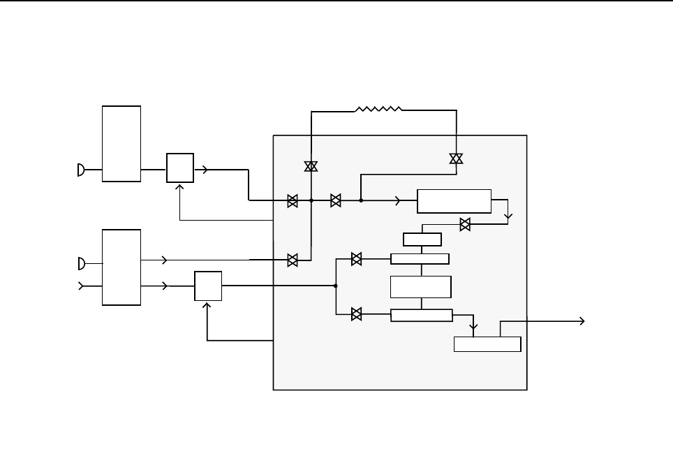
Transmit Audio Circuits 2-15
7.0 Transmit Audio Circuits
Figure 2-7 Transmit Audio Paths
7.1 Microphone Input Path
The radio supports 2 distinct microphone paths known as internal (from control head J2-15) and
external mic (from accessory connector P1-2) and an auxiliary path (FLAT TX AUDIO, from
accessory connector P1-5). The microphones used for the radio require a DC biasing voltage
provided by a resistive network.
The two microphone audio input paths enter the ASFIC CMP at U504-pin 48 (external mic) and
U504-pin 46 (internal mic). The microphone is plugged into the radio control head and connected to
the audio DC via J2-pin 15. The signal is then routed via C5045 to MUX U509 that select between
two paths with different gain to support Low Cost Mic (Mic with out amplifier in it) and Standard Mic.
7.1.1 Low Cost Microphone
Hook Pin is shorted to Pin 1(9.3V) inside the Low Cost Mic, This routes 9.3V to R429, and creates
2.6V on MIC_SENSE (u.P U403-67) by Voltage Divider R429/R430. U403 senses this voltage and
sends command to ASFIC_CMP U504 to get GCB3 = ‘0’. The audio signal is routed from C5045 via
U509-5 (Z0), R5072, U507, R5026, C5091, R5014 via C5046 to U504- 46 int. mic (C5046 100nF
creates a159Hz pole with U504- 46 int mic impedance of 16Kohm).
MIC
IN
MOD IN TO
RF
SECTION
(SYNTHESIZER)
36
44
40
P1
ACCESSORY
CONNECTOR
J2
CONTROL HEAD
CONNECTOR
MIC
EXT MIC
FLAT TX
AUDIO
42
5
48
46
15
2
24kOhms
FILTERS AND
PREEMPHASIS
HS SUMMER
SPLATTER
FILTER
LS SUMMER
LIMITER
ATTENUATOR
VCO
ATN
TX RTN
TX SND
MIC
INT
AUX
TX
ASFIC_CMP
U504
U509
MIC
EXT
FLAT TX
AUDIO MUTE
GCB3
MUX
35
U509
MUX
GCB5
38

2-16 THEORY OF OPERATION
7.1.2 Standard Microphone
Hook Pin is shorted to the hook mic inside the standard Mic, If the mic is out off hook, 3.3V is routed
to R429 via R458, D401, and it create 0.7V on MIC_SENSE (u.P U403-67) by Voltage Divider
R429/R430. U403 senses this voltage and sends command to ASFIC_CMP U504 to get GCB3 =‘1’.
The audio signal is routed from C5045 via U509-3 (Z1), R5072, U507, R5026, C5091, R5014 via
C5046 to U504- 46 int mic (C5046 100nF create a159Hz pole with U504- 46 int mic impedance of
16Kohm). 9.3VDC is routed via R5077, R5075 to J2-15, It create 4.65V with Mic Impedance. C5010
supplies AC Ground to create AC impedance of 510 Ohms via R5075. and Filter 9.3V DC mic bias
supply.
Note: The audio signal at U504-pin 46 should be approximately 12mV for 1.5kHz or 3kHz of
deviation with 12.5kHz or 25kHz channel spacing.
The external microphone signal enters the radio on accessory connector P1 pin 2 and is routed via
line EXT MIC to R5054. R5078 and R5076 provide the 9.3Vdc bias. Resistive divider R5054/ R5070
divide the input signal by 5.5 and provide input protection for the CMOS amplifier input. R5076 and
C5009 provide a 510 ohm AC path to ground that sets the input impedance for the microphone and
determines the gain based on the emitter resistor in the microphone’s amplifier circuit.
C5047 serves as a DC blocking capacitor. The audio signal at U504-pin 48 should be approximately
14mV for 1.5kHz or 3kHz of deviation with 12.5kHz or 25kHz channel spacing.
The FLAT TX AUDIO signal from accessory connector P1-pin 5 is fed to the ASFIC CMP (U504 pin
42 through U509 pin 2 to U509 pin 15 via U506 OP-AMP circuit and C5057.
The ASFIC has an internal AGC that can control the gain in the mic audio path. The AGC can be
disabled / enabled by the µP. Another feature that can be enabled or disabled in the ASFIC is the
VOX. This circuit, along with Capacitor C5023 at U504-pin 7, provides a DC voltage that can allow
the µP to detect microphone audio. The ASFIC can also be programmed to route the microphone
audio to the speaker for public address operation.
7.2 PTT Sensing and TX Audio Processing
Internal microphone PTT is sensed by µP U403 pin 71. Radio transmits when this pin is “0” and
selects inside the ASFIC_ CMP U504 internal Mic path. When the internal Mic PTT is “0” then
external Mic PTT is grounded via D402. External Mic PTT is sensed by U403 pin 72 via Q412
circuits. The radio transmits when this pin is “0” and selects inside the ASFIC _CMP U504 External
Mic path.
Inside the ASFIC CMP, the mic audio is filtered to eliminate frequency components outside the 300-
3000Hz voice band, and pre-emphasized if pre-emphasis is enabled. The signal is then limited to
prevent the transmitter from over deviating. The limited mic audio is then routed through a summer,
which is used to add in signaling data, and then to a splatter filter to eliminate high frequency
spectral components that could be generated by the limiter. The audio is then routed to an
attenuator, which is tuned in the factory or the field to set the proper amount of FM deviation. The
TX audio emerges from the ASFIC CMP at U504-pin 40 MOD IN, at which point it is routed to the
RF section.

Transmit Signalling Circuits 2-17
8.0 Transmit Signalling Circuits
Figure 2-8 Transmit Signalling Path
From a hardware point of view, there are 3 types of signaling:
■Sub-audible data (PL / DPL / Connect Tone) that gets summed with transmit voice or
signaling,
■DTMF data for telephone communication in trunked and conventional systems, and
■Audible signaling including MDC and high-speed trunking.
Note: All three types are supported by the hardware while the radio software determines which
signaling type is available.
8.1 Sub-Audio Data (PL/DPL)
Sub-audible data implies signaling whose bandwidth is below 300Hz. PL and DPL waveforms are
used for conventional operation and connect tones for trunked voice channel operation. The
trunking connect tone is simply a PL tone at a higher deviation level than PL in a conventional
system. Although it is referred to as “sub-audible data”, the actual frequency spectrum of these
waveforms may be as high as 250 Hz, which is audible to the human ear. However, the radio
receiver filters out any audio below 300Hz, so these tones are never heard in the actual system.
Only one type of sub-audible data can be generated by U504 (ASFIC CMP) at any one time. The
process is as follows, using the SPI BUS, the µP programs the ASFIC CMP to set up the proper low-
speed data deviation and select the PL or DPL filters. The µP then generates a square wave which
strobes the ASFIC PL / DPL encode input LSIO U504-pin 18 at twelve times the desired data rate.
For example, for a PL frequency of 103Hz, the frequency of the square wave would be 1236Hz.
This drives a tone generator inside U504 which generates a staircase approximation to a PL sine
wave or DPL data pattern. This internal waveform is then low-pass filtered and summed with voice
or data. The resulting summed waveform then appears on U504-pin 40 (MOD IN), where it is sent to
the RF board as previously described for transmit audio. A trunking connect tone would be
generated in the same manner as a PL tone.
19
18
40
MOD IN
TO RF
SECTION
(SYNTHESIZER)
80
44 HIGH SPEED
CLOCK IN
(HSIO)
LOW SPEED
CLOCK IN
(LSIO)
ASFIC_CMP U504
MICRO
CONTROLLER
U403
HS
SUMMER
5-3-2 STATE
ENCODER
DTMF
ENCODER
SPLATTER
FILTER
PL
ENCODER
LS
SUMMER
ATTENUATOR
85
82
SPI
BUS

2-18 THEORY OF OPERATION
8.2 High Speed Data
High speed data refers to the 3600 baud data waveforms, known as Inbound Signaling Words
(ISWs) used in a trunking system for high speed communication between the central controller and
the radio. To generate an ISW, the µP first programs the ASFIC CMP (U504) to the proper filter and
gain settings. It then begins strobing U504-pin 19 (HSIO) with a pulse when the data is supposed to
change states. U504’s 5-3-2 State Encoder (which is in a 2-state mode) is then fed to the post-
limiter summer block and then the splatter filter. From that point it is routed through the modulation
attenuator and then out of the ASFIC CMP to the RF board. MDC is generated in much the same
way as trunking ISW. However, in some cases these signals may also pass through a data pre-
emphasis block in the ASFIC CMP. Also these signaling schemes are based on sending a
combination of 1200 Hz and 1800 Hz tones only. Microphone audio is muted during high speed data
signaling.
8.3 Dual Tone Multiple Frequency (DTMF) Data
DTMF data is a dual tone waveform used during phone interconnect operation. It is the same type
of tones which are heard when using a “Touch Tone” telephone.
There are seven frequencies, with four in the low group (697, 770, 852, 941Hz) and three in the high
group (1209, 1336, 1477Hz). The high-group tone is generated by the µP (U403-46) strobing U504-
19 at six times the tone frequency for tones less than 1440Hz or twice the frequency for tones
greater than 1440Hz. The low group tone is generated by the ASFIC CMP, controlled by the µP via
SPI bus. Inside U504 the low-group and high-group tones are summed (with the amplitude of the
high group tone being approximately 2 dB greater than that of the low group tone) and then pre-
emphasized before being routed to the summer and splatter filter. The DTMF waveform then follows
the same path as was described for high-speed data.

Receive Audio Circuits 2-19
9.0 Receive Audio Circuits
Figure 2-9 Receive Audio Paths
9.1 Squelch Detect
The radio’s RF circuits are constantly producing an output at the discriminator (IF IC). This signal
(DISC AUDIO) is routed to the ASFIC CMP’s squelch detect circuitry input DISC (U504-pin 2). All of
the squelch detect circuitry is contained within the ASFIC CMP. Therefore from a user’s point of
view, DISC AUDIO enters the ASFIC CMP, and the ASFIC CMP produces two CMOS logic outputs
based on the result. They are CH ACT (U504-16) and SQ DET (U504-17).
The squelch signal entering the ASFIC CMP is amplified, filtered, attenuated, and rectified. It is then
sent to a comparator to produce an active high signal on CH ACT. A squelch tail circuit is used to
produce SQ DET (U504-17) from CH ACT. The state of CH ACT and SQ DET is high (logic “1”)
when carrier is detected, otherwise low (logic “0”).
CH ACT is routed to the µP pin 84 while SQ DET is routed to the µP pin 83.
SQ DET is used to determine all audio mute / unmute decisions except for Conventional Scan. In
this case CH ACT is a pre-indicator as it occurs slightly faster than SQ DET.
FLT RX AUDIO
P1
11
16
1EXTERNAL
SPEAKER
INTERNAL
SPEAKER
ACCESSORY
CONNECTOR
CONTROL HEAD
CONNECTOR
HANDSET
AUDIO
18
20
19
J2
INT
SPKR-
SPKR +
SPKR -
1
9
2
U509
4110
INT
SPKR+
4
6
DISC
ASFIC_CMP
U504
AUDIO
PA
U502
VOLUME
ATTEN.
FILTER AND
DEEMPHASIS
17
MICRO
CONTROLLER
U403
80
FROM
RF
SECTION
(IF IC) LIMITER, RECTIFIER
FILTER, COMPARATOR
SQ DET
SQUELCH
CIRCUIT
16
PL FILTER
LIMITER
CH ACT
AUX RX
43
18
LS IO
U IO AUDIO
83
84
39
URX OUT
DISC
AUDIO
37
85
GCB4
MUTE
GCB1
14
U505

2-20 THEORY OF OPERATION
9.2 Audio Processing and Digital Volume Control
The receiver audio signal (DISC AUDIO) enters the controller section from the IF IC where it is.DC
coupled to ASFIC CMP via the DISC input U504-pin 2. The signal is then applied to both the audio
and the PL/DPL paths
The audio path has a programmable amplifier, whose setting is based on the channel bandwidth
being received, an LPF filter to remove any frequency components above 3000Hz, and a HPF to
strip off any sub-audible data below 300Hz. Next, the recovered audio passes through a de-
emphasis filter (if it is enabled to compensate for Pre-emphasis which is used to reduce the effects
of FM noise). The IC then passes the audio through the 8-bit programmable attenuator whose level
is set depending on the value of the volume control. Finally the filtered audio signal passes through
an output buffer within the ASFIC CMP. The audio signal exits the ASFIC CMP at AUDIO output
(U504 pin 41).
The µP programs the attenuator, using the SPI BUS, based on the volume setting. The minimum /
maximum settings of the attenuator are set by codeplug parameters.
Since sub-audible signaling is summed with voice information on transmit, it must be separated
from the voice information before processing. Any sub-audible signaling enters the ASFIC CMP
from the IF IC at DISC U504-2. Once inside, it goes through the PL/DPL path. The signal first
passes through one of the two low-pass filters, either the PL low-pass filter or the DPL/LST low-pass
filter. Either signal is then filtered and goes through a limiter and exits the ASFIC CMP at LSIO
(U504-pin 18). At this point, the signal will appear as a square wave version of the sub-audible
signal which the radio received. The µP U403 pin 80 will decode the signal directly to determine if it
is the tone / code which is currently active on that mode.
9.3 Audio Amplification Speaker (+) Speaker (-)
The output of the ASFIC CMP’s digital volume pot, U504-pin 41 is routed through DC blocking
capacitor C5049 to the audio PA (U502 pin 1 and 9).
The audio power amplifier has one inverted and one non-inverted output that produces the
differential audio output SPK+/SPK- (U502 pins 4 and 6)
The audio PA is enabled via the ASFIC CMP (U504-GCB1). When the base of Q501 is low, the
transistor is off and U502-pin 8 is high, using pull up resistor R5041, and the audio PA is ON. The
voltage at U502-pin 8 must be above 8.5Vdc to properly enable the device.
If the voltage is between 3.3 and 6.4V, the device will be active but has its input (U502-pins 1/9) off.
This is a mute condition which is used to prevent an audio pop when the PA is enabled.
The SPK+ and SPK- outputs of the audio PA have a DC bias which varies proportionately with B+
(U502- pin 7). B+ of 11V yields a DC offset of 5V, and B+ of 17V yields a DC offset of 8.5V. If either
of these lines is shorted to ground, it is possible that the audio PA will be damaged. SPK+ and SPK-
are routed to the accessory connector (P1-pin 1 and 16) and to the control head (connector J2-pins
19 and 20).

Receive Signalling Circuits 2-21
9.4 Handset Audio
Certain handheld accessories have a speaker within them which require a different voltage level
than that provided by U502. For these devices HANDSET AUDIO is available at control head
connector J2 pin18.
The received audio from the output of the ASFIC CMP’s digital volume attenuator is routed to U505
pin 2 where it is amplified. This signal is routed from the output of the op-amp U505 to J2-pin 18.
From the control head, the signal is sent directly to the microphone jack.
9.5 Filtered Audio and Flat Audio
The ASFIC CMP output audio at U504-pin 39 is filtered and de-emphasized, but has not gone
through the digital volume attenuator. From ASFIC CMP U504-pin 39 the signal is routed via R5034
through gate U509-pin 12 and AC coupled to U505-pin 6. The gate controlled by ASFIC CMP port
GCB4 selects between the filtered audio signal from the ASFIC CMP pin 39 (URXOUT) or the
unfiltered (flat) audio signal from the ASFIC CMP pin 10 (UIO). Resistors R5034 and R5021
determine the gain of op-amp UU505-pin 6 for the filtered audio while R5032 and R5021 determine
the gain for the flat Audio. The output of U505-pin 7 is then routed to P1 pin 11 via DC blocking
capacitor C5003. Note that any volume adjustment of the signal on this path must be done by the
accessory.
10.0 Receive Signalling Circuits
Figure 2-10 Receive Signalling Paths
10.1 Sub-Audio Data (PL/DPL) and High Speed Data Decoder
The ASFIC CMP (U504) is used to filter and limit all received data. The data enters the ASFIC CMP
at input DISC (U504 pin 2). Inside U504 the data is filtered according to data type (HS or LS), then it
is limited to a 0-3.3V digital level. The MDC and trunking high speed data appear at U504-pin 19,
where it connects to the µP U403 pin 80.
DET AUDIO
DISCRIMINATOR AUDIO
FROM RF SECTION
(IF IC)
19
18
25
2
82
80
DISC
PLCAP2
LSIO
HSIO
DATA FILTER
AND DEEMPHASIS LIMITER
FILTER LIMITER
ASFIC_CMP
U504
MICRO
CONTROLLER
U403
85
44
8
PLEAP

2-22 THEORY OF OPERATION
The low speed limited data output (PL, DPL, and trunking LS) appears at U504-pin18, where it
connects to the µP U403-pin 80.
The low speed data is read by the µP at twice the frequency of the sampling waveform; a latch
configuration in the ASFIC CMP stores one bit every clock cycle. The external capacitors C5028,
and C5026 set the low frequency pole for a zero crossings detector in the limiters for PL and HS
data. The hysteresis of these limiters is programmed based on the type of received data.
10.2 Alert Tone Circuits
When the software determines that it needs to give the operator an audible feedback (for a good
key press, or for a bad key press), or radio status (trunked system busy, phone call, circuit failures),
it sends an alert tone to the speaker. It does so by sending SPI BUS data to U504 which sets up the
audio path to the speaker for alert tones. The alert tone itself can be generated in one of two ways:
internally by the ASFIC CMP, or externally using the µP and the ASFIC CMP.
The allowable internal alert tones are 304, 608, 911, and 1823Hz. In this case a code contained
within the SPI BUS load to the ASFIC CMP sets up the path and determines the tone frequency,
and at what volume level to generate the tone. (It does not have to be related to the voice volume
setting.)
For external alert tones, the µP can generate any tone within the 100-3000Hz audio band. This is
accomplished by the µP generating a square wave which enters the ASFIC CMP at U504 pin 19.
Inside the ASFIC CMP this signal is routed to the alert tone generator.
The output of the generator is summed into the audio chain just after the RX audio de-emphasis
block. Inside U504, the tone is amplified and filtered, then passed through the 8-bit digital volume
attenuator, which is typically loaded with a special value for alert tone audio. The tone exits at U504-
pin 41 and is routed to the audio PA like receive audio.
Chapter 3
TROUBLESHOOTING CHARTS
This section contains detailed troubleshooting flowcharts. These charts should be used as a guide in
determining the problem areas. They are not a substitute for knowledge of circuit operation and
astute troubleshooting techniques. It is advisable to refer to the related detailed circuit descriptions
in the theory of operation sections prior to troubleshooting a radio.
Most troubleshooting charts end up by pointing to an IC to replace. It is not always noted, but it is
good practice to verify supplies and grounds to the affected IC and to trace continuity to the
malfunctioning signal and related circuitry before replacing any IC. For instance, if a clock signal is
not available at a destination, continuity from the source IC should be checked before replacing the
source IC.
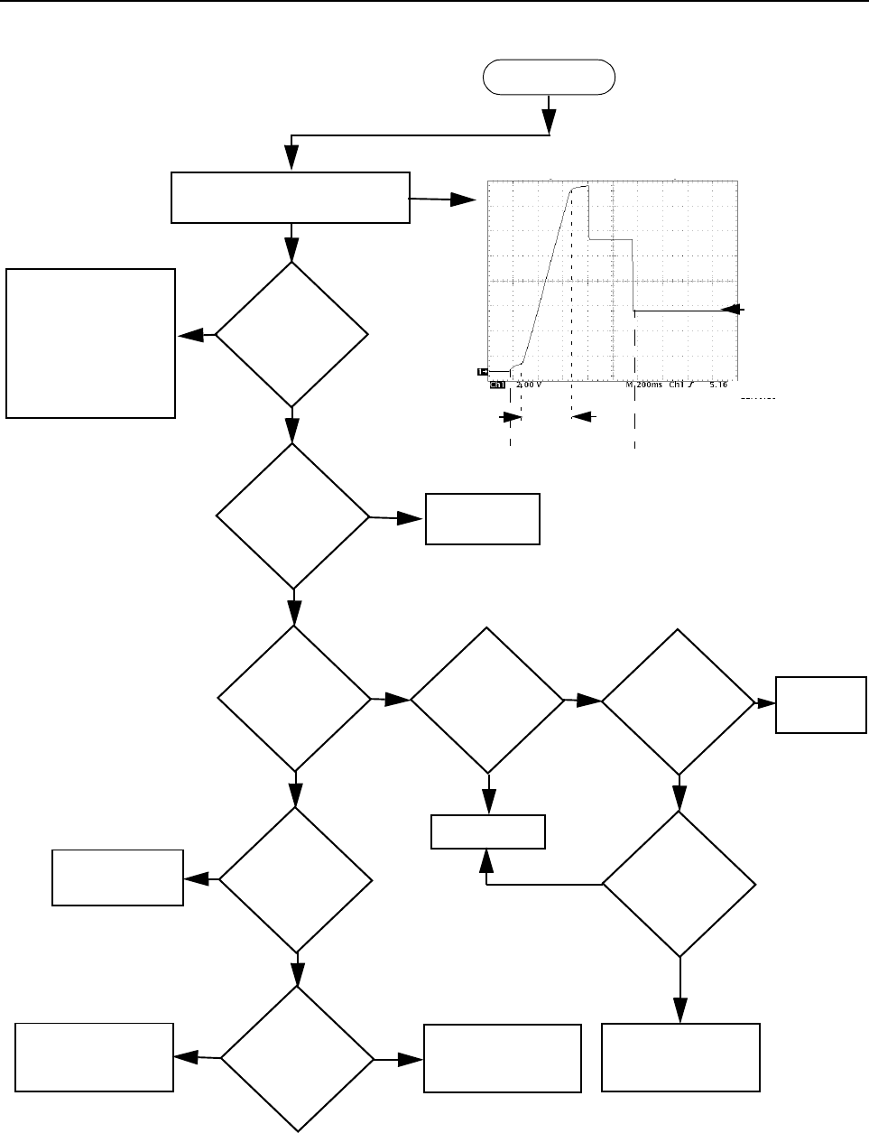
3-2 TROUBLESHOOTING CHARTS
1.0 Troubleshooting Flow Chart for Out-of-Lock Receiver (Sheet 1 of 2)
Monitor TP200 at turn-on
See figure for typical trace
TP200
Is Voltage
correct for freq?
Typ. 4V for 66MHz
to 11v for 88MHz
(Rx freq.)
No
Check C2078, R217,
R224, C2074, R200,
R234
Check U200-4
(lock detect line)
Check U200-45, 43 lines.
If all ok, replace U200
Yes
TP200
Is ramp-up
slope correct?
Typ.14V in 500ms
No
Yes
START
Yes
No
Go to ‘A’
sheet 2 of 2
Go to
Rx VCO Section
Yes
No
TP200
Does voltage
reach typ. 14.7V
Check LO level
TP1 approx
-18dBm into
50 Ohms
Check voltage
on U200-47
typ. 14.7V
No
No
Yes
Is freq approx
118MHz TP200
approx 14.7V ?
or
<75MHz TP200
approx <1V
Check D2751, D2752,
L2750-L2753,
C2751-C2756
Check Q2790 and
associated cctry
check C2796, R2796
Replace U200
U200-19
should be
16.8MHz, 0.5Vpp
U200-14,15
should be
square wave
1.05MHz, 3.6Vpp
No
Go to Ref.
Osc.Section
No
Yes
Yes
Yes
Check R228, R225
D200, D201,
C2024 -C2027, C2001
NOTE: HANDLE WITH CARE
C2078 (main loop filter capacitor) is
easily damaged by heat or soldering
Voltage dependent
on power-on
channel:
typ. 3.8v for 66Mhz
10.7V for 88MHz
(Rx Freq.)
typ.14.7V
turn-on
synth programmed
with power-up channel
500ms
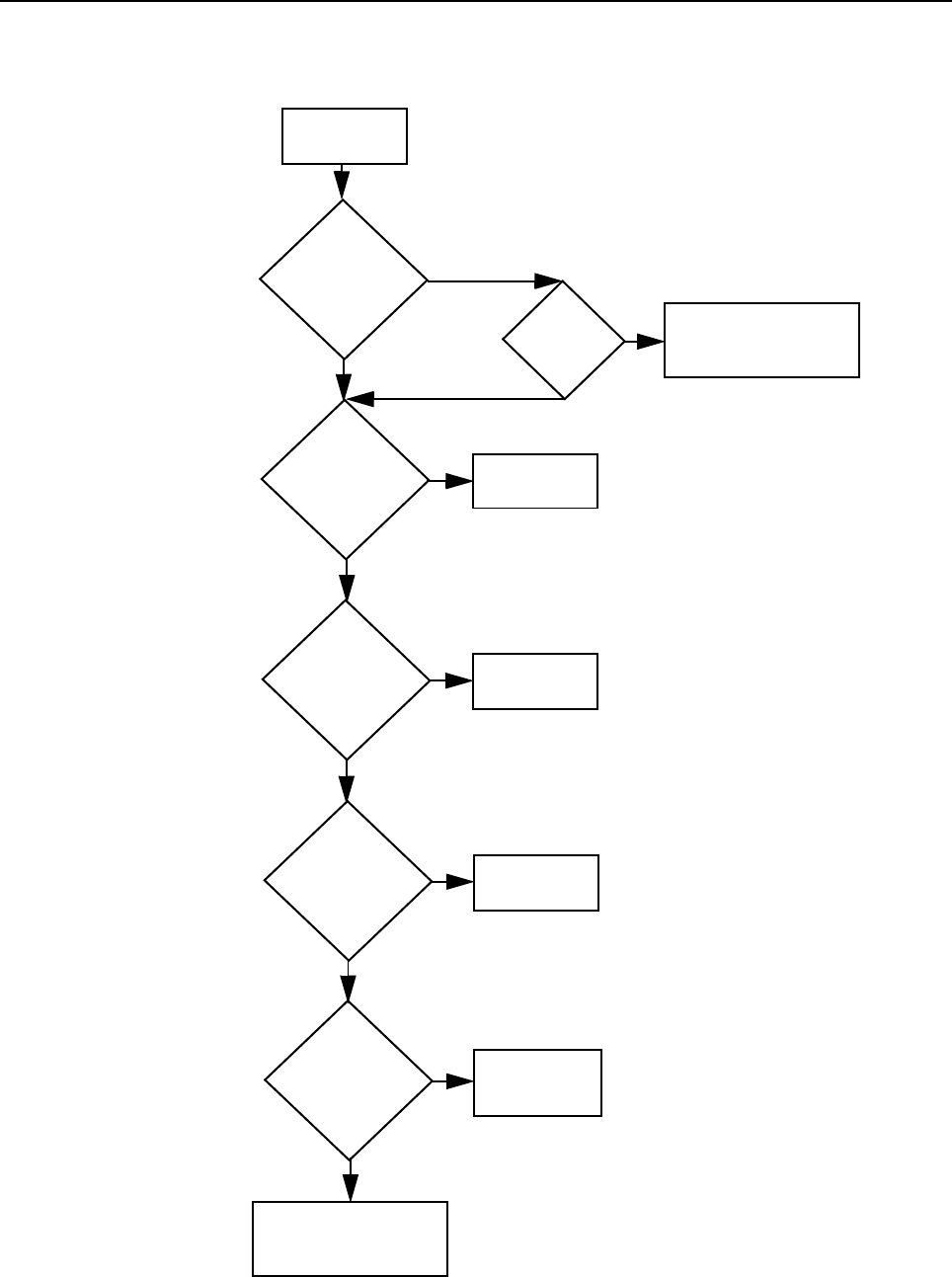
Troubleshooting Flow Chart for Out-of-Lock Receiver (Sheet 1 of 2) 3-3
1.1 Troubleshooting Flow Chart for Out-of-Lock Receiver (Sheet 2 of 2)
Yes
Yes
No
From ‘A’
sheet 1 of 2
TP200
Does Voltage
stay <1V ?
3.3V
on U200-5, 20
34, 36?
5V
on U200-13?
V-SF
8.7V on
U200-28?
9.2V
on U200-30?
SPI
activity on
U200-7, 8, 9?
No
No
No
Check SPI Connections
Fault in digital area
Check U508
Check U503
Yes
Yes
Check R2808,
Check U501
No
Yes
Check C2006,
U200-26, if ok
replace U200
No
Check C2078, R234,
R217, C2074, R200
If all ok, replace U200
Yes
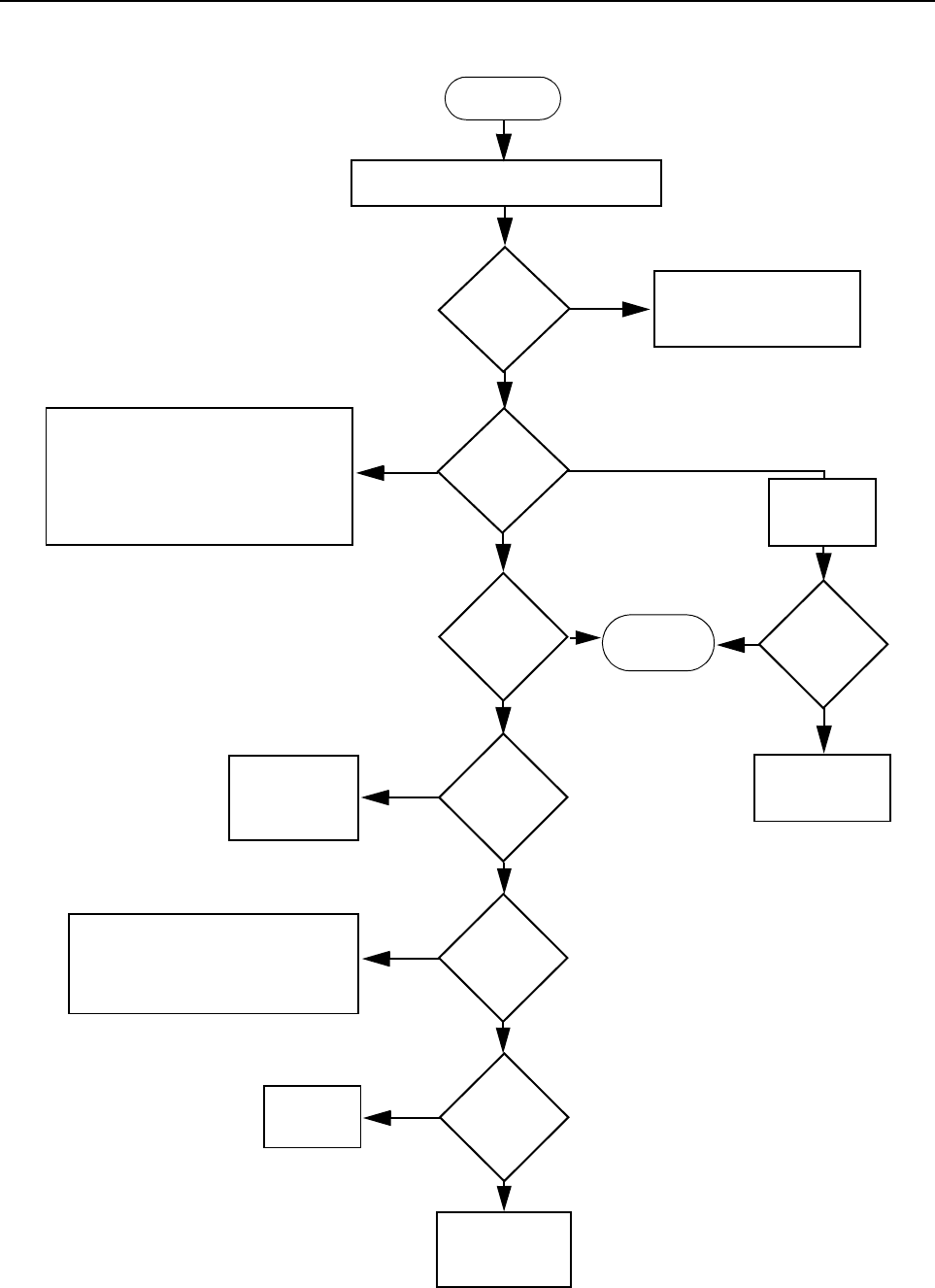
3-4 TROUBLESHOOTING CHARTS
2.0 Troubleshooting Flow Chart for 25W Transmitter (Sheet 1 of 4)
START
No
Check components between Q100 and
RF output, Antenna Switch D104,
D103, VR102 and Q106, Q103 and
associated bias circuitry.
Check DC volts present at anode of
D103.
No or too low power when keyed
Current
increase when
keyed?
Check power settings, tuning, R142,
R143, R156 & components between
U103 Pin 3 and ASFIC Pin 6 before
replacing ASFIC
Control
Voltage at
TP150
>1.6V?
Check Harmonic Filter
components C1537 to
Antenna Connector
>1A
Voltage U103
pin 5 =
4.7V?
U103 Pin 3
<2.7Vdc
PA Bias
Voltage@R134
>2Vdc
Check 9.3V
Regulator
U501, R180 &
R181
Yes
Yes
No
No
Yes
Check
U103
Check Forward
Power Sense
Circuit
No
Short U100
Pin 3 to
ground
Voltage at
TP150 rises?
Check PA
Stages
Check Forward
Power Sense
Circuit
Yes
No
>800mA & <1A
<800mA
Rx
sensitivity
OK?
Yes
Ensure that the radio is set-up
via the CPS to have 25W channels
No
Yes
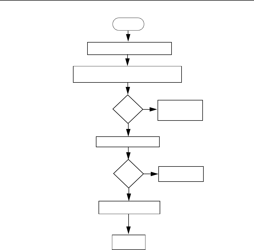
Troubleshooting Flow Chart for 25W Transmitter (Sheet 1 of 4) 3-5
2.1 Troubleshooting Flow Chart for 25W Transmitter (Sheet 2 of 4)
Check PA
Stages
Quick check of PA devices.
Connect power supply.
Key radio.
Replace Q100.
Re-tune PA Bias
with Tuner.
Check 13.8v present at drain Q100. Disconnect
power supply, measure R131 to Ground.
10kOhm?
Yes
No
Measure R147 to Ground.
Replace Q105.
22kOhm?
Yes
No
Go to ‘A’
sheet 3 of 4
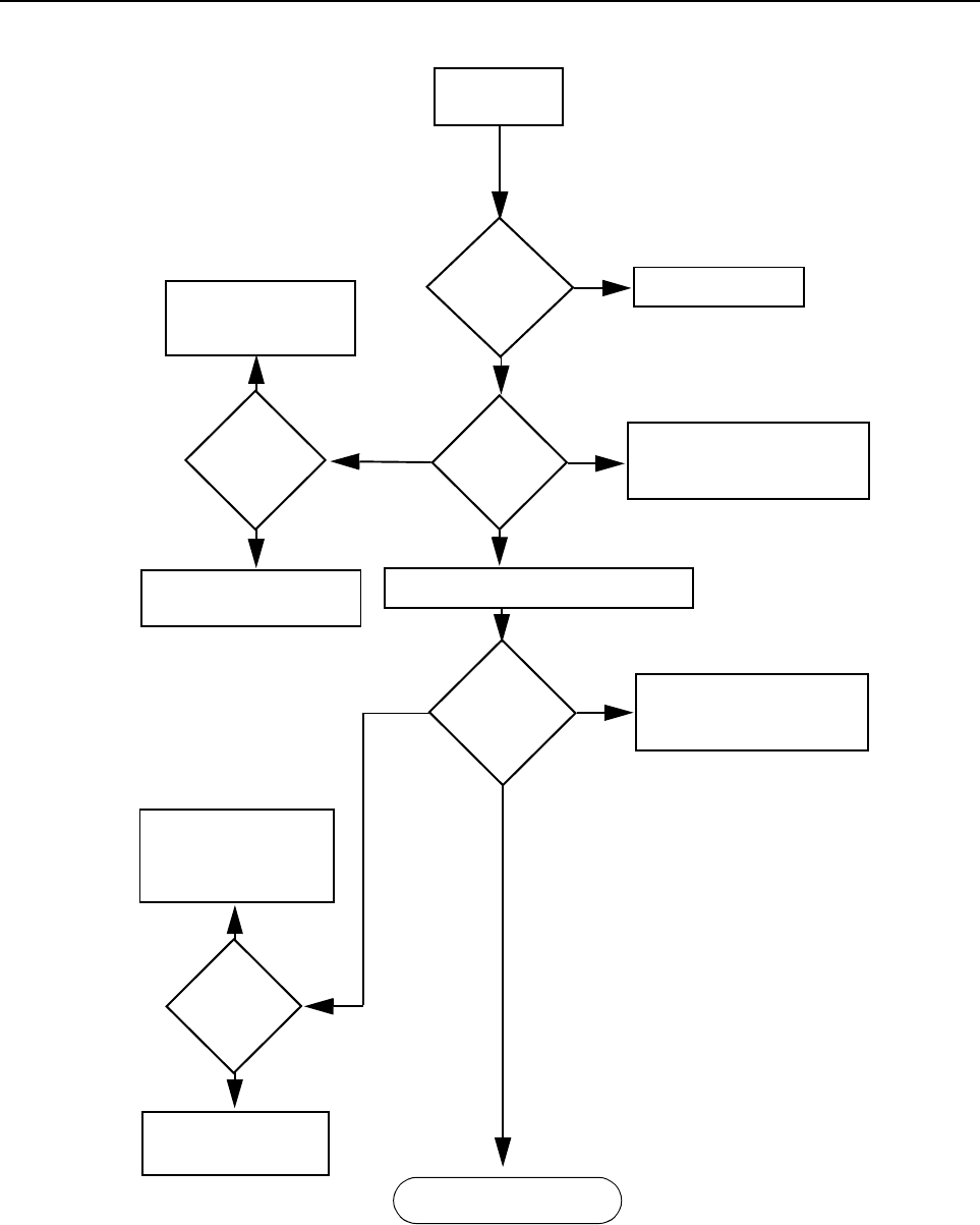
3-6 TROUBLESHOOTING CHARTS
2.2 Troubleshooting Flow Chart for 25W Transmitter (Sheet 3 of 4)
Yes
>3V
Check Q102, R139,
R166, R126, R169,
R138, R175, R147
DC
Voltage
at Q101 & Q102
base=0?
DC
Voltage
at U103
Pin 8
Check U403
Check resistive network at
Pin 9 and 10 of U103
before replacing U101
Measure DC Voltage at U102 Pin 1
Pin 1
Voltage
Check resistive network at
Pin 2 & 3 of U102 before
replacing Q105
Check Final PA Stages
DC
Voltage at
U103 Pin 3 =
8.8V
Check U102 before
replacing Q105
DC
Voltage at
U103 Pin
10=8.8V
Check Q101, Q102,
R153, R136, R165,
R122, R168 & R137
Check U103 before re-
placing U101
No
No
Yes
>5.0V
2.0 to 5.0V
2-3V
Yes
No
<2.0V
<2V
From ‘A’
sheet 2 of 4
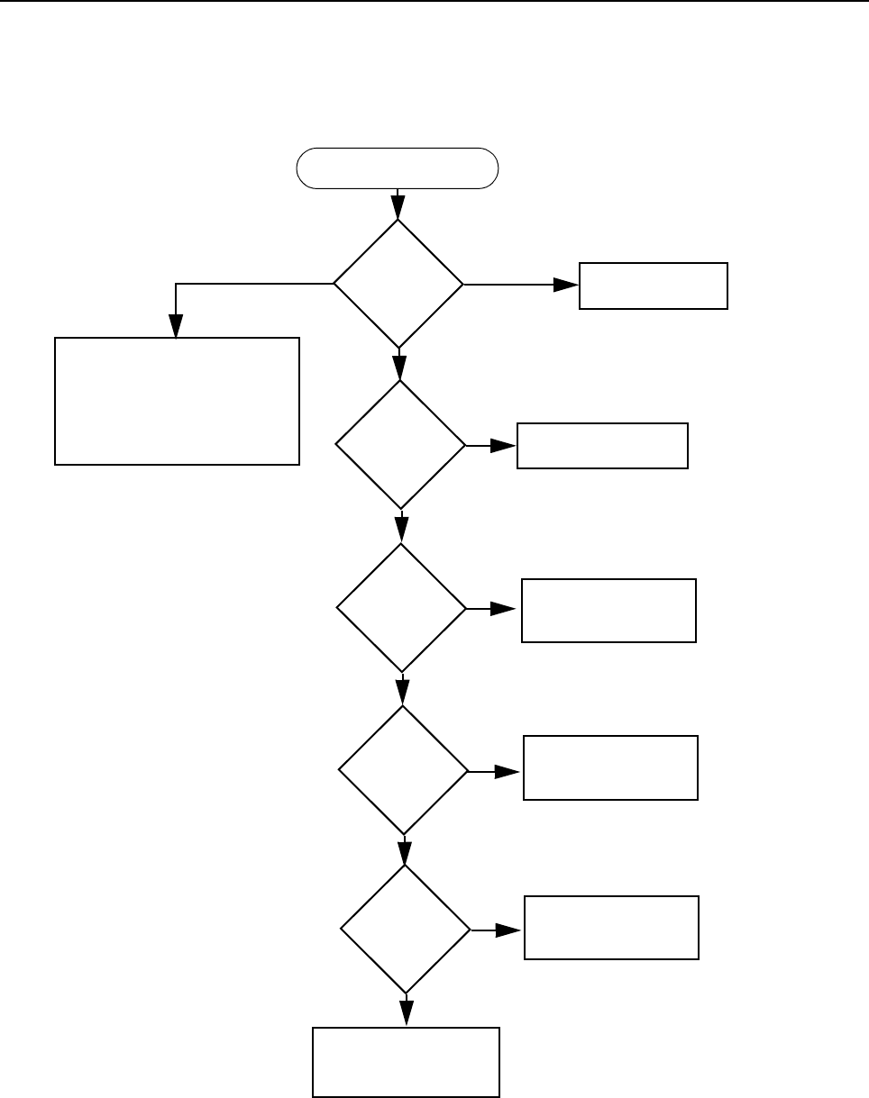
Troubleshooting Flow Chart for 25W Transmitter (Sheet 1 of 4) 3-7
2.3 Troubleshooting Flow Chart for 25W Transmitter (Sheet 4 of 4)
No
Yes
Yes
No
Check Final PA Stage
PA_Bias
Voltage at
R134
RF Voltage
after C1044
>100mV?
Voltage
across R122
>50mV?
RF Voltage
Q105 gate
>250mV?
RF Voltage
Q100 gate
>1.0V?
Check components
between Q100 &
antenna connector
Replace Q100
Check FGU
Check components
between C1044 &
C182
Check components
between C182 &
Q105
Check components
between Q105 &
Q100
No
No
Yes
Yes
2-3V
Supply Voltage
Check voltage varies as bias
softpot is tuned (in small steps)
via the Global Tuner.
Check Bias Tuning, R134, R131,
R105 & R106 before replacing
ASFIC U504.
>100mV & <2V
or 0V
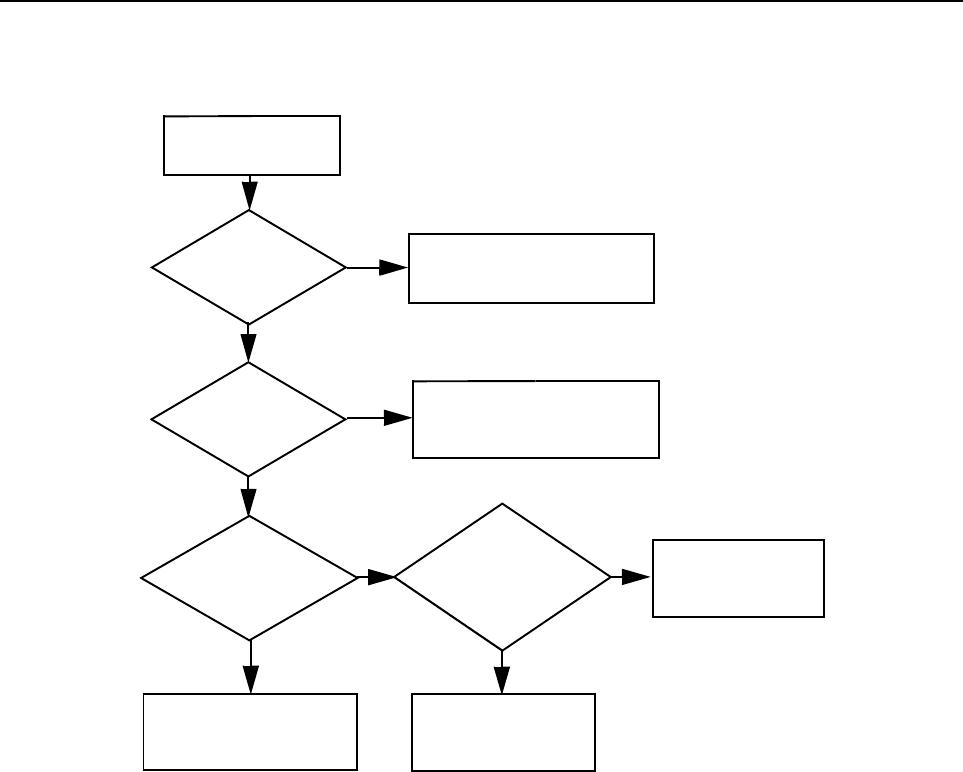
3-8 TROUBLESHOOTING CHARTS
3.0 Troubleshooting Flow Chart for Synthesizer (Reference Oscillator)
Incorrect or no
µ
P
clock signal
TP403
NO
YES
NO
YES
Power-up default freq.
Fault with ASFIC
or Controller section
Check U504-28
should be 16.8MHz
YES
NO Check Y201 and
associated
circuitry
Check U504 and
C504, C5025, R5033
Reference Oscillator
working
Freq. = 14.7MHz
or 7.4MHz ?
TP403
Freq. = 3.68MHz
0.5Vpp
Check U504-28
Check Y202-1
should be 16.8MHz
0.5Vpp
NO
YES
Faulty U200,
or R229
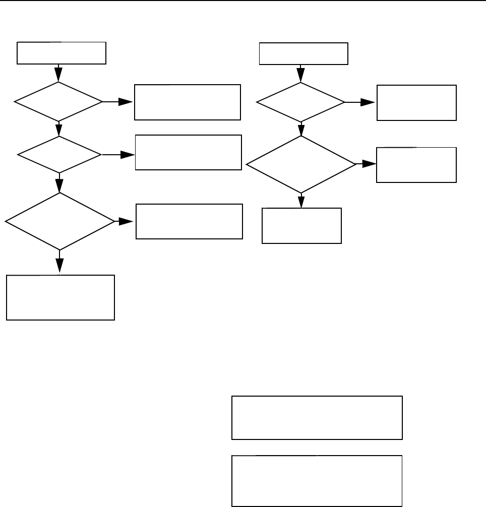
Troubleshooting Flow Chart for VCO 3-9
4.0 Troubleshooting Flow Chart for VCO
No Receive VCO Signal
at TP1
>7V at Q2751D ?
NO
YES
NO
YES
Check Q2742, R2743
U200-2 should be 0V
Check Rx - Tx switching
Q2742, Q2752 (should be turned on)
Check Q2741 and associated circuitry.
Use Hi - impedance
probe to check frequency
YES
NO
Check Rx VCO parts
<0.1V at Q2742-2?
Fault in buffer section
Q2760, Q2770
- check supplies and parts
Check supply at Q2751
Is freq. approx 118 MHz?
Out-of-Lock in TX
On detection of an out-of-lock in Tx,
the radio returns to the Rx mode.
NOTE:
The TX VCO can be force enabled by
grounding Q2742-3
Power Ok but
Audio from U200-11?
NO
YES
Check modulation
tuning softpots
Check audio on D2731
and Vdc approx 8.6V
No modulation
YES
NO Check R2714, C2722,
C2731, C2733, L2731
Check D27312, R2731,
C2734
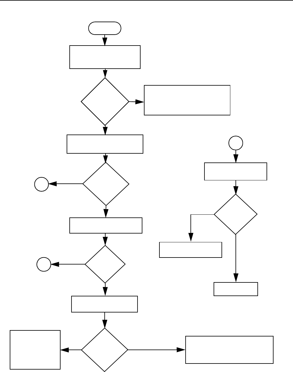
3-10 TROUBLESHOOTING CHARTS
5.0 Troubleshooting Flow Chart for Receiver (Sheet 1 of 2)
Bad SINAD
Bad 20dB Quieting
No Recovered Audio
START
Audio at
pin 8 of
U2 ?
Check Controller
(in the case of no audio)
OR ELSE go to “B”
Yes
No
Spray or inject 21.4MHz
into XTAL Filter FL3101
Audio heard ?
B
Yes
No
Check 2nd LO
(20.945MHz) at C53
LO present ?
B
Yes
Check voltages on U2
Biasing OK ?
No
No
A
Yes
Check Q6 bias
for faults
Replace Q6
Go to B
Yes
No
Check circuitry
around U2.
Replace
U2 if defect
Check circuitry around Y2
Replace Y2 if defect
Voltages
OK?
Ensure that all Power Supplies are correct, as
detailed in paragraph 6.
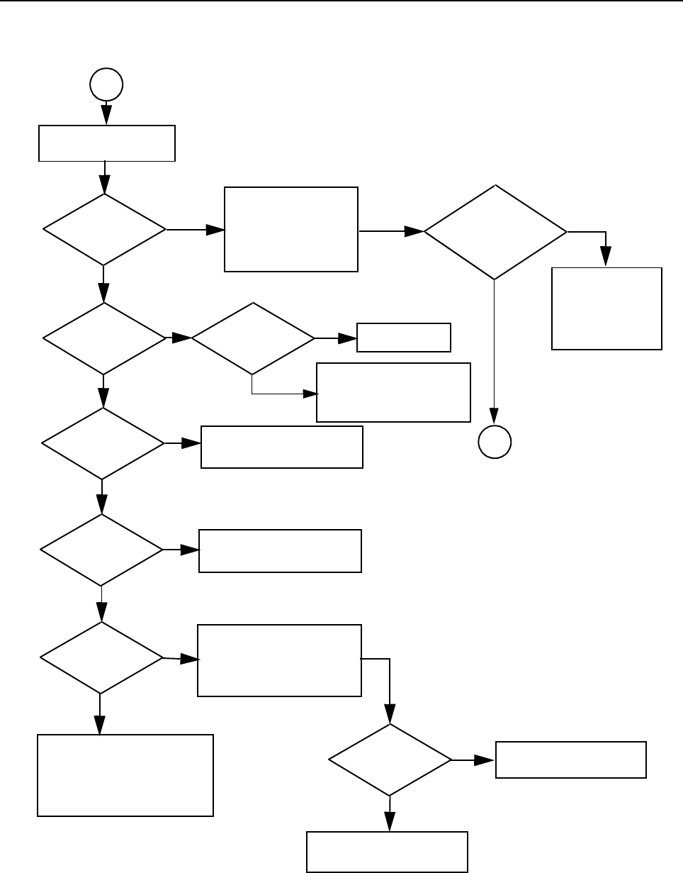
Troubleshooting Flow Chart for Receiver (Sheet 1 of 2) 3-11
5.1 Troubleshooting Flow Chart for Receiver (Sheet 2 of 2)
IF Signal at
C58?
No
RF Signal at T1?
RF Signal at
C2337?
No
RF Signal at
C2308?
No
RF Signal at
C1108?
No or
Check Harmonic Filter
J1 and
Antenna Switch
D103,D104,L1514
Check filter between C1108
& C2308. Check tuning
voltage at R2309
Inject RF into J1
Is tuning
voltage OK?
No
Yes
Check RF amp
(Q2301) Stage
Check filter between
C2337 & T1
Yes
Check T1, T2, U1 (diode),
R41, L2, L2792, C59 and
L6
Yes
1st
LO level OK?
Locked?
Yes
Check FGU
Yes
Trace IF signal from
C58 to Q6. Check for
bad XTAL filters
No
Yes
IF signal at Q6
collector?
Yes
No
Check U517
Check varactor filter
D2301, D2304
No
Yes
A
B
weak RF
Before replacing
U2, check
U2 voltages
3-12 TROUBLESHOOTING CHARTS
6.0 Troubleshooting Flow Chart for DC Supply (1 of 2)
Since the failure of a critical voltage supply might cause the radio to automatically power down,
supply voltages should first be probed with a multimeter. If all the board voltages are absent, then
the voltage test point should be retested using a rising-edge-triggered oscilloscope. If the voltage is
still absent, then another voltage should be tested using the oscilloscope. If that voltage is present,
then the original voltage supply in question is defective and requires investigation of associated
circuitry.
Check VDC on
C5008
V=3.3V
?
Check Voltage on
C5043
No
Go to D3_3V
Yes
9v<V<9.8v
?
Go to Start
No
Replace U508
Yes
3V
Check VDC on
C5006
V=5V
?
Check Voltage on
C5042
No
Go to 3V
Yes
9v<V<9.8v
?
Go to Start
No
Replace U503
Yes
5V
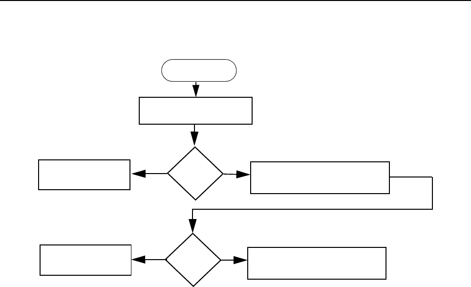
Troubleshooting Flow Chart for DC Supply (1 of 2) 3-13
6.1 Troubleshooting Flow Chart for DC Supply (2 of 2)
Check VDC on
C5007
V=3.3V
?
Check Voltage on
C5041
No
Go to Digital Section
Yes
9v<V<9.8v
?
Go to Start
No
Replace U510
Yes
D3_3V

3-14 TROUBLESHOOTING CHARTS

Chapter 4
MIDBAND PCB/SCHEMATICS/PARTS LISTS
1.0 Allocation of Schematics and Circuit Boards
1.1 Midband and Controller Circuits
The Midband circuits are contained on the printed circuit board (PCB) which also contains the
Controller circuits. This Chapter shows the schematics for both the Midband circuits and the
Controller circuits. The PCB component layouts and the Parts Lists in this Chapter show both the
Controller and Midband circuit components. The Midband and Controller schematics and the related
PCB and parts list are shown in the tables below.
Table 4-1 Midband 1-25W Diagrams and Parts Lists
PCB :
8489012U01-C Main Board Top Side
8489012U01-C Main Board Bottom
Side
Page 4-3
Page 4-4
SCHEMATICS
Main Circuit
Transmitter
Synthesiser and VCO
Receiver Front and Back End
DC and Audio Ccts
Microprocessor and Controller Ccts
Page 4-5
Page 4-6
Page 4-7
Page 4-8
Page 4-9
Page 4-10
Parts List
8489012U01-C Page 4-11
Controller version is T1

4-2 Midband PCB/Schematics/parts lists
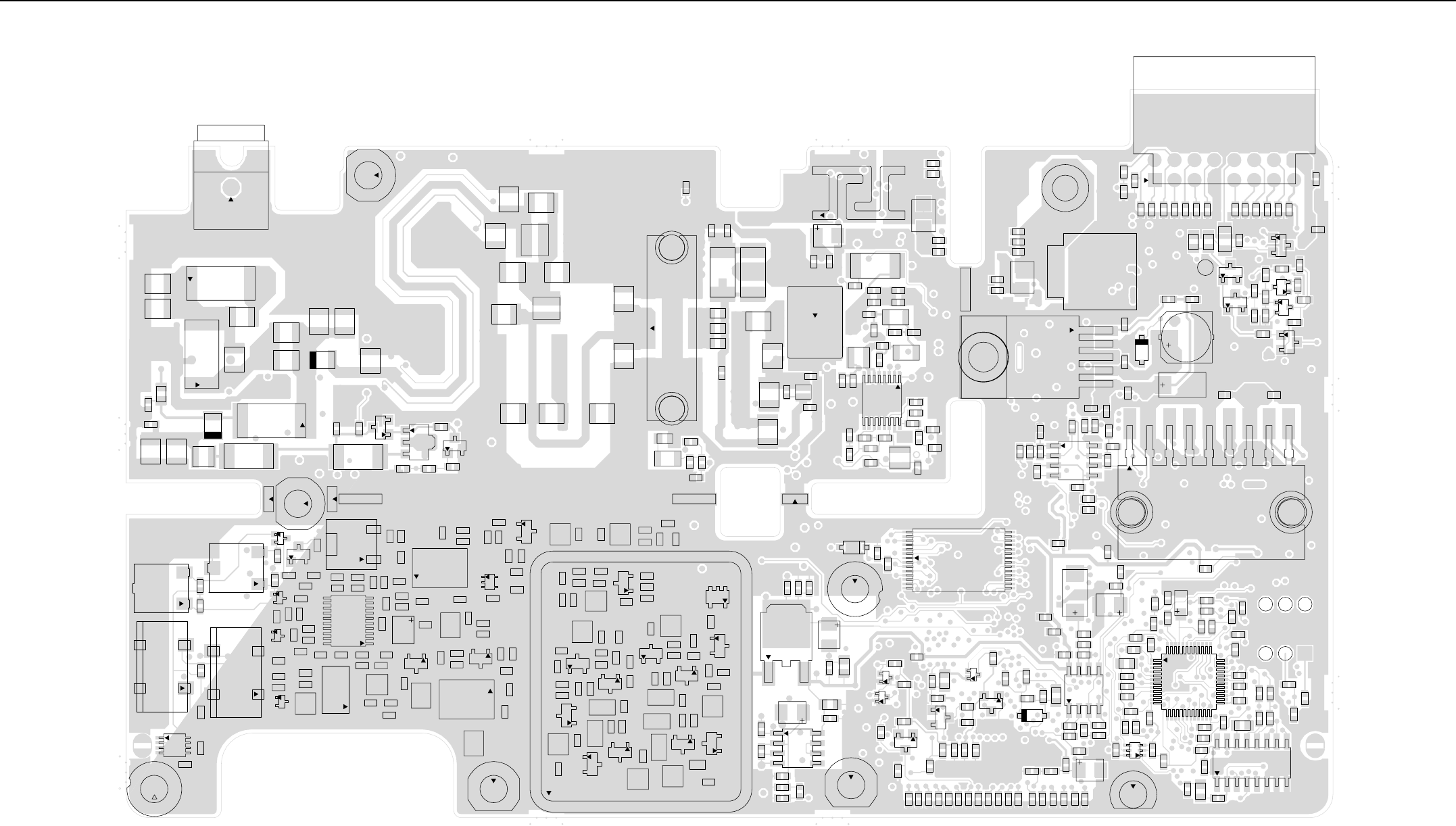
Midband 1-25W PCB 8489012U01 (rev. C) / Schematics 4-3
2.0 Midband 1-25W PCB 8489012U01 (rev. C) / Schematics
J1
M4
C1518
C1519
C1520
C1521
C1532
C1534
C1538
D104
L1512
L1513
C1006
C1010
C1108
C1121
C1536
D103
L108
L1514
R108
FL2
43
R7 R16
FL3
43
2
FL4
2
FL5
R8 R18
C13
C14
M1
4
58
U3
C53
C54
C57
C2338
D6
L16
R4
R9
R10R12
R19
R27
R36
2
4
3
1Y2
C2207
C2209
L3
11
1
20
10
U2
C11
C12
C18
C19
C20
C17
D5
R20
R26
R28
D3
D4
2
Q3
R6
R15
R17
R35
C16C58
R31
2
Y1
C2
C3
C9 C10
C15 C21 C22
R14
R21
R23
R30
R33
C1035
C1078
Q106
R107 R157
R185
2
VR102
M5
M203
M205
M206
C1067
C1510 C1511
2
Q103
R172
C8
C1077
C2201
C2202
C2779
C2780
C2781
C2782
23
4
5
6FL2201
2
Q2780
Q2791
R2778
R2779
R2781
R2782
R2783
R2784
C5
C6
C7
C2205
C2206
C2210
C2211
2
D2201
2
3
456
FL2202
L2201
L2202
L2203
2Q6
R5
R13
R24
R25 R34
R37
R39
C2731
C2733
C2734
2
D2731
2
D2733
L2731
L2733
L2734
M7
R2731
C2735
C2736
C2737
C2738
C2750
C2751
2
D2732
2
D2751
L2732
L2750
L2751
L2752
L2753
SH2
C2743
C2744
C2752
C2753C2754
2
D2752 L2742
C2755 C2756
C2757
C2762
2
D2754
L2754
Q2742
2
Q2751
2
Q2752
R2740
R2751
R2752
R2753
R2754
C2732
C2739
C2740
C2741
C2745
C2758
C2761
2
D2739
L2741
2
Q2741
R2739
R2741
R2742 R2743
C2763
C2764
C2765
L2761
2
Q2760
R2758
R2760
R2761
R2762
R2763
R2765
R2766
R2767
C2783
C2784
C2785
C2786
L2781
L2783
M202
R2785
R2786
R2787
C5008
C5018
C5070
M3
M204
R5010
3
2
1
U508
VR401
C5006
C5016
C5039
C5040
C5042
C5043
C5064
C5066
C5068
M8
R5002
R5011
1
4
58
U503
C602
C603
C604
C605
C606
C607
C608
C609
C610
C611
C612
C613
C614
C615
C616
C617
C618
C619
C406
C414
C418
C490
2
D400
2
D401
Q400
Q407
2
Q415
R428
R429
R431
R439
R441
R444
R450
R458
R459
R462
C1034
Q414
R445
R451
R5000
C5010
C5048
C5062
C5071
C5076
C5087
C5102
R430
R5019
R5031
R5050
R5055
R5066
R5075
R5077
14
58
U505
VR504
C5013
C5014
C5020
C5023
C5025
C5027
C5028
C5056
C5059
C5101
C5103
R5009
R5033
R5043
R5044
R5084
1
37
25
13
U504
43
6
U515
M2
C5024
C5026
C5029
C5034
C5035
C5044
C5053
C5054
R5024
R5032
R5034
R5071
R5079
16
18
9
U509
C1122
C5011
C5012
C5022 C5046
C5047
C5050
C5051
C5052
R461
R5006
R5040
R5047
R5052
R5053
R5054
R5063
R5070
R5080
C1123
R5064
C1125
C5003
C5030
C5079
C5088
R5021
R5065
C5015
C5019
C5033
C5057
C5074
C5078
C5081
C5089
C5090
C5095
R5022
R5045
R5046
R5056
R5057
R5067
R5068
1
4
58
U506
C5032
D502
R5001R5038
5
2
3
4
U501
C5001
C5005 C5021
C5038
C5080
C5096
C5110
C5111
2
D500
2
D513
Q500
Q503
R5039
R5048
R5073
R5074
R5081
R5082
R5083
R5085
R5089
TP3 2
VR501
C620
C621
C622
C623
C625
C627
C628
C629
C630
C631
C632
C633
C662
C624
C626
C678
R601
R610
2
VR693
C5100
15
16
P1
C5559
1
M9 1
2
R406R440
C1088
C1097
C1098
C1113
C1114
L120
M201
VR500
C182
C1033
C1063
C1099
C1105
C1115
C1525
C1526
C1527
L119
L1506
L1507
1M6
4
R102
R178
R179
R1506
C1524
C1001
C1031
C1037
C1064
C1074
C1501
C1502
C1503
L105
1
M105
R105
1
8
U101
C1030
C1039
C1041
C1044
C1057
C1110 C1119
L104
L107
R109
R171
R173
R174
R176
16
9
C1504
C1505
C1506
C1529
L1503
C1065
C1104
C1507 R106
R123
R124
R125
C1508 C1509
5
2
64
31
Q1008
C1513 C1514
C1515
C1516
C1517
C1531
L1504
L1505
C1052
C1070
C1530
L103
R148
R151
RT100
C1018
C1537
C1089
C1100
C1116
1
3
2
R101
C402
C411
22
21 8
7
1
U402
9
1
U502
Midband (66-88MHz) 1-25W 8489012U01 (rev. C)
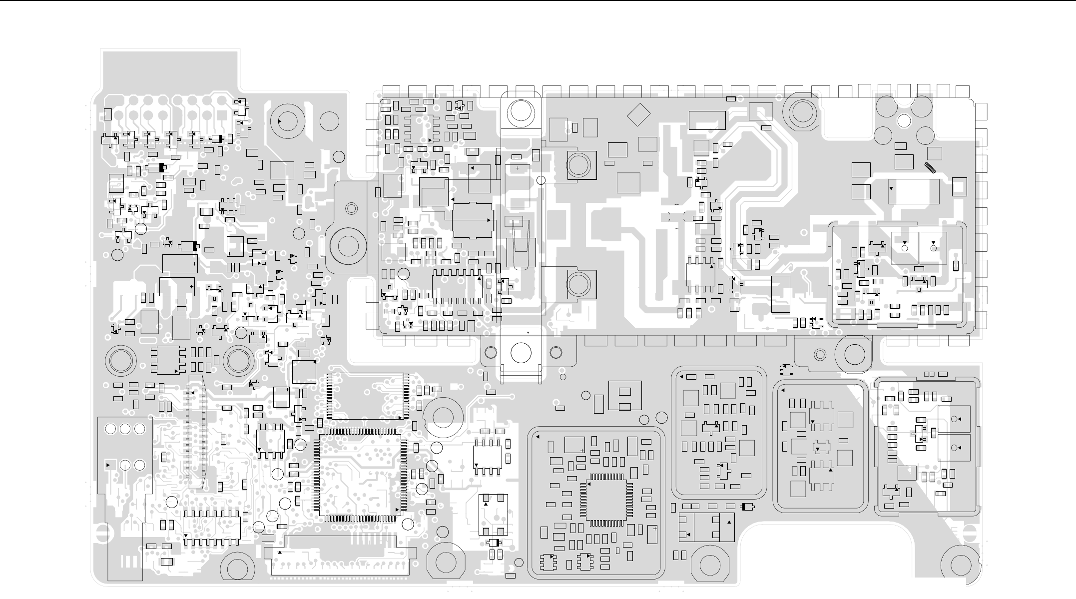
4-4 Midband 1-25W PCB 8489012U01 (rev. C) / Schematics
C417
C5037
C5055
C5119
D402
2
Q506
R402
R403 R404
R405
R407
R421
R600
R5020
R5023
R5025
R5030
R5036
R5049
R5062
R5091
R5092
VR503
2
VR692
2
VR694
2
VR697
2
VR698
2
VR699
C5002
C5063
C5092
C5094
C5120
2
D501
Q502
2
Q505
Q507
R5007
R5037
R5069
R5103
TP555
TP556
2
U511 VR502
C5031
C5036
C5049
C5058
C5072
C5073
C5075
C5077
C5082
C5091
C5097
C5098
C5104
232
31
L501
L502
Q501
R446
R455
R5008 R5013
R5014
R5026
R5041
R5051
R5058
R5059
R5060
R5061
U401
14
58
U507
2
VR402
C422
C423
28
29
30 J3
R5027
R5042
R5072
1
6
5
4
3
2S5010
TP403
16
1U405
C5045
C404
C416
C421
C1091
C5555
1R423
R424
R425
R468
R611
TP400
TP401
TP402
TP408
8
9
C400
C401
C408
C5007
C5017
C5069
Q413
2
Q417
R422R438
R442
R443
R463
R466
R467
R469
TP425
14
58
U400
51
U510
C1085
C1135
C5041
C5065
2
Q401
Q403
Q404
Q409
Q410
Q411
Q412
Q504
R190
R401
R433
R434
R435
R436
R454
R456 R457
R5035
R5076
R5078
TP405
2
VR400
C1093
C1094
C1126
C1127
C5009
C5060 C5061
C5067
C5083 C5085
L500
Q405
Q408
Q514
R432
R453
R5028
R5029 TP500
R460
C5000
C5084
C5086
C5099
1P2
2
VR695
2
VR696
C1055
C1056
C1095
C1096
L121 R111
R112
R113
R114R132
R177
R188
TP2
C1040
C1058
C1061
C1068
C1073
C1079
C1092
2
D100
L122
M104
Q107
R110
R115
R116
R126
R127
R131
R134
R138
R147
R166 R169
R175
R183
14
58
U102
C1028
C1029
C1032
C1036
C1038
C1042
C1043
C1050
C1054
C1059C1062
C1066
C1072
C1087
C1090
L118
1
2
3
Q105
R136
R139
R143R145
R149 R156
R158
R159
R167
R170
R180
R181
TP150
7
814
U103
2
VR101
C1051C1053 C1060
C1069
C1129
Q101
Q102
R100
R122
R130
R135
R137
R165
R168
R1502 C1081
C1128
2
D102
M103
R142
R187
C403
C410
C412
C1083
R182
R414 R415 R426
R427
R692
R693R694
R2811
TP409
TP410
26
16
14
58
U517
C405
C407
C413
C415
R447
TP404
TP406
TP407
1
U403
C2072B
D202B
R209
R207B
TP201
4
3
2
Y202
C200
C2001
C2002
C2004
C2005
C2006
C2013
C2014
C2015
C2016
C2023
C2024
C2025
C2026
C2027
C2028
C2033
C2034
C2035
C2036
C2037
C2045
C2046
C2047
C2048
C2049
C2050
C2051
C2054
C2055
C2074
C2076
C2722
C2796
C2805
D200
D201 L200
L205
L217
R200
R202
R206
R207
R217
R224
R225
R226
R228
R229
R234
R2714
R2796
R2797
R2808
SH1 1
37
25
13
U200
C2017
C2020
C2053
C2072
D202
R204
R205
R210
Y200
43
2
Y201
C2766
C2767
C2771
C2772 C2773
C2775
C2776
C2777
C2778
C2790
C2791
C2792
C2793
C2794
C2795
L2768
L2774
L2775
L2790
2
Q2770
2
Q2790
R2768
R2769
R2770
R2771
R2772
R2773
R2774 R2775
R2776
R2777
R2790
R2791
R2792
R2793
R2794
R2795
R2810
SH3
C1124 C2077
C2078
C2079
C2080
TP1
TP4
TP100
TP200
C40
C47
C48
C49
C59
C62
C63
L2
L6
L13
L14
L2792
Q4
R2
R41
SH4
6
4
3
T1
64
3
T2
U1
C1
C2312
C2313
C2314
C2315
C2316
C2317
C2318
C2320
C2321
C2325
C2326
C2327
C2335
C2336
C2337
C2806
2D1
2
D2304
L1
L2303 L2304
R1
R38
R2306
R2307
R2308
R2309
R2316
R2317
R2318
R2321
SH2302
TP51
TP52
17
32
U404
76
J2
C1027
C1103
C1107
L1502
M100
R184
TP557
C1003
L117
M101
R1503
C1002 C1007
C1008
C1009 C1011
L115
C1075
C1101
C1106
C1540
C1541
C5560
D105
D106
L101
L1519
R104
R118
R119
R160
R161
R186
SH100
C1000
L100
C195
C1045
C1046
C1047
C1048 C1049
C1071
C1076
C1082
C1086
C1102
2
D101
D107
D108
L102
R103
R117
R120
R121
R140
R141
R144
R146
R162
R163
R164
1
4
58
U100
C2300
C2330
Q1
C2301
C2302
C2304
C2305
C2306
C2307
C2308
C2309
C2310
C2311
C2319
C2322
C2323
C2324
C2328
C2329
2
D2301
2
D2303
L2300
L2301
L2302
2
Q2301
2
Q2302
R2301
R2302
R2303
R2304
R2305
R2311
R2312
R2313
R2314
SH2301
M102
C1522
C1523
C1535
C1539
L1511
L1518
R152
E1
E2
E3
E4
E5
E6
E7
E8
Midband (66-88MHz) 1-25W 8489012U01 (rev. C)
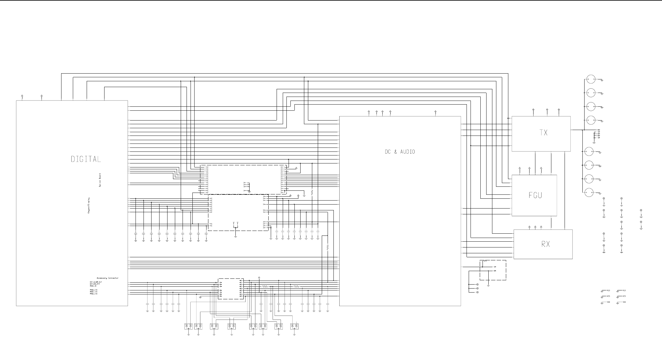
Midband 1-25W PCB 8489012U01 (rev. C) / Schematics 4-5
FILT_SW_B+
D3_3V
FILT_SW_B+
D3_3V
SPI_MISO
SPI_MOSI
TX_EN SPI_CLK
SQ_DET
SYNTH_CS
SYNTH_LOCK
RSSI
RX_EN
ASFIC_CS
CH_ACT
HSIO
LOC_DIST
LSIO
VS_AUDIO_SEL
VS_CS
VS_GAIN_SEL
VS_INT
VS_RAC
uP_CLK
RESET
F1200
OPT_DATA_R_OPBD
OPT_EN_OPBD
SCI_CH
SHIFT_R_CS
BOOT_EN_IN_CH
COMM_DATA_SEL_CH
DISPLAY_CS_CH
KEYPAD_COL_CH
KEYPAD_ROW_CH
MIC_PTT_CH
HOOK_CH
VOL_INDIRECT
VOX
VSTBY
ONOFF_SENSE
BATT_SENSE
EMERGENCY_SENSE
PROG_I-ACC_C_3
PROG_I-ACC_C_6
PROG_IO-ACC_C_12
PROG_IO-ACC_C_14
PROG_IO-ACC_C_8
PROG_O-ACC_C_4
Place capacitors near J2
1000pF
C628
C632
1000pF 1000pF
C630
1000pF
C633
1000pF
C629
1000pF
C631
VR698
6.8V
4813830A75:STD
6.8V
4813830A75:STD
VR699 VR696
4813830A75:STD
6.8V
4813830A75:STD
6.8V
VR697
4813830A75:STD
VR695
6.8V
4813830A75:STD
VR694
6.8V 6.8V
VR693
4813830A77:STD
Place capacitors near J2
6.8V
4813830A75:STD
VR692
1000pF
C622
C678
0.1uF
C623
1000pF 1000pF
C621
1000pF
C620
1000pF
C662 1000pF
C625
1000pF
C627
1000pF
C626
C624
1000pF
Accessory Connector
P1-6
P1-8
P1-14
P1-3
P1-4
P1-7
P1-12
P1-10
P1-11
P1-9
P1-15
P1-16
P1-5
P1- 2
P1-1
P1-13
FILT_SW_B+
R601
330
R610
100
0662057C59:STD
Place capacitors near J2
Control Head Connector
1000pF
C604 150pF
C608
C603
1000pF
C612
1000pF
150pF
C609
C607
1000pF
1000pF
C606 C610
1000pF
1000pF
C605 C611
1000pF
M206
M205
M201
M202
M203
M204
GND
U521
U518
GND
M4
GND
GND
U519
GND
M3
M7
GND GND
M2
GND
M5
GND
M1
M8
GND
U520
GND
E7
E6
E8SPARK_GAP
12
SPARK_GAP
12
SPARK_GAP
12
SPARK_GAP
12
SPARK_GAP
12
SPARK_GAP
12
SPARK_GAP
12
SPARK_GAP
12
E5
Antenna Connector
G2 J1-5
J1-3
3
G1 J1-4
J1-2
2J1-1
1
E3
E1
E2
E4
ANTENNA
BIAS_ADJ_EN RX
TX_INJ
PA_BIAS
PA_CURRENT
PWR_SET
RX_EN
TX_EN
9V
B+
FILT_SW_B+9V
FILT_SW_B+ B+
DC Connector
P2-1
BW_SEL
B+
P2-2
TP3
TP2
M9
TP4
BW_SEL
DEMOD
LOC_DIST
RSSI
RX_EN
RX_FE_TUNE
5V 9V 3V
RX_INJ
9V RX
RX_INJ
3V5V
16.8MHz
MOD_IN
SYNTH_CS
SYNTH_LOCK
5V
3V5V 9V
BIAS_ADJ_EN
SPI_CLK
SPI_MOSI
TX_EN TX_INJ
3V 9V
MOD_OUT
RX_FE_TUNE
DEMOD
16.8MHz
PA_BIAS
PA_CURRENT
PWR_SET
(SOURCE)
FILT_SW_B+
FILT_SW_B+
(SOURCE)
5V 9V
D3_3V
D3_3V
3V 5V 9V
3V
SPI_CLK
SPI_MOSI
SQ_DET
CH_ACT
ASFIC_CS
VS_AUDIO_SEL
uP_CLK
RESET
F1200
HSIO
LSIO
MIC_AUDIO_CH
HANDSET_RX_AUDIO_CH
5V_CH
Used only in MARLIN+
TX_AUDIO_RETURN_OPT_BRD
TX_AUDIO_SEND_OPT_BRD
UNMUTED_RX_AUDIO_SEND_OPT_BRD
VS_MIC
POST_LIMITER_FLAT_TX_AUDIO_RETURN_OPT_BRD
RX_AUDIO_RETURN_OPT_BRD
DETECTOR_AUDIO_SEND_OPT_BRD
RX_AUDIO_OUTPUT_ACCESS_CONN
SPKR+
SPKR-
EMERGENCY_ACCES_CONN
EXTERNAL_MIC_AUDIO_ACCESS_CONN
FLAT_TX_AUDIO_INPUT_ACCESS_CONN
IGNITION
VOL_INDIRECT
VOX
VSTBY
ONOFF_SENSE
BATT_SENSE
EMERGENCY_SENSE
Internal spkr+ jumper
0
R600
Place capacitors near J2
1000pF
C618
150pF
C619
C617
1000pF
C615
1000pF
1000pF
C613
1000pF
C602 1000pF
C616
1000pF
C614
D3_3V 0
R611
9V
NC ELP ONLY
NC ELP ONLY
NC ELP ONLY
NC ELP ONLY
GND
DISPLAY_DRIVER_RESET
MIC_PTT
HOOK GND
SPI_CLK J2-2 2
J2-1313
J2-22
G2
J2-21
G1
11J2-11
J2-4 4
J2-14 14
J2-16
16
SCI_PROGRAMMING
KEYPAD_ROW
KEYPAD_COLUMN
DISPLAY_DRIVER_COMMAND/DATA_SEL
SPI_MOSI
SHIFT_REG_CS
BOOT/RESET
DISPLAY_DRIVER_CS_EN
J2-1010
J2-66
J2-55
J2-33
17 J2-88 J2-17
J2-99
J2-11 HANDSET_RX_AUDIO
J2-7 7
15
J2-15
J2-1818
J2-20 20
J2-19 19
J2-12 12
SPKR-
SPKR+
MIC_AUDIO
9.3V
D3_3V
NC ELP ONLY
NC ELP ONLY
D3_3V
3
6
1
13
16
15
5
2
19
18
17
8
10
7J3-3
J3-6
J3-1
J3-13
J3-16
J3-15
J3-2
J3-5
J3-19
J3-18
J3-17
J3-8
J3-10
J3-7
DISPLAY_DRIVER_COMMAND/DATA_SEL
KEYPAD COLUMN
KEYPAD ROW
VOICE STORAGE INT
VOICE STORAGE CS
VOICE STORAGE GAIN SELECT
PUSH TO TALK
DISPLAY DRIVER CHIP SELECT
SERIAL CLOCK
SERIAL DATA SEND
OPTION BOARD ENABLE
DATA READY/REQUEST
VOICE STORAGE RAC
SERIAL DATA RETURN
28 pins connector
Option Board Connector
J3-31
J3-32
J3-29
J3-30
J3-28 28
J3-4 4
11
J3-22 22
J3-11
J3-9 9
J3-14 14
J3-21 21
20J3-20
J3-24 24
J3-12 12
J3-26 26
25
J3-23 23
J3-27 27
J3-25
TX AUDIO SEND
VOICE STORAGE AUDIO SELECT
POST-LIMITER FLAT TX AUDIO RETURN
DETECTOR AUDIO SEND
ANALOG 3 VOLT SUPPLY
GND
UNMUTED RX AUDIO SEND
DIGITAL 3.3 VOLT SUPPLY
BACKLIGHT
RX AUDIO RETURN
TX AUDIO RETURN
EXTERNAL MIC
RESET
GND
Midband (66-88MHz) Main Circuit
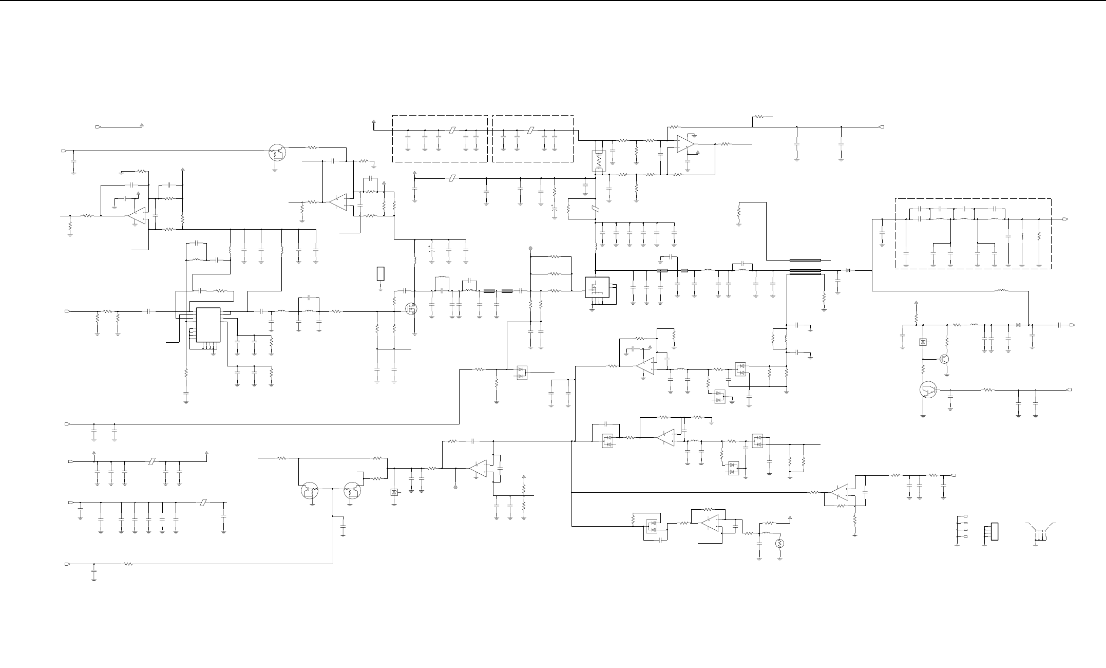
4-6 Midband 1-25W PCB 8489012U01 (rev. C) / Schematics
C1068
2200pF
BIAS_ADJ_EN
B+
B+
R130
0
39K
R100
V_CTRL_PREDRIVER
2.2K
R168
C1069
1000pF
1000pF
C1072
C1060
1n
C1053
1000pF
R165
2.4K
9
10
84
11
MC3303
U103
R137
39.K
FILT_SW_B+_PA
VCNTR1
R122
4.7
FLT_9V
R171
470
1000pF
C1119
C1110
150pF
6.8nH
L107
1n
C1041
.022uF
C1039 C1057
2200pF
2200pF
C1074 150nH
L105
680nH
L104
C1031
.022uF
VCNTR2
0611077A01:STD
L1506
100nH
C182
33pF R1506
10
51pF
C1525
56nH
L1507
C1527
43pF
C1526
43pF
43pF
C1524
C1043
2200pF
5.6K
R159
2200pF
C1042 22n
C1038
22n
C1032 R158
5.6K
22n
C1030
R176
100
V_CTRL_PREDRIVER
R109
39
R174
150
150
R173
TX_INJ
2200pF
C1044
14
8
9
10
15
16
1
11
17
4
5
12
13
VD1 VG1 2
VG2 3
NC1
NC2
NC3
NC4
RFIN RFOUT1 6
RFOUT2 7
VCNTRL
EP
G2
GND1
GND2
GND3
GND4
30C65
U101
FILT_SW_B+
PA_BIAS
2200pF
C1093
C1092
2200pF
9V
FILT_SW_B+
1000pF
C1096
C1127
1000pF
C1085
1000pF
57R01
L121
C1128
1000pF
FILT_SW_B+_PA
C1086
1000pF
22n
C1034
2200pF
C1087
220pF
C1122 220pF
C1124
C1123
220pF
220pF
C1126
C1125
220pF
C1070
2200pF
L118
57R01
FLT_9V
1000pF
C1083
R182
0
RX_EN
R1502
30K
VCNTR2
10K
47K
Q102
10K
47K Q101
C1129
2200pF
15K
R139
R136
39.K
VCNTR1
C1054
1n
510
R170
5.6V
VR101
C1028
100n
V_CNTRL
5
74
11
MC3303
U103
6
TP150
1
C1066
1n
FLT_9V
R180
47K
47K
R181
C1062
1n
C1029
100n
V_REF_OPAMP
22n
C1036
R167
2.2K
10K
47K
Q107
22K
R147
R175
220
R183
47K
VCNTR3
V_CTRL_DRIVER
LM2904
U102
2
3
18
4
2200pF
C1040
1000pF
C1079
R126
11
R127
1n
C1061
2.2K
2.4K
R169
R166
47K
R138
FLT_9V
C1000
220pF
L100
57R01
PA_FILT_B+
Place outside of the PA compartment
(SOURCE)
C1097
1n
220pF
C1113 1n
C1088 1n
C1098
B+ L120
57R01
C1089
1n C1107
470p
470p
C1106
Place inside of the PA compartment
L119
57R01
C1099
2200pF C1100
2200pF
C1116
220pF
220pF
C1115
C1114
220pF
C1058
1n
1.639m
R101
10u
C1027
57R01
L117
10
R1503
R110
1.K
1n
C1055
C1103
33n
R111
1.K
0
R184
C1073
2200pF
R132
750K
1.8MEG
R112
10.K
R1151n
C1056 U102
LM2904
6
5
8
4
R116
10.K
R113
10.K
10.K
R114
FILT_SW_B+_PA
R177
22K
PA_CURRENT
Final_cur_sense
0
R188
C1094
2200pF
V_CTRL_DRIVER
2200pF
C1095
PA_CURRENT
470pF
C1520 C1538
20pF
47pF
C1537
C1534
27pF
71.5nH
L1513
C1518
16pF
C1519
150pF
HARMONIC FILTER
L1512
71.5nH 71.5nH
L1511
39pF
C1535
8.2pF
C1539
18pF
C1532
39pF
C1522
C1521
22pF
10K
R152
18pF
C1523
L1518
1.2uH
ANTENNA
71.5nH
2485873L11:STD
L1514
56pF
C1121
C1006
470pF
C1108
330pF
D103 RX
1.2uH
L108
2200pF
C1536
R108
51.000
C1010
470pF
51.000
R107
10K
R185
R172
470
.
VR102
5.6
Q103
Q106
C1035
22n
C1067
1000pF
R157
56K
2200pF
C1077
2200pF
C1078
TX_EN
C1090
1n
0
R190
1n
C1091
1000pF
C1135
22.K
R149
PWR_SET
M101
M104
M103
M102 1P1
2P2
P3
3P4
4
DRV_CLIP
M100 SH100
PA Shield
1
2
3
4
R143
22.K
R142
22.K
2
3
14
11
MC3303
U103
R156
10.K
C1059
1n
Temp. Sense
FLT_9V
6.8K
R151
1n
C1052
1uH
L103
RT100
47K
0680361L01:STD
4.65V
43K
R135
22K
R145
1000pF
C1051 22.K
R148
4
11
MC3303
U103
13
12
14
V_REF_OPAMP
1n
C1050
D102
0
R187
Final_cur_sense
MRF1511’s Thermal pad
POS
1
M105
HEATSINK
470p
C1105
R102
120
36
R179
R178
100
MRF1511
Q105
V_CTRL_DRIVER
470pF
C1502
C1501
300pF
160pF
C1503
2460591E64:STD
30.15nH
L1502
C1506
240pF C1505
160pF
L1503
7.66nH
C1529
43pF
C1504
270pF 51.0
R105
C1507
2200pF
51.0
R106
2200pF
C1065
C1104
.022uF
R125
2.7
R124
2.7
R123
2.7
TP557
TEST_POINT
1
S3
S4
Q100
D
GGND1
GND2
S1
S2
MRF1550
C1530
180pF
C1508
150pF 150pF
C1509 270pF
C1511
20pF
C1510
L1504
16.03nH
C1531
240pF
C1513
56pF
20pF
C1515
C1514
240pF
2485873L09:STD
38.13nH
L1505
62pF
C1516
16pF
C1517
V_forward
DIRECTIONAL COUPLER
120
R103
V_reverse
D104
C1018
16.00p
33pF
C1541
33pF
C1540
L1519
180nH
R186
0
R119
150
680
R118
2200pF
C5560
D106
D105
R161
3.3K 100pF
3.3K
R160
C1101
1n
C1075
1n
C1046
1n
C1045
L101
1uH
15K
R117
2200pF
C1071 22K
R140
FILT_SW_B+_PA
2
3
18
4
U100
LM2904
R141
22.K
R146
22.K
C1049
1n
D101
22.K
R144
LM2904
U100
6
5
78
4
C1048
1n
1n
C1076
C1047
1n
L102
1uH
R164
15K
3.3K
R163
R162
3.3K
C1102
100pF
D107
D108
C195
2200pF 680
R120 R121
150
V_reverse
22n
C1033 C1063
2200pF
C1064
2200pF
120nH
L122
C1037
22n
1uF
C1001
R131
10K
4.7K
R134
C1081
1n C1082
1n
D100
VCNTR3
38.13nH
2485873L09:STD
L115
.022uF
C1011
C1008
470pF
2200pF
C1009
C1003
470pF
470pF
C1002
470pF
C1007
7
R104
120
PA_FILT_B+
Midband (66-88MHz) Transmitter
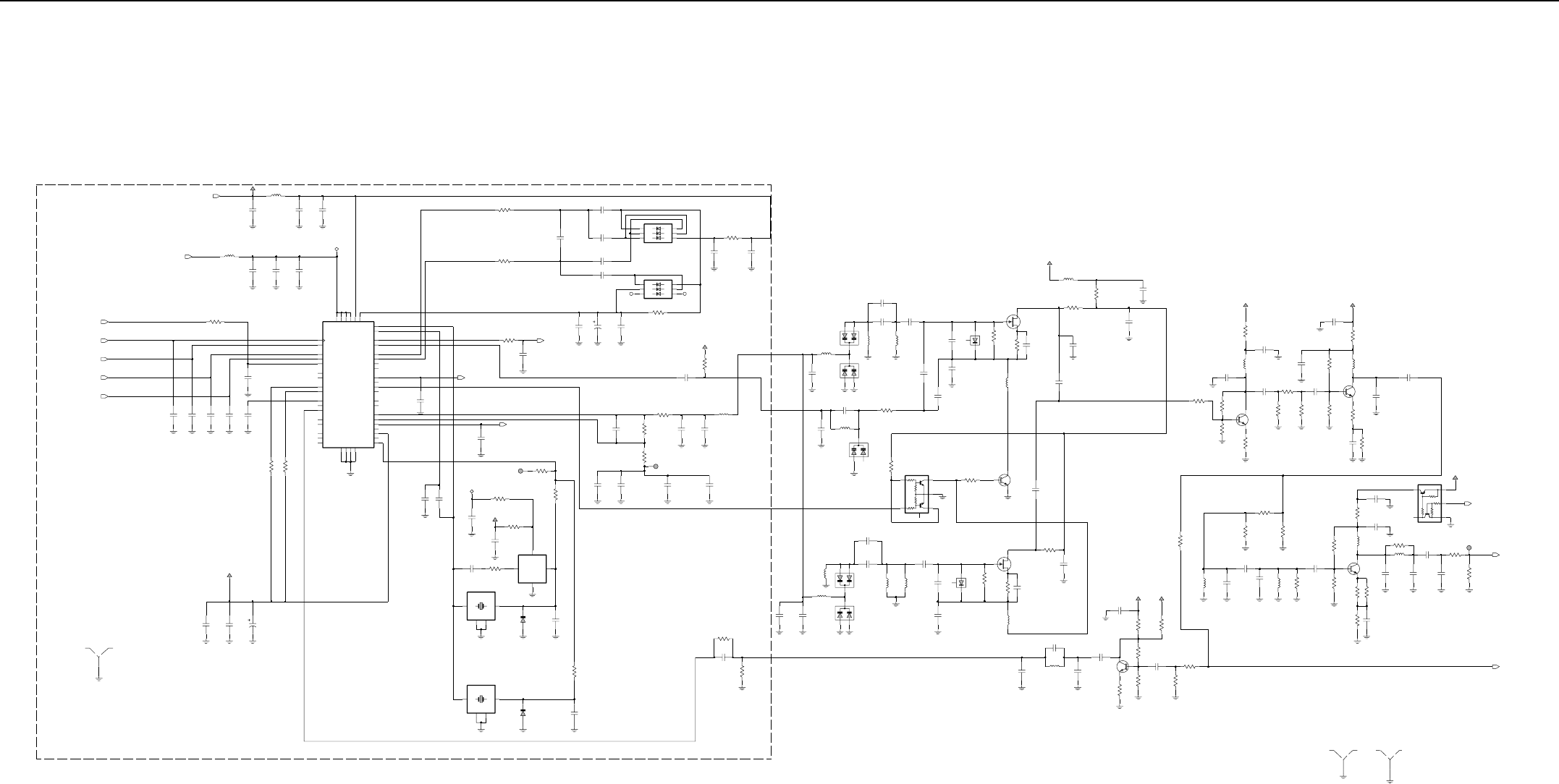
Midband 1-25W PCB 8489012U01 (rev. C) / Schematics 4-7
9V
SPI_MOSI
SPI_CLK
MOD_IN
SYNTH_CS
0.1uF
C2805
220pF
C2047
C2046
220pF
220pF
C2045
2.2uF
C2006
C2048
220pF
R206
150K
240K
R200
C200
2.2uF
820nH
L217
5V
C2015
0.1uF
5V
2200pF
C2034
3V_FLTR
2.2uF
C2005
820nH
L200
2200pF
C2035
C2023
10n
3V
R2808
10
LVFRACN Shield
shield
SH1
1
C2033
1n C2014
0.1uF 4.7uF
C2002
V_SF
D202B
16.8MHz
14R06
Y202
GND
2
GND1
4
OUT 3
IN
1
2.7p
C2072B
150K
R207B
D202 2.7p
C2072
IN
16.8MHz
2
GND
4
GND1
3
OUT
1
Y201
14R06
1
VCON
Y200
45J68
2
GND
3OUT
VCC
4
16.8MHz
100K
R210
C2053
100p
0.1uF
C2017 0
R204
5V
R205
0
0.1uF
C2020
C2054
62p
C2051
220p
3V_FLTR 100K
R209
150K
R207
TP201 1
C2050
1000pF
SYNTH_LOCK
2200p
C2037
BIAS_ADJ_EN
C2049
1000pF
100
R229 16.8MHZ
C2036
1n C2001
4.7uF
R202
0
0.1uF
C2013
C2722
1uF
150K
R2714
V_SF
NC
K3
D201
A1
A2
A3
K1
K2
NC
C2027
10n
C2024
10n
22p
C2055 C2025
10n
A2
A3
K1
K2
K3
D200
A1
10n
C2026
R226
150
R225
150
C2016
0.1uF 2.2uF
C2004
100
R228
1TP200
1uF
C2078
C2079
C2077
470
R224
C2074
0.1uF
R217
560 C2076
0.1uF
R234
100
180pF
C2080
L205
0.1uF
C2028
R2797
0
.01uF
C2796
R2796
270
1uH
L2751
.01uF
C2750
.01uF
C2751
43pF
C2752
C2753
43pF
1uH
L2750
D2752
D2751
L2752
180nH
C2754
27pF
180nH
L2753 D2754
10pF
C2756
10pF
C2755
68
R2753
27K
R2751
1000pF
C2757
L2754
1uH
D
SQ2751
39
R2754
1000pF
C2758
15pF
C2762
2.2K
R2752 Q2752
R2743
4.7K
14
Q2742
35
2
FMG8A
D2731
33
R2731
270nH
L2731
15pF
C2733
1000pF
C2731
100pF
C2736
470pF
C2735
100pF
C2737
470nH
L2733
2.7pF
C2734
1uH
L2732
D2733
120nH
L2734
C2738
43pF
D2732
15pF
C2761
D2739
C2732
1pF
1uH
L2741
1000pF
C2745
D
S
Q2741
R2739
68
R2741
C2740
27K
24pF
C2739
18pF
39
R2742
47pF
C2741
1000pF
C2744
L2742
1uH 0.1uF
C2743
22
R2740
V_SF
Q2760
120nH
L2768
0.1uF
C2771
.01uF
C2767
150nH
L2761
Q2770
5V
1K
R2769
39
R2766
100
R2758
C2766
1000pF
C2772
100pF
C2765
30pF
470
R2762
R2760
0
150
R2767
C2763
.01uF
9V
150
R2771
5.6pF
C2764
100
R2763
R2765
150
2.7K
R2768
100
R2772
10
R2770
R2761
1.8K
27pF
C2775
4.7pF
C2773
FIT RES 150
Q2780
82pF
C2783
33pF
C2785
1000pF
C2782
39
R2785
R2781
100
4.7pF
C2784
100
R2782
C2786
0662057A29:STD
10pF
Q2791
150
R2786
0
R2787
C2780
0.1uF
120nH
L2783
9V
.01uF
C2781
180nH
L2781
10
R2783
10
R2784
2.7K
R2778 TP100
TEST_POINT
1
TX_EN
RX_INJ
TX_INJ
L2775
C2778
56nH
47pF
C2777
27pF
L2774
56nH
R2774
R2775
100
R2776
270
R2773
270
68pF
C2776
470pF
C2779
1.5K
R2779
270
R2777
shield
SH2
1
SH3
shield
1
5V
C2790
12pFQ2790
51
R2794
1K
R2793
1K
R2795
C2791
.01uF
0
R2790
R2792
1K
.01uF
C2793
6.8pF
C2795
7.5pF
C2794
L2790
180nH
R2791
470
0.1uF
C2792 9V
R2810
470
10
21
35
18
27
26
30
10
17
29
31
32
7
40
39
42
9
8
33
44
6
22
25
23
24
37
38
15
14
12
11
28
41
19
45
16
43
4
2
3
46
48
1
47
13
34
5
36
20
VRO
WARP
XTAL1
XTAL2
TEST1
TEST2
VBPASS
VCP
VMULT1
VMULT2
VMULT3
VMULT4
PRE_GND
PRE_VDD
PVREF
REFSEL
SFBASE
SFCAP
SFIN
SFOUT
MODIN
MODOUT
NC1
NC2
NC3
PD_GND
PD_VDD
PREIN
DATA
DGND
DVDD
FREFOUT
IADAPT
INDMULT
IOUT
LOCK
AUX3
AUX4
AVDD
BIAS1
BIAS2
CCOMP
CEX
CLK
U200
63A27
ADAPTSW
AGND
AUX1
AUX2
Midband (66-88MHz) Synthesiser and VCO
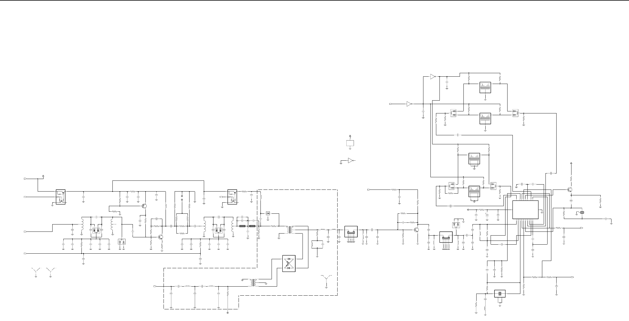
4-8 Midband 1-25W PCB 8489012U01 (rev. C) / Schematics
FRONT-END SHIELD
9V
RX_EN
9V
2
5
4
1
3
Q4
RX_FE_TUNE
RX
SHIELD
SH2302
SH2301
SHIELD
11
20pF
C2323
C2301
10pF
C2328
100pF
L2300
1
3
100K
R2301
1000pF
C2319
C2329
100pF
D2303
27pF
C2306
C2305
180pF
220pF
C2304
20pF
C2324
R2312
2.7K
22pF
C2302
1
2
3
2
L2301
1
2
3
D2301
R2311
3.9K
C2300
3300pF 3300pF
C2311
Q2302
1000pF
C2308
C2309
R2313
3.3K
330pF
R2303
1K
C2310
330pF
R2305
10K
Q2301
C2322
.01uF
R2302
330
C2307
3300pF
1.5K
R2304 R2314
62
C2317
27pF
R2309
100K
C2316
180pF
C2315
220pF
C2320
1000pF
C2335
100pF
100pF
C2336
1000pF
C2312
R2307
68
150
R2317
150
R2316
33
R2318
33pF
C2326
C2337
3300pF
3L2304
1
2
D2304
12
3
C2313
100pF
C2327
100pF
4.7pF
C2318
C2314
22pF
33pF
C2325
1
2
3
L2303
100pF
C2321
FIT CAP 12pF
D1
2113740F29:STD
R2321
270
R38
220
1000pF
C2806
6
3
1
2
T1
XFMR
2580541Z02:STD
4
U1
A2
4
A4
3
K1 1
K3 2
shield
SH4
1
C59
20pF
L6
1.2uH
L2
1.2uH 47pF
C40
R41
51
1.2uH
L2792
5
GND
6IN 3
OUT
TS2-21B01
FL2201
1
GND
2
GND
4
GND
L2201
2.7uH 4.7pF
C2201
20pF
C2202
15pF
C58 R13
10K
56pF
C2210
6.8K
R24
Q6
100n
C5
R5
24K
56pF
C2205
L2202
2.7uH
C2206
20pF
GND
2
GND
4
GND
5
GND
6IN 3
OUT
TS2-21B01
FL2202
1
D2201
L2203
2.7uH
20pF
C2207
10pF
C2211
2
3
1
1.2uH
L3
0.1uF
C20
100n
C7
R25
4.7K
C2209
30pF
C2338
82pF
R10
15K
C54
27pF
43pF
C53
R4
027nH
L16
C57
30p
15K
R12
GND
2
GND
4
31
20.945MHz
Y2
TSX-5 8.2K
R23
680
R33
10K
R21
C22
4.7n
DEMOD
C21
0.1uF 100n
C10
12K
R14
C15
100n
3
455KHz
Y1
45B02
1.2K
R31 C16
100n
RSSI
21
Q3
C3
130pF
R35
390
R30
1.8K
0.1uF
C18
3V
C12
100n C11
100n
R20
12K
D5
R19
12K
10uF
C2 C9
100n
51
R39
C8
100n
3V
R9
20K
0.1uF
C19
D6
3
GND1
GND2
4
1IN 2
OUT
FL4
CFWC455G
R36
0
R27
3.3K
R34
2.7K
C6
100n
R37
100
5V
Check if it is 3v or another value
5
4
GND
8
VCC
U3
TC7W04F
3
U3
PWR_GND
3V
24pF
C62
C49
220pF
RX_INJ
C47
47pF
100nH
L13
24pF
C63
L14
100nH
C48
220pF
R2
470
TP1
TEST_POINT
1
2580541Z02:STD
4
6
3
1
2
T2
XFMR
470nH
L2302 R2306
270 270
R2308
1
TP51
TP52 C2330
3300pF
LOC_DIST
R1
430
Q1
.01uF
C1 L1
2.7uH
MIXER SHIELD
62
TC7W04F
U3
BW_SEL
100n
C13
2.4K
R28
D4
3.3K
R26
C17
0.1uF
20K
R6
IN
1OUT2
FLTR
FL3
GND
3
D3
12K
R15
12K
R17
12K
R16
R7
20K
IN
1OUT 2
FLTR
FL2
GND
3
TC7W04F
U3
7
1
C14
100n
R8
20K R18
12K
4GND2
1IN 2
OUT
FL5
CFWC455D
GND1
3
3
10
1
2
5
9
6
19 17
14 11
13
12
20
4
SA616
U2
8
7
15
18 16
OSCOUT
QUADIN
RFIN
RFIN_DEC
RSSIOUT
RSSI_FEED
VCC
IFAMP_DEC1
IFAMP_DEC2
LIMIN LIMOUT
LIM_DEC1
LIM_DEC2
MIXOUT
OSCIN
AUDIOOUT
AUDIO_FEED
GND
IFAMPIN IFAMPOUT
Midband (66-88MHz) Receiver
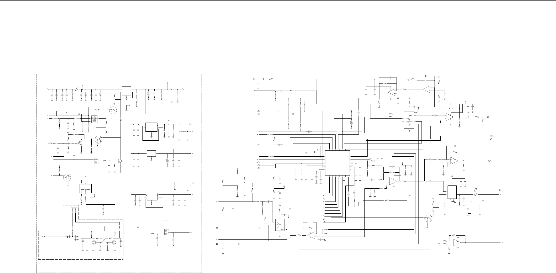
Midband 1-25W PCB 8489012U01 (rev. C) / Schematics 4-9
57R01
L500
FILT_B+
C5083
100pF
C5086
.022uF
C5001
10uF
0.1uF
C5061
C5060
100n
C5000
1000pF
C5085
.022uF
1000pF
C5067
B+
FILT_SW_B+
100pF
C5084 VR500
MR2835S
24V
0.1uF
C5062 3.3V
VR504 R5050
13K
C5094 220pF
0
R5000
C5092
220pF
TP500
62K
R5031
FILT_B+
FILT_SW_B+
BATT_SENSE
R5036
47K
VR503
3.3V
EMERGENCY_ACCES_CONN
DC_POWER_ON
EMERGENCY_SENSE
47K
R5035
D3_3V
DTC144EKA
Q504
ONOFF_SENSE
Smart Fuse Circuit
5.1V
VR501
D500
R5074
1K
D513
IGNITION R5082
51K Q503
C5038
100n
R5048
24K
Q500
R5039
100K
R5085
1MEG
R5089
1MEG
R5083
270K
FILT_B+
1000pF
C5110
R5073
1K
FILT_B+
1000pF
C5111 47uF
C5120
24K
R5103
3.3V
VR502
D501
C5071
1000pF
VS_MIC
VS_AUDIO_SEL
MIC_AUDIO_CH
VSTBY
C5045
1uF
0.1uF
C5102
USE NLAS459
R5047
0
C5046
0.1uF
GND
3
1
IN
4NC
NO
VPOS2
MAX4599EXT
U515
5
COM
C5103
100n
3V
0
R5084
6R5026
33K
U507
LM2904
6
5
78
4
1000pF
C5091
82pF
0
R5014
270K
R5027
C5077
4.7K
R5072
AUDIO_PA_EN
LM2904
U517
6
57
8
4
100K
R694
3V
39K
9V
R693
R2811
100K
R692
39K
RX_FE_TUNE
SPKR-
SPKR+
C5099
220pF
0n
L501
57R01
0n
L502
57R01 C5100
220pF
C5098
220pF
1000pF
C5073
220pF
C5097
C5072
1000pF
47uF
C5002
10K
47K
24K
R5041
12K
R5051
Q501
DTC114YE
FILT_SW_B+
B+
1000pF
C5080
C502
0.1uF
OUT2
6
RR
3
VCC
7
GND1 2
GND2 5
GND3 10
11
GND4
IN
9
M_SS
8
NINV
1OUT1
4
TDA1519C
U502
R5013
0
C5104
1000pF
C5049
0.1uF
1000pF
C5082
C5031
0.1uF
3V
0
R5008
3V
47K
R5033
C5025
0.1uF
C5024
0.1uF
R5061
R5060
10K
10K 3V
C5036
0.1uF
C5058
0.1u
R5058
10K
LM2904
U507
2
31
8
4
10K
R5059
C5075
1000pF
3V 5V3V
0
R5011
C5034
0.1uF
0
R5010
3V
0.1uF
C5029
C5026
0.1uF
3V
C5022
0.1uF
SPI_MOSI
F1200
DC_POWER_ON
uP_CLK
SQ_DET
LSIO
HSIO
BW_SEL
ASFIC_CS
SPI_CLK
CH_ACT
VAG=4.5v
10uF
C5011
R5052
10K C5019
0.1uF
R5053
10K
VAG
2.2K
R5070
R5054
10K C5047
0.1uF
R5075
510.
C5559
1000pF
EXTERNAL_MIC_AUDIO_ACCESS_CONN
C5009
10uF
C5010
10uF
300
R5077
510.
R5076
R5078
100.
9V VOX
DEMOD
PWR_SET
PA_CURRENT
PA_BIAS
C5050
0.1uF
0
R5006
TX_AUDIO_RETURN_OPT_BRD
TX_AUDIO_SEND_OPT_BRD
RX_AUDIO_RETURN_OPT_BRD
R5042
24K
0.1uF
C5051
24K
R5043
0.1uF
C5052
0.1uF
C5053
30.K
R5040
8.2K
R5063
8.2K
R5064
3V
24K
R5044
3V
UNMUTED_RX_AUDIO_SEND_OPT_BRD
DETECTOR_AUDIO_SEND_OPT_BRD 0.1uF
C5054
SOURCE
POWER SUPPLY
9.3V
AUDIO
0.1uF
C5055
R5025
100K
R5023
100K
POST_LIMITER_FLAT_TX_AUDIO_RETURN_OPT_BRD
FLAT_TX_AUDIO_INPUT_ACCESS_CONN
R5024
100K
C5056
0.1uF
C5101
1000pF
9.3V
C5096
C5095
220pF
220pF
C5005
33uF 0.1uF
C5015 C5074
1000pF
9V
9V
5V TO LVFRACN
SOURCE
5V
5V
For mid_band
0
R5002
C5040
100n 100n
C5039
0.1uF
C5016
C5068
1000pF
C5006
10uF
5V_CH
3.3V to IFIC, ASFIC
SOURCE
3V
C5008
10uF
0.1uF
C5018
1000pF
C5070
3V
SOURCE
3.3v digital
.01uF
C5555
D3_3V
RESET
D3_3V
C5007
10uF
C5069
1000pF
C5017
0.1uF
3.3v Digital REGULATOR
1000pF
C5065
2.2uF
C5041
U510
LP2986ILDX
VOL_INDIRECT
8
SHUTDOWN
3
TAP
7
ERROR
2
FEEDBACK
GND
1
9
GND
4
INPUT
5
OUTPUT
6
SENSE
Place near uP
C5035
100n
Audio
Indirect
Volume
R5079
100.
2.2K
R5071 4
2
S5010
SWITCH
3LOW
HIGH
1
5
6
D3_3V
10uF
C5119 R5037
10K
U511 Q505
MMBT3904
R5069
10K
10K
47K Q502
0.1uF
C5037
Q506
TP556
R5062
10K
R5020
150K
R5030
33K
R5049
15K
100K
R5028
C5063
0.1uF
Q514
1
25
6
3
4
4802393L66:STD
D502
4813825A23:STD
R5029
100K
47K
R5007 10K
47K
On/Off for ATE
spacer for TO-220
M6
33K
R5038
R5001
1%
1K
1%
6.34K
R5081
TP555
Q507
SOURCE
5
VOUT
LM2941T
U501
1
ADJ
3GND
2
ON_OFF
4VIN
1u
C5042
1000pF
C5064
5V RF Regulator
3
SHUTDOWN
U503
6
5V_TAP
5ERROR
7FEEDBACK
4
GND
8INPUT 1OUTPUT
2
SENSE
LP2951C
1000pF
C5066
1u
C5043
3.3V RF REGULATOR
1GND
3IN 2
OUT
MC33269D
U508
3V
R5080
10.
C5012
4.7u
0.1uF
C5057
R5067
6.2K
56K
R5032
47K
R5034
9V
C5081
1000pF 0.1uF
C5033
82p
C5090
R5046
24K
U506
LM2904 2
3
18
4
6.2K
R5068
R5045
33K
10K
R5056
100K
R5022
5
7
8
4
U506
LM2904 6
C5089
82pF 3V
R5057
10K
0.1uF
C5032
R5021
100K
82pF
C5088
6
57
8
4
U505
LM2904
VAG
1u
C5044
9V
R5091
560
R5065
6.2K
C5003
47uF
0.1uF
C5030 1000pF
C5079
R5092
100K
RX_AUDIO_OUTPUT_ACCESS_CONN
MOD_OUT
16.8MHz
need to add 10uF in C.H
HANDSET_RX_AUDIO_CH
R5019
270.K
6.2K
R5066
C5076
1000pF
C5087
82p
R5055
VAG
10K
C5048
0.1uF LM2904
U505
2
31
8
4
FLAT_TX_AUDIO_MUTE
FLAT_OR_DEEMPH_RX_AUD_SEL
3V
0
R5009
1000pF
C5078
0.1uF
C5027
ZC
4
YOA
12
Y0B
2
Y0C
5
13
Y1A
Y1B
1
3
Y1C
ZA
14
ZB
15
6
EN
11
SA
SB
10
SC
9
VDD
16
VEE
7
VSS
8
HEF4053B
U509
C5028
0.1uF
2.2uF
C5014
C5023
0.1uF
0.1uF
C5020 C5059
C5013
.022uF
1u 3V
30C53
U504
33
11
45
27
7
17
9 28
36
44
10
1
32
46
40
26
8
25
43
39
12
31
30
47
23
19
24
18
48
29
15
14
13
35
37
38
3
21
34
20
6
5
4
22
2
41
42
16
VDDD
VDDDAC
VDDRC
VDDSYN
VOX
SQDET
SQIN SYN
TXRTN
TXSND
UIO
VDDA
VDDCP
MICINT
MOD
NC
PLCAP
PLCAP2
RXRTN
RXSND
SQCAP
GNDD
GNDDO
GNDRC
GNDSYN
HSIO
LCAP
LSIO
MICEXT
F1200
GCB0
GCB1
GCB2
GCB3
GCB4
GCB5
GNDA
CLK
CLK168
CSX
DACG
DACR
DACU
DAT
DISC
AUDIO
AUXTN
CHACT
Midband (66-88MHz) DC and Audio Circuits
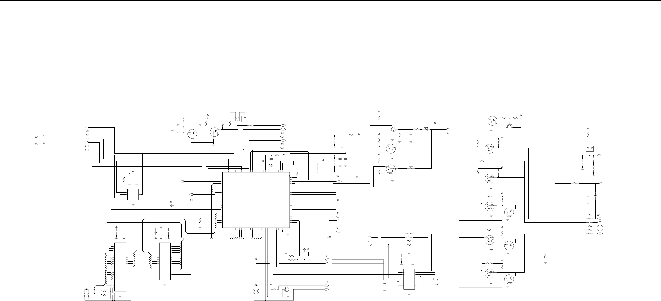
4-10 Midband 1-25W PCB 8489012U01 (rev. C) / Schematics
FILT_SW_B+
D3_3V
FILT_SW_B+
D3_3V
SPI_MOSI
SPI_CLK
ASFIC_CS
SYNTH_CS
DISPLAY_CS_CH
SPI_MISO
SHIFT_R_CS
SPI_MOSI
SPI_CLK
EE_CS
SCK
6
SI
5
SO 2
VCC 8
VSS
4
3WP
CS
1
HOLD
7
X25128-2.7
U400
1n
C400
D3_3V
R438
10K
100n
C401
SPI_MISO
TP400
TP409
SHIFT_R_CS
COMM_DATA_SEL_CH
LOC_DIST
R428
100K
A(0:18)
D(0:7)
C402
100n
C411
1n
VR401
4.3V
D3_3V
D3_3V
C412
1n
100n
C403
D3_3V
100K
R427
R426
100K 0.
0.
R414
R415
A(18)
A(17)
A18_RES
TP404
10K
R451
C410
100n
10K
47K Q400
D3_3V
R450
10K
TP410
10K
47K Q407
TP406
R439
10K
D400
51
R462
SCI_CH
CH_ACT
LSIO
SQ_DET
uP_CLK
OPT_DATA_R_OPBD
HSIO
100n
C404
D3_3V
R425
100K
TP403
R441
10K
D3_3V
D3_3V
C416
1n
1n
100n
C415
C407
100n
C408
1n
D3_3V
C414 100n
C406
RESET
F1200 TEST_POINT
TP408
10K
47K
10K
R446 Q413
10K
R422
10K
47K
Q414
D3_3V
D3_3V
R445
10K
D3_3V
R444
10K
Q415
1uF
C490
47K
R459 10K
R431
TP405
VR400
MMBZ5235B
6.8V
BOOT_EN_IN_CH
VSTBY
R436
33K
ACCESS_PTT R457
3.3K
D3_3V
Q412
0
R421
SCI_CH
33K
R435
Q411
PROG_IN-P6_I
R456
D3_3V
3.3K
33K
R434
3.3K
R455
D3_3V
Q410
PROG_IO-P8_I
PROG_IO-P8_O
Q409
PROG_IO-P12_I
D3_3V
R454
3.3K
R433
33K
10K
47K Q404
R432
33K
3.3K
R453
D3_3V
Q408
PROG_IO-P14_I
PROG_IO-P14_O
10K
47K Q405
10.K
R440
0
R407
R404
0
0
R406
0
R403
R405
0
0
R402
PROG_IN
PROG_I/O
PROG_I/O
PROG_I/O
EXT_ALARM_OUT
EXT_MIC_PTT
PROG_I-ACC_C_3
PROG_O-ACC_C_4
PROG_I-ACC_C_6
PROG_IO-ACC_C_8
PROG_IO-ACC_C_12
PROG_IO-ACC_C_14
D402
1000pF
C417
R461
220 MIC_PTT_CH
MIC_PTT
39K
R430
100K
R429
D401
C418
1000pF
HOOK_CH
MIC_SENSE
3.3K
R458
D3_3V
10K
47K 2.7K
R401
Q403
PROG_OUT-ALARM_4
Q401
FILT_SW_B+
1.5K
R460
10K
47K U401
3.3V
VR402
PROG_IO-P12_O
C405
100n
R447
10
D3_3V
C413
1n
EE_CS
SHIFT_R_CS
SYNTH_CS
SPI_MOSI SPI_MISO
SPI_CLK
ASFIC_CS
DISPLAY_CS_CH
R467 0
0
R466
0
0
R468
R469
TP425
R442
10K
3.3K
R443
D3_3V
10K
R463
D3_3V
Q417
D3_3V
100K
R424
R423
100K
TP402 TP401
SYNTH_LOCK
KEYPAD_COL_CH
KEYPAD_ROW_CH
PROG_IO-P8_O
PROG_IO-P12_O
PROG_IO-P14_O
PROG_OUT-ALARM_4
VS_AUDIO_SEL
VS_GAIN_SEL
VS_INT
VS_CS
VS_RAC
D3_3V
0.1uF
C423
1000pF
C422
ACCESS_PTT
PROG_IN-P6_I
PROG_IO-P8_I
PROG_IO-P14_I
PROG_IO-P12_I
MIC_PTT
MIC_SENSE
EMERGENCY_SENSE
VOL_INDIRECT
BATT_SENSE
ONOFF_SENSE
TEST_POINT
TP407
RSSI
VOX
TX_EN
RX_EN
OPT_EN_OPBD
PROG_IO-P8_O
PROG_IO-P12_O
PROG_IO-P14_O
SHIFT_REGN_CS
VS_RAC
MARLIN
PROG_OUT-ALARM_4 VS_INT
VS_CS
MARLIN+
.022uF
C421
SPI_CLK
SPI_MOSI
Q7
10 RESET
14 SERIN 9
SEROUT
16
VCC
GND
15
Q0 1
Q1 2
Q2 3
Q3 4
Q4 5
Q5 6
Q6 7
MC74HC595A
U405
12 CLK_L
11 CLK_S
13 EN_OE
8
SHIFT_R_CS
DISPLAY_CS_CH
17 D6
18 D7
19 D8
22
OE
28
VDD
14 VSS
27
WE
25
A8 24
A9
20
CS
11 D1
12 D2
13 D3
15 D4
16 D5
26
A13 1
A14
8
A2 7
A3 6
A4 5
A5 4
A6 3
A7
SRM2B256
U402
10
A0 9
A1
21
A10 23
A11 2
A12
A(10)
A(11)
A(12)
A(13)
A(14)
A(2)
A(3)
A(4)
A(5)
A(6)
A(7)
A(8)
A(9)
A(0)
A(1)
D(0)
D(1)
D(2)
D(3)
D(4)
D(5)
D(6)
D(7)
R_W
28
D6 29
D7
30 EN_CE
EN_OE
32
7EN_WE
GND
24 8
VCC
A8
3A9
2
21
D0 22
D1 23
D2 25
D3 26
D4 27
D5
A17
6A18
9
A2
18 A3
17 A4
16 A5
15 A6
14 A7
13
A1
19
A10
31 A11
1A12
12 A13
4A14
5A15
11 A16
10 U404
AT49LV040-70VI
A0
20
A(11)
A(12)
A(13)
A(14)
A(2)
A(3)
A(4)
A(5)
A(6)
A(7)
A(8)
A(9)
A(15)
A(16)
R_W
D(7)
D(6)
D(5)
D(4)
D(3)
D(2)
D(1)
D(0)
A(0)
A(1)
A(10)
DO NOT CONNECT THIS CS IN ORDER TO
PROVIDE WIRED OR OPERATION ON CSPROG
47
46
45
44
43
42
41
38
6
16
20
19
17
18
5
37
30
31
32
33
34
35
36
D(4)
D(5)
D(6)
D(7)
D(0)
A(14)
A(15)
A(16)
A(17)
A(18)
D(1)
D(2)
D(3)
40
87
13
56
55
54
53
52
51
50
49
28
27
26
25
24
23
22
29
14
10
11
9
21
15
8
7
70
A(9)
A(10)
A(11)
A(12)
A(13)
A(8)
A(1)
A(2)
A(3)
A(4)
A(5)
A(6)
A(7)
A(0)
MC68HC11FL0
U403
PH1_PW2
PH2_PW3
PH3_PW4
PH4_CSIO
PH5_CSGP1
PH6_CSGP2
PH7_CSPROG
PG1_XA14
PG2_XA15
PG3_XA16
PG4_XA17
PG5_XA18
PG6_AS
PH0_PW1
PG0_XA13
PF2_ADDR2
PF3_ADDR3
PF4_ADDR4
PF5_ADDR5
PF6_ADDR6
PF7_ADDR7
PFO_ADDR0
PF1_ADDR1
PC0_DATA0
PC1_DATA1
PC2_DATA2
PC3_DATA3
PC4_DATA4
PC5_DATA5
PC6_DATA6
PC7_DATA7
PB1_ADDR9
PB2_ADDR10
PB3_ADDR11
PB4_ADDR12
PB5_ADDR13
PB6_ADDR14
PB7_ADDR15
PBO_ADDR8
PI1
PI2
PI3
PI4
PI5
PI6
PI7
PI0
VSSR
VSS
VSSL
AVSS
PE0_AN0
66
PE1_AN1
65
PE2_AN2
64
PE3_AN3
63
PE4_AN4
62
PE5_AN5
61
PE6_AN6
60
PE7_AN7
67
71
PJ1_CSGP4 72
PJ2 73
PJ3 74
PJ4 75
PJ5 76
PJ6 77
PJ7 78
PJ0_CSGP3
PD0_RXD 97
PD1_TXD 98
PD2_MISO 99
PD3_MOSI 100
PD4_SCK 1
PD5_SS 2
3
PD6_LVIN ASF_CS
EE_CS
SPI_MOSI
SPI_CLK
SYNTH_CS
SPI_MISO
86
PA0_IC3 79
PA1_IC2 80
PA2_IC1 81
PA3_IC4_OC5_OC1 82
PA4_OC4_OC1 83
PA5_OC3_OC1 84
PA6_OC2_OC1 85
PA7_PA1_OC1
93
48
91
94
12
39
88
92
69
68
4
57
59
89
90
96
95
58 R_W
XFC
XIRQ
XTAL
VDD
VDDL
VDDR
VDDSYN
VRH
VRL
RESET
PG7_R_W
AVDD
ECLK
EXTAL
IRQ
LVOUT
MODA_LIR
MODB_VSTBY
Midband (66-88MHz) Microprocessor and Controller

Midband 1-25W PCB 8489012U01 (rev. C) / Schematics 4-11
2.1 MB PCB 8489012U01 (rev. C) Parts List 1-25W
Circuit
Ref. MotorolaPart
No. Description
C1 2113741F49 CAP .01uF
C2 2311049A57 CAPP 10uF
C3 2113740F54 CAP130pF
C5 2113743E20 CAP 100n
C6 2113743E20 CAP100n
C7 2113743E20 CAP100n
C8 2113743E20 CAP100n
C9 2113743E20 CAP100n
C10 2113743E20 CAP100n
C11 2113743E20 CAP100n
C12 2113743E20 CAP100n
C13 2113743E20 CAP100n
C14 2113743E20 CAP100n
C15 2113743E20 CAP100n
C16 2113743E20 CAP100n
C17 2113743E20 CAP 0.1uF
C18 2113743E20 CAP 0.1uF
C19 2113743E20 CAP 0.1uF
C20 2113743E20 CAP 0.1uF
C21 2113743E20 CAP 0.1uF
C22 2113741F41 CAP 4.7n
C40 2113740F43 CAP 47pF
C47 2113740F43 CAP 47pF
C48 2113740F59 CAP 220pF
C49 2113740F59 CAP 220pF
C53 2113740F42 CAP 43pF
C54 2113740F37 CAP 27pF
C57 NOT PLACED CAP 30p
C58 2113740F31 CAP 15pF
C59 2113740F34 CAP 20pF
C62 2113740F36 CAP 24pF
C63 2113740F36 CAP 24pF
C182 2113740F39 CAP 33pF
C195 2113741F33 CAP 2200pF
C200 2113743F18 CAP 2.2uF
C400 2113741F25 CAP1n
C401 2113743K15 CAP100n
C402 2113743K15 CAP100n
C403 2113743K15 CAP100n
C404 2113743K15 CAP100n
C405 2113743K15 CAP100n
C406 2113743K15 CAP100n
C407 2113743K15 CAP100n
C408 2113743K15 CAP100n
C410 2113743K15 CAP100n
C411 2113741F25 CAP1n
C412 2113741F25 CAP1n
C413 2113741F25 CAP1n
C414 2113741F25 CAP1n
C415 2113741F25 CAP1n
C416 2113741F25 CAP1n
C417 2113741F25 CAP1000pF
C418 2113741F25 CAP1000pF
C419 NOT PLACED CAP.01uF
C421 2113743E07 CAP.022uF
C422 2113741F25 CAP1000pF
C423 2113743K15 CAP0.1uF
C490 NOT PLACED CAP 1uF
C602 2113741F25 CAP1000pF
Circuit
Ref. MotorolaPart
No. Description
C603 2113741F25 CAP1000pF
C604 2113741F25 CAP1000pF
C605 2113741F25 CAP1000pF
C606 2113741F25 CAP1000pF
C607 2113741F25 CAP1000pF
C608 NOT PLACED CAP150pF
C609 NOT PLACED CAP150pF
C610 2113741F25 CAP1000pF
C611 2113741F25 CAP1000pF
C612 2113741F25 CAP1000pF
C613 2113741F25 CAP1000pF
C614 2113741F25 CAP1000pF
C615 2113741F25 CAP1000pF
C616 2113741F25 CAP1000pF
C617 2113741F25 CAP1000pF
C618 2113741F25 CAP1000pF
C619 NOT PLACED CAP150pF
C620 2113741F25 CAP1000pF
C621 2113741F25 CAP1000pF
C622 2113741F25 CAP1000pF
C623 2113741F25 CAP1000pF
C624 2113741F25 CAP1000pF
C625 2113741F25 CAP1000pF
C626 2113741F25 CAP1000pF
C627 2113741F25 CAP1000pF
C628 2113741F25 CAP1000pF
C629 2113741F25 CAP1000pF
C630 2113741F25 CAP1000pF
C631 2113741F25 CAP1000pF
C632 2113741F25 CAP1000pF
Circuit
Ref. MotorolaPart
No. Description
C633 2113741F25 CAP1000pF
C662 2113741F25 CAP1000pF
C678 2113741M69 CAP 0.1uF
C1000 NOT PLACED CAP220pF
C1001 2311049A08 CAP 1uF
C1002 2111078B59 CAP 470pF
C1003 2111078B59 CAP 470pF
C1006 2111078B59 CAP 470pF
C1007 2111078B59 CAP 470pF
C1008 2111078B59 CAP 470pF
C1009 NOT PLACED CAP 2200pF
C1010 2111078B59 CAP470pF
C1011 NOT PLACED CAP .022uF
C1018 NOT PLACED CAP16.00p
C1027 NOT PLACED CAP10u
C1028 2113743K15 CAP 100n
C1029 2113743K15 CAP100n
C1030 2113743E07 CAP 22n
C1031 2113743E07 CAP .022uF
C1032 2113743E07 CAP 22n
C1033 2113743E07 CAP 22n
C1034 2113743E07 CAP 22n
C1035 2113743E07 CAP 22n
C1036 2113743E07 CAP 22n
C1037 2113743E07 CAP 22n
C1038 2113743E07 CAP 22n
C1039 2113743E07 CAP .022uF
C1040 2113741F33 CAP 2200pF
C1041 2113741F25 CAP1n
C1042 2113741F33 CAP 2200pF
Circuit
Ref. MotorolaPart
No. Description

4-12 Midband 1-25W PCB 8489012U01 (rev. C) / Schematics
C1043 2113741F33 CAP 2200pF
C1044 2113741F33 CAP 2200pF
C1045 2113741F25 CAP1n
C1046 2113741F25 CAP 1n
C1047 2113741F25 CAP 1n
C1048 2113741F25 CAP1n
C1049 2113741F25 CAP1n
C1050 2113741F25 CAP1n
C1051 2113741F25 CAP1000pF
C1052 2113741F25 CAP1n
C1053 2113741F25 CAP1000pF
C1054 2113741F25 CAP1n
C1055 2113741F25 CAP1n
C1056 2113741F25 CAP1n
C1057 2113741F33 CAP 2200pF
C1058 2113741F25 CAP1n
C1059 2113741F25 CAP1n
C1060 2113741F25 CAP1n
C1061 2113741F25 CAP1n
C1062 2113741F25 CAP1n
C1063 2113741F33 CAP 2200pF
C1064 2113741F33 CAP 2200pF
C1065 2113741F33 CAP 2200pF
C1066 2113741F25 CAP1n
C1067 2113741F25 CAP1000pF
C1068 NOT PLACED CAP 2200pF
C1069 2380090M24 CAPP10uF
C1070 2113741F33 CAP 2200pF
C1071 2113741F33 CAP 2200pF
C1072 2113741F25 CAP1000pF
Circuit
Ref. MotorolaPart
No. Description
C1073 2113741F33 CAP 2200pF
C1074 2113741F33 CAP 2200pF
C1075 2113741F25 CAP1n
C1076 2113741F25 CAP1n
C1077 2113741F33 CAP 2200pF
C1078 2113741F33 CAP 2200pF
C1081 2113741F25 CAP1n
C1082 2113741F25 CAP1n
C1083 NOT PLACED CAP1000pF
C1084 NOT PLACED CAP 2200pF
C1085 2113741F25 CAP 1000pF
C1086 2113741F25 CAP1000pF
C1087 NOT PLACED CAP 2200pF
C1088 2113741F25 CAP1n
C1089 2113741F25 CAP1n
C1090 2113741F25 CAP1n
C1091 2113741F25 CAP1n
C1092 NOT PLACED CAP 2200pF
C1093 NOT PLACED CAP 2200pF
C1094 2113741F33 CAP 2200pF
C1095 2113741F33 CAP 2200pF
C1096 2113741F25 CAP1000pF
C1097 2113741F25 CAP1n
C1098 2113741F25 CAP1n
C1099 2113741F33 CAP 2200pF
C1100 2113741F33 CAP 2200pF
C1101 2113740F51 CAP100pF
C1102 2113740F51 CAP100pF
C1103 2113741A57 CAP 33n
C1104 2113743E07 CAP.022uF
Circuit
Ref. MotorolaPart
No. Description
C1105 2113740F67 CAP 470p
C1106 2113740F67 CAP 470p
C1107 2113740F67 CAP 470p
C1108 2113740A67 CAP 330pF
C1110 2113740F55 CAP150pF
C1113 2113740F59 CAP 220pF
C1114 2113740F59 CAP 220pF
C1115 2113740F59 CAP 220pF
C1116 2113740F59 CAP 220pF
C1119 2113741F25 CAP1000pF
C1121 2113740F43 CAP 47pF
C1122 NOT PLACED CAP 220pF
C1123 NOT PLACED CAP 220pF
C1124 NOT PLACED CAP 220pF
C1125 NOT PLACED CAP 220pF
C1126 NOT PLACED CAP 220pF
C1127 2113741F25 CAP1000pF
C1128 2113741F25 CAP1000pF
C1129 NOT PLACED CAP 2200pF
C1130 2113741F33 CAP 2200pF
C1131 2113741F33 CAP 2200pF
C1132 2113741F33 CAP 2200pF
C1133 2113741F33 CAP 2200pF
C1135 NOT PLACED CAP 1000pF
C1501 2113740F62 CAP 300pF
C1502 NOT PLACED CAP 470pF
C1503 2111078B48 CAP160pF
C1504 NOT PLACED CAP 270pF
C1505 NOT PLACED CAP160pF
C1506 2113740F60 CAP 240pF
Circuit
Ref. MotorolaPart
No. Description
C1507 2113741F33 CAP 2200pF
C1508 2111078B47 CAP150pF
C1509 2111078B47 CAP150pF
C1510 2111078B21 CAP 20pF
C1511 NOT PLACED CAP 270pF
C1513 2111078B36 CAP 56pF
C1514 NOT PLACED CAP 240pF
C1515 NOTPLACED CAP 20pF
C1516 2111078B37 CAP 62pF
C1517 NOT PLACED CAP16pF
C1518 NOT PLACED CAP16pF
C1519 2111078B47 CAP150pF
C1520 NOT PLACED CAP 470pF
C1521 2111078B34 CAP 47pF
C1522 2111078B38 CAP 68pF
C1523 2111078B39 CAP 75pF
C1524 NOT PLACED CAP 43pF
C1525 NOT PLACED CAP 51pF
C1526 NOT PLACED CAP 43pF
C1527 NOT PLACED CAP 43pF
C1528 2111078B34 CAP 47pF
C1529 NOT PLACED CAP 43pF
C1530 2111078B49 CAP180pF
C1531 2111078B52 CAP 240pF
C1532 2111078B18 CAP15pF
C1534 NOT PLACED CAP 27pF
C1535 NOT PLACED CAP 39pF
C1536 2113741F33 CAP 2200pF
C1537 2111078B34 CAP 47pF
C1538 2111078B16 CAP13pF
Circuit
Ref. MotorolaPart
No. Description

Midband 1-25W PCB 8489012U01 (rev. C) / Schematics 4-13
C1539 2111078B05 CAP 4.7pF
C1540 2113740F39 CAP 33pF
C1541 2113740F39 CAP 33pF
C1542 NOT PLACED CAP 8.2pF
C2001 2311049J11 CAPP 4.7uF
C2002 2311049A56 CAPP 4.7uF
C2004 2113743F18 CAP 2.2uF
C2005 2113743F18 CAP 2.2uF
C2006 2113743F18 CAP 2.2uF
C2013 2113743E20 CAP 0.1uF
C2014 2113743E20 CAP 0.1uF
C2015 2113743E20 CAP 0.1uF
C2016 2113743E20 CAP 0.1uF
C2017 2113743E20 CAP 0.1uF
C2020 2113743K15 CAP 0.1uF
C2023 2113741F49 CAP 10n
C2024 2113741F49 CAP 10n
C2025 2113741F49 CAP 10n
C2026 2113741F49 CAP 10n
C2027 2113741F49 CAP 10n
C2028 2113743E20 CAP 0.1uF
C2033 2113741F25 CAP1n
C2034 2113741F33 CAP 2200pF
C2035 2113741F33 CAP 2200pF
C2036 2113741F25 CAP1n
C2037 NOT PLACED CAP 2200pF
C2045 2113740F59 CAP 220pF
C2046 2113740F59 CAP 220pF
C2047 2113740F59 CAP 220pF
C2048 2113740F59 CAP 220pF
Circuit
Ref. MotorolaPart
No. Description
C2049 NOT PLACED CAP 1000pF
C2050 2113741F25 CAP 1000pF
C2051 2113740F54 CAP130pF
C2053 2113740F51 CAP100p
C2054 2113740F45 CAP 56pF
C2055 2113740F35 CAP 22p
C2072 NOT PLACED CAP 2.7p
C2074 2113743E20 CAP 0.1uF
C2076 NOT PLACED CAP 0.1uF
C2077 NOT PLACED CAP DNF
C2078 0886629Z02 CAP 1uF
C2079 NOT PLACED CAP DNF
C2072B 2113740F21 CAP 5.6pF
C2080 NOT PLACED CAP 180pF
C2201 NOT PLACED CAP 4.7pF
C2202 2113740F34 CAP 20pF
C2205 2113740F45 CAP 56pF
C2206 NOT PLACED CAP 20pF
C2207 2113740F34 CAP 20pF
C2209 2113740F38 CAP 30pF
C2210 2113740F45 CAP 56pF
C2211 NOT PLACED CAP 10pF
C2300 2113741F37 CAP 3300pF
C2301 2113740F27 CAP 10pF
C2302 2113740F35 CAP 22pF
C2304 2113740F59 CAP 220pF
C2305 2113740F57 CAP 180pF
C2306 NOT PLACED CAP 27pF
C2307 2113741F37 CAP 3300pF
C2308 2113741F25 CAP 1000pF
Circuit
Ref. MotorolaPart
No. Description
C2309 2113741F13 CAP 330pF
C2310 2113741F13 CAP 330pF
C2311 2113741F37 CAP 3300pF
C2312 2113741F25 CAP 1000pF
C2313 2113740F51 CAP 100pF
C2314 2113740F35 CAP 22pF
C2315 2113740F59 CAP 220pF
C2316 2113740F57 CAP 180pF
C2317 NOT PLACED CAP 27pF
C2318 NOT PLACED CAP 4.7pF
C2319 2113741F25 CAP 1000pF
C2320 2113741F25 CAP 1000pF
C2321 NOT PLACED CAP 100pF
C2322 2113741F49 CAP .01uF
C2323 2113740F34 CAP 20pF
C2324 2113740F34 CAP 20pF
C2325 2113740F39 CAP 33pF
C2326 2113740F39 CAP 33pF
C2327 2113740F51 CAP 100pF
C2328 NOT PLACED CAP 100pF
C2329 NOT PLACED CAP 100pF
C2330 2113741F37 CAP 3300pF
C2335 NOT PLACED CAP 100pF
C2336 NOT PLACED CAP 100pF
C2337 2113741F37 CAP 3300pF
C2338 2113740F49 CAP 82pF
C2722 2113743A31 CAP 1uF
C2731 2113741F25 CAP 1000pF
C2732 NOT PLACED CAP 1pF
C2733 2113740F31 CAP 15pF
Circuit
Ref. MotorolaPart
No. Description
C2734 2113740F13 CAP 2.7pF
C2735 2113741F17 CAP 470pF
C2736 2113740F51 CAP 100pF
C2737 2113740F51 CAP 100pF
C2738 2113740F42 CAP 43pF
C2739 2113740F33 CAP 18pF
C2740 2113740F36 CAP 24pF
C2741 NOT PLACED CAP 47pF
C2743 2113743E20 CAP 0.1uF
C2744 2113741F25 CAP 1000pF
C2745 2113741F25 CAP 1000pF
C2750 NOT PLACED CAP .01uF
C2751 2113741F49 CAP .01uF
C2752 2113740F42 CAP 43pF
C2753 2113740F42 CAP 43pF
C2754 2113740F37 CAP 27pF
C2755 2113740F27 CAP 10pF
C2756 2113740F27 CAP 10pF
C2757 2113741F25 CAP 1000pF
C2758 2113741F25 CAP 1000pF
C2761 2113740F31 CAP 15pF
C2762 2113740F31 CAP 15pF
C2763 2113741F49 CAP .01uF
C2764 2113740F21 CAP 5.6pF
C2765 2113740F38 CAP 30pF
C2766 2113740F51 CAP 100pF
C2767 2113741F49 CAP .01uF
C2771 2113743E20 CAP 0.1uF
C2772 2113741F25 CAP 1000pF
C2773 NOT PLACED CAP 4.7pF
Circuit
Ref. MotorolaPart
No. Description

4-14 Midband 1-25W PCB 8489012U01 (rev. C) / Schematics
C2775 2113740F37 CAP 27pF
C2776 2113740F47 CAP 68pF
C2777 2113740F37 CAP 27pF
C2778 2113740F43 CAP 47pF
C2779 2113741F17 CAP 470pF
C2780 2113743E20 CAP 0.1uF
C2781 2113741F49 CAP .01uF
C2782 2113741F25 CAP 1000pF
C2784 2113740F19 CAP 4.7pF
C2785 2113740F39 CAP 33pF
C2790 2113740F29 CAP 12pF
C2791 2113741F49 CAP .01uF
C2792 2113743E20 CAP 0.1uF
C2793 2113741F49 CA .01uF
C2794 2113740F24 CAP 7.5pF
C2795 2113740F23 CAP .8pF
C2796 2113741F49 CAP VALUE
C2805 2113743E20 CA 0.1uF
C2806 2113741F25 CAP 1000pF
C5000 2113741F25 CAP 1000pF
C5001 2380090M24 CAPP 10uF
C5002 2311049A99 CAPP 47uF
C5003 2311049A99 CAPP 47uF
C5005 2311049A97 CAPP 33uF
C5006 2311049A57 CAPP 10uF
C5007 2311049A57 CAPP 10uF
C5008 2311049A57 CAPP 10uF
C5009 2311049A57 CAPP 10uF
C5010 2311049A57 CAPP 10uF
C5011 2311049A57 CAPP 10uF
Circuit
Ref. MotorolaPart
No. Description
C5012 2311049A56 CAPP 4.7u
C5013 2113928P04 CAP 1u
C5014 NOT PLACED CAP 2.2uF
C5015 NOT PLACED CAP 0.1uF
C5016 NOT PLACED CAP 0.1uF
C5017 NOT PLACED CAP 0.1uF
C5018 NOT PLACED CAP 0.1uF
C5019 2113743K15 CAP 0.1uF
C5020 2113743K15 CAP 0.1uF
C5021 2113743K15 CAP 0.1uF
C5022 2113743K15 CAP 0.1uF
C5023 2113743K15 CAP 0.1uF
C5024 2113743K15 CAP 0.1uF
C5025 2113743K15 CAP 0.1uF
C5026 2113743K15 CAP 0.1uF
C5027 2113743K15 CAP 0.1uF
C5028 2113743K15 CAP 0.1uF
C5029 2113743K15 CAP 0.1uF
C5030 2113743K15 CAP 0.1uF
C5031 2113743K15 CAP 0.1uF
C5032 2113743K15 CAP 0.1uF
C5033 2113743K15 CAP 0.1uF
C5034 2113743K15 CAP 0.1uF
C5035 2113743K15 CAP100n
C5036 2113743K15 CAP 0.1uF
C5037 2113743K15 CAP 0.1uF
C5038 2113743K15 CAP 100n
C5039 NOT PLACED CAP 100n
C5040 NOT PLACED CAP 100n
C5041 2113743F18 CAP 2.2uF
Circuit
Ref. MotorolaPart
No. Description
C5042 2113743F16 CAP 1u
C5043 2113743F16 CAP 1u
C5044 2113743F16 CAP 1u
C5045 2113743F16 CAP 1uF
C5046 2113743E20 CAP 0.1uF
C5047 2113743E20 CAP 0.1uF
C5048 2113743E20 CAP 0.1uF
C5049 2113743E20 CAP 0.1uF
C5050 2113743E20 CAP 0.1uF
C5051 2113743E20 CAP 0.1uF (CM360)
C5052 2113743E20 CAP 0.1uF
C5053 2113743E20 CAP 0.1uF (CM360)
C5054 2113743E20 CAP 0.1uF (CM360)
C5055 2113741M69 CAP 0.1uF
C5056 2113741M69 CAP 0.1uF (CM360)
C5057 2113743E20 CAP 0.1uF
C5058 NOT PLACED CAP 0.1uF
C5059 2113743E07 CAP .022uF
C5060 2113743K15 CAP 100n
C5061 2113741M69 CAP 0.1uF
C5062 2113741M69 CAP 0.1uF
C5063 2113741M69 CAP 0.1uF
C5064 NOT PLACED CAP1000pF
C5065 NOTPLACED CAP 1000pF
C5066 NOT PLACED CAP 1000pF
C5067 2113741F25 CAP 1000pF
C5068 NOT PLACED CAP 1000pF
C5069 NOT PLACED CAP 1000pF
C5070 NOT PLACED CAP 1000pF
C5071 2113741F25 CAP 1000pF
Circuit
Ref. MotorolaPart
No. Description
C5072 2113741F25 CAP 1000pF
C5073 2113741F25 CAP 1000pF
C5074 NOT PLACED CAP 1000pF
C5075 NOT PLACED CAP 1000pF
C5076 2113741F25 CAP 1000pF
C5077 2113741F25 CAP 1000pF
C5078 2113741F25 CAP 1000pF
C5079 2113741F25 CAP 1000pF
C5080 2113741F25 CAP 1000pF
C5081 2113741F25 CAP 1000pF
C5082 2113741F25 CAP 1000pF
C5083 2113740F51 CAP 100pF
C5084 2113740F51 CAP 100pF
C5085 2113741A53 CAP .022uF
C5086 2113741A53 CAP .022uF
C5087 2113740F49 CAP 82p
C5088 2113740F49 CAP 82pF
C5089 NOT PLACED CAP 82pF
C5090 2113740F49 CAP 82p
C5091 2113740F49 CAP 82pF
C5092 NOT PLACED CAP 220pF
C5094 NOT PLACED CAP 220pF
C5095 NOT PLACED CAP 220pF
C5096 NOT PLACED CAP 220pF
C5097 2113740F59 CAP 220pF
C5098 2113740F59 CAP 220pF
C5099 2113740F59 CAP 220pF
C5100 2113740F59 CAP 220pF
C5101 2113741F25 CAP 1000pF (CM360)
C5102 2113743E20 CAP 0.1uF (CM360)
Circuit
Ref. MotorolaPart
No. Description

Midband 1-25W PCB 8489012U01 (rev. C) / Schematics 4-15
C5103 2113743K15 CAP100n (CM360)
C5104 2113741F25 CAP 1000pF
C5110 2113741F25 CAP 1000pF
C5111 2113741F25 CAP 1000pF
C5119 2113743H14 CAP 10uF
C5120 2311049A99 CAPP 47uF
C5555 2113741A45 CAP .01uF
C5559 2113741F25 CAP 1000pF
C5560 2113741F33 CAP 2200pF
D1 4880142L01 MMBV3401LT
D3 4802245J97 DAN235ETL
D4 4802245J97 DAN235ETL
D5 4802245J97 DAN235ETL
D6 4802245J97 DAN235ETL
D100 NOT PLACED MMBD6100
D101 4813833C02 MMBD6100
D102 4813833C02 MMBD6100
D103 4802482J02 MA4P959
D104 4802482J02 MA4P959
D105 4805218N57 RB715F
D106 4805218N57 RB715F
D107 4805218N57 RB715F
D108 4805218N57 RB715F
D200 4802233J09 IMN10
D201 4802233J09 IMN10
D202 NOT PLACED 1SV232
D202B 4862824C03 1SV232
D400 4813833C07 MMBD7000
D401 4813833C02 MMBD6100
D402 NOT PLACED RB751V40
Circuit
Ref. MotorolaPart
No. Description
D500 4813833C02 MMBD6100
D501 4813833C02 MMBD6100
D502 4813825A23 MMSD301T1
D513 4813833C02 MMBD6100
D2201 4880154K03 MMBD353
D2301 4805649Q13 1SV228
D2303 4880154K03 MMBD353
D2304 4805649Q13 1SV228
D2731 4805649Q13 1SV228
D2732 4805649Q13 1SV228
D2733 4805649Q13 1SV228
D2739 4813825A05 MMBD301
D2751 4805649Q13 1SV228
D2752 4805649Q13 1SV228
D2754 4813825A05 MMBD301
FL2 9180468V06 FLTR
FL3 9180468V04 FLTR
FL4 9180469V03 CFWC455G
FL5 9180469V06 CFWC455D
FL2201 9166509A01 TS2-21B01
FL2202 9166509A01 TS2-21B01
J1 2889309U01 CONN_P
J2 0989241U02 CONN_J 20 PIN
J3 0986615Z01 CONN 28PIN ZIF
(CM360)
L1 2462587M23 IDCTR 2.7uH
L2 2462587N69 IDCTR 1.2uH
L3 2462587N69 IDCTR 1.2uH
L6 2462587N69 IDCTR 1.2uH
L13 2462587N53 IDCTR 100nH
Circuit
Ref. MotorolaPart
No. Description
L14 2462587N53 IDCTR 100nH
L16 NOT PLACED IDCTR 27nH
L100 2484657R01 57R01
L101 2462587T30 IDCTR 1uH
L102 2462587T30 IDCTR 1uH
L103 2462587T30 IDCTR 1uH
L104 2462587N64 IDCTR 680nH
L105 2462587N55 IDCTR 150nH
L107 2409377M03 IDCTR 6.8nH
L108 2462587N69 IDCTR 1.2uH
L115 2485873L09 IDCTR 38.13nH
L117 2484657R01 57R01
L118 2484657R01 57R01
L119 2484657R01 57R01
L120 2484657R01 57R01
L121 2484657R01 57R01
L122 2408384A10 IDCTR 120nH
L200 2462587Q46 IDCTR 820nH
L205 2462587Q47 IDCTR1uH
L217 2462587Q46 IDCTR 820nH
L500 2484657R01 57R01
L501 2484657R01 57R01 0n
L502 2484657R01 57R01 0n
L1502 2460591E64 IDCTR 30.51nH
L1503 2460591A11 IDCTR 7.66nH
L1504 2460591L29 IDCTR 16.03nH
L1505 2485873L09 IDCTR 38.13nH
L1507 2462587T12 IDCTR 56nH
L1511 2485873L12 IDCTR 71.5nH
L1512 2485873L12 IDCTR 71.5nH
Circuit
Ref. MotorolaPart
No. Description
L1513 2485873L12 IDCTR 71.5nH
L1514 2485873L12 IDCTR 71.5nH
L1515 2485873L12 IDCTR 71.5nH
L1518 NOT PLACED IDCTR 1.2uH
L1519 2462587N56 IDCTR 180nH
L2201 2462587M23 IDCTR 2.7uH
L2202 NOT PLACED IDCTR 2.7uH
L2203 2462587M23 IDCTR 2.7uH
L2302 2462587T23 IDCTR 470nH
L2731 2462587N58 IDCTR 270nH
L2732 2462587N68 IDCTR 1uH
L2733 2462587T23 IDCTR 470nH
L2734 2462587T16 IDCTR 120nH
L2741 2462587N68 IDCTR 1uH
L2742 2462587N68 IDCTR 1uH
L2750 2462587T30 IDCTR 1uH
L2751 2462587N68 IDCTR 1uH
L2752 2462587T18 IDCTR 180nH
L2753 2462587T18 IDCTR 180nH
L2754 2462587N68 IDCTR 1uH
L2761 2462587N55 IDCTR150nH
L2768 2462587N54 IDCTR 120nH
L2774 2462587N50 IDCTR 56nH
L2775 2462587N50 IDCTR 56nH
L2781 2462587N56 IDCTR 180nH
L2790 2462587N56 IDCTR 180nH
L2792 2462587N69 IDCTR 1.2uH
M9 0289511U01 NUT
M100 NOT PLACED DRV_CLIP
M101 NOT PLACED CONTACT
Circuit
Ref. MotorolaPart
No. Description

4-16 Midband 1-25W PCB 8489012U01 (rev. C) / Schematics
M102 NOT PLACED CONTACT
M103 NOT PLACED CONTACT
M104 NOT PLACED CONTACT
M105 2680499Z01 HEATSINK
M201 7588823L03 CONTACT
M202 7588823L03 CONTACT
M203 7588823L03 CONTACT
M204 7588823L04 CONTACT
M205 7588823L04 CONTACT
M206 7588823L04 CONTACT
PCB 8489012U01
P1 2804503J01 CONN_P
P2 NOT PLACED CONN_P
Q1 4809939C04 UMC3
Q3 4813824A10 MMBT3904
Q4 4809939C04 UMC3
Q6 4802197J95 PBR941
Q100 4886136B01 MRF1550
Q101 4809940E02 DTC114YE
Q102 4809940E02 DTC114YE
Q103 4813824A06 MMBTA13
Q104 4813824A10 MMBT3904
Q105 4813828A08 MRF1511
Q106 4805128M27 BSR33
Q107 4809940E02 DTC114YE
Q108 NOT PLACED MMBT3904
Q109 4813824A10 MMBT3904
Q110 4809940E02 DTC114YE
Q400 4809940E02 DTC114YE
Q401 4880141L03 BCW68G
Circuit
Ref. MotorolaPart
No. Description
Q403 4809940E02 DTC114YE
Q404 4809940E02 DTC114YE
Q405 4809940E02 DTC114YE
Q407 4809940E02 DTC114YE
Q408 4880048M01 DTC144EKA
Q409 4880048M01 DTC144EKA
Q410 4880048M01 DTC144EKA
Q411 4880048M01 DTC144EKA
Q412 4880048M01 DTC144EKA
Q413 4809940E02 DTC114YE
Q414 4809940E02 DTC114YE
Q415 NOT PLACED MMBT3904
Q417 4813824A10 MMBT3904
Q500 4813824A65 MMBT3904WT1
Q501 4809940E02 DTC114YE
Q502 4809940E02 DTC114YE
Q503 4813824A65 MMBT3904WT1
Q504 4880048M01 DTC144EKA
Q505 4813824A10 MMBT3904
Q506 4813824A10 MMBT3904
Q507 NOTPLACED DTC114YE
Q514 4802393L66 SI3455ADV
Q2301 4802197J95 PBR941
Q2302 4813824A17 MMBT3906
Q2741 4813823A05 MMBFU310L
Q2742 4805921T09 FMG8A
Q2751 4813823A05 MMBFU310L
Q2752 4813824A10 MMBT3904
Q2760 4802197J95 PBR941
Q2770 4802197J95 PBR941
Circuit
Ref. MotorolaPart
No. Description
Q2780 4802197J95 PBR941
Q2790 4802197J95 PBR941
Q2791 4809939C04 UMC3
R1 0662057A40 RES 430
R2 0662057A41 RES 470
R4 0662057B47 RES 0.
R5 0662057A82 RES 24K
R6 0662057A80 RES 20.K
R7 0662057A80 RES 20.K
R8 0662057A80 RES 20.K
R9 0662057A80 RES 20.K
R10 0662057A77 RES15.K
R12 NOT PLACED RES 15.K
R13 0662057A73 RES 10K
R14 0662057A75 RES 12.K
R15 0662057A75 RES 12.K
R16 0662057A75 RES 12.K
R17 0662057A75 RES 12.K
R18 0662057A75 RES 12.K
R19 0662057A75 RES 12.K
R20 0662057A75 RES 12.K
R21 0662057A73 RES 10K
R23 0662057A71 RES 8.2K
R24 0662057A69 RES 6.8K
R25 0662057A65 RES 4.7K
R26 0662057A61 RES 3.3K
R27 0662057A61 RES 3.3K
R28 0662057A58 RES 2.4K
R30 0662057A55 RES 1.8K
R31 0662057A51 RES 1.2K
Circuit
Ref. MotorolaPart
No. Description
R33 0662057A45 RES 680.
R34 0662057A59 RES 2.7K
R35 0662057A39 RES 390.
R36 NOT PLACED RES 0
R37 0662057A25 RES 100.
R38 0662057A33 RES 220
R39 0662057A18 RES 51.
R41 0662057A18 RES 51.
R100 NOT PLACED RES 39K
R101 1705603W01 SHUNT 1.639m
R102 0683962T51 RES 120
R103 0683962T51 RES 120
R104 0683962T51 RES 120
R105 0680194M18 RES 51.0
R106 0680194M18 RES 51.0
R107 0680194M18 RES 51.000
R108 0680194M18 RES 51.000
R109 0662057A15 RES 39
R110 0662057P10 RES 10K
R111 0662057P10 RES 10K
R112 0662057T21 RES 332K
R113 0662057P10 RES 10.K
R114 0662057P10 RES 10.K
R115 0662057P10 RES 10.K
R116 0662057P10 RES 10.K
R117 0662057A77 RES 15K
R118 0662057A45 RES 680
R119 0662057A29 RES 150
R120 0662057A45 RES 680
R121 0662057A29 RES 150
Circuit
Ref. MotorolaPart
No. Description

Midband 1-25W PCB 8489012U01 (rev. C) / Schematics 4-17
R122 0662057C19 RES 4.7
R123 0662057C13 RES 2.7
R124 0662057C13 RES 2.7
R125 0662057C13 RES 2.7
R126 0662057C03 RES 1
R127 0662057C03 RES 1
R130 0662057B47 RES 0
R131 0662057A73 RES 10K
R132 0662057T38 RES 750K
R134 0662057A65 RES 4.7K
R135 0662057A88 RES 43K
R136 0662057A87 RES 39.K
R137 0662057A87 RES 39.K
R138 0662057A89 RES 47K
R139 0662057A89 RES 47K
R140 0662057A81 RES 22K
R141 0662057A81 RES 22.K
R142 0662057A81 RES 22.K
R143 0662057A81 RES 22.K
R144 0662057A81 RES 22K
R145 0662057A81 RES 22K
R146 0662057A81 RES 22.K
R147 0662057A81 RES 22K
R148 0662057A81 RES 22.K
R149 0662057A81 RES 22.K
R151 0662057A69 RES 6.8K
R152 0662057C99 RES 10K
R156 0662057A73 RES 10.K
R157 0662057A91 RES 56K
R158 0662057A67 RES 5.6K
Circuit
Ref. MotorolaPart
No. Description
R159 0662057A67 RES5.6K
R160 0662057A61 RES 3.3K
R161 0662057A61 RES 3.3K
R162 0662057A61 RES 3.3K
R163 0662057A61 RES 3.3K
R164 0662057A74 RES 11K
R165 0662057A58 RES 2.4K
R166 0662057A58 RES 2.4K
R167 0662057A57 RES 2.2K
R168 0662057A57 RES 2.2K
R169 0662057A57 RES 2.2K
R170 0662057A42 RES 510.
R171 0662057A41 RES 470
R172 0662057A41 RES 470.
R173 0662057A29 RES 150
R174 0662057A29 RES 150
R175 0662057A33 RES 220
R176 0662057A25 RES 100
R177 NOT PLACED RES 22K
R178 0662057A25 RES 100
R179 NOT PLACED RES 36.
R180 0662057A89 RES 47K
R181 0662057A89 RES 47K
R182 0662057B47 RES 0
R183 NOT PLACED RES 47K
R185 0662057A73 RES 10K
R186 NOT PLACED RES 0
R187 NOT PLACED RES 0
R188 NOT PLACED RES 0
R189 0662057A61 RES 3.3K
Circuit
Ref. MotorolaPart
No. Description
R190 0662057B47 RES 0
R191 0662057A73 RES 10K
R192 0662057A61 RES 3.3K
R193 0662057A73 RES 10K
R194 0662057A86 RES 36K
R195 0662057A73 RES 10K
R196 NOT PLACED RES 3.3K
R197 NOT PLACED RES 10K
R198 NOT PLACED RES 100K
R199 NOT PLACED RES 0
R200 0662057B07 RES 240K
R201 0662057A73 RES 10K
R202 NOT PLACED RES 0.
R204 NOT PLACED RES 0
R205 NOT PLACED RES 0
R206 0662057B02 RES 150K
R207 NOT PLACED RES 150.K
R209 0662057A97 RES 100.K
R207B 0662057B02 RES 150.K
R210 0662057A97 RES 100.K
R217 0662057A43 RES 560
R224 0662057A41 RES 470
R225 0662057A29 RES 150.
R226 0662057A29 RES 150.
R228 0662057A25 RES 100.
R229 0662057A25 RES 100.
R234 0662057A25 RES 100
R235 NOT PLACED RES 0
R401 0662057C85 RES 2.7K
R402 0662057B47 RES 0.
Circuit
Ref. MotorolaPart
No. Description
R403 0662057B47 RES 0.
R404 0662057B47 RES 0.
R405 0662057B47 RES 0.
R406 0662057B47 RES 0.
R407 0662057B47 RES 0.
R414 0662057B47 RES 0.
R415 0662057B47 RES 0.
R421 0662057B47 RES 0
R422 NOT PLACED RES10K
R423 NOT PLACED RES 100.K
R424 NOT PLACED RES 100.K
R425 0662057A97 RES 100.K
R426 NOT PLACED RES 100.K
R427 NOT PLACED RES 100.K
R428 0662057A97 RES 100.K
R429 0662057A97 RES 100K
R430 0662057A87 RES 39K
R431 NOT PLACED RES 10K
R432 0662057A85 RES 33.K
R433 0662057A85 RES 33.K
R434 0662057A85 RES 33.K
R435 0662057A85 RES 33.K
R436 0662057A85 RES 33.K
R438 0662057A73 RES 10.K
R439 0662057A73 RES 10.K
R440 0662057A73 RES 10.K
R441 0662057A73 RES 10.K
R442 0662057A73 RES 10.K
R443 0662057A61 RES 3.3K
R444 0662057A73 RES 10.K
Circuit
Ref. MotorolaPart
No. Description

4-18 Midband 1-25W PCB 8489012U01 (rev. C) / Schematics
R445 0662057A73 RES 10.K
R447 0662057A01 RES 10
R450 0662057A73 RES 10.K
R451 0662057A73 RES 10.K
R453 0662057A61 RES 3.3K
R454 0662057A61 RES 3.3K
R455 0662057A61 RES 3.3K
R456 0662057A61 RES 3.3K
R457 0662057A61 RES 3.3K
R458 0662057A61 RES 3.3K
R459 NOT PLACED RES 47K
R460 0662057A53 RES 1.5K
R461 0662057A33 RES 220
R462 0662057A18 RES 51
R463 0662057A73 RES 10K
R466 NOT PLACED RES 0
R467 NOT PLACED RES 0
R468 NOT PLACED RES 0
R469 NOT PLACED RES 0
R470 0662057A73 RES 10.K
R472 NOT PLACED RES 100K
R473 NOT PLACED RES 100K
R600 0662057C01 RES 0
R601 0611077A62 RES 330
R610 0662057C59 RES 220
R611 NOT PLACED RES 0
R612 0662057C01 RES 0
R613 0662057C01 RES 0
R692 0662057A87 RES 39K
R693 0662057A87 RES 39K
Circuit
Ref. MotorolaPart
No. Description
R694 0662057A97 RES 100K
R1502 0662057B47 RES 0
R1503 0662057A01 RES 10
R1506 0662057A01 RES 10
R1507 0611077A01 RES 0
R2301 0662057A97 RES 100K
R2302 0662057A37 RES 330
R2303 0662057A49 RES 1K
R2304 0662057A53 RES 1.5K
R2305 NOT PLACED RES 10K
R2306 0662057A35 RES 270
R2307 0662057A21 RES 68
R2308 0662057A35 RES 270
R2309 0662057A97 RES 100K
R2311 0662057A63 RES 3.9K
R2312 0662057A59 RES 2.7K
R2313 0662057A61 RES 3.3K
R2314 0662057B67 RES 6.2
R2316 0662057A29 RES 150
R2317 0662057A29 RES 150
R2318 0662057A13 RES 33
R2321 2113740F29 RES 12pF
R2714 0662057B02 RES 150K
R2731 0662057A13 RES 33
R2739 0662057A83 RES 27K
R2740 0662057A09 RES 22
R2741 0662057A21 RES 68
R2742 0662057A15 RES 39
R2743 0662057A65 RES 4.7K
R2751 0662057A83 RES 27K
Circuit
Ref. MotorolaPart
No. Description
R2752 0662057A57 RES 2.2K
R2753 0662057A21 RES 68
R2754 0662057A15 RES 39
R2758 0662057A25 RES 100
R2760 0662057B47 RES 0
R2761 0662057A55 RES 1.8K
R2762 0662057A41 RES 470
R2763 0662057A25 RES 100
R2765 0662057A29 RES 150
R2766 0662057A15 RES 39
R2767 0662057A29 RES 150
R2768 0662057A59 RES 2.7K
R2769 0662057A49 RES 1K
R2770 0662057A01 RES 10
R2771 0662057A29 RES 150
R2772 0662057A25 RES 100
R2773 0662057A35 RES 270
R2774 0662057A01 RES 10
R2775 NOT PLACED RES 270
R2776 0662057A25 RES 100
R2777 0662057A35 RES 270
R2778 0662057A59 RES 2.7K
R2779 0662057A53 RES 1.5K
R2781 0662057A25 RES 100
R2782 0662057A25 RES 100
R2783 NOT PLACED RES 10
R2784 0662057A01 RES 10
R2785 0662057A15 RES 39
R2786 0662057A29 RES 150
R2788 0662057A29 RES 150
Circuit
Ref. MotorolaPart
No. Description
R2790 0662057B47 RES 0
R2791 0662057A41 RES 470
R2792 0662057A49 RES 1K
R2793 NOT PLACED RES 1K
R2794 0662057A18 RES 51
R2795 0662057A49 RES 1K
R2796 0662057A35 RES VALUE
R2797 NOT PLACED RES 0
R2808 0662057A01 RES 10
R2810 NOT PLACED RES 470
R2811 0662057A97 RES 100K
R5000 0662057B47 RES 0
R5001 0662057T68 RES 1K
R5002 0662057B47 RES 0 (CM360)
R5006 0662057B47 RES 0
R5007 0662057A89 RES 47K
R5008 0662057B47 RES 0
R5009 0662057B47 RES 0
R5010 0662057B47 RES 0
R5011 NOT PLACED RES 0
R5013 NOT PLACED RES 0
R5014 0662057B47 RES 0
R5019 0662057B08 RES 270.K
R5020 0662057B02 RES 150K
R5021 0662057A97 RES 100K
R5022 0662057A97 RES 100K
R5023 0662057A97 RES 100K
R5024 0662057A97 RES 100K (CM360)
R5025 0662057A97 RES 100K
R5026 0662057A85 RES 33K
Circuit
Ref. MotorolaPart
No. Description

Midband 1-25W PCB 8489012U01 (rev. C) / Schematics 4-19
R5027 0662057B08 RES 270K
R5028 0662057A97 RES 100K
R5029 0662057A97 RES 100K
R5030 0662057A85 RES 33K
R5031 0662057A92 RES 62K
R5032 0662057A91 RES 56.K
R5033 0662057A89 RES 47K
R5034 0662057A89 RES 47K
R5035 0662057A89 RES 47K
R5036 0662057A89 RES 47K
R5037 0662057A73 RES 10K
R5038 0662057A85 RES 33K
R5039 0662057A97 RES 100K
R5040 0662057A84 RES 30.K
R5041 0662057A82 RES 24K
R5042 0662057A82 RES 24K
R5043 0662057A82 RES 24K
R5044 0662057A82 RES 24K
R5045 0662057A85 RES 33K
R5046 0662057A82 RES 24K
R5047 0662057B47 RES 0 (CM340)
R5048 0662057A82 RES 24K
R5049 0662057A77 RES 15K
R5050 0662057A76 RES 13K
R5051 0662057A75 RES 12K
R5052 0662057A73 RES 10K
R5053 0662057A73 RES 10K
R5054 0662057A73 RES 10K
R5055 0662057A73 RES 10K
R5056 0662057A73 RES 10K
Circuit
Ref. MotorolaPart
No. Description
R5057 0662057A73 RES 10K
R5058 NOT PLACED RES 10K
R5059 NOT PLACED RES 10K
R5060 0662057A73 RES 10K
R5061 0662057A73 RES 10K
R5062 0662057A73 RES 10K
R5063 NOT PLACED RES 8.2K
R5064 NOT PLACED RES 8.2K
R5065 0662057A68 RES 6.2K
R5066 0662057A68 RES 6.2K
R5067 NOT PLACED RES 6.2K
R5068 NOT PLACED RES 6.2K
R5069 0662057A73 RES 10K
R5070 0662057A57 RES 2.2K
R5071 0662057A57 RES 2.2K
R5072 0662057A65 RES 4.7K
R5073 0662057A49 RES 1K
R5074 0662057A49 RES 1K
R5075 0662057A42 RES 510.
R5076 0662057A42 RES 510.
R5077 0662057A36 RES 300
R5078 0662057A25 RES 100.
R5079 0662057A25 RES 100.
R5080 0662057A01 RES 10.
R5081 0613952D78 RES 6.34K
R5082 0662057A90 RES 51K
R5083 0662057B08 RES 270K
R5084 0662057B47 RES 0 (CM360)
R5085 NOT PLACED RES 1MEG
R5089 NOT PLACED RES 1MEG
Circuit
Ref. MotorolaPart
No. Description
R5091 0662057A43 RES 560
R5092 0662057A97 RES 100K
R5103 0662057A82 RES 24K
RT100 0680361L01 THERM 47K
S5010 1889288U01 SWITCH
SH1 2602023X12 shield
SH2 2602641Y02 shield
SH3 2602023X10 shield
SH4 2602023X10 shield
SH100 NOT PLACED PA Shield
SH2301 2605915V01 SHIELD
SH2302 NOT PLACED SHIELD
T1 2580541Z02 XFMR
T2 2580541Z02 XFMR
U1 4808612Y05 SMS3928_023
U2 5186144B01 SA616
U3 5109522E10 TC7W04F
U100 5113818A01 LM2904
U101 5185130C65 30C65
U102 5113818A01 LM2904
U103 5113819A04 MC3303
U200 5185963A27 63A27
U400 5102463J64 X25128-2.7
U401 4809940E02 DTC114YE
U402 5102463J36 SRM2B256
U403 5102226J56 MC68HC11FL0
U404 5189233U21 FLASH 4 MEG
AT49LV040-70VI
U405 5113805A75 MC74HC595A
U501 0104016J81 LM2941T
Circuit
Ref. MotorolaPart
No. Description
U502 5102463J95 TDA1519C
U503 5105469E65 LP2951C
U504 5185130C53 30C53
U505 5113818A01 LM2904
U506 5113818A01 LM2904
U507 5113818A01 LM2904
U508 5113816A30 MC33269D
U509 5184704M60 HEF4053B
U510 5104187K94 LP2986ILDX
U511 4813833C02 MMBD6100
U515 5162852A59 MAX4599EXT (CM360)
U517 5113818A01 LM2904
VR101 4813830A15 MMBZ5232B
VR102 4813830A15 MMBZ5232B
VR103 4813830A33 MMBZ5250B
VR104 4813830A33 MMBZ5250B
VR400 NOT PLACED MMBZ5235B
VR401 4813830G12 MMSZ4687T1
VR402 4813830A09 MMBZ5226B
VR500 4813832C77 MR2835S
VR501 4813830A14 MMBZ5231B
VR502 4813830G09 MMSZ4684
VR503 4813830G09 MMSZ4684
VR504 4813830G09 MMSZ4684
VR692 4813830A75 MMBZ20VAL
VR693 4813830A77 MMBZ33VAL
VR694 4813830A75 MMBZ20VAL
VR695 4813830A77 MMBZ33VAL
VR696 4813830A75 MMBZ20VAL
VR697 4813830A75 MMBZ20VAL
Circuit
Ref. MotorolaPart
No. Description

4-20 Midband 1-25W PCB 8489012U01 (rev. C) / Schematics
VR698 4813830A75 MMBZ20VAL
VR699 4813830A75 MMBZ20VAL
Y1 9186145B02 45B02
Y2 4866541A01 TSX-5
Y200 NOT PLACED 45J68
Y201 NOT PLACED 14R06
Y202 4880114R06 14R06
Circuit
Ref. MotorolaPart
No. Description

Commercial Series
CM Radios
UHF2 (438-470MHz) High Power
Service Information
Issue: December 2003

ii
Computer Software Copyrights
The Motorola products described in this manual may include copyrighted Motorola computer programs stored
in semiconductor memories or other media. Laws in the United States and other countries preserve for
Motorola certain exclusive rights for copyrighted computer programs, including the exclusive right to copy or
reproduce in any form, the copyrighted computer program. Accordingly, any copyrighted Motorola computer
programs contained in the Motorola products described in this manual may not be copied or reproduced in
any manner without the express written permission of Motorola. Furthermore, the purchase of Motorola
products shall not be deemed to grant, either directly or by implication, estoppel or otherwise, any license
under the copyrights, patents or patent applications of Motorola, except for the normal non-exclusive royalty-
free license to use that arises by operation of law in the sale of a product.

iii
Table of Contents
Chapter 1 MODEL CHART AND TECHNICAL SPECIFICATIONS
1.0 CM140/CM160 Model Chart ................................................................................1-1
2.0 Technical Specifications ......................................................................................1-2
Chapter 2 THEORY OF OPERATION
1.0 Introduction ..........................................................................................................2-1
2.0 UHF (438-470MHz) Receiver ..............................................................................2-1
2.1 Receiver Front-End ........................................................................................2-1
2.2 Receiver Back End.........................................................................................2-2
3.0 UHF Transmitter Power Amplifier (438-470 MHz) ...............................................2-2
3.1 First Power Controller Stage ..........................................................................2-2
3.2 Power Controlled Driver Stage.......................................................................2-3
3.3 Final Stage .....................................................................................................2-3
3.4 Directional Coupler .........................................................................................2-3
3.5 Antenna Switch...............................................................................................2-3
3.6 Harmonic Filter ...............................................................................................2-4
3.7 Power Control.................................................................................................2-4
4.0 UHF (438-470MHz) Frequency Synthesizer........................................................2-4
4.1 Reference Oscillator.......................................................................................2-4
4.2 Fractional-N Synthesizer ................................................................................2-5
4.3 Voltage Controlled Oscillator (VCO)...............................................................2-6
4.4 Synthesizer Operation....................................................................................2-7
5.0 Controller Theory of Operation ............................................................................2-8
5.1 Radio Power Distribution................................................................................2-8
5.2 Protection Devices........................................................................................2-10
5.3 Automatic On/Off..........................................................................................2-10
5.4 Microprocessor Clock Synthesiser ...............................................................2-11
5.5 Serial Peripheral Interface (SPI)...................................................................2-12
5.6 SBEP Serial Interface...................................................................................2-12
5.7 General Purpose Input/Output......................................................................2-12
5.8 Normal Microprocessor Operation................................................................2-13
5.9 Static Random Access Memory (SRAM)......................................................2-14
6.0 Control Board Audio and Signalling Circuits......................................................2-14
6.1 Audio Signalling Filter IC and Compander (ASFIC CMP) ............................2-14
7.0 Transmit Audio Circuits......................................................................................2-15
7.1 Microphone Input Path .................................................................................2-15
7.2 PTT Sensing and TX Audio Processing .......................................................2-16

iv
8.0 Transmit Signalling Circuits ...............................................................................2-17
8.1 Sub-Audio Data (PL/DPL) ............................................................................2-17
8.2 High Speed Data .......................................................................................... 2-18
8.3 Dual Tone Multiple Frequency (DTMF) Data ...............................................2-18
9.0 Receive Audio Circuits....................................................................................... 2-19
9.1 Squelch Detect ............................................................................................. 2-19
9.2 Audio Processing and Digital Volume Control.............................................. 2-20
9.3 Audio Amplification Speaker (+) Speaker (-) ................................................2-20
9.4 Handset Audio.............................................................................................. 2-21
9.5 Filtered Audio and Flat Audio .......................................................................2-21
10.0 Receive Signalling Circuits ................................................................................2-21
10.1 Sub-Audio Data (PL/DPL) and High Speed Data Decoder ..........................2-21
10.2 Alert Tone Circuits........................................................................................ 2-22
Chapter 3 TROUBLESHOOTING CHARTS
1.0 Troubleshooting Flow Chart for Receiver RF (Sheet 1 of 2)................................3-2
1.1 Troubleshooting Flow Chart for Receiver (Sheet 2 of 2) ................................3-3
2.0 Troubleshooting Flow Chart for 40W Transmitter (Sheet 1 of 3) .........................3-4
2.1 Troubleshooting Flow Chart for 40W Transmitter (Sheet 2 of 3).................... 3-5
2.2 Troubleshooting Flow Chart for 40W Transmitter (Sheet 3 of 3).................... 3-6
3.0 Troubleshooting Flow Chart for Synthesizer........................................................3-7
4.0 Troubleshooting Flow Chart for VCO...................................................................3-8
5.0 Troubleshooting Flow Chart for DC Supply (1 of 2).............................................3-9
5.1 Troubleshooting Flow Chart for DC Supply (2 of 2) .....................................3-10
Chapter 4 UHF2 PCB/ SCHEMATICS/ PARTS LISTS
1.0 Allocation of Schematics and Circuit Boards .......................................................4-1
1.1 UHF2 and Controller Circuits .........................................................................4-1
2.0 UHF2 25-40W PCB 8486577Z01 / Schematics...................................................4-3
2.1 UHF2 PCB 8486577Z01 Parts List 40W ......................................................4-19

Chapter 1
MODEL CHART AND TECHNICAL SPECIFICATIONS
1.0 CM140/CM160 Model Chart
CM Series, UHF2, 438-470 MHz
Model Description
MDM50RPC9AA2 CM140 438-470 MHz, 40W, 8CH, BNC
MDM50RPF9AA2 CM160 438-470 MHz, 40W, 64CH, BNC
Item Description
X PMUE2008_ CM140 Super Tanapa UHF2, 40W, 8CH, BNC
X PMUE2011_ CM160 Super Tanapa UHF2, 40W, 64CH, BNC
X PMUE2033_ CM140 Tanapa UHF2, 40W, 8CH, BNC
X PMUE2035_ CM160 Tanapa UHF2, 40W, 64CH, BNC
X FCN6288_ Control Head
X FCN5523_ Control Head
X PMUE2033_S CM140 UHF2 U/C BNC Service Board
X PMUE2035_S CM160 UHF2 U/C BNC Service Board
XXRMN5018 Mag One Microphone
X X 6866546D02_ RTTE Leaflet
X X 6866537D37_ Safety Leaflet
X X GLN7324_ Low Profile Trunnion
x = Indicates one of each is required.
1-2 MODEL CHART AND TECHNICAL SPECIFICATIONS
2.0 Technical Specifications
Data is specified for +25°C unless otherwise stated.
General
Specification UHF2
Frequency Range: 438-470 MHz
Frequency Stability
(-30°C to +60°C, 25°C Ref.)
±2.5 PPM
Channel Capacity: CM140 - 8
CM160 - 64
Channel Spacing: 12.5/25 kHz
Power Supply: 13.6 Vdc (10.88 Vdc - 16.32 Vdc) negative Vehicle
ground
Dimensions (L x W x H)
118mm X 169.5mm X 44mm
(4.65” X 6.67” X 1.73”)
Weight 1.01 kg (2.22 lbs)
FCC Description ABZ99FT4048
Operating Temperature -30 to 60° C (Display only -20°C to 60°C)
Storage Temperature -40 to 85° C
Thermal Shock -40 to 80° C
High Humidity 95% RH @ 50° C for 8 hrs
ESD 15KV air discharge
Packing Test Impact Test
Technical Specifications 1-3
Transmitter
Specification UHF2
Power Output 25-40W
Conducted/Radiated
Emissions:
-36 dBm < 1 GHz
-30 dBm > 1 GHz
Audio Response: (from 6 dB/
oct. Pre-Emphasis, 300 to
3000Hz)
TIA603 and CEPT
Tx Audio Distortion < 3%
Modulation Limiting: ±2.5 kHz @ 12.5 kHz
±4.0 kHz @ 20 kHz
±5.0 kHz @ 25 kHz
FM Hum and Noise: -35 dB@12.5 kHz
-40 dB@25 kHz
Receiver
Specification UHF2
Sensitivity (12 dB SINAD): 0.35 µV @ 12.5 kHz
0.3 µV @ 25 kHz
Intermodulation: 60 dB@12.5 kHz
70 dB@25 kHz
Adjacent Channel Selectivity: 60 dB @ 12.5 kHz
70 dB @ 25 kHz
Spurious Response 70 dB
Rated Audio Power 4 W (typ.) Internal
7.5 W @ 5 % External
Audio Distortion < 5 %
Hum and Noise: -35 dB @ 12.5 kHz
-40 dB @ 25 kHz
Audio Response TIA603 and CEPT
Conducted Spurious Emission
per FCC Part 15:
-57 dBm <1 Ghz
-47 dBm >1 Ghz
Specifications subject to change without notice. All electrical specifications and methods
refer to EIA/TIA 603 standards.

1-4 MODEL CHART AND TECHNICAL SPECIFICATIONS
THIS PAGE INTENTIONALLY LEFT BLANK
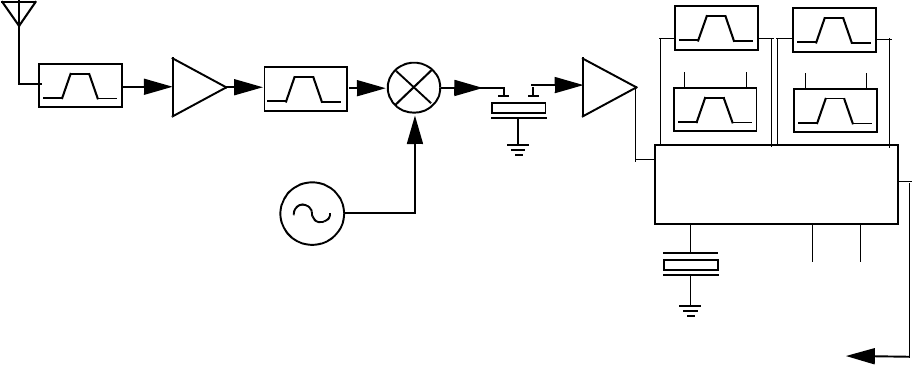
Chapter 2
THEORY OF OPERATION
1.0 Introduction
This Chapter provides a detailed theory of operation for the UHF circuits in the radio. Details of the
theory of operation and trouble shooting for the the associated Controller circuits are included in this
Section of the manual.
2.0 UHF (438-470MHz) Receiver
2.1 Receiver Front-End
The received signal is applied to the radio’s antenna input connector and routed through the
harmonic filter and antenna switch. The insertion loss of the harmonic filter/antenna switch is less
than 1 dB. The signal is routed to the first filter (3-pole), which has an insertion loss of 2 dB typically.
The output of the filter is matched to the base of the LNA (Q303) that provides a 16 dB gain and a
noise figure of better than 2 dB. Current source Q301 is used to maintain the collector current of
Q303. Diode CR301 protects Q303 by clamping excessive input signals. Q303 output is applied to
the second filter (4-pole) which has an insertion loss of 1.5 dB. In Distance mode, Q304 turns on and
causes D305 to conduct, thus bypassing C322 and R337. In Local mode, the signal is routed
through C322 and R337, thus inserting 7 dB attenuation. Since the attenuator is located after the RF
amplifier, the receiver sensitivity is reduced only by 6 dB, while the overall third order input intercept
is raised.
The first mixer is a passive, double-balanced type, consisting of T300, T301 and U302. This mixer
provides all of the necessary rejection of the half-IF spurious response. Low-side injection at +10
dBm is delivered to the first mixer. The mixer output is then connected to a duplex network which
matches its output to the XTAL filter input (FL300) at the IF frequency of 44.85 MHz. The duplex
network terminates into a 50 ohm resistor (R340) at all other frequencies.
Figure 2-1 UHF Receiver Block Diagram
Mixer Xtal Filter
Controller
Front Filter
Antenna
First LO
2nd LO Xtal Osc
IF Amp
Second Filter 4- Pole
25kHzFilter
12.5kHzFilter
Phase Shift
Element
IFIC
LNA
25kHzFilter
12.5kHzFilter
2-2 THEORY OF OPERATION
2.2 Receiver Back End
The IF signal from the crystal filter enters the IF amplifier which provides 20 dB of gain and feeds
the IF IC at pin 1. The first IF signal at 44.85 MHz mixes with the second local oscillator (LO) at
44.395 MHz to produce the second IF at 455 kHz. The second LO uses the external crystal Y301.
The second IF signal is amplified and filtered by two external ceramic filters (FL303/FL302 for
12.5KHz channel spacing and FL304/FL301 for 25KHz channel spacing). The IF IC demodulates
the signal by means of a quadrature detector and feeds the detected audio (via pin 7) to the audio
processing circuits. At IF IC pin 5, an RSSI signal is available with a dynamic range of 70 dB.
3.0 UHF Transmitter Power Amplifier (438-470 MHz)
The radio’s 40W PA is a three-stage amplifier used to amplify the output from the VCOBIC to the
radio transmit level. All three stages utilize LDMOS technology. The gain of the first stage (U101) is
adjustable and controlled by pin 7 of U103-2 via U103-3. It is followed by an LDMOS stage Q105
and LDMOS final stage Q100.
Figure 2-2 UHF Transmitter Block Diagram
Devices U101, Q105 and Q100 are surface mounted. Q100 is screwed down to the chassis to
ensure good thermal contact. This scheme also ensures sufficient thermal contact between driver
and chassis.
3.1 First Power Controller Stage
The first stage (U101) is a 24dB gain integrated circuit containing two LDMOS FET amplifier stages.
It amplifies the RF signal from the VCO (TX_INJ). The output power of stage U101 is controlled by a
DC voltage applied to pin 1 from the op-amp U103-3, pin 8. The control voltage simultaneously
varies the bias of two FET stages within U101. This biasing point determines the overall gain of
U101 and therefore its output drive level to Q105, which in turn controls the output power of the
Loop
Pin Diode
Antenna
Switch RF Jack
Antenna
Harmonic
Filter
Coupler
PA-Final
Stage
From VCO
Controlled
Stage
Bias
Temperature
Sense
SPI BUS
ASFIC_CMP
PA
PWR
SET
PA
Driver
Controller
U103-2
Forward

UHF Transmitter Power Amplifier (438-470 MHz) 2-3
PA.Op-amp U103-3 monitors the drain current of U101 via resistor R122 and adjusts the bias
voltage of U101.
In receive mode, the DC voltage from RX_EN line turns on Q101, which in turn switches off the
biasing voltage to U101.
3.2 Power Controlled Driver Stage
The next stage is an LDMOS device (Q105) which provides a gain of 12dB. This device requires a
positive gate bias and a quiescent current flow for proper operation.The voltage of the
PA_CURRENT is set in transmit mode by ASFIC (U504 pin 5) and fed to the gate of Q105 via
resistive network R186, R187. This bias voltage is tuned in the factory. If the transistor is replaced,
the bias voltage must be tuned using Global Tuner. Care must be taken so that the transistor is not
tuned exceeding the allowed bias voltage. This device directly drains current from B+ via L122.
3.3 Final Stage
The final stage is an LDMOS device (Q100) providing a gain of 12dB. This device also requires a
positive gate bias and a quiescent current flow for proper operation. The voltage of the line PA_BIAS
is set in transmit mode by ASFIC (U504 pin 4) and fed to the gate of Q100 via the resistive network
R134, R131. This bias voltage is tuned in the factory. If the transistor is replaced, the bias voltage
must be tuned using the Global Tuner. Care must be taken not to damage the device by exceeding
the maximum allowed bias voltage. The device’s drain current is drawn directly from the radio’s DC
supply voltage input, B+, via L117, L115, L124 and L125.
A matching network consisting of C1005, C1017, C1004, C1009, C1008, C1007, C1274, C1279,
C1275, C1276, C1277, C1278, C1021, C1280, C1013, L126, L127 and two striplines, transforms
the impedance to 50 ohms and feeds the directional coupler.
3.4 Directional Coupler
The directional Coupler is a microstrip printed circuit, which couples a small amount of the forward
power of the RF power from Q100. Coupled power is rectified by diode D105 to produce a
proportional DC voltage; and the resulting DC voltage is routed to the power control section to
ensure that the forward power out of the radio is held to a constant value.
3.5 Antenna Switch
The antenna switch utilizes the existing dc feed (B+) to the last stage device (Q100). The basic
operation is to have both PIN diodes (D103, D104) turned on during key-up by forward biasing
them. This is achieved by pulling down the voltage at the cathode end of D104 to around 12.4V
(0.7V drop across each diode). The current through the diodes needs to be set around 100 mA to
fully open the transmit path through resistor R108. Q106 is a current source controlled by Q103
which is turned on in Tx mode by TX_EN. VR102 ensures that the voltage at resistor R107 never
exceeds 5.6V.

2-4 THEORY OF OPERATION
3.6 Harmonic Filter
Inductors L111, L113 and L128 along with capacitors C1011, C1023, C1020, C1016, C1025 and
C1026 form a low-pass filter to attenuate harmonic energy coming from the transmitter. Resistor
R150 along with L130 drains any electrostatic charges that might otherwise build up on the antenna.
The harmonic filter also prevents high level RF signals above the receiver passband from reaching
the receiver circuits to improve spurious response rejection.
3.7 Power Control
The output power is regulated by using a forward power detection control loop. A directional coupler
samples a portion of the forward and reflected RF power. The forward sampled RF is rectified by
diode D105, and the resulting DC voltage is routed to the operational amplifier U100. The error
output current is then routed to an integrator, and converted into the control voltage. This voltage
controls the bias of the pre-driver (U101) stage. The output power level is set by PWR_SET at
ASFIC (U504 pin 6) which acts as the reference for forward power control loop.
The reflected coupled power is rectified by diode D107,The resulting DC voltage is amplified by an
operational amplifier U100 and routed to the summing junction. This detector protects the final stage
Q100 from reflected power by increasing the error current. The temperature sensor protects the
final stage Q100 from overheating by increasing the error current. A thermistor RT100 measures the
final stage Q100 temperature. The voltage divider output is routed to an operational amplifier U103
and then goes to the summing junction. The Zener Diode VR101 keeps the loop control voltage
below 5.6V and eliminates the DC current from the 9.3 regulator U501.
One local loop for the Pre Driver (U101) is used in order to stabilize the current for each stage.
In Rx mode, the two transistors Q101 and Q102 go to saturation and shut down the transmitter by
applying ground to the Pre Driver U101.
4.0 UHF (438-470MHz) Frequency Synthesizer
The synthesizer consists of a reference oscillator (Y201), low voltage Fractional-N (LVFRAC-N)
synthesizer (U200), and a voltage controlled oscillator (VCO) (U201).
4.1 Reference Oscillator
The reference oscillator is a crystal (Y201) controlled Colpitts oscillator and has a frequency of
16.8MHz. The oscillator transistor and start-up circuit are located in the LVFRAC-N (U200) while the
oscillator feedback capacitors, crystal, and tuning varactors are external. An analog-to-digital (A/D)
converter internal to the LVFRAC-N (U200) and controlled by the microprocessor via SPI sets the
voltage at the warp output of U200 pin 25. This sets the frequency of the oscillator. Consequently,
the output of the crystal Y201 is applied to U200 pin 23.
The method of temperature compensation is to apply an inverse Bechmann voltage curve, which
matches the crystal’s Bechmann curve to a varactor that constantly shifts the oscillator back on
frequency. The crystal vendor characterizes the crystal over a specified temperature range and
codes this information into a bar code that is printed on the crystal package. In production, this
crystal code is read via a 2-dimensional bar code reader and the parameters are saved.
This oscillator is temperature compensated to an accuracy of +/-2.5 PPM from -30 to 60 degrees C.
The temperature compensation scheme is implemented by an algorithm that uses five crystal
UHF (438-470MHz) Frequency Synthesizer 2-5
parameters (four characterize the inverse Bechmann voltage curve and one for frequency accuracy
of the reference oscillator at 25 degrees C). This algorithm is implemented by the LVFRAC-N (U200)
at the power up of the radio.
TCXO Y200, along with its corresponding circuitry R204, R205, R210, and C2053, are not placed as
the temperature compensated crystal proved to be reliable.
4.2 Fractional-N Synthesizer
The LVFRAC-N U200 consists of a pre-scaler, programmable loop divider, control divider logic,
phase detector, charge pump, A/D converter for low frequency digital modulation, balanced
attenuator used to balance the high and low frequency analog modulation, 13V positive voltage
multiplier, serial interface for control, and a super filter for the regulated 5 volts.
Figure 2-3 UHF Synthesizer Block Diagram
A voltage of 5V applied to the super filter input (U200, pin 30) supplies an output voltage of 4.5Vdc
(VSF) at U200, pin 28. This supplies 4.5 V to the VCO Buffer IC U201.
To generate a high voltage to supply the phase detector (charge pump) output stage at pin VCP
(U200, pin 47) while using a low voltage 3.3Vdc supply, a 13V positive voltage multiplier is used
(D200, D201, and capacitors C2024, 2025, 2026, 2055, 2027, 2001).
Output lock (U200, pin 4) provides information about the lock status of the synthesizer loop. A high
level at this output indicates a stable loop. A 16.8 MHz reference frequency is provided at U200, pin
19.
DATA
CLK
CEX
MODIN
VCC, DC5V
XTAL1
XTAL2
WARP
PREIN
VCP
REFERENCE
OSCILLATOR
VOLTAGE
MULTIPLIER
DATA (U403 PIN 100)
CLOCK (U403 PIN 1)
CSX (U403 PIN 2)
MOD IN (U501 PIN 40)
+5V (U503 PIN 1)
7
8
9
10
13, 30
23
24
25
32
47
VMULT2 VMULT1
BIAS1
SFOUT
AUX3
AUX4
IADAPT
IOUT
GND
FREFOUT
LOCK 4
19
6, 22, 33, 44
43
45
3
2
28
14 15
40
FILTERED 5V
STEERING
LOCK (U403 PIN 56)
PRESCALER IN
FREF (U504 PIN 34)
39
BIAS2
41
48
5, 20, 34, 36
+5V (U503 PIN 1)
AUX1
VDD, DC5V MODOUT
U200
LOW VOLTAGE
FRACTIONAL-N
SYNTHESIZER
AUX2 1 (NU)
BWSELECT
VCO Bias
TRB
To IF
Section
TX RF INJECTION
(1ST STAGE OF PA)
LO RF INJECTION
VOLTAGE
CONTROLLED
OSCILLATOR
LINE
LOOP
FILTER
2-6 THEORY OF OPERATION
4.3 Voltage Controlled Oscillator (VCO)
The Voltage Controlled Oscillator (VCO) consists of the VCO/Buffer IC (VCOBIC, U201), the TX and
RX tank circuits, the external RX buffer stages, and the modulation circuitry.
Figure 2-4 UHF VCO Block Diagram
The VCOBIC together with the LVFRAC-N (U200) generate the required frequencies in both
transmit and receive modes. The TRB line (U201, pin 19) determines which VCO and buffer is
enabled (high being TX output at pin 10, low being RX output at pin 8). A sample of the signal from
the enabled output is routed from U201, pin 12 (PRESC_OUT), via a low pass filter to U200, pin 32
(PREIN).
A steering line voltage between 3.0V and 10.0V at varactor D204 tunes the TX VCO through the
frequency range of 438-470MHz, and at D203 tunes the RX VCO through the frequency range of
393.15-425.15MHz.
The external RX amplifier is used to increase the output from U201, pin 8 from 3-4 dBm to the
required 10dBm for proper mixer operation. In TX mode, the modulation signal from the LVFRAC-N
(U200, pin 41) is applied to the VCO by way of the modulation circuit D205, R212, R211, C2073.
Presc
RX
TX
Buffers
Q200 Low Pass
Filter
Attenuator
Pin8
Pin14
Pin10
(U200 Pin28)
VCC Buffers
TX RF Injection
U200 Pin 32
AUX3 (U200 Pin 2)
Prescaler Out
Pin 12Pin 19
Pin 20
TX/RX/BS
Switching Network
U201
VCOBIC
Rx
Active Bias
Tx
Active Bias
Pin2
Rx-I adjust
Pin1
Tx-I adjust
Pins 9,11,17
Pin18
Vsens
Circuit
Pin15
Pin16
RX VCO
Circuit
TX VCO
Circuit
RX Tank
TX Tank
Pin7
Vcc-Superfilter
Collector/RF in
Pin4
Pin5
Pin6
RX
TX
(U200 Pin 28)
Rx-SW
Tx-SW
Vcc-Logic
(U200 Pin 28)
Steer Line
Voltage
(VCTRL)
Pin13
Pin3
TRB IN
LO RF INJECTION

UHF (438-470MHz) Frequency Synthesizer 2-7
4.4 Synthesizer Operation
The synthesizer consists of a low voltage FRAC-N IC (LVFRAC-N), reference oscillator, charge
pump circuits, loop filter circuit, and DC supply. The output signal (PRESC_OUT) of the VCOBIC
(U201, pin 12) is fed to the PREIN, pin 32 of U200 via a low pass filter which attenuates harmonics
and provides a correct input level to the LVFRAC-N in order to close the synthesizer loop.
The pre-scaler in the synthesizer (U200) is a dual modulus pre-scaler with selectable divider ratios.
The divider ratio of the pre-scaler is controlled by the loop divider, which in turn receives its inputs
via the SPI. The output of the pre-scaler is applied to the loop divider. The output of the loop divider
is connected to the phase detector, which compares the loop divider’s output signal with the
reference signal. The reference signal is generated by dividing down the signal of the reference
oscillator (Y201).
The output signal of the phase detector is a pulsed dc signal that is routed to the charge pump. The
charge pump outputs a current from U200, pin 43 (IOUT). The loop filter (consisting of R224, R217,
R234, C2074, C2078, C2028, and L205) transforms this current into a voltage that is applied the
varactor diodes D203 and D204 for RX and TX respectively. The output frequency is determined by
this control voltage. The current can be set to a value fixed in the LVFRAC-N or to a value
determined by the currents flowing into BIAS 1 (U200, pin 40) or BIAS 2 (U200, pin 39). The
currents are set by the value of R200 or R206 respectively. The selection of the three different bias
sources is done by software programming.
To modulate the synthesizer loop, a two-spot modulation method is utilized via the MODIN (U200,
pin 10) input of the LVFRAC-N. The audio signal is applied to both the A/D converter (low frequency
path) and the balance attenuator (high frequency path). The A/D converter converts the low
frequency analog modulating signal into a digital code which is applied to the loop divider, thereby
causing the carrier to deviate. The balance attenuator is used to adjust the VCO’s deviation
sensitivity to high frequency modulating signals. The output of the balance attenuator is presented
at the MODOUT port of the LVFRAC-N (U200,pin 41) and connected to the VCO modulation
varactor D205.
2-8 THEORY OF OPERATION
5.0 Controller Theory of Operation
This section provides a detailed theory of operation for the radio and its components. The main
radio is a single-board design, consisting of the transmitter, receiver, and controller circuits. A
control head is connected by an extension cable. The control head contains LED indicators, a
microphone connector, buttons, and speaker.
In addition to the power cable and antenna cable, an accessory cable can be attached to a
connector on the rear of the radio. The accessory cable enables you to connect accessories to the
radio, such as an external speaker, emergency switch, foot-operated PTT, and ignition sensing, etc.
Figure 2-5 Controller Block Diagram
5.1 Radio Power Distribution
Voltage distribution is provided by five separate devices:
• U514 P-cH FET - Batt + (Ext_SWB+)
• U501 LM2941T - 9.3V
• U503 LP2951CM - 5V
• U508 MC 33269DTRK - 3.3V
• U510 LP2986ILDX - 3.3V Digital
External
Microphone
Internal
Microphone
External
Speaker
Internal
Speaker
SCI to
Control Head
Audio
PA
Audio/Signaling
Architecture
To Synthesizer
Mod
Out
16.8 MHz
Reference Clock
from Synthesizer
Disc Audio
To R F S ec ti on SPI
Digital
Architecture
µP Clock
3.3V
Regulator
RAM
EEPROM
FLASH
HC11FL0
ASFIC_CMP
Accessory &
Connector
Handset
.

Controller Theory of Operation 2-9
The DC voltage applied to connector P2 supplies power directly to the following circuitry:
• Electronic on/off control
• RF power amplifier
• 12 volts P-cH FET -U514
• 9.3 volt regulator
•Audio PA
Figure 2-6 DC Power Distribution Block Diagram
Regulator U501 is used to generate the 9.3 volts required by some audio circuits, the RF circuitry
and power control circuitry. Input and output capacitors are used to reduce high frequency noise.
Resistors R5001 / R5081 set the output voltage of the regulator. This regulator output is
electronically enabled by a 0 volt signal on pin 2. Q502, Q505 and R5038 are used to disable the
regulator when the radio is turned off.
Voltage regulator U510 provides 3.3 volts for the digital circuitry. Operating voltage is from the
regulated 9.3V supply. Input and output capacitors are used to reduce high frequency noise and
provide proper operation during battery transients. U510 provides a reset output that goes to 0 volts
if the regulator output goes below 3.1 volts. This is used to reset the controller to prevent improper
operation.
Voltage regulator U508 provides 3.3V for the RF circuits and ASFIC_CMP. Input and output
capacitors are used to reduce the high frequency noise and provide proper operation during battery
transients.
U501
9.3V Regulator
FET
P-CH
On/Off
Control
500mA
SW_Filt_B+
Acces Conn
Audio PA_Soutdown
Power Loop Op_Amp
Auto
On/Off
Switch
Control
Ignition B+
RF_PA, 8.5A
Audio_PA
Antenna Switch
Power Control
Filt_B+
Ferrite Bit
Control Head
Mic Connector
Mic Bias
9V, 5mA
Keypad
7_Seg
Bed
to
7-Seg
Shift
Reg
3.2V
72mA
9.3V
65mA
Status LEDs
7_Seg
DOT
Back
light
On/Off
Control
10.9-16.3V
0.9A 0.85A
U503
5V RF Regulator
U508
3.3V RF Reg
U510
3.3V D Reg
Reset
Rx_Amp
PA_Pre-driver
PA D river
500mA
LVFRAC_N
IF_Amp
ASFIC_CMP
IFIC
RX Cct
micro P
RAM
Flash
EEPROM
90mA
25mA50mA45mA
9.3V
45mA
9.3V
75mA
9.3V
162mA

2-10 THEORY OF OPERATION
Voltage regulator U503 provides 5V for the RF circuits. Input and output capacitors are used to
reduce the high frequency noise and provide proper operation during battery transients.
VSTBY is used only for GM3689 5-tone radios.
The voltage VSTBY, which is derived directly from the supply voltage by components R5103 and
VR502, is used to buffer the internal RAM. Capacitor C5120 allows the battery voltage to be
disconnected for a couple of seconds without losing RAM parameters. Dual diode D501 prevents
radio circuitry from discharging this capacitor. When the supply voltage is applied to the radio,
C5120 is charged via R5103 and D501.
5.2 Protection Devices
Diode VR500 acts as protection against ESD, wrong polarity of the supply voltage, and load dump.
VR692 - VR699 are for ESD protection.
5.3 Automatic On/Off
The radio can be switched ON in any one of the following three ways:
• On/Off switch. (No Ignition Mode)
• Ignition and On/Off switch (Ignition Mode)
•Emergency
5.3.1 No Ignition Mode
When the radio is connected to the car battery for the first time, Q500 will be in saturation, Q503 will
cut-off, Filt_B+ will pass through R5073, D500, and S5010-pin 6 (On/Off switch). When S5010 is
ON, Filt_B+ will pass through S5010-pin5, D511, R5069, R5037 and base of Q505 and move Q505
into saturation. This pulls U501-pin2 through R5038, D502 to 0.2V and turns On U514 and U501
9.3V regulator which supplies voltage to all other regulators and consequently turns the radio on,
When U504 (ASFIC_CMP) gets 3.3V, GCB2 goes to 3.3V and holds Q505 in saturation, for soft turn
off.
5.3.2 Ignition Mode
When ignition is connected for the first time, it will force high current through Q500 collector, This
will move Q500 out of saturation and consequently Q503 will cut-off. S5010 pin 6 will get ignition
voltage through R601 (for load dump), R610, (R610 & C678 are for ESD protection), VR501,
R5074, and D500. When S5010 is ON, Filt_B+ passes through S5010-pin 5, D511, R5069, R5037
and base of Q505 and inserts Q505 into saturation. This pulls U501-pin 2 through R5038, D502 to
0.2V and turns on U514 and U501 9.3V regulator which supply voltage to all other regulators and
turns the radio on, When U504 (ASFIC_CMP) get 3.3V supply, GCB2 goes to 3.3V and holds Q505
in saturation state to allow soft turn off,
When ignition is off Q500, Q503 will stay at the same state so S5010 pin 6 will get 0V from Ignition,
Q504 goes from Sat to Cut, ONOFF_SENSE goes to 3.3V and it indicates to the radio to soft turn
itself by changing GCB2 to ‘0’ after de registration if necessary.

Controller Theory of Operation 2-11
5.3.3 Emergency Mode
The emergency switch (P1 pin 9), when engaged, grounds the base of Q506 via EMERGENCY
_ACCES_CONN. This switches Q506 to off and consequently resistor R5020 pulls the collector of
Q506 and the base of Q506 to levels above 2 volts. Transistor Q502 switches on and pulls U501
pin2 to ground level, thus turning ON the radio. When the emergency switch is released R5030 pulls
the base of Q506 up to 0.6 volts. This causes the collector of transistor Q506 to go low (0.2V),
thereby switching Q502 to off.
While the radio is switched on, the µP monitors the voltage at the emergency input on the accessory
connector via U403-pin 62. Three different conditions are distinguished: no emergency kit is
connected, emergency kit connected (unpressed), and emergency press.
If no emergency switch is connected or the connection to the emergency switch is broken, the
resistive divider R5030 / R5049 will set the voltage to about 3.14 volts (indicates no emergency kit
found via EMERGENCY_SENSE line). If an emergency switch is connected, a resistor to ground
within the emergency switch will reduce the voltage on EMERGENCY _SENSE line, and indicate to
the µP that the emergency switch is operational. An engaged emergency switch pulls line
EMERGENCY _SENSE line to ground level. Diode VR503 limits the voltage to protect the µP input.
While EMERGENCY _ACCES_CONN is low, the µP starts execution, reads that the emergency
input is active through the voltage level of µP pin 64, and sets the DC POWER ON output of the
ASFIC CMP pin 13 to a logic high. This high will keep Q505 in saturation for soft turn off.
5.4 Microprocessor Clock Synthesiser
The clock source for the µP system is generated by the ASFIC CMP (U504). Upon power-up the
synthesizer IC (FRAC-N) generates a 16.8 MHz waveform that is routed from the RF section to the
ASFIC CMP pin 34. For the main board controller the ASFIC CMP uses 16.8 MHz as a reference
input clock signal for its internal synthesizer. The ASFIC CMP, in addition to audio circuitry, has a
programmable synthesizer which can generate a synthesized signal ranging from 1200Hz to
32.769MHz in 1200Hz steps.
When power is first applied, the ASFIC CMP will generate its default 3.6864MHz CMOS square
wave UP CLK (on U504 pin 28) and this is routed to the µP (U403 pin 90). After the µP starts
operation, it reprograms the ASFIC CMP clock synthesizer to a higher UP CLK frequency (usually
7.3728 or 14.7456 MHz) and continues operation.
The ASFIC CMP may be reprogrammed to change the clock synthesizer frequencies at various
times depending on the software features that are executing. In addition, the clock frequency of the
synthesizer is changed in small amounts if there is a possibility of harmonics of the clock source
interfering with the desired radio receive frequency.
The ASFIC CMP synthesizer loop uses C5025, C5024 and R5033 to set the switching time and jitter
of the clock output. If the synthesizer cannot generate the required clock frequency it will switch
back to its default 3.6864MHz output.
Because the ASFIC CMP synthesizer and the µP system will not operate without the 16.8 MHz
reference clock it (and the voltage regulators) should be checked first when debugging the system.

2-12 THEORY OF OPERATION
5.5 Serial Peripheral Interface (SPI)
The µP communicates to many of the IC’s through its SPI port. This port consists of SPI TRANSMIT
DATA (MOSI) (U403-pin100), SPI RECEIVE DATA (MISO) (U403-pin 99), SPI CLK (U0403-pin1)
and chip select lines going to the various IC’s, connected on the SPI PORT (BUS). This BUS is a
synchronous bus, in that the timing clock signal CLK is sent while SPI data (SPI TRANSMIT DATA
or SPI RECEIVE DATA) is sent. Therefore, whenever there is activity on either SPI TRANSMIT
DATA or SPI RECEIVE DATA there should be a uniform signal on CLK. The SPI TRANSMIT DATA
is used to send serial from a µP to a device, and SPI RECEIVE DATA is used to send data from a
device to a µP.
There are two IC’s on the SPI BUS, ASFIC CMP (U504 pin 22)), and EEPROM (U400). In the RF
sections there is one IC on the SPI BUS, the FRAC-N Synthesizer. The chip select line CSX from
U403 pin 2 is shared by the ASFIC CMP and FRAC-N Synthesizer. Each of these IC’s check the
SPI data and when the sent address information matches the IC’s address, the following data is
processed.
When the µP needs to program any of these Is it brings the chip select line CSX to a logic “0” and
then sends the proper data and clock signals. The amount of data sent to the various IC’s are
different; e.g., the ASFIC CMP can receive up to 19 bytes (152 bits). After the data has been sent
the chip select line is returned to logic “1”.
5.6 SBEP Serial Interface
The SBEP serial interface allows the radio to communicate with the Customer Programming
Software (CPS), or the Universal Tuner via the Radio Interface Box (RIB) or the cable with internal
RIB. This interface connects to the SCI pin via control head connector (J2-pin 17) and to the
accessory connector P1-6 and comprises BUS+. The line is bi-directional, meaning that either the
radio or the RIB can drive the line. The µP sends serial data and it reads serial data via pin 97.
Whenever the µP detects activity on the BUS+ line, it starts communication.
5.7 General Purpose Input/Output
The controller provides six general purpose lines (PROG I/O) available on the accessory connector
P1 to interface to external options. Lines PROG IN 3 and 6 are inputs, PROG OUT 4 is an output
and PROG IN OUT 8, 12 and 14 are bi-directional. The software and the hardware configuration of
the radio model define the function of each port.
• PROG IN 3 can be used as external PTT input, or others, set by the CPS. The µP reads this
port via pin 72 and Q412.
• PROG OUT 4 can be used as external alarm output, set by the CPS. Transistor Q401 is
controlled by the µP (U403 pin 55)
• PROG IN 6 can be used as normal input, set by the CPS. The µP reads this port via pin 73
and Q411. This pin is also used to communicate with the RIB if resistor R421 is placed.
• DIG IN OUT 8,12,14 are bi-directional and use the same circuit configuration. Each port uses
an output Q416, Q404, Q405 controlled by µP pins 52, 53, 54. The input ports are read
through µP pins 74, 76, 77; using Q409, Q410, Q411

Controller Theory of Operation 2-13
5.8 Normal Microprocessor Operation
For this radio, the µP is configured to operate in one of two modes, expanded and bootstrap. In
expanded mode the µP uses external memory devices to operate, whereas in bootstrap operation
the µP uses only its internal memory. In normal operation of the radio the µP is operating in
expanded mode as described below.
During normal operation, the µP (U403) is operating in expanded mode and has access to 3
external memory devices; U400 (EEPROM), U402 (SRAM), U404 (Flash). Also, within the µP there
are 3 Kilobytes of internal RAM, as well as logic to select external memory devices.
The external EEPROM (U400) space contains the information in the radio which is customer
specific, referred to as the codeplug. This information consists of items such as: 1) what band the
radio operates in, 2) what frequencies are assigned to what channel, and 3) tuning information.
The external SRAM (U402) as well as the µP’s own internal RAM space are used for temporary
calculations required by the software during execution. All of the data stored in both of these
locations is lost when the radio powers off.
The µP provides an address bus of 16 address lines (ADDR 0 - ADDR 15), and a data bus of 8 data
lines (DATA 0 - DATA 7). There are also 3 control lines; CSPROG (U403-38) to chip select U404-pin
30 (FLASH), CSGP2 (U403-pin 41) to chip select U404-pin 20 (SRAM) and PG7_R_W (U403-pin 4)
to select whether to read or to write. The external EEPROM (U400-pin1).
When the µP is functioning normally, the address and data lines should be toggling at CMOS logic
levels. Specifically, the logic high levels should be between 3.1 and 3.3V, and the logic low levels
should be between 0 and 0.2V. No other intermediate levels should be observed, and the rise and
fall times should be <30ns.
The low-order address lines (ADDR 0 - ADDR 7) and the data lines (DATA 0-DATA 7) should be
toggling at a high rate, e.g., you should set your oscilloscope sweep to 1us/div. or faster to observe
individual pulses. High speed CMOS transitions should also be observed on the µP control lines.
On the µP the lines XIRQ (U403-pin 48), MODA LIR (U403-pin 58), MODB VSTPY (U403-pin 57)
and RESET (U403-pin 94) should be high at all times during normal operation. Whenever a data or
address line becomes open or shorted to an adjacent line, a common symptom is that the RESET
line goes low periodically, with the period being in the order of 20ms. In the case of shorted lines you
may also detect the line periodically at an intermediate level, i.e. around 2.5V when two shorted
lines attempt to drive to opposite rails.
The MODA LIR (U403-pin 58) and MODB VSTPY (U403-pin 57) inputs to the µP must be at a logic
“1” for it to start executing correctly. After the µP starts execution it will periodically pulse these lines
to determine the desired operating mode. While the Central Processing Unit (CPU) is running,
MODA LIR is an open-drain CMOS output which goes low whenever the µP begins a new
instruction. An instruction typically requires 2-4 external bus cycles, or memory fetches.
There are eight analog-to-digital coverter ports (A/D) on U403 labelled within the device block as
PEO-PE7. These lines sense the voltage level ranging from 0 to 3.3V of the input line and convert
that level to a number ranging from 0 to 255 which is read by the software to take appropriate action.

2-14 THEORY OF OPERATION
5.9 Static Random Access Memory (SRAM)
The SRAM (U402) contains temporary radio calculations or parameters that can change very
frequently, and which are generated and stored by the software during its normal operation. The
information is lost when the radio is turned off.
The device allows an unlimited number of write cycles. SRAM accesses are indicated by the CS
signal U402 (which comes from U403-CSGP2) going low. U402 is commonly referred to as the
external RAM as opposed to the internal RAM which is the 3 Kilobytes of RAM which is part of the
68HC11FL0. Both RAM spaces serve the purpose. However, the internal RAM is used for the
calculated values which are accessed most often.
Capacitor C402 and C411 serves to filter out any AC noise which may ride on +3.3 V at U402
6.0 Control Board Audio and Signalling Circuits
6.1 Audio Signalling Filter IC and Compander (ASFIC CMP)
The ASFIC CMP (U504) used in the controller has the following four functions:
1. RX/TX audio shaping, i.e. filtering, amplification, attenuation
2. RX/TX signaling, PL/DPL/HST/MDC
3. Squelch detection
4. µP clock signal generation
The ASFIC CMP is programmable through the SPI BUS (U504 pins-20/21/22), normally receiving
19 bytes. This programming sets up various paths within the ASFIC CMP to route audio and/or
signaling signals through the appropriate filtering, gain and attenuator blocks. The ASFIC CMP also
has 6 General Control Bits GCB0-5 which are CMOS level outputs and used for the following:
• GCBO - BW Select
• GCBI - switches the audio PA On/Off
• GCB2 - DC Power On switches the voltage regulator (and the radio) on and off
• GCB3 - Control on MUX U509 pin 9 to select between Low Cost Mic path to STD Mic Path
• GCB4 - Control on MUX U509 pin 11 to select between Flat RX path to filtered RX path on the
accessory connector.
• GCB5 - Control on MUX U509 pin 10 to select between Flat TX path mute and Flat TX path

Transmit Audio Circuits 2-15
7.0 Transmit Audio Circuits
Figure 2-7 Transmit Audio Paths
7.1 Microphone Input Path
The radio supports 2 distinct microphone paths known as internal (from control head J2-15) and
external mic (from accessory connector P1-2) and an auxiliary path (FLAT TX AUDIO, from
accessory connector P1-5). The microphones used for the radio require a DC biasing voltage
provided by a resistive network.
The two microphone audio input paths enter the ASFIC CMP at U504-pin 48 (external mic) and
U504-pin 46 (internal mic). The microphone is plugged into the radio control head and connected to
the audio DC via J2-pin 15. The signal is then routed via C5045 to MUX U509 that select between
two paths with different gain to support Low Cost Mic (Mic with out amplifier in it) and Standard Mic.
7.1.1 Low Cost Microphone
Hook Pin is shorted to Pin 1(9.3V) inside the Low Cost Mic, This routes 9.3V to R429, and creates
2.6V on MIC_SENSE (u.P U403-67) by Voltage Divider R429/R430. U403 senses this voltage and
sends command to ASFIC_CMP U504 to get GCB3 = ‘0’. The audio signal is routed from C5045 via
U509-5 (Z0), R5072, U507, R5026, C5091, R5014 via C5046 to U504- 46 int. mic (C5046 100nF
creates a159Hz pole with U504- 46 int mic impedance of 16Kohm).
MIC
IN
MOD IN TO
RF
SECTION
(SYNTHESIZER)
36
44
40
P1
ACCESSORY
CONNECTOR
J2
CONTROL HEAD
CONNECTOR
MIC
EXT MIC
FLAT TX
AUDIO
42
5
48
46
15
2
24kOhms
FILTERS AND
PREEMPHASIS
HS SUMMER
SPLATTER
FILTER
LS SUMMER
LIMITER
ATTENUATOR
VCO
ATN
TX RTN
TX SND
MIC
INT
AUX
TX
ASFIC_CMP
U504
U509
MIC
EXT
FLAT TX
AUDIO MUTE
GCB3
MUX
35
U509
MUX
GCB5
38

2-16 THEORY OF OPERATION
7.1.2 Standard Microphone
Hook Pin is shorted to the hook mic inside the standard Mic, If the mic is out off hook, 3.3V is routed
to R429 via R458, D401, and it create 0.7V on MIC_SENSE (u.P U403-67) by Voltage Divider
R429/R430. U403 senses this voltage and sends command to ASFIC_CMP U504 to get GCB3 =‘1’.
The audio signal is routed from C5045 via U509-3 (Z1), R5072, U507, R5026, C5091, R5014 via
C5046 to U504- 46 int mic (C5046 100nF create a159Hz pole with U504- 46 int mic impedance of
16Kohm). 9.3VDC is routed via R5077, R5075 to J2-15, It create 4.65V with Mic Impedance. C5010
supplies AC Ground to create AC impedance of 510 Ohms via R5075. and Filter 9.3V DC mic bias
supply.
Note: The audio signal at U504-pin 46 should be approximately 12mV for 1.5kHz or 3kHz of
deviation with 12.5kHz or 25kHz channel spacing.
The external microphone signal enters the radio on accessory connector P1 pin 2 and is routed via
line EXT MIC to R5054. R5078 and R5076 provide the 9.3Vdc bias. Resistive divider R5054/ R5070
divide the input signal by 5.5 and provide input protection for the CMOS amplifier input. R5076 and
C5009 provide a 510 ohm AC path to ground that sets the input impedance for the microphone and
determines the gain based on the emitter resistor in the microphone’s amplifier circuit.
C5047 serves as a DC blocking capacitor. The audio signal at U504-pin 48 should be approximately
14mV for 1.5kHz or 3kHz of deviation with 12.5kHz or 25kHz channel spacing.
The FLAT TX AUDIO signal from accessory connector P1-pin 5 is fed to the ASFIC CMP (U504 pin
42 through U509 pin 2 to U509 pin 15 via U506 OP-AMP circuit and C5057.
The ASFIC has an internal AGC that can control the gain in the mic audio path. The AGC can be
disabled / enabled by the µP. Another feature that can be enabled or disabled in the ASFIC is the
VOX. This circuit, along with Capacitor C5023 at U504-pin 7, provides a DC voltage that can allow
the µP to detect microphone audio. The ASFIC can also be programmed to route the microphone
audio to the speaker for public address operation.
7.2 PTT Sensing and TX Audio Processing
Internal microphone PTT is sensed by µP U403 pin 71. Radio transmits when this pin is “0” and
selects inside the ASFIC_ CMP U504 internal Mic path. When the internal Mic PTT is “0” then
external Mic PTT is grounded via D402. External Mic PTT is sensed by U403 pin 72 via Q412
circuits. The radio transmits when this pin is “0” and selects inside the ASFIC _CMP U504 External
Mic path.
Inside the ASFIC CMP, the mic audio is filtered to eliminate frequency components outside the 300-
3000Hz voice band, and pre-emphasized if pre-emphasis is enabled. The signal is then limited to
prevent the transmitter from over deviating. The limited mic audio is then routed through a summer,
which is used to add in signaling data, and then to a splatter filter to eliminate high frequency
spectral components that could be generated by the limiter. The audio is then routed to an
attenuator, which is tuned in the factory or the field to set the proper amount of FM deviation. The
TX audio emerges from the ASFIC CMP at U504-pin 40 MOD IN, at which point it is routed to the
RF section.

Transmit Signalling Circuits 2-17
8.0 Transmit Signalling Circuits
Figure 2-8 Transmit Signalling Path
From a hardware point of view, there are 3 types of signaling:
• Sub-audible data (PL / DPL / Connect Tone) that gets summed with transmit voice or
signaling,
• DTMF data for telephone communication in trunked and conventional systems, and
• Audible signaling including MDC and high-speed trunking.
Note: All three types are supported by the hardware while the radio software determines which
signaling type is available.
8.1 Sub-Audio Data (PL/DPL)
Sub-audible data implies signaling whose bandwidth is below 300Hz. PL and DPL waveforms are
used for conventional operation and connect tones for trunked voice channel operation. The
trunking connect tone is simply a PL tone at a higher deviation level than PL in a conventional
system. Although it is referred to as “sub-audible data”, the actual frequency spectrum of these
waveforms may be as high as 250 Hz, which is audible to the human ear. However, the radio
receiver filters out any audio below 300Hz, so these tones are never heard in the actual system.
Only one type of sub-audible data can be generated by U504 (ASFIC CMP) at any one time. The
process is as follows, using the SPI BUS, the µP programs the ASFIC CMP to set up the proper low-
speed data deviation and select the PL or DPL filters. The µP then generates a square wave which
strobes the ASFIC PL / DPL encode input LSIO U504-pin 18 at twelve times the desired data rate.
For example, for a PL frequency of 103Hz, the frequency of the square wave would be 1236Hz.
This drives a tone generator inside U504 which generates a staircase approximation to a PL sine
wave or DPL data pattern. This internal waveform is then low-pass filtered and summed with voice
or data. The resulting summed waveform then appears on U504-pin 40 (MOD IN), where it is sent to
the RF board as previously described for transmit audio. A trunking connect tone would be
generated in the same manner as a PL tone.
19
18
40
MOD IN
TO RF
SECTION
(SYNTHESIZER)
80
44 HIGH SPEED
CLOCK IN
(HSIO)
LOW SPEED
CLOCK IN
(LSIO)
ASFIC_CMP U504
MICRO
CONTROLLER
U403
HS
SUMMER
5-3-2 STATE
ENCODER
DTMF
ENCODER
SPLATTER
FILTER
PL
ENCODER
LS
SUMMER
ATTENUATOR
85
82
SPI
BUS

2-18 THEORY OF OPERATION
8.2 High Speed Data
High speed data refers to the 3600 baud data waveforms, known as Inbound Signaling Words
(ISWs) used in a trunking system for high speed communication between the central controller and
the radio. To generate an ISW, the µP first programs the ASFIC CMP (U504) to the proper filter and
gain settings. It then begins strobing U504-pin 19 (HSIO) with a pulse when the data is supposed to
change states. U504’s 5-3-2 State Encoder (which is in a 2-state mode) is then fed to the post-
limiter summer block and then the splatter filter. From that point it is routed through the modulation
attenuator and then out of the ASFIC CMP to the RF board. MDC is generated in much the same
way as trunking ISW. However, in some cases these signals may also pass through a data pre-
emphasis block in the ASFIC CMP. Also these signaling schemes are based on sending a
combination of 1200 Hz and 1800 Hz tones only. Microphone audio is muted during high speed data
signaling.
8.3 Dual Tone Multiple Frequency (DTMF) Data
DTMF data is a dual tone waveform used during phone interconnect operation. It is the same type
of tones which are heard when using a “Touch Tone” telephone.
There are seven frequencies, with four in the low group (697, 770, 852, 941Hz) and three in the high
group (1209, 1336, 1477Hz). The high-group tone is generated by the µP (U403-46) strobing U504-
19 at six times the tone frequency for tones less than 1440Hz or twice the frequency for tones
greater than 1440Hz. The low group tone is generated by the ASFIC CMP, controlled by the µP via
SPI bus. Inside U504 the low-group and high-group tones are summed (with the amplitude of the
high group tone being approximately 2 dB greater than that of the low group tone) and then pre-
emphasized before being routed to the summer and splatter filter. The DTMF waveform then follows
the same path as was described for high-speed data.
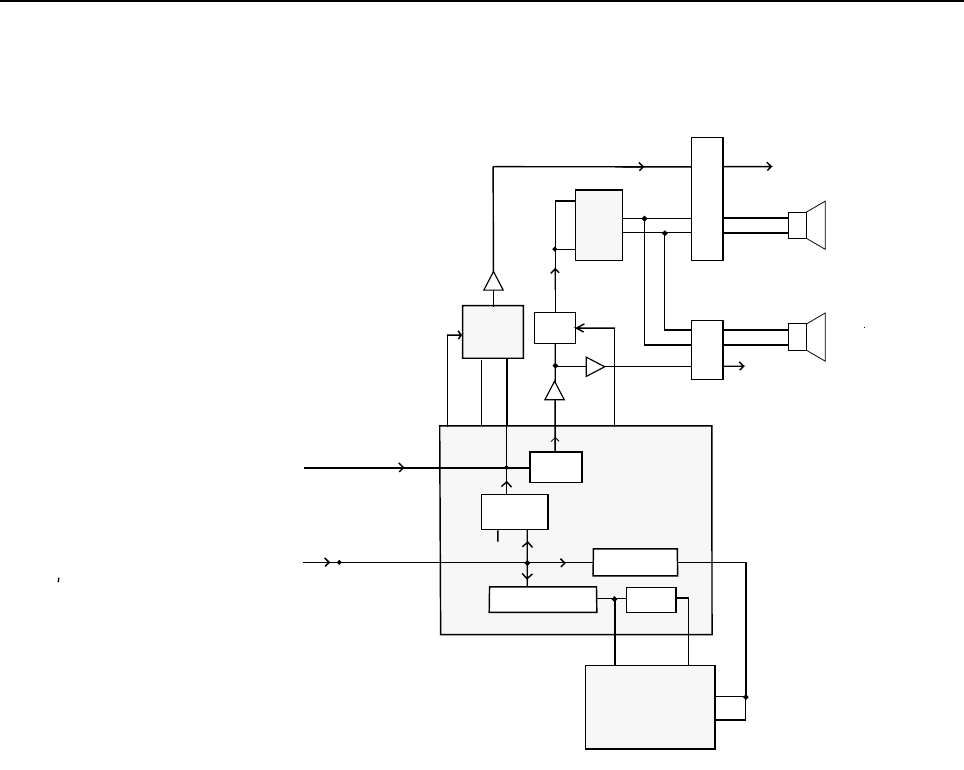
Receive Audio Circuits 2-19
9.0 Receive Audio Circuits
Figure 2-9 Receive Audio Paths
9.1 Squelch Detect
The radio’s RF circuits are constantly producing an output at the discriminator (IF IC). This signal
(DISC AUDIO) is routed to the ASFIC CMP’s squelch detect circuitry input DISC (U504-pin 2). All of
the squelch detect circuitry is contained within the ASFIC CMP. Therefore from a user’s point of
view, DISC AUDIO enters the ASFIC CMP, and the ASFIC CMP produces two CMOS logic outputs
based on the result. They are CH ACT (U504-16) and SQ DET (U504-17).
The squelch signal entering the ASFIC CMP is amplified, filtered, attenuated, and rectified. It is then
sent to a comparator to produce an active high signal on CH ACT. A squelch tail circuit is used to
produce SQ DET (U504-17) from CH ACT. The state of CH ACT and SQ DET is high (logic “1”)
when carrier is detected, otherwise low (logic “0”).
CH ACT is routed to the µP pin 84 while SQ DET is routed to the µP pin 83.
SQ DET is used to determine all audio mute / unmute decisions except for Conventional Scan. In
this case CH ACT is a pre-indicator as it occurs slightly faster than SQ DET.
FLT RX AUDIO
P1
11
16
1EXTERNAL
SPEAKER
INTERNAL
SPEAKER
ACCESSORY
CONNECTOR
CONTROL HEAD
CONNECTOR
HANDSET
AUDIO
18
20
19
J2
INT
SPKR-
SPKR +
SPKR -
1
9
2
U509
4110
INT
SPKR+
4
6
DISC
ASFIC_CMP
U504
AUDIO
PA
U502
VOLUME
ATTEN.
FILTER AND
DEEMPHASIS
17
MICRO
CONTROLLER
U403
80
FROM
RF
SECTION
(IF IC) LIMITER, RECTIFIER
FILTER, COMPARATOR
SQ DET
SQUELCH
CIRCUIT
16
PL FILTER
LIMITER
CH ACT
AUX RX
43
18
LS IO
U IO AUDIO
83
84
39
URX OUT
DISC
AUDIO
37
85
GCB4
MUTE
GCB1
14
U505

2-20 THEORY OF OPERATION
9.2 Audio Processing and Digital Volume Control
The receiver audio signal (DISC AUDIO) enters the controller section from the IF IC where it is.DC
coupled to ASFIC CMP via the DISC input U504-pin 2. The signal is then applied to both the audio
and the PL/DPL paths
The audio path has a programmable amplifier, whose setting is based on the channel bandwidth
being received, an LPF filter to remove any frequency components above 3000Hz, and a HPF to
strip off any sub-audible data below 300Hz. Next, the recovered audio passes through a de-
emphasis filter (if it is enabled to compensate for Pre-emphasis which is used to reduce the effects
of FM noise). The IC then passes the audio through the 8-bit programmable attenuator whose level
is set depending on the value of the volume control. Finally the filtered audio signal passes through
an output buffer within the ASFIC CMP. The audio signal exits the ASFIC CMP at AUDIO output
(U504 pin 41).
The µP programs the attenuator, using the SPI BUS, based on the volume setting. The minimum /
maximum settings of the attenuator are set by codeplug parameters.
Since sub-audible signaling is summed with voice information on transmit, it must be separated
from the voice information before processing. Any sub-audible signaling enters the ASFIC CMP
from the IF IC at DISC U504-2. Once inside, it goes through the PL/DPL path. The signal first
passes through one of the two low-pass filters, either the PL low-pass filter or the DPL/LST low-pass
filter. Either signal is then filtered and goes through a limiter and exits the ASFIC CMP at LSIO
(U504-pin 18). At this point, the signal will appear as a square wave version of the sub-audible
signal which the radio received. The µP U403 pin 80 will decode the signal directly to determine if it
is the tone / code which is currently active on that mode.
9.3 Audio Amplification Speaker (+) Speaker (-)
The output of the ASFIC CMP’s digital volume pot, U504-pin 41 is routed through DC blocking
capacitor C5049 to the audio PA (U502 pin 1 and 9).
The audio power amplifier has one inverted and one non-inverted output that produces the
differential audio output SPK+/SPK- (U502 pins 4 and 6)
The audio PA is enabled via the ASFIC CMP (U504-GCB1). When the base of Q501 is low, the
transistor is off and U502-pin 8 is high, using pull up resistor R5041, and the audio PA is ON. The
voltage at U502-pin 8 must be above 8.5Vdc to properly enable the device.
If the voltage is between 3.3 and 6.4V, the device will be active but has its input (U502-pins 1/9) off.
This is a mute condition which is used to prevent an audio pop when the PA is enabled.
The SPK+ and SPK- outputs of the audio PA have a DC bias which varies proportionately with B+
(U502- pin 7). B+ of 11V yields a DC offset of 5V, and B+ of 17V yields a DC offset of 8.5V. If either
of these lines is shorted to ground, it is possible that the audio PA will be damaged. SPK+ and SPK-
are routed to the accessory connector (P1-pin 1 and 16) and to the control head (connector J2-pins
19 and 20).

Receive Signalling Circuits 2-21
9.4 Handset Audio
Certain handheld accessories have a speaker within them which require a different voltage level
than that provided by U502. For these devices HANDSET AUDIO is available at control head
connector J2 pin18.
The received audio from the output of the ASFIC CMP’s digital volume attenuator is routed to U505
pin 2 where it is amplified. This signal is routed from the output of the op-amp U505 to J2-pin 18.
From the control head, the signal is sent directly to the microphone jack.
9.5 Filtered Audio and Flat Audio
The ASFIC CMP output audio at U504-pin 39 is filtered and de-emphasized, but has not gone
through the digital volume attenuator. From ASFIC CMP U504-pin 39 the signal is routed via R5034
through gate U509-pin 12 and AC coupled to U505-pin 6. The gate controlled by ASFIC CMP port
GCB4 selects between the filtered audio signal from the ASFIC CMP pin 39 (URXOUT) or the
unfiltered (flat) audio signal from the ASFIC CMP pin 10 (UIO). Resistors R5034 and R5021
determine the gain of op-amp UU505-pin 6 for the filtered audio while R5032 and R5021 determine
the gain for the flat Audio. The output of U505-pin 7 is then routed to P1 pin 11 via DC blocking
capacitor C5003. Note that any volume adjustment of the signal on this path must be done by the
accessory.
10.0 Receive Signalling Circuits
Figure 2-10 Receive Signalling Paths
10.1 Sub-Audio Data (PL/DPL) and High Speed Data Decoder
The ASFIC CMP (U504) is used to filter and limit all received data. The data enters the ASFIC CMP
at input DISC (U504 pin 2). Inside U504 the data is filtered according to data type (HS or LS), then it
is limited to a 0-3.3V digital level. The MDC and trunking high speed data appear at U504-pin 19,
where it connects to the µP U403 pin 80.
DET AUDIO
DISCRIMINATOR AUDIO
FROM RF SECTION
(IF IC)
19
18
25
2
82
80
DISC
PLCAP2
LSIO
HSIO
DATA FILTER
AND DEEMPHASIS LIMITER
FILTER LIMITER
ASFIC_CMP
U504
MICRO
CONTROLLER
U403
85
44
8
PLEAP

2-22 THEORY OF OPERATION
The low speed limited data output (PL, DPL, and trunking LS) appears at U504-pin18, where it
connects to the µP U403-pin 80.
The low speed data is read by the µP at twice the frequency of the sampling waveform; a latch
configuration in the ASFIC CMP stores one bit every clock cycle. The external capacitors C5028,
and C5026 set the low frequency pole for a zero crossings detector in the limiters for PL and HS
data. The hysteresis of these limiters is programmed based on the type of received data.
10.2 Alert Tone Circuits
When the software determines that it needs to give the operator an audible feedback (for a good
key press, or for a bad key press), or radio status (trunked system busy, phone call, circuit failures),
it sends an alert tone to the speaker. It does so by sending SPI BUS data to U504 which sets up the
audio path to the speaker for alert tones. The alert tone itself can be generated in one of two ways:
internally by the ASFIC CMP, or externally using the µP and the ASFIC CMP.
The allowable internal alert tones are 304, 608, 911, and 1823Hz. In this case a code contained
within the SPI BUS load to the ASFIC CMP sets up the path and determines the tone frequency,
and at what volume level to generate the tone. (It does not have to be related to the voice volume
setting.)
For external alert tones, the µP can generate any tone within the 100-3000Hz audio band. This is
accomplished by the µP generating a square wave which enters the ASFIC CMP at U504 pin 19.
Inside the ASFIC CMP this signal is routed to the alert tone generator.
The output of the generator is summed into the audio chain just after the RX audio de-emphasis
block. Inside U504, the tone is amplified and filtered, then passed through the 8-bit digital volume
attenuator, which is typically loaded with a special value for alert tone audio. The tone exits at U504-
pin 41 and is routed to the audio PA like receive audio.
Chapter 3
TROUBLESHOOTING CHARTS
This section contains detailed troubleshooting flowcharts. These charts should be used as a guide in
determining the problem areas. They are not a substitute for knowledge of circuit operation and
astute troubleshooting techniques. It is advisable to refer to the related detailed circuit descriptions
in the theory of operation sections prior to troubleshooting a radio.
Most troubleshooting charts end up by pointing to an IC to replace. It is not always noted, but it is
good practice to verify supplies and grounds to the affected IC and to trace continuity to the
malfunctioning signal and related circuitry before replacing any IC. For instance, if a clock signal is
not available at a destination, continuity from the source IC should be checked before replacing the
source IC.

3-2 TROUBLESHOOTING CHARTS
1.0 Troubleshooting Flow Chart for Receiver RF (Sheet 1 of 2)
Problem in 12 KHz and
25 KHz channel spacing
9V on
R310 (LNA)
OK
?
Check
RX_EN
No
Go to
DC Section
Yes
RX_EN
ON ?
No
Check Q306, Q300
and U403
Yes
START
LOC_DIST
ON?
Check Q304, D305
and U403
LO
POWER
OK ?
Go to SYN
Section
Yes
Yes
No
No
Go
to A
3 V
to U301
Okay ?
No
Check
LOC_DIST
Go to
DC Section
Yes
Check D301-304
Replace IF Filters( FL304, FL301)
If problem in 25 KHz spacing
Check
TPI
Check 5V
on R337 )
5V
(IF AMP)
OK ?
Go to
DC Section
Yes
No
Check 3V
on R339

Troubleshooting Flow Chart for Receiver RF (Sheet 1 of 2) 3-3
1.1 Troubleshooting Flow Chart for Receiver (Sheet 2 of 2)
3V
(IFIC -Vcc)
OK ?
Installation
OK ?
Yes
Yes
No
No
A
From
Check visually
all receiver
components
installation ?
Inject - 40dBm (CW)
to RF connector
Check Power on
C335
RF
Power
> -28 dBM?
Yes
No
Check Power on
C337
Go to
DC Section
Check
the component
Antenna to Mixer
circuitry problem
Replace
Q303, Q301
Check passive
components
RF
Power
> -28 dBM?
Yes
No
Replace
Q305, Q300, U302
Check passive
components
Check Y301
44.395 MHz
Y301
OK?
Yes
No
Replace Q302, Y300
Check D301 - 304
Replace Y301
3V to
U301
OK?
Yes
No
Replace U300
Go to DC Section
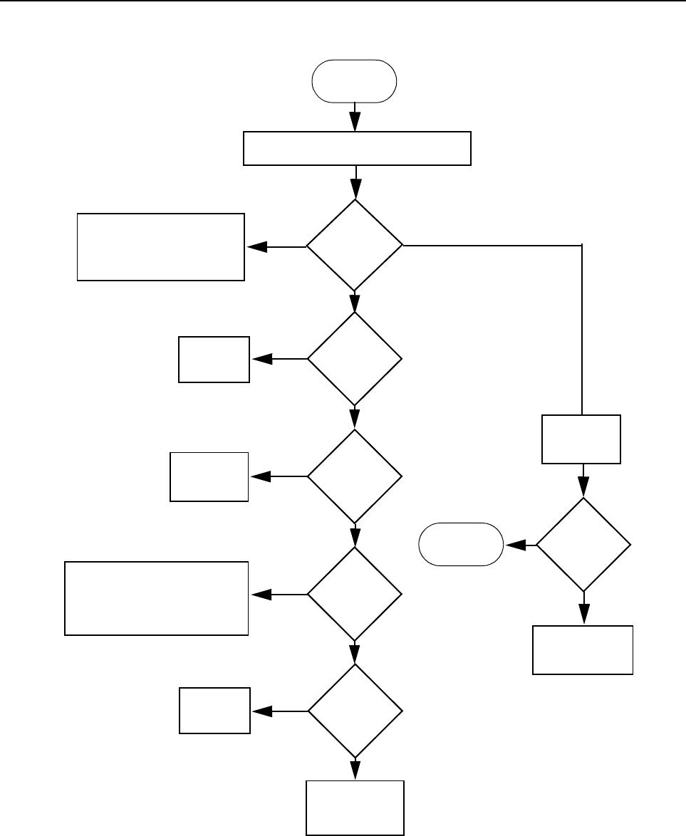
3-4 TROUBLESHOOTING CHARTS
2.0 Troubleshooting Flow Chart for 40W Transmitter (Sheet 1 of 3)
START
Yes
No
Check components between
Q100 and RF output,
Antenna Switch D104,
D103, VR102 and Q106
No or too low power when keyed
Current
increase when
keyed?
Check power settings, tuning
& components between U103
Pin 3 and ASFIC Pin 6 before
replacing ASFIC
Control
Voltage at
TP150
>4Vdc?
Check PA
Stages
>4A
Voltage U103
pin 5 =
4.7V?
U103 Pin 3
<1.6Vdc
U100 Pin 3
>1.8Vdc
Check 9.3V
Regulator
U501
Yes
Yes
No
No
Yes
Check
U103
Check forward
Power Sense
Circuit
No
Short U100
Pin 3 to
ground
Voltage at
TP150 rises?
Check PA
Stages
Check Forward
Power Sense
Circuit
Yes
No
>500mA & <4A
<500mA
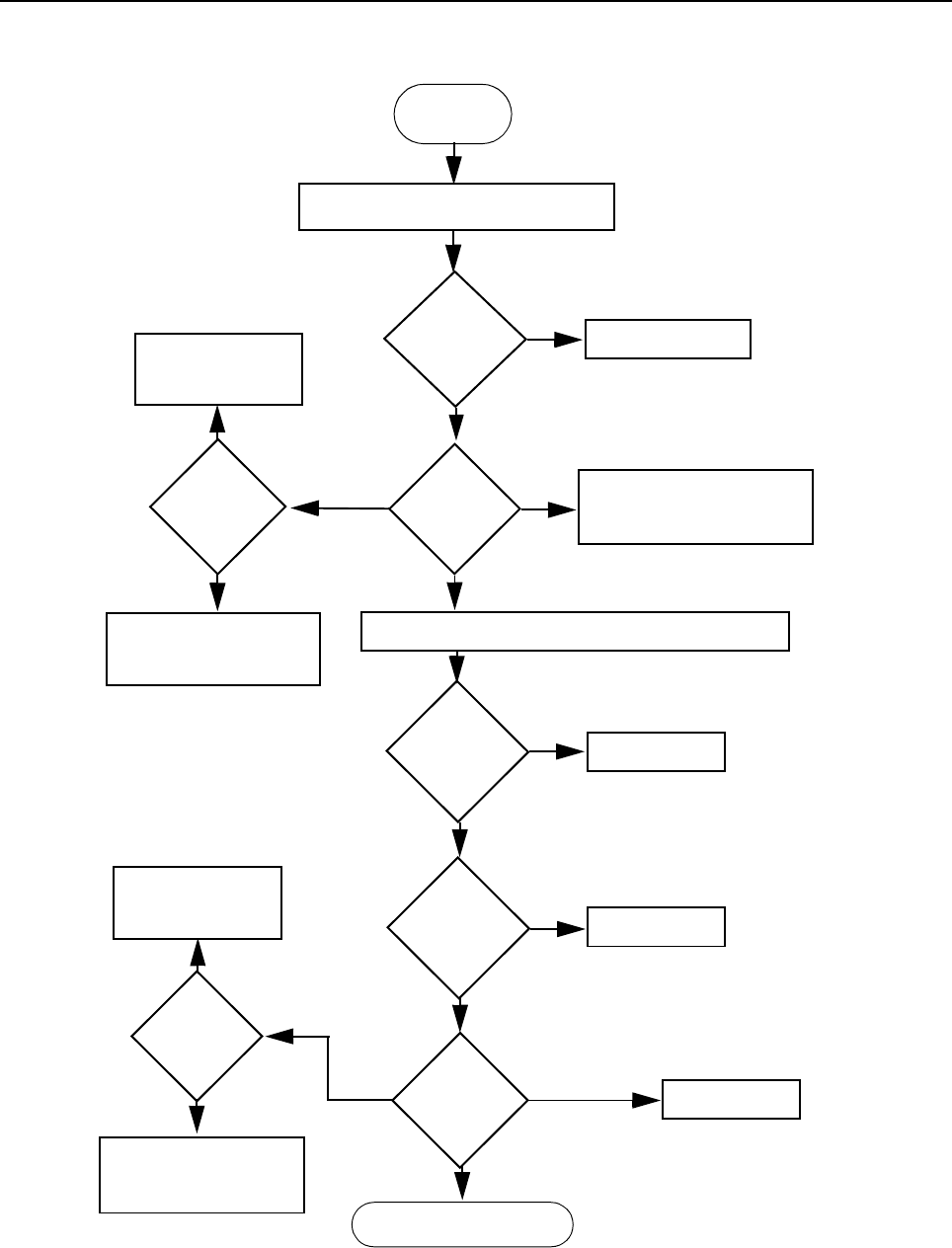
Troubleshooting Flow Chart for 40W Transmitter (Sheet 1 of 3) 3-5
2.1 Troubleshooting Flow Chart for 40W Transmitter (Sheet 2 of 3)
No
Yes
Yes
No
Check bias tuning
before replacing
U504
Check PA
Stages
No or too low power when keyed
DC
Voltage
at Q101 & Q102
base=0?
DC
Voltage
at U103
Pin 8
Check U510
Check resistive network at
Pin 9 and 10 of U103
before replacing U101
Measure DC Voltage at Pin 2 & 3 of U5401
Pin 2
Voltage
0.62 x Voltage
at Pin 1
Replace U5410
Pin 3
Voltage
0.51 x Voltage
at Pin 1
Replace U5410
DC
Voltage at
PA_CURRENT
line?
Replace Q105
Check Final PA Stages
ASFIC
U504
Pin 5 2-3V
Check components be-
tween ASFIC and Q105
before replacing Q105
DC
Voltage at
U103 Pin
10=8.9V
Check Q102,
Q101, R122, R165
Check U103 and Resistive
Network at Pin 10 of U103
before replacing U101
No
No
Yes
>5V
2 to 5V
Yes
Supply Voltage
2-3V
Yes
No
0V
<2V
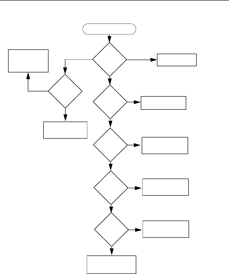
3-6 TROUBLESHOOTING CHARTS
2.2 Troubleshooting Flow Chart for 40W Transmitter (Sheet 3 of 3)
No
Yes
Yes
No
Check Final PA Stage
PA_Bias
Voltage at
R134
RF Voltage
after C1044
>100mV?
Voltage
across R122
>2V?
RF Voltage
Q105 gate
>1V?
RF Voltage
Q100 gate
>7V?
Check components
between Q100 &
antenna connector
Replace Q100
Check FGU (U5301)
Check components
between C1044 &
C1117
Check components
between C117 &
Q105
Check components
between Q105 &
Q100
No
No
Yes
Yes
1-4V
Supply Voltage
Check components
between ASFIC &
Q100 before re-
placing Q100
RF Voltage
after C1044
>100mV?
Check Bias Tuning
before replacing
ASFIC U504
Yes
No
0V

Troubleshooting Flow Chart for Synthesizer 3-7
3.0 Troubleshooting Flow Chart for Synthesizer
5V
at pin 6 of
D200
Is
information
from uP U403
correct
?
Is
U200 Pin 47
at = 14.6VDC
?
Is
U201 Pin 19
<40 mVDC in RX &
>4.5 VDC in TX?
(at VCO section)
?
Start
Visual
check of the
Board
OK?
Correct
Problem
Check 5V
Regulator
U503
+5V
at U200
Pin’s
13 & 30
?
Is
16.8MHz
Signal at U200
Pin 19
?
Check
Y201 and associated
Parts
Are
signals
at Pin’s 14 &15
of U200
?
Check
R228 Check R201
Is
U200
Pin 2 >4.5 VDC in
Tx & <40 mVDC
in Rx
?
Replace U200
Remove
Shorts
Is
there a short
between Pin 47 and
Pins 14 & 15 of
U200
?
Is
RF level at
U200 Pin 32
-12 < x <-25
dBm
?
Replace U200
Are
Waveforms
at Pins 14 & 15
triangular
?
Do
Pins 7,8 & 9
of U200 toggle
when channel is
changed?
Check programming
lines between
U403 and U200
Pins 7,8 & 9
Replace U200
Check uP U403
Troubleshooting
Chart
NO
YES
NO
YES
NO
YES
NO
NO
NO
YES
YES
YES
NO
YES
YES
YES
NO
NO
NO
NO
YES
NO
YES
YES
Check D200, D201,
C2026, C2025, &
C2027
3.3V
at U200
pins 5, 20, 34
& 36
C h e c k 3 V
Regulator
U503
Is
16.8MHz
signal at
U200 Pin
23?
Replace
U200
YES
NO
NO
YES
NO
YES
If C2052, R208,C2067,
C2068, L210 are OK, then
see VCO
troubleshooting chart
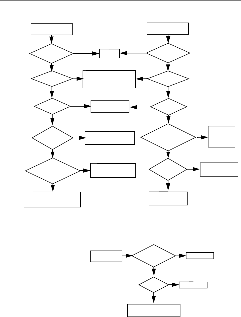
3-8 TROUBLESHOOTING CHARTS
4.0 Troubleshooting Flow Chart for VCO
Are Q200
Base at 2.9V
Collector at 6.6V
Emitter at 2.2V
Are U201 Pins
15 at 1.0V
10 at 3.9V
16 at 1.8V
Low or no RF Signal
at TP1
Visual check
of board
OK?
370mV DC at
U201 Pin 19
NO
YES
at base of Q200
NO
NO
NO
YES
YES
YES
Low or no RF Signal
at input to PA
4.5V DC at
U201 Pin 19
Is RF available
at C2060
YES
YES
YES
YES
NO
NO
NO
NO
NO
Audio =180mVRMS
at “-” Side of
4.5VDC
at D205
If R211 and R12 are OK,
then replace D205
Replace R211
Replace R212
NO
NO
YES
YES
If parts between
R109 & U201 Pin10
are OK, replace U201
TX VCO
RX VCO
Correct
Problem
Visual check
of board
OK?
Check runner
between U200 Pin 2
and U201 Pin 19
Is RF available Replace U201
If all parts associated
with the pins are OK,
replace Q200
If all parts from collector
of Q200 to TP1 are
OK, replace Q200
Power OK but
no modulation
Check parts to pre-driver
If all parts
associated
with the pins
are OK,
replace U201
YES YES
Make sure Synthesizer is
working correctly and runner
between U200 Pin 28 and
U201 Pin 14 & 18 is OK
4.5V DC
OK ?
OK? OK?
D205
at U201 Pin 14 & 18
4.5V DC
OK ?
at U201 Pin 14 & 18
NO
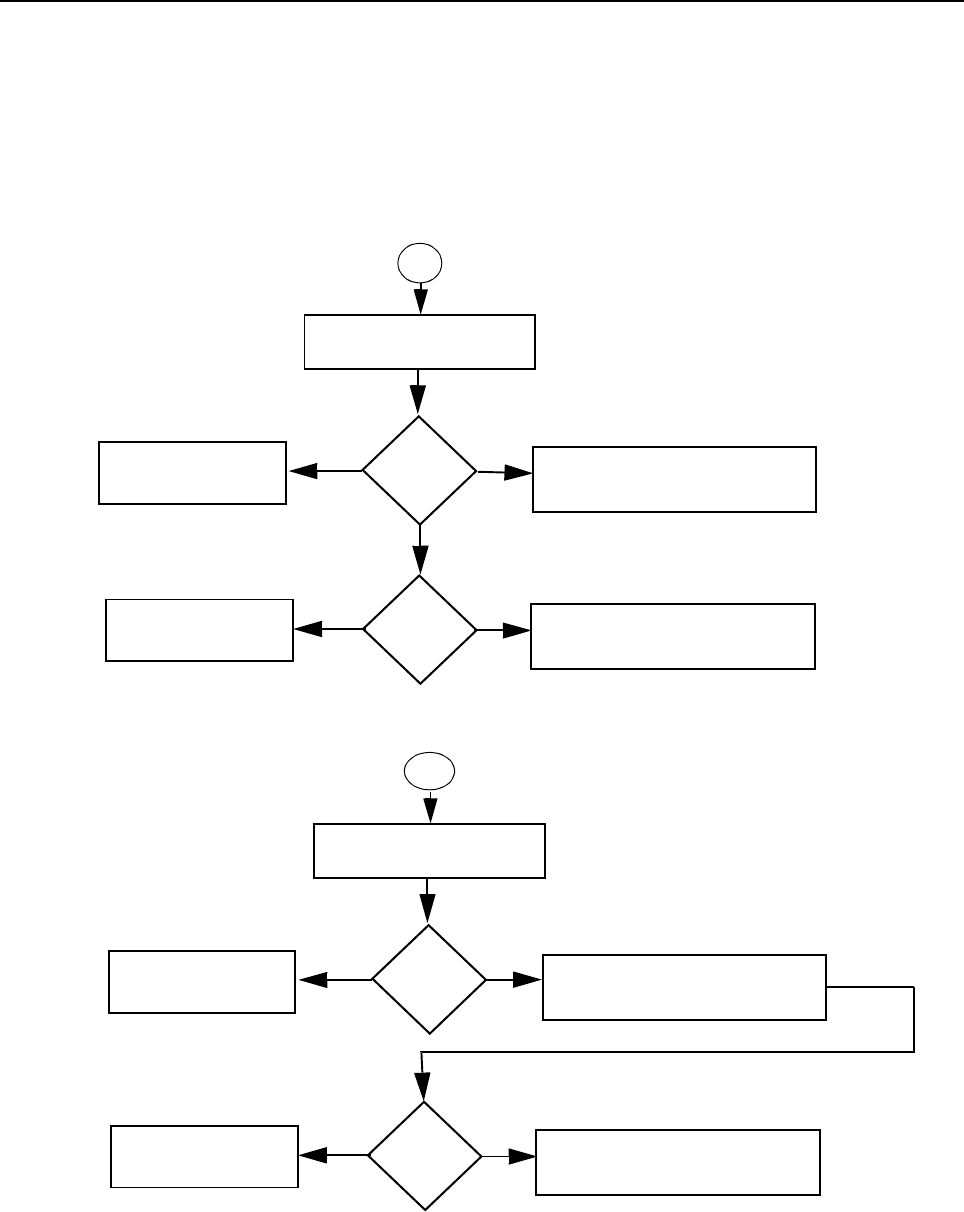
Troubleshooting Flow Chart for DC Supply (1 of 2) 3-9
5.0 Troubleshooting Flow Chart for DC Supply (1 of 2)
Since the failure of a critical voltage supply might cause the radio to automatically power down,
supply voltages should first be probed with a multimeter. If all the board voltages are absent, then
the voltage test point should be retested using a rising-edge-triggered oscilloscope. If the voltage is
still absent, then another voltage should be tested using the oscilloscope. If that voltage is present,
then the original voltage supply in question is defective and requires investigation of associated
circuitry.
Check VDC on
C5008
V=3.3V
?
Check Voltage on
C5043
No
Go to D3_3V
Yes
9v<V<9.8v
?
Go to Start
No
Replace U508
Yes
3V
Check VDC on
C5006
V=5V
?
Check Voltage on
C5042
No
Go to 3V
Yes
9v<V<9.8v
?
Go to Start
No
Replace U503
Yes
5V

3-10 TROUBLESHOOTING CHARTS
5.1 Troubleshooting Flow Chart for DC Supply (2 of 2)
Check VDC on
C5007
V=3.3V
?
Check Voltage on
C5041
No
Go to Digital Section
Yes
9v<V<9.8v
?
Go to Start
No
Replace U510
Yes
D3_3V

Chapter 4
UHF2 PCB/ SCHEMATICS/ PARTS LISTS
1.0 Allocation of Schematics and Circuit Boards
1.1 UHF2 and Controller Circuits
The UHF circuits are contained on the printed circuit board (PCB) which also contains the Controller
circuits. This Chapter shows the schematics for both the UHF circuits and the Controller circuits. The
PCB component layouts and the Parts Lists in this Chapter show both the Controller and UHF circuit
components. The UHF and Controller schematics and the related PCB and parts list are shown in
the tables below.
Table 4-1 UHF2 25-40W Diagrams and Parts Lists
PCB :
8486577Z01 Main Board Top Side
8486577Z01 Main Board Bottom Side
Page4-4
Page4-5
SCHEMATICS
Main Circuit
Transmitter
Synthesiser and VCO
Receiver Front and Back End
DC and Audio Ccts
Microprocessor and Controller Ccts
Power Control Cct
Page4-6/Page 4-7
Page 4-8/Page 4-9
Page 4-10/Page 4-11
Page 4-12/Page 4-13
Page 4-14/Page 4-15
Page 4-16/Page 4-17
Page 4-18
Parts List
8486577Z01 Page 4-19
Controller version is T1

4-2 UHF2 PCB/ SCHEMATICS/ PARTS LISTS
THIS PAGE INTENTIONALLY LEFT BLANK

UHF2 25-40W PCB 8486577Z01 / Schematics 4-3
2.0 UHF2 25-40W PCB 8486577Z01 / Schematics
TX_INJ VREV_BUFFER_IN
9V
COMP_B+
DET_VFWD
FILT_SW_B+
INTEGRATOR
PA_BIAS
PA_CURRENT
PWR_SET
RX
RX_EN
TX_EN
TX_INJ
VREV_BUFFER_IN
9V
COMP_B+
DET_VFWD
FILT_SW_B+
INTEGRATOR
PA_BIAS
PA_CURRENT
PWR_SET
RX
RX_EN
TX_EN
MAIN COMPARTMENT
UHF 2 Interconnection between Main Board and
Power Amplifier Compartment
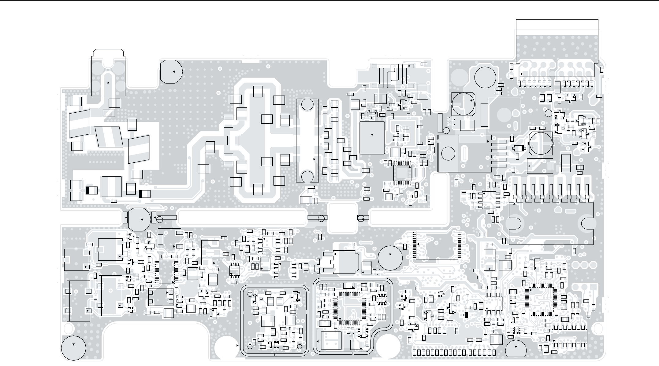
4-4 UHF2 25-40W PCB 8486577Z01 / Schematics
C1016
C1020
C1025
C1026
J11
L111
L113
L128
L130
M4
C1007
C1008
C1009
C1013
C1017
C1021
C1276
C1277
C1278
C1279
C1280
L126
L127
C1004
C1005
C1274
C1275
3
2
14
5
6
7
8
Q100
C1037
C1251
C1252
C1253
C1267
L122
R195
C1012
C1151
C1156
C1254
C1268
C1269
C1270
C1014
C1255
C1256
R194
C1258
C1052
L103
RT100
M110
R148
R151
C1082
M103
M104
M106
C110
1
C1064
4
3
R101
C1001
2
Q104
R193
R198
R199
C1281
C1153
C1099
C1152
C1095
C1116
C1283
R196
2
Q108
C1115
L119
2
R197
C1100
C1031
C1033
C1038
C1039
C1041
C1042
C1044
C1057
C1063
C1074
C1084
C1117
C1118
C1119
C1129
C1154
C1155
C1263
C1264
L104
L105
L107
1
M100
R109
R159
R171
R173
R174
R178
R179
R182
R186
R187
R188
1
16
8
9
U101
1
M6
U501
C1098
C1114
C5004
L120
M9
M107
U517
C1088
C1097
C1113
R406
R440
D502
R5001
R5038
R5081
VR500
5
2
3
4
C620
C621
C622
C623
C625
C627
C628
C629
C630
C631
C632
C633
C5100
1
R601
R602
R5087
C626
P1
C624
C678
R610
2
VR693
C662
C5021
C5038
C5080
C5110
C5111
2
D500
2
D513
2Q500
2
Q503
R5018
R5039
R5048
R5073
R5074
R5082 R5083
R5085
R5089
2
VR501
C5001
C5005
TP3
C5096
C1131
C5057
C5074
C5078
C5081
C5090
R5045
R5046 R5067
1
4
58
U506
C5015
C5032
C5089
C5095
R5022 R5068
1
C5019
R5056
R5057
C5033
C1006
C1010
C1011
C1023
C1108
D103
D104
L114
M5
M108
M105
M109
U516
FL301
FL302
43
2
FL303
2
FL304
R306
R307
R315
R317
43
C310
C311
C314 C316 C317
C318
C319
C320
D301
D302
D303
Q302
R302
R305
R308
R314
R316
R318
R319
R324
R325
R327
R335
3
2
2
C361
D304
L315
R303
4
Y301
11
1
20
10
U300
C303
C304 C305
C306
C337
C359
C360
C364
C365
C371
2
CR300
L303
2
Q305
R304
R309
R311
R322
R323
R333
R337
C301
C307
C308
C369
6
L305
R312
R320
R321
R339
C309
C315
C322
C336
C362
23
4
5
FL300
R313
R329
R332
C302
R328
2
Y300
C312
C313
C5016
C5068
C5113
C5114
C5115
R144
R146 R5092
R5093
R5095
R5096
R5097
4
58
U301
C5006
C5042
C5043
C5064
C5116
C5117
C5118
R5011
R5094
R5098
R5099 R5100
1
4
58
U500
1
4
58
U503
C1124
C5066
3
1
U508
C5008
C5018
C5070
R5010
2
C402
C411
22 7
1
U402
M3
21 8
C1122
C1125
C5003
C5011
C5014
C5030
C5079
C5088
R5021
R5052
R5053
R5065
R5086
C5012
C5022
C5046
C5047
C5050
C5051
C5052
R461
R5040
R5054
R5063
R5064
R5070
R5080
1
37
25
13
U504
C5024
C5025
C5026
C5029
C5034
C5044
C5053
C5054
R5032
R5033
R5034
C5035
R5071
R5079
C1123
U502
C2012 C2030
C2063
C2064
C2066
C2069
2
D203
2
D204
L203
L204
L211 L213
C2056
C2057
C2058
C2059
C2061
C2062
C2073
D205
L206 L207
L214 L215
R211
R212
R221
R222
R232
R233
SH202
C2028
C2052
C2067
C2068
C2074
C2078
L205
L210
R200
R206
R208
R217
R224
R234
1
SH200
1
37 25
13
U200
C2001
C2013
C2036
D201
R202
C2002
C2004
C2014
C2016
C2024
C2025
C2026
C2027
C2033
C2055
D200
R225
R226
R228
C406
C414
C418
C490
C1034
2
D400
2
D401
Q400
Q407
Q414
2
Q415
R428
R429
R431
R439
R441
R444
R445
R450
R451
R458
R459
R462
R472
R473 R5000
C602
C603
C604
C605
C606
C607
C608
C609
C610
C611
C612
C613
C614
C615
C616
C617
C618
C619
C5010
C5062
C5071
C5087
R430
R5019
R5031
R5050
R5055
R5066
R5075
R5077
1
8
U505
VR504 4
5
C5027
C5056
C5101
R5009
R5024
R5084
16
18
9
U509
M2
C5048
C5059
C5076
C5102
C5103
R5043
R5044
R5047
43
6
U515
C5013
C5020
C5023
C5028
M1
1
9
UHF 2 (438-470MHz) 25-40W 8486577Z01
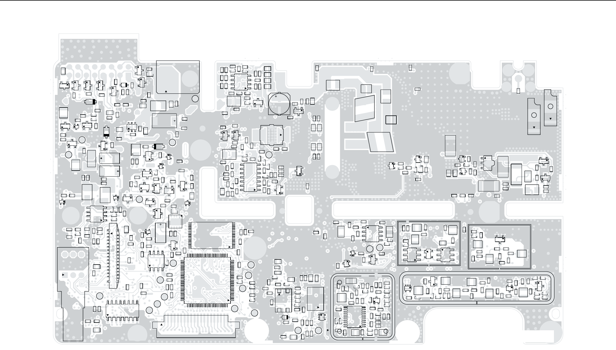
UHF2 25-40W PCB 8486577Z01 / Schematics 4-5
2
M101
2
M102
R150
C1002
C1089
C1106
C1112
C1273
L115
L124
L125
C1000
L117
C1027
C1065
C1103
C1104
C1107
C1282
2
Q107
R106
R184
R189
R192
R190
R191
C1040
C1055
C1056
C1061
C1073
C1086 C1092
2
D100
L121
R110
R111
R112
R113
R114
R115
R116
R126
R127
R128
R129
R131
R132
R134
R138
R147
R166
R169
R175
R177
14
58
U102
C1028
C1054
C1066
C1070
C1091 C1157
L118
2
Q101
2
Q102
1
2
3
Q105
R136
R139
R149
R153 R155
R176
R180
TP150
C1126
C1051
C1053
C1060
C1260
C1261
R122
R130
R135
R137
R145
R165
R168
8
7
1
14
U103
R170
C1029
C1032
C1036
C1043
C1050
C1059 C1062
C1072
C1081
2
D102
R142
R143
R156
R158
R167
R181
2
VR101
C1271
C1272
C1069
C1080
C1101
C1110
1
D105
1
D106
R118
R119
R160
R161
R183
C1076
C1079
C1102
1
D107
1
D108
Q106
R104
R120
R121
R152
R162
R163
C1068
C1111
R103
R105
R107
R108
C1077 C1109
R157
C1035
C1067
C1130
L100
L108
2
Q103
R172
R185
2
VR102
R402
R403 R404
R600
VR503
2
VR692
2VR694
2VR698
2VR699
C5037
C5119
2
D511
Q502
2
Q505
2
Q506
R5020 R5030
R5036
R5037
R5062
R5069
TP555
TP556
R5049
C5092
R5017
C417
C5000
C5067
C5083
C5086
C5099
D402
R407
R615
2
VR695
2
VR696
2
VR697
C5060
L500
C5055
R405 R421
R5023
R5025
C5063
C5085
C5094
2
D501
R432
R5028
R5029
R5103
U514
VR502
C5002
C5120
VR401
C5072
C5097
C5104
C5073
C5098
L502
Q501
R5041
R5051
14
58
U507
C5077
R5060
C5036
R5061
R5058
R5088
VR402
2
L501
Q416
C1094
C5009
Q405
Q408
R453
R5076
R5078
Q404
C1132
Q409
R433 R456 R457
R454
C1096
TP500
R435
R455
Q411
Q410
R434
C1093
2
Q401
R401 R460
Q403
C5065
R436
R5035
Q412
Q504
TP405
4
58
U510
2
VR400
C5041
1P2
TP2
C1087
C1127
C1128
C5061
C5084
C5031
C5049
C5058
C5075
C5082
C5091
R5008 R5013
R5014
R5016
R5026 R5059
6
5
4
1
3
2S5010
R603
R5042
TP403
29
28 2
29
30
32
31
J3
R466
R467
R469
R604
C400
C401
Q413
R422
R438 R470
14
5
8
U400
C5007
C408 C5017
C5069
2
Q417
R442
R443
R463
TP425
32
17
U404
C422
C423
C5045
R5027
R5072
16
18
9
U405
C421
R468
C404
C416
R423
R424
R425
TP401
TP402
TP408
TP400
1
76 51
26
U403
TP404
C403
C412
R415
R426
R427
16
1
C413
R414
TP409
TP410
C405
C407
C410
C415
R471
TP406
C2000
C2005
C2006
C2015
C2023
C2034
C2035
C2051
C2053
C2054
L200
L217
C2049
R229
C2047
4
3
2
Y201
Y200
C2045
C2046
C2048
C2050
C2129
C2198
D202 R207
R210
C2072
TP201
C2017
C2020
C5039
C5040
R5002
R204
R205
R209
TP200
1
J2
TP407
C1090
C1075
C1083
C1085
L101
C1045
C1046
C1047
C1048
C1071
1
D101
L102
Q300
2
Q306
R117
R140
R141
R164
R345
R346
TP1
TP4
1
4
58
U100
C1049
C324
C325
C354
C356
C366
C367
L302
L306
L307
L308
R301
R340
SH302
6
4
3
T300
64
3
T301
U302
C300
C328
C334
C338
C339
C340
C341
C345
C353
C368
C370
C1078
C1121
2
CR301
L300
L309
L310
SH300
C321
C327
C329
C330
C333
C335
C348
C358 2
D305
L304
L313
L314
Q304
R334
R338
C331
C332
C342
C343
C344
C346
C347
C355
L311
L312
SH301
C323
C326
C349
C350C351
C352
C357
L301
2
Q301
Q303
R300 R310
R326
R330
R331
R336
Q201
1
C2003
C2007
C2008
C2009
C2010
C2011
C2018
C2019
C2021
C2022
C2029
C2031
C2032
C2037
C2038
C2039
C2040
C2041
C2042
C2043
C2044
C2060
C2065
C2070
C2071
C2076
L201
L202
L208
L209
L212
L216 Q200
R201
R203
R213
R214
R215
R216
R218
R219
R220
R223
R227
R230
R231
R235
SH201
11
1
20
10
U201
UHF2 (438-470MHz) 25-40W 8486577Z01
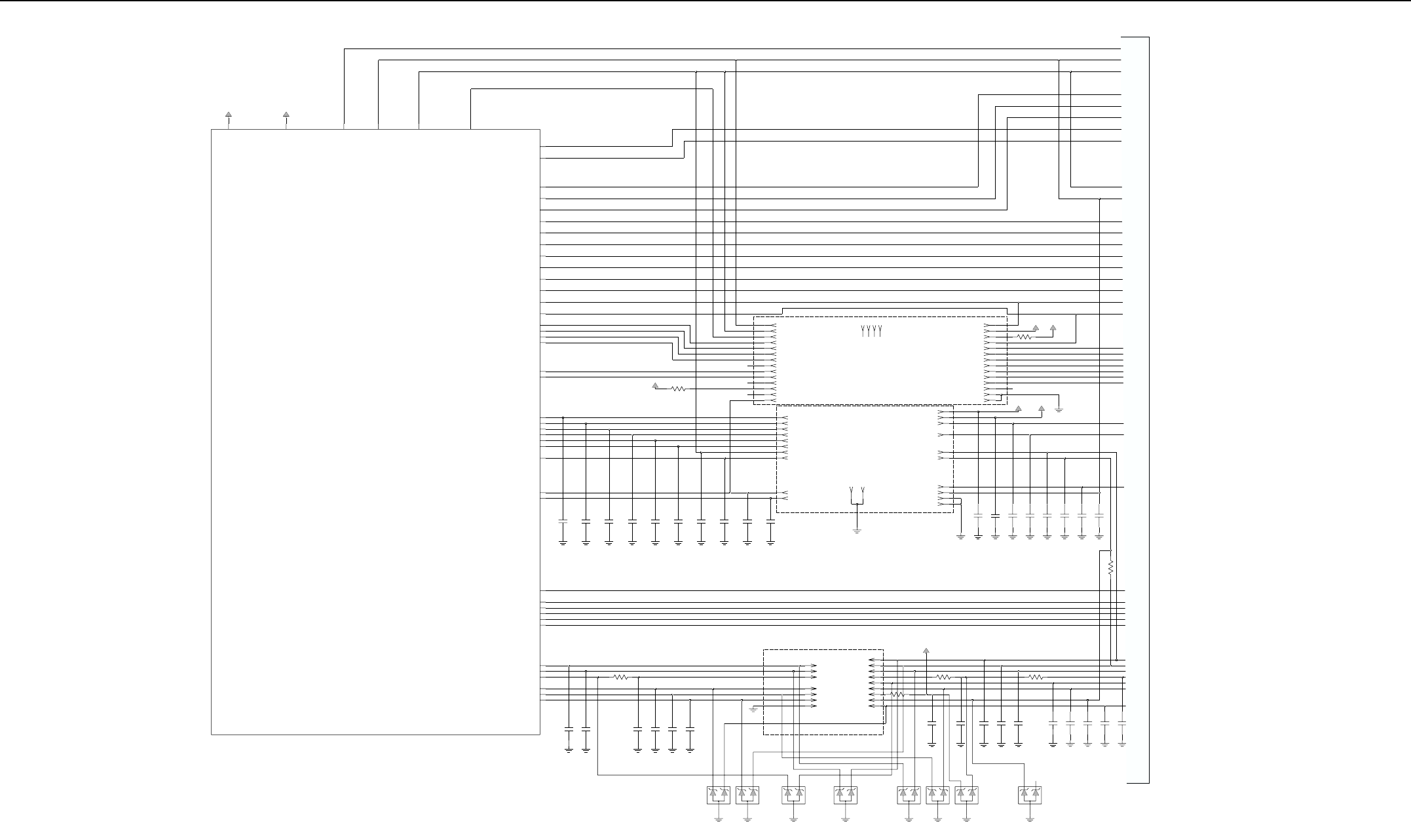
4-6 UHF2 25-40W PCB 8486577Z01 / Schematics
FILT_SW_B+ D3_3V
D3_3V
FILT_SW_B+ TX_EN SPI_CLK SPI_MOSI SPI_MISO
SYNTH_CS
SYNTH_LOCK
VS_AUDIO_SEL
VS_CS
VS_GAIN_SEL
VS_INT
VS_RAC
uP_CLK
OPT_EN_OPBD
RESET
RSSI
RX_EN
SQ_DET
CH_ACT
F1200
HSIO
LOC_DIST
LSIO
OPT_DATA_R_OPBD
ASFIC_CS
SCI_CH
SHIFT_R_CS
COMM_DATA_SEL_CH
DISPLAY_CS_CH
HOOK_CH
KEYPAD_COL_CH
KEYPAD_ROW_CH
MIC_PTT_CH
BOOT_EN_IN_CH
VOL_INDIRECT
VOX
VSTBY
EMERGENCY_SENSE
ONOFF_SENSE
BATT_SENSE
PROG_I-ACC_C_3
PROG_I-ACC_C_6
PROG_IO-ACC_C_12
PROG_IO-ACC_C_14
PROG_IO-ACC_C_8
PROG_O-ACC_C_4
39.p
C633 C632
39.p
39.p
C631 39.p
C630 39.p
C629 C628
39.p
R615
100.
1
2
20.0
VR698
1
2
VR697
1
VR699
20.0 20.0
1
2
VR696
20.0
10
13
P1-10
P1-77
P1-13
12 P1-1414
P1-88 P1-12
6
P1-9 9
3P1-6
P1-44 P1-3
11
P1-15 15
P1-5 5
P1-11
16
P1-2 2
P1-1 1
P1-16
R602
0
R601
330.0
R610
220.
33.
VR693
1
1
20.0
VR692
1
2
20.0
VR694
1
2
VR695
20.0
100.n
C678
39.p
C662
39.p
C627 39.p
C626 39.p
C625
C624
39.p 39.p
C623 39.p
C622 39.p
C621 C620
39.p
FILT_SW_B+
21
R600
0.
39.p
C619
39.p
C618
39.p
C617
C616
39.p
39.p
C615
39.p
C614
39.p
C613
39.p
C602
9V D3_3V
3V
R6030
D3_3V
J3-11 11
J3-9 9
J3-20 20
27
J3-25 25
J3-23 23
26
J3-24 24
J3-27
J3-22 22
J3-28 28
J3-26
J3-21 21
J3-14 14
J3-4 4
J3-12 12
J3-3232
29 J3-3030 J3-3131
J3-29
13
J3-88 J3-55 J3-13
J3-1919 J3-1010
3J3-77 J3-1818
1J3-66 J3-3
J3-1515 J3-22 J3-1
J3-1717 J3-1616
9V
R604 0
J2-1717 J2-55
3J2-99 J2-88
1J2-66 J2-3
J2-1
J2-1010
J2-1616 J2-1313
G2
J2-21
G1 J2-22
2
J2-2
J2-14 14
J2-4 4
19
J2-11 11
15
J2-20 20
J2-19
J2-7 7
J2-18 18
J2-15
J2-12 12
C612
39.p
C611
39.p 39.p
C610
39.p
C609
C608
39.p
C607
39.p 39.p
C606
39.p
C605
C604
39.p
C603
39.p
DIGITAL
Accessory Connector
EXT_ALARM_OUT
EXT_MIC_PTT
PROG_IN
PROG_I/O
PROG_I/O
PROG_I/O
Option Board
Keypad/Display
DNP
NC ELP ONLY
NC ELP ONLY
NC ELP ONLY
SERIAL CLOCK
SERIAL DATA SEND
SERIAL DATA RETURN
VOICE STORAGE INT
VOICE STORAGE RAC
VOICE STORAGE CS
VOICE STORAGE GAIN SELECT
KEYPAD ROW
OPTION BOARD ENABLE
DATA READYREQUEST
DISPLAY DRIVER CHIP SELECT
DISPLAY_DRIVER_COMMAND/DATA_SEL
KEYPAD COLUMN
PUSH TO TALK
Option Board Connector
28 Pins Connector
VOICE STORAGE AUDIO SELECT
DIGITAL 3.3 VOLT SUPPLY
ANALOG 3.3 VOLT SUPPLY
RESET
EXTERNAL_MIC
TX AUDIO SEND
TX AUDIO RETURN
POST-LIMITER FLAT TX AUDIO RETURN
DETECTOR AUDIO SEND
UNMUTED RX AUDIO SEND
RX AUDIO RETURN
BACKLIGHT
GND
GND
J3 - DNP
DISPLAY_DRIVER_CS_LN 9.3V
D3_3V
SHIFT_REG_CS
DISPLAY_DRIVER_COMMAND/DATA_SEL
KEYPAD_COLUMN
KEYPAD_ROW
SCI_PROGRAMMING
SPI_MOST
BOOT/RESET
MIC_PTT
HOOK
HANDSET_RX_AUDIO
MIC_AUDIO
SPKR-
SPKR+
DISPLAY_DRIVER_RESET
SPI_CLK
GND
GND
Control Head Connector
DNP DNP
Place capacitors near J2
Place capacitors near J2
DNP
NC ELP ONLY
Place capacitors near J2
Accessory Connector
Place capacitors near J2
DNP
Internal SPKR+ Jumper
TO SHEET 1
UHF2 (438-470MHz) Main Circuit (Sht 1 of 2)
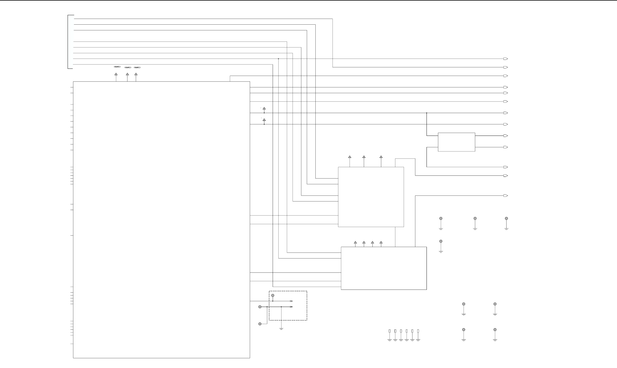
UHF2 25-40W PCB 8486577Z01 / Schematics 4-7
SPI_CLK
SPI_MOSI
SQ_DET
VS_AUDIO_SEL
uP_CLK
F1200
HSIO
LSIO
RESET
ASFIC_CS
CH_ACT
3V D3_3V 5V
3V 5V
D3_3V
SPKR+
SPKR-
VOL_INDIRECT
VOX
VSTBY
FLAT_TX_AUDIO_INPUT_ACCESS_CONN
IGNITION
ONOFF_SENSE
RX_AUDIO_OUTPUT_ACCESS_CONN
BATT_SENSE
EMERGENCY_ACCES_CONN
EMERGENCY_SENSE
EXTERNAL_MIC_AUDIO_ACCESS_CONN
HANDSET_RX_AUDIO_CH
MIC_AUDIO_CH
5V_CH
TX_AUDIO_RETURN_OPT_BRD
TX_AUDIO_SEND_OPT_BRD
UNMUTED_RX_AUDIO_SEND_OPT_BRD
VS_MIC
POST_LIMITER_FLAT_TX_AUDIO_RETURN_OPT_BRD
RX_AUDIO_RETURN_OPT_BRD
DETECTOR_AUDIO_SEND_OPT_BRD
9V
FILT_SW_B+
FILT_SW_B+
PA_BIAS
PA_CURRENT
PWR_SET
9V
COMP_B+
DET_VFWD
FILT_SW_B+
INTEGRATOR
VREV_BUFFER_IN
INTEGRATOR
TX_EN
RX_EN
COMP_B+
PA_CURRENT
VREV_BUFFER_IN
9V
PA_BIAS
PWR_SET
FILT_SW_B+
DET_VFWD
RX
TX_INJ
M2
PLTD_HOLE3_5x6_0_TRIMMED
GND
1
M5
PLTD_HOLE3_5x7_0_TRIMMED
GND
1
PLTD_HOLE3_5x7_0
M3
1
GND
M1
PLTD_HOLE3_5x7_0
GND
1
3V 9R5V
SYNTH_CS
SYNTH_LOCK
TX_INJ
16.8MHz
3V5V 9R
MOD_IN RX_INJ
SPI_CLK
SPI_MOSI
9R 5V 9V 3V
3V5V
9R 9V
BW_SEL
DEMOD
LOC_DIST
RSSI RX
RX_EN
RX_INJ
M108
1
M110
1M109
1
M106
1
1
M107
1
M105
PLTD_HOLE1_4X1_8
M104
1
GND
1
GND
U517
PLTD_HOLE1_4X1_8
GND
1
U516
PLTD_HOLE1_4X1_8
GND
1
PLTD_HOLE1_4X1_8
M103
M9
PLTD_NUT
GND
1
1
TP3
TEST_POINT
1
TEST_POINT
TP2 2P2-11 P2-2
MOD_OUT
B+
BW_SEL
DEMOD
16.8MHz
FGU
DC & AUDIO
RX
(SOURCE) (SOURCE) (SOURCE)
(SOURCE)
(SOURCE)
(SOURCE)
POWER CONTROL
BOARD HOLES
HOLES FOR PA SHIELD
PEDS FOR GND CONTACTS
DC Connector
TO SHEET 2
UHF2 (438-470MHz) Main Circuit (Sht 2 of 2)
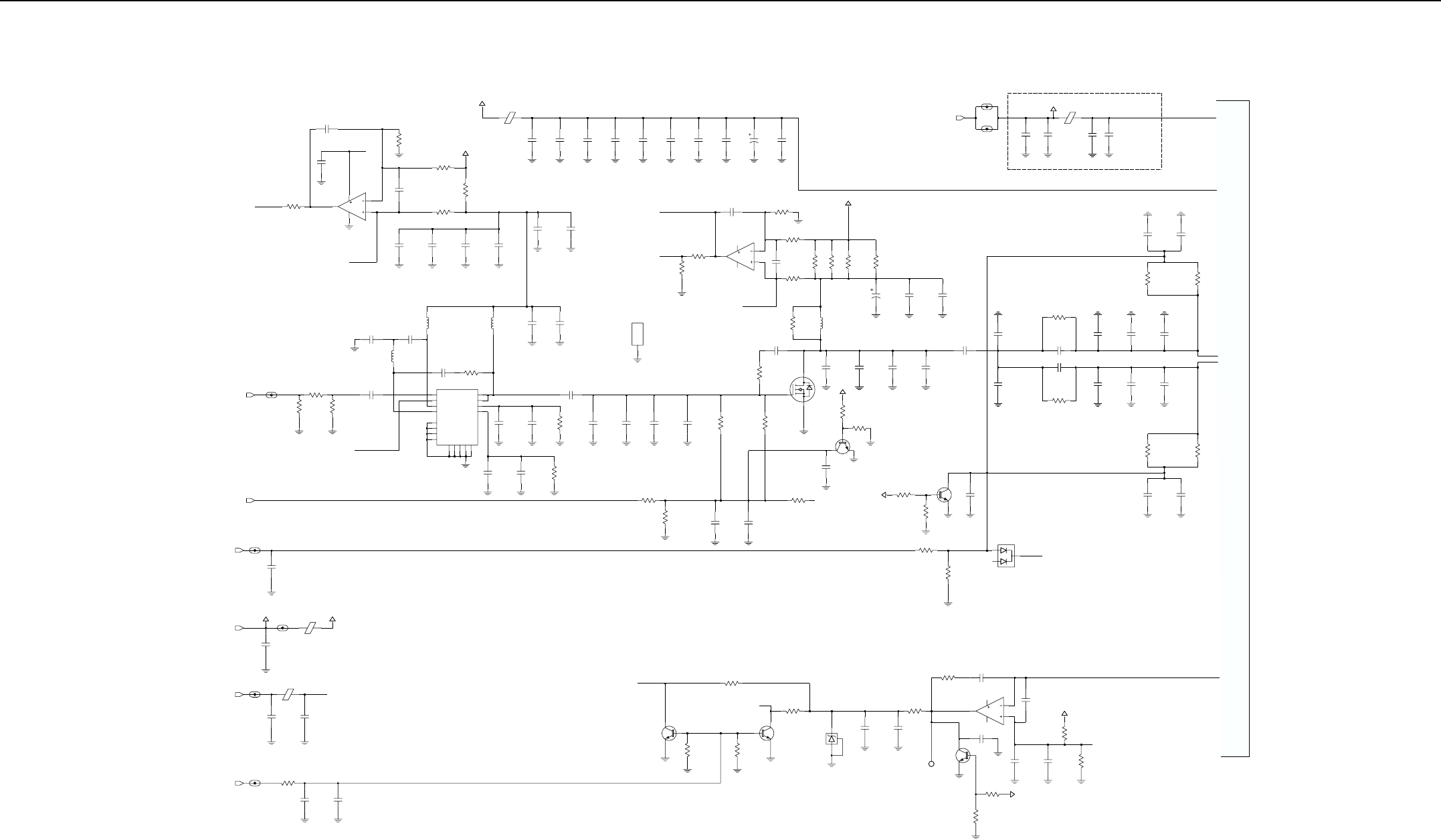
4-8 UHF2 25-40W PCB 8486577Z01 / Schematics
0.
0662057B47
R130 U103
9
10
84
11
MC3303
120.p
C1072
2113740F53
180.p
2113740F57
C1053
R137
39.K
FILT_SW_B+_PA
V_CTRL_PREDRIVER
VCNTR1 2113743K15
100n
C1264 C1263
2113741F25
1.n 2113740F53
120.p
C1261 10.n
2113741F49
C1260
120.p
C1060
0662057C19
R122
FLT_9V
R168
4.7
0662057A58
2.2K
0662057A57
R165
2.4K
57R01
L100
PA_FILT_B+
120.p
C1000 39.p
C1112 39.p
C1111 C1110
39.p 39.p
C1109 120.p
C1089
120.p
C1107
C1106
39.p C1027
10uF
C1103
33n
2680499Z01
HEATSINK
M100
1POS
0662057A59
R147
2.7K
560.
R175
0662057A43
VCNTR3
V_CTRL_DRIVER
2113741F25
C1040
1.n
0662057A86
R138
36.K
4
5113818A01
LM2904
U102
2
3
18
C1061
120.p
0662057C01
0
R128
0662057C01
R127
0
R126
0662057C01
0
2.K
R169
2.7K
R166
VCNTR2
0662057C01
R129
0
120.p
C1064
2113740F53
C1001
2311049A08
1.0u
10
R193
2460591C23
L122
13.85nH
FILT_SW_B+_PA
2113740A23
C1254
6.2pF
27pF
C1156
2113740A39
2113743E13
C1037
.068uF
L119
57R01
LOAD_3
C1116
39.p
39.p
C1115 120.p
C1100
C1099
120.p
IF108
IF109
COMP_B+
C1272
2113743E10
C1271
2113740F53
.033uF
120pF
0662057C35
R191
0662057C35
R190
22 22
10
R195
10
R194
33pF
C1268
33pF
C1270
C1267
33pF
2113740A412113740A23
C1251
6.2pF 150pF
C1252
2113740A59 2113740A31
C1253
12pF
12pF
C1256
2113740A31
2113740A59
C1255
150pF 33pF
C1269
2113740A41
IF107
120.p
2113740F53
C1044
36
R109
0662057A14
2460591B04
L107
11.030n
150
R174
0662057A29
0662057A29
150
R173
TX_INJ
V_CTRL_PREDRIVER
120.p
C1119
2113740F53
2113740F23
C1118
6.8p 2462587N50
L104
56.n
560.
R171
0662057A43
C1041
2113740F67
470.p
NC4
16 RFIN 6
RFOUT17
RFOUT2
1VCNTRL
14 VD1 2
VG1 3
VG2
G2
4GND1
5GND2
12 GND3
13 GND4
8NC1
9NC2
10 NC3
15
U101
30C65
EP
17
11
120.p
2113740F53
C1057
2113741F37
C1031
3.3n
L105
2462587N44
18.n
22n R159
6.8K
C1038
120.p
2113740F53
C1042
2113740F38
C1117
30.p
R158
6.8K
120.p
C1043
2113740F53
C1032
22n
2113743E07
C1152
2113740F28
15.p
11.p
C1153
18.p
C1154
2113740F33
4.3p
C1155 51.
R178
0662057A18
100K
0662057A97
R187
10K
0662057A73
R186
C1074
2113740F53
120.p 2113743E13
C1039
.068uF
C1063
2113740F53
120.p
10.n
2113741F49
C1033
560
R176
51.
0662057A18
R179
C1157
470pF
Q105
R197
0662057A59
R196
0662057A97 2.7K
Q108
100K
4813824A10
LOAD_3 2113740A42
C1258
36pF
C1012
4.3pF 4.7pF
C1151
4.7pF
C1014
2113740A19
LOAD_2
120.p
2113740F53
C1283
0
R188
V_CTRL_DRIVER
0662057A59
R184
2.7K
0662057A97
R189
100K
Q107
4813824A10
C1282
2113740F53
120.p
D100
0662057A97
R131
100.K
0662057A59
R134
2.7K VCNTR3
R192
0662057C35
22
2113740F53
C1065
120.p 33.n
C1104
2113743E10
22
0662057C35
R106
IF106
39.p
C1092
PA_CURRENT
PA_BIAS
FILT_SW_B+
57R01
L118
IF104
120.p
2113740F53
C1126 C1070
2113740F53
120.p
FLT_9V
9V
L121
57R01
IF105
FILT_SW_B+
2113740F41
C1086
39.p
FILT_SW_B+_PA
C1129
39.p
2113740F41
C1084
2113740F41
39.p
IF103 10.K
R182
0662057A73
RX_EN
0662057A83
R155
27K
Q102
4813824A10
27K
R153
0662057A83
R139
39.K
0662057A87
VCNTR1
VCNTR2
VR101
6.8
4813830A18
4813824A10
Q101
R136
0662057A86
36.K
4813824A10
Q104
120.p
2113740F53
C1281
U103
MC3303
5113819A04
6
5
74
11
2113740F53
0662057A42
2113743K15
C1028
100n
R170
510.
2.2K
R167
0662057A57
C1036
0.1uF
2113743E20
C1054
120.p
1
TPSM2_032X
TEST_POINT
TP150
FILT_SW_B+_PA
2.7K
R199
0662057A59
100K
R198
0662057A97
100n
2113740F53
C1066 C1029
2113743K15
120.p
120.p
C1062
2113740F53
47.K
FLT_9V
0660082A89
0660082A89
R181
R180
47.K
V_REF_OPAMP
DNP
PLACED NEAR R122
(SOURCE)
DNP
PLACED NEAR CHIP’s PIN
DNP
DNP DNP
DNP
MRF1513’s Thermal pad
DNP
DNP
DNP
DNP DNP
DNP
MRF 1518 DNP
DNP
DNP
DNP
V_CNTRL
Place inside of the PA compartment
DNP
DNP
DNP
DNP
DNP
UHF2 (438-470MHz) Transmitter (Sht 1 of 2)
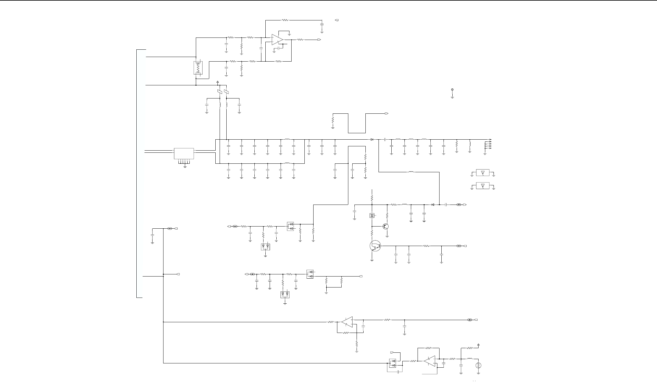
UHF2 25-40W PCB 8486577Z01 / Schematics 4-9
39pF
C1095
FINAL_CURRENT_SENSE
PA_CURRENT
120.p
C1073
5113818A01
6
57
8
4
U102
LM2904
R112
0662057B05
200K
R177
100
FILT_SW_B+_PA
R132
100K
120.p
C1055
C110
120.p C1056
120.p
10K
1K R115
10K
0662057A49
R110
0662057A73
R116
R113
0662057A73
0662057A49
10K
10K
1K
R111
0662057A73
R114
17nH
L115
2460592A01
120pF
C1002
2111078B44
2111078B44
C1273
120pF
2460592A01
L125
17nH
57R01
L117
57R01
L124
LOAD_2
43
12
1.639m
R101
3
IN2
6
OUT1
7
OUT2
1
GND1
4GND2
GND3
5
8GND4
GND5
9
GND6
10
2IN1
4813828C32
MRF1570
Q100
9.1p
C1021
6.8pF
C1007
3.9pF
C1009 3.9pF
C1008
2111078B03
30pF
C1005 C1004
2111078B18
2111078B27
15pF
C1278
3.9pF
13.9nH
L127
2460591B77
13.9nH
L126
2460591B77
2111078B03
C1277
3.9pF
C1276
6.8pF
DNP DNP
2111078B18
C1275
15pF
2111078B27
C1274
30pF 30pF
DNP
C1279
30pF
C1017
120.
R103
0683962T51
13.p
C1069
2113740F30
C1068
120.p
2113740F53
0662057A41
R105
470.
V_forward
3.3pF
C1013
2111078B01
2111078B03
C1280
3.9pF
120.
0683962T51
R104
18.n
L114
2485873L01
2111078B13
C1020
10pF
4802482J02
D104 L113
2460592A01 2460592A01
17.n 17.n
L111
10pF
2111078B13
C1016
2111078B32
C1011
39.p
C1023
12pF
2111078B15
2460592A01
L128
17nH
V_REVERSE
R150
0662057A73
10K
C1026
6.2pF
2111078B08
J11-4
G1
2462587T22
L130
390nH J11-3
3
J11-5
G2
J11-11 J11-2
2
5.6pF
C1025
ANTENNA
1TAB1 2
TAB2
3980686Z01
ANTENNA_CONTACT
M101
M102
ANTENNA_CONTACT
3980686Z01
TAB1
1TAB2
2
4802482J02
D103
2113740F22
C1108
6.2pF
15pF
2111078B18
C1010
2111078B18
C1006
15pF
IF100 RX
2113740F41
C1081
39.p
DNP
IF111
INTEGRATOR
INTEGRATOR
DET_VFWD
VREV_BUFFER_IN
C1080
39.p
2113740F41
100.
R183
0662057A25
IF110
D106
4805218N57
0662057A61
R161
3.3K
R160
0662057A61
3.3K
20.p
C1101
2113740F34
4805218N57
D105
100.
R118
0662057C51 0662057C51
R119
100.
2113740F41
C1077
39.p
IF101
TX_EN
R157
56.K
0662057A91
C1067
2113740F53
120.p 2113740F41
C1130
39.p
2113740F53
C1035
120.p
Q106
4805128M27
VR102
5.6
4813830A15
0662057A41
R172
470.
51.000
R107
0680194M18
Q103
4813824A06
L108
2462587T22
390.0n
51.000
R108
0680194M18
10K
R185
0662057A73
PA_FILT_B+
1
GND
PLTD_HOLE3_5x7_0_TRIMMED
M4
0662057A25
R152
100.
120pF
C1079
13pF
2113740F53
2113740F30
C1076
4805218N57
D108
3.3K
R163
0662057A61
3.3K
20.p
0662057A61
R162
2113740F34
C1102
D107
4805218N57
IF112
R121
100
0662057C51
100
R120
0662057C51
V_REVERSE
R143
0662057A79
18K
22.K
R142
0662057A81
120.p
2113740F53
C1059
R156
10.K
0662057A73
11
MC3303
U103
5113819A04
2
3
14
22.K
0662057A81
R149
C1091
39.p
IF102
PWR_SET
120.p
C1050
D102
13
12
14 4
11
MC3303
U103
22.K
R148
FLT_9V
RT100
47.0K
L103
1.u
R151
0662057A72
9.1K
120.p C1052
120.p
C1051
36K
R135
0662057A86
22.K
R145
FINAL_CURRENT_SENSE
V_REF_OPAMP
DNP
DNP
Current sense protection(option)
DNP DNP DNP
DNP
Coupler
PA’s Temp Sensor
Antenna Connector
TO SHEET 2
UHF2 (438-470MHz) Transmitter (Sht 2 of 2)
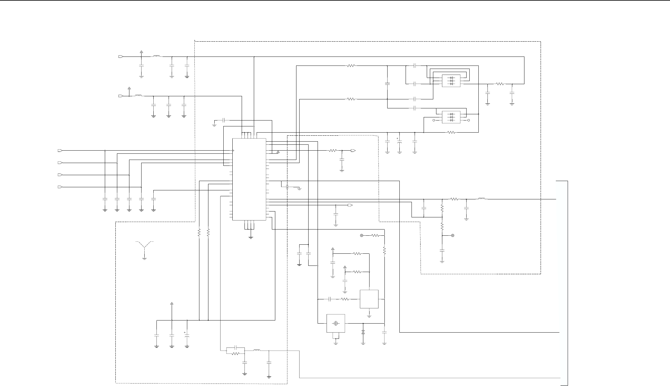
4-10 UHF2 25-40W PCB 8486577Z01 / Schematics
5V
C2015
0.1uF
C2000
2.2uF
L217
390nH
5V
120.p
C2034
3V
C2005
2.2uF
10n
C2023
L200
390nH
3V
C2035
120.p
0.1uF
C2016 2.2uF
C2004
100.
R228
A2
A3
K1
K2
K3
D200
A1
R202
0.
NC
NC A1
A2
A3
K1
K2
K3
D201
120.p
C2036
4.7uF
C2001 0.1uF
C2013
C2055
22p
C2027
10n
10n
C2026
10n
C2025
C2024
10n
150.
R225
R226
150.
120.p
C2049
100.
R229
16.8MHZ
120.p
C2050
SYNTH_LOCK
TEST_POINT
TP201
1
R205
0.
R209
100.K
R207
150.K
3V
R204
0.
100n
C2020 5V
C2054
62.00p
120.p
C2053
R210
100.K
FREQ
14R06
Y201
1
GND
2
GND1
4
OUT 3
IN
D202
4
VCC
VCON 1
45J68
Y200
16.8MHz
GND
2
OUT
3
C2017
0.1uF
TP200
TEST_POINT
1
R224
1.5K
100.n
C2074 R217
1.3K
39.
R234
2200pF
C2028
1uH
L205
C2078
1uF
C2072
2.7p
220p
C2051
120.p
C2129
VCO_MOD
23
XTAL1
24
XTAL2
21
VBPASS
47
VCP
15
VMULT1
14
VMULT2
12
VMULT3
11
VMULT4
VRO
13
25
WARP
35
PVREF
18
REFSEL
27
SFBASE
26
SFCAP
30
SFIN
28
SFOUT
37
TEST1
38
TEST2
17
NC1
29
NC2
31
NC3
44
PD_GND
PD_VDD
5
32
PREIN
33
PRE_GND
34
PRE_VDD
36
DVDD
19
FREFOUT
45
IADAPT
16
INDMULT
43
IOUT
LOCK
4
10
MODIN
41
MODOUT
20
AVDD
40
BIAS1
39
BIAS2
42
CCOMP
9
CEX
8
CLK
7
DATA
6
DGND
46
ADAPTSW
22
AGND
48
AUX1
1
AUX2
2
AUX3
3
AUX4
FRACN_63A27
U200
R206
120.K
100.K
R200
V_SF
2311049A72
C2002
10uF
C2033
120.p
C2014
0.1uF
100.K
R208
5.1p
C2067
120.p
C2052
L210
47.n
5.1p
C2068
1.n
C2198
SPI_MOSI
SPI_CLK
MOD_IN
SYNTH_CS
C2006
2.2uF
120.p
C2048 C2047
120.p120.p 120.p
C2046 C2045
SHIELD
SH200
1
LVFRACN Shield
DNP
DNP
DNP
DNP
DNP
DNP
DNP
TO SHEET 1
UHF2 (438-470MHz) Synthesiser and VCO (Sht 1 of 2)
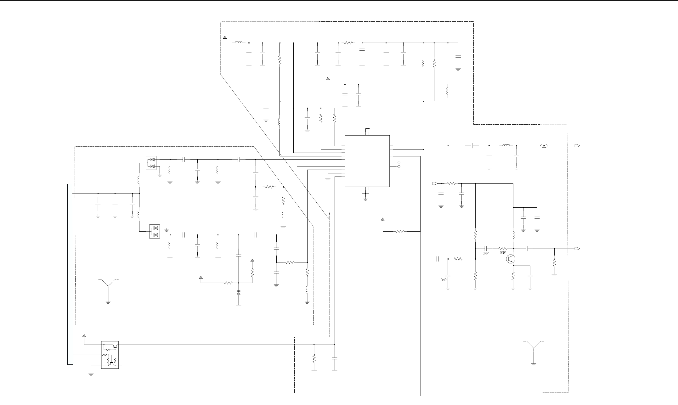
UHF2 25-40W PCB 8486577Z01 / Schematics 4-11
100.n
C2076
150.n
L204
3900pF
C2012
3900pF
C2030
DNP DNP
L203
150.n
D203 C2069
1.2p
6.2pF
C2064
100.0n
L211 L206
12.5n
2.4p
C2066
8.200p
100.0n
L213
C2063
L207
7.80n
D204
1
SH201
SHIELD
VCOShield
V_SF
Q201
C2062
12p
L214
47nH
47.
R232
R221
220.
C2057
5.1p
C2056
12pF
C2061
5.1p
VCO_MOD
V_SF
C2059
5.1p
C2073
1.p 5.1p
C2058
R233
47.
R212
47.K
6.8K
R211
47nH
L215
R222
220.
680nH
L201
120.p
C2038
V_SF
18.
R235
100n
C2009
V_SF
C2040
120.p
C2008
0.1uF
51.
R231
10n
C2022
680nH
L202
2.7K
R216
0662057A62
3.6K
R215
1.n
C2021
120.p
C2039
C2010
100n
C2042
120.p C2041
120.p
510.
R220
0.1uF
C2011
C2007
0.1uF
L209
100.0n
100.0n
L208
V_SF
1.K
R218
0.
R203
C2044
3.3p
C2043
6.8p
C2019
120.p
120.p
C2018
R230
75.
9R
IF200
1
2113740L13
6.2pF
C2071
L216
18.n
2113740L13
C2070
6.2pF
15p
C2060
TX_INJ
SHIELD
SH202
1
R223
220.
100n
C2003
C2037
120.p
2113740F53
120pF
C2065
C2032
120.p
R214
4.7K L212
33n
R227
82.
820.
1n R219
R213
C2031
13
2
4.7K
BFS540
Q200
RX_INJ
R201
10.K 120.p
C2029
NC
NC
19
TRB_IN
16
TX_BASE
15
TX_EMITTER
1
TX_IADJ
10
TX_OUT
13
TX_SWITCH
14
VCC_BUFFERS
18
VCC_LOGIC
GND_LOGIC
17
12
PRESC_OUT
5
RX_BASE
6
RX_EMITTER
2
RX_IADJ
8
RX_OUT
7
RX_SWITCH
3
SUPER_FLTR
50U54
U201
4
COLL_RFIN
20
FLIP_IN
11
GND_BUFFERS
9
GND_FLAG
D205
VCOBIC Shield
TO SHEET 2
UHF2 (438-470MHz) Synthesiser and VCO (Sht 2 of 2)
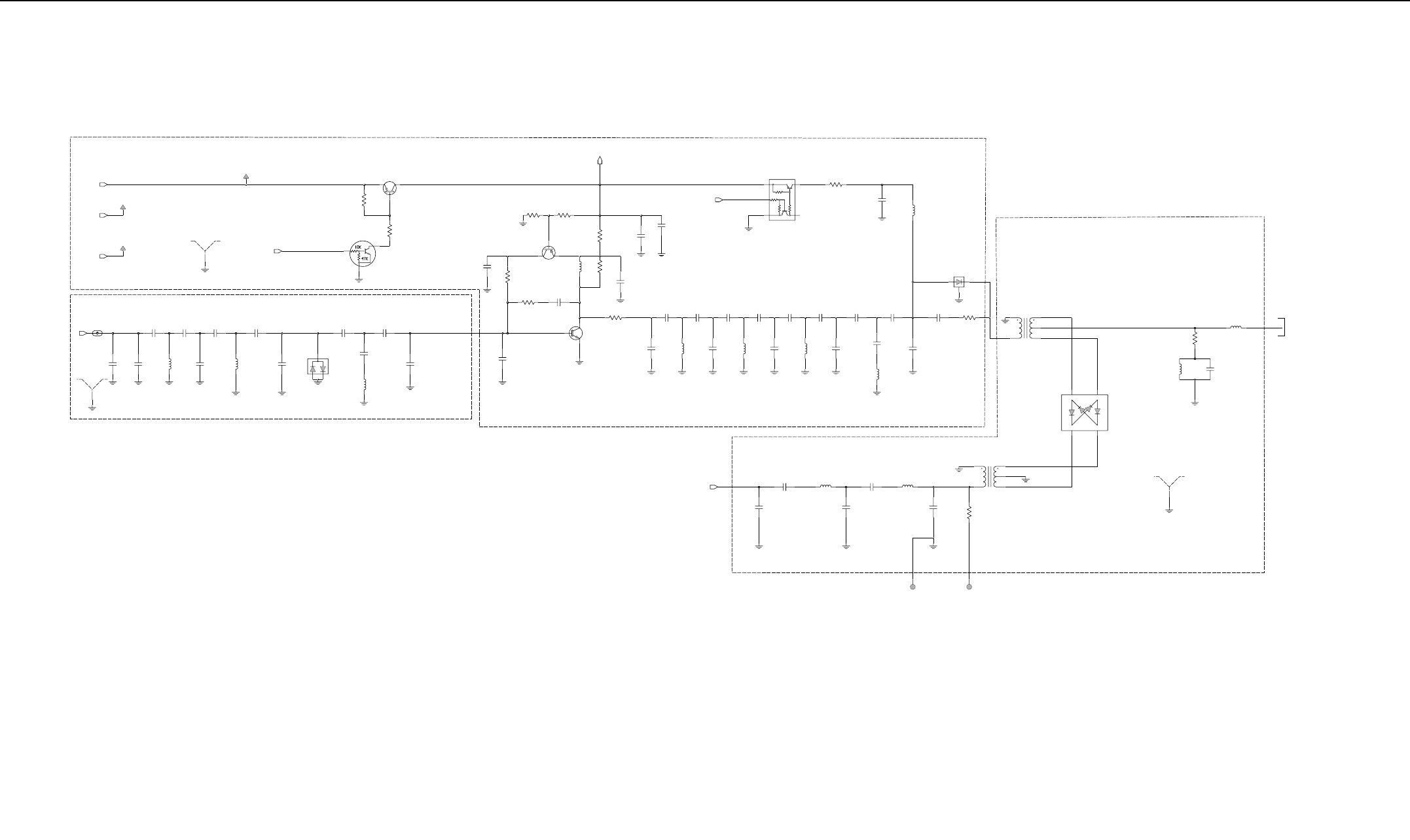
4-12 UHF2 25-40W PCB 8486577Z01 / Schematics
SH301
SHIELD
1
9V
3V
5V
3V
5V
9V
RX_EN
IF300
1
C1121
3.3pF
SH300
SHIELD
1
4.7p
C341
18.08n
18.08n L309
L300 C334
20.p
3.9p
C345
10.p
C338
2.4p
C340C339
2.4pF
C300
51.p
RX
C370
24.p
C328
43.p
8.2p
C368
L310
18.08n
CR301
82.p
C353
Q300
Q306
10.K
R346
R345
10.K
10.K
R300 R310
15.K
9R
R326
2.7K
Q301
120.p
C349
C326
2113743E07
.022uF
0662057A47
R330
820
L301
150.n
BFS540
Q303
36.p
C357
0662057A05
R347
15
220.
R336
C346
4.3p
39.p
C355
0.1uF
C351
2113743E20
1n
C323 120.p
C350
100
0662057A25
R331
Q304
LOC_DIST L304
150.n
120.p
C321
430.
R334
L314
18.08n
10.p
C330
12.p
C333
10.p
C335
36.p
C329C348
3.6p
C344 3.3p
C342
4.7p C347
3.6p
L313
18.08n
L312
18.08n
L311
18.08n C358
36.p
10.p
C332
3.6p
C343
10.p
C331
A4
K1
K3
U302
A2
T300
XFMR
4
6
3
1
2
R338
100.
C327
330p
4880142L01
D305
TP4
TEST_POINT
1
TEST_POINT
TP1
1
R301
470.
18.08n
L308
C367
8.2pF
4
6
3
1
2
XFMR
T301
C325
120.p 120.p
C324
C356
18.08n
L307
15pF
10pF
C366
RX_INJ 1
SH302
SHIELD
150.n C354
L302
51.
R340
82p
L306
2413926K32
560nH
DNP
DNP DNP
DNP DNP
DNP DNP FRONT-END SHIELD
MIXER SHIELD
DNP
TO SHEET 2
UHF2 (438-470MHz) Receiver Front and Back End (Sht 1 of 2)
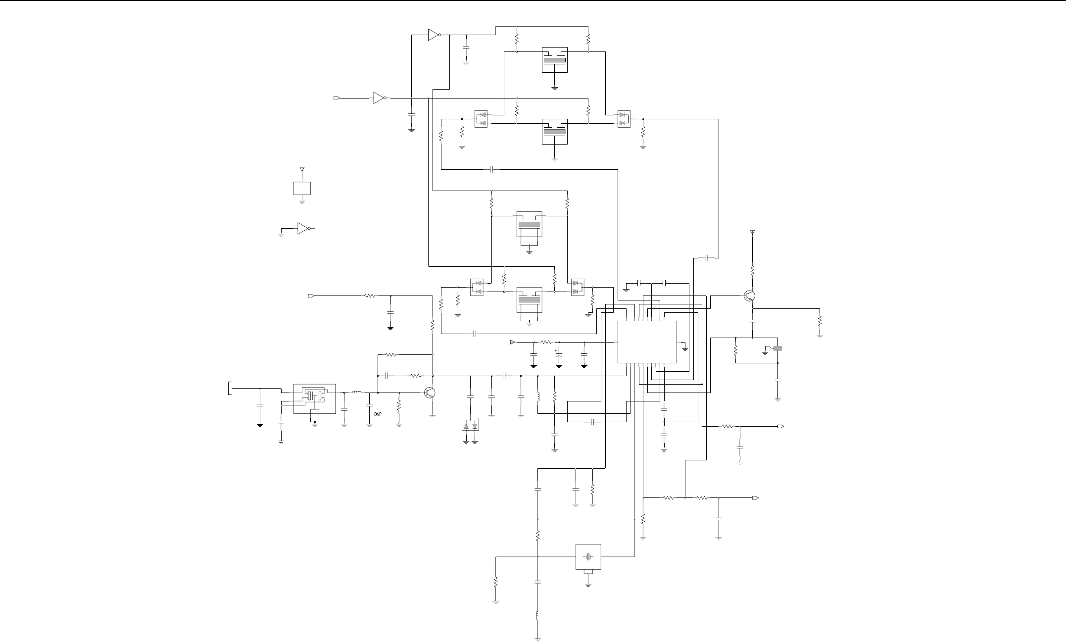
UHF2 25-40W PCB 8486577Z01 / Schematics 4-13
TC7W04F
U301
62
C312
100n
BW_SEL
3V
U301
TC7W04F
35
U301
PWR_GND
4
GND
8
VCC
R324
3.3K
D302
2.4K
R327
TC7W04F
U301
17
100n
C313
R306
20.K 12.K
R315
2
FLTR
FL301
GND
3
IN
1OUT
12.K
R316
OUT 2
FLTR
FL302
GND
3
IN
1
20.K
R305
0.1uF
C316
20.K
R307 R317
12.K
IN 2
OUT
FL304
CFWC455D
GND1
3
4
GND2
1
D304 D303
12.K
R318
2
OUT
FL303
CFWC455G
3
GND1
GND2
4
1IN
SA616
20.K
R308
0.1uF
C318
R319
12.K
560.
R333
R302
0.
R325
3.3K
C305
100n
R337
100.
C304
100n 4.7K
R322
R304
33.K
C369
8.2p
C336
9.1p
GND1
4
GND2
3IN 6
OUT
FREQ
FLTR_44.85M
FL300
2CC1
5CC2
1
R312
13.K
C364
22p
1.2u
L305
2113740F33
C362
18pF
12.K
R314
D301
C311
100n C310
100n
0.1uF
C317
R335
390.
Q302
C302
130.0p
1.2K
R329
R328
1.8K
C315
100n
1
455KHz
Y300
45B02
3
2
C309
100n
12.K
R313
RSSI
680.
R332
10.K
R320
DEMOD
C322
4.7n
C314
100n
C320
0.1uF
R321
8.2K
15.K
R309
C360
30p
R311
15.K
C359
33p
IN
06B09
44.395MHz
GND
2
GND1
4
OUT
31
Y301
30p
C361
L315
27nH
0.
R303
R339
10.0u
C301
51.
100n
C308
C307
100n
100n
R323
C306
4.7K
L303
1.2u
C371
2.7p
C337
6.8p
CR300
C303
100n
4802197J95
Q305
3V
C365
22p
0.1uF
C319
OSCIN
3
OSCOUT
10
QUADIN
1
RFIN
2
RFIN_DEC
5
RSSIOUT
9
RSSI_FEED
6
VCC
IFAMPOUT
19
IFAMP_DEC1
17
IFAMP_DEC2
14
LIMIN
11
LIMOUT
13
LIM_DEC1
12
LIM_DEC2
20
MIXOUT
4
U300
8
AUDIOOUT
7
AUDIO_FEED
15
GND
18
IFAMPIN
16
5V
3V
Check if it is 3v or another value
DNP
DNP
DNP
DNP
DNP
DNP
TO SHEET 2
UHF2 (438-470MHz) Receiver Front and Back End (Sht 2 of 2)
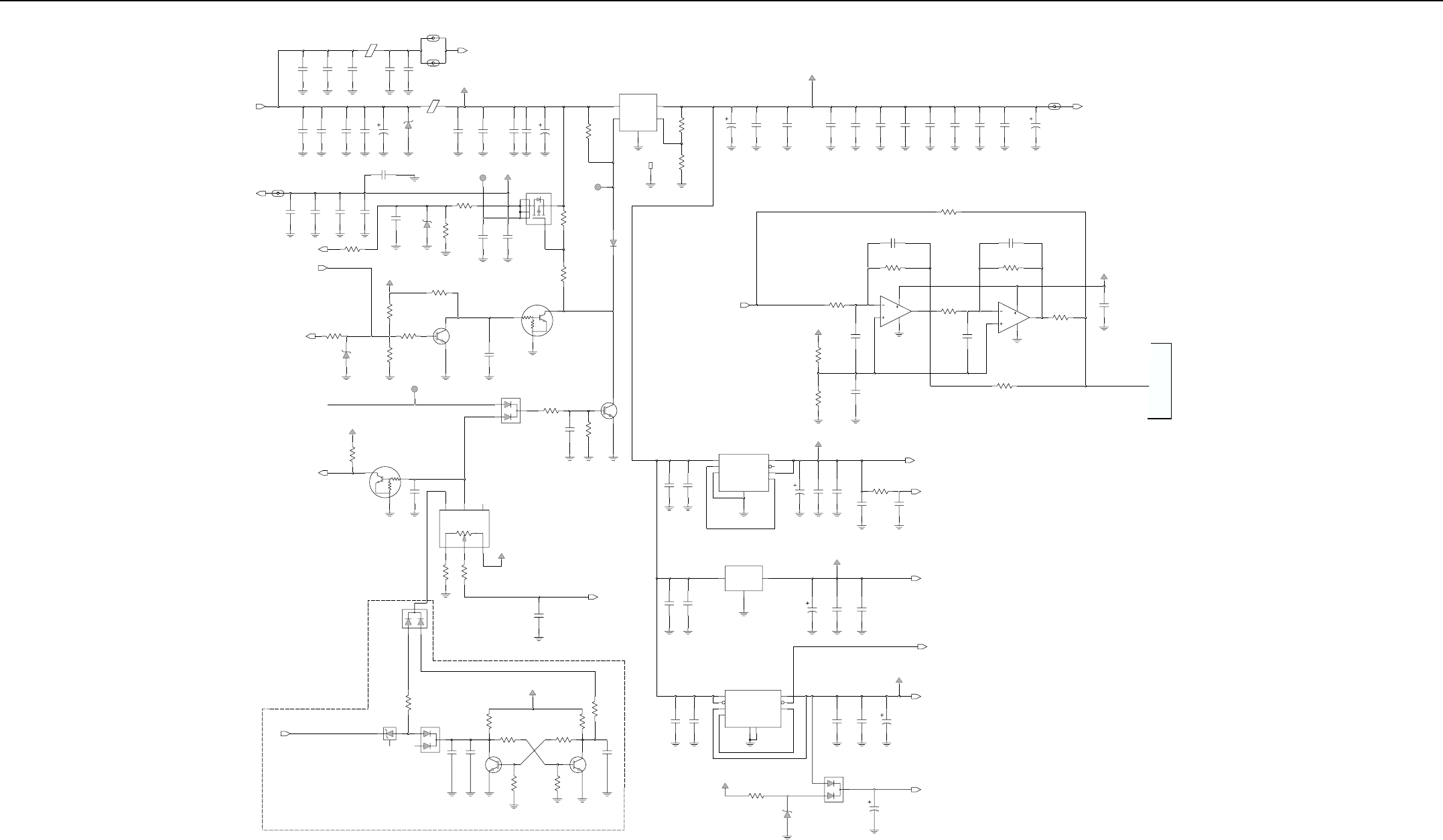
4-14 UHF2 25-40W PCB 8486577Z01 / Schematics
57R01
L120
120.p
C1113 39.p
C1097 39.p
C1088
1
1
IF502
IF503
C1114
39.p
C1098
120.p
COMP_B+
FILT_B+
1019447
L500
10.u
C5004
220.p
C5094
22.n
C5086
120.p
C5084
100.n
C5061
C5000
1n
28.0
VR500
C5085
22.n
C5083
120.p
C5060
100.n C5001
10.u
C5067
1n
33.K
R5038
TEST_POINT
TP500
1
U514
FILT_SW_B+
TP555
On/Off for ATE
Spacer for T0-220
TEST_POINT
1
D502
R5028
100.K
C5092
220.p
100.n
C5063
C5062
100.n
VR504
3.3
R5050
13.K
62.K
R5031
39.p
C1132
C1096
39.p
C1085
39.p
R5000
0.
BATT_SENSE
EMERGENCY_ACCES_CONN
IF504
1
C1128
39.p
FILT_SW_B+
B+
TP556
TEST_POINT
1
FILT_B+
47.K
R5036
3.3
VR503
D511
DC_POWER_ON
Come from Pin GCB2 of ASFIC
C5037
100.n
R5062
10.K
15.K
R5030
R5049
33.K
Q506
D3_3V
150.K
R5020
EMERGENCY_SENSE
100.K
R5029
Q502
47K
10K
M6
1%
1%
GND
3
ON_OFF
2
VIN
4
VOUT
5
U501
LM2941T
ADJ
1
C5005
100.u
9.3V
9.3V
SOURCE
R5081
6.34K
R5001
1.K
C1124
39.p
39.p
C1123
39.p
C1122
39.p
C1087 39.p
C1034
C5096
220.p
220.p
C5095
C5074
120.p
9V
C5015
100n
IF505
1
C1127
100.u
C1125
39.p
9V
5V
100n
C5118
C5117
16.p
R5097
0.
DNP
DNP
DNP
DNP
DNP
DNP
DNP
DNP
DNP
DNP
DNP
DNP
DNP
DNP
DNP
R5099
100.K
C5115
6.8p
R5094
R5093
220.K
1
8LM2904
U500
2
34R5100
1.M
0.
R5098
220.p
C5116
1.M 57
8
4
LM2904
U500
6
5V
1.u
C5114
220.p
C5113
R5096
100.K
R5095
200.K
R5092
100.K
10.M
R5002
100.n C5039
5V_CH
C5040 100.n
C5006
10.0u
C5068
120.p
100n
C5016
5V
DNP
DNP DNP
For mid_band
5V SOURCE
SOURCE
SOURCE
5V TO LVFRACN
1u
C5042
OUTPUT
2
SENSE
3
SHUTDOWN
6
5V_TAP
5
ERROR
7
FEEDBACK
4
GND
8
INPUT
1
LP2951C
U503
5V RF Regulator
3.3V RF Regulator
3.3V to IFIC, ASFIC
3.3V Digital REGULATOR
3.3V Digital
120.p
C5064
Q505
RESET
3V
10.0u
C5008 C5070
120.p
C5018
100n
3V
MC33269D
1GND
3IN 2
OUT
U508
1u
C5043
C5066
120.p
D3_3V
47u
C5007
120.p
C5069
C5017
D3_3V
100n
47u
VSTBY
C5120
D501
DNP
DNP
DNP
DNP
FILT_B+
VR502
3.9
R5103
24.K
GND2
9
4
INPUT
5
OUTPUT
6
SENSE
8
SHUTDOWN
TAP
3
LP2986ILDX
U510
ERROR
7
2
FEEDBACK
1
GND1
2.2u
C5041 C5065
120.p
100n
Place near uP
C5035
VOL_INDIRECT
D3_3V
100.
R5079
2
50.K
Indirect
Audio
Volume
3LOW
1HIGH 6
5
4
SWITCH
S5010
2.2K
R5071
10.u
C5104
47.K
47K
47K
DNP
R5035
Q504
ONOFF_SENSE
D500
10.u
C5119
R5069
10.K
R5037
10.K
R5089
1.M
R5082
51.K
1.n
C5110
R5074
1.K
D513
VR501
5.1
C5038
100.n
R5039
100.K
Q500
IGNITION
Smart Fuse Circuit
1.M
R5085
R5083
270.K
1.n
C5111
R5073
1.K
FILT_B+
R5048
24.K
Q503
DNP
DNP
DEMOD
DNP
SOURCE
POWER SUPPLY AUDIO
DNP
TO SHEET 1
UHF2 (438-470MHz) DC and Audio Circuits (Sht 1 of 2)
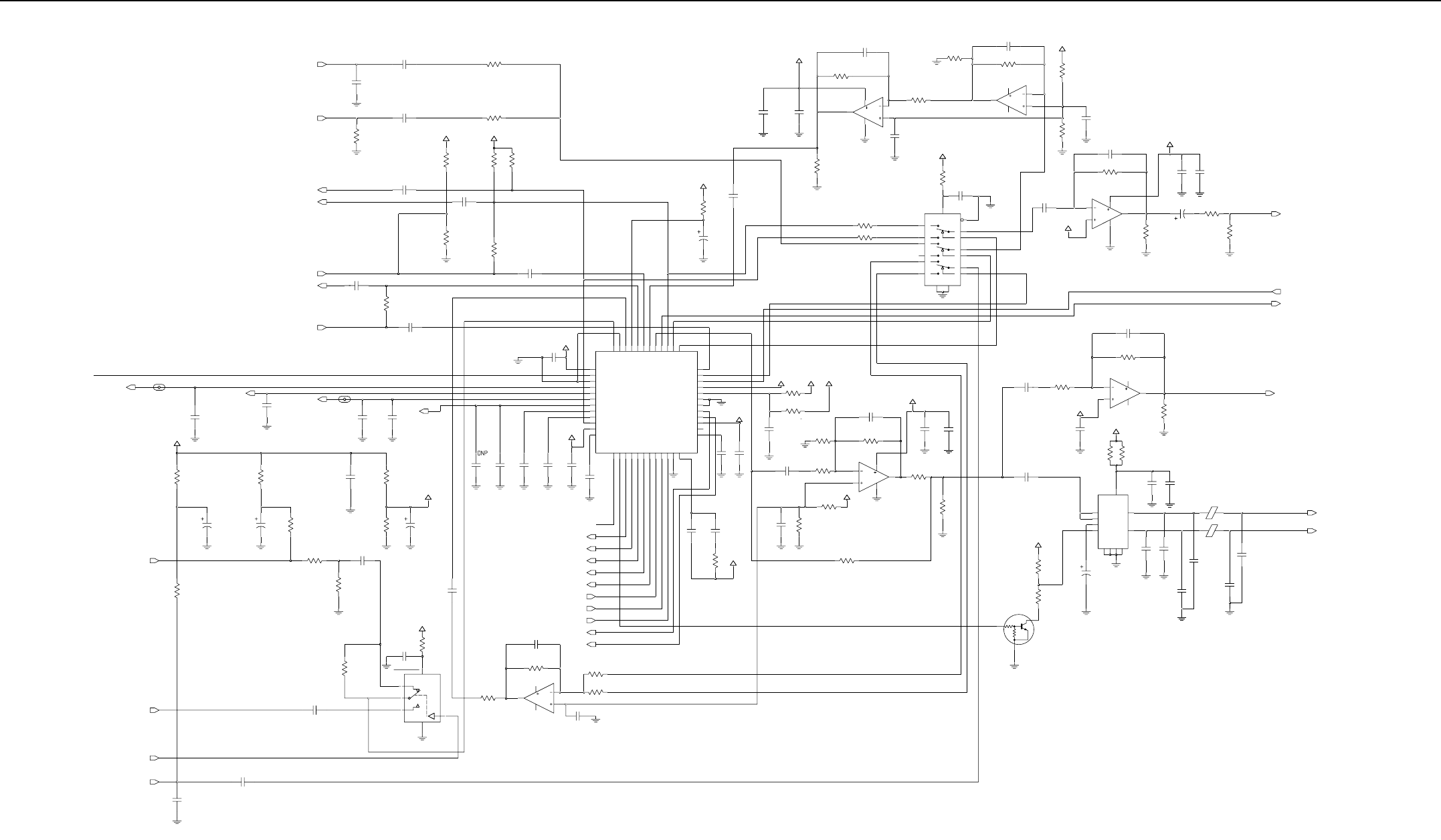
UHF2 25-40W PCB 8486577Z01 / Schematics 4-15
POST_LIMITER_FLAT_TX_AUDIO_RETURN_OPT_BRD
DETECTOR_AUDIO_SEND_OPT_BRD
UNMUTED_RX_AUDIO_SEND_OPT_BRD
FLAT_TX_AUDIO_INPUT_ACCESS_CONN
C5101
1.n
100.K
R5025
C5056
4.7uF
C5055
4.7uF
3V
R5044
24.K
100n
C5054
R5043
24.K
C5053
100n
30.K
R5040
100n
C5051
24.K
R5042
C5050
100n
RX_AUDIO_RETURN_OPT_BRD
TX_AUDIO_SEND_OPT_BRD
TX_AUDIO_RETURN_OPT_BRD
100n
C5052
3V
100n
C5022
8.2K
R5064
8.2K
R5063
3V
100.K
R5023
R5024
100.K
C5081
120.p
C5033
100n
9V
4.7uF
C5057
3V
4.7u
C5012
10.
R5080
C5078
1.n
C5090
82.p
6.2K
R5068
R5067
6.2K
0.
R5009
R5046
24.K
R5045
33.K
C5027
100n
3V
U506
LM29048 2
3
1
4
36K
0662057A86
R5034
47.K
R5032
15
Y0
2
Y1
1
4
Z
Z0
5
3Z1
EN6
GND
8VCC16
VEE
7
X14
X0
12
X1
13
Y
MC14053B
U509
11
A
10
B
C9
FLAT_TX_AUDIO_MUTE
100n
C5032
3V
R5057
10.K
10.K
R5056
82.p
C5089
R5022
100.K
U506
LM29046
5
78
4
C5088
82.p
R5065
6.2K
4.7uF
C5044 U505
LM2904
6
57
8
4
R5021
VAG
100.K
47u
C5003
C5030
100n
9V
R5087
100.K
R5086
560.
C5079
120.p
RX_AUDIO_OUTPUT_ACCESS_CONN
MOD_OUT
16.8MHz
SPKR+
SPKR-
HANDSET_RX_AUDIO_CH
1.5
R5017
0609887C05 0609887C05
R5018
1.5
C5080
120.p
120.p
C5076
1K
R5066
B+
TDA1519C
U502
U505
LM2904
2
31
8
4
VAG
100.n
C5021
2113740F53
C5087
120pF
R5019
0662057B05
200K
10.K
R5055
100n
C5049
C5048
100n
C5097
220.p
OUT2
3
RR
7
VCC
GND1
5
GND2
10
GND3
11
GND4
9
INV
8
M_SS
1
NINV
4
OUT1
6
2
FILT_SW_B+
120.p
C5073
120.p
C5072
24.K
R5041
12.K
R5051
47u
C5002
Q501
47K
10K
220.p
C5100
220.p
C5099
C5098
220.p
L502
1019447
L501
1019447
120.p
C1094
1IF507
C1093
39.p
PWR_SET
PA_CURRENT
PA_BIAS
9V
300.
R5077
C5010
10.0u C5009
10.0u
R5078
100.
510.
R5076
R5054
10.K
510.
R5075
EXTERNAL_MIC_AUDIO_ACCESS_CONN
VS_MIC
VS_AUDIO_SEL
C5045
1.u
C5071
MIC_AUDIO_CH
120.p
0.
R5047
100n
C5102
C5047
2.2K
100n
R5070
IF506
1
39.p
C1131
39.p
C1090
10.0u
C5011
VAG
VAG=4.5V
VOX
C5046
100n
C5019
100n
R5053
10.K
10.K
R5052 2.2u
C5014 100n
C5028
C5023
100n C5013
1u 100n
C5020 C5059
22n
3V
C5091
82.p
SQ_DET
uP_CLK
LSIO
HSIO
F1200
BW_SEL
DC_POWER_ON
ASFIC_CS
SPI_MOSI
CH_ACT
SPI_CLK
C5077
120.p
R5014
0. 270.K
R5027
33.K 4.7K
R5026 R5072
LM2904 6
5
78
4
U507
3V
R5084
0.
100.n
C5103
5
COM
GND
3
1
IN
4
NC
6
NO
VPOS
2
MAX4599EXT
U515
VOX
7
UIO
10
VDDA
1
VDDCP
32
VDDD
33
VDDDAC
11
VDDRC
45
VDDSYN
27
RXSND
39
SQCAP
12
SQDET
17
SQIN
9
SYN
28
TXRTN
36
TXSND
44
LSIO
18
MICEXT
48
MICINT
46
40
MOD
NC
26
PLCAP
8
25
PLCAP2
RXRTN
43
GNDA
3
GNDD
31
30
GNDDO
GNDRC
47
GNDSYN
23
HSIO
19
LCAP
24
GCB0
15
14
GCB1
GCB2
13
GCB3
35
GCB4
37
GCB5
38
20
CSX
DACG
6
DACR
5
DACU
4
DATA
22
DISC
2
F1200
29
AUDIO
41
AUXTN
42
CHACT
16
21
CLK
CLK168
34
30C53
U504
R5088
0.
C5034
100n
0.
3V 5V
R5011
0.
R5010
C5058
100n
10.K
R5058
3V
3V
C5029
100n
C5026
100n
FLAT_OR_DEEMPH_RX_AUD_SEL
3V
120.p
C5082
0.
R5013
3V
100.n
C5036 10.K
R5061
10.K
R5060
C5075
1n
R5016
1.M
10.K
R5059
100n
C5031
LM2904
U507
2
31
8
4
R5008
0.
3V
R5033
47.K
100n
C5025
C5024
100n
AUDIO_PA_EN
DNP
DNP
DNP
DNP
DNP
DNP
DNP
DNP
DNP
DNP
DNP
DNP
DNP
DNP
DNP
DNP
DNP
DNP
DNP DNP
DNP
DNP
DNP
USE NLAS4599
DNP IN MARLIN
DNP IN MARLIN+
UHF2 (438-470MHz) DC and Audio Circuits (Sht 2 of 2
)
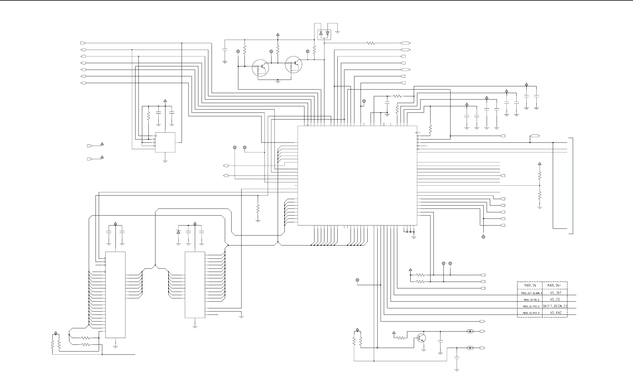
4-16 UHF2 25-40W PCB 8486577Z01 / Schematics
69
VRH 68
VRL
13 VSS
40 VSSL
87 VSSR
XFC 93
48
XIRQ
91
XTAL
76
PJ5 77
PJ6 78
PJ7
94
RESET
12
VDD
39
VDDL 88
VDDR
92
VDDSYN
51 PI5
50 PI6
49 PI7
71
PJ0_CSGP3 72
PJ1_CSGP4 73
PJ2 74
PJ3 75
PJ4
42 PH5_CSGP1
41 PH6_CSGP2
38 PH7_CSPROG
56 PI0
55 PI1
54 PI2
53 PI3
52 PI4
18 PG5_XA18
5PG6_AS
4
PG7_R_W
47 PH0_PW1
46 PH1_PW2
45 PH2_PW3
44 PH3_PW4
43 PH4_CSIO
23 PF6_ADDR6
22 PF7_ADDR7
29 PFO_ADDR0
6PG0_XA13
16 PG1_XA14
20 PG2_XA15
19 PG3_XA16
17 PG4_XA17
PE5_AN5 62
PE6_AN6 61
PE7_AN7 60
28 PF1_ADDR1
27 PF2_ADDR2
26 PF3_ADDR3
25 PF4_ADDR4
24 PF5_ADDR5
1
PD4_SCK 2
PD5_SS
PD6_LVIN 3
PE0_AN0 67
PE1_AN1 66
PE2_AN2 65
PE3_AN3 64
PE4_AN4 63
34 PC4_DATA4
35 PC5_DATA5
36 PC6_DATA6
37 PC7_DATA7
97
PD0_RXD 98
PD1_TXD 99
PD2_MISO 100
PD3_MOSI
15 PB5_ADDR13
8PB6_ADDR14
7PB7_ADDR15
14 PBO_ADDR8
30 PC0_DATA0
31 PC1_DATA1
32 PC2_DATA2
33 PC3_DATA3
83
PA4_OC4_OC1 84
PA5_OC3_OC1 85
PA6_OC2_OC1 86
PA7_PA1_OC1
10 PB1_ADDR9
11 PB2_ADDR10
9PB3_ADDR11
21 PB4_ADDR12
96
IRQ
LVOUT 95
58
MODA_LIR 57
MODB_VSTBY
79
PA0_IC3 80
PA1_IC2 81
PA2_IC1 82
PA3_IC4_OC5_OC1
U403
MC68HC11FL0
59
AVDD
70 AVSS
89
ECLK
90
EXTAL
A(5)
A(6)
A(7)
A(0)
A(14)
A(15)
A(16)
A(17)
A(18)
D(1)
D(2)
D(3)
D(4)
D(5)
D(6)
D(7)
A(9)
A(10)
A(11)
A(12)
A(13)
A(8)
D(0)
A(1)
A(2)
A(3)
A(4)
SHIFT_R_CS
SYNTH_CS
DISPLAY_CS_CH
SPI_MISO
SPI_MOSI
SPI_CLK
ASFIC_CS
FILT_SW_B+
D3_3V
FILT_SW_B+
D3_3V
SPI_MOSI
SPI_CLK
100n
C400
120.p C401
10.K
R438
D3_3V
3
1CS
7HOLD
6SCK
5SI
2
SO
8
VCC
4VSS
WP
U400
X25128-2.7
1
TEST_POINT
TP409
1
TP400
TEST_POINT
COMM_DATA_SEL_CH
LOC_DIST
1
TEST_POINT
TP410
1
TEST_POINT
TP404
1
TP406
TEST_POINT
C410
100n
10.K
R451 R450
10.K
Q400
Q407
10.K
R439
D400
D3_3V
R462
51.
SCI_CH
uP_CLK
OPT_DATA_R_OPBD
LSIO
HSIO
SQ_DET
CH_ACT
1
R471
10.
TEST_POINT
TP403
R425
C404
100n
100.K
10.K
R441
R_W
D3_3V
100n
C416
120.p C408
C415
D3_3V
120.p
D3_3V
100n
C407
120.p
C414 100n
C406
D3_3V
C413
120.p
C405
100n
RESET
F1200
D3_3V
100.K
R473
R472
100.K
TEST_POINT
TP407
1
PROG_IO-P8_I
PROG_IO-P14_I
PROG_IO-P12_I
MIC_PTT
MIC_SENSE
PROG_IN-P6_I
ACCESS_PTT
ONOFF_SENSE
VOL_INDIRECT
BATT_SENSE
EMERGENCY_SENSE
RSSI
VOX
TX_EN
SYNTH_LOCK
OPT_EN_OPBD
RX_EN
KEYPAD_COL_CH
KEYPAD_ROW_CH
TEST_POINT
TP402
1
TP401
TEST_POINT
1
R424
100.K
D3_3V
R423
100.K
1
IF401
1
39.p
IF400
C1083
C1078
39.p
10.K
R463
D3_3V
Q417
R443
D3_3V
3.3K
R442
10.K
1
TP425
TEST_POINT
R428
100.K
A(0:18)
D(0:7)
4.3
VR401 120.p
C411 100n
C402
D8
19
OE 22
VDD 28
VSS
14
WE 27
D3_3V
CS 20
D1
11
D2
12
D3
13
D4
15
D5
16
D6
17
D7
18
A2 8
A3 7
A4 6
A5 5
A6 4
A7 3
A8 25
A9 24
A0 10
A1 9
A10 21
A11 23
A12 2
A13 26
A14 1
U402
SRM2B256
A(0)
A(1)
A(10)
A(11)
A(12)
A(13)
A(14)
A(2)
A(3)
A(4)
A(5)
A(6)
A(7)
A(8)
A(9)
D(0)
D(1)
D(2)
D(3)
D(4)
D(5)
D(6)
D(7)
R_W
I_O5 27
I_O6 28
29
I_O7
I_O0 21
I_O1 22
I_O2 23
I_O3 25
I_O4 26
D(7)
D(6)
D(5)
D(4)
D(3)
D(2)
D(1)
D(0)
C412
120.p
C403
100n
D3_3V
GND
24
A13
A14
5
A15
11
A16
10
6A17
100.K
D3_3V
R427
100.K
R426 0.
R415
0.
R414
A(13)
A(14)
A(18)
A(17)
A(15)
A(16)
A18_RES
RESET
9
VCC8
EN_OE
32
EN_WE
7
A3
17
A4
16
A5
15
A6
14
A7
13
A8
3
A9
2
EN_CE
30
A11
1
A12
12
4
A2
18
AT49LV002N_70VI
U404
A0
20
A1
19
A10
31
A18_RES
A(10)
A(11)
A(12)
A(2)
A(3)
A(4)
A(5)
A(6)
A(7)
A(8)
A(9)
R_W
A(0)
A(1)
10K
10K
47K
47K
SPI_MISO
SPI_MOSI
SPI_CLK
ASFIC_CS
EE_CS
SYNTH_CS
DISPLAY_CS_CH
SHIFT_R_CS
PLACE NEAR U402
DNP
DNP DNP
DNP
DNP
DNP
DNP
DNP
DO NOT CONNECT THIS CS IN ORDER TO
PROVIDE WIRED OR OPERATION ON CSPROG
DNP
DNP
TO SHEET 1
UHF2 (438-470MHz) Microprocessor and Controller Circuits (Sht 1 of 2)
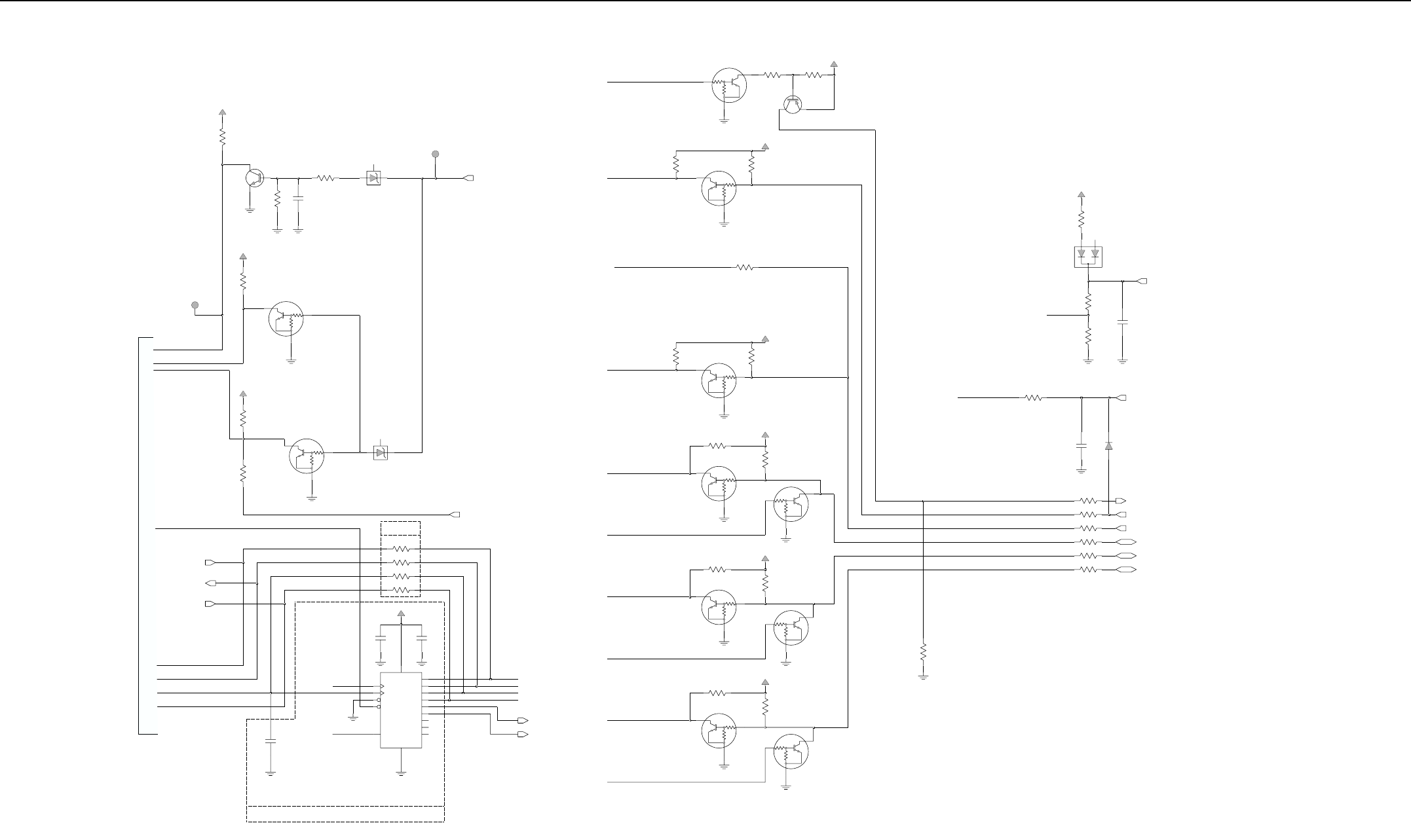
UHF2 25-40W PCB 8486577Z01 / Schematics 4-17
1
TP408
TEST_POINT
D3_3V
10.K
R445
Q414
R459
47.K
1.u
C490
10.K
R431
VR400
6.80
D3_3V
10.K
R444
Q415
TEST_POINT
TP405
1
BOOT_EN_IN_CH
R421
220.
Q403 R401
2.7K R460
FILT_SW_B+
1.5K
Q401
33.K
R436
D3_3V
3.3K
R457
Q412
SCI_CH
ACCESS_PTT
PROG_OUT-ALARM_4
39.K
R430
R429
100.K
D401
220.
R461
120.p
R458
D3_3V
C418
3.3K
MIC_PTT_CH
MIC_PTT
MIC_SENSE
HOOK_CH
120.p
C417
D402
R407 0.
0.
R406
0.
R405
0.
R404
R403 0.
R402 0.
PROG_I-ACC_C_3
PROG_O-ACC_C_4
PROG_I-ACC_C_6
PROG_IO-ACC_C_8
PROG_IO-ACC_C_12
PROG_IO-ACC_C_14
Q416
R435
33.K
D3_3V
R456
3.3K
R434 D3_3V
Q411
33.K
R455
3.3K
Q410
D3_3V
PROG_IO-P8_I
PROG_IO-P8_O
PROG_IN-P6_I
Q404
33.K
R433
3.3K
R454
Q409
D3_3V
R432
33.K
R453
3.3K
PROG_IO-P14_I
PROG_IO-P12_I
PROG_IO-P12_O
Q405
Q408
PROG_IO-P14_O
PROG_OUT-ALARM_4
PROG_IO-P8_O
PROG_IO-P12_O
PROG_IO-P14_O
VS_AUDIO_SEL
VS_GAIN_SEL
10.K
R470
D3_3V
R422
10.K
3.30
VR402
Q413
VS_INT
VS_RAC
VS_CS R469 0.
0.
R468
0.
0.
R466
R467
22.n
C421
SPI_CLK
SPI_MOSI
120.p
C422 100n
C423
D3_3V
RESET
10
SERIN
14
SEROUT
9
VCC 16
Q0 15
Q1 1
Q2 2
Q3 3
Q4 4
Q5 5
Q6 6
Q7 7
U405
MC74HC595A
CLK_L
12 CLK_S
11
EN_OE
13
GND
8
R440
10.K
VSTBY
DNP DNP
DNP
DNP
DNP
10K
47K
DNP
DNP IN MARLIN+
10K
47K
DNP IN MARLIN
10K
47K
47K
47K
47K
47K
47K
47K
47K
47K
47K
47K
10K
47K
10K
47K
10K
47K
EXT_ALARM_OUT
EXT_MIC_PTT
PROG_IN
PROG_I/O
PROG_I/O
PROG_I/O
TO SHEET 2
UHF2 (438-470MHz) Microprocessor and Controller Circuits (Sht 2 of 2)
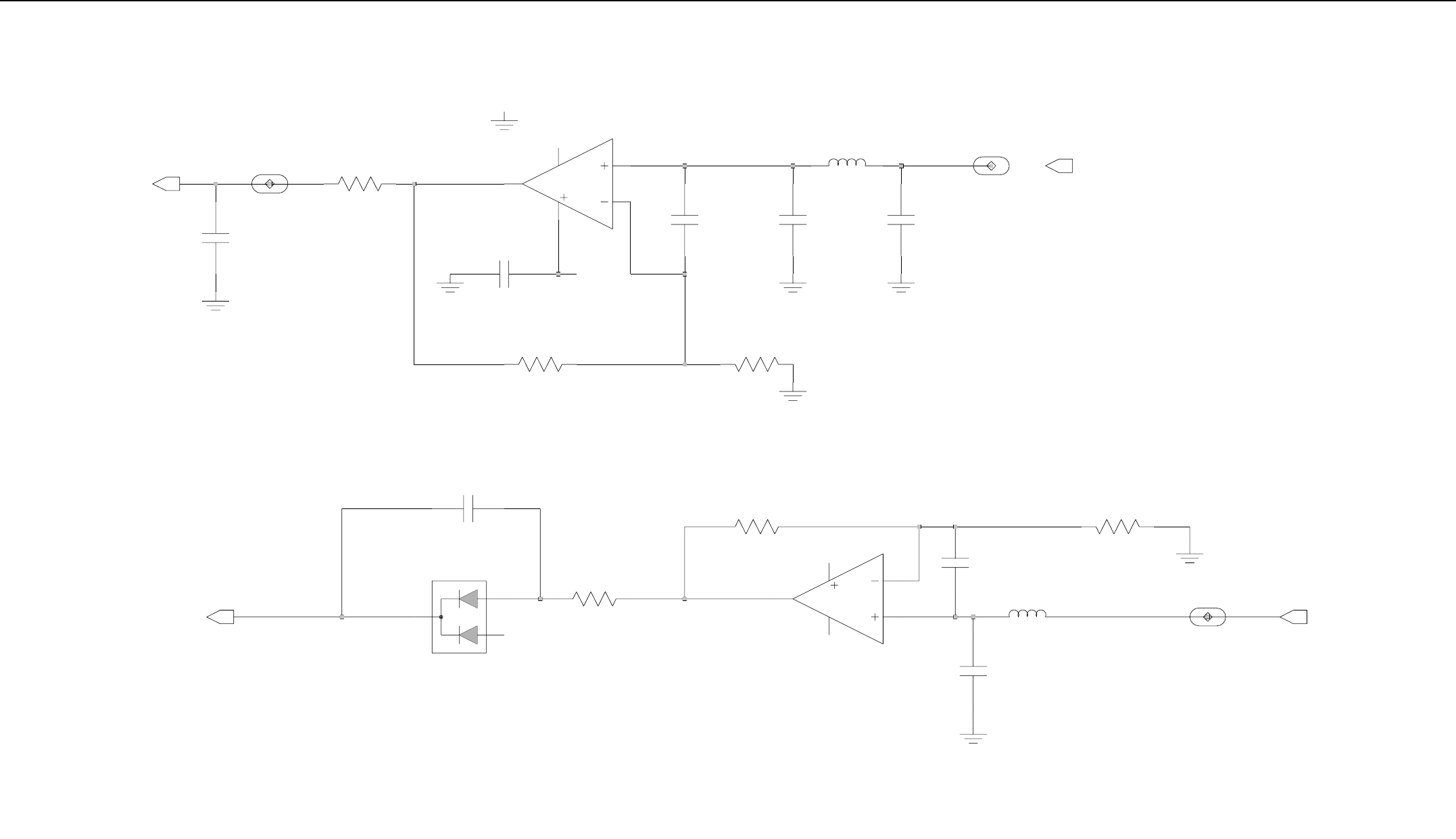
4-18 UHF2 25-40W PCB 8486577Z01 / Schematics
22.K
R141
0662057A81
C1082
39pF
IF701
1
INTEGRATOR
5180932W01
LM2904
U100
2
3
1
8
4
120.p
C1071
2113740F53
18K
R140
0662057A79
2113740F53
C1046
120.p
FILT_SW_B+
0662057A81
R146
22.K
C1049
120.p
D101
2113740F53
INTEGRATOR
LM2904
U100
6
5
7
8
4
5180932W01
0662057A81
R144
22K
0662057P02
15K
R117
39.p
2113740F41
C1075
120.p
C1045
2113740F53
2462587T30
1.u
L101
IF700
1
DET_VFWD
IF702
1
L102
1.u
2462587T30
R164
10K
0662057A73
2113740F53
120.p
2113740F53
C1047
C1048
120.p
VREV_BUFFER_IN
DNP
DNP
UHF2 (438-470MHz) Power Control Circuit
UHF2 25-40W PCB 8486577Z01 / Schematics 4-19
2.1 UHF2 PCB 8486577Z01 Parts List 40W
Circuit
Ref.
Motorola
Part No. Description
C1000 2113740F53 CAP CHIP REEL CL1 +/-30
120
C1001 2311049A08 KEMET CAPS
C1002 2111078B44 CAP CHIP RF 120 5 NPO
100V
C1004 2111078B18 CAP CHIP RF 15 5 NPO
100V
C1005 2111078B27 CAP CHIP RF 30 5 NPO
100V
C1006 2111078B18 CAP CHIP RF 15 5 NPO
100V
C1007 NOT PLACED GCAM DUMMY PART NUM-
BER
C1008 2111078B03 CAP CHIP RF 3.9.25 NPO
100V
C1009 NOT PLACED GCAM DUMMY PART NUM-
BER
C1010 2111078B18 CAP CHIP RF 15 5 NPO
100V
C1011 2111078B32 CAP ALT E12
C1012 NOT PLACED GCAM DUMMY PART NUM-
BER
C1013 2111078B01 CAP CHIP RF 3.3 .25 NPO
100V
C1014 2113740A19 CAP CHIP REEL CL1 +/-30
4.7
C1016 2111078B13 CAP ALT E16
C1017 NOT PLACED GCAM DUMMY PART NUM-
BER
C1020 2111078B13 CAP ALT E16
C1021 NOT PLACED GCAM DUMMY PART NUM-
BER
C1023 2111078B15 CAP CHIP RF 12 5 NPO
100V
C1025 NOT PLACED GCAM DUMMY PART NUM-
BER
C1026 2111078B08 CAP CHIP RF 6.2 .25NPO
100V
C1027 2389289U01 10UF 50V 20% ALUMINUM
SMD
C1028 2113743K15 CHIP CAP, CER 0.1UF
C1029 2113743K15 CHIP CAP, CER 0.1UF
C1031 2113741F37 CAP CHIP CL2 X7R REEL
3300
C1032 2113743E07 CER CHIP CAP .022UF
C1033 2113741F49 CAP CHIP CL2 X7R REEL
10000
C1034 2113740F41 CAP CHIP REEL CL1 +/-30
39
C1035 2113740F53 CAP CHIP REEL CL1 +/-30
120
C1036 2113743E20 CAP CHIP. 10 UF 10%
C1037 2113743E13 CAP CHIP 0.068UF
C1038 NOT PLACED GCAM DUMMY PART NUM-
BER
C1039 2113743E13 CAP CHIP 0.068UF
C1040 2113741F25 CAP CHIP CL2 X7R REEL
1000
C1041 2113740F67 CAP CHIP CL1 +/-30 470 5%
C1042 2113740F53 CAP CHIP REEL CL1 +/-30
120
C1043 2113740F53 CAP CHIP REEL CL1 +/-30
120
C1044 2113740F53 CAP CHIP REEL CL1 +/-30
120
C1045 2113740F53 CAP CHIP REEL CL1 +/-30
120
C1046 2113740F53 CAP CHIP REEL CL1 +/-30
120
C1047 2113740F53 CAP CHIP REEL CL1 +/-30
120
C1048 2113740F53 CAP CHIP REEL CL1 +/-30
120
Circuit
Ref.
Motorola
Part No. Description
C1049 2113740F53 CAP CHIP REEL CL1 +/-30
120
C1050 2113740F53 CAP CHIP REEL CL1 +/-30
120
C1051 2113740F53 CAP CHIP REEL CL1 +/-30
120
C1052 2113740F53 CAP CHIP REEL CL1 +/-30
120
C1053 2113740F57 CAP CHIP REEL CL1 +/-30
180
C1054 2113740F53 CAP CHIP REEL CL1 +/-30
120
C1055 2113740F53 CAP CHIP REEL CL1 +/-30
120
C1056 2113740F53 CAP CHIP REEL CL1 +/-30
120
C1057 2113740F53 CAP CHIP REEL CL1 +/-30
120
C1059 2113740F53 CAP CHIP REEL CL1 +/-30
120
C1060 NOT PLACED GCAM DUMMY PART NUM-
BER
C1061 NOT PLACED GCAM DUMMY PART NUM-
BER
C1062 2113740F53 CAP CHIP REEL CL1 +/-30
120
C1063 2113740F53 CAP CHIP REEL CL1 +/-30
120
C1064 2113740F53 CAP CHIP REEL CL1 +/-30
120
C1065 2113740F53 CAP CHIP REEL CL1 +/-30
120
C1066 2113740F53 CAP CHIP REEL CL1 +/-30
120
C1067 2113740F53 CAP CHIP REEL CL1 +/-30
120
C1068 2113740F53 CAP CHIP REEL CL1 +/-30
120
Circuit
Ref.
Motorola
Part No. Description
C1069 2113740F30 CAP CHIP REEL CL1+/-30
13
C1070 2113740F53 CAP CHIP REEL CL1 +/-30
120
C1071 2113740F53 CAP CHIP REEL CL1 +/-30
120
C1072 2113740F53 CAP CHIP REEL CL1 +/-30
120
C1073 2113740F53 CAP CHIP REEL CL1 +/-30
120
C1074 2113740F53 CAP CHIP REEL CL1 +/-30
120
C1075 2113740F41 CAP CHIP REEL CL1 +/-30
39
C1076 2113740F30 CAP CHIP REEL CL1+/-30
13
C1077 2113740F41 CAP CHIP REEL CL1 +/-30
39
C1078 2113740F41 CAP CHIP REEL CL1 +/-30
39
C1079 2113740F53 CAP CHIP REEL CL1 +/-30
120
C1080 2113740F41 CAP CHIP REEL CL1 +/-30
39
C1081 NOT PLACED GCAM DUMMY PART NUM-
BER
C1082 NOT PLACED GCAM DUMMY PART NUM-
BER
C1083 2113740F41 CAP CHIP REEL CL1 +/-30
39
C1084 2113740F41 CAP CHIP REEL CL1 +/-30
39
C1085 2113740F41 CAP CHIP REEL CL1 +/-30
39
C1086 2113740F41 CAP CHIP REEL CL1 +/-30
39
C1087 2113740F41 CAP CHIP REEL CL1 +/-30
39
Circuit
Ref.
Motorola
Part No. Description
4-20 UHF2 25-40W PCB 8486577Z01 / Schematics
C1088 2113740F41 CAP CHIP REEL CL1 +/-30
39
C1089 2113740F53 CAP CHIP REEL CL1 +/-30
120
C1090 NOT PLACED GCAM DUMMY PART NUM-
BER
C1091 NOT PLACED GCAM DUMMY PART NUM-
BER
C1092 NOT PLACED GCAM DUMMY PART NUM-
BER
C1093 NOT PLACED GCAM DUMMY PART NUM-
BER
C1094 2113740F53 CAP CHIP REEL CL1 +/-30
120
C1095 2113740F41 CAP CHIP REEL CL1 +/-30
39
C1096 2113740F41 CAP CHIP REEL CL1 +/-30
39
C1097 2113740F41 CAP CHIP REEL CL1 +/-30
39
C1098 2113740F53 CAP CHIP REEL CL1 +/-30
120
C1099 2113740F53 CAP CHIP REEL CL1 +/-30
120
C110 2113740F53 CAP CHIP REEL CL1 +/-30
120
C1100 2113740F53 CAP CHIP REEL CL1 +/-30
120
C1101 2113740F34 CAP CHIP REEL CL1 +/-30
20
C1102 2113740F34 CAP CHIP REEL CL1 +/-30
20
C1103 2113741A57 CAP CHIP 33K +-5%
(2160521A31
C1104 2113743E10 CAP CHIP .033 UF 10% X 7R
C1106 2113740F41 CAP CHIP REEL CL1 +/-30
39
C1107 2113740F53 CAP CHIP REEL CL1 +/-30
120
Circuit
Ref.
Motorola
Part No. Description
C1108 2113740F22 CAP CHIP REEL CL1 +/-30
6.2
C1109 2113740F41 CAP CHIP REEL CL1 +/-30
39
C1110 2113740F41 CAP CHIP REEL CL1 +/-30
39
C1111 2113740F41 CAP CHIP REEL CL1 +/-30
39
C1112 2113740F41 CAP CHIP REEL CL1 +/-30
39
C1113 2113740F53 CAP CHIP REEL CL1 +/-30
120
C1114 2113740F41 CAP CHIP REEL CL1 +/-30
39
C1115 2113740F41 CAP CHIP REEL CL1 +/-30
39
C1116 2113740F41 CAP CHIP REEL CL1 +/-30
39
C1117 2113740F38 CAP CHIP REEL CL1 +/-30
30
C1118 2113740F23 CAP CHIP REEL CL1 +/-30
6.8
C1119 2113740F53 CAP CHIP REEL CL1 +/-30
120
C1121 2113740F15 CAP CHIP REEL CL1 +/-30
3.3
C1122 2113740F41 CAP CHIP REEL CL1 +/-30
39
C1123 2113740F41 CAP CHIP REEL CL1 +/-30
39
C1124 2113740F41 CAP CHIP REEL CL1 +/-30
39
C1125 2113740F41 CAP CHIP REEL CL1 +/-30
39
C1126 2113740F53 CAP CHIP REEL CL1 +/-30
120
C1127 2360567A03 CAP TANTALUM
C1128 2113740F41 CAP CHIP REEL CL1 +/-30
39
Circuit
Ref.
Motorola
Part No. Description
C1129 2113740F41 CAP CHIP REEL CL1 +/-30
39
C1130 2113740F41 CAP CHIP REEL CL1 +/-30
39
C1131 NOT PLACED GCAM DUMMY PART NUM-
BER
C1132 2113740F41 CAP CHIP REEL CL1 +/-30
39
C1151 NOT PLACED GCAM DUMMY PART NUM-
BER
C1152 NOT PLACED GCAM DUMMY PART NUM-
BER
C1153 2113740F28 CAP CHIP REEL CL1 +/-30
11
C1154 2113740F33 CAP CHIP REEL CL1 +/-30
18
C1155 NOT PLACED GCAM DUMMY PART NUM-
BER
C1156 2113740A39 CAP CHIP REEL CL1 +/-30
27
C1157 NOT PLACED GCAM DUMMY PART NUM-
BER
C1251 2113740A23 CAP CHIP REEL CL1 +/-30
6.2
C1252 2113740A59 CHIP CAPACITORS 150PF
+-30%
C1253 2113740A31 CAP CHIP REEL CL1 +/-30
12
C1254 2113740A23 CAP CHIP REEL CL1 +/-30
6.2
C1255 2113740A59 CHIP CAPACITORS 150PF
+-30%
C1256 2113740A31 CAP CHIP REEL CL1 +/-30
12
C1258 2113740A42 CAP CHIP REEL CL1 +/-30
36
C1260 2113741F49 CAP CHIP CL2 X7R REEL
10000
Circuit
Ref.
Motorola
Part No. Description
C1261 2113740F53 CAP CHIP REEL CL1 +/-30
120
C1263 2113741F25 CAP CHIP CL2 X7R REEL
1000
C1264 2113743K15 CHIP CAP, CER 0.1UF
C1267 2113740A41 CAP CHIP REEL CL1 +/-30
33
C1268 NOT PLACED GCAM DUMMY PART NUM-
BER
C1269 2113740A41 CAP CHIP REEL CL1 +/-30
33
C1270 NOT PLACED GCAM DUMMY PART NUM-
BER
C1271 2113740F53 CAP CHIP REEL CL1 +/-30
120
C1272 2113743E10 CAP CHIP .033 UF 10% X 7R
C1273 2111078B44 CAP CHIP RF 120 5 NPO
100V
C1274 2111078B27 CAP CHIP RF 30 5 NPO
100V
C1275 2111078B18 CAP CHIP RF 15 5 NPO
100V
C1276 NOT PLACED GCAM DUMMY PART NUM-
BER
C1277 2111078B03 CAP CHIP RF 3.9.25 NPO
100V
C1278 NOT PLACED GCAM DUMMY PART NUM-
BER
C1279 NOT PLACED GCAM DUMMY PART NUM-
BER
C1280 2111078B03 CAP CHIP RF 3.9.25 NPO
100V
C1281 2113740F53 CAP CHIP REEL CL1 +/-30
120
C1282 2113740F53 CAP CHIP REEL CL1 +/-30
120
C1283 2113740F53 CAP CHIP REEL CL1 +/-30
120
Circuit
Ref.
Motorola
Part No. Description
UHF2 25-40W PCB 8486577Z01 / Schematics 4-21
C2000 2113743F18 CAP CHIP 2.2 UF 16V +80-
20%
C2001 2311049J11 CAPACITOR TANT 10%
4.7UF
C2002 2311049A72 CAP TANT CHIP 10.0UF
10% 10V
C2003 2113743K15 CHIP CAP, CER 0.1UF
C2004 2113743F18 CAP CHIP 2.2 UF 16V +80-
20%
C2005 2113743F18 CAP CHIP 2.2 UF 16V +80-
20%
C2006 2113743F18 CAP CHIP 2.2 UF 16V +80-
20%
C2007 2113743E20 CAP CHIP. 10 UF 10%
C2008 2113743E20 CAP CHIP. 10 UF 10%
C2009 2113743E20 CAP CHIP. 10 UF 10%
C2010 2113743E20 CAP CHIP. 10 UF 10%
C2011 2113743E20 CAP CHIP. 10 UF 10%
C2012 NOT PLACED GCAM DUMMY PART NUM-
BER
C2013 2113743E20 CAP CHIP. 10 UF 10%
C2014 2113743E20 CAP CHIP. 10 UF 10%
C2015 2113743E20 CAP CHIP. 10 UF 10%
C2016 2113743E20 CAP CHIP. 10 UF 10%
C2017 2113743E20 CAP CHIP. 10 UF 10%
C2018 2113740F53 CAP CHIP REEL CL1 +/-30
120
C2019 2113740F53 CAP CHIP REEL CL1 +/-30
120
C2020 2113743E20 CAP CHIP. 10 UF 10%
C2021 2113741F25 CAP CHIP CL2 X7R REEL
1000
C2022 2113741F49 CAP CHIP CL2 X7R REEL
10000
C2023 2113741F49 CAP CHIP CL2 X7R REEL
10000
Circuit
Ref.
Motorola
Part No. Description
C2024 2113741F49 CAP CHIP CL2 X7R REEL
10000
C2025 2113741F49 CAP CHIP CL2 X7R REEL
10000
C2026 2113741F49 CAP CHIP CL2 X7R REEL
10000
C2027 2113741F49 CAP CHIP CL2 X7R REEL
10000
C2028 2113741F33 CAP CHIP CL2 X7R REEL
2200
C2029 2113740F53 CAP CHIP REEL CL1 +/-30
120
C2030 2113741F39 CAP CHIP CL2 XTR REEL
3900
C2031 NOT PLACED GCAM DUMMY PART NUM-
BER
C2032 2113740F53 CAP CHIP REEL CL1 +/-30
120
C2033 2113740F53 CAP CHIP REEL CL1 +/-30
120
C2034 2113740F53 CAP CHIP REEL CL1 +/-30
120
C2035 2113740F53 CAP CHIP REEL CL1 +/-30
120
C2036 2113740F53 CAP CHIP REEL CL1 +/-30
120
C2037 2113740F53 CAP CHIP REEL CL1 +/-30
120
C2038 2113740F53 CAP CHIP REEL CL1 +/-30
120
C2039 2113740F53 CAP CHIP REEL CL1 +/-30
120
C2040 2113740F53 CAP CHIP REEL CL1 +/-30
120
C2041 2113740F53 CAP CHIP REEL CL1 +/-30
120
C2042 2113740F53 CAP CHIP REEL CL1 +/-30
120
Circuit
Ref.
Motorola
Part No. Description
C2043 2113740L14 CAP CER CHIP 6.8PF +-
0.1PF
C2044 NOT PLACED GCAM DUMMY PART NUM-
BER
C2045 2113740F53 CAP CHIP REEL CL1 +/-30
120
C2046 2113740F53 CAP CHIP REEL CL1 +/-30
120
C2047 2113740F53 CAP CHIP REEL CL1 +/-30
120
C2048 2113740F53 CAP CHIP REEL CL1 +/-30
120
C2049 NOT PLACED GCAM DUMMY PART NUM-
BER
C2050 2113740F53 CAP CHIP REEL CL1 +/-30
120
C2051 2113740F59 CAP CHIP REEL CL1 +/-30
220
C2052 2113740F53 CAP CHIP REEL CL1 +/-30
120
C2053 NOT PLACED GCAM DUMMY PART NUM-
BER
C2054 2113740L37 CAP 62.0 PF 50V 2.0%
C2055 2113740F35 CAP CHIP REEL CL1 +/-30
22
C2056 2113740F20 CAP CHIP REEL CL1 +/-30
5.1
C2057 2113740F20 CAP CHIP REEL CL1 +/-30
5.1
C2058 2113740F20 CAP CHIP REEL CL1 +/-30
5.1
C2059 2113740F20 CAP CHIP REEL CL1 +/-30
5.1
C2060 2113740F31 CAP CHIP REEL CL1 +/-30
15
C2061 2113740A31 CAP CHIP REEL CL1 +/-30
12
C2062 2113740F29 CAP CHIP REEL CL1 +/-30
12
Circuit
Ref.
Motorola
Part No. Description
C2063 2113740L16 CAP CER CHIP 8.2 PF+-
0.1PF
C2064 2113740A23 CAP CHIP REEL CL1 +/-30
6.2
C2065 2113740F53 CAP CHIP REEL CL1 +/-30
120
C2066 2113740L03 CAP CER CHIP 2.4PF +-
0.1PF
C2067 2113740F20 CAP CHIP REEL CL1 +/-30
5.1
C2068 2113740F20 CAP CHIP REEL CL1 +/-30
5.1
C2069 2113740F05 CAP CHIP REEL CL1 +/-30
1.2
C2070 2113740L13 CAP CER CHIP 6.2 PF+-
0.1PF
C2071 2113740L13 CAP CER CHIP 6.2 PF+-
0.1PF
C2072 2113740L04 CAP CER CHIP 2.7 PF +-
0.1PF
C2073 2113740F03 CAP CHIP REEL CL1 +/-30
1.0
C2074 2109720D14 CAP CER CHIP LOW DIST
0.1UF
C2076 NOT PLACED GCAM DUMMY PART NUM-
BER
C2078 0886629Z02 CAP,FILM,1UF,+10%,--
10%,63V-D
C2129 2113740F53 CAP CHIP REEL CL1 +/-30
120
C2198 2113741F25 CAP CHIP CL2 X7R REEL
1000
C300 NOT PLACED GCAM DUMMY PART NUM-
BER
C301 2311049A57 CAP TANT CHIP A/P 10UF
10% 16
C302 2113740F54 CAP CHIP REEL CL1+/-30
130
C303 2113743K15 CHIP CAP, CER 0.1UF
Circuit
Ref.
Motorola
Part No. Description
4-22 UHF2 25-40W PCB 8486577Z01 / Schematics
C304 2113743E20 CAP CHIP. 10 UF 10%
C305 2113743E20 CAP CHIP. 10 UF 10%
C306 2113743E20 CAP CHIP. 10 UF 10%
C307 2113743E20 CAP CHIP. 10 UF 10%
C308 2113743E20 CAP CHIP. 10 UF 10%
C309 2113743E20 CAP CHIP. 10 UF 10%
C310 2113743E20 CAP CHIP. 10 UF 10%
C311 2113743E20 CAP CHIP. 10 UF 10%
C312 2113743E20 CAP CHIP. 10 UF 10%
C313 2113743E20 CAP CHIP. 10 UF 10%
C314 2113743E20 CAP CHIP. 10 UF 10%
C315 2113743E20 CAP CHIP. 10 UF 10%
C316 2113743E20 CAP CHIP. 10 UF 10%
C317 2113743E20 CAP CHIP. 10 UF 10%
C318 2113743E20 CAP CHIP. 10 UF 10%
C319 2113743E20 CAP CHIP. 10 UF 10%
C320 2113743E20 CAP CHIP. 10 UF 10%
C321 2113740F53 CAP CHIP REEL CL1 +/-30
120
C322 2113741F41 CAP CHIP CL2 X7R REEL
4700
C323 2113741F25 CAP CHIP CL2 X7R REEL
1000
C324 2113740F53 CAP CHIP REEL CL1 +/-30
120
C325 2113740F53 CAP CHIP REEL CL1 +/-30
120
C326 2113743E07 CER CHIP CAP .022UF
C327 2113741F13 CAP CHIP CL2 X7R REEL
330
C328 2113740F42 CAP CHIP REEL CL1 +/-30
43
C329 2113740L31 CAP 36.0 PF 50V 2.0 %
C330 2113740L18 CAP CER CHIP 10.0 PF +/-
.25PF
Circuit
Ref.
Motorola
Part No. Description
C331 2113740L18 CAP CER CHIP 10.0 PF +/-
.25PF
C332 2113740L18 CAP CER CHIP 10.0 PF +/-
.25PF
C333 2113740L20 CAP 12.0 PF 50V 2.0 %
C334 2113740L25 CAP CER CHIP 20.0 PF +/-
.25PF
C335 2113740L18 CAP CER CHIP 10.0 PF +/-
.25PF
C336 2113740L17 CAP CER CHIP 9.1 PF+-
0.1PF
C337 2113740L14 CAP CER CHIP 6.8PF +-
0.1PF
C338 2113740L18 CAP CER CHIP 10.0 PF +/-
.25PF
C339 2113740L03 CAP CER CHIP 2.4PF +-
0.1PF
C340 2113740L03 CAP CER CHIP 2.4PF +-
0.1PF
C341 2113740F19 CAP CHIP REEL CL1 +/-30
4.7
C342 2113740F19 CAP CHIP REEL CL1 +/-30
4.7
C343 2113740L07 CAP CER CHIP 3.6PF +-
0.1PF
C344 2113740L07 CAP CER CHIP 3.6PF +-
0.1PF
C345 2113740L08 CAP CER CHIP 3.9 PF+/-
0.1PF
C346 2113740L09 CAP CER CHIP 4.3 PF +-
0.1PF
C347 2113740L07 CAP CER CHIP 3.6PF +-
0.1PF
C348 2113740L06 CAP CER CHIP 3.3 PF+/-
0.1PF
C349 2113740F53 CAP CHIP REEL CL1 +/-30
120
C350 2113740F53 CAP CHIP REEL CL1 +/-30
120
Circuit
Ref.
Motorola
Part No. Description
C351 2113743E20 CAP CHIP. 10 UF 10%
C352 0662057A05 CHIP RES 15 OHMS 5%
C353 NOT PLACED GCAM DUMMY PART NUM-
BER
C354 2113740F49 CAP CHIP REEL CL1 +/-30
82
C355 NOT PLACED GCAM DUMMY PART NUM-
BER
C356 2113740L22 CAP 15.0 PF 50V 2.0 %
C357 NOT PLACED GCAM DUMMY PART NUM-
BER
C358 NOT PLACED GCAM DUMMY PART NUM-
BER
C359 2113740F39 CAP CHIP REEL CL1 +/-30
33
C360 2113740F38 CAP CHIP REEL CL1 +/-30
30
C361 NOT PLACED GCAM DUMMY PART NUM-
BER
C362 2113740F33 CAP CHIP REEL CL1 +/-30
18
C364 NOT PLACED GCAM DUMMY PART NUM-
BER
C365 NOT PLACED GCAM DUMMY PART NUM-
BER
C366 2113740L18 CAP CER CHIP 10.0 PF +/-
.25PF
C367 2113740L16 CAP CER CHIP 8.2 PF+-
0.1PF
C368 2113740F25 CAP CHIP REEL CL1+/-30
8.2
C369 2113740F25 CAP CHIP REEL CL1+/-30
8.2
C370 2113740L27 CAP 24.0 PF 50V 2.0 %
C371 NOT PLACED GCAM DUMMY PART NUM-
BER
C400 2113740F53 CAP CHIP REEL CL1 +/-30
120
Circuit
Ref.
Motorola
Part No. Description
C401 2113743K15 CHIP CAP, CER 0.1UF
C402 NOT PLACED GCAM DUMMY PART NUM-
BER
C403 2113743K15 CHIP CAP, CER 0.1UF
C404 2113743K15 CHIP CAP, CER 0.1UF
C405 2113743K15 CHIP CAP, CER 0.1UF
C406 2113743K15 CHIP CAP, CER 0.1UF
C407 2113743K15 CHIP CAP, CER 0.1UF
C408 2113743K15 CHIP CAP, CER 0.1UF
C410 2113743K15 CHIP CAP, CER 0.1UF
C411 NOT PLACED GCAM DUMMY PART NUM-
BER
C412 2113740F53 CAP CHIP REEL CL1 +/-30
120
C413 2113740F53 CAP CHIP REEL CL1 +/-30
120
C414 2113740F53 CAP CHIP REEL CL1 +/-30
120
C415 2113740F53 CAP CHIP REEL CL1 +/-30
120
C416 2113740F53 CAP CHIP REEL CL1 +/-30
120
C417 2113740F53 CAP CHIP REEL CL1 +/-30
120
C418 2113740F53 CAP CHIP REEL CL1 +/-30
120
C421 2113743E07 CER CHIP CAP .022UF
C422 2113740F53 CAP CHIP REEL CL1 +/-30
120
C423 2113743K15 CHIP CAP, CER 0.1UF
C490 NOT PLACED GCAM DUMMY PART NUM-
BER
C5000 2113741F25 CAP CHIP CL2 X7R REEL
1000
C5001 2389289U01 10UF 50V 20% ALUMINUM
SMD
Circuit
Ref.
Motorola
Part No. Description
UHF2 25-40W PCB 8486577Z01 / Schematics 4-23
C5002 2311049A99 CAP TANT CHIP 47 UF 10V
20%
C5003 2311049A99 CAP TANT CHIP 47 UF 10V
20%
C5004 NOT PLACED GCAM DUMMY PART NUM-
BER
C5005 2360567A03 CAP TANTALUM
C5006 2311049A57 CAP TANT CHIP A/P 10UF
10% 16
C5007 2311049A99 CAP TANT CHIP 47 UF 10V
20%
C5008 2311049A57 CAP TANT CHIP A/P 10UF
10% 16
C5009 2311049A57 CAP TANT CHIP A/P 10UF
10% 16
C5010 2311049A57 CAP TANT CHIP A/P 10UF
10% 16
C5011 2311049A57 CAP TANT CHIP A/P 10UF
10% 16
C5012 2311049A56 CAP TAN CHIP A/P 4.7 20 10
C5013 2113928P04 CAP CER CHIP 1.0UF 20%
6.3V
C5014 NOT PLACED GCAM DUMMY PART NUM-
BER
C5015 2113743K15 CHIP CAP, CER 0.1UF
C5016 2113743K15 CHIP CAP, CER 0.1UF
C5017 2113743K15 CHIP CAP, CER 0.1UF
C5018 2113743K15 CHIP CAP, CER 0.1UF
C5019 2113743K15 CHIP CAP, CER 0.1UF
C5020 2113743K15 CHIP CAP, CER 0.1UF
C5021 2113741M69 CAP CHIP CLS2 100000 PF
20V 1
C5022 2113743K15 CHIP CAP, CER 0.1UF
C5023 2113743K15 CHIP CAP, CER 0.1UF
C5024 2113743K15 CHIP CAP, CER 0.1UF
C5025 2113743K15 CHIP CAP, CER 0.1UF
Circuit
Ref.
Motorola
Part No. Description
C5026 2113743K15 CHIP CAP, CER 0.1UF
C5027 2113743K15 CHIP CAP, CER 0.1UF
C5028 2113743K15 CHIP CAP, CER 0.1UF
C5029 2113743K15 CHIP CAP, CER 0.1UF
C5030 2113743K15 CHIP CAP, CER 0.1UF
C5031 2113743K15 CHIP CAP, CER 0.1UF
C5032 2113743K15 CHIP CAP, CER 0.1UF
C5033 2113743K15 CHIP CAP, CER 0.1UF
C5034 2113743K15 CHIP CAP, CER 0.1UF
C5035 2113743K15 CHIP CAP, CER 0.1UF
C5036 2113743K15 CHIP CAP, CER 0.1UF
C5037 2113743K15 CHIP CAP, CER 0.1UF
C5038 2113743K15 CHIP CAP, CER 0.1UF
C5039 NOT PLACED GCAM DUMMY PART NUM-
BER
C5040 NOT PLACED GCAM DUMMY PART NUM-
BER
C5041 2113743F18 CAP CHIP 2.2 UF 16V +80-
20%
C5042 2113743F16 CAP CHIP 1.0UF 16V+80-
20%
C5043 2113743F16 CAP CHIP 1.0UF 16V+80-
20%
C5044 2113928C04 CAP CER CHIP 4.7UF
6.3V10%080
C5045 2113743F16 CAP CHIP 1.0UF 16V+80-
20%
C5046 2113743E20 CAP CHIP. 10 UF 10%
C5047 2113743E20 CAP CHIP. 10 UF 10%
C5048 2113743E20 CAP CHIP. 10 UF 10%
C5049 2113743E20 CAP CHIP. 10 UF 10%
C5050 2113743E20 CAP CHIP. 10 UF 10%
C5051 2113743E20 CAP CHIP. 10 UF 10%
(CM160)
C5052 2113743E20 CAP CHIP. 10 UF 10%
Circuit
Ref.
Motorola
Part No. Description
C5053 2113743E20 CAP CHIP. 10 UF 10%
(CM160)
C5054 2113743E20 CAP CHIP. 10 UF 10%
(CM160)
C5055 2113928C04 CAP CER CHIP 4.7UF
6.3V10%080
C5056 2113741M69 CAP CHIP CLS2 100000 PF
20V 1 (CM160)
C5057 2113928C04 CAP CER CHIP 4.7UF
6.3V10%080
C5058 NOT PLACED GCAM DUMMY PART NUM-
BER
C5059 2113743E07 CER CHIP CAP .022UF
C5060 2113741M69 CAP CHIP CLS2 100000 PF
20V 1
C5061 2113741M69 CAP CHIP CLS2 100000 PF
20V 1
C5062 2113741M69 CAP CHIP CLS2 100000 PF
20V 1
C5063 2113741M69 CAP CHIP CLS2 100000 PF
20V 1
C5064 2113740F53 CAP CHIP REEL CL1 +/-30
120
C5065 2113740F53 CAP CHIP REEL CL1 +/-30
120
C5066 2113740F53 CAP CHIP REEL CL1 +/-30
120
C5067 2113741F25 CAP CHIP CL2 X7R REEL
1000
C5068 2113740F53 CAP CHIP REEL CL1 +/-30
120
C5069 2113740F53 CAP CHIP REEL CL1 +/-30
120
C5070 2113740F53 CAP CHIP REEL CL1 +/-30
120
C5071 2113740F53 CAP CHIP REEL CL1 +/-30
120
C5072 2113740F53 CAP CHIP REEL CL1 +/-30
120
Circuit
Ref.
Motorola
Part No. Description
C5073 2113740F53 CAP CHIP REEL CL1 +/-30
120
C5074 2113740F53 CAP CHIP REEL CL1 +/-30
120
C5075 NOT PLACED GCAM DUMMY PART NUM-
BER
C5076 2113740F53 CAP CHIP REEL CL1 +/-30
120
C5077 2113740F53 CAP CHIP REEL CL1 +/-30
120
C5078 2113741F25 CAP CHIP CL2 X7R REEL
1000
C5079 2113740F53 CAP CHIP REEL CL1 +/-30
120
C5080 2113740F53 CAP CHIP REEL CL1 +/-30
120
C5081 2113740F53 CAP CHIP REEL CL1 +/-30
120
C5082 2113740F53 CAP CHIP REEL CL1 +/-30
120
C5083 2113740F53 CAP CHIP REEL CL1 +/-30
120
C5084 2113740F53 CAP CHIP REEL CL1 +/-30
120
C5085 2113741A53 CAP CHIP CL2 X7R REEL
22000
C5086 2113741A53 CAP CHIP CL2 X7R REEL
22000
C5087 2113740F53 CAP CHIP REEL CL1 +/-30
120
C5088 2113740F49 CAP CHIP REEL CL1 +/-30
82
C5089 2113740F49 CAP CHIP REEL CL1 +/-30
82
C5090 2113740F49 CAP CHIP REEL CL1 +/-30
82
C5091 2113740F49 CAP CHIP REEL CL1 +/-30
82
Circuit
Ref.
Motorola
Part No. Description
4-24 UHF2 25-40W PCB 8486577Z01 / Schematics
C5092 2113740F59 CAP CHIP REEL CL1 +/-30
220
C5094 2113740F59 CAP CHIP REEL CL1 +/-30
220
C5095 2113740F59 CAP CHIP REEL CL1 +/-30
220
C5096 2113740F59 CAP CHIP REEL CL1 +/-30
220
C5097 2113740F59 CAP CHIP REEL CL1 +/-30
220
C5098 2113740F59 CAP CHIP REEL CL1 +/-30
220
C5099 2113740F59 CAP CHIP REEL CL1 +/-30
220
C5100 2113740F59 CAP CHIP REEL CL1 +/-30
220
C5101 2113741F25 CAP CHIP CL2 X7R REEL
1000 (CM160)
C5102 2113743E20 CAP CHIP. 10 UF 10%
(CM160)
C5103 2113743K15 CHIP CAP, CER 0.1UF
(CM160)
C5104 NOT PLACED GCAM DUMMY PART NUM-
BER
C5110 2113741F25 CAP CHIP CL2 X7R REEL
1000
C5111 2113741F25 CAP CHIP CL2 X7R REEL
1000
C5113 NOT PLACED GCAM DUMMY PART NUM-
BER
C5114 NOT PLACED GCAM DUMMY PART NUM-
BER
C5115 NOT PLACED GCAM DUMMY PART NUM-
BER
C5116 NOT PLACED GCAM DUMMY PART NUM-
BER
C5117 NOT PLACED GCAM DUMMY PART NUM-
BER
Circuit
Ref.
Motorola
Part No. Description
C5118 NOT PLACED GCAM DUMMY PART NUM-
BER
C5119 2113743H14 CAP CHIP 10.0 UF 16V +80-
20%
C5120 NOT PLACED GCAM DUMMY PART NUM-
BER
C602 2113740F41 CAP CHIP REEL CL1 +/-30
39
C603 2113740F41 CAP CHIP REEL CL1 +/-30
39
C604 2113740F41 CAP CHIP REEL CL1 +/-30
39
C605 2113740F41 CAP CHIP REEL CL1 +/-30
39
C606 2113740F41 CAP CHIP REEL CL1 +/-30
39
C607 2113740F41 CAP CHIP REEL CL1 +/-30
39
C608 NOT PLACED GCAM DUMMY PART NUM-
BER
C609 NOT PLACED GCAM DUMMY PART NUM-
BER
C610 2113740F41 CAP CHIP REEL CL1 +/-30
39
C611 2113740F41 CAP CHIP REEL CL1 +/-30
39
C612 2113740F41 CAP CHIP REEL CL1 +/-30
39
C613 2113740F41 CAP CHIP REEL CL1 +/-30
39
C614 2113740F41 CAP CHIP REEL CL1 +/-30
39
C615 2113740F41 CAP CHIP REEL CL1 +/-30
39
C616 2113740F41 CAP CHIP REEL CL1 +/-30
39
C617 2113740F41 CAP CHIP REEL CL1 +/-30
39
Circuit
Ref.
Motorola
Part No. Description
C618 2113740F41 CAP CHIP REEL CL1 +/-30
39
C619 NOT PLACED GCAM DUMMY PART NUM-
BER
C620 2113740F41 CAP CHIP REEL CL1 +/-30
39
C621 2113740F41 CAP CHIP REEL CL1 +/-30
39
C622 2113740F41 CAP CHIP REEL CL1 +/-30
39
C623 2113740F41 CAP CHIP REEL CL1 +/-30
39
C624 2113740F41 CAP CHIP REEL CL1 +/-30
39
C625 2113740F41 CAP CHIP REEL CL1 +/-30
39
C626 2113740F41 CAP CHIP REEL CL1 +/-30
39
C627 2113740F41 CAP CHIP REEL CL1 +/-30
39
C628 2113740F41 CAP CHIP REEL CL1 +/-30
39
C629 2113740F41 CAP CHIP REEL CL1 +/-30
39
C630 2113740F41 CAP CHIP REEL CL1 +/-30
39
C631 2113740F41 CAP CHIP REEL CL1 +/-30
39
C632 2113740F41 CAP CHIP REEL CL1 +/-30
39
C633 2113740F41 CAP CHIP REEL CL1 +/-30
39
C662 2113740F41 CAP CHIP REEL CL1 +/-30
39
C678 2113741M69 CAP CHIP CLS2 100000 PF
20V 1
CR300 4880154K03 SOT MMBD353 RH DIODE
DUAL SCH
Circuit
Ref.
Motorola
Part No. Description
CR301 4880154K03 SOT MMBD353 RH DIODE
DUAL SCH
D100 NOT PLACED GCAM DUMMY PART NUM-
BER
D101 NOT PLACED GCAM DUMMY PART NUM-
BER
D102 4813833C02 DIODE DUAL 70V ‘5B’
COMM CATH
D103 4802482J02 PIN DIODE SMD
D104 4802482J02 PIN DIODE SMD
D105 4805218N57 DIODE DUAL
D106 4805218N57 DIODE DUAL
D107 4805218N57 DIODE DUAL
D108 4805218N57 DIODE DUAL
D200 4802233J09 DIODE TRIPLE SOT25-RH
D201 4802233J09 DIODE TRIPLE SOT25-RH
D202 4862824C03 DIODE VARACTOR
D203 4805649Q13 DIODE VCTR ISV 228
D204 4805649Q13 DIODE VCTR ISV 228
D205 4862824C01 DIODE VARACTOR
D301 4802245J97 Band Switchind Diode, Rohm
DA
D302 4802245J97 Band Switchind Diode, Rohm
DA
D303 4802245J97 Band Switchind Diode, Rohm
DA
D304 4802245J97 Band Switchind Diode, Rohm
DA
D305 4880142L01 SOT MMBV109 RH
D400 4813833C07 DIODE DUAL 100V ‘5C’
SERIES
D401 4813833C02 DIODE DUAL 70V ‘5B’
COMM CATH
D402 4809948D42 DIODE SCHOTTKY RB751V-
40
Circuit
Ref.
Motorola
Part No. Description
UHF2 25-40W PCB 8486577Z01 / Schematics 4-25
D500 4813833C02 DIODE DUAL 70V ‘5B’
COMM CATH
D501 NOT PLACED GCAM DUMMY PART NUM-
BER
D502 4813825A23 DIODE, DISCRETE SPE-
CIALS VAR&
D511 4813833C02 DIODE DUAL 70V ‘5B’
COMM CATH
D513 4813833C02 DIODE DUAL 70V ‘5B’
COMM CATH
FL300 9180022M11 XTAL FILTER 44.85MHZ
FL301 9180468V06 SMD455KHZ 4 ELEMENT
CER FLTR
FL302 9180468V04 SMD455KHZ 4 ELEMENT
CER FLTR
FL303 9180469V03 SMD455KHZ 6 ELEMENT
CER FLTR
FL304 9180469V06 SMD455KHZ 6 ELEMENT
CER FLTR
J11 2889309U01 MINI-UHF PCB R.A
J2 0989241U02 FLEX 20PIN 1MM TOP NON
ZIF
J3 0986615Z01 CONN,ZIF,F,28CONT,,TIN,,,
CBL (CM160)
L100 7686135U02 FLTR,EMI
L101 2462587T30 IND CHIP 1000NH 5% LOW
PRO
L102 2462587T30 IND CHIP 1000NH 5% LOW
PRO
L103 2462587T30 IND CHIP 1000NH 5% LOW
PRO
L104 2462587N50 CHIP IND 56 NH 5%
L105 2462587N44 CHIP IND 18 NH 5%
L107 2460591B04 COIL AIR WOUND INDUC
11.03
L108 2462587T22 IND. CHIP 390NH 5% LOW
PRO
L111 2460592A01 COIL AW 2 TURN 17 NH
Circuit
Ref.
Motorola
Part No. Description
L113 2460592A01 COIL AW 2 TURN 17 NH
L114 2485873L01 ENCAPSULATED AIR
WOUND COIL
L115 2460592A01 COIL AW 2 TURN 17 NH
L117 7686135U02 FLTR,EMI
L118 7686135U02 FLTR,EMI
L119 7686135U02 FLTR,EMI
L120 7686135U02 FLTR,EMI
L121 7686135U02 FLTR,EMI
L122 2460591C23 COIL AIR WOUND INDUC
13.85
L124 7686135U02 FLTR,EMI
L125 2460592A01 COIL AW 2 TURN 17 NH
L126 2460591B77 COIL AIR WOUND INDUC
13.90
L127 2460591B77 COIL AIR WOUND INDUC
13.90
L128 2460592A01 COIL AW 2 TURN 17 NH
L130 2462587T22 IND. CHIP 390NH 5% LOW
PRO
L200 2462587Q42 IND CHIP 390NH 10%
L201 2462587V44 IND CHIP 680 NH 10%
L202 2462587V44 IND CHIP 680 NH 10%
L203 2462587V36 CHIP IND 150NH 5% 0805
L204 2462587V36 CHIP IND 150NH 5% 0805
L205 2462587Q47 IND CHIP 1000 NH 10%
L206 2484562T11 COIL SURF MNT AIR
WOUND
L207 2413923C12 IND CHIP 7.8 NH 2%
L208 2413926N24 IND CER CHIP 100.0 NH 5%
L209 2413926N24 IND CER CHIP 100.0 NH 5%
L210 2413926H20 IND CHIP 47.0 NH 5%
L211 2413926N24 IND CER CHIP 100.0 NH 5%
L212 2413926N18 IND CER CHIP 33.0 NH 5%
Circuit
Ref.
Motorola
Part No. Description
L213 2413926N24 IND CER CHIP 100.0 NH 5%
L214 2413926H20 IND CHIP 47.0 NH 5%
L215 2413926H20 IND CHIP 47.0 NH 5%
L216 2462587N44 CHIP IND 18 NH 5%
L217 2462587Q42 IND CHIP 390NH 10%
L300 2460591C35 COIL AIR WOUND INDUC
18.08
L301 2462587N55 CHIP IND 150 NH 5%
L302 2462587N55 CHIP IND 150 NH 5%
L303 2462587X69 IND CHIP LO-PRO 1200 NH
5%
L304 2462587N55 CHIP IND 150 NH 5%
L305 2483411T74 INDUCTOR CHIP SHIELDED
L306 2413926K32 IND CER CHIP 560.0 NH 5%
L307 2460591C35 COIL AIR WOUND INDUC
18.08
L308 2460591C35 COIL AIR WOUND INDUC
18.08
L309 2460591C35 COIL AIR WOUND INDUC
18.08
L310 2460591C35 COIL AIR WOUND INDUC
18.08
L311 2460591C35 COIL AIR WOUND INDUC
18.08
L312 2460591C35 COIL AIR WOUND INDUC
18.08
L313 2460591C35 COIL AIR WOUND INDUC
18.08
L314 2460591C35 COIL AIR WOUND INDUC
18.08
L315 NOT PLACED GCAM DUMMY PART NUM-
BER
L500 7686135U02 FLTR,EMI
L501 7686135U02 FLTR,EMI
L502 7686135U02 FLTR,EMI
M100 2680499Z01 HEAT SPREADER
Circuit
Ref.
Motorola
Part No. Description
M101 3980686Z01 CONTACT (ANTENNA)
M102 3980686Z01 CONTACT (ANTENNA)
M105 7588823L03 PAD GROUND LCD
M106 7588823L03 PAD GROUND LCD
M107 7588823L03 PAD GROUND LCD
M108 7588823L04 PAD GROUND LCD
M109 7588823L04 PAD GROUND LCD
M110 7588823L04 PAD GROUND LCD
M9 0289511U01 NUTS
P1 2804503J01 CONNECTOR,ACCY 16 PIN
P2 NOT PLACED GCAM DUMMY PART NUM-
BER
PCB 8486577Z01 Main PC Board, UHF Band 2
40W
Q100 4813828C32 TSTR UHF 70W 12.5V
LDMOS
Q101 4813824A10 TSTR NPN 40V .2A GEN
PURP
Q102 4813824A10 TSTR NPN 40V .2A GEN
PURP
Q103 4813824A06 XSTR NPN 30V DARLING-
TON
Q104 4813824A10 TSTR NPN 40V .2A GEN
PURP
Q105 4886212B01 LDMOS PWR TSTR
MRF1518
Q106 4805128M27 SOT TRANS
Q107 4813824A10 TSTR NPN 40V .2A GEN
PURP
Q108 4813824A10 TSTR NPN 40V .2A GEN
PURP
Q200 4802245J95 BJT, NPN TRANSISTOR
Q201 4809939C04 TSTR DUAL PNP/NPN
UMC3
Q300 4809940E02 TSTR DIG NPN DTC114YE
Circuit
Ref.
Motorola
Part No. Description
4-26 UHF2 25-40W PCB 8486577Z01 / Schematics
Q301 4813824A17 XSTR PNP40V .2A
GENPB=100-300
Q302 4813824A10 TSTR NPN 40V .2A GEN
PURP
Q303 4802245J95 BJT, NPN TRANSISTOR
Q304 4809939C04 TSTR DUAL PNP/NPN
UMC3
Q305 4802197J95 RF TRANSISTOR PBR941
Q306 4813824A17 XSTR PNP40V .2A
GENPB=100-300
Q400 4809940E02 TSTR DIG NPN DTC114YE
Q401 4880141L03 QSTR PNP SOT23 LO PRO-
FILE TAP
Q403 4809940E02 TSTR DIG NPN DTC114YE
Q404 4809940E02 TSTR DIG NPN DTC114YE
Q405 4809940E02 TSTR DIG NPN DTC114YE
Q407 4809940E02 TSTR DIG NPN DTC114YE
Q408 4880048M01 TSTR NPN DIG 47K/47K
Q409 4880048M01 TSTR NPN DIG 47K/47K
Q410 4880048M01 TSTR NPN DIG 47K/47K
Q411 4880048M01 TSTR NPN DIG 47K/47K
Q412 4880048M01 TSTR NPN DIG 47K/47K
Q413 4809940E02 TSTR DIG NPN DTC114YE
Q414 4809940E02 TSTR DIG NPN DTC114YE
Q415 NOT PLACED GCAM DUMMY PART NUM-
BER
Q416 4809940E02 TSTR DIG NPN DTC114YE
Q417 4813824A10 TSTR NPN 40V .2A GEN
PURP
Q500 4813824A10 TSTR NPN 40V .2A GEN
PURP
Q501 4809940E02 TSTR DIG NPN DTC114YE
Q502 4809940E02 TSTR DIG NPN DTC114YE
Q503 4813824A10 TSTR NPN 40V .2A GEN
PURP
Circuit
Ref.
Motorola
Part No. Description
Q504 4880048M01 TSTR NPN DIG 47K/47K
Q505 4813824A10 TSTR NPN 40V .2A GEN
PURP
Q506 4813824A10 TSTR NPN 40V .2A GEN
PURP
R101 1705603W01 RES SMT SHUNT
R103 0683962T51 RES CHIP 120 5-1
R104 0683962T51 RES CHIP 120 5-1
R105 0662057A41 CHIP RES 470 OHMS 5%
R106 0662057C35 CHIP RES 22 OHMS 5%
R107 0680194M18 RES 51 OHMS 5% 1W
R108 0680194M18 RES 51 OHMS 5% 1W
R109 0662057A14 RES CHIP 36 OHM 5 1/8W
R110 0662057A49 CHIP RES 1000 OHMS 5%
R111 0662057A49 CHIP RES 1000 OHMS 5%
R112 0662057B05 CHIP RES 200K OHMS 5%
R113 0662057A73 CHIP RES 10K OHMS 5%
R114 0662057A73 CHIP RES 10K OHMS 5%
R115 0662057A73 CHIP RES 10K OHMS 5%
R116 0662057A73 CHIP RES 10K OHMS 5%
R117 0662057P02 RES. CHIP 15K 1% 30X60
R118 0662057C51 CHIP RES 100 OHMS 5%
R119 0662057C51 CHIP RES 100 OHMS 5%
R120 0662057C51 CHIP RES 100 OHMS 5%
R121 0662057C51 CHIP RES 100 OHMS 5%
R122 0662057C19 CHIP RES 4.7 OHMS 5%
R126 0662057C01 CHIP RES 0 OHMS .050
OHMS
R127 0662057C01 CHIP RES 0 OHMS .050
OHMS
R128 0662057C01 CHIP RES 0 OHMS .050
OHMS
R129 0662057C01 CHIP RES 0 OHMS .050
OHMS
Circuit
Ref.
Motorola
Part No. Description
R130 0662057B47 CHIP RES 0 OHMS +-.050
OHMS
R131 0662057A97 CHIP RES 100K OHMS 5%
R132 NOT PLACED GCAM DUMMY PART NUM-
BER
R134 0662057A59 CHIP RES 2700 OHMS 5%
R135 0662057A86 CHIP RES 36K OHMS 5%
R136 0662057A86 CHIP RES 36K OHMS 5%
R137 0662057A87 CHIP RES 39K OHMS 5%
R138 0662057A86 CHIP RES 36K OHMS 5%
R139 0662057A87 CHIP RES 39K OHMS 5%
R140 0662057A79 CHIP RES 18K OHMS 5%
R141 0662057A81 CHIP RES 22K OHMS 5%
R142 0662057A81 CHIP RES 22K OHMS 5%
R143 0662057A79 CHIP RES 18K OHMS 5%
R144 0662057A81 CHIP RES 22K OHMS 5%
R145 0662057A81 CHIP RES 22K OHMS 5%
R146 0662057A81 CHIP RES 22K OHMS 5%
R147 0662057A59 CHIP RES 2700 OHMS 5%
R148 0662057A81 CHIP RES 22K OHMS 5%
R149 0662057A81 CHIP RES 22K OHMS 5%
R150 0662057A73 CHIP RES 10K OHMS 5%
R151 0662057A72 CHIP RES 9100 OHMS 5%
R152 0662057A25 CHIP RES 100 OHMS 5%
R153 0662057A83 CHIP RES 27K OHMS 5%
R155 0662057A83 CHIP RES 27K OHMS 5%
R156 0662057A73 CHIP RES 10K OHMS 5%
R157 0662057A91 CHIP RES 56K OHMS 5%
R158 NOT PLACED GCAM DUMMY PART NUM-
BER
R159 NOT PLACED GCAM DUMMY PART NUM-
BER
R160 0662057A61 CHIP RES 3300 OHMS 5%
Circuit
Ref.
Motorola
Part No. Description
R161 0662057A61 CHIP RES 3300 OHMS 5%
R162 0662057A61 CHIP RES 3300 OHMS 5%
R163 0662057A61 CHIP RES 3300 OHMS 5%
R164 0662057A73 CHIP RES 10K OHMS 5%
R165 0662057A58 CHIP RES 2400 OHMS 5%
R166 NOT PLACED GCAM DUMMY PART NUM-
BER
R167 0662057A57 CHIP RES 2200 OHMS 5%
R168 0662057A57 CHIP RES 2200 OHMS 5%
R169 NOT PLACED GCAM DUMMY PART NUM-
BER
R170 0662057A42 CHIP RES 510 OHMS 5%
R171 0662057A43 CHIP RES 560 OHMS 5%
R172 0662057A41 CHIP RES 470 OHMS 5%
R173 0662057A29 CHIP RES 150 OHMS 5%
R174 0662057A29 CHIP RES 150 OHMS 5%
R175 0662057A43 CHIP RES 560 OHMS 5%
R176 NOT PLACED GCAM DUMMY PART NUM-
BER
R177 NOT PLACED GCAM DUMMY PART NUM-
BER
R178 0662057A18 CHIP RES 51 OHMS 5%
R179 0662057A18 CHIP RES 51 OHMS 5%
R180 0660082A89 RES CHIP 47K OHMS 1% 1/
16W
R181 0660082A89 RES CHIP 47K OHMS 1% 1/
16W
R182 0662057A73 CHIP RES 10K OHMS 5%
R183 0662057A25 CHIP RES 100 OHMS 5%
R184 0662057A59 CHIP RES 2700 OHMS 5%
R185 0662057A73 CHIP RES 10K OHMS 5%
R186 0662057A73 CHIP RES 10K OHMS 5%
R187 0662057A97 CHIP RES 100K OHMS 5%
Circuit
Ref.
Motorola
Part No. Description
UHF2 25-40W PCB 8486577Z01 / Schematics 4-27
R188 NOT PLACED GCAM DUMMY PART NUM-
BER
R189 0662057A97 CHIP RES 100K OHMS 5%
R190 0662057C35 CHIP RES 22 OHMS 5%
R191 0662057C35 CHIP RES 22 OHMS 5%
R192 0662057C35 CHIP RES 22 OHMS 5%
R193 NOT PLACED GCAM DUMMY PART NUM-
BER
R194 NOT PLACED GCAM DUMMY PART NUM-
BER
R195 NOT PLACED GCAM DUMMY PART NUM-
BER
R196 0662057A97 CHIP RES 100K OHMS 5%
R197 0662057A59 CHIP RES 2700 OHMS 5%
R198 0662057A97 CHIP RES 100K OHMS 5%
R199 0662057A59 CHIP RES 2700 OHMS 5%
R200 0662057A97 CHIP RES 100K OHMS 5%
R201 0662057A73 CHIP RES 10K OHMS 5%
R202 NOT PLACED GCAM DUMMY PART NUM-
BER
R203 0662057B47 CHIP RES 0 OHMS +-.050
OHMS
R204 NOT PLACED GCAM DUMMY PART NUM-
BER
R205 NOT PLACED GCAM DUMMY PART NUM-
BER
R206 0662057A99 CHIP RES 120K OHMS 5%
R207 0662057B02 CHIP RES 150K OHMS 5%
R208 0662057A97 CHIP RES 100K OHMS 5%
R209 0662057A97 CHIP RES 100K OHMS 5%
R210 NOT PLACED GCAM DUMMY PART NUM-
BER
R211 0662057A69 RES CHIP 6800 OHM 5 1/8W
R212 0662057A89 CHIP RES 47K OHMS 5%
R213 0662057A65 CHIP RES 4700 OHMS 5%
Circuit
Ref.
Motorola
Part No. Description
R214 0662057A65 CHIP RES 4700 OHMS 5%
R215 0662057A62 CHIP RES 3600 OHMS 5%
R216 0662057A59 CHIP RES 2700 OHMS 5%
R217 0662057A52 CHIP RES 1300OHMS 5%05
R218 0662057A49 CHIP RES 1000 OHMS 5%
R219 NOT PLACED GCAM DUMMY PART NUM-
BER
R220 0662057A42 CHIP RES 510 OHMS 5%
R221 0662057A33 CHIP RES 220 OHMS 5%
R222 0662057A33 CHIP RES 220 OHMS 5%
R223 0662057A33 CHIP RES 220 OHMS 5%
R224 0662057A53 CHIP RES 1500 OHMS 5%
R225 0662057A29 CHIP RES 150 OHMS 5%
R226 0662057A29 CHIP RES 150 OHMS 5%
R227 0662057A23 CHIP RES 82 OHMS 5%
R228 0662057A25 CHIP RES 100 OHMS 5%
R229 0662057A25 CHIP RES 100 OHMS 5%
R230 0662057A22 CHIP RES 75 OHMS 5%
R231 0662057A18 CHIP RES 51 OHMS 5%
R232 0662057A17 RES CHIP 47 OHMS 5%
R233 0662057A17 RES CHIP 47 OHMS 5%
R234 0662057A15 CHIP RES 39 OHMS 5%
R235 0662057A07 CHIP RES 18 OHMS 5%
R300 0662057A73 CHIP RES 10K OHMS 5%
R301 0662057A41 CHIP RES 470 OHMS 5%
R302 0662057B47 CHIP RES 0 OHMS +-.050
OHMS
R303 0662057B47 CHIP RES 0 OHMS +-.050
OHMS
R304 0662057A85 CHIP RES 33K OHM 5%
R305 0662057A80 CHIP RES 20K OHMS 5%
R306 0662057A80 CHIP RES 20K OHMS 5%
R307 0662057A80 CHIP RES 20K OHMS 5%
Circuit
Ref.
Motorola
Part No. Description
R308 0662057A80 CHIP RES 20K OHMS 5%
R309 0662057A77 CHIP RES 15K OHMS 5%
R310 0662057A77 CHIP RES 15K OHMS 5%
R311 NOT PLACED GCAM DUMMY PART NUM-
BER
R312 0662057A76 CHIP RES 13K OHMS 5%
R313 0662057A75 CHIP RES 12K OHMS 5%
R314 0662057A75 CHIP RES 12K OHMS 5%
R315 0662057A75 CHIP RES 12K OHMS 5%
R316 0662057A75 CHIP RES 12K OHMS 5%
R317 0662057A75 CHIP RES 12K OHMS 5%
R318 0662057A75 CHIP RES 12K OHMS 5%
R319 0662057A75 CHIP RES 12K OHMS 5%
R320 0662057A73 CHIP RES 10K OHMS 5%
R321 0662057A71 CHIP RES 8200 OHMS 5%
R322 0662057A65 CHIP RES 4700 OHMS 5%
R323 0662057A65 CHIP RES 4700 OHMS 5%
R324 0662057A61 CHIP RES 3300 OHMS 5%
R325 0662057A61 CHIP RES 3300 OHMS 5%
R326 0662057A59 CHIP RES 2700 OHMS 5%
R327 0662057A58 CHIP RES 2400 OHMS 5%
R328 0662057A55 CHIP RES 1800 OHM 5%
R329 0662057A51 CHIP RES 1200 OHMS 5%
R330 0662057A47 CHIP RES 820 OHMS 5%
R331 0662057A25 CHIP RES 100 OHMS 5%
R332 0662057A45 CHIP RES 680 OHMS 5%
R333 0662057A43 CHIP RES 560 OHMS 5%
R334 0662057A40 CHIP RES 430 OHMS 5%
R335 0662057A39 CHIP RES 390 OHMS 5%
R336 0662057A33 CHIP RES 220 OHMS 5%
R337 0662057A25 CHIP RES 100 OHMS 5%
R338 0662057A25 CHIP RES 100 OHMS 5%
Circuit
Ref.
Motorola
Part No. Description
R339 0662057A18 CHIP RES 51 OHMS 5%
R340 0662057A18 CHIP RES 51 OHMS 5%
R345 0662057A73 CHIP RES 10K OHMS 5%
R346 0662057A73 CHIP RES 10K OHMS 5%
R401 0662057C85 CHIP RES 2700 OHMS 5%
R402 0662057B47 CHIP RES 0 OHMS +-.050
OHMS
R403 0662057B47 CHIP RES 0 OHMS +-.050
OHMS
R404 0662057B47 CHIP RES 0 OHMS +-.050
OHMS
R405 0662057B47 CHIP RES 0 OHMS +-.050
OHMS
R406 0662057B47 CHIP RES 0 OHMS +-.050
OHMS
R407 0662057B47 CHIP RES 0 OHMS +-.050
OHMS
R414 0662057B47 CHIP RES 0 OHMS +-.050
OHMS
R415 NOT PLACED GCAM DUMMY PART NUM-
BER
R421 0662057A33 CHIP RES 220 OHMS 5%
R422 0662057A73 CHIP RES 10K OHMS 5%
R423 NOT PLACED GCAM DUMMY PART NUM-
BER
R424 NOT PLACED GCAM DUMMY PART NUM-
BER
R425 0662057A97 CHIP RES 100K OHMS 5%
R426 0662057A97 CHIP RES 100K OHMS 5%
R427 NOT PLACED GCAM DUMMY PART NUM-
BER
R428 0662057A97 CHIP RES 100K OHMS 5%
R429 0662057A97 CHIP RES 100K OHMS 5%
R430 0662057A87 CHIP RES 39K OHMS 5%
R431 NOT PLACED GCAM DUMMY PART NUM-
BER
Circuit
Ref.
Motorola
Part No. Description
4-28 UHF2 25-40W PCB 8486577Z01 / Schematics
R432 0662057A85 CHIP RES 33K OHM 5%
R433 0662057A85 CHIP RES 33K OHM 5%
R434 0662057A85 CHIP RES 33K OHM 5%
R435 0662057A85 CHIP RES 33K OHM 5%
R436 0662057A85 CHIP RES 33K OHM 5%
R438 0662057A73 CHIP RES 10K OHMS 5%
R439 0662057A73 CHIP RES 10K OHMS 5%
R440 0662057A73 CHIP RES 10K OHMS 5%
R441 0662057A73 CHIP RES 10K OHMS 5%
R442 0662057A73 CHIP RES 10K OHMS 5%
R443 0662057A61 CHIP RES 3300 OHMS 5%
R444 0662057A73 CHIP RES 10K OHMS 5%
R445 0662057A73 CHIP RES 10K OHMS 5%
R450 0662057A73 CHIP RES 10K OHMS 5%
R451 0662057A73 CHIP RES 10K OHMS 5%
R453 0662057A61 CHIP RES 3300 OHMS 5%
R454 0662057A61 CHIP RES 3300 OHMS 5%
R455 0662057A61 CHIP RES 3300 OHMS 5%
R456 0662057A61 CHIP RES 3300 OHMS 5%
R457 0662057A61 CHIP RES 3300 OHMS 5%
R458 0662057A61 CHIP RES 3300 OHMS 5%
R459 NOT PLACED GCAM DUMMY PART NUM-
BER
R460 0662057A53 CHIP RES 1500 OHMS 5%
R461 0662057A33 CHIP RES 220 OHMS 5%
R462 0662057A18 CHIP RES 51 OHMS 5%
R463 0662057A73 CHIP RES 10K OHMS 5%
R466 NOT PLACED GCAM DUMMY PART NUM-
BER
R467 NOT PLACED GCAM DUMMY PART NUM-
BER
R468 NOT PLACED GCAM DUMMY PART NUM-
BER
Circuit
Ref.
Motorola
Part No. Description
R469 NOT PLACED GCAM DUMMY PART NUM-
BER
R470 NOT PLACED GCAM DUMMY PART NUM-
BER
R471 0662057A01 CHIP RES 10 OHMS 5%
R472 NOT PLACED GCAM DUMMY PART NUM-
BER
R473 NOT PLACED GCAM DUMMY PART NUM-
BER
R5000 0662057B47 CHIP RES 0 OHMS +-.050
OHMS
R5001 0662057T68 RES CHIP 1.0K 1% 30*60
R5002 0662057C01 CHIP RES 0 OHMS .050
OHMS (CM160)
R5008 0662057B47 CHIP RES 0 OHMS +-.050
OHMS
R5009 0662057B47 CHIP RES 0 OHMS +-.050
OHMS
R5010 0662057B47 CHIP RES 0 OHMS +-.050
OHMS
R5011 NOT PLACED GCAM DUMMY PART NUM-
BER
R5013 NOT PLACED GCAM DUMMY PART NUM-
BER
R5014 0662057B47 CHIP RES 0 OHMS +-.050
OHMS
R5016 NOT PLACED GCAM DUMMY PART NUM-
BER
R5017 0609887C05 RES CHIP 1.5 OHM 1/2W
2010
R5018 0609887C05 RES CHIP 1.5 OHM 1/2W
2010
R5019 0662057B05 CHIP RES 200K OHMS 5%
R5020 0662057B02 CHIP RES 150K OHMS 5%
R5021 0662057A97 CHIP RES 100K OHMS 5%
R5022 0662057A97 CHIP RES 100K OHMS 5%
R5023 0662057A97 CHIP RES 100K OHMS 5%
Circuit
Ref.
Motorola
Part No. Description
R5024 0662057A97 CHIP RES 100K OHMS 5%
(CM160)
R5025 0662057A97 CHIP RES 100K OHMS 5%
R5026 0662057A85 CHIP RES 33K OHM 5%
R5027 0662057B08 CHIP RES 270K OHMS 5%
R5028 0662057A97 CHIP RES 100K OHMS 5%
R5029 0662057A97 CHIP RES 100K OHMS 5%
R5030 0662057A85 CHIP RES 33K OHM 5%
R5031 0662057A92 CHIP RES 62K OHMS 5%
R5032 0662057A89 CHIP RES 47K OHMS 5%
R5033 0662057A89 CHIP RES 47K OHMS 5%
R5034 0662057A86 CHIP RES 36K OHMS 5%
R5035 0662057A89 CHIP RES 47K OHMS 5%
R5036 0662057A89 CHIP RES 47K OHMS 5%
R5037 0662057A73 CHIP RES 10K OHMS 5%
R5038 0662057A85 CHIP RES 33K OHM 5%
R5039 0662057A97 CHIP RES 100K OHMS 5%
R5040 0662057A84 CHIP RES 30K OHMS 5%
R5041 0662057A82 CHIP RES 24K OHMS 5%
R5042 0662057A82 CHIP RES 24K OHMS 5%
R5043 0662057A82 CHIP RES 24K OHMS 5%
R5044 0662057A82 CHIP RES 24K OHMS 5%
R5045 0662057A85 CHIP RES 33K OHM 5%
R5046 0662057A82 CHIP RES 24K OHMS 5%
R5047 0662057B47 CHIP RES 0 OHMS +-.050
OHMS (CM160)
R5048 0662057A82 CHIP RES 24K OHMS 5%
R5049 0662057A77 CHIP RES 15K OHMS 5%
R5050 0662057A76 CHIP RES 13K OHMS 5%
R5051 0662057A75 CHIP RES 12K OHMS 5%
R5052 0662057A73 CHIP RES 10K OHMS 5%
R5053 0662057A73 CHIP RES 10K OHMS 5%
R5054 0662057A73 CHIP RES 10K OHMS 5%
Circuit
Ref.
Motorola
Part No. Description
R5055 0662057A73 CHIP RES 10K OHMS 5%
R5056 0662057A73 CHIP RES 10K OHMS 5%
R5057 0662057A73 CHIP RES 10K OHMS 5%
R5058 NOT PLACED GCAM DUMMY PART NUM-
BER
R5059 NOT PLACED GCAM DUMMY PART NUM-
BER
R5060 0662057A73 CHIP RES 10K OHMS 5%
R5061 0662057A73 CHIP RES 10K OHMS 5%
R5062 0662057A73 CHIP RES 10K OHMS 5%
R5063 NOT PLACED GCAM DUMMY PART NUM-
BER
R5064 NOT PLACED GCAM DUMMY PART NUM-
BER
R5065 0662057A68 CHIP RES 6200 OHMS 5%
R5066 0662057A49 CHIP RES 1000 OHMS 5%
R5067 NOT PLACED GCAM DUMMY PART NUM-
BER
R5068 NOT PLACED GCAM DUMMY PART NUM-
BER
R5069 0662057A73 CHIP RES 10K OHMS 5%
R5070 0662057A57 CHIP RES 2200 OHMS 5%
R5071 0662057A57 CHIP RES 2200 OHMS 5%
R5072 0662057A65 CHIP RES 4700 OHMS 5%
R5073 0662057A49 CHIP RES 1000 OHMS 5%
R5074 0662057A49 CHIP RES 1000 OHMS 5%
R5075 0662057A42 CHIP RES 510 OHMS 5%
R5076 0662057A42 CHIP RES 510 OHMS 5%
R5077 0662057A36 CHIP RES 300 OHMS 5%
R5078 0662057A25 CHIP RES 100 OHMS 5%
R5079 0662057A25 CHIP RES 100 OHMS 5%
R5080 0662057A01 CHIP RES 10 OHMS 5%
R5081 0613952D78 CER CHIP RES 6340 OHM
1% 0603
Circuit
Ref.
Motorola
Part No. Description
UHF2 25-40W PCB 8486577Z01 / Schematics 4-29
R5082 0662057A90 CHIP RES 51K OHMS 5%
R5083 0662057B08 CHIP RES 270K OHMS 5%
R5084 0662057B47 CHIP RES 0 OHMS +-.050
OHMS (CM160)
R5085 NOT PLACED GCAM DUMMY PART NUM-
BER
R5086 0662057A43 CHIP RES 560 OHMS 5%
R5087 0662057A97 CHIP RES 100K OHMS 5%
R5088 0662057B47 CHIP RES 0 OHMS +-.050
OHMS
R5089 NOT PLACED GCAM DUMMY PART NUM-
BER
R5092 NOT PLACED GCAM DUMMY PART NUM-
BER
R5093 NOT PLACED GCAM DUMMY PART NUM-
BER
R5094 NOT PLACED GCAM DUMMY PART NUM-
BER
R5095 NOT PLACED GCAM DUMMY PART NUM-
BER
R5096 NOT PLACED GCAM DUMMY PART NUM-
BER
R5097 0662057B47 CHIP RES 0 OHMS +-.050
OHMS
R5098 NOT PLACED GCAM DUMMY PART NUM-
BER
R5099 NOT PLACED GCAM DUMMY PART NUM-
BER
R5100 NOT PLACED GCAM DUMMY PART NUM-
BER
R5103 NOT PLACED GCAM DUMMY PART NUM-
BER
R600 0662057C01 CHIP RES 0 OHMS .050
OHMS
R601 0611077A62 RES CHIP 330 5 1/8W
R602 0662057B47 CHIP RES 0 OHMS +-.050
OHMS
Circuit
Ref.
Motorola
Part No. Description
R603 NOT PLACED GCAM DUMMY PART NUM-
BER
R604 NOT PLACED GCAM DUMMY PART NUM-
BER
R610 0662057C59 CHIP RES 220 OHMS 5%
R615 0662057A25 CHIP RES 100 OHMS 5%
RT100 0680361L01 THERMISTOR 47KOHM
S5010 1889288U01 POTENTIOMETER W/
SWITCH VOLUME
SH200 2689590U01 VCO SHIELD
SH201 2689589U01 VCO SHIELD
SH202 2689589U01 VCO SHIELD
SH300 2689591U01 MIXER SHIELD
SH301 2689593U01 FRONT ENA SHIELD
SH302 2689591U01 MIXER SHIELD
T300 2580541Z01 BALUN TRANSFORMER
T301 2580541Z01 BALUN TRANSFORMER
U100 5113818A01 IC LOW COST SING SPLY
LM2904D
U101 5185130C65 IC VHF/UHF/800 MHZ
LDMOS DRIV
U102 5113818A01 IC LOW COST SING SPLY
LM2904D
U103 5113819A04 IC QD OP AMP GEN PURP
MC3303D
U200 5185963A27 IC TESTED AT25016 48 PIN
GFP
U201 5105750U54 IC PKG DIE VCO BUFFER
U300 5186144B01 FM IF IC SA616
U301 5109522E10 IC 3-INV LMOS TC7W04FU
U302 4808612Y05 CROSSOVER QUAD DIODE
SMS3928-
U400 5102463J64 16KX8 SPI SERIAL
EEPROM
U402 NOT PLACED GCAM DUMMY PART NUM-
BER
Circuit
Ref.
Motorola
Part No. Description
U403 5102226J56 68HC11FLO_PASS5 100P IN
TQFP
U404 5189233U02 FLASH 2MEG AT49LV002N-
70VI
U405 5113805A75 IC 8 BIT SER TO PAR/PAR
HC595
U500 NOT PLACED GCAM DUMMY PART NUM-
BER
U501 0104016J81 9V REGULATOR ASSEMBLY
U502 5102463J95 AUDIO PA TDA1519C
U503 5105469E65 IC VLTG REGLTR
U504 5185130C53 IC ASFIC_CMP_R1
U505 5113818A01 IC LOW COST SING SPLY
LM2904D
U506 5113818A01 IC LOW COST SING SPLY
LM2904D
U507 5113818A01 IC LOW COST SING SPLY
LM2904D
U508 5113816A30 IC 3.3V LOW DROPOUT
POS. REG.
U509 5113806A20 IC MUX/DEMUX TRIPLE 2-
CHNL
U510 5104187K94 IC LP2986ILDX-3.3 VLTG
REG
U514 4802393L66 MOSFET P-CH
U515 5162852A59 IC CMOS ANALOG SWITCH
SPDT (CM160)
VR101 4813830A18 DIODE 6.8V 5%
225MWMMBZ5235B_
VR102 4813830A15 TSTR 5.6V 5% 20MA 225MW
VR400 NOT PLACED GCAM DUMMY PART NUM-
BER
VR401 NOT PLACED GCAM DUMMY PART NUM-
BER
VR402 4813830A09 DIODE 3.3V 5% 225MW
MMBZ5226B
VR500 4813832C77 TRANS SUP. 24V HIGH
PWR
Circuit
Ref.
Motorola
Part No. Description
VR501 4813830A14 DIODE 5.1V 5% 225MW
MMBZ5231B
VR502 NOT PLACED GCAM DUMMY PART NUM-
BER
VR503 4813830G09 DIODE 3.3V 5% ‘CK’ 500MW
_468
VR504 4813830G09 DIODE 3.3V 5% ‘CK’ 500MW
_468
VR692 4813830A75 DIODE DUAL COM ANODE
VR693 4813830A77 DIODE DL ZENER TVS 33V
1.0A
VR694 4813830A75 DIODE DUAL COM ANODE
VR695 4813830A77 DIODE DL ZENER TVS 33V
1.0A
VR696 4813830A75 DIODE DUAL COM ANODE
VR697 4813830A75 DIODE DUAL COM ANODE
VR698 4813830A75 DIODE DUAL COM ANODE
VR699 4813830A75 DIODE DUAL COM ANODE
Y200 NOT PLACED GCAM DUMMY PART NUM-
BER
Y201 4880114R06 CRYSTAL 16.8MHZ
Y300 9186145B02 CER.DISCR.
CDBCA455CX36-TC
Y301 4880606B09 2ND OSC XTAL 44.395 MHZ
0786637Z01 SPRT,REINFORCE-
MENT,CRS
Circuit
Ref.
Motorola
Part No. Description

4-30 UHF2 25-40W PCB 8486577Z01 / Schematics

Commercial Series
CM Radios
VHF2 (146-174MHz) High Power
Service Information
Issue: December 2003

ii
Computer Software Copyrights
The Motorola products described in this manual may include copyrighted Motorola computer programs stored
in semiconductor memories or other media. Laws in the United States and other countries preserve for
Motorola certain exclusive rights for copyrighted computer programs, including the exclusive right to copy or
reproduce in any form, the copyrighted computer program. Accordingly, any copyrighted Motorola computer
programs contained in the Motorola products described in this manual may not be copied or reproduced in
any manner without the express written permission of Motorola. Furthermore, the purchase of Motorola
products shall not be deemed to grant, either directly or by implication, estoppel or otherwise, any license
under the copyrights, patents or patent applications of Motorola, except for the normal non-exclusive royalty-
free license to use that arises by operation of law in the sale of a product.

iii
Table of Contents
Chapter 1 MODEL CHART AND TECHNICAL SPECIFICATIONS
1.0 CM140/CM160 Model Chart ................................................................................1-1
2.0 Technical Specifications ......................................................................................1-2
Chapter 2 THEORY OF OPERATION
1.0 Introduction ..........................................................................................................2-1
2.0 VHF (146-174MHz) Receiver..............................................................................2-1
2.1 Receiver Front-End .......................................................................................2-1
2.2 Receiver Back-End.........................................................................................2-2
3.0 VHF (146-174MHz) Transmitter Power Amplifier ...............................................2-2
3.1 First Power Controller Stage...........................................................................2-2
3.2 Power Controlled Driver Stage .......................................................................2-3
3.3 Final Stage......................................................................................................2-3
3.4 Directional Coupler.........................................................................................2-3
3.5 Antenna Switch...............................................................................................2-3
3.6 Harmonic Filter ...............................................................................................2-4
3.7 Power Control.................................................................................................2-4
4.0 VHF (146-174MHz) Frequency Synthesis ..........................................................2-4
4.1 Reference Oscillator.......................................................................................2-4
4.2 Fractional-N Synthesizer ................................................................................2-5
4.3 Voltage Controlled Oscillator (VCO) ...............................................................2-6
4.4 Synthesizer Operation....................................................................................2-7
5.0 Controller Theory of Operation ............................................................................2-8
5.1 Radio Power Distribution ................................................................................2-8
5.2 Protection Devices........................................................................................2-10
5.3 Automatic On/Off ..........................................................................................2-10
5.4 Microprocessor Clock Synthesiser ...............................................................2-11
5.5 Serial Peripheral Interface (SPI)...................................................................2-12
5.6 SBEP Serial Interface...................................................................................2-12
5.7 General Purpose I/O.....................................................................................2-12
5.8 Normal Microprocessor Operation................................................................2-13
5.9 Static Random Access Memory....................................................................2-14
6.0 Control Board Audio and Signalling Circuits ......................................................2-14
6.1 Audio Signalling Filter IC and Compander (ASFIC CMP) ............................2-14
7.0 Transmit Audio Circuits......................................................................................2-15
7.1 Microphone Input Path .................................................................................2-15
7.2 PTT Sensing and TX Audio Processing .......................................................2-16

iv
8.0 Transmit Signalling Circuits ...............................................................................2-17
8.1 Sub-Audio Data (PL/DPL) ............................................................................2-17
8.2 High Speed Data .......................................................................................... 2-18
8.3 Dual Tone Multiple Frequency (DTMF) Data ...............................................2-18
9.0 Receive Audio Circuits....................................................................................... 2-19
9.1 Squelch Detect ............................................................................................. 2-19
9.2 Audio Processing and Digital Volume Control.............................................. 2-20
9.3 Audio Amplification Speaker (+) Speaker (-) ................................................2-20
9.4 Handset Audio.............................................................................................. 2-21
9.5 Filtered Audio and Flat Audio .......................................................................2-21
10.0 Receive Audio Circuits .....................................................................................2-21
10.1 Sub-Audio Data (PL/DPL) and High Speed Data Decoder ..........................2-21
10.2 Alert Tone Circuits........................................................................................ 2-22
Chapter 3 TROUBLESHOOTING CHARTS
1.0 Troubleshooting Flow Chart for Receiver RF (Sheet 1 of 2)................................3-2
1.1 Troubleshooting Flow Chart for Receiver (Sheet 2 of 2) ................................3-3
2.0 Troubleshooting Flow Chart for 45W Transmitter (Sheet 1 of 3) ........................3-4
2.1 Troubleshooting Flow Chart for 45W Transmitter (Sheet 2 of 3)...................3-5
2.2 Troubleshooting Flow Chart for 45W Transmitter (Sheet 3 of 3)...................3-6
3.0 Troubleshooting Flow Chart for Synthesizer .......................................................3-7
4.0 Troubleshooting Flow Chart for VCO...................................................................3-8
5.0 Troubleshooting Flow Chart for DC Supply (Sheet 1 of 2) ..................................3-9
5.1 Troubleshooting Flow Chart for DC Supply (Sheet 2 of 2) ...........................3-10
Chapter 4 VHF PCB/SCHEMATICS/PARTS LISTS
1.0 Allocation of Schematics and Circuit Boards .......................................................4-1
1.1 VHF2 25-45W and Controller Circuits ............................................................4-1
2.0 VHF2 25-45W PCB 8486487Z03-B / Schematics ...............................................4-3
2.1 VHF2 25-45W PCB 8486487Z03-B Parts List .............................................4-19
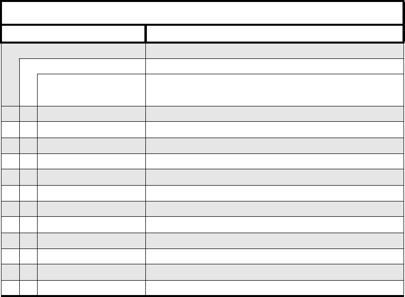
Chapter 1
MODEL CHART AND TECHNICAL SPECIFICATIONS
1.0 CM140/CM160 Model Chart
CM Series, VHF2, 146-174 MHz
Model Description
MDM50KQC9AA2 CM140 146-174 MHz, 45W, 8CH, BNC
MDM50KQF9AA2 CM160 146-174 MHz, 45W, 64CH, BNC
Item Description
XPMUD1848_ CM140 Super Tanapa VHF2, 45W, 8CH, BNC
X PMUD1894_ CM160 Super Tanapa VHF2, 45W, 64CH, BNC
XPMUD1885_ CM140 Tanapa VHF2, 45W, 8CH, BNC
X PMUD1887_ CM160 Tanapa VHF2, 45W, 64CH, BNC
XFCN6288_ Control Head
X FCN5523_ Control Head
XPMUD1885_S CM140 UHF2 U/C BNC Service Board
X PMUD1887_S CM160 UHF2 U/C BNC Service Board
XXRMN5018 Mag One Microphone
X X 6866546D02_ RTTE Leaflet
XX6866537D37_ Safety Leaflet
X X GLN7324_ Low Profile Trunnion
x = Indicates one of each is required.

1-2 MODEL CHART AND TECHNICAL SPECIFICATIONS
2.0 Technical Specifications
Data is specified for +25°C unless otherwise stated.
General
Specification VHF2
Frequency Range: 146-174 MHz
Frequency Stability
(-30°C to +60°C, 25°C Ref.)
±2 PPM
Channel Capacity: CM140 - 8
CM160 - 64
Channel Spacing: 12.5/20/25 kHz
Power Output: 25-45W
Power Supply: 13.2Vdc (10.8 - 15.6 Vdc) negative vehicle ground
Dimensions (L X W X H) 118mm X 169mm X 44mm
Weight:
Low power (1-25W) 1.02 Kg
Operating Temperature -30 to 60 o C
Storage temperature -40 to 80o C
Shock and Vibration Meets MIL-STD 810-C,D&E and TIA/EIA 603
Dust Meets MIL-STD 810-C,D&E and TIA/EIA 603
Humidity Meets MIL-STD 810-C,D&E and TIA/EIA 603

Technical Specifications 1-3
*Availability subject to the laws and regulations of individual countries.
Transmitter
Specification VHF2
Frequency Stability: +/- 2.5ppm
Modulation Limiting: ±2.5 kHz @ 12.5 kHz
±4.0 kHz @ 20 kHz
±5.0 kHz @ 20/25 kHz
Current Drain Transmit: 7A (25W)
FM Hum and Noise: -40 dB@12.5 kHz
-45 dB@ 20/25 kHz
Conducted/Radiated
Emissions:
-36 dBm < 1 GHz
-30 dBm > 1 GHz
Adjacent Channel Power -60dB @12.5,
-70dB @ 20/25kHz
Audio Response:
( 300 to 3000Hz) +1, -3dB
Audio Distortion:
@ 1000 Hz, 60%
Rated Maximum Deviation:
3% Typical
Receiver
Specification VHF2
Sensitivity (12dBSINAD): (ETS) 0.35µV (12.5kHz) 0.30µV (25kHz) Typical
Intermodulation : (ETS) >65dB
Adjacent Channel
Selectivity: (ETS)
75 dB @ 25 kHz
65 dB @ 12.5 kHz
Spurious Rejection: (ETS) 75 dB
Rated Audio: (ETS) (Extended audio with 4 Ohm
speaker)
4W Internal , 13W External
Audio Distortion @ Rated Audio: 3% Typical
Hum and Noise: -40 dB @ 12.5 kHz
-45 dB @ 20/25 kHz
Audio Response:
( 300 to 3000Hz) +1, -3dB
Conducted Spurious
Emission per FCC Part 15:
-57 dBm <1 GHz
-47 dBm >1 GHz

1-4 MODEL CHART AND TECHNICAL SPECIFICATIONS
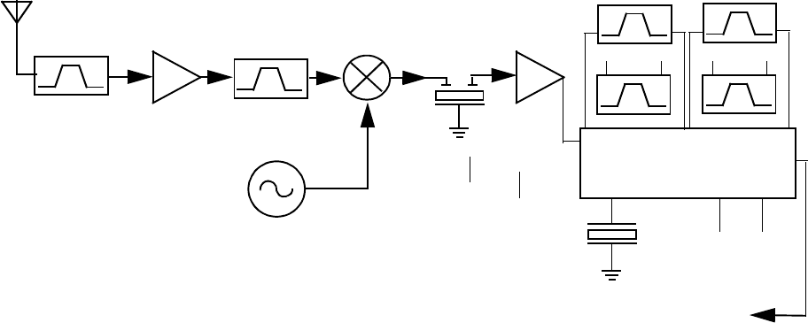
Chapter 2
THEORY OF OPERATION
1.0 Introduction
This Chapter provides a detailed theory of operation for the VHF circuits in the radio. Details of the
theory of operation and trouble shooting for the the associated Controller circuits are included in this
Section of the manual.
2.0 VHF (146-174MHz) Receiver
2.1 Receiver Front-End
The received signal is applied to the radio’s antenna input connector and routed through the
harmonic filter and antenna switch. The insertion loss of the harmonic filter/antenna switch is less
than 1 dB. The signal is routed to the first filter (4-pole), which has an insertion loss of 2 dB typically.
The output of the filter is matched to the base of the LNA (Q303) that provides a 16 dB gain and a
noise figure of better than 2 dB. Current source Q301 is used to maintain the collector current of
Q303. Diode CR301 protects Q303 by clamping excessive input signals. Q303 output is applied to
the second filter (3-pole) which has an insertion loss of 1.5 dB. In Distance mode, Q304 turns on and
causes D305 to conduct, thus bypassing C322 and R337. In Local mode, the signal is routed
through C322 and R337, thus inserting 7 dB attenuation. Since the attenuator is located after the RF
amplifier, the receiver sensitivity is reduced only by 6 dB, while the overall third order input intercept
is raised.
The first mixer is a passive, double-balanced type, consisting of T300, T301 and U302. This mixer
provides all of the necessary rejection of the half-IF spurious response. High-side injection at +15
dBm is delivered to the first mixer. The mixer output is then connected to a duplex network which
matches its output to the XTAL filter input (FL300) at the IF frequency of 44.85 MHz. The duplex
network terminates into a 50 ohm resistor (R340) at all other frequencies.
Figure 2-1 VHF Receiver Block Diagram
Mixer Xtal Filter
Controller
Front Filter
Antenna
First LO
2nd LO Xtal Osc
IF Amp
Second Filter 4- Pole
25kHzFilter
12.5kHzFilter
Phase Shift
Element
IFIC
LNA
25kHzFilter
12.5kHzFilter
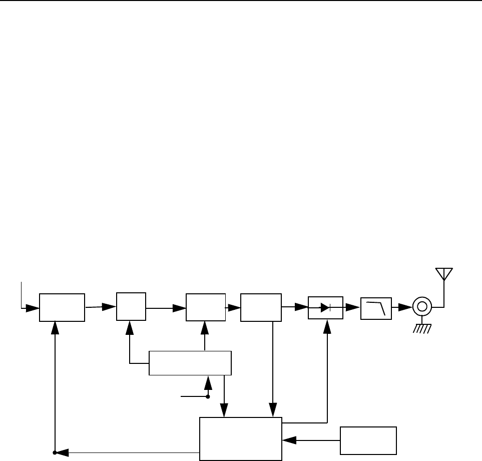
2-2 THEORY OF OPERATION
2.2 Receiver Back End
The IF signal from the crystal filter enters the IF amplifier which provides 20 dB of gain and feeds
the IF IC at pin 1. The first IF signal at 44.85 MHz mixes with the second local oscillator (LO) at
44.395 MHz to produce the second IF at 455 kHz. The second LO uses the external crystal Y301.
The second IF signal is amplified and filtered by two external ceramic filters (FL303/FL302 for
12.5KHz channel spacing and FL304/FL301 for 25KHz channel spacing). The IF IC demodulates
the signal by means of a quadrature detector and feeds the detected audio (via pin 7) to the audio
processing circuits. At IF IC pin 5, an RSSI signal is available with a dynamic range of 70 dB.
3.0 VHF Transmitter Power Amplifier (146-174 MHz)
The radio’s 45W PA is a three-stage amplifier used to amplify the output from the TX_INJ to the
antenna port. All three stages utilize LDMOS technology. The gain of the first stage (U101) is
adjustable and is controlled by pin 7 of U103-2 via U103-3 and U102-1. It is followed by an LDMOS
driver Q105 and final stage Q100.
Figure 2-2 VHF Transmitter Block Diagram
Devices U101, Q105 and Q100 are surface mounted.Two screws with Belleville washers provide
direct pressure ensuring good thermal contact between both the driver and final stage, and the
chassis.
3.1 First Power Controller Stage
The first stage (U101) is a 20dB gain integrated circuit containing two LDMOS FET amplifier stages.
It amplifies the RF signal from the VCO (TX_INJ). The output power of stage U101 is controlled by a
DC voltage applied to pin 1 from the op-amp U103-3, pin 8. The control voltage simultaneously
varies the bias of two FET stages within U101. This biasing point determines the overall gain of
U101 and therefore its output drive level to Q105, which in turn controls the output power of the PA.
Loop
Pin Diode
Antenna
Switch RF Jack
Antenna
Harmonic
Filter
Coupler
PA-Final
Stage
From VCO (TX_INJ)
Controlled
Stage
Bias
Temperature
Sense
SPI BUS
ASFIC_CMP
PA
PWR
SET
PA
Driver
Controller
U103-2
Forward
Bias

VHF Transmitter Power Amplifier (146-174 MHz) 2-3
Op-amp U103-3 monitors the drain current of U101 via resistor R122 and adjusts the bias voltage of
U101.
In receive mode, the DC voltage from RX_EN line turns on Q101, which in turn switches off the
biasing voltage to U101.
3.2 Power Controlled Driver Stage
The next stage is an LDMOS device (Q105) which provides a gain of 12dB. This device requires a
positive gate bias and a quiescent current flow for proper operation. The bias is set during transmit
mode by the V_cntrl_driver which is set to provide 100-150mA of quiescent current by the factory,
and fed to the gate of Q105 via the resistive network.
The V_cntrl_driver is directly controlled by the ASFIC CMP. In receive mode, the ASFIC CMP
(U504) sets V_cntrl_driver to 0V (DACR pin 5).
3.3 Final Stage
The final stage is an LDMOS device (Q100) providing a gain of 12dB. This device also requires a
positive gate bias and a quiescent current flow for proper operation. The voltage of the line PA_BIAS
is set in transmit mode by the ASFIC and fed to the gate of Q100 via the resistive network R134,
R131. This bias voltage is tuned in the factory. If the transistor is replaced, the bias voltage must be
tuned using the Tuner. Care must be taken not to damage the device by exceeding the maximum
allowed bias voltage. The device’s drain current is drawn directly from the radio’s DC supply voltage
input, B+, via L117 and L115.
A matching network consisting of C1004-5, C1007-9, C1096, C1021, C1013, C1019, L116: and two
striplines, transforms the impedance to 50 ohms and feeds the directional coupler.
3.4 Bi-Directional Coupler
The bi-directional Coupler is a microstrip printed circuit, which couples a small amount of the
forward and reverse power of the RF power from Q100.The coupled signal is rectified to an output
power which is proportional to the DC voltage rectified by diode D105; and the resulting DC voltage
is routed to the power control section to ensure that the forward power out of the radio is held to a
constant value.
3.5 Antenna Switch
The antenna switch utilizes the existing dc feed (B+) to the last stage device (Q100). The basic
operation is to have both PIN diodes (D103, D104) turned on during key-up by forward biasing
them. This is achieved by pulling down the voltage at the cathode end of D104 to around 12.4V
(0.7V drop across each diode). The current through the diodes needs to be set around 100 mA to
fully open the transmit path through resistor R108. Q106 is a current source controlled by Q103
which is turned on in Tx mode by TX_EN. VR102 ensures that the voltage at resistor R107 never
exceeds 5.6V.

2-4 THEORY OF OPERATION
3.6 Harmonic Filter
Inductors L111, L112, L124 and L113 along with capacitors C11321, C1022, C1020, C1137, C1018
and C1017 form a low-pass filter to attenuate harmonic energy coming from the transmitter.
Resistor R150 drains any electrostatic charges that might otherwise build up on the antenna. The
harmonic filter also prevents high level RF signals above the receiver passband from reaching the
receiver circuits to improve spurious response rejection.
3.7 Power Control
The output power is regulated by using a forward power detection control loop. A directional coupler
samples a portion of the forward and reflected RF power. The forward sampled RF is rectified by
diode D105, and the resulting DC voltage is routed to the operational amplifier U100. The error
output current is then routed to an integrator, and converted into the control voltage. This voltage
controls the bias of the pre-driver (U101) stage. The output power level is set by way of a DAC,
PWR_SET, in the audio processing IC (U504), which acts at the forward power control loop
reference.
The sampled reflected power is rectified by diode D107. The resulting DC voltage is amplified by an
operational amplifier U100 and routed to the summing junction. This detector protects the final stage
Q100 from reflected power by increasing the error current. The temperature sensor protects the
final stage Q100 from overheating by increasing the error current. A thermistor RT100 measures the
final stage Q100 temperature. The voltage divider output is routed to an operational amplifier U103
and then goes to the summing junction. The Zener Diode VR101 keeps the loop control voltage
below 5.6V and eliminates the DC current from the 9.3 regulator U501.
A local loop for the Pre Driver (U101) is used in order to stabilize the current for each stage.
In Rx mode, the two transistors Q101 and Q102 go to saturation and shut down the transmitter by
applying ground to the Pre Driver U101.
4.0 VHF (146-174MHz) Frequency Synthesis
The synthesizer consists of a reference oscillator (Y201), low voltage Fractional-N (LVFRAC-N)
synthesizer (U200), and a voltage controlled oscillator (VCO) (U201).
4.1 Reference Oscillator
The reference oscillator is a crystal (Y201) controlled Colpitts oscillator and has a frequency of
16.8MHz. The oscillator transistor and start-up circuit are located in the LVFRAC-N (U200) while the
oscillator feedback capacitors, crystal, and tuning varactors are external. An analog-to-digital (A/D)
converter internal to the LVFRAC-N (U200) and controlled by the microprocessor via SPI sets the
voltage at the warp output of U200 pin 25. This sets the frequency of the oscillator. Consequently,
the output of the crystal Y201 is applied to U200 pin 23.
The method of temperature compensation is to apply an inverse Bechmann voltage curve, which
matches the crystal’s Bechmann curve to a varactor that constantly shifts the oscillator back on
frequency. The crystal vendor characterizes the crystal over a specified temperature range and
codes this information into a bar code that is printed on the crystal package. In production, this
crystal code is read via a 2-dimensional bar code reader and the parameters are saved.
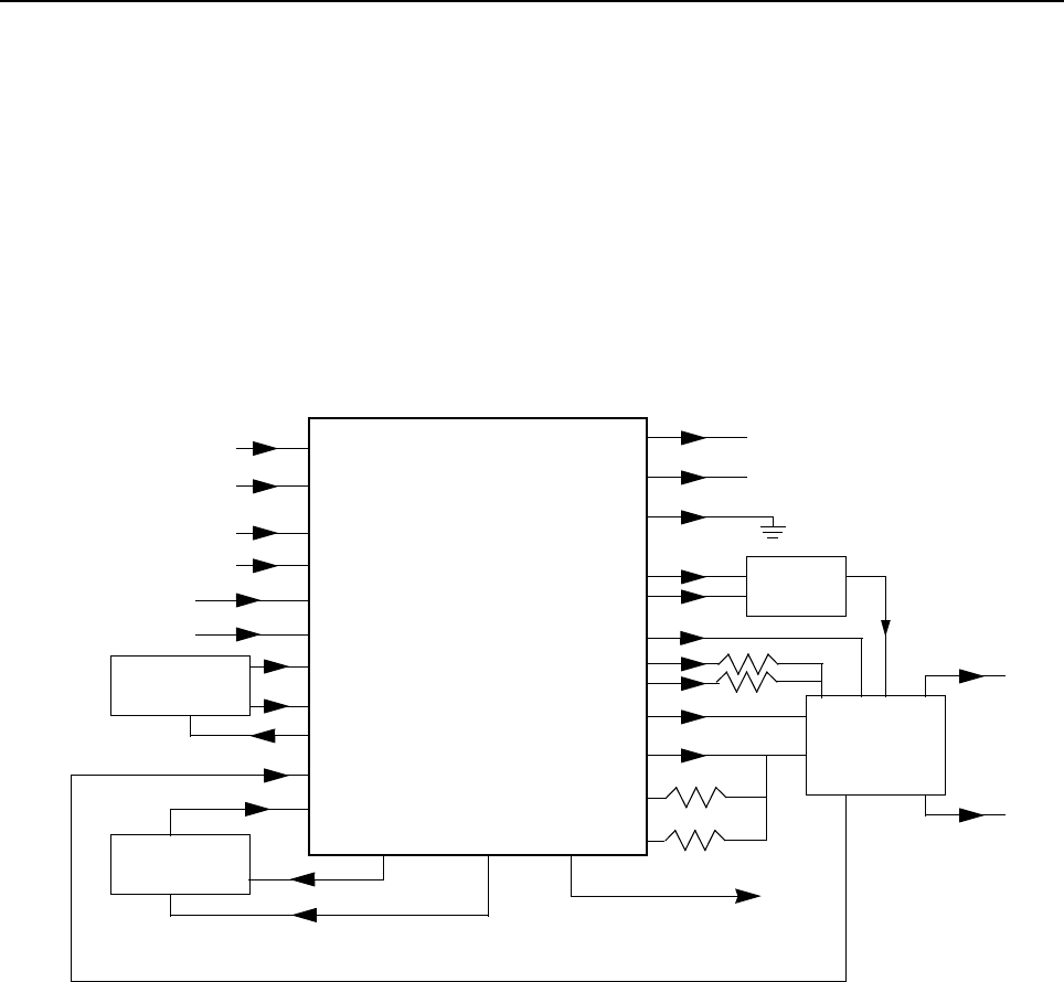
VHF (146-174MHz) Frequency Synthesis 2-5
This oscillator is temperature compensated to an accuracy of +/-2.5 PPM from -30 to 60 degrees C.
The temperature compensation scheme is implemented by an algorithm that uses five crystal
parameters (four characterize the inverse Bechmann voltage curve and one for frequency accuracy
of the reference oscillator at 25 degrees C). This algorithm is implemented by the LVFRAC-N (U200)
at the power up of the radio.
4.2 Fractional-N Synthesizer
The LVFRAC-N U200 consists of a pre-scaler, programmable loop divider, control divider logic,
phase detector, charge pump, A/D converter for low frequency digital modulation, balanced
attenuator used to balance the high and low frequency analog modulation, 13V positive voltage
multiplier, serial interface for control, and a super filter for the regulated 5 volts.
Figure 2-3 VHF Synthesizer Block Diagram
A voltage of 5V applied to the super filter input (U200, pin 30) supplies an output voltage of 4.5Vdc
(VSF) at U200, pin 28. This supplies 4.5 V to the VCO Buffer IC U201.
To generate a high voltage to supply the phase detector (charge pump) output stage at pin VCP
(U200, pin 47) while using a low voltage 3.3Vdc supply, a 13V positive voltage multiplier is used
(D200, D201, and capacitors C2024, 2025, 2026, 2055, 2027, 2001).
Output lock (U200, pin 4) provides information about the lock status of the synthesizer loop. A high
level at this output indicates a stable loop. A 16.8 MHz reference frequency is provided at U200, pin
19.
DATA
CLK
CEX
MODIN
VCC, DC5V
XTAL1
XTAL2
WARP
PREIN
VCP
REFERENCE
OSCILLATOR
VOLTAGE
MULTIPLIER
DATA (U403 PIN 100)
CLOCK (U403 PIN 1)
CSX (U403 PIN 2)
MOD IN (U501 PIN 40)
+5V (U503 PIN 1)
7
8
9
10
13, 30
23
24
25
32
47
VMULT2 VMULT1
BIAS1
SFOUT
AUX3
AUX4
IADAPT
IOUT
GND
FREFOUT
LOCK 4
19
6, 22, 33, 44
43
45
3
2
28
14 15
40
FILTERED 5V
STEERING
LOCK (U403 PIN 56)
PRESCALER IN
FREF (U504 PIN 34)
39
BIAS2
41
48
5, 20, 34, 36
+5V (U503 PIN 1)
AUX1
VDD, DC5V MODOUT
U200
LOW VOLTAGE
FRACTIONAL-N
SYNTHESIZER
AUX2 1
BWSELECT
VCO Bias
TRB
To IF
Section
TX RF INJECTION
(1ST STAGE OF PA)
LO RF INJECTION
VOLTAGE
CONTROLLED
OSCILLATOR
LINE
LOOP
FILTER

2-6 THEORY OF OPERATION
4.3 Voltage Controlled Oscillator (VCO)
The Voltage Controlled Oscillator (VCO) consists of the VCO/Buffer IC (VCOBIC, U201), the TX and
RX tank circuits, the external RX amplifier, and the modulation circuitry.
Figure 2-4 VHF VCO Block Diagram
The VCOBIC together with the LVFRAC-N (U200) generate the required frequencies in both
transmit and receive modes. The TRB line (U201, pin 19) determines which VCO and buffer is
enabled (high being TX output at pin 10, low being RX output at pin 8). A sample of the signal from
the enabled output is routed from U201, pin 12 (PRESC_OUT), via a low pass filter to U200, pin 32
(PREIN).
A steering line voltage between 3.0V and 10.0V at varactor D204 tunes the TX VCO through the
frequency range of 146-174MHz, and at D203 tunes the RX VCO through the frequency range of
190-219MHz.
The external RX amplifier is used to increase the output from U201, pin 9 from 3-4 dBm to the
required 15dBm for proper mixer operation. In TX mode, the modulation signal from the LVFRAC-N
(U200, pin 41) is applied to the VCO by way of the modulation circuit D205, R212, R211, C2073.
Presc
RX
TX
Q200 Low Pass
Filter
Attenuator
Pin8
Pin14
Pin10
(U200 Pin28)
VCC Buffers
TX RF Injection
U200 Pin 32
AUX3 (U200 Pin 2)
Prescaler Out
Pin 12Pin 19
Pin 20
TX/RX/BS
Switching Network
U201
VCOBIC
Rx
Active Bias
Tx
Active Bias
Pin2
Rx-I adjust
Pin1
Tx-I adjust
Pins 9,11,17
Pin18
Vsens
Circuit
Pin15
Pin16
RX VCO
Circuit
TX VCO
Circuit
RX Tank
TX Tank
Pin7
Vcc-Superfilter
Collector/RF in
Pin4
Pin5
Pin6
RX
TX
(U200 Pin 28)
Rx-SW
Tx-SW
Vcc-Logic
(U200 Pin 28)
Steer Line
Voltage
(VCTRL)
Pin13
Pin3
TRB IN
LO RF INJECTION
Buffer

VHF (146-174MHz) Frequency Synthesis 2-7
4.4 Synthesizer Operation
The synthesizer consists of a low voltage FRAC-N IC (LVFRAC-N), reference oscillator, charge
pump circuits, loop filter circuit, and DC supply. The output signal (PRESC_OUT) of the VCOBIC
(U201, pin 12) is fed to the PREIN, pin 32 of U200 via a low pass filter which attenuates harmonics
and provides a correct input level to the LVFRAC-N in order to close the synthesizer loop.
The pre-scaler in the synthesizer (U200) is a dual modulus pre-scaler with selectable divider ratios.
The divider ratio of the pre-scaler is controlled by the loop divider, which in turn receives its inputs
via the SPI. The output of the pre-scaler is applied to the loop divider. The output of the loop divider
is connected to the phase detector, which compares the loop divider’s output signal with the
reference signal. The reference signal is generated by dividing down the signal of the reference
oscillator (Y201).
The output signal of the phase detector is a pulsed dc signal that is routed to the charge pump. The
charge pump outputs a current from U200, pin 43 (IOUT). The loop filter (consisting of R224, R217,
R234, C2074, C2075, C2077, C2078, C2079, C2080, C2028, and L205) transforms this current into
a voltage that is applied the varactor diodes D203 and D204 for RX and TX respectively. The output
frequency is determined by this control voltage. The current can be set to a value fixed in the
LVFRAC-N or to a value determined by the currents flowing into BIAS 1 (U200, pin 40) or BIAS 2
(U200, pin 39). The currents are set by the value of R200 or R206 respectively. The selection of the
three different bias sources is done by software programming.
To modulate the synthesizer loop, a two-spot modulation method is utilized via the MODIN (U200,
pin 10) input of the LVFRAC-N. The audio signal is applied to both the A/D converter (low frequency
path) and the balance attenuator (high frequency path). The A/D converter converts the low
frequency analog modulating signal into a digital code which is applied to the loop divider, thereby
causing the carrier to deviate. The balance attenuator is used to adjust the VCO’s deviation
sensitivity to high frequency modulating signals. The output of the balance attenuator is presented
at the MODOUT port of the LVFRAC-N (U200,pin 41) and connected to the VCO modulation
varactor D205.

2-8 THEORY OF OPERATION
5.0 Controller Theory of Operation
This section provides a detailed theory of operation for the radio and its components. The main
radio is a single-board design, consisting of the transmitter, receiver, and controller circuits. A
control head is connected by an extension cable. The control head contains LED indicators, a
microphone connector, buttons, and speaker.
In addition to the power cable and antenna cable, an accessory cable can be attached to a
connector on the rear of the radio. The accessory cable enables you to connect accessories to the
radio, such as an external speaker, emergency switch, foot-operated PTT, and ignition sensing, etc.
Figure 2-5 Controller Block Diagram
5.1 Radio Power Distribution
Voltage distribution is provided by five separate devices:
■U514 P-cH FET - Batt + (Ext_SWB+)
■U501 LM2941T - 9.3V
■U503 LP2951CM - 5V
■U508 MC 33269DTRK - 3.3V
■U510 LP2986ILDX - 3.3V Digital
External
Microphone
Internal
Microphone
External
Speaker
Internal
Speaker
SCI to
Control Head
Audio
PA
Audio/Signaling
Architecture
To Synthesizer
Mod
Out
16.8 MHz
Reference Clock
from Synthesizer
Disc Audio
To R F S ec ti on SPI
Digital
Architecture
µP Clock
3.3V
Regulator
RAM
EEPROM
FLASH
HC11FL0
ASFIC_CMP
Accessory &
Connector
Handset
.
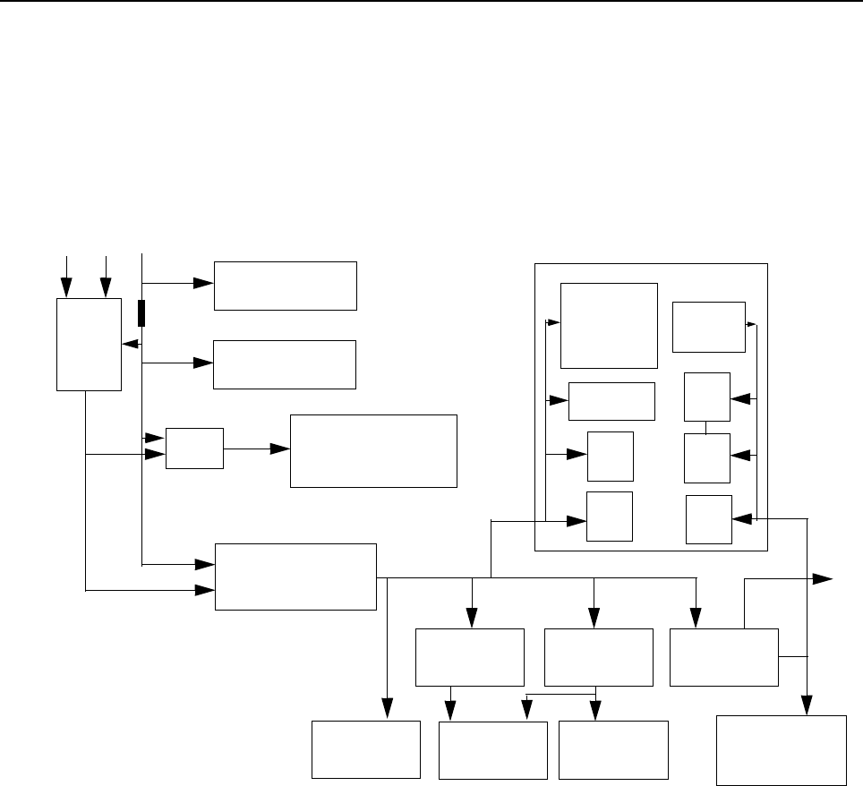
Controller Theory of Operation 2-9
The DC voltage applied to connector P2 supplies power directly to the following circuitry:
■Electronic on/off control
■RF power amplifier
■12 volts P-cH FET -U514
■9.3 volt regulator
■Audio PA
Figure 2-6 DC Power Distribution Block Diagram
Regulator U501 is used to generate the 9.3 volts required by some audio circuits, the RF circuitry
and power control circuitry. Input and output capacitors are used to reduce high frequency noise.
Resistors R5001 / R5081 set the output voltage of the regulator. This regulator output is
electronically enabled by a 0 volt signal on pin 2. Q502, Q505 and R5038 are used to disable the
regulator when the radio is turned off.
Voltage regulator U510 provides 3.3 volts for the digital circuitry. Operating voltage is from the
regulated 9.3V supply. Input and output capacitors are used to reduce high frequency noise and
provide proper operation during battery transients. U510 provides a reset output that goes to 0 volts
if the regulator output goes below 3.1 volts. This is used to reset the controller to prevent improper
operation.
Voltage regulator U508 provides 3.3V for the RF circuits and ASFIC_CMP. Input and output
capacitors are used to reduce the high frequency noise and provide proper operation during battery
transients.
U501
9.3V Regulator
FET
P-CH
On/Off
Control
500mA
SW_Filt_B+
Acces Conn
Audio PA_Soutdown
Power Loop Op_Amp
Auto
On/Off
Switch
Control
Ignition B+
RF_PA
Audio_PA
Antenna Switch
Power Control
Filt_B+
Ferrite Bit
Control Head
Mic Connector
Mic Bias
9V, 5mA
Keypad
7_Seg
Bed
to
7-Seg
Shift
Reg
3.2V
72mA
9.3V
65mA
Status LEDs
7_Seg
DOT
Back
light
On/Off
Control
11-16.6V
0.9A 0.85A
U503
5V RF Regulator
U508
3.3V RF Reg
U510
3.3V D Reg
Reset
Rx_Amp
PA_Pre-driver
PA D river
500mA
LVFRAC_N
IF_Amp
ASFIC_CMP
IFIC
RX Cct
micro P
RAM
Flash
EEPROM
90mA
25mA50mA45mA
9.3V
45mA
9.3V
75mA
9.3V
162mA

2-10 THEORY OF OPERATION
Voltage regulator U503 provides 5V for the RF circuits. Input and output capacitors are used to
reduce the high frequency noise and provide proper operation during battery transients.
VSTBY is used only for CM360 5-tone radios.
The voltage VSTBY, which is derived directly from the supply voltage by components R5103 and
VR502, is used to buffer the internal RAM. Capacitor C5120 allows the battery voltage to be
disconnected for a couple of seconds without losing RAM parameters. Dual diode D501 prevents
radio circuitry from discharging this capacitor. When the supply voltage is applied to the radio,
C5120 is charged via R5103 and D501.
5.2 Protection Devices
Diode VR500 acts as protection against ESD, wrong polarity of the supply voltage, and load dump.
VR692 - VR699 are for ESD protection.
5.3 Automatic On/Off
The radio can be switched ON in any one of the following three ways:
■On/Off switch. (No Ignition Mode)
■Ignition and On/Off switch (Ignition Mode)
■Emergency
5.3.1 No Ignition Mode
When the radio is connected to the car battery for the first time, Q500 will be in saturation, Q503 will
cut-off, Filt_B+ will pass through R5073, D500, and S5010-pin 6 (On/Off switch). When S5010 is
ON, Filt_B+ will pass through S5010-pin5, D511, R5069, R5037 and base of Q505 and move Q505
into saturation. This pulls U501-pin2 through R5038, D502 to 0.2V and turns On U514 and U501
9.3V regulator which supplies voltage to all other regulators and consequently turns the radio on,
When U504 (ASFIC_CMP) gets 3.3V, GCB2 goes to 3.3V and holds Q505 in saturation, for soft turn
off.
5.3.2 Ignition Mode
When ignition is connected for the first time, it will force high current through Q500 collector, This
will move Q500 out of saturation and consequently Q503 will cut-off. S5010 pin 6 will get ignition
voltage through R601 (for load dump), R610, (R610 & C678 are for ESD protection), VR501,
R5074, and D500. When S5010 is ON, Filt_B+ passes through S5010-pin 5, D511, R5069, R5037
and base of Q505 and inserts Q505 into saturation. This pulls U501-pin 2 through R5038, D502 to
0.2V and turns on U514 and U501 9.3V regulator which supply voltage to all other regulators and
turns the radio on, When U504 (ASFIC_CMP) get 3.3V supply, GCB2 goes to 3.3V and holds Q505
in saturation state to allow soft turn off,
When ignition is off Q500, Q503 will stay at the same state so S5010 pin 6 will get 0V from Ignition,
Q504 goes from Sat to Cut, ONOFF_SENSE goes to 3.3V and it indicates to the radio to soft turn
itself by changing GCB2 to ‘0’ after de registration if necessary.

Controller Theory of Operation 2-11
5.3.3 Emergency Mode
The emergency switch (P1 pin 9), when engaged, grounds the base of Q506 via EMERGENCY
_ACCES_CONN. This switches Q506 to off and consequently resistor R5020 pulls the collector of
Q506 and the base of Q506 to levels above 2 volts. Transistor Q502 switches on and pulls U501
pin2 to ground level, thus turning ON the radio. When the emergency switch is released R5030 pulls
the base of Q506 up to 0.6 volts. This causes the collector of transistor Q506 to go low (0.2V),
thereby switching Q502 to off.
While the radio is switched on, the µP monitors the voltage at the emergency input on the accessory
connector via U403-pin 62. Three different conditions are distinguished: no emergency kit is
connected, emergency kit connected (unpressed), and emergency press.
If no emergency switch is connected or the connection to the emergency switch is broken, the
resistive divider R5030 / R5049 will set the voltage to about 3.14 volts (indicates no emergency kit
found via EMERGENCY_SENSE line). If an emergency switch is connected, a resistor to ground
within the emergency switch will reduce the voltage on EMERGENCY _SENSE line, and indicate to
the µP that the emergency switch is operational. An engaged emergency switch pulls line
EMERGENCY _SENSE line to ground level. Diode VR503 limits the voltage to protect the µP input.
While EMERGENCY _ACCES_CONN is low, the µP starts execution, reads that the emergency
input is active through the voltage level of µP pin 64, and sets the DC POWER ON output of the
ASFIC CMP pin 13 to a logic high. This high will keep Q505 in saturation for soft turn off.
5.4 Microprocessor Clock Synthesiser
The clock source for the µP system is generated by the ASFIC CMP (U504). Upon power-up the
synthesizer IC (FRAC-N) generates a 16.8 MHz waveform that is routed from the RF section to the
ASFIC CMP pin 34. For the main board controller the ASFIC CMP uses 16.8 MHz as a reference
input clock signal for its internal synthesizer. The ASFIC CMP, in addition to audio circuitry, has a
programmable synthesizer which can generate a synthesized signal ranging from 1200Hz to
32.769MHz in 1200Hz steps.
When power is first applied, the ASFIC CMP will generate its default 3.6864MHz CMOS square
wave UP CLK (on U504 pin 28) and this is routed to the µP (U403 pin 90). After the µP starts
operation, it reprograms the ASFIC CMP clock synthesizer to a higher UP CLK frequency (usually
7.3728 or 14.7456 MHz) and continues operation.
The ASFIC CMP may be reprogrammed to change the clock synthesizer frequencies at various
times depending on the software features that are executing. In addition, the clock frequency of the
synthesizer is changed in small amounts if there is a possibility of harmonics of the clock source
interfering with the desired radio receive frequency.
The ASFIC CMP synthesizer loop uses C5025, C5024 and R5033 to set the switching time and jitter
of the clock output. If the synthesizer cannot generate the required clock frequency it will switch
back to its default 3.6864MHz output.
Because the ASFIC CMP synthesizer and the µP system will not operate without the 16.8 MHz
reference clock it (and the voltage regulators) should be checked first when debugging the system.

2-12 THEORY OF OPERATION
5.5 Serial Peripheral Interface (SPI)
The µP communicates to many of the IC’s through its SPI port. This port consists of SPI TRANSMIT
DATA (MOSI) (U403-pin100), SPI RECEIVE DATA (MISO) (U403-pin 99), SPI CLK (U0403-pin1)
and chip select lines going to the various IC’s, connected on the SPI PORT (BUS). This BUS is a
synchronous bus, in that the timing clock signal CLK is sent while SPI data (SPI TRANSMIT DATA
or SPI RECEIVE DATA) is sent. Therefore, whenever there is activity on either SPI TRANSMIT
DATA or SPI RECEIVE DATA there should be a uniform signal on CLK. The SPI TRANSMIT DATA
is used to send serial from a µP to a device, and SPI RECEIVE DATA is used to send data from a
device to a µP.
In the controller section, there are two IC’s on the SPI BUS, ASFIC CMP (U504 pin 22), and
EEPROM (U400). In the RF sections there is one IC on the SPI BUS, the FRAC-N Synthesizer. The
chip select line CSX from U403 pin 2 is shared by the ASFIC CMP and FRAC-N Synthesizer. Each
of these IC’s check the SPI data and when the sent address information matches the IC’s address,
the following data is processed.
When the µP needs to program any of these Is it brings the chip select line CSX to a logic “0” and
then sends the proper data and clock signals. The amount of data sent to the various IC’s are
different; e.g., the ASFIC CMP can receive up to 19 bytes (152 bits). After the data has been sent
the chip select line is returned to logic “1”.
5.6 SBEP Serial Interface
The SBEP serial interface allows the radio to communicate with the Customer Programming
Software (CPS), or the Universal Tuner via the Radio Interface Box (RIB) or the cable with internal
RIB. This interface connects to the SCI pin via control head connector (J2-pin 17) and to the
accessory connector P1-6 and comprises BUS+. The line is bi-directional, meaning that either the
radio or the RIB can drive the line. The µP sends serial data and it reads serial data via pin 97.
Whenever the µP detects activity on the BUS+ line, it starts communication.
5.7 General Purpose Input/Output
The controller provides six general purpose lines (PROG I/O) available on the accessory connector
P1 to interface to external options. Lines PROG IN 3 and 6 are inputs, PROG OUT 4 is an output
and PROG IN OUT 8, 12 and 14 are bi-directional. The software and the hardware configuration of
the radio model define the function of each port.
■PROG IN 3 can be used as external PTT input, or others, set by the CPS. The µP reads this
port via pin 72 and Q412.
■PROG OUT 4 can be used as external alarm output, set by the CPS. Transistor Q401 is
controlled by the µP (U403 pin 55)
■PROG IN 6 can be used as normal input, set by the CPS. The µP reads this port via pin 73
and Q411. This pin is also used to communicate with the RIB if resistor R421 is placed.
■DIG IN OUT 8,12,14 are bi-directional and use the same circuit configuration. Each port uses
an output Q416, Q404, Q405 controlled by µP pins 52, 53, 54. The input ports are read
through µP pins 74, 76, 77; using Q409, Q410, Q411

Controller Theory of Operation 2-13
5.8 Normal Microprocessor Operation
For this radio, the µP is configured to operate in one of two modes, expanded and bootstrap. In
expanded mode the µP uses external memory devices to operate, whereas in bootstrap operation
the µP uses only its internal memory. In normal operation of the radio the µP is operating in
expanded mode as described below.
During normal operation, the µP (U403) is operating in expanded mode and has access to 3
external memory devices; U400 (EEPROM), U402 (SRAM), U404 (Flash). Also, within the µP there
are 3 Kilobytes of internal RAM, as well as logic to select external memory devices.
The external EEPROM (U400) space contains the information in the radio which is customer
specific, referred to as the codeplug. This information consists of items such as: 1) what band the
radio operates in, 2) what frequencies are assigned to what channel, and 3) tuning information.
The external SRAM (U402) as well as the µP’s own internal RAM space are used for temporary
calculations required by the software during execution. All of the data stored in both of these
locations is lost when the radio powers off.
The µP provides an address bus of 16 address lines (ADDR 0 - ADDR 15), and a data bus of 8 data
lines (DATA 0 - DATA 7). There are also 3 control lines; CSPROG (U403-38) to chip select U404-pin
30 (FLASH), CSGP2 (U403-pin 41) to chip select U404-pin 20 (SRAM) and PG7_R_W (U403-pin 4)
to select whether to read or to write.
When the µP is functioning normally, the address and data lines should be toggling at CMOS logic
levels. Specifically, the logic high levels should be between 3.1 and 3.3V, and the logic low levels
should be between 0 and 0.2V. No other intermediate levels should be observed, and the rise and
fall times should be <30ns.
The low-order address lines (ADDR 0 - ADDR 7) and the data lines (DATA 0-DATA 7) should be
toggling at a high rate, e.g., you should set your oscilloscope sweep to 1us/div. or faster to observe
individual pulses. High speed CMOS transitions should also be observed on the µP control lines.
On the µP the lines XIRQ (U403-pin 48), MODA LIR (U403-pin 58), MODB VSTPY (U403-pin 57)
and RESET (U403-pin 94) should be high at all times during normal operation. Whenever a data or
address line becomes open or shorted to an adjacent line, a common symptom is that the RESET
line goes low periodically, with the period being in the order of 20ms. In the case of shorted lines you
may also detect the line periodically at an intermediate level, i.e. around 2.5V when two shorted
lines attempt to drive to opposite rails.
The MODA LIR (U403-pin 58) and MODB VSTPY (U403-pin 57) inputs to the µP must be at a logic
“1” for it to start executing correctly. After the µP starts execution it will periodically pulse these lines
to determine the desired operating mode. While the Central Processing Unit (CPU) is running,
MODA LIR is an open-drain CMOS output which goes low whenever the µP begins a new
instruction. An instruction typically requires 2-4 external bus cycles, or memory fetches.
There are eight analog-to-digital coverter ports (A/D) on U403 labelled within the device block as
PEO-PE7. These lines sense the voltage level ranging from 0 to 3.3V of the input line and convert
that level to a number ranging from 0 to 255 which is read by the software to take appropriate action.

2-14 THEORY OF OPERATION
5.9 Static Random Access Memory (SRAM)
The SRAM (U402) contains temporary radio calculations or parameters that can change very
frequently, and which are generated and stored by the software during its normal operation. The
information is lost when the radio is turned off.
The device allows an unlimited number of write cycles. SRAM accesses are indicated by the CS
signal U402 (which comes from U403-CSGP2) going low. U402 is commonly referred to as the
external RAM as opposed to the internal RAM which is the 3 kilobytes of RAM which is part of the
68HC11FL0. Both RAM spaces serve the purpose. However, the internal RAM is used for the
calculated values which are accessed most often.
Capacitor C402 and C411 serves to filter out any AC noise which may ride on +3.3 V at U402
6.0 Control Board Audio and Signalling Circuits
6.1 Audio Signalling Filter IC and Compander (ASFIC CMP)
The ASFIC CMP (U504) used in the controller has the following four functions:
1. RX/TX audio shaping, i.e. filtering, amplification, attenuation
2. RX/TX signaling, PL/DPL/HST/MDC
3. Squelch detection
4. µP clock signal generation
The ASFIC CMP is programmable through the SPI BUS (U504 pins-20/21/22), normally receiving
19 bytes. This programming sets up various paths within the ASFIC CMP to route audio and/or
signaling signals through the appropriate filtering, gain and attenuator blocks. The ASFIC CMP also
has 6 General Control Bits GCB0-5 which are CMOS level outputs and used for the following:
■GCBO - BW Select
■GCBI - switches the audio PA On/Off
■GCB2 - DC Power On switches the voltage regulator (and the radio) on and off
■GCB3 - Control on MUX U509 pin 9 to select between Low Cost Mic path to STD Mic Path
■GCB4 - Control on MUX U509 pin 11 to select between Flat RX path to filtered RX path on the
accessory connector.
■GCB5 - Control on MUX U509 pin 10 to select between Flat TX path mute and Flat TX path

Transmit Audio Circuits 2-15
7.0 Transmit Audio Circuits
Figure 2-7 Transmit Audio Paths
7.1 Microphone Input Path
The radio supports 2 distinct microphone paths known as internal (from control head J2-15) and
external mic (from accessory connector P1-2) and an auxiliary path (FLAT TX AUDIO, from
accessory connector P1-5). The microphones used for the radio require a DC biasing voltage
provided by a resistive network.
The two microphone audio input paths enter the ASFIC CMP at U504-pin 48 (external mic) and
U504-pin 46 (internal mic). The microphone is plugged into the radio control head and connected to
the audio DC via J2-pin 15. The signal is then routed via C5045 to MUX U509 that select between
two paths with different gain to support Low Cost Mic (Mic with out amplifier in it) and Standard Mic.
7.1.1 Low Cost Microphone
Hook Pin is shorted to Pin 1(9.3V) inside the Low Cost Mic, This routes 9.3V to R429, and creates
2.6V on MIC_SENSE (u.P U403-67) by Voltage Divider R429/R430. U403 senses this voltage and
sends command to ASFIC_CMP U504 to get GCB3 = ‘0’. The audio signal is routed from C5045 via
U509-5 (Z0), R5072, U507, R5026, C5091, R5014 via C5046 to U504- 46 int. mic (C5046 100nF
creates a 159Hz pole with U504- 46 int mic impedance of 16k ohm).
MIC
IN
MOD IN TO
RF
SECTION
(SYNTHESIZER)
36
44
40
P1
ACCESSORY
CONNECTOR
J2
CONTROL HEAD
CONNECTOR
MIC
EXT MIC
FLAT TX
AUDIO
42
5
48
46
15
2
24kOhms
FILTERS AND
PREEMPHASIS
HS SUMMER
SPLATTER
FILTER
LS SUMMER
LIMITER
ATTENUATOR
VCO
ATN
TX RTN
TX SND
MIC
INT
AUX
TX
ASFIC_CMP
U504
U509
MIC
EXT
FLAT TX
AUDIO MUTE
GCB3
MUX
35
U509
MUX
GCB5
38

2-16 THEORY OF OPERATION
7.1.2 Standard Microphone
Hook Pin is shorted to the hook mic inside the standard Mic, If the mic is out off hook, 3.3V is routed
to R429 via R458, D401, and it create 0.7V on MIC_SENSE (u.P U403-67) by Voltage Divider
R429/R430. U403 senses this voltage and sends command to ASFIC_CMP U504 to get GCB3 =‘1’.
The audio signal is routed from C5045 via U509-3 (Z1), R5072, U507, R5026, C5091, R5014 via
C5046 to U504- 46 int mic (C5046 100nF create a159Hz pole with U504- 46 int mic impedance of
16Kohm). 9.3VDC is routed via R5077, R5075 to J2-15, It create 4.65V with Mic Impedance. C5010
supplies AC Ground to create AC impedance of 510 Ohms via R5075. and Filter 9.3V DC mic bias
supply.
Note: The audio signal at U504-pin 46 should be approximately 12mV for 1.5kHz or 3kHz of
deviation with 12.5kHz or 25kHz channel spacing.
The external microphone signal enters the radio on accessory connector P1 pin 2 and is routed via
line EXT MIC to R5054. R5078 and R5076 provide the 9.3Vdc bias. Resistive divider R5054/ R5070
divide the input signal by 5.5 and provide input protection for the CMOS amplifier input. R5076 and
C5009 provide a 510 ohm AC path to ground that sets the input impedance for the microphone and
determines the gain based on the emitter resistor in the microphone’s amplifier circuit.
C5047 serves as a DC blocking capacitor. The audio signal at U504-pin 48 should be approximately
14mV for 1.5kHz or 3kHz of deviation with 12.5kHz or 25kHz channel spacing.
The FLAT TX AUDIO signal from accessory connector P1-pin 5 is fed to the ASFIC CMP (U504 pin
42 through U509 pin 2 to U509 pin 15 via U506 OP-AMP circuit and C5057.
The ASFIC has an internal AGC that can control the gain in the mic audio path. The AGC can be
disabled / enabled by the µP. Another feature that can be enabled or disabled in the ASFIC is the
VOX. This circuit, along with Capacitor C5023 at U504-pin 7, provides a DC voltage that can allow
the µP to detect microphone audio. The ASFIC can also be programmed to route the microphone
audio to the speaker for public address operation.
7.2 PTT Sensing and TX Audio Processing
Internal microphone PTT is sensed by µP U403 pin 71. Radio transmits when this pin is “0” and
selects inside the ASFIC_ CMP U504 internal Mic path. When the internal Mic PTT is “0” then
external Mic PTT is grounded via D402. External Mic PTT is sensed by U403 pin 72 via Q412
circuits. The radio transmits when this pin is “0” and selects inside the ASFIC _CMP U504 External
Mic path.
Inside the ASFIC CMP, the mic audio is filtered to eliminate frequency components outside the 300-
3000Hz voice band, and pre-emphasized if pre-emphasis is enabled. The signal is then limited to
prevent the transmitter from over deviating. The limited mic audio is then routed through a summer,
which is used to add in signaling data, and then to a splatter filter to eliminate high frequency
spectral components that could be generated by the limiter. The audio is then routed to an
attenuator, which is tuned in the factory or the field to set the proper amount of FM deviation. The
TX audio emerges from the ASFIC CMP at U504-pin 40 MOD IN, at which point it is routed to the
RF section.

Transmit Signalling Circuits 2-17
8.0 Transmit Signalling Circuits
Figure 2-8 Transmit Signalling Path
From a hardware point of view, there are 3 types of signaling:
■Sub-audible data (PL / DPL / Connect Tone) that gets summed with transmit voice or
signaling,
■DTMF data for telephone communication in trunked and conventional systems, and
■Audible signaling including MDC and high-speed trunking.
Note: All three types are supported by the hardware while the radio software determines which
signaling type is available.
8.1 Sub-Audio Data (PL/DPL)
Sub-audible data implies signaling whose bandwidth is below 300Hz. PL and DPL waveforms are
used for conventional operation and connect tones for trunked voice channel operation. The
trunking connect tone is simply a PL tone at a higher deviation level than PL in a conventional
system. Although it is referred to as “sub-audible data”, the actual frequency spectrum of these
waveforms may be as high as 250 Hz, which is audible to the human ear. However, the radio
receiver filters out any audio below 300Hz, so these tones are never heard in the actual system.
Only one type of sub-audible data can be generated by U504 (ASFIC CMP) at any one time. The
process is as follows, using the SPI BUS, the µP programs the ASFIC CMP to set up the proper low-
speed data deviation and select the PL or DPL filters. The µP then generates a square wave which
strobes the ASFIC PL / DPL encode input LSIO U504-pin 18 at twelve times the desired data rate.
For example, for a PL frequency of 103Hz, the frequency of the square wave would be 1236Hz.
This drives a tone generator inside U504 which generates a staircase approximation to a PL sine
wave or DPL data pattern. This internal waveform is then low-pass filtered and summed with voice
or data. The resulting summed waveform then appears on U504-pin 40 (MOD IN), where it is sent to
the RF board as previously described for transmit audio. A trunking connect tone would be
generated in the same manner as a PL tone.
19
18
40
MOD IN
TO RF
SECTION
(SYNTHESIZER)
80
44 HIGH SPEED
CLOCK IN
(HSIO)
LOW SPEED
CLOCK IN
(LSIO)
ASFIC_CMP U504
MICRO
CONTROLLER
U403
HS
SUMMER
5-3-2 STATE
ENCODER
DTMF
ENCODER
SPLATTER
FILTER
PL
ENCODER
LS
SUMMER
ATTENUATOR
85
82
SPI
BUS

2-18 THEORY OF OPERATION
8.2 High Speed Data
High speed data refers to the 3600 baud data waveforms, known as Inbound Signaling Words
(ISWs) used in a trunking system for high speed communication between the central controller and
the radio. To generate an ISW, the µP first programs the ASFIC CMP (U504) to the proper filter and
gain settings. It then begins strobing U504-pin 19 (HSIO) with a pulse when the data is supposed to
change states. U504’s 5-3-2 State Encoder (which is in a 2-state mode) is then fed to the post-
limiter summer block and then the splatter filter. From that point it is routed through the modulation
attenuator and then out of the ASFIC CMP to the RF board. MDC is generated in much the same
way as trunking ISW. However, in some cases these signals may also pass through a data pre-
emphasis block in the ASFIC CMP. Also these signaling schemes are based on sending a
combination of 1200 Hz and 1800 Hz tones only. Microphone audio is muted during high speed data
signaling.
8.3 Dual Tone Multiple Frequency (DTMF) Data
DTMF data is a dual tone waveform used during phone interconnect operation. It is the same type
of tones which are heard when using a “Touch Tone” telephone.
There are seven frequencies, with four in the low group (697, 770, 852, 941Hz) and three in the high
group (1209, 1336, 1477Hz). The high-group tone is generated by the µP (U403-46) strobing U504-
19 at six times the tone frequency for tones less than 1440Hz or twice the frequency for tones
greater than 1440Hz. The low group tone is generated by the ASFIC CMP, controlled by the µP via
SPI bus. Inside U504 the low-group and high-group tones are summed (with the amplitude of the
high group tone being approximately 2 dB greater than that of the low group tone) and then pre-
emphasized before being routed to the summer and splatter filter. The DTMF waveform then follows
the same path as was described for high-speed data.

Receive Audio Circuits 2-19
9.0 Receive Audio Circuits
Figure 2-9 Receive Audio Paths
9.1 Squelch Detect
The radio’s RF circuits are constantly producing an output at the discriminator (IF IC). This signal
(DISC AUDIO) is routed to the ASFIC CMP’s squelch detect circuitry input DISC (U504-pin 2). All of
the squelch detect circuitry is contained within the ASFIC CMP. Therefore from a user’s point of
view, DISC AUDIO enters the ASFIC CMP, and the ASFIC CMP produces two CMOS logic outputs
based on the result. They are CH ACT (U504-16) and SQ DET (U504-17).
The squelch signal entering the ASFIC CMP is amplified, filtered, attenuated, and rectified. It is then
sent to a comparator to produce an active high signal on CH ACT. A squelch tail circuit is used to
produce SQ DET (U504-17) from CH ACT. The state of CH ACT and SQ DET is high (logic “1”)
when carrier is detected, otherwise low (logic “0”).
CH ACT is routed to the µP pin 84 while SQ DET is routed to the µP pin 83.
SQ DET is used to determine all audio mute / unmute decisions except for Conventional Scan. In
this case CH ACT is a pre-indicator as it occurs slightly faster than SQ DET.
FLT RX AUDIO
P1
11
16
1EXTERNAL
SPEAKER
INTERNAL
SPEAKER
ACCESSORY
CONNECTOR
CONTROL HEAD
CONNECTOR
HANDSET
AUDIO
18
20
19
J2
INT
SPKR-
SPKR +
SPKR -
1
9
2
U509
4110
INT
SPKR+
4
6
DISC
ASFIC_CMP
U504
AUDIO
PA
U502
VOLUME
ATTEN.
FILTER AND
DEEMPHASIS
17
MICRO
CONTROLLER
U403
80
FROM
RF
SECTION
(IF IC) LIMITER, RECTIFIER
FILTER, COMPARATOR
SQ DET
SQUELCH
CIRCUIT
16
PL FILTER
LIMITER
CH ACT
AUX RX
43
18
LS IO
U IO AUDIO
83
84
39
URX OUT
DISC
AUDIO
37
85
GCB4
MUTE
GCB1
14
U505

2-20 THEORY OF OPERATION
9.2 Audio Processing and Digital Volume Control
The receiver audio signal (DISC AUDIO) enters the controller section from the IF IC where it is.DC
coupled to ASFIC CMP via the DISC input U504-pin 2. The signal is then applied to both the audio
and the PL/DPL paths
The audio path has a programmable amplifier, whose setting is based on the channel bandwidth
being received, an LPF filter to remove any frequency components above 3000Hz, and a HPF to
strip off any sub-audible data below 300Hz. Next, the recovered audio passes through a de-
emphasis filter (if it is enabled to compensate for Pre-emphasis which is used to reduce the effects
of FM noise). The IC then passes the audio through the 8-bit programmable attenuator whose level
is set depending on the value of the volume control. Finally the filtered audio signal passes through
an output buffer within the ASFIC CMP. The audio signal exits the ASFIC CMP at AUDIO output
(U504 pin 41).
The µP programs the attenuator, using the SPI BUS, based on the volume setting. The minimum /
maximum settings of the attenuator are set by codeplug parameters.
Since sub-audible signaling is summed with voice information on transmit, it must be separated
from the voice information before processing. Any sub-audible signaling enters the ASFIC CMP
from the IF IC at DISC U504-2. Once inside, it goes through the PL/DPL path. The signal first
passes through one of the two low-pass filters, either the PL low-pass filter or the DPL/LST low-pass
filter. Either signal is then filtered and goes through a limiter and exits the ASFIC CMP at LSIO
(U504-pin 18). At this point, the signal will appear as a square wave version of the sub-audible
signal which the radio received. The µP U403 pin 80 will decode the signal directly to determine if it
is the tone / code which is currently active on that mode.
9.3 Audio Amplification Speaker (+) Speaker (-)
The output of the ASFIC CMP’s digital volume pot, U504-pin 41 is routed through DC blocking
capacitor C5049 to the audio PA (U502 pin 1 and 9).
The audio power amplifier has one inverted and one non-inverted output that produces the
differential audio output SPK+/SPK- (U502 pins 4 and 6)
The audio PA is enabled via the ASFIC CMP (U504-GCB1). When the base of Q501 is low, the
transistor is off and U502-pin 8 is high, using pull up resistor R5041, and the audio PA is ON. The
voltage at U502-pin 8 must be above 8.5Vdc to properly enable the device.
If the voltage is between 3.3 and 6.4V, the device will be active but has its input (U502-pins 1/9) off.
This is a mute condition which is used to prevent an audio pop when the PA is enabled.
The SPK+ and SPK- outputs of the audio PA have a DC bias which varies proportionately with B+
(U502- pin 7). B+ of 11V yields a DC offset of 5V, and B+ of 17V yields a DC offset of 8.5V. If either
of these lines is shorted to ground, it is possible that the audio PA will be damaged. SPK+ and SPK-
are routed to the accessory connector (P1-pin 1 and 16) and to the control head (connector J2-pins
19 and 20).

Receive Signalling Circuits 2-21
9.4 Handset Audio
Certain handheld accessories have a speaker within them which require a different voltage level
than that provided by U502. For these devices HANDSET AUDIO is available at control head
connector J2 pin18.
The received audio from the output of the ASFIC CMP’s digital volume attenuator is routed to U505
pin 2 where it is amplified. This signal is routed from the output of the op-amp U505 to J2-pin 18.
From the control head, the signal is sent directly to the microphone jack.
9.5 Filtered Audio and Flat Audio
The ASFIC CMP output audio at U504-pin 39 is filtered and de-emphasized, but has not gone
through the digital volume attenuator. From ASFIC CMP U504-pin 39 the signal is routed via R5034
through gate U509-pin 12 and AC coupled to U505-pin 6. The gate controlled by ASFIC CMP port
GCB4 selects between the filtered audio signal from the ASFIC CMP pin 39 (URXOUT) or the
unfiltered (flat) audio signal from the ASFIC CMP pin 10 (UIO). Resistors R5034 and R5021
determine the gain of op-amp UU505-pin 6 for the filtered audio while R5032 and R5021 determine
the gain for the flat Audio. The output of U505-pin 7 is then routed to P1 pin 11 via DC blocking
capacitor C5003. Note that any volume adjustment of the signal on this path must be done by the
accessory.
10.0 Receive Signalling Circuits
Figure 2-10 Receive Signalling Paths
10.1 Sub-Audio Data (PL/DPL) and High Speed Data Decoder
The ASFIC CMP (U504) is used to filter and limit all received data. The data enters the ASFIC CMP
at input DISC (U504 pin 2). Inside U504 the data is filtered according to data type (HS or LS), then it
is limited to a 0-3.3V digital level. The MDC and trunking high speed data appear at U504-pin 19,
where it connects to the µP U403 pin 82.
DET AUDIO
DISCRIMINATOR AUDIO
FROM RF SECTION
(IF IC)
19
18
25
2
82
80
DISC
PLCAP2
LSIO
HSIO
DATA FILTER
AND DEEMPHASIS LIMITER
FILTER LIMITER
ASFIC_CMP
U504
MICRO
CONTROLLER
U403
85
44
8
PLEAP

2-22 THEORY OF OPERATION
The low speed limited data output (PL, DPL, and trunking LS) appears at U504-pin18, where it
connects to the µP U403-pin 80.
The low speed data is read by the µP at twice the frequency of the sampling waveform; a latch
configuration in the ASFIC CMP stores one bit every clock cycle. The external capacitors C5028,
and C5026 set the low frequency pole for a zero crossings detector in the limiters for PL and HS
data. The hysteresis of these limiters is programmed based on the type of received data.
10.2 Alert Tone Circuits
When the software determines that it needs to give the operator an audible feedback (for a good
key press, or for a bad key press), or radio status (trunked system busy, phone call, circuit failures),
it sends an alert tone to the speaker. It does so by sending SPI BUS data to U504 which sets up the
audio path to the speaker for alert tones. The alert tone itself can be generated in one of two ways:
internally by the ASFIC CMP, or externally using the µP and the ASFIC CMP.
The allowable internal alert tones are 304, 608, 911, and 1823Hz. In this case a code contained
within the SPI BUS load to the ASFIC CMP sets up the path and determines the tone frequency,
and at what volume level to generate the tone. (It does not have to be related to the voice volume
setting.)
For external alert tones, the µP can generate any tone within the 100-3000Hz audio band. This is
accomplished by the µP generating a square wave which enters the ASFIC CMP at U504 pin 19.
Inside the ASFIC CMP this signal is routed to the alert tone generator.
The output of the generator is summed into the audio chain just after the RX audio de-emphasis
block. Inside U504, the tone is amplified and filtered, then passed through the 8-bit digital volume
attenuator, which is typically loaded with a special value for alert tone audio. The tone exits at U504-
pin 41 and is routed to the audio PA like receive audio.
Chapter 3
TROUBLESHOOTING CHARTS
This section contains detailed troubleshooting flowcharts. These charts should be used as a guide in
determining the problem areas. They are not a substitute for knowledge of circuit operation and
astute troubleshooting techniques. It is advisable to refer to the related detailed circuit descriptions
in the theory of operation sections prior to troubleshooting a radio.
Most troubleshooting charts end up by pointing to an IC to replace. It is not always noted, but it is
good practice to verify supplies and grounds to the affected IC and to trace continuity to the
malfunctioning signal and related circuitry before replacing any IC. For instance, if a clock signal is
not available at a destination, continuity from the source IC should be checked before replacing the
source IC.
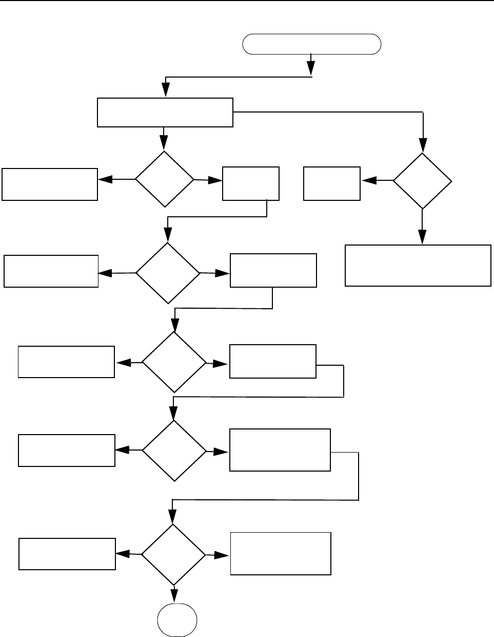
3-2 TROUBLESHOOTING CHARTS
1.0 Troubleshooting Flow Chart for Receiver RF (Sheet 1 of 2)
Problem in 12 KHz and
25 KHz channel spacing
9V on
R310 (LNA)
OK?
Check
RX_EN
No
Go to
DC Section
Yes
RX_EN
ON ?
No
Check Q306, Q300
and U403
Yes
START
LOC_DIST
ON?
Check Q304, D305
and U403
LO
POWER
OK ?
Go to SYN
Section
Yes
Yes
No
No
Go
to A
Yes
3 V
to U301
Okay ?
No
Check
LOC_DIST
Go to
DC Section
Yes
Check D301-304
Replace IF Filters( FL304, FL301)
If problem in 25 KHz spacing
Check
TP1
Check 5V
on R336
5V
(IF AMP)
OK ?
Go to
DC Section
Yes
No
Check 3V
on R338
No
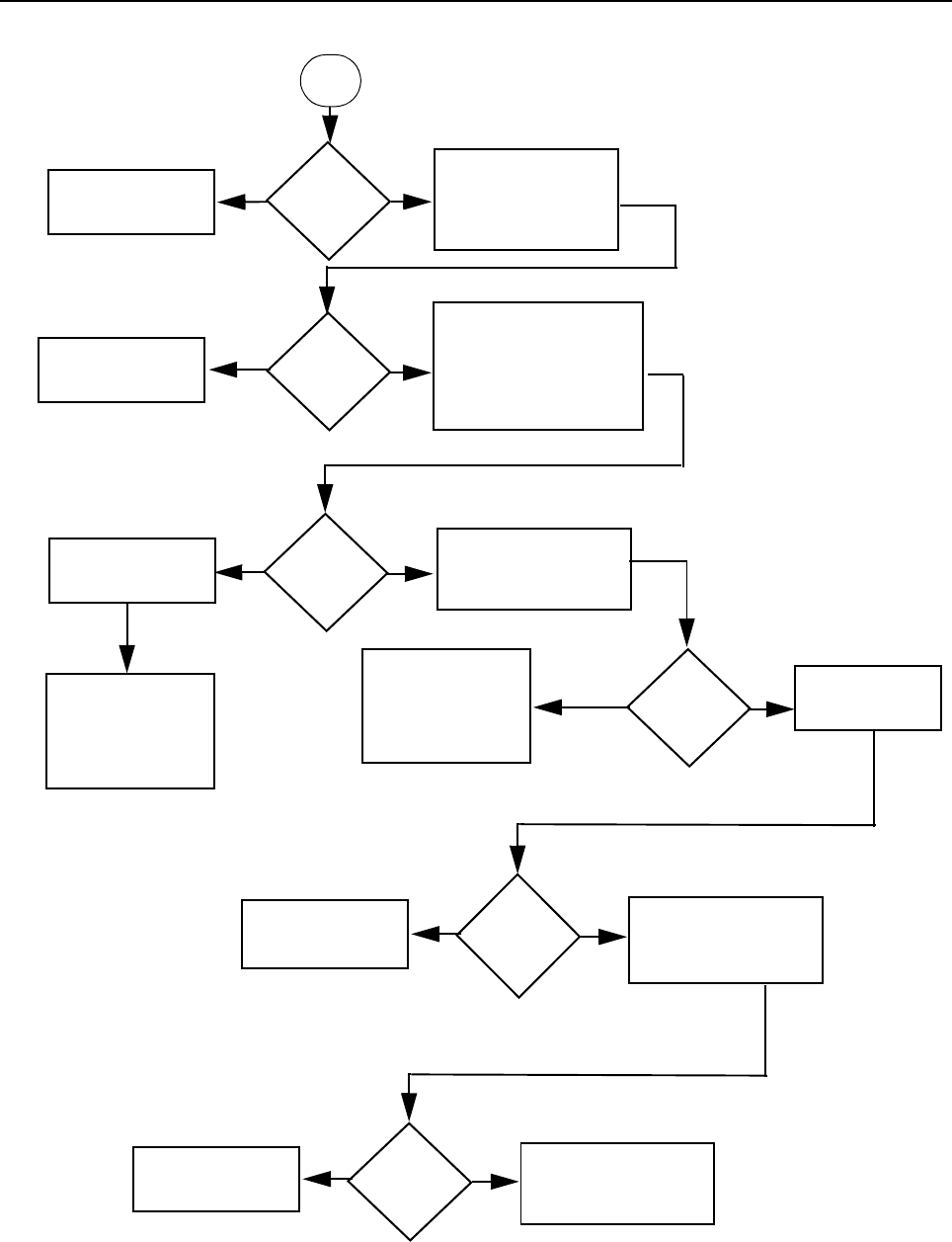
Troubleshooting Flow Chart for Receiver RF (Sheet 1 of 2) 3-3
1.1 Troubleshooting Flow Chart for Receiver (Sheet 2 of 2)
3V
(IFIC -Vcc)
OK ?
Installation
OK ?
Yes
Yes
No
No
A
From
Check visually
all receiver
components
installation ?
Inject - 40dBm (CW)
to RF connector
Check Power on
C332
RF
Power
> -28 dBM?
Yes
No
Check Power on
C336
Go to
DC Section
Check
the component
Antenna to Mixer
circuitry problem
Replace
Q303, Q301
Check passive
components
RF
Power
> -28 dBM?
Yes
No
Replace
Q305, Q300, U302
Check passive
components
Check Y301
44.395 MHz
Y301
OK?
Yes
No
Replace Q302, Y300
Check D301 - 304
Replace Y301
3V to
U301
OK?
Yes
No
Replace U300
Go to DC Section
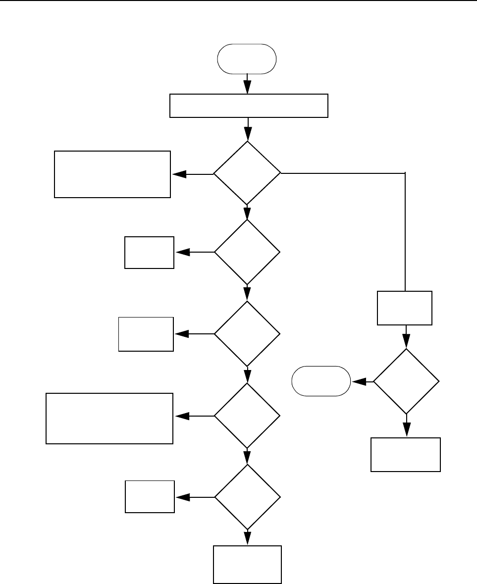
3-4 TROUBLESHOOTING CHARTS
2.0 Troubleshooting Flow Chart for 45W Transmitter (Sheet 1 of 3)
START
Yes
No
Check components between
Q100 and RF output,
Antenna Switch D104,
D103, VR102 and Q106
No or too low power when keyed
Current
increase when
keyed?
Check power settings, tuning
& components between U103
Pin 3 and ASFIC Pin 6 before
replacing ASFIC
Control
Voltage at
TP150
>4Vdc?
Check PA
Stages
>4A
Voltage U103
pin 5 =
4.6V?
U103 Pin 3
<1.6Vdc
U100 Pin 3
>1.8Vdc
Check 9.3V
Regulator
U501
Yes
Yes
No
No
Yes
Check
U103
Check forward
Power Sense
Circuit
No
Short U100
Pin 3 to
ground
Voltage at
TP150 rises?
Check PA
Stages
Check Forward
Power Sense
Circuit
Yes
No
>500mA & <4A
<500mA
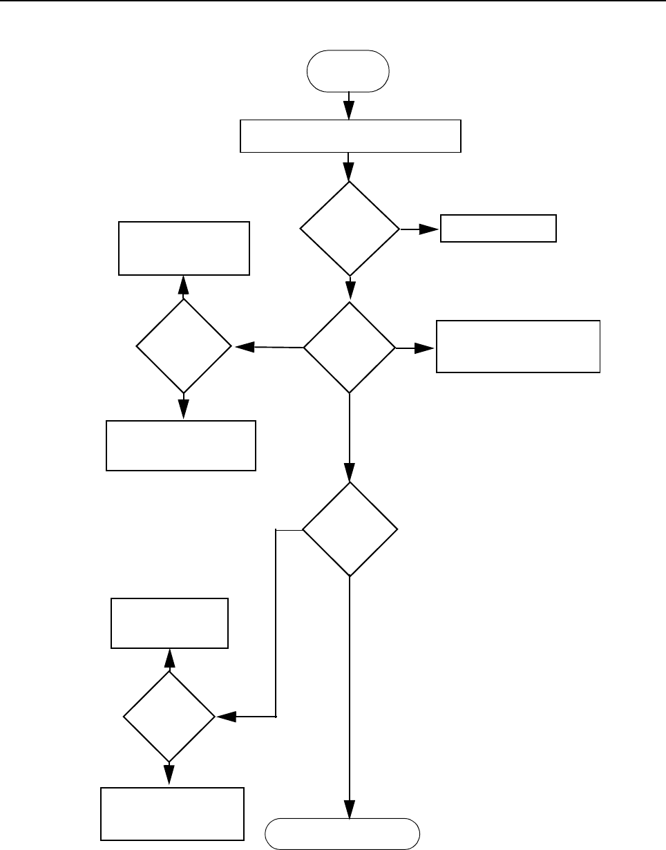
Troubleshooting Flow Chart for 45W Transmitter (Sheet 1 of 3) 3-5
2.1 Troubleshooting Flow Chart for 45W Transmitter (Sheet 2 of 3)
Yes
Check bias tuning
before replacing
U504
Check PA
Stages
No or too low power when keyed
DC
Voltage
at Q101
base=0?
DC
Voltage
at U103
Pin 8
Check U510
Check resistive network at
Pin 9 and 10 of U103
before replacing U101
DC
Voltage at
C1095
Check Final PA Stages
ASFIC
U504
Pin 5 2-3V
Check components be-
tween ASFIC and Q105
before replacing Q105
DC
Voltage at
U103 Pin
10=8.9V
Check Q101, R122,
R197, R153, R136,
R165, R168,
Check U103 before re-
placing U101
No
No
Yes
>5V
2 to 5V
2-3V
Yes
No
0V
<2V
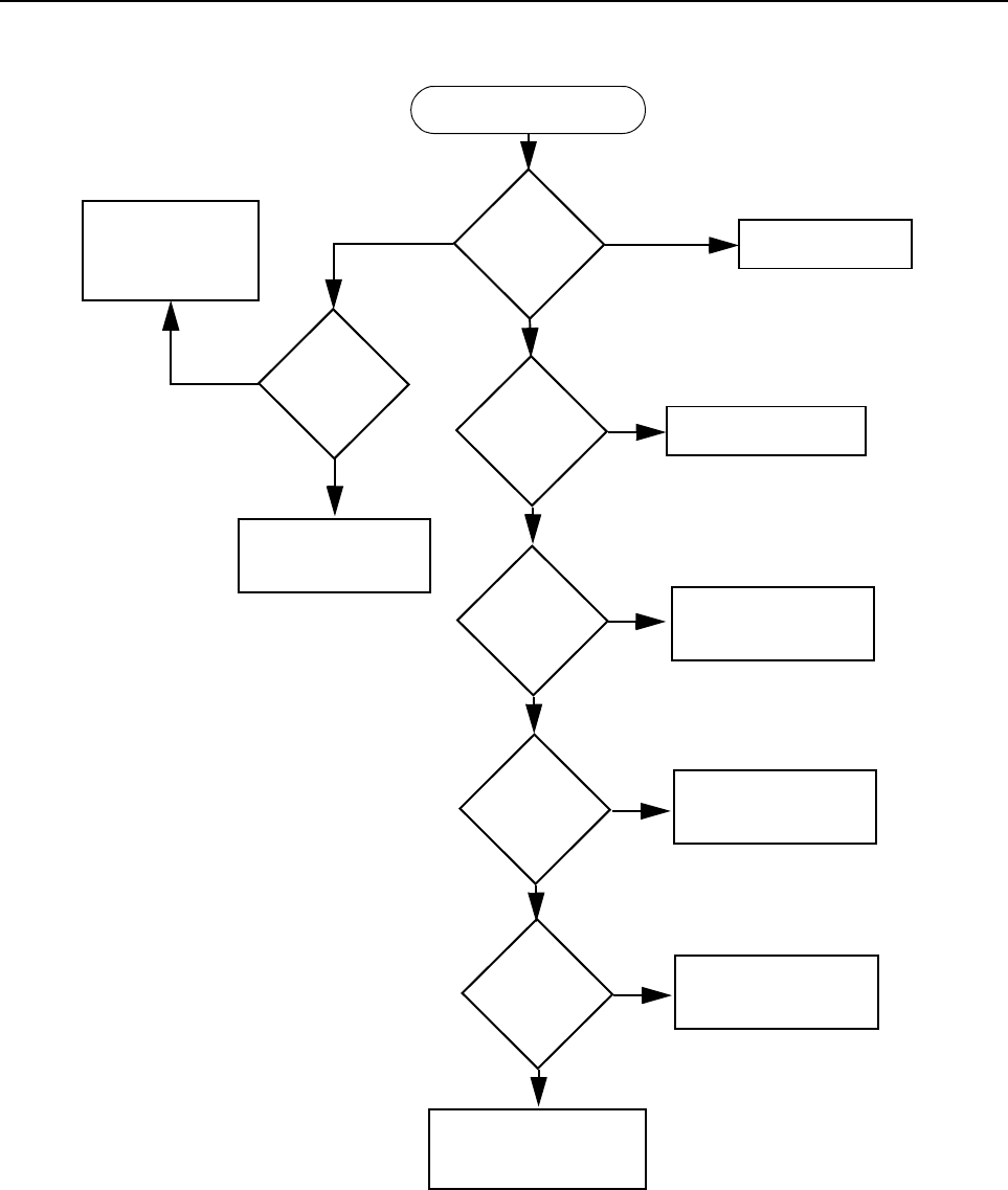
3-6 TROUBLESHOOTING CHARTS
2.2 Troubleshooting Flow Chart for 45W Transmitter (Sheet 3 of 3)
No
Yes
Yes
No
Check Final PA Stage
PA_Bias
Voltage at
R134
RF Voltage
after C1044
>100mV?
Voltage
across R122
>2V?
RF Voltage
Q105 gate
>1V?
RF Voltage
Q100 gate
>1.5V?
Check components
between Q100 &
antenna connector
Replace Q100
Check FGU
Check components
between C1044 &
C1117
Check components
between C1117 &
Q105
Check components
between Q105 &
Q100
No
No
Yes
Yes
1-4Vdc
Supply Voltage
Check components
between ASFIC &
Q100 before re-
placing Q100
RF Voltage
after C1044
>100mV?
Check Bias Tuning
before replacing
ASFIC U504
Yes
No
0V
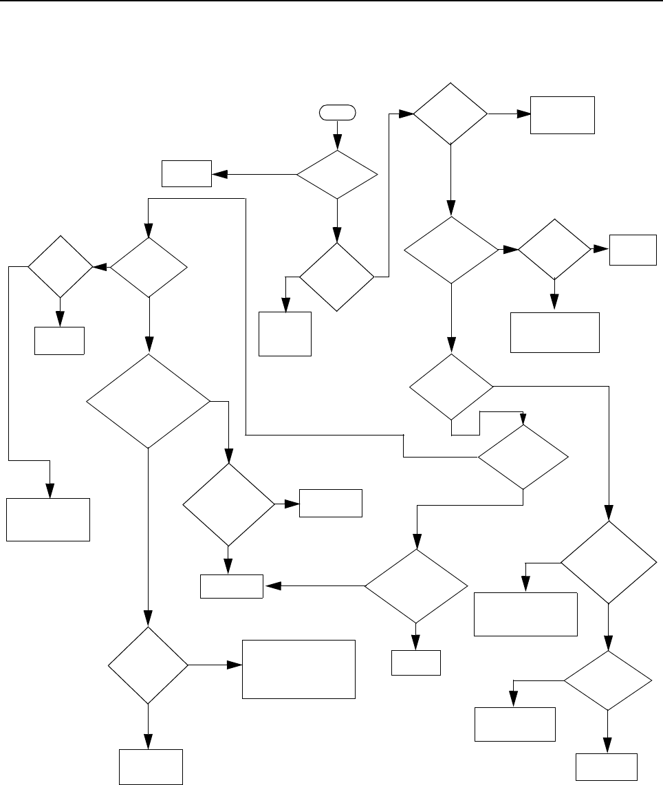
Troubleshooting Flow Chart for Synthesizer 3-7
3.0 Troubleshooting Flow Chart for Synthesizer
+5V at
U200 Pins
13 & 30?
5V
at pin 6 of
D200
Is information
from µP U403
correct?
Is U200
Pin 47
= 13VDC?
Is U201 Pin 19
<40 mVDC in RX &
>4.5 VDC in TX?
(at VCO section)
Start
Visual
check of the
Board OK?
Correct
Problem
Check 5V
Regulator
U503
Is 16.8MHz
Signal at
U200 Pin 19?
Check
Y201 and associated
parts
Are signals
at Pins 14 &
15 of U200?
Check
R228
Check R201
Is U200 pin 2
>4.5 VDC in Tx &
<40 mVDC in Rx
Replace U200
Remove
Shorts
Is there a short
between Pin 47 and
Pins 14 & 15 of
U200?
Is RF level at
U200 Pin 32
-12 < x <-25
dBm?
Replace
U200
If C2052, R208, C2067
C2068. C210, are OK, then
see VCO
troubleshooting chart
Are Waveforms
at Pins 14 & 15
triangular?
Do Pins
7,8 & 9 of
U200 toggle
when channel is
changed?
Check programming
lines between U403
and U200 Pins 7,8 & 9
Replace U200
Check µP U403
Troubleshooting
Chart
No
Yes
No
Yes
No
Yes
No
No
No
Yes
Yes
Yes
No
No
Yes
Yes
No
No
No
Yes
No
Yes
Yes
Check D200, D201,
C2026, C2025,
C2024 & C2027
3V at
U200 pins 5,
20, 34 & 36
C h e c k 3 V
Regulator
U508
Is
16.8MHz
signal at
U200 pin
23?
Replace
U200
Yes
No
No
Yes
No
Yes
Yes
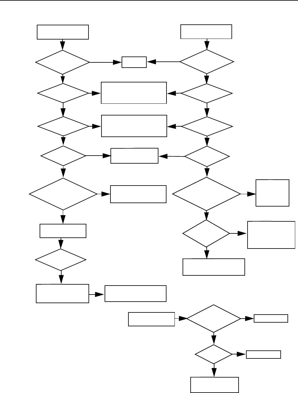
3-8 TROUBLESHOOTING CHARTS
4.0 Troubleshooting Flow Chart for VCO
Are Q200
Base at 2.4V
Collector at 4.5V
Emitter at 1.7V
Are U201 Pins
13 at 4.4V
15 at 1.1V
10 at 4.5V
16 at 1.9V
Low or no RF Signal
at TP1
Visual check
of board
OK?
35mV DC at
U201 Pin 19
NO
YES
at base of Q200
NO
NO
NO
NO
YES
YES
YES
YES
Low or no RF Signal
at input to PA
3.3V DC at U201
Pin 14 & 18 OK?
4.8V DC at
U201 Pin 19
Is RF available
at C2060
YES
YES
YES
YES
YES
NO
NO
NO
NO
NO
Audio =180mVrms
at “+” side of
D205
2.5VDC
at D205
If R211 is Ok,
replace D205
Replace R211
Replace R212
NO
NO
YES
YES
TX VCO
RX VCO
Correct
Problem
Visual check
of board
OK?
Make sure U508 is working
correctly and runner
between U508 Pin 1 and
U201 Pin 14 & 18 is OK
Check runner
between U200 Pin 2
and U201 Pin 19
Is RF available
If all parts from U200 Pin 8
to Base of Q200 are OK,
replace U200
Check parts between
TP1 and Q200
Power OK but
no modulation
Check Transmiter
Pre Driver
If all parts
associated
with the pins
are OK,
replace U201
4.5V DC at
U201 Pin 3 OK?
YES
NO 4.5V DC at
U201 Pin 3 OK?
YES
NO
Make sure Synthesizer is
working correctly and runner
between U200 Pin 28 and
U201 Pin 3 is OK
3.3 DC at U201
Pin 14 & 18 OK?
OK? OK?
If all parts associated
with the pins are OK
replace U201
If L216, C2071, C2070,
C2060 are okay
replace U201
Check 9V at R230
YES

Troubleshooting Flow Chart for DC Supply (1 of 2) 3-9
5.0 Troubleshooting Flow Chart for DC Supply (1 of 2)
Since the failure of a critical voltage supply might cause the radio to automatically power down,
supply voltages should first be probed with a multimeter. If all the board voltages are absent, then
the voltage test point should be retested using a rising-edge-triggered oscilloscope. If the voltage is
still absent, then another voltage should be tested using the oscilloscope. If that voltage is present,
then the original voltage supply in question is defective and requires investigation of associated
circuitry.
Check VDC on
C5008
V=3.3V
?
Check Voltage on
C5043
No
Go to D3_3V
Yes
9v<V<9.8v
?
Go to Start
No
Replace U508
Yes
3V
Check VDC on
C5006
V=5V
?
Check Voltage on
C5042
No
Go to 3V
Yes
9v<V<9.8v
?
Go to Start
No
Replace U503
Yes
5V
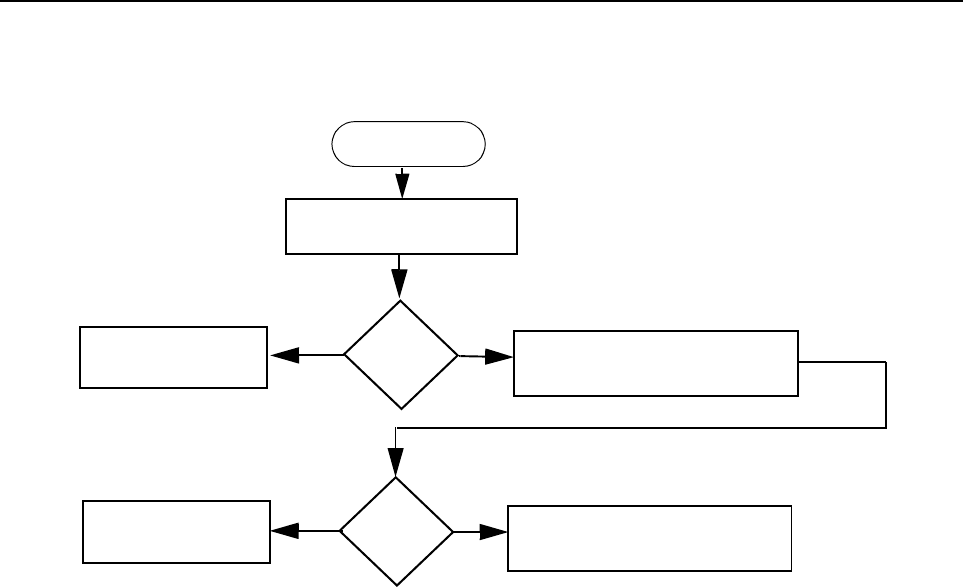
3-10 TROUBLESHOOTING CHARTS
5.1 Troubleshooting Flow Chart for DC Supply (2 of 2)
Check VDC on
C5007
V=3.3V
?
Check Voltage on
C5041
No
Go to Digital Section
Yes
9v<V<9.8v
?
Go to Start
No
Replace U510
Yes
D3_3V

Chapter 4
VHF2 PCB/ SCHEMATICS/ PARTS LISTS
1.0 Allocation of Schematics and Circuit Boards
1.1 VHF2 and Controller Circuits
The VHF circuits are contained on the printed circuit board (PCB) which also contains the Controller
circuits. This Chapter shows the schematics for both the VHF circuits and the Controller circuits. The
PCB component layouts and the Parts Lists in this Chapter show both the Controller and VHF circuit
components. The VHF and Controller schematics and the related PCB and parts list are shown in
the tables below.
Table 4-1 VHF2 25-45W Diagrams and Parts Lists
PCB :
8486487Z03-B Main Board Top Side
8486487Z03-B Main Board Bottom Side
Page 4-4
Page 4-5
SCHEMATICS
Main Circuit
Transmitter
Synthesiser and VCO
Receiver Front and Back End
DC and Audio Ccts
Microprocessor and Controller Ccts
Power Control Cct
Page 4-6/Page 4-7
Page 4-8/Page 4-9
Page 4-10/Page 4-11
Page 4-12/Page 4-13
Page 4-14/Page 4-15
Page 4-16/Page 4-17
Page 4-18
Parts List
8486487Z03-B Page 4-19
Controller version is T1

4-2 VHF2 PCB/ SCHEMATICS/ PARTS LISTS
THIS PAGE INTENTIONALLY LEFT BLANK
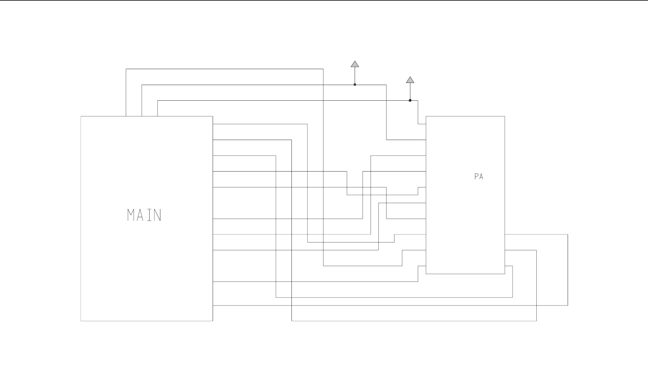
VHF 25-45W Band 2 PCB 8486487Z03-B / Schematics 4-3
2.0 VHF 25-45W Band 2 PCB 8486487Z03-B / Schematics
FILT_SW_B+
9V
COMP_B+
DET-VFWD
DET_VRVS
FILT_SW_B+
INTEGRATOR
PA_BIAS
PWR_SET
RX
RX_EN
TX_EN
TX_INJ
V_CTRL_DRIVER
9V
COMP_B+
DET_VFWD
DET_VRVS
FILT_SW_B+
INTEGRATOR
PA_BIAS
PWR_SET
RX
RX_EN
TX_EN
TX_INJ
V_CTRL_DRIVER
9V
VHF2 Interconnection between Main Board and Power Amplifier Compartment
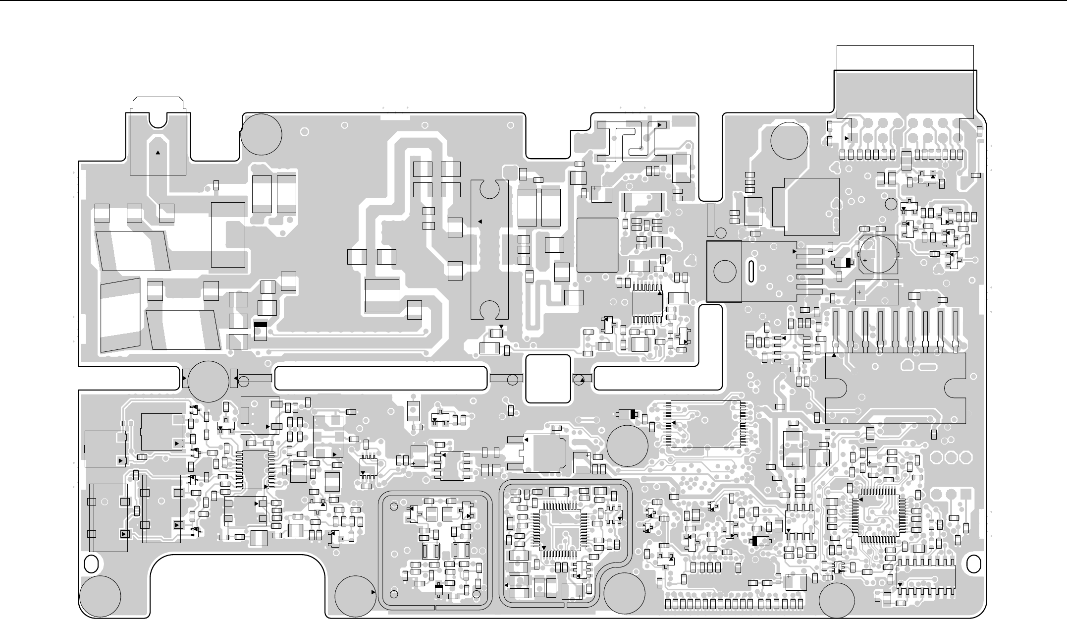
4-4 VHF 25-45W Band 2 PCB 8486487Z03-B / Schematics
C301
C302
C303
C304 C305
C306
C307
C308 C309
C310
C311
C312
C313
C314
C315
C316 C317
C318
C319
C320
C322
C335
C336
C352
C353
C356
C357
C359
C360
C364
C367
C402
C406
C411
C414
C418
C490
C602
C603
C604
C605
C606
C607
C608
C609
C610
C611
C612
C613
C614
C615
C616
C617
C618
C619
C620
C621
C622
C623
C624
C625
C626
C627
C628
C629
C630
C631
C632
C633
C662
C678
C1001
C1004C1005
C1007
C1008 C1009
C1011
C1012
C1013
C1014
C1015
C1017
C1018
C1019
C1020
C1021
C1022
C1026
C1030
C1031
C1033
C1034
C1037
C1039
C1041
C1044
C1047
C1049
C1052
C1057
C1063
C1064
C1065
C1068
C1069
C1074
C1076
C1082
C1087
C1088
C1096 C1097
C1098
C1099
C1100
C1104
C1105
C1111
C1113
C1114
C1115
C1116
C1117
C1118 C1119
C1120
C1122
C1123
C1124
C1125
C1132
C1137
C1199
C2001
C2002 C2004
C2012
C2013
C2014
C2016
C2024
C2025
C2026
C2027
C2028
C2030
C2033
C2036
C2052
C2055
C2056
C2057
C2058
C2059
C2061
C2062
C2063
C2064
C2066
C2067
C2068
C2069
C2073 C2074
C2075
C2077
C2078
C2079
C2080
C2081
C5001
C5003
C5005
C5006
C5008
C5010
C5011
C5012
C5013
C5014
C5015
C5016
C5018
C5019
C5020
C5021
C5022
C5023
C5024
C5025
C5026
C5027
C5028 C5029
C5030
C5032
C5033
C5034
C5035
C5038
C5042
C5043
C5044
C5046
C5047
C5048
C5050
C5051
C5052
C5053
C5054
C5056
C5057
C5059
C5062
C5064
C5066
C5068
C5070
C5071
C5074
C5076
C5078
C5079
C5080
C5081
C5087
C5088
C5089
C5090
C5095
C5096
C5100
C5101
C5102
C5103
C5110
C5111
C5112
CR300
D101
D104
D200
D201
D203
D204
D205
D301
D302
D303
D304
D400
D401
D500
D502
D513
23
4
5
6FL300
2
3
FL301
2
3
FL302
43
2
FL303
43
2
FL304
J11
L102
L103
L104
L105
L106
L107
L111
L112
L113
L116
L119
L120
L122
L123
21 L124
L203
L204
L205
L206
L207
L210
L211 L213
L214
L215
L301
L304
L315
M1 M2
M3
M4
M5
1M6
M7
M8
M9
M100
M101
M102
M103
M104
M105 M106
M107
M108 M109 M110
115
216
P1
5
2
64
31
78Q100
Q302
Q305
Q400
Q407
Q414
Q415
Q500
Q503
1
4
32
R101
R102
R105
R106
R107
R108
R109
R123
R124
R125
R146
R148
R150
R151
R171
R173
R174
R176
R178
R179
R190
R191
R197
R199
R200
R202
R206
R208
R211
R212
R217
R221
R222
R224 R225
R226
R228
R232
R233
R234
R302
R303
R304
R305
R306
R307
R308
R309
R311
R312
R313
R314
R315
R316
R317
R318
R319
R320
R321
R322
R323
R324
R325
R326
R328
R329
R331
R332
R334
R336
R338
R406
R428
R429
R430
R431
R439
R440
R441
R444
R445
R450
R451
R458
R459
R461
R462
R472
R473
R601
R602
R610
R5000
R5001
R5009
R5010
R5011
R5019
R5021
R5022
R5024
R5031
R5032
R5033
R5034
R5038
R5039
R5040
R5043
R5044
R5045
R5046
R5047
R5048
R5050
R5052
R5053
R5054
R5055
R5056
R5057
R5063
R5064
R5065
R5066
R5067
R5068
R5070
R5071
R5073
R5074
R5075
R5077
R5079
R5080
R5081 R5082
R5083
R5084
R5085
R5086
R5087
R5089
R6000 R6001
1
RT100
1
SH200
1
SH202
TP3
1
16
8
9
U101
1
37 25
13
U200
11
1
20
10
U300
4
58U301
22
21 8
7
1
U402
4
3
2
5
U501
1
9
U502
1
4
58
U503
1
37
25
13
U504
14
58
U505
1
4
U506
3
2
1
U508
9
8
1
16
U509
43
6
U515
VR101
VR105
VR401
VR500 VR501
VR504
VR693
2
3
Y300
4
3
2
Y301
85
VHF2 (146-174MHz) 25-45W 8486487Z03-B Top Side
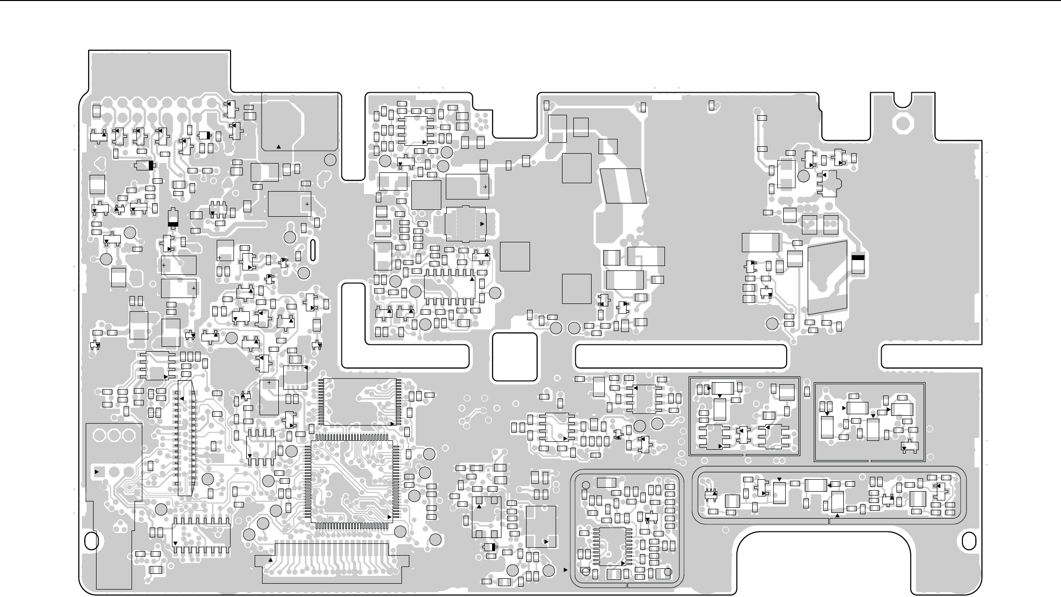
VHF 25-45W Band 2 PCB 8486487Z03-B / Schematics 4-5
C300
C321
C323
C324
C325
C326
C327
C328
C329
C330C331
C332
C333
C334
C337
C338
C339
C340
C341
C342
C343
C344
C345
C346
C347
C348
C349
C350
C351
C354
C355
C361
C362
C363
C365
C366
C400
C401
C403
C404
C405
C407
C408
C410
C412
C413
C415
C416
C417
C421
C422
C423
C1000
C1002
C1003
C1006
C1010
C1027
C1028
C1029
C1032
C1035
C1036
C1038
C1040
C1042
C1043
C1045
C1046
C1048
C1050
C1051
C1053
C1054
C1055
C1056
C1058
C1059
C1060
C1061
C1062
C1066
C1067
C1070
C1071
C1072
C1073
C1075
C1077
C1078
C1079
C1080
C1081
C1083
C1084
C1085
C1086
C1089
C1090
C1091
C1092
C1093 C1094
C1095
C1101
C1102
C1103
C1106
C1107
C1108
C1109
C1110
C1112
C1121
C1126
C1127
C1128
C1129
C1130
C1131
C1133
C1134
C1136
C2000
C2003
C2005
C2006
C2007
C2008
C2009
C2010
C2011
C2015
C2017
C2018
C2019
C2020
C2021
C2022
C2023
C2029
C2031
C2032
C2034
C2035
C2037
C2038
C2039
C2040
C2041
C2042
C2043
C2044
C2045
C2046
C2047
C2048
C2049
C2050
C2051
C2053
C2054
C2060
C2065
C2070
C2071
C2072
C2076
C5000
C5002
C5007
C5009
C5017
C5031
C5036
C5037
C5039
C5040
C5041
C5045
C5049
C5055
C5058
C5060
C5061
C5063
C5065
C5067
C5069
C5072
C5073
C5075
C5077
C5082
C5083
C5084
C5085
C5086
C5091
C5092
C5094
C5097
C5098
C5099
C5104
C5113
C5114
C5115
C5116
C5117
C5118
C5119
C5120
CR301
D100
D102
D103
D105
D106
D107
D108
D202
D305
D402
D501
D511
1
J2
29
28 2
29
30 32
31
J3
L100
L101
L108
L109
L110
L114
L115
L117
L118
L121
L131
L132
L200
L201
L202
L208
L209
L212
L216
L217
1L300
L302 L303
L305
L306
1 L307
1L308
1 L309
1L310
1L311
1 L312
1L313
1 L314
L500
L501
L502
M111
M112
M113
M114
1P2
Q101Q102
Q103
1
2
3
Q105
Q106
Q200
Q300
Q301
Q303
Q304
Q306
Q401
Q403
Q404
Q405
Q408
Q409
Q410
Q411
Q412
Q413
Q416
Q417
Q501
Q502
Q504
Q505 Q506
R103
R104
R110
R111
R112
R113
R114
R115
R116
R117
R118
R120
R121
R122
R126
R127
R130
R131
R132
R134
R135
R136
R137
R138
R139
R140
R141
R142
R143
R144
R145
R147
R149
R153
R155
R156
R157
R158
R159
R160
R161
R162
R163
R164
R165
R166
R167
R168
R169
R170
R172
R175
R177
R180
R181
R182
R185
R186 R188
R189
R195
R196
R198
R201
R203
R204
R205
R207
R209
R210
R213
R214
R215
R216
R218
R219
R220
R223
R227
R229
R230
R231
R235
R300
R301
R310
R327
R330
R333 R335
R337
R339
R340
R341
R342
R343
R344
R345
R346
R401
R402
R403 R404
R405
R407
R414 R415
R421
R422
R423
R424
R425
R426
R427
R432
R433
R434
R435
R436
R438
R442
R443
R453
R454
R455
R456 R457
R460
R463
R466
R467
R468
R469
R470
R471
R600
R615
R5002
R5008
R5013
R5014
R5016
R5020
R5023
R5025
R5026
R5027
R5028
R5029
R5030
R5035
R5036
R5037
R5041
R5042
R5049
R5051
R5058
R5059
R5060
R5061
R5062
R5069
R5072
R5076
R5078
R5088
R5092
R5093
R5094
R5095
R5096
R5097
R5098
R5099
R5100
R5103
R5290
R5291
1
6
5
4
3
2
1
S5010
1
SH201
SH300
SH301
SH302
6
4
3T300
64
3
T301
TP1
TP2
TP4
TP101
TP102
TP103
TP104
TP106
TP107
TP108
TP110
TP111
TP112
TP113
TP114
TP150
TP200
TP201
TP400
TP401
TP402
TP403
TP404
TP405
TP406
TP407
TP408
TP409
TP410
TP425
TP500
TP555
TP556
1
4
58
U100
14
58
U102
8
71
14
U103
11
1
20
10
U201
U302
14
58
U400
1
76 51
26
U403
16
17
32
U404
9
8
1
16
U405
14
58
U500
14
58
U507
4
58
U510
U514
VR102
VR400
VR402
VR502
VR503
VR692
VR694
VR695
VR696
VR697
VR698
VR699
Y200
4
3
2
Y201
VHF2 (146-174MHz) 25-45W 8486487Z03-B Bottom Side
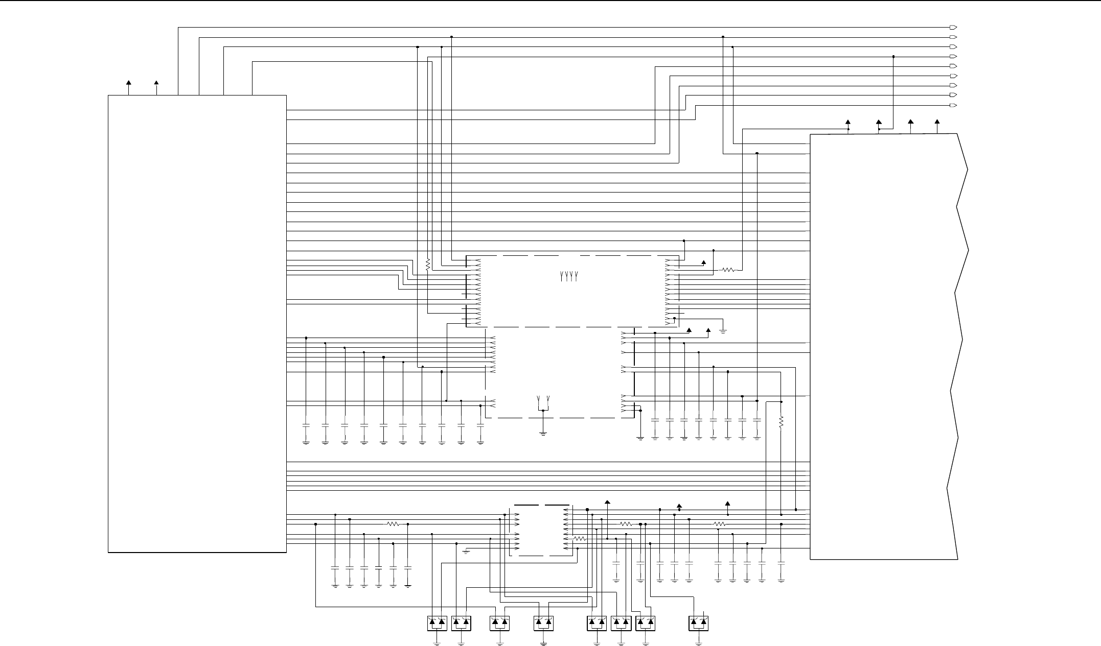
4-6 VHF 25-45W Band 2 PCB 8486487Z03-B / Schematics
GND
KEYPAD COLUM N
Internal spkr+ jumper
SPI_MOSI
ELP ONLY
SERIAL CLOCK
ELP ONLY
KEYPAD_COLUMN
DNP
Option Board Connector
ELP ONLY
VOICE STORAGE IN T
RX AUDIO RETURN
BACKLIGHT
SCI_PROGRAMMING
Accessory Connector
DATA READY/REQUEST
SPI_CLK
NC
DNP
DISPLAY DRIVER CHIP SELEC TNC
TX AUDIO RETURN
D3_3V
DNP
ANALOG 3 VOLT SUPPLY
OPTION BOARD ENABLE
EXTERNAL MIC
(SOURCE)
9V3
9.3V
DETECTOR AUDIO SEND
KEYPAD ROW
DISPLAY_DRIVER_CS_EN
NC
Place capacitors near J2
INT_SPKR-
SERIAL DATA RETURN
VOICE STORAGE GAIN SELEC T
NC
SERIAL DATA SEN D
HANDSET_RX_AUDI O
RESET
NC
VOICE STORAGE AUDIO SELEC T
MIC_AUDIO
(SOURCE )
ELP ONLY
VOICE STORAGE CS
Control Head Connector
KEYPAD_ROW
BOOT/RESET
PUSH TO TAL K
UNMUTED RX AUDIO SEND
INT_SPKR+
DISPLAY_DRIVER_COMMAND/DATA_SEL
(SOURCE)
J3 -
TX AUDIO SEND
28 pins connector
Place capacitors near J2
MIC_PTT
GND
DNP
(SOURCE)
ELP ONLY
GND
VOICE STORAGE RA C
DIGITAL 3.3 VOLT SUPPL Y
Place capacitors near J2
SHIFT_REG_CS
GND
HOOK
Place capacitors near J2
POST-LIMITER FLAT TX AUDIO RETURN
DISPLAY_DRIVER_RESET
J2-22
G2
2
24
C609 1000pF
J3-26 26
J3-24
14
J3-28 28
J3-21 21
J3-14
R602
0
J3-1212
J2-18 18
1000pF
2
C621
4
2
J2-4
2
R615 100
J2-2
2
C678
0.1uF
2
P1-2
C623
1000pF
C611 1000pF
2
VR695
1
2
J2-1616
20.0
2
J2-1717
C605 1000pF
2
P1-11 11
1000pF
C620
J2-77
SPKR+
J2-55
J2-21
G1
2
D3_3V
1000pF
C632
J3-22
1000pF
C628
2
20.0
1
VR697
1000pF C624
2
C631 1000pF
D3_3V
C615 1000pF
2
3
J3-9
J2-14 14
J2-3
1000pF
2
C607
P1-33 330
R6011
J3- 77
J3-4
J3-55
22
J3-20 20
J3-11 11
J3-22
J3-25 25
J3-23 23
1
2
J3-27 27
VR694
20.0 VR692
20.0
1
4
J2-88
2
P1-4
1000pF
C602
J2-20 20
J2-12 12
1000pF
2
FILT_SW_B+
2
C633
C617 1000pF
VR698
20.0
1
2
2
J2-1010
1000pF
C622
1000pF
C604
2
J2-11
P1-1 1
C625
1000pF
2
1000pF
2
VOX
VSTBY
VS_AUDIO_SEL
VS_MIC
uP_CLK
C627
ONOFF_SENSE
POST_LIMITER_FLAT_TX_AUDIO_RETURN_OPT_BRD
RESET
RX_AUDIO_OUTPUT_ACCESS_CONN
RX_AUDIO_RETURN_OPT_BRD
SPI_CLK
SPI_MOSI
SPKR+
SPKR-
SQ_DET
TX_AUDIO_RETURN_OPT_BRD
TX_AUDIO_SEND_OPT_BRD
UNMUTED_RX_AUDIO_SEND_OPT_BRD
VOL_INDIRECT
D3_3V
DETECTOR_AUDIO_SEND_OPT_BRD
EMERGENCY_ACCES_CONN
EMERGENCY_SENSE
EXTERNAL_MIC_AUDIO_ACCESS_CONN
F1200
FLAT_TX_AUDIO_INPUT_ACCESS_CONN
HANDSET_RX_AUDIO_CH
HSIO
IGNITION
LSIO
MIC_AUDIO_CH
3V 5V
5V_CH
9V
ASFIC_CS
BATT_SENSE
CH_ACT
P1-9 9
1000pF
2
C608
2
C619
1000pF
1000pF
2
J2-99
C603
6
15
J3- 33 J3-6
J2-15
J2-1313
FILT_SW_B+
1000pF
C614
2
19 J3-1818
2
J3-19
1000pF
C662
P1-1010
3V
9V
2
J2-66
C613 1000pF
11
P1-1414
J2-11
29
J3-30
30
J3-29
13
J3-1515
J3-1010
J3-13
P1-66
D3_3V
1000pF
2
9V
C629
0R6001
0
R6000
1
1
2
VR693
33.
20.0
VR696
J2-19 19
SPKR -
D3_3V
P1-16 16
5V
J3-11
15
R610 220
VS_GAIN_SEL
VS_INT
VS_RAC
uP_CLK
P1-15
RSSI
RX_EN
SCI_CH
SHIFT_R_CS
SPI_CLK SPI_MISO
SPI_MOSI
SQ_DET
SYNTH_CS
SYNTH_LOCK
TX_EN
VOL_INDIRECT
VOX
VSTBY
VS_AUDIO_SEL
VS_CS
HSIO
KEYPAD_COL_CH
KEYPAD_ROW_CH
LOC_DIST
LSIO
MIC_PTT_CH
ONOFF_SENSE
OPT_DATA_R_OPBD
OPT_EN_OPBD
PROG_I-ACC_C_3
PROG_I-ACC_C_6
PROG_IO-ACC_C_12
PROG_IO-ACC_C_14
PROG_IO-ACC_C_8
PROG_O-ACC_C_4
RESET
8
ASFIC_CS
BATT_SENSE
BOOT_EN_IN_CH
CH_ACT
COMM_DATA_SEL_CH
D3_3V
DISPLAY_CS_CH
EMERGENCY_SENSE
F1200
FILT_SW_B+
HOOK_CH
2
P1-8
1000pF
C612
17
J3-1616
5
J3-88
J3-17
2
P1-5
1000pF
C606
P1-1212
20.0
VR699
1
2
J3-31
31
2
J3-32
32
1000pF
C616
P1-13 13
1000pF
C630
2
C618 2
1000pF
1000pF
C626
2
1000pF
C610 2
P1-7
7
R600
21 0
ACCESSORY CONNECTOR
EXT_ALARM_OUT
EXT_MIC_PTT
PROG_IN
PROG_I/O
PROG_I/O
PROG_I/O
KEYPAD / DISPLAY OPTION BOARD
DC & AUDIO
9
4
DIGITAL
TX_EN
SPI_CLK
SPI_MOSI
9V
RSSI
SYNTH_CS
LOC_DIST
RX_EN
SYNTH_LOCK
FULL DISPLAY ONLY
FULL DISPLAY ONLY
VHF2 (146-174MHz) 25-45W Main Circuit (Sht 1 of 2)
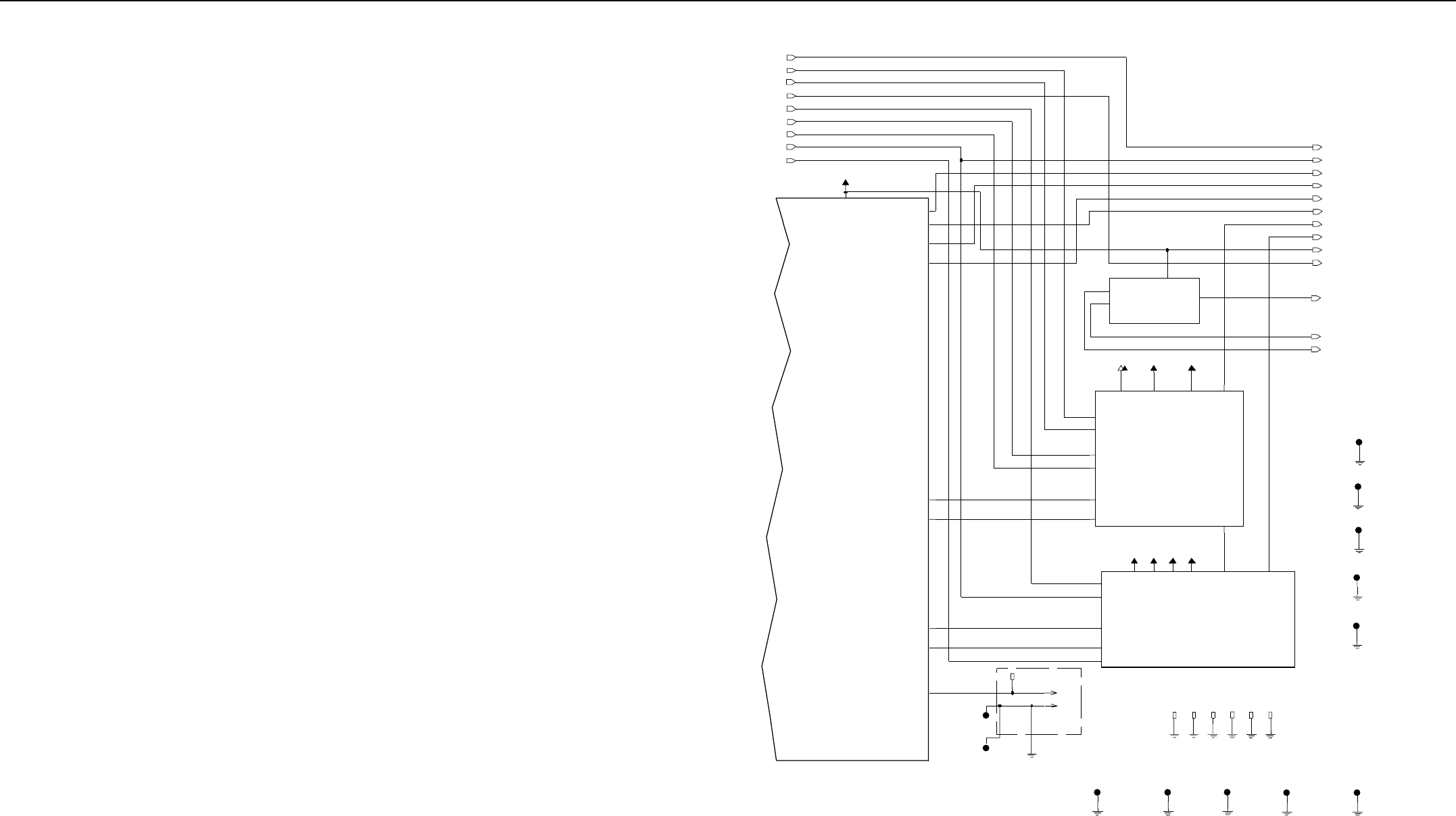
VHF 25-45W Band 2 PCB 8486487Z03-B / Schematics 4-7
(SOURCE)
DC Connector
HOLES FOR PA SHIELD
(SOURCE)
BOARD HOLES
PEDS FOR GND CONTACTS
M110
1
3V
FILT_SW_B+
TEST_POINT
M101
1
FILT_SW_B+
INTEGRATOR
M106
1
DET_VFWD
DET_VRVS
9R
M104
TEST_POINT
1
1
9R
TEST_POINT
TP3
TP 2
TEST_POINT
1
TEST_POINT
M8
1
SPI_MOSI
SYNTH_CS
SYNTH_LOCK
TX_INJ
TEST_POINT
M3
1
16.8MHz
3V5V 9R
MOD_IN RX_IN J
SPI_CLK
TEST_POINT
M102
1
V_CTRL_DRIVER
PA_BIAS
PWR_SET
COMP_B+
DEMOD
FILT_SW_B+
MOD_OUT
M9
NUT
16.8MHz
B+
BW_SEL
M108
1
M7
TEST_POINT
1
M5
TEST_POINT
1
5V
P2-11
TEST_POINT
M1
1
3V5V
9R 9V
BW_SEL
DEMOD
LOC_DIST
RSSI RX
RX_EN
RX_INJ
1
1
M109
1
M107
TEST_POINT
M2
M103
TEST_POINT
1
9V
2
M105
1
P2-2
5V VCC
COMP_B+
9V
DET-VFWD
DET_VRVS
INTEGRATOR
RX
PWR_SET
V_CTRL_DRIVER
PA_BIAS
FILT_SW_B+
TX_EN
RX_EN
TX_INJ
DC & AUDIO
FGU
RX
POWER_CONTROL
TX_EN
SPI_CLK
SPI_MOSI
9V
RSSI
SYNTH_CS
LOC_DIST
RX_EN
SYNTH_LOCK
VHF2 (146-174MHz) 25-45W Main Circuit (Sht 2 of 2)
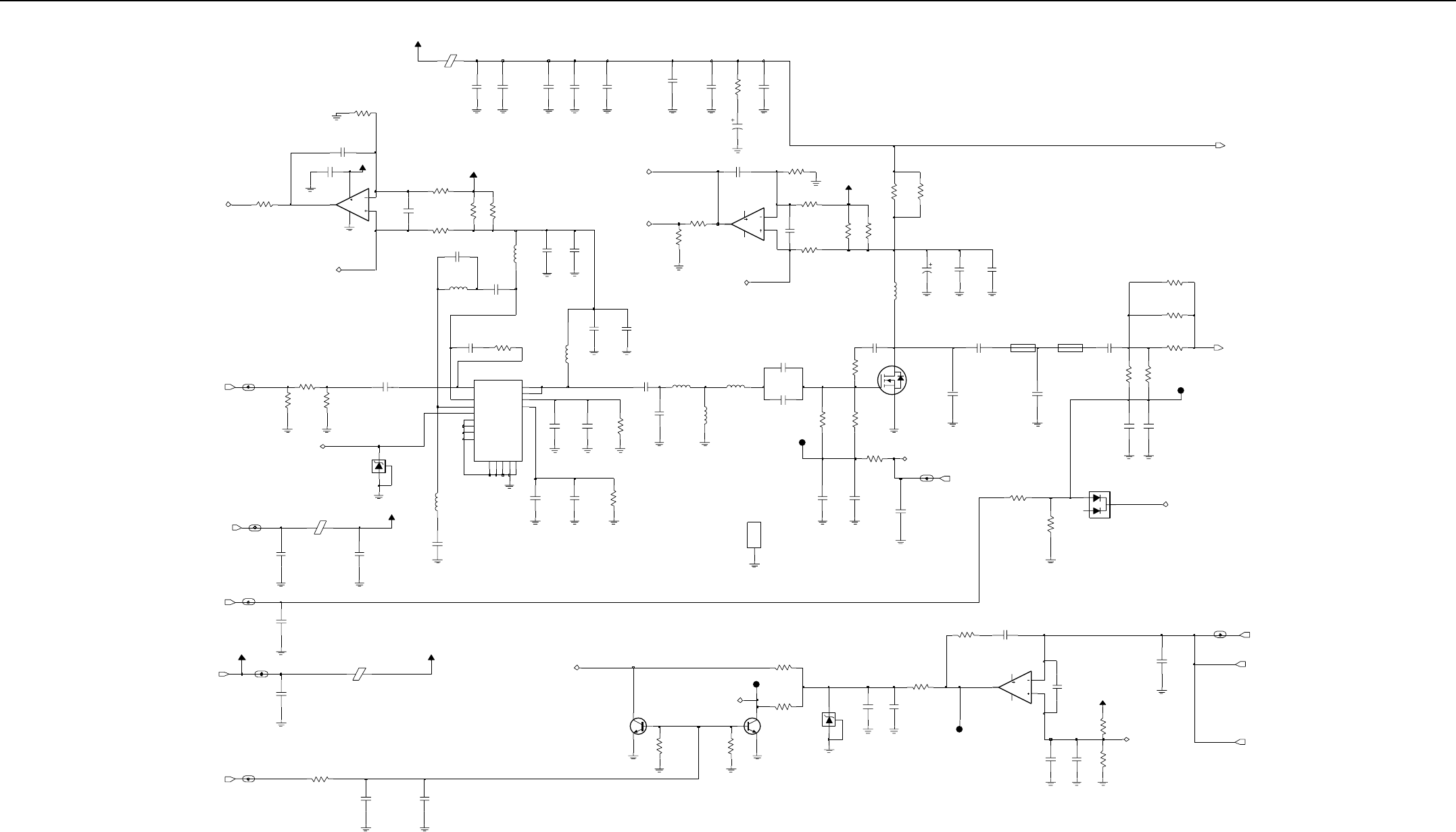
4-8 VHF 25-45W Band 2 PCB 8486487Z03-B / Schematics
MRF1518’s Thermal pad
1.542*4 0.8*2 5
(SOURCE)
V_CNTRL
220pF
C1095
2.4K
NU
R166
R168
2.2K
C1063
330pF
C1062
1000pF
R137
39K
C1001
1uF
C1105
470pF
R106
51
C1117
1000pF
36pF
C1089
IF113
C1043
110pF
100K
R131
5.6K
R159
NU
NU
R188
0
39K
R139
NU
FILT_SW_B+_PA
C1107
470pF
470pF
C1106
510
R170
330pF
C1068
C1014
56pF
FLT_9V
NU
.022uF
C1037
.022uF
C1039
FILT_SW_B+_PA
C1030
27pF
L105
68nH
C1029
0.1uF
12nH
L104
FLT_9V
R122
4.7
R189
330pF
C1065
NU
0
R102
51
C1084
220pF
VR105
5.6V
TP102
1
IF106
C1104
.01uF
MC3303
U103-3
9
10
8
4
11
MC3303
U103-2
6
5
74
11
C1119
24pF
33pF
C1118
NU
R175
220
TP150
1
36
R178
C1040 NU
2200pF
FILT_SW_B+
PA_FILT_B+
35U02
L121
110pF
C1042
0.1uF
C1028
220pF
C1109
R130
0
C1038
M100
HEATSINK
POS
1
NU
.022uF
13.85nH
L122
R173
150
C1026
1000pF
220pF
C1126
330pF
C1044
10K
R155
22K
R147
120nH
R176
470pF
C1041
R174
150
NU
2
3
18
4
U102-1
LM2904
5.6V
VR101
R136
39K
.022uF
C1033
R167
2.2K
1000pF
C1066
R109
30
4.7
R197
FLT_9V
IF107
R134
47K
C1057
1000pF
0
R199
NU
11.03nH
L109
2.2K
NU
R169
C1060
1000pF
56pF
C1012
R126
1
10uF
C1027
220pF
C1000 C1112
220pF
R165
2.4K
C1120
33pF
L118
35U02
C1061
NU
1000pF
R179
36
R182
10K
R153
10K
RFIN
16 RFOUT1 6
RFOUT2 7
VCNTRL
1
VD1
14 VG1 2
VG2 3
GND1
4
GND2
5
GND3
12
GND4
13
NC1
8
NC2
9
NC3
10
NC4
15 30C65
U101
17 EP
G2
11
.022uF
C1032
R171
220
C1053 1000pF
1000pF
C1092
.022uF
C1036
2.7
R124
R125
2.7
R123
2.7
Q105
NU
C1069
330pF
FLT_9V
R186
5.1
C1064
1000pF
4.22nH
L107
C1054
IF100
1000pF
Q101
R158
5.6K
NU
39K
R138
220pF
C1110
.033uF
C1103
C1086
1000pF
IF104
D100
NU
IF108
220pF
C1129
1
R127
C1081
1000pF
C1072
1000pF
C1070
1000pF
IF105
7.66nH
L106
47K
R181
47K
R180
C1074
51
1000pF
1
R105
TP104
Q102
12nH
L110
TP103
1
L100
35U02
.022uF
C1031
C1015
FILT_SW_B+
9V
PA_BIAS
V_CTRL_DRIVER
V_CTRL_DRIVER
V_CTRL_PREDRIVER
110pF
V_CTRL_DRIVER
VCNTR3
RX_EN
V_REF_OPAMP
VCNTR1
VCNTR1 VCNTR1
VCNTR2
VCNTR2 VCNTR2
INTEGRATOR
VCNTR3
VCNTR3
TX_INJ
V_CTRL_PREDRIVER
V_CTRL_PREDRIVER
PA_FILT_B+
Q100-G
INTEGRATOR
INTEGRATOR
NU
NU
VHF2 (146-174MHz) 25-45WT ransmitter (Sht 1 of 2)
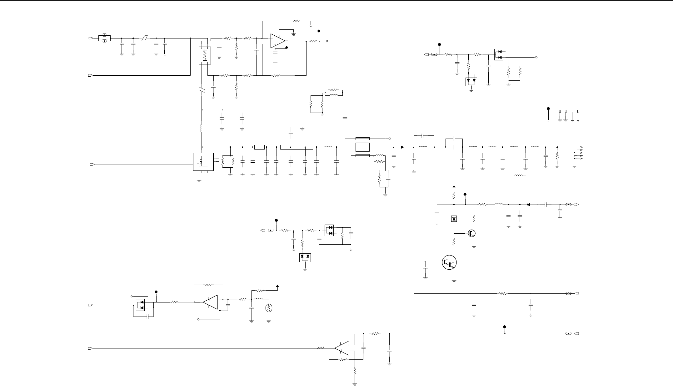
VHF 25-45W Band 2 PCB 8486487Z03-B / Schematics 4-9
Coupler
Temp. Sense
Place near both sides of PA shields
7.5 width 2.032 Antenna Connector (Mini-U / BNC )
3.3K
R160
S3
S4
D
G
GND1
GND2
S1
S2
MRF1550
Q100
IF101
R185
10K
16pF
NU
C5112
NU
6.8pF
C1121
C1020
39pF
D108
100nH
L132
NU
0
R196
0
R198
82pF
C1096
1000pF
C1067
NU
10K
R114
R110
NU
TP114
1
1K
R172
470
1MEG
R191
1
M111
22K
R142
J11- 5
G2
3.3K
R162
R113
10K
NU
35U02L119
R161
3.3K
1uF
C1002
4
11
MC3303
U103-4
13
12
14
C1134
24pF
1000pF
C1099
32pF
C1019
FLT_9V
Q106
D103
D104
NU
C1010
100pF
IF103
220pF
C1116
L108
1.2uH
R143
22K
0
R195
NU
R115
NU 62K
R112
10K
TP113
1
150
R118
TP112
1
IF102
L123
1.2uH
62pF
C1009
51nH
L113
D106
M112
1
1000pF
C1091
C1111
470pF
L114
82pF
51nH
C1007
51nH
L112 L124
48nH
R157
56K
C1101
100pF
D105
7.5pF
C1008
C1051
1000pF
IF109
24K
R135
100pF
C1005
J11- 22
35U02
L117
C1080
1000pF
MC3303
U103-1
2
3
1
4
11 C1059
1000pF
R190
1MEG
C1013
6.2pF
7.5K
R151
C1052
1000pF
470pF
NU
C1003
D107
VR102
5.6V
100pF
C1004
82pF
C1132
NU
1000pF
1
TP110
1
C1055
TP107
IF110
160pF
C1006
R121
R120 100
C1056
NU
100
1000pF
L103
1uH
47K
R132
NU
RT100
100K
51nH
L111
68pF
G1
C1108
J11- 33 J11-4
33pF
C1133
1000pF
C1079
R156
10K
1
TP108
C1130
220pF
82pF
C1011
NU
120nH
L131
1.639m
R101
R148
22K
R150
47K
1000pF
C1058
NU
NU
C1021
6.2pF
Q103
100
R5291
R5290
100
C1100
1000pF
R149
22K
C1017
15pF
R103
51
51
R104
C1035
.022uF
PA_FILT_B+
C1115 7
8
4
220pF
U102-2
LM2904
NU
6
5
17nH
L116
17nH
L115
C1018
39pF
FILT_SW_B+_PA
C1199
NU
16pF
4.7pF
C1136
3.3K
R163
IF111
28pF
C1022
IF112
M4
1
C1102
100pF
51
R108
NU
51
R107
R111
1K
C1137
43pF
C1073
NU
1000pF
C1077
1000pF
R116
NU
10K
R177
100 NU
C1050
22K
R145
1000pF
D102
1 J11-1
TX_EN
PWR_SET
DET_VRVS
DET_VFW D
COMP_B+
Final_cur_sense
V_forward
Final_cur_sense
V_reverse
V_reverse
V_REF_OPAMP
V_REF_OPAMP
RX
INTEGRATOR
INTEGRATOR
PA_FILT_B+
R123
R124
R125
NU
1
M113
M114
1
NU
VHF2 (146-174MHz) 25-45W Transmitter (Sht 2 of 2)
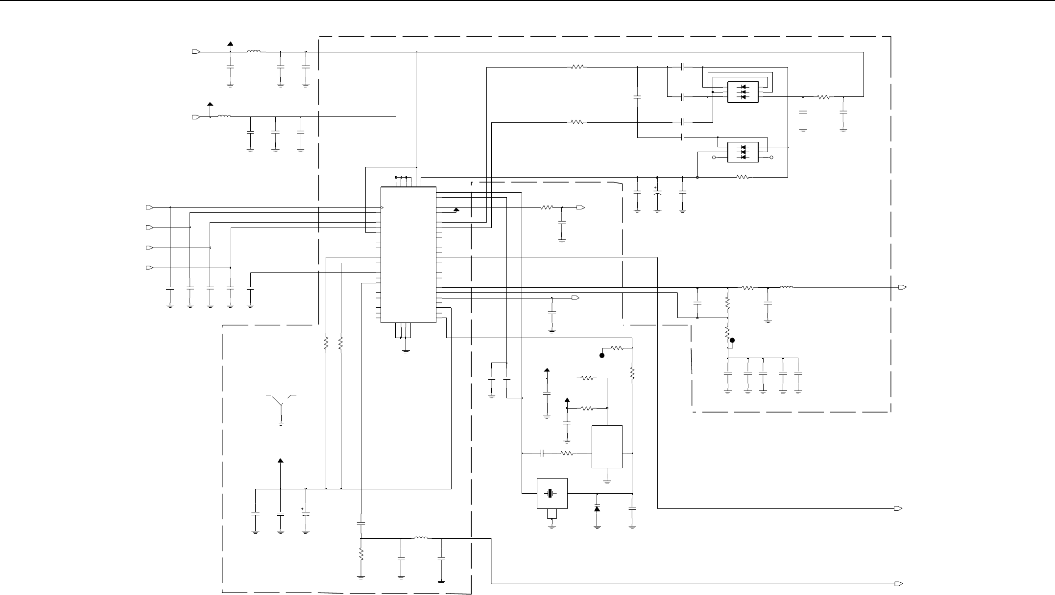
4-10 VHF 25-45W Band 2 PCB 8486487Z03-B / Schematics
DNP
DNP
DNP
DNP
DNP
DNP
LVFRACN Shield
DNP
3V
2.7pF
C2072
C2001
4.7u F
C201 5
0.1u F
C2014
5V
0.1uF
390nH
L200
470pF
C2046
2.2uF
C2006
45J68
2
GND
3OUT
VCC
4
1
VCON
16.8MHz
Y200
0.1uF
C2075
1.5K
R224
SH200
SHIELD
1
NC
2.2uF
C2000
.01uF
C2026
22pF
C2055
C2047
470pF
C2053
100pF
.01uF
C2024
C2080
0.1uF
R209
100K
C2052
470pF
C2049
470pF
TEST_POINT
TP201
1
L210
100nH
R202 0
C2036
1000pF
0
R205
1000pF
C2035
C2079
0.1uF
C2020
0.1uF
C2068
6.8pF
2200pF
C2028
R226
150
100K
R210
R208
51
C2078
0.1uF
C2002
10uF
390nH
L217
C2051
220pF
C2017
0.1uF
K2
K3
D201
A1
A2
A3
K1
TP200
TEST_POINT
1
C2074
0.1uF
150K
V_SF
R207
8.2pF
C2067
100
R228
C2033
1000pF
1000pF
C2034
R229
100
C2013
0.1u F
R234
39
A1
A2
A3
K1
K2
K3
D200
C2025
.01uF
150
R225
0.1uF
C2077
1.3K
R217
C2023
.01uF
62pF
C2054
0
R204
C2016
0.1uF
470pF
C2048
VCO_MOD
3
OUT
1IN
Y201
14R06
16.8MHz
2
GND
4
GND1
1uH
L205
12
VMULT4 11
13
VRO
WARP 25
XTAL
123
XTAL2 24
30
SFOUT 28
TEST1 37
TEST238
VBPASS
21
VCP 47
VMULT1 15
VMULT2 14
VMULT3
PD_VDD
PREIN
32
PRE_GND
33 PRE_VDD 34
PVREF
35
REFSEL
18
SFBASE
27 SFCAP
26
SFIN
43
4
LOCK
MODIN
10
MODOUT 41
NC1
17
NC2
29
NC3
31
PD_GND
44
5
9CLK
8
DATA
7
DGND
6
DVDD 36
FREFOUT 19
IADAPT 45
INDMULT 16
IOUT
48
AUX2 1
AUX3 2
AUX4 3
AVDD 20
BIAS1
40
BIAS2
39
CCOMP
42
CEX
U200
63A27
ADAPTSW 46
AGND
22
AUX1
470pF
C2050
150K
R206
2.2uF
C2004
R200
120K
470pF
C2045
5V
3V
C2027
.01uF
2.2u F
C2005
D202
NC
3V
5V
SYNTH_LOCK
16.8MHZ
SYNTH_CS
MOD_I N
SPI_CLK
SPI_MOSI
AU3
PRESEC_CLK
VCO SHLD
L203 & L204
VHF2 (146-174MHz) 25-45W Synthesiser and VCO (Sht 1 of 2)
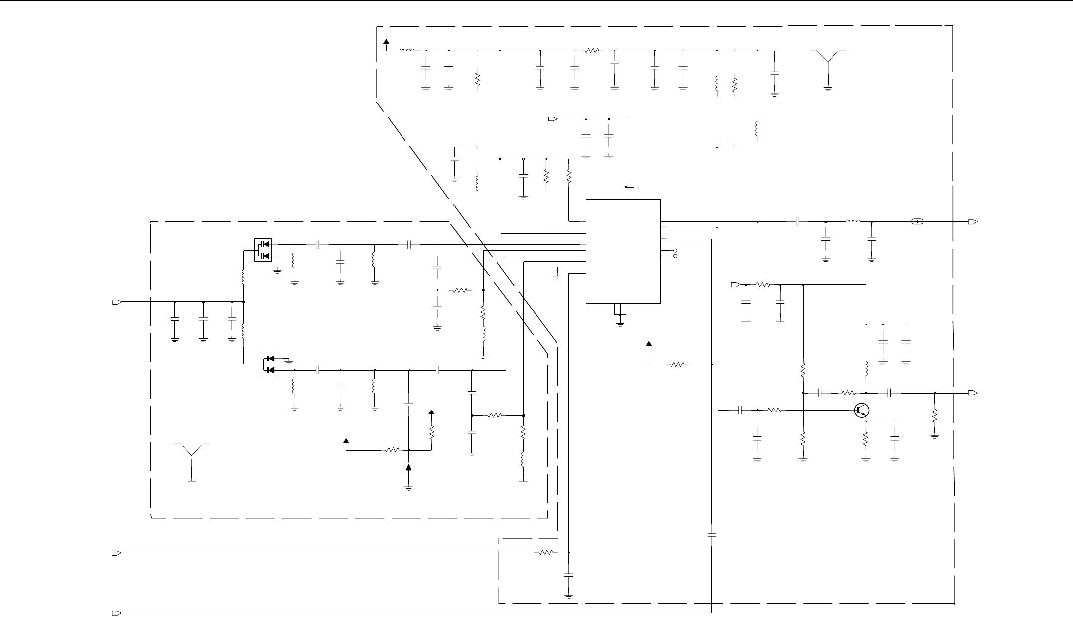
VHF 25-45W Band 2 PCB 8486487Z03-B / Schematics 4-11
DNP
DNP
DNP
DNP
VCOBIC Shield
VCO Shield
16pF
C2064
D204
L203 100nH
L211
680nH
47nH
L216
L209
100nH
R215
4.7K
R216
3.9K
18pF
C2057
100
R230
100nH
L212
NC
R218
1K
C2007
0.1uF
V_SF
C2021
.01uF
C2030
3900pF
R235
18
C2061
12pF
220
R222
100
R227
R221
L201
680nH
220
SHIELD
SH201
1
C2032
1000pF
R223
220
C2012
0.1uF
0.1uF
C2019
18pF
C2058
C2081
470pF
C2071
39pF
V_SF
0.1uF
C2076
8.2pF
C2066
C2039
1000pF
1000pF
C2029
D205
V_SF
C2063
15pF
R233
47
1pF
C2073
47nH
L214
L213
100nH
30K
R212
C2065
10pF
IF200
1
C2009
0.1uF
C2031
1000pF
510
R220
L204
680nH
SH202
SHIELD
1
C2069
5.6pF TX_EMITTER
15
TX_IADJ
1TX_OUT 10
TX_SWITCH 13
VCC_BUFFERS 14
VCC_LOGIC18
NC
RX_BASE
5
RX_EMITTER
6
RX_IADJ
2RX_OUT8
RX_SWITCH 7
SUPER_FLTR
3
TRB_IN
19
TX_BASE
16
50U54
COLL_RFIN
4
FLIP_IN
20
GND_BUFFERS
11 GND_FLAG
9
17 GND_LOGIC
PRESC_OUT 12
L215
U201
47nH
.01uF
C2022
0
R203
C2011
0.1uF
3.3pF
C2044
820
R219
C2018
0.1uF
R231
51
C2060
15pF
R201
0
47nH
L207
0.1uF
C2010
C2041
1000pF
18pF
C2056
39pF
C2070
C2038
1000pF
VCO_MOD
3
2
Q200
BFS540
1
L202
680nH
R232
47
R214
C2008
4.7K
L206
0.1uF
4.7K
33nH
R213
L208
100nH
12pF
C2062
1000pF
C2042
1000pF
C2040
R211
47K
1000pF
C2037 C2003
0.1uF
6.8pF
C2043
18pF
C2059
D203
TX_INJ
3V
9R
RX_IN J
AU3
PRESEC_CLK
VCO SHLD
L203 & L204
VHF2 (146-174MHz) 25-45W Synthesiser and VCO (Sht 2 of 2)
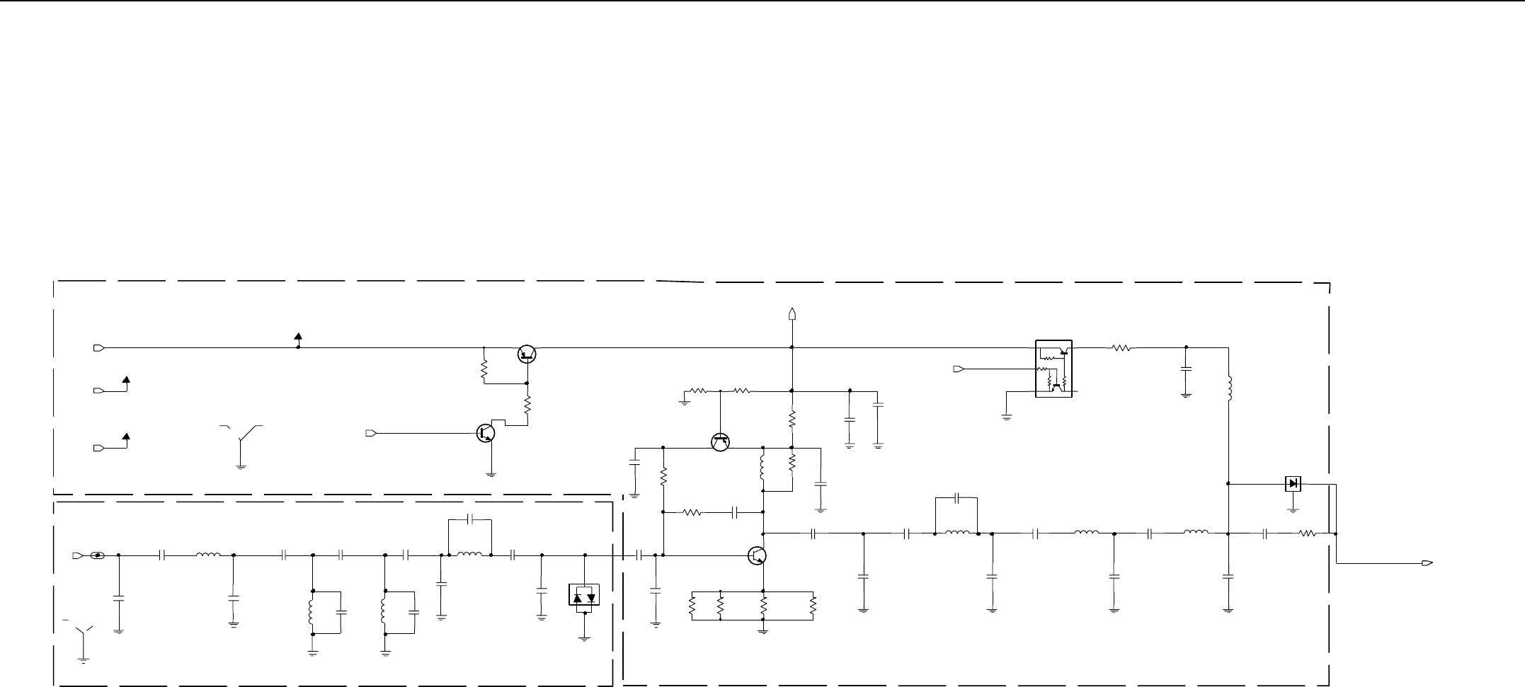
4-12 VHF 25-45W Band 2 PCB 8486487Z03-B / Schematics
DNP
DNP
DNP
DNP
FRONT-END SHIELD
DNP
R346
10K
C363
12pF
120pF
C338 C365
5.6pF
C329
470pF 51
R339
1
SHIELD
SH301
33.47nH
L308 R344
10
C355
30pF
C341
82pF
C333
91pF
C334
91pF
D305
R342
10
82pF
C345
L300
33.47nH
9V
C323
1000pF
CR301
R300
10K
L302
1.2uH
C331
470pF
82pF
C343
1000pF
C325
10
R341
L303
1.2uH
1000pF
C324
IF300
1
L310
33.47nH
51pF
C300
C350
36pF
C349
36pF
Q301
3V
330pF
C332
100
R337
C330
470pF
Q300
C354
30pF 180pF
C337
2.4K
R327
Q304
470pF
C328
Q306
C340
82pF
.01uF
C321
L309
33.47nH
15K
R310
C347
39pF
33.47nH
L314
82pF
C344
1K
R330
C351
36pF
56pF
C346C339
100pF
5V
R333
430
R345
10K
220
R335
Q303
BFS540
L307
33.47nH
3.3pF
C366
10
R343
L311
33.47nH
SHIELD
SH300
1
RX_EN
9V
9R
LOC_DIST
RX
3V
5V
TO T300
VHF2 (146-174MHz) 25-45W Receiver Front and Back End (Sht 1 of 2)
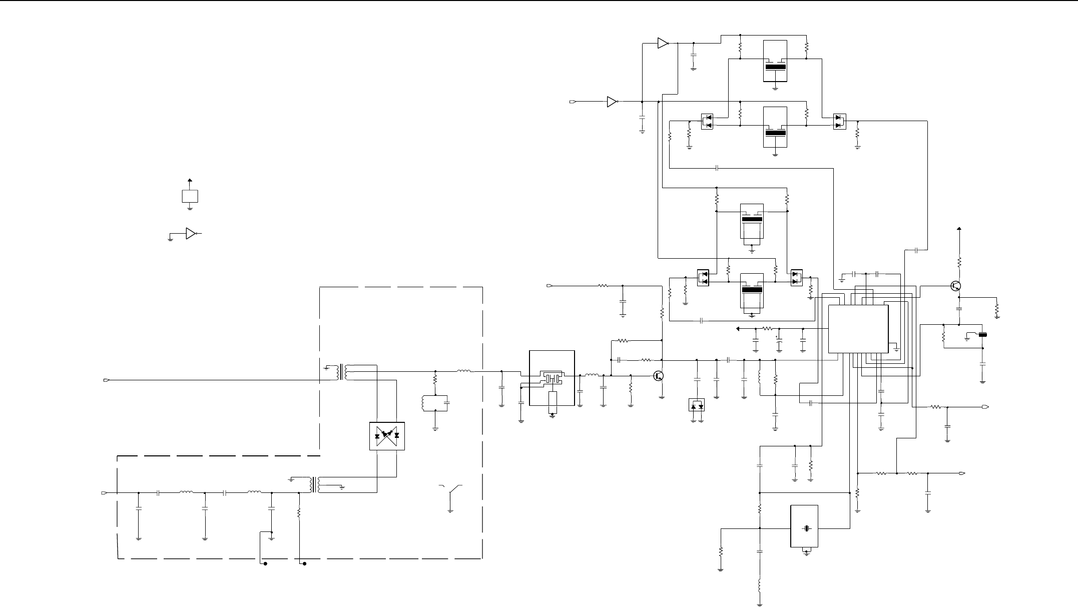
VHF 25-45W Band 2 PCB 8486487Z03-B / Schematics 4-13
NU
DNP
NU
TC7W04F
U301-2
NU
DNP
DNP
MIXER SHIELD
Check if it is 3v or another value
1.8K
R328
22pF
C360
10K
R320
20K
R306
2.4K
R326
12 K
R313
A2
A4
K1
K3
U302
FL303
CFWC455G
3
GND1
GND2
4
1IN 2
OUT
R304
33K
C367
2.7pF
100
R336
33pF
C307
0.1uF
C352
T301
XFMR
4
6
3
1
2
1.2K
R329
C336
6.8pF
30pF
C353
R323
4.7K
0.1uF
C311
C319
0.1uF
U301-3
TC7W04F
R312
13K
TEST_POINT
TP4
1
R316
12K
R302 0
0.1uF
33.47nH
C313
L312
D302
C335
9.1pF
1000pF
C326
C305
0.1uF
15K
R311
C364
8.2pF
20 K
R305
C317
0.1uF
L301
1.2uH
L305
470nH
CR300
R314
12K
R325
3.3K
15K
R309
4.7K
R322
D303
C320
0.1uF
R334
390
3V
R338
51
2CC1
5CC2
1
GND1
4
GND2
3IN 6
OUT
5
RSSIOUT
9RSSI_FEED
6
VCC
44.85MHz
MXF45
FL300
13
LIM_DEC1
12 LIM_DEC2
20
MIXOUT
4OSCIN
3
OSCOUT
10 QUADIN
1RFIN
2RFIN_DEC
7
AUDIO_FEED
15
GND
18 IFAMPIN
16
IFAMPOUT
19 IFAMP_DEC1 17
IFAMP_DEC
2
14 LIMIN
11
LIMOU
T
SA616
U300
8
20K
R308
Q302
R307
20K
C310
0.1uF
C308
0.1uF
150nH
L306
0.1uF
C304
C342
82pF
Q305
C314
0.1uF
R319
12K
GND
2
GND1
4
OUT
31
IN
Y301
06B09
44.395MHz
0
R303
L315
27nH
C361
18pF
0.1uF
C315
1
SHIELD
SH302
12K
R315
D301
L313
33.47nH
TC7W04F
U301-1
R331
4
GND2
1IN 2
OUT
680
FL30 4
CFWC455D
GND1
3
C303
0.1uF
D304
C318
R317
12K
0.1uF
C348
39pF
3.3K
R324
0.1uF
C316
U301-4
PWR_GND
4
GND
8
VCC
TP1
TEST_POINT
1
R340
51 C359
22pF
10uF
C301
C357
22pF
12K
R318
GND
3
IN
1OUT 2
6
3
1
2
FLTR
FL301
XFMR
T300
4
560
R332
C322
4700pF
1
C306
0.1uF
455KHz
Y300
45B02
3
2
1000pF
C327
18pF
C362
470
R301
8.2K
R321
1.2uH
L304
3V
C309
0.1uF
C302
130pF
0.1uF
C312
2
3V
30pF
C356
FLTR
FL302
GND
3
IN
1OUT
RX_INJ
DEMOD
RSSI
BW_SEL
5V
35
62
17
AUDIOOUT
FROM R337
VHF2 (146-174MHz) 25-45W Receiver Front and Back End (Sht 2 of 2)
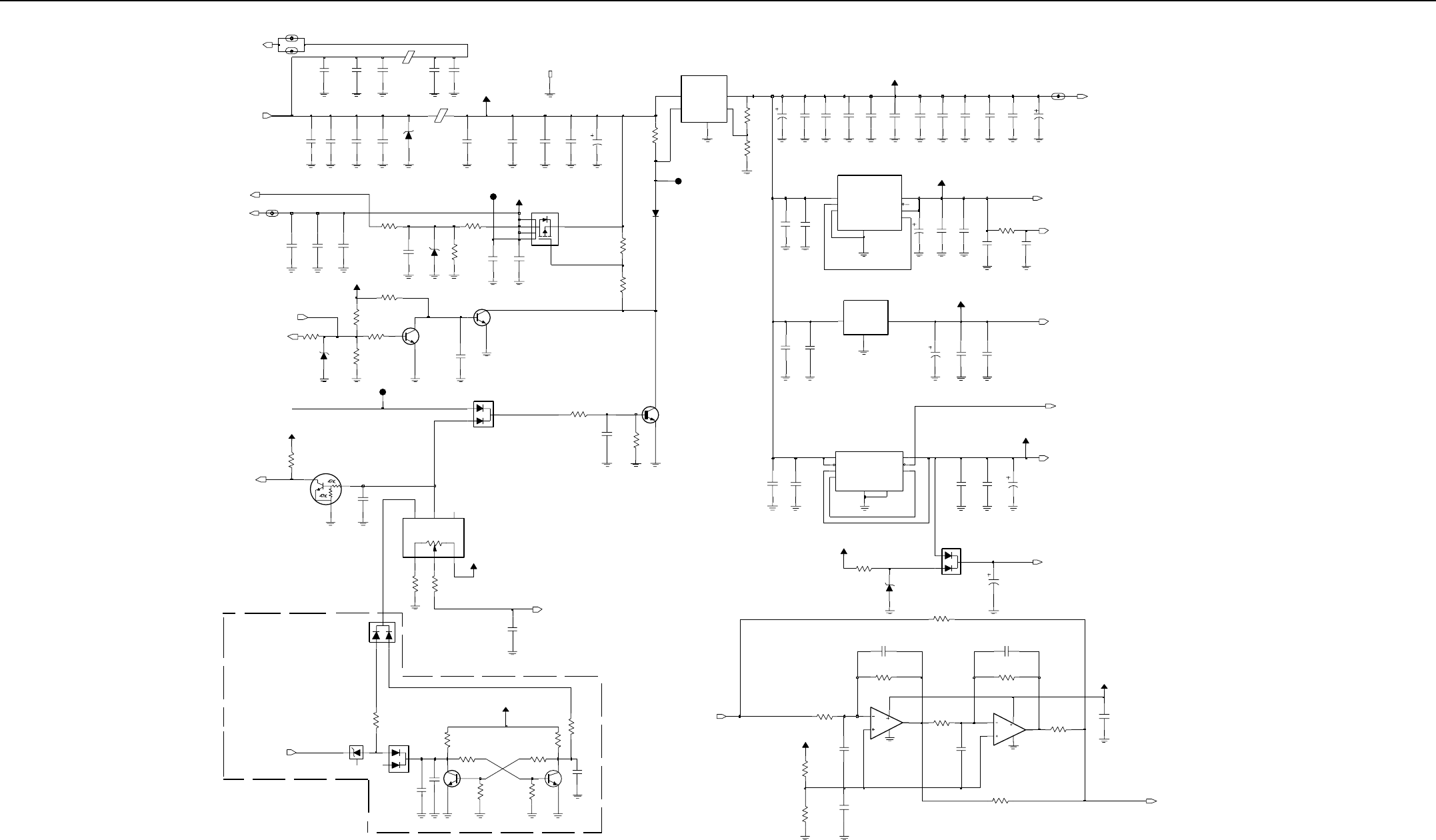
4-14 VHF 25-45W Band 2 PCB 8486487Z03-B / Schematics
1%
Smart Fuse Circuit
AUDIO
spacer for TO-22 0
SOURCE
Volume
SOURCE 9.3V
Place near uP
Audio
9.3V
Indirect
On/Off for ATE
1%
POWER SUPPLY
DNP DNP
C5067
.022uF
1000pF
C5085
Q500
R5062
10K
.022uF
C5086
13K
R5050
C5104
10uF
R5074
1K
GND
3
ON_OFF
2
VIN
4VOUT 5
U501
LM2941T
ADJ 1
VR501
5.1V
1K
R5001
Q504
R5049
15K
Q503
R5071
2.2K
IF500
1
33K
R5038
L500
35U02
1TP555
TEST_POINT
C5060
0.1uF
24V
VR500
33K
R5030
D3_3V
654
2
SWITCH
S5010
50.K
3
LOW
1
HIGH
3.3V
VR503
220pF
C5094
220pF
C1125
220pF
C5095
FILT_SW_B+
C5001
10uF
D511
C5000
1000pF
0.1uF
C5063
24K
R5048
M6
C1128
220pF 100K
0.1uF
R5028
C5037
C1085
1000pF
100
R5079
0.1uF
C5038
100pF
C5083
47K
R5035
220pF
C1113
Q502
1000pF
C1097
L120
35U02
FILT_B +
C5110
1000pF
150K
R5020
C5062
0.1uF
C1124
220pF
R5081
6.34K
C1087
FILT_B+
1000pF
C1098
1000pF
100K
R5029
220pF
C1123
C1122
220pF
C5061
0.1uF 100pF
C5084
10K
R5069
Q505
R5037
10K
C5119
10uF
220pF
C1034
1K
R5073
TEST_POINT
TP556
1
220pF
C5092
R5000
0
D500
TEST_POINT
TP500
1
Q506
220pF
C5096
R5082
51K
C5005
100uF
C5015
0.1uF
D3_3V
R5039
100K
C1114
220pF
47K
R5036
1
IF502
1
IF503
IF501
1MEG
R5085
R5089
1MEG
0.1uF
C5035
VR504
3.3V
9V
1000pF
C5074
R5031
62K
D513
D502
1000pF
C5111
U514
FILT_B+
R5083
270K
1000pF
C1088
100uF
C1127
FILT_SW_B+
ONOFF_SENSE
9V
B+
COMP_B+
POST_LIMITER_FLAT_TX_AUDIO_RETURN_OPT_BR
DC_POWER_ON
BATT_SENSE
FLAT_TX_AUDIO_INPUT_ACCESS_CONN
VOL_INDIRECT
IGNITION
EMERGENCY_SENSE
DNP
DNP
DNP
3.3v Digital REGULATOR
SOURCE
5V TO LVFRACN
For mid_band
3.3V RF REGULATOR
DNP
SOURCE
SOURCE
5V RF Regulator
3.3V to IFIC, ASFI
DNP
DNP
3.3v digital
DNP
C5069
1000pF 47uF
C5007
FILT_B+
24K
R5103
C5040
0.1uF 0.1uF
C5039
1uF
C5043
0.1uF
C5018
0.1uF
C5016
D3_3V
2.2uF
C5041
C5070
1000pF
47uF
C512
0
C5065
1000pF
5V
D501
C5066
1000pF
3V
10uF
C5006 C5068
1000pF
R5002 0
10uF
C5008
3.9V
VR502
TAP
3
ERROR 7
2
FEEDBACK
GND1
19
GND2
4INPUT 5
OUTPUT
6SENSE
8SHUTDOWN
LP2986ILDX
U510
MC33269D
1
GND
3IN 2
OUT
3SHUTDOWN
U508
U503
6
5V_TAP
5
ERROR
7FEEDBACK
4
GND
8INPUT 1
OUTPUT
2
SENSE
LP2951C
1uF
C5042
C5017
0.1uF
C5064
1000pF
D3_3V
VSTBY
5V_CH
RESET
EMERGENCY_ACCES_CONN
DNP
DNP
DNP
DNP
DNP
DNP
0
R5098
R5100
1MEG
24K
R5095
2
31
8
4
LM2904
U500-1
5V
10K
R5096
10K
R5092
6.8pF
C5115
C5113
220pF
5V
1uF
C5114
C5116
220pF
R5094
1MEG
0
R5097
NU
16pF
C5117
LM2904
U500-2
6
57
8
4
0.1uF
C5118
10K
R5093 R5099
100K
DEMOD
DISC
VHF2 (146-174MHz) 25-45W DC and Audio Circuits (Sht 1 of 2)
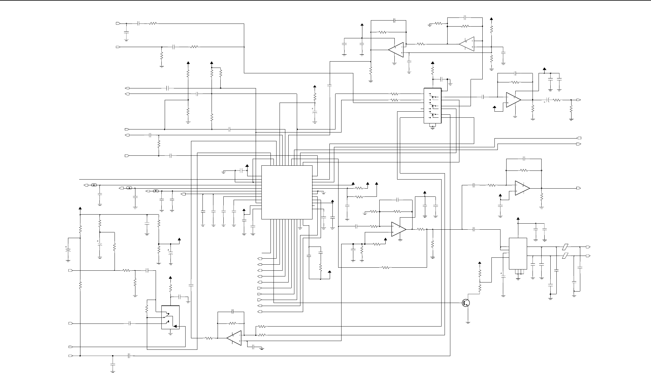
VHF 25-45W Band 2 PCB 8486487Z03-B / Schematics 4-15
DNP
DNP IN MARLIN
DNP
DNP
DNP IN MARLIN
DNP
DNP
DNP
DNP
+
DNP
USE NLAS4599
DNP
DNP DNP
VAG=4.5v
DNP
DNP IN MARLIN
C5058
0.1uF
12K
R5051
0.1uF
C5025
0.1uF
C5020
200K
R5019
C5031
0.1uF
C5048
0.1uF
R5065
6.2K
C5080
1000pF
C5036
0.1uF
R5011
0
FILT_SW_B+
L501
35U02
47uF
C5002
1000pF
C5076
C5019
0.1uF
C5022
5V
Q501
0.1uF
220pF
NU
C1090
C5059
.022uF
10
R5080
0.1uF
C5103
3V
3V
0.1uF
C5029
C5034
0.1uF
VAG
0.1uF
C5054
3V
3V
24K
L502
35U02
R5043
100K
R5023
0.1uF
C5047
C5055
4.7uF
R5064
8.2K
1MEG
R5016
C5012
9V
4.7uF
10K
R5059
C5052
0.1uF
R5057
10K
C5030
0.1uF
4.7uF
C5056
C5078
1000pF
U505-1
LM2904
2
31
8
4
2.2K
R5070
C5075
1000pF
C5023
0.1uF
R5047
0
0
R5010
R5060
10K
33K
R5045
C5077
1000pF
10K
R5061
C5089
82pF
R5034 36K
3V
3V
10K
R5053
10K
R5058
10K
R5052
4NC
6
NO
VPOS
2
MAX4599EXT
U515
5
COM
GND
3
1
IN
C5091
82pF
0.1uF
C5024
6.2K
R5068
3V
1000pF
C5101
R5008
0
0.1uF
C5028
R5086
560
3V
0
R5009
U507-2
LM2904
6
5
7
8
4
0.1uF
C5102
1000pF
C5082
R5046
24K
C5003
VAG
9V
47uF
0.1uF
C5053
R5084
0
R5087
100K
R5072
4.7K
VDDA
1
VDDCP 32
VDDD 33
VDDDAC
11
VDDRC 45
VDDSYN27
VOX
7
RXSND 39
SQCAP
12
SQDET
17
SQI N
9SYN 28
TXRTN 36
TXSND 44
UIO
10
LSIO
18
MICEXT 48
MICINT 46
40
MOD
NC 26
PLCAP
8
25
PLCAP2
RXRTN 43
GCB5 38
GNDA
3
GNDD 31
30
GNDDO
GNDRC 47
GNDSYN
23
HSIO
19
LCAP
24
DAT A
22
DISC
2
F1200 29
GCB0
15
14 GCB1
GCB2
13
GCB3 35
GCB4 37
AUXTN 42
CHACT
16
21 CLK
CLK168 34
20 CSX
DACG
6DACR
5DACU
4
30C53
U504
AUDIO 41
C5014
2.2uF
82pF
C5090
220pF
C5098
U506-2
LM2904 6
5
7
8
4
C5021
0.1uF
220pF
C5099
R5025
100K 0.1uF
C5032
C5071
1000pF
3V
3V
C5087
120pF
10K
R5055
C5009
10uF
1000pF
C5073
510
R5076
C5079
1000pF
3V
C5100 220pF
C5050
0.1uF
8.2K
R5063
C5033
0.1uF
R5054
10K
R5014
0
C5011
10uF
4.7uF
B+
C5044
1000pF
C5072
R5027
270K
8
4
U506-1
LM2904
2
3
1
3V
3V
LM2904
U507-1
2
31
8
4
NU
R5013
0
C1094
1000pF
47K
R5033
9V
47K
R5032
10K
R5056
IF505
1
VAG
IF506
R5088
0
IF504
100K
R5024
R5026
33K
4
Z
Z0
5
3Z1
VCC
16
VEE
7
X14
X0
12
13 X1
Y15
Y0
2
Y1
1
U509
MC14053B
11
A
B10
C9
EN 6
GND
8
R5067
6.2K
R5078
C5057
100
4.7uF
INV
9
M_SS
8
NINV
1OUT14
OUT26
RR
3
VCC
7
U502
TDA1519C
GND1
2
GND2
5
10 GND3
GND4
R5041
24K
NU
C1093
220pF C1131
220pF
NU
U505-2
LM2904
6
5
7
8
4
C5027
0.1uF
100K
R5021
0.1uF
C5051
C5013
1.0uF
C5026 0.1uF
220pF
C5097
510
R5075
C5081
1000pF
30K
R5040
C5088
82pF
300
R5077
R5044
24K
0.1uF
C5046
10uF
C5010
1uF
C5045
24K
R5042
C5049
1K
R5066
0.1uF
PWR_SET
V_CTRL_DRIVE
R
3V
R5022
100K
DC_POWER_ON
MIC_AUDIO_CH
SPKR
-
SPKR+
POST_LIMITER_FLAT_TX_AUDIO_RETURN_OPT_BRD
VS_AUDIO_SEL
VS_MIC
RX_AUDIO_OUTPUT
_ACCESS_CONN
FLAT_TX_AUDIO_INPUT_ACCESS_CONN
VOX
EXTERNAL_MIC_AUDIO
_ACCESS_CONN
16.8MHz
MOD_OUT
TX_AUDIO_RETURN_OPT_BRD
TX_AUDIO_SEND_OPT_BRD
RX_AUDIO_RETURN_OPT_BRD
UNMUTED_RX_AUDIO_SEND_OPT_BRD
DETECTOR_AUDIO_SEND_OPT_BRD
CH_ACT
SPI_CLK
ASFIC_CS
PA_BIAS
SPI_MOSI
F1200
BW_SEL
AUDIO_PA_EN
FLAT_OR_DEEMPH_RX_AUD_SEL FLAT_TX_AUDIO_MUTE
HSIO
LSIO
SQ_DET
uP_CLK
HANDSET_RX_AUDIO_CH
DISC
11
VHF2 (146-174MHz) 25-45W DC and Audio Circuits (Sht 2 of 2)
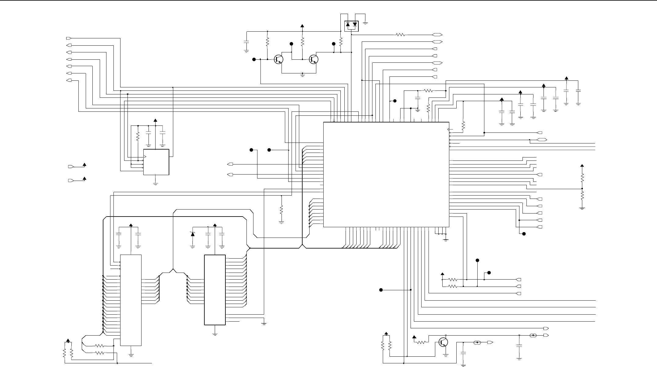
4-16 VHF 25-45W Band 2 PCB 8486487Z03-B / Schematics
DNP
DNP
SYNTH_CS
ASFIC_CS
DISPLAY_CS_CH
DNP
DNP
DNP
SPI_MOSI
PROVIDE WIRED OR OPERATION ON CSPROG
EE_CS
DNP
SPI_CLK
SHIFT_R_CS
DO NOT CONNECT THIS CS IN ORDER TO
SPI_MISO
R415 0
1
TP404
TEST_POINT
1
TP402
TEST_POINT
0.1uF
C405
C413
1000pF
C414
1000pF
D3_3V
D3_3V
10K
R463
R473
100K
D3_3V
R472
100K
R441
10K
100K
R427
1000pF
C415 C407
0.1uF
R425
100K
51
R462
9RESET
8
VCC
21
I_O0 22
I_O1 23
I_O2 25
I_O3 26
I_O4 27
I_O5 28
I_O6
I_O7 29
14 A6
13 A7
3A8
2A9
30 EN_CE
32 EN_OE
7EN_WE
24 GND
5A14
11 A15
10 A16
A17
6
18 A2
17 A3
16 A4
15 A5
AT49LV002N_70VI
20 A0
19 A1
31 A10
1A11
12 A12
4A13
28
VDD
14
VSS 27
WE
U404
12 D2
13 D3
15 D4
16 D5
17 D6
18 D7
19 D8
22
OE
6
A4 5
A5 4
A6 3
A7 25
A8 24
A9
20
CS
11 D1
9
A1
21
A10 23
A11 2
A12 26
A13 1
A14
8
A2 7
A3
SRM2B256
U402
10
A0
TP410
TEST_POINT
1
10K
R450
R451
10K
C401
VSSR
87
93
XFC
XIRQ 48
XTAL 91
0.1uF
VDD 12
VDDL 39
VDDR 88
VDDSYN 92
VRH 69
VRL 68
VSS
13
VSSL
40
PJ1_CSGP4 72
PJ2 73
PJ3 74
PJ4 75
PJ5 76
PJ6 77
PJ7 78
RESET 94
PI1
55 PI2
54 PI3
53 PI4
52 PI5
51 PI6
50 PI7
49
PJ0_CSGP3 71
PH1_PW2
46
PH2_PW3
45
PH3_PW4
44
PH4_CSIO
43
PH5_CSGP1
42
PH6_CSGP2
41
PH7_CSPROG
38
PI0
56
PG1_XA14
16
PG2_XA15
20
PG3_XA16
19
PG4_XA17
17
PG5_XA18
18
PG6_AS
5
PG7_R_W 4
PH0_PW1
47
PF2_ADDR2
27 PF3_ADDR3
26 PF4_ADDR4
25 PF5_ADDR5
24 PF6_ADDR6
23 PF7_ADDR7
22
PFO_ADDR0
29
PG0_XA13
6
66
PE1_AN1 65
PE2_AN2 64
PE3_AN3 63
PE4_AN4 62
PE5_AN5 61
PE6_AN6 60
PE7_AN7
PF1_ADDR1
28
PD0_RXD 97
PD1_TXD 98
PD2_MISO 99
PD3_MOSI 100
PD4_SCK 1
PD5_SS 2
3
PD6_LVIN
67
PE0_AN0
PC0_DATA0
30
PC1_DATA1
31
PC2_DATA2
32
PC3_DATA3
33
PC4_DATA4
34
PC5_DATA5
35
PC6_DATA6
36
PC7_DATA7
37
PB1_ADDR9
10 PB2_ADDR10
11 PB3_ADDR11
9PB4_ADDR12
21 PB5_ADDR13
15 PB6_ADDR14
8PB7_ADDR15
7
PBO_ADDR8
14
PA0_IC3 79
PA1_IC280
PA2_IC181
PA3_IC4_OC5_OC1 82
PA4_OC4_OC1 83
PA5_OC3_OC1 84
PA6_OC2_OC1 85
PA7_PA1_OC1 86
AVDD 59
AVSS
70
ECLK 89
EXTAL 90
IRQ 96
95
LVOUT
MODA_LIR58
MODB_VSTBY 57
MC68HC11FL0
U403
C402
0.1uF
D40
D3_3V
D3_3V
1
TP400
TEST_POINT
0.1uF
C408
100K
R423
D3_3V
0.1uF
C404
100K
R428
D3_3V
1
R443
3.3K
TP425
TEST_POINT
R426
100K
220pF
C1078
R438
10K
Q407
D3_3V
D3_3V
FILT_SW_B+
TP403
TEST_POINT
1
100K
R424
CS
1
HOLD
7
SCK
6
SI
5
SO 2
VCC
8
VSS
4
3WP X25128-2.7
U400
D3_3V
1
IF401
1
IF400
10K
R442
Q417
D3_3V
1000pF
C411
10
R47 1
0.1uF
C403
1
TP406
TEST_POINT
0
R414
1000pF
C416
D3_3V
C410
0.1uF
1000pF
C412
1000pF
C1083
TP409
TEST_POINT 1
Q400
R439
10K
0.1uF
C406
1000pF
C400
TP401
TEST_POINT
1
D3_3V
4.3V
VR401
TP407
TEST_POINT
1
EMERGENCY_SENSE
BATT_SENSE
VOX
ONOFF_SENSE
VOL_INDIRECT
F1200
DISPLAY_CS_CH
DISPLAY_CS_CH
KEYPAD_COL_CH
KEYPAD_ROW_CH
RSSI
RESET
TX_EN
OPT_EN_OPBD
D3_3V
RX_EN
ASFIC_CS
ASFIC_CS
SYNTH_CS
SYNTH_CS
SPI_CLK
SPI_CLK
SPI_CLK
SPI_MOSI
SPI_MOSI
SPI_MOSI
SPI_MISO
SPI_MISO
SPI_MISO
MIC_SENSE
SCI_CH
A(8)
A(9)
A(0:18)
EE_CS
EE_CS
OPT_DATA_R_OPBD
D(0:7)
HSIO
PROG_IN-P6_I
PROG_IO-P8_I
PROG_IO-P14_I
PROG_IO-P12_I
COMM_DATA_SEL_CH
SHIFT_R_CS
SHIFT_R_CS
MIC_PTT
D(3)
D(4)
D(6)
D(7)
A18_RES
D(5)
A(0)
A(1)
A(10)
A(11)
A(12)
A(13)
A(14)
A(2)
A(3)
A(4)
A(5)
A(6)
A(7)
A(4)
A(5)
A(6)
A(7)
A(8)
A(9)
A(15)
A(16)
A(18)
A(17)
A18_RES
R_W
uP_CLK
ACCESS_PTT
D(0)
D(1)
D(2)
FILT_SW_B+
R_W
A(0)
A(1)
A(10)
A(11)
A(12)
A(13)
A(14)
A(2)
A(3)
D(1)
D(2)
D(3)
D(4)
D(5)
D(6)
D(7)
D(0)
D(1)
D(2)
D(3)
D(4)
D(5)
D(6)
D(7)
R_W
D3_3V
LSIO
SQ_DET
CH_ACT
A(9)
A(10)
A(11)
A(12)
A(13)
A(8)
D(0)
A(1)
A(2)
A(3)
A(4)
A(5)
A(6)
A(7)
A(0)
A(14)
LOC_DIST
SYNTH_LOCK
A(15)
A(16)
A(17)
A(18)
RESET
PI1
PI2
PI3
PI4
MODB_VSTBY
MODA_LIR
VHF2 (146-174MHz) 25-45W Microprocessor and Controller Circuits (Sht 1 of 2)
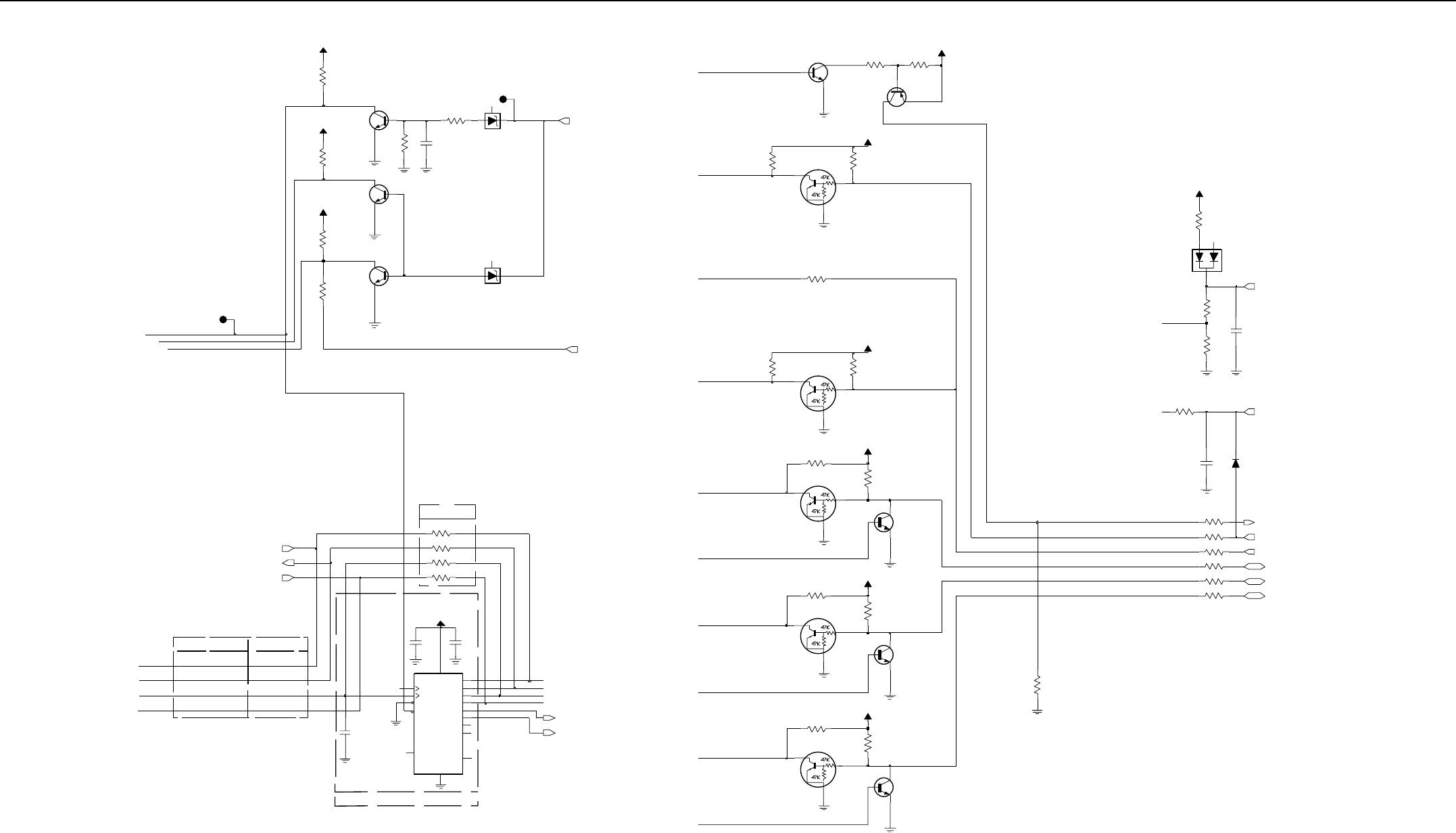
VHF 25-45W Band 2 PCB 8486487Z03-B / Schematics 4-17
PROG_I/O
EXT_ALARM_OUT
PROG_I/O
DNP
SHIFT_REGN_CS
DNP
VS_CS
PROG_I N
DNP
PROG_I/O
PROG_OUT-ALARM_4
VS_RAC
EXT_MIC_PTT
DNP IN MARLIN
DNP IN MARLIN
DNP
MARLIN
PROG_IO-P14_O
DNP
DNP
VS_INT
PROG_IO-P8_O
PROG_IO-P12_O
MARLIN +
2.7K
R401
7
RESET
10
SERIN
14
SEROUT 9
VCC
16
8
Q0 15
Q1 1
Q2 2
Q3 3
Q4 4
Q5 5
Q6
6
Q7
U405
MC74HC595A
CLK_L
12 CLK_S
11
EN_OE
13
GND
TP405
TEST_POINT
1
D3_3V
R429
100K
R436
33K
10K
R431
D401
C422
1000pF
220
R421
R430
39K
1000pF
C417
FILT_SW_B+
R433
33K
R458
3.3K
33K
R434
33K
R432
D3_3V
D3_3V
3.3K
R455
R405 0
3.3K
R456
47K
R459
C423
0.1uF
.022uF
C421
0
R403
VR402
3.3V
1000pF
C418
C490
1uF
1.5K
R460
Q408
R461
220
0
3.3K
R402
3.3K
R454
R453
TP408
TEST_POINT
1
Q411
Q401
Q415
6.8V
VR400
D402
R4680
R4670
D3_3V
D3_3V
0
R469
Q413
R457
3.3K
0
R466
Q414
D3_3V
Q409
R406 0
0
D3_3V
R407
D3_3V
Q412
10K
R470
Q403
Q410
R445
10K
Q416
10K
R422
Q405
D3_3V
10K
R440
R435
33K
0
R404
10K
Q404
R444
D3_3V
SPI_CLK
SPI_MOSI
BOOT_EN_IN_CH
VSTBY
SCI_CH
HOOK_CH
VS_INT
VS_RAC
VS_CS
PROG_OUT-ALARM_4
PROG_IO-P8_O
PROG_IO-P12_O
PROG_IO-P14_O
VS_AUDIO_SEL
VS_GAIN_SEL
PROG_IO-P8_O
PROG_IO-P8_ I
PROG_IO-P12_O
PROG_IO-P12_I
PROG_IO-P14_O
PROG_IO-P14_I
MIC_PTT_CH
MIC_PT T
MIC_SENSE
PROG_O-ACC_C_4
PROG_I-ACC_C_ 3
PROG_OUT-ALARM_4
ACCESS_PTT
PROG_IN-P6_I
PROG_I-ACC_C_6
PROG_IO-ACC_C_8
PROG_IO-ACC_C_12
PROG_IO-ACC_C_14
RESET
PI1
PI2
PI3
PI4
MODB_VSTBY
MODA_LIR
VHF2 (146-174MHz) 25-45W Microprocessor and Controller Circuits (Sht 2 of 2)
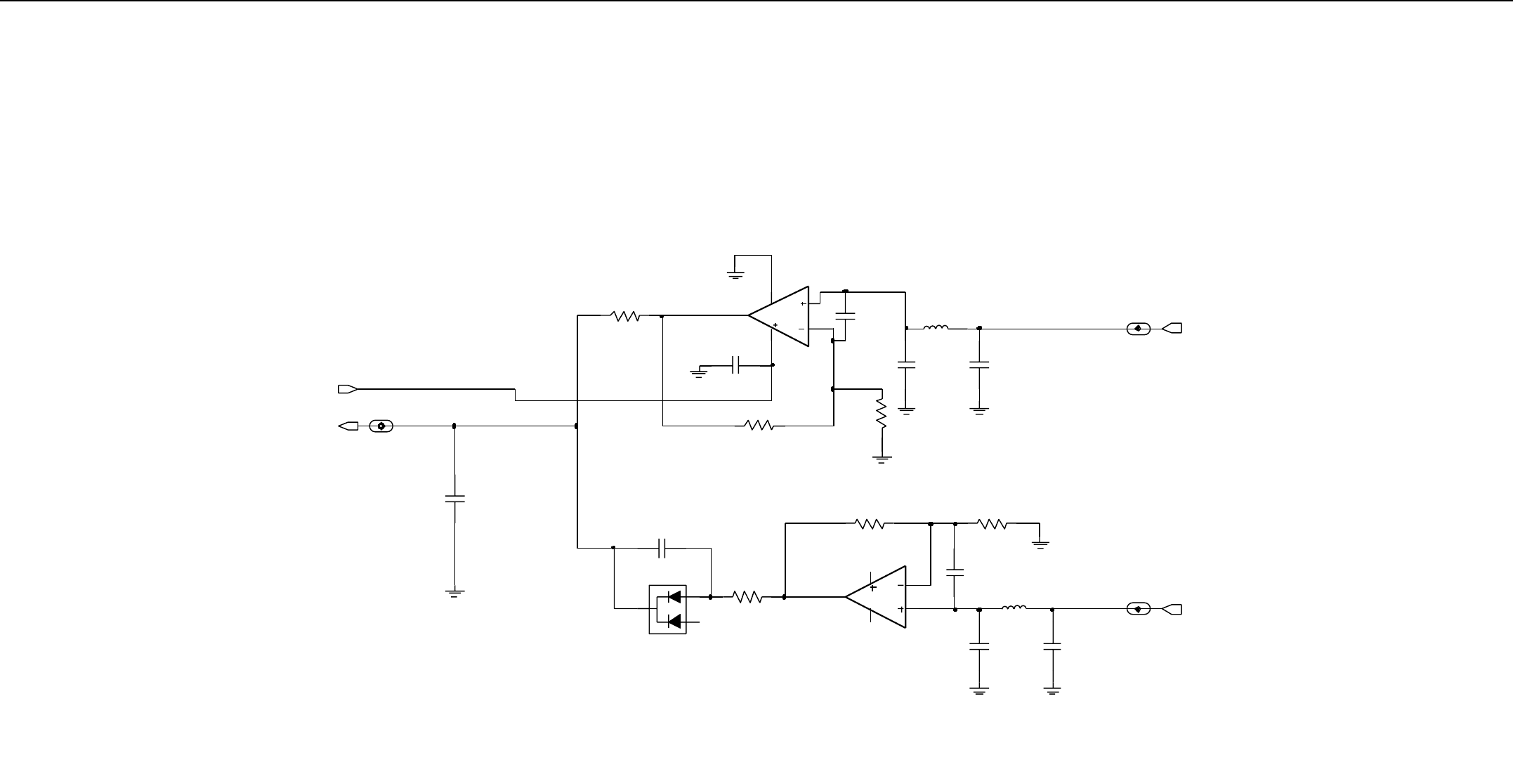
4-18 VHF 25-45W Band 2 PCB 8486487Z03-B / Schematics
1uH
L102
R117
22K
R141
22K
R140
18K
1000pF
C1046
C1045
1000pF
1uH
IF702
L101
1
IF701
1
IF700
NU
1000pF
C1082
C1076
1000pF
7
8
4
1000pF
C1075
3
1
8
4
U100-2
LM2904
6
5
U100-1
LM2904
2
C1071
1000pF
22K
R146
C1049
1000pF
D101
6.2K
R164
R144
22K
C1048
1000pF
C1047
DET_VFWD
INTEGRATOR
DET_VRVS
FILT_SW_B+
1000pF
VHF2 (146-174MHz) 25-45W Power Control Circuit
VHF 25-45W Band 2 PCB 8486487Z03-B / Schematics 4-19
2.1 VHF2 PCB 8486487Z03-B Parts List 25-45W
Circuit
Ref.
Motorola
Part No. Description
C300 2113740F44 CAP, 51pF
C301 2311049A57 CAP, 10uF
C302 2113740F54 CAP, 130pF
C303 2113743K15 CAP, 0.1uF
C304 2113743E20 CAP, 0.1uF
C305 2113743E20 CAP, 0.1uF
C306 2113743E20 CAP, 0.1uF
C307 2113743E20 CAP, 0.1uF
C308 2113743E20 CAP, 0.1uF
C309 2113743E20 CAP, 0.1uF
C310 2113743E20 CAP, 0.1uF
C311 2113743E20 CAP, 0.1uF
C312 2113743E20 CAP, 0.1uF
C313 2113743E20 CAP, 0.1uF
C314 2113743E20 CAP, 0.1uF
C315 2113743E20 CAP, 0.1uF
C316 2113743E20 CAP, 0.1uF
C317 2113743E20 CAP, 0.1uF
C318 2113743E20 CAP, 0.1uF
C319 2113743E20 CAP, 0.1uF
C320 2113743E20 CAP, 0.1uF
C321 2113741F49 CAP, .01uF
C322 2113741F41 CAP, 4700pF
C323 2113741F25 CAP, 1000pF
C324 2113741F25 CAP, 1000pF
C325 2113741F25 CAP, 1000pF
C326 2113741F25 CAP, 1000pF
C327 2113741F25 CAP, 1000pF
C328 2113740F67 CAP, 470pF
C329 2113740F67 CAP, 470pF
C330 2113740F67 CAP, 470pF
C331 2113740F67 CAP, 470pF
C332 2113741F13 CAP, 330pF
C333 2113740L41 CAP, 91pF
C334 2113740L41 CAP, 91pF
C335 2113740L17 CAP, 9.1pF
C336 2113740L14 CAP, 6.8pF
C337 2113740F57 CAP, 180pF
C338 2113740F53 CAP, 120pF
C339 2113740F51 CAP, 100pF
C340 2113740F49 CAP, 82pF
C341 2113740F49 CAP, 82pF
C342 2113740F49 CAP, 82pF
C343 2113740F49 CAP, 82pF
C344 NOT PLACED CAP, 82pF
C345 NOT PLACED CAP, 82pF
C346 2113740F45 CAP, 56pF
C347 2113740F41 CAP, 39pF
C348 2113740F41 CAP, 39pF
C349 NOT PLACED CAP, 36pF
C350 2113740F40 CAP, 36pF
C351 2113740F40 CAP, 36pF
C352 2113740F39 CAP, 33pF
C353 2113740F38 CAP, 30pF
C354 2113740F38 CAP, 30pF
C355 2113740F38 CAP, 30pF
C356 NOT PLACED CAP, 30pF
C357 2113740F35 CAP, 22pF
C359 NOT PLACED CAP, 22pF
Circuit
Ref.
Motorola
Part No. Description
C360 NOT PLACED CAP, 22pF
C361 2113740F33 CAP, 18pF
C362 2113740F33 CAP, 18pF
C363 NOT PLACED CAP, 12pF
C364 2113740F25 CAP, 8.2pF
C365 2113740F21 CAP, 5.6pF
C366 NOT PLACED CAP, 3.3pF
C367 NOT PLACED CAP, 2.7pF
C400 2113741F25 CAP, 1000pF
C401 2113743K15 CAP, 0.1uF
C402 2113743K15 CAP, 0.1uF
C403 2113743K15 CAP, 0.1uF
C404 2113743K15 CAP, 0.1uF
C405 2113743K15 CAP, 0.1uF
C406 2113743K15 CAP, 0.1uF
C407 2113743K15 CAP, 0.1uF
C408 2113743K15 CAP, 0.1uF
C410 2113743K15 CAP, 0.1uF
C411 2113741F25 CAP, 1000pF
C412 2113741F25 CAP, 1000pF
C413 2113741F25 CAP, 1000pF
C414 2113741F25 CAP, 1000pF
C415 2113741F25 CAP, 1000pF
C416 2113741F25 CAP, 1000pF
C417 2113741F25 CAP, 1000pF
C418 2113741F25 CAP, 1000pF
C421 NOT PLACED CAP, .022uF
C422 NOT PLACED CAP, 1000pF
C423 NOT PLACED CAP, 0.1uF
C490 NOT PLACED CAP, 1uF
Circuit
Ref.
Motorola
Part No. Description
C602 2113741F25 CAP, 1000pF
C603 2113741F25 CAP, 1000pF
C604 2113741F25 CAP, 1000pF
C605 2113741F25 CAP, 1000pF
C606 2113741F25 CAP, 1000pF
C607 2113741F25 CAP, 1000pF
C608 NOT PLACED CAP, 1000pF
C609 NOT PLACED CAP, 1000pF
C610 2113741F25 CAP, 1000pF
C611 2113741F25 CAP, 1000pF
C612 2113741F25 CAP, 1000pF
C613 2113741F25 CAP, 1000pF
C614 2113741F25 CAP, 1000pF
C615 2113741F25 CAP, 1000pF
C616 2113741F25 CAP, 1000pF
C617 2113741F25 CAP, 1000pF
C618 2113741F25 CAP, 1000pF
C619 NOT PLACED CAP, 1000pF
C620 2113741F25 CAP, 1000pF
C621 2113741F25 CAP, 1000pF
C622 2113741F25 CAP, 1000pF
C623 2113741F25 CAP, 1000pF
C624 2113741F25 CAP, 1000pF
C625 2113741F25 CAP, 1000pF
C626 2113741F25 CAP, 1000pF
C627 2113741F25 CAP, 1000pF
C628 2113741F25 CAP, 1000pF
C629 2113741F25 CAP, 1000pF
C630 2113741F25 CAP, 1000pF
C631 2113741F25 CAP, 1000pF
Circuit
Ref.
Motorola
Part No. Description

4-20 VHF 25-45W Band 2 PCB 8486487Z03-B / Schematics
C632 2113741F25 CAP, 1000pF
C633 2113741F25 CAP, 1000pF
C662 2113741F25 CAP, 1000pF
C678 2113741M69 CAP, 0.1uF
C1000 2113740F59 CAP, 220pF
C1001 2311049A08 CAPP, 1uF
C1002 2113741W01 CAP, 1uF
C1003 NOT PLACED CAP, 470pF
C1004 2111078B42 CAP, 100pF
C1005 2111078B42 CAP, 100pF
C1006 2111078B48 CAP, 160pF
C1007 2111078B40 CAP, 82pF
C1008 2111078B10 CAP, 7.5pF
C1009 2111078B37 CAP, 62pF
C1010 NOT PLACED CAP, 100pF
C1011 NOT PLACED CAP, 82pF
C1012 2111078B36 CAP, 56pF
C1013 2111078B08 CAP, 6.2pF
C1014 NOT PLACED CAP, 56pF
C1015 2111078B43 CAP, 110pF
C1017 2111078B18 CAP, 15pF
C1018 2111078B32 CAP, 39pF
C1019 2111078B28 CAP, 32pF
C1020 2111078B32 CAP, 39pF
C1021 NOT PLACED CAP, 6.2pF
C1022 2111078B26 CAP, 28pF
C1026 2113740A79 CAP, 1000pF
C1027 2311049A45 CAPP, 10uF
C1028 2113743K15 CAP, 0.1uF
C1029 2113743K15 CAP, 0.1uF
Circuit
Ref.
Motorola
Part No. Description
C1030 2113740F37 CAP, 27pF
C1031 2113743E07 CAP, .022uF
C1032 2113743E07 CAP, .022uF
C1033 2113743E07 CAP, .022uF
C1034 2113740F59 CAP, 220pF
C1035 2113743E07 CAP, .022uF
C1036 2113743E07 CAP, .022uF
C1037 2113743E07 CAP, .022uF
C1038 NOT PLACED CAP, .022uF
C1039 2113743E07 CAP, .022uF
C1040 NOT PLACED CAP, 2200pF
C1041 2113741F17 CAP, 470pF
C1042 2113740F52 CAP, 110pF
C1043 2113740F52 CAP, 110pF
C1044 2113741F13 CAP, 330pF
C1045 2113741F25 CAP, 1000pF
C1046 2113741F25 CAP, 1000pF
C1047 2113741F25 CAP, 1000pF
C1048 2113741F25 CAP, 1000pF
C1049 2113741F25 CAP, 1000pF
C1050 2113741F25 CAP, 1000pF
C1051 2113741F25 CAP, 1000pF
C1052 2113741F25 CAP, 1000pF
C1053 2113741F25 CAP, 1000pF
C1054 2113741F25 CAP, 1000pF
C1055 NOT PLACED CAP, 1000pF
C1056 NOT PLACED CAP, 1000pF
C1057 2113741F25 CAP, 1000pF
C1058 NOT PLACED CAP, 1000pF
C1059 2113741F25 CAP, 1000pF
Circuit
Ref.
Motorola
Part No. Description
C1060 2113741F25 CAP, 1000pF
C1061 NOT PLACED CAP, 1000pF
C1062 2113741F25 CAP, 1000pF
C1063 2113740F63 CAP, 330pF
C1064 2113741F25 CAP, 1000pF
C1065 2113740F63 CAP, 330pF
C1066 2113741F25 CAP, 1000pF
C1067 2113741F25 CAP, 1000pF
C1068 2113741F13 CAP, 330pF
C1069 NOT PLACED CAP, 330pF
C1070 2113741F25 CAP, 1000pF
C1071 2113741F25 CAP, 1000pF
C1072 2113741F25 CAP, 1000pF
C1073 NOT PLACED CAP, 1000pF
C1074 2113741F25 CAP, 1000pF
C1075 2113741F25 CAP, 1000pF
C1076 2113741F25 CAP, 1000pF
C1077 2113741F25 CAP, 1000pF
C1078 2113740F59 CAP, 220pF
C1079 2113741F25 CAP, 1000pF
C1080 2113741F25 CAP, 1000pF
C1081 2113741F25 CAP, 1000pF
C1082 NOT PLACED CAP, 1000pF
C1083 2113741F25 CAP, 1000pF
C1084 2113740F59 CAP, 220pF
C1085 2113741F25 CAP, 1000pF
C1086 2113741F25 CAP, 1000pF
C1087 2113741F25 CAP, 1000pF
C1088 2113741F25 CAP, 1000pF
C1089 2113741F25 CAP, 1000pF
Circuit
Ref.
Motorola
Part No. Description
C1090 NOT PLACED CAP, 220pF
C1091 2113741F25 CAP, 1000pF
C1092 2113741F25 CAP, 1000pF
C1093 NOT PLACED CAP, 220pF
C1094 NOT PLACED CAP, 1000pF
C1095 2113740F59 CAP, 220pF
C1096 2111078B40 CAP, 82pF
C1097 2113741F25 CAP, 1000pF
C1098 2113741F25 CAP, 1000pF
C1099 2113741F25 CAP, 1000pF
C1100 2113741F25 CAP, 1000pF
C1101 2113741F01 CAP, 100pF
C1102 2113741F01 CAP, 100pF
C1103 2113741A57 CAP, .033uF
C1104 2113741A45 CAP, .01uF
C1105 2113740F67 CAP, 470pF
C1106 2113740F67 CAP, 470pF
C1107 2113740F67 CAP, 470pF
C1108 2113740F47 CAP, 68pF
C1109 2113740F59 CAP, 220pF
C1110 2113740F59 CAP, 220pF
C1111 2111078B59 CAP, 470pF
C1112 2113740F59 CAP, 220pF
C1113 2113740F59 CAP, 220pF
C1114 2113740F59 CAP, 220pF
C1115 2113740F59 CAP, 220pF
C1116 2113740F59 CAP, 220pF
C1117 2113740F40 CAP, 36pF
C1118 2113740F39 CAP, 33pF
C1119 2113740F36 CAP, 24pF
Circuit
Ref.
Motorola
Part No. Description

VHF 25-45W Band 2 PCB 8486487Z03-B / Schematics 4-21
C1120 2113740F39 CAP, 33pF
C1121 NOT PLACED CAP, 6.8pF
C1122 2113740F59 CAP, 220pF
C1123 2113740F59 CAP, 220pF
C1124 2113740F59 CAP, 220pF
C1125 2113740F59 CAP, 220pF
C1126 2113740F59 CAP, 220pF
C1127 2360567A03 CAPP, 100uF
C1128 2113740F59 CAP, 220pF
C1129 2113740F59 CAP, 220pF
C1130 2113740F59 CAP, 220pF
C1131 NOT PLACED CAP, 220pF
C1132 2111078B40 CAP, 82pF
C1133 2113740A41 CAP, 33pF
C1134 2113740A38 CAP, 24pF
C1136 2113740F19 CAP, 4.7pF
C1137 2111078B33 CAP, 43pF
C1199 NOT PLACED CAP, 16pF
C2000 2113743F18 CAP, 2.2uF
C2001 2311049J11 CAPP, 4.7uF
C2002 2311049A72 CAPP, 10uF
C2003 2113743K15 CAP, 0.1uF
C2004 2113743F18 CAP, 2.2uF
C2005 2113743F18 CAP, 2.2uF
C2006 2113743F18 CAP, 2.2uF
C2007 2113743E20 CAP, 0.1uF
C2008 2113743E20 CAP, 0.1uF
C2009 2113743E20 CAP, 0.1uF
C2010 2113743E20 CAP, 0.1uF
C2011 2113743E20 CAP, 0.1uF
Circuit
Ref.
Motorola
Part No. Description
C2012 NOT PLACED CAP, 0.1uF
C2013 2113743E20 CAP, 0.1uF
C2014 2113743E20 CAP, 0.1uF
C2015 2113743E20 CAP, 0.1uF
C2016 2113743E20 CAP, 0.1uF
C2017 2113743E20 CAP, 0.1uF
C2018 2113743E20 CAP, 0.1uF
C2019 2113743E20 CAP, 0.1uF
C2020 2113743E20 CAP, 0.1uF
C2021 2113741F49 CAP, .01uF
C2022 2113741F49 CAP, .01uF
C2023 2113741F49 CAP, .01uF
C2024 2113741F49 CAP, .01uF
C2025 2113741F49 CAP, .01uF
C2026 2113741F49 CAP, .01uF
C2027 2113741F49 CAP, .01uF
C2028 2113741F33 CAP, 2200pF
C2029 2113741F25 CAP, 1000pF
C2030 2113741F39 CAP, 3900pF
C2031 NOT PLACED CAP, 1000pF
C2032 2113741F25 CAP, 1000pF
C2033 2113741F25 CAP, 1000pF
C2034 2113741F25 CAP, 1000pF
C2035 2113741F25 CAP, 1000pF
C2036 2113741F25 CAP, 1000pF
C2037 2113741F25 CAP, 1000pF
C2038 2113741F25 CAP, 1000pF
C2039 2113741F25 CAP, 1000pF
C2040 2113741F25 CAP, 1000pF
C2041 2113741F25 CAP, 1000pF
Circuit
Ref.
Motorola
Part No. Description
C2042 2113741F25 CAP, 1000pF
C2043 2113740L14 CAP, 6.8pF
C2044 2113740L06 CAP, 3.3pF
C2045 2113740F67 CAP, 470pF
C2046 2113740F67 CAP, 470pF
C2047 2113740F67 CAP, 470pF
C2048 2113740F67 CAP, 470pF
C2049 NOT PLACED CAP, 470pF
C2050 2113740F67 CAP, 470pF
C2051 2113740F59 CAP, 220pF
C2052 2113740F67 CAP, 470pF
C2053 NOT PLACED CAP, 100pF
C2054 2113740L37 CAP, 62pF
C2055 2113740F35 CAP, 22pF
C2056 2113740F33 CAP, 18pF
C2057 2113740F33 CAP, 18pF
C2058 2113740F33 CAP, 18pF
C2059 2113740F33 CAP, 18pF
C2060 2113740F31 CAP, 15pF
C2061 2113740F29 CAP, 12pF
C2062 2113740F29 CAP, 12pF
C2063 2113740L22 CAP, 15pF
C2064 2113740F32 CAP, 16pF
C2065 2113740F27 CAP, 10pF
C2066 2113740L16 CAP, 8.2pF
C2067 2113740F25 CAP, 8.2pF
C2068 2113740F23 CAP, 6.8pF
C2069 2113740L12 CAP, 5.6pF
C2070 2113740F41 CAP, 39pF
C2071 2113740F41 CAP, 39pF
Circuit
Ref.
Motorola
Part No. Description
C2072 2113740L04 CAP, 2.7pF
C2073 2113740F03 CAP, 1pF
C2074 2109720D14 CAP, 0.1uF
C2075 2109720D14 CAP, 0.1uF
C2076 NOT PLACED CAP, 0.1uF
C2077 2109720D14 CAP, 0.1uF
C2078 2109720D14 CAP, 0.1uF
C2079 2109720D14 CAP, 0.1uF
C2080 2109720D14 CAP, 0.1uF
C2081 2113740F67 CAP, 470pF
C5000 2113741F25 CAP, 1000pF
C5001 2389289U01 CAPP, 10uF
C5002 2311049A99 CAPP, 47uF
C5003 2311049A99 CAPP, 47uF
C5005 2360567A03 CAPP, 100uF
C5006 2311049A57 CAPP, 10uF
C5007 2311049A99 CAPP, 47uF
C5008 2311049A57 CAPP, 10uF
C5009 2311049A57 CAPP, 10uF
C5010 2311049A57 CAPP, 10uF
C5011 2311049A57 CAPP, 10uF
C5012 2311049A56 CAPP, 4.7uF
C5013 2113928P04 CAP, 1.0uF
C5014 NOT PLACED CAP, 2.2uF
C5015 2113743K15 CAP, 0.1uF
C5016 2113743K15 CAP, 0.1uF
C5017 2113743K15 CAP, 0.1uF
C5018 2113743K15 CAP, 0.1uF
C5019 2113743K15 CAP, 0.1uF
C5020 2113743K15 CAP, 0.1uF
Circuit
Ref.
Motorola
Part No. Description
4-22 VHF 25-45W Band 2 PCB 8486487Z03-B / Schematics
C5021 2113741M69 CAP, 0.1uF
C5022 2113743K15 CAP, 0.1uF
C5023 2113743K15 CAP, 0.1uF
C5024 2113743K15 CAP, 0.1uF
C5025 2113743K15 CAP, 0.1uF
C5026 2113743K15 CAP, 0.1uF
C5027 2113743K15 CAP, 0.1uF
C5028 2113743K15 CAP, 0.1uF
C5029 2113743K15 CAP, 0.1uF
C5030 2113743K15 CAP, 0.1uF
C5031 2113743K15 CAP, 0.1uF
C5032 2113743K15 CAP, 0.1uF
C5033 2113743K15 CAP, 0.1uF
C5034 2113743K15 CAP, 0.1uF
C5035 2113743K15 CAP, 0.1uF
C5036 2113743K15 CAP, 0.1uF
C5037 2113743K15 CAP, 0.1uF
C5038 2113743K15 CAP, 0.1uF
C5039 NOT PLACED CAP, 0.1uF
C5040 NOT PLACED CAP, 0.1uF
C5041 2113743F18 CAP, 2.2uF
C5042 2113743F16 CAP, 1uF
C5043 2113743F16 CAP, 1uF
C5044 2113928C04 CAP, 4.7uF
C5045 2113743F16 CAP, 1uF
C5046 2113743E20 CAP, 0.1uF
C5047 2113743E20 CAP, 0.1uF
C5048 2113743E20 CAP, 0.1uF
C5049 2113743E20 CAP, 0.1uF
C5050 2113743E20 CAP, 0.1uF
Circuit
Ref.
Motorola
Part No. Description
C5051 NOT PLACED CAP, 0.1uF
C5052 2113743E20 CAP, 0.1uF
C5053 NOT PLACED CAP, 0.1uF
C5054 NOT PLACED CAP, 0.1uF
C5055 2113928C04 CAP, 4.7uF
C5056 2113928C04 CAP, 4.7uF
C5057 2113928C04 CAP, 4.7uF
C5058 NOT PLACED CAP, 0.1uF
C5059 2113743E07 CAP, .022uF
C5060 2113741M69 CAP, 0.1uF
C5061 2113741M69 CAP, 0.1uF
C5062 2113741M69 CAP, 0.1uF
C5063 2113741M69 CAP, 0.1uF
C5064 2113741F25 CAP, 1000pF
C5065 2113741F25 CAP, 1000pF
C5066 2113741F25 CAP, 1000pF
C5067 2113741F25 CAP, 1000pF
C5068 2113741F25 CAP, 1000pF
C5069 2113741F25 CAP, 1000pF
C5070 2113741F25 CAP, 1000pF
C5071 2113741F25 CAP, 1000pF
C5072 2113741F25 CAP, 1000pF
C5073 2113741F25 CAP, 1000pF
C5074 2113741F25 CAP, 1000pF
C5075 NOT PLACED CAP, 1000pF
C5076 2113741F25 CAP, 1000pF
C5077 2113741F25 CAP, 1000pF
C5078 2113741F25 CAP, 1000pF
C5079 2113741F25 CAP, 1000pF
C5080 2113741F25 CAP, 1000pF
Circuit
Ref.
Motorola
Part No. Description
C5081 2113741F25 CAP, 1000pF
C5082 2113741F25 CAP, 1000pF
C5083 2113740F51 CAP, 100pF
C5084 2113740F51 CAP, 100pF
C5085 2113741A53 CAP, .022uF
C5086 2113741A53 CAP, .022uF
C5087 2113740F53 CAP, 120pF
C5088 2113740F49 CAP, 82pF
C5089 2113740F49 CAP, 82pF
C5090 2113740F49 CAP, 82pF
C5091 2113740F49 CAP, 82pF
C5092 2113740F59 CAP, 220pF
C5094 2113740F59 CAP, 220pF
C5095 2113740F59 CAP, 220pF
C5096 2113740F59 CAP, 220pF
C5097 2113740F59 CAP, 220pF
C5098 2113740F59 CAP, 220pF
C5099 2113740F59 CAP, 220pF
C5100 2113740F59 CAP, 220pF
C5101 NOT PLACED CAP, 1000pF
C5102 NOT PLACED CAP, 0.1uF
C5103 NOT PLACED CAP, 0.1uF
C5104 NOT PLACED CAP, 10uF
C5110 2113741F25 CAP, 1000pF
C5111 2113741F25 CAP, 1000pF
C5112 NOT PLACED CAP, 16pF
C5113 NOT PLACED CAP, 220pF
C5114 2113743F16 CAP, 1uF
C5115 NOT PLACED CAP, 6.8pF
C5116 NOT PLACED CAP, 220pF
Circuit
Ref.
Motorola
Part No. Description
C5117 NOT PLACED CAP, 16pF
C5118 2113743E20 CAP, 0.1uF
C5119 2113743H14 CAP, 10uF
C5120 NOT PLACED CAPP, 47uF
CR300 4880154K03 MMBD353, SCHOTTKY
COMM AK
CR301 4880154K03 MMBD353, SCHOTTKY
COMM AK
D100 NOT PLACED MMBD6100, DUAL COMM
CATH
D101 4813833C02 MMBD6100, DUAL COMM
CATH
D102 4813833C02 MMBD6100, DUAL COMM
CATH
D103 4802482J02 MA4P959, PIN
D104 4802482J02 MA4P959, PIN
D105 4805218N57 RB715F, DUAL COMM
CATH
D106 4805218N57 RB715F, DUAL COMM
CATH
D107 4805218N57 RB715F, DUAL COMM
CATH
D108 4805218N57 RB715F, DUAL COMM
CATH
D200 4802233J09 IMN10, 3 DIODE ARRAY
D201 4802233J09 IMN10, 3 DIODE ARRAY
D202 4862824C03 1SV232, VARACTOR
D203 4805649Q13 1SV228, VARACTOR
D204 4805649Q13 1SV228, VARACTOR
D205 4862824C01 1SV229, VARACTOR
D301 4802245J97 DAN235ETL, DUAL
COMM CATH
D302 4802245J97 DAN235ETL, DUAL
COMM CATH
Circuit
Ref.
Motorola
Part No. Description
VHF 25-45W Band 2 PCB 8486487Z03-B / Schematics 4-23
D303 4802245J97 DAN235ETL, DUAL
COMM CATH
D304 4802245J97 DAN235ETL, DUAL
COMM CATH
D305 4880142L01 MMBV3401LT, PIN
D400 4813833C07 MMBD7000, DUAL COMM
AK
D401 4813833C02 MMBD6100, DUAL COMM
CATH
D402 4809948D42 RB751V40, SCHOTTKY
D500 4813833C02 MMBD6100, DUAL COMM
CATH
D501 NOT PLACED MMBD6100, DUAL COMM
CATH
D502 4813825A23 MMSD301T1, SCHOTTKY
D511 4813833C02 MMBD6100, DUAL COMM
CATH
D513 4813833C02 MMBD6100, DUAL COMM
CATH
FL300 9180022M11 MXF45, 44.85MHz BPF
FL301 9180468V06 FLTR, 455kHZ, BW
25KHZ
FL302 9180468V04 FLTR, 455kHZ, BW
12.5KHZ
FL303 9180469V03 FLTR, 455kHZ, BW
12.5KHZ
FL304 9180469V06 FLTR, 455kHZ, BW
25KHZ
J2 0989241U02 CONNECTOR 22 PIN
J3 NOT PLACED CONNECTOR 32 PIN
J11 2889309U01 ANTENNA CONNECTOR
L100 7686135U02 FERRITE BEAD
L101 2462587T30 IDCTR, 1uH
L102 2462587T30 IDCTR, 1uH
L103 2462587T30 IDCTR, 1uH
Circuit
Ref.
Motorola
Part No. Description
L104 2462587T38 IND CHIP 22NH 5% LOW
PRO
L105 2462587T13 IDCTR, 68nH
L106 2460591A11 IDCTR, 7.66nH
L107 2460591A01 IDCTR, 4.22nH
L108 2462587X69 IDCTR, 1.2uH
L109 NOT PLACED IDCTR, 11.03nH
L110 2462587N42 IDCTR, 12nH
L111 2460592B01 IDCTR, 51nH
L112 2460592B01 IDCTR, 51nH
L113 2460592B01 IDCTR, 51nH
L114 2460592B01 IDCTR, 51nH
L115 2460592A01 IDCTR, 17nH
L116 2460592A01 IDCTR, 17nH
L117 7686135U02 FERRITE BEAD
L118 7686135U02 FERRITE BEAD
L119 7686135U02 FERRITE BEAD
L120 7686135U02 FERRITE BEAD
L121 7686135U02 FERRITE BEAD
L122 2460591C23 IDCTR, 13.85nH
L123 2462587X69 IDCTR, 1.2uH
L124 2485873L05 IDCTR, 48nH
L131 NOT PLACED IDCTR, 120nH
L132 2462587N15 IDCTR, 100nH
L200 2462587Q42 IDCTR, 390nH
L201 2462587V44 IDCTR, 680nH
L202 2462587V44 IDCTR, 680nH
L203 2462587V44 IDCTR, 680nH
L204 2462587V44 IDCTR, 680nH
L205 2462587Q47 IDCTR, 1uH
L206 2413923C05 IDCTR, 33nH
Circuit
Ref.
Motorola
Part No. Description
L207 2413923C07 IDCTR, 47nH
L208 2413926N24 IDCTR, 100nH
L209 2413926N24 IDCTR, 100nH
L210 2413926N24 IDCTR, 100nH
L211 2413926N24 IDCTR, 100nH
L212 2413926N24 IDCTR, 100nH
L213 2413926N24 IDCTR, 100nH
L214 2413926H20 IDCTR, 47nH
L215 2413926H20 IDCTR, 47nH
L216 2413926H20 IDCTR, 47nH
L217 2462587Q42 IDCTR, 390nH
L300 2460591G24 IDCTR, 33.47nH
L301 2462587X69 IDCTR, 1.2uH
L302 2462587X69 IDCTR, 1.2uH
L303 2462587N69 IDCTR, 1.2uH
L304 2483411T74 IDCTR, 1.2uH
L305 2413926K31 IDCTR, 470nH
L306 2462587N55 IDCTR, 150nH
L307 2460591G24 IDCTR, 33.47nH
L308 2460591G24 IDCTR, 33.47nH
L309 2460591G24 IDCTR, 33.47nH
L310 2460591G24 IDCTR, 33.47nH
L311 2460591G24 IDCTR, 33.47nH
L312 2460591G24 IDCTR, 33.47nH
L313 2460591G24 IDCTR, 33.47nH
L314 2460591G24 IDCTR, 33.47nH
L315 NOT PLACED IDCTR, 27nH
L500 7686135U02 FERRITE BEAD
L501 7686135U02 FERRITE BEAD
L502 7686135U02 FERRITE BEAD
Circuit
Ref.
Motorola
Part No. Description
M6 4387454V01 SPACER
M9 0289511U01 NUT
M100 2680499Z01 HEATSINK
M105 7588823L03 CONTACT, METAL
M106 7588823L03 CONTACT, METAL
M107 7588823L03 CONTACT, METAL
M108 7588823L04 CONTACT, METAL
M109 7588823L04 CONTACT, METAL
M110 7588823L04 CONTACT, METAL
M111 NOT PLACED CONTACT, METAL
M112 NOT PLACED CONTACT, METAL
M113 NOT PLACED CONTACT, METAL
M114 NOT PLACED CONTACT, METAL
P1 2804503J01 CONNECTOR, 16 PIN
P2 NOT PLACED CONNECTOR, 2 PIN DC
Q100 4886136B01 MRF1550, LDMOS RF
Q101 4813824A10 MMBT3904, BIPOLAR
NPN
Q102 NOT PLACED MMBT3904, BIPOLAR
NPN
Q103 4813824A06 MMBTA13, DARLINGTON,
NPN
Q105 4886212B01 MRF1518, LDMOS RF
Q106 4805128M27 BSR33, BIPOLAR, PNP
Q200 4802245J95 BFS540, NPN
Q300 4809940E02 DTC114YE, NPN
Q301 4813824A17 MMBT3906, BIPOLAR
PNP
Q302 4813824A10 MMBT3904, BIPOLAR
NPN
Q303 4802245J95 BFS540, NPN
Q304 4809939C04 UMC3
Circuit
Ref.
Motorola
Part No. Description
4-24 VHF 25-45W Band 2 PCB 8486487Z03-B / Schematics
Q305 4802197J95 PBR941, NPN
Q306 4813824A17 MMBT3906, BIPOLAR
PNP
Q400 4809940E02 DTC114YE, NPN
Q401 4880141L03 BCW68G, BIPOLAR PNP
Q403 4809940E02 DTC114YE, NPN
Q404 4809940E02 DTC114YE, NPN
Q405 4809940E02 DTC114YE, NPN
Q407 4809940E02 DTC114YE, NPN
Q408 4880048M01 DTC144EKA, BIPOLAR
Q409 4880048M01 DTC144EKA, BIPOLAR
Q410 4880048M01 DTC144EKA, BIPOLAR
Q411 4880048M01 DTC144EKA, BIPOLAR
Q412 4880048M01 DTC144EKA, BIPOLAR
Q413 4809940E02 DTC114YE, NPN
Q414 4809940E02 DTC114YE, NPN
Q415 NOT PLACED MMBT3904
Q416 4809940E02 DTC114YE, NPN
Q417 4813824A10 MMBT3904, BIPOLAR
NPN
Q500 4813824A10 MMBT3904, BIPOLAR
NPN
Q501 4809940E02 DTC114YE, NPN
Q502 4809940E02 DTC114YE, NPN
Q503 4813824A10 MMBT3904, BIPOLAR
NPN
Q504 4880048M01 DTC144EKA, BIPOLAR
Q505 4813824A10 MMBT3904, BIPOLAR
NPN
Q506 4813824A10 MMBT3904, BIPOLAR
NPN
R101 1705603W01 SHUNT, 1.639m
R102 0680194M18 RES, 51
Circuit
Ref.
Motorola
Part No. Description
R103 0683994M18 RES, 51
R104 0680194M18 RES, 51
R105 0680194M18 RES, 51
R106 0680194M18 RES, 51
R107 0680194M18 RES, 51
R108 0680194M18 RES, 51
R109 0662057A12 RES, 30
R110 NOT PLACED RES, 1K
R111 NOT PLACED RES, 1K
R112 NOT PLACED RES, 62K
R113 NOT PLACED RES, 10K
R114 NOT PLACED RES, 10K
R115 NOT PLACED RES, 10K
R116 NOT PLACED RES, 10K
R117 0662057A81 RES, 22K
R118 0662057C55 RES, 150
R120 0662057C51 RES, 100
R121 NOT PLACED RES, 100
R122 0662057C19 RES, 4.7
R123 0662057C13 RES, 2.7
R124 0662057C13 RES, 2.7
R125 0662057C13 RES, 2.7
R126 0662057C03 RES, 1
R127 0662057C03 RES, 1
R130 0662057B47 RES, 0
R131 0662057A97 RES, 100K
R132 NOT PLACED RES, 100K
R134 0662057A89 RES, 47K
R135 0662057A82 RES, 24K
R136 0662057A87 RES, 39K
Circuit
Ref.
Motorola
Part No. Description
R137 0662057A87 RES, 39K
R138 NOT PLACED RES, 39K
R139 NOT PLACED RES, 39K
R140 0662057A79 RES, 718K
R141 0662057A81 RES, 22K
R142 0662057A81 RES, 22K
R143 0662057A81 RES, 22K
R144 0662057A75 RES, 12K
R145 0662057A81 RES, 22K
R146 0662057A81 RES, 22K
R147 0662057A81 RES, 22K
R148 0662057A81 RES, 22K
R149 0662057A81 RES, 22K
R150 0662057A89 RES, 47K
R151 0662057A70 RES, 7.5K
R153 0662057A73 RES, 10K
R155 NOT PLACED RES, 10K
R156 0662057A73 RES, 10K
R157 0662057A91 RES, 56K
R158 0662057A67 RES, 5.6K
R159 NOT PLACED RES, 5.6K
R160 0662057A61 RES, 3.3K
R161 0662057A61 RES, 3.3K
R162 0662057A61 RES, 3.3K
R163 0662057A61 RES, 3.3K
R164 0662057A68 RES, 6.2K
R165 0662057A58 RES, 2.4K
R166 NOT PLACED RES, 2.4K
R167 0662057A57 RES, 2.2K
R168 0662057A57 RES, 2.2K
Circuit
Ref.
Motorola
Part No. Description
R169 NOT PLACED RES, 2.2K
R170 0662057A42 RES, 510
R171 0662057A33 RES, 220
R172 0662057A41 RES, 470
R173 0662057A29 RES, 150
R174 0662057A29 RES, 150
R175 NOT PLACED RES, 220
R176 2413926N25 IDCTR, 120nH
R177 NOT PLACED RES, 100
R178 0662057A14 RES, 36
R179 0662057A14 RES, 36
R180 0660082A89 RES, 47K
R181 0660082A89 RES, 47K
R182 0662057A73 RES, 10K
R185 0662057A73 RES, 10K
R186 0662057C20 RES, 5.1
R188 NOT PLACED RES, 0
R189 NOT PLACED RES, 0
R190 0662057G64 RES, 1MEG
R191 0662057G64 RES, 1MEG
R195 0662057C01 RES, 0
R196 NOT PLACED RES, 0
R197 0662057C19 RES, 4.7
R198 0662057C01 RES, 0
R199 0662057B47 RES, 0
R200 0662057A99 RES, 120K
R201 0662057B47 RES, 0
R202 NOT PLACED RES, 0
R203 0662057B47 RES, 0
R204 NOT PLACED RES, 0
Circuit
Ref.
Motorola
Part No. Description

VHF 25-45W Band 2 PCB 8486487Z03-B / Schematics 4-25
R205 NOT PLACED RES, 0
R206 0662057B02 RES, 150K
R207 0662057B02 RES, 150K
R208 0662057A18 RES, 51
R209 0662057A97 RES, 100K
R210 NOT PLACED RES, 100K
R211 0662057A89 RES, 47K
R212 0662057A84 RES, 30K
R213 0662057A65 RES, 4.7K
R214 0662057A65 RES, 4.7K
R215 0662057A65 RES, 4.7K
R216 0662057A63 RES, 3.9K
R217 0662057A52 RES, 1.3K
R218 0662057A49 RES, 1K
R219 NOT PLACED RES, 820
R220 0662057A42 RES, 510
R221 0662057A33 RES, 220
R222 0662057A33 RES, 220
R223 0662057A33 RES, 220
R224 0662057A53 RES, 1.5K
R225 0662057A29 RES, 150
R226 0662057A29 RES, 150
R227 0662057A25 RES, 100
R228 0662057A25 RES, 100
R229 0662057A25 RES, 100
R230 0662057A25 RES, 100
R231 0662057A18 RES, 51
R232 0662057A17 RES, 47
R233 0662057A17 RES, 47
R234 0662057A15 RES, 39
Circuit
Ref.
Motorola
Part No. Description
R235 0662057A07 RES, 18
R300 0662057A73 RES, 10K
R301 0662057A41 RES, 470
R302 0662057B47 RES, 0
R303 0662057B47 RES, 0
R304 0662057A85 RES, 33K
R305 0662057A80 RES, 20K
R306 0662057A80 RES, 20K
R307 0662057A80 RES, 20K
R308 0662057A80 RES, 20K
R309 0662057A77 RES, 15K
R310 0662057A77 RES, 15K
R311 NOT PLACED RES, 15K
R312 0662057A76 RES, 13K
R313 0662057A75 RES, 12K
R314 0662057A75 RES, 12K
R315 0662057A75 RES, 12K
R316 0662057A75 RES, 12K
R317 0662057A75 RES, 12K
R318 0662057A75 RES, 12K
R319 0662057A75 RES, 12K
R320 0662057A73 RES, 10K
R321 0662057A71 RES, 8.2K
R322 0662057A65 RES, 4.7K
R323 0662057A65 RES, 4.7K
R324 0662057A61 RES, 3.3K
R325 0662057A61 RES, 3.3K
R326 0662057A58 RES, 2.4K
R327 0662057A58 RES, 2.4K
R328 0662057A55 RES, 1.8K
Circuit
Ref.
Motorola
Part No. Description
R329 0662057A51 RES, 1.2K
R330 0662057A49 RES, 1K
R331 0662057A45 RES, 680
R332 0662057A43 RES, 560
R333 0662057A40 RES, 430
R334 0662057A39 RES, 390
R335 0662057A33 RES, 220
R336 0662057A25 RES, 100
R337 0662057A25 RES, 100
R338 0662057A18 RES, 51
R339 0662057A18 RES, 51
R340 0662057A18 RES, 51
R341 0662057A01 RES, 10
R342 0662057A01 RES, 10
R343 0662057A01 RES, 10
R344 0662057A01 RES, 10
R345 0662057A73 RES, 10K
R346 0662057A73 RES, 10K
R401 0662057C85 RES, 2.7K
R402 0662057B47 RES, 0
R403 0662057B47 RES, 0
R404 0662057B47 RES, 0
R405 0662057B47 RES, 0
R406 0662057B47 RES, 0
R407 0662057B47 RES, 0
R414 0662057B47 RES, 0
R415 NOT PLACED RES, 0
R421 0662057A33 RES, 220
R422 0662057A73 RES, 10K
R423 NOT PLACED RES, 100K
Circuit
Ref.
Motorola
Part No. Description
R424 NOT PLACED RES, 100K
R425 0662057A97 RES, 100K
R426 0662057A97 RES, 100K
R427 NOT PLACED RES, 100K
R428 0662057A97 RES, 100K
R429 0662057A97 RES, 100K
R430 0662057A87 RES, 39K
R431 NOT PLACED RES, 10K
R432 0662057A85 RES, 33K
R433 0662057A85 RES, 33K
R434 0662057A85 RES, 33K
R435 0662057A85 RES, 33K
R436 0662057A85 RES, 33K
R438 0662057A73 RES, 10K
R439 0662057A73 RES, 10K
R440 0662057A73 RES, 10K
R441 0662057A73 RES, 10K
R442 0662057A73 RES, 10K
R443 0662057A61 RES, 3.3K
R444 0662057A73 RES, 10K
R445 0662057A73 RES, 10K
R450 0662057A73 RES, 10K
R451 0662057A73 RES, 10K
R453 0662057A61 RES, 3.3K
R454 0662057A61 RES, 3.3K
R455 0662057A61 RES, 3.3K
R456 0662057A61 RES, 3.3K
R457 0662057A61 RES, 3.3K
R458 0662057A61 RES, 3.3K
R459 NOT PLACED RES, 47K
Circuit
Ref.
Motorola
Part No. Description
4-26 VHF 25-45W Band 2 PCB 8486487Z03-B / Schematics
R460 0662057A53 RES, 1.5K
R461 0662057A33 RES, 220
R462 0662057A18 RES, 51
R463 0662057A73 RES, 10K
R466 0662057B47 RES, 0
R467 0662057B47 RES, 0
R468 0662057B47 RES, 0
R469 0662057B47 RES, 0
R470 NOT PLACED RES, 10K
R471 0662057A01 RES, 10
R472 NOT PLACED RES, 100K
R473 NOT PLACED RES, 100K
R600 0662057C01 RES, 0
R601 0611077A62 RES, 330
R602 0662057B47 RES, 0
R610 0662057C59 RES, 220
R615 0662057A25 RES, 100
R5000 0662057B47 RES, 0
R5001 0662057T68 RES, 1K
R5002 NOT PLACED RES, 0
R5008 0662057B47 RES, 0
R5009 0662057B47 RES, 0
R5010 0662057B47 RES, 0
R5011 NOT PLACED RES, 0
R5013 NOT PLACED RES, 0
R5014 0662057B47 RES, 0
R5016 NOT PLACED RES, 1MEG
R5019 0662057B05 RES, 200K
R5020 0662057B02 RES, 150K
R5021 0662057A97 RES, 100K
Circuit
Ref.
Motorola
Part No. Description
R5022 0662057A97 RES, 100K
R5023 0662057A97 RES, 100K
R5024 NOT PLACED RES, 100K
R5025 0662057A97 RES, 100K
R5026 0662057A85 RES, 33K
R5027 0662057B08 RES, 270K
R5028 0662057A97 RES, 100K
R5029 0662057A97 RES, 100K
R5030 0662057A85 RES, 33K
R5031 0662057A92 RES, 62K
R5032 0662057A89 RES, 47K
R5033 0662057A89 RES, 47K
R5034 0662057A86 RES, 36K
R5035 0662057A89 RES, 47K
R5036 0662057A89 RES, 47K
R5037 0662057A73 RES, 10K
R5038 0662057A85 RES, 33K
R5039 0662057A97 RES, 100K
R5040 0662057A84 RES, 30K
R5041 0662057A82 RES, 24K
R5042 0662057A82 RES, 24K
R5043 0662057A82 RES, 24K
R5044 0662057A82 RES, 24K
R5045 0662057A85 RES, 33K
R5046 0662057A82 RES, 24K
R5047 0662057B47 RES, 0
R5048 0662057A82 RES, 24K
R5049 0662057A77 RES, 15K
R5050 0662057A76 RES, 13K
R5051 0662057A75 RES, 12K
Circuit
Ref.
Motorola
Part No. Description
R5052 0662057A73 RES, 10K
R5053 0662057A73 RES, 10K
R5054 0662057A73 RES, 10K
R5055 0662057A73 RES, 10K
R5056 0662057A73 RES, 10K
R5057 0662057A73 RES, 10K
R5058 NOT PLACED RES, 10K
R5059 NOT PLACED RES, 10K
R5060 0662057A73 RES, 10K
R5061 0662057A73 RES, 10K
R5062 0662057A73 RES, 10K
R5063 NOT PLACED RES, 8.2K
R5064 NOT PLACED RES, 8.2K
R5065 0662057A68 RES, 6.2K
R5066 0662057A49 RES, 1K
R5067 NOT PLACED RES, 6.2K
R5068 NOT PLACED RES, 6.2K
R5069 0662057A73 RES, 10K
R5070 0662057A57 RES, 2.2K
R5071 0662057A57 RES, 2.2K
R5072 0662057A65 RES, 4.7K
R5073 0662057A49 RES, 1K
R5074 0662057A49 RES, 1K
R5075 0662057A42 RES, 510
R5076 0662057A42 RES, 510
R5077 0662057A36 RES, 300
R5078 0662057A25 RES, 100
R5079 0662057A25 RES, 100
R5080 0662057A01 RES, 10
R5081 0613952D78 RES, 6.34K
Circuit
Ref.
Motorola
Part No. Description
R5082 0662057A90 RES, 51K
R5083 0662057B08 RES, 270K
R5084 NOT PLACED RES, 0
R5085 NOT PLACED RES, 1MEG
R5086 0662057A43 RES, 560
R5087 0662057A97 RES, 100K
R5088 0662057B47 RES, 0
R5089 NOT PLACED RES, 1MEG
R5092 0662057A73 RES, 10K
R5093 0662057A73 RES, 10K
R5094 NOT PLACED RES, 1MEG
R5095 0662057A82 RES, 24K
R5096 0662057A73 RES, 10K
R5097 NOT PLACED RES, 0
R5098 0662057B47 RES, 0
R5099 NOT PLACED RES, 100K
R5100 NOT PLACED RES, 1MEG
R5103 NOT PLACED RES, 24K
R5290 0662057A25 RES, 100
R5291 0662057A25 RES, 100
R6000 NOT PLACED RES, 0
R6001 NOT PLACED RES, 0
RT100 0680361L01 THERM, 47K
S5010 1889288U01 SWITCH, 50.K
SH200 2689590U01 SHIELD
SH201 2689589U01 SHIELD
SH202 2689589U01 SHIELD
SH300 2689591U01 SHIELD
SH301 2689593U01 SHIELD
SH302 2689591U01 SHIELD
Circuit
Ref.
Motorola
Part No. Description
VHF 25-45W Band 2 PCB 8486487Z03-B / Schematics 4-27
T300 2580541Z01 XFMR
T301 2580541Z01 XFMR
U100 5180932W01 LM2904
U101 5185130C65 30C65, RF PREDRIVER
U102 NOT PLACED LM2904, OPAMP
U103 5113819A04 MC3303
U200 5185963A27 63A27, LVFRACN
U201 5105750U54 50U54, VCOBIC
U300 5186144B01 SA616, IFIC
U301 5109522E10 TC7W04F, INVERTER
U302 4808612Y05 SMS3928_023, MIXER
U400 5102463J64 X25128-2.7, EEPROM
U402 5102463J36 SRM2B256, SRAM
U403 5102226J56 MC68HC11FL0, MICRO
PROC
U404 5189233U02 AT49LV002N_70VI,
FLASH
U405 NOT PLACED MC74HC595A, SHIFT
REG
U500 5180932W01 LM2904, OPAMP
U501 5102190C33 LM2941T, 9.3V REGULA-
TOR
U502 5102463J95 TDA1519C, AUDIO PA
U503 5105469E65 LP2951C, 5V REGULA-
TOR
U504 5185130C53 30C53, ASFIC CMP
U505 5180932W01 LM2904, OPAMP
U506 5180932W01 LM2904, OPAMP
U507 5180932W01 LM2904, OPAMP
U508 5113816A30 MC33269D, 3.3V REGU-
LATOR
U509 5113806A20 MC14053B, MUX
Circuit
Ref.
Motorola
Part No. Description
U510 5104187K94 LP2986ILDX, 3.3V REGU-
LATOR
U514 4802393L66 SI3455ADV, 12V P-Ch
FET
U515 NOT PLACED MAX4599EXT, SWITCH
VR101 4813830A15 MMBZ5232B, 5.6V
ZENER
VR102 4813830A15 MMBZ5232B, 5.6V
ZENER
VR105 4813830A15 MMBZ5232B, 5.6V
ZENER
VR400 NOT PLACED MMBZ5232B, 5.6V
ZENER
VR401 4813830G12 MMSZ4687T1, 4.3V
ZENER
VR402 4813830A09 MMBZ5226B, 3.3V
ZENER
VR500 4813832C77 MR2835S, 24V ZENER
VR501 4813830A14 MMBZ5231B, 5.1V
ZENER
VR502 NOT PLACED MMSZ4686T1, 3.9V
ZENER
VR503 4813830G09 MMSZ4684, 3.3V ZENER
VR504 4813830G09 MMSZ4684, 3.3V ZENER
VR692 4813830A75 MMBZ20VAL, 20V DUAL
ZENER
VR693 4813830A77 MMBZ33VAL, 33V DUAL
ZENER
VR694 4813830A75 MMBZ20VAL, 20V DUAL
ZENER
VR695 4813830A77 MMBZ33VAL, 33V DUAL
ZENER
VR696 4813830A75 MMBZ20VAL, 20V DUAL
ZENER
VR697 4813830A75 MMBZ20VAL, 20V DUAL
ZENER
Circuit
Ref.
Motorola
Part No. Description
VR698 4813830A75 MMBZ20VAL, 20V DUAL
ZENER
VR699 4813830A75 MMBZ20VAL, 20V DUAL
ZENER
Y200 NOT PLACED 45J68, TCXO
Y201 4880114R06 14R06, 16.8MHZ XTAL
OSC
Y300 9186145B02 45B02, 455KHZ XTAL
Y301 4880606B09 06B09, 44.395MHZ XTAL
OSC
Circuit
Ref.
Motorola
Part No. Description

4-28 VHF 25-45W Band 2 PCB 8486487Z03-B / Schematics
