DDR2 DDR3 SDRAM Pcb Design Guide
User Manual:
Open the PDF directly: View PDF ![]() .
.
Page Count: 16

Signal Integrity and PCB layout considerations
for DDR2-800 Mb/s and DDR3 Memories
Fidus Systems Inc.
900, Morrison Drive, Ottawa, Ontario, K2H 8K7, Canada
Chris Brennan, Cristian Tudor, Eric Schroeter, Heike Wunschmann, and Syed Bokhari
Session # 8.13
Abstract
The paper addresses the challenge of meeting Signal Integrity (SI) and Power Integrity (PI) requirements of
Printed Circuit Boards (PCBs) containing Double Data Rate 2 (DDR2) memories. The emphasis is on low layer
count PCBs, typically 4-6 layers using conventional technology. Some design guidelines have been provided.
1. Introduction
DDR2 usage is common today with a push towards higher speeds such as 800 Mbps [1] and more recently,
1066 Mbps. DDR3 [2] targets a data rate of 1600 Mbps. From a PCB implementation standpoint, a primary
requirement is delay matching which is dictated by the timing requirement. This brings into it a number of related
factors that affect waveform integrity and delay. These factors are interdependent, but where a distinction can
be made, they can be termed PCB layer stackup and impedance, interconnect topologies, delay matching, cross
talk, PI and timing. Cadence ALLEGRO™SI-230 and Ansoft’s HFSS™ are used in all computations.
Technology DDR2
VDD / Vref
DDR3
Max Clock Freq. (MHz)/Data rate(Mbps) 533/1066 800/1600
Power Requirement
VDD (Volts) 1.8 +/- 0.1 1.5 +/- 0.075
Vtt (Volts) 0.9 +/- 0.04 0.75 +/- TBD
Vref (Volts) 0.9 +/- 0.018 0.75 +/- 0.015
Input Thresholds
Vih/Vil (Volts) 0.9 +/- 0.2 0.75 +/- 0.175
Delay Matching Requirement
Match ADDR/CMD/CNTRL to Clock tightly Yes Yes
Match DQ<7,0>, DM0 to DQS0 tightly Yes Yes
Match DQ<15,8>, DM1 to DQS1 tightly Yes Yes
Match DQ<22,16>, DM2 to DQS2 tightly Yes Yes
Match DQ<31,23>, DM3 to DQS3 tightly Yes Yes
Match DQS0-3 to Clock loosely Yes Not required
Table 1: Comparison of DDR2 and DDR3 requirements
CKE
,
CS
,
ODT
,
RAS
,
CAS
,
WE
,
BA0-2
ADDR<15
,
0>
Clock CKP
,
CKN
Address
Command/
Control
DataStrobe
(differential)
DataMask
Data
Controller
V
DD / Vtt / Vref
DQS0,DQS1,DQS2,DQS3
DM0
,
DM1
,
DM2
,
DM3
DQ <7,0>, DQ<15,8>,DQ<23,16>, DQ<31,24> Memory
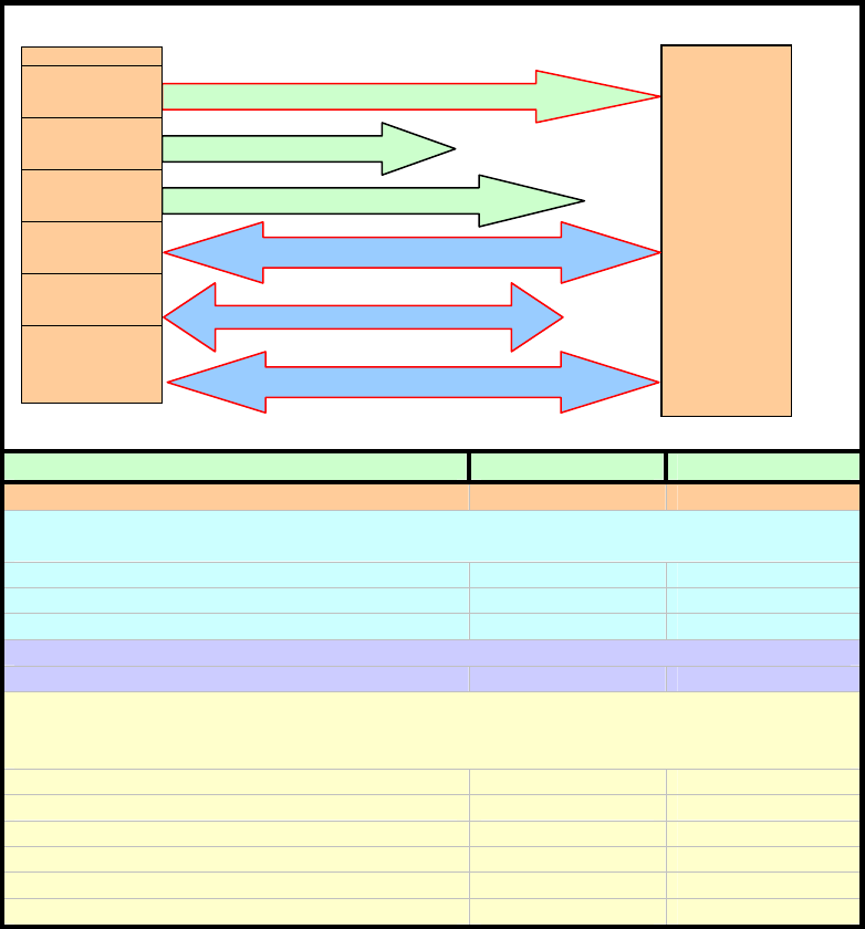
Signals common to both technologies and a general comparison of DDR2 and DDR3 is shown in Table 1. It
must be noted that “matching” includes cases where the clock net may be made longer (termed DELTA in
ALLEGRO SigXP). We have assumed a configuration comprising a Controller and two SDRAMs in most
illustrations that follow.
2. PCB Layer stackup and impedance
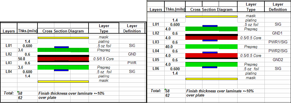
In a layer constrained implementation, a 4 layer PCB (Figure 1) is a minimum with all routing on TOP and
BOTTOM layers. One of the internal layers will be a solid ground plane (GND). The other internal plane layer is
dedicated to VDD. Vtt and Vref can be derived from VDD. Use of a 6-layer PCB makes the implementation of
certain topologies easier. PI is also enhanced due to the reduced spacing between power and GND planes.
The interconnect characteristic impedance for DDR2 implementation can be a constant. A single-ended trace
characteristic impedance of 50 Ohms can be used for all single-ended signals. A differential impedance of 100
Ohms can be used for all differential signals, namely CLOCK and DQS. Further, the termination resistor pulled
up to VTT can be kept at 50 Ohms and ODT settings can be kept at 50 Ohms.
In the case of DDR3 however, single ended trace impedances of 40 and 60 Ohms used selectively on loaded
sections of ADDR/CMD/CNTRL nets have been found to be advantageous. Further, the value of the termination
resistor pulled up to Vtt needs to be optimized in combination with the trace impedance through SI simulations.
Typically, it is in the range 30 – 70 Ohms. The differential trace impedance can remain at 100 Ohms.
Figure 1 : Four and Six layer PCB stackup
3. Interconnect Topologies
In both cases of DDR2 and DDR3, DQ, DM and DQS signals are point-to-point and do not need any topological
consideration. An exception is in the case of multi-rank Dual In Line Memory Modules (DIMMs). Waveform
integrity is also easily addressed by a proper choice of drive strengths and On Die Termination (ODT). The
ADDR/CMD/CNTRL signals, and sometimes the clock signal will involve a multipoint connection where a
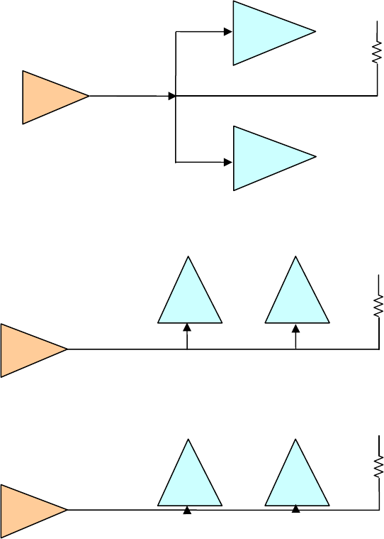
suitable topology is needed. Possible choices are indicated in Figure 2 for cases involving two SDRAMs. The
Fly-By Topology is a special case of a daisy chain with a very short or no stub.
For DDR3, any of these topologies will work, provided that the trace lengths are minimized. The Fly-by topology
shows the best waveform integrity in terms of an increased noise margin. This can be difficult to implement on a
4-layer PCB and the need for a 6-layer PCB arises. The daisy chain topology is easier to implement on a 4 layer
PCB. The tree topology on the other hand requires the length of the branch AB to be very close to that of AC
(Figure 2). Enforcing this requirement results in the need to increase the length of the branches which affects
waveform integrity. Therefore, for DDR3 implementation, the daisy chain topology with minimized stubs proves
to be best suited for 4-layer PCBs.
For DDR2-800 Mbps any of these topologies are applicable with the distinction between each other being less
dramatic. Again, the daisy chain proves to be superior in terms of both implementation as well as SI.
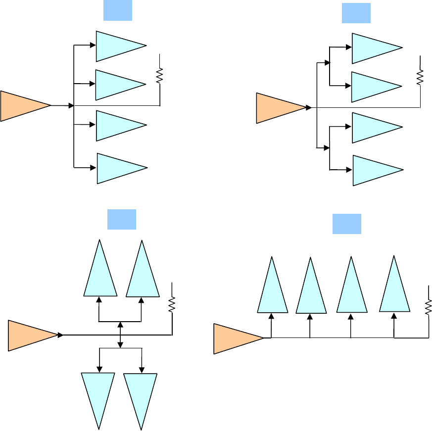
Where more than two SDRAMs are present, often, the topology can be dictated by constraints on device
placement. Figure 3 shows some examples where a topology could be chosen to suit a particular component
placement. Of these, only A and D are best suited for 4-layer PCB implementation. Again, for DDR2-800 Mbps
operations all topologies yield adequate waveform integrity. For a DDR3 implementation, in particular at 1600
Mbps, only D appears to be feasible.
U1
M1 M2
U1
M1 M2
Vtt
Rt
Vtt
Rt
U1
M1
M2
Vtt
Rt
Tree topology
C
A
B
Fly-By topology
Daisy Chain topology
Figure 2: ADDR/CMD/CNTRL topologies with 2 SDRAMS
(A)
Figure 3: ADDR/CMD/CNTRL topologies with four SDRAMS
4. Delay matching
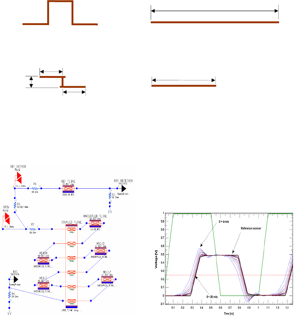
Implementing matched delay is usually carried out by bending a trace in a trombone shape. Routing blockage
may require layer jumping. Unfortunately, while physical interconnect lengths can be made identical in layout,
electrically, the two configurations shown in Figure 4 will not be the same.
The case of trombone delay has been well understood, and the case of a via is obvious. The delay of a
trombone trace is smaller than the delay of a straight trace of the same center-line length. In the case of a via,
the delay is more than that of a straight microstrip trace of length equal to the via length. The problem can be
resolved in two different ways. In the first approach, these values can be pre-computed precisely and taken into
account while delay matching. This would become a tedious exercise which could perhaps be eased with user
M1 Vtt
Rt
U1
M2
M3
M4
Vtt
Rt
M1
U1
M2
M3
M4
Vtt
Rt
M
1
M
2
M
4
M
3
(B)
(C) (D)
Vtt
Rt
U1
M
1
M
2
M
3
M
4
U1
defined constraints in ALLEGRO 16.0. In the second approach, one would use means to reduce the disparity to
an acceptable level.
Trombone trace Straight trace
L3 L1+ L2 + L3+ L4+ L5
L2 L4
≠
L1 L5
Figure 4: Illustration of Trombone traces and Vias
Figure 5: Circuit for estimation of trombone effect and resulting waveforms.
≠
L1
Straight trace
Via cross sectional view
L1+ L2 + L3
L2
L3
Consider the case of a trombone trace. It is known that the disparity can be reduced by increasing the length of
L3 (Figure 4). Details can be found in reference [3]. A simulation topology can be set up in SigXP to represent
parallel arms of a trombone trace as coupled lines. A sweep simulation is carried out with L3 (S in Figure 5) as a
variable and the largest reasonable value that reduces the delay difference with respect to a reference trace is
selected. For microstrip traces, L3 > 7 times the distance of the trace to ground is needed.
Delay values are affected in a trombone trace due to coupling between parallel trace segments. Another way to
reduce coupling without increasing the spacing is to use a saw tooth profile. The saw tooth profile shows better
performance as compared to a trombone although it eventually ends up requiring more space. In either case, it
is possible to estimate the effect on delay precisely by using a modified equation for the computation of the
effective trace length [3]. This would need to be implemented as a user defined constraint in ALLEGRO.
Consider the case of a through hole via on the 6 layer stackup of Figure 2. Ground vias placed close to the
signal vias play an important role in the delay. For the illustration, the microstrip traces on TOP and BOTTOM
layers are 150 mils long, and 4 mils wide. The via barrel diameter = 8 mils, pad diameter is 18 mils and the anti-
pad diameter is 26 mils.
Three different cases are considered. In the first case, the interconnect with via does not have any ground vias
in its immediate neighborhood. Return paths are provided at the edges of the PCB 250 mils away from the
signal via. In the second case, a reference straight microstrip trace of length = 362 mils is considered. The third
case is the same as case 1 with four ground vias in the neighborhood of the signal via. Computed s-parameters
with 60 Ohm normalization are shown in Figure 6. It can be seen that the use of 4 ground vias surrounding the
signal via makes its behavior more like a uniform impedance transmission line and improves the s21
characteristic. In the absence of a return path in the immediate neighborhood, the via impedance increases.
For the present purpose, it is important to know the resulting impact on the delay.
A test circuit is set up similar to Figure 5. The driver is a linear source of 60 Ohms output impedance and
outputs a trapezoidal signal of rise time = fall time = 100 ps and amplitude = 1V. It is connected to each of the 3
interconnects shown in Figure 6 and the far end is terminated in a 60 Ohm load. The excitation is a periodic
signal with a frequency of 800 MHz. The time difference between the driver waveform at V = 0.5 V and the
waveform at the receiver gives the switched delay.
Results are illustrated in Figure 7 where only the rising edge is shown. It can be seen that the delay with four
neighboring ground vias differs from that of the straight trace by 3 ps. On the other hand, the difference is 8 ps
for the interconnect with no ground vias in the immediate neighborhood.
It is therefore clear that increasing the ground via density near signal vias will help. However, in the case of 4
layer PCBs, this will not be possible as the signal traces adjacent to the Power plane will be referenced to a
Power plane. Consequently, the signal return path would depend on decoupling. Therefore, it is very important
that the decoupling requirement on 4 layer PCBs addresses return paths in addition to meeting power integrity
requirements.
The clock net is differential in both DDR2 and DDR3. In DDR2, DQS can be either single ended or differential
although it is usually implemented as differential at higher data rates. The switched delay of a differential trace is
less than that of a single ended trace of identical length. Where timing computations indicate the need, the clock
and DQS traces may need to be made longer than the corresponding ADDR/CMD/CNTRL nets and DATA nets.
This would ensure that the clock and DQS transitions are centered on the associated ADDR/CMD/CNTRL nets
and DQ nets.
Since DQ and DM nets run at the maximum speed, it is desirable that all of these nets in any byte lane be routed
identically, preferably without vias. Differential nets are less sensitive to discontinuities and where layer jumping
is needed, the DQS and CLOCK nets should be considered first.
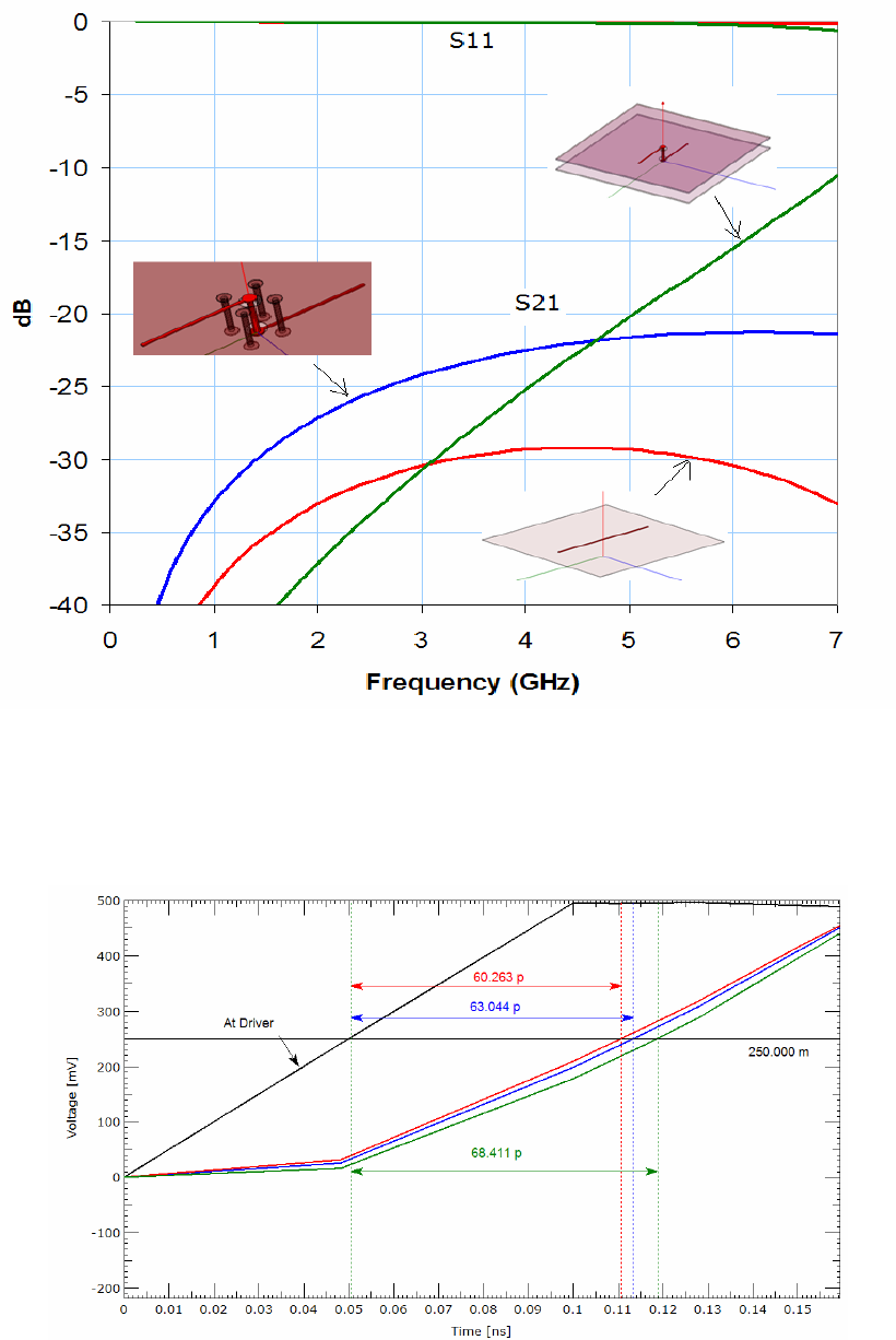
Figure 6: s-parameters of interconnects with vias (60 Ohm normalization)
Figure 7: Driver and Receiver waveforms for the 3 cases of Figure 6. (Plot colors correspond)
5. Crosstalk
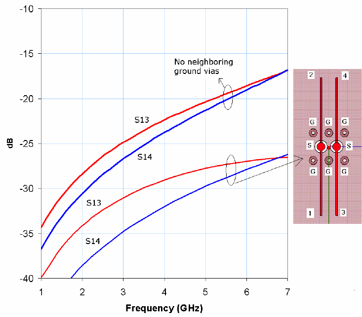
Cross talk contributes to delay uncertainty being significant for microstrip traces. This is generally reduced by
increasing the spacing between adjacent traces for long parallel runs. This has the drawback of increasing the
total trace length and therefore a reasonable value must be chosen. Typically the spacing should be greater
than twice the trace distance to ground. Again, ground vias play an important role. Near and far end coupling
levels are illustrated in Figure 8. Use of multiple ground vias reduces coupling levels by 7 dB. To derive the
interconnect budget, a simulation of a victim trace with two aggressors on both sides is adequate. Using a
periodic excitation on all nets will yield the cross talk induced jitter. Using a pseudo random excitation on all nets
will show the effect of both cross talk as well as data dependencies. Time domain results are not shown here,
but it is easily done by setting up a 5 coupled line circuit in SigXP with the spacing between traces set up for
sweeping. Reasonable spacing values that keep the jitter in the waveform due to both cross talk as well as
pattern dependence at an acceptable level are chosen.
Figure 8: s-parameters of coupled traces (60 Ohm normalization)

6. Power Integrity
Power Integrity here refers to meeting the Power supply tolerance requirement under a maximum switching
condition. Failure to address this requirement properly leads to a number of problems, such as increased clock
jitter, increased data dependent jitter, and increased cross talk all of which eventually reduce timing margins.
The theory for decoupling has been very well understood and usually starts with the definition of a “target
impedance” as [4]
CurrentTransient
toleranceVoltage
Zett =
arg (1)
An important requirement here is knowledge of the transient current under worst case switching condition. A
second important requirement is the frequency range. This is the range of frequencies over which the
decoupling network must ensure that its impedance value is equal to or below the required target impedance.
On a printed circuit board, capacitance created by the Power-Ground sandwich and the decoupling capacitors
needs to handle a minimum frequency of ~100 kHz up to a maximum frequency of ~100-200 MHz. Frequencies
below 100 kHz are easily addressed by the bulk capacitance of the voltage regulator module. Frequencies
above 200 MHz should be addressed by the on-die and in some cases on-package decoupling capacitance.
Due to the finite inductance of the package, there is no need to provide decoupling on the PCB to handle
frequencies greater than 200 MHz. The actual computation of power integrity can be very complex involving IC
package details, simultaneously switched signals and the PCB power distribution network. For PCB design, the
use of the target impedance approach to decoupling design is simpler and provides a practical solution with very
little computational effort.
The three power rails of concern are the VDD, VTT and Vref. The tolerance requirements on the VDD rail is ~
5% and the transient current is determined as the difference between Idd7 and Idd2 as specified by JEDEC
[1,4]. This is accomplished by using plane layers for power distribution and a modest number of decoupling
capacitors. It is preferable to use decoupling capacitors of 10 different values distributed in the range of 10 nF to
10 uF. Further, the capacitor pad mounting structure should be designed for reduced mounted inductance.
The Vref rail has a tighter tolerance, but it draws very little current. Its target impedance is easily met using
narrow traces and one or two decoupling capacitors. It is important however that the capacitors be located very
close to the device pins.
The VTT rail proves to be challenging because it not only has a tighter tolerance, but it also draws a transient
current close to that of the VDD rail. The transient current is easily calculated as described in reference [5].
Again, the target impedance requirement can be met using an increased number of decoupling capacitors.
On a 4 layer PCB, the planes are too far apart and consequently the advantage of inter-plane capacitance is
lost. The number of decoupling capacitors needs to be increased and higher frequency capacitors with values
less than 10 nF may be needed. These computations are easily done using ALLEGRO SI Power Integrity option.

7. Timing
Timing computation is carried out as described in reference [6]. A table needs to be setup for the following eight
cases:
1. Write Setup analysis DQ vs. DQS
2. Write Hold analysis DQ vs. DQS
3. Read Setup analysis DQ vs. DQS
4. Read Hold analysis DQ vs. DQS
5. Write Setup analysis DQS vs. CLK
6. Write Hold analysis DQS vs. CLK
7. Write Setup analysis ADDR/CMD/CNTRL vs. CLK
8. Write Hold analysis ADDR/CMD/CNTRL vs. CLK
An example is shown for the case of Write setup analysis in Table 2. Actual numbers have been omitted as they
are not precisely known yet for DDR3. These numbers are obtained from data sheets of Controller and memory
manufacturers. The numbers in the interconnect section are determined by SI simulations. All the eight cases
need to be analyzed for DDR2. For DDR3, 5 and 6 are not needed due to its write leveling feature. In the PCB
implementation, length match tolerances must ensure that the total margin is positive.
Element Skew Component Setup Units Comments
a.)DQ vs. DQS skew at
transmitter output ps From controller design data
Controller
b.) Data / Strobe PLL jitter ps Used if not included in transmitter skew
Total
Controller a + b ps
Setup requirement (tDSb
@ Vih/Vil level)
ps From SDRAM datasheet; this number is to
be adjusted based on DQ and DQS slew
rates
DQ slew rate V/ns Measured as per JEDEC specification from
SI simulation results
SDRAM (or
DIMM)
DQS slew rate V/ns Measured as per JEDEC specification from
SI simulation results
Total
SDRAM
setup
requirement
tDSb + slew rate
adjustment ps Includes slew rate adjustment
a.) Data Xtalk ps 2 aggressors (one each side of the victim);
victim – repetitive; aggressor- PRBS
b.) DQS Xtalk ps 2 aggressors (one each side of the victim);
victim – repetitive; aggressor- PRBS
c.) Length matching
tolerance ps Extracted from SI simulation results
longest data net, worst case PVT corner
Interconnect
d.) Characteristic
impedance mismatch ps can be omitted if routing of DQ and
corresponding DQS signals are done on
same layer
Total
Interconnect Interconnect skew
(a + b + c + d) ps
Min. Total
Setup
Budget
0.24*tck ps From SDRAM datasheet (includes clock
duty cycle variation)
Setup
margin Min. Total Setup Budget –
(Total Controller + Total
SDRAM + Total
Interconnect )
ps Must be positive
Table 2: Illustration of DDR3 Write Setup timing analysis summary for DQ vs. DQS
8. PCB Layout
Implementation on a PCB involves a number of tradeoffs to meet SI requirements. Often, the question is how far
does one need to go? PCB layout tasks are facilitated using the following approach:
1. Set up topology and constraints in ALLEGRO Constraint Manager.
2. Design Controller BGA breakout. A controller pin arrangement with ADDR/CMD/CNTRL pins in the
middle and DQ/DQS/DM byte lanes on either side is best suited. Within these groups, individual pins
may need to be swapped to ensure routing with minimum cross-over.
3. Attempt routing with reduced stub length and a minimum trace spacing as obtained from cross talk
simulation. Often, most stubs can be eliminated but it will not be possible for all the pins. One may try
two traces between BGA pads of the memory devices. This would require narrow PCB traces which can
increase manufacturing cost. Yet, it will not be possible for all signals unless micro via and via-in-pad
technology is used. Complete routing with coarse length matching tolerances.
4. Place Vref decoupling capacitors close to the Vref pins. Vtt decoupling can be placed at the far end of
the last SDRAM and will not come in the way of routing. VDD decoupling can be placed close to devices
where possible without blocking routing channels. The smaller valued capacitors should be placed
closer to the devices. With a proper decoupling design, it will not be necessary to cram all capacitors
close to the devices. All decoupling capacitors should use a fan out for the footprint designed for
reduced inductance. This is typically two short wide traces perpendicular to the capacitor length. This
can be automated by using a user defined capacitor footprint that can be attached to all the decoupling
capacitors in the schematic.
5. Implement fine length matching and insert multiple ground vias where signal traces jump layers. It is
better to use the delay matching option in ALLEGRO and one must include z-axis delay. Typically, P
and N nets of differential pairs should be matched with a tolerance of +/- 2ps and the tolerance for all
other matched nets can be +/- 10 ps or more based on the timing margin computation.
9. DIMM
Considerations described above apply to the case of PCBs containing one or more DIMMs. The only exception
is that the decoupling requirement for the memories can be relaxed as it is already accounted for on the DIMM
PCB. SI analysis of registered DIMMs is also much simpler where the DIMM is treated as a single load. While
the routing topology for ADDR/CMD/CNTRL nets is usually a daisy chain with reduced stubs, tree topologies can
also be used for registered DIMMs. Analysis of un-buffered DIMMs can become tedious as the timing
requirement at all the SDRAMs must be analyzed. DIMM routing on 4-layer PCBs is relatively simpler compared
to the case of SDRAMs.
10. Examples
The detail described above has been used in the implementation of a DDR2 PCB, a DDR3 PCB and a DDR3 –
DIMM PCB. The controller is from MOSAID [7] which is designed to provide both DDR2 as well as DDR3
functionality. For the SI simulations, IBIS models have been used. Models for the memories are from MICRON
Technology, Inc [8]. The IBIS models for the DDR3 SDRAMs were available at 1333 Mbps speed. These were
used at 1600 Mbps. For the unbuffered DDR3 DIMM (MT_DDR3_0542cc) EBD models from Micron Technology
were used. All waveforms are for the typical case and are computed at the SDRAM die. The 6 layer PCB
stackup of Figure 2 is used with routing on TOP and BOTTOM layers only. The memory consists of 2 SDRAMs
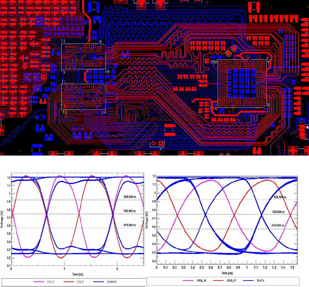
routed as a daisy chain. In the case of the DIMM, a single unbufferred DIMM is used. Snapshots of
TOP/BOTTOM layer routing and Signal Integrity waveforms are shown in Figures. 9-11.
Figure 9: Illustration of TOP and BOTTOM layers of a DDR3 PCB with computed waveforms at the farthest
SDRAM. Waveform on left is an ADDRESS net compared to that of the CLOCK net. Waveform
on the right is a DATA net compared to that of a DQS net. Clock frequency = 800 MHz and data rate
is 1600 Mbps.
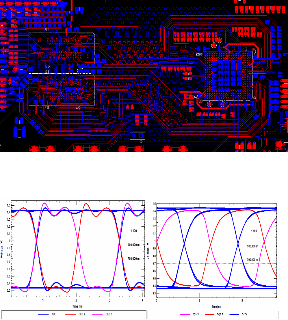
Figure 10: Illustration of TOP and BOTTOM layers of a DDR2 PCB with computed waveforms at the farthest
SDRAM. Waveform on left is an ADDRESS net compared to that of the CLOCK net. Waveform
on the right is a DATA net compared to that of a DQS net. Clock frequency = 400 MHz and data rate
is 800 Mbps.
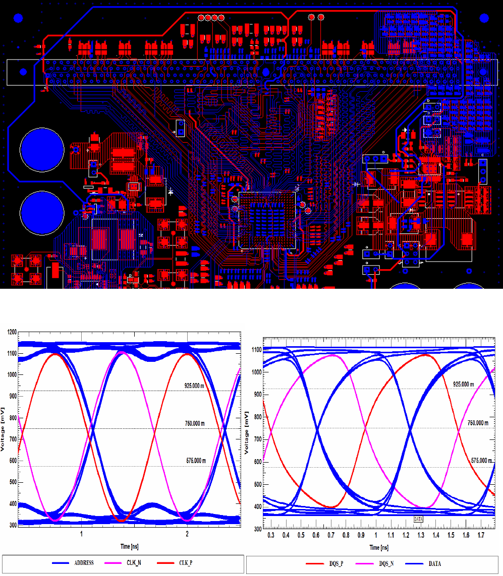
Figure 11: Illustration of TOP and BOTTOM layers of a DDR3 – DIMM PCB with computed waveforms at the 8th
(last) SDRAM on DIMM. Waveform on left is an ADDRESS net compared to that of the CLOCK net.
Waveform on the right is a DATA net compared to that of a DQS net.
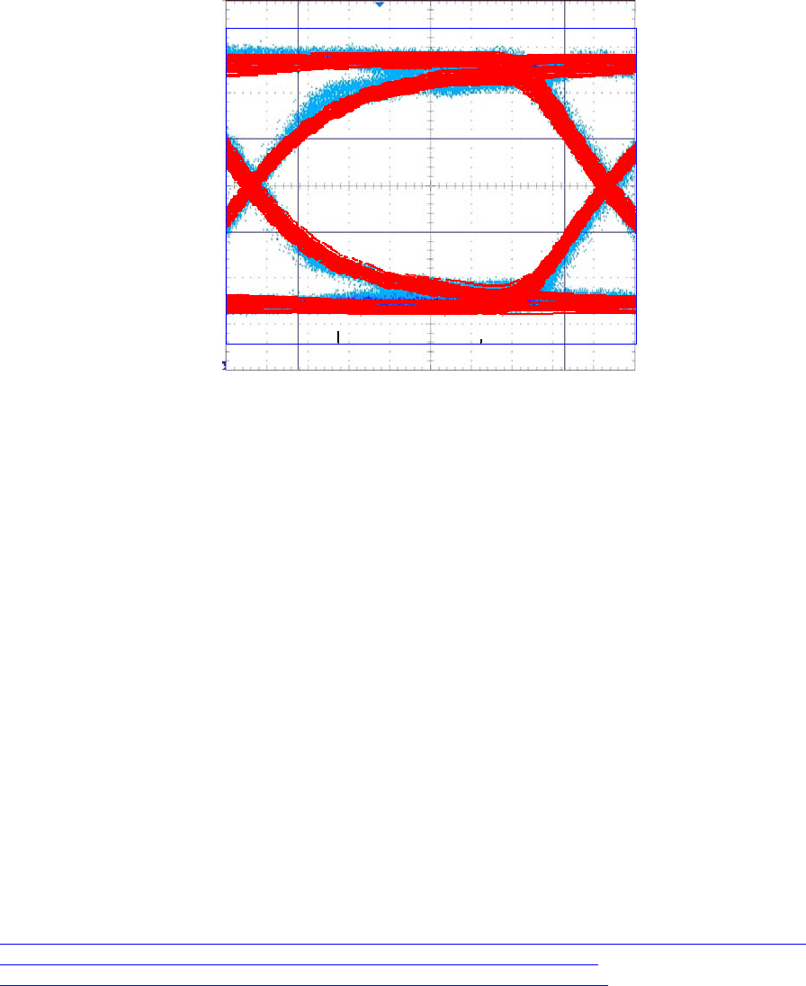
Lastly, Figure 12 shows a comparison of computed and measured DATA eye patterns of an 800 Mbps DDR2. In
all cases waveform integrity can be seen to be excellent.
Figure 12: Computed (Red) and Measured (blue) waveforms of a data net of an 800 Mbps DDR2 PCB.
11. Conclusion
In this paper, all aspects related to SI, and PI of DDR2 and DDR3 implementation have been described. Use of
Constraint Manager in ALLEGROTM makes implementation easy. While a four layer PCB implementation of 800
Mbps DDR2 and DDR3 appears to be feasible, DDR3-1600 Mbps will prove to be challenging. It will become
clearer as the memory devices become available and one has a good handle on timing numbers.
References
[1] DDR2 SDRAM Specification, JEDEC JESD79-2B, January 2005.
[2] DDR3 SDRAM Standard, JEDEC JESD79-3, June 2007.
[3] Syed Bokhari, “Delay matching on Printed Circuit Boards”, Proceedings of the CDNLIVE 2006, San Jose.
[4] Larry D Smith, and Jeffrey Lee, “Power Distribution System for JEDEC DDR2 memory DIMM, Proc. IEEE
EPEP conference, Princeton, N.J., pp. 121-124, October 2003.
[5] Hardware and layout design considerations for DDR2 SDRAM Memory Interfaces, Freescale semiconductor
Application Note, Doc. No. AN2910, Rev. 2, 03/2007.
[6] DDR2 design guide for 2 DIMM systems, Technical Note, Micron Technology Inc. TN-47-01, 2003.
[7] http://www.mosaid.com/corporate/products-services/ip/SDRAM_Controller_whitepaper_Oct_2006.pdf
[8] http://www.micron.com/products/dram/ddr2/partlist.aspx?speed=DDR2-800
[9] http://www.micron.com/products/dram/ddr3/partlist.aspx?speed=DDR3-1066