DEC 11 HBMAA E D BM792 Read Only Memory And MR11 DB Bootstrap Loader
DEC-11-HBMAA-E-D BM792 Read-Only-Memory and MR11-DB Bootstrap Loader DEC-11-HBMAA-E-D BM792 Read-Only-Memory and MR11-DB Bootstrap Loader
User Manual: DEC-11-HBMAA-E-D BM792 Read-Only-Memory and MR11-DB Bootstrap Loader
Open the PDF directly: View PDF ![]() .
.
Page Count: 54
BM792
read-only-memory
and
MR11-DB
bootstrap
loader

l
(
BM792
read-only-memory
and
MR11~DB
bootstrap
loader
DEC-II-HBMAA-E-D
digital
equipment
corporation
0
maynard.
massachusetts
1st Edition, July 1971
2 ns Printing, December 1971
3rd Printing (Rev), October 1972
4th
Printing, December 1972
5th
Printing, May 1973
6th
Printing (Rev), January 1974
Copyright © 1971, 1972, 1973, and 1974 by Digital Equipment Corporation
The material
in
this manual
is
for informational
purposes and is subject to change without notice.
Printed
in
U.S.A.
The following are trademarks
of
Digital Equipment
Corporation, Maynard, Massachusetts:
DEC
FLIP CHIP
DIGITAL
PDP
FOCAL
COMPUTER
LAB
CHAPTER 1
1.1
1.2
CHAPTER 2
2.1
2.2
2.3
2.4
2.5
CHAPTER 3
3.1
3.2
CHAPTER 4
APPENDIX A
APPENDlXB
APPENDlXC
APPENDlXD
APPENDIXE
APPENDlXF
Figure No.
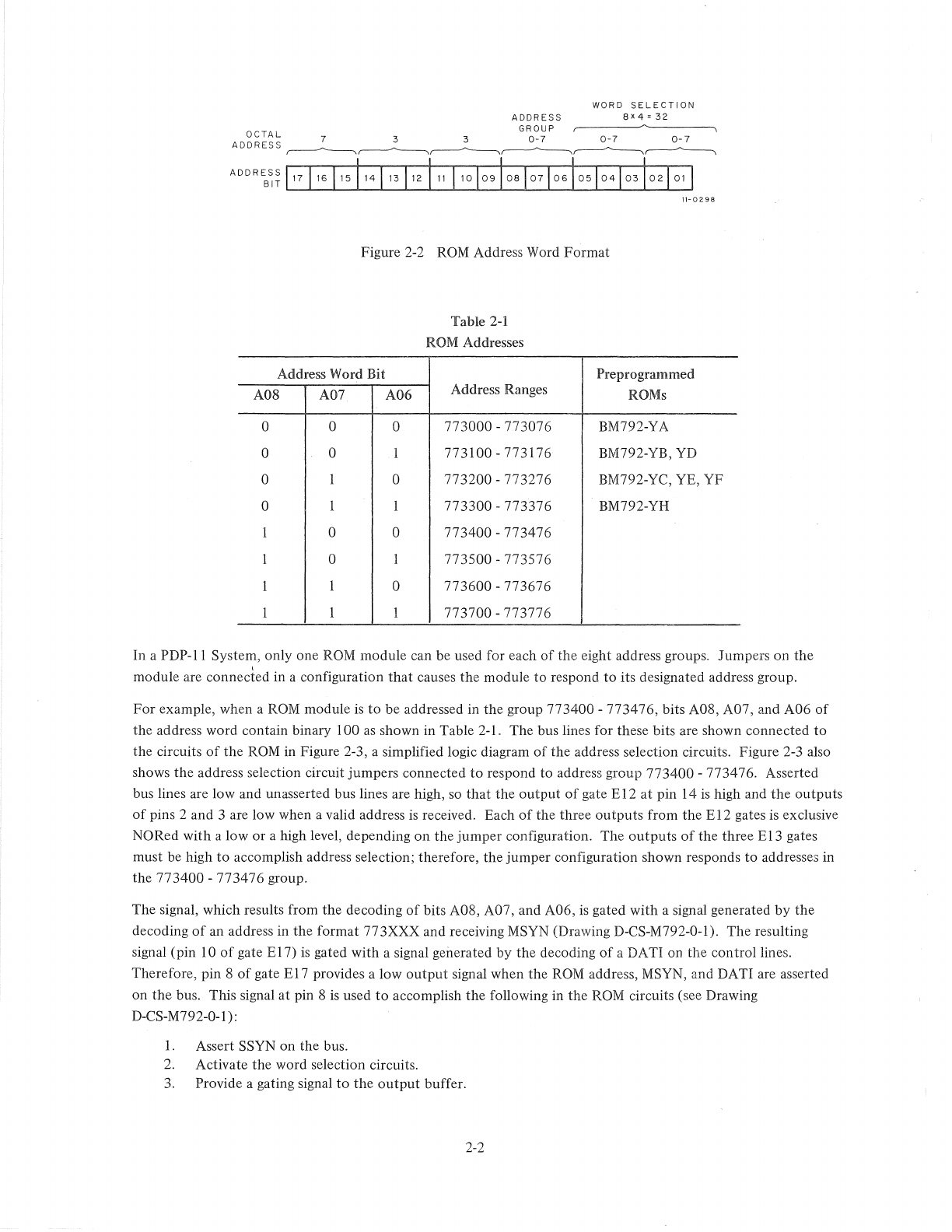
2-1
2-2
2-3
2-4
2-5
2-6
3-1
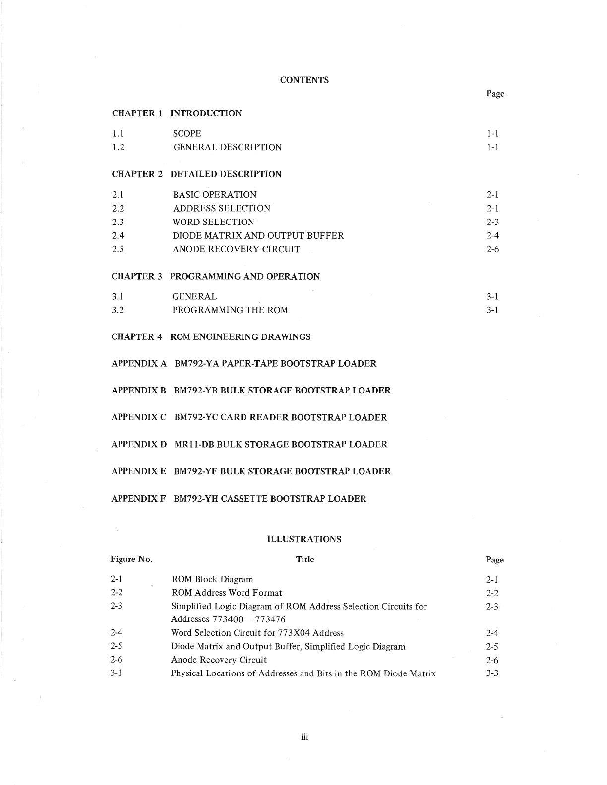
CONTENTS
INTRODUCTION
SCOPE
GENERAL DESCRIPTION
DETAILED DESCRIPTION
BASIC OPERATION
ADDRESS SELECTION
WORD SELECTION
DIODE MATRIX AND OUTPUT BUFFER
ANODE RECOVERY CIRCUIT
PROGRAMMING AND OPERATION
GENERAL
PROGRAMMING THE
ROM
ROM
ENGINEERING DRAWINGS
BM792-YA PAPER-TAPE BOOTSTRAP LOADER
BM792-YB BULK STORAGE BOOTSTRAP LOADER
BM792-YC CARD READER BOOTSTRAP LOADER
MRII-DB
BULK STORAGE BOOTSTRAP LOADER
BM792-YF BULK STORAGE BOOTSTRAP LOADER
BM792-YH CASSETTE BOOTSTRAP LOADER
ILLUSTRATIONS
Title
ROM
Block Diagram
ROM
Address Word
Format
Simplified Logic Diagram
of
ROM Address Selection Circuits for
Addresses
773400
-
773476
Word Selection Circuit for 773X04 Address
Diode Matrix and
Output
Buffer, Simplified Logic Diagram
Anode Recovery Circuit
Physical Locations
of
Addresses and Bits in the ROM Diode Matrix
iii
Page
1-1
1-1
2-1
2-1
2-3
2-4
2-6
3-1
3-1
Page
2-1
2-2
2-3
2-4
2-5
2-6
3-3
TABLES
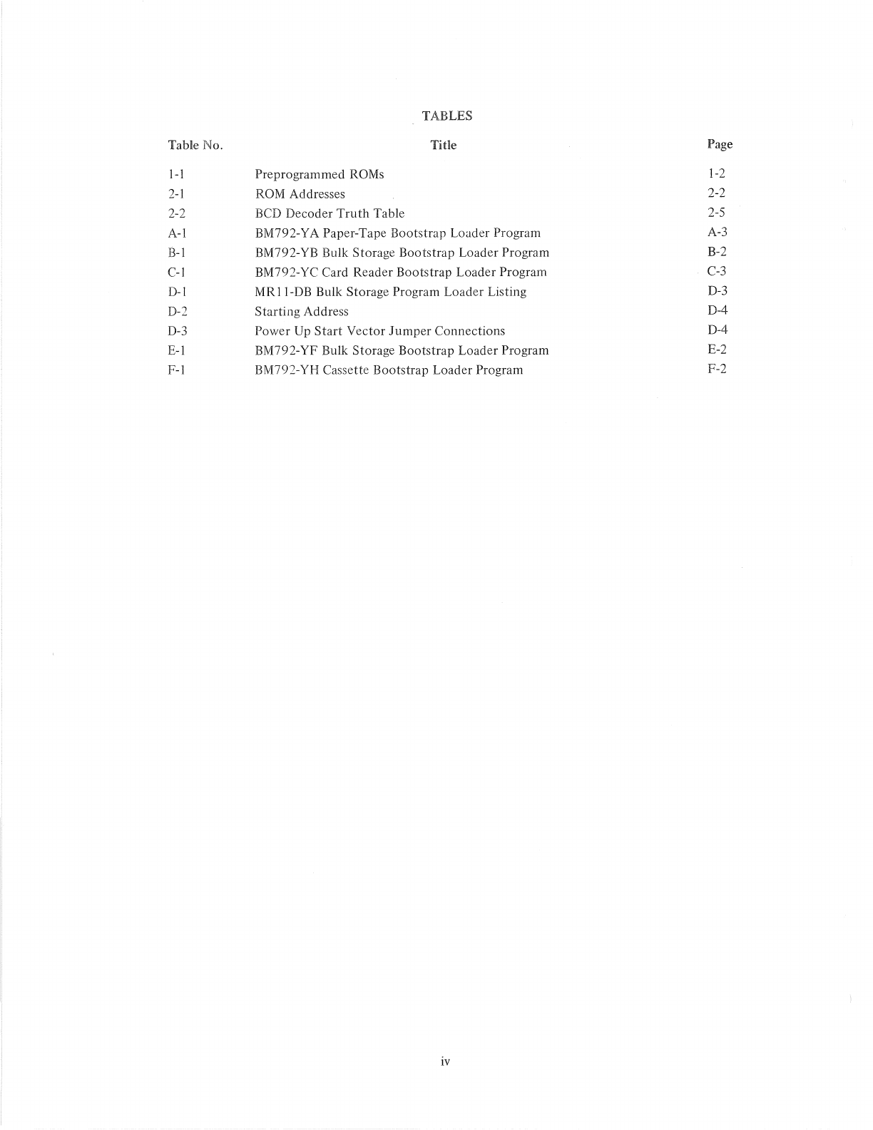
Table No. Title Page
I-I Preprogrammed
ROMs
1-2
2-1
ROM
Addresses 2-2
2-2
BCD
Decoder
Truth
Table
2-5
A-I BM792-Y A Paper-Tape Bootstrap Loader Program
A-3
B-1
BM792-YB Bulk Storage Bootstrap Loader Program
B-2
C-I
BM792-YC Card Reader Bootstrap Loader Program
C-3
D-I MR II-DB Bulk Storage Program Loader Listing
D-3
D-2
Starting Address D-4
D-3
Power Up Start Vector Jumper Connections D-4
E-I BM792-YF Bulk Storage Bootstrap Loader Program E-2
F-I BM792-YH Cassette Bootstrap Loader Program F-2
iv
CHAPTER 1
INTRODUCTION
1.1 SCOPE
This manual provides the user with
theory
of
operation, programming information, and schematics necessary to
understand and program
the
BM792 Read-Only-Memory (ROM). The level
of
discussion assumes
that
the
reader
is
familiar with basic digital
computer
theory.
Although
the
input
and
output
signals
of
the
ROM are carried
by
the Unibus @ , it
is
beyond
the
scope
of
this
manual
to
describe
the
Unibus itself. A detailed description
of
the Unibus is presented in
the
PDP-ii
Peripherals
Handbook.
1.2 GENERAL DESCRIPTION
The BM792 is a 32-word read-only-memory (ROM). The diode matrix and address selection circuits
that
consti-
tute
the
ROM are
mounted
on an extra-width quad-board module. This module
is
inserted in either one
of
the
two small peripheral controller slots in
the
PDP-II processor
or
in one
of
the
four slots in
the
DD-ll
peripheral
mounting
panel.
The ROM
is
available either unprogrammed (designated BM792)
or
preprogrammed (designated BM792-Y
X,
where
the
letter
in
the
X position identifies
the
program). The unprogrammed module can be programmed
to
form code conversion tables
or
contain frequently-used mathematical values and subroutines. These applications
of
the
ROM provide an access time
of
100 ns, which can increase
the
program speed.
Preprogrammed ROMs are used for implementing small standard programs required in
PDP-Il
System operation,
such
as
bootstrap
loaders for paper tape
or
DECtape. The preprogrammed ROMs
that
are available at publica-
tion
of
this manual are described in
the
Appendices and listed
in
Table 1-1. As additional preprogrammed ROMs
become available, additional appendices will be published
to
describe them.
@ Unibus is a registered
trademark
of
Digital
Equipment
Corporation.
1-1
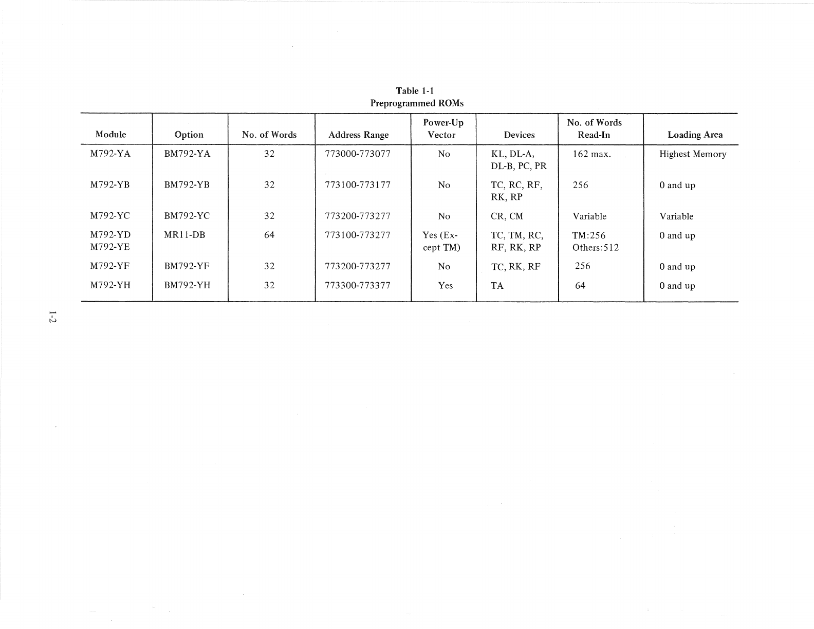
Module Option No.
of
Words
M792-YA BM792-YA
32
M792-YB BM792-YB 32
M792-YC BM792-YC 32
M792-YD
MRll-DB
64
M792-YE
M792-YF BM792-YF 32
M792-YH BM792-YH
32
>-'
N
Table
1-1
Preprogrammed ROMs
Power-Up
Address Range Vector
773000-773077 No
No.
of
Words
Devices Read-In
KL, DL-A, 162 max.
DL-B, PC,
PR
773l00
c
773l77
No TC, RC, RF, 256
RK,RP
773200-773277 No
CR,CM
Variable
773100-773277 Yes (Ex- TC, TM, RC, TM:256
cept TM)
RF,RK,RP
Others:5l2
773200-773277 No
TC,RK,
RF
256
773300-773377 Yes TA 64
_______
L....-_.
__________
--
-----------
Loading Area
Highest Memory
o and up
Variable
o and up
o and up
o and up
---
---
-----------
CHAPTER 2
DETAILED DESCRIPTION
2.1
BASIC OPERATION
The ROM diode matrix contains 32 16-bit words, each
of
which can be applied
to
the bus under program control.
The ROM responds only
to
a DATI from
the
Unibus, DATO, DATOB, and DATIP are ignored. A block diagram
of
the
ROM
is
shown in Figure 2-1.
When
both
a DATI and a ROM address are sent
to
the
ROM,
the
word in
the
addressed location
of
the diode
matrix
is
applied
to
the Unibus. When
the
ROM address
is
received,
the
5-bit code on address lines
AO
1 through
A05
is
decoded
to
apply a signal
to
the
cathodes
of
the diodes in the addressed word location. The word in
the
addressed location
is
transferred through
the
output
buffer to data lines
DOO
through
DIS
of
the
Unibus.
I
ADDRESS
A<06:17>
SELECTOR
ANODE
DATI
RECOVERY
MSYN
1
SIGNAL
32
x 16
SSYN
OUTPUT
UNIBUS
DIODE
r-------
BUFFER
MATRIX
WORD
A<01:05>
SELECTOR
CATHODE
DRIVER
I
S I G N
AL
D<00:15>
11-0299
Figure
2-1
ROM
Block Diagram
2.2 ADDRESS SELECTION
The address word format for the
ROM
is
shown in Figure 2-2. Octal addresses for the
ROM
must be
of
the
773XXX
format. The
ROM
reads-out only fuI116-bit words and does
not
issue
byte
data; thus, address bit
AOO
is
not
used.
The addresses are further divided into eight groups, which are determined
by
address bits
AOS,
A07, and A06 and
listed
ill
Table 2-1.
2-1
WORD
SELECTION
ADDRESS
OCTAL
GROUP
ADDRESS
7 3 3
0-7
0-7
0-7
~~~~~~
ADDRESS
BIT
~-L
__
~-L
__
~-L
__
~~
__
~-L
__
~~
__
~~
__
~~
__
~~
11-0298
Figure 2-2 ROM Address Word
Format
Address Word Bit
A08 A07
0 0
0 0
0 1
0 1
1 0
1 0
1 1
1 1
A06
0
I
0
1
0
1
0
1
Table
2-1
ROM Addresses
Address Ranges
773000
-
773076
773100-773176
773200
-
773276
773300
-
773376
773400
-
773476
773500
-
773576
773600
-
773676
773700
-
773776
Preprogrammed
ROMs
BM792-YA
BM792-YB, YD
BM792-YC, YE,
YF
BM792-YH
In a
PDP-II
System,
only
one ROM
module
can be used for each
of
the
eight address groups.
Jumpers
on
the
module are connected in a configuration
that
causes
the
module
to
respond
to
its designated address group.
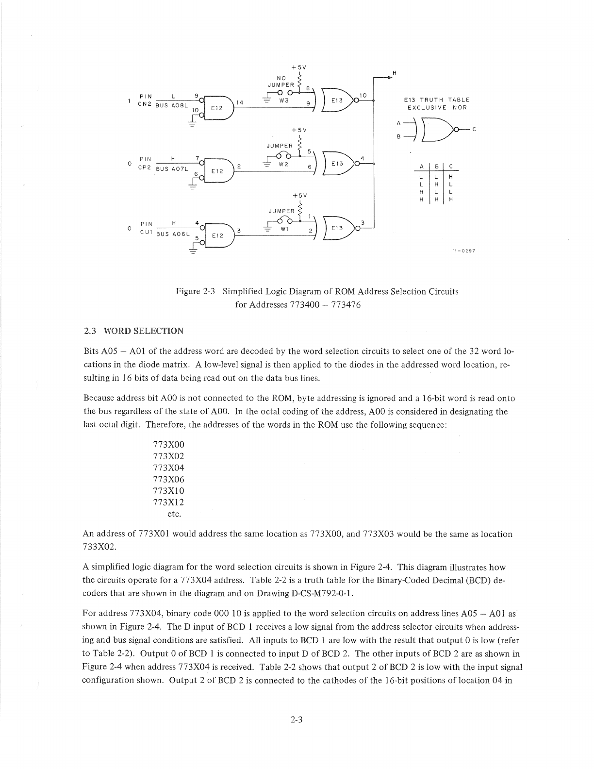
For
example, when a ROM module
is
to
be
addressed in
the
group
773400
-
773476,
bits A08, A07, and
A06
of
the
address word contain binary 100
as
shown in Table 2-1. The bus lines for these bits are shown
connected
to
the
circuits
of
the
ROM in Figure 2-3, a simplified logic diagram
of
the
address selection circuits. Figure 2-3 also
shows
the
address selection circuit
jumpers
connected
to
respond
to
address group
773400
-
773476.
Asserted
bus lines are low and unasserted bus lines are high,
so
that
the
output
of
gate E 12
at
pin 14
is
high and
the
outputs
of
pins 2 and 3 are low when a valid address
is
received. Each
of
the three
outputs
from
the
El2
gates
is
exclusive
NORed
with
a low
or
a high level, depending
on
the
jumper
configuration.
The
outputs
of
the
three E13 gates
must be high
to
accomplish address selection; therefore, the
jumper
configuration shown responds
to
addresses in
the
773400
-
773476
group.
The
signal, which results from the decoding
of
bits A08, A07, and A06,
is
gated
with
a signal generated
by
the
decoding
of
an address in
the
format
773XXX
and receiving MSYN (Drawing D-CS-M792-0-1).
The
resulting
signal (pin 10
of
gate E17)
is
gated
with
a signal generated
by
the
decoding
of
a DATI on the
control
lines.
Therefore, pin 8
of
gate
El7
provides a low
output
signal
when
the
ROM address, MSYN, and DATI are asserted
on
the
bus. This signal
at
pin 8
is
used
to
accomplish
the
following in
the
ROM circuits (see Drawing
D-CS-M792-0-1):
1.
Assert SSYN on
the
bus.
2.
Activate
the
word selection circuits.
3.
Provide a gating signal
to
the
output
buffer.
2-2
0
0
+5V
H
PIN
L E13
TRUTH
TABLE
CN2
BUS
A08L
14
EXCLUSIVE
NOR
PIN
CP2
PIN
C
U1
=
:~[>-C
+5V
H
BUS
A07L
A B C
L L H
L H L
=
+5V
H L L
~
H H H
H 4
BUS
A06L~3
= Wl
2/
I
11-0297
Figure
2-3
Simplified Logic Diagram
of
ROM
Address Selection Circuits
for Addresses 773400 -773476
2.3
WORD
SELECTION
Bits A05 -
AOI
of
the address word are decoded by the word selection circuits to select one
of
the 32 word lo-
cations in the diode matrix. A low-level signal
is
then applied to the diodes in the addressed word location, re-
sulting in 16 bits
of
data being read out on
the
data bus lines.
Because address bit
AOO
is
not
connected to
the
ROM, byte addressing
is
ignored and a l6-bit word
is
read
onto
the bus regardless
of
the state
of
AOO.
In the octal coding
of
the address,
AOO
is
considered in designating the
last octal digit. Therefore, the addresses
of
the
words in the
ROM
use the following sequence:
773XOO
773X02
773X04
773X06
773XlO
773X12
etc.
An address
of
773XO 1 would address the same location
as
773XOO,
and 773X03 would be the same
as
location
733X02.
A simplified logic diagram for the word selection circuits
is
shown in Figure 2-4. This diagram illustrates how
the circuits operate for a 773X04 address. Table 2-2
is
a
truth
table for the Binary-Coded Decimal (BCD) de-
coders
that
are shown in the diagram and
on
Drawing D-CS-M792-0-1.
For
address 773X04, binary code 000 10
is
applied to the word selection circuits on address lines A05 -
AOI
as
shown in Figure 2-4. The D input
of
BCD
1 receives a low signal from the address selector circuits when address-
ing and bus signal conditions are satisfied. All inputs
to
BCD
1 are low with
the
result
that
output
0
is
low (refer
to
Table 2-2).
Output
0
of
BCD
1
is
connected to input D
of
BCD
2.
The other inputs
of
BCD
2 are
as
shown in
Figure 2-4 when address 773X04
is
received. Table 2-2 shows
that
output
2
of
BCD 2
is
low with the
input
signal
configuration shown.
Output
2
of
BCD
2
is
connected to the cathodes
of
the
l6-bit
positions
of
location
04
in
2-3
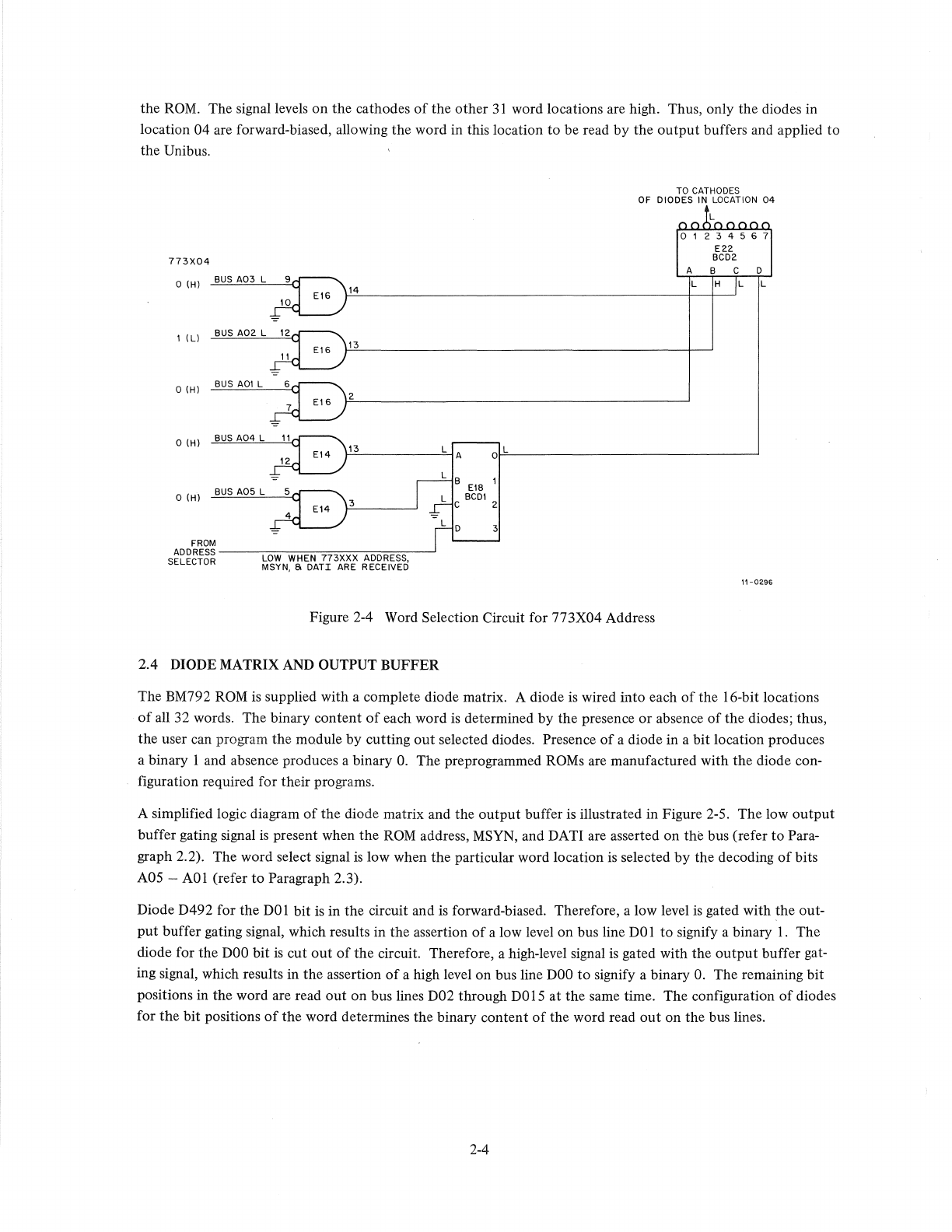
the
ROM.
The signal levels
on
the cathodes
of
the other
31
word locations are high. Thus, only the diodes in
location 04 are forward-biased, allowing
the
word in this location
to
be read
by
the
output
buffers and applied to
the Unibus.
TO CATHODES
OF DIODES
IN
LOCATION
04
EZZ
773X04
BCDZ
ABC
D
o (H) BUS
A03
L
14 L H L L
1
(L)
BUS
ADZ
L
13
o (H) BUS AOI L
Z
o
(H)
BUS
A04
L
13
L A o L
L
BUS
A05
L B E18 1
o
(H)
L C
BCD
1 Z
L D 3
FROM
ADDRESS
----:-L:::Ow~W::-::H:-::E:::N-::7=7:=:3X7."X:7.X,...A:-::D=D::-RE=:S=S-.
---.J
SELECTOR MSYN. a
DATI
ARE RECEIVED
11-02.96
Figure 2-4 Word Selection Circuit for 773X04 Address
2.4 DIODE MATRIX AND OUTPUT
BUFFER
The BM792
ROM
is
supplied with a complete diode matrix. A diode
is
wired into each
of
the 16-bit locations
of
all 32 words. The binary content
of
each word
is
determined
by
the presence
or
absence
of
the
diodes; thus,
the
user can program the module
by
cutting
out
selected diodes. Presence
of
a diode in a
bit
location produces
a binary I and absence produces a binary
O.
The preprogrammed ROMs are manufactured with
the
diode con-
figuration required for their programs.
A simplified logic diagram
of
the
diode matrix and the
output
buffer
is
illustrated in Figure 2-5. The low
output
buffer gating signal
is
present when
the
ROM
address, MSYN, and DATI are asserted
on
the
bus (refer
to
Para-
graph 2.2). The word select signal
is
low when
the
particular word location is selected
by
the decoding
of
bits
A05 -
AOI
(refer
to
Paragraph 2.3).
Diode D492 for
the
DOl
bit
is
in the circuit and
is
forward-biased. Therefore, a low level
is
gated with the out-
put
buffer gating signal, which results
in
the assertion
of
a low level on bus line
DO
I
to
signify a binary I. The
diode for the
DOO
bit
is
cut
out
of
the
circuit. Therefore, a high-level signal
is
gated with the
output
buffer gat-
ing signal, which results in the assertion
of
a high level on bus line
DOO
to
signify a binary
O.
The remaining
bit
positions in
the
word are read
out
on
bus lines
002
through
DOl
5
at
the
same time. The configuration
of
diodes
for
the
bit
positions
of
the
word determines the binary content
of
the word read
out
on the bus lines.
2-4
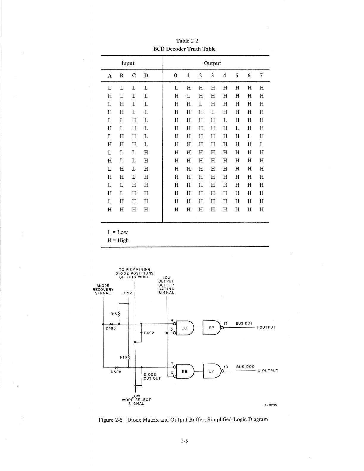
Table 2-2
BCD Decoder
Truth
Table
Input
A B
L L
H L
L H
H H
L L
H L
L H
H H
L L
H L
L H
H H
L L
H L
L H
H H
L=Low
H = High
C
L
L
L
L
H
H
H
H
L
L
L
L
H
H
H
H
D
L
L
L
L
L
L
L
L
H
H
H
H
H
H
H
H
TO
REMAINING
DIODE
POSITIONS
OF
THIS
WORD
ANODE
RECOVERY
SIGNAL
+5V
RI5
0
LOW
OUTPUT
BUFFER
GATING
SIGNAL
L
H
H
H
H
H
H
H
H
H
H
H
H
H
H
H
Output
1 2 3 4 5 6 7
H H H H H H H
L H H H H H H
H L H H H H H
H H L H H H H
H H H L H H H
H H H H L H H
H H H H H L H
H H H H H H L
H H H H H H H
H H H H H H H
H H H H H H H
H H H H H H H
H H H H H H H
H H H H H H H
H H H H H H H
H H H H H H H
13
BUS
001
0495
I OUTPUT
0492
RI6
0528
LOW
WORD SELECT
SIGNAL
10 BUS
000
10-----
0
OUTPUl
11-0Z95
Figure 2-5 Diode Matrix and
Output
Buffer, Simplified Logic Diagram
2-5
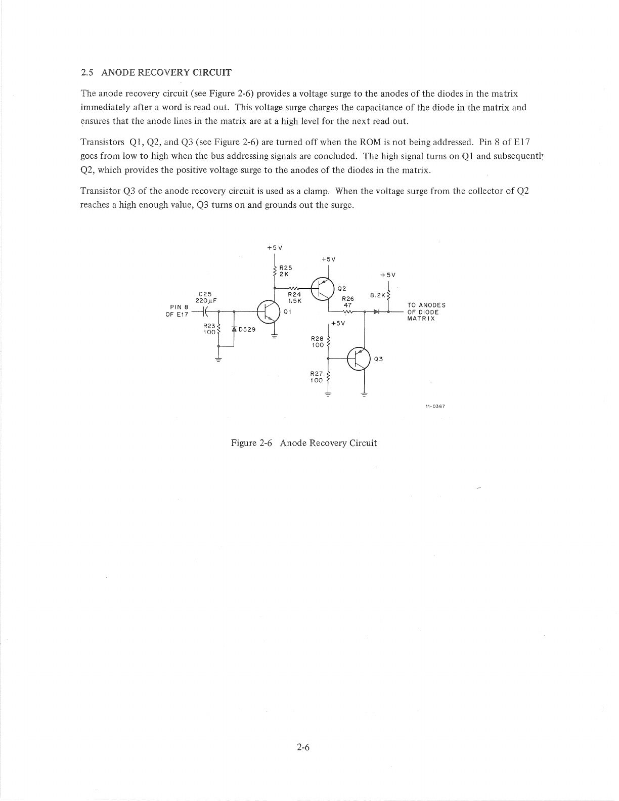
2.5 ANODE RECOVERY CIRCUIT
The anode recovery circuit (see Figure 2-6) provides a voltage surge
to
the
anodes
of
the diodes in the matrix
immediately after a word
is
read out. This voltage surge charges the capacitance
of
the diode in the matrix and
ensures that the anode lines in the matrix are at a high level for the next read out.
Transistors Q
1,
Q2, and Q3 (see Figure 2-6) are turned
off
when the
ROM
is
not
being addressed. Pin 8
of
E 17
goes from low
to
high when the bus addressing signals are concluded. The high signal turns on
Ql
and
subsequentl~
Q2, which provides the positive voltage surge
to
the anodes
of
the diodes in the matrix.
Transistor Q3
of
the
anode recovery circuit
is
used
as
a clamp. When the voltage surge from the collector
of
Q2
reaches a high enough value,
Q3
turns
on
and grounds
out
the
surge.
+5V
R25
2K
R24
1.5K
01
+5V
R28
100
R27
100
+5V
8.2K
02
R26
47
TO
ANODES
L---~I"v-....,..""'H>---
0 F D
10
D E
MATR
IX
+5V
03
11-0367
Figure 2-6 Anode Recovery Circuit
2-6
CHAPTER 3
PROGRAMMING AND OPERATION
3.1 GENERAL
The ROM operates in a manner similar
to
other
memory devices
that
can be included in a PDP-II system. When
the ROM
is
used for storage
of
constants,
the
processor may be programmed
to
address
the
appropriate ROM
location for the required constant. When the ROM
is
used for storage
of
a subroutine, a
jump
instruction
is
used
to
get into the subroutine and place the first address in the program counter. Then
the
program counter
is
changed
to
address the other sequential steps in the subroutine. The last step
of
a subroutine stored on the ROM
should be either a
jump
instruction
to
a location
out
of
the ROM
or
a return from subroutine instruction.
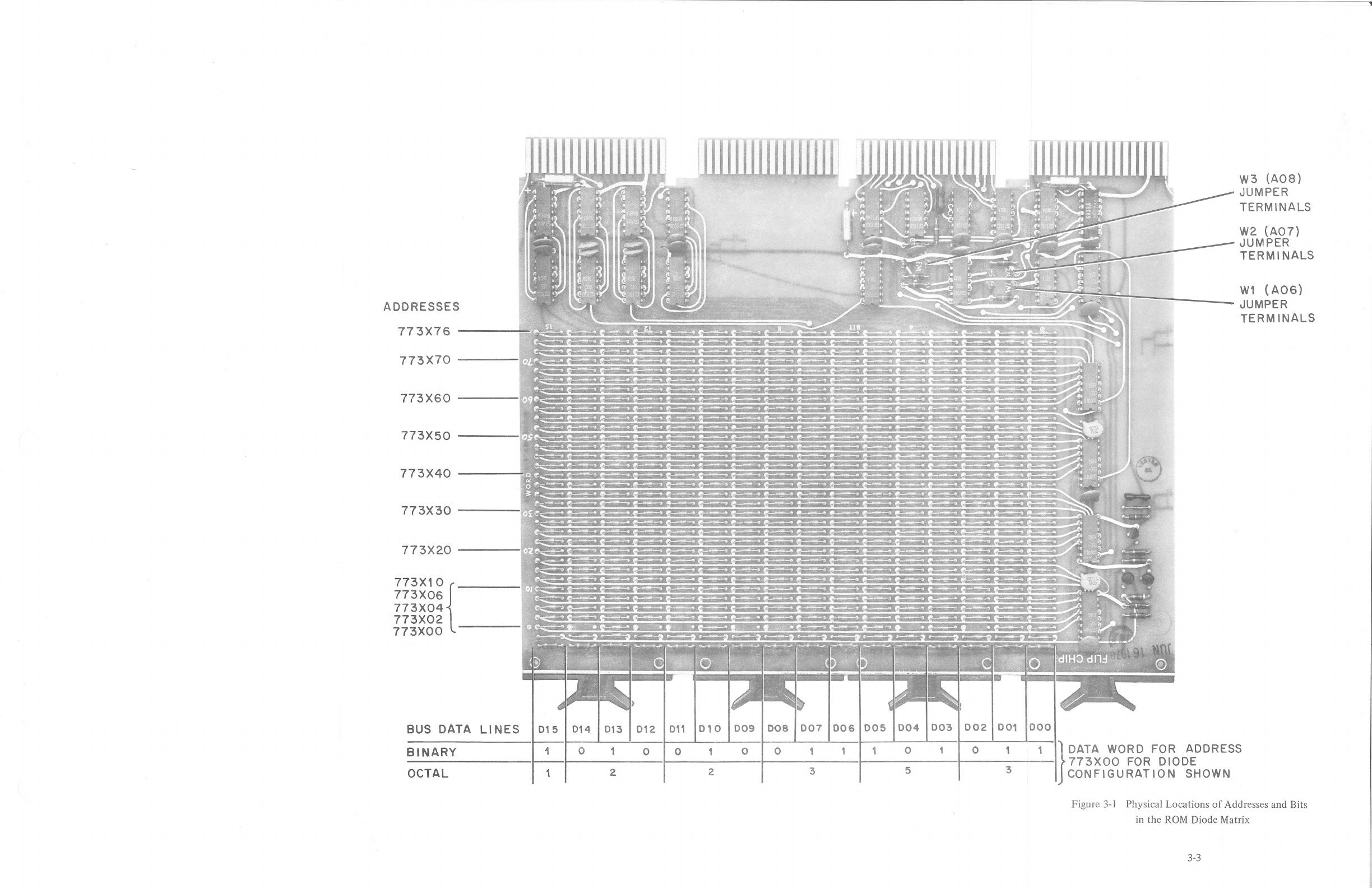
3.2 PROGRAMMING THE ROM
Programming
the
ROM
is
accomplished by cutting diodes
out
of
the diode matrix in
the
configuration required
for the binary data words
to
be used. The diode must be removed for each
bit
position
that
is
to
read
out
as
a
binary
O.
The physical orientation
of
the
diode matrix with respect
to
the
addresses and -the
bit
positions
is
shown in Figure
3-1. Address
773XOO
is
shown with diodes removed in a configuration
that
reads
out
the binary word 1 010 010
all
101
a 11. With Figure
3-1
and a binary listing
of
up
to
32
l6-bit
words, the user can program his ROM mod-
ule.
The ROM module must also be programmed
to
respond
to
one
of
the address groups determined
by
address bits
A08, A07, and A06 (refer
to
Table 2-1). Figure
3-1
shows the locations
of
the three sets
of
address-bit
jumper
terminals which are labeled WI,
W2,
and
W3
on
the
ROM printed circuit board. The relationship between
the
jumper
terminals and the address bit
is
as
follows:
WI
A06
W2
A07
W3
A08
Jumper
wires are connected across each
of
the three sets
of
jumper terminals
on
an unprogrammed ROM when
it
is
shipped from
the
factory. The jumper wire must be cut
out
from between the two terminals for each address
bit
(A08, A07,
or
A06),
that
is
a binary 1
in
the ROM address used.
3-1

ADD RESSES
773X7
6
--
---..,,,,.
'Ji!!
773X70
-----
--
L~
773X60
----
~
773X50
773X40
---
~
773X30
----
~~
773
X
20
----
r:
773X10{
773X06
773X04
773X02
_____
•
773XOO
W3
(A08)
JUMPER
TERMINALS
W2
(A07)
JUMPER
TERMI
NALS
"Jj~
~~
___
_____
W1
(A06)
JUMPER
BUS DATA
LINES
01
5 D
14
013
012
011
010
009
0'08
007
006 005
004
003
002001
000
-------
---~
--
r
--
---------~-----------~----------,~---------~----------
773XOO
F
OR
DIODE
BINARY
1 0 1 0 0 0 0 0 0 1
}DATA
WOR
D FOR ADDRESS
OCTAL 1 2 2 3 5 3 CONFIG
URATION
SHOWN
Figure
3-
1 Physical Locations
of
Addresses and Bits
in the
ROM
Diode Matrix
3-3

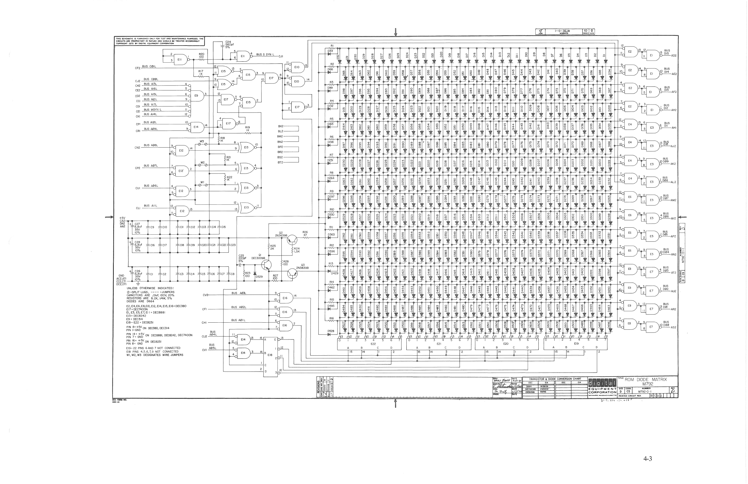
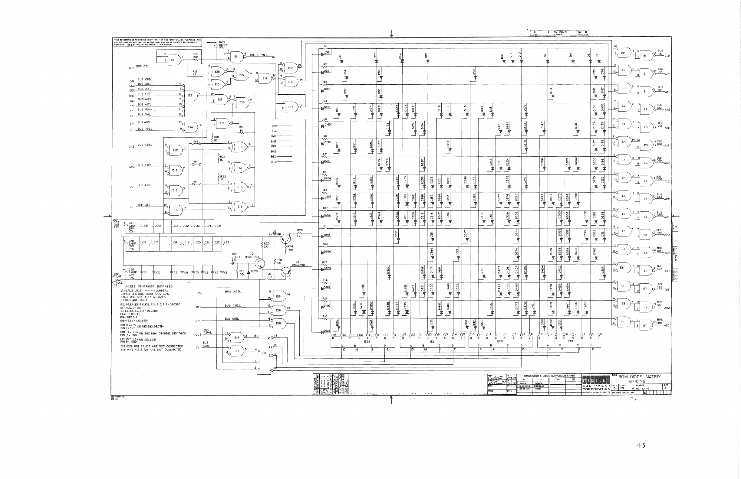
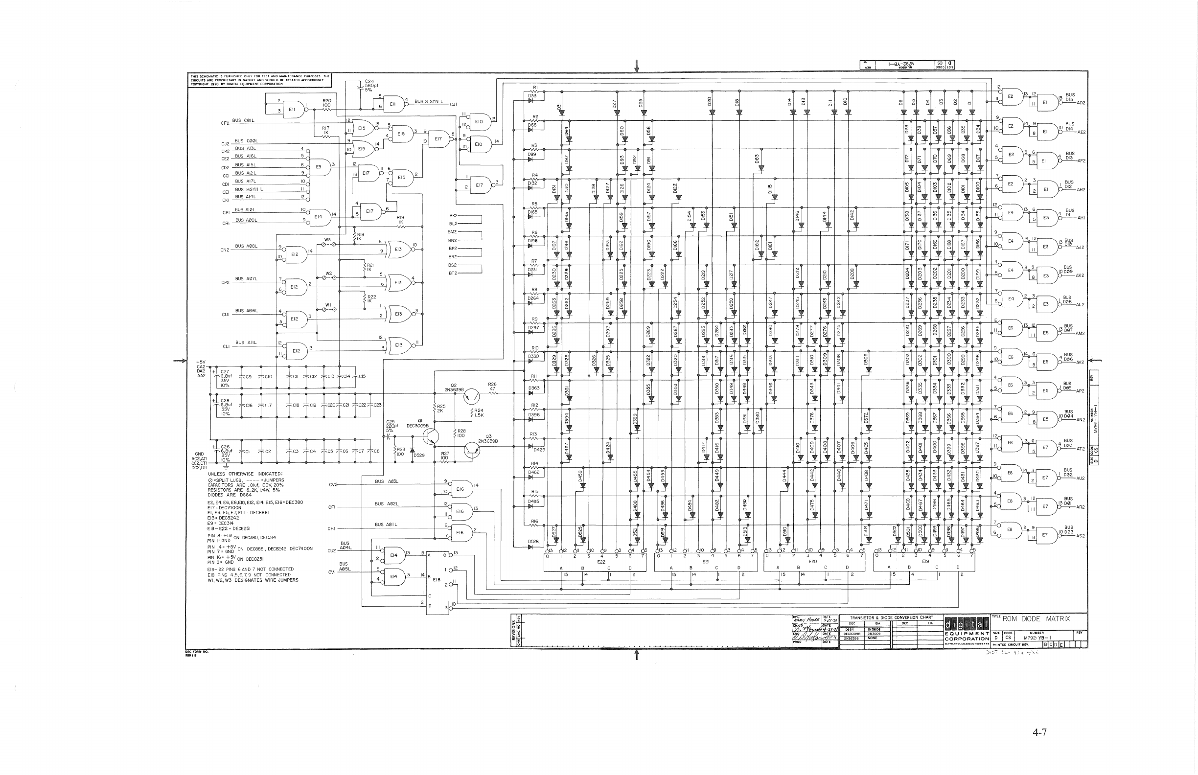
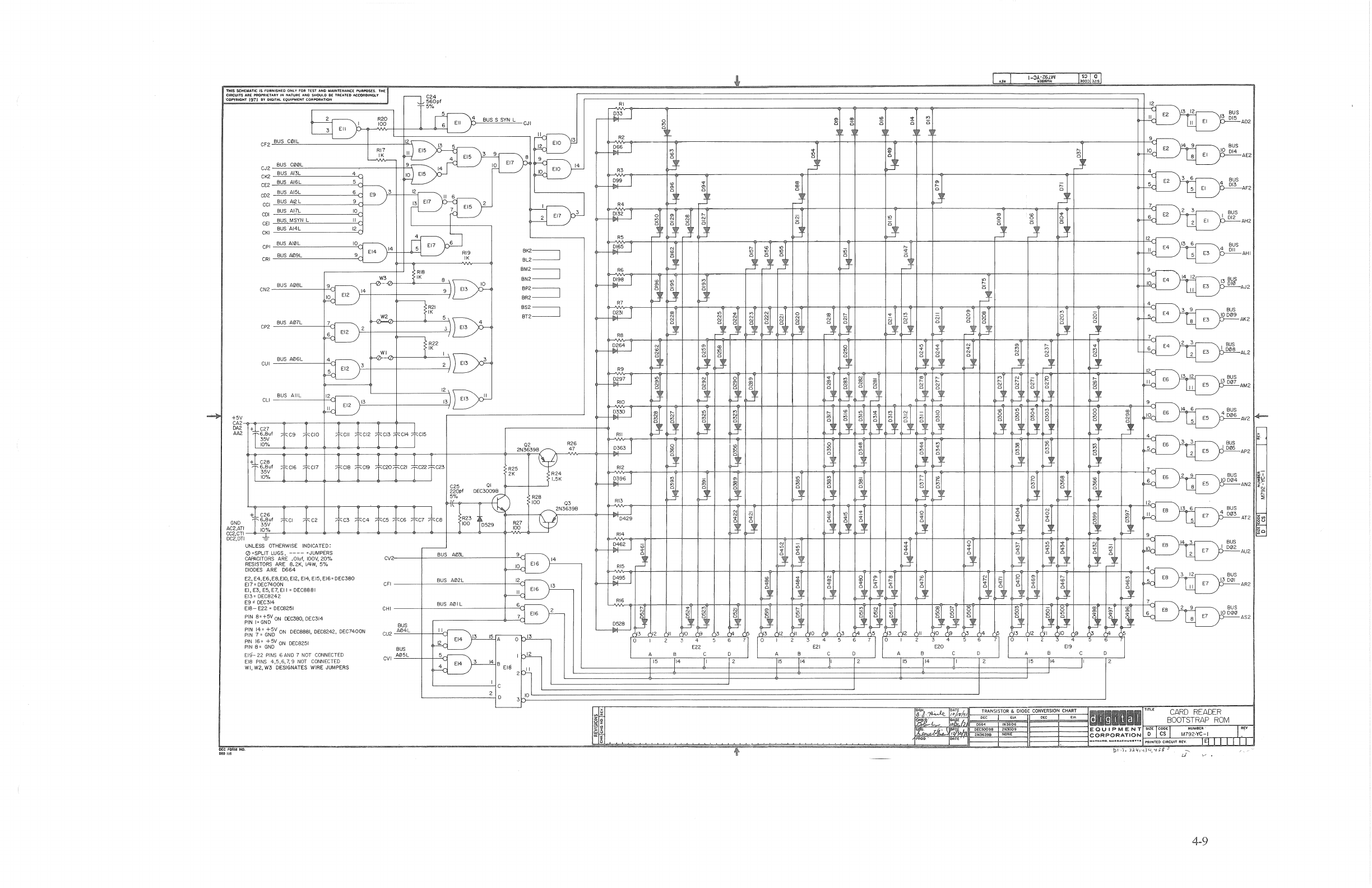
CHAPTER 4
ROM ENGINEERING DRAWINGS
The
following engineering drawings are applicable
to
the
BM792 ROM:
Title
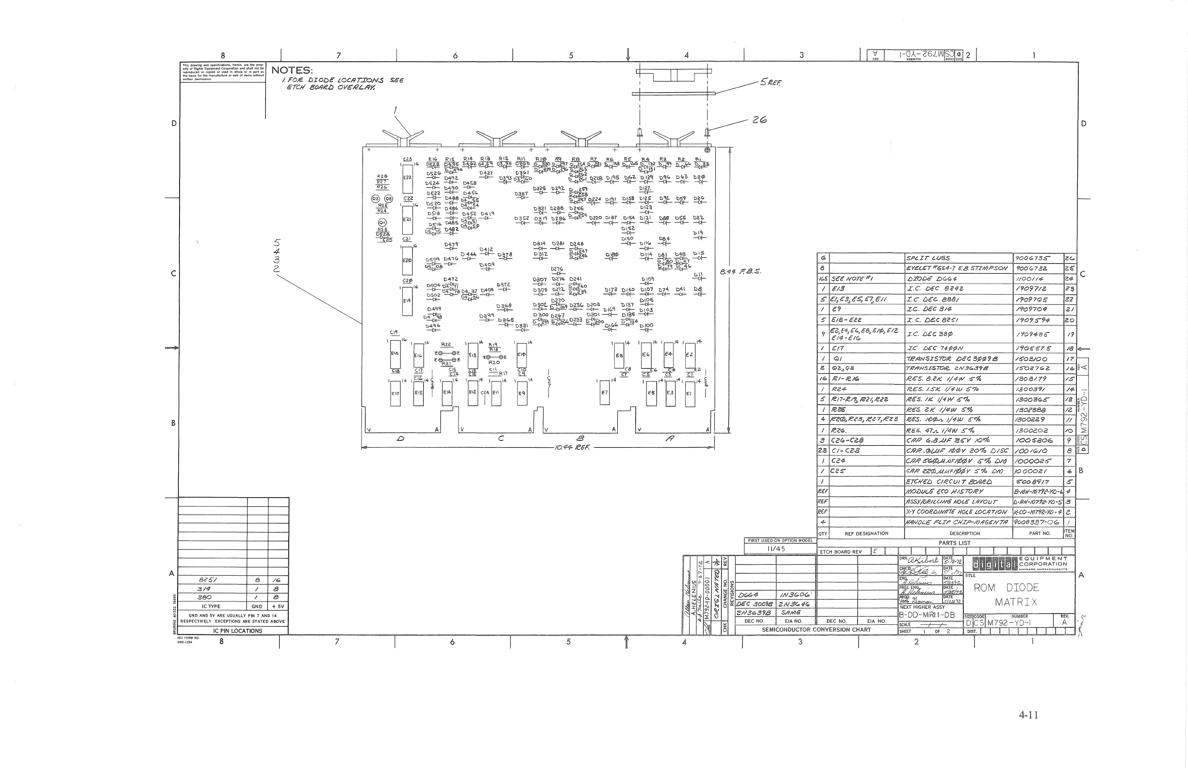
ROM Diode Matrix
M792
ROM Diode Matrix M792-YA
ROM
Diode
Matrix
ROM Card
Reader
Bootstrap
ROM
Diode
Matrix
ROM
Diode
Matrix
ROM
Diode
Matrix
Cassette
Bootstrap
ROM
Drawing
No.
D-CS-M792-0-l
D-CS-M792-Y A-I
D-CS-M792-YB-l
D-CS-M792-YC-l
D-CS-M792-YD-l
D-CS-M792-YE-l
D-CS-M792-YF-l
D-CS-M792-YH-l
4-1
Rev.
D
H
A
A
Page
4-3
4-5
4-7
4-9
4-11
4-15
4-19
4-23

CIRCUITS
ARE
I'ftOf'RIETARY IN NATURE AND SHOULD H TIIU.TEO ACCOltDlNGLY
CO",IUGHT
1910
IY DIGITAL EQutPWEHT CORf'OIIIATION
CF2
BUS
C01L
CJ2
BUS
C00L
CK2
BUS
AI3L 4
CE2
BUS
AI6L
CO2
BUS
AJ5L E9
CCI
BUS
AI2L
COl
BUS
AI7L
10
CEI
BUS MSYN L
BUS
AI4L
12
CKI
Cpl
BUS
AI0L
CRI
BUS
Ae)9L
CN2
BUS
A0BL
BUS
A07L
CP2
BUS
A06L
CUI
BUS
AIIL
CLI
+5V
CA2
DA2
AA2
4
BUS
S
SYN
L CJI
BK2-----,
BL2-
BM2====:J
BN2
BP2-----,
BR2-
BS2-----,
BT2-
GND
~f~~~~--~--~~--~~--~~--~--~--~--~--~~~--~----~~~~~
De2,DTI
UNLESS OTHERWISE INDICATED:
CZl
=SPLIT WGS,
----
:::JUMPERS
CAPACITORS
ARE
,Cluf,
IOOV,
20%
RESISTORS ARE
8.2K,
1/4W,
5'"/0
DIODES
ARE
D664
E2, E4,
E6,
E8,EIO,
EI2,
E14,
E15,
E16=
DEC380
EI7'
DEC7400N
EI,
£3,
E5,
E7,
EJ
I::
DEeSSSI
E13" DEC8242
E9"
DEC314
E18-
E?2
'"
DEca2S)
~~~
1~=Gt~V
ON
C€C380, DEC314
~r~
~4==
Gt~v
ON
DEGS8el, DEC8242, DEC7400N
~l~
~6:=
~~v
ON
DECa25!
E19-
22
PINS
6
AND
7
NOT
CONNECTED
EI8
PINS
4,5,6,7,9
NOT
CONNECTED
WI,
W2,
W3
DESIGNATES
WIRE
JUMPERS
DEC
FORM
MO.
DRDII.
cv~
____
~
__
~B~U~S~A~~
________
-+
__
~
CFI
_____
~---"B'::USe....':A""":="2L=------------I__'=cJ
CHI------~--~B~US~A"~I~L~--------I_~
BUS
CU2
A04L
BUS
CVI
A05L
.1.
AH2
TRANSISTOR
&
DIODE
CONVERSION
CHART
111-0-0
,,'"
ROM
DIODE
MATRIX
~
WII
!;I M792
0664
IN3606
EQUIPMENT
SIZE
CODE
HUM.Eft
DEC300&8 2N&>09'
CORPORATION
D
CS
M792-0-1
NO
E
BCD
~
4-3

CI"'CUITS ARE
~IHARY
IN NATURE AND SHOULD
IU
TNUrED
M:CO¥IOINGlY
COPVRIGHT
1970
IIY
DIGITAL EQUIPMENT CORPCWiATION
5%
n
;~6PF
r~2
~
,--1}--~-,\~ON20,-0_1-1+-_-L---.J---"J~
Ell
/
BUS
S
SYN
L
CJI
3 Ell < I
L-/
12~
~
-r-~.I.7
r,ll
EI5
"')].
5
~
CF2.
BUS
cmlL
L1L-
~II
EI5
4'
E~15
3 9 8
~
-==--""=
__________
-++9'-',
10
EI7
14
4
10
EI5
14
I EIO
~~~
__________
~5d_
___
eJ2
BUS
C00L
CK2
BUS
AI3L
EE2
BUS
AI6L
6 E9
\'3'-+-+-~'ce2-l-"
-"'==~
_____
__"_9_d_---"')
13
EI7
II
6 2
10
7
EI5
II
CDZ
BUS
AI5L
eCI
BUS
AI2L
eDI
BUS
AI7L
eEl
BUS
MSYN
L
CKI
8US
AI4L
CPI
BUS
AI0L
CRI
BUS
A09L
12
®~F
10
: EI7 6
9 E
14
1-',,,,4+-t-JL4
RI9
IK
Ria
CNZ
BUS
A08L
IK
\~lO
l-'-'~--+------:"-il
~
n~1
9
,--o-w.~
~'4
10
EI2
17
~_Z
~2
4
~_'
~3
CUI
BUS
A06L
~~
__
+-
_____
52iB)~
~RZ2
/
I
1'K
~~
__
+-
____
~~~1
~
CP2
BUS
A07L
-+
~V,_,----r--,-~--,__,--_r--~-,
IZ
~13
II
EI2
12E>
13
EI3)d-'-
\E---f-----E.J
Cli
BUS
AIIL
BMZ~
BN2
BP2==:J
BRZ
852------,
BT2------.l
Rfe
I +
~~UF
t
C9
tCIO
TCII
CI2
t
C13
+C14
CI5
r
L,1~r-~l-~;-~-F-ok]'r-C-16--ok]'r-C-174---1'.-cc-,B-,-e-,9--r1'-(e2-0-r-e2-'-1'~CC-~~-C-23~-----~L,~-~~2~N~~~l3~9~~(
~;,:
e25
QI
1---+------'
2.20PF
OEC3009~
RZ6
47
RI
R2
RB
Ddl
~I
RII
~
RI2
D39\:i1
100
Q3
RI3
5%
©
R2B
1:
1
-g
~2N3639B
~D4291
GND
+~
~~yF
lei
tz
+C3
AC~;;I
110%
rl~'
T'
CTI,DC2
DTI
I UNLESS OTHERWISE INDICATED:
o
=-SPLIT
LUGS,
-----
"JUMPERS
CAPACITORS
ARE
.OIUF,100V,20%
RESISTORS
ARE
8.2K,1/4W,5%
DIODES
ARE
0664
E2, E4,E6, E8,EIO, EI2, EI4,
E15,
E16= DEC380
E17"
OEC7400
EI, E3, E5,
E7,
Ell
=-
OEC8881
E13=
OEC8242
E9"
OEC314
EI8-E22"
OEC8251
~:~
~="tN56
ON
OEC380,OEC314
~:~
~~=
:~V
ON
OEC8881,
OEC8242,
DEC7400
~II~
~6","
~£V
ON
OEC8251
E19-E22
PINS
6AND7
ARE NOT CONNECTED
EI8
PINS
4,5,6,7,9
ARE
NOT
CONNECTED
ea
~02~
D5291~R-2-7-+-(
100
CVZ
BUS
A03L
eFI
CHI
BUS
CU2
A04L
BUS
CVI
A05L
N
"
j
j
jj
"
"
1-
1t)..-Z6LVII
bJtlflnN
12
II
E2
13
DIS
~
1312
BUS
II
EI
AD2
9
~
2
149:
BUS
10
10
014
8
EI
O-------:::----AE2
4
rJ
E2
~i
~~i
~~AFZ
E2 2 3
B.JS
~
c
6 2
EI
~AH2
~
2,
13
6
BUS
II
E4 4
011
5 E3
AHI
~
I
14
12
BUS
10
E4
13
010
II E3
~AJ2
4
5 E4
10
009
~
9'--
BUS,
8
E3
AK2
7d~
2 3
BUS
: 6r.! E4 I
008
~l
£3
AL2
E6
13
12
13
BUS
12~
rl!c.
II
E5
~AM2
~
146C
BUS
10
E6
5
E5
~AVZ
f4--
-
EG
33
I
BUS
~
~
c
~::c
5 Z
E5
c).l&LAP2
T
~
6
E6 2 9
.,IO~~~
~;:
8 E5
C"
--AN2
~~
'"
t-
"
~4~~~
~~AT2
~
,
14
3
BUS
10
E8 I
002
2 E7
AU2
5
13
001
~
E8
31
BUS,
II
E7 AR2
~
2 9
BUS
6
EB
10000
8 E7
AS2
4-5

THIS SCHE
..
..,TlC
IS
rUANISt1EO
ONLY
FOR
nST
...
NO
lII"INTEJroI"'NCE PUIlPOSES.
Tt4[
1
CIItCUITS
...
IIE PROPRIETARY
IN
N",'U"[
....
ND
SHOULD
IE
,,,u.no
ACCOfIDINGlY
CO",IUGHT
1970
I'"
DlGlT,It,l
EQUIPWENT COliPOflAnON
e24
560pf
5%
~\I
~Jg
I
~
Ell /
8US
S
SYN
L eJI
~b-"-~Iv--+-+--~--4-"-jL--/
CF2
BUS
C01L
L-+I'~_~-I
E-'5-
'X>-'-3-=5=;~~-------'
~
~~"EI5
4EI539
B~
9
10
EI7
14
---"=="'--------4-----+-+'0"
EI5
14
10
£10
eJ2
BUS
C(lI0L
eK2
BUS
AI3L
---"~~~
____
~5~~~
:
E9)-
~11:EI7
116
2
10
7 £15
II
eE2
BUS
AI6L
CO2
BUS
AI5L
eel
BUS
AI2
L
eDI
BUS
AI7L
eEl
BUS
MSytJ L
eKI
BUS
AI4L
epi
BUS
Alfbl
eRI
BUS
Af)9L
12
~
ID
45
£17 6
14
9
EI4
l"'-H---+-"j
~I~
eN2
BUS
A08L
ep2
BUS
A07L
BUS
A06L
eUI
~RIB
-o-W:
IK
B9)U
9
~'4
10
EJ2
IF
2I
IK
~_2
5
b)E/-
7
~2
'f
R22
IK
4
~'
~)EY-
~3
BUS
AIIL
eLi
12)EY-
12
I~)
EI3 II
~3
II
GND
-J~tJf
lei
le2
le3
C4
le5
e6
le7
AC2,ATI
·1"10%
TL
TL
T' T' T'
gg~',~~1
-=l=-
BK2_
BL2----.J
BM2~
8N2
BP2===:J
8R2
BS2~
BT2
UNLESS
OTHERWISE
INDICATED:
0=SPLIT
LUGS,
----
"JUMPERS
CAPACITORS
ARE .Oluf,
100Y,
20%
RESISTORS
ARE
8~2K,
1/4W,
5%
DIODES
ARE
0664
,~----~--EB~US~A~~~--------~~9'C
~
~~1~4
____
~
E2,
£4,
E6,E8,EIO,
EI2.,
EI4,
E15,
E16=
DEC380
EI7 = DEC7400N
EI, E3,
E5, E7,
Ell
= DEC8881
E13=
DECS242
E9 =
DEC314
EIS-
E?2
=-
DEC8251
~11~
I~~~~V
ON
CEC380,
DEC314
~:~
!,4:=
Gt~V
ON
DECS881,
DEC8242, DEC7400N
~:~
~6==-
~~
ON
DEC8251
E19- 22
PINS
6
AND
7
NOT
CONNECTED
Ela
PINS
4,5,6,7,9
NOT
CONNECTED
WI,
W2,
W3
DESIGNATES
WIRE
JUMPERS
DEC
fCIItM
HO.
DIID,,,
______
+-~8~U~S~A~"~2~L
________
4~--~1213
eFI
~
BUSA01L
G
eHI
---~----'==:.::-----+----"o7J
EIG
2
-----------~~~
BUS
CU2
Aill4L
BUS
CVI
A05L
"-
_____
-'--'
C
RI
D33
T
R2
D66 I
R3
D99
1
R4
D132
lj:g
0
....
~
R5
DI65 T
R6
l
t
2
'"
<0
Ci
" "
Ci
liI'ItOO
-
IDATE
o
Ci
mamaala
TIm
ROM
DIODE
MATRIX
~g~~6:A~I~~
$~E
IC~;EI
M7;~~~;
I
J_~EV
BCD
E
4-7

nus
SCHEMATIC
15
roffNISHED
ONLY
FOil TEST
AND
MAINTEN
..
NCE
PUffl'05£$.
THE1
CIItCUITS
AlliE
PItOf'ItIET
..
ffY
IN N
..
TURE
..
NO SHOULD M
TflUTED
ACCOfIDlHGlY
'CCW'fItIGl-lT 197'
IY
OIG,lTAL
EQUIPMENT COffl'OltATlOfoi
.-----
e24
560pf
5%
~",)-<>-,,~0;.;28\,-1~+-_~_
.....
r-:12..~
Ell
/
BUS
S
SYN
L
eJI
~
I
'----'
L-+~-----'3--==5==---)--r---Y-
~'~
EIO
13
I
~!!
II
EI5 3 9
~
4EI5
8~
-,,~~~
__________
+-+=9~
~_"'
10
EI7
14
10
EI5
14
Kl
EIO
~~~--------~D-
___
CF2
BUS
C01L
eJ2
BUS
C00L
eK2
BUS
AI3L
4
eE2
BUS
AI6L 5
eD2
BUS
AI5L 6
eel
BUS
AI2L 9
eDI
BUS
AF7L
10
eEl
BUS
MSYN
L
II
BUS
'AI4L
12
eKI
epl
BUS
AI0L
10
eRI
BUS
AfD9L
9
BUS
A08L 9
eN2
~'4
10
EI2
ep2
BUS
A07L 7
~2
BUS
A06L
4
CUI
~3
BUS
AIIL
12
eLi
~13
II
l
~e2a
+ +
~t,yf
CI6
CI7
10%
E9
j-
~EI7~
11'----'
P
EI4
14
~~
F-+-H~>--"iF
RI9
IK
~
Ria
,-<ZJ-W3
IK
a)~
9 1
EI3
n
,R2'
IK
W2
5
o
)V-
n
R22
IK
WI
~lEY-
""'U-w
13) EI3 II
12)~
e23
C25
QI
BM2~
BN2
BP2_
BR2-----.J
BS2_
BT2-----.J
02
2N3639B
R25
2K
~~
O-------\----'
§~~Pf
OEC3009b
R28
R26
47
100
Q3
GND
i~}~f
lei
+e2
le3
e4
1
e5 e6
le7
ea
lro"o'
ID52~
R27
-UN3639B
~~:tf:_-4-l-":'O'T0'''-O_-*-r_----<O-_O-_T'''''_-4-
__
-*-T_-*-_-4-T_-4-_+-_
.....
f;
__
i~D
__
t-",IO;;.,O~_---,'--V
OC2,OTI
-::;:-
UNLESS
OTHERWISE
INDICATED:
Q}
=SPUT
LUGS,
----
=JUMPERS
C~CITORS
ARE
,Oluf,
100Y,
20%
RESISTORS
ARE
8.2K,
1/4W.
5''10
DIODES
ARE
0664
E2, E4, E6,E8,EI0, EI2,
E14,
E15,
E16=
OEC3BO
EI7 =
OEC7400N
EI,
E3,
E5,
E7,
Ell
=
OECBBB
I
EI3 = oEC8242
E9'"
OEC314
E18-
E;?2
=
OEC8251
~11~
1~=Gt~V
ON
CEC3BO,
DEC314
~i~
~4==
iN~V
ON
DEC8881,
OEC8242,
DEC7400N
~:~
~6==
ciNg
v
ON
DECB251
EIS- 22
PINS
6
AND
7
NOT
CONNECTED
EIB
PINS
4,5,6,7,9
NOT
CONNECTED
WI,
W2,
W3
DESIGNATES
WIRE
JUMPERS
O£e
FOMII
NO.
DRDIII
ev
BUS
AVJ:L
eFI
BUS
A02L
CHI
BUS
eU2
A04L
BUS
eVI
A05L
RI
D33 I
R2
D66
I
R3
D99 ,
R4
D132
I
R5
0165
T
R6
0198
I
R7
D231
1
Ra
D264 I
R9
D297
T
RIO
D330
,
RII
0363
.1
RI2
0396
1
RI3
1
0429
RI4
t
'"
is
.,
o
'"
o
1
'"
o
'"
o
1 1
1".1
.,
'"
o
~
2,
E2
13
12
BUS
II
13
015
Jf
EI
AD2
10
E2
10
014
~
49
BUS,
8
EI
AE2
4
WE2~gl~S,
~~AF2
~
,
2 3
BUS
6
E2
I
012
2
EI
AH2
~
2!
13
6
BUS
II
E4 4
011
5
E3
AHI
9
10
13
010
~
4
1412.---
BUS,
II
E3
AJ2
~
3 9
BUS
E4
10009
8
E3
AK2
WE4~,
16_'----------"
~D0a
AL2
13
~~~
~~AM2
~
146
BUS,
10
E6
4006
5
E5
AV2
-
~I~~
~~AP2
-
~
E6
2 9
BUS,
i~
6 8
E5
001214
AN2
i:~
g>
II
E740Ql3
~
2
E8
136
BUS.
5
AT2
I D02
~Ea
143
BUS,
2 E7
AU2
5
1301211
~
EB
312
BUS
II
E7
AR2
~IO~~~
~~AS2
4-9
"

D
-
c
8
TlIls drlllwlnl and SpoKlllcmons, herein, II'l! the prap'
erty01 Dlaltlll EqulpmantCol'J!Oratlon and shall
nolbe
reproduced orCOllied
Of
und
In
wilDie
orin
part
as
the basis for the
manuladutll
Of
sale
of
ltams without
writt..n permiSSion.
I 7 I
NOTES:
I.
FO,€
DrOD€
LOC!;/.ION..S
S;Ge
€rClI
BOl9leLJ
OVe-.RLI9Y.
5
4
3
~
+
C2¢
IDI~
o
6 I 5
+ + + +
10
14
o
CIO
h9..
\01'
U
I
r
3
+ +
B.41
!fe.s.
16
14
11
:(
16
/
+
E~
0
foZ
C5~
c;+
""IT
Z I
HHHr
I
l:t
I
d
1(,,5
$ee
1V0T4'
#1
I £1.3
S ciS-ceil!.
Spt.ITUJ6.$
l!:Ve;t.€T
#"5:>4-7
e:e.
STIMPSON
b:tODG"
Dc;,,,
4-
I.e.
DeC
8242
I.c,
DeC
31<1-
I,
C,
De;c
82>:1
900':'73.5""
900
c;,
732.
1100114-
/909712.
1909704
1'1094-8
<>"
D
-
22
2.1
20
I~
r/~_£~/_T
____________
~~I._.C_.
__
De
__
C_7_4~¢~¢~IV
____________
t-/9~0~~~~~?_~~~~/~~
.--
I
QI
7;?.qIVSISTOIe
DcC3¢¢~S
/oo.a;OO
17-
e
Co/a~<j).3
TI?I'9NSIS"TOJe
ZN3r.898
/S'027CoZ.
It;,
~<t
/
RZ4
R.e:s.I.S..t:
1/,tW
S'1.
1.300391
14
'I
5 R.17-;e1'l:, ;e;;'Iet?2- leO's.
/!<:
1/4
W 0''1.
1300'S':'S-
/3
~~
B
foo~>-\}---D----A--lv----c---A--v_Ia#!F.--A--L.:.V--------
_-/7_-=:_-_-_-:_-_.:;:.J--I!~
I tet:£:
/if?€,s.
Zk
1/4W
S%
130?388
IZ
;,
I
1--:-4-+n¢,=::-:~=(?'::-'3::-~-.e=(?::-~:-e=Z:-8:-1r-e~~::-3-.-/-'€J:-¢4-:-''-I.-V=:-4:-W-O':':-''''-;----+/a~O-02='-Z~'7~-+I-/-f
S!
r--
I
/c2~.
lees.
47./1.
1/4W
S%
1300202
/0:2:
A
1--_--:-::-=-:-
__
-+_-+_----1
8Z51
8
16
3/<?
1
<3
380
I
<3
Ie
TYPE GND + SV
GND
AND 5V ARE USUALLY
PIN
7 AND 14
RESPECTIVELY EXCEPTIONS ARE STATED ABOVE
DEC
FORM
NO.
ORO·USA
IC
PIN
LOCATIONS
8 1 7 I 6 I 5 t 4
1
CZS'
I
CI9/?
i?e¢A~FI#V
S'?h
LJ/t)
10000ZI
6 B
E7CIle-b
ClleCIJITB::lIlt€b
s-008917
S
X-y
cooeCJINl17€
)ioa
tOCllTION
K-co-/(J~Z-yt)-
9-
e.
QTY
REF
DESIGNATION
DESCRIPTION
PART
NO.
FIRST USED ON OPTION MODEL PARTS LIST
I
11/45
ETCH
BOARD
REV
I E
I,
I I I I I I I I I I I I
IIV3('0('"
/J6C
300~
ZN3('4('
NEXT
HIGHER
ASSY
MATRIX
TEM
NO.
rZ~IV~3~~~3~~~~~;;S~~M~6~~g;~~~~&;~~~=1~B~-~D=D=-~M~R~I~I~D~B='=iS~IZ~EI~~ro1D~fiEI~~~~NU~MQBE~Rl,r-,JJ~R~~~'J<!iN
r-
DEC
NO.
EIA
NO.
DEC
NO.
EIA NO.
SCALE
-----?----r Die
51
M792
YD
I
SEMICONDUCTOR CONVERSION CHART
SHEET
I
OF
2
DIST,
I 3
121
4-11

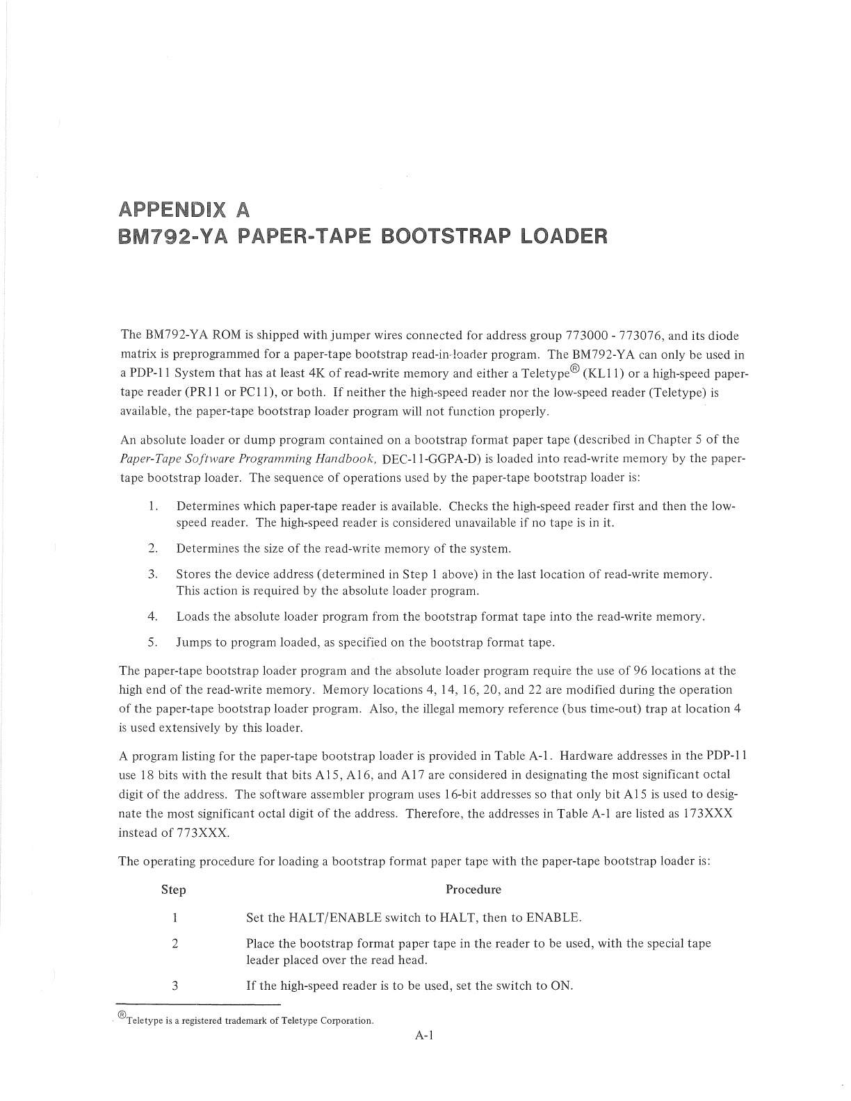
APPENDIX A
BM792-YA
PAPER~TAPE
BOOTSTRAP
LOADER
The BM792-YA ROM
is
shipped with
jumper
wires
connected
for address group
773000
-773076,
and its diode
matrix
is
preprogrammed
for
a paper-tape
bootstrap
read-in-!oarler program.
The
BM792-YA can only be used in
a
PDP-II
System
that
has at least
4K
of
read-write
memory
and
either
a
Teletype®
(KL
II)
or
a high-speed paper-
tape reader
(PRII
or
PCII),
or
both.
If
neither
the
high-speed reader
nor
the
low-speed reader (Teletype)
is
available,
the
paper-tape
bootstrap
loader program will
not
function
properly.
An absolute loader
or
dump
program
contained
on a
bootstrap
format
paper
tape (described in
Chapter
5
of
the
Paper-Tape
Software
Programming
Handbook,
DEC-II-GGPA-D)
is
loaded
into
read-write
memory
by
the
paper-
tape
bootstrap
loader.
The
sequence
of
operations
used
by
the
paper-tape
bootstrap
loader
is:
I. Determines which paper-tape
reader
is
available. Checks
the
high-speed reader first and
then
the
low-
speed reader.
The
high-speed
reader
is
considered unavailable
if
no
tape
is
in it.
2. Determines
the
size
of
the
read-write
memory
of
the system.
3.
Stores
the
device address
(determined
in
Step
1 above) in
the
last
location
of
read-write
memory.
This
action
is
required
by
the
absolute loader program.
4. Loads
the
absolute loader program from
the
bootstrap
format
tape
into
the
read-write
memory.
5.
Jumps
to
program loaded,
as
specified
on
the
bootstrap
format
tape.
The
paper-tape
bootstrap
loader program and
the
absolute loader program require
the
use
of
96 locations
at
the
high
end
of
the
read-write
memory.
Memory
locations 4, 14, 16, 20,
and
22 are modified during
the
operation
of
the
paper-tape
bootstrap
loader
program. Also,
the
illegal
memory
reference
(bus
time-out) trap at location 4
is
used extensively
by
this loader.
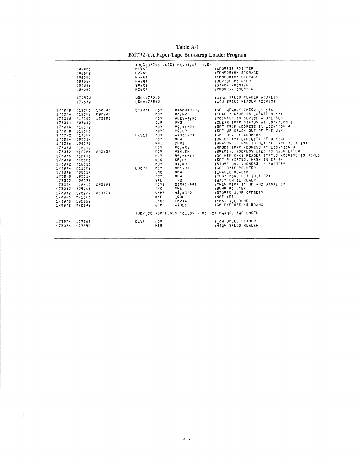
A program listing for
the
paper-tape
bootstrap
loader
is provided in Table
A-I.
Hardware addresses in
the
PDP-II
use 18 bits
with
the
result
that
bits A 15, A 16, and A
17
are considered in designating
the
most
significan t octal
digit
of
the
address.
The
software assembler program uses 16-bit addresses so
that
only
bit
AI5
is used
to
desig-
nate
the
most
significant octal digit
of
the
address. Therefore,
the
addresses in Table A-I are listed
as
173XXX
instead
of
773XXX.
The
operating
procedure
for loading a
bootstrap
format
paper
tape
with
the
paper-tape
bootstrap
loader is:
Step
2
3
Procedure
Set
the
HALT/ENABLE
switch
to
HALT,
then
to
ENABLE.
Place
the
bootstrap
format
paper
tape in
the
reader
to
be used,
with
the
special
tape
leader placed over
the
read head.
If
the
high-speed
reader
is
to
be used, set
the
switch
to
ON.
@Teletype is a registered trademark
of
Teletype
Corporation.
A-I

Step
4
5
6
7
Procedure
If
the low-speed reader
is
to
be used, set the high-speed reader switch
to
OFF
and
set the low-speed reader switch
to
START.
Set the starting address, 773000, into the SWITCH REGISTER.
Depress the LOAD ADDR switch.
Depress the START switch. After a short pause, the paper tape should read in.
A-2
173000
1731304
1731310
173"'14
1731316
1731320
173022
173024
173026
173030
173032
1731336
173i2140
173042
173044
1731;,46
17305",
173""2
173",54
173",b0
1730b2
17J0b6
173",70
113"'72
173074
173076
0"00~1
J000~~
e0",,0~
J000~4
~0"009
<JU0~1
1715'0
1775b0
J12701
H2102
J12703
~0501~
<~U74'
1107
r9
<143~4
l05714
UIil775
~1~712
J127~6
3104 41
1406~1
~U111
LJl1102
~05214
105714
100376
116412
~1il'211
12n27
001366
105222
~00142
1775b0
177550
16000~
000006
1731~ci
Table A-I
BM792-YA Paper-Tape Bootstrap Loader Program
IR~GISTE~S
USED!
R1,R?,R3,R4,SP
Rh"l
R2~"2
RJa".
R4!X,
SP.X6
PC.X7
HSR:177551il
I.SR·1775~0
SURT I
MOV
MOV
MOV
C~R
~OV
Move
DEvil
MOV
TST
8MI
MOV
MOV
MOV
SIC
MOV
LOOP
I
MOV
INC
TSTB
BPI.
MOVB
I~e
CM~8
BNE
I~CB
JM~
DEVI
l..SR
HSR
#l600~Iil,Rl
_~,R2
#DEV
...
~,R1
IIR2
P9,·(H21
Pg,sP
.(R3)
,R4
l'K4
D~Vl
PC,IJR~
#24,S~
R~,.(HP
SP,Rl
R:L,ilR;
!lRl,R?
~R4
(11K
4
,.2
2(R4),~R2
-H1
R;i,.3?~
LOOP
I
K2)
...
·IR2)
A-3
IADO~ESS
POINTER
ITEMPORARY
STORAGE
IT~MPORARY
STORAGE
IDEVICF
POINTER
J
STACK
PO
INTER
JPqOr,RAM
COUNTER
IHlu~
SP~ED
READER
A~DRESS
IL~~
SPEEO
READER
ADDRES5
JSET
MEMORY
CHECK
I.!~ITS
JT~AP
VECTOR
IS
,O~
T
ON
4/b
JP~INTER
TO
DEVICE
ADD~ESSES
ICcEAR
TRAP
5TA'U5
AT
~O~A'ION
6
ISEt
T~AP
AD6~~ss
IN
LOCATIO~
4
ISET
UP
STACK
OUT
or
THE
WAY
IG[r
DEVICE
AODRESS
IC~ECK
AVAILABI~ITY
or
DEVICE
18~~'CH
IF
HSR
IS-OUT
OF
TAPE
fSI!
'5)
,Rr.SET
THAP
ADDRESS
AT
,OCATION
4
,SPEr.IAL
AODR~SS
USED
AS
MAS-
kATER
ID~
MEM
CHKI
READER
STATUS
A'DRESS
IS
MOVED
ISET
R1=X7752,
MASK
IN
S~~24
,STOQE
OWN
AODRESS
I~
POINT~Q
,GFT
BYTE
POINTER
IENABLE
READlR-
ITE~T
DONE
BIT
(BIT
07)
IWAI'
VNTI~
~EADV
IT~EN
~ICK
IT
UP
A~D
STOqE
IT
,SUMP
P01NTE~
ISTOQED
JUMP
OFFSET7
INOT
HT
,HS,
ALL.
DON~
IGO
EXEC~TE
AS
BRA~CH
I"OW
S~E~D
READER
IHI~H
SPEED
READER

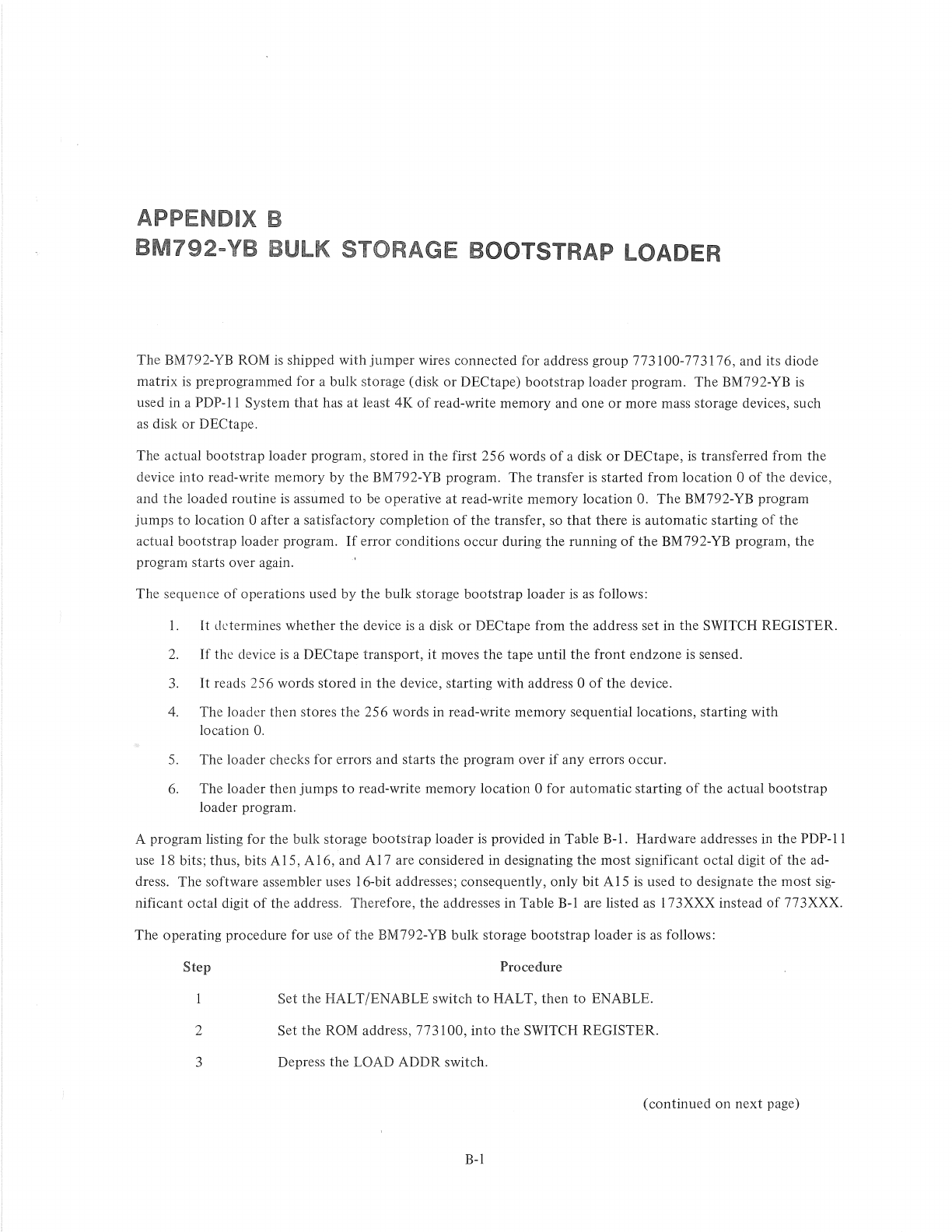
APPENDIX B
BM792-YB
BULK STORAGE BOOTSTRAP LOADER
The BM792-YB
ROM
is
shipped
with
jumper
wires connected for address group 773100-773176, and its diode
matrix
is
preprogrammed for a
bulk
storage (disk
or
DECtape)
bootstrap
loader program. The BM792-YB
is
used in a PDP-II System
that
has
at
least 4K
ofread-write
memory and one
or
more mass storage devices, such
as disk
or
DECtape.
The actual
bootstrap
loader program, stored in
the
first 256 words
of
a disk
or
DECtape,
is
transferred from
the
device
into
read-write memory
by
the
BM792-YB program. The transfer
is
started from location 0
of
the
device,
and
the
loaded routine
is
assumed to be operative
at
read-write memory location
O.
The BM792-YB program
jumps
to
location 0 after a satisfactory completion
of
the
transfer, so
that
there
is
automatic
starting
of
the
actual
bootstrap
loader program.
If
error
conditions occur during
the
running
of
the
BM792-YB program,
the
program starts over again.
The sequence
of
operations used
by
the
bulk storage bootstrap loader
is
as
follows:
1.
It
determines whether
the
device
is
a disk
or
DECtape from
the
address set in
the
SWITCH REGISTER.
2.
If
the device
is
a DECtape transport,
it
moves
the
tape
until
the
front
endzone
is
sensed.
3.
It
reads 256 words stored in
the
device, starting with address 0
of
the
device.
4.
The loader
then
stores
the
256
words in read-write
memory
sequential locations, starting with
location
O.
5.
The loader checks for errors and starts
the
program over
if
any errors occur.
6.
The loader
then
jumps
to
read-write memory location 0 for automatic starting
of
the
actual
bootstrap
loader program.
A program listing for the bulk storage
bootstrap
loader
is
provided in Table B-1. Hardware addresses
in
the
PDP-II
use 18 bits; thus, bits A15, A16, and A17 are considered in designating
the
most significant octal digit
of
the
ad-
dress. The software assembler uses 16-bit addresses; consequently, only bit A15
is
used
to
designate
the
most
sig-
nificant octal digit
of
the address. Therefore,
the
addresses in Table
B-1
are listed as 1 73XXX instead
of
773XXX.
The operating procedure for use
of
the
BM792-YB
bulk
storage
bootstrap
loader
is
as follows:
Step
Procedure
Set
the
HALT/ENABLE switch
to
HALT,
then
to
ENABLE.
2
Set
the
ROM address,
773100,
into
the
SWITCH REGISTER.
3 Depress
the
LOAD
ADDR
switch.
(continued
on
next
page)
B-1
Step
4
5
173100
173104
113196
173110
173114
173120
173122
173126
173130
173132
173134
173136
173140
173144
173146
173150
173152
173154
173156
BEGIN
START
Procedure
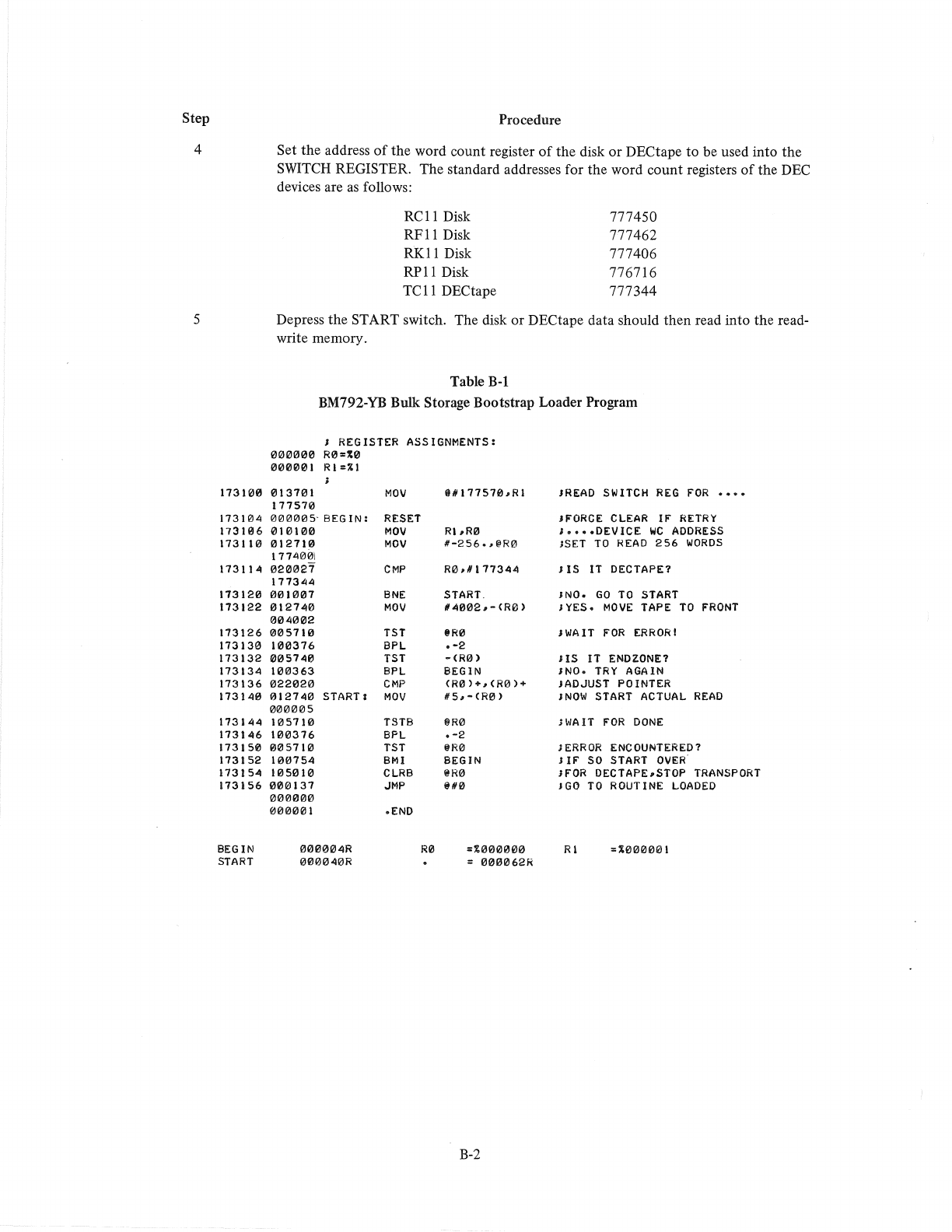
Set the address
of
the word count register
of
the disk or DECtape
to
be used into the
SWITCH
REGISTER. The standard addresses for the word count registers
of
the DEC
devices are
as
follows:
RC11
Disk
RF11 Disk
RK11 Disk
RP11 Disk
TC
11
DECtape
777450
777462
777406
776716
777344
Depress the START switch. The disk or DECtape data should then read into the read-
write memory.
Table
B-1
BM792-YB Bulk Storage Bootstrap Loader Program
, REGISTER ASSIGNMENTS:
000000
R0=%0
000001
Rl=%1
013701
177570
000005-BEGIN:
010100
012710
1774001
020027
177344
001007
012740
004002
005710
100376
005740
100363
022020
012740
START.
000005
105710
100376
005710
100754
105010
000137
000000
000001
000004R
000040R
MOV
RESET
MOV
MOV
CMP
BNE
MOV
TST
BPL
TST
BPL
eMP
MOV
TSTB
BPL
TST
BMI
CLRB
JMP
.END
1<0
11177570.Rl
RI.R0
#-256
••
I!R0
R0.NI77344
START.
14002.-(R0)
8R0
•
-2
-(R0)
BEGIN
(R0
>+.
(R0)+
'"
5.
-
(R0)
@R0
.-2
@R0
BEGIN
@R0
110
=%000000
=
0000621(
B-2
'READ SWITCH
REG
FOR
••••
'FORGE
CLEAR
IF
RETRY
'
••••
DEVICE
WC
ADDRESS
ISET
TO
READ
256
WORDS
JlS
IT DECTAPE?
JNO.
GO
TO
START
'YES.
MOVE
TAPE
TO
FRONT
JWAIT
FOR
ERRORI
JIS
IT
ENOZON£?
JNO.
TRY
AGAIN
,ADJUST POINTER
'NOW
START
ACTUAL
READ
JWAlT
FOR
DONE
JERROR ENCOUNTERED?
JIF
SO
START
OVER
IFOR DECTAPE.STOP
TRANSPORT
JGO
TO
ROUTINE
LOADED
RI
=%000001
APPENDIX C
BM792-YC
CARD READER BOOTSTRAP LOADER
The BM792-YC
ROM
is
shipped with
jumper
wires connected for address group 773200-773276. Its diode
matrix
is
preprogrammed for loading binary data into
the
PDP-II memory from cards using the
CRII
or
CMll
Card Reader.
If
the data represents a PDP-II program, the program can be automatically started upon comple-
tion
of
loading. The BM792-YC
is
used in PDP-II Systems
that
have at least 4K
of
read-write memory and a
card reader.
On
the
card
that
is
read, each pair
of
columns (column 1 and column 2; 3 and 4; etc.) beginning with column 1
contains two 8-bit bytes which represent one l6-bit word. Also a control
bit
can be contained in the second
column
of
a pair. The eight bits
that
represent each byte are punched
or
marked in rows 2 through 9
of
each
column.
The fIrst column
of
a pair contains the high-order byte (PDP-II bits 15-8)
of
the
word and the second column
of
the
pair contains the low-order byte (PDP-II bits 7-0)
of
the word. A control
bit
punched
or
marked in row
o
of
the
second column
of
a pair designates
that
the word in those two columns
is
a new Loading Address. Each
Loading Address must be equal to zero modulo two because loading must begin at a word boundary in memory
rather than a
byte
boundary. Loading
is
accomplished one word at a time, thus a new Loading Address can
appear anywhere on the card. However, a Loading Address must be in the fIrst two columns
of
the fIrst card
read.
The absence
of
control bits in rows 12, 11, 1, and 0
of
the second column
of
a pair designates the word as a
Data Word to be loaded into the PDP-II memory. The Data Word can represent a machine instruction
or
data.
After each Data Word
is
loaded into memory the current loading address
is
incremented by two.
A control
bit
in row 1
of
the second column
of
a pair designates the word
as
a Transfer Address. When a Transfer
Address
is
read, the bootstrap program issues a RESET and branches to the Transfer Address. The card which
contains the Transfer Address passes through the card reader,
but
no
other
Loading Addresses
or
Data Words are
read from it.
A program listing for the card reader bootstrap loader
is
provided in Table C-I. Hardware addresses in the PDP-II
use
18
bits; thus, bits A15, A16, and A17 are considered in designating the most significant octal digit
of
the
address. The software assembler uses 16-bit addresses; consequently, only bit
Al5
is
used
to
designate the most
significant octal digit
of
the address. Therefore, the addresses in Table C-l are listed
as
1 73XXX instead
of
773XXX.
C-l
The
operating
procedure
for
use
of
the
BM792-YC card
reader
bootstrap
loader
is as follows:
Step
2
3
4
5
6
7
Procedure
Set
the
HALT/ENABLE
switch
to
HALT,
then
to
ENABLE.
Load
the
input
hopper
of
the
card
reader
with
the
cards
to
be read.
01'1
the
card
reader
set
the
MODE
switch
to
REMOTE.
On
the
card
reader
depress
the
RESET
switch
and observe
that
the
associated green
indicator
lights.
The
card
reader
is
now
on-line.
Set
the
starting
address,
773200,
into
the
switch register.
Depress
the
LOAD
ADDR
switch.
Depress
the
START
switch.
After
a
short
pause,
the
card
reader
should
read
the
data
on
the
cards
into
the
computer
memory.
C-2
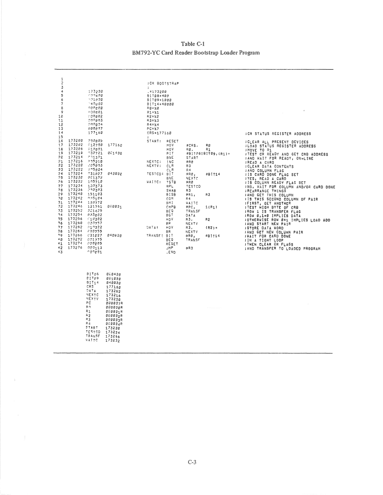
Table C-l
BM792-YC Card Reader Bootstrap Loader Program
1
2 ;eR
BOOTSTRAP
3
4
1732~0
,'173200
5
'"'0'140121
81T08=400
6
;,
:010:)0
8IT09·1000
7
81114040000
8
R0'=-~{0
9
:1
JIJ~01
Rl=%l
10
'."D0002
R2=%2
11
~~g"003
R3=%3
12
~000~4
R4=%4
13
0000~7
PC=%7
j 4
1771
60 CRS=177160
15
1
CR
STA
iUS
REGISTER
~OOA"S
16
173200
?,'3000~
START'
RESET
;
CLEAR
ALL
pRESENT
DEVle.s
17
173202
1:12700
17716e
MOV
#CR$,
R0
;LOAD
STATUS
R[GISTER
~DORns
18
173206
C'1~0n
MOV
R0,
Rl
;MBVE
TO
A1
19
173210
cl3n21
0'1
430
PIT
#8IT~818IU9,
(Ril.
;HS;
CR
RUDY
AND
GEr
e~B
ADORE~$
2e
173214
'"'1371
8NE
START
; HID
WA
l!
rOR
READ'!,
ON'I.!N[
21
173216
0'15210
NEXTC'
INC
~R0
,RfAD
A
CIIRO
22
173220
,10
50'13
NEXTV:
CLR
R3
,CLEAR
onA
CONHNiS
23
173222
~1"l1;0Zl4
Cc
R
R4
;AND
COLUMN
nA~
24
173224
"31027
04~0Ve
TESTCD'
sIT
~R0,
#B!T14
:
13
CA~D
O~NE
nAG
sn
:?5
173230
00372
8NE
NEXTC
;
YE:S,
ROD
A
CARD
26
173232
105710
WAITC.
TST8
~R0
, ! S
COLUt~N
READV
rbAG
SEI
n
173234
1J~373
8PL
TESTCD
;NO~
~,
A!
T rCR
COI.UMN
i\NO/M
C~~D
oor,[
'6
173236
,"~303
SWA8
R3
; RURRANGE
r~ING$
29
173240
1511
03 81SB
@R1,
R3
lAND
GET
TMlS
eObuMN
~0
173242
'''51
04
COM
R4
I !
~
TH!S
SI:CONa
CObUMN
Or
PA!~
31
17~244
B\'772
8M
I
WA
ITC
Ir!RST,
GEl
AN©T~E~
:-;2
173246
121761
0l'00~1
CMPS
@PC,
1
(Ri)
,HST
HIGH
avn
01'
CRS
~3
173252
f.l~i4Z5
8EQ
TRA~SF
lROW
1
IS
TRANSr~R
rl.AG
'4
173254
o~3002
BGT
DA
TA
lROW
0"~.m
IMPLlU
OAU
35
173256
'·1~3~2
MOV
R3.
R2
IOTHERWISE
ROW
~"1
I~~~!E"
bOAD
ADO
36
173260
I.]
2107
57
eR
NEXTV
;AND
START
NEW
P~!R
n
173262
"1'322
GAT
A'
MOV
R3, (R2,"
;STORE
DATA
WO~O
38
173264
n~755
BR
NEXTV
;AND
en
NHI
COLUMN
~A!~
'9
173266
C31e27
040~"0
TR'NSF'
BIT
@R0,
#81,14 ; HA! 7
rOR
eAIiQ
DON.
40
173272
Gn
1
7'S
8EQ
TRM,S,
;nl
A
TICHY
bOOP
41
173274
V80e05
RESET
lTHEN
eb[A~
CR
rbA~$
42
173276
0Z0113
JMP
@R3
;AND
TRANsrER
TO
LO~~tO
P~O\'l~AM
43
r>'2J(lj~~1
,END
8I
T0!; 0;;042)0
elT09
0D
102)0
8 IT 14
0400~0
CRS
177150
~ATA
17
3262
'JDTe
173216
I\J(
Xr
v
173220
PC
00002J7R
p"
00002J0R
R1
0~002J1R
"2
00002J2R
~3
00002)3 R
R4
0e002J4R
,HRT
17322J0
TESTCD
170224
TRANSF
173256
(.,1
ArT C 17
3232
C-3

APPENDIX D
MR11-DB BULK
STORAGE
BOOTSTRAP
LOADER
The MR
II-DB
is
a 64-word
bootstrap
loader for
the
following bulk storage control devices:
RF
II,
RKII,
TC 11,
TM
11, RP 11, and
RC
II.
This
option
can be used in any
PDP-li
system.
It
includes a feature
of
special value to
PDP-l 1/45 systems that are equipped with
MSII
Semiconductor Memory (MOS
or
bi-polar) Systems. On those
PDP-l 1/45 systems, the
KBII-A
start vector for power
up
can be selected for
bootstrap
load from any
of
the
above-listed devices, except the
TM
11, which loses vacuum on power fail.
The
MRll-DB
option
consists
of
two
programmed ROM diode matrix modules. The M792-YD
ROM
Diode
Matrix stores
the
first 32 words
of
the
bootstrap
loader program at addresses 773100-773176. The M792-YE
ROM Diode Matrix stores the second 32 words
of
the
bootstrap loader program at addresses 773200-773276.
Table D-l
is
a program listing
of
the
MRll-DB
Bootstrap Loader program
that
is
encoded on
the
two ROM diode
matrix modules. PDP-II hardware addresses use 18 bits. The software assembler uses
l6-bit
addresses. There-
fore,
the
addresses listed in Table D-l are listed
as
l73XXX,
instead
of
773XXX.
KEY START LOADING
Operate the
MRll-DB
Bulk Storage
Bootstrap
Loader
as
follows:
1.
Set the HALT/ENABL switch
to
HALT,
then
to
ENABL.
2. Set
the
console switches
to
the
starting address assigned to
the
selected
bulk
storage device control,
as
listed in Table D-2.
3.
Press LOAD ADRS.
4. Press START.
The processor will start executing
the
bulk
storage
bootstrap
loader program
at
the
selected address. The pro-
gram loads
the
first 512 words from
unit
0
into
memory, starting at memory location
O.
After
the
bootstrap
is
loaded from
the
bulk storage device,
the
loader program causes
the
processor
to
start
executing
the
bootstrap
at
location
O.
NOTE
When magnetic tape is
the
bulk
storage medium, magnetic
drive
unit
0
must
be
selected and positioned
at
the
load
point.
Loading
from
Disks -The program starts
at
the
selected address, then branches
to
a common routine
that
resets
all Unibus devices. Thus, disk address registers and current memory address registers are initialized
to
O.
The
pointer
to
the
device's word
count
register is located in R1. Then,
the
word
count
register
is
loaded
with
the
2s
D-l
complement
of
512. The device command
to
read and
go
is
issued
to
the
device command register. As
the
512-
word record
is
read
into
memory from
the
disk, the loader program checks for errors.
If
an error
is
detected,
the entire routine
is
repeated, starting
at
the selected address. When
no
errors are detected and the last word has
been transferred,
the
PC
is
cleared, and
the
bootstrap
is
executed, starting at memory location
O.
Loading from Tapes -The program starts at the selected address for DECtape
or
magtape;
then
branches
to
a
common tape routine which first resets all the device registers. Then,
the
device's word count register
(or
byte
count)
is
decremented by one.
If
the
routine
is
entered from the TC
11
address, a first command
is
issued
to
re-
wind
the
DECtape to the forward
end
zone.
If
the routine
is
entered from the TM
11
address, a first command
is
issued
to
advance the magnetic tape one record. After the specified operation
is
done and checked for errors, the
program branches to the common disk loading routine
that
reads a 512-word record
into
memory from
the
se-
lected tape storage device.
POWER UP LOADING
The
MRII-DB
provides for automatically loading a bootstrap program from a pre-selected bulk storage device
during the power
up
sequence. This feature
is
provided for PDP-l 1/45 systems with
MOS
or
bipolar
memory
and no power backup. The
KB
ll-A
Central Processor Unit in those systems has a
start
vector
jumper
field lo-
cated on DAP module
M81
00. Table D-3 lists the start vector
jumper
connections required to select the specific
MRII-DB
starting address for each
type
of
bulk storage device.
START VECTOR PROGRAM OPERATION
The start vector jumpers on the DAP module select bits SV(07:00)
of
the
start
vector. Bits SV(OI :00) are always
O.
High-order bits
of
the starting address are generated by CPU sign-extension logic, blocking bits
II
and 8. A
hard-wired address 773XXX with the SV(07:00) offset
is
generated. The
power
up
sequence uses
the
resultant
address to load
the
PC
and
PS
from
the
address pointed
to
by
the
start
vector.
For
example,
jumper
selection
of
the
RK
II
provides start vector 260. The resultant address, 173260, accesses a
location provided
by
the
MRII-DB,
to
load
the
PC
with starting address 173110 and the
PS
with 000340.
The
bulk storage program loader proceeds
to
load a bootstrap from the RK 11,
with
the
CPU operating at priority
level 7, which prevents external devices from intermpting
the
program.
INSTALLATION
PDP-I 1/45 Systems -Install
the
M792-YD and M792-YE modules
that
comprise
the
MRII-DB
option
in
two
of
the
three spaces reserved on the CPU backplane for small peripheral controllers. The quad-height slots are desig-
nated 26, 27, and 28. Refer
to
Table D-3 and remove jumpers WI through
W6,
as
required, from the DAP
module
to
select the bulk storage device
that
is
to provide
the
bootstrap
program during power up.
NOTE
The TMJ1 must be restarted manually,
with
the
tape
drive positioned
at
the
load point. Therefore, power
up
start
vector selection
is
not
provided.
Other
PDP-ll Systems -Install
the
MRII-DB
modules on a
DDII-A
Peripheral Mounting Panel
that
is
con-
nected
to
the Unibus by an M920 Unibus Connector module.
D-2
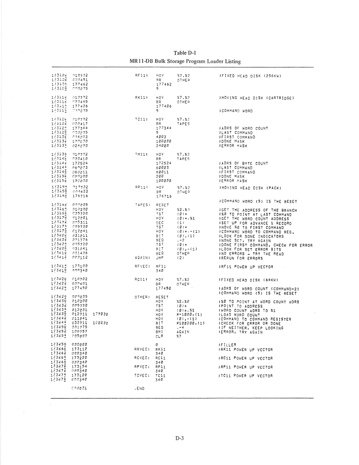
Table D-I
MRll-DB
Bulk Storage Program Loader Listing
1
311'1
~10732
RFlll
~10
V
%7,~2
lFlXED
HEAD
DISK
(256KW)
1
31J
0801451
RR
OTHER
1
31:3
177462 177462
1
3~~1
~~00~5
5
1!311~
1)1~7n
RKlll
MOV
%7,~2
'MOVING
HEAD
DISK
(CARTRIDGE)
1/311<
"~'J445
SR
OTHER
1i3:'l~
1774~6
177 406
1~311~
~I
~
1710'l5
5
'COMMAND
WORD
1/3l2k,
:>107n
TClll
MOV
%7,"2
li3122
~,
7,(
i1
417
8R
TAPES
li312~
1773
44
177344
IADRS
OF
WORD
COUNT
17312~
"'J;)~~5
5
ILAST
COMMAND
1/313~
'~''14003
4~03
IFIRST
COMMAND
li
3i3t
10~03~
1~0000
IDONE
MASK
1(3i3~
0240~0
24001'1
IERROR
MASK
1(313~
110702
TM111
MOV
%7,%2
1(n4~
rM410
BR
TAPES
1/314'
172524 172524
IADRS
OF
BYTE
COUNT
1i3~4~
~60,,?3
60003
ILAST
COMMAND
11314~
06iJ~11
60011 IFIRST
COMMAND
1!315~
~00200
200
IDONE
MASK
1!3l5~
1~0~00
100000
IERROR
MASK
1/315q
"'P702
RPlll
MOV
'O,X2
lMOVING
HEAD
DISK
(PACK)
1?3i5~
0"'A423
8R
OTHER
1(316~
176716 176716
ICOMMAND
WORD
(5
)
IS
T~E
RESET
11310(
~0'~005
TAPES:
RESET
1(3i6~
0102~0
MOV
%2,~~
IGET
H~E
ADDRESS
or
THE
BRANCH
113160
C;J572121
TST
(121)
•
1%121
TO
POINT
AT
LAST
COMMAND
1i3i7~
'J12~"1
MOV
(121)·,%1
lGET
T~E
WORD
COUNT
ADDREsS
lj,li7~
0~5311
DEC
(1)
lSET
UP
FOR
ADVANCe:
1
RECORD
17317q
"'(1)57213
TST
(121)
•
'MOVE
"0
TO
,IRST
COMMAND
1?3i7§
012041
MOV
(0)
•.
-(1)
ICOMMAND
WORD
TO
COMMAND
REG,
173~0.
031011
sIT
(0)
,
(1)
ILOOK
rOR
DONE
INDICATORS
1~3;2\l2
0n776
9EQ
•
-2
INONE
SET,
TRY
AGAIN
F3~1l~
1'10572121
TST
(0).
IDON£
'IRST
COMMAND,
CIO£CK
rOR
ERROR
1'3~0b
']310 41
BIT
(0)
,-
(1)
ILOOK
F'OR
S£T
[RROll
BITS
1i3~1~
07.11406
8EQ
OTHER
INO
ERRORS
.
TRY
T~E
READ
1(3~1~
('I!1'21112
AGAIN:
JMP
(2 )
IRERUN
FOR
ERRORS
1!3~1~
17310~
RFVEC:
RF11
I
RF'l1
POWER
UP
VECTOR
1(3(1~
'~~"'340
34121
1 3
2~
010702
Rclll
MOV
%7,
~2
I FI
XED
HEAO
DISK
(64KW)
1 3
22
0!l~401
SR
OTHER
1 3
2~
17
7450 177450
IAORS
OF
WORD
COUNT
(COMMAND·21
ICOMMAND
WORD
(5
) ! S
T~E
RESET
1 3
20
0e00~5
OTHER:
RESET
1 3
3~
01121200
MOV
%2,,,0
1%0
TO
POINT
AT
WORD
COUNT
ADR!
1 3
3~
@0572121
TST
(121)
•
IPOINT
TO
ADDR£SS
1 3
34
12112e21
MOV
(0).,%1
IWORD
COUNT
ADRS
TO
"1
1 3
30
012711
17703121
MOV
#-10121121,
(1)
ILOAD
WORD
COUNT
1 3
4~
0112'41
MOV
(121)
,-
(1)
lCOMMAND
TO
COMMAND
REG
UnR
1 3
44
032711
101212~0
8IT #1130200,
(1)
IcHECK
FOR
ERROR
OR
DONE
1 3
5~
~Ql1775
SEQ
•
-4
IIr
NEITHER,
KEEp
l.OOKING
1 3
52
100757
8MI
AGAIN
IERROR,
TRV
AGAIN
1 3
5~
~05~~7
CLR
~7
1 3 5
00012100
121
I
FI
Ll.ER
1 3 6
1731112i
RKVEC:
RKll IRKU
POWER
UP
VECTOR
1 3 6 0003
40
340
1 3 6
1732213
RCVEC:
Rcll
I
Rca
~OWER
UP
VECTOR
1 3 6 0003
40
3413
1 3 7 173154
RPVEC:
RPll
1 RPl1
POWEf!
UP
VECTOR
1 3 7 0003 40 340
1 3 7
17
3
1213
TCVEC:
Tca
ITC11
POWER
UP
VECTOR
1 7
0~n3412'
34121
0'~~0'H
.END
D-3
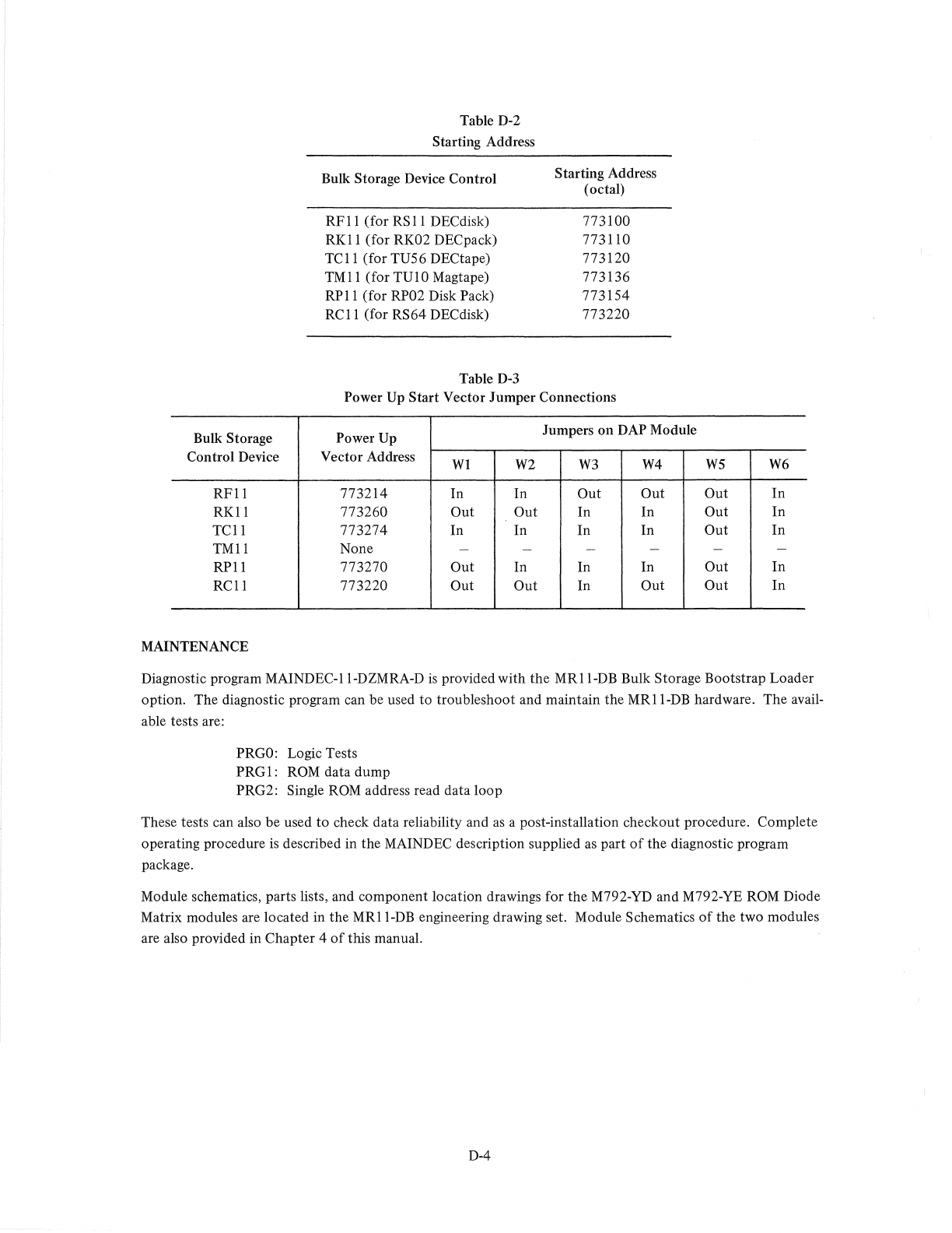
Bulk Storage
Control Device
RFll
RKII
TCII
TMII
RPII
RCII
MAINTENANCE
Table D-2
Starting Address
Bulk Storage Device Control
RFll
(for
RSII
DECdisk)
RKII
(for RK02 DECpack)
TCII
(for TU56.DECtape)
TMII
(forTUlOMagtape)
RPll
(for RP02 Disk Pack)
RCII
(for RS64 DEC disk)
Table
D-3
Starting Address
( octal)
773100
773110
773120
773136
773154
773220
Power Up Start Vector Jumper Connections
Power Up Jumpers on DAP Module
Vector Address
WI
W2
W3 W4
773214
In In Out Out
773260 Out Out In
In
773274
In In
In
In
None
~
~ ~
~
773270 Out In In In
773220 Out Out In Out
W5 W6
Out
In
Out
In
Out
In
~ ~
Out
In
Out
In
Diagnostic program MAINDEC-II-DZMRA-D
is
provided with the
MRII-DB
Bulk Storage Bootstrap Loader
option. The diagnostic program can be used
to
troubleshoot and maintain the
MRII-DB
hardware. The avail-
able tests are:
PRGO:
Logic Tests
PRG I:
ROM
data dump
PRG2: Single
ROM
address read data loop
These tests can also be used
to
check data reliability and
as
a post-installation checkout procedure. Complete
operating procedure
is
described in the MAINDEC description supplied
as
part
of
the diagnostic program
package.
Module schematics, parts lists, and component location drawings for the M792-YD and M792-YE
ROM
Diode
Matrix modules are located in the MRII-DB engineering drawing set. Module Schematics
of
the two modules
are also provided in Chapter 4
of
this manual.
D-4
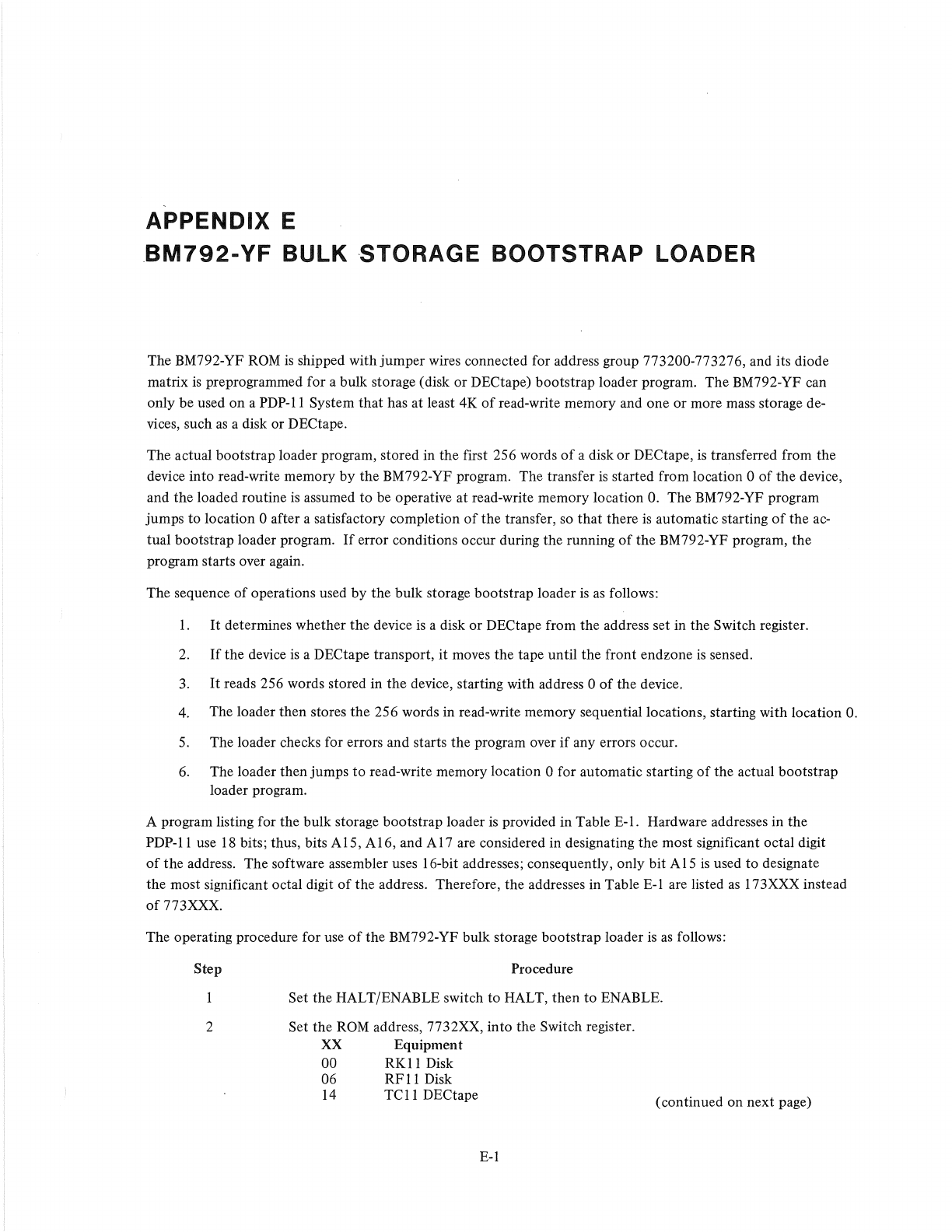
APPENDIX E
BM792-YF
BULK
STORAGE
BOOTSTRAP
LOADER
The BM792-YF
ROM
is
shipped with
jumper
wires connected for address group 773200-773276, and its diode
matrix
is
preprogrammed for a bulk storage (disk or DECtape) bootstrap loader program. The BM792-YF can
only be used
on
a PDP-II System
that
has at least 4K
of
read-write memory and one
or
more mass storage de-
vices, such
as
a disk or DECtape.
The actual bootstrap loader program, stored in the first 256 words
of
a disk
or
DECtape,
is
transferred from the
device into read-write memory
by
the BM792-YF program. The transfer
is
started from location 0
of
the device,
and the loaded routine
is
assumed
to
be operative at read-write memory location
O.
The BM792-YF program
jumps
to
location 0 after a satisfactory completion
of
the transfer,
so
that
there
is
automatic starting
of
the
ac-
tual bootstrap loader program.
If
error conditions occur during the running
of
the BM792-YF program, the
program starts over again.
The sequence
of
operations used
by
the bulk storage bootstrap loader
is
as
follows:
1.
It
determines whether the device
is
a disk or DECtape from the address set in the Switch register.
2.
If
the device
is
a DECtape transport,
it
moves the tape until the front end zone
is
sensed.
3.
It
reads 256 words stored in the device, starting with address 0
of
the device.
4.
The loader then stores
the
256 words in read-write memory sequential locations, starting with location
O.
5.
The loader checks for errors and starts the program over
if
any errors occur.
6.
The loader then jumps
to
read-write memory location 0 for automatic starting
of
the actual bootstrap
loader program.
A program listing for the bulk storage bootstrap loader
is
provided in Table
E-l.
Hardware addresses in the
PDP-II use
18
bits; thus, bits A15, A16, and
Al7
are considered in designating the most significant octal digit
of
the address. The software assembler uses 16-bit addresses; consequently, only bit A
15
is
used to designate
the most significant octal digit
of
the address. Therefore, the addresses in Table E-l are listed
as
173XXX instead
of
773XXX.
The operating procedure for use
of
the BM792-YF bulk storage bootstrap loader
is
as
follows:
Step Procedure
Set the HALT/ENABLE switch
to
HALT, then
to
ENABLE.
2 Set the
ROM
address, 7732XX, into the Switch register.
XX Equipment
00
RKll
Disk
06
RFll
Disk
14
Tell
DECtape (continued on next page)
E-l
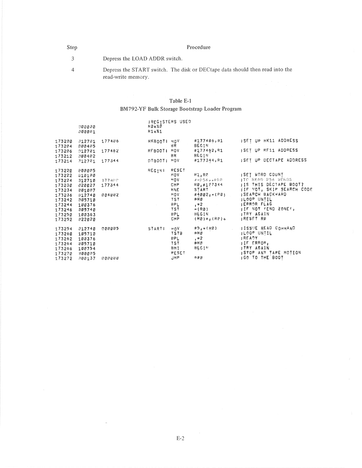
Step
3
4
:JIZI1J0210
000001
t7S2011J
;1;1,2701
173204
011111J4~5
173206
:J:l.27Kll
173212
:'fII04eJ2
173214
?!lZ701
173220
0'HHJ05
173222
0101"0
173224
n2710
17323~
020027
173234
0"111)(17
173236
0127"f/I
173242
['Iiil'571~
173244
11<":137()
173246
i11057Hl
1732'0
11~Qj3()3
173252
022(1)20
173254
012740
17326111
10571[11
173262
111J0371;>
173264
011J57HJ
173266
1"0754
1732713
'~00"2'5
173272
/100137
Procedure
Depress
the
LOAD
ADDR
switch.
Depress
the
START
switch.
The
disk
or
DECtape
data
should
then
read
into
the
read-write
memory.
Table
E-l
BM792-YF Bulk Storage Bootstrap Loader Program
'REG~SrERS
lJSED
Rfh%
Rh%1
In'HJo
RKBOaTI
'10V
jl/~n4f!J6,
Rl
Isq
UP
fiKU
ADDRESS
tlf<
BEGIN
17746~
prBOOrl
MOV
#~
774~2,
Rl
J
SET
UP
RF11
ADDRESS
BR
Hi-G!N
177.344
DT[JOO'f1
MOV
jjl773~~,Rl
IS
F.T
UP
OECTAPE:
ADDRESS
flEG
pH
RESET
MOV
Rl,R~
ISET
WORD
COUNT
177
<j,'"".
"OV
fJ
-c,;'.
S 6
~
~~'
F
()1
pc
RFJ'fl
25"
1,\ICf~fJ5
177344
CMf'
R~,1I177344
I
IS
THIS
DECTAPE:
Soon
NNE
START
II,
"(H,
SKIP
SEAI'WH
CODE
flJQj41/1kJ2
MOV
#~11I02i,,(R0l
;SEARCH
BACKWARO
,S1'
"~0
j~OOP
UNTIe
aPb
1"2
1!:F1ROR
F"I,.AG
TST
~
I
Rf1J)
1IF"
NO'!
'END
HJNEI,
gpl.
HE-GIN
jlRY
AGAIN
eMf' (Hlill<-,
(R~
I"
I
REHT
RW
001')"",
START!
MOV
iI',,,OHll
I!
SSIJE
READ
COMMAND
1'51'8
1\>~0
11.001'
UNTI
~
BPI.
,"2
IR[M'V
1ST
@H0
j !
F"
ERROR
a
BM!
8~GP'
l'l'fl'l'
AflAIN
RESET
i
~HOP
ANY
U;>E
MOIlON
0IZH'Ir"I6(,J
JMP
",11[11
,G5
TO
THE
-SOOT
E-2
APPENDIX F
BM792-YH
CASSETTE
BOOTSTRAP LOADER
The BM792-YH
ROM
is
shipped with jumper wires connected for address group 773300-773376, and its diode
matrix
is
preprogrammed for a tape cassette
(TAll/TU60
Cassette System) bootstrap loader program. This
quad-sized module
is
one
of
the Small Peripheral Controllers (SPC) and can be mounted in any
SPC
slot in a
DD
II-A,
DD
ll-B,
or
most PDP-II family processors. Any PDP-II System
that
has 4K
of
read-write memory
and a cassette can use the BM792-
YH.
The actual bootstrap loader program, stored in the first 128 bytes
of
a cassette tape,
is
transferred from
the
cassette into read-write memory
by
the
BM792-YH program. The bytes are consecutively read from the cassette
and loaded
into
memory locations 0 through 177 (octal). When the loading
is
complete, program control
is
transferred
to
location 0 so
that
the loaded program can be executed.
At
the point when the program control
is
transferred, the cassette
is
positioned at the end
of
the second block
of
the first file so
that
the loaded program
can continue
to
read in additional data.
The sequence
of
operations used by the cassette bootstrap loader
is
as
follows:
1.
The cassette
is
rewound and then spaced forward one block. This action skips the header block
(normally 32 bytes) associated with the first file and positions the tape at the second block
of
the
first file.
2.
The BM792-YH program consecutively reads 128 bytes from the cassette tape into read-write memory
locations 0 through 177 (octal).
3. The first byte read
is
compared
to
octal 240 (NOP) and
if
it does
not
equal octal 240, the program
comes
to
a halt at location 17335Q. To restart the program from this halt,
the
CONT switch
is
depressed.
4. After the 128 bytes are read, the loader program checks the
TAll
error
bit
(block check error, off-
line error, etc.) and
if
an error
is
detected, the program comes
to
a halt at location 173350 and can
be restarted by depressing the CONT switch.
5.
If
no error
is
detected, program control
is
transferred to location 0
to
execute the loaded program.
A program listing for the cassette bootstrap loader
is
provided in Table
F-l.
Hardware addresses in the PDP-II
use 18 bits; thus, bits A15, A16, and
Al7
are considered in designating the most significant octal digit
of
the
address. The software assembler uses 16-bit addresses; consequently, only bit
Al5
is
used
to
designate the most
significant octal digit
of
the address. Therefore, the addresses in Table
F-l
are listed
as
I 73XXX instead
of
773XXX.
The BM792-YH program has no provisions for initializing
the
system since
it
does
not
issue a RESET instruction.
Initialization
is
necessary because
other
devices may issue interrupts
or
an internal processor option may be en-
abled. When
the
BM792-YH program
is
started from the console, initialization
is
performed because the START
F-I
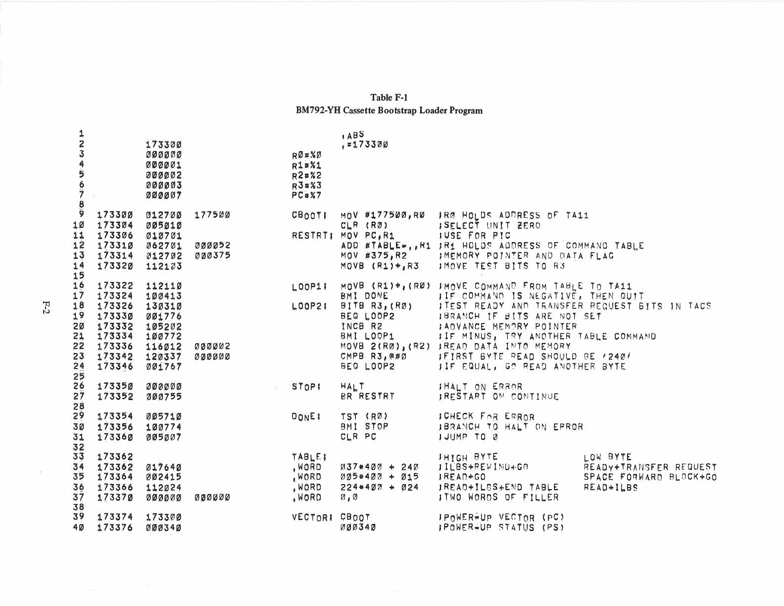
::;
1
2
3
4
5
6
j
8
9
Ul
11
12
1~
14
15
1~
17
1~
19
2f(J
~1
22
23
2~
2~
26
ii
28
29
30
31
32
3~
34
3'
36
37
38
39
41D
1733130
1t331214
173306
173310
173314
17332121
173322
173324
173326
173330
173332
173334
173336
173342
1733~6
17330121
~H"'J12I0121
0210001
f(J00Q102
00~11J1/l3
IUJI2I2I01
U2?0121
0"50Ul
0107"1
062103-
121121
l:'l
2
112103
1121UJ
1021413
13031121
0flli
716
105202
UII1l?72
116012
120331
001H1
17335121
01210210121
173352
000755
173354
173356
1733621
173362
173362
173364
173366
173370
173374
173376
21"571121
1021774
00511)07
01
'64121
002415
112024
0000eJr2I
1733~eJ
0r210342J
177500
"13210'2
000375
000002
0U000
'H~0012111J
Table
F-l
BM792-YH Cassette Bootstrap Loader Program
Rh%0
Rh"l
R211"2
R3.%3
PCd?
lABS
1=1733210
C800TI
MOV
#177500,RIi'l
CL.R
(RI1l) .
RESTRTI
MOV
PC,Ri
L.OOP11
L.OOP21
STOP'
DONEI
TABLE
I
,WORD·
.WORD
.WORD
.WORO
ADO
#T
ABL.E.! , Hi
MOV
#375,R2
MOVB
(Rl)+,R3
MOVB
(R1)+,(RflI)
8M
l
DOfliE
BJTS
R3,(RIlJ)
SEQ
l.OOP2
tNCB
R2
8MI LOOPl
~10VB
2(RP.I),(R2)
CMPB
R3,1iD#0
SEQ
LOOP2
j,jAL,T
SR
RESTRT
TST
(RI2I)
B~l
I
STOP
CL,R
PC
03'*400
+
24121
005*41?J~
...
1"15
224*4fa0
...
~24
0,0
VECTOR
I
CBOOT
I2lfal:5341ZJ
,R0
HO~D~
ADr,R~SS
OF
TA1l
,SELECT
UNIT
2ERO
IUSE
FOR
PtC
/R!
HOLD~
ADDRESS
OF
COMMAND
TABLE
;MEMORY
POYNTER
AND
DATA
f~AG
JMOVE
TE~T
BITS
TO
R~
.
JMOVE
COMMAND
FROM
TA~hE
TO
TAll
!IF
CO~MA~n
IS
NlGATIVE,
THEN
OUIT
ITEST
READY
ANn
T~ANSFER
REQUEST
6ITS
IN
TACS
JBRANCH
IF
~ITS
ARE
NOT
SET
JADVANCE
MEM~RY
POINTER
IIF
MINUS,
TRY
ANOTHER
TABLE
COMMAND
IREAD
DATA
INTO
MEMORY
JFIRST
BVTE
READ
SHOULD
BE
'24~1
IlF
EQUAL,
G~
READ
ANOTHER
BYTE
IHALT
ON
ERR~R
,RESTART
O~
CONTINUE
!C~ECK
F~R
ERROR
J8RA~CH
TO
HALT
ON
EPROR
,JUMP
TO
~
IHIGH
8YTE
, I
LBS+REw
1
hiD,,·Gr:J
IREAn"'GO
,REAo+rL8S+E~D
TAB~E
lTWO
WORnS
OF
PILLER
JPOWER~Up
VEr,TOR
(pC,
!POWER~Up
5TATUS
(PS)
L.OW
BYTE
REAOy+TRANSFER
REQUEST
SPACE
fO~W~RD
RLOCK+GO
REAO"'IL,BS

switch initializes
the
system prior
to
starting. However,
if
the
BM792-YH program is started
by
a program
transferring
control
to
location
173300,
then
that
program
must
issue a RESET instruction prior
to
the
JMP
173300.
Normally,
the
PDP-II
processor's power-up vector
is
address
24/26;
however, processors such
as
the
PDP-l
1/40
and PDP-I 1/ 45 have
jumper
selectable power-up vectors
that
allow
the
vector address
to
be set
to
an address
within a restricted range in the highest 4K-words
of
Unibus address.
The
power-down
vector
remains at
24/26.
The BM792-YH provides a power-up
vector
at address
173374/6.
When
the
power-up
trap
sequence executes
with a vector address set
to
173374/6,
program
execution
begins
at
173300 with a priority level
of
7.
The operating procedure for use
of
the
BM792-YH cassette
bootstrap
loader when
the
cassette
is
operating from
cassette
unit
number
0 at
the
standard
octal
address
of
777500
is
as
follows:
Step
2
3
4
5
6
Procedure
Write-lock the cassette for security.
Mount
the
cassette in cassette
unit
number
0 (left-hand drive
unit
on
the
TU60).
Set
the
HALT/ENABLE switch
to
HALT,
then
to
ENABLE.
Set
the
ROM address,
773300,
into
the
Switch register.
Depress
the
LOAD ADDR switch.
Depress the
START
switch. The cassette
data
should
then
read
into
the
read-write
memory.
The operating procedure
to
bootstrap
load from cassette
unit
number
1 or from a cassette
unit
other
than
one
at
the
standard octal address
of
777500
is
as follows:
Step
2
3
4
5
6
7
8
9
10
11
12
Procedure
Write-lock
the
cassette for security.
Mount
the
cassette in the selected unit.
Set
the
HALT/ENABLE switch
to
HALT,
then
to
ENABLE.
Set
the
RO
address,
777700,
into
the Switch register.
Depress
the
LOAD
ADDR
switch.
Set
the
address
of
the
cassette
unit
into
the
Switch register.
Depress the DEP switch. This loads
RO
with
the
address
of
the
cassette unit.
With the Switch register still set at
the
address
of
the
cassette unit, depress LOAD ADDR
switch.
Set
the
octal designation for
the
cassette
unit
number
into
Switch register
(000
for
unit
number
0
or
400
for
unit
number
I).
Depress
the
DEP switch. This establishes
bit
08,
the
Unit Select bit,
of
the
TAli
Com-
mand
and
Status
register.
Set
the
R7 address,
777707
into
the
Switch register.
Depress
the
LOAD
ADDR
switch.
(continued
on
next
page)
F-3
Step
13
14
15
Procedure
Set 773306 into
the
Switch register.
Depress
the
DEP switch. This sets the
PC
to the BM792-YH restart address.
Depress
the
CONT switch. This starts the processor without system initialization.
When started at address 773306, the BM792-YH program uses
RO
to
reference the
cassette registers
but
does
not
modify
RO
or
the Unit Select bit.
,
When the 1 28-byte program
is
loaded from the cassette into the read-write memory,
this 1 28-byte program determines whether read-in will continue from this same cassette.
RO
and the Unit Select
bit
can be modified by the loaded program
so
that
a different
cassette can be accessed for loading.
F-4

READER'S
COMMENTS
BM792 ROM
DEC-II-HBMAA-E-D
Your comments and suggestions will help us in
our
continuous effort
to
improve
the
quality and usefUlness
of
our
publications.
What
is
your
general reaction to this manual? In
your
judgment
is
it
complete, accurate, well organized, well
written, etc.?
Is
it easy to use?
What features are most useful?
What faults do you find with the manual?
_____________
~
___________
_
Does this manual satisfy the need you think it
was
intended to satisfy?
Does
it
satisfy
your
needs?
Why?
_________________________
_
Would you please indicate any factual errors you have found.
Please describe
your
position.
Name Organization
Street
____________________
Department
_______________
__
City
__________
_ State
___________
_ Zip
or
Country
-
--
--
--
-.
-
-.-
--
--
--
--
FoldHere
- -
- - - - - - - - -
Do
Not Tear -Fold Here and Staple - - -
--
--
--
--
--
BUSINESS REPLY MAIL
NO
POSTAGE STAMP NECESSARY IF MAILED IN THE UNITED STATES
Postage will
be
paid
by:
Digital Equipment Corporation
Technical Documentation Department
146 Main Street
Maynard, Massachusetts 01754
•
FIRST CLASS
PERMIT NO. 33
MAYNARD, MASS.


· "
DIGITAL EQUIPMENT CORPORATION
MAYNARD,
MAS
SACHUSETTS
01754
