DP3300D
User Manual: DP3300D
Open the PDF directly: View PDF ![]() .
.
Page Count: 63
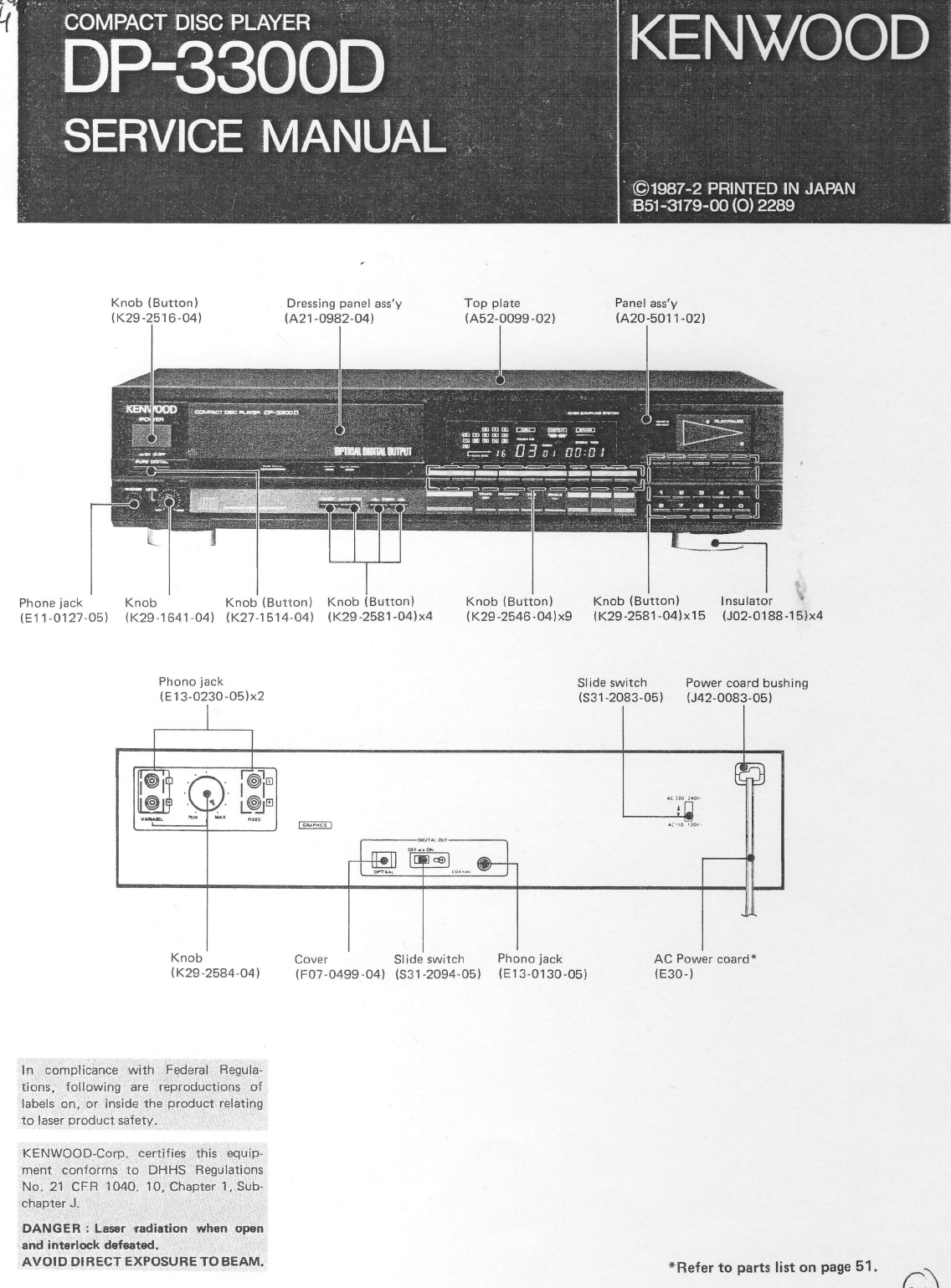
Knob (Button)
(
K29
-251
6
-04)
Phone
jack Knob Knob {Button)
(E11-0127-05) (K29-1641-04) (K27-1514-O4l
Top plate
(A52-0099-02) Panel
ass'y
{A20-501
1-021
Knob (Button)
lK29-25a1-O4lx4
Knob (Buttonl Knob (Button)
(K29-2546-04)x9 (K29-2581-04)x15 lnsu
latJr \
(J02-01
88
-1
5lx4
Phono
jack
(E
1 3-023O-05)x2
Knob
lK29-2584-o4l Cover Slide
switch
(
F07-0499
-04) (S31
-2094-05)
Slide
switch Power
coard bushing
(s31-2083-05) (J42-0083-051
Phono
jack
(E
13-0130-05) AC Power
coard*
{E30- }
In complicance with Federal Begula-
tions, f ollowing are reproductions of
labels on, or inside the product relating
to laser
product safety.
K€NWOOD-Corp. certifies this eguin.
ment conforms to DHHS Regulations
No. 21 CFB 1040. 10, Chapter
1, Sub-
chapter J.
DANGER : Lasor r8diltion when opon
and int€rlock dofeatsd.
AVOID DIRECT EXPOSURE
TO BEAM, *Refer
to parts
list
on
Page
51
.
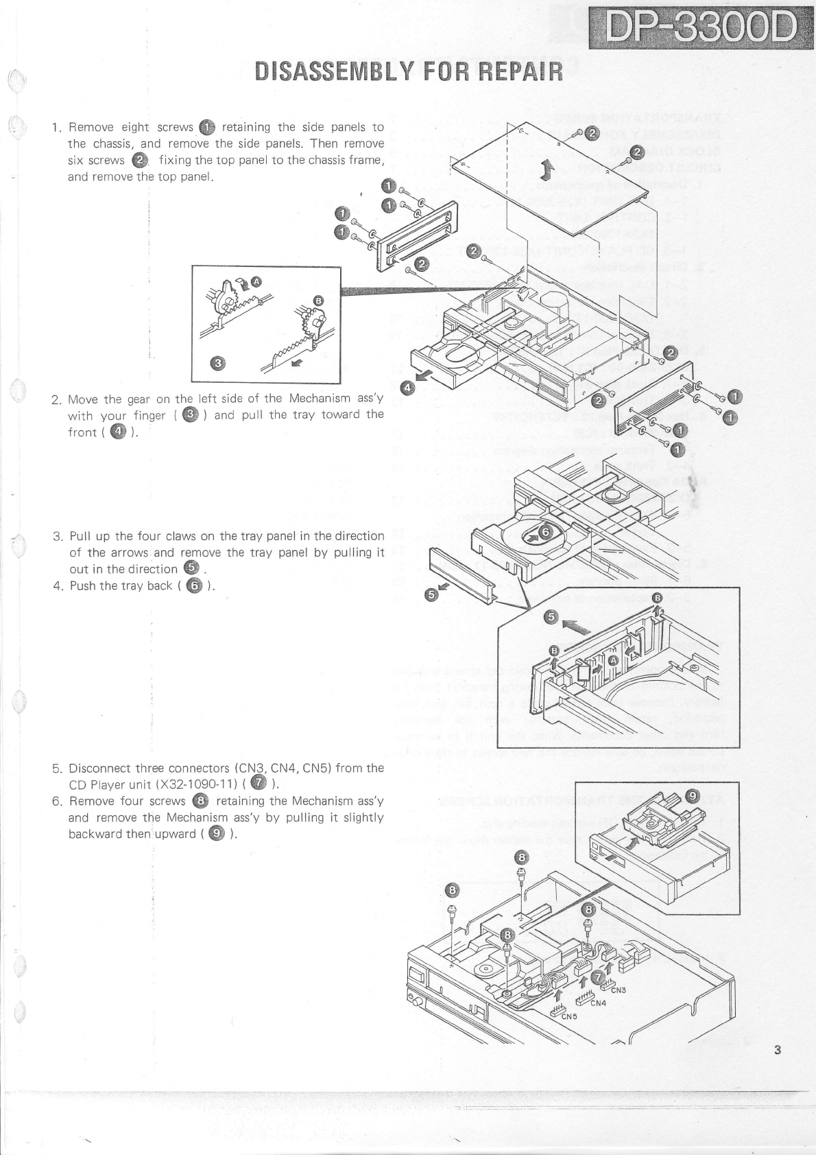
1.
2.
4.
Remove
eight screws
db retaining
the side
panels
to
the chassis, and remove
the side
panels.
Then
remove
six screws
@ tixing
the top
panel
to the
chassis frame,
and remove the top
panel.
DISASSEMBLY FOR
HEPAIR
the Mechanism
ass'y
the tray toward
the
Move
the gear
on the left side
of
with your finger
(
@ ) and Putt
tront
(
@ ).
\a@
@
5.
Pull up the four claws on the tray
panel
in the
direction
of the arrows and remove the tray panel
by pulling
it
ouT
in
the
ciirection
@ .
Push
the
tray back
( G! )
Disconnect three
connectors
(CN3,
CN4, CN5)
from
the
CD
plaver
unit
(X32-1090-11)
(G ).
Remove
four screws
@ retaining
the Mechanism ass'y
and remove the Mechanism
ass'y by pulling
it slightly
backward
thenrupward
(
GF ).
2
3
5
7
7
7
10
10
12
12
12
12
12
12
12
12
13
13
13
13
16
16
16
17
6-3. Explanationof
functions ...... 14
7. Signal
processor
lG : GX23035
(X32-1090-11
:lC3). 14
7-1. Block
diagram 14
7-2. Explanation
of terminals 15
8. Digital
output signal
demodulator
lC : CXDl075P
7
8
9
9
(X32-1090-11
: lC9) .
B-1 . Block
diagram
B-2. Terminal
connection
diagram
8-3. Explanation
of terminals 17
...20
21
21
20
20
24
27
4.
5.
E] E] E] E] tr)
I!]E)EElE)
u@gE@
EgUE@
@
t@r
,-l l-t *'
L, L, i.[]
CO
NTENTS/THANSPO
RTATI
O
N
SCREW
TRANSPORTATION
SCREW
DISASSEMBLY
FOR REPAIR
BLOCK
DIAGRAM
CIRCUIT
DESCRIPTION
1. Description
of components
. .
1-1
. DAC UN
rT
(X25-2860-1
1)
. . . .
1_2.
CONTROL
UNIT
(x29-1780-00).
. ..
1-3. CD
PLAYER UNIT
(X32-1090-11)
..... .
2, Circuit
description
2-1. DAC
lnterface
circuit
(X25-286O-11)
. . . . .
2-2. Distortion
correction
circuit
lx25=2860-11)....
2-3. Dropout
control
circuit
(X29-1780-00)
Dual D Flip-Ffop lC : TC74HC74F
(X25-2850-00
: lCl,lC4)
3-1 . Block diagram
3-2. Truth table .
Hex D Flip-Flop lC : TC74HC174F
(X25-2850-00
: lC3)
4-1 . Terminal
connection diagram
4-2. Truth
table .
DA Converter
: PCM56P-K
(X25-2860-1
1 z
lCl,lC2l
5-1 . Block
diagram/Terminal connection
li^^-^-
u tout dI l
S-2. ExJtanation
of terminals
Digitalfifter: SM58O4B
(X25-2860-11
: lC4) . .
6-1 . Block diagram
6-2. Explanation of termlnals
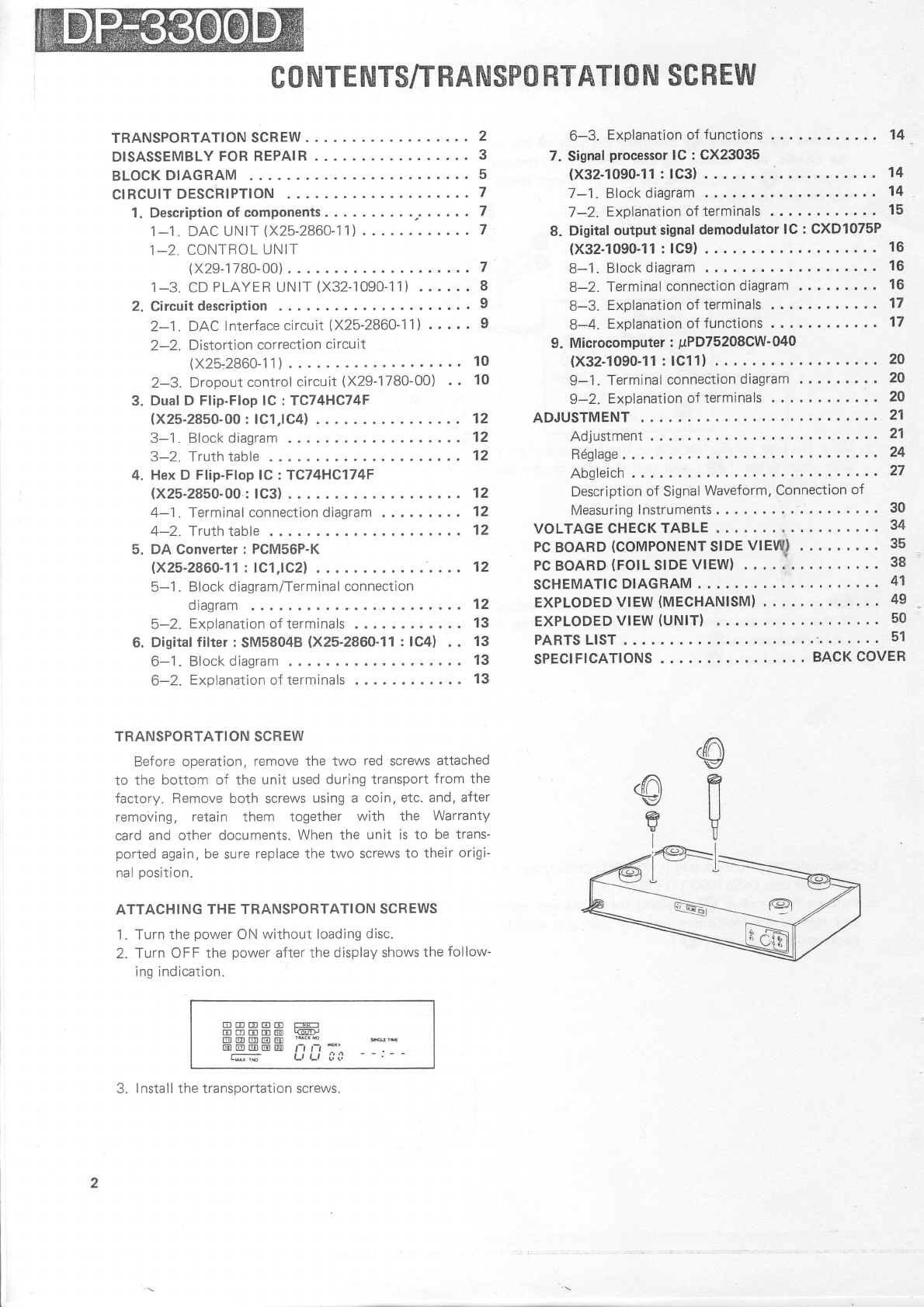
TRANSPOBTATION SCREW
Before
operation,
remove the two red
screws
attached
to the bottom of the unit used
during transport
from the
factory. Remove both screws
using a coin, etc. and,
after
removing, retain them together with the Warranty
card and other documents.
When the unit is to be trans-
ported
again, be
sure
replace the two screws
to their
origi-
nal
position.
ATTACHING
THE TRANSPORTATION
SCREWS
1.
Turn the
power
ON
without loading
disc.
2. Turn OFF the power
after
the display
shows the
follow-
inq indication.
8-4. Explanation
of functions
. . .
9. Microcomputer
: PPD75208CW-040
(X32-1090'11
: lCl1)
9-1 . Terminal
connection
diagram
9-2. Explanation
of terminals
. . .
ADJUSTMENT
...
Adjustment
Q6nlrna
I rEgrqgs
Abgleich
Description
of Signal
Waveform,
Connection
of
Measuring
Instruments 30
VOLTAGECHECKTABLE ... 34
Pc
BoARD
(CoMPONENT
slDE
vtEvQ . . . . 1? -
pcBoARD(FO|LSIDEVIEW)
..... .... 38
SCHEMATIC
DIAGRAM 41
EXPLODEDVIEW(MECHANISM) ...49
EXPLODEDVIEW(UNIT)
.... 50
PARTS LIST . 51
SPECIFICATIONS
. BACK
COVER
3. Install the transportation screws.

CO
NTE NTS/THAI\ISPO
RTATI
O
N
SCREW
TRANSPORTATION
SCREW
DISASSEMBLY
FOB REPAIR
BLOCK
DIAGRAM
CIBCUIT
DESCRIPTION
1. Description
of components
. .
1-1.
DAC UN|T
(X25-2860-11)
....
1_2.
CONTROL
UNIT
(x29-1780-00).
. ..
'r-3.
cD
PLAYER UNIT
(X32-1090-11)
..... .
2. Circuit
description
2-1. DAC lnterface
circuit
(X25-2860-11)
' . . . .
2-2. Dislort"ion
correction
ci rcuit
(x25,2860-1
1
) . . . .
2-3. Dropout
control
circuit
(X29-1780-00)
Dual D Ff ip-Flop lC : TC74HC74F
(X25-2850-00
: lCl,lC4)
3-1 . Block
diagram
3-2. Truth table .
Hex D Flip-Flop lC : TC74HC174F
(X25-2850-00
: lC3)
4-'l . Terminal connection
diagram
4-2. Truth table .
DA Converter
r PCM56P-K
(X25-286O-11
: lCl,lC2)
5-1 . Block
diagram/Terminal connection
di^^-^-
ulqqldlll
5-2. ExJlanation
of termrnats
Digitalfifter :
SM58O4B
(X25-2860-11
: lC4) . .
6-1 . Block
diagram
6-2. Explanation of terminals
TRANSPORTATION SCREW
Refnre nnpr:ti.}n remove the two red scfews
attached
vPv, u!,v',, '
v
to the bottom of the unit used
during
transport
from the
factory.
Remove both screws
using a coin,
etc. and, after
remoVing,
retain them together with the Warranty
card and other documents.
When the unit is
to be trans-
ported
again, be
sure
replace the two screws to their
origi-
nal
position.
ATTACHING THE
TRANSPORTATION
SCBEWS
1. Turn
the
power
ON
without loading
disc.
2. Turn OFF the power
after
the display
shows the
follow-
inq indication.
8-4. Explanation
of functions
. . .
9. Microcomputer
: PPD75208CW-040
(X32-1090.11
: lCl1)
9-1 . Terminal
connection
diagram
9-2. Explanation
of terminals
. . .
ADJUSTMENT
...
Adjustment
6-3. Explanationof
functions ...... 14
7. Signal
processor
lC : CX23035
(X32-1090-11
:lC3). 14
7-1. Block
diagram 14
7-2. Exolanation
of terminals 15
8. Digital
output signal
demodulator
lC : CXDl075P
2
3
5
7
7
7
7
I
9
9
10
10
(X32-1090-11
: lC9) .
B-1 . Block
diagram
B-2. Terminal
connection
diagram
8-3. Explanation
of terminals
16
16
16
17
17
...20
21
21
20
20
24
27
3.
4.
5.
12
12
12
12
12
12
12
12
13
13
13
13
P6nlano
I rE9rqgs
Abgleich
Description
of Signal
Waveform,
Connection
of
Measuringlnstruments ...30
VOLTAGECHECKTABLE ... 34
Pc
BOABD
(coMPoNENr
slDE
vtEvQ . . . 1? -
pcBoARD(FO|LSIDEVIEW)
....- .... 38
SCHEMATIC
DIAGRAM 41
EXPLODEDVIEW(MECHANISM) ...49
EXPLODEDVIEW(UNIT)
.... 50
PARTS LIST . 51
SPECIFICATIONS
. BACK
COVER
/^\
((Lr)
\Y/
@
vI
@
fl
U
ElEtElElCt C@
@gltEtrtE) r@r
ID ID IEI E
E0@tD@@ ,-rr-r
*^
c;;; L, L, ili.]
3. lnstall the transportation screws.
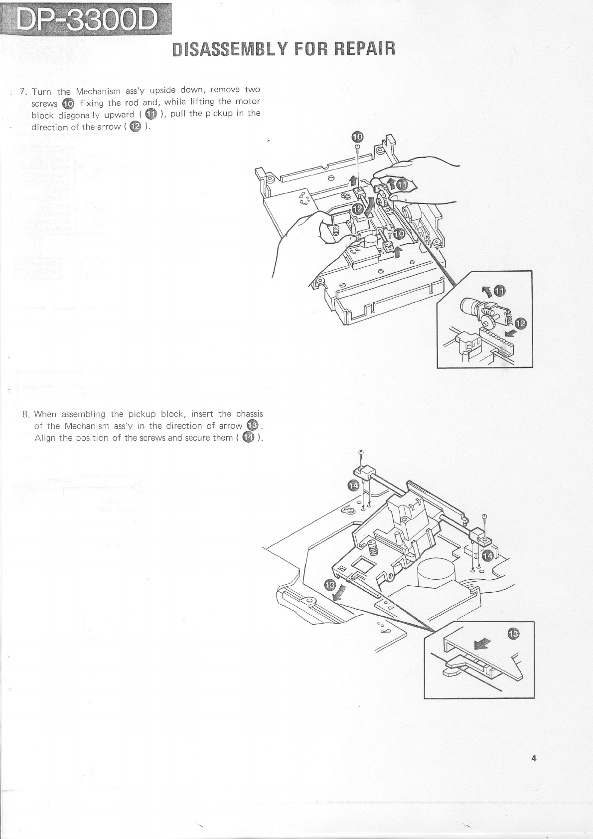
DISASSEMBLY
FOR REPAIR
7. Turn the Mechanism
ass'y
upside
down, remove
two
screws
@ tixing the rod
and,
while
lifting
the motor
block
diigonally
upward
((E )' pull
the
pickup
in the
direction of the
arrow
(
(D )
8. When assembling
the pickup
block,
insert the chassis
of the Mechanism ass'y
in the direction of arrow
@ .
Align the position
of the screws and secure them
( (E ).
BLOCK
DI
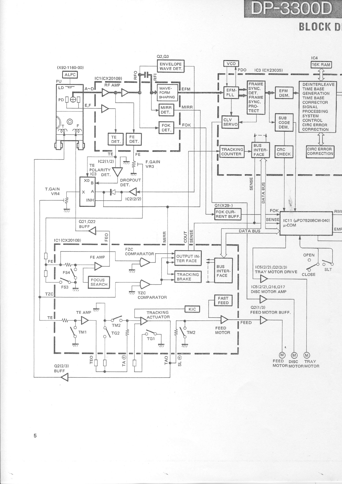
ENVELOPE
WAVE DET,
FFIAME
SYNC.
DET.
FRAME
SYNC.
PBO.
TECT
DEINTERLEAVE
TIME
BASE
GENERATION
TIME BASE
CORRECTOB
SIGNAL
PBOCESSING
SYSTEM
CONTROL
CIRC ERROR
CORRECTION
^\-
| 'r' I
| 'v7,
I
-l--
rl
ll F
BUS
INTER"
FACE
E- U
z
U
o
01
(x29-
)
tc1
(cx20108)
r-- OUTPUT IN.
TER FACE
TRACKING
BFIAKE
u-
rcl
(cx20109) (r
PDO tc3
(cx23035)
----
^_J-F-
tc5l2t2l,o2l3l3l
TBAY
MOTOR DRIVE
GC-
OPEN
CLOSE
NT
JLI
I
,rl
FEED
MOTOB I FEED
I
E_J
@
J
U' FEED DISC TRAY
MOTOR
MOTOR
MOTOR
OCK
OIAG
BAM
:1
TER LEAVE
OAJE
iRATION
BASE
iECTOR
qL
ESSING
EM
'FOL
ERHOR
ECTION
tcs,tc7,
tc9 f
c1 1,ol,o3 tc13l1l2l
tc7
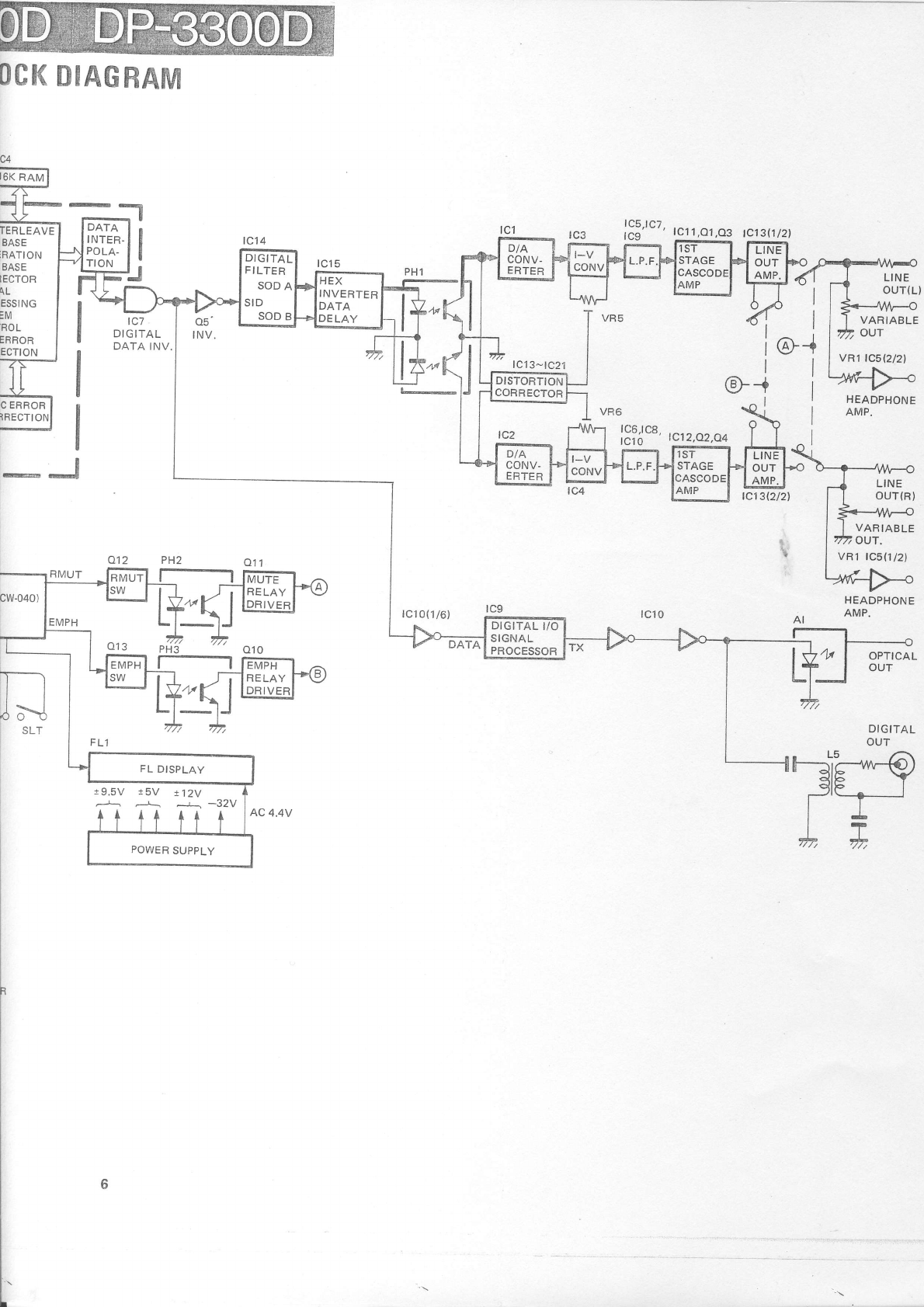
DIGITAL
DATA INV.
lc13-tc21
C
ERROR
IRECTI
HEADPHONE
AMP.
HEADPHONE
AMP.
DIGITAL
OUT
t--- -.,l'--'w.-6)
-AIBY
qtb I
r-Jl\---a____J
tl
l-
IT
,7v ,ln
tc6,tc8,
lc10 \c12,o2,A4
tcls(2121
ol 1
rc
l1-fllffiej-@
L I-'U
+rh
PH3 010
/v
rc10(1/6)
Q13
ti
t12V
--r- -32V
DATA
INTER.
POLA-
TION DIGITAL
FI
LTER
SOD
A
SID
LINE
OUT(R)
VARIABLE
OUT.
FL DISPLAY
CIRCUIT
DESCRIPTION
1. Description
of components
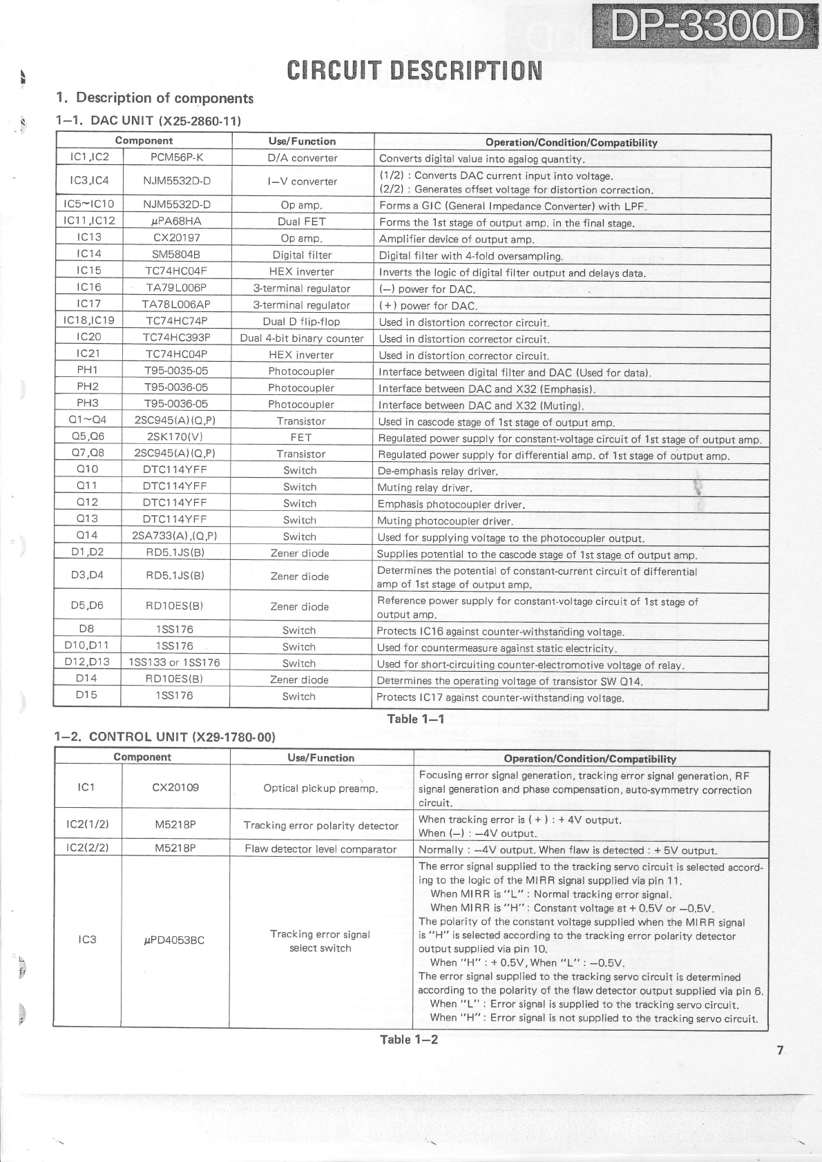
1-1. DAC UNIT
(x25-2860-11)
Component Use/Function Operation/Condition/Compatibility
lcl ,lc2 PCM56P.K D/A converter Converts digital
value
into agalog
quantity.
tc3,rc4 NJM5532D.D l-V converter 11/21
: Converts
DAC current
input into voltage.
(2121
: Generates
offset voltage {or distortion correction.
tc5-rc10 NJM5532D-D Op amp Forms
a GIC (General
lmpedance Converterl with LPF.
tc ,1c12 pPA6SHA Dual
FET Forms
the 1st
stage of output amp.
in the
final
stage.
LIJ cx20197 Op amp Amplifier device
of output amp,
a1A SM5804B Digital filter Digital filter with 4-fold oversampling.
L t3 TC74HCO4F HEX inverter Inverts
the logic
of digital filter output and delays
data.
Lto TA79LO06P 3-terminal reoulator (-) power
for DAC.
c't7 TATSLOO6AP 3-terminal regulator (
+
)
power
for
DAC.
tc 8,tc19 TC74HC74P Dual
D flip-flop Used in distortion corrector
circuit
tc20 TC74HC393P Dual 4-bit binary
counter Used in distortion
corrector circuit.
tc21 TC74HCO4P HEX inverler Used in
distortion
corrector circuit.
PH1 T95-0035-05 Photocoupler Interface
between digital filter and DAC (Used
for data).
PH2 T95-0036-05 Photocoupler Interface between
DAC and X32 (Emphasis).
PH3 T95-0036-05 Photocoupler Interface
between
DAC and X32 (Muting).
01
-o4 2SC945(A)(O,P) Transistor Used
in cascode
stage of 1
st stage
o.f
output amp.
05.06 25K170(V) FET Begulated
power
supply
for constant-voltage
circuit of ist stage
of output amp.
07,Q8 2SC945(A)(O.P) Tra
nsistor Regulated
power
supply
for differential
amp. of 1st
staqe of output amp.
01 0 DTCl
14YFF Switch De-emphasis
relav driver
Q1
1DTC] 14YFF Switch Muting relay driver. 'r
012 DTC1 14YFF Switch Emphasis
photocoupler
driver.
n1? DTC1 1
4YFF Switch Muting photocoupler
driver.
014 2SA733(A),(O,P) Switch Used for supplying voltage
to the
photocoupler
output.
D1
.D2 RD5,iJS{B) Zener
diode Supplies
potential to the cascode stage of lst stage of output amp
D3,D4 RD5.1JS(B) Zener
diode Determines
the
potential
of constant-current
circuit of differential
amp of 1
st staqe of output amp.
D5,D6 RDl
OES(B) Zener
diode Feference
power
supply
for constant-voltage
circuit of 1st
stage of
output amp.
D8 tSst/u Switch Protects I C 1
6 a
ga
i nst cou nte
r-withstan-d
i
ng vol
taqe.
D 10,D1 1 tsSt/t) Switch Used for countermeasure
against
static electricity.
D12.D13 iSS133
or 1SS176 Switch Used for short-circuiting
counter-electromotive
voltaqe
of relav.
ut4 RDl
OES(B} Zener
diode Determines
the operating voltage
of transistor
SW 014
Litc 1
SS1
76 Switch Protects
lC1
7 against counter-withstanding
voltage.
Table 1-1
l-,
a(
t:
t
ji
1-2. CONTBOL
UN|T
(X29-1780-00)
Component Use/Function Operatiory'Cond
ition/Compatibil
ity
tcl cx201 09 Optical
pickup preamp.
Focusing
error
signal
generation,
tracking error
signal
generation,
RF
signal
generation
and phase
compensation,
auto-symmetry correction
ci
rcu i t.
tc20/21 M5218P Tracking error
polarity detector When
tracking
error
is
(
+ ) :
+
4V output.
When
(-) :
-4V output.
tc2l2l2l M5218P Flaw
detector
level comparator Normally : -4V output. When flaw is
detected : + 5V output.
ILJ pPD4053BC Tracking error
signal
select switch
The error signal supplied to the tracking servo circuit is selected
accord-
ing to the logic
of the MIRR signal supplied
via
pin 11.
When
MIRR is
"L" : Normal
tracking error
signal.
When
MIRR is
"H" : Constant voltage
at + 0.5V or -0.5V.
The polarity of the constant voltage
supplied when the Ml R R signal
is "H" is selected according
to the tracking error polarity detector
output supplied via
pin 1O.
When
"H" : + 0.5V. When
"L" : -0.5V.
The error
signal supplied to the tracking
servo circuit is determined
according
to the polarity of the flaw detector output supplied via pin 6.
When
"L" : Error
signal is
supplied to the tracking
servo circuit.
When
"H": Error
signal is not supplied
to the
tracking
servo
circuit.
Table 1-2 7
1-3. CD
PLAYER
UNIT
(X32'1090'11)
CIRCUIT
DESCRIPTION
012\
: PLL
compensator
circuit
l2l2l : CLY
compensator
circuit
Generates
search
pulses
for focusing servo,
tracking servo
and feed m
servo.
Generates
microprocessor reset
pulse.
EFM decoder,
correction/intetpolut!9n
citcuit, PLL cit'
Signal
processor
RAM (16K).
(LPF
+
amP.1.
(LPF + level
shifter).
11l2J
: CLV
compensator
silsui{
(amp.)'
l2l2l : TraY
driver
circuit
Digital
data
inverter
circuit.
Controls
digital
signal
supply
to DAc'
Converts
digital
audio
data
into Sony/Philips
digital l/O foimat to g'
transmission
signal
lC9
demodulation amp,
pulse
transformer
driver'
Controls
disPlaY,
key-inPut and
servo
lC.
Interface
circuit
between
microprocessor
9!ql! if:919y
+ 5V
resulated
voltase
for a449lel9-!!!-!i!91
-5V requlated
voltage
for digital
and
PLL lines'
+ 5V regula'ted
voltage
for servo
line.
Error
amp
oI x12V constant regulated
circuit
for DAC'
Digital
data
inverter
circuit
For loqic
inversion
usi -disital
SW.
Current
buffer for tracking
actuator,
feed
motor and
tray motor
or
ci
rcu
itrv.
Used
to prevent operation of eye-pattern center sampling
circuit w
the
disc
motor is
not driven'
inversion
and
level
shifting
of MON
ortp,4-|1on'
9I?9991
lnverts
digital
data
at high speed
and
amplifies
the current'
Discharges
-5V DAC
unit
to 0V.
Supplies
-5V to DAC
unit
An
emitter-follower
used
for
supplying
+
5V
to DAC
unit'
Controts
SWs
Q6
and
07
Controls potential at base
of Q8'
Eliminates
offset
of motor
driver
circuit
while
me19!l1l99q9d'
Turns
-5V for laser ON/OFF
Power
supply in the constant-voltage
regulated
laser
power supply
Gomponenl Use/Function Operation/Condition/Compatibility
Goes
"H" when
a signal
is
output from the pickup'
Detects
the
+ side
envelope
of RF signal.
(Small
time constant)
Detects
the + side
envelope
of RF signal.
(Large
time constant)
When lC2l2l2l output becomes
-4V, the switches
function to
vent the negative
potential to be applied to pin 6 of lC3'
When lC2ll/21 output becomes
-4V, the switches
function to
vent the negative
potential to be applied
to pin 10 of lC3'
When the flaw detector level
goes
"H" by detecting a flaw, the
turns
the
MIBR signal
also
"H".
atl 25C945(A)(o,P) FOK
current
buffer
a2 2SC945(A)(o,P) RF siqnal
enveloPed
detector
o3 2Sc945(A)(o,P) RF siqnal
enveloped
deteclor
Dl ,D2 1SS176
or
1SS131 Switch
D3,D4 1SS176
or
'l
SS131 Switch
D5 1SS176
or
1SS131 Switch
Table
1-2
M51
951 ASL
cxK581
6M
TCT4HCOOP
AND gate
(switch)
TC74HC08P
Digital
output signal
modulator lC
cxDl
075P
withstanding
buff.
rc12-lC'l
5
3-terminal
3-terminal
regulator
TC74HC74P
Current
amPl
if ier
transistor
STA341
M
Di
gital
transistor
switch
Dioital
transistor
switch
DTA1
24EN
2SC1923(R,O)
2SA733(A)(O,P)
2SC945(A),(O,P)
2SA992(F,E )
2SC1845(E,F
)
25 K246(Y,G
R
)
2SA733(A)(O,P)
25K246(Y,G
R
)
Table
1-3
($
rs
CIRCUIT
BESCHIPTION
Component Use/Function Operation/Condition/Compatibility
o14 2SC945(A)(O.P) Ripple
filter Transistor
ripple
filter
for constant-voltage
regulated
VDD supply circuit
for FLdrivers
lCs
(lC12to
lClb).
ut3 2SA1
286 Ripple filter Transistor
ripple filter
for constant-voltage
laser
power
supply
circuit.
Cl z>L5240 Current
buffer Current
buffer
for
disc
motor driver
circuit.
72SA1286 Current
buffer Current
buffer
for
disc
motor
driver circuit.
o25C945(A)(O,P) Switch Inverts
the logic
of pre-digital
SW.
019 2SA733(A)(O,P) Switch Connects
rhe low muting
potential
in DAC unit to GND.
o20 2SC945(A)(O,P) Switch Control
SW
used
to set
r12V regulated
DAC
unit
power
to tOV.
421 2S,A1286 Current buffer Current
buffer
for focus
actuator
driver
circuit.
422 2SD1
266 Current
buffer Current
buffer
for focus
actuator
driver
circuit-
o23 z>u I
zoo Bipple
filter Transistor
ripple
filter for
+ 12V regulated
DAC
unit
powersupply
circuit.
o24 258941
(P) Ripple
filter Transistor
ripple filter
lor
-12V regulated
DAC unit
power
supply circuit
D,I rJJt/o Switch Preiigital SW.
D2 1
SS1 76 Switch Diode
SW used for key
scanning
in test mode.
D3 1
SSl 76 Switch Time-constant
SW
for quick discharge
ot C4E.
D4 1
SS1 76 Switch Used
to prevent
variation
of MUTE and EMpH digital
audio
data
during
searching,
etc.
D5 RD6.8ES(82) Zener
diode Provides
reference
potential for constant-voltage
regutated
V6p supply
circuit
for FL
driver
lCs
(1C12
to lC15).
D6,D7 DSM1A1 Rectif
ier diodes Used
for voltage
multiplyinS
rectifier.
D8 RD8.2ES(B) Zener
diode Used to maintain FL dispay erase
potential
no 1
SS1 76 Switch Diode
SW used
to interrupt
optical
output
while
the
digital
output
sw is oFF.
OFF.
Dl0 BD2.7ES(B} Switch Used
to
decrease
r12V DAC
power
quickly
when
power
is turned
OFF.
Dl1 RD6.2JS(82) Zener
diode Provides
reference
potential
for r1
2V regulated
DAC power
supply
circuit.
Dl
2-Di
5rJJ | /O Switch Diode
SW used for countermeasure
against
static
electricity
in digital
output.
D1
6.D17 1
SS1
76 Switch Qiode
used for countermeasure
against
static electricity.
D1
8-D20 1
SS1 76 Switch Diode
SW
connected
to limir SW.
D21 RD5.6ES(82) Zener
diode Provides
reference
potential for -5V laser
oower.
D22 1B4841 Bectif
ier diode fiectifier diode
bridge
for servo
and
digital
lines.
D23 1B4B'41 Fectifier
diode Rectifier
diode
bridge
for DAC line.
D24 1
SV1 47 Vari-cap Vari-cap
in VCO circuit of PLL.
Table 1-3
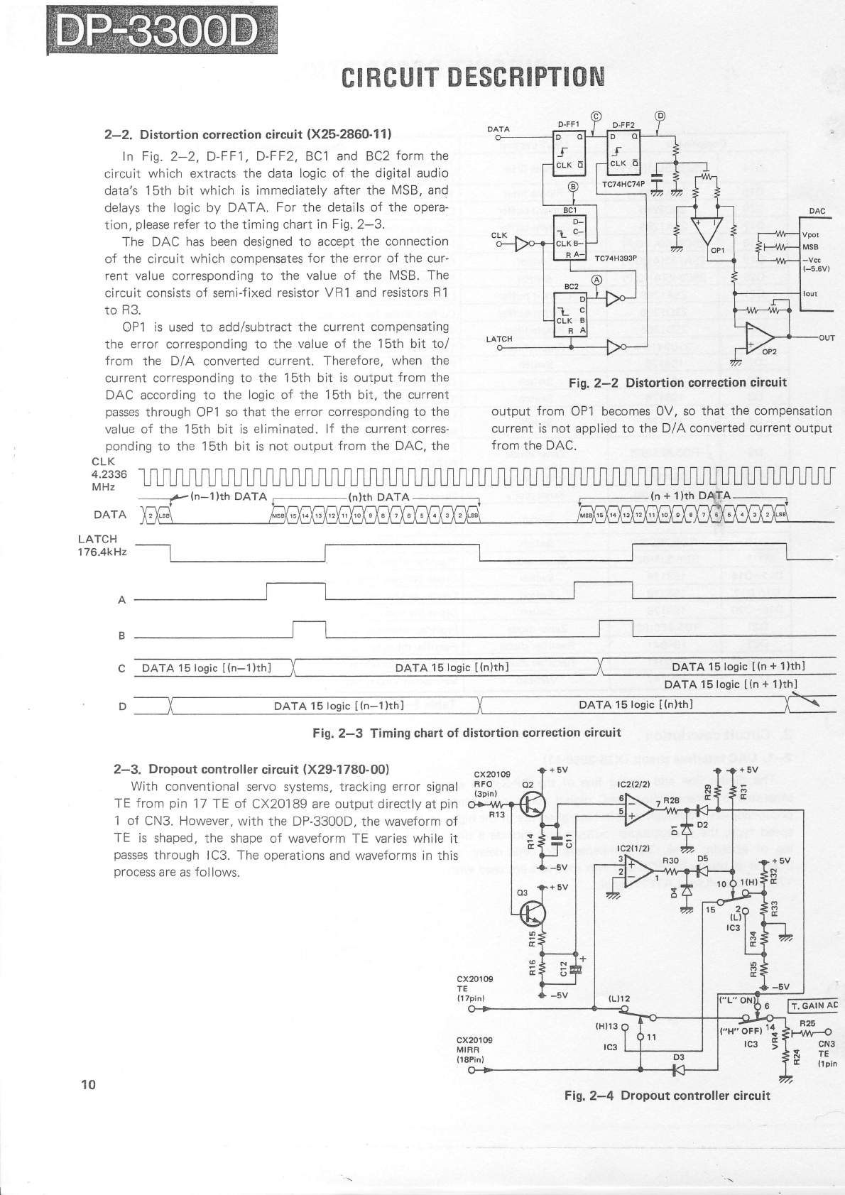
2. Circuit
description
2-1. DAC
Interface
circuit
(X25-2860-11)
The digital
line
and
analog
line
of the Dp-3300D
are
separated
by transmitting
DAC digital
audio
data
using
photocouplers.
Although
the
photocouplers
are
of the high_
speed
type,
the photocoupler
outputs
stili
include
a time
lag of approx.
20ns.
To compensate
for this delay,
an
inverter
is used
with BCK
and
two inverters
are
used
with
176.5kH2
used for LATCH
signal.
tc14
(Digital
filter)
DAC
to DATA (Lch}
DAC
to DATA (Rch)
DAC
tO BCK
DAC
to LATCH
Ftu
FIJ'
r;
$Bi
;v
T
Fig.2-1 DAC
Interface
circuit
CIRCUIT
DESCRIPTION
2-2. Distortion correction
circuit
(X25-2860-11)
In Fig.
2-2, D-FF1,
D-FF2,
BC1
and BC2
form the
circuit which extracts the data logic
of the digital audio
data's
1sth bit which is immediately
after
the MSB, and
delays the logic
by DATA. For the details of the opera-
tion,
please
refer to the timing
chart in Fig.2-3.
The DAC has been designed to accept the connection
of the circuit which compensates
for the error
of the cur-
rent value corresponding to the value
of the MSB. The
circuit
consists
of semi-fixed
resistor VR1 and
resistors R1
to R3.
OP1 is used to add/subtract
the current compensating
the error
corresponding to the
value
of the 15th Oit to/
from the D/A converted
current. Therefore,
when the
current corresponding to the 1 sth bit is output
from the
DAC according to the logic
of the 15th bit, the current
passes
through OPi so that the error corresponding to the
value of the 1sth bit is
eliminated. lf the current corres-
ponding
to the 1sth bit is
not output
from
the
DAC,
the
Fig. 2-2 Distortion correction
circuit
output from OP1 becomes
0V, so that the compensation
current is not applied to the
D/A converted
current output
from
the DAC.
CLK
4.2336
MHz
DATA
LATCH
176.4kH2
(n-1)th DATA {n)th
DATA
C DATA
15 losic
[(n-1]thl DATA
15 logic
[(n
+
1)th]
D X DATA
1slosic
t(n-1
)thl X DATA
15 tosic
[(n]thl I \
Fig. 2-3 Timing
chart of distortion
coruection
circuit
2-3. Dropout controller
circuit
(X29-1780-00)
With conventional
servo systems, tracking
error
signal
TE
from
pin 17
TE of CX2O'I
89
are output directlyat
pin
i of CN3. However,
with the DP-3300D,
the waveform of
TE is shaped,
the shape of waveform
TE varies while it
passes
through lC3. The operations
and waveforms in this
process
are as
follows.
DATA
15
logic
[(n
+
1)th]
n;r fE
rcgl f
@
IE
Fig.
2-4 Dropout
controller circuit
10
is
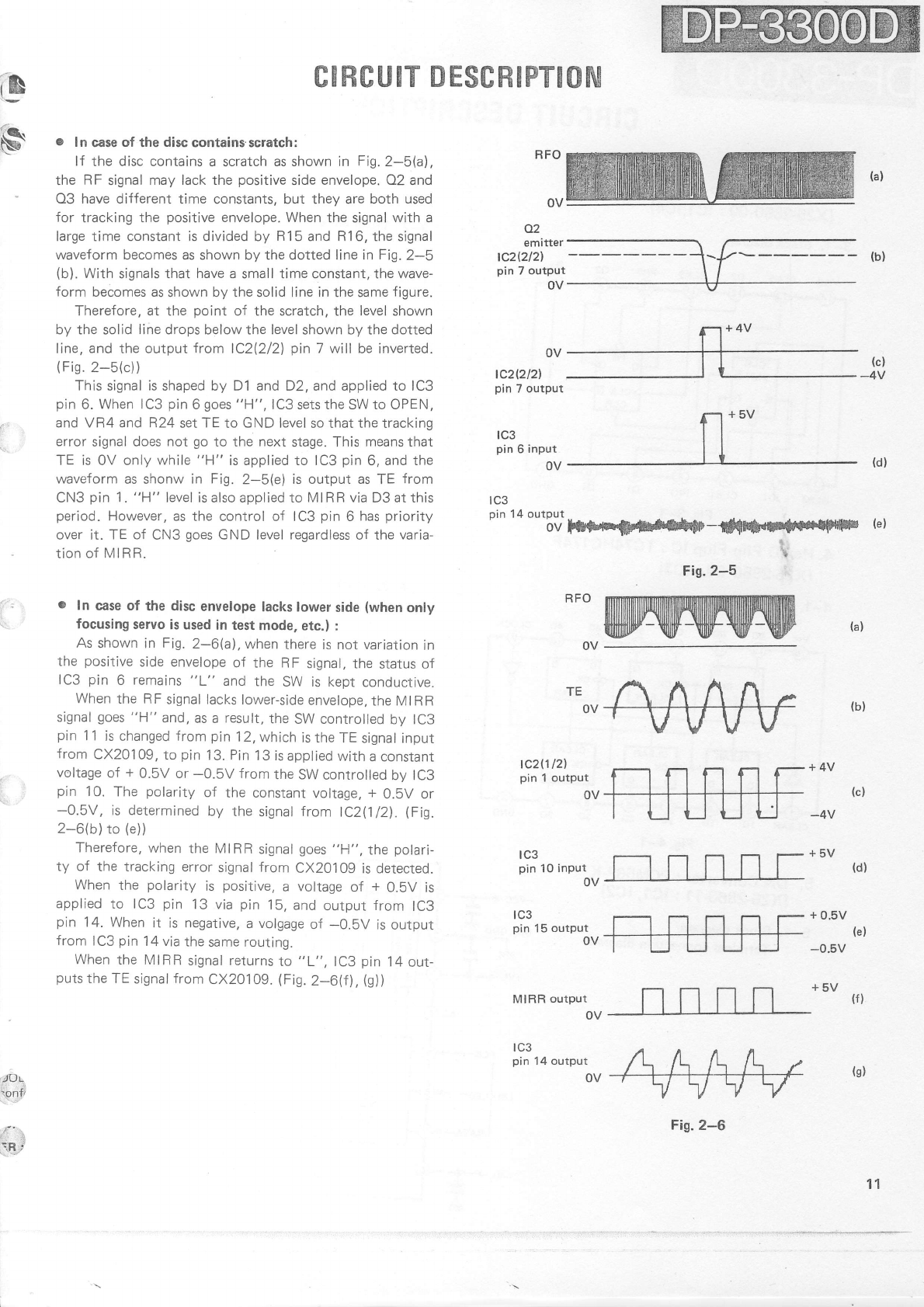
$o In case
of the disc
contains scratch:
lf the disc contains a scratch
as shown in Fig.2-5(al
,
the RF
signal
may lack the
positive
side
envelope. 02 and
03 have different
time constants, but they are both used
for tracking
the positive
envelope. When
the signal
with a
large time constant is divided by R15
and R16, the signal
waveform becomes as shown by the dotted line
in Fig.
2-5
(b).
With signals that have
a small time constant, the wave-
form becomes as
shown by the solid line
in
the same
figure.
Therefore,
at the point of the scratch. the level shown
by the solid
line
drops below the level
shown
by the dotted
line,
and
the output
trom lC2(212)
pin
7 will be inverted.
(Fig.2-5(c))
This signal
is
shaped by D1 and D2, and applied to lC3
pin
6.
When lC3
pin
6
goes
"H", lC3 sets the SW to OPEN,
and VR4 and R24
set
TE
to GND level so that the tracking
error
signal
does not go
to the next
stage.
This means that
TE is 0V only
while
"H" is applied to lC3
pin
6, and the
waveform as shonw in Fig. 2-5(e) is output as
TE from
CN3
pin
1
.
"H" level
is
also applied to MIRR
via
D3 at this
period.
However, as the control of lC3
pin
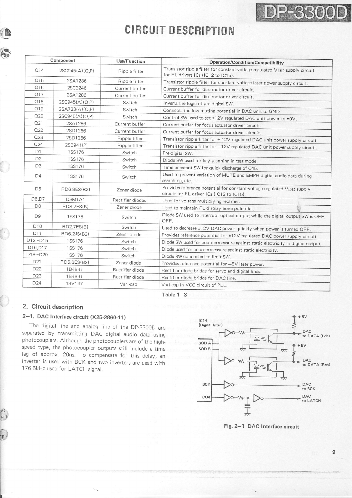
6 has
priority
over it. TE of CN3
goes
GND level
regardless
of the varia-
tion of MIRR.
o In case of the disc
envelope
lacks
lower
side
(when
only
focusing
servo
is used
in test
mode,
etc.) :
As
shown in Fig.
2-6(a),
when
there
is not variation
in
the positive
side envelope
of the RF signal,
the status of
lC3 pin 6 remains
"L" and
the SW is kept
conductive.
When
the RF
signal
lacks lower-side
envelope,
the MIRR
signal
goes
"H" and,
as a result,
the
SW controlled
by lC3
pin
11
is changed from
pin
'l
2,
which
is the
TE
signal
input
from
CX20109,
to pin
13. Pin
13 is
applied
with
a constant
voltage
of + 0.5V or -0.5V from
the SW
controlled
by lC3
pin 10. The polarity
of the constant
voltage,
+ 0.5V or
-0.5V, is determined
by the signal from lC2(112ir.
(Fig.
2-6(b)
to (e))
Therefore,
when
the MIRR
signal
goes
"H", the
polari-
ty of the tracking error
signal
from CX20l09 is detected.
When
the polarity
is positive,
a voltage
of + 0.bV is
applied
to lC3
pin 13 via
pin
15,
and
output from lC3
pin 14. When
it is
negative,
a volgage
of -0.5V is
output
from
lC3
pin
14 via
the
same routing.
When
the MIRR
signal rerurns
Lo
"L",lC3 pin
I4 out-
puts
the TE
signalfrom
CX20109.
(Fig.
2-6(f),
(S))
C!RCUIT
DESCRIPTICIIU
RFO
OV
o2
emitter
tc2l2l2l
pin 7 output
OV
OV
tc212l2l
pin
7 output
RFO
OV
tc2l1l2l
pin
'l
output
OV
{-l +5v
tc3 ll
pinoinput I I (d)
lc3
pin
14 output
.
' bv
FnHrt*.1*F-{fift}.|r{ilrttlF (e}
?
I
Fis.2-5
(b)
(c)
-4V
(a)
(b)
+4V
(c)
-4V
(s)
F,,
ie-nJ,
","n/v\Y
lC3 t- =
5V
pin
10
input I I (d)
OVa
lC3 t- +
0.5V
Pin
15
outPutu
ffi -o.uu
t"'
MrRRoutput n n n n +5v (rl
l?nt,oou,ou,
A f- tl- /l- /
ovm
:{-;
Fis.
2-6
11
CIRCUIT
DESCRIPTION
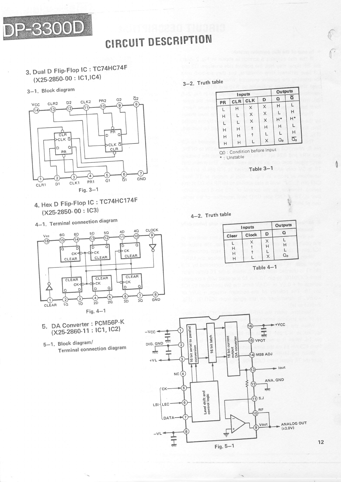
3.
Duaf
D FliP-FloP
lC:TC74HC74F
(X25-2850-
O0
: lC1'lC4)
d:
\l
4'
\i
3-2. Truth table
4-2. Truth table
Table
3-1
CLR1 Dl CLKT
Fig'
3-1
4.
Hex
D FliP-FloP
lC
:
TC74HC174F
lX25-285O-00:
lG3)
CLEAR 10 ru
Fis'
4-1
5. DA Converter
: PCM56P-K
"' ifisl-iebo-rr
:
lc1,lcz)
5-1 . Block
diagram/
Terminal
connection
diagram
\.
ANALOG OUT
(r3.0vl
3-1. Block
diagram
CLK1 PRl
Fis.
3-1
L
H
H+
L
H
G
O0 : Condition before
inPut
4-1 . Terminal
connection
diagram
vcc 60 6-D P X
Table
4-1
cK-
LEC'
(OAT
Fis.
5-1 12
r3
s^
cf
RculT
0EscRtPTt0tu
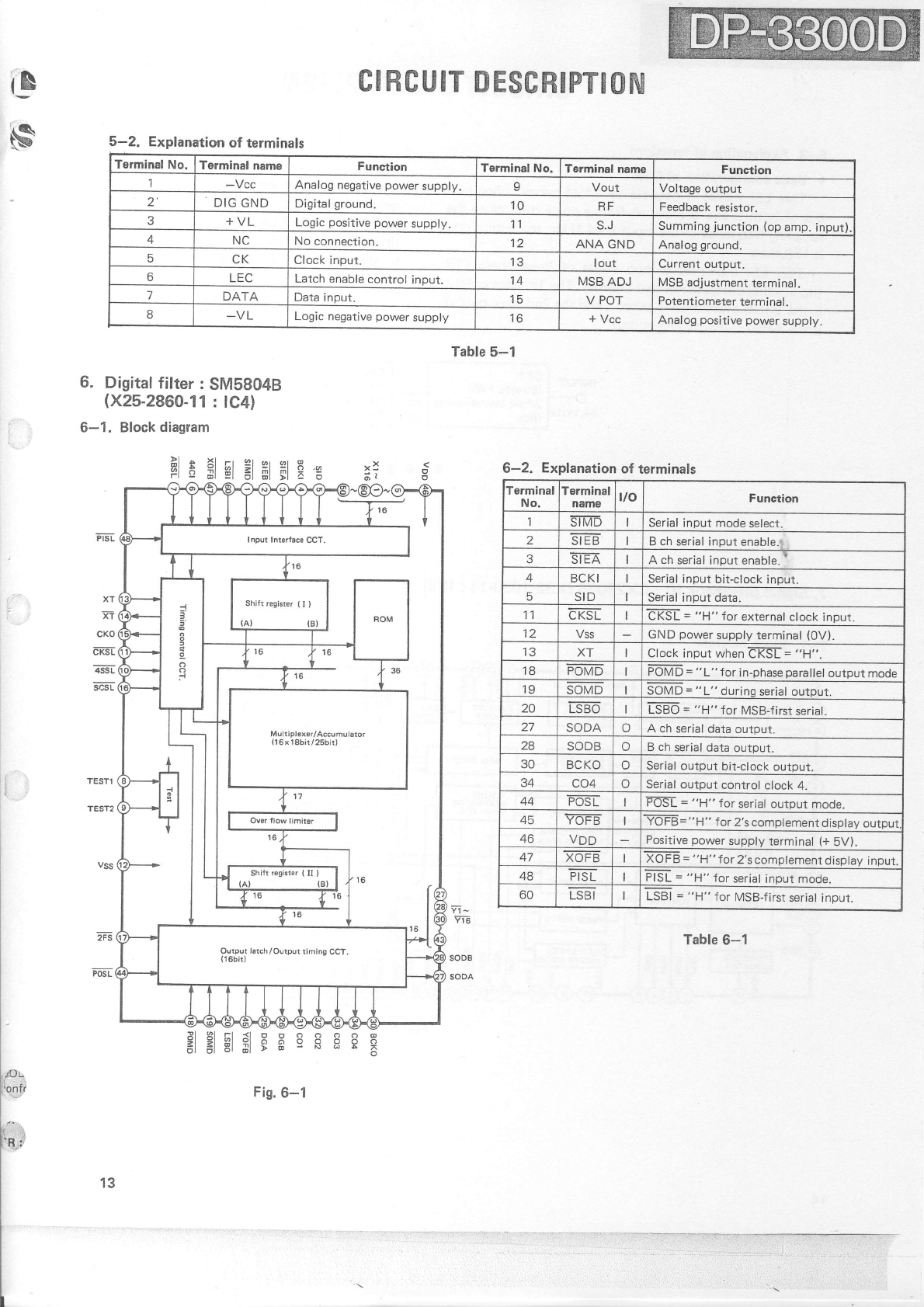
6. Digital
filter
: SMS804B
(X25-2860-11
: lC4)
6-1. Block
diagram
xI
XT
;-T
cKo
CKSL
lssf
scsL
Table 6-1
glElglflrac
oOO@
oooo
No5x
"0L
iq.nf
tii':::
'B;:t
5-2. Explanation
of terminals
Terminal
No. Terminal
name Function Terminal No. Terminal
name Function
1-Vcc Analog negative
power
supply. IVout Voltage
output
2' DIG
GND Digital
ground. 10 HF Feedback
resistor.
+VL Logic
positive
power
supply. tl el Summing
junction
(op
amp.
input)
NC No connection. 12 ANA GND Analog
ground.
CK Clock input. IJ I out Current
output.
6LEC Latch enable
control inout. l4 MSB
ADJ MSB
adjustment
terminal.
DATA Data input. tc V POT Potentiometer terminal.
ILogic negative
power supply to * Vcc Analog
positive
power
supply.
Table
5-1
FlESletBlfitfitEc
Mu!tiplexer/Accumulator
{16x18bit/25bitl
Outpur lslch/Output timin€ CCT.
6-2. Explanation
of terminals
Terminal
No. rerminal
name alo Function
S-two Serial
input mode
select.
SI
EB B ch serial inout enable.r
siEa ,A ch
serial input enable.'
ABCKI ISerial
input bit-clock
input.
5SID ISerial input data
11 CKSL IERSI = "H" for external
clock
inout.
12 Vss GND
power
supply
terminal
(0V).
XT Clock input
when
e KSf = "H"
18 POMD POMD
=
"L" for in-phase
parallel
output mode
19 SOMD SOMD
=
"
L" during
serial
output.
tn LSBO
27 SODA oA ch serial
data outout.
28 SODB oB ch
serial
data
output.
30 BCKO oSerial
output bit-clock
outpur.
co4 OSerial
output control clock
4.
44 FdST FOS-L
= "H" for serial outpur
mooe.
45 YOFB TOFB="U" for
2's comptement
display
outpur
46 VDD Positive
power
supply
terminal (+
5V).
47 XOFB XOFB
=
"H" for
2's complement
display
input.
48 PISL IPISL
= "H" for serial
input mode.
60 LSBI ILSBI
= "H" for MSB-first
serial input.
13
Fis.6-1
6-3. Explanation
of functions
o Basic
configuration
of filter
This LSI makes
it possible
to 4-fold
oversampling
out-
put of both L and R channels
from a single
chip'
When
the
sampling
frequency
of the
input
is
44'1kHz,
the
output
rate
is
176.4kH2.
This LSI incorporates
two stages
of linear-phase
FIR
(non-cyclic) filters
connected
in series'
The
1st
stage
output
isthe2-foldoversamplingoutput,andthe2ndstageoutput
is
the
4-fold
oversampling
output'
CIRCUIT
DESCRIPTION
Fig.6-2
Fig.
7-1
Fig. 6-2 shows
the simplified diagram
of filter
configu-
ration.
The lst stage
filter (DFl) is an 8O-step
FIR type
filter,
and.the
2nd
stage
filter (DF2)
is
a 15-step
FIR
type
filter. Both filters
have
the.2-fold
oversampling
function,
so that a total of 4-fold oversampling
output can be ob-
tained.
OUTPUT
176.4kH2
(4-fold
over-
sampling)
7. Signal
processorlC: CX23035
(X32-1090-11 : lC3)
7-1. Block
diagram
Eg s
99I
;NF
I' s
-t
=o
aa
o6
t003uu'
lSUEuoo
eo9
383,
ERROR DET.
€RROR
CORRECTION
EEEHa
RHgFHsBEEaE
14
CIRCIJIT
DESCRIPITOru
\.
)7-2. Explanation
of terminals
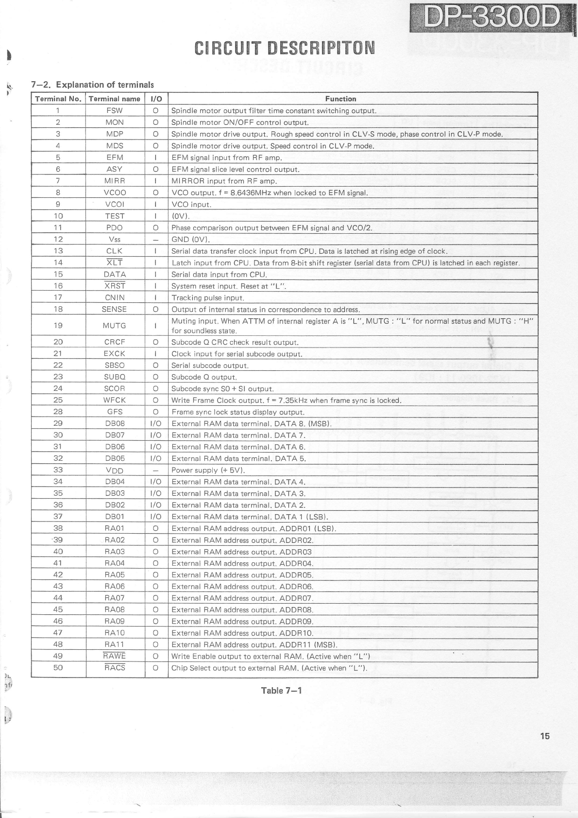
Terminal No. Terminal name vo Function
1FSW oSpindle
motor output filter time constant switching output.
2MON oSpindle motor ON/OFF control output.
?MDP oSpindle motor drive output. Rough
speed
control in CLV-S
mode,
phase
control in CLV-P mode
4MDS oSpindle motor drive output. Speed
control in CLV-P
mode.
5EFM EFM
signal input from RF amp.
6ASY oEFM signal
slice
level control output.
7MI
RR IMIBROR
input
from RF amp.
8vcoo oVCO output. f = 8.6436MH2 when locked to EFM sional.
vcol VCO
input.
10 TEST tov).
11 PDO oPhase
comparison outpu't between
EFM signal
andVCO12.
12 Vss GND
(OV)
tc CLK Serial
data
transfer clock input from CPU. Data
is latched at rising
edge
of clock.
14 V'T Latch input from CPU. Data from B-bit shift register
(serial
data
from CPU) is latched in
each
register.
15 DATA Serial
data input from CPU.
to XRST System
reset input. Feset at "L"
CNIN Tracking
pulse
input.
i8 SENSE oOutput of internal status in correspondence
to address,
19 MUTG Muting input. When
ATTM of internal register A is
"L", MUTG : "L" Ior normal
status
and
MUTG : "H"
for soundless state.
20 CRCF oSubcode
O CRC check
result output
t1 EXCK Clock input for serial subcode output.
zz SBSO oSerial subcode output.
23 SUBQ oSubcode Q output.
SCOR oSubcode sync
SO
+ Sl output.
25 WFCK oWrite Frame
Clock output. f = 7.35kHz when
frame
sync
is locked.
28 GFS oFrame
sync
lock
status display output.
29 DBOS tlo External FAM data
terminal. DATA 8. (MSB).
30 DBOT /o Exlernal
FAM data
terminal. DATA 7.
5t DB06 t/o External
BAM data
terminal. DATA 6.
5Z DBOS /o Exlernal
FAM data terminal.
DATA 5.
33 VDD Power
supplV
(+
5V).
34 DB04 t/o External RAM
data
terminal. DATA 4.
35 DBO3 tlo External
RAM data
terminal. DATA 3.
JO DB02 t/o External RAM data terminal. DATA 2.
37 DBOl tlo External RAM
data terminal. DATA 1 (LSB).
38 RAOl oExternal
FAM address
output. ADDROl (LSB).
'39 FA02 nExternal RAM address
output. ADDR02.
40 RAO3 oExternal
RAM
address output. ADDR03
41 RA04 oExternal FAM address output. ADDR04.
4Z RAOS oExternal
FAM address
output. ADDR05.
FAO6 oExternal RAM address output. ADDR06.
44 RAOT oExternal RAM address output. ADDR07,
FAOS OExternal RAM address
output. ADDR08.
46 BAO9 oExternal
BAM address
output. ADDR09.
47 RA1
OoExternal RAM address
output. ADDF10.
48 FlA I I oExternal RAM address output. ADDR1l (MSB).
49 RAWE oWrite Enable
output to external RAM. (Active
when "L")
50 BACS oChip
Select output to external
RAM. (Active
when "L")
Table 7-1
)L
1Tl
t-
r ;';
15
:
f*ut ilffiid"o outP" t =
+'23gonllHt'
GND
(OV). - -
I'.JlIiiu,* inp"'
+
=
e'aoz2MH'' ', ,
c
r*.
" * "\"d"yJ,
-!-,1
*T: r:
::i
ii
li
;::i:;
iffiilH::;
Terminal No. Terminal name l/o
51 c4M
52 Vss
53 XTA
56 c2PO o
58 SLOB IAudio
9ata
o"lp'] !"]i^ r,:;;i:;;i;;i;;; ;;t;;
;;;;;;i;i o* "*,
"*" to'
parutt"' ou*out'
59 A!1i:
oala
oi:P:;Uf' " 1=
"1"
Power
suPPlY
(+
5V)' ffiI.tout when
PSSL
= "L"
70 DA09 n
VDD
-14 DA12 oDA12 outPu NtrNIP rt when PSSL
-
75 DA13 o
76 DA14 n
7A DA1
6oDA16
outpur
80 LRCK o44.1kt12 strooe srgl
CIBCUIT
DESCRIPTION
Table
7-1
Notes) PLCK : YCOt2output' t = 4'3218w{zwhen locked
with EFM signal'
DENL : L CH serial
data
enable
signal'
DENR : R CH serial
data
enable
signat'
8.
Digital
output
signal
demodulator
lC : CXD1075P
(X32-1090-11
: lC9)
8-1 . Block
diagram
o
flcsse
C21O: lnverted
dZT-0
o'tPut'
Tzro , Bit
clock
output'
f =
2'116BMHz'
DATA : Audio
signal
serial
data
outpur'
t
9x
ii
-f
8-2. Terminal
connection
diagram
BCK
DATA
LRCK
VRDTY
cl0
CFCF
vss
CKSL
EXCK
D1
02
D3
D4
D5
D6
VDD
D7
LSFT
XILR
INVB
I92FS
XTAL
EXTAL
CBSL
RSET
TEST
c9
TX
Fig.8-2
?I
241
231
221
21
20
19
18
17
't6
15
t
2
4
o
6
9
10
I
111
I
112
| 13
lra
16
Fig.
8-1
!
\
p
8-4. Explanation
of functions
o Selector
pins
For increased
freedom in the selection of the signal
processor
LSI
lC,
the
digital
output
signal demodulator lC
is
equipped with various
selectors that can
select
the inter-
nal
functions
according
to the
signal
processor
LSI
lC used.
TEST
(pin'i
7) :
Test mode setting
input.
Fixed
at
"L".
RSET
(pin
18)
:When
TEST is
"L", the signal
demo-
CIRCIUT
DESCRIPTION
Table 8-2
LSI lC are
set
by
the
"H" and stops
when it is
"L". When
the
LSI is not
operating, only
192Fs is
output norrnally
while other outputs
are
fixed.
The following five pins
are the selector
pins
which sets
the
signal
processor
LSI
lC.
)u
eTt
l: The modes
of the signal
processor
above
methods.
8-3. Explanation
of terminals
Terminal
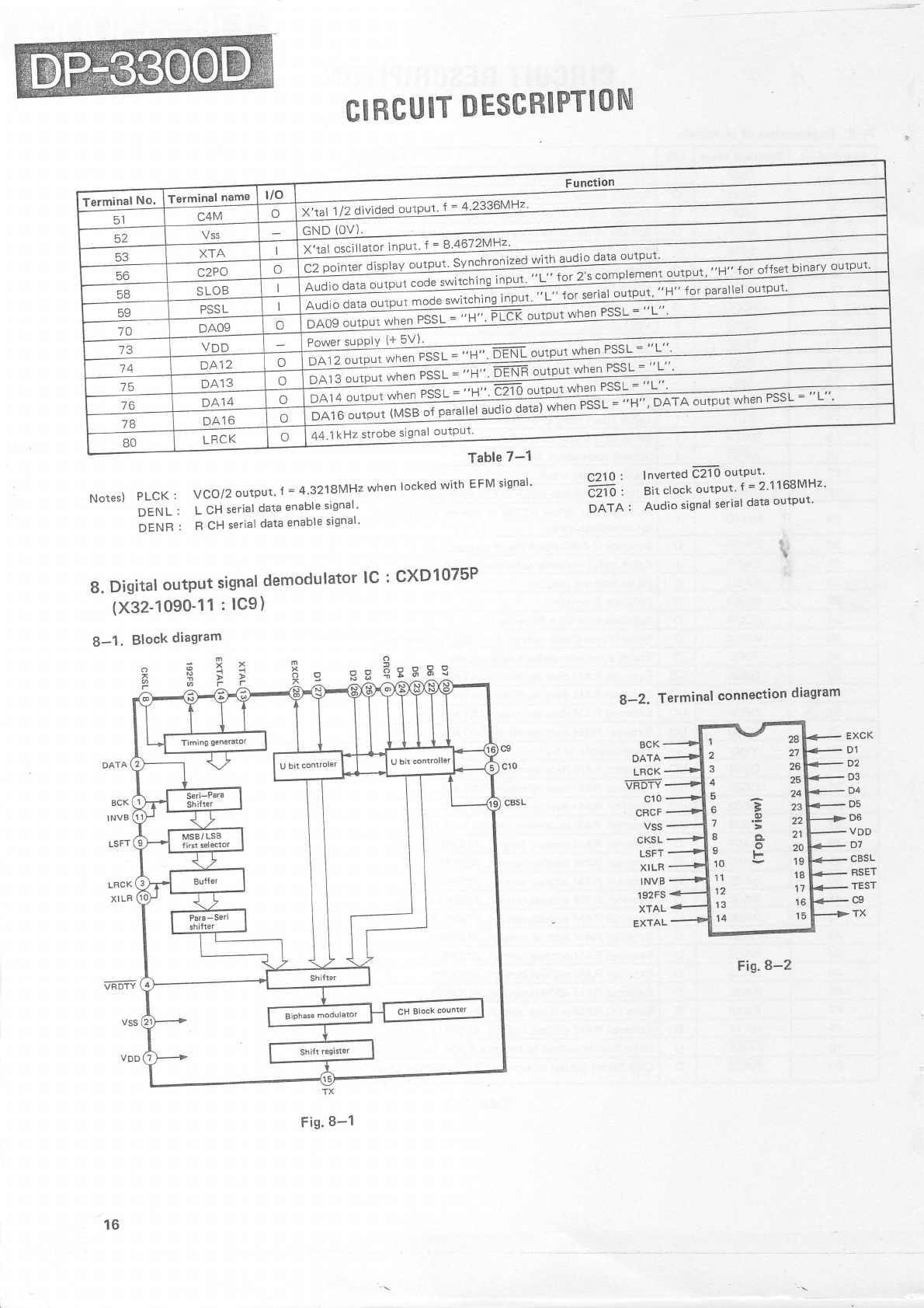
No. Symbol vo Function
BCK IBit clock input. Connect
the clock
which shifts
out data
in the external digital audio data output circuit.
DATA Digital audio data input (NRZ).
LFICK IClock input for L/R channel identification of digital audio data input.
The frequency
is
equal
to Fs
(sampling
frequency).
4VRDTY IValidity flag input. "H" flaq is used when the
data
is
being
processed
by interpolation,
etc.
5cl0 IC-bit category code C1 0 presetting
input.
6LNUT IC-bit
block
start
sync input. When
CX23035 is
used, connected this terminal
to the CBCF output
(pin
12),
I
n
other cases, the siqnal is fixed at
"H".
7Vss GND.
8CKSL Input for
selecting if the reference clock
is
EXTAL or its 1/3.
YLSFT Input for selecting between LSB firsr
and MSB
first operation.
10 XI
LR lnput for selecting between LRCK "H" and
"L"
11 INVB lnput for selecting if BCK timing used
is the rise or fall
12 ts,zrs UClock output for use as
CD master clock
when CD is connected.
The frequency
is
192
times the sampling frequency.
IJ XTAL oWhen
a X'tal oscillator is used. it is
connected acrossthis
pin and EXTAL (pin 14)
14 EXTAL When
a X'tal oscillator
is
used, it is connected
across this
pin and XTAL (pin 13). In other cases, this pin
is used for external
clock input.
15 TX oOutput of transmission data converted
into the digital interface
format.
to C-bit
category
code C9 presetting
input.
ItrJt Test
mode
select inDut.
Fixed
at "L" in normal operation.
't
8RSET LSI operation
start/stop input. "H" during operation
IY CBSL Input for selecting if the C-bit
input is serial
or parallel.
20 D7 C4 {Emphasis
information) presettinq
input when C-bit
input is
parallel.
21 VDD +
5V.
22 UO IC3
(Copy
Inhibit information)
presettinq
input when C-bit input is
parallel.
ZJ D5 C2 (lD1)
presetting
input when
C-bit input
is
parallel.
.A D4 IC1 (lD0) presetting
input when C-bit input is
parallel.
When it is
serial, used as
SUBO input which pro-
vides
C1 to C4.
25 ISCOR input which indicates the start of subcode block to be included in U-bit
data.
26 D2 WFCK input which indicates the frame of subcode
to be
included
in U-bit data.
27 D1 Serial
input for subcode
to be
included
in U-bit data.
(Connected
to SBSO).
28 EXCK Clock output to be supplied to the external subcode output cirucit in order to shift
subcode out.
{Connect
EXCK).
Table
8-1
dulator
tsl lC operates when RSET
is
Terminal No, Symbol Doscription
ICKSL Fixed
at "H" when EXTAL input is 384Fs,
"L" when it is 128 Fs
LSFT Fixed
at "H" when DATA input is MSB
first,
and
"L" when it is LSB
first.
10 XI
LB Fixed at "L" when
LBCK input is L-ch and
"H"."H" when
it is
"L"
11 INVB Fixed
at "L" when DATA is shifted at the falling edge of BCK,
"H" when it is shifted at the risinq edqe.
IY CBSL Fixed
at "L" when C-bit input is serial,
"H" when it is
parallel.
17
CIRCUIT
DESCRIPTION
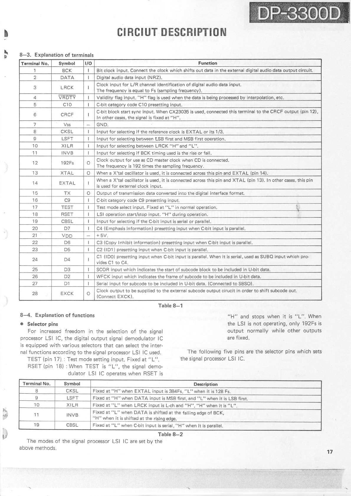
o Input signal
description
(ex,
CX23035)
1) Digiul audio
data
This LSI uses
16-bit
serial
digital
audio
data'
and
the
data bits are arranged
from backward
with respect
to
LRCK.
As
the period
of clock
BCK
is
equal
to the data
bit rate,
more
than 16 clocks
are
required
for each
word'
For example,
when
the signal
processor LSI
connected
is
CX23035,
which
is
a CD
signal
processor, LRCK
is
"H"
during
the L-ch
audio
data
and
"L" during
the
R-ch
audio
data,
and the audio
data
is shifted
in MSB-first
mode
at
the fall of BCK. These
Jactors
can
be set
by the above-
mentioned
selector
Pins.
LRCK
DATA
BCK
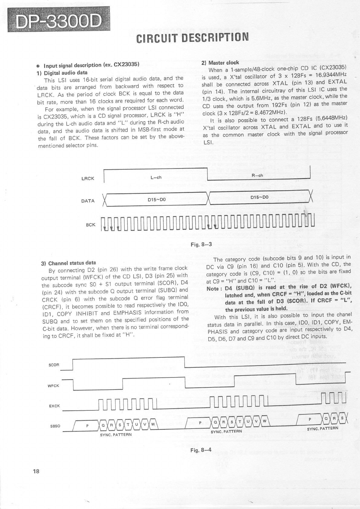
3) Channel
status
data
By connecting
D2 (pin 26) with the
write
frame
clock
output
terminal
(wFcK) of the
cD LSl,
D3 (pin
25)
with
the subcode
sync
S0 + 51 output
terminal
(SCOR)'
D4
lpin 24\ with the subcode
O output
terminal
(SUBO)
and
CRCK (pin 6) with the subcode
O error
flag
terminal
(CRCF),
it becomes
possible
to read
respectively
the lD0'
iot, COpv lNHlBlT
and
EMPHASIS
information
from
SUBO
and to set
them on the specified
positions
of the
C-bit
data.
However,
when
there
is no
terminal
correspond-
ing
to
cRCF,
it
shall
be
f
ixed
a|"H"
'
2) Master
clock
When
a 1-sample/48-clock
one-chip
CD lC (CX23035)
is used, a X'tal oscillator
of 3 x 128Fs
= 16'9344MH2
shall be connected
across
XTAL (pin 13) and EXTAL
(pin 14). The internal
circuitray
of this LSI lC uses
the
1/3
clock,
which
is
5.6MHz,
as
the
master
clock'whilethe
CD uses
the output from 192Fs
(pin 12) as
the master
clock (3 x 12BFsl2
= 8.4672MH21.
It is also possible
to connect
a 128Fs
(5'6448MH2)
X'tal oscillator
across
XTAL and EXTAL and to use
it
as the common master
clock with the signal
processor
LSI.
Fig.8-3
The category
code
(subcode
bits
9 and 10)
is
input
in
DC via Cg (pin 16) and CiO (pin
5)' With
the CD'
the
category
code
is (C9,
C10)
= (1' 0) so
the bits
are
fixed
at
C9
= "H" and
C10
= "L"'
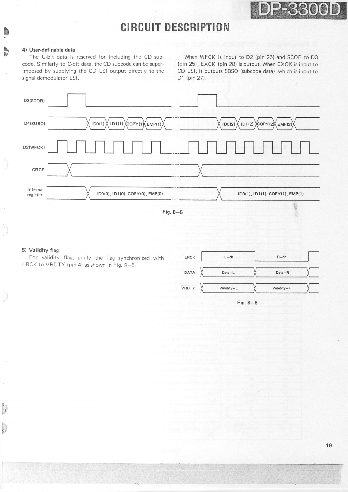
Note : D4 (SUBO) is read at the rise of D2 (WFCK)'
latched
and,
when CRCF
= "H"' loaded
as
the
C'bit
data
at the fall of D3 (SCORI'
lf CRCF
= "L" '
the Previous
value
is
held'
With this LSl, it is also
possible
to input the chanel
status
data
in parallel.
In this
case'
lDO'
lD1' COPY'
EM-
PHASIS
and category
code
are
input respectively
to D4'
D5,
D6,
D7
and
C9
and
C10
bv
direct
DC
inputs'
WFCK
EXCK
SBSO
18
SYNC.
PATTERN
Fig.
8-4
I
\
3
D3{SCOR}
-rr-r rTr l-r l-rz- r l-r l-r r-r l-r l-
D4(suBol v lp0(1lv
lp1(1)
vcopy(1xEMp(1)\____ X
rootzlXrortzlrcopvtztY
euptztv
D2{WFCK)
CRCF
lnternal
register
Fis.8-5
LFCK
5) Validity flag
For validity flag, apply the flag synchronized
LRCK to VRDTY
(pin
4)
as shown in Fig.
g-6.
i;.',li | ;i;:r:r,:.1
:'r:
DATA
VNDTY
Fis.8-6
Pu
NU
r.'
t3
CIRCUIT
DESCRIPTION
4) User-definable
data
The U-bit data is reserved
for inch:ding the CD sub-
code. Similarly to C-bit data,
the CD
subcode
can be
super-
imposed
by supplying
the CD LSI output directly to the
signal
demodulator LSl.
When
WFCK is input to D2 (pin
26) and
SCOR to D3
(pin
25), EXCK
{pin
28) is output. When
EXCK
is input
to
CD LSl, it outputs
SBSO
(subcode
data),
which
is
input
to
D1
(pin
27).
rD0{0), rD1
(0),
coPY{o}, EMP(ol rD0(1
1,
lDl
(1
),
COPY(1
),
Er,rP(l
)
19
CIRCUIT
DESCRIPTION
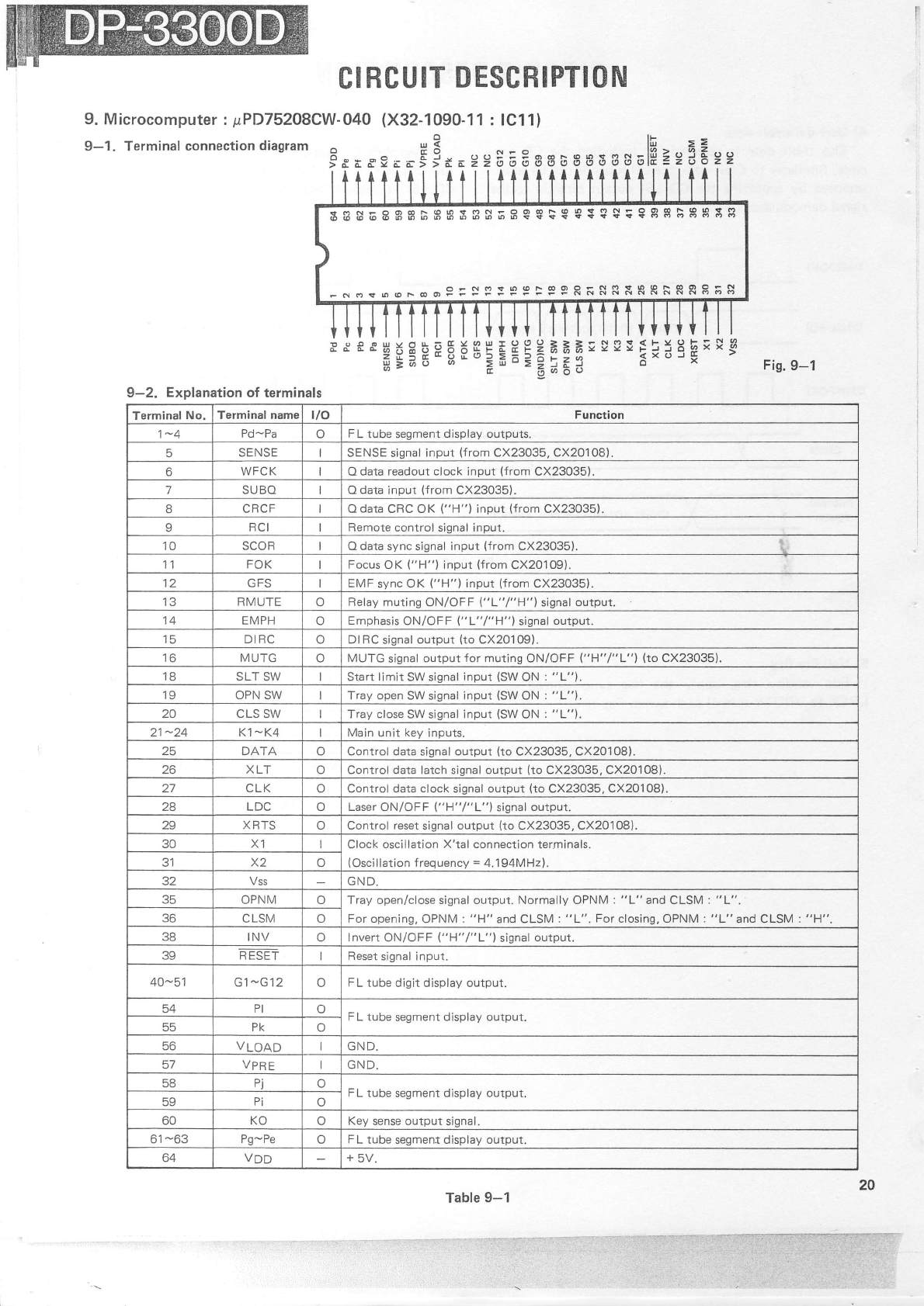
9.
Microcomputer:
pPDTS2OBCW-O4O
(X32-1090-11
: l0l1)
9-1. Terminal
connectiondiagram
o HB .-.
'od
E s9 c irg i* e
9 9 a o
u 3 E
D 3 3
3
gbe
6o
s
s 6 z=aizz
H ?Eg:Eiil""uevn!:sErrs
f,8eHX
zi
a= Fig.9-1
33S68ESEE333$689e5€9$SSE9gSDgggs
OFNO:P9:P9RFN&SRRRRRSES
FNO{o@F@OFF_
9-2. Explanation
of terminals
Terminal
No. Terminal name t/o Function
Pd
-Pa oF
L tube
segment
display
outputs.
5SENSE SENSE sisnal
input
(from
CX23035, CX20108).
6WFCK O data
readout
clock input (from CX23035).
7SUBO O data
input (from CX23035).
8O
dara
CRC OK
("H")
input
(from
CX23035).
IRCI Remote
control siqnal input.
10 SCOR O data sync
signal
input (from CX23035).
11 FOK Focus OK
("H")
input
(from
CX2O109)
1a GFS EMF
sync
OK ("H") input
(from
CX23035).
IJ RMUTE oRelay muting
ON/OFF ('L"l"H"l signal
output.
14 EMPH oEmphasis
ON/OFF ('L"l"H"l signal
output.
i5 DI RC oDIRC signal output (to
CX20109).
tb MUTG oMUTG
siqnal output
for mutins
ON/OFF
('H"/"L"| (to
CX23035).
'1
8SLT SW Start limit SW signal
input
(SW
ON : "L").
19 OPN SW Tray open SW signal input (SW
ON : "L")
20 CLS SW Tray close SW signal input
(SW
ON : "L")
11 -aA Ki
-K4 Main unit key
inputs.
25 DATA oControl data signal output (to CX23035, CX20108).
zo XLT oControl data Iatch siqnal output
(to
CX23035, CX20108).
27 CLK oControl
data clock
signal output
(to
CX23035,
CX20108).
28 LDC oLaser ON/OFF ('H" /"L"1 sisnal
output.
XRTS oControl reset
signal
output (to CX23035,
CX20108).
30 X1 Clock oscillation X'tal connection
ter.minals
(Oscillation
f requency
=
4.1 94MHz).
JI x2 o
32 Vss GND.
35 OPNM oTray open/close signal output. Normally OPNM
: "L" and CLSM
: "L".
For opening,
OPNM
: "H" and CLSM
: "L". For
closing, OPNM
: "L" and CLSM
: "H".
36 CLSM o
38 INV olnvert
ON/OFF ('H" /"L"\signal output.
JY R ESET Reset
signal input.
40-51 G1-G'1 2 oFL tube
digit display output.
AA PI oFL tube segment
display output.
55 PK o
56 VLOAD GND.
57 VPRE GND.
5B Pj oFL tube segment display
output.
59 Pi o
60 KO oKey sense
output signal.
61
-63 Pq-Pe oF
L tube segmen-t display output
64 VDD +
5V.
Table
9-1 20
ADJUSTMENT
I
t
l.
F;
w
p
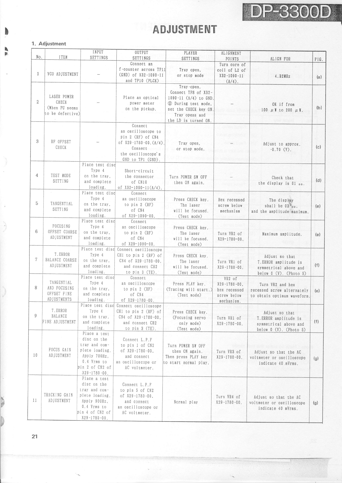
1. Adjustment
No. ITI}I I NPUT
SETT I IiGS OUTPUT
SETT I IiCS PLA
YBR
SETT I I,{GS
AL
I G l{}lENT
P0l
l,lTS AL I OlI FOR FIG,
YCO
ADJUSTMENT
Connect
an
f-counter
across
TP1
(Gl'lD)
of )(32-1090-11
and
TP10
(PLC()
Tray
open,
or stop mode
Turn
core
of
coil of L2 of
x32-1090-11
$/4). 4.32MHz (a)
LASEB
POYER
CIIECI{
(Yhen
PU
seems
o be defective
Place
an
opt ical
power
|Ileter
on
the
pickup.
Tray
-open.
Connect
TP8
of X32-
1090-11
(A/4)
to G}lD
O During
test mode,
set the CHECK
key
0N
Tray opens
and
the LD
is turned 0N.
0( if from
100
p{ to
200
zI (b)
RF
OFFSET
CH EC(
Con
nec
t
an osci I
loscope
to
pin 2 (RF)
of Cll4
of X29-1780-00.
(A/4)
Connec
t
the oscilloscope's
GND
to TPl (GND).
Tray open,
or stop mode. Adjust
to approx.
-0.70
(v). (c)
4IEST }I{ODI
SETT
I NG
Place
test di
Type
4
ol the
tray,
and colnplete
Ioading.
Short-circuit
the
connector
of CNl0
of X32-1090-i1(A/4)
Turn
P0}{Efi
S[ OFF
then 0N
again. Check
that
the
display
is 01
oo (d)
qTANCENT
I,{L
sErT I t{c
Place
test dis
Type
4
on
the tray,
and conp
I et
e
loading.
Con
nec
t
an
osciiloscope
to pin 2 (RF)
of CN4
ol X29-1090-00.
Press
CIIECK key.
Ihe laser
ttill be
focused.
(Test node)
Hex
recessed
scre,r
below
nechanism
The
displfy
shal
l be 03\0,
and
the
anplitude
naxinum.
(e)
o
FOCUS
I NG
OFFSET
COARSE
AD
J
UST}i1ENT
Place
test
dis
Type
4
on
the
tray,
and
complete
loading.
Con nec
t
an
osci
I loscope
to pin 2 (RF)
of CN4
of X29-1090-00.
Press
CHEC(
key.
The laser
will be focused.
(Test
mode)
Turn
YR2 of
)(29-1780-00. ilaximum
ampl
itude. (e)
7T.
ERROR
BALANCO
COARSE
AD
J
USTII ENT
Place
test
disr
Type
4
on
the tray,
and conpl
ete
Ioading.
Connect
oscilloscope
CHI
to pin 2 (RF)
of
CN4
of X29-1780-00,
and
connect
CH2
to pin 3 (TE).
Press
CHECK
key.
The I aser
vill be
focused.
(Test node)
Turn
VB1 of
)(29-1?80-00.
Adjust
so that
T.ERR0R
arnpiitude
is
synmetrical
above and
below
0 (V). (Photo
5)
(f)
8TA],{GENT
IAL
AND FOCUS
I }iG
OFFSET
F I NE
AD
J
UST}ll ENTS
Place
test dis
Type
4
on
the tray,
and conpl
ete
loading.
Colnec
t
an
osci
I loscope
to pin 2 (RF)
of CN4
of X29-1780-00.
Press
PLAY
key.
(Tracing ,till start
(Test node)
YR2 of
x29-1780-00,
hex
recessed
scretr
below
nechanism.
Turn
YR2 and
hex
recessed screw
alternately
to obtain
opt itrrun
waveforn
(e)
9T.
ERROR
BALA
NC E
II{E ADJUST]ilENT
Place
test
dis
Type 4
on
the tray,
and
corl)pl
ete
loading.
Connect
osci I loscope
CH1
to pin 2 (RF)
of
CN4
of X29
-1780
-00,
and connect
CH2
to pin 3 (TE).
Press
CIIDCI(
key.
(Focusing
servo
on I
y rnode)
(Test
mode)
Turn
l/RI
of
x2
I
-l
780
-00
Adjust so that
T.ERROR
arnplitude
is
sYnnelrical
above and
below
0 (V). (Photo
5)
(f)
l0 FOCUS
CA ] N
,4 DJ
UST}lENT
Place
a test
disc
on
the
tray and con-
plete
loading.
Appiy
700H2,
0.4
Vrns
to
in 2 of CN2
of
x29
-1780
-00.
LOnnect
L_f.f
to pin 1 of CN2
of I29
-1780
-00,
and
connect
oscilloscope
or
AC
voltlireter.
Turn POilER
Sll OFF
then 0N again.
Then
press
PLAY key
o start
nornal
play.
Turn
VR3
of
x29-1'i80-00. Adjust
so
that
the
AC
voltneter
or oscilloscope
indicate
40 rnVrms. (s)
t1 TRACI(
JNG
GA Il{
IDJ USTIjE],{T
Place
a test
disc
on
the
tray and coln-
plete
loading.
Apply 900H2,
0.4
lrnrs to
tin
4 of CN2
of
.tr29
-1780
-00
Connec!
L.P.F
to pin 5
of CN2
of X29-1780
-00,
and
connec
t
an osc i I loscope
or
AC vo
I
tneter.
Nornal
play Turn
VR4 of
x29-1780-00. Adjust
so
that
the AC
voltneter
or oscilloscope
indicate
40 mVrns.
(s)
:
21
AL IGI{ FOR
AL
I
GN11DNT
PO
I I,ITS
PLAYER
SETT
I NGS
OUTPUT
SETT
I NGS
Adjust
so
that
the
output
is betveen
1.9
and
2.0 Yrms.
i I Turn
YRI
Connect I Ptav
t kltz' lof
X25-2860-11
, rlttiuoitr.t.r,o | 0
dB
sisnal l for
L
ch vR2
,h.
orrou,
terninal.
I I tor
R
ctt'
Test
disc
TvPe
4
I2 I
DAC
,{DJUSTIIENT
Effective
keys
in the Test
mode
and
their functions
ADJUSTMENT
Table
1
(
Note : How
to enter
the test
mode
Sfrort-circuit
connector
CNi
0 of the
(X32-1090-11
| lAl4l, turn Power switch
Power
switch
ON
again.
CD Player
unit
OFF,
then
turn
2.
Funstion T. No. dirplay
No, Input key
frFAcK
No.
I
LFI
F
l-t -t
J
Displayed
for a few
seconds
after
(1
)
to (3).
J
Disc's
Track
No. is
displayed.
1PLAY
(1) Focus
servo " ' ON'
l2l Trackingservo """ ON'
(3) Feed servo " " ON'
When
the key
is
pressed
in the
Stop
mode'
the servoes
are switched
ON
automatically
in
the
order
from
(1)
to (3)'
(1) Focus
servo " ' ON'
Ql Tracking
servo OFF'
(3)
Feedservo....
'. '... " " ' OFF'
(1) Focusservo ' ' ' ON'
Ql Trackingservo " " ' ON'
,O\ E^^A-^^r^ -.. OFF,
1:;_-;
Lt _t
CHECK
f
rEAcK
No
t_
Lt U_l
l_l t
\
CLEAB
f rRAcK No.
t_
'lll
t_tt
STOP
(1) Focus
servo ' ' OFF
l2l Trackingservo . . .. ' OFF
(3) Feed servo . OFF
(1) Tray : OPen.
l2l Laser. ."" ON' l_^ _"
'l_l/
5BEPEAT
oFF(>t) In Stoo mode : Moves
the PU slightly to the outer tracKs'
,^[+h {A^i .-^'^ nNl qwil.hcc the trackino oain to "H".
7FR(<<) ln Stop mode : Moves
the PU slightly to the inner tracks'
r^r:+h {aarl "orwn ON : Switches the trackinS gain to "L".
IOPEN/CLOSE Release
the Test mode and opens
the tray'
22
)
\
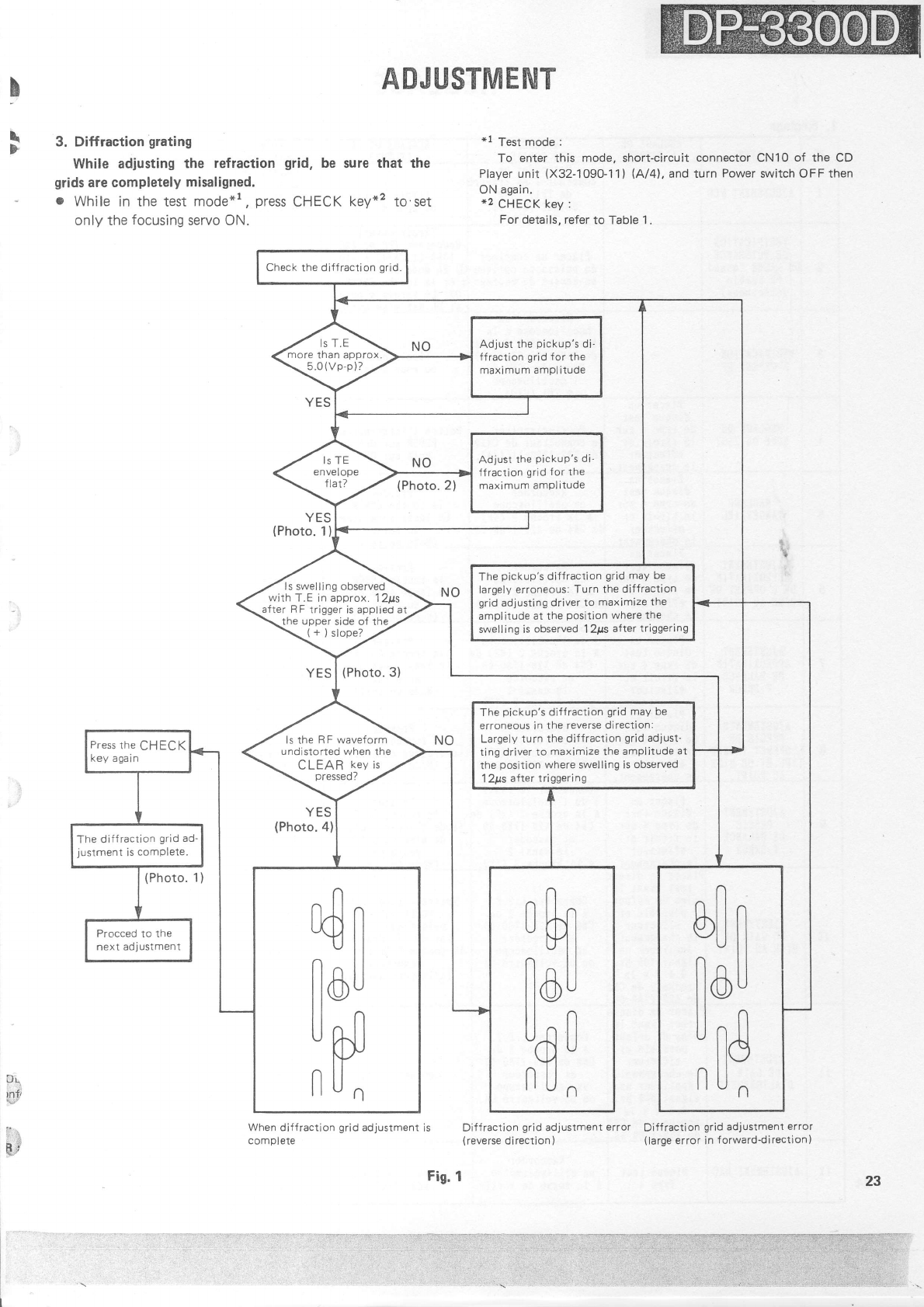
>3. Diffraction grating
While adjusting the refraction grid, be
grids
are completely
misaligned,
o While
in the test
mode*l, press
CHECK
only the
focusing
servo ON.
*1 Test
mode
:
To enter this mode, short-circuit connector CN10 of the CD
Player unit {X32-1090-1
1l |"4'l4l
, and turn Power
switch OFF then
ON
again.
*2 CHECK key
:
For details, refer
to Table
1.
ADJUSTMENT
sure that the
key"2 to set
Difiraction grid
adjustment
error
(reverse
direction)
Check the diffraction
grid.
Adjust
the
pickup's
di-
ffraction
grid
for
the
maximum amplitude
5.0(Vp-p)?
Adjusl
the
pickuP's
di'
ffraction
grid
for
the
maximum
amplitude
ls swelling observed
with T.E in approx. 12gs
after
RF
trigger
is applied at
the upper
side of the
(
+ )
slope?
The
pickup's
diffraction
grid
may be
largely
erroneous: Turn the diffraction
grid
ad.justing driver
to maximize
the
amplitude
at the position
where the
swelling is
observed
12ps alter
triggering
ls the
RF waveform
undistorted
when the
CLEAR key
is
The pickup's
diffraction grid
may be
erroneous
in the reverse direction:
Largely
turn the diffraction
grid
adjust-
ting driver to maximize
the
amPlitude
at
the position
where swelling is observed
12ps after triggering
Press
the
CHECK
key again
The dilfraction
grid
ad-
justment
is
comPlete.
nLl
"u
n
lln
ll0
ll
,d
NU
bf|l
llou
unE
flUn
4il
llctl
tld
fl
un
Procced
to the
next adjustment
YES
(Photo.
1
YES
(Photo.
UL
w
&,^
$3 When diffraction
grid
adjustment
is
complete Diffraction grid
adjustment
error
(large
error in f
orward-di
rectionl
Fis.
123
ixf
,.' ' j
|.1::
,".:l
li
BEG
LAG
E
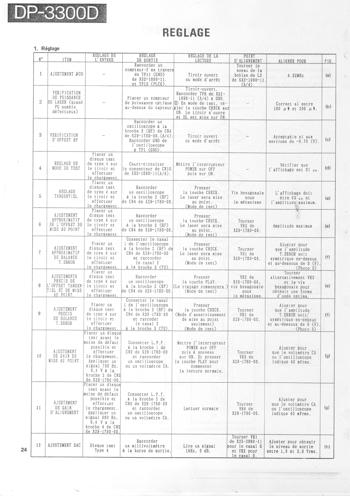
1. R6glage
tI" I TE}d LlrLAttI l]U
I.' FIITPFF TEULAbL
DE SORTIE REGLAGU
DE
LA
LECTURE ful Ilt
D, AL I GNEI{EI{T I,IOI'IER POIiR Flc
IAJ
USTE]|IEI{T
rVC0
raccoroer un
compteur-f
en
traverl
de
TP11
(GND)
de
)(32-1090-11.
et TP10
(Pl.C()
Tiroir ouvert
ou node d'arr6t
Tourner
le
noyau de
la
bobine
de
L2
de
X32-1090-11
(A/L)
4.32MHz (a)
l/ERIFIC,tTION
DE PUISSANCE
)U
LASER
(quand
PU senble
dd fec
t
ueux)
Placer
un conpteur
de
puissance
optique
au-dessus du
capteur
Tiroir-ouvert.
Raccorder
TP8 de
X32-
1090-11
(A/4)
a CND.
D En mode de
test, 16-
tler la touche
CHECK su
0N. Le
t.iroir s'ouvre
et DI- est mise srrr 0N
Correct
si entre
100
pI et 200
tf. (b)
VERIFICATION
D'OFFSET
RF
raccoroel un
oscilloscope d la
broche
2 (RF)
de CN4
de
X29-1?80-00.(i/4)
Raccorder GliD de
l'osci
I loscope
r Tpr rnilD)
Tiroir
ouvert
ou node d'arr6t Acceptable si aux
envlrons 0e
-u,
tu (vl (c)
,1 RECLACE
DE
MODE
DD TEST
d
de
le
acel
un
que
test
ype
4 sur
iroir et
fectuer
Court-circuiter
le connecteur
de
CN10
de
I32-1090-11(A/4).
]Vl6ttre
I'interrupteur
P0YER
sur OFF
puis
sur 0N.
Vdri
fier que
1' affichage
est 01
oo. (d)
R
ECLAGD
I,{l{GEliT
I
EL
Placer
un
disque
tes!
de
type 4 sur
ie
tiroir
et
elfectuer
I a ahrrsahAnf
Rac
co rd er
un
oscilloscope
d la broche 2 (RF)
le
CN4 de
X29-1780-00
Presser
la touche CHECI(.
Le laser
sera
nise
au
point.
(Mnda dc tact)
Vis hexagonale
sous
le n6canisne
L'affichage doit
etre 03
oo
et
I' ampl
i
t
ude
max i nun
.
?
(e)
o
A
J
USTEi,l ENT
A PPROX I }{trT
I F
DE L'OFFSOT
DE
IIISE AU POINT
Placer
un
disque
test
de
type
4 sur
le tiroir et
effectuer
I c chargpnpnt
Raccorder
un osci
I loscope
la broche
2 (RF)
CN4 de
X29-1780-00
e
Pres s er
la touche
CIIEC(,
Le laser
sera nise
au
point.
(l,lndp dp +oct)
Tou rne
r
YRZ
de
)(29-1780-00. Anplitude maxinum (e)
7A
J
USTE}i{ENT
A PPROX I }i{,{T
I F
DE
BALANCE
T,
ERROR
P
di
de
le
e
la
acer
un
que
test
ype
4 sur
iroir et
fec
t
uer
Connecter
le canal
I de
I' osc i I loscope
A la broche
2 (RF)
d
0N4
de
X2s-1780-00
et raccorder
le canal 2
A
la lpssSs 3 (TE).
Presser
la touche
CHEC(.
Le laser sera
nise
au
poi
nt .
(Mode
de
test)
Tourner
YR1
de
x29-1780-00.
Ajuster
pour
que
l' ampl
itude
T. ERROR soi
t
syndtrique
en-dessus
et au-dessous
de 0 (V)
{Phntn \)
(f)
8
AJUSTE},{ENTS
PREClS
DE
,'OFFSET
TANGEN
.IEL
DT DE
iIISE
AII PN I N?
P
di
de
le
e
le
acer
un
que
test
ype
4 sur
iroir et
fec
t uer
hargenent
Raccorder
un osci
I
Ioscope
d ]a broche
2 (RF)
le CN4
de
X29-1780-00
Presser
1a
touche PLAY.
Le
tracage connencera
(Mode
de
test)
VR2
de
x29
-1780 -00,
vis hexagonale
sous
lp m6nenicmp
I OUrner
alt.ernativenent
YR2
et la vis
hexagonal
e pour
obtenir une forme
d' onde oot i nr
(e)
9A
j USTEIiiENT
PREC
I S
DE
BALANCE
T. ERROR
Pl acer un
dj sque
test
0e
type 4 sur
le tiroir et.
effectuer
I e chargement
Connecter
le canal
I de
I'oscil
loscope
A la broche
2 (RF)
dr
CN4 de
X29-1780-00
et raccoder
le canal
2
A
la broche
3 (TE).
Presser
la touche
CHECI{.
(}i|ode
d'
asservissenent
de
mise au
point
seulernent)
(Mndp de tecr)
Tour n er
VR1
de
x29
-1780 -00
Ajuster
pour
que
I'amplitude,.'
T.
ERROR so
i
r
/
syn6trique
en-debsus
et au-dessous
de
0 (Y).
(Phot
o 5)
(f)
t0 AJUSTE}ilEI,{T
DE GA III DE
}i|ISE AU POINT
ilacer
un disqu
test ayant le
noins de
d6laut
possible
et
effectuer
I e chargement
.
Appl
iquer
un
signal
700
Hz,
0,4
v a la
broche
2 de Clli
dp I90-1?10-nn
Connecter
L. P. F.
d la broche
1
de
CN2 de
X29-1?80-00
et raccorder
un
oscilloscope
ou un voltn6tre
CA
Mettre
I'interrupteur
P0{ER sur OFF
puis
e nouveau
sur 0l{.
Et
presser
la touche
PLAY
pour
c0nfienceI
la Iecture nornale.
Tourner
VR3
de
x29-1?80-00
Ajus!er
pour
que
1e voltmdtre
CA
ou
I'oscilloscope
indique
40 mYrnrs.
(s)
tt
AJUSTE}lENT
DE G,4IN
D' AL I GNEIIENT
)lacer
un disqur
test ayant
le
roins
de d6faut
possible
et
effectuer
I e chargernent
.
Appl iquer
un
signal
900
Hz,
0,4
\/
e la
broche
4 de
Clil
dc Xr9-l7Rn-0n
Connecter
L. P.
f.
i la broche
5
de
Cltl2
de
X29
-1780
-00
et raccorder
un oscilloscope
ou un
voltndtre CA.
Lectuer nornale Tour ne
r
VR4
de
x29-1780-00.
Ajuster
pour
que
le volt|116tre
ou 1' osc i I
loscope
indique
40
nVrms.
(g)
t2 ,{JUSTE}|EIIT
DAC Disque
test
Type
4
Rac corder
un
nillivoltn6tre
A la borne de sortie Lire un signal
lkHz, 0 dB.
'lourner
yRl
de
)(25-2860-1i
rour
1e canal
G
et Yn2
pour
lc.nrnel I)
Ajuster
pour
obtenir
le niveau de
sortie
entre
1, 9 et 2, 0 Yr||.s. (h)
24
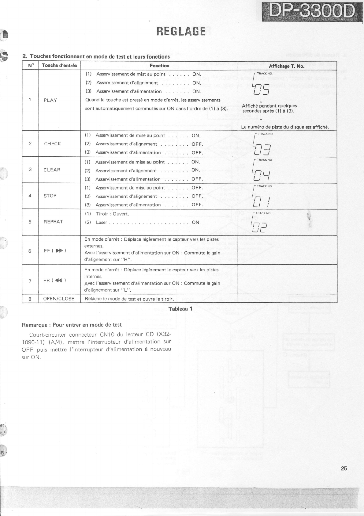
L
s
REGLAGE
/n'
!l
t-
ir-
;f
t:
8"
Remarque
: Pour
entrer en
mode de test
Court-circuiter
connecteur CN10 du lecteur
CD (X32-
1090-1
1l (Al4l
, mettre
l'interrupteur
d'alimentation
sur
OFF puis
mettre l'interrupteur
d'alimentation
a nouveau
sur ON.
@u
tr
ffi
2. Touches fonctionnant en mode
de test et leurs fonctions
NO Touche d'entr& Fonction Affichagc T. No.
1PLAY
(1) Asservissementdemistauooint
. . . . . . ON.
(2) Asservissementd'alignement
. .... ON.
(31 Asservissementd'alimentation
. . . . .. ON.
Ouand la touche est
press6
en mode d'arr€t,
les
asservissements
sont
automatiquement
commutds
sur ON dans
l'ordre de
(1)
a
{3).
f rFAcK No.
I
LFt
F
Lt:]t
J
Aff ich6
pendant
quelques
secondes aprAs
(1
)
d (3).
J
Le
numdro de
piste
du disque est affich6.
zCHECK
t1) Asservissementdemiseaupoint
. . . . . . ON.
l2l Asservissementd'alignement ... OFF.
(31 Asservissementd'alimentation
. .. ... OFF. t;:
Lt a
CLEAR
1) Asservissementdemiseaupoint . . . . . . ON.
2l Asservissement
d'alignement . . ON.
3) Asservissement
d'alimentation OFF.
I t"^.- ""
Ti'-l
4STOP
1) Asservissementdemiseaupoint
. . . . . . OFF
2l Asservissement
d'alignement . . OFF
3l Asservissementd'alimentation
. . .. . . . OFF
f
rFAcx
No
t_.
'l
ll
Lt I
REPEAT
{1) Tiroir:
Ouvert.
lA Laser. ..... ON.
,-;'
tl
bFF(>t)
En mode d'arr€t : D6place lfudrement le capteur vers les
pistes
exlernes.
Avec l'asservissement d'alimentation
sur ON : Commute le
gain
d'alignement
sur
"H".
FR(+{)
En
mode
d'arr€t
: D6place lfudrement le capteur vers les
pistes
internes,
Avec
l'asservissement
d'alimentation sur ON : Commute le
gain
d'alignement
sur
"L".
IOPEN/CLOSE Rel6che le
mode
de test
et ouvre le tiroir.
Tableau
I
25
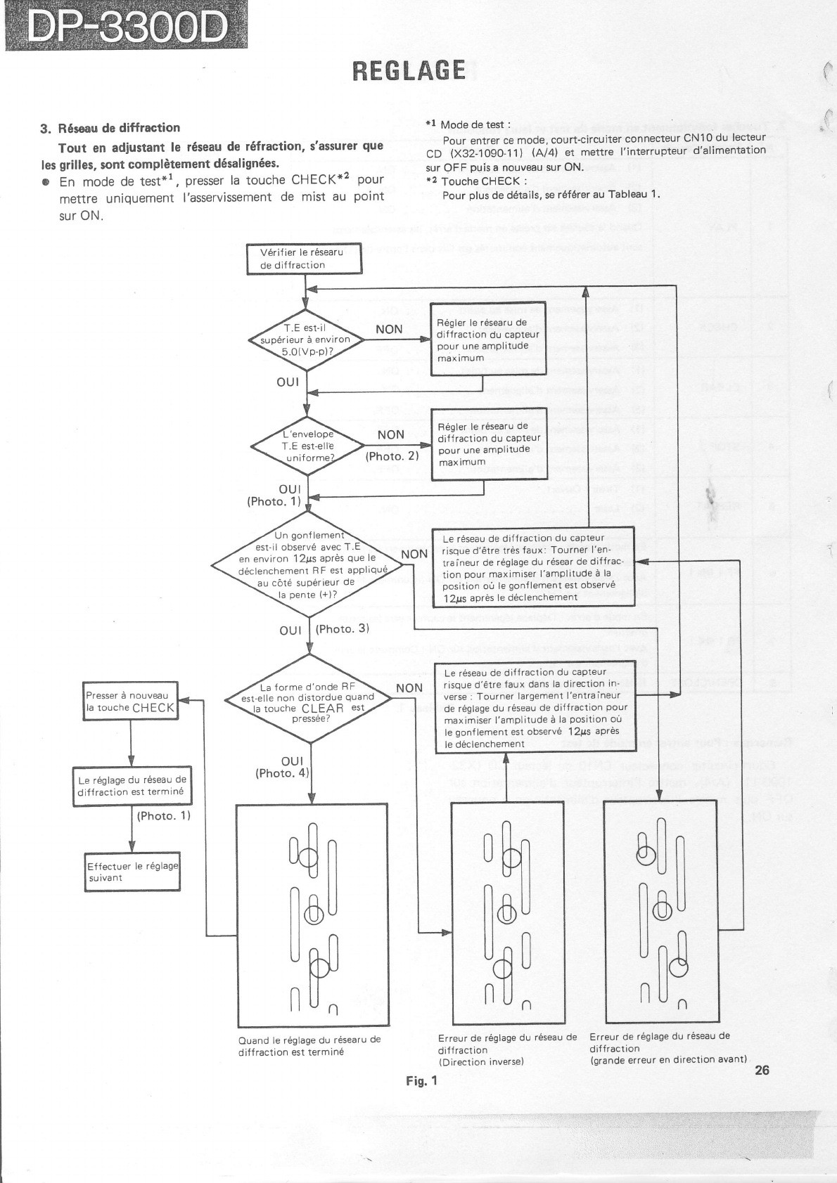
Ouand
le r6glage du r6searu
de
diff raction
est termine
REG
LAG
E
Erreur de r5glage
du
reseau
de
d
iffract
ion
(Direction
inverse)
Erreur
de r6glage
du reseau
de
d
iffract
ion
(grande
erreur
en direction
avant) 26
r
3. R6seau
de diffraction
Tout en adiustant
le r6seau
de r6fraction,
s'assurer
gue
les
grilles,
sont
completement
d6salign6es'
o En mode
de test*l, presser
la touche
CHECK*2 pour
mettre uniquement
l'asservissement
de mist au point
sur
ON.
*l Mode
de test
:
Pour entrer
ce mode,
court-circuiter
connecteur
CNlOdu lecteur
CD (X32-1090-11ir
(Al4t et mettre
l'interrupteur
d'alimentation
sur OF F
puis
a nouveau
sur ON.
*2
Touche CHECK
:
Pour
plus
de d6tails,
se
r6f6rer au Tableau
1.
V6rifier
le rEsearu
de diffraction
F69ler le
r6searu de
diffraction du capteur
pour
une amplitude
max
imu
m
T.E
est-il
5.0(Vp-p)?_
R69ler
le
r6searu
de
diffraction
du
capleur
pour
une
amPlitude
max
lmu
m
est-il observ6 avec
T
en environ
12us
aprds
que
le
d6clenchement FIF
es1
au
c6t6 sup6rieur
de
la
pente
(+)?
Le r6seau
de
di{{raction
du capteur
risque
d'6tre
tres
faux: Tourner
I en-
traineur
de
reglage du r6sear de diffrac'
tion
pour
maximiser
I'amplitude
a
la
position
oi le
gonflement
est observe
1 2gs
aprds
le declenchement
La
forme
d'onde
RF
est-elle
non distordue quand
la
touche
CLEAR
Le
r6seau
de di{fraction
du
capleur
risque
d'6tre
faux
dans
la
direction
in-
verse
: Tourner
largement
l'entraineur
de
r6glage
du r6seau
de diffraction
pour
maximiser
l'amplitude
a
la
position
ou
le
gon{lement
est
observ6
1 2ps apres
le
ddclenchement
Presser d nouveau
la touche
CHECK
Le r6glage
du r6seau
de
diffraction
est termine
bl
I
I]oU
unE
flUn
tlLi
"s
iln
lt:
tl
,d
tlU
4l
llou
ubf
lUn
oul
oul
(Photo.
4
(Photo.
Fig.
1
",,:_ -."
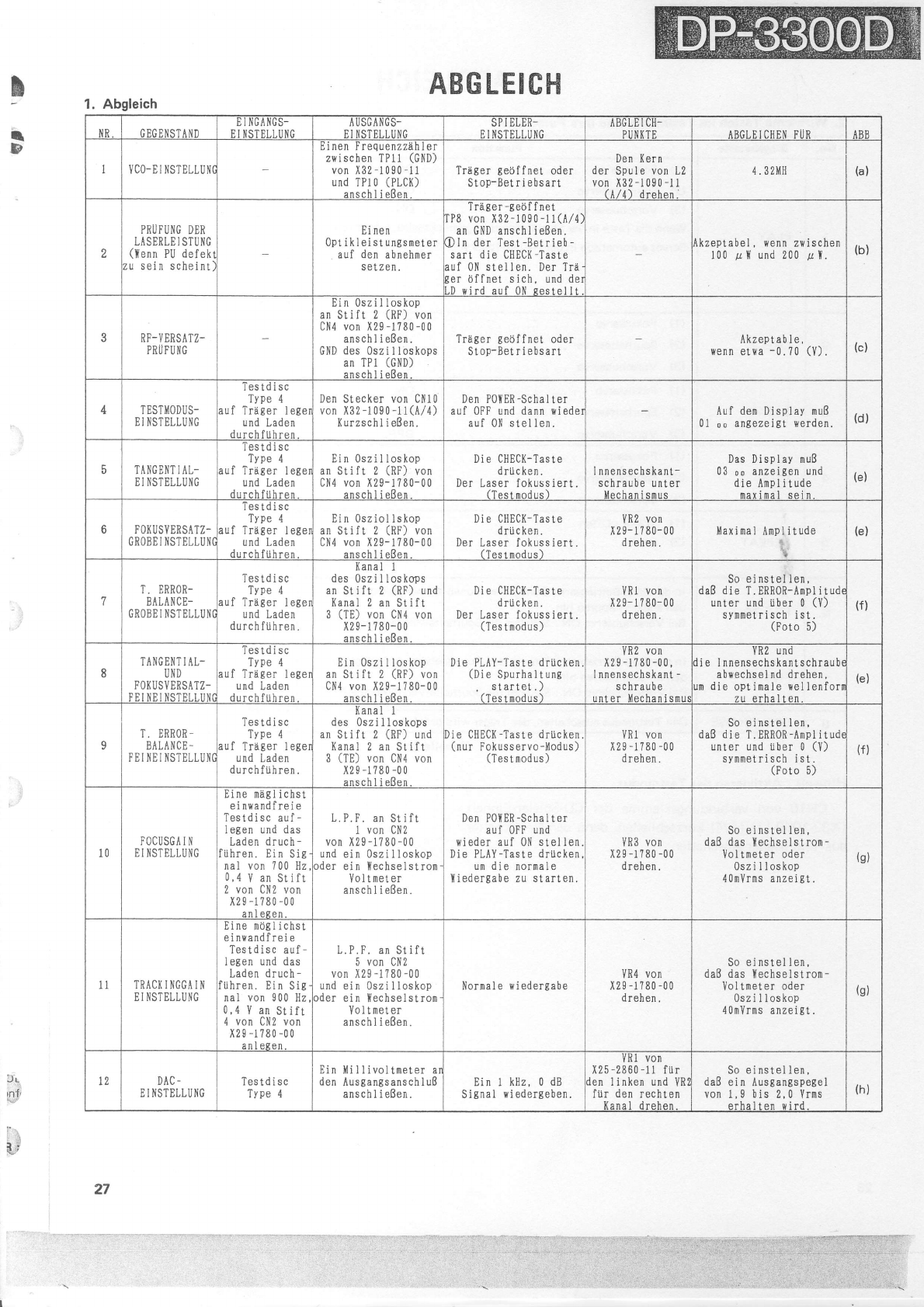
!
I
P
ABG I-EICI-I
1.Abgleich
NR C EG Ell STA ND I] I NGA liGS-
E I IiSTELI,UNC AUSG,{NGS-
FI NCTFI I IINN SP I ELER_
E I NSTEI,I,IIN('; AbGLE I UII-
PIINI(T E ABGI,E I CHEI{ FiiR ABB
YCO.D
I IiSTELLUN(
Einen Frequenzziihler
zrrischen TPll (CND)
von
X32-1090-11
und TP10
(PLCI{)
ancnhl ioRon
Triiger getjffnet oder
Stop-Betriebsart
Den I(ern
der Spule
von
L2
von X32-1090-11
rl //) dr6hon'
4.32}{H (a)
a
PRUFUNG
DDR
LASERLEISTUI,IG
(lenn
PU defek
u sein scheint
Ei nen
0ptikleistungsmeter
auf den
abnehner
setzen.
'I
raSer
-geoll
net
'P8
von X32-1090-11(A/4.
an
GND
ansch I i eBen.
DIn der
Test-Beirieb-
sart die CHECI{-Taste
ruf 0N stel
len. Der Trii
Ier tiffnet sich, und
de:
.D vird auf 0N cestel lf
kzeptabel, wenn
zwischen
100
pY und 200
rzt. (b)
RF-YERSATZ-
PRU FU
NG
Ein 0szilloskop
an
Stift 2 (RF)
von
Cll4 von
X29-1780-00
anschl ieBen.
GND
des 0szi
I Ioskops
an TPl (GND)
cncnh I i aRpn
Trager
getjffnet
oder
Stop-Betriebsart Akzeptable,
$enn
etrYa
-0.
70 (Y) (c)
4TESTl{ODUS-
E i I{STELLUNC
Testdisc
Tvpe 4
ruf Trager lege
und
Laden
.llr.hfiih"."
Den
Stecker
von CNl0
von X32-1090-11(A/4)
(urzschl
ieBen.
Den POliER-Schalter
auf OFF und dann wiede.
auf 0il
stellen. Auf dem Display muB
01
oo
anSezeiSt rerden. (d)
Trtl{0DNT IAL-
DI NSTELLUNG
lestdisc
Tvpe 4
tuf TrriSer lege
und Laden
durchfilhren-
Ein 0szilloskop
an
Stift 2 (RF)
von
CN4 von
X29-1 ?80-00
anschlieBen.
Die CHEC(-Taste
driicken.
Der
Laser fokussiert
(Tpct nndr<)
I nnensechskant-
schtaube unter
Mprhan i <nrrc
Das Di sp
03
oo
0llZe
die Anp
nax i na
ay muB
gen
und
itude
sern.
(e)
6FOI(USY ERS,{TZ-
OROBE] NSTBLLUI{(
lestdisc
Type 4
tuf TriiSer lege
und Laden
durchfUhren.
Din 0sziol
lskop
an
Stift 2 (RF)
von
Cl,l4
von
X29-1780-00
anschl ieBen-
Die CHEC(-Taste
dri.icken.
Der Laser
fokussiert
(Tpcr mndrc)
YR2
von
x29-1?80-00
drehen. )laxinal
Amplitude
I,f
(e)
7T. ERROR-
BALA NCE-
GROBE I I,ISTELLUil(
Testdisc
Tl,pe 4
ruf Treger
lege
und Laden
durchfiihren.
I(anal I
des 0szilloskops
an
Stift 2 (RF)
und
Xanal 2 an
Stift
3 (TE) von CN4 von
x29-1,l80-00
ancnh I i oRon
Die CHECI(-Taste
drticken.
Der Laser
fokussiert
(Testmodus)
YR1
von
x29-1780-00
drehen.
So einstellen,
daB
die T.
ERR0R-Arnpl
itudr
unter und iiber 0 (Y)
synnetrisch
ist.
(Foto
5)
(f)
8TA
NG El,{T
I AL-
U IID
FOI(
USY ERSATZ-
FEINFINSTFI I.IIi]I
Testdisc
Type 4
ruf Treger
Iege
und
Laden
d rrrnh fiih ron
Ein 0szilloskop
an
Stift 2 (RF)
von
Cl'14 von
X29-1780-00
rocnh 1 ; oRon
Die PLAY-Taste
drticken.
(Die
Spurhaltung
. startet.
)
fToc+n^.1,,e)
YR2
von
x2
I
-1
780
-00,
I nnensechskant
schraube
,n+6. Llo.h.ni<
YR2
und
li
e I nnensechskanlschraubr
abvechselnd drehen,
rn die optimale vellenforr
zrr orhal ton
(e)
qT, ERROR-
BALANCE
_
FEIilDINSTELLUII(
Testdisc
Tvpe 4
ruf Trager
lege
und
Laden
durchfiihren.
an
l(anal
1
des
0szilloskops
Stift 2 (BF)
und
Xanal
2 an Stift
(TE) von Cil4 von
I29-1?80-00
oncnh I i oRon
3
ie CHECX
-Taste
driicken.
(nur Fokusservo-lilodus)
(Tes
t
mod us
)
VB1
von
x29
-1780 -00
drehen.
So einstel len,
daB die T.ERROR-lrnpl itud
unter und iiber 0 (Y)
sy|n|netrisch ist.
(foto D,
(f)
10 FOCUSGA I }I
E I NSTELLUNG
Bine nAglichst
einvandfreie
Testdisc auf-
legen
und das
Laden
druch-
fiihren. Ein
Sig.
nal von 700 Hz,
0,4
Y
an
Stift
2 von CN2
von
x29
-1.i80 -00
enl egen
L.P.F.
an Stift
I von CN2
von
X29
-1780 -00
und
ein 0szi 1 loskop
rder
ein Xechselstrom
Vol tneter
anschl ieBen.
Den POIER-Schalter
auf OFF und
wieder auf 0N stel len.
Die PLAY-Taste
drilcken,
um die normale
l{iedergabe
zu starten.
YB3
von
x29-1780-00
drehen.
So einstellen,
daB
das
l{echselstron-
Voltneter oder
0szi I loskop
40nVrns
anzeigt.
(s)
11 TRACXINCGiIN
E I NSTELLU}lG
Elne
niigl ichst
einwandfreie
Testdisc
auf
-
legen
und das
Laden
druch-
iihren.
Ein
SiB'
nal von 900
Hz,
0,4
Y an
Stifr
4 von
CN2
von
x29-r780-00
L.P.F. an Stift
5 von
CN2
von
X29-1780-00
und ein 0szi I loskop
rder
ein {echselstrom
Yoltneter
anschl ie8en.
Nornale viedergabe YB4
von
x29
-i780 -00
drehen.
So einstel len,
daB das
lechselstron-
Yo1 tneler oder
0szi
I loskop
40rnvr|ns
anzeiSt.
(s)
I2 DAC
-
EI
NSTELLUNC Testdisc
Type 4
Ein
denItlillivoltmeter a
AusgangsanschluB
anschl ieBen. EinlkHz,0dB
Signai
viedergeben.
x25
en
fiir
YR1
von
-2860 -11
fiir
linken und
YRI
den
rechten
qnr I rlrohar
So
einstellen,
daB
ein Ausgangspegei
von
1,
I b
is 2, 0 Yrns
arhrlron oird
(h)
Jr
rnf,
i",i'
27
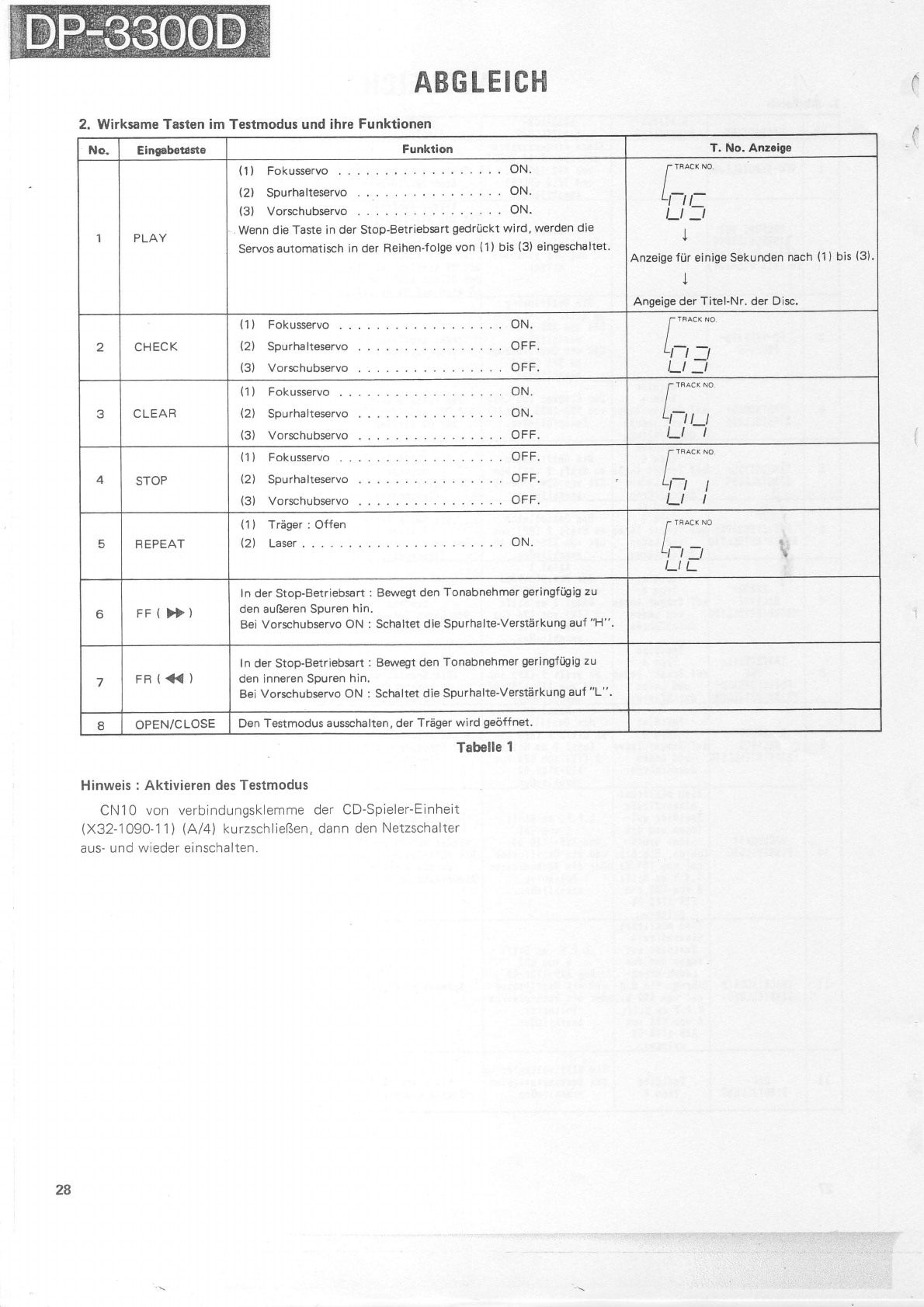
ABG
LEIC}I
2. Wirksame Tasten
im Testmodus
und ihre
Funktionen
No- Eingsbabno Funktion T. No. Anzeige
IPLAY
(11
Fokusservo ....... ON.
Ql Spurhalteservo .... ON'
(3) Vorschubservo .... ON.
Wenn
die Taste in
der
Stop-Betriebsart
gedriickt
wird.
werden
die
Servos
automatisch in
der
Fleihen-folge
von (1
) bis
(31
eingeschaltet'
f
rBAcK No.
t__
Ll ll
t_t :t
J
Anzeige
fOr einige Sekunden
nach
(1
)
bis
(3).
J
Angeige
der Titel-Nr. der Disc,
zCHECK
(l) Fokusservo ...... ON.
Ql Spurhalteservo .... OFF.
(3) Vorschubservo ..... OFF. fi-;
t_t :i
5C LEAR
1
2
Fokusservo ...... ON.
Spurhalteservo ..... ON.
Vorschubservo ..... OFF.
[*"*"
'l-l'-l
4STOP
1
z
Fokusservo ...... OFF
Spurhalteservo .... OFF
Vorschubservo .... OFF
f
rRAcK
No
t_
'lll
Lt t
FBEPEAT
(1) Trdger: Offen
l2l Laser. .. ON. f
rFAcK No
t__
,l l_l
I_IL \
6FF(>))
In
der Stop-Betriebsart
: Bewegt
den
Tonabnehmer
geringfiigig
zu
den auReren
Souren
hin.
Bei Vorschubservo
ON : Schaltet
die Spurhalte-VerstArkung
auf
"H"
FR{+{) In der Stop-Betriebsart
: Bewegt
den
Tonabnehmer
geringfiigig
zu
den inneren Souren
hin.
Bei Vorschubservo
ON : Schaltet
die Spurhalte-Verstarkung
aul
"L"
IOPEN/CLOSE Den
Testmodus ausschalten, der
Trdger
wird
geoffne't.
Hinweis
: Aktivieren des Testmodus
CN10 von verbindungsklemme
(X32-1090-1
1
| (Al4l kurzschlieBen,
aus- und
wieder einschalten.
Tabelle
Aar f'l-]-Qnialor-Finhoit
dann den
Netzschalter
28
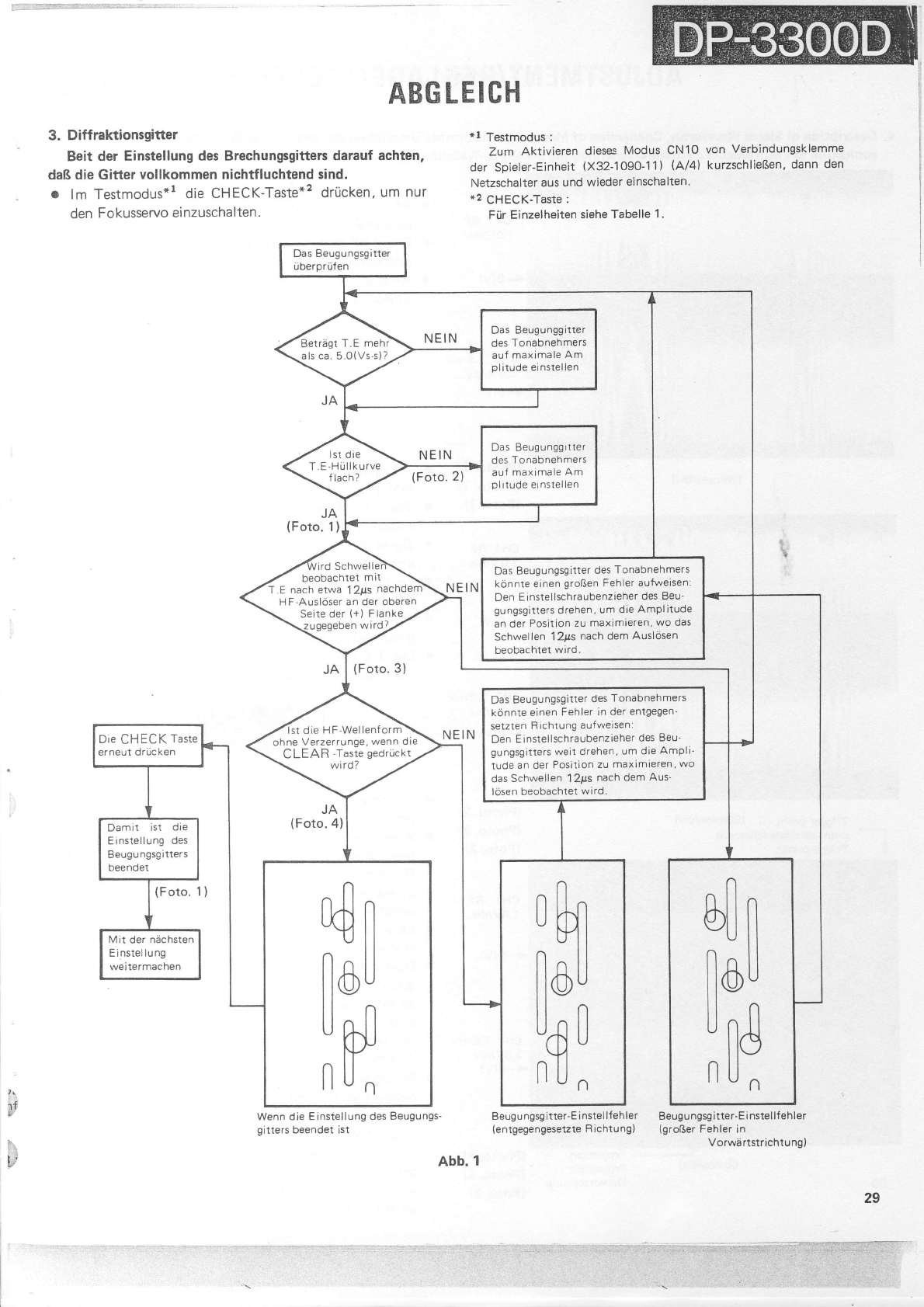
ABG
LEICH
3. Diffraktionsgitter
Beit der Einstellung
des
Brechungsgitters
darauf
achten,
daB die Gitter vollkommen nichtfluchtend
sind.
o lm Testmodus*l
die
CHECK-Taste*2
drucken,
um nur
den
Fokusservo
einzuschalten.
*1
Testmodus:
Zum Aktivieren
dieses
Modus CN1O
der
Spieler-Einheit
(X32-1090-11)
(A/4)
Netzschalter
aus
und wieder
einschalten.
*2 cHEcK-Taste
:
Fiir Einzelheiten
siehe Tabelle
1 .
von Verbindungsklemme
kurzschlieBen,
dann
den
Das Beugungsgittel
Das
Beugunggitter
des
Tonabnehmers
auf
maximale
Am
plitude
einstellen
Betriigr
T.E mehr
als ca.
5.0(Vs-s)?
Das Beugunggrtter
des
Tonabnehmers
auf
maximale
Am
plrtude
ernstellen
T. E-H
iil lk urve
ird Schwell
beobachlet mit
E nach etwa 12lls
HF-Ausloser an der oberen
Seite
der (+) Flanke
Das
Beugu
ngsgitter des
Tonabnehmers
konnte einen
groBen
Fehler
aufweisen:
Den
Einstellschraubenzieher
des
Beu-
gungsgitters drehen, um
die
Amplitude
an der
Position
zu
maximieren,
wo das
Schwellen
1 2ps
nach dem
Auslosen
beobachtet
wird.
(Foto.3)
Das
Beugungsgrtler
des
Tonabnehmers
konnle einen
Fehler
in der
entgegen-
setzten R ichtung aufweisen:
Den Einstellschraubenzieher
des 8eu-
gungsgitters weit
drehen,
um dle
Ampli-
tude an der Position zu maximieren, wo
das
Schwellen 1 21rs
nach dem Aus'
losen
beobachtet wrrd.
lst
dre
HF-Welleniorm
ohne Verzerrunge,
wenn dle
CLEAR -Taste
gedrtlcki
\ wird? -/
Die
CHECK Taste
erneut drucken
Damit ist dte
Einstellung
des
Beug
u
ngsg
itters
beendet bf|]
llcu
unE
lUn
tlI
-U
lln
II:
tl
UA
\l/
|lU
ndn
rcu
tld
lun
Mit der
nachsten
E instel lu
ng
weitermachen
JA
.1)
JA
(Foto.
4)
(Foto,
ef
,;" Wenn die
Einstellung des Beugungs-
^irror. Freonripr ici
Beug u
ngsg
itter-E
i
nstel
lleh
ler
(entgegengesetzte
R
ichtung) Beugu
ngsg
itter-E
i nstel lfehler
{gro8er
Fehler in
Vorwd rtstrichtung)
1..
LJ
29
Abb.
l
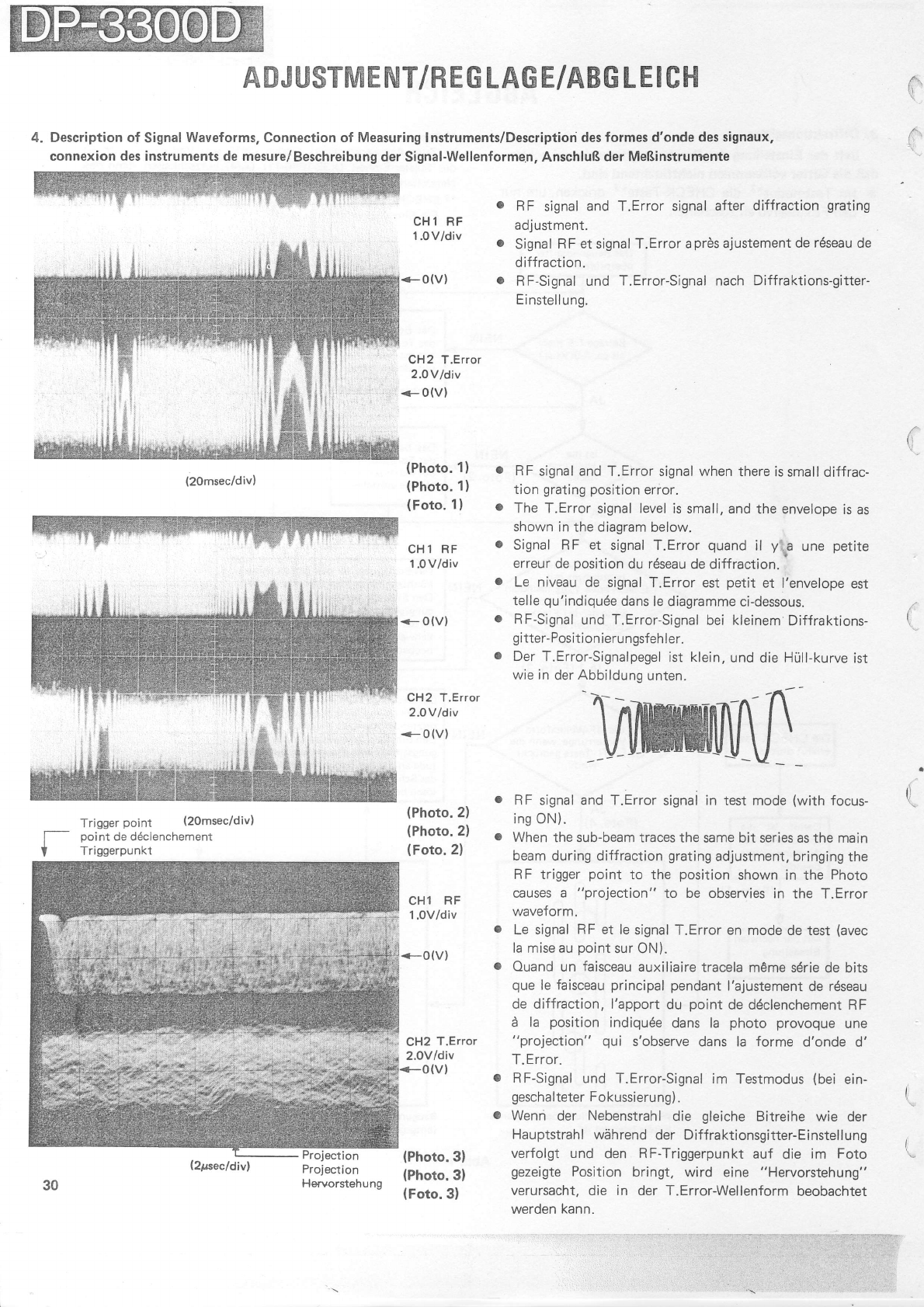
AD.'USTNNENT/REG
LAG
E/ABG
LEICH
4. Description of Signal
Waveforms, Connection of Measuring Instruments/Descriptiori des
formes d'onde des signaux,
connexion des instruments de mesure/Beschreibung
der Signal-Wellenformen, AnschluR
der MeRinstrunrente
C
r.
(2Omsec/divl
Projection
Projection
Hervorstehung
CH1 RF
1.0V/div
<-o(V)
CH2 T.Error
2.Ov
ldiv
<-0(V)
(Photo.1)
(Photo.1)
(Foto.1)
CH1 RF
1.0V/div
<-o(v)
CH2 T.Error
2.OV
ldiv
<-0(Vl
(Photo.2)
(Photo.
2)
(Foto.
2)
CH1 RF
1.OV/div
<-0(v)
CH2
T.Error
2.OYldiv
0{v}
{Photo.3}
{Photo.
3)
{Foto.3}
o RF signal
and T.Error signal
after diffraction
grating
adjustment.
Signal
RF et signal T.Error
aprds ajustement
de rdseau de
diff raction.
R F-Signal und T.Error-Signal
nach Diffraktions-gitter-
Ei
nstell ung.
RF
signal
and
T.Error signal when
there is
small diffrac-
tion
grating position
error.
The T.Error
signal level is small,
and the envelope
is
as
shown
in
the
diagram
below.
Signal RF et signal
T.Error quand
il v\a une petite
erreur
de
position
du r6seau
de diffraction.
Le niveau
de signal
T.Error est petit et I'envelope
est
telle
qu'indiqu6e
dans
le diagramme
ci-dessous.
RF-Signal
und
T.Error-Signal
bei
kleinem
Diffraktions-
gitter-Position
ierun
gsfeh
ler.
Der
T.Error-Signalpegel
ist
klein,
und die Hrill-kurve
ist
wie in
der
Abbildung
unten.
RF signal and T.Error
signal
in test mode
(with
focus-
ins ON).
When
the sub-beam traces
the same bit series as
the
main
beam
during
diffraction
grating
adjustment, bringing
the
RF trigger
point to the position
shown in the Photo
causes a "projection"
to be observies
in the T.Error
waveform.
Le signal
RF et le
signal T.Error en mode
de test
(avec
la mise au
point
sur ON).
Ouand
un faisceau
auxiliaire
tracela
mdme s6rie
de bits
que
le faisceau
principal
pendant
l'ajustement
de r6seau
de diffraction, l'apport
du point
de d6clenchement
RF
d la position indiqu6e
dans la photo provoque
une
"projection" qui s'observe
dans la forme d'onde d'
T.
Error.
RF-Signal
und T.Error-Signal
im Testmodus
(bei
ein-
geschalteter
Fokussierung).
o Wenn der Nebenstrahl
die gleiche
Bitreihe wie der
Hauptstrahl wdhrend
der Diffraktionsgitter-Einstellung
verfolgt und den RF-Triggerpunkt
auf die im Foto
gezeigte
Position
bringt, wird eine "Hervorstehung"
verursacht, die in der T.Error-Wellenform
beobachtet
werden
kann.
l:::!I;iil.rir
f',;T::l
ljra:; i{ :i'i".r. :
a
,.
r,.j,
(
Trigger
point (2omsec/div)
point
de d6clenchement
Triggerpunkt
{
30
(2rsecldivl
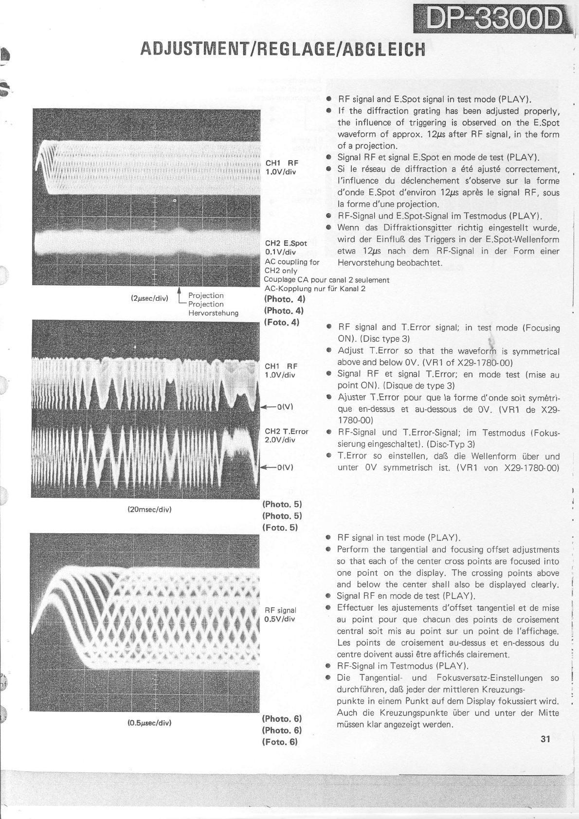
!
I
b
A
BJ
USTM
E
NT/R
E
G
LAG
E/AB
G L
E
IC H
CHl RF
1.0V/div
CH2 E.Spot
0.1Vldiv
AC coupling
for
CH2
only
Couplage
CA pour canal 2 seulement
AC-Kopplung
nur
flir Kanal 2
(Photo.
4)
(Photo.
4)
(Foto.4)
CH1 BF
1.0V/div
<_0(vl
CH2
T.Error
2.OV/div
(Photo.
5)
(Photo.5)
(Foto.5)
RF signal
O.5V/div
(Photo.6)
(Photo.6)
(Foto.6)
RF
signaland
E.Spot
signal
in
test mode
(PLAY).
lf the diffraction
grating
has been
adjusted
properly,
the influence of triggering is observed
on the E.Spot
waveform of approx. 12ps atter RF signal, in the form
of a
projection.
Signal RF
et
signal
E.Spot
en mode de test
(PLAY).
Si le r6seau de diffraction a 6td ajust6 correctement,
l'influence
du ddclenchement s'observe
sur la forme
d'onde
E.Spot
d'environ 12trn aprds le signal
RF,
sous
la forme d'une
projection.
RF-Signal
und
E.Spot-Signal
im Testmodus
(PLAY).
Wenn das Diffraktionsgitter
richtig eingestellt
wurde,
wird der EinfluB
des Triggers in der E.Spot-Wellenform
etwa 121a nach dem RF-Signal
in der Form einer
Hervorstehunq beobachtet.
o
a
(20msec/div)
';;.$,
',tft
{..q
*d
$*tf
*$${
GS*$
****$*
$'$$$*$*
e4&$&*
o
o
c
a
a
o
e
o
c
o
RF signal and
T.Error
signal; in test mode
(Focusing
ON).
(Disc
type 3) 1
Adjust T.Error so that the waveforfr is symmetrical
above
and
below 0V.
(VR1
of X29-1780-00)
Signal RF et signal T.Error; en mode test {mise
au
point
ON).
(Disque
de type
3)
Ajuster T.Error pour gue
la forme
d'onde
sort
sym6tri-
que en-dessus
et au-dessous
de 0V. (VB1 de X29-
1780-00)
RF-Signal
und T.Error-Signal;
im Testmodus
(Fokus-
sierung eingeschaltet).
(Disc-Typ
3)
T.Error so einstellen,
daB die Wellenform
iiber und
unter 0V symmetrisch
ist. (VR1 von X29-1780-00)
RF
signal in
test mode
(PLAY).
Perform
the tangential and
focusing
offset adjustments
so that each
of the center cross
points
are
focused
into
one point on the display. The crossing
points
above
and below the center
shall
also
be displayed clearly.
Signal
RF en
mode de test
(PLAY).
Effectuer
les
ajustements
d'offset tangentiel
et de mise
au point pour que chacun des
points
de croisement
central soit mis au point sur un point de l'affichage.
Les points de croisement au-dessus et en-dessous du
centre
doivent aussi €tre
affich6s clairement.
RF-Signal im Testmodus
(PLAY).
Die Tangential-
und Fokusversatz-Einstellungen
so
durchfrlhren, daB
jeder
der mittleren Kreuzungs-
punkte
in einem Punkt
auf dem
Display
fokussiert wird.
Auch die Kreuzungspunkte ilber und unter der Mitte
mr..issen
klar
angezeigt werden.
31
,!$*
s.*s*:
,t,l.rf
'**
s $.s
.!. di -{, 4 {
,q'*u*''s*.s'
.s
,
s,.
* 's;'
l!
tf,
3
qat
t.g'4
(O.Slerec/div)
t.r
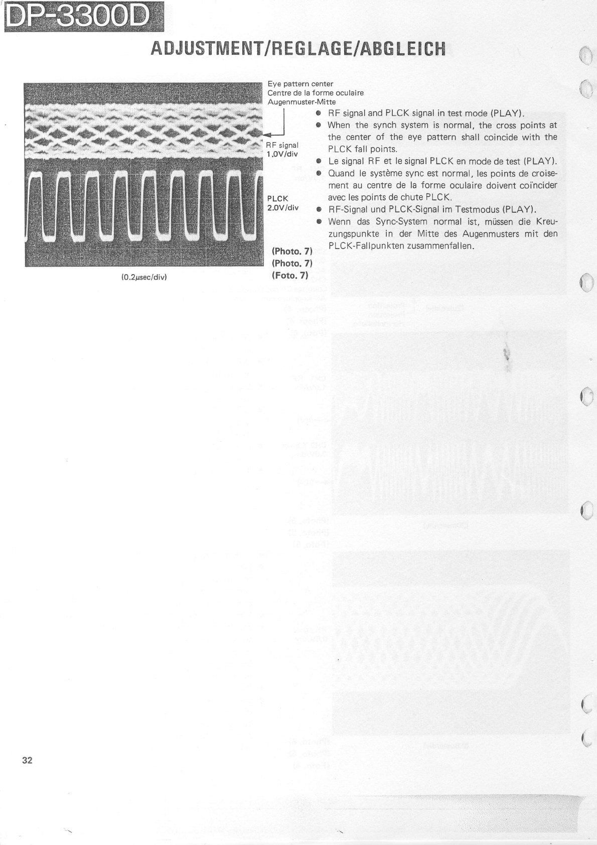
It"|-., ;*. i.**L*r;*;.**i"e ; I
.v+?+Y.lY+Y+Y+Y+Y*--r
+I+^+^+^* ^+;+;+; R r .irn"l
-*.--*"'+ + .+'- * .-L-.-f*^ t.OV/Aiv
(0,2rrsecldiv)
ADJUSTME
NT/R
EG
LAG
E/ABG
L
EI
CH
Eye
pattern
center
Centre de la
forme
oculaire
Augenmuster-Mitte
f,"1
(.i
PLCK
2.OYldiv
o RF
signaland
PLCK
signal in test
mode
(PLAY).
o When the synch system is normal,
the cross
points at
the center of the eye pattern shall coincide with the
PLCK
fall
points.
o Le signal
RF et le signal
PLCK
en
mode de
test
(PLAY).
o Ouand le systdrne sync
est normal,
les
points
de croise-
ment au centre
de la forme oculaire
doivent coi'ncider
avec les Doints
de chute
PLCK.
o RF-Signal
und
PLCK-Signal
im
Testmodus
(PLAY).
o Wenn das Sync-System normal ist, mtlssen die Kreu-
zungspunkte
in der Mitte des Augenmusters mit den
P LCK-Fal lpun
kten
zusammenfal
len.
(Photo.7)
{Photo.7)
(Foto.7) {:r
tt,
I
{:.,
l. l
(
(
(.
32
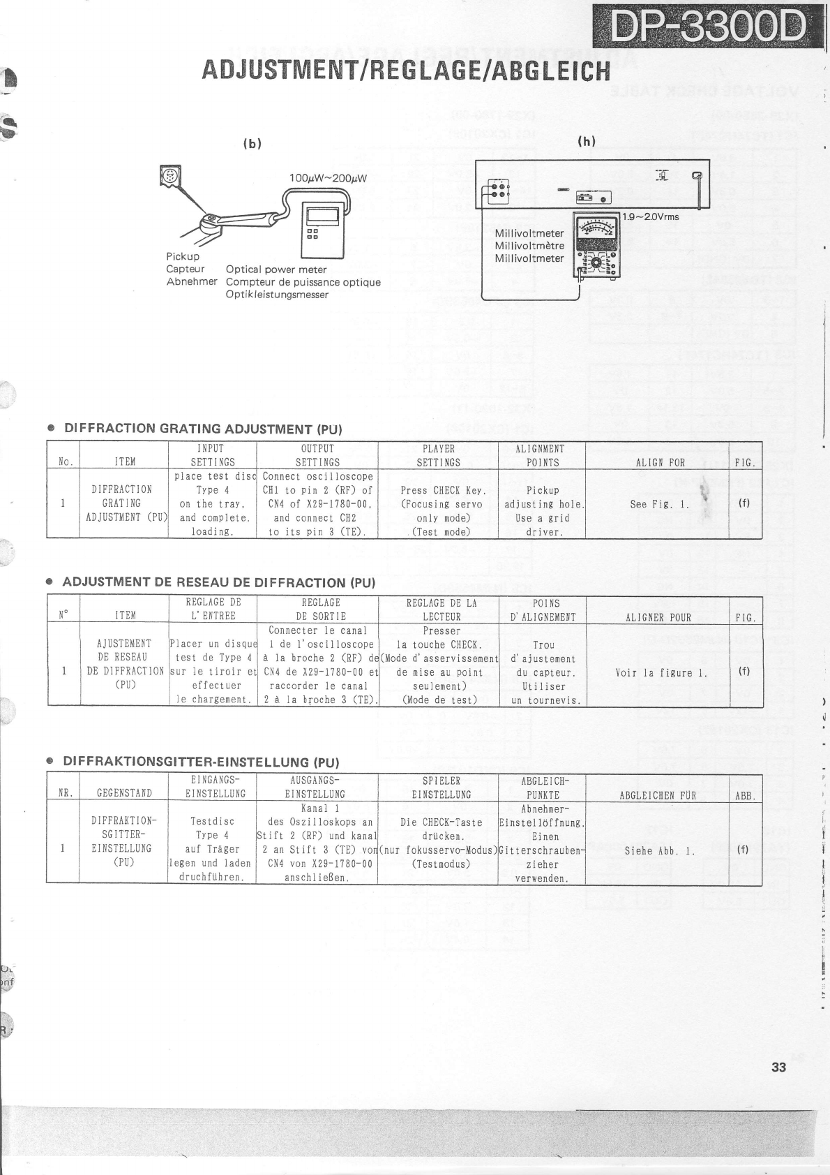
!
s
L
ADJUSTMENT/REG
LAG E/ABG
LEICH
(b)
Capteur Optical
power
meter
Abnehmer Compteur de puissance
optique
Optik leistu
ngsmesser
Millivoltmeter
Millivoltmdtre
Millivoltmeter
. DIFFRACTION
GRATING
ADJUSTMENT
(PU)
Ito. ITE}l I Ii PUT
SETT I NGS OUT PUT
SETT
I l,iGS PLAY DR
SETT
I NGS
ALIGN}ilENT
PO
I l{TS ALIGl,l
FOR Ft0.
DiFFRACTION
CRAT
II,IG
ADJUSTIlEl,]T
(PU
place
test dis
Tvpe 4
on
the tray,
and colnplete.
loading.
Connect osci iloscope
CHl
to pin 2 (RF)
of
CN4 of X29-1780-00,
and
connect
CH2
to its pin 3 (TE).
Press CHEC]( l(ey.
(Focus
i ng servo
only mode)
(Test mode)
Pickup
adjust
ing
hole
Use a grid
driver.
See Fig. 1l
1. (f)
. ADJUSTMENT
DE
RESEAU
DE DIFFRACTION
(PU}
NI TE]il BECLAGE DE
L'ENTREE REGLAGE
DE SORT I E REGLACE DE LA
LECT EU R PO I iis
D'ALICNE]|{ENT AL I GNER
POUR FIG
I
AJUSTE}ilEi,iT
DE RESE,{U
DE DIIFRACTiON
(
PU)
I acer un d
i
sque
test de
Type 4
ur le tiroir et
effectuer
I e chargement.
.
Connecter
le canal
1 de
I'oscilloscope
d 1a
broche 2 (RF)
dr
CN4
de
I29-1780-00 et
raccorder
I e canal
2 d 1a broche
3 (TE),
Presser
la touche
CHECI(.
]tlode
d'
asservissenen
de mise
au
poi
ni
seulement)
(]ilode
de test)
Trou
d'ajustement
du
capteur.
Ut i I iser
un
tournevis.
Voir la ligure 1 (f)
O DI FFRAKTIONSGITTER.EINSTELLUNG (PU)
NR. (]
EG El,lST A ND E i NGANCS-
E
I NSTELLU
NG AUSGANCS-
E I I.{STELLUNG SP
I
ELER
E I NSTELLUNG
ABGLE I CIl-
PUNKTE ABCLEICHEN
FUR ABB.
D 1 FFRAl{T ]OI,i-
SG
i TTER-
E I NSTELLUNC
(
PU)
Testdisc
Tvpe 4
aLif
TrAger
egen und
laden
druchfiihren.
Kanal
1
des
0szi I loskops
an
tiit 2 (RF)
und
kana
2
an Stift 3 (T[) vo
CN4 von
X29-1
780-00
anschlieBen.
Die CHECK-Taste
driicken.
(nur
fokusservo-}{odus
(Tes
t rrrod us
)
Abnehmer-
Einstelltjffnung
Ei nen
iitterschrauben
z i eher
vertvenden.
Siehe Abb, I (f)
n{
t.:
:, ;:',:.t-' ,.
.t,
t'
t-
33
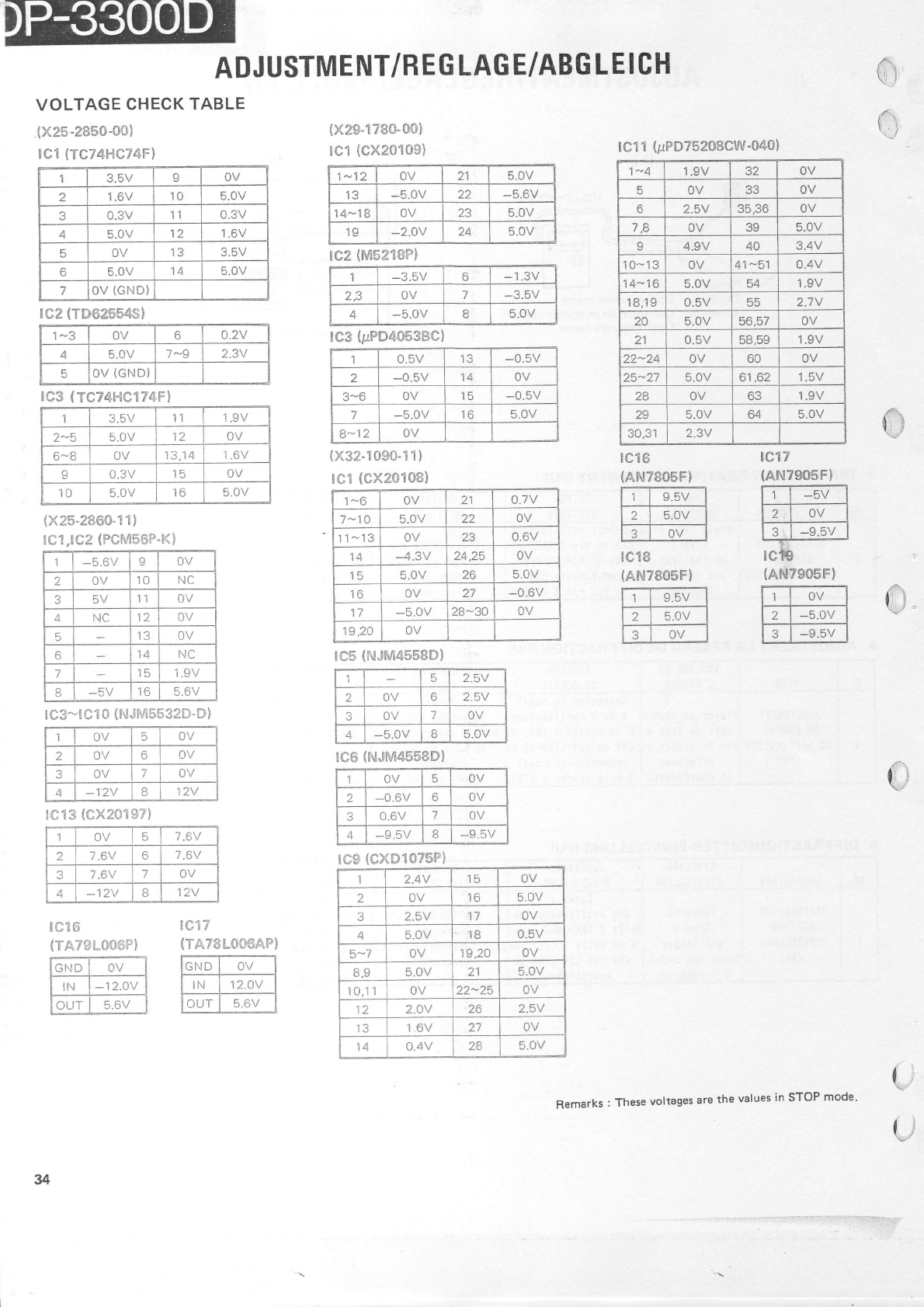
I2 R\/ IOV
zt.ov 10 5.OV
0.3v tl 0.3v
45.0v tz 1.6V
OV 13 3.5V
5-0v 14 5.0v
7OV
(GND)
VOLTAGE
CHECK TABLE
{x25-2850-0S}
lcl (Tc74l+c74F)
{x25-2860-X
t}
!e1,!c2
(PCM56P'-K)
ADJ
USTME
NT/R
E
G
LAG
E/AB
G L
E IC
H
txzg",|780-00)
rcl (cx201091
1*12 OV 21 5.0v
IJ -5.0v z1 -5.6V
14-18 OV ZJ 5.OV
1g -2.0v 5.0v
lc2
(M52t8p)
12 tr\/ 6-I.JV
2,3 OV 1-3.5V
4-5,OV I5.0v
!C3
(pFD4053EC)
0.5v IJ -0.5v
-0.5v 14 OV
3-6 OV 15 -0.5v
7-5.OV 16 5.OV
B-12 OV
(x32-109CI-1
1)
re,i
tex20108)
6J'
(t
,c17
(AN7905F)
rT-* I
L:_l_ev_l
l3l-e.5v I
.-Tb--
rclg
(AN7905F)
fl-* 1
lzl-s.ovl
ftT=Ev I
iex6
(TA7gL006F)
te 17
(TATELOO64F}
tc18
tAN7805Fl I
t;
Remarks : These
voltages
are the values
in STOP mode'
lC'!
1 (gFD75208CW-040)
1-A 1.gv 32 OV
5OV OV
62.5V JC,50 OV
t6 OV 39 5.0v
Y4.9V 40 3.4V
10-13 OV 41-51 0.4v
14-16 5.0v il 1.9V
I 8.19 o.5v 2.7V
2n 5.0v 56,57 OV
21 0.5v 58.59 1.9V
22-24 OV 60 OV
25-27 5.0v 61
.62 1.5V
28 OV 1-9V
29 5.0v 64 5.0v
30.31 2.3V
rc2
(Ts62554S)
t-J OV o0.2v
45.0v 7-S 2.3V
OV
(GND}
rc3
{TC74r-rC17$Fl
3.5V 11 1.9V
2-5 5.OV OV
6-8 OV 13,14 1.6V
0.3v OV
10 5.0v to 5.0v l-o OV ZI 0.7v
/- tu 5.0v 22 OV
'I
1
-13 OV ZJ 0.6v
14 -4.3V 24.25 OV
15 5.OV 26 5.0v
IO OV 27 -0.6v
-5.0v 28*30 OV
19.2O OV
!c5 (NJM4558Dl
,i IOV
2OV NC
35V 1OV
4NC 2OV
5JOV
64I.JC
75l.9v
8lo 5.6V
!e3-t e1
E
{f{J[M5532D-&]
52.5V
2OV o2.5V
3OV 7OV
4-5.0v 5.0v
!C6
($\iJM4558Dl
OV 5OV
2OV 6OV
JOV 7OV
4812V
!e13
(exzsts7)
1OV FOV
2-0.6v 6OV
30.6v 7OV
A-9.5V 8-9.5V
1OV 57.6V
27.6V 67.6V
a7.6V 7OV
4-12V 812V
res
tcxDl075Pi
2.4V t5 OV
2OV to 5.0v
32.5V 17 OV
5.0v to 0.5v
5-7 OV 19.20 OV
RO 5.0v a1 5.0v
'10,1
1OV 22-25 OV
2.OV 26 t F\/
IJ 1.6V 27 OV
14 0.4v zo 5.OV
u
i ''l_'l -
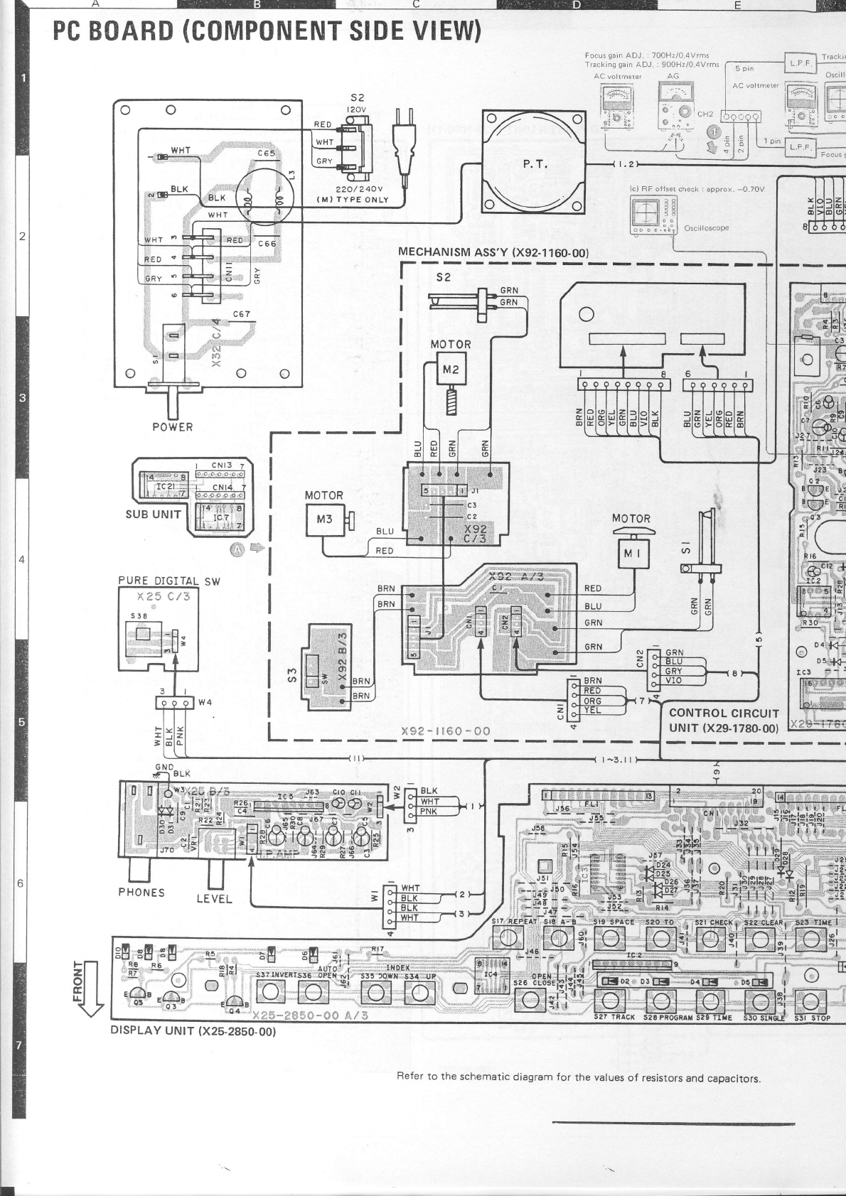
PC BOARD
(COMPONENT
SIDE
VIEW)
Focus gain ADJ l
Tracking gain ADJ
AC volrmeler
ffir
tr'-. -r I
i+-==..:
MECHANTSM
ASS'Y
{X92-1
160-00)
t--
I s2
ri
h'"'ii,
tl-tH
' t)i
-,.l.iiltj
POWER
CONTROL
CIRCUIT
uNrT (x29-1780-001
wr.i25
E-lca
,l,.ltl$|",
HF
llt"'fl*r
ff
ii I---------'t L:.Io
',,o
!l5l l-
I
Refer
to the
schematic
diagram for the values
of resistors
and capacitors.
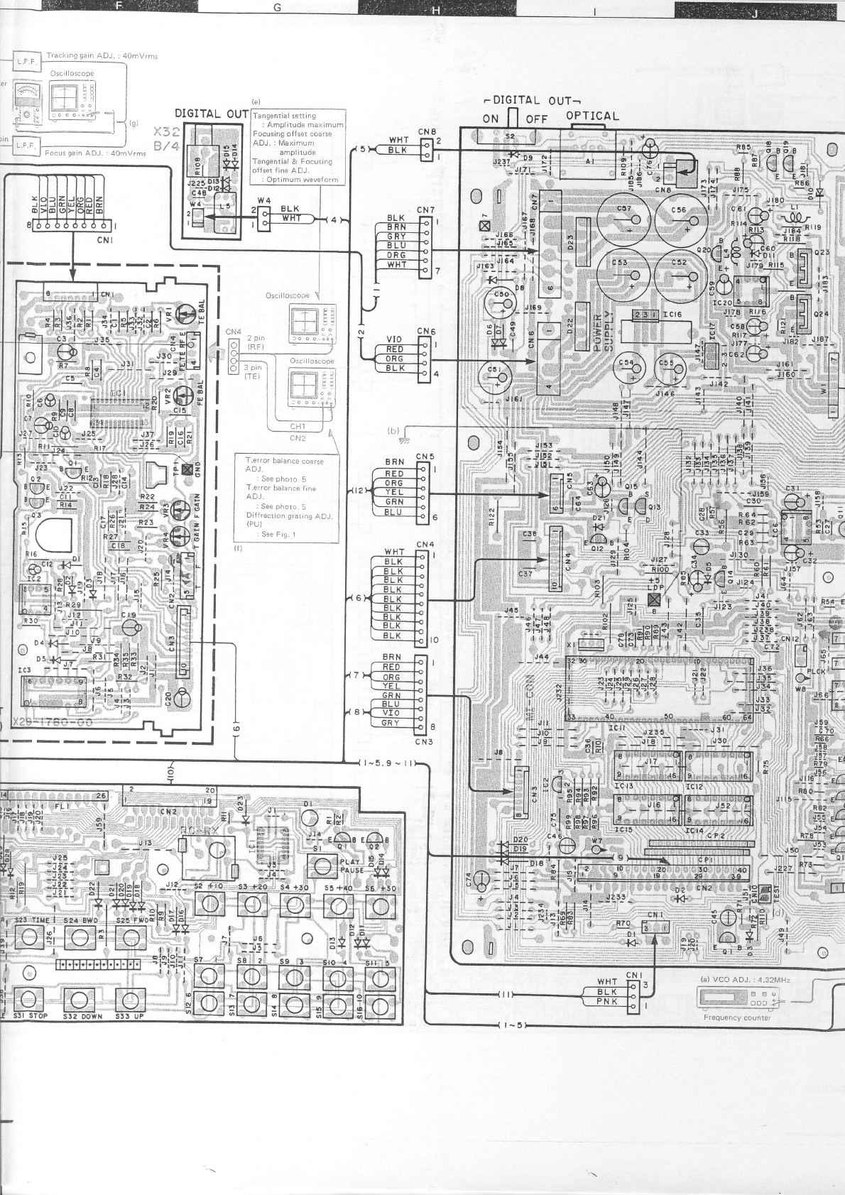
- DIGITAL
OUT-
ampr I
l!o€
Tangential & Focusing
ofJset
Jine ADJ.
: Opiimun vvavelorr
OPTICA
L
J.
, I ';Q{t,
.:" :r
i" ,...,.
"r,
'i.T:;tr.lr,;l
,
{ ."'T"ff :'i:.i
-t ;-'!tra '
-l r:--i--l
rl"t,b.ir
'liiioE
r .r ''8!1.
,K*p$
:i
lLr I
c16 Jll-id{-8,
---'l 1"* i-:'cc
__J '-E l,l
i:i -
ci;:;::
o J\>
"(Jt
'H#'ltnri,
, .r',i-o,..
...
_$ .:h":-::f?f:i
t; ...
:::^:
.:.:?" l.
I
,i
-.iJ1:L"r
i
1'1,
:,:l*liliiri
!,
Le|ct ba'tanaa
cozr.e
ADJ
Sec
pholc 5
T.ettar L,a
at,ae f
f .
A
DJ,
: See
phcr!. i
Drilraciron grairn! ADJ
{PU
J
: S€e
Frg l
cN5
BRN
,i ::i :
Lolr,ng
.6:-9 -,
'Nl;
j \!b
I irrN
.:
'l .-t...'rll:i
:,*
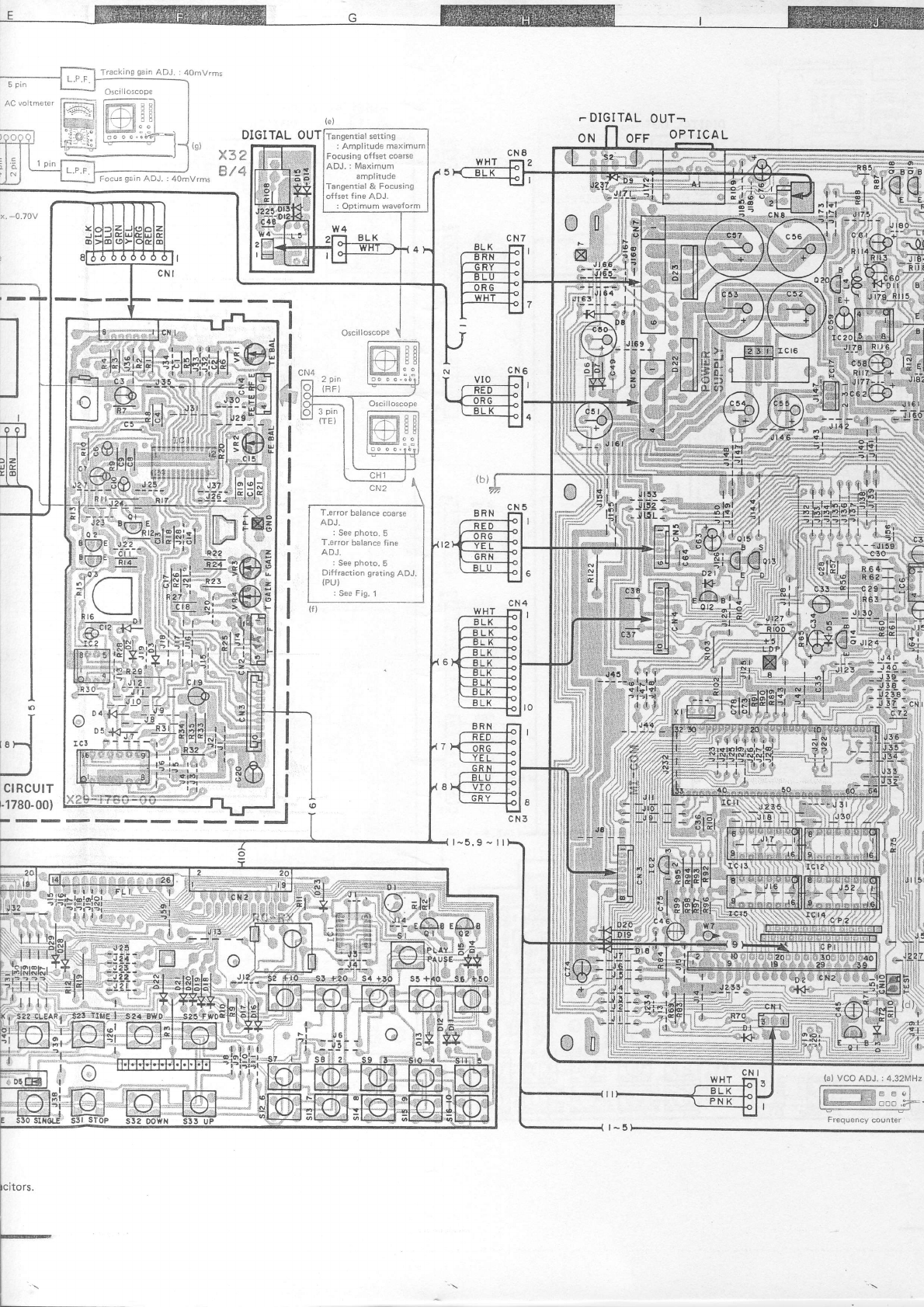
ONIIOFF OPTICA
L
-DIGITAL OUT-
ffi#'
Frequency counter
40mVrms
>i32
B/4
T.error balance
coarse
ADJ.
:
See
photo.5
T.error
balance fine
ADJ.
: See
photo. 5
Diffraction grating
ADJ
{PU]
: Se€
Fig.
1
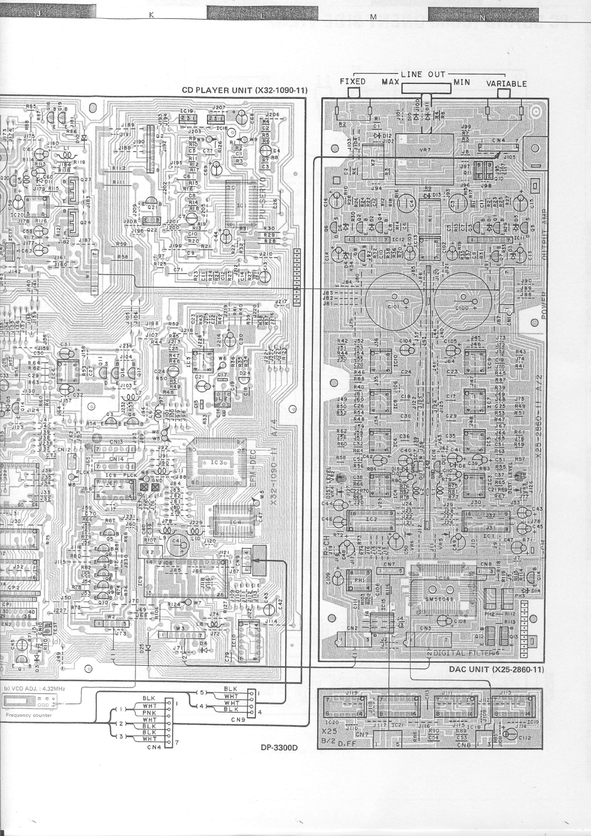
{l
:,
^J-
-
..1
lt9
,.
l
I,
lo23
t.
|.,:'.'
I
i;,,'
t':
I
024
I
|. .:
-J!81.
,. ns
, a,6,
_ _Jf8g _ ffl ,;Fa
---Jrer ll lo,
Jlsolll.*
_,r'J:-:
ll I
ig
. ilI
il.1
R| 2 ll.l n
I
Blll *r
' Rl
-l
. ..'t:::
t:l
cD PLAYER
UNtT
(X32-1090-11)
nn
oll
,:24' :
'-"-*m--
LINE OUT
FIXED MAX
I--! MIN VARIABLE
DAC
UNrT
(X25-2860-11)
'|
.
.
.".=:...,::,..,
rA
,l{ cP2
DP-3300D
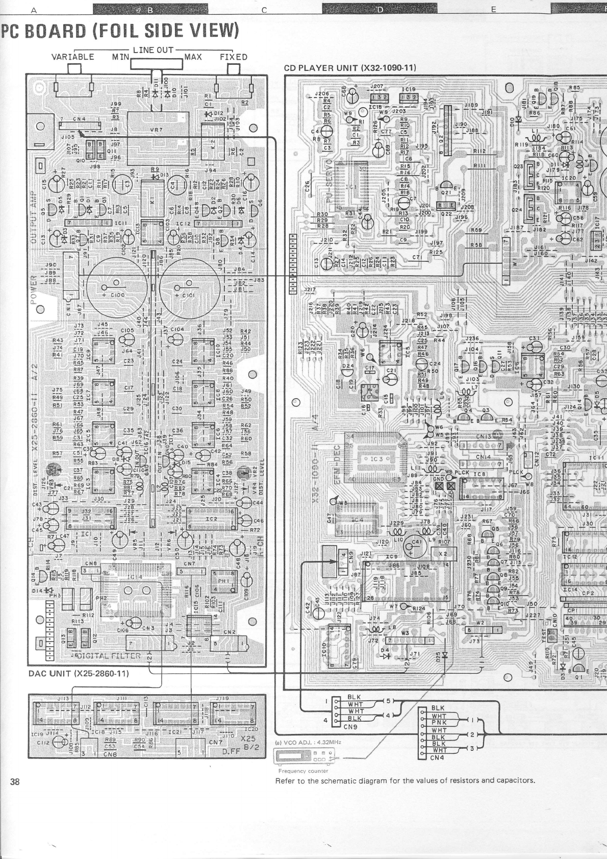
ffi c W e W*ffiffi
LINE
OUT
'rs
l
ii: i: R
J99 cl R2
cl
r+qri-l
I
? cN4 r i! | | -'lJrozlol'
r--------------ll I I t:199
E] oro-l-eP-" I I ' n
lij +i JsB e ;--Ee* -! ,;,
,I 5 1l'1uFt
;r:r@
ffi '@l:r
:
rtrxrtrnr:'9
:;:
qEX-;E.g l; | '- io pB.-q
:,1
aD*T.D6,D:lEI:l
I - |
:l:t:l
$)a;)ir )"
:i: - f7-::1:r::f,.,J:l
r.,r "ffi13 rc
rz
Fl-:-:.-i-:ITil 6
Ll
:Df I
.l)6rl)rlslrl
I |
:l:t:l
iDagEl
6 D-
,:, : F-.._-rtl'.1^:FTH_rc',r? _--ri-l
i
l,
i :
"Oi
rril
*
a
t
e
rlrlp'
I
"
_.
|
$.rr
Er
a
I
rai
:f I'
fD
,-" lt'"-l-ti i- <a;Pl;sif---ri*'
" i
te
s165 H
lqj"H$"ji:
I lul:
lrur'
R'Plre I
rllr2'.2' \ gl
tl
lt ./ \ -
l__Jq:_
J90
-: =---
fr
-Jer:l
f1 I JE2
l-lcr_:
o Y-rr\ /'li
Iql\_/rili,,\_/qi
iii :iil:
:<=Fili-iax
{l q:i
q+r
1n Jt. cro5
' 'll t15 :1 j:: :+i
H-;
:ij tr-€ ,illiSr
ffi,ii: .#;
;;, ]]isl , l'""g1 llr | : l:vev
:r:
p4b-E-l-j c23 i ll c24 l; l{l ;A
: Nl ll .^l
-' ,,, f:i"f n' iilnli
i ;r ffi--ri;
:r H
trrt*LJ
le'pil'lP1:-*
L!r# f:
;i 8",.1
Ei : i
il
li
i : ii 31.;
i; 3s+
JF!"F=
.._,Eisll=*=*.
ffigiii F:
ij E-1"
S":"tI*irerel r{fi .oo
to
'o
t tu
( *- s-l'''"-!--
'.X;Dl
l;DR,',9q.
d.
; _!
: -ff F:'FI?'{ei
i:Bfnrtr"ffi
::
I;;s-fc,:::31.
"l
*ry9
lnlr9-U-;
t+rF*:igE
o =-"r33 :' ;;- fi
't€F? _
:",'
ifi- | l--*-;-u-:!i{€'*
"f;51,-'t' - -lll-i?s:
td ::u',.1.
"' ilRJ:"
:i ffig-iil"li lE:r.-E:
o
'j .' H|€;sQ:rii iJ
t i l;43, nso
lo c .l -p5a
+ agc42; R5s
rza;1{ - J3'
- -,ll
:!?s- td ::1t;L_*jl1_dp,::.
:fifl,ffiqtt*,lffi^* 3:
i'*$'
;-
ilgli =i {qm-,,S";;t
rt..-};i TFd9
'i =1:rs,il-
g
--'l lg .'",;l
'' [Fl---]l-l s
eilb---l'
rLl6 Jrl5 Jil6 tczl
R89 R90 @
|
:;T tra El
PC
EOAffiD
{FOIL
SEOE
VEEW}
VARIABLE M MAX FiXED
CD
PLAYER
UNIT
(X32.1090-11)
iilprEi$r
:r,riprltltltg
Riz
, ",gi:i
J
,l .:...
:
::!r1.,
ol@: I I I !..'
9 t!trloio,+lnl-
- r-lhlDlnlErnln
I r-t-l-l-i>rr
I Jrl J | | |
" c3o '. -l
.tslFl
:? F,l
-ri
ii/
r'..
tf ,
.\
a l:\
'Pt
\\ \,
.vj \
DAC UNtT
(X25.2860-11)
38 Refer to the schematic
diagram
for the
values
of resistors and
capacitors.
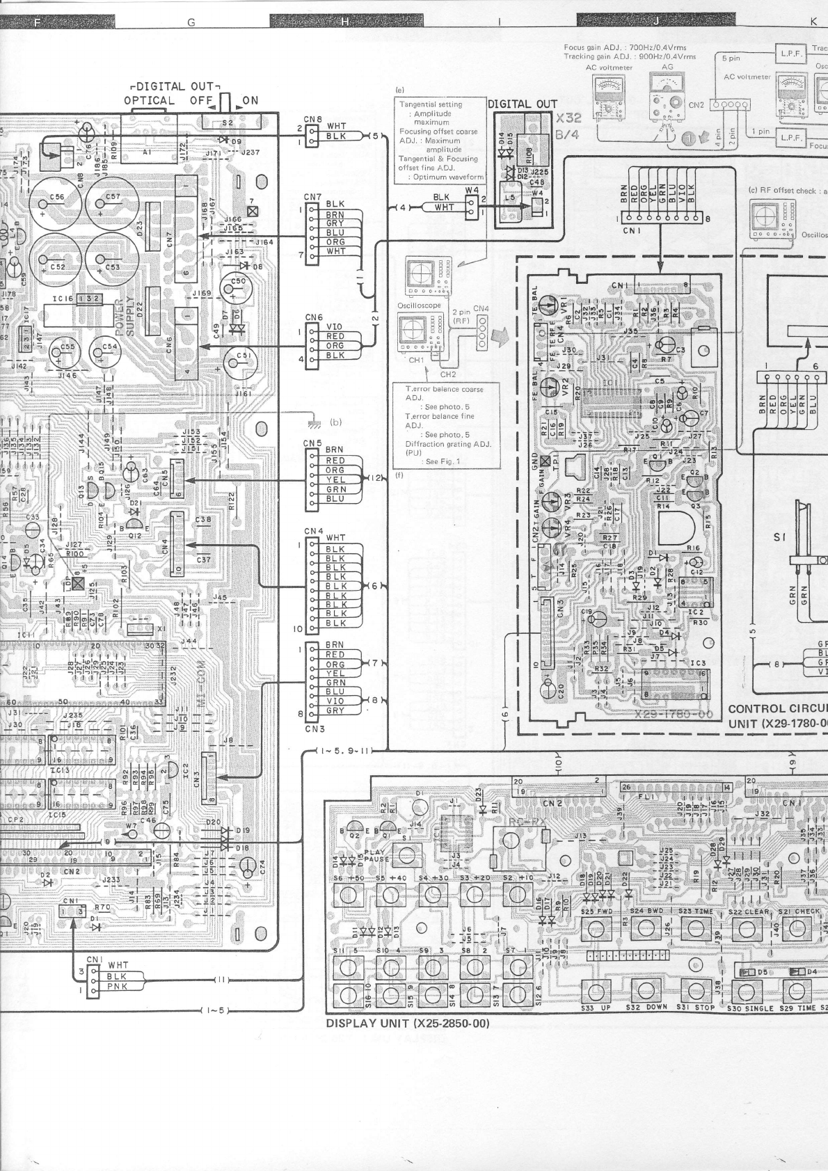
ffitu?ffi c @ r @
-DIGITAL
OUT-
0ry1 oFLll>oN
,- .la.o9 :
.Jt?t
ir-?-'J237
:F:!-!
i|ino
ilo
Tangential
seitrng
:AmPlrtude
maxifrum
Focusing
otfsei coars€
ADJ.:h4aximum
amplitud€
Tangenti6l
& Focusing
offset {in€ ADJ.
: Optimum wav€iorm
Focus
gain
ADJ.: 700H2/0.4vrms
Trackin!
gain
ADJ. :9oOHZ/O.4vrms
|' ,,"f,6,{,
GITAL OUT
AC voltmeter
l.Alil
L--.
::
t:.; ;:-
>,-
FN
en
H;
rc re
lT"ii'l ";
r----'"r-]?
ltE
L-lo
,z---. ,--+
q)_e
r69 \V
-'*l
I bl'l
3tw
ol.' '
a
Ir-l
ilt
ltl
ILJ .
I t. 2
'
,,t' ,u
tAi t**
;l
ol
'l
$ia
.
'l t I
.l*lo!
- t-l-t ,
;:
il ..1
,l i
', ttlr
"'',i
l:d
,1;*
t7
!91
zl
. lclS
l11 | l/'\ |
l\Jt
l\rl
-*u,
**'.t
E+rEl;i
sil 5 slo 4
f-51
lvl
t
, "t
r
t.t
sr -r
..
.qlel'!
111:l;lli:lll
l\Jt,
FFI* l-Al,
l\1 l;lL/ l-s ,TIHE
'r,*--.-.It
l:-"-r :J
]6-, &,'1"'u,
lo "":
.
z
pin
clf
{c) RF offset checl. : al
CONTROL
CIRCUI
uNlT (x29-1780-0(
T,error balance
co6rs€
ADJ.
:
See
photo.5
T.error balance
flne
A DJ.
:
Se€
photo.5
Dif
f
raciion graling
ADJ
(pU
l:
See
Fig.1
slehlnl
"l"l"rl
cHlgCIl
*, "o",
€\
DISPLAY UNtT
(X25-2850-00)
39\' *Ht
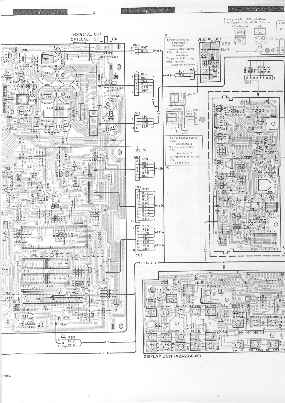
Focus
gain
ADJ. :
Tracking
gain
ADJ
700H2/0.4Vrms
-DIGITAL OUT-
oPTrcAL
OFL GITAL
OUT
900H2/0.4Vrms
AG
FYT'
nr;.'4
l6-,
sl.,u,
le";.1
b
pin
ACr
ON Tangenti6l
setting
: AmPlitude
maximum
Focusing
offset coarse
ADJ. : Maximum
amPlitude
Tangential
& Focusing
otfset fine ADJ.
Optimum wave
t "Tr
ffi,,g s
x32
&/4
r ' ii
. ,El
i--
j
!-- :
^rji!
,i:ii+
,i
if li
ii
ii.:
ii:
I
:!J!
.s8
ti
i: 1..
i"l,;
z
pin
ci!
T.error balance coarse
ADJ.
I See
photo. 5
T.error balance
fine
ADJ,
: See
photo. 5
Di{{raction grating
ADJ.
iPU)
: See
Fig. 1
-91i"
::t.i::
!t'_
DISPLAY
UNlr (X25-2850-00)
l
"'o^
I
I
L
_:.JZJ A:
sToP
""
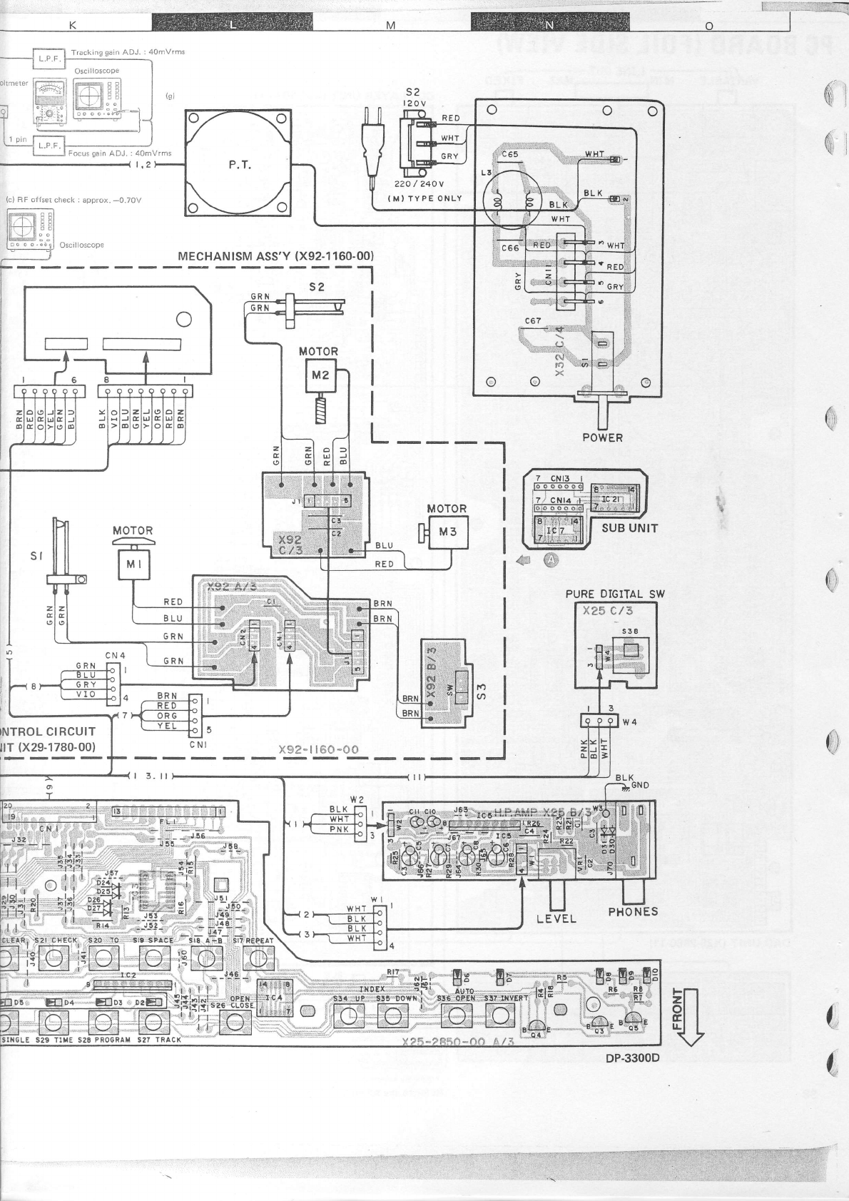
40mVrms
1gJ
MECHANTSM
ASS'Y
{X92-1
160-00)
-1
t_
"i
_$ Jai
..:''.
."
c65 ' i ., WHT
.-
t- .: (--::--v
L3:"r/-4. I
ff,r
$i
fl,
0
PURE
DIGITAL
SW
l/)
xgz-t t66*00
t.
{
(cl RF ofisei check : approx.
-0.70V
)NTROL CIRCUIT
ilT (X29-1780-00)
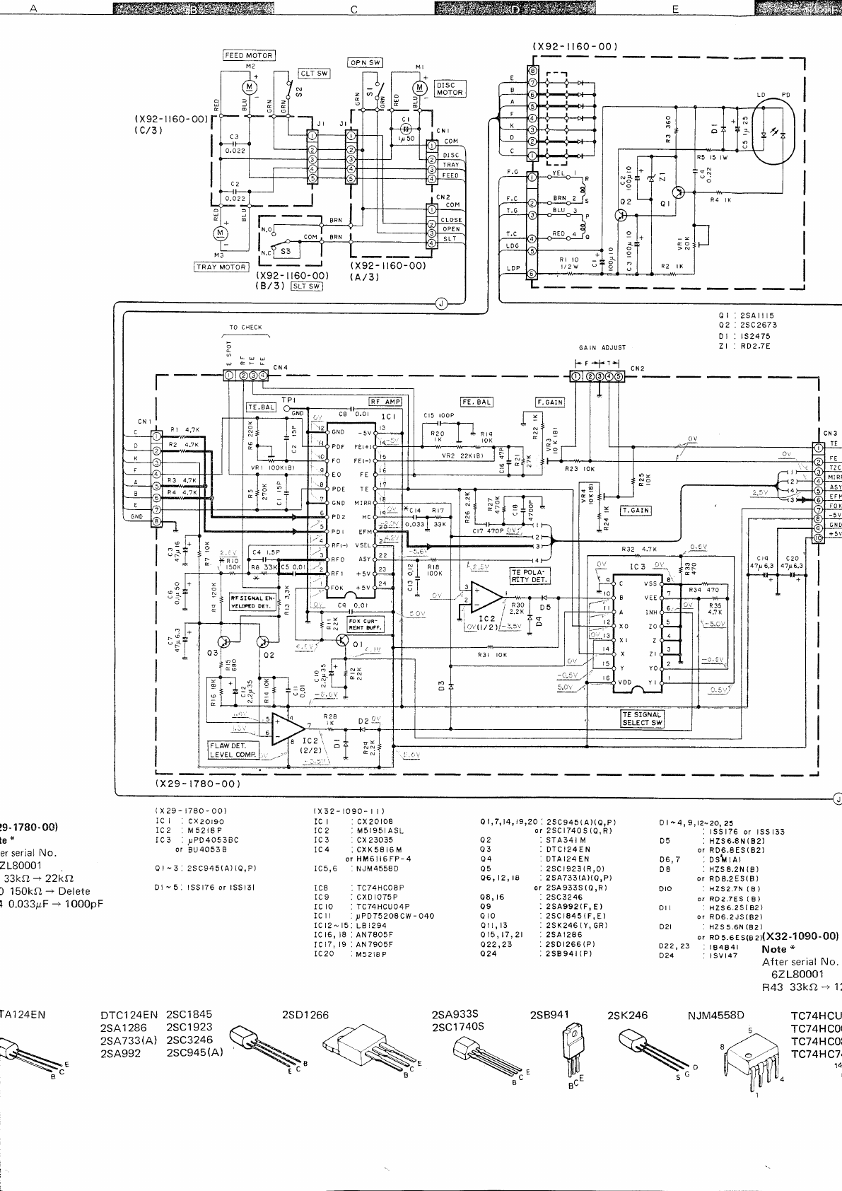
e @lE@Mffi c @il*M e @@
(x92-il60-00)
r
(c/3) ,
I
oPN swl
Icr-r
swl
-J
L:J (x92-
| r60-00)
(x92-
il60-00)
(B/3) tsLr.wl (A/3)
(x92-il60-00)
GA
IN AOJUST
0r
:2sAill5
o2
.2SC?673
D | '. ts2475
L I nu z,t L
F* r *i- r-l
' ' ' cN2
M3
IIRAY
MoroE
TO CHECK
o
c
ouuu
u&FL
I
l
I
I
lrE,
uALl lF.
GAf rrl
!
I
I
I
I
Dl-419,12-?o,?3
: lSSl76
or lSSl33
D5 :HZS6.8N(82)
or
R06.8ES(82)
06,7 : DSf,{ tAl
08 :Hzs8.2N(B)
or
RD8.2ES(B)
DIO :HZSz.7N(B)
or RD2.7ES
(B)
D| :HZS6.2S(82)
or
RD6.2JS(82)
D2r : HZS
5.6N
(82
)
or
RD
5.6Es(B
?)(x32-1090-00)
D22,23 : tB4B4t NOte
*
D24 : lsvl47 After serial
No.
62L80001
R43 33kA
--+
11
>o
R23
rOK
No
E-
@
o
?
r@
u"{
: lr.GArNl
l-- __J
(x29-
t780-00 )
!9.1780-00)
le*
er serial
No.
zLB0001
33kS2,
-' 22kA
) 150kO
--+
Delete
l 0,033pF
--+
1O00pF
{
x29- r780-OO)
IC | : cx2olgo
lc2 .
M52t8P
iC3 i
pPD4053BC
or 8U4053
B
al"3l 25C945(A){0,P)
Dl
" 5. lSS176 or lSS13l
(x32-1o90-
|
t)
IC | :CX20|O8
tc2 :M5r95tASt-
IC3 . CX23035
IC4 .
CXK58r6M
or
HM6ll6FP-4
IC5,6 . NJM4558D
IC8 . TC74HC08F
IC9 . CXDt075P
IC rO : TC74HCU04P
ICII .pPD752OBC\{-O40
IC
l2
- l5:
LB
1294
IC
t6, 18
: AN78O5F
ICr7,
r9
: AN79O5F
lc20 :
Mszl8
P
Q1,7,14t,9,2O:
ua
n?
o4
nE
06,
12,
rB :
or
Q8,
t6 :
UY
Qro :
Qil,13 :
0 15, 17,
21
Q22,23 :
o24 .
2SC945(A)(Q,P)
2SCr740S
(O,R)
STA34I M
DTCI24EN
DTA
I24
EN
2SCt923(R,0)
2SA733(A)(Q,P)
2SA933S
(0,R)
2SC 3246
2SA992(F,
E)
2SCl845(F,E)
2SK246(Y,cR)
2SA r286
2SD
r266
(P)
2SB94i
(P)
DTCl
24EN
2SA1286
2SA733(A)
25A992
2SC1B45 2SD1
266 2SA933S 2SB941
2SC1923 -\ z.->--'-., 2SC1740S K^ t
\, --rN>r\, W
-B*
B
- Rc'
NJM4558D TCT4HCU
TC74HCol
TC74HCOi
TC74HC7,
14
,..>>
(\ g/A
" {,NflJli[],
Il,lU"
T
G
ll-A124EN 25K246
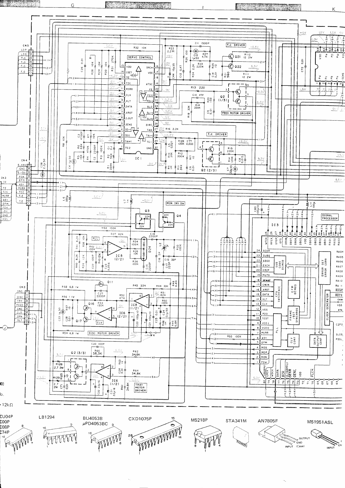
q
!obdE
ocd[
.-m
-No96@
sl s+ st5+
sTgfs
Qr@6a9oN--No
9ooa;ooooooo
3338;3338;;f
RA
O4
RAO5
RAO6
RA
O7
RA
O8
RAOq
RA
IO
RAI
RA !r'8
RACS
c4 u
TTA
g@r@o
@@@@@
:i'-.-, IEc pn'/EE -::
o
r
o
VDD N SRCH
ISET,
, fT VEE
02 l
(r
/3,
I
+
z't.;1! ata z.zx
A
o
r
o
&- L___f-;
Q2 t2/3
) 5.?
lMon
rNvstl
>k
-S
o
N
o
c
o
o
c
@
o
o
z
r
5 t2/?l
I /2)
a
t0)
lo.
,1ZkQ
CU04P
c00P
cOBP
974P
i14
STA34? M
[]
%/
BU4O53B CX
D1O75P 15
PPD4OS3BC s- ---t;
-
-^'"";->> -/'a
*@,,@
,,
AN7805F
fvr521BP M51
951
ASL
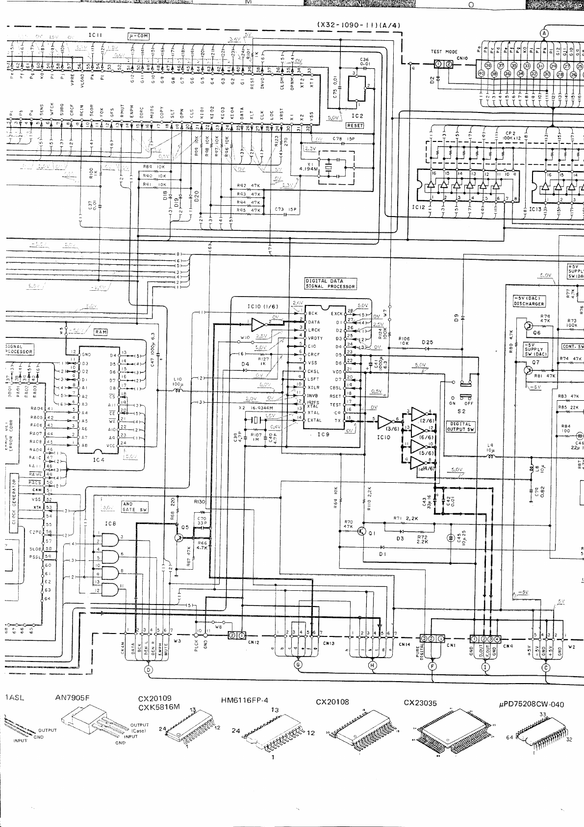
(x32-
1090-
|
t',
tA,/4)
-Noco@r@o9:!yoso@
ll
IL
:
"r,
oouo
OYcde<C[
>J
o-oL,E
zY@o:-
:
--;;5
H
r,?
ovoNotfN
ooooofia3.=:i
9O
::::g;s3t:5:i:
@r@
ooogooo
c2P0
PSS
ITEv-
I
suPPL,
lsw(DAl
i /J
I
O0x
iioNi. sw
R'74 47 t<
R83 47K
R85 22K
roo
c46
z4J I
i!.
__l
l60
6i
e2
63
I
!
I
I
\d2
cx20109
r0
I t^^
..r,.t\ LVa
a'.i i
' i"1'.' i
ICtO
il/6)
8CX EXCX
DATA O
I
LRCK D2
VRDTY O 3
CIO D4
lFLr u5
VSS D6
CXSL VDD
I qFT
XILR CBSL
INVB RSET
r
q2Fs
XTAL IE)I
XTAL .Cq
EXTAL TX
n? Ktz
a,<
cxK5B16M g
g
-9/
rPUT ^{
ser tK*,K
HM6116FP-4
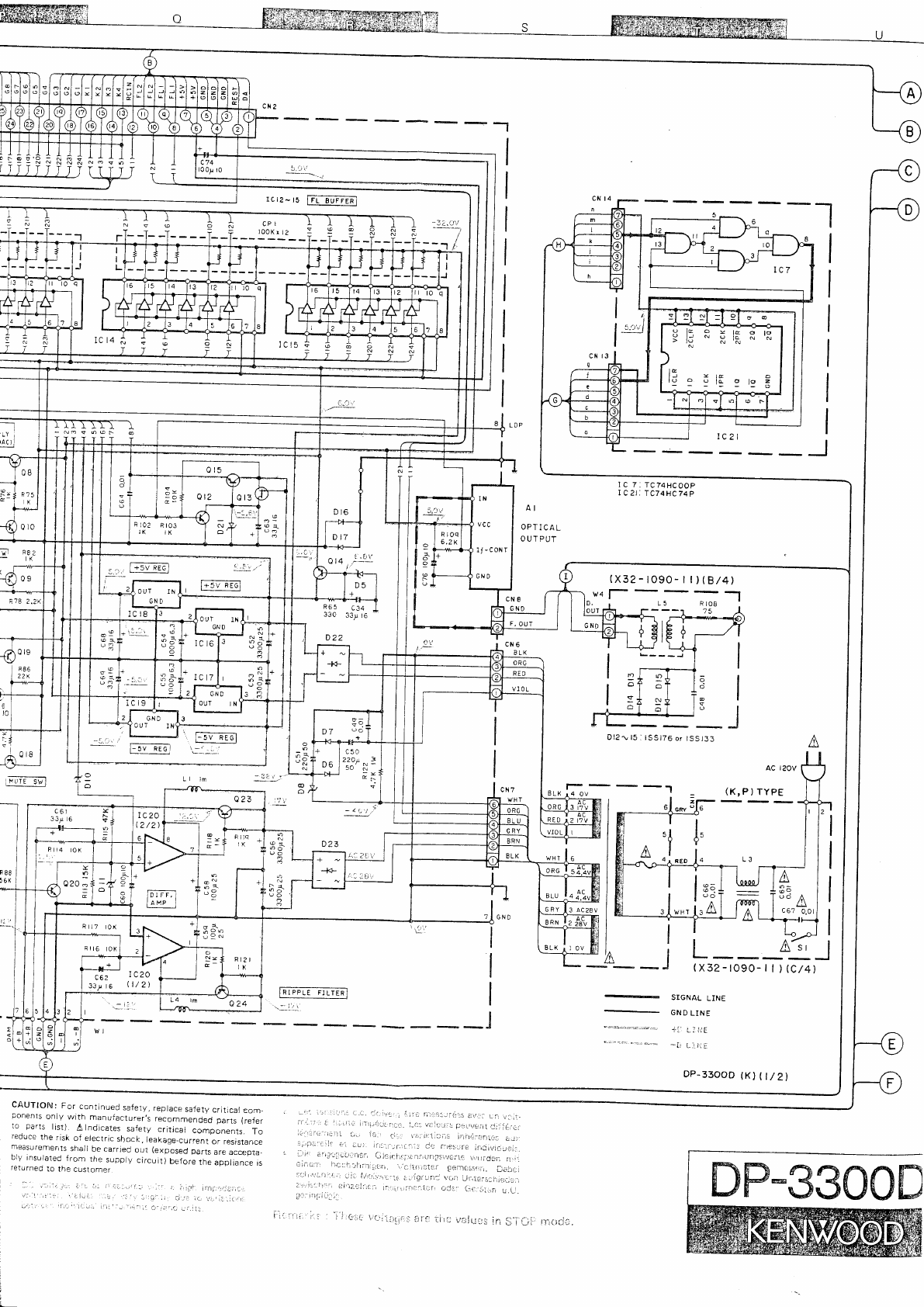
Y:=sXnRRX*;;--
iJIIITTITTTTTT
rctZ-t5 Fr BUFFERI
--l
,:i,
I
cN8
cN0
_l
I
ffil
CAUTION: For conlinued
safety,
replace
sa{ety
cr;tjcal
€om-
ponents
oniy with manufacturer,s
recommended parts (refer
1o parts tist). Alndicates sa{ety critical components. To
reduce
the risk of electric
sbock, leakage-.urrun,-or
r"f,rr"n"u
measurements
shall
be
carrjed
out (expp5s6
parts
are
accepra-
bly insulaied
from the 5upply
circuit)
before
the
appliance
is
returned
to the cuslomer
rcts+
6 6 6 i +
::
oYlceto
N o Io N N
NN
Y lE o
o lo o lo z
o
R65 c34
330 33;
tG
(x32-t090-t
t)(B/4)
ct, cN6
BLK
D12a 15
: tSStZ6
or tSSt33
clt T
ac t20v
(K,P) TYPE
A
5I
A
I
I
'.::'l I
a
I
--ai
h I
:*_ _J (x32-1o90-
| ) tc/4|
lFtPPrc Frr rrol
--; / r'
SIGNAL LINE
GND
LINE
-i; J iafi
DP-33ooD
(Klu/2t
o
o
N
OQ
o
o
o
r
GND
oui IN
UO
o6
,2, r
czo
33t l5 \l/2)
J
1C 7
IC2I TCT4HCOOP
TC74HC74P
AI
OPT
ICA
L
O
UT PUT
mp*ffi3ffi0ffi
't i:r::;{, i'r.-,,,,;,1.,11;
i:i{: \.t.itt
!,;ili.ii:: in $"1 1;:, it.:il*;.
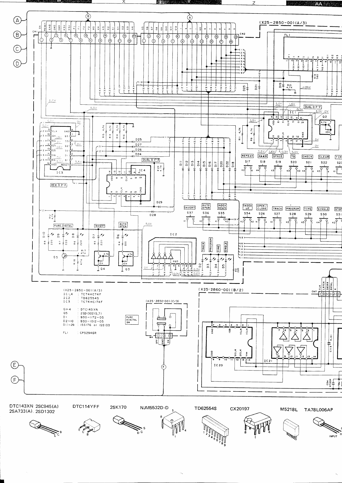
FNvEfil
s37
IFEPEAN
sl7
(
x25-
2850-OO)
(A/3)
I
,/ f',1 \ |
:"sy-/ Lgv
/ r,,_q.iy.',,.-l.cl
F><Bl lsFATEl @
sr8 srg s20
FFA.KI @;RAHf @B
S27 S28 S29
--J-- -J- ---l_
IcLEARI
>zz
Eu.
0(
*,1
r-_:.-
ILNEL(I
s2 l
(,
n
n
o
N
o
IoFEN
7l
lcLosEl
) zb
r-
I
J
T
lul
tJt
l9l
tzl
tE)
/+/./
T
ol
r:l
I
t
rn
l;t lEl
l3l lgl tll
lFl 14l lEl
/7
g
o
Furol
IOPENI
5 5b
./J
n
o
frNDerl
I
powNl
s35
tiNDE t
I UP
I
s34 FrNaE
5 5U
KI
(x25-2860-oo)(B/2)
t--
{x25-2850-OO)(A,/3)
ICl,4 _ TC74HC74F
IC2 : T062554S
IC3 . rc74
HCt74F
al^4 :DTCl43xN
05 : 2SDt302(S,T)
D
l . B3O-|72-O5
D2-to :830-rot2-o5
Dll-29 : lSSl76
or tSSl33
cP5294cR
DTC143XN
2SC945tA)
2SA733(A).
2SD1302 DTC1
14YFF
<-\.t
e^,
NJM5532D-D M5218L TATSLOOoAP
t a,-->
$iw.
i
!
I
\
25K1
70 TD62554S cx201
97
S}\
\# INPUT-
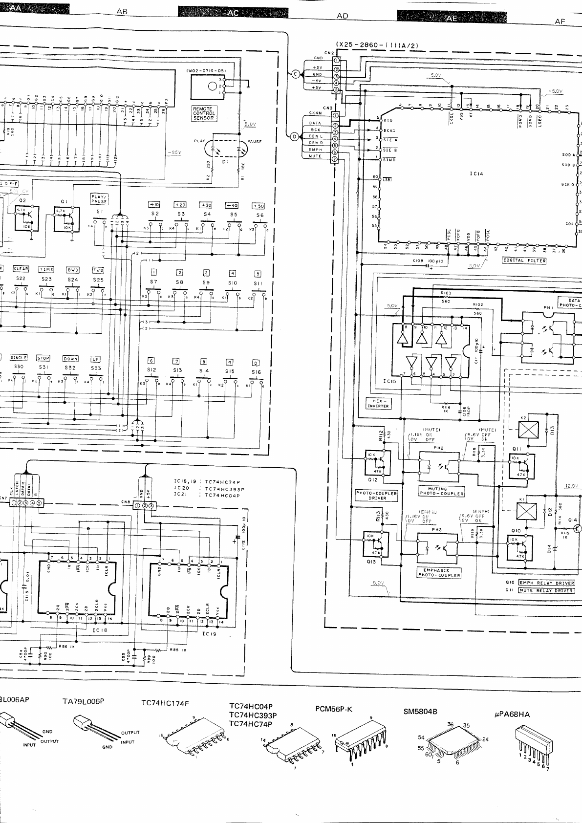
(x25-2860-
tt],(A/?)
r0F-Fl I
--!1,t" I
1 |
'/'o?
i
lil*Tfl
ITfi I
I lMl
I -1'
J.'
IPLAy/ I
lpausr
J
SI
d
Y
l.'i_fil D
s7
r-:-l
L'
JO
t-:l
)5
tr
sro
m
E
stl
g;93I
FIGIiAL FILTERT
{f.tu1'a}
/c.6v
0FF
I
ov n,i
@
)35
x4
J lr
|l{i,TE)
PH2
ICt8,l9:
rc74HC74P
rc
ao : rc74Hc393p
IC2t : TC74
HCO4P
-1
^l
:l
9l
:l
ol
;
IEHPH RELAY
DRIvERI
IHUTE RELAY
ORIVER
I
E| +rul t=;6]
53
L - _l
>25
I hrNA;l
s30 FNE
JJ I
Fofil r:l
B
qr2 tr
>t5 tr
> tf,
tsLOO6AP
G
\:,,
TA79LO06P
<>.
\;;;;'
T074HC174F TC74HC04p pCM56p_K
s ^ TC74HC393P
-"--\ rc74Ha;;; ' .-'>
q^**"e'
'qk,@ SM5804B pPA6SHA
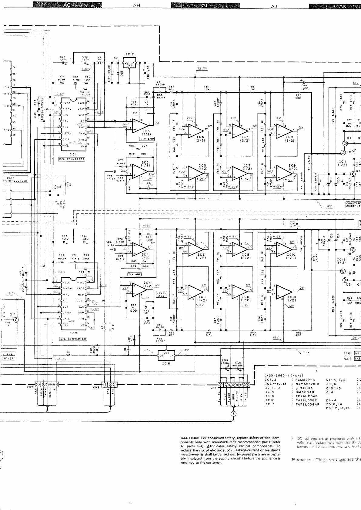
EEIEEIEIffi eH EIE aL EETrE
L_
I
c-'
'!---l:-: FoNsrANr
ICURRENT
DAr;---]
^'an-anrrprFal
IC5
(t/21 t/2)
l?/2) \c/ z)
ICI
Io/a coNvERrE-l
T
I
T
---
ICrO
(2/21
o o 'lZV o q -i2i/
3 U
--v'
ItA coNVERTETI
I
(
I
R
88
rc'z FlJl
oa,a ltls
IC3
- lO,l3
IC
lr, r2
rc
l4
IC
r5
NJM5532D-D
!PA68HA
SM58O4B
TC74HC04F
TA79
L006P
TA78
LOO6AP
(a/?)
: PCM56P.
KOl-4,7,
I
o
5,6
Q
ro- r3
Qr4
Dl-4
D5,6,
r4
D8,12,13,15
2
CAUTION: For continued sa{ety, replace sa{ety
critical com-
ponents only with manufacturer's recommended parts (re{er
to parts list). Alndicates safety critical components. To
reduce
the risk oJ electric shock, leakage-current or resistance
measurements shall be carried out (exposed parts are accepta-
bly insulated
{rom the supply circuit) be{ore the appliance
is
returned to the customer.
DC voltage: are a:.ne'rsured vrit!-i ;, h
voiintetei. Velues ma7 verT s;lightl,7 di
bei'rve:n indirliciuel insirui-neri.is ar
lanC r
Reittari.,s : Tl"rese vG!taglts 6fe th{
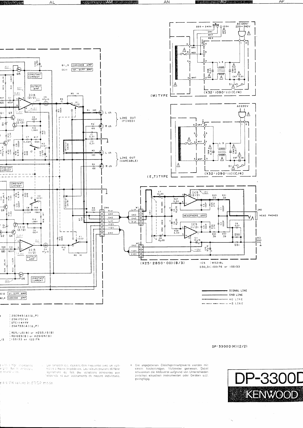
I
ACI?OV/ I
?20 - 240V
;l
3e1
oo I
AI
or,s ltlstop€ A-il;l
ICil ll3r. DIFF AMPI
L-I
I
F
t,
tl
tl
) 'ut,:,,
(M)
TYPE J
^ii"
I
A
3",
IA
c67 0.ol
'\
'-,*. ou.,
I rvanrrer-er
lao
N
s
ra Ni'l I
lcu
RRENr
| |
------J
__l__-- I
(x32-
lO90-
ttl-
(C/4)
(x25-
2850-
OO)
(B/3)
SIGNAL LINE
GND
L1NE
+!j LrN !
DP-
33
AOO
(K)
l2/?l
zi.",isafieil einzelnen inslr-L!fflanten oitr Ge:'ate:r u.U.
g.ri'ii"rg{Lig
1g .
:2SC945(A)(0,P)
;2SKr70(v)
:DTCII4YFF
:2SA733(A)(O,P)
, nO:.rUS(8)
or
HZS5.lS(B)
'
RDTOES(B
) or
HZSIoN(B)
:lSSl33
or lSSl76
DP-3300t
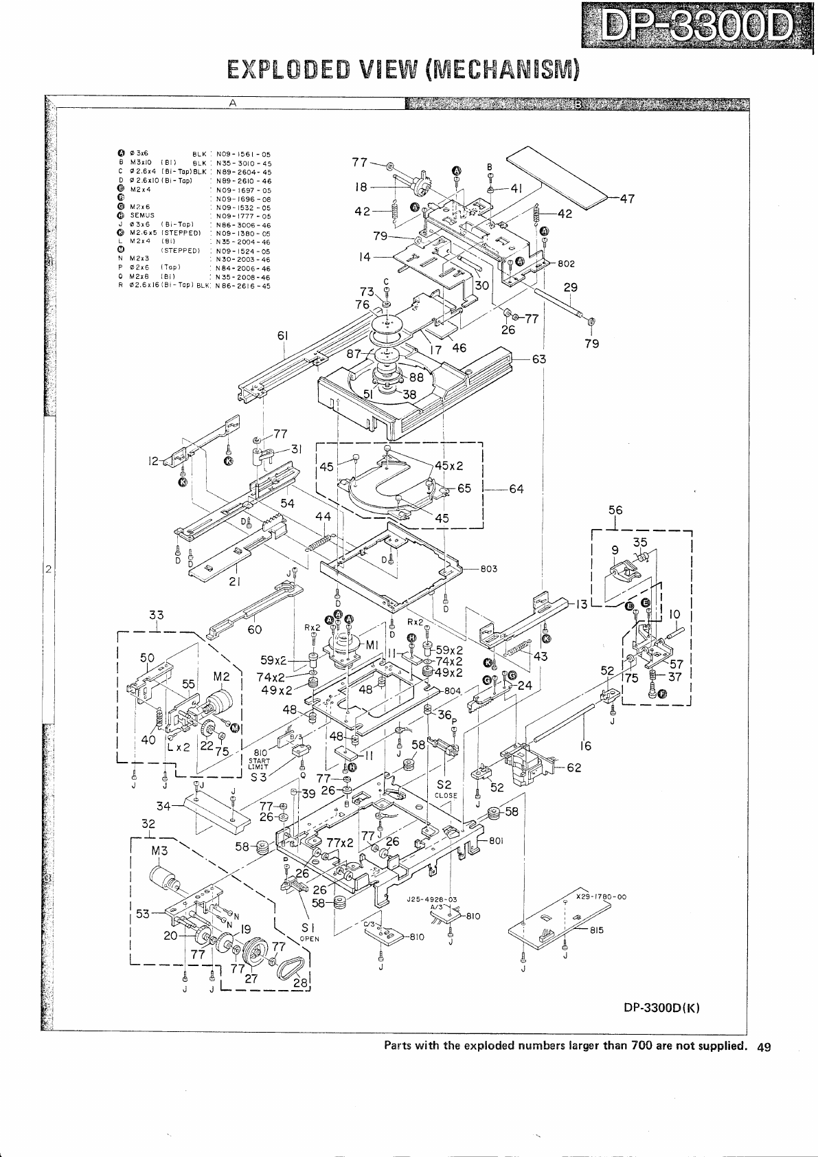
@ osxo 8LK
.
N09- 156t
-05
I M3xlO tBl) BLK
: NSi-
SOIO
-
45
C a2.6x4 (Bi-Top)BLK
: N99-
2604- 45
D a 2.6xl9
(Bi- Top) : N
89
- Z6t0
- 46
77
t8
@ uzrq
It
@ uzxo
@ SEMUS
N09- t697
- 05
N09- r696
-
08
N09-r532-05
N09-
t777
- 05 .r#-.o,
\ Y,w
J @316 (Bi-Top) : N86-3006-46
@ Mz.6r5
{sTEppED)
. N09-t3Bo-05
L MZx4 (Bi) . N35-2OO4-46
@ {srEppED) : Nog-
tbz4
-05
M?x3
6?xO (
Top )
MZxB { Bi
)
62.6x16
(Bi-Top)BLK
: N35-2008-46
t4 802
a
73,.
?
76^.)@
J^l zs
V'9*-tr
26
l7 46
L--l
45x2 i
I
I
-l
65 l-6a
DP-3300D(K)
Parts
with the exploded
nurnbers
larger than 700 are not supplied. 49
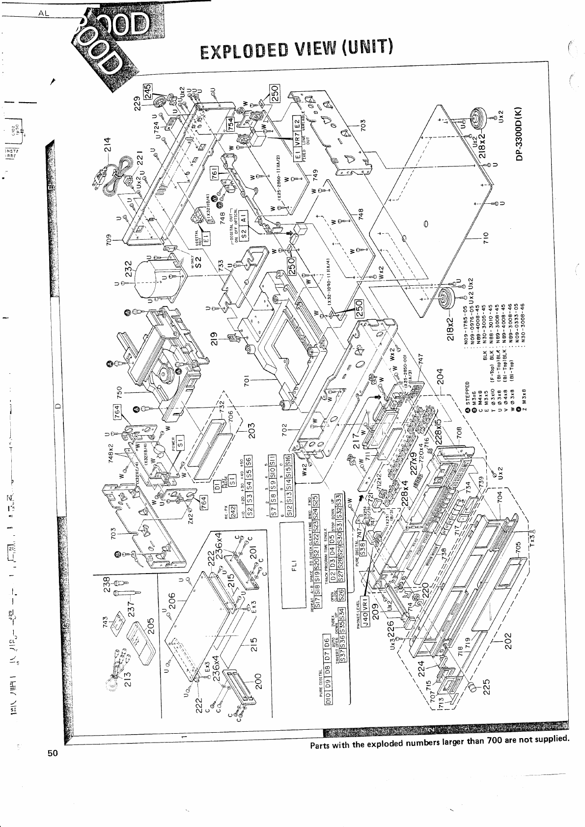
ffiKwLffiruffiffi
VE€W
{UrugT}
o
()
o
(Y)
0/)
I
CL
o
N
x
@
fr
on9ooo @
{;';;;; ';
E=oeee 2
grdFl>=€*
.w
\\\ \
,\\\ !--d)
lilI
"2,/ n
l9
I'
NE
XF
@;
N3
7
(f,
o
N
,L_
R\
\
t() -r
-;l.' 3
N\r'-
N \1
onnn(o
9*s<tg
ponPP
3-o665
r.)rQnrfD
lrlll
BggES
zzz2Z
rxYY,
dd66
aaa
XFFF
ljrtt
|
---
-
scocDo
(o
N
N
I
I
J
ol
I
I)
t,
-s
=1
-
W/\/,
/, / crt
t-o N
\s
\C.t
\N
**H
9o
\- 1..-
I
:J
\,
\ro
\E'
ffiroded nurnbers
rarger
than
700
are
not supplied'
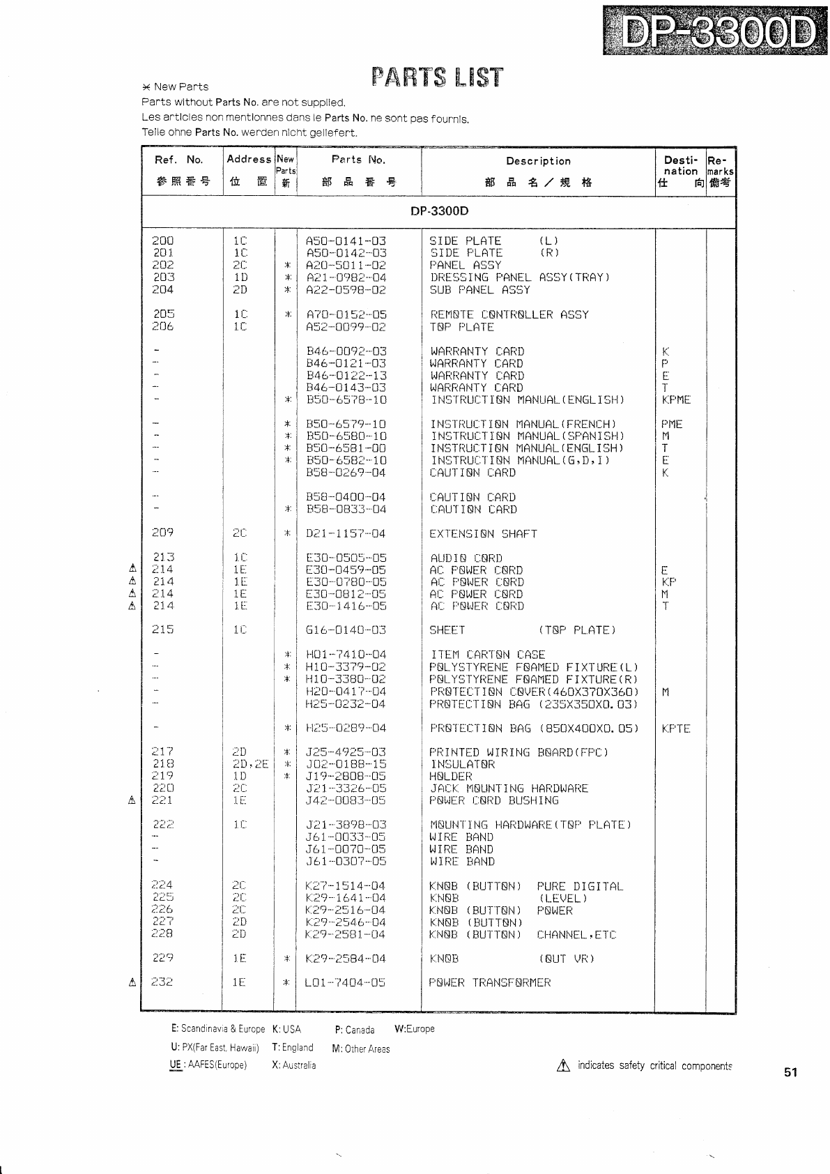
ffi;ffi @I@;ffi
A
l[
l\
A
PAffiTS
LffST
Par'ts without Parts No. ane not suDDlied.
Les antlcles non
mentionnes dans
le
Parts
No. ne
sont pas
fournls.
Telle ohne
Parts No.
wenden
nlcht qellefert.
E:
Scandrnavia
& Europe
K:
USA P:
Canada W:Europe
U: PX(Far
East,
Hawaii)
T: England IVI:
Orher lireas
U!:A"AFES(Europe) X:Australia 7\ indicates
safety
critical
components
A
A
51
Ref. No.
*HR#€
Address
{i. E
New
larts
al
Parts l\lo.
g$#€€
Desc
r ipt
ion
*$fr
ft A/ffi. #
Desti-
nation
ftFr
Re-
mar
ks
ffi+
DP-3300D
20u
{u J.
2Lr2
20:l
204
205
2Uh
'2D9
lJ Js
'-.t 1 ,4
a--L+
214
'-r 1 .4
a..t+
?14
d.L:J
':r'l ':t
21 rl
c L-/
2ltl
'A'-r I
c:c- .L
2i;::
''J'-.t A
t-L_+
LL-J
,:'-2,6
2l?
;ilB
229
;i3e
J l-'
1L:
'1 f-
Lt.-.
111
LU
iD
Lt_.
.[ r_
i r-'
J.t:
i t--
.tI:
Il_
l. L'-
I r.-.
.]D
;:'ll
' tE
1D
tr'
_L r_
It:
'I f'
It
'-t i'
;l r::
'.rl
c-t-,.
-tn
':r Tl
LU
JI:
1r_
.t r_
'*'
.+.
.+.
.?
*:
-t.
.t.
.t.
'*'
.+.
'+.
4.
.+'
.+.
.t.
.+.
fi50-0141-03
Asil--CIi4t-CI3
At0*5ir 1
1
-0t
AtI
-
0?82-04
Ar2-n5?n
-n;i
A-/U- Lr 1
5l- 05
A3t
-UU?9-U:
114
6*OCI?i-
U3
Lr46
-01i i
-t)3
1146--CIili-
i3
846
-t:l
i
43-U3
t_..i ..
LJ:]U--b: /U-- L U
1150-65
7.t-
10
85CI-65U0-
1u
Elll]-i:581 -CIu
1150-65Ut-
1u
li58""U26?-04
Er58
-0400
*04
il5ir- 0t333-"
n4
Li;i1*1157-04
ii30* 0505-05
[3t] -0459-05
830- Lt7tiCI- tJ3
E3CI-08 1 t-il5
830"14i6"05
G16-014t]-U3
t-tu1---i4i0-04
t-11U*337?
-0t
Fi 1 CI-338U-0t
fl20- 04 r
-1--CI4
r-1t5--0r3l..tJ4
t-E:]"
Ut8rt- []4
J:l?..49Z'J-43
JUt-01[Jf_]- 15
J
1't-"til08--il5
J lll --33tir-
tlS
J4r-Uil$ i -U5
Ji i--389i1--Lt3
J6 i *U03f*U5
J6 1
-U0
70-U5
"161--il3lt-l-
05
k::17* 1514-"U4
F:.i?- i {-,41- 04
BB::?-251.b-44
F:.;:?--c'54 6- il4
l(..ltl-i5ll I -il4
F:.t?- t5B4--L]4
Lil
1--?4U4*il5
5I T]E f]LA'IE (
L )
51UE
fiLA-t-E (R)
I}ANEL A55Y
I]I1H55ING
F,ANEL
A55Y(TITAY )
5UB f',ANEL
A55Y
flEt'lN1E.
t::Ef.lTRNLLIR
A55Y
.TNF,
[:'LATI
t^]AIlRANT Y L:ARI)
HARRANTY
I::A[ID
hJAF{RANTY
I-:ARi)
LJART(ANTY
I:ARD
t. f{51tru[:] i EN NANI_rAL
(
ENGL I5rj )
I I'ISTIIUI::T l SN I'IANURL
(
FRENI].H )
] N5I RUI-:] I EN NANUAL
(
:]f:'AN 1!]I-I )
I NSI"[iUI::I'i NN IIANUAL
(
ENIiL
i 5IJ )
INSTRU|::] IflN I'lAl..tUAL
(6'.Ii, I )
I::AU'I-INN i:.AITD
I::AU'I
I NN I-:AFiI]
I..:AU-I
].NN L:ARI)
EXI-ENiJ
i EN SIIAFJT
AL'I] i N I-:tiF'TD
AI::
FNI^J[fi
I:SRD
AI-:
F'f!I^IER L:NRI)
AI:: FNI^JER
i::NRD
AI..: FNIJER L:i!ITD
sHE.[ I ('IEP F,L.AT[
)
i I IiN r:.AR]NN
t_:A5tj
f]ELY5I-YREhIE F:EAI"|IIJ FIXTURE:
(L)
|TSLYSIYfi[NE
FNANEI] F IXTURE(R)
[rRN]'Er::T t. NN t_NVL_ri
(
460X3?UX360
)
frRN l[r::t-I
Nht L1AG
(
!35X35L]X0. il3 )
f:'[i8l L:r_:'[
I &N tlAG (
850X4U0X0.
05
)
fTR I NTED I^J
I R i Nfi IIITARD
(
F:fTI-: )
I
NSULAT NF{
rlNLIlIfi
J'AI-:K:.
I'INLIN]
I NG IjAF{I]I^]AIiE
i:'Nt^lIR
t::Nfil]
FUSl-{ING
I'INUNI I NG I-IAIII]I,JAI{E
(
TNP ITLAT
[ )
I^JI RE LIANI]
HIRE L1AND
I,Ji ITE
LIAND
l(:N8N
(L{UTI"NN)
PUFIE
T]iGiI-At-
k..N8tt (
l_E\rEL )
k:.NNLr
(
Fut-t-8ht) FNHEti
K.NNtI
(
L]UT
T NI.I
)
l'::I.JNLI
(
FUI-I'NN ) I::I.IANNEL,
EI'I::
l.::.tlfiB (NU-T
UR
)
iTNhJFJII
TRANSF NRi-1[R
FI"IE
lrl
T
E
Y...
F
P
L
'1-
F::F.NE
M
Ktrlt-
E
l.;:F'
l'1
T
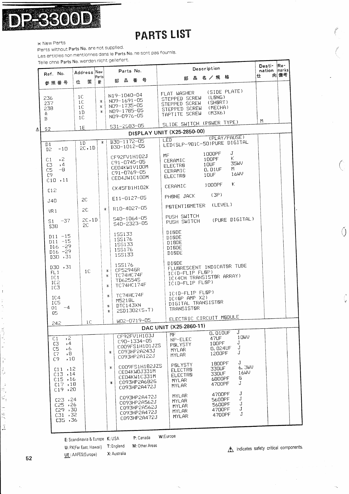
Desti-
nation
.{t Fr
Descr
iPtion
*$ fi &,/ffi. ffi
Parts No.
$fr*E
Ref
. No.
#ffi&E
5Ll.DE
SUt-r'Uu
G'S
FiLAT
I^JA5H[R (51I]E
F-'LA]-E)
gl EPF
tln sr-:f{Et^l
(
LNNG
)
Er-Erprn StREt^l (
SHNRI-)
ElEr;r'rn SIREH (flEtt-ln)
t:ApIIl-E 5t:ttL"il (f-13x6)
Ni9-i04u'-04
NCI?-
16'11-
u5
N0?-1
i35-05
N0?'-
1-i
85- CI5
N0?--0?
76
-115
531-';LU3-
05
DTsPLAY
UN
lr (x25'2850-00) ALI!,E
)
lE"n
t SLfr-
gu
lL'--50
)
F'utlE
D I
crI
TAL
NI:
L:ERf\t'l1t
ELEI::IFTN
t-[--RAl'lI
L.
ELEITRN
1000rri: J
100F
f: t(
10UF: 35t'JV
0.01uF l"l
10ur: 161^lv
L:E.RA['II
L. I UUIIF
F K'
Pt-tNNE
JALF:. (
3F1)
PNT
EN-t
I t!NE]
Etl (
LE\rL:L
)
frusl-1
5HlTr:l-t
;,'"usij
Er^rrrr:H (f.'uRr
DIGITAL)
DINDE
I]INDI
DlEDE
DISDE
I]INDE
DINDE
ifirhiirErENl INDItAINFt
luL{E
I l::
(
Il-riL I F FLNfI )
ii t
+rif hnnsI5lNii ARRAY
)
T
I:
(
D.FL I T.,
FLNIT
)
I1..(D-I.L]F
F'L-SF')
II:(NT'
fiNP
X2)
nir,rrnl 'rtlANSISINR
1 F{AN5l5TEIi
il-Et::l-F{Ir:
r:Itlr-:uIT
r{SDULE
L]:O-
1i?';-05
[r30-
luii-t]5
r-:F?ZFV
1l-{
iu2J
r?1-0?45-05
t:E04K.t^l1V
1CIUl1
r-:91- U76?-
u5
l-lE04Jt^,1t
1001'l
r-K45Ft1111102k:
E11'-U127-Ll5
R 1.0-
4 CI2-i
- o5
$40--i
064
-u5
540-i323-'0:;
1
r.tf: 1 ?n
IJJIJJ
1551?6
i55133
1551?6
155i3-1
1551?6
l_:ir5i?46t1
'Tl::?4lll:.74F
1D6t5i545
'l-l:?41-ll-:1?4F
UI
Di -1u
'-. I )
l-_. .[ , c-
c3 ,4-
l_.-J -u
C?
t1CI
'
11
f. 1-)
J40
VR1
51 -3 i
53tl
D1i *15
ll11 --15
D1C-,
-19
Il1
f, -;:9
D3U
'31
-l-l_:-/4!-ll--i4.F
f,15218L
D'Ir::143XN
t5D130Z(5-T)
l'^10i-CI?
19
-U5
DAC
uN
lr (x25'2860'1
1)
Flp.=-- Ll.
U10Ur--
NF-
ELEIJ 4?UF
frNLygTY lUCIF'F
Nvlnh o.
ol4uF
r,rvr-nR l;tlCIPF--
;:,NLySTY 1BCIUFF l' --,
,,,
tiF,j inn 330UF 6.
:ltlv
EIE;iiiN 33ouF 1.6wv
illnit - 6BLloF'F'
q
Nirnn 4?o0F'r:
J
|'IYLAR 4?0tjt1F {
Nifnii 56CIonr: 'l
nilnrt 56,ooFF {
t'lYLAfl 4?00PF J
MYLAR 4?OOPF J
r':r-+iFV
i l-1103J
l::c)0- 1334-05
[:l]CI'tr:51fi
10
r
J'25
r-.r,t?3Flf-'tAr43J
t-tt.t',
3l'lf:'
il] i ei J
L:110?F
51i-l1BIJZ5
l:EO4K.l^10J33
i fl
l_.E04K:t
l1l_.331
f,l
t-:n93FlF'tA6U2tr
r:It?3HP';44?aJ
rtl1?3t-lF'iA4?iJ
t:tl?3Ht-'2A562J
L.a?3tiPaA5e'2J
Ll[l't3HF
tA 47ZJ
L:N':)3HF'EA4?TJ
i-.1
C3 ,4
'-'E l-
l_.J t LJ
ll? 'B
t? 'lCI
c1
l. ' 12
l-:13 '
14
l-:15 ' 16
tl.1?
' 1.8
t::.1?,e0
ca3 .i4
l-.c13 r CD
c2':, '
30
l:.:J
1 t 3:l
c3:i ' 36
x New
Pants
Parts
wlthout
Par"cs
No'
are
not
supplled'
Les
artlcles
non
mentionnes
dans
le
Parts
No'
ne sont
pas
founnls
Telle
ohne
Parts
No.
werden nicht gellefent
E:Scandinavia
&
EuroPe
K:USA
U:
PX(Far
East,
Hawaii)
T:England
UE:MFES(EuroPe) X:Australia
PARTS
E-I$T
P:
Canada W:EuroPe
M: Other
Areas
i3
I
52
fi indicates
safety
critical
components'
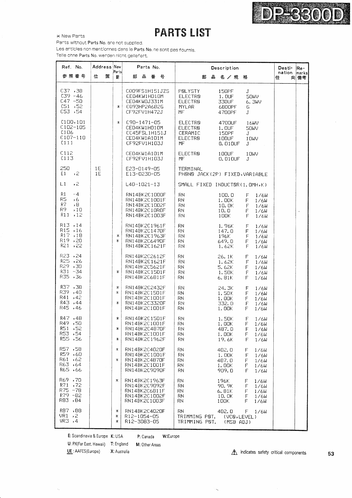
Ref . No.
6ffi&E
Address
ffiE
New
Har
ts
1l
Parts No.
$ff*E
Desc r
ipt ion
gr
# &/fr +s
Desti-
nation
{l ffi
Re-
mar
ks
1\ffiE
l::3'? , -38
c39 -46
t::47 --50
r-..J l. ! Jc.
r-'F ? E: A
r-.,JJ !,J+
t:10u,l.u1.
r-.{ -r\
t.-..[
Uc:- I Ull
L J, L'b
r::1CI?-11u
tll l l
t::i
i;i
r-'1 1 -?
rJf l.L,
250
ra
Ll r C
1
R] -4
fl5 , (i
R7 ,[J
ti', ' 10
Ri
L l.l
Fii3
.14
R15 ,16
Rl
-i , l.
f3
R1? ,:CI
Rt l. ,ll
fi23 ,;i4
Rt:i ,26
R.i? ,30
R3 r -:14
fi35 ,36
R3-i ,:3ti
R3't ,4ll
R41.,4'Z
R43 ,44
ti45 ,46
R4-i ,4[3
R49 '5!
K:, J. r Ja
tir--.-t E-
A
I\JJ I.JI
R3:i ,56
R5? ,SEl
R5? ,6lJ
fl61 , h2
fi63 ,64
R6:l ,66
R6? ' ?0
R-i 1. ,7l
R75 --7u
R?'-2
- B;l
R83 ,84
' B[3
IL
,4
L
RB-i
VRl
VR:3
lr'
.t- t
1t-
-tL
.t.
t.
.f.
.+.
'*
'lr
.+.
.r.
+.
.4,
.+.
.t.
.l-
+'
,.
.1.
.t.
t::1.:!0?rj5
1 l-{ 1 5 1
JZ5
L.E04K:t^l
1
t-t0 i ilt'l
l::[t]4F..i^J0J331H
t_:t:.lrt3HF'iA6g;:6
r:.F-cliFv
1Ft47tJ
L:?CI- 14
71
-
05
t::[04K:t^,
1t-l01Ut'l
[:L:45F'5L 1 Ft151J
l-:EU4k:.t^li
A 101l-l
t::F'?Zfrv1H103J
r::804F..r,41A
101N
[:F
rttFV
]. t-t1.03J
823
-01
4?
-U5
E 13- UISU- 05;
L4U--10t
i
-
13
tiN
14lrk:.tr_:1000F
FiNl4Bk:.tr_:1U0iFj
tiN
i 4tih::tt_:1001F
fiN
l4LtK:2r::1UR0r:
ttNi4FK2r::1U03F
tthll4Ek:.2r_:1961r:
tlN
I 4Blr:.ii::
I 4'7[']f:
flN
I 4tiK.t[:
].963[:
flN
14ttk:.er_.64jar:
iil'li 4 L{k.ll::l
6';t 1F
RN
I 4Lthiit_.:;i612F
fit.l1
4Bl.;:lt::162
i f:
tiN
14t1F:.il:56t
1F
ItN
14BK.lr_:150
i F
ttN I 4Etk:.lt::68
1 1t:
fi
l.l
1 4
LJ[(:I
r::
i 4
3 i: F
FiN
1 4LrK:er::1
50
i F--
ftN
14Bk:.Zr_:
1CI01F-
F{l,l
I 4
Llk.:Z
r::
33t 0F
flN
1 4tlh::tt::
1001F:
iiNi4BK.;:r::1501fr
RN 14Bk::;il-:100
i F
tiN
1
4[iK.;I-4
ti-i
0f-
RN I4Erk:.lr::1UU
1F:
RN
14LrK.lt-:1cr6lf:
RN
i 4EtF:lr::40i0F
RN
1
4BK.IL:1CIO1fr
RN
14Ek:.tt::4U
70F
R.N 14Lrh::2r::
1CICI i F--
ti'N
l4LIKZr::?Dc)DF
RN 14ttK:lt::1c)63F
FtN
1 4 Ltl.:.l
L:':i0?lF'
RN 14Bt'.:Ir-16U
1 1F
RN 14BK:2t_:1002f-
RN
14Erh::2t_r
1U03Fj
RN i 4LtK:tr::40tOF
Ri2-i054-05
Frl
t- 3083- 05
150frF: J
i. ouF 5ut^JV
330LlF: 6. 3ttv
6B00F F [i
4 7l]Ofrrj J
4700uF 16t^JV
1.
0ur- 5CIt^Jv
150F'F J
100ut- 1O[^JV
0.
0iOuF J
100uF- 10t^JV
0.0it]uF J
fTNLYSTY
ELEI::]'iTN
ELE.t::Ifi8
I,IYLAR
l'1 l--
ELEL:T RI]
ELEI-:TftN
[EIlAN
I I]
ELEI:I-fIN
N[r
ELEI::TRN
NF
I-ERf"iI
NAL
F'I.INNN
J'AI-:K:(IfT) F]XED,VAIIIAELE
SNALL_
F I XEII i NDUr::'rNR
( 1. t']t'1t-1 .' k:. )
IIN 100.
0
tiN 1.
00k.
RN 10. Or:
RN 10.0
fiN 10UK
tiN te,. lK.
i(N 1. 6th:
RN 5. 6tk::
Fif.l 1, 50lr
RN 6. U 1F:.
ftN 1.96V.. [:' 7/6W
trN 147.U F t/6W
fiN 1?6F:. [r 1/6W
fiN 641.A F: I/6W
Rf..t 1. 6ih;. fr t /c,w
r L/ow
F t/tw
F l/tw
F I/6W
F I/&,W
F r/6W
F 1/6W
F: L/6W
f'
t- l./ bw
F L/6W
i4.3t;: F t/tw
1.:iCIr F r/6w
1.00k:: F t/tu
332.0 F I/(,W
1. U0F.. [-- L/bW
FTN
RN
RN
ft
I'l
RN
ITN
RN
FTN
ftN
RN
1. 3Ut.
1. 00F..
4ts?.
0
1. 0uF:
Ig.6Y
F 1./6W
F t/6W
F 1/6W
F L/6W
F t/6W
flN 4Ui.0 F- t/6W
iiN 1.U0k:. F I/6W
RN 4B?.D F 1/6t4
RN 1. OOK: F I/bW
tlN 9U?.0 F l/tw
RN
RN
RN
fiN
RN
1?6k::
?0.':rK.
6. 8ik::
10.
llK
100F::
F I/6W
F t/6U
F T/6W
F t/6W
F T/6W
RN 40t.CI F 1/6U
TR i T'II,II
NG F,ET. (
VI]8
, LEVEL
)
TR I I'II'II
NG FET. (
I'ISL{
ADJ
)
x New Pants
Pants wlthout Parts No.
ane not suDDlled.
Les artlcles non mentlonnes
dans le
Parts
No.
Teile
ohne
Parts No. wenden
nicht qellefer-t.
E:Scandinavia
& Europe
K:USA
U: PX(Far
East,
Hawaii) T: England
UE:MFES(Europe) X:Australia
PAffiTS
E-$$T
ne
sont
pas
fournls.
P:Canada W:EuroPe
M:
Other Areas
7\ indicates
safety
critical
components 53
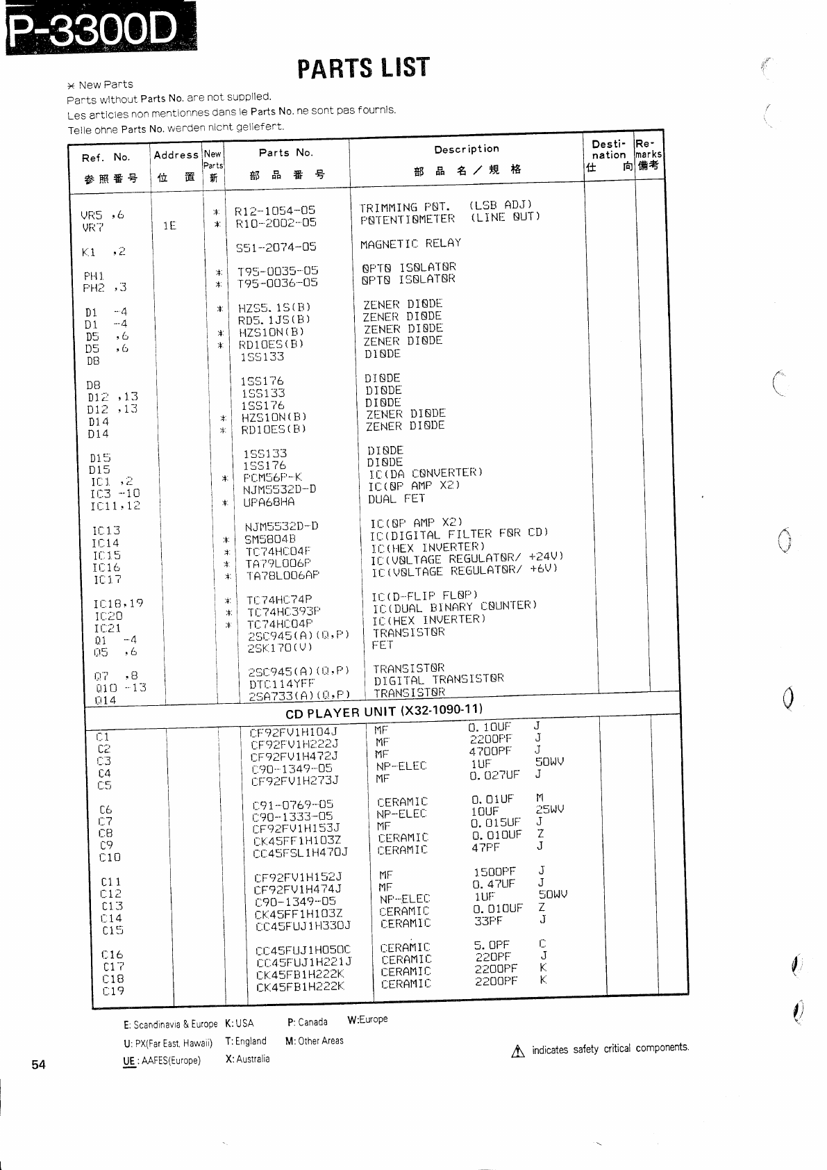
PART$
LIST
x New Pants
Parts wlthout Parts
No.
are not supplled'
LeSart]clesnonment]onnesdanslePartsNo,nesontpasfournls.
Telle
ohne
Parts
No.
wenden
nicnt gellefert'
it1!
Desti-
nation
{rH
Descr
iPt
ion
*$ F" *,/ffi, H
Parts No.
gFF"*E
Ref
. No'
#ffR#€
VR5
I lTr _-,
F:.1
Pt-l1
F
r-{;l
Dl -4
Di -4
U*J ro
IJJ I LJ
DB
D€]
D].;i
' 1.3
nr.f 1:2
Dtc- ! r'J
014
D14
Fr
1i- 1054-05
R1U-i0il2--05
551--2il?4-05
1':75-
U035-
U5
r95
-0036
-05
Flz55.
15
(
ti )
RDs.
1J5(B)
t-lzs10N
(
[i
)
fiDl0[5(B)
r f-f' 1 ?-?
IJJT'9
I'RiI'INING
f:'NI-. (L5B ADJ)
r;s
trru-r
l ErlrlEf;l (LINE
8u1
)
f'lA6N[l-Ir::
RELAY
EFTN 158LA1NR
NF.TN
ISNLAINfi
ZENEI1
D]EDI:
ZENER
DINDE
ZENEI1
DIEDE
ZENEII
I]I8DE
D
I Ni]E
D INDE
I]
I NDE
DINDI
Zf:|'lEfi
DINDE
ZENEii
DINI]E
Dl itDE
DIEi]E
t.r:
(
IIA r:.tlNVEt{TEFt
)
I I::
(
NF AI{P XZ
)
DUAL
FET
i r (
tJF At'ttr xi )
ir-:tnIGITAL-
FILTEti F:Efi
r-:D)
t. L:
(
t-lEX L
NvEftTEft
)
iirvur-racr REGULAINFI/
+24V)
i i t vbr-roGE
rIEGULA-I-NI1/
-r-€'\'
)
II: (
D-F:Li[:';LNP )
r I t iiunl Lj
I NARY riNL,N-rER
)
IL.(HEX
iNVERTER)
TRANS
I
51
8R
i:E
I
TITANS
I STNIi
I]I6]1AL lRAI.I5I5TER
,b *:
1E
!-J
,1.
,t.
U.I :J
D15
rf'l
Ir_. J. r f_
I
r-:3
- 10
It::l1
'
li
11
1.3
i
l-'14
It:.1
5
Ir_.1d:
lr- { a
ll-. J. I
1t::18,
1?
IL.iO
I
l::21
rl1 -4
l;!5 ' 6
t-:!'7 ' B
rJ10
-
1:1
r;t14
.1.
n,
.+-
.].
.t.
'1.
!i
IJJI IU
I t^f^ 1 'a-J
IJ:)IJJ
1551?6
HZ510N(E)
RUlUEi.i(F)
1 i: r-l 1 -:i -1
IJJI'JJ
155176
fr[:m56F
-
K.
NJfl:i53ill-D
UITA6BI{A
NJI'15532D-D
5115404E
-l-t::-l4flt::CI4
i:
Tfi
??LOO6fr
1A-iillou6AF'
Tt::741'lt:.?4P
-r[:?411[.3?3i:'
Tr:'741-{r:04F
i5l:'t45(A) (l:.1,F
)
c5K1?0(v)
l5t-:?45(A)(l'.!'F
)
IIT
t_:1
1 4Y[:'F
z3A
733
(
Al l_[!E:-l IRANS
I'J
INiI
CD
PLAYER
UNIT
(X32-1090-11)
l.1r tl' louF:
t'tF ii00F[r
t'lF 4 ?ilOF.'F:
NF.-
ELEL 1UF
f'fft 0. 0t?UF
rEFiAl'I][ CI.
CIlUF t'l
ntF-rlE': louF t5t^'v
r.rr=
--- 0.
tl15UF J
,l:-uttRNt'- 0.
010uF Z
r-frrnm
t
r-: 4?F
F J
t'tF l5OoFF {
rlr' 0. 4?UF J
'N'F'--.ELEr-: lurr 50t^lv
r::rnRmtr: 0.0t0uF z
lErtnmiu 33t-'F J
r:ERAr'1It 5.
0frF l-
LrnnNt':, leoF'F J
r-:innmrr: ee0oPF K'
iEnnr'|tl, 22oCIPFj K
t::F-?21:v 1l-{
104J
L:F9IF
V i li;:22J
r:F:?2FU 1ll4?aJ
I i.ln-
134?-'05
t_:FrgiFv
1Fl273J
r€, I I lr-'11-!le:i-P:
':i I I lt;:2q;1rll.9*:
ijB I i lr_:rr4_1y1f1111{
a..l i I lt::r-asr1if1,9lf
']io I I ir::c+':r'sl1l-t47oJ
c1i I I lrllilYltll!+{
,:ii i i ir:12ary1:14itr
ai3 I I lr_:ro-r:1?:91
':i+ i I lr-.x:asrr'ry1.0_i,1
ii:l I I i tr-:a:ruJ1l-133CIJ
r::le, I I l r:r-:+st=uJ_11q59';
ii-r I I lr:r:asruJlt1iili
'iie I I lt:r:+115111??ll':
i:i4 | I lt:r:a=rnlHrzir
*
0
{,
t\
7t
\.
E: Scandrnavia
&
EuroPe
K: USA
U:
PX(Far East,
Hawaii)
T:England
UE:MFES(EuroPe) X:Australia
P:
Canada W:EuroPe
M: Other
Areas
54 I indicates
sa{ety
critical
components'
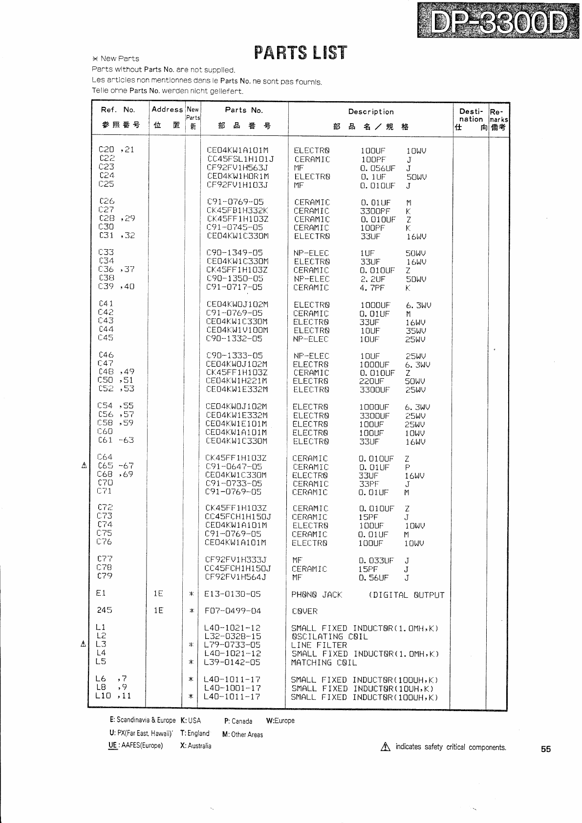
w.
ffiffi, ffi@ffi.
x NewPar.ts pAffiT'S
tgsT
Parts
without
Parts No.
ane
not
suoplied
Les
antlcles non menilonnes
dans
le
parts
No. ne
sont
pas
founnls.
Telle
ohne Parts
No.
werden
nicht
qeliefer-t.
E:
Scandinavia
& Europe
K:
US,A p:
Canada W:Europe
U:
PX(Far
East, Hawaii)'
T: England M:
Qther Areas
UE
:MFES(Europe) X:Australia fi indicates
safety
critical
components.
Ref
. No.
#na&+
Address
$tr
New
Part:
,11
Parts No.
$fr*+
Desc
r ipt ion
$ ff 4/ffi. ffi
Desti-
nation
.fi Fr
Re-
nar
ks
ffi+
r-)n -J1
L-LU ! A I
r- -) ":l
UL{-
t::?3
f'1 A
LLIt.
l:125
L.i t-j
i- ':r':t
I_.L T
ttB ,19
r::30
t3l. ,3t
r::3:i
17A
t::36 ,37
[3r]
t-:3? ' 40
[4]
t:.4;l
t._.
{+
J
t44
t::.4S
ll4
Cr
t- A -.J
r.--|
ll4$ ,49
|:50 ,51
t5l ,53
r-E/ L-r
r-.J+ I J-J
t5C, ' 57
l-.58 ' 5t)
r_:(:0
116I -63
l.-.
t-r +
c6:i -67
l::68
,69
[?u
t:::Z
1
rn_'r'- l
t- t r:.
r- 7?
c74
t::?E
t::"?6
f'-f -:J
LT I
[7€]
C?'}
rl
E.t
?45
t_1
LC
L-3
L4
L5
L6
LB
L10
,7
t"/
,11
II:
1r'
IL
r:804k:.t^J1A
101t'l
[:t*45F51-
1H 1O
i J
r::F?tFV
1H563J
l::E04.K.t^,
i t-lCItt 1 N
l::r--'rlr--v
1 l-{ 1
03
J
L'q1'a769--O3
r_.:
k:.
4
5
f:
E
i t-l
3 3t F::
r::K45FF
i lJ103Z
t::'r
1-0'745.-t:15
t_:E04lr:t^Ji
L:33uN
t:_'.go*
134,:i
-Ll5
l-:E04t;:t^J1l::330N
t::K:45Fi:1t-11032
t_:,:t0-.1
35CI--il5
tl',
1-0? 1 ?--Ll5
l::EU4.F:'tJUJ
1UtN
r::?
1-CI
76?
-U5
l:[04F:.
i^l
1
l_:33
0l''1
L:EO4ll.t^J
1V
1UON
t:.'t0--1332-il5
t::cr0-.1333-
U5
r_:804k:.t^J0J
1uil1
t::k.:45frF
l.l-t1032
t:ECI4k::t^t
1t-l:t 1fl
r-.
L_
04 l.:. t^J 1
ti:J 3 if,l
l::E04k::UUJ
10ir'i
LECI4K:t^l18332N
t_:En4k::t^Ji
E i 01t'l
t_.:ELl4t(:.t^J
i A l. u l N
l-:E
U4.li. t^l
i t-:
33 6Y1
t::r::45FF
1F{1032
L:?
l.
- 064-t--il5
t::E0
4
tr..t^J
1
l::
3301"1
t_:,:)
1- 0?33- 05
t::?
1-CI76?-CI5
rtK.45[rF
i. t-I1032
t_:t:45Ft::t-i
1 l-i
1 50 J
t:E04K.t^l1A
101N
r:? 1*0?6?-05
r::EU4K:t^li
A
I01l'1
t_:t-,:)iFV
l. t-|333J
t::t::45Ftlll
1 t-t
I 5u J
[F':tiF v
1t-t564J
E
13-0130
-ilS
F0?- CI499*
U4
L40-10:1-1I
L3t-03IU- 15
L7?-0?33.-U5
L40*i0t1-1t
L39.-0142-05
L40-.1011-1?
L40-
1001-
1?
L40-101
1*17
ILEI::TRN
r::IRAf'|1.1_:
['1F:
ELEIl Rti
l'l f-
t_:ItiAf'l]t-
I::ERAI'1I
I-:
t_:EtiAN
i t:.
I-:EIIAI"II
I::
ELEI-1R8
NF-EI-EI::
ELEI::]'fIN
t:EtiRl-1I
t::
I'IF'- ELEI::
t_:ERAf"li
t::
ELtir_:Tft8
t:.EttRt'1I t::
ELEI::'TRN
ELEI]] TiN
Nfr-[LEt_:
NF-"ELEI-:
L.LEr::'IttE
L:EflAI'II
I::
E.LEI::TRE
L:LEI::] I(N
ELEITITN
ELEI::TfiN
ELEI::TRN
ELEII'RN
i:LEl:.l'RN
I::ERAN
I
I::
t_:tiRAl,ll
t_:
ELEI:TRE
l::EfiAl,lIl_:
I::Ef?ANII-:
l-:tjt(fiftl11-'
I::ERAHII::
ELEI::]'RN
I::EF(AI'1I
I:
ELEI-'TIIN
I'IF
t-_:ERAI'1I
t::
NF
PHNNN
JfiI:l(:
100uF 10t^JV
100F'F J
il. u56ul: J
Ll. l. LIF SUI^,V
ti. ulLLJF J
O.
O1UF N
330lrF
F k::
0. iliuufr 7
100f:'F k::
33UF 16,I^JV
1UF-- 5U|^JV
33UF 16t^tv
0. 010ur: z
t. tUF Sili^,\,
4, ?F'r: F:.
1t)00uF 6. 3t^lu
0.01uF-- N
33UF 16t^'V
10ui- 35t^JV
i t]UF :5I^JV
lCIUF i:5tJV
t0CIOuF 6. :it^JU
0. uluuF z
ZTOUF SOHV
3300uF 25t^'V
1000uF 6. 3t^,v
3300uF t5t \r
10CIutj t5t^JV
100uF: lut^Jv
33UF 161 \r
u. CI1ituF
7
0.0iuF [r
33UF 16t^lv
-l-?rjr: T
0.
uluF: f"i
0.
oiOuF z
15PF J
10CIuF 1CIt^Jv
0. uluF t1
1U0UF l UidV
D. L]33LJF J
i SF,F J
CI.
sC,UF J
(DIGITAL
EUT|TUT
I-:NVEtI
5I'IALL FIXED INDUI::'I'NR(
1. OI'.1H,I::)
85I::ILAl ING I]EIL
LIN[ FJILTER
SNALL F I
XED I NDUI-]TNR
(
1. OI'IH , K: )
I,IRTI::HING
I]NIL
SHALL- FIXEi] INDUI-:I'ER(
1Ot]UI.1, K:)
SNRLL F
I XED i NDUI]TNR
(
1OUH,
K: )
SI'IALL-
FIXED INDUI::TNR(
1CINUFi,K:)
55
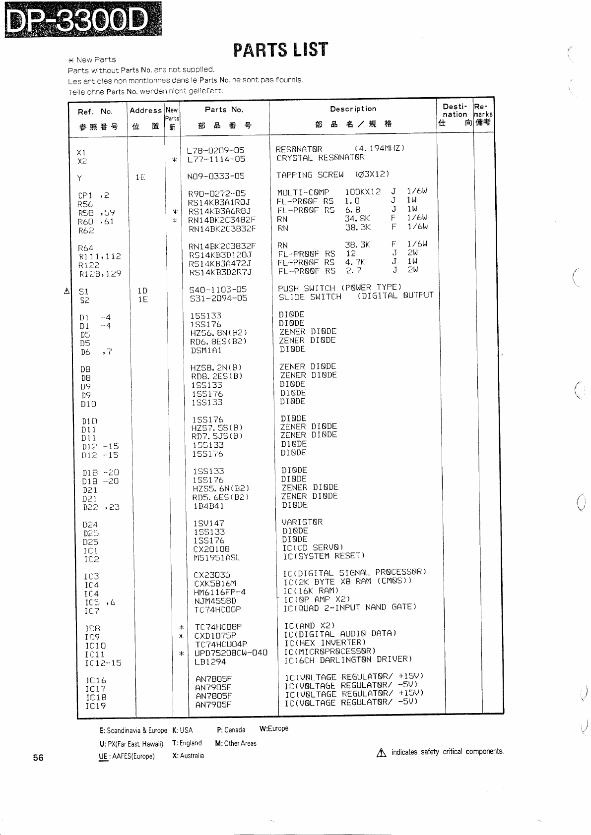
PAffiTS
LIST
x New
Pants
Pants
wlthout
Parts
No. ane
not supplled.
Les
ar^tlcles
non
mentionnes
dans
le
Pads
No.
ne sont
pas
fournls.
Telle
ohne
Parts
No.
wenden
nicht
gellefent.
Desti-
nation
It Fl
Descr
iPt
ion
*r ft 4/ffi. H
Parts No.
$ff*E
Ref
. No.
6ffi*z
RESSNATNR (
4. 194l.ll-lz
)
r_:RY51'Al-
ttESiiNA'r$Ft
l-APF'
Il'lG SLlREt^, (O3X1;l
)
NULT
I
-
[NNF' l OCIKX
12 J
F:L--PRSN[j
ti5 1.
0 J
FL-
FIINNF
Ii5 6. T] J
RN 34. 8F: F:
F{N 38. 3Fl [r
F{N 3t3.
3t(:.
FL-.FITNNF
II5 T-S
FL--f:'flNNF
R5 4.71<'.:.
f]L-.F
F{8NF
Il5 2.'7
F: L/6W
.J TH
Jlt
T -tt I
rJ C.w
FUSl-l
St^lI
l-lll-l (
frNt^,EF{
TYPE
)
5L]DE 5I^J111:FI (I]]6ITAL I]UTF'UI
D I EI]E
DIEDE
ZIJNEII
DINDT--
ZENER
I]INI]E
DlNDE
ZENIR DIEI]E
ZENER
DINDE
DINDE
DiSI]E
I]INDE
Dl
NI]E
ZENER
DINI]E
ZENER
DlNDI
DlNDE
DINDE
I]]EI]E
DINDE
ZENEII
I]INDE
ZENEFT
DiEDE
I]
I NI]E
VAFT
I
g
INR
D J
TIDE
DIOI]E
iL:
(
r-D SEfivN
)
]L:
(
5Y5'IEI'I
RESE]
)
II-:
(
DIGITAL SiGNAL F[INI-:E55NfI
)
I r::
(
tK. LrYTE
Xtl RAN (
I'l'lNs
) )
I t::
( 1
6K: ftAf'l
)
I I:
(
NF' ANF' Xi )
iI::(AUAD
E-INPUT
NAND
GATE)
I[(AND X2)
II.:(
DIGITAL AUDIN
DATA
)
II::(
HEX INVEIITER
)
i ; 1 1v1 I t-:RNfrRNl-:E55NR
)
II.:(
6I]H DARLINGTEN
DRiVER
)
II-:(
V8L-TAGE
fiE6ULATER,/
'I-15V
)
IL:(VSLTAGE
REGULATNR/
*5V)
iI: (
VNLTAGE
IIEGULATNFT/
'I-15\'
)
II] (
VELTAGE
REGULATSR/
_5V
)
L78 -020'?.-05
L-/?-
1
1 14-CI5
NCI?.-U333
-U5
tic)0-
ul-i 2--05
R514K:Ei3A
1tt0J
R514
KIE3A6RBJ
riN
14BF:.Zr:3482F;
F{N i 4trK.It::3B3lfr
flN 14BK
2t-:3ii32F:
R514t::F3D
l.l0.J
ttS14k::F344?ZJ
ItS l4KLr3llZtt-/J
$40-1
103
-u5
531-
t0?4--tl:;
r rr. I '? ?
IJJIJJ
155176
t-tz|56,
BN
(
Bt )
RD6.
B[5 (
LrZ
)
I]SNiA1
t-{258.;N(B)
tlDu. iE5 (
Lr
)
155133
15!11-16
I -t. i ?:?
IJJIJJ
1551'/e,
t1:Z|57,
55 (
Lr
)
RII?.
5J5 (
tr )
155133
1551'76
155133
1f a1 a a/
IJJI TE
l-1255.
6N
(
112 )
ftil5. 6[5 (
L]2
)
1 tt4
Ll4 1
15Vi47
15!l133
l ff\a -J
IJJI f C,
r::x201uB
f,151?5145L
r:xi3035
r::xK.38i
6l'l
t-Jl'l6116FP-.4
NJN455BI]
Tr_.?41-l[00P
Tl::?4f-lt::utlF'
l-xD10'75P
-rl::?4t-lL:u04
F'
UPD?5208[hJ-CI40
LB 1
294
AN?BO5F
AN??O5F
AN?BO5F
f;N?905F
X1
Ai
Y
CF'1.
,'J
fi5(:
RSTJ
,'J9
R60 '
(r1
R6;::
ti64
Ri
1.1
,1.12
l( I r-c-
R1;iU,1.:Jc)
Dl -4
Di .-4
D5
D5
n/ __,
UCi )(
I]B
DB
D?
nc?
D
1il
Dru
11 1t
UI I
011
n<.-i i c'
DJ.t- - tJ
D
1;i --15
D1
8 -20
Diu --20
Dt1
D21
Di {-. t e. -)
D;4
nar [::
Di5
r l._.
I
I L.;i
Ti'2
-t t_.J
I l-.
{+
I l::4
I[.:'i ,6
I l::?
I l_.
tJ
Il-:9
Ir'1 n
ri-11
I
rt
12--15
Il::1.6
I
r:l1?
IC]
B
Il: 1?
t
t
(;
I
E: Scandinavra
& Europe K: USA
U:
PX(Far East,
Hawaii)
T:England
UE:MFES(Europe)
X:Australia
P:Canada W:EuroPe
M: 0ther
Areas
co 7\ indicates
safety
critical
components.
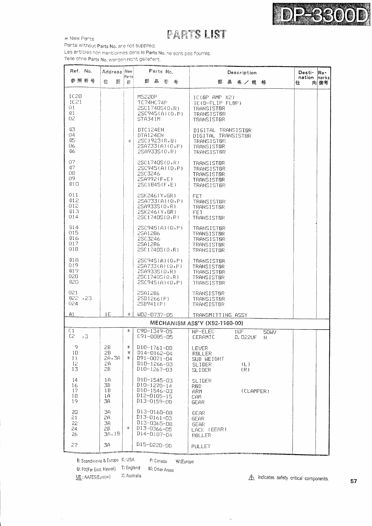
x New Parts
Pants
wlthout
parts
No.
are
not
supplied.
p'#.ffiTffi
n-EsT
Les
antlcles
non
mentionnes
dans
le
Parts
fi{o.
ne
sont
pas
founnis.
Teile
ohne
Parts
No.
\ruerCen
nicl+,
geliefei-t.
Ref
. No.
8ffieE.
F.ddrese1l'{ew
lPari:
I
I t;j!
Farts fts.
*F#
*A
Descr
ipt
ion
gf ft A,/ffi. ffi
Desti-
nation
ftrfi
Re-
mar
ks
XH€
rl:i
t;:.14
D3
r_:t6
06
,-|..}
t:.1 I
tl-i
t,!ll
t::.tq
t.l
I tl
i t:".20
I l-.
r:l l"
r..i.t-
t-l 1
t:.1c-
t.t11
r.t
1 ;i:
r-r i '1
t:l .L z
[t1:3
t,.!
l.4
il14
t,!15
016
t.t1'7
l;t1B
til tl
t.t1?
ll i. ':)
r,!;i0
L'l;:n
t,t:1
al;:l
t;!;t4
A1
' !i,i
1t:. 'f.
r'15;:JUF'
'r
L'i At-tr:'i4fr
i3t::i 74Ug
(
r".i
,
Fi
)
l3;l::rt43
(
A ) (
t:.i,
F
)
5T434
I fi
Ll-rl::124EN
Iit-A
i:4El..l
;t5r-.1913(R-$)
2'i4733 (
r) )
(
t;1,
Fr
)
t!,4't335 (
l::l*
!{
)
l5t_:i
740'i
(
t;
.
ll
)
i5i_:'t45(A)
([.!,f])
25r_'3i4h
;5A99;t(Fj,[)
25i::1.845(F,|:)
i58..'Z4L
(
Y, CiF:)
i5A-/33
(A
)
(
t:.!,
f])
i5A?335 (
t.;t,
tt )
15ll..;:'.46
(
Y, Gf{ )
i'jt::1'74U5(t_:t*R)
i5l_:(t45(R) {l.:!.P)
i5A 1.]tsd:
i:ir::3i46
l:rfl I lULr
i3t::174115(l,t,R)
;1St::945
(A
) { [!, f]
]
;54t33(A) (l-;t,F,)
l:rArl335il:.!,R)
:5r::174U5
(
r;t
, r{ )
t:tt::.r45(A)
tt,t,F)
;i5fl
i iB6
t:iu l.;id,6
(
Ir )
iiiB?41 (
F
)
ilnr--0?3-i--05
I I::(
NfT
AMP X;::
)
I t::
(
il-.FL I Fr IrLfll-,
)
TtiAl.lS
I S
rNR
TRANSLsTf!ti
rFiANS
i 5TE[I
01 G
11
AL l fiAN:J
1I]TNF{
T]IGITAL
TIIANSigTIJR
l nAhl51518F;:
t-RAl.l5 i 5T8R
I ttANS I5l Nfl
I-fiANS I STNR
I t-{ANS
MTNf{
TRANS
I 5 INR
IRANS I i-JTNR
] RANS
] !]'t
NFI
rJET
T
RANS
I ST NTi
1-flAN5I5t-$fl
FLJ]
l-tiAN5I5t'Nfi
TRAF{SI5T
NT.:
l-rlAN5
r
5TSR
TtiANSl:l-rriR
TRANS
I STNTi
fRANS
I SI-NR
T F{ANS
15T iJR
TRRN! I5I'NIi
-rnAN:t
I5l 8R
IRANS
I SI'NIi:
l rirrf't:t
15T$R
t-f-rAN5I5t-8R
I iiANS15TNR
t-[tAN5 i 5t-Nii
TfiANSI,Il-ITiNfi
A55Y
MECHAiUEST{fi
ASS'Y
(XSZ-'3
f
60-00)
r-1
r,_.
.t
r'-j -1
t-L. 5 -J
al
1 r'l
ILJ
.L .1,
t-l
13
1A
ILJ
t(
tn
1 r-l
2n
CL
/{L
2{-,
'-l -)
':, t]
a- Lr
TB
2A'34
LN
':r fJ
LLI
1A
3B
1rl
J. LI
1A
JTI
3A
L11
3A
'-rn
f- Ll
34,
].8
'+. l::'t0--
i 34't -u5
r::r]
I *Lluu3- u5
01CI--1761*08
Di4-.CIi6t-"04
D?1-"fil?1*il4
D l
Ll-
1166--03
D
i
0-"L
i6? *il3
D
i
0* I
54
5--Lt3
D 10*i I?0 *
1.:r
Din- 1546--il3
n1l-CIin5".15
D
i 3-f_]i
5?*fin
IJI3-U16n-L'1fi
Il
I 3""u
161
_ni
D
1.3-.Llf,f,g*.11fi
!li3-ijj6,fr-CF
itL/i*ilI LJ?*il1,l
015*tJ;Jil_ilil
NF
-ELEI: lul- IUt^tV
t::L:RtimLt:. 0" ut2uf- N
LEVER
RNLLiitl
5ti8 [^iI
i [il-i
r
SL]D[ti {L}
sr_Iil[R (R)
I]L
I ililR
RSn
ff Rf
i (
[:LAI''IF'ER
)
l::4f,1
fi[AR
r{r[:-fi[:i
{'-rIAii
GF:fiFi
to,-lr.. (
f;flfiF-{
}
RiILL!:F{
rrt-it_LIY
E:Scandinayia
&
EuroPe
li:USA
U:
FX(Far
[est,
Hav,'aii)
T:
England
l-lE-:/+/rFESitu'c'ri;)
)l:Austtalia
P:eanacla W:Europe
.qf:
Other
Areas
7fr indicates
safety
critical
comoonents. 57
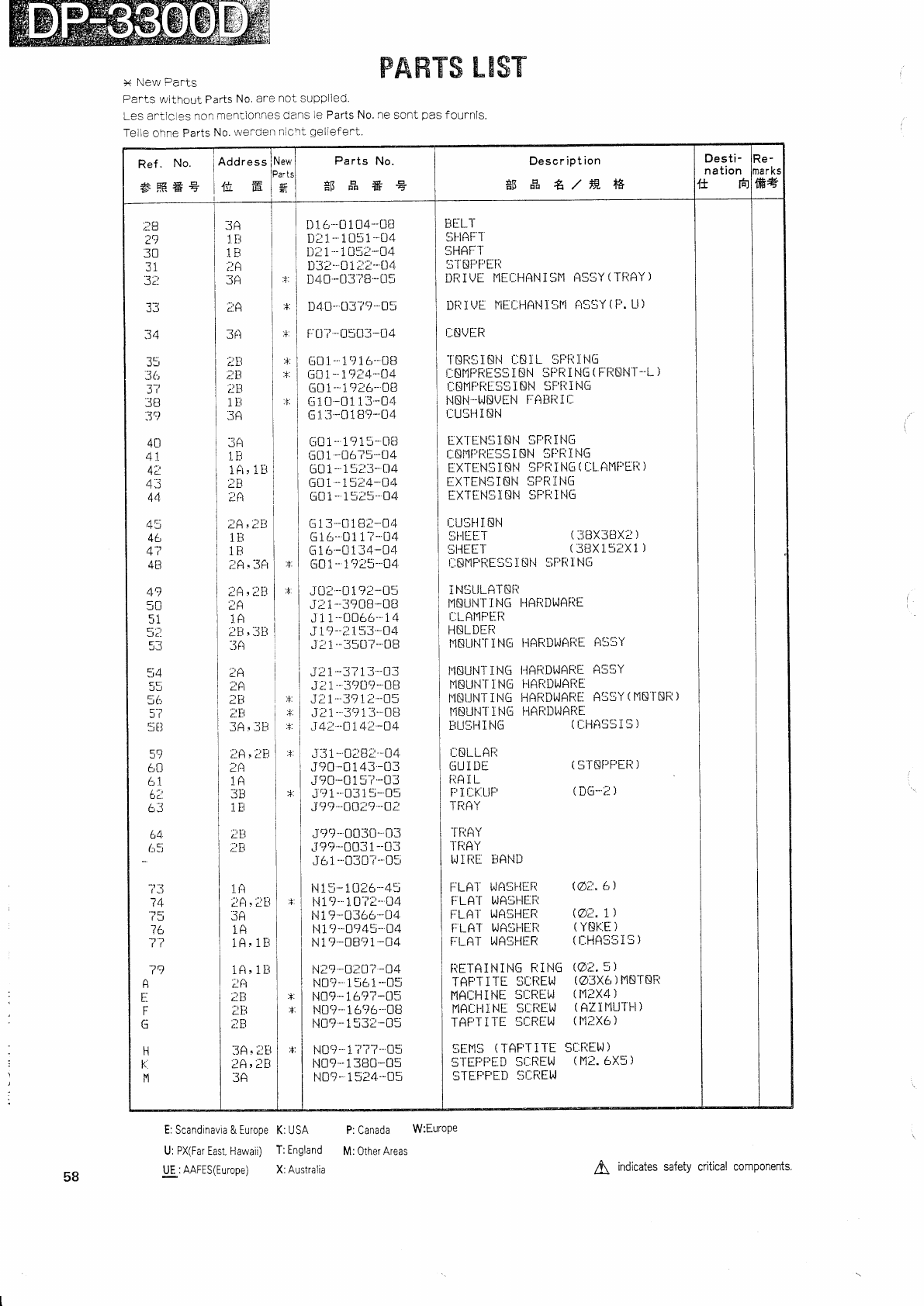
ffi,,
ffiW ww
W
PAffiT$
LE$T
x New Parts
Pa'ts wirhout
Parts
No.
are
not
supplled.
Les antic es
non
mentlonnes
dans
le
Parts No.
ne
sont pas
f
ounnls.
Teile
ohne
Parts
No.
werden
nicnt
geliefert.
Ref
. No.
Effi*+
Address
.tii i5
New
Par tt
tpl
Parts No.
gFffi*E
Descr ipt
ion
*$ ff &/ffi. ffi
Desti-
nation
I+ r:l
IJ IHJ
narks
ffi+
e-
R
33
35
3{:
3i
3tl
J7
40
41
qL
43
44
/-l:J
^1
+(
4U
Ar)
50
-JL
JC-
53
Ci
-J+
55
5(:
5-1
r-- rl
JCI
-Jn
lti
lti
;JA
3A
f-n
3A
i:Lr
':' tl
L- LI
;tLl
1Li
'?n
Il16-0104-08
Dti--1051..U4
Dt
I
- 1ll5i-04
D32--U
1;i:l-"04
Il40
-il3 7B*Ll5
D4U-
0379--05
i:u? -tJ5[']3
-u4
G01-- 1?
i 6- U€l
G[ 1"-1r24-D4
GU1-1i.tL-OB
G1U-U113-U4
G I :J
"01U?-04
C,0i-'1?i3-0u
bll1-06?5-U4
G0i- 15;:3-il4
Gil1
-
15:4-ll4
Gill- 1525--04
G i 3-t']1Ui
-04
Gi6--1111-i
-U4
Gi6-0134-U4
C-r01
--
1r)15-
Ll4
J0';-il1?2 -ll5
J2
1
-3?08
-08
J11--0066--i4
J l't--l l.53
-u4
J l1 --350-i
- Lltl
Jt1-3713-03
J;l1
--3':)U':i-
0u
J; 1--3?
i 2-Ll5
Jt 1--3?
13- UEI
J4t*U 1
4t -04
J:31- Lli8t--U4
Jr)0
-0143
-CI3
J':t0
-015?-03
J':) i
--0315-
05
J't9-0il'l'r-02
J'?'t-
i1030-
03
J??-U03
1
-U3
J
61
-030-i-
05
N 15- i
Ui6-4:i
N1't-
l.n-/i-04
N 1 ?-0366-04
N i'r-u't45- CI4
N1?-08?i
-CI4
N;?"-02il?
-lr4
N0'r-
1561-
ll5
NU9--16't7-Ll5
NU't--
16?6--Llts
N0?-153t -il5
NCI't- 1-/-17-"CI5
N0?- 1
380
-U5
N0?- 15t4--05
t]r--t '1-
LIL.L I
:tt-tAFl
5HAT.-
T
5] iJF,PEIi
]]R
I V[ NE[:I-IAN
I5I'1 A55Y
(
TTiAY
)
Dfi I VE f'lEL:tlAt'lI':lN
A55Y
(
P. U
)
I::8VIR
1NR5I8N
i::NIL
SiTfilNIi
I::NIIFT{E55I
fJN 5f1R
I NG
(
F
R8N
T-I.
)
r:t!NF'titi55I
NN 5F'ii
I NG,
l'lNN-t^,NVEN
t--ALltl I l::
I::U5I-JINN
EXI EN5lNl.l 5F'Fi
il'16
t::Nt'1f]tifi55
I
NN SfrR I NG
EX-rt-N5I
Ni.l 5F'Fi
I NCI
(
l-:L
Al'lFEii
)
IXI-ENSINN
5f:'F{ING
EXIENSItlN
llfrfiIl.lG
I-:U5III
NN
5l-lE[ir (:]Fix3tlxi
)
SIJEET (
StlX
152X
1
)
t_:Nf.lF'itE55
L Nft SF'r{
I Flc.l
I NSLILATt\lfi
I.lNUNT
I NG HAIIDT^JATI
I
I-:LAI{F'LiR
HNLDIFl
NNUI{]
i NCr i-lAtiDl^iAtlE
A':]SY
I'I8UNI-
I NG IlAIIDI^JARI
A5'JY
f'lfluN-f
I NGt
l-lARlll^lAflE
I.INIJNIiNG
IIAITI]WAIIL"
A55Y(
I"ININR
)
NNUNl
ING }.IAIIDI^JARE
LIU5I.]
I NG (
I-HA55I5
)
I-:TILLAF]
GUlDE
IiAiL
P l.
t::k:.LlF
TRfiY
-rfiAY
TfiRY
i^tI ri[ LtAN]l
r-.LAI-
I^JA5I-JIR
f: LA-l- t^iA3f-lER
i:LAl- t^lA5HIR
F LAT I^JA$FIEIT
r.LA
T UJASI-JER
ITETAINING
RIN6
TAF'T
I TE 5I::REI^I
t4qt_:l-IINE
Gt_REt^J
NAr_:f-tlNE
5t::REi^f
Tf,F,T I'IE 5I::R[t,J
'JEMS
(TAFTiIE
5I-EF,flED
5I::REI^J
STEF'F.ED
iJL:{EUJ
(
5l-Ntlf:'Eil )
(
DG-;r
)
(@;' (:')
(@:;.
I)
(
YfJK:[
)
(
[:HA55I5
)
(@2.5)
(@3Xt,
) f'lETNft
(
N2X4
)
(
AZ
I I1UI FI )
(
f,ltx6 )
5L:REI^J)
(N2.6X5)
;8
30
JI
JL- I
tl
ll
il
rll
tl1
tlt
3p)
ilJ
1A
,
1Lt
':' rl
LLI
iA
2A, iB
iLt
I l-:
I t_1
;iA,3A
iA
2A
1A
tv
:l t)
'1 I-J
L !-l ,+.
"<ii i
I
:R
;JA
'-) L-r
c- L_l
;i t]
'?n ?[1
JN T.JL'
3'
60
6I
6;
L:,,J
.iA ' c'kl
c,-1
1.)
-41-l
1 f.r
'-:'
I-r
LLI
':r rJ
LLI
L.A
/:,3i
'73
14
'l L-
rJ
76
77
79
iA
IA
3A
1A
IA
iA
ifl
IB
':1
li
;]F
3A
2A
3A
-i tt
LLI
ifl
IL]
lTl
II:)
11
t:
F
G
n
k5Hl.
E: Scandinavia & Europe
K: USA P: Canada W:Europe
U:
PX(Far
East, Hawaii)
T: England M: Other Areas
UE:AAFES(Europe)
X:Australia
58 fi indicates
safety
critical components.
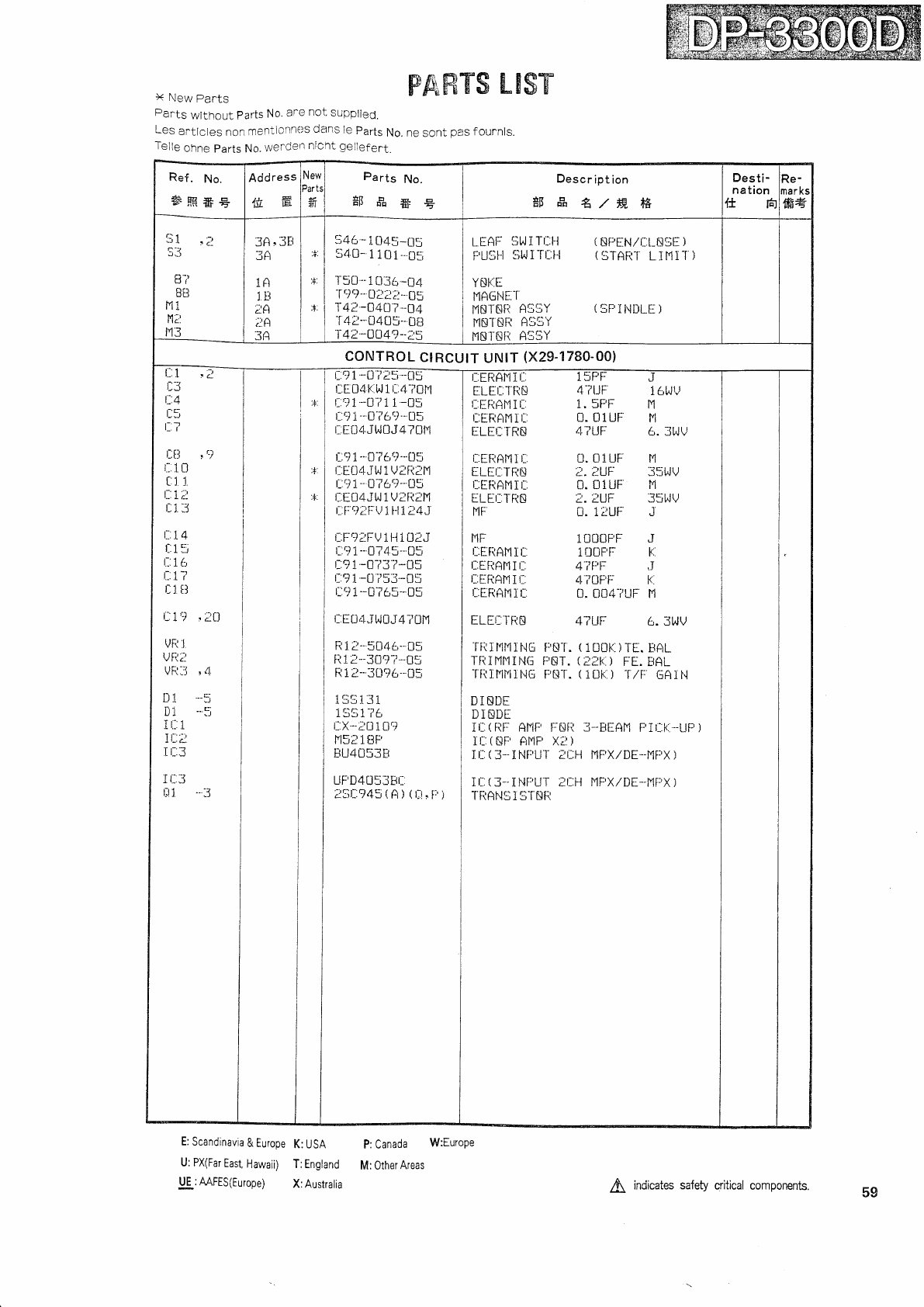
PAffiT$
LgST
X NeW
Parts
Par^ts
wlthout Parts
No.
ane
not supplied.
Les
angcles
non
mentlonnes
dans
le
Parts
No.
ne sont pas
fournls.
Telle
onne
parts
No.
wenderr
nicnt gellefert.
Ref. No.
#H€*€
Address
tl; E
New
9arts
a)
Parts No.
*tsft
&E
Descr
ipt
ion
*F & &,/ffi. ffi
Desti-
na
tion
ftFr
Re-
mar
ks
ffi*
J.L tcl
B7
Bu
l',l1
M':r
I ta_
I'13
JFI r JLt
-aA
Jt-l
1A
lra
LLl
2A
;J:A
Jta
,4.
.+:
.+.
ii46-
1045-05
540- i iCI1-.CI:;
TSil--1t]36
-U4
1tt9--Llc:i;]-
05
t'4.i
-04u
?-04
14t- 04U5--0t1
T42-4O49_;5
t_[At- $f^li
Tt:.Fl (
SPEN/I::I_N5I:
)
F'U5f-t
!]t^JI
-rl:i-l (
STAftl L 1N i 1 )
YNF
E
IlAGI.IE.T
I-1NTNII
A55Y (
5F'I
hIDLE
)
I'181$ri
A:l5Y
NETNI1
A55Y
CONTROL
CIRCL
f
T uNrT
(x29-1780-00)
I'1
D3
t:._"4
?
t--5
t::7
,-L)
l- 1 r-1
[:] l.
r-1.'
t.-. L c_
t-i. J
t:.14
t-:
I ::i
t__.
r t:,
t:.17
Dl il
t_.
L'1
fl
i0
VR]
vfii
VR:1
,4.
t\{
u.l" '--:l
n 1 --.c:
!J
T r'1
T f' -:'
f r- a-.
tt I
.t.
.{.
t::91.-U';'l:;
-05
t:.EU4
K.l,J
1t::4-i
0r"l
t-.rL-u7
i
1-05
l::?
i--1176't--u5
l::L.04Jt^l0J4
70t1
t_i1--o-i69'ai:
t::[l] 4.T
t^J
1
V 2 ti
it'l
L:9I
-
0-i 6?- U5
t_:[l]4Jt^J1VZfitt'l
t-.[r?l[r\r
i l._1124J
t::lj,:]lFV
1t-ll
LltJ
r::9I
--074
5--.05
r::?1-CI?3-/-05
r::?
1
-ti
753-05
l_:'-l
l.
-0765- D5
t::Eil4JtJ0J4
i
t-lf"l
11l
2..
5046--05
R 1t-3il't r'-O:i
R
1t- 30.t6--05
IJJI,]I
155
i-/{r
t::x-;u
10?
N5t 18F'
BU4U53B
UF'D4U5.JLtI:
i:lr:?45(A)
(r.l,F)
t:.Et(Al.1I
t_.
E.LEI_:1'ti&
t-.EtiAl.lIt-:
t_:tiRAf,li
t_:
ELEI::IRN
I:EfIAI'IT
L.
ILEI::'IRN
r::ERANir_:
ILEI::TIIE
NF
l'1F
t:.EilAHIt_:
r:EfinFl
I r_:
I::E.RAH
I
I-:
t_:EIiAl.li
t:.
[LEI::TIIE
15PF-
4'7tJr
I. :rt't-
0. uluF
47Ul:
J
i {,t^JV
f'1
l'l
6. 3ilV
0. uluF f4
:. ZUF: 3IJ|,JV
0. CI1ltF N
T. TUF 35|^JV
CI.
1LUF J
10u0irF J
100F'F l:..
4'7t1F ,I
4 70F'i:: h.
u. 0CI4-/ur- H
4?UF 6.3I^JV
-rfi
I r'ln
1i.]G F N]. (
1UUK.
)
-t-8.
L]AL
TR I NI'lI NG FNT.
(
i:TK::
) F
E. BAL
l fil.
NN I i.tfi frNl. ( l ilh:. ) l /F GA I f.l
DIEI]E
DJNDt:
I I:.
1
P1P AI'IF' F-NfI 3_BEAN F'I
I::l(::.-LJP
)
I l-:
(
tqF' ANF' Xi:
)
Ir::
(3-INPUI- ;t:.H nPX/DE-f{irx)
I
l_:
(
3--I
NirU'T tt:.l-{
l.1F'X,/llE-r'1px
)
l ftAN5
i:t-rNR
E:
Scandinavia
& Europe
K:
USA
U: PX(Far
East,
Hawaii) T:Engtand
UE:MFES(Europe) X:Austratia
P:Canada
W:EuroPe
M: Other
Areas
fi inciicates
safety
critical
components. 59
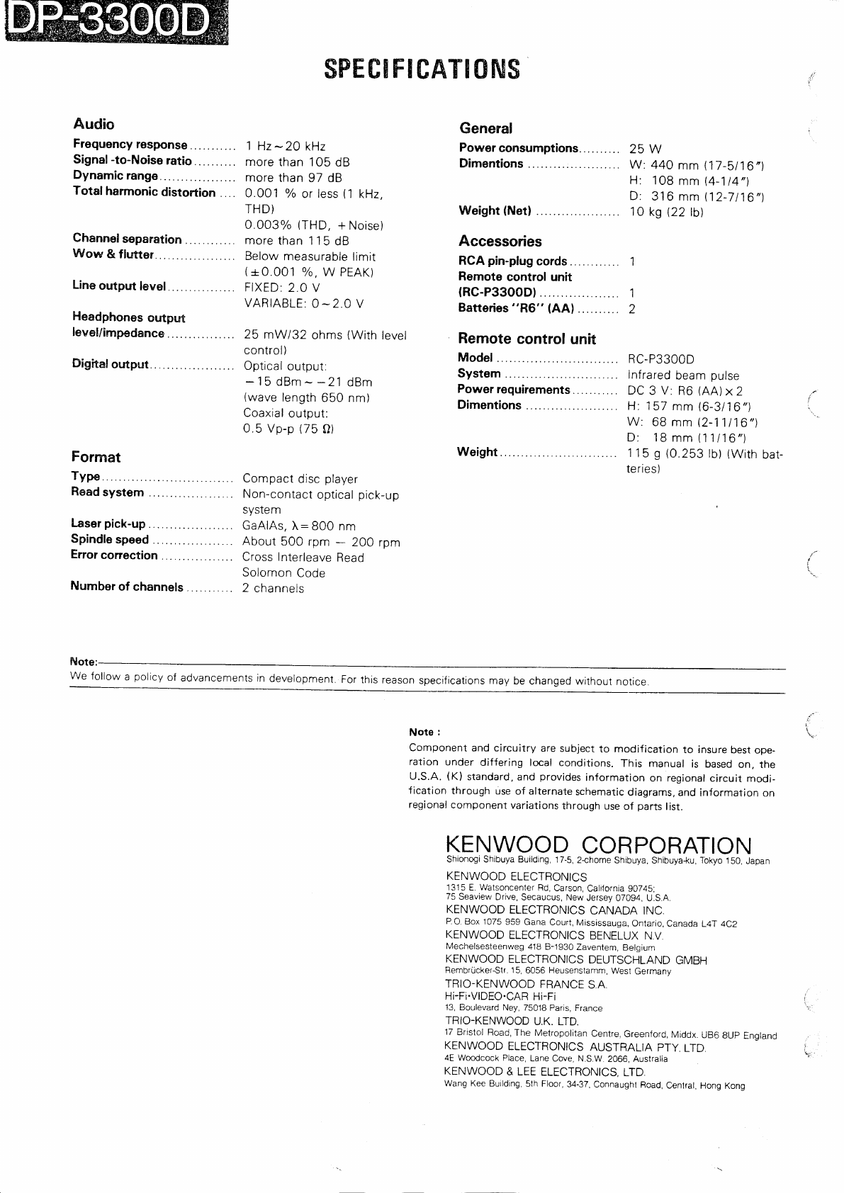
ffiffi. @@@
spEesFrcATt0rus
Audio
Frequoncy rosponse
Signal
-to-Noise ratio.
Dynamic range
Total harmonic
distortion ....
Channel s€paration
Wow & flutter.
Line
output level.
Headphones outpr.rt
level/irnpedance
Digitaloutpnt.
Format
Type
Read
system
laser
pick-up.....
Spindle
speed
....
Error
correction
..
1 Hz-20 k1z
more
than i
05 dB
more
than
97 dB
0.001 o/o
or less
(1 kHz,
THD)
0 003% (THD,
+
Noise)
more
than 1 15
dB
Below
measurable
limit
(+0.001 o/o,W
PEAK)
FIXED:
2.O
V
VARIABLE:
0-2.0 V
25 mW/32 ohms (With
tevel
control)
Optical
output:
- 15
dBm
- -21 dBm
(wave
length
650 nm)
Coaxial
output:
0.5
Vp-p
(75
0)
Compact
disc
player
Non-contact
optical
pick-up
system
GaAlAs,
L:800 nm
About 500 rpm - 200 rpm
Cross Interleave
Read
Solomon
Code
2 channels
General
Power consumptions..
Dimentions
.....
Weight
(Netl
25W
W: 440
mm
(17-5l1O"l
H: 108
mm
(4-114"1
D: 316
mm
(12-7liO"l
'10
ks
(22
tb)
1
1
2
RC-P33OOD
lnfrared
beam
pulse
DC
3 V:
R6
(AA)x
2
H. 157
mm
(6-3/16")
W: 68
mm
{2-11116')
D, 18
mm
(11/'16")
1
15
g
(0.253
lb)
(With
bar-
teries)
'i
Note:
We foliow
a policy
of
advancements in
developmenl For
this
reason
specifications
may be changed without notice
Note :
component and circuitry are subject
to modification to insure
best
ope-
ration under differing local conditions. This manual is based
on. the
u.s.A. (K) standard,
and
provides
information
on regional
circuit
modi-
fication through use
of alternate
schematic
diagrams,
and
information on
regional
component
variations
through
use
of parts
list.
KENWOOD
CORPORATION
Shionogi Shibuya Building,
17-5,
2chome Shibuya,
Shibuya*u,
Tokyo
150,
Japan
KENWOOD
ELECTRONICS
1315
E. Walsoncenter
Rd,
Carson,
California
90745;
75
Seaview
Drive,
Secaucus, New
Jersey
07094, U.S.A.
KENWOOD
ELECTRONICS
CANADA INC
PO.
Box
1075
959 Gana
Court,
Mississauga,
Ontario,
Canada
L4T 4Cz
KENWOOD
ELECTRONICS
BENELUX
N V
Mechelsesteenweg
418
B-1930
Zaventem,
Belgium
KENWOOD
ELECTRONICS
DEUTSCHLAND
GMBH
RembruckerSlr
15,
6056
Heusenstamm,
Wesl
Germany
TRIO-KENWOOD
FRANCE
S
A
Hi-Fi.VIDEO.CAR
Hi-Fi
-13,
Boulevard
Ney,
75018 Paris,
France
TRIO-KENWOOD
U.K. LTD.
17
Bristol Road,
The Metropolitan
centre,
Greenford,
Middx.
UB6 gUp Enqland
KENWOOD
ELECTRONICS
AUSTRALIA
PTY.
LTD
4E Woodcock Place,
Lane
Cove, N.S
W. 2066, Australia
KENWOOD
& LEE
ELECTRONICS,
LTD
Wang
Kee Building,
sth Floor,
34-37,
Connaught
Road,
Central, Hong
Kong
