COVER DVDR129
User Manual: DVDR129
Open the PDF directly: View PDF ![]() .
.
Page Count: 208 [warning: Documents this large are best viewed by clicking the View PDF Link!]
- 1-1 Safety Precautions
- 1-2 Servicing Precautions
- 1-3 ESD Precautions
- 1-4 Handling the optical pick-up
- 2-1 Product Specification
- 2-2 Chassis Product Specification
- 2-3 Option Product Specification
- 2-4 Introduction to DVD
- 2-5 DVD-Video Fromat
- 3-1 Drive Firmware Update
- 3-2 Flash Update (Main PCB)
- 4-1 Cabinet and PCB
- 4-2 PCB Location
- NO Power Detected(Stand by LED OFF)
- There's no Digital Audio Out
- C VBS (Video) output error
- S-Video output error
- AV2 CVBS Video Input Error
- A V1 CVBS Video Input Error
- AV1 S-Video Video Input Error
- Tuner Video Input Error
- Component output error
- A udio Input is not Recording
- T here is no Audio Output
- ED S [Extended data Services]is abnormal
- Disc Ioading error
- Tuner Video Out Abnormal
- Tuner Audio Out Abnormal
- Remocon Error
- 6-1 Cabinet Assembly
- ASSY PCB-MAIN
- ASSY PCB-KEY PCB
- ASSY PCB-KEY
- ASSY PCB-JACK
- ASSY-LOADER
- REMOCON-ASSY
- 8-1 All Block Diagram
- 8-2 DIC1(S5L3200) Block Diagram
- 8-3 AIC1(PCM1742) Block Diagram
- 8-4 AIC2 (PCM1802) Block Diagram
- 8-5 FIC1 (TSB4AB1) Block Diagram
- 8-6 VIC1 (TW9906) Block Diagram
- 8-7 IC4N01(MSP3407G) Block Diagram
- 10-1 Main PCB
- 10-2 Jack PCB
- 10-3 Key PCB
- 10-4 Sub PCB
- 11-1 S.M.P.S (Jack PCB)
- 11-2 TM Block (Jack PCB)
- 11-3 AV Input (Jack PCB)
- 11-4 Micom (Jack PCB)
- 11-5 CBS Function Block (Jack PCB)
- 11-6 I/O (Jack PCB)
- 11-7 AV Codec (Main PCB)
- 11-8 DDR (Main PCB)
- 11-9 DV_1394 (Main PCB)
- 11-10 Latch And Audio (Main PCB)
- 11-11 Main Connector (Main PCB)
- 11-12 Video Decoder (Main PCB)
- 11-13 Sub and Key (Sub and Key PCB)
- 13-1 Power
- 13-2 AV Codec
- 13-3 SERVO (DVP Multi Drive)
- 13-4 Video Input
- 13-5 Video Output
- 13-6 Audio
- 13-7 Tuner
- 13-8 IF
- 14-1 About IEEE-1394

DVD- RECORDER
Chassis : ANDES (3rd Generation)
DVD-R129/XAA, XAC
SERVICE
ŒMulti format recording
DVD-RW/ DVD-R
´Multi format playback
DVD/ DVD-RAM/ DVD-RW/ DVD-R
CD/ CD-R/ CD-RW/ MP3/ JPEG/
VCD(Canada Only)
ˇRecording mode
XP(1Hour)/ SP(2Hour)/ LP(4Hour)/ EP(6~8Hour)
¨Progressive scan
ˆAutomatic Chapter product on
Ø49mm Slim Design
∏Quick Recording
Manual
DVD-RECORDER Main Features
SERVICE MANUAL DVD-R129
ELECTRONICS
© Samsung Electronics Co., Ltd. JUN. 2006
Printed in Korea
AK82-01188A
This Service Manual is a property of Samsung Electronics Co.,Ltd.
Any unauthorized use of Manual can be punished under applicable
international and/or domestic law.

CONTENTS
1. Precautions 1-1 ~ 1-6
1-1 Safety Precaution (1-1)
1-2 Servicing Precautions (1-3)
1-3 ESD Precautions (1-4)
1-4 Handling the optical pick-up (1-5)
2. Product Specification 2-1 ~ 2-12
2-1 Reference Information (2-1)
2-2 Chassis Product Specification (2-2)
2-3 Option Product Specification (2-3)
2-4 Introduction to DVD (2-4)
2-5 DVD-Video Fromat (2-6)
3. Software Update 3-1 ~ 3-4
3-1 Drive Firmware Update (3-1)
3-2 Flash Update (3-3)
4. Disassembly and Reassembly 4-1 ~ 4-6
4-1 Cabinet and PCB (4-1)
4-2 PCB Location (4-6)
5. Trouble Shooting 5-1 ~ 5-16
6. Exploded View and Parts List 6-1 ~ 6-4
6-1 Cabinet Assembly (6-2)
7. Electrical Parts List 7-1 ~ 7-12
8. Block Diagrams 8-1 ~ 8-8
8-1 All Block Diagram (8-2)
8-2 DIC1(S5L3200) Block Diagram (8-3)
8-3 AIC1(PCM1742) Block Diagram (8-4)
8-4 AIC2 (PCM1802) Block Diagram (8-5)
8-5 FIC1 (TSB4AB1) Block Diagram (8-6)
8-6 VIC1 (TW9906) Block Diagram (8-7)
8-7 IC4N01(MSP3407G) Block Diagram (8-8)

9. Wiring Diagram 9-1 ~ 9-2
10. PCB Diagrams 10-1 ~ 10-8
10-1 Main PCB (10-2)
10-2 Jack PCB (10-4)
10-3 Key PCB (10-6)
10-4 Sub PCB (10-7)
11. Schematic Diagrams 11-1 ~ 11-14
11-1 S.M.P.S (Jack PCB) (11-2)
11-2 TM Block (Jack PCB) (11-3)
11-3 AV Input (Jack PCB) (11-4)
11-4 Micom (Jack PCB) (11-5)
11-5 CBS Function Block (Jack PCB) (11-6)
11-6 I/O (Jack PCB) (11-7)
11-7 AV Codec (Main PCB) (11-8)
11-8 DDR (Main PCB) (11-9)
11-9 DV_1394 (Main PCB) (11-10)
11-10 Latch And Audio (Main PCB) (11-11)
11-11 Main Connector (Main PCB) (11-12)
11-12 Video Decoder (Main PCB) (11-13)
11-13 Sub and Key (Sub and Key PCB) (11-14)
12. Operating Instructions 12-1 ~ 12-18
13. Circuit Operating Descriptions 13-1 ~ 13-16
13-1 Power (13-1)
13-2 AV Codec (13-4)
13-3 SERVO (DVP Multi Drive) (13-7)
13-4 Video Input (13-9)
13-5 Video Output (13-11)
13-6 Audio (13-13)
13-7 Tuner (13-14)
13-8 IF (13-15)
CONTENTS

14. Reference Information 14-1 ~ 14-4
14-1 About IEEE-1394 (14-1)
CONTENTS
Samsung Electronics 1-1
1. Precautions
1-1 Safety Precautions
1) Before returning an instrument to the customer,
always make a safety check of the entire instrument,
including, but not limited to, the following items:
(1) Be sure that no built-in protective devices are
defective or have been defeated during servicing.
(1)Protective shields are provided to protect both
the technician and the customer. Correctly replace
all missing protective shields, including any
removed for servicing convenience.
(2)When reinstalling the chassis and/or other as-
sembly in the cabinet, be sure to put back in place
all protective devices, including, but not limited to,
nonmetallic control knobs, insulating fish papers,
adjustment and compartment covers/shields, and
isolation resistor/capacitor networks. Do not oper-
ate this instrument or permit it to be operated with-
out all protective devices correctly installed and
functioning.
(2) Be sure that there are no cabinet openings through
which adults or children might be able to insert
their fingers and contact a hazardous voltage. Such
openings include, but are not limited to, excessive-
ly wide cabinet ventilation slots, and an improper-
ly fitted and/or incorrectly secured cabinet back
cover.
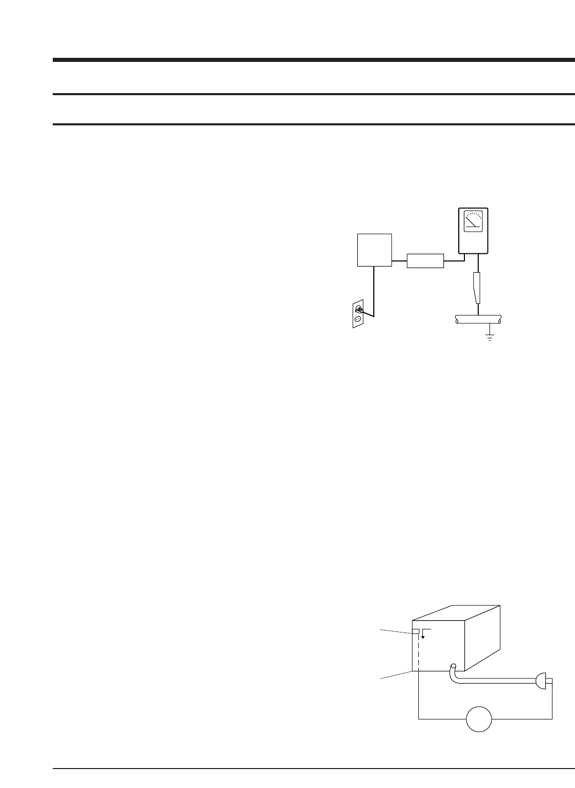
(3) Leakage Current Hot Check-With the instrument
completely reassembled, plug the AC line cord
directly into a 120V AC outlet. (Do not use an iso-
lation transformer during this test.) Use a leakage
current tester or a metering system that complies
with American National Standards institute (ANSI)
C101.1 Leakage Current for Appliances and
Underwriters Laboratories (UL) 1270 (40.7). With
the instrument’s AC switch first in the ON position
and then in the OFF position, measure from a
known earth ground (metal water pipe, conduit,
etc.) to all exposed metal parts of the instrument
(antennas, handle brackets, metal cabinets, screw-
heads, metallic overlays, control shafts, etc.), espe-
cially any exposed metal parts that offer an electri-
cal return path to the chassis.
Any current measured must not exceed 0.5mA.
Reverse the instrument power cord plug in the out-
let and repeat the test. See Fig. 1-1.
Any measurements not within the limits specified
herein indicate a potential shock hazard that must
be eliminated before returning the instrument to
the customer.
Fig. 1-1 AC Leakage Test
(4) Insulation Resistance Test Cold Check-(1) Unplug
the power supply cord and connect a jumper wire
between the two prongs of the plug. (2) Turn on the
power switch of the instrument. (3) Measure the
resistance with an ohmmeter between the
jumpered AC plug and all exposed metallic cabinet
parts on the instrument, such as screwheads,
antenna, control shafts, handle brackets, etc. When
an exposed metallic part has a return path to the
chassis, the reading should be between 1 and 5.2
megohm. When there is no return path to the chas-
sis, the reading must be infinite. If the reading is
not within the limits specified, there is the possibil-
ity of a shock hazard, and the instrument must be
repaired and rechecked before it is returned to the
customer. See Fig. 1-2.
Fig. 1-2 Insulation Resistance Test
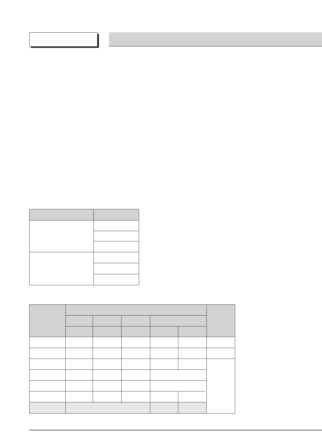
DEVICE
UNDER
TEST
(READING SHOULD
NOT BE ABOVE
0.5mA)
LEAKAGE
CURRENT
TESTER
EARTH
GROUND
TEST ALL
EXPOSED METER
SURFACES
ALSO TEST WITH
PLUG REVERSED
(USING AC ADAPTER
PLUG AS REQUIRED)
2-WIRE CORD
Antenna
Terminal
Exposed
Metal Part
ohm ohmmeter

Precautions
1-2 Samsung Electronics
2) Read and comply with all caution and safety re-
lated notes on or inside the cabinet, or on the chas-
sis.
3) Design Alteration Warning-Do not alter or add to
the mechanical or electrical design of this instru-
ment. Design alterations and additions, including
but not limited to, circuit modifications and the
addition of items such as auxiliary audio output
connections, might alter the safety characteristics of
this instrument and create a hazard to the user. Any
design alterations or additions will make you, the
servicer, responsible for personal injury or property
damage resulting therefrom.
4) Observe original lead dress. Take extra care to
assure correct lead dress in the following areas:
(1) near sharp edges, (2) near thermally hot parts (be
sure that leads and components do not touch ther-
mally hot parts), (3) the AC supply, (4) high voltage,
and (5) antenna wiring. Always inspect in all areas
for pinched, out-of-place, or frayed wiring, Do not
change spacing between a component and the
printed-circuit board. Check the AC power cord for
damage.
5) Components, parts, and/or wiring that appear to
have overheated or that are otherwise damaged
should be replaced with components, parts and/ or
wiring that meet original specifications.
Additionally, determine the cause of overheating
and/or damage and, if necessary, take corrective
action to remove any potential safety hazard.
6) Product Safety Notice-Some electrical and mechani-
cal parts have special safety-related characteristics
which are often not evident from visual inspection,
nor can the protection they give necessarily be
obtained by replacing them with components rated
for higher voltage, wattage, etc. Parts that have spe-
cial safety characteristics are identified by shading,
an ( )or a ( )on schematics and parts lists. Use
of a substitute replacement that does not have the
same safety characteristics as the recommended
replacement part might create shock, fire and/or
other hazards. Product safety is under review con-
tinuously and new instructions are issued whenev-
er appropriate.

Precautions
Samsung Electronics 1-3
1-2 Servicing Precautions
CAUTION : Before servicing units covered by this
service manual and its supplements, read and follow
the Safety Precautions section of this manual.
Note : If unforseen circumstances create conflict
between the following servicing precautions and any
of the safety precautions, always follow the safety pre-
cautions. Remember: Safety First.
1-2-1 General Servicing Precautions
(1) a. Always unplug the instrument’s AC power cord
from the AC power source before (1) re-moving
or reinstalling any component, circuit board,
module or any other instrument assembly, (2)
disconnecting any instrument electrical plug or
other electrical connection, (3) connecting a test
substitute in parallel with an electrolytic capaci-
tor in the instrument.
b. Do not defeat any plug/socket B+ voltage inter-
locks with which instruments covered by this
service manual might be equipped.
c. Do not apply AC power to this instrument and
/or any of its electrical assemblies unless all
solid-state device heat sinks are correctly in-
stalled.
d. Always connect a test instrument’s ground lead
to the instrument chassis ground before connect-
ing the test instrument positive lead. Always
remove the test instrument ground lead last.
Note : Refer to the Safety Precautions section ground
lead last.
(2) The service precautions are indicated or printed on
the cabinet, chassis or components. When servic-
ing, follow the printed or indicated service precau-
tions and service materials.
(3) The components used in the unit have a specified
flame resistance and dielectric strength.
When replacing components, use components
which have the same ratings. Components identi-
fied by shading, by( ) or by ( ) in the circuit dia-
gram are important for safety or for the characteris-
tics of the unit. Always replace them with the exact
replacement components.
(4) An insulation tube or tape is sometimes used and
some components are raised above the printed
wiring board for safety. The internal wiring is
sometimes clamped to prevent contact with heat-
ing components. Install such elements as they
were.
(5) After servicing, always check that the removed
screws, components, and wiring have been in-
stalled correctly and that the portion around the
serviced part has not been damaged and so on.
Further, check the insulation between the blades of
the attachment plug and accessible conductive
parts.
1-2-2 Insulation Checking Procedure
Disconnect the attachment plug from the AC outlet
and turn the power ON. Connect the insulation resi-
stance meter (500V) to the blades of the attachment
plug. The insulation resistance between each blade of
the attachment plug and accessible conductive
parts(see note) should be more than 1 Megohm.
Note : Accessible conductive parts include metal pan-
els, input terminals, earphone jacks, etc.

Precautions
1-4 Samsung Electronics
1-3 ESD Precautions
Electrostatically Sensitive Devices (ESD)
Some semiconductor (solid state) devices can be dam-
aged easily by static electricity.
Such components commonly are called Electrostati-
cally Sensitive Devices(ESD). Examples of typical ESD
devices are integrated circuits and some field-effect
transistors and semiconductor chip components. The
following techniques should be used to help reduce
the incidence of component damage caused by static
electricity.
(1) Immediately before handling any semiconductor
component or semiconductor-equipped assembly,
drain off any electrostatic charge on your body by
touching a known earth ground. Alternatively,
obtain and wear a commercially available dis-
charging wrist strap device, which should be
removed for potential shock reasons prior to apply-
ing power to the unit under test.
(2) After removing an electrical assembly equipped
with ESD devices, place the assembly on a conduc-
tive surface such as aluminum foil, to prevent elec-
trostatic charge buildup or exposure of the assem-
bly.
(3) Use only a grounded-tip soldering iron to solder or
unsolder ESD devices.
(4) Use only an anti-static solder removal devices.
Some solder removal devices not classified as
“anti-static” can generate electrical charges suffi-
cient to damage ESD devices.
(5) Do not use freon-propelled chemicals. These can
generate electrical charges sufficient to damage
ESD devices.
(6) Do not remove a replacement ESD device from its
protective package until immediately before your
are ready to install it.(Most replacement ESD
devices are packaged with leads electrically short-
ed together by conductive foam, aluminum foil or
comparable conductive materials).
(7) Immediately before removing the protective ma-
terials from the leads of a replacement ESD device,
touch the protective material to the chassis or cir-
cuit assembly into which the device will be
installed.
CAUTION : Be sure no power is applied to the ch-
assis or circuit, and observe all other safety precau-
tions.
(8) Minimize bodily motions when handling unpack-
aged replacement ESD devices. (Otherwise harm-
less motion such as the brushing together of your
clothes fabric or the lifting of your foot from a car-
peted floor can generate static electricity sufficient
to damage an ESD device).
Precautions
Samsung Electronics 1-5
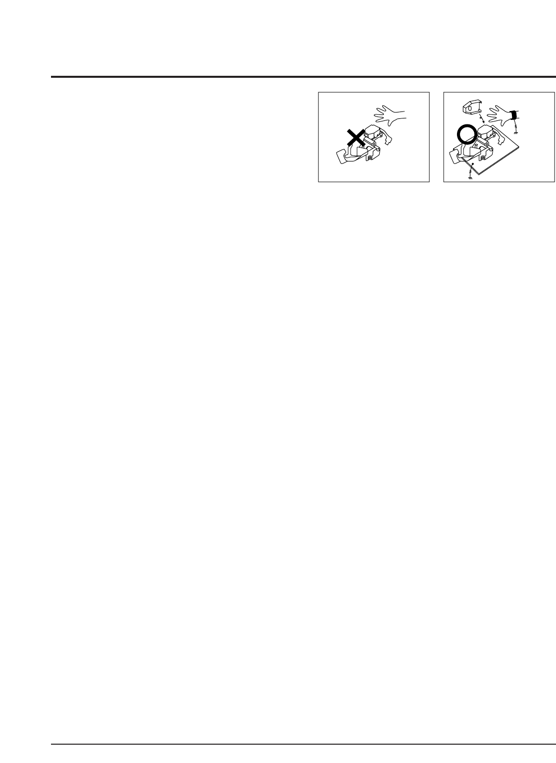
1-4 Handling the optical pick-up
The laser diode in the optical pick up may suffer elec-
trostatic breakdown because of potential static elec-
tricity from clothing and your body.
The following method is recommended.
(1) Place a conductive sheet on the work bench (The
black sheet used for wrapping repair parts.)
(2) Place the set on the conductive sheet so that the
chassis is grounded to the sheet.
(3) Place your hands on the conductive sheet(This
gives them the same ground as the sheet.)
(4) Remove the optical pick up block
(5) Perform work on top of the conductive sheet. Be
careful not to let your clothes or any other static
sources to touch the unit.
◆Be sure to put on a wrist strap grounded to the
sheet.
◆Be sure to lay a conductive sheet made of copper
etc. Which is grounded to the table.
Fig.1-3
(6) Short the short terminal on the PCB, which is in-
side the Pick-Up ASS’Y, before replacing the Pick-
Up. (The short terminal is shorted when the Pick-
Up Ass’y is being lifted or moved.)
(7) After replacing the Pick-up, open the short termi-
nal on the PCB.
THE UNIT
WRIST-STRAP
FOR GROUNDING
1M
1M CONDUCTIVE SHEET

Precautions
1-6 Samsung Electronics
MEMO
Samsung Electronics 2-1
Power requirements 120V AC,60Hz
Power consumption 19Watts
General Weight 5.07 IB
Dimensions 16.9inch(W) x 8.2inch(D) x 1.9inch(H)
Operating temp +41°F to 95°F
Other conditions Keep level when operating. Less than 75% operating humidity
Video (1,2) 1.0 V p-p at 75ohm load, sync negative
S-Video input (Y:1.0Vp-p, C: 0.286Vp-p at 75ohm load)
Audio (1,2) Max. Audio input level : 2Vrms
Input DV Input IEEE 1394(4p) compatible jack
Receivable Channels Regular TV broadcasting : VHF (2~13), UHF (14~69)
Cable TV broadcasting: 1~125
Audio output jacks 1,2
Optical/coaxial digital audio output
Audio
Full scale analog output level : 2Vrms
Output Video output jacks 1,
S-Video output 1 (Y: 1.0Vp-p, C:0.286Vp-p at 75 ohm load)
Video
Component output (Y: 1.0Vp-p ,Pb:0.70Vp-p, Pr:0.70Vp-p at 75ohm load)
Picture compression format MPEG-II
Audio compression format Dolby digital 2ch/256kbps
Recording Recording Quality XP (about 8 Mbps), SP (about 4 Mbps), LP (about 2 Mbps),
EP (about 1.2 Mbps), FR (about 1.2 Mbps to 8Mbps)
Audio frequency characteristics 20 Hz ~ 20 KHz
2. Product Specification
2-1 Product Specification

Product Specification
2-2 Samsung Electronics
2-2 Chassis Product Specification
General Model Name DVD-R129/XAA
Info Function Standard
COLOR SYSTEM NTSC
SYSTEM BROADCAST SSTEM M
AUTO CLOCK O
DVD-RAM -
DVD-R O
DVD-RW O
VIDEO MPEG-2
AUDIO 2ch
RECORER DVD-RAM/-R(4.7GB) O
FUNCTION HDD -
Flexible Recording O
OTR O
Time Slip -
VCR+Plus -/-
Quick Dubbing -
EPG(Gemstar) -
IR Blaster -
Play Lis O
SUB Auto Chaptering O
FUNCTION JPEG Browser with BG music -
DV Input O
10in2 Memory Slot -
DVD-RAM/-R/-RW O/O/(O)
DVD-Video/VCD/CD-DA O/-/O
CD-R/RW O/O
PLAYBACK Music CD O
FUNCTION MPEG4/Divx -/-
Multi Memory Card -
Progressive Scan Output O
Upscaling(720P/1080i) -
DV/AV1/AV2/CH O/O/O/O
Video Input 2ea
Video Output 1ea
S-Video Input 1ea
S-Video Output 1ea
IN/OUT Component Output 1ea
HDMI Output -
Analog Audio Input(L/R) 2sets
Analog Audio Output(L/R) 2sets
Optical/Coaxial O/O
Panel disply LED Module
REMOCON Multi 47key
ETS IB English
Size: Net(W x H x D) 430X49.5X210
Weight 2.3Kg
Product Specification
Samsung Electronics 2-3
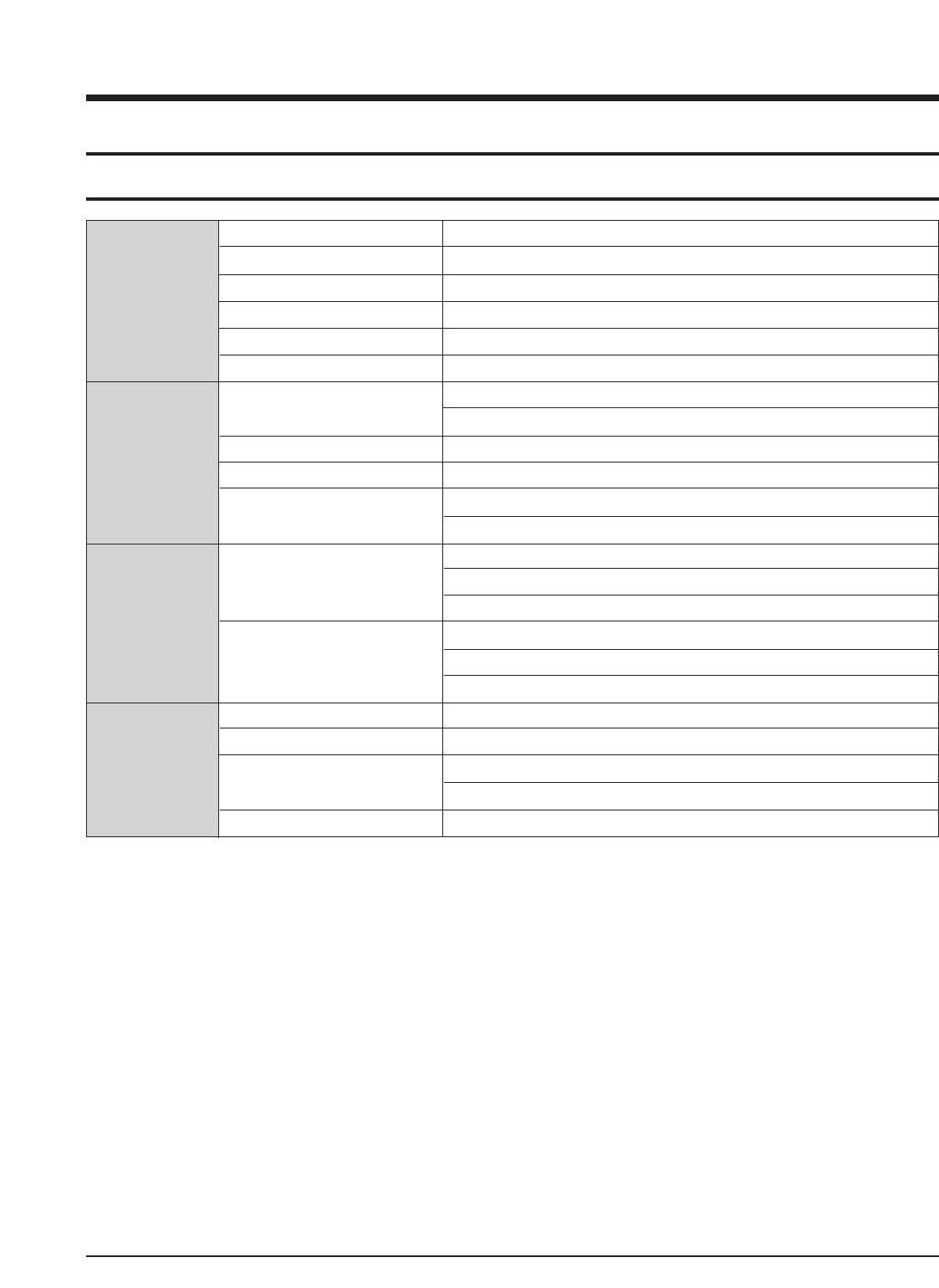
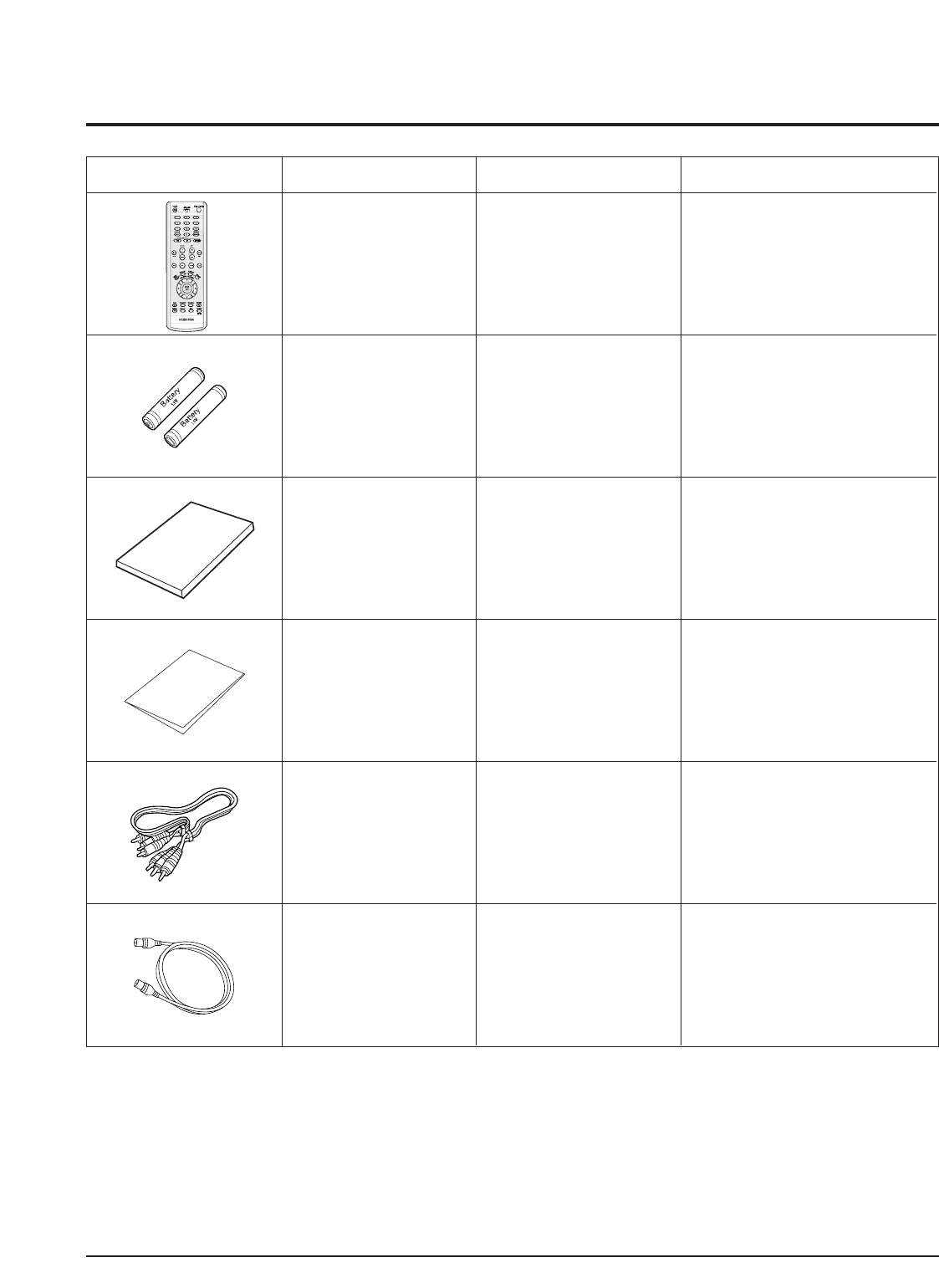
2-3 Option Product Specification
Description Fig Description Parts No Remark
Remote
Control
Batteries for
Remote Control
AK59-00055A
AC43-12002H
Model Standard of
DVD-R129/XAA
Model Standard of
DVD-R129/XAA
S.N.A
Model Standard of
DVD-R129/XAA
Model Standard of
DVD-R129/XAA
S.N.A
Model Standard of
DVD-R129/XAA
Model Standard of
DVD-R129/XAA
AK68-01174A
AK68-01175A
AC39-00073A
AC39-42001J
User’s Manual
Quick Guide
Video/Audio
Cable
RF Cable
Product Specification
2-4 Samsung Electronics
2-4 Introduction to DVD
2-4-1 The Definition of DVD
DVD is the next generation medium and is the acronym of the Digital Versatile Disc or thr Digital Video Disc,
which maximizes the saving density of the disk surface using the MPEG-2 compression technology to enable the
storage of 17G bytes of data on the same size CD.
1) 7 times the storage capacity of the conventional CD
- Minimized the track pitch and pit size to 1/2 of conventional CD.
- Uses red laser with short-wavelenght of 650nm (635nm).
DVD Vs. CD-ROM
CD-ROM CD-R/RW DVD-ROM DVD-R/RW DVD-RAM
Disc Thickness 1.2mm 1.2mm 0.6*2mm 0.6*2mm 0.6*2mm
Lens NA 0.45 0.45(0.5) 0.6 0.6 0.6
Laser wavelenght 780um 780um 650um 650um 650um
Track pitch 1.6pm 1.6pm 0.74pm 0.74pm 0.615pm
Capacity 0.65GB 0.65GB 4.7GB 4.7GB 4.7GB
Track structure Pit train Groove Pit train Groove Land/Groove
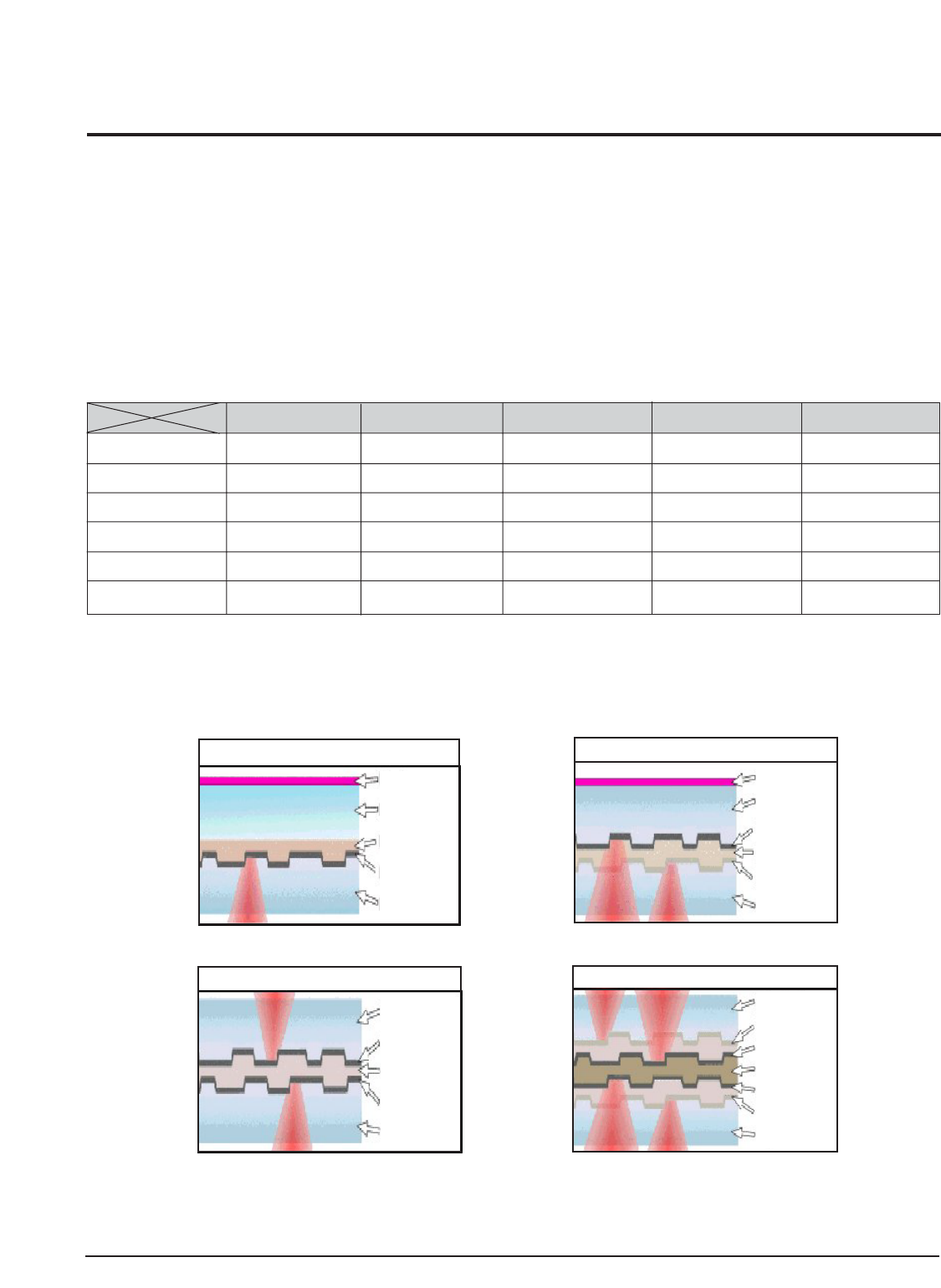
2) Disc Formats
DVD consists of two 0.6mm discs attached together, enabling access to the upper and lower side of the disk,
and 4 sides could be used at maximum.
Single Layer : 4.7GByte
Polycarbonate
Label
Bonding layer
Reflective layer
Polycarbonate
Label
Polycarbonate
Bonding layer
Reflective layer
Semi-reflective layer
Polycarbonate
Dual Layer : 8.5GByte
Bonding layer
Reflective layer
Reflective layer
Polycarbonate
Polycarbonate
Dual Side Single Layer : 9.5GByte
Polycarbonate
Bonding layer
Reflective layer
Reflective layer
Semi-reflective layer
Semi-reflective layer
Polycarbonate
Dual Side Dual Layer : 17GByte

Samsung Electronics 2-5
2-4-2 DVD Types
FORMAT TYPE APPLICATIONS
DVD-Video Playback Only High quality image and sound for movies and other video media.
DVD-ROM Read Only Multi-functional, multi-media software that requires large storage capacity.
DVD-Audio Playback Only High quality sound that exceeds the CD, multi-channel Audio.
DVD-R 1 Time Recording As with CD-R, write only once
DVD-RAM
Rewritable This can be virtually used as hard-disk, with a random
(more than 100,000 times) read-write access
Rewritable Similar to DVD-RAM except than its technology features
DVD-RW
(About 1,000 times) a separated read-write access more like phonograph than a hard disk.
Product Specification
2-6 Samsung Electronics
2-5 DVD-Video Fromat
2-5-1 Main Features
1) Able to store up to 160 minutes of Movie by utilizing the MPEG-2 compression technology. ( Aver. 133min.)
2) Enables more than 500 lines of horizontal resolution. (Class corresponding to the Master Tapes used in
broadcasting stations)
3) Provides Dolby Digital 5.1ch Surround 3D sound, which enables theater quality sound (NTSC area).
• For PAL areas, 1 of either MPEG-2 Audio or Dolby Digital must be selected.
4) Multi-Language
• Able to store up to 8 languages of dubbing.
•Able to store up to 32 subtitle languages.
5) Multi-Aspect Ratio
3TV Mode alternatives ; 16:9 Wide Screen (DVD Basic)/4:3 Pan & Scan/Letter Box.
6) Multi-Story
Possible to implement Interactive Viewing which enables the user to select the scenario.
7) Multi-Angle
Able to view the camera angle you selected among the scenes recorded with multiple camera angles.
Note ; The above media features must have the DVD Title that contains the appropriate contents to function
properly.
2-5-2 Audio & Video Specifications
Classification DVD-Video Video-CD LD
Compression MPEG-2 MPEG-1 Analog
Pixel 720 x 480 352 x 240
VIDEO Horizontal resolution Max. 500 Lines Max. 250 Lines Max.420 Lines
Compression rate 1/40 1/140 Analog
Transmission speed Max. 9.8Mbps (variable) 1.15Mbps (fixed)
TV aspect 16:9 / 4:3 4:3 4:3
Audio Max. 8 streams 2CH stereo
Recording type Dolby Digital Linear PCM MPEG-1 Layer 2
AUDIO Transmission rate 448Kbps/stream 6.144Mbps/stream 224Kbps or
Channel 5.1CH/stream 8CH/stream 2CH
Sampling frequency 48KHz 16, 20, 24Bit/48, 96KHz 16Bit/44.1KHz
2 Analog CH.
2 Digital CH.
(16Bit/44.1KHz)
1 Analog CH.
1 Stream of Dolby Digital
2 Digital CH.
(16Bit/44.1KHz)

Samsung Electronics 2-7
2-5-3 Detailed Feature
As the storage capacity increases, the DVD-Video separates the main data and the additional data such as the
Multi-Function into different data areas, enabling the control of time-data ratio to provide the format that enables
the flexible Software development
• 1 Movie (3.5Mbps)
+ Subtitle (1 Language)
+ Surround Audio (1 Language)
= 160min storage (4.673Gbytes)
• 1 Movie (3.5Mbps)
+ Subtitle (4 Language)
+ Surround Audio (4 Language)
= 160min storage (4.680Gbytes)
• 1 Music Video (4Mbps)
+ 2ch High quality Audio (96kHz/24bit)
= 72min storage (4.648Gbytes)
DVD-Video Feature 1 When Developing the DVD Software, various addition and modification is possible.
DVD-Video uses the variable compresion technology, the MPEG-2 to compress the moving image optimally, mini-
mizing the Data loss to Provide a clear, natural screen while increasing the storage time.
DVD-Video Feature 2 Application of the MPEG-2 compression technology.
• MPEG-2 (Variable compression : Max. 1/40)
- Field unit compression.
DVD-Video - Compression rate change according to the amount of Data.
- Differentiates the still image and the moving image
compression rate, reducing Data loss and enables
efficient compression.
•MPEG-1 (Fixed compression : Max. 1/140)
- Frame unit compression.
Video-CD - Compresses all data using the same ratio.
- Fast movements are jagged, and unnatural
Time
Amount of data
Time
Amount of data Loss area
Product Specification
2-8 Samsung Electronics
DVD-Video can store the audio using the 5.1ch Dolby Digital compression or the advanced Liner PCM method,
providing the better-than-CD quality and theater like audio quality.
•DTS (Digital Theater System)
Home theatre and music playback in the home, DTS provides high quality 5.1-channel surround sound with
many extras not offered by other consumer formats. As well as handling DTS-branded releases from a growing
number of music labels and consumer software producers, DTS provides enhanced 6.1 matrix and DTS 6.1
discrete decoding that envelopes the listener in sound. DTS technology is featured in a wide cross section of
receiver/pre-amplifiers, DVD players and and add-on components from leading consumer audio vendors
•Dolby Digital (AC-3)
- Unlike the traditional Dolby pro-Logic method, the Dolby Digital method separates all 5 main channels
(Front L/R, Center, Surround (Rear) L/R)and the Sub woofer to provide live surround audio.
- Using the Down Mix method, the conventional Dolby Pro-Logic and Stereo are all compatible.
- Each separated channels are played back at CD quality sound. (Frequency band: 20Hz ~ 20KHz)
•Linear PCM (Pulse Code Modulation)
- Provides the high quality Digital sound without the audio data compression.
- Various Digital Recordings are possible as shown in the table to the right.
DVD-Video Feature 3 High quality surround audio.
Sampling Frequency Bit Rate
16bit
48KHz 20bit
24bit
16bit
96KHz 20bit
24bit
•Dolby Digital compatible Audio Mode
Audio Coding
Channel Format
Mode
Front Surround (Rear) Remark
LCRLR
1/0 O Mono
2/0 O O Stereo
3/0 OOO
2/1 O O Mono
3/1 O O O Mono Surround
2/2 OOOO
3/2 OOOOO
Samsung Electronics 2-9
•Audio Dubbing - Max. 8 Languages
•Subtitle - Max. 32 Languages. Capable of storing, and selectiong.
•Linear PCM (Pulse Code Modulation)
DVD-Video Feature 4 Multi-Language
•Unlike the conventional VCD or LD, DVD-Video has the default of 16:9 Wide, and can be viewed using the
conventional 4:3 TV, enabling the expansion of viewer selection capabilities.
- 16 : 9 TV : Wide Mode (16:9 Wide Full Screen)
- 4 : 3 TV : Letter Box Mode, Pan & Scan Mode
DVD-Video Feature 5 Multi-Aspect
4:3 Pan & Scan
16:9 Wide 4:3 Letter Box
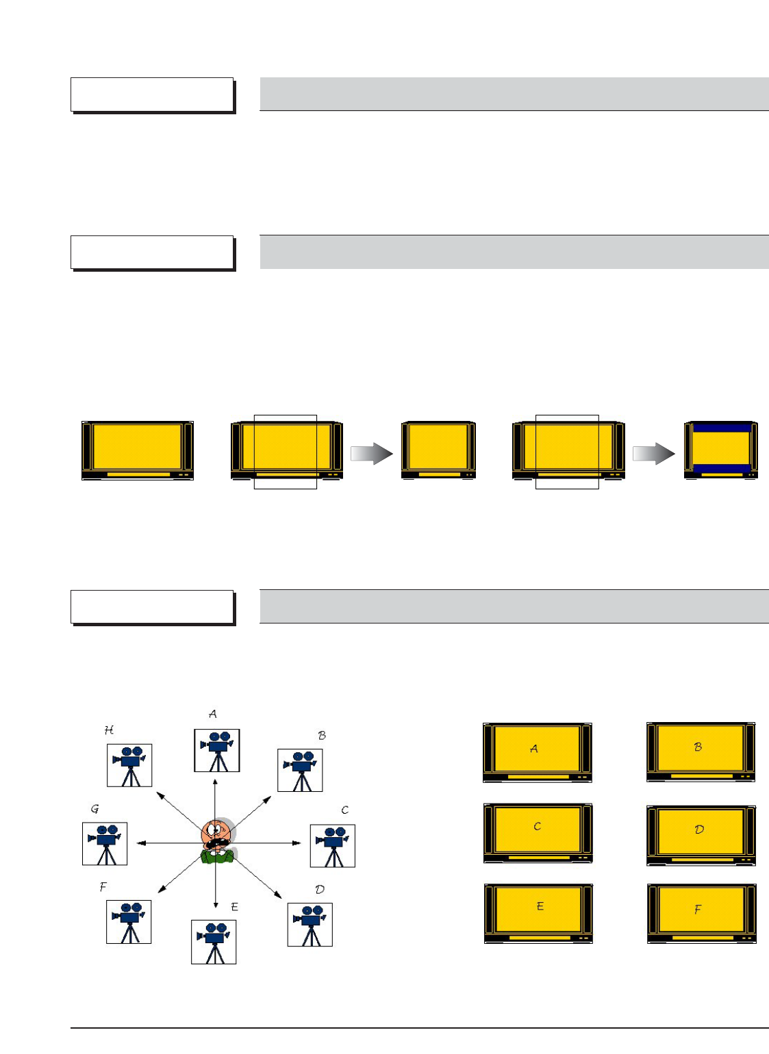
•Up to 9 angles of view may be stored, enabling the viewer to select a specific viewpoint at a given time.
--> Especially, for the Music Video and Sports Title, this provides a more lively image of the scene.
DVD-Video Feature 6 Multi-Angle
Note ; This function is disc-dependent, may not work on all DVDs.
Note ; This function is disc-dependent, may not work on all DVDs.

Product Specification
2-10 Samsung Electronics
•DVD-Video provides the enviroment suitable for the bi-directional Software develoment, providing multiple
scenarios. This feature enables the Multi-Story function.
DVD-Video Feature 7 Multi-Story
• For the titles that are not suitable for children viewing, Parental Locks are set, requesting user defined
passwords for viewing
•Parential Locks may be set on specific frames of the Title, enabling the player to skip those frames during
playback.
OPTION Parental Lock
•Classify the world into 6 regions, and if the DVD Title and the Player’s “Reginal Code” do not agree, playback
is prohibited.
•Regionnal Coding is optional for the Soft developers (Region 0 All Code), but the Hardware developers
must adopt the appropriate regionnal code for sale.
- Region 1 : The United States and its territories, Canada.
- Region 2 : Europe, Japan, Greenland, Egypt, South Africa, the Middle East.
- Region 3 : Taiwan, Hongkong, Korea, South East Asia.
- Region 4 : Mexico, South America, Australia, New Zealand.
- Region 5 : Russia, Eastern Europe, India, Africa.
- Region 6 : China.
- Region 0 : Worldwide (All Code)
COPYRIGHT Regional Code & Macrovision
•Adoptation of the Macrovision System disables the copying on to other media.
Œ
Œ
¨
¨
Œ
´
ˇ
ˆ
Ø
´
´ˆ
Product Specification
Samsung Electronics 2-11
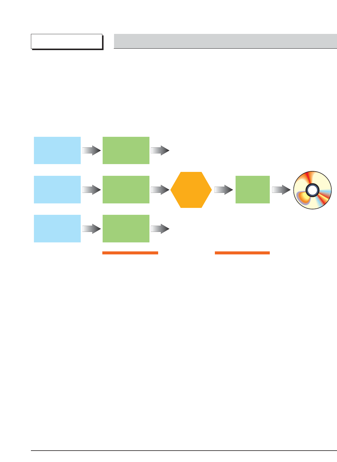
• The image quality of the DVD-Video may vary accoring to the quality of the Master and the Authoring Process
- The image quality of the DVD-Video varies according to the Digital Mastering Source such as the
conventional LD, VCD, or Original Film.
- Different Authoring Process are used accoring to the Software developers, and this may affect the
DVD image quality.
•Authoring Process
Remark DVD-Video Authoring Process
Video/Audio
Master
Surround Audio
Master
Subtitle
Master
MPEG-2
Encoding
AC-3/MPEG Audio
Encoding
Cutting
Master
Disc
Production
Subtitle
Encoding
Authoring Process
Video/Audio
Subtitle
Multiplexing
bit stream
bit stream
bit stream

Product Specification
2-12 Samsung Electronics
MEMO

Samsung Electronics 3-1
3. Software Update
3-1 Drive Firmware Update
3-1-1 Introduction
When you can not record and play on specific recording media (especially on newly available DVD-RW or DVD-R).
3-1-2 How to make an update disc
• Write the downloaded file onto a blank CD-R or CD-RW disc, using the following settings :
1) Download the software update file from the samsung internet site. (www.samsung.com)
2) Write the file to disc using the CD-RW of your computer.
• Recommended Application Program
- Nero Burning / Easy CD Creator ..etc
• Option
- Extension name : “*.SMD”
- Multisession : No Multisession
- File name lenght : Max. of 11 = 8 + 3
- Character set : ISO 9660 or Joliet Format
- CD Close & Disc at once
N O T E
It is very important : please read the below notice below before updating your unit.
The following events may interrupt the update process and MAY RESULT IN PERMANENT DAMAGE TO THE UNIT WHILE UPDATING
!Unplugging the power cord.
@Power Outage.
#Dirt or Scratches on the disc.
$Opening a disc tray during processing.
WARNING
3-2
Software Update
Samsung Electronics
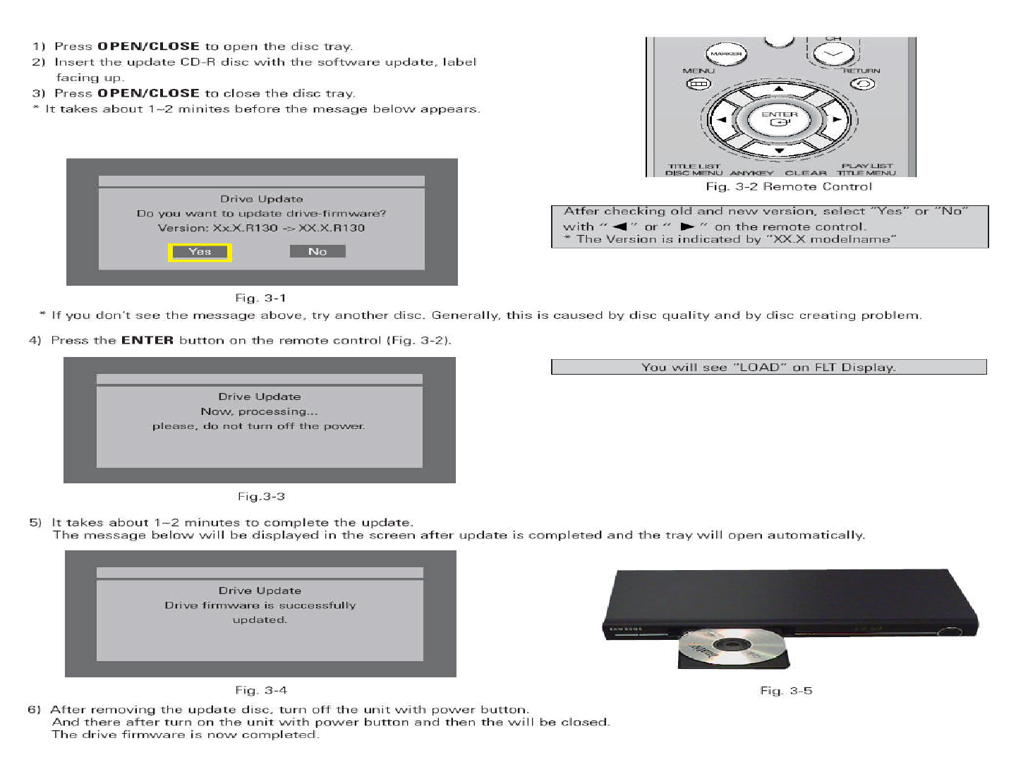
Fig. 3-1
* If you don’t see the message above, try another disc. Generally, this is caused by disc quality and by disc creating problem.
4) Press the ENTER button on the remote control (Fig. 3-2).
Fig.3-3
5) It takes about 1~2 minutes to complete the update.
The message below will be displayed in the screen after update is completed and the tray will open automatically.
Fig. 3-4
6) After removing the update disc, turn off the unit with power button.
And there after turn on the unit with power button and then the will be closed.
The drive firmware is now completed.
Drive Update
Do you want to update drive-firmware?
Version: Xx.X.R129-> XX.X.R129
No
Yes
Atfer checking old and new version, select “Yes” or “No”
with “” or “ ” on the remote control.
* The Version is indicated by “XX.X modelname”
You will see “LOAD” on FLT Display.
Drive Update
Now, processing...
please, do not turn off the power.
Drive Update
Drive firmware is successfully
updated.
Fig. 3-5
1) Press OPEN/CLOSE to open the disc tray.
2) Insert the update CD-R disc with the software update, label
facing up.
3) Press OPEN/CLOSE to close the disc tray.
* It takes about 1~2 minites before the mesage below appears.
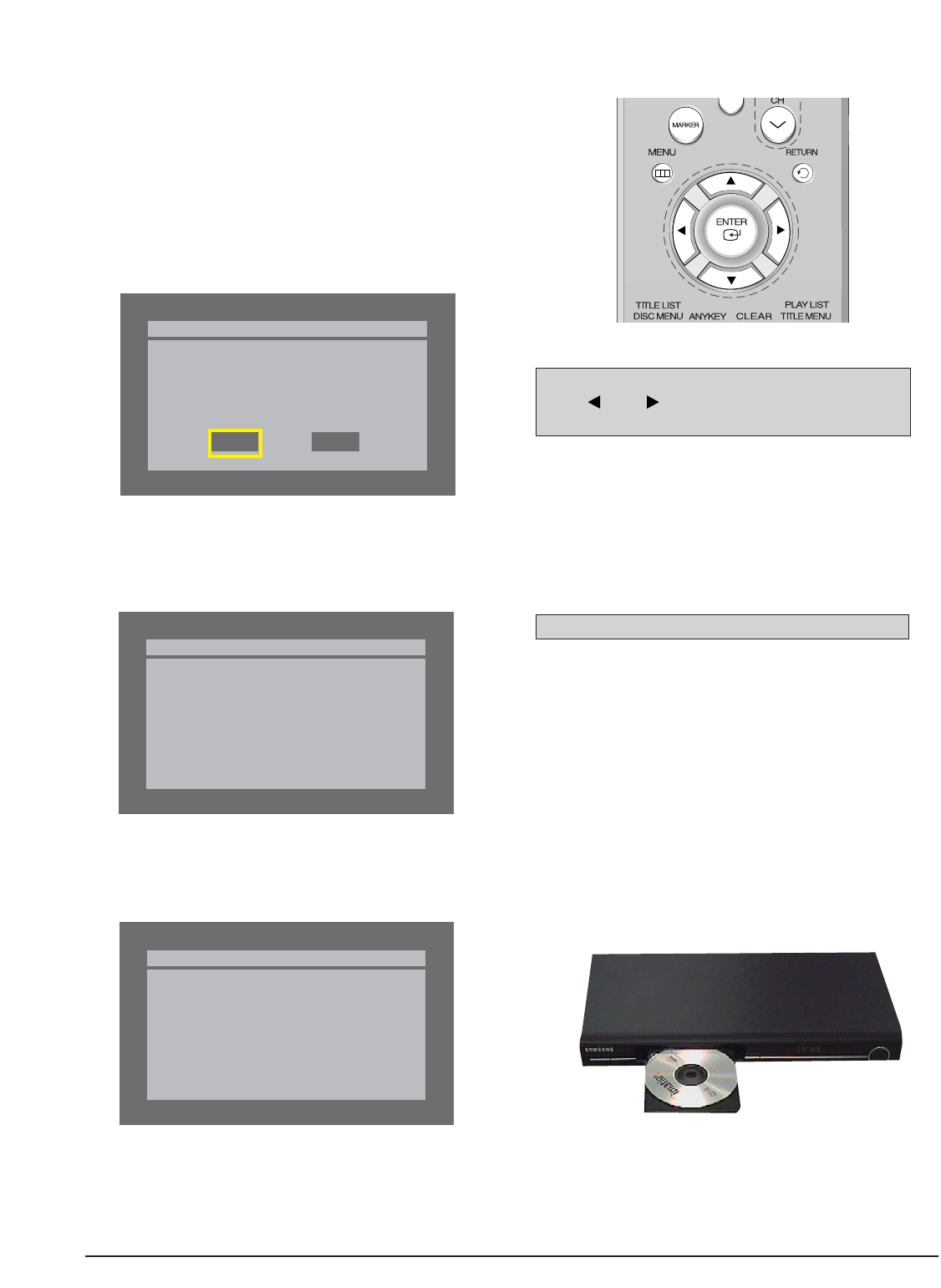
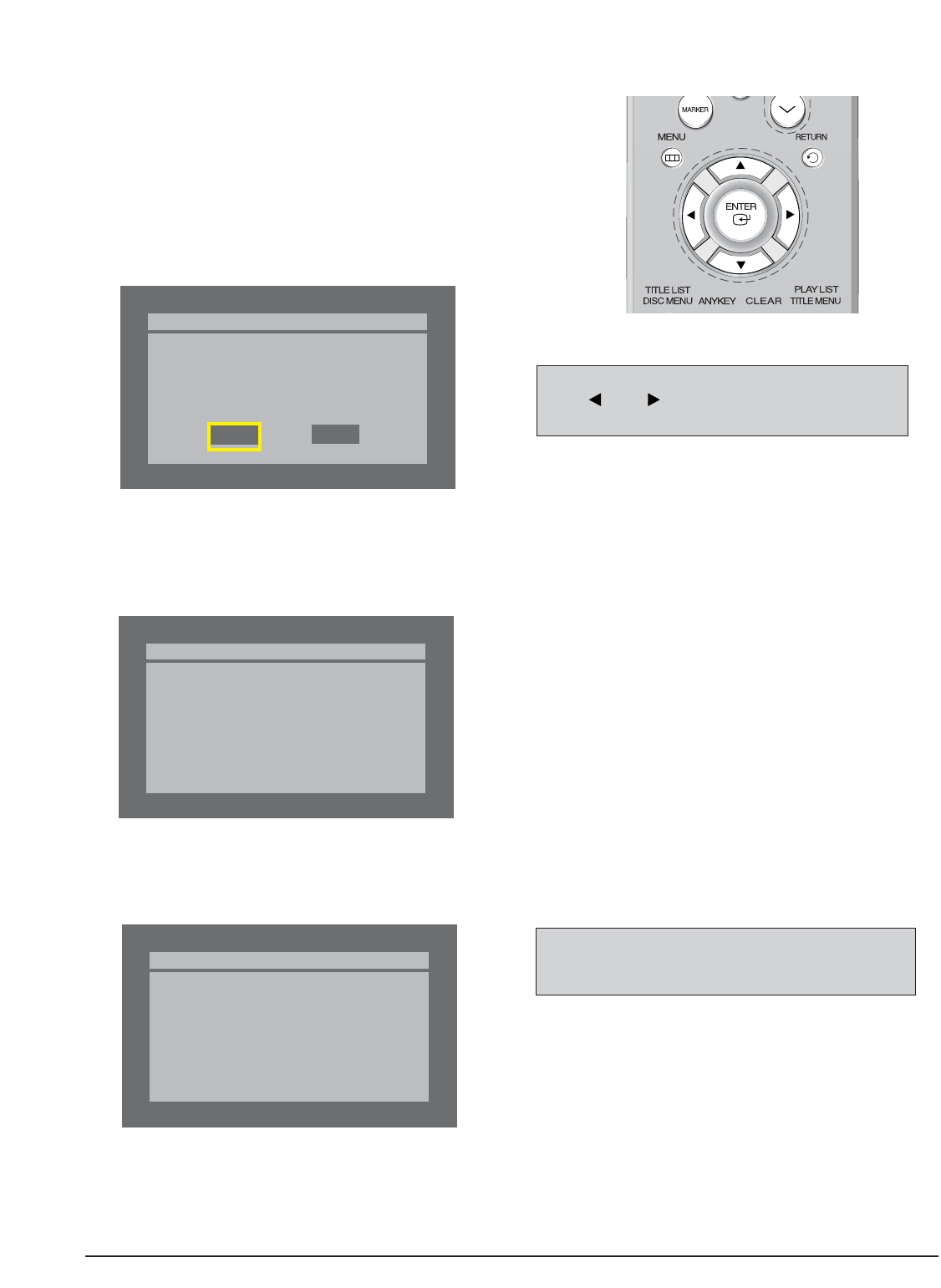
Fig. 3-2 Remote Control

Software Update
3-3
Samsung Electronics
3-2 Flash Update (Main PCB)
3-2-1 Introduction
When you encounter a problem which is not related to the DVD drive.
3-2-2 How to make an update disc
Write the downloaded file onto a blank CD-R or CD-RW disc, using the following settings :
1) Download the software update file from the samsung internet site. (www.samsung.com)
2) Write the file to disc using the CD-RW of your computer.
• Recommended Application Program
- Nero Burning / Easy CD Creator ..etc
• Option
- Multisession : No Multisession
- CD close & disc at once
- ISO 9660 or joliet format
- Extension name : “*.RUF”
• In order to increase dise playability, add a dummy file (over 100MB) together with the latest program.
(The dummy file can be used any kind of file except MP3 file etc which can be played in the unit and we recommend to use a file whin
extension name as “*.dmy”, which can be changed from original one.)
N O T E
It is very important : please read the below notice below before updating your unit.
The followong events may interrupt the update process and MAY RESULT IN PERMANENT DAMAGE TO THE UNIT WHILE UPDATING
!Unplugging the power cord.
@Power Outage.
#Dirt or Scratches on the disc.
$Opening a disc tray during processing.
WARNING
3-4
Software Update
Samsung Electronics
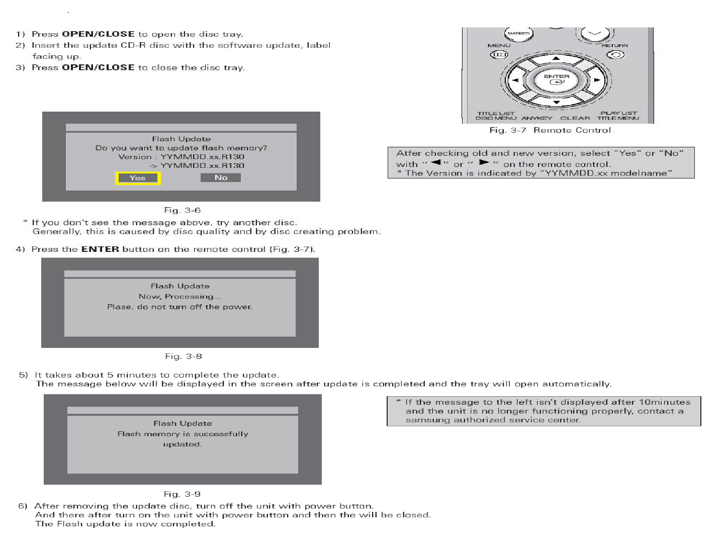
Fig. 3-6
* If you don’t see the message above, try another disc.
Generally, this is caused by disc quality and by disc creating problem.
4) Press the ENTER button on the remote control (Fig. 3-7).
Fig. 3-8
5) It takes about 5 minutes to complete the update.
The message below will be displayed in the screen after update is completed and the tray will open automatically.
Fig. 3-9
6) After removing the update disc, turn off the unit with power button.
And there after turn on the unit with power button and then the will be closed.
The Flash update is now completed.
* If the message to the left isn’t displayed after 10minutes
and the unit is no longer functioning properly, contact a
samsung authorized service center.
Atfer checking old and new version, select “Yes” or “No”
with “” or “ ” on the remote control.
* The Version is indicated by “YYMMDD.xx modelname”
Flash Update
Do you want to update flash memory?
Version : YYMMDD.xx.R129
-> YYMMDD.xx.R129
No
Yes
Flash Update
Now, Processing...
Plase. do not turn off the power.
Flash Update
Flash memory is successfully
updated.
1) Press OPEN/CLOSE to open the disc tray.
2) Insert the update CD-R disc with the software update, label
facing up.
3) Press OPEN/CLOSE to close the disc tray.
Fig. 3-7 Remote Control
Samsung Electronics 4-1
4. Disassembly and Reassembly
4-1 Cabinet and PCB
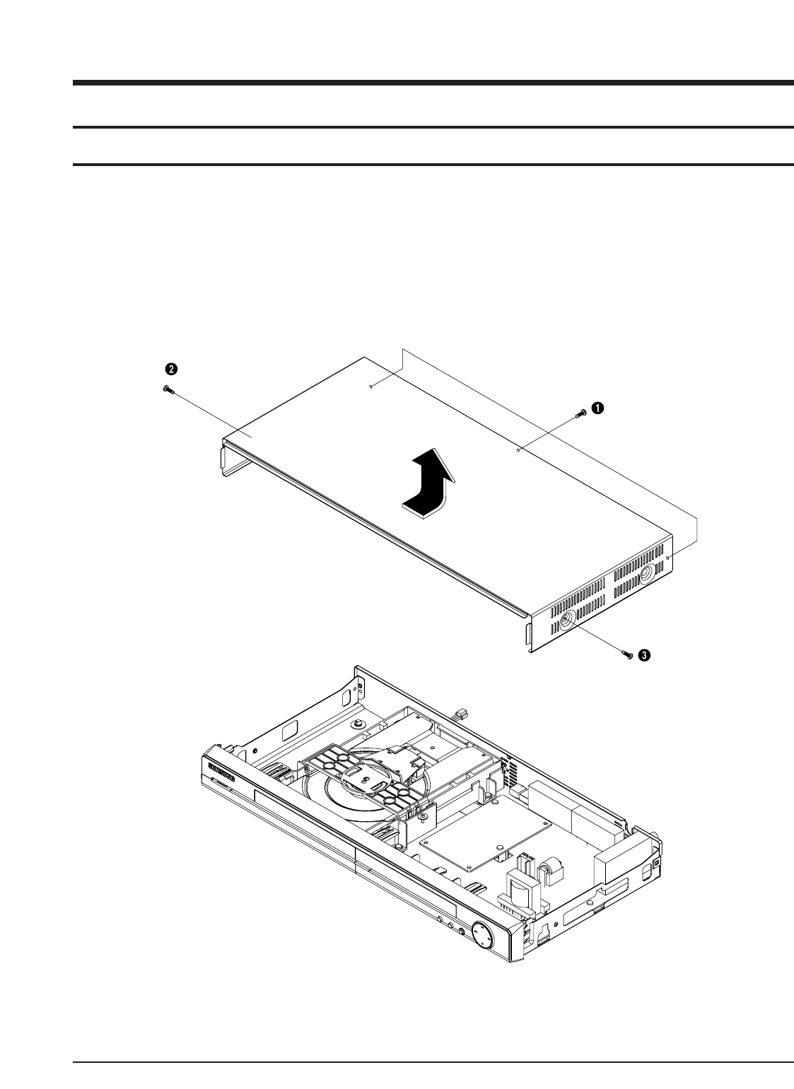
4-1-1 Top Cabinet Removal
1) Remove 5 Screws Œ, ´, ˇ.
2) Lift up the Top Cabinet in direction of arrow.
1 SCREW
(3 x 10 B)
1 SCREW
(3 x 10 B)
3 SCREWS
(3 x 10 B)
Fig. 4-1 Top Cabinet Removal
Note : Reassembly in reverse order.
4-2 Samsung Electronics
Disassembly and Reaasembly
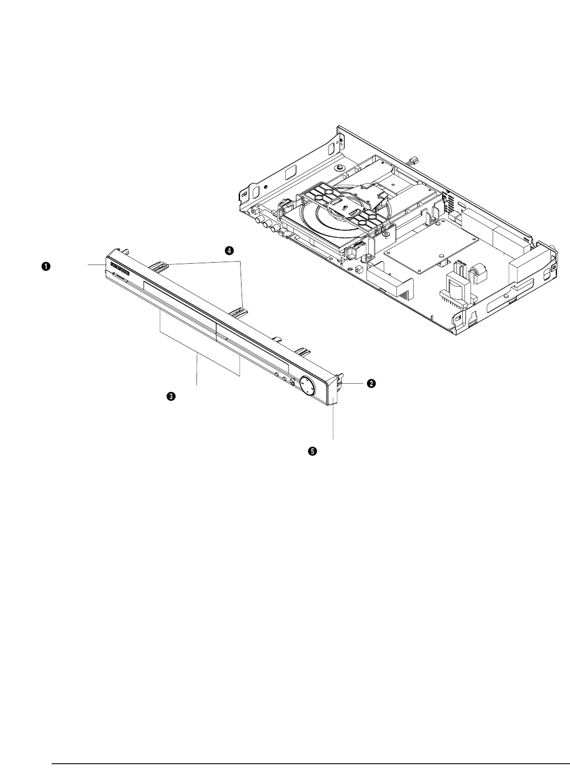
1 HOOK
1 HOOK
Assy Front-Cabinet
2 HOOKS
2 HOOKS
Fig. 4-2 Ass’y Front-Cabinet Removal
4-1-2 Ass’y Front-Cabinet Removal
1) Release 6 Hooks Œ, ´, ˇ,¨ and Ass’y Front-Cabinet ˆ.
Disassembly and Reaasembly
Samsung Electronics 4-3
2 SCREWS
(3 x 8 Y)
2 SCREWS
(3 x 10 Y)
Ass’y Deck
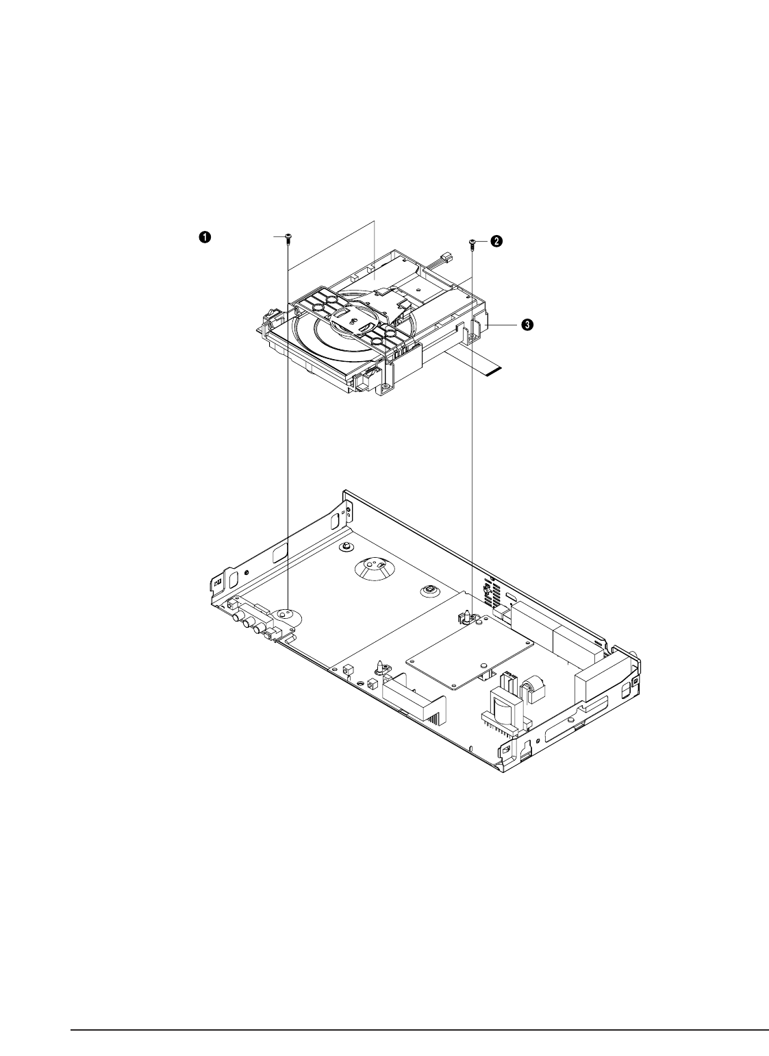
4-1-3 Ass’y Deck Removal
1) Remove 4 Screws Œ, ´ from the Ass’y Deck ˇand lift it up.
Fig. 4-3 Ass’y Deck Removal
4-4 Samsung Electronics
Disassembly and Reaasembly
2 SCREWS
(3 x 8 Y)
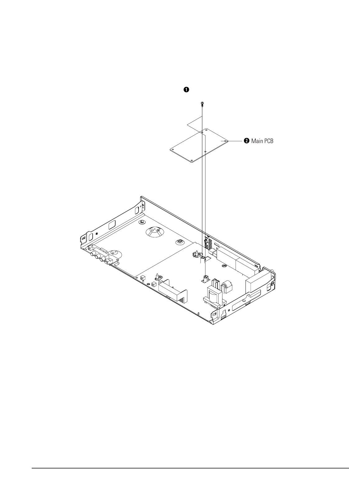
Fig. 4-4 Main PCB Removal
4-1-4 Main PCB Removal
1) Remove 2 Screws Œ, from the Main PCB ´ and lift it up.
Disassembly and Reaasembly
Samsung Electronics 4-5
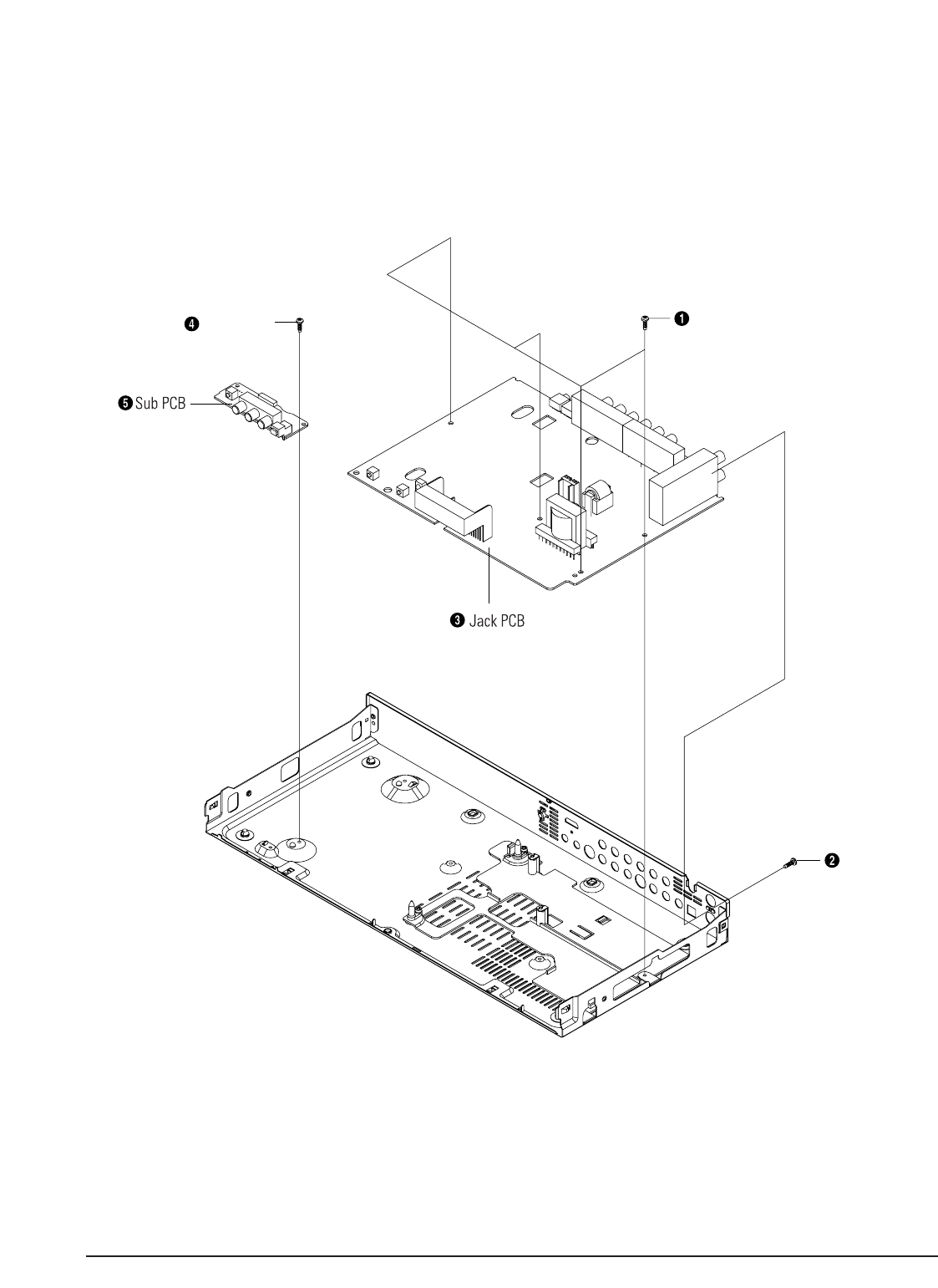
4-1-5 Jack PCB and Sub PCB Removal
1) Remove 5 Screws Œ, ´ from the Jack PCB ˇ and lift it up.
2) Remove 1 Screw ¨ from the Sub PCB ˆ and lift it up.
4 SCREWS
(3 x 6 Y)
1 SCREW
(3 x 6 Y)
1 SCREW
(3 x 6 W)
Fig. 4-5 Jack PCB and Sub PCB Removal
4-6 Samsung Electronics
Disassembly and Reaasembly
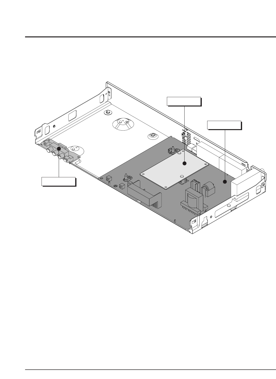
4-2 PCB Location
Fig. 4-6 PCB Location
Sub PCB
Main PCB
Jack PCB
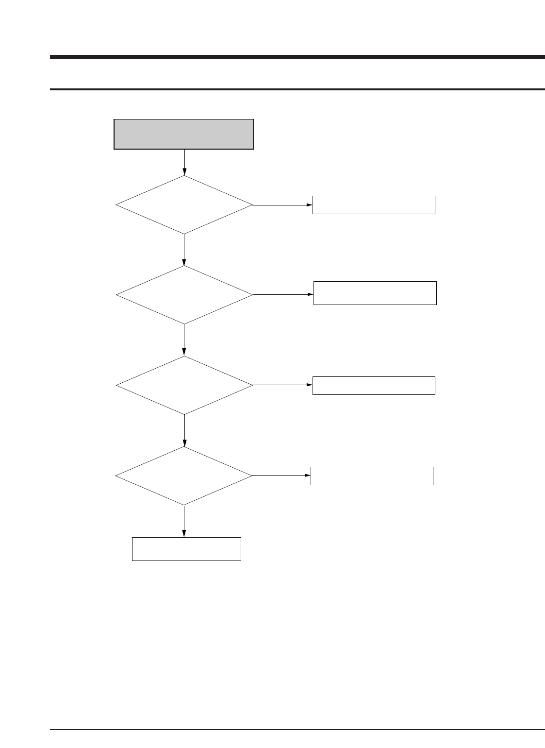
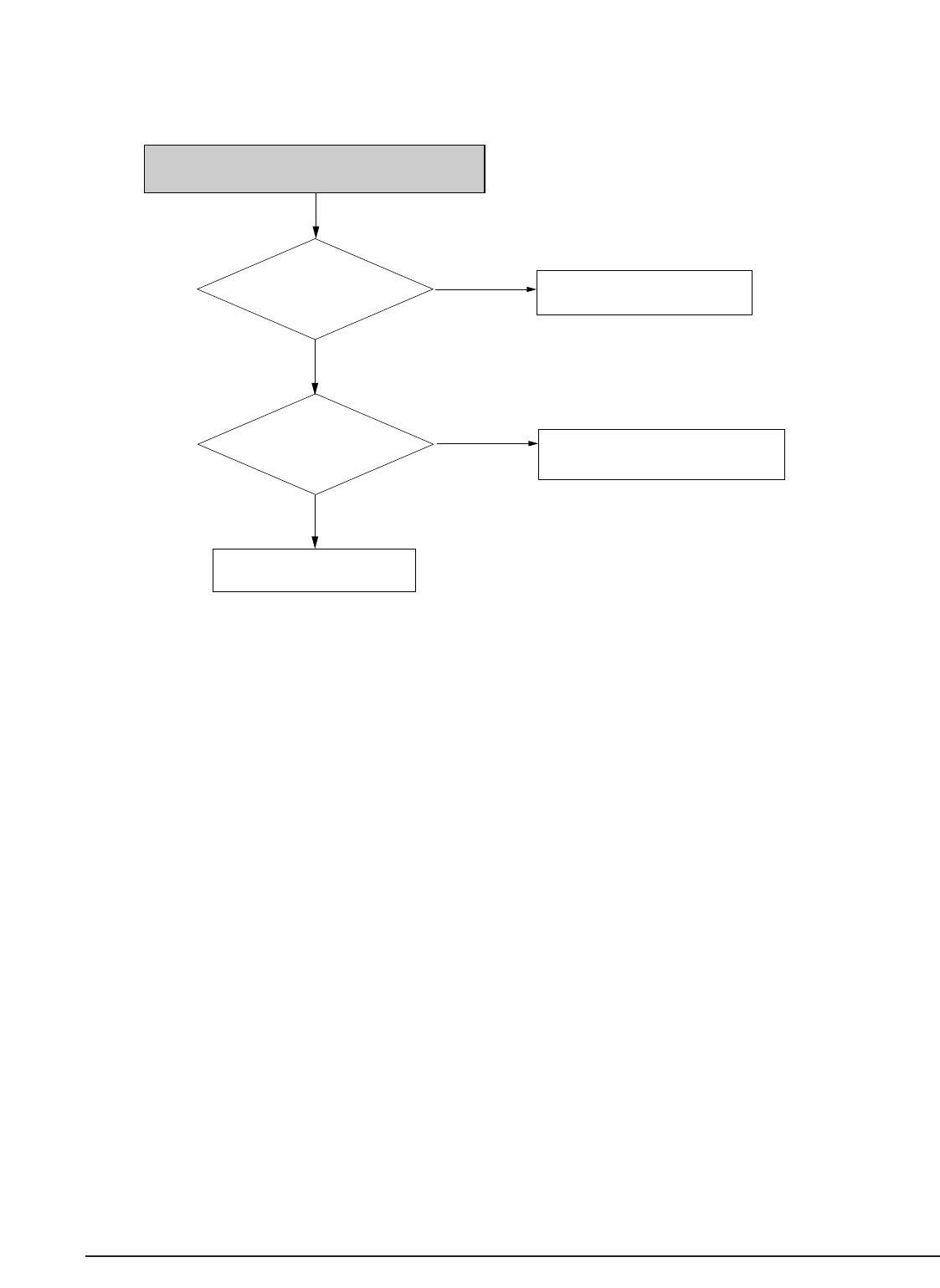
PAFT1 is normal?
Check feed back PQIZ1[PIN 3]
Is 5.8V
Change fuse
No
No
Change short circuited or
opened parts
No
No
Change PQIZ1 IC.
Yes
Yes
Yes
Yes
NO Power Detected
(Stand by LED OFF)
PVDL1/2~PSDZ1/2
PFZZ1/2~ PVZL1/2
SHORT and OPEN
Are normal?
Is there voitage at
PQIZ1[Pin 5]?
(Over 10V)
Operation of PQIZ1 is
Normal? Replace PQIZ1
Samsung Electronics 5-1
5. Troubleshooting
Troubleshooting
5-2 Samsung Electronics
Check the Cable
No
No
Yes
Yes
Yes
There's no Digital Audio Out
Check Current Digital Audio
Setting is PCM.
ChecK Digital Audio data
at pin 2 of CN4
(MAIN PCB)
Check 5V AVJ5
No
Replace AVJ5
Replace Main PCB
Set audio setting to
Bitstream in customer
menu.
Check the A/V Receiver
can Decode Current
Bit-Steam
No
Yes
AUDIO DATA
Troubleshooting
Samsung Electronics 5-3
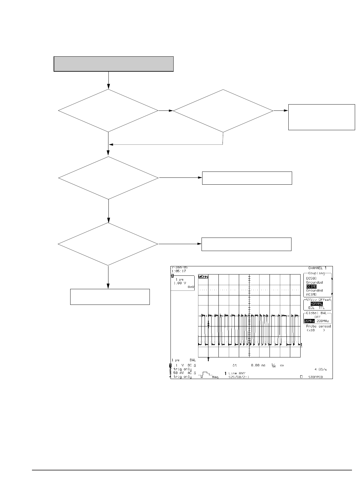
PIN 10 of
CN3 of Jack PCB
or CN2 of Main PCB has
1V pk-pk level?
Check the RCA Cable
No Check the DIC1 on MAIN PCB
Analog signals are
Inputted normally
VIC1[pin4]
No
No
Check the connection between
10Pin in CN3 Of JACK PCB and VIC1
Power is
Normal(5v) at VIC1[pin1]? Check the connection between
VIC1[pin1] and Power line (VL6, PPIF1).
Yes
Yes
Yes
No
Pin5 in VIC1 is
In high state?
Check the connection between
VIC1(PIN5) and IC601(PIN89).
Check VIC1 peripheral circuit.
Yes
No
Video signal of
About P-P1V appears at
Output Jack?
Check the connection between
VIC1 and output jack.
Yes
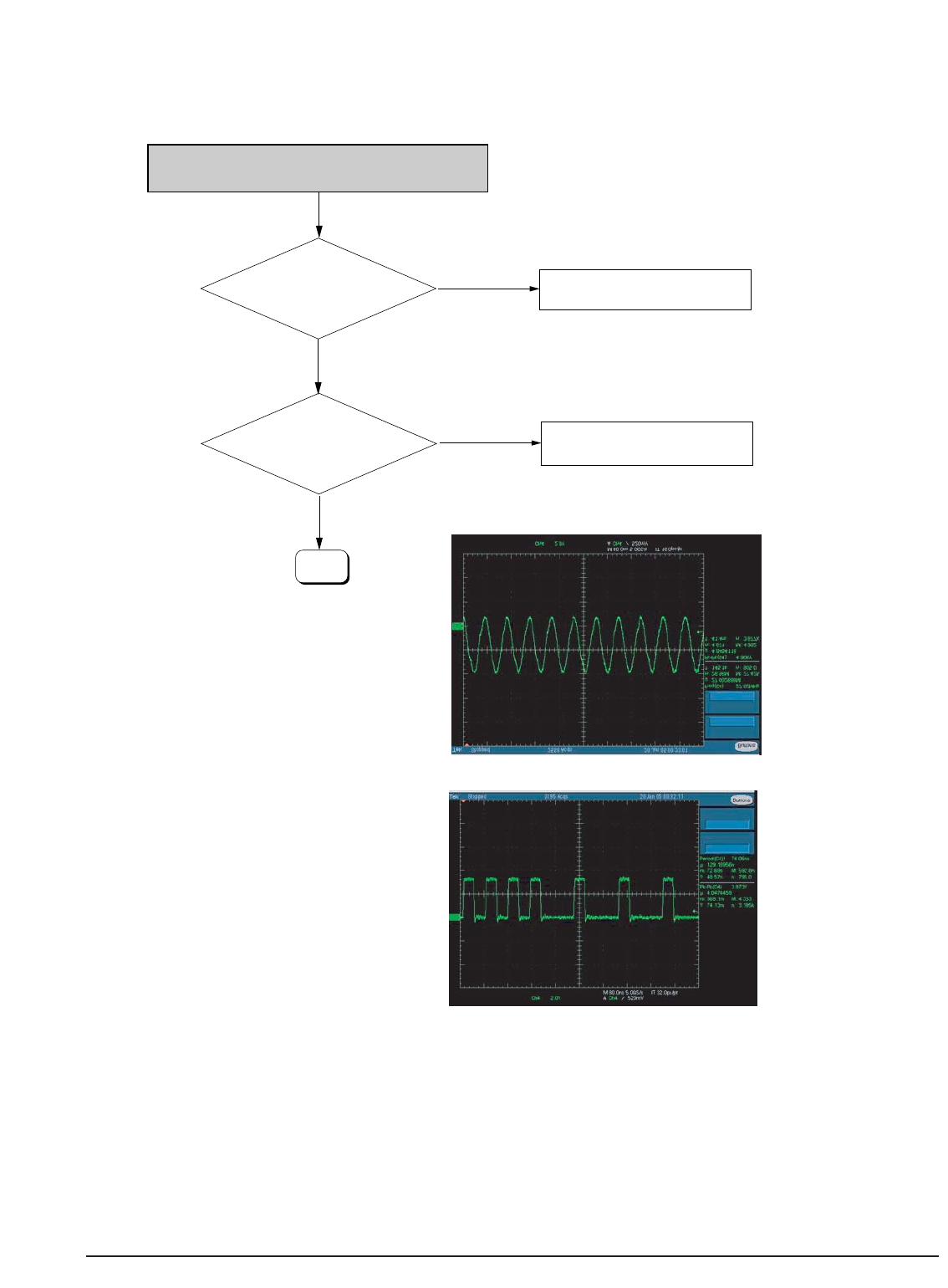
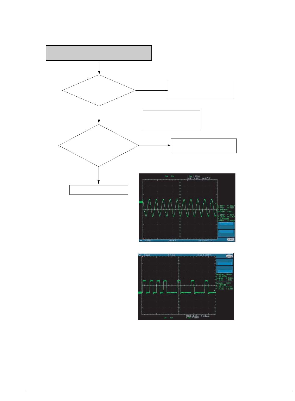
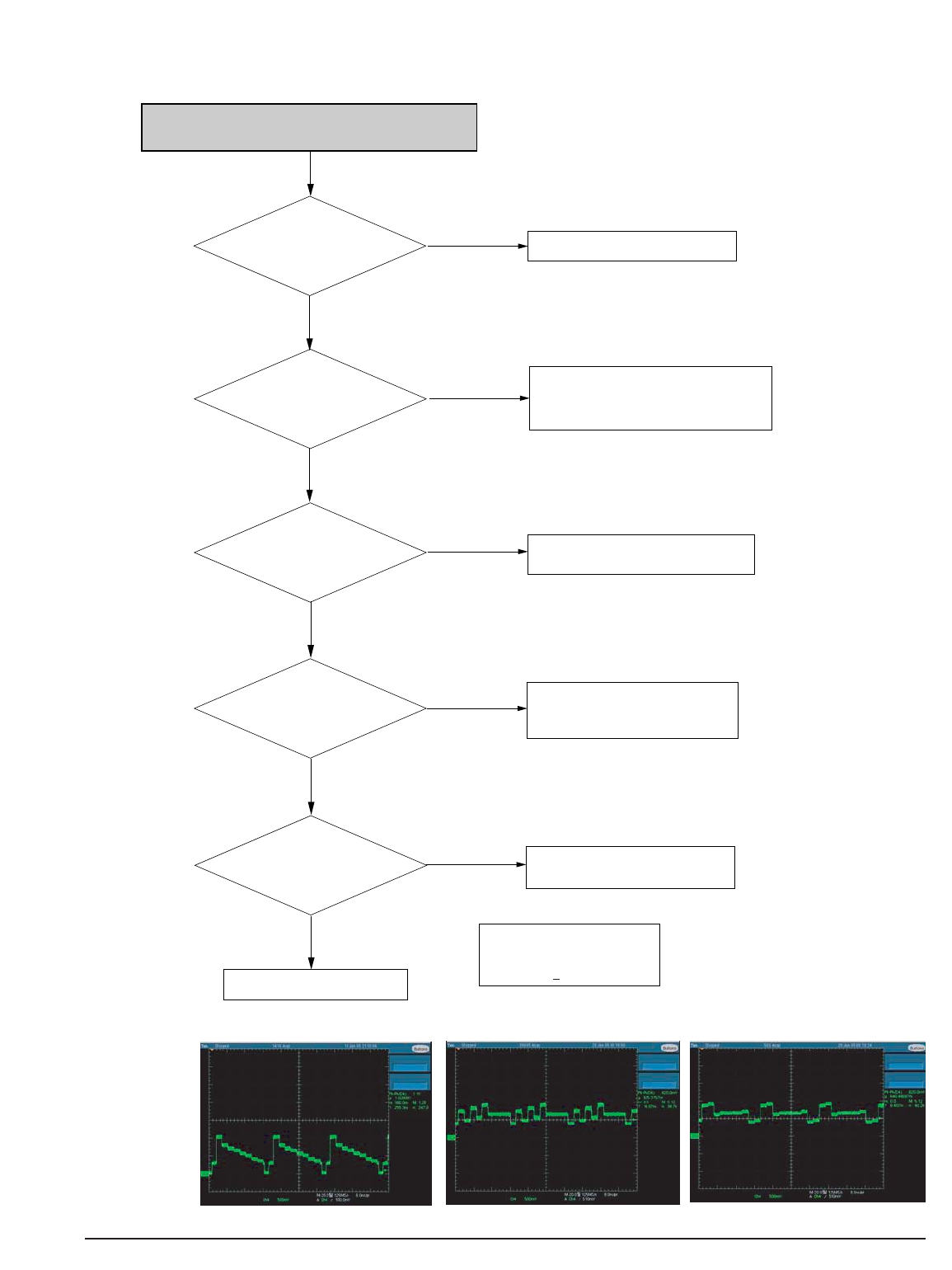
CVBS (Video) output error
# IF Recorder is under PSO (progressive scan output) MODE, it does not
output the CVBS& S-Video signal.
CVBS(Color-bar)
Troubleshooting
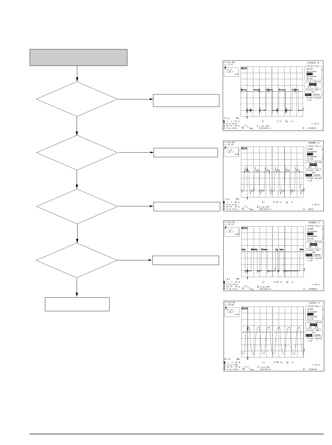
5-4 Samsung Electronics
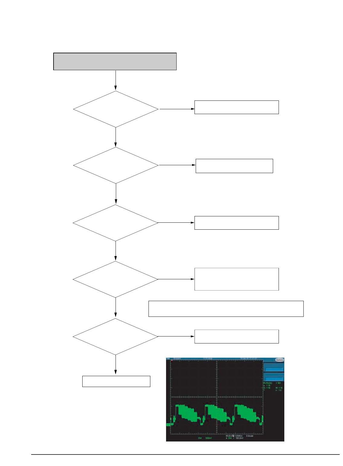
Check the RCA cable
No
No
Analog signals are
Inputted normally
VIC1(pin4,2)
No
No
No
Check the connection between
VIC1[pin1] and Power line (VL6, PPIF1).
Power is
Normal(5v) at VIC1(pin1)?
Pin5 in VIC1 is
In high state?
Check the connection between
VIC1(PIN5) and IC601(PIN89).
Check VIC1 peripheral circuit.
Check the connection between
VIC1 and output jack.
Yes
Yes
Yes
Yes
Yes
S-Video output error
Pin10 and
Pin8 in CN3 of Jack PCB or
CN2 of Main PCB has *
normal level?
Video signal of
About P-P1V appears at
Output Jack?
Check the DIC1 on MAIN PCB
Check the connection between
Pin10 and Pin8 in CN3 Of JACK PCB
and VIC1
# IF Recorder is under PSO (progressive
scan output) MODE, it does not output the CVBS& S-Video signal.
# Nomal level
: pin 10 is 1Vpk-pk
pin 8 is 0.28V on color burst
Y(Color-bar) C(Color-bar)
Troubleshooting
Samsung Electronics 5-5
Pin 5 In IC702
Has about p-p 1V level?
Pin 13 In IC702
Has about p-p 1V signal?
Check the connection between
Pin 5 in IC702 and L2 Pin-Jack.
No
No
Check Pin 1 in IC702
of input power(5V).
Yes
Yes
AV2 CVBS Video Input Error
A
VIC1 of Main PCB Clock
VIC1 of Main PCB DATA
Troubleshooting
5-6 Samsung Electronics
Pin 3 In IC702
Has about p-p 1V level?
Pin 7 In IC702
Has about p-p 1V signal?
Change Main PCB
Check the connection between
Pin 3 in IC702 and L1 Pin-Jack.
Check Pin 7 in IC702
of input power(5V).
No
No
Pin 2 / 4 in IC702 is
In Low and high state
Respectively?
No
No
No
Check the connection between Pin 2 and
Pin 4 in IC702 and Pin 92 and 91 in IC601.
Pin80 in VIC1 of Main PCB
has about p-p 1V level?
Pin40 and pin 54~43 in VIC1
of Main PCB has Clock and
Digital Video Signal
normal form ?
Check the connection between Pin 80 in
VIC1 of Main PCB and Pin 7 in IC702.
Check VIC1 of Main PCB
peripheral circuit. .
Yes
Yes
Yes
Yes
Yes
AV1 CVBS Video Input Error
Pin9/10
L/L : RF Signal
L/H : Line1
H/L : Line2
H/H : Reserved
CVBS(Color -bar)
A
Troubleshooting
Samsung Electronics 5-7
Change Main PCB
Check the connection between
Pin 36 and 42 in VIC1 of Main PCB
and L1 S-Video Jack.
No
Check VIC1 of Main PCB
peripheral circuit.
Pin 36 and 42 in VIC1 of Main
PCB has *normal level?
Yes
AV1 S-Video Video Input Error
Pin40 and pin 54~43 in VIC1
of Main PCB has Clock and
Digital Video Signal
normal form ?
No
Yes VIC1 of Main PCB Clock
VIC1 of Main PCB DATA
# Nomal level
: pin 35 is 1Vpk-pk
pin 42 is 0.28V on color burst
Troubleshooting
5-8 Samsung Electronics
Tuner input line signal is OK?
(jack PCB)
Supplied power
(Pin 3 : 5V pin 14 : 33V) for
tuner is OK?
Connect tuner line to TV directly
No
No
Pin 3 : 5V pin 14 : 33V check its line
(jack PCB)
Yes
Yes
Tuner Video Input Error
A
Troubleshooting
Samsung Electronics 5-9
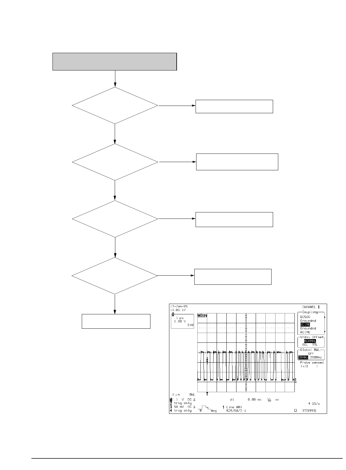
Pin2/4/6 in CN3 of
Jack PCB or CN2 of Main PCB
has * normal level?
Analog signals are
Inputted normally
VIC1(pin6/8/9)
Check the RCA cable
Check the DIC1 on MAIN B/D.
No
No
Check the connection between
Pin2/4/6 in CN3 Of JACK PCB
and VIC1(pin6/8/9)
Power is
Normal(5v) at VIC1(pin1)? No
No
Check the connection between
VIC1[pin1] and Power line (VL6, PPIF1).
Video signal of
About 1V pk-pk appears at
Output Jack?
Check the connection between
VIC1 and output jack.
Yes
Yes
Yes
Yes
Component output error
Yes
No
Pin13 in VIC1 is
In high state?
Check the connection between
VIC1(PIN3) and IC601(PIN89).
Check VIC1 peripheral circuit.
Y(Color-bar) Pb(Color-bar) Pr(Color-bar)
# Nomal level
: pin 6 is 1Vpk-pk
pin 2/4 is + 0.35V
Troubleshooting
5-10 Samsung Electronics
Check the select signal pin9,10
of IC203(JACK PCB)
Check the passive parts
around jack pin.
No
No
No
No
Yes
Yes
Yes
Yes
Audio Input is not Recording
Check all the 12Vcc
pin 16 of IC203 and 12Vcc of CN10
AIC4(JACK).
Check the 3.3V pin14
and 5V pin5 of AU5
(MAIN PCB)
Check Digital clock and data
pin 10, 11, 12, 15 of
AU5(MAIN PCB)
Check pin 90,91(5V) of the
Front Micom IC601 (JACK PCB)
Check SMPS
Replace Main PCB
Replace Main PCB
Digital clock(10)
Digital clock(11)
Digital clock(12)
Digital clock(15)
Troubleshooting
Samsung Electronics 5-11
Check he audio signal
AR413 and AR437
(JACK PCB)
Check all the 5V pin8
of AIC1
(MAIN PCB)
Check the passive parts
arond Jack pin.
Check the Low state pin22 of the
Front Micom IC601(JACL PCB)
No
No
Check SMPS
Check the audio signal pin7
pin8 of AIC1
(MAIN PCB)
No
No
Replace Main PCB
Check digital clock and
data pin1, 2, 3, 16 of AIC1
(MAIN PCB)
Replace MAIN PCB
Yes
Yes
Yes
Yes
There is no Audio Output
AUDIO
DATA
Troubleshooting
5-12 Samsung Electronics
Tuner input line signal
is OK?
IIC line (SCL,SDA) from
front micom is OK?
Change IC601 or check
around elements
Tuner line connect TV directly.
No
No
Check the IIC line
Does TY2 make 14.31
Mhz signal? (jack PCB)
No Check TY2 or around elements
Yes
Yes
Yes
EDS [Extended data Services]
is abnormal
Troubleshooting
Samsung Electronics 5-13
Are Main and deck
power OK?
(5v, 12v)
Is the 40pin
FFC cable(betweenmain & deck)
inserted correctly?
Check he power
No
No
Reinsert FFC cable correctly
Is the wavefrom
of DIC3 pin26 normal?
(MAIN PCB)
No
Yes
Yes
Yes
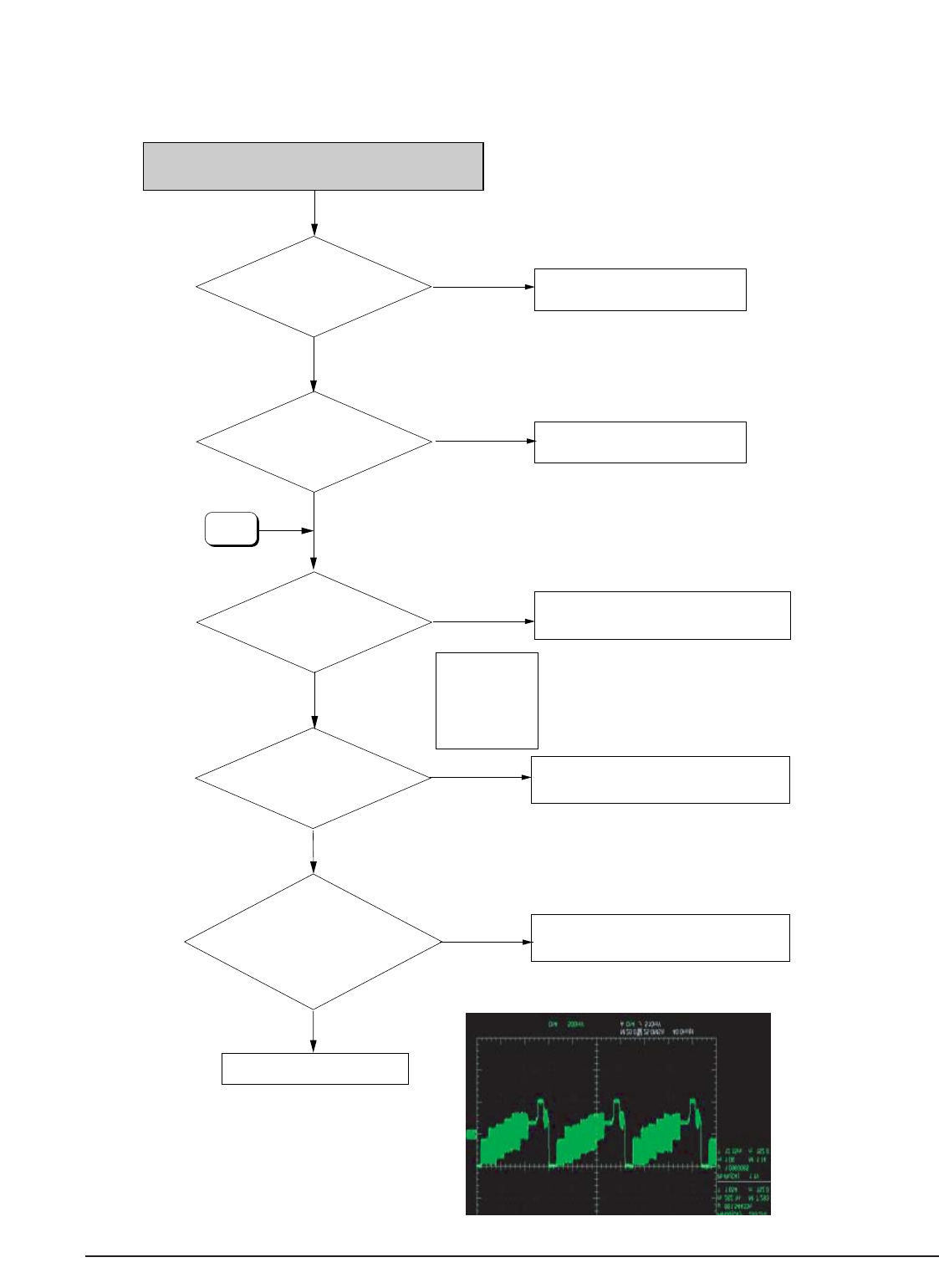
Disc Ioading error
Change the Main board
Change the deck
DIC3-Pin26
Troubleshooting
5-14 Samsung Electronics
Tuner input line signal(pin16)
is OK? (Jack PCB)
Supplied power
(Pin 3 : 5V pin 14 : 33V) for
tuner is OK?
Refer to video line in abnormal
Connect tuner line to TV directly
No
No
Pin 3 : 5V pin 14 : 33V check its line
(jack PCB)
No
Video signal of TE14 is OK?
(jack PCB)
Check IC203 or its around elements
(jack PCB)
Yes
Yes
Yes
Tuner Video Out Abnormal
Tuner Video
Troubleshooting
Samsung Electronics 5-15
Tuner line signal is OK?
Supplied power
IC604(Jack PCB) is OK?
(Pin 5 : about 5V)
If TIC1 is normal, refer to
audio line in abnomal
Connect tuner line to TV directly.
No
No
Check its power line or around elements
4.5MHz signal from 13 pin
of tuner(TM1) is OK?
No
No
Check the SIF signal or tuner
Does XT4M01
make 3.58MHz signal?
(jack PCB)
Check XT4M01 or around elements
Yes
Yes
Yes
Yes
Tuner Audio Out Abnormal
Tuner Audio
Troubleshooting
5-16 Samsung Electronics
KRMC1(pin1) signal
is OK? (SMPS PCB)
IC601(pin5) signal
is OK? (Jack PCB)
Change IC601 or
surrounding elements
Check the power(pin2) line
orchange KRMC1.
No
No
Check the signal line or surrounding
elements.
Yes
Yes
Remocon Error

Samsung Electronics 6-1
6. Exploded View and Parts List
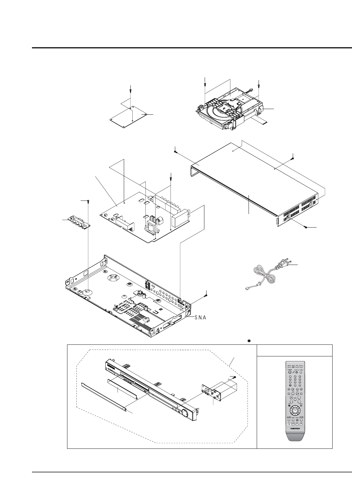
6-1 Cabinet Assembly - - - - - - - - - - - - - - - - - - - - - - - - - - - - - - - - - - - - - - - - -
Page
6-2
Exploded Views and Parts List
6-2 Samsung Electronics
6-1 Cabinet Assembly
A001
C001
S.N.A.: Service Not Available
W200
(3 x 8 Y)
W275
(3 x 6 Y)
W275
(3 x 6 Y)
W268
(3 x 6 W)
W009
(3 x 10 Y)
H001
C015
W009
(3 x 10 Y)
W001
(3 x 10 B) W001
(3 x 10 B)
P001
P022
P004
W001
(3 x 10 B)
P007
C002
C657
W009
(3 x 10 Y)
P025
Exploded Views and Parts List
6-3
Samsung Electronics
Loc. No Parts No. Description ; Specification Q ty S.N.A Remark
A001 AK59-00055A REMOCON-ASSY;DVD-R130/XAA,SEC,197. 1 SA
C001 AK97-01447L ASSY-CABINET FRONT;HIPS 94 HB,DVD- 1 SA
C002 AK64-01432A DOOR-TRAY;DVD-R130,ABS 94HB,T2,H15 1 SA
C015 AK64-01444B CABINET-TOP;SV-R3600,PCM,T0.6,W430 1 SA
C657 AK64-01433G DOOR-JACK;DVD-R130/XSA,ABS 94HB,T2 1 SA
H001 AK97-01553A ASSY-LOADER;-,SV-R3600,LOADER ASSY 1 SA
P001 AK92-00872A ASSY PCB-MAIN;DVD-R130/XAA,MAIN PC 1 SA
P004 AK97-01530A ASSY PCB-KEY PCB;SV-R3600,ANDES 1 SA
P007 AK92-00891A ASSY PCB-KEY;DVD-R130/XAA,KEY PCB 1 SA
P022 AK92-00873A ASSY PCB-JACK;DVD-R130/XAA,JACK PC 1 SA
P025 AH39-10061A CBF-POWER CORD;KJ-10W,EP2,AWG2/18, 1 SA
W001 6003-000275 SCREW-TAPTITE;BH,+,-,B,M3,L10,ZPC( 5 SA
W009 6003-000276 SCREW-TAPTITE;BH,+,-,B,M3,L10,ZPC( 8 SA
W200 6003-001375 SCREW-TAPTITE;BH,+,B,M3,L8,ZPC(YEL 2 SA
W268 6003-000254 SCREW-TAPTITE;BH,+,-,S,M3,L6,ZPC(W 1 SA
W275 6003-001561 SCREW-TAPTITE;BH,+,-,B,M3,L6,ZPC(Y 5 SA

Exploded Views and Parts List
6-4 Samsung Electronics
MEMO

Samsung Electronics 7-1
This Document can not be used without Samsung’s authorization
P001 AK92-00872A ASSY PCB-MAIN;DVD-R130/XAA,MAIN PC 1 SA
AC1 2203-005148 C-CER,CHIP;100nF,10%,16V,X7R,1608 1 SA
AC12 2203-005148 C-CER,CHIP;100nF,10%,16V,X7R,1608 1 SA
AC14 2203-005148 C-CER,CHIP;100nF,10%,16V,X7R,1608 1 SA
AC15 2203-005148 C-CER,CHIP;100nF,10%,16V,X7R,1608 1 SA
AC18 2203-005148 C-CER,CHIP;100nF,10%,16V,X7R,1608 1 SA
AIC1 1002-001395 IC-D/A CONVERTER;PCM1753,24Bit,SSO 1 SA
AIC2 1002-001459 IC-A/D CONVERTER;PCM1803A,24BIT,SS 1 SA
AL1 3301-001419 BEAD-SMD;220ohm,1608,TP,133ohm/70M 1 SA
AL2 3301-001419 BEAD-SMD;220ohm,1608,TP,133ohm/70M 1 SA
AR1 2011-000515 R-NET;4.7Kohm,5%,1/16W,L,CHIP,8P,T 1 SA
AR11 2007-000084 R-CHIP;4.7Kohm,5%,1/10W,TP,1608 1 SA
AR13 2007-000070 R-CHIP;0ohm,5%,1/10W,TP,1608 1 SA
AR2 2011-000515 R-NET;4.7Kohm,5%,1/16W,L,CHIP,8P,T 1 SA
AR3 2011-000515 R-NET;4.7Kohm,5%,1/16W,L,CHIP,8P,T 1 SA
AR4 2011-000515 R-NET;4.7Kohm,5%,1/16W,L,CHIP,8P,T 1 SA
ATC1 2402-001217 C-AL,SMD;220UF,20%,16V,WT,TP,6.6X6 1 SA
ATC2 2402-000204 C-AL,SMD;10UF,20%,16V,WT,TP,4.3X4. 1 SA
ATC3 2402-001059 C-AL,SMD;220UF,20%,6.3V,-,TP,6X6.6 1 SA
ATC5 2402-000007 C-AL,SMD;22uF,20%,6.3V,GP,TP,4.3x4 1 SA
ATC6 2402-000204 C-AL,SMD;10UF,20%,16V,WT,TP,4.3X4. 1 SA
C1 2203-000384 C-CER,CHIP;0.015nF,5%,50V,C0G,1608 1 SA
C10 2203-005148 C-CER,CHIP;100nF,10%,16V,X7R,1608 1 SA
C100 2203-005148 C-CER,CHIP;100nF,10%,16V,X7R,1608 1 SA
C101 2203-005148 C-CER,CHIP;100nF,10%,16V,X7R,1608 1 SA
C102 2203-005148 C-CER,CHIP;100nF,10%,16V,X7R,1608 1 SA
C103 2203-005148 C-CER,CHIP;100nF,10%,16V,X7R,1608 1 SA
C104 2203-005148 C-CER,CHIP;100nF,10%,16V,X7R,1608 1 SA
C106 2203-005148 C-CER,CHIP;100nF,10%,16V,X7R,1608 1 SA
C107 2203-005148 C-CER,CHIP;100nF,10%,16V,X7R,1608 1 SA
C108 2203-005148 C-CER,CHIP;100nF,10%,16V,X7R,1608 1 SA
C109 2203-005148 C-CER,CHIP;100nF,10%,16V,X7R,1608 1 SA
C11 2203-005148 C-CER,CHIP;100nF,10%,16V,X7R,1608 1 SA
C110 2203-005148 C-CER,CHIP;100nF,10%,16V,X7R,1608 1 SA
C112 2203-005148 C-CER,CHIP;100nF,10%,16V,X7R,1608 1 SA
C113 2203-005148 C-CER,CHIP;100nF,10%,16V,X7R,1608 1 SA
C114 2203-005148 C-CER,CHIP;100nF,10%,16V,X7R,1608 1 SA
C116 2203-001683 C-CER,CHIP;0.068nF,5%,50V,NP0,1608 1 SA
C117 2203-005148 C-CER,CHIP;100nF,10%,16V,X7R,1608 1 SA
C119 2203-005148 C-CER,CHIP;100nF,10%,16V,X7R,1608 1 SA
C12 2203-005148 C-CER,CHIP;100nF,10%,16V,X7R,1608 1 SA
C121 2203-005148 C-CER,CHIP;100nF,10%,16V,X7R,1608 1 SA
C122 2203-000315 C-CER,CHIP;0.12nF,5%,50V,C0G,1608 1 SA
C13 2203-005148 C-CER,CHIP;100nF,10%,16V,X7R,1608 1 SA
C14 2203-005148 C-CER,CHIP;100nF,10%,16V,X7R,1608 1 SA
C15 2203-005148 C-CER,CHIP;100nF,10%,16V,X7R,1608 1 SA
C16 2203-005148 C-CER,CHIP;100nF,10%,16V,X7R,1608 1 SA
C17 2203-005148 C-CER,CHIP;100nF,10%,16V,X7R,1608 1 SA
C18 2203-005148 C-CER,CHIP;100nF,10%,16V,X7R,1608 1 SA
C19 2203-005148 C-CER,CHIP;100nF,10%,16V,X7R,1608 1 SA
C2 2203-000426 C-CER,CHIP;0.018nF,5%,50V,C0G,1608 1 SA
C20 2203-005148 C-CER,CHIP;100nF,10%,16V,X7R,1608 1 SA
C21 2203-005148 C-CER,CHIP;100nF,10%,16V,X7R,1608 1 SA
C22 2203-001554 C-CER,CHIP;1.8nF,10%,50V,X7R,TP,16 1 SA
C23 2203-001554 C-CER,CHIP;1.8nF,10%,50V,X7R,TP,16 1 SA
C24 2203-005148 C-CER,CHIP;100nF,10%,16V,X7R,1608 1 SA
C25 2203-001554 C-CER,CHIP;1.8nF,10%,50V,X7R,TP,16 1 SA
C26 2203-001554 C-CER,CHIP;1.8nF,10%,50V,X7R,TP,16 1 SA
C27 2203-005148 C-CER,CHIP;100nF,10%,16V,X7R,1608 1 SA
C28 2203-005148 C-CER,CHIP;100nF,10%,16V,X7R,1608 1 SA
C29 2203-005148 C-CER,CHIP;100nF,10%,16V,X7R,1608 1 SA
C3 2203-005148 C-CER,CHIP;100nF,10%,16V,X7R,1608 1 SA
C30 2203-005148 C-CER,CHIP;100nF,10%,16V,X7R,1608 1 SA
C31 2203-005148 C-CER,CHIP;100nF,10%,16V,X7R,1608 1 SA
C32 2203-005148 C-CER,CHIP;100nF,10%,16V,X7R,1608 1 SA
C33 2203-005148 C-CER,CHIP;100nF,10%,16V,X7R,1608 1 SA
C34 2203-005148 C-CER,CHIP;100nF,10%,16V,X7R,1608 1 SA
C35 2203-005148 C-CER,CHIP;100nF,10%,16V,X7R,1608 1 SA
C36 2203-005148 C-CER,CHIP;100nF,10%,16V,X7R,1608 1 SA
C37 2203-005148 C-CER,CHIP;100nF,10%,16V,X7R,1608 1 SA
C38 2203-005148 C-CER,CHIP;100nF,10%,16V,X7R,1608 1 SA
C39 2203-005148 C-CER,CHIP;100nF,10%,16V,X7R,1608 1 SA
C4 2203-005148 C-CER,CHIP;100nF,10%,16V,X7R,1608 1 SA
C41 2203-005148 C-CER,CHIP;100nF,10%,16V,X7R,1608 1 SA
C42 2203-005148 C-CER,CHIP;100nF,10%,16V,X7R,1608 1 SA
C43 2203-005148 C-CER,CHIP;100nF,10%,16V,X7R,1608 1 SA
C44 2203-005148 C-CER,CHIP;100nF,10%,16V,X7R,1608 1 SA
C46 2203-005148 C-CER,CHIP;100nF,10%,16V,X7R,1608 1 SA
C48 2203-005148 C-CER,CHIP;100nF,10%,16V,X7R,1608 1 SA
C49 2203-005148 C-CER,CHIP;100nF,10%,16V,X7R,1608 1 SA
C5 2203-005148 C-CER,CHIP;100nF,10%,16V,X7R,1608 1 SA
C50 2203-005148 C-CER,CHIP;100nF,10%,16V,X7R,1608 1 SA
C51 2203-005148 C-CER,CHIP;100nF,10%,16V,X7R,1608 1 SA
C52 2203-005148 C-CER,CHIP;100nF,10%,16V,X7R,1608 1 SA
C53 2203-005148 C-CER,CHIP;100nF,10%,16V,X7R,1608 1 SA
C54 2203-005148 C-CER,CHIP;100nF,10%,16V,X7R,1608 1 SA
C55 2203-005148 C-CER,CHIP;100nF,10%,16V,X7R,1608 1 SA
C6 2203-005148 C-CER,CHIP;100nF,10%,16V,X7R,1608 1 SA
C64 2203-000440 C-CER,CHIP;1nF,10%,50V,X7R,1608 1 SA
C65 2203-005148 C-CER,CHIP;100nF,10%,16V,X7R,1608 1 SA
C66 2203-005148 C-CER,CHIP;100nF,10%,16V,X7R,1608 1 SA
C67 2203-005148 C-CER,CHIP;100nF,10%,16V,X7R,1608 1 SA
C68 2203-000440 C-CER,CHIP;1nF,10%,50V,X7R,1608 1 SA
C69 2203-005148 C-CER,CHIP;100nF,10%,16V,X7R,1608 1 SA
C7 2203-005148 C-CER,CHIP;100nF,10%,16V,X7R,1608 1 SA
C70 2203-005148 C-CER,CHIP;100nF,10%,16V,X7R,1608 1 SA
C71 2203-005148 C-CER,CHIP;100nF,10%,16V,X7R,1608 1 SA
C74 2203-000440 C-CER,CHIP;1nF,10%,50V,X7R,1608 1 SA
C75 2203-005148 C-CER,CHIP;100nF,10%,16V,X7R,1608 1 SA
C76 2203-005148 C-CER,CHIP;100nF,10%,16V,X7R,1608 1 SA
C77 2203-005148 C-CER,CHIP;100nF,10%,16V,X7R,1608 1 SA
C78 2203-005148 C-CER,CHIP;100nF,10%,16V,X7R,1608 1 SA
Loc.No Part No Description ; Specification Q’ty S.N.A Remark Loc.No Part No Description ; Specification Q’ty S.N.A Remark
7. Electrical Parts List

7-2 Samsung Electronics
Electrical Parts List
This Document can not be used without Samsung’s authorization
C79 2203-005148 C-CER,CHIP;100nF,10%,16V,X7R,1608 1 SA
C8 2203-005148 C-CER,CHIP;100nF,10%,16V,X7R,1608 1 SA
C80 2203-005148 C-CER,CHIP;100nF,10%,16V,X7R,1608 1 SA
C81 2203-000440 C-CER,CHIP;1nF,10%,50V,X7R,1608 1 SA
C82 2203-005148 C-CER,CHIP;100nF,10%,16V,X7R,1608 1 SA
C83 2203-005148 C-CER,CHIP;100nF,10%,16V,X7R,1608 1 SA
C84 2203-005148 C-CER,CHIP;100nF,10%,16V,X7R,1608 1 SA
C85 2203-005148 C-CER,CHIP;100nF,10%,16V,X7R,1608 1 SA
C86 2203-005148 C-CER,CHIP;100nF,10%,16V,X7R,1608 1 SA
C87 2203-005148 C-CER,CHIP;100nF,10%,16V,X7R,1608 1 SA
C89 2203-005148 C-CER,CHIP;100nF,10%,16V,X7R,1608 1 SA
C9 2203-005148 C-CER,CHIP;100nF,10%,16V,X7R,1608 1 SA
C90 2203-005148 C-CER,CHIP;100nF,10%,16V,X7R,1608 1 SA
C91 2203-005148 C-CER,CHIP;100nF,10%,16V,X7R,1608 1 SA
C92 2203-005148 C-CER,CHIP;100nF,10%,16V,X7R,1608 1 SA
C93 2203-000975 C-CER,CHIP;47nF,10%,25V,X7R,TP,160 1 SA
C94 2203-005148 C-CER,CHIP;100nF,10%,16V,X7R,1608 1 SA
C95 2203-001607 C-CER,CHIP;0.22nF,5%,50V,NP0,1608 1 SA
C96 2203-000851 C-CER,CHIP;0.039nF,5%,50V,C0G,1608 1 SA
C97 2203-005148 C-CER,CHIP;100nF,10%,16V,X7R,1608 1 SA
C99 2203-000851 C-CER,CHIP;0.039nF,5%,50V,C0G,1608 1 SA
CE1 2402-001059 C-AL,SMD;220UF,20%,6.3V,-,TP,6X6.6 1 SA
CE3 2402-001059 C-AL,SMD;220UF,20%,6.3V,-,TP,6X6.6 1 SA
CE4 2402-001059 C-AL,SMD;220UF,20%,6.3V,-,TP,6X6.6 1 SA
CN5 3708-001935 CONNECTOR-FPC/FFC/PIC;40P,0.5mm,SM 1 SA
CON1 3710-002075 SOCKET-BOARD TO BOARD;30P,2R,2MM,S 1 SA
CON2 3710-002075 SOCKET-BOARD TO BOARD;30P,2R,2MM,S 1 SA
DIC1 1205-002704 IC-CODEC;S5L3200,BGA,292P,27x27mm, 1 SA
DIC2 1105-001563 IC-DRAM;HYB25D256160CE-6,16Mx16Bit 1 SA
DIC3 1107-001242 IC-FLASH MEMORY;39VF160,1Mx16,TSOP 1 SNA
DIC4 0801-002624 IC-CMOS LOGIC;74LVC16374A,16BIT D 1 SA
DIC5 0801-002624 IC-CMOS LOGIC;74LVC16374A,16BIT D 1 SA
DIC6 1103-001134 IC-EEPROM;24C040,512x8,SOP,8P,5.13 1 SA
DIC7 0801-002701 IC-CMOS LOGIC;74VHCT125A,BUFFER,TS 1 SA
DIC9 0801-002166 IC-CMOS LOGIC;7SHU04,INVERTER,SSOP 1 SA
FIC1 1205-001988 IC-DATA COMM./GEN.;TSB41AB1-PAP,QF 1 SA
R10 2007-000084 R-CHIP;4.7Kohm,5%,1/10W,TP,1608 1 SA
R102 2007-001014 R-CHIP;51OHM,5%,1/10W,TP,1608 1 SA
R103 2007-001014 R-CHIP;51OHM,5%,1/10W,TP,1608 1 SA
R104 2007-001014 R-CHIP;51OHM,5%,1/10W,TP,1608 1 SA
R105 2007-001014 R-CHIP;51OHM,5%,1/10W,TP,1608 1 SA
R11 2007-000084 R-CHIP;4.7Kohm,5%,1/10W,TP,1608 1 SA
R113 2007-000078 R-CHIP;1Kohm,5%,1/10W,TP,1608 1 SA
R118 2007-000074 R-CHIP;100ohm,5%,1/10W,TP,1608 1 SA
R119 2007-000113 R-CHIP;33ohm,5%,1/10W,TP,1608 1 SA
R12 2007-000070 R-CHIP;0ohm,5%,1/10W,TP,1608 1 SA
R122 2007-000071 R-CHIP;22ohm,5%,1/10W,TP,1608 1 SA
R123 2007-000071 R-CHIP;22ohm,5%,1/10W,TP,1608 1 SA
R124 2007-000071 R-CHIP;22ohm,5%,1/10W,TP,1608 1 SA
R125 2007-000071 R-CHIP;22ohm,5%,1/10W,TP,1608 1 SA
R13 2007-000070 R-CHIP;0ohm,5%,1/10W,TP,1608 1 SA
R14 2007-000070 R-CHIP;0ohm,5%,1/10W,TP,1608 1 SA
R15 2007-000070 R-CHIP;0ohm,5%,1/10W,TP,1608 1 SA
R16 2007-000070 R-CHIP;0ohm,5%,1/10W,TP,1608 1 SA
R17 2007-000070 R-CHIP;0ohm,5%,1/10W,TP,1608 1 SA
R18 2007-000084 R-CHIP;4.7Kohm,5%,1/10W,TP,1608 1 SA
R19 2007-000763 R-CHIP;330ohm,1%,1/10W,TP,1608 1 SA
R2 2007-000084 R-CHIP;4.7Kohm,5%,1/10W,TP,1608 1 SA
R20 2007-000078 R-CHIP;1Kohm,5%,1/10W,TP,1608 1 SA
R21 2007-000078 R-CHIP;1Kohm,5%,1/10W,TP,1608 1 SA
R29 2007-000090 R-CHIP;10Kohm,5%,1/10W,TP,1608 1 SA
R3 2007-000109 R-CHIP;1Mohm,5%,1/10W,TP,1608 1 SA
R33 2007-000084 R-CHIP;4.7Kohm,5%,1/10W,TP,1608 1 SA
R34 2007-000074 R-CHIP;100ohm,5%,1/10W,TP,1608 1 SA
R35 2007-000074 R-CHIP;100ohm,5%,1/10W,TP,1608 1 SA
R36 2007-000070 R-CHIP;0ohm,5%,1/10W,TP,1608 1 SA
R37 2007-000078 R-CHIP;1Kohm,5%,1/10W,TP,1608 1 SA
R38 2007-000070 R-CHIP;0ohm,5%,1/10W,TP,1608 1 SA
R39 2007-000077 R-CHIP;470ohm,5%,1/10W,TP,1608 1 SA
R40 2007-000086 R-CHIP;5.6Kohm,5%,1/10W,TP,1608 1 SA
R41 2007-000102 R-CHIP;100Kohm,5%,1/10W,TP,1608 1 SA
R43 2007-000078 R-CHIP;1Kohm,5%,1/10W,TP,1608 1 SA
R45 3301-001419 BEAD-SMD;220ohm,1608,TP,133ohm/70M 1 SA
R46 2007-000090 R-CHIP;10Kohm,5%,1/10W,TP,1608 1 SA
R50 2007-000070 R-CHIP;0ohm,5%,1/10W,TP,1608 1 SA
R51 2007-000113 R-CHIP;33ohm,5%,1/10W,TP,1608 1 SA
R52 2007-000074 R-CHIP;100ohm,5%,1/10W,TP,1608 1 SA
R53 2007-001044 R-CHIP;56ohm,5%,1/10W,TP,1608 1 SA
R54 2007-000965 R-CHIP;5.1Kohm,5%,1/10W,TP,1608 1 SA
R55 2007-001044 R-CHIP;56ohm,5%,1/10W,TP,1608 1 SA
R56 2007-001056 R-CHIP;6.2Kohm,5%,1/10W,TP,1608 1 SA
R58 2007-001044 R-CHIP;56ohm,5%,1/10W,TP,1608 1 SA
R59 2007-000090 R-CHIP;10Kohm,5%,1/10W,TP,1608 1 SA
R6 2007-000070 R-CHIP;0ohm,5%,1/10W,TP,1608 1 SA
R60 2007-001044 R-CHIP;56ohm,5%,1/10W,TP,1608 1 SA
R61 2007-000090 R-CHIP;10Kohm,5%,1/10W,TP,1608 1 SA
R66 2007-000074 R-CHIP;100ohm,5%,1/10W,TP,1608 1 SA
R7 2007-000084 R-CHIP;4.7Kohm,5%,1/10W,TP,1608 1 SA
R71 2007-000083 R-CHIP;3Kohm,5%,1/10W,TP,1608 1 SA
R72 2007-000074 R-CHIP;100ohm,5%,1/10W,TP,1608 1 SA
R73 2007-000074 R-CHIP;100ohm,5%,1/10W,TP,1608 1 SA
R8 2007-000084 R-CHIP;4.7Kohm,5%,1/10W,TP,1608 1 SA
R88 2007-000078 R-CHIP;1Kohm,5%,1/10W,TP,1608 1 SA
R89 3301-001309 BEAD-SMD;47ohm,1608,TP,-,- 1 SA
R90 3301-001309 BEAD-SMD;47ohm,1608,TP,-,- 1 SA
RIC1 1203-003996 IC-POSI.FIXED REG.;KIA78R025F,DPAK 1 SA
RIC2 1203-003806 IC-POSI.ADJUST REG.;KIA78R000,DPAK 1 SA
RP1 2011-000585 R-NET;47ohm,5%,1/16W,L,CHIP,8P,TP, 1 SA
RP10 2011-000585 R-NET;47ohm,5%,1/16W,L,CHIP,8P,TP, 1 SA
RP12 2011-000585 R-NET;47ohm,5%,1/16W,L,CHIP,8P,TP, 1 SA
RP2 2011-000585 R-NET;47ohm,5%,1/16W,L,CHIP,8P,TP, 1 SA
RP20 2011-001194 R-NET;51ohm,5%,1/16W,L,CHIP,8P,TP, 1 SA
RP21 2011-001194 R-NET;51ohm,5%,1/16W,L,CHIP,8P,TP, 1 SA
RP22 2011-001194 R-NET;51ohm,5%,1/16W,L,CHIP,8P,TP, 1 SA
RP23 2011-001194 R-NET;51ohm,5%,1/16W,L,CHIP,8P,TP, 1 SA
RP24 2011-001194 R-NET;51ohm,5%,1/16W,L,CHIP,8P,TP, 1 SA
RP25 2011-001194 R-NET;51ohm,5%,1/16W,L,CHIP,8P,TP, 1 SA
RP26 2011-001194 R-NET;51ohm,5%,1/16W,L,CHIP,8P,TP, 1 SA
RP27 2011-001194 R-NET;51ohm,5%,1/16W,L,CHIP,8P,TP, 1 SA
Loc.No Part No Description ; Specification Q’ty S.N.A Remark Loc.No Part No Description ; Specification Q’ty S.N.A Remark

Electrical Parts List
Samsung Electronics 7-3
This Document can not be used without Samsung’s authorization
RP28 2011-001194 R-NET;51ohm,5%,1/16W,L,CHIP,8P,TP, 1 SA
RP3 2011-000585 R-NET;47ohm,5%,1/16W,L,CHIP,8P,TP, 1 SA
RP30 2011-000585 R-NET;47ohm,5%,1/16W,L,CHIP,8P,TP, 1 SA
RP31 2011-000585 R-NET;47ohm,5%,1/16W,L,CHIP,8P,TP, 1 SA
RP42 2011-000002 R-NET;22ohm,5%,1/16W,L,CHIP,8P,TP, 1 SA
RP43 2011-000002 R-NET;22ohm,5%,1/16W,L,CHIP,8P,TP, 1 SA
RP44 2011-000002 R-NET;22ohm,5%,1/16W,L,CHIP,8P,TP, 1 SA
RP45 2011-000002 R-NET;22ohm,5%,1/16W,L,CHIP,8P,TP, 1 SA
RP5 2011-000585 R-NET;47ohm,5%,1/16W,L,CHIP,8P,TP, 1 SA
RP6 2011-000585 R-NET;47ohm,5%,1/16W,L,CHIP,8P,TP, 1 SA
RP8 2011-000585 R-NET;47ohm,5%,1/16W,L,CHIP,8P,TP, 1 SA
TC1 2402-001059 C-AL,SMD;220UF,20%,6.3V,-,TP,6X6.6 1 SA
TC14 2402-001059 C-AL,SMD;220UF,20%,6.3V,-,TP,6X6.6 1 SA
TC16 2402-001238 C-AL,SMD;1uF,20%,50V,HR,TP,4.3x4.3 1 SA
TC3 2402-001086 C-AL,SMD;100UF,20%,16V,WT,TP,6.6X6 1 SA
TC5 2402-001086 C-AL,SMD;100UF,20%,16V,WT,TP,6.6X6 1 SA
TC6 2402-001086 C-AL,SMD;100UF,20%,16V,WT,TP,6.6X6 1 SA
TC7 2402-001059 C-AL,SMD;220UF,20%,6.3V,-,TP,6X6.6 1 SA
TC9 2402-001059 C-AL,SMD;220UF,20%,6.3V,-,TP,6X6.6 1 SA
VC1 2203-005148 C-CER,CHIP;100nF,10%,16V,X7R,1608 1 SA
VC11 2203-005148 C-CER,CHIP;100nF,10%,16V,X7R,1608 1 SA
VC12 2203-005148 C-CER,CHIP;100nF,10%,16V,X7R,1608 1 SA
VC13 2203-005148 C-CER,CHIP;100nF,10%,16V,X7R,1608 1 SA
VC15 2203-005148 C-CER,CHIP;100nF,10%,16V,X7R,1608 1 SA
VC16 2203-005148 C-CER,CHIP;100nF,10%,16V,X7R,1608 1 SA
VC17 2203-005148 C-CER,CHIP;100nF,10%,16V,X7R,1608 1 SA
VC18 2203-005148 C-CER,CHIP;100nF,10%,16V,X7R,1608 1 SA
VC2 2203-005148 C-CER,CHIP;100nF,10%,16V,X7R,1608 1 SA
VC20 2203-005148 C-CER,CHIP;100nF,10%,16V,X7R,1608 1 SA
VC21 2203-005148 C-CER,CHIP;100nF,10%,16V,X7R,1608 1 SA
VC22 2203-005148 C-CER,CHIP;100nF,10%,16V,X7R,1608 1 SA
VC23 2203-005148 C-CER,CHIP;100nF,10%,16V,X7R,1608 1 SA
VC24 2203-005148 C-CER,CHIP;100nF,10%,16V,X7R,1608 1 SA
VC25 2203-005148 C-CER,CHIP;100nF,10%,16V,X7R,1608 1 SA
VC26 2203-005148 C-CER,CHIP;100nF,10%,16V,X7R,1608 1 SA
VC27 2203-000280 C-CER,CHIP;0.01nF,0.5pF,50V,C0G,16 1 SA
VC28 2203-005148 C-CER,CHIP;100nF,10%,16V,X7R,1608 1 SA
VC29 2203-005148 C-CER,CHIP;100nF,10%,16V,X7R,1608 1 SA
VC5 2203-005148 C-CER,CHIP;100nF,10%,16V,X7R,1608 1 SA
VC6 2203-005148 C-CER,CHIP;100nF,10%,16V,X7R,1608 1 SA
VC7 2203-005148 C-CER,CHIP;100nF,10%,16V,X7R,1608 1 SA
VC8 2203-005148 C-CER,CHIP;100nF,10%,16V,X7R,1608 1 SA
VC9 2203-005148 C-CER,CHIP;100nF,10%,16V,X7R,1608 1 SA
VIC1 1204-002419 IC-VIDEO DECODER;TW9906,TQFP,80P,1 1 SA
VL1 2703-000398 INDUCTOR-SMD;10uH,10%,3225 1 SA
VR1 2007-000113 R-CHIP;33ohm,5%,1/10W,TP,1608 1 SA
VR14 2007-000113 R-CHIP;33ohm,5%,1/10W,TP,1608 1 SA
VR15 2007-000080 R-CHIP;2Kohm,5%,1/10W,TP,1608 1 SA
VR16 2007-000080 R-CHIP;2Kohm,5%,1/10W,TP,1608 1 SA
VR2 2007-000113 R-CHIP;33ohm,5%,1/10W,TP,1608 1 SA
VR23 2007-000074 R-CHIP;100ohm,5%,1/10W,TP,1608 1 SA
VR4 2007-000113 R-CHIP;33ohm,5%,1/10W,TP,1608 1 SA
VR8 2007-000113 R-CHIP;33ohm,5%,1/10W,TP,1608 1 SA
VRP1 2011-000002 R-NET;22ohm,5%,1/16W,L,CHIP,8P,TP, 1 SA
VRP2 2011-000002 R-NET;22ohm,5%,1/16W,L,CHIP,8P,TP, 1 SA
VRP3 2011-000816 R-NET;100ohm,5%,1/16W,L,CHIP,8P,TP 1 SA
VRP4 2011-000816 R-NET;100ohm,5%,1/16W,L,CHIP,8P,TP 1 SA
VTC3 2402-001059 C-AL,SMD;220UF,20%,6.3V,-,TP,6X6.6 1 SA
VTC4 2402-001059 C-AL,SMD;220UF,20%,6.3V,-,TP,6X6.6 1 SA
Y1 2801-004095 CRYSTAL-SMD;27MHz,20ppm,28-ABY,14p 1 SA
Y2 2801-004021 CRYSTAL-SMD;24.576MHz,20ppm,28-AAN 1 SA
P004 AK97-01530A ASSY PCB-KEY PCB;SV-R3600,ANDES 1 SA
CN704 3708-001803 CONNECTOR-FPC/FFC/PIC;10P,1.25MM,A 1 SA
FL286 3809-001667 FFC CABLE-FLAT;30V,80C,70mm,10P,1. 1 SA
SW703 3404-001182 SWITCH-TACT;DC12V,50MA,100GF,6.0X6 1 SA
SW705 3404-001182 SWITCH-TACT;DC12V,50MA,100GF,6.0X6 1 SA
SW706 3404-001182 SWITCH-TACT;DC12V,50MA,100GF,6.0X6 1 SA
SW707 3404-001182 SWITCH-TACT;DC12V,50MA,100GF,6.0X6 1 SA
SW708 3404-001182 SWITCH-TACT;DC12V,50MA,100GF,6.0X6 1 SA
SW709 3404-001182 SWITCH-TACT;DC12V,50MA,100GF,6.0X6 1 SA
SW710 3404-001182 SWITCH-TACT;DC12V,50MA,100GF,6.0X6 1 SA
P007 AK92-00891A ASSY PCB-KEY;DVD-R130/XAA,KEY PCB 1 SA
AR702 2001-000591 R-CARBON;3.3KOHM,5%,1/8W,AA,TP,1.8 1 SA
AR715 2001-000591 R-CARBON;3.3KOHM,5%,1/8W,AA,TP,1.8 1 SA
AR722 2001-000472 R-CARBON;2.7KOHM,5%,1/8W,AA,TP,1.8 1 SA
AR740 2001-000472 R-CARBON;2.7KOHM,5%,1/8W,AA,TP,1.8 1 SA
AVIN2 3722-002384 JACK-PIN;3P,SN/NI,YEL/WHT/RED,ANGL 1 SA
AVIN2B AK63-00307A GROUND-FRONT AV;DVD-R130,SUS,T0.2, 1 SA
CN7 3722-002383 JACK-IEEE1394;4P/1,AU,BLK,ANGLE,IE 1 SA
ESD01 0403-001083 DIODE-ZENER;UDZ9.1B,8.85-9.23V,200 1 SA
ESD02 0403-001083 DIODE-ZENER;UDZ9.1B,8.85-9.23V,200 1 SA
ESD03 0403-001083 DIODE-ZENER;UDZ9.1B,8.85-9.23V,200 1 SA
ESD04 0403-001083 DIODE-ZENER;UDZ9.1B,8.85-9.23V,200 1 SA
ESD05 0403-001083 DIODE-ZENER;UDZ9.1B,8.85-9.23V,200 1 SA
ESD06 0403-001083 DIODE-ZENER;UDZ9.1B,8.85-9.23V,200 1 SA
ESD07 0403-001083 DIODE-ZENER;UDZ9.1B,8.85-9.23V,200 1 SA
ESD08 0403-001083 DIODE-ZENER;UDZ9.1B,8.85-9.23V,200 1 SA
FCON4 3708-001695 CONNECTOR-FPC/FFC/PIC;13P,1MM,STRA 1 SA
FL615 3809-001787 FFC CABLE-FLAT;30V,80C,115mm,13P,1 1 SA
R720 2007-000098 R-CHIP;56Kohm,5%,1/10W,TP,1608 1 SA
SW711 3404-001261 SWITCH-TACT;15V DC,20mA,100gf,7.4X 1 SA
VR40 2001-000969 R-CARBON;75OHM,5%,1/8W,AA,TP,1.8X3 1 SA
P022 AK92-00873A ASSY PCB-JACK;DVD-R130/XAA,JACK PC 1 SA
AC16 2203-000315 C-CER,CHIP;0.12nF,5%,50V,C0G,1608 1 SA
AC17 2203-000315 C-CER,CHIP;0.12nF,5%,50V,C0G,1608 1 SA
AC405 2203-005148 C-CER,CHIP;100nF,10%,16V,X7R,1608 1 SA
AC406 2203-005148 C-CER,CHIP;100nF,10%,16V,X7R,1608 1 SA
AC407 2203-000125 C-CER,CHIP;1.2nF,10%,50V,X7R,TP,16 1 SA
AC408 2203-000125 C-CER,CHIP;1.2nF,10%,50V,X7R,TP,16 1 SA
AC409 2203-000315 C-CER,CHIP;0.12nF,5%,50V,C0G,1608 1 SA
AC410 2203-000315 C-CER,CHIP;0.12nF,5%,50V,C0G,1608 1 SA
AC413 2203-005148 C-CER,CHIP;100nF,10%,16V,X7R,1608 1 SA
AC702 2203-000783 C-CER,CHIP;0.33nF,5%,50V,C0G,1608 1 SA
Loc.No Part No Description ; Specification Q’ty S.N.A Remark Loc.No Part No Description ; Specification Q’ty S.N.A Remark

7-4 Samsung Electronics
Electrical Parts List
This Document can not be used without Samsung’s authorization
AC705 2203-000783 C-CER,CHIP;0.33nF,5%,50V,C0G,1608 1 SA
AC714 2203-000783 C-CER,CHIP;0.33nF,5%,50V,C0G,1608 1 SA
AC715 2203-000783 C-CER,CHIP;0.33nF,5%,50V,C0G,1608 1 SA
ACC2 2203-000315 C-CER,CHIP;0.12nF,5%,50V,C0G,1608 1 SA
ACC3 2203-000315 C-CER,CHIP;0.12nF,5%,50V,C0G,1608 1 SA
AD1 0407-000123 DIODE-ARRAY;DAN202K,80V,100mA,CA2- 1 SA
AD2 0407-000123 DIODE-ARRAY;DAN202K,80V,100mA,CA2- 1 SA
AD3 0407-000123 DIODE-ARRAY;DAN202K,80V,100mA,CA2- 1 SA
AE404 2401-003107 C-AL;47uF,20%,16V,GP,TP,5x7,5 1 SA
AE405 2401-003107 C-AL;47uF,20%,16V,GP,TP,5x7,5 1 SA
AE41 2401-000414 C-AL;10uF,20%,16V,GP,TP,4x7,5 1 SA
AE412 2401-002165 C-AL;100uF,20%,16V,GP,TP,6.3x7,5 1 SA
AE42 2401-000922 C-AL;22uF,20%,16V,GP,TP,5x5,5 1 SA
AE46 2401-000922 C-AL;22uF,20%,16V,GP,TP,5x5,5 1 SA
AE47 2401-000414 C-AL;10uF,20%,16V,GP,TP,4x7,5 1 SA
AE701 2401-000922 C-AL;22uF,20%,16V,GP,TP,5x5,5 1 SA
AE702 2401-000922 C-AL;22uF,20%,16V,GP,TP,5x5,5 1 SA
AE703 2401-000414 C-AL;10uF,20%,16V,GP,TP,4x7,5 1 SA
AE704 2401-000414 C-AL;10uF,20%,16V,GP,TP,4x7,5 1 SA
AE705 2401-000922 C-AL;22uF,20%,16V,GP,TP,5x5,5 1 SA
AE712 2401-000922 C-AL;22uF,20%,16V,GP,TP,5x5,5 1 SA
AE714 2401-000922 C-AL;22uF,20%,16V,GP,TP,5x5,5 1 SA
AE715 2401-000922 C-AL;22uF,20%,16V,GP,TP,5x5,5 1 SA
AIC4 1201-000163 IC-OP AMP;4560,SOP,8P,173MIL,DUAL, 1 SA
AMC01 2203-005148 C-CER,CHIP;100nF,10%,16V,X7R,1608 1 SA
AME01 2401-003107 C-AL;47uF,20%,16V,GP,TP,5x7,5 1 SA
AQ1 0501-000341 TR-SMALL SIGNAL;KSC1623-L,NPN,200m 1 SA
AQ3 0501-000341 TR-SMALL SIGNAL;KSC1623-L,NPN,200m 1 SA
AQ4 0504-000128 TR-DIGITAL;-,NPN,200MW,22K/22K,SOT 1 SA
AQ5 0504-000156 TR-DIGITAL;KSR2103,PNP,200MW,22K/2 1 SA
AQ51 0504-000128 TR-DIGITAL;-,NPN,200MW,22K/22K,SOT 1 SA
AQ52 0504-000156 TR-DIGITAL;KSR2103,PNP,200MW,22K/2 1 SA
AQ6 0504-000128 TR-DIGITAL;-,NPN,200MW,22K/22K,SOT 1 SA
AQ7 0504-000156 TR-DIGITAL;KSR2103,PNP,200MW,22K/2 1 SA
AR26 2007-000078 R-CHIP;1Kohm,5%,1/10W,TP,1608 1 SA
AR301 2007-000078 R-CHIP;1Kohm,5%,1/10W,TP,1608 1 SA
AR302 2001-000429 R-CARBON;1KOHM,5%,1/8W,AA,TP,1.8X3 1 SA
AR303 2007-000070 R-CHIP;0ohm,5%,1/10W,TP,1608 1 SA
AR4 2001-000290 R-CARBON;10KOHM,5%,1/8W,AA,TP,1.8X 1 SA
AR40 2007-000078 R-CHIP;1Kohm,5%,1/10W,TP,1608 1 SA
AR403 2007-001010 R-CHIP;51Kohm,5%,1/10W,TP,1608 1 SA
AR404 2007-001010 R-CHIP;51Kohm,5%,1/10W,TP,1608 1 SA
AR407 2007-001010 R-CHIP;51Kohm,5%,1/10W,TP,1608 1 SA
AR408 2001-000837 R-CARBON;51KOHM,5%,1/8W,AA,TP,1.8X 1 SA
AR409 2007-000092 R-CHIP;15Kohm,5%,1/10W,TP,1608 1 SA
AR410 2007-000092 R-CHIP;15Kohm,5%,1/10W,TP,1608 1 SA
AR411 2007-000070 R-CHIP;0ohm,5%,1/10W,TP,1608 1 SA
AR412 2007-000090 R-CHIP;10Kohm,5%,1/10W,TP,1608 1 SA
AR413 2007-000075 R-CHIP;220ohm,5%,1/10W,TP,1608 1 SA
AR414 2007-000075 R-CHIP;220ohm,5%,1/10W,TP,1608 1 SA
AR415 2007-000075 R-CHIP;220ohm,5%,1/10W,TP,1608 1 SA
AR420 2007-000122 R-CHIP;1.2Kohm,5%,1/10W,TP,1608 1 SA
AR421 2007-000090 R-CHIP;10Kohm,5%,1/10W,TP,1608 1 SA
AR460 2007-000122 R-CHIP;1.2Kohm,5%,1/10W,TP,1608 1 SA
AR461 2007-000090 R-CHIP;10Kohm,5%,1/10W,TP,1608 1 SA
AR471 2007-000070 R-CHIP;0ohm,5%,1/10W,TP,1608 1 SA
AR472 2007-000090 R-CHIP;10Kohm,5%,1/10W,TP,1608 1 SA
AR473 2007-000075 R-CHIP;220ohm,5%,1/10W,TP,1608 1 SA
AR474 2007-000075 R-CHIP;220ohm,5%,1/10W,TP,1608 1 SA
AR475 2007-000075 R-CHIP;220ohm,5%,1/10W,TP,1608 1 SA
AR5 2001-000290 R-CARBON;10KOHM,5%,1/8W,AA,TP,1.8X 1 SA
AR705 2007-000082 R-CHIP;3.3Kohm,5%,1/10W,TP,1608 1 SA
AR713 2007-000070 R-CHIP;0ohm,5%,1/10W,TP,1608 1 SA
AR714 2007-000082 R-CHIP;3.3Kohm,5%,1/10W,TP,1608 1 SA
AR725 2007-000081 R-CHIP;2.7Kohm,5%,1/10W,TP,1608 1 SA
AR734 2007-000081 R-CHIP;2.7Kohm,5%,1/10W,TP,1608 1 SA
AR735 2007-001167 R-CHIP;75ohm,5%,1/10W,TP,1608 1 SA
AR900 2007-000070 R-CHIP;0ohm,5%,1/10W,TP,1608 1 SA
AR901 2007-000070 R-CHIP;0ohm,5%,1/10W,TP,1608 1 SA
ASQ01 0504-000142 TR-DIGITAL;FJN4301R,PNP,300MW,4.7K 1 SA
ASQ02 0504-000118 TR-DIGITAL;KSR1003,NPN,300MW,22K/2 1 SA
ASQ03 0504-000142 TR-DIGITAL;FJN4301R,PNP,300MW,4.7K 1 SA
ASQ04 0504-000118 TR-DIGITAL;KSR1003,NPN,300MW,22K/2 1 SA
ASR01 2007-000084 R-CHIP;4.7Kohm,5%,1/10W,TP,1608 1 SA
ASR02 2007-000084 R-CHIP;4.7Kohm,5%,1/10W,TP,1608 1 SA
AVJ1 3722-002449 JACK-PIN;6P+VHS,Ni/Sn,RD-BU-GN/RD- 1 SA
AVJ2 3722-002450 JACK-PIN;6P+VHS,Ni/Sn,RD-WH-YL/BL- 1 SA
AVJ5 3707-001070 CONNECTOR-OPTICAL;PLUG,GP1FA550TZ, 1 SA
BD05 3301-001419 BEAD-SMD;220ohm,1608,TP,133ohm/70M 1 SA
BD06 3301-001419 BEAD-SMD;220ohm,1608,TP,133ohm/70M 1 SA
BD07 3301-001419 BEAD-SMD;220ohm,1608,TP,133ohm/70M 1 SA
BD08 3301-001419 BEAD-SMD;220ohm,1608,TP,133ohm/70M 1 SA
BD21 3301-001419 BEAD-SMD;220ohm,1608,TP,133ohm/70M 1 SA
BD22 3301-001419 BEAD-SMD;220ohm,1608,TP,133ohm/70M 1 SA
BD23 3301-001419 BEAD-SMD;220ohm,1608,TP,133ohm/70M 1 SA
BD24 3301-001419 BEAD-SMD;220ohm,1608,TP,133ohm/70M 1 SA
C216 2203-005148 C-CER,CHIP;100nF,10%,16V,X7R,1608 1 SA
C220 2203-005171 C-CER,CHIP;1000nF,10%,16V,X7R,2012 1 SA
C222 2203-000062 C-CER,CHIP;47nF,+80-20%,50V,Y5V,16 1 SA
C4M17A 2203-000323 C-CER,CHIP;12nF,10%,50V,X7R,TP,201 1 SA
C4M18A 2203-000357 C-CER,CHIP;0.15nF,5%,50V,C0G,1608 1 SA
C4M19A 2203-000681 C-CER,CHIP;0.027nF,5%,50V,C0G,1608 1 SA
C603 2203-005065 C-CER,CHIP;1000nF,+80-20%,10V,Y5V, 1 SA
C616 2203-005148 C-CER,CHIP;100nF,10%,16V,X7R,1608 1 SA
C617 2401-003107 C-AL;47uF,20%,16V,GP,TP,5x7,5 1 SA
C618 2203-000426 C-CER,CHIP;0.018nF,5%,50V,C0G,1608 1 SA
C619 2203-000426 C-CER,CHIP;0.018nF,5%,50V,C0G,1608 1 SA
C620 2203-000626 C-CER,CHIP;0.022nF,5%,50V,C0G,1608 1 SA
C621 2203-000626 C-CER,CHIP;0.022nF,5%,50V,C0G,1608 1 SA
C622 2203-005065 C-CER,CHIP;1000nF,+80-20%,10V,Y5V, 1 SA
C623 2203-000236 C-CER,CHIP;0.1nF,5%,50V,C0G,1608 1 SA
C626 2203-005148 C-CER,CHIP;100nF,10%,16V,X7R,1608 1 SA
C627 2203-001697 C-CER,CHIP;0.082nF,5%,50V,NP0,1608 1 SA
C628 2401-002069 C-AL;33uF,20%,16V,GP,TP,6.3x5,5 1 SA
C629 2203-005221 C-CER,CHIP;15nF,10%,50V,X7R,1608 1 SA
C630 2401-003107 C-AL;47uF,20%,16V,GP,TP,5x7,5 1 SA
C631 2203-000257 C-CER,CHIP;10nF,10%,50V,X7R,1608 1 SA
C635 2203-000257 C-CER,CHIP;10nF,10%,50V,X7R,1608 1 SA
C636 2203-005148 C-CER,CHIP;100nF,10%,16V,X7R,1608 1 SA
Loc.No Part No Description ; Specification Q’ty S.N.A Remark Loc.No Part No Description ; Specification Q’ty S.N.A Remark

Electrical Parts List
Samsung Electronics 7-5
This Document can not be used without Samsung’s authorization
C637 2401-003107 C-AL;47uF,20%,16V,GP,TP,5x7,5 1 SA
C647 2203-000681 C-CER,CHIP;0.027nF,5%,50V,C0G,1608 1 SA
C651 2202-000216 C-CERAMIC,MLC-AXIAL;0.027NF,5%,50V 1 SA
C652 2203-000681 C-CER,CHIP;0.027nF,5%,50V,C0G,1608 1 SA
C658 2203-001683 C-CER,CHIP;0.068nF,5%,50V,NP0,1608 1 SA
C701 2401-000118 C-AL;1000uF,20%,10V,GP,TP,10x12.5, 1 SA
C702 2203-000257 C-CER,CHIP;10nF,10%,50V,X7R,1608 1 SA
C703 2203-000257 C-CER,CHIP;10nF,10%,50V,X7R,1608 1 SA
C704 2401-000240 C-AL;100uF,20%,10V,GP,TP,5x11,5 1 SA
C707 2203-000257 C-CER,CHIP;10nF,10%,50V,X7R,1608 1 SA
C708 2401-000118 C-AL;1000uF,20%,10V,GP,TP,10x12.5, 1 SA
CN3 3711-005563 HEADER-BOARD TO BOARD;BOX,30P,2R,2 1 SA
CN4 3711-005563 HEADER-BOARD TO BOARD;BOX,30P,2R,2 1 SA
CVL1 3301-001419 BEAD-SMD;220ohm,1608,TP,133ohm/70M 1 SA
CVL2 3301-001419 BEAD-SMD;220ohm,1608,TP,133ohm/70M 1 SA
CVL3 3301-001419 BEAD-SMD;220ohm,1608,TP,133ohm/70M 1 SA
D702 0401-000005 DIODE-SWITCHING;1N4148,75V,150mA,D 1 SA
D703 0401-000005 DIODE-SWITCHING;1N4148,75V,150mA,D 1 SA
D704 0401-000005 DIODE-SWITCHING;1N4148,75V,150mA,D 1 SA
D705 0401-000005 DIODE-SWITCHING;1N4148,75V,150mA,D 1 SA
D719 0402-001533 DIODE-RECTIFIER;1N5408,1000V,3A,-, 1 SA
D720 0402-000165 DIODE-RECTIFIER;1N5819,40V,1A,DO-4 1 SA
DAR01 2007-000070 R-CHIP;0ohm,5%,1/10W,TP,1608 1 SA
DOC3 2203-005148 C-CER,CHIP;100nF,10%,16V,X7R,1608 1 SA
DOC4 2203-005148 C-CER,CHIP;100nF,10%,16V,X7R,1608 1 SA
DOC5 2203-000998 C-CER,CHIP;0.047nF,5%,50V,C0G,1608 1 SA
DOE1 2401-001915 C-AL;1uF,20%,50V,GP,TP,3x5,5 1 SA
DOL2 3301-001419 BEAD-SMD;220ohm,1608,TP,133ohm/70M 1 SA
DOL3 2701-000114 INDUCTOR-AXIAL;10UH,10%,2534 1 SA
DOR1 2007-000040 R-CHIP;150ohm,1%,1/10W,TP,1608 1 SA
DOR2 2007-000074 R-CHIP;100ohm,5%,1/10W,TP,1608 1 SA
DOR3 2007-000075 R-CHIP;220ohm,5%,1/10W,TP,1608 1 SA
DT701 AK07-00034A LED DISPLAY-OVAL TYPE;BCD-9032B,DV 1 SA
E201 2401-001915 C-AL;1uF,20%,50V,GP,TP,3x5,5 1 SA
E202 2401-001915 C-AL;1uF,20%,50V,GP,TP,3x5,5 1 SA
E205 2401-001915 C-AL;1uF,20%,50V,GP,TP,3x5,5 1 SA
E212 2401-003107 C-AL;47uF,20%,16V,GP,TP,5x7,5 1 SA
E213 2401-003107 C-AL;47uF,20%,16V,GP,TP,5x7,5 1 SA
FC10 2203-000257 C-CER,CHIP;10nF,10%,50V,X7R,1608 1 SA
FC12 2203-005148 C-CER,CHIP;100nF,10%,16V,X7R,1608 1 SA
FC1S01 3602-000103 FUSE-CLIP;-,-,10mohm 1 SNA
FC1S02 3602-000103 FUSE-CLIP;-,-,10mohm 1 SNA
FCON1 3708-001802 CONNECTOR-FPC/FFC/PIC;10P,1.25MM,S 1 SA
FCON3 3708-001695 CONNECTOR-FPC/FFC/PIC;13P,1MM,STRA 1 SA
FD2 0402-000165 DIODE-RECTIFIER;1N5819,40V,1A,DO-4 1 SA
FD3 0402-000165 DIODE-RECTIFIER;1N5819,40V,1A,DO-4 1 SA
FD4 0401-000005 DIODE-SWITCHING;1N4148,75V,150mA,D 1 SA
FD7 0402-000165 DIODE-RECTIFIER;1N5819,40V,1A,DO-4 1 SA
FDJ1 0402-000165 DIODE-RECTIFIER;1N5819,40V,1A,DO-4 1 SA
FDJ2 0402-000165 DIODE-RECTIFIER;1N5819,40V,1A,DO-4 1 SA
FE4 2401-002165 C-AL;100uF,20%,16V,GP,TP,6.3x7,5 1 SA
FIC5 AC14-12006C IC;KA7533,DIP,- 1 SA
FL1 2701-000114 INDUCTOR-AXIAL;10UH,10%,2534 1 SA
FL2 2701-000181 INDUCTOR-AXIAL;33uH,5%,2434 1 SA
FL3 2701-000181 INDUCTOR-AXIAL;33uH,5%,2434 1 SA
FL4 2701-000114 INDUCTOR-AXIAL;10UH,10%,2534 1 SA
FR24 2007-000100 R-CHIP;68Kohm,5%,1/10W,TP,1608 1 SA
FR25 2007-000503 R-CHIP;2.2ohm,5%,1/10W,TP,1608 1 SA
IC203 0801-001270 IC-CMOS LOGIC;4052,MUX/DEMUX,SOP,1 1 SA
IC601 AK09-00106A IC MICOM;MN101D10G-CB2,DVD-R130/XA 1 SA
IC603 1103-001134 IC-EEPROM;24C040,512x8,SOP,8P,5.13 1 SA
IC604 1204-002509 IC-SIGNAL PROCESSOR;CXA2207N,SSOP, 1 SA
IC701 1003-001561 IC-LED DRIVER;PT6961,SOP,32P,300MI 1 SA
IC702 1001-001056 IC-VIDEO SWITCH;MM1113XF,-,SOP,8P, 1 SA
JP34 2007-000070 R-CHIP;0ohm,5%,1/10W,TP,1608 1 SA
JPS07 2701-000002 INDUCTOR-AXIAL;100UH,10%,4298 1 SA
KRMC1 0609-001225 MODULE REMOCON;VERTICAL,3.6mm,TR 1 SA
L701 2701-000002 INDUCTOR-AXIAL;100UH,10%,4298 1 SA
ME01 2401-003499 C-AL;330uF,20%,16V,LZ,TP,8x11.5mm, 1 SA
PACT1 2301-001792 C-FILM,LEAD;150nF,20%,275V,BK,17.5 1 SA
PACT2 2301-001792 C-FILM,LEAD;150nF,20%,275V,BK,17.5 1 SA
PADT1 0402-001111 DIODE-RECTIFIER;1N5397GP,600V,1.5A 1 SA
PADT2 0402-001111 DIODE-RECTIFIER;1N5397GP,600V,1.5A 1 SA
PADT3 0402-001111 DIODE-RECTIFIER;1N5397GP,600V,1.5A 1 SA
PADT4 0402-001111 DIODE-RECTIFIER;1N5397GP,600V,1.5A 1 SA
PAFT1 3601-000244 FUSE-CARTRIDGE;250V,2A,SLOW-BLOW,G 1 SC
PALT2 AC29-00002A FILTER LINE NOISE;-,30mH,-,-,BLF-2 1 SA
PART1 2002-000121 R-COMPOSITION;1Mohm,10%,1/2W,AA,TP 1 SA
PAVV1 1405-000186 VARISTOR;470V,2500A,17.5x7.5mm,TP 1 SA
PAVV2 1405-001026 VARISTOR;470V,600A,9x7mm,TP 1 SA
PAWT1 3711-000203 HEADER-BOARD TO CABLE;1WALL,2P/3P, 1 SA
PBCU1 2201-002044 C-CERAMIC,DISC;0.1NF,10%,400V,Y5P, 1 SA
PBCU2 2201-002044 C-CERAMIC,DISC;0.1NF,10%,400V,Y5P, 1 SA
PBCU3 2201-000828 C-CERAMIC,DISC;3.3NF,20%,400V,Y5U, 1 SA
PBCU4 2201-000828 C-CERAMIC,DISC;3.3NF,20%,400V,Y5U, 1 SA
PBIZ1 0604-001028 PHOTO-COUPLER;TR,50-600%,250mW,DIP 1 SA
PDCZ1 2301-001654 C-FILM,LEAD-PEF;1000nF,5%,100V,TP, 1 SA
PFCF1 2301-000129 C-FILM,LEAD-PEF;100nF,5%,50V,TP,10 1 SA
PFCZ1 2307-000104 C-FILM,LEAD-PCF;10nF,5%,50V,TP,-,5 1 SA
PFID1 AC14-12006D IC;KA431Z,TO-92,TAPING 1 SA
PFRF1 2001-000780 R-CARBON;470OHM,5%,1/8W,AA,TP,1.8X 1 SA
PFRF2 2001-000221 R-CARBON;1.2KOHM,5%,1/8W,AA,TP,1.8 1 SA
PFRF3 2001-000429 R-CARBON;1KOHM,5%,1/8W,AA,TP,1.8X3 1 SA
PFRF4 2001-000674 R-CARBON;360OHM,5%,1/8W,AA,TP,1.8X 1 SA
PFRF5 2004-000459 R-METAL;2.2Kohm,1%,1/8W,AA,TP,1.8x 1 SA
PFRF6 2004-000459 R-METAL;2.2Kohm,1%,1/8W,AA,TP,1.8x 1 SA
PFRZ1 2001-000429 R-CARBON;1KOHM,5%,1/8W,AA,TP,1.8X3 1 SA
PLCZ1 2301-000129 C-FILM,LEAD-PEF;100nF,5%,50V,TP,10 1 SA
PLRU1 1404-001361 THERMISTOR-NTC;3ohm,4A,-,35mW/C,0u 1 SA
PLRZ1 2003-000105 R-METAL OXIDE;0.33ohm,5%,2W,AD,TP, 1 SA
PPCD1 2401-003480 C-AL;1000UF,20%,10V,LZ,TP,10X16MM, 1 SA
PPCD2 2401-001479 C-AL;470uF,20%,10V,GP,TP,6.3*11mm, 1 SA
PPCF1 2401-003480 C-AL;1000UF,20%,10V,LZ,TP,10X16MM, 1 SA
PPCF2 2401-003480 C-AL;1000UF,20%,10V,LZ,TP,10X16MM, 1 SA
PPCF3 2401-001479 C-AL;470uF,20%,10V,GP,TP,6.3*11mm, 1 SA
PPCF4 2401-001250 C-AL;4.7uF,20%,35V,GP,TP,4x5,5 1 SA
PPCF5 2401-001250 C-AL;4.7uF,20%,35V,GP,TP,4x5,5 1 SA
PPCF6 2401-001479 C-AL;470uF,20%,10V,GP,TP,6.3*11mm, 1 SA
PPCF7 2401-001479 C-AL;470uF,20%,10V,GP,TP,6.3*11mm, 1 SA
PPCF8 2401-002165 C-AL;100uF,20%,16V,GP,TP,6.3x7,5 1 SA
Loc.No Part No Description ; Specification Q’ty S.N.A Remark Loc.No Part No Description ; Specification Q’ty S.N.A Remark

7-6 Samsung Electronics
Electrical Parts List
This Document can not be used without Samsung’s authorization
PPCF9 2401-001502 C-AL;47uF,20%,16V,GP,TP,6.3x5,2.5 1 SA
PPCI1 2401-001126 C-AL;330uF,20%,25V,WT,TP,10x12.5,5 1 SA
PPCI2 2401-001126 C-AL;330uF,20%,25V,WT,TP,10x12.5,5 1 SA
PPCI3 2401-003499 C-AL;330uF,20%,16V,LZ,TP,8x11.5mm, 1 SA
PPCO1 2401-000385 C-AL;10uF,20%,100V,GP,TP,6.3x11,5 1 SC
PPCO2 2401-002300 C-AL;47uF,20%,50V,GP,TP,6.3x11,5 1 SA
PPDD1 0404-001235 DIODE-SCHOTTKY;SHK65-45R,60V,3000m 1 SA
PPDD2 0401-000005 DIODE-SWITCHING;1N4148,75V,150mA,D 1 SA
PPDF10 0404-001235 DIODE-SCHOTTKY;SHK65-45R,60V,3000m 1 SA
PPDF2 0404-001235 DIODE-SCHOTTKY;SHK65-45R,60V,3000m 1 SA
PPDF3 0402-001533 DIODE-RECTIFIER;1N5408,1000V,3A,-, 1 SA
PPDI1 0402-001624 DIODE-RECTIFIER;SF26,400V,2A,DO-15 1 SA
PPDO1 0402-000012 DIODE-RECTIFIER;UF4007,1KV,1A,DO-4 1 SA
PPID1 1203-003216 IC-POSI.FIXED REG.;G9133,TO-220F,4 1 SA
PPIF1 1203-001589 IC-POSI.FIXED REG.;278R05,TO-220F, 1 SA
PPIF2 1203-001589 IC-POSI.FIXED REG.;278R05,TO-220F, 1 SA
PPII1 1203-002183 IC-SWITCH VOL. REG.;278R12,TO-220F 1 SA
PPLD1 AC27-12001N COIL CHOKE;10UH-15%,RA,K-30,Q80,15 1 SA
PPLF1 AH27-00039A COIL CHOKE;DR CHOKE(8*6),DVD-R2000 1 SA
PPLI1 AC27-12001N COIL CHOKE;10UH-15%,RA,K-30,Q80,15 1 SA
PPRD1 2003-000148 R-METAL OXIDE;100ohm,5%,2W,AE,TP,6 1 SC
PPRF2 2001-000429 R-CARBON;1KOHM,5%,1/8W,AA,TP,1.8X3 1 SA
PPRF3 2007-000078 R-CHIP;1Kohm,5%,1/10W,TP,1608 1 SA
PPRF4 2007-000078 R-CHIP;1Kohm,5%,1/10W,TP,1608 1 SA
PPRF5 2001-000281 R-CARBON;100OHM,5%,1/8W,AA,TP,1.8X 1 SA
PPRF6 2007-000078 R-CHIP;1Kohm,5%,1/10W,TP,1608 1 SA
PPRI1 2001-000281 R-CARBON;100OHM,5%,1/8W,AA,TP,1.8X 1 SA
PPRO1 2001-000062 R-CARBON;470OHM,5%,1/4W,AA,TP,2.4X 1 SA
PPZO1 0403-000390 DIODE-ZENER;UZP33B,31.4-34.6V,1000 1 SA
PQIZ1 1203-003883 IC-PWM CONTROLLER;3B2065P-2,TO-220 1 SA
PQIZ1A AH62-30122A HEAT SINK-POWER;1,AL,VO,T1.3,ANODI 1 SNA
PQTZ1 AC26-00014K TRANS SWITCHING-RAM RECORDER;EER35 1 SA
PRCU1 2401-003024 C-AL;220uF,20%,200V,WT,BK,22x35,10 1 SA
PSCX1 2305-001029 C-FILM,LEAD-PEF;10nF,10%,630V,TP,1 1 SA
PSCZ2 2201-000129 C-CERAMIC,DISC;0.1nF,10%,1000V,Y5P 1 SA
PSDZ1 0402-000012 DIODE-RECTIFIER;UF4007,1KV,1A,DO-4 1 SA
PSRZ1 2006-000273 R-CEMENT;27KOHM,5%,2W,CA,BK,6.4X6. 1 SA
PSRZ2 2006-000273 R-CEMENT;27KOHM,5%,2W,CA,BK,6.4X6. 1 SA
PVCL1 2401-002608 C-AL;33uF,20%,35V,GP,TP,5x11,5 1 SA
PVDL1 0402-001195 DIODE-RECTIFIER;F1T4,400V,1A,DO-20 1 SA
PVRL4 2001-000793 R-CARBON;47OHM,5%,1/8W,AA,TP,1.8X3 1 SA
PVZL1 0403-000713 DIODE-ZENER;MTZJ20B,18.63-17.7V,50 1 SA
PWR09 2007-000119 R-CHIP;560ohm,5%,1/10W,TP,1608 1 SA
PWR10 2007-000078 R-CHIP;1Kohm,5%,1/10W,TP,1608 1 SA
PZWZ1 3711-004379 HEADER-BOARD TO CABLE;BOX,4P,1R,2m 1 SA
Q4M01 0501-000398 TR-SMALL SIGNAL;KSC945-Y,NPN,250mW 1 SA
Q4M02 0501-000398 TR-SMALL SIGNAL;KSC945-Y,NPN,250mW 1 SA
R4M06 2007-000090 R-CHIP;10Kohm,5%,1/10W,TP,1608 1 SA
R4M07 2007-000084 R-CHIP;4.7Kohm,5%,1/10W,TP,1608 1 SA
R4M08 2007-000124 R-CHIP;2.2Kohm,5%,1/10W,TP,1608 1 SA
R4M09 2007-000084 R-CHIP;4.7Kohm,5%,1/10W,TP,1608 1 SA
R4M10 2007-000965 R-CHIP;5.1Kohm,5%,1/10W,TP,1608 1 SA
R4M20 2007-000070 R-CHIP;0ohm,5%,1/10W,TP,1608 1 SA
R611 2007-000074 R-CHIP;100ohm,5%,1/10W,TP,1608 1 SA
R621 2001-000780 R-CARBON;470OHM,5%,1/8W,AA,TP,1.8X 1 SA
R622 2001-000780 R-CARBON;470OHM,5%,1/8W,AA,TP,1.8X 1 SA
R623 2007-000084 R-CHIP;4.7Kohm,5%,1/10W,TP,1608 1 SA
R624 2007-000084 R-CHIP;4.7Kohm,5%,1/10W,TP,1608 1 SA
R633 2007-000106 R-CHIP;220Kohm,5%,1/10W,TP,1608 1 SA
R638 2007-000082 R-CHIP;3.3Kohm,5%,1/10W,TP,1608 1 SA
R639 2007-000081 R-CHIP;2.7Kohm,5%,1/10W,TP,1608 1 SA
R652 2007-000090 R-CHIP;10Kohm,5%,1/10W,TP,1608 1 SA
R653 2007-000078 R-CHIP;1Kohm,5%,1/10W,TP,1608 1 SA
R656 2007-000090 R-CHIP;10Kohm,5%,1/10W,TP,1608 1 SA
R666 2001-000281 R-CARBON;100OHM,5%,1/8W,AA,TP,1.8X 1 SA
R667 2001-000281 R-CARBON;100OHM,5%,1/8W,AA,TP,1.8X 1 SA
R668 2001-000429 R-CARBON;1KOHM,5%,1/8W,AA,TP,1.8X3 1 SA
R670 2007-000074 R-CHIP;100ohm,5%,1/10W,TP,1608 1 SA
R673 2007-000078 R-CHIP;1Kohm,5%,1/10W,TP,1608 1 SA
R674 2007-000078 R-CHIP;1Kohm,5%,1/10W,TP,1608 1 SA
R676 2007-000078 R-CHIP;1Kohm,5%,1/10W,TP,1608 1 SA
R677 2001-000429 R-CARBON;1KOHM,5%,1/8W,AA,TP,1.8X3 1 SA
R678 2001-000281 R-CARBON;100OHM,5%,1/8W,AA,TP,1.8X 1 SA
R680 2001-000472 R-CARBON;2.7KOHM,5%,1/8W,AA,TP,1.8 1 SA
R6A01 2007-000090 R-CHIP;10Kohm,5%,1/10W,TP,1608 1 SA
R6A02 2007-000090 R-CHIP;10Kohm,5%,1/10W,TP,1608 1 SA
R6A04 2007-000078 R-CHIP;1Kohm,5%,1/10W,TP,1608 1 SA
R6A05 2007-000078 R-CHIP;1Kohm,5%,1/10W,TP,1608 1 SA
R6A10 2001-000273 R-CARBON;100KOHM,5%,1/8W,AA,TP,1.8 1 SA
R701 2001-000837 R-CARBON;51KOHM,5%,1/8W,AA,TP,1.8X 1 SA
R702 2007-000078 R-CHIP;1Kohm,5%,1/10W,TP,1608 1 SA
R703 2007-000078 R-CHIP;1Kohm,5%,1/10W,TP,1608 1 SA
R704 2007-000078 R-CHIP;1Kohm,5%,1/10W,TP,1608 1 SA
R711 2007-000090 R-CHIP;10Kohm,5%,1/10W,TP,1608 1 SA
R7K1 2007-000092 R-CHIP;15Kohm,5%,1/10W,TP,1608 1 SA
R7K2 2007-000092 R-CHIP;15Kohm,5%,1/10W,TP,1608 1 SA
R7K3 2007-000092 R-CHIP;15Kohm,5%,1/10W,TP,1608 1 SA
RA606 2001-000281 R-CARBON;100OHM,5%,1/8W,AA,TP,1.8X 1 SA
SVL2 3301-001419 BEAD-SMD;220ohm,1608,TP,133ohm/70M 1 SA
SVLA 3301-001419 BEAD-SMD;220ohm,1608,TP,133ohm/70M 1 SA
SW701 3404-001261 SWITCH-TACT;15V DC,20mA,100gf,7.4X 1 SA
SW702 3404-001261 SWITCH-TACT;15V DC,20mA,100gf,7.4X 1 SA
TC1 2401-004014 C-AL;4.7•ÏF,20%,16V,NP,TP,4x5,2.5m 1 SA
TC10 2401-001915 C-AL;1uF,20%,50V,GP,TP,3x5,5 1 SA
TC11 2401-004014 C-AL;4.7•ÏF,20%,16V,NP,TP,4x5,2.5m 1 SA
TC12 2202-000253 C-CERAMIC,MLC-AXIAL;4.7nF,20%,16V, 1 SA
TC13 2401-000414 C-AL;10uF,20%,16V,GP,TP,4x7,5 1 SA
TC14 2401-002165 C-AL;100uF,20%,16V,GP,TP,6.3x7,5 1 SA
TC15 2401-001250 C-AL;4.7uF,20%,35V,GP,TP,4x5,5 1 SA
TC16 2401-001250 C-AL;4.7uF,20%,35V,GP,TP,4x5,5 1 SA
TC17 2203-001652 C-CER,CHIP;470nF,+80-20%,16V,Y5V,1 1 SA
TC19 2203-001662 C-CER,CHIP;5.6nF,10%,50V,X7R,1608 1 SA
TC2 2203-000531 C-CER,CHIP;2.7nF,10%,50V,X7R,1608 1 SA
TC20 2203-005148 C-CER,CHIP;100nF,10%,16V,X7R,1608 1 SA
TC21 2203-000257 C-CER,CHIP;10nF,10%,50V,X7R,1608 1 SA
TC22 2203-005148 C-CER,CHIP;100nF,10%,16V,X7R,1608 1 SA
TC3 2203-000972 C-CER,CHIP;47nF,10%,16V,X7R,1608 1 SA
TC4 2401-001250 C-AL;4.7uF,20%,35V,GP,TP,4x5,5 1 SA
TC5 2401-001020 C-AL;3.3UF,20%,50V,GP,TP,4X7,5 1 SA
TC6 2401-004014 C-AL;4.7•ÏF,20%,16V,NP,TP,4x5,2.5m 1 SA
Loc.No Part No Description ; Specification Q’ty S.N.A Remark Loc.No Part No Description ; Specification Q’ty S.N.A Remark

Electrical Parts List
Samsung Electronics 7-7
This Document can not be used without Samsung’s authorization
TC7 2401-000414 C-AL;10uF,20%,16V,GP,TP,4x7,5 1 SA
TC74 2203-005148 C-CER,CHIP;100nF,10%,16V,X7R,1608 1 SA
TC8 2401-000414 C-AL;10uF,20%,16V,GP,TP,4x7,5 1 SA
TC9 2401-000414 C-AL;10uF,20%,16V,GP,TP,4x7,5 1 SA
TE12 2401-001250 C-AL;4.7uF,20%,35V,GP,TP,4x5,5 1 SA
TE5 2401-003107 C-AL;47uF,20%,16V,GP,TP,5x7,5 1 SA
TE8 2401-002165 C-AL;100uF,20%,16V,GP,TP,6.3x7,5 1 SA
TM1 AK40-00019A TM BLOCK;VRA05ASE,NTSC,181CH,-,25d 1 SA
TR1 2007-000082 R-CHIP;3.3Kohm,5%,1/10W,TP,1608 1 SA
TR10 2007-000121 R-CHIP;820ohm,5%,1/10W,TP,1608 1 SA
TR2 2007-000842 R-CHIP;3Kohm,1%,1/10W,TP,1608 1 SA
TR3 2007-000125 R-CHIP;3.9Kohm,5%,1/10W,TP,1608 1 SA
TR4 2007-001125 R-CHIP;68Kohm,1%,1/10W,TP,1608 1 SA
TR5 2007-000109 R-CHIP;1Mohm,5%,1/10W,TP,1608 1 SA
TR6 2007-000102 R-CHIP;100Kohm,5%,1/10W,TP,1608 1 SA
TR7 2007-000075 R-CHIP;220ohm,5%,1/10W,TP,1608 1 SA
TR8 2007-000075 R-CHIP;220ohm,5%,1/10W,TP,1608 1 SA
TR9 2007-000121 R-CHIP;820ohm,5%,1/10W,TP,1608 1 SA
VC17 2203-005148 C-CER,CHIP;100nF,10%,16V,X7R,1608 1 SA
VC6 2203-005148 C-CER,CHIP;100nF,10%,16V,X7R,1608 1 SA
VC7 2202-000797 C-CERAMIC,MLC-AXIAL;10NF,30%,16V,Y 1 SA
VC8 2202-002037 C-CERAMIC,MLC-AXIAL;100nF,80-20%,5 1 SA
VC9 2202-002037 C-CERAMIC,MLC-AXIAL;100nF,80-20%,5 1 SA
VDR1 2007-001164 R-CHIP;75ohm,1%,1/10W,TP,1608 1 SA
VDR2 2007-001164 R-CHIP;75ohm,1%,1/10W,TP,1608 1 SA
VDR4 2007-001164 R-CHIP;75ohm,1%,1/10W,TP,1608 1 SA
VDR5 2007-001164 R-CHIP;75ohm,1%,1/10W,TP,1608 1 SA
VDR6 2007-001164 R-CHIP;75ohm,1%,1/10W,TP,1608 1 SA
VE1 2401-002165 C-AL;100uF,20%,16V,GP,TP,6.3x7,5 1 SA
VE10 2401-001479 C-AL;470uF,20%,10V,GP,TP,6.3*11mm, 1 SA
VE2 2401-000922 C-AL;22uF,20%,16V,GP,TP,5x5,5 1 SA
VE4 2401-001479 C-AL;470uF,20%,10V,GP,TP,6.3*11mm, 1 SA
VE5 2401-001479 C-AL;470uF,20%,10V,GP,TP,6.3*11mm, 1 SA
VE6 2401-001479 C-AL;470uF,20%,10V,GP,TP,6.3*11mm, 1 SA
VE7 2401-001479 C-AL;470uF,20%,10V,GP,TP,6.3*11mm, 1 SA
VE8 2401-001915 C-AL;1uF,20%,50V,GP,TP,3x5,5 1 SA
VE9 2401-001915 C-AL;1uF,20%,50V,GP,TP,3x5,5 1 SA
VIC1 1201-002335 IC-VIDEO AMP;MM1692XVBE,TSOP,16P,5 1 SA
VL1 3301-001419 BEAD-SMD;220ohm,1608,TP,133ohm/70M 1 SA
VL11 2701-000181 INDUCTOR-AXIAL;33uH,5%,2434 1 SA
VL12 2701-000181 INDUCTOR-AXIAL;33uH,5%,2434 1 SA
VL6 2703-000398 INDUCTOR-SMD;10uH,10%,3225 1 SA
VR30 2007-001167 R-CHIP;75ohm,5%,1/10W,TP,1608 1 SA
VR31 2007-001167 R-CHIP;75ohm,5%,1/10W,TP,1608 1 SA
VR32 2007-001167 R-CHIP;75ohm,5%,1/10W,TP,1608 1 SA
VR33 2007-001167 R-CHIP;75ohm,5%,1/10W,TP,1608 1 SA
VR34 2007-001167 R-CHIP;75ohm,5%,1/10W,TP,1608 1 SA
VR35 2007-001167 R-CHIP;75ohm,5%,1/10W,TP,1608 1 SA
VR36 2007-001167 R-CHIP;75ohm,5%,1/10W,TP,1608 1 SA
VR60 2007-001167 R-CHIP;75ohm,5%,1/10W,TP,1608 1 SA
VZ1 0403-001083 DIODE-ZENER;UDZ9.1B,8.85-9.23V,200 1 SA
VZ10 0403-001083 DIODE-ZENER;UDZ9.1B,8.85-9.23V,200 1 SA
VZ11 0403-001083 DIODE-ZENER;UDZ9.1B,8.85-9.23V,200 1 SA
VZ12 0403-001083 DIODE-ZENER;UDZ9.1B,8.85-9.23V,200 1 SA
VZ2 0403-001083 DIODE-ZENER;UDZ9.1B,8.85-9.23V,200 1 SA
VZ3 0403-001083 DIODE-ZENER;UDZ9.1B,8.85-9.23V,200 1 SA
VZ4 0403-001083 DIODE-ZENER;UDZ9.1B,8.85-9.23V,200 1 SA
VZ5 0403-001083 DIODE-ZENER;UDZ9.1B,8.85-9.23V,200 1 SA
VZ6 0403-001083 DIODE-ZENER;UDZ9.1B,8.85-9.23V,200 1 SA
VZ7 0403-001083 DIODE-ZENER;UDZ9.1B,8.85-9.23V,200 1 SA
VZ8 0403-001083 DIODE-ZENER;UDZ9.1B,8.85-9.23V,200 1 SA
VZ9 0403-001083 DIODE-ZENER;UDZ9.1B,8.85-9.23V,200 1 SA
W004 6003-000283 SCREW-TAPTITE;BH,+,B,M3,L8,ZPC(YEL 1 SA
W623 2007-000033 R-CHIP;0ohm,5%,1/4W,TP,3216 1 SA
W793 2007-000033 R-CHIP;0ohm,5%,1/4W,TP,3216 1 SA
W807 2007-000033 R-CHIP;0ohm,5%,1/4W,TP,3216 1 SA
W823 2007-000033 R-CHIP;0ohm,5%,1/4W,TP,3216 1 SA
W846 2007-000033 R-CHIP;0ohm,5%,1/4W,TP,3216 1 SA
W868 2007-000033 R-CHIP;0ohm,5%,1/4W,TP,3216 1 SA
W881 2007-000070 R-CHIP;0ohm,5%,1/10W,TP,1608 1 SA
W882 2007-000070 R-CHIP;0ohm,5%,1/10W,TP,1608 1 SA
W885 2007-000033 R-CHIP;0ohm,5%,1/4W,TP,3216 1 SA
W889 2007-000033 R-CHIP;0ohm,5%,1/4W,TP,3216 1 SA
W890 2007-000033 R-CHIP;0ohm,5%,1/4W,TP,3216 1 SA
W893 2007-000070 R-CHIP;0ohm,5%,1/10W,TP,1608 1 SA
W894 2007-000070 R-CHIP;0ohm,5%,1/10W,TP,1608 1 SA
W920 2007-000033 R-CHIP;0ohm,5%,1/4W,TP,3216 1 SA
W922 2007-000033 R-CHIP;0ohm,5%,1/4W,TP,3216 1 SA
W923 2007-000033 R-CHIP;0ohm,5%,1/4W,TP,3216 1 SA
W927 2007-000033 R-CHIP;0ohm,5%,1/4W,TP,3216 1 SA
XT4M01 2801-003399 CRYSTAL-UNIT;3.579545MHz,15ppm,28- 1 SA
XT601 2801-001384 CRYSTAL-UNIT;14.31818MHz,30ppm,28- 1 SC
XT602 2801-003318 CRYSTAL-UNIT;32.768KHz,20ppm,28-AA 1 SA
H001 AK97-01553A ASSY-LOADER;-,SV-R3600,LOADER ASSY 1 SA
C012 AK61-00475A SPRING ETC;SOH-DDR,SUS,-,-,-,L6.8, 1 SNA
C771 AK61-00390A HOLDER-WIRE;SOH-DR2,PPS,T5.2,W14.1 1 SNA
CIC1 1203-003177 IC-VOL. DETECTOR;BD5326G,SSOP,5P,2 1 SA
CN1 3708-002193 CONNECTOR-FPC/FFC/PIC;50P,0.5mm,SM 1 SA
DECK_C 3708-002176 CONNECTOR-FPC/FFC/PIC;5P,1mm,SMD-A 1 SA
H001 AK97-01324A ASSY-RECORDER DECK;-,DP-RW2,- 1 SNA
H103 AK66-00042A GEAR-PULLEY;DP-15,POM,-,-,-,WHT,-, 1 SA
H104 AK97-00608A ASSY-MOTOR LOAD;-,DP-15,- 1 SA
H105 6602-001076 BELT-RECTANGULAR;CR,T1.2,4.3%,1.2X 1 SA
H106 AK66-00041A GEAR-TRAY;DP-15,POM,-,-,-,WHT,-,-, 1 SA
H107 AK66-00071A SLIDER-HOUSING;DP-RW2,POM,T17,W17. 1 SNA
H108 AK63-00276A TRAY-DISC;DP-RW2,ABS,T1.5,W124,L18 1 SNA
H202 AK73-00038A RUBBER-INSULATOR;DP-R3L,Butyl,8.9* 4 SNA
H207 AK31-00028A MOTOR SPINDLE;DP-R3L,8500,9.8mN.m, 1 SNA
H209 AK64-01335A CHASSIS-SUB;DP-RW2,ABS,T1.5,W60.9, 1 SNA
H211 AK97-01360A ASSY-PICK UP;ZN,SOH-DR3,- 1 SNA
H212 AK61-00484A HOLDER-CHUCK;DP-RW2,ABS,T3,W141,L9 1 SNA
H213 AK97-01330A ASSY-PCB MOTOR;ASSY,DP-RW2,ASSY 1 SNA
H241 AK41-00399A FFC-PU;DP-RW2,PITCH : 0.5,UL2896,5 1 SNA
H265 AK61-00489A BRACKET-SHAFT PU;DP-RW2,SUS-301CSP 2 SNA
H268 AK61-00452A SPRING ETC-HINGE PU;DP-R2,SUS304WP 1 SNA
H271 AK61-00491A HINGE-PU;DP-RW2,POM KEPITAL TX-31, 1 SNA
H275 AK66-00072A SHAFT-PU;DP-RW2,SUS420J2,91.5,3,NA 2 SNA
H401 AK61-00485B FRAME-MAIN;DP-R3,ABS,ABS,-,BLK,-,W 1 SNA
Loc.No Part No Description ; Specification Q’ty S.N.A Remark Loc.No Part No Description ; Specification Q’ty S.N.A Remark

7-8 Samsung Electronics
Electrical Parts List
This Document can not be used without Samsung’s authorization
JP9 3708-001331 CONNECTOR-FPC/FFC/PIC;40P,0.5mm,SM 1 SA
PC1 2203-006048 C-CER,CHIP;100nF,10%,10V,X7R,1005 1 SA
PC10 2402-000179 C-AL,SMD;47uF,20%,16V,GP,TP,6.6x6. 1 SA
PC12 2203-006048 C-CER,CHIP;100nF,10%,10V,X7R,1005 1 SA
PC14 2203-006048 C-CER,CHIP;100nF,10%,10V,X7R,1005 1 SA
PC15 2404-001131 C-TA,CHIP;22UF,10%,10V,GP,TP,3528 1 SA
PC2 2203-006214 C-CER,CHIP;2200nF,10%,25V,X7R,3216 1 SA
PC3 2402-001042 C-AL,SMD;100uF,20%,16V,GP,TP,6.6x6 1 SA
PC4 2203-005061 C-CER,CHIP;100nF,+80-20%,16V,Y5V,1 1 SA
PC5 2402-001042 C-AL,SMD;100uF,20%,16V,GP,TP,6.6x6 1 SA
PC6 2203-006048 C-CER,CHIP;100nF,10%,10V,X7R,1005 1 SA
PC7 2203-005171 C-CER,CHIP;1000nF,10%,16V,X7R,2012 1 SA
PC8 2203-005171 C-CER,CHIP;1000nF,10%,16V,X7R,2012 1 SA
PC9 2402-000179 C-AL,SMD;47uF,20%,16V,GP,TP,6.6x6. 1 SA
PCN 3711-005477 HEADER-BOARD TO CABLE;BOX,4P,1R,2m 1 SA
PIC2 1203-003997 IC-MULTI REG.;BA30E00WHFP,HRP,7P,9 1 SA
PIC3 1203-003999 IC-POSI.FIXED REG.;BH25FB1WHFV,HVS 1 SA
PL1 2901-001281 FILTER-EMI SMD;16V,2A,-,220000pF,2 1 SA
PL3 2901-001281 FILTER-EMI SMD;16V,2A,-,220000pF,2 1 SA
PL4 2901-001281 FILTER-EMI SMD;16V,2A,-,220000pF,2 1 SA
PL5 2901-001281 FILTER-EMI SMD;16V,2A,-,220000pF,2 1 SA
PR1 2007-000097 R-CHIP;47Kohm,5%,1/10W,TP,1608 1 SA
PR2 2007-000616 R-CHIP;24Kohm,5%,1/10W,TP,1608 1 SA
RC10 2203-006048 C-CER,CHIP;100nF,10%,10V,X7R,1005 1 SA
RC13 2203-006048 C-CER,CHIP;100nF,10%,10V,X7R,1005 1 SA
RC14 2203-006048 C-CER,CHIP;100nF,10%,10V,X7R,1005 1 SA
RC15 2203-006048 C-CER,CHIP;100nF,10%,10V,X7R,1005 1 SA
RC16 2203-006048 C-CER,CHIP;100nF,10%,10V,X7R,1005 1 SA
RC17 2203-006048 C-CER,CHIP;100nF,10%,10V,X7R,1005 1 SA
RC19 2203-006048 C-CER,CHIP;100nF,10%,10V,X7R,1005 1 SA
RC21 2203-006048 C-CER,CHIP;100nF,10%,10V,X7R,1005 1 SA
RC22 2404-001020 C-TA,CHIP;10uF,20%,10V,GP,TP,3216 1 SA
RC23 2203-006048 C-CER,CHIP;100nF,10%,10V,X7R,1005 1 SA
RC25 2404-001020 C-TA,CHIP;10uF,20%,10V,GP,TP,3216 1 SA
RC26 2203-006048 C-CER,CHIP;100nF,10%,10V,X7R,1005 1 SA
RC27 2404-001020 C-TA,CHIP;10uF,20%,10V,GP,TP,3216 1 SA
RC28 2203-000254 C-CER,CHIP;10nF,10%,16V,X7R,1005 1 SA
RC29 2203-000254 C-CER,CHIP;10nF,10%,16V,X7R,1005 1 SA
RC3 2203-006048 C-CER,CHIP;100nF,10%,10V,X7R,1005 1 SA
RC30 2203-000254 C-CER,CHIP;10nF,10%,16V,X7R,1005 1 SA
RC31 2203-006048 C-CER,CHIP;100nF,10%,10V,X7R,1005 1 SA
RC32 2203-000233 C-CER,CHIP;0.1nF,5%,50V,C0G,1005 1 SA
RC33 2203-000254 C-CER,CHIP;10nF,10%,16V,X7R,1005 1 SA
RC34 2203-000254 C-CER,CHIP;10nF,10%,16V,X7R,1005 1 SA
RC35 2203-000254 C-CER,CHIP;10nF,10%,16V,X7R,1005 1 SA
RC36 2203-006048 C-CER,CHIP;100nF,10%,10V,X7R,1005 1 SA
RC37 2404-000284 C-TA,CHIP;10uF,20%,16V,-,TP,3528 1 SA
RC38 2203-000254 C-CER,CHIP;10nF,10%,16V,X7R,1005 1 SA
RC39 2404-000284 C-TA,CHIP;10uF,20%,16V,-,TP,3528 1 SA
RC40 2203-006048 C-CER,CHIP;100nF,10%,10V,X7R,1005 1 SA
RC41 2203-000254 C-CER,CHIP;10nF,10%,16V,X7R,1005 1 SA
RC42 2203-000254 C-CER,CHIP;10nF,10%,16V,X7R,1005 1 SA
RC43 2203-006048 C-CER,CHIP;100nF,10%,10V,X7R,1005 1 SA
RC44 2203-006048 C-CER,CHIP;100nF,10%,10V,X7R,1005 1 SA
RC45 2203-000438 C-CER,CHIP;1nF,10%,50V,X7R,1005 1 SA
RC46 2203-000438 C-CER,CHIP;1nF,10%,50V,X7R,1005 1 SA
RC47 2203-000627 C-CER,CHIP;0.022nF,5%,50V,C0G,1005 1 SA
RC48 2203-000438 C-CER,CHIP;1nF,10%,50V,X7R,1005 1 SA
RC49 2203-000438 C-CER,CHIP;1nF,10%,50V,X7R,1005 1 SA
RC50 2203-000254 C-CER,CHIP;10nF,10%,16V,X7R,1005 1 SA
RC51 2203-000254 C-CER,CHIP;10nF,10%,16V,X7R,1005 1 SA
RC52 2203-000254 C-CER,CHIP;10nF,10%,16V,X7R,1005 1 SA
RC53 2203-000233 C-CER,CHIP;0.1nF,5%,50V,C0G,1005 1 SA
RC54 2203-006048 C-CER,CHIP;100nF,10%,10V,X7R,1005 1 SA
RC55 2404-000284 C-TA,CHIP;10uF,20%,16V,-,TP,3528 1 SA
RC56 2203-006048 C-CER,CHIP;100nF,10%,10V,X7R,1005 1 SA
RC57 2203-006048 C-CER,CHIP;100nF,10%,10V,X7R,1005 1 SA
RC58 2404-000284 C-TA,CHIP;10uF,20%,16V,-,TP,3528 1 SA
RC59 2203-006048 C-CER,CHIP;100nF,10%,10V,X7R,1005 1 SA
RC6 2203-005496 C-CER,CHIP;220nF,+80-20%,10V,Y5V,1 1 SA
RC60 2203-006048 C-CER,CHIP;100nF,10%,10V,X7R,1005 1 SA
RC61 2203-006048 C-CER,CHIP;100nF,10%,10V,X7R,1005 1 SA
RC62 2203-005642 C-CER,CHIP;0.22nF,5%,50V,NP0,1005 1 SA
RC63 2203-005642 C-CER,CHIP;0.22nF,5%,50V,NP0,1005 1 SA
RC64 2203-005642 C-CER,CHIP;0.22nF,5%,50V,NP0,1005 1 SA
RC65 2203-005642 C-CER,CHIP;0.22nF,5%,50V,NP0,1005 1 SA
RC66 2203-000254 C-CER,CHIP;10nF,10%,16V,X7R,1005 1 SA
RC67 2203-000254 C-CER,CHIP;10nF,10%,16V,X7R,1005 1 SA
RC68 2203-000254 C-CER,CHIP;10nF,10%,16V,X7R,1005 1 SA
RC69 2203-000233 C-CER,CHIP;0.1nF,5%,50V,C0G,1005 1 SA
RC7 2203-005496 C-CER,CHIP;220nF,+80-20%,10V,Y5V,1 1 SA
RC70 2203-001239 C-CER,CHIP;0.082nF,5%,50V,NP0,1005 1 SA
RC71 2203-001239 C-CER,CHIP;0.082nF,5%,50V,NP0,1005 1 SA
RC72 2203-000254 C-CER,CHIP;10nF,10%,16V,X7R,1005 1 SA
RC73 2203-006048 C-CER,CHIP;100nF,10%,10V,X7R,1005 1 SA
RC74 2203-000489 C-CER,CHIP;2.2nF,10%,50V,X7R,1005 1 SA
RIC2 AK13-00028A IC ASIC;S1L1101X01,-,128,5V,-0 ~ + 1 SNA
RR10 2007-000151 R-CHIP;15Kohm,5%,1/16W,TP,1005 1 SA
RR11 2007-000143 R-CHIP;4.7Kohm,5%,1/16W,TP,1005 1 SA
RR13 2007-000171 R-CHIP;0ohm,5%,1/16W,TP,1005 1 SA
RR16 2007-000159 R-CHIP;56Kohm,5%,1/16W,TP,1005 1 SA
RR17 2007-003009 R-CHIP;16Kohm,5%,1/16W,TP,1005 1 SA
RR18 2007-000157 R-CHIP;47Kohm,5%,1/16W,TP,1005 1 SA
RR21 2007-007107 R-CHIP;100Kohm,1%,1/16W,TP,1005 1 SA
RR22 2007-007107 R-CHIP;100Kohm,1%,1/16W,TP,1005 1 SA
RR24 2007-000145 R-CHIP;6.2Kohm,5%,1/16W,TP,1005 1 SA
RR25 2007-000154 R-CHIP;24KOHM,5%,1/16W,TP,1005 1 SA
RR26 2007-001320 R-CHIP;1.8Kohm,5%,1/16W,TP,1005 1 SA
RR27 2007-000148 R-CHIP;10Kohm,5%,1/16W,TP,1005 1 SA
RR28 2007-000148 R-CHIP;10Kohm,5%,1/16W,TP,1005 1 SA
RR29 2007-000148 R-CHIP;10Kohm,5%,1/16W,TP,1005 1 SA
RR30 2007-000157 R-CHIP;47Kohm,5%,1/16W,TP,1005 1 SA
RR32 2007-000159 R-CHIP;56Kohm,5%,1/16W,TP,1005 1 SA
RR33 2007-000154 R-CHIP;24KOHM,5%,1/16W,TP,1005 1 SA
RR35 2007-000140 R-CHIP;1Kohm,5%,1/16W,TP,1005 1 SA
RR37 2007-000170 R-CHIP;1Mohm,5%,1/16W,TP,1005 1 SA
RR40 2007-000171 R-CHIP;0ohm,5%,1/16W,TP,1005 1 SA
RR41 2007-000171 R-CHIP;0ohm,5%,1/16W,TP,1005 1 SA
RR43 2007-000171 R-CHIP;0ohm,5%,1/16W,TP,1005 1 SA
RR44 2007-000151 R-CHIP;15Kohm,5%,1/16W,TP,1005 1 SA
Loc.No Part No Description ; Specification Q’ty S.N.A Remark Loc.No Part No Description ; Specification Q’ty S.N.A Remark

Electrical Parts List
Samsung Electronics 7-9
This Document can not be used without Samsung’s authorization
RR45 2007-000151 R-CHIP;15Kohm,5%,1/16W,TP,1005 1 SA
RR46 2007-000171 R-CHIP;0ohm,5%,1/16W,TP,1005 1 SA
S.N.A AK66-00006A PULLEY MOTOR;DP-9,POM ,-,BLK,-,-,- 1 SNA
S.N.A AH31-00025A MOTOR-LOADING;RF-300EA-1D390,DP-7, 1 SNA
S.N.A 0201-001006 ADHESIVE-AA;#7452,TRP,-,- 0.02 SNA
S.N.A 0201-000169 ADHESIVE-CYA;ARCN-A501F,NTR 0.01 SNA
S.N.A 0201-001411 ADHESIVE-UV;8833,YEL,50000,250G/1B 0.01 SNA
S.N.A 0201-001525 ADHESIVE-UV;8840L,YEL,TRANS,23000, 0.05 SNA
S.N.A 0201-001819 ADHESIVE-UV;8833M,YELLOW,21000mPas 0.08 SNA
S.N.A 0202-001214 SOLDER-WIRE FLUX;HI-ALMIT HR19M LF 0.2 SNA
S.N.A AK97-01362A ASSY-SUB PICK UP;ZN,SOH-DR3,- 1 SNA
S.N.A 0201-001718 ADHESIVE-A.C.F;A-80T,SILVER,11000- 0.003 SNA
S.N.A 0201-001553 ADHESIVE-TP;G-800-A,GRY,220?40Pa.S 0.013 SNA
S.N.A 0202-001214 SOLDER-WIRE FLUX;HI-ALMIT HR19M LF 0.5 SNA
S.N.A AK97-01358A ASSY-FPCB;-,SOH-DR2.5,RAMBO2.5 FPC 1 SNA
S.N.A 0603-001181 PHOTO DIODE;5.5V,658.79nm,- 1 SA
S.N.A 0603-001187 PHOTO-RECEIVER;6.0V,17.0mA,650nm,M 1 SNA
S.N.A 1003-001854 IC-DIODE DRIVER;EL6939CLZ,LPP,32P, 1 SA
S.N.A 2104-001087 VR-SMD;2.2Kohm,25%,0.15W,TOP 2 SA
S.N.A AK32-00004A SENSOR PHOTO;CNB1001,-25~85,-,-,20 1 SNA
S.N.A 1404-001328 THERMISTOR-NTC;10Kohm,-,3370K,-,-, 1 SNA
S.N.A 2007-000076 R-CHIP;330ohm,5%,1/10W,TP,1608 1 SA
S.N.A 3708-002193 CONNECTOR-FPC/FFC/PIC;50P,0.5mm,SM 1 SA
S.N.A 0201-000172 ADHESIVE-AA;EP-171,BRN 0.01 SNA
S.N.A AK41-00422A FPC-FPCB-MAIN;SOH-DR2.5,00,POLYAMI 1 SNA
S.N.A AK61-00548A PLATE-PD;SOH-DR3.5,Zn,T1.3,-,L11.5 1 SNA
S.N.A AK67-00053A LENS-CDL;SOH-DR3,ZEONEX,CLEAR,4.2X 1 SNA
S.N.A 2011-001344 R-NET;100ohm,5%,1/16W,L,CHIP,8P,TP 1 SA
S.N.A 2203-000189 C-CER,CHIP;100nF,+80-20%,25V,Y5V,1 8 SA
S.N.A 2203-000626 C-CER,CHIP;0.022nF,5%,50V,C0G,1608 1 SA
S.N.A 2203-005664 C-CER,CHIP;4700nF,10%,6.3V,X5R,201 1 SA
S.N.A 3301-001419 BEAD-SMD;220ohm,1608,TP,133ohm/70M 1 SA
S.N.A 2007-000070 R-CHIP;0ohm,5%,1/10W,TP,1608 1 SA
S.N.A 2007-000078 R-CHIP;1Kohm,5%,1/10W,TP,1608 1 SA
S.N.A 2007-000309 R-CHIP;10ohm,5%,1/10W,TP,1608 1 SA
S.N.A 2007-000869 R-CHIP;4.7Kohm,1%,1/10W,TP,1608 1 SA
S.N.A 2007-000929 R-CHIP;470ohm,1%,1/10W,TP,1608 1 SA
S.N.A 2011-001261 R-NET;33ohm,5%,1/16W,L,CHIP,8P,TP, 1 SA
S.N.A AK97-01361A ASSY-OPT;ZN,SOH-DR3,- 1 SNA
S.N.A 0201-001411 ADHESIVE-UV;8833,YEL,50000,250G/1B 0.04 SNA
S.N.A 0201-001525 ADHESIVE-UV;8840L,YEL,TRANS,23000, 0.01 SNA
S.N.A 0201-001819 ADHESIVE-UV;8833M,YELLOW,21000mPas 0.03 SNA
S.N.A AH61-00812A SPRING ETC-L/G HOLDER;SOH-DH2,PBR, 1 SNA
S.N.A AK61-00470A HOLDER-LD CD;SOH-DDR,Zn,-,W6.8,L6. 1 SNA
S.N.A AK61-00472A HOLDER-LD DVD;SOH-DDR,Zn,T3.14,W7. 1 SNA
S.N.A AK61-00473A HOLDER-LG;SOH-DDR,Zn,T5.7,W7.2,L10 1 SNA
S.N.A AK61-00546A BASE-PU;SOH-DR3.5,ZnDC,T14.1,W36.3 1 SNA
S.N.A AK61-00547A HOLDER-DVD GT;SOH-DR3.5,Zn,-,T5,L3 1 SNA
S.N.A AK63-00264A COVER-BASE;SOH-DDR,CU,T0.3,W31.3,L 1 SNA
S.N.A 0602-001127 DIODE-LASER;160mW,2,658nm,CAN 1 SNA
S.N.A 0602-001128 DIODE-LASER;8.5mW,2,785nm,CAN 1 SNA
S.N.A AK67-00012A LENS-DR1 CL;SHO-DR1,PLASTIC,NTR,•’ 1 SNA
S.N.A AK67-00033A LENS-PLATE;SOH-DR3,GLS,WHT,8.0*4.0 1 SNA
S.N.A AK67-00034A LENS-PBS;SOH-DR3,GLS,WHT,8.7*4.0,2 1 SNA
S.N.A AK67-00035A LENS-MR;SOH-DR3,GLS,WHT,5.0*4.0,2. 1 SNA
S.N.A AK67-00036A LENS-DVD GT;SOH-DR3,GLS,WHT,2.5*3. 1 SNA
S.N.A AK67-00038A LENS-CBS;SOH-DR3,GLS,WHT,3.0*3.0,3 1 SNA
S.N.A AK67-00041A LENS-CD GT;SOH-DR2.5,GLS,WHT,2.0*1 1 SNA
S.N.A AK67-00052A LENS-ASL;DR3/BDP,APEL/Z340R,WHT,4P 1 SNA
S.N.A 0201-001709 ADHESIVE-UV;8839L,YEL,24500mPa.s,- 0.02 SNA
S.N.A AK97-01377A ASSY-ACT;-,SOH-DR3,- 1 SNA
S.N.A 0201-001081 ADHESIVE-AA;1401C,RED,-,BOND-LOCK 0.006 SNA
S.N.A 0201-001230 ADHESIVE-CYA;LOCTITE 480,BLK,300,- 0.002 SNA
S.N.A 0201-001793 ADHESIVE-UV;8791L3,WHITE,20000mPa. 0.004 SNA
S.N.A 0202-001214 SOLDER-WIRE FLUX;HI-ALMIT HR19M LF 0.085 SNA
S.N.A 3302-001651 MAGNET-RARE EARTH;AF,14000Gauss,47 2 SNA
S.N.A 3812-001263 WIRE-NO SHEATH CU;SCW,-,19MM,-,-,W 5 SNA
S.N.A 3812-001419 WIRE-NO SHEATH CU;SCW,0V,18.5mm,1/ 1 SNA
S.N.A AK62-00020A YOKE-ACT;SOH-DR3,SPCC,T7.6,W24.8,L 1 SNA
S.N.A AK97-01376A ASSY-BLADE;-,SOH-DR3,- 1 SNA
S.N.A 0201-001371 ADHESIVE-SIL;KE3494,GRAY,50 PA,OL 0.001 SNA
S.N.A 0202-001215 SOLDER-BAR;HSE-16,S60S-20,D3,SN/0. 0.01 SNA
S.N.A AK61-00480A BLADE-ACT;SOH-DR3,E5006J\L,IVORY,1 1 SNA
S.N.A AK67-00037A LENS-QWP;SOH-DR3,GLS,WHT,4.5*4.5,1 1 SNA
S.N.A AK67-00040A LENS-OL;SOH-DR3,PLS,WHT,3.8,1.7,-, 1 SNA
S.N.A 0201-001421 ADHESIVE-UV;SDM-118,TRP,5500,250G/ 0.04 SNA
S.N.A 0201-001709 ADHESIVE-UV;8839L,YEL,24500mPa.s,- 0.01 SNA
S.N.A AK61-00490A SPRING ETC-SHAFT PU;DP-RW2,PW2,0.8 2 SNA
S.N.A AK31-00024A MOTOR STEP-FEED;-,DP-RW,727 mA,200 1 SNA
S.N.A AK61-00488A BRACKET-DECK;DP-RW2,SECC US COATIN 1 SNA
SPIN_C 3708-002067 CONNECTOR-FPC/FFC/PIC;12P,1mm,SMD- 1 SA
STEP_C 3708-002018 CONNECTOR-FPC/FFC/PIC;4P,1MM,SMD-A 1 SA
U8 AK13-00025A IC ASIC;S5L1484A01,RAMBO-3,256,3.3 1 SNA
U9 1107-001369 IC-FLASH MEMORY;29LV800,8Mbit,1Mx8 1 SNA
UB1 1105-001397 IC-DRAM;K4S641632,-,64Mbit,1Mx16x4 1 SA
UC19 2203-000386 C-CER,CHIP;0.015nF,5%,50V,C0G,1005 1 SA
UC21 2203-006048 C-CER,CHIP;100nF,10%,10V,X7R,1005 1 SA
UC22 2203-006048 C-CER,CHIP;100nF,10%,10V,X7R,1005 1 SA
UC23 2203-006048 C-CER,CHIP;100nF,10%,10V,X7R,1005 1 SA
UC24 2203-006048 C-CER,CHIP;100nF,10%,10V,X7R,1005 1 SA
UC25 2203-006048 C-CER,CHIP;100nF,10%,10V,X7R,1005 1 SA
UC26 2203-006048 C-CER,CHIP;100nF,10%,10V,X7R,1005 1 SA
UC27 2203-006048 C-CER,CHIP;100nF,10%,10V,X7R,1005 1 SA
UC28 2404-001020 C-TA,CHIP;10uF,20%,10V,GP,TP,3216 1 SA
UC29 2404-001020 C-TA,CHIP;10uF,20%,10V,GP,TP,3216 1 SA
UC30 2404-001020 C-TA,CHIP;10uF,20%,10V,GP,TP,3216 1 SA
UC31 2203-006048 C-CER,CHIP;100nF,10%,10V,X7R,1005 1 SA
UC32 2203-006048 C-CER,CHIP;100nF,10%,10V,X7R,1005 1 SA
UC33 2203-006048 C-CER,CHIP;100nF,10%,10V,X7R,1005 1 SA
UC34 2203-006048 C-CER,CHIP;100nF,10%,10V,X7R,1005 1 SA
UC35 2203-006048 C-CER,CHIP;100nF,10%,10V,X7R,1005 1 SA
UC36 2203-006048 C-CER,CHIP;100nF,10%,10V,X7R,1005 1 SA
UC37 2203-006048 C-CER,CHIP;100nF,10%,10V,X7R,1005 1 SA
UC38 2203-006048 C-CER,CHIP;100nF,10%,10V,X7R,1005 1 SA
UC39 2203-006048 C-CER,CHIP;100nF,10%,10V,X7R,1005 1 SA
UC40 2203-006048 C-CER,CHIP;100nF,10%,10V,X7R,1005 1 SA
UC41 2203-006048 C-CER,CHIP;100nF,10%,10V,X7R,1005 1 SA
UC42 2203-006048 C-CER,CHIP;100nF,10%,10V,X7R,1005 1 SA
UC43 2203-006048 C-CER,CHIP;100nF,10%,10V,X7R,1005 1 SA
UC44 2203-006048 C-CER,CHIP;100nF,10%,10V,X7R,1005 1 SA
Loc.No Part No Description ; Specification Q’ty S.N.A Remark Loc.No Part No Description ; Specification Q’ty S.N.A Remark

7-10 Samsung Electronics
Electrical Parts List
This Document can not be used without Samsung’s authorization
UC45 2203-000438 C-CER,CHIP;1nF,10%,50V,X7R,1005 1 SA
UC46 2203-006048 C-CER,CHIP;100nF,10%,10V,X7R,1005 1 SA
UC47 2203-000254 C-CER,CHIP;10nF,10%,16V,X7R,1005 1 SA
UC48 2203-006048 C-CER,CHIP;100nF,10%,10V,X7R,1005 1 SA
UC49 2203-006048 C-CER,CHIP;100nF,10%,10V,X7R,1005 1 SA
UC50 2203-006048 C-CER,CHIP;100nF,10%,10V,X7R,1005 1 SA
UC51 2203-006048 C-CER,CHIP;100nF,10%,10V,X7R,1005 1 SA
UC52 2203-006048 C-CER,CHIP;100nF,10%,10V,X7R,1005 1 SA
UC53 2203-006048 C-CER,CHIP;100nF,10%,10V,X7R,1005 1 SA
UC54 2203-006048 C-CER,CHIP;100nF,10%,10V,X7R,1005 1 SA
UC55 2203-006048 C-CER,CHIP;100nF,10%,10V,X7R,1005 1 SA
UC56 2203-001071 C-CER,CHIP;0.056nF,5%,50V,C0G,1608 1 SA
UC57 2203-005438 C-CER,CHIP;0.15nF,10%,50V,X7R,1005 1 SA
UC62 2203-006048 C-CER,CHIP;100nF,10%,10V,X7R,1005 1 SA
UC63 2203-006048 C-CER,CHIP;100nF,10%,10V,X7R,1005 1 SA
UC64 2203-006048 C-CER,CHIP;100nF,10%,10V,X7R,1005 1 SA
UC65 2203-006048 C-CER,CHIP;100nF,10%,10V,X7R,1005 1 SA
UC67 2203-006048 C-CER,CHIP;100nF,10%,10V,X7R,1005 1 SA
UC69 2404-001020 C-TA,CHIP;10uF,20%,10V,GP,TP,3216 1 SA
UC70 2203-006048 C-CER,CHIP;100nF,10%,10V,X7R,1005 1 SA
UC71 2404-001020 C-TA,CHIP;10uF,20%,10V,GP,TP,3216 1 SA
UC72 2203-006048 C-CER,CHIP;100nF,10%,10V,X7R,1005 1 SA
UC75 2404-001020 C-TA,CHIP;10uF,20%,10V,GP,TP,3216 1 SA
UC76 2203-006048 C-CER,CHIP;100nF,10%,10V,X7R,1005 1 SA
UC77 2203-006048 C-CER,CHIP;100nF,10%,10V,X7R,1005 1 SA
UC79 2203-006048 C-CER,CHIP;100nF,10%,10V,X7R,1005 1 SA
UC80 2203-000438 C-CER,CHIP;1nF,10%,50V,X7R,1005 1 SA
UC81 2203-006048 C-CER,CHIP;100nF,10%,10V,X7R,1005 1 SA
UR1 2011-001432 R-NET;82ohm,5%,1/16W,L,CHIP,8P,TP, 1 SA
UR10 2007-001217 R-CHIP;82OHM,5%,1/16W,TP,1005 1 SA
UR11 2007-000173 R-CHIP;22ohm,5%,1/16W,TP,1005 1 SA
UR12 2007-000173 R-CHIP;22ohm,5%,1/16W,TP,1005 1 SA
UR13 2007-001217 R-CHIP;82OHM,5%,1/16W,TP,1005 1 SA
UR14 2007-001217 R-CHIP;82OHM,5%,1/16W,TP,1005 1 SA
UR16 2007-000170 R-CHIP;1Mohm,5%,1/16W,TP,1005 1 SA
UR17 2007-000143 R-CHIP;4.7Kohm,5%,1/16W,TP,1005 1 SA
UR2 2011-001261 R-NET;33ohm,5%,1/16W,L,CHIP,8P,TP, 1 SA
UR20 2007-000148 R-CHIP;10Kohm,5%,1/16W,TP,1005 1 SA
UR21 2007-000148 R-CHIP;10Kohm,5%,1/16W,TP,1005 1 SA
UR22 2007-000148 R-CHIP;10Kohm,5%,1/16W,TP,1005 1 SA
UR23 2007-000174 R-CHIP;47ohm,5%,1/16W,TP,1005 1 SA
UR24 2007-000148 R-CHIP;10Kohm,5%,1/16W,TP,1005 1 SA
UR25 2007-001292 R-CHIP;33ohm,5%,1/16W,TP,1005 1 SA
UR26 2007-001292 R-CHIP;33ohm,5%,1/16W,TP,1005 1 SA
UR27 2007-000148 R-CHIP;10Kohm,5%,1/16W,TP,1005 1 SA
UR28 2007-000148 R-CHIP;10Kohm,5%,1/16W,TP,1005 1 SA
UR29 2007-000148 R-CHIP;10Kohm,5%,1/16W,TP,1005 1 SA
UR3 2011-001261 R-NET;33ohm,5%,1/16W,L,CHIP,8P,TP, 1 SA
UR32 2007-000171 R-CHIP;0ohm,5%,1/16W,TP,1005 1 SA
UR36 2007-000171 R-CHIP;0ohm,5%,1/16W,TP,1005 1 SA
UR37 2007-001325 R-CHIP;3.3Kohm,5%,1/16W,TP,1005 1 SA
UR39 2007-000775 R-CHIP;33KOHM,5%,1/16W,TP,1005 1 SA
UR4 2011-001261 R-NET;33ohm,5%,1/16W,L,CHIP,8P,TP, 1 SA
UR40 2007-000171 R-CHIP;0ohm,5%,1/16W,TP,1005 1 SA
UR41 2007-000171 R-CHIP;0ohm,5%,1/16W,TP,1005 1 SA
UR42 2007-007001 R-CHIP;3.9KOHM,5%,1/16W,TP,1005 1 SA
UR43 2007-000148 R-CHIP;10Kohm,5%,1/16W,TP,1005 1 SA
UR44 2007-000171 R-CHIP;0ohm,5%,1/16W,TP,1005 1 SA
UR47 2007-000148 R-CHIP;10Kohm,5%,1/16W,TP,1005 1 SA
UR48 2007-000148 R-CHIP;10Kohm,5%,1/16W,TP,1005 1 SA
UR49 2007-000143 R-CHIP;4.7Kohm,5%,1/16W,TP,1005 1 SA
UR5 2011-001261 R-NET;33ohm,5%,1/16W,L,CHIP,8P,TP, 1 SA
UR55 2007-000143 R-CHIP;4.7Kohm,5%,1/16W,TP,1005 1 SA
UR58 2007-000143 R-CHIP;4.7Kohm,5%,1/16W,TP,1005 1 SA
UR59 2007-000143 R-CHIP;4.7Kohm,5%,1/16W,TP,1005 1 SA
UR6 2007-000173 R-CHIP;22ohm,5%,1/16W,TP,1005 1 SA
UR63 2007-000084 R-CHIP;4.7Kohm,5%,1/10W,TP,1608 1 SA
UR64 2007-000143 R-CHIP;4.7Kohm,5%,1/16W,TP,1005 1 SA
UR69 2007-000148 R-CHIP;10Kohm,5%,1/16W,TP,1005 1 SA
UR7 2007-001217 R-CHIP;82OHM,5%,1/16W,TP,1005 1 SA
UR73 3301-001419 BEAD-SMD;220ohm,1608,TP,133ohm/70M 1 SA
UR75 2007-000113 R-CHIP;33ohm,5%,1/10W,TP,1608 1 SA
UR76 2007-000070 R-CHIP;0ohm,5%,1/10W,TP,1608 1 SA
UR77 3301-001419 BEAD-SMD;220ohm,1608,TP,133ohm/70M 1 SA
UR8 2007-001217 R-CHIP;82OHM,5%,1/16W,TP,1005 1 SA
UR80 2007-000140 R-CHIP;1Kohm,5%,1/16W,TP,1005 1 SA
UR81 2007-000171 R-CHIP;0ohm,5%,1/16W,TP,1005 1 SA
UR87 2007-000148 R-CHIP;10Kohm,5%,1/16W,TP,1005 1 SA
UR88 3301-001419 BEAD-SMD;220ohm,1608,TP,133ohm/70M 1 SA
UR89 2007-000171 R-CHIP;0ohm,5%,1/16W,TP,1005 1 SA
UR9 2007-000173 R-CHIP;22ohm,5%,1/16W,TP,1005 1 SA
UR90 2007-000831 R-CHIP;39Kohm,5%,1/16W,TP,1005 1 SA
UR91 2007-000171 R-CHIP;0ohm,5%,1/16W,TP,1005 1 SA
UR92 2007-000171 R-CHIP;0ohm,5%,1/16W,TP,1005 1 SA
UR93 2007-000171 R-CHIP;0ohm,5%,1/16W,TP,1005 1 SA
UR97 2007-000171 R-CHIP;0ohm,5%,1/16W,TP,1005 1 SA
UR98 2007-000148 R-CHIP;10Kohm,5%,1/16W,TP,1005 1 SA
VC1 2203-006047 C-CER,CHIP;33nF,10%,16V,X7R,1005 1 SA
VC10 2203-000438 C-CER,CHIP;1nF,10%,50V,X7R,1005 1 SA
VC11 2203-005061 C-CER,CHIP;100nF,+80-20%,16V,Y5V,1 1 SA
VC12 2203-005061 C-CER,CHIP;100nF,+80-20%,16V,Y5V,1 1 SA
VC13 2404-000284 C-TA,CHIP;10uF,20%,16V,-,TP,3528 1 SA
VC14 2203-006048 C-CER,CHIP;100nF,10%,10V,X7R,1005 1 SA
VC15 2203-000254 C-CER,CHIP;10nF,10%,16V,X7R,1005 1 SA
VC16 2203-005061 C-CER,CHIP;100nF,+80-20%,16V,Y5V,1 1 SA
VC17 2203-005061 C-CER,CHIP;100nF,+80-20%,16V,Y5V,1 1 SA
VC18 2203-005061 C-CER,CHIP;100nF,+80-20%,16V,Y5V,1 1 SA
VC19 2203-005061 C-CER,CHIP;100nF,+80-20%,16V,Y5V,1 1 SA
VC2 2203-006047 C-CER,CHIP;33nF,10%,16V,X7R,1005 1 SA
VC20 2203-006048 C-CER,CHIP;100nF,10%,10V,X7R,1005 1 SA
VC21 2404-001020 C-TA,CHIP;10uF,20%,10V,GP,TP,3216 1 SA
VC3 2203-006047 C-CER,CHIP;33nF,10%,16V,X7R,1005 1 SA
VC4 2203-006047 C-CER,CHIP;33nF,10%,16V,X7R,1005 1 SA
VC5 2203-006047 C-CER,CHIP;33nF,10%,16V,X7R,1005 1 SA
VC6 2203-006047 C-CER,CHIP;33nF,10%,16V,X7R,1005 1 SA
VIC1 1003-001881 IC-MOTOR DRIVER;BD7956FS,HSSOP,54P 1 SA
VR1 2007-000138 R-CHIP;100ohm,5%,1/16W,TP,1005 1 SA
VR10 2007-000138 R-CHIP;100ohm,5%,1/16W,TP,1005 1 SA
VR11 2007-000034 R-CHIP;1OHM,5%,1/4W,TP,3216 1 SA
VR12 2007-000034 R-CHIP;1OHM,5%,1/4W,TP,3216 1 SA
Loc.No Part No Description ; Specification Q’ty S.N.A Remark Loc.No Part No Description ; Specification Q’ty S.N.A Remark

Electrical Parts List
Samsung Electronics 7-11
This Document can not be used without Samsung’s authorization
VR13 2007-000034 R-CHIP;1OHM,5%,1/4W,TP,3216 1 SA
VR14 2007-000034 R-CHIP;1OHM,5%,1/4W,TP,3216 1 SA
VR16 2007-000034 R-CHIP;1OHM,5%,1/4W,TP,3216 1 SA
VR18 2007-000034 R-CHIP;1OHM,5%,1/4W,TP,3216 1 SA
VR20 2007-000148 R-CHIP;10Kohm,5%,1/16W,TP,1005 1 SA
VR25 2007-007107 R-CHIP;100Kohm,1%,1/16W,TP,1005 1 SA
VR26 2007-000159 R-CHIP;56Kohm,5%,1/16W,TP,1005 1 SA
VR27 2007-000159 R-CHIP;56Kohm,5%,1/16W,TP,1005 1 SA
VR28 2007-000148 R-CHIP;10Kohm,5%,1/16W,TP,1005 1 SA
VR31 3301-001419 BEAD-SMD;220ohm,1608,TP,133ohm/70M 1 SA
VR32 3301-001419 BEAD-SMD;220ohm,1608,TP,133ohm/70M 1 SA
VR33 3301-001419 BEAD-SMD;220ohm,1608,TP,133ohm/70M 1 SA
VR34 3301-001419 BEAD-SMD;220ohm,1608,TP,133ohm/70M 1 SA
VR35 3301-001419 BEAD-SMD;220ohm,1608,TP,133ohm/70M 1 SA
VR36 3301-001419 BEAD-SMD;220ohm,1608,TP,133ohm/70M 1 SA
VR37 3301-001419 BEAD-SMD;220ohm,1608,TP,133ohm/70M 1 SA
VR38 3301-001419 BEAD-SMD;220ohm,1608,TP,133ohm/70M 1 SA
VR39 3301-001419 BEAD-SMD;220ohm,1608,TP,133ohm/70M 1 SA
VR40 3301-001419 BEAD-SMD;220ohm,1608,TP,133ohm/70M 1 SA
VR41 3301-001419 BEAD-SMD;220ohm,1608,TP,133ohm/70M 1 SA
VR42 3301-001419 BEAD-SMD;220ohm,1608,TP,133ohm/70M 1 SA
VR43 3301-001419 BEAD-SMD;220ohm,1608,TP,133ohm/70M 1 SA
VR5 2007-000148 R-CHIP;10Kohm,5%,1/16W,TP,1005 1 SA
VR6 2007-000148 R-CHIP;10Kohm,5%,1/16W,TP,1005 1 SA
VR8 2007-000148 R-CHIP;10Kohm,5%,1/16W,TP,1005 1 SA
VR9 2007-000164 R-CHIP;150KOHM,5%,1/16W,TP,1005 1 SA
W012 6002-001086 SCREW-TAPPING;PH,+,B,M1.7,L5.0,ZPC 1 SA
W018 6003-001450 SCREW-TAPTITE;PH,+,S,M2.6,L5,ZPC(Y 2 SA
W274 6001-001730 SCREW-MACHINE;BH,+,-,M1.7,L2.5,ZPC 2 SA
W291 6001-001291 SCREW-MACHINE;CH(0.5),*,-,M1.7,L4, 3 SA
W350 6001-001003 SCREW-MACHINE;BH,+,M2.6,L6,ZPC(BLK 4 SA
W352 6001-000883 SCREW-MACHINE;PH,+,M1.4,L5,ZPC(BLK 1 SNA
W353 6003-001199 SCREW-TAPTITE;PWH,+,B,M2,L7,ZPC(YE 4 SA
W354 6003-001258 SCREW-TAPTITE;PH,+,B,M1.4,L2.0,NI 4 SA
W355 6003-001526 SCREW-TAPTITE;CH,+,S-TITE,M1.4,L4, 2 SNA
Y1 2802-001163 RESONATOR-CERAMIC;33.86MHz,0.5%,TP 1 SA
AK92-00876A ASSY PCB-F/END;SV-R3600,F/END ASSY 1 SNA
AC99-40311H ASSY PCB-F/END,c;SV-R3600,F/END AS 1 SNA
0202-001221 SOLDER-CREAM;PF305-116HO(A),-,25~4 4.04 SNA
AK41-00476A PCB-FONT;RAMBO3,EPOXY,2,-,1.3T,132 0.5 SNA
AC99-90312K ASSY PCB-F/END,m;SV-R3600,F/END AS 1 SNA
0202-001214 SOLDER-WIRE FLUX;HI-ALMIT HR19M LF 0.167 SNA
AK97-01325A ASSY-HOUSING;-,DP-RW2,ASSY 1 SNA
3403-001026 SWITCH-PUSH;5V,0.7mA,DPST,OFF-ON-O 1 SA
AK41-00397A PCB-DECK;DP-RW2,PHENOL,1,00,T1.6,2 1 SNA
AK41-00400A FFC-DECK;DP-RW2,PITCH1.0,PET,5P,-, 1 SNA
AK68-00433A LABEL WARNING-DRIVE;DP-R1,-,ART PA 1 SNA
AK97-01328A ASSY-HOLDER CHUCK;ASSY,DP-RW2,DP-R 1 SNA
AK97-01331A ASSY-CLAMPER;POM+MAGNET,DP-RW2,ASS 1 SNA
AK61-00486A BODY CLAMPER-UPPER;DP-RW2,POM,T0.7 1 SNA
AK61-00487A BRACKET-CLAMPER;DP-RW2,SECC,T0.6,1 1 SNA
BG33-30001D MAGNET-CLAMPER;-,-,-,-,13.5x6x1.1 1 SNA
AK97-01327A ASSY-P U DECK;ASSY,DP-RW2,DP-RW2 1 SNA
0202-001221 SOLDER-CREAM;PF305-116HO(A),-,25~4 0.12 SNA
0201-001253 ADHESIVE-STR;TB2212B,BLK,25(250),T 0.008 SNA
A001 AK59-00055A REMOCON-ASSY;DVD-R130/XAA,SEC,197. 1 SA
CT01 2401-002144 C-AL;47uF,20%,16V,GP,TP,5x11,5 1 SA
CT02 2203-000192 C-CER,CHIP;100nF,+80-20%,50V,Y5V,2 1 SA
LDT01 0601-000519 LED-IR;ROUND,5mm,170mW,4V,940nm,TP 1 SA
OP03 2007-000029 R-CHIP;0ohm,5%,1/8W,TP,2012 1 SA
QT01 0501-000534 TR-SMALL SIGNAL;2SC2412K,NPN,200mW 1 SA
RT01 2007-000881 R-CHIP;4.7ohm,5%,1/8W,TP,2012 1 SA
RT02 2007-000593 R-CHIP;22ohm,5%,1/8W,TP,2012 1 SA
RT03 2007-000029 R-CHIP;0ohm,5%,1/8W,TP,2012 1 SA
C001 AK97-01447L ASSY-CABINET FRONT;HIPS 94 HB,DVD- 1 SA
C002 AK64-01432A DOOR-TRAY;DVD-R130,ABS 94HB,T2,H15 1 SA
C011 AK61-00519A SPRING ETC-DOOR;DVD-SR420,STS304WP 1 SA
C015 AK64-01444B CABINET-TOP;SV-R3600,PCM,T0.6,W430 1 SA
C657 AK64-01433G DOOR-JACK;DVD-R130/XSA,ABS 94HB,T2 1 SA
FL614 3809-001780 FFC CABLE-FLAT;30V,80C,105mm,40P,0 1 SA
P025 AH39-10061A CBF-POWER CORD;KJ-10W,EP2,AWG2/18, 1 SA
S.N.A AK69-00371Y PACKING CASE;DVD-R129/XAA,SW-2, PA 1.01 SA
VS106 AK39-00086A LEAD CONNECTOR;SV-R3600,LEAD CONNE 1 SA
W001 6003-000275 SCREW-TAPTITE;BH,+,-,B,M3,L10,ZPC( 2 SA
W009 6003-000276 SCREW-TAPTITE;BH,+,-,B,M3,L10,ZPC( 4 SA
W200 6003-001375 SCREW-TAPTITE;BH,+,B,M3,L8,ZPC(YEL 2 SA
W268 6003-000254 SCREW-TAPTITE;BH,+,-,S,M3,L6,ZPC(W 1 SA
W272 6003-001464 SCREW-TAPTITE;BH,+,B,M3,L10,ZPC(WH 5 SA
W275 6003-001561 SCREW-TAPTITE;BH,+,-,B,M3,L6,ZPC(Y 5 SA
AC39-00073A CABLE-RCA;SJ01-08-099,1.2MT,3P,A/V 1 SA
AC39-42001J CABLE-RF ASSY;-,-,#1365,1200mm,3A, 1 SA
AK68-01174A MANUAL USERS;DVD-R129/XAA,XAA,ENG, 1 SA
Loc.No Part No Description ; Specification Q’ty S.N.A Remark Loc.No Part No Description ; Specification Q’ty S.N.A Remark

7-12 Samsung Electronics
Electrical Parts List
This Document can not be used without Samsung’s authorization
MEMO

This Document can not be used without Samsung’s authorization.Samsung Electronics 8-1
8. Block Diagrams
8-1 All Block Diagram- - - - - - - - - - - - - - - - - - - - - - - - - - - - - - - - - - - - - - - -
8-2 DIC1(S5L3200) Block Diagram - - - - - - - - - - - - - - - - - - - - - - - - - - - - - - - -
8-3 AIC1(PCM1742) Block Diagram - - - - - - - - - - - - - - - - - - - - - - - - - - - - - - -
8-4 AIC2 (PCM1802) Block Diagram- - - - - - - - - - - - - - - - - - - - - - - - - - - - - - -
8-5 FIC1 (TSB4AB1) Block Diagram - - - - - - - - - - - - - - - - - - - - - - - - - - - - - -
8-6 VIC1 (TW9906) Block Diagram- - - - - - - - - - - - - - - - - - - - - - - - - - - - - - - -
8-7 IC4N01(MSP3407G) Block Diagram - - - - - - - - - - - - - - - - - - - - - - - - - - - -
8-2
8-3
8-4
8-5
8-6
8-7
8-8
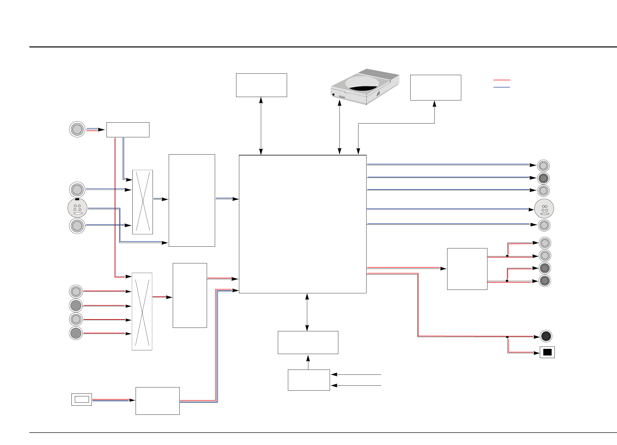
Block Diagrams
8-2 Samsung Electronics
This Document can not be used without Samsung’s authorization.
8-1 All Block Diagram
RF
CVBS1
S-VIDEO1
CVBS2
CVBS from Tuner
VIC1(Main)
Video Decoder
DIC1 (Main)
MPEG-2 A/V CODEC
TM1(JACK)
TM BLOCK
DIC3(Main) FLASH
DVD- DRIVE (4.7GB)
L1
R1
L2
R2
L/R from
Tuner
AIC2(Main)
Audio A/D
1394 JACK
FIC1 (Main)
IEEE1394PHY
IC601 (JACK)
Front Micom
Front PCB
Key Input
Remocon
DIC2 (Main)
DDR-SDRAM
ATAPI
Y
PB
PR
S-VIDEO
VIDEO
AIC1(Main)
Audio D/A
L1
L2
R1
R2
COAXIAL
OPTICAL
DIGITAL AUDIO OUT
IEC-958
Component (480i / 480P)
IC201
(JACK)
IC203
(JACK)
AUDIO
VIDEO
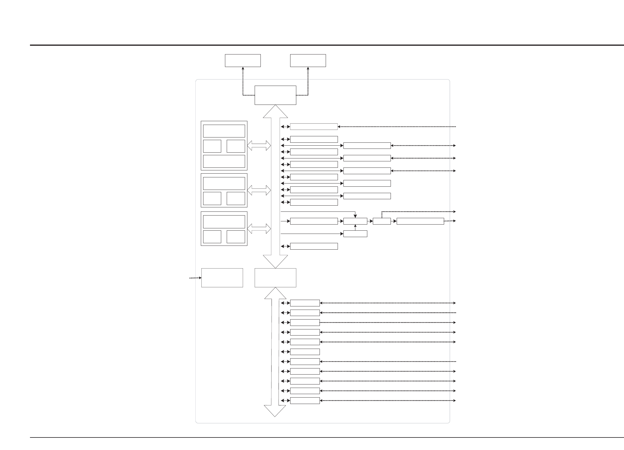
Block Diagrams
Samsung Electronics 8-3This Document can not be used without Samsung’s authorization.
8-2 DIC1(S5L3200) Block Diagram
DDR SDRAM #0
Dual Channel
DDR Controller
& AHB+ BUS
DDR SDRAM #1
ARM9TDMI
4KB
I-Cache
4KB
D-Cache
AHB+ Wrapper
CalmADM #0
4KB
I-Cache
12KB
D-Cache
CalmADM #1
4KB
I-Cache
12KB
D-Cache
APB Bridge
SDIN
Video Pre-processor
MPEG2 Encoder
MPEG2 Decoder
PIP Scaler
MIXER
SPD
Video Processor SDOUT Video PENTA DAC
Graphic Accelerator
DV Decoder
Dual ATAPI (w/ AES)
USB 1.1 Host
IEEE1394
IODMA
PSD
PSM
SPDIF(OUT)
SPDIF(IN)
UART
IR
I2C
I2S
GPIO
TIMER
WDT
SPI
PLL, Clock/Reset
Generation Block
Host I/F
BT656(IN)
IEEE1394
USB
ATAPI
Analog Video Out
BT656(OUT)
27MHz X-tal
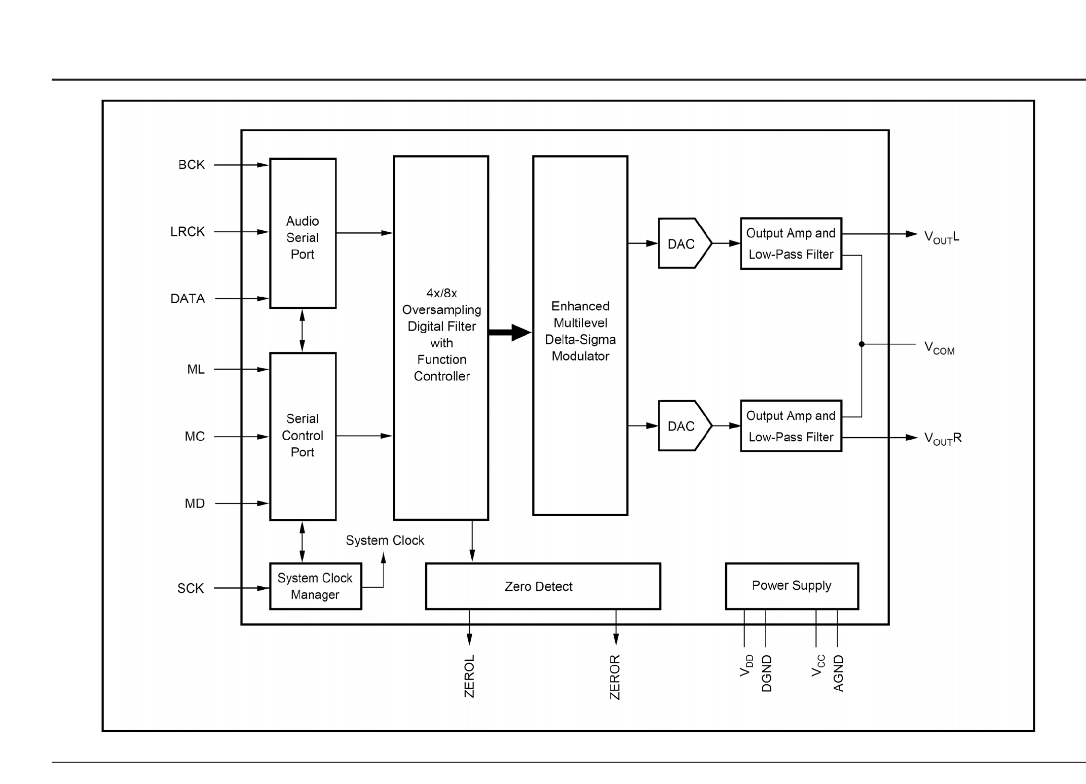
Block Diagrams
8-4 Samsung Electronics
This Document can not be used without Samsung’s authorization.
8-3 AIC1(PCM1742) Block Diagram
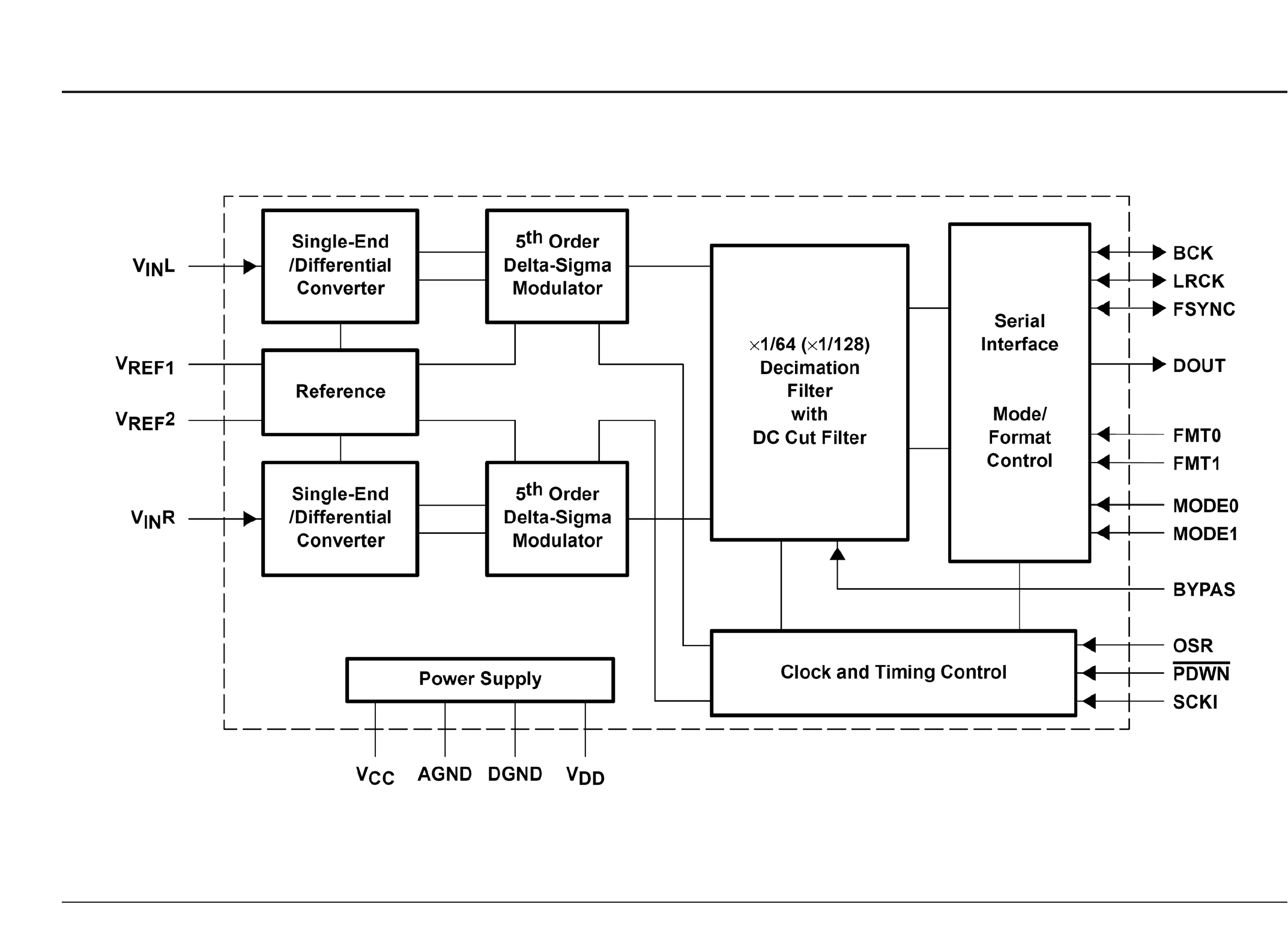
Block Diagrams
Samsung Electronics 8-5This Document can not be used without Samsung’s authorization.
8-4 AIC2 (PCM1802) Block Diagram
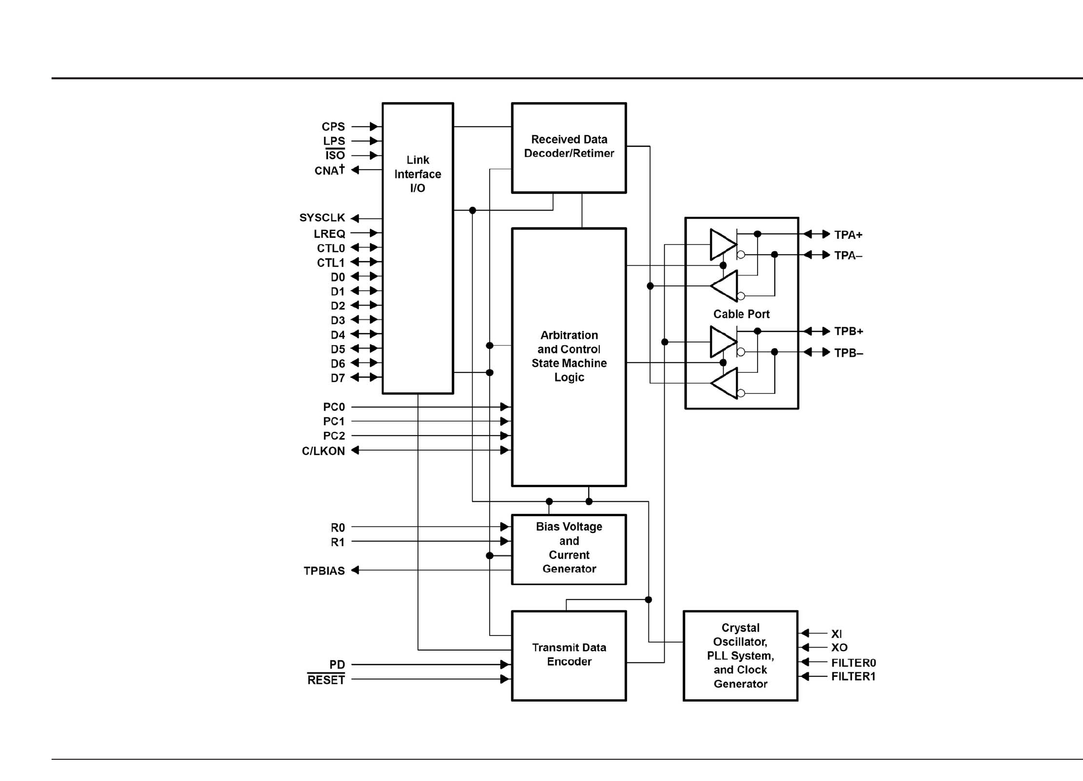
Block Diagrams
8-6 Samsung Electronics
This Document can not be used without Samsung’s authorization.
8-5 FIC1 (TSB4AB1) Block Diagram
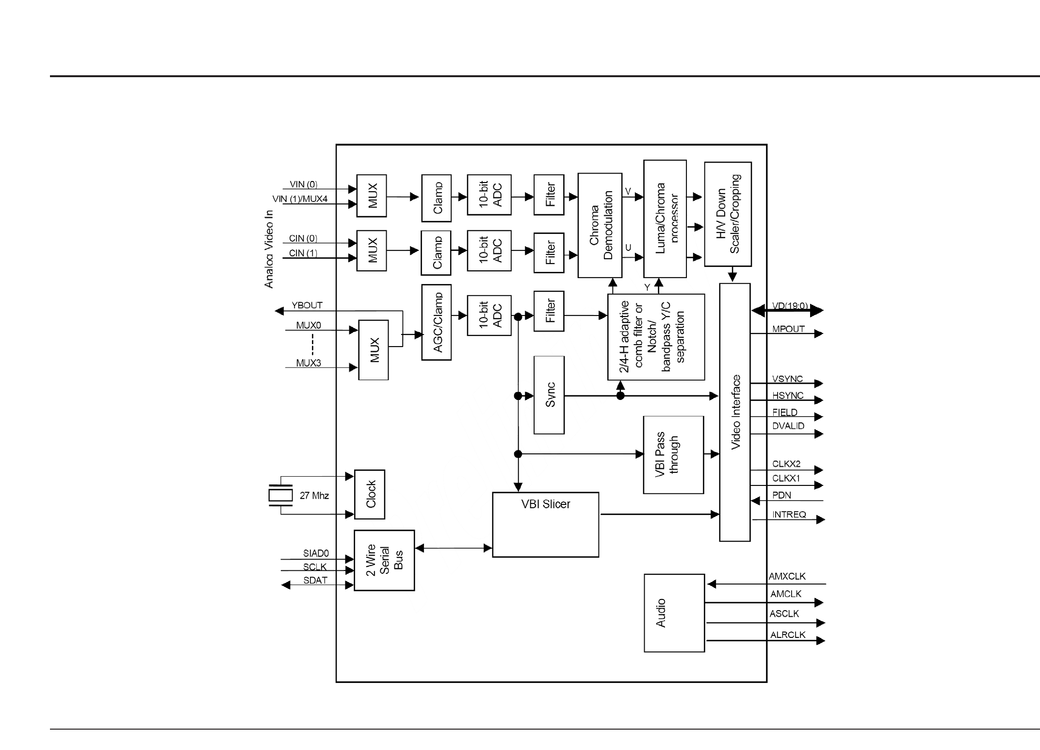
Block Diagrams
Samsung Electronics 8-7This Document can not be used without Samsung’s authorization.
8-6 VIC1 (TW9906) Block Diagram
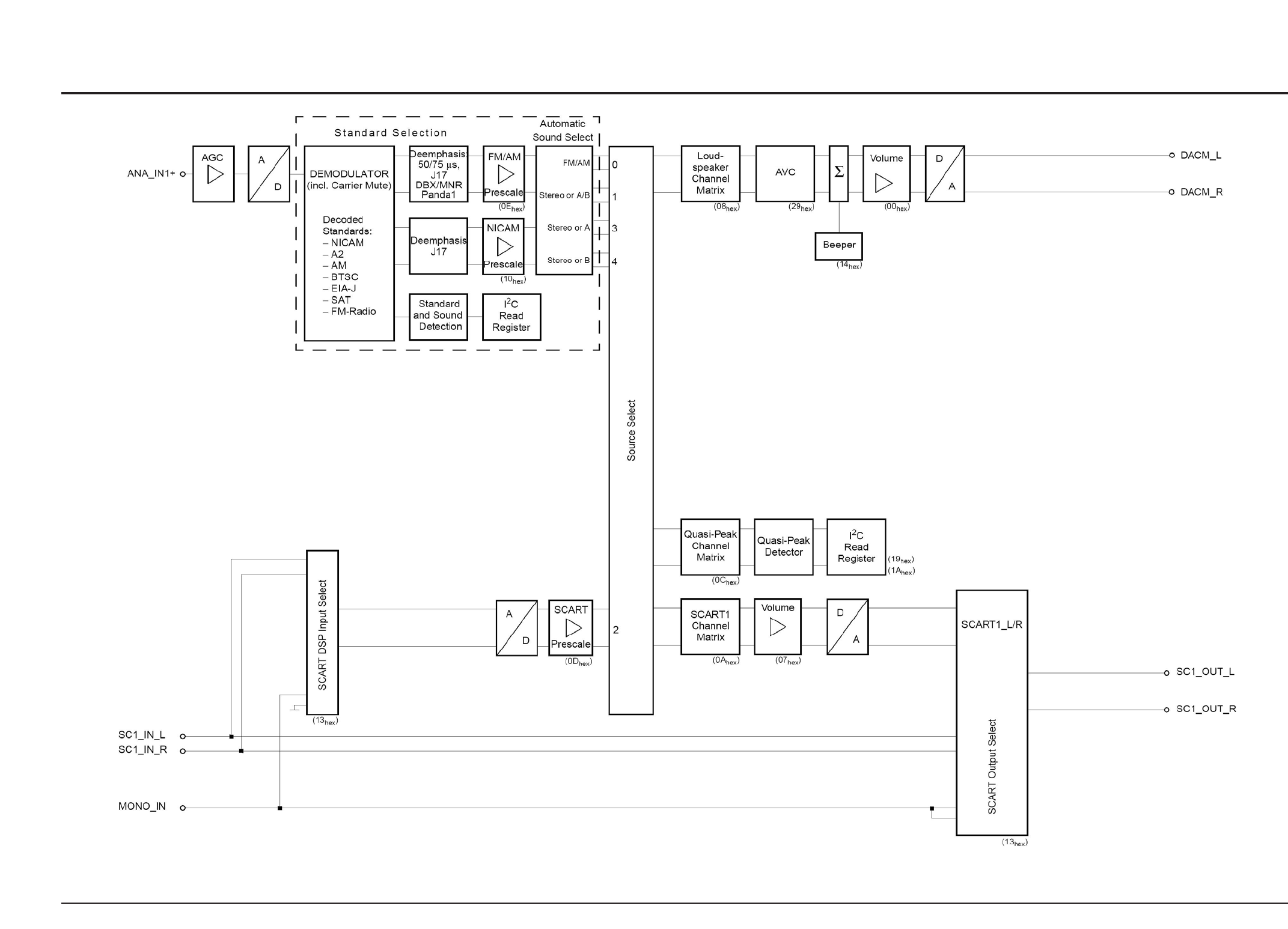
Block Diagrams
8-8 Samsung Electronics
This Document can not be used without Samsung’s authorization.
8-7 IC4N01(MSP3407G) Block Diagram
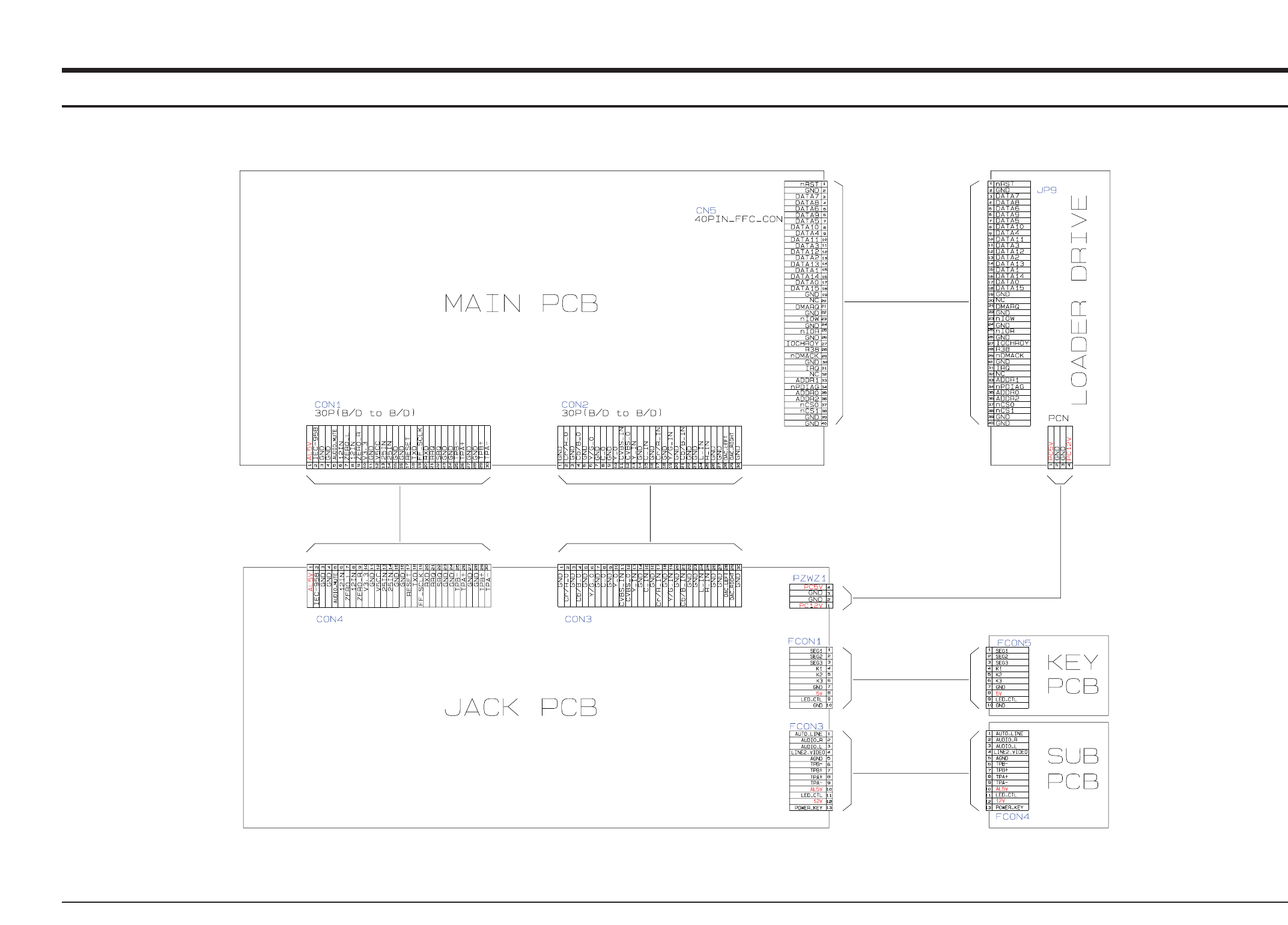
Samsung Electronics 9-1
9. Wiring Diagram

Wiring Diagram
9-2 Samsung Electronics
MEMO

Samsung Electronics 10-1
10. PCB Diagrams
10-1 Main PCB - - - - - - - - - - - - - - - - - - - - - - - - - - - - - - - - - - - - - - - - - - - -
10-2 Jack PCB - - - - - - - - - - - - - - - - - - - - - - - - - - - - - - - - - - - - - - - - - - - - -
10-3 Key PCB - - - - - - - - - - - - - - - - - - - - - - - - - - - - - - - - - - - - - - - - - - - - - -
10-4 Sub PCB - - - - - - - - - - - - - - - - - - - - - - - - - - - - - - - - - - - - - - - - - - - - - -
10-2
10-4
10-6
10-7
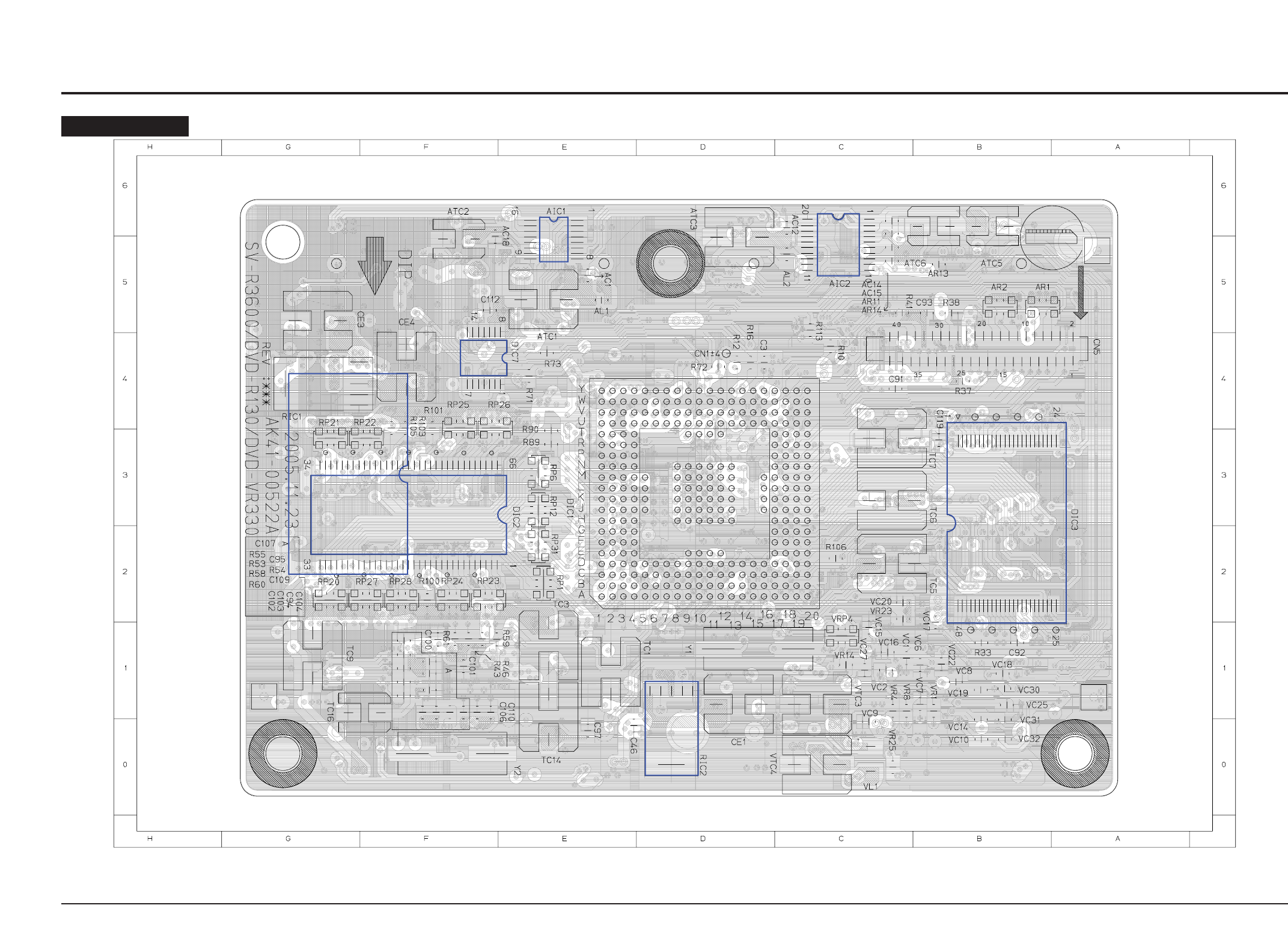
PCB Diagrams
10-2 Samsung Electronics
10-1 Main PCB
AIC1
DIC7
RIC1
DIC2
RIC2
DIC3
AIC2
COMPONENT SIDE
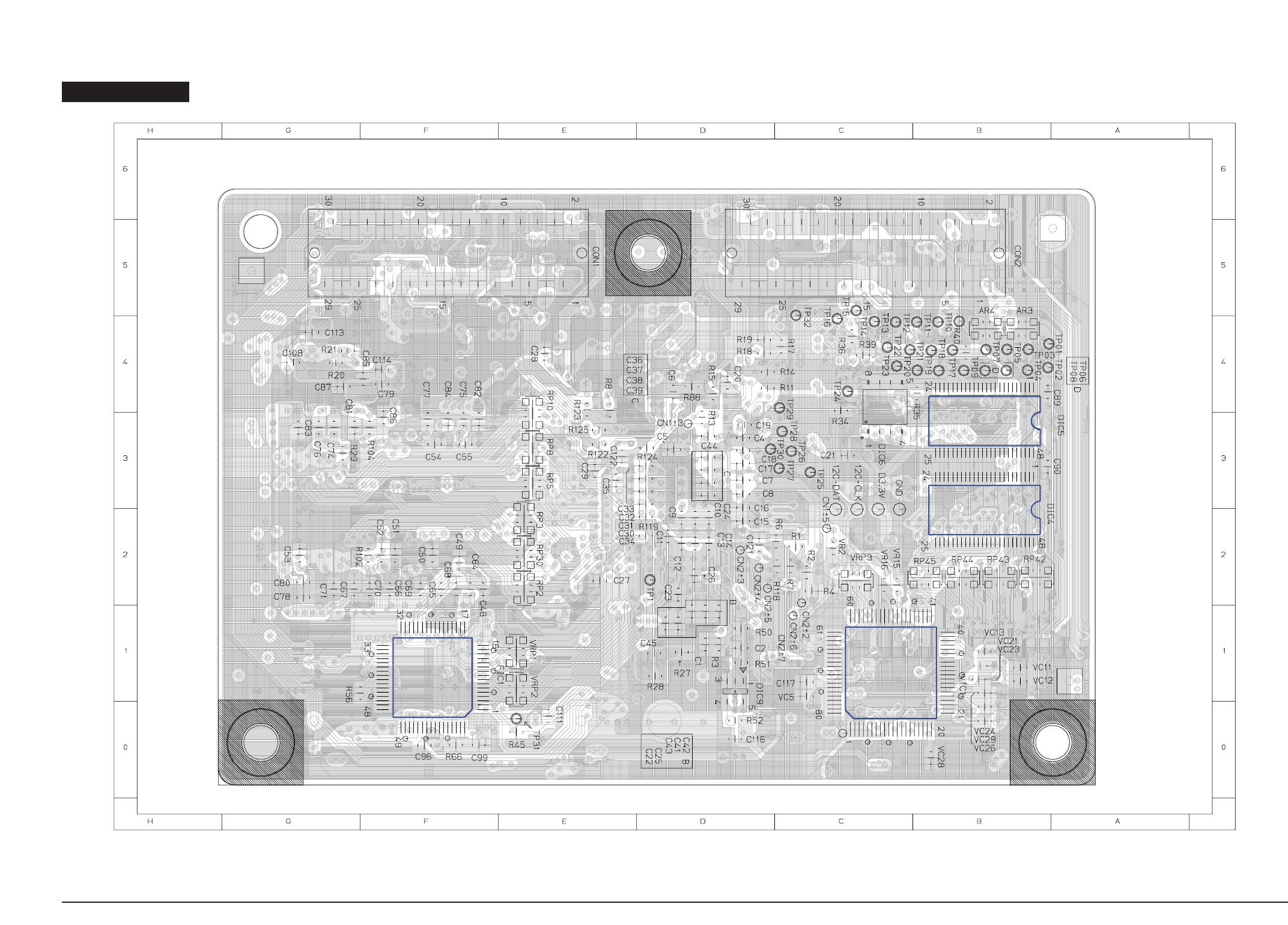
PCB Diagrams
Samsung Electronics 10-3
FIC1
DIC5
DIC4
VIC1
CONDUCTOR SIDE
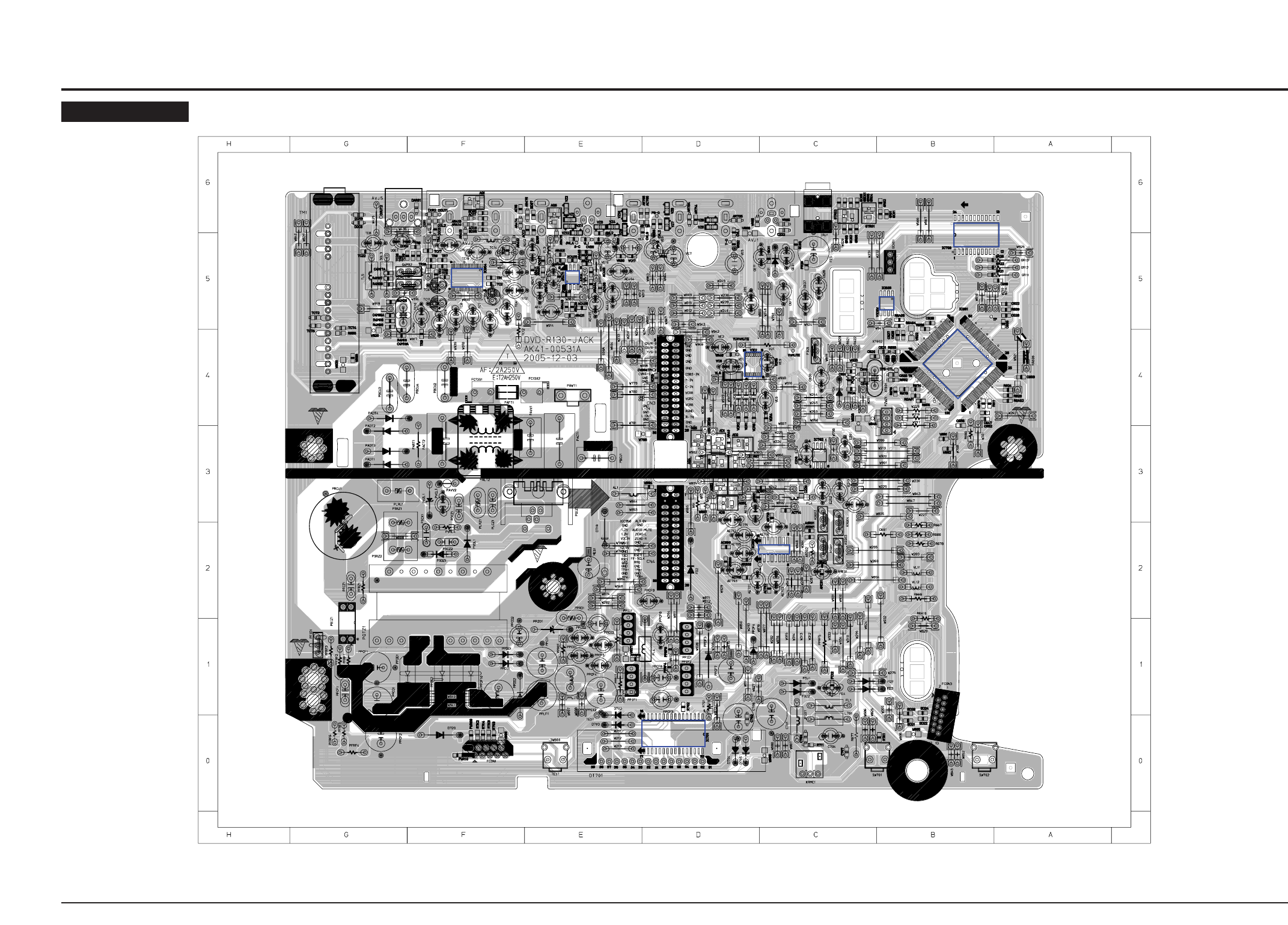
PCB Diagrams
10-4 Samsung Electronics
IC604
AIC4
IC601
IC603
IC703
IC203
IC701
VIC1
10-2 Jack PCB
COMPONENT SIDE
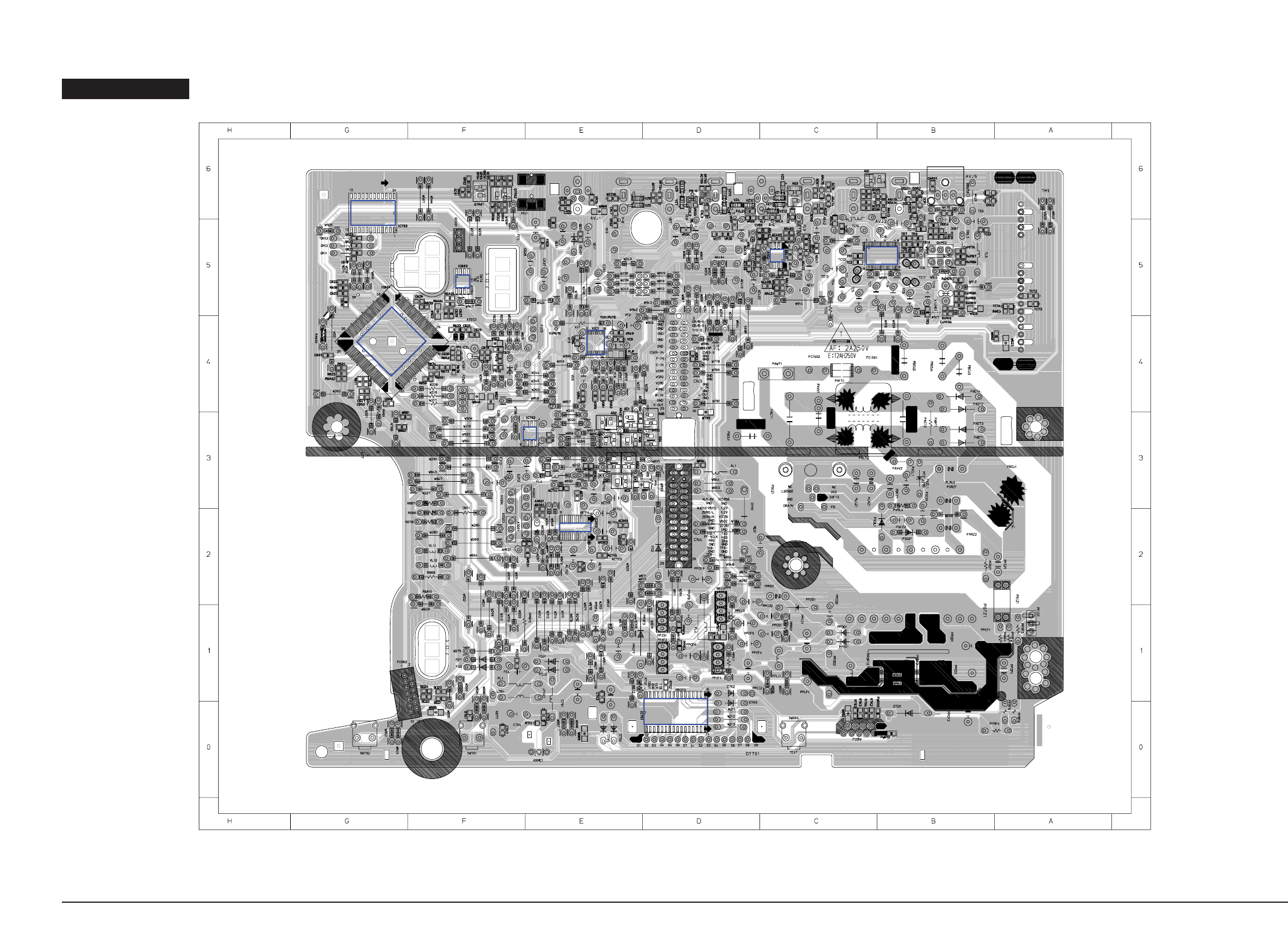
PCB Diagrams
Samsung Electronics 10-5
IC703
IC603
IC601
IC203
IC702
VIC1
IC604
AIC4
IC701
CONDUCTOR SIDE
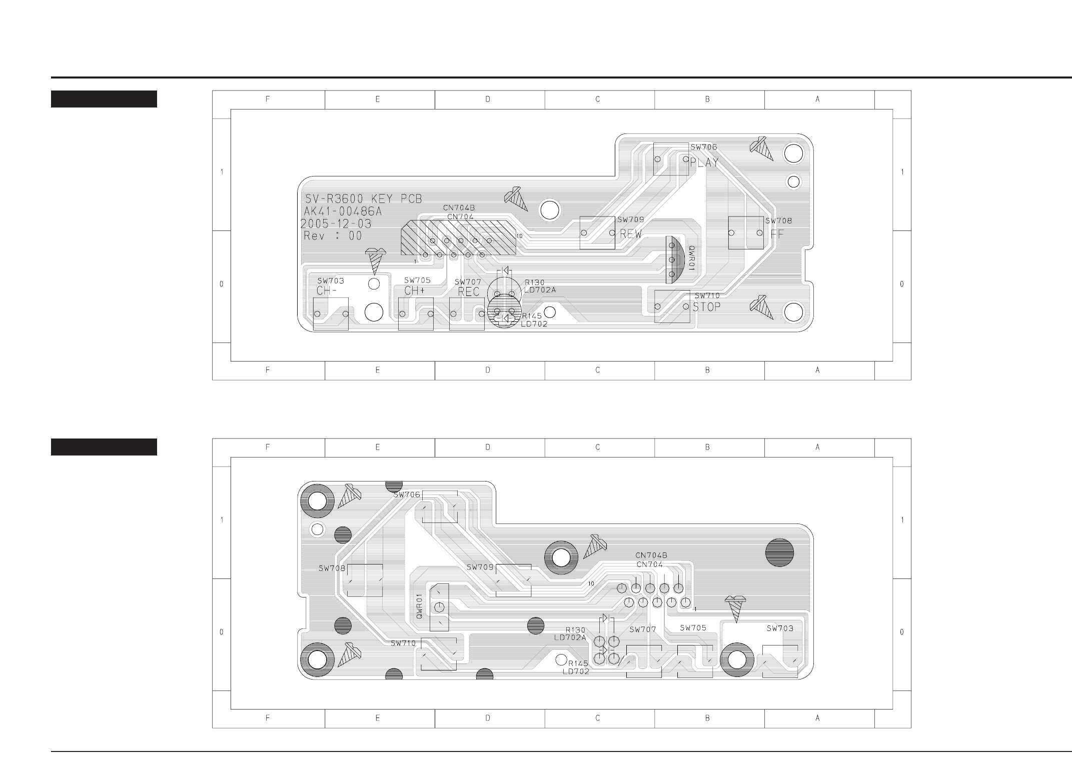
PCB Diagrams
10-6 Samsung Electronics
10-3 Key PCB
COMPONENT SIDE
CONDUCTOR SIDE
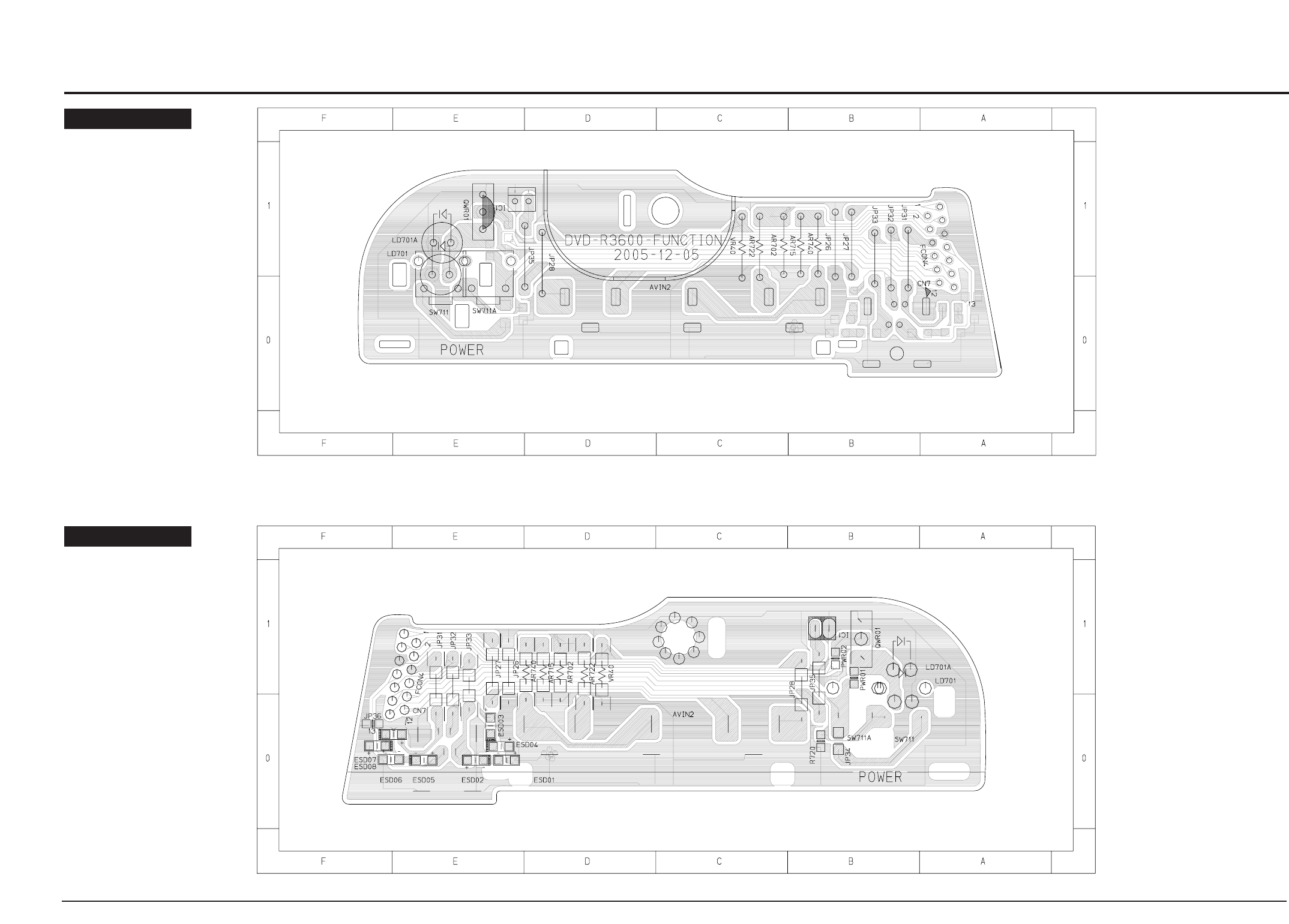
PCB Diagrams
Samsung Electronics 10-7
10-4 Sub PCB
COMPONENT SIDE
CONDUCTOR SIDE

PCB Diagrams
10-8 Samsung Electronics
MEMO

This Document can not be used without Samsung’s authorization.
Samsung Electronics 11-1
11. Schematic Diagrams
11-1 S.M.P.S (Jack PCB) - - - - - - - - - - - - - - - - - - - - - - - - - - - - - - - - - - - - - -
11-2 TM Block (Jack PCB) - - - - - - - - - - - - - - - - - - - - - - - - - - - - - - - - - - - -
11-3 AV Input (Jack PCB) - - - - - - - - - - - - - - - - - - - - - - - - - - - - - - - - - - - -
11-4 Micom (Jack PCB) - - - - - - - - - - - - - - - - - - - - - - - - - - - - - - - - - - - - - - -
11-5 CBS Function Block (Jack PCB)- - - - - - - - - - - - - - - - - - - - - - - - - - - - - -
11-6 I/O (Jack PCB)- - - - - - - - - - - - - - - - - - - - - - - - - - - - - - - - - - - - - - - - - -
11-7 AV Codec (Main PCB)- - - - - - - - - - - - - - - - - - - - - - - - - - - - - - - - - - - - -
11-8 DDR (Main PCB) - - - - - - - - - - - - - - - - - - - - - - - - - - - - - - - - - - - - - - - -
11-9 DV_1394 (Main PCB)- - - - - - - - - - - - - - - - - - - - - - - - - - - - - - - - - - - - - -
11-10 Latch And Audio (Main PCB) - - - - - - - - - - - - - - - - - - - - - - - - - - - - - - -
11-11 Main Connector (Main PCB) - - - - - - - - - - - - - - - - - - - - - - - - - - - - - - -
11-12 Video Decoder (Main PCB) - - - - - - - - - - - - - - - - - - - - - - - - - - - - - - - -
11-13 Sub and Key (Sub and Key PCB) - - - - - - - - - - - - - - - - - - - - - - - - - - - - -
11-2
11-3
11-4
11-5
11-6
11-7
11-8
11-9
11-10
11-11
11-12
11-13
11-14
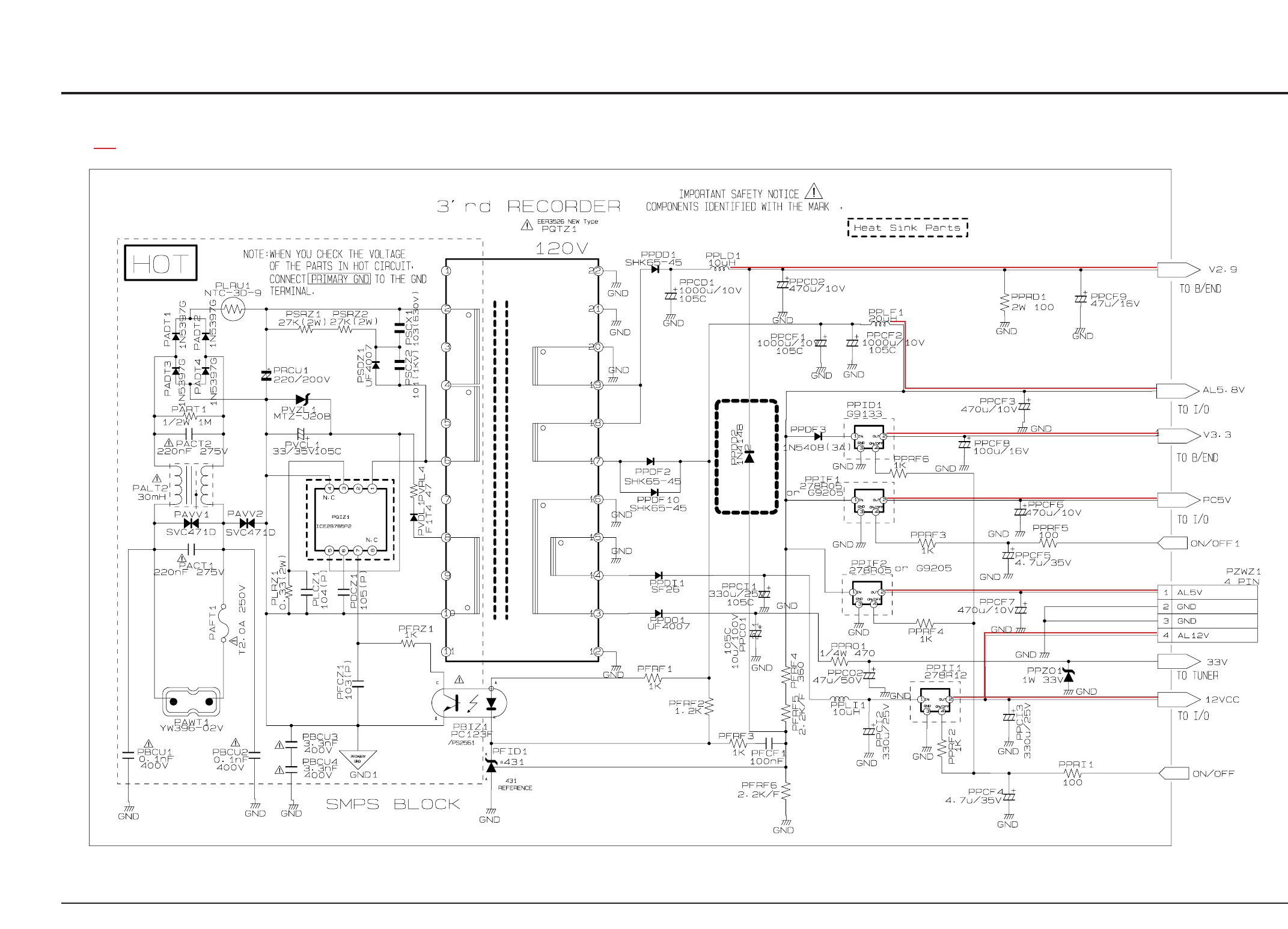
Schematic Diagrams
11-2 Samsung Electronics
This Document can not be used without Samsung’s authorization.
11-1 S.M.P.S (Jack PCB)
Power
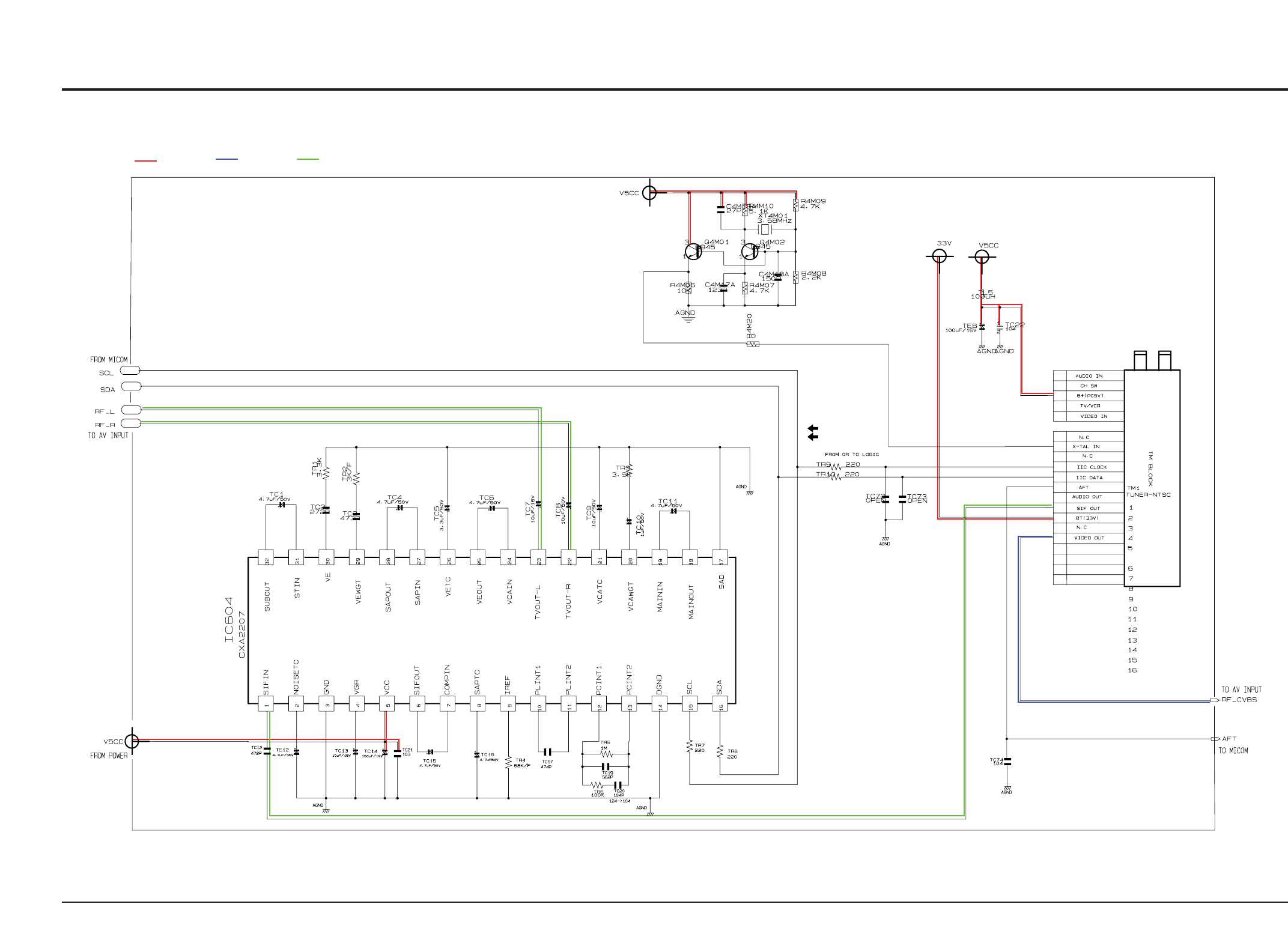
Schematic Diagrams
Samsung Electronics 11-3
This Document can not be used without Samsung’s authorization.
Power Video Audio
11-2 TM Block (Jack PCB)
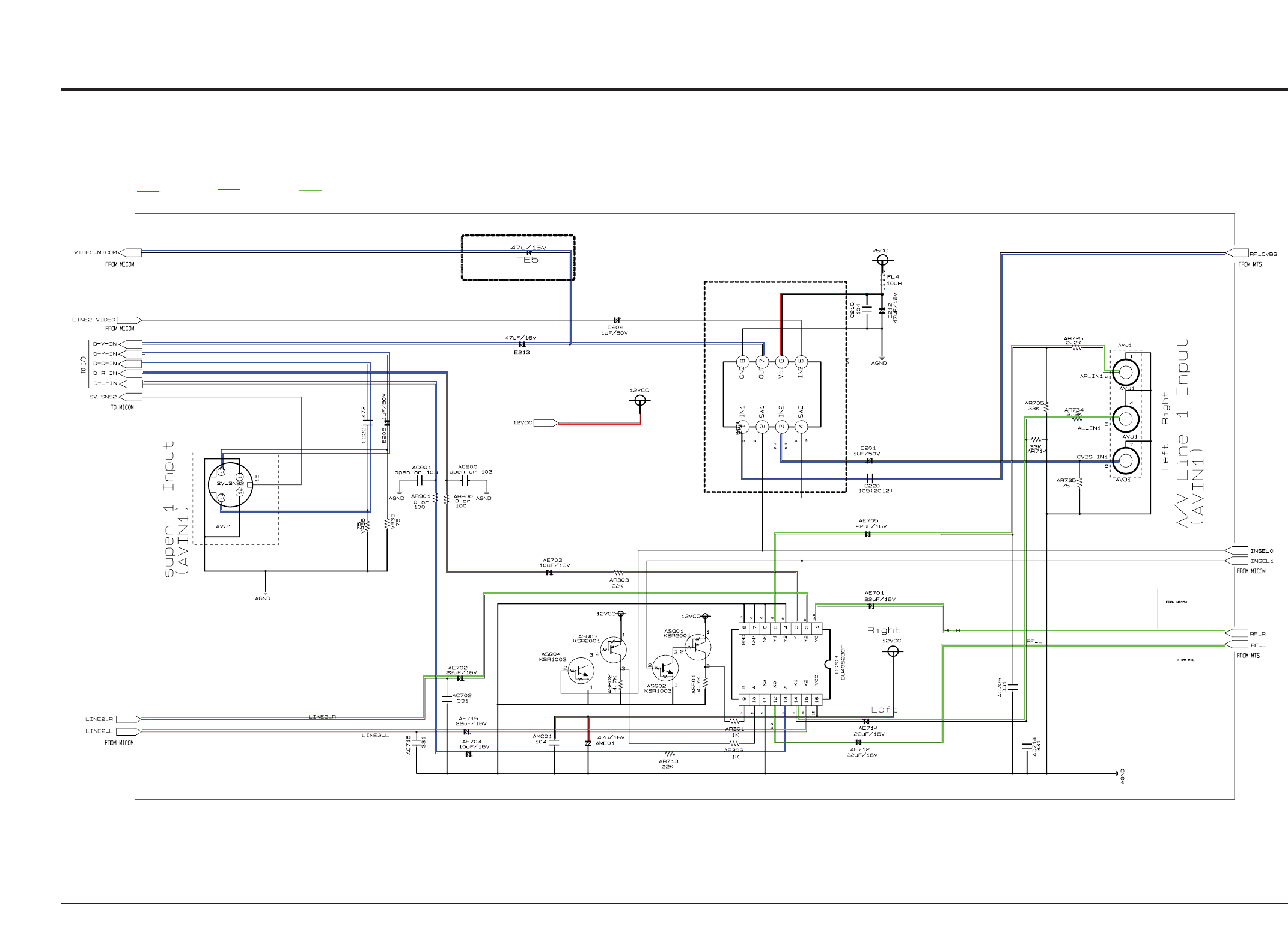
Schematic Diagrams
11-4 Samsung Electronics
This Document can not be used without Samsung’s authorization.
Power Video Audio
11-3 AV Input (Jack PCB)
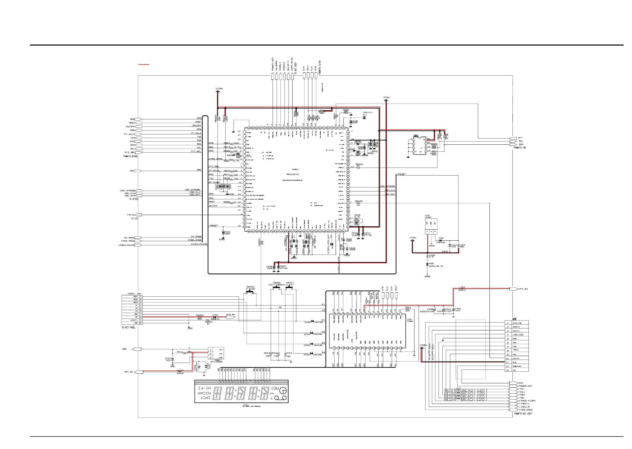
Schematic Diagrams
Samsung Electronics 11-5
This Document can not be used without Samsung’s authorization.
Power
11-4 Micom (Jack PCB)
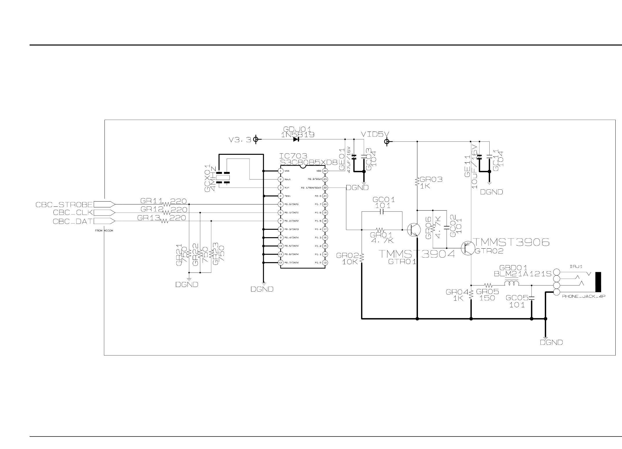
Schematic Diagrams
11-6 Samsung Electronics
This Document can not be used without Samsung’s authorization.
11-5 CBS Function Block (Jack PCB)
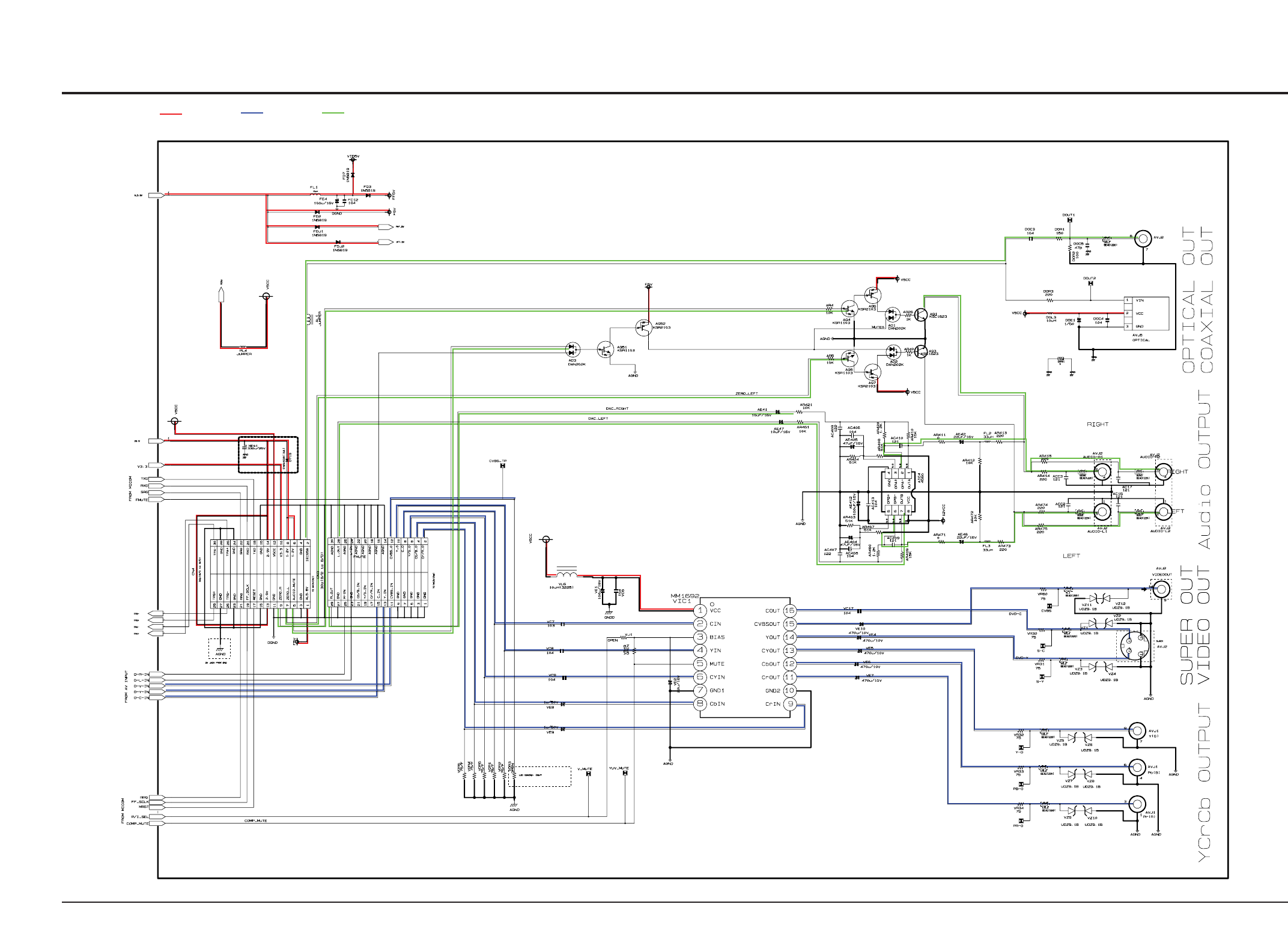
Schematic Diagrams
Samsung Electronics 11-7
This Document can not be used without Samsung’s authorization.
Power Video Audio
11-6 I/O (Jack PCB)
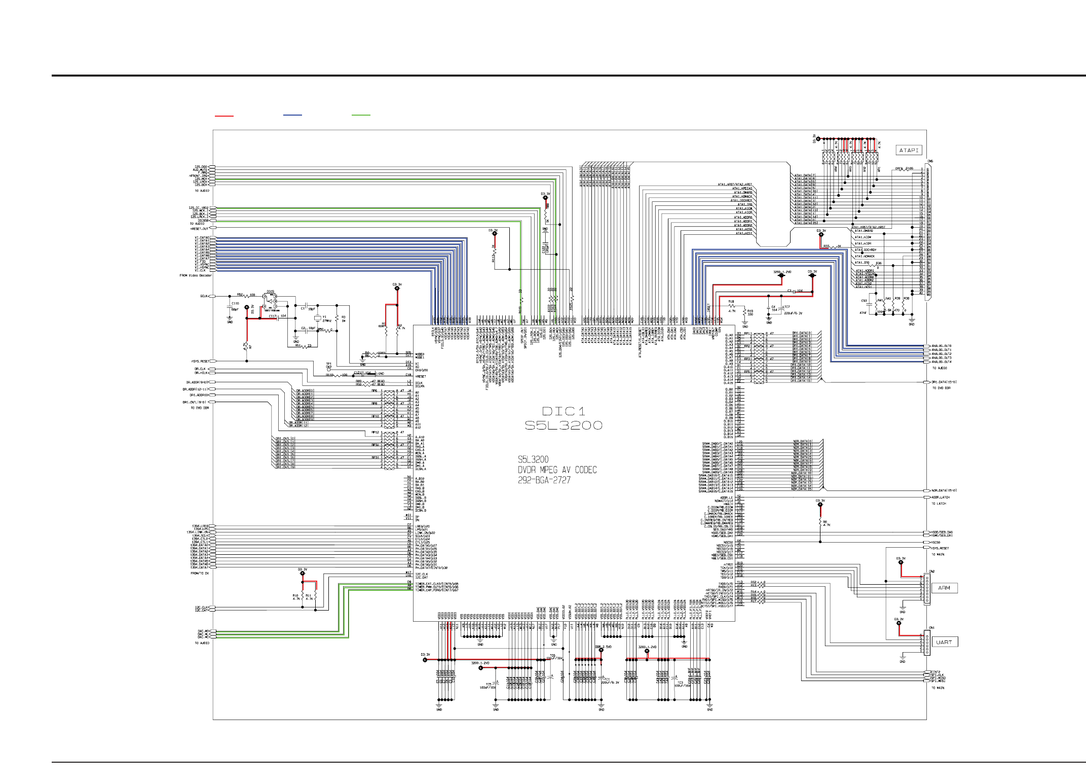
Schematic Diagrams
11-8 Samsung Electronics
This Document can not be used without Samsung’s authorization.
Power Video Audio
11-7 AV Codec (Main PCB)
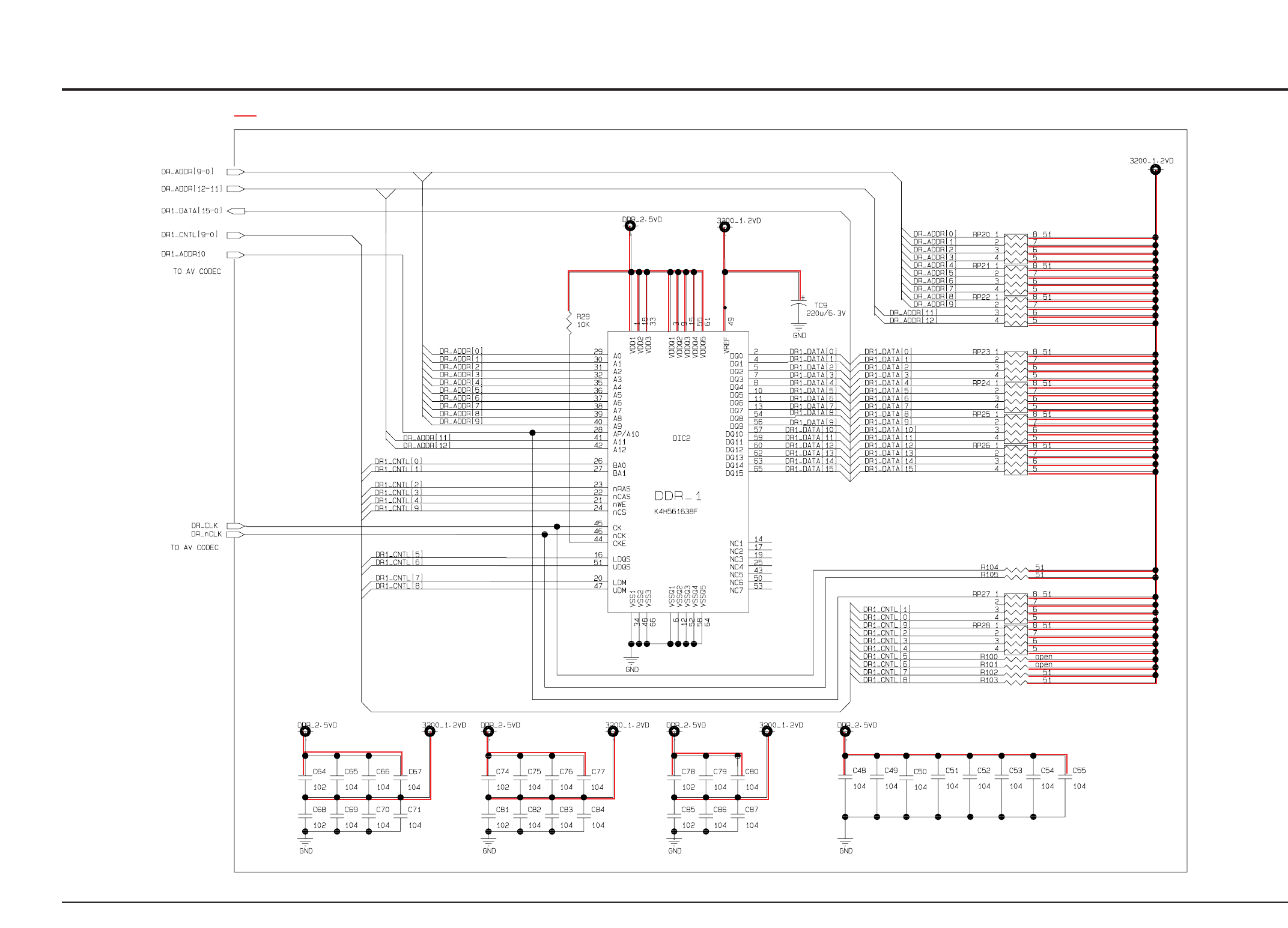
Schematic Diagrams
Samsung Electronics 11-9
This Document can not be used without Samsung’s authorization.
Power
11-8 DDR (Main PCB)
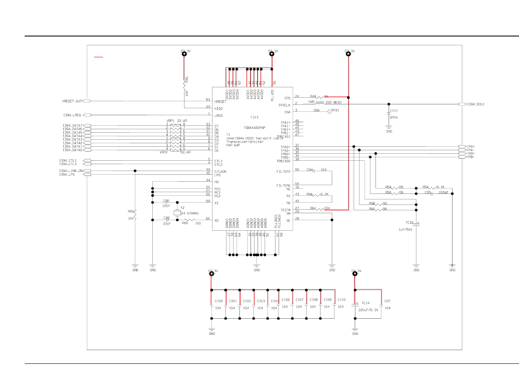
Schematic Diagrams
11-10 Samsung Electronics
This Document can not be used without Samsung’s authorization.
Power
11-9 DV_1394 (Main PCB)
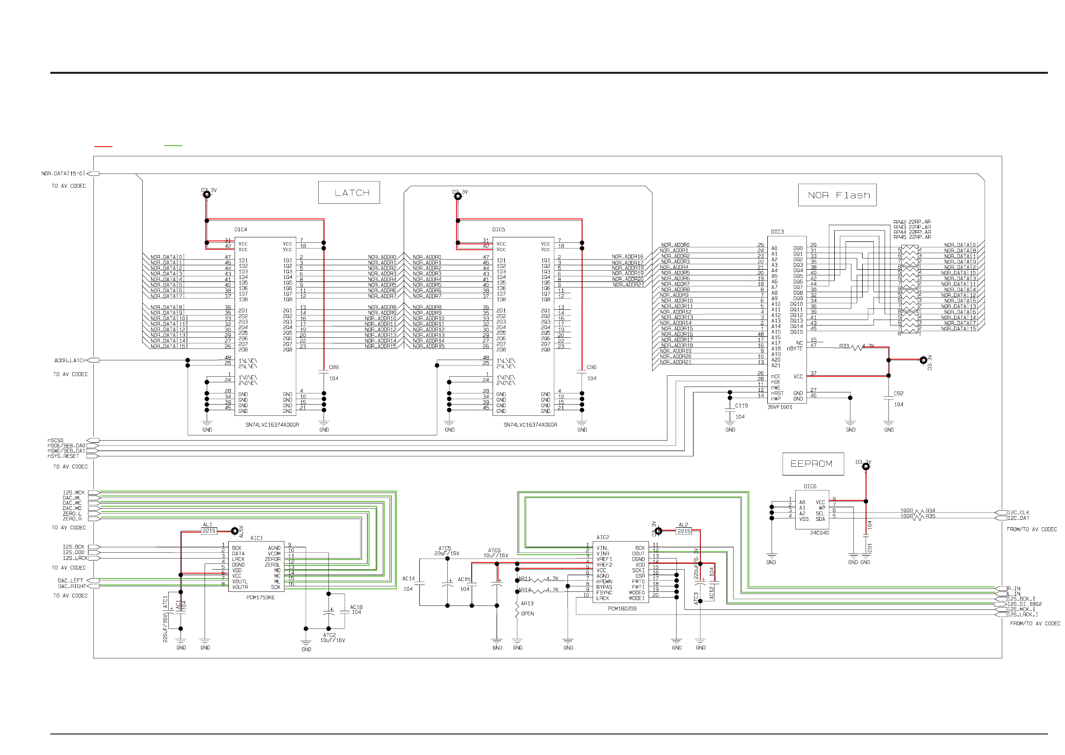
Schematic Diagrams
Samsung Electronics 11-11
This Document can not be used without Samsung’s authorization.
Power Audio
11-10 Latch And Audio (Main PCB)
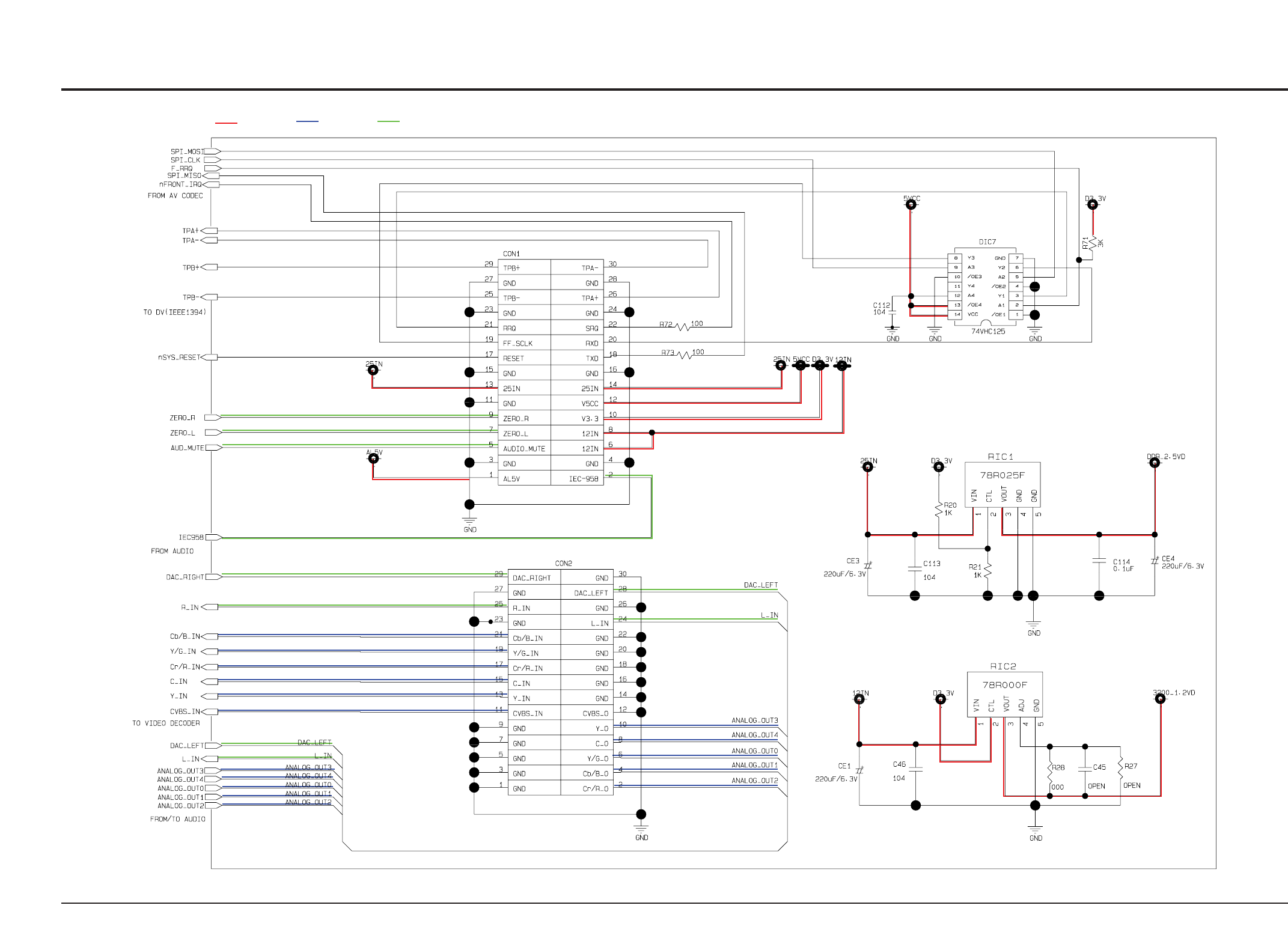
Schematic Diagrams
11-12 Samsung Electronics
This Document can not be used without Samsung’s authorization.
Power Video Audio
11-11 Main Connector (Main PCB)
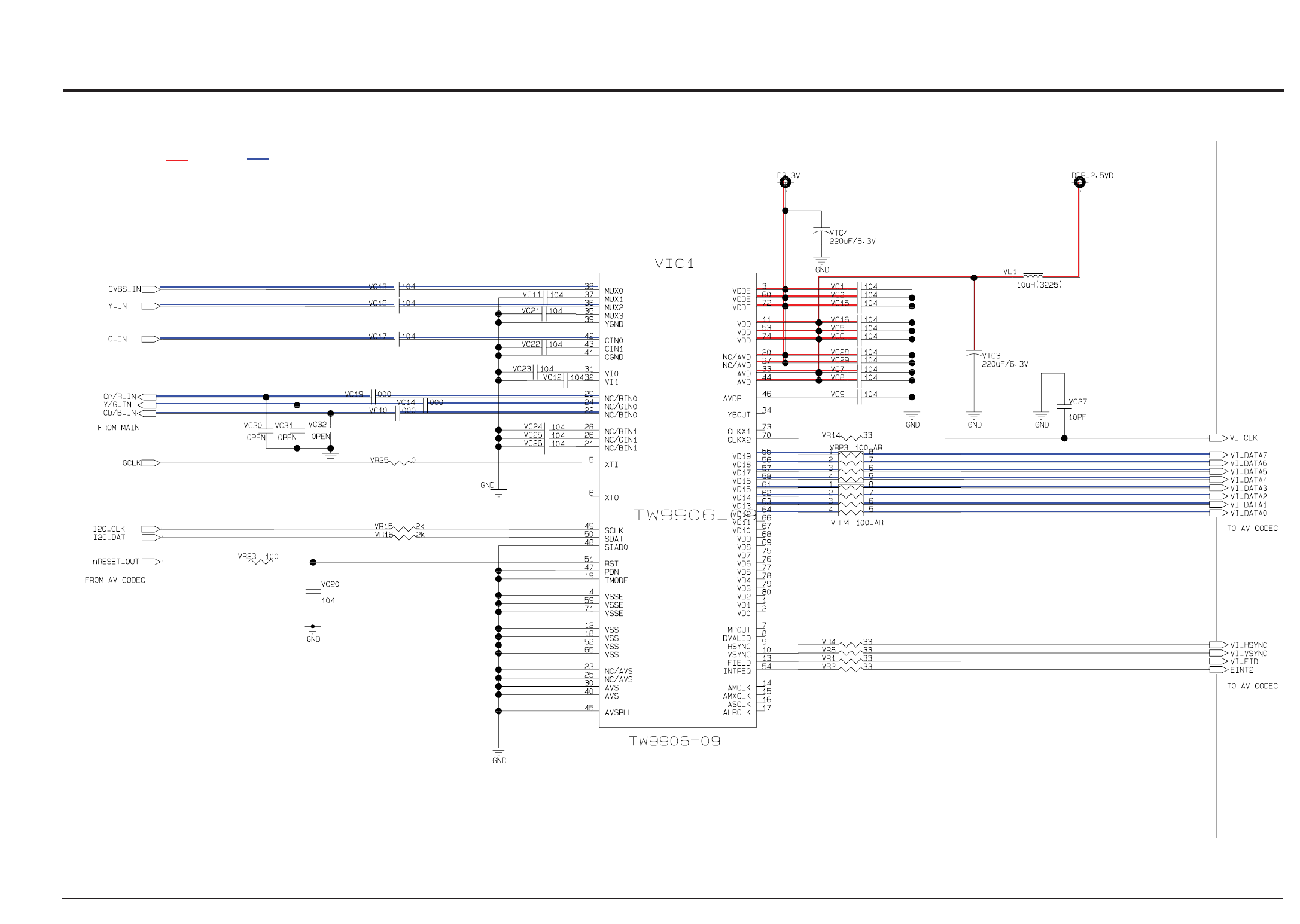
Schematic Diagrams
Samsung Electronics 11-13
This Document can not be used without Samsung’s authorization.
Power Video
11-12 Video Decoder (Main PCB)
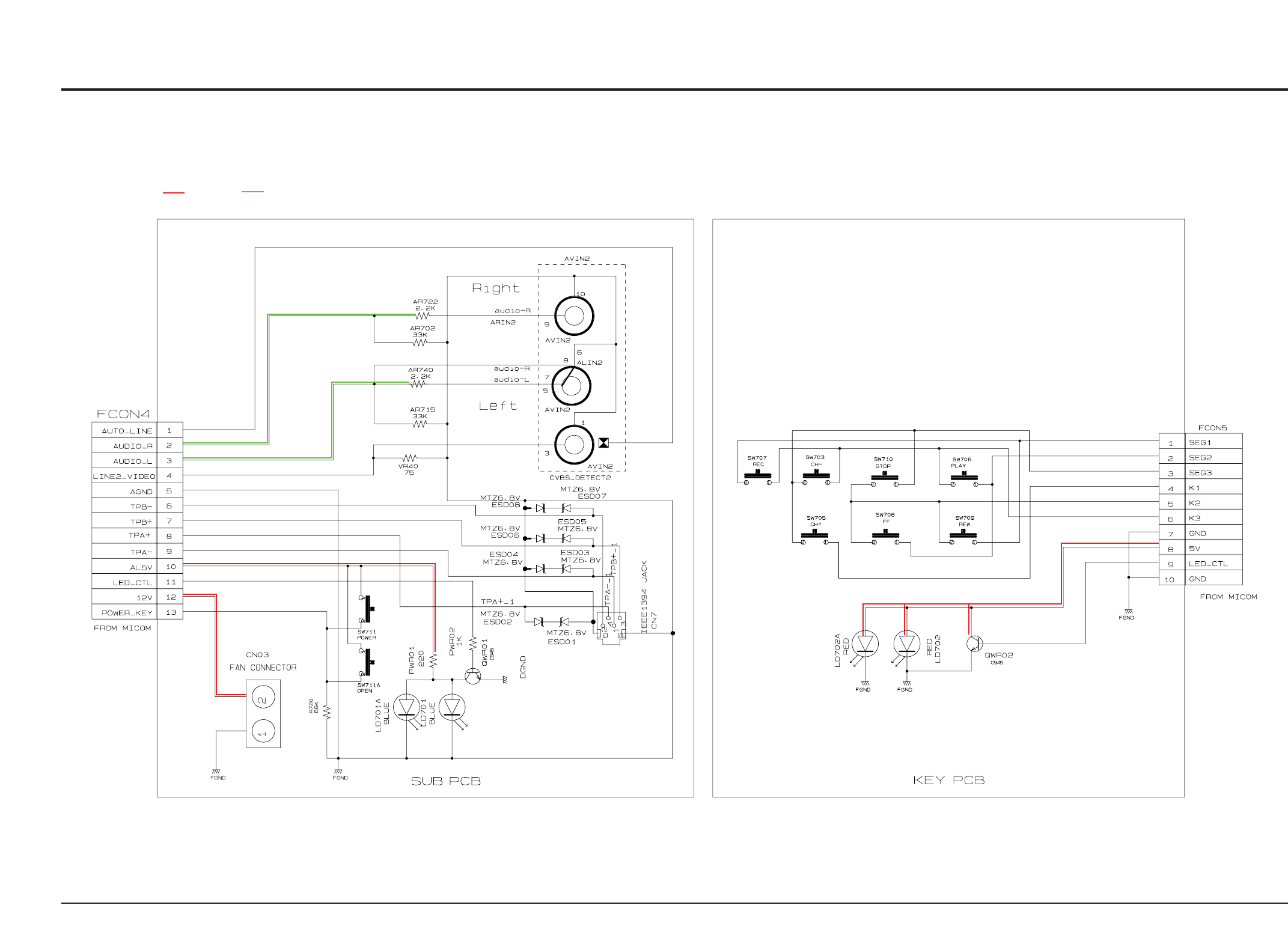
Schematic Diagrams
11-14 Samsung Electronics
This Document can not be used without Samsung’s authorization.
Power Audio
11-13 Sub and Key (Sub and Key PCB)
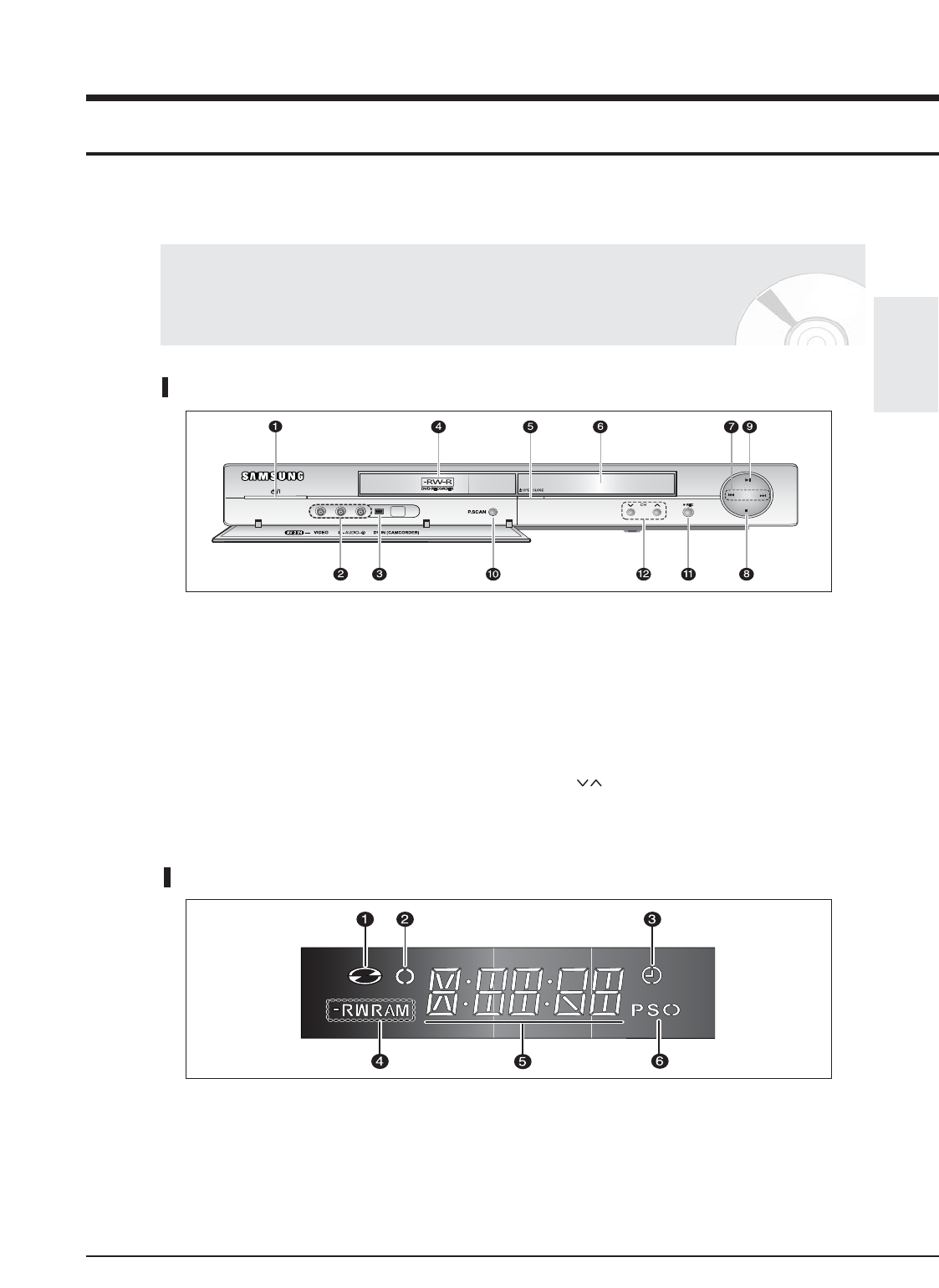
Getting Started
English - 11
Front panel
1. POWER
Turns the recorder on and off.
2. AV 2 IN
Connect external equipment.
3. DV-IN
Connects external digital equipment with a DV
jack. (such as a camcorder)
4. DISC TRAY
Opens to accept a disc.
5. OPEN/CLOSE
Opens and closes the disc tray.
6. DISPLAY
Displays the playing status, time, etc.
7. SEARCH
Go to the next title/chapter/track, or goes back
to the previous title/chapter/track.
8. STOP
Stops disc playback.
9. PLAY/PAUSE
Plays a disc or pauses playback.
10. P.SCAN
Selects the progressive scan mode.
11. REC
Starts recording.
12. CH ( )
Select TV channels.
Description
Front Panel Display
1. Lights when a disc is loaded.
2. Lights in the record mode.
3. Lights to indicate the timer record mode.
4. Lights when a DVD-R/-RW/-RAM disc is
loaded.
5. Alpha/Numeric display.
6. Lights in the progressive scan mode.
Samsung Electronics 12-1
12. Operating Instructions
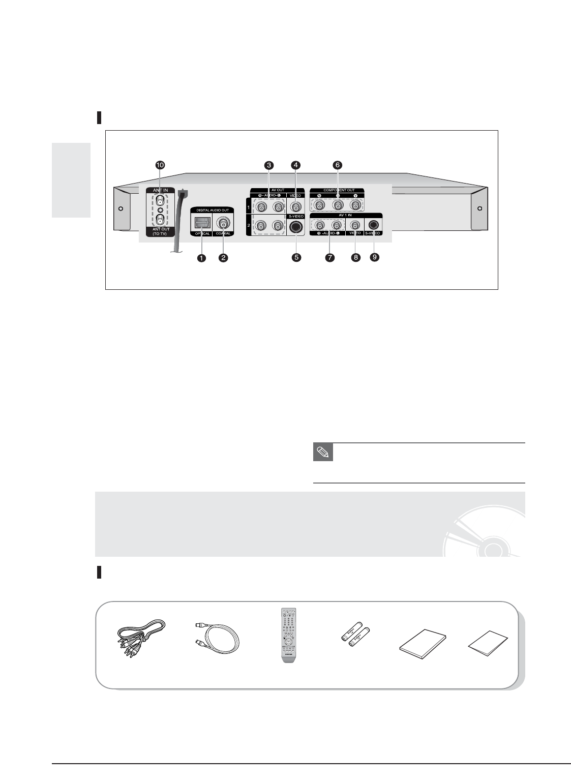
Operating Instructions
12-2
Getting Started
12 - English
Rear Panel
1. DIGITAL AUDIO OUT(OPTICAL)
Connects to an amplifier having a digital optical
audio input jack.
2. DIGITAL AUDIO OUT(COAXIAL)
Connects to an amplifier having a digital coaxial
audio input jack.
3. AV AUDIO OUT
Connect to the audio input of external equipment
using audio cables.
4. AV VIDEO OUT(good video quality)
Connects the input of external equipment using a
Video cable.
5. AV S-VIDEO OUT(better video quality)
Connects the input of external equipment using
an S-Video cable.
6. COMPONENT VIDEO OUT(best video quality)
Connect to equipment having Component video
input jacks.
7. AV 1 AUDIO IN
Connect the output of external equipment using
audio cables
8. AV 1 VIDEO IN
Connects the output of external equipment using
a video cable.
9. AV 1 S-VIDEO IN
Connects the output of external equipment using
an S-Video cable.
10. ANT IN/ANT OUT (TO TV)
Connect antenna cables.
■
The Antenna connection does not pass
audio/video signals. To watch a DVD on your
TV, you must connect audio/video cables.
NOTE
Accessories
Check for the supplied accessories below.
Unpacking
Video/Audio Cable
(AC39-00073A)
RF Cable for TV
(AC39-42001J)
Batteries for Remote
Control (AAA Size)
(AC43-12002H)
Remote Control
(AK59-00055A)
Instruction Manual
(AK68-01174A)
Quick Guide
(AK68-01175A)
Samsung Electronics
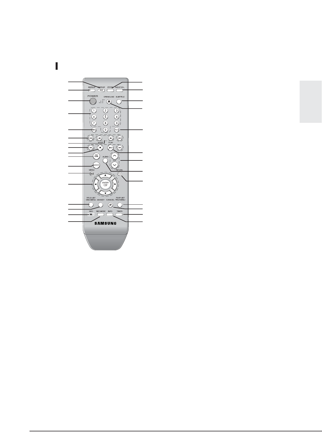
Operating Instructions
12-3
Getting Started
English - 13
Tour of the Remote Control 12. TITLE LIST/DISC MENU Button
Use this to enter the View Recording list/Disc menu.
13. ANYKEY Button
Use this to view the status of the disc that is being played.
14. REC Button
Use to make a recording on DVD-RW/-R discs.
15. REC MODE Button
Use this to set the desired Recording time and picture quality.
(XP/SP/LP/EP)
16. SUBTITLE Button
Press this to switch the DVD’s subtitle language.
17. OPEN/CLOSE Button
To open and close the disc tray.
18. ANGLE Button
19. PLAY/PAUSE Button
Press to play/pause a disc or pause the recording.
20. CH Button
Use this to select a TV channel.
21. AUDIO Button
Use this to access various audio functions on a disc.
22. RETURN Button
23. PLAY LIST/TITLE MENU Button
Use this to return to the Title menu, or to view the recorded
Playlist.
24. CANCEL Button
25. TIMER Button
Press to directly enter the Timer Recording Mode menu.
26. INFO Button
This will display current setting or disc status.
27. REPEAT Button
Allows you to repeat a title, chapter, track or disc.
28. REPEAT A-B Button
Allows you to repeat a certain section.
29. ZOOM Button
30. INPUT SEL. Button
Selects line input signal in external input mode. (Tuner, AV1,
AV2 or DV)
1. POWER Button
2. NUMBER Buttons
3. 100+ Button
Press this to select channel 100 or higher.
4. REVERSE/FORWARD SKIP Buttons
Press to skip a disc backwards or forwards.
5. REVERSE/FORWARD STEP Buttons
Press to play frame by frame.
6. REVERSE/FORWARD SEARCH Buttons
Press to search a disc backwards or forwards.
7. STOP Button
Press to stop a disc or to stop the recording.
8. CM SKIP Button
The unit can be set to automatically skip a portion of the
program during playback of a DVD disc.
9. MARKER Button
Use this to bookmark or mark a position while playing a disc.
10. MENU Button
Brings up the DVD recorder’s setup menu.
11. ENTER/DIRECTION Buttons
(UP/DOWN and LEFT/RIGHT Buttons)
This button functions as a toggle switch.
116
27
2
3
4
6
10
12
11
7
5
28
13
9
15
15
14
8
30
18
17
29
19
21
24
20
22
23
25
26
Samsung Electronics

Operating Instructions
12-4
Connecting &
Setting Up
14 - English
Connecting &
Setting Up
This section involves various methods of
connecting the DVD Recorder to other external
components and setting required initial modes.
Quick Overview
A Quick Overview presented in this guide will give
you enough information to start using the recorder.
•
Note to CATV system installer: : This reminder is
provided to call CATV system installer’s attention to
Article 820-40 of the National Electrical Code
(Section 54 of Canadian Electrical Code, Part I),
that provides guidelines for proper grounding and,
in particular, specifies that the cable ground shall
be connected to the grounding system of the
building as close to the point of cable entry as
practical.
Step 1 : Connecting the Antenna Cable
†
Step 2 : Connecting the Video Cable
†
Step 3 : Connecting the Audio Cable
†
Step 4 : Connecting External Devices
†
Step 5 : Connecting the Power Cord
†
Step 6 : Preparing the Remote Control
Quick Overview . . . . . . . . . . . . . . . . . . . . . . . . . . .14
Step 1 : Connecting the Antenna Cable . . . . . . . .15
Step 2 : Connecting the Video Cable . . . . . . . . . .18
Step 3 : Connecting the Audio Cable . . . . . . . . . .21
Step 4 : Connecting External Devices . . . . . . . . . .24
Step 5 : Connecting the Power Cord . . . . . . . . . . .27
Step 6 : Preparing the Remote Control . . . . . . . . .27
Samsung Electronics
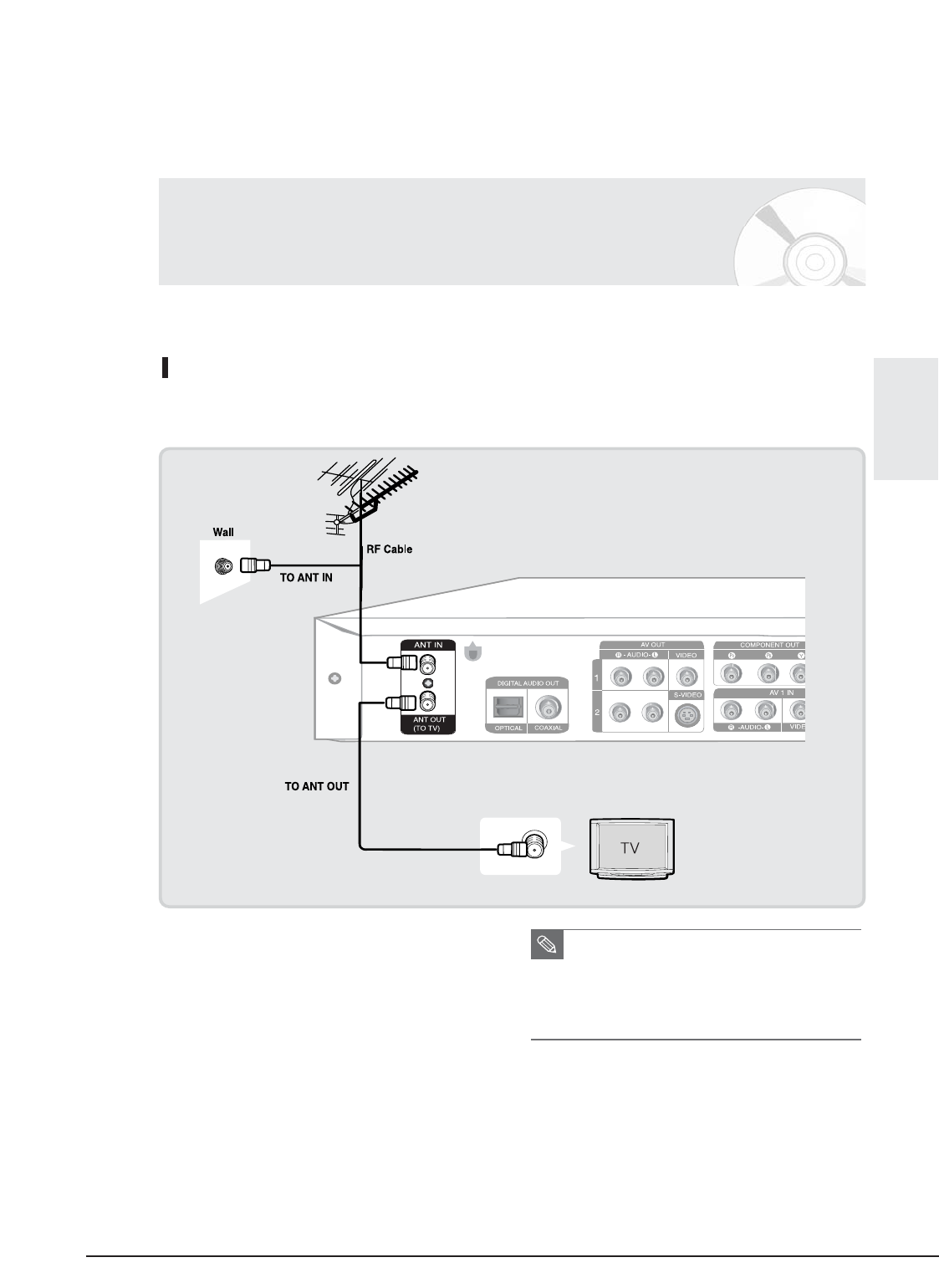
Operating Instructions
12-5
Step 1: Connecting the Antenna Cable
There are several ways to connect your DVD Recorder. Select one of the Antenna connections on the following pages.
Antenna + DVD Recorder + TV : No Cable box
You can record non-scrambled channels by selecting the channel on the DVD Recorder. Also use this method if you
watch channels without cable box.
■
The VHF/UHF ANT (RF) OUT jack of this
product sends only signals received through
the antenna. It does not output Audio/Video
signals. You must connect Audio/Video cables
to view Video from the unit.
(i.e. DVD playback)
NOTE
Connecting &
Setting Up
English - 15
Samsung Electronics
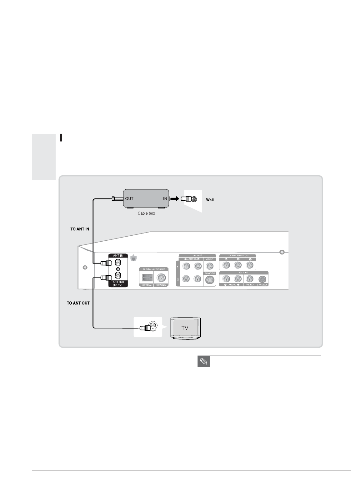
Operating Instructions
12-6
Connecting &
Setting Up
16 - English
Antenna + Cable box + DVD Recorder + TV : Cable box with many scrambled
channels
You can record channels by selecting the channel on the cable box. You cannot record one channel while watching
another channel. Be sure that the cable box is turned on.
■
The VHF/UHF ANT (RF) OUT jack of this
product sends only signals received through
the antenna. It does not output Audio/Video
signals. You must connect Audio/Video cables
to view Video from the unit.
(i.e. DVD playback)
NOTE
Samsung Electronics
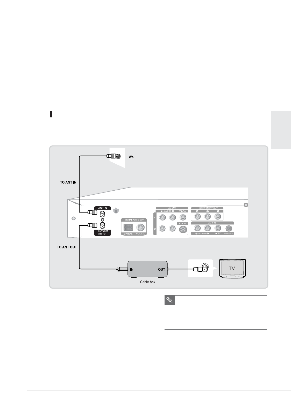
Operating Instructions
12-7
Connecting &
Setting Up
English - 17
Antenna + DVD Recorder + Cable box + TV : Cable box with a few scrambled
channels
You can record non-scrambled channels by selecting the channel on the DVD Recorder. You cannot record scrambled
channels that require a cable box.
■
The VHF/UHF ANT (RF) OUT jack of this
product sends only signals received through
the antenna. It does not output Audio/Video
signals. You must connect Audio/Video cables
to view Video from the unit.
(i.e. DVD playback)
NOTE
Samsung Electronics
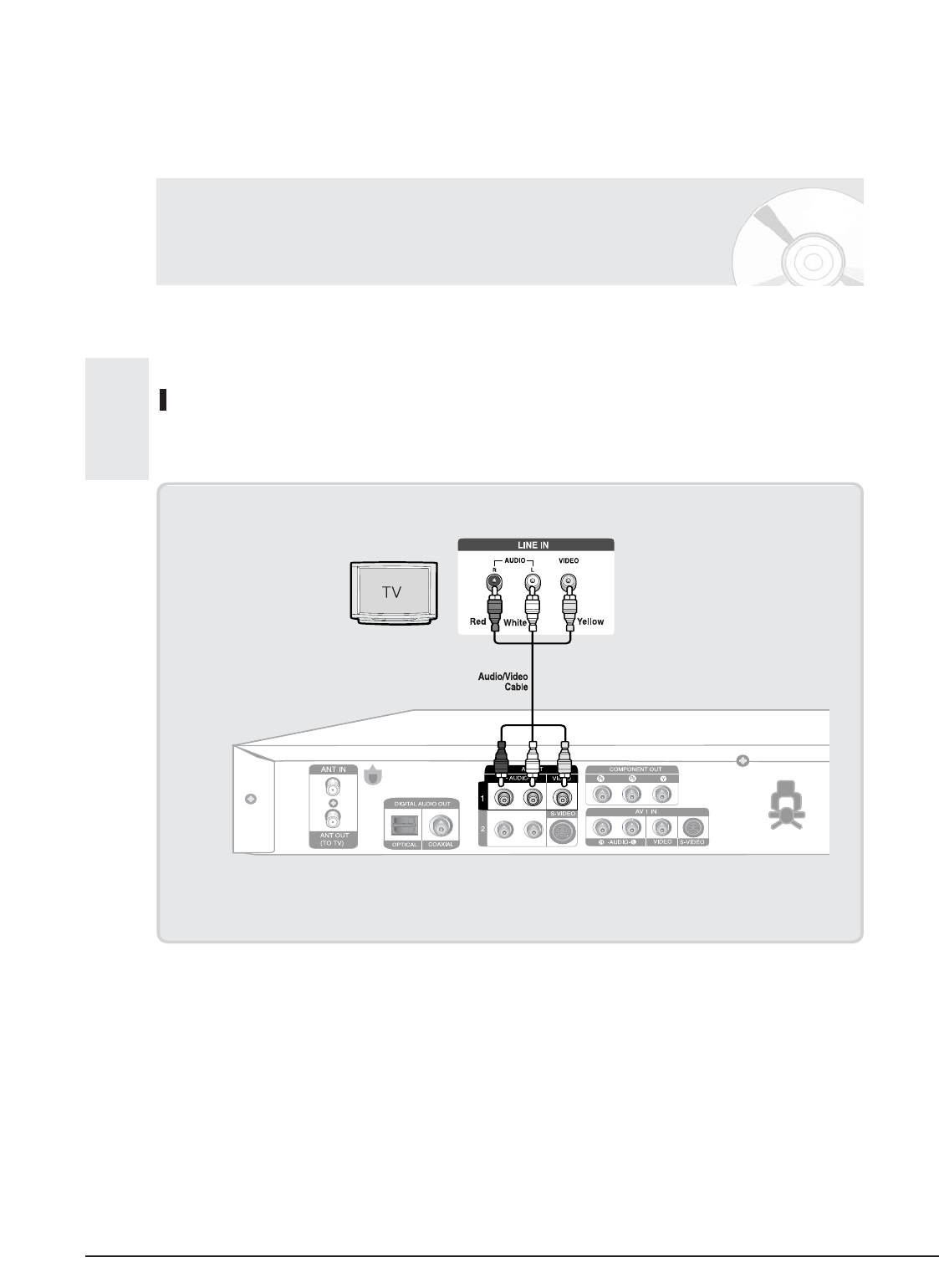
Operating Instructions
12-8
Connecting &
Setting Up
18 - English
Step 2 : Connecting the Video Cable
There are several ways to connect your DVD Recorder. Select one of the video connections on the following pages.
The VHF/UHF RF OUT jack of this product sends only signals received through the antenna. It does not output
audio/video signals. You must use one of the following audio/video connections on this unit.
Connecting to a Video input jack
Connect a video(yellow) cable between the VIDEO(yellow) OUT jack on DVD Recorder and VIDEO(yellow) IN jack on
the TV (or AV amplifier).
• You will enjoy normal quality images.
• Connect audio cables(white and red) between the
AUDIO OUT jacks on the DVD Recorder and AUDIO
IN jacks on your TV(or AV amplifier).
(See pages 21 ~ 23)
Samsung Electronics
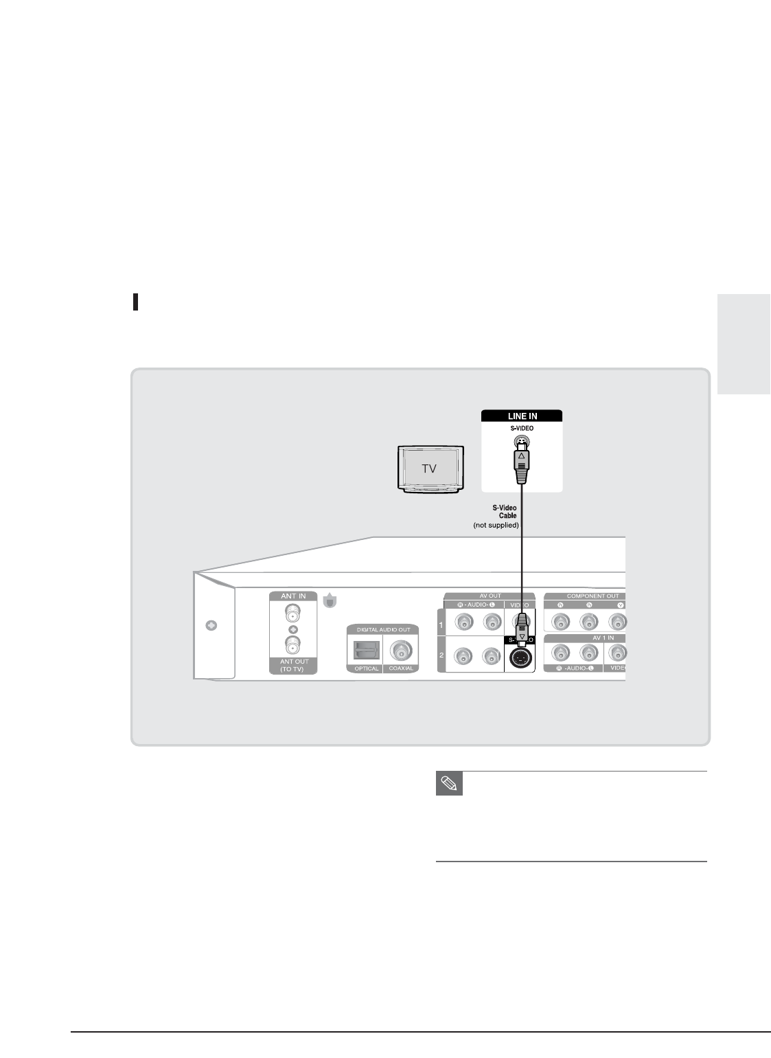
Operating Instructions
12-9
Connecting &
Setting Up
English - 19
• You will enjoy high quality images. S-Video separates
the picture element into black and white (Y) and color
(C) signals to present clearer images than regular
video input mode.
• Connect audio cables(white and red) between the
AUDIO OUT jacks on the DVD Recorder and AUDIO
IN jacks on TV(or AV amplifier).
(See pages 21 ~ 23)
Connecting to an S-Video input jack
Connect an S-Video cable(not supplied) between the S-VIDEO OUT jack on DVD Recorder and S-VIDEO IN jack on
your TV (or AV amplifier).
■
S-Video or Component video outputs are
available only if your TV supports S-Video
input or Component video input, respectively.
If S-Video or Component video output does
not work, check the TV connections and the
TV input selection settings.
NOTE
Samsung Electronics
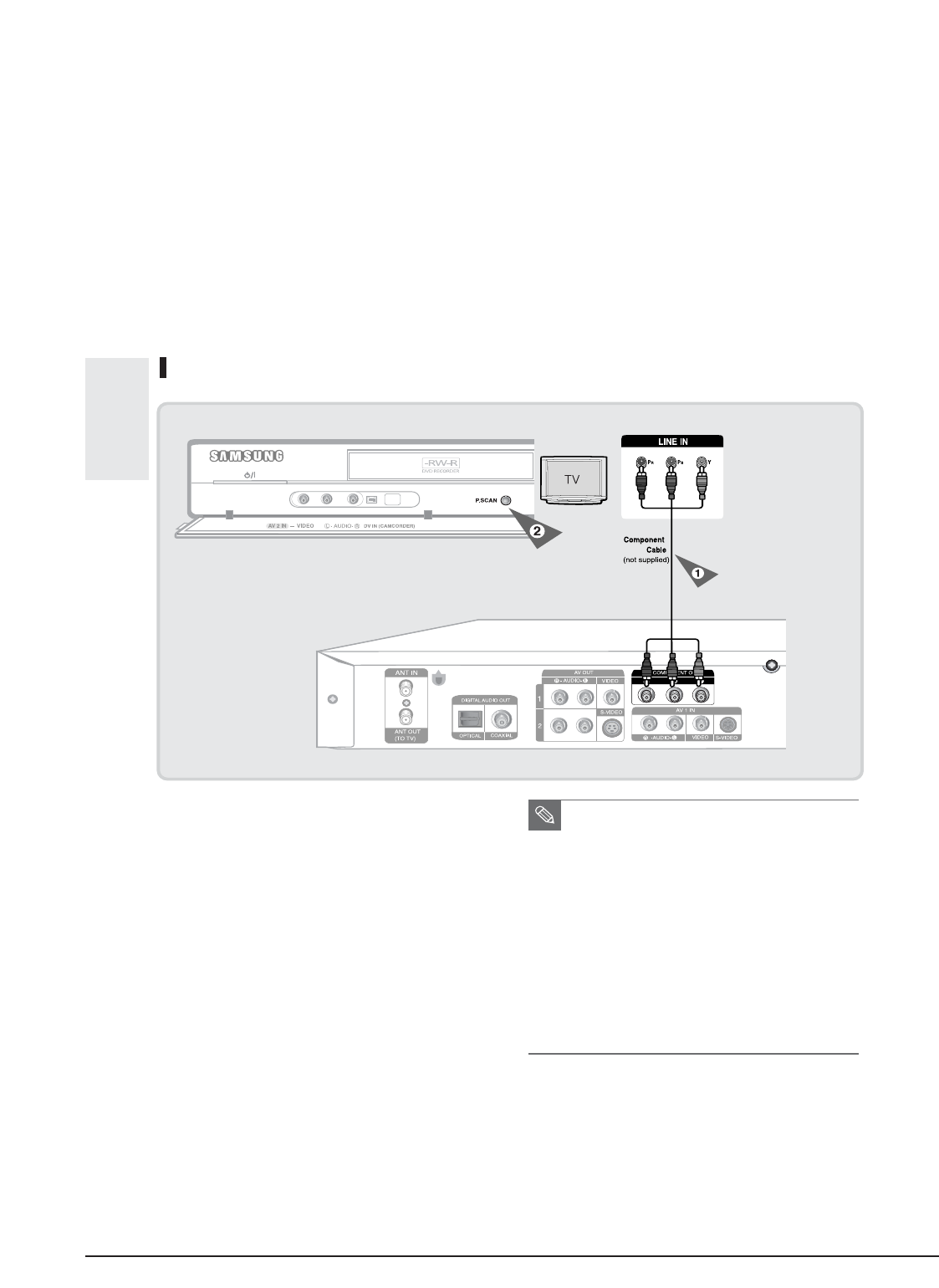
Operating Instructions
12-10
Connecting &
Setting Up
20 - English
Connecting to Component video input jacks (Y,P
B
,P
R
)
1. Connect Component video cables(not supplied)
between the COMPONENT OUT(Y,P
B
,P
R
) jacks on
DVD Recorder and COMPONENT IN(Y,P
B
,P
R
) jacks
on your TV (or AV amplifier).
2. If the connected TV supports Progressive Scan,
press the P.SCAN button on the front of the DVD
Recorder to enjoy best quality video.
Pressing the P.SCAN button switches Progressive
(480p) / Interlace (480i) scan mode in turn.
• You will enjoy best quality accurate color reproduction
images. Component video separates the picture
element into black and white(Y), blue(P
B
), red(P
R
)
signals to present clear and clean images.
• Connect audio cables(white and red) between the
AUDIO OUT jacks on the DVD Recorder and AUDIO
IN jacks on TV(or AV amplifier).
(See pages 21 ~ 23)
■ Compared to standard interlaced video, progressive
scan doubles the amount of video lines fed to your
TV, resulting in a more stable, flicker-free, and clear
image than interlaced video. The progressive scan
video output jack is used in progressive output
mode. This is only available with TVs that support
progressive scan.
■ Progressive Scan Output (480p).
Not all high definition television sets are fully
compatible with this product. If the 480p progressive
scan picture is not satisfactory, press the P.SCAN
button on the unit to switch to the Interlace mode.
If there are questions regarding TV set compatibility
with this model, please contact our customer
service center at 1-800-SAMSUNG.
NOTE
Samsung Electronics
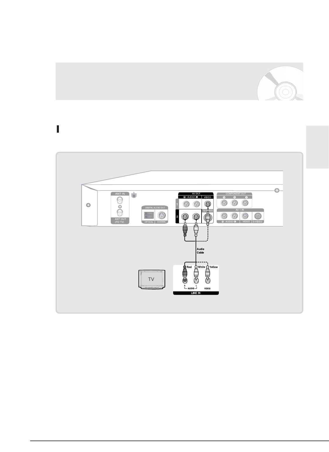
Operating Instructions
12-11
Connecting &
Setting Up
English - 21
Step 3 : Connecting the Audio Cable
There are several ways to connect your DVD Recorder. Select one of the audio connections on the following pages.
Connecting to your TV
This connection will use your TV’s speakers.
Samsung Electronics
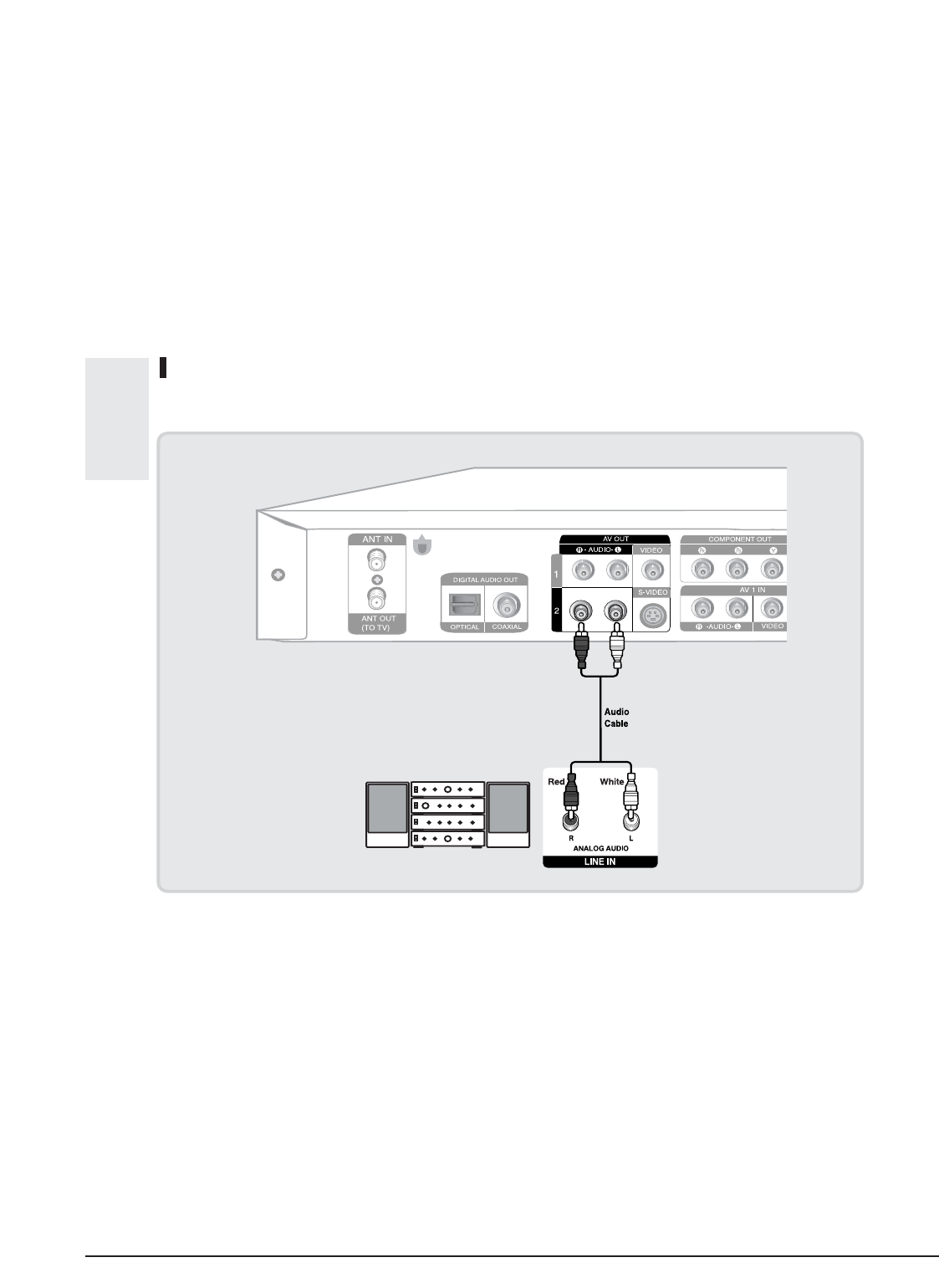
Operating Instructions
12-12
Connecting &
Setting Up
22 - English
Connecting to a stereo amplifier with analog input jacks
If your stereo amplifier only has AUDIO INPUT jacks(L and R), use the AUDIO OUT jacks.
Samsung Electronics
Operating Instructions
12-13
Connecting &
Setting Up
English - 23
Connecting to an AV amplifier with a digital input jack
If your AV amplifier has a Dolby Digital or DTS decoder and a digital input jack, use this connection. To enjoy Dolby
Digital or DTS sound, you will need to set up the audio settings. (See pages 32~33)
Manufactured under license from Dolby
Laboratories. “Dolby” and the double-D symbol are
trademarks of Dolby Laboratories.
“DTS” and “DTS Digital Out” are trademarks of
DTS, Inc.
Samsung Electronics
Operating Instructions
12-14
Connecting &
Setting Up
24 - English
Step 4 : Connecting External Devices
This allows you to connect your DVD Recorder to other external devices and view or record their outputs.
Connecting a VCR, Set-Top Box(STB) or DVD Player to the AV 1 IN jacks
Connecting a VCR or external device to the AV 1 IN jacks of the DVD Recorder.
You can record from connected equipment (VCR, STB or DVD Player).
Samsung Electronics
Operating Instructions
12-15
Connecting &
Setting Up
Connecting a Camcorder to the AV 2 IN jacks
You can also use the AV 2 IN jacks on the front panel of the DVD Recorder. You can record from connected
equipment, such as a camcorder.
When an input source is inserted into AV 2 while watching TV, the input will be switched to AV 2 automatically.
English - 25
Samsung Electronics
Operating Instructions
12-16
Connecting &
Setting Up
26 - English
■ If the input is not selected automatically, press the
INPUT SEL. button on the remote control to select
the DV input.
■ Check your camcorder's owner's manual to see
how to use the camcorder in this mode.
NOTE
Connecting a Camcorder to the DV IN jack
If your camcorder has a DV output jack, connect it to the DV input jack of your DVD Recorder.
(See page 48)
Samsung Electronics
Operating Instructions
12-17
Connecting &
Setting Up
English - 27
Step 5 : Connecting the
Power Cord
■
After the current time is set automatically, the
recorder will perform Auto Channel Memory for
about 3 minutes. If power is on before finishing
the Auto Channel Memory process, Auto
Channel Memory will stop.
In this case, do Auto Channel Memory from
MENU(see page 31).
NOTE
After all connections are complete, plug the power cord
in the wall outlet.
“Auto” appears in the panel display. This means
that the current time is being set automatically
(Auto Program) through the antenna under
connection and also the channel is being set.
The setup may take a few minutes.
When the DVD Recorder operates normally, the current time
is automatically set and displayed in the front panel display.
Step 6 : Preparing the
Remote Control
Install Batteries in the Remote Control
•
Open the battery cover on the back of the remote.
•
Insert two AAA batteries. Make sure that the polarities
(+ and -) are aligned correctly.
•
Replace the battery cover.
If the remote control does not operate properly:
•
Check the polarity + - of the batteries (Dry-Cell)
•
Check if the batteries are drained.
•
Check if remote sensor is blocked by obstacles.
•
Check if there is any fluorescent lighting nearby.
Dispose of batteries according to local environmental
regulations. Do not put them in the household trash.
Samsung Electronics

Operating Instructions
12-18 Samsung Electronics
MEMO
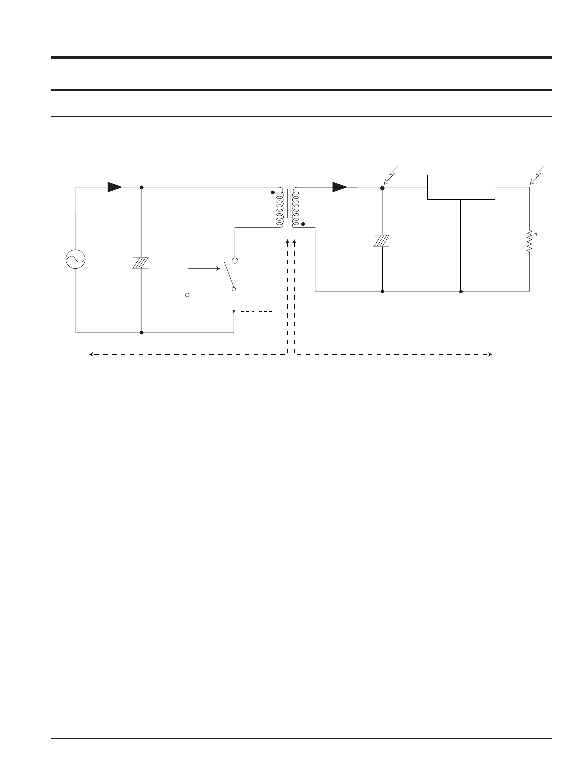
Samsung Electronics 13-1
13. Circuit Operating Descriptions
13-1 Power
13-1-1 About S.M.P.S (Ringing Choke Converter Method)
◆Terms
1) 1st : Common power input to 1st winding.
2) 2nd : Circuit followings output winding of transformer.
3) f (Frequency) : Switching frequency (T : Switching cycle)
4) Duty : (Ton/T) x 100
Transformer Vout
(Np)
(Vp)
Switch
Vs switch
I switch
Vin
ON/OFF Control
+
–+
–
+
+
+
–
(Vs)
(Ns)
Vreg
REGULATOR
Fig. 13-1
13-1-2 Circuit description [FLY-Back RCC(Ringing Choke Converter)] Control
(a) AC Power Rectification/Smoothing Terminal
1) PADT1, PADT2, PADT3, PADT4 : Convert AC power to DC (Wave rectification).
2) PRCU1 : Smooth the voltage converted to DC.
3) PALT1, PALT2, PACT1, PACT2 : Noise removal at power input/output.
4) PLRU1 : Rush current limit resistance at the momemt of power cord insertion.
· Without PLRT1, the bridge diode might be damaged as the rush current increases.
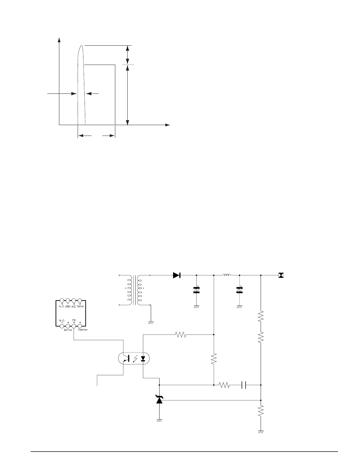
Circuit Operating Descriptions
13-2 Samsung Electronics
0
Vswitch
dt
Toff
t
Inverted power
by leakage
inductance
Fig. 13-2
(b) SNUBBER Circuit :
PSRZ1, PSRZ2, PSCX1, PSCZ2, PSDZ1
1) Prevent residual high voltage at the terminals of
switch during switch off/Suppress noise.
High inverted power occurs at switch off,
because of the 1st winding of transformer :
(V=-L1 xdi/dt. L1 : Leakage Induction)
A very high residual voltage exist on both terminals
of PQIZ1 because dt is a very short.
2) SNUBBER circuit protects PQIZ1 from damage
through leakage voltage suppression by RC,
(Charges the leakage voltage to PSDZ1 and PSCX1
and discharges to PSRZ1, PSRZ2).
3) PSCZ2 : For noise removal
(c) PQIZ1 Vcc circuit
1) PQIZ1 Vcc : PVRL4, PVDL1, PVCL1
!Use the output of transformer as Vcc,because the current starts to flow into transformer while PQIZ1 is
active
@Rectify to PVDL1 and smooth to PVCL1.
#Use the output of transformer as PQIZ1 Vcc : The loads are different before and after PQIZ1 driving.
(Vcc of PQIZ1 decreases below OFF voltage , using only the resistance dut to lode increase after PQIZ1
driving.)
(d) Feedback Control Circuit
ICE3B2065P
TRANS(PQTZ1) PPDF1 PPLF1
PFRF5
PFRF3
PFID1
PBIZ1
PFRF1
PFRF2
PFRF6
PFCF1
PFRF4
PPCF3
PPC1
5.8V
Fig. 13-3
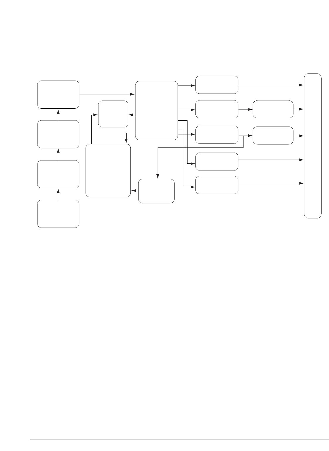
Circuit Operating Descriptions
Samsung Electronics 13-3
1) F/B terminal of PQIZ1 determines output duty cyle.
2) C-E (Collector-Emitter) of PQIZ1 and F/B potential of PQIZ1 are same.
13-1-3 Internal Block Diagram (Internal Block Diagram of S.M.P.S. Circuit)
Smoothing
Circuit
Rectified Circuit
Line Filter
Power IN
(110V)
Noise
Removal
(SNUBBER)
PWM Control
Circuit
(ICE3B2065P)
Converter
Voltage
Detection
Circuit
3.0V Rectified
Smoothing Circuit
5.4V Rectified
Smoothing Circuit
12V Rectified
Smoothing Circuit
3.3V Rectified
Smoothing Circuit
12V Rectified
VoltageCircuit
5V Rectified
VoltageCircuit
O
U
T
P
U
T
33V Rectified
Smoothing Circuit
Fig. 13-4
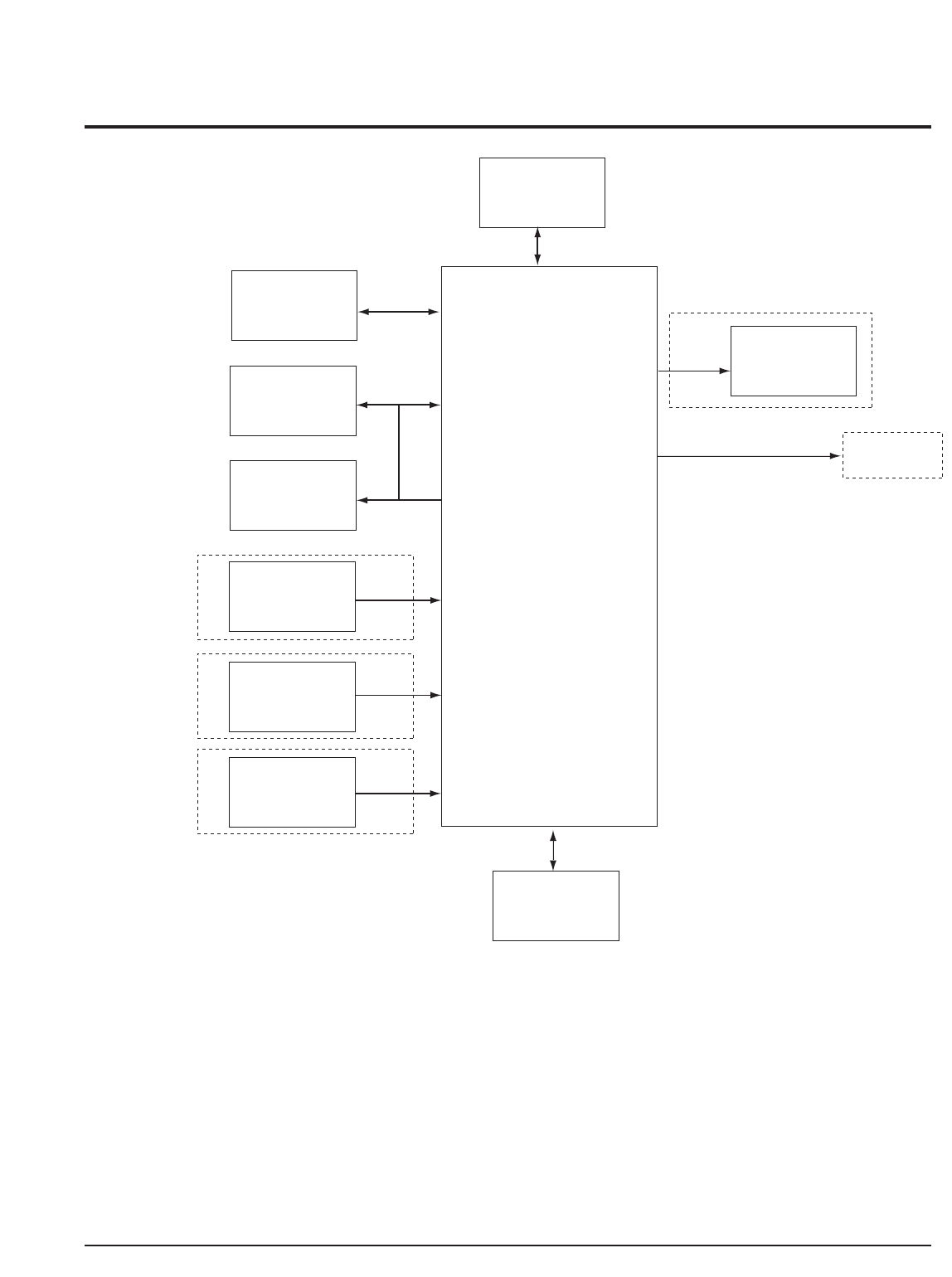
Circuit Operating Descriptions
13-4 Samsung Electronics
13-2 AV Codec
DVD
MULTI DRIVE
(SERVO)
DIC2
K4H561638F
(DDR SDRAM)
DIC4,DIC5
LVC16374 x2
DIC3
39V51601
(Flash Memory)
FIC1
IEEE 1934
(DV Input) Block
Audio Input
Block
Video Input
Block
TSB41AB2PAP
(1394 PHY)
AIC2
PCM1802
(AUDIO A/D)
IC601
MN101DF06
(Front MICOM)
AIC1
PCM1753KE
(AUDIO D/A)
VIC1
TW9906
(VIDEO DEC)
SDRAM I/F
AUDIO OUT
HOST I/F
VIDEO OUT
DIC1
S5L3200
(A/V CODEC)
DV I/F
AUDIO IN
VIDEO IN
Front Panel I/F
Y,Pb,Pr, Y/C, CVBS
I2S
32bit
16bit
8bit
12S
ITU-R656
ATAPI
Audio output block
Video output
block
Fig. 13-5
· Main system control · ATAPI interface with DVD-Multi Drive
· A/V Encoding/Decoding · Analog Progressive/interlaced video output
· Transcoding/rating
· IEEE 1394 link layer function

Circuit Operating Descriptions
Samsung Electronics 13-5
13-2-1 GENERAL DESCRIPTION
Samsung S5L3200 MPEG AV Codec is designed to provide a cost-effective, low power size and high performance
DVD recorder solution for DVD-VR, DVD-video, DVD-audio & many of CD applications. To reduce total system
cost, The S5L3200 also provides the following features: a front-end controller, a back-end decoder, a control CPU
with separate 4KB instruction and 4KB data cache, an improved audio DSP, a programmable video encoder with
a dual output capability of interlaced and progressive scan, DDR memory controller, 4-channel timers with PWM,
I/O ports, 5-channel 10-bit DACs, 2-channel UARTs with handshake, IIC bus interface, IIS bus interface, SPI, dual
ATAPI, IEEE1394, USB 1.1 Host I/F and PLL for clock generation.
13-2-2 A/V Processor (DIC1) Functional Description
1) RISC processor architecture
· ARM940T core processor
· Fully 16/32-bit RISC architecture
· Harvard cache architecture with separate 4KB instruction and 4KB data cache
· Protection unit to partition memory and set individual protection attributes for each partition
· Up to 200 MHz operating frequency.
2) Memory controller
· Address space: 256 M-byte for each bank (total 1 Gbyte space)
· Supports programmable 8/16-bit data bus width for ROM/SRAM interface
· Supports 16-bit data bus width for DDR-SDRAM interface
· 3 memory banks; 2 memory banks for ROM, SRAM etc, 1 memory bank for SDRAM
· Fully programmable access cycles for all memory banks
· Supports external wait signal to expand the bus cycle.
3) Cache memory
· 64 way set-associative cache with I-cache (4KB) and Dcache (4KB)
· 8-words per line with one valid bit and two dirty bits per line
· Pseudo random or round robin replacement algorithm
· Write through or write back cache operation to update the main memory
· Write buffer can hold 8 words of data and four addresses.
Clock & power manager
· Low power consumption
· On-chip PLLs
· Clock can be fed selectively to each function block by software
· Power mode: normal, slow and idle mode (normal mode: normal operating mode, slow mode:
low frequencclock without PLL, idle mode: stop CPU clock only)
· Wake up by interrupt from idle mode.

Circuit Operating Descriptions
13-6 Samsung Electronics
4) Interrupt controller
· 32 interrupt sources (watch dog timer, 4 timers, UARTs, 8 external interrupts, IIC, IIS, SPI, IR, etc.)
· Edge detect mode on external interrupt source
· Programmable polarity of rising and falling
· Supports FIQ (fast interrupt request) for very urgent interrupt request.
5) Video pre-processor
· Noise reduction by motion-compensated temporal filtering
· Bitmap generation for motion estimation of MPEG encoder
· Scene change detection.
6) MPEG video encoder
· Encodes MPEG1 & MPEG2 video stream (MP@ML)
· Efficient motion estimation by hierarchical motion vector search and binary image matching.
7) MPEG video decoder
· Decodes MPEG1 & MPEG2 video stream (MP@ML)
· Error detection and autonomous error concealment.
8) Audio DSP
· Decodes Dolby AC-3, MPEG1, MPEG2, DTS, MLP, HDCD, AAC and WMA
· Supports down mix
· MAC2424 for audio signal processing
– 24-bit high performance fixed-point DSP coprocessor, 24x24 MAC operation in 1 cycle.
– 2 multiplier accumulator registers, 4 general accumulator registers, and 8 pointer registers.

Circuit Operating Descriptions
Samsung Electronics 13-7
13-3 SERVO (DVP Multi Drive)
1) Pick-Up
Data in the disc is processed from the optical pick-up unit (OPU). OPU includes the Elantec chip (EL6912c)
which is a highly integrated laser diode driver designed to support multi-standard writable optical drives. This
chip also has an IV amplifier with concurrent read and write sampling. The architecture allows reprogramming
of the timers to support different media DVD or CD standards, and different speed.
2) A-Chip
A chip is RF processor. This module performs RF signal processing which includes RFIP, RFIN, AGC, RF equal
izer. This processor is able to detect tracking error, focus error and various signals such as CE, PE, SBAD,
DEFECT, BCA, MIRROR, Wobble, TZC, RC, and RECD.
3) C-Chip
C-Chip is composed of DP1, PRML and WS.
First, the Data processor1 (DP1) performs EFM/EFM+ Demodulation and data is stored in the buffer
memory in data processor2 (DP2). DVD data in this buffer is transferred to CSS/ATAPI through
error-correction code
(ECC), descramble process and error detection code (EDC).
Second, WS performs the following processes.
! Delay compensation using Shift register
@ Sample/Hold pulse generation
# I/V Gain Control
$ Providing clock for RF chip
% OPC Control signal generation
Lastly, PRML completes the adaptive EQ/VD and Digital PLL.
4) D-Chip
D-Chip consists of Servo DSP, DP2 and 1Mbit memory. Servo DSP is dealing with controlling the servo-mecha
nism in DVD recorder. Servo-DSP has the following features.
! Bulit-in 10Bit ADC(8ch), DAC(3ch) and PWM(7ch)
@ Step Motor Control Logic: Macro/Micro Step
# Track Counter: long distance velocity control direct seek
$ Shock/Defect detection
% Header (DVD-RAM)/Land Pre-Pit (DVD-R/RW) Detection
^ Several Servo Monitor Signal Detection
& RF IC Interface
* Micom Interface
( Digital Servo Control of focus, tracking, sled and seek
) Disc Auto-Detection
1 Automatic Adjustment of the offset, balance and gain of Focus and Tracking Signal
2 Direct Seek with Velocity Control
3 Step Motor Control: Macro Seek
4 De-Track and Lens Shift Detection and Compensation
5 Center Error Control
6 DVD Layer Jump
7 Tilt Detect and Compensation
DP2 performs High Speed ECC and CD DA Decoder.
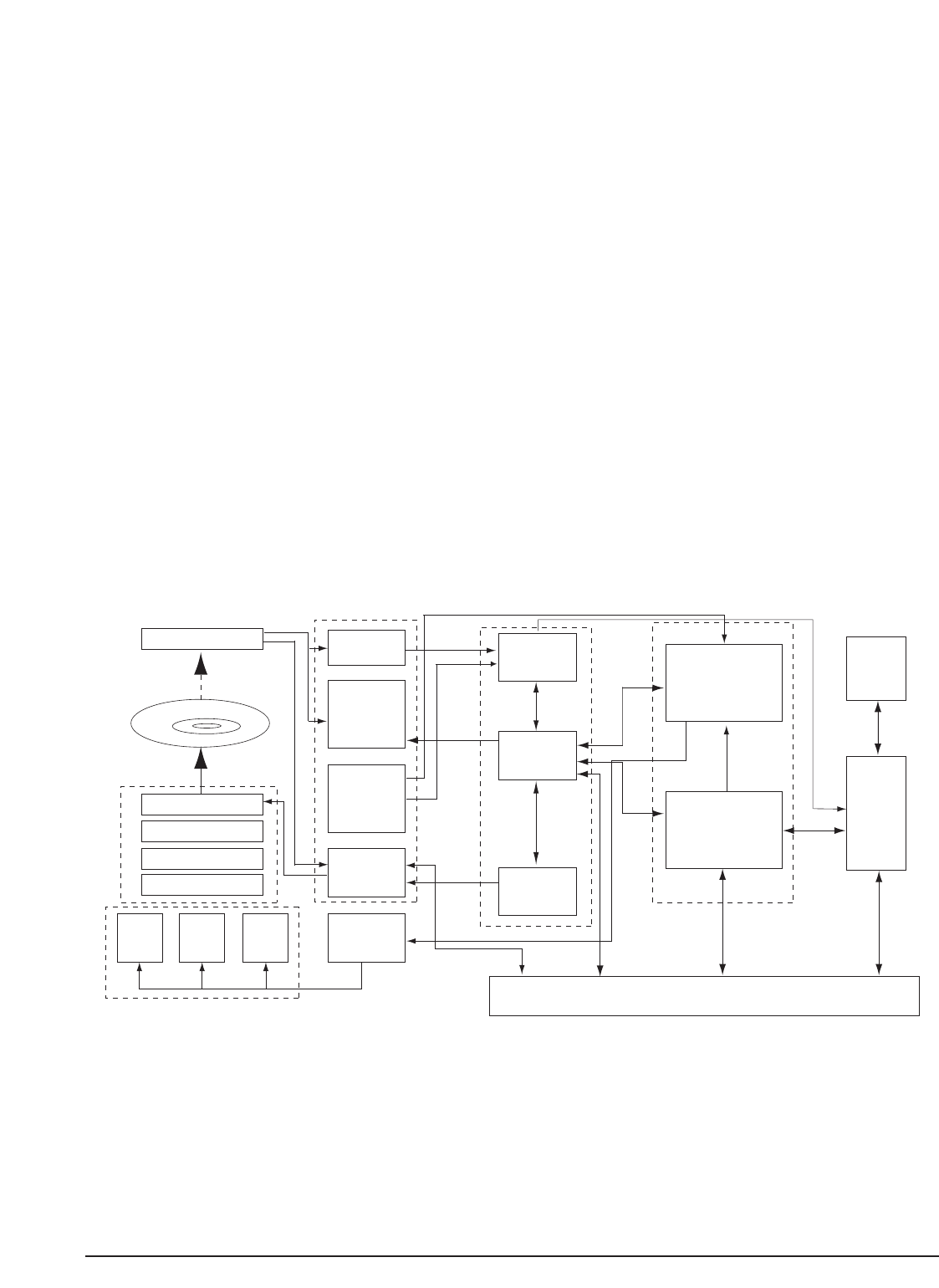
Circuit Operating Descriptions
13-8 Samsung Electronics
5) ATAPI Controller
ATAPI (ATA Packet Interface) the standard interface protocol used to connect the CD/DVD Drive to IDE inter
face. Data from the front-end is processed to back-end through this ATAPI protocol. Sanyo chip (LC98600CT-
XB0) is utilized for ATAPI interface. LC98600CT-XB0 has the following features.
! ECC and EDC correction/addition for CD-ROM data
@ Subcode decoding/encoding
# Spindle servo control
$ CLV/CAV servo control using ATIP data
% ATIP decoding and CRC check functions
^Providing random EFM output for PCA use
& High-accuracy write strategy signal output enabled (CD-R 52x)
* Buffer RAM can be accessed by the microcontroller through the LC98600CT-XB0
( Built-in ATA-PI(IDE) interface (supports Ultra DMA modes 0,1, and 2)
) 52x decoding speed/52x encoding speed supported with 33.8688Mhz
1 Maximum transfer speed PIO mode: 16.6 MB/s (with IORDY), Ultra-DMA: 66MB/s (with DMARQ)
2 User can freely set the CD main channel, C2 flag, and subcode areas in buffer RAM
3 Built-in batch transfer function for transferring (CD main channel, C2 flag, etc., in a single operation)
4 Built-in multi-transfer function (allows multiple blocks to be sent to the host automatically in a single
operation)
FPD,PD,I/V amp
LD,LD Driver
Focus Actuator
Tracking Actuator
TILT Actuator
Sled
Motor
Spindle
Motor
Tray
Motor
Motor
Driver
PRML
ENDEC
WRITE
STRATEGY
APC & OPC
Miscellaneous
Signal
(DFT/LPP
/WOBBLE)
Servo Error
(FE/TE/CE/PE
SBAD/RC/TILT)
RF Signal
(AGC/EQ)
SERVO
Processor
ECC
Processor
HOST
ATAPI chip
(ZIC1)
MICOM (MIC1)
A.chip (RIC1) C.chip (CIC1) D.chip (DIC1)
Pick up
Deck
Fig. 13-6
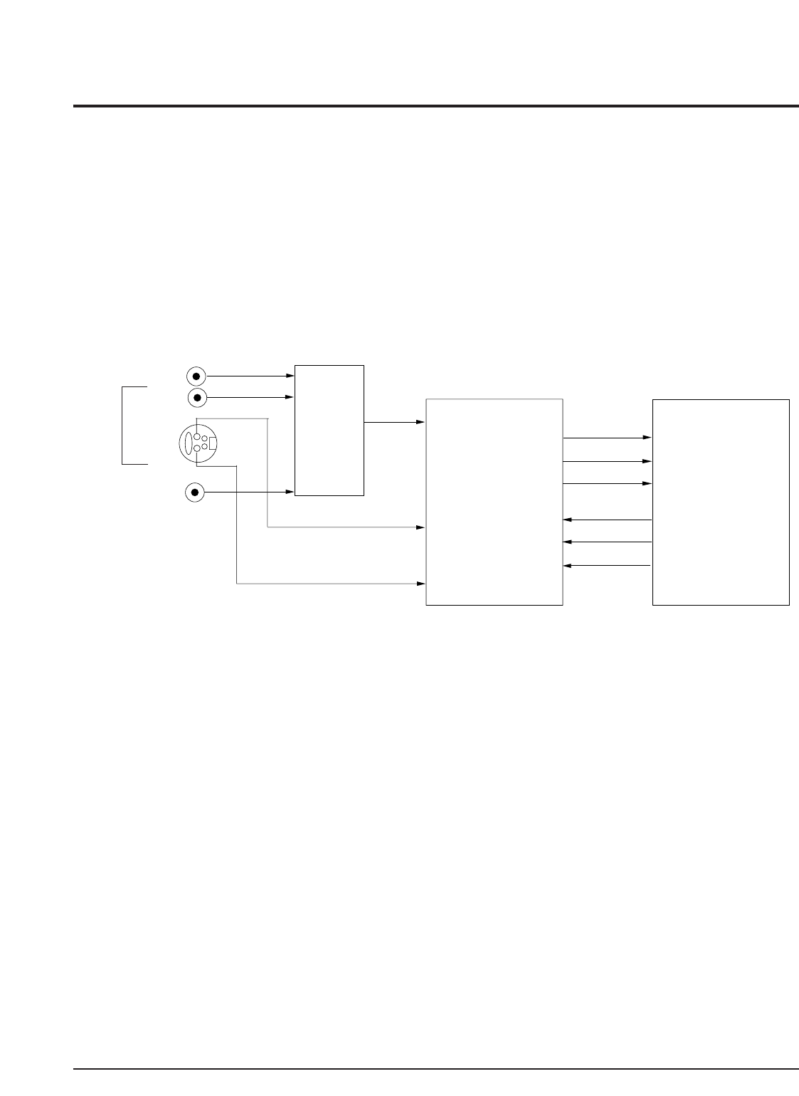
Circuit Operating Descriptions
Samsung Electronics 13-9
13-4 Video Input
13-4-1 Video Input Outline
DVD-R129 is the two AV Video input. AV 1 Video input is CVBS1 & S-Video1 at the Rear Panel. Line 2 Video
input is CVBS2 at the Front Panel.
The analog Video signal select AV 1 or AV 2 by the IC601 (Front Micom).
TIC1 (Video Decoder) diverges from the 27MHz crystal, then generates ITU-R656 (10bits) and
27MHz clock. VIC1 (Video Decoder) does closed caption, copy guard detect processing and A/D conversion
of analog Video signal converted into 11bit Digital Video signal (ITU-R656 Format) is outputted via DIC1 (MPEG2
Decoder &Encoder with video Encoder) of digital part.
AV 1
(Rear)
Video
Input
CVBS 1
Y1
C1
AV 2
(Front)
Video
Input
CVBS2
MM1113
Analog MUX
IC702
Video
Decoder
VIC1
A/V CODEC
DIC1
CVBS
Y
C
ITU-R656 10bit
27MHz
V_SYNC
SDA
SCL
/RSTAV
CVBS
RF
Fig. 13-7
13-4-2 Analog Mux (MM1113)
IC702 is Analog Mux.
As Pin 2, 4 of the IC702 are controlled by the Front Micom, IC702 select RF OF CVBS(Pin1)
Line1 of CVBS[Pin3] and AV2 of CVBS[Pin 5].
The analog Video Signal of IC201 output is selected by the IC601 via VIC1(Video Decoder : TW9906) of analog
Video Input parts.

Circuit Operating Descriptions
13-10 Samsung Electronics
13-4-3 NTSC/PAL Video Decoder (TW9906 : Video Decoder)
The VIC1 (Video Decoder : TW9906) device is a high quality, single-chip digital video decoder that digitizes and
decodes all popular baseband analog video formats into digital component video. The VIC1 (Video Decoder :
TW9906) supports the analog-to-digital (A/D) conversion of component RGB and YPbPr signals, as well as the
A/D conversion and decoding of NTSC, PAL and SECAM composite and S-video into component YCbCr.
This VIC1 (Video Decoder : TW9906) includes four 10-bit 30-MSPS A/D converters. and A/D conversion of 10bit
analog Video signal converted into Digital Video signal (ITU-R656 Format) is outputted via DIC1 (MPEG2
Decoder & Encoder with video Encoder) of digital part.
The following output formats supply 10-bit 4:2:2 YCbCr to the DIC1 (MPEG2 Decoder & Encoder with video
Encoder) of digital part.
On CVBS and S-video inputs, the user can control video characteristics such as contrast, Brightness, saturation,
and hue via an I2C DIC1 port [PIN V17, V18] interface.
The TW9906 decoder includes methods for advanced vertical blanking interval (VBI) data retrieval. The VBI data
processor (VDP) slices, parses, and performs error checking on teletext, closed caption (CC), Copy Guard Detect
Processing and other VBI data.
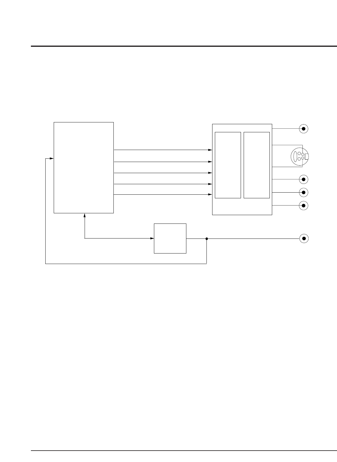
Circuit Operating Descriptions
Samsung Electronics 13-11
13-5 Video Output
13-5-2 NTSC/PAL Digital
DIC1 inputted from pin E1 with 13.5MHz generates HSYNC and VSYNC which are based on video signal. DIC1
is synchronous signals with decoded video signal.
The above signals, which are CVBS (Composite Video Burst Synchronized), Y(S_Video), C(S_Video),
Y(Component)/G(Green), Cr(component)/R(Red), Cb(component)/B(Blue), are selectively outputted 480I(inter-
laced Video Output), 480P(progressive Video Output) by the Pront button DIC1 adopts 10bit D/A converter.
DIC1 perform video en-coding as well as copy protection.
Fig. 13-8
A/V CODEC
DIC1
Y
C
Y
Cb
Cr
MM1692
VIC1
6dB
AMP
&
75ohm
Drive
LOW
PASS
FILTER
(6MHz)
CVBS
Y
C
Y
Cb
Cr
Front
Micom
IC601
PSO
13-5-1 Outline
DIC1 (MPEG2 Decoder & Encoder with video Encoder) diverges from the 13.5MHz crystal, then generates
VSYNC and HSYNC.
DIC1 (MPEG2 Decoder & Encoder with video Encoder) does RGB encoding, copy guard processing and D/A
conversion of 10bit Video signal converted into analog signal is outputted via amplifer of
analog part.

Circuit Operating Descriptions
13-12 Samsung Electronics
13-5-3 Amplifier (MM1692)
VIC1 of JACK PCB is 6dB amplifier.
Based on CVBS signal, the final output level must be 2Vpp without 75ohm terminal resistance.
Because the level of video encoder output is only 1Vpp, the level is adjusted with the special
amplifier.
When mute of pin 5 is high active, if the pin is floating and connect to power, the output
signal is never outputted.
Y, C, Y(R), Cb(B), Cr(R) outputted from video encoder are inputted to VIC1 [Pin14, 16, 13, 12,
11] respectively. And CVBS Output[Pin 15] is made by Y & C Mixing signal.
The signal to which gain is adjusted by amplifier is outputted from jack via 75ohm Resistance
(VDR1,2,4,5,6,).
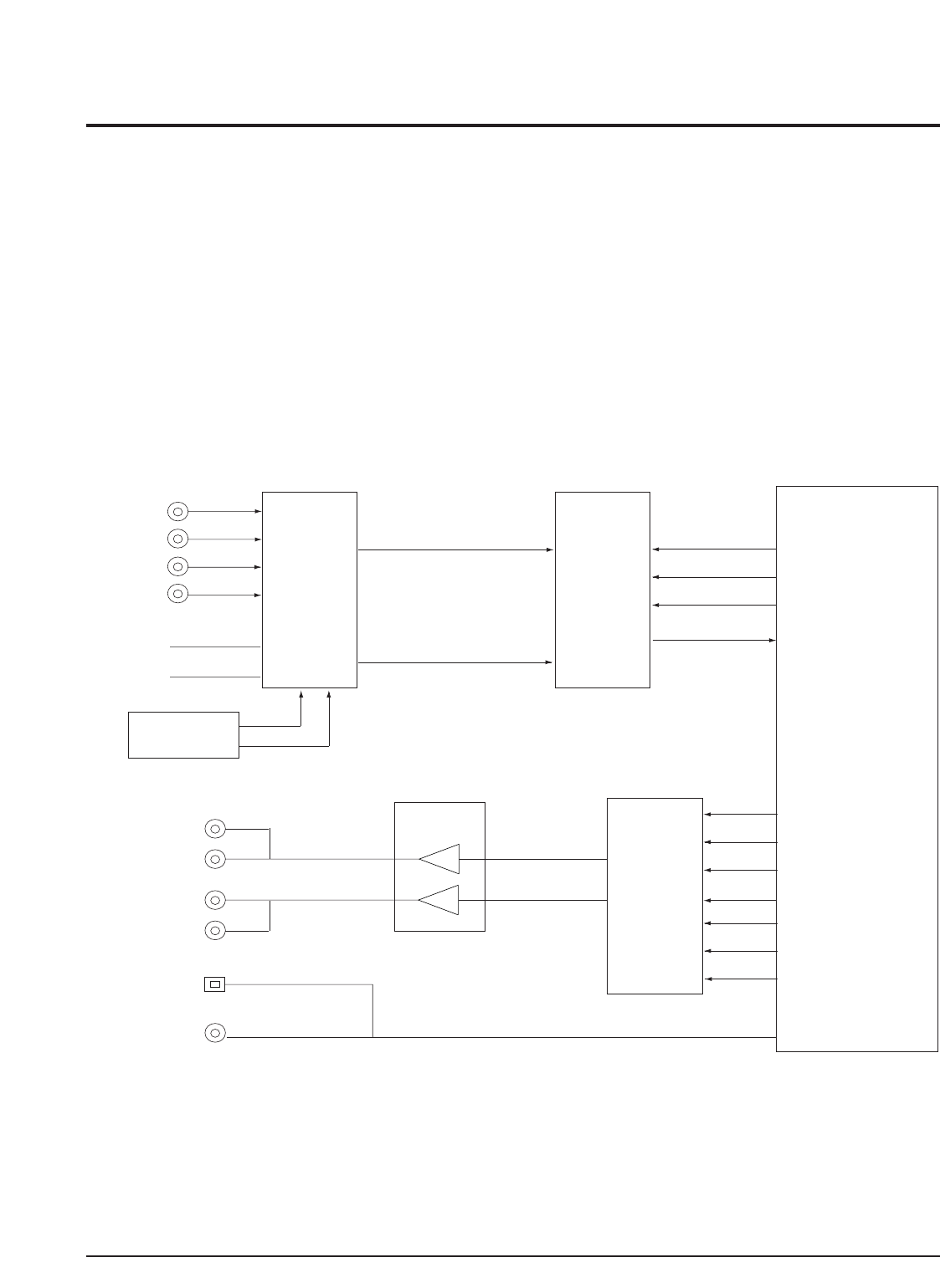
Circuit Operating Descriptions
Samsung Electronics 13-13
13-6 Audio
13-6-1 Input Block
This Model has two stereo line input terminals. and internal TV-audio from RF Tuner Block.
These three Analog audio signal source are converted to digital data by Input Block.
Input Block has a Multiplexer (IC203), A/D converter (AIC2).
IC203 change it’s output by selection control signal from IC601 (Front Micom).
13-6-2 Output Block
DVD-R129 has two stereo analog line out terminal, and two digital output terminal.
Decoded signal by DIC1 is inputted to AIC1 (D/A Converter), then filtered and amplified by AIC4 (OP-Amp).
And the digital audio signal (IEC-958) is outputted in Optical/Coaxial (S/PDIF) terminal.
AV IN1
(Rear)
L1-in
R1-in
L2-in
L2-in
AV IN2
(Front)
TV Audio
(from tuner
block) RF-R
RF-L
IC203
BU4052
Multiplexer
IC601
(micro controller)
AU5
PCM1803
(Audio A/D
Coverter)
SCKI
BCK
LRCK
DOUT
AV OUT
(Rear)
Optical
Out
Coaxial
Out
AIC4
4560 OP-AMP
AU2
PCM1742KE
(Audio D/A
Coverter)
L-out
R-out
SCKI
BCK
LRCK
DOUT
ML
MC
MD
DIC1
S5L3200
A/V Processor
(Dolby AC-3
Encoder/Decoder)
IEC958 DATA
Fig. 13-9
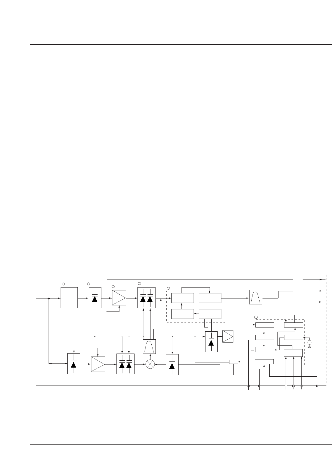
Circuit Operating Descriptions
13-14 Samsung Electronics
13-7 Tuner
1) Low Pass Filter & High Pass Filter
This consists of IF trap circuit and UHF & VHF separation circuit. If the input signal is IF (45.75MHz),
this filter
prevents interference.
2) Single tune
This consists of a filter circuit, RF AMF, impedance conversion circuit, image trap and a single tuning circuit. It
prevents noise and other interference signals. It is very important part which improves NF (noise figure) and
prevents the various of spurious signals.
3) RF AMF
RF AMF is made of FET (Field Effects Transistor). It is controlled by AGC coming from IF DEMOD block.
4) Double tune
It consists of a double tuning circuit to improve characteristic of rejection that results in a better band
characteristic.
5) Mixer IC (Mixer, OSC, PLL)
It consists a VHF and UHF OSC and Mixer circuit. We applied mixer to make better characteristic of rejection,
it shows especially various beat characteristic.
6) PLL IC
The PLL IC plays a role selection of Tuner channel. It was built-in three wire PLL IC, charge pump and band
driver.
The minimum of step frequency is 31.25KH z.
<
<
>
>
Fran
Modulafor
b
a
c
d
e
VHF
8.P.F
VHF
SingleTune VHF
RF Amp
VHF
Double Tune
Mixer IF Amp
OSC 8uffer VHF OSC
IF Single
IF
<>
+B
1/8 Prescaler Band Driver
Prog.Dirlder
Phese Code
Charge Pump
Band Driver
3wice Bas
Recelver
VHF
Single Tune
VHF
-RF Amp
VHF
Double Tune
VHF Mixer
VHF OSC
VHF
OSC Amp
~
VHF OCS
L.P.F
~
~
~
AGC
10 986
15 X-tal
4MHz
1
*()1
4
3
2
1
^&
16 14 13 12
V
L
V
H
U
Fram IF Sectlon
Fram IF Sect lon
TO IF Sect lon
PB TU CLOCK DATA ENABLE LOCK
35
12
1
78 9
Mix IC IC100
fPLL IC
Fig.13-10
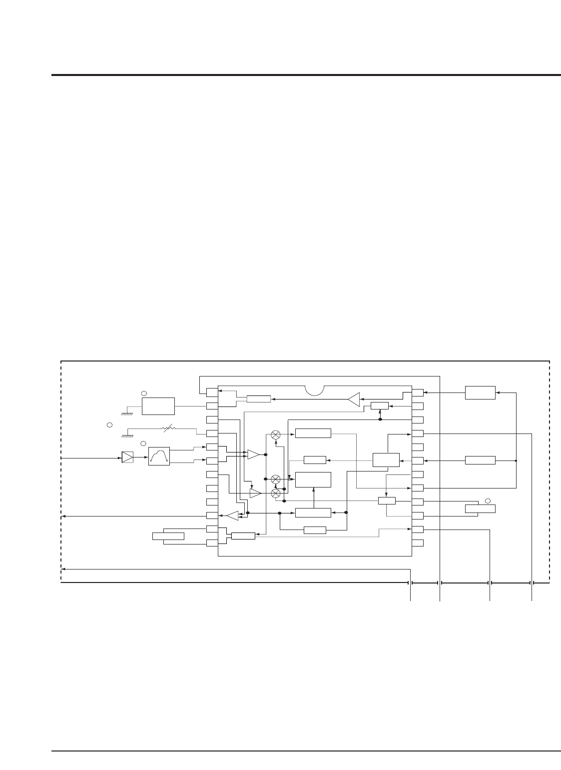
Circuit Operating Descriptions
Samsung Electronics 13-15
13-8 IF
1) SAW FILTER
It passes only needed band of the signal that is converted to IF frequency and decrease the others band to
minimize the effect of adjacent channel.
2) RF AGC Control
It used adjusting to determine RF AGC working point in tuner.
3) VCO Tank
When VCO tank detects PLL, it makes the signal which sets a standard.
4) AFT (Auto Frequency Tuning)
AFT automatically controls the oscillator frequency in the tuner, so that it retains a constant level.
It is a quadrature detection type. The carrier, which is detected from video det is directly input to AFT.
The 90 degree delayed phase signal is input at the same time to AFT and, the results come out.
5) IF AMP
IF signal , which is selected in Saw filter, is amplified in IF amp frequency enough to be detected. The IF amp
has parallel inputs & outputs structure.
FM Det
AFT
Lim Amp
1
2
4
5
6
10
11
12
24
21
19
14
15
16
17
Video Amp
N.S.C
APC Tine
Const SW
Lock Det
IF AGC
EQ.Amp
B/W
VCD
AGC
RF AGC Amp
Pra
Amp Mix
APC
Det
Video Det
4.5 MHz
Tunlng
AFT Tank
SIF filter
4.5MHz
SIF Trap
VCD Tank
3456
+B AUDIO OUT AFT OUT VIDEO OUT
To Tuner Section
RF AGC
To Tuner Section
From
Tuner Section
a
b
c
d
SAM Filter
RF AGC Control
(IF Amp)
Fig. 13-11

Circuit Operating Descriptions
13-16 Samsung Electronics
MEMO

Samsung Electronics 14-1
14-1-1 Comparison between IEEE-1394 and other digital interfaces
Since there are many different interfaces available, for example, RS422, RS644, and USB, vision system integ rators
are very likely to be confused when choos ing the right interface for their application. For the ideal design of a
vision syste m, it is vital to have the righ t bus/inte rface. To make things even more complex, ther e is no easy
answer such as IEEE-1394 is the best choice.
Furthermore, the new CameraLink standard, promoted by compan ies such as Puln ix, Basler AG, and many
frame grabb er companies, seems to be the stat e of the art interface. So why should IEEE-1394 be an alternative?
These questions are as complex as mostvision applicatio ns and there is no simple guideline .
Each of these interfaces offers many benefits and each of them has its individual drawbacks and restric tions. In
the table below, we try to give a brief comparison of the most popular interface systems.
[1] These specs are for a typical 8-bit camera application operating at 20 MHz or at 40 MHz.
[2] 80% of the bus bandwidth is used for image data and 20% is used for parameter data.
[3] 16 wires are used for data bit transfer and two wires each are used for the separate Line
Valid, Frame Valid, and Pixel Clock signals required with RS-644 transmission.
A careful comparison of the specifications shown in the table should be your first sele ction guide for the inter-
face. For example, for an integ rator who needs very high speed, USB 2 and IEEE-1394 are not the first choice. On
the other hand, these buses are the ones to select in cases
where multiple cameras are needed or cost is a critical issue. Also, the user needs to be aware
that the D-Cam specification curre ntly does not specifically support Line Scan cameras.
However, the specification is open and line scan suppor t could be achieved via Format 7. As
for USB 2, it is still in its infancy in machine vision and we are not aware of any kind of machine vision support.
≥
RS 644 [1] CameraLink IEEE-1394 USB 2
Topology Link Link Bus Bus
Windows Driver Proprietary Proprietary Native Native
(Win 200, Win 98) (Win 200, Win 98)
“Guaranteed” ~20 to 40 MByte/s ~255 MBytes/s ~32 MBytes/s[2] ~38 MBytes/s[2]
Bandwidth
Cable Length ~10 m @ 40MHz ~10 meters 4.5 meters 5 meters
~20 m @ 200MHz
Wires Needed for 22[3] 10 4 2
8 Data Bits
Parameter Port No 1 KByte/s ~8 MBytes/s [2] ~9 MBytes/s [2]
14. Reference Information
14-1 About IEEE-1394
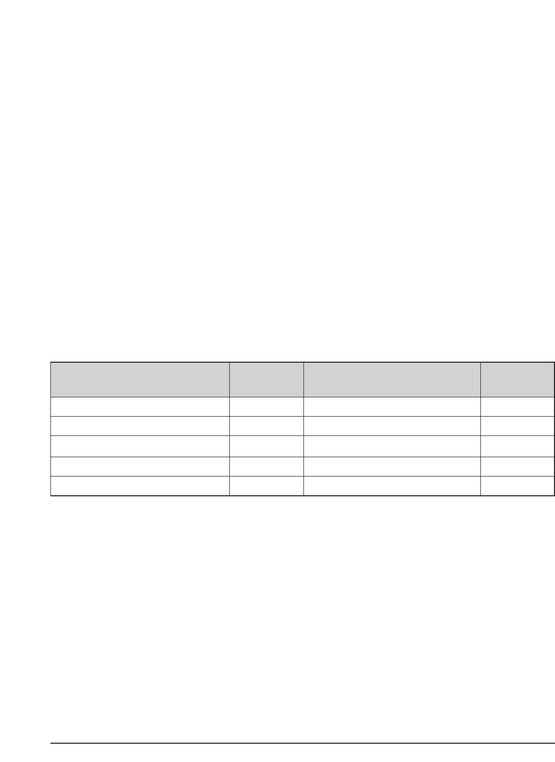
Reference Information
14-2 Samsung Electronics
14-1-2 Fiexibility and Cost Reduction
1) Hardware Cost Example
Many image processing application engineers face a familiar group of problems when designing and building a
system. The end user requires system flexib ility, simple adaptation, fast delivery times, and most importantly a
reasonable price. With conve ntional systems, whether analogor digital, engine ers must confine them selves to
certain combina tions of the existing cameras, frame grabbers, and software. The product choice for this system
config uration is limited. Unless the decision is made to use a high cost frame grabber that supports multiple cam-
eras, sometimes known as multi-norm , it is usually not possible to operate camera s with different resolutions
from the same frame grabber.
For many applications, the introductio n of digital cameras is hindered by the cost specified by the end custom er,
however technically effective digital cameras may be. With the increa sed use of IEEE-1394 in the industrial image
processing business, many of these problems are solvable in a sure , safe , and cost effec tive way.
This example compares two simi lar vision systems. Each system uses four Megapixel
resolution digital cameras . The traditio nal solu tion consists of one frame grabber per camera, one parallel digital
data cable per camera, and one power supply per camera.
The 1394 solution requi res one hub and one interface card to connect the four cameras , along
with five ine xpensive 1394 cables. The 1394 cables carry power to the cameras directly from the computers inter-
nal power supply. (Note tha t not all compute rs are capab le of supplyi ng enough power for the cameras. In
some cases a separate power supply may be required.)
Traditional Solution
Price 1394 Solution Price
with multiple frame grabbers
Four Cameras 18,000 Four 1394 Cameras 18,000
Four Frame Grabbers 4,400 One 1394 Interface Card 100
Four Cable 400 One 1394 Hub 120
Four power Supplies 320 Five Cables 150
Total $23,120 Total $18,370

Reference Information
14-3Samsung Electronics
14-1-3 Application Examples
1) Solution used before Basler s Intervention
2) Possible solution wih digial cameas using RS 644 OR Camera Link
3) IEEE-1394 solution
Today, there are already applications realizing the benefits of IEEE-1394 technology. For example, at one of our
customer sites, Basler was faced with a vision system which has the following specificatio ns:
The machine is a hig h-speed assembly system . Two indepe ndent robots take different par ts
(different in size, shape, and reflection) from a support unit and mount these parts on a mounting plate. Timing is
crucial, and in the worst case, a part must be taken from the tray every 100 ms. Accuracy of parts mounting is also
critical (0.5 mm) . To have a vision system inspecting these operations , 4 cameras (2 on each of the rob ots) are
needed:
- 2 low resolution Basler A302f camera s (640 x 480) for checking if the mounting plate is in place
- 2 high-resolution Basler A101f cameras (13 00 x 1030) for checking the components to be mounted.
Since most of the parts are differen t, the two A101f cameras must be reconfigured before almost every image
acquisit ion. In the worst case, the AOI, shutter, and som etim es gain need to be adjusted.
The customer used analog camera s with CCIR resolution (768 x 582) only. This drast ically restricted the number
of parts which could be mounted using the robots. Sin ce thes e camera s had no communication por t for config-
uration, adjusting the AOI was not possible and differ ences in reflection of the parts needed to be adjusted for by
driving a flash circuit. All cameras were interfaced into one frame grabber (one PC).
Using RS 644 or CameraLink based camera s, the customer would need one frame grabber for
each camera. It is very likely that the user would need two PCs (one for each robot). Changing the camera-config-
uration on the fly would require adv ance d grab ber cards since simple grabbers are not capable of easily chang-
ing their registers for different AOIs.
All cameras are attached to a sing le interface card in the PC. The Basler A302f is only used when a new mounting
plate is pos itione d by the handler. In norm al operation , only the two Basler A101f cameras will be sending data
at the same time and they will be operating at about 10 FPS. This results in a data rate of about 27 MBytes/s,
which is well within the specification for IEEE-1394.
Since IEEE-1394 supports bi-directional communication between the camera and the PC, before each frame
capture , the PC can easily change resolution, gain , offset, shutter speed, or whatev er is required.
The IEEE-13 94 solution results in the se clea r advanta ges for the custom er:
- Onlyone PC,
- Only one inter face card (very inexpensive compare d with frame grabber cards ),
- Easy and inexpens ive cabl ing ,
- The system meet s the expect ations for spee d and accuracy,
- The range of inspect able parts is much bigger than with the old syste m.

Reference Information
14-4 Samsung Electronics
MEMO

Introducing Samsung DVD Recorder
( DVD-R128_R129 )
Introducing Samsung DVD Recorder
( DVD-R128_R129 )
Samsung Electronics Co. LTD
Digital Video Division

2
1. What is SEC’s DVD-R128_R129?
Digital A/V system for video playing & recording
using optical disc as the medium format
Digital A/V system for video playing & recording
using optical disc as the medium format
High picture and sound quality
recording capability comparing
with analog medium recording
systems
Digital recording by an optical
medium format allows random
access capability and easy &
convenient recording
High-quality Recording Optical Medium Recording

3
Model No : DVD-R128_R129
Market Introduction Date
: Feb 2006 (Europe)
2. Samsung DVD Recorder
1. Super picture & sound quality recording with MPEG-2(VBR)
2. Convenient control through random accessibility of optical discs
- One touch recording : Automatic empty area recording
- Program Navigation
- High Speed Search and Play
3. Advanced playback functions for multiple purposes
(Compatible with DVD, Audio-CD, CD-R/RW(MP-3), DVD-R, DVD-RW,DVD-RAM Disc)
General Introduction
Characteristics
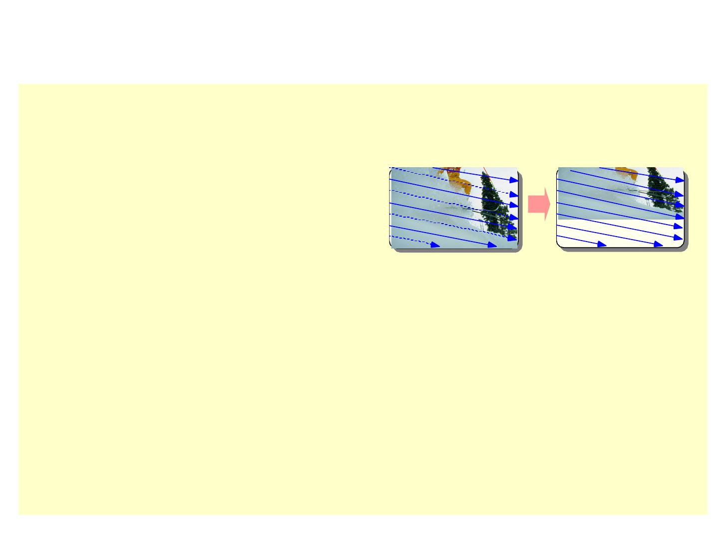
4
3. DVD-R128_R129 Playback & other Features
■Progressive Scan
■Program Navigator
By scanning all 480 lines in one pass,
progressive scanning provides high vertical
resolution and flicker-free, high-density image
output that does not suffer from the loss of
quality during subject movement -- which is
characteristic of the conventional interlaced
scanning method. (U.S. version Only) 60 Frame/Sec30 Frame/Sec
Recorded programs are shown as thumbnail pictures, and information such as title, recording
dates and times are displayed on menu screen. User can choose a desired program.
■Editing
Simple non-linear editing is possible on menu screen without additional editing
system. User can delete part of a program or entire program, and edit program title.
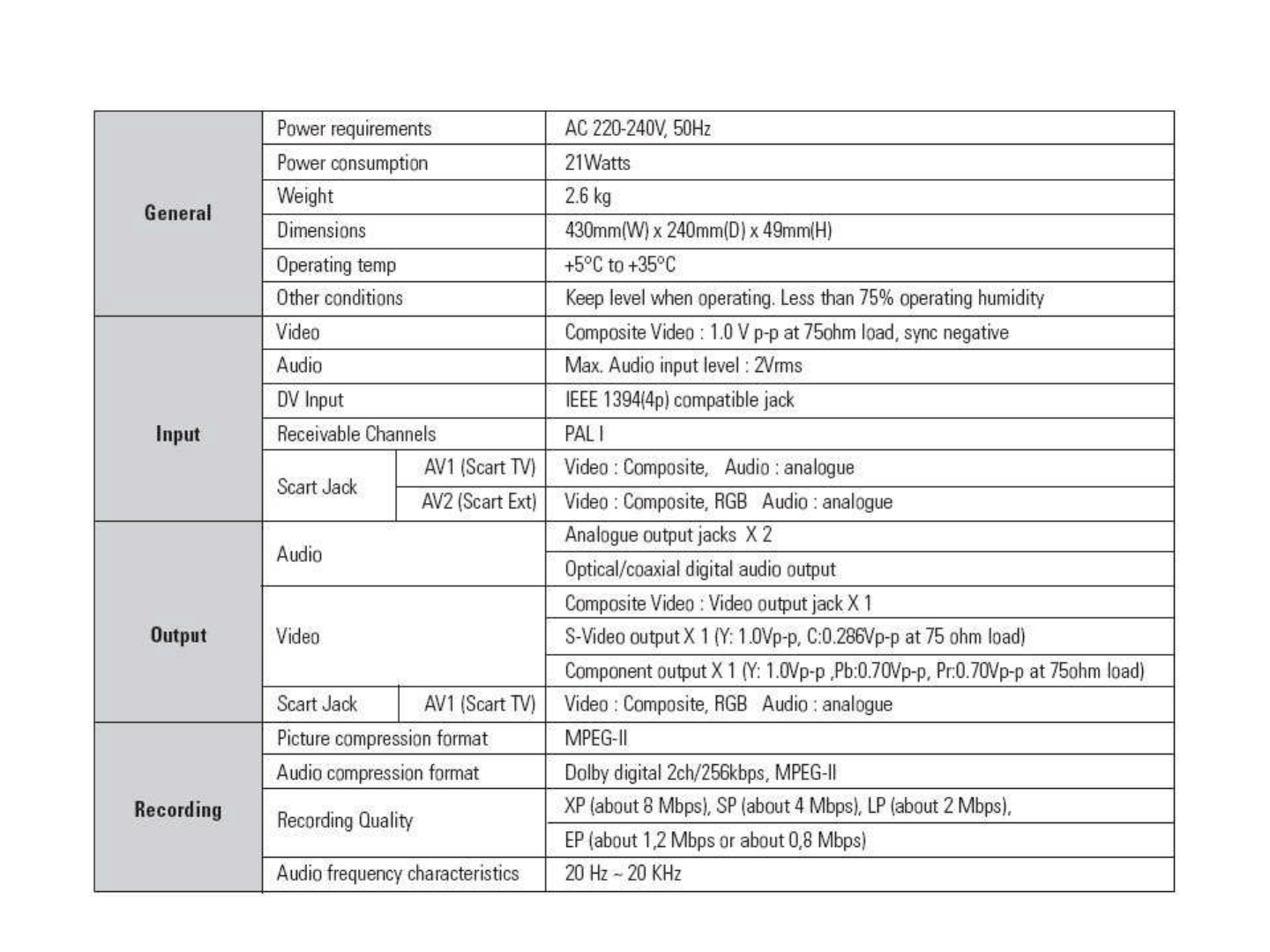
■Product Specification
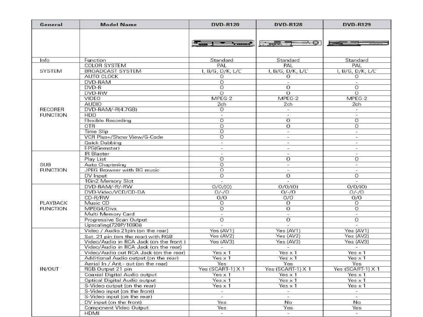
■Chassis Product Specification
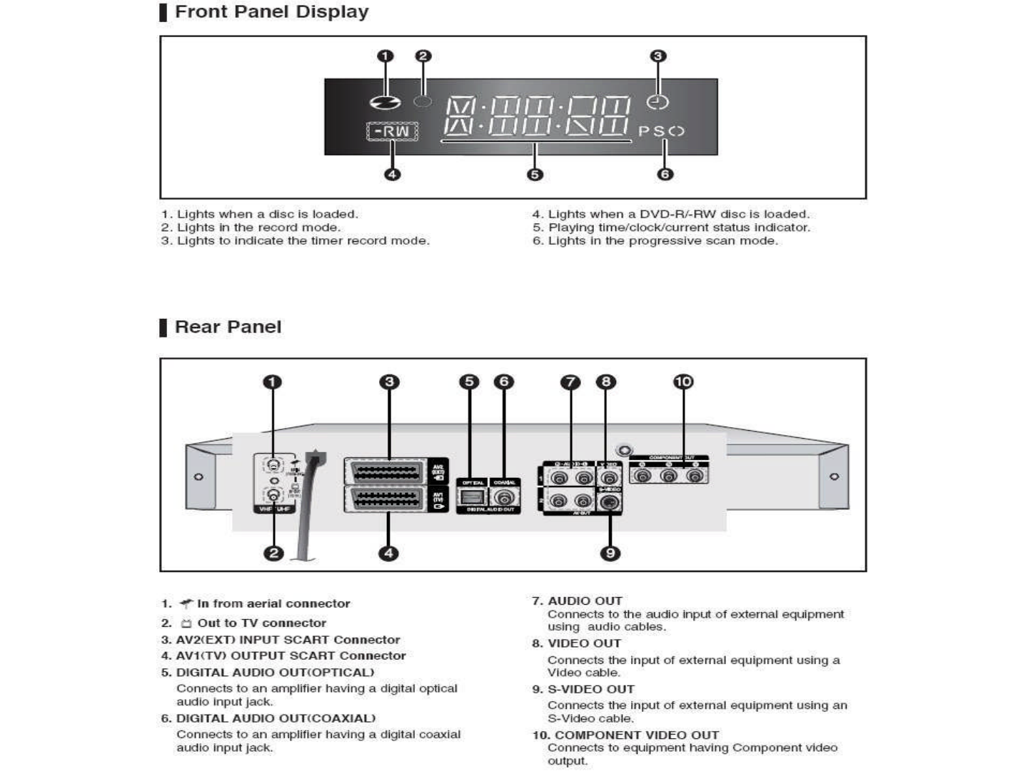
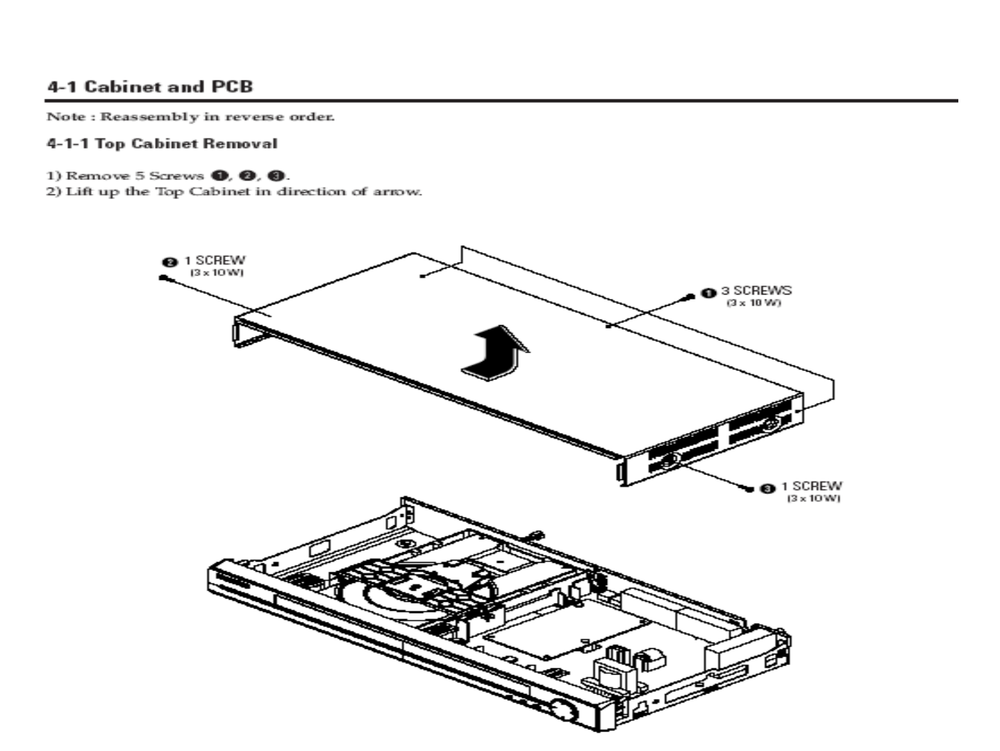
4. Disassembly and Reassembly
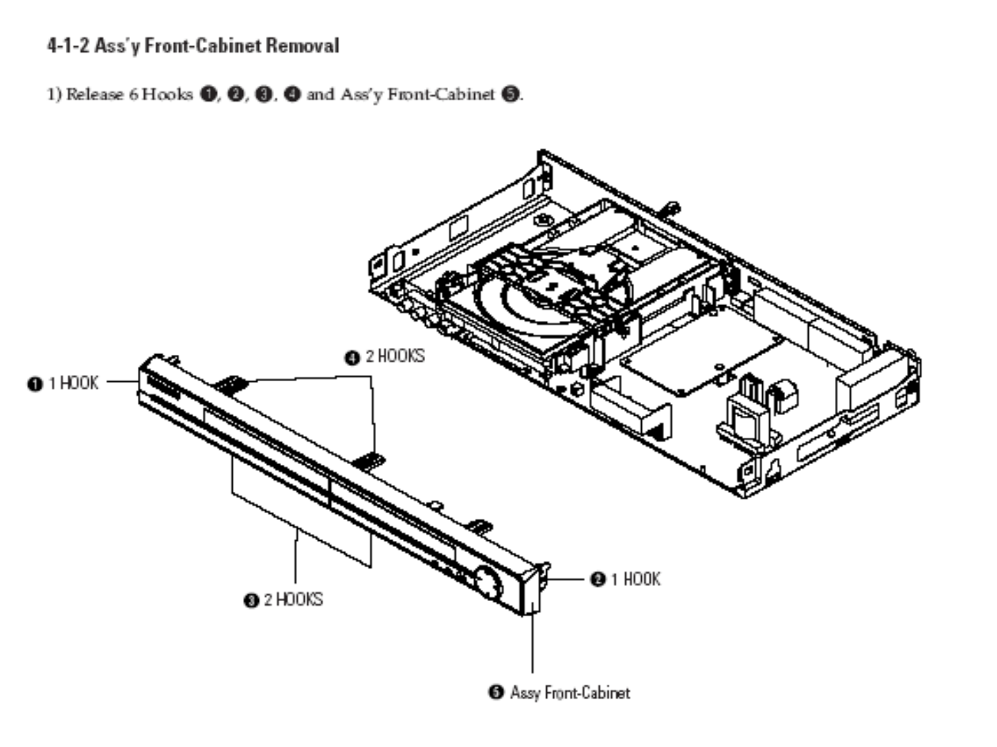
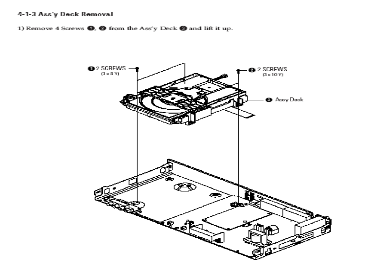
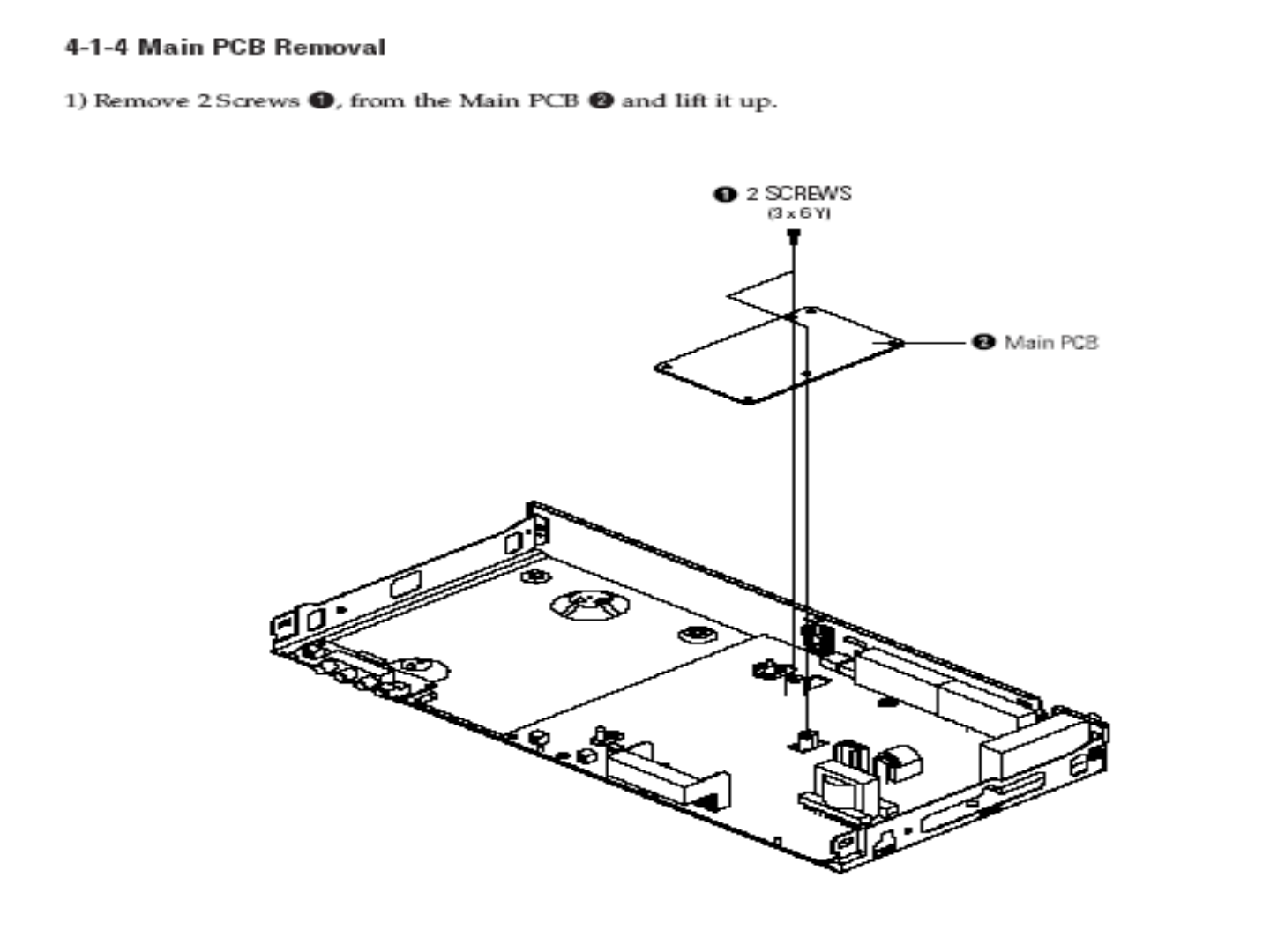
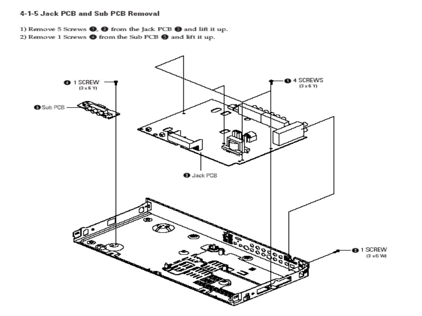
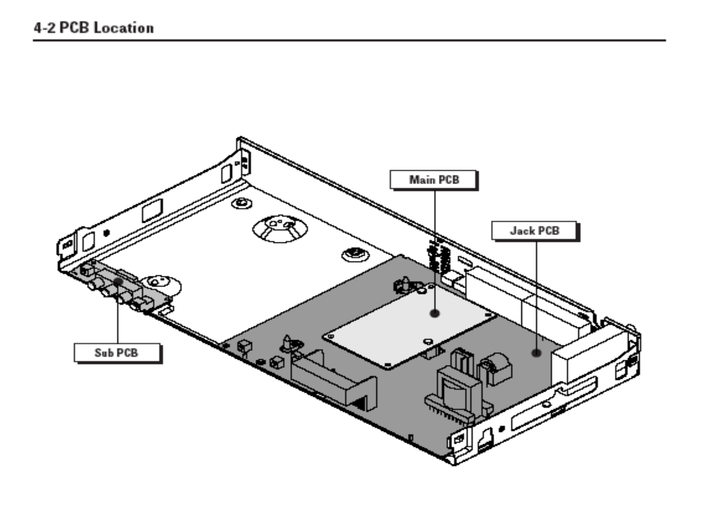
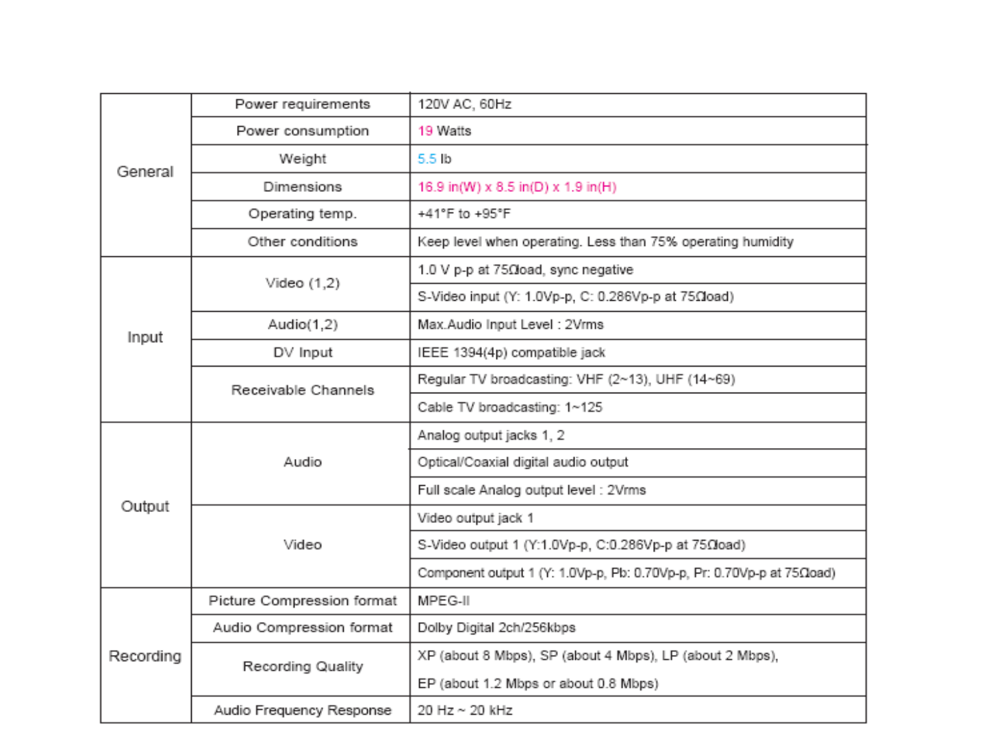
5. Specifications

16
6. DVD-R120 Key Features
■MPEG-2 VBR(Variable Bit Rate) Recording
■Creating a DVD video title using DVD-RW/DVD-R
■One-Touch Recording
■Automated Quality Adjustment for Timer Recording
■Copying data from a digital camcorder using a DV input jack
■Selectable Recording Mode
■Quick Recording
Recording Features
Playing Features
■Progressive Scan
■Program Navigation
Other Features
■Easy Editing
■Auto Chaptering
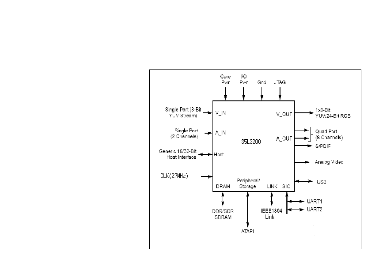
■HOST Interface
■Peripheral / Storage Interface
■ATAPI Controller
■IEEE 1394 Interface
■Video Interface
■Audio Interface
■SDRAM Interface
■Serial I/O Interface
■UART Interface
7-1. S5L3200 H/W Interface
7. BLOCK DIAGRAM & CIRCUITS EXPLANATION

7-2. Front-Micom Interface
•Front-Micom MN101D10F(IC601, Panasonic)is used to
control Power, LED Module, MTS Block, EDS, KEY Input
Matrix etc.
•The SPI(Serial Peripheral Interface) port provides a bus
for a serial interface with AV-CODEC
S5L3200(DIC1)
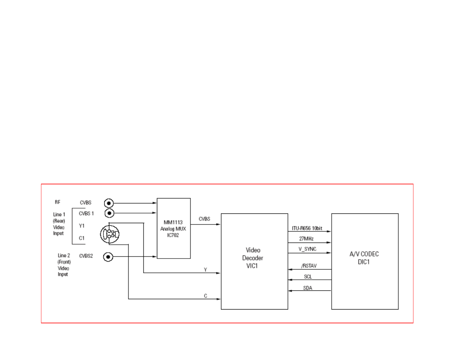
7-3. Video Input Outline
•DVD-R130 is the two AV Video input. AV 1 Video input is CVBS1 & S-Video1 at the Rea
r Panel. AV 2 Video input is CVBS2 at the Front Panel.
The analog Video signal select AV 1 or AV 2 by the IC601 (Front Micom).
VIC1 (Video Decoder) diverges from the 27MHz crystal, then generates ITU-R656 (10bit
s) and 27MHz clock.
VIC1 (Video Decoder) does closed caption, copy guard detect processing and A/D conve
rsion of analog Video signal converted into 11bit Digital Video signal (ITU-R656 Format)
is outputted via U1 (MPEG2 Decoder & Encoder with video Encoder) of digital part.

7-4. Analog MUX(MM1113)
IC702 is Analog Mux.
As Pin 2, 4 of the IC702 are controlled by the Front Micom, IC702 select
RF OF CVBS(Pin1) AV1 of CVBS[Pin3] and AV2 of CVBS [Pin 5]
The analog Video Signal of IC201 output is selected by the ic601 via VIC
1(Video Decoder : TW9906) of analog Video Input parts.

7-5. NTSC/PAL Video DECODER
The VIC1 (Video Decoder : TW9906) device is a high quality, single-chip digital video dec
oder that digitizes and decodes all popular baseband analog video formats into digital co
mponent video. The VIC1 (Video Decoder :TW9906) supports the analog-to-digital (A/D)
conversion of component RGB and YPbPr signals, as well as the A/D conversion and dec
oding of NTSC, PAL and SECAM composite and S-video into component YCbCr.
This VIC1 (Video Decoder : TW9906) includes four 10-bit 30-MSPS A/D converters. and
A/D conversion of 10bit analog Video signal converted into Digital Video signal (ITU-R656
Format) is outputted via DIC1 (MPEG2 Decoder & Encoder with video Encoder) of digital
part.
The following output formats supply 10-bit 4:2:2 YCbCr to the DIC1 (MPEG2 Decoder &
Encoder with video Encoder) of digital part.
On CVBS and S-video inputs, the user can control video characteristics such as contrast,
Brightness, saturation, and hue via an I2C U1 port [PIN V17, V18] interface.
The TW9906 decoder includes methods for advanced vertical blanking interval (VBI) data
retrieval. The VBI data processor (VDP) slices, parses, and performs error checking on te
letext, closed caption (CC), Copy Guard Detect Processing and other VBI data.
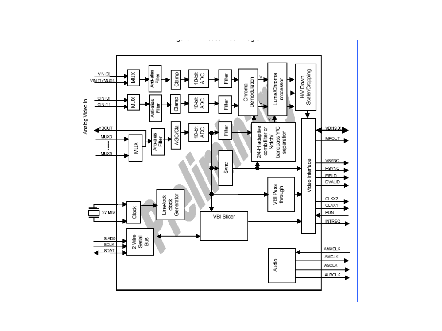
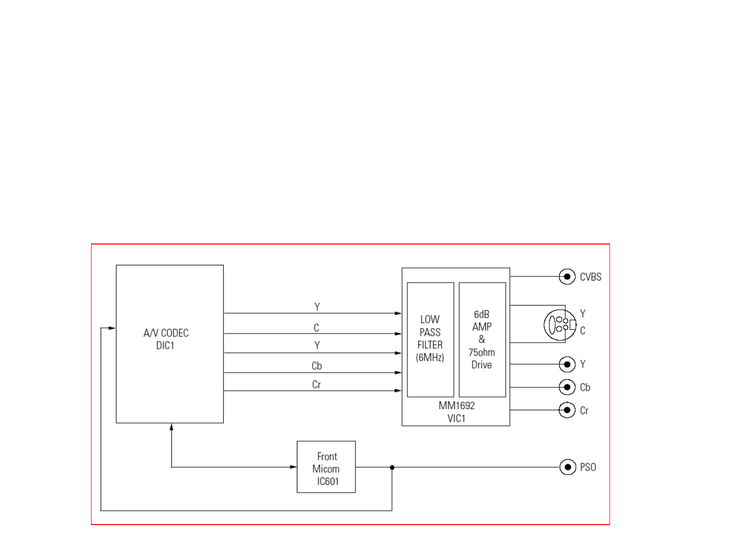
7-6. Video Output Interface
DIC1 (MPEG2 Decoder & Encoder with video Encoder) diverges from the 1
3.5MHz crystal, then generates VSYNC and HSYNC.
DIC1 (MPEG2 Decoder & Encoder with video Encoder) does RGB encodin
g, copy guard processing and D/A conversion of 10bit Video signal converte
d into analog signal is outputted via amplifer of analog part.
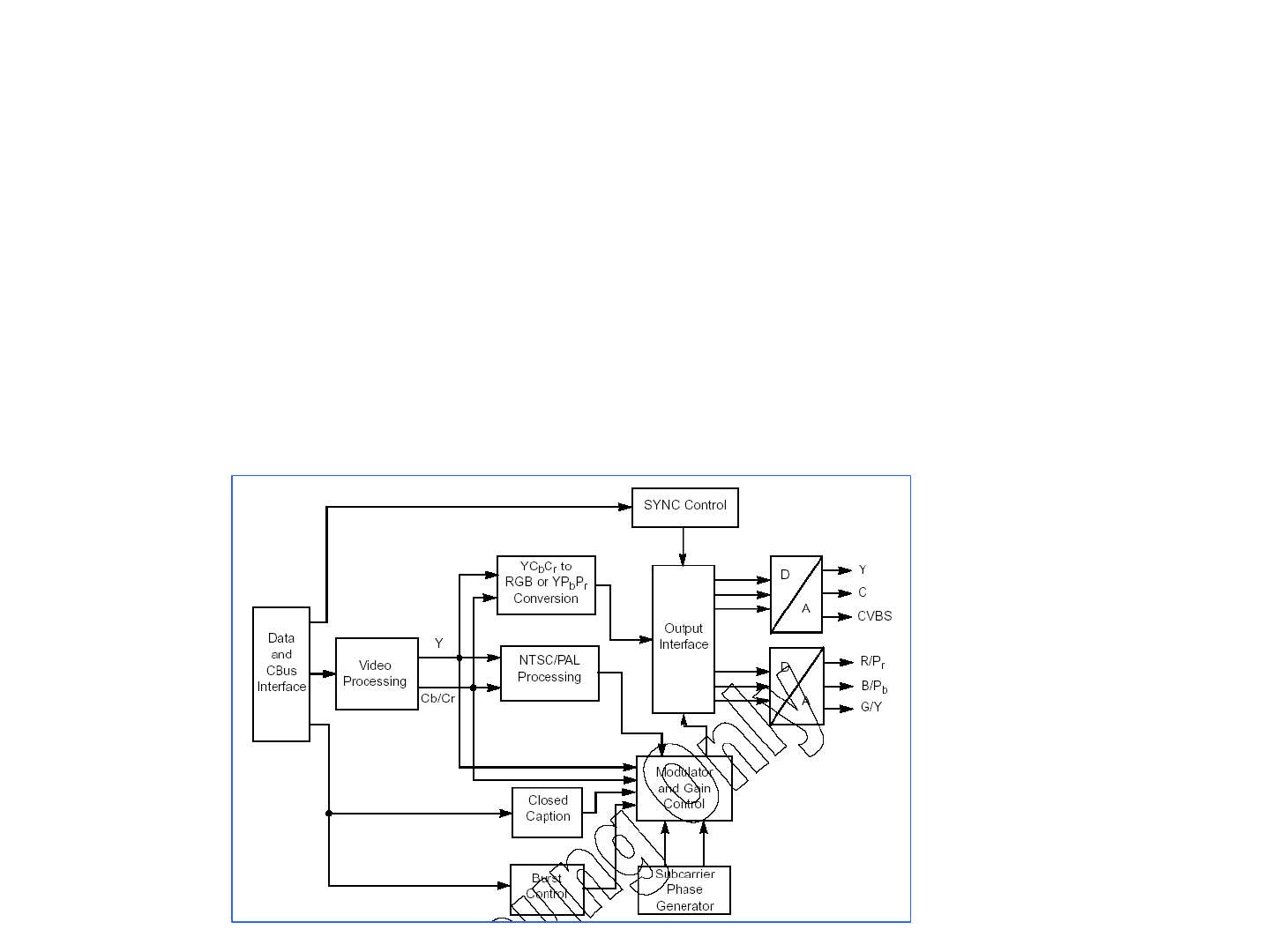
7-7. NTSC/PAL Digital encoder
DIC1 inputted from pin E1 with 13.5MHz generates HSYNC and VSYNC
which are based on video signal. DIC1 is synchronous signals with
decoded video signal.
The above signals, which are CVBS (Composite Video Burst Synchroniz
ed), Y(S_Video), C(S_Video), Y(Component)/G(Green), Cr(component)/
R(Red), Cb(component)/B(Blue), are selectively outputted 480i (interlace
d Video Output), 480P(progressive Video Output) by the Pront button DI
C1 adopts 10bit D/A converter.
DIC1 perform video en-coding as well as copy protection.

7-8. AMP (MM1692)
VIC1 is 6dB amplifier.
Based on CVBS signal, the final output level must be 2Vpp without 75 ohm
terminal resistance. Because the level of video encoder output is only 1Vpp,
the level is adjusted with the special amplifier.
When mute of pin 5 is high active, if the pin is floating and connect to power
, the output signal is never outputted.
Y, C, Y(R), Cb(B), Cr(R) outputted from video encoder are inputted to VIC1 [
Pin14, 16, 13, 12, 11] respectively. And CVBS Output[Pin 15] is made by Y
& C Mixing signal.
The signal to which gain is adjusted by amplifier is outputted from jack via
75ohm Resistance (VDR1,2,4,5,6,).

1. Input block
This Model has two stereo line input terminals. and internal TV-audio from RF
Tuner Block.
These three Analog audio signal source are converted to digital data by Input
Block.
Input Block has a Multiplexer (IC203), A/D converter (AIC2).
IC203 change it’s output by selection control signal from IC601 (Front Micom).
2. Output Block
DVD-R130 has two stereo analog line out terminal, and two digital output
terminal.
Decoded signal by DIC1 is inputted to AIC1 (D/A Converter), then filtered and
amplified by AIC4 (OP-Amp).
And the digital audio signal (IEC-958) is outputted in Optical/Coaxial (S/PDIF)
terminal..
7-9. AUDIO
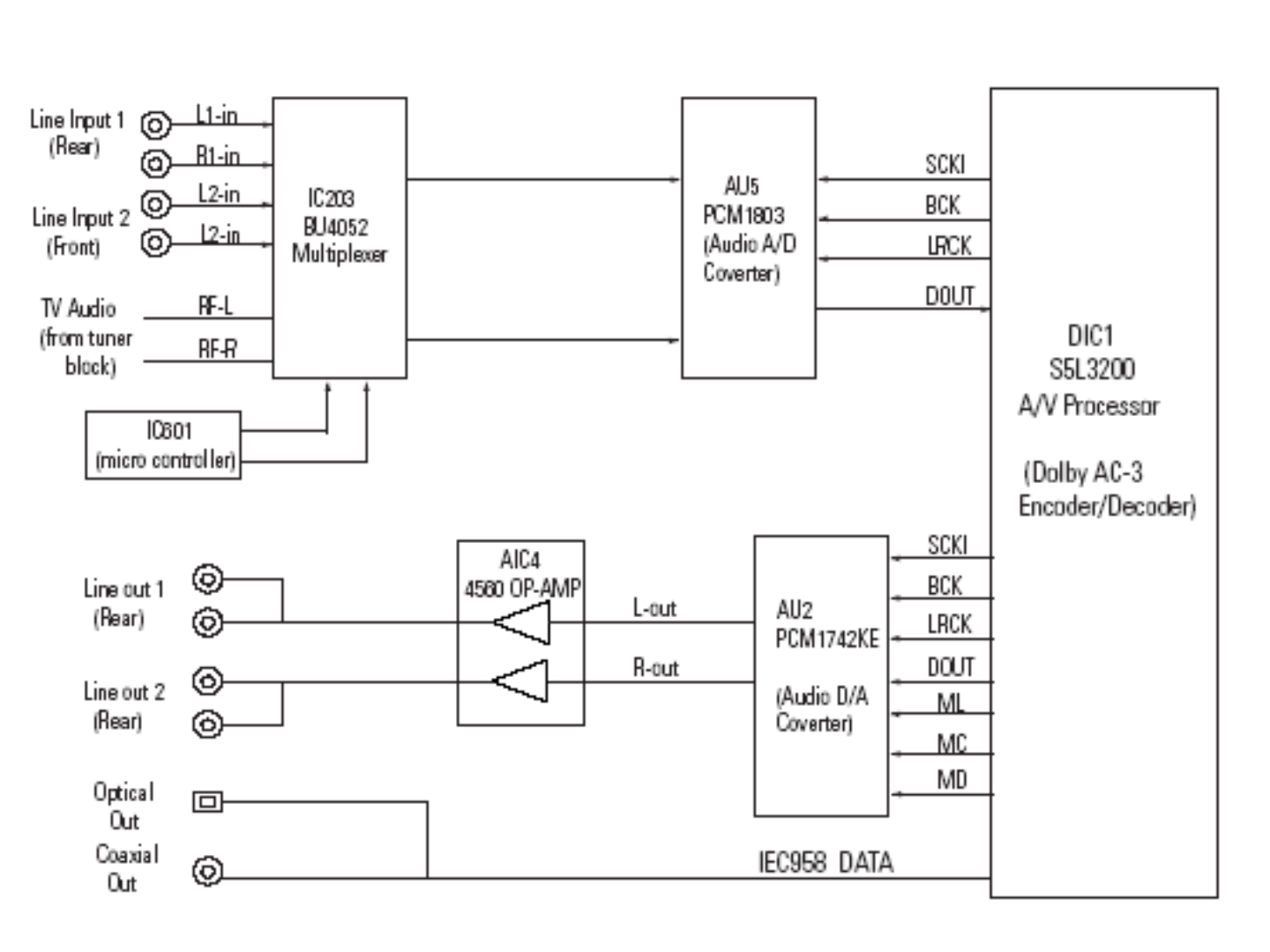
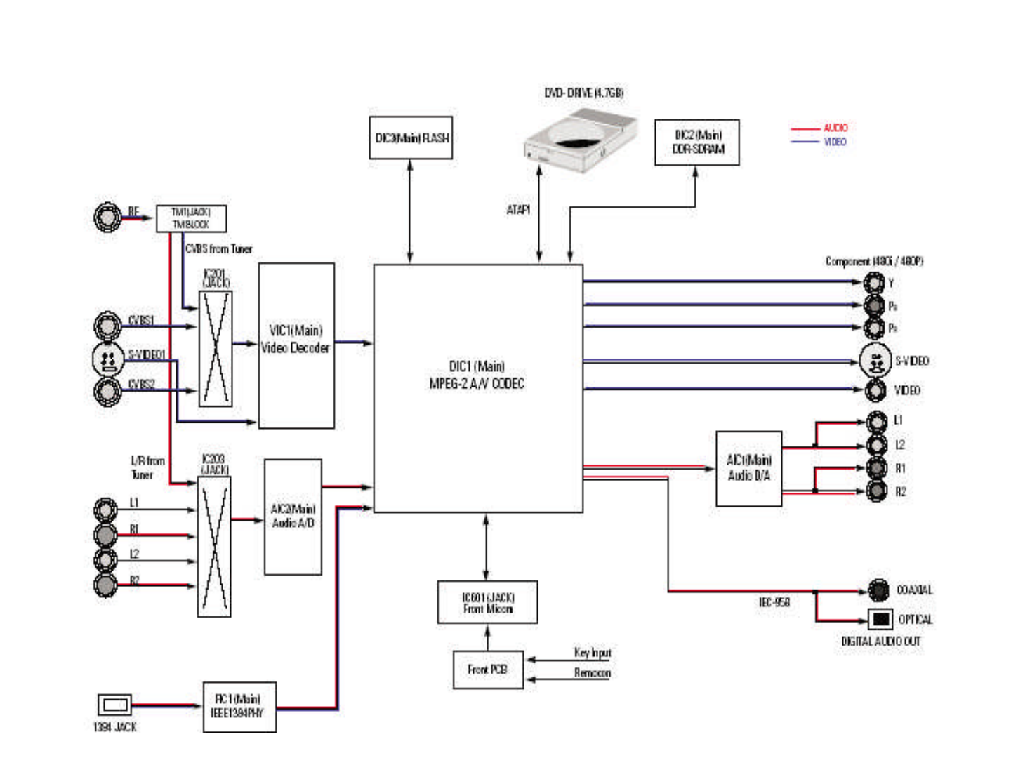
<Block diagram>
7-10. Stereo/Bilingual (MTS)
summary
1) MTS SIGNAL : mono(L+R),STEREO(L,R),MONO+SAP,STEREO+SAP
2) SAP : Sub Audio Program Signal (american MTS system only)
< MTS system base-band spectrum >
FM
L+R
50~ 15KHz
AM- DBS- SC
0 fh 2fh 3fh 4fh 5fh 6fh 6.5fh
50
25
15
5
3
Sub Audio Program Signal
↓
(KHz)
주
파
수
편
이
Telemetry Signal
↓
L- R
dbx- TV
NR
SAP
dbx- TV NR
FM 10KHz
50~ 10KHz
Pilot
↙

i t em
si gnal
Si gnal
freq. Band Si gnal Processi ng Syst em Maxi mumAudi o
Carri er dev(KHz)
Monaural Si gnal
( L + R ) 50Hz~15KHz 25
Stereo Pi l ot 15. 734 KHz Onl y St ereo Broadcast i ng 5
Stereo Si gnal
( L - R ) 50Hz~15KHz AMmodul at i on(Carr i er fr equency 2f h)
dbx Noi se Reduct ion processi ng 50
SAP Si gnal 50Hz~10KHz FMmodul at i on(Carr i er fr equency 5f h)
Maxi mumf requency devi at i on 10KHz)
dbx Noi se Reduct ion processi ng 15
Tel emet ry
Si gnal
Audi o 0Hz~3. 4KHz FMmodul at i on(Carr i er fr equency 6. 5f h)
Maxi mumf requency devi at i on 3KHz) 3
Data 0Hz~1. 5KHz
< MTS signal table >

Signal route
1) SIF signal from tuner(TM1) is connected to MTS processor (IC604 1pin).
*.SIF : Sound Intermediate Frequency
2) MTS processor(IC604) detect the stereo and sap signal , send the
detecting state to front micom(IC601) by I2C data.
It will display the screen by OSD.
*.OSD : On Screen Display
3) MTS processor decode the SIF signal and send the decoded audio signal to
22pin(R out) and 23pin(Lout).
4) Lout(23pin) and Rout(22pin) of MTS processor go to IC203 for audio processing.
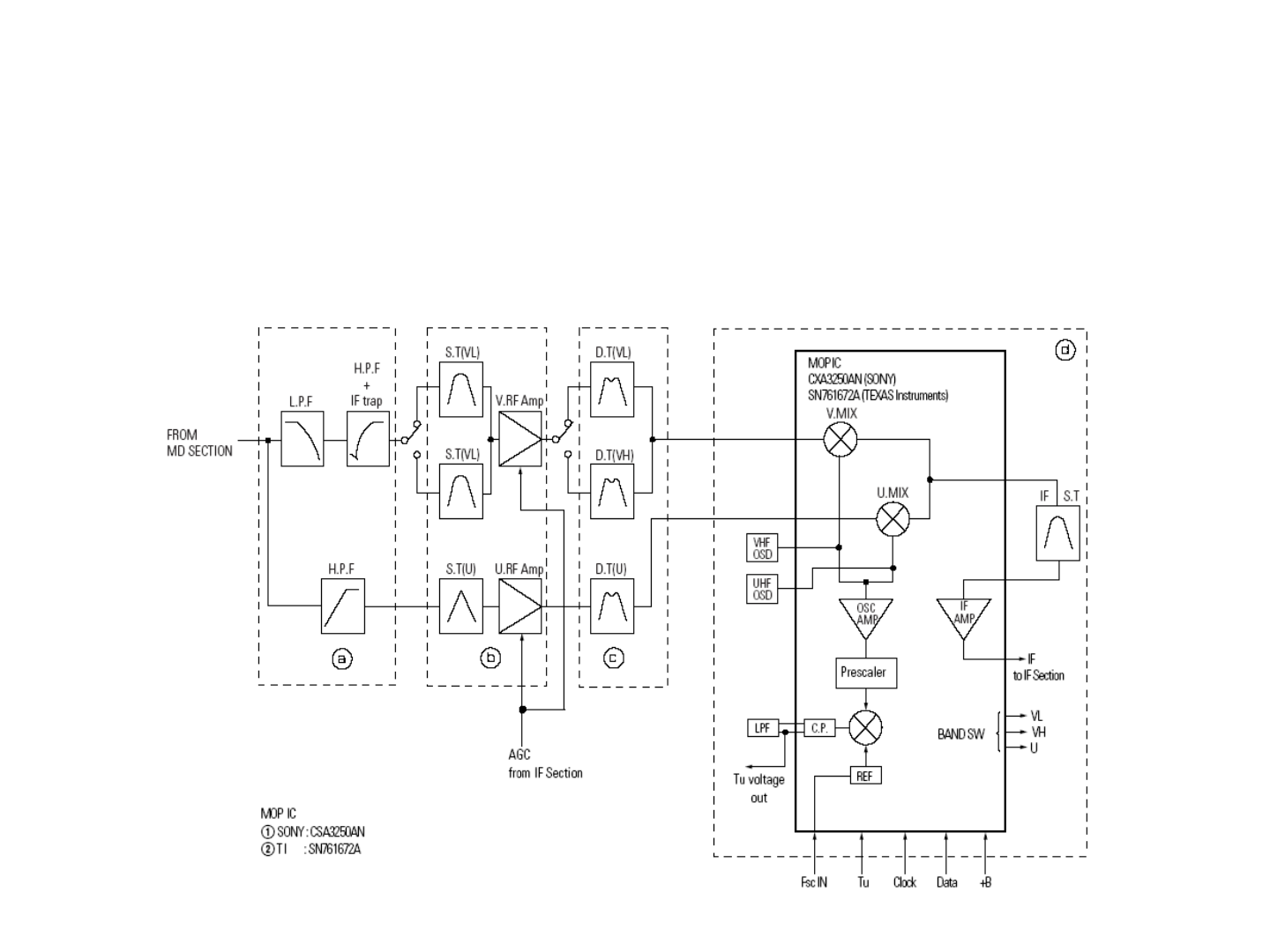
7-11. Tuner/Demodulator
<Block diagram of Tuner >

Tuner
Tuner consists of LPF/HPF,Single Tune,RF amplifier,Double Tune and MOP
circuits.(see the block diagram)
ⓐLPF/HPF(Low Pass Filter/High Pass Filter)
-. IF rejection : preventing for IF frequency signal interference from antenna.
-. LPF : for VHF band ,remove UHF band signal
-. HPF : for UHF band, remove VHF band signal
ⓑSingle Tune/RF AMP
-. Single Tune: for receiving Channel initially
-. RF AMP : Gain control of tuned signal from Single Tune.
AMP Gain is controlled by AGC circuits in IF Demodulator.
ⓒDouble Tune
-. Improve the band quality,
-. minimize the loss of band signal
-. Remove the spurious signal

ⓓMOP(Mixer,OSC,PLL)
-. MOP is consisted of VHF OSC,UHF OSC,Mixer circuits.
-. It have double balance mixer for removing interference.
-. MOP tuned the selected channel.
-. It is very important function in tuner.
-. MOP generate IF signal and connect to IF demodulator.
*.OSC : OSCILLATOR, PLL : Phase Locked Loop
IF : Intermediate Frequency
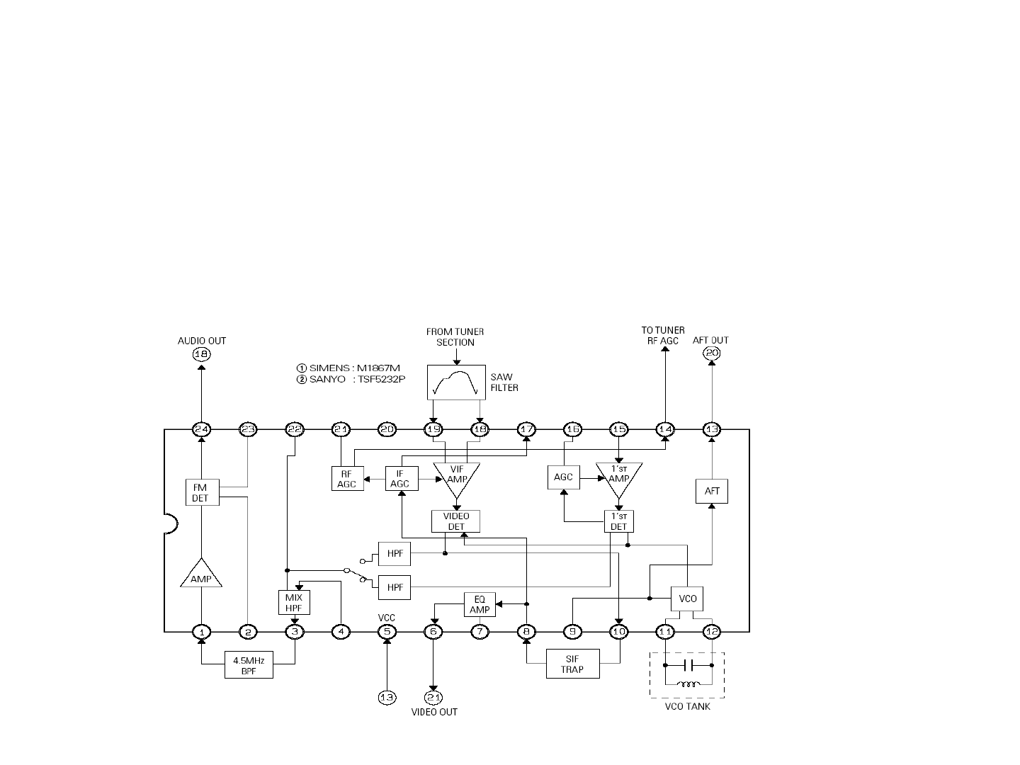
Demodulator
-. Demodulate the IF signal for base band video and audio.
-. The demodulated video and audio signal go to AV processing.
: go to MUX IC for AV input switching
*.MUX : Multiplexer
< Block diagram of demodulator>

7-12. Loader
Loader System Overview and Rambo-II Block Diagram
S5L1482
S5L1482 Features
PRML
Data Processor I, II (DP1, DP2)
ATAPI
ARM7TDMI
WSC Interface
Servo Block
Servo Hardware and Software Features
Data Management
One Chip Solution
RF Processor and Sub Blocks
FPD, PD, I/V amp
LD, LD Driver
Focus Actuator
Tracking Actuator
TILT Actuator
Sled
Motor Spindle
Motor Tray
Motor
RF Signal
(AGC/EQ)
Servo Error
(FE/TE/CE/PE
SBAD/RC/TILT)
Miscellaneous
Signal
(DFT/LPP
/WOBBLE)
APC & OPC
PRML
ENDEC
WRITE
STRATEGY
SERVO
Processor
ECC
Processor
MICOM
ATAPI
DRAM
Motor
Driver
Loader System Overview
Pick-up
I/V AMP
Elantec
LD Drive
Elantec
RF Processor
APC
Data Processor 1
1-Mbit SRAM
Data Processor 2
Host I/F
16-Mbit DRAM
CD ENDEC
Copy Protection
·CSS/CPRM/CPPM
LC895040
CMOS/0.35um
216Pins/LQFP
MICOM
ARM7
Mecha.
SpindleMotor
Feed Motor
PRML
WSC Servo DSP
ATAPI Controller Back-
End
RAMBO II Chipset
Rambo-III Block Diagram

S5L1482A is the Integrated Circuit(IC) adequate for dvd-recorder which
not only plays CD Family, DVD-ROM/-R/-RW/+R/+RW/RAM Disc but
record video and audio to DVD-R/-RW/+R/+RW/RAM Disc.
This IC is dealing with transferring playable signals generated by optical
pick-up unit (OPU). Signal from OPU is transferred to RF chip which
performs analog signal processing in order to generate RF signal. This
RF signal is fed to S5L1482A which the RF signal is transferred to the
HOST through PRML, Data Processor1(DP1), Data Processor2(DP2)
and ATAPI inside of.
Various blocks such as ARM7TDMI core which controls the entire chip
itself, WSC I/F block for the support of dvd-recording, SERVO Control
block dealing with controlling spindle motor and processing focus and
tracking signals are embedded in S5L1482A.
S5L1482A

§ CD-ROM/R/RW/DA/Video Maximum 8X Play
§ DVD-ROM/R/RW,DVD-RAM 8X Play
§ DVD-R/-RW/+R/+RW/RAM 8X Play
§ System on Chip Solution which includes SERVO, PRML, Data
Processor I(DP1), Data Processor II(DP2), ATAPI, WSC I/F
§ ARM 7TDMI Embedded
§ ATAPI Interface Support
§ External Micom I/F Support
§ Auto Disc Detection and Motor Control
§ Tilt Compensation
S5L1482 Features 1

§ Digital DC Offset Compensation
§ EFM & EFM+ De-modulation
§ BCA(Burst Cutting Area) Decoding
§ Descrambling, ECC & EDC Check
§ Bus-authentication (CSS, CPPM, CPRM)
§ Jitter Measurement of Write pattern
§ Maximum 16MByte External SDRAM Support
§ 33.8688MHz x 8 PLL Adoption
§ 0.18um(STD130, Samsung Library)
§ 3.3V (5V tolerant)
§ Operating Temperature Range : 0℃~ 70℃
§ 256-PIN QFP
S5L1482 Features 2

Data Sync-Lock is generated as well as Asymmetry and DC-offset are
compensated by extracting frequency and phase difference using analog-
to-digital(A/D) conversion of signal from RF.
Data restoration ability is improved by adopting wave quantization,
Viterbi detector and adaptation technique through the equalizer.
PRML

EFM/EFM+ demodulation is performed by detection, protection and
insertion of bit stream transferred from PRML in terms of synchronization
signal, and generation of internal synchronization signal.
Data is transferred to DP2 in order to be stored in buffer memory.
During encoring, the position information is identified by land pre-pit(LPP)
data, PID or address in pre-groove(ADIP).
After performing EFM+ 8/16 modulation by requesting data stored in
buffer memory embedded in DP2, data related to DVD format such as
SYNC, Guard1, VFO3, PS, Guard2 and etc. are added and NRZI bit
stream transformed in order to facilitate record propagate through Write
Strategy Block.
Data Processor I (DP1)

After deinterleaving data transferred from DP1, data is stored in buffer
memory. As far as the DVD data in buffer memory, after performing error
correction code(ECC), descrambling and verifying error detection
code(EDC), data is transferred to ATAPI. As for CD data, after
performing error correction, interpolation and attenuation, data is
transferred to DAC/ATAPI/AV Decoder. Burst cutting area(BCA) data fed
through RF-Amp. originated from DVD-Disc, is stored to the buffer
memory after detecting the synchronization signal, then it performs error
correction and verifies EDC. Next, data is transferred to the
microprocessor unit. In addition, data transferred from ATAPI is activated
by EDC and scrambling. Data is stored in buffer memory after appending
EDC parity and Data-ID. After the procedures of appending the parity
utilized in error correction, transferring to DP1, performing EFM+
modulation, and adding data required for the DVD-format such as SYNC,
bit stream which will be recorded in DVD-RAM is outputted to Auto Laser
Power Controller(ALPC).
Data Processor II (DP2)

It is dealing with data scramble(CD case), functionalities related to data
communication to host(PIO,DMA,UDMA), management of packet
command, and authentication(CSS,CPRM).
It supports PIO/MDMA/UltraDMA, which abide by ATA/ATAPI standard
transmission method.
It is capable of controlling external buffer memory. SRAM, external
buffer, can be supported by maximum capacity of 16Mbytes, which is
shared with DP2 for the purpose of data storage.
ATAPI

ARM7TDMI play a role of microprocessor by controlling various internal
blocks. Without intervention of an external microprocessor, it is capable
of controlling S5L1482A.
It embeds 16KByte SRAM and 4KByte ROM as well as supports an
external ROM/SDRAM/Flash.
If necessary, the firmware is upgradeable through ATAPI interface.
S5L1482A not only embeds ARM core but also has the capability of
adopting various kinds of external microprocessor units according to its
hardware configurations.
ARM7TDMI

WSC I/F is in charge of the interface between LD driver chip generating
the write pulses utilized in recording to optical disc and data processors
making write data.
The recordable optical discs are DVD-R, DVD-RW, 4.7GB DVD-RAM
and 2.6GB DVD-RAM.
WSC Interface

Servo block includes digital servo controller(Teaklite Core) in order to
play DVD-RAM/ROM/R/RW and CD-ROM/R/RW discs.
Disc auto detection, focus and tracking control is performed in
automatic manner.
Servo Block

- Downloadable 16Kwords Program RAM
- Built-in 10Bit ADC, 8ch Sample&Hold DAC
- Track Counter : Long Distance Velocity Control Oriented Direct Seek
- Shock / Defect Detection
- De_track Detection
- Header(DVD-RAM)/LAND Pre-Pit(DVD-R/RW) Detection
- Various Servo Monitor Signal Generation
- Determination of Various Loop Filter Characteristics and Coefficients by
System Controller
- RF IC , Elantec IC serial Interface
- Micom Interface : Compatible with NEC and HITACHI Microprocessor
I/F
Servo Block Hardware Features

- Digital Servo Controller (Focus Controller, Tracking Controller, Sled
Controller, Seek Controller)
- Disc Auto Detection, Focus/Tracking Pull_in
- Auto Adjustment/Calibration: Focus/Tracking Loop의
Offset/Balance/Loop Gain Adjustment
- Velocity Control Oriented Direct Seek
- Step Motor Control : Macro Seek
- De-track Compensation
- Center Error Control Servo
- DVD Layer Jump
- Shock/Defect Handling
- Tilt Compensation
Servo Block Software Features

The data size for data transfer between internal buffer memory and
each functional block of data processor is dependent upon disc media.
Data is transferred by 2 symbol units(2bytes, 16bits) in the case of DVD
and 2 symbol units(1bytes, 8bits) in the case of CD and BCA. The
microprocessor deals with memory management.
The microprocessor manages DVD data by 1 ECC block unit and CD
data by frame unit automatically.
BCA data is stored at the specific location of memory and managed. In
the case of an external buffer memory, the microprocessor is also in
charge of memory management and the buffer control block of ATAPI
deals with the a serious if data transfer process.
Data Management

The rest block systems except RF, that is PRML, SERVO, Data
Processor, ATAPI, WSC I/F and ARM7TDMI, integrated into one chip.
This system on chip solution reinforces the reduction of power
consumption, stable and hi-speed data transfer, minimal size and
improvement of reliability.
One Chip Solution

RAMBO-II drive RF processor is the analog front end LSI which has the
capability of playing and recording DVD media(DVD-ROM/R/RW/RAM)
as well as playing CD media.
By adopting 0.65um Bi-CMOS manufacturing process, the frequency
characteristics and power consumption are significantly improved.
It is operated by +5V power and it does level shift for the external
interface. RF processor LSI is mainly divided by for four sub-blocks.
RF Processor

▶Pick-up Interface Block : As the input interface block, this block
consists of RF Input Mux and Servo Input Mux. By receiving PD signal
and sum signal from pick-up as inputs, it selects corresponding signal
and amplification degree with respect to disc media.
▶RF Signal Processing Block : By receiving output from RF Input mux, it
performs AGC, EQ, and Header signal processing. Then, it outputs
signals to PRML and DP.
▶Servo Error Signal Processing Block : It generates various servo signal
and outputs to Servo DSP.
▶Various Signal Detection and ALPC Block : It detects Mirror, Defect,
BCA, Land Pre-pit, Wobble signals which are utilized for signal
processing in Servo and DP. Also, it has the functionality of controlling
LD Power which are Automation Power Control(APC), Optimum Power
Control(OPC) and Running Optimum Power Contol(ROPC).
RF Processor Sub Blocks
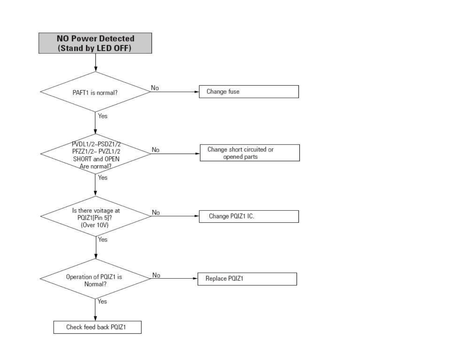
8. Troubleshooting
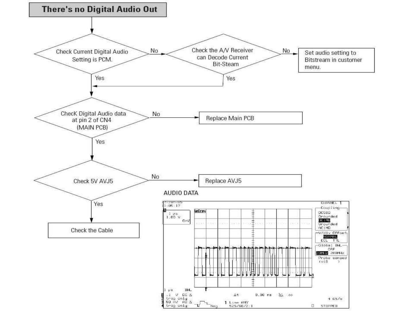
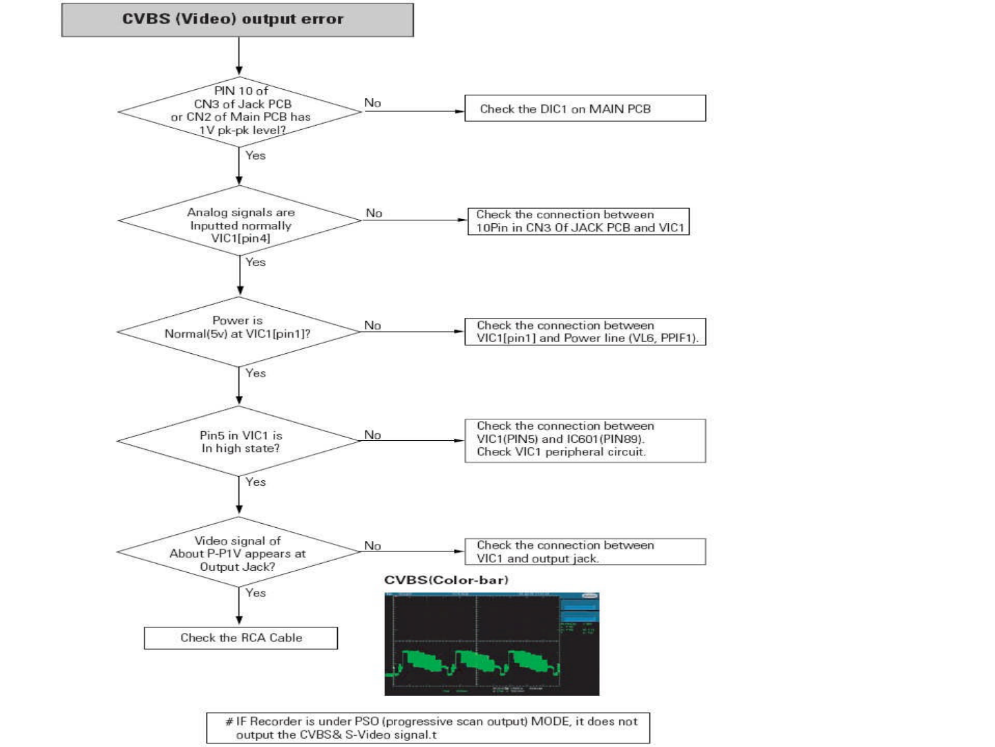
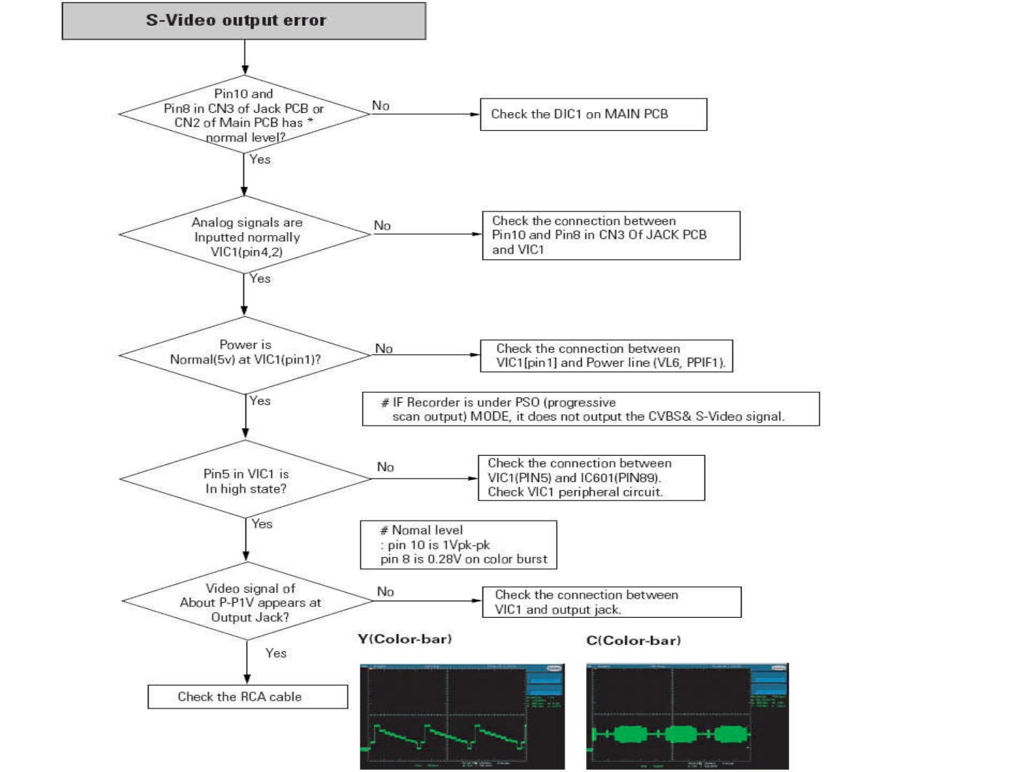
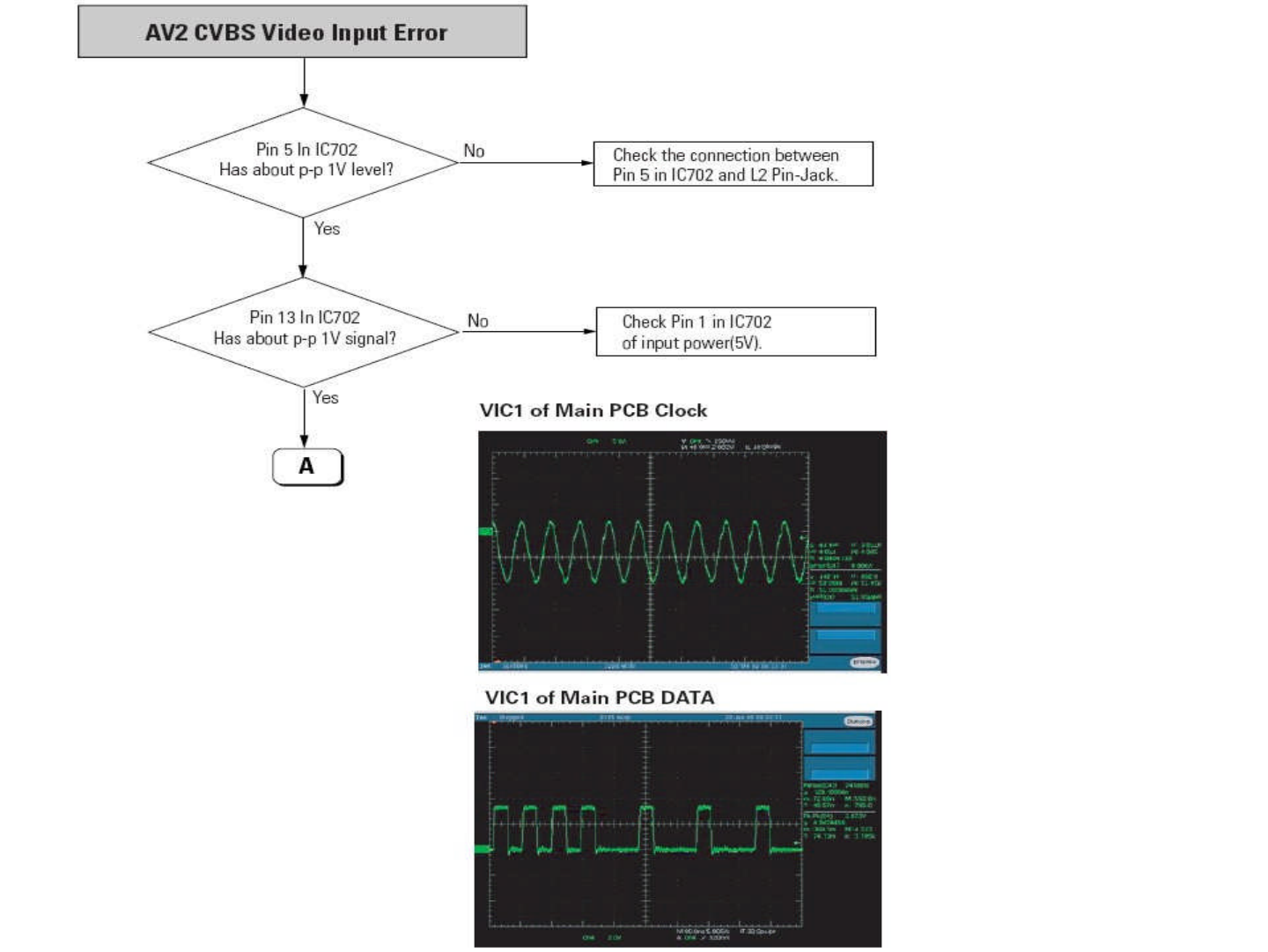
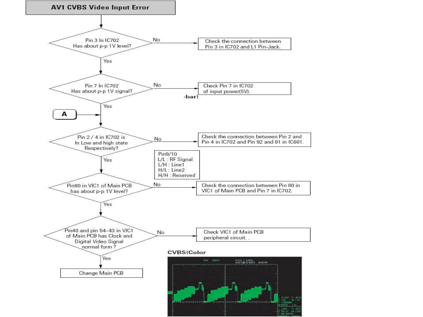
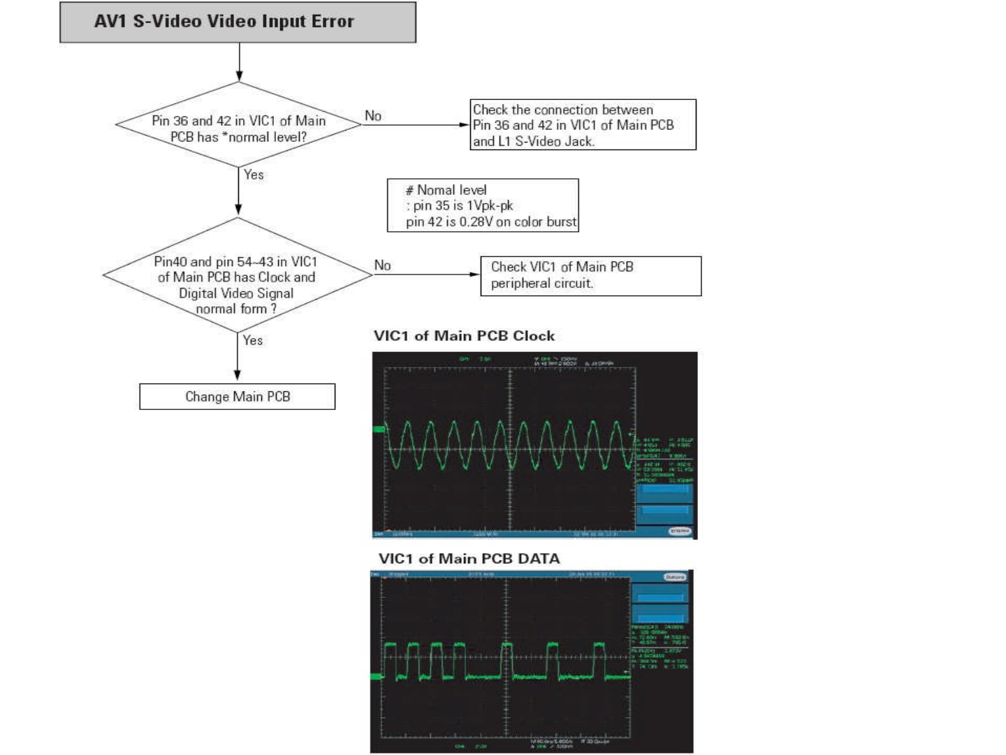
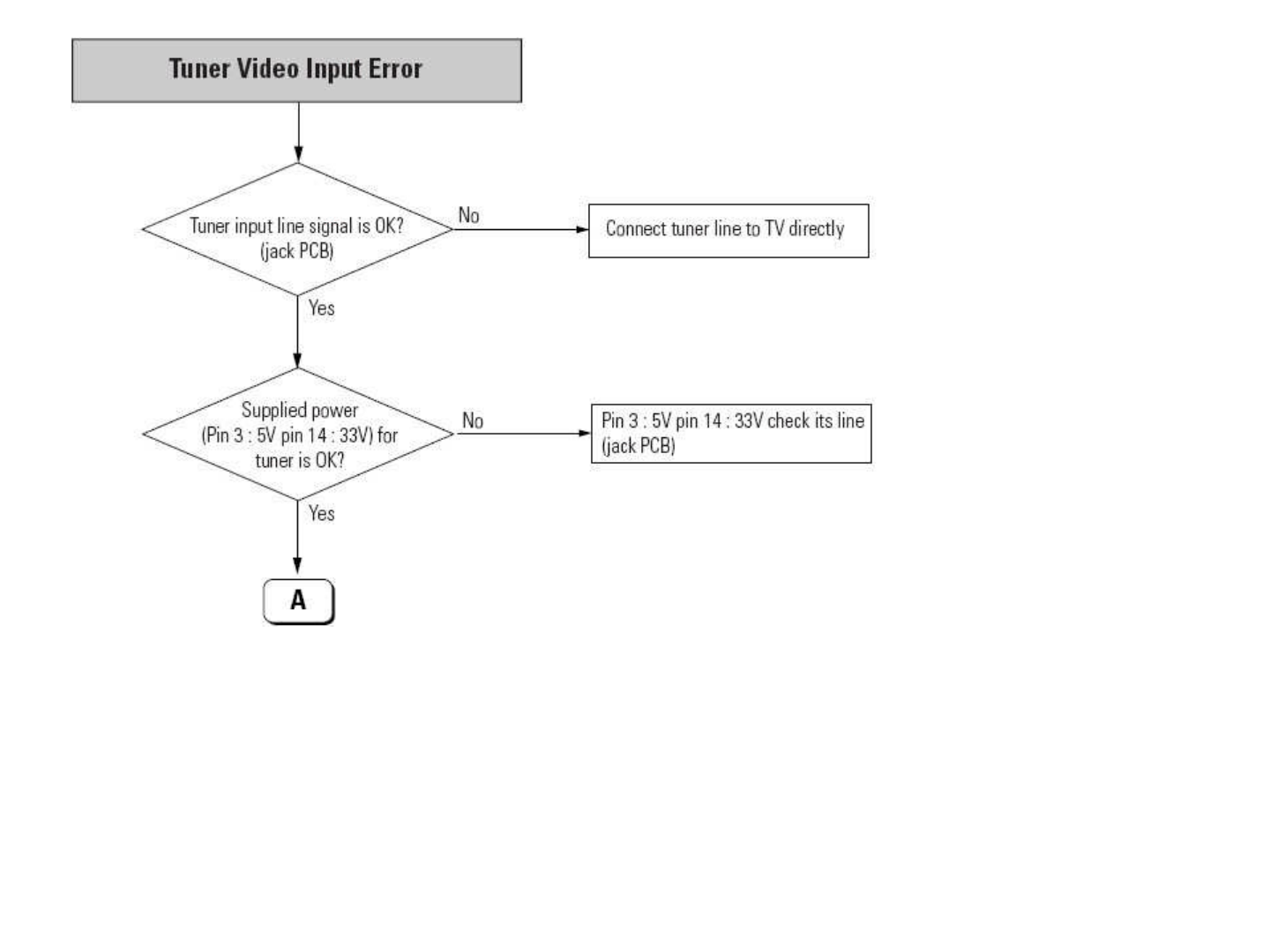
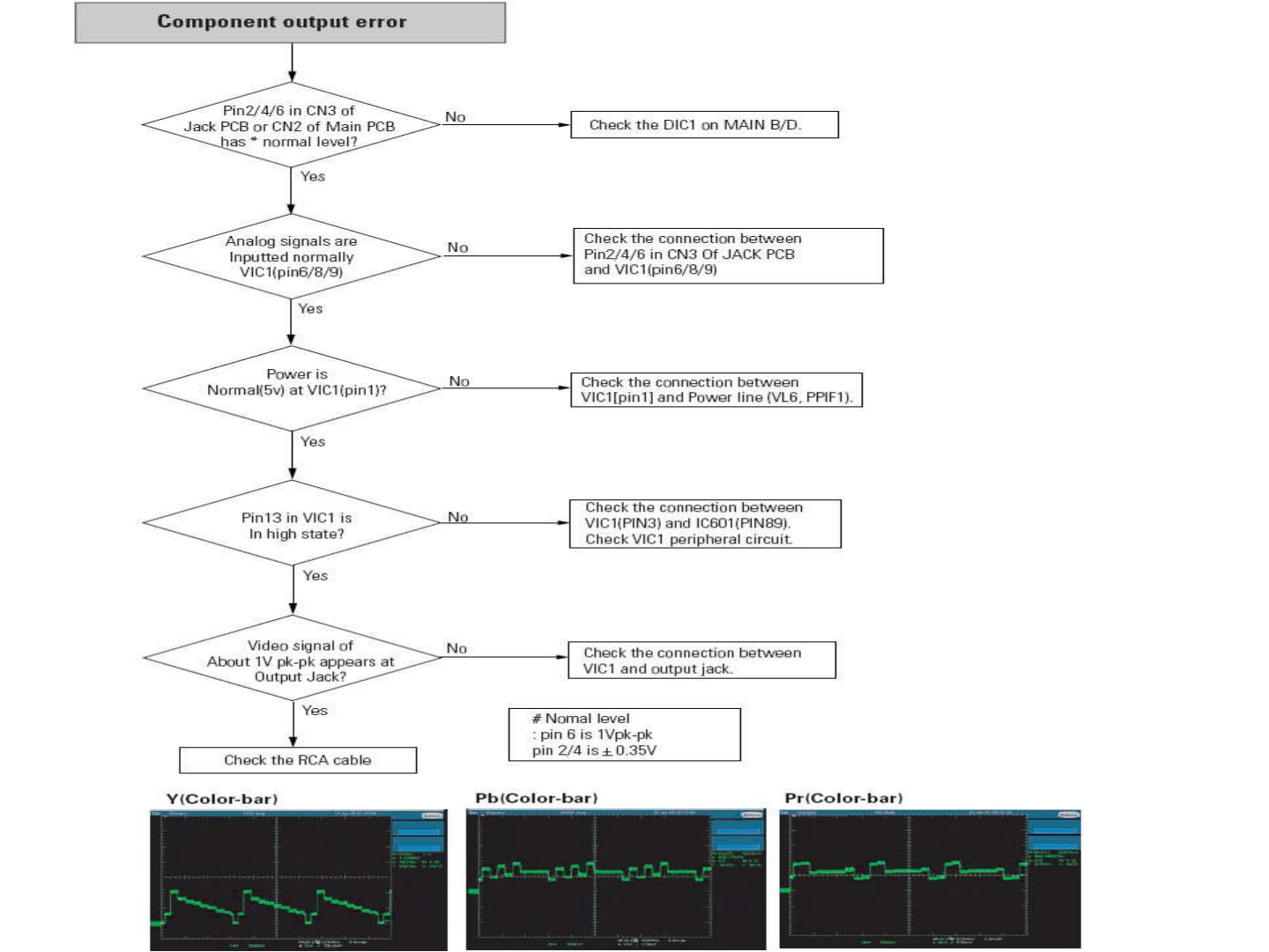
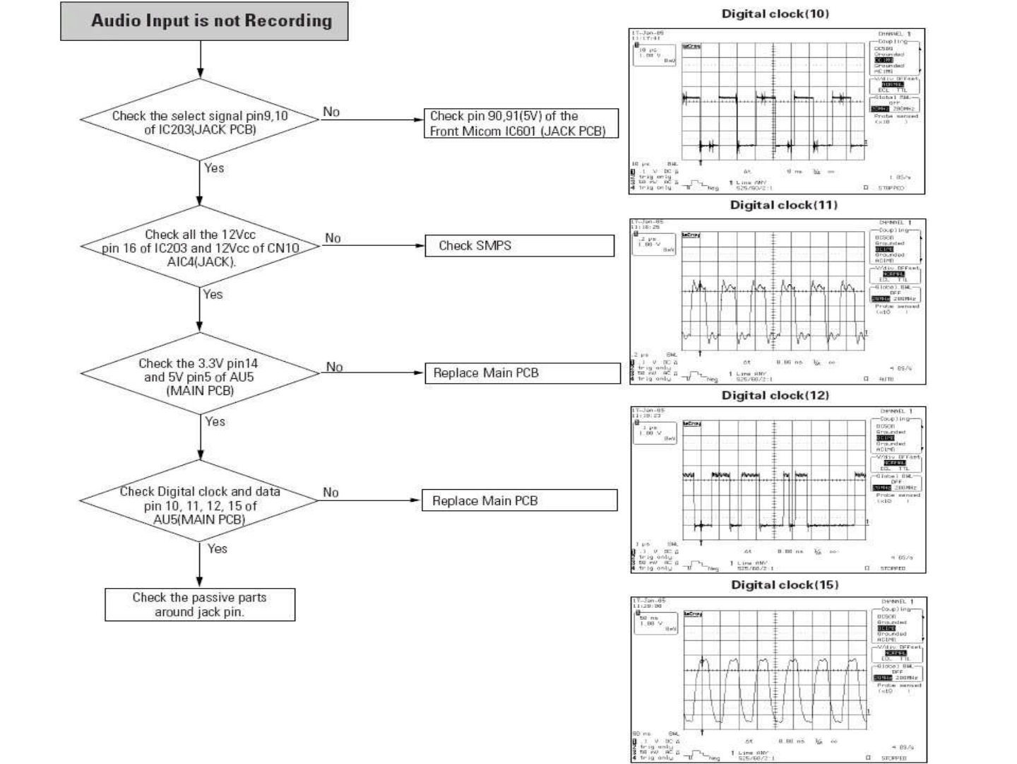
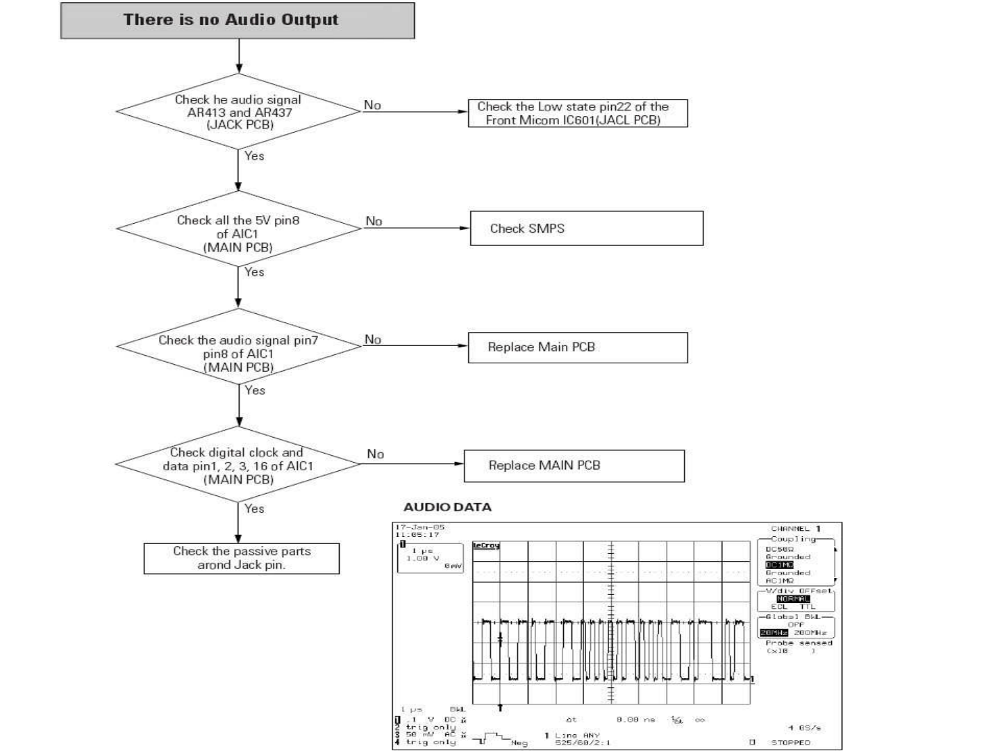
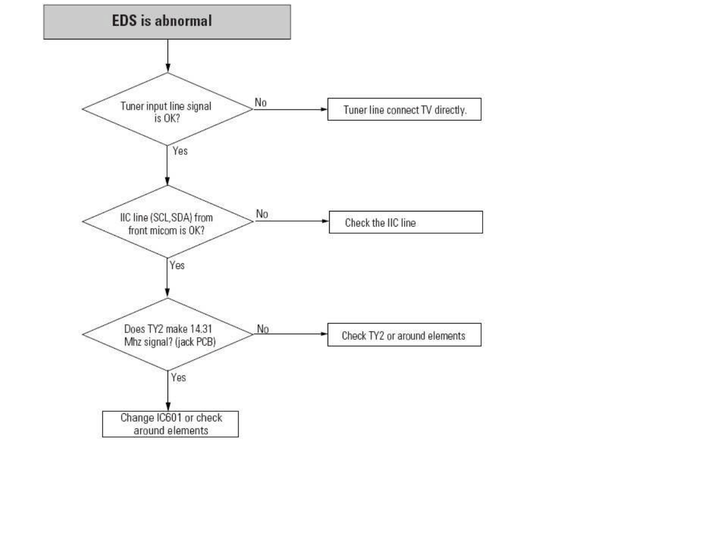
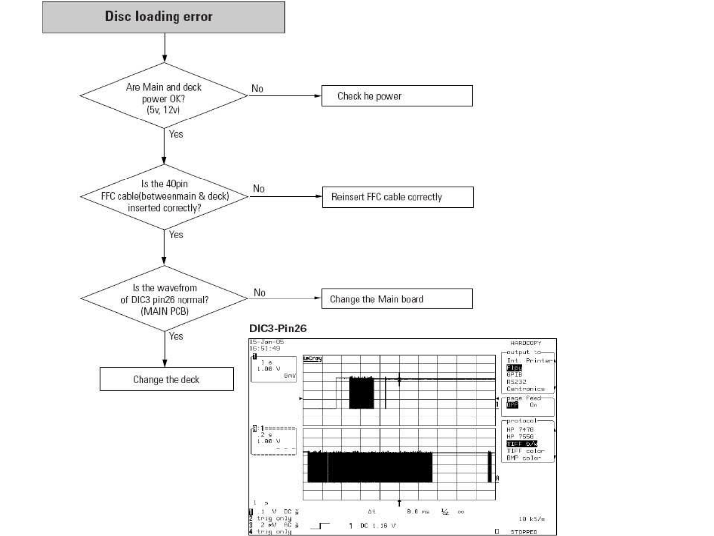
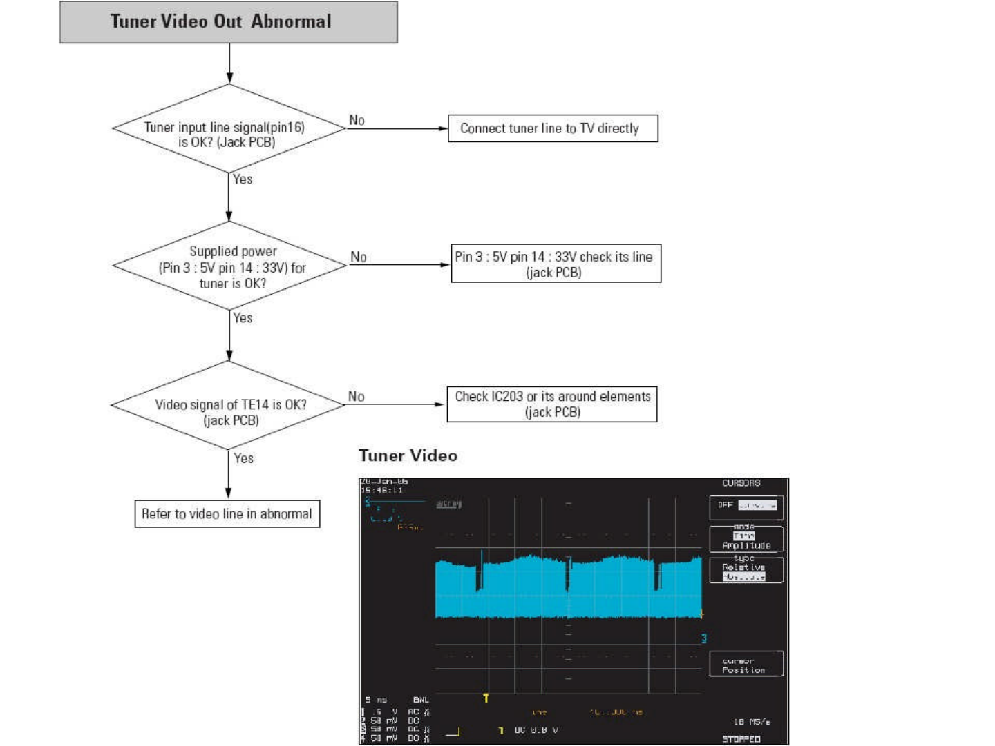
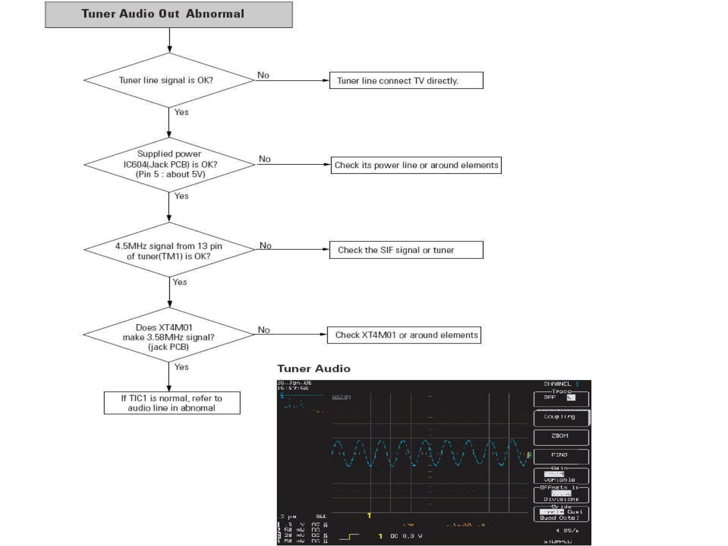
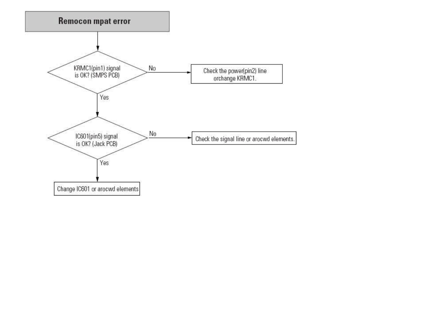
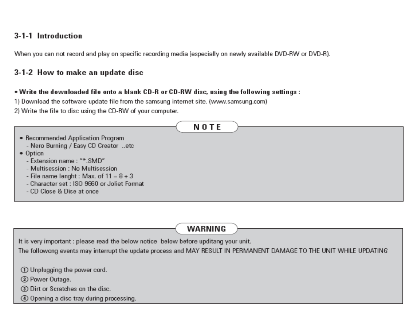
9. Software Upgrade