Acrobat Distiller, Job 9 DVDR980
User Manual: DVDR980
Open the PDF directly: View PDF ![]() .
.
Page Count: 335 [warning: Documents this large are best viewed by clicking the View PDF Link!]
- 1. Technical Specifications and Connection Facilities
- 2. Safety Instructions, Warnings, Notes, and Service Hints
- 3. Directions For Use
- 4. Mechanical Instructions
- 5. Diagnostic Software and Faultfinding Trees
- 5.1 End User/Dealer Script Interface
- 5.2 Player Script Interface
- 5.3 Menu and Command Mode Interface
- 5.3.1 Nuclei Numeration
- 5.3.2 Error Handling
- 5.3.3 Command Mode Interface
- 5.3.4 Menu Mode Interdace
- Activation
- Menu Structure
- Main Menu
- Digital Board Menu
- Host Decoder Menu
- Digital Board Versions Menu
- Audio Mute Menu
- Colourbar Menu
- Pink Noise Menu
- Sine Generate Menu
- VSM Menu
- AVENC Menu
- Empress Menu
- Video Input Processors Menu
- NVRAM Menu
- Analogue Board Menu
- Analogue Board Versions Menu
- Analogue Components Menu
- Analogue Board Re-virginize Menu
- Front Panel Menu
- Flap Control Menu
- Segment Test Menu
- Basic Engine Menu
- Basic Engine Error Log
- Basic Engine Spindle Motor Menu
- Basic Engine Radial Menu
- Basic Engine Sledge Menu
- Basic Engine Tray Menu
- DVIO Menu
- DVIO Led Menu
- Progressive Scan Board Menu
- Loop Tests Menu
- Digital Board Loops Menu
- User/Dealer Loops Menu
- System Loops Menu
- Basic Engine Loops Menu
- Log Menu
- Script Menu
- 5.4 Nuclei Error Codes
- 5.5 Loop tests
- 5.5.1 Nucleus 900: Digital Audio Loop
- 5.5.2 Nucleus 901: Audio User Dealer Loop
- 5.5.3 Nucleus 902: Digital Video Loop
- 5.5.4 Nucleus 903: Digital Video VBI Loop
- 5.5.5 Nucleus 904: System Video Loop
- 5.5.6 Nucleus 905: System Video VBI Loop
- 5.5.7 Nucleus 906: Video User Dealer Loop
- 5.5.8 Nucleus 907: Video VBI User Dealer Loop
- 5.5.9 Nucleus 908: System Audio Loop Scart (Europe)
- 5.5.10 Nucleus 909: System Audio Loop CINCH (Nafta)
- 5.6 Faultfinding trees
- 6. Block and Wiring Diagram.
- 7. Electrical Diagrams and Print-Layouts
- Power Supply
- Power Supply
- Layout Power Supply (Top View)
- Layout Power Supply (Overview Bottom View)
- Layout Power Supply (Part 1 Bottom View)
- Layout Power Supply (Part 2 Bottom View)
- Display Panel
- Layout Display Panel (Top View)
- Layout Display Panel (Overview Bottom View)
- Layout Display Panel (Part 1 Bottom View)
- Layout Display Panel (Part 2 Bottom View)
- Front AV Part
- Layout Front AV Part
- IR and Standby Panel
- Analog Board: All in One 1
- Analog Board: All in One 2
- Analog Board: Tuner / Demodulator
- Analog Board: In / Out 1
- Analog Board: In / Out 2
- Analog Board: In / Out 3
- Analog Board: In / Out 4
- Analog Board: Sound Processing
- Analog Board: Follow Me
- Analog Board: VPS
- Analog Board: Power Supply
- Analog Board: Audio Converter
- Analog Board: RGB-YUV-Converter
- Analog Board: Digital In / Out
- Analog Board: Fan Control
- Layout Analog Board (Overview Top View)
- Layout Analog Board (Part 1 Top View)
- Layout Analog Board (Part 2 Top View)
- Layout Analog Board (Overview Bottom View)
- Layout Analog Board (Part 1 Bottom View)
- Layout Analog Board (Part 2 Bottom View)
- Layout Analog Board (Testlands Top View)
- Layout Analog Board (Testlands Bottom View)
- DVIO Front Board
- Layout DVIO Front Board
- DVIO Board: 1394 Interface
- DVIO Board: Microprocessor
- DVIO Board: Fifo & Control
- DVIO Board: DVCODEC
- DVIO Board: Audio & Video Output
- Layout DVIO Board (Overview Top View)
- Layout DVIO Board (Part 1 Top View)
- Layout DVIO Board (Part 2 Top View)
- Layout DVIO Board (Testlands Bottom View)
- Digital Board: VSM, Buffer Memory and Bit Engine Interface
- Digital Board: AV Decoder STI5508
- Digital Board: AV Decoder Memory
- Digital Board: Video Encoder, Empress
- Digital Board: VIP CVBS Y/C Video Input
- Digital Board: Analog Board Cons. Video In / Output
- Digital Board: Progressive Scan
- Digital Board: Progressive Scan
- Digital Board: Power, Clock, and Reset Audio Clock
- Layout Digital Board (Overview Top View)
- Layout Digital Board (Part 1 Top View)
- Layout Digital Board (Part 2 Top View)
- Layout Digital Board (Overview Bottom View)
- Layout Digital Board (Part 1 Bottom View)
- Layout Digital Board (Part 2 Bottom View)
- Layout Digital Board (Testlands Bottom View)
- Layout Digital Board (Mapping Testlands )
- 8. Alignments
- 9. Circuit-, IC Descriptions and List of Abbreviations
- 9.1 Multi-Mode SOPS 50PS203
- 9.2 Display Board
- 9.3 Analogue Board Europe
- 9.4 Analog Board Nafta version
- 9.5 Digital Board
- 9.6 Divio Board
- 9.7 IC’s Analog Board
- 9.8 IC’s Digital Board
- 9.9 IC’s Divio
- 9.10 List of Abbreviations
- 10. Spare Parts List
Published by MT 0261 Service PaCE Printed in the Netherlands Subject to modification EN 3122 785 11970
©
Copyright 2002 Philips Consumer Electronics B.V. Eindhoven, The Netherlands.
All rights reserved. No part of this publication may be reproduced, stored in a
retrieval system or transmitted, in any form or by any means, electronic,
mechanical, photocopying, or otherwise without the prior permission of Philips.
DVD-Video Recorder DVDR980 & DVDR985
/001 /021 /051
CL 26532011_000.eps
160102
Contents Page Contents Page
1 Technical Specifications and
Connection Facilities 2
2 Warnings, Laser Safety Instructions and Notes 5
3 Directions for Use 7
4 Mechanical Instructions and Exploded Views 33
5 Diagnostic Software Descriptions and
Troubleshooting 38
6Block and Wiring Diagram
Block Diagram 93
Wiring Diagram 94
7Electrical Diagrams And Print-Layouts Diagram PWB
Power Supply (Diagram 1) 95 97-100
Power Supply (Diagram 2) 96 97-100
Display Panel (Diagram 1) 101 102->
Front AV Part 105 106
IR & Standby Panel 107 107
Analog Board: All In One 1 (Diagram 1) 108 121->
Analog Board: All In One 2 (Diagram 2) 109 121->
Analog Board: Tuner / Demodul. (Diagram 3) 110 121->
Analog Board: In / Out 1 (Diagram 4) 111 121->
Analog Board: In / Out 2 (Diagram 5) 112 121->
Analog Board: In / Out 3 (Diagram 6) 113 121->
Analog Board: In / Out 4 (Diagram 7) 114 121->
Analog Board: Sound Processing (Diagram 8) 115 121->
Analog Board: Follow Me (Diagram 9) 116 121->
Analog Board: VPS (Diagram 10) 116 121->
Analog Board: Power Supply (Diagram 11) 117 121->
Analog Board: Audio Converter (Diagram 12) 118 121->
Analog Board: RGB-YUV Conv. (Diagram 13) 119 121->
Analog Board: Digital In / Out (Diagram 14) 119 121->
Analog Board: Fan Control (Diagram 15) 120 121->
DVIO Front Board 129 129
DVIO Board: 1394 Interface (Diagram 1) 130 135->
DVIO Board: Microprocessor (Diagram 2) 131 135->
DVIO Board: FIFO & Control (Diagram 3) 132 135->
DVIO Board: DVCODEC (Diagram 4) 133 135->
DVIO Board: A/V Output (Diagram 5) 134 135->
Digital Board: VSM Buffer Mem. (Diagram 1) 139 148->
Digital Board: AV Dec. STI5508 (Diagram 2) 140 148->
Digital Board: AV Decoder Mem. (Diagram 3) 141 148->
Digital Board: Video Enc. Empress(Diagram 4) 142 148->
Digital Board: VIP CVBS Y/C (Diagram 5) 143 148->
Digital Board: Video In/Out (Diagram 6) 144 148->
Digital Board: Progressive Scan (Diagram 7) 145 148->
Digital Board: Progressive Scan (Diagram 8) 146 148->
Digital Board: Audio Clock (Diagram 9) 147 148->
8 Electrical Alignments 157
9 Circuit Descriptions and 160
List of Abbreviations 322
10 Spare Part List 327

Technical Specifications and Connection Facilities
EN 2 DVDR980-985 /0X11.
1. Technical Specifications and Connection Facilities
1.1 General:
Mains voltage : 220V-240V (198 -
264V AC) for Europe/
Asia
Mains frequency : 50 Hz - 60Hz
Power consumption mains : 32 W
Power consumption standby : < 7 W
Power consumption low power
stand-by : < 3 W
1.2 RF Tuner
Test equipment:Fluke 54200 TV Signal generator
Test streams:PAL BG Philips Standard test pattern
1.2.1 System:
PAL B/G, PAL D/K, SECAM L/L’, PAL I
1.2.2 RF - Loop Through:
Frequency range : 45 MHz - 860 MHz
Gain: (ANT IN - ANT OUT) : -4 dB /±2 dB
1.2.3 Radio Interference:
input voltage /3 tone method (+40
dB min) : typ. 80 dBµV at 75Ω
1.2.4 Receiver:
PLL tuning with AFC for optimum reception
Frequency range: : 45.25 MHz - 860 MHz
Sensitivity at 40 dB S/N : ≥ 60dBµV at 75Ω
(video unweighted )
1.2.5 Video Performance:
Channel 25 / 503,25 MHz,
Test pattern: PAL BG PHILIPS standard test pattern,
RF Level 74 dBV
Measured on SCART 1
Frequency response: : 1 MHz - 4.00 MHz ±
2 dB
Group delay ( 0.1 MHz - 4.4 MHz ) : 0 nsec ± 30 nsec
1.2.6 Audio Performance:
Audio Performance Analogue - HiFi:
Frequency response at SCART 1
(L+R) output: : 40 Hz - 15 kHz / ± 1.5
dB
S/N according to DIN 45405, 7, 1967 :
and PHILIPS standard test pattern
video signal: : -50 dB unweighted
Harmonic distortion ( 1 kHz, ± 25
kHz deviation ): : 0.5 %
Audio Performance NICAM:
Frequency response at SCART
1(L+R) output: : 40 Hz - 15 kHz ± 1.5
dB
S/N according to DIN 45405, 7, 1967 :
and PHILIPS standard test pattern
video signal: : -60 dB unweighted
Harmonic distortion (1 kHz): : 0.1 %
1.2.7 Tuning
Automatic Search Tuning
scanning time without antenna : 2.5 min. PAL
stop level (vision carrier) : 75 V, 75
Maximum tuning error of a recalled
program : ± 62.5 kHz
Maximum tuning error during
operation : ± 100 kHz
Tuning Principle
automatic B,G, I, DK and L/L’detection
manual selection in "STORE" mode
1.3 Analogue Inputs
1.3.1 SCART 1 (Connected to TV)
Pin Signals:
1 - Audio R 1.8V RMS
2 - Audio R
3 - Audio L 1.8V RMS
4 - Audio GND ,
5 - Blue/Chroma
GND ,
6 - Audio L
7 - Blue out/
Chroma in 0.7Vpp ± 0.1V into 75 Ohm (*)
8 - Function
switch <2V = TV
>4.5V / <7V = asp. ratio 16:9 DVD
>9.5V / <12V = asp. ratio 4:3 DVD
9 - Green GND ,
10 - P50 control
11 - Green 0.7Vpp ± 0.1V into 75 Ohm (*)
12 - Nc
13 - Red/Chroma
GND ,
14 - fast switch
GND ,
15 - Red out/
Chroma out 0.7Vpp ± 0.1V into 75 Ohm (*)
± 3dB 0.3Vpp Chroma (burst)
16 - fast switch
RGB/ CVBS or Y <0.4V into 75 Ohm = CVBS
>1V / <3V into 75 Ohm = RGB
17 - Y/CVBS GND
OUT ,
18 - Y/CVBS GND
IN ,
19 - CVBS/Y 1Vpp ± 0.1V into 75 Ohm (*)
20 - CVBS/Y
21 - Shield ,
1.3.2 SCART 2 (Connected to AUX)
Pin Signals:
1 -Audio R 1.8V RMS
2 -Audio R
3 -Audio L 1.8V RMS
4 -Audio GND ,
5 -Blue/Chroma
GND ,
6 -Audio L
7 -Blue in/
Chroma out ± 3dB 0.3Vpp Chroma (burst)
8 -Function
switch
9 -Green GND ,
10 -P50 control

Technical Specifications and Connection Facilities EN 3DVDR980-985 /0X1 1.
11 -Green
12 -Nc
13 -Red/Chroma
GND ,
14 -fast switch
GND ,
15 -Red in/
Chroma in
16 -fast switch
RGB/ CVBS or
Y
17 -CVBS GND
OUT ,
18 -CVBS GND
IN ,
19 -CVBS/Y/RGB
sync 1Vpp ± 0.1V into 75 Ohm (*)
20 -CVBS/Y
21 -Shield ,
(*) for 100% white
1.3.3 Audio/Video Front Input Connectors
Audio
Input voltage : 2 Vrms
Input impedance : >10kΩ
Video - Cinch
Input voltage : 1 Vpp ± 0.1V
Input impedance : 75 Ω
Video - YC (Hosiden)
Input voltage Y : 1Vpp ± 0.1V
Input impedance Y : 75 Ω
Input voltage C : burst 300 mVpp ± {x}
dB
Input impedance C : 75 Ω
1.3.4 Cinch Audio/Video Line Input Rear
Audio (EXT1)
Input voltage : 2 Vrms
Input impedance : >10k Ω
Video (EXT4)
Input voltage : 1 Vpp ± 0.1V
Input impedance : 75 Ω
1.3.5 YC Input Rear (Hosiden; EXT3)
1-GND !
2 -GND !
3-Input voltage Y 1Vpp ± 0.1V/ 75 Ω
4-Input voltage C Burst 300 mVpp ± {x} dB/ 75 Ω
1.4 Video Performance
All outputs loaded with 75 Ohm
SNR measurements over full bandwidth without weighting.
1.4.1 CVBS Output Rear (EXT4)
SNR Luminance : > -65 dB
SNR Chrominance AM : > -65 dB
SNR Chrominance PM : > -65 dB
Bandwidth Luminance : 5 MHz ± 1 dB
1.4.2 YC Output Rear (Hosiden ; EXT3)
SNR : > -65 dB
SNR C - AM : > -65 dB
SNR C - PM : > -65 dB
Bandwidth Y : 5 MHz ± 1 dB
1.4.3 SCART (RGB)
SNR : > -65 dB on all output
Bandwidth : 5 MHz ± 1 dB
1.5 Audio Performance
1.5.1 Cinch Output Rear
Output voltage 2 channel mode : 2Vrms ± 1.5dB
Output voltage 5.1 channel Dolby : 1.41Vrms ± 1.5dB
Channel unbalance (1kHz) : <0.85dB
Crosstalk 1kHz : >105dB
Crosstalk 20Hz-20kHz : > 95dB
Frequency response 20Hz- 20kHz : ± 0.1dB max
Signal to noise ratio : >100 dB
Dynamic range 1kHz : >90dB
Dynamic range 20Hz-20kHz : >88dB
Distortion and noise 1kHz : >90dB
Distortion and noise20Hz-20kHz : >80dB
Intermodulation distortion : >87dB
Phase non linearity : ± 1ο max.
Level non linearity : ± 0.5dB max.
Mute (spin-up, pause, access) : >100dB
Outband attenuation: : > 50dB above 25kHz
1.5.2 Scart Audio
Output voltage 2 channel mode : 2Vrms ± 1.5dB
Output voltage 5.1 channel Dolby : 1.41Vrms ± 1.5dB
Channel unbalance (1kHz) : <0.85dB
Crosstalk 1kHz : >105dB
Crosstalk 20Hz-20kHz : > 95dB
Frequency response 20Hz- 20kHz : ± 0.1dB max
Signal to noise ratio : >100 dB
Dynamic range 1kHz : >90dB
Dynamic range 20Hz-20kHz : >88dB
Distortion and noise 1kHz : >90dB
Distortion and noise20Hz-20kHz : >80dB
Intermodulation distortion : >87dB
Phase non linearity : ± 1o max
Level non linearity : ± 0.5dB max
Mute (spin-up, pause, access) : >100dB
Outband attenuation: : > 50dB above 25kHz
1.6 Digital Output
1.6.1 Coaxial
CDDA/ LPCM (incl MPEG1) : according IEC958
MPEG2, AC3 audio : according IEC1937
DTS : according IEC1937,
amendment 1
1.6.2 Optical
identical to coaxial
1.7 Digital Video Input (IEEE 1394)
1.7.1 Applicable Standards
Implementation according:
IEEE Std 1394-1995
IEC 61883 - Part 1
IEC 61883 - Part 2 SD-DVCR (02-01-1997)

Technical Specifications and Connection Facilities
EN 4 DVDR980-985 /0X11.
Specification of consumer use digital VCR’s using 6.3 mm
magnetic tape - dec.1994
Mechanical connection according:
Annex A of 61883-1
1.7.2 Audio Quality
Output voltage 2 channel mode : 2Vrms +/- 1.5dB
Channel unbalance (1kHz) : Tbd
Crosstalk 1kHz : > 85 dB
Crosstalk 20Hz-20kHz : > 95 dB
Frequency response 20Hz- 12kHz : +/- 1dB max
Signal to noise ratio : >95 dB
Dynamic range 1kHz : tbd
Dynamic range 20Hz-20kHz : Tbd
Distortion and noise 1kHz : >65dB
Distortion and noise 20Hz-20kHz : >65dB
Intermodulation distortion : >80dB
Phase non linearity : tbd
Level non linearity : tbd
Outband attenuation : tbd
1.8 P50 System Control
Via SCART pin nr 10
1.9 Dimensions and Weight
Height of feet : 12mm
Apparatus tray closed : WxDxH :435 x 325 x
107
Apparatus tray open : WxDxH :435 x 465 x
107
Weight without packaging : 5.67 Kg
Weight accesoiries : 1.675 Kg
1.10 Laser Output Power & Wavelength
1.10.1 DVD
Output power during reading : 0.8mW
Output power during writing : 20mW
Wavelength : 660nm
1.10.2 CD
Output power : 0.3mW
Wavelength : 780nm

Safety Instructions, Warnings, Notes, and Service Hints EN 5DVDR980-985 /0X1 2.
2. Safety Instructions, Warnings, Notes, and Service Hints
2.1 Safety Instructions
2.1.1 General Safety
Safety regulations require that during a repair:
•Connect the unit to the mains via an isolation transformer.
•Replace safety components, indicated by the symbol ,
only by components identical to the original ones. Any
other component substitution (other than original type) may
increase risk of fire or electrical shock hazard.
Safety regulations require that after a repair, you must return
the unit in its original condition. Pay, in particular, attention to
the following points:
•Route the wires/cables correctly, and fix them with the
mounted cable clamps.
•Check the insulation of the mains lead for external
damage.
•Check the electrical DC resistance between the mains plug
and the secondary side:
1. Unplug the mains cord, and connect a wire between
the two pins of the mains plug.
2. Set the mains switch to the 'on' position (keep the
mains cord unplugged!).
3. Measure the resistance value between the mains plug
and the front panel, controls, and chassis bottom.
4. Repair or correct unit when the resistance
measurement is less than 1 MΩ.
5. Verify this, before you return the unit to the customer/
user (ref. UL-standard no. 1492).
6. Switch the unit ‘off’, and remove the wire between the
two pins of the mains plug.
2.1.2 Laser Safety
This unit employs a laser. Only qualified service personnel may
remove the cover, or attempt to service this device (due to
possible eye injury).
Laser Device Unit
Type : Semiconductor laser
GaAlAs
Wavelength : 650 nm (DVD)
: 780 nm (VCD/CD)
Output Power : 20 mW
(DVD+RW writing)
:0.8 mW
(DVD reading)
:0.3 mW
(VCD/CD reading)
Beam divergence : 60 degree
Figure 2-1
Note: Use of controls or adjustments or performance of
procedure other than those specified herein, may result in
hazardous radiation exposure. Avoid direct exposure to beam.
2.2 Warnings
2.2.1 General
•All ICs and many other semiconductors are susceptible to
electrostatic discharges (ESD, "). Careless handling
during repair can reduce life drastically. Make sure that,
during repair, you are at the same potential as the mass of
the set by a wristband with resistance. Keep components
and tools at this same potential.
Available ESD protection equipment:
–Complete kit ESD3 (small tablemat, wristband,
connection box, extension cable and earth cable) 4822
310 10671.
–Wristband tester 4822 344 13999.
•Be careful during measurements in the live voltage section.
The primary side of the power supply (pos. 1005), including
the heatsink, carries live mains voltage when you connect
the player to the mains (even when the player is 'off'!). It is
possible to touch copper tracks and/or components in this
unshielded primary area, when you service the player.
Service personnel must take precautions to prevent
touching this area or components in this area. A 'lightning
stroke' and a stripe-marked printing on the printed wiring
board, indicate the primary side of the power supply.
•Never replace modules, or components, while the unit is
‘on’.
2.2.2 Laser
•The use of optical instruments with this product, will
increase eye hazard.
•Only qualified service personnel may remove the cover or
attempt to service this device, due to possible eye injury.
•Repair handling should take place as much as possible
with a disc loaded inside the player.
•Text below is placed inside the unit, on the laser cover
shield:
Figure 2-2
2.2.3 Notes
Dolby
Manufactered under licence from Dolby Laboratories. “Dolby”,
“Pro Logic” and the double-D symbol are trademarks of Dolby
Laboratories. Confidential Unpublished Works.
©1992-1997 Dolby Laboratories, Inc. All rights reserved.
Figure 2-3
Trusurround
TRUSURROUND, SRS and symbol (fig 2-4) are trademarks of
SRS Labs, Inc. TRUSURROUND technology is manufactured
under licence frm SRS labs, Inc.
Figure 2-4
CAUTION VISIBLE AND INVISIBLE LASER RADIATION WHEN OPEN AVOID EXPOSURE TO BEAM
ADVARSEL SYNLIG OG USYNLIG LASERSTRÅLING VED ÅBNING UNDGÅ UDSÆTTELSE FOR STRÅLING
ADVARSEL SYNLIG OG USYNLIG LASERSTRÅLING NÅR DEKSEL ÅPNES UNNGÅ EKSPONERING FOR STRÅLEN
VARNING SYNLIG OCH OSYNLIG LASERSTRÅLNING NÄR DENNA DEL ÄR ÖPPNAD BETRAKTA EJ STRÅLEN
VARO! AVATT AESSA OLET ALTTIINA NÄKYVÄLLE JA NÄKYMÄTTÖMÄLLE LASER SÄTEILYLLE. ÄLÄ KAT SO SÄT EESEEN
VORSICHT SICHTBARE UND UNSICHTBARE LASERSTRAHLUNG WENN ABDECKUNG GEÖFFNET NICHT DEM STRAHL AUSSETSEN
DANGER VISIBLE AND INVISIBLE LASER RADIATI ON WHEN OPEN AVOID DIRECT EXPOSURE TO BEAM
AT TENTION RAYONNEMENT LASER VISIBLE ET INVISIBLE EN CAS D'OUVERTURE EXPOSITION DANGEREUSE AU FAISCEAU
!

Safety Instructions, Warnings, Notes, and Service Hints
EN 6 DVDR980-985 /0X12.
Video Plus
“Video Plus+” and “PlusCode” are registered trademarks of the
Gemstar Development Corporation. The “Video Plus+” system
is manufactored under licence from the Gemstar Development
Corporation.
Figure 2-5
Macrovision
This product incorporates copyright protection technology that
is protected by method claims of certain U.S. patents and other
intellectual property rights owned by Macrovision Corporation
and other rights owners.
Use of this copyright protection technology must be autorized
by Macrovision Corporation, and is intended for home and
other limited viewing uses only unless otherwise authorized by
Macrovision Corporation. Reverse engineering or disassembly
is prohibited.

Directions For Use EN 7DVDR980-985 /0X1 3.
3. Directions For Use
English
INTRODUCTION 7
Box contents
First check and identify the contents of your DVD
recorder package, as listed below:
- DVD recorder
- Remote Control Handset with separately-packed
batteries
- 2-core power cord
-
SCART
cable
- S-video cable
- Antenna (aerial) cable
- Audio cable
- Video cable
- DVD+RW disc
- User Manual
- Warranty card
If any item should be damaged or missing, please inform
your supplier without delay.
Keep the packaging materials; you may need them to
transport your recorder in the future.
Placement
lPlace the recorder on a firm, flat surface.
lKeep away from domestic heating equipment and
direct sunlight.
lIn a cabinet, allow about 2.5 cm (1 inch) of free
space all around the recorder for adequate
ventilation.
lThe lense may cloud over when the DVD recorder
is suddenly moved from cold to warm surroundings.
Playing a CD/DVD is not possible then. Leave the
DVD recorder in a warm environment for two
hours before use, so the moisture can evaporate.
lThe recorder should not be exposed to dripping or
splashing, no objects filled with liquids, such as vases,
should be placed on the recorder.
Cleaning discs
Some problems may occur because the disc inside the
recorder is dirty. To avoid these problems clean your
discs regularly, in the following way:
lWhen a disc becomes dirty, clean it with a cleaning
cloth. Wipe the disc from the centre out.
Caution:
Do not use solvents such as benzine, thinner,
commercially available cleaners, or anti-static
spray intended for analogue discs.
Do not use commercially available cleaning discs
to clean the lens, as these discs may damage the
optical unit.
Remote control
Loading the batteries
lOpen the battery compartment cover.
lInsert two 'AA' (LR-6) batteries as indicated inside
the battery compartment.
lClose the cover.
Caution:
Do not mix old and new batteries. Never mix
different types of batteries (standard, alkaline,
etc.). This may reduce the lifetime of the
batteries.
English
6INTRODUCTION
Introduction
DVD Video Recorder
DVD (Digital Versatile Disc) is the new storage medium
that combines the convenience of the Compact Disc
with the latest advanced digital video technology.
DVD-Video uses state-of-the-art MPEG2 data
compression technology to register an entire movie on a
single 5-inch disc. DVD’s variable bitrate compression,
running at up to 9.8 Mbits/second, captures even the
most complex pictures in their original quality.
The crystal-clear digital pictures have a horizontal
resolution of over 500 lines, with 720 pixels (picture
elements) to each line. This resolution is more than
double that of VHS, superior to Laser Disc, and entirely
comparable with digital masters made in recording
studios.
DVD recording is the next step in video technology.
DVD+ReWritable (DVD+RW) uses phase-change media,
the same technology that formed the basis for CD-
ReWritable. A high-power laser is used to change the
reflectivity of the recording layer. This process can be
repeated more than a thousand times. DVD+Recordable
(DVD+R) uses discs based on an organic dye, a
technology pioneered with the successful CD-
Recordable format, to produce discs that keep your data
for a lifetime.
Your Philips DVD recorder is a recorder and player
for digital video discs, with a two-way compatibility
to the universal DVD-Video standard. This means that:
- existing pre-recorded DVD-Video discs can be
played on your Philips DVD recorder and
- recordings, made on your Philips DVD recorder, can
be played on most DVD-Video players and
DVD-ROM drives.
With it, you will be able to record TV programmes or
to edit and archive your own camcorder recordings.
Superb digital picture and sound quality, quick access to
the tracks you have recorded and extensive playback
features contribute to a completely new video
experience.
From now on you will enjoy full-length movies with true
cinema picture quality, and stereo or Multi-channel
sound (depending on the disc, and on your playback set-
up).You will find your recorder remarkably easy to use,
by way of the On-Screen Display on your TV and the
display on the DVD recorder, in combination with the
remote control.
pre-recorded DVD DVD+R(W)
DVD Video
player
Philips DVD
recorder
Directions For Use
EN 8 DVDR980-985 /0X13.
English
INSTALLATION 9
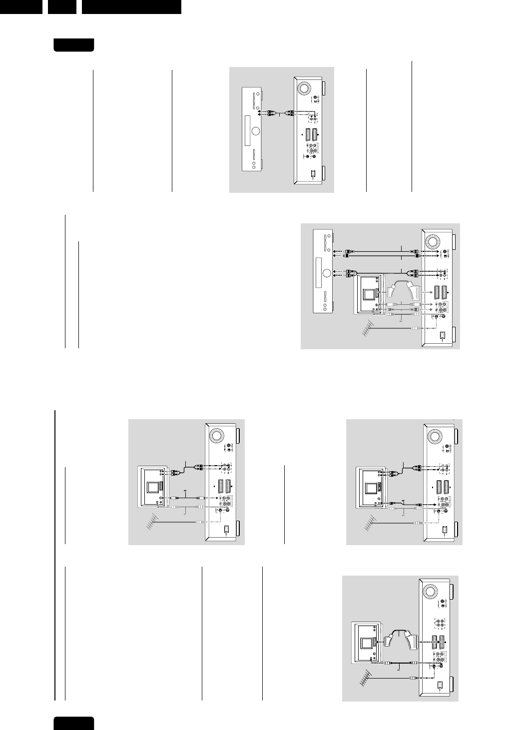
Connecting to audio equipment
Connecting to A/V receiver or A/V
amplifier with digital Multi-channel
decoder
The best possible sound quality is obtained by
connecting your DVD recorder to an A/V receiver with
Multi-channel decoder (Dolby Digital, MPEG 2 and DTS).
Digital Multi-channel sound
Digital Multi-channel connection provides the optimum
sound quality. For this you need a Multi-channel A/V
receiver that supports one or more of the audio types
supported by your DVD recorder (MPEG 2, Dolby
Digital and DTS). For this you can check the receiver
manual and the logos on the front of the receiver.
lConnect the recorder’s digital audio output to the
corresponding input on the receiver. Use a digital
coaxial cable (7) or a digital optical audio cable (8).
If you do not own a digital coaxial audio cable (not
supplied), you may use the supplied video cable (4).
Note:
If the audio type of the digital output does not match the
capabilities of your receiver, the receiver will produce a
strong, distorted sound. The audio type of the DVD disc in
play is displayed in the Status Window, when changing the
language. 6 Channel Digital Surround Sound via digital
connection can only be obtained if your receiver is equipped
with a Digital Multi-channel decoder.
If you cannot connect your DVD recorder to an A/V
receiver with Multi-channel decoder, choose one of the
following alternatives.
Connecting to a receiver equipped with
two channel digital stereo (PCM)
lConnect the recorder’s digital audio output to the
corresponding input on your receiver. Use the
supplied video (CVBS) cable (7) or an optional
digital optical audio cable (8).
lAfter installation you will need to activate PCM on
the DVD recorder’s digital output (see ‘User
Preferences’).
Connecting to a receiver equipped with
Dolby Pro Logic
lConnect the recorder to the TV set and connect the
recorder’s audio Left and Right output sockets to the
corresponding inputs on the Dolby Pro Logic
Audio/Video receiver, using the audio cable supplied (6).
lMake the appropriate Sound settings for Analogue
Output in the user preferences menu.
Connecting to a TV set equipped with a
Dolby Pro Logic decoder
lConnect the recorder to the TV set as described in
chapter ‘Connecting to a TV set’.
Connecting to a receiver with two channel
analogue stereo
lIf you have a receiver with two-channel analogue
stereo without any of the above mentioned sound
systems, connect the audio Left and Right output
sockets to the corresponding sockets on your
receiver, amplifier or stereo system. Use the audio
cable supplied (6).
AUX- I/0
EXT 2
TO TV I/0
EXT 1
EXT 4 EXT 3
AMPLIFIER
6
AMPLIFIER
AUX- I/0
EXT 2
TO TV I/0
EXT 1
TV
643 87
EXT 4 EXT 3
English
8INSTALLATION
Installation
Connections - back side of your
DVD recorder
- Please refer to your TV set, VCR, Stereo System and
any other User Manual(s) as necessary to make the
optimal connections.
- Do not connect the power until all other connections
are made.
- Do not connect your DVD recorder to your TV set
via your VCR, because the video quality could be
distorted by the copy protection system.
- For better sound reproduction you can connect the
recorder audio outputs to your amplifier, receiver,
stereo system or A/V equipment. For this see
‘Connecting to A/V receiver or A/V amplifier’.
Caution:
Do not connect the recorder’s audio output to
the phono input of your audio system in order to
avoid damage to your equipment.
Connecting to the antenna
lRemove the antenna (aerial) cable plug from your
TV set and insert it into the antenna socket at the
back of the DVD recorder.
lPlug one end of the antenna (aerial) cable supplied (1)
into the TV socket on the DVD recorder and the other
end into the antenna input socket on your TV set.
Connecting to a TV set
To obtain the highest possible picture and sound quality
from your TV set it is recommended to use the
SCART
connector on both DVD recorder and TV set.
lConnect the bottom
SCART
connector (EXT 1) to
the TV set, using the
SCART
cable supplied (2) as
shown in the drawing. If your TV set is equipped
with EasyLink or Cinema Link, make sure you use
the correct
SCART
connector. For this refer to the
user manual of your TV set.
If your TV set is not equipped with a
SCART
connector,
you can connect the DVD recorder with the S-video
(Y/C) sockets.
S-video (Y/C) connection
lConnect the S-video output socket to the
corresponding input socket on the TV set, using the
supplied S-video cable (3).
lConnect the audio Left (white) and Right (red)
output sockets to the corresponding sockets on the
TV set using the audio cable supplied (5).
If your TV set is not equipped with S-video sockets, then
connect the DVD recorder with the CVBS sockets to
your TV set.
Video (CVBS) connection
lConnect the Video (CVBS) output socket (yellow)
to the corresponding input socket on the TV set
using the video cable supplied (4).
lConnect the audio Left (white) and Right (red)
output sockets to the corresponding sockets on the
TV set using the audio cable supplied (5).
AUX- I/0
EXT 2
TO TV I/0
EXT 1
5
TV
EXT 4 EXT 3
AUX- I/0
EXT 2
TO TV I/0
EXT 1
5
TV
EXT 4 EXT 3
AUX- I/0
EXT 2
TO TV I/0
EXT 1
2
TV
EXT 4 EXT 3
Directions For Use EN 9DVDR980-985 /0X1 3.
English
INSTALLATION 11
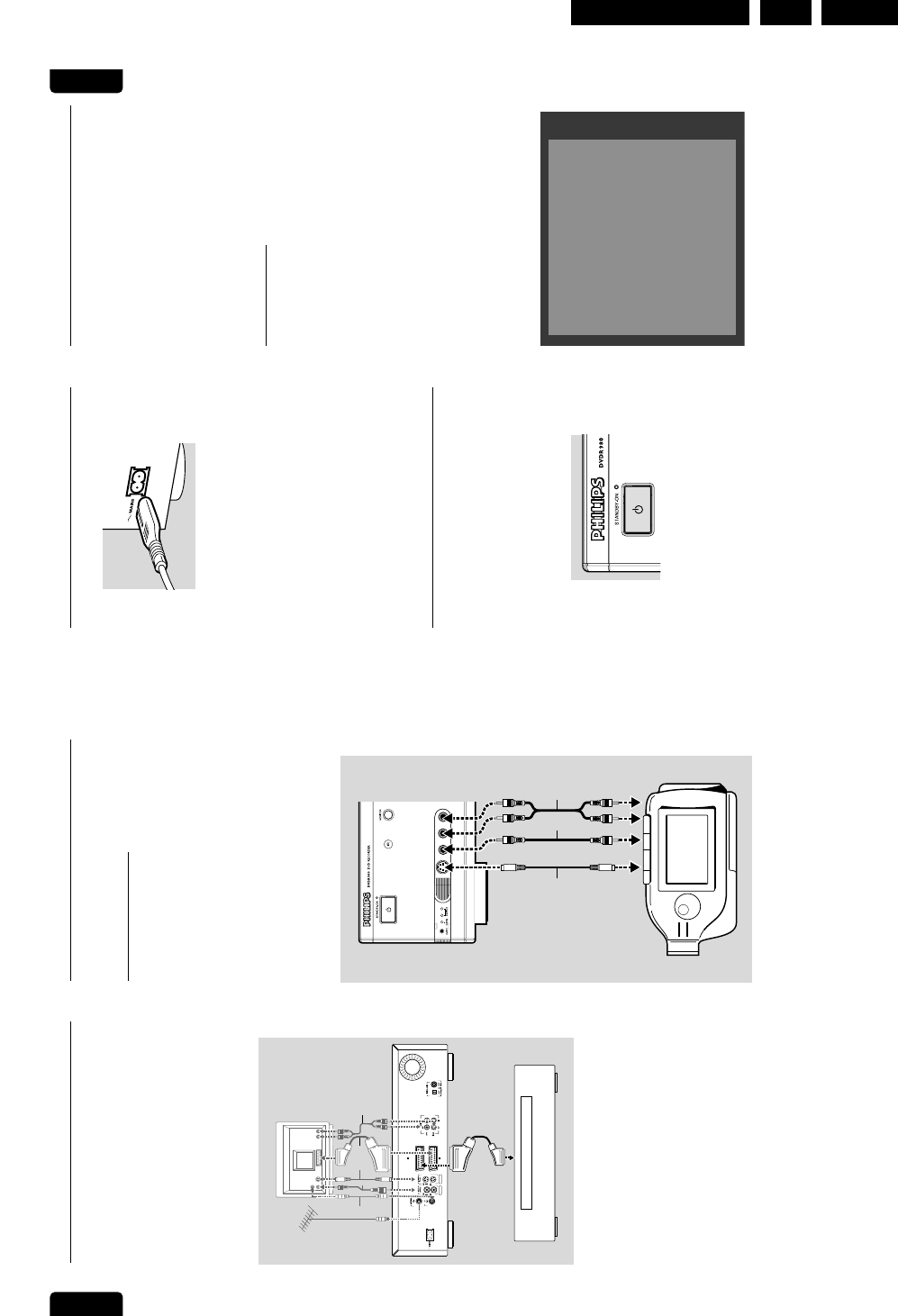
Power supply
lMake sure that all necessary connections are made
before connecting the DVD recorder to the power
supply.
lPlug the power cable supplied into the Power
connector on the rear of the recorder.
lPlug the mains plug into an AC outlet.
Note:
Always check if the local mains voltage matches the required
220V - 240V.
When the recorder is in the Standby position, it is still
consuming some power.
If you wish to disconnect your DVD recorder completely from
the mains, withdraw the plug from the AC Outlet.
When the DVD recorder is disconnected from the mains, TV
channels and timer data will be stored typically 1 year.
Switching on
lSwitch on the TV set and select the programme
number that you have chosen for video playback
(see operating manual for your TV set).
lPress BSTANDBY/ON.
‰The recorder display lights up. If you have not yet
installed your DVD recorder, it will enter ‘virgin
mode’. In this mode you will have to set your
personal preferences.
First time set-up: virgin mode
After switching on the DVD recorder for the very first
time the ‘virgin mode screen’ will appear.
In ‘virgin mode’ you may have to set your preferences
for some of the recorder features.
If the ‘virgin mode screen’ does not appear, your DVD
recorder has been installed already. You may still change
the settings via the ‘installation menu’.
Depending on the kind of TV set, preferences will have
to be set manually or they will be taken over
automatically from the TV set.
Automatic setting
When your TV set is equipped with EasyLink
TM
, Cinema
Link
TM
, N
EX
TV
IEW
Link
TM
, SmartLink
TM
, Q-Link
TM
or
MegaLogic
TM
, the TV settings will be taken over from the
TV set but they cannot be changed manually afterwards.
When preferences are taken over from your TV set, the
message ‘
Easy Link loading data from TV
-
please
wait
’ will appear.
Menus for which no preferences are available will be
displayed. They have to be set manually.
Note:
Preferences have to be set in the order in which the item
menus will appear on the screen.
If the recorder is switched off while setting user preferences,
all preferences have to be set again after switching the
recorder on again.
The ‘virgin mode’ will only be concluded after the
preferences for the last item have been confirmed.
Follow TV
Easy Link
loading data from TV -
please wait
English
10 INSTALLATION
Connecting to other equipment
Use the top
SCART
connector (EXT 2) on your DVD
recorder to make connections to a:
- Satellite receiver or Set top box,
- VCR,
- DVD-Video player
Most pre-recorded video cassettes and DVD discs are
copy protected. If you try to copy them the display
shows ‘COPY PROTECT’.
For installation of a decoder, see ‘User Preferences’ -
‘Installation’.
Notes:
- If the power is off or Low Power Standby is selected (see
User Preferences - features), the signal from EXT 2 will not
be passed on to the TV set on EXT 1.
- EasyLink functionality will not be available to devices
connected via the DVD recorder’s EXT 2
SCART
connector.
Connections - frontside of your
DVD recorder
Camcorder connection
lIf you have a DV, Digital 8, Hi-8 or S-VHS(C)
camcorder, connect the S-video input socket to the
corresponding output socket on the camcorder,
using the S-video cable supplied (1) and connect the
audio cable (3) supplied.
lOtherwise connect the Video input socket (yellow)
to the corresponding output socket on the
camcorder using the video cable supplied (2) and
connect the audio Left (white) and Right (red) input
sockets to the corresponding sockets on the
camcorder using the audio cable supplied (3).
lIf your camcorder has mono sound, use only the left
audio connector. In this case the sound will be
recorded on both audio channels.
AUDIOS-VIDEO VIDEO LR
32
1
Camcorder
Camcorder
TV
Set top box
432 5
1
AUX- I/0
EXT 2
TO TV I/0
EXT 1
EXT 4 EXT 3
Directions For Use
EN 10 DVDR980-985 /0X13.
English
INSTALLATION 13
Country
Select your country. This is used as input for the
‘Parental Control’ feature (see ‘Access Control’) as well
as the searching of TV channels.
Auto TV Channel Search
Make sure the antenna is connected. See ‘Connecting to
the antenna’. Your DVD recorder will search for all TV
channels.
It stores channels in the sequence they are found.
lConfirm with OK.
‰Auto search starts. This can take several minutes.
‰When Auto search is completed ‘
Autom.
search complete
-
XX channels found
’ appears
on the TV screen.
After Auto channel search you can have TV channels
stored automatically in the same order as your TV set.
See ‘User preferences installation’ - ‘Follow TV’.
Time/Date
When Channel auto search is completed the actual Time
and Date are also set automatically.
If the time in the DVD recorder display is not correct,
the clock must be set manually.
lAdjust ’
Time
’, ’
Year
’, ’
Month
’, ’
Date
’ if required,
with the w(down cursor) or v(up cursor) key.
lChange values with the the t(left cursor) or u
(right cursor) key or the digit keys 0-9.
lTo end, press OK.
Note:
All these items may have to be set after first start up (‘virgin
mode’). After that they can always be adapted in the user
preferences menu. When your TV set is equipped with
EasyLink the TV set presets will be taken over from the TV
set but they cannot be changed manually afterwards.
Virgin mode settings are now completed.
All settings can still be changed. See ‘User preferences’.
Autom.search
To continue
Press OK
Autom.search complete
XX channels found
Time
Year
Month
Date
09: 40
2001
02
09
Please wait
Autom.search
Searching for TV channels
XX channels found
Virgin mode
Country
Press OK to continue
Austria
Belgium
Denmark
Finland
France
English
12 INSTALLATION
Manual setting
When a menu is displayed:
lUse the wv (down up cursor) keys to go through
the options in the menu. The icon of the selected
option will be highlighted.
lUse OK to confirm your selection and to select the
next menu.
The following items may have to be set in virgin mode:
Menu language
The on-screen menus of DVD-Video discs will be
displayed in the language you choose.
Audio language
The sound of DVD-Video discs will be in the language
you choose, provided this is available on the disc in play.
If not, speech will revert to the first spoken language on
the disc. Also the DVD-Video disc menu will be in the
language you choose, provided this is available on the disc.
Subtitle language
The subtitles of DVD-Video discs will be in the language
you choose provided this is available on the disc in play. If
not, subtitles will revert to the first subtitle language on
the disc.
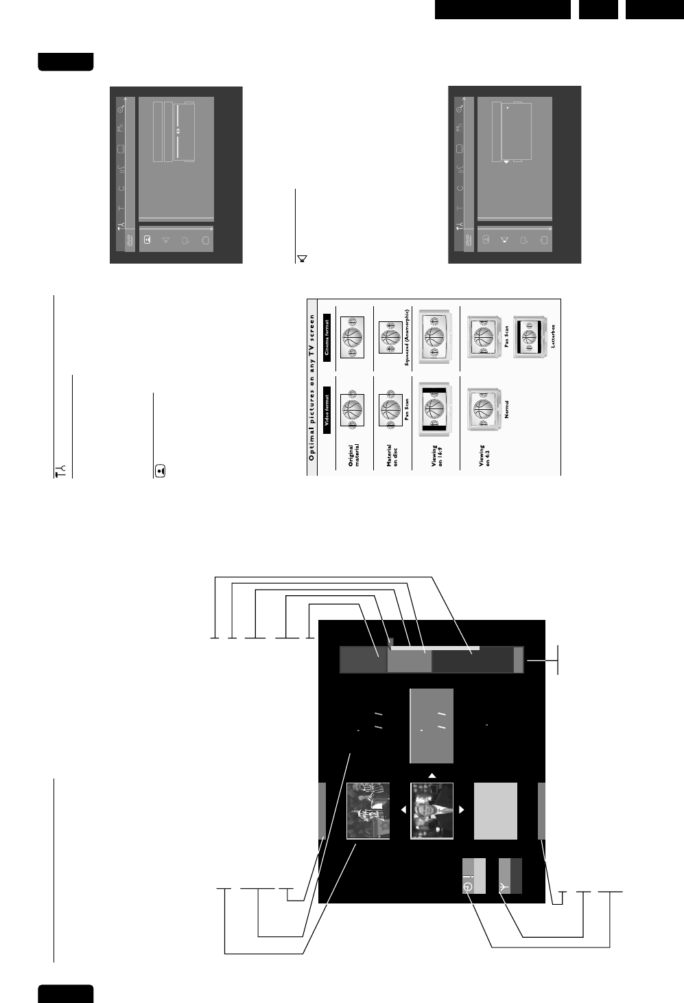
TV Shape
You can choose:
-
16:9
if you have a wide screen (16:9) TV set.
-
4:3
if you have a regular (4:3) TV set. In this case you
can also choose between:
-
Letterbox
for a ‘wide-screen’ picture with black
bars at the top and bottom,
-
Pan Scan
, for a full-height picture with the sides
trimmed. If a disc has Pan Scan, the picture then
moves (pans) horizontally to keep the main action
on the screen.
Virgin mode
TV Shape
Press OK to continue
4:3 letterbox
4:3 panscan
16:9
Virgin mode
Subtitle language
Press OK to continue
English
Español
Français
Português
Italiano
Virgin mode
Audio language
Press OK to continue
English
Español
Français
Português
Italiano
Virgin mode
Menu language
Press OK to continue
English
Español
Français
Italiano
Deutsch
Directions For Use EN 11DVDR980-985 /0X1 3.
English
FUNCTIONAL OVERVIEW 15
Apparatus Claims of U. S. Patent Nos.
4,631,603, 4,577,216, 4,819,098, and 4,907,093
licensed for limited viewing uses only.
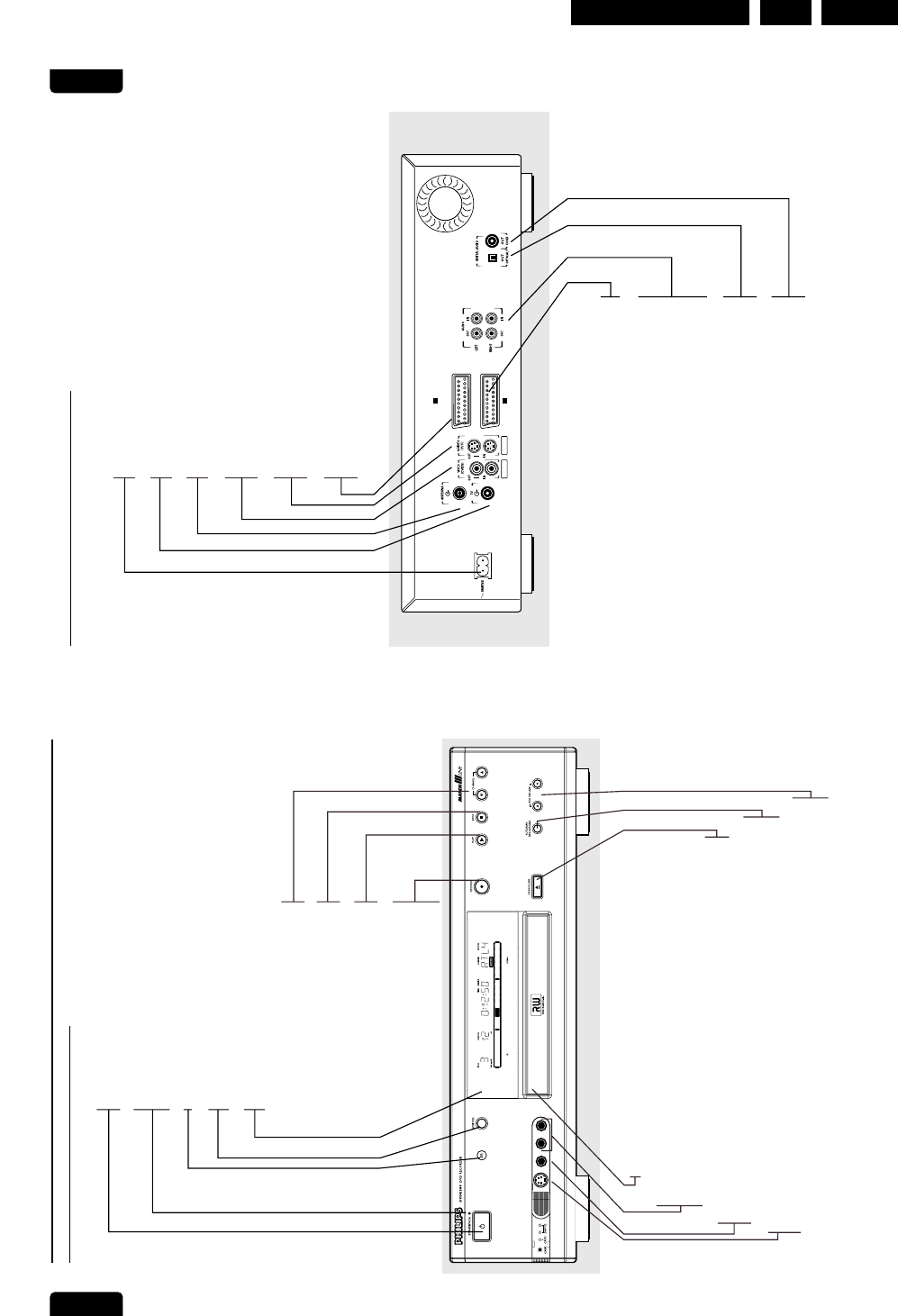
AUX- I/0
EXT 2
TO TV I/0
EXT 1
EXT 4 EXT 3
MAINS
- connection to the mains
TV
- RF connection to TV set
ANTENNA
- RF connection to antenna/cable TV signal
Video (CVBS)
- OUT: for connection to a TV, receiver or amplifier with CVBS video inputs
- IN: for connecting a video source with CVBS outputs
S-video (Y/C)
- OUT: for connection to a TV, receiver or amplifier with S-video (Y/C) inputs
- IN: for connecting a video source with S-video (Y/C) outputs
AUX I/O (EXT II)
- for connection to a satellite receiver, decoder, video recorder, set top box
etc. via
SCART
TO TV I/O (EXT I)
- for connection to a TV with
SCART
AUDIO OUT L/R
- connection to an amplifier, receiver, stereo system or
to a TV that is not equipped with a
SCART
connector
AUDIO IN L/R
- connection to the audio output of a video source that
is not equipped with a
SCART
connector
OUT OPTICAL
- connection to an amplifier, receiver or stereo system
with a digital (optical) audio input
OUT COAX
- connection to an amplifier, receiver or stereo system
with a digital (coaxial) audio input
Rear of recorder
English
Functional overview
14 FUNCTIONAL OVERVIEW
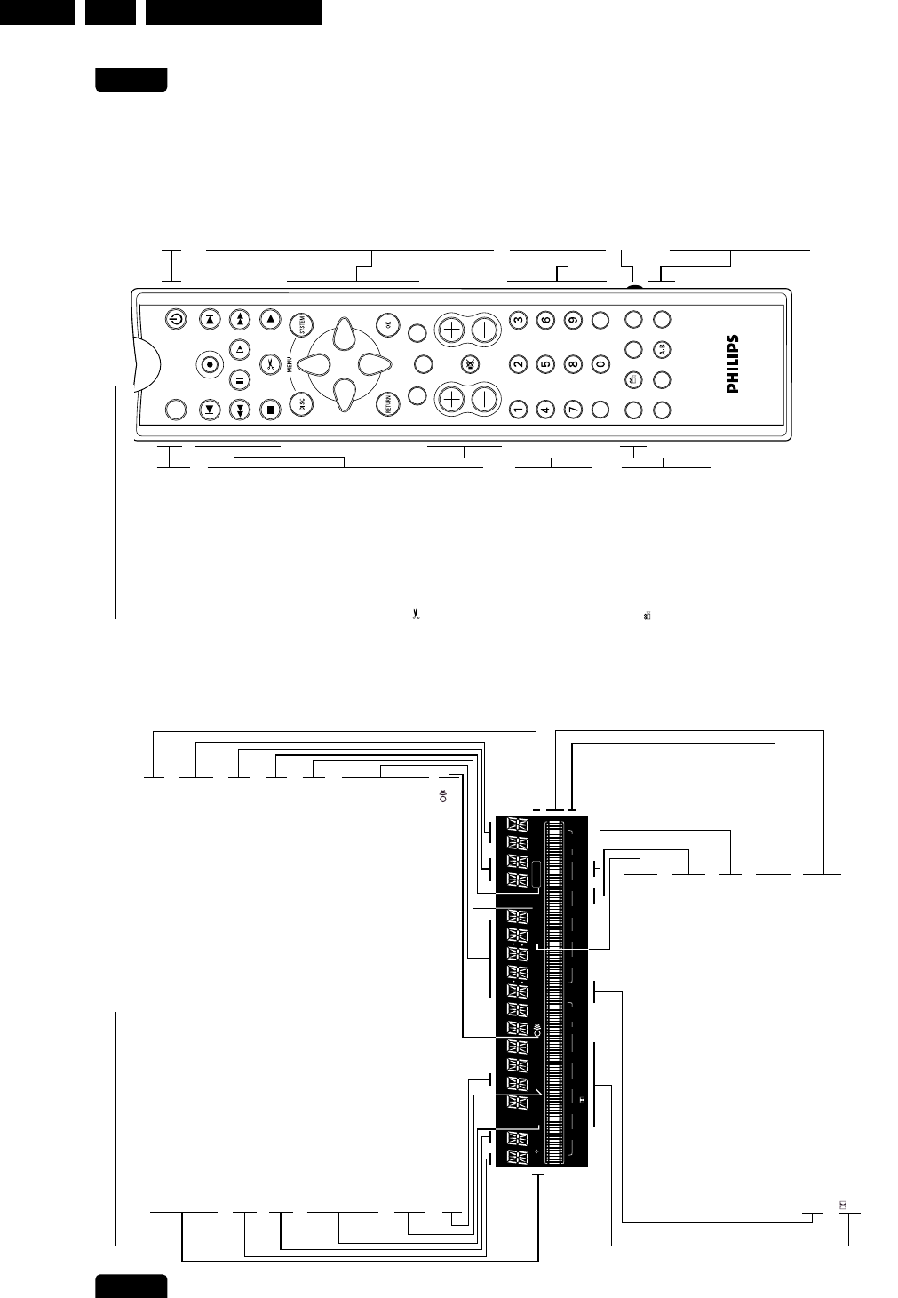
AUDIOS-VIDEO VIDEO LR
DIGITAL
B STANDBY/ON
- switches the recorder to power/standby mode
Standby indicator
- lights up red when the recorder is in standby mode
- lights up green when the recorder is operative
Infrared remote control receiver
MONITOR
- switches between disc mode and monitor mode
Display
- displays the current status of the recorder
CHANNEL
- to select channels manually
9 STOP
- stops video/audio play or recording
2 PLAY
- starts video/audio play
0 RECORD
- direct recording of the selected programme
on TV or the recorder (depending on the
DIRECT RECORD setting)
Disc loading tray
AUDIO (Left/Right)
- Audio input socket left/right to
connect a camcorder or video
recorder
VIDEO (CVBS)
- Video input socket to connect a
camcorder or video recorder
S-VIDEO
- Video input socket to connect a
camcorder or video recorder
/ OPEN/CLOSE
- opens/closes the disc tray
AUTO/MAN REC VOLUME
- to adjust the recording level
automatically or manually
MANUAL
- 3 4 to increase/decrease
the recording level
Front of recorder
Directions For Use
EN 12 DVDR980-985 /0X13.
English
FUNCTIONAL OVERVIEW 17
MONITOR ON/OFF
REC/OTR
PLAYSTOP FSS
FORWARDREVERSE
NEXT PREVIOUS
PAUSE SLOW
CLEAR
CH
VOL
SELECT
TIMER
MUTE
T/C
ZOOM ANGLE SUBTITLE AUDIO
DIM REPEAT REPEAT SCAN
A/CH
ZYa
ON/OFF B
DISC MENU
- displays DVD disc menu or index
picture screen
SYSTEM MENU
- displays recorder system menu
bar
w v u t
- down/up/right/left cursor
movement
RETURN
- return to previous menu on
(S)VCD disc
CLEAR
- delete last entry/clear timer
TIMER
- displays the ‘timer menu’
SELECT
- switches between different values
in a menu
- switches between record modes
in the Index Picture Screen and in
monitor mode
OK
- acknowledge menu selection
0-9
- numerical key pad
T/C
- select title
- select chapter
A/CH Alternate Channel
- switches to the previous TV
channel
SIDE SWITCH
- enables other keys to operate
the TV set (see Appendix)
DIM
- changes brightness setting of
display
REPEAT
- repeat chapter, track, title, disc
REPEAT A-B
- repeat sequence
SCAN
- playback of the first 10 seconds
of each chapter within a title
(DVD) or the first 10 seconds of
each track on a disc
(
VCD/CD
)
MONITOR
- switches between disc mode and
monitor mode
J
- previous chapter, track or title
0
- direct recording of the currently
selected programme
K
- next chapter, track or title
Q
- search backward
;
- pause
H
- slow motion
R
- search forward
9
- stop
FSS
- displays Favorite Scene Selection
menu for DVD+RW or DVD+R
disc
2
- play
VOL +/–
- TV volume up/down
c
- TV Mute ON/OFF
CH +/–
- programme up/down
a ZOOM
- enlarge video image
ANGLE
- select DVD camera angle
Z SUBTITLE
- subtitle language selector
Y AUDIO
- audio language selector
Remote control
English
16 FUNCTIONAL OVERVIEW
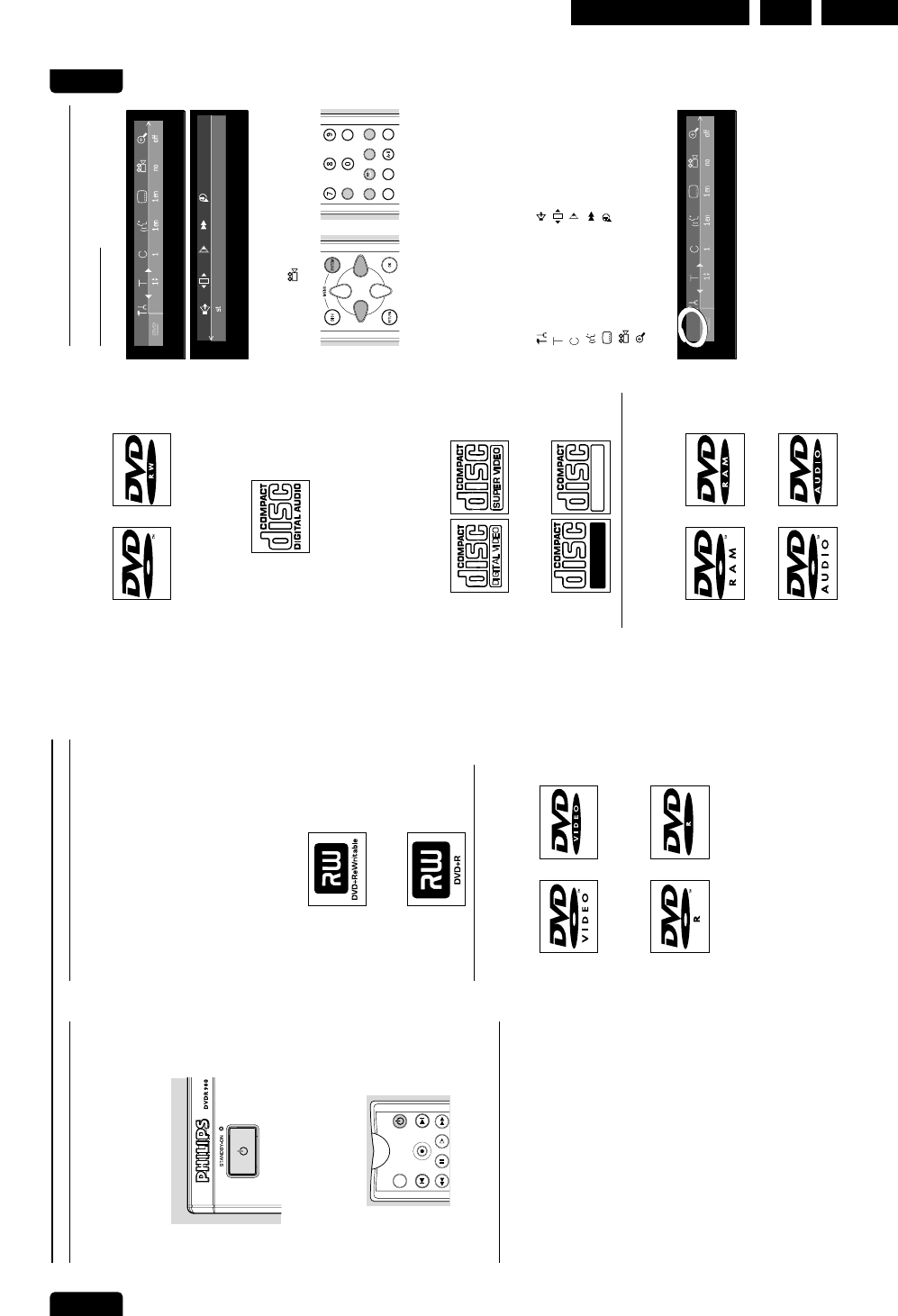
PCMDTS DIGITALMPEG
HQ SP LP EP+
VPS/PDC
DECODER
CHANNEL
DVD CDVRW
TITLE TRACK CHAPTER TOTAL TIME REMAINTRACK
MANUAL
TIMER
SAT
-30-40 -10-20 0
OVER
-30-40 -10-20 0
OVER
SA
NICAM STEREO
RECORD
DVD
- DVD Video disc inserted
DVD+R
- DVD+Recordable disc inserted
DVD+RW
- DVD+Rewritable disc inserted
TITLE
- DVD title number
TRACK
- VCD/CD track number
VCD
- Video CD inserted
CD
- Audio CD inserted
SVCD
- Super Video CD inserted
HQ - SP - LP - EP
- Selected recording mode: High Quality,
Standard Play, Long Play or Extended Play
CHAPTER
- DVD chapter number
DECODER
- Decoder activated for current preset
VPS/PDC
- Video Programming System/Programme
Delivery Control active on current preset
CHANNEL
- Preset name or number
RECORD
- Recording in progress
TIMER
- Timer programmed or active
TRACK TIME
- Track time in minutes and seconds
TOTAL TIME
- Total playback or recording time in hours,
minutes and seconds
TOTAL REMAIN
- Total remaining playback or recording time
in hours, minutes and seconds
- Remote control active (flashing)
SAT
- Recorder prepared for or engaged in satellite
recording
NICAM
- NICAM digital stereo sound on current
preset
STEREO
- Stereo sound from tuner
dB scale
- indicates recording volume when using
manual level control
Disc bar
- Displays disc content, recording level or
formatting progress
MANUAL
- Manual recording level control
DIGITAL - DTS - MPEG - PCM
- Active audio format
Display
Directions For Use EN 13DVDR980-985 /0X1 3.
English
OPERATION 19
DVD-RW
Only plays if it is recorded in Video mode and has been
finalized.
CD Digital Audio
You can play digital audio CDs in conventional style
through a stereo system, using the keys on the remote
control and/or front panel, or via the TV set using the
on-screen display (OSD).
Super Audio CD
Of hybrid SACD discs, the CD layer can be played.
(Super) Video CD
Depending on the material on the disc (a movie, video
clips, a drama series, etc.) these discs may have one or
more tracks, and tracks may have one or more indexes,
as indicated on the disc case. To make access easy and
convenient, your recorder lets you move between
tracks, and between indexes.
CD-R/CD-RW
Plays if it contains Audio CD.
The following disc types cannot be used at
all, neither for recording nor for playback:
DVD-RAM
DVD-Audio
On-screen display information
System menu bar
The system menu bar can be called up by pressing any of
the following keys on the remote control: SYSTEM
MENU, T/C,ANGLE, ZSUBTITLE, Y
AUDIO and aZOOM.
Widescreen (16:9) TV sets may show only part of the
system menu bar in certain screen modes. Select a
different screen mode on the TV to see the full menu.
A number of recorder functions can be controlled via
the system menu bar. You can navigate between the two
parts of the system menu bar with the t(left cursor)
and the u(right cursor) key.
System menu bar icons
PART 1 PART 2
User preference Sound
Title/Track Step motion
Chapter/Index Slow motion
Audio language Fast motion
Subtitle language Time search
Angle
Zoom
Temporary Feedback Field
The system menu bar contains a ‘Temporary Feedback
Field’ with information concerning prohibited actions,
playback modes, available angles, etc.
T/C
ZOOM ANGLE SUBTITLE AUDIO
DIM REPEAT REPEAT SCAN
A/CH
ZYa
ReWritable
Recordable
RW
English
18 OPERATION
Important notes for operation
You can switch on the DVD recorder with the
BSTANDBY/ON key. Keep your DVD recorder
connected to the mains at all times to ensure that
programmed recordings can be made and that the
television functions normally.
Both the DVD recorder and the remote control have an
’Emergency interrupt’ button. You can use the
BSTANDBY/ON button to interrupt a function.
When you have an operating problem, you can interrupt
the function and start again.
When you switch off the DVD recorder, the display will
briefly show ‘WAIT’.
Loading discs
1Press / OPEN/CLOSE on the front of the
recorder. The disc loading tray opens.
2Lay your chosen disc in the tray, label side up.
Make sure it is sitting properly in the correct recess.
3Press / Open/Close, to close the tray.
‰‘READING’ appears in the status box and on the
recorder display. If the inserted disc is pre-recorded
or write-protected, playback always starts
automatically.
You can always unload a disc by pressing
/OPEN/CLOSE again or pressing 9STOP on the
remote control for two seconds.
Note:
If ‘Child Lock’ is set to ON and the disc inserted is not in the
‘child safe’ list (not authorized), the PIN code must be entered
and/or the disc has to be authorized. (see ‘Access Control’)
Disc types
You will recognize the different types of discs, that can
be used in your DVD recorder by the logo. Depending
on the disc type you can either use it for recording and
playback or playback only. Some discs are not suitable at
all to be used in the DVD recorder.
In the next table a summary is given of all excisting disc
types and their DVD recorder compatibility.
The following disc types can be used for
recording and playback:
DVD+RW
Records and plays; In case of a new blank disc, after the
first recording, some more time (up to two minutes) is
needed to make the disc compatible with DVD-Video
players.
DVD+R
Records and plays.
The following disc type can be used for
playback only:
DVD-Video
DVD-R
Only plays if it contains DVD-Video.
MONITOR ON/OFF
REC/OTR NEXTPREVIOUS
FORWARDREVERSE PAUSE SLOW
Operation
Directions For Use
EN 14 DVDR980-985 /0X13.
English
OPERATION 21
Disc type icons
DVD+RW
DVD+R
DVD-Video
Super Video-CD
Video-CD
no disc
disc error
Disc status icons
recording
stop
playing
pause play
record pause
erasing
fast forward
fast reverse
slow motion
Tuner info box
The tuner info box is located at the bottom left of the
screen and is displayed in monitor mode (See: Recording
Checking input). It displays the currently selected input.
When the tuner is selected it shows programme number
and/or channel name.
Current channel
No signal
Copy-protected signal
Timer info box
The timer info box is located above the tuner info box
and is displayed in monitor mode. It displays the current
status of the timer.
When a timer is programmed it shows a timer indication
and the start time or date of the first programmed
recording.
Timer event due today
Timer event due on another day
When an OTR recording is in progress it shows the end
time.
OTR recording in progress
When no timer is programmed it displays the current
time.
Current time
Note:
Tuner info box and timer info box disappear during playback
and after recording is started.
Warning box
The warning box will be displayed near the bottom of
the screen when appropriate. For instance: ‘
Disc locked
’.
Disc locked
10: 13 h r
10: 15h r
10: 13 h r
H
Q
R
0
0 ;
;
2
9
0
DVD+R
English
20 OPERATION
Scan
Repeat All
Repeat Title
Repeat Track
Repeat Chapter
Repeat A to end
Repeat A-B
Angle
Child Lock On
Child Safe
Resume
Action prohibited
User preference menu operation
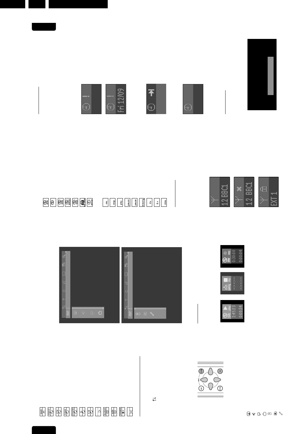
lPress SYSTEM MENU on the remote control.
lSelect in the system menu bar and press w
(down cursor).
‰The user preferences menu appears.
lUse the t u v w (left right up down cursor) keys
to toggle through the menus, sub menus and
submenu options.
‰When a menu item is selected, the cursor keys
(on the remote control) to operate the item are
displayed next to the item.
lPress OK to confirm and return to the main menu.
The following functions can be operated via the user
preference menu.
User preference menu icons
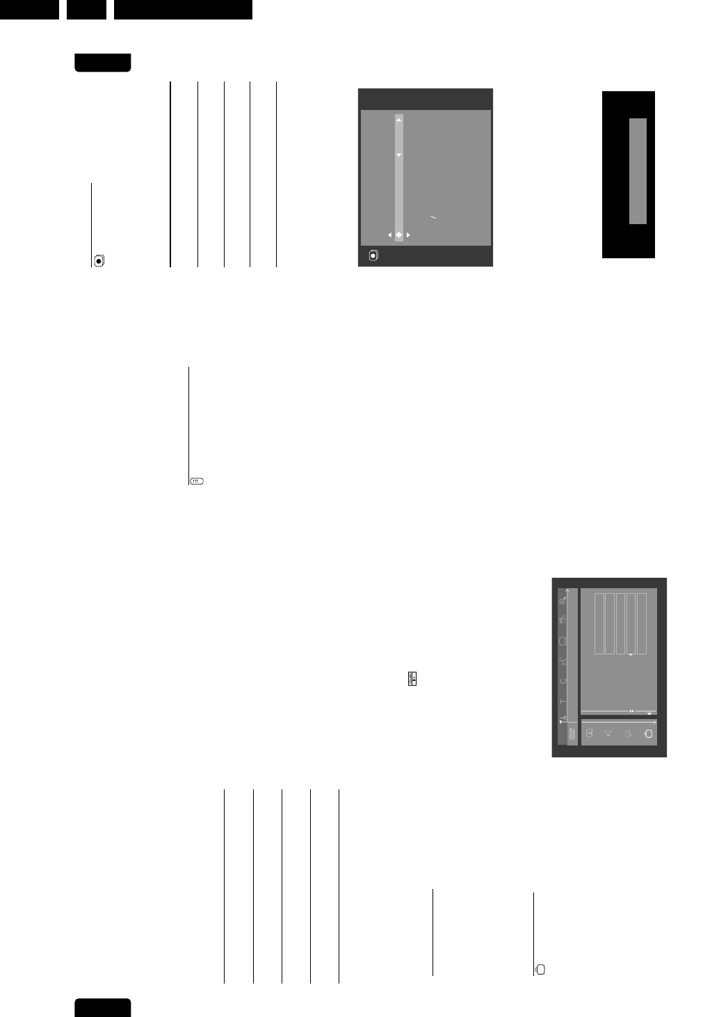
Picture settings
Sound settings
Language settings
Feature settings
Remote control settings
Record settings
Installation
lYou can navigate between the various items of the
user preferences menu with the v(up cursor) and
the w(down cursor) key. To select an item press u
(right cursor) key.
lBy pressing SYSTEM MENU the system menu bar
will disappear from the screen.
Status box
The status box on the left hand side of the screen
displays the current status of the recorder and the disc
type loaded for several seconds.
-- --- off on off
-- --- off on off
Directions For Use EN 15DVDR980-985 /0X1 3.
English
OPERATION 23
User preferences
Setting user preferences
You can set your user preferences for some of the
recorder features. (See ‘Operation’ - ‘User preferences
menu operation’)
The following items can be adapted:
Picture settings
TV Shape
With TV Shape you can adjust the output of your DVD
Recorder to optimally fit your TV screen. You can
choose:
-
16:9
if you have a wide screen (16:9) TV set.
-
4:3
if you have a regular (4:3) TV set. In this case you
can also choose between:
-
Letterbox
: for a ‘wide-screen’ picture with black
bars at the top and bottom,
-
Pan Scan
: for a full-height picture with the sides
trimmed. If a disc has Pan Scan, the picture then
moves (pans) horizontally to keep the main action
on the screen.
Black level shift (NTSC only)
Adapts the colour dynamics to obtain richer contrasts.
Select ‘
On
’ or ‘
Off
’.
Video shift
Factory setting is such that the video will be centered on
your screen. Use this setting to adjust the position of
the picture on your TV set by scrolling it to the left or
right.
SCART
Video
Factory setting is RGB. Select ‘
S
-
video
’ (Y/C) via
SCART
when connecting to an S-VHS recorder.
Sound settings
Digital output
Factory setting ‘
All
’ means that both coaxial and optical
outputs are switched on, and that Dolby Digital Multi-
channel is fed to the outputs as such MPEG audio is
converted to PCM. If your equipment doesn’t include a
digital Multi-channel decoder, set the digital output to
‘
PCM only
’ (Pulse Code Modulation). Both coaxial and
optical outputs are then switched on, and Dolby Digital
and MPEG audio are converted to PCM. If you are not
connecting equipment with a digital input, change the
setting to ‘
Off
’.
Analogue output
Select ‘
Stereo
’, ‘
Surround
’ or ‘
3D Sound
’. Factory
setting is Stereo.
Digital output
Analogue output
Night mode
Sound
-- --- off on off
Stereo
Surround
3D sound
TV shape
Black Level shift
Video shift
SCART video
Picture
OK to exit
-- --- off on off
English
22 OPERATION
Index Picture Screen
The Index Picture Screen displays an overview of the
titles recorded on the disc. Each title is represented by
an index picture. Next to the index picture the
programme name, duration, recording mode and
recording date of the title are shown. If no name is
known, the DVD recorder will fill in the source and the
time of the recording instead.
Empty spaces (erased titles, or blank space at the end of
the disc) are also shown as such.
lAt maximum three titles will be shown on the
screen at once. If more titles are present, you can
navigate to those with the wv (down up cursor)
keys.
lOn the right hand side of the Index Picture Screen,
you can see the disc bar. This gives an overview of
all titles on the disc, as well as any empty spaces.
On the disc bar, an arrow – the disc pointer –
indicates your current position on the disc. From
this point you may resume playback or recording.
lIf you navigate trough the list of titles with wv
(down up cursor) or J PREVIOUS / KNEXT, the
disc pointer will move along.
lPress 9STOP to reset the disc pointer to the
beginning of the disc.
lTo move the disc pointer to the end of the last title,
keep KNEXT pressed.
lIf you navigate from an Index Picture to the box
right next to it (containing name, rec mode, etc.),
you enter the title settings menu (see under
‘Managing disc content - Title settings’).
ZDF 11:11
00: 00: 55 -SP
T h u 08 02 2001
Empty title
00: 00: 59-SP
1: 15
hr
01 Z D F
VRT 11:13
00: 00: 57 -SP
T h u 08 02 2001
2
4
Index Picture
- image that represents a recorded title
Title description
- programme name
- duration + recording mode
- recording date
Cue to go to Disc Info Screen
or to title on previous screen
Empty title
Current title
Indication what disc area
will be overwritten by
upcoming timer event
Disc Pointer
- shows number and place
of current title on disc
Other title
Cue to go to title on next screen
Tuner Info Box
- displays the selected channel
Timer Info Box
- displays the current time or time/date
of the next timer programme
Disc Bar
- shows an overview of
all titles on disc
Directions For Use
EN 16 DVDR980-985 /0X13.
English
PBC
This feature is only available when a (Super) Video CD is
loaded. It allows you to disable or enable the PBC
(Playback Control) menu of VCD discs. See under
‘Special VCD features’: Factory settings is ‘
On
’.
Finalise disc
This option is only available on unfinalised DVD+R discs.
See ‘Managing disc content - Finalising a DVD+R disc’.
Remote Control settings
Key sound
The recorder makes a ‘beep’ sound upon every key
command given via recorder or remote control keys.
Select ‘
Off
’ to disable this sound. Factory setting is ‘
On
’.
Remote control used
If you want to use the remote control of a Philips DVD
player instead of the standard DVD recorder remote
control, select ‘
DVD player
’. Factory setting is ‘
DVD
recorder
’.
System information
When you move further down in the Remote Control
settings menu, the system status screen will appear.
Press v(cursor up) to go back.
Record Settings
Record mode
By selecting a recording mode you define picture quality
of recordings and maximum recording time for a disc.
Mode Picture quality Total recording
time
HQ best possible 60 minutes
(High Quality) picture quality
SP pre-recorded 120 minutes
(Standard Play) DVD quality
LP better than 180 minutes
(Long Play) S-VHS picture quality
EP better than 240 minutes
(Extended Play) VHS picture quality
In practice, the DVD recorder may record a few
minutes more than indicated. For playback, the correct
recording mode will automatically be selected.
The HQ mode is optimised for recording via the
external inputs. For tuner recordings it is recommended
to use SP, LP or EP.
lIn the record settings menu, select ‘
Record mode
’.
lAlter the recording mode with tor u(left right
cursor).
lConfirm with the OK key.
lTo end, press SYSTEM MENU.
An alternative way to select the record mode is available
in the Index Picture Screen and in monitor mode:
lPress SELECT.
‰The new record mode appears on the screen and
the display.
It is not possible to switch record modes during
recording.
Record Mode: LP
Record settings
To exit press
SYSTEM MENU
Record mode
Direct record
Sat record
Auto chapters
LP/EP rec mode Stndrd
SP
Off
Off
On
OPERATION 25
English
24 OPERATION
Surround: Select this setting when using equipment
with a Dolby Surround Pro Logic decoder.
In this setting the 5.1 audio channels (Dolby
Digital, MPEG-2) are downmixed to a
Surround-compatible 2-channel output.
3D Sound: In a set-up without rear speakers (analogue
stereo output), this option remixes the six
channels of digital surround (Dolby Digital,
MPEG-2) into a two speaker output, while
retaining all of the original audio information.
The result is the listening sensation of being
surrounded by multiple speakers.
Connected audio system Digital out Analogue out
Amplifier or TV with two channel Off Stereo
analogue stereo
Amplifier or TV with Dolby Surround Off Surround
or Dolby Pro Logic
Amplifier with two channel digital PCM only Stereo
stereo
A/V receiver with Multi-channel All Stereo or
decoder (Dolby Digital, MPEG, DTS) Surround
Multi-channel A/V receiver with Off Surround
6-ch connectors
Night Mode
Night mode optimizes the dynamics of the sound with
low volume playback for less disturbance in quiet
environments. This only works for Dolby Digital audio
on DVD-Video discs.
r
Language settings
The preferred language can be adapted via the system
menu bar. Also see ‘virgin mode’. Settings can be
changed for:
- Playback audio language
- Subtitle language
- Menu language
- Country setting.
Feature settings
Access Control
Access Control contains the following features:
Child Lock - When Child Lock is set on, a 4-digit code
needs to be entered in order to play discs.
Parental Level - Allows the conditional presentation of
DVD discs containing Parental Level information.
Change country - Allows conditional presentation of
DVD-Video discs containing country information.
Change code - To change the pin code.
See ‘Acces Control’.
Adapt disc format
This option is only available when a DVD+RW or
DVD+R disc recorded on a different brand of recorder
is loaded. You can adapt the menu to your own
recorder.
A DVD+RW video disc that has been recorded on a
different type or brand of recorder can be played, but
may not provide all features commonly available to
DVD+RW discs, such as the on-screen disc bar, the disc
settings menu, the title settings menu, and editing. If the
disc is not write-protected, the disc format can be
adapted to the own recorder, after which these
functions are available.
Status box
The status box displays the current status of the recorder
and the disc type loaded (See ‘Operation’ - ‘On-screen
display information’). You can switch it On or Off.
Off
= always Off.
On
= displayed together with the system menu bar or
displayed temporarily (disappears after time-out)
when changing the playback or record status.
Factory setting is ‘
On
’.
Auto resume
The Auto resume setting only applies to pre-recorded
DVD-video and Video CD discs only - not only to the
disc in the recorder but also to the last twenty discs you
have played.
If ‘
Auto resume
’ is set to ‘
On
’, playback will start from
the point where it was stopped the last time the disc
was played.
When ‘
Auto resume
’ is set to ‘
Off
’, the recorder will
start playing from the beginning of a disc. In this case you
can still resume when appears on screen by
pressing 2PLAY. Factory setting is ‘
On
’.
Low power standby
If low power standby is ‘
On
’, the recorder will consume
minimum power in standby mode.
Factory setting is ‘
Off
’.
Notes:
When the recorder is in low power standby mode:
- the output of the equipment connected to EXT 2 will not
be passed through to the TV set on EXT 1,
- the Display will be Off,
- the Standby indicator on the recorder will still light up in
standby mode.
Access control
Status box
Autoresume
Low power standby
PBC
Features
Enter code...
On
Off
Off
Off
-- --- off on off
Directions For Use EN 17DVDR980-985 /0X1 3.
English
OPERATION 27
Manual TV channel search
You can perform a search to select and store TV
channels manually. If the DVD recorder is connected via
EasyLink, this function is not available.
lPress SYSTEM MENU.
lSelect ‘
Installation
’.
lSelect ‘
Manual search
’.
lIn the line ‘
Channel
/
freq
.’ select the display for:
Freq.
: frequency
CH
: channel
S
-
CH
: special channel
lIf you know the frequency or channel of the desired
TV channel, you can enter the data in line
‘
Entry
/
search
’ with the digit keys 0-9. If you don’t
know the frequency or channel of the TV channel of
your choice, press u(right cursor) to start channel
search.
lIn the line ‘
Programme number
’ select the
programme number you want, using tor u (left
right cursor) or digit keys 0-9.
lIf you want to change the TV channel name, press
the u(right cursor) key in line ‘
TV channel name
’.
lSelect the character you want to change with the t
(left cursor) or u(right cursor) key.
lChange the character with the w(down cursor) or
v(up cursor) key.
lPress OK to confirm.
This DVD recorder can receive HiFi sound transmissions
in NICAM Stereo. However, if sound distorsion occurs,
due to poor reception, you can switch off NICAM:
lIn the line ‘
NICAM
’ select ‘
On
’ or ‘
Off
’ with the t
(left cursor) or u(right cursor) key.
If you want to change the automatic TV channel setting,
select the line ‘
Fine tuning
’. With the t(left cursor) or
u(right cursor) key you can vary the automatic TV
channel setting.
Important: This re-tuning is only necessary and useful
in special cases, e.g. when stripes appear on your TV
screen when using a cable-TV system.
lPress OK to store the TV channel.
lTo end, press SYSTEM MENU.
Connecting a decoder:
lSwitch on the TV set and select the programme
number for the DVD recorder.
lSelect the TV programme you wish to link with the
decoder function with CH+ or CH-.
lPress SYSTEM MENU
lSelect ‘
Installation
’.
lSelect ‘
Manual search
’.
lSelect ‘
Decoder
’.
lSelect ‘
On
’ with t(left cursor) or u (right cursor).
lConfirm with OK.
‰‘
DECODER
’ apperars on the display.
lTo end, press SYSTEM MENU.
Sort/Clear TV channels manually
lIf the DVD recorder is connected to the TV set
with EasyLink or a similar system, manual sort
cannot be executed. In all other cases, you can
select.
lPress SYSTEM MENU.
lSelect the line ’
Installation
’.
lSelect the line ’
Sort TV channels
’.
lSelect the TV channel to which you want to allocate
a programme number (starting with ‘
P01
’) with the
v(up cursor) or w(down cursor) key and press the
u(right cursor) key.
lSelect the desired position with vor w(up down
cursor) key.
lTo store, press OK.
lTo end, press SYSTEM MENU.
Time/Date
To adjust ‘
Time
’, ‘
Year
’, ‘
Month
’ and ‘
Date
’ with the
digit keys 0-9. Switch between fields with the wv
(down up cursor) keys.
Installation
To exit press
SYSTEM MENU
Time/Date
Time
Year
Month
Date
09: 38
2001
02
09
Installation
To sort
Press To exit press
SYSTEM MENU
Sort TV channels
PO1 NED 1
...
...
PO2 NED 2
PO3 NED 3
PO4 RTL 4
PO5 RTL 5
PO6 VERON
English
26 OPERATION
Direct record
With the Direct Record function switched ‘
On
’ and the
DVD recorder switched to standby, the channel number
selected on your television will be automatically taken
over by the DVD recorder, at the moment it starts
recording. This only applies for televisions connected via
SCART
, which have video output via
SCART
or which have
EasyLink. Factory setting is ‘
Off’
.
lIn the record settings menu, select ‘
Direct record
’.
lSelect ‘
On
’. If you select ‘
Off
’, the function will be
switched off.
lConfirm with OK.
lTo end, press SYSTEM MENU.
Sat record
You can only use this function, when you have a satellite
receiver, which can control other equipment by a
’programming’ function. In this mode your DVD
recorder starts recording when the satellite receiver
releases a signal. The start and end of the recording is
controlled via one of the
SCART
sockets.
lIn the record settings menu, select ‘
Sat record
’.
lSelect the
SCART
socket to which the satellite
receiver is connected with tor u(left right cursor).
lConfirm with OK.
lInsert a recordable DVD+RW disc.
lPress BSTANDBY/ON.
‰When this function is switched on,
SAT
appears
on the display.
‰The DVD recorder is now prepared for
recording.
Factory setting is ‘
Off
’.
Auto chapters
If autochapters is ‘
On
’ every five to six minutes a
chapter marker (beginning of a new chapter) is inserted
during recording. This enables easy navigation through a
title during playback. In either case you can manually
insert chapter markers afterwards. (See ‘Managing disc
content’ - ‘Edit in playback mode’.)
LP/EP rec mode
In long play or extended play recording mode you can
select the ‘
Sport
’ setting to optimize the video
recording for images that contain fast movements, like
sports programmes. The setting does not influence high
quality or standard play recording mode.
Factory setting is ‘
Stndrd
’.
Installation
Auto TV Channel Search
Your DVD recorder will search for all TV channels.
It stores channels in the sequence they are found. (See
‘Installation - First time Set-up’)
Note:
All channels stored so far will be erased.
Follow TV
With Follow TV you can programme the same channel
sequence on the DVD recorder as on the TV set.
This only functions if the recorder socket (EXT1) and
the TV set are connected with a
SCART
cable. Additional
equipment connected to socket EXT2 must be switched
off.
lPress OK.
‰If the DVD recorder recognizes that the TV set
has been connected with a
SCART
cable, ‘TV01’
appears on the display.
‰When ‘NOTV’ (no signal from TV set) appears on
the display, the TV channels can not be allocated
automatically. In this case read ‘Manual TV channel
search’.
lSelect programme number ‘1’ on the TV set.
lConfirm with OK on the remote control of the
DVD recorder.
‰The DVD recorder compares the TV channels on
the TV set and the DVD recorder. If the channels
match, this channel is stored at ‘P01’.
lWait until 'TV02’ appears and repeat the previous
two steps for programme number 2 and the rest of
the channels you want to store.
lTo end, press SYSTEM MENU.
TV 01
Installation
To exit press
SYSTEM MENU
Follow TV
Autom.search
Manual search
Sort TV channels
Time Date
Directions For Use
EN 18 DVDR980-985 /0X13.
English
RECORDING 29
The following programme numbers are provided for
recording from external sources:
‘EXT1’ : TV set via
SCART
1
socket
‘EXT2’ : for recording from external sources via
SCART
2
socket
’EXT3’ : rear S-video
‘EXT4’ : rear CVBS
‘CAM1’ : front S-video (Y/C)
‘CAM2’ : front Video (CVBS)
lPress RECORD (on the recorder) or REC/OTR
(on the remote control).
‰
RECORD
is shown on the display.
‰The status box is shown on the screen for a few
seconds.
lTo bring back the status box during recording press
SYSTEM MENU. Pressing SYSTEM MENU once
more will remove the status box again.
lPress
;
PAUSE to pause recording. You can
resume recording by pressing
;
PAUSE once more.
The DVD recorder will make a seamless connection.
lPress 9STOP to stop recording. If you are recording
from a camcorder watch the video output of the
DVD recorder on the TV - instead of the camcorder
viewer - to determine the right moment to stop.
lThe Index Picture Screen is updated.
‰‘MENU UPDATE’ is shown on the display.
lAfter a short recording on a new DVD+RW disc, a
few minutes will be needed to complete the
formatting of the disc.
Safe Recording
When you start recording on a DVD+RW disc by briefly
pressing the RECORD or REC/OTR key, a recording
on DVD+RW will be made from the current position of
the disc pointer. To prevent this do the following:
lHold the RECORD key (on the recorder) or
REC/OTR key (on the remote control) press for
about two seconds until ‘SAFE RECORD’ appears
on the display.
lThe recorder automatically jumps to the end of the
last title on the disc and starts recording.
‰If no free space is left. The display will show
‘DISC FULL’. Safe record is not possible then.
Recordings on DVD+RW are always automatically made
after the last title on the disc.
Direct Record
With Direct Record you can start recording immediately
from the programme selected on the TV set.
lMake sure ‘
Direct record
’ is switched ‘
On
’.
(See record settings).
lOn the TV set, select the programme number you
want make the recording from.
lMake sure the DVD recorder is switched to
standby.
lPress RECORD (on the recorder) or REC/OTR
(on the remote control).
Notes :
- Don’t select another programme number on your TV set,
until the ‘WAIT’ on the display of your DVD recorder
disappears. This can take up to one minute.
- When ‘NOTV’ appears on the display, the programme
number could not be found. The DVD recorder switches off
automatically.
- If your loudspeakers are connected (via an amplifier /
receiver) to your DVD recorder, the sound will be delayed
relative to the TV picture when recording directly from the TV
set.
- You can use Direct Record in combination with Safe Record.
Manual audio control
You can control the audio recording level of your DVD
recorder manually.
lIn monitor mode, press AUTO/MAN REC
VOLUME on the DVD recorder.
‰The display will show the current audio level and
MANUAL
appears.
SP
CHANNEL
DVD RW
TITLE CHAPTER TIME REMAIN
-30-40 -10-20 0 OVER-30-40 -10-20 0 OVER
STEREO
RECORD
MANUAL
MONITOR ON/OFF
REC/OTR
PLAYSTOP FSS
FORWARDREVERSE
NEXT PREVIOUS
PAUSE SLOW
CHVOL
MUTE
T/C A/CH
English
28 RECORDING
Before you start recording
Recordings on a DVD disc are called ‘titles’. Every title
consists of one or more chapters.
For more information about how to go to other titles or
chapters see ‘Playback - general features’.
Important:
Recordings on a DVD+RW disc are normally
started from the position of the so-called disc
pointer, i.e. the point where the last recording
was stopped. From there on earlier recordings
may be overwritten without notice, unless the
disc is write protected. In this respect your DVD
recorder behaves just like a Video Cassette
Recorder.
If you want to make a recording without the risk
of overwriting earlier recordings use the safe
Record Function (see Manual Recording - Safe
Record)
In the Index Picture Screen you can select the point
where you want to start your recording. Use the wv
(down up cursor) and 5REVERSE / 6FORWARD
keys. You can see the the current location on the disc
bar, indicated by the arrow.
Your DVD recorder always checks the disc that you
have inserted:
‰When a DVD+RW disc is inserted on which
recordings have been made, the Index Picture
Screen is shown on your TV screen.
‰If the inserted disc is a completely empty
recordable disc, the message ‘EMPTY DISC’ appears
on the display.
‰If the inserted disc is a DVD+RW disc with a
content that is not DVD-Video compatible (e.g. a
data disc), a dialog box is shown with the option to
erase or eject the disc. You can only record on this
disc after erasing it with the RECORD key.
Note:
- On a disc containing PAL recordings, no NTSC recordings
can be made and vice versa. On an empty disc, either type of
recordings can be made.
- No recordings can be made from so-called ‘Pseudo-PAL’ or
PAL-60 sources.
‰A disc can hold up to 48 titles (including empty
titles). When this maximum is reached the on-
screen message ‘
Too many titles
’ appears, if you
want to make a new recording. You have to erase a
title first next to an empty title. (See ‘Managing Disc
Content’.)
Manual recording
Checking input
Normally, the DVD recorder displays the contents of
the disc on screen.
lPress MONITOR in order to switch to the internal
tuner, or whichever other source is selected, if you
want to check the input before starting a recording.
‰On the TV screen, you will see the actual picture
quality that you will get if you record: the video has
been encoded and decoded again. This is why you
will see a delay of about 1.5 seconds when using a
‘live’ source such as a camera.
lIn monitor mode you can choose programme
numbers directly with the digit keys 0-9 on the
remote control.
lPress SELECT repeatedly to select the desired
record mode.
lPress MONITOR again to go back to disc mode.
Recording
lInsert a recordable DVD+RW or DVD+R disc.
lNormally, the DVD recorder displays the contents
of the disc on the screen.
lUse the MONITOR button to see the currently
selected TV channel.
lUse CHANNEL 3or CHANNEL 4(on the
recorder) or CH+, CH- (on the remote control) to
select the programme number (programme name)
from which you wish to record.
‰When a TV channel transmits a channel name,
it will be shown on the display.
stop
11: 15
01 B B C 1
Disc is not a DVD video disc
Press OK to open tray or
press REC to erase disc
TITLE 1 TITLE 2
CHAPTER 1 CHAPTER 2 CHAPTER 3 CHAPTER 1 CHAPTER 2
DVD+RW
Recording
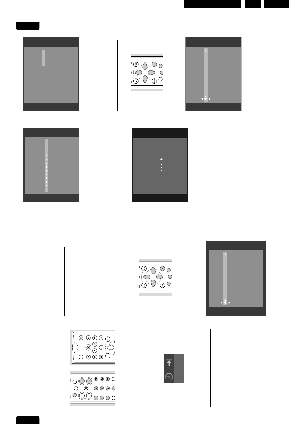
Directions For Use EN 19DVDR980-985 /0X1 3.
English
RECORDING 31
lEnter the entire PlusCode number (up to nine digits)
printed in your TV guide next to the start time of a
TV programme. If you made a mistake, you can
correct it with CLEAR.
lConfirm with OK.
lIf the VIDEO Plus+ system does not recognize the
TV channel, the message ‘
Please enter
programme number
’ will appear on screen. Select
the required programme number (programme name)
with tu(left right cursor) or the digit keys 0-9 and
confirm with OK.
‰The data will appear on the TV screen.
lPress u(right cursor).
lUse SELECT to select the programming key at
daily or weekly intervals.
Mo
-
Fr
: Recording at daily
intervals from Mondays to Fridays inclusive.
Weekly
:
Recording at weekly intervals on the same day of
the week.
lPress u(right cursor).
lUse SELECT to switch VPS/PDC on or off.
‰When VPS/PDC is switched on, the start time is
marked with an asterisk.
lPress u(right cursor).
lUse SELECT to select the recording mode (‘
HQ
’,
‘
SP
’, ‘
LP
’, ‘
EP
’).
lConfirm with OK.
‰The data has been stored in a timer block.
lTo end, press TIMER.
lMake sure that you inserted a recordable disc.
If you inserted a write-protected disc recording
will be refused.
lSwitch off with BSTANDBY/ON.
Timer programming without the VIDEO
Plus+ system
lPress TIMER on the remote control.
lSelect ‘
Timer programming
’ with v(up cursor) or
w(down cursor).
lPress u(right cursor).
lEnter the date with v(up cursor) or w(down
cursor), or with the digit keys 0-9.
Timer
To exit
Press TIMER
ShowView programming
Timer programming
Timer list
CLEAR SELECT
TIMER
Timer
ShowView programming
Date
09 N E D 1 09: 35 11: 35 S P
Prog. Start VPS
PDC End Rec
Mode
LP/SP
Press SELECT To store
Press OK
Timer
VIDEO Plus+ programming
Please enter
programme number
Timer
Mo-Fr/Weekly
Press SELECT To store
Press OK
ShowView programming
ShowView number
English
30 RECORDING
lAdjust the recording level with MANUAL 3or 4
on the DVD recorder, so that the ‘0 dB’ mark lights
up during the loudest parts of the recording.
lYou can switch back to automatic audio level control
by pressing AUTO/MAN REC VOLUME again.
‰The display will show the current disc position
and
MANUAL
disappears.
Recording with automatic switch-off (OTR
One-Touch Recording)
lInsert a recordable DVD+RW or DVD+R disc.
lUse CHANNEL 3or CHANNEL 4(on the
recorder) or CH+, CH- (on the remote control) to
select the programme number (programme name)
from which you wish to record.
lPress RECORD (on the recorder) or REC/OTR
(on the remote control) twice.
‰A recording will be made of 30 minutes.
‰The required end time of the recording is shown
in the timer box on screen. The remaining recording
time is shown on the display.
lPress RECORD or REC/OTR again to obtain a
30 minute increment.
lShortly after pressing REC/OTR, OTR can be
cancelled by pressing CLEAR.
Timer programming
The DVD recorder needs the following information for
every programmed recording:
- the date on which the recording is to be made;
- the channel;
- the start and stop time of the recording;
- VPS/PDC on or off;
- the recording mode (HQ, SP, LP or EP).
The DVD recorder stores all the information mentioned
above in a timer block. You can programme up to six
timer blocks, one month in advance.
When you have programmed the timer, a red line on
the disc bar (both on the display and on the Index
Picture Screen) indicates what part of the disc will be
overwritten by the programmed recording from the
current disc position (on DVD+RW) or after the last
title (on DVD+R).
When all timer blocks are full, the options timer
programming and VIDEO Plus+ programming cannot be
accessed. For clearing a timer block, see ‘How to clear a
timer block’.
Timer programming with the VIDEO
Plus+
®
system
A PlusCode number is a number of up to nine digits,
printed in most TV guides next to the start time of a TV
programme.
All the information required for a programming is
contained encoded in the PlusCode programming number.
lSelect ‘
VIDEO Plus+programming
’ with v(up
cursor) or w(down cursor).
lPress u(right cursor).
Timer
To exit
Press TIMER
ShowView programming
Timer programming
Timer list
CLEAR SELECT
TIMER
What is ’VPS’/‘PDC’?
With ’VPS/PDC’, the TV station controls the
beginning and the length of the programmed
recording. This means that the video recorder
switches itself on and off at the right time even if a
TV programme you have programmed begins earlier
or finishes later than expected.
Usually the start time is the same as the VPS/PDC
time. If, however, in the TV guide, in addition to a TV
programmes start time, a different VPS/PDC time is
given, e.g.: ’20.15 (VPS 20.14)’, you must enter ’20.14’
as the start time exactly to the minute. If you want
to enter a time that differs from the VPS/PDC time,
you must switch off ’VPS/PDC’.
10: 15h r
MONITOR ON/OFF
REC/OTR
PLAYSTOP FSS
FORWARDREVERSE
NEXT PREVIOUS
PAUSE SLOW
CLEAR
CHVOL
SELECT
TIMER
MUTE
T/C A/CH
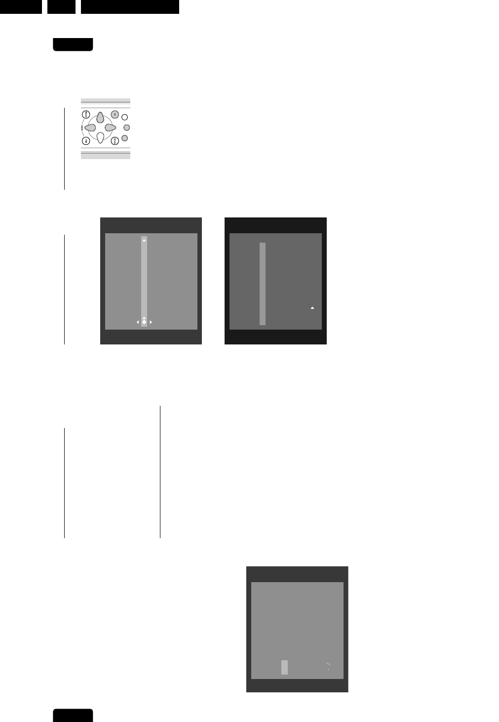
Directions For Use
EN 20 DVDR980-985 /0X13.
English
RECORDING 33
How to check or alter a timer block
lPress TIMER on the remote control.
lSelect ‘
Timer list
’ with wor v(down up cursor).
lPress u(right cursor).
lSelect the timer block you want to check or alter
with wor v(down up cursor).
lPress u (right cursor).
lSelect what you want to check or alter with tor u
(left right cursor).
lAlter data with wor v(down up cursor) or with
the digit keys 0-9.
lConfirm with OK.
lTo end, press TIMER.
lSwitch off by pressing BSTANDBY/ON.
How to clear a timer block
lPress TIMER on the remote control.
lSelect ‘
Timer list
’ with wor v(down up cursor).
lPress u(right cursor).
lSelect the timer block you want to clear with wor
v(down up cursor).
lPress CLEAR.
lConfirm with OK.
lSwitch off by pressing TIMER.
CLEAR SELECT
TIMER
Timer
Timer list
Date
09
12
14
NED 1
RTL 2
VRT
09: 35
21: 00
20: 30
11: 35
23: 00
22: 00
SP
SP
SP
Prog. Start
*
*
VPS
PDC End
Rec
Mode
Total record time 05: 30
To exit
Press TIMER
To change
Press
Timer
To exit
Press TIMER
ShowView programming
Timer programming
Timer list
English
32 RECORDING
lIf desired, select recording at daily or weekly
intervals in the field ‘
Date
’ with SELECT. ‘
Mo
-
Fr
’:
Recording to be made from Mondays to Fridays
inclusive. ‘
Weekly
’: Recording at weekly intervals on
the same day of the week.
lPress u(right cursor).
lEnter the programme number from which you want
to record. If you want to record from an external
source, select ‘
EXT1
’, ‘
EXT2
’, ‘
EXT3
’, ‘
EXT4
’, ‘
CAM1
’
or ‘
CAM2
’ with vw (up down cursor).
lPress u(right cursor).
lEnter the Start time with vw (up down cursor) or
the digit keys 0-9.
lAfter entering the Start time, use SELECT to
switch VPS/PDC on or off. With most TV stations
the VPS/PDC time is always the same as the start
time.
‰When VPS/PDC is switched on, the start time is
marked with an asterisk.
lPress u(right cursor).
lEnter the End time with vw (up down cursor) or
the digit keys 0-9.
lUse SELECT to choose the recording mode ‘
HQ
’,
‘
LP
’, ‘
SP
’ or ‘
EP
’.
lIf you made a mistake, you can go back with t(left
cursor).
lConfirm with OK .
‰The data has been stored in a timer block.
lTo end, press TIMER .
‰Make sure that you inserted a disc without write
protection. If you inserted a write-protected
(locked) disc, recording will be refused.
lSwitch off with BSTANDBY/ON.
Programming with ’N
EX
TV
IEW
Link’
This DVD recorder is equipped with the function
’N
EX
TV
IEW
Link’. If your television is also equipped with
this function, you can mark TV programmes on the
television for programming. These TV programmes will
automatically be transmitted to a timer block on the
DVD recorder. If you clear the marking of the TV
programme on the television, the corresponding timer
block on the DVD recorder will also be cleared.
For more information, read the instruction manual of
your TV set.
If a timer setting is incorrect
The following warnings can be displayed in the timer
menu:
Collision
recording programme overlaps with another recording
programme.
Solution:
lIgnore by pressing TIMER. The programme
with the earlier start time will be recorded
completely before the later programme starts.
lEdit one or both timers.
lDelete one of the recording programmes.
Please enter programme number
The VIDEO Plus+ system does not recognize the TV
channel.
Solution:
lSelect the required programme number
(programme name) with tor u (left right
cursor).
lConfirm with OK.
PlusCode number wrong
You entered an incorrect PlusCode number or the
incorrect date.
Solution:
lRepeat the entry or end by pressing TIMER.
Weekend programming
-
not possible
Date was incorrectly entered. Daily programming can
only be used for recordings to be made from Mondays
to Fridays inclusive.
Memory full
The maximum number of recording programmes is used.
Solution:
lDelete one of the recording programmes.
Timer
Timer programming
Date
09 N E D 1 09: 35 11: 35 S P
Prog. Start VPS
PDC End Rec
Mode
Mo Fr Weekly
Press SELECT To store
Press OK
*
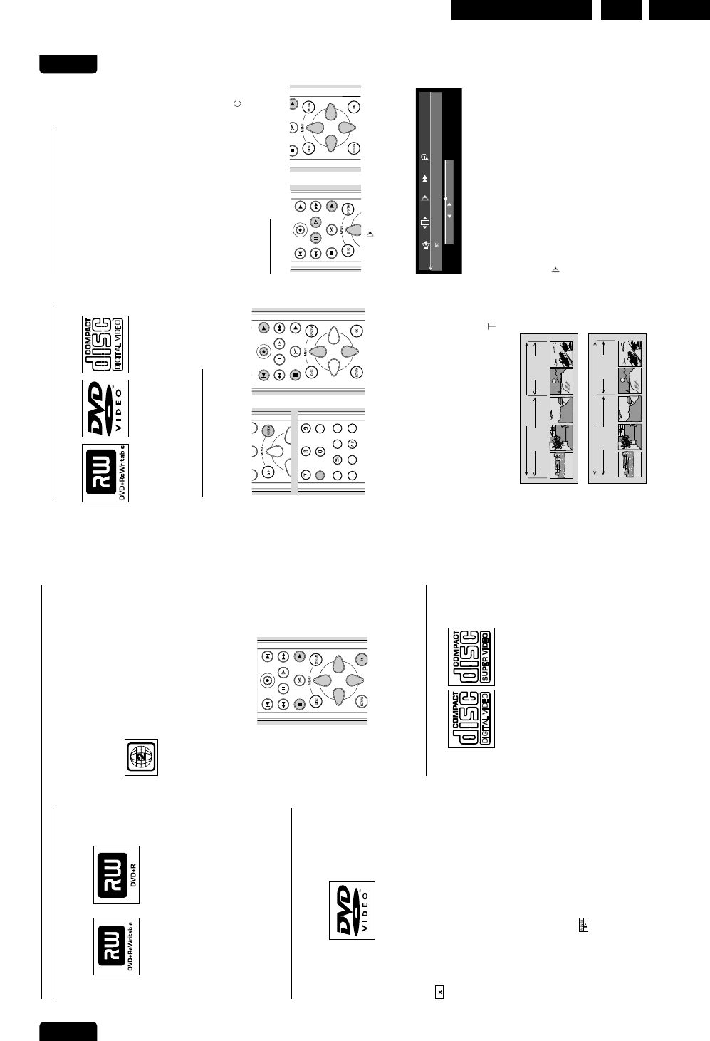
Directions For Use EN 21DVDR980-985 /0X1 3.
English
PLAYBACK 35
General features
Note:
Unless stated otherwise, all operations described are based
on remote control operation. A number of operations can also
be carried out via the system menu bar on the screen. (see
‘System menu bar operation’)
Moving to another title/track
When a disc has more than one title or track, you can
move to another title as follows:
lPress T/C.
lPress KNEXT during play to step forward to the
next title.
lPress JPREVIOUS during play to return to the
beginning of the current title. Rapidly press
JPREVIOUS twice to step back to the previous
title.
lTo go directly to any title or track, enter the title
number using the numerical keys 0-9.
Notes:
- If the number has more than one digit, press the keys in
rapid succession.
- If the system menu bar is on screen, make sure the icon
is selected.
Moving to another chapter/index
When a title on a disc has more than one chapter or a
track has more than one index, you can move to
another chapter/index as follows:
lPress KNEXT during play to select the next
chapter/index.
lPress JPREVIOUS during play to return to the
beginning of the current chapter/index. Rapidly press
JPREVIOUS twice to step back to the previous
chapter/index.
lTo go directly to any chapter or index, enter the
chapter or index number using the numerical keys
0-9.
Notes:
- If the number has more than one digit, press the keys in
rapid succession.
- If the system menu bar is on screen, make sure the icon
is selected.
Slow Motion
lSelect (Slow motion) in the system menu bar.
lUse the w(down cursor) key to enter the slow
motion menu.
‰The recorder will now go into pause mode.
lUse the t u (left right cursor) keys to select the
required speed: ‘-
1
’, ‘-
1
/
2
’, ‘-
1
/
4
’ or ‘-
1
/
8
’
(backward); ‘
1
/
8
’, ‘
1
/
4
’, ‘
1
/
2
’ or ‘
1
’ (forward).
lSelect ‘
1
’ to play at normal speed again.
lIf ;PAUSE is pressed, the speed will be set to ‘
0
’.
lPress 2PLAY to exit slow motion mode.
lPress v(up cursor) to delete the slow motion menu.
You can also select Slow Motion speeds by using the
SLOW key on the remote control.
-1 -1
/
2 -1/4 -1/8 0 1/8 1/4 1/2 1
REC/OTR
PLAY
STOP
FORWARDREVERSE
NEXT
PREVIOUS
PAUSE SLOW
FSS
TRACK 1 TRACK 2
INDEX 1 INDEX 2 INDEX 3 INDEX 1 INDEX 2
VIDEO CD
TITLE 1 TITLE 2
CHAPTER 1 CHAPTER 2 CHAPTER 3 CHAPTER 1 CHAPTER 2
DVD VIDEO
REC/OTR
PLAYSTOP FSS
FORWARDREVERSE
NEXT PREVIOUS
PAUSE SLOW
CLEAR SELECT
T/C
ZOOM ANGLE SUBTITLE AUDIO
DIM REPEAT REPEAT SCAN
A/CH
ZYa
English
34 PLAYBACK
Playing a DVD+RW or DVD+R
disc
lInsert a DVD+RW or DVD+R disc.
‰If the inserted disc is write-protected, playback
starts automatically otherwise the Index Picture
Screen appears.
lPress 2PLAY.
‰Playback starts automatically from the point
where it was stopped the last time the disc was
played or recorded. If you want to start playback
from the beginning of the disc, you can do so via the
Index Picture Screen (see ‘Index Picture Screen’).
‰If the disc is a new blank disc, the display will
show ‘EMPTY DISC’.
lTo stop playback at any time, press 9 STOP.
‰You return to the Index Picture Screen.
Playing a pre-recorded DVD-
Video disc
Some DVD discs are produced in a way that requires
specific operation or allows only limited operation
during playback. In these cases the recorder may not
respond to all operating commands. When this occurs,
please refer to the instructions in the disc inlay. When a
appears on the TV screen, the operation is not
permitted by the recorder or the disc.
lInsert a pre-recorded DVD-Video disc. Make sure
the label is facing up. If the disc is two-sided, make
sure the label of the side you want to play is facing
up.
‰When ‘
autoresume
’ is set to ‘
On
’ (see ‘User
Preferences’) playback starts automatically from the
point where it was stopped, the last time the disc
was played.
‰When ‘
autoresume
’ is set to ‘
Off
’, the disc will
play from the start of the disc. You can however
resume play from the point at which you stopped,
the last time the disc was played, by pressing
2PLAY when appears on screen.
‰The currently playing title and chapter number
are displayed on the recorder display. The elapsed
time is shown also.
Notes:
- DVD movies to be released at different times in different
regions of the world, all players have region codes and discs
can have an optional region code. If you load a disc of a
different region code to your recorder, you will see the region
code notice on the screen. The disc will not play, and should
be unloaded.
- The region code is stated on a label on the
back side of your recorder.
- Regional coding is not applicable for
recordable DVD discs.
lThe disc may invite you to select an item from a
menu. If the selections are numbered, press the
appropriate numerical key; if not, use the w v u t
(down up right left cursor) keys to highlight your
selection, and press OK.
lTo stop play at any time, press 9STOP.
‰The default screen will appear, giving information
about the current status of the recorder.
Note:
During playback you can display and enter the menu by
pressing DISC MENU.
Playing a (Super) Video CD disc
lInsert a (Super) Video CD.
‰When ‘
autoresume
’ is set to ‘
On
’ (see ‘User
Preferences’) playback starts automatically from the
point where it was stopped, the last time the disc
was played.
‰The disc may invite you to select an item from a
menu. If the selections are numbered, press the
appropriate numerical key 0-9.
lTo stop play at any time, press 9STOP.
‰The default screen will appear.
REC/OTR
PLAYSTOP
FORWARDREVERSE
NEXT PREVIOUS
PAUSE SLOW
FSS
Playback
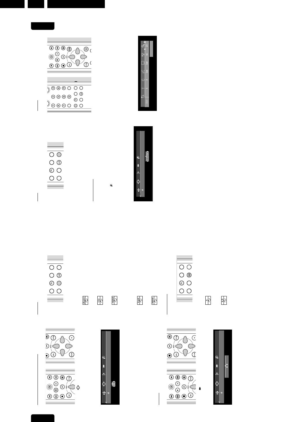
Directions For Use
EN 22 DVDR980-985 /0X13.
English
PLAYBACK 37
Scan
Plays the first 10 seconds of each chapter/index on the
disc.
lPress SCAN.
lTo continue play at your chosen chapter/index,
press SCAN again or press 2 PLAY.
Time search
The Time Search function allows you to start playing at
any chosen time stamp.
lSelect (Time Search) in the system menu bar.
lPress w (down cursor).
‰The recorder will now go into pause mode.
‰A time entry box appears on the screen showing
the elapsed playing time of the current disc.
lUse the digit keys 0-9 to enter the required start
time. Enter hours, minutes and seconds in the box.
‰Each time an item has been entered, the next
item will be highlighted.
lPress OK to confirm the start time.
‰The time entry box will disappear and play starts
from the selected time position.
Zoom
The Zoom function allows you to enlarge the video
image and to pan through the enlarged image.
lSelect aZoom in the system menu bar.
lPress w v (down up cursor) to activate the Zoom
function and select the required zoom factor; 1.33
or 2 or 4.
‰The recorder will go into pause mode.
‰The selected zoom factor appears below the
Zoom icon in the system menu bar and ‘
Press OK
to pan
’ appears below the system menu bar.
‰The picture will change accordingly.
lPress OK to confirm the selection.
‰The panning icons appear on the screen:
wvut(down up right left cursor) and OK.
lUse the wvut(down up right left cursor) keys
to pan all over the screen.
lWhen OK is pressed only the zoomed picture will
be shown on the screen.
lIf you wish to zoom at any moment, press aZoom
and select the required zoom factor as described
above.
lPress 2PLAY to exit zoom mode.
press OK to pan
REC/OTR
PLAYSTOP FSS
FORWARDREVERSE
NEXT PREVIOUS
PAUSE SLOW
CLEAR SELECT
TIMER
T/C
ZOOM ANGLE SUBTITLE AUDIO
DIM REPEAT REPEAT SCAN
A/CH
ZYa
ZOOM ANGLE SUBTITLE AUDIO
DIM REPEAT REPEAT SCAN
ZYa
English
36 PLAYBACK
Still Picture and Step Frame
lSelect (picture by picture) in the system menu
bar.
lUse the w(down cursor) key to enter the picture
by picture menu.
‰The recorder will now go into pause mode.
lUse tu(left right cursor) keys to select previous
or next picture.
lPress 2PLAY to exit picture by picture mode.
lPress v(up cursor) to exit the picture by picture
menu.
You can also step forward by using the ;PAUSE
repeatedly on the remote control.
Search
lSelect (Fast motion) in the system menu bar.
lUse the w(down cursor) keys to enter the fast
motion menu.
lUse the t u (left right cursor) keys to select the
required speed: ‘-
32
’, ‘-
8
’ or ‘-
4
’ (backward); ‘
4
’,
‘
8
’, ‘
32
’ (forward).
lSelect ‘
1
’ to play at normal speed again.
lPress 2PLAY to exit fast motion mode.
lPress v(up cursor) to delete the fast motion menu.
To search forward or backward through different speeds,
you can also press 5REVERSE or 6 FORWARD
again.
Repeat
DVD Discs - Repeat chapter/title/disc
lTo repeat the currently playing chapter, press
REPEAT.
‰appears on screen.
lTo repeat the currently playing title, press REPEAT
a second time
‰appears on screen.
lTo repeat the entire disc, press REPEAT a third
time
‰appears on screen.
lTo exit repeat mode, press REPEAT a fourth time.
Video CDs - Repeat track/disc
lTo repeat the currently playing track, press
REPEAT.
‰appears on screen.
lTo repeat the entire disc, press REPEAT a second
time.
‰appears on screen.
lTo exit repeat mode, press REPEAT a third time.
Repeat A-B
To repeat or loop a sequence in a title:
lPress REPEAT A-B at your chosen starting point;
‰appears on screen.
lPress REPEAT A-B again at your chosen end
point;
‰repeat appears on screen, and the repeat
sequence begins.
lTo exit the sequence, press REPEAT A-B.
ZOOM ANGLE SUBTITLE AUDIO
DIM REPEAT REPEAT SCAN
ZYa
ZOOM ANGLE SUBTITLE AUDIO
DIM REPEAT REPEAT SCAN
ZYa
- 32 -8 -4 1 4 8 32
REC/OTR
PLAY
STOP
FORWARDREVERSE
NEXT PREVIOUS
PAUSE SLOW
FSS
REC/OTR
PLAY
STOP
FORWARDREVERSE
NEXT PREVIOUS
PAUSE SLOW
FSS
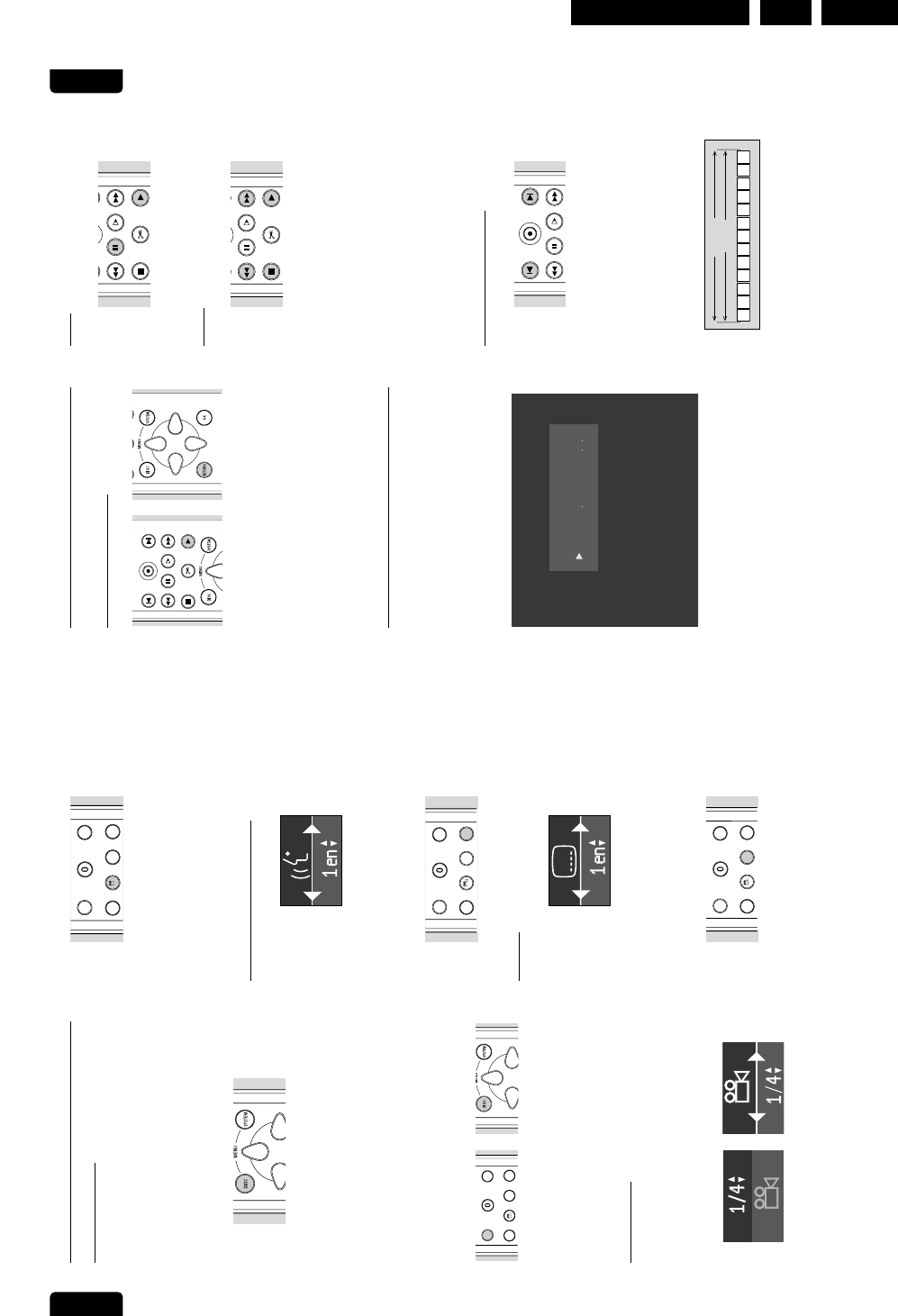
Directions For Use EN 23DVDR980-985 /0X1 3.
English
PLAYBACK 39
Special VCD features
Playback Control (PBC)
lMake sure PBC is switched ‘
On
’. See ‘User
Preferences-features settings’.
lLoad a (Super) Video CD with PBC and press
2PLAY.
‰The PBC menu appears on screen.
lGo through the menu with the keys indicated on the
TV screen until your chosen passage starts to play.
If a PBC menu consists of a list of titles, you can
select a title directly.
lEnter your choice with the numerical keys 0-9.
lPress RETURN to go back to the previous menu.
Playing an audio CD
lInsert the disc.
‰After loading the disc, playback starts
automatically.
‰If the TV set is on, the Audio CD screen appears.
‰During play, the current track number and its
elapsed playing time will be shown on the screen
and the recorder display.
lTo stop play at any time, press 9STOP.
‰The number of tracks and the total playing time
will be shown on the screen and the recorder
display.
Pause
lPress ;PAUSE during play.
lTo return to play, press 2PLAY.
Search
lTo search forwards or backwards through the disc
at 4x normal speed, press 5REVERSE or 6
FORWARD.
‰Search begins.
lTo step up to 8x normal speed, press 5REVERSE
or 6FORWARD again.
‰Search goes to 8x speed, and the sound is muted.
lTo return to 4x normal speed, press 5REVERSE
or 6FORWARD again.
lIf the TV set is on, search speed and direction are
indicated on the screen each time 5REVERSE or
6FORWARD is pressed.
lTo end the search, press 2PLAYor 9STOP as
desired.
Moving to another track
lPress KNEXT during play to step forward to the
next track.
lPress JPREVIOUS during play to return to the
beginning of the current track. Rapidly press
JPREVIOUS twice to step back to the previous
track.
lTo go directly to any track, enter the track number
using the numerical keys 0-9.
2 3 5 6 7 8 9 10 11 12 ...41
TRACKS
AUDIO CD
REC/OTR
FORWARDREVERSE
NEXT PREVIOUS
PAUSE SLOW
PLAYSTOP FSS
FORWARDREVERSE PAUSE SLOW
PLAYSTOP FSS
FORWARDREVERSE PAUSE SLOW
Audio disc mode
1412 78 1 12 78
play track time total tracks total time
repeat track
REC/OTR
PLAY
STOP
FORWARDREVERSE
NEXT PREVIOUS
PAUSE SLOW
FSS
English
38 PLAYBACK
Special DVD-Video features
Menus on the disc
For titles and chapters, selection menus may be included
on the disc.
The DVD’s menu feature allows you to make selections
from these menus. Press the appropriate numerical key;
or use the wvut(down up right left cursor) keys to
highlight your selection, and press OK .
Title menus
lPress DISC MENU .
‰If the current title has a menu, this appears on
the screen. If no menu is present in the title, the
disc menu will be displayed.
lThe menu can list camera angles, spoken language
and subtitle options, and chapters for the title.
lTo exit the title menu, press DISC MENU again.
Note:
Most DVD discs do not have separate disc and title menus.
Disc menu
If a DVD-Video disc has separate disc and title menus,
you can navigate to the disc menu as follows:
lPress T/C followed by DISC MENU .
‰The disc menu is displayed.
lTo remove the disc menu, press DISC MENU
again.
Camera Angle
If the disc contains sequences recorded from different
camera angles, the angle box appears, showing the
number of available angles, and the angle being shown.
You can then change the camera angle if you wish.
lUse the wvkeys to select the required angle in the
angle box.
lTo go to any angle directly, enter the angle number
using the numerical keys 0-9.
‰After a small delay, play changes to the selected
angle. The angle box remains displayed until multiple
angles are no longer available.
Changing the audio language
lSelect Y(Audio) in the system menu bar.
lPress YAUDIO or wv(down up cursor)
repeatedly to step through the different languages.
lYou can enter the required language number directly
using the numerical keys 0-9.
Subtitles
lSelect Z(Subtitle) in the system menu bar.
lPress ZSUBTITLE or wv(down up cursor)
repeatedly to step through the different subtitles, or
to switch the subtitles off.
lYou can enter the required subtitle number directly
using the numerical keys 0-9.
T/C
ZOOM ANGLE SUBTITLE AUDIO
A/CH
ZYa
T/C
ZOOM ANGLE SUBTITLE AUDIO
A/CH
ZYa
T/C
ZOOM ANGLE SUBTITLE AUDIO
A/CH
ZYa
T/C
ZOOM ANGLE SUBTITLE AUDIO
A/CH
ZYa
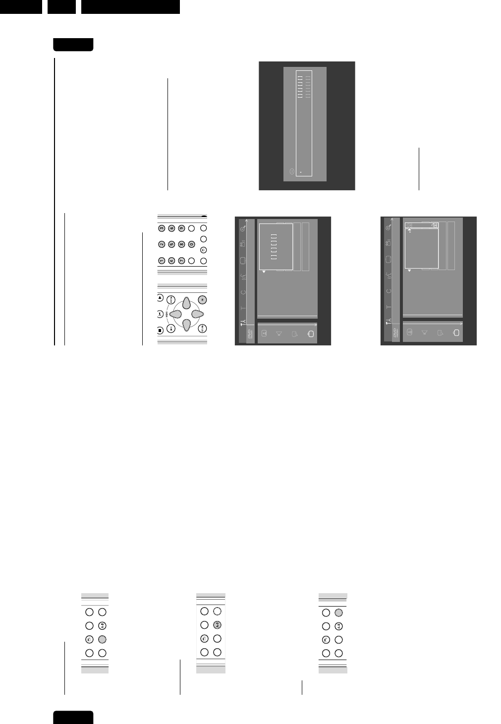
Directions For Use
EN 24 DVDR980-985 /0X13.
English
ACCESS CONTROL 41
Access control
Child Lock (DVD and VCD)
When activating Child lock, only discs that are authorised
can be played without PIN code.
The recorder memory maintains a list of 50 authorized
(‘Child safe’) disc titles. A disc will be placed in the list
when ‘Play Always’ is selected in the ‘Child protect’ dialog.
Each time a ‘Child safe’ disc is played it will be placed on
top of the list. When the list is full and a new disc is added,
the least recently used will be removed from the list.
Activating/deactivating the child lock
lSelect ‘
Access control
’ in the features menu using
wv (down up cursor) and press u(right cursor).
lEnter a 4-digit PIN code of your own choice using
the digit keys 0-9.
lEnter the code a second time.
lMove to ‘
Child lock
’ using wv (down up cursor).
lMove to Ç/ Éusing the u(right cursor) key.
lSelect Çusing wv (down up cursor).
lPress OK or t(left cursor) to confirm and press
SYSTEM MENU again to exit the menu.
‰Now unauthorized discs will not be played unless
the 4-digit code is entered.
lSelect Éto deactivate the Child Lock.
Note:
Reconfirmation of the 4-digit PIN code is necessary when:
The code is entered for the very first time (see above);
The code is changed (see ‘Changing the 4-digit code’);
The code is cancelled (see ‘Changing the 4-digit code’);
Both Child Lock and Parental Control are switched Off and
the code is requested.
Authorizing discs when Child Lock is
activated
lInsert the disc.
‰The ‘Child protect’ dialog will appear. You will be
asked to enter your secret code for ‘
Play once
’ or
‘
Play always
’. If you select ‘
Play once
’, the disc
can be played as long as it is in the recorder and the
recorder is in the On position. If you select ‘
Play
always
’, the disc will become Child safe
(authorized) and can always be played even if the
Child lock is set to ‘
On
’.
Note:
Double sided DVD discs may have a different ID for each
side. In order to make the disc ‘Child safe’, each side has to
be authorized.
Multi volume VCD disc may have a different ID for each
volume. In order to make the complete set ‘Child safe’, each
volume has to be authorized.
Securing discs
lInsert the disc.
‰Playback starts automatically.
lPress 9STOP while {is visible.
‰|will appear and the disc is now banned i.e. it is
not Child safe any longer.
Play once
Play always
Choose 'Play always' to insert the disc in
the child-safe list
locked
Access Control
Access control
Status box
Autoresume
Low power standby
PBC
Features
-- --- off on off
Child lock
Parental level
Change country
Change code
Access control
Status box
Autoresume
Low power standby
PBC
Features
-- --- off on off
Enter code
T/C
ZOOM ANGLE SUBTITLE AUDIO
A/CH
ZYa
English
40 PLAYBACK
Repeat track/disc
lTo repeat the currently playing track, press
REPEAT.
‰‘
Repeat track
’ appears on screen.
lTo repeat the entire disc, press REPEAT a second
time.
‰‘
Repeat disc
’ appears on screen.
lTo exit repeat mode, press REPEAT a third time.
Repeat A-B
To repeat or loop a sequence:
lPress REPEAT A-B at your chosen starting point;
‰‘
Repeat A
’ appears on screen.
lPress REPEAT A-B again at your chosen end
point;
‰‘
Repeat A
-
B
’ appears on the display, and the
repeat sequence begins.
lTo exit the sequence, press REPEAT A-B again.
Scan
Plays the first 10 seconds of each track on the disc.
lPress SCAN.
lTo continue play at your chosen track, press SCAN
again or press 2PLAY.
ZOOM ANGLE SUBTITLE AUDIO
DIM REPEAT REPEAT SCAN
ZYa
ZOOM ANGLE SUBTITLE AUDIO
DIM REPEAT REPEAT SCAN
ZYa
ZOOM ANGLE SUBTITLE AUDIO
DIM REPEAT REPEAT SCAN
ZYa
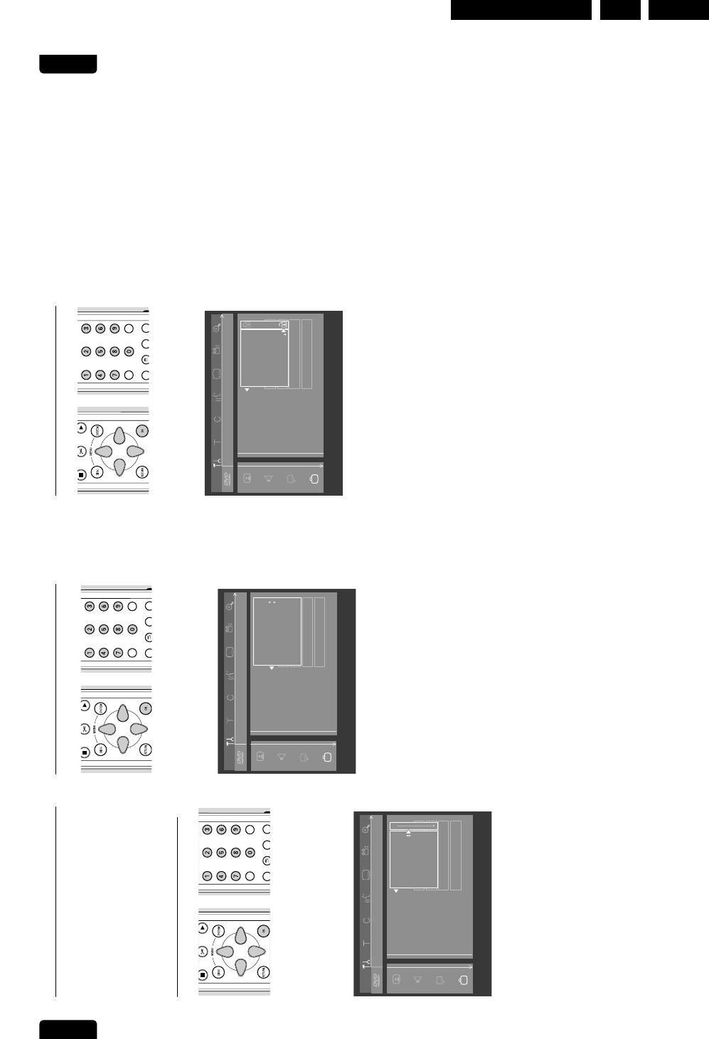
Directions For Use EN 25DVDR980-985 /0X1 3.
English
ACCESS CONTROL 43
Changing the 4-digit code
lSelect ‘
Access control
’ in the features menu using
wv (down up cursor) and press u(right cursor).
lEnter the old code.
lMove to ‘
Change code
’ using w(down cursor).
lPress u(right cursor).
lEnter the new 4-digit PIN code.
lEnter the code a second time and reconfirm with OK.
lPress SYSTEM MENU to exit the menu.
Note:
If you forgot your code, press
9
STOP four times while in
the access control PIN code box and exit with OK. Access
control is now switched off. You can then enter a new code
as described above.
Access control
Status box
Autoresume
Low power standby
PBC
Features
-- --- off on off
Child lock
Parental level
Change country
Change code
T/C
ZOOM ANGLE SUBTITLE AUDIO
A/CH
ZYa
English
42 ACCESS CONTROL
Parental Level (DVD-Video only)
Movies on pre-recorded DVD discs may contain scenes
not suitable for children. Therefore discs may contain
‘Parental Control’ information which applies to the
complete disc or to certain scenes on the disc.
These scenes are rated from 1 to 8 and alternative, more
suitable scenes are available on the disc. Ratings are
country dependent. The ‘Parental Control’ feature allows
you to prevent discs from being played by your children
or to have certain discs played with alternative scenes.
Activating/Deactivating Parental Control
lSelect ‘
Access control
’ in the features menu using
wv (down up cursor) and press u(right cursor).
lEnter your 4-digit PIN code using the digit keys 0-9.
If necessary enter the code a second time.
lMove to ‘
Parental level
’ using wv (down up cursor).
lMove to the Value Adjustment bar using u(right
cursor).
lUse the wv(down up cursor) keys or the
numerical keys 0-9 on the remote control to select
a rating from 1 to 8 for the disc inserted.
Rating 0 (displayed as ‘– –’):
Parental Control is not activated. The disc will be played
in full.
Ratings 1 to 8 (1 = childsafe - 8 = adults only):
The disc contains scenes not suitable for children. If you
set a rating for the recorder, all scenes with the same
rating or lower will be played. Higher rated scenes will
not be played unless an alternative is available on the
disc. The alternative must have the same rating or a
lower one. If no suitable alternative is found, play will
stop and the 4-digit code has to be entered.
lPress OK or t(left cursor) to confirm and press
SYSTEM MENU again to exit the menu.
Country
lSelect ‘
Access control
’ in the features menu using
wv (down up cursor) and press u(right cursor).
lEnter the four digit PIN code.
lMove to ‘
Change country
’ using w(down cursor).
lPress u(right cursor).
lSelect a country using wv (down up cursor).
lPress OK or t(left cursor) to confirm and press
SYSTEM MENU again to exit the menu.
Access control
Status box
Auto resume
Low power standby
PBC
-- --- off on off
Austria
Belgium
Denmark.
Finland
T/C
ZOOM ANGLE SUBTITLE AUDIO
A/CH
ZYa
Access control
Status box
Autoresume
Low power standby
PBC
Features
-- --- off on off
Child lock
Parental level
Change country
Change code
--
T/C
ZOOM ANGLE SUBTITLE AUDIO
A/CH
ZYa

Directions For Use
EN 26 DVDR980-985 /0X13.
English
MANAGING DISC CONTENT 45
Disc Settings
For each DVD+RW or DVD+R disc the settings can be
changed to your personal preference in the disc settings
menu.
lIn the Disc Info Screen press u(right cursor).
‰You will now enter the ‘disc settings’ menu.
Changing the Disc Name
lIn the Disc Info Screen press u(right cursor).
‰You will now enter the ‘disc settings’ menu.
lEnter the new name. A name may contain a
maximum of 64 characters.
lUse tu(left right cursor) for the position of the
characters. Use wv (down up cursor) to change
characters.
lUse SELECT to toggle between capitals and lower
case characters.
lUse CLEAR to erase a character.
lConfirm by pressing OK.
Protection of recordings
lIn the Disc Info Screen press u(right cursor).
‰You will now enter the ‘disc settings’ menu.
lSelect ‘
Protection
’ and press u(right cursor).
lSelect ‘
Protected
’ with wv(down up cursor).
lPress OK on the remote control to confirm.
‰No further changes can be made to the disc.
It will also disable most title/disc settings options, as
well as the complete edit menu.
‰Future editing is only possible after resetting the
Protection feature to ‘
Unprotected
’ again.
Erasing a disc
This option is only aivailable for DVD+RW discs that are
not erase-protected.
lIn the Disc Info Screen press u(right cursor).
‰You will now enter the ‘disc settings’ menu.
lSelect ‘
Erase disc
’ and press OK.
‰The message '
This will erase all titles
’ is
displayed.
lPress OK to confirm or t(left cursor) to cancel.
‰‘
Erasing disc
’ is shown until the action is
completed.
‰After the disc has been erased, the Index Picture
Screen will show the free space on the disc.
Finalising a DVD+R disc
While a DVD+RW disc can be played instantly on most
DVD players, a DVD+R disc can be played only on the
DVD recorder until it is finalised. After finalisation no
changes can be made to the disc anymore.
lIn the Disc Info Screen press u(right cursor).
‰You will now enter the ‘disc settings’ menu.
lSelect ‘
Finalise disc
’ and press OK to confirm.
‰‘
Finalise disc
’ is shown until the action is
completed.
‰After finalisation the Index Picture Screen will
appear.
If the DVD+R disc was recorded on a different brand of
DVD recorder you may not be able to access the Disc
Settings screen. In this case you can use the ‘
Finalise
disc
’ option in the features menu of the user
preferences menu.
Access control
Status box
Autoresume
Low power standby
Finalise disc
Features
Enter code ...
On
Off
Off
Press OK
-- --- off on off
Settings for Summer holiday
Summer holiday
Disc name
Pr o t ection
Era se disc
Finalise disc
Unpr o t e ct e d
Press OK
Settings for Summer holiday
Summer holiday
Disc name
Protection
Erase disc
Unprotected
English
44 MANAGING DISC CONTENT
Managing disc content
Title settings
For each title on a DVD+RW or DVD+R disc the
default settings can be changed to your personal
preference in the title settings menu.
Changing the title name
lIn the Index Picture Screen, select the required title
with wv (down up cursor).
lPress u(right cursor) to enter the title settings menu.
lEnter the new name. A name may contain a
maximum of 64 characters.
lUse tu(left right cursor) for the position of the
characters. Use wv(down up cursor) to change
characters.
lUse SELECT to toggle between capitals and lower
case characters.
lUse CLEAR to erase a character.
lConfirm by pressing OK.
Play full title
lIn the Index Picture Screen, select the required title
with wv (down up cursor).
lPress u(right cursor) to enter the title settings menu.
lSelect ‘
Play full title
’.
When this item is selected the title will be played in full,
including hidden chapters. Follow the instructions on the
screen. (See ‘managing disc content - Favorite Scene
Selection’)
Erasing a title
You may simply erase a title on DVD+RW by recording
over it, but if you want to erase the whole title instantly,
do the following:
lIn the Index Picture Screen, select the required title
with wv (down up cursor).
lPress u(right cursor) to enter the title settings menu.
lSelect ‘
Erase this title
’
.
‰The message '
This will completely erase this
title
', '
Press OK to confirm
' is shown.
lPress OK to confirm.
‰‘
Erasing title
...’ is shown until the action is
completed.
‰After the title has been erased, the Index Picture
Screen will show an empty space instead. If there
was an empty space in front of or behind this title,
then these are combined into one empty space.
Empty spaces of less then one minute will not be
shown.
On DVD+R titles can also be erased but the space
occupied cannot be used anymore. During
finalisation erased titles are removed from the Index
Picture Screen.
Disc Info Screen
lWhen on the Index Picture Screen, press 9STOP.
‰You are now on Title 1.
lPress v(up cursor).
‰You enter the Disc Info Screen.
lPress w(down cursor) to exit the Disc Info Screen.
The Disc Info Screen contains the following
information:
Settings for title BBC soccer
BBC soccer
Name
Play full title
Erase this title
Unlocked5
5
5
PAL5
5
5
DVD playback
Edits
Summer holiday5
02:05:10 used5
Sun 13 12 99
23: 13 h r
12 BBC1
Compatibility status
- indicates compatibility of any edits
with DVD players
Video system
- PAL or SECAM
- NTSC
DVD+R disc status
- unlocked
- locked
- finalised
Disc description
- disc name
- total recording duration
- date of last recording
Cue to go back to the Index Picture
Screen

Directions For Use EN 27DVDR980-985 /0X1 3.
English
MANAGING DISC CONTENT 47
Inserting chapter markers
lIn play mode press FSS on the remote control,
to call up the FSS menu.
lSelect ‘
Insert chapter marker
’.
lPress OK on the remote control to insert a marker.
The maximum number of chapter markers is 99.
When this maximum is reached the on-screen message
‘
Too many chapters
’ appears. You have to delete some,
before inserting new chapter markers.
During recording you can add chapter markers by
pressing FSS on the remote control. The message
‘
Chapter marker inserted
’ will appear on the screen.
Hiding chapters
Initially all chapters are visible. You can hide chapters or
make them visible again on playback. In FSS mode however
hidden chapters are displayed in a dimmed mode.
lIn play mode press FSS on the remote control to
call up the FSS menu.
lSelect
‘
‘
Current chapter
‘
’
with wor v(down up
cursor).
lSelect ‘
Visible
’ or ‘
Hidden
’ with the u(right cursor)
key.
lYou can toggle between ‘
Visible
’ and ‘
Hidden
’
directly from any line in the FSS menu with the
SELECT key on the remote control.
Deleting chapter markers
You van combine a chapter with the previous chapter in
the current title by deleting the chapter at the beginning
of the current chapter.
lIn play mode press FSS on the remote control
to call up the FSS menu.
lSelect ‘
Delete chapter marker
‘.
lPress OK on the remote control to confirm
‰‘
Deleting marker
’ will appear.
You can delete all chapter markers (manually and
automatically generated) in the current title.
lIn play mode press FSS on the remote control
to call up the FSS menu.
lSelect ‘
Delete chapter markers
‘.
lPress OK on the remote control to confirm
‰‘
Deleting markers
’ will appear.
Changing the index picture
You can define the current video frame as a miniature
picture to be used for this title’s entry in the Index
Picture Screen.
lIn play mode press FSS on the remote control
to call up the FSS menu.
lSelect ‘
New index picture
‘.
lYou can use ;PAUSE and/or xSLOW to
accurately choose the desired picture.
lPress OK on the remote control to confirm.
‰‘
Updating menu
’ will appear.
play
1 2
Favourite scene selection
Insert chapter marker
Current chapter
Delete chapter marker
Delete all chapter markers
Divide title
Hidden
REC/OTR
PLAYSTOP FSS
FORWARDREVERSE
NEXT PREVIOUS
PAUSE SLOW
English
46 MANAGING DISC CONTENT
Making your edits DVD-compatible
If one or more titles have been edited (see ‘Favourite
Scene Selection’), then the edits will play on your DVD
recorder, but a DVD player may show the original
versions instead of the edits. You can prepare your
DVD+RW discs so that also a DVD player will show the
edited version. This is not possible with DVD+R discs.
lIf the Disc Settings menu shows the option ‘
Make
edits DVD compatible
’, select this option. If the
menu does not show this option, then your
DVD+RW disc is already compatible, and no
conversion is needed.
lPress OK on the remote control to confirm.
‰The messages ‘
This will take
...’ and ‘
Press OK
to confirm
’ will appear to indicate how long the
action will take.
lPress OK on the remote control to confirm.
‰‘
Processing...
’ and a progress bar are shown
until the action is completed.
Favourite Scene Selection
The basic function of any edit operations is to improve
accessibility and handling of your recordings. For instance:
scenes you do not want to see during playback (e.g.
commercials during a movie) can be marked as chapters
and made hidden. During playback you will see your
recording without the hidden chapters as one sequence.
Note:
In between the scenes the picture may freeze for a short moment.
Each title consists of chapters. With the FSS menu any
chapter can be made hidden or made visible again.
Normally, during recording, chapter markers are inserted
automatically every five to six minutes (this setting can be
changed in the record settings menu). After the recording
is finished, you can manually add and remove chapter
markers via the FSS menu. Both automatically generated
and manually inserted chapter markers can be removed.
After editing, the modified version of a title is the default
playback version. The original can be accessed via the
‘
Play full title
’ option in the title settings menu. Other
DVD players may still play the original. To guarantee
that the edited version will play on these DVD players,
choose ‘
Make edits DVD
-
compatible
’ in the disc
settings menu (only available on DVD+RW discs).
Calling up the FSS menu
lPlay the title you want to edit.
lPress the FSS key on the remote control.
‰The video image is overlayed with a transparant edit
menu. Title and chapter information appear in an
information box at the top of the screen.
Note:
The Favourite Scene Selection menu may disappear after
about five minutes if you do not edit any information.
lUse wor v(down up cursor) to toggle through the
menu’s functions.
play
1 1
Favourite scene selection
Insert chapter marker
Current chapter
Delete chapter marker
Delete all chapter markers
Use picture as index
Divide title
Press OK
Hidden
CLEAR SELECT
TIMER
MONITOR ON/OFF
REC/OTR
PLAYSTOP FSS
FORWARDREVERSE
NEXT PREVIOUS
PAUSE SLOW
Settings for Summer holiday
Summer holiday
Disc name
Protection
Erase disc
Make edits DVD compatible
Unprotected
Press OK
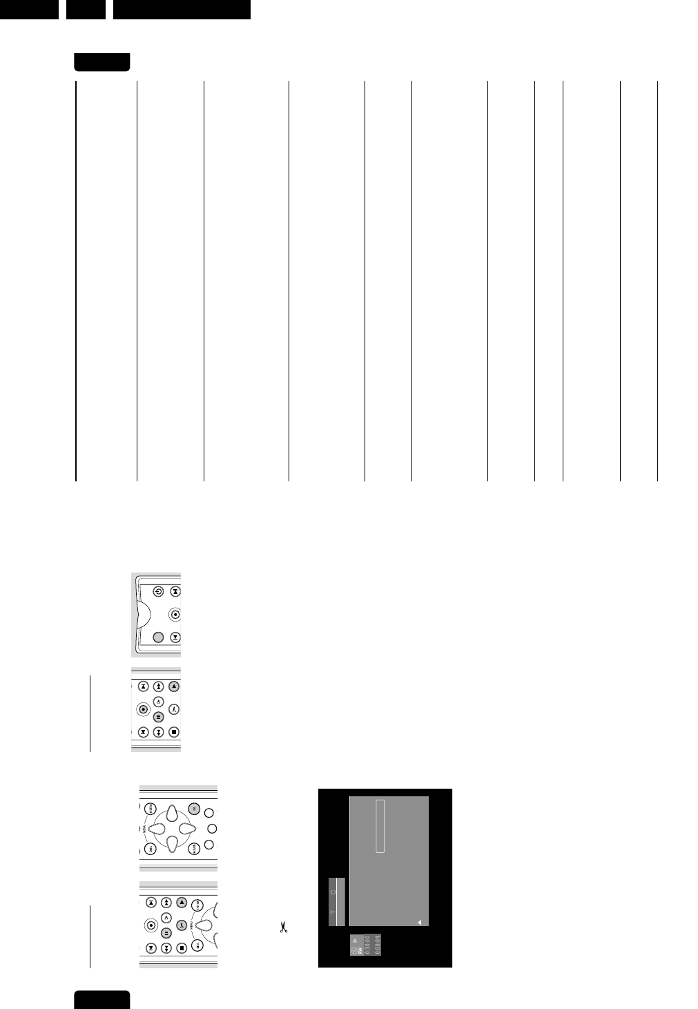
Directions For Use
EN 28 DVDR980-985 /0X13.
English
TROUBLESHOOTING 49
Troubleshooting
If it appears that the DVD recorder is faulty, first consult this checklist. It may be that something has been overlooked.
Under no circumstances attempt to repair the system yourself; this will invalidate the warranty. Look for the specific
symptom(s). Then perform only the actions listed to remedy the specific symptom(s).
Symptom Remedy
The recorder does not respond to • The remote control may be configured for a second DVD recorder.
the remote control Hold SELECT+1pressed simultaneously to revert to DVD recorder 1.
• Aim the remote control directly at the sensor on the front of the
recorder.
• Avoid all obstacles which may interfere with the signal path.
• Inspect or replace the batteries.
Keys on the DVD recorder do not work • The DVD recorder may still be in Virgin mode. See ‘First time set-up:
virgin mode’.
• Otherwise disconnect and reconnect the DVD recorder from the
mains.
• If this does not solve the problem, check if the remote control still
works. If so, the recorder is probably in trade mode.
Disconnect the recorder from the mains and reconnect it while holding
/OPEN/CLOSE and 9STOP pressed.
No picture • Check if the TV set is switched on.
• Check the video connection.
• When the DVD recorder is connected to the TV set via
SCART
, you
may not see the picture at the DVD recorder after selecting the correct
programme number on your TV set when a timer recording takes place.
• This way, you can still view another device (e.g. a satellite receiver).
• To view the DVD recorder press TV/DVD on the remote control.
Distorted picture distorted sound • Check the disc for fingerprints and clean with a soft cloth, wiping from
centre to edge.
• Sometimes a small amount of picture distortion may appear. This is
not a malfunction.
Recorder does not play disc • Ensure the disc label is upwards and that the right disc type is inserted.
• Clean the disc.
• Check if the disc is defective by trying another disc.
• Check if the region code of the disc matches the region code of the
recorder. (pre-recorded DVD discs only). See ‘playing a pre-recorded
DVD-Video disc’.
• Check if Child Lock is activated.
Distorted sound from HiFi amplifier • Check to make sure that no audio connections are made to amplifier
phono input.
• Check to make sure that analogue input of the amplifier is not
connected to the digital output of the DVD recorder.
Distorted or black and white picture with • The disc format is not according to the TV set used (PAL/NTSC).
DVD or Video CD disc
No audio at digital output • Check the digital connections.
• Check the settings menu to make sure that the digital output is set to
on.
• Check if the audio format of the selected audio language matches your
receiver capabilities.
Recorder does not respond to all • Some operations are not permitted by the disc. Refer to the
operating commands during playback instructions in the disc inlay.
of a DVD-Video disc
English
48 MANAGING DISC CONTENT
Dividing a title
On a DVD+RW disc you split one title into two
separate titles. (On DVD+R this is not possible.)
lOn the Index Picture Screen, select the title you
want to divide.
lPress 2PLAY.
lGo to the point where you want to divide the title
and press ;PAUSE.
lPress FSS.
‰The Favourite Scene Selection menu is shown.
lSelect ‘
Divide title
’.
lPress OK on the remote control to confirm.
‰‘
Dividing title...
’ is shown until the action is
completed. This divide operation cannot be undone.
The Index Picture Screen will show two titles instead of
one. Both will have the same name. If you want to
change the name, you can do so in the title settings
menu. For one of the two resulting titles, a new index
picture is created.
If you want to divide one title into more than two titles,
use the above procedure several times.
Append recording
This function is only available on DVD+RW discs.
If you want to append a video recording to an earlier
recorded title, do the following.
lOn the Index Picture Screen, select the title to
which you want to add a video recording.
lPress 2PLAY.
lAt the point where you want to append the title
press ;PAUSE.
lTo monitor the video input you may press
MONITOR.
lPress RECORD (on the recorder) or REC/OTR
(on the remote control).
The video recording will now be appended from this
point. Video material beyond this point is overwritten.
This may include titles following the current title.
Any remaining video material that is not overwritten,
which may include the last part of the original title, is
maintained. You can access these titles from the Index
Picture Screen.
MONITOR ON/OFF
REC/OTR NEXT PREVIOUS
REC/OTR
PLAYSTOP FSS
FORWARDREVERSE
NEXT PREVIOUS
PAUSE SLOW
play
1 2
Favourite scene selection
Insert chapter marker
Current chapter
Delete chapter marker
Delete all chapter markers
Use picture as index
Divide title
Hidden
Press OK
CLEAR
aP
SELECT
TIMER
REC/OTR
PLAYSTOP FSS
FORWARDREVERSE
NEXT PREVIOUS
PAUSE SLOW
Directions For Use EN 29DVDR980-985 /0X1 3.
English
TROUBLESHOOTING 51
Diagnosis programme
If the recorder is still faulty you can start the Diagnosis
Programme in the recorder.
You can operate the Diagnosis Programme by following
the instructions step by step.
Instructions
lUnplug the power cord of the recorder.
lPress the 2PLAY key and keep them pressed
while you plug the recorder.
‰On the display the message ‘BUSY’ appears
together with a counter. This counter indicates the
termination of the test when zero is reached.
‰After a few minutes the message on the local
display changes over from ‘BUSY’ to ‘FAIL’ or to
‘PASS’.
‰If the message ‘FAIL’ appears on the display,
there is apparently a failure in your recorder and
your recorder should be repaired.
lConsult your dealer or the Philips Customer Care
Centre for the nearest Service Repair Shop in your
country. The phone number is given in your
warranty booklet.
lIf the message ‘PASS’ appears on the display, there
is apparently no failure in your recorder, in this case
the failure can be caused by incorrect interpretation
of the operating instructions or a wrong disc is used
or your recorder is not correctly connected. In this
case you should consult your dealer or the Philips
Customer Care Centre for further assistance in
solving the problem.
lIf the problem remains, then consult your Philips
Customer Care Centre.
System limitations
DVD+RW and DVD+R discs may not play on certain
DVD Video players.
A DVD+RW video disc that has been recorded on a
different type or brand of recorder can be played, but
may not provide all features commonly available to
DVD+RW discs, such as the on-screen disc bar, the disc
settings menu, the title settings menu, and editing.
Refer to ‘Adapt disc format’. If the disc is write-
protected, the status cannot be changed.
When using manual recording, the DVD recorder will
warn before adapting the format of the disc or removing
non-video data. When using timer recording however,
the DVD recorder will always start to record, unless the
disc is write-protected. Menus, edits and other data
recorded on a different device (e.g. a PC) may be lost.
Because of the Variable Bit Rate, a title map take up less
or more space than the overwritten title, even though
the duration is the same. As a result, a part of the
original title may remain, or a part of the next title may
be lost. The maximum deviation is five minutes.
After a power interruption during recording, the Index
Picture Screen will may not match with the actual video
content on the disc. The last recorded title may be lost.
English
50 TROUBLESHOOTING
The recorder does not record • Make sure that the recorder is switched to standby before the timer
timer programme starts.
No new title can be recorded • Check if the maximum number of titles has been reached (message:
‘
too many titles
’ on screen). If so, delete a title next to a free space.
• Check if the disc is write protected. If so, unlock the disc in the disc
settings menu (message: ‘
Disc locked
’ on screen).
• Check if the (DVD+R) disc has been finalized. If so, no new titles can
be recorded anymore.
Service codes on the display • Clean the disc. The recording was most probably done correctly.
‘Disc warning’ message on screen • A write error has occured, but it could be corrected. No user action
is required.
‘Disc error’ message on screen • A write error has occured from which the recorder could not
recover. Inspect the disc and clean it if necessary (refer to ‘Intoduction -
Cleaning discs’ for cleaning instruction). Record (overwrite) again over
the same part of the disc to see if the problem is solved
Disc errors • A disc might be corrupted because of dust, scratches or fingerprints.
If the disc cannot be accessed anymore, use the back-up disc erase
procedure to repair it. Proceed as follows:
1. Clean the disc.
2. Put disc in the drawer (do not close the tray).
3. Press and hold CLEAR for several seconds until the tray closes.
Two languages are ‘mixed’ when • When the TV set does not automatically detect the dual-language
recording from a stereo VCR signal,use left/right audio balance on the TV set to amplify the one or
the other language.
The disc cannot be erased because the 1. Open the tray while leaving the disc in.
Index Picture Screen does not appear 2. Hold CLEAR pressed for around 5 seconds until the tray closes. The
disc is technically not yet erased but you can start a new recording like
on a blank disc.
The Index Picture Screen does not appear • Take out the disc. Clear the disc. Insert the disc.
but the titles on the disc can still be played Choose ‘Adapt to own disc format’ (See ‘User Preferences - Features).
A DVD player shows the Index Picture • Press 9STOP to exit the Index Picture Screen, then press 2PLAY.
Screen but does not react to
the 2PLAY key
A DVD+RW disc does not play • There are DVD Players that will not play recordings made with a DVD
on a certain DVD player Recorder. With a special procedure the recorder will solve this problem
for some players. Proceed as follows:
1. Put the disc in the drawer (do not close the tray)
2. Press and hold the 2key on the remote control for several seconds
until the tray closes. The disc is now modified.
3. If the change has no effect, you may perform the same procedure
with the 3key on the remote control.
Note :
Modifying the disc can solve the problem for a specific player model, but
playback in other DVD players may no longer be possible.
It is therefore recommended to use this procedure carefully and only when
needed.
• To revert the disc to the original state, follow the same procedure
with the 1 key on the remote control.
Directions For Use
EN 30 DVDR980-985 /0X13.
English
52 GLOSSARY
This section explains most important terms, abbreviations, and acronyms used in this document.
Term Explanation
AC-3 Audio Coding 3, also known as Dolby Digital. Multi-channel digital audio
compression system from Dolby Labs.
A/V Audio/Video
Chapter A part of a title.
Disc Bar A graphical representation of the contents of a (DVD+RW) disc.
Disc Pointer An arrow indicating the current playback/recording position on the
DVD+RW disc, displayed on the ‘disc bar’.
DTS Digital Theater System. A high-end Multi-channel audio compression
format.
DV Digital Video. A camcorder format for high-quality video, different from
MPEG. It is converted into MPEG 2 Video when recorded on DVD+RW
DVD Digital Versatile Disc
DVD+R DVD+Recordable. The write-once disc standard used by the DVD
recorder.
DVD+RW DVD+ReWritable. One of the disc standards used by the DVD
recorder.
EasyLink If your TV set and your video recorder are equipped with this feature,
they can exchange information to adjust certain settings to each other,
such as the TV channel order and other user preferences.
FSS Favorite Scene Selection. see ‘Managing disc content’.
i.LINK Also known as ‘FireWire’ and ‘IEEE 1394’. A cable for transfer of high-
bandwidth digital signals, as used by Digital Video camcorders.
Index Picture Screen A screen that gives an overview of a DVD+RW disc, wih ‘index
pictures’ that each represent a recording.
MPEG Motion Picture Experts Group. A collection of compression systems for
digital audio and video.
N
EX
TV
IEW
Link A system that enables easy programming of a video recorder via a TV
set. Also see EasyLink.
NICAM System for reception of digital stereo TV sound.
NTSC See TV system.
OSD On-screen Display. The ‘user interface’ by which you can control the
DVD recorder via the TV screen.
OTR One-Touch Recording. With this feature you can easily start a
recording (by pushing just one button) and select the switch-off time in
intervals of 30 minutes.
Glossary
Directions For Use EN 31DVDR980-985 /0X1 3.
English
APPENDIX 55
Firstline. . . . 348, 036, 243, 244,
. . . . . . . . . . . . . . . . . . . . . . 321
Fisher . . . . . . . . . 244, 181, 397
Flint. . . . . . . . . . . . . . . . . . . 482
Formenti . . . . . . . . . . . 347, 064
Frontech . . . . . . . . . . . 458, 291
Fujitsu . . . . . . . . . 206, 099, 233
Funai . . 321, 198, 206, 207, 291
Futuretech . . . . . . . . . . . . . 207
GE. . . . 048, 074, 078, 205, 478,
. . . . . . . . . . . . . . . . . . 120, 309
GEC . . . . . . . . . . 099, 064, 244
GPM . . . . . . . . . . . . . . . . . . 245
Geloso . . . . . . . . . . . . . . . . 036
Genexxa . . . . . . . . . . . . . . . 245
Gibralter . . . . . . . 044, 046, 057
GoldStar . . . 064, 046, 057, 205,
. . . . . . . . . . . . . . 244, 083, 136
Goodmans . . . . . 064, 099, 206,
. . . . . . . . . . 398, 063, 244, 401
Gorenje. . . . . . . . . . . . . . . . 397
Gradiente . . . . . . . . . . 083, 080
Granada. . . . . . . . 064, 099, 244
Grandin. . . . . . . . . . . . . . . . 309
Grundig . . . . . . . . 097, 581, 064
Grunpy . . . . . . . . . . . . 206, 207
HCM . . . . . . . . . . . . . . 036, 309
Hallmark . . . . . . . . . . . . . . . 205
Hanseatic. . . . . . . . . . . 064, 347
Harley Davidson . . . . . . . . . 206
Harman/Kardon . . . . . . . . . 081
Harvard. . . . . . . . . . . . . . . . 207
Hinari . . . . . 036, 063, 064, 245,
. . . . . . . . . . . . . . . . . . . . . . 206
Hisawa. . . . . . . . . . . . . 309, 482
Hitachi. . . . . 136, 071, 172, 244,
. . . . . . . . . . . . . . 063, 083, 132
Huanyu . . . . . . . . . . . . 243, 401
Hypson . . . . . . . . 291, 064, 309
ICE . . . . . . . . . . . 244, 291, 398
ICeS . . . . . . . . . . . . . . . . . . 245
ITS . . . . . . . . . . . . . . . . . . . 398
Imperial . . . . . . . . . . . . 445, 397
Indiana. . . . . . . . . . . . . . . . . 064
Infinity . . . . . . . . . . . . . . . . . 081
Inno Hit. . . . . . . . . . . . . . . . 099
Innova . . . . . . . . . . . . . . . . . 064
Inteq . . . . . . . . . . . . . . . . . . 044
Interfunk . . . . . . . . . . . . . . . 064
Intervision . . 064, 129, 244, 291
Isukai. . . . . . . . . . . . . . . . . . 245
JBL . . . . . . . . . . . . . . . . . . . 081
JCB . . . . . . . . . . . . . . . . . . . 027
JVC . . . . . . . 080, 063, 398, 680
KEC . . . . . . . . . . . . . . . . . . 207
KTV . . . . . . . 207, 244, 057, 066
Kaisui . . 245, 244, 036, 243, 309
Kamp . . . . . . . . . . . . . . . . . 243
Kapsch . . . . . . . . . . . . . . . . 233
Kawasho . . . . . . . . . . . . . . . 243
Kendo . . . . . . . . . . . . . . . . . 064
Kenwood. . . . . . . . . . . 057, 046
Kingsley. . . . . . . . . . . . . . . . 243
Korpel. . . . . . . . . . . . . . . . . 064
Koyoda . . . . . . . . . . . . . . . . 036
LG. . . . . . . . . . . . . . . . . . . . 083
LXI . . . . 181, 074, 081, 183, 205
Leyco . . . . . . 099, 064, 291, 321
Liesenk & Tter . . . . . . . . . . 064
Luma. . . . . . . . . . . . . . . . . . 233
Luxman . . . . . . . . . . . . . . . . 083
M Electronic . . . . 132, 244, 036,
. . . . . . . . . . . . . . 064, 136, 401
MGA . . . . . . 177, 046, 057, 205
MTC. . . 087, 057, 046, 083, 243
Magnadyne . . . . . . . . . . . . . 129
Magnafon. . . . . . . . . . . . . . . 129
Magnavox. . . 081, 057, 063, 206
Manesth . . . . . . . . 347, 244, 291
Marantz . . . . . . . . 064, 081, 057
Mark . . . . . . . . . . . . . . . . . . 064
Matsui . 036, 064, 244, 398, 062,
. . . . . . . . . . . . . . 063, 099, 321
Matsushita . . . . . . . . . . 277, 677
Mediator . . . . . . . . . . . 039, 064
Megatron. . . . . . . . . . . 172, 205
Memorex . . 205, 036, 083, 177,
. . . . . . . . . . . . . . 181, 277, 490
Midland . . . . 044, 066, 074, 078
Minerva . . . . . . . . . . . . 097, 581
Minutz . . . . . . . . . . . . . . . . . 048
Mitsubishi . . 063, 135, 177, 205,
. . . . . . . . . . . . . . . . . . 046, 120
Mivar. . . . . . . . . . . . . . . . . . 243
Motorola. . . . . . . . . . . . . . . 120
Multitech . . . 036, 129, 207, 243,
. . . . . . . . . . . . . . . . . . . . . . 244
NAD . . . . . . . . . . 183, 193, 205
NEC . . . 057, 063, 046, 083, 482
NEI . . . . . . . . . . . . . . . 064, 458
NTC . . . . . . . . . . . . . . . . . . 119
Neckermann . . . . . . . . 064, 581
Nesco . . . . . . . . . . . . . . . . . 206
Netsat . . . . . . . . . . . . . . . . . 064
Nikkai . 064, 062, 245, 099, 243,
. . . . . . . . . . . . . . . . . . . . . . 291
Nikko . . . . . . . . . 205, 057, 119
Nobliko. . . . . . . . . . . . . . . . 129
Nordmende . . . . . . . . . . . . 136
Onwa . . . . . . . . . . . . . . . . . 207
Optimus. . . . 277, 193, 181, 677
Optonica . . . . . . . . . . . 120, 192
Orion . 321, 490, 064, 206, 263,
. . . . . . . . . . . . . . . . . . 347, 348
Osaki . . . . . . 099, 244, 245, 291
Oso. . . . . . . . . . . . . . . . . . . 245
Osume . . . . . . . . . . . . . . . . 099
Otto Versand . . . 064, 037, 063,
. . . . . . . . . . . . . . 244, 347, 581
Palladium . . . . . . . . . . . 397, 445
Panama . . . . . . . . . . . . 244, 291
Panasonic. . . . . . . 078, 277, 677
Pathe Cinema . . . . . . . 347, 243
Pausa. . . . . . . . . . . . . . . . . . 036
Penney . . . . 074, 087, 057, 048,
. . . . . . . . . . 205, 078, 066, 046,
. . . . . . . . . . . . . . . . . . 083, 183
Perdio . . . . . . . . . . . . . . . . . 347
Philco . . 172, 046, 057, 081, 490
Philips. . 064, 039, 081, 401, 581
Phonola . . . . . . . . . . . . 064, 039
Pilot . . . . . . . . . . . 046, 057, 066
Pioneer . . . . . . . . . . . . 136, 193
Portland. . . . . . . . 046, 066, 119
Prism. . . . . . . . . . . . . . . . . . 078
Profex . . . . . . . . . . . . . . . . . 036
Proline . . . . . . . . . . . . . . . . 348
Proscan . . . . . . . . . . . . . . . . 074
Protech . . . . 064, 129, 036, 458,
. . . . . . . . . . . . . . 244, 291, 445
Proton. . . . . . . . . . . . . . . . . 205
Pulsar . . . . . . . . . . . . . 044, 046
Pye . . . . . . . . . . . . . . . . . . . 039
Quasar . . . . . 078, 277, 192, 677
Quelle . . . . . 064, 097, 037, 581
Questa . . . . . . . . . . . . . . . . 063
R-Line . . . . . . . . . . . . . . . . . 064
RBM . . . . . . . . . . . . . . . . . . 097
RCA . . . 074, 046, 078, 117, 120
Radio Shack . . . . 192, 207, 057,
. . . . . . . . . . 205, 066, 181, 046,
. . . . . . . . . . . . . . . . . . 074, 083
Radiola . . . . . . . . . . . . 064, 039
Rank Arena . . . . . . . . . . . . . 063
Realistic. . . . 192, 207, 181, 057,
. . . . . . . . . . 066, 205, 046, 083
Revox . . . . . . . . . . . . . . . . . 064
Rex . . . . . . . . . . . . . . . 233, 291
Rhapsody. . . . . . . . . . . . . . . 243
Roadstar . . . 036, 291, 245, 445
Runco . . . . . . . . . . . . . 044, 057
SBR . . . . . . . . . . . . . . . 039, 064
SEG . . . . . . . . . . . 244, 063, 291
SEI . . . . . . . . . . . . 129, 037, 321
SKY. . . . . . . . . . . . . . . . . . . 064
SSS . . . . . . . . . . . . . . . 046, 207
Saba. . . . . . . . . . . . . . . . . . . 136
Saisho . . . . . . . . . 036, 291, 458
Sambers . . . . . . . . . . . . . . . 129
Sampo . . . . . . . . . . . . . 057, 066
Samsung . . . 064, 046, 205, 244,
. . . . . . . . . . 291, 397, 036, 057,
. . . . . . . . . . 066, 083, 087, 117
Samsux . . . . . . . . . . . . . . . . 066
Sandra . . . . . . . . . . . . . . . . . 243
Sansei . . . . . . . . . . . . . . . . . 478
Sansui . . . . . . . . . . . . . . . . . 490
Sanyo. . . . . . . . . . 181, 063, 099
Schneider. . . . . . . 064, 245, 398
Scimitsu. . . . . . . . . . . . . . . . 046
Scotch . . . . . . . . . . . . . . . . . 205
Scott. . . 263, 046, 205, 206, 207
Sears . . 181, 083, 183, 074, 081,
. . . . . . . . . . . . . . 198, 205, 206
Seleco . . . . . . . . . . . . . . . . . 233
Semivox . . . . . . . . . . . . . . . 207
Semp. . . . . . . . . . . . . . . . . . 183
Sentra . . . . . . . . . . . . . . . . . 062
Sharp . . . . . . 120, 192, 063, 066
Shogun . . . . . . . . . . . . . . . . 046
Shorai . . . . . . . . . . . . . . . . . 321
Siarem . . . . . . . . . . . . . . . . . 129
Siemens . . . . . . . . . . . . 581, 064
Silver . . . . . . . . . . . . . . . . . . 063
Sinudyne . . . . . . . 129, 037, 321
Sonoko . . . . . . . . . . . . 036, 064
Sontec. . . . . . . . . . . . . . . . . 064
Sony. . . . . . . . . . . 037, 063, 027
Soundesign. . . . . . 205, 206, 207
Soundwave . . . . . . . . . 064, 445
Squareview . . . . . . . . . . . . . 198
Standard . . . . . . . 244, 245, 036
Starlite. . . . . . . . . . . . . . . . . 207
Stern . . . . . . . . . . . . . . . . . . 233
Sunkai . . . . . . . . . . . . . 321, 348
Supra. . . . . . . . . . . . . . . . . . 083
Supreme . . . . . . . . . . . . . . . 027
Susumu . . . . . . . . . . . . . . . . 245
Sylvania . . . . . . . . . . . . 081, 057
Symphonic. . . . . . . . . . . . . . 198
Sysline . . . . . . . . . . . . . . . . . 064
TMK . . . . . . . . . . . . . . 083, 205
Tandy. . . . . . 245, 099, 244, 120
Tashiko . . . . . . . . . . . . 063, 244
Tatung . . . . . . . . . 099, 244, 064
Tec . . . . . . . . . . . . . . . . . . . 244
Technema . . . . . . . . . . . . . . 347
Technics . . . . . . . 078, 277, 677
Technol Ace . . . . . . . . . . . . 206
Techwood . . . . . . . . . . 078, 083
Teknika . . . . 081, 206, 207, 046,
. . . . . . . 066, 119, 083, 087, 177
Telefunken. . . . . . . . . . 136, 083
Telemeister . . . . . . . . . . . . . 347
Teletech . . . . . . . . . . . . . . . 036
Teleton . . . . . . . . 233, 063, 244
Tensai . . . . . . . . . 245, 321, 347
Texet. . . . . . . . . . . . . . 243, 245
Thomson. . . . . . . . . . . . . . . 136
Thorn . . . . . . . . . 064, 062, 099
Tomashi . . . . . . . . . . . . . . . 309
Toshiba . . . . 062, 183, 063, 097,
. . . . . . . . . . . . . . . . . . 087, 181
Totevision . . . . . . . . . . . . . . 066
Uher . . . . . . . . . . . . . . 233, 347
Ultravox . . . . . . . . . . . . . . . 129
Universum . . 132, 064, 291, 397
Vector Research . . . . . . . . . 057
Vestel . . . . . . . . . . . . . . . . . 064
Victor . . . . . . . . . . . . . . . . . 080
Videotechnic . . . . . . . . . . . . 244
Vidikron . . . . . . . . . . . . . . . 081
Vidtech . . . . . . . . 046, 063, 205
Vision . . . . . . . . . . . . . . . . . 347
Waltham . . . . . . . . . . . . . . . 244
Wards. . . . . 081, 192, 205, 046,
. . . . . . . . . . 048, 057, 083, 206
Watson . . . . . . . . . . . . 347, 064
Watt Radio . . . . . . . . . . . . . 129
Wega . . . . . . . . . . . . . . . . . 063
White Westinghouse . . . . . 347,
. . . . . . . . . . . . . . 064, 243, 490
Yamaha . . . . . . . . . . . . 046, 057
Yoko . . . . . . 244, 064, 291, 458
Zanussi . . . . . . . . . . . . . . . . 233
Zenith . . . . . . . . . 044, 119, 490
English
Remote control set-up codes
for television
AOC . . . . . . . . . . . . . . 046, 057
Acura . . . . . . . . . . . . . . . . . 036
Admiral . . . . . . . . . . . . 120, 490
Adyson . . . . . . . . . . . . . . . . 244
Aiko . . . . . . . . . . . . . . . . . . 119
Akai . . . . . . . . . . . . . . . . . . 057
Akura . . . . . . . . . . . . . 245, 291
Alaron . . . . . . . . . . . . . 206, 243
Alba . . . 064, 036, 245, 063, 398
Allorgan . . . . . . . . . . . . . . . 321
America Action. . . . . . . . . . 207
Amplivision . . . . . . . . . . . . . 244
Amstrad. . . . 198, 398, 036, 064
Anam . . . . . . . . . . . . . 207, 036
Anitech . . . . . . . . . . . . . . . . 036
Arcam . . . . . . . . . . . . . 243, 244
Asuka . . . . . . . . . . . . . . . . . 245
Atlantic . . . . . . . . . . . . . . . . 233
Audiosonic . . . . . . . . . 064, 136
Audiovox. . . . . . . 119, 207, 478
Autovox . . . . . . . . . . . . . . . 233
BPL . . . . . . . . . . . . . . . . . . . 309
BSR . . . . . . . . . . . . . . . . . . . 321
BTC . . . . . . . . . . . . . . . . . . 245
Bang & Olufsen . . . . . . . . . . 592
Basic Line . . . . . . . . . . 036, 245
Baur. . . . . . . . . . . 064, 037, 581
Baysonic . . . . . . . . . . . . . . . 207
Beaumark . . . . . . . . . . . . . . 205
Beko . . . . . . . . . . . . . . . . . . 397
Belcor . . . . . . . . . . . . . . . . . 046
Bell & Howell . . . . . . . . . . . 181
Beon . . . . . . . . . . . . . . . . . . 064
Binatone . . . . . . . . . . . . . . . 244
Blaupunkt . . . . . . . . . . . . . . 581
Blue Sky . . . . . . . . . . . . . . . 245
Blue Star . . . . . . . . . . . . . . . 309
Boots . . . . . . . . . . . . . . . . . 244
Bradford . . . . . . . . . . . . . . . 207
Brandt. . . . . . . . . . . . . . . . . 136
Britannia . . . . . . . . . . . . . . . 243
Brockwood . . . . . . . . . . . . . 046
Broksonic . . . . . . . . . . 263, 490
Bush . . 064, 398, 245, 036, 063,
. . . . . . . . . . . . . . 309, 321, 401
CCE . . . . . . . . . . . . . . 064, 244
CS Electronics. . . . . . . . . . . 243
CXC . . . . . . . . . . . . . . . . . . 207
Candle. . . . . . . . . . . . . 057, 083
Carnivale. . . . . . . . . . . . . . . 057
Carrefour . . . . . . . . . . . . . . 063
Carver . . . . . . . . . . . . . . . . 081
Cascade . . . . . . . . . . . . . . . 036
Cathay . . . . . . . . . . . . . . . . 064
Celebrity. . . . . . . . . . . . . . . 027
Centurion . . . . . . . . . . . . . . 064
Cimline . . . . . . . . . . . . . . . . 036
Cineral . . . . . . . . . . . . 478, 119
Citizen . . . . 083, 057, 066, 087,
. . . . . . . . . . . . . . . . . . . . . . 119
Clarivox . . . . . . . . . . . . . . . 064
Clatronic. . . . . . . . . . . . . . . 397
Concerto . . . . . . . . . . . . . . 083
Condor . . . . . . . . . . . . 347, 397
Contec. . . . . 036, 063, 207, 243
Craig. . . . . . . . . . . . . . . . . . 207
Crosley . . . . . . . . . . . . . . . . 081
Crown . . . . 397, 036, 064, 066,
. . . . . . . . . . . . . . . . . . 207, 445
Crystal . . . . . . . . . . . . . . . . 458
Curtis Mathes . . . 087, 057, 066,
. . . . . . 074, 078, 081, 083, 120,
. . . . . . . . . . 172, 181, 193, 478
Cybertron. . . . . . . . . . . . . . 245
Daewoo . . . 119, 046, 401, 478,
. . . . . . . . . . . . . . 036, 064, 066
Dainichi. . . . . . . . . . . . . . . . 245
Dansai. . . . . . . . . . . . . . . . . 064
Dayton . . . . . . . . . . . . . . . . 036
Daytron . . . . . . . . . . . . . . . 046
Decca . . . . . . . . . . . . . 064, 099
Denon. . . . . . . . . . . . . . . . . 172
Dixi . . . . . . . . . . . . . . . 036, 064
Dual Tec . . . . . . . . . . . . . . . 244
Dumont. . . . . . . . 044, 046, 097
Electroband. . . . . . . . . . . . . 027
Elin . . . . . . . . . . . . . . . . . . . 064
Elite. . . . . . . . . . . . . . . 245, 347
Elta . . . . . . . . . . . . . . . . . . . 036
Emerson . . . 263, 207, 205, 206,
. . . . . . 490, 309, 066, 046, 181
Envision. . . . . . . . . . . . . . . . 057
Erres . . . . . . . . . . . . . . 039, 064
Expert. . . . . . . . . . . . . . . . . 233
Ferguson . . . . . . . . . . . 136, 064
Fidelity . . . . . . . . . . . . . . . . 243
Finlux . . 064, 132, 097, 099, 206
54 APPENDIX
Using your DVD recorder
remote control with your TV set
Your DVD recorder remote control can transmit
several commands to TV sets of different brands.
The following keys will always operate the TV set:
-VOL+ increase TV volume
-VOL - decrease TV volume
-cmute TV
Some other keys normally operate the DVD recorder,
but will operate the TV set when you keep the button
on the side of the remote control pressed:
- CH + next TV programme number
- CH - previous TV programme number
- 0 - 9 choose TV channel
- Bswitch TV set to standby
If your TV set does not respond to the remote control,
you can re-programme your remote control. Below you
will find a list of all available remote control codes for
various TV brands. The following procedure re-
programmes your remote control:
lLook up the set-up code for your TV set in the
code list below.
lPress and hold the RETURN and SELECT key
simultaneously for at least 3 seconds.
lRelease both keys.
lEnter, within 30 seconds, the correct three-digit
code with the digit keys 0-9.
lIf the selected code does not work with your TV
set, or if the brand of your TV set is not in the list,
try out the codes one after the other.
Alternative procedure:
lSwitch on your television set.
lPress and hold the RETURN and SELECT key
simultaneously for at least 3 seconds.
lRelease both keys.
lPoint the remote control to your TV set.
lPress and hold the BSTANDBY key.
‰Your TV set switches off when the right code is
found.
lWhen your TV set switches off, immediately release
the BSTANDBY key.
‰Your remote control is now re-programmed.
lThis complete procedure may take up to 2 minutes.
CLEAR
CHVOL
SELECT
TIMER
MUTE
MONITOR ON/OFF
REC/OTR
PLAYSTOP FSS
FORWARDREVERSE
NEXT PREVIOUS
PAUSE SLOW
CHVOL
MUTE
T/C
ZOOM ANGLE SUBTITLE AUDIO
DIM REPEAT REPEAT SCAN
A/CH
ZYa
MONITOR ON/OFF
REC/OTR
PLAYSTOP FSS
FORWARDREVERSE
NEXT PREVIOUS
PAUSE SLOW
CLEAR
CHVOL
SELECT
TIMER
MUTE
Appendix

Directions For Use
EN 32 DVDR980-985 /0X13.
Personal Notes:
English
56 APPENDIX
Philips Customer Care Centers
Austria
tel: 43-0810 001 203
Belgium
tel: 32-2-070 222 303
Denmark
tel: 808 82 814
Finland
tel: 358-09-6158 0250
France
tel: 33-1-825 889 789
Germany
tel: 49-0-180-535 6767
Greece
tel: 30-0-0800-3122 1280
Ireland
tel: 353-1-7640292
Italy
tel: 800-820026 (Toll Free)
Luxembourg
tel: 352-404061215
Netherlands
tel: 0900-8406
Norway
tel: 22-748 250
Portugal
tel: 352-1-4163063
Spain
tel: 34-902-113 384
Sweden
tel: 08 5985 2250
Switzerland
tel: 0844 800 544
United Kingdom
tel: 44-0-208 665 6350
Poland
tel: 48-22-571 0571
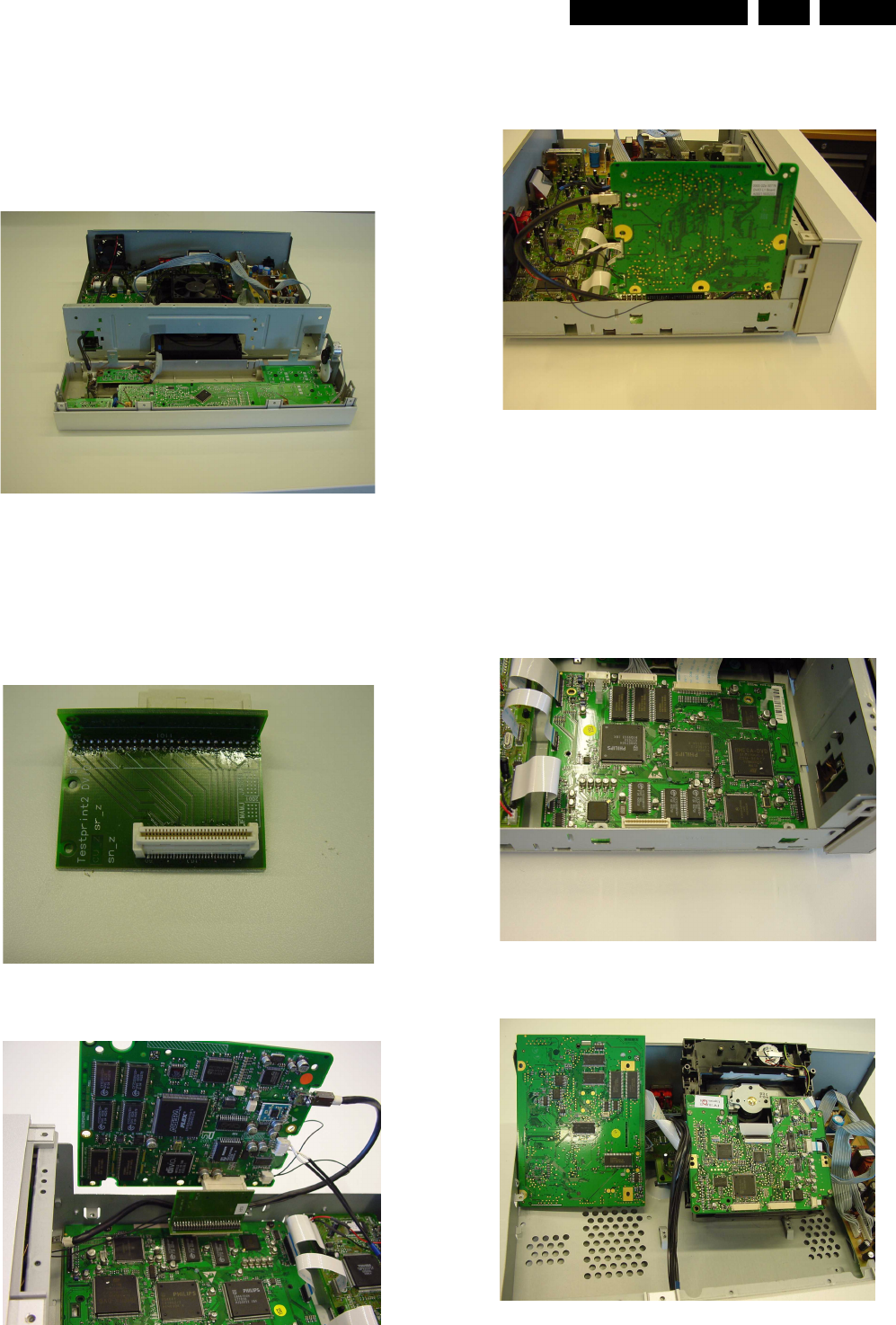
Mechanical Instructions EN 33DVDR980-985 /0X1 4.
4. Mechanical Instructions
4.1 Service Positions
4.1.1 Front
Front
Figure 4-1
4.1.2 DVIO board
To put the DVIO board in a service position, an extender board
must be used. This extender board can be ordered with
codenumber 3104 128 07770.
DVIO Extender
Figure 4-2
DVIO 1
Figure 4-3
DVIO 2
Figure 4-4
4.1.3 Digital board
After demounting of DVIO board, the top side of the digital
board is in reach. To reach the bottom side of the digital board,
the DVDR module must be demounted together with the digital
board. Connected to each other, the assembly can be set in a
service position. In this position, the bottom side of the digital
board and the servo board are in reach to be serviced.
Digital 1
Figure 4-5
Digital 2
Figure 4-6
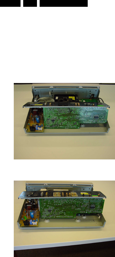
Mechanical Instructions
EN 34 DVDR980-985 /0X14.
4.1.4 Analog board
To put the analog board in service position, demount the
assembly of analog board and backplate as follows:
1. Remove 3 screws from the backplate to the frame
2. Remove the screw from the backplate to the mains inlet of
the power supply
3. Remove the screw of the analog board to the frame
4. Release the snaps of the 4 spacers of the analog board to
the frame.
Turn the assembly of the backplate and the analog board
against the loader.
Analog Europe
Figure 4-7
Analog NAFTA
Figure 4-8
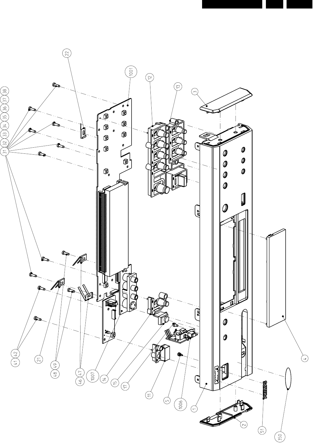
Mechanical Instructions EN 35DVDR980-985 /0X1 4.
4.2 Exploded View of the Front Assembly
Front EV
Figure 4-9
DISPLAY
FRONT AV IN
FRONT DV IN
IR/STBY
CL 26532011_019.eps
160102
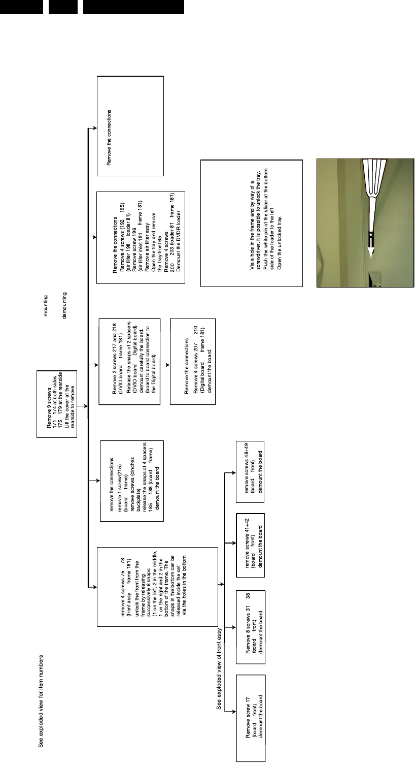
Mechanical Instructions
EN 36 DVDR980-985 /0X14.
4.3 Dismantling Instructions
Dismantling Instructions
Figure 4-10
DISMANTLING INSTRUCTIONS
Front assy
⇒
⇒
→
→
⇒
↑
↓
Cover 151
⇒→
→
⇒
Analog board 1003
⇒
⇒
⇒
⇒
⇒
→
→→
→
→
→
→
→
→
→
→
DVIO board 1005 (DVDR985)
⇒
⇒
⇒
DVDR LOADER 81
Manually removal of tray front 65
In case the loader is defective and cannot be
opened electrically, you can open the tray
as follows:
⇒
⇒
⇒
⇒
⇒
Switched Operating Power supply 1002
⇒
⇒
⇒⇒
⇒
→
→
→
→
Display board 1001
⇒
⇒
→
→
IR/STBY Board 1001
→
⇒
⇒
FRONT AV Board1007
→
⇒
⇒
open the tray and remove
tray front 65 Remove screws 204 206
(board
Remove screw 268
(mains inlet
⇒Demount the board
⇒Release the snaps of 2 spacers
183 and 184 (board
frame)
backplate)
frame)
FRONT DV Board 1006(DVDR985)
⇒
⇒
→
→
→
Digital board 1001
⇒
⇒
the
⇒
⇒
⇒
CL 26532011_020.eps
160102
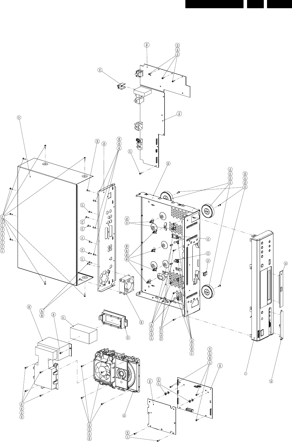
Mechanical Instructions EN 37DVDR980-985 /0X1 4.
4.4 Exploded View of the Set
Complete Set EV
Figure 4-11
DVDR LOADER
DIGITAL PCB
DVIO PCB
I/O ANALOG PCB
SOPS
CL 26532011_021.eps
160102
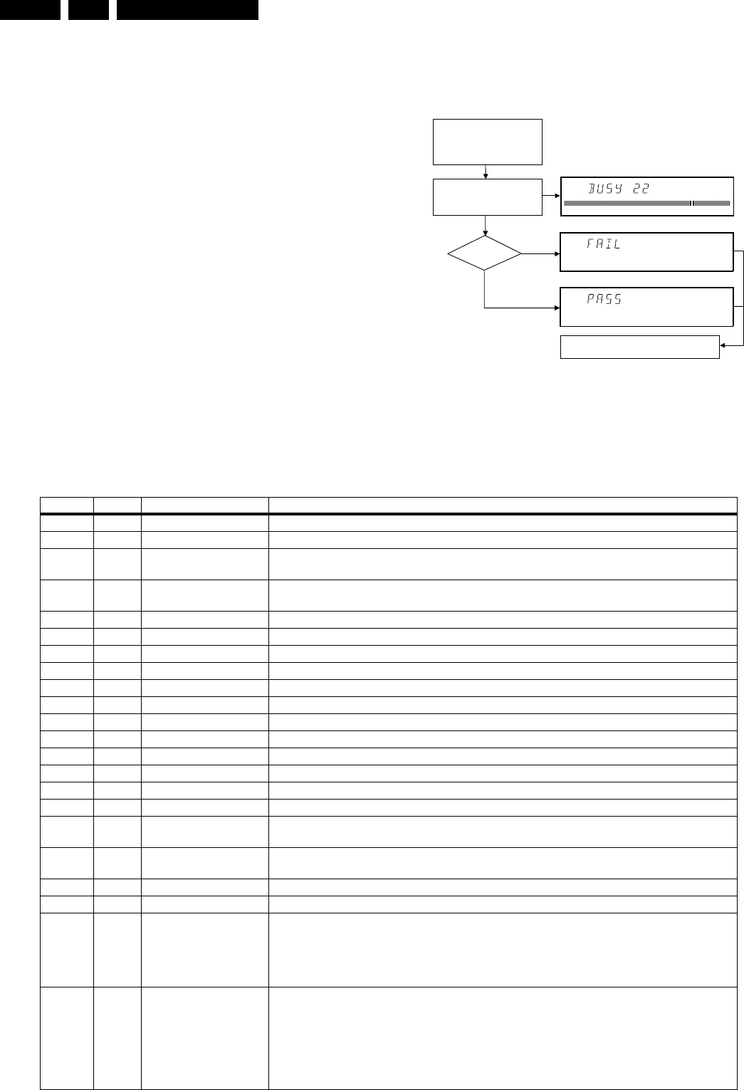
Diagnostic Software and Faultfinding Trees
EN 38 DVDR980-985 /0X15.
5. Diagnostic Software and Faultfinding Trees
Due to the complexity of the DVD recorder, the time to find a
defect in the recorder can become long. To reduce this time,
the recorder has been equipped with Diagnostic and Service
software (DS). The DS offers functionality to diagnose the
DVDR hardware and tests the following:
• Interconnections between components
• Accessibility of components
• Functionality of the audio and video paths
This functionality can be accessed via several interfaces:
1. End user/Dealer script interface
2. Player script interface
3. Menu and command interface
5.1 End User/Dealer Script Interface
5.1.1 Description
The End user/Dealer script interface gives a diagnosis on a
stand alone DVD recorder; no other equipment is needed.
During this mode, a number of hardware tests (nuclei) are
automatically executed to check if the recorder is faulty. The
diagnosis is simply a "fail" or "pass" message. If the message
"FAIL" appears on the display, there is apparently a failure in
the recorder. If the message "PASS" appears, the nuclei in this
mode have been executed successfully. There can be still a
failure in the recorder because the nuclei in this mode don't
cover the complete functionality of the recorder.
5.1.2 Contents
Figure 5-1
The End use/Dealer script executes all diagnostic nuclei that
do not need any user interaction and are meaningful on a
standalone DVD recorder. The nuclei called in the End user/
Dealer script are the following:
Hold key <PLAY> pressed
while you plug the recorder
Unplug the power cord
During the test, the following display
is shown: the counter counts down
from the number of nuclei to be run
before the test finishes. Example:
SET O.K.?
YES
NO
To exit DEALER SCRIPT, unplug the power cord
CL 16532095_068.eps
150801
Counter Nucleus Name Description
22 104 HostdSdramWrR checks all memory locations of the 4MB SDRAM
21 106 HostdDramWrR checks all the DRAM connected to the microprocessor of the digital board
20 123 HostdI2cNvram checks the data line (SDA) and the clock line (SCL) of the I2C bus between the host decoder
and NVRAM
19 202 SAA7118I2c checks the interface between the Host I2C controller and the AVENC SAA7118 Video Input
Processor
18 200 VideoEncI2c checks the interface between the host I2C controller and Empress SAA6752
17 207 AudioEncI2c checks the I2C connection between the host decoder and Empress SAA6752
16 204 AudioEncAccess tests the HIO8 interface lines between the host decoder and the audio encoder
15 203 AudioEncSramAccess checks the access of the SRAM by the audio encoder (address and data lines).
14 205 AudioEncSramWrR tests the SRAM connected to the audio encoder
13 206 AudioEncInterrupt tests the interrupt line between the host decoder and the audio encoder
12 300 VsmAccess checks whether the VSM interrupt controllers and DRAM are accessible
11 303 VsmInterrupt checks both interrupt lines between the VSM and the host decoder
10 302 VsmSdramWrR tests the entire SDRAM of the VSM
9 1400 Clock11_289MHz switches the A_CLK of the micro clock to 11.2896 MHz
8 1401 Clock12_288MHz switches the A_CLK of the micro clock to 12.288 MHz
7 601 BeS2Bengine checks the S2B interface with the Basic Engine by sending an echo command
6 500 DisplayEcho checks the interface between the host processor and the slave processor on the display
board
5 700 AnalogueEcho checks the interface between the host processor and the microprocessor on the analogue
board
4 711 AnalogueNvram checks the NVRAM on the analogue board
3 706 AnalogueTuner checks whether the tuner on the analogue board is accessible
2 901 LoopAudioUserDealer This nucleus tests the components on the audio signal path The host decoder
- The analogue board
- The audio encoder
- The VSM
On the analogue board the audio is internally looped back to the digital board
1 906 LoopVideoUserDealer Nucleus for testing the components on the video signal system path:
- The VIP
- The video encoder
- The VSM
- The host decoder
- The analogue board
On the analogue the video signal is internally routed back to the digital board.

Diagnostic Software and Faultfinding Trees EN 39DVDR980-985 /0X1 5.
5.2 Player Script Interface
5.2.1 Description
The Player script will give the opportunity to perform a test that
will determine which of the DVD recorder's modules are faulty,
to read the error log and to perform an endurance loop test. To
successfully perform the tests, the DVD recorder must be
connected to a TV set.
To be able to check results of certain nuclei, the player script
expects some interaction of the user (i.e. to approve a test
picture or a test sound). Some nuclei (e.g. nuclei that test
functionality of the DVDR module) require that a DVD+RW disc
is inserted.
Only tests within the scope of the diagnostic software will be
executed hence only faults within this scope can be detected.
5.2.2 Structure of the Player Script
The player script consists of a set of nuclei testing the hardware
modules in the DVD recorder: the Display PWB, the Digital
PWB, the Analogue In/Out PWB and the DVDR module.
Nuclei run by the player test need some user interaction; in the
next table this interaction is described. The player test is done
in two phases:
•Interactive tests: this part of the player test depends
strongly on user interaction and input to determine nucleus
results and to progress through the full test. Reading the
error log information can be useful to determine any errors
that occurred recently during normal operation of the DVD
player.
•The loop test will perform the same nuclei as the dealer
test, but it will loop through the list of nuclei indefinitely.
STEP DESCRIPTION NUCLEUS
1 Press OPEN/CLOSE and PLAY at the same time and POWER ON the recorder to start the playerscript 2
2 The local display shows FPSEGMENTS. Press PLAY to start the test.
First the starburst pattern is lit, then the horizontal segments are lit, followed by the vertical segments and the
last test is light all segments test. After each of the 4 tests the user has to confirm that the correct pattern was
lit.
Press PLAY to confirm that the correct pattern was lit (four times if the FPSEGMENTS test was successful).
Press RECORD to indicate that the correct pattern was not successfully lit.
Press STOP to skip this nucleus.
502
3 The local display shows FPLABELS. Press PLAY to start the test.
Press PLAY to confirm that all labels are lit.
Press RECORD to indicate that not all labels are lit.
Press STOP to skip this nucleus.
503
4 The local display shows FPLIGHT ALL. Press PLAY to start the test.
Press PLAY to confirm that everything was lit.
Press RECORD to indicate that not all patterns are lit.
Press STOP to skip this nucleus.
520
5 The local display shows FPLED. Press PLAY to start the test.
Press PLAY to confirm that the led is lit.
Press RECORD to indicate that the led is not lit.
Press STOP to skip this nucleus.
504
6 The local display shows FPFLAP OPEN. Press PLAY to start the test.
Press PLAY to confirm that the flap has opened.
Press RECORD to indicate that the flap did not open.
Press STOP to skip this nucleus.
522
7 The local display shows FPKEYBOARD. Press PLAY to start the test.
Attention all keys have to be pressed to get a positive result!
Press PLAY for more than one second to confirm that all the keys were pressed and shown on the local dis-
play. If not all the keys were pressed, a FAIL message will appear on the local display.
Press RECORD for more than one second to indicate that not all keys were pressed and shown on the local
display.
Press STOP for more than one second to skip this nucleus.
505
8 The local display shows FPREMOTE CONTROL. Press PLAY to start the test.
Press PLAY to confirm that a key on the remote control was pressed and shown on the local display. Only
one key has to be pressed to get a successful result.
Press RECORD to indicate that the key on the remote control was pressed but not shown on the local display.
Press STOP to skip this nucleus.
506
9 The local display shows FPDIMMER. Press PLAY to start the test.
Press PLAY to confirm that the text on the local display was dimmed.
Press RECORD to indicate that the text on the local display was not dimmed.
Press STOP to skip this nucleus.
518
10 The local display shows FPBEEPER. Press PLAY to start the test.
Press PLAY to confirm that the beeper on the front panel sounded.
Press RECORD to indicate that the beeper on the front panel did not sound.
Press STOP to skip this nucleus.
514
11 The local display shows FPFLAP CLOSE. Press PLAY to start the test.
Press STOP to skip this nucleus.
523
12 The local display shows ROUTE VIDEO. Press PLAY to start the test.
Press STOP to skip this nucleus.
712
13 The local display shows ROUTE AUDIO. Press PLAY to start the test.
Press STOP to skip this nucleus.
713
14 The local display shows COLOUR-BAR ON. Press PLAY to start the test.
Press STOP to skip this nucleus.
120

Diagnostic Software and Faultfinding Trees
EN 40 DVDR980-985 /0X15.
Remark
In case of failure, the display shows " FAIL XXXXXX ". The
description of the shown error code can be retrieved in the
survey of Nuclei Error Codes (paragraph 5.4). Once an error
occurs, it is not possible to continue the player script. Unplug
the set and restart the player script. By pressing the STOP key,
it is possible to jump over the failure and to continue the player
script.
15 The local display shows PINK NOISE ON. Press PLAY to start the test.
Press STOP to skip this nucleus.
115
16 The local display shows PINK NOISE OFF. Press PLAY to start the test.
Press STOP to skip this nucleus.
116
17 The local display shows SINE ON. Press PLAY to start the test.
Press STOP to stop the sine.
Press STOP to skip this nucleus.
117
18 The local display shows COLOUR-BAR OFF. Press PLAY to start the test.
Press STOP to skip this nucleus.
121
19 The local display shows BERESET. Press PLAY to start the test.
Press STOP to skip this nucleus.
603
20 The local display shows BETRAY OPEN. Press PLAY to start the test.
Press STOP to skip this nucleus.
616
21 The local display shows BETRAY CLOSE. Press PLAY to start the test.
Press STOP to skip this nucleus.
615
22 The local display shows BEWRITE READ. Press PLAY to start the test.
Press STOP to skip this nucleus.
617
23 The local display shows BETRAY OPEN. Press PLAY to start the test.
Press STOP to skip this nucleus.
616
24 The local display shows BETRAY CLOSE. Press PLAY to start the test.
Press STOP to skip this nucleus.
615
25 The local display shows READ ERRORLOG. Press PLAY to start the test.
Press STOP to skip this nucleus.
If the player test succeeded, the user/dealer script will start in an endless loop.
If the player test failed, the local display will display FAIL and the error code
633
STEP DESCRIPTION NUCLEUS
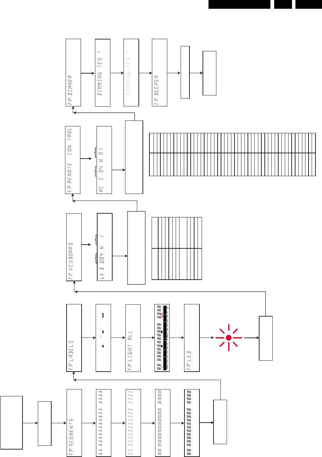
Diagnostic Software and Faultfinding Trees EN 41DVDR980-985 /0X1 5.
Player Script
Figure 5-2
Hold 2 keys
<OPEN/CLOSE> + <PLAY>
simultaneously pressed while
you plug the recorder
Unplug the power cord
FRONTPANEL TEST
PRESS
<PLAY>
TO START TEST
PRESS
<PLAY>
IF OK
PRESS
<STOP>
TO ABORT
PRESS
<PLAY>
IF OK
PRESS
<STOP>
TO ABORT
PRESS
<PLAY>
IF OK
PRESS
<STOP>
TO ABORT
PRESS
<PLAY>
IF OK
PRESS
<RECORD>
IF NOT OK
PRESS
<PLAY>
IF OK
PRESS
<RECORD>
IF NOT OK
PRESS
<PLAY>
IF OK
PRESS
<RECORD>
IF NOT OK
PRESS
<PLAY>
IF OK
PRESS
<RECORD>
IF NOT OK
PRESS
<PLAY>
IF OK
PRESS
<RECORD>
IF NOT OK
PRESS
<PLAY>
IF OK
PRESS
<RECORD>
IF NOT OK
BEEP IS AUDIBLE
PRESS
<PLAY>
TO START TEST
PRESS
<STOP>
TO SKIP TEST
PRESS
<STOP>
TO SKIP TEST PRESS
<STOP>
TO SKIP TEST
PRESS
<STOP>
TO SKIP TEST
PRESS
<STOP>
TO SKIP TEST
PRESS
<STOP>
TO SKIP TEST
PRESS
<STOP>
TO SKIP TEST
PRESS
<PLAY>
TO START TEST
PRESS
<PLAY>
TO START TEST
PRESS
<PLAY>
TO START TEST
PRESS
<PLAY>
TO START TEST
PRESS ALL KEYS AT LEAST ONCE
SEE TABLE FOR KEY CODES
PRESS
<PLAY>
MORE THAN 1S IF TEST IS OK
PRESS
<RECORD>
MORE THAN 1S IF TEST IS NOT OK
FRONT KEY NAME
PLAY
STANDBY/ON
STOP
OPEN/CLOSE
RECORD
MONITOR
AUTOMAN
REC VOLUME
MANUAL UP
MANUAL DOWN
CHANNEL DOWN
CHANNEL UP
FRONT KEY CODE
00E
00F
001
002
003
004
00D
00B
00C
009
00A
LED BECOMES RED
PRESS
<PLAY>
TO START TEST
PRESS
<PLAY>
TO START TEST
PRESS AT LEAST ONE KEY
ON THE REMOTE CONTROL
SEE TABLE FOR RC KEY CODES
TO EXIT TEST: PRESS ONE OF FOLLOWING KEYS
ON THE LOCAL KEYBOARD
PRESS
<PLAY>
IF TEST IS OK
PRESS
<RECORD>
IF TEST IS NOT OK
DIGITAL BOARD TEST
RC KEY NAME
MONITOR
ON/OFF
STOP
REC/OTR
PLAY
REVERSE
PAUSE
SLOW
RC KEY CODE
0C
37
EE
31
2C
29
30
22
28
21
CF
20
54
0F
58
5A
5B
59
83
5C
41
FE
FA
F7
EE
85
00
01
02
03
04
05
06
07
08
09
C8
4B
4E
13
1D
3B
2A
FORWARD
PREVIOUS
FSS
NEXT
DISC
SYSTEM
UP
LEFT
RIGHT
DOWN
RETURN
OK
CLEAR
TIMER
SELECT
ZOOM
A/CH
ANGLE
0
1
2
3
4
5
6
7
8
9
T/C
SUBTITLE
AUDIO
DIM
REPEAT
REPEAT A-B
SCAN
VOL +
VOL -
CH +
CH -
MUTE
ONLY FOR TV
ONLY FOR TV
1E
1F
ONLY FOR TV
HEXADECIMAL
KEY CODE XX TIMES
PRESSED
HEXADECIMAL
RC KEY CODE XX TIMES
PRESSED
CHAPTER TRACK TIME REMAINTITLE TRACK CHANNEL VPS/PDC
DVD RW SAVCD HQ SP L:P EP+ MONITOR SAT TIMER RECORD DECODER
AM
PM
PROLOGIC MPEG DTS PCM MANUAL DIGITAL NICAM STEREO SAP
I
II
TOTAL
DIGITAL
D
D
CHAPTER TRACK TIME REMAINTITLE TRACK CHANNEL VPS/PDC
DVD RW SAVCD HQ SP L:P EP+ MONITOR SAT TIMER RECORD DECODER
-40 -30 -20 -10 0 OVER
AM
PM
PROLOGIC
-40 -30 -20 -10 0 OVER
MPEG DTS PCM MANUAL DIGITAL NICAM STEREO SAP
I
II
TOTAL
DIGITALD
D
CL 265362011_022.eps
160102
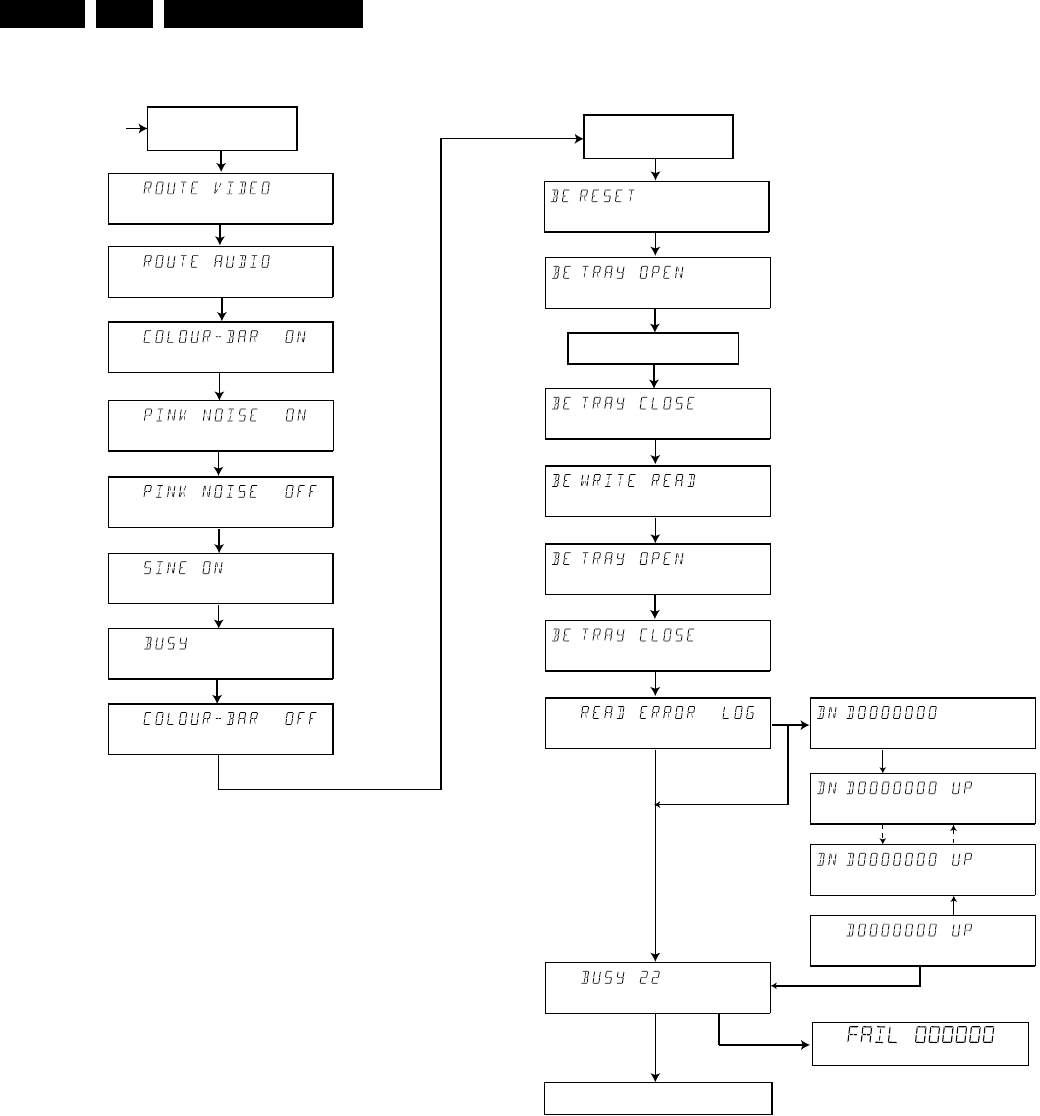
Diagnostic Software and Faultfinding Trees
EN 42 DVDR980-985 /0X15.
Figure 5-3
5.2.3 Error Log
Explanation:
The application errors will be logged in the NVRAM. The
maximum number of error bytes that will be visible is 19. The
last reported error is shown as DN D0000000, the oldest visible
error as D0000000 UP and the errors in between as DN
D0000000 UP. DN stands for DOWN, UP stands for
UPWARDS. The shown
D error codes are identical to the Nuclei Error Codes
(paragraph 5.4).
press
<PLAY>
to execute
press
< STOP >
to skip
press
<PLAY>
to execute
press
< STOP >
to skip
press
<PLAY>
to execute
press
<PLAY>
to execute
press
< STOP >
to skip
press
<PLAY>
to execute
press
< STOP >
to skip
press
<PLAY>
to execute
press
<NEXT >
to skip
press
<PLAY>
to execute
press
< STOP >
to skip
press
<PLAY>
to execute
press
<NEXT >
to skip
press
<PLAY>
to execute
press
<STOP>
to skip
press
<PLAY>
to execute
press
<STOP>
to skip
press
<STOP>
to continue
DIGITAL BOARD &
ANALOG BOARD
TEST
FRONTPANEL
TEST
<PLAY>
BASIC ENGINE
TEST
IF ERROR
PRESS
<STOP>
TO STEP DOWN
NO ERRORS LOGGED
PRESS
<RECORD>
TO STEP UP
PRESS
<RECORD>
TO STEP UP
PRESS
<STOP>
TO STEP DOWN
PRESS
<PLAY>
TO CONTINUE
To exit PLAYER SCRIPT, unplug the power cord
press
<PLAY>
to execute
press
<NEXT >
to skip
press
<PLAY>
to execute
press
<STOP>
to skip
press
<STOP>
to skip
press
<PLAY>
to execute
press
<STOP>
to skip
INSERT DVD +RW DISC TO EXECUTE
WRITE / READ TEST
CL 16532095_070.eps
031201
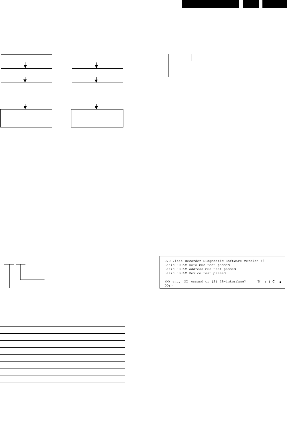
Diagnostic Software and Faultfinding Trees EN 43DVDR980-985 /0X1 5.
5.2.4 Trade Mode
Figure 5-4
5.2.5 Virgin mode
If you want that the recorder starts up in Virgin mode, follow this
procedure:
•Unplug the recorder
•plug the recorder again while you keep the STAND BY/ON
key pressed
•the set starts up in Virgin mode.
5.3 Menu and Command Mode Interface
5.3.1 Nuclei Numeration
Each nucleus has a unique number of four digits. This number
is the input of the command mode.
Figure 5-5
The following groups are defined:
5.3.2 Error Handling
Each nucleus returns an error code. This code contains six
numerals, which means:
Figure 5-6
The nucleus group numbers and nucleus numbers are the
same as above.
5.3.3 Command Mode Interface
Set-Up Physical Interface Components
Hardware required:
•Service PC
•one free COM port on the Service PC
•special cable to connect DVD recorder to Service PC
The service PC must have a terminal emulation program (e.g.
OS2 WarpTerminal or Procomm) installed and must have a
free COM port (e.g. COM1). Activate the terminal emulation
program and check that the port settings for the free COM port
are: 19200 bps, 8 data bits, no parity, 1 stop bit and no flow
control. The free COM port must be connected via a special
cable to the RS232 port of the DVD recorder. This special cable
will also connect the test pin, which is available on the
connector, to ground (i.e. activate test pin).
Code number of PC interface cable: 3122 785 90017
Activation
Plug the recorder to the mains and the following text will appear
on the screen of the terminal (program):
Figure 5-7
The first line indicates that the Diagnostic software has been
activated and contains the version number. The next lines are
the successful result of the SDRAM interconnection test and
the basic SDRAM test. The last line allows the user to choose
between the three possible interface forms. If pressing C has
made a choice for Command Interface, the prompt ("DD>") will
appear. The diagnostic software is now ready to receive
commands. The commands that can be given are the numbers
of the nuclei.
Group number Group name
0 Basic / Scripts
1 Host decoder (Sti5505 and memory)
2 Audio / video encoder (DVDR only)
3 VSM (DVDR only)
4NVRAM
5 Front Panel
6 Basic Engine
7 Analogue board (DVDR only)
8 DVIO (DVDR only)
9 Loop nuclei (DVDR only)
10 Library sub nuclei (I2C nuclei)
11 User interface
12 Furore (SACD only)
13 DAC (SACD only)
14 Miscellaneous
UNPLUG THE RECORDER
IF TRADE MODE OFF
PRESS 2 KEYS
SIMULTANEOUSLY
PLUG THE RECORDER
RECORDER IS IN TRADE MODE
WHEN PRESSING FRONT
KEYS, THE RECORDER
DOESN'T RESPOND
TRADE MODE
When the recorder is in Trade Mode, the recorder cannot be
controlled by means of the front key buttons, but only by means
of the remote control.
<STOP> + <OPEN/CLOSE>
UNPLUG THE RECORDER
IF TRADE MODE ON
PRESS 2 KEYS
SIMULTANEOUSLY
PLUG THE RECORDER
RECORDER IS IN NORMAL MODE
WHEN PRESSING FRONT
KEYS, THE RECORDER
WILL RESPOND
<STOP> + <OPEN/CLOSE>
CL 16532095_071.eps
150801
[ XX YY ]
Nucleus number
Nucleus group number
CL 06532152_012.eps
051200
[ XX YY ZZ ]
Error code
Nucleus number
Nucleus group number
CL 06532152_013.eps
051200
CL 16532095_073.eps
150801
Diagnostic Software and Faultfinding Trees
EN 44 DVDR980-985 /0X15.
Command Overview
We provide an overview of the nuclei and their numbers. This
overview is preliminary and subject to modifications.
Host Decoder [01]
Audio Video Decoder [02]
VSM [03]
NVRAM [04]
Front Panel [05]
Basic Engine [06]
[xx yy]
Number
Nuclei
100 Checksum Flash
101 Flash Write Access 1
102 Flash Write Access 2
103 Flash Write Read
104 SdRam Write Read
105 SdRam Write Read Fast
106 Dram Write Read
107 Dram Write Read Fast
108 Hardware Version
109 Mute On
110 Mute Off
115 Pink Noise On
116 Pink Noise Off
117 Sine On
118 Sine Burst 1kHz
119 Sine Burst 12kHz
120 Colour-bar On
121 Colour-bar Off
122 NvramWrR
123 NvramI2c
130 Boot Version
131 Application Version
132 Diagnostics Version
133 Download Version
134 Write / read I2C message to / from digital board
135 Video Test Signal On
136 Video Test Signal Off
137 Macrovision Off
[xx yy]
Number
Nuclei
200 Video Encoder I2C
202 SAA7118 I2C
203 Audio Encoder SRAM Access
204 Audio Encoder Access
205 Audio Encoder SRAM Write Read
206 Audio Encoder Interrupts
207 Audio Encoder I2C
208 SAA7118 select input
209 Empress Version
[xx yy]
Number
Nuclei
300 Register Access
301 SDRAM Access
302 SDRAM Write Read
303 Interrupt lines
304 VSM Interconnection
305 UART
[xx yy]
Number
Nuclei
400 Reset
401 Read
402 Modify
403 UniqueNr Read
404 Read Error Log
407 Reset Error Log
409 Line2 Region-Code Reset
410 UniqueNr Store
[xx yy]
Number
Nuclei
500 Echo
501 Version
502 Segment
503 Label
504 Led
505 Keyboard
506 Remote-Control
507 Segment Starburst
508 Segment Vertical
509 Segment Horizontal
514 Beeper
515 Discbar
516 Discbar Dots
517 Vu / Grid
518 Dimmer
519 Blinking
520 Light All Segments
522 Flap Open
523 Flap Close
[xx yy]
Number
Nuclei
600 S2B Pass
601 S2B Echo
602 Version
603 Reset
604 Focus On
605 Focus Off
606 Disc Motor On
607 Disc Motor Off
608 Radial On
609 Radial Off
615 Tray In
616 Tray Out
617 Write Read
618 Write Read Endless Loop
619 Selftest
620 BE Test
621 Laser Test
622 Spindle (Disc) Motor Test
623 Focus Test
624 Sledge Motor Test
625 Sledge Motor Slow
626 Tilt
627 EEPROM Read
628 EEPROM Write
629 Optimise Jitter
630 Radial ATLS Calibration
631 Get Statistics Information
632 Reset Statistics Information
[xx yy]
Number
Nuclei
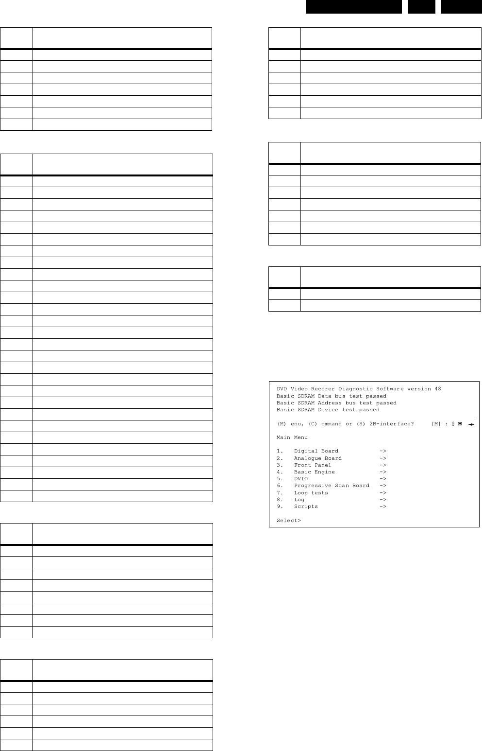
Diagnostic Software and Faultfinding Trees EN 45DVDR980-985 /0X1 5.
Analog Board [07]
DVIO [08]
Loop Nuclei [09]
Miscellanious [14]
Scripts [00]
5.3.4 Menu Mode Interdace
Activation
Plug the recorder to the mains and the following text will appear
on the screen of the terminal (program):
Figure 5-8
The first line indicates that the Diagnostic software has been
activated and contains the version number. The next lines are
the successful result of the SDRAM interconnection test and
the basic SDRAM test. The last line allows the user to choose
between the three possible interface forms. If pressing M has
made a choice for Menu Interface, the Main Menu will appear.
633 BE Read Error Log
634 BE Reset Error Log
638 Get Self Test Result
639 Radial Initialisation
640 Get OPU info
641 Write read +R
642 Write read +R endless loop
[xx yy]
Number
Nuclei
700 Echo
703 Boot Version
704 Hardware Version
705 Clock Adjust
706 Tuner
707 Frequency Download
708 Data Slicer
709 Sound Processor
710 AV Selector
711 Nvram
712 Route Video
713 Route Audio
715 Set Slash Version
716 Application Version
717 Diagnostics Version
718 Download Version
720 Bargraph Level Adjustment
721 Clock correction
722 Clock reference
723 Re-virginise Recorder
724 Flash Checksum
725 Tuner frequency selection
727 Set virgin bit
728 Clear Virgin Bit
729 Write / read I2C message to / from analogue board
730 Store external presets
731 Get slash version
732 AFC Reference Voltage Tuner
[xx yy]
Number
Nuclei
800 Check DVIO board presence
801 Reset DVIO
802 DVIO Access
803 Get DVIO error codes
804 Get DVIO module Ids
805 Execute DVIO module SelfTest
806 Set DVIO led on.
807 Set DVIO led off.
[xx yy]
Number
Nuclei
900 Digital Audio Loop
901 User / Dealer Audio Loop
902 Digital Video Loop
903 Digital Video VBI Loop
904 System Video Loop
905 System Video VBI Loop
[xx yy]
Number
Nuclei
906 User / Dealer Video Loop
907 User / Dealer Video VBI Loop
908 System Audio Loop SCART
909 System Audio Loop CINCH
910 Digital DVIO Video Loop
911 System Video Vip
[xx yy]
Number
Nuclei
1400 Clock 11.289 MHz
1401 Clock 12.288 MHz
1412 Progressive Scan I2C
1413 Progressive Scan test image on
1414 Progressive Scan test image off
1415 Progressive Scan Route Enable
1416 Progressive Scan Route Disable
[xx yy]
Number
Nuclei
1 UserDealer Script
2 Player Script
[xx yy]
Number
Nuclei
CL 16532095_074.eps
150801

Diagnostic Software and Faultfinding Trees
EN 46 DVDR980-985 /0X15.
Menu Structure
The following menu structure is given after starting up the DVD
recorder in menu mode. The symbol -> indicates that the
current menu choice will invoke the display of a submenu.
Main Menu
1.Digital Board ->
2.Analogue Board ->
3.Front Panel ->
4.Basic Engine ->
5.DVIO ->
6.Progressive Scan Board ->
7.Loop Tests ->
8.Log ->
9.Scripts ->
Digital Board Menu
1.Host Decoder ->
2.VSM ->
3.AVENC ->
4.NVRAM ->
Host Decoder Menu
1.Flash Checksum
2.Flash1 Write Access
3.Flash2 Write Access
4.Flash Write/Read
5.Host SDRAM Write/Read
6.Host SDRAM Fast Write/Read
7.Host DRAM Write/Read
8.Host DRAM Fast Write/Read
9.I2C NVRAM
10.NVRAM Write/Read
11.Engine S2B Echo
12.Versions ->
13.Audio Mute ->
14.Colourbar ->
15.Pink Noise ->
16.Sine Generate ->
Digital Board Versions Menu
1.Hardware Version
2.Bootcode version
3.Applications Version
4.Diagnostics Version
5.Download Version
Audio Mute Menu
1.Audio Mute On
2.Audio Mute Off
Colourbar Menu
1.Colourbar On
2.Colourbar Off
Pink Noise Menu
1.Pink Noise On
2.Pink Noise Off
Sine Generate Menu
1.Sine On
2.Sine Burst 1kHz
3.Sine Burst 12kHz
VSM Menu
1.Register Access
2.SDRAM Access
3.VSM SDRAM Write/Read
4.Interrupt Lines
5.VSM Interconnection
6.UART
AVENC Menu
1.Empress ->
2.Video Input Processors ->
Empress Menu
1.Version number
Video Input Processors Menu
1.SAA7118 I2C Access
NVRAM Menu
1.Read Error Log
2.Reset Error Log
3.Read DVIO Unique ID
Analogue Board Menu
1.Echo
2.Obsolete
3.Route Video Input back to Digital board
4.Route Audio Input back to Digital board
5.Flash Checksum
6.Versions ->
7.Components ->
8.Re-virginize Recorder ->
Analogue Board Versions Menu
1.Hardware Version
2.Bootcode version
3.Application version
4.Diagnostics version
5.Download version
Analogue Components Menu
1.Tuner
2.Data Slicer
3.Sound Processor
4.AV Selector
5.NVRAM
Analogue Board Re-virginize Menu
1.Re-virginize Recorder
2.Set Virgin-bit
3.Clear Virgin-bit
4.Store external presets
Front Panel Menu
1.Echo
2.Version
3.Flap Control ->
4.Segment Test ->
5.Light Labels
6.Led test
7.Keyboard test
8.Remote Control
9.Beep
10.Disc Bar
11.Disc Bar Dots
12.Vu Grid
13.Dimmer
14.Blink
15.Light All Segments
Flap Control Menu
1.Open Flap
2.Close Flap
Segment Test Menu
1.Starburst
2.Light Horizontal Segments
3.Light Vertical Segments
4.Light All Segments

Diagnostic Software and Faultfinding Trees EN 47DVDR980-985 /0X1 5.
Basic Engine Menu
1.Reset
2.S2B Pass-through
3.S2B Echo
4.Focus On
5.Focus Off
6.Version
7.Self Test
8.Get Self Test Result
9.Basic Engine Test
10.Laser Test
11.Focus Test
12.Tilt Test
13.Optimise Jitter
14.Statistics Info
15.Log ->
16.Spindle Motor ->
17.Radial ->
18.Sledge ->
19.Tray ->
Basic Engine Error Log
1.Read Error Log
2.Reset Error Log
Basic Engine Spindle Motor Menu
1.Spindle Motor On
2.Spindle Motor Off
3.Spindle Motor Test
Basic Engine Radial Menu
1.Radial On
2.Radial Off
3.Radial Initialisation
4.Radial ATLS Calibration
Basic Engine Sledge Menu
1.Sledge test
2.Sledge test slow
Basic Engine Tray Menu
1.Tray In
2.Tray Out
DVIO Menu
1.Check Presence
2.Reset
3.Access
4.Error Codes
5.Module Identifiers
6.Led ->
DVIO Led Menu
1.Led On
2.Led Off
Progressive Scan Board Menu
1.I2C Access
2.Test Image On
3.Test Image Off
Loop Tests Menu
1.Digital Board Loops ->
2.User/Dealer Loops ->
3.System Loops ->
4.Basic Engine Loops ->
Digital Board Loops Menu
1.Obsolete
2.Digital Video Loop
3.Digital Video Loop VBI
User/Dealer Loops Menu
1.User/Dealer Audio Loop
2.User/Dealer Video Loop
3.User/Dealer Video Loop VBI
System Loops Menu
1.System Video Loop
2.System Video Loop VBI
3.System Audio Loop SCART(EURO)
4.System Audio Loop CINCH (NAFTA)
Basic Engine Loops Menu
1.Basic Engine write read
2.Basic Engine write read endless loop
Log Menu
1.Read Error Log
2.Reset Error Log
Script Menu
1.User/Dealer Script
2.Player Script
5.4 Nuclei Error Codes
In the following table the error codes will be described.
Error Nr Error String
10000 "Checksum is OK"
10001 "segment name Checksum doesn't match" or "seg-
ment name segment not found"
10100 ""
10101 "FLASH 1 Write access test failed"
10200 ""
10201 "FLASH 2 Write access test failed"
10300 ""
10301 "FLASH write test failed"
10302 "FLASH write command failed"
10303 "FLASH write test done max. number of times"
10400 ""
10401 "HostDec SDRAM Memory data bus test goes
wrong."
10402 " HostDec SDRAM Memory address bus test goes
wrong."
10403 " HostDec SDRAM Physical memory device test
goes wrong."
10500 ""
10501 " HostDec SDRAM Memory data bus test goes
wrong."
10502 " HostDec SDRAM Memory address bus test goes
wrong."
10503 " HostDec SDRAM Physical memory device test
goes wrong."
10600 ""
10601 "HostDec DRAM Memory data bus test goes
wrong."
10602 "HostDec DRAM Memory address bus test goes
wrong."
10603 "HostDec DRAM Physical memory device test
goes wrong."
10700 ""
10701 "HostDec DRAM Memory data bus test goes
wrong."
10702 "HostDec DRAM Memory address bus test goes
wrong."
10703 "HostDec DRAM Physical memory device test
goes wrong."

Diagnostic Software and Faultfinding Trees
EN 48 DVDR980-985 /0X15.
10800 "Host Decoder version(cut) number: version
number""Digital hardware version"
10801 "Can not find version in FLASH."
10900 ""
10901 "Error muting audio"
11000 ""
11001 "Error demuting audio"
11500 ""
11501 "Init of I2C failed"
11502 "The selection of the clock source failed"
11504 "The demute of the audio failed"
11600 ""
11601 "Init of I2C failed"
11602 "The mute of the audio failed"
11700 ""
11701 "Init of I2C failed"
11702 "The muting of the audio failed"
11703 "The demute of the audio failed"
11704 "The selection of the clock source failed"
11707 "Setup of Front panel failed"
11708 "Sine on Front panel keyboard failed"
11800 ""
11801 "Init of I2C failed"
11802 "The muting of the audio failed"
11803 "The demute of the audio failed"
11804 "The selection of the clock source failed"
11805 "Error cannot start VSM audio in port"
11900 ""
11901 "Init of I2C failed"
11902 "The muting of the audio failed"
11903 "The demute of the audio failed"
11904 "The selection of the clock source failed"
11905 "Error cannot start VSM audio in port"
12000 ""
12001 "Invalid input
12100 ""
12200 ""
12201 "I2C bus busy before start"
12202 "NVRAM access time-out"
12203 "No NVRAM acknowledge"
12204 "NVRAM time-out"
12205 "NVRAM Write/Read back failed"
12300 ""
12301 "I2C bus busy before start"
12302 "NVRAM read access time-out"
12303 "No NVRAM read acknowledge"
12304 "NVRAM read failed"
13000 "Bootcode application version : bootversion"
13001 "Can not find version in FLASH."
13100 "Recorder application version : recorderversion"
13101 "Can not find version in FLASH."
13200 "Diagnostics application version : diagversion"
13201 "Can not find version in FLASH."
13300 "Download application version : downloadversion"
13301 "Can not find version in FLASH."
13700 ""
13701 "Turning off MacroVision failed"
20000 ""
20001 "I2C bus busy before start"
20002 "Video Encoder access time-out"
20003 "No acknowledge from Video Encoder"
Error Nr Error String
20004 "No data send/received to or from Video Encoder"
20005 "SAA7118 VIP can not be initialised"
20200 ""
20201 "I2C bus busy before start"
20202 "SAA7118 VIP access time-out"
20203 "No acknowledge from SAA7118 VIP"
20204 "No data received from SAA7118 VIP"
20300 ""
20301 "Error audio encoder SRAM access cannot initial-
ise I2C"
20302 "Error audio encoder SRAM access cannot reset
DSP through I2C"
20303 "Error audio encoder SRAM access cannot down-
load boot"
20304 "Error audio encoder cannot download test code"
20305 "Error audio encoder cannot obtain result of test"
20306 "Error audio encoder SRAM access stuck-at-zero
data line "
20307 "Error audio encoder SRAM access stuck-at-one
data line "
20308 "Error audio encoder SRAM access stuck-at-one
address line "
20309 "Error audio encoder SRAM access address line
address line x is connected to data line data line y"
20310 "Error audio encoder SRAM access address lines
address line x and address line y are connected "
20311 "Error audio encoder SRAM access data lines data
line x and data line y are connected "
20312 "Error audio encoder SRAM access illegal data re-
ceived"
20400 ""
20401 "Error audio encoder access cannot initialise I2C"
20402 "Error audio encoder access cannot reset DSP
through I2C"
20403 "Error audio encoder accessing ICR register"
20404 "Error audio encoder access stuck-at-zero of data
line "
20405 "Error audio encoder access stuck-at-one of data
line "
20406 "Audio encoder access data lines data line x and
data line y are interconnected "
20500 ""
20501 "Error audio encoder SRAM WRR cannot initialise
I2C"
20502 "Error audio encoder SRAM WRR cannot reset
DSP through I2C"
20503 "Error audio encoder WRR cannot download boot"
20504 "Error audio encoder cannot download test code"
20505 "Error audio encoder SRAM WRR cannot obtain
result of test"
20506 "Error audio encoder WRR SRAM stuck-at-zero
data bit "
20507 "Error audio encoder WRR SRAM stuck-at-one
data bit "
20508 "Error audio encoder WRR SRAM data lines data
line x and data line y are connected"
20509 "Error audio encoder WRR SRAM illegal data re-
ceived"
20600 ""
20601 "Error audio encoder interrupt cannot initialise I2C"
20602 "Error audio encoder interrupt cannot reset DSP
through I2C"
20603 "Error audio encoder cannot download test code"
20604 "Error occurred accessing VSM"
20605 "Audio encoder interrupt not received"
Error Nr Error String
Diagnostic Software and Faultfinding Trees EN 49DVDR980-985 /0X1 5.
20606 "Error occurred while activating the encoder"
20607 "Error audio encoder interrupt cannot initialise em-
press"
20608 "Error occurred while getting interrupt reason"
20700 ""
20701 "Error audio encoder I2C cannot reset DSP
through I2C"
20702 "Error audio encoder cannot download boot"
20703 "Error audio encoder cannot download TEST
code"
20704 "Error audio encoder I2C bus busy"
20705 "Error audio encoder I2C cannot write slave ad-
dress"
20706 "Error audio encoder I2C no acknowledge re-
ceived"
20707 "Error audio encoder I2C cannot send/receive da-
ta"
20708 "Error audio encoder received data through I2C
was invalid"
20800 ""
20801 "I2C access failed."
20802 "SAA7118 VIP can not be initialised."
20803 "Invalid input"
20900 "B1.B2. B3.B4. B5.B6. B7.B8. B9.B10. B11.B12."
20901 "Firmware download of EMPRESS failed"
20902 "I2C bus busy before start"
20903 "EMPRESS access time-out"
20904 "No acknowledge from the EMPRESS"
20905 "No data send to the EMPRESS"
20906 "No data received from the EMPRESS"
30000 ""
30001 "VSM SDRAM Bank1 Memory databus test goes
wrong."
30002 "VSM SDRAM Bank1 Memory addressbus test
goes wrong."
30003 "VSM SDRAM Bank1 Physical memory device test
goes wrong."
30004 " VSM SDRAM Bank2 Memory databus test goes
wrong."
30005 " VSM SDRAM Bank2 Memory addressbus test
goes wrong."
30006 " VSM SDRAM Bank2 Physical memory device
test goes wrong."
30007 "VSM SDRAM Bank1 VSM interrupt register A has
a -stuck at- error for value:"
30008 "VSM SDRAM Bank2 VSM interrupt register A has
a -stuck at- error for value:"
30100 ""
30101 "VSM SDRAM Bank1 Memory databus test goes
wrong."
30102 "VSM SDRAM Bank1 Memory addressbus test
goes wrong."
30103 "VSM SDRAM Bank1 Physical memory device test
goes wrong."
30104 " VSM SDRAM Bank2 Memory databus test goes
wrong."
30105 " VSM SDRAM Bank2 Memory addressbus test
goes wrong."
30106 " VSM SDRAM Bank2 Physical memory device
test goes wrong."
30200 ""
30201 "VSM SDRAM Bank1 Memory databus test goes
wrong."
30202 "VSM SDRAM Bank1 Memory addressbus test
goes wrong."
Error Nr Error String
30203 "VSM SDRAM Bank1 Physical memory device test
goes wrong."
30204 " VSM SDRAM Bank2 Memory databus test goes
wrong."
30205 " VSM SDRAM Bank2 Memory addressbus test
goes wrong."
30206 " VSM SDRAM Bank2 Physical memory device
test goes wrong."
30300 ""
30301 "VSM interrupt register A has a -stuck at- error for
value:"
30302 "VSM interrupt register B has a -stuck at- error for
value:"
30303 "Interrupt A wasn't raised."
30304 "Interrupt B wasn't raised."
30305 "Interrupts A and B were raised."
30400 ""
30401 "VSM SDRAM Bank1 Memory databus test goes
wrong."
30402 "VSM SDRAM Bank1 Memory addressbus test
goes wrong."
30403 "VSM SDRAM Bank1 Physical memory device test
goes wrong."
30404 " VSM SDRAM Bank2 Memory databus test goes
wrong."
30405 " VSM SDRAM Bank2 Memory addressbus test
goes wrong."
30406 " VSM SDRAM Bank2 Physical memory device
test goes wrong."
30500 ""
30501 "Communication with the analogue board fails."
30502 "Echo test to analogue board returned wrong
string."
40000 ""
40001 "NVRAM Reset; I2C failed"
40100 "NVRAM address = 0xaddress -> Byte value =
0xvalue"
40101 "NVRAM Read; I2C failed"
40102 "NVRAM Read; Invalid input"
40200 ""
40201 "NVRAM Modify; I2C failed"
40202 "NVRAM Modify; Invalid input"
40300 "DV Unique ID = id"
40301 "NVRAM Read DV Unique ID; I2C failed"
40400 "\r\n Error log:\r\n errorString \r\n Ö "
40401 "NVRAM error log; I2C failed"
40402 "NVRAM error log is invalid"
40403 "Front panel failed"
40700 ""
40701 "NVRAM error log reset; I2C failed"
40900 "Region code Change counter is reset"
40901 "NVRAM region code reset; I2C failed"
41000 ""
41001 "NVRAM Store DV Unique ID; I2C failed"
41002 "NVRAM Store DV Unique ID; Invalid input"
50000 ""
50007 "Execution of the command on the analogue board
failed."
50008 "The frontpanel could not be accessed by the ana-
logue board."
50009 "The echo from the frontpanel processor was not
correct."
50100 " Front panel version: FPversion "
Error Nr Error String

Diagnostic Software and Faultfinding Trees
EN 50 DVDR980-985 /0X15.
50102 "Execution of the command on the analogue board
failed."
50103 "The frontpanel could not be accessed by the ana-
logue board."
50200 ""
50204 "Execution of the command on the analogue board
failed."
50205 "The frontpanel could not be accessed by the ana-
logue board."
50206 "The frontpanel did not show a starburst."
50207 "The user skipped the FP-which pattern test."
50208 "The user returned an unknown confirmation: con-
firmation "
50209 "The frontpanel did not show horizontal segments."
50210 "The frontpanel did not show vertical segments."
50300 ""
50304 "Execution of the command on the analogue board
failed."
50305 "The frontpanel could not be accessed by the ana-
logue board."
50306 "The frontpanel did not light all labels."
50307 "The user skipped the rest of the FP-label test."
50308 "The user returned an unknown confirmation: con-
firmation"
50400 ""
50404 "Execution of the command on the analogue board
failed."
50405 "The frontpanel could not be accessed by the ana-
logue board."
50406 "The LED's could not be turned on."
50407 "The user skipped the rest of the FP-LED test."
50408 "The user returned an unknown confirmation: con-
firmation"
50500 ""
50502 "Front panel Keyboard; test failed"
50503 "Front panel Keyboard; test aborted"
50504 "Front panel Keyboard; not all keys were pressed"
50505 "Front panel keyboard I2C connection failed"
50506 "Unable to get slashversion"
50600 ""
50602 "Front panel Remote control; test failed"
50603 "Front panel Remote control; test aborted"
50604 "Front panel remote control; can not access FP"
50605 "Front panel remote control; no user input re-
ceived"
50700 ""
50701 "Execution of the command on the analogue board
failed."
50702 "The frontpanel could not be accessed by the ana-
logue board."
50703 "The frontpanel did not show a starburst."
50704 "The user skipped the FP-starburst test."
50705 "The user returned an unknown confirmation: con-
firmation "
50800 ""
50801 "Execution of the command on the analogue board
failed."
50802 "The frontpanel could not be accessed by the ana-
logue board."
50803 "The frontpanel did not show vertical segments."
50804 "The user skipped the FP-vertical segments test."
50805 "The user returned an unknown confirmation: con-
firmation "
50900 ""
Error Nr Error String
50901 "Execution of the command on the analogue board
failed."
50902 "The frontpanel could not be accessed by the ana-
logue board."
50903 "The frontpanel did not show horizontal segments."
50904 "The user skipped the FP-horizontal segments
test."
50905 "The user returned an unknown confirmation: con-
firmation "
51400 ""
51401 "Execution of the command on the analogue board
failed."
51402 "The frontpanel could not be accessed by the ana-
logue board."
51403 "The beeper did not sound."
51404 "The user skipped the FP-Beep test."
51405 "The user returned an unknown confirmation: con-
firmation"
51500 ""
51501 "Execution of the command on the analogue board
failed."
51502 "The frontpanel could not be accessed by the ana-
logue board."
51503 "The discbar did not display properly."
51504 "The user skipped the discbar test."
51505 "The user returned an unknown confirmation: con-
firmation"
51600 ""
51601 "Execution of the command on the analogue board
failed."
51602 "The frontpanel could not be accessed by the ana-
logue board."
51603 "The discbar dots did not display properly."
51604 "The user skipped the discbar dots test."
51605 "The user returned an unknown confirmation: con-
firmation"
51700 ""
51701 "Execution of the command on the analogue board
failed."
51702 "The frontpanel could not be accessed by the ana-
logue board."
51703 "The VU grid did not display properly."
51704 "The user skipped the VU gridtest."
51705 "The user returned an unknown confirmation: con-
firmation"
51800 ""
51801 "Execution of the command on the analogue board
failed."
51802 "The frontpanel could not be accessed by the ana-
logue board."
51803 "The frontpanel could not be dimmed."
51804 "The user skipped the FP-Dim test."
51805 "The user returned an unknown confirmation: con-
firmation"
51900 ""
51901 "Execution of the command on the analogue board
failed."
51902 "The frontpanel could not be accessed by the ana-
logue board."
51903 "The frontpanel did not show segments blinking."
51904 "The user skipped the FP-blinking test."
51905 "The user returned an unknown confirmation: con-
firmation"
52000 ""
Error Nr Error String

Diagnostic Software and Faultfinding Trees EN 51DVDR980-985 /0X1 5.
52001 "Execution of the command on the analogue board
failed."
52002 "The frontpanel could not be accessed by the ana-
logue board."
52003 "The frontpanel did not show all segments lit."
52004 "The user skipped the FP-light all segments test."
52005 "The user returned an unknown confirmation: con-
firmation"
52200 ""
52201 "Communication with Analogue Board fails."
52202 "Frontpanel can not be accessed by the Analogue
Board."
52300 ""
52301 "Communication with Analogue Board fails."
52302 "Frontpanel can not be accessed by the Analogue
Board."
60000 ""
60100 ""
60101 "Basic Engine returned error number
0xerrornumber"
60102 "Parity error from Basic Engine to Serial"
60103 "Communication time-out error"
60104 "Unexpected response from Basic Engine"
60105 "Echo loop could not be closed"
60106 "Wrong echo pattern received"
60200 "Version: nr1.nr2.nr3"
60201 "Basic Engine returned error number
0xerrornumber"
60202 "Parity error from Basic Engine to Serial"
60203 "Communication time-out error"
60204 "Unexpected response from Basic Engine"
60205 "Front Panel failed."
60300 ""
60301 "Basic-Engine time-out error"
60400 ""
60401 "Basic Engine returned error number
0xerrornumber"
60402 "Parity error from Basic Engine to Serial"
60403 "Communication time-out error"
60404 "Unexpected response from Basic Engine"
60405 "Focus loop could not be closed"
60500 ""
60501 "Basic Engine returned error number
0xerrornumber"
60502 "Parity error from Basic Engine to Serial"
60503 "Communication time-out error"
60504 "Unexpected response from Basic Engine"
60600 ""
60601 "Basic Engine returned error number
0xerrornumber"
60602 "Parity error from Basic Engine to Serial"
60603 "Communication time-out error"
60604 "Unexpected response from Basic Engine"
60700 ""
60701 "Basic Engine returned error number
0xerrornumber"
60702 "Parity error from Basic Engine to Serial"
60703 "Communication time-out error"
60704 "Unexpected response from Basic Engine"
60800 ""
60801 "Basic Engine returned error number
0xerrornumber"
60802 "Parity error from Basic Engine to Serial"
Error Nr Error String
60803 "Communication time-out error"
60804 "Unexpected response from Basic Engine"
60805 "Radial loop could not be closed"
60900 ""
60901 "Basic Engine returned error number
0xerrornumber"
60902 "Parity error from Basic Engine to Serial"
60903 "Communication time-out error"
60904 "Unexpected response from Basic Engine"
61500 ""
61501 "Basic Engine returned error number
0xerrornumber"
61502 "Parity error from Basic Engine to Serial"
61503 "Communication time-out error"
61504 "Unexpected response from Basic Engine"
61600 ""
61601 "Basic Engine returned error number
0xerrornumber"
61602 "Parity error from Basic Engine to Serial"
61603 "Communication time-out error"
61604 "Unexpected response from Basic Engine"
61700 ""
61701 "BE tray-in command failed"
61702 "BE read-TOC command failed"
61703 "BE VSM interrupt initialisation failed"
61704 "BE set irq command failed"
61705 "BE no disc or wrong disc inserted"
61706 "BE rec-pause command failed"
61707 "BE VSM BE out DMA initialisation failed"
61708 "BE VSM BE out initialisation failed"
61709 "BE VSM BE out DMA start failed"
61710 "BE VSM BE out start failed"
61711 "BE rec command failed"
61712 "BE VSM out underrun error occurred"
61713 "BE record complete interrupt not raised"
61714 "BE get irq command failed"
61715 "BE no interrupt was raised by BE"
61716 "BE VSM DMA out not finished"
61717 "BE stop command after writing failed"
61718 "BE VSM Sector processor initialisation failed"
61719 "BE VSM sector processor DMA initialisation
failed"
61720 "BE VSM sector processor DMA start failed"
61721 "BE VSM sector processor start failed"
61722 "BE seek command failed"
61723 "BE VSM sector processor error occurred"
61724 "BE read timeout occurred"
61725 "BE stop command after reading failed"
61726 "BE difference found in data at disc sector
0xdiscsector"
61727 "This nucleus cannot be executed because the
Self-Test failed"
61800 ""
61801 "BE i2c initialisation failed"
61802 "This nucleus cannot be executed because the
Self-Test failed"
61900 ""
61901 "The SelfTest failed with result: 0xnr1 0xnr2 0xnr3"
61902 "Basic Engine returned error number
0xerrornumber"
61903 "Parity error from Basic Engine to Serial"
61904 "Communication time-out error"
Error Nr Error String

Diagnostic Software and Faultfinding Trees
EN 52 DVDR980-985 /0X15.
61905 "Unexpected response from Basic Engine"
62000 ""
62001 "Self-Test : errorstring1 Laser-Test :
errorstring2 SpindleM-Test: errorstring3 Sledg-
eM-Test : errorstring4 Focus-Test : errorstring5"
62100 "The forward sense level is 0xlevel"
62101 "Basic Engine returned error number
0xerrornumber"
62102 "Parity error from Basic Engine to Serial"
62103 "Communication time-out error"
62104 "Unexpected response from Basic Engine"
62200 ""
62201 "The BE-self-diagnostic-spindle-motor-test failed"
62202 "Basic Engine returned error number
0xerrornumber"
62203 "Parity error from Basic Engine to Serial"
62204 "Communication time-out error"
62205 "Unexpected response from Basic Engine"
62300 ""
62301 "The BE-focus-test failed"
62302 "Basic Engine returned error number
0xerrornumber"
62303 "Parity error from Basic Engine to Serial"
62304 "Communication time-out error"
62305 "Unexpected response from Basic Engine"
62400 ""
62401 "The BE-self-diagnostic-sledge-motor-test failed"
62402 "Basic Engine returned error number
0xerrornumber"
62403 "Parity error from Basic Engine to Serial"
62404 "Communication time-out error"
62405 "Unexpected response from Basic Engine"
62500 ""
62600 ""
62700 "BE EEPROM address = address -> Byte value =
0xvalue"
62701 "Basic Engine returned error number
0xerrornumber"
62702 "Parity error from Basic Engine to Serial"
62703 "Communication time-out error"
62704 "Unexpected response from Basic Engine"
62705 "BE read EEPROM; invalid input"
62800 ""
62801 "Basic Engine returned error number
0xerrornumber"
62802 "Parity error from Basic Engine to Serial"
62803 "Communication time-out error"
62804 "Unexpected response from Basic Engine"
62805 "BE write EEPROM; invalid input"
62900 ""
62901 "Basic Engine returned error number
0xerrornumber"
62902 "Parity error from Basic Engine to Serial"
62903 "Communication time-out error"
62904 "Unexpected response from Basic Engine"
62905 "Radial loop could not be closed"
63000 ""
63001 "Basic Engine returned error number
0xerrornumber"
63002 "Parity error from Basic Engine to Serial"
63003 "Communication time-out error"
63004 "Unexpected response from Basic Engine"
Error Nr Error String
63100 " Number of times Tray went Open/Closed : nr1""
Total hours the CD laser was on : nr2"" Total hours
the DVD laser was on : nr3"" Total hours the write
laser was on : nr4"
63101 "Basic Engine returned error number
0xerrornumber"
63102 "Parity error from Basic Engine to Serial"
63103 "Communication time-out error"
63104 "Unexpected response from Basic Engine"
63200 ""
63201 "Basic Engine returned error number
0xerrornumber"
63202 "Parity error from Basic Engine to Serial"
63203 "Communication time-out error"
63204 "Unexpected response from Basic Engine"
63300 Momentary errors (Byte 1 - Byte 7) : 0xb1 0xb2
0xb3 0xb4 0xb5 0xb6 0xb7 Cumulative errors
(Byte 1 - Byte 7): : 0xb1 0xb2 0xb3 0xb4 0xb5 0xb6
0xb7 Fatal errors (Oldest - Youngest) : : 0xb1
0xb2 0xb3 0xb4 0xb5
63301 "Basic Engine returned error number
0xerrornumber"
63302 "Parity error from Basic Engine to Serial"
63303 "Communication time-out error"
63304 "Unexpected response from Basic Engine"
63400 ""
63401 "Basic Engine returned error number
0xerrornumber"
63402 "Parity error from Basic Engine to Serial"
63403 "Communication time-out error"
63404 "Unexpected response from Basic Engine"
63500 ""
63501 "Basic Engine returned error number
0xerrornumber"
63502 "Parity error from Basic Engine to Serial"
63503 "Communication time-out error"
63504 "Unexpected response from Basic Engine"
63505 "errorstring ÖThe basic engine will reject all player
commands"
63900 ""
63901 "Basic Engine returned error number
0xerrornumber"
63902 "Parity error from Basic Engine to Serial"
63903 "Communication time-out error"
63904 "Unexpected response from Basic Engine"
64000 "BE OPU number = opunumber"
64001 "Basic Engine returned error number
0xerrornumber"
64002 "Parity error from Basic Engine to Serial"
64003 "Communication time-out error"
64004 "Unexpected response from Basic Engine"
64100 "The data was successfully written on and read
from a DVD disc"
64101 "The tray-in command failed"
64102 "The read-TOC command failed"
64103 "The VSM interrupt initialisation failed"
64104 "The set irq command failed"
64105 "No disc or wrong disc inserted"
64106 "The rec-pause command failed"
64107 "The VSM BE out DMA initialisation failed"
64108 "The VSM BE out initialisation failed"
64109 "The VSM BE out DMA start failed"
64110 "The VSM BE out start failed"
64111 "The rec command failed"
Error Nr Error String

Diagnostic Software and Faultfinding Trees EN 53DVDR980-985 /0X1 5.
64112 "The VSM out underrun error occurred"
64113 "The record complete interrupt was not raised"
64114 "The get irq command failed"
64115 "There was no interrupt raised by BE"
64116 "The VSM DMA did not finished"
64117 "The stop command after writing failed"
64118 "The VSM Sector processor initialisation failed"
64119 "The VSM sector processor DMA initialisation
failed"
64120 "The VSM sector processor DMA start failed"
64121 "The VSM sector processor start failed"
64122 "The seek command failed"
64123 "The VSM sector processor error occurred"
64124 "The read timeout occurred"
64125 "The stop command after reading failed"
64126 "There was a difference found in data at a specific
disc sector"
64127 "The result of the self test contains errors"
64128 "An error interrupt was raised by BE"
64129 "The calibrate-record command failed"
64130 "To many retries"
64131 "BE update RAI command after writing failed"
64132 "BE find first recordable address command failed"
64133 "DVD+R disc is full"
64200 ""
64201 "BE i2c initialisation failed"
64202 "This nucleus cannot be executed because the
Self-Test failed"
70000 "Echo test OK"
70001 "Echo test returned wrong string."
70002 "Communication with Analogue Board fails"
70300 "SoftwareVersion"
70301 "Can not find segment in FLASH ROM on the Ana-
logue Board"
70302 "Communication with Analogue Board fails"
70400 "HardwareVersion"
70401 "Can not find segment in FLASH ROM on the Ana-
logue Board"
70402 "Communication with Analogue Board fails"
70500 "Clock adjusted OK"
70501 "Can not adjust the clock on the Analogue Board."
70502 "Wrong date/time text size."
70503 "Communication with Analogue Board fails"
70600 "Tuner accessibility test OK"
70601 "Can not access tuner on the Analogue Board."
70602 "Communication with Analogue Board fails"
70700 "Frequency download OK"
70701 "Wrong frequency table size."
70702 "Can not download the frequency table into the an-
alogue NVRAM."
70703 "Can not download the frequency table into the an-
alogue NVRAM."
70704 "Communication with Analogue Board fails"
70800 "Data slicer test OK"
70801 "Test of the Data slicer on the Analogue Board
fails."
70802 "Communication with Analogue Board fails"
70900 "Sound Processor test OK"
70901 "Test of the Sound Processor on the Analogue
Board fails."
70902 "Communication with Analogue Board fails"
71000 "AV Selector test OK"
Error Nr Error String
71001 "Test of the AV Selector on the Analogue Board
fails."
71002 "Communication with Analogue Board fails"
71100 "NVRAM test OK"
71101 "Test of the NVRAM on the Analogue Board fails."
71102 "Communication with Analogue Board fails"
71200 "Video routing on the Analogue Board OK"
71201 "Routing the video on the Analogue Board fails."
71202 "Invalid input."
71203 "Communication with Analogue Board fails"
71300 "Audio routing on the Analogue Board OK"
71301 "Routing the audio on the Analogue Board fails."
71302 "Invalid input."
71303 "Communication with Analogue Board fails"
71500 ""
71501 "Invalid slash version, default slash version is set."
71502 "Setting the slash version on the Analogue Board
fails."
71503 "Communication with Analogue Board fails"
71600 "ApplicationVersion"
71601 "Can not find segment in FLASH ROM on the Ana-
logue Board"
71602 "Communication with Analogue Board fails"
71700 "DiagnosticsVersion"
71701 "Can not find segment in FLASH ROM on the Ana-
logue Board"
71702 "Communication with Analogue Board fails"
71800 "DownloadVersion"
71801 "Can not find segment in FLASH ROM on the Ana-
logue Board"
71802 "Communication with Analogue Board fails"
72300 ""
72000 ""
72001 "Adjusting BarGraphLevel failed"
72002 "Communication with Analogue Board fails"
72100 ""
72101 "Storing clock correction failed"
72102 "Value out of range : default value stored "
72103 "Invalid input."
72104 "Communication with Analogue Board fails"
72200 ""
72201 "Initialising the 1Hz signal on the Clock IC failed"
72202 "Communication with Analogue Board fails"
72301 "Clearing the NVRAM on the Analogue Board fails"
72302 "Communication with Analogue Board fails"
72400 "segment checksum is : checksum which is cor-
rect" for every segment
72401 "segment could not be found" or "segment check-
sum is : checksumC ,however it should be : check-
sumE" for every segment
72402 "Communication with Analogue Board fails"
72900 "Date received"
72901 "Data returned"
72902 "Communication on I2C-bus failed on the Ana-
logue Board fails."
72903 "Communication with Analogue Board fails"
73000 ""
73001 "Storing the external presets on the Analogue
Board fails"
73002 "Communication with Analogue Board fails"
73100 "0xslashversion" where slashversion is the slash
version read from the analogue board
73101 "Error while reading out slash version."
Error Nr Error String
Diagnostic Software and Faultfinding Trees
EN 54 DVDR980-985 /0X15.
73102 "I2C Write error."
73103 "I2C Read error."
73104 "Communication with Analogue Board fails"
73200 ""
73201 "Storing the Reference Voltage for the Tuner
failed"
73202 "Invalid input."
73203 "Communication with Analogue Board fails"
80000 "The DVIO module is present in the system."
80001 "The DVIO module is not present in the system."
80100 "The DVIO module has been reset OK."
80101 "The DVIO module is not present in the system."
80102 "The DVIO module could not be reset."
80103 "Could not initialise I2C before Reset."
80200 "The accessibility of the DVIO module is OK."
80201 "The DVIO board is not present in this DVDR."
80202 "Could not initialise I2C."
80203 "Unable to reset the DVIO module."
80204 "Unable to receive the reset indication from the
DVIO module."
80205 "Unable to send the configuration to the DVIO
module."
80206 "Unable to download the chip ID to the DVIO mod-
ule."
80207 "Unable to set the mode of the DVIO module to
IDLE."
80208 "Software Error in function HandleStateAwaitin-
gReply !!"
80209 "Maximal number of retries reached by HandleS-
tateSending !!"
80210 "Maximal number of retries (NACKs) reached
(HandleStateSending)"
80211 "We tried to receive a reply for
DVIO_MAX_RETRIES_ACKREPLY times !!"
80212 "We tried to receive a reply for
DVIO_MAX_RETRIES_REPLY times !!"
80213 "We tried to receive an Ack for
DVIO_MAX_RETRIES_ACK times!!"
80214 "VSM UART error timeout transmitting command"
80215 "VSM UART error timeout receiving reply"
80216 "VSM UART frame error occurred receiving from
DVIO board"
80217 "VSM UART parity error occurred receiving from
DVIO board"
80218 "The confirmation/indication from the DVIO module
is invalid."
80300 "The accessibility of the DVIO module is OK."
80301 "The DVIO board is not present in this DVDR."
80302 "Could not initialise I2C."
80303 "Unable to reset the DVIO module."
80304 "Unable to receive the reset indication from the
DVIO module."
80305 "Unable to send the configuration to the DVIO
module."
80306 "Unable to download the chip ID to the DVIO mod-
ule."
80307 "Unable to set the mode of the DVIO module to
IDLE."
80308 "Software Error in function HandleStateAwaitin-
gReply !!"
80309 "Maximal number of retries reached by HandleS-
tateSending !!"
80310 "Maximal number of retries (NACKs) reached
(HandleStateSending)"
Error Nr Error String
80311 "We tried to receive a reply for
DVIO_MAX_RETRIES_ACKREPLY times !!"
80312 "We tried to receive a reply for
DVIO_MAX_RETRIES_REPLY times !!"
80313 "We tried to receive an Ack for
DVIO_MAX_RETRIES_ACK times!!"
80314 "VSM UART error timeout transmitting command"
80315 "VSM UART error timeout receiving reply"
80316 "VSM UART frame error occurred receiving from
DVIO board"
80317 "VSM UART parity error occurred receiving from
DVIO board"
80318 "The confirmation/indication from the DVIO module
is invalid."
80400 "The accessibility of the DVIO module is OK."
80401 "The DVIO board is not present in this DVDR."
80402 "Could not initialise I2C."
80403 "Unable to reset the DVIO module."
80404 "Unable to receive the reset indication from the
DVIO module."
80405 "Unable to send the configuration to the DVIO
module."
80406 "Unable to download the chip ID to the DVIO mod-
ule."
80407 "Unable to set the mode of the DVIO module to
IDLE."
80408 "Software Error in function HandleStateAwaitin-
gReply !!"
80409 "Maximal number of retries reached by HandleS-
tateSending !!"
80410 "Maximal number of retries (NACKs) reached
(HandleStateSending)"
80411 "We tried to receive a reply for
DVIO_MAX_RETRIES_ACKREPLY times !!"
80412 "We tried to receive a reply for
DVIO_MAX_RETRIES_REPLY times !!"
80413 "We tried to receive an Ack for
DVIO_MAX_RETRIES_ACK times!!"
80414 "VSM UART error timeout transmitting command"
80415 "VSM UART error timeout receiving reply"
80416 "VSM UART frame error occurred receiving from
DVIO board"
80417 "VSM UART parity error occurred receiving from
DVIO board"
80418 "The confirmation/indication from the DVIO module
is invalid."
80500 ""
80501 "The DVIO board is not present in this DVDR."
80502 "The I2C could not be initialised."
80503 "The DVIO module could not be reset."
80504 "Unable to receive the reset indication from the
DVIO module."
80505 "Unable to send the configuration to the DVIO
module."
80506 "Unable to download the chip ID to the DVIO mod-
ule."
80507 "Unable to set the mode of the DVIO module to
IDLE."
80508 "Software Error in HandleStateAwaitingReply func-
tion!"
80509 "Maximal number of retries reached by HandleS-
tateSending!"
80510 "Maximal number of retries (NACK's) reached
"(HandleStateSending)
80511 "We tried to receive a reply for
DVIO_MAX_RETRIES_ACKREPLY times!"
Error Nr Error String
Diagnostic Software and Faultfinding Trees EN 55DVDR980-985 /0X1 5.
80512 "We tried to receive a reply for
DVIO_MAX_RETRIES_REPLY times!"
80513 "We tried to receive an Acknowledge for
DVIO_MAX_RETRIES_ACK times!"
80514 "VSM UART error timeout transmitting command"
80515 "VSM UART error timeout receiving reply"
80516 "VSM UART frame error occurred receiving from
DVIO board"
80517 "VSM UART parity error occurred receiving from
DVIO board"
80518 "The confirmation/indication from the DVIO module
is invalid."
80519 "Setting the DVIO module in/out diagnostics mode
failed"
80520 "Invalid input"
80521 "Getting the errors of the self-test failed"
80522 "Self-test failed"
80600 ""
80601 "The DVIO board is not present in this DVDR."
80602 "The I2C could not be initialised."
80603 "The DVIO module could not be reset."
80604 "Unable to receive the reset indication from the
DVIO module."
80605 "Unable to send the configuration to the DVIO
module."
80606 "Unable to download the chip ID to the DVIO mod-
ule."
80607 "Unable to set the mode of the DVIO module to
IDLE."
80608 "Software Error in HandleStateAwaitingReply func-
tion!"
80609 "Maximal number of retries reached by HandleS-
tateSending!"
80610 "Maximal number of retries (NACK's) reached
"(HandleStateSending)
80611 "We tried to receive a reply for
DVIO_MAX_RETRIES_ACKREPLY times!"
80612 "We tried to receive a reply for
DVIO_MAX_RETRIES_REPLY times!"
80613 "We tried to receive an Acknowledge for
DVIO_MAX_RETRIES_ACK times!"
80614 "VSM UART error timeout transmitting command"
80615 "VSM UART error timeout receiving reply"
80616 "VSM UART frame error occurred receiving from
DVIO board"
80617 "VSM UART parity error occurred receiving from
DVIO board"
80618 "The confirmation/indication from the DVIO module
is invalid."
80619 "Setting the DVIO module in/out diagnostics mode
failed"
80700 ""
80701 "The DVIO board is not present in this DVDR."
80702 "The I2C could not be initialised."
80703 "The DVIO module could not be reset."
80704 "Unable to receive the reset indication from the
DVIO module."
80705 "Unable to send the configuration to the DVIO
module."
80706 "Unable to download the chip ID to the DVIO mod-
ule."
80707 "Unable to set the mode of the DVIO module to
IDLE."
80708 "Software Error in HandleStateAwaitingReply func-
tion!"
Error Nr Error String
80709 "Maximal number of retries reached by HandleS-
tateSending!"
80710 "Maximal number of retries (NACK's) reached
"(HandleStateSending)
80711 "We tried to receive a reply for
DVIO_MAX_RETRIES_ACKREPLY times!"
80712 "We tried to receive a reply for
DVIO_MAX_RETRIES_REPLY times!"
80713 "We tried to receive an Acknowledge for
DVIO_MAX_RETRIES_ACK times!"
80714 "VSM UART error timeout transmitting command"
80715 "VSM UART error timeout receiving reply"
80716 "VSM UART frame error occurred receiving from
DVIO board"
80717 "VSM UART parity error occurred receiving from
DVIO board"
80718 "The confirmation/indication from the DVIO module
is invalid."
80719 "Setting the DVIO module in/out diagnostics mode
failed"
90121 "Error: audio data in host memory contains wrong
frequency: frequency Hz"
90122 "Error: audio data in host memory contains si-
lence!"
90123 "There is no correct audio frame in the buffer"
90124 "The audio frame has an illegal version bit"
90125 "The audio frame has an illegal bitrate-index"
90126 "The audio frame has an illegal sampling rate"
90127 "The CRC of the audio frame is wrong"
90128 "The audio frame is not MPEG-I layer II !"
90129 "Error cannot de-mute DAC on analogue board"
90200 ""
90201 "Initialisation of I2C failed"
90202 "Initialisation of VIP and EMPIRE failed"
90203 "Initialisation of PLL / Link failed."
90204 "Next descriptor address set wrong."
90205 "Turning on the colourbar failed"
90206 "No I2C communication possible to start video en-
coder."
90207 "Starting the video encoder failed."
90208 "Transfer of data from video encoder to VSM
failed."
90209 "Stopping the encoder failed."
90210 "Turning off the colourbar failed."
90211 "Cannot intialize hostdecoder parallel input"
90212 "Cannot initialise VSM AV-out DMA port"
90213 "Cannot initialise VSM AV-out port"
90214 "Cannot start VSM AV-out DMA port"
90215 "Cannot start VSM AV-out port"
90216 "Transfer of data from VSM to host decoder failed."
90217 "VSM and Hostdec memory do not match (com-
pared after transfer)"
90218 "Decoding of the video data in the hostdecoder
memory failed"
90219 "The data in the hostdecoder is not equal to a col-
ourbar"
90220 "The video encoder did not return the Group Of
Picture count."
90221 "The video encoder did not receive data from the
VIP."
90223 "Initialisation of VIP and EMPRESS failed"
90224 "The video encoder did not return the current sta-
tus."
Error Nr Error String

Diagnostic Software and Faultfinding Trees
EN 56 DVDR980-985 /0X15.
90225 "The video encoder timed out in BUSY mode. (no
VIP input)"
90226 "The video encoder did not return the current bi-
trate."
90227 "The video encoder did not switch to ENCODING
mode."
90228 "The video encoder could not start from STOP/
IDLE mode."
90229 "The video encoder did not switch from IDLE to
STOP mode."
90300 ""
90301 "Initialisation of I2C failed"
90302 "I2C communication to VIP failed"
90303 "Initialisation of VIP failed"
90304 "Generation of Close Caption data failed"
90305 "VIP not locked to video signal"
90306 "Initialisation of VBI Extractor failed
90307 "No CC data received"
90308 "Closed Caption data overrun"
90309 "Closed Caption data does not match"
90310 "Switch off ColourBar failed"
90400 ""
90401 "Initialisation of I2C failed"
90402 "Initialisation of VIP and EMPIRE failed"
90403 "Initialisation of PLL / Link failed."
90404 "Next descriptor address set wrong."
90405 "Turning on the colourbar failed"
90406 "No I2C communication possible to start video en-
coder."
90407 "Starting the video encoder failed."
90408 "Transfer of data from video encoder to VSM
failed."
90409 "Stopping the encoder failed."
90410 "Turning off the colourbar failed."
90411 "Cannot intialize hostdecoder parallel input"
90412 "Cannot initialise VSM AV-out DMA port"
90413 "Cannot initialise VSM AV-out port"
90414 "Cannot start VSM AV-out DMA port"
90415 "Cannot start VSM AV-out port"
90416 "Transfer of data from VSM to host decoder failed."
90417 "VSM and Hostdec memory do not match (com-
pared after transfer)"
90418 "Decoding of the video data in the hostdecoder
memory failed"
90419 "The data in the hostdecoder is not equal to a col-
ourbar"
90420 "The video encoder did not return the Group Of
Picture count."
90421 "The video encoder did not receive data from the
VIP."
90422 "Execution of the command on the analogue board
failed."
90423 "Initialisation of VIP and EMPRESS failed"
90424 "The video encoder did not return the current sta-
tus."
90425 "The video encoder timed out in BUSY mode. (no
VIP input)"
90426 "The video encoder did not return the current bi-
trate."
90427 "The video encoder did not switch to ENCODING
mode."
90428 "The video encoder could not start from STOP/
IDLE mode."
Error Nr Error String
90429 "The video encoder did not switch from IDLE to
STOP mode."
90500 ""
90501 "Initialisation of I2C failed"
90502 "I2C communication to VIP failed"
90503 "Initialisation of VIP failed"
90504 "Generation of Close Caption data failed"
90505 "VIP not locked to video signal"
90506 "Initialisation of VBI Extractor failed
90507 "No CC data received"
90508 "Closed Caption data overrun"
90509 "Closed Caption data does not match"
90510 "Switch off ColourBar failed"
90511 "Execution of the command on the analogue board
failed."
90600 ""
90601 "Initialisation of I2C failed"
90602 "Initialisation of VIP and EMPIRE failed"
90603 "Initialisation of PLL / Link failed."
90604 "Next descriptor address set wrong."
90605 "Turning on the colourbar failed"
90606 "No I2C communication possible to start video en-
coder."
90607 "Starting the video encoder failed."
90608 "Transfer of data from video encoder to VSM
failed."
90609 "Stopping the encoder failed."
90610 "Turning off the colourbar failed."
90611 "Cannot intialize hostdecoder parallel input"
90612 "Cannot initialise VSM AV-out DMA port"
90613 "Cannot initialise VSM AV-out port"
90614 "Cannot start VSM AV-out DMA port"
90615 "Cannot start VSM AV-out port"
90616 "Transfer of data from VSM to host decoder failed."
90617 "VSM and Hostdec memory do not match (com-
pared after transfer)"
90618 "Decoding of the video data in the hostdecoder
memory failed"
90619 "The data in the hostdecoder is not equal to a col-
ourbar"
90620 "The video encoder did not return the Group Of
Picture count."
90621 "The video encoder did not receive data from the
VIP."
90622 "Execution of the command on the analogue board
failed."
90623 "Initialisation of VIP and EMPRESS failed"
90624 "The video encoder did not return the current sta-
tus."
90625 "The video encoder timed out in BUSY mode. (no
VIP input)"
90626 "The video encoder did not return the current bi-
trate."
90627 "The video encoder did not switch to ENCODING
mode."
90628 "The video encoder could not start from STOP/
IDLE mode."
90629 "The video encoder did not switch from IDLE to
STOP mode."
90700 ""
90701 "Initialisation of I2C failed"
90702 "I2C communication to VIP failed"
90703 "Initialisation of VIP failed"
90704 "Generation of Close Caption data failed"
Error Nr Error String
Diagnostic Software and Faultfinding Trees EN 57DVDR980-985 /0X1 5.
5.5 Loop tests
The following loops can be distinguished:
•Loops performed on the digital board only
•User Dealer loops performed on the digital and analogue
board
•System loops performed via an external connection:
outputs are looped back to the inputs.
90705 "VIP not locked to video signal"
90706 "Initialisation of VBI Extractor failed
90707 "No CC data received"
90708 "Closed Caption data overrun"
90709 "Closed Caption data does not match"
90710 "Switch off ColourBar failed"
90711 "Execution of the command on the analogue board
failed."
90800 ""
90801 "Error routing the audio back to the digital board."
90802 "Error cannot initialise I2C"
90803 "Error cannot initialise VIP"
90804 "Error cannot set ADC enable pin"
90805 "Error cannot set VSM audio clock"
90806 "Error preparing the 12kHz audio-sine"
90807 "Error cannot initialise audio encoder"
90808 "Error cannot initialise VSM audio in port"
90809 "Error cannot initialise VSM audio in DMA port"
90810 "Error cannot initialise VSM audio out DMA port"
90811 "Error cannot initialise audio VSM out port"
90812 "Error cannot initialise host decoder audio in"
90813 "Error loop audio user/dealer cannot start audio en-
coder"
90814 "Error cannot start VSM audio in DMA port"
90815 "Error starting the 12kHz audio-sine"
90816 "Error transfer data from audio encoder to VSM"
90817 "Error cannot start VSM AV out DMA port"
90818 "Error cannot start VSM AV out port"
90819 "Error transfer data from VSM to host decoder"
90820 "Error: audio data in host memory and VSM mem-
ory differ"
90821 "Error: audio data in host memory contains wrong
frequency: frequency Hz"
90822 "Error: audio data in host memory contains si-
lence!"
90823 "There is no correct audio frame in the buffer"
90824 "The audio frame has an illegal version bit"
90825 "The audio frame has an illegal bitrate-index"
90826 "The audio frame has an illegal sampling rate"
90827 "The CRC of the audio frame is wrong"
90828 "The audio frame is not MPEG-I layer II !"
90829 "Error cannot de-mute DAC on analogue board"
90900 ""
90901 "Error routing the audio back to the digital board."
90902 "Error cannot initialise I2C"
90903 "Error cannot initialise VIP"
90904 "Error cannot set ADC enable pin"
90905 "Error cannot set VSM audio clock"
90906 "Error preparing the 12kHz audio-sine"
90907 "Error cannot initialise audio encoder"
90908 "Error cannot initialise VSM audio in port"
90909 "Error cannot initialise VSM audio in DMA port"
90910 "Error cannot initialise VSM audio out DMA port"
90911 "Error cannot initialise audio VSM out port"
90912 "Error cannot initialise host decoder audio in"
90913 "Error loop audio user/dealer cannot start audio en-
coder"
90914 "Error cannot start VSM audio in DMA port"
90915 "Error starting the 12kHz audio-sine"
90916 "Error transfer data from audio encoder to VSM"
90917 "Error cannot start VSM AV out DMA port"
90918 "Error cannot start VSM AV out port"
Error Nr Error String
90919 "Error transfer data from VSM to host decoder"
90920 "Error: audio data in host memory and VSM mem-
ory differ"
90921 "Error: audio data in host memory contains wrong
frequency: frequency Hz"
90922 "Error: audio data in host memory contains si-
lence!"
90923 "There is no correct audio frame in the buffer"
90924 "The audio frame has an illegal version bit"
90925 "The audio frame has an illegal bitrate-index"
90926 "The audio frame has an illegal sampling rate"
90927 "The CRC of the audio frame is wrong"
90928 "The audio frame is not MPEG-I layer II !"
90929 "Error cannot de-mute DAC on analogue board"
140000 ""
140001 "I2C to Clock failed" or "I2C initialisation failed"
140100 ""
140101 "I2C to Clock failed" or "I2C initialisation failed"
141200 ""
141201 "Progressive Scan Board I2C bus busy"
141211 "Progressive Scan Board I2C FLI2200 bus busy"
141212 "Progressive Scan Board I2C FLI2200 read access
time-out"
141213 "Progressive Scan Board I2C FLI2200 no read ac-
knowledge"
141214 "Progressive Scan Board I2C FLI2200 read failed"
141215 "Progressive Scan Board I2C FLI2200 write ac-
cess time-out"
141216 "Progressive Scan Board I2C FLI2200 no write ac-
knowledge"
141217 "Progressive Scan Board I2C FLI2200 write failed"
141218 "Progressive Scan Board I2C FLI2200 failed"
141221 "Progressive Scan Board I2C AD7196 bus busy"
141222 "Progressive Scan Board I2C AD7196 read access
time-out"
141223 "Progressive Scan Board I2C AD7196 no read ac-
knowledge"
141224 "Progressive Scan Board I2C AD7196 read failed"
141225 "Progressive Scan Board I2C AD7196 write ac-
cess time-out"
141226 "Progressive Scan Board I2C AD7196 no write ac-
knowledge"
141227 "Progressive Scan Board I2C AD7196 write failed"
141228 "Progressive Scan Board I2C AD7196 failed"
141300 ""
141301 "Progressive Scan Route Enable failed"
141302 "Generating test image in Hostdecoder failed"
141400 ""
141401 "Progressive Scan Route Disable failed"
141402 "Turning off test image in Hostdecoder failed"
141500 ""
141501 "Progressive Scan Board I2C failed"
141600 ""
141601 "Progressive Scan Board I2C failed"
Error Nr Error String
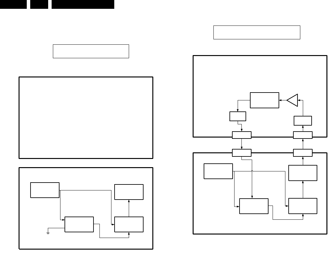
Diagnostic Software and Faultfinding Trees
EN 58 DVDR980-985 /0X15.
5.5.1 Nucleus 900: Digital Audio Loop
This nucleus tests the audio path through the digital board
Figure 5-9
5.5.2 Nucleus 901: Audio User Dealer Loop
A PCM audio sine of 12kHz is generated in the Host Decoder
for a while and sent to the analogue board. The signal coming
from the analogue board is encoded again and sent to the
memory of the host decoder for comparison. This nucleus tests
the components on the audio signal path:
•Host decoder
•Flex connection between connector 1602 (digital board)
and connector 1900 (analogue board)
•DAC
•Op-amp
•Scart switch IC
•ADC
•Audio Encoder
•VIP
•VSM
Figure 5-10
NUCLEUS 900: AUDIO LOOP DIGITAL
VIP STI 5508
VSM
EMPRESS
DIGITAL BOARD
ANALOGUE BOARD
GND
VIP_ICLK: 27MHz
CL 16532145_036.eps
031201
7500
7403
7200
7100
NUCLEUS 901: AUDIO USER DEALER LOOP
VIP STI 5508
VSM
EMPRESS
DIGITAL BOARD
ANALOGUE BOARD
STV6410
DAC
ADC
connector
1900
connector
1900
connector
1602
connector
1602
VIP_ICLK: 27MHz
I2S I2S
CL 16532145_037.eps
031201
7500
7004
7507 7002
7100
7403
7200
7100
Diagnostic Software and Faultfinding Trees EN 59DVDR980-985 /0X1 5.
5.5.3 Nucleus 902: Digital Video Loop
A colourbar generated in the host decoder is looped through
the VIP, Empire, and VSM and checked again in the host
decoder. The following components are tested on the video
signal path:
•VIP
•Empire
•VSM
•Host decoder
Figure 5-11
NUCLEUS 902: DIGITAL VIDEO LOOP
VIP STI 5508
VSM
EMPRESS
DIGITAL BOARD
ANALOGUE BOARD
STV6410
VIP_ICLK: 27MHz
CL 16532145_038.eps
031201
7500
7507
7403
7200
7100
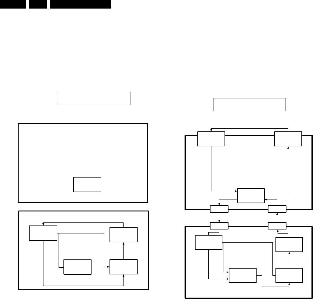
Diagnostic Software and Faultfinding Trees
EN 60 DVDR980-985 /0X15.
5.5.4 Nucleus 903: Digital Video VBI Loop
Nucleus for testing the components on the video VBI signal
path:
•The VIP
•The VSM
•The Host Decoder
This is done by using the internal test signal source (digital
board only)
Remark: this test is only successful if nucleus 121 is carried out
first.
Figure 5-12
5.5.5 Nucleus 904: System Video Loop
Nucleus for testing the components on the video signal system
path:
•The VIP
•The video encoder
•The VSM
•The host decoder
•The analogue board
On the analogue board the video signal will be routed to the
SCART (EUROPE) or CINCH (NAFTA). There it will be looped
back externally by means of the proper cable
Figure 5-13
NUCLEUS 903: DIGITAL VIDEO VBI LOOP
VIP STI 5508
VSM
EMPRESS
DIGITAL BOARD
ANALOGUE BOARD
STV6410
VIP_ICLK: 27MHz
CL 16532145_039.eps
031201
7500
7507
7403
7200
7100
NUCLEUS 904: SYSTEM VIDEO LOOP
VIP STI 5508
VSM
EMPRESS
DIGITAL BOARD
ANALOGUE BOARD
STV6410
SCART TVSCART AUX
connector
1954
connector
1954
connector
1601
connector
1601
VIP_ICLK: 27MHz
7500
7507
7403
7200
7100
CL 16532145_040.eps
121201
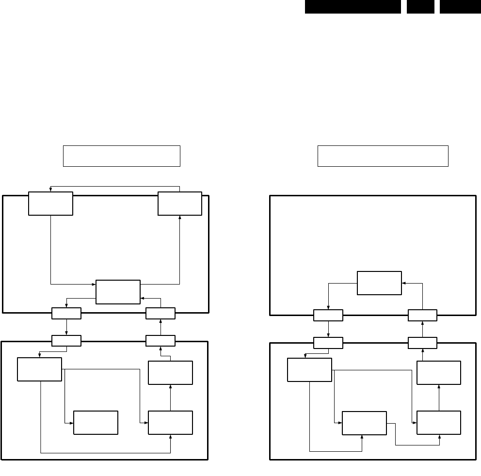
Diagnostic Software and Faultfinding Trees EN 61DVDR980-985 /0X1 5.
5.5.6 Nucleus 905: System Video VBI Loop
This nucleus tests the components on the video signal path:
•The VIP
•The VSM
•The Host Decoder
The video CVBS signal is routed to the output of the analogue
board where it will be looped back by means of an external
cable
Remark: this test is only successful if nucleus 121 is carried out
first.
Figure 5-14
5.5.7 Nucleus 906: Video User Dealer Loop
Nucleus for testing the components on the video signal system
path:
•The VIP
•The video encoder
•The VSM
•The host decoder
•The analogue board
On the analogue board, the video signal is internally routed
back to the digital board.
Figure 5-15
NUCLEUS 905: SYSTEM VIDEO VBI LOOP
VIP STI 5508
VSM
EMPRESS
DIGITAL BOARD
ANALOGUE BOARD
STV6410
SCART TVSCART AUX
connector
1954
connector
1954
connector
1601
connector
1601
VIP_ICLK: 27MHz
CL 16532145_041.eps
031201
7500
7507
7403
7200
7100
NUCLEUS 906: VIDEO USER DEALER LOOP
VIP STI 5508
VSM
EMPRESS
DIGITAL BOARD
ANALOGUE BOARD
STV6410
connector
1954
connector
1954
connector
1601
connector
1601
VIP_ICLK: 27MHz
7500
7507
7403
7200
7100
CL 16532145_042.eps
031201
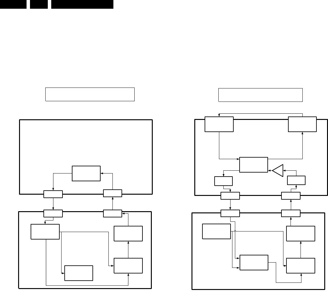
Diagnostic Software and Faultfinding Trees
EN 62 DVDR980-985 /0X15.
5.5.8 Nucleus 907: Video VBI User Dealer Loop
This nucleus tests the components on the video VBI signal
path:
•The VIP
•The VSM
•The Host Decoder
The signal is routed back internally on the analogue board
Remark: this test is only successful if nucleus 121 is carried out
first.
Figure 5-16
5.5.9 Nucleus 908: System Audio Loop Scart (Europe)
Nucleus for testing the components on the audio signal path:
•The hostdecoder
•The analogue board
•The audio encoder
•The VSM
On the analogue board, audio is passed to the SCART
connector, where a SCART cable needs to be used to loop
back the audio signal to the digital board
Figure 5-17
NUCLEUS 907: VIDEO VBI USER DEALER LOOP
VIP STI 5508
VSM
EMPRESS
DIGITAL BOARD
ANALOGUE BOARD
STV6410
connector
1954
connector
1954
connector
1601
connector
1601
VIP_ICLK: 27MHz
CL 16532145_043.eps
031201
7500
7507
7403
7200
7100
NUCLEUS 908: SYSTEM AUDIO LOOP SCART
VIP STI 5508
VSM
EMPRESS
DIGITAL BOARD
ANALOGUE BOARD
STV6410
DAC
ADC
connector
1900
connector
1900
connector
1602
connector
1602
SCART TVSCART AUX
VIP_ICLK: 27MHz
CL 16532145_044.eps
121201
7500
7004
7507
7002 7100
7403
7200
7100
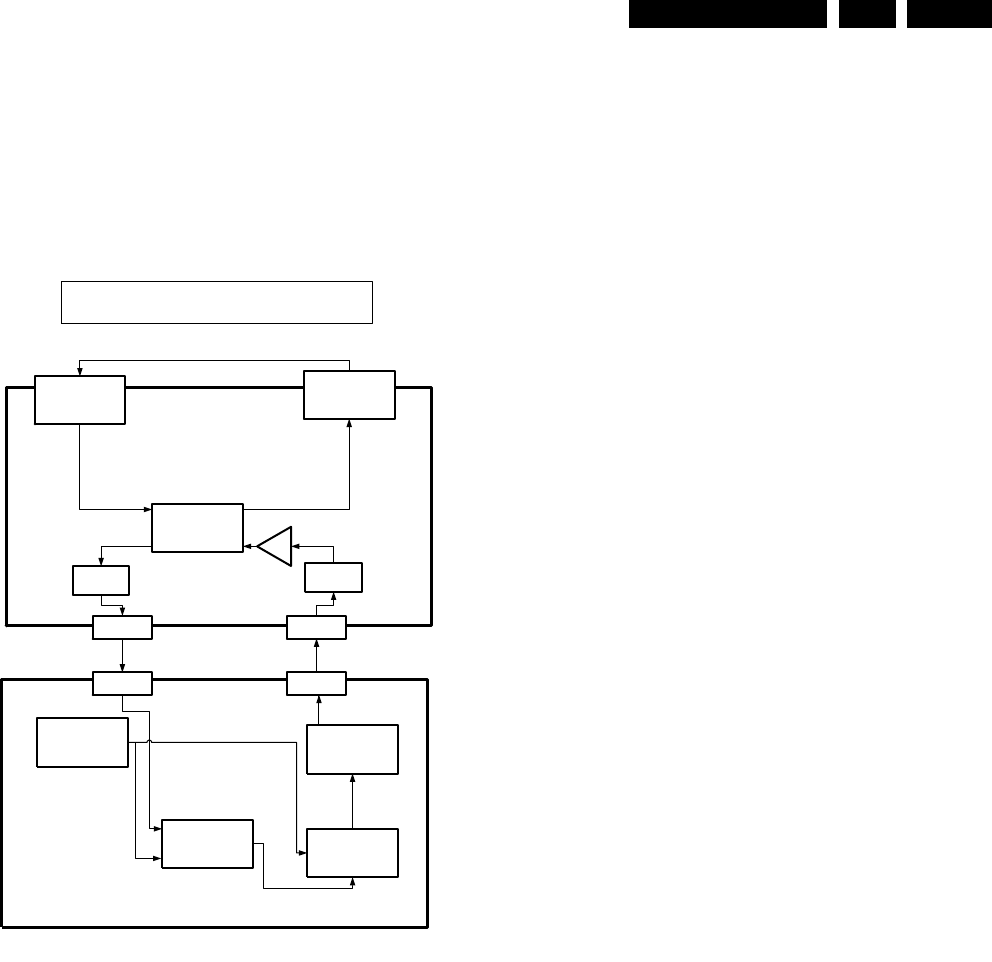
Diagnostic Software and Faultfinding Trees EN 63DVDR980-985 /0X1 5.
5.5.10 Nucleus 909: System Audio Loop CINCH (Nafta)
Nucleus for testing the components on the audio signal path:
•The hostdecoder
•The analogue board
•The audio encoder
•The VSM
On the analogue board the audio is passed to the CINCH
connector, where a CINCH cable needs to be used to loop back
the audio signal to the digital board
Figure 5-18
NUCLEUS 909: SYSTEM AUDIO LOOP CINCH
VIP STI 5505
VSM
EMPRESS
DIGITAL BOARD
ANALOGUE BOARD
STV6410
DAC
ADC
connector
1900
connector
1900
connector
1602
connector
1602
CINCH OUT
(NAFTA)
CINCH IN
(NAFTA)
VIP_ICLK: 27MHz
7500
7004
7507
7002
7100
7403
7200
7100
CL 16532145_045.eps
031201
Diagnostic Software and Faultfinding Trees
EN 64 DVDR980-985 /0X15.
5.6 Faultfinding trees
5.6.1 General
Figure 5-19
PLAYBACK MODE
Plug Recorder
to the mains.
No disc loaded
Standby LED changes
from green to red.
Display shows time
NOK
OK
Press "STOP" button
OK
Press "OPEN/CLOSE" button
OK
Insert DVD Disc
Press "OPEN/CLOSE" button
Standby LED changes
from Red to Green.
Display shows successively
"READING"
"NO DISC"
Display shows successively
"OPENING"
"TRAY OPEN"
Tray is open
OK
OK
Display shows successively
"CLOSING"
"READING"
Recorder starts playback of
DVD-disc
Audio & Video OK ?
Playback DVD OK
Check PSU(see chapter 5.6.2)
Check Analog PCB(see chapter 5.6.4)
Check Front PCB(see chapter 5.6.5)
NOK Check Trade Mode(see chapter 5.2.4)
Check Front PCB(see chapter 5.6.5)
Check Digital PCB(see chapter 5.6.3)
NOK Check Front PCB(see chapter 5.6.5)
Check Basic Engine(see chapter 5.6.3)
NOK Check Digital PCB(see chapter 5.6.3)
Check Basic Engine(see chapter 5.6.3)
NOK Check Digital PCB(see chapter 5.6.3)
Check Analog PCB(see chapter 5.6.4)
CL 16532095_243.eps
170801
Diagnostic Software and Faultfinding Trees EN 65DVDR980-985 /0X1 5.
Figure 5-20
RECORD MODE
Insert DVDR Disc
Display shows:
- Disc content
- Source
- DVD+RW
- Disc Bar
Press NEXT button to
select empty title
Press "RECORD" button
Recording starts
Press "STOP" button
Menu update
Check recorded title
Recording OK
NOK - Check Basic Engine(see chapter 5.6.3)
NOK - Check Analog PCB(see chapter 5.6.4)
- Check Digital PCB(see chapter 5.6.3)
- Check Basic Engine(see chapter 5.6.3)
- Check DVDR Disc
NOK - Check Basic Engine(see chapter 5.6.3)
- Check DVDR Disc
OK
OK
OK
CL 16532095_242.eps
170801
Diagnostic Software and Faultfinding Trees
EN 66 DVDR980-985 /0X15.
5.6.2 Power supply
Figure 5-21
Digital board
Check DC voltages on connector 0205:
Remove all the connectors from the PSU
None of the voltages are present +12Vstby and +5V2stby are oke.
Check +12Vreg circuit:
- D6210, C2210, C2212
Check +Vreg circuit:
- D6240, C2240, C2242
Check Prot_3V3 circuit:
- D6215, C2214, C2215,
- R3520, R3521, D6520
Connect PSU to a mains isolated variac.
Turn the input voltage up and measure
voltage across C2125. Do not exceed
max. mains voltage indicated on player.
This voltage must be +/- 1.41 x Vin AC.
Check +33Vstby circuit:
- D6200, C2200, R3200, D6201, R3201
Check -5Nstby circuit:
- D6220, C2220, IC7220, C2222, C2221
Check FLYB circuit:
- D6221, T7241, R3220, R3221, R3222,
R3223.
Check -Vgnstby circuit:
- D6230, C2230, R3230, D6231, R3233,
R3234, C2235.
Check +12V circuit:
must be present for the other voltages
- Q7511, T7512, D6511, D6512,
- R3511, R3513, R3514, L551, C2512.
Check +3V3 circuit:
- Q7520, Q7521, L5520, C2521, F1520,
- R3522, R3523, R3524, R3525, C2520.
Check +5V circuit:
- Q7501, Q7502, L5501, C2502, R3501
- R3502, R3503, R3504, C2540.
Check +3V3E circuit:
- Q7505, Q7506, D6505, L5505, C2506,
- R3505, R3506, R3507, R3508, C2502.
Check -5V circuit:
- Q7515, D6515, L5515, C2515, R3515.
Standby voltages are oke. Check DC
voltages on connectors 0207 and 0209.
Connector 0207:
+3V3, +5V, -5V, +12V.
Connector 0209:
+3V3, +12V, +5V, -5V, STBY_ctrl.
If not oke, check supply path of failed
supply voltages.
Check primary circuit:
- F1120, D6151, D6152, D6153, D6154,
- R3120, L5120, L5520, C2125.
If fuse 1120 is defective, always check
Q7125, D6145, T7140, Rsense (R3133,
R3134, R3135, R3136 and R3137).
Check with an oscilloscope Vds and Vg
of Q7125.
Is PSU ticking?
Check power switch circuit:
- Q7125, D6130, D3131, D6132
- D6145, D6146, L5125
- C2136
- R3131, R3132, R3133, R3134
- R3135, R3136, R3137, R3146
Check Control circuit
- T7140, D6141, D6142, L5131,
- C2144, C2145, C2147, C2151
- R3151, R3147, R3148, R3150
Check Regulation circuit
- T7251, Q7200, R3250, R3253
- R3254, R3255, R3256, C2251
Check Overvoltage circuit
- T7142, D6143, D6144,
- R3149, R3144, C2152, C2142
Check Overload circuit
- T7141, T7143, R3145, R3143,
- R3142, C2143.
Check start-up circuit:
- R3125, R3126, R3141, R3132
- Q7125, L5131, R3150, C2146
All voltages are present.
+12Vstby, +5V2stby, -5Nstby, -Vgnstby, +33Vstby
NO
YES
If oke, the power supply seems to be ok.
Check the other boards in the player
for the cause of the overload.
Check if STBY_ctrl is LOW.
- Check standby control path via digital
board to analog board.
CL 16532095_085.eps
150801
Diagnostic Software and Faultfinding Trees EN 67DVDR980-985 /0X1 5.
5.6.3 Digital Board
Start-up DSW
Figure 5-22
START UP DSW
NOT OK
OK
OK
OK
OK
Check EMI_PROCCLK(50MHz)
on I181
NOK - Check IC 7100
NOK - Check connection to PSU
- Check Power Supply
Check Power Supplies on con. 1900
(ION should be LOW)
OK
NOK - Check IC 7202
- Check IC 7916-C
- Check IC 7801
Check that Sysclk_5505 on I819
appears earlier then Resetn_5505
is high on I202
OK
NOK - Check IC 7202
- Check R 3266
- Check L 5200, 5201 and 5202
Check VDD_STi(+3V3) on I272
Check VDDA(+3V3) on I275
Check VDDA_PCM(+3V3) on I252
NOK - Check IC 7305
- Check IC 7301
- Check IC 7202
Check activity on EMI_CE3n(pin1 of IC 7305)
Check activity on ROMH_CEn(pin6 of IC 7305)
Check activity on EMI_OEn(pin29 of IC 7301)
NOK - Check IC 7202
- Check IC 7302 and IC 7304
- Check IC 7100
Check if FLASH_OEn is LOW on I245
Check if EMI_RWn is HIGH(pin133 of IC7202)
OK
NOK - Check IC 7202
- Check L 5200
Check if F201 is HIGH and I201 is LOW
Check if I208 is LOW and I209 is HIGH
OK
OK
NOK - Check L 5300
- Check L 5302
NOK - Check Jumper 4206
Check VDD_MEM(+3V3) on I306
Check VDD_MEM1(+3V3) on I310
OK
NOK - Check L 5100
- Check L 5101
Check VCC3_VSM(+3V3) on I100
Check VCC3_VSM_MEM(+3V3) on I141
OK
OK
Check for short circuits or open circuits on the
IC pins which are connected to the EMI-bus
OK
NOK - Check IC 7202
Check TCK (HIGH) on I247
Check TDI (HIGH) on I248
Check TMS (HIGH) on I249
Check TRST (LOW) on I250
START UP DSW
OK
OK
Check LOW pulses on EMI_CE3n
on pin 126 of IC 7202
NOK - Check IC 7202
- Check IC 7305
Check if service pin is LOW on testpoint I207
CL 16532095_086.eps
150801
Diagnostic Software and Faultfinding Trees
EN 68 DVDR980-985 /0X15.
Power part check
Figure 5-23
Power On and exit
stand-by mode
POWER PART CHECK DIGITAL BOARD
USE DIGITAL BOARD CIRCUIT DIAGRAMS 1 2, 3, 4, 5, 7 AND 8 AND DIGITAL BOARD BOTTOM VIEW TESTPOINTS
OK
OK
OK
OK
OK
OK
OK
OK
Check +3V3 on Testpoints I905
Check +12V on Testpoint I907
Check +5V on Testpoint I906
Check -5V on Testpoint I908
Vcc3_VSM(+3V3) on testpoint I100 NOK
NOK
NOK
NOK
check L5100
Vcc3_VSM_mem(+3V3) on testpoint I141 check L5101
Vdd_sti(+3V3) on tespoint I244 check L5200
NOK check L5300
NOK check L5302
Vdd_flash_L(+3V3) on testpoint I304
Vdd_flash_H1(+3V3) on testpoint I301
NOK check L5404
NOK check IC7404
VDD_EMP(+3V3) on tespoint I413
VDD_EMP_CORE(+3V3) on tespoint I412
NOK check L5507
NOK check L5500
NOK check L5501
VDDA_7118(+3V3) on testpoint I509
VDDA_1A_7118(+3V3) on testpoint I508
VDDA_2A_7118(+3V3) on testpoint I510
NOK check L5502VDDA_3A_7118(+3V3) on testpoint I513
NOK check L5503VDDA_4A_7118(+3V3) on testpoint I514
NOK check L5508VDDX_7118(+3V3) on testpoint I518
NOK check L5506
NOK check L5505
VDDE_7118(+3V3) on testpoint I511
VDDI_7118(+3V3) on testpoint I515
NOK check L5504VDD_LVC32(+3V3) on testpoint I526
NOK check L5905VDD5_OSC(+5V) on tespoint I925
NOK check L5103VCC5_4046(+5V) on testpoint I130
NOK check L5907VCC3_CLK_BUF(+3V3) on testpoint I930
Power Part OK
- Check connection to PSU
- Check PSU
CL 16532145_046.eps
031201
Diagnostic Software and Faultfinding Trees EN 69DVDR980-985 /0X1 5.
Reset and Clock Check
Figure 5-24
RESET & CLOCK CHECK DIGITAL BOARD
Power on and exit
stand-by mode
Resetn(+3V3) on testpoint I912
Resetn_BE(+3V3) on testpoint I126
Resetn_DVIO(+3V3) on testpoint I659
Resetn_VE(+3V3) on testpoint I206
Sysclk_VSM_5508(27MHz) on testpoint I917
Sysclk_ProgScan(27MHz) on testpoint I920
Sysclk_Empress(27MHz) on testpoint I924
OK
OK
ACC_ACLK_PLL(12MHz) on testpoint I902
OK
EMI_PROCCLK(60MHz) on testpoint I170
OK
VIP_ICLK(27MHz) on testpoint I101
OK
OK
NOK
NOK
- Check IC7902
- Check R3924 and R3925
- Check D6900
- Check IC7702
- Check IC7403
- Check IC7200
NOK - Check Oscillator 7906
- Check R3906, R3908 and R3917
- Check IC7904
NOK - Check Oscillator 7906
- Check R3901
- Check IC7900
ACC_ACLK_OSC(12MHz) on testpoint I143
OK
NOK
- Check R3125
- Check IC7102
NOK - Check IC7200
- Check IC7100
- Check R3208
NOK - Check IC7500
- Check R3505
- Check IC7100
Reset- & clock signals are OK
USE DIGITAL BOARD CIRCUIT DIAGRAMS 1,2,7 AND 8 AND DIGITAL BOARD BOTTOM VIEW TESTPOINTS
CL 16532145_047.eps
031201
Diagnostic Software and Faultfinding Trees
EN 70 DVDR980-985 /0X15.
DSW Memory Tests
Figure 5-25
Start Diagnostic Software
and select Command mode
OK
NOK
OK
Flash Checksum
Command: 100
NVRAM I2C Test
Command: 123
NVRAM Write Read Test
Command: 122
NOK
- Check IC 7301
- Check IC 7302
OK
NOK
Flash Write/Read
Command: 103
- Check IC 7301
- Check IC 7302
OK
Flash 1 Write Access
Command: 101 - Check IC 7301
OK
Flash 2 Write Access
Command: 102 - Check IC 7302
- Check I2C-signals
- Check 7201
DSW MEMORY TESTS
MEMORY PART OK
NOK
NOK
OK
SDRAM Write/Read
Command: 104 - Check IC 7300
NOK
OK
SDRAM Write/Read fast
Command: 105 - Check IC 7300
NOK
CL 16532145_048.eps
031201
Diagnostic Software and Faultfinding Trees EN 71DVDR980-985 /0X1 5.
DSW VSM Tests
Figure 5-26
Start Diagnostic Software
and select Command mode
DSW VSM TESTS
OK
OK
VSM Interconnection Test
Command: 304
SDRAM Access Test
Command: 301
SDRAM Write/Read Test
Command: 302
OK
NOK
NOK
NOK
NOK
NOK
- Check IC 7100
- Check IC 7101
- Check IC 7100
- Check IC 7101
VSM Interrupt Test
Command: 303
OK
- Check IC 7101
- Check IC 7100
VSM Connection to analog board Test
Command: 305
OK
- Check connection to analog
board
- Check IC 7100
VSM PART OK CL 16532145_049.eps
031201
Diagnostic Software and Faultfinding Trees
EN 72 DVDR980-985 /0X15.
DSW Audio Part Check
Figure 5-27
Audio Clock Test
Command: 1400
Measure ACC_ACLK_PLL on I902
(11.289MHz)
NOK - Check IC 7900
- Check IC 7906
- Check IC 7100
OK
OK
Audio Clock Test
Command: 1401
Measure ACC_ACLK_PLL on I902
(12.288MHz)
Host Pink Noise ON
Command: 115
Check AD_BCLK(3.072MHz) on pin14 of con.1602
Check AD_WCLK(48KHz) on pin12 of con.1602
Check AD_ACLK(12.288MHz) on pin9 of con.1602
Check AD_DATAO(Activity) on pin11 of con.1602
Check AD_SPDIF33(Activity) on pin2 of con.1602
NOK - Check IC 7900
- Check IC 7906
- Check IC 7100
NOK - Check IC 7202
DSW AUDIO PART CHECK
Start Diagnostic Software
and select Command mode
- Check IC 7200
OK
OK
Host Pink Noise OFF
Command: 116
Check AD_BCLK(3.072MHz) on pin14 of con.1602
Check AD_WCLK(48KHz) on pin12 of con.1602
Check AD_ACLK(12.288MHz) on pin9 of con.1602
Check AD_DATAO(No Activity) on pin11 of con.1602
Check AD_SPDIF33(No Activity) on pin2 of con.1602
NOK - Check IC 7202
- Check IC 7200
NOK - Check IC 7100
- Check IC 7403
Audio I2S Encoding Path Test
Command: 900
Check AE_BCLK(3.072MHz) on pin21 of con.1602
Check AE_WCLK(48KHz) on pin20 of con.1602
Check AE_DATAI(Activity) on pin18 of con.1602
Check AE_DATAO(Activity) on testpoint I155
Check AE_ACLK on pin16 of con. 1602
OK
OK
OK
NOK - Check IC 7100
- Check IC 7500
NOK - Check IC 7200
Video Encoding Path Test
Command: 902
Check VIP_ICLK(27MHz) on testpoint I101
Check VIP_VS(50Hz) on pin1 of IC7502
Check VE_DSn(Activity) on testpoint I104
Check VE_DTACKn(Activity) on testpoint I103
Mute ON Test --> Command: 109
Check Mute level(high) on testpoint I609
Mute OFF Test --> Command: 110
Check Mute Level(low) on testpoint I609
AUDIO PART OK
- Check IC 7502
- Check IC 7202
CL 16532145_050.eps
031201
Diagnostic Software and Faultfinding Trees EN 73DVDR980-985 /0X1 5.
DSW Vidoe Part Check
Figure 5-28
DSW VIDEO PART CHECK
Start Diagnostic Software
and select Command mode
Gateway Test to Analog Board
Command: 700
NOK - Check Analog Board
- Check IC 7100
NOK - Check IC 7701
- Check IC 7200
- Check IC 7702
NOK - Check IC 7200
- Check IC 7500
- Check IC 7100
NOK - Check T7600, T7601, T7603
T7604, T7605 and T7606
- Check IC 7200
Color Bar ON Test
Command: 120
Check Red Video Out on pin 5 of con.1601
Check Green Video Out on pin 3 of con.1601
Check Blue Video Out on pin 1 of con.1601
Check CVBS Video Out on pin 11 of con.1601
Check Y-Video Out on pin 9 of con.1601
Check C-Video Out on pin 7 of con.1601
OK
OK
Color Bar OFF Test
Command: 121
OK
VBI(Vertical Blanking Interval) Loopback Test
Command: 903
Check the Color Bar on the TV creen
OK
OK
OK
Check HSYNC on testpoint I221
Check VSYNC on testpoint I701
VIDEO PART OK
CL 16532145_051.eps
031201
Diagnostic Software and Faultfinding Trees
EN 74 DVDR980-985 /0X15.
DSW Video Part Check Progressive Scan
Figure 5-29
Start Diagnostic Software
and select Command mode
VIDEO PART CHECK PROGRESSIVE SCAN
Generate NTSC Testpicture
Command: 135 10 1
Switch off Macrovision
Command: 137
Route PS to Analog Board
Command: 1415
Route Video on Analog Board
Command: 712
OK
OK
OK
OK
Check activity on Yy_OUT(0:7) of IC7801
Check activity on Cr_OUT(0:7) of IC7801
Check activity on Cb_OUT(0:7) of IC7801
Check DAC-A/Y on testpoint I808
Check DAC-B on testpoint I809
Check DAC-C on testpoint I812
Check Y-signal on testpoint I821
Check Cb-signal on testpoint I822
Check Cr-signal on testpoint I823
Video Part Progressive Scan OK
NOK - Check IC 7800
- Check IC 7801
NOK - Check IC 7701 and IC 7702
- Check IC 7200
NOK - Check IC 7801
NOK - Check IC 7802
- Check IC 7803
- Check R3801, R3812 and R3819
Check HSOUT on testpoint I824
Check VSOUT on testpoint I825
CL 265362011_023.eps
160102
Diagnostic Software and Faultfinding Trees EN 75DVDR980-985 /0X1 5.
DSW Basic Engine Check
Figure 5-30
Start Diagnostic Software
and select Command mode
DSW BASIC ENGINE TESTS
OK
Basic Engine S2B Echo Test
Command: 601
OK
Basic Engine Tray Open Test
Command: 616
OK
Insert a DVDRW video disc
NOK - Check IC 7202
- Check Basic Engine
NOK - Check Basic Engine
OK
Basic Engine Tray Close Test
Command: 615
NOK - Check Basic Engine
OK
Basic Engine S2B Write Read Test
Command: 617
NOK - Check Basic Engine
BASIC ENGINE PART OK
- Check IC 7100
CL 16532095_094.eps
150801
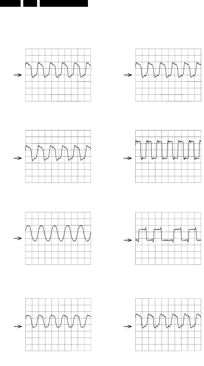
Diagnostic Software and Faultfinding Trees
EN 76 DVDR980-985 /0X15.
Waveforms
Figure 5-31
2V / div DC 20ns / div
2V / div DC 20ns / div
2V / div DC 10ns / div 2V / div DC 10ms / div
2V / div DC 20ns / div
2V / div DC 50ns / div
Sysclk_VSM
27M_clk_PS
EMI_PROCCLK
2V / div DC 20ns / div
VIP_ICLK
Sysclk_5505
acc_aclk_pll
DSP_clk
2V / div DC 20ns / div
VSM_M_CLK
Waveforms Digital Board
CL 16532145_053.eps
031201
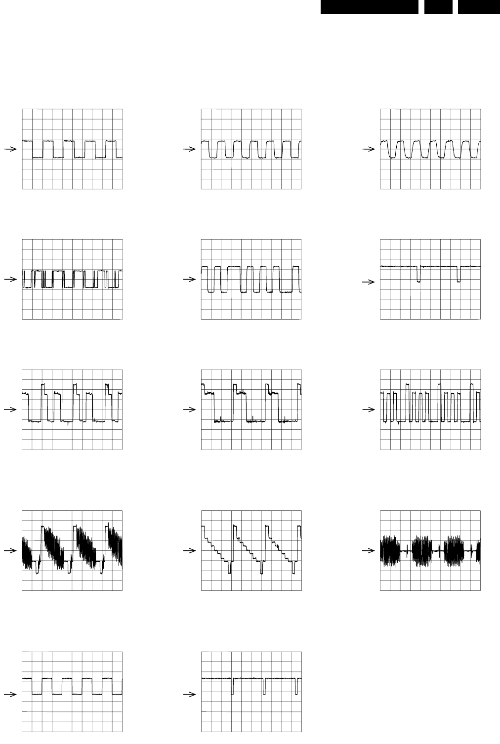
Diagnostic Software and Faultfinding Trees EN 77DVDR980-985 /0X1 5.
Figure 5-32
2V / div AC 10us / div 2V / div AC 200ns / div
AD_WCLK; AE_WCLK
200mV / div AC 20us / div
R_OUT
200mV / div AC 20us / div
CVBS_OUT
2V / div DC 20ms / div
VSYNC
2V / div DC 20ms / div
HSYNC
200mV / div AC 20us / div
G_OUT
200mV / div AC 20us / div
Y_OUT
200mV / div AC 20us / div
C_OUT
200mV / div AC 20us / div
B_OUT
2V / div AC 5us / div
AD_DATAO; AE_DATAO; AE_DATAIAD_DATAO; AE_DATAO; AE_DATAI
2V / div AC 250ns / div
AD_SPDIF
AD_BCLK; AE_BCLK
2V / div AC 50ns / div
AD_ACLK
2V / div DC 5ms / div
I401 VIP_VS
Waveforms Digital Board
CL 16532145_054.eps
031201
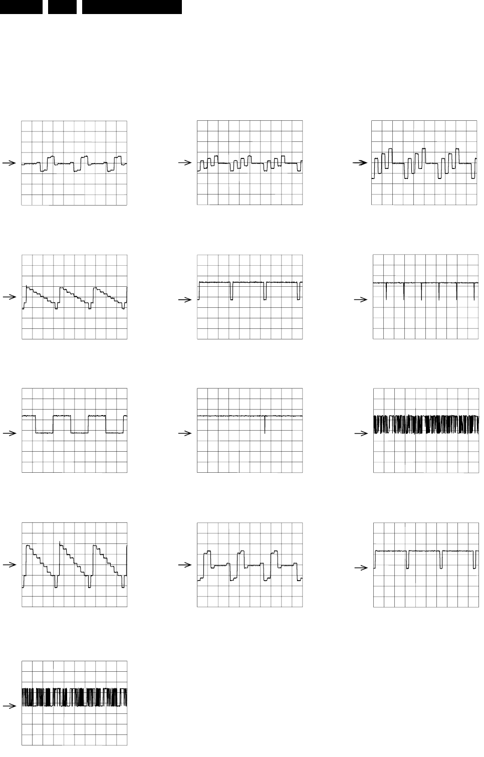
Diagnostic Software and Faultfinding Trees
EN 78 DVDR980-985 /0X15.
Figure 5-33
500mV / div AC 10us / div
DAC-B
500mV / div AC 10us / div
DAC-C
2V / div DC 10ms / div
FRAME_IN
500mV / div AC 10us / div
Y-signal
500mV / div AC 10us / div
Cb-signal
2V / div DC 10ms / div
VS_IN
500mV / div AC 10us / div
DAC-A/Y
2V / div DC 20us / div
HS_IN
Waveforms Digital Board
500mV / div AC 10us / div
Cr-signal
2V / div DC 10ms / div
VSOUT
2V / div DC 10ms / div
YUV_IN
2V / div DC 10us / div
HSOUT
2V / div DC 20us /div
Y_OUT; Cr_OUT; Cb_OUT
CL 16532145_055.eps
031201
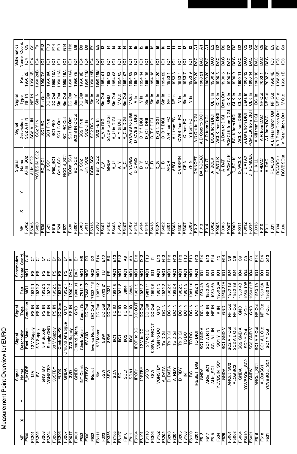
Diagnostic Software and Faultfinding Trees EN 79DVDR980-985 /0X1 5.
5.6.4 Analogue board
Measurement Points Overview
Figure 5-34
CL 16532095_097.eps
150801
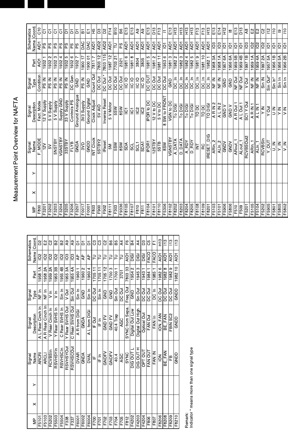
Diagnostic Software and Faultfinding Trees
EN 80 DVDR980-985 /0X15.
Figure 5-35
CL 16532095_098.eps
150801
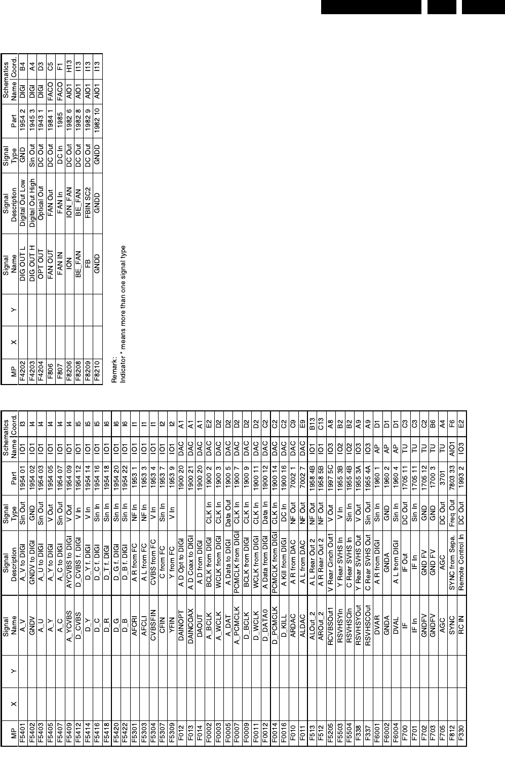
Diagnostic Software and Faultfinding Trees EN 81DVDR980-985 /0X1 5.
Figure 5-36
CL 16532095_099.eps
150801
Diagnostic Software and Faultfinding Trees
EN 82 DVDR980-985 /0X15.
Power Part Check
Figure 5-37
OK
Check internal Power supply voltages
Power Part OK
5M on testpoint F9340
12STBY on testpoint F810
8STBY on pin 3 of IC7332
8SW on testpoint F9336
NOK
NOK
check Fuse 1327
check Fuse 1326
NOK check IC 7332
5STBY on testpoint F9333 NOK check Fuse 1325
5STBY2 on testpoint F900 NOK check L5901, IC7900
5STBY_uP on IC7803 NOK check L5903, IC7803
NOK check - ISTBY HIGH?
- T7329, T7324, MOSFET7321
5SW on testpoint F303 NOK check - ISTBY HIGH?
- T7329, T7324, MOSFET7323
CL 16532145_056.eps
031201
Diagnostic Software and Faultfinding Trees EN 83DVDR980-985 /0X1 5.
DSW Check Analoge Board
Figure 5-38
DSW CHECK ANALOGUE BOARD
Start Diagnostic Software
and select Command mode
Echo Test Analogue Board
Command: 700
NOK
Hardware Version Check
Command: 704
NOK
- Check Reset signal(+5V) on F902
- Check Clock(20MHz) on I915
OK - Check IC 7803
- Check connection to Digital Board
Boot Code Version Test
Command: 703
Analogue Flash Checksum Test
Command: 724
NOK
OK
OK
- Check IC 7906
- Check IC 7906
Tuner Test
Command: 706
NOK
OK
OK
OK
- Check tuner 1705
Data Slicer Test
Command: 708
NOK
OK
- Check IC 7990
Sound Processor Test
Command: 709
NOK
OK
- Check IC 7600
Audio Video Selector Test
Command: 710
NOK
OK
- Check IC 7507
Frequency Download Test
Command: 707
NVRAM Test
Commdo: 711
NOK - Check IC 7815
Clock Adjust Test
Command: 705 2001 07 16 09 15 45 NOK - Check IC 7811
(YYYY MM DD HH MM SS) - Check x-tal 1602
DCW CHECK ANALOGUE
BOARD OK CL 16532095_101.eps
150801
Diagnostic Software and Faultfinding Trees
EN 84 DVDR980-985 /0X15.
Routing Audio and Video
Route Video
Nucleus Number: 712
Description
This nucleus routes the video signals on the analogue board to
the destination determined by the input parameters
The paths that are available for video routing and their
description(Europe version)
The paths that are available for video routing and their
description (Nafta region)
Example
DD:> 712 01
71200: Video routing on the Analogue Board OK.
Test OK @
Route Audio
Nucleus Number: 713
Description
This nucleus routes the audio on the analogue board to the
destination determined by the input parameters
The paths that are available for audio routing and their
description (Europe version)
PATH ID DESCRIPTION
00 Input signal is VIDEO(CVBS) from digital board
and will be re-routed back to the digital board.
01 Input signal is from FRONT VIDEO(CVBS) IN and
will be routed to the digital board.
02 Input signal is from REAR VIDEO(CVBS) IN and
will be routed to the digital board.
03 Input signal is from FRONT S-VIDEO(Y/C) and will
be routed to the digital board.
04 Input signal is from REAR S-VIDEO(Y/C) and will
be routed to the digital board.
05 Input signal is CVBS from SCART1 and will be
routed to the digital board.
06 Input signal is CVBS from SCART2 and will be
routed to the digital board.
07 No routing.
08 Input signal is VIDEO(CVBS) from ANTENNA IN
and will be routed to SCART1.
09 Input signal is VIDEO(CVBS) from SCART1 and
will be routed to SCART2.
10 Input signal is VIDEO(CVBS) from SCART2 and
will be routed to SCART1.
11 No routing.
12 Input signal is from REAR VIDEO(CVBS) IN and
will be routed to SCART1 and SCART2.
13 Input signal is from FRONT VIDEO(CVBS) IN and
will be routed to SCART1.
14 Input signals VIDEO(CVBS and Y/C) from SCART
1 will be routed to SCART2.
15 Input signal is from REAR S-VIDEO(Y/C) IN and
will be routed to SCART2.
16 Input signal is from FRONT S-VIDEO(Y/C) IN and
will be routed to SCART2.
17 No routing
18 No routing
19 Input signals VIDEO(RGB and FAST BLANKING)
from SCART2 will be routed to the corresponding
pins of SCART1.
20 Signal path is routed from digital board RGB to
RGB SCART1 and from RGB SCART2 to digital
board YUV and from digital board CVBS to digital
board CVBS.
21 Signal path is routed from digital board YC to
REAR S-VIDEO(YC) OUT and from REAR S-VID-
EO(YC) IN to digital board YC.
PATH ID DESCRIPTION
00 Input signal is VIDEO(CVBS) from digital board
and will be re-routed back to the digital board.
01 Input signal is from FRONT VIDEO(CVBS) IN and
will be routed to the digital board.
02 Input signal is from REAR VIDEO(CVBS) IN and
will be routed to the digital board.
03 Input signal is from FRONT S-VIDEO(Y/C) IN and
the signal received will be routed to the digital
board.
04 Input signal is from REAR S-VIDEO(Y/C) IN and
will be routed to the digital board.
05 Input signal is from YUV IN and will be routed to the
digital board.
06 No routing.
07 No routing.
08 Input signal is VIDEO(CVBS) from ANTENNA IN
and will be routed to VIDEO(CVBS) OUT and .
09 Input signal is from YUV IN and will be routed to
YUV OUT.
10 No routing.
11 No routing.
12 Input signal is from REAR VIDEO(CVBS) IN and
will be routed to REAR VIDEO(CVBS) OUT.
13 Input signal is from FRONT VIDEO(CVBS) IN and
will be routed to REAR VIDEO(CVBS) OUT.
14 Input signal is from REAR S-VIDEO(Y/C) IN and
will be routed to REAR S-VIDEO(Y/C) OUT.
15 Input signal is from FRONT S-VIDEO(Y/C) IN and
will be routed to REAR S-VIDEO(Y/C) OUT.
16 No routing.
17 Signal path is routed from digital board RGB to
REAR VIDEO(YUV) OUT and from REAR VID-
EO(YUV) IN to digital board YUV and from digital
board CVBS to digital board CVBS.
18 Signal path is routed from digital board CVBS to
REAR VIDEO(CVBS) OUT and from REAR VID-
EO(CVBS) IN to digital board CVBS.
19 Signal path is routed from digital board YC to
REAR S-VIDEO(YC) OUT and from REAR S-VID-
EO(YC) IN to digital board YC.
PATH ID DESCRIPTION
00 Input signal is VIDEO(CVBS) from digital board
and will be re-routed back to the digital board.
01 Input signal is from FRONT AUDIO IN and will be
routed to the digital board.
02 Input signal is from REAR AUDIO IN and will be
routed to the digital board.
03 Input signal is AUDIO from SCART1 and will be
routed to the digital board.
04 Input signal is AUDIO from SCART2 and will be
routed to the digital board.
05 No routing.
06 No routing.
07 No routing.
08 Input signal is VIDEO(CVBS) and AUDIO from AN-
TENNA IN and will be routed to SCART1.
09 Input signal is VIDEO(CVBS) and AUDIO from
SCART1 and will be routed to SCART2.
10 Input signal is VIDEO(CVBS) and AUDIO from
SCART2 and will be routed to SCART1.
11 Input signal is AUDIO from dvio board and will be
routed to SCART1.
PATH ID DESCRIPTION
Diagnostic Software and Faultfinding Trees EN 85DVDR980-985 /0X1 5.
The paths that are available for audio routing and their
description (Nafta region)
EXAMPLE
DD:> 713 00
71300: Audio routing on the Analogue Board OK.
Test OK @
12 No routing.
13 No routing.
14 No routing.
15 No routing.
16 No routing.
17 Input signal is from REAR AUDIO IN and will be
routed to SCART1.
18 Input signal is from FRONT AUDIO IN and will be
routed to SCART1.
PATH ID DESCRIPTION
00 Input signal is VIDEO(CVBS) from digital board
and will be re-routed back to the digital board.
01 Input signal is from FRONT AUDIO IN and will be
routed to the digital board.
02 Input signal is from REAR AUDIO IN 2 and will be
routed to the digital board.
03 Input signal is from FRONT AUDIO IN and will be
routed to the digital board.
04 No routing.
05 No routing.
06 No routing.
07 No routing.
08 Input signal is VIDEO(CVBS) and AUDIO from AN-
TENNA IN and will be routed to VIDEO(CVBS)
OUT and REAR CINCH OUT 2.
09 No routing.
10 Input signal is from REAR AUDIO CINCH IN 2 and
will be routed to REAR AUDIO CINCH OUT 2.
11 Input signal is from FRONT AUDIO CINCH IN and
will be routed to REAR AUDIO CINCH OUT 2.
12 No routing.
13 No routing.
14 No routing.
15 No routing.
16 Input signal is AUDIO from dvio board and will be
routed to AUDIO CINCH OUT 2.
17 No routing.
18 No routing.
19 No routing.
20 Input signal is from digital board and will be routed
to the REAR AUDIO OUT 1 and input signal is from
REAR AUDIO IN 2 and will be routed to the digital
board.
21 Input signal is from digital board and will be routed
to the REAR AUDIO OUT 1 and input signal is from
REAR AUDIO IN 1 and will be routed to the digital
board.
22 Input signal is from digital board and will be routed
to the REAR AUDIO OUT 2 and input signal is from
REAR AUDIO IN 1 and will be routed to the digital
board.
PATH ID DESCRIPTION
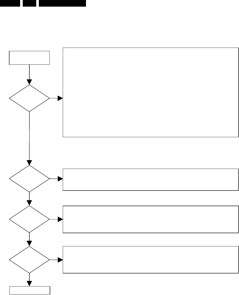
Diagnostic Software and Faultfinding Trees
EN 86 DVDR980-985 /0X15.
5.6.5 Display Board
Figure 5-39
DISPLAY PCB OK.
NO DISC
POWER ON
DISPLAY?
• Check presence of low pulses at pin 5 of connector 1917 while pressing a key on remote control.
• Check IR receiver 7140.
•Diagnostic software “Player script” : Remote control test.
• Check if voltage at connector 1915-2 is 5V when power on (green light)
• Check if voltage at base of Tr 7141 is 2V when power on (green light).
• Check if voltage at base of Tr7141 is 0V when switching to standby (red light)
• Diagnostic software “Player script” : LED test.
• Diagnostic software “Player script” : Keyboard test.
• Check appropriate key and resistor
• Check supply voltage
Connector1916-2 12STBY +12V
Connector1916-3 VGNSTB -32V
Connector1916-11 5STBY +5V
Connector1916-12 5M +5.2V
⇒
⇒
⇒
⇒
Testpoint F105 12STBYSI +12V
⇒
• Check filament voltage
⇒ AC voltage is created via oscillator circuit (7152-7153).
⇒ Check heater voltage on testpoints F102 and F101 3.2VAC, -24,4VDC, 42 kHz.
• Check oscillator frequency of 12MHz at pin 91 of IC7156
• Check I2C bus SDA / SCL nucleus 500 of diagnostic software
• Check version of software nucleus 501 of diagnostic software
• Diagnostic software : Player script of Front panel
NO
YES
Key Function NO
YES
Standby LED ?
YES
Remote control? NO
YES
TROUBLESHOOTING DISPLAY BOARD
NO
CL 265362011_024.eps
160102
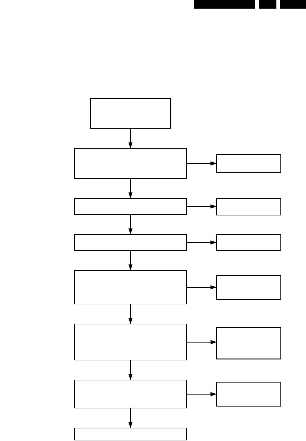
Diagnostic Software and Faultfinding Trees EN 87DVDR980-985 /0X1 5.
DVIO Board
Power part check
Figure 5-40
Power On and exit
stand-by mode
+5V on testpoint F536
+3V3 on testpoint F531
OK
OK
OK
OK
OK
OK
OK
NOK Check connector 1500
to Digital board
NOK Check L 5200
Check IC 7203
NOK Check IC 7204
Check IC 7208
NOK Check L 5302
Check L 5303
Check L 5304
NOK Check L 5404
Check L 5403
Check L 5402
NOK
Check L 5106
Check L 5109
Check L 5110
Check L 5103
+5V_PROC on testpoint F212
PSEN(+5V) on testpoint F203
+3V3_FPGA on testpoint F311
+3V3_FPGA_CONF on testpoint F312
+3V3_SRAM on testpoint F313
+3V3_PLL on testpoint F325
+Vcc_DV_RAM(+3V3) on testpoint F417
+35V_DV_EDO(+3V3) on testpoint F425
+3V3_DV on testpoint F416
+3V3_IEEE_PLL on testpoint F138
+3V3_IEEE_A on testpoint F139
+3V3_IEEE_D on testpoint F140
+3V3_LINK on testpoint F141
Power Part OK
POWER PART CHECK DVIO
USE DVIO BOARD CIRCUIT DIAGRAMS 1 2, 3, 4 AND 5 AND DVIO TOP VIEW TESTPOINTS
CL 16532145_057.eps
031201
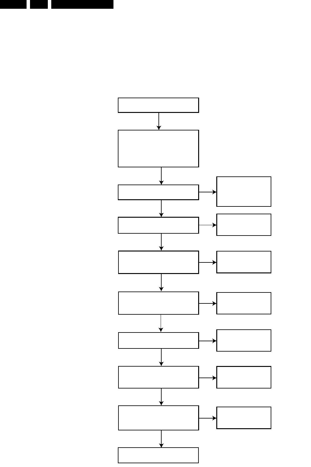
Diagnostic Software and Faultfinding Trees
EN 88 DVDR980-985 /0X15.
Reset and Clock check
Figure 5-41
Power On and exit
stand-by mode
Enable DVIO board:
- press channel up or down
untill the display shows CAM3
- press tuner key in order to
switch to the DV-source
The red LED above the
DV-input will light up.
NOK
NOK
NOK
OK
OK
OK
OK
OK
OK
OK
- Check connection
to Front DVIO
- Check IC 7203
- Check T 7207
- Check R 3203
- Check IC 7203
- Check T 7202
- Check IC 7303
- Check IC 7307
- Check R 3315
- Check IC 7308
- Check IC 7303
- Check R 3317
- Check IC 7308
- Check IC 7404
- Check R 3318
- Check IC 7308
- Check IC 7500
- Check R 3319
- Check x-tal1200
- Check IC 7203
- Check R 3201
Check Reset signal (LOW)
on testpoint F214
Check uP clock
on testpoint F201
(11,05MHz)
Check CLOCKAUDTMP
on testpoint F303
(8,192MHz)
Check Clock 27MHz
on testpoint F305
Check Clock 27M_DV
on testpoint F307
(27MHz)
Check Clock 27M_CON
on testpoint F308
(27MHz)
Reset- and clock signals
are OK
RESET & CLOCK CHECK DVIO
USE DVIO BOARD CIRCUIT DIAGRAMS 2, 3, 4 AND 5 AND DVIO TOP VIEW TESTPOINTS
NOK
NOK
NOK
NOK
CL 16532145_057.eps
031201
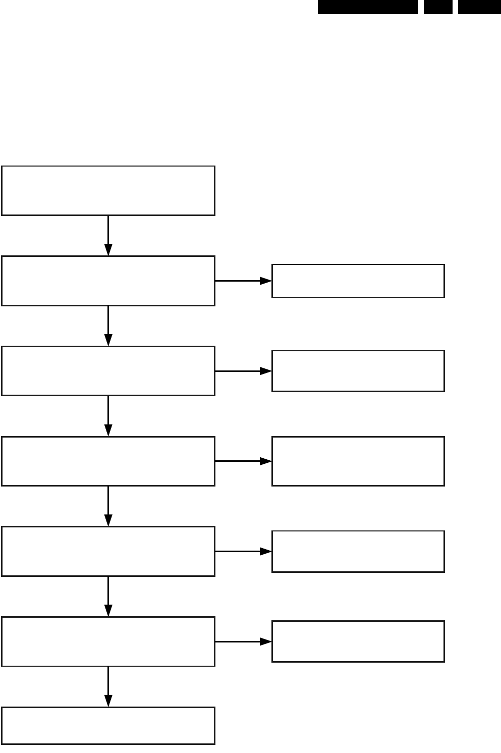
Diagnostic Software and Faultfinding Trees EN 89DVDR980-985 /0X1 5.
DSW DVIO tests
Figure 5-42
Start Diagnostic Software
and select Command mode
DSW DVIO TESTS
OK
DVIO Board Presence Test
Command: 800
OK
Reset DVIO Test
Command: 801
NOK - Check DVIO Board
- Check Connector 1500
- Check DVIO Board
- Check Connector 1500
- Check Digital Board
NOK - Check IC7303
- Check IC 7203
OK
DVIO Access Test
Command: 802
NOK
OK
OK
DVIO Module ID's Test
Command: 804
NOK - Check IC 7303
DVIO DSW CHECK OK
- Check IC 7404
DVIO Selftest
Command: 805
NOK Check ERROR LIST
in COMPAIR
CL 16532145_059.eps
031201
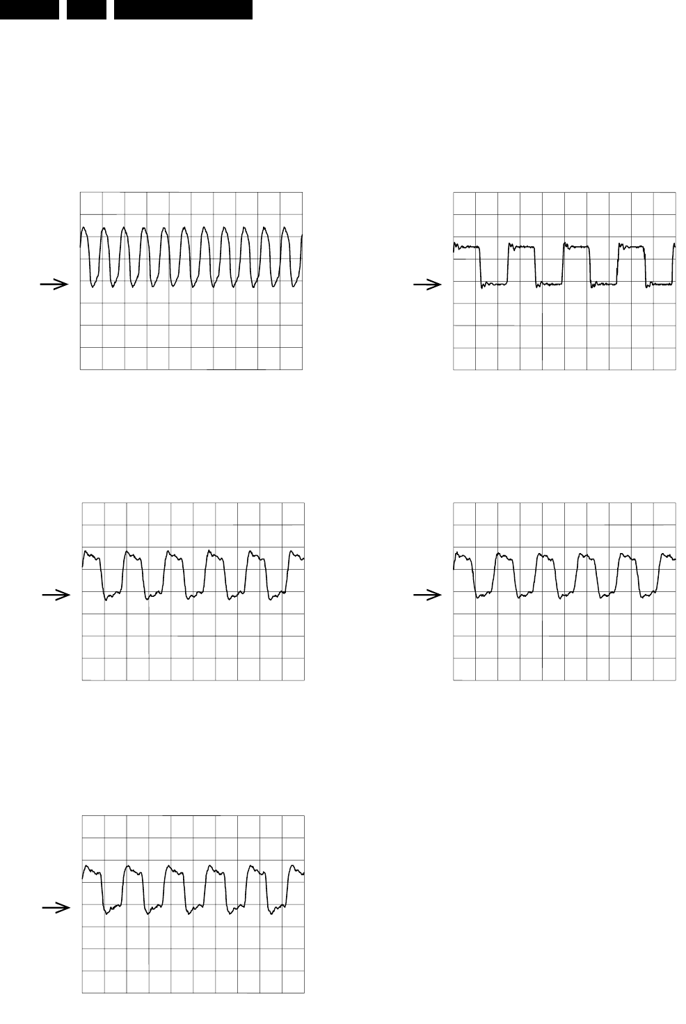
Diagnostic Software and Faultfinding Trees
EN 90 DVDR980-985 /0X15.
Waveforms
Figure 5-43
2V / div DC 100ns / div
2V / div DC 20ns / div
2V / div DC 20ns / div
2V / div DC 20ns / div
2V / div DC 50ns / div
uP_clock
Clock 27MHz
Clockaudtmp
Clock 27M_DV
Clock 27M_CON
Waveforms DVIO
CL 16532145_060.eps
031201

Diagnostic Software and Faultfinding Trees EN 91DVDR980-985 /0X1 5.
Personal Notes:

Diagnostic Software and Faultfinding Trees
EN 92 DVDR980-985 /0X15.
Personal Notes:
Block and Wiring Diagram. EN 93DVDR980-985 /0X1 6.
6. Block and Wiring Diagram.
Block Diagram DVDR980-985 EU
FRONT
Analog input
FRONT
Digital Video input
IEEE 1394
4
DIGITAL PCB
VSM
Stream
Manager
SDRAM
MPEG VIDEO
ENCODING
EMPRESS
SDRAM
FLASH 4MBDRAM
VIDEO INPUT
PROCESSING
MPEG
AV
DECODER
+ HOST
(Sti5508)
2MB
SDRAM
ANAL.VIDEO
DIG. AUDIO
VSM_UART1
IRESET_DIG
ION
CVBS-RGB-Y/C
RS232
SERVICE
AUDIO PCM I2S
SPDIF
AE_WCLK
AE_BCLK
AD_DATAI
OPT_IN
COAX_IN
MUTEN
AD_ACLK
AUDIO ENCODER I2S
YUV-YCVBS/C
ANALOG AUDIO L/R
ANALOG AUDIO VIDEO
DVIO
PHY LINK FPGA
SRAM
BE_FAN
+3V3
CVBS_OUT_B
C_OUT_B
Y_OUT_B
R_OUT_B
G_OUT_B
B_OUT_B
V_IN
U_IN
Y_IN
C_IN
CVBS_Y_IN
+5V
RESETN_BE
BE_LOADN
S2BS2B
I2S
FRONT-END I2S
FRONT-END I2S or //
DRAM
8051
4
9
DV CODEC
AUDIO DAC
(DATA+CONTROL+PSU)
DVD & RW ENGINE
TRAY CONTROL
SERVO
READ
WRITE
DISC
PSU
INFRA RED
EYE
DISPLAY & CONTROL
PSU
INT/IPOR1
I2C
2
CLOCK
&
BACKUP TUNER
INPUT/OUTPUT
PROCESSING &
SOURCE
SELECTION
DAC
CONTROL
uP
P50
FAN
12VDC
INTELLIGENT
CONTROL
ANALOG BOARD
MULTI-MODE SOPS
MAINS
AC
AUDIO L/R
CVBS
S-VIDEO
SCART II
AUX-
I/O
SCARTI
TO TV
- I/O
CVBS
AUDIO DIGITAL
AUDIO OPTICAL
DIGITAL PCB
ENGINE
7
DATA
&CONTROL
LASER
EMI BUS
0207 0209
1
1234567
2
3
4
5
6
7
8
+3V3
+3V3
+3V3
+3V3
GND
GND
+5V
+12V
GND
GND
-5V
ION
+12Vstby
-5Nstby
-Vgnstby
+33Vstby
FLYB
GND
+5V2stby
+12Vstby
+12Vstby
-5Nstby
-Vgnstby
-Vgnstby
+33Vstby
FLYB
GND
+5V2stby
5M
SCL
SDA
INT
IPOR1
5STBY
1
2
4
6
8
9101112
A1
A1
V1
V2
V3
A1
A2
A2
A3
A4
A1
V1
V2
V3
V9
V4
V5
V6
V7
V8
V10
V11
V12
V13
V14
2
1
AFCRI
AFCLI
CVBSFIN
8SW
CFIN
YFIN
3
4
5
6
7
8
9
8
1900
1402
1911
1001 1101
1500
1953
1960
1954
1982
1900
1981
1932
1903
1916
2 3 11 12 9 5 6 8
1602
1600
1601
1501
4
1501
1902
1234567
+3V3
+5V
GND
GND
GND
+4V6E
-5V
+12V
8
PSU
1
2
4
6
8
1234567
+3V3
+3V3
+3V3
+3V3
GND
GND
GND
ION
+5V
+12V
8
1
1000
1915
1917
91011
GND
-5V
12
0205
1234567
1234567
S-VIDEO
CVBS
AUDIO R
AUDIO L
AFCRI
ANA_R
ANA_L
AFCLI
CVBSFIN
8SW
CFIN
YFIN
S-VIDEO
AUDIO L/R
5
+12V
DV_HS_OUT
DV_VS
DV_CLK
VSM_UART2
YUV(7:0)
4
4
60
ANTENNE INPUT
TV OUT
ADC
DIG.VIDEO
VIDEO MPEG2
AUDIO MPEG1
CHAPTER TRACK TIME REMAINTITLE TRACK CHANNEL VPS/PDC
DVD RW SAVCD HQ SP L:P EP+ MONITOR SAT TIMER RECORD DECODER
-40 -30 -20 -10 0 OVER
AM
PM
PROLOGIC
-40 -30 -20 -10 0 OVER
MPEG AC-3 DTS PCM MANUAL DIGITAL NICAM STEREO SAP
I
II
TOTAL
1
2
3
4
5
6
7
8
9
1
4
12
14
16
18
20
22
110
56
20
21
18
2
4
3
7
9
11
12
14
22 20 18 16 14
+3V3
+5V
GND
GND
GND
+4V6E
-5V
+12V
OPEN/CLOSE
PLAY
STOP
RECORD
REC-LEVEL
RELEASE
CHANNEL
MANUAL
TRACK
SEARCH
7
5STBY
FRONT PROCESSOR
AD_DATAO
AD_WCLK
AD_BCLK
ONLY FOR DVDR985
CL 26532011_026.eps
170102
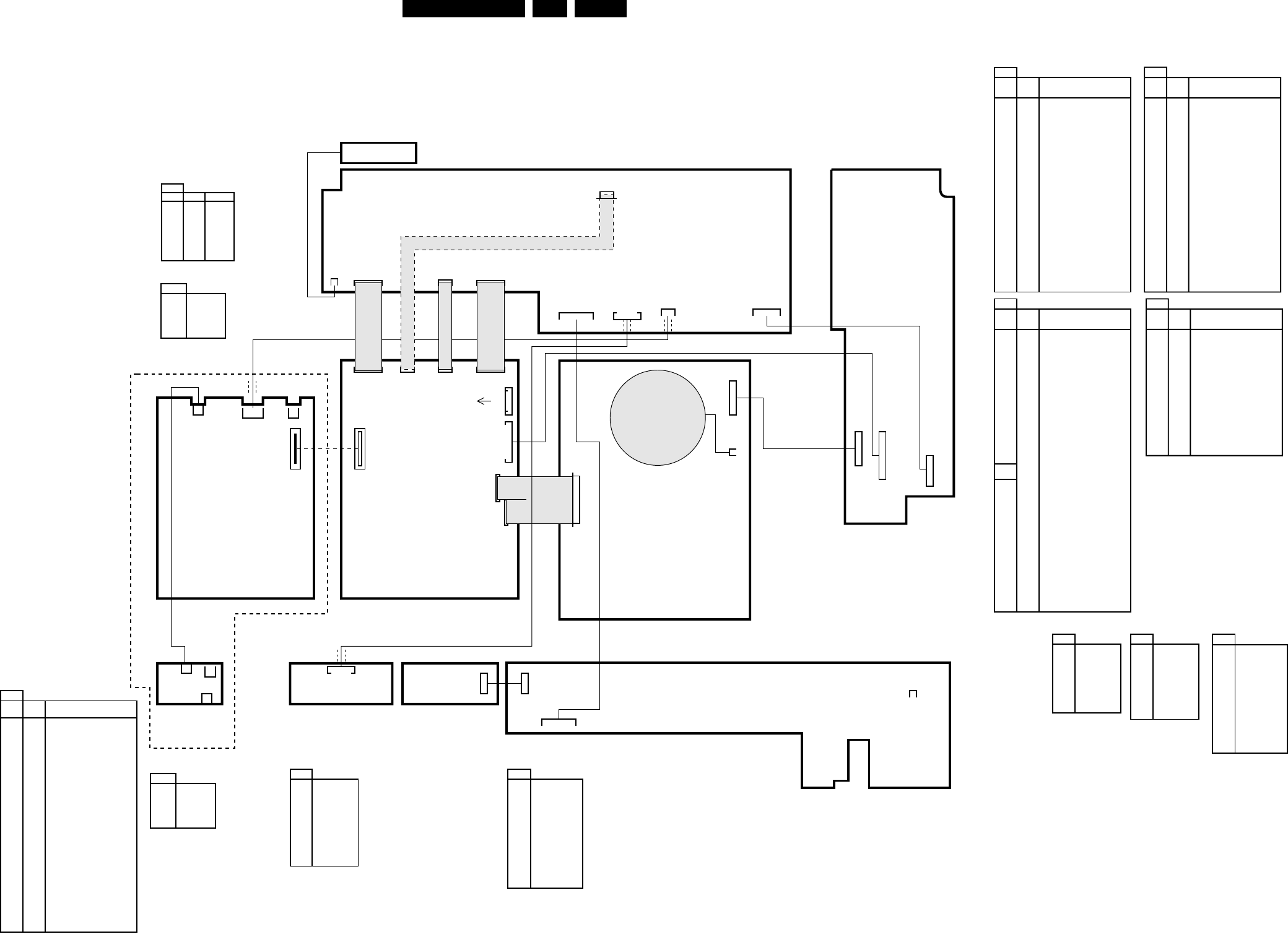
EN 94DVDR980-985 /0X1 6.
Block and Wiring Diagram.
Wiring Diagram
8005
1 AFCRI
2 GNDA
3 AFCLI
4 VBSFIN
5 GNDV
6 8SW
7 CFIN
8 GNDV
9 YFIN
8007
1 +12Vstby
2 +5V2stby
3 -5Nstby
4 -Vgnstby
5 +33Vstby
6FLYB
7 GND
8009
1 +3V3
2 +3V3
3 +3V3
4 +3V3
5 GNDD
6 +12V
7 GNDD
8 GNDD
9 +5V
10 ION(STBY_ctrl
11 GNDD
12 -5V
8011
1 TEMP_SENSE
2 12VSTBY
3 VGNSTBY
4 -GNDD
5 IPOR1
6 SDA
7 GNDD
8 SCL
9 INT
10 RC
11 5STBY
12 5M
8008
1 +3V3
2 +5V
3 GND
4 +4V6E
5 GND
6 -5V
7 GND
8 +12V
8006
1 ANA_R
2 GNDA
3 GNDA
4 ANA_L
8013
1 TPB1-
2 TPB1+
3 TPA1-
4 TPA1+
22
22
22
22
10
12
1981 1953 1960 1932
9
10
1
11
14 71
1
111442
11
712
1
1
60
60
8
12
71
1
1
115
30
15
1
11
11
1602
1201
15011101
1900 1982 1954
1600 1601
SERVICE
INTERFACE
16031900
1501
1500
0207
0209
0205
1101
1100
1402
WIRING DIAGRAM
8001
8004
8002
12
1916
1
1911
91
1984
12
1918
12
12
17
1915
17
1917
ANALOG
FAN
DIGITAL
SERVO
DVIO
FRONT
AV INPUT
FRONT
DV INPUT IR & STBY
DISPLAY
PSU
BOARD
TO
BOARD
14
1001
14
1000
12
1002
18
1000
8003
FAN
8006
8005
8009
8008
8007
8013
71
1800
8015
8011
IEEE WIRE
pH
pH
8001
1602 1900
1 22 GNDD
2 21 SPDIF
3 20 COAX_IN
4 19 OPT_IN
5 18 +5V
6 17 +3V3
7 16 MUTEN
8 15 GNDD
9 14 AD_ACLK
10 13 GNDD
11 12 AD_DATAO
12 11 AD_WCLK
13 10 GNDD
14 9 AD_BCLK
15 8 GNDD
16 7 AD_ACLK
17 6 GNDD
18 5 AD_DATAI
19 4 GNDD
20 3 AE_WCLK
21 2 AE_BCLK
22 1 GNDD
8002
1601 1954
1 22 B_OUT_B
2 21 GNDD
3 20 G_OUT_B
4 19 GNDD
5 18 R_OUT_B
6 17 GNDD
7 16 C_OUT_B
8 15 GNDD
9 14 Y_OUT_B
10 13 GNDD
11 12 CVBS_OUT_B
12 11 GNDD
13 10 GNDD
14 9 CVBS_Y_IN
15 8 GNDD
16 7 C_IN
17 6 GNDD
18 5 Y_IN
19 4 GNDD
20 3 U_IN
21 2 GNDD
22 1 V_IN
8004
1600 1982
1 10 GNDD
29FB
3 8 BE_FAN
4 7 ANA_WE
5 6 ION
6 5 VSM_UART1_RTSn
(D_RDY)
7 4 VSM_UART1_CTSn
(A_RDY)
8 3 VSM_UART1_TX
(D_DATA)
9 2 VSM_UART1_RX
(A_DATA)
10 1 IRESET_DIG
8003
1100 1402
15 1 GNDD
14 2 GNDD
13 3 NC
12 4 GNDD
11 5 BE_DATA_WR
10 6 GNDD
9 7 BE_SYNC
8 8 GNDD
7 9 BE_FLAG
6 10 GNDD
5 11 BE_BCLK
4 12 GNDD
3 13 BE_DATA_RD
2 14 GNDD
1 15 BE_WCLK
1101
15 16 GNDD
14 17 BE_RXD
13 18 GNDD
12 19 BE_TXD
11 20 BE_CPR
10 21 BE_IRQn
9 22 BE_SUR
8 23 BE_V4
7 24 GNDD
6 25 BE_LOAD
5 26 GNDD
4 27 BE_FAN
3 28 RESETn_BE
2 29 GNDD
1 30 GNDD
8015
1800 1962
1 7 GND
26Y
3 5 GND
44Cb
5 3 GND
62Cr
7 1 GND
ONLY FOR NAFTA
ONLY USED FOR DVDR985
pH-pH LF SHIELDED
pH-pH LF SHIELDED
WIRE WRAP
IEEE WIRE
pH
EH
EH
EH
EH
pH
pH
EH
8014
1200 1100
1 24 GND
2 23 YUV_IN(7)
3 22 GND
4 21 YUV_IN(6)
5 20 +3V3
6 19 YUV_IN(5)
7 18 +3V3
8 17 YUV_IN(4)
9 16 +5V
10 15 YUV_IN(3)
11 14 GND
12 13 YUV_IN(2)
13 12 GND
14 11 YUV_IN(1)
15 10 GND
16 9 YUV_IN(0)
17 8 GND
18 7 CLK_27MHZ
19 6 GND
20 5 HS_IN
21 4 FRAME_IN
22 3 SCL
23 2 SDA
24 1 GND
1962
17
CL 26532011_027.eps
170102
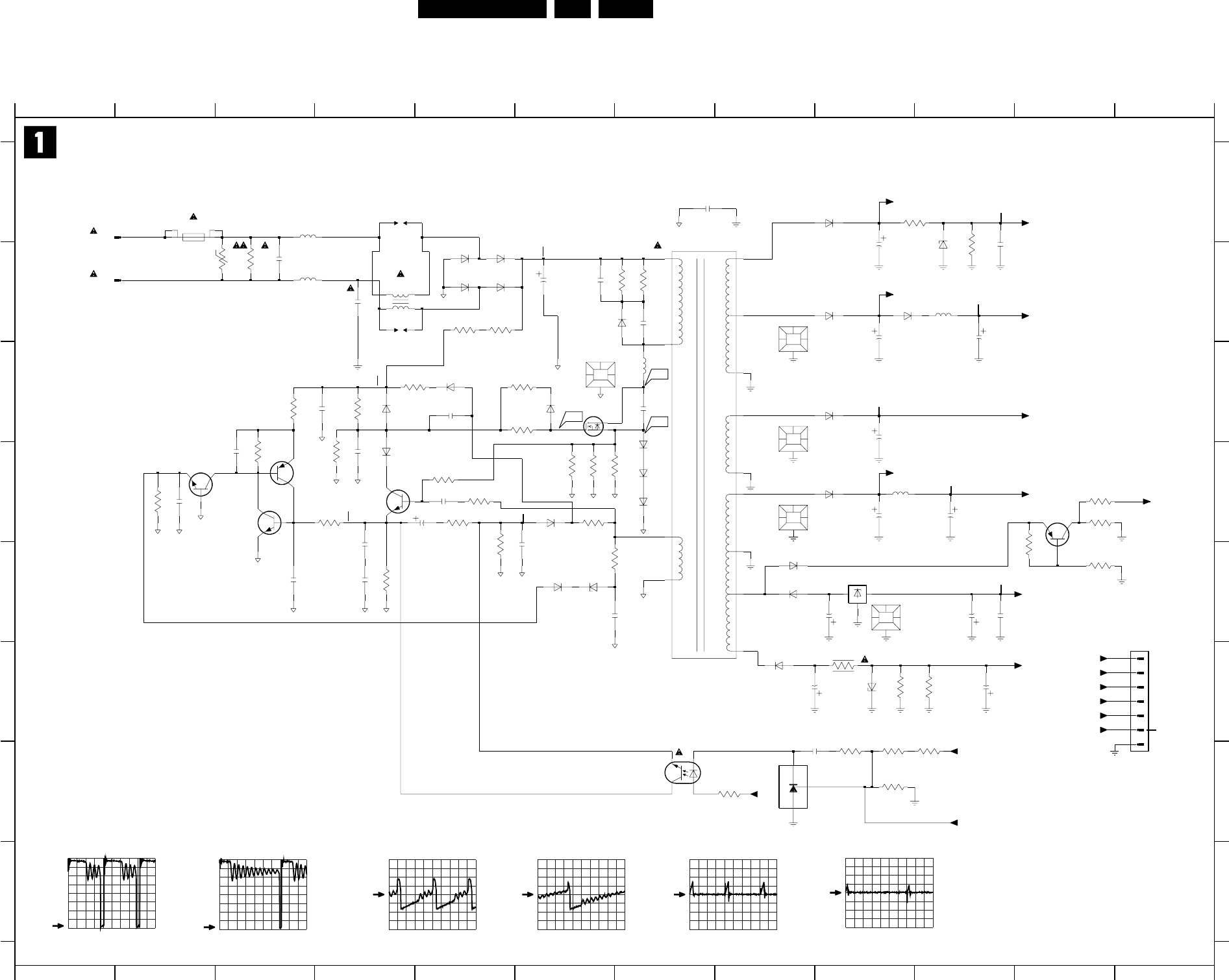
Electrical Diagrams and Print-Layouts EN 95DVDR980-985 /0X1 7.
7. Electrical Diagrams and Print-Layouts
Power Supply
V
1 2 3 4 5 6 7 8 9 10 11 12
1 2 3 4 5 6 7 8 9 10 11 12
A
B
C
D
E
F
G
H
A
B
C
D
E
F
G
H
0101-1 B1
0101-2 A1
0125 C6
0205 F12
0210 C8
0240 D8
0260 D8
0290 E9
1120 A2
1124 A4
1125 B4
2119 B4
2120 B3
2125 B6
2126 B6
2127 A4
2129 B6
2130 B7
2131 A7
2136 C7
2139 D3
2140 C4
2141 D4
2142 D2
2143 E3
2144 E4
2145 E4
2146 C5
2147 D5
2151 E5
2152 E7
2153 D5
2200 B9
2201 B10
2210 B9
2211 B10
2212 B9
2214 C9
2215 C9
2220 E9
2221 E10
2222 E10
2223 E10
2230 F9
2235 F10
2240 D9
2241 D10
2242 D9
2251 G9
3120 B3
3122 B3
3123 B2
3125 B5
3126 B5
3127 B7
3128 B7
3129 A5
3131 C6
3132 C6
3133 D6
3134 D6
3135 D6
3139 D4
3140 C5
3141 C4
3142 C3
3143 D3
3144 D2
3145 D4
3146 D5
3147 D5
3148 E5
3149 E7
3150 D6
3151 E4
3152 D5
3200 A10
3201 B10
3220 E11
3221 E11
3222 D11
3223 D11
3230 F9
3233 F9
3234 F10
3250 G8
3253 G9
3254 G10
3255 G9
3256 G9
5110 A3
5115 B3
5120 B4
5121 B4
5125 C7
5131 B7
5210 B10
5240 D9
6125 B7
6128 A4
6129 A5
6130 D7
6131 D7
6132 D7
6140 C5
6141 D4
6142 D6
6143 E6
6144 E6
6145 C4
6146 C6
6151 B5
6152 B5
6153 B5
6154 B5
6200 A9
6201 B10
6210 B9
6211 B9
6215 C9
6220 E8
6221 E8
6230 F8
6231 F9
6240 D9
7125 C6
7140 D4
7141 D3
7142 D2
7143 D3
7200 G7
7220 E9
7241 D11
7251 G8
9110 A3
9115 B3
1000u
2240
100n
2139
680u
2210
470n
2145
100u
2230
100n
2223
470n
2144
100n
2151
100n
2201
2140
100n
3140
2K7
3141
22K
+5Vstby
3152
22K
+33Vstby
FLYB
6
7
+12Vstby
-5Nstby
-Vgnstby
0205 EH-B
1
2
3
4
5
2141
470p
470p
2146
1R5
3134
3135
1R5
3133
1R5
STP5NB60FP
7125
BAS216
6146
3253
BAS216
6141 6145
BAS216
2251
22n 47K
2214
2m2
330u
2235
BYV27-200
6220
+33Vctrl
+12Vreg
+33Vstby
2125
68u
1125
5120
12
43
3234
10K
UF1922P4
100K
3139
0260
MECHPART
7
8
6211
1N4004
5131
10
11
12
13
14
15
16
17
18
2
4CT286D8
1124
0240
Heatsink
Heatsink
0290
0210
Heatsink
FLYB
100R
3146
0125
MECHPART
3223
4K7
22K
3221
7241
BC857B
4K7
3222
220R
3142
3201
33K
2K2
3220
6201
BZX79-C33
2K7
3200
+12Vstby
47u
2200
100u
2211
5210
10u
BYW29EX
6210
6200
BYD33J
+3V9
-5Nstby
6215
STPS745FP
IN
2
OUT
3
100u
2221
7220
L7905
GND
1
220u
2220
-Vgnstby
6221
BAV21
10K
3233
47R
3230
BZX79-C33
6231
BYD33J
6230
Prot_3V3
+5Vstby
Vreg
+12Vreg
Vreg
100u
2241
1u
5240
6240
BYW29EX
2
1
3
4K7
3256
7251
TL431CZ
4K7
3255
470R
3250
470R
3254
7200
TCET1102
2131
1n
BZX284-B15
6144
330p
2152
BAV21
6143
68R
3150
2K2
3149
68p 6142
BAV21
3148
2K2
2153
2147
10u 2K2
3147
100K
3151
100n
2143
22K
3145
3144
1K
220p
2142
7143
BC847B
7142
BC847B
1K
3143
BC857B
7141
6140
BAV21
BC847B
7140
3132
47R
47R
3131
83R
5125
220p
2136
1N4004
61316132
1N4004 6125
BYD33J
6130
1N4004 47p
2130 3128
220K
10n
2129
220K
3127
1M
31253126
1M
6154
1N40061N4006
6152
6153
1N4006
6151
1N4006
2u2
5110
2u2
5115
220n
2120
3120
1n
2119
680K
3122
1
HSC0528
0101-2
2
1120
VALUE
HSC0528
0101-1
Vdrain (no disc loaded)
50V/div DC 5us/div
Vdrain (standby)
50V/div DC 5us/div
Vgate (no disc loaded)
10V/div DC 5us/div
Vgate(standby)
10V/div DC 5us/div
Vsource (no disc loaded)
500mV/div DC 5us/div
Vsource(standby)
500mV/div DC 5us/div
Vd
Vs
Vg
300V
30V
(20V)
-0.07V
(-0.3V)
-13V
+33V
(.....V) MEASURED IN STANDBY
+12V
+3.9V
+5V
-5V
+4.4V
(+1.7V)
CL 16532095_024.eps
080801
POWER SUPPLY
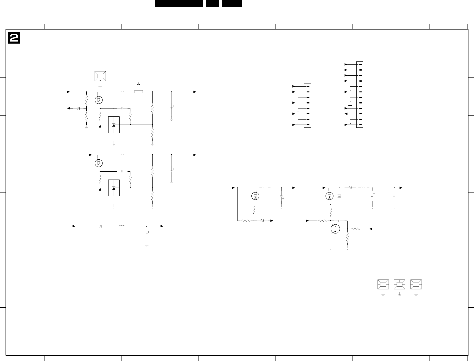
EN 96DVDR980-985 /0X1 7.
Electrical Diagrams and Print-Layouts
Power Supply
IRLML2502
IRLML2502
IRLML2502
1 2 3 4 5 6 7 8 9 10 11 12
1 2 3 4 5 6 7 8 9 10 11 12
A
B
C
D
E
F
G
H
A
B
C
D
E
F
G
H
0200 G10
0201 G11
0202 G11
0207 B8
0209 A10
0221 B3
1520 B4
2501 D4
2502 D5
2506 F4
2511 E9
2512 E10
2513 E11
2515 E8
2520 B4
2521 B5
3501 D3
3502 D4
3503 D4
3504 E4
3511 E9
3512 E9
3513 F9
3514 E10
3515 E7
3516 E7
3520 B3
3521 C3
3522 C3
3523 C4
3524 C4
3525 B4
5501 C4
5505 E4
5511 D10
5515 D7
5520 B4
6505 E3
6511 E9
6512 D9
6515 E7
6520 B2
7501 D3
7502 E3
7511 E9
7512 E9
7515 D7
7520 B3
7521 C3
BZX284-C8V2
6511
02020200 0201
+4V6 6515
BZX79-C6V8
680R
3503
+33Vctrl
+4V6
3523
680R
2520
22n
22n
2501
3516
10K
BAS216
6520
2513
100n
6505
BYV10-40
MP
1520
3A15
6512
1N4004
0221
MECHPART
+3V3
+3V3
+5V
-5V
+12V
+5V
STBY_ctrl
-5V
+3V3
+3V3
+3V3
+12V
1
2
3
4
5
6
7
8
+3V3
12
2
3
4
5
6
7
8
9
EH-B
0207
+12V
-5V
EH-B
0209
1
10
11
10K
-5Nstby
2515
100u
3515
7515
10u
5515
STBY_ctrl
+12Vreg +12V
3513
47K
7512
BC847B 3514
10K
10K
3511
100n
2511
4K7
3512
5511
10u
100u
2512
7511
+5V 10u
5505
2506
100u
100u
2502
+5V
3502
4K7
1
3
4K7
3504
+12V
7502
TL431CZ
2
5501
2u2
3501
2K2
+5Vstby
Prot_3V3
7501
510R
3520
1K
3521
2521
100u
3524
4K7 1K5
3525
TL431CZ
7521
2
1
3
+12V
2u2
5520
2K2
3522
+3V9
7520
STP16NE06
POWER SUPPLY
CL 16532095_025.eps
080801
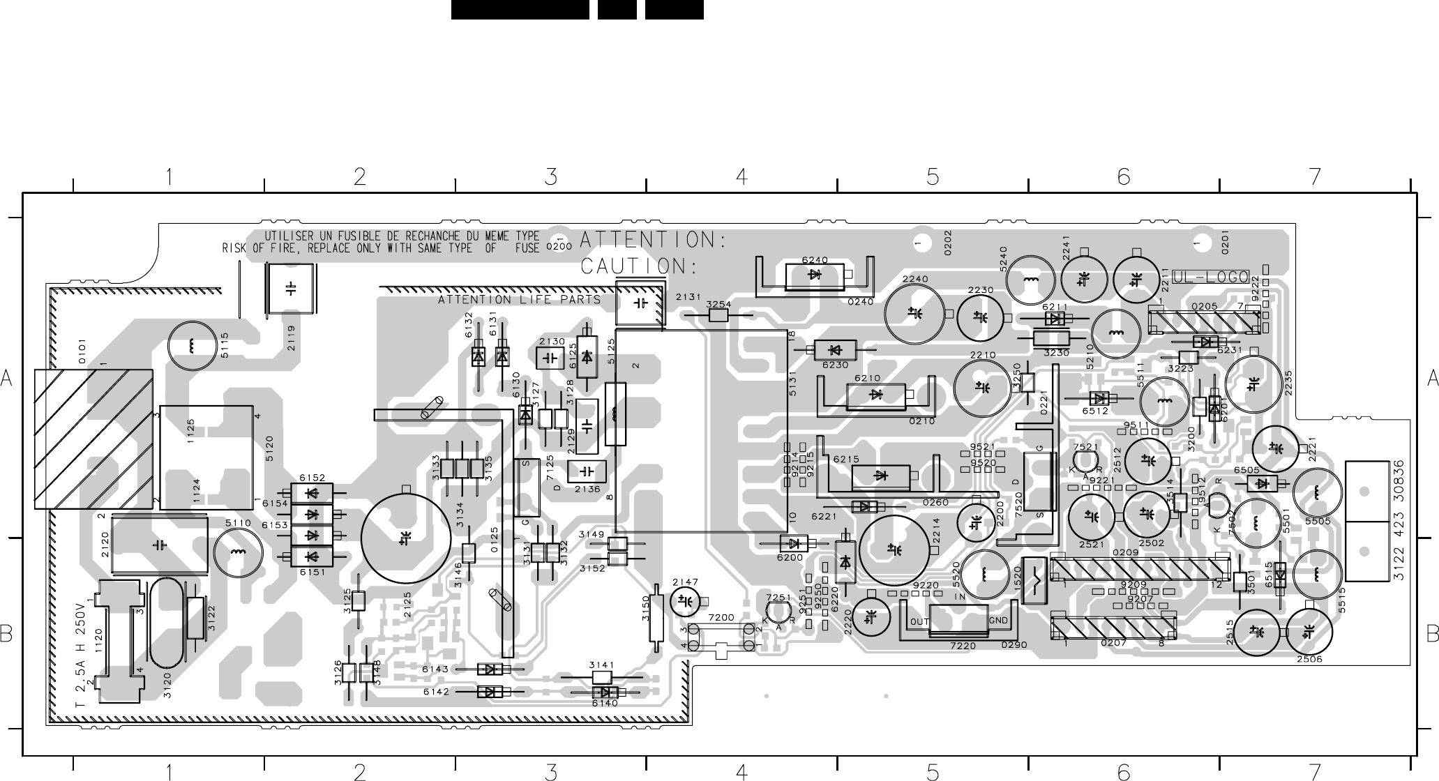
Electrical Diagrams and Print-Layouts EN 97DVDR980-985 /0X1 7.
Layout Power Supply (Top View)
CL 16532095_048.eps
100801
0101A1
0125B3
0200A3
0201A7
0202A5
0205A6
0207B6
0209B6
0210A5
0221A6
0240A5
0260A5
0290B5
1120B1
1520B5
2119A2
2120B1
2125B2
2126B2
2127B1
2129A3
2130A3
2131A4
2136A3
2147B4
2200A5
2210A5
2211A6
2212A5
2214A5
2215A5
2220B5
2221A7
2230A5
2235A7
2240A5
2241A6
2242A4
2502B6
2506B7
2512A6
2515B7
2521B6
3120B1
3122B1
3123A1
3125B2
3126B2
3127A3
3128A3
3129B2
3131B3
3132B3
3133A2
3134A3
3135A3
3141B3
3146B3
3148B2
3149A3
3150B3
3152B3
3200A6
3223A6
3230A6
3250A5
3254A4
3501B7
3514A6
5110A1
5115A1
5120A2
5121A1
5125A3
5131A4
5210A6
5240A5
5501A7
5505A7
5511A6
5515B7
5520B5
6125A3
6128B1
6129B1
6130A3
6131A3
6132A3
6140B3
6142B2
6143B2
6151B2
6152A2
6153A2
6154A2
6200B4
6201A7
6210A5
6211A6
6215A5
6220B4
6221A4
6230A4
6231A7
6240A4
6505A7
6512A6
6515B7
7125A3
7200B4
7220B5
7251B4
7502A7
7520A5
7521A6
9110B1
9115A1
9207B6
9209B6
9214A4
9215A4
9220B5
9221A6
9222A7
9250B4
9251B4
9511A6
9512A6
9520A5
9521A5
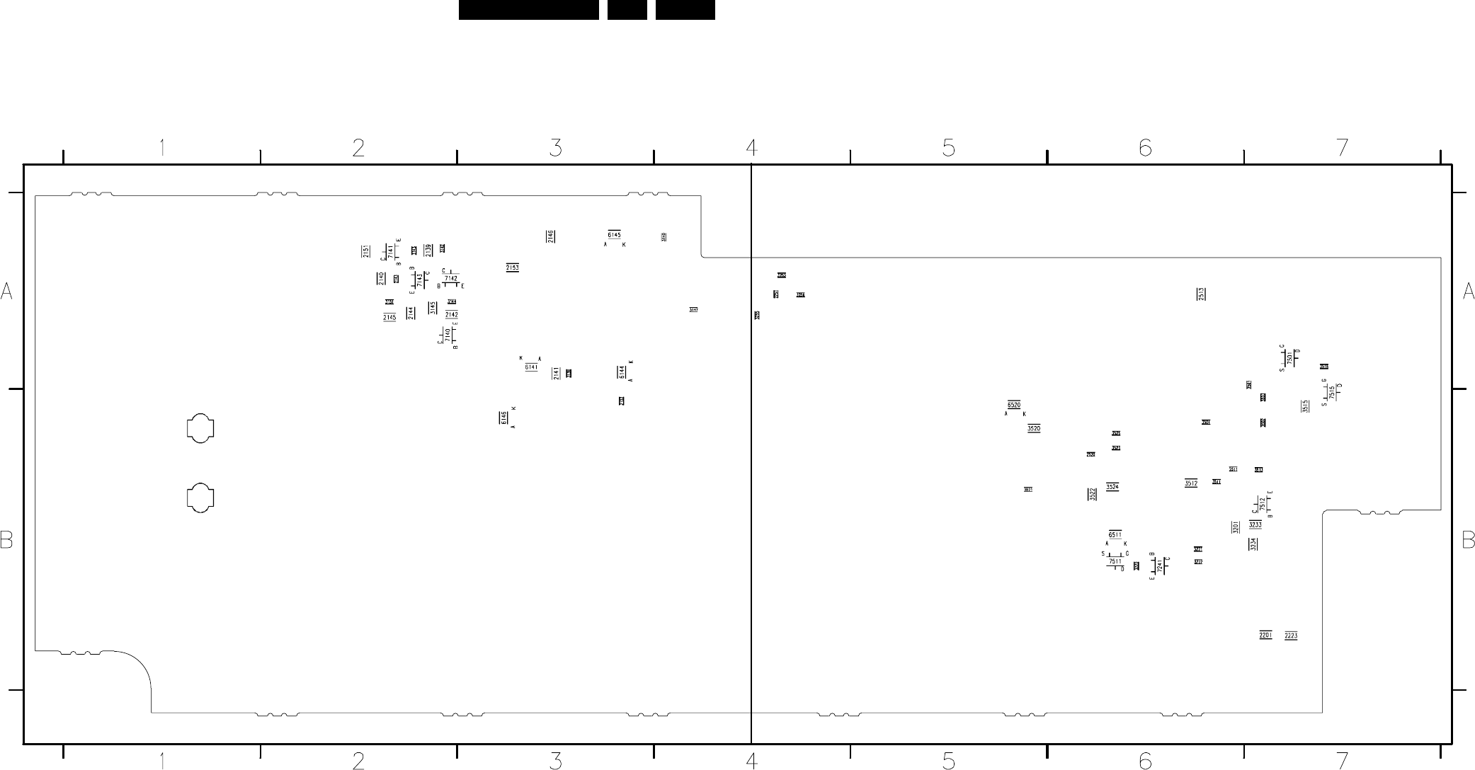
EN 98DVDR980-985 /0X1 7.
Electrical Diagrams and Print-Layouts
Layout Power Supply (Overview Bottom View)
CL 16532095_049.eps
100801
2139 A2
2140 A2
2141 A3
2142 A2
2143 A2
2144 A2
2145 A2
2146 A3
2151 A2
2152 B3
2153 A3
2201 B7
2222 A5
2223 B7
2251 A4
2501 A7
2511 B6
2513 A6
2520 B6
3139 A3
3140 A4
3142 A2
3143 A2
3144 A2
3145 A2
3147 A4
3151 A2
3201 B6
3220 B6
3221 B6
3222 B6
3233 B7
3234 B7
3253 A4
3255 A4
3256 A4
3502 B7
3503 B7
3504 B6
3511 B6
3512 B6
3513 B7
3515 B7
3516 A7
3520 B5
3521 B5
3522 B6
3523 B6
3524 B6
3525 B6
6141 A3
6144 A3
6145 A3
6146 B3
6511 B6
6520 B5
7140 A2
7141 A2
7142 A2
7143 A2
7241 B6
7501 A7
7511 B6
7512 B7
7515 B7
PART 1
CL 16532095_49a.eps
PART 2
CL 16532095_49b.eps
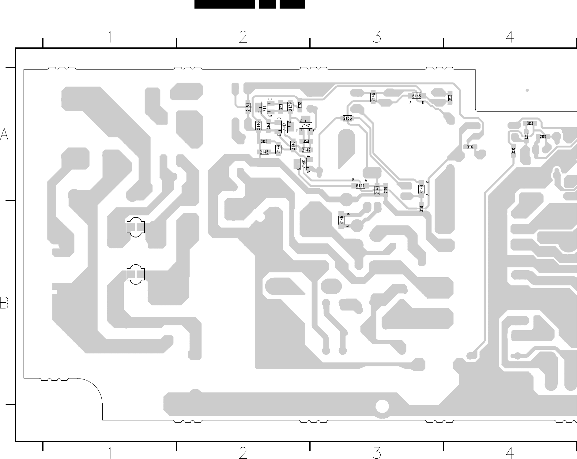
Electrical Diagrams and Print-Layouts EN 99DVDR980-985 /0X1 7.
Layout Power Supply (Part 1 Bottom View)
CL 16532095_49a.eps
100801
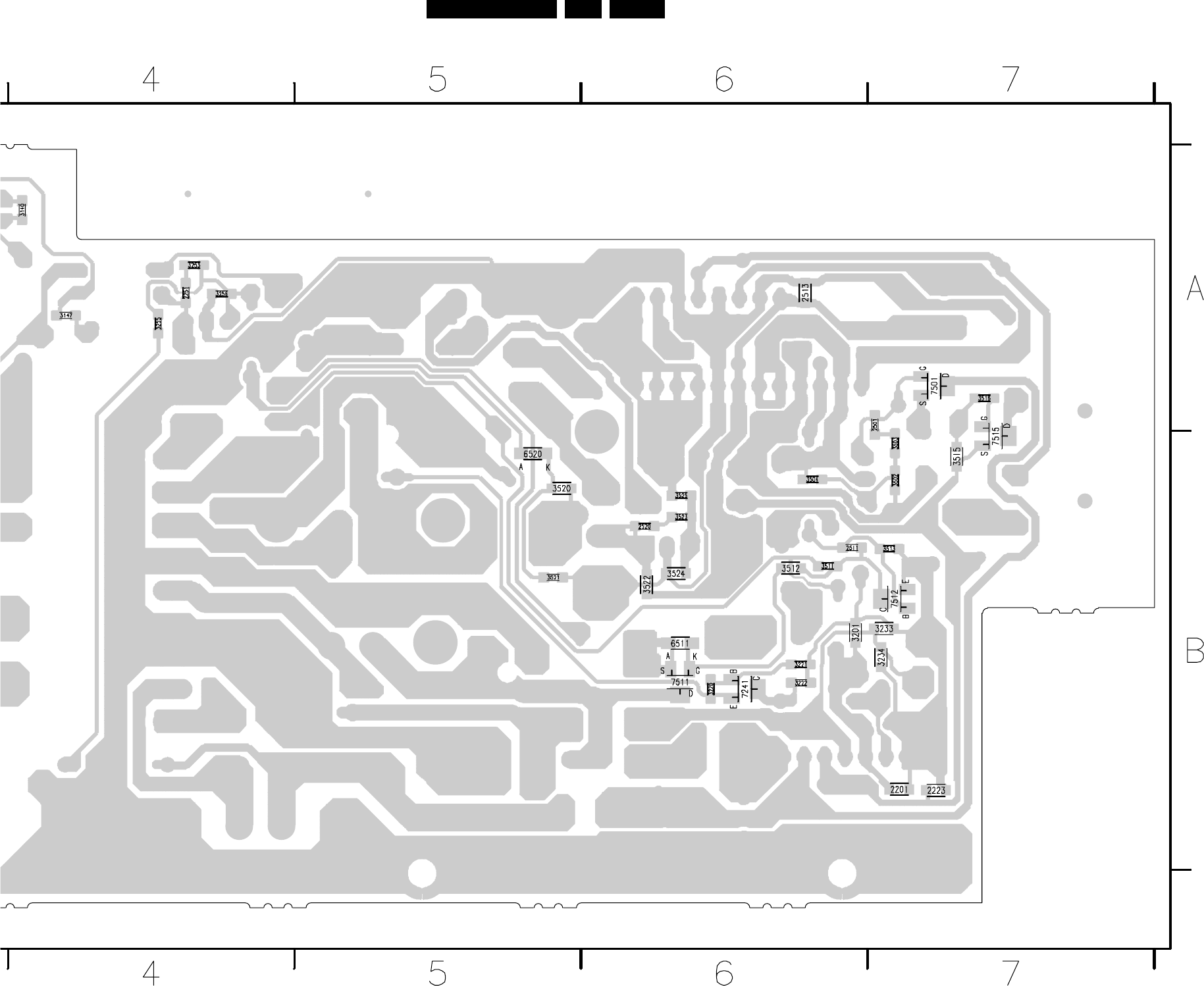
EN 100DVDR980-985 /0X1 7.
Electrical Diagrams and Print-Layouts
Layout Power Supply (Part 2 Bottom View)
CL 16532095_49b.eps
100801
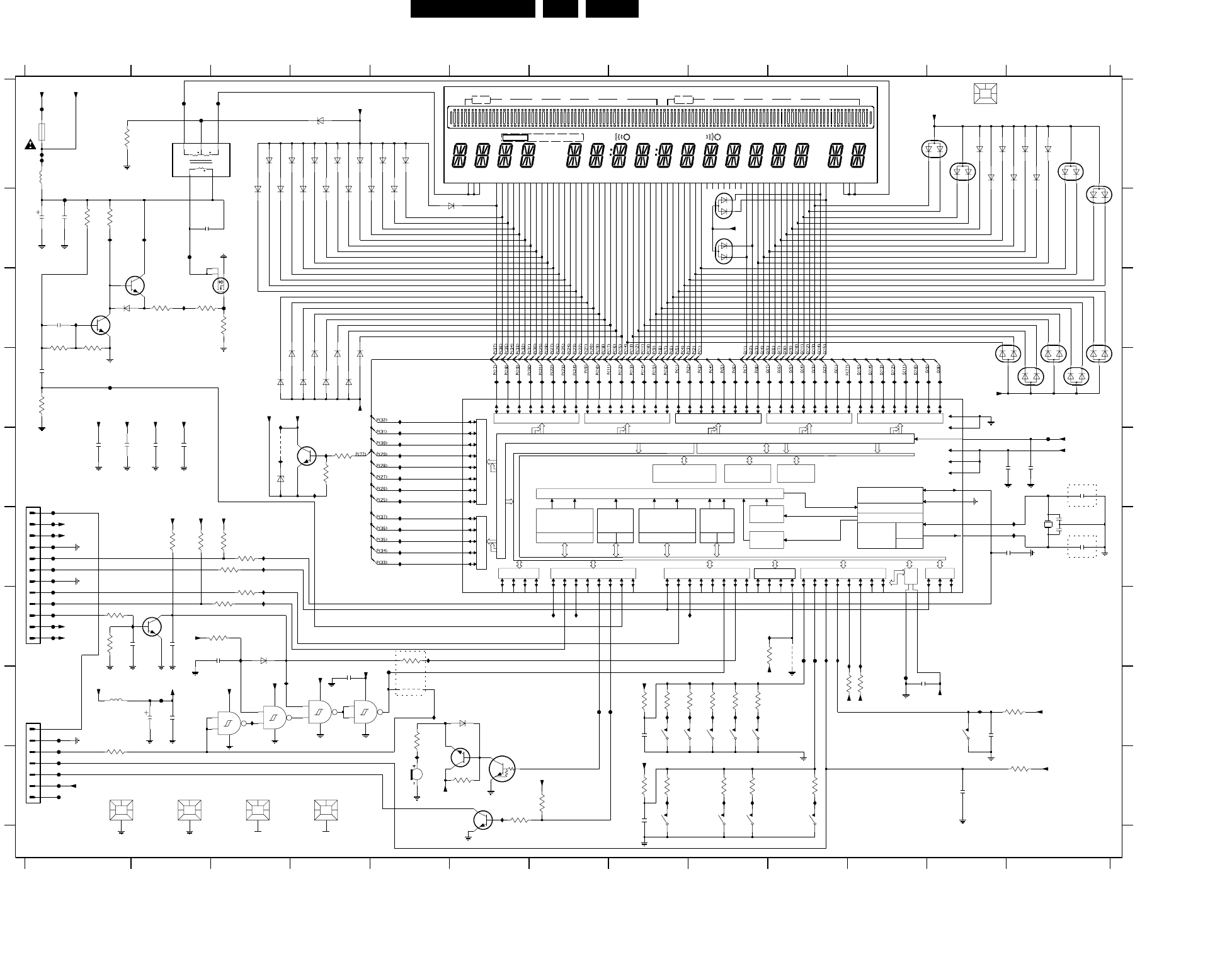
Electrical Diagrams and Print-Layouts EN 101DVDR980-985 /0X1 7.
Display Panel
CHAPTERTRACKREMAIN TIME TRACK TITLEVPS/PDC CHANNEL
DVD+RWSAVCDHQSPL:PMONITORSATTIMERRECORDDECODER
403020100OVER
AM
PM
PROLOGIC
403020100OVER
MPEGAC-3DTSPCMMANUALDIGITALNICAMSTEREOSAPIII
TOTAL
PD
EXPANSION
TIMER/
COUNTER 1
ETC1
I2C BUS
INTERFACES
SERIAL
SIO0/1
P3 P0 P2
8-BIT
A/D
CONV
TC4
P4P5
TIME BASE
INTERRUPT CONTROLLER
TC2
SIO3
TIMER
CLOCK
DATA MEMORY
P6
GENERATOR
P8P9
P1
VFT DRIVE CIRCUIT
SYSTEM CONTROLLER
STANDBY CONTROLLER
TIMING GENERATOR
HIGH FR
LOW FR
TLCS-870/X
CPURAM
PROGRAM MEMORY
ROM
WATCHDOG
TIMER
16-BIT
TIMER/
COUNTERS
TC1
8-BIT
TIMER/
COUNTER
PF PE
P7
<<
F118 F1
F117 F1
NC* NC* NC* NC*
MONITOR
RECORD
STOP
PLAY
CHANNEL
REC VOLUME
AUTO-MAN
F131 H1
F130 H2
F129 H5
F128 G1
F127 G1
F126 G1
temp_sensor
IPOR1
SDA
SCL
INT
RC
temp_sense
IRR
Key in
stbyled
NC
7150 A5
6198 H6
CHANNEL
REC VOLUME
<
<
REC VOLUME
OPEN/CLOSE
Hz
7166 I6
7165 H6
7164 I6
7160-D H3
7160-C H3
7160-B H4
F114 G10
F113 G10
F112 F1
F111 E13
F110 D1
F109 C3
F108 B2
F107 B1
F106 A1
F105 A1
F125 G1
F124 G1
F123 F1
F122 H7
F121 H7
F120 F1
F119 F1
6167 A13
6166 A12
F116 H11
F115 F1
F136 I1
F135 I1
F134 I1
F133 I1
F132 I1
6180 D4
6179 D4
6178 D4
6177 D4
6176 D4
6175 D4
6195 B5
6194 A5
6193 B4
6192 A4
6191 B4
6190 A4
6189 B4
6188 A4
6187 B4
6186 A3
7160-A H4
7157 G2
7156 D12
7155 E4
7153 C2
7152 C2
7151 C1
3178 I9
3177 I9
6197 B6
6196 A5
F104 A1
F103 A2
F102 A2
F101 A3
9100 E3
4100 G10
3197 I10
3194 I13
3193 F2
3192 I1
3190 H8
6161 A12
6160 A11
6159 A13
6158 A13
6157 A13
6156 G3
6155 A13
6154 E3
6152 B9
6151 C1
6174 C13
6173 D13
6172 C13
6171 D13
6170 D12
6169 B9
6168 A13
2179 H12
2177 I12
6165 A12
6164 A12
6185 B3
6184 A3
6183 B3
6182 D3
6181 D3
3157 C3
3156 I7
3155 B1
3154 F3
3153 C2
3152 A1
3172 G1
3171 I8
3170 G5
3169 F2
3168 G3
3167 G3
3166 F3
3165 I6
3164 F3
3163 D1
3189 H8
3188 H9
3187 H9
3186 H9
3183 H8
3182 H5
3180 I8
1163 H12
1162 I8
3174 G3
3173 G1
6150 A4
5153 A2
5151 A1
5150 H1
4151 H5
2155 B1
2154 B1
2152 B2
2151 H2
2150 H2
1917 H1
2173 H8
2171 G3
2170 I8
2169 H4
2168 G1
2167 G2
2165 F13
2163 F13
2162 E13
2161 E2
3151 I6
3150 C1
3148 G9
3147 H11
3146 H10
3145 H13
2180 C1
11
G
2175 H11
2174 E2
3162 E4
3161 E4
3160 C2
3159 C1
3158 B1
I
H H
G
F
E
D
1156 I5
1153 F13
1150 A1
0206 A12
0204 I4
0203 I3
0202 I2
0201 I1
I
1916 E1
1174 I10
1171 H8
1170 H8
1169 H9
1168 H9
1167 H9
1160 I9
1159 I9
2160 E1
2159 E13
2158 E12
2157 D1
2156 E1
543 1312111098
4321 1098765
B
A
1312
F
E
D
C C
B
A
21 76
1
OPTION
OPTION
OPTION
5R6
3153 3160
5R6
22K
3158
I102
GNDD
2K2
3155
2152
47n
F107
GNDD
I101
GNDD
I100
F104
F106
F105
100n
2155
330u
2154
GNDD
PSC
250mA
1150
100n
2161
GNDDGNDD
1
10
11
12
2
3
4
5
6
7
8
9
47u
2150
1916
PH-B
100n
2151
64 6768 69789
F130
4950 5152 5354 5556 5758 59660 6162 6333 3435 36 37 3839 40 4142 43 444546 47 48192 2021222324252627282933031 32
7150
BJ801GNK
1 101112131415161718
1174
1168
1170
1167
1169
1171
12M
CST
1153
15p
2162
2163
15p
GNDD
I155
1162
I156
1159
BC847BW
7153
1160
7151
BC847BW
7157
BC847BW
BC847BW
7155
GNDD
3173
10K
GNDD
1u
2175
10n
2177
F116
GNDD
2179
10n
2165
10n
GNDD
GNDD
470p
2167
GNDD
100p
2168
2170
10n
220n
2171
2174
100n
10n
2173
10n
2157
100n
2158
GNDD
100n
2159
GNDD
100n
2156
F111
2K2
2160
100n
GNDD
3178
2K2
3183
I168
3187
2K2
GNDD GNDD
I187
GNDD
I191
I185
I188
I179
10K
3169
I180
3180
10K
10K
3189
3193
10K
I166
GNDD
I167
2180
100n
GNDD
1163
3145
3146
10K
10K
3147
10K
68K
3161
3163
10K
22K
3152
10K
3154
3164
I401
3156
10K
I170
10K
3177
1K
F132
1K
3186
3192
1K
F131
F133
F134
F135 2K2
3194
F136
5K6
3159
I103
1K
3151
I178
3150
5K6
I177
I176
3171
3148
2K2
F120
2K2
F117
F124
F112
GNDD
F115
68K
3162
I158
GNDD
F127 I174
F128
F123
F126
F125
F119
47K
3157
F118
GNDD
100R
3168
270R
3166
3167
270R I173
I171
I172
I152
6182
1N4148
1N4148
6175
BAW56W
6170
6171
BAW56W
BAW56W
6172
BAW56W
6173
6154
BZX384-C2V7
6174
BAW56W
BAW56W
6152
6169
BAW56W
F103
BAW56W
6160
BAW56W
6168
6161
BAW56W
6155
BAW56W
3197
4K7
1K5
3182
47K
3190
4100
BZX284-C6V8
GNDD
4151
I154
6150
I148
4M7
3174
4K7
3172
3165
2K2
4K7
3188
I199
7
7160-C
HEF4093BT
8
9
10
14
7
HEF4093BT
7160-B
5
6
4
14
6165
1N4148
1N4148
6166
1N4148
6157
6167
1N4148
6197
1N4148
6158
1N4148
F109
7152
STN3NE06
6187
1N4148
1N4148
6194
1N4148
6188
1N4148
6196
6195
1N4148
6189
1N4148
1N4148
6164
1N4148
6159
6183
1N4148
1N4148
6190
1N4148
6184
1N4148
6192
6191
1N4148
6185
1N4148
6193
1N4148
1N4148
6186
6176
1N4148
1N4148
6177
1N4148
6179
6178
1N4148
1N4148
6181
6180
1N4148
F101
I125
I124
I123
I198
10n
2169
I400
7166
BC847BW
BC847BW
7164
F102
GNDD
GNDD
GNDD
7160-A
HEF4093BT
1
2
3
14
7
GNDD GNDD
F108
GNDD
GNDD GNDD
77165
PDTC124EU
GNDD
HEF4093BT
7160-D
12
13
11
14
I130
I128
I132
I135
I133
I131
I134
I136
I110
I137
I138
I111
I107
I106
I109
I104
I108
I126
I105
I122
I127
I121
I120
I119
I116
I118
I117
I113
I115
I114
I197
I112
I184
F121
F114
F122
F113
I165
I164
I159
GNDD GNDD
10u
5151
I157
I162
I160
I161
MCL4148
6198
I143
6151
MCL4148
MCL4148
6156
F110
I141
I139
I142
I140
I144
I145
I146
I151
I147
I153
I150
I129
0204
EARTH SPRING
GNDD
EARTH SPRING
0203
GNDD GND_FC GND_FC
I149
0202
EARTH SPRING
I404
GNDD
GNDD
I406I403
89
XOUT 91
0206
DISPLAY HOLDER
GNDD
81
82
PF0
83
PF1
84
PF2
85
PF3
86
PF4
RESET_ 92
TEST 95
31
VAREF
VASS
30
VDD1 88
32VDD2
VDD3 51
VKK 87
29VSS1
90VSS2
XIN
6566
PD0
67
PD1
68
PD2
69
PD3
70
PD4
71
PD5
72
PD6
73
PD7
PE0
74
PE1
75
PE2
76
PE3
77
PE4
78
PE5
79
80
PE6
PE7
48
P80
49
P81
50
P82
52
P83
53
P84
54
P85
55
P86
56
P87
57
P90
58
P91
59
P92
60
P93
61
P94
62
P95
63 64
P96
P97
28
P60
33
P61
34
P62
35
P63
36
P64
37
P65
38
P66
39
P67
40
P70
41
P71
42
P72
43
P73
44
P74
45
P75
46 47
P76
P77
94
P30
13
P31
14
P32
15
P33
16
P40
17
P41
18
P42
19
P43
20
P44
21
P45
22
P46
23
P47
24
P50
25
P51
26
P52
27
P53
99
P03
100
P04
1
P05
23
P06
P07
4
P10
5
P11
6
P12
7
P13
8
P14
9
P15
10
P16
11
P17
12
P20
96
P21
93
P22
TMP88CU77F
7156
P00
97
P01
98
P02
F129
I175
5153
1
3
4
5
6
I402
4
5
6
7
5150
10u
S16977-03
CABLE TREE
1917
1
2
3
9100
1156
3170
1K
GNDD
EARTH SPRING
0201
GNDD
5STBY1
{P(37:0),G(15:0),P(77)}
5STBY
12STBYSI
5STBY1
5STBY
VGNSTBY1
VGNSTBY
12STBY
5STBY
VGNSTBY
5STBY
5STBY
5STBY 5STBY
12STBYSI
VGNSTBY1
VGNSTBY1
VGNSTBY1 VGNSTBY1
VGNSTBY1
12STBY
5STBY
VGNSTBY 5M 5STBY 12STBY
VGNSTBY1
5STBY
5STBY
5STBY
5STBY 5STBY
5STBY
5STBY
5STBY
5STBY
5STBY
5STBY
5M
5STBY
CL 26532011_004.eps
150102
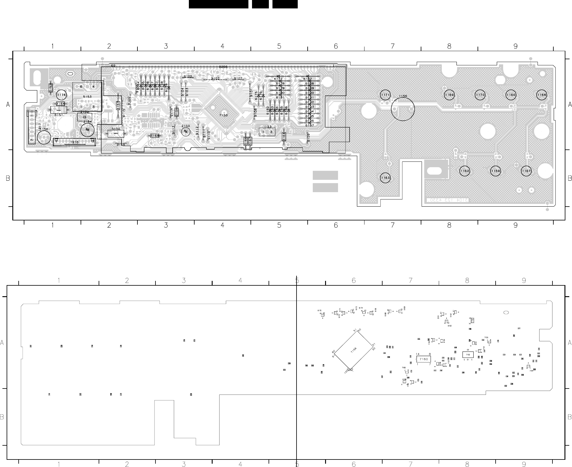
EN 102DVDR980-985 /0X1 7.
Electrical Diagrams and Print-Layouts
Layout Display Panel (Top View)
Layout Display Panel (Overview Bottom View)
0206 A4
1140 B2
1150 A1
1153 A5
1156 A7
1159 B9
1160 A9
1162 B8
1163 B7
1167 B9
1168 A9
1169 A8
1170 A9
1171 A7
1174 A1
1910 B4
1911 B4
1915 B1
1916 A1
1917 A1
2140 B1
2150 A3
2152 A2
2154 A2
9102 A4
9103 A3
9104 A3
9105 A3
9106 A2
9107 A4
9108 A5
9109 A6
9110 A4
9111 A4
9112 A4
9113 A3
9114 A3
9115 A2
9116 A2
9151 B3
3110 B4
3135 B1
3152 A1
3154 A1
3156 A3
3157 A2
3164 A5
3166 A4
3167 A4
3168 A3
5150 A2
5151 A1
5153 A2
6140 B2
6157 A3
6158 A3
6159 A3
6164 A3
6165 A3
6166 A3
6167 A3
6175 A5
6176 A5
6177 A5
6178 A5
6179 A5
6180 A5
6181 A5
6182 A5
6183 A5
6184 A5
6185 A5
6186 A5
6187 A5
6188 A6
6189 A6
6190 A6
6191 A6
6192 A6
6193 A6
6194 A6
6195 A6
6196 A6
6197 A6
7140 B1
7150 A4
9100 A2
9101 A5
CL 26532011_007.eps
170102
2100 B6
2101 B7
2102 B7
2103 B7
2104 B7
2105 B7
2106 B5
2151 A7
2155 A8
2156 A9
2157 A8
2158 A5
2159 A5
2160 A8
2161 A9
2162 A5
2163 A5
2165 A5
2167 A8
2168 A8
2169 A7
2170 B2
2171 A8
2173 A3
2174 A9
2175 A7
2177 A9
2179 B3
6198 A7
7100 B7
7101 B6
7141 B8
7142 B8
7143 B8
7144 B8
7145 B8
7151 A8
7152 A8
7153 A8
7155 A7
7156 A6
7157 A8
7160 A7
7164 A9
7165 A7
7166 A7
2180 A8
3100 B7
3101 B7
3102 B7
3103 B7
3104 B7
3105 B7
3106 B7
3107 B7
3108 B7
3109 B7
3111 B6
3112 B6
3113 B5
3136 B8
3137 B8
3138 B8
3139 B8
3140 B9
3141 B8
3142 B8
3143 B8
3144 B8
3145 A9
3146 A7
3147 A7
3148 A7
3149 B9
3150 A8
3151 A9
3153 A8
3155 A9
3158 A8
3159 A8
3160 A8
3161 A7
3162 A7
3163 A8
3165 A7
3169 A8
3170 A7
3171 A9
3172 A8
3173 A8
3174 A8
3177 B1
3178 A1
3180 B2
3182 A4
3183 A9
3186 B1
3187 A1
3188 A2
3189 A1
3190 A3
3192 A9
3193 A8
3194 A9
3197 A9
3999 B9
4100 A7
4101 B7
4102 B7
4103 A9
4104 A9
4105 A9
4106 A9
4107 A9
4108 A8
4109 A8
4113 A7
4114 A6
4115 A5
4116 A7
4110 A8
4111 A8
4112 A7
4117 A9
4118 A9
4119 A9
4120 A9
4121 A9
4122 A9
4151 A7
4300 B9
6100 B7
6101 B6
6102 B6
6103 B6
6104 B6
6150 A8
6151 A8
6152 A8
6154 A8
6155 A6
6156 A8
6160 A8
6161 A7
6168 A7
6169 A7
6170 A5
6171 A6
6172 A6
6173 A6
6174 A6
CL 26532011_008.eps
170102
Part 1
CL 26532011_08a.eps
Part 2
CL 26532011_08b.eps
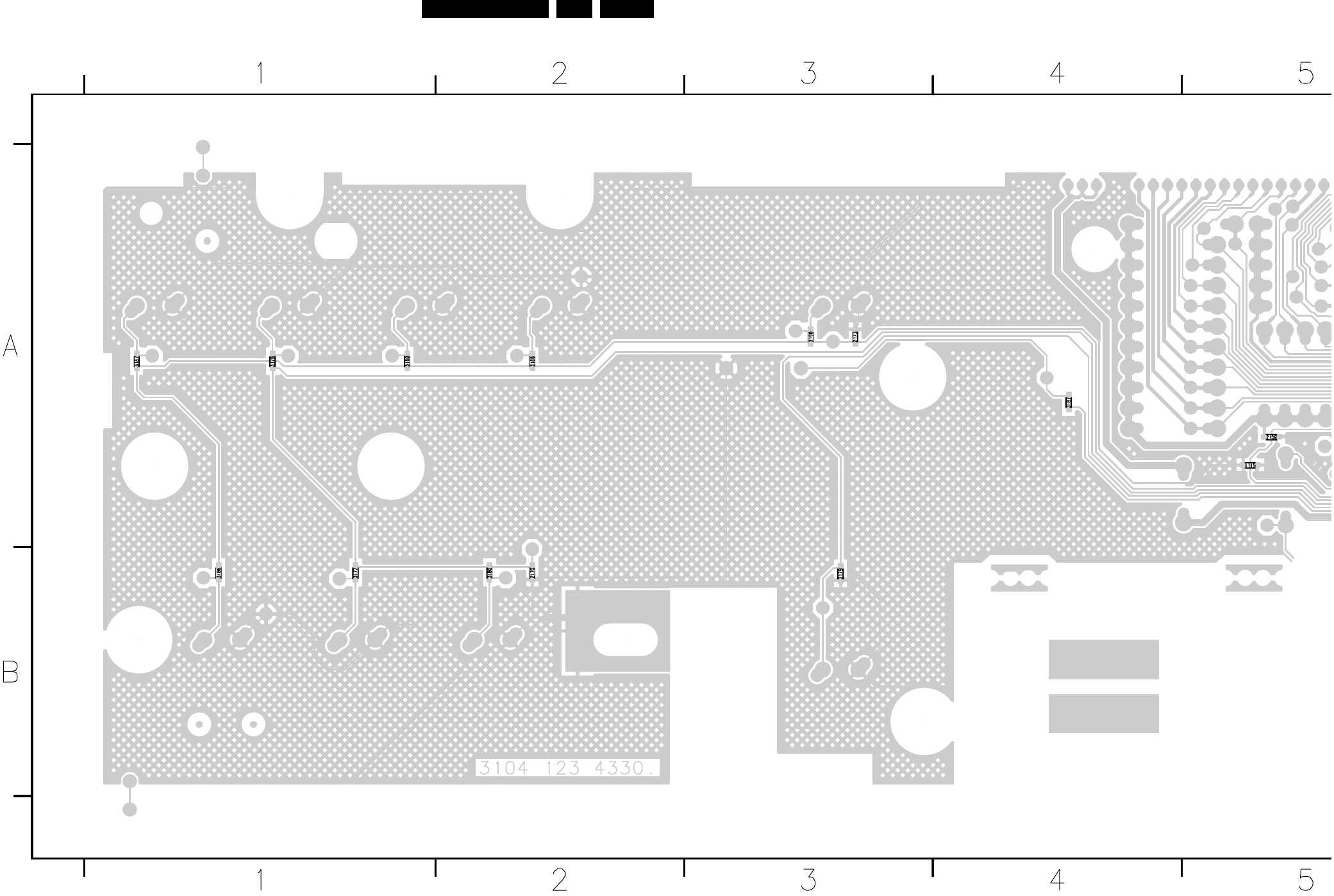
Electrical Diagrams and Print-Layouts EN 103DVDR980-985 /0X1 7.
Layout Display Panel (Part 1 Bottom View)
CL 26532011_08a.eps
170102
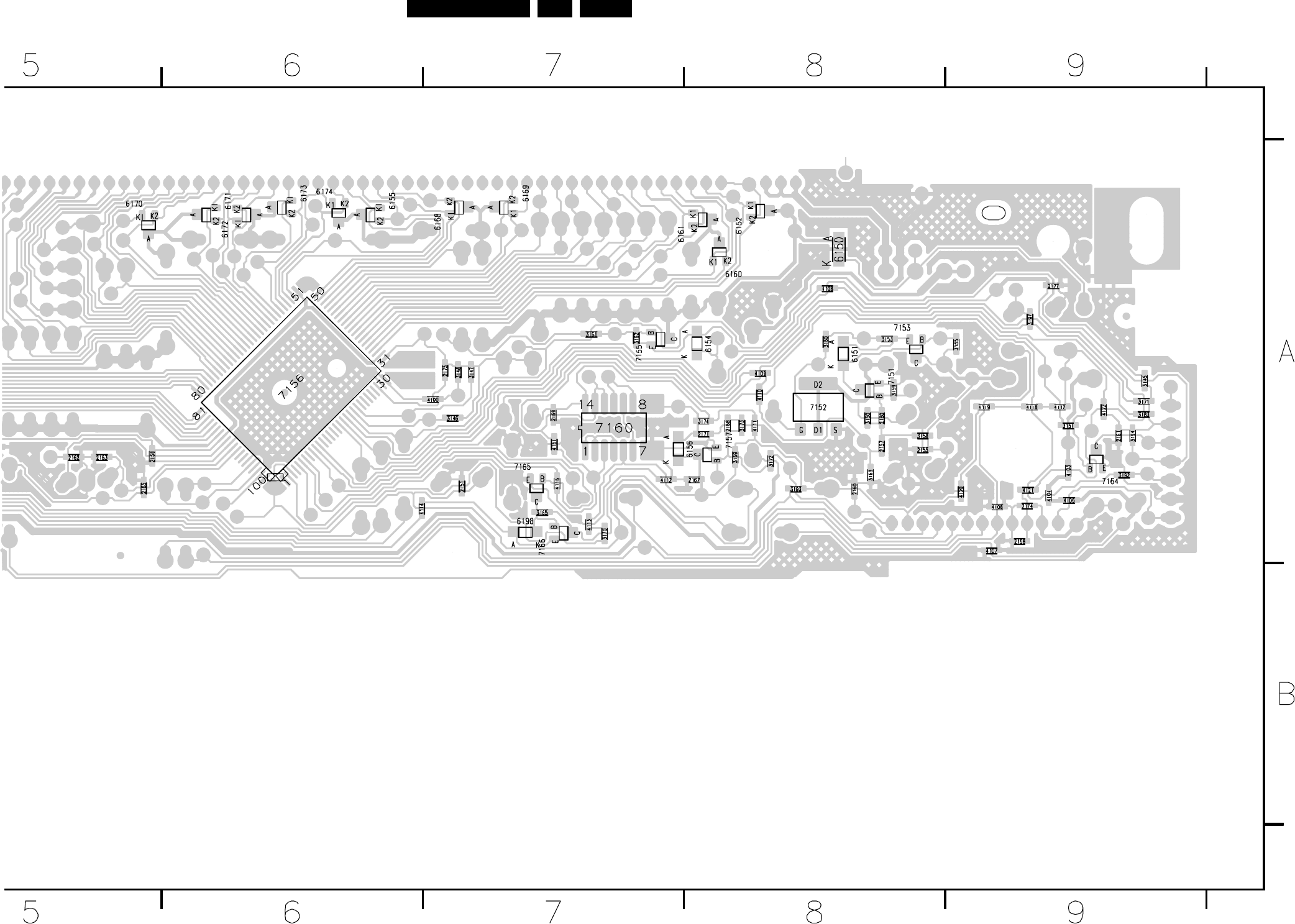
EN 104DVDR980-985 /0X1 7.
Electrical Diagrams and Print-Layouts
Layout Display Panel (Part 2 Bottom View)
CL 26532011_08b.eps
170102
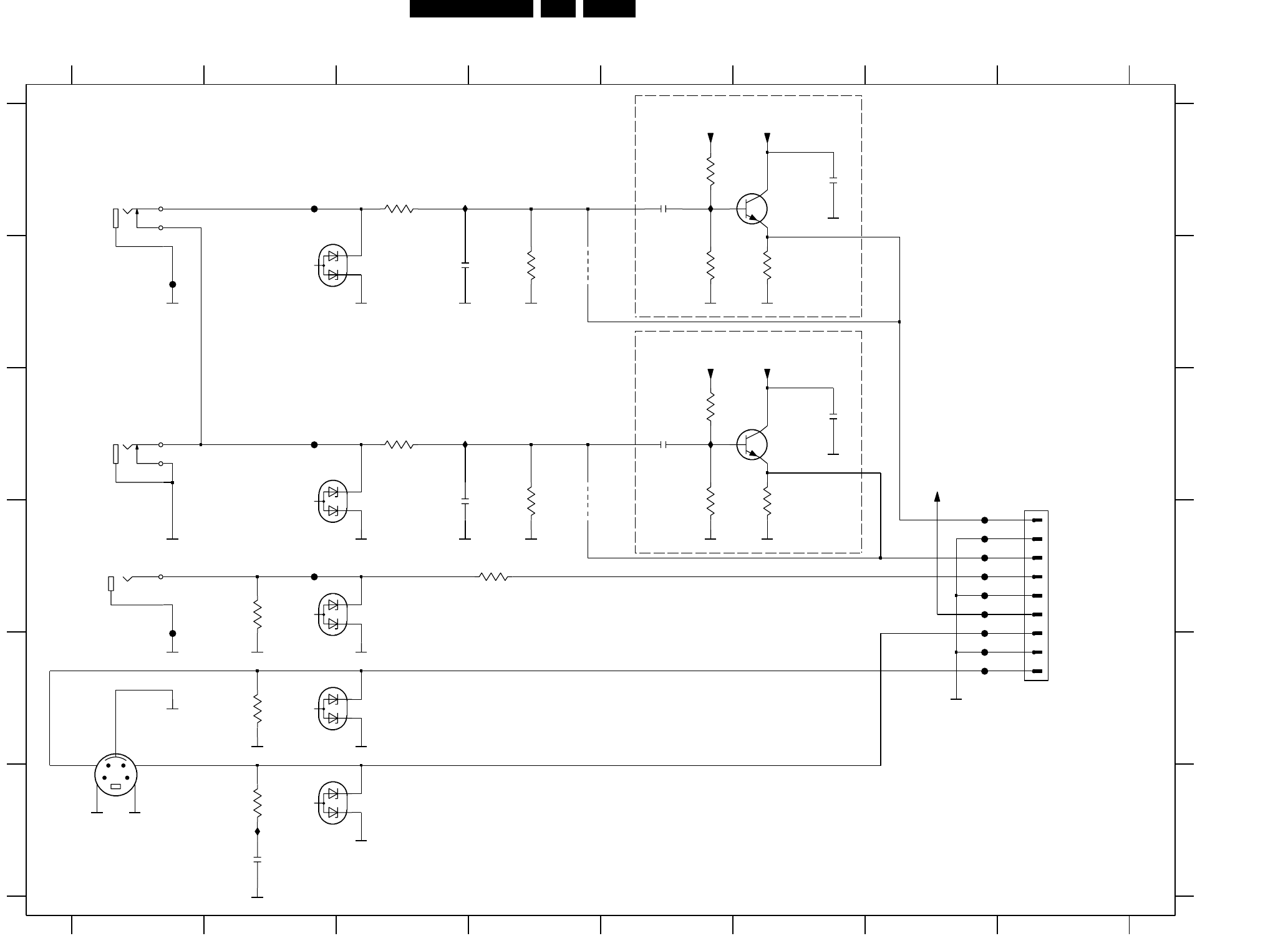
Electrical Diagrams and Print-Layouts EN 105DVDR980-985 /0X1 7.
Front AV Part
6102 D3
6101 C3
1910-B B1
1910-A D1
F
E
GND_FC
AFCRI_FC
AFCLI_FC
AL/MONO
CVBS
I304 F2
I303 C5
I302 C3
I301 A5
I300 A3
AR
YFIN_FC
GND_FC
GND_FC
3111 D2
3110 D4
3109 D6
3108 D5
3107 D4
3106 C3
3105 C5
F202 C2
F201 B1
F200 A2
7101 C6
7100 A6
6104 F3
6103 E3
654
E
6100 A3
F213 E7
F212 E7
F211 E1
F210 D7
F209 D7
F208 D7
F207 D7
F206 D2
F205 D7
F204 D7
F203 D7
CVBSFIN_FC
8SW_FC
CFIN_FC
D
C
B
A
D
C
B
A
F
2100 A6
1911 D8
1910-D F1
1910-C C1
3104 B6
3103 B5
3102 B4
3101 A3
3100 A5
2106 F2
2105 D3
2104 C5
2103 C6
2102 B3
2101 A5
4102 D4
4101 B4
3113 F2
3112 E2
1 65432
321
87
87
F209
GND_FC
OPTION
OPTION
F210
F208
F212
F213
GND_FC
470K
3100
BC847BW
7100
680K
3103
1M
3102
2101
4101
I300
1u
F203
I301
F204
F205
F207
F201
GND_FC
2100
100n
GND_FC
F200
DF3A6.8FU
6100
GND_FC
1K
3101
GND_FC
330p
2102
PH-S
1911
1
2
3
4
5
6
7
8
9
GND_FC
75R
DF3A6.8FU
6102
GND_FC
3111
GND_FC
3110
150R
GND_FC
I303
2104
1u
3108
680K
7101
BC847BWGND_FC
4K7
3109
6101
DF3A6.8FU
GND_FC
2105
330p
GND_FC GND_FCGND_FC
3106
1K
I302
3107
1M
4102
GND_FC
2103
GND_FC
3104
4K7
GND_FC
100n
1
3
2
4
F202
YKC22-0489
1910-D
5
470K
3105
2106
100n
GND_FC
GND_FC
I304
13
12
GND_FC
GND_FC
1910-B 7
8
6
YKC22-0489
1910-A
1910-C
YKC22-048910
11
9
YKC22-0489
6103
DF3A6.8FU
3112
75R
GND_FC GND_FC
DF3A6.8FU
6104
GND_FC
75R
3113
F206
F211
8SW_FC
8SW_FC
8SW_FC
8SW_FC
8SW_FC
CL 26532011_006.eps
150102
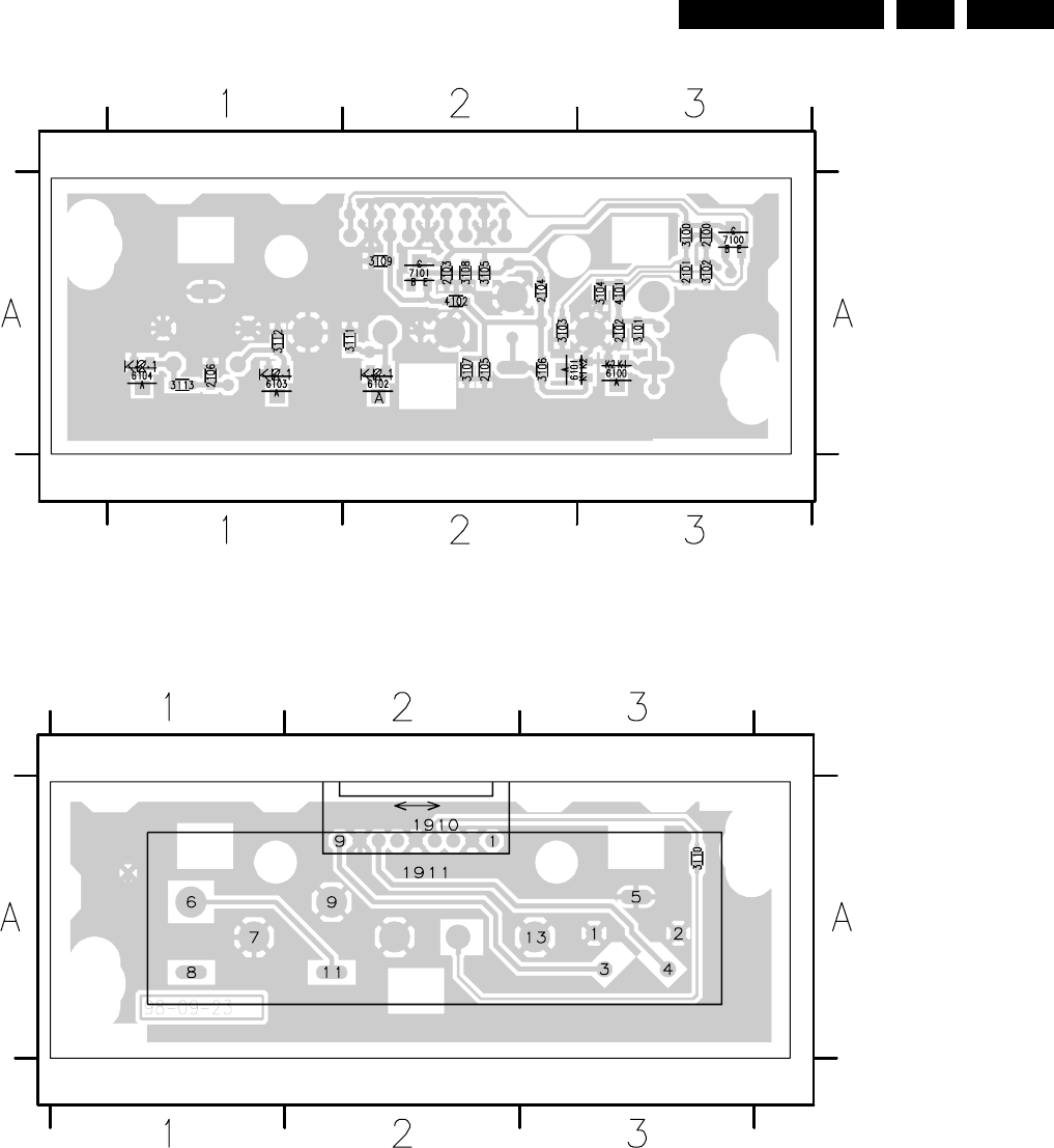
EN 106DVDR980-985 /0X1 7.
Electrical Diagrams and Print-Layouts
Layout Front AV Part
CL 16532095_035.eps
080801
2100 A3
2101 A3
2102 A3
2103 A2
2104 A2
2105 A2
2106 A1
3100 A3
3101 A3
3102 A3
3103 A3
3104 A3
3105 A2
3106 A2
3107 A2
3108 A2
3109 A2
3111 A1
3112 A1
3113 A1
4101 A3
4102 A2
6100 A3
6101 A3
6102 A2
6103 A1
6104 A1
7100 A3
7101 A2
1910 A2
1911 A2
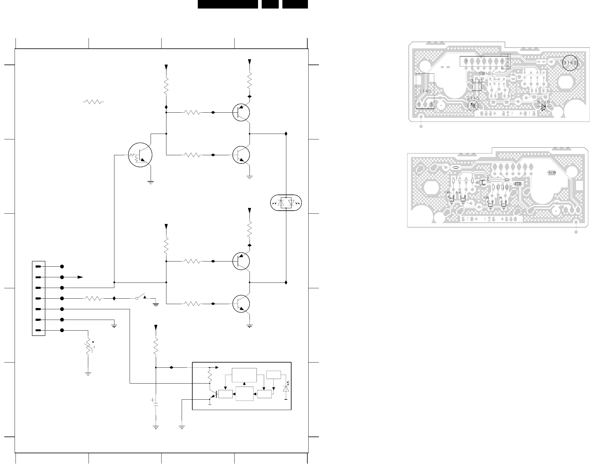
Electrical Diagrams and Print-Layouts EN 107DVDR980-985 /0X1 7.
IR and Standby Panel
DEM BAND
PASS
CTRL
CIRCUIT
AGC
INP
PIN
t
F300 C1
3142 D2
3143 A3
3144 A4
7140 D4
7141 A2
7142 B4
7143 A4
7144 C4
7145 D4
stbyled
1234
123
3149 C3
3999 A2
6140 B4
F301 C1
F302 C1
F303 D1
F304 D1
F305 D1
F306 D1
I310 A4
I311 A2
I312 A3
I313 B3
I314 A4
4
A
B
C
D
E
3135 D1
3136 A3
key in
IRR
temp_sense
STBY
NC
3137 B3
3138 C3
3139 C4
3140 D2
3141 D3
B
C
D
E
1140 D2
1915 C1
2140 E2
I315 D4
I316 C4
I317 C3
I318 D3
3139
390R
I319 D2
I320 D3
A
4K7
3136
4K7
3141
I314
GND
3140
220R
GND
2322640
3135
BC857BW
7143
GND
BC857BW
7144
1140
7142
BC847BW
TSOP2236
3 GND
1 OUT
2VS
4K7
3137
7145
BC847BW
7140
7141
I311
F306
GND
PDTC124EU
F300
F303
F305
F304
F301
2140
I320
GND
GND
22u
3144
390R
F302
I316
3138
10K
3143
10K
I318
I310
I317
I313
I319
I312
GND
3142
47K
GND
4K7
3149
7
6140
LTL-14CHJ
1
2
I315
CABLE TREE
1915
1
2
3
4
5
6
3999
5VSTBY
5VSTBY
5VSTBY
5VSTBY
5VSTBY
5VSTBY
IR and Standby Panel
Layout IR and Standby Panel (Top View)
Layout IR and Standby Panel (Bottom View)
CL 26532011_005.eps
170102
3142
3140
3137
3144
3136
3143
3141
3139
3138
3149

EN 108DVDR980-985 /0X1 7.
Electrical Diagrams and Print-Layouts
Analog Board: All in One 1
SEPA
V.SEPA
H.OSC PHASE
COMP
SYNC
OSCILLATOR
RESET
I2C-BUS
INTERFACE
ADDRESS
REGISTER
CONTROL
LOGIC
DIVIDER
CLOCK /
CALENDAR
5,1V
0V
3842 B4
I839 D6
I841 C10
I842 C10
I843 C10
I844 C10
I845 C10
I846 C10
I848 D10
I849 D10
3843 D5
3844 D10
3845 D5
3846 D11
D
E
F
G
H
131234
3835 B6
3836 B11
I894 D2
I896 F3
I897 F4
I898 F5
I899 F2
I903 F11
I945 B13
I946 C14
I948 D10
I970 E7
5678
5,1V
3852 D1
I859 D7
not used
1%
3837 B2
3838 B4
3839 C6
3840 C10
3841 C11
4,8V
I863 D10
I864 D10
I865 D10
I866 D6
I867 E10
I870 G5
I871 H4
I872 H5
I874 H5
I875 H5
I852 F10
I853 F10
I854 G9
I855 G9
3847 D10
3848 D3
3849 D4
3850 D2
3851 D4
C
I890 D1
I891 D2
I
1802 H4
1980 A10
1981 D13
not used
I893 E2
I809 B2
I810 C3
I813 I11
I815 A5
I816 A5
I817 A6
I818 A6
I819 A6
I820 A5
I971 D6
I972 C6
I973 E6
I974 D6
9101112
I837 A5
I838 D6
I861 G8
I862 D10
from VPS
not used
1%
F8111 F13
F8112 D13
F812 F6
F8201 H13
F8202 H13
F8203 H13
F8204 H13
F8205 H13
F8206 H13
I876 H5
I877 I6
I878 I5
I880 I4
I856 G9
I857 G8
I858 G8
I981 C6
I982 A7
I983 F11
I807 C3
I808 B2
I892 F14
5,1V
not used
F8007 A11
F8008 A11
F801 A1
F802 B1
F803 H5
F804 G5
F808 I10
I821 A5
I822 I9
I823 A7
I829 B8
I975 D3
I976 D6
I977 C6
I978 C6
I979 C6
I980 C6
F811 A9
F8110 F13
1%
not used
for SAA7118 (VIP) only
0V
7801 A7
7803-B D8
7804 D1
7805 D3
7806 E2
7807 F5
7809 F4
7810 H1
7811 H7
F8207 H13
F8208 I13
F8209 I13
F8210 I13
I881 I4
I882 H3
I885 H2
I886 G1
I887 I1
I888 I1
F8005 A11
F8006 A11
1%
not used
0V
3895 F2
3896 F6
3897 G8
3898 G2
3899 D11
3914 C14
3915 C13
3916 F11
F810 A9
F8101 D13
F8102 E13
F8103 E13
I830 B8
I831 B9
I832 B9
I833 B9
I835 A6
I836 A5
7800-C B3
7800-D A3
5,2V
to TU, AP, VPS
0,1V
3876 H3
3877 H5
3878 I4
3879 F6
3880 H8
3881 I5
3882 I1
7812 I3
7813 I5
7815 B13
7816 A3
I800 A1
I801 A3
I802 A2
I803 A2
I804 B3
I806 B1
3893 D5
3894 E1
2,5V
for SATCONTROL only
0V
for SW contr. (FACO) only
5,2V
3855 E3
3856 B7
3857 F4
3858 E1
3859 E2
3860 E6
3861 G5
3862 F3
3863 F10
3917 F11
4801 D13
4906 G2
6801 A7
F8104 E13
F8105 E13
F8106 E13
F8107 E13
F8108 E13
F8109 F13
3874 G7
3875 H13
from FOME
to TU, AP, VPS
3814 I13
3815 A2
3816 B8
3817 B9
3818 B9
3819 B9
3820 B6
3821 B5
3822 A1
3823 B10
3883 H3
3884 G7
3885 G9
3886 I4
7817 B3
F800 C10
F8001 A10
F8002 A10
F8003 A11
F8004 A11
3853 D1
3854 C2
2813 G6
2814 H4
2815 H5
2816 H3
2817 H3
2818 I6
2819 A2
2820 B2
2821 B4
2822 C4
3864 F10
3865 E10
3866 E5
3867 G8
6802 A3
6803 B3
6805 F6
6807 F13
7800-A A2
7800-B B2
3807 A2
3808 A7
0V
for HDR only
5,1V
from PS
3813 A4
not used
10 11 12
3824 C4
3825 C5
3826 A10
3828 A10
3887 I2
3888 I1
3889 D11
3890 G11
3891 D6
3892 D6
2801 A8
2802 A4
2803 A7
2804 A9
2805 A9
5,2V
not used
2812 G1
B
C
D
E
F
G
H
I
A
B
2823 D14
2827 F2
2831 A3
2832 A4
3868 G9
3869 G9
3870 G9
3871 B8
3872 G5
3873 G6
14
1234
not used
5,1V
3809 B4
3810 A2
3811 A4
3812 B6
not used
1982 H14
1987 D14
2800 A1
not used
to EPG
for SW contr. (FACO) only
3829 B2
3830 E6
3831 C4
3832 C1
3833 B12
3834 B12
0V
14
A
2806 B1
2807 B4
2808 D12
2809 D12
2810 F3
2811 G6
I808
3800 B4
3801 A7
3802 A8
3803 A8
3804 A9
3805 A9
56789 13
F8103
I971
I886
I831
3868
10K
F800
3873
10K
1n
2817
2
1
4
11
3899
10K
TL074
7800-A
3
100p
2804
I892
GNDD
3888
22K
10K
3835
3833
2K2
100R
3870
100R
3877
330R
3876
F810
GNDD
10K
3839
3880
10K
5STBY2
10K
3879
3885
2K2
I983
I843
10n
2818
GNDD
100R
3841
I817
100R
3916
I829
1K
3815
I823
10K
3893
BC847BW
7809
I891
I859
100n
2812
I893
F8107
GNDD
GNDA
10n
2814
F8204
12STBY
F803
GNDD
2807
470n
I846
I975
3821
10K
3
4
5
6
7
8
9
GNDD
FMN
1982
1
10
2
F8007
I881
32K768
1802
DT-38
I801
100R
3863
GNDD
I821
220K
3895
All In One 1 AIO1
2819
470n
3884
1K
5STBY2
3850
4K7
GNDD
I870
8
9
5STBY2
GNDD
1
10
11
12
2
3
4
5
6
7
I848
PH-B
1987
GNDA
5STBY2
BC847BW
1K
3844
4K7
3811
7817
4K7
680K
3842
470n
2802
3838
3817
1K
GNDD
10
9
8
4
11
220R
3812
100R
3867
7800-C
TL074
I978
1K
3875
100R
3865
I976
F8201
2827
100n
10K
3849
5STBY2
I875
5SW
3820
100R
3816
F8102
GNDA
4K7
2809
100p
100R
3914
I867
I833
F8109
GNDD
I849
2K2
3857
F808
3828
100R
GNDD
10K
3831
13
14
4
11
7800-B
TL074
5
6
7
4
11
TL074
7800-D
12
I802
GNDD
3843
10K
I974
5M
GNDD
GNDD
3866
47K
F8105
GNDD
I877
100R
3915
5STBY2
27K
3801
4801
100K
3802
F8004
2815
18p
7
VCC
4
GNDD
I872
BA7046F
7810
5
GND
HD
2
18
3
SYNC
6
I822
3892
10K
12K
3874
6K8
3803
I803
I832
I878
I982
3814
100R
VGNSTBY
F811
3818
100R
3856
100K
3869
3K3
3837
100K
100K
3852
I977
220p
2803
4K7
3855
I863
GNDD
I887
I946
5STBY2
I945
GNDD
GNDD
F8003
I854
3859
100K
7806
BC857BW
5SW
GNDD
I842
F8005
5STBY
I856
10K
3823
BC847BW
7801
I810
GNDD
100R
3836
3854
6801
BAS385
I835
VGNSTBY
1K
5STBY2
I806
I888
BC857BW
7812
F8104
3860
6K8
5SW
F8006
F8111
I858
8
I852
1
2
3
4
5
6
7
3896
10K
1980
PH-B
GNDD
100R
3871
I903
GNDD
I861
GNDD
2n2
2801
F8206
47R
3886
3832
100K
5SW5SW
GNDA
GNDD
I874
F801
F8106
3882
100K
2805
100p
GNDA
100p
2808
2K7
3829
8SW
I876
GNDD
I864
I885 3883
330R
GNDA
I882
10K
3809
2816
1u
I853
5SW
5STBY2
I894
2831
47u
10K
100K
3822
GNDD
F8208
3861
GNDD
100R
3840
2821
4u7
5STBY2
4u7
2822
3824
10K
3804
2K2
F812
5
6
7
8
9
I838
PH-B
1
10
11
2
3
4
I866 1981
I836
5STBY2
I809
7813
BC847BW
F8008
I813
8SW
100K
3858
GNDD
GNDD
GNDD
3894
100K
F8203
I839
I800
100R
3891
3890
100R
GNDD
470n
2806
100n
GNDD
2K2
3805
6805
GNDD
2823
3898
10K
5SW
BAS385
F8112
12STBY
6802
MCL4148
3813
680K
F8108
GNDD
GNDD
2K2
3834
12STBY
GNDA
3851
10K
I818
3K3
3847
F8205
100K
I898
3810
GNDD
I844
I819
I970
5SW
I972
I981
I896
I862
GNDA
I841
BC847BW
7805
MCL4148
6807
I897
1K
3846
3878
100R
3848
47K
1K
3889
7816
3807
2K7
4K7
3830
BC847BW
22 PC0|AIN11
23 PC1|AIN12
24 PC2|AIN13
25 PC3|AIN14
26 PC4|AIN15
87
PWM0
88
PWM1
3819
100R
37
P92|TPG02
38
P93|TPG03
39
P94|TPG04
40
P95|TPG13
41
P96|TPG10
42
P97|TPG11
84
PA0|PV|PH
85
PA1|HA|TPG05
86
PA2|CR|TPG00
89
PA3|PWM2
91
PA5|PWM3|HWR_
119
PB2|SO1|SI1
120
PB3|SCK1
1
PB4|SDA1
2
PB5|SCL1
P72|CTS_
106
P73|SDA0
107
P74|SCL0
108
P75|SO0
109
P76|SI0
110
P77|SCK0
27 P80|CTLIN
28 P81|DFGIN
29 P82|RMTIN
30 P83|EXT
31 P84|DPGIN
32 P85|CFGIN
33 P86|CSYNCIN
34 P87|COMPIN
35
P90|TPG12
P91|TPG01
36
P47|AIN10
3
P50|INT4|TI3
4
P51|INT3|TI2
5
P52|INT2|TI1
6
P53|INT1
7P54|INT0
8P55|TI5|AIN0
9P56|TI4|AIN1
10 P57|TI0|AIN2
95
P63|PMW7
96
P64|PWM8
97
P65|PWM9
98
P66|PWM10
99
P67|PWM11
100
P70|TXD
P71|RXD 101
102
7803-B
TMP93C071
14 P40|AIN3
15 P41|AIN4
16 P42|AIN5
17 P43|AIN6
18 P44|AIN7
19 P45|AIN8
P46|AIN9
20
21
I830
I880
5NSTBY
5STBY
I815
F802
3826
4K7
3845
I980
100R
I804
F8202
F8101
2800
470n
3917
100R
I948
MCL4148
6803
GNDD
F8001
I979
F804
GNDD
10K
3881
3887
5SW
12STBY
I855
470K
I890
5NSTBY
GNDA
470u
2813
8
VDD
4
VSS
I899
7811
PCF8593T
7INT_
1OSCI
2OSCO
3RESET
6SCL
5SDA
GNDA
I820
E2 3
SCL
6
SDA
5
VCC
8
VSS
4
WC_ 7
4906
7815
ST24E16
E0 1
E1
2
GNDD
GNDD
22K
3862
1n
2810
10K
3800
F8002
470n
2820
I837
3872
10K
F8209
5NSTBY
2811
220m
GNDD
BC857BW
7804
5STBY
I845
GNDD
5STBY
I807
7807
PDTA124EU
GNDD
100K
3853
I865
3864
100R
10K
3825
F8210
5NSTBY
I816
I871
3808
33K
3897
100R
I857
2832
100n
F8110
12STBY
F8207
I973
VGNSTBY
RC
RC
INT
GNDDGNDD
5M
TEMP_SENSE
BE_FAN
FB
FBIN_SC2
WE
WE
ARADC
SCL
SCL
SCL
SDA
SDA
SDA
D_DATA
A_DATA
SW_BE_FAN
SW_CAB_FAN
ISTBY
IPOR_EPG
TEMP
BE_FAN
D_RDY
GNDD
ION
IRESET_DIG
A_RDY
GNDD
5STBY
SCL1
SCL1
SDA1
SDA1
F_MODE
12STBY
IPOR1
5STBY
ALADC
A_YCVBS
ION_FAN
WSFI
WSRI
FOME
P50
KIR
KIL
IPFAIL
AGC_MUTE
AFC
VGNSTBY
IPOR
GNDD
YUV_ON
SATCO
8SW
5SW
VMUTE
SC1YC_H
SC2RGB_H
SCL
SDA
IS2
IS1
WSRO
GNDD
INT_EPG
5SW
A_YCVBS
A_YCVBS
GNDD
5NSTBY
5STBY2
16_SC2
12STBY
FL_READY
FLYB
VD
WU
CL 16532095_009.eps
070801
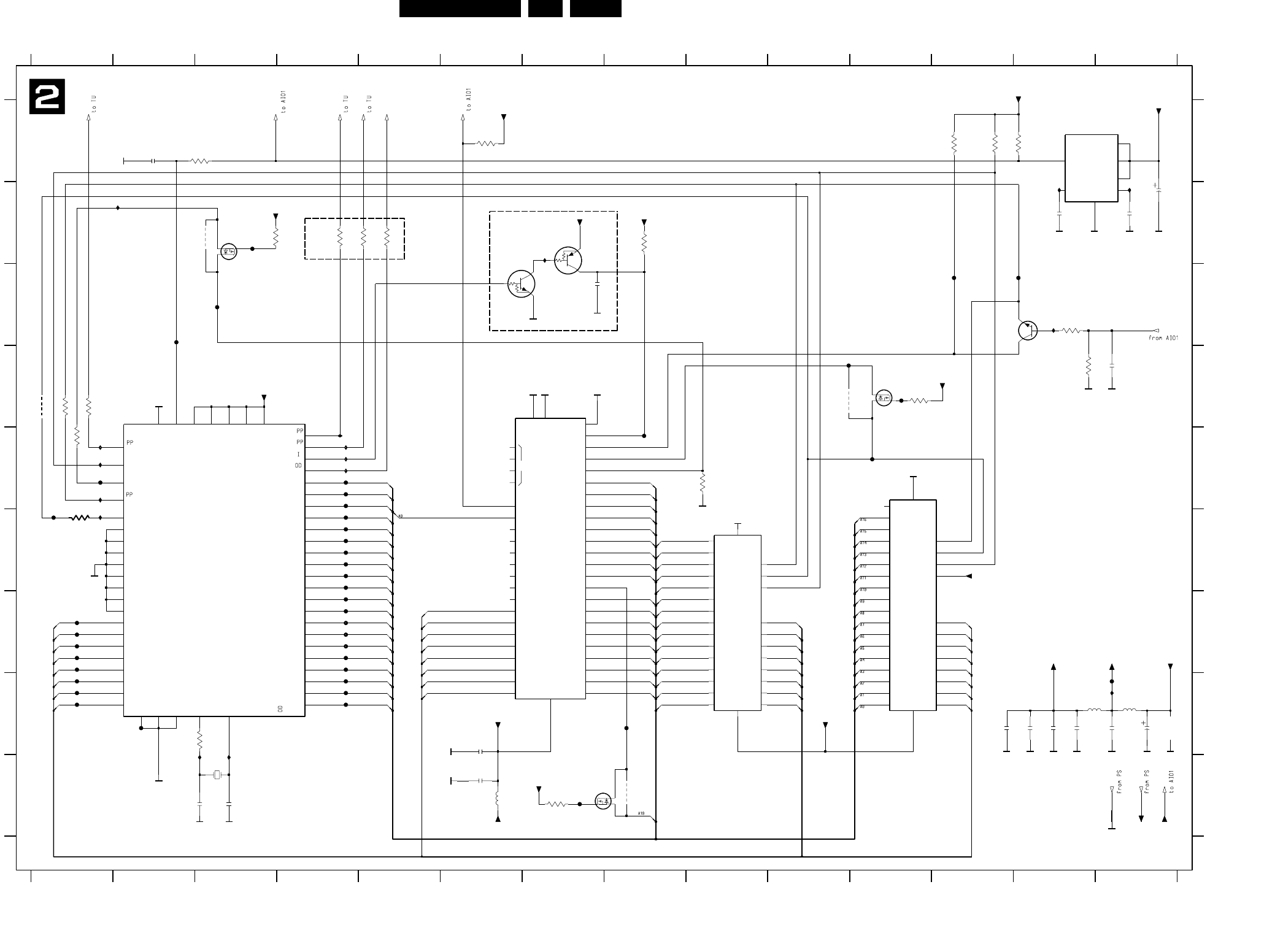
Electrical Diagrams and Print-Layouts EN 109DVDR980-985 /0X1 7.
Analog Board: All in One 2
NC
0V
not used
not used
3900 A13
5,1V
I
0,1V
5,1V
H
5,1V
not used
3907 E1
3908 D1
3909 E1
5,1V
89
5,1V
2900 A2
2901 B14
2902 B13
2903 B14
2904 H14
2905 H14
2906 H14
1234567
7903 D11
not used
0,1V
7904 I7
7905 H9
7906 H7
7907 H11
7908 B7
7909 C7
C900 I14
F900 H14
F901 H2
F902 C2
2907 D14
2909 H6
2910 I3
2911 I3
2913 C7
2914 H12
2915 H13
2916 H13
2917 H13
2918 I6
3901 A12
2,2V
3905 B5
3906 E9
not used
not used
5,1V
3910 D1
3911 A12
3912 C13
3913 D13
3918 A6
3919 B8
3920 B3
3921 D11
3924 I7
F
G
H
I
A
B
C
D
E
F
G
4902 D10
4903 I8
4907 D1
5901 H14
7803-A F3
7900 A14
7901 C13
10
2,1V
not used
0V
not used
5,1V
0V
11 12 13 14
89
1234567 10
11 12 13 14
A
B
C
D
EF905 E4
F906 F4
F908 F4
0,2V
5,1V
not used
F912 F4
F913 F4
F914 G4
1994 I3
F916 G4
F917 G4
F918 G4
3902 A3
3903 B4
3904 B5
F922 H4
F923 H4
F924 E8
F925 E11
F926 C3
F927 E1
F928 F1
F929 G1
F930 G1
F931 G1
F932 G1
F933 G1
F934 H1
F935 H1
3925 H3
4901 B3
F937 B3
F938 D10
F939 D11
5903 H13
5904 I6
F940 I7
F941 H8
F942 C13
7902 C3
F943 C12
I847 C13
I900 E1
Pos. 3920, 3921,3922, 7902,7903, 7904 are for "ON-BOARD-PROGRAMMING"
I901 E1
I902 B2
I904 F1
I905 B7
I914 I3
I915 I3
I934 E4
I935 E4
I936 E4
I938 E4
I942 B13
I943 B14
I947 H14
I984 E1
F903 E4
F904 E4
22R
3925
F909 F4
F910 F4
F911 F4
F915 G4
F919 G4
F920 G4
F921 H4
F936 H1
3913
100K
12STBY
GNDD
220n
100n
2902
GNDD
33K
3906
2903
100n
C900
2911
33p
2916
GNDD GNDD
I900
F926
GNDD
F902
2900
PMBT2369
7901
10n
F922
7904
BSH111
4903
GNDD
GNDD
CT 3
4
GND
1REF
6RESET
5RESETQ_
2
RESIN_
7
SENSE
8
VS
F925
5STBY2
GNDD
7900
TL7705
2904
I901
F909
1u
3911
4K7
GNDD
F943
GNDD
2913
10n
GNDD
All In One 2
100n
2906
F941
GNDD
GNDD
I942
GNDD
5STBY_uP
3910
1K
F932
2905
I935
F936
F942
47u
F923
1K
3904
F938
100MHZ
5903
220K
3924 F940
F904
F920
F927
2901
47u
GNDD
F930
F939
4901
5STBY2
GNDD
GNDD
GNDD
2914
100n
3908
F935
F911
100R
I905
220K
3921
3907
100R
PDTC124EU
12STBY
F906
7909
5STBY_uP
GNDD
F915
12STBY
F931
14
13
15 RB_
12
RP_
37
VCC
27
VSS1
46
VSS2
W_ 11
GNDD
DQ12
39
41 DQ13
43 DQ14
DQ15|A-1
45
33 DQ2
35 DQ3
38 DQ4
40 DQ5
42 DQ6
44 DQ7
30 DQ8
32 DQ9
26
E_
28
G_
10
9
48
A16
17
A17
A18 16
23
A2
22
A3
21
A4
20
A5
19
A6
A7 18
8
A8
7
A9
47
BYTE_
29 DQ0
31 DQ1
34 DQ10
36 DQ11
M29F800AT
7906
25
A0
24
A1
6
A10
5
A11
A12 4
3
A13
A14 2
1
A15
2910
27p
F929
GNDD
5STBY
I936
5STBY2
I938
5STBY_F
3902
4K7
10K
3912
F901
4902
1K
F903
F912
3905
100R
3909
7903
BSH111
220K
3920
10K
3919
20M00
AT-49
1994
GNDD
100n
2915
7902
BSH111
GNDD
F924
I947
GNDD
F921
GNDD
5901
100MHZ
100n
2917
F913
5STBY2
F905
5STBY2
F918
3918
10K
F933
PB0|XT1
117
PB1|XT2
103 RD_
RESET_
115
112
X1
113
X2
114
DGND1
13
DGND2|ADGND
59
DGND3
111
DVCC1
DVCC2
11
105
DVCC3
118
EA_
P24|A20 80
81
P25|A21
82
P26|A22
83
P27|A23
92 P60|PWM4|CS0_
93 P61|PWM5|CS1_
94 P62|PWM6|CS2_
90 PA4|WR_
116
43 D0
44 D1
53 D10
54 D11
D12
55
56 D13
D14
57
58 D15
45 D2
46 D3
47 D4
48 D5
49 D6
50 D7
51 D8
52 D9
74
A14
75
A15
76
A16
77
A17
A18 78
79
A19
A2 62
63
A3
64
A4
65
A5
66
A6
67
A7
68
A8
69
A9
12
ADREF
104
AM8|16_
7803-A
TMP93C071
A0 60
61
A1
70
A10
71
A11
72
A12
73
A13
3901
5STBY_uP
GNDD
F916
GNDD
47K
14
GND
I|O0
11
12
I|O1 13
I|O2 15
I|O3 16
I|O4 17
I|O5
I|O6
18
I|O7
19
22
OE_
28
VCC
27
WE_
23
6A10
7A11
8A12
9A13
10 A14
24 A2
25 A3
A4
26
1A5
2A6
3A7
4A8
A9
5
20
CE_
7905
CY62256
21 A0
A1
I915
F928
I902
F919
100n
2909
GNDD
2918
100n
GNDD
5904
100MHZ
GNDD
2907
10n
I943
5STBY2
7908
PDTA124EU
5STBY2
F934
F914
3900
10K
3903
1K
I984
F900
I|O7 21
NC
1
OE_ 24
VCC
32
WE_ 29
5STBY_uP
A5
7
A6
6
A7
5
A8
27
A9
26
CE1_ 22
CE2 30
GND
16
I|O0 13
I|O1 14
I|O2 15
I|O3 17
I|O4 18
19
I|O5
I|O6 20
7907
CY62128
A0
12
A1
11
A10
23
A11
25
A12
4
A13
28
A14
3
A15
31
A16
2
10 A2
A3
9
A4
8
F908
F937
I914
F917
F910
I934
I904
I847
12STBY
5STBY
A9
A8
A7
A6
A5
A4
A3
A2
A1
A0
D0
D1
D2
D3
D4
D5
D6
D7
A1
A2
A3
A4
A5
A6
A7
A8
A9
A11
A12
A18
A17
A13
A14
A15
A16
A19
A13
A14
A12
A11
A10
D3
D2
D1
D0
A9
A8
A7
A6
A5
A4
A3
A2
A19
A18
A17
A16
A15
A14
A13
A12
A11
A10
A1
A0
WE
FL_READY
D0
IPOR
SB1
TS
SAWS
D7
D6
D5
D4
D3
D2
D1
D0
PSS
5STBY2
GNDD
5STBY
D7
D6
D5
D4
D3
D2
D1
D7
D6
D5
D4
AIO2
CL 16532145_130.eps
121201
4907
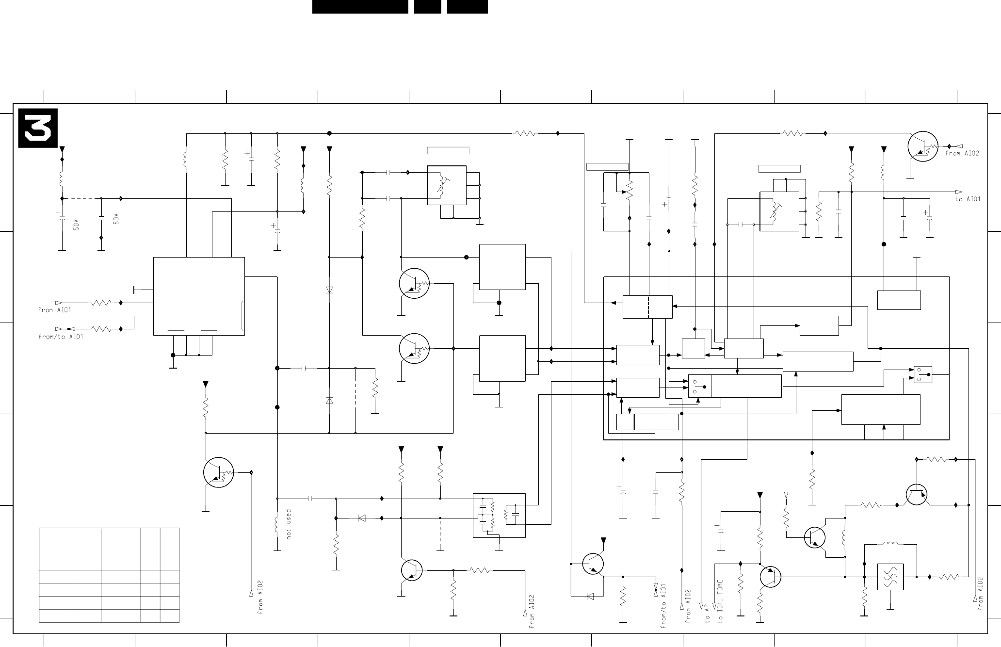
EN 110DVDR980-985 /0X1 7.
Electrical Diagrams and Print-Layouts
Analog Board: Tuner / Demodulator
NC
GND
TUNER
AGC AGC
VIF
VIF
AMPLIFIER
SIF
AMPLIFIER
AGC
INTERCARRIER
MODE SWITCH
SIF
QSS MIXER
INTERCARRIER MIXER
AM DEMODULATOR
FPLL VCO
TWD VIDEO DEMODULATOR
AND AMPLIFIER
FM-PLL DEMODULATOR
AFC
DETECTOR
VOLTAGE
REFERENCE
I764 D3
7708 D2
12
H
L
3715 D10
PSS H
H
L
5701 A10
5702 A5
5703 B9
L
I713 A8
3721 E10
3719 C2 3724 D7
3725 E9
3726 D9
low leakage
H
D
E
3722 E9
3,3V
TS
SAWS
PAL D/K
1701 C5
1702 D5
5707 E10
Bead
0V
not used
3,3V
4702 E5
5009 E9
5700 A2
3716 C1
I751 E4
7709 E9
F303 B10
C
3717 E8
3718 E4 I712 B8
3456
I731 E10
I732 E9
I733 E103727 E8
3728 E8
3729 E5
3730 E5
L
3
2715 D7
45
2718 E8 3703 A2
3704 A4
3705 A9
3706 A8
3707 A7
3708 A4
3709 A9 3720 B1
3,3V
5V
L
I709 A7
I710 B7
I711 A7I706 C5 I718 A10
I719 E7
I720 A43723 E7
I752 D4
I753 E4
I756 B1
I757 B1
I758 B1
I759 A1
not used
2,7V
1705 B2
2700 A3
2701 A4
1703 E10 6702 E4
H
4701 C4
2702 A4
2703 A7
2704 A7
2705 A9
3710 D10
3711 A1
A
B
I736 D9
I737 D10
I739 D7
H
I730 E10
5,2V
I734 D10
3,5V
H
3,3V
PAL I
2,5V
7
F705 A4
I701 A6
I703 A4
2717 A1
SEC B/G
2V
3,1V
5704 E3
2716 A3
6
3700 A3
D
E
I707 C6
I708 C6
B
C
89
I760 A1
I761 A1
I762 A3
I704 B4
1700 B5
I763 A3I714 B8
I717 A9
0,9V
PAL B/G
F701 C3
F702 C2
F703 B6
78910
12
5705 A1
7700 A10
7701 B5
L
I735 E8
2707 A10 7702 C5
7703 B7
7704 D10
AFC-ADJUST
6703 E6
3,2V
SEC D/K
7705 E7
7706 E9 I741 D7
SB1
N750
F704 B5
2,8V
0,7V
AGC-ADJUST
2,7V
3,2V
3712 D4
3713 D5
3714 C4
2709 A8
2710 A8
2711 C3
2712 D3
3701 A6
3702 A9
10
A
5SW
L
L
SEC L'
3V
2713 A1
2714 D7
6700 B4 7707 E4
SEC L
40,4-ADJUST
5706 A3
F700 C3
2V
L
6701 C4
2708 A10
2706 A7
10u
2708
3K3
3722
6703
MCL4148
5700
GNDFV
3723
100K
GNDFV
GNDFV
I709
330R
3706
18K
3709
680R
3701
47u
2717
2u2
GNDFV
2718
I762
4701
I753
GNDFV
1
2
3
4
6
78
5SW
I712
7KMY 5702
GNDFV
I757
7700
PDTC124EU
I732
5SW
680R
3724
GNDFV
3707
22K
BC847C
7705
I718
GNDFV
5SW
GNDFV
I711
3716
100R
1u
5704
57037KMY
1
2
34
678
8p2
2710
GNDFV
I708
3710
100R
470p
2704
3708
100R
5705
10u
F705
2706
100n
3703
150K
2712
1n
3714
4K7
15u
5707
5SW
3730
5K6
GNDFV
I763
5SW
7708
GNDFV
I735
I752
PDTC124EU
5SW
2u2
2714
7702
PDTC124EU
I704
2K7
3727
I713
10n
2707
19
2
202122
23
24
3
4
5
67
8
9
TDA9818
7703
1
10 1112 13
14
15
16
1718
GNDFV
I759
GNDFV
3715
100R
F700
47n
2713
F703
BC857BW
7706
GNDFV
6701
1SS356
I736
I730
GNDFV
GNDFV
3717
1K
I761
6u8
5701
TU
2
VCC
7
4K7
3725
9
AGC
1
AS
3
IF 11
12 13 14 15
6
10
NC|ADC 8
SCL
4
SDA
5
GNDFV
1705
UV1316K
+33V
GNDFV
270R
3721
3718
4K7
120p
2701
3712
2K2
I720
F704
100R
I756
33STBY
3720
220p
2702
6K8
3713
1n
2715
5K6
3729
I703
GNDFV
I714
I758
6u8
5009
GNDFV
I751
4702
220n
2709
7709
BC847BW
I741
GNDFV
F702
GNDFV
GNDFV
4K7
3719
I733
GNDFV
6702
1SS356
7704
BC857BW
I734
3711
F303
5SW
GNDFV
2700
22u
I706
1703
TPS
3
2
1
3704
4K7
I737
OFWK3953M
1700
1
2
3
4
5
I739
GNDFV
GNDFV
2703
2u2
GNDFV
2705
100n
GNDFV
F701
I760
GNDFV
2
3
4
5
5K6
3702
1n
2711 OFWG3956M
1701
1
330R
3728
I764
I731
BC847BW
7707
100u
2716
5SW
I710
OFWK9656M
1702
3
GND
1
2
4
5
Tuner/Demod. TU
GNDFV
GNDFV
GNDFV
GNDFV
GNDFV
I719
GNDFV
3705
18K
GNDFV
6u8
5706
5K6
3726
I707
3700
33K
GNDFV
7701
PDTC124EU
I701
1SS356
6700
VFV
SB1
AGC_MUTE
I717
SB1
SIF1
SAWS
SCL1
SDA1
SB1
AFC
TS
PSS
CL 16532095_011.eps
070801
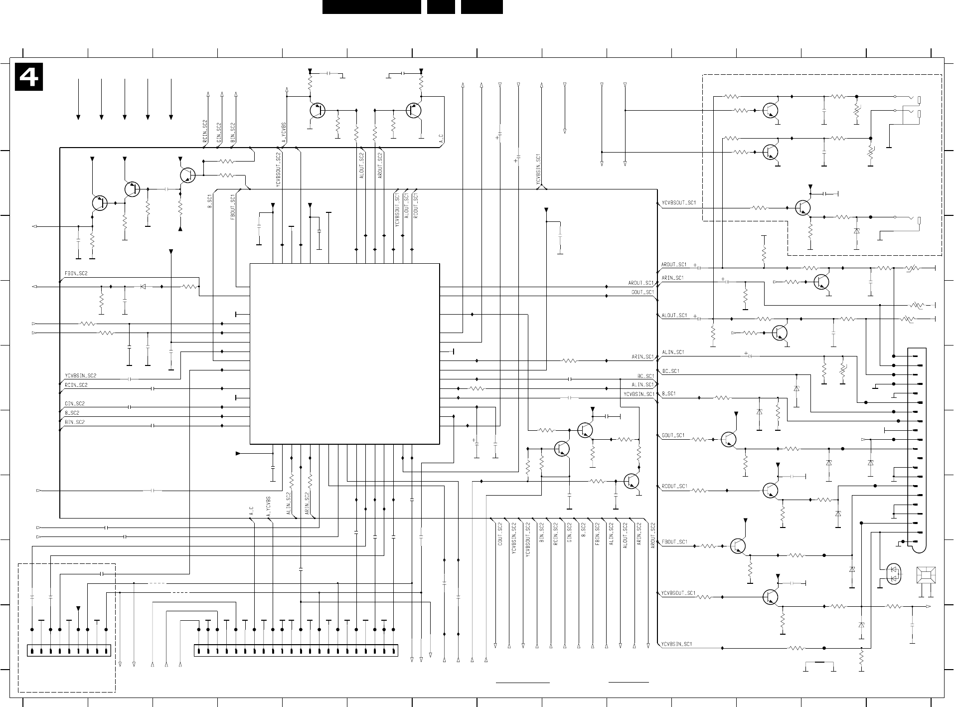
Electrical Diagrams and Print-Layouts EN 111DVDR980-985 /0X1 7.
Analog Board: In / Out 1
V
V
V
V
V
V
7
1952-C C14
A
to FOME
from PS
1950-1 E14
ARIN
2516 E2
2517 E2
from PS
2549 G7
2550 G9
2518 E9
2504 B13
2505 C4
2506 C5
E
11 12 13
2501 A6
2502 A8
9
2528 G2
2529 G6
2530 G2
H
2519 E2
to AIO1
910
2521 F8
56
from PS
1
2503 B8
2527 F12
3523 D14
3524 D2
3525 D2
2531 G2
2532 H1
678
3531 E8
10 11 12
2540 I14
2541 C1
45
1
P50
AR
3
3543 G11
to ADC, AIO1
from IO4
1954 I3
from AIO1
3548 H11
2551 G10
14
SCART 1
from YUV _CON
from IO2
from PS
F519 E13
F521 F14
3552 H13
3500 A5
3501 A6
B
C
D
7508 F12
2537 G6
2538 G6
2539 H7
3535 F9
3536 F12
B
from AIO1
from YUV _CON
from AIO1
F
G
F510 A13
3544 G9
from AP
to AIO1
to AIO1
F517 E14
2522 F2
2510 D11
to ADC, AIO1
from DAC
to AIO1, VPS
ALOUT
I534 G6
I535 G6
I505 G11
7503 B12
7504 B13
3528 E9
3529 E13
3530 E13
F5304 I1
3506 A7
3507 A12
3508 A13
3562 D13
3563 C14
3537 F10
234
3541 G5
3542 G5
F5409 I4
6500 C13
AROUT
from IO2
GNDA
F5418 I6
3549 H12
to IO3
6506 H13
6507 E12
6508 I13
I502 B12
I561 B3
I563 B2
I564 A6
I506 H11
I507 H11
7505 D13
7506 D12
7507 C4
I511 H7
3532 E11
3533 F12
3534 F11
7512 H12
7513 H12
7514 B2
2544 D2
2545 D13
2546 D14
C570 I13
F509 A13
I522 H12
F511 B14
3545 G13
from AP
3547 I12 I527 E4
F518 E14
from AIO1
from / to IO4
GNDV
from PS
I533 G6
I585 D7
I586 E7
I587 F9
I537 G6
I538 F6
F530 H13
F5301 I1
F5303 I1
I542 E9
3559 C2
3560 B2
3561 B3
F531 G13
F534 I13
F536 E14
3512 B12
3513 B13
3514 C13
F5405 I4
F5407 I4
delete for HDR
F5410 I4
6501 F12
from DAC
6503 F13
I554 H11
F5420 I6
from YUV _CON
F5422 I6
I500 A12
I501 A12
I560 B3
I552 G10
I553 F10
I566 A6
I568 C6
I569 C6
I508 G13
I509 C12
I510 H7
I573 C6
7509 F9
7510 G12
7511 F10
I515 D4
I516 E4
I517 D2
3538 F12
3539 F9
3540 F10 I520 I11
I521 H13
I514 D4
I580 A12
F513 E14
3546 G12
F516 E14
to IO3
I528 F4
AL
I530 F5
I531 F5
I532 F5
I584 D12
I543 E11
I544 D11
I545 D9
FBOUT
I518 D3
I539 E7
I540 E7
I541 E9
F5307 I1
F5309 I2
I546 D9
I547 E7
I523 F11
F5401 I3
I548 E7
3565 A13
3567 F8
3568 F8
I524 F12
I525 E4
I551 F10
F5414 I5
F5412 I5
6502 F13
F5416 I5
to IO3
I555 G8
F5421 I6
I557 F6
I558 C1
I559 B2
I526 E4
to IO2
I582 C13
from AIO1
2nd REAR_OUT
GNDA
I570 C6
I571 C6
I572 C6
2536 G6
2511 E2
2512 E2
to YUV_CON
13 14
GNDV
7515 F9
7516 B3
7517 B2
I512 I7
I513 I7
not used
8
1953 I1
GNDV
2500 A5
from Front A/V Board
RCOUT
I529 F4
1950-3 H14
1951-C A14
GNDV
2548 B13
3550 H12
I583 C13
2nd REAR_OUT
I574 C6
I575 C5
I576 C4
from TU
F5306 I1
3504 A6
3505 A6
2507 C9
2508 C11
2509 C11
I
F5402 I3
F5403 I3
I556 F8
GNDV
I549 F7
I550 F7
7501 A7
GNDV
I
GOUT
2
ALIN
I581 A12
F515 F14
2523 F9
2524 H5
2525 H2
2526 F4
3522 D12
7500 A5
7502 A12
3526 D11
3527 D12
2533 H1
2534 H12
2535 H7
3556 B4
3557 B4
3558 C2
F
G
H
2542 B3
3551 H11
from AIO1
to IO2
2547 A13
8SC1
D
E
3570 D2
4400 H3
4401 H3
CVBS
not used
from / to Digital Board
I504 D12
not used
2520 F7
6504 G13
6505 H14
3518 C12
3519 D12
3520 D14
3521 D3
6509 D2
I503 C13
F524 F13
3553 I12
3554 I14
3502 A11
3503 A5
I536 G6
F525 G14
F527 G14
3555 H14
A
3511 B14
2513 E3
2514 E9
2515 E12
3515 C12
3509 A11
3510 A12
3564 A13
C
3516 C13
3517 C14
I584
GNDV
I574
2547
470p
3549
68R
F5412
7503
BC817-25W(COL)
F5307
5STBY
1u
2538
2533
10u
16
GNDV
2500
100n
100R
3562
470R
3542
GNDV
GNDVGNDV
3556
47K
47u
2508
I581
3515
100K
25
10n
2551
3511
GNDV
I573
GNDV
7513
BC847BW
I553
2521
100n
BZM55-C6V8
6500
7512
BC847BW
6509
BAS385
3550
1K
7510
I555
BC847BW
GNDV
GNDA
3537
68R
GNDV
2528
1u
100R
3534
I551
1u
2518
10
7509
BC847BW
F536
3510
4K7
2512
47p
GNDA
GNDV
2542
100n
F511
I559
I570
I563
GNDA
2536
1u
5NSTBY
8STBY
GNDV
100n
2501
GNDV
GNDA
F5401
2502
4u7
50
GNDV
F5301
4400
1u
2550
3536
68R
I568
GNDV
1u
2530
GNDA
3502
470R
5STBY
100n
2504
I540
1u
2517
3563
100R
5NSTBY
GNDV
8STBY
GNDA
2524
1u
BC817-25W(COL)
7515
GNDA
5STBY
I501
3K3
3561
F530
8STBY
I520
3526
100K
2
20
21
22
3
4
5
6
7
8
9
FMN
1954 1
10
11
12
13
14
15
16
17
18
19
3544
4K7
F517
I523
2540
1n
I547
GNDV
I561
7511
BC817-25W(COL)
16
10u
2532
I539
3555
10K
GNDV
GNDA
5STBY
I544
1u
2549
3553
1K
I580
F531
YKC21-4157
1952-C
6
5
GNDA
GNDV
I536
6504
BZM55-C6V8
BC857BW
7500
470K
3560
2527
100n
I571
I554
3559
3K9
470p
2546
100R
3551
F5402
55
VCCV1
33
VCCV2
16
VCCV3
12
VOUT-RF
9
VREF 51
YCVBSIN-AUX
24
36
YCVBSIN-ENC
52
YCVBSIN-TV
YCVBSIN-VCR 50
YCVBSOUT-AUX
15
YCVBSOUT-TV
3
YCVBSOUT-VCR
7
YIN-AUX
26
YIN-ENC
38
RIN-AUX
37
RIN-ENC
43
RIN-STB
39
RIN-TV 56
RIN-VCR
47
ROUT-AUX
4
ROUT-CINCH 58
ROUT-TV 64
ROUT-VCR 60
SCL
21
SDA
22
SLB-AUX
31
SLB-TV
25
SLB-VCR
27
VCC12
23
VCCA
29 GNDV1
GNDV2
14
GNDV3
10
GOUT-TV 63
LIN-AUX
35
LIN-ENC
45
LIN-STB
41
LIN-TV 53
LIN-VCR 49
LOUT-AUX
6
59
LOUT-CINCH
2
LOUT-TV
LOUT-VCR 62
RCIN-AUX
28
42
RCIN-ENC
RCOUT-TV
1
32
BIN-ENC
46
BOUT-TV 61
CIN-ENC
40
CIN-TV 54
48
CIN-VCR
COUT-AUX
13 5
COUT-VCR
CVBSIN-STB
34
FBIN-AUX
18
FBIN-ENC
19
17 FBOUT-TV
FILTER
11
GIN-AUX
30
GIN-ENC
44
GNDA 57
STV6410A
7507
ADD
20
AOUT-RF
8
BIN-AUX
I530
I532
7516
BC847BW
F516
100n
2506
GNDV
I560
I546
F5422
I583
5STBY
I517
I515
2523
100n
I527
100n
2514
GNDV
I534
50
4u7
2503
F510
GNDV
GNDV
3539
1K
75R
3554
F513
GNDA
3558
22K
GNDA
3512
100R
I549
1u
2525
F5403
GNDV
I542
F5304
6507
BZM55-C6V8
5STBY
F5414
I548
GNDV
4401
12STBY
3514
F5409
150R
3547
1K
F521
2507
100n
3528
470R
F525
5STBY
3565
100R
3570
100K
3520
7517
BC857BW
F5303
I550
GNDV
8SW
5STBY
3517
1u
2537
F5410
GNDA
2510
47u
25
470R
3522
GNDV
470R
3516
10K
3567
F534
GNDV
I586
F519
F5407
2539
10u
16
50
4u7
2509
GNDV
GNDV
F5416
I552
I521
GNDA
3530
3552
68R
GNDV
6505
DF3A6.8FU
I585
F524
I518
F527
BC857BW
GNDV
F5309
7514
6503
BZM55-C6V8
GNDV
3523
8SW
3521
I516
I507
1K
470R
2545
470p
F515
3541
1u
GNDV
GNDV
I566
2519
GNDV
GNDA
GNDV
3525
100R
GNDV
I535
2505
100n
17A
18A
19A
2A
20A
21A
3A
4A
5A
6A
7A
8A
9A
1950-1
1A
10A
11A
12A
13A
14A
15A
16A
100R
3564
12STBY
BZM55-C6V8
6506
GNDV
GNDV
GNDV
GNDA
I513
F5421
I556
GNDV
100n
2531
I524
I508
470p
2548
I500
GNDV
1u
2522
GNDV
I572
GNDV
5STBY
100n
2529
PH-B 1
2
3
4
5
6
7
8
9
I510
GNDV
1953
470R
3509
100R
3524
GNDV
I528
100R
3543
1K
3546
GNDA
GNDV
8
50
4u7
2515
I537
1951-C
YKC21-4159
9
7
5STBY
I564
BC847BW
7504
GNDV
100K
3519
47K
3533
100n
2513
I587
470R
3531
GNDV
F5418
100n
2541
GNDV
GNDV
GNDV
3527
4K7
100u
2520
10
I557
GNDV
F518
I505
3504
2K2
GNDA
GNDV
GNDV
GNDV
I569
6508
BZM55-C6V8
GNDV
GNDA
I538
GNDA
2526
100n
4K7
3507
GNDV
I506
3538
I545
2544
100n
1K
I509
I525
GNDA
3503
220R
6501
BZM55-C15
BC817-25W(COL)
7502
I533
3513
75R
GNDV
4K7
3568
GNDA
2516
1u
16
10u
2535
GNDA
GNDA
BZM55-C6V8
6502
2K7
3501
BC847BW
7508
2511
47p
I541
I576
GNDA
3557
47K
I502
GNDA
5STBY
BC817-25W(COL)
7505
I511
I582
I529
I504
1950-3
0350808190
MT1 MT2
In / Out 1 I/O 1
GNDV
GNDV
GNDV
470R
3532
I514
I575
8STBY
C570
I543
GNDV
100R
3548
I512
F5420
I558
68R
GNDA
3535
470R
3545
4K7
3518
GNDA
I503
F5306
I526
8STBY
GNDV
I531
GNDV
GNDV
100K
3529
GNDV
F5405
7506
BC817-25W(COL)
3508
5STBY
F509
2K2
3505
3540
82R
7501
BC857BW
3500
2K7
GNDA
100n
2534
I522
220R
3506
AFCLI
CVBSFIN
D_CVBS
D_CVBS
D_Y
D_Y
YFIN
YFIN
D_C
D_C
CFIN
CFIN
BC_KILL_DC
YCVBSIN_SC1
CIN
A_YCVBS
AFCRI
COUT_SC2
A_R
A_R
A_C
GNDV
GNDV
GNDA
AFER
8SW
16_SC2
ALADC
ARADC
D_B
GNDV
GNDV
GNDV
GNDV
GNDV
GNDV
A_YCVBS
A_B
A_B
A_G
A_G
SC1YC_H
KIR
KILKIL
KIRKIR
P50 P50
GNDV
GNDV
GNDV
D_R
GNDV
D_G
GNDV
COUT_SC2
AFEL
VD
YCVBSIN_SC2
WU
YCVBSIN_SC1
KIL
YCVBSIN
P50
ALDAC
ARDAC
BIN_SC2
RCIN_SC2
VFV
FBIN_SC2
AROUT_SC2
ALOUT_SC2
ALIN_SC2
GIN_SC2
RCIN_SC2
8_SC2
YCVBSIN_SC2
ARIN_SC2
YCVBSOUT_SC2
SDA
SCL
BIN_SC2
GIN_SC2
CL 16532095_012.eps
080801
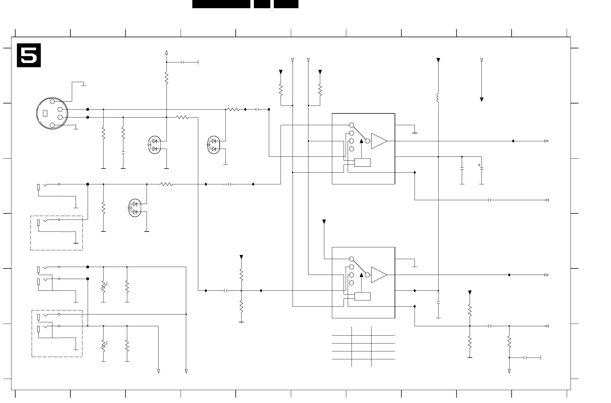
EN 112DVDR980-985 /0X1 7.
Electrical Diagrams and Print-Layouts
Analog Board: In / Out 2
V
LOGIC
LOGIC
V
3416 F2
3417 F2
3418 A5
3419 A6
5400 A8
6402 B4
6403 B3
6405 C2
7400 B6
7401 D6
F5101 D2
F5103 E2
F5202 C2
F5503 B2
F5504 B2
I402 B5
I404 B5
I406 C5
I407 C4
I409 E4
I410 E5
I411 E8
I412 E8
I414 E9
I416 C8
I417 B10
2400 B5
2401 B2
2402 C9
2403 C9
2404 C4
2405 C9
2406 E4
2407 E8
2408 E9
2410 A4
2411 F10
3402 A3
3403 B4
3404 B4
3405 B2
3406 B2
3407 C3
3408 C2
3409 E5
3410 E2
3411 E2
3412 E5
3413 E9
3414 F9
from IO1
IN2
AL /
OUT
L
CTLA
S-CONN
3415 F9
from IO1
MONO
to IO1
Y
L
C
not used
REAR_IN
not used
H
12345678910
1234
REAR_IN
IN1
Y/C IN
REAR_IN
CVBS
to IO1
1958-A E1
1959-A C1
L
from AIO1
H
from AIO1
from PS
5678910
A
B
C
D
E
F
A
B
C
D
E
F
1951-A F1
1952-A D1
1955-B A1
to AIO1
to AIO1
to AP
H
CTLB
AR
to AP
L
IN3
H
MUTE
5SW
GNDV
3418
100K
YKC21-4158
1959-A
4
2
1958-A
YKC21-3620
3
1
2
47u
2403
2404
10n
GNDV
I402
GNDV
5SW
75R
3405
100R
3407
100n
2407
5SW
8GND
IN1
1
IN2
3
IN3 5
OUT 7
6VCC
3416
BA7652AF
7400
2CTLA
4CTLB
2CTLA
4CTLB
8GND
IN1
1
IN2
3
IN3 5
OUT 7
6VCC
F5101
F5504
BA7652AF
7401
GNDV
100K
3417
GNDV
GNDA
3410
GNDV
GNDV
GNDV
GNDA
3413
10K
5SW
3415
100K
100K
3419
5SW
GNDA
GNDV
3408
75R
GNDV
I416
10n
2411
GNDV
6403
DF3A6.8FU
2410
10n
3411
100K
10n
2400
3402
3412
10K
GNDA
2402
100n
100K
2408
1n
GNDV
GNDV
3406
75R
I411
I414
I417
I409
GNDA
I407
10K
3409
100n
2401
F5202
F5503
10u
5400
3
1
2
GNDV
GNDV
GNDA
GNDV
1951-A
YKC21-4159
DF3A6.8FU
6402
100R
3403
DF3A6.8FU
6405
5SW
I404
F5103
10n
2405
TCX0310
1955-B
1B
3B
4B
2B
10K
3414
I410
I412
1952-A
YKC21-4157 4
2
I406
3404
100R
GNDV
GNDV
GNDV
WSRI
WSFI
5SW
1n
2406
CFIN
YFIN
IS2
IS1
YCVBSIN
CIN
5SW
ARCRI
ARCLI
CL 26532011_002.eps
150102
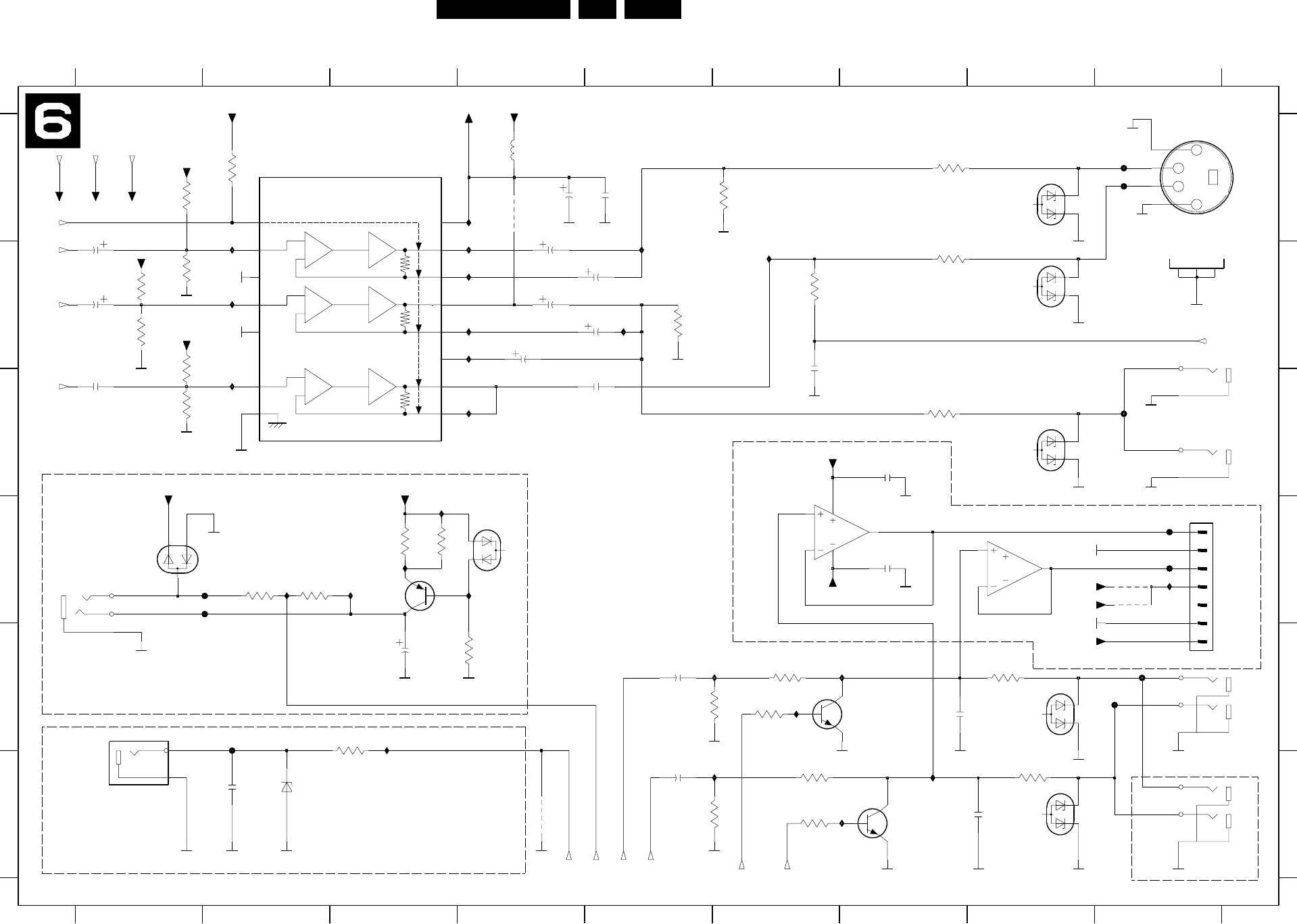
Electrical Diagrams and Print-Layouts EN 113DVDR980-985 /0X1 7.
Analog Board: In / Out 3
6dB
6dB
75E
75E6dB
75E
1952-B C9
1955-A A9
1955-C B9
1956 D9
1958-B E9
1959-B C9
1991 F1
1992 E1
2430 B6
2431 A4
2432 A5
2433 A1
2434 A4
2436 B5
2437 C1
2438 C5
2439 B1
2440 B4
2441 B5
2442 E5
2443 F5
2444 E3
2445 F2
Y
123456789
123456789
A
B
C
D
E
F
A
B
S_CONN
from PS
E
F
1951-B F9
from DAC
from AIO1
2448 B4
2449 C7
2450 D7
3423 C1
3424 B1
3425 B1
3426 A1
3431 B6
3432 A7
3433 B7
3434 B1
3435 A6
3436 C7
3437 B1
3438 B5
3439 E6
3440 E8
3441 E5
3442 E6
3444 D3
3445 F6
3446 F8
3447 D2
3448 D2
2446 E7
2447 F8
from DAC
to AIO1
from IO1
to headphone
AR
from AIO1
from PS
from AIO1
3452 E4
3453 E3
3454 D3
3455 A2
4404 A4
4405 D9
4406 D9
4904 F4
5430 A4
6430 A8
6431 B8
6432 C8
6436 D4
6437 D1
6438 F2
6439 E8
6440 F8
7430 A2
7431 E7
7432 D3
7433 F7
7434-A D7
C
D
for SATCONTROL only
not used
REAR_OUT
from IO1
not used
from AIO1
for RC only
NC
AL
C
AL
not used
F331 E9
F334 E9
F336 C9
F337 A9
F338 A9
F340 D9
F341 D9
F9202 D2
F9203 D2
I430 A2
I431 B2
I432 C2
I433 A4
I434 A4
I435 B4
I436 B4
I437 B4
3450 F5
3451 F6
SATCONTROL
from AIO2
delete for HDR
I438 C4
I439 B5
BC327-40
from AIO1
not used
CVBS
not used
I440 B6
I441 B5
I445 E6
I446 F6
I449 D2
I450 D3
I451 D3
I452 D3
I453 D4
I454 E7
I455 E6
I456 F7
I457 F7
I458 D9
I459 E3
7434-B D8
F330 E2
AR
from IO1
RC IN
F331
3438
100K
F334
5SWS
I435
1952-B
YKC21-4157
3
1
GNDV
3425
470K
GNDV
I439
7434-B
MC33078
5
6
7
8
4
F336
2450
100n
5NSTBY
GNDA
10u
4K7
3431
470K
3424
2442
I459
I449
67
2447
470p
3
4
5
6
7
1955-C
TCX0310
5
1956
EH-B
1
2
100K
3435
5SW
100u
2434
10n
2432
6439
I431
DF3A6.8FU
4404 5430
10u
3426
470K
GNDV
5SW
5NSTBY
5SW
2440
100u
GNDV
DF3A6.8FU
6432
5SWS
GNDV
GNDA
I437
GNDV
OB2
12
OC1
10
OC2
9
VCC
16
100n
2449
3
GND1
5
GND2
GND3
8
INA
2
INB
4
7
INC
1
MUTE
NC1
611
NC2
15
OA1
OA2
14
13
OB1
5
4
6
GNDD
7430
BA7660FS
GNDD
1958-B
YKC21-3620
GNDA
2436
22u
5STBY2 5STBY
I434
4406
F330
BZM55-C6V8
6438
47K
3448
GNDV
I454
BAV99W
6437
GNDV
I452
GNDD
I450
I441
3450
100R
3440
100K
3455
100K
7434-A
MC33078
3
2
1
8
4
GNDV
100R
3446
8STBY
4904
I433
GNDD
GNDV
YKC21-4158
1959-B
3
1
3432
75R
GNDV
I445
F9203
GNDA
3441
100K
470R
3439
5SWS
In / Out 3 I/O 3
GNDV
F9202
I456
GNDV
I453
GNDD GNDA
GNDV
GNDV
100u
2444
I455
2441
22u
F341
4405
F340
6440
DF3A6.8FU
5STBY
4A
2A
I440
2433
22u
1955-A
TCX0310
1A
3A
6
4
5
GNDV
22u
2439
YKC21-4159
1951-B
470p
2446
6431
DF3A6.8FU
GNDA
GNDD
7432
5SW
GNDV
4K7
3451
BC817-25W(COL)
7433
GNDA
GNDA
3437
82K
10R
3444
F338
5SWS
GNDV
2K2
3452
1n
2445
GNDD
2437
100n
GNDD
GNDA
GNDA
68R
3433
3454
10R
GNDA
3442
4K7
I432
I451
GNDV
3423
82K
I430
7431
BC817-25W(COL)
10n
2430
100n
2438
10u
2443
2431
47u
I457
1
2
3
I446
2448
22u
YKB21-5130
1992
6436
BAV99W
470R
3445
GNDA
82K
3434
YKC21-3478
1991
3
2
GNDA
F337
I438
6430
DF3A6.8FU
5SW
1K5
3447 8STBY
GNDA
3453
1K
I458
I436
VCC_HA
5STBY
5STBY2
RC
3436
75R
ALDAC
KIL
WSRO
HPR
GNDA
GNDA
5NSTBY
HPL
KIR
D_CVBS
D_C
D_Y
ARDAC
SATCO
5SW
VMUTE
CL 16532095_014.eps
080801
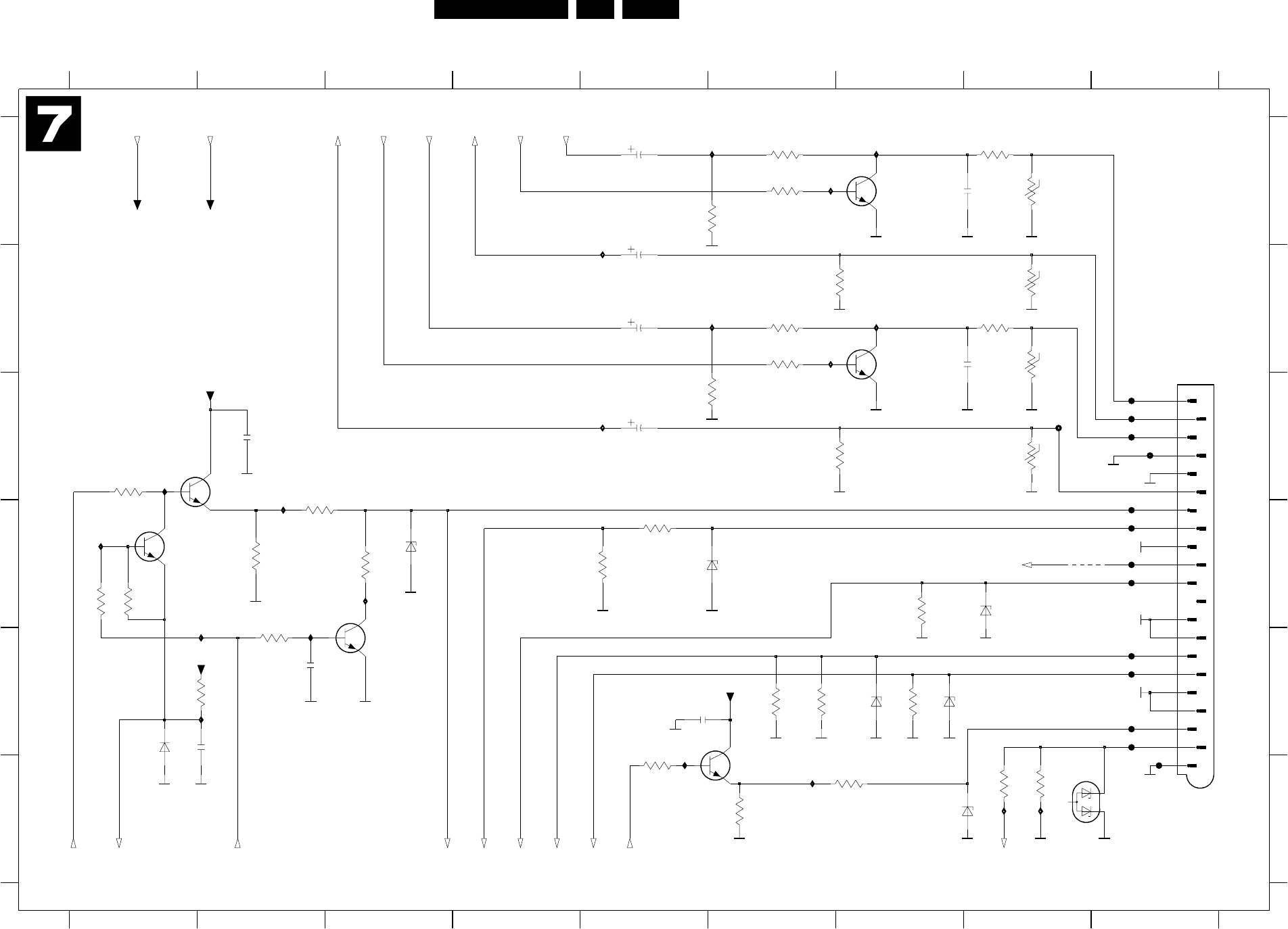
EN 114DVDR980-985 /0X1 7.
Electrical Diagrams and Print-Layouts
Analog Board: In / Out 4
V VV V
3463 A5
2462 B5
3481 E7
from IO1
3474 D5
to IO1
F5002 C9
to IO1
2467 A7
YCVBSIN
3467 B6
F5010 D9
3468 B8
6465 F7
3487 A8
to IO1
2463 C5
D
F5020 E9
4403 D8
3480 E6
1
I472 A7
3473 D3
2460 A5
I471 F8
6462 D8
7462 C2
to IO1
6464 E7
6
to IO1
to IO1
from AIO1
FBIN
F5019 E9
from IO1
8
3489 D1
2
2465 E6
C
7
12
I479 A7
I469 A5
3484 F8
I460 D2
2466 E2
3
6468 E1
not used
to IO1
2469 E2
2461 B5
E
B
6466 F9
7461 B7
I473 B7
3478 D7
from AIO1
7
3461 A6
3472 C1
3482 F5
C
3460 A6
B
RCIN
I465 C5
I462 C1
I476 F8
F5006 C8
3458 E2
6460 D3
F
3485 F6
F5003 C9
7463 E3
SCART 2
3464 B7
not used
1950-2 C9
from PS
5
8SC2
8
F5016 E9
I481 D1
3469 C5
I480 B7
6
I463 D2
F5004 C9
3471 C8
4
5
GIN
4
7460 A7
A
3466 B6
9
3477 D5
3457 E6
2464 C2
3470 C6
3465 B8
I464 A6
I477 E5
3475 D2
A
3459 D1
6463 E7
1%
F5008 D9
F5007 D9
F
I461 D3
D
F5011 D9
3
from IO1
3486 F8
3483 F7
to I/O 1
from IO1
3479 E2
6461 D5
E
I483 E2
F5001 C9
9
BIN/COUT
F5021 F9
to IO1
to IO1, AIO1
2460
25
from AIO1
7466 D1
3488 B8
7464 F6
from PS
I474 B6
I482 D2
I478 F62468 B7
3476 D3
3462 A8
F5015 E9
17B
18B
19B
2B
20B
21B
3B
4B
5B
6B
7B
8B
9B
47u
1950-2
1B
10B
11B
12B
13B
14B
15B
16B
F5003
470R
I461
GNDA
470p
2467
3466 I480
47K
3477
470R
3472
68R
3473
BC847BW
7462
6466
DF3A6.8FU
4K7
3467
I477
GNDV
34623471
7466
BC817-25W(COL)
I472
F5001
6465
BZM55-C6V8
I471
I462
5STBY
F5021
3457
390R
3470
3468
82R
3476
100K
GNDA
3485
1K
BZM55-C15
6461
GNDV
2468
470p
I463
I474
5NSTBY
2463
4u7
50
GNDA
F5015
100n
2464
GNDA
GNDV
GNDV
GNDA
GNDV
10K
3489
I476
100K
3469
I465
F5008
GNDV
6460
BZM55-C6V8
4K7
3459
3484
GNDV
GNDV
75R
7460
BC817-25W(COL)
4403
F5004
F5006
F5020
3488
100R
470R
3474
I460
5STBY
GNDA
GNDV
GNDA
2465
100n
F5002
100K
3464
3461
4K7
3483
68R
F5016
5NSTBY
I482
GNDV
F5011
47u
2462
25
GNDV
GNDV
F5010
In / Out 4 I/O 4
GNDA
2466
10n
3480
75R
GNDA
BZM55-C6V8
6462
I481
GNDV
GNDV
GNDV
F5019
1K5
3458
100R
34873460
470R
6468
MCL4148
GNDA
150R
3486
GNDV
3465
5STBY
GNDA
GNDV
2461
4u7
50
75R
3478
GNDV
GNDV
BC817-25W(COL)
7463
I469
F5007
BC817-25W(COL)
7461
1K
3475
GNDV
GNDV
1u
2469
I464
GNDV
I483
GNDA
100R
3482
GNDA
GNDA
75R
3481
GNDV
3463
100K
I478
BZM55-C6V8
6463
I473
I479
GNDA
GNDV
7464
BC847BW
BZM55-C6V8
6464
4K7
3479
GNDV
5NSTBY
GNDA
BC_KILL_DC
RCIN_SC2
GNDV
GNDV
GNDV
GNDV
GNDV
GIN_SC2
FBIN_SC2
AROUT
ARIN
ALOUT
ALIN
BIN_SC2
YCVBSOUT
YCVBSIN_SC2
P50
GNDV
YCVBSOUT_SC2
SC2RGB_H
COUT_SC2
KIR
ARIN_SC2
KIL
AROUT_SC2
ALOUT_SC2
ALIN_SC2
5STBY
8_SC2
CL 16532095_015.eps
080801
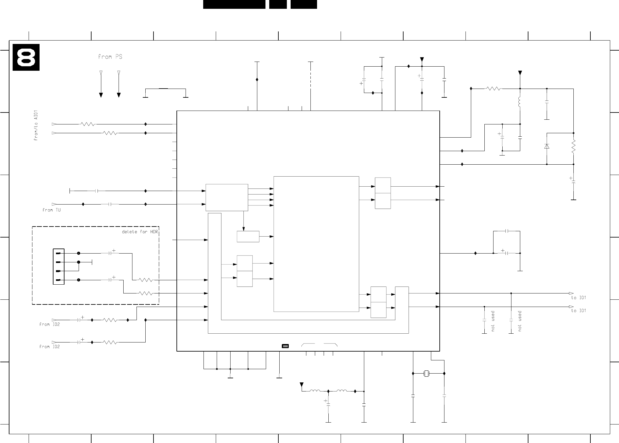
Electrical Diagrams and Print-Layouts EN 115DVDR980-985 /0X1 7.
Analog Board: Sound Processing
SCART-L
SCART-R
SCART-R
DFP
Switching Facilities
LOUDSPEAKER L D/A
D/A
I2SL/R
HEADPHONE R
IDENT
NC
SCART
LOUDSPEAKER R
A/D
D/A
DEMODULATOR
S1...4
FM1
FM2
I2SL/R
NICAM B
NICAM A
SCART-L
HEADPHONE L
IDENT
LOUDSPEAKER
A/D
D/A
F6004 D1
I600 A4
I601 A6
I602 A7
I603 A7
I604 A8
I605 B7
I606 B7
I607 D8
I609 F7
I611 F7
I612 F6
I613 F5
I614 E2
F
A
B
C
D
E
from DV - Board
QFP44
DVAR
2624 D2
2625 D2
3600 A8
3601 B1
3602 B9
3603 B2
3604 E2
3605 E2
3606 D2
3607 D2
4601 A5
5600 A8
5601 F5
5602 F6
6600 B9
7600 B6
C670 A3
F6001 D1
F6002 D1
2616 E8
2617 E8
2620 F7
2621 F7
2622 F5
2623 F6
GND
123456789
123456789
A
B
C
D
E
I617 E2
I619 C2
I620 C1
I622 C2
I623 B2
I624 B2
DVAL
GND
F
1600 F7
1960 D1
2600 A6
2601 A6
2602 A7
2603 A7
2604 A9
2605 B8
2606 B8
2607 C2
2608 C9
2609 C2
2610 C8
2612 D8
2614 E1
2615 E1
GNDDGNDD
I615 E2
I616 E2
GNDA
I604
F6004
4K7
3602
3601
100R
1n
2616
2622
10u
10u
2602
2609
56p
10n
2601
3607
1K
I606
2u2
2615
I619
I624
3604
1K
I617
GNDD
I600
3p3
2621
2u2
2614
1K
3606
I614
1960
1
2
3
4
HC-49/U
1600
18M432
C670
EH-B
GNDA
2624
2u2
10u
2608
8SW
GNDD
2625
2u2
I605
4u7
2612
Sound Processing AP
10n
2623
2603
100n
8SW
GNDA
I616
5602
10u
10n
2604
1n
2617
GNDD
I615
10n
2610
10u
2600
I602
F6001
GNDD
10K
3600
6600
MCL4148
F6002
2605
10u
I609
56p
2607
I607
7
TP
VREF1
29
VREF2
25
VREFTOP
42
5
XTAL_IN
6
XTAL_OUT
5SW
I2S_WS15
43 MONO_IN
23 24 28 32
RESETQ 22
SC1_IN_L
40
SC1_IN_R41
SC1_OUT_L 31
SC1_OUT_R 30
SC2_IN_L37
38 SC2_IN_R
STBYQ 11
4
TESTEN
44
AVSUP
1
CAPL_M
34
27DACM_L
26DACM_R
20
DVSS
DVSUP 19
D_CTR_IO0
9
D_CTR_IO1
8
I2C_CL12
I2C_DA13
I2S_CL14
I2S_DA_IN117
21 I2S_DA_IN2
16 I2S_DA_OUT
7600
MSP3415G
18
ADR_CL
ADR_SEL
10
AGNDC 36
35
AHVSS
AHVSUP
33
ANA_IN+2
ANA_IN-3
ASG
39
AVSS
5SW
I611
2620
3p3
5SW
GNDD
GNDA
GNDA
GNDA
I622
GNDA
I603
I601
100u
5601
100R
3603
4601
GNDD
GNDA
GNDD
2606
10n
GNDA
GNDA
GNDA
I623
5600
10u
I620
I612I613
1K
3605
5SW
SIF1
SCL1
SDA1
ARCRI
ARCLI
8SW
AFEL
AFER
CL 16532095_016.eps
080801
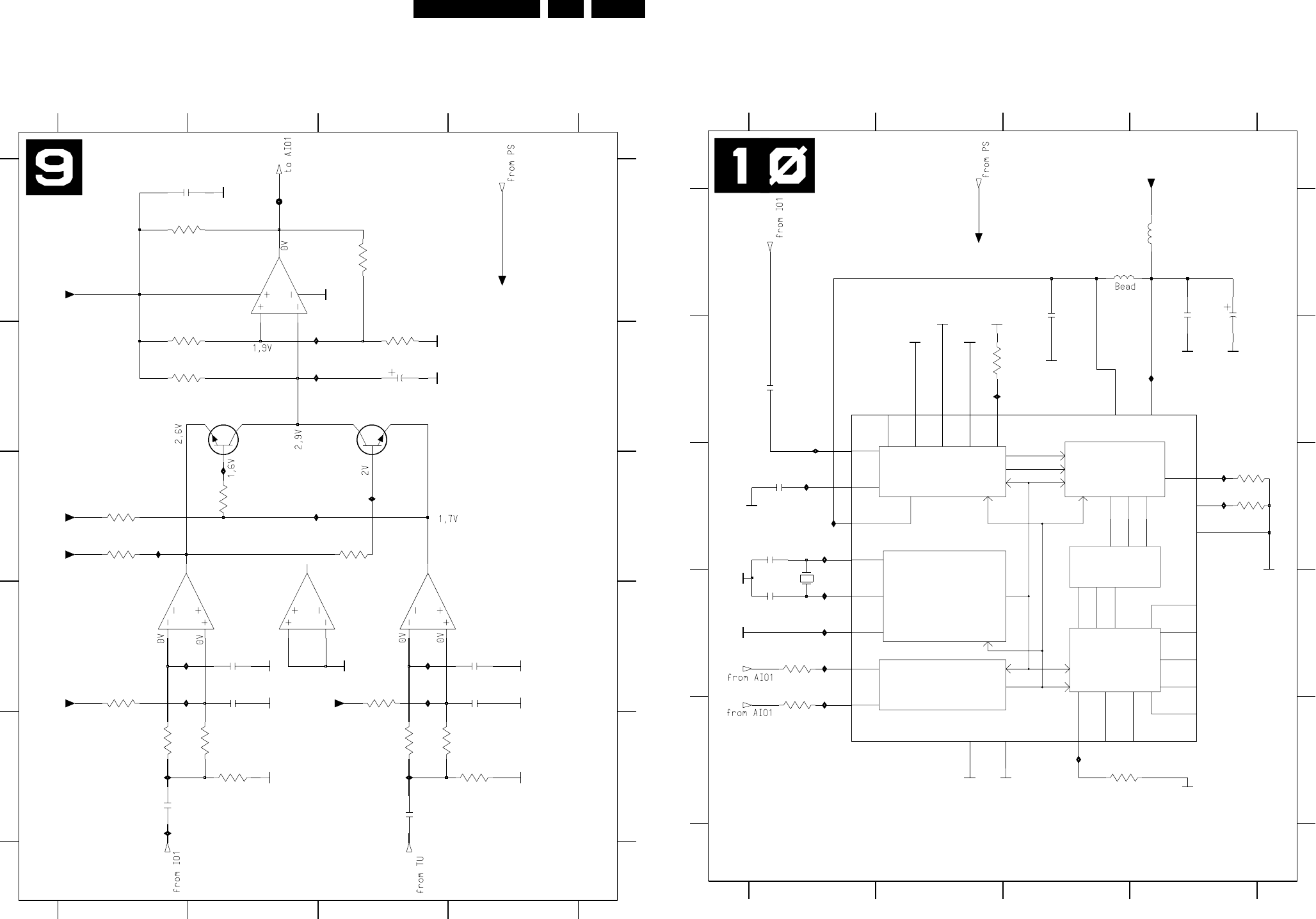
EN 116DVDR980-985 /0X1 7.
Electrical Diagrams and Print-Layouts
Analog Board: Follow Me
C
I955 C1
E
7950 D2
3952 B1
I951 B2
3961 E1
3955 C2
A
E
3957 C1
7950 D4
7951 B2
3
I954 C3
3966 E4
A
2953 D4
2954 D2 I959 D3
3
2
I958 D3
B
7950 D2
2957 E3
3962 E2
4
7952 B3
2951 B3 3963 E3 I952 B2 I960 E1
I953 C2 I956 D1
2956 E1
2
3956 C1
D
3964 E3
3951 A3
4
3965 E2
3950 A1
2952 D2
I963 E1
I961 E3
3954 B1
1
1
3959 D12955 D4
3958 C3
7950 A2
3960 D3
I962 C2
2950 A1
I957 D1
C
3953 B3
D
B
F950 A3
I962
3956
2K2
3952
22K
I960
5SW
3957
2K2
5SW
GNDV
3954
4K7
3965
33K
4K7
3950
GNDV
GNDV
GNDV
5SW
33K
3966
LM339D
7950-A
5
4
2
5SW
3955
4K7
7952
BC847BW
5SW
3959
7950-B
LM339D
7
6
1
3
12
10M
BC847BW
7951
I953
I957
I952
180p
2954
I963
2955
180p
2957
1u
I954
33K
3961
I958
F950
GNDV
2951
10u
GNDV
GNDV
GNDV
3951
100K
GNDV
5SW GNDV
33K
3962
GNDV
4K7
3958
1u
2956
3964
33K
3963
33K
I956
I961
Follow Me FOME
2950
100n
I951
7950-C
LM339D
9
8
14
2953
2n2
LM339D
11
10
13
2n2
2952
I959
7950-D
3960
10M
I955
3953
15K
VFV
YCVBSIN_SC1
FOME
5SW
CL 16532095_017.eps
080801
Analog Board: VPS
CTRL
Data
Clock
Data
Address
INTERFACE
DISPLAY
MEMORY
8 PAGES
PROCESSING
DATA
DATA DECODING
INTERFACE
I2C BUS
TIME BASE
SYNTHETIZER
FREQUENCY
OSCILLATOR
DATA EXTRACTION
SYNCHRONIZING
CLAMPING
CTRL
Address
Data
C
D
5990 A4
5991 A33994 E1
3995 E3 7990 B1
I987 E3 I989 D1
I990 B4
I991 C4
I992 C4
I993 B2
I994 B1
I995 C1
I996 C1
I997 C1
I998 D1
I988 D1
2990 A4
B
1234
1234
E
A
B
C
D
E
1990 D1
A
2991 A4
2992 A3
2993 B1
2994 C1
2995 C1
2996 D1
3990 C4
3991 C4
3992 B2
3993 D1 I999 D1
I994
5990
10u
GNDV
TEST2
27
VCR_|TV
21
VDDA
3
VDDD
22
VSSA
26
VSSD
7
VSSO
25
XTI
24
XTO
23
Y
15
GNDV GNDV
CBLK
28
COR_
13
CVBS
1
DV_
19
FFB
6
G
9
L23
18
MA_|SL
2
ODD_|EVEN
14
POL
4
R
8
RGBREF
11
SCL
16
SDA
17
STTV
5
TEST1
20
5SW
7990
STV5348
B
10
BLAN
12
3990
47K
I995
GNDV
3993
100R
GNDV
GNDV
2995
22p
100n
2992
GNDV
I990
13M875
1990
HC-49/U
22p
2996
GNDV
100n
2993
3992
47K
5991
2990
100n
5SW
3995
10K
100R
3994
47K
3991
GNDV
GNDV
GNDV
47u
2991
VPS
GNDV
I987
GNDV
I999
100n
2994
GNDV
I993
I991
I992
I989
I998
I988
I997
SDA1
SCL1
A_YCVBS
5SW
I996
CL 16532095_018.eps
080801
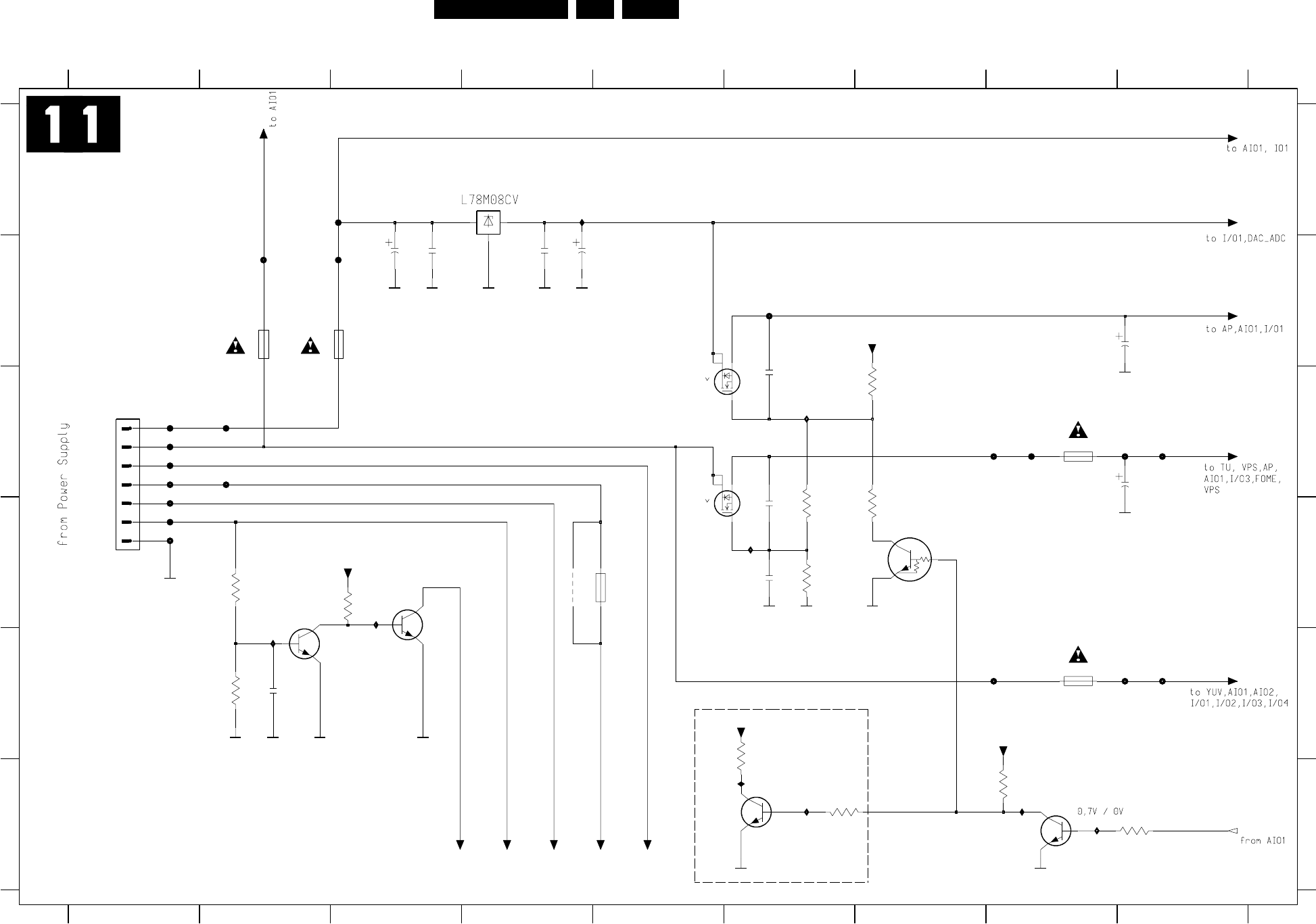
Electrical Diagrams and Print-Layouts EN 117DVDR980-985 /0X1 7.
Analog Board: Power Supply
to DAC_ADC,AIO1
2324 B3
2325 B4
2328 C8
2331 B4
2332 B8
0V / 5.3V
5.3V / 0V
2323 D6
3336 F8
34
3337 D6
3338 D3
3339 D2
89
I339 D6
F9332 E9
F9333 E9
to AIO1, DAC_ADC,YUV,
to AIO1
2330 B3
78
3321 C7
3322 E6
3323 F6
I326 F6
I337 F8
I338 F8
3335 F9
I340 E2
3325 D6
3326 D7
56
F9346 C2
F9347 C2
I324 C6
F9342 C9
1
3340 E2
1996 D4
2321 C6
2322 D6
1932 C1
91
F3206 D1
F3207 D1
F9330 E8
F9340 B2
D
E
F
0V / 5.3V
F3203 C1
F3204 C1
F3205 C1
not used
not used
F9341 C9
12.3V / 0V
to AIO1
2345
F
B
C
I325 F6
IO1, IO3, IO4
VGNSTBY
1327 B2
7
6
D
delete for HDR
1326 B2
2329 E2
2
1324 E8
not used
7330 E2
A
B
C
1325 C8
7331 E3
7332 A4
F3201 C1
F3202 C1
F9336 B6
F9338 C8
4320 D4
7321 C5
I341 D3
I345 A4
7329 F8
to TU
E
17.9V / 0V
not used
5.2V / 0V
220K
3321
F9343 C8
F9344 A3
F9345 B3
A
7322 F6
7323 D5
7324 D7
GNDA
100u
2331
GNDA
3337
100K
5STBY
F9338
F9330
12STBY
3340
220K
GNDA
F9345
1
2
3
4
5
6
7
VGNSTBY
EH-B 1932
2SK2839
7321
5M
100n
2325
F9342
8STBY
PSC
1327
500mA
I324
I338
F9346
33STBY
GNDA
GNDA
I337
3336
10K
GNDA
2324
330n
220K
3338
500mA
1325
PSC
BC847BW
7330
Power Supply PS
5STBY
220K
3325
7332
GND
2
IN
1
OUT
3
GNDA
3323
10K
10K
3326
FLYB
GNDAGNDA
I340
220K
3339
GNDAGNDA
F9347
5STBY
F3202 F9341
F9333
8SW
2328
100u
F3206
I345
1A
47R
3322
4320
1324
PSC
2329
470n
I339
F9332
GNDA
2330
47u
GNDA
BC847BW
7322
5SW
3335
4K7
2323
47n
GNDA
100n
2322
I326
7323
2SK2839
GNDA
F3207
GNDA
5SW
7329
BC847BW
PDTC124EU
7324
BC847BW
7331
100n
2321
33STBY
I341
F9344
F9340
IPFAIL
250mA
1996
100u
2332
F9336
GNDA
F9343
F3205
5NSTBY
1A
1326
PSC
F3204
F3201
F3203
I325
FLYB
5V
12V
ISTBY
33STBY
5NSTBY
GNDA
CL 16532095_019.eps
080801
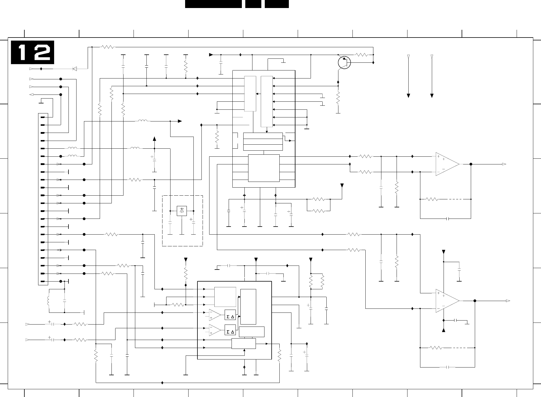
EN 118DVDR980-985 /0X1 7.
Electrical Diagrams and Print-Layouts
Analog Board: Audio Converter
ADC
CLOCK
CONTROL
ADC
DIGITAL
INTERFACE
DECIMATION
FILTER
DC-CANCEL
FILTER
CONTROL
INTERFACE
DAC'S
VOL/MUTE/DEEMPH
INTERPOL FILTER
NOISE SHAPER
NC
DIGITAL
INTERFACE
3025 B2
2
3011 D7
1234
3032 F8
5000 B3
5001 E1
5002 B3
9
B
D
F0005 D2
F0007 D2
F0009 D2
F0011 C2
2025 A3
2026 A3
2027 D3
2028 D4
to IO1, IO3
not used
from PS
3021 F2
3002 A6
3003 B4
67
3004 A3
3005 B7
F014 A1
I001 A1
I009 B6
I010 C6
3010 C6
from IO1
from AIO1
from IO1
not used
B
C
D
E
F
3012 D7
2000 A4
3013 F2
2002 C7
3014 D2
3015 E2
3016 D2
3017 D7
3018 E6
3019 E6
3020 E2
3022 F8
3023 E3
3024 E3
2030 C3
3000 A2
345
not used
not used
not used
not used
3008 C6
3009 C8
2013 E1
2014 E8
2015 F1
2016 F5
2017 F6
2018 F8
2019 E5
A
Bead
C
from DIGIO
E
F
A
from PS
to DIGIO
Bead
5VD
from DIGIO
not used
1
I033 A4
I034 A4
89
5678
2004 C4
I038 E1
I039 F1
5003 B1
5004 B1
6000 A1
7000 A6
7001 A4
7002-A B8
7002-B E8
1900 B1
7005 C3
2001 E1
F0002 E2
2003 C4
2021 F2
2022 E3
2023 D3
2024 A2
2005 D5
2006 D5
2007 D8
2008 D7
2029 C3
I014 F6
I015 E3
3001 A7
2009 D4
2010 E8
2011 E6
2012 E6
3006 C7
3007 C7
I017 F3
I018 F3
I019 F3
I020 F3
I022 E8
I023 F5
I024 B8
I025 C8
1%
2020 F2
I026 D8
not used
I027 E8
3VD
I028 A4
I029 C4
I030 C5
I031 A6
3026 A2
3027 B2
3028 F5
3029 C8
I032 A7
I016 E3
I035 A4
to DIGIO
to IO1, IO3
not used
3030 C3
I036 B4
I037 E3
1%
1%
1%
1%
1%
1%
1%
1%
1%
7004 E4
F0001 E1
F0003 D2
F0012 C2
F0014 C2
F0016 C2
F0017 B1
F010 C9
F011 E9
F012 A1
F013 A1
I011 D6
I012 D6
I013 D5
GNDD
22n
2000
4K7
I026
3 VINR
2VREF
4VREFN
5VREFP
15
VSSA
10
VSSD
12 WS
GNDD
3005
UDA1360TS
7004
11 BCK 13DATAO
FSEL14
7 PWON
6 SFOR
8 SYSCLK
16
VDDA
9
VDDD
1 VINL
8STBY
I036
47p
2029
GNDD
100n
2027
GNDA
3009
5K1
GNDA
3013
22R
2023
47p
47u
2017
I017
3V3DD
I016
GNDD
I010
5001
GNDD
2025
47p
I037
I028
GNDD
47u
2006
22R
3030
I027
I013
10u
5002
47u
2015
2003
GNDD
47K
3024
GNDD
22n
2002
330p
F0011
GNDD
I025
3032
I039
BC857BW
7000
GNDD
I018
I034
GNDA
47p
2024
I029
3016
22R
I019
F0003
GNDA
GNDA
I038
22R
3027
I014
OUT
3002
10K
7005
LF33CV
GND
IN
32
VO31 VO4 2
VO54 VO6 5
VREFA
30
VSSA
3
VSSD
20
WS11
100n
2012
19
L3MODE 17
MUTE 23
7
8
15
STATIC 9
16 SYSCLK
TST127
TST2 22
VDDA
6
VDDD
21
VO1N29
VO1P28
VO2N 31
VO2P
UDA1328T
7001
BCK10
DEEM0 25
DEEM1 24DI1212
DI3413
DI5614
DS 26
L3CLK 18
L3DATA
3007
4K7
I024
8STBY
5VDD
5K1
3022
4K7
3000
21
22
3
4
5
6
7
8
9
F011
FMN1900
1
10
11
12
13
14
15
16
17
18
19
2
20
F012
GNDA
2021
47p
10K
3003
3V3DD
GNDA
2013
47u
I020
22R
3025
I033
5000
GNDD
F013
100u
2030
GNDA
I023
I012
GNDA
100n
100n
2019
3019
1R5
2016
3006
4K7
3
2
1
GNDD
3004
10K
7002-A
MC33078
6000
MCL4148
GNDD
GNDD
F014
Audio
Converter DAC_ADC
100n
2009
GNDD
I009
GNDA
GNDD
GNDD
1n
2001
3012
4K7
GNDD
3023
47K
100n
2010
GNDA GNDA
4K7
3011
I011
F0012
2011
47u
GNDD
F0007
GNDA
GNDD
GNDA
GNDD
F0005
10u
2028
3021
12K
GNDD
I030
2005
100n
3V3DD
GNDD
GNDD
GNDD
GNDA
F010
3008
1R5
330p
2008
MC33078
7002-B
5
6
7
8
4
220p
2018
GNDA
I001
5NSTBY
47p
2022
3015
22R
5003
5004
3010
1R5
3018
F0016
1R5
4K7
3017
5NSTBY
2026
47p
2004
47u
F0009
47p
2020
GNDD
100K
3001
I022
GNDD
F0001
F0017
3V3DD
GNDD
2014
100n
GNDA
2007
220p
GNDD
I032
GNDD
3V3DD
3029
4R7
3028
3V3DD
12K
3020
I015
GNDD
GNDD
GNDA
I035
F0002
GNDA
I031
22R
3014
3026
22R
F0014 GNDD
D_PCMCLK
GNDD
A_DAT
DAINOPT
DAINOPT
GNDD
GNDD
DAINCOAX
DAINCOAX
DAOUT
DAOUT
ARDAC
ALDAC
D_BCLK
D_DATA0
D_WCLK
D_IKILL
GNDD
GNDD
GNDD
GNDD
A_BCLK
A_WCLK
A_PCMCLK
ALADC
ARADC
8STBY
5NSTBY
GNDD
IPFAIL
CL 16532095_020.eps
080801
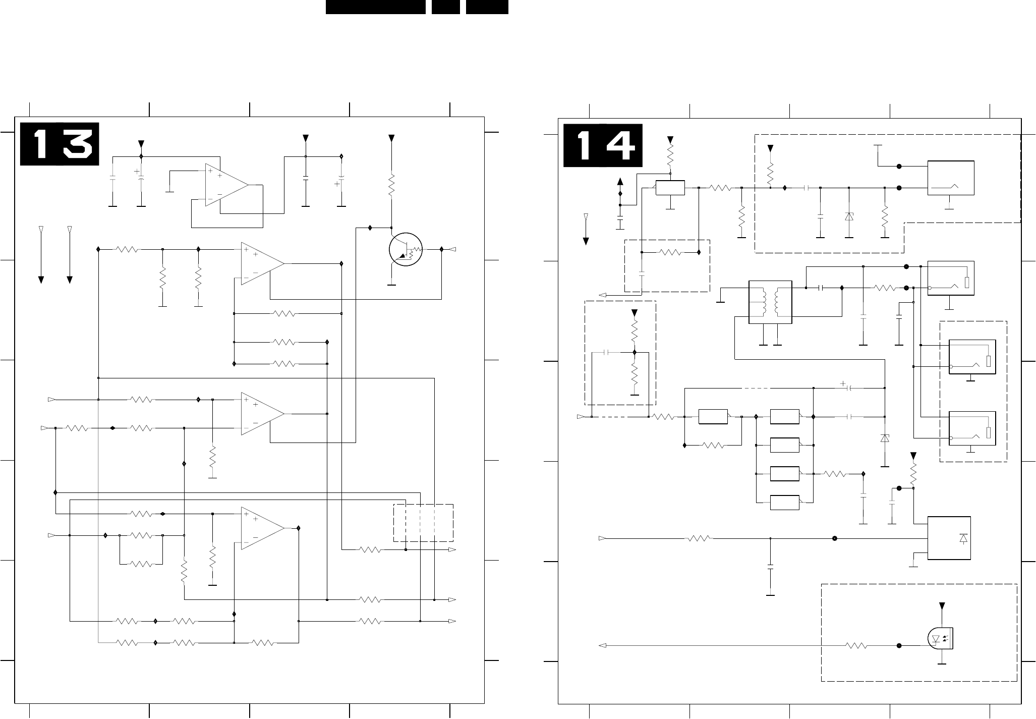
Electrical Diagrams and Print-Layouts EN 119DVDR980-985 /0X1 7.
Analog Board: RGB-YUV-Converter
4203 D4
1%
delete for
1%
2202 A3
2203 A3 I209 C2
I204 A4
I205 A3
I206 A2
3212 D1
123
I207 A1
I208 B3 I213 D1
I214 D2
B
C
D
1%
1%
from IO1
1%
from AIO1
3200 A4
I226 E2
1%
1%
7200-D A2
7201 B4
I201 A2
3206 B3 I211 C1
I212 C2
not used for SA7118
3207 C1
3208 C1
to I/O 1
1%
1%
3202 B2
3203 B2 7200-A C3
7200-B D3
7200-C A33205 B3
3209 C1
3210 C2
I202 A3
I203 A4
E
from IO1
3204 B3
4201 D4
4202 D4
2200 A1
2201 A1
3213 D1
3214 D2 3223 D4
I210 C23211 D1
4
12
from IO1
B
C
D
1%
3222 E2
1%
34
A
Y` = R - V x 1,402
3220 E3
3221 E1
I216 D3
to I/O 1
I224 E2
I225 E2
U = B/2 - 0,169R - 0,331G
1%
V = R/2 - 0,419G - 0,081B
3219 E2
E
A
3201 A1
1%
1%
to I/O 1
HDR
I215 D1
3215 E2
3218 E1
from PS
from PS
1%
3224 E4
3225 E4
I206
GNDV
1%
1%
3220
1K
750R
15K
3203
GNDV
3210
5STBY
GNDV
4203
GNDV
I209
5STBY
1K5
3207
7200-C
TSH95
12
11
10
9
3208
6K8
750R
3214
I201
I204
3200
22K
I210
GNDV
1K5
3211
100R
100R
3225
5NSTBY
I213
3224
7201
PDTC124EU
4K7
47u
2203
5K62
3209
3222
3204
1K
22n
750R
3206
7200-D
TSH95
14
15
16
4
13
2200
7200-A
TSH95
3
2
1
8
5NSTBY
5STBY
3202
750R
I226
I205
I202
GNDV
3218
I216
3215
1K
1K5
GNDV
I207
I214
I224
I212
47u
2201
22n
2202
I211
GNDV
GNDV
3221
I225
GNDV
1K2
7200-B
TSH95
5
6
7
I215
I203
4K7
3212
I208
3213
4K7
4202
3219
4201
100R
3223
1K5
3201
1K
RGB-YUV-Conv. YUV_CON
3205
15K
RCIN_SC2
A_R
A_B
A_G
YUV_ON
5NSTBY
5STBY
GIN_SC2
BIN_SC2
CL 16532095_021.eps
080801
Analog Board: Digital In / Out
not used
to the rear plane
to DAC_ADC
from DAC_ADC
OPTICAL
from DAC_ADC
OPTICAL
to DAC_ADC
DIGITAL
F4102 A4
F4103 A4
F4202 B4
F4203 A4
F4204 D3
I489 C1
IN
not used
not used
not used
IN
DIGITAL
from DAC_ADC
not used
not used
3443 D4
3456 B1
3490 C1
3491 A1
3492 A2
I490 C2
I492 C3
I495 A1
I496 A2
I497 B13498 E3
3499 A1
4470 C1
4471 C2
5470 B2
6470 A3
6471 C3
7470-A C2
7470-B C2
7470-C C2
7470-D A1
7470-E C2
7470-F D2
C
D
E
A
B
C
D
E
1941-A A4
1941-B C4
1942 E4
1943 D4
1945 A4
1948 B4
F4205 E4
F488 D4
I485 A2
I486 D3
I487 B3
Ground not connected
OUT
2477 D3
2479 C3
2480 B1
2481 E2
2483 A1
2484 D3
2485 B4
2486 B1
3427 A2
3428 A2
3429 D3
F4205
2470 C3
2471 A3
2472 A3
2473 B3
2474 B3
not used
3493 A3
3494 B3
3495 C2
3496 C1
3497 D2
not used
OUT
not used
1234
1234
A
B
GNDD
1941-A
YKC21-3600
5
3
1
2483
1u
7470-D
PC74HCU04D
9
A
14
Vcc
7
Vss
8
Y
3496
2474
100n
GNDD
100K
GNDD
5VDD
6471
BZX284-C6V8
F4202
7470-F
PC74HCU04D
A
13
Y
12
GNDD
5
4
2
2472
150p
I496
YKC21-3600
1941-B
2473
150p
I487
4470
GNDD
3498
1K
3495
2K2
1n
2484
10K
3491
F4103
3493
75R
GNDD
GNDD
3494
75R
7470-A
PC74HCU04D
1
A
2
Y
GNDD
F4203
33p
2481
PC74HCU04D
7470-E
11
A
10
Y
7470-C
PC74HCU04D
5
AY
6
10u
2479
100R
3428
4471
VCC
2480
100n
GNDD
GNDD
1942
GP1FA550RZ
GND
2
OUT
3
1
3497
I492
F4102
100R
6RG
1
2
34
6
2470
100n
5470
100K
3456
GNDD
F488
100K
3427
GNDD
5VD1
5VDD
100n
2471
A
3
Y
4
3
2
GNDD
5VDD
7470-B
PC74HCU04D
Digital In / Out DIGIO
YKC21-3479
1945
1
470R
3490
GNDD
560R
3429
100n
2485
GNDD
I495
I497
3499
330R
2
BZX284-C6V8
6470
1948
YKC21-3416
1
3
I485
10n
2486
F4204
GNDD
GNDD
1943
GP1FA550TZ
GND
3
VCC
2
VIN
1
5VD1
GNDD
I490
I486
5VD1
5VDD
GNDD
GNDD
47R
3443
100K
3492
2477
100n
I489
GNDD
GNDD
GNDD
5VDD
DAINCOAX
DAINOPT
DAOUT
DAOUT
CL 16532095_022.eps
080801
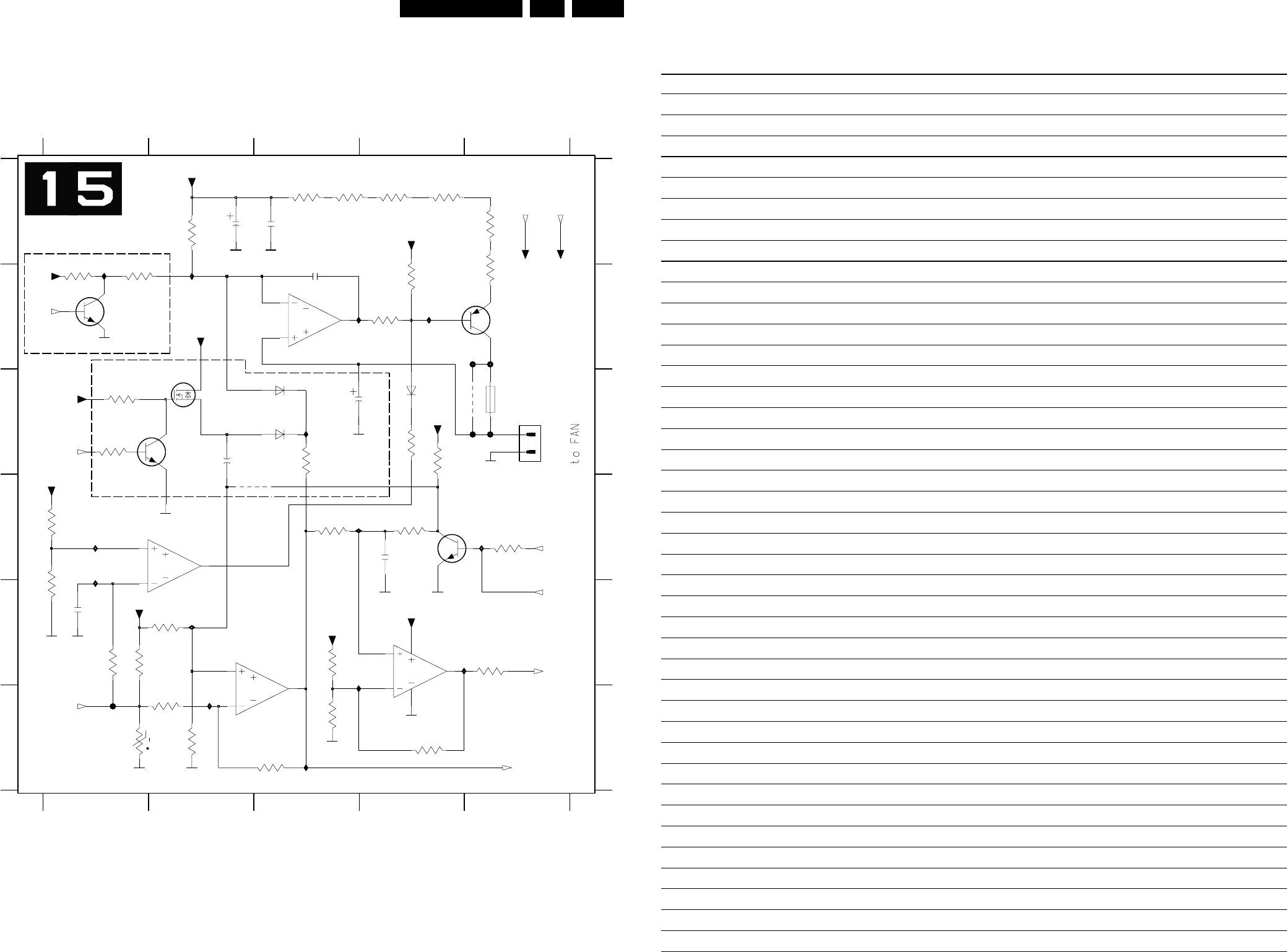
EN 120DVDR980-985 /0X1 7.
Electrical Diagrams and Print-Layouts
Analog Board: Fan Control
t
I920 B2
I921 B3
I922 B4
I923 E2
I924 F3
I925 C3
I926 F2
I927 D1
I928 D1
I929 D4
I930 E4
I931 D5
I932 B1
I933 E3
3978 B5
3979 B4
from AIO1
delete for
delete for SW contr.
3980 D3 3989 D5
3996 A4
3997 A5
4905 C5
6970 C3
6971 C4
6972 C3
7970-A E4
7970-B B3
7970-C E3
7970-D D2
7971 B5
7972 D5
7973 B1
7974 C2
7975 C2
2970 C2
2980 A2
to AIO1
from PS
to AIO1
from PS
from AIO1
for SW contr. only
from AIO1
for SW contr. only
SW contr.
F805 B5
F806 C5
F807 F1
F813 B5
F814 C5
3943 C1
3944 C1
3946 B1
3947 B4
3948 D2
3967 A3
3968 A3
3969 A4
3970 E2
3971 E1
3972 C3
3973 F2
3974 F1
3975 F2
3976 F3
3977 A2
from AIO1
for SW contr. only
not used
from AIO1
not used
for SW contr. only
12
3981 F4
3982 E3
3983 F3
3984 E5
3985 D1
3986 E1
3987 C4
3988 E1
345
12345
A
B
C
D
E
F
A
B
C
D
E
F
1983 C5
1984 C5
2981 A3
2982 C3
2983 D4
2984 E1
2985 B3
3940 C4
3941 D4
3942 B1
3996
10R
10R
3997
4
11
1K
3979
12
13
14
4
11
7970-C
LM324D
10
9
8
LM324D
7970-D
I923
22K
3942
100n
2981
10R
3969
2970
10u
BC847BW
7974
1
2
3985
5K6
3948
3975
56K
EH-B
1984
3983
56K
3986
10K
GNDD
I927
3944
220K
33K
3980
2985
10n
5SW
12STBY
GNDD
3946
2K2
2982
100u
6971
BSH111
7975
MCL4148
F813
F814
7971
BC636
10K
3943
12STBY
GNDD
GNDD
3947
10K1K
3987
GNDD
12STBY
5SW
12STBY
3978
10R
F807
10n
2983
GNDD
10R
3968
3971
33K
I925
GNDD
I926
220K
3970
GNDD
3972
470R
GNDD
GNDD
BC847BW
7972
GNDD
I920
I929
I921
4K7
3940
MP13
125mA
I932
3989
10K
1983
Fan Control FACO
I922
3974
LM324D
7970-B
5
6
7
4
11
3941
22K
6972
MCL4148
12STBY
I924
12STBY
3976
39K
2984
1n
I931
F805
3981
15K
3
2
1
4
11
12STBY
3988
27K
3982
7970-A
LM324D
MCL4148
22K
3977
18K
12STBY
12STBY
6970
I933
GNDD
I928
GNDA
3967
10R
100u
2980
12STBY
3984
1K
I930
GNDD
7973
BC847BW
4905
F806
MOTMOT
1K
3973
TEMP
GNDD
TEMP_SENSE
12STBY
5SW
BE_FAN
ION_FAN
SW_BE_FAN
SW_CAB_FAN
ION_FAN
CL 16532095_023.eps
080801
Personal Notes:
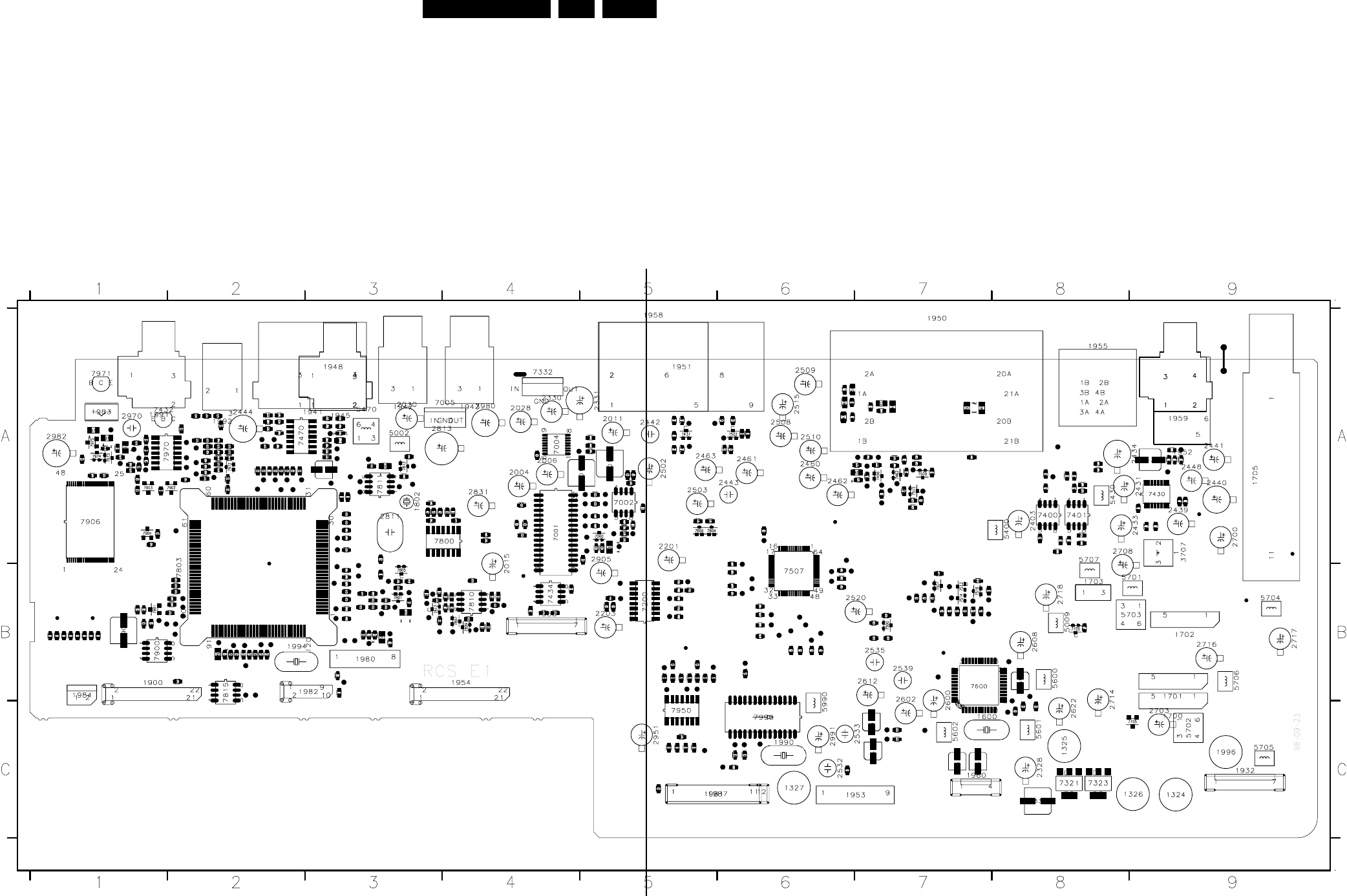
Electrical Diagrams and Print-Layouts EN 121DVDR980-985 /0X1 7.
Layout Analog Board (Overview Top View)
CL 26532011_001.eps
170102
Part 1
CL 26532011_01a.eps
Part 2
CL 26532011_01b.eps
1323 C8
1324 C9
1326 C9
1327 C6
1600 C7
1700 C9
1701 B9
1702 B9
1703 B8
1703 A9
1802 A3
1900 B1
1910 C3
1911 C3
1932 C9
1941 A3
1942 A3
1943 A4
1943 A3
1948 A3
1950 A7
1951 A5
1952 A9
1953 C7
1954 B4
1955 A8
1956 B4
1958 A5
1959 A9
1960 C7
1980 B3
1981 C5
1982 B3
1983 A1
1984 B1
1987 C6
1990 C6
1991 A1
1992 A2
1994 B2
1996 C9
2000 A3
2003 A4
2004 A4
2006 A4
2007 A5
2010 A5
2011 A5
2012 A5
2013 A5
2015 B4
2017 A5
2018 A5
2020 B1
2021 B1
2022 B1
2023 B1
2024 B1
2025 B1
2026 B1
2028 A4
2029 B1
2030 A3
2201 A5
2203 B5
2328 C8
2330 A4
2331 A5
2332 C8
2336 B6
2400 A8
2403 A8
2405 A8
2406 A8
2407 A8
2408 A8
2430 A9
2431 A9
2433 A9
2434 A9
2436 A9
2437 A9
2438 A9
2439 A9
2440 A9
2441 A9
2442 A3
2443 A6
2444 A2
2446 A5
2448 A9
2449 B4
2450 B4
2460 A6
2461 A6
2462 A6
2463 A5
2464 A7
2466 A7
2469 A7
2470 A3
2471 A3
2479 A3
2480 A2
2483 A3
2484 A2
2486 A3
2500 B7
2501 B7
2502 A5
2503 A5
2508 A6
2509 A6
2510 A6
2512 B6
2513 A6
2514 A7
2517 B6
2520 B7
2521 B6
2522 B6
2523 A7
2523 C6
2528 B6
2529 B6
2530 B6
2530 A7
2532 C6
2533 C7
2533 B7
2537 B6
2538 B6
2539 B7
2541 B7
2542 B7
2544 B3
2547 A6
2600 B7
2602 B7
2603 B8
2608 B8
2612 B7
2614 C7
2615 C7
2622 C8
2624 C7
2625 C7
2700 A9
2703 C9
2708 A8
2714 B8
2716 B9
2717 B9
2718 B8
2800 A4
2801 B3
2803 B3
2804 B3
2806 A4
2810 B4
2811 A3
2812 B4
2813 A3
2816 B3
2817 B3
2818 A3
2820 A3
2831 A4
2901 B1
2903 A3
2918 A1
2950 C5
2951 C5
2952 B5
2953 B5
2956 B6
2957 B5
2970 A1
2980 A4
2982 A1
2983 A2
2984 A2
2985 A1
2991 C6
3000 A5
3001 A5
3005 A5
3006 A5
3008 A4
3009 A5
3010 A4
3011 A5
3012 A5
3018 A5
3021 A5
3022 A5
3028 A4
3029 A5
3032 A5
3110 C4
3201 B5
3202 B5
3203 B5
3207 B5
3208 B5
3210 B5
3211 B5
3214 B5
3402 A8
3403 A8
3404 A8
3409 A8
3412 A8
3413 A8
3414 A8
3415 A8
3418 B3
3419 B3
3423 A9
3427 A3
3428 A3
3429 A2
3431 A9
3432 A8
3433 A9
3434 A9
3435 A8
3437 A9
3439 A5
3440 A5
3441 A5
3442 A5
3455 A9
3456 A2
3457 A7
3458 A7
3459 A7
3464 A6
3465 A6
3470 A6
3471 A6
3472 A7
3473 A7
3474 A7
3475 A7
3477 A7
3479 A7
3489 A7
3490 A2
3491 A3
3492 A3
3496 A2
3499 A3
3500 B7
3501 B7
3502 A6
3503 B7
3503 B7
3504 B7
3506 B7
3507 A6
3517 A6
3521 B3
3523 A7
3523 B6
3526 A6
3528 B6
3531 B6
3532 A6
3533 A6
3533 A7
3536 B7
3537 A7
3537 B7
3538 B7
3539 A7
3539 B7
3541 B6
3542 B6
3560 B7
3561 B7
3564 A6
3568 A7
3570 B3
3600 C8
3600 B8
3601 C8
3603 C8
3604 C7
3605 C7
3707 A9
3725 B8
3801 B3
3802 B3
3803 B3
3804 B3
3807 A4
3808 B3
3812 B3
3814 B3
3815 A4
3817 B3
3818 B3
3819 C6
3821 B3
3822 A3
3829 A3
3830 A3
3832 A4
3837 A3
3839 B3
3840 B2
3841 B2
3844 B2
3847 B2
3848 B3
3850 A5
3852 A5
3853 A6
3854 A3
3855 A5
3856 B3
3857 B4
3859 A5
3860 B5
3861 B4
3862 B4
3863 A2
3864 A2
3865 B2
3866 B3
3867 A2
3868 A2
3869 A2
3870 A2
3872 A3
3874 A3
3875 B3
3876 B4
3877 A3
3878 A3
3879 A3
3880 A2
3881 A3
3882 B4
3883 B3
3884 A3
3885 A2
3886 B3
3887 B4
3888 B4
3890 B2
3891 A3
3892 A3
3896 B3
3897 A2
3898 B4
3901 B1
3903 B2
3904 B2
3905 B2
3906 A1
3908 B2
3910 B2
3911 B1
3912 B1
3916 B2
3917 B2
3918 B1
3920 A2
3921 A1
3922 A1
3930 C5
3940 A2
3941 A2
3942 A1
3943 A1
3944 A1
3946 A1
3947 A1
3948 A2
3951 C5
3952 C5
3953 C5
3961 B5
3962 B5
3963 B5
3964 B5
3965 B5
3966 B5
3967 A2
3968 A2
3969 A2
3970 A2
3971 A2
3972 A2
3973 A2
3975 A2
3976 A2
3977 A1
3979 A1
3980 A2
3981 A1
3982 A1
3983 A1
3984 A2
3985 A2
3986 A2
3987 A2
3988 A2
3989 A2
3993 C6
3994 C6
3996 A2
3997 A2
4202 B3
4405 B4
4406 B4
4470 A2
4471 A2
4801 C5
4901 A1
4902 A1
4903 A1
4906 B4
5000 A4
5002 A3
5003 B2
5009 B8
5400 A8
5430 A8
5470 A3
5601 C8
5602 C7
5701 B9
5702 C9
5703 B9
5703 C9
5704 B9
5706 B9
5707 A8
5902 B2
5990 C6
6000 A5
6304 A7
6309 B3
6461 A7
6463 A7
6468 A7
6471 A3
6801 B3
6803 A3
6807 B2
6970 A1
6971 A1
6972 A1
7000 A5
7001 A4
7002 A5
7003 A4
7004 A4
7200 B5
7315 A7
7316 B7
7317 B7
7321 C8
7323 C8
7332 A4
7400 A8
7401 A8
7430 A9
7431 A5
7432 A1
7434 B4
7462 A7
7466 A7
7470 A2
7500 B7
7501 B7
7502 A6
7507 B6
7509 A7
7514 B7
7600 B7
7705 C9
7709 B8
7800 A4
7801 B3
7803 B2
7804 A3
7805 B3
7806 A5
7807 B4
7809 B4
7810 B4
7811 A3
7812 B3
7813 A3
7815 B2
7900 B1
7901 B1
7902 A2
7903 A1
7904 A1
7906 A1
7950 C5
7970 A1
7971 A1
7972 A2
7973 A1
7974 A1
7975 A1
7990 C6
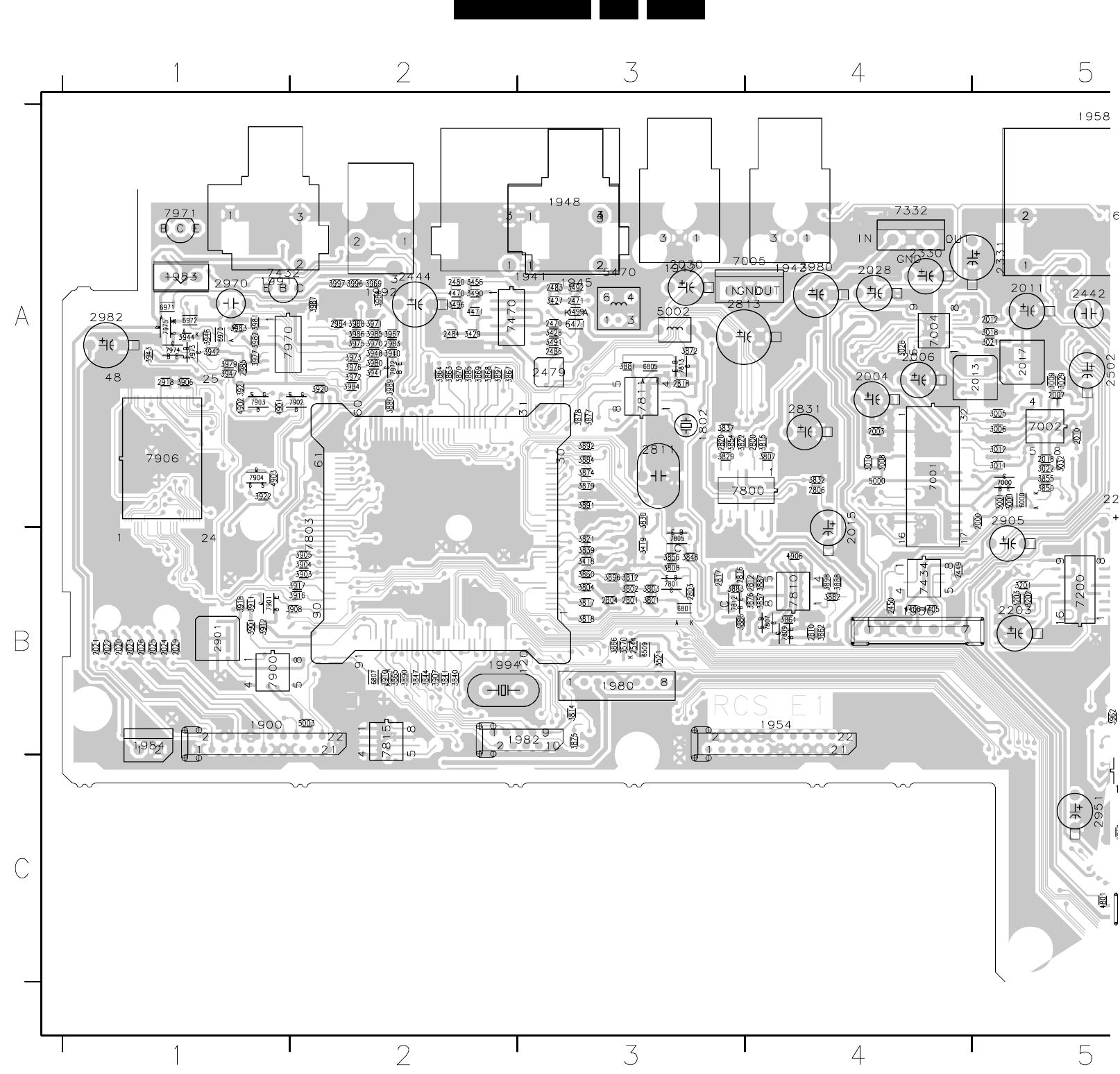
EN 122DVDR980-985 /0X1 7.
Electrical Diagrams and Print-Layouts
Layout Analog Board (Part 1 Top View)
CL 26532011_01a.eps
170102
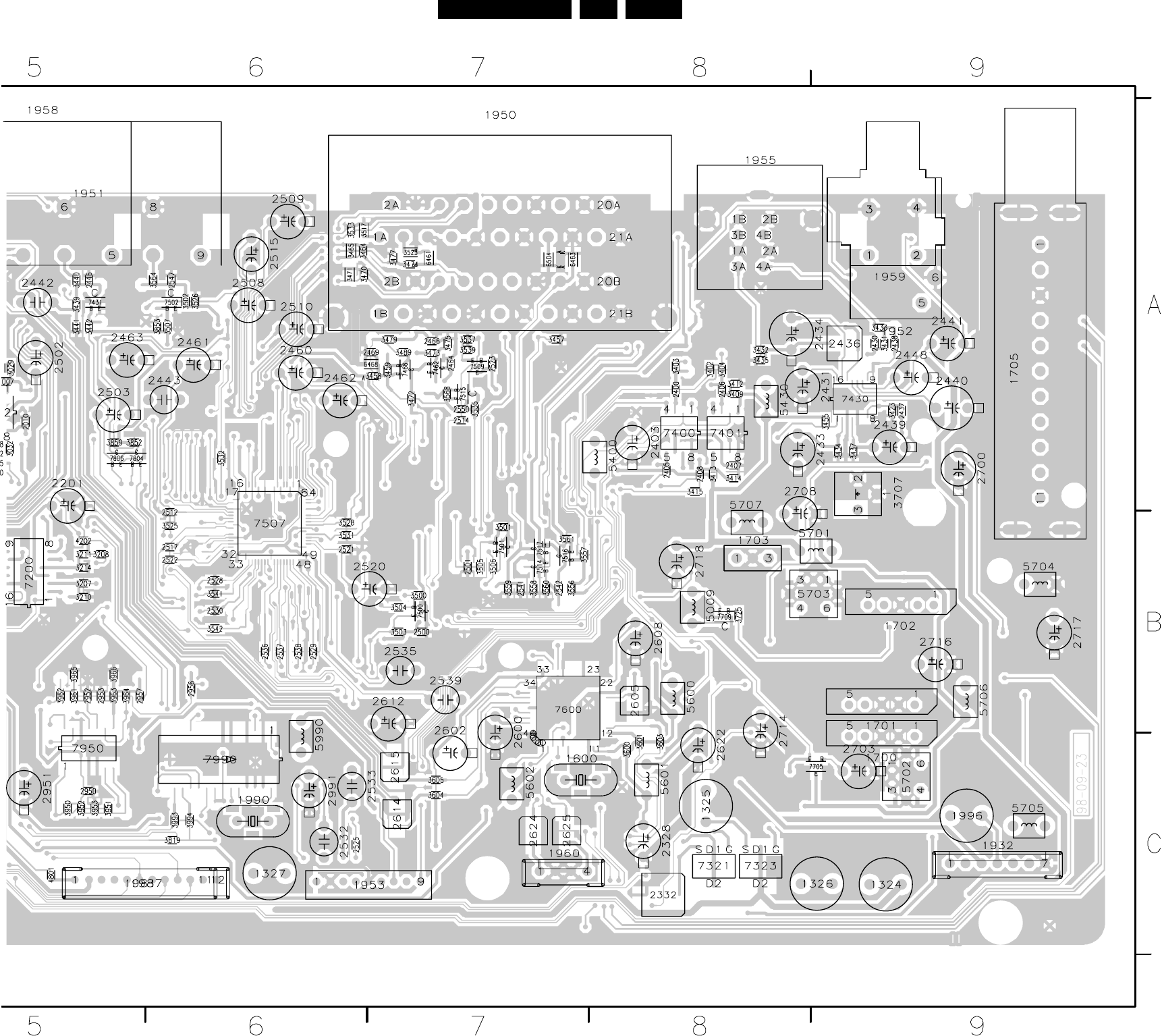
Electrical Diagrams and Print-Layouts EN 123DVDR980-985 /0X1 7.
Layout Analog Board (Part 2 Top View)
CL 26532011_01b.eps
170102
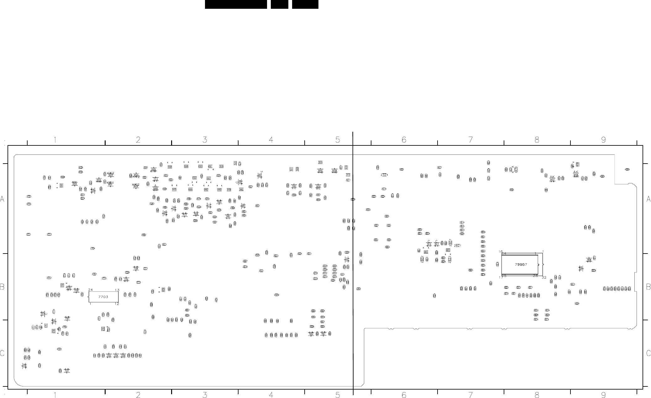
EN 124DVDR980-985 /0X1 7.
Electrical Diagrams and Print-Layouts
Layout Analog Board (Overview Bottom View)
CL 26532011_003.eps
170102
Part 1
CL 26532011_03a.eps
Part 2
CL 26532011_03b.eps
2001 A6
2002 A5
2005 A6
2008 A5
2009 A6
2014 A5
2016 A5
2019 A6
2027 A6
2100 C7
2101 C7
2102 C7
2103 C7
2104 C7
2105 C7
2106 C6
2200 A5
2202 B5
2321 C2
2322 C2
2323 C2
2324 A6
2325 A6
2329 C1
2401 A1
2402 A2
2404 A1
2410 A2
2411 A2
2432 A1
2445 A9
2447 A5
2465 A2
2467 A3
2468 A3
2472 A8
2473 A7
2474 A7
2477 A7
2481 A6
2485 A7
2504 A1
2505 B4
2506 A4
2507 B4
2511 B5
2513 B4
2516 B4
2518 B4
2519 B5
2524 B6
2526 B4
2527 A3
2531 B4
2534 A2
2540 A2
2545 A3
2546 A4
2548 A4
2549 B4
2551 A3
2601 C3
2603 B3
2604 B2
2606 B2
2607 B2
2609 C3
2610 B3
2616 B3
2617 B3
2620 B3
2621 B3
2623 C3
2701 C1
2702 C1
2704 A1
2705 B2
2706 B2
2707 B1
2709 B2
2710 B1
2711 C1
2712 B1
2713 A1
2715 B1
2802 B6
2805 B7
2807 A7
2808 B8
2809 B8
2814 A7
2815 A7
2819 A6
2821 A7
2822 B7
2823 A7
2827 C1
2832 A6
2900 B8
2902 B9
2903 B9
2904 A9
2906 B5
2907 B8
2908 B8
2909 A9
2910 B8
2911 B8
2912 B9
2914 B8
2915 B8
2916 B7
2917 B8
2954 B5
2955 B5
2981 A8
2990 C4
2992 C4
2993 C4
2994 C4
2995 C4
2996 C4
3002 A6
3005 A6
3004 A6
3007 A5
3015 B9
3014 B9
3015 B9
3016 B9
3017 A5
3019 A6
3020 A5
3023 A6
3024 A6
3025 B9
3026 B9
3027 B9
3030 B9
3100 C7
3101 C7
3102 C7
3103 C7
3104 C7
3105 C7
3106 C7
3107 C7
3108 C7
3109 C6
3111 C6
3112 C6
3113 C6
3200 A5
3204 B5
3205 B5
3206 B5
3209 B5
3212 B5
3213 B5
3215 B5
3218 B5
3219 B5
3220 B5
3221 B5
3222 B5
3223 B5
3224 B5
3225 B5
3321 C1
3322 C1
3323 C1
3325 C2
3326 C2
3335 C2
3336 C1
3337 C2
3338 C1
3339 C1
3340 C1
3405 A2
3406 A1
3407 A1
3408 A1
3410 A5
3411 A5
3416 A5
3417 A5
3424 A1
3425 A1
3426 A1
3436 A1
3438 A1
3443 A7
3444 A8
3445 A5
3446 A5
3447 A8
3448 A8
3450 A5
3451 A5
3452 A9
3453 A9
3454 A8
3460 A4
3461 A4
3462 A4
3463 A4
3466 A3
3467 A3
3468 A3
3469 A3
3476 A3
3478 A3
3480 A3
3481 A3
3482 A2
3483 A2
3484 A2
3485 A2
3486 A2
3487 A4
3488 A3
3493 A8
3494 A7
3495 A8
3497 A6
3498 A7
3508 A4
3509 A4
3510 A4
3511 A4
3512 A1
3513 A1
3514 A1
3515 A4
3516 A4
3518 A4
3519 A4
3520 A3
3522 A4
3524 B4
3527 A4
3529 A3
3530 A3
3534 A3
3536 A3
3538 A3
3540 A3
3543 A3
3544 A3
3545 A3
3546 A3
3547 A2
3548 A3
2549 A3
3550 A3
3551 A2
3552 A2
3553 A2
5554 A2
3555 A2
3562 A3
3565 A4
3565 A4
3567 A3
3602 B2
3606 B3
3607 B3
3700 B1
3701 A1
3702 B1
3703 A1
3704 C1
3705 B2
3706 B2
3708 C1
3709 B2
3710 C2
3711 A1
3712 B1
3713 B1
3714 C1
3715 B2
3716 A1
3717 B2
3718 B1
3719 B1
3720 A1
3721 B2
3722 B2
3723 C2
3724 B1
3726 B2
3727 B2
3728 B2
3729 B1
3730 B1
3800 B6
3805 B7
3809 A6
3810 A6
3811 A6
3813 B6
3816 B7
3820 B7
3823 B7
3824 B7
3825 B7
3826 B7
3828 B7
3831 B7
3833 B8
3834 B8
3835 B7
3836 B7
3838 A7
3843 A7
3843 A7
3845 A7
3846 B8
3849 A7
3851 A7
3858 A5
3871 B7
3873 A7
3889 B8
3893 A7
3894 C1
3895 C1
3899 B8
3900 B8
3902 B8
3909 B8
3913 B9
3914 B8
3915 B8
3919 B9
3925 B8
3954 C5
3955 C5
3956 C5
3957 C5
3958 C5
3959 B5
3960 B5
3974 A5
3978 A9
3990 C4
3991 C4
3992 C4
3995 C4
4101 C7
4102 C7
4201 B5
4203 B5
4520 C1
4400 B3
4401 B3
4403 A3
4404 A1
4601 B3
4701 C1
4702 B1
4904 A7
4905 A9
4907 B8
4999 A9
5001 A6
5004 B9
5700 A1
5901 B5
5903 B8
5904 A9
5991 C4
6100 C7
6101 C7
6102 C6
6103 C6
6104 C6
6402 A2
6403 A2
6405 A1
6430 A2
6431 A2
6432 A1
6436 A9
6437 A8
6438 A9
6439 A5
6440 A5
6460 A3
6462 A3
6464 A3
6465 A3
6466 A2
6470 A8
6500 A1
6501 A3
6502 A3
6503 A3
6505 A2
6506 A3
6507 A3
6508 A2
6600 B2
6700 C1
6701 C1
6702 B1
6703 C1
6802 A6
6803 A7
7100 C7
7101 C7
7201 B5
7322 C2
7324 C2
7329 C2
7330 C1
7331 C1
7433 A5
7460 A4
7461 A3
7463 A3
7464 A2
7505 A4
7504 A1
7505 A4
7506 A4
7508 A3
7510 A3
7511 A3
7512 A3
7513 A2
7700 B1
7701 B1
7702 C1
7703 B1
7704 B2
7706 B2
7707 B1
7708 B1
7816 A6
7817 A6
7905 B8
7907 B8
7908 B9
7909 B9
7951 C5
7952 C5
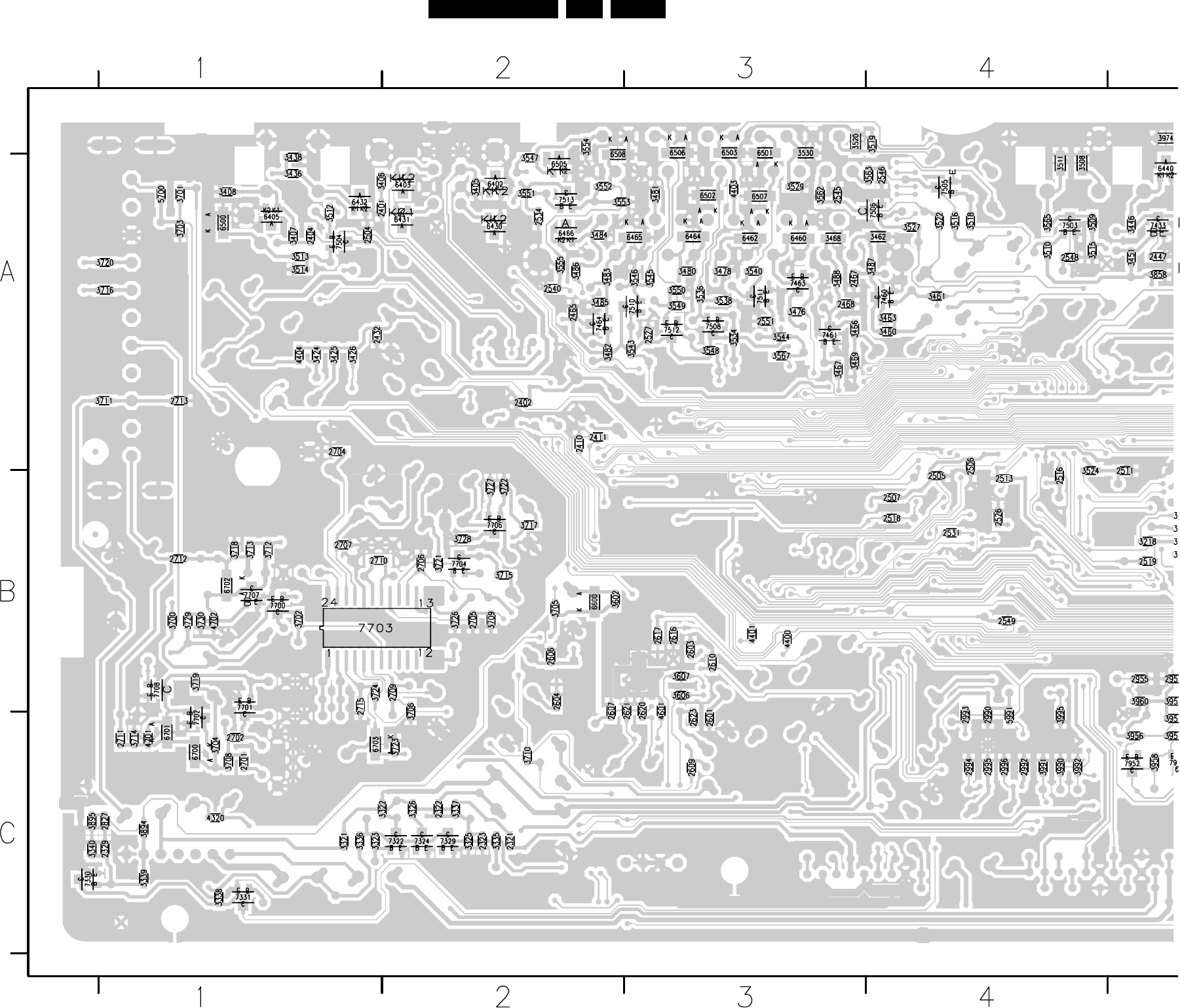
Electrical Diagrams and Print-Layouts EN 125DVDR980-985 /0X1 7.
Layout Analog Board (Part 1 Bottom View)
CL 26532011_03a.eps
190201
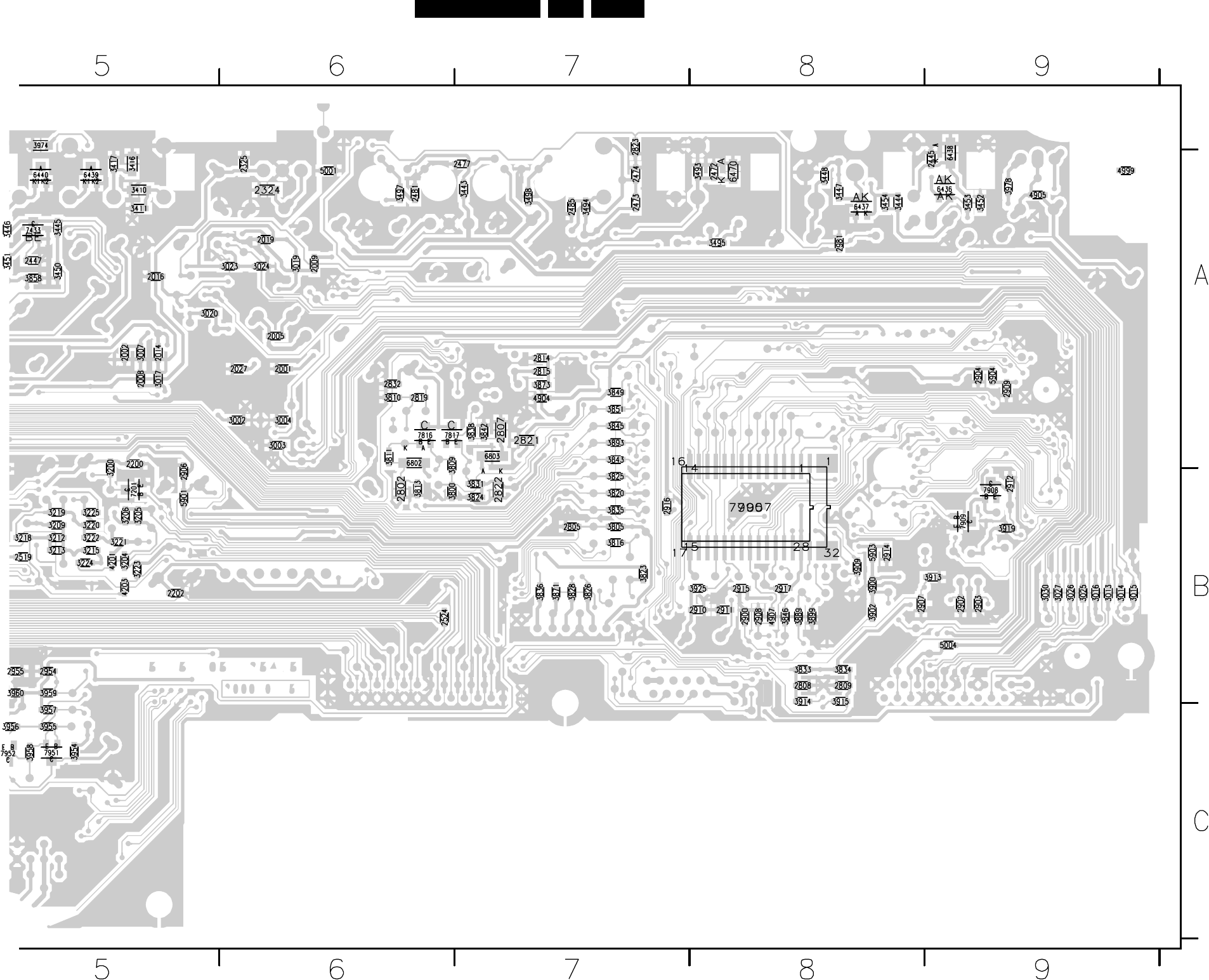
EN 126DVDR980-985 /0X1 7.
Electrical Diagrams and Print-Layouts
Layout Analog Board (Part 2 Bottom View)
CL 26532011_03b.eps
170102
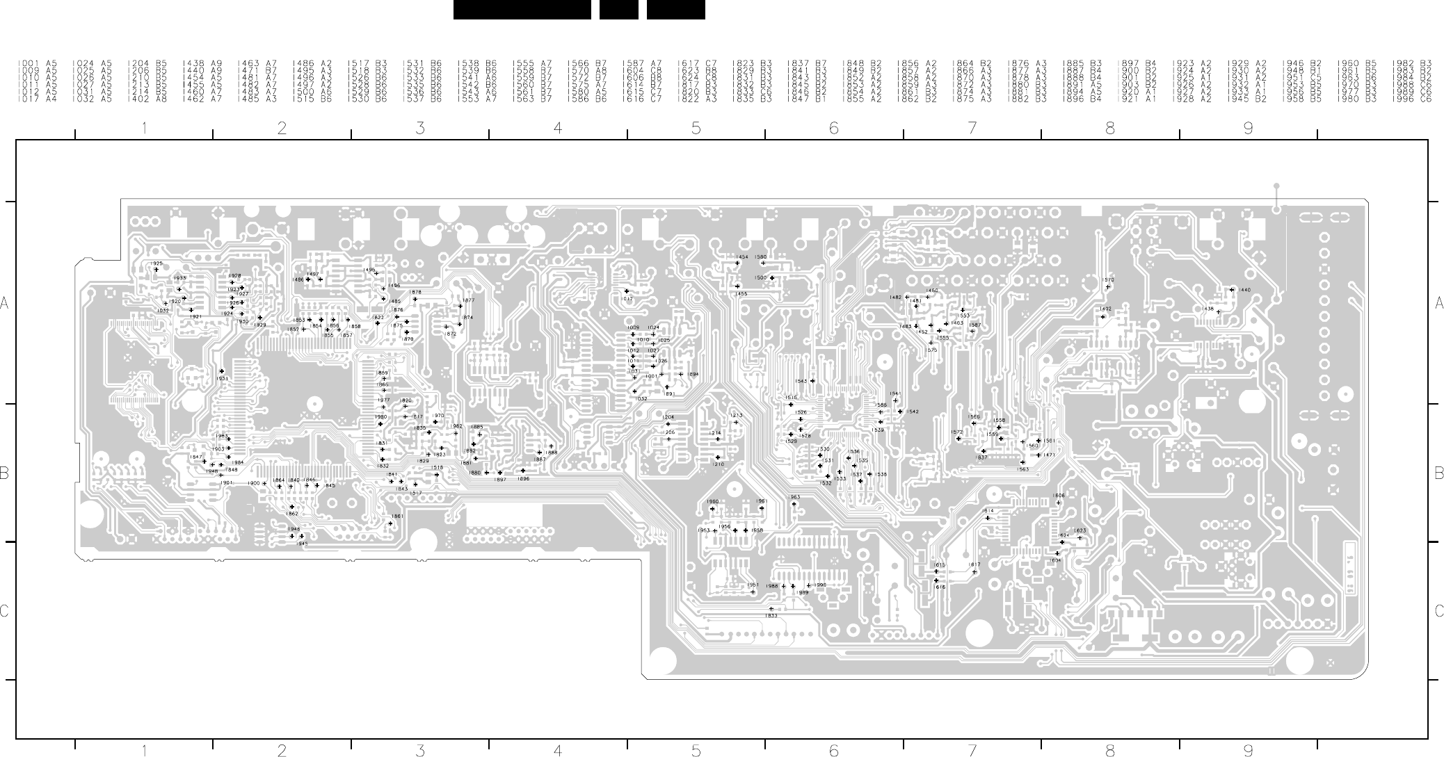
Electrical Diagrams and Print-Layouts EN 127DVDR980-985 /0X1 7.
Layout Analog Board (Testlands Top View)
CL 16532095_051.eps
100801
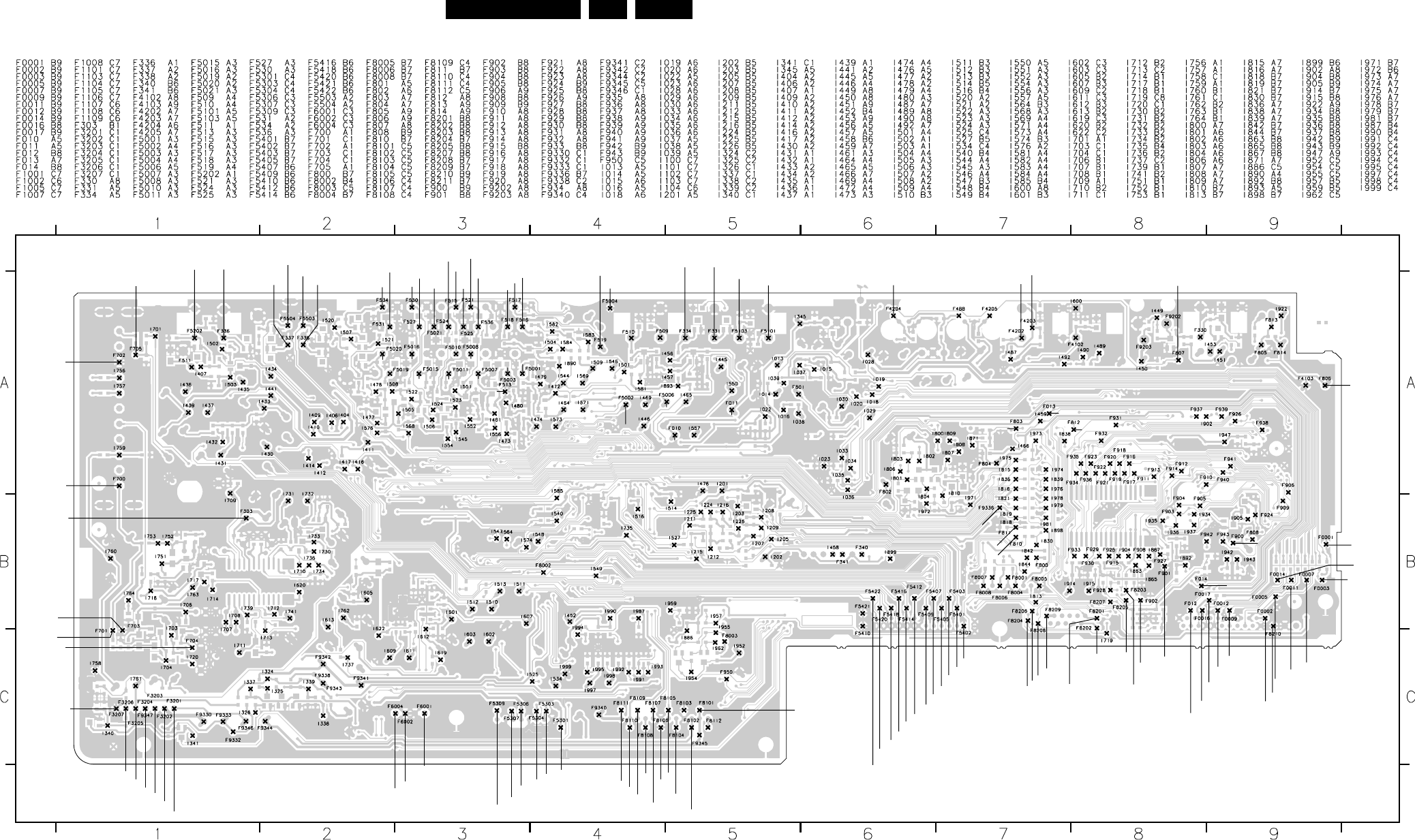
EN 128DVDR980-985 /0X1 7.
Electrical Diagrams and Print-Layouts
Layout Analog Board (Testlands Bottom View)
FLYB
33STBY
VGNSTBY
5NSTBY5V
12V
GNDA
IF
5SW
GNDFV
IF-In
40.4
GNDFV
AGC
RCVBSOut
RCVBSIn
RSVHSCOut
RSVHSCIn
RSVHSYIn
RSVHSYOut YCVBSIN_SC1
YCVBSOut_SC1
FBin_SC2
RCin_SC2 Gin_SC2 BC_SC2
8_SC2
GNDV
GNDVFBOut_SC1
RCOut_SC1 P50_SC1
Gout_SC1
BC_SC1
ARIn_SC1
AROut_SC1
ALOut_SC1
AROut_SC2
ALOut_SC2
8_SC1
ALIn_SC1
SDA
SCL
IPOR1
5M
5STB
5M
8SW
DVAR
GNDA
DVAL
AFCRI
AFCLI
CVBSFIN
CFIN
YFIN VGNSTBY
RC
12STBY
INT
3VD
DAOUT
DAINOPT
GNDD
D_PCMCLK
A_WCKL
A_PCMCLK
D_WCLK
A_DAT
GNDD
A_BCLK
D_BCLK
D_DATAO
D_KILL
SCL
IReset
D_RDY
A_RDY
FB
BE_FAN
ION
GNDV
A_V
A_U
A_Y
A_C
A_YCVBS
D_CVBS
D_Y
D_R
D_G
D_B
D_C
ADATA
8SW
SDA1
SCL1
IRESET_DIG D_DATA
INT Clock
DAINCOAX
SYNC
5STBY2
GNDA
GNDA
RCAROut RCALOut
ARCLI ARCRI OPT OUT DIG OUT L
DIG OUT H
FAN_IN
FAN_OUT
ARIn_SC2
ARIn_SC2
ARDAC
ALDAC
YCVBSIN_SC2
CL 16532095_050.eps
100801
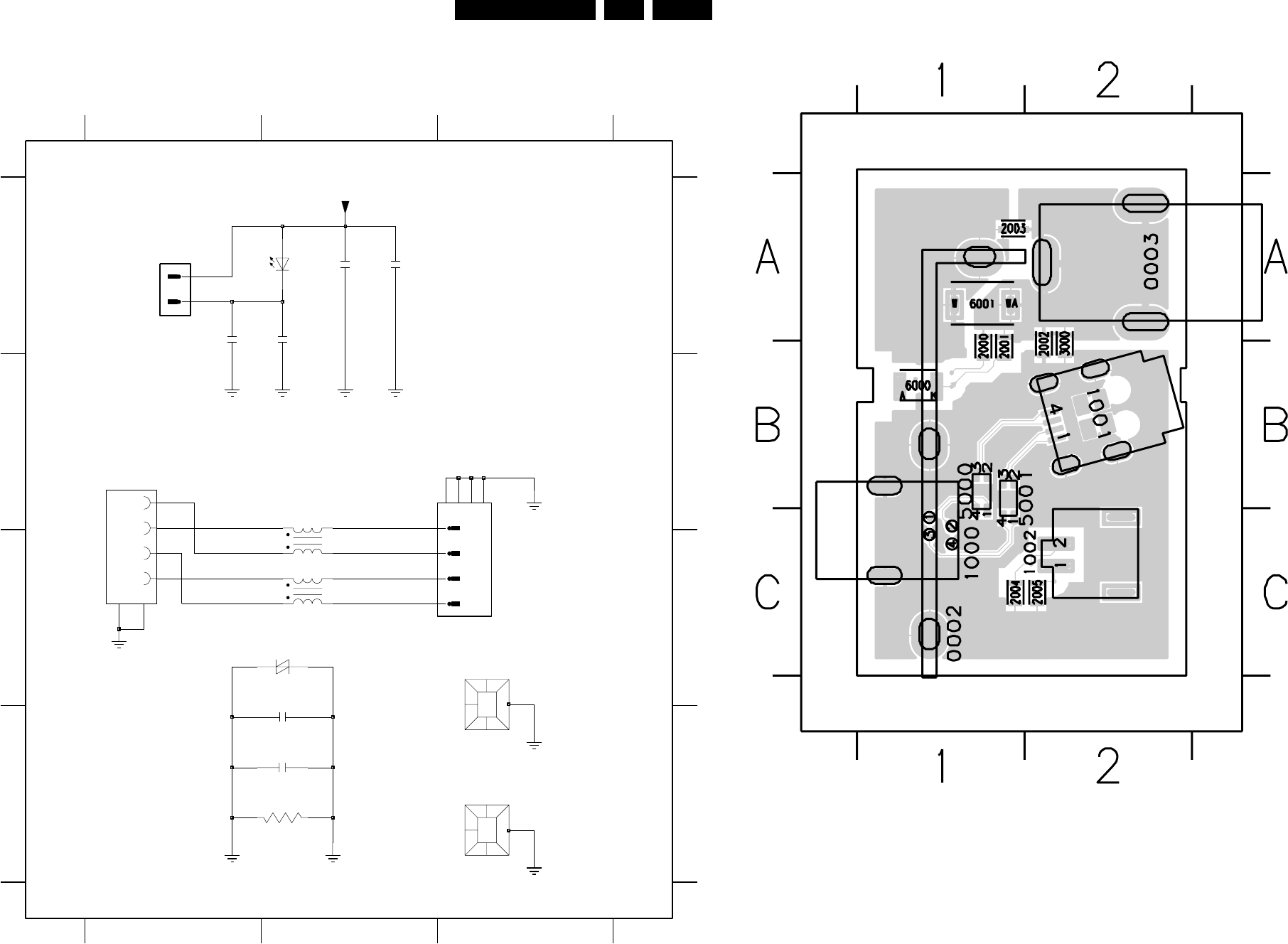
Electrical Diagrams and Print-Layouts EN 129DVDR980-985 /0X1 7.
DVIO Front Board
GND1394GND1394
A
B
D
C
D
0002 C3
0003 D3
1000 B1
1001 B2
1002 A1
2000 A2
2001 A1
2002 D2
2003 D2
3000 D2
5000 B2
5001 C2
6000 A2
6001 C2
123
123
A
B
C
2005
2004
4n7
GND1394
GND
4n7
310412124452
0002
SM6T
6001
5001
DLW31S
6000
TLMH3100
DLW31S
5000 GND1394
2002
4n7
3000
1M 0003
EARTH SPRING
GND1394
5678
1
2
3
4
GND
1000
540301
2
3
4
56
1318141
1001
GND
GND1394
2000
1n
2
2001
1n
4n7
2003
5V
GND
PH-S
1002
1
DVIO FRONT BOARD
CL 16532095_032.eps
080801
Layout DVIO Front Board
CL 16532095_033.eps
080801
0002 C1
0003 A2
1000 C1
1001 B2
1002 C2
2000 B1
2001 B1
2002 B2
2003 A1
2004 C1
2005 C2
3000 B2
5000 B2
5001 B2
6000 B1
6001 A1
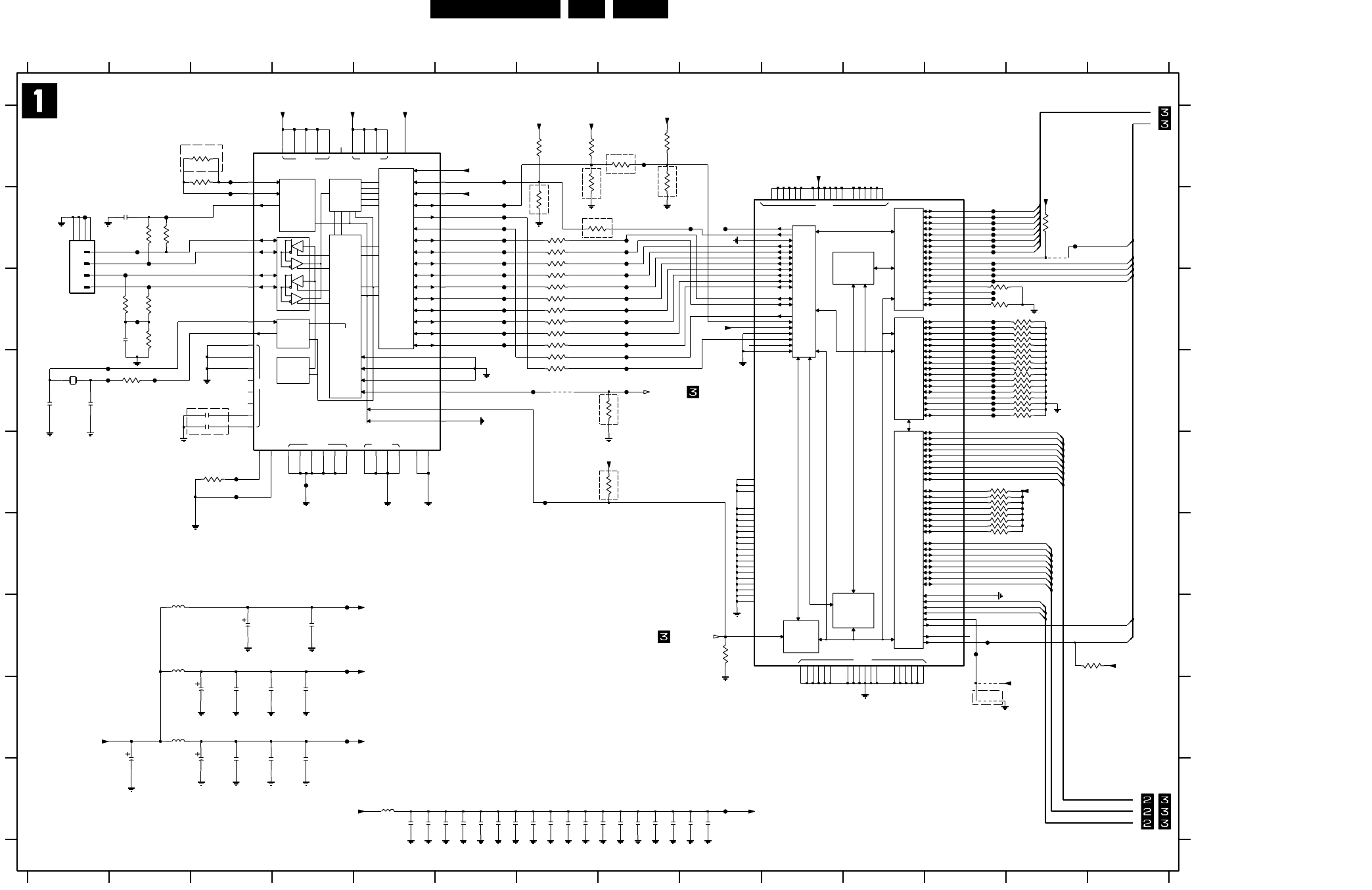
EN 130DVDR980-985 /0X1 7.
Electrical Diagrams and Print-Layouts
DVIO Board: 1394 Interface
PLLGND
DVDDAVDD
STATE
MACHINE
LOGIC
TRANSMIT
CLOCK
PLL
XTAL OSC.
AGND
ENCODER
DATA
GENERATOR
CURRENT
AND
VOLTAGE
BIAS
LINK
INTERFACE
RECEIVED
DATA
DECODER/
TIMER
ARBITR’N
AND
CONTROL
NC
DGND
AV1 LAYER
ISOCHRONOUS
TRANSMITTER/RECEIVER
ASYNC
TRANSMITTER
AND
RECEIVER
CONTROL
AV1 LAYER
INTERFACE
8-BIT
REGISTERS
STATUS
AND
TRANSMITTER/RECEIVER
ISOCHRONOUS
LINK
CORE
12KB BUFFER
MEMORY
VDD
GND
A
B
C
D
1 2 3 4 5 6 7 8 9 10 11 12 13 14
E
F
G
H
I
A
B
C
D
E
F
G
H
I
1 2 3 4 5 6 7 8 9 10 11 12 13 14
FROM FRONT
DV INPUT PCB
LINK
PHY
1394 INTERFACE
OPTION
OPTION
OPTION
OPTION
OPTION
OPTION
OPTION
OPTION
OPTION
OPTION
3124 47K
47K
3125
F189
F166
F167
5110
100MHZ
22K
3134
100MHZ
5109
56R
3178
F175
F198
F146
R0
41
R1
53
RESET_
2SYSCLK
TEST0
29
TEST1
28
TESTM
27
37
TPA0+
36
TPA0-
35
TPB0+
34
TPB0-
38
TPBIAS0
59
XI
60
XO
LREQ
54
55
16
43
44
45
46
47
20
PC0
21
PC1
22
PC2
14
PD
5758
56
PLLVDD
40
D2
9
D3
D4
10
D5
11
D6
12
D7
13
17186364
25266162
23
ISO_
15
LPS
1
484950
3031425152
CNA
3
24
CPS
4
CTL0
5
CTL1
19
C|LKON
6
D0
7
D1
8
3193
1R
7101
PDI1394
323339
F601
F186
3133 22K
F134
3166
2163
270p
3165
56R
2K2
100n
2176
F131
100n
2152
F135
F157
F150
3139
10K 10K
3138
F108
F132
3119 47K
10K
3147
F126
100n
2197
2173
10u
24M576
1102
CX-11F
3197 47K
2196
100n
F191
3115
1K
F128
F602
2153
100n
2K2
3111
100n
2154
2182
10u
47R
3190
5678
1
2
3
4
F153
1101
F116
3131 47K
F137
100n
47K
3120
F149
2194
3107
F130
3105
10R
10R
100n
2151
2170
12p
100n
2147
2181
100u
F174
3176
10R
F171
3172
10R
2146
100n
56R
3164
2171
12p
F127
F154
F136
3126 47K
100n
2184
47K
3100
100MHZ
5103
F118
3116
1R
F172
2174
100n
F117
9K1
3141 3140
10K
4103
F190
4100
F115
4102
10R
3174
47R
3188
10u
2175
F188
47K
3110
47K
3122
4101
47K
3130
5K1
3177
F101
F185
100n
2104
100n
2105
3173
56R
F107
3128 47K
F106
F113
3191
10R
100n
2156
3137
1R
2157
100n
F193
2150
100n
3121 47K
F165
100n
2149
10R
3171
F184
F102
F168
F161
47K
3132
F163
F197
35
24
18
12
6
70
F100
RESET_
88 SCLK
TESTPIN1
62
TESTPIN2
63
TESTPIN3
64
61
78
84
90
95
107
113
120
132
138
54
44
RESERVED11
RESERVED12
72
104 RESERVED13
RESERVED14
105
129 RESERVED15
RESERVED16
130
144 RESERVED17
50 RESERVED2
51 RESERVED3
RESERVED4
52
58 RESERVED5
RESERVED6
59
65 RESERVED7
RESERVED8
66
67 RESERVED9
42
LPS91
87 LREQ
48 PD
86 PHYCTL0
85 PHYCTL1
PHYD082
PHYD181
PHYD280
PHYD379
PHYD476
PHYD575
PHYD674
PHYD773
49 RESERVED1
RESERVED10
68
71
8
HIFD10
7
HIFD11
4
HIFD12
3
HIFD13
2
HIFD14
1
HIFD15
10
HIFD8
9
HIFD9
HIFINTN 38
HIFMUX 46
HIFRDN 40
41
HIFWAIT
HIFWRN 37
ISON93
92 LINKON
30
HIFA4 29
HIFA5 28
HIFA6 27
HIFA7 26
HIFA8 25
HIFAD0 22
HIFAD1 21
HIFAD2 20
19
HIFAD3
HIFAD4 16
HIFAD5 15
HIFAD6 14
HIFAD7 13
HIFALE 39
HIFCSN 36
119
131
137
11
17
23
34
43
53
60
69
HIF16BIT 45
HIFA0 33
HIFA1 32
HIFA2 31
HIFA3
121
AV2ERR1|DATAINV 122
AV2FSYNC 125
AV2READY 143
AV2SY 126
AV2SYNC 128
AV2VALID 127
55 CLK50
CYCLEIN56
CYCLEOUT57
5
77
83
89
94
106
112
97
AV1FSYNC 100
AV1READY 118
101AV1SY
103AV1SYNC
AV1VALID 102
AV2CLK 124
AV2D0 133
AV2D1 134
AV2D2 135
AV2D3 136
AV2D4 139
AV2D5 140
141
AV2D6
AV2D7 142
AV2ENDPCK 123
AV2ERR0|LTLEND
1394MODE47
AV1CLK 99
AV1D0 108
AV1D1 109
AV1D2 110
AV1D3 111
AV1D4 114
AV1D5 115
AV1D6 116
AV1D7 117
AV1ENDPCK 98
AV1ERR0 96
AV1ERR1
F121
PDI1394
7103
F120
2183
100n
F152
2148
100n
F124
F199
10K
3106
10K
3113
F109
F156
F162
3108
10R
47K
3101
3136
1R
F125
2177
100n
F122
6K34
3148
2158
1u
2155
100n
F143
F195
F170
F194
F169
F112
F141
47K
3118
47K
3127
F140
F187
F133
3179
10K
3180
10K
F105 F129
F148
10K
3102
3103 10K
2192
100n
47K
3192
F158
F110
3199 47K
F111
3189
10R
F123
F138
100n
2187
F139
47K
3198
2195
F119
100n
2178
100n
100n
2193
3109 47K
3104 47K
F144
3123 47K
F114
10R
3117
F103
5106
100MHZ
F142
F192
1394_RSTn
+3V3_IEEE_D
F104
+3V3_IEEE_D
+3V3_IEEE_A
+3V3_IEEE_D
+3V3_IEEE_A
PHY_CNA
+3V3_LINK
LINK_AVREADY
+3V3_LINK
PALE
LINK_CSn
LINK_INTn
PRDn
PWRn
+3V3_LINK
+3V3_LINK
+3V3_LINK
PA(0)
PA(1)
+3V3_IEEE_D +3V3_LINK
+3V3_IEEE_D
PA(2)
PA(3)
PA(4)
PA(5)
PA(6)
PA(7)
PA(8)
PAD(0)
PAD(1)
PAD(2)
PAD(3)
PAD(4)
PAD(5)
PAD(6)
PAD(7)
PA(0:15)
{LINK_AVCLK,LINK_AVSYNC,LINK_AVVALID,LINK_AVFSYNC,LINK_CSn,LINK_INTn,LINK_AVREADY}
{SRAMCE0n,SRAMRDn,PINT0n,PINT1n,PALE,PWRn,PRDn,PRSTn}
+3V3_IEEE_PLL
+3V3_IEEE_D
+3V3_LINK
LINK_AVCLK
LINKFIFO_DQ(1)
LINKFIFO_DQ(2)
LINKFIFO_DQ(3)
LINKFIFO_DQ(4)
LINKFIFO_DQ(5)
LINKFIFO_DQ(6)
LINKFIFO_DQ(7)
LINK_AVFSYNC
LINK_AVSYNC
LINK_AVVALID
PAD(7:0)
LINKFIFO_DQ(7:0)
LINKFIFO_DQ(0)
+3V3_LINK
+3V3
+3V3_IEEE_PLL
+3V3
+3V3
CL 16532145_014.eps
221101
1101 B1
1102 D1
2104 D3
2105 D3
2146 I5
2147 I5
2148 I6
2149 I6
2150 I6
2151 I6
2152 I6
2153 I7
2154 I7
2155 I7
2156 I7
2157 I8
2158 B2
2163 C2
2170 D1
2171 D1
2173 G3
2174 G4
2175 H3
2176 H3
2177 H3
2178 H4
2181 I2
2182 I3
2183 I3
2184 I3
2187 I4
2192 I8
2193 I8
2194 I8
2195 I8
2196 I9
2197 I9
3100 C13
3101 D13
3102 B13
3103 C12
3104 D13
3105 C7
3106 C12
3107 C7
3108 C7
3109 D13
3110 D13
3111 E8
3113 G9
3115 G14
3116 D2
3117 C7
3118 D13
3119 D13
3120 D13
3121 D13
3122 D13
3123 D13
3124 E12
3125 E12
3126 E12
3127 E12
3128 F12
3130 F12
3131 F12
3132 F12
3133 D13
3134 D13
3136 E3
3137 A8
3138 A7
3139 A7
3140 A8
3141 A8
3147 A3
3148 A3
3164 B2
3165 B2
3166 D8
3171 B7
3172 B7
3173 C2
3174 C7
3176 C7
3177 C2
3178 C2
3179 A7
3180 B7
3188 D7
3189 B7
3190 D7
3191 C7
3192 C13
3193 B7
3197 C13
3198 C13
3199 C13
4100 H12
4101 D7
4102 H12
4103 B13
5103 I5
5106 G2
5109 G2
5110 H2
7101 A5
7103 B12
F100 B8
F101 B8
F102 C8
F103 C8
F104 D8
F105 B8
F106 D8
F107 C8
F108 D7
F109 C6
F110 B6
F111 B6
F112 B6
F113 B6
F114 B6
F115 C6
F116 C6
F117 E7
F118 B2
F119 B2
F120 C2
F121 C2
F122 B2
F123 C2
F124 B12
F125 B12
F126 B9
F127 B12
F128 B12
F129 B12
F130 B12
F131 B12
F132 B12
F133 B12
F134 C12
F135 C12
F136 C12
F137 E4
F138 G4
F139 G4
F140 H4
F141 I9
F142 C6
F143 C12
F144 C12
F146 D1
F148 A3
F149 C6
F150 B3
F152 C6
F153 C8
F154 C8
F156 C8
F157 C6
F158 C8
F161 D12
F162 D1
F163 C12
F165 C12
F166 C12
F167 C12
F168 C12
F169 D12
F170 D12
F171 D12
F172 D12
F174 G12
F175 D8
F184 D12
F185 D2
F186 D12
F187 D12
F188 D12
F189 D12
F190 D12
F191 D12
F192 E3
F193 E3
F194 B6
F195 A8
F197 B13
F198 G12
F199 B1
F601 A6
F602 B9
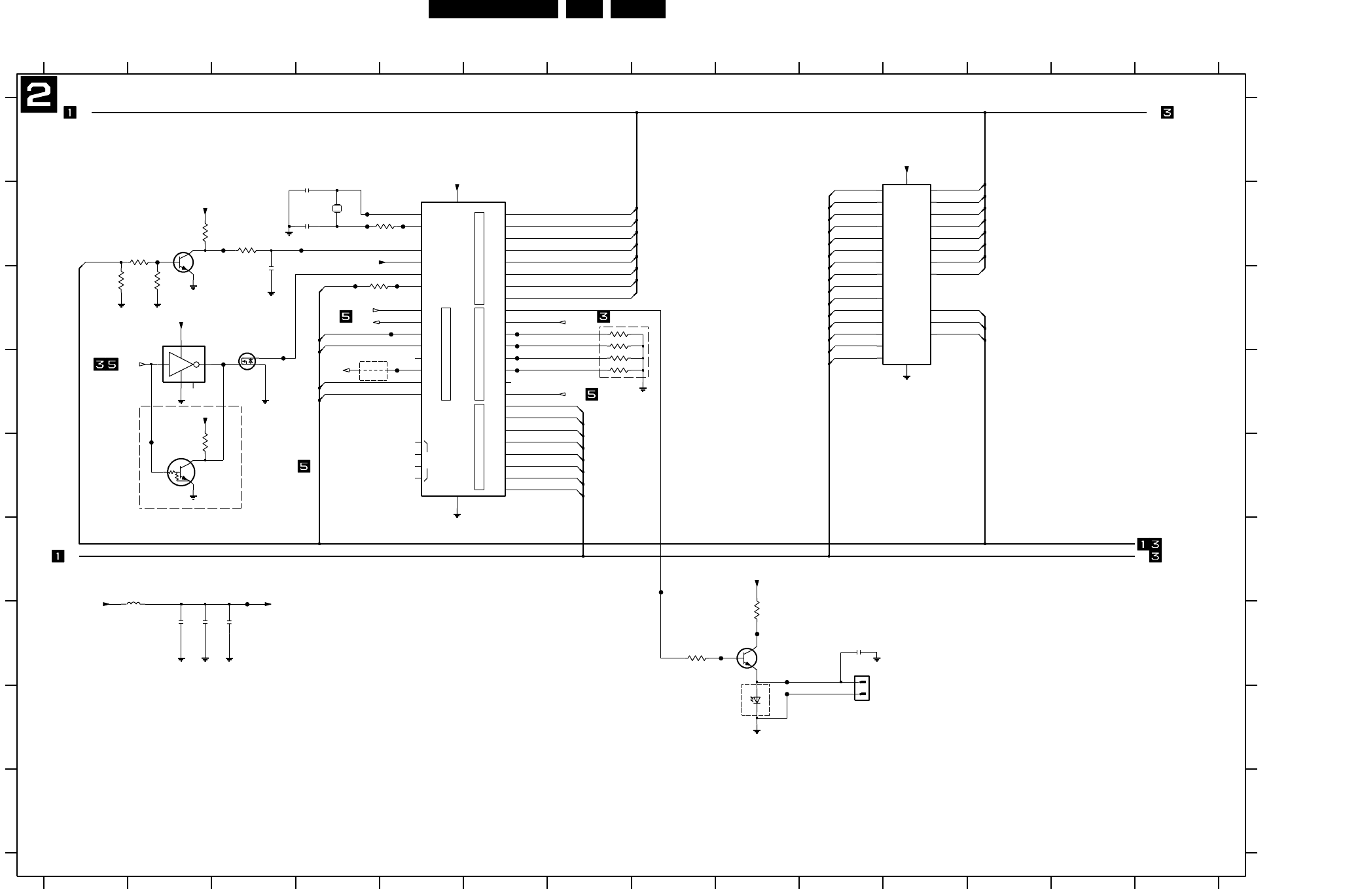
Electrical Diagrams and Print-Layouts EN 131DVDR980-985 /0X1 7.
DVIO Board: Microprocessor
PORT1 PORT0
PORT3
NC
PORT2
SRAM
MICROPROCESSOR
12345 11 12 13 14
123 5 7
E
G
H
I
B
678910
84 106 12 13 14
A
B
C
D
F
G
H
I
A
911
D
E
F
Board ID
To front DV input PCB
Micro processor
C
Option
Option
OPTION
OPTION
2205
12p
F212
F209
100p
2206
F202
7209
PDTC144EU
F214
2203
100n
2202
6200
TLMH3100
100n
330R
BST82
7204
3224
F219
1
2
7202
BC847B
1201 PH-S
2
3
NC
1
5
44206
I|O2 13
I|O3 15
I|O4 16
I|O5 17
I|O6 18
I|O7 19
OE_ 22
VCC
28
WE_ 27
74HCT1G04
7208
7
A12
8
A13
9
A14
10
A2
24
A3
25
A4
26
A5
1
A6
2
A7
3
A8
4
A9
5
CE_ 20
GND
14
I|O0 11
I|O1 12
CY62256
7201
A0
21
A1
23
A10
6
A11
3202
F203
10K
F205
10R
3225
F201
F216
3223
4K7
F223
F213
100n
2204
1K 3215
F208
F211 3214
1K
F207
1K
BC847B
7207
3203
11M05
1200
DSX840GA
F232
47R
3201
12p
2200
100n
2207
10K
3226
F204
F200
3
T2EX
13 TXD
44
VCC
22
VSS
18 WR_
21 XTAL1
20 XTAL2
F230
9
CEX4
35 EA_VPP
4
ECI
14 INT0_
15 INT1_
1
12
23
34
32 PSEN_
19 RD_
10 RST
11 RXD
16 T0
17 T1
2
T2
31
A15
24
A8
25
A9
43
AD0
42
AD1
41
AD2
40
AD3
39
AD4
38
AD5
37
AD6
36
AD7
33 ALE
5
CEX0
6
CEX1
7
CEX2
8
CEX3
7203
P89C51
26
A10
27
A11
28
A12
29
A13
30
A14
3204
10K
3205
47K
3206
47K
F222
F210
F221
100MHZ
5200
F206
F220
3217
+5V
PRSTn
1K 3216
1K
PAD(2)
PAD(3)
PAD(4)
PAD(5)
PAD(6)
PAD(7)
PAD(0:7) PAD(0:7)
PA(0:15) PA(0:15)
{SRAMCE0n,SRAMRDn,PINT0n,PINT1n,PALE,PWRn,PRDn,PRSTn}
PRDn
PINT1n
RTSn
TXD
RXD SRAMRDn
PALE
+5V_PROC
+5V_PROC
+5V_PROC
PA(12)
PA(13)
PA(14)
PA(8)
PA(9)
PAD(0)
PAD(1)
PAD(2)
PAD(3)
PAD(4)
PAD(5)
PAD(6)
PAD(7)
+5V_PROC
PWRn
+5V
CTSn
+5V_PROC
+5V_PROC
ISPn
PAD(0)
PAD(1)
PINT0n PORT1_1
SRAMCE0n
PA(10)
PA(11)
PA(12)
PA(13)
PA(14)
PA(15)
PA(8)
PA(9)
+5V_PROC
PWRn
PA(0)
PA(1)
PA(2)
PA(3)
PA(4)
PA(5)
PA(6)
PA(7)
PA(10)
PA(11)
CL 16532145_015.eps
221101
1200 B4
1201 G10
2200 B4
2202 G2
2203 G2
2204 G3
2205 B4
2206 C3
2207 G10
3201 B5
3202 B2
3203 B3
3204 C1
3205 B2
3206 C2
3214 C8
3215 C8
3216 D8
3217 D8
3223 G8
3224 G9
3225 C4
3226 E2
4206 D4
5200 F2
6200 H9
7201 A10
7202 B2
7203 B5
7204 C3
7207 G9
7208 C2
7209 E2
F200 B4
F201 B4
F202 B3
F203 D3
F204 C4
F205 C6
F206 C6
F207 D6
F208 D6
F209 C5
F210 G9
F211 C5
F212 F3
F213 D3
F214 B4
F216 G9
F219 F8
F220 E2
F221 G9
F222 G9
F223 B2
F230 D5
F232 B5
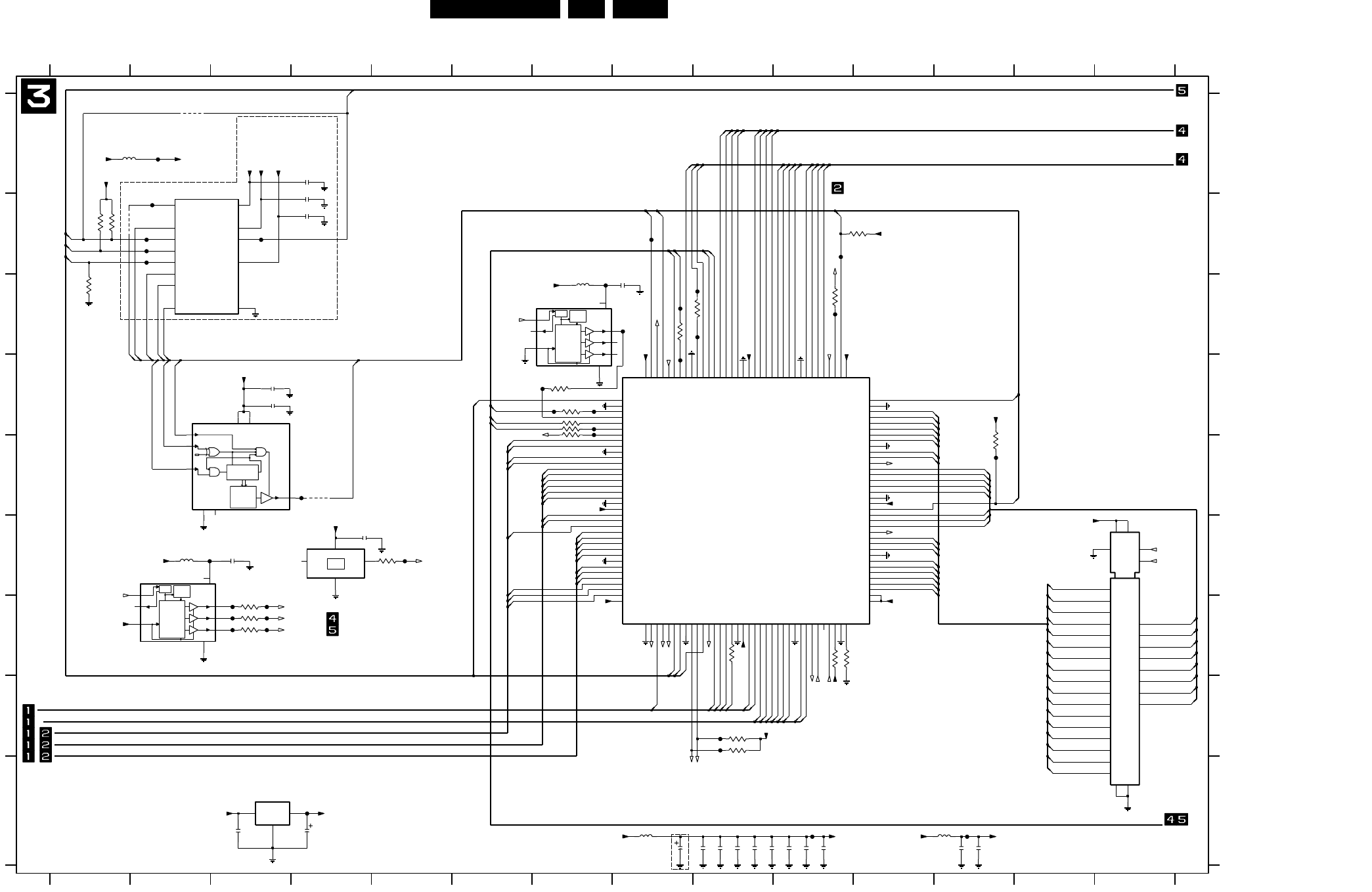
EN 132DVDR980-985 /0X1 7.
Electrical Diagrams and Print-Layouts
DVIO Board: Fifo & Control
VCC
CELL
MATRIX
COUNTER
EPROM
ADDR
BLOCK
OSC
MULTIPLEXER
AND DIVIDE
LOGIC
CONFIGURABLE
PLL
EPROM
BLOCK
OSC
MULTIPLEXER
AND DIVIDE
LOGIC
CONFIGURABLE
PLL
EPROM
OSC
VCC
GND
AUD_SDO_DAC
AUD_SDO_CON
TDI
TCK
TMS
CCLK
PROGRAMn
{DATA,CCLK,DONE,INITn,PROGRAMn}
{TDI,TCK,TDO,TDO_CONF,TMS}
TDO_CONF
PA(8:15)
+3V3_FPGA
CONFIG FLASH
CONFIG ROM
PLL VIDEO
PLL AUDIO
11 12 1334567
1223456
FIFO & CONTROL
FPGA / EPLD
SRAM
F
G
H
I
A
B
C
D
E
D
E
F
G
H
I
14
A
B
C
8910
OPTION
OPTION
13 14
12
78910111
F316
F322
F319
F326
47u
2314
3331
47R
4302
F310
3330
47R
F309
F301
F302
2332
100n
4300
F333
F335
F336
2330
100n
2331
100n
15
16
16
17
17
18
18
19
19
22
20
20
33
44
55
66
77
88
99
XC18V01
7309
11
1010 11
11
12
12
13
13
14
14
15
10K
3328
3329 10K
4301
VCC2 37
VCC3 54
VCC4 73
VCC5 90
VCC6 108
VCC7
128
144 VCC8
I|O91
117
I|O92
119
I|O93
120
I|O94
121
I|O95
122
123 I|O96
I|O97
124
I|O98
125
I|O99
126
M0
36
M1
34
O-TDO
109
74
PROGRAM_
PWRDWN_ 38
VCC1
18
I|O77 98
I|O78 99
I|O79-D1 101
I|O8
10
I|O80 102
I|O81 103
I|O82 104
I|O83-D0-DIN 105
I|O84-GCK6-DOUT 106
I|O85
111
I|O86-GCK7
112
I|O87
113
114 I|O88
I|O89-CS1
115
I|O9-TMS
11
I|O90
116
I|O62 80
I|O63 82
I|O64 83
I|O65-D5 84
I|O66 85
I|O67 86
I|O68 87
I|O69-D4 88
I|O7
9
I|O70 89
I|O71-D3 92
I|O72 93
94
I|O73
I|O74 95
I|O75-D2 96
I|O76 97
I|O48 61
I|O49 62
I|O5-TDI
6
I|O50 63
I|O51 65
I|O52 66
I|O53 67
I|O54 68
I|O55 69
I|O56-GCK4 70
I|O57-D7 75
I|O58-GCK5 76
77
I|O59
I|O6-TCK
7
I|O60 78
I|O61-D6 79
I|O33 43
I|O34-LDC_ 44
I|O35 46
I|O36 47
I|O37 48
I|O38 49
I|O39 50
I|O4
5
I|O40 51
I|O41 52
I|O42-INIT_ 53
I|O43 56
57
I|O44
I|O45 58
I|O46 59
I|O47 60
I|O19
23
I|O2
3
I|O20
24
I|O21
25
I|O22
26
I|O23
28
I|O24
29
I|O25
30
I|O26
31
32 I|O27
I|O28-GCK2
33
I|O29-GCK3 39
4I|O3
I|O30-HDC 40
I|O31 41
I|O32 42
I|O106
135
I|O107
136
I|O108
138
I|O109
139
I|O11
13
I|O110
140
I|O111
141
I|O112
142
I|O113-GCK8
143
14 I|O12
I|O13
15
16 I|O14
19 I|O15
I|O16
20
I|O17
21
I|O18
22
GND2
8
GND3
17
GND4
27
GND5
35
GND6 45
GND7 55
GND8 64
GND9 71
I|O1-GCK1
2
12 I|O10
I|O100
129
130 I|O101
131 I|O102
I|O103
132
I|O104
133
I|O105
134
7303
XCS30XL
CCLK 107
DONE 72
GND1
1
81
GND10
GND11 91
GND12 100
110 GND13
GND14
118
127 GND15
GND16
137
F330
F331F332 3327
47R
GND
5
NC
6
RESET|OE_3
78
F329
7300
XC17S30XL
CE_4
CLK2
DATA 1
47R
3321
47R
3322
47R
3325
3312
10R
47R
3320
F328
F314
F317
F315
F321
F318
F323
F324
F325
F320
F303
5300
100MHZ
6300
LD1117
GND
1
IN
3OUT 2
100n
2304
F300
47u
2302
2305
100n
100n
2301
CLKB 5
6CLKC
2
GND
OE|FS8
7
VDD
3XTI
4 XTO
100MHZ
5301
3315
CY2071AS
7307
1CLKA
33R
3318
33R
3319
33R
3317
33R
F305
F308
F307
1VDD
4
F306
7304
FXO-31FT
GND
2
OUT 3
TS
2303
100n
CY2071AS
7308
CLKA 1
5CLKB
6CLKC
2
GND
8 OE|FS
7
VDD
3 XTI
4 XTO
3305
1K
F311 F313
F312
F304
3313
10K
10K
3314
5303
100MHZ
100MHZ
5302
3303
1K
1K
3306
3301
1K
1K
3307
2312
100n
100n
2313
100n
5304
100MHZ
2324
10R
3300
100n
2325
100n
2319
100n
2306
2309
100n
2307
100n
100n
2308
2311
100n
100n
2310
WE_
2318
100n
A8
A9
18
CE_
5
925
I|O0 6
I|O1 7
I|O2 10
I|O3 11
I|O4 22
I|O5 23
I|O6 26
I|O7 27
OE_ 28
824
12
1
A1
2
A10
19
20 A11
A12
21
29 A13
A14
30
31 A15
32 A16
A2
3
A3
4
13 A4
A5
14
15 A6
16 A7
17
7301
CY7C1019BV33-10VC
A0
LINK_AVREADY
+3V3_FPGA
CCLK
+3V3_FPGA_CONF
+3V3_FPGA_CONF
DATA
+3V3_FPGA_CONF
+3V3_FPGA_CONF
PROGRAMn
+3V3_FPGA
INITn
INITn
+3V3_FPGA
DONE
INITn
CCLK
DATA
DOUT
IO1
IO3
IO4
IO10
{AUD_BCLK,AUD_WS_OUT,AUD_WS_701,AUD_MUTE,AUD_SDI,AUD_SDO_DAC,AUD_SDO_CON}
DV_HS_IN
DV_HS_OUT
HAD(7)
HAD(6)
HAD(5)
HAD(4)
HAD(3)
HAD(2)
HAD(1)
HAD(0)
DV_LCn
DV_ERRn
DV_DRQn
DV_DTACKn
DV_RSTn
DV_RWn
DV_DSUn
DV_DSLn
CLK27M
HAD(7:0)
{DV_LCn,DV_ERRn,DV_DRQn,DV_DTACKn,DV_ASn,DV_PDn,DV_DSUn,DV_RWn,DV_VS,DV_HS_IN,DV_RSTn,DV_HS_OUT,DV_DSLn}
FIFOA_D(7:0)
+3V3_FPGA_CONF
CLK27M_OSC
DONE
{LINK_CYCLEOUT,LINK_AVCLK,LINK_AVSYNC,LINK_AVVALID,LINK_AVFSYNC,LINK_AVERR1,LINK_AVERR0,LINK_CSn,LINK_INTn,LINK_AVREADY}
AUD_WS_OUT
PAD(0)
PAD(1)
PAD(2)
PAD(3)
PAD(4)
PAD(5)
PAD(6)
PAD(7)
PAD(7:0)
PA(8)
PA(9)
PA(10)
PA(11)
PA(12)
PA(13)
PA(14)
PA(15)
TDO
SRAMCE0n
SRAMRDn
PWRn
PRDn
PRSTn
PINT0n
PINT1n
PALE
{SRAMCE0n,SRAMRDn,PINT0n,PINT1n,PALE,PWRn,PRDn,PRSTn}
LINKFIFO_DQ(4)
LINKFIFO_DQ(5)
LINKFIFO_DQ(0:7)
LINKFIFO_DQ(6)
LINKFIFO_DQ(7)
LINK_AVVALID
LINK_AVSYNC
LINK_AVCLK
LINK_AVFSYNC
LINK_INTn
LINK_CSn
TDO_CONF
TCK
TMS
+3V3
BUFENn_AUD
BUFENn_VID
AUD_BCLK
FIFOA_D(4)
FIFOA_D(3)
FIFOA_D(5)
FIFOA_D(0)
FIFOA_D(7)
FIFOA_D(1)
FIFOA_D(6)
FIFOA_D(2)
FIFOA_A(16:0)
DONE
DATA
AUD_MUTE
AUD_SDI
AUD_WS_701
DV_ASn
CLK27M_OSC
PHY_CNA
1394_RSTn
LINKFIFO_DQ(0)
LINKFIFO_DQ(1)
LINKFIFO_DQ(2)
LINKFIFO_DQ(3)
RESETn
+3V3_SRAM
+3V3_FPGA
+3V3_FPGA
+3V3_FPGA
+3V3_FPGA
+3V3_FPGA
+3V3_FPGA
+3V3_FPGA
FIFOA_A(0)
FIFOA_A(16)
FIFOA_A(1)
FIFOA_A(15)
FIFOA_A(2)
FIFOA_A(14)
FIFOA_A(3)
FIFOA_A(13)
FIFOA_A(8)
FIFOA_A(7)
FIFOA_A(9)
FIFOA_A(6)
FIFOA_A(10)
FIFOA_A(5)
FIFOA_A(11)
FIFOA_A(4)
FIFOA_A(12)
+3V3
CLOCKGENAUD
+5V_PROC
CLK27M_DV
CLK27M_CON
+3V3
CLOCKGENVID
+3V3_PLL
+3V3_PLL
+5V +3V3_PLL
CLOCKGENAUD
CLOCKGENVID
CLK27M
FIFOA_WEn
FIFOA_OEn
FIFOA_A(0)
FIFOA_A(1)
FIFOA_A(10)
FIFOA_A(11)
FIFOA_A(12)
FIFOA_A(13)
FIFOA_A(14)
FIFOA_A(15)
FIFOA_A(16)
FIFOA_A(2)
FIFOA_A(3)
FIFOA_A(4)
FIFOA_A(5)
FIFOA_A(6)
FIFOA_A(7)
FIFOA_A(8)
FIFOA_A(9)
FIFOA_D(0)
FIFOA_D(1)
FIFOA_D(2)
FIFOA_D(3)
FIFOA_D(4)
FIFOA_D(5)
FIFOA_D(6)
FIFOA_D(7)
FIFOA_OEn
+3V3_SRAM
FIFOA_WEn
+3V3_FPGA
+3V3_FPGA_CONF
+3V3+3V3
CL 16532145_016.eps
221101
2301 I3
2302 I4
2303 F4
2304 C8
2305 F3
2306 I9
2307 I9
2308 I9
2309 I9
2310 I9
2311 I10
2312 I10
2313 I10
2314 I8
2318 D3
2319 D3
2324 I12
2325 I12
2330 A4
2331 B4
2332 B4
3300 G9
3301 B11
3303 E12
3305 B1
3306 B1
3307 C1
3312 F5
3313 H9
3314 H9
3315 D7
3317 G3
3318 G3
3319 G3
3320 D7
3321 D7
3322 C10
3325 D7
3327 C9
3328 G10
3329 G11
3330 C8
3331 D7
4300 B1
4301 E4
4302 A2
5300 C7
5301 F2
5302 I8
5303 A1
5304 I12
6300 I3
7300 D2
7301 F13
7303 D10
7304 F4
7307 C7
7308 F2
7309 A2
F300 F5
F301 C8
F302 C8
F303 D7
F304 D7
F305 G3
F306 C10
F307 G3
F308 G3
F309 D7
F310 D7
F311 I10
F312 A2
F313 I12
F314 C7
F315 C8
F316 B2
F317 F2
F318 H9
F319 B2
F320 H9
F321 G3
F322 B2
F323 G3
F324 B2
F325 I4
F326 B3
F328 E4
F329 G3
F330 D7
F331 C8
F332 C8
F333 E12
F335 B10
F336 B8
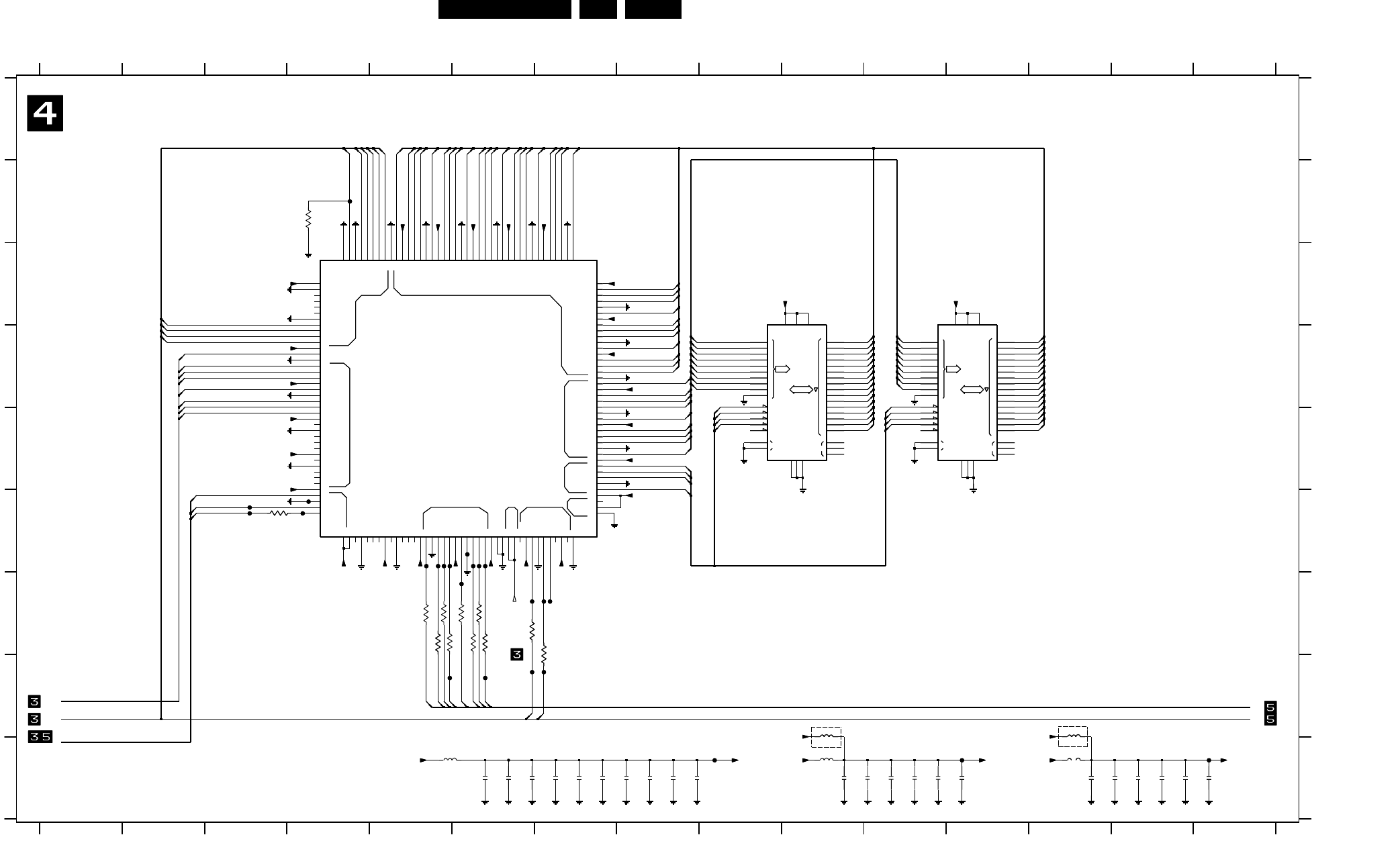
Electrical Diagrams and Print-Layouts EN 133DVDR980-985 /0X1 7.
DVIO Board: DVCODEC
1Mx16 devices are used as 256kx16
DVCODEC
III
HH
I
HH
GG
FF
EE
DD
FF
EE
DD
CC CC
BB
AA
88
BB
AA
151514141313
GG
65544332 12121111101099
88
77
2
11
151514141313
776
55443322 1212111110109911 66
DRAM DATA [ 0...31] BUS
GENERAL
PURPOSE I/O
HOST AD BUS [ 0....15 ]
AUDIO
INTERFACE VIDEO BUS
VIDEO BUS CLOCK INPUTS
SYNCHRONOUS
VIDEO INTERFACE
DRAM CTRL DRAM ADDRESS BUS
DV Decoder
DRAM DATA [ 0...31] BUS
GENERAL
PURPOSE I/O
HOST AD BUS [ 0....15 ]
AUDIO
INTERFACE VIDEO BUS
VIDEO BUS CLOCK INPUTS
SYNCHRONOUS
VIDEO INTERFACE
DRAM CTRL DRAM ADDRESS BUS
DV Decoder
12
11
10
9
8
7
6
5
4
3
2
1
0
OE
WE
HCAS
LCAS
9
8
7
6
5
4
3
NC
NC
2
1
RAS
0
DATA
ADR
15
14
13
12
11
10
9
8
7
6
5
4
3
2
1
0
OE
WE
HCAS
LCAS
9
8
7
6
5
4
3
NC
NC
2
1
RAS
0
DATA
ADR
15
14
13
12
11
10
9
8
7
6
5
4
3
2
1
0
OE
WE
HCAS
LCAS
9
8
7
6
5
4
3
NC
NC
2
1
RAS
0
DATA
ADR
15
14
13
12
11
10
9
8
7
6
5
4
3
2
1
0
OE
WE
HCAS
LCAS
9
8
7
6
5
4
3
NC
NC
2
1
RAS
0
DATA
ADR
15
14
13
1Mx16 devices are used as 256kx16
DVCODEC
OPTION OPTION
H
G
F
E
D
I
7
1
15141312
765432 12111098
B
A
151413
G
F
E
D
C C
B
A
I
H
HAD(3)
HAD(4)
HAD(5)
HAD(6)
HAD(0)
HAD(1)
HAD(2)
IO(31)
LCASn
RASn
UCASn
WEn
+3V3_DV
+3V3_DV
+3V3_DV
A(0)
+3V3_DV
+3V3_DV
+3V3_DV
+3V3_DV
1
CLK27M_DV
65432 111098
CRTL{RASn,LCASn,UCASn,WEn}
IO(31:0)
A(6)
A(7)
A(8)
A(2)
A(3)
A(4)
A(5)
A(6)
A(7)
A(8)
A(0)
A(1)
A(2)
A(3)
A(4)
A(5)
A(0)
A(1)
+3V3_DV
+3V3_DV
+3V3_DV
+3V3_DV
+3V3_DV
+3V3_DV
+3V3_DV
+3V3_DV
+3V3_DV
+3V3_DV
HAD(7)
IO(30)
A(3)
A(4)
A(5)
A(6)
+35V_DV_EDO
+35V_DV_EDO
+35V_DV_EDO
A(1)
A(2)
IO(10)
+35V_DV_EDO
+35V_DV_EDO
+35V_DV_EDO
IO(28)
IO(29)
IO(30)
IO(31)
IO(9)
IO(24)
IO(25)
IO(26)
IO(27)
IO(19)
IO(20)
IO(21)
IO(22)
IO(23)
IO(16)
IO(17)
IO(18)
+VCC_DV_RAM
IO(4)
IO(3)
IO(2)
IO(1)
IO(11)
IO(8)
IO(7)
IO(6)
IO(5)
IO(15)
IO(14)
IO(13)
IO(12)
IO(20)
IO(19)
IO(18)
IO(17)
IO(16)
IO(24)
IO(23)
IO(22)
IO(21)
IO(29)
IO(28)
IO(27)
IO(26)
IO(25)
A(7)
A(8)
+3V3_DV
+3V3_DV
DV_RSTn
DV_RWn
DV_DTACKn
DV_DRQn
HAD(7:0) YUV(7:0)
+5V
A(0:8)
UCASn LCASn
UCASn
+3V3
+5V
RASn
WEn
+3V3
LCASn
+3V3
RASn
WEn
+VCC_DV_RAM+35V_DV_EDO+3V3_DV
+VCC_DV_RAM
IO(0)
YUV(7)
YUV(6)
YUV(4)
YUV(5)
YUV(2)
AUD_BCLK
YUV(0)
YUV(1)
DV_DSUn
DV_DSLn
DV_PDn
DV_ASn
DV_ERRn
DV_LCn
IO(5)
IO(6)
IO(7)
IO(8)
IO(9)
IO(15)
IO(2)
IO(3)
IO(4)
IO(10)
IO(11)
IO(12)
IO(13)
IO(14)
IO(0)
IO(1)
AUD_WS_701
{AUD_BCLK,AUD_WS_OUT,AUD_WS_701,AUD_MUTE,AUD_SDI,AUD_SDO_DAC,AUD_SDO_CON}
AUD_SDI
DV_HS_IN
{DV_LCn,DV_ERRn,DV_DRQn,DV_DTACKn,DV_ASn,DV_PDn,DV_DSUn,DV_RWn,DV_VS,DV_HS_IN,DV_RSTn,DV_HS_OUT,DV_DSLn}
{DV_LCn,DV_ERRn,DV_DRQn,DV_DTACKn,DV_ASn,DV_PDn,DV_DSUn,DV_RWn,DV_VS,DV_HS_IN,DV_RSTn,DV_HS_OUT,DV_DSLn}
DV_VS
YUV(3)
44
VSS6
38
VSS5
32
VSS4
26
VSS3
20
VSS26 160
VSS16 98
VSS15 92
VSS14 86
VSS13
80
VSS12
74
VSS11
7404
NW700LQ
VSS9
56
VSS8
50
VSS7
VID-DTACK_ 82
VID-D7
65
VID-D6
64
VID-D5
63
VID-D4
61
VID-D3
59
VSS25 152
VSS24 146
VSS23 140
VSS22 134
VSS21 128
VSS20 122
VSS2
14
VSS19 116
VSS18 110
VSS17 104
VCC3.3-6
36
VCC3.3-5
30
VCC3.3-4
24
VCC3.3-3
18
150
VCC3.3-25
VCC3.3-24 144
VCC3.3-23 138
VCC3.3-22
68
VSS10
62
VSS1
7
VID-VS
73
VID-RDY 83
VID-OE_ 81
VID-HS
75 VID-FLD
76
VCC3.3-14 84
VCC3.3-13
78
VCC3.3-12
72
VCC3.3-11
66
VCC3.3-10
60
VCC3.3-1
1
TEST
67
VID-D2
58
VID-D1
57
VID-D0
55
VID-CLK1
69 VID-CLK0
70
VCC3.3-9
54
VCC3.3-8
48
VCC3.3-7
41
RES9
71
RES8
53
RES7
52
RES6
51
RES5
49
132
VCC3.3-21 126
VCC3.3-20 120
VCC3.3-2
12
VCC3.3-19 114
VCC3.3-18 108
VCC3.3-17 102
VCC3.3-16 96
VCC3.3-15 90
HOST-DTAC_
8
HOST-DSU_ 156
HOST-DSL_ 155
HOST-DRQ_
9
HOST-CS_ 158
HOST-AS_ 153
HOST-AD9
27
RES4
47
RES3
46
RES2
45
RES11
79
RES10
77
RES1
25
HOST-AD7
23 HOST-AD6
22 HOST-AD5
21
HOST-AD4
19
HOST-AD3
17 HOST-AD2
16
HOST-AD15
35 HOST-AD14
34 HOST-AD13
43 HOST-R|W_ 157
HOST-RST_ 159
HOST-PD_ 154
HOST-LC_
11 HOST-ERR_
10
DRAM-RAS_ 85
DRAM-LCAS_ 88
DRAM-D9 118
DRAM-D8 117
DRAM-D7 115
DRAM-D6
33
HOST-AD12
31
HOST-AD11
29 HOST-AD10
28
HOST-AD1
15
HOST-AD0
13
HOST-16|8_
2
GPIO3
6
HOST-AD8
148
DRAM-D28 147
DRAM-D27 145
DRAM-D26 143
DRAM-D25 142
DRAM-D24 141
DRAM-D23 139
DRAM-D22 137
DRAM-D21 136
DRAM-D20 135
DRAM-D2
GPIO2
5GPIO1
4GPIO0
3
DRAM-WE_ 89
DRAM-UCAS_ 87
125
DRAM-D13 124
DRAM-D12 123
DRAM-D11 121
DRAM-D10 119
DRAM-D1 106
DRAM-D0 105
DRAM-A8 103
DRAM-A7 101
DRAM-A6 100
113
DRAM-D5 112
DRAM-D4 111
DRAM-D31 151
DRAM-D30 149
DRAM-D3 109
DRAM-D29
93
DRAM-A0 91
AUD-WS
37
AUD-SDO
40
AUD-SDI
42
AUD-BCLK
39
107
DRAM-D19 133
DRAM-D18 131
DRAM-D17 130
DRAM-D16 129
DRAM-D15 127
DRAM-D14
DRAM-A5 99
DRAM-A4 97
DRAM-A3 95
DRAM-A2 94
DRAM-A1
100n
2400
100n
2403
2401
100n
2404
100n
2402
100n
100n
2405
100n
2406
2407
100n
100n
2408
100n
2411
2409
100n
2412
100n
2410
100n
100n
2413
100n
2414
2415
100n
100n
2416
2417
100n
100n
2420
100n
2418
2421
100n
2419
100n
5404
100MHZ
5402
100MHZ
3400
10K
F405
F417
F406
F404
F407
F408
F409
F410
F414
F412
F413
F401
F411
F403
F416
13
42
37
F402
29
16
15
EDO RAM
1Mx16
Φ
MT4LC1M16E5
7402
31
30
34
33
10
22
21
6
1
14
5
4
41
40
39
38
36
32
12
11
27
26
25
24
23
20
19
9
8
7
EDO RAM
1Mx16
Φ
18
17
35
3
2
28
MT4LC1M16E5
7403
13
42
37
22
21
10
9
8
6
1
14
29
16
15
32
36
35
3
2
12
11
31
30
34
33
20
19
18
17
7
5
4
41
40
39
38
28
27
26
25
24
23
100MHZ
5400
100MHZ
5401
5403
100MHZ
F425
F418
F400
3401-D
47R
47R
3401-A 47R
3401-C
3402-D
47R
3401-B
47R
47R
3402-C 3402-B
47R
47R
3402-A
F419
3404
47R
F420
F421
47R
3403
F422
47R
3405
F426
CL 16532145_017.eps
221101
2400 I6
2401 I6
2402 I6
2403 I7
2404 I7
2405 I7
2406 I8
2407 I8
2408 I8
2409 I8
2410 I10
2411 I10
2412 I11
2413 I11
2414 I11
2415 I12
2416 I13
2417 I13
2418 I14
2419 I14
2420 I14
2421 I15
3400 B4
3401-A H5
3401-B G5
3401-C H5
3401-D G5
3402-A H6
3402-B G6
3402-C H6
3402-D G6
3403 G6
3404 G7
3405 F3
5400 H10
5401 H13
5402 I5
5403 I10
5404 I13
7402 C9
7403 C11
7404 C4
F400 B4
F401 F3
F402 F4
F403 F3
F404 G6
F405 G7
F406 F5
F407 F5
F408 F5
F409 H6
F410 G6
F411 F6
F412 F6
F413 F6
F414 F6
F416 I9
F417 I15
F418 G7
F419 F6
F420 H6
F421 H6
F422 H7
F425 I12
F426 F4
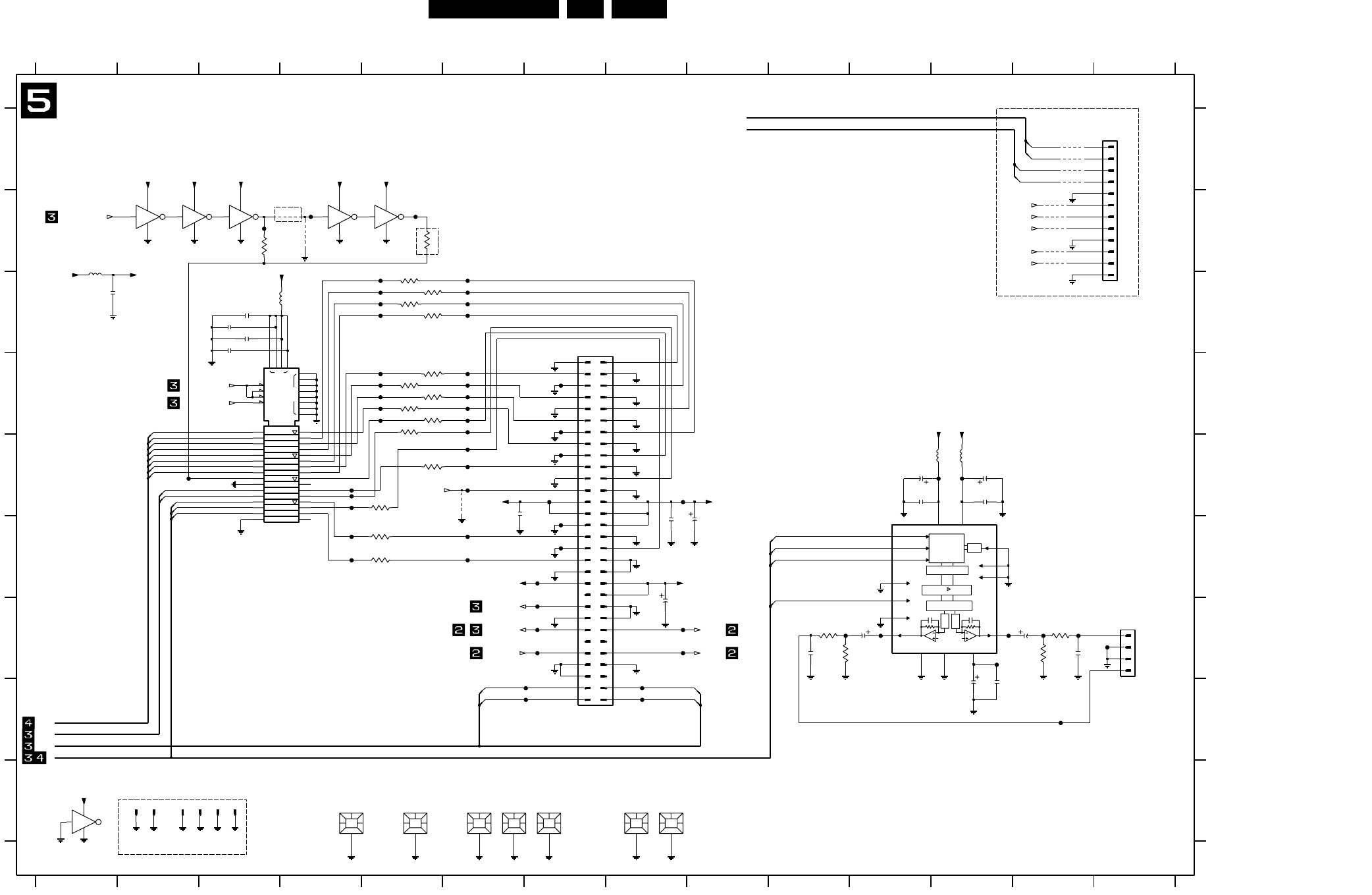
EN 134DVDR980-985 /0X1 7.
Electrical Diagrams and Print-Layouts
DVIO Board: Audio & Video Output
DAC
DIGITAL
INTERFACE
FILTER
NOISE SHAPER
DAC
PLL
DE-EMPHASIS
INTERPOLATION
3
2
11
1
1
1
EN2
EN3
EN4
GND
VC
EN1
4
15
VSSD
5
2
WS
47u
2518
1505
56789
B
C
To digital PCB
1234
C
D
E
F
G
H
I
Shielding connection on mounting holes
8 9 10 11 12 13 14
A
AUDIO & VIDEO OUTPUT
To analog PCB
D
E
F
G
H
I
A
B
Buffer
DAC
Clock delay
10 11 12 13 14
1234567
OPTION
OPTION
OPTION
OPTION
F546
F523
3527
F554
F517
33R
33R
3504-D 4
5
100R
3518
220K
3520
2516
10n
F518
F547
F513
F524
0001
Hole 4.0 mm with Cu
F521
Hole 4.0 mm with Cu
0002
2514
47u
2
7
F551
F508
3505-B
33R
2504
100n
F515
F505
47u
2515
3521
220K
3
6
3504-A
33R
18
0006
Hole 3.6 mm
33R
3504-C
F538
100MHZ
F537
4512
5500
4511
4510
100n
0005
2500
100MHZ
5501
3504-B
33R
2
7
33R
3525
34
39
45
718 42
33R
3526
17
30
29
27
26
24
19
20
22
23
4
10
15
21
28
38
37
48
8
9
11
12
31
36
35
33
32
25
13
14
16
7505
74LVC16244AD
47
46
44
43
1
2
3
5
6
41
40
14 4
F503
74LVC04A
7500-B
3
7
F531
F539
F528
4508
4509
4507
4506
1503
10n
2517
1502
F519
F553
4
5
6
7
8
9
14 10
PH-S
1508
1
10
11
12
2
3
74LVC04A
7500-E
11
7
F500
3505-D
33R
45
4513
4514
F534
F535
5503
1507
F540
1506
74LVC04A
7500-F
13
7
14 12
100n
2509
F541
F530
F543
14 8
7500-A
74LVC04A
1
7
14 2
74LVC04A
7500-D
9
7
33R
3502
3505-A
33R
18 33R
3505-C 3
6
F544
F522
F548
100n
2501
F545
F525
1504
F550
F516
4501
F549
4500
100n
2503
47u
2507
F536
F527
F509
F512
F507
F532
2510
100n
0004
47u
2512
47R
3512
47R
3510
F514
F552
F542
12
F511
3524
33R
F557
F559
F558
F556
0007
5502
100n
2508
F506
F529
2502
100n
100n
2519
50
51 52
53 54
55 56
57 58
59
6
60
78
9
36
37 38
39
4
40
41 42
43 44
45 46
47 48
49
5
21 22
23 24
25 26
27 28
29
3
30
31 32
33 34
35
1
10
11 12
13 14
15 16
17 18
19
2
20
2505
1500
179161
F526
47u
3519
100R
100n
2506
F555
4505
74LVC04A
7500-C
5
7
14 6
F510
F533
Hole 4.9mm
0003
F502
F501
BCK
1
DATAI3
DEEM|CLKO9
8 MUTE
PLL0
10
SFOR0 11
SFOR1 7
6 SYSCLK|PLL1
VDDA
13
VDDD
4
VOL
14
VOR
16
VREF-DAC
12
VSSA
7506
UDA1334ATS
F504
2
3
4
F520
1501
PH-S
1
2511
47u
YUV(5)
YUV(6)
YUV(7)
3506
33R
PINT0n
PINT1n
LINK_AVVALID
LINK_AVFSYNC
{SRAMCE0n,SRAMRDn,PINT0n,PINT1n,PALE,PWRn,PRDn,PRSTn}
{LINK_AVCLK,LINK_AVSYNC,LINK_AVVALID,LINK_AVFSYNC,LINK_CSn,LINK_INTn,LINK_AVREADY}
DOUT
IO1
IO3
IO4
IO10
{AUD_BCLK,AUD_WS_OUT,AUDIO_WS_701,AUD_MUTE,AUD_SDI,AUD_SDO_DAC,AUD_SDO_CON}
YUV(0)
YUV(1)
YUV(2)
YUV(3)
YUV(4)
+3V3
+3V3
+3V3_dly+3V3_dly+3V3_dly+3V3_dly+3V3_dly
+3V3_dly
+3V3_dly
DV_HS_OUT
{DV_LCn,DV_ERRn,DV_DRQn,DV_DTACKn,DV_ASn,DV_PDn,DV_DSUn,DV_RWn,DV_VS,DV_HS_IN,DV_RSTn,DV_HS_OUT,DV_DSLn}
TDO
TCK TMS
TDI
{TDI,TCK,TDO,TDO_CONF,TMS}
AUD_SDO_DAC
+3V3
+5V
RESETn
ISPN CTSN
TXD RXD
+3V3
CLK27M_CON
YUV(7:0)
AUD_WS_OUT
AUD_BCLK
AUD_MUTE
+3V3
BUFENn_VID
DV_VS
AUD_BCLK
AUD_SDO_CON
AUD_WS_OUT
BUFENn_AUD
+3V3
+5V
RTSN
CL 16532145_018.eps
221101
0001 I4
0002 I5
0003 I6
0004 I6
0005 I7
0006 I8
0007 I8
1500 C7
1501 G14
1502 I2
1503 I2
1504 I2
1505 I2
1506 I3
1507 I3
1508 A14
2500 C1
2501 C3
2502 C3
2503 C3
2504 C3
2505 E12
2506 E12
2507 E11
2508 E11
2509 E6
2510 F8
2511 F8
2512 G8
2514 G11
2515 G13
2516 G10
2517 G13
2518 H12
2519 H12
3502 D5
3504-A D5
3504-B C5
3504-C D5
3504-D C5
3505-A D5
3505-B C5
3505-C D5
3505-D C5
3506 E5
3510 B3
3511 B4
3512 B5
3518 G10
3519 G13
3520 G10
3521 G13
3524 D5
3525 E5
3526 F5
3527 F5
4500 B4
4505 E6
4506 A13
4507 A13
4508 A13
4509 A13
4510 B13
4511 B13
4512 B13
4513 B13
4514 B13
5500 B1
5501 C3
5502 E12
5503 E12
7500-A B2
7500-B B2
7500-C B3
7500-D B4
7500-E B4
7500-F I1
7505 D3
7506 F11
F500 B4
F501 B5
F502 B3
F503 C6
F504 C5
F505 C6
F506 C5
F507 C6
F508 C5
F509 C6
F510 C5
F511 D6
F512 D6
F513 D7
F514 D6
F515 D6
F516 D6
F517 D6
F518 D7
F519 D5
F520 D5
F521 E7
F522 D5
F523 E6
F524 D5
F525 E12
F526 E12
F527 E2
F528 E6
F529 D5
F530 E4
F531 E7
F532 E8
F533 E4
F534 F7
F535 F7
F536 F7
F537 G7
F538 G7
F539 G8
F540 G10
F541 G13
F542 G13
F543 G14
F544 G12
F545 G11
F546 G7
F547 G8
F548 G12
F549 H7
F550 H8
F551 H7
F552 H8
F553 H13
F554 E4
F555 F4
F556 F4
F557 F6
F558 F6
F559 E6
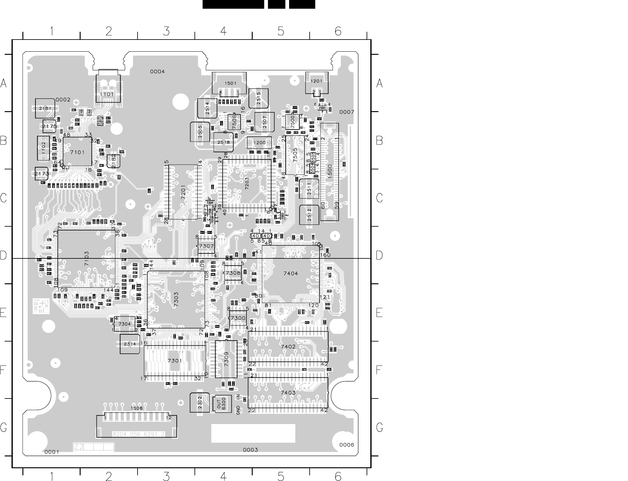
Electrical Diagrams and Print-Layouts EN 135DVDR980-985 /0X1 7.
Layout DVIO Board (Overview Top View)
CL 16532145_019.eps
201101
1101 A2
1102 B1
1200 B5
1201 A6
1500 C6
1501 A4
1508 G2
2104 B1
2105 C1
2146 D2
2147 D2
2148 D2
2149 D2
2150 D2
2151 C2
2152 C2
2153 C1
2154 C1
2155 D1
2156 D1
2157 D1
2158 A1
2163 B2
2170 B1
2171 B1
2173 C1
2174 B1
2175 B1
2176 B1
2177 B1
2178 B2
2181 A1
2182 B2
2183 B2
2184 B2
2187 B1
2192 D1
2193 D1
2194 E1
2195 E1
2196 E2
2197 E2
2200 B4
2202 C4
2203 C4
2204 C3
2205 B5
2206 C5
2207 A6
2301 G4
2302 G4
2303 E2
2304 D4
2305 D4
2306 E3
2307 E3
2308 E4
2309 E4
2310 D4
2311 D3
2312 D3
2313 E3
2314 F2
2318 E4
2319 E4
2324 E3
2325 F3
2330 E4
2331 F4
2332 F4
2400 D6
2401 D5
2402 D5
2403 D5
2404 D5
2405 D5
2406 D5
2407 D5
2408 E5
2409 E5
2410 E5
2411 E5
2412 E6
2413 E6
2414 D6
2415 D6
2416 F4
2417 F5
2418 F6
2419 E4
2420 E5
2421 E6
2500 A5
2501 B5
2502 B5
2503 B6
2504 C5
2505 B4
2506 B4
2507 B5
2508 B4
2509 C6
2510 B6
2511 C5
2512 C5
2514 A4
2515 A5
2516 A4
2517 A4
2518 B4
2519 B4
3100 E2
3101 E2
3102 E1
3103 D1
3104 E2
3105 C1
3106 D1
3107 C2
3108 C2
3109 E2
3110 E2
3111 C2
3113 C2
3115 C2
3116 B1
3117 C2
3118 E2
3119 E2
3120 E2
3121 E2
3122 E2
3123 E2
3124 D2
3125 D2
3126 D2
3127 D2
3128 D2
3130 D2
3131 E2
3132 E2
3133 E1
3134 E1
3136 B2
3137 C2
3138 B2
3139 C2
3140 D1
3141 D1
3147 B1
3148 B1
3164 B2
3165 B2
3166 C3
3171 C1
3172 C1
3173 B2
3174 C1
3176 C1
3177 B2
3178 B2
3179 C2
3180 C2
3188 C1
3189 C1
3190 C1
3191 C2
3192 E2
3193 D1
3197 E2
3198 E2
3199 E2
3201 B5
3202 C5
3203 C5
3204 C5
3205 C5
3206 C5
3214 C5
3215 C5
3216 C5
3217 C5
3223 A6
3224 B6
3225 C4
3226 C4
3300 E3
3301 E4
3303 E3
3305 F4
3306 F4
3307 F4
3312 E3
3313 E3
3314 E3
3315 D4
3317 E4
3318 D4
3319 D4
3320 D3
3321 D4
3322 E4
3325 D4
3327 E4
3328 E3
3329 E3
3330 D4
3331 D4
3400 D6
3401 D5
3402 D5
3403 E5
3404 E4
3405 D4
3502 B6
3504 B6
3505 B6
3506 B6
3510 B5
3512 B5
3518 A4
3519 A4
3520 A4
3521 A4
3524 B6
3525 C5
3526 B6
3527 B6
4100 C2
4101 C2
4102 C2
4103 E1
4206 B5
4300 E4
4301 E4
4302 E4
4500 B5
4501 B5
4505 B5
5103 C2
5106 C1
5109 B1
5110 B2
5200 C5
5300 D4
5301 D4
5302 E2
5303 F4
5304 F3
5400 E6
5401 F6
5402 E5
5403 E6
5404 F6
5500 A5
5501 A5
5502 B4
5503 B4
6300 G4
7101 B1
7103 D2
7201 C3
7202 C5
7203 C4
7204 C4
7207 A6
7208 C4
7209 C4
7300 E4
7301 F3
7303 E3
7304 E2
7307 D4
7308 D4
7309 F4
7402 F5
7403 F5
7404 D5
7500 B5
7505 B5
7506 B4
PART 1
CL 16532145_19a.eps
PART 2
CL 16532145_19b.eps
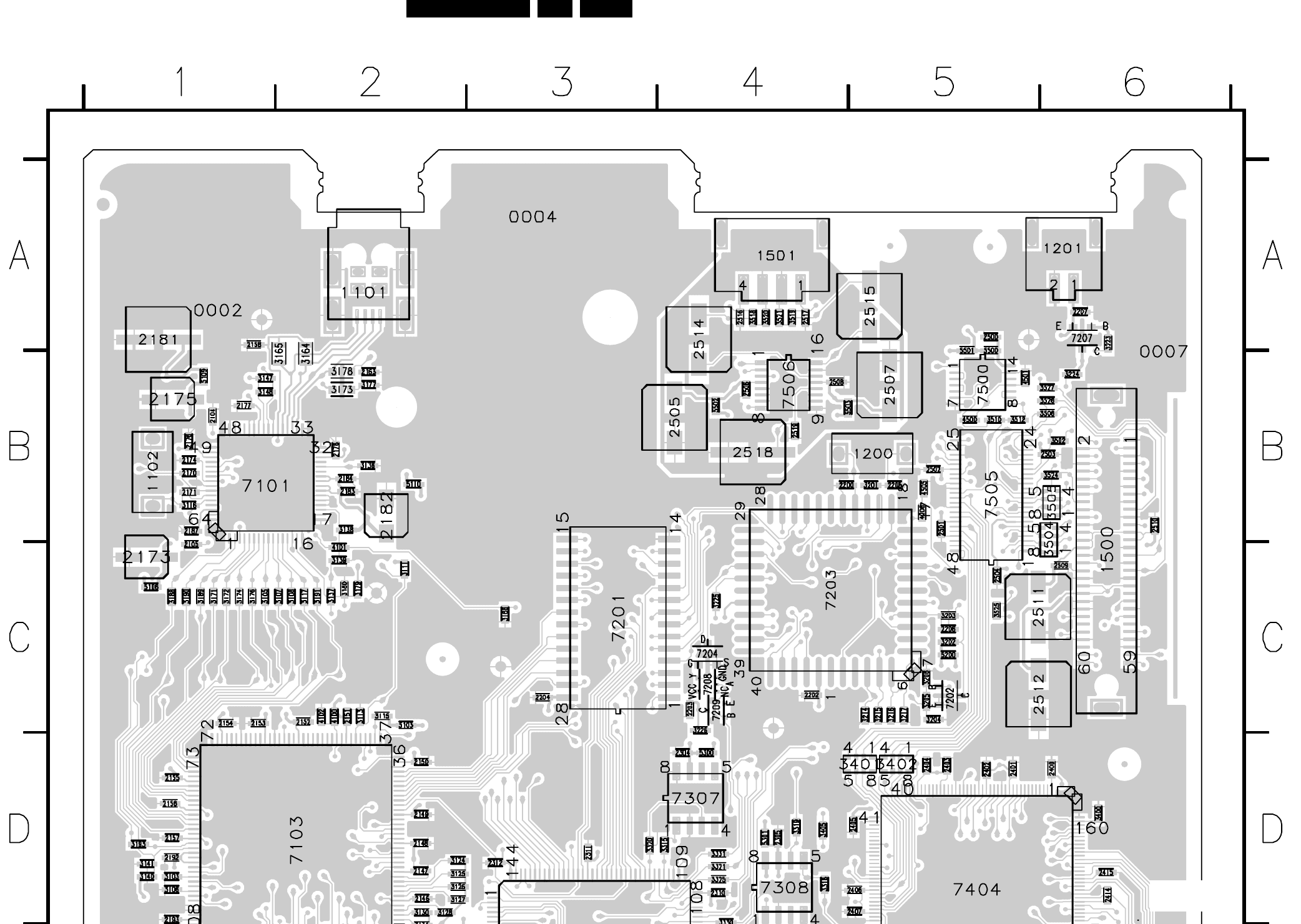
EN 136DVDR980-985 /0X1 7.
Electrical Diagrams and Print-Layouts
Layout DVIO Board (Part 1 Top View)
CL 16532145_19a.eps
211101
PART 1
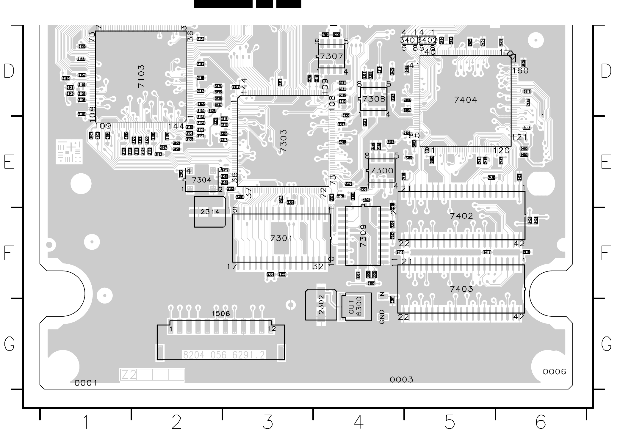
Electrical Diagrams and Print-Layouts EN 137DVDR980-985 /0X1 7.
Layout DVIO Board (Part 2 Top View)
CL 16532145_019b.eps
211101
PART 2
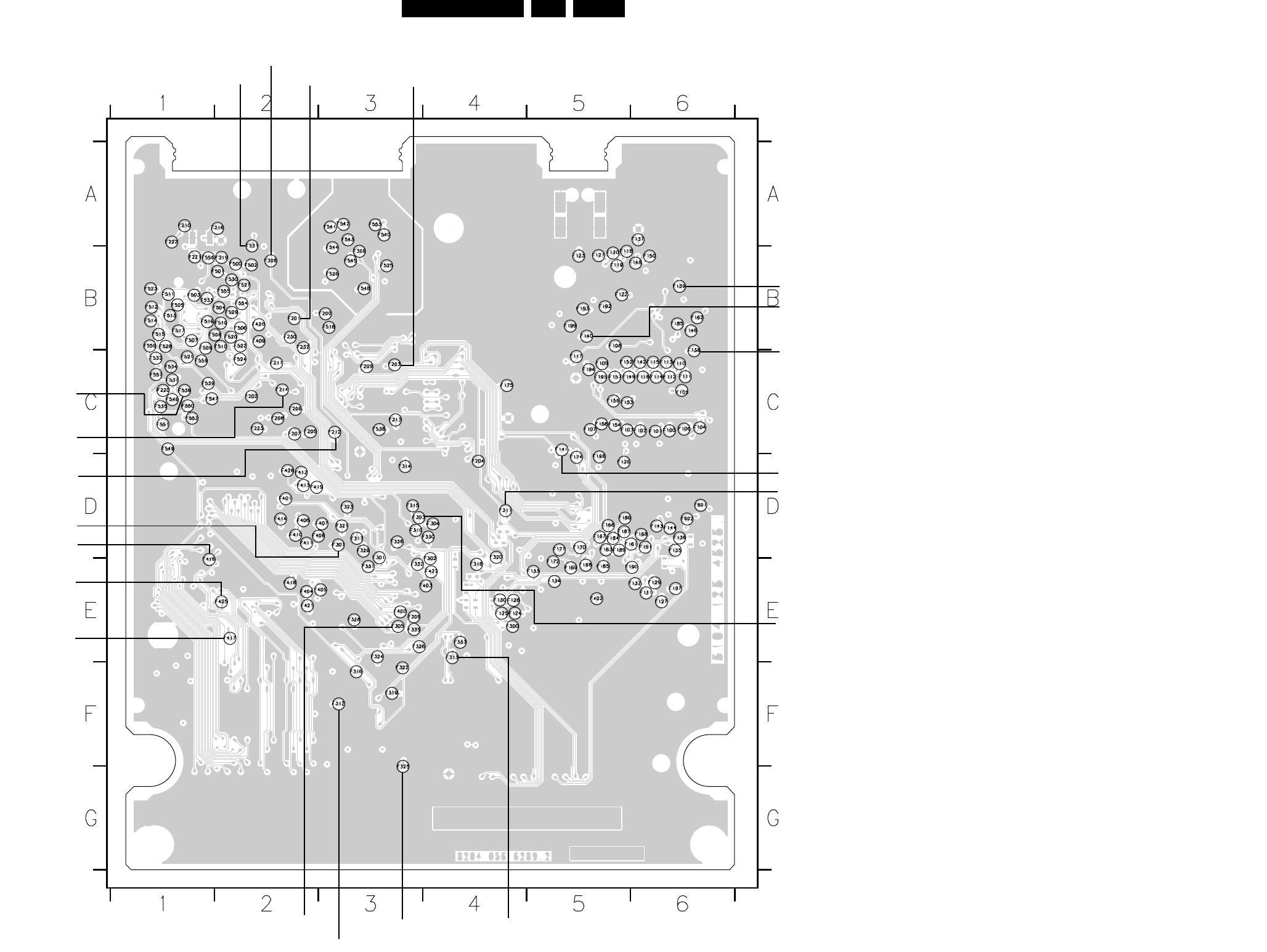
EN 138DVDR980-985 /0X1 7.
Electrical Diagrams and Print-Layouts
Layout DVIO Board (Testlands Bottom View)
CL 16532145_021.eps
221101
+5V
+3V3
CLK27M_con
uP_CLK PSEN
+3V3_IEEE_A
+3V3_IEEE_D
+3V3_IEEE_PLL
+3V3_LINK
+3V3_FPGA
+3V3_SRAM
+3V3_PLL
CLK27M
+3V3_FPGA_CONF
RESET
+5V_PROC
CLK27M_DV
+3V3_DV
+35V_DV_EDO
+Vcc_DV_RAM
CLOCKAUDTMP
F100 C6
F100 C6
F101 C6
F101 C6
F102 C6
F102 C6
F103 C5
F103 C5
F104 C6
F104 C6
F105 C6
F105 C6
F106 C6
F106 C6
F107 C5
F107 C5
F108 B5
F108 B5
F109 C5
F109 C5
F110 C6
F110 C6
F111 C6
F111 C6
F112 C6
F112 C6
F113 C6
F113 C6
F114 C6
F114 C6
F115 C6
F115 C6
F116 C6
F116 C6
F117 C5
F117 C5
F118 B5
F118 B5
F119 B5
F119 B5
F120 B5
F120 B5
F121 B5
F121 B5
F122 B5
F122 B5
F123 B5
F123 B5
F124 E4
F124 E4
F125 E4
F125 E4
F126 D5
F126 D5
F127 E6
F127 E6
F128 E4
F128 E4
F129 E6
F129 E6
F130 E4
F130 E4
F131 E6
F131 E6
F132 E6
F132 E6
F133 E5
F133 E5
F134 E5
F134 E5
F135 D6
F135 D6
F136 D6
F136 D6
F137 A6
F137 A6
F138 C6
F138 C6
F139 B6
F139 B6
F140 B5
F140 B5
F141 C5
F141 C5
F142 C6
F142 C6
F143 D6
F143 D6
F144 D6
F144 D6
F146 B6
F146 B6
F148 B6
F148 B6
F149 C5
F149 C5
F150 B6
F150 B6
F152 C5
F152 C5
F153 C5
F153 C5
F154 C5
F154 C5
F156 C5
F156 C5
F157 C5
F157 C5
F158 C5
F158 C5
F161 D6
F161 D6
F162 B6
F162 B6
F163 D5
F163 D5
F165 E5
F165 E5
F166 D5
F166 D5
F167 D5
F167 D5
F168 E5
F168 E5
F169 E5
F169 E5
F170 D5
F170 D5
F171 D5
F171 D5
F172 E5
F172 E5
F174 D5
F174 D5
F175 C4
F175 C4
F184 D5
F184 D5
F185 B6
F185 B6
F186 D5
F186 D5
F187 D5
F187 D5
F188 D6
F188 D6
F189 D5
F189 D5
F190 E6
F190 E6
F191 D6
F191 D6
F192 B5
F192 B5
F193 B5
F193 B5
F194 C5
F194 C5
F195 C5
F195 C5
F197 E6
F197 E6
F198 D5
F198 D5
F199 B5
F199 B5
F200 B3
F200 B3
F201 B2
F201 B2
F202 C2
F202 C2
F203 C3
F203 C3
F204 D4
F204 D4
F205 C2
F205 C2
F206 C2
F206 C2
F207 C2
F207 C2
F208 C2
F208 C2
F209 C3
F209 C3
F210 A1
F210 A1
F211 C2
F211 C2
F212 C3
F212 C3
F213 C3
F213 C3
F214 C2
F214 C2
F216 A2
F216 A2
F219 B2
F219 B2
F220 C1
F220 C1
F221 B1
F221 B1
F222 A1
F222 A1
F223 C2
F223 C2
F230 B2
F230 B2
F232 B2
F232 B2
F300 E4
F300 E4
F301 D3
F301 D3
F302 E4
F302 E4
F303 D3
F303 D3
F304 D4
F304 D4
F305 E3
F305 E3
F306 E3
F306 E3
F307 D3
F307 D3
F308 B2
F308 B2
F309 B3
F309 B3
F310 D3
F310 D3
F311 D4
F311 D4
F312 F3
F312 F3
F313 E4
F313 E4
F314 D3
F314 D3
F315 D3
F315 D3
F316 F3
F316 F3
F317 D3
F317 D3
F318 E4
F318 E4
F319 F3
F319 F3
F320 D4
F320 D4
F321 D3
F321 D3
F322 F3
F322 F3
F323 D3
F323 D3
F324 E3
F324 E3
F325 G3
F325 G3
F326 E3
F326 E3
F328 E3
F328 E3
F329 D3
F329 D3
F330 D4
F330 D4
F331 E3
F331 E3
F332 E3
F332 E3
F333 E4
F333 E4
F335 E3
F335 E3
F336 D3
F336 D3
F400 E3
F400 E3
F401 D2
F401 D2
F402 E5
F402 E5
F403 E4
F403 E4
F404 E2
F404 E2
F405 E3
F405 E3
F406 D2
F406 D2
F407 D3
F407 D3
F408 D2
F408 D2
F409 B2
F409 B2
F410 D2
F410 D2
F411 D2
F411 D2
F412 D2
F412 D2
F413 D2
F413 D2
F414 D2
F414 D2
F416 E1
F416 E1
F417 E2
F417 E2
F418 E2
F418 E2
F419 D2
F419 D2
F420 B2
F420 B2
F421 E2
F421 E2
F422 E4
F422 E4
F425 E2
F425 E2
F426 D2
F426 D2
F500 B2
F500 B2
F501 B2
F501 B2
F502 B2
F502 B2
F503 B1
F503 B1
F504 B2
F504 B2
F505 B1
F505 B1
F506 B2
F506 B2
F507 B1
F507 B1
F508 B2
F508 B2
F509 B1
F509 B1
F510 B2
F510 B2
F511 B1
F511 B1
F512 B1
F512 B1
F513 B1
F513 B1
F514 B1
F514 B1
F515 B1
F515 B1
F516 B1
F516 B1
F517 B1
F517 B1
F518 B3
F518 B3
F519 B2
F519 B2
F520 B2
F520 B2
F521 C1
F521 C1
F522 B2
F522 B2
F523 B1
F523 B1
F524 C2
F524 C2
F525 B3
F525 B3
F526 B3
F526 B3
F527 B2
F527 B2
F528 B1
F528 B1
F529 B2
F529 B2
F530 B2
F530 B2
F531 A2
F531 B2
F532 C1
F532 C1
F533 B1
F533 B1
F534 C1
F534 C1
F535 C1
F535 C1
F536 C1
F536 C1
F537 C1
F537 C1
F538 C3
F538 C3
F539 C1
F539 C1
F540 A3
F540 A3
F541 A3
F541 A3
F542 A3
F542 A3
F543 A3
F543 A3
F544 B3
F544 B3
F545 B3
F545 B3
F546 C1
F546 C1
F547 C1
F547 C1
F548 B3
F548 B3
F549 C1
F549 C1
F550 C1
F550 C1
F551 C1
F551 C1
F552 C1
F552 C1
F553 A3
F553 A3
F554 B2
F554 B2
F555 B2
F555 B2
F556 B1
F556 B1
F557 C1
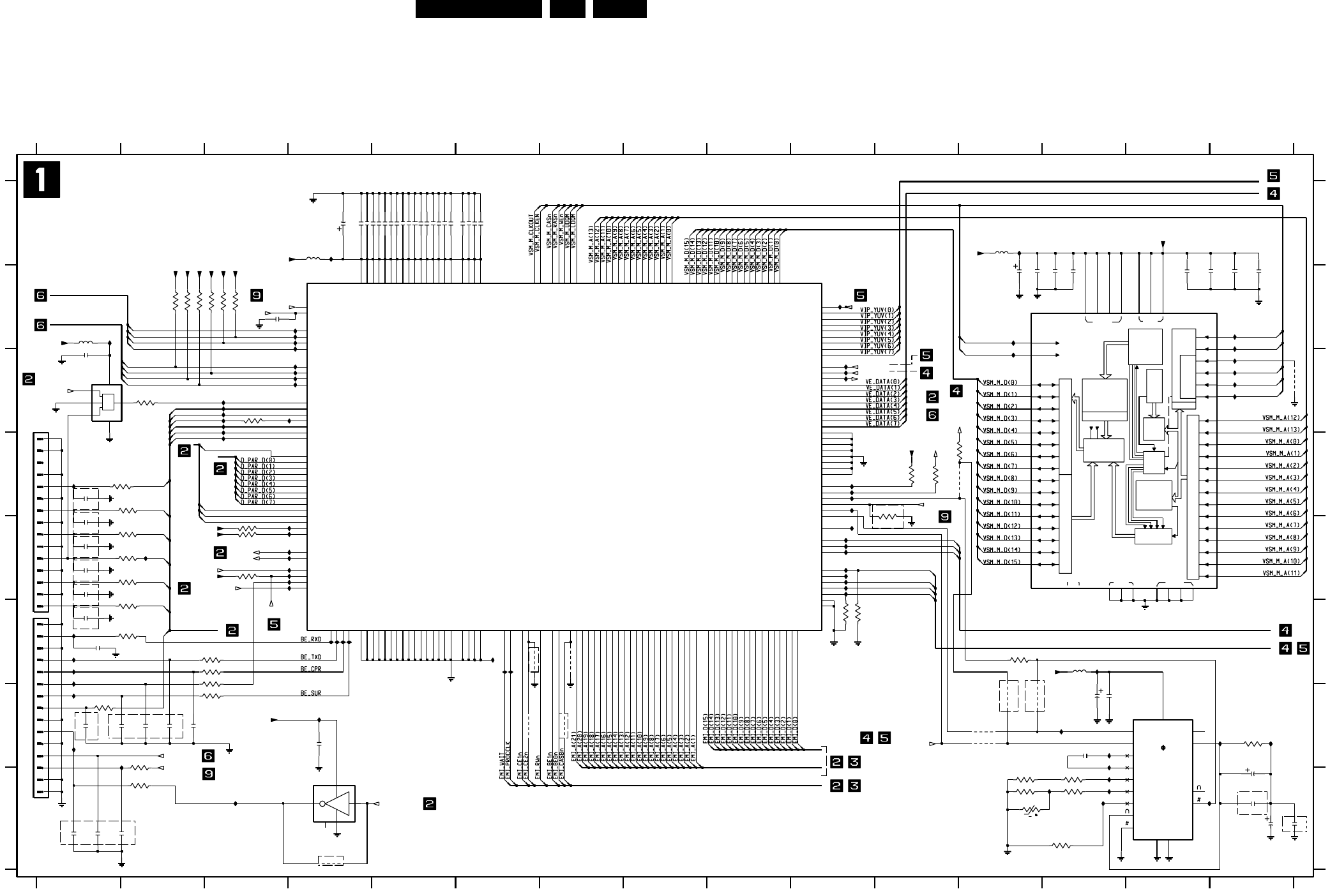
Electrical Diagrams and Print-Layouts EN 139DVDR980-985 /0X1 7.
Digital Board: VSM, Buffer Memory and Bit Engine Interface
DVDR VERSATILE STREAM MANAGER
VSM
DQMH
SENSE AMPLIFIERS
COMMAND
DECODE
CTRL
LOGIC
MODEREG
ADDRESS REGISTER
ROW
ADDR
MUX
LOGIC
CTRL
BANK
COLUMN
ADDR
COUNTER/
I/O GATING
DQM DATA LOGIC
READ DATA LATCH
WRITE DRIVERS
DATA INPUT REGISTER DATA OUTPUT REGISTER
DQML
VDDQ VDD
NC VSSQVSS
LATCH
REFRESH
COUNTER
BANK0
ROW-
ADDR
LATCH &
DECODER
COLUMN
DEDCODER
BANK0
MEMORY
ARRAY
(4,096x256x16)
GND
PLL
t
Audio PLL
67
UART1
SYSTEM_CONTROL
SDRAM
13 14 15
A
B
C
D
E
F
G
H
A
B
C
D
E
F
G
H
11 12
12345
JTAG_CHAIN3
SYSTEM DATA BUS
SYSTEM ADDRESS BUS
AUDIO ENCODER
8 9 10 11 12 13 14 15
12345678910
TO BITENGINE
Encoding
MPEG2 VIDEO
DATA STREAM BUS
UART2
DIGITAL VIDEO(CCIR656)
BE_SERIAL
OPTION
OPTION
OPTION
OPTION
OPTION OPTION
OPTION
OPTION
OPTION
GNDD
2154
10n
OPTION
OPTION
OPTION
OPTION
OPTION
OPTION
OPTION
OPTION
2153
100n
4109
4110
4107
4108
3113 4K7
4106
13
14
15
2
3
4
5
6
7
8
9
FMN
1101
1
10
11
12
22R
3117
I165
I174
I133
2107 100n
2122
100n
GNDD
2147
10p
2100 100n
I126
I143
47R
3128
124652
16WE_
47R
3129
DQ9
39 DQMH
15 DQML
3640
18RAS_
11427394349
284154 6
CS_
2 DQ0
4 DQ1
45 DQ10
47 DQ11
48 DQ12
50 DQ13
51 DQ14
53 DQ15
5 DQ2
7 DQ3
8 DQ4
10 DQ5
11 DQ6
13 DQ7
42 DQ8
44
A1
22A10
35A11
25A2
26A3
29A4
30A5
31A6
32A7
33A8
34A9
20BA0
21BA1
17CAS_
37CKE
38CLK
19
2130
7101
MT48LC4M16A2TG-7E
23A0
24
2u2
100MHZ
5103
3103
10K
I121
3132
1R
VSS_36
36
VSS_46
46
VSS_57
57
VSS_67
67
78 VSS_78
VSS_80
80
VSS_90
90
150
VSS_154
154
VSS_155
155
VSS_161
161
VSS_175
175
VSS_182
182
VSS_192
192
VSS_208
208
21 VSS_21
VSS_24
24
VSS_26
26
VE_D9 119
VE_DSn 127
VE_DTACKn 128
VE_VIP_ERROR 142
VSS_10
10
VSS_100
100
116 VSS_116
VSS_130
130
VSS_132
132
VSS_135
135
VSS_150
VE_D12 122
VE_D13 123
VE_D14 124
VE_D15 125
111
VE_D2
VE_D3 112
VE_D4 113
VE_D5 114
VE_D6 115
VE_D7 117
VE_D8 118
5
VDD_52 52
VDD_62 62
VDD_73 73
VDD_77 77
VDD_85 85
VDD_95 95
VE_D0 109
110
VE_D1
VE_D10 120
VE_D11 121
VDD_144 144
VDD_15 15
VDD_156 156
169
VDD_169
VDD_181 181
VDD_183 183
201
VDD_201
VDD_25 25
VDD_31 31
VDD_41 41
VDD_5
VBI_IPD0 133
VBI_IPD1 134
VBI_IPD2 136
VBI_IPD3 137
138
VBI_IPD4
VBI_IPD5 139
VBI_IPD6 140
VBI_IPD7 141
VDD_108 108
VDD_126 126
VDD_129 129
165
TRSTn 166
UART1_CTSn
148 UART1_RTSn
147
UART1_RX
145
UART1_TX
146
UART2_CTSn
153
UART2_RTSn
152
149 UART2_RX
UART2_TX
151
VBI_ICLK 131
M_RASn 70
M_UDQM 75
M_Wen 76
RESETn
48 SYSCLK
47
TCK 162
163
TDI 164
TDO
TEST0 172
TEST1 173
TMS
M_D14 96
M_D15 98
M_D2 94
M_D3 92
89
M_D4
M_D5 87
M_D6 84
M_D7 82
M_D8 81
M_D9 83
M_LDQM 79
64
M_A9 66
M_CASn 74
M_CLKEN 71
M_CLKOUT 72
M_D0 99
M_D1 97
M_D10 86
88
M_D11
M_D12 91
M_D13 93
M_A10 63
M_A11 69
M_A12 65
M_A13 68
M_A2 55
M_A3 53
54
M_A4
M_A5 56
M_A6 59
M_A7 61
M_A8
12
HO_D5
11
HO_D6
9
HO_D7
8
7HO_D8
HO_D9
6
HO_PROCCLK
18
HO_RWn
20
HO_WAIT
19
M_A0 60
M_A1 58
HO_D0
17
HO_D1
16
HO_D10
4
HO_D11
3
HO_D12
2
HO_D13
1
HO_D14
207
206 HO_D15
HO_D2
14
HO_D3
13
HO_D4
203
HO_A4
202
200 HO_A5
HO_A6
199
HO_A7
198
HO_A8
197
196 HO_A9
HO_BEN0
28
HO_BEN1
27
HO_CSHn
23
HO_CSLn
22
HO_A14
190
HO_A15
189
188 HO_A16
187 HO_A17
HO_A18
186
185 HO_A19
HO_A2
204
HO_A20
184
HO_A21
180
HO_A22
179
HO_A3
D_V4
45
D_WCLK
44
EXT_INT0
171
EXT_INT1
170
EXT_INT2
168
EXT_INT3
167
HO_A1
205
195 HO_A10
HO_A11
194
HO_A12
193
HO_A13
191
34
D_PAR_D2
39
40 D_PAR_D3
D_PAR_D4
42
D_PAR_D5
43
D_PAR_D6
35
37 D_PAR_D7
D_PAR_DVALID
38
D_PAR_REQ
30
D_PAR_STR
32 D_PAR_SYNC
29
BE_BCLK
101
BE_DATI
103
BE_DATO
104
106 BE_FLAG
BE_SYNC
105
BE_V4
107
BE_WCLK
102
CPUINT0
50
CPUINT1
49
D_PAR_D0
33
D_PAR_D1
ACC_ACLK_DAI 160
ACC_ACLK_DEC 51
ACC_ACLK_OSC 158
ACC_ACLK_PLL 159
ACC_FID 143
ACC_PWM 157
176
AE_BCLK
AE_CS 174
AE_DATA 178
AE_WCLK 177
7100
SAA7333HL
I136
4105
100n2112
I164
4u7
2127
GNDD
I134
I110
2129
68p
GND
2
3
1
6VCC
5
4
7103NC7SZ58
I124
I162
I176
47p
47R
3110
2141
3123
2K
3127
47R
GNDD
I101
I175
I106
I172
GNDD
GNDD
I119
100n
2132
I160
I120
I178
GNDD
I114
I118
2K2
3119
I117
GNDD
I182
10K3102
I116
I171
I128
I145
I166
GNDD
GNDD
I115
I142
2118 100n
3K
3124
GNDD
5102
I107
I102
I156
10p
2148
2149
10p
3135
1R
I188
I163
100n2101
I181
3136
1R
2152
10p
2139
100n
GNDD
I177
I113
22R
3118
I152
I112
3111 4K7
100n
2126
I184
GNDD
I104
I158
I130
100n
2123
I132
I170
GNDD
2111 100n
4100
R1
12 R2
15 RB
14 SIGI
16
VCC
9VCOI
4
VCOO
10p
2134
74HCT9046AD
7102
6C1A
7C1B
3COMPI
10
DEMO
18
5INH
2
PC1O|PCPO
13
PC2O
11
I153
I109
220K
3126
I159
22R
3125
GNDD
I138
GNDD
3133
1R
3134
1R
3109
47R
11
12
13
14
15
2
3
4
5
6
7
8
9
GNDD
1100
FMN
1
10
I155
4K73114
2104 100n
GNDD
2114 100n
3120
15K
4101
2117 100n
1n
2128
I122
I105
I103
I125
2142
10p
10p
2143
2137100n
47R
3106
2135
4u7
47R
3104
GNDD
GNDD
2125
100n
I179
3121
1R
3108
47R
GNDD
GNDD
10p
2140
GNDD
I108
100n2102
GNDD
I127
12K
3122
2119
4u7
2105 100n
I140
10p
2150
I173
10p
I137
I141
2138
2120
100n
4K73112
I161
2116 100n
2136
GNDD
100n2108
74HC1G04GW
7104
2
3
NC
1
5
4
47p
I157
47R
3105
100n
2121
I167
GNDD
I100
2144
10p
GNDD
GNDD
100n2106
I180
I183
GNDD
4104 4102
5100
100MHZ
I186
I168
I131
I187
GNDD
GNDD
GNDD
3101
2K2
100n2113
I129
100n2146
I111
I123
5101
100MHZ
3116 10K
22u
2131
22p
2145
3137 4K7
4K73138
GNDD
3115 10K
I149
100n2109
NTH5G16P
3130
10K
3100
2110 100n
10R 3107
I154
I169
I147
100n2103
GNDD
4103
3131
1R
GNDD
2151
10p
100n2115
100n
2124
BE_FAN
BE_BCLK
BE_WCLK
BE_DATA_RD
BE_FLAG
BE_SYNC
BE_V4
VIP_INT
ACC_ACLK_PLL
VSM_UART2_RX
VSM_UART2_CTSn
+5V+5V
BE_IRQn
+3V3
VSM_UART2_RTSn
AE_ACLK
JTAG3_TMS
JTAG3_TD_VSM_TO_VIP
JTAG3_TCK
VSM_M_A(13:0)
VSM_M_D(15:0)
VSM_UART1_RX
+3V3
BCLK_CTL_SERVICE
BE_BCLK_VSM
BE_LOADN
+5V
VCC5_4046
RESETn_BE
BE_DATA_WR
+5V
VSM_UART2_TX
+5V
VSM_UART1_RTSn
+5V
VSM_UART1_TX
VCC3_VSM
JTAG3_TRSTn
AE_DATAO
AE_BCLK_VSM
ACC_ACLK_OSC
VCC3_VSM
EMPRESS_IRQn
VCC3_VSM
VIP_FID_FF
D_PAR_SYNC
D_PAR_STR
D_PAR_REQ
D_PAR_DVALID
CPUINT1
CPUINT0
AE_WCLK_VSM
5508_odd_even
VIP_ICLK
VSM_UART1_CTSn
SYSCLK_VSM_5508
RESETn
ACLK_EMP
VCC3_VSM
+5V
BE_V4
BE_FLAG
BE_SYNC
BE_DATA_WR
BE_DATA_RD
BE_WCLK
VIP_ERROR
VE_DTACKn
VE_DSn
VCC3_VSM_MEM
VSM_M_LDQM
{VSM_M_LDQM,VSM_M_UDQM,VSM_M_WEn,VSM_M_RASn,VSM_M_CASn,VSM_M_CLKEN,VSM_M_CLKOUT}
D_PAR_D(7:0)
VCC3_VSM
+3V3
+3V3
VSM_M_CASn
VSM_M_UDQM
VSM_M_RASn
VSM_M_WEn
VSM_M_CLKOUT
VSM_M_CLKEN
VERSATILE STREAM MANAGER (VSM), BUFFER MEMORY & BITENGINE INTERFACE
CL 16532145_022.eps
211101
1100 C1
1101 H1
2100 A4
2101 A5
2102 A5
2103 A5
2104 A5
2105 A5
2106 A5
2107 A5
2108 A5
2109 A5
2110 A5
2111 A5
2112 A5
2113 A5
2114 A5
2115 A6
2116 A6
2117 A6
2118 A6
2119 A4
2120 B15
2121 B15
2122 B14
2123 B14
2124 B13
2125 B13
2126 B12
2127 B12
2128 B3
2129 G13
2130 G15
2131 H15
2132 B1
2134 D1
2135 G13
2136 F1
2137 G4
2138 G1
2139 G13
2140 G2
2141 G2
2142 G2
2143 H1
2144 H1
2145 H1
2146 A4
2147 D1
2148 E1
2149 E1
2150 E1
2151 F1
2152 G1
3100 D11
3101 F10
3102 E3
3103 D11
3104 C2
3105 D2
3106 F2
3107 C3
3108 F3
3109 F3
3110 F3
3111 B3
3112 B3
3113 B3
3114 B2
3115 E3
3116 E3
3117 D11
3118 D11
3119 F10
3120 G15
3121 G12
3122 H12
3123 H12
3124 H12
3125 G14
3126 H12
3127 G3
3128 G2
3129 H2
3130 H12
3131 D2
3132 E2
3133 E2
3134 E2
3135 E2
3136 G1
3137 B2
3138 B2
4100 C15
4101 H4
4102 F6
4103 F7
4104 G6
4105 G7
5100 A4
5101 A12
5102 B1
5103 F13
7100 B4
7101 B14
7102 G13
7103 C1
7104 H4
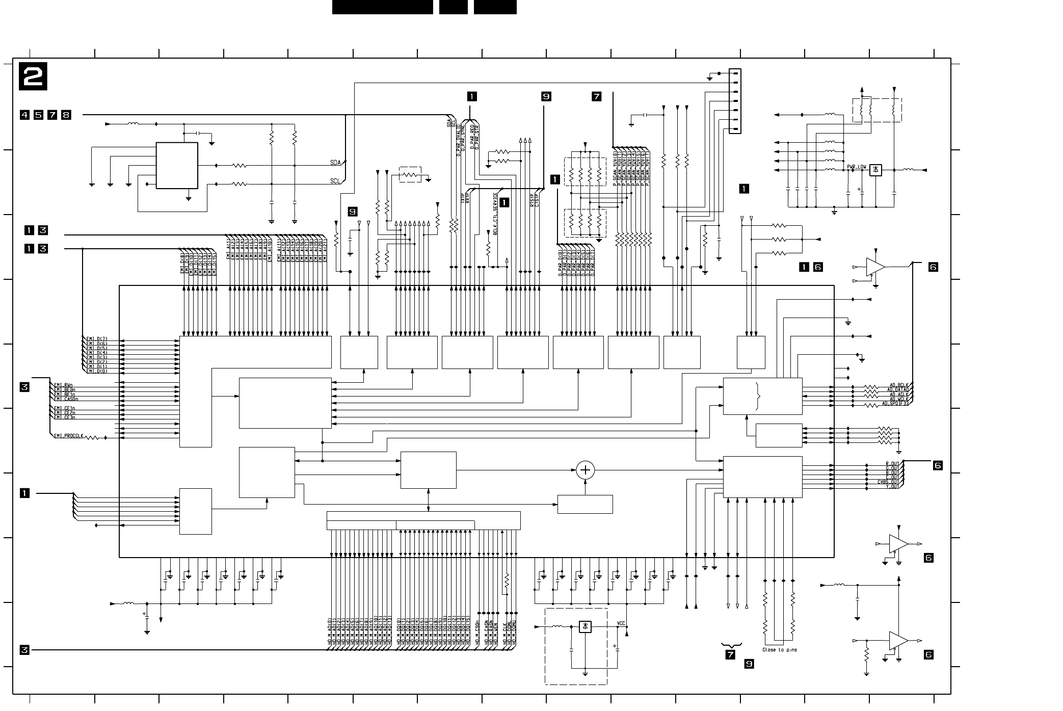
EN 140DVDR980-985 /0X1 7.
Electrical Diagrams and Print-Layouts
Digital Board: AV Decoder STI5508
MPEG1/2
2
I S
ADDRESS DATA
Interface
MEMORY interface
VIDEO
ENCODER
DECODER
AC3
LPCM AUDIO
IRQPORT 0 I/O PORT 1 I/O
Subpicture
Video
Audio
CSn
KARAOKE
USE
SDRAM CONTROLLER
SYSTEM JTAGPORT 2 I/O PORT 3 I/O PORT 4 I/O
FRONT-END
uP ST20cpu
A/V/Sub
demultiplexer
MPEG
DECODER
Subpicture
decoder
control
BE_SERIAL
AUDIO_OUT
12345
AV decoder : STI5508
SYSTEM DATA BUS
D
E
F
G
H
I
A
B
C
D
E
F
G
H
I
5 6 7 8 9 10 11 12 13 14
A
B
C
I2C BUS
1%
1%
SDRAM Interface
1%
SYSTEM ADDRESS BUS
1%
DCU
connector
NVRAM
Audio / Video
VIDEO_OUT
SYSTEM CONTROL
6 7 8 9 10 11 12 13 14
1234
decoder
HW version
OPTION
OPTION
OPTION
OPTIONOPTION
GNDD
GNDD
GNDD
4u7
2218
2200
1n
2231
100n
100n
2210
2230
I253
3230
13K
4u7
I224
2206
1
2
3
4
5
6
7
100n
10K
GNDD
FMN
1200
3213
10K
3219
2229
100n
100n
2224
3224
10K
13K
3229
GNDD
45
GNDD
I218
GNDD
GNDD
3237-D 33R
3236-D 33R45
GNDD
3235 1R
I241
2223
100n
F248
I242
3202
10K
I235
GNDD
I213
100R
3218
I220
2221
22R
3208
10K
100n
I237
3215
I208
I232
8
VCC
VSS
4
WC_
7
I216
M24C64
7201
E0
1
E1
2
E2
3
6
SCL
5
SDA
10K
3221
I255
GNDD
I259
GNDD
10K
3220
2203
4u7
I257
2211
100n
100n
2228
100n
2220
10K
3233
14
7
6
100n
2222
36
74HCT125D
7202-B
5
4
GNDD
GNDD
3234-C 4K7
3222
10K
100n
2215
100n
2226
5
GNDD
I239
4K7
3234-D4
2
1
14
7
3
1K5
3201
74HCT125D
7202-A
I270
100n
I227
2227
GNDD
GNDD
I264
5206
100MHZ
I221
22R
3227
3232
3212
1K5
I271
GNDD
3K9
2225
100n
GNDD
I262
3207
10K
I256
I210
100R
3206
GNDD
5203
2213
100n
GNDD
GNDD
10K
3214
2201
22n
I246
22R
3228
I231
I258
I230
GNDD
I268
I269
I265
I267
I266
10K
3216
VSS8
121 VSS9
32
Y-OUT
I217
VSS-PLL
24 VSS-RGB
31 VSS-YCC
5 VSS1
137 VSS10
150 VSS11
160 VSS12
172 VSS13
185 VSS14
199 VSS15
15 VSS2
38 VSS3
50 VSS4
65 VSS5
83 VSS6
96 VSS7
108
VDD2-51
37 VDD2-52
64 VDD2-53
94 VDD2-54
119 VDD2-55
149 VDD2-56
171 VDD2-57
198 VDD2-58
4VDD3-31
47 VDD3-32
81 VDD3-33
107 VDD3-34
136 VDD3-35
159 VDD3-36
184 VDD3-37
49VSS-PCM
123
SMI-RAS
78 SMI-WE
57
SPDIF-OUT
113
TCK
112
TDI
111
TDO
110
TMS
202
TRIGGER-IN
203
TRIGGER-OUT
109
TRST
28 V-REF-RG
35 V-REF-YC
48
VDD-PCM
122VDD-PLL
23 VDD-RGB
30 VDD-YCC
14
SMI-DATA10
98 SMI-DATA11
99 SMI-DATA12
100 SMI-DATA13
101 SMI-DATA14
102 SMI-DATA15
86 SMI-DATA2
87 SMI-DATA3
88 SMI-DATA4
89 SMI-DATA5
90 SMI-DATA6
91 SMI-DATA7
92 SMI-DATA8
93 SMI-DATA9
79 SMI-DQML
80 SMI-DQMU
76
73
67 SMI-ADR2
66 SMI-ADR3
58 SMI-ADR4
59 SMI-ADR5
60 SMI-ADR6
61 SMI-ADR7
62 SMI-ADR8
63 SMI-ADR9
77 SMI-CAS
82 SMI-CLKIN
95 SMI-CLKOUT
74 SMI-CS0
75 SMI-CS1
84 SMI-DATA0
85 SMI-DATA1
97
PIO4-3
43
PIO4-4
44
PIO4-5
45
PIO4-6
46
PIO4-7
120 PIX-CLK
116 PWM0
115
PWM1
114 PWM2
27
R-OUT
124
RESET
69 SMI-ADR0
68 SMI-ADR1
70 SMI-ADR10
71 SMI-ADR11
SMI-ADR12
72
SMI-ADR13
208
PIO2-4
PIO2-5 1
PIO2-6 2
PIO2-7 3
6
PIO3-0
7
PIO3-1
8
PIO3-2
9
PIO3-3
10
PIO3-4
11
PIO3-5
12
PIO3-6
13
PIO3-7
39
PIO4-0
40
PIO4-1
41
PIO4-2
42
188
PIO0-2
189
PIO0-3
190
PIO0-4
191
PIO0-5
192
PIO0-6
193
PIO0-7
PIO1-0 194
195
PIO1-1
196
PIO1-2
197
PIO1-3
200
PIO1-4
201
PIO1-5
204
PIO2-0
205
PIO2-1
206
PIO2-2
207
PIO2-3
CV-OUT
56
DAC-LRCLK
55
DAC-PCMCLK
52
DAC-PCMOUT0
DAC-PCMOUT1
53
DAC-PCMOUT2
54
51
DAC-SCLK
26
G-OUT
29 I-REF-RG
36 I-REF-YC
127IRQ0
IRQ1 126
125
IRQ2
NRSS-OUT
22
PIO0-0 186
PIO0-1 187
157
CPU-DATA14
158
CPU-DATA15
143
CPU-DATA2
144
CPU-DATA3
145
CPU-DATA4
146
CPU-DATA5
147
CPU-DATA6
148
CPU-DATA7
151
CPU-DATA8
152
CPU-DATA9
117
CPU-OE
CPU-PROCLK
118
138
CPU-RAS1
130
CPU-RW
131
CPU-WAIT
34
168
CPU-ADR8
169
CPU-ADR9
128
CPU-BE0
129
CPU-BE1
139
CPU-CAS0
140
CPU-CAS1
135
CPU-CE0
134
CPU-CE1
133
CPU-CE2
132
CPU-CE3
141
CPU-DATA0
142
CPU-DATA1
153CPU-DATA10
154CPU-DATA11
155
CPU-DATA12
156CPU-DATA13
174
CPU-ADR12
175
CPU-ADR13
176
CPU-ADR14
177
CPU-ADR15
178
CPU-ADR16
179
CPU-ADR17
180
CPU-ADR18
181
CPU-ADR19
162
CPU-ADR2
182
CPU-ADR20
183
CPU-ADR21
163
CPU-ADR3
164
CPU-ADR4
165
CPU-ADR5
166
CPU-ADR6
167
CPU-ADR7
ADC-DATA 105
ADC-LRCLK 104
106
ADC-PCMCLK
ADC-SCLK 103
17
B-BCLK
16
B-DATA
18
B-FLAG
25
B-OUT
19
B-SYNC
21
B-V4
20
B-WCLK
33
C-OUT
161
CPU-ADR1
170
CPU-ADR10
173
CPU-ADR11
STI5508
7200
I203
100MHZ
5208
100n
2219
5201
I251
100n
2214
GNDD
7203
GND INOUT
I240
LF25C
I209
I219
I200
IN OUT
2207
33p
I260
7204
LF25C
GND
GNDD
3200 3K3
I236
GNDD
33R3237-A 1 8
100n
2212
I252
GNDD
100MHZ
5205
GNDD
I245
100n 2208
I201
GNDD
I223
18
10K
3238
I233
GNDD
3234-A 4K7
F249
5209
100R
3217
I211
100n
2205
I226
I202
2202
100n
I206
5202
F250
I204
I229
I261
100n
2209
5211
I263
5212
I254
12
13
14
7
11
100n
2216
3231
3K9
74HCT125D
7202-D
5207
100MHZ
GNDD
GNDD
I234
GNDD
33p
2204
GNDD
I207
GNDD
I212
3203 22R
3204
100R
I244
5204
10K
F265
3226
GNDD
I225
3211
2K2
GNDD
F214
100R
3205
I228
100MHZ
5200
GNDD
10K
3225
GNDD
F247
2K2
I205
I238
3223
36
GNDD
10K
3209
4K7
3234-B 2 7
33R3237-C
GNDD
33R3236-A 1 8
5210
100MHZ
6
3236-B 33R27
33R3236-C 3
F264
100n
2217
3237-B 33R27
GNDD
GNDD
I243
I222
10K
3245
GNDD
3244
10K
10K
3241
10K
32423243
10K
3240
10K
3239
10K
I215
BCLK_CTL_SERVICE
+3V3
GNDD
VDD_STI
+5V
VDD_PLL
VDD_CORE
VDD_PCM
VDD_CORE
AD_ACLK
AE_ACLK
EMPRESS_BOOT
{BCLK_CTL_SERVICE,TX1P,RX1P,RTS1P,CTS1P}
VDD_CORE
BE_LOADN
VDD_STI
ANA_WE
MUTEN
VDD_125
AE_ACLK_OEn
VDD_125
ANA_WE_LV
VDD_STI
+3V3
AE_ACLK_OEn
VDD_STI
SEL_ACLK1
VDD_STI
P_SCAN_YUV(7:0)
MUTEN_LV
ANA_WE_LV
LOAD_DVN
VDD_STI
Flash_Oen
RESETn_VE
EMI_WAIT
+3V3
MUTEN_LV
5508_HS
VDD_PCM
RESETn
D_PAR_D(7:0)
RSTN_BE
RSTN_DVIO
VDD_PLL
VDD_RGB
VDD_YCC
SYSCLK_VSM_5508
+3V3
+5V
VDD_125
BE_DATA_RD
BE_SYNC
BE_FLAG
BE_V4
VDD_STI
CPUINT0
VDD_STI
VDD_STI
+3V3
VDD_RGB
VDD_YCC
BE_BCLK
BE_WCLK
CPUINT1
VDD_STI
5508_odd_even
CL 16532145_023.eps
211101
1200 A11
2200 C5
2201 C11
2202 A3
2203 I2
2204 B4
2205 B13
2206 B13
2207 B5
2208 B13
2209 B12
2210 B14
2211 H3
2212 H3
2213 H3
2214 H3
2215 H4
2216 H4
2217 H4
2218 I10
2219 I9
2220 H8
2221 H9
2222 H9
2223 H9
2224 H10
2225 H10
2226 H10
2227 H10
2228 B12
2229 H13
2230 B13
2231 A10
3200 C5
3201 A4
3202 C12
3203 E13
3204 E13
3205 B4
3206 B4
3207 I13
3208 F1
3209 A8
3211 C11
3212 A5
3213 C6
3214 C6
3215 B10
3216 B8
3217 C7
3218 C7
3219 B11
3220 B10
3221 B6
3222 B6
3223 C7
3224 C12
3225 C12
3226 C8
3227 E13
3228 E13
3229 H12
3230 H12
3231 I12
3232 I12
3233 B6
3234-A F13
3234-B F13
3234-C F13
3234-D F13
3235 H8
3236-A C10
3236-B C10
3236-C C10
3236-D C10
3237-A C10
3237-B C10
3237-C C10
3237-D C10
3238 B9
3239 C9
3240 B9
3241 C9
3242 B9
3243 C9
3244 B9
3245 C9
5200 H2
5201 A13
5202 A13
5203 B13
5204 B13
5205 B14
5206 I9
5207 A2
5208 H13
5209 A13
5210 A14
5211 A13
5212 A13
7200 C2
7201 A2
7202-A C13
7202-B I14
7202-D G14
7203 B14
7204 I9
F214 C11
F247 C10
F248 C10
F249 C11
F250 C11
F264 C6
F265 A11
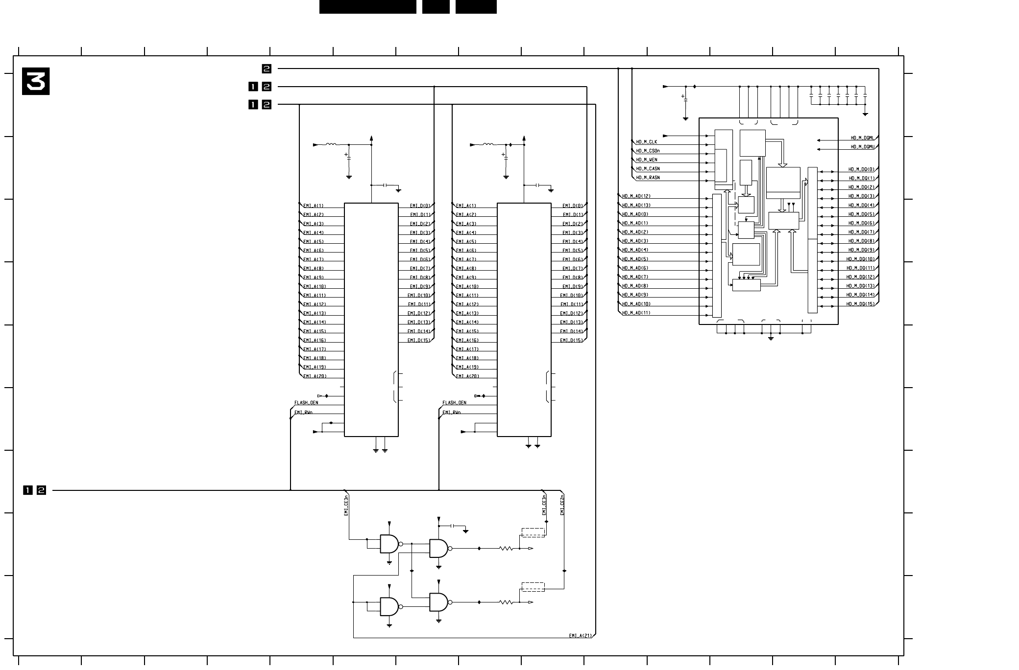
Electrical Diagrams and Print-Layouts EN 141DVDR980-985 /0X1 7.
Digital Board: AV Decoder Memory
NC
DQMH
SENSE AMPLIFIERS
COMMAND
DECODE
CTRL
LOGIC
MODE REG
ADDRESS REGISTER
ROW
ADDR
MUX
LOGIC
CTRL
BANK
COLUMN
ADDR
COUNTER/
I/O GATING
DQM DATA LOGIC
READ DATA LATCH
WRITE DRIVERS
DATA INPUT REGISTER DATA OUTPUT REGISTER
DQML
VDDQ
VDD
NC
VSSQ VSS
LATCH
REFRESH
COUNTER
BANK0
ROW-
ADDR
LATCH &
DECODER
COLUMN
DEDCODER
BANK0
MEMORY
ARRAY
(4,096x256x16)
NC
SYSTEM CONTROL
FLASH 2
SDRAM
A
B
C C
SDRAM Interface
5 6 7 8 9 10 11 12 13 14
12345 14
D
E
F
G
H
I
A
B
AV Decoder Memory
SYSTEM ADDRESS BUS
SYSTEM DATA BUS
1234
OPTION
OPTION
6 7 8 9 10 11 12 13
FLASH 1
D
E
F
G
H
I
2306
100n
3300
2302 100n
GNDD
47R
2308 100n
GNDD
4301
100n
2309
12
13
7
14
11
74LVC00AD
7303-D
11
38
DQ5 40
DQ6 42
DQ7 44
DQ8 30
DQ9 32
E_
26
G_
28 10
13
14
RB_
15
RP_
12
VCC
37
VSS1
27
VSS2
46
W_
20
A6
19
A7
18
A8
8
A9
7
BYTE_
47
DQ0 29
DQ1 31
DQ10 34
DQ11 36
DQ12 39
DQ13 41
DQ14 43
45
DQ15|A-1
33
DQ2
DQ3 35
DQ4
A0
25
A1
24
A10
6
A11
5
A12
4
A13
3
A14
2
A15
1
A16
48
A17
17
A18
16
A19
9
A2
23
22 A3
21 A4
A5
M29W160DT
7302
I306
I309
I307
GNDD
100n
2301
I305
I304
GNDD
I303
47R
3301
I300
2310
GNDD
GNDD
GNDD
100n
GNDD
100n
2307
1
2
7
14
3
GNDD
7303-A
74LVC00AD
2304
4u7
GNDD
74LVC00AD
7303-C
9
10
7
14
8
2311
4u7
2303 100n
GNDD
2312
100n
2300 100n
4u7
2305
7303-B
74LVC00AD
4
5
7
14
6
I308
RB_
15
RP_
12
37
VCC
27
VSS1
46
VSS2
W_
11
41
DQ13
43
DQ14
DQ15|A-1 45
DQ2 33
35
DQ3
38
DQ4
40
DQ5
42
DQ6
44
DQ7
30
DQ8
32
DQ9
E_
26
G_
28 10
13
14
16 A18
9A19
23 A2
A3
22
A4
21
20 A5
19 A6
18 A7
8A8
7A9
47 BYTE_
29
DQ0
31
DQ1
34
DQ10
36
DQ11
39
DQ12
7301
M29W160DT
25 A0
24 A1
6A10
5A11
4A12
3A13
2A14
1A15
48 A16
17 A17
16 WE_
I302
40
18 RAS_
11427 394349
28 41 546 124652
47DQ11
48DQ12
50DQ13
51DQ14
53DQ15
5DQ2
7DQ3
8DQ4
10DQ5
11DQ6
13DQ7
42DQ8
44DQ9
39DQMH
15DQML
36
26 A3
29 A4
30 A5
31 A6
32 A7
33 A8
34 A9
20 BA0
21 BA1
17 CAS_
37 CKE
38 CLK
19 CS_
2DQ0
4DQ1
45DQ10
7300
MT48LC4M16A2TG-7E
23 A0
24 A1
22 A10
35 A11
25 A2
100MHZ
5302
4300
GNDD
I301
5300
100MHZ
GNDD
{EMI_RWn,FLASH_OEN,EMI_CE2n,EMI_CE3n}
ROML_CEn
GNDD
VDD_FLASH_L
VDD_FLASH_L
ROMH_CEn
VDD_FLASH_H
VDD_STI
VDD_FLASH_H
ROML_CEn
+3V3
VDD_FLASH_L
VDD_STI
+3V3
VDD_FLASH_L
VDD_FLASH_L
VDD_FLASH_L
ROMH_CEn
CL 16532145024.eps
221101
2300 A14
2301 A14
2302 A14
2303 A13
2304 B8
2305 B6
2306 B6
2307 B9
2308 A13
2309 A13
2310 A13
2311 A11
2312 H7
3300 H8
3301 I8
4300 H9
4301 I9
5300 B5
5302 B8
7300 A11
7301 B8
7302 B6
7303-A H6
7303-B H7
7303-C I6
7303-D I7
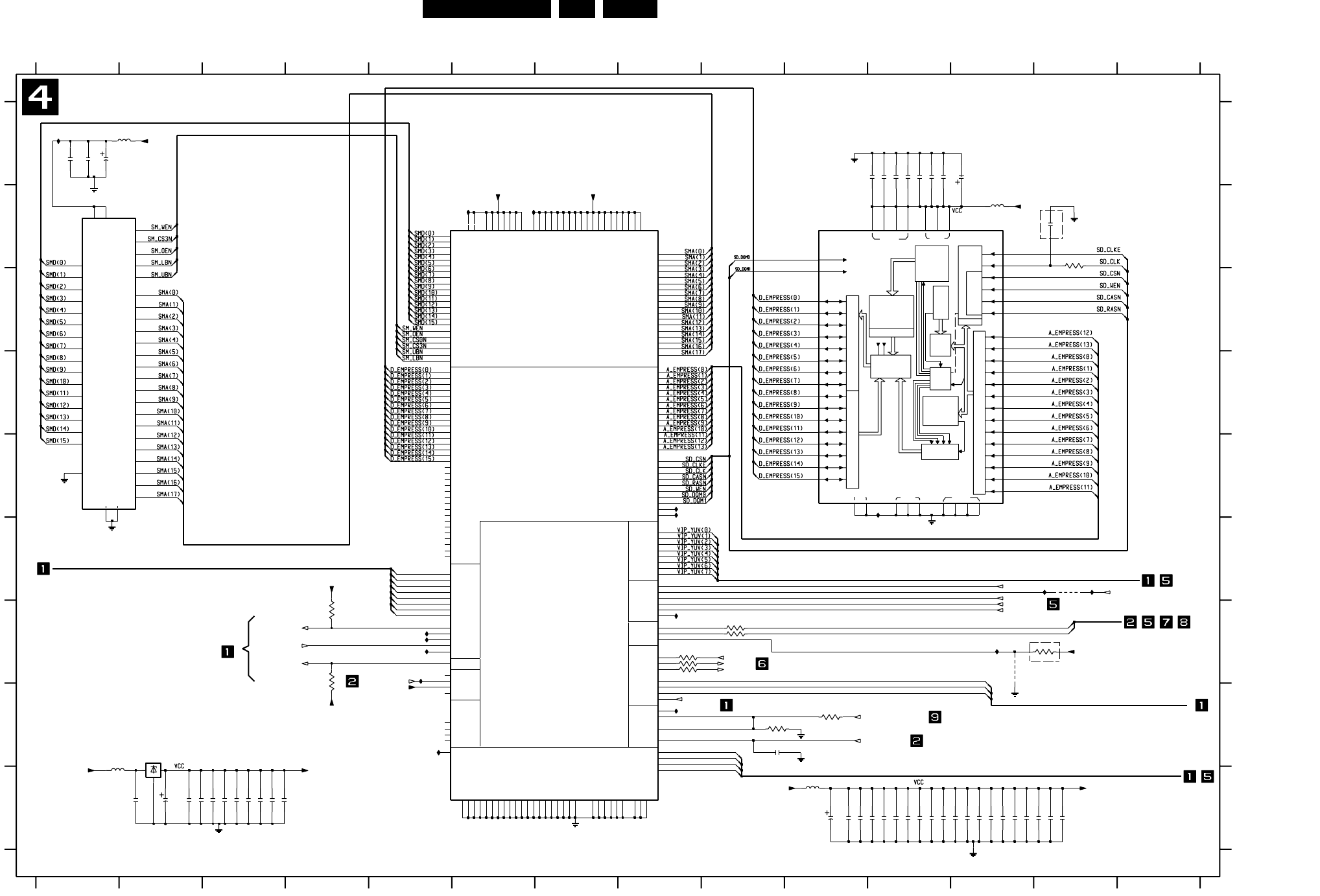
EN 142DVDR980-985 /0X1 7.
Electrical Diagrams and Print-Layouts
Digital Board: Video Encoder, Empress
DQMH
SENSE AMPLIFIERS
COMMAND
DECODE
CTRL
LOGIC
MODEREG
ADDRESS REGISTER
ROW
ADDR
MUX
LOGIC
CTRL
BANK
COLUMN
ADDR
COUNTER/
I/O GATING
DQM DATA LOGIC
READ DATA LATCH
WRITE DRIVERS
DATA INPUT REGISTER DATA OUTPUT REGISTER
DQML
VDDQ VDD
NC VSSQVSS
LATCH
REFRESH
COUNTER
BANK0
ROW-
ADDR
LATCH &
DECODER
COLUMN
DEDCODER
BANK0
MEMORY
ARRAY
(4,096x256x16)
VSS
VCC
EMPRESS
2425
100n
DATA STREAM BUS
JTAG_CHAIN3
Video Encoder Empress
E
F
G
H
I
A
B
7 8 9 1011121314
1234567891011121314
A
B
C
D
H
I
MPEG2 VIDEO DIGITAL VIDEO(CCIR656)
I2C BUS
123456
OPTION
OPTION
MPEG2 / AC-3 encoder
SRAM SDRAM
AUDIO ENCODER
C
D
E
F
G
2403
4u7
I405
3406
47R
2419
100n
2424
2410 100n
100n
100n
2407
2433
100n
100n
2442
I414 I415
I416
I407
124652
WE_ 16
2434
100n
3640
RAS_ 18
11427394349
284154 6
45
DQ1147
DQ1248
DQ1350
DQ1451
DQ1553
DQ25
7DQ3
DQ48
DQ510
DQ611
DQ713
DQ842
DQ944
DQMH39
DQML15
25
A3 26
A4 29
A5 30
A6 31
A7 32
A8 33
34A9
BA0 20
BA1 21
CAS_ 17
CKE 37
CLK 38
CS_ 19
DQ02
DQ14
DQ10
7402
MT48LC4M16A2TG-7E
A0 23
A1 24
A10 22
A11 35
A2
100MHZ
5404
10K
3402
LF25C
7404
GND
IN OUT
2440
100n
100n
2405
100n
2439
I402
100n
2412
2402
100n
4409
100n
2430
2408 100n
2429
100n
100n
100n
2428
2438
5400
100MHZ
GNDD
2411
4u7
GNDD
GNDD
2432
100n
180R
3407
GNDD
2441
4u7
100n
2418
2417
100n
I410
100n
2416
100n
2415
100n
100n
2426
2427
I408
I400
I403
GNDD
2404 100n
I404
3404
2436
100n
1R
YUV3 15
YUV4 16
YUV5 17
YUV6 18
YUV7 19
4406
VSSP19
190
VSSP2
10
VSSP20
200
VSSP3
20
VSSP4
34
VSSP5
44
VSSP6
53
VSSP7
62
VSSP8
72
VSSP9
86
VSYNC 22
XTALI 126
XTALO 127
YUV0 12
YUV1 13
YUV2 14
VSSCO3
77
78 VSSCO4
VSSCO5
129
VSSCO6
130
VSSCO7
181
VSSCO8
182
VSSP1
1
VSSP10
96
VSSP11
105
114 VSSP12
VSSP13
124
VSSP14
138
VSSP15
148
VSSP16
157
VSSP17
166
VSSP18
176 VDDP15 161
VDDP16 171
VDDP17 185
VDDP18 195
VDDP19 205
VDDP2 29
VDDP3 39
VDDP4 49
VDDP5 57
VDDP6 67
VDDP7 81
VDDP8 91
VDDP9 101
VSSAOSC
125
VSSCO1
25
VSSCO2
26
VCLK2 30
VDDAOSC 128
VDDCO1 27
VDDCO2 28
VDDCO3 79
VDDCO4 80
VDDCO5 131
VDDCO6 132
VDDCO7 183
VDDCO8 184
VDDP1 5
VDDP10 109
VDDP11 119
VDDP12 133
VDDP13 143
VDDP14 153
SM-LB_
154
SM-OEN
158
SM-UB_
155
SM-WEN
172
SWS1 4
SWS2 8
TCLK 136
TDI 134
TDO
137
TEST0
141
TEST1
142
TEST2
144
TMS 135
TRSTN 139
TXD
152
VCLK1 24
SM-D0
194
SM-D1
192
SM-D10
179
SM-D11
186
SM-D12
188
SM-D13
191
SM-D14
193
SM-D15
196
SM-D2
189
SM-D3
187
SM-D4
180
SM-D5
178
SM-D6
175
SM-D7
173
SM-D8
174
SM-D9
177
SM-A12 165
SM-A13 168
SM-A14 170
SM-A15 202
SM-A16 204
SM-A17 207
SM-A2 201
SM-A3 199
SM-A4 198
SM-A5 169
SM-A6 167
SM-A7 164
SM-A8 162
SM-A9 159
SM-CS0_
208
SM-CS3N
197
SD-DQ7
68
SD-DQ8
66
SD-DQ9
64
SD-DQM0 70
SD-DQM1 69
SD-DQM2 102
SD-DQM3 100
SD-RASN 75
SD-WEN 71
SDA 145
SDATA1 2
SDATA2 6
SM-A0 206
SM-A1 203
SM-A10 160
SM-A11 163
SD-DQ20
115
SD-DQ21
117
SD-DQ22
120
SD-DQ23
122
SD-DQ24
121
SD-DQ25
118
SD-DQ26
116
SD-DQ27
113
SD-DQ28
111
SD-DQ29
108
SD-DQ3
58
SD-DQ30
106
SD-DQ31
103
SD-DQ4
60
SD-DQ5
63
65 SD-DQ6
SD-CKE 76
SD-CLK 74
SD-CSN 82
SD-DQ0
50
SD-DQ1
52
SD-DQ10
61
SD-DQ11
59
SD-DQ12
56
SD-DQ13
54
SD-DQ14
51
SD-DQ15
48
SD-DQ16
104
SD-DQ17
107
110 SD-DQ18
SD-DQ19
112
SD-DQ2
55
SCLK2 7
SD-A0 94
SD-A1 97
SD-A10 92
SD-A11 87
SD-A12 89
SD-A13 83
SD-A2 99
SD-A3 98
SD-A4 95
SD-A5 93
SD-A6 90
SD-A7 88
SD-A8 85
SD-A9 84
SD-CASN 73
PDO0
36
PDO1
37
PDO2
38
PDO3
40
PDO4
41
42 PDO5
PDO6
43
PDO7
45
PDOAV
31
PDOSYNC
33
PDOVAL
35
RESETN 147
RTSN
149
RXD
151
146
SCL
SCLK1 3
7403
SAA6752HS
ACLK 9
CLKOUT
140
CTSN
150
EXTCLK 123
FID 23
H-IRF
156
HSYNC 21
I2CADDRSEL 47
IDQ 11
PDIDS
32
PDIOCLK
46
41
UB_ 40
33 11
1234
WE_ 17
31
IO12
32
IO13
35
IO14
36
IO15
37
IO16
38
IO2
8
IO3
9
IO4
10
IO5
13
IO6
14
IO7
15
IO8
16
IO9
29
LB_ 39
NC
28
OE_
A14 27
A15 42
A16 43
A17 44
A2 3
A3 4
A4 5
A5 18
A6 19
A7 20
A8 21
A9 22
CS_ 6
IO1
7
IO10
30
IO11
7401
K6R4016V1CT
A0 1
A1 2
A10 23
A11 24
A12 25
A13 26
2446
1n GNDD
GNDD
2413
100n
I406
GNDD
3405
3K3
100n
2444
GNDD
100n
2422
I409
2421
100n
100n
2409
100MHZ
5403
I401
GNDD
2406 100n
3400 100R
4u7
2431
100R
3401
100n
2435
GNDD
3403
10K
GNDD
22R3408
5402
100MHZ
I412 I413
2437
100n
100n
2414
2443
22p
100n
2420
2423
100n
3409 22R3410
VE_DATA(3)
VE_DATA(2)
VE_DATA(1)
VE_DATA(0)
VE_DSn
EMPRESS_IRQn
VDD_EMP
AE_DATAI
AE_BCLK
AE_WCLK
22R
EMPRESS_BOOT
VE_DTACKn
VE_DATA(7)
VE_DATA(6)
VE_DATA(5)
VE_DATA(4)
VDD_EMP
VIP_VS
AE_WCLK_VSM
JTAG3_TCK
JTAG3_TD_VIP_TO_VE
JTAG3_TMS
JTAG3_TRSTn
VIP_ICLK
VDD_EMP_CORE
VIP_IDQ
RESETn_VE
AE_BCLK_VSM
AE_DATAO
+3V3
VDD_EMP_CORE
VDD_EMP_CORE
VDD_EMP
SYSCLK_EMPRESS
SMD(15:0)
{SM_WEN,SM_OEN,SM_CS0N,SM_CS3N,SM_UBN,SM_LBN}
ACLK_EMP
VIP_FID_FF
+3V3
SDA
SCL
VDD_EMP
VDD_EMP
VDD_EMP
VDD_EMP
+3V3
VIP_HS
D_EMPRESS(15:0)
A_EMPRESS(13:0)
{SD_CLKE,SD_CLK,SD_CSN,SD_WEN,SD_CASN,SD_RASN,SD_DQM0,SD_DQM1}
+3V3
SMA(17:0)
CL 16532145_025.eps
221101
2402 A1
2403 A1
2404 B11
2405 B11
2406 B11
2407 B11
2408 B11
2409 B11
2410 B11
2411 A12
2412 I13
2413 I13
2414 I13
2415 I12
2416 I12
2417 I12
2418 I12
2419 I12
2420 I12
2421 I12
2422 I11
2423 I11
2424 I11
2425 I11
2426 I11
2427 I11
2428 I11
2429 I10
2430 I10
2431 I10
2432 I3
2433 I3
2434 I3
2435 I3
2436 I3
2437 I3
2438 I3
2439 I2
2440 I2
2441 I2
2442 I2
2443 B13
2444 A1
2446 H9
3400 G9
3401 G9
3402 G13
3403 G4
3404 B13
3405 G4
3406 H10
3407 H9
3408 G8
3409 G8
3410 G8
4406 F13
4409 G12
5400 B12
5402 A2
5403 H1
5404 I10
7401 B2
7402 B12
7403 B8
7404 H2
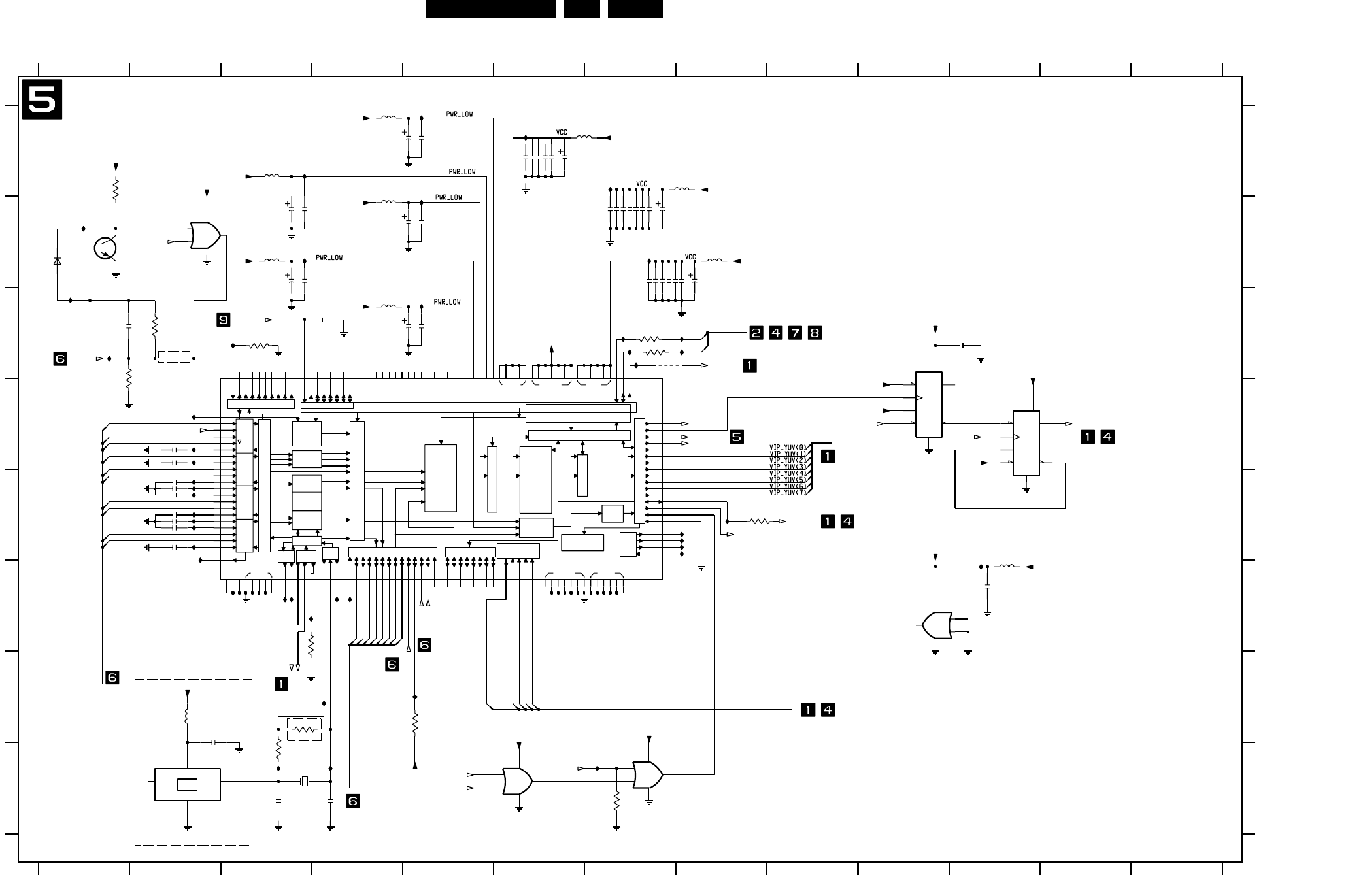
Electrical Diagrams and Print-Layouts EN 143DVDR980-985 /0X1 7.
Digital Board: VIP CVBS Y/C Video Input
RAW S
YCBCR
YCBCR
YCBCRS
CBCR
CBCR
RAW
BCS-SCALER
VDDA VDDE VDDI
VSSA VSSE VSSI
IIC REGISTER MAP
R
COMB
PROC
CHROM
PROC
COMP
DELAY
SWITCH
FAST
VIDEO
DECODER OUTPUT CONTROL
BOUNDARY
SCAN
OUTPUT FORMATTER I-PORT
1ST TASK IIC REG MAP SCALER
SCALER EVENT CONTROLLER
VIDEO/TEXT
ARBITER
TEXT
FIFO
VBI DATA
SLICER
ANALOG1
+ ADC1
VIDEO FIFO
VERTICAL SCALING
HORIZONTAL FINE-
(PHASE-) SCALING
LINE FIFO BUFFER
FIR-PREFILTER
PRESCALER
ANALOG1
+ ADC1
ANALOG1
+ ADC1
G
B
Y
S
C
CLK GPO XTAL
S
S
Y
CR
CB
CB
CR
Y
AUDIO
CLK
H-PORTX-PORT
2ST TASK IIC REG MAP SCALER
SYNC
PROC
LUM
FIL
ANALOG INPUT CONTROL
AD-PORT
CONTROL
ANALOG1
+ ADC1
OSC
VIP CVBS Y/C Video Input
processor
VIP ANALOG VIDEO INPUT
Video Input
JTAG_CHAIN3
91011
DIGITAL VIDEO(CCIR656)
345678910111213
12345678
12
I2C BUS
12 13
A
B
C
D
E
F
G
H
A
B
C
D
E
F
G
H
2541
OPTION
OPTION
OPTION
I525
4u7
2511
18p
I509
GNDD
I516
100n
2535
I522
I515
2504 100n
XPD2
B9
XPD3
A10
XPD4
B10
XPD5
A11
XPD6
C11
XPD7
A6
XRDY
C7
XRH
D8
XRV
A3
XTAL
B4
XTALI
A2
XTOUT
B11
XTRI
L4
L8
L11
D7
D10
F11
J11
L5
L9
B3
VXDD
A4
VXSS
A7
XCLK
B7
XDQ
A8
XPD0
B8
XPD1
A9
M11
C8
C10
F12
J12
M5
M9
M2
J4
H3
E4
C1
D5
D9
D11
G11
TMS
C6
TRSTN
M3
K4
L1
VDDA1A
H4
J1
VDDA2A
F4
G2
VDDA3A
D4
E2
VDDA4A
C5
C9
D12
H12
M4
M8
RES9
P5
RESON
M10
RST0
N10
RST1
L10
RTCO
N9
SCL P10
SDA
B6
TCK
B5
TDI
A5
TDO
TEST0
P13
TEST1
D13
TEST2
C14
TEST3
A13
TEST4
B12
TEST5
A12
D6
ITRDY
L12ITRI
P4
LLC
N5
LLC2
B2
RES1
N3
RES10
N13
RES11
N14
RES12
P2
RES13
B13
RES2
B14
RES3
C3
RES4
C4
RES5
C12
RES6
C13
RES7
N1
RES8
N2
HPD7
M14ICLK
G14IDP0
G12IDP1
H11IDP2
H14IDP3
H13IDP4
J14IDP5
J13IDP6
K11IDP7
L13IDQ
L14IGP0
K13IGP1
K12IGPH
K14IGPV
P9
INT_A
N12
A|41
D2 A|42
D1 A|43
E1 A|44
D3 A|4D
N4
CE
N6
CLKEXT
P3
EXMCLR
M13 FSW
D14
HPD0
E11
HPD1
E13
HPD2
E12
HPD3
E14
HPD4
F13
HPD5
F14
HPD6
G13
N11
J2 A|11
K1 A|12
K2 A|13
L3 A|14
K3 A|1D
G4 A|21
G3 A|22
H2 A|23
J3 A|24
H1 A|2D
E3 A|31
F2 A|32
F3 A|33
G1 A|34
F1 A|3D
B1
N8
ADP0
P8
ADP1
M7
ADP2
L7
ADP3
P7
ADP4
N7
ADP5
L6
ADP6
M6
ADP7
P6
ADP8
C2
AGND
L2
AGNDA
P12ALRCLK
P11AMCLK
M12AMXCLK
M1 AOUT
ASCLK
3501 100R
7500
SAA7118E
I535
100MHZ
5500
2540
4u7
I529
100n
2524
I502
I505
2531 100n
I521
CX-11F
1500
24M576
I519
I501
I508
I531
I514
I511
100n
I527
2522 100n
2529
GNDD
2536
100n
2534
2545
100n
100n
FXO-31FT
7503
2
GND
3
OUT
1TS
4
VDD
100MHZ
5503
GNDD
GNDD
3515
1R
2520
4u7
GNDD
GNDD
2538
GNDD
2506 100n
GNDD
100n
GNDD
4500
2500
1n
I510
4u7
2539
GNDD
5506
100MHZ
GNDD
GNDD
GNDD
100n
2537
GNDD
GNDD
100n
2503
100n
2532
GNDD
GNDD
2528 100n
11
14
7
GNDD
2533 100n
7501-D
74LVC32AD
12
13
I518
100MHZ
5504
2544
100n
I512
GNDD
GNDD
5509
2501 100n
100n
2514
GNDD
100MHZ
5507
7504
BC847B
I538
2508 100n
I520
4K7
3507
GNDD
4u7
2519
I537
100n
2505
GNDD
2565
150p
I526
2523 100n
14
14
7
74HC74D
7502-B
11
12
7
9
813
10
GNDD
74LVC32AD
7501-A
1
2
3
3513
680R
GNDD
GNDD
I555 I552
I543
I553
I540
I503
100n
2521
I506
2513 100n
2542
4u7
3509
1M
GNDD
I533
100n
2530
7501-B
4
56
14
7
100n
2512
I532
74LVC32AD
I530
100n
100n
2527
2517
4u7
2515
2525 100n
I504
100n
2509
100R
3500
3505 22R
GNDD
GNDD
I551
18p
2510
6500
BAT54 COL
I536
GNDD
GNDD
100MHZ
5501
4u7
2518
4501
100n
2507
3
2
7
5
61
4
14
GNDD
7502-A
74HC74D
GNDD
3508
10K
100MHZ
I513
2502 100n
5502
GNDD
680R
3504
74LVC32AD
7501-C
9
10 8
14
7
100n
2516
I524
I507
I500
100MHZ
I528
5505
2K2
3502
5508
I523
100MHZ
GNDD
2526 100n
1K
3503
2543 100n
2K2
3506
VIP_FB
I517
VDDA1A_7118
VDDA2A_7118
VDDA3A_7118
VDDX_7118
VIP_IDQ
VIP_ICLK
VIP_INT
+3V3
+3V3
+3V3
VIP_VS
+3V3
VIP_VS
+3V3
VIP_FID_FF
+3V3
+3V3
Y_IN_VIP
U_IN_VIP
V_IN_VIP
B_IN_VIP
VIP_IGP1
VDDI_7118
VDDA_7118
VDD_LVC32
VDD_LVC32
VIP_IGP1
VIP_RTS1
+3V3
VDD_LVC32
DV_IN_CLK
SDA
SCL
VDDA4A_7118
DV_IN_DATA(0:7)
+3V3
+3V3
+3V3
+3V3
+3V3
+3V3
+3V3
CVBS_Y_IN_A
CVBS_Y_IN_B
CVBS_Y_IN_C
C_IN_VIP
G_IN_VIP
R_IN_VIP
DV_IN_DATA(4)
DV_IN_DATA(5)
DV_IN_DATA(6)
DV_IN_DATA(7)
DV_IN_HS
DV_IN_VS
VIP_VS
VIP_RTS1
VIP_HS
vip_error
DV_IN_HS
VDD_LVC32
+3V3
VDDE_7118
CVBS_OUT_B_VIP
RESETn
VIP_IGP1
JTAG3_TCK
JTAG3_TD_VSM_TO_VIP
JTAG3_TD_VIP_TO_VE
JTAG3_TMS
JTAG3_TRSTn
VDDE_7118
DV_IN_DATA(0)
DV_IN_DATA(1)
DV_IN_DATA(2)
DV_IN_DATA(3)
1500 H3
2500 C4
2501 D2
2502 D2
2503 E2
2504 E2
2505 E2
2506 E2
2507 E2
2508 E2
2509 E2
2510 H3
2511 H4
2512 F11
2513 B3
2514 A5
2515 C3
2516 B5
2517 A4
2518 B3
2519 B3
2520 B4
2521 C7
2522 B7
2523 C7
2524 B7
2525 C7
2526 B7
2527 A6
2528 C7
2529 B7
2530 C5
2531 A6
2532 C8
2533 B7
2534 A6
2535 C7
2536 B7
2537 B7
2538 A6
2539 A6
2540 B7
2541 B8
2542 C4
2543 A6
2544 C11
2545 G2
2565 C1
3500 C7
3501 C7
3502 C3
3503 C1
3504 A1
3505 E8
3506 H7
3507 F3
3508 G5
3509 G3
3513 C2
3515 H3
4500 C2
4501 C7
5500 A4
5501 A3
5502 A4
5503 B3
5504 E11
5505 B8
5506 A8
5507 A6
5508 C4
5509 G2
6500 B1
7500 C3
7501-A F11
7501-B B2
7501-C H7
7501-D H6
7502-A C10
7502-B D11
7503 H2
7504 B1
CL 16532145_026.eps
221101
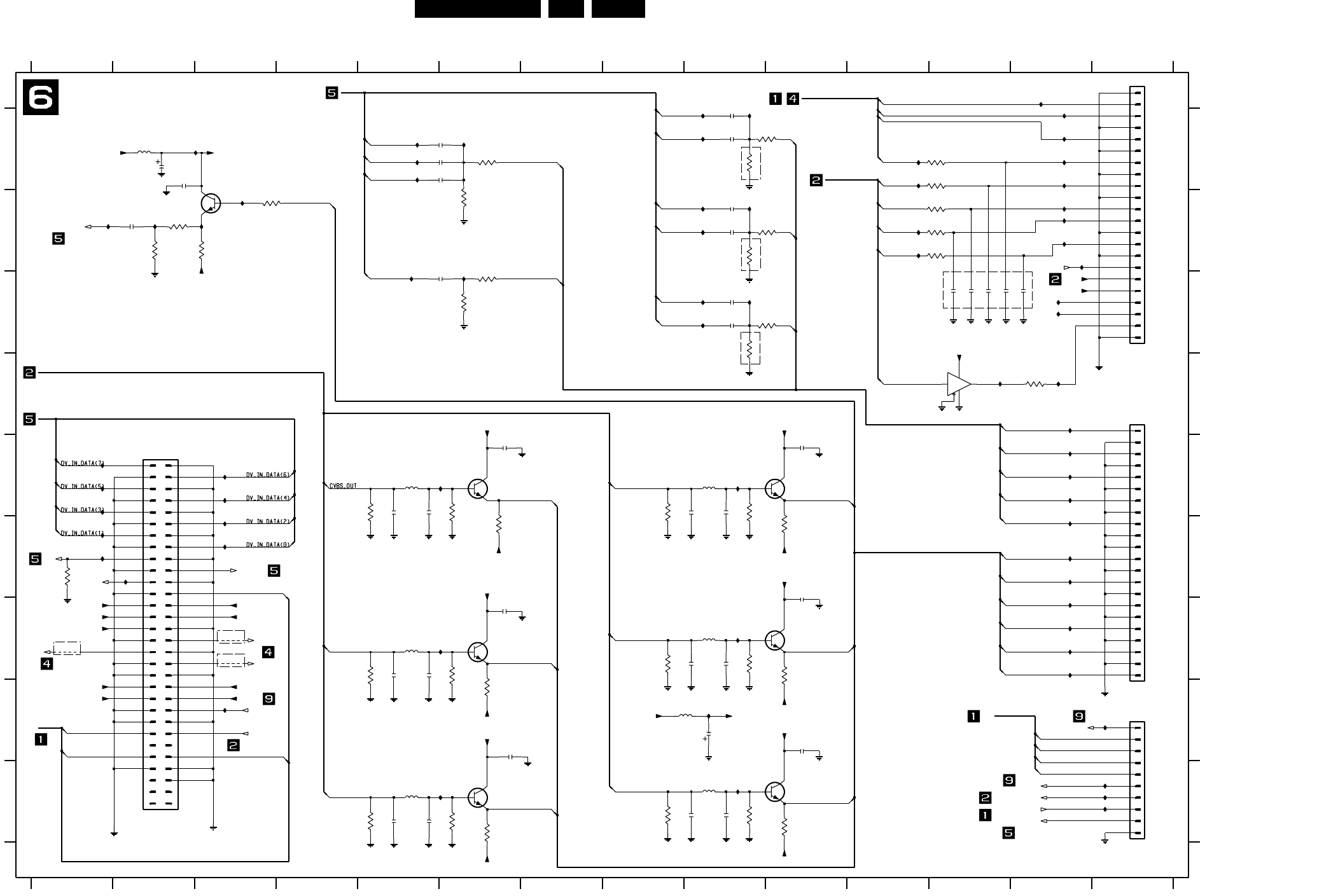
EN 144DVDR980-985 /0X1 7.
Electrical Diagrams and Print-Layouts
Digital Board: Analog Board Cons. Video In / Output
1%
1%
ANALOG BOARD
F
G
H
INTERFACE CONTROL
UART2
DIVIO
1%
1%
VIP ANALOG VIDEO INPUT
4567891011121314
A
B
1%
1%
Analog Board Cons.
Video In / Output
1%
13
ANALOG BOARD INTERFACE VIDEO IN/OUT
1%
ANALOG BOARD INTERFACE AUDIO IN/OUT
AUDIO OUT
DATA STREAM BUS
1%
UART1
3
123456789
C
D
E
VIDEO_OUT
1%
14
12
10 11 12
OPTION
OPTION
OPTION
OPTION
OPTION
OPTION
OPTION
E
I
1%
1%
AUDIO ENCODER
F
G
H
I
A
B
C
D
3623
100R
47p
2601
GNDD
GNDD
I604
I600
GNDD
3628
1K
7604
BC847B
I626
2606
47p
GNDD
GNDD
GNDD
3606
560R
I618
3600
56R
22p
2623
GNDD
I627
BC847B
7605
3614
75R
2626
47p
GNDD
1R
3631
GNDD
I610
BC847B
7600
GNDD
I641
4u7
2630
15
16
17
18
19
2
20
21
22
3
4
5
6
7
8
9
1602
1
10
11
12
13
14
I637
47p
2612
3612
560R
3602
560R
47p
2616
GNDD
2618
100n
I615
GNDD
560R
3601
I663
I668
I660
GNDD
I665
I606
2617
47p
560R
3621
2608
100n
100n
2615
I617
2633
100n
GNDD
100n
2614
2600
100n
I649
2622
47p
100n
2609
GNDD
GNDD
I659
I664
I654
I671
I662
I661
I666
3630
180R
I667
2628
100n
75R
3634
I642
2611
47p
GNDD
100n
2625
GNDD
7606
BC847B
100n
2605
560R
3627
GNDD
I629
GNDD
5606
4u7
47p
2607
I605
2602
47p
560R
3607
I611
GNDD
GNDD
2635
100n
I670
100n
2613
GNDD
GNDD
I655
3619
560R
I613
2632
100n
8I669
GNDD
74HCT125D
7202-C
9
10
14
7
560R
3633
GNDD
560R
3632
I658
I628
I643
GNDD
2610
100n
I633
5604
12u
100n
2619
3626
560R
12u
5602
GNDD
4u7
5607
12u
5600
3625
100R
GNDD
3620
2K2
GNDD
I634
I646
7
8
9
I631
1600
FMN
1
10
2
3
4
5
6
47p
2627
I619
17
18
19
2
20
21
22
3
4
5
6
7
8
9
1601
1
10
11
12
13
14
15
16
I614
2604
1p
I612
78
9
I623
4748
49
5
50
5152
5354
5556
5758
59
6
60
3132
3334
3536
3738
39
4
40
4142
4344
4546
18
19
2
20
2122
2324
2526
2728
29
3
30
1603
84816 1
10
1112
1314
1516
17
GNDD
I636
I657
I630
I632
BC847B
7602
GNDD
GNDD
GNDD
3637
100R
GNDD
3611
560R
GNDD
I601
I621
I640
3624
1K
3608
1K
560R
3616
I603
GNDD
GNDD
I644
4u7
2636
3615
100R
22n
2634
180R
3636
560R
3622
1K
3618
2603
22p
GNDD
GNDD
GNDD GNDD
12u
5601
47p
2621
GNDD
1p
2631
I639
I656
I609
I635
I624 BC847B
7601
2624
22p
3629
180R
5605
12u
1K
3613
GNDD
I650 3605
1R
3609
75R
3617
560R
GNDDGNDD
GNDD
I607
5603
12u
I608
I625
3603
1K
GNDD
I622
4602
4600
GNDD
4601
I645
2K2
3638
GNDD
GNDD
2629
100n
3604
100R
I653
I651
I652
I638
I602
3610
1R
GNDD
100n
2620
7603
BC847B
I616
I647
AE_WCLK
-5V_Buffer
-5V
AD_SPDIF33
VDD_125
AE_DATAI_DV
AE_WCLK
AE_BCLK
3635
100R
+5V_Buffer
CVBS_OUT_B
CVBS_OUT_B_VIP
-5V_Buffer
+5V
{R_OUT_B,G_OUT_B,B_OUT_B,C_OUT_B,CVBS_OUT_B,Y_OUT_B}
{V_IN,U_IN,Y_IN,C_IN,CVBS_Y_IN}
AE_BCLK
RESETn_DVIO
DV_IN_HS
LOAD_DVN
AE_WCLK_DV
+12V
VSM_UART2_RX
+3V3
VSM_UART2_CTSn
+3V3
+5V
AE_DATAI
AE_DATAI
DV_IN_DATA(0:7)
AE_BCLK_DV
+3V3
VSM_UART2_TX
+3V3
VSM_UART2_RTSn
+3V3
+5V
+5V
DV_IN_CLK
DV_IN_VS
VIP_FB
BE_FAN
CVBS_Y_IN
C_IN
V_IN
U_IN
Y_IN
CVBS_Y_IN_A
C_IN_VIP
Y_IN_VIP
G_IN_VIP
U_IN_VIP
B_IN_VIP
V_IN_VIP
R_IN_VIP
CVBS_Y_IN_B
CVBS_Y_IN_C
C_OUT_B
Y_OUT_B
C_OUT_B
R_OUT_B
G_OUT_B
V_IN
U_IN
Y_IN
C_IN
CVBS_Y_IN
CVBS_OUT_B
B_OUT_B
MUTEN
+3V3
+5V
IRESET_DIG
VSM_UART1_RX
VSM_UART1_TX
VSM_UART1_CTSn
VSM_UART1_RTSn
IOn
ANA_WE
CVBS_OUT_B
+5V_Buffer +5V_Buffer
B_OUT_B
+5V_Buffer
G_OUT_B
Y_OUT_B
R_OUT_B
+5V_Buffer
+5V_Buffer
-5V_Buffer
-5V_Buffer
-5V_Buffer
-5V_Buffer
-5V_Buffer-5V_Buffer
+5V_Buffer
G_OUT
R_OUT
B_OUT
Y_OUT
C_OUT
AE_ACLK
AD_BCLK
AD_WCLK
AD_DATAO
AD_ACLK
CL 16532145_027.eps
221101
1600 H14
1601 D14
1602 C14
1603 E2
2600 E6
2601 E5
2602 E5
2603 C12
2604 C13
2605 E10
2606 E9
2607 E9
2608 A6
2609 A6
2610 G6
2611 G5
2612 G5
2613 A9
2614 B9
2615 F10
2616 G9
2617 G9
2618 A9
2619 C9
2620 H6
2621 I5
2622 I5
2623 C12
2624 C12
2625 H10
2626 I9
2627 I9
2628 C6
2629 A6
2630 A2
2631 C12
2632 A2
2633 B9
2634 B2
2635 C9
2636 H9
3600 D13
3601 E5
3602 E6
3603 F6
3604 B12
3605 A10
3606 E8
3607 E9
3608 F10
3609 A9
3610 C10
3611 G5
3612 G6
3613 H6
3614 C9
3615 B3
3616 G8
3617 G9
3618 G10
3619 B2
3620 F1
3621 I5
3622 I6
3623 A12
3624 I6
3625 A12
3626 I8
3627 I9
3628 I10
3629 A6
3630 C6
3631 B10
3632 B6
3633 C6
3634 B9
3635 B12
3636 B2
3637 B12
3638 B3
4600 G3
4601 G1
4602 G3
5600 E5
5601 G9
5602 I5
5603 G5
5604 I9
5605 E9
5606 A2
5607 H9
7202-C D12
7600 E6
7601 G10
7602 B3
7603 G6
7604 I10
7605 I6
7606 E10
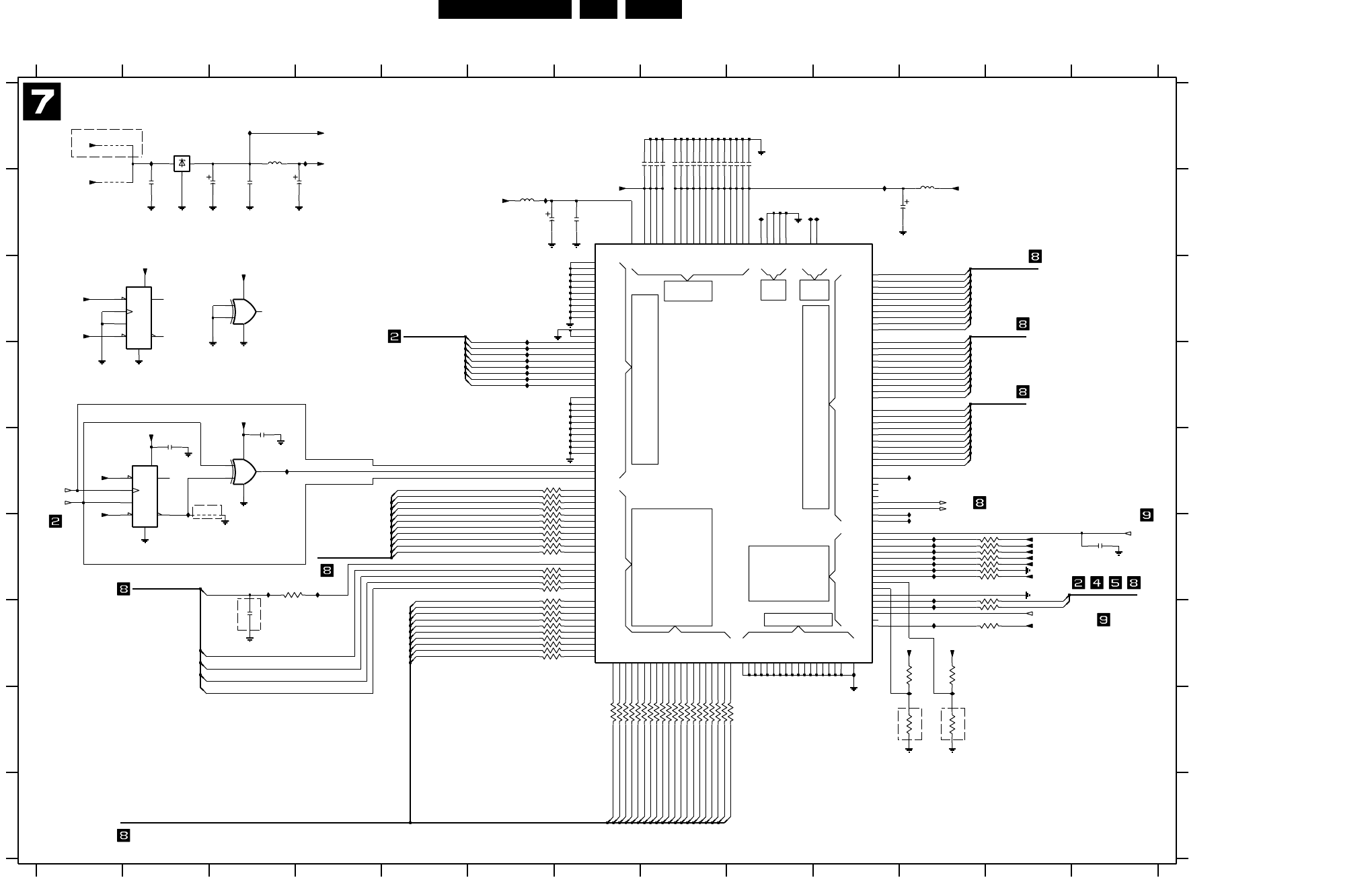
Electrical Diagrams and Print-Layouts EN 145DVDR980-985 /0X1 7.
Digital Board: Progressive Scan
INTERFACE
SIGNALS
CONTROL
SIGNALS
OUTPUT SIGNALS
POWER
SUPPLY
TEST
INPUT TEST
OUTPUT
POWER GND
INPUT SIGNALS
SDRAM
I724
DATA BUS
I2C BUS
Progressive Scan
ADDRESS BUS
C
D
E
4 5 6 7 8 9 10 11 12 13
A
B
DEINTERLACER
CONTROL BUS
LINE DOUBLER
12345678910111213
123
F
G
H
I
A
B
C
D
E
F
G
H
I
OPTION
OPTION
OPTION
OPTION OPTION
5702
4u7
18
4702
4K73701-C 36
3701-A 4K7
100n2727
GNDD
I714
2704
GNDD
2709
100n2703 100n
2718 100n
100n
VSS9
4VSYNCREFI
91
VSYNC|CREFO
119 WEN
117
YCLKO
100n2701
VSS1
115 VSS10
124 VSS11
132 VSS12
138 VSS13
145 VSS14
152 VSS15
159 VSS16
168 VSS17
17 VSS2
34 VSS3
55 VSS4
64 VSS5
74 VSS6
85 VSS7
96 VSS8
106
VDD25-3
158
VDD25-4
1
VDD33-1
137
VDD33-10
144
VDD33-11
151
VDD33-12
167
VDD33-13
33
VDD33-2
63
VDD33-3
73
VDD33-4
84
VDD33-5
95
VDD33-6
105
VDD33-7
114
VDD33-8
123
VDD33-9
89
VREFO
2
R|CROUT5 80
R|CROUT6 79
R|CROUT7 78
R|CROUT8 77
R|CROUT9
48
SCL
47
SDA
TEST0 111
TEST1 109
TEST2 51
TEST3 50
TEST4 41
TESTO1 113
TESTO2 112
16
VDD25-1
54
VDD25-2
107
RESETB
28 R|CRIN0
29 R|CRIN1
30 R|CRIN2
31 R|CRIN3
32 R|CRIN4
35 R|CRIN5
36 R|CRIN6
37 R|CRIN7
38 R|CRIN8
39 R|CRIN9
88
R|CROUT0 87
R|CROUT1 86
R|CROUT2 83
R|CROUT3 82
R|CROUT4 81
HREFO
3HSYNCREFI
92
H|CSYNCO
58
IFORMAT0 57
IFORMAT1 56
IFORMAT2
118 MEMCLKO
46
MODE
NOMEM 52
62
N|P|IN|OUT
53
OE
61
OFORMAT0 60
OFORMAT1 59
OFORMAT2
40
PIXCLK
120 RASN
49
G|YIN4
23 G|YIN5
24 G|YIN6
25 G|YIN7
26 G|YIN8
27 G|YIN9
76
G|YOUT0 75
G|YOUT1 72
G|YOUT2 71
G|YOUT3 70
G|YOUT4 69
G|YOUT5 68
G|YOUT6 67
G|YOUT7 66
G|YOUT8 65
G|YOUT9
90
DATA28
176 DATA29
142 DATA3
143 DATA4
146 DATA5
147 DATA6
148 DATA7
149 DATA8
150 DATA9
5FIELDIN
110
FILM
108
FSYNC
18 G|YIN0
19 G|YIN1
20 G|YIN2
21 G|YIN3
22
DATA13
157 DATA14
160 DATA15
161 DATA16
162 DATA17
163 DATA18
164 DATA19
141 DATA2
165 DATA20
166 DATA21
169 DATA22
170 DATA23
171 DATA24
172 DATA25
173 DATA26
174 DATA27
175
B|CBOUT3 100
B|CBOUT4 99
B|CBOUT5 98
B|CBOUT6 97
B|CBOUT7 94
B|CBOUT8 93
B|CBOUT9
121 CASN
116
CCLKO
45
DADDR0 44
DADDR1
139 DATA0
140 DATA1
153 DATA10
154 DATA11
155 DATA12
156 AVDD
43 AVSS
122 BSEL
6B|CBIN0
7B|CBIN1
8B|CBIN2
9B|CBIN3
10 B|CBIN4
11 B|CBIN5
12 B|CBIN6
13 B|CBIN7
14 B|CBIN8
15 B|CBIN9
104
B|CBOUT0 103
B|CBOUT1 102
B|CBOUT2 101
7700
136 ADDR0
135 ADDR1
125 ADDR10
134 ADDR2
133 ADDR3
131 ADDR4
130 ADDR5
129 ADDR6
128 ADDR7
127 ADDR8
126 ADDR9
42
FLI2200
100n2700
3702-A 4K718
I727
I701
I702 GNDD
I720
I722
I721
I718
I725
I719
100n2702
2712 100n
2719 100n
GNDD
I726
7701-A
3
2
7
5
61
4
14
4u7
2720
1n
2714
74HC74D
GNDD
I708
4u7
2725
2717
100n2705
GNDD
100n
5701
3714
4K7
100n
2716
GNDD
GNDD
I700
I703
100n2710
I706
I704
I705
100n
I715
2707
10p
2713
GNDD
GNDD
I716
I723
I717
74HC74D
11
12
7
9
813
10
14
4700
100R3705
7701-B
GNDD
7702-A
74LVC86ADB
1
23
14
7
GNDD
7703
2
GND
1
IN
3
OUT
4701
GNDD
LF25C
3706 100R
2726
GNDD
3712
33R
GNDDGNDD
100n
GNDD
2708 100n
27
4K73702-C 36 4K73702-D 45
3702-B 4K7
5
I713
4K73701-D 4
18
100n2711
33R27 33R3713-A
45 33R3713-C 36
3713-B
27
3711-A 33R18
3713-D 33R
3711-C 33R36 33R3711-B
2715
47u
GNDD
GNDD
GNDD
GNDD
I710
GNDD
GNDD
5700
I709
I712
I711
GNDD
2723
47u
33R3716-D 45 33R3715-A 18
3716-B 27
3716-C 33R36
5
33R3710-B 27
33R
36 33R3704-D 4
18 33R3704-B 27
3704-C 33R
6
3709-D 33R45
3704-A 33R
27 33R3709-C 3
100n
33R3709-A 18
3709-B 33R
2724
4K73701-B 27
I728
100n
I707
GNDD
GNDD
2706
3708
4K7
3700
4K74K7
3707
33R3718-A 18 33R3719-D 45
36
3718-B 33R27
3718-D 33R45 33R3718-C
33R3717-B 27
3717-A 33R18
3717-D 45
3717-C 33R36
3720
33R
33R
33R3715-C 36
3716-A 33R18
33R3711-D 45
3715-B 33R27
5
3710-A 33R18
18
33R3715-D 4
36 33R3719-B 27
3719-A 33R
74LVC86ADB
12
13 11
14
7
GNDD
3719-C 33R
GNDD
7702-D
2721
100n GNDD
2722
100n
36 33R3710-D 45
3703-A 33R18
3710-C 33R
36 33R3703-B 27
33R3703-D 45
3703-C 33R
I730
I729
I731
I733
I732
I735
I734
+2V5_FLI
+3V3_FLI
D_ADDR(0)
D_ADDR(2)
D_ADDR(3)
D_ADDR(1)
CAS
BA
D_DATA(2)
D_DATA(1)
D_DATA(3)
D_DATA(4)
D_DATA(0)
D_DATA(7)
D_DATA(6)
D_DATA(8)
D_DATA(5)
D_DATA(9)
+2V5_PLL
P_SCAN_YUV(7)
P_SCAN_YUV(7:0)
SYSCLK_PROGSCAN
P_SCAN_YUV(6)
P_SCAN_YUV(5)
P_SCAN_YUV(4)
P_SCAN_YUV(3)
P_SCAN_YUV(2)
P_SCAN_YUV(1)
P_SCAN_YUV(0)
Yy_OUT(5)
Yy_OUT(7)
Yy_OUT(9)
D_DATA(13)
D_DATA(12)
D_DATA(11)
D_DATA(10)
D_ADDR(4)
D_ADDR(5)
D_ADDR(6)
D_ADDR(7)
D_ADDR(9)
D_ADDR(8)
D_ADDR(10)
CLK4
VSOUT
HSOUT
Cb_OUT(9)
Cb_OUT(8)
Yy_OUT(0)
Yy_OUT(1)
RESETn
+3V3_FLI +3V3_FLI
Yy_OUT(3)
Yy_OUT(4)
Yy_OUT(6)
Yy_OUT(8)
+3V3_FLI
+3V3_FLI
+3V3_FLI
+3V3_FLI
+3V3_FLI
+3V3_FLI
+3V3_FLI
Cb_OUT(9:0)
D_DATA(29)
D_DATA(28)
D_DATA(27)
D_DATA(26)
D_DATA(25)
D_DATA(24)
D_DATA(23)
D_DATA(22)
D_DATA(21)
D_DATA(20)
D_DATA(19)
D_DATA(18)
D_DATA(17)
D_DATA(16)
D_DATA(15)
D_DATA(14)
+3V3
+3V3
+3V3
+3V3
+3V3
Yy_OUT(9:0)
+3V3
Cb_OUT(7)
Cb_OUT(6)
Cb_OUT(5)
Cb_OUT(4)
Cb_OUT(3)
Cb_OUT(2)
Cb_OUT(1)
Cb_OUT(0)
Yy_OUT(2)
Cr_OUT(3)
Cr_OUT(4)
Cr_OUT(5)
Cr_OUT(6)
Cr_OUT(7)
Cr_OUT(8)
Cr_OUT(9)
+2V5_FLI
+3V3
+5V
+2V5_PLL
+3V3
+3V3
+3V3
SDA
SCL
Cr_OUT(9:0)
Cr_OUT(0)
Cr_OUT(1)
Cr_OUT(2)
WE
VS_IN
RAS
5508_HS
5508_odd_even
2700 B9
2701 B8
2702 B9
2703 B9
2704 B9
2705 B8
2706 B8
2707 G3
2708 B8
2709 B8
2710 B8
2711 B8
2712 B8
2713 B8
2714 F13
2715 B6
2716 B7
2717 B8
2718 B8
2719 B8
2720 B11
2721 E2
2722 E3
2723 B3
2724 B2
2725 B2
2726 B3
2727 B8
3700 G11
3701-A F11
3701-B F11
3701-C F11
3701-D F11
3702-A G11
3702-B F11
3702-C F11
3702-D F11
3703-A F6
3703-B F6
3703-C F6
3703-D F6
3704-A F6
3704-B F6
3704-C F6
3704-D F6
3705 G11
3706 G11
3707 H11
3708 H11
3709-A E6
3709-B E6
3709-C F6
3709-D F6
3710-A G6
3710-B G6
3710-C E6
3710-D E6
3711-A G6
3711-B G6
3711-C G6
3711-D G6
3712 F3
3713-A G6
3713-B G6
3713-C G6
3713-D G6
3714 G11
3715-A H7
3715-B H7
3715-C H7
3715-D H7
3716-A H8
3716-B H8
3716-C H8
3716-D H7
3717-A H8
3717-B H8
3717-C H8
3717-D H8
3718-A H8
3718-B H8
3718-C H8
3718-D H8
3719-A H9
3719-B H8
3719-C H8
3719-D H8
3720 F6
4700 A1
4701 B1
4702 E2
5700 B11
5701 A3
5702 B6
7700 B7
7701-A E1
7701-B C1
7702-A E3
7702-D C3
7703 A2
CL 16532145_028.eps
221101
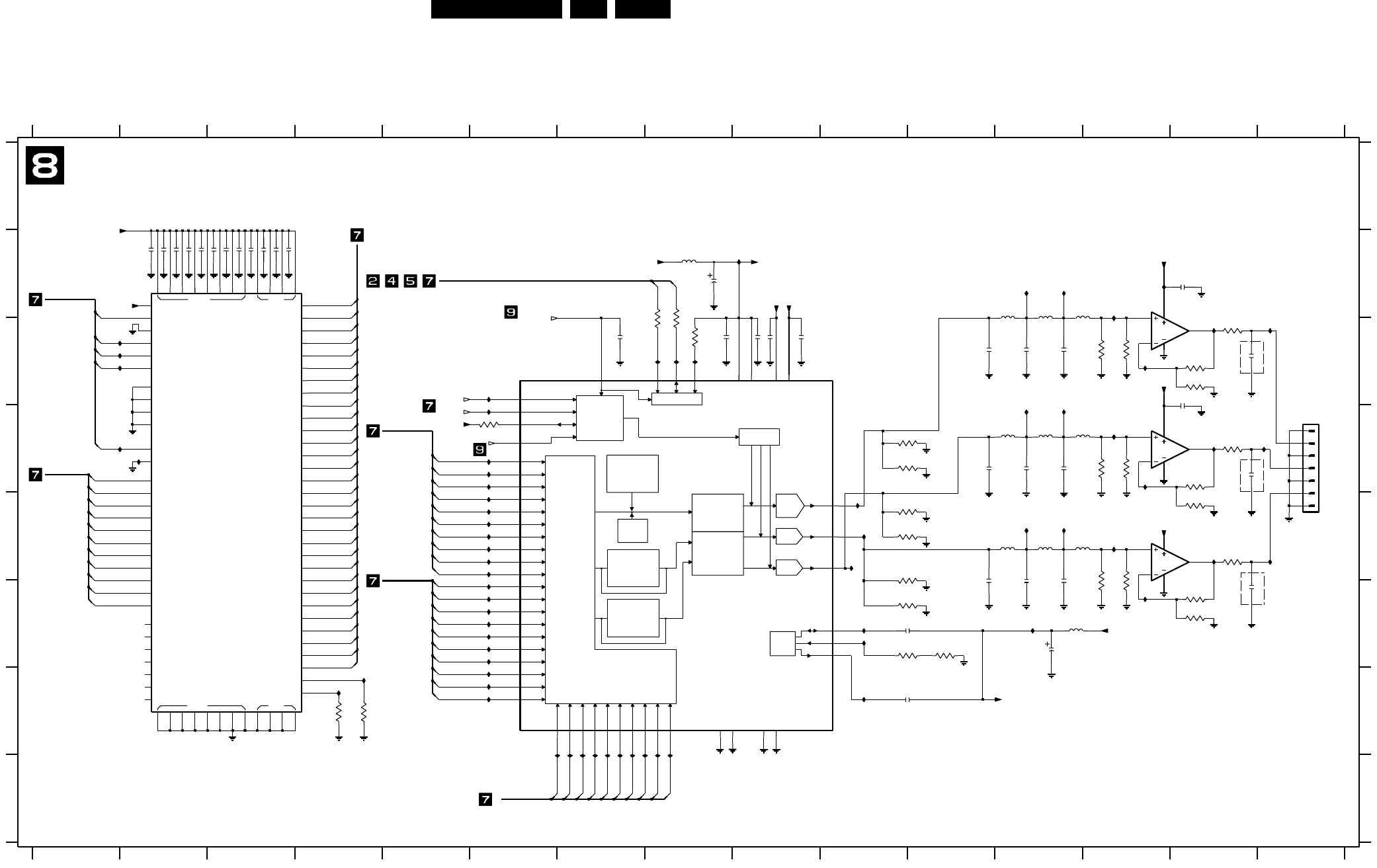
EN 146DVDR980-985 /0X1 7.
Electrical Diagrams and Print-Layouts
Digital Board: Progressive Scan
VSSQ VSS
VDDQ VSS
SYNC
FILTER CTRL
I C MPU PORT
2
VDD
GND AGND
CHROMA
4:2:2 TO 4:4:4
( 99AF )
CHROMA
VAA
BLOCK
CTRL
TEST-
PATTERN
GENERATOR
&
DELAY
&
GAMMA
CORRECTION
4:2:2 TO 4:4:4
( 99AF )
DAC
MACRO-
TIMING
GENERATOR
DAC
11-BIT
SHARPNESS
ADAPTIVE
&
FILTER CTRL
CGMS
SYNC
GEN
VISION 11-BIT
POLATION
INTER-
2X
DAC
LUMA
99 AF
11-BIT
DAC
1K
ANALOG BOARD
DATA BUS
SDRAM
ADDRESS BUS
I2C BUS
DENC
C
A
B
123456789101112131415
123456789101112131415
OPTION
CONTROL BUS
Progressive Scan
D
E
F
G
H
A
B
C
D
E
F
G
H
1K2
3814
OPTION
OPTION
2826
8p2
GNDD
I802
3821
1K2
1K
3808
2800
100n
3816
I800
GNDD
GNDD
I813
GNDD
I874
I873
I815
I805
I816
GNDD
GNDD
I839
I830
GNDD
I840
GNDD
GNDD
2u2
GNDD
100n2805
5805
100n2803
2802 100n
100n2811
100n2809
3815
1K2
3823
1K2
4
1800
FMN
1
2
3
4
5
6
7
7803-B
AD8062
5
6
7
8
78 84
17 WE_
GNDD
2834
220p
354149557581
44 58 72 866 1232384652
28 DQM2
59 DQM3
14 NC1
21 NC2
30 NC3
57 NC4
69 NC5
70 NC6
73 NC7
19 RAS_
115294339
47
DQ25
48
DQ26
50
DQ27
51
DQ28
53
DQ29
7
DQ3
54
DQ30
56
DQ31
8
DQ4
10
DQ5
11
DQ6
13
DQ7
74
DQ8
76
DQ9
16 DQM0
71 DQM1
77
DQ10
79
DQ11
80
DQ12
82
DQ13
83
DQ14
85
DQ15
31
DQ16
33
DQ17
34
DQ18
36
DQ19
5
DQ2
37
DQ20
39
DQ21
40
DQ22
42
DQ23
45
DQ24
27 A2
60 A3
61 A4
62 A5
63 A6
64 A7
65 A8
66 A9
22 BA0
23 BA1
18 CAS_
67 CKE
68 CLK
20 CS_
2
DQ0
4
DQ1
MT48LC2M32B2TG
7800
25 A0
26 A1
24 A10
GNDD
2827
22p
10K
3828
I810
3809
1K2
GNDD
2806 100n
I838
I837
I849
10u
5801
I847
2833
18p
3807
1K
GNDD
1K2
3811
I828
I831
GNDD
I829
5800
6u8
GNDD
270R
I809
6u8
5803
3827
I870
I817
5806
6u8
I836
2804 100n
75R
3819
3818
1K
1K2
3817
GNDD
100R
3806
2815
22p
8p2
2814
GNDD GNDD
1K2
I814
3824
1K
3820
2810 100n
GNDD
I880
GNDD
GNDD
I879
I878
GNDD
GNDD
I850
3802
100R
I869
GNDD
10K
3810
GNDD
I868
I806
GNDD
I824
I851
100n
2820
2831
I852
I818
8p2
2835
100n
3800
10K
I876
I871 I872
GNDD
I811
I822
GNDD
GNDD
2817
47u
5802
2u2
GNDD
3812
75R
I844
I848
GNDD
I845
GNDD
GNDD
22p
2832
I877
4u7
2837
I820
5810
112
39VREF
28 VSYNC_|TSYNC_
2Y0
3Y1
4Y2
5Y3
6Y4
7Y5
8Y6
9Y7
Y810
11 Y9
21 CR7
CR822
23 CR9
34DAC-A|Y
36DAC-B
32DAC-C
27 DV|CLKOUT
13 52
29 HSYNC_|SYNC_
RESET
40
38RSET
SCL
30 31
SDA
24 35
CB|CR3
48 47
CB|CR4
CB|CR5
46 45
CB|CR6
CB|CR7
44 43
CB|CR8
CB|CR9
42
CLKIN25
37COMP
14 CR0
15 CR1
16 CR2
CR317
18 CR4
19 CR5
CR620
7801
ADV7196A
26 33
ALSB
41
51
CB|CR0
CB|CR1
50 49
CB|CR2
GNDD
GNDD GNDD
I875
I846
AD8061
7802
3
4
1
5
2
100n
2818
1n
100n2813
2819
GNDD
7803-A
AD8062
3
2
1
8
4
2812 100n
GNDD
GNDD
3813
1K2
I832
I834
5808
2u2
GNDD
I801
3826
2K2
I819
GNDD
220p
1K2
3822
100n
2824
2821
2816
GNDD
I807
18p
GNDD
I808
I821
I843
I803
3805
4K7
I841
2807
I884
2808 100n
100n
I835
GNDD
2823
GNDD
GNDD
10u
5807
100n
1K
3825
GNDD
18p
5804
10u
2829
220p
2828
2822 100n
1K2
3804
I823
I826
I825
I827
3801
75R
GNDD
3803
1K2
GNDD
100n
I842
5809
GNDD
2836
I812
GNDD
I882
I883
I881
CLK4
GNDD
I833
Yy_OUT(3)
Yy_OUT(2)
Yy_OUT(1)
Yy_OUT(0)
Yy_OUT(9:0)
SDA
SCL
+3V3_DD
Cb_OUT(1)
Cb_OUT(2)
Cb_OUT(3)
Cb_OUT(4)
Cb_OUT(5)
Cb_OUT(6)
Cb_OUT(7)
Cb_OUT(8)
Cb_OUT(9)
Cb_OUT(9:0)
Yy_OUT(9)
Yy_OUT(8)
Yy_OUT(7)
Yy_OUT(6)
Yy_OUT(5)
Yy_OUT(4)
+3V3_ANA
SYSCLK_PROGSCAN
Cr_OUT(9)
Cr_OUT(8)
Cr_OUT(7)
Cr_OUT(6)
Cr_OUT(5)
Cr_OUT(4)
Cr_OUT(3)
Cr_OUT(2)
Cr_OUT(1)
Cr_OUT(0)
Cr_OUT(9:0)
Cb_OUT(0)
+3V3_FLI
+3V3_DD
+3V3_ANA
RESETn
HSOUT
VSOUT
D_DATA(14)
D_DATA(13)
D_DATA(12)
D_DATA(11)
D_DATA(10)
D_DATA(9)
D_DATA(8)
D_DATA(29)
D_DATA(28)
D_DATA(27)
D_DATA(26)
D_DATA(25)
D_DATA(24)
D_DATA(23)
D_DATA(22)
D_DATA(21)
D_DATA(20)
D_DATA(19)
D_DATA(18)
D_DATA(17)
D_DATA(16)
BA
CAS
RAS
WE
D_ADDR(6)
D_ADDR(7)
D_ADDR(8)
D_ADDR(9)
+3V3_FLI
D_DATA(7)
D_DATA(6)
D_DATA(5)
D_DATA(4)
D_DATA(3)
D_DATA(2)
D_DATA(1)
D_DATA(0)
+3V3
+3V3_ANA
+3V3_ANA
+3V3
D_DATA(15)
+5V
+5V
+5V
D_ADDR(0)
D_ADDR(1)
D_ADDR(10)
D_ADDR(2)
D_ADDR(3)
D_ADDR(4)
D_ADDR(5)
1800 D15
2800 B14
2802 B2
2803 B2
2804 B2
2805 B2
2806 B3
2807 B3
2808 B2
2809 B3
2810 B3
2811 B3
2812 B3
2813 B3
2814 C11
2815 C12
2816 C12
2817 F12
2818 C7
2819 C8
2820 C9
2821 C14
2822 C9
2823 C9
2824 C14
2826 D11
2827 D12
2828 D12
2829 D14
2831 E11
2832 E12
2833 E12
2834 F14
2835 F10
2836 G10
2837 B8
3800 G4
3801 C14
3802 B8
3803 C13
3804 C13
3805 C8
3806 B8
3807 C14
3808 C14
3809 D10
3810 D6
3811 D11
3812 D14
3813 D13
3814 D13
3815 E10
3816 D14
3817 E11
3818 E14
3819 E14
3820 E10
3821 E13
3822 E13
3823 F11
3824 F14
3825 F14
3826 F11
3827 F11
3828 G4
5800 B12
5801 B12
5802 B12
5803 D12
5804 D12
5805 D12
5806 E12
5807 E12
5808 E12
5809 F12
5810 B8
7800 B1
7801 C6
7802 B14
7803-A D14
7803-B E14
CL 16532145_029.eps
221101
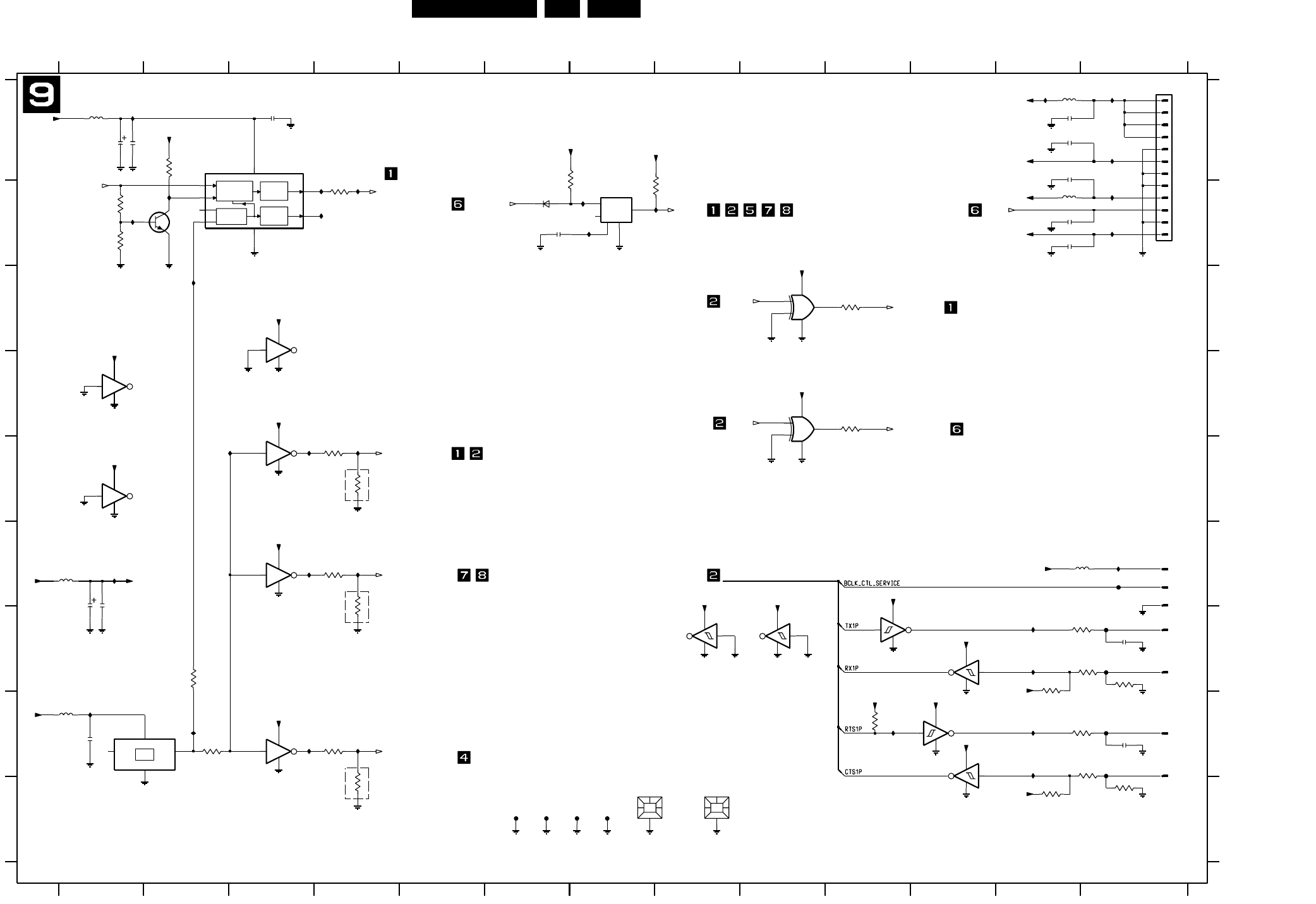
Electrical Diagrams and Print-Layouts EN 147DVDR980-985 /0X1 7.
Digital Board: Power, Clock, and Reset Audio Clock
OSC
CRYSTAL
PLL
OUTPUT
BUFFER
CTRL CIRC.
CLK SYNTHESIS
AND
OUTPUT
BUFFER
NC RESET
OSC
I913
11 12 13
12345
C
D
E
F
G
H
I
45678910
Power, Clock and Reset - AudioClock
SERVICE CONNECTOR
BLM31
BLM31
POWER SUPPLY
6 13
A
B
C
D
E
F
G
H
I
A
B
123
100n
2903
OPTION
OPTION
OPTION
7 8 9 10 11 12
29074u7
GNDD
I917
GNDD
3904
22R
Hole 4.0 mm with Cu
1907
GNDD
I923
1906
Hole 4.0 mm with Cu
GNDD
3910
100R
F932
GNDD
GNDD
I922
5
1901-6
6
74HCT14D
7905-A
12
14
7
1901-5
1903
100n
2904
GNDD
2909
1n5
I932
I931
I933
3900
10K
3907
1K
I905
PH-S
1901-7
7
56 14
7
I907
GNDD
3924
1K5
74HCT14D
7905-C
74LVC04A
7904-C
5
7
14 6
GNDD
100K
3923 3922
6K8 GNDD
GNDD
GNDD
I924
100n
2901
I908
I925
1904 1905 1902
100K
3903
2916
22n
5901
100MHZ
BAT54 COL
3925
4K7
7
14 12
GNDD
6900
GNDD
7904-F
74LVC04A
13
9
7
14 8
100n
2902
7904-D
74LVC04A
7905-D
74HCT14D
98 14
7
3911
10K
GNDD
GNDD
GNDDGNDD
GNDD
GNDD
GNDD
3908
22R
74LVC86ADB
7702-C
9
10 8
14
7
GNDD
GNDD
GNDD
1K
3912
I928
I920
GNDD
100K
3918
10K
3921
I927
100R
3919 F934
GNDD
GNDD
7905-B
74HCT14D
34
14
7
3915
47R
22R
3917
GNDD
I915
GNDD
100n
2900
I918
I904
GNDD
74LVC04A
7904-E
11
7
14 10
GNDDGNDD
BC847B
7901
13
2
47K
3902
6K8
3913
GNDD
I912
GNDD
5900
100MHZ
GNDD
F933
GNDD
GNDD
2908100n
5905
GNDD
2911
100n
22R
3901
I926
1K
3909
I921
7
8
9
2906
100n
PH
1900
1
10
11
12
2
3
4
5
6
3920
22R
3914
47R
7904-B
74LVC04A
3
7
14 4
MK2703S
7900
4
27M
5
CLK
3
GND
7S0
6S1
2
VDD
1X1
8X2
I906
47R
3906
1n5
2912
GNDD
GNDD
GNDD
29144u7
2915100n
14 2
GNDD
I916
NCP303
7902
CD
53
GND
2INP
41
OUTP
74LVC04A
7904-A
1
7
100MHZ
5904
I903
3916
100K
56
14
7
I911
5903
GNDD
7702-B
74LVC86ADB
4
I900
100MHZ
12 14
7
GNDD
GNDD
1110 14
7
7905-F
74HCT14D
13
1901-2
2
74HCT14D
7905-E
I909
I901
100MHZ
I930
5907
GNDD
F931
GNDD
I902
GNDD
F935
1901-3
3
1901-4
4
1901-1
1
FXO-31FT
7906
2
GND
3
OUT
1TS
4
VDD
GNDD
I919
RESETn
GNDD
GNDD
+3V3 VCC3_CLK_BUF
VDD5_OSC
+3V3
IRESET_DIG
+3V3
+3V3
+3V3
-5V
+3V3
RESETn_BE
RESETn_DVIO
acc_aclk_pll
VCC3_CLK_BUF
SYSCLK_VSM_5508
VCC3_CLK_BUF
SYSCLK_PROGSCAN
VCC3_CLK_BUF
VCC3_CLK_BUF
SYSCLK_EMPRESS
VCC3_CLK_BUF
+5V
+5V
VDD5_MK2703
VCC3_CLK_BUF
+5V +5V +5V
+5V
+5V
+5V
{BCLK_CTL_SERVICE,TX1P,RX1P,RTS1P,CTS1P}
-5V
+5V
SEL_ACLK1
+3V3
+5V
IOn
-5V
RSTN_DVIO
RSTN_BE
+12V
+5V
1900 A13
1901-1 G13
1901-2 F13
1901-3 G13
1901-4 H13
1901-5 F13
1901-6 H13
1901-7 F13
1902 I7
1903 I6
1904 I6
1905 I7
1906 I7
1907 I8
2900 A12
2901 A12
2902 A12
2903 B12
2904 B12
2906 A3
2907 A1
2908 A1
2909 G13
2911 H1
2912 H13
2914 F1
2915 F1
2916 B6
3900 A2
3901 B4
3902 B1
3903 B1
3904 G2
3906 E4
3907 E4
3908 F4
3909 F4
3910 G13
3911 G13
3912 I4
3913 G13
3914 C10
3915 D10
3916 G12
3917 H4
3918 H10
3919 H13
3920 H2
3921 H13
3922 I13
3923 I12
3924 A6
3925 B7
5900 A12
5901 B12
5903 A1
5904 F13
5905 H1
5907 F1
6900 B6
7702-B C9
7702-C D9
7900 A2
7901 B2
7902 B7
7904-A D1
7904-B F3
7904-C D3
7904-D H3
7904-E C3
7904-F E1
7905-A G10
7905-B H10
7905-C G11
7905-D H11
7905-E G8
7905-F G9
7906 H1
F931 F13
F932 G13
F933 G13
F934 H13
F935 H13
CL 16532145_030.eps
221101
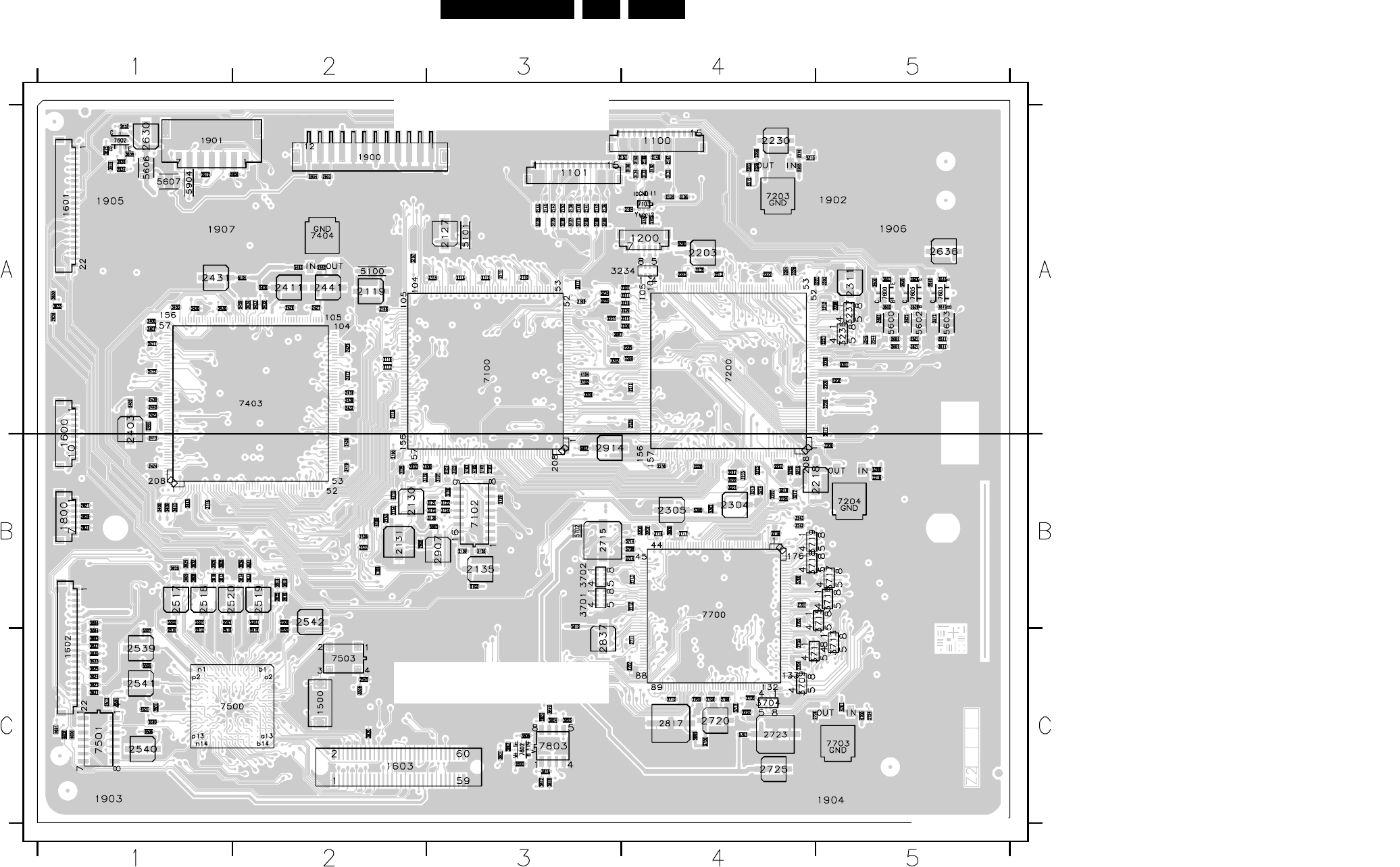
EN 148DVDR980-985 /0X1 7.
Electrical Diagrams and Print-Layouts
Layout Digital Board (Overview Top View)
CL 16532145_032.eps
231101
1100 A4
1101 A3
1200 A4
1500 C2
1600 A1
1601 A1
1602 C1
1603 C2
1800 B1
1900 A2
1901 A1
2100 B2
2101 B3
2102 B3
2103 B3
2109 A3
2110 A3
2111 A3
2112 A3
2113 A3
2114 A3
2116 A2
2117 A2
2118 A2
2119 A2
2127 A3
2129 B3
2130 B2
2131 B2
2132 A4
2134 A4
2135 B3
2136 A3
2138 A3
2139 B3
2140 A3
2141 A3
2142 A3
2143 A3
2144 A3
2145 A3
2146 A2
2147 A4
2148 A4
2149 A4
2150 A4
2151 A4
2152 A3
2153 B2
2154 B2
2200 A4
2201 A4
2203 A4
2204 B4
2205 A4
2206 A5
2207 B4
2208 A4
2209 A5
2210 A4
2211 A5
2212 A5
2213 A4
2215 A4
2216 B4
2217 B4
2218 B5
2219 B5
2220 A5
2221 A5
2222 A4
2223 A4
2225 A4
2226 B4
2227 B4
2228 A5
2230 A4
2231 A3
2304 B4
2305 B4
2311 A5
2403 A1
2411 A2
2412 B1
2413 B1
2417 A2
2418 A2
2419 B2
2420 A1
2421 A1
2422 A1
2423 A1
2424 B1
2425 A2
2426 B2
2427 A2
2428 A2
2429 A2
2430 A1
2431 A1
2432 A2
2433 A2
2434 A2
2437 A2
2438 A2
2439 A1
2440 A1
2441 A2
2442 A2
2444 A1
2512 C1
2513 C1
2514 C1
2515 C2
2516 C1
2517 B1
2518 B1
2519 B2
2520 B1
2530 C2
2539 C1
2540 C1
2541 C1
2542 B2
2545 C2
2600 A5
2601 A5
2602 A5
2603 C1
2604 C1
2608 B1
2609 B1
2610 A5
2611 A5
2612 A5
2613 B1
2614 B2
2618 B1
2619 B2
2620 A5
2621 A5
2622 A5
2623 C1
2624 C1
2628 A1
2629 B1
2630 A1
2631 C1
2632 A1
2633 B2
2634 A1
2635 B2
2636 A5
2700 B4
2701 B4
2702 B4
2703 C4
2704 C4
2705 C4
2706 C4
2707 C4
2708 C4
2709 C4
2710 C4
2711 C4
2712 B4
2713 B4
2714 B4
2715 B3
2716 B4
2717 B4
2719 B4
2720 C4
2723 C4
2724 C5
2725 C4
2726 C4
2727 C4
2800 C3
2817 C4
2821 B1
2824 C3
2829 B1
2834 B1
2837 C3
2903 A2
2904 A2
2907 B3
2908 B2
2909 A2
2912 A1
2914 B3
3100 B3
3101 B3
3102 B3
3103 B2
3104 A4
3105 A4
3106 A3
3107 A2
3108 A3
3109 A3
3110 A3
3117 A3
3118 B1
3119 B2
3120 B3
3121 B3
3122 B3
3123 B3
3124 B3
3125 B2
3126 B3
3127 A3
3128 A3
3129 A3
3130 B3
3131 A4
3132 A4
3133 A4
3134 A4
3135 A4
3136 A3
3137 B2
3138 B2
3200 A4
3202 A3
3203 A5
3204 A4
3208 A3
3209 B5
3211 A4
3213 B4
3214 B4
3215 A4
3216 B4
3217 B4
3218 B4
3219 A4
3220 A4
3221 B4
3222 B4
3223 B4
3224 A3
3225 A3
3226 B4
3227 A5
3228 A4
3233 B4
3234 A4
3235 A4
3236 A5
3237 A5
3242 B4
3243 B4
3244 A5
3245 A5
3400 A1
3401 A1
3403 A1
3408 B1
3409 B1
3410 B1
3500 C1
3501 C1
3601 A5
3602 A5
3603 A5
3604 B1
3605 B1
3609 B1
3610 B2
3611 A5
3612 A5
3613 A5
3614 B2
3615 A1
3619 A1
3620 C2
3621 A5
3622 A5
3623 C1
3624 A5
3625 C1
3629 B1
3630 A1
3631 B2
3632 B1
3633 A1
3634 B2
3635 C1
3636 A1
3637 C1
3638 A1
3700 B4
3701 B3
3702 B3
3704 C4
3707 B4
3708 B4
3709 C4
3711 C4
3712 C4
3713 C5
3714 B4
3715 B5
3716 B5
3717 B5
3718 B4
3719 B4
3801 C3
3807 C3
3808 C3
3812 C3
3816 C3
3818 C3
3819 C3
3824 C3
3825 C3
3907 A3
3909 B4
4102 A3
4103 B3
4104 A3
4105 B3
4108 B2
4109 B2
4110 B2
4501 C1
4600 C1
4601 C1
4602 C1
4700 C5
4701 C5
5100 A2
5101 A3
5102 A4
5103 B3
5200 A4
5201 A5
5202 A5
5203 A4
5205 A4
5206 B5
5209 A4
5210 A4
5212 A4
5300 B4
5302 B4
5400 A2
5402 A1
5403 A2
5404 A2
5500 B1
5501 B1
5502 B1
5503 B2
5504 C1
5505 C1
5506 C1
5507 C1
5508 B2
5509 C2
5600 A5
5602 A5
5603 A5
5606 A1
5607 A1
5700 C4
5701 C4
5702 B3
5809 C4
5810 B3
5903 B3
5904 A1
5907 B3
7100 A3
7102 B3
7103 A4
7200 A4
7203 A4
7204 B5
7403 A2
7404 A2
7500 C2
7501 C1
7503 C2
7600 A5
7602 A1
7603 A5
7605 A5
7700 B4
7703 C5
7802 C3
7803 C3
PART 1
CL 16532145_32a.eps
PART 2
CL 16532145_32b.eps
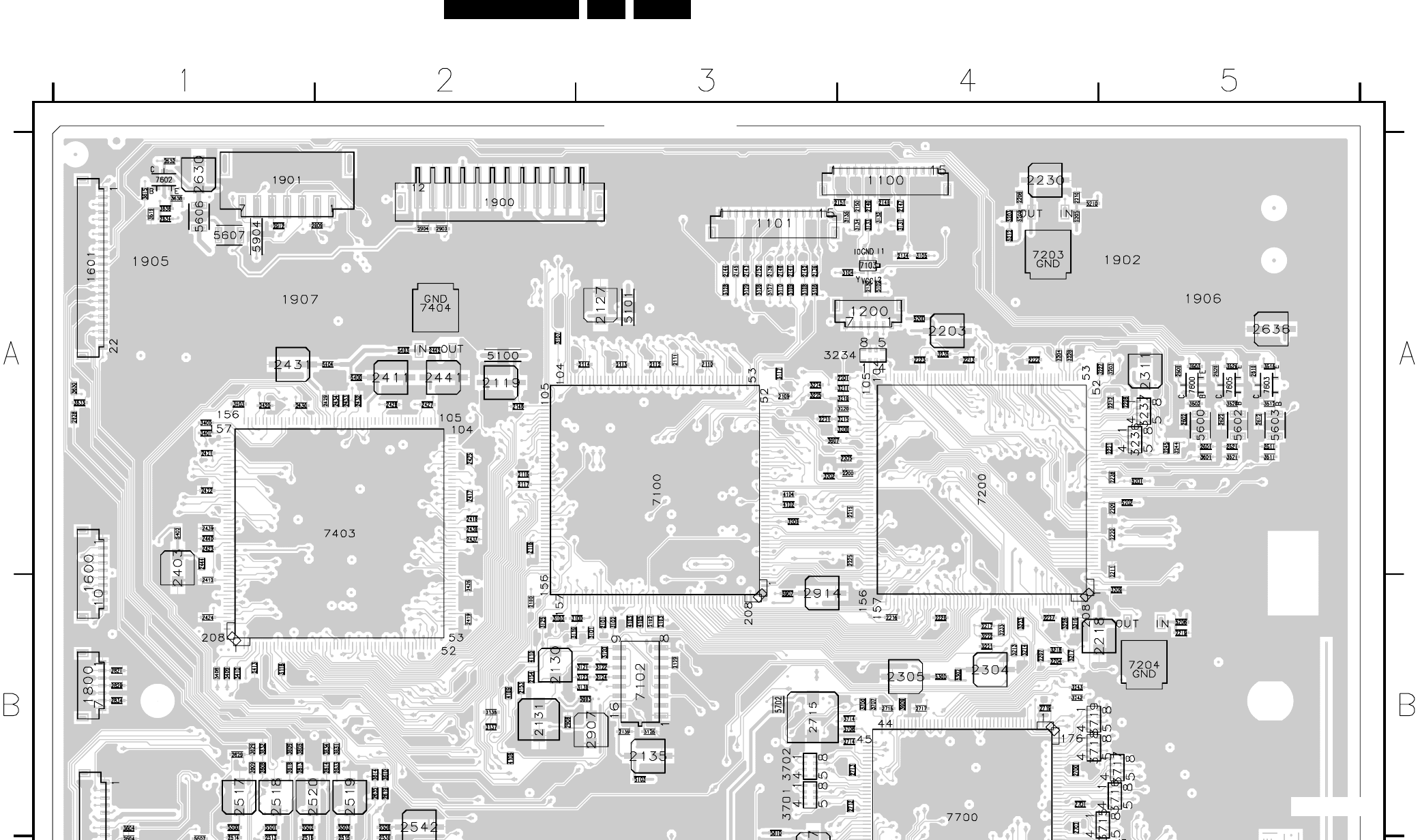
Electrical Diagrams and Print-Layouts EN 149DVDR980-985 /0X1 7.
Layout Digital Board (Part 1 Top View)
CL 16532145_32a.eps
231101
PART 1
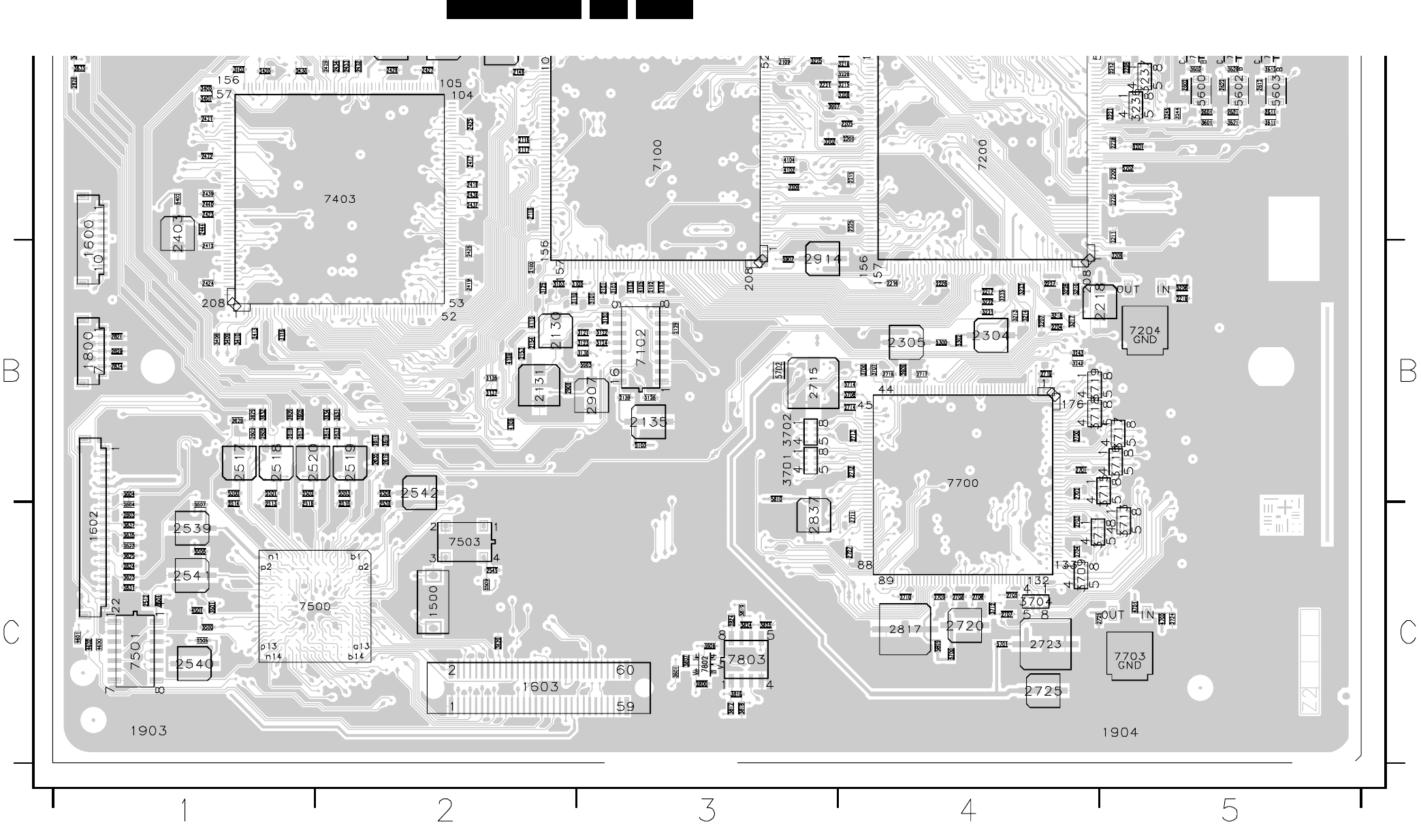
EN 150DVDR980-985 /0X1 7.
Electrical Diagrams and Print-Layouts
Layout Digital Board (Part 2 Top View)
CL 16532145_32b.eps
231101
PART 2
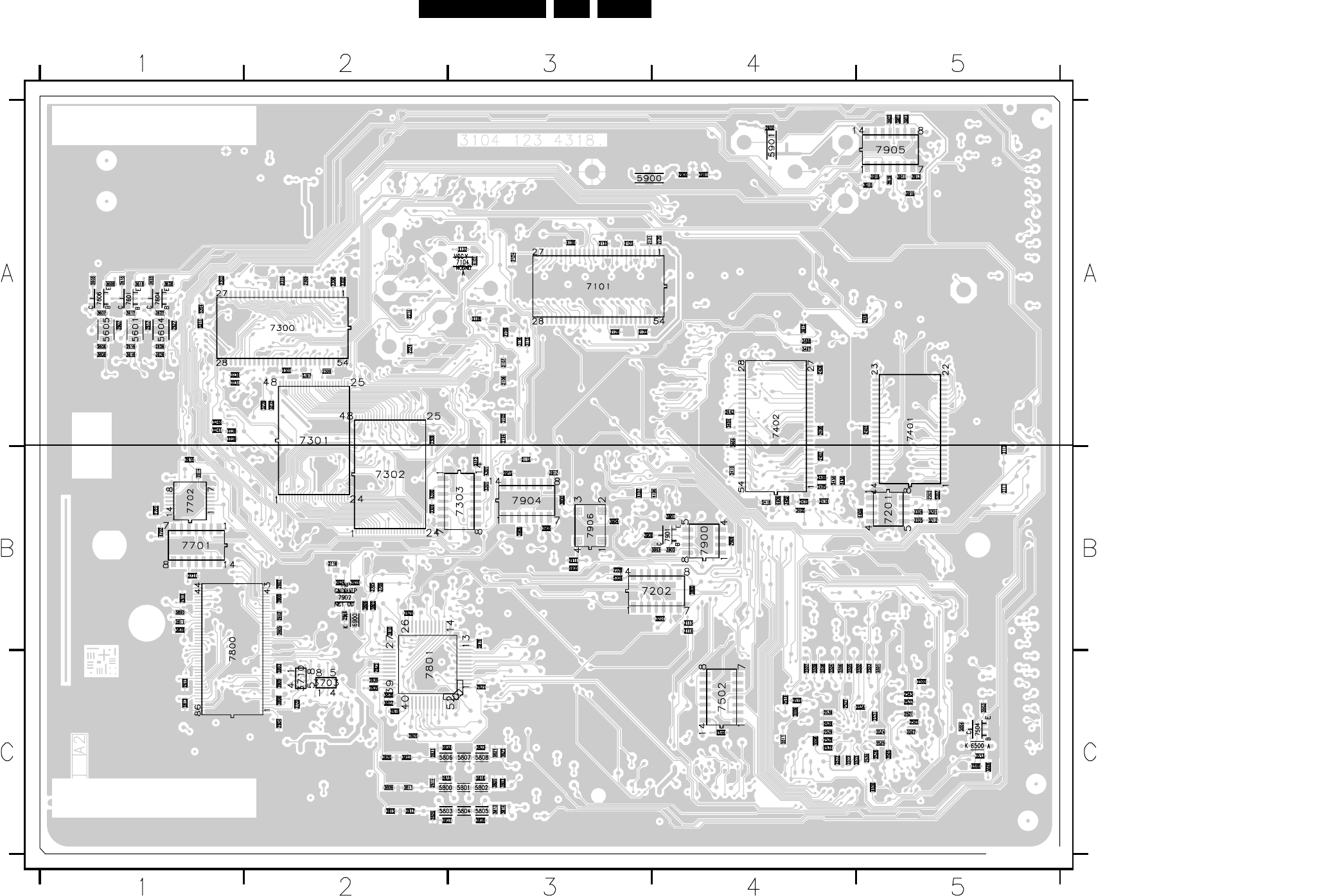
Electrical Diagrams and Print-Layouts EN 151DVDR980-985 /0X1 7.
Layout Digital Board (Overview Bottom View)
2104 A3
2105 A3
2106 A3
2107 A3
2108 A3
2115 B3
2120 A4
2121 A3
2122 A3
2123 A3
2124 A3
2125 A3
2126 A3
2128 A3
2137 A3
2202 B5
2214 A2
2224 A2
2229 B3
2300 A2
2301 A2
2302 A2
2303 A1
2306 A2
2307 A2
2308 A2
2309 A2
2310 A2
2312 B3
2402 A5
2404 A4
2405 B4
2406 B4
2407 B4
2408 A4
2409 A4
2410 B4
2414 B4
2415 B4
2416 B4
2435 B4
2436 B4
2443 A4
2446 A5
2500 C5
2501 C5
2502 C5
2503 C5
2504 C4
2505 C4
2506 C4
2507 C4
2508 C4
2509 C4
2510 C4
2511 C4
2521 C5
2522 C4
2523 C4
2524 C5
2525 C5
2526 C4
2527 C4
2528 C4
2529 C4
2531 C5
2532 C4
2533 C5
2534 C5
2535 C5
2536 C5
2537 C5
2538 C4
2543 C5
2544 C4
2565 C5
2605 A1
2606 A1
2607 A1
2615 A1
2616 A1
2617 A1
2625 A1
2626 A1
2627 A1
2718 B2
2721 B1
2722 B1
2802 B2
2803 C2
2804 C2
2805 B2
2806 B2
2807 B2
2808 C2
2809 C2
2810 B1
2811 B1
2812 C1
2813 C1
2814 C2
2815 C2
2816 C3
2818 C2
2819 B3
2820 B2
2822 C3
2823 C2
2826 C2
2827 C2
2828 C3
2831 C2
2832 C2
2833 C3
2835 C2
2836 C2
2900 A4
2901 A4
2902 A4
2906 B4
2911 B3
2915 B3
2916 B2
3111 B5
3112 B5
3113 B4
3114 B4
3115 A3
3116 A3
3201 B5
3205 B5
3206 B5
3207 B4
3212 B5
3229 A2
3230 A1
3231 A1
3232 A2
3238 A1
3239 A1
3240 A1
3241 A1
3300 B2
3301 B3
3402 B4
3404 A4
3405 B4
3406 A4
3407 A4
3502 C5
3503 C5
3504 C5
3505 C5
3506 C5
3507 C5
3508 C4
3509 C4
3513 C5
3515 C4
3600 B4
3606 A1
3607 A1
3608 A1
3616 A1
3617 A1
3618 A1
3626 A1
3627 A1
3628 A1
3703 C2
3705 B2
3706 B2
3710 C2
3720 C2
3800 B1
3802 B2
3803 C3
3804 C3
3805 C2
3806 B2
3809 C2
3810 B2
3811 C2
3813 C3
3814 C3
3815 C2
3817 C2
3820 C2
3821 C3
3822 C3
3823 C2
3826 C2
3827 C2
3828 B1
3900 B3
3901 B4
3902 B4
3903 B4
3904 B3
3906 B3
3908 B3
3910 A5
3911 A5
3912 A4
3913 A5
3914 B1
3915 B1
3916 A5
3917 B3
3918 A5
3919 A5
3920 B3
3921 A5
3922 A5
3923 A5
3924 B2
3925 B2
4100 A3
4101 A3
4106 B4
4107 B3
4300 B2
4301 B3
4406 B5
4409 B4
4500 C5
4702 B1
5204 A1
5207 B5
5208 B3
5211 A1
5601 A1
5604 A1
5605 A1
5800 C2
5801 C3
5802 C3
5803 C2
5804 C3
5805 C3
5806 C2
5807 C3
5808 C3
5900 A3
5901 A4
5905 B3
6500 C5
6900 B2
7101 A3
7104 A3
7201 B5
7202 B4
7300 A2
7301 A2
7302 B2
7303 B3
7401 A5
7402 A4
7502 C4
7504 C5
7601 A1
7604 A1
7606 A1
7701 B1
7702 B1
7800 B1
7801 C2
7900 B4
7901 B4
7902 B2
7904 B3
7905 A5
7906 B3
CL 16532145_033.eps
231101
PART 1
CL 16532145_33a.eps
PART 2
CL 16532145_33b.eps
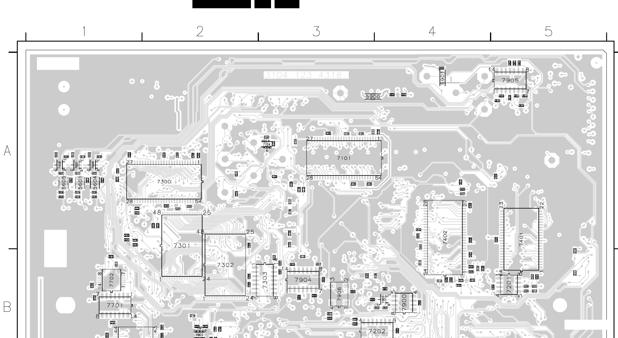
EN 152DVDR980-985 /0X1 7.
Electrical Diagrams and Print-Layouts
Layout Digital Board (Part 1 Bottom View)
CL 16532145_33a.eps
231101
PART 1
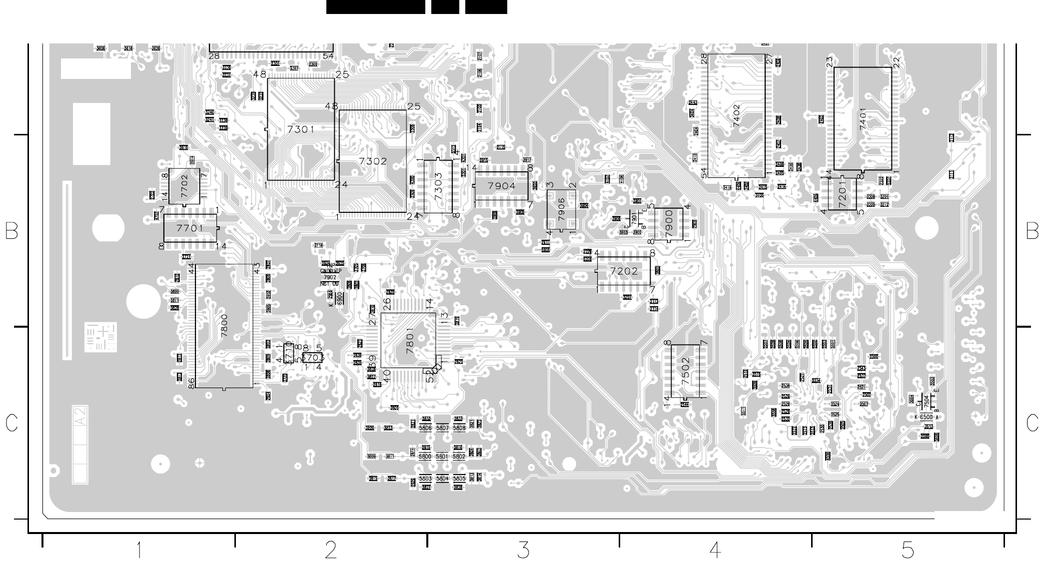
Electrical Diagrams and Print-Layouts EN 153DVDR980-985 /0X1 7.
Layout Digital Board (Part 2 Bottom View)
CL 16532145_33b.eps
231101
PART 2
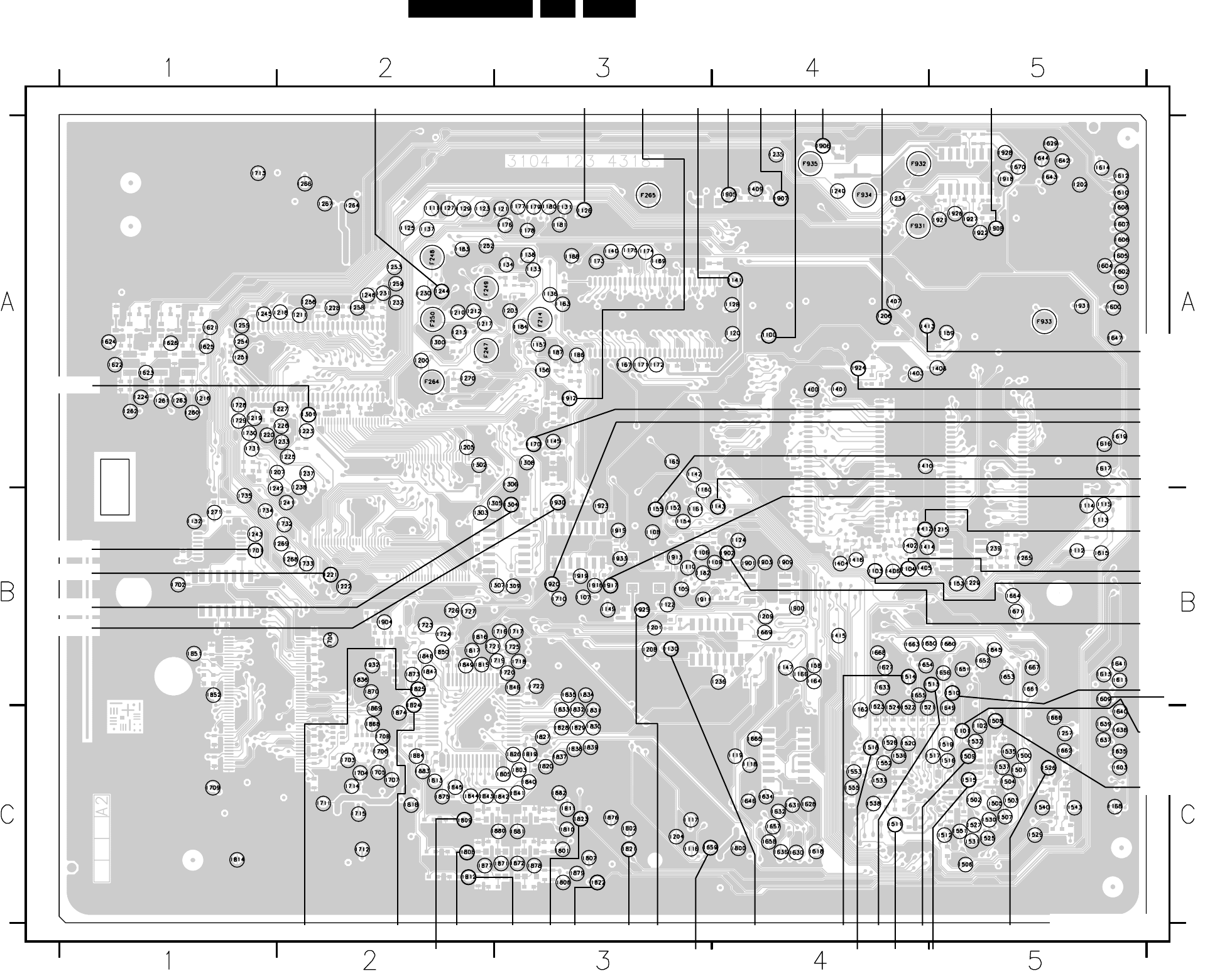
EN 154DVDR980-985 /0X1 7.
Electrical Diagrams and Print-Layouts
Layout Digital Board (Testlands Bottom View)
+3V3+3V3
+3V3 +12V +5V -5V
+3V3
+3V3
+3V3
+3V3
+3V3
+3V3
+3V3
+3V3 +3V3
+3V3
+3V3
+3V3
+5V +5V
Resetn
Resetn_BE
Reset_DVIO
Resetn_VE
Sysclk_VSM_5508
ACC_ACLK_OSC
ACC_ACLK_PLL
VIP_ICLK
Sysclk_ProgScan
Sysclk_Empress
EMI_PROCCLK
AE_DATAO
VE_DSn
VE_DTACKn
Mute
HSOUT
VSOUT DAC-A/Y
DAC-B
DAC-C YCb
Cr
+3V3
+3V3
+3V3
HSYNC
VSYNC
CL 16532145_034.eps
101201

Electrical Diagrams and Print-Layouts EN 155DVDR980-985 /0X1 7.
Layout Digital Board (Mapping Testlands )
F214 A3
F247 A2
F248 A2
F249 A2
F250 A2
F264 A2
F265 A3
F931 A4
F932 A4
F933 A5
F934 A4
F935 A4
I100 A4
I101 C5
I102 C5
I103 B4
I104 B4
I105 B3
I106 B3
I107 B3
I108 B3
I109 B4
I110 B3
I111 A2
I112 B5
I113 B5
I114 B5
I115 B5
I116 C3
I117 C3
I118 C4
I119 C4
I120 A4
I121 A3
I122 B3
I123 A2
I124 B4
I125 A2
I126 A3
I127 A2
I128 A4
I129 A2
I130 B3
I131 A3
I132 B1
I133 A3
I134 A3
I136 A3
I137 A2
I138 A3
I140 A3
I141 A4
I142 A3
I143 B4
I145 A3
I147 B4
I149 B3
I152 B3
I153 B5
I154 B3
I155 B3
I156 A3
I157 A3
I158 B4
I159 A5
I160 B3
I161 B3
I162 C4
I163 A3
I164 B4
I165 A3
I166 B4
I167 A3
I168 C5
I169 A3
I170 A3
I171 A3
I172 A3
I173 A3
I174 A3
I175 A3
I176 A3
I177 A3
I178 A3
I179 A3
I180 A3
I181 A3
I182 B3
I183 A2
I184 A3
I186 A3
I187 A3
I188 A3
I200 A2
I201 B3
I202 A5
I203 A3
I204 C3
I205 A2
I206 A4
I207 A2
I208 B3
I209 B4
I210 A2
I211 A2
I212 A2
I213 A2
I215 B5
I216 A1
I217 A2
I218 A2
I219 A1
I220 A1
I221 B2
I222 B2
I223 A2
I224 A1
I225 A2
I226 A2
I227 A2
I228 A2
I229 B5
I230 A2
I231 A2
I232 A2
I233 A2
I234 A4
I235 A4
I236 B4
I237 A2
I238 A2
I239 B5
I240 A4
I241 B2
I242 B1
I243 B1
I244 A2
I245 A1
I246 A2
I251 A1
I252 A2
I253 A2
I254 A1
I255 A1
I256 A2
I257 C5
I258 A2
I259 A2
I260 A1
I261 A1
I262 A1
I263 A1
I264 A2
I265 B5
I266 A2
I267 A2
I268 B2
I269 B2
I270 A2
I271 B1
I300 A2
I301 A2
I302 A2
I303 B2
I304 B3
I305 B3
I306 A3
I307 B3
I308 A3
I309 B3
I400 A4
I401 A4
I402 B4
I403 A4
I404 B4
I405 B4
I406 B4
I407 A4
I408 A5
I409 A4
I410 A4
I412 B4
I413 A4
I414 B4
I415 B4
I416 B4
I500 C5
I501 C5
I502 C5
I503 C5
I504 C5
I505 C5
I506 C5
I507 C5
I508 C5
I509 C5
I510 B5
I511 C4
I512 C5
I513 B5
I514 B4
I515 C5
I516 C5
I517 C5
I518 C4
I519 C5
I520 C4
I521 C4
I522 C4
I523 C4
I524 C4
I525 C5
I526 C5
I527 C5
I528 C4
I529 C5
I530 C5
I531 C5
I532 C5
I533 C4
I535 C5
I536 C4
I537 C5
I538 C4
I540 C5
I543 C5
I551 C5
I552 C4
I553 C4
I555 C4
I600 A5
I601 A5
I602 A5
I603 C5
I604 A5
I605 A5
I606 A5
I607 A5
I608 A5
I609 B5
I610 A5
I611 B5
I612 A5
I613 B5
I614 A5
I615 B5
I616 A5
I617 A5
I618 C4
I619 A5
I621 A1
I622 A1
I623 A1
I624 A1
I625 A1
I626 A1
I627 B4
I628 C4
I629 A5
I630 C4
I631 C4
I632 C4
I633 B4
I634 C4
I635 C5
I636 C4
I637 C5
I638 C5
I639 C5
I640 C5
I641 B5
I642 A5
I643 A5
I644 A5
I645 B5
I646 C4
I647 A5
I649 C5
I650 B4
I651 B5
I652 B5
I653 B5
I654 B4
I655 B4
I656 B5
I657 C4
I658 C4
I659 C3
I660 B5
I661 B5
I662 C5
I663 B4
I664 B5
I665 C4
I666 C5
I667 B5
I668 B4
I669 B4
I670 A5
I671 B5
I700 B2
I701 B1
I702 B1
I703 C2
I704 C2
I705 C2
I706 C2
I707 C2
I708 C2
I709 C1
I710 B3
I711 C2
I712 C2
I713 A1
I714 C2
I715 C2
I716 B3
I717 B3
I718 B3
I719 B3
I720 B3
I721 B2
I722 B3
I723 B2
I724 B2
I725 B3
I726 B2
I727 B2
I728 A1
I729 A1
I730 A1
I731 A1
I732 B2
I733 B2
I734 B1
I735 B1
I800 C4
I801 C3
I802 C3
I803 C3
I805 C3
I806 C3
I807 C3
I808 C2
I809 C2
I810 C3
I811 C3
I812 C2
I813 C2
I814 C1
I815 B2
I816 B2
I817 B2
I818 C2
I819 C3
I820 C3
I821 C3
I822 C3
I823 C3
I824 B2
I825 B2
I826 C3
I827 C3
I828 C3
I829 C3
I830 C3
I831 C3
I832 C3
I833 C3
I834 B3
I835 B3
I836 B2
I837 C3
I838 C3
I839 C3
I840 C3
I841 C3
I842 C3
I843 C2
I844 C2
I845 C2
I846 B3
I847 B2
I848 B2
I849 B2
I850 B2
I851 B1
I852 B1
I868 C2
I869 C2
I870 B2
I871 C3
I872 C3
I873 B2
I874 C2
I875 C2
I876 C3
I877 C2
I878 C3
I879 C3
I880 C3
I881 C3
I882 C3
I883 C2
I884 C2
I900 B4
I901 B4
I902 B4
I903 B4
I904 B2
I905 A4
I906 A4
I907 A4
I908 A5
I909 B4
I911 B3
I912 A3
I913 B3
I915 B3
I916 B3
I917 B3
I918 A5
I919 B3
I920 B3
I921 A5
I922 A5
I923 B3
I924 A4
I925 B3
I926 A5
I927 A5
I928 A5
I930 B3
I931 A5
I932 B2
I933 B3
CL 16532145-34m.eps
101201
Personal Notes:

EN 156DVDR980-985 /0X1 7.
Electrical Diagrams and Print-Layouts
Personal Notes: Personal Notes:
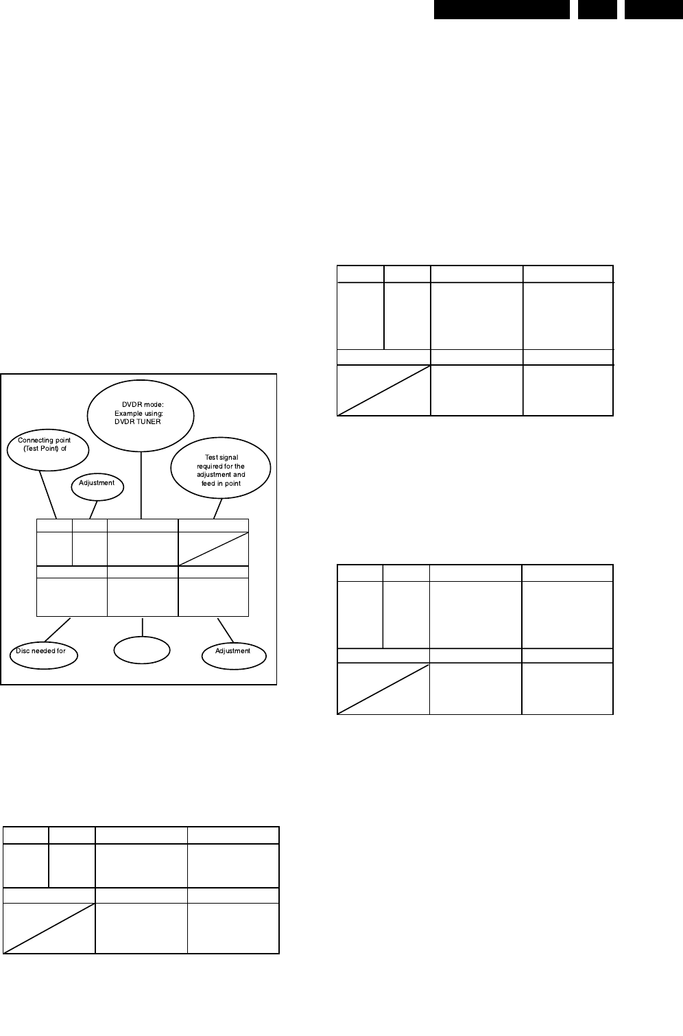
Alignments EN 157DVDR980-985 /0X1 8.
8. Alignments
8.1 Alignment Instructions Analogue Board
Alignments Analog PCB Eur
Figure 8-1
TP ADJ. MODE INPUT
Frequency-
Counter
Disc
R3054
Pin 2 of
Con.1911
(FMRV)
3,800MHz
±10kHz
DISC MEAS.EQ.
MEAS.EQ.
MEAS.EQ.
MEAS.EQ.
SPEC.
TUNER
component
adjustment Specification
Measuring
equipment
measuring
equipment
Test equipment:
1. Dual-trace oscilloscope
Voltage range : 0.001 ~ 50 V/div
Frequency : DC ~ 50 MHz
Probe : 10:1, 1:1
2. DVM (Digital voltmeter)
3. Frequency counter
4. Sinus generator
Sinus : 0 ~ 50 MHz
5. Test pattern generator
How to read the adjustment procedures:
Front End (FV)
Service tasks after replacement of IC 7703, coil L5702 and L5703:
1 AFC Adjustment:
Purpose:
Storage in NVRAM via command mode interface of DSW:
Correct adjustment of demodulator AFC - circuit
After adjustment, the AFC reference value has to be stored in the NVRAM.
This reference value is 256 * measured voltage/Ucc. Ucc is 5.0V.
Store the reference value via command 732 , followed by the ref. value.
Example: DD:> 732 128
Symptom, if incorrectly set:
Bad or disturbed TV channel reception.
PAL - AFC adjustment [5703]:
2 HF - AGC adjustment [3707]:
Service tasks after replacement of IC 7703:
Purpose:
Set amplifier control.
Symptom, if incorrectly set:
Picture jitter if input level is too low and picture distortion
if input level is too high.
TP ADJ. MODE INPUT
DC Voltmeter
Frequ. Generator
TUNER 38,9MHz 500mVpp
at Tuner 1705, Pin 11
(F700, IF-out)
2,5V ±0,1V
DISC
DISC
DISC
SPEC.
L5703
IC 7703
Pin 17
(I976)
TP ADJ. MODE INPUT
5mV(74dBµV)
on aerial input
PAL white picture,
audio IF on,
no modulation
SPEC.
R3707
Oscilloscope
Video Pattern
Generator
500mVpp +/-0.5dB
(use a 10:1 probe )
Set tuned to
channel 25
503.25 MHz
Tuner
1705
Pin 11
(F700,
IF-out)
3 Attenuating the 40.4 MHz [5702]:
(SECAM only)
Service tasks after replacement of coil 5702:
Purpose:
To attenuate the band I carrier rests.
Symptom, if incorrectly set:
Bad picture quality when the filter attenuates the picture
carrier (38.9MHz).
If the adjustment is correct the signal at pin 1 of OFW [1700] must be
smaller than the input signal amplitude by at least 6 dB.
TP ADJ. MODE INPUT
L5702
Oscilloscope,
Sinus Generator,
Counter
adjust minimum
amplitude
TUNER
OFW
1700
Pin 1
(F704)
40.4 MHz, 200mV
rms
at Tuner 1705, Pin 11
(F700, IF-out)
SPEC.
CL 16532145_061.eps
041201

Alignments
EN 158 DVDR980-985 /0X18.
8.2 Reprogramming Procedure of NVM on the
Analogue PCB
The NVM, item 7815, on the Analogue board contains the
following factory settings:
1. Bargraph 0dB correction factor
2. Clock correction factor
3. AFC reference value
4. Slash version
The settings 1,2 and 3 are stored in the NVM during the
production of the analogue board.
The slash version is stored at the end of the production line of
the set.
In case of failure, the NVM must be replaced by an empty
device. By way of commands via the Diagnostic Software or via
ComPair, the factory settings must be restored in the NVM.
8.2.1 Bargraph 0db Alignment
For an exact functionality of the bar graph in the display, a
correction factor for the left and the right channel is stored in the
NVM.
Procedure:
• Put the set in DSW command mode
• route Audio path from Audio front connectors to digital with
the following command:
DD:> 713 01
• apply a sine wave of 1 kHz, 1.65 Vrms (0 dB) to the front
connectors, audio left and right
• store 0 dB bar graph level with command 720
DD:>720
8.2.2 Clock Correction Adjustment
To guarantee an exact function of the real time clock, an
adjustment of the clock frequency is possibe and stored in the
NVM.
Procedure:
• Connect a pull up resistor of 10k between pin 7 an 8 of the
clock IC PCF8593T, item 7811, on the analogue PCB
• put the set in service command mode
• execute command 722 to initiate that a 1 Hz signal is
available on pin 7 of the clock IC
DD:>722
• measure the frequency of the Clock Crystal with an
accuracy of ±1(s. Normally the measured frequency must
be between 999902 (s and 1000097 (s. If the frequency is
outside this range, the clock IC must be replaced.
• Execute command 721 with the measured frequency as an
input parameter
example:
DD:>721 1000023
8.2.3 AFC Reference Voltage Tuner
This function stores the reference voltage for the tuner in the
NVM. Before this value can be stored, the AFC adjustment,
described in the adjustment instructions of the analogue board,
must be carried out.
Procedure:
• Adjust AFC circuit
• Calculate the reference value
• Execute command 732 and use the calculated reference
value as parameter
example:
DD:>732 128
8.2.4 Slash Version
The slash version is stored with command 715 followed by the
slash version as parameter.
The slash versions used in DVDR1000 and DVDR1500 are the
following:
• DVDR980/00X: 2
• DVDR980/02X: 2
• DVDR980/05X: 4
• DVDR985/00X: 5
• DVDR985/02X: 5
• DVDR985/05X: 6
Example:
DD:>715 1
Reset of Slash Version
Use command 729 to reset the analogue board to the default
setting.
Procedure:
• Put the set in DSW command mode
• Execute command 729 with the following parameters:
DD:> 729 w 0xA0 3 0x07 0xD0 0x00
• Leave the DSW command mode and start up the set in
application mode No background is visible on the TV
screen. The analogue board is ready to accept the
appropriate slash version.
8.3 Rework Procedure IEEE Unique Number
8.3.1 Scope:
The procedure describes how to upgrade sets with a unique
number after repair. This unique number is stored in the
NVRAM (item 7201) of the digital board at the end of the
production line.
This procedure is only valid or necessary when:
• The digital board is replaced
• NVRAM on the digital board is replaced
• NVRAM is cleared
In all other cases the repaired set retains its unique number.
The procedure defines several means to re-assure the unique
number depending on the possibilities of repair or the state the
faulty set is in.
8.3.2 Handling:
State of Original (Defective) Board:
1. The digital board starts up in Diagnostics Mode: follow
procedure A to retrieve the valid unique number
2. The digital board does NOT start up in Diagnostics Mode:
follow procedure B.
8.3.3 Procedure A
1. Connect defective digital board to PC via serial cable (3122
785 90017)
2. start up hyper terminal or any other serial terminal via the
correct settings (DSW command mode interface)
3. read out existing unique number via nucleus 403
example:
DD:> 403
40300: DV Unique ID = 00D7A1FC6C
Test OK @
4. note read out
5. program new digital board via nucleus 410
example: DD:> 410 00D7A1FC6C
41000:
Test OK @
The set has now the original unique number

Alignments EN 159DVDR980-985 /0X1 8.
8.3.4 Procedure B
1. Note the serial number of the set example:
AH050136130156
–AH = production centre Hasselt. According to UAW-
500: A=1 and H=8
–05 = change code (this is not used for this calculation)
–01 = YEAR
–36 = Production WEEK
–130156 = Lot and SERIAL number
2. Calculate the unique number: this number always exists
out of 10 hexadecimal numbers.
3. First 5 numbers: First we calculate a decimal number
according to the formula below: 35828*YEAR + 676*
WEEK + 26*A + H + 8788 The figures are fixed, YEAR +
WEEK + factory code ( A + H) are variable
Example: 35828*01+676*36+26*1+8+8788 = 68986
(decimal) Then we translate the decimal number to a
hexadecimal number.
example: 68986 (decimal)= 10D7A (hex)
4. Last 5 numbers: The last 5 numbers exist out of the Lot
and SERIAL number. We have to translate the decimal
number to the next 5 hexadecimal numbers:
Example: 130156 (decimal) = 1FC6C (hex)
5. Program new digital board via nucleus 410 Therefore we
use the 10 hexadecimal numbers we calculated above:
example:
DD:> 410 10D7A1FC6C
41000:
Test OK @
The set has now its original unique numbe
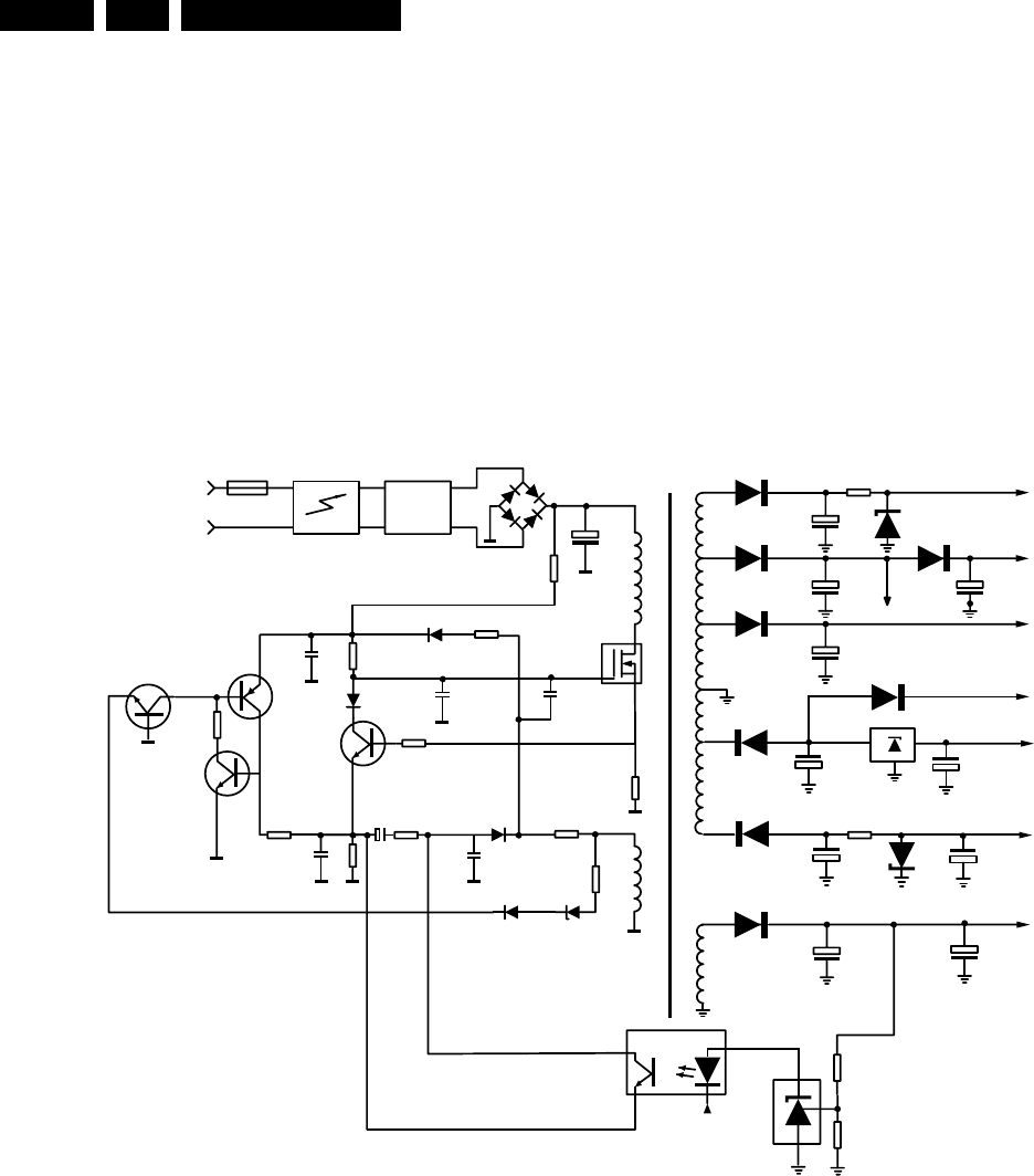
Circuit-, IC Descriptions and List of Abbreviations
EN 160 DVDR980-985 /0X19.
9. Circuit-, IC Descriptions and List of Abbreviations
9.1 Multi-Mode SOPS 50PS203
9.1.1 Why Multi-Mode SOPS?
Using ordinary SOPS results in a decrease of the efficiency at
low output loads due to the increase of the switching frequency.
The Multi-Mode SOPS will reduce the switching frequency at
low loads but still preserves valley switching.
9.1.2 Block Diagram
Figure 9-1
9.1.3 Circuit Description
Input Circuit
The input circuit consists of a lightning protection circuit and an
EMI filter.
The lightning protection comprises R3120, sparkgaps 1124
and 1125. D6128, 6129, C2127 and R3129 are optional.
L5110, L5115, C2120 and L5120 form the EMI filter. It prevents
inflow of noises into the mains.
Primary Rectifier/smoothing Circuit
The AC input is rectified by diodes 6151,6152, 6153, 6154 and
smoothed into C2125. The voltage over C2125 is
approximately 300V. It can vary from 200V to 390V.
Start Circuit
This circuit is formed by R3125, 3126, R3141, C2140 and
R3132.
When the power plug is connected to the mains voltage, the
MOSFET 7125 will start conducting as soon as the gate
voltage reaches a treshold value. A current starts to flow in
primary winding 2-4. The MOSFET will be fed forward via
winding 7-8, R3150 and C2146.
+Vb Supply and Negative Regulation Voltage
The positive part of the voltage over winding 7-8 will be rectified
via R3150, D6140 and charged via R3140 into C2140. The
voltage over C2140 has a value of +30 till +40V. This value
depends on the value of the mains voltage Vi and the load.
The negative part of the voltage over winding 7-8 will be
rectified via R3150, D6142 and charged into C2151. The
voltage over C2151 has a value of -15V and is used as
regulation voltage.
Control Circuit
The control circuit exists of T7140, D6141, C2144 and 2145,
C2147, R3147 and 3148.
This circuit is fed by supply voltage +Vb via R 3141. This circuit
controls the conduction time and the switching frequency of the
power switch circuit. It switches off the MOSFET as soon as the
voltage over Rsense reaches a certain value. This value
7251
7200
6240
6230
6220
2220
2220 2235
6231
2222
6221
7220
6215
6210 6211
6200
6201
5131
7125
7140
7141
7143
7142
6142
6144
6143
2151
6140
2125
Regulation
EMI
FILTER
MAINS
Vi 33Vstby
+12Vstby
+3V9
Lightning
Protection
Rectifier
Overload
protection
Control
feed forward
Power
switch
Overvoltage
protection
Rsense
4
2
8
7
-5Nstby
5.2Vstby
-Vgnstby
2260
2210
2214
2240
2211
2241
+ Vb
-Vreg
3141
2140
2146
2141
+12Vreg
+12Vreg
FLYB
CL 16532095_111.eps
150801

Circuit-, IC Descriptions and List of Abbreviations EN 161DVDR980-985 /0X1 9.
depends on the error voltage at the emittor of T7140, which can
be positive or negative (+/- 0,66V). The voltage fed back by the
regulation circuit defines this error voltage.
Power Switch Circuit
This circuit comprises MOSFET 7125, Rsense formed by
R3133, 3134, 3135, 3136 and 3137, R3131, R3132, D6146.
Diodes 6130, 6131 and 6132 protect the control circuit in case
of failure of the MOSFET.
Regulation Circuit
The regulation circuit comprises opto-coupler 7200, which
isolates the base voltage of transistor 7140 at the primary side
from a reference component 7251 at the secondary side. The
TL431(7251) can be represented by two components:
•a very stable and accurate reference diode
•a high gain amplifier
Figure 9-2
TL431 will conduct from cathode to anode when the reference
is higher than the internal reference voltage of about 2.5V. If the
reference voltage is lower, the cathode current is almost zero.
The cathode current flows through the LED of the opto-coupler.
The collector current of the opto-coupler will adjust the
feedback level of the error voltage at the emittor of T7140.
Overload Protection Circuit
This circuit consists of R3145, C2143, a thyristor circuit formed
by T7141 and T7143, R3143 and R3142. When the output is
shortened, the thyristor circuit will start to conduct and switch
off the supply voltage over C2140. This results in a switching of
f of the drain current of the MOSFET 7125 and the output will
be disabled. The start circuit will try to start up the power supply
again. If the circuit is still shortened, the complete start and stop
sequence will repeat. The power supply comes in a hiccup
mode (is ticking).
Overvoltage Protection Circuit
This circuit consists of R3149, D6144, 6143, R3144, C2142
and T7142.
When the regulation circuit is interrupted due to an error in the
control loop, the regulated output voltage will increase
(overvoltage). This overvoltage is sensed on the primary
winding 7-8.
When an overvoltage is detected, the circuit will start up the
thyristor circuit T7141-7143. The power supply will come in a
hiccup mode as long as the error in the control loop is present.
Secondary Rectifier/Smoothing Circuit
There are 6 rectifier/smoothing circuits on the secondary side.
Each voltage depends on the number of windings of the
transformer.
From these circuits a lot of voltages are derived and fed to 3
connectors. The following voltages are present at the output:
Connector 209
Functional use: to Digital board + Dvio board
1. +3V3(for dig pcb + DVio)
2. +3V3(for dig pcb + DVio)
3. +3V3(for dig pcb + DVio)
4. +3V3(for dig pcb + DVio)
5. GND(for dig pcb + DVio)
6. +12V(for dig pcb + DVio)
7. GND(for dig pcb + DVio)
8. GND(for dig pcb + DVio)
9. +5V(for dig pcb + DVio)
10. STBY control(for dig pcb + DVio)
11. GND(for dig pcb + DVio)
12. -5V(for dig pcb + DVio)
The +12V is switched off by the STBY_ctrl signal.
When the +12V is switched off, also the +3V3, +5V and -5V are
switched off. All these voltages are low drop regulated.
Connector 0205
Functional use: to analogue board + display board + flap motor
‘STBY‘ indicates that the voltage will not be switched off in the
standby situation.
1. +12VSTBY(= +12V Standby, for display heating, 8Vstby)
2. +5VSTBY(= +5V Standby; general use)
3. -5NSTBY(= -5V Standby; neg. voltage for drivers)
4. VGNSTBY(= -32V Standby; for display grids)
5. +33STBY(= +33V Standby; for tuner)
6. FLYB(flyback pulse for power fail + measurement)
7. GNDA(Ground for the analogue board)
Connector 0207
Functional use: to engine
1. +3V3(for engine servo board)
2. +5V(for engine servo board)
3. GND(for engine servo board)
4. +4V6E(for engine analog part)
5. GND(for engine servo board)
6. -5V(for engine servo board)
7. GND(for engine motor currents)
8. +12V(for engine motor currents)
9.2 Display Board
9.2.1 Operation Unit DC (DC Part)
The core element of the operation unit DC is the microcontroller
TMP88CU77ZF [7156]. The TMP88CU77ZF is an 8 bit
microcontroller fitted with 96kB ROM and 3kB RAM and is
responsible for following functions:
•Integrated VFD driver
•Timer
•Evaluation of the keyboard matrix
•Decoding the remote control commands from the infra-red
receiver pos. 6170
•Activation of the display
•Motor driver
The system clock is generated with the 12MHz quartz (Pos.
1153).
9.2.2 Evaluation of the Keyboard Matrix
There are 15 different keys on the display board. A resistor
network is used to generate a specific direct voltage value,
depending on the key pressed, via the resistors 3145, 3171,
3183 and 3194 on the analog/digital (A/D) ports (7156 Pin 17,
18, 19, 20). Pressing keys simultaneously may lead to
undesired functions!
9.2.3 IR Receiver and Signal Evaluation
The IR receiver [7140] contains a selectively controlled
amplifier as well as a photo-diode. The photo-diode changes
the received transmission (approx. 940nm) in electrical pulses,
which are then amplified and demodulated. On the output of
the IR receiver [7140], a pulse sequence with TTL-level, which
corresponds to the envelope curve of the received IR remote
control command, can be measured. This pulse sequence is
input into the controller for further signal evaluation via input
IRR [7156, pin 2].
A
2.5V
R
K
CL 96532065_071.eps
130799
Circuit-, IC Descriptions and List of Abbreviations
EN 162 DVDR980-985 /0X19.
9.2.4 Motor Driver Flap
The flap-motor is controlled via the 2 Port-Pins (MD1, MD2) of
the P (7156, Pin 12, Pin 100). The motor driver part is
constructed as a bridged dual power operational amplifier.
Between the IC outputs (7120, Pin1, Pin3) and a Boucherot
circuit (2121, 3126) suppresses a spurious 3MHz oscillation
from the output stage. The two ports-pins (MD1, MD2) of the P
are PWM-outputs and are controlled in the following way:
Flap Motor:
Figure 9-3
For the detection of the end-positions of the flap there are two
switches (1178, 1179) installed and the information is
evaluated from the P via the signals SW_1178 and SW_1179.
Flap Switches:
9.2.5 Bi-Color LED (Standby and ON)
The STBY-LED is a red/green bi-color-LED and is controlled
via the STBYLED-signal of the P (7156 Pin 10) in the following
way:
9.3 Analogue Board Europe
9.3.1 Microprocessor TMP93C071F
The microcontroller „AIO“ TMP93C071F is a 16bit
microcontroller with internal ROM and 8kB RAM. It includes the
following functions:
•A/D converters
•composite sync input
•I
2
C bus interface
Following connection to the mains, a positive pulse on the reset
input on the P is generated by the reset-IC TL7705 (Pos.7900).
The system clock is generated with the 20MHz quartz (Pos.
1994).
9.3.2 Bus Systems
The communication between the P and the other functional
groups is via the I
2
C-bus (SDA, SCL). The clock rate is approx.
95kHz.
Functional groups on the I
2
C bus:
•E
2
PROM ST24E16 (Pos. 7815)
•Tuner (Pos. 1705)
•Matrix-switch STV6410 (Pos. 7507)
•Audio IC / MSP (Pos. 7600)
•Display board (Pos. 1987)
•VPS-IC (Pos. 7990).
9.3.3 E
2
PROM
The E
2
PROM ST24E16 (Pos. 7815) is an electric erasable and
programmable, non-volatile memory. The E
2
PROM stores data
specific to the device, such as the AFC-reference value, clock-
correction-factor, etc. The data is accessed by the P via the
I
2
C-bus.
9.3.4 VPS, PDC, Teletext (Europe Only)
The STV5348 (Pos. 7990) is a VPS, PDC, and Teletext
Decoder with an external 13,875Mhz quartz.
The following data formats are identified:
•VPS (Timer data and station name)
•PDC Format 2 (Timer data and station name)
•PDC Format 1 (station name and time)
•TXT header line (time for „time download“)
9.3.5 FOME
The FOME-circuit compares the video signal coming from the
tuner and the one coming from the Scart-plug 1. If the video-
signals are identical the output of the FOME-circuit is low.
9.3.6 Fan Control
The fan control circuit is necessary to control the speed of the
cabinet fan (Pos. 1984) according to the requirements in
temperature and noise. The temperature is measured via an
NTC on the display board (Pos. 3145). When the temperature
is lower than 25°C the fan-voltage is approx. 5V and will reach
approx. 10V at a temperature of 40°C. It is also possible to
switch off the fan via the control line ION_FAN. The circuit
generates also two control-signals: TEMP goes to the P and
BE_FAN is the control-line for the basic engine fan.
9.3.7 Power Supply
The 5SW and 8SW supply are switched off in case of standby
from the P via the ISTBY-line. This is possible for power-save.
The ISTBY-line must be low in case of STBY. There is also a
„power fail“ circuit on the PS-schematic which is necessary to
mute AUDIO when IPFAIL is low.
9.3.8 Front End (TU, AP Part)
The Front End Comprises the Following Parts:
•Tuner [1705]
•IF amplifier & video demodulator IC TDA 9818 [7703]
•Sound processor MSP3415G [7600]
MD1 MD2
off H L
open H PWM(H)
close L PWM(L)
SW1 SW2
open L H
closed H L
moving H H
error L L
Colour of STBY
LED Status of the Set
red STBY
green ON
D
uty
C
yc
l
e
50%
f
or
OPEN
an
d
CLO
S
E
Duty Cycle app. 10% for CLOSE
Duty Cycle app. 10% for OPEN
CL 16532095_112.eps
150801

Circuit-, IC Descriptions and List of Abbreviations EN 163DVDR980-985 /0X1 9.
IF Selection
The IF frequency of the video carrier is 38.9 MHz for all
systems except SECAM L' (33.9 MHz).
A quasi-split audio system is used. Separate surface-wave
filters (SAW) are required. [1700], [1701] for video, [1702] for
audio. [1700] Is switched into the signal path for DK/I-SECAM
L/L' reception, if the signal SAWS is “high”. In this case the
switches [7701], [7702] are open and the diode [6700] is
conducting. [1701] Is switched into the signal path for BG
reception, if the signal SAWS is “low”. Then the switch [7708]
is open and the diode [6701] is conducting. For DK/I-SECAM L/
L' reception, an additional circuit for suppressing the adjacent
channel audio carrier is provided, which is set using coil [5702]
to maximum suppression at 40.4MHz.
IF Demodulator
TDA 9818
The IF signal from the tuner is processed by the demodulator
IC TDA 9818 [7703]. The signal PSS to pin3 switches between
demodulation of positive SECAM or negative PAL modulated
video carriers. A QSS-audio-IF signal SIF1 is generated for
demodulation in the sound processor [7600]. The audio-IF
carrier is selected in the audio SAW filter [1702]. This filter is
switched for SECAM L’. If the signal SB1 is “high”, the switch
[7707] is closed and the diode [6702] is not conducting. For all
other standards the diode [6702] is conducting and the switch
[7707] is open. The output signal from this SAW filter is first
processed in the TDA 9818. Audio carriers are converted from
the tuner IF level into the audio IF position and further
processed in the audio demodulator [7600]. The AFC coil
[5703] on the TDA 9818 is adjusted so that when a frequency
of 38.90 MHz is supplied to the IF output of the tuner, the AFC
voltage on pin 17 of the TDA 9818 is 2.5V. The setting of the
picture carrier frequency for SECAM L in the TDA 9818 is
achieved by connecting pin 7 of the IC via a resistor [3702] to
earth. The switch [7700] and the signal SB1 "high" do this. The
HF-AGC is set using the AGC controller [3707] so that, with a
sufficiently large antenna input signal (74 dBV), the voltage at
the IF output of the tuner [1705] pin 11 is 500 mVpp. This
setting must be carried out, when the audio carrier is switched
off. The demodulated video signal appears on pin 16 [7703].
The demodulator AGC voltage at pin4 is used to determine the
antenna signal strength after a buffer [7705] with the signal
AGC_MUTE. In the opposite direction this line may be used to
mute the demodulator to avoid cross talk in all cases, where the
tuner signal is not needed. In this case a „high“ signal is sent
via AGC_MUTE and the conducting diode [6703] to pin4. The
video trap [1703] reduces adjacent channel video and sound
carrier remainders in the video for BG standards. For all other
standards the switch [7704] and signal TS "low" bypass this
trap. In this cases the selectivity of the SAW filter [1700] is
sufficient. A frequency response correction is achieved by the
inductance [5009] for not BG standards. This correction is not
preferred for SECAM L' and therefore shorts circuited by
[7709], if the signal SB1 is “high”. The demodulated video
signal VFV is available after the buffer and limiting stage for
noise peaks [7706]. The FM-PLL demodulator function of TDA
9818 is not used and deactivated by the resistor [3726].
Audio Demodulator
Sound processor MSP 3415G
The MSP 3415G [7600] is a multistandard sound processor
which can demodulate FM Mono/Stereo, NICAM and AM
signals. The incoming signal is first controlled and then
digitised. The digital signal is then demodulated in 2 separate
channels. In the first MSP channel, FM and NICAM (B/G/I/D/K)
are demodulated, whereas in the second MSP channel, FM
and are demodulated again (NICAM L corresponds to NICAM
B/G). These demodulated signals are selected digitally in the I/
O and switched to the D/A converter on the outputs. Amplitude
and bandwidth of the demodulated audio signals can be
determined in the MSP using the corresponding commands via
the I2C bus. The audio signal from the tuner is available at the
pins 30 AFER and 31 AFEL.
9.3.9 Input/Output Video-Routing (Europe-Version)
General Description:
The complete Video- I/O-switching is basically realised by the
I/O switch STV6410A. It is controlled via IIC-Bus-0 (SDA/SCL)
by the all in one C on the analogue board. The STV 6410 has
three YCVBS switches, three chroma switches and one RGB
switch. All switches have 6-dB amplification on the outputs.
The YCVBS inputs have bottom clamp, the chroma inputs have
average clamp, and the RGB inputs have bottom clamp circuits
at the inputs. The R/C inputs can be switched to average clamp
for chroma signals via I2C bus.
The IC has also one slow blanking monitor and one fast
blanking switch for fast RGB insertion (see detailed description
in chapter 1.5). Two pre-selectors BA 7652 are additionally
used: One for switching between Rear CVBS, Y- Rear and
Front, the second for switching between Chroma- Rear and
Front signal. Both pre-selectors are controlled via IS1 and IS2
from the analogue board C.
CVBS Signals:
There are four CVBS input connection possibilities: Front
chinch (E6), Rear Chinch (E4), Scart 1 (E1) and Scart 2 (E2).
Rear Chinch In is routed via the pre selector BA 7652; the other
signals are connected direct to the STV 6410. The selected
CVBS signal is routed to Rear Chinch Out (via BA 7660, 6dB
amplification, 75 Ohm driver) and to Scart 1. Independent of
the input signal quality (CVBS, S-Video or RGB) the digital
board supplies also S-Video and RGB signals to the
corresponding socket.
S-Video Signals:
There are also four S-Video input connection possibilities:
Front In (E5), Rear In (E3), Scart 1 and Scart 2. For S-Video
from Scart this option has to be switched on in the OSD menu.
The pre-selectors and the STV 6410 do the signal selection (for
detailed routing see overview). Also the video quality will be S-
Video, the digital board supplies also CVBS to the
corresponding sockets. The S-Video signal that is coming from
the digital board is routed via BA 7660 (6-dB amplification and
75-Ohm driver) to the S-Video Rear Out socket.
RGB Signals:
The Scart 2 RGB input signal (Decoder socket) is connected to
the RGB switch of STV 6410 and to the digital board in parallel.
The RGB from Scart 2 is routed to Scart 1 in low power standby
mode. The direct connection (not via STV 6410) is for loop
through and REC. The RGB signal, which is coming from the
digital board, is connected to the RGB encoder input of the STV
6410 and is routed to Scart 1 in all other modes.
As the Scart-connection can carry either RGB- or Y/C-signals
it is necessary to define the available and selected signal-
property. While Pin15 of Scart (Red or Chroma-upstream) is
fully handled via STV6410A the Pin7 (Blue or Chroma-
downstream) has to be extra set.
•Scart1: Pin42 of C (SC1YC_H-line):
–Low ( Blue-Out on SC1
–High ( Chroma-In on SC1
•Scart2: Pin41 of C (SC2RGB_H-line):
–Low ( Chroma-Out on SC2
–High ( Blue-In on SC2
Detection of Status-Information
Pin-8 (Slow-Blank):
Level-detection of Pin-8 (Scart-1 and -2) is realised by using
STV6410A. It can be readout via IIC-Bus by the CC-C. To
obtain the status of Scart1-Pin8, Bit 0 & 1 of register 06h must
be set to 0 (Input-mode). The corresponding bits for verification
of Scart2-Pin8-status are set to input-mode as default.

Circuit-, IC Descriptions and List of Abbreviations
EN 164 DVDR980-985 /0X19.
Meaning of Read-Register-Bits:
•Bit 7 & 6: not used
•Bit 5 & 4: Status Scart-2/Pin8:
–0 1 Low-level
–1 0 Medium-level (16:9)
–1 1 High-level (4:3)
•Bit 3 &2: not used
•Bit 1 & 0: Status Scart-1/Pin8:
–0 1 Low-level
–1 0 Medium-level (16:9)
–1 1 High-level (4:3)
Pin-16 (Fast Blank):
Only the status/level of Scart-2/Pin16 must be detected; this is
realised by using PortC3/AIN14 (Pin25) of the CC-C as an
Analogue-input.
•ADC-value lower or equal 24h ( Pin16 low (no RGB-
signals)
•ADC-value greater 24h ( Pin16 high (RGB present on
Scart-2)
To avoid misdetection a “software-integration” (result is first
valid if it was 3-times the same) must be implemented,
determination has to be done approx. every 47msec (no
multiple of V-sync).
WSS on Y/C-Plug:
Picture-Ratio-Information (16:9 or 4:3) on SVHS-connections
is coded via the average DC-level of the Chroma-signal-line,
detection is realised by using an analogue-input-port of the CC-
C.
•ADC- value lower or equal 40h ( 4:3-picture-ratio delivered
•ADC-value greater 40h ( 16:9-picture-ratio available on
plug
Y/C-Rear is determined via Port40/AIN3 (Pin14) of CC (WSRI-
line) and Port41/AIN4 (Pin15) is used for Y/C-Front (WSFI-
line).
Generation of Status-Information
Pin-8 (Slow Blank):
Only on Scart-1 the Slow-Blank-Status (Level of Pin8) must be
created, which is done via IIC-Bus-register 06h (Bits 0 & 1) of
the STV6410A.
Pin-16 (Fast Blank):
Only the status/level of Pin16-Scart1 must be controlled; this is
realised by using the FB-switch-capabilities of the STV6410A,
which are set via IIC-Bus-register 04h (bits 4 & 5).
WSS on Y/C-Plug:
The appropriate DC-level on Chroma-signal-line for Y/C-Rear-
Out is produced via Port57 (Pin10) of the CC-C (WSRO-line).
•4:3 - Picture-ratio supported on Y/C-Plug: Port57 set to 0
•16:9 - Picture-ratio supported on Y/C-Plug: Port57 set to 1
9.3.10 Audio Routing Analogue board (Europe / Nafta)
General Description:
The Audio- I/O switching is realised by the STV6410 I/O switch.
By I
2
C Bus (SDA-0/SCL-0) it is possible to control all the Audio
in- and outputs (for detailed Information we refer to the
STV6410 routing overview).
Analog audio coming from DV-Board and second rear Cinch
input is routed via MSP3415 to the STV 6410. After selecting
the audio source via STV 6410, the signal must be transformed
into the digital domain. For this, the UDA 1360TS (ADC) is
responsible. An input-voltage of up to 2Vrms can be handled
from the IC´s. For further processing, the UDA 1360TS (ADC)
delivers the data-in I
2
S format to the digital-board. After a
certain delay the (processed) data come back from the digital
board to the UDA 1328 (DAC). The UDA 1328 (DAC)
transforms the I
2
S data back into the analog domain and feeds
the signals direct to the MC33078 (OPV). From the MC33078
(OPV) the signals are delivered back to the STV 6410 and also
direct to the 2nd rear out Cinch. The other outputs (Scart,
Cinch) are supported by the STV 6410.
Detailed Description STV 6410:
The STV 6410 is an I
2
C bus controlled audio and video switch
matrix, which is able to handle audio input signals up to 2 Vrms.
The used outputs are equipped with internal level adjustment
possibility. Low distortion and very good channel separation is
a typical peculiarity of this IC. The output resistance is very low
and the frequency bandwidth is up to 50 kHz.
Detailed Description UDA 1360:
The UDA 1360TS is a stereo Analog-to-Digital Converter
employing bitstream conversion techniques.
The UDA supports the I
2
S-bus data format and the MSB-
justified data format with word lengths of up to 20 bits. The IC
supports also 2Vrms input signals and is designed for 3V3
supply voltage.
The device is able to handle system clocks of 256fs and 384fs.
Typical THD+N at 0dB is -85dB and a S/N performance up to
97dB is possible.
Detailed Description UDA 1328:
The UDA1328 is a 6 channel DAC employing bitstream
conversion techniques, which can be used either in L3
microcontroller mode or in static pin mode.
The UDA 1328 supports the I
2
S-bus data format with word
lengths of up to 24 bits.
Digital sound features can be controlled with the L3 interface.
System clock can be set to 256fs or 384fs.
The Device also provides 2 high quality differential outputs.
Typical THD+N at 0dB is -95dB and a S/N of up to 106dB is
possible.
Supply voltage is 3V3.
Detailed Description MC 33078:
The MC33078 is a dual operational amplifier for audio
applications.
It offers low voltage noise (4,5nV/√Hz) and high frequency
performances (15MHz Gain Bandwidth product, 7V/s slew
rate).
In addition the MC33078 has a very low distortion (0,002%).
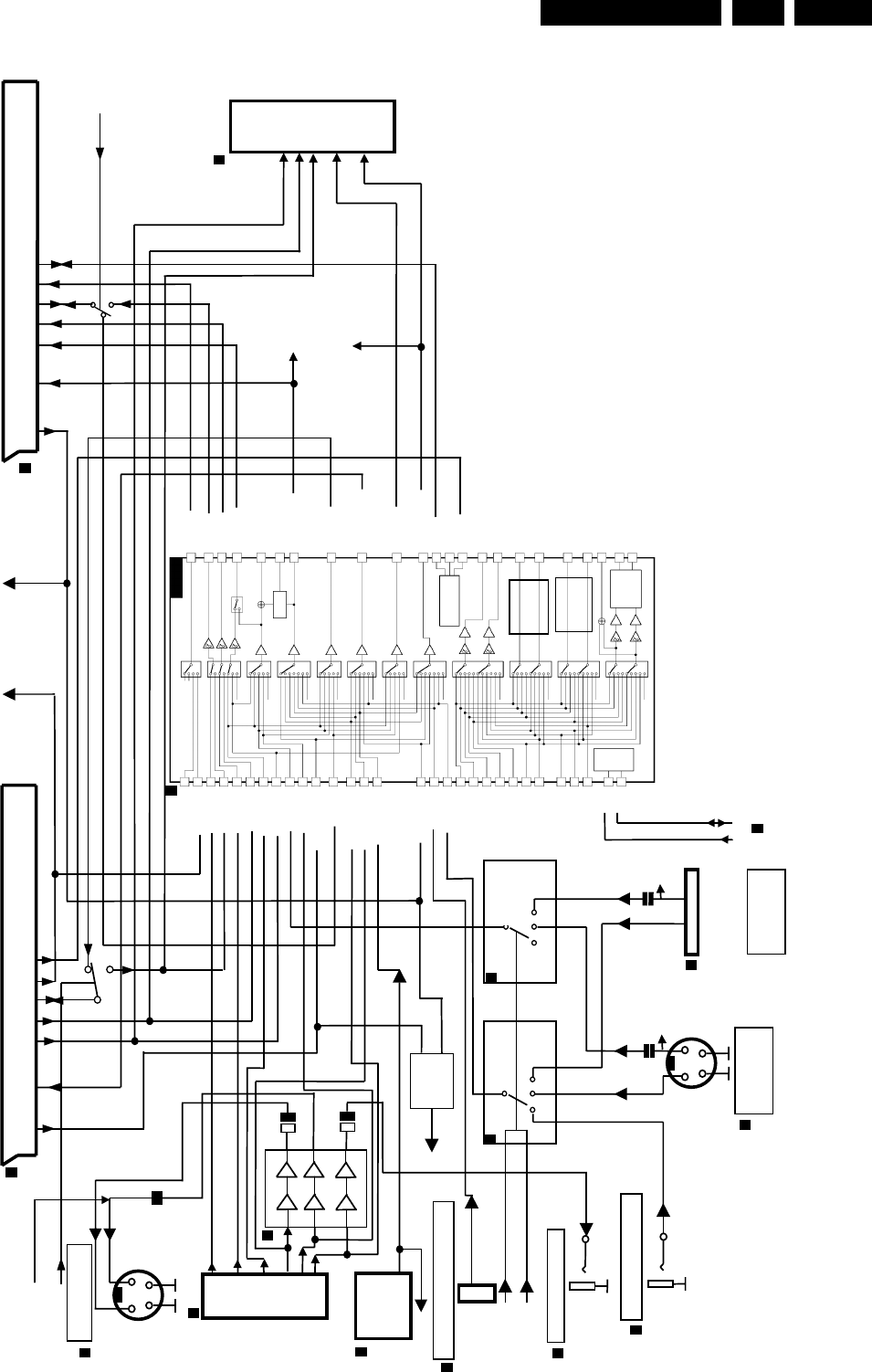
Circuit-, IC Descriptions and List of Abbreviations EN 165DVDR980-985 /0X1 9.
Figure 9-4
FB SWITCH
4V
0V
RGB SWITCH
C SWITCH
Y/CVBSSWITCH
C SWITCH
Y/CVBSSWITCH
C SWITCH
Y/CVBSSWITCH
CINCHSWITCH
AUX SWITCH
VCRSWITCH
TV SWITCH
64
6dB
6dB
-14dB
6dB
6dB
6dB
6dB
6dB
6dB
0/6dB
-14dB
0/6dB
-14dB
0/6dB
-14dB
0/6dB
STEREO/
MONO
2LOUT_TV
ROUT_TV
8AOUT_RF
60
62
4
6
ROUT_VCR
LOUT_VCR
LOUT_AUX
ROUT_AUX
58
59 LOUT_CINCH
ROUT_CINCH
7
5COUT_VCR
YCVBSOUT_VCR
25
27
31
SLOW BLANK,
I/O MONITOR
SLB_TV
SLB_VCR
SLB_AUX
15
13
YCVBSOUT_AUX
COUT_AUX
3YCVBS/OUT_TV
6dB
61
63
17
GOUT_TV
BOUT_TV
FBOUT_TV
1RCOUT_TV
9VOUT_RF
11 FILTER
TRAP
B_ENC
B_AUX
G_ENC
G_AUX
R/C_ENC
R/C_AUX
MUTE
R/C_AUX
R/C_ENC
C_ENC
C_VCR
MUTE
MUTE
MUTE
MUTE
MUTE
MUTE
MUTE
MUTE
MUTE
MUTE
Y_ENC
CVBS/Y_TV
CVBS_STB
CVBS/Y_VCR
CVBS/Y_ENC
Y_ENC
CVBS_STB
CVBS/Y_VCR
CVBS/Y_ENC
CVBS/Y_AUX
Y_AUX
L_ENC
L_STB
L_VCR
L_AUX
R_ENC
R_STB
R_VCR
R_AUX
L_ENC
L_STB
L_TV
L_AUX
R_ENC
R_STB
R_TV
R_AUX
L_ENC
L_STB
L_TV
R_ENC
R_STB
R_TV
L_VCR
R_VCR
L_ENC
L_STB
L_TV
R_ENC
R_STB
R_TV
L_VCR
R_VCR
L_AUX
R_AUX
R/C_ENC
C_ENC
C_VCR
C_TV
R/C_ENC
C_ENC
C_AUX
C_TV
Y_AUX
CVBS/Y_TV
CVBS_STB
CVBS/Y_AUX
CVBS/Y_ENC
Y_ENC
43
39
56
47
37
53
49
45
41
35
38
26
34
52
50
36
24
54
48
40
42
28
30
44
46
32
18
19
FBIN_ENC
FBIN_AUX
BIN_ENC
BIN_AUX
GIN_ENC
GIN_AUX
RCIN_ENC
RCIN_AUX
CIN_ENC
CIN_VCR
YCVBSIN_AUX
CIN_TV
YCVBSIN_ENC
YCVBSIN_VCR
CVBSIN_STB
YCVBSIN_TV
YIN_AUX
YIN_ENC
LIN_ENC
LIN_STB
LIN_TV
LIN_VCR
LIN_AUX
RIN_ENC
RIN_STB
RIN_TV
RIN_VCR
RIN_AUX
21
22
SCL
SDA
I
2
C BUS
DECODER
STV6410
6410-02.EPS
4
WU to
AIO1
TU
CVBSFIN
STEREO/
MONO
STEREO/
MONO
WSRO
WSFI
CVBS
CVBS
VPS
BA7652
BA7652
1
YC
YFIN CFIN
3
535
WSRI
IS1
IS2
2
4
YC
to VIP
A_R
A_G
A_ B
A_C
A_YCVBS
VFV
(Y/CVBS) (Y/CVBS)
VideoIn VideoOut R/C G B/C BL SW AudInL AudOutL AudInR AudOutR
19 15 11
20 716 86
3
21
(Y/CVBS) (Y/CVBS)
VideoIn VideoOut R/C G B/C BL SW AudInL AudOutL AudInR AudOutR
19 15 11
20 716 86
321
SC2RGB_H
SC1YC_H
AIO 1 FOME
FOME
7
6
7
6
7
6
Wake
up
VD to
AIO1
SCART 2 DOWN TO VCR / SAT / DVD / DECODER SCART 1 UP TO TV / MONITOR
Y/C Rear Out
Front Cinch In (E6 CVBS)
Rear Cinch Out
Rear Cinch In (E4)
Y/C Rear In
(E3) Y/C Front In
(E5 SVID)
FROM FRONT
A/V BOARD
FROM FRONT
A/V BOARD
FROM DIGITAL BOARD
TO DIGITAL BOARD
FRONT
END
SAA7718
IC
2
BLOCK DIAGRAM VIDEO IN/OUT EUROPE-VERSION
7
6
4
6
3
4
6
5
5
4
1
4
4
4
5
5
1950-2
1955
1954
7430
BA7660
1953
1959
1959
1955
1953
7507
1950-1
1954
7400 7401
D_B
D_G
D_R
D_Y
D_C
D_CVBS
CL 16532095_113.eps
150801
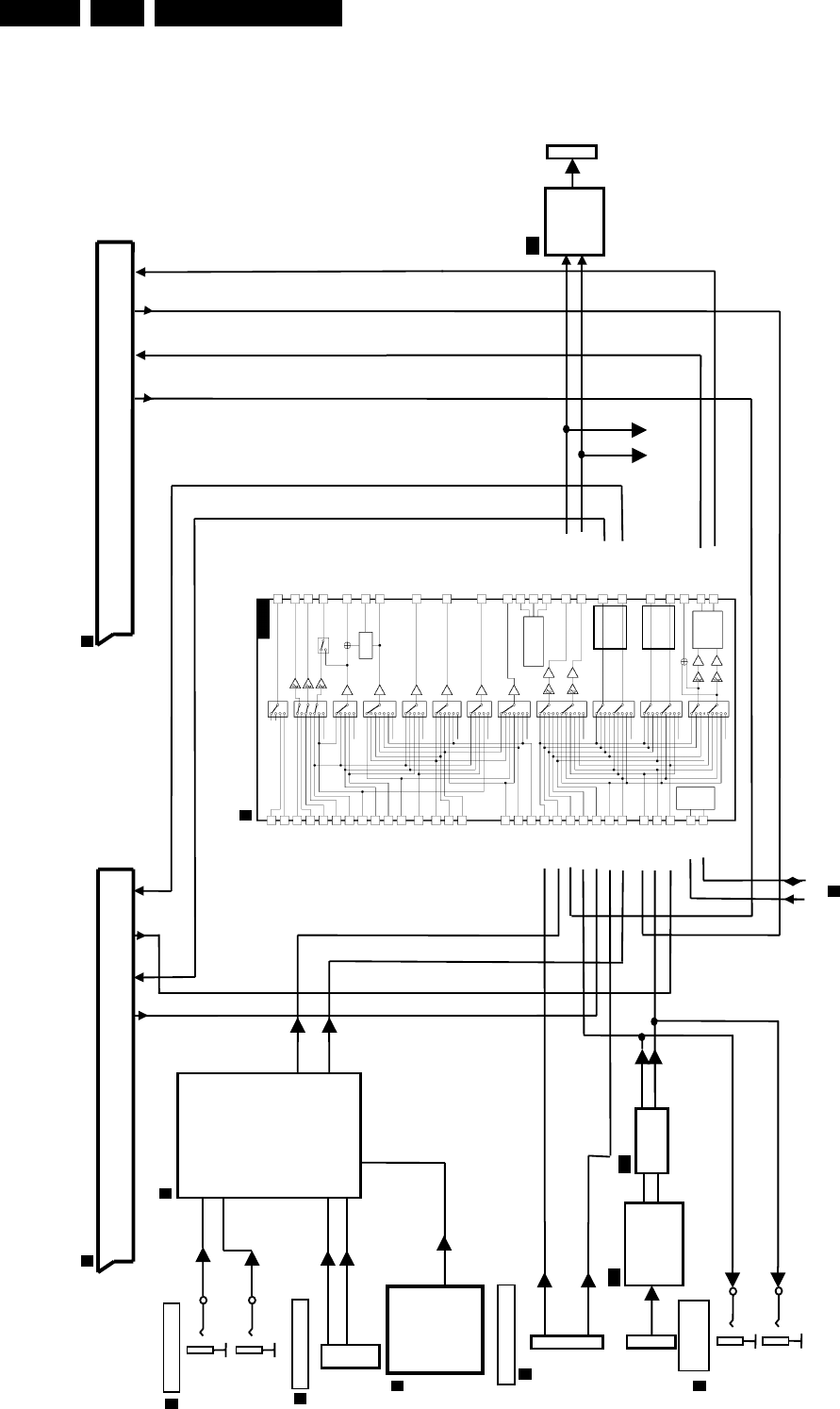
Circuit-, IC Descriptions and List of Abbreviations
EN 166 DVDR980-985 /0X19.
Figure 9-5
FB SWITCH
4V
0V
RGB SWITCH
C SWITCH
Y/CVBSSWITCH
C SWITCH
Y/CVBSSWITCH
C SWITCH
Y/CVBSSWITCH
CINCHSWITCH
AUX SWITCH
VCRSWITCH
TV SWITCH
64
6dB
6dB
-14dB
6dB
6dB
6dB
6dB
6dB
6dB
0/6dB
-14dB 0/6dB
-14dB 0/6dB
-14dB 0/6dB
STEREO/
MONO
2LOUT_TV
ROUT_TV
8AOUT_RF
60
62
4
6
ROUT_VCR
LOUT_VCR
LOUT_AUX
ROUT_AUX
58
59 LOUT_CINCH
ROUT_CINCH
7
5COUT_VCR
YCVBSOUT_VCR
25
27
31
SLOW BLANK,
I/O MONITOR
SLB_TV
SLB_VCR
SLB_AUX
15
13
YCVBSOUT_AUX
COUT_AUX
3YCVBS/OUT_TV
6dB
61
63
17
GOUT_TV
BOUT_TV
FBOUT_TV
1RCOUT_TV
9VOUT_RF
11 FILTER
TRAP
B_ENC
B_AUX
G_ENC
G_AUX
R/C_ENC
R/C_AUX
MUTE
R/C_AUX
R/C_ENC
C_ENC
C_VCR
MUTE
MUTE
MUTE
MUTE
MUTE
MUTE
MUTE
MUTE
MUTE
MUTE
Y_ENC
CVBS/Y_TV
CVBS_STB
CVBS/Y_VCR
CVBS/Y_ENC
Y_ENC
CVBS_STB
CVBS/Y_VCR
CVBS/Y_ENC
CVBS/Y_AUX
Y_AUX
L_ENC
L_STB
L_VCR
L_AUX
R_ENC
R_STB
R_VCR
R_AUX
L_ENC
L_STB
L_TV
L_AUX
R_ENC
R_STB
R_TV
R_AUX
L_ENC
L_STB
L_TV
R_ENC
R_STB
R_TV
L_VCR
R_VCR
L_ENC
L_STB
L_TV
R_ENC
R_STB
R_TV
L_VCR
R_VCR
L_AUX
R_AUX
R/C_ENC
C_ENC
C_VCR
C_TV
R/C_ENC
C_ENC
C_AUX
C_TV
Y_AUX
CVBS/Y_TV
CVBS_STB
CVBS/Y_AUX
CVBS/Y_ENC
Y_ENC
43
39
56
47
37
53
49
45
41
35
38
26
34
52
50
36
24
54
48
40
42
28
30
44
46
32
18
19
FBIN_ENC
FBIN_AUX
BIN_ENC
BIN_AUX
GIN_ENC
GIN_AUX
RCIN_ENC
RCIN_AUX
CIN_ENC
CIN_VCR
YCVBSIN_AUX
CIN_TV
YCVBSIN_ENC
YCVBSIN_VCR
CVBSIN_STB
YCVBSIN_TV
YIN_AUX
YIN_ENC
LIN_ENC
LIN_STB
LIN_TV
LIN_VCR
LIN_AUX
RIN_ENC
RIN_STB
RIN_TV
RIN_VCR
RIN_AUX
21
22
SCL
SDA
I
2
CBUS
DECODER
STV6410
6410-02.EPS
4
(Y/CVBS) (Y/CVBS)
VideoIn VideoOut R/C G B/C BL SW AudInL AudOutL AudInR AudOutR
19 15 11
20 716 86321
(Y/CVBS) (Y/CVBS)
VideoIn VideoOut R/C G B/C BL SW AudInL AudOutL AudInR AudOutR
19 15 11
20 716 8 6 321
UDA1360
SIF1
STEREO/
MONO
STEREO/
MONO
UDA1328
MC33078
MSP3415
37
38
AL
AR
40
41
2
31
30
DVAL
DVAR
AFEL
AFER
ALDAC
ARDAC
AFCLI
AFCRI
A
L
A
R
to Audio-
Level meter
Rear Cinch in
DV-Audio in
FRONT
END
Rear Cinch
out
DAC
SCART 2 DOWN TO VCR/ SAT/ DVD/ DECODER SCART 1 UP TO TV/ MONITOR
ADC
BLOCK DIAGRAM AUDIO IN/OUT EUROPE-VERSION
I
2
C
8
3
6
12
12
12
5
1
8
7 4
4
7600
1950-2
7507
1950-1
7004 1900
1900
1705
7001
1958
7002
7703
1958
ARCLI
ARCLI
FROM
DIGITAL
BOARD
TO
DIGITAL
BOARD
41953
FROM
FRONT
A/V BOARD
Front Cinch in
1960
FROM
DVIO
BOARD
I
2
S
I
2
S
CL 16532095_114.eps
150801

Circuit-, IC Descriptions and List of Abbreviations EN 167DVDR980-985 /0X1 9.
9.4 Analog Board Nafta version
9.4.1 Microprocessor TMP93C071F
The microcontroller „AIO“ TMP93C071F is a 16bit
microcontroller with internal ROM and 8kB RAM. It includes the
following functions:
•A/D converters
•composite sync input
•I
2
C bus interface
The following connection to the mains, a positive pulse on the
reset input on the P is generated by the reset-IC TL7705
(Pos.7900).
The system clock is generated with the 20MHz quartz (Pos.
1994).
9.4.2 Bus Systems
The communication between the P and the other functional
groups is via the I
2
C-bus (SDA, SCL). The clock rate is approx.
95kHz.
Functional groups on the I
2
C bus:
•E
2
PROM ST24E16 (Pos. 7815)
•Tuner (Pos. 1705)
•Matrix-switch STV6410 (Pos. 7507)
•Audio IC / MSP (Pos. 7600)
•Display board (Pos. 1987)
9.4.3 E
2
PROM
The E
2
PROM ST24E16 (Pos. 7815) is an electric erasable and
writeable, non-volatile memory. The E
2
PROM stores data
specific to the device, such as the AFC-reference value, clock-
correction-factor, etc. The data is accessed by the P via the
I
2
C-bus.
9.4.4 FOME
The FOME (Follow Me) -circuit compares the video signal
coming from the tuner and the one coming from the Scart-plug
1. If the video-signals are identical the output of the FOME-
circuit is low.
9.4.5 Fan Control
The fan control circuit is necessary to control the speed of the
cabinet fan (Pos. 1984) according to the requirements in
temperature and noise. The temperature is measured via an
NTC on the display board (Pos. 3145). When the temperature
is lower than 25°C the fan-voltage is approx. 5V and will reach
approx. 10V at a temperature of 40°C. It is also possible to
switch off the fan via the control line ION_FAN. The circuit
generates also two control-signals: TEMP goes to the P and
BE_FAN is the control-line for the basic engine fan.
9.4.6 Power Supply
The 5SW and 8SW supply are switched off in case of Stby from
the P via the ISTBY-line. This is possible for power-save. The
ISTBY-line must be low in case of STBY. There is also a „power
fail“ circuit on the PS-schematic which is necessary to mute
AUDIO when IPFAIL is low.
9.4.7 Front End (TU, AP Part)
The front end comprises the following parts:
•Tuner [1705]
•IF amplifier & video demodulator IC TDA 9817 [7703]
•Sound processor MSP3445G [7600]
IF Selection
The IF frequency of the video carrier is 45.75 MHz. A quasi-split
audio system is used. Separate surface-wave filters (SAW) are
required. [1701] for video, [1702] for audio.
IF Demodulator
TDA 9817
The IF signal from the tuner is processed by the demodulator
IC TDA 9817 [7703]. A QSS-audio-IF signal SIF1 is generated
for demodulation in the sound processor [7600]. Audio carriers
are converted from the tuner IF level into the audio IF position
and further processed in the audio demodulator [7600]. The
AFC coil [5703] on the TDA 9817 is adjusted so that when a
frequency of 45.75 MHz is supplied to the IF output of the tuner,
the AFC voltage on pin 17 of the TDA 9817 is 2.5V. The HF-
AGC is set using the AGC controller [3707] so that, with a
sufficiently large antenna input signal (74 dBV) the voltage at
the IF output of the tuner [1705] pin 11 is 500 mVpp. This
setting must be carried out, when the audio carrier is switched
off. The demodulated video signal appears on pin 16 [7703].
The demodulator AGC voltage at pin4 is used to determine the
antenna signal strength after a buffer [7705] with the signal
AGC_MUTE. In the opposite direction this line may be used to
mute the demodulator to avoid crosstalk in all cases, where the
tuner signal is not needed. In this case a „high“ signal is sent
via AGC_MUTE and the conducting diode [6703] to pin4. The
video trap [1703] reduces adjacent channel video and sound
carrier remainders in the video. The demodulated video signal
VFV is available after the buffer and limiter stage for noise
peaks [7706]. The FM-PLL demodulator function of TDA 9817
is not used and deactivated by the resistor [3726].
Audio Demodulator
Sound processor MSP 3445G
The MSP 3445G [7600] is a NTSC sound processor. Amplitude
and bandwidth of the demodulated audio signals can be
determined in the MSP using the corresponding commands via
the I2C bus. The audio signal from the tuner is available at the
pins 30 AFER and 31 AFEL.
9.4.8 Video-Routing (Nafta Version)
General Description:
The complete Video- I/O-switching is basically realised by the
I/O switch STV6410A, which is controlled via IIC-Bus-0 (SDA/
SCL) by the all in one C on the analogue board. The STV 6410
has three YCVBS, three chroma, and one RGB switch which is
not used in the Nafta I/O. All switches have 6-dB amplification
on the outputs. The YCVBS inputs have bottom clamp, the
chroma inputs have average clamp, and the RGB switch has
bottom clamp circuits at the inputs. The R/C inputs can be
switched to average clamp for chroma signals via I2C bus.
Two pre-selectors BA 7652 are additionally used: One for
switching between Y- Rear and Front, the second for switching
between Chroma- Rear and Front signal. Both pre-selectors
are controlled via IS1 and IS2 from the analogue board C.
CVBS Signals:
There are two CVBS input connection possibilities: Front
chinch (E5) and Rear Chinch In (E3). Both CVBS sources are
connected direct to the STV 6410 and routed to Rear Out 1 and
Rear Out 2 via the 75-Ohm driver BA 7623. Both CVBS output
sockets are connected to BA 7623 in parallel.
Independent of the input signal quality (CVBS, S-Video or Y/
UV) the digital board supplies also S-Video and Y/UV signals
to the corresponding sockets.
S-Video Signals:
There are also two S-Video input connection possibilities: Front
(E4) and Rear (E2) S-Video In which are connected to the pre-
selector IC's BA 7652. One is used for Y, the other for Chroma

Circuit-, IC Descriptions and List of Abbreviations
EN 168 DVDR980-985 /0X19.
switching. The output of the pre-selector switches is connected
to the STV 6410, and then the signal is routed via the 75-Ohm
driver BA 7623 to the Rear Out S-Video socket.
Also the video quality will be S-Video, the digital board supplies
also CVBS and Y/UV to the corresponding sockets.
Y/UV Signals:
The Y/UV In signal is routed direct to the digital board, there is
no Y/UV IN -> Y/UV Out loop through in low power standby. As
the digital board supplies only RGB signals, a RGB Y/UV
matrix is used. This matrix consists of the operational amplifier
TSH95 which generates the U and V signals according the
formulas: 2U=B-0,338R-0,661G, 2V=R-0,838G-0,161B. Then
the signals are routed to the UV Output sockets via the 75-Ohm
driver BA 7623. The corresponding Y signal is coming from the
digital board via the STV 6410. The 75 Ohm Y socket is driven
by the 75-Ohm driver BA 7623 and finally connected to the of
the Y/UV Output.
Detection of Status-Information
WSS on Y/C-Plug:
•Picture-Ratio-Information (16:9 or 4:3) on SVHS-
connections is coded via the average DC-level of the
Chroma-signal-line, detection is realised by using an
analogue-input-port of the CC-C.
•ADC- value lower or equal 40h ( 4:3-picture-ratio delivered
•ADC-value greater 40h ( 16:9-picture-ratio available on
plug
•Y/C-Rear is determined via Port40/AIN3 (Pin14) of CC
(WSRI-line) and Port41/AIN4 (Pin15) is used for Y/C-Front
(WSFI-line).
Generation of Status-Information
WSS on Y/C-Plug:
The appropriate DC-level on Chroma-signal-line for Y/C-Rear-
Out is produced via Port57 (Pin10) of the CC-C (WSRO-line).
•4:3 - Picture-ratio supported on Y/C-Plug: Port57 set to 0
•16:9 - Picture-ratio supported on Y/C-Plug: Port57 set to 1
9.4.9 Audio routing Analogue board (Europe / Nafta)
General Description:
The Audio- I/O switching is realised by the STV6410 I/O switch.
By I
2
C Bus (SDA-0/SCL-0) it is possible to control all the Audio
in- and outputs (for detailed Information we refer to the
STV6410 routing overview).
Analog audio coming from DV-Board and second rear Cinch
input is routed via MSP3415 to the STV 6410. After selecting
the audio source via STV 6410, the signal must be transformed
into the digital domain. For this, the UDA 1360TS (ADC) is
responsible. An input-voltage of up to 2Vrms can be handled
from the IC´s. For further processing, the UDA 1360TS (ADC)
delivers the data-in I
2
S format to the digital-board. After a
certain delay the (processed) data come back from the digital
board to the UDA 1328 (DAC). The UDA 1328 (DAC)
transforms the I
2
S data back into the analog domain and feeds
the signals direct to the MC33078 (OPV). From the MC33078
(OPV) the signals are delivered back to the STV 6410 and also
direct to the 2nd rear out Cinch. The other outputs (Scart,
Cinch) are supported by the STV 6410.
Detailed Description STV 6410:
The STV 6410 is an I
2
C bus controlled audio and video switch
matrix, which is able to handle audio input signals up to 2 Vrms.
The used outputs are equipped with internal level adjustment
possibility. Low distortion and very good channel separation is
a typical peculiarity of this IC. The output resistance is very low
and the frequency bandwidth is up to 50 kHz.
Detailed Description UDA 1360:
The UDA 1360TS is a stereo Analog-to-Digital Converter
employing bitstream conversion techniques.
The UDA supports the I
2
S-bus data format and the MSB-
justified data format with word lengths of up to 20 bits. The IC
supports also 2Vrms input signals and is designed for 3V3
supply voltage.
The device is able to handle system clocks of 256fs and 384fs.
Typical THD+N at 0dB is -85dB and a S/N performance up to
97dB is possible.
Detailed Description UDA 1328:
The UDA1328 is a 6 channel DAC employing bitstream
conversion techniques, which can be used either in L3
microcontroller mode or in static pin mode.
The UDA 1328 supports the I
2
S-bus data format with word
lengths of up to 24 bits.
Digital sound features can be controlled with the L3 interface.
System clock can be set to 256fs or 384fs.
The Device also provides 2 high quality differential outputs.
Typical THD+N at 0dB is -95dB and a S/N of up to 106dB is
possible.
Supply voltage is 3V3.
Detailed Description MC 33078:
The MC33078 is a dual operational amplifier for audio
applications.
It offers low voltage noise (4,5nV/√Hz) and high frequency
performances (15MHz Gain Bandwidth product, 7V/s slew
rate).
In addition the MC33078 has a very low distortion (0,002%).
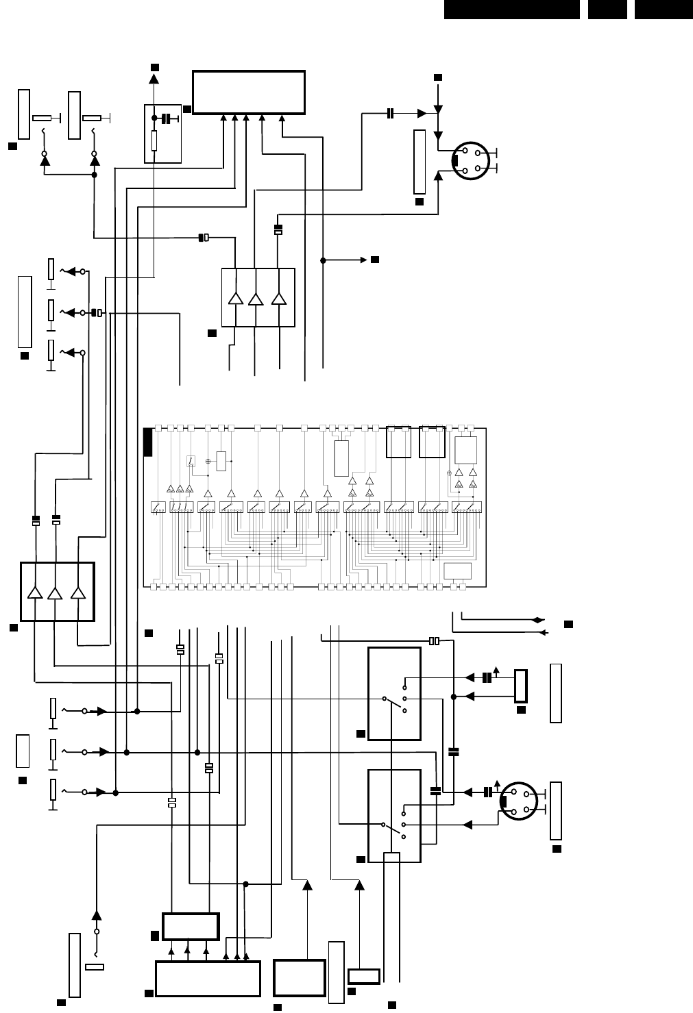
Circuit-, IC Descriptions and List of Abbreviations EN 169DVDR980-985 /0X1 9.
Figure 9-6
FB SWITCH
4V
0V
RGB SWITCH
C SWITCH
Y/CVBSSWITCH
C SWITCH
Y/CVBSSWITCH
C SWITCH
Y/CVBSSWITCH
CINCHSWITCH
AUX SWITCH
VCRSWITCH
TV SWITCH
64
6dB
6dB
-14dB
6dB
6dB
6dB
6dB
6dB
6dB
0/6dB
-14dB
0/6dB
-14dB
0/6dB
-14dB
0/6dB
STEREO/
MONO
2LOUT_TV
ROUT_TV
8AOUT_RF
60
62
4
6
ROUT_VCR
LOUT_VCR
LOUT_AUX
ROUT_AUX
58
59 LOUT_CINCH
ROUT_CINCH
7
5COUT_VCR
YCVBSOUT_VCR
25
27
31
SLOW BLANK,
I/O MONITOR
SLB_TV
SLB_VCR
SLB_AUX
15
13
YCVBSOUT_AUX
COUT_AUX
3YCVBS/OUT_TV
6dB
61
63
17
GOUT_TV
BOUT_TV
FBOUT_TV
1RCOUT_TV
9VOUT_RF
11 FILTER
TRAP
B_ENC
B_AUX
G_ENC
G_AUX
R/C_ENC
R/C_AUX
MUTE
R/C_AUX
R/C_ENC
C_ENC
C_VCR
MUTE
MUTE
MUTE
MUTE
MUTE
MUTE
MUTE
MUTE
MUTE
MUTE
Y_ENC
CVBS/Y_TV
CVBS_STB
CVBS/Y_VCR
CVBS/Y_ENC
Y_ENC
CVBS_STB
CVBS/Y_VCR
CVBS/Y_ENC
CVBS/Y_AUX
Y_AUX
L_ENC
L_STB
L_VCR
L_AUX
R_ENC
R_STB
R_VCR
R_AUX
L_ENC
L_STB
L_TV
L_AUX
R_ENC
R_STB
R_TV
R_AUX
L_ENC
L_STB
L_TV
R_ENC
R_STB
R_TV
L_VCR
R_VCR
L_ENC
L_STB
L_TV
R_ENC
R_STB
R_TV
L_VCR
R_VCR
L_AUX
R_AUX
R/C_ENC
C_ENC
C_VCR
C_TV
R/C_ENC
C_ENC
C_AUX
C_TV
Y_AUX
CVBS/Y_TV
CVBS_STB
CVBS/Y_AUX
CVBS/Y_ENC
Y_ENC
43
39
56
47
37
53
49
45
41
35
38
26
34
52
50
36
24
54
48
40
42
28
30
44
46
32
18
19
FBIN_ENC
FBIN_AUX
BIN_ENC
BIN_AUX
GIN_ENC
GIN_AUX
RCIN_ENC
RCIN_AUX
CIN_ENC
CIN_VCR
YCVBSIN_AUX
CIN_TV
YCVBSIN_ENC
YCVBSIN_VCR
CVBSIN_STB
YCVBSIN_TV
YIN_AUX
YIN_ENC
LIN_ENC
LIN_STB
LIN_TV
LIN_VCR
LIN_AUX
RIN_ENC
RIN_STB
RIN_TV
RIN_VCR
RIN_AUX
21
22
SCL
SDA
I
2
C BUS
DECODER
STV6410
6410-02.EPS
4
V_CON
CVBS
STEREO/
MONO
STEREO/
MONO
WSFI
U
V
FOME
BA7652 BA7652
1
Y
C
3
5
3
5
WSRI
IS1
IS2
2
4
Y
C
A_U
A_Y
A_V
A_C
A_YCVBS
VFV
VY
UUYV
CVBS
U_CON
BA7623
7
7
7
BA7623
7
7
7
6
AIO,VD
Rear Cinch In
YUV In
Front Cinch In
Matrix
CVBS
From Digital Board
FRONT
END
Y/C Rear In Y/C Front In
Y/C Rear Out
Rear Out 1
Rear Out 2
to VIP
to Digital Board
YUV Out / Monitor
IC
2
BLOCK DIAGRAM VIDEO IN/OUT NAFTA-VERSION
CVBSFIN
FROM FRONT
A/V BOARD
FROM FRONT
A/V BOARD
4
5
55
4
1
3
4
5
4
4
4
10
1953
1955
1955 1955
1953
1954
1997
1956
7516
1957
7200
D_R
D_G
D_B
D_CVBS
D_C
D_Y
YFIN
YS_IN
C_IN
CFIN
77
61997
1997
6
4
1
1
1
1
6
5
1955
7430
1955
WSRO
CL 16532095_115.eps
150801
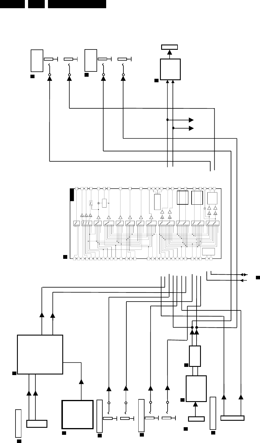
Circuit-, IC Descriptions and List of Abbreviations
EN 170 DVDR980-985 /0X19.
Figure 9-7
FB SWITCH
4V
0V
RGB SWITCH
C SWITCH
Y/CVBSSWITCH
C SWITCH
Y/CVBSSWITCH
C SWITCH
Y/CVBSSWITCH
CINCHSWITCH
AUX SWITCH
VCRSWITCH
TV SWITCH
64
6dB
6dB
-14dB
6dB
6dB
6dB
6dB
6dB
6dB
0/6dB
-14dB
0/6dB
-14dB
0/6dB
-14dB
0/6dB
STEREO/
MONO
2LOUT_TV
ROUT_TV
8AOUT_RF
60
62
4
6
ROUT_VCR
LOUT_VCR
LOUT_AUX
ROUT_AUX
58
59 LOUT_CINCH
ROUT_CINCH
7
5COUT_VCR
YCVBSOUT_VCR
25
27
31
SLOW BLANK,
I/O MONITOR
SLB_TV
SLB_VCR
SLB_AUX
15
13
YCVBSOUT_AUX
COUT_AUX
3YCVBS/OUT_TV
6dB
61
63
17
GOUT_TV
BOUT_TV
FBOUT_TV
1RCOUT_TV
9VOUT_RF
11 FILTER
TRAP
B_ENC
B_AUX
G_ENC
G_AUX
R/C_ENC
R/C_AUX
MUTE
R/C_AUX
R/C_ENC
C_ENC
C_VCR
MUTE
MUTE
MUTE
MUTE
MUTE
MUTE
MUTE
MUTE
MUTE
MUTE
Y_ENC
CVBS/Y_TV
CVBS_STB
CVBS/Y_VCR
CVBS/Y_ENC
Y_ENC
CVBS_STB
CVBS/Y_VCR
CVBS/Y_ENC
CVBS/Y_AUX
Y_AUX
L_ENC
L_STB
L_VCR
L_AUX
R_ENC
R_STB
R_VCR
R_AUX
L_ENC
L_STB
L_TV
L_AUX
R_ENC
R_STB
R_TV
R_AUX
L_ENC
L_STB
L_TV
R_ENC
R_STB
R_TV
L_VCR
R_VCR
L_ENC
L_STB
L_TV
R_ENC
R_STB
R_TV
L_VCR
R_VCR
L_AUX
R_AUX
R/C_ENC
C_ENC
C_VCR
C_TV
R/C_ENC
C_ENC
C_AUX
C_TV
Y_AUX
CVBS/Y_TV
CVBS_STB
CVBS/Y_AUX
CVBS/Y_ENC
Y_ENC
43
39
56
47
37
53
49
45
41
35
38
26
34
52
50
36
24
54
48
40
42
28
30
44
46
32
18
19
FBIN_ENC
FBIN_AUX
BIN_ENC
BIN_AUX
GIN_ENC
GIN_AUX
RCIN_ENC
RCIN_AUX
CIN_ENC
CIN_VCR
YCVBSIN_AUX
CIN_TV
YCVBSIN_ENC
YCVBSIN_VCR
CVBSIN_STB
YCVBSIN_TV
YIN_AUX
YIN_ENC
LIN_ENC
LIN_STB
LIN_TV
LIN_VCR
LIN_AUX
RIN_ENC
RIN_STB
RIN_TV
RIN_VCR
RIN_AUX
21
22
SCL
SDA
I
2
C BUS
DECODER
STV6410
6410-02.EPS
4
UDA1360
SIF1
AL
AR
STEREO/
MONO
UDA1328
MC33078
MSP3435
AL
AR
40
41
2
31
30
AL1_IN
AR1_IN
DVAL
DVAR
AFEL
AFER
ALDAC
ARDAC
AFCLI
AFCRI
AL
A
R
AR
AL
AL2_IN
AR2_IN
AR
AL
STEREO/
MONO
to Audio-
Level meter
DV-Audio in
Rear Cinch in 2
Rear Cinch in 1
Front Cinch in
FRONT
END
DAC
Rear Cinch
out 1
Rear Cinch
out 2
ADC
BLOCK DIAGRAM AUDIO IN/OUT NAFTA-VERSION
I
2
C
I
2
S
I
2
S
7
1
7
1960
7600
FROM
DVIO
BOARD
3
5
5
99
9
9
4
4
4
4
1705
1959
1958
7703
1900 7001
7002
1953
7507
1959
1958
7004
FROM
DIGITAL
BOARD
FROM
FRONT
A/V BOARD
1900
TO
DIGITAL
BOARD
CL 16532095_116.eps
150801

Circuit-, IC Descriptions and List of Abbreviations EN 171DVDR980-985 /0X1 9.
9.5 Digital Board
9.5.1 Record Mode
Video Part
Analog Video input signals CVBS, YC and UV(RGB for EURO
and YUV for USA) are routed via the analog board to connector
1601 and sent to IC7500 SAA7118 (Video Input Processor).
Digital video input signals (DV_IN_DATA(7:0)) are sent from
the DIVIO board through the connector 1603 and further also
to IC7500.
IC7500 (VIP) encodes the analog video to digital video and
processes the digital video to a digital video stream (CCIR656
format). This output stream (VIP_YUV[7:0]) goes to IC7403
SAA6752H (EMPRESS) and to IC7100 Versatile Stream
Manager. The latter uses the data for VBI (vertical blanking
interval) extraction.
IC7403 (EMPRESS) encodes the digital video stream into a
MPEG2 video stream that is fed to IC7100 (VSM).
Audio Part
I2S audio are sent from the analog board to IC7403 EMPRESS
via connector 1602. The EMPRESS compresses I2S audio
data into an AC3 audio stream which is fed to IC7100 (VSM).
Front-End I2S
IC7100 (VSM) interfaces directly to the different hardware
modules such as Basic Engine, EMPRESS IC7403, MPEG
decoder IC7200 (Sti5508) and buffers the data streams that
are coming from or going to these hardware modules.
In IC7100 (VSM), the video MPEG2 stream and the audio AC3
stream are multiplexed into a I2S packetized stream. The serial
data are sent to the Basic Engine to be recorded.
Loop-Through
The multiplexed audio and video stream in the VSM is fed back
via the parallel front-end interface to IC7200 (Sti5508). This IC
decodes the MPEG stream into analog video and I2S audio.
The video and audio signals are routed to the analog board via
connectors 1601 and 1602. During recording, the recorded
signal is present at the outputs of the analog board.
9.5.2 Playback Mode
During playback, the serial data from the Basic Engine is going
directly to the Sti5505 via the serial front-end I2S interface.
The Sti5508 is a MPEG & Audio/video decoder and has the
following outputs:
•To the analog board:
–analog video RGB, YC, CVBS
–I2S audio (PCM format)
–SPDIF audio (digital audio output)
•To the Progressive scan board:
–digital video YC(7:0).
9.5.3 S2B Interface
The S2B interface between the VSM (IC7100) and the Servo
processor MACE3 controls the Basic Engine during record and
playback mode.
9.5.4 System Clock
System clocks(27MHz) of VSM, Sti5508, EMPRESS and
Progressive Scan are generated by oscillator 7906
9.5.5 Audio Clock
During record mode, the audio clock ACC_ACLK_OSC is
generated by IC7102 (PLL) because then, the audio clock must
be sychronized with the incoming video (VIP_FID) from the
VIP.
During playback mode, the audio clock ACC_ACLK_PLL is
generated by the clock synthesizer IC7900 (MK2703S).
Both ACC_ACLK_OSC(also goes to the EMPRESS as
ACLK_EMP) and ACC_ACLK_PLL are fed to the VSM. This IC
selects the appropriate clock to the STI5508. The EMPRESS
IC derives from the incoming ACLK_EMP the I2S audio
encoder clocks AE_BCLK and AE_WCLK which are sent to the
VSM.
9.5.6 On/Off
The digital board is not powered in standby mode. Control
signal ION, coming from the analog board, will enable the PSU
and power the digital board.
•ION = High: the digital board is in powered down standby
mode
•ION = Low: the power supply to the digital board is enabled
9.5.7 Reset
Control signal IRESET_DIG, controlled by the microprocessor
on the analog board is sent to the RESET LOGIC circuit.
•IRESET_DIG = Low in standby mode
•IRESET_DIG = High: the whole system is reset and the
Digital board is waked up.
9.5.8 I2C Bus
Sti5508 is master of the I2C bus. The following IC's are
controlled by the I2C bus:
•IC7201 NVRAM
•IC7403 EMPRESS
•IC7500 VIP
•IC7700 FLI2200 Video Deinterlacer Line Doubler
•IC7801 ADV7196 Video Denc
9.5.9 EMI Bus
The following IC's are connected to the External Memory
Interface bus (EMI) which functions as system bus:
•IC7301 and 7302: Flash memories which contain the
application and diagnostic software
•IC7100: VSM
•IC7200: MPEG AV Decoder
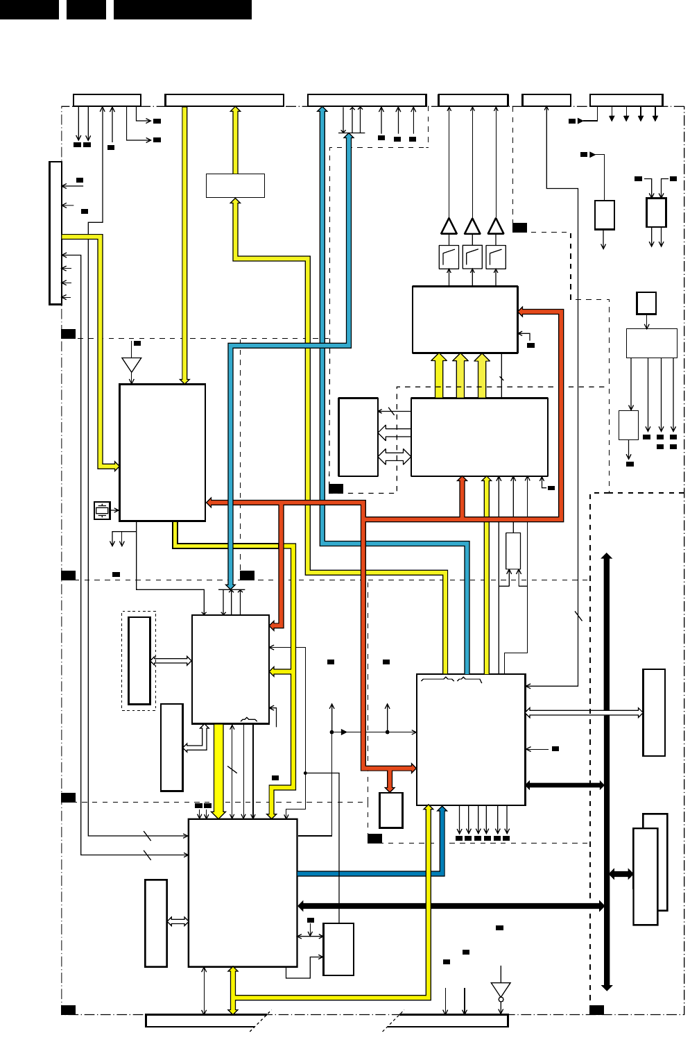
Circuit-, IC Descriptions and List of Abbreviations
EN 172 DVDR980-985 /0X19.
Block Diagram Digital Board
Figure 9-8
VERSATILE
STREAM
MANAGER
4M*16
SDRAM
7102
7100
7101
BE_BCLK
BE_WCLK
BE_DATA_RD
BE_DATA_WR
BE_SYNC
BE_FLAG
BE_V4
SYSCLK_VSM
UART1
UART2VSM_M_A(13:0)
VSM_M_D(15:0)
VSM_M_CTRL
EMI_D(15:0)
EMI_A(21:1)
EMI_CTRL
D_PAR_D(7:0)
D_PAR_CTRL
VE_DATA(7:0)
VIP_YUV(7:0)
PLL
74HCT9046AD
VIP_FID
DSn
DTACKn
VIP_ICLK
VIP_FIDACC_PWM
ACC_PWM
AE_BCLK_VSM
AE_WCL_VSM
AE_DATAO
SERVO BOARD
SERVO BOARD
1100
MPEG
AV
DECODER
STi5508
NVRAM
4M*16
SDRAM
7201
7200
7300
EMI_D(15:0)
EMI_A(21:1)
EMI_CONTROL
D_PAR_D(7:0)
D_PAR_CTRL
SCL
SDA
SCL
SDA
AD_BCLK
AD_DATAO
AD_WCLK
AD_SPDIF
R_OUT
G_OUT
B_OUT
C_OUT
CVBS_OUT
Y_OUT
P_SCAN_YUV(7:0)
5508_HS
5508_ODD_EVEN
HD_M_AD(13:0)
HD_M_DQ(15:0)
HD_M_CTRL
AD_ACLK
AD_ACLK
AD_ACLK
(playback)
AE_ACLK
(record)
SAA6752H
EMPRESS
256K*16
SRAM
4M*16
SDRAM
7402
7403
7401
VIP_YUV(7:0)
AE_DATAI
SCL
SDA
VIP_HS
VIP_VS
VIP_ICLK
SAA7118
VIP
7500
7501
VIP_YUV(7:0)
SCL
SDA
DV_IN_DATA(7:0)
DV_IN_VS
DV_IN _HS
DV_IN_CLK
VIP_HS
VIP_FID
VIP_VS
VIP_ICLK
V_IN_7118
R_IN_7118
U_IN_7118
B_IN_7118
Y_IN_7118
G_IN_7118
C_IN_7118
CVBS_Y_IN_7118_A
CVBS_Y_IN_7118_B
CVBS_Y_IN_7118_C
24M576
DVIO BOARD
LOAD_DVN 9
2RESETN_DIVIO
ANALOG
BOARD
ANALOG
BOARD
ANALOG
BOARD
ANALOG
BOARD
SERVICE
INTERFACE
POWER SUPPLY
1600
1603
1601
1602
1901
1900
+3V3
+12V
+5V
-5V
ION
6
88
1
ION
IRESET_DIG
BE_FAN
5
2
VIP_FB
7902
7702
RESET
RESET
LOGIC
6
2
2
IRESET_DIG
RESETn
RSTN_BE
RSTN_DVIO
RESETn_BE
RESETn_DVIO
7904
7900
7906
27MHz
SYSCLK_EMPRESS
SYSCLK_PROGSCAN
SYSCLK_VSM_5508
CLOCK
BUFFER
MK2703S
ACC_ACLK_PLL
1
2
8
7
1
4OSC
YUV_IN(7:0)
7700
DATA ADDRESS CTRL
7800
7801
7802
7803
7803
1800
CLK_27MHZ
CLK_27MHZ
Y_OUT(9:0)
U_OUT(9:0)
V_OUT(9:0)
HSOUT
VSOUT
DAC_A
DAC_B
DAC_C
Y
Cb
Cr
SCL
SDA
SCL
SDA
SDRAM
64M*32
FLI2200
VIDEO
DEINTERLACER
LINE DOUBLER
ADV7196
VIDEO DENC
5
VIDEO
AMPLIFIER
FILTERS
2
LOW
PAS S
LOW
PASS
LOW
PAS S
EMI BUS
2M*16
FLASH
7301
7302
1456
7
8
9
2
3
I2C BUS
I2C
I2C
I2C
I2C
ANALOG VIDEO
1VIP_FID
VIP_ICLK
CLOCK & SYNC
DIGITAL VIDEO(CCIR656)
VIDEO
FILTER
ANALOG VIDEO
AUDIO PCM I2S & SPDIF
DIGITAL VIDEO
BE_LOADN 2
SYSCLK_PROGSCAN
SYSCLK_PROGSCAN
9
9
RS232 GATEWAY TO ANALOG BOARD
44
ANA_WE
2
2
MUTEN
AD_ACLK
2AE_ACLK
MUTEN
6
9
1
9
6
6
9
ANA_WE
VIDEO MPEG2
2
CTRL
9
9
5
5
I S AUDIO
2
AC3
ACLK_EMP
ACC_ACLK_OSC
RS232 DIVIO GATEWAY
RSTN_BE
LOAD_DVN
RSTN_DVIO
SYSCLK_VSM_5508
5
SYSCLK_EMPRESS
ACLK_EMPRESS
UART3
S2B
RESETn_BE 9
6BE_FAN
A_EMPRESS(13:0)
D_EMPRESS(15:0)
SD_CTRL
SMD(15:0)
SMA(17:0)
SM_CTRL
+5V +3V3 +12V
BE_LOADN
AE_WCLK
AE_BCLK
I S AUDIO IN
6
6
OPTION
VIP_FB
6
2AE_DATAI
AE_WCLK
AE_BCLK
7701-7702
VS
EXTRACTOR
HS_IN
FRAME_IN
VS_IN
FRONT-END I2S
cl 26532011_025.eps
160102
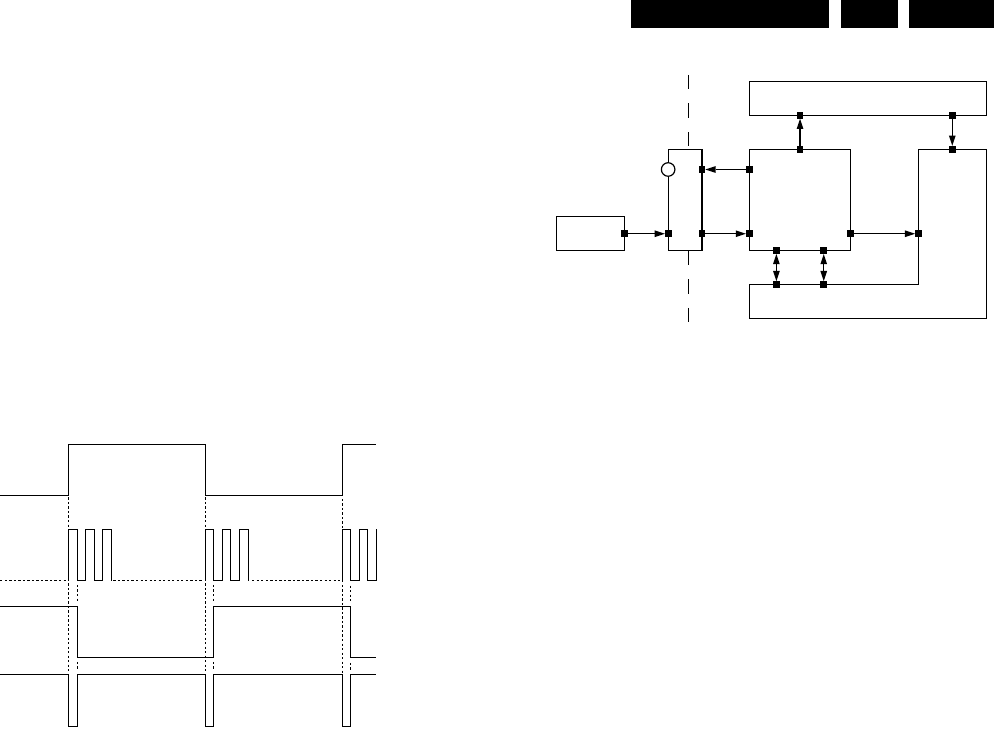
Circuit-, IC Descriptions and List of Abbreviations EN 173DVDR980-985 /0X1 9.
9.5.10 Progressive Scan
Description
The progressive scan part is integrated in the Digital Board and
built around the SAGE Fli2200 de-interlacer / line doubler
(7701). This I2C controlled de-interlacer uses a 64Mbit SDRAM
(32bit x 2M) to perform high quality deinterlacing (meshing).
The de-interlacer gets his digital YUV input data from the
STi5508 (7200). The format of the digital YUV input to the
SAGE is CCIR656 with separated Hsync, Vsync and odd/even
signal running on 27Mhz.
Because the STi5508 doesn't have a Vsync output the odd/
even output of this IC has to be translated to a Vsync signal.
Some glue logic has been added to extract the vertical sync.
The glue logic circuit consists of Flip-Flop IC 74HC74D (7701)
and EXOR 74LVC86 (7702). The next diagram shows how the
vertical sync is extracted.
Vertical Sync
Figure 9-9
The output of the de-interlacer (4:4:4 progressive video) is fed
to the Analog Devices ADV71967 MacroVision compliant
DENC (7801).
The YUV current output of the DENC is fed via a low pass filter
to the single supply output opamps AD8061/8062 (7802-7803).
The analog video is fed via a 7 poled flex to the analog board
where the YUV 2FH cinch connectors are located.
9.6 Divio Board
9.6.1 Short Description of the Module:
The DVIO Module is a decoder for DV streams. The module is
intended for the Philips DVDR1000/002 en DVDR1000/172
DVD+RW recorders. Input is a stream from a DV-camcorder
IEEE1394. Outputs are CCIR656 Video and Analog audio
(L+R). A serial control interface is present.
The following picture shows the location of the DVIO Module
inside the DVDR set.
Description DIVIO Module
Figure 9-10
FRAME_IN
(odd/even)
HS_IN
VS_IN
pin 6 IC7102
CL 16532095_123.eps
150801
camcorder
Front DV PCB
On/Off
IEEE1394
IEEE1394
Analog
audio L+R
Digital
Audio I2S
Digital video
CCIR656
Control RS232Control Misc.
LED
DVIO Module
ADC (analog PCB)
Audio
Encoder
(dig. PCB)
Video
Encoder
(dig. PCB)
Host decoder STi5505
(dig. PCB)
CL 16532095_118.eps
150801
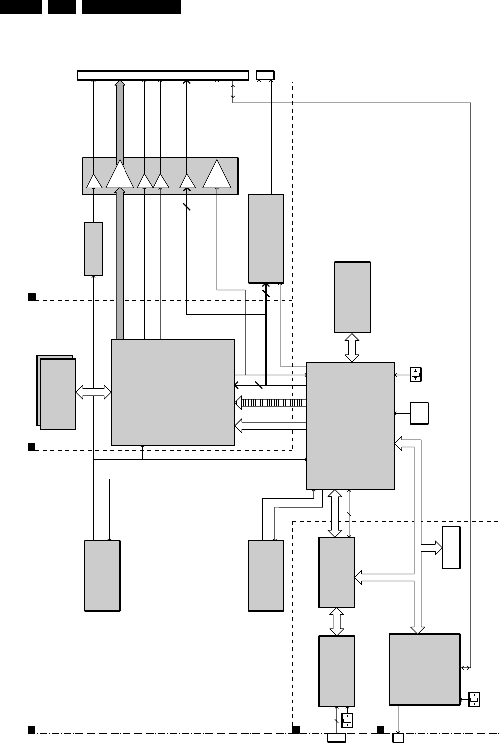
Circuit-, IC Descriptions and List of Abbreviations
EN 174 DVDR980-985 /0X19.
9.6.2 Block Diagram
Block Diagram DVIO
Figure 9-11
4
7103
7203
7201
7300 7304
7101
1101
24.576 MHz
11.05 MHz
SERIAL INTERFACE
RXD
TXD
RTSN
CTSN
7307
7308
7404
7505
1500
7500
7402 - 7403
7506
1501
7301
7303
PDI1394
P25
PHY
Microprocessor
P89C51RD
SRAM
Tuneable audio clock
(+/- 256 x fs)
Tuneable clock
(+/- 27Mhz)
DRAM
CLOCK DELAY
DV DECODER
NW700
FPGA/EPLD SRAM
ROM
AUDIO DAC
UDA1334ATS
PDI1394
L21
LINK
uP BUS
LINK DATA
LINK CONTROLE
3
1
45
2
Isolated domain
1394 INTERFACE
DV CODEC AUDIO & VIDEO OUTPUT
FIFO & CONTROL
MICROPROCESSOR
9
TRISTATE BUFFER
27 MHz
22
2
INPUT
LED
CLOCKGENAUD
CLKAUDTMP
CLOCKGENVID
CLK27M_CON
CLK27M_DV
CLOCK27M
(SYSTEM CLOCK)
AUD_SDI
AUD_SDI
AUD_SDI
AUD_SDI
AUD_SDO
AUD_BCLK
AUD_WS
AUD_BCLK
AUD_WS
AUD_BCLK
AUD_WS
DIGITAL
VIDEO
STREAM
HOST
AD
BUS
YUV(7:0) YUV(7:0)
DV_VS DV_VS
DV_HS_OUT DV_HS_OUT
ANALOG AUDIO LEFT
CLK27M
SERIAL INTERFACE
ANALOG AUDIO RIGHT
CL 16532145_020.eps
211101
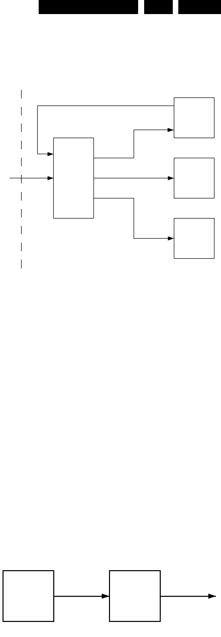
Circuit-, IC Descriptions and List of Abbreviations EN 175DVDR980-985 /0X1 9.
9.6.3 Functional Description
The DVIO module consists of the following blocks (see
blockdiagram):
1. IEEE1394 Interface
•PDI1394P25(7101)
•PDI1394L40(7103)
2. Micro-controller
•89C51RD2(7203)
•32kb SRAM(7201)
3. FIFO and Control
•FPGA/EPLD(7303)
•SRAM(7301)
•Clock generation(7307, 7308)
–Independently tuneable audio and video clock,
implemented with FPGA and PLL
4. DV-Decoder
•NW700(7404)
•EDO DRAM(7402, 7403)
5. Audio & Video output
•Audio DAC UDA1334ATS(7602)
•Clock delay(7500)
•Tristate buffer(7505)
IEEE1394 Interface
The 1394 interface consists of a PDI1394P25 physical layer
and a PDI1394L40 link layer.
It has the following features:
•S200 operation (200 megabit per second)
•One i.Link port (4 pin)
•AV link port
Micro-Controller
The 89C51RD2 processor has a 8051 cpu with the following
extra features:
•64 kilobyte of flash memory as program memory
•1 kilobyte of internal data memory
•watchdog timer
•PCA outputs
•Power control modes
•Speed allowed up to 33 MHz but used at 11.0592 MHz
•On board ISP(In Circuit Programming) functionality
ISP
By use of In Circuit Programming, it is possible to update the
software of the DVIO board that is in the 89C51RD2. ISP can
be made active by resetting the processor and keeping the
ISPN pin low during reset. During ISP, the ISPN signal on the
board has to be kept low. A programming voltage of 5V is
always present at the Vpp pin. When the ISP mode is active,
the new program can be sent to the microprocessor through
the serial port.
Fifo and Control
In decode mode, an isochronous AV-stream is flowing through
the IEEE1394 Interface into the FPGA. The FPGA stores the
data in a FIFO buffer (ping-pong buffer type, i.e. 2 buffers that
can hold one whole frame each).
Reset
The FPGA controls the reset signals on the board. This has the
advantage that it is possible to reset the board both from
software and hardware.
Reset
Figure 9-12
The board reset NRESET will reset the whole board, and the
software reset can reset everything except the microprocessor
itself. Power-on reset is implemented by adding pull-ups and
pull-downs to the reset inputs of the devices. Since the FPGA
will tri-state all the pins during configuration, reset is active
during configuration time. After configuration of the FPGA, the
reset signals are driven inactive. The NRESET signal is used
to reset the DVIO board. After reset, the tri-state buffers to
connector 1500 are disabled.
Clock Circuit
There are 2 clocks to consider in the system, this is the video
clock and the audio clock. These two clocks do not have a
relation, so these clocks must be considered independently.
The video clock is approximately 27 MHz. When data is flowing
from an external source that is supposed to have the same
frequency, it does not have exactly the same clock. Because of
this, buffers may under-run of over-run. Since the clock can not
be directly recovered from the 1394 interface, there has to be
another solution. This solution is a tuneable clock that is
adjusted to the required frequency to process at the rate of the
incoming data.
The hardware implementation of such a tuneable clock is as
follows:
Clock Circuit
Figure 9-13
The same can be applied for the audio clock. For this clock, a
frequency of 8.192 MHz, 11.2896 MHz or 12.228 MHz is
required. This depends on the sample-rate frequency(32kHZ,
44.1kHZ or 48kHZ)of the audio signal.
NRESET
DIGITAL BOARD
DVIO BOARD
FPGA
89C51RD+
PDI1394L21
SOFTWARE RESET
NW701
CL 16532095_120.eps
150801
ClockGen
(FPGA)
Raw clock PLL
(CY2071)
slow-
loopfilter
regular clock
CL 16532095_121.eps
150801

Circuit-, IC Descriptions and List of Abbreviations
EN 176 DVDR980-985 /0X19.
DV Decoder
The AV-data will go from the FIFO to the NW700. The NW700
decodes the stream into video data in 656 format and audio
data in I2S format.
The microprocessor has the ability to read the status registers
of the NW700 through the FPGA. By reading these registers,
extra data from the DV stream, that is not decoded into audio
or video, can be sent to the digital board using pin TXD of the
serial interface. This data includes time stamp and some more.
Audio & Video Output
The audio I2S data are sent to audio DAC UDA1334. Analog
audio left and right signals are connected to the analog board.
The tristate buffer enables the digital video stream to the Video
Input Processor on the digital board when the DV source is
selected.
The clock delay synchronizes the AV clock with the AV data at
the output.
Circuit-, IC Descriptions and List of Abbreviations EN 177DVDR980-985 /0X1 9.
9.7 IC’s Analog Board
9.7.1 IC7001: UDA1328T
Multi-channel filter DAC UDA1328T
1 FEATURES
1.1 General
•2.7 to 3.6 V power supply
•5 V tolerant TTL compatible inputs
•Selectable control via L3 microcontroller interface or via
static pin control
•Multi-channel integrated digital filter plus non-inverting
Digital-to-Analog Converter (DAC)
•Supports sample frequencies between 5 and 100 kHz
•Digital silence detection (output)
•Slave mode only applications
•No analog post filtering required for DAC
•Easy application.
1.2 Multiple format input interface
•I
2S-bus, MSB-justified and LSB-justified format
compatible (in L3 mode)
•I2S-bus and LSB-justified format compatible
•1fs input format data rate.
1.3 Multi-channel DAC
•6-channel DAC with power on/off control
•Digital logarithmic volume control via L3; volume can be
set for each of the channels individually
•Digital de-emphasis for 32, 44.1, 48 and 96 kHz fs via
L3 and, for 32, 44.1 and 48 kHz in static mode
•Soft or quick mute via L3
•Output signal polarity control via L3 microcontroller
interface.
1.4 Advanced audio conÞguration
•6-channel line output (under L3 volume control)
•A stereo differential output (channel 1 and channel 2) for
improved performance
•High linearity, wide dynamic range, low distortion.
2 APPLICATIONS
This multi-channel DAC is eminently suitable for DVD-like
applications in which 5.1 channel encoded signals are
used.
3 GENERAL DESCRIPTION
The UDA1328 is a single-chip 6-channel DAC employing
bitstream conversion techniques, which can be used either
in L3 microcontroller mode or in static pin mode.
The UDA1328 supports the I2S-bus data format with word
lengths of up to 24 bits, the MSB-justified data format with
word lengths of up to 24 bits and the LSB-justified serial
data format with word lengths of 16, 18, 20 and 24 bits.
All digital sound processing features can be controlled with
the L3 interface e.g. volume control, selecting digital
silence type, output polarity control and mute. Also system
features such as power control, digital silence detection
mode and output polarity control.
Under static pin control, via static pins, the system clock
can be set to either 256fsor 384fs support, digital
de-emphasis can be set, there is digital mute and the
digital input formats can also be set.
4 ORDERING INFORMATION
TYPE
NUMBER
PACKAGE
NAME DESCRIPTION VERSION
UDA1328T SO32 plastic small outline package; 32 leads; body width 7.5 mm SOT287-1
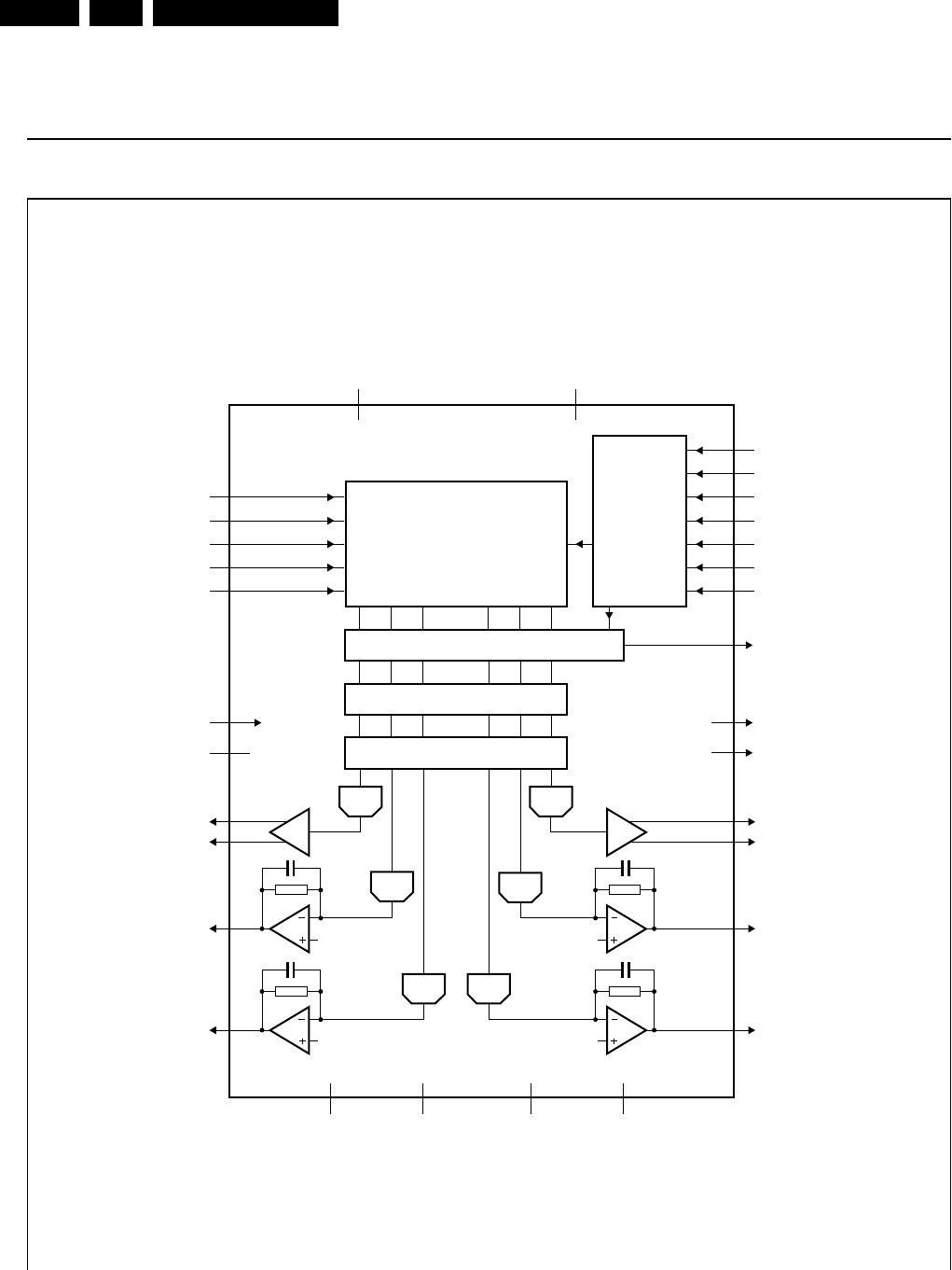
Circuit-, IC Descriptions and List of Abbreviations
EN 178 DVDR980-985 /0X19.
Multi-channel filter DAC UDA1328T
6 BLOCK DIAGRAM
handbook, full pagewidth
MGR979
STATIC
9
DS
26
MUTE
23
DEEM1
24
DEEM0
25
18
19
17
10
11
12
13
14
TEST3
8
TEST2
22
TEST1 27
VOUT3 1
4
SYSCLK 16
CONTROL
INTERFACE
DIGITAL
INTERFACE
VOLUME/MUTE/DE-EMPHASIS
UDA1328T
DAC
INTERPOLATION FILTER
6-CHANNEL NOISE SHAPER
DAC
DAC DAC
DAC
DAC
VOUT1N 29
6
VOUT1P 28
VOUT5
VOUT4
2
5
VOUT2N
31 VOUT2P
32
VOUT6
VDDA
7, 15
n.c.
3
VSSA
30
Vref
21 20
BCK
WS
DATAI12
DATAI34
DATAI56
L3DATA
L3CLOCK
L3MODE
VDDD VSSD
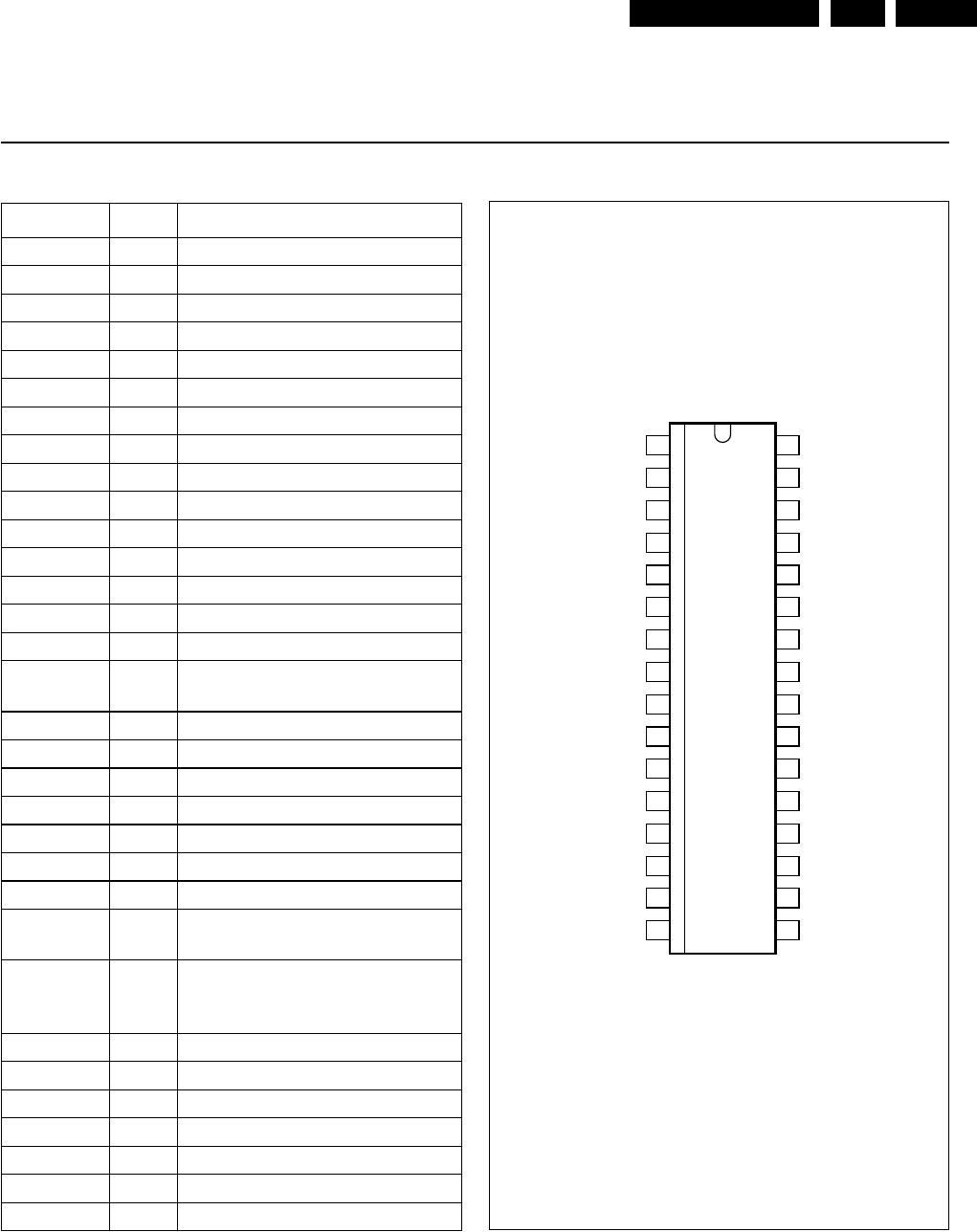
Circuit-, IC Descriptions and List of Abbreviations EN 179DVDR980-985 /0X1 9.
Multi-channel filter DAC UDA1328T
7 PINNING
SYMBOL PIN DESCRIPTION
VOUT3 1 channel 3 analog output
VOUT4 2 channel 4 analog output
VSSA 3 analog ground
VOUT5 4 channel 5 analog output
VOUT6 5 channel 6 analog output
VDDA 6 analog supply voltage
n.c. 7 not connected (reserved)
TEST3 8 test output 3
STATIC 9 static mode/L3 mode switch input
BCK 10 bit clock input
WS 11 word select input
DATAI12 12 data input channel 1 and 2
DATAI34 13 data input channel 3 and 4
DATAI56 14 data input channel 5 and 6
n.c. 15 not connected (reserved)
SYSCLK 16 system clock: 256fs, 384fs,
512fsand 768fs
L3MODE 17 L3 mode selection input
L3CLOCK 18 L3 clock input
L3DATA 19 L3 data input
VSSD 20 digital ground
VDDD 21 digital supply voltage
TEST2 22 test output 2
MUTE 23 static mute control input
DEEM1 24 DEEM control 1 input
(static mode)
DEEM0 25 L3 address select
(L3 mode)/DEEM control 0 input
(static mode)
DS 26 digital silence detect output
TEST1 27 test input 1
VOUT1P 28 channel 1 analog output P
VOUT1N 29 channel 1 analog output N
Vref 30 DAC reference voltage
VOUT2N 31 channel 2 analog output N
VOUT2P 32 channel 2 analog output P Fig.2 Pin configuration.
handbook, halfpage
UDA1328T
MGR980
1
2
3
4
5
6
7
8
9
10
11
12
13
14
15
16
32
31
30
29
28
27
26
25
24
23
22
21
20
19
18
17
VOUT3
VOUT4
VSSA
VOUT5
VOUT6
VDDA
n.c.
TEST3
STATIC
BCK
WS
DATAI12
DATAI34
DATAI56
VOUT2P
VOUT2N
Vref
VOUT1N
TEST1
DS
VOUT1P
DEEM0
DEEM1
MUTE
TEST2
VDDD
VSSD
L3DATA
n.c.
SYSCLK
L3CLOCK
L3MODE
Circuit-, IC Descriptions and List of Abbreviations
EN 180 DVDR980-985 /0X19.
Multi-channel Þlter DAC UDA1328T
8 FUNCTIONAL DESCRIPTION
8.1 System clock
The UDA1328 operates in slave mode only, this means
that in all applications the system must provide the system
clock. The system frequency is selectable. The options are
256f
s
, 384f
s
, 512f
s
and 768f
s
for the L3 mode and 256f
s
or
384f
s
for the static mode. The system clock must be
frequency-locked to the digital interface signals.
It should be noted that the UDA1328 can operate from
5 to 100 kHz sampling frequency (f
s
). However in 768f
s
mode the sampling frequency must be limited to 55 kHz.
8.2 Application modes
Operating mode can be set with the STATIC pin, either to
L3 mode (STATIC = LOW) or to the static mode
(STATIC = HIGH). See Table 1 for pin functions in the
static mode.
Table 1 Mode selection in the static mode
Notes
1. SF1 and SF0 are the Serial Format inputs (2-bit).
2. X means that the pin has no function in this mode and
can best be connected to ground.
8.3 Interpolation Þlter (DAC)
The digital filter interpolates from 1 to 128f
s
by cascading
a half-band filter and a FIR filter, see Table 2. The overall
filter characteristic of the digital filters is illustrated in Fig.3,
and the pass-band ripple is illustrated in Fig.4. Both figures
are with a 44.1 kHz sampling frequency.
Table 2 Interpolation Þlter characteristics
8.4 Digital silence detection
The UDA1328 can detect digital silence conditions in
channels 1 to 6, and report this via the output pin DS. This
function is implemented to allow for external manipulation
of the audio signal in the absence of program material,
such as muting or recorder control.
An active LOW output is produced at the DS pin if the
channels selected via L3 or for all channels in static mode,
carries all zeroes for at least 9600 consecutive audio
samples (equals 200 ms for f
s
= 48 kHz). The DS pin is
also active LOW when the output is digitally muted either
via the L3 interface or via the STATIC pin.
In static mode all channels participate in the digital silence
detection. In L3 mode control each channel can be set,
either to participate in the digital silence detection or not.
8.5 Noise shaper
The 3rd-order noise shaper operates at 128f
s
. It shifts
in-band quantization noise to frequencies well above the
audio band. This noise shaping technique enables high
signal-to-noise ratios to be achieved. The noise shaper
output is converted into an analog signal using a Filter
Stream DAC (FSDAC).
8.6 Filter stream DAC
The FSDAC is a semi-digital reconstruction filter that
converts the 1-bit data stream of the noise shaper to an
analog output voltage. The filter coefficients are
implemented as current sources and are summed at
virtual ground of the output operational amplifier. In this
way very high signal-to-noise performance and low clock
jitter sensitivity is achieved. No post-filter is needed due to
the inherent filter function of the DAC. On-board amplifiers
convert the FSDAC output current to an output voltage
signal capable of driving a line output.
The output voltage of the FSDAC scales proportionally
with the power supply voltage.
8.7 Static mode
The UDA1328 is set to static mode by setting the STATIC
pin HIGH. The function of 6 pins of the device now get
another function as can be seen in Table 1.
8.7.1 SYSTEM CLOCK SETTING
In static mode pin 18 (L3CLOCK) is used to select the
system clock setting. When pin 18 is LOW, the device is in
256f
s
mode, when pin 18 is HIGH the device is in 384f
s
mode.
PIN L3 MODE STATIC MODE
L3CLOCK L3CLOCK clock select
L3MODE L3MODE SF1
(1)
L3DATA L3DATA SF0
(1)
MUTE X
(2)
MUTE
DEEM1 X
(2)
DEEM1
DEEM0 L3ADR DEEM0
ITEM CONDITION VALUE (dB)
Pass-band ripple 0 to 0.45f
s
±0.02
Stop band >0.55f
s
−55
Dynamic range 0 to 0.45f
s
>114
DC gain −−3.5
Circuit-, IC Descriptions and List of Abbreviations EN 181DVDR980-985 /0X1 9.
Multi-channel filter DAC UDA1328T
8.7.2 DE-EMPHASIS CONTROL
In static pin mode the pins DEEM0 and DEEM1 control the
de-emphasis mode; see Table 3.
Table 3 De-emphasis control
8.7.3 DIGITAL INTERFACE FORMATS
In static pin mode the digital audio interface formats can be
selected via pin 17 (SF1) and 19 (SF0). The following
interface formats can be selected (see also Table 4):
•I
2
S-bus with data word length of up to 24 bits
•LSB-justified format with data word length of
16, 20 or 24 bits.
Table 4 Input format selection in the static mode
It should be noted that the digital audio interface holds that
the BCK frequency can be 64 times the WS maximum
frequency, or f
BCK
≤64 ×f
WS
DEEM MODE DEEM1 DEEM0
No de-emphasis 0 0
32 kHz de-emphasis 0 1
44.1 kHz de-emphasis 1 0
48 kHz de-emphasis 1 1
INPUT FORMAT SF1 SF0
I
2
S-bus 0 0
LSB-justiÞed 16bits 0 1
LSB-justiÞed 20bits 1 0
LSB-justiÞed 24bits 1 1
8.8 L3 mode
The device is set to L3 mode by setting the STATIC pin to
LOW. The device can then be controlled via the L3
microcontroller interface (see Chapter 9).
8.8.1 DIGITAL INTERFACE FORMATS
The following interface formats can be selected in the
L3 mode:
•I
2
S-bus with data word length of up to 24 bits
•MSB-justified with data word length of up to 24 bits
•LSB-justified format with data word length of 16, 18,
20 or 24 bits.
8.8.2 L3 ADDRESS
The UDA1328 can be addressed via the L3 microcontroller
interface using one of two addresses. This is done in order
to individually control the UDA1328 and other Philips
DACs or CODECs via the same L3 bus.
The address can be selected using pin 25 (DEEM0) in
L3 mode. When pin 25 is set LOW, the address is 000100.
When pin 25 is set HIGH the address is 000101.
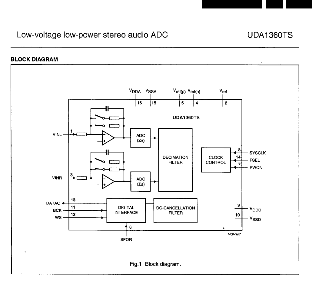
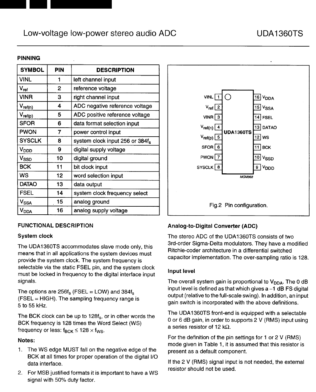

Circuit-, IC Descriptions and List of Abbreviations
EN 186 DVDR980-985 /0X19.
9.7.3 IC7430: BA7660FS
3-channel 75Ωdriver
BA7660FS
The BA7660FS is a 75Ωdriver with a 6dB amplifier and three internal circuits, and provides 75Ωdrive of composite
Y signals and C signals, as well as RGB signals. Each load is capable of driving two circuits, and a sag correction
function reduces the capacitance of the output coupling capacitor.
The input voltage is within a range of 0V to 1.5V, enabling direct connection of ordinary D / A converter output. An
internal power-saving circuit is also included which provides simultaneous muting on all three channels, and output
pin shorting protection.
•Applications
DVDs, set top boxes and other digital video devices
•Features
1) Can be coupled directly to D / A converter output.
2) Operates at a low power consumption (115mW typ.).
3) Internal output muting circuit.
4) Internal power-saving circuit.
5) Internal output protection circuit.
6) An internal sag correction function makes it possible
to reduce the capacitance of the output coupling
capacitor.
7) Each load is capable of driving two circuits.
8) The compact 16-pin SSOP-A package is used.
•Absolute maximum ratings (Ta = 25C)
Parameter Symbol
Vcc
Pd
Topr
Tstg
Limits Unit
8
650
– 25 ~ + 75
– 55 ~ + 125
V
mW
°C
°C
Power supply voltage
Power dissipation
Operating temperature
Storage temperature
•Recommended operating conditions (Ta = 25C)
Parameter Symbol
Vcc
Min.
4.5
Typ.
5.0
Max.
5.5
Unit
VOperating power supply voltage
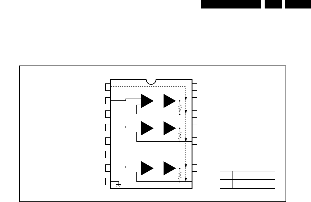
Circuit-, IC Descriptions and List of Abbreviations
EN 188 DVDR980-985 /0X19.
•Pin descriptions and input / output circuits
Pin. No Pin name IN OUT
Reference
voltage
Equivalent circuit Function
1 MUTE ——
——
2
4
7
INA
INB
INC
—
0.9V
0.95V
14
12
9
15
13
10
OUTA2
OUTB2
OUTC2
OUTA1
OUTB1
OUTC1
—— 5.0V16 VCC
Muting control
If MUTE (pin 1) is set to HIGH, muting
is carried out simultaneously on all
three channels.
Signal input
Input signals consist of composite
video signals, Y signals, C signals,
RGB, and others. The input level is
within a range of 0 to 1.3 (min.) to 1.5
(typ.).
—— 0V
3
5
8GND Ground
Signal output
The signal output level is (0.9 + 2 ×
input voltage [V]). Pins 9, 12, and 14
are the pins for sag correction. If pins
10, 13, and 15 are set to 0.2V or less,
the protective circuit is triggered and
the power-saving mode is accessed.
Power supply
15k
8k
GND
15pin
13pin
10pin
14pin
12pin
9pin
Vcc
Circuit-, IC Descriptions and List of Abbreviations EN 189DVDR980-985 /0X1 9.
9.7.4 IC7507: STV6410
AUDIO/VIDEO SWITCH MATRIX
December 1997
TQFP64
(Plastic Quad Flat Pack)
ORDER CODE : STV6410D
.I2C BUS CONTROL
.STANDBY MODE
VIDEO SECTION
.5 CVBS INPUTS, 4 CVBS OUTPUTS (ONE
WITH SELECTABLE CHROMATRAP FILTER)
.5 Y/C INPUTS, 3 Y/C OUTPUTS
.6dB GAIN ON ALL CVBS/Y AND C OUTPUTS
.1 Y/C ADDER
.2 RGB/FB INPUTS, 1 RGB/FB OUTPUT WITH
6dB ADJUSTABLE GAIN
.VIDEO MUTING ON ALL THE OUTPUTS
.3 SLOW BLANKING INPUTS/OUTPUTS
.SYNC BOTTOM CLAMP ON ALL CVBS/Y
AND RGB INPUTS, AVERAGE ON C INPUTS
.BANDWIDTH : 15MHz
.CROSSTALK : 60dB Typ.
AUDIO SECTION
.5 STEREO INPUTS, 4 STEREO OUTPUTS
(TWO WITH LEVEL ADJUSTMENT)
.MONO SOUND OUTPUT
.MONO SOUND CAPABILITYON TV OUTPUTS
.AUDIO MUTING ON ALL THE OUTPUTS
DESCRIPTION
The STV6410 is a highly integrated I2C bus-con-
trolled audio and video switch matrix, optimized for
use in digital set-top box applications. It provides
all the audio and video routings required in a full
three scart set-top box design. It is also fully pin
compatible with STV6411, the two scart version.
1
STV6410
Circuit-, IC Descriptions and List of Abbreviations
EN 190 DVDR980-985 /0X19.
64
63
62
61
60
59
58
57
56
55
54
53
52
51
50
49
17
18
19
20
21
22
23
24
25
26
27
28
29
30
31
32
16
15
14
13
12
11
10
9
8
7
6
5
4
3
2
1
33
34
35
36
37
38
39
40
41
42
43
44
45
46
47
48
ROUT_TV
GNDA
RIN_TV
V
CCA
YCVBSIN_TV
V
REF
GOUT_TV
LOUT_VCR
BOUT_TV
ROUT_VCR
LOUT_CINCH
ROUT_CINCH
CIN_TV
LIN_TV
LIN_VCR
YCVBSIN_VCR
FBOUT_TV
FBIN_AUX
FBIN_ENC
ADD
SCL
SDA
V
CC12
YCVBSIN_AUX
SLB_TV
YIN_AUX
GNDV1
SLB_VCR
RCIN_AUX
GIN_AUX
SLB_AUX
BIN_AUX
RCOUT_TV
V
CC1
CVBSIN_STB
LIN_AUX
YCVBSIN_ENC
LOUT_TV
YCVBSOUT_TV
ROUT_AUX
COUT_VCR
LOUT_AUX
YCVBSOUT_VCR
AOUT_RF
VOUT_RF
GNDV3
FILTER
V
CC3
COUT_AUX
GNDV2
V
CC2
YCVBSOUT_AUX
RIN_AUX
YIN_ENC
RIN_STB
CIN_ENC
RCIN_ENC
LIN_STB
RIN_ENC
GIN_ENC
LIN_ENC
BIN_ENC
RIN_VCR
CIN_VCR
6410-01.EPS
PIN CONNECTIONS
PIN LIST
Pin Number Symbol Description
1 RCOUT_TV Red/chroma Output, to TV Scart
2 LOUT_TV Audio Left Output, to TV Scart
3 YCVBSOUT_TV Y/CVBS Output, to TV scart
4 ROUT_AUX Audio Right Output, to AUX Scart
5 COUT_VCR Chroma Output, to VCR Scart
6 LOUT_AUX Audio Left Output, to AUX Scart
7 YCVBSOUT_VCR Y/CVBS Output, to VCR Scart
8 AOUT_RF Audio (L+R) Output to RF Modulator
9 VOUT_RF Video (CVBS) Output to RF Modulator
10 GNDV3 Video Switches Ground 3
11 FILTER Chroma Trap Filter
12 VCCV3 Video Switches Supply 3 (8V)
13 COUT_AUX Chroma Output, to AUX Scart
14 GNDV2 Video Switches Ground 2
15 YCVBSOUT_AUX Y/CVBS Output, to AUX Scart
6410-01.TBL
STV6410
2

Circuit-, IC Descriptions and List of Abbreviations EN 191DVDR980-985 /0X1 9.
Pin Number Symbol Description
16 V
CCV2
Video Switches Supply 2 (8V)
17 FBOUT_TV Fast Blanking Output, to TV Scart
18 FBIN_AUX Fast Blanking Input, from AUX Scart
19 FBIN_ENC Fast Blanking Input, from Encoder
20 ADD I
2
C Bus IC Address Programmation
21 SCL I
2
C Bus Clock
22 SDA I
2
C Bus Data
23 V
CC12
Slow Blanking Power Supply (12V)
24 YCVBSIN_AUX Y/CVBS Input from AUX Scart
25 SLB_TV Slow Blanking Input/Ouput from TV
26 YIN_AUX Y Input, from AUX Scart
27 SLB_VCR Slow Blanking Input/Ouput from VCR
28 RCIN_AUX Red/Chroma Input, from AUX Scart
29 GNDV1 Video Switches Ground 1
30 GIN_AUX Green Input, from AUX Scart
31 SLB_AUX Slow Blanking Input/Ouput from AUX
32 BIN_AUX Blue Input, from AUX Scart
33 V
CCV1
Video Switches Supply 1 (8V)
34 CVBSIN_STB CVBS Input from STB
35 LIN_AUX Audio Left Input, from AUX Scart
36 YCVBSIN_ENC Y/CVBS Input from Encoder
37 RIN_AUX Audio Right Input, from AUX Scart
38 YIN_ENC Y Input, from Encoder
39 RIN_STB Audio Right Input, from STB
40 CIN_ENC Chroma Input, from Encoder
41 LIN_STB Audio Left Input, from STB
42 RCIN_ENC Red/Chroma Input, from Encoder
43 RIN_ENC Audio Right Input, from Encoder
44 GIN_ENC Green Input, from Encoder
45 LIN_ENC Audio Left Input, from Encoder
46 BIN_ENC Blue Input, from Encoder
47 RIN_VCR Audio Right Input, from VCR Scart
48 CIN_VCR Chroma Input, from VCR Scart
49 LIN_VCR Audio Left Input, from VCR
50 YCVBSIN_VCR Y/CVBS Input from VCR Scart
51 V
REF Voltage Reference Decoupling
52 YCVBSIN_TV Y/CVBS Input, from TV Scart
53 LIN_TV Audio Left Input, from TV Scart
54 CIN_TV Chroma Input, from TV Scart
55 V
CCA Audio Switches Supply (8V)
56 RIN_TV Audio right input, from TV Scart
57 GNDA Audio Switches Ground
58 ROUT_CINCH Audio Right Output, to CINCH
59 LOUT_CINCH Audio Left Output, to CINCH
60 ROUT_VCR Audio Right Output, to VCR sCart
61 BOUT_TV Blue Output, to TV Scart
62 LOUT_VCR Audio Left Output, to VCR Scart
63 GOUT_TV Green Output, to TV Scart
64 ROUT_TV Audio Right Output, to TV Scart
6410-01.TBL
PIN LIST (continued)
STV6410
3

Circuit-, IC Descriptions and List of Abbreviations
EN 192 DVDR980-985 /0X19.
FB SWITCH
4V
0V
RGB SWITCH
C SWITCH
Y/CVBSSWITCH
C SWITCH
Y/CVBSSWITCH
C SWITCH
Y/CVBSSWITCH
CINCHSWITCH
AUX SWITCH
VCRSWITCH
TV SWITCH
64
6dB
6dB
-14dB
6dB
6dB
6dB
6dB
6dB
6dB
0/6dB
-14dB
0/6dB
-14dB
0/6dB
-14dB
0/6dB
STEREO/
MONO
2LOUT_TV
ROUT_TV
8AOUT_RF
60
62
4
6
ROUT_VCR
LOUT_VCR
LOUT_AUX
ROUT_AUX
58
59 LOUT_CINCH
ROUT_CINCH
7
5COUT_VCR
YCVBSOUT_VCR
25
27
31
SLOW BLANK,
I/O MONITOR
SLB_TV
SLB_VCR
SLB_AUX
15
13
YCVBSOUT_AUX
COUT_AUX
3YCVBS/OUT_TV
6dB
61
63
17
GOUT_TV
BOUT_TV
FBOUT_TV
1RCOUT_TV
9VOUT_RF
11 FILTER
TRAP
B_ENC
B_AUX
G_ENC
G_AUX
R/C_ENC
R/C_AUX
MUTE
R/C_AUX
R/C_ENC
C_ENC
C_VCR
MUTE
MUTE
MUTE
MUTE
MUTE
MUTE
MUTE
MUTE
MUTE
MUTE
Y_ENC
CVBS/Y_TV
CVBS_STB
CVBS/Y_VCR
CVBS/Y_ENC
Y_ENC
CVBS_STB
CVBS/Y_VCR
CVBS/Y_ENC
CVBS/Y_AUX
Y_AUX
L_ENC
L_STB
L_VCR
L_AUX
R_ENC
R_STB
R_VCR
R_AUX
L_ENC
L_STB
L_TV
L_AUX
R_ENC
R_STB
R_TV
R_AUX
L_ENC
L_STB
L_TV
R_ENC
R_STB
R_TV
L_VCR
R_VCR
L_ENC
L_STB
L_TV
R_ENC
R_STB
R_TV
L_VCR
R_VCR
L_AUX
R_AUX
R/C_ENC
C_ENC
C_VCR
C_TV
R/C_ENC
C_ENC
C_AUX
C_TV
Y_AUX
CVBS/Y_TV
CVBS_STB
CVBS/Y_AUX
CVBS/Y_ENC
Y_ENC
43
39
56
47
37
53
49
45
41
35
38
26
34
52
50
36
24
54
48
40
42
28
30
44
46
32
18
19
FBIN_ENC
FBIN_AUX
BIN_ENC
BIN_AUX
GIN_ENC
GIN_AUX
RCIN_ENC
RCIN_AUX
CIN_ENC
CIN_VCR
YCVBSIN_AUX
CIN_TV
YCVBSIN_ENC
YCVBSIN_VCR
CVBSIN_STB
YCVBSIN_TV
YIN_AUX
YIN_ENC
LIN_ENC
LIN_STB
LIN_TV
LIN_VCR
LIN_AUX
RIN_ENC
RIN_STB
RIN_TV
RIN_VCR
RIN_AUX
21
22
SCL
SDA
I
2
C BUS
DECODER
STV6410
6410-02.EPS
BLOCK DIAGRAM
STV6410
4
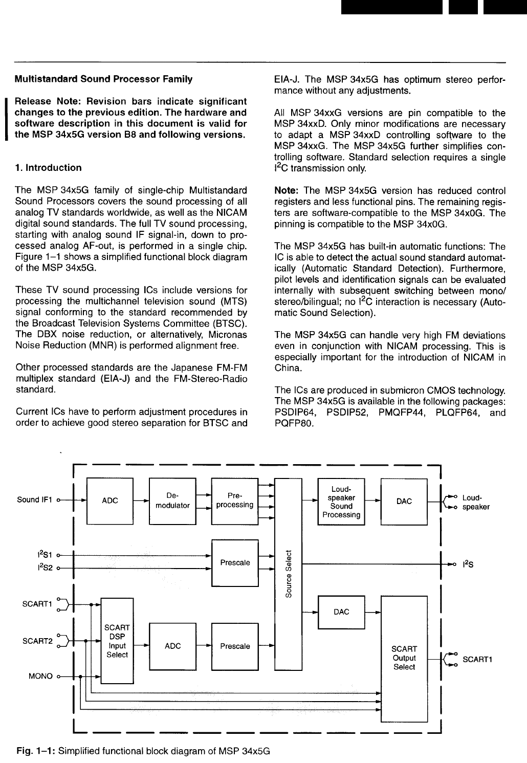
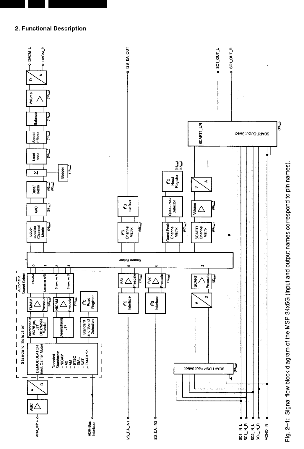
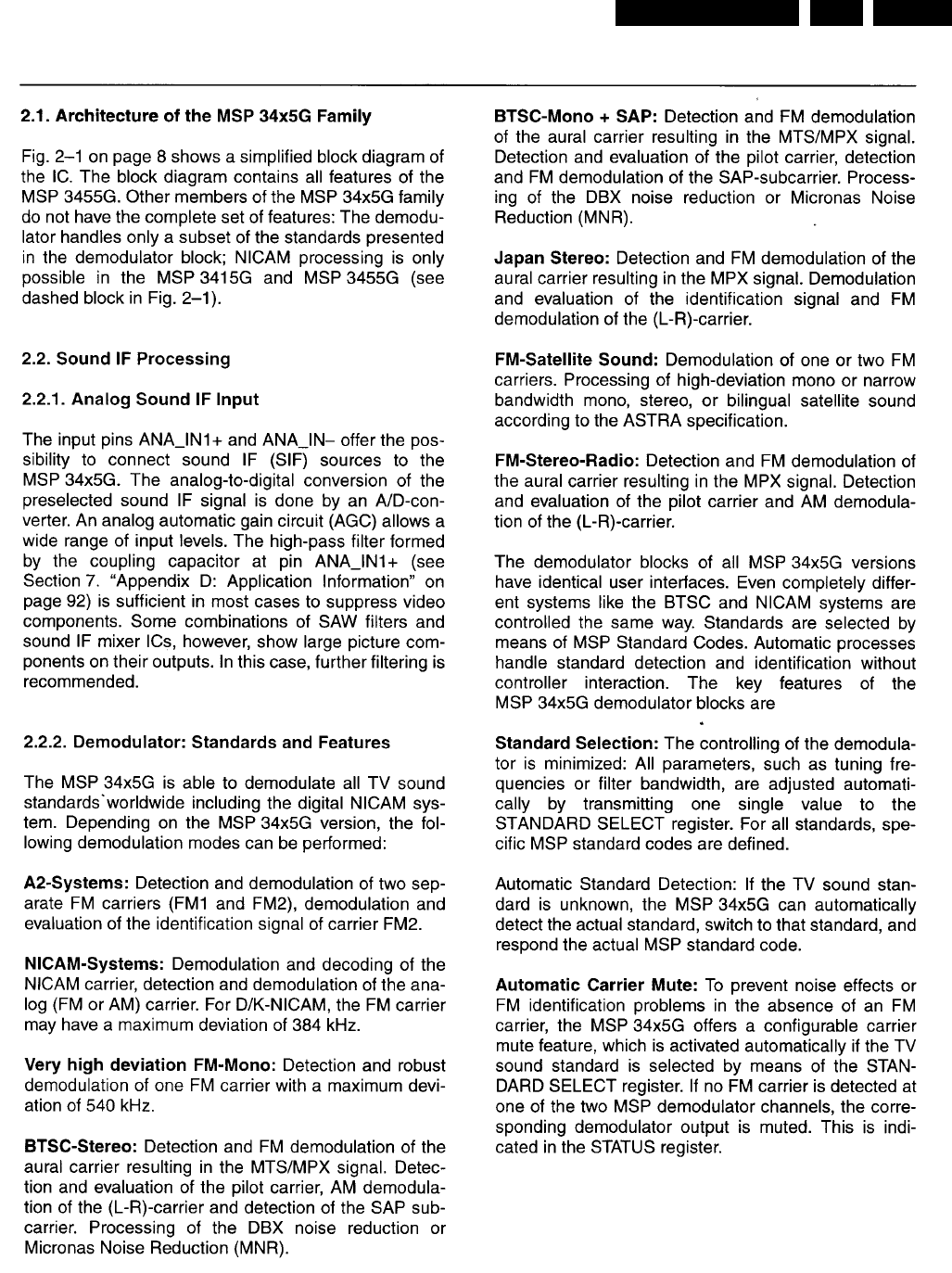
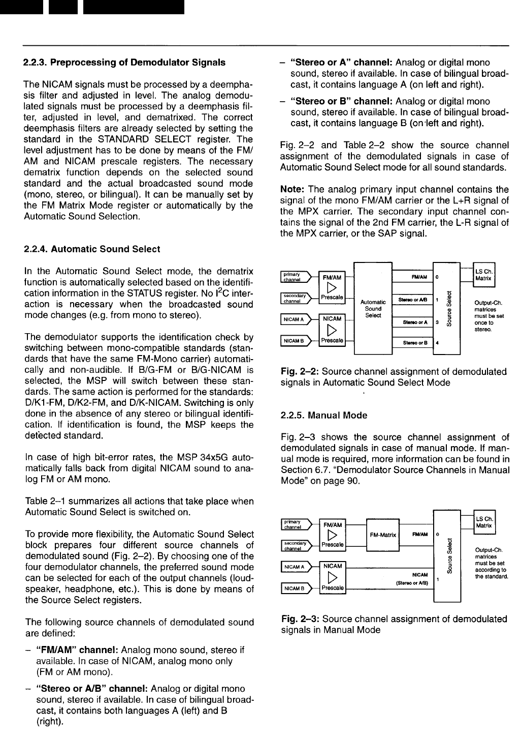
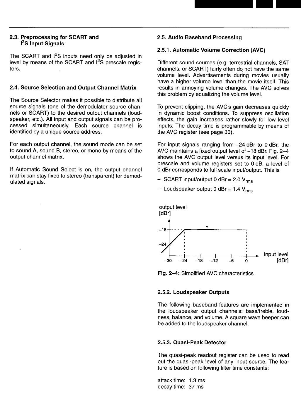
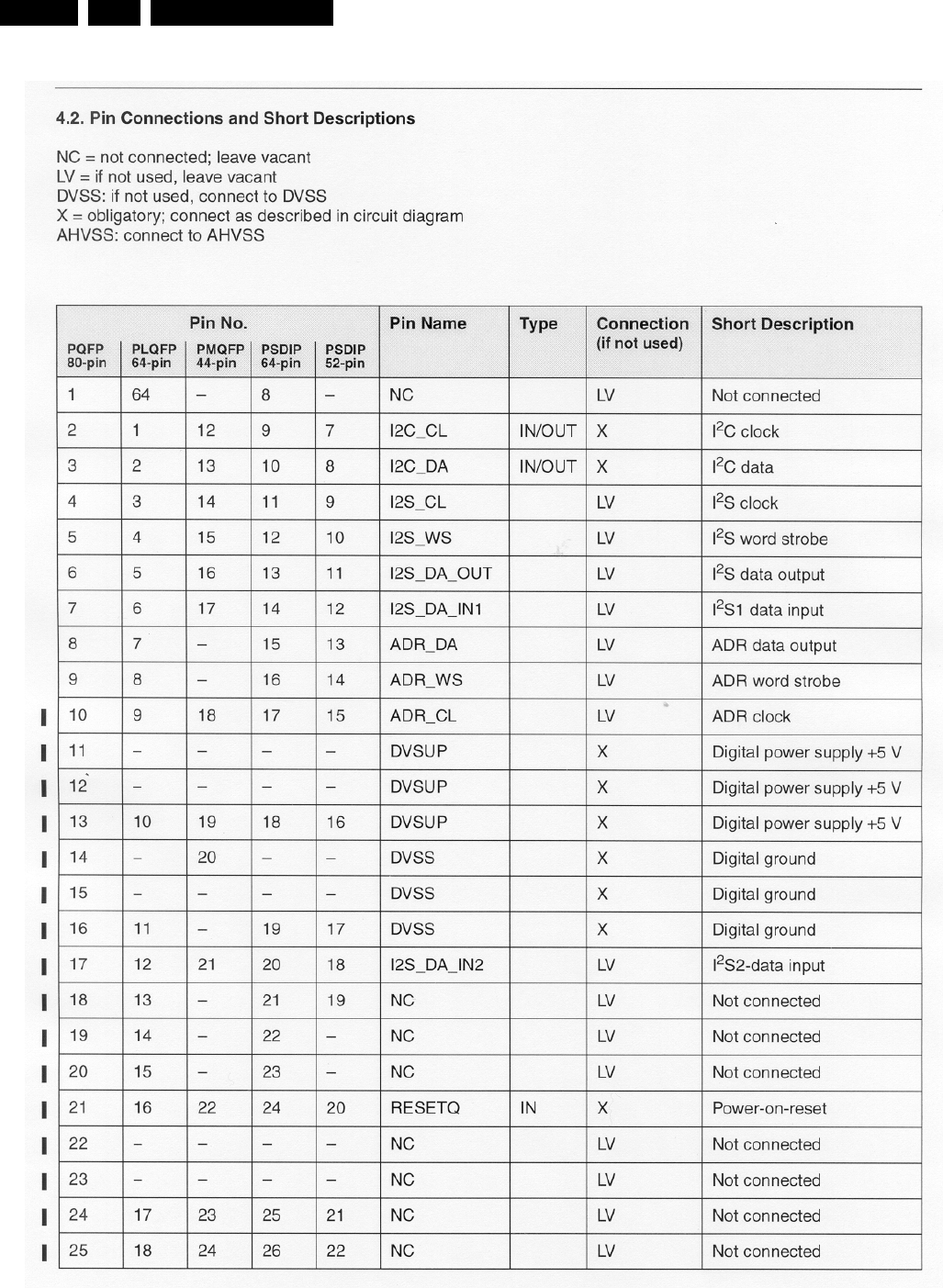
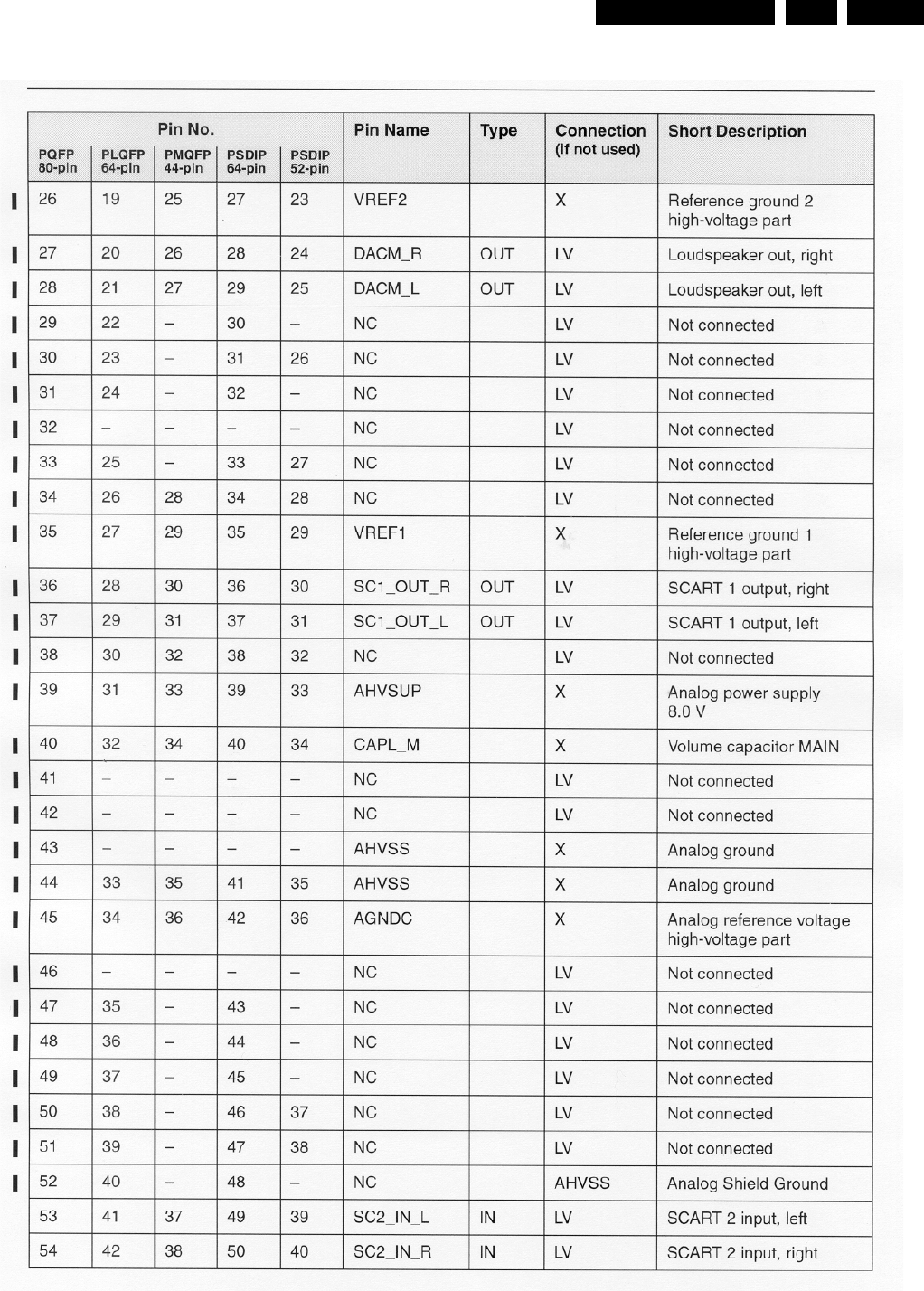
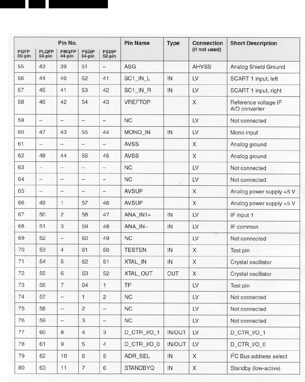
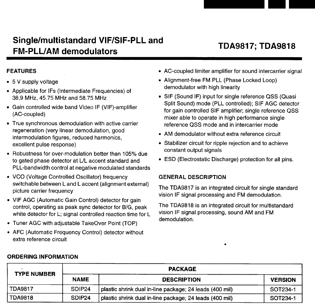
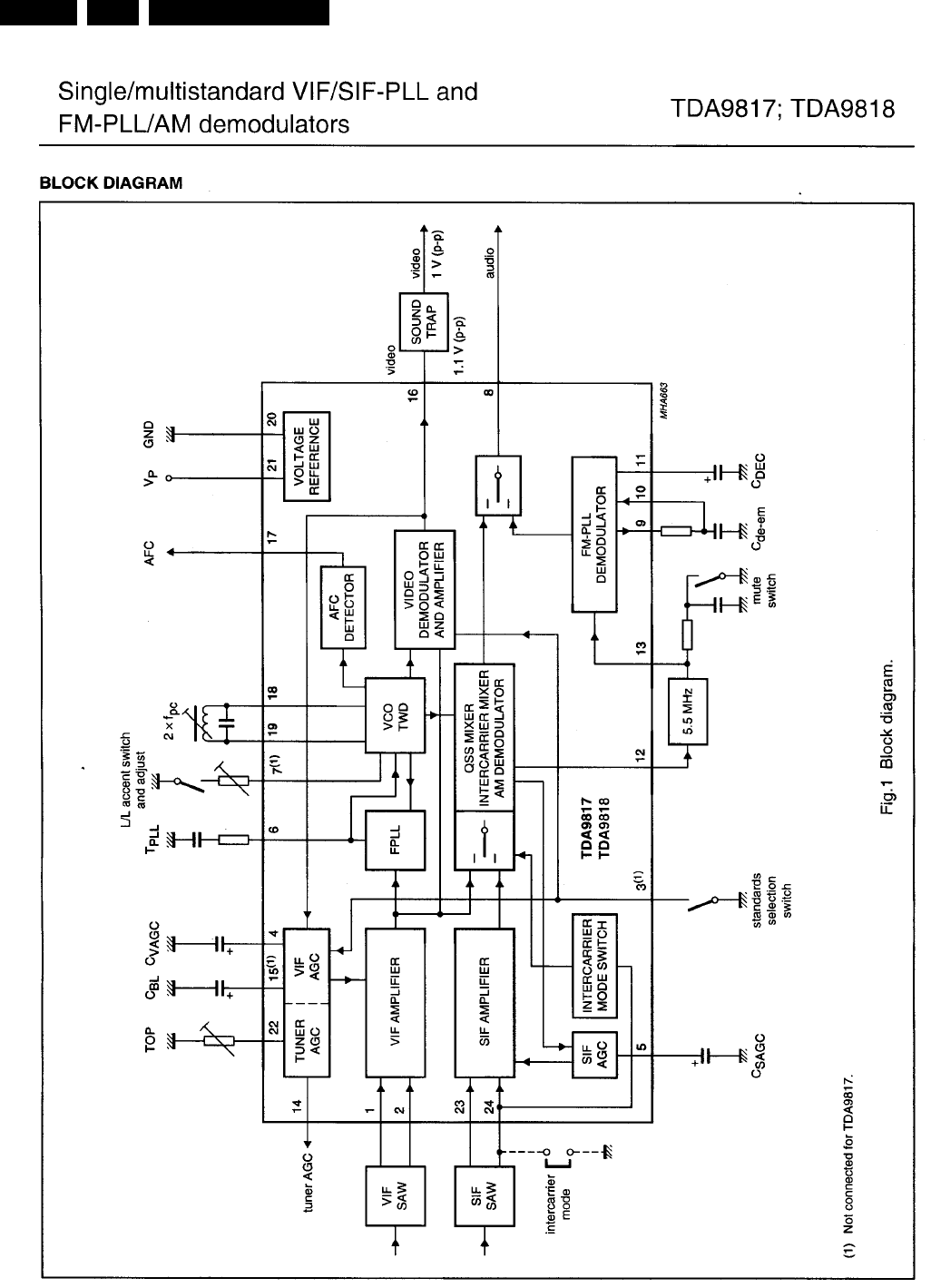
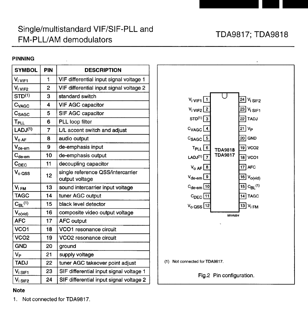
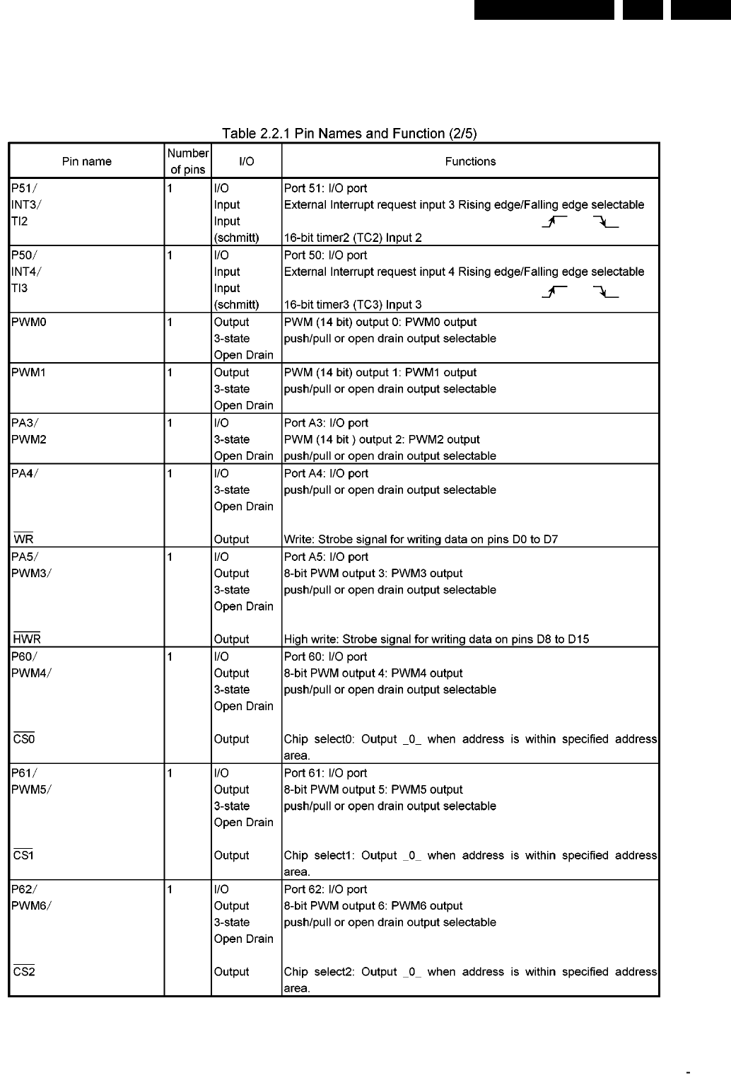
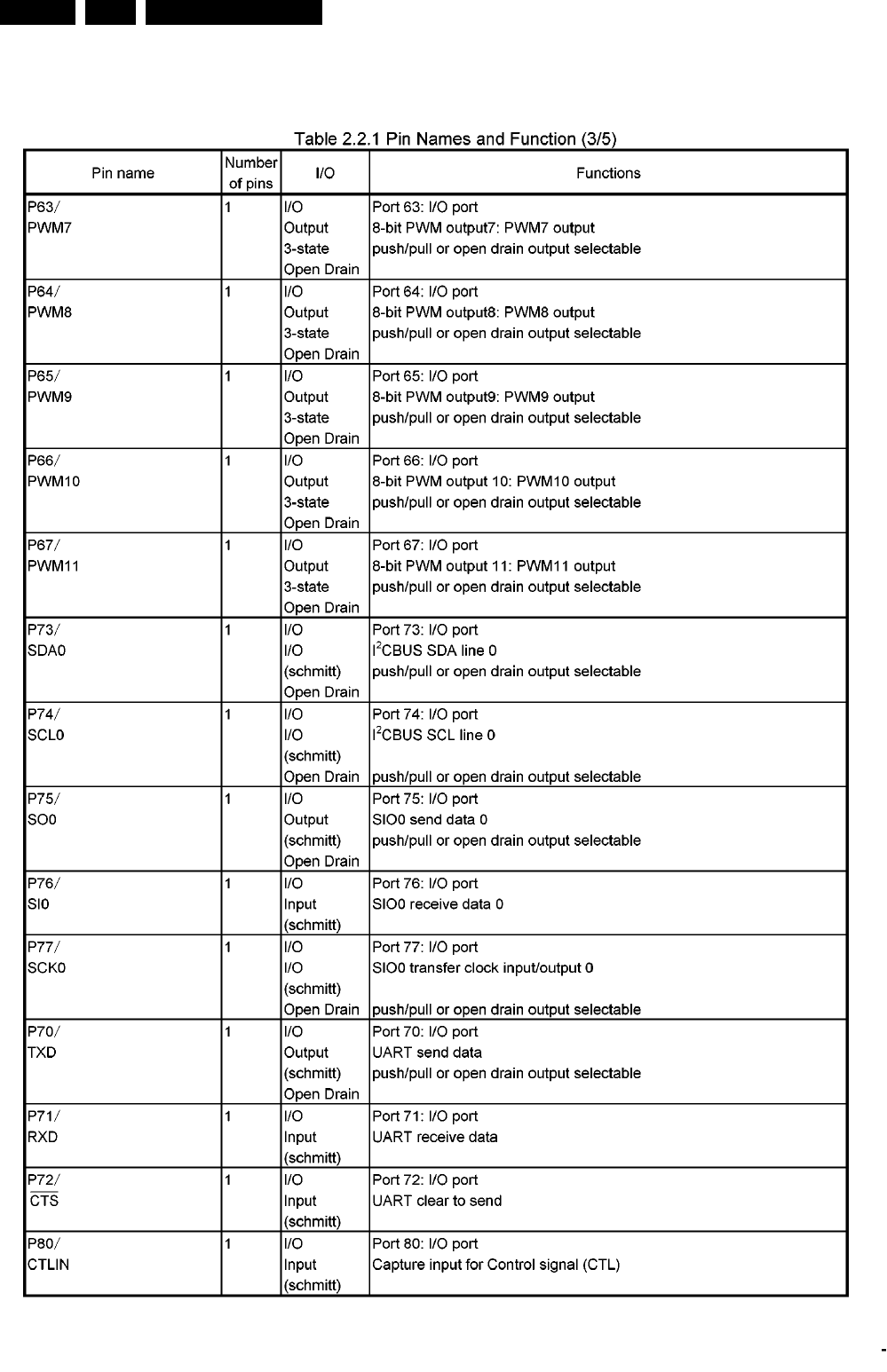
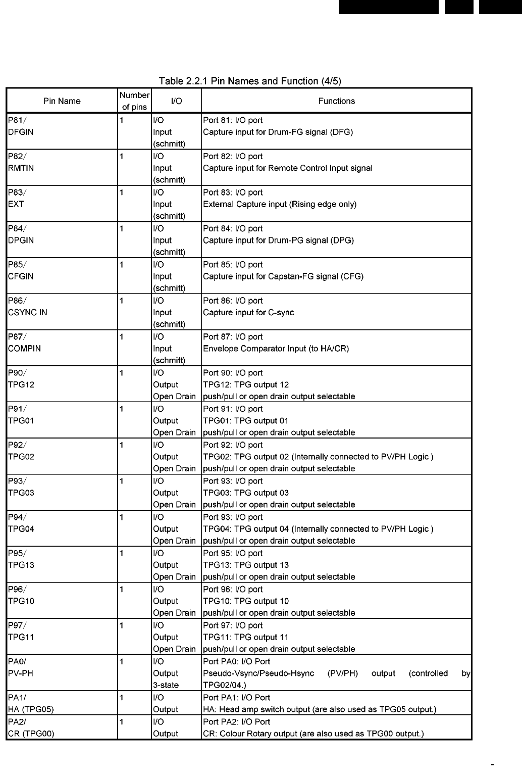
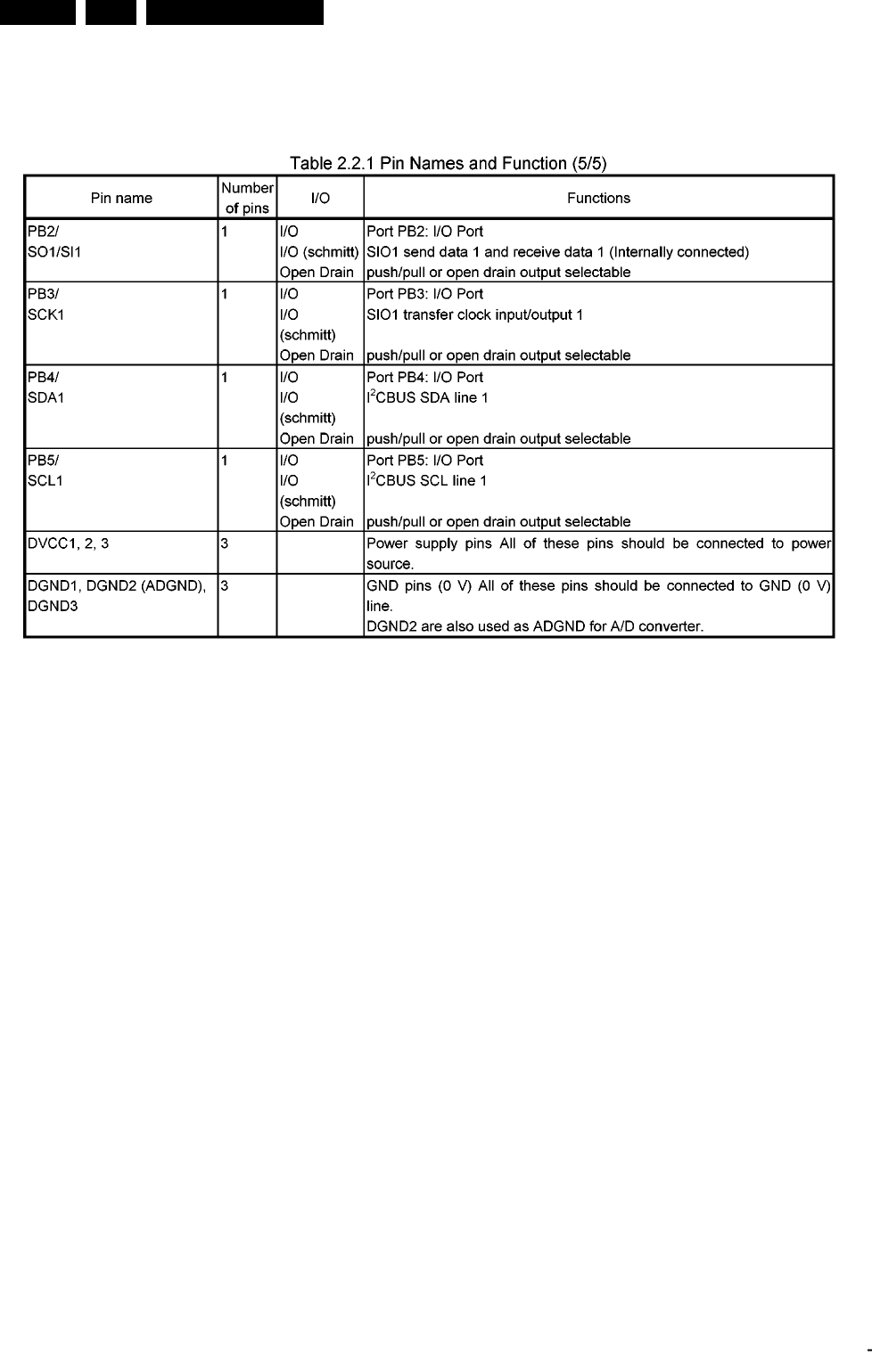
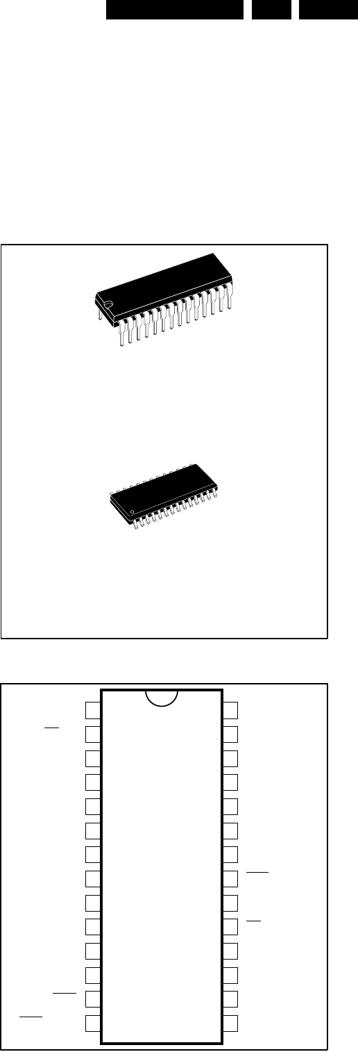
Circuit-, IC Descriptions and List of Abbreviations EN 217DVDR980-985 /0X1 9.
9.7.8 IC7990: STV5348
STV5348
.
COMPLETE TELETEXT AND VPS DECODER
INCLUDING AN 8 PAGE MEMORY ON A SIN-
GLE CHIP
.
UPWARD SOFTWARE COMPATIBLE WITH
PREVIOUS SGS-THOMSON's MULTICHIP
SOLUTIONS (SAA5231, SDA5243, STV5345)
.
PERFORM PDC SYSTEM A (VPS) AND PDC
SYSTEM B (8/30/2) DATA STORAGE SEPA-
RATLY
.
DEDICATED "ERROR FREE" OUTPUT FOR
VALID PDC DATA
.
INDICATION OF LINE 23 FOR EXTERNAL
USE
.
SINGLE +5V SUPPLY VOLTAGE
.
SINGLE 13.875MHz CRYSTAL
.
REDUCED SET OF EXTERNAL COMPO-
NENTS, NO EXTERNAL ADJUSTMENT
.
OPTIMIZED NUMBER OF DIGITAL SIGNALS
REDUCING EMC RADIATION
.
HIGH DENSITY CMOS TECHNOLOGY
.
DIGITAL DATA SLICER AND DISPLAY
CLOCK PHASE LOCK LOOP
.
28 PIN DIP & SO PACKAGE
DESCRIPTION
The STV5348 decoder is a computer-controlled
teletext device including an 8 page internal mem-
ory. Data slicing and capturing extracts the teletext
information embedded in the composite video sig-
nal. Control is accomplished via a two wire serial
I
2
C bus . Chip address is 22h. Internal ROM pro-
vides a character set suitable to display text using
up to seven national languages. Hardware and
software features allow selectable master/slave
synchronization configurations. The STV5348 also
supports facilities for reception and display of cur-
rent level protocol data.
DIP28
(Plastic Package)
ORDER CODE :
STV5348 West European
STV5348/H East European
STV5348/T Turkish & European
1
2
3
4
5
6
28
27
26
25
24
23
7
8
9
22
21
20
10 19
11 18
12 17
13 16
14 15ODD/EVEN
COR
BLAN
RGB REF
R
B
G
V
SSD
FFB
STTV/LFB
POL
V
DDA
CVBS
MA/SL
CBLK
TEST
V
SSA
V
SSO
XTI
XTO
V
DDD
VCR/TV
RESERVED
DV
L23
SDA
SCL
Y
PIN CONNECTIONS
SO28
(Plastic Package)
ORDER CODE :
STV5348D West European
STV5348D/H East European
STV5348D/T Turkish & European
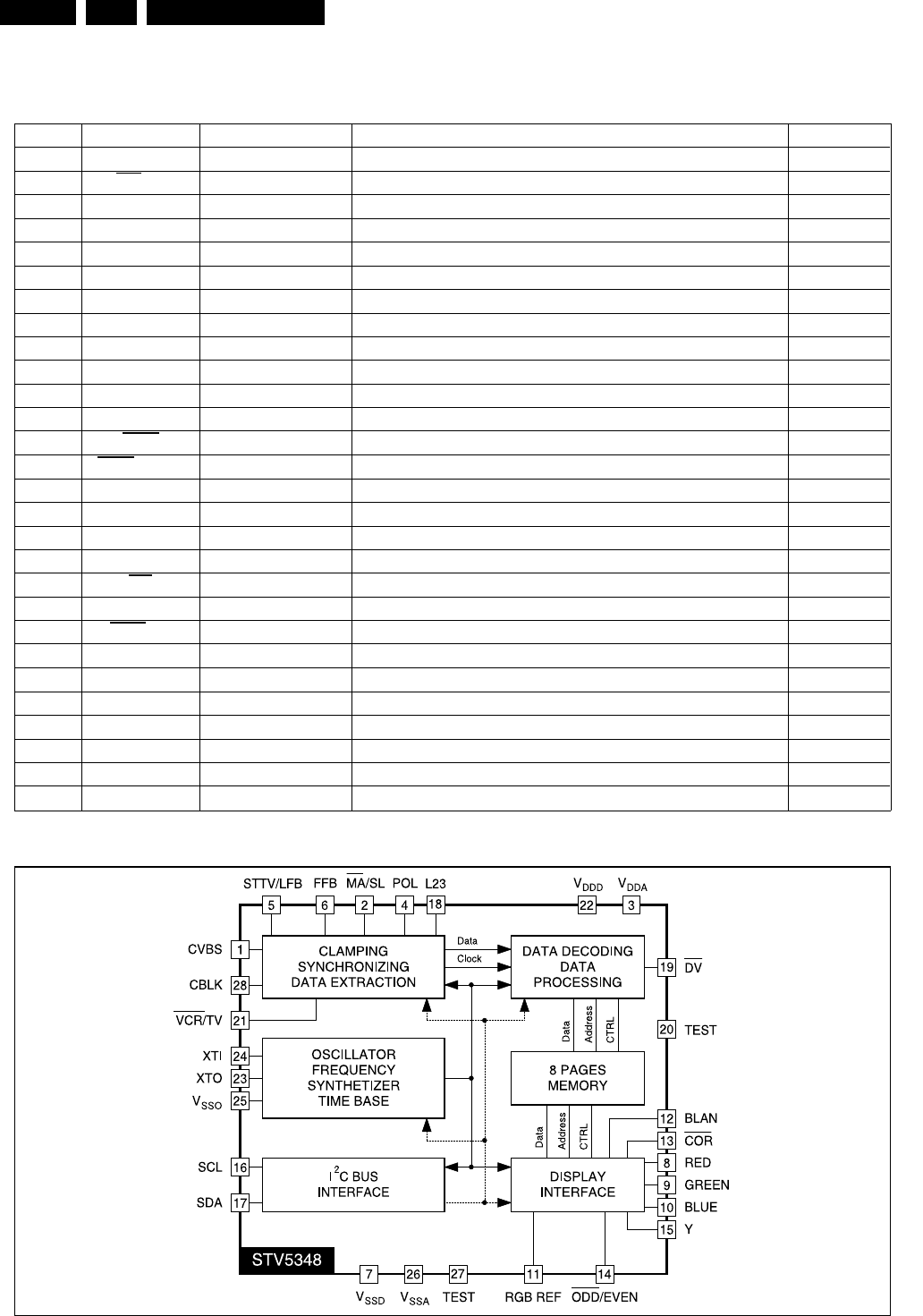
Circuit-, IC Descriptions and List of Abbreviations
EN 218 DVDR980-985 /0X19.
PIN DESCRIPTION
Pin NoSymbol Function Description Figure
1 CVBS Input Composite Video Signal Input through Coupling Capacitor 9
2MA/SL Input Master/Slave Selection Mode 11
3V
DDA Analog Supply +5V -
4 POL Input STTV / LFB / FFB Polarity Selection 12
5 STTV/LFB Output / Input Composite Sync Output, Line Flyback Input 15
6 FFB Input Field Flyback Input 12
7V
SSD Ground Digital Ground -
8 R Output Video Red Signal 13
9 G Output Video Green Signal 13
10 B Output Video Blue Signal 13
11 RGBREF Supply DC Voltage to define RGB High Level 13
12 BLAN Output Fast Blanking Output TTL Level 15
13 COR Output Open Drain Contrast Reduction Output 15
14 ODD/EVEN Output 25Hz Output Field synchronized for non-interlaced display 15
15 Y Output Open Drain Foreground Information Output 15
16 SCL Input Serial Clock Input 16
17 SDA Input/ Output Serial Data Input/Output 17
18 L23 Output Line 23 Identification 15
19 DV Output VPS Data Valid 15
20 RESERVED Test To be connected to VSSD through a resistor 15
21 VCR/TV Input PLL Time Constant Selection 15
22 VDDD Digital Supply +5V -
23 XTO Crystal Output Oscillator Output 13.875MHz 14
24 XTI Crystal Input Oscillator Input 13.875MHz 14
25 VSSO Ground Oscillator Ground -
26 VSSA Ground Analog Ground -
27 TEST Test Grounded to VSSA 11
28 CBLK Input / Output To connect Black Level Storage Capacitor 28
5348-01.TBL
BLOCK DIAGRAM

Circuit-, IC Descriptions and List of Abbreviations EN 219DVDR980-985 /0X1 9.
9.7.9 Tuner1705: UV1316K
VHF/UHF television tuner UV1336K MK3
FEATURES
Member of UV1300 MK3 family of small-sized
UHF/VHF tuners
Integrated with passive splitter
Covers systems M, N
Digitally-controlled (PLL) tuning via I2C-bus
Fast 400kHz I2C bus protocol compatible with
3.3V and 5V micro controllers
181 channels coverage ( Off-air and full cable )
World standardized mechanical dimensions and
pinning. Horizontal mounting is optionally
available.
DESCRIPTION
The UV1336K MK3 splitter - tuner belongs to the
UV1300 family of WSP tuners, which are designed to
meet a wide range of TV applications. It is a full band
tuner suitable for NTSC M, N and PAL M, N. The low
IF output impedance is designed for direct drive of a
wide variety of SAW filters with sufficient suppression
of triple transient.
The UV1336K MK3 incorporates internal wideband-
AGC with selectable TOP adjustment via I2C.
This tuner complies with the requirements of
radiation, conforming with:
FCC Part 15, Subpart B
BETS 7
CISPR13
ORDERING INFORMATION
TYPE DESCRIPTION ORDER NUMBERS
UV1336K/A F G S-3 F connector, wideband AGC, switchable FM trap 3139 147 17011
MARKING
The following items of information are
printed on a sticker that is on the top
cover of the tuner:
Type number
Code number
Origin letter of factory
Change code
Year and week code
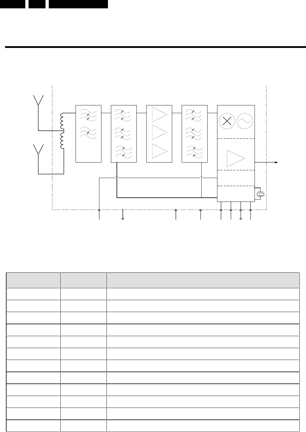
Circuit-, IC Descriptions and List of Abbreviations
EN 220 DVDR980-985 /0X19.
VHF/UHF television tuner UV1336K MK3
BLOCK DIAGRAM
PINNING
SYMBOL PIN DESCRIPTION
AGC 1 Gain Control Voltage
TU 2 Tuning voltage
AS 3 I
2
C-Bus Address Select
SCL 4 I
2
C-Bus Serial Clock
SDA 5 I
2
C-Bus Serial Data
n.c. 6 Not Connected
V
s
7 PLL Supply Voltage +5V
n.c 8 Not Connected
V
ST
9 Fixed tuning Supply Voltage +33V
n.c 10 Not connected
IF1 11 Asymmetrical IF Output
GND M1,M2,M3,M4 Mounting Tags (Ground)
Gain
controllable
Pre-amplifiers
TV IF o/p
RF i/p
AS SDASCL33V
Pre-
filtering
Tracking
filters
PLL
AGC
Detector
Mix-Osc
IF amp
Tracking
filters
RF o/p
11
VccAGC ADC**
19 73458
** ADC option not available in NTSC versions
2
Vt
(monitor)
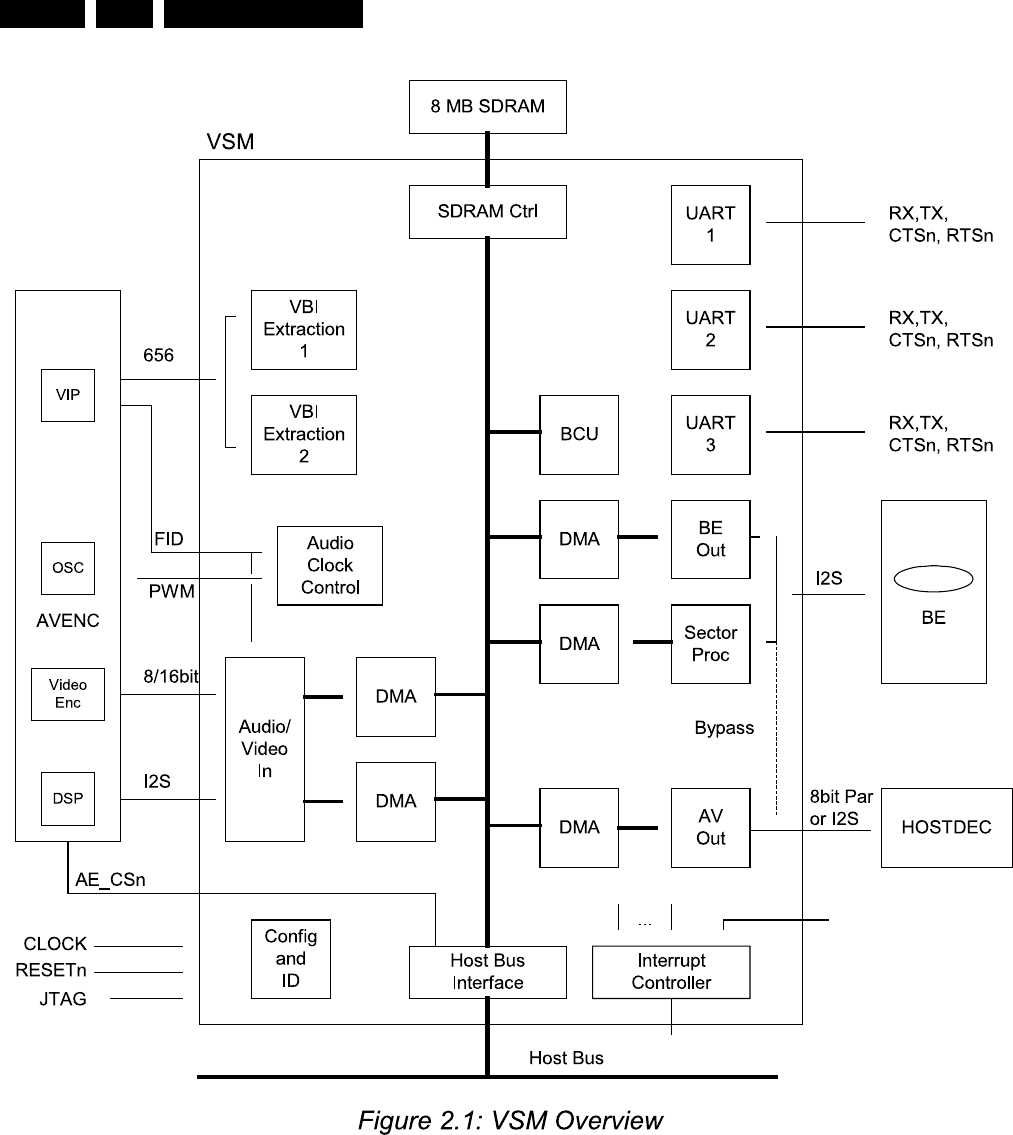
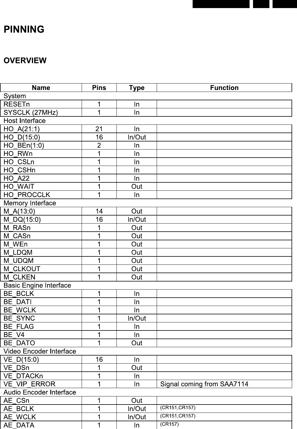
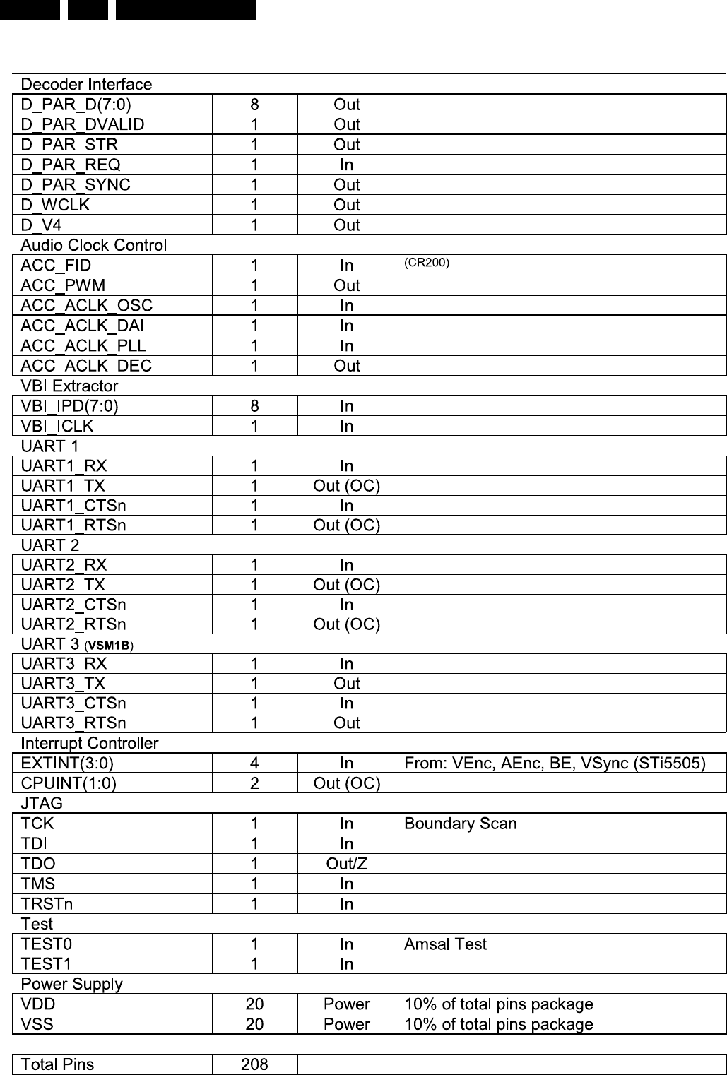
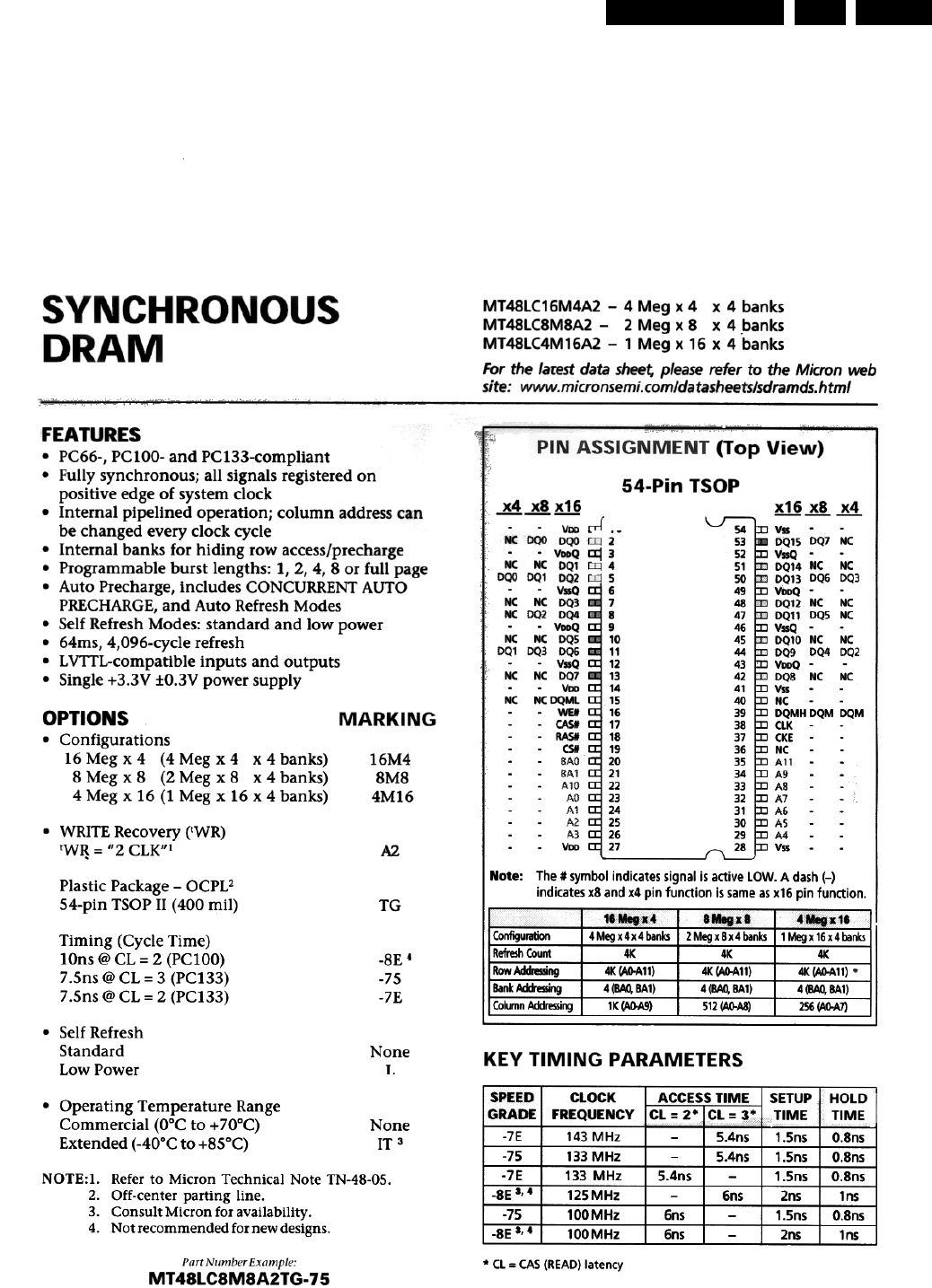
Circuit-, IC Descriptions and List of Abbreviations EN 227DVDR980-985 /0X1 9.
9.8.3 IC7200: STi5508
STi5508
DVD HOST PROCESSOR WITH ENHANCED AUDIO
FEATURES
■Integrated 32-bit host CPU @ 60MHz
•2 Kbytes of Icache, 2 Kbytes of Dcache, and
4Kbytes of SRAM configurable as Dcache.
■Audio decoder
•5.1 channel Dolby Digital® /MPEG-2 multi-channel
decoding, 3 X 2-channel PCM outputs
•IEC60958 -IEC61937 digital output
•SRS®/TruSurround®
•DTS digital out and MP3 decoding
■Karaoke processor
•Echo, pitch shift, microphone inputs, voice
cancellation and multiple other effects
■Video decoder
•Supports MPEG-2 MP@ML
•Fully programmable zoom-in and zoom-out
•PAL to NTSC and NTSC to PAL conversion
■DVD and SVCD subpicture decoder
■High performance on-screen display
•2 to 8 bits per pixel OSD options
•Anti-flicker, anti-flutter and anti-aliasing filters
■PAL/NTSC/SECAM encoder
•RGB, CVBS, Y/C and YUV outputs with 10-bit DACs
•Macrovision® 7.01/6.1 compatible
■Shared SDRAM memory interface
•Supports 1 or 2x16Mbit, or 1x64Mbit 125MHZ
SDRAM
■Programmable CPU memory interface for SDRAM,
ROM, peripherals...
■Front-end interface
•DVD, VCD, SVCD and CD-DA compatible
•Serial, parallel and ATAPI interfaces
•Hardware sector filtering
•Integrated CSS decryption and track buffer
■Integrated peripherals
•2 UARTS, 2 SmartCards, I2C controller, 3 PWM
outputs, 3 capture timers
•Modem support
•38 bits of programmable I/O
■Professional toolset support
•ANSI C compiler and libraries
■208 pin PQFP package
The STi5508 provides a highly integrated back-end
solution for DVD applications. A host CPU handles both
the general application (the user interface, and the DVD,
CD-DA, VCD, SVCD navigation) and the drivers of the
different embedded peripheral (audio/video, karaoke,
sub-picture decoders, OSD, PAL/NTSC encoder...).
Because of its memory savings, increased number of
internal peripherals, improved development platform and
reference design, the STi5508 offers a cost-effective
solution to DVD applications, with rapid time-to-market.
DMA
channels
arbitrator
Front-end interface
(sector processor
& DVD decryption)
2K
instruction
cache
2K data
cache and
4K SRAM
ST20 CPU
2 UART,
2 SmartCard,
PIO, 3PWM,
MAFE interface
Diagnostics
controller and
system services
Programmable
CPU memory
interface
MPEG2 video
Sub-picture
OSD & background
PA L /NT S C
& SECAM
Karaoke
MPEG-2 multichannel
Dolby Digital®
MP3
Circuit-, IC Descriptions and List of Abbreviations
EN 228 DVDR980-985 /0X19.
STi5508 1 Architecture overview
1 Architecture overview
1.1 Introduction
The figure below shows the architecture of the STi5508. This device has the same global architecture as the STi5505,
with the addition of new features such as karaoke, a shared SDRAM memory interface and extra display planes.
Because of this increased performance, the STi5508 and STi5505 are not pin compatible. This chapter gives a brief
overview of each of the functional blocks of the STi5508.
Figure 1 Functional block diagram
Internal peripherals
Front-end &
link interface
DMA
Central
command port
BLOCK MOVE
DEBUG
MPEG
MPEG
DMAs
Communications
arbiter
CPU
(C2+)
CLOCK
GENERATION
Refill
control
RID
Diagnostic
controller
DCACHE
SRAM
ICACHE
TAP
CPU arbiter
CACHE SUBSYSTEM
ST20 arbiter & memory controller
I/F
SDRAM
BLOCK MOVE
CD FIFOs Command I/F
SDRAM arbiter (LMC)
OSD, SP
decoder Video
filtering
DENC
Programmable
CPU interface
(EMI)
Shared SDRAM
interface (SMI)
Video
decoder
and mixing
Karaoke
processor Audio in/out
JTAG
debugging
interface
Analog/digital
video output
16, 32 or
64 Mbit
SDRAM
Ext peripherals:
Flash, additional
DRAM SDRAM
DVD
2 UART &
2 SmartCards
I2C
Audio
decoder
Circuit-, IC Descriptions and List of Abbreviations EN 229DVDR980-985 /0X1 9.
1 Architecture overview STi5508
1.2 Central processor
The STi5508 Central Processing Unit is a ST20C2+ 32-bit processor core. It contains instruction processing logic,
instruction and data pointers, and an operand register. It directly accesses the high-speed on-chip SRAM, which can
store data or programs and uses the cache to reduce access time to off-chip program and data memory.
The processor can access memory via the Programmable CPU Interface (often referred to as the EMI) or the Shared
Memory Interface (SMI), which is shared with the video, audio, sub-picture and OSD decoders.
1.3 MPEG video decoder
This is a real-time video compression processor supporting the MPEG-1 and MPEG-2 standards at video rates up to
720 x 480 x 60 Hz and 720 x 576 x 50 Hz. Picture format conversion for display is performed by vertical and horizontal
filters. User-defined bitmaps can be super-imposed on the display picture by using the on-screen display function.
The display unit is part of the MPEG video decoder, it overlays the four display planes shown in the figure below. The
display planes are normally overlaid in the order illustrated, with the background color at the back and the sub-picture
at the front (used as a cursor plane). The sub-picture plane can alternatively be positioned between the OSD and
MPEG video planes where it can be used as a second on-screen display plane.
Figure 2 Display planes
On-screen display
08:23pm
Repl ay Score St ats
Repl ay Score St ats
Sub-picture plane
08:23pm
ReplayScoreStats
08:23pm
MPEG video
Overlaid planes
Background color

Circuit-, IC Descriptions and List of Abbreviations
EN 230 DVDR980-985 /0X19.
STi5508 1 Architecture overview
1.4 Audio decoder
The audio decoder accepts: Dolby Digital, MPEG-1 layers I and II, MPEG-2 layer II 6-channel, PCM, CDDA data
formats; MPEG2 PES streams for MPEG-2, MPEG-1, Dolby Digital, MP3, and Linear PCM (LPCM). The audio decoder
supports DTS digital out (DVD DTS and CDDA DTS).
S/PDIF input data (IEC-60958 or IEC-61937 standards) is accepted if an external circuitry extracts the PCM clock from
the stream.
Skip frame, repeat blocks and soft mute frame features can be used to synchronize audio and video data. PTS audio
extraction is also supported.
The device outputs up to 6 channels of PCM data and appropriate clocks for external digital-to-analog converters.
Programmable downmix enables 1,2,3 or 4 channel outputs. Data can be output in either I²S format or Sony format. The
decoder can format output data according to IEC-60958 standard (for non compressed data: L/R channels, 16, 18, 20
and 24-bits) or IEC-61937 standard (for compressed data), for FS = 96kHz, 48kHz, 44.1kHz or 32kHz.
Sampling frequencies of 96kHz, 48kHz, 44.1kHz, 32kHz and half sampling frequencies are supported. A
downsampling filter (96kHz/48kHz) is available.
The decoder supports dual mode for MPEG and Dolby Digital. It is karaoke aware and capable in Dolby Digital and
MPEG formats according to DVD specifications. It includes a Dolby surround compatible downmix and a ProLogic
decoder.
A pink noise generator enables the accurate positioning of speakers for optimal surround sound setup.
In global mute mode, the decoder decodes the incoming bitstream normally but the PCM and SPDIF outputs are
softmuted. This mode is used to prepare a period of decoding mode, to synchronize audio and video data without
hearing the audio.
Slow-forward and fast-forward trick modes are available for compressed and non-compressed data.
The control interface of the decoder is activated via memory mapped registers in the ST20 address space.
1.5 Karaoke
The karaoke processor is a post-processing module which supports the following features: 2 micro PCM input, pitch
shift, echo effect, reverberation, chorus, voice cancellation, level-sensitive vocal cancelling, vocal partnering,
independant volume control on music and vocal channels.
1.6 Modem analog front-end interface
The Modem Analog Front-end interface is used to transfer transmit and receive DAC and ADC samples between the
memory and an external modem analog front-end (MAFE), using a synchronous serial protocol. DMA is used to
transfer the sample data between memory buffers and the MAFE interface module, with separate transmit and receive
buffers and double buffering of the buffer pointers. FIFOs are used to take into account the access latency to memory,
in a worst case system and to allow the use of bursts for memory bandwidth efficiency improvement. The V22 bis
standard is supported.
1.7 Memory subsystem
On-chip
The on-chip memory includes 2Kbytes of instruction cache, 2Kbytes of data cache and 4Kbytes of SRAM that can be
optionally configured as data cache. The subsystem provides 240M/bytes of internal bandwidth, supporting pipelined 2-
cycle internal memory access.

Circuit-, IC Descriptions and List of Abbreviations EN 231DVDR980-985 /0X1 9.
1 Architecture overview STi5508
The instruction and data caches are direct-mapped, with a write-back system for the data-cache. The caches support
burst accesses to the external memories for refill and write-back. Burst access increases the performance of page-
mode DRAM memories.
Off-chip
There are two off-chip memory interfaces:
•The external memory interface (EMI) accessed by the ST20 is used for the transfer of data and programs between
the STi5508 and external peripherals, flash and additional SDRAM and DRAM.
•Shared memory interface (SMI) controls the movement of data between the STi5508 and 16, 32 or 64 Mbits of
SDRAM. This external SDRAM stores the display data generated by the MPEG decoder and CPU and the C2+
code data.
The EMI uses minimal external support logic to support memory subsystems, and accesses a 32 Mbytes of physical
address space (greater if SDRAM or DRAM is used) in four general purpose memory banks of 8 or 16 bits wide, 21 or
22 address lines, and byte select. For applications requiring extra memory, the EMI supports this extra memory with
zero external support logic, even for 16-bit SDRAM devices. The EMI can be configured for a wide variety of timing and
decode functions by the configuration registers. The timing of each of the four memory banks can be set separately,
with different device types being placed in each bank with no need for external hardware.
1.8 Serial communication
Asynchronous serial controllers
The Asynchronous Serial Controller (ASC), also referred to as the UART interface, provides serial communication
between the STi5508 and other microcontrollers, microprocessors or external peripherals. The STi5508 has four ASCs,
two of which are generally used by the SmartCard controllers.
Eight or nine bit data transfer, parity generation, and the number of stop bits are programmable. Parity, framing, and
overrun error detection increase data transfer reliability. Transmission and reception of data can be double-buffered, or
16-deep FIFOs can be used. A mechanism to distinguish the address from the data bytes is included for multiprocessor
communication. Testing is supported by a loop-back option. A 16-bit baud-rate generator provides the ASC with a
separate serial clock signal.
Each ASC supports full-duplex asynchronous communication where both the transmitter and the receiver use the same
data frame format and the same baud-rate. Each ASC can be set to operate in SmartCard mode for use when
interfacing to a SmartCard.
Synchronous serial control
The Synchronous Serial Controller (SSC) provides a high-speed interface to a wide variety of serial memories, remote
control receivers and other microcontrollers. The SSC supports all of the features of the Serial Peripheral Interface bus
(SPI) and the I2C bus. The SSC can be programmed to interface to other serial bus standards. The SSC shares pins
with the parallel input/output (PIO) ports, and support full-duplex and half-duplex synchronous communication when
used in conjunction with the PIO configuration.
1.9 Front-end interface
The STi5508 can be connected to a front-end through the following interfaces:
•I2S interface;
•multi-format serial interface;
•multi-format parallel interface;

Circuit-, IC Descriptions and List of Abbreviations
EN 232 DVDR980-985 /0X19.
STi5508 1 Architecture overview
•ATAPI interface (for DVD-ROMs)
1.10 On-chip PLL
The on-chip PLL accepts 27 MHz input and generates all the internal high-frequency clocks needed for the CPU,
MPEG and audio subsystems.
1.11 Diagnostic controller (DCU)
The ST20 Diagnostic Controller Unit (DCU) is used to boot the CPU and to control and monitor the chip systems via the
standard IEEE 1194.1 Test Access Port. The DCU includes on-chip hardware with ICE (In Circuit Emulation) and LSA
(Logic State Analyzer) features to facilitate verification and debugging of software running on the on-chip CPU in real
time. It is an independent hardware module with a private link from the host to support real-time diagnostics.
1.12 Interrupt subsystem
The interrupt system allows an on-chip module or external interrupt pin to interrupt an active process so that an
interrupt handling process can be run. An interrupt can be signalled by one of the following: a signal on an external
interrupt pin, a signal from an internal peripheral or subsystem, software asserting an interrupt in the pending register.
Interrupts are implemented by an on-chip interrupt controller and an on-chip interrupt-level controller. The interrupt
controller supports eight prioritized interrupts as inputs and manages the pending interrupts. This allows the nesting of
pre-emptive interrupts for real-time system design. Each interrupt can be programmed to be at a lower or higher priority
than the high priority process queue.
1.13 PAL/NTSC/SECAM encoder
The integrated digital encoder converts a multiplexed 4:2:2 or 4:4:4 YCbCr stream into a standard analog baseband
PAL/NTSC or SECAM signal and into RGB, YUV, Yc and CVBS components. The encoder can perform closed-caption,
CGMS encoding, and allows MacrovisionTM 7.01/6.1 copy protection.
1.14 SmartCard interfaces
Two SmartCard interfaces support SmartCards compliant with ISO7816-3. Each interface is has a UART (ASC), a
dedicated programmable clock generator, and eight bits of parallel IO port.
1.15 PWM and counter module
The PWM and counter module provides three PWM encoder outputs, three PWM decoder (capture) inputs and four
programmable timers. Each capture input can be programmed to detect rising edge, falling edge, both edges or neither
edge (disabled). These facilities are clocked by two independent clocks, one for PWM outputs and one for capture
inputs/timers. The PWM counter is 8-bit, with 8-bit registers to set the output-high time. The capture/compare counter
and the compare and capture registers are 32-bit. The module generates a single interrupt signal.
1.16 Parallel I/O module
38 bits of parallel I/O are configured in 5 ports, and each bit is programmable as output or input. The output can be
configured as a totem-pole or open-drain driver. The input compare logic can generate an interrupt on any change of
any input bit. Many parallel IO have alternate functions and can be connected to an internal peripheral signal such as a
UART or SSC.
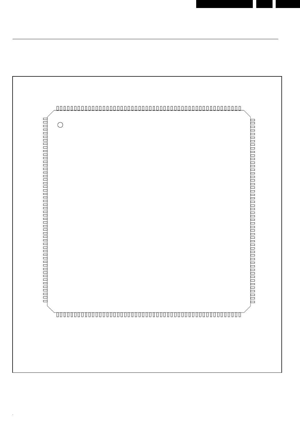
Circuit-, IC Descriptions and List of Abbreviations EN 233DVDR980-985 /0X1 9.
2 Pin data STi5508
2 Pin data
2.1 Pin out
208
207
206
205
204
203
202
201
200
199
198
197
196
195
194
193
192
191
190
189
188
187
186
185
184
183
182
181
180
179
178
177
176
175
174
173
172
171
170
169
168
167
166
165
164
163
162
161
160
159
158
157
PIO2[4]
PIO2[3]
PIO2[2]
PIO2[1]
PIO2[0]
TRIGGER_OUT
TRIGGER_IN
PIO1[5]
PIO1[4]
VSS
VDD2_5
PIO1[3]
PIO1[2]
PIO1[1]
PIO1[0]
PIO0[7]
PIO0[6]
PIO0[5]
PIO0[4]
PIO0[3]
PIO0[2]
PIO0[1]
PIO0[0]
VSS
VDD3_3
CPU_ADR[21]
CPU_ADR[20]
CPU_ADR[19]
CPU_ADR[18]
CPU_ADR[17]
CPU_ADR[16]
CPU_ADR[15]
CPU_ADR[14]
CPU_ADR[13]
CPU_ADR[12]
CPU_ADR[11]
VSS
VDD2_5
CPU_ADR[10]
CPU_ADR[9]
CPU_ADR[8]
CPU_ADR[7]
CPU_ADR[6]
CPU_ADR[5]
CPU_ADR[4]
CPU_ADR[3]
CPU_ADR[2]
CPU_ADR[1]
VSS
VDD3_3
CPU_DATA[15]
CPU_DATA[14]
1
2
3
4
5
6
7
8
9
10
11
12
13
14
15
16
17
18
19
20
21
22
23
24
25
26
27
28
29
30
31
32
33
34
35
36
37
38
39
40
41
42
43
44
45
46
47
48
49
50
51
52
PIO2[5]
PIO2[6]
PIO2[7]
VDD3_3
VSS
PIO3[0]
PIO3[1]
PIO3[2]
PIO3[3]
PIO3[4]
PIO3[5]
PIO3[6]
PIO3[7]
VDD2_5
VSS
B_DATA
B_BCLK
B_FLAG
B_SYNC
B_WCLK
B_V4
NRSS_OUT
VDD_RGB
VSS_RGB
B_OUT
G_OUT
R_OUT
V_REF_RG
I_REF_RG
VDD_YCC
VSS_YCC
Y_OUT
C_OUT
CV_OUT
V_REF_YC
I_REF_YC
VDD2_5
VSS
PIO4[0]
PIO4[1]
PIO4[2]
PIO4[3]
PIO4[4]
PIO4[5]
PIO4[6]
PIO4[7]
VDD3_3
VDD_PCM
VSS_PCM
VSS
DAC_SCLK
DAC_PCMOUT0
156
155
154
153
152
151
150
149
148
147
146
145
144
143
142
141
140
139
138
137
136
135
134
133
132
131
130
129
128
127
126
125
124
123
122
121
120
119
118
117
116
115
114
113
112
111
110
109
108
107
106
105
CPU_DATA[13]
CPU_DATA[12]
CPU_DATA[11]
CPU_DATA[10]
CPU_DATA[9]
CPU_DATA[8]
VSS
VDD2_5
CPU_DATA[7]
CPU_DATA[6]
CPU_DATA[5]
CPU_DATA[4]
CPU_DATA[3]
CPU_DATA[2]
CPU_DATA[1]
CPU_DATA[0]
CPU_CAS1
CPU_CAS0
CPU_RAS1
VSS
VDD3_3
CPU_CE[0]
CPU_CE[1]
CPU_CE[2]
CPU_CE[3]
CPU_WAIT
CPU_RW
CPU_BE[1]
CPU_BE[0]
IRQ[0]
IRQ[1]
IRQ[2]
RESET
VSS_PLL
VDD_PLL
VSS
PIX_CLK
VDD2_5
CPU_PROCLK
CPU_OE
PWM0
PWM1
PWM2
TCK
TDI
TDO
TMS
TRST
VSS
VDD3_3
ADC_PCMCLK
ADC_DATA
DAC_PCMOUT1
DAC_PCMOUT2
DAC_PCMCLK
DAC_LRCLK
SPDIF_OUT
SMI_ADR[4]
SMI_ADR[5]
SMI_ADR[6]
SMI_ADR[7]
SMI_ADR[8]
SMI_ADR[9]
VDD2_5
VSS
SMI_ADR[3]
SMI_ADR[2]
SMI_ADR[1]
SMI_ADR[0]
SMI_ADR[10]
SMI_ADR[11]
SMI_ADR[12]
SMI_ADR[13]
SMI_CS[0]
SMI_CS[1]
SMI_RAS
SMI_CAS
SMI_WE
SMI_DQML
SMI_DQMU
VDD3_3
SMI_CLKIN
VSS
SMI_DATA[0]
SMI_DATA[1]
SMI_DATA[2]
SMI_DATA[3]
SMI_DATA[4]
SMI_DATA[5]
SMI_DATA[6]
SMI_DATA[7]
SMI_DATA[8]
SMI_DATA[9]
VDD2_5
SMI_CLKOUT
VSS
SMI_DATA[10]
SMI_DATA[11]
SMI_DATA[12]
SMI_DATA[13]
SMI_DATA[14]
SMI_DATA[15]
ADC_SCLK
ADC_LRCLK
53
54
55
56
57
58
59
60
61
62
63
64
65
66
67
68
69
70
71
72
73
74
75
76
77
78
79
80
81
82
83
84
85
86
87
88
89
90
91
92
93
94
95
96
97
98
99
100
101
102
103
104
PQFP 208
(rev F)
STi5508
Circuit-, IC Descriptions and List of Abbreviations
EN 234 DVDR980-985 /0X19.
STi5508 2 Pin data
2.2 Pin list sorted by function
Alternate functions printed in
Italic
show a suggested use of the PIO; alternate functions not printed in
Italic
are
multiplexed with a specific hardware.
Pin number Pin name Main function Alternate function Type
Input Output
Audio DAC
51 DAC_SCLK OVER SAMPLING CLK EXT_AUD_CLK O
52 DAC_PCMOUT0 PCM_OUT0 EXT_AUD_DATA O
53 DAC_PCMOUT1 PCM_OUT1 EXT_AUD_REQ I/O
54 DAC_PCMOUT2 PCM_OUT2 O
55 DAC_PCMCLK PCM_CLOCK I/O
56 DAC_LRCLK LEFT/RIGHT CLK EXT_AUD_WCLK O
57 SPDIF_OUT SPDIF_OUT O
48 VDD_PCM VDD FREQ SYNTHE=2.5V PWR
2.5V
49 VSS_PCM VSS FREQ SYNTHE=GND PWR
Audio ADC input
104 ADC_LRCLK Left/Right Clock I/O
106 ADC_PCMCLK PCM CLOCK I/O
105 ADC_DATA DATA I
103 ADC_SCLK SAMPLING CLK I/O
Clock & reset
124 RESET CHIP RESET I
122 VDD_PLL VDD PLL=2.5V PWR
2.5V
123 VSS_PLL GND PLL=GND PWR
120 PIX _CLK 27 MHz main clock I
PIOs and communication
186 PIO0[0] PIO0[0] UART0_DATA
(SC0_DATA)
I/O
187 PIO0[1] PIO0[1] ATAPI_RD I/O
188 PIO0[2] PIO0[2] ATAPI_WR I/O
189 PIO0[3] PIO0[3] SC0_CLOCK I/O
190 PIO0[4] PIO0[4] SC0_RST I/O
191 PIO0[5] PIO0[5] SC0_CMD_VCC I/O
192 PIO0[6] PIO0[6] SC0_DATA_DIR I/O
193 PIO0[7] PIO0[7] SC0_DETECT I/O
194 PIO1[0] PIO1[0] SSC0_DATA (MTSROut/MRSTin) I/O
195 PIO1[1] PIO1[1] SSC0_CLOCK I/O
196 PIO1[2] PIO1[2] SC EXTERNAL
CLOCK
PARA_DVALID I/O
197 PIO1[3] PIO1[3] UART2_TXD I/O
200 PIO1[4] PIO1[4] UART2_RXD I/O
Table 1 Pins sorted by function
Circuit-, IC Descriptions and List of Abbreviations EN 235DVDR980-985 /0X1 9.
2 Pin data STi5508
201 PIO1[5] PIO1[5] PARA_SYNC UART1_TXD I/O
202 TRIGGER_IN TRIGGER_IN for DCU I/O
203 TRIGGER_OUT TRIGGER_OUT for DCU I/O
204 PIO2[0] PIO2[0] UART3_DATA
(SC1_DATA)
I/O
205 PIO2[1] PIO2[1] UART1_RXD MAFEIF_DOUT
PARA_REQ
I/O
206 PIO2[2] PIO2[2] PARA_STROBE MAFEIF_HC1 I/O
207 PIO2[3] PIO2[3] SC1_CLOCK I/O
208 PIO2[4] PIO2[4] SC1_RST I/O
1 PIO2[5] PIO2[5] SC1_CMD_VCC I/O
2 PIO2[6] PIO2[6] SC1_DATA_DIR I/O
3 PIO2[7] PIO2[7] SC1_DETECT I/O
6 PIO3[0] PIO3[0] MAFEIF_SCLK
PARA_DATA{0]
I/O
7 PIO3[1] PIO3[1] MAFEIF_DIN
PARA_DATA[1]
I/O
8 PIO3[2] PIO3[2] MAFEIF_FSI
PARA_DATA[2]
I/O
9 PIO3[3] PIO3[3] CAPTURE_IN0
PARA_DATA[3]
I/O
10 PIO3[4] PIO3[4] CAPTURE_IN1
PARA_DATA[4]
I/O
11 PIO3[5] PIO3[5] CAPTURE_IN2
PARA_DATA[5]
I/O
12 PIO3[6] PIO3[6] PARA_DATA[6] COMP_OUT1 I/O
13 PIO3[7] PIO3[7] PARA_DATA[7] COMP_OUT0 I/O
39-46 PIO4[0:7] PIO4[0:7] YC[0:7] I/O
SSC1_DATA/ NRSS_CLOCK1
SSC1_CLOCK
SDAV_CLK/ P1394_Clk2
SDAV_DATA2
SDAV_DIR / P1394_P_CLK2
OSC_IN_CLK2
EMI Interface
161-170 CPU_ADR[1:10] ADR[1:10] O
173-183 CPU_ADR[11:21] ADR[11:21] O
141-148 CPU_DATA[0:7] DATA[0:7] I/O
151-158 CPU_DATA[8:15] DATA[8:15] I/O
138 CPU_RAS1 DRAM RAS NOT_SDRAM_CS1 I/O
131 CPU_WAIT WAIT STATE I
Pin number Pin name Main function Alternate function Type
Input Output
Table 1 Pins sorted by function
Circuit-, IC Descriptions and List of Abbreviations
EN 236 DVDR980-985 /0X19.
STi5508 2 Pin data
130 CPU_RW READ-NOT WRITE NOT_SDRAM_WE O
128 CPU_BE[0] BYTE 0 ENABLE DQM[0] O
129 CPU_BE[1] BYTE 1 ENABLE DQM[1] O
139 CPU_CAS0 DRAM CAS0 SDRAM_CAS/
CPU_ADR[22]
O
140 CPU_CAS1 DRAM NOT_SDRAM_CS0 O
135 CPU_CE[0] DRAM_RAS0 SDRAM_RAS O
134 CPU_CE[1] CHIP SEL. BANK 1 O
133 CPU_CE[2] CHIP SEL. BANK 2 O
132 CPU_CE[3] CHIP SEL. BANK 3 CS_SUB_BANK3 O
118 CPU_RAM_CLK SDRAM CLOCK O
117 CPU_OE OUTPUT ENABLE I/O
Interrupt
127 IRQ[0] IRQ[0]
(SERVO_IRQ)
I
126 IRQ[1] IRQ[1]
(ATAPI IRQ)
I
125 IRQ[2] IRQ[2]
(MD_IRQ)
I
Timers
116 PWM0 Pulse Width Modula 0 HSYNC O
115 PWM1 Pulse Width Modula1 BOOT FROM ROM
3
I/O
114 PWM2 Pulse Width Modula 2 VSYNC O
JTAG
113 TCK TEST CLOCK I
112 TDI TEST DATA IN I
111 TDO TEST DATA OUT O
110 TMS TEST MODE SELECT I
109 TRST
4
TEST RESET I
Front-end
16 B_DATA I2S DATA SER_DATA I
17 B_BCLK I2S BIT CLOCK SER_BCLK I
18 B_FLAG I2S ERROR FLAG DVD SER_VALID I
19 B_SYNC I2S SECTOR/ABS TIME SER_SYNC I
20 B_WCLK I2S WORD CLOCK NRSS CLOCK I/O
21 B_V4 I2S VERSATILE INPUT PIN NRSS_IN I
22 NRSS_OUT NRSS OUT O
Video DAC
27, 26, 25 R_OUT, G_OUT, B_OUT R_OUT, G_OUT, B_OUT O
32, 33, 34 Y_OUT, C_OUT,
CV_OUT
Y_OUT, C_OUT, CV_OUT O
29 I_REF_RGB I_REF_DAC_RGB I
28 V_REF_RGB V_REF_DAC_RGB I
36 I_REF_YCC I_REF_DAC_YCC I
Pin number Pin name Main function Alternate function Type
Input Output
Table 1 Pins sorted by function
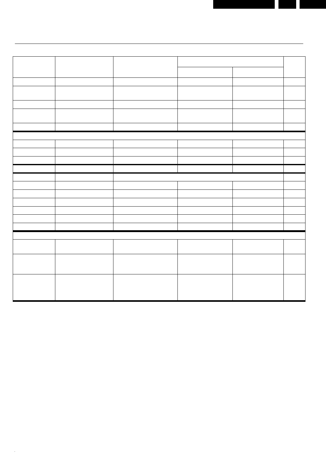
Circuit-, IC Descriptions and List of Abbreviations EN 237DVDR980-985 /0X1 9.
2 Pin data STi5508
35 V_REF_YCC V_REF_DAC_YCC I
23 VDD_RGB VDDA_RGB=2.5V PWR
2.5V
24 VSS_RGB VSSA_RGB=GND PWR
30 VDD_YCC VDDA_YCC=2.5V PWR
2.5V
31 VSS_YCC VSSA_YCC=GND PWR
Shared memory interface
69-66 SMI_ADR[0:3] Address bus SDRAM O
58-63 SMI_ADR[4:9] Address bus SDRAM O
70-73 SMI_ADR [10:13] Address bus SDRAM O
84-93, 97-102 SMI_DATA[0:15] Data bus SDRAM I/O
74, 75 SMI_CS[0,1] Chip select bank 0,1 O
76 SMI_RAS RAS SDRAM O
77 SMI_CAS CAS SDRAM O
78 SMI_WE SDRAM write enable O
79, 80 SMI_DQML, U DQ MASK EN LOW, UP O
82 SMI_CLKIN SDRAM CLOCK IN I
95 SMI_CLKOUT SDRAM CLOCK OUT O
Power supply
4, 47, 81, 107,
136, 159, 184
VDD3_3 3.3 V POWER SUPPLY PWR
14, 37, 64, 94,
119, 149, 171,
198
VDD2_5 2.5V POWER SUPPLY PWR
5, 15, 38, 50, 65,
83, 96, 108, 121,
137, 150, 160,
172, 185, 199
VSS GROUND PWR
1. FEI_CFG bits 8 and 9 must be programmed according to the required NRSS configuration.
2. Register LNK_SDAV_CONF bit 22 (SDE) must be set to 1 to validate the output path.
3. BOOTFROMROM is active during reset.
4. Tie low whenever JTAG is not used.
Pin number Pin name Main function Alternate function Type
Input Output
Table 1 Pins sorted by function
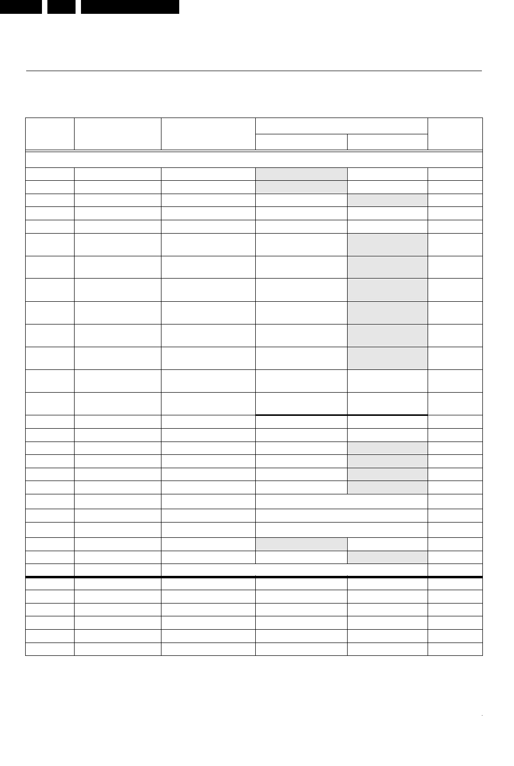
Circuit-, IC Descriptions and List of Abbreviations
EN 238 DVDR980-985 /0X19.
STi5508 2 Pin data
2.3 Pins sorted by pin number
Pin N°Pin name Main function Alternate function Dir func.
Input Output
Left Side
1 PIO2[5] PIO2[5] SC1_CMD_VCC I/O
2 PIO2[6] PIO2[6] SC1_DATA_DIR I/O
3 PIO2[7] PIO2[7] SC1_DETECT I/O
4 VDD3_3 3.3 V POWER SUPPLY POWER
5 VSS GROUND POWER
6 PIO3[0] PIO3[0] MAFEIF_SCLK
PARA_DATA{0]
I/O
7 PIO3[1] PIO3[1] MAFEIF_DIN
PARA_DATA[1]
I/O
8 PIO3[2] PIO3[2] MAFEIF_FSI
PARA_DATA[2]
I/O
9 PIO3[3] PIO3[3] CAPTURE_IN0
PARA_DATA[3]
I/O
10 PIO3[4] PIO3[4] CAPTURE_IN1
PARA_DATA[4]
I/O
11 PIO3[5] PIO3[5] CAPTURE_IN2
PARA_DATA[5]
I/O
12 PIO3[6] PIO3[6] PARA_DATA[6] COMP_OUT1 I/O
13 PIO3[7] PIO3[7] PARA_DATA[7] COMP_OUT0 I/O
14 VDD2_5 2.5V POWER SUPPLY POWER
15 VSS GROUND POWER
16 B_DATA I2S DATA SER_DATA I
17 B_BCLK I2S BIT CLOCK SER_BCLK I
18 B_FLAG I2S ERROR FLAG DVD SER_VALID I
19 B_SYNC I2S SECTOR/ABS TIME SER_SYNC I
SSC1_DATA/ NRSS_CLOCK1
SSC1_CLOCK
SDAV_CLK/ P1394_CLK2
20 B_WCLK I2S WORD CLOCK NRSS CLOCK I/O
21 B_V4 I2S VERSATILE INPUT NRSS_IN I
22 NRSS_OUT NRSS OUT O
23 VDD_RGB VDDA_RGB=2.5V POWER
24 VSS_RGB VSSA_RGB=GND POWER
25 B_OUT B_OUT O
26 G_OUT G_OUT O
27 R_OUT R_OUT O
28 V_REF_RGB V_REF_DAC_RGB I
Table 2 Pins sorted by number

Circuit-, IC Descriptions and List of Abbreviations EN 239DVDR980-985 /0X1 9.
2 Pin data STi5508
29 I_REF_RGB I_REF_DAC_RGB I
30 VDD_YCC VDDA_YCC=2.5V POWER
31 VSS_YCC VSSA_YCC=GND POWER
32 Y_OUT Y_OUT O
33 C_OUT C_OUT O
34 CV_OUT CV_OUT O
35 V_REF_YCC V_REF_DAC_YCC I
36 I_REF_YCC I_REF_DAC_YCC I
37 VDD2_5 2.5V POWER SUPPLY POWER
38 VSS GROUND POWER
39 PIO4[0] PIO4[0] YC[0] I/O
40 PIO4[1] PIO4[1] YC[1] I/O
41 PIO4[2] PIO4[2] YC[2] I/O
42 PIO4[3] PIO4[3] YC[3] I/O
43 PIO4[4] PIO4[4] YC[4] I/O
44 PIO4[5] PIO4[5] YC[5] I/O
45 PIO4[6] PIO4[6] YC[6] I/O
46 PIO4[7] PIO4[7] YC[7] I/O
47 VDD3_3 3.3 V POWER SUPPLY POWER
48 VDD_PCM VDD FREQ SYNTH=2.5V POWER
49 VSS_PCM VSS FREQ SYNTH=GND POWER
50 VSS GROUND POWER
51 DAC_SCLK SAMPLING CLK EXT_AUD_CLK O
52 DAC_PCMOUT0 PCM_OUT0 EXT_AUD_DATA O
Bottom side
53 DAC_PCMOUT1 PCM_OUT1 EXT_AUD_REQ I/O
54 DAC_PCMOUT2 PCM_OUT2 O
55 DAC_PCMCLK PCM_CLOCK I/O
56 DAC_LRCLK LEFT/RIGHT CLK EXT_AUD_WCLK O
57 SPDIF_OUT SPDIF_OUT O
58 SMI_ADR[4] Adress bus SDRAM O
59 SMI_ADR[5] Adress bus SDRAM O
60 SMI_ADR[6] Adress bus SDRAM O
61 SMI_ADR[7] Adress bus SDRAM O
62 SMI_ADR[8] Adress bus SDRAM O
63 SMI_ADR[9] Adress bus SDRAM O
64 VDD2_5 2.5V POWER SUPPLY POWER
65 VSS GROUND POWER
66 SMI_ADR[3] Adress bus SDRAM O
67 SMI_ADR[2] Adress bus SDRAM O
Pin N°Pin name Main function Alternate function Dir func.
Input Output
Table 2 Pins sorted by number

Circuit-, IC Descriptions and List of Abbreviations
EN 240 DVDR980-985 /0X19.
STi5508 2 Pin data
68 SMI_ADR[1] Adress bus SDRAM O
69 SMI_ADR[0] Adress bus SDRAM O
70 SMI_ADR[10] Adress bus SDRAM O
71 SMI_ADR[11] Adress bus SDRAM O
72 SMI_ADR[12] Adress bus SDRAM O
73 SMI_ADR[13] Adress bus SDRAM O
74 SMI_CS[0] Chip select bank 0 O
75 SMI_CS[1] Chip select bank 1 O
76 SMI_RAS RAS SDRAM O
77 SMI_CAS CAS SDRAM O
78 SMI_WE SDRAM write enable O
79 SMI_DQML DQ MASK EN LOW O
80 SMI_DQMU DQ MASK EN UP O
81 VDD3_3 3.3 V POWER SUPPLY POWER
82 SMI_CLKIN SDRAM CLOCK IN I
83 VSS GROUND POWER
84 SMI_DATA[0] Data bus SDRAM I/O
85 SMI_DATA[1] Data bus SDRAM I/O
86 SMI_DATA[2] Data bus SDRAM I/O
87 SMI_DATA[3] Data bus SDRAM I/O
88 SMI_DATA[4] Data bus SDRAM I/O
89 SMI_DATA[5] Data bus SDRAM I/O
90 SMI_DATA[6] Data bus SDRAM I/O
91 SMI_DATA[7] Data bus SDRAM I/O
92 SMI_DATA[8] Data bus SDRAM I/O
93 SMI_DATA[9] Data bus SDRAM I/O
94 VDD2_5 2.5V POWER SUPPLY POWER
95 SMI_CLKOUT SDRAM CLOCK OUT O
96 VSS GROUND POWER
97 SMI_DATA[10] Data bus SDRAM I/O
98 SMI_DATA[11] Data bus SDRAM I/O
99 SMI_DATA[12] Data bus SDRAM I/O
100 SMI_DATA[13] Data bus SDRAM I/O
101 SMI_DATA[14] Data bus SDRAM I/O
102 SMI_DATA[15] Data bus SDRAM I/O
103 ADC_SCLK SAMPLING CLK I/O
104 ADC_LRCLK Left/Right Clock I/O
SDAV_DATA2
Sdav_dir / P1394_P_CLK2
Right side
Pin N°Pin name Main function Alternate function Dir func.
Input Output
Table 2 Pins sorted by number
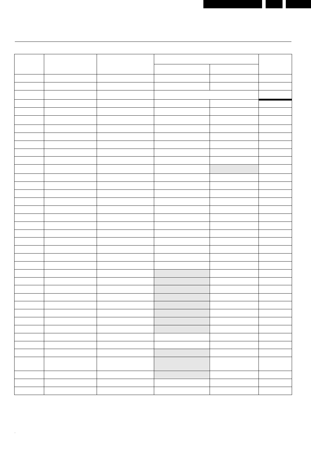
Circuit-, IC Descriptions and List of Abbreviations EN 241DVDR980-985 /0X1 9.
2 Pin data STi5508
105 ADC_DATA DATA I
106 ADC_PCMCLK PCM CLOCK I/O
OSC_IN_CLK2
107 VDD3_3 3.3 V POWER SUPPLY POWER
108 VSS GROUND POWER
109 TRST3TEST RESET I
110 TMS TEST MODE SELECT I
111 TDO TEST DATA OUT O
112 TDI TEST DATA IN I
113 TCK TEST CLOCK I
114 PWM2 Pulse Width Modul 2 VSYNC O
115 PWM1 Pulse Width Modul 1 BOOT_FROM_ROM4I/O
116 PWM0 Pulse Width Modul 0 HSYNC O
117 CPU_OE OUTPUT ENABLE I/O
118 CPU_RAM_CLK SDRAM CLOCK O
119 VDD2_5 2.5V POWER SUPPLY POWER
120 PIX _CLK 27 MHz main clock I
121 VSS GROUND POWER
122 VDD_PLL VDD PLL=2.5V POWER
123 VSS_PLL GND PLL=GND POWER
124 RESET CHIP RESET I
125 IRQ[2] IRQ[2]
(MD_IRQ)
I
126 IRQ[1] IRQ[1]
(ATAPI IRQ)
I
127 IRQ[0] IRQ[0]
(SERVO_IRQ)
I
128 CPU_BE[0] BYTE 0 ENABLE DQM[0] O
129 CPU_BE[1] BYTE 1 ENABLE DQM[1] O
130 CPU_RW READ-NOT WRITE NOT_SDRAM_WE O
131 CPU_WAIT WAIT STATE I
132 CPU_CE[3] CHIP SEL. BANK 3 CS_SUB_BANK3 O
133 CPU_CE[2] CHIP SEL. BANK 2 O
134 CPU_CE[1] CHIP SEL. BANK 1 O
135 CPU_CE[0] DRAM_RAS0 SDRAM_RAS O
136 VDD3_3 3.3 V POWER SUPPLY POWER
137 VSS GROUND POWER
138 CPU_RAS1 DRAM RAS NOT_SDRAM_CS1 I/O
139 CPU_CAS0 DRAM CAS0 SDRAM_CAS/
CPU_ADR[22]
O
140 CPU_CAS1 DRAM NOT_SDRAM_CS0 O
141 CPU_DATA[0] DATA[0] I/O
142 CPU_DATA[1] DATA[1] I/O
Pin N°Pin name Main function Alternate function Dir func.
Input Output
Table 2 Pins sorted by number
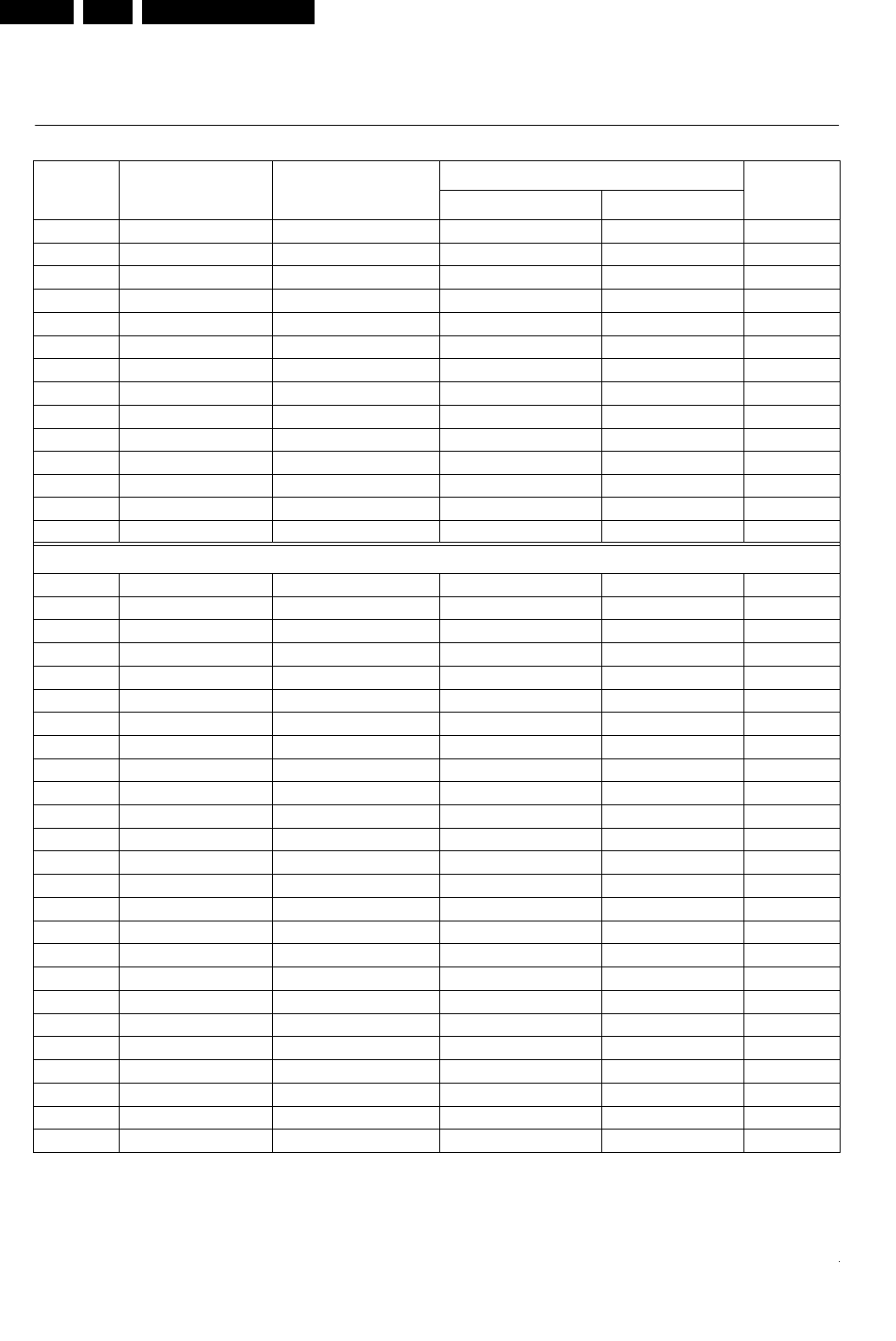
Circuit-, IC Descriptions and List of Abbreviations
EN 242 DVDR980-985 /0X19.
STi5508 2 Pin data
143 CPU_DATA[2] DATA[2] I/O
144 CPU_DATA[3] DATA[3] I/O
145 CPU_DATA[4] DATA[4] I/O
146 CPU_DATA[5] DATA[5] I/O
147 CPU_DATA[6] DATA[6] I/O
148 CPU_DATA[7] DATA[7] I/O
149 VDD2_5 2.5V POWER SUPPLY POWER
150 VSS GROUND POWER
151 CPU_DATA[8] DATA[8] I/O
152 CPU_DATA[9] DATA[9] I/O
153 CPU_DATA[10] DATA[10] I/O
154 CPU_DATA[11] DATA[11] I/O
155 CPU_DATA[12] DATA[12] I/O
156 CPU_DATA[13] DATA[13] I/O
Top side
157 CPU_DATA[14] DATA[14] I/O
158 CPU_DATA[15] DATA[15] I/O
159 VDD3_3 3.3 V POWER SUPPLY POWER
160 VSS GROUND POWER
161 CPU_ADR[1] ADR[1] O
162 CPU_ADR[2] ADR[2] O
163 CPU_ADR[3] ADR[3] O
164 CPU_ADR[4] ADR[4] O
165 CPU_ADR[5] ADR[5] O
166 CPU_ADR[6] ADR[6] O
167 CPU_ADR[7] ADR[7] O
168 CPU_ADR[8] ADR[8] O
169 CPU_ADR[9] ADR[9] O
170 CPU_ADR[10] ADR[10] O
171 VDD2_5 2.5V POWER SUPPLY POWER
172 VSS GROUND POWER
173 CPU_ADR[11] ADR[11] O
174 CPU_ADR[12] ADR[12] O
175 CPU_ADR[13] ADR[13] O
176 CPU_ADR[14] ADR[14] O
177 CPU_ADR[15] ADR[15] O
178 CPU_ADR[16] ADR[16] O
179 CPU_ADR[17] ADR[17] O
180 CPU_ADR[18] ADR[18] O
181 CPU_ADR[19] ADR[19] O
Pin N°Pin name Main function Alternate function Dir func.
Input Output
Table 2 Pins sorted by number
Circuit-, IC Descriptions and List of Abbreviations EN 243DVDR980-985 /0X1 9.
2 Pin data STi5508
182 CPU_ADR[20] ADR[20] O
183 CPU_ADR[21] ADR[21] O
184 VDD3_3 3.3 V POWER SUPPLY POWER
185 VSS GROUND POWER
186 PIO0[0] PIO0[0] UART0_DATA
(SC0_DATA)
I/O
187 PIO0[1] PIO0[1] ATAPI_RD I/O
188 PIO0[2] PIO0[2] ATAPI_WR I/O
189 PIO0[3] PIO0[3] SC0_CLOCK I/O
190 PIO0[4] PIO0[4] SC0_RST I/O
191 PIO0[5] PIO0[5] SC0_CMD_VCC I/O
192 PIO0[6] PIO0[6] SC0_DATA_DIR I/O
193 PIO0[7] PIO0[7] SC0_DETECT I/O
194 PIO1[0] PIO1[0] SSC0_DATA I/O
195 PIO1[1] PIO1[1] SSC0_CLOCK I/O
196 PIO1[2] PIO1[2] SC EXTERNAL CLOCK PARA_DVALID I/O
197 PIO1[3] PIO1[3] UART2_TXD I/O
198 VDD2_5 2.5V POWER SUPPLY POWER
199 VSS GROUND POWER
200 PIO1[4] PIO1[4] UART2_RXD I/O
201 PIO1[5] PIO1[5] PARA_SYNC UART1_TXD I/O
202 TRIGGER_IN TRIGGER_IN for DCU I/O
203 TRIGGER_OUT TRIGGER_OUT for DCU I/O
204 PIO2[0] PIO2[0] UART3_DATA
(SC1_DATA)
I/O
205 PIO2[1] PIO2[1] UART1_RXD MAFEIF_DOUT
PARA_REQ
I/O
206 PIO2[2] PIO2[2] PARA_STROBE MAFEIF_HC1 I/O
207 PIO2[3] PIO2[3] SC1_CLOCK I/O
208 PIO2[4] PIO2[4] SC1_RST I/O
1. FEI_CFG bits 8 and 9 must be programmed according to the required NRSS configuration.
2. Register LNK_SDAV_CONF bit 22 (SDE) must be set to 1 to validate the output path.
3. Tie low whenever JTAG is not used
4. BOOTFROMROM is active during reset.
Pin N°Pin name Main function Alternate function Dir func.
Input Output
Table 2 Pins sorted by number
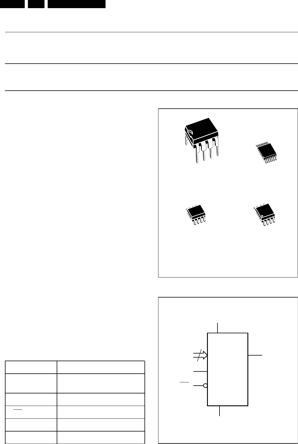
Circuit-, IC Descriptions and List of Abbreviations
EN 244 DVDR980-985 /0X19.
9.8.4 IC7201: NVRAM
M24C64
M24C32
64/32 Kbit Serial I²C Bus EEPROM
■
Compatible with I
2
C Extended Addressing
■
Two Wire I
2
C Serial Interface
Supports 400 kHz Protocol
■
Single Supply Voltage:
–4.5V to 5.5V for M24Cxx
–2.5V to 5.5V for M24Cxx-W
–1.8V to 3.6V for M24Cxx-R
■
Hardware Write Control
■
BYTE and PAGE WRITE (up to 32 Bytes)
■
RANDOM and SEQUENTIAL READ Modes
■
Self-Timed Programming Cycle
■
Automatic Address Incrementing
■
Enhanced ESD/Latch-Up Behavior
■
1 Million Erase/Write Cycles (minimum)
■
40 Year Data Retention (minimum)
DESCRIPTION
These I
2
C-compatible electrically erasable pro-
grammable memory (EEPROM) devices are orga-
nized as 8192x8 bits (M24C64) and 4096x8 bits
(M24C32), and operate down to 2.5 V (for the -W
version of each device), and down to 1.8 V (for the
-R version of each device).
The M24C64 and M24C32 are available in Plastic
Dual-in-Line, Plastic Small Outline and Thin Shrink
Small Outline packages.
Figure 1. Logic Diagram
AI01844B
3
E0-E2 SDA
VCC
M24C64
M24C32
WC
SCL
VSS
Table 1. Signal Names
E0, E1, E2 Chip Enable Inputs
SDA Serial Data/Address Input/
Output
SCL Serial Clock
WC Write Control
V
CC
Supply Voltage
V
SS
Ground
PSDIP8 (BN)
0.25 mm frame
SO8 (MN)
150 mil width
TSSOP14 (DL)
169 mil width
8
1
8
1
14
1
SO8 (MW)
200 mil width
8
1
Circuit-, IC Descriptions and List of Abbreviations EN 245DVDR980-985 /0X1 9.
M24C64, M24C32
These memory devices are compatible with the
I
2
C extended memory standard. This is a two wire
serial interface that uses a bi-directional data bus
and serial clock. The memory carries a built-in 4-
bit unique Device Type Identifier code (1010) in
accordance with the I
2
C bus definition.
The memory behaves as a slave device in the I
2
C
protocol, with all memory operations synchronized
by the serial clock. Read and Write operations are
initiated by a START condition, generated by the
bus master. The START condition is followed by a
Device Select Code and RW bit (as described in
Table 3), terminated by an acknowledge bit.
When writing data to the memory, the memory in-
serts an acknowledge bit during the 9
th
bit time,
following the bus master's 8-bit transmission.
Figure 2A. DIP Connections
Figure 2B. SO Connections
SDAVSS
SCL
WCE1
E0 VCC
E2
AI01845B
M24C64
M24C32
1
2
3
4
8
7
6
5
1
AI01846B
2
3
4
8
7
6
5SDAVSS
SCL
WCE1
E0 VCC
E2
M24C64
M24C32
Figure 2C. TSSOP Connections
Note: 1. NC = Not Connected
1
AI02129
2
3
7
14
13
12
8SDAVSS
NC
WCE1
E0 VCC
NC
M24C64
M24C32
SCL
NCNC
NC NC
E2
4
5
11
10
69
Table 2. Absolute Maximum Ratings
1
Note: 1. Except for the rating “Operating Temperature Range”, stresses above those listed in the Table “Absolute Maximum Ratings” may
cause permanent damage to the device. These are stress ratings only, and operation of the device at these or any other conditions
above those indicated in the Operating sections of this specification is not implied. Exposure to Absolute Maximum Rating condi-
tions for extended periods may affect device reliability. Refer also to the ST SURE Program and other relevant quality documents.
2. MIL-STD-883C, 3015.7 (100 pF, 1500 Ω)
Symbol Parameter Value Unit
TAAmbient Operating Temperature -40 to 125 ˚C
TSTG Storage Temperature -65 to 150 ˚C
TLEAD Lead Temperature during Soldering
PSDIP8: 10 sec
SO8: 40 sec
TSSOP14: t.b.c.
260
215
t.b.c.
˚C
VIO Input or Output range -0.6 to 6.5 V
VCC Supply Voltage -0.3 to 6.5 V
VESD Electrostatic Discharge Voltage (Human Body model)
2
4000 V
Circuit-, IC Descriptions and List of Abbreviations
EN 246 DVDR980-985 /0X19.
9.8.5 IC7301; IC7302: FLASH
1/29
PRELIMINARY DATA
January 2001
This is preliminary information on a new product now in development or undergoing evaluation. Details are subject to change without notice.
M29W160DT
M29W160DB
16 Mbit (2Mb x8 or 1Mb x16, Boot Block)
3V Supply Flash Memory
FEATURES SUMMARY
■SINGLE 2.7 to 3.6V SUPPLY VOLTAGE for
PROGRAM, ERASE and READ OPERATIONS
■ACCESS TIME: 70ns
■PROGRAMMING TIME
–10µs per Byte/Word typical
■35 MEMORY BLOCKS
–1 Boot Block (Top or Bottom Location)
–2 Parameter and 32 Main Blocks
■PROGRAM/ERASE CONTROLLER
–Embedded Program and Erase algorithms
■ERASE SUSPEND and RESUME MODES
–Read and Program another Block during
Erase Suspend
■UNLOCK BYPASS PROGRAM COMMAND
–Faster Production/Batch Programming
■TEMPORARY BLOCK UNPROTECTION
MODE
■SECURITY MEMORY BLOCK
■LOW POWER CONSUMPTION
–Standby and Automatic Standby
■100,000 PROGRAM/ERASE CYCLES per
BLOCK
■ELECTRONIC SIGNATURE
–Manufacturer Code: 0020h
–Top Device Code M29W160DT: 22C4h
–Bottom Device Code M29W160DB: 2249h
Figure 1. Packages
44
1
TSOP48 (N)
12 x 20mm
SO44 (M)
LFBGA48 (ZA)
8 x 6 solder balls
FBGA
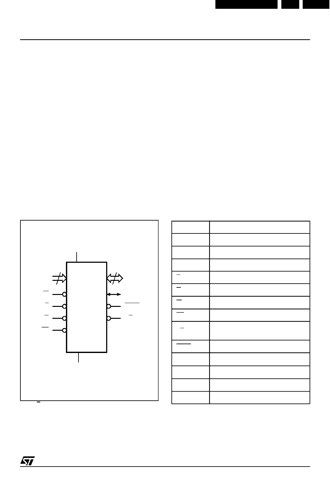
Circuit-, IC Descriptions and List of Abbreviations EN 247DVDR980-985 /0X1 9.
5/29
M29W160DT, M29W160DB
SUMMARY DESCRIPTION
The M29W160D is a 16 Mbit (2Mb x8 or 1Mb x16)
non-volatile memory that can be read, erased and
reprogrammed. These operations can be per-
formed using a single low voltage (2.7 to 3.6V)
supply. On power-up the memory defaults to its
Read mode where it can be read in the same way
as a ROM or EPROM.
The memory is divided into blocks that can be
erased independently so it is possible to preserve
valid data while old data is erased. Each block can
be protected independently to prevent accidental
Program or Erase commands from modifying the
memory. Program and Erase commands are writ-
ten to the Command Interface of the memory. An
on-chip Program/Erase Controller simplifies the
process of programming or erasing the memory by
taking care of all of the special operations that are
required to update the memory contents.
The end of a program or erase operation can be
detected and any error conditions identified. The
command set required to control the memory is
consistent with JEDEC standards.
The blocks in the memory are asymmetrically ar-
ranged, see Tables 2 and 3, Block Addresses. The
first or last 64 Kbytes have been divided into four
additional blocks. The 16 Kbyte Boot Block can be
used for small initialization code to start the micro-
processor, the two 8 Kbyte Parameter Blocks can
be used for parameter storage and the remaining
32K is a small Main Block where the application
may be stored.
Chip Enable, Output Enable and Write Enable sig-
nals control the bus operation of the memory.
They allow simple connection to most micropro-
cessors, often without additional logic.
The memory is offered in TSOP48 (12 x 20mm),
SO44 and LFBGA48 (0.8mm pitch) packages and
it is supplied with all the bits erased (set to ’1’).
Figure 2. Logic Diagram
Note: RB not available on SO44 package.
Table 1. Signal Names
AI03843
20
A0-A19
W
DQ0-DQ14
VCC
M29W160DT
M29W160DB
E
VSS
15
G
RP
DQ15A–1
BYTE
RB
A0-A19 Address Inputs
DQ0-DQ7 Data Inputs/Outputs
DQ8-DQ14 Data Inputs/Outputs
DQ15A–1 Data Input/Output or Address Input
E Chip Enable
G Output Enable
W Write Enable
RP Reset/Block Temporary Unprotect
RB Ready/Busy Output
(Not available on SO44 package)
BYTE Byte/Word Organization Select
VCC Supply Voltage
VSS Ground
NC Not Connected Internally
DU Don’t Use as internally connected
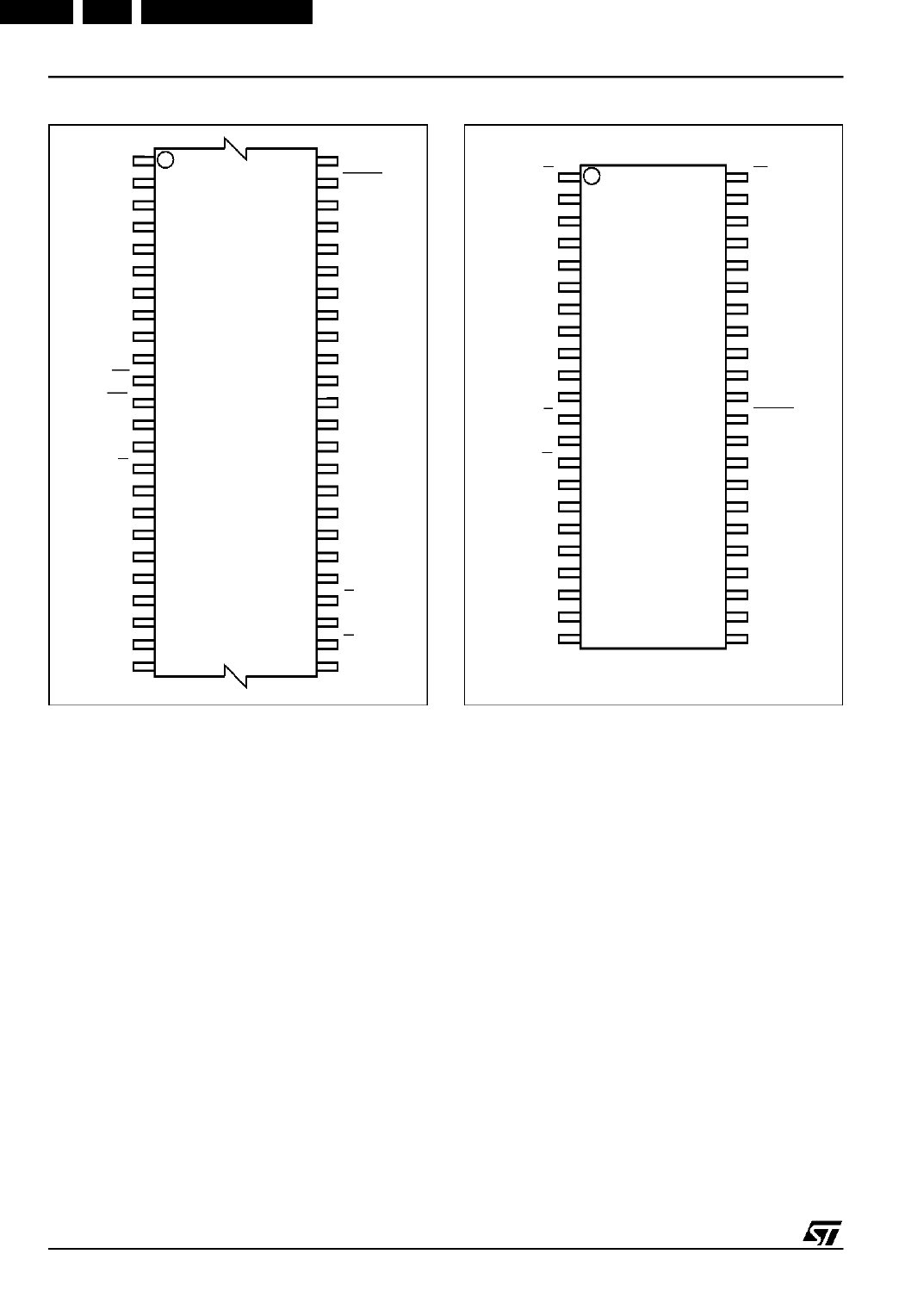
Circuit-, IC Descriptions and List of Abbreviations
EN 248 DVDR980-985 /0X19.
M29W160DT, M29W160DB
6/29
Figure 3. TSOP Connections Figure 4. SO Connections
DQ3
DQ9
DQ2
A6
DQ0
W
A3
RB
DQ6
A8
A9
DQ13
A17
A10 DQ14
A2
DQ12
DQ10
DQ15A–1
VCC
DQ4
DQ5
A7
DQ7
NC
NC
AI03844
M29W160DT
M29W160DB
12
1
13
24 25
36
37
48
DQ8
NC
A19
A1
A18
A4
A5
DQ1
DQ11
G
A12
A13
A16
A11
BYTE
A15
A14
VSS
E
A0
RP
VSS
G
DQ0
DQ8
A3
A0
E
VSS
A2
A1
A13
VSS
A14
A15
DQ7
A12
A16
BYTE
DQ15A–1
DQ5DQ2
DQ3
VCC
DQ11
DQ4
DQ14
A9
A19
RP
A4
W
A7
AI03845
M29W160DT
M29W160DB
8
2
3
4
5
6
7
9
10
11
12
13
14
15
16
32
31
30
29
28
27
26
25
24
2322
20
19
18
17DQ1
DQ9
A6
A5
DQ6
DQ13
44
39
38
37
36
35
34
33
A11
A10
DQ10
21
DQ12
40
43
1
42
41
A17 A8
A18

Circuit-, IC Descriptions and List of Abbreviations EN 249DVDR980-985 /0X1 9.
9.8.6 IC7403: SAA6752H (EMPRESS)
2001 Aug 01 3
MPEG-2 video and MPEG-audio/AC-3 audio
encoder with multiplexer SAA6752HS
1 FEATURES
1.1 Video input and preprocessing
•Digital YUV input according to
“ITU-R BT.656”
(8 bits at
27 MHz) and
“ITU-R BT.601”
•Support of enhanced
“ITU-R BT.656”
input format
containing decoded VBI data readable via I2C-bus;
Closed Caption (CC), Wide Screen Signalling (WSS)
and copyright information [Copy Generation
Management System (CGMS)]
•Processing of non broadcast video signals from analog
VCR according to IEC 756
•Two video clock input pins for switching two digital video
sources
•
“ITU-R BT.601”
format conversion to 1/2D1, 2/3D1 and
Standard Interchange Format (SIF)
•4:2:2to4:2:0 colour format conversion
•Decimation filtering for all format conversions
•Adaptive median filter and motion compensated filter for
input noise reduction.
1.2 Video compression
•Real time MPEG-2 encoding compliant to Main Profile at
Main Level (MP@ML) for 625 and 525 interlaced line
systems
•Supported resolutions: D1, 2/3D1, 1/2D1 and SIF
•IPB frame, IP frame and I frame only encoding
supported at all modes
•Supported bit rates: up to 25 Mbit/s I-only encoding;
up to 15 Mbit/s IP-only or IBP encoding.
•Variable video bit rate mode for constant picture quality
and constant bit rate mode to gain optimum picture
quality from a fixed channel transfer rate
•Access to bit rate control parameters whilst encoding to
support external real-time control algorithms (e.g.
constrained variable bit rate control)
•Programmable Group Of Pictures (GOP) structure
•Innovative motion estimation with wide search range
•Adaptive quantization
•Motion compensated noise filter.
1.3 Audio input
•Audio inputs: I2S format or EIAJ format (16, 18 or
20 bits), master or slave mode at 32, 44.1 and 48 kHz
•Two digital I2S input ports for selection between two
digital audio sources
•Audio clock generation: 256/384 ×fs(48 kHz) locked to
video frame rate (if video is present)
•Sample rate conversion to 48 kHz (locked to video
frame rate) for slave mode operation in all modes except
Digital Versatile Disc (DVD) compliant bypass.
1.4 Audio compression
•Dolby(1) Digital Consumer Encoding (DDCE) also
known as AC-3(2) 2 channel audio encoding at
256 kbit/s or 384 kbit/s (only for SAA6752HS/01)
•MPEG-1 layer 2 audio encoding at 256 kbit/s or
384 kbit/s
•Input data bypass for Linear Pulse Code Modulation
(LPCM) and compressed audio data [MPEG-1,
MPEG-2, Dolby Digital (DD) and Digital Theatre
System (DTS)] according to IEC 61937
•Preamble Pc, Preamble Pd and bit stream information
captured for identification of modes during bypass of
compressed audio data for MPEG-1, MPEG-2, DD and
DTS according to IEC 61937
•Audio mute via I2C-bus control for all modes except
DVD-compliant bypass.
1.5 Stream multiplexer
•Multiplexing of video and audio streams according to the
MPEG-2 systems standard (
“ISO 13818-1”
)
•Generation and output of MPEG-2 Transport Streams
(TS), MPEG-2 Program Streams (PS), Packetized
Elementary Streams (PES) and Elementary Streams
(ES) compliant to the DVD, D-VHS and DVB standards
•MPEG time stamp (PTS/DTS/SCR/PCR) generation
and insertion (synchronization)
•Insertion of metadata
•Optional generation of empty time slots for subsequent
insertion of application specific data packets
•Optional insertion of user data in the GOP header and in
the picture header.
(1) Dolby is a registered trademark of Dolby Laboratories
Licensing Corporation.
(2) AC-3 is a registered trademark of Dolby Laboratories
Licensing Corporation.

Circuit-, IC Descriptions and List of Abbreviations
EN 250 DVDR980-985 /0X19.
2001 Aug 01 4
MPEG-2 video and MPEG-audio/AC-3 audio
encoder with multiplexer SAA6752HS
1.6 Output interface
•Parallel interface 8-bit master/slave output
•3-state output port
•Glueless interfacing with IEEE 1394 chip sets (for
example, PDI 1394 L11)
•Data Expansion Bus Interface (DEBI) interface.
1.7 Control domain
•All control done via I2C-bus
•I2C-bus slave transceiver up to 400 kHz
•I2C-bus slave address select pin
•Host interrupt flag pin.
1.8 Other features
•Single external clock or single crystal 27 MHz
•Separate 27 MHz system clock output
•Interface voltage 3.3 V
•TTL compatible digital outputs
•Power supply voltage 3.3 and 2.5 V
•Boundary Scan Test (BST) supported
•Power-down mode
•Single SDRAM system memory (16 Mbit@16 bit or
64 Mbit@16 bit).
2 GENERAL DESCRIPTION
2.1 General
Philips Semiconductors' second generation real time
MPEG-2 encoder, the SAA6752HS, is a highly integrated
single chip audio and video encoding solution with very
flexible multiplexing functionality. With our expertise in two
critical areas for consumer video encoding, noise filtering
and motion estimation, we have pushed the boundaries for
video quality even further, providing enhanced quality for
low bit rates and enabling increased recording times for a
given storage capacity. The SAA6752HS will also enable
a key driver for new consumer digital recording
applications; system cost reduction. By integrating all
audio encoding and multiplexing functionality we will be
moving from a three chip to a one chip system, with cost
efficient design and process technology, thus providing a
truly low cost, high quality encoding system.
The SAA6752HS/02 is intended for customers whose
application does not require the DDCE function.
The SAA6752HS gives significant advantages to
customers developing digital recording applications:
•Fast time-to-market and low development
resources: By adding a simple external video input
processor IC, audio analog-to-digital converter, and an
external SDRAM, analog video and audio sources are
compressed into high quality MPEG-2 video and
MPEG-1 layer 2 or AC-3 audio streams, multiplexed into
a single program or transport stream for simple
connection to various storage media or broadcast
media. Hence, making design effort for our customers a
minimum, as well as removing the need for in-depth
experience in MPEG encoding.
•Low system host resources: All video and audio
encoding algorithms and software are run on an internal
MIPS(1) processor. The SAA6752HS only requires
small amount of communication from system host
processor to set up and control required encoding
parameters via I2C-bus.
2.2 Application ?elds
2.2.1 DVD BASED OPTICAL DISC RECORDERS (DVD+RW,
DVD-RW, DVD-RAM)
Emerging optical disc based recording systems target to
replace the existing consumer recording (VCR) and
playback (DVD and VCD) products. The first generation
recordable DVD based products will want to maximise
recording times for the 4.7 Gbyte storage capacity. For
these systems the SAA6752HS is critical, with its superior
noise filtering and motion estimation, in enabling high
quality at low bit rates.
Playback compatibility with existing DVD decoding
solutions will also be important, which is why the
SAA6752HS provides Dolby digital consumer (AC-3)
audio encoding to allow playback through existing players
implementing DDCE (AC-3) decoding dominant in current
DVD platforms.
The DVD stream is based on MPEG Program Stream
(PS). The SAA6752HS directly outputs MPEG PS
compliant to the DVD standard.
(1) MIPS is a registered trademark of MIPS Technologies.
Circuit-, IC Descriptions and List of Abbreviations EN 251DVDR980-985 /0X1 9.
2001 Aug 01 5
MPEG-2 video and MPEG-audio/AC-3 audio
encoder with multiplexer SAA6752HS
2.2.2 HDD BASED TIME SHIFT RECORDING
Hard Disc Drive (HDD) based time-shift systems enable
Personalized TV (PTV) functionality, providing consumers
with new powers of control over what and when to watch
broadcast content. With the audio and video content
recorded digitally, identification, search and retrieval
becomes a `no brainer' task as compared to traditional
VCR functionality. Combine this with electronic program
guides and intelligent control, and the PTV can also
analyse the viewers watching habits to search for
programs likely to be of interest and automatically
recorded in anticipation of the viewers preferences.
Since HDD recorders are closed systems, the recording
format stream can be proprietary. SAA6752HS flexible
multiplexing formats, support a number of recording
stream formats for HDD including MPEG Transport
Stream (TS) or MPEG Packetized Elementary Stream
(PES).
2.2.3 DIGITAL VCR (DVHS) RECORDING
A DVHS player records streams based on MPEG
Transport Streams (TS) packed in logical tape tracks. The
SAA6752HS output streams are compliant with DVHS
standard requirements.
2.2.4 VIDEO EDITING/TRANSMISSION/SURVEILLANCE/
CONFERENCING
The SAA6752HS can operate as a stand-alone device in
all above applications. The SAA6752HS' full features and
flexibility allows customers to tailor functionality and
performance to specific application requirements. All
required control settings such as GOP size and bit rate
modes can be selected via I2C-bus.
3 QUICK REFERENCE DATA
4 ORDERING INFORMATION
Notes
1. MPEG-2 video and MPEG-audio/AC-3 audio encoder with multiplexer.
2. MPEG-2 video and MPEG-audio encoder with multiplexer, but without AC-3 audio encoder.
SYMBOL PARAMETER MIN. TYP. MAX. UNIT
VDDP digital supply voltage (pad cells) 3.0 3.3 3.6 V
VDDCO digital supply voltage (core) 2.3 2.5 2.7 V
VDDA analog supply voltage (oscillator and PLL) 2.3 2.5 2.7 V
IDD(tot) analog + digital supply current 407 453 525 mA
Ptot total power dissipation 1.2 1.4 1.9 W
fDCXO quartz frequency (digital controlled tuning) 27 ×(1 −200 ×10−6)27 27×(1 + 200 ×10−6) MHz
fSDRAM SDRAM clock frequency −108 −MHz
fSCL I2C-bus input clock frequency 100 −400 kHz
B output bit-rate 1.5 −25 Mbit/s
VIH HIGH-level digital input voltage 1.7 −3.6 V
VIL LOW-level digital input voltage −0.5 −+0.7 V
VOH HIGH-level digital output voltage VDDP −0.4 −VDDP V
VOL LOW-level digital output voltage 0 −0.4 V
Tamb ambient temperature 0 −70 °C
TYPE NUMBER PACKAGE
NAME DESCRIPTION VERSION
SAA6752HS/01(1) SQFP208 plastic shrink quad ?at package; 208 leads (lead length 1.3 mm);
body 28 ×28 ×3.4 mm; high stand-off height
SOT316-1
SAA6752HS/02(2)
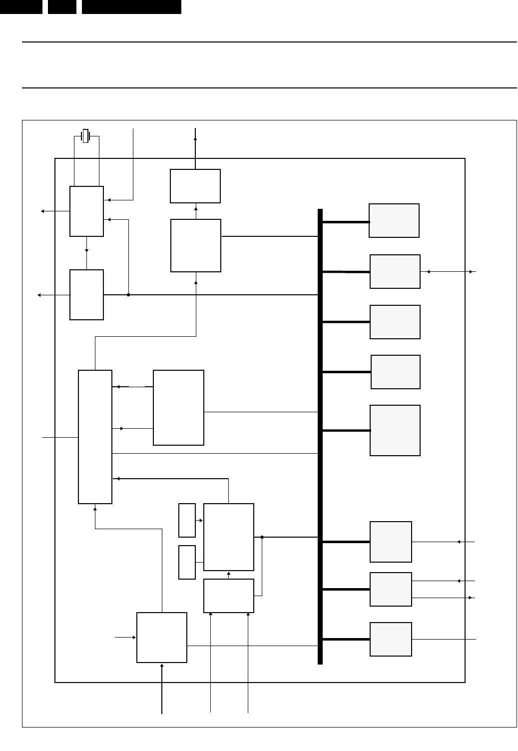
Circuit-, IC Descriptions and List of Abbreviations
EN 252 DVDR980-985 /0X19.
2001 Aug 01 6
MPEG-2 video and MPEG-audio/AC-3 audio
encoder with multiplexer SAA6752HS
5 BLOCK DIAGRAM
Fig.1 Block diagram.
SDRAM-INTERFACE
STREAM DOMAIN SCHEDULER
AUDIO
COMPRESSION
AUDIO
INTER
VIDEO
FRONT-END
RAM ROM STREAM
MULTIPLEXER
OUTPUT
INTER
VIDEO
COMPRESSION
SAA6752HS SYSTEM
CLOCK
REFERENCE
CLOCK
27 MHz
audio clock
I2CGPIO
reset
digital
I2C-bus
MIPSRAM ROM TAP
PI-bus
video
input
digital
audio
input
external
MPEG
boundary scan
CPU
clock
host interrupt
output
SDRAM
16 bit 16 Mbit or 16 bit 64 Mbit
system
clock
reference
STATIC
MEM
DEBUG
ONLY
RESET
CONTROL
FACE
FACE
System Clock
Output

Circuit-, IC Descriptions and List of Abbreviations EN 253DVDR980-985 /0X1 9.
2001 Aug 01 7
MPEG-2 video and MPEG-audio/AC-3 audio
encoder with multiplexer SAA6752HS
6 PINNING
SYMBOL PIN INPUT/OUTPUT(1) Imax
(mA) DESCRIPTION
VSSP 1 ground −pad ground
SDATA1 2 input −I2S-bus serial data input port 1 with internal pull-down resistor
SCLK1 3 input/output 4 I2S-bus serial clock port 1 with internal pull-down resistor
SWS1 4 input/output 4 I2S-bus word select port 1 with internal pull-down resistor
VDDP 5 supply −pad ring supply voltage (3.3 V)
SDATA2 6 input/output 4 I2S-bus serial data port 2 with internal pull-down resistor
SCLK2 7 input/output 4 I2S-bus serial clock port 2 with internal pull-down resistor
SWS2 8 input/output 4 I2S-bus word select port 2 with internal pull-down resistor
ACLK 9 output 4 audio clock output (256 ×fs or 384 ×fs)
VSSP 10 ground −pad ground
IDQ 11 input −reserved (recommended connect to pin VSSP) with internal
pull-down resistor
YUV0 12 input −video input signal bit 0 (LSB)
YUV1 13 input −video input signal bit 1
YUV2 14 input −video input signal bit 2
YUV3 15 input −video input signal bit 3
YUV4 16 input −video input signal bit 4
YUV5 17 input −video input signal bit 5
YUV6 18 input −video input signal bit 6
YUV7 19 input −video input signal bit 7 (MSB)
VSSP 20 ground −pad ground
HSYNC 21 input −horizontal sync input (video) with internal pull-down resistor
VSYNC 22 input −vertical sync input (video) with internal pull-down resistor
FID 23 input −video ?eld identi?cation input (odd/even ?eld) with internal
pull-down resistor
VCLK1 24 input −video clock input 1 (27 MHz) with internal pull-down resistor
VSSCO 25 ground −core ground
VSSCO 26 ground −core ground
VDDCO 27 supply −core supply voltage (2.5 V)
VDDCO 28 supply −core supply voltage (2.5 V)
VDDP 29 supply −pad ring supply voltage (3.3 V)
VCLK2 30 input −video clock input 2 (27 MHz) with internal pull-down resistor
PDOAV 31 3-state output 4 parallel stream data output for audio/video identi?er
PDIDS 32 input −parallel stream data input for data strobe (request for packet in
Data Expansion Bus Interface (DEBI) slave mode) with internal
pull-up resistor
PDOSYNC 33 3-state output 4 parallel stream data output for packet sync
VSSP 34 ground −pad ground
PDOVAL 35 3-state output 4 parallel stream data valid output with internal pull-up resistor
PDO0 36 3-state output 4 parallel stream data output bit 0 (LSB)
Circuit-, IC Descriptions and List of Abbreviations
EN 254 DVDR980-985 /0X19.
2001 Aug 01 8
MPEG-2 video and MPEG-audio/AC-3 audio
encoder with multiplexer SAA6752HS
PDO1 37 3-state output 4 parallel stream data output bit 1
PDO2 38 3-state output 4 parallel stream data output bit 2
VDDP 39 supply −pad ring supply voltage (3.3 V)
PDO3 40 3-state output 4 parallel stream data output bit 3
PDO4 41 3-state output 4 parallel stream data output bit 4
PDO5 42 3-state output 4 parallel stream data output bit 5
PDO6 43 3-state output 4 parallel stream data output bit 6
VSSP 44 ground −pad ground
PDO7 45 3-state output 4 parallel stream data output bit 7 (MSB)
PDIOCLK 46 input/output 4 parallel stream clock input/output
I2CADDRSEL 47 input −I2C-bus address select input with internal pull-up resistor
SD_DQ15 48 input/output 8 SDRAM data input/output bit 15 (MSB)
VDDP 49 supply −pad ring supply voltage (3.3 V)
SD_DQ0 50 input/output 8 SDRAM data input/output bit 0 (LSB)
SD_DQ14 51 input/output 8 SDRAM data input/output bit 14
SD_DQ1 52 input/output 8 SDRAM data input/output bit 1
VSSP 53 ground −pad ground
SD_DQ13 54 input/output 8 SDRAM data input/output bit 13
SD_DQ2 55 input/output 8 SDRAM data input/output bit 2
SD_DQ12 56 input/output 8 SDRAM data input/output bit 12
VDDP 57 supply −pad ring supply voltage (3.3 V)
SD_DQ3 58 input/output 8 SDRAM data input/output bit 3
SD_DQ11 59 input/output 8 SDRAM data input/output bit 11
SD_DQ4 60 input/output 8 SDRAM data input/output bit 4
SD_DQ10 61 input/output 8 SDRAM data input/output bit 10
VSSP 62 ground −pad ground
SD_DQ5 63 input/output 8 SDRAM data input/output bit 5
SD_DQ9 64 input/output 8 SDRAM data input/output bit 9
SD_DQ6 65 input/output 8 SDRAM data input/output bit 6
SD_DQ8 66 input/output 8 SDRAM data input/output bit 8
VDDP 67 supply −pad ring supply voltage (3.3 V)
SD_DQ7 68 input/output 8 SDRAM data input/output bit 7
SD_DQM1 69 output 8 SDRAM data mask enable output bit 1
SD_DQM0 70 output 8 SDRAM data mask enable output bit 0 (LSB)
SD_WE 71 output 8 SDRAM write enable output (active LOW)
VSSP 72 ground −pad ground
SD_CAS 73 output 8 SDRAM column address strobe output (active LOW)
SD_CLK 74 output 8 SDRAM clock output
SD_RAS 75 output 8 SDRAM row address strobe output (active LOW)
SD_CKE 76 output 8 SDRAM clock enable output
SYMBOL PIN INPUT/OUTPUT(1) Imax
(mA) DESCRIPTION

Circuit-, IC Descriptions and List of Abbreviations EN 255DVDR980-985 /0X1 9.
2001 Aug 01 9
MPEG-2 video and MPEG-audio/AC-3 audio
encoder with multiplexer SAA6752HS
VSSCO 77 ground −core ground
VSSCO 78 ground −core and substrate ground
VDDCO 79 supply −core supply voltage (2.5 V)
VDDCO 80 supply −core supply voltage (2.5 V)
VDDP 81 supply −pad ring supply voltage (3.3 V)
SD_CS 82 output 8 SDRAM chip select output (active LOW)
SD_A13 83 output 8 SDRAM address output bit 13 (bank selection for 64 Mbit)
SD_A9 84 output 8 SDRAM address output bit 9
SD_A8 85 output 8 SDRAM address output bit 8
VSSP 86 ground −pad ground
SD_A11 87 output 8 SDRAM address output bit 11 (bank selection for 16 Mbit)
SD_A7 88 output 8 SDRAM address output bit 7
SD_A12 89 output 8 SDRAM address output bit 12 (bank selection for 64 Mbit)
SD_A6 90 output 8 SDRAM address output bit 6
VDDP 91 supply −pad ring supply voltage (3.3 V)
SD_A10 92 output 8 SDRAM address output bit 10
SD_A5 93 output 8 SDRAM address output bit 5
SD_A0 94 output 8 SDRAM address output bit 0 (LSB)
SD_A4 95 output 8 SDRAM address output bit 4
VSSP 96 ground −pad ground
SD_A1 97 output 8 SDRAM address output bit 1
SD_A3 98 output 8 SDRAM address output bit 3
SD_A2 99 output 8 SDRAM address output bit 2
SD_DQM3 100 output 8 reserved (do not connect)
VDDP 101 supply −pad ring supply voltage (3.3 V)
SD_DQM2 102 output 8 reserved (do not connect)
SD_DQ31 103 input/output 8 reserved (do not connect)
SD_DQ16 104 input/output 8 reserved (do not connect)
VSSP 105 ground −pad ground
SD_DQ30 106 input/output 8 reserved (do not connect)
SD_DQ17 107 input/output 8 reserved (do not connect)
SD_DQ29 108 input/output 8 reserved (do not connect)
VDDP 109 supply −pad ring supply voltage (3.3 V)
SD_DQ18 110 input/output 8 reserved (do not connect)
SD_DQ28 111 input/output 8 reserved (do not connect)
SD_DQ19 112 input/output 8 reserved (do not connect)
SD_DQ27 113 input/output 8 reserved (do not connect)
VSSP 114 ground −pad ground
SD_DQ20 115 input/output 8 reserved (do not connect)
SD_DQ26 116 input/output 8 reserved (do not connect)
SYMBOL PIN INPUT/OUTPUT(1) Imax
(mA) DESCRIPTION

Circuit-, IC Descriptions and List of Abbreviations
EN 256 DVDR980-985 /0X19.
2001 Aug 01 9
MPEG-2 video and MPEG-audio/AC-3 audio
encoder with multiplexer SAA6752HS
VSSCO 77 ground −core ground
VSSCO 78 ground −core and substrate ground
VDDCO 79 supply −core supply voltage (2.5 V)
VDDCO 80 supply −core supply voltage (2.5 V)
VDDP 81 supply −pad ring supply voltage (3.3 V)
SD_CS 82 output 8 SDRAM chip select output (active LOW)
SD_A13 83 output 8 SDRAM address output bit 13 (bank selection for 64 Mbit)
SD_A9 84 output 8 SDRAM address output bit 9
SD_A8 85 output 8 SDRAM address output bit 8
VSSP 86 ground −pad ground
SD_A11 87 output 8 SDRAM address output bit 11 (bank selection for 16 Mbit)
SD_A7 88 output 8 SDRAM address output bit 7
SD_A12 89 output 8 SDRAM address output bit 12 (bank selection for 64 Mbit)
SD_A6 90 output 8 SDRAM address output bit 6
VDDP 91 supply −pad ring supply voltage (3.3 V)
SD_A10 92 output 8 SDRAM address output bit 10
SD_A5 93 output 8 SDRAM address output bit 5
SD_A0 94 output 8 SDRAM address output bit 0 (LSB)
SD_A4 95 output 8 SDRAM address output bit 4
VSSP 96 ground −pad ground
SD_A1 97 output 8 SDRAM address output bit 1
SD_A3 98 output 8 SDRAM address output bit 3
SD_A2 99 output 8 SDRAM address output bit 2
SD_DQM3 100 output 8 reserved (do not connect)
VDDP 101 supply −pad ring supply voltage (3.3 V)
SD_DQM2 102 output 8 reserved (do not connect)
SD_DQ31 103 input/output 8 reserved (do not connect)
SD_DQ16 104 input/output 8 reserved (do not connect)
VSSP 105 ground −pad ground
SD_DQ30 106 input/output 8 reserved (do not connect)
SD_DQ17 107 input/output 8 reserved (do not connect)
SD_DQ29 108 input/output 8 reserved (do not connect)
VDDP 109 supply −pad ring supply voltage (3.3 V)
SD_DQ18 110 input/output 8 reserved (do not connect)
SD_DQ28 111 input/output 8 reserved (do not connect)
SD_DQ19 112 input/output 8 reserved (do not connect)
SD_DQ27 113 input/output 8 reserved (do not connect)
VSSP 114 ground −pad ground
SD_DQ20 115 input/output 8 reserved (do not connect)
SD_DQ26 116 input/output 8 reserved (do not connect)
SYMBOL PIN INPUT/OUTPUT(1) Imax
(mA) DESCRIPTION

Circuit-, IC Descriptions and List of Abbreviations EN 257DVDR980-985 /0X1 9.
2001 Aug 01 10
MPEG-2 video and MPEG-audio/AC-3 audio
encoder with multiplexer SAA6752HS
SD_DQ21 117 input/output 8 reserved (do not connect)
SD_DQ25 118 input/output 8 reserved (do not connect)
VDDP 119 supply −pad ring supply voltage (3.3 V)
SD_DQ22 120 input/output 8 reserved (do not connect)
SD_DQ24 121 input/output 8 reserved (do not connect)
SD_DQ23 122 input/output 8 reserved (do not connect)
EXTCLK 123 input −27 MHz external clock input with internal pull-up resistor
VSSP 124 ground −pad ground
VSSA 125 ground −oscillator analog ground
XTALI 126 analog input −crystal oscillator input (27 MHz); note 2
XTALO 127 analog output −crystal oscillator output (27 MHz)
VDDA 128 supply −oscillator analog supply voltage (2.5 V)
VSSCO 129 ground −core ground
VSSCO 130 ground −core ground
VDDCO 131 supply −core supply voltage (2.5 V)
VDDCO 132 supply −core supply voltage (2.5 V)
VDDP 133 supply −pad ring supply voltage (3.3 V)
TDI 134 input −boundary scan test data input; pin must ?oat or set to HIGH
during normal operating; with internal pull-up resistor; note 3
TMS 135 input −boundary scan test mode select; pin must ?oat or set to HIGH
during normal operating; with internal pull-up resistor; note 3
TCK 136 input −boundary scan test clock; pin must be set to LOW during
normal operating; with internal pull-up resistor; note 3
TDO 137 3-state output 4 boundary scan test data output; pin not active during normal
operating; with 3-state output; note 3
VSSP 138 ground −pad ground
TRST 139 input −test reset input (active LOW), for boundary scan test (with
internal pull-up); notes 3 and 4
CLKOUT 140 output 4 27 MHz system clock output
TEST0 141 input/output 4 reserved (do not connect)
TEST1 142 input/output 4 reserved (do not connect)
VDDP 143 supply −pad ring supply voltage (3.3 V)
TEST2 144 input/output 4 reserved (do not connect)
SDA 145 input/open-drain
output
−serial data input/output (I2C-bus)
SCL 146 input/open-drain
output
−serial clock input/output (I2C-bus)
RESET 147 input −reset input (active LOW); with internal pull-up resistor
VSSP 148 ground −pad ground
RTS 149 output 4 reserved (do not connect); Universal Asynchronous
Receiver/Transmitter (UART) request to send output (active
LOW)
SYMBOL PIN INPUT/OUTPUT(1) Imax
(mA) DESCRIPTION
Circuit-, IC Descriptions and List of Abbreviations
EN 258 DVDR980-985 /0X19.
2001 Aug 01 11
MPEG-2 video and MPEG-audio/AC-3 audio
encoder with multiplexer SAA6752HS
CTS 150 input −reserved (recommended connect to pin VDDP); UART clear to
send input; external static memory select input (active LOW);
with internal pull-up resistor
RXD 151 input −reserved (recommended connect to pin VDDP); UART receive
data; internal boot select input; with internal pull-up resistor
TXD 152 output 4 reserved (do not connect); UART transmit data
VDDP 153 supply −pad ring supply voltage (3.3 V)
SM_LB 154 input/output 4 reserved (do not connect)
SM_UB 155 input/output 4 reserved (do not connect)
H_IRF 156 3-state output 4 host interrupt ?ag output; with internal pull-up resistor
VSSP 157 ground −pad ground
SM_OE 158 output 4 reserved (do not connect), static memory output enable output
(active LOW)
SM_A9 159 output 4 reserved (do not connect), static memory address output bit 9
SM_A10 160 output 4 reserved (do not connect), static memory address output bit 10
VDDP 161 supply −pad ring supply voltage (3.3 V)
SM_A8 162 output 4 reserved (do not connect), static memory address output bit 8
SM_A11 163 output 4 reserved (do not connect), static memory address output bit 11
SM_A7 164 output 4 reserved (do not connect), static memory address output bit 7
SM_A12 165 output 4 reserved (do not connect), static memory address output bit 12
VSSP 166 ground −pad ground
SM_A6 167 output 4 reserved (do not connect), static memory address output bit 6
SM_A13 168 output 4 reserved (do not connect), static memory address output bit 13
SM_A5 169 output 4 reserved (do not connect), static memory address output bit 5
SM_A14 170 output 4 reserved (do not connect), static memory address output bit 14
VDDP 171 supply −pad ring supply voltage (3.3 V)
SM_WE 172 output 4 reserved (do not connect), static memory write enable output
(active LOW)
SM_D7 173 input/output 4 reserved (do not connect), static memory data input/output
bit 7 with internal pull-down resistor
SM_D8 174 input/output 4 reserved (do not connect), static memory data input/output
bit 8 with internal pull-down resistor
SM_D6 175 input/output 4 reserved (do not connect), static memory data input/output
bit 6 with internal pull-down resistor
VSSP 176 ground −pad ground
SM_D9 177 input/output 4 reserved (do not connect), static memory data input/output
bit 9 with internal pull-down resistor
SM_D5 178 input/output 4 reserved (do not connect), static memory data input/output
bit 5 with internal pull-down resistor
SM_D10 179 input/output 4 reserved (do not connect), static memory data input/output
bit 10 with internal pull-down resistor
SYMBOL PIN INPUT/OUTPUT(1) Imax
(mA) DESCRIPTION

Circuit-, IC Descriptions and List of Abbreviations EN 259DVDR980-985 /0X1 9.
2001 Aug 01 12
MPEG-2 video and MPEG-audio/AC-3 audio
encoder with multiplexer SAA6752HS
SM_D4 180 input/output 4 reserved (do not connect), static memory data input/output
bit 4 with internal pull-down resistor
VSSCO 181 ground −internal pre-driver and substrate ground
VSSCO 182 ground −core ground
VDDCO 183 supply −core supply voltage (2.5 V)
VDDCO 184 supply −internal pre-driver supply voltage (2.5 V)
VDDP 185 supply −pad ring supply voltage (3.3 V)
SM_D11 186 input/output 4 reserved (do not connect), static memory data input/output
bit 11 with internal pull-down resistor
SM_D3 187 input/output 4 reserved (do not connect), static memory data input/output
bit 3 with internal pull-down resistor
SM_D12 188 input/output 4 reserved (do not connect), static memory data input/output
bit 12 with internal pull-down resistor
SM_D2 189 input/output 4 reserved (do not connect), static memory data input/output
bit 2 with internal pull-down resistor
VSSP 190 ground −pad ground
SM_D13 191 input/output 4 reserved (do not connect), static memory data input/output
bit 13 with internal pull-down resistor
SM_D1 192 input/output 4 reserved (do not connect), static memory data input/output
bit 1 with internal pull-down resistor
SM_D14 193 input/output 4 reserved (do not connect), static memory data input/output
bit 14 with internal pull-down resistor
SM_D0 194 input/output 4 reserved (do not connect), static memory data input/output
bit 0 (LSB) with internal pull-down resistor
VDDP 195 supply −pad ring supply voltage (3.3 V)
SM_D15 196 input/output 4 reserved (do not connect), static memory data input/output
bit 15 (MSB) with internal pull-down resistor
SM_CS3 197 output 4 reserved (do not connect), static memory chip select output for
external ROM or RAM (active LOW)
SM_A4 198 output 4 reserved (do not connect), static memory address output bit 4
SM_A3 199 output 4 reserved (do not connect), static memory address output bit 3
VSSP 200 ground −pad ground
SM_A2 201 output 4 reserved (do not connect), static memory address output bit 2
SM_A15 202 output 4 reserved (do not connect), static memory address output bit 15
SM_A1 203 output 4 reserved (do not connect), static memory address output bit 1
SM_A16 204 output 4 reserved (do not connect), static memory address output bit 16
VDDP 205 supply −pad ring supply voltage (3.3 V)
SM_A0 206 output 4 reserved (do not connect), static memory address output bit 0
(LSB)
SM_A17 207 output 4 reserved (do not connect), static memory address output bit 17
(MSB)
SM_CS0 208 output 4 reserved (do not connect)
SYMBOL PIN INPUT/OUTPUT(1) Imax
(mA) DESCRIPTION

Circuit-, IC Descriptions and List of Abbreviations
EN 260 DVDR980-985 /0X19.
2001 Aug 01 13
MPEG-2 video and MPEG-audio/AC-3 audio
encoder with multiplexer SAA6752HS
Notes
1. All input pins, input/output pins (in input mode), output pins (in 3-state mode) and open-drain output pins are limited
to 3.3 V.
2. If used with external clock source the input voltage has to be limited to 2.5 V.
3. In accordance with the
“IEEE 1149.1”
standard.
4. Special function of pin TRST:
a) For board designs without boundary scan implementation, pin TRST must be connected to ground.
b) Pin TRST provides easy initialization of the internal BST circuit. By applying a LOW it can be used to force the
internal Test Access Port (TAP) controller to the Test-Logic-Reset state (normal operating) at once.
Fig.2 Pin configuration.
handbook, halfpage
SAA6752HS
1
208
157
53
104
52
156
105

Circuit-, IC Descriptions and List of Abbreviations EN 261DVDR980-985 /0X1 9.
9.8.7 IC7500: SAA7118 (VIP)
PAL/NTSC/SECAM Video Decoder with Adaptive Comb Filter,
Component Video Input, VBI-Data Slicer and High Performance Scaler
SAA7118
1FEATURES
The SAA7118 is a video capture device for application at
the image port of VGA controller, with following feature
high lights:
Video Acquisition/ Clock
Up to sixteen analog CVBS, split as desired (All of the
CVBS inputs optionally can be used to convert VSB
signals)
Up to eight analog Y+C inputs, split as desired
Up to four analog component inputs, with embedded or
separate sync, split as desired
Four on-chip anti-aliasing filters in front of the ADC’s
Automatic Clamp Control (ACC) for CVBS, Y and C (or
VSB) and component signal
Switchable white Peak Control
Four 9 Bit Low Noise CMOS analog-to-digital converters
at two-fold ITU-656 oversampling (27 MHz)
Digitized CVBS or Y+C-signals are available on the
expansion port
Fully programmable static gain or automatic gain
control, matching to the particular signal properties
On-Chip Line Locked Clock Generation according
ITU601
Requires only one crystal (32.11 or 24.576 MHz) for all
standards
Horizontal and vertical Sync Detection
Video Decoder
Digital PLL for Synchronization and Clock Generation
from all Standards and Non- Standard Video Sources
e.g. consumer grade VTR
Digital PLL for Synchronization and Clock Generation
from all Standards and Non- Standard Video Sources
e.g. consumer grade VTR
Automatic detection of any supported colour standard
Luminance and chrominance signal processing for PAL
BGDHIN, Combination-PAL N, PAL M, NTSC M,
NTSC-Japan, NTSC 4.43 and SECAM
Adaptive 2/4-line comb filter for two dimensional
chrominance/luminance-separation, also with VTR
signals
–Increased Luminance and Chrominance Bandwidth
for all PAL and NTSC-standards
–Reduced cross colour and cross luminance artefacts
PAL delay line for correcting PAL phase errors
Brightness Contrast Saturation (BCS)- adjustment,
separately for composite and baseband signals
User programmable sharpness control
Fast Blanking between component inputs and a CVBS
input through a dedicated pin
Detection of copy-protected signals acc. to the
Macrovision standard, indicating level of protection
Independent Gain and Offset - adjustment for raw data
path
Component Video Processing
Synchronous Component Video (RGB) input via fast
blanking, YCbCr input
Digital matrix
Video Scaler
Horizontal and Vertical Down-Scaling and Up-Scaling to
randomly sized windows
Horizontal and Vertical Scaling range: variable zoom to
1/64 (icon)
(Note: H and V zoom are restricted by the transfer data
rates)
Anti-Alias- and Accumulating Filter for Horizontal
Scaling
Vertical Scaling with Linear Phase Interpolation and
Accumulating Filter for Anti-Aliasing (6 bit phase
accuracy)
Horizontal Phase Correct Up- and Down-Scaling for
improved signal quality of scaled data, especially for
compression and video phone applications, with 6 bit
phase accuracy (1.2 nsec step width)
Two independent programming sets for scaler part, to
define two “ranges” per field or sequences over frames
Fieldwise switching between Decoder-part and
Expansion port (X-port) input
Brightness, contrast and saturation controls for scaled
outputs
VBI-Data Decoder and Slicer
versatile VBI-data decoder, slicer, clock regeneration
and byte synchronization
e.g. for WST, NABST, Close Caption, WSS, etc.
Audio Clock Generation
Generation of a field locked Audio Master Clock to
support a constant number of audio clocks per video
field

Circuit-, IC Descriptions and List of Abbreviations
EN 262 DVDR980-985 /0X19.
PAL/NTSC/SECAM Video Decoder with Adaptive Comb Filter,
Component Video Input, VBI-Data Slicer and High Performance Scaler
SAA7118
Generation of an audio serial and left/right (channel)
clock signal
Digital I/O Interfaces
Real Time signal port (R - port), incl. continuous line
locked reference clock and real time status information
supporting RTC level 3.1 (refer to external document
“RTC Functional Specification” for details)
Bidirectional Expansion Port (X - port) with half duplex
functionality (D1), 8-bit YCbCr
–output from Decoder part, real time and unscaled, or
–input to Scaler part, e.g. video from MPEG-decoder
(extension to 16 bit possible)
Video Image port (I - port) configurable for 8 - bit data
(extension to 16 bit possible) in Master Mode (own
clock), or Slave Mode (external clock), with auxiliary
timing and hand shake signals
Discontinuous data streams supported
32-word * 4 Byte FIFO register for video output data
28-word * 4 Byte FIFO register for decoded VBI output
data
Scaled 4:2:2, 4:1:1, 4:2:0, 4:1:0 YCbCr output
Scaled 8-bit luminance only and raw CVBS data output
sliced, decoded VBI data output
Miscellaneous
Power On Control
5 V tolerant digital inputs and I/O ports
Software controlled power saving stand-by modes
supported
Programming via serial I2C-bus, full read-back ability by
an external controller, bit rate up to 400 kbit/s
Boundary Scan Test circuit complies to the IEEE Std.
1149.b1 -1994
BGA156 package
2 APPLICATIONS
Multimedia
Digital Television
Image Processing
Video Phone
PC- Editing cards
PC- Tuner cards
3 GENERAL DESCRIPTION
Philips X-VIP is a new Multistandard Comb Filter Video
Decoder chip with additional component processing,
providing high quality, optionally scaled, video.
The SAA7118 is a combination of a four channel analog
preprocessing circuit including source selection,
anti-aliasing filter and A/D-converter, an automatic clamp
and gain control, a Clock Generation Circuit (CGC), a
Digital Multi Standard Decoder containing
two-dimensional chrominance/luminance separation by an
adaptive comb filter and a high performance scaler,
including variable horizontal and vertical up and down
scaling and a Brightness- Contrast- Saturation- Control
circuit.
It is a highly integrated circuit for Desktop Video and
similar applications. The decoder is based on the principle
of line-locked clock decoding and is able to decode the
colour of PAL, SECAM and NTSC signals into ITU-601
compatible colour component values. The SAA7118
accepts as analog inputs CVBS or S-Video (Y+C) from TV
or VCR sources, including weak and distorted signals, as
well as baseband component signals YCbCr or RGB. An
expansion port (X-port) for digital video (bi-directional half
duplex, D1 compatible) is also supported to connect to
MPEG or video phone codec. At the so called image port
(I-port) the 7118 supports 8 (16) bit wide output data with
auxiliary reference data for interfacing to VGA controllers.
The target application for SAA7118 is to capture and
optionally scale video images, to be provided as digital
video stream through the image port of a VGA controller,
for capture to system memory, or just to provide digital
baseband video to any picture improvement processing.
SAA7118 also provides means for capturing the serially
coded data in the vertical blanking interval (VBI-data). Two
principal functions are available:
- to capture raw video samples, after interpolation to the
required output data rate, via the scaler and
- a versatile data slicer (data recovery) unit.
SAA7118 incorporates also a field locked audio clock
generation. This function ensures that there is always the
same number of audio samples associated with a field, or
a set of fields. This prevents the loss of sychronization
between video and audio, during capture or playback.
All of the A/D- converters may be used to digitize a VSB
signal for further for further decoding; a dedicated output
port and a selectable VSB clock input is provided.
The circuit is controlled via I2C-bus (full write / read
capability for all programming registers, bit rate up to 400
kbits/s)
Circuit-, IC Descriptions and List of Abbreviations EN 263DVDR980-985 /0X1 9.
PAL/NTSC/SECAM Video Decoder with Adaptive Comb Filter,
Component Video Input, VBI-Data Slicer and High Performance Scaler SAA7118
4 QUICK REFERENCE DATA
Note
1. Power consumption is measured in CVBS-input mode (only one ADC active) and 8 bit image port output mode,
expansion port is tristated
5 ORDERING AND PACKAGE INFORMATION
SYMBOL PARAMETER MIN TYP MAX UNIT
VDDx digital supply voltage 3.0 3.3 3.6 V
VDDCx digital core supply voltage 3.0 3.3 3.6 V
VDDA analog supply voltage 3.1 3.3 3.5 V
Tamb ambient temperature 0 - 70 °C
PA+D analog and digital power dissipation(1) - t.b.d. - W
EXTENDED TYPE
NUMBER
PACKAGE
PINS PIN POSITION MATERIAL CODE
SAA7118 156 BGA156 Plastic SOT 472-1(BB3)
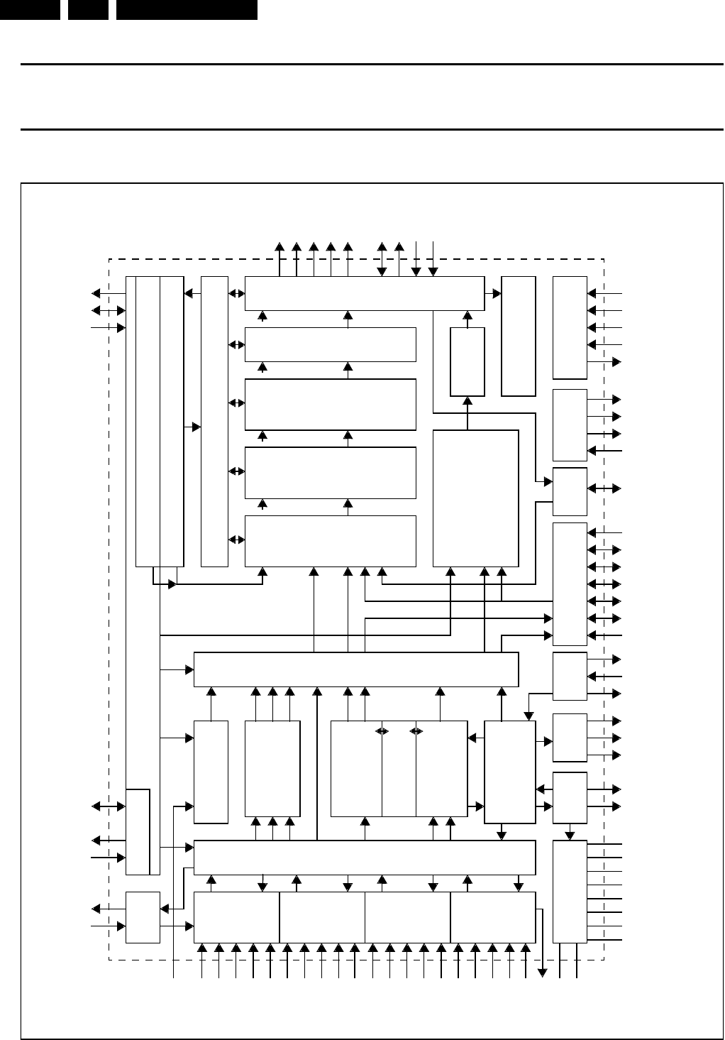
Circuit-, IC Descriptions and List of Abbreviations
EN 264 DVDR980-985 /0X19.
PAL/NTSC/SECAM Video Decoder with Adaptive Comb Filter,
Component Video Input, VBI-Data Slicer and High Performance Scaler SAA7118
6 SYSTEM BLOCK DIAGRAM
Boundary Scan
Audio
XTAL
Video
Synchronization
Luminance
Chrominance
Processing
Processing
Components
Processing
Fast Switch Delay
Analog1
Analog2
Analog3
Analog4
AD-Port IIC Register MAP
VBI Data Slicer FIFO
Video FIFO
FIR-Prefilter
Prescaler
BCS-Scaler
H-Port
Output Formatter I-Port
2nd Task IIC Register Map Scaler
Line FIFO Buffer
Vertical Scaling
Video/Text Arbiter
Analog Input Control
Decoder Output Control
X-Port
Scaler Event Controller
1st Task IIC Register Map Scaler
Power Supply Clock
Horizontal Fine-
(Phase-) Scaling
FSW
AI11
AI12
AI13
AI14
AI21
AI22
AI23
AI24
AI31
AI32
AI33
AI34
AI41
AI42
AI43
AI44
Power-On Control
Text
IPD(7:0)
ICLK
IDQ
ITRDY
ITRI
IGPH
IGPV
IGP0
IGP1
SDA
SCL
COMB Filter
AI1D
AI2D
AI3D
AI4D
AGND
AGNDA
VSSA
VDDA
VSSI
VSSE
VDDI
VDDE
LLC
LLC2
XTAL
XTALI
XTOUT
XPD(7:0)
HPD(7:0)
ADP(8:0)
TRSTN
TCK
TMS
TDI
TDO
AMCLK
ALRCLK
ASCLK
AMXCLK
XCLK
XRH
XRV
XTRI
Clock
RTS0
RTS1
XDQ
XRDY
INT_A
Blockdiagram SAA7118
GPO
CE
RESON
ADC1
ADC2
ADC3
ADC4
+
+
+
+
Control
VXDD
VXSS
CLKEXT
AOUT
TEST
RTCO
CbCr CbCr
YCbCr
Y
Cb
Cr
Y
Cb
Cr
S
YCbCr
YCbCrS
RAW
RAW
C
Y
S
R
G
B
S
S
S
Fig.1 Blockdiagram SAA7118

Circuit-, IC Descriptions and List of Abbreviations EN 265DVDR980-985 /0X1 9.
PAL/NTSC/SECAM Video Decoder with Adaptive Comb Filter,
Component Video Input, VBI-Data Slicer and High Performance Scaler SAA7118
7 PINNING AND CONFIGURATION
7.1 Pinning List
Table 1 Pinning List SAA7118
PIN NAME TYPE DESCRIPTION
A02 XTOUT O Crystal oscillator output signal
A03 XTAL O Connect output pin for quartz
A04 VXSS P Ground for crystal oscillator
A05 TDO O Test Data Output for Boundary Scan Test (2)
A06 XRDY O Status flag or ready signal from scaler
A07 XCLK I/O Clock I/O expansion port
A08 XPD0 I/O LSB of expansion port bus
A09 XPD2 I/O MSB-5 of expansion port bus
A10 XPD4 I/O MSB-3 of expansion port bus
A11 XPD6 I/O MSB-1 of expansion port bus
A12 TEST5 I/pu Scan test input; do not connect
A13 TEST3 I/pu Scan test input; do not connect
B01 AI41 I Analog input #41
B02 RES1 O Reserved pin for future extensions or testing, do not connect
B03 VXDD P Supply for crystal oscillator
handbook, halfpage
1
A
B
C
D
E
F
G
H
J
K
L
M
N
P
234567891011121314
MXXxxx
SAA7108E
SAA7109E
Fig.2 Package/Pinning SAA7118
SAA7118
Bottom View

Circuit-, IC Descriptions and List of Abbreviations
EN 266 DVDR980-985 /0X19.
PAL/NTSC/SECAM Video Decoder with Adaptive Comb Filter,
Component Video Input, VBI-Data Slicer and High Performance Scaler SAA7118
B04 XTALI I Connect input pin for quartz
B05 TDI I/pu Test Data Input for Boundary Scan Test (with internal pull-up) (2)
B06 TCK I/pu Test Clock for Boundary Scan Test (with internal pull-up) (2)
B07 XDQ I/O Data qualifier for expansion port
B08 XPD1 I/O MSB-6 of expansion port bus
B09 XPD3 I/O MSB-4 of expansion port bus
B10 XPD5 I/O MSB-2 of expansion port bus
B11 XTRI I X-port output control signal; effects (XPD[7:0], XRH, XRV, XDQ and XCLK)
B12 TEST4 O Scan test output; do not connect
B13 RES2 NC Reserved pin for future extensions or testing, do not connect
B14 RES3 NC Reserved pin for future extensions or testing, do not connect
C01 VSSA4 P Ground for analog input AI4x
C02 AGND P Analog Signal Ground
C03 RES4 NC Reserved pin for future extensions or testing, do not connect
C04 RES5 NC Reserved pin for future extensions or testing, do not connect
C05 VDDE1 P Digital supply peripheral cells
C06 TRSTN I/pu Test ReSeT Not for Boundary Scan Test (with internal pull-up) (1)
C07 XRH I/O Horizontal reference expansion-port
C08 VDDI1 P Digital supply core
C09 VDDE2 P Digital supply peripheral cells
C10 VDDI2 P Digital supply core
C11 XPD7 I/O MSB of expansion port bus
C12 RES6 NC Reserved pin for future extensions or testing, do not connect
C13 RES7 NC Reserved pin for future extensions or testing, do not connect
C14 TEST2 I/pu Scan test input; do not connect
D01 AI43 I Analog input #43
D02 AI42 I Analog input #42
D03 AI4D I/O Differential input for AI4x
D04 VDDA4 P Supply for analog input AI4x
D05 VSSE1 P Digital ground peripheral cells
D06 TMS I/pu Test Mode Select for Boundary Scan Test or Scan Test (with internal pull-up) (2)
D07 VSSI1 P Digital ground core (Substrate connection)
D08 XRV I/O Vertical reference for expansion-port
D09 VSSE2 P Digital ground peripheral cells
D10 VSSI2 P Digital ground core
D11 VSSE3 P Digital ground peripheral cells
D12 VDDE3 P Digital supply peripheral cells
D13 TEST1 I/pu Scan test input; do not connect
D14 HPD0 I/O LSB of H-port bus, extended CbCr input for X-port, extended CbCr output for
I-port
E01 AI44 I Analog input #44
PIN NAME TYPE DESCRIPTION

Circuit-, IC Descriptions and List of Abbreviations EN 267DVDR980-985 /0X1 9.
PAL/NTSC/SECAM Video Decoder with Adaptive Comb Filter,
Component Video Input, VBI-Data Slicer and High Performance Scaler
SAA7118
E02 VDDA4A P Supply for analog input AI4x
E03 AI31 I Analog input #31
E04 VSSA3 P Ground for analog input AI3x
E11 HPD1 I/O MSB-6 of H-port bus, extended CbCr input for X-port, extended CbCr output for
I-port
E12 HPD3 I/O MSB-4 of H-port bus, extended CbCr input for X-port, extended CbCr output for
I-port
E13 HPD2 I/O MSB-5 of H-port bus, extended CbCr input for X-port, extended CbCr output for
I-port
E14 HPD4 I/O MSB-3 of H-port bus, extended CbCr input for X-port, extended CbCr output for
I-port
F01 AI3D I/O Differential input for AI3x
F02 AI32 I Analog input #32
F03 AI33 I Analog input #33
F04 VDDA3 P Supply for analog input AI3x
F11 VSSI3 P Digital ground core
F12 VDDI3 P Digital supply core
F13 HPD5 I/O MSB-2 of H-port bus, extended CbCr input for X-port, extended CbCr output for
I-port
F14 HPD6 I/O MSB-1 of H-port bus, extended CbCr input for X-port, extended CbCr output for
I-port
G01 AI34 I Analog input #34
G02 VDDA3A P Supply for analog input AI3x
G03 AI22 I Analog input #22
G04 AI21 I Analog input #21
G11 VSSE4 P Digital ground peripheral cells
G12 IPD1 O MSB-6 of Image port bus
G13 HPD7 I/O MSB of H-port bus, extended CbCr input for X-port, extended CbCr output for
I-port
G14 IPD0 O LSB of Image port bus
H01 AI2D I/O Differential input for AI2x
H02 AI23 I Analog input #23
H03 VSSA2 P Ground for analog input AI2x
H04 VDDA2 P Supply for analog input AI2x
H11 IPD2 O MSB-5 of Image port bus
H12 VDDE4 P Digital supply peripheral cells
H13 IPD4 O MSB-3 of Image port bus
H14 IPD3 O MSB-4 of Image port bus
J01 VDDA2A P Supply for analog input AI2x
J02 AI11 I Analog input #11
J03 AI24 I Analog input #24
J04 VSSA1 P Ground for analog input AI1x
PIN NAME TYPE DESCRIPTION

Circuit-, IC Descriptions and List of Abbreviations
EN 268 DVDR980-985 /0X19.
PAL/NTSC/SECAM Video Decoder with Adaptive Comb Filter,
Component Video Input, VBI-Data Slicer and High Performance Scaler SAA7118
J11 VSSI4 P Digital ground core
J12 VDDI4 P Digital supply core
J13 IPD6 O MSB-1 of Image port bus
J14 IPD5 O MSB-2 of Image port bus
K01 AI12 I Analog input #12
K02 AI13 I Analog input #13
K03 AI1D I/O Differential input for AI1x
K04 VDDA1 P Supply for analog input AI1x
K11 IPD7 O MSB of Image port bus
K12 IGPH O Multi purpose horizontal reference signal
K13 IGP1 O General purpose signal #1
K14 IGPV O Multi purpose vertical reference signal
L01 VDDA1A P Supply for analog input AI1x
L02 AGNDA P Analog signal ground connection
L03 AI14 I Analog input #14
L04 VSSE5 P Digital ground peripheral cells
L05 VSSI5 P Digital ground core
L06 ADP6 O MSB-2 of Direct A/D-converted output bus (VSB)
L07 ADP3 O MSB-5 of Direct A/D-converted output bus (VSB)
L08 VSSE6 P Digital ground peripheral cells
L09 VSSI6 P Digital ground core
L10 RTCO
O/st/pd
(3)
RTC output;
strap to LOW (4k7) for first I2C slave address 42h
strap to HIGH (4k7) for second I2C slave address 40h
L11 VSSE7 P Digital ground peripheral cells
L12 ITRI I/O Image-port control signal, effects all Image port pins
L13 IDQ O Data qualifier for image port
L14 IGP0 O General purpose signal #0
M01 AOUT O Analog test output (not for use in application)
M02 VSSA0 P Ground for internal clock generator
M03 VDDA0 P Supply for internal clock generator
M04 VDDE5 P Digital supply peripheral cells
M05 VDDI5 P Digital supply core
M06 ADP7 O MSB-1 of Direct A/D-converted output bus (VSB)
M07 ADP2 O MSB-6 of Direct A/D-converted output bus (VSB)
M08 VDDE6 P Digital supply peripheral cells
M09 VDDI6 P Digital supply core
M10 RTS0 O Real time status or sync information
M11 VDDE7 P Digital supply peripheral cells
M12 AMXCLK I Audio Master External clock input
PIN NAME TYPE DESCRIPTION

Circuit-, IC Descriptions and List of Abbreviations EN 269DVDR980-985 /0X1 9.
PAL/NTSC/SECAM Video Decoder with Adaptive Comb Filter,
Component Video Input, VBI-Data Slicer and High Performance Scaler SAA7118
Notes
1. This pin provides easy initialization of BST circuitry. TRSTN can be used to force the TAP (Test Access Port)
controller to the Test-Logic-Reset state (normal operation) at once
2. According to the IEEE1149.b1-1994 standard the pads TDI and TMS are input pads with a internal pull-up transistor
and TDO a tri-state output pad. TCK, TRSTN are also built with internal pile-up
3. Strapping remark: If the strapping pin is unused, the internal pull-down resistor is sufficient for strap function.
If pin is used in an application, an external strapping resistor (4,7k) is necessary to get a certain strap function.
M13 FSW I/pd Fast Switch (Blanking), with internal pull-down,
inserts component inputs into CVBS signal
M14 ICLK I/O Clock output signal for image-port, LCLK of LPB image port mode, or optional
asynchronous backend clock input
N01 RES8 NC Reserved pin for future extensions or testing, do not connect
N02 RES9 I/pu Reserved pin for future extensions or testing, do not connect
N03 RES10 I/pd Reserved pin for future extensions or testing, do not connect
N04 CE I/pu Chip Enable or Reset with internal pull-up
N05 LLC2 O Line-locked clock at half frequency (13.5 MHz nominal)
N06 CLKEXT I External clock input intended for A/D-conversion of VSB signals (36 MHz)
N07 ADP5 O MSB-3 of Direct A/D-converted output bus (VSB)
N08 ADP0 O LSB of Direct A/D-converted output bus (VSB)
N09 SCL I I2C Serial Clock
N10 RTS1 O Real time status or sync information
N11 ASCLK O Audio serial clock
N12 ITRDY I Target Ready for image port bus
N13 RES11 NC Reserved pin for future extensions or testing, do not connect
N14 RES12 NC Reserved pin for future extensions or testing, do not connect
P02 RES13 I/O Reserved pin for future extensions or testing, do not connect
P03 EXMCLR I/pd External Mode Clear, with internal pull-down
P04 LLC O Line-locked clock (27 MHz nominal)
P05 RESON O Reset Output Not signal
P06 ADP8 O MSB of Direct A/D-converted output bus (VSB)
P07 ADP4 O MSB-4 of Direct A/D-converted output bus (VSB)
P08 ADP1 O MSB-7 of Direct A/D-converted output bus (VSB)
P09 INT_A O/od I2C interrupt flag (Low if any enabled status bit has changed)
P10 SDA I/O/od I2C Serial Data
P11 AMCLK O Audio Master clock, must be less than half the crystal clock frequency
P12
ALRCLK
O/st/pd Audio left/right clock,
strap to LOW (4k7) for 24.576 MHz crystal
strap to HIGH (4k7) for 32.11 MHz crystal (3)
P13 TEST0 I/pu Scan test input; do not connect
TYPE description:
I=input, O=output, P=power, NC=not connected, st=strapping, pu=pull-up, pd=pull-down, od=open drain
PIN NAME TYPE DESCRIPTION

Circuit-, IC Descriptions and List of Abbreviations
EN 270 DVDR980-985 /0X19.
9.8.8 FLI2200
Description
The FLI2200 is a single chip implementation of Faroudja
Laboratories’ award winning deinterlacing and post-
processing algorithms that produce the highest quality
progressive video output from a variety of interlaced video
inputs including 525/60 (NTSC) or 625/50 (PAL or SECAM).
It uses patented and patent pending motion-adaptive
deinterlacing that selects the optimal filtering on a per-pixel
basis. This includes detection and proper interleaving of 3:2
and 2:2 pulldown for film-base sources, including continuous
monitoring and compensation for bad edits that occur
frequently in broadcast material due to poor scene cuts or
insertion of commercials. Video material is processed by a
set of content-sensitive spatio-temporal filters that adapt to
the appropriate direction for smoothest interpolation using
the patented Faroudja DCDi™ algorithm. The FLI2200 also
includes motion-adaptive cross-color suppression that
removes highly objectionable coloration artifacts produced
by commonly used video decoders. Its internal processing
uses 10 bits per channel to maintain the highest quality. Its
inputs and outputs are 10 bits/channel for best quality but
also supports 8 bits/channel for more cost-sensitive
applications. The FLI2200 requires 4 MB of low cost SDRAM
for best quality deinterlacing, but it can also be operated in
an optimized intra-field mode without memory for more cost-
sensitive applications. This makes possible the use of a
single design for both high-end and low-end applications.
The FLI2200 integrates a number of functions to provide
maximum flexibility in a low cost configuration. This includes
an on-chip clock generator, SDRAM controller, display
controller, input and output color-space converters. It uses
a standard 2-wire serial control interface for easy control
and access to the registers.
The FLI2200 can be connected without glue logic to the
FLI2000 video decoder and FLI2220 Enhancer and OSD
Generator to produce the highest quality video pipeline for
premium applications. It is also fully compatible with other
decoders having a ITU-R BT 656 output format.
Applications
Flat panel TV – LCD, PDP
Progressive scan TVs
Multimedia front/rear projectors
Home Theater
Scan Converters
Multimedia PCs/Workstations
DCDi™ is a Faroudja trademark
Features
Motion-adaptive cross-color suppression removes
artifacts produced by improper Y/C separation in low-
cost video decoders
Motion-adaptive video deinterlacing selects optimal
filtering on a per-pixel basis
Film-mode for proper handling of 3:2 and 2:2
pulldown material
Bad-edit detection/correction compensates for poor
scene cuts and insertions common in broadcast
material
Motion-weighted interpolation for video sources
produces maximum resolution without introducing
motion artifacts
Directional Correlational Deinterlacing (DCDi™)
minimizes jaggies on angled lines
8/10-bit Y/Cb/Cr (D1) (ITU-R BT 656), 16/20-bit Y Cb/Cr
(ITU-R BT 601), 24/30-bit RGB or YCbCr/YPbPr
interlaced input options
Supports 525/60 (NTSC), 625/50 (PAL/SECAM)
Accepts up to 1100 pixels/line
8/10-bit, 16/20-bit YUV, 24/30-bit RGB or YCbCr/YPbPr
progressive output options
Supports 8- or 10-bit inputs and outputs
10-bit internal processing for highest quality
Includes color-space converters at input and output
for maximum flexibility
Auto-detection of NTSC/PAL/SECAM inputs
High-order filtering produces smooth chroma output in
4:2:2 to 4:4:4 or 4:4:4 to 4:2:2 conversions
Resolution recovery maximizes output signal-to-noise
ratio and dynamic range
Can be operated without glue logic with FLI2000 Video
Decoder and FLI2220 Enhancer and OSD Generator ICs
to produce highest quality video pipeline
Glue-less interface to most standard video decoders
Built-in display timing generator
On-chip clock generator eliminates external PLLs
On-chip SDRAM controller
Uses low cost SDRAM as field memory – 4 MB
Optimized intra-field operation allows memory-less
configuration for lowest cost applications with same
design and layout as for high-end applications
2-wire serial control interface for easy control
176-pin TQFP package
FLI2200
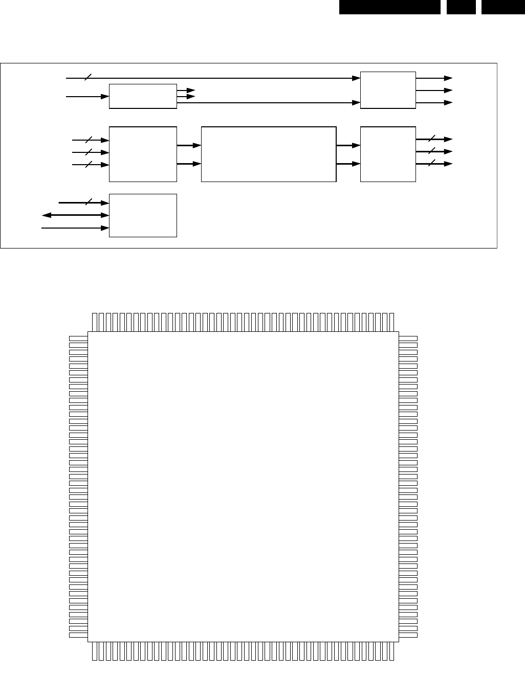
Circuit-, IC Descriptions and List of Abbreviations EN 271DVDR980-985 /0X1 9.
Pin description
Simplified Block Diagram
DATA5
DATA6
DATA7
DATA8
DATA9
DATA10
DATA11
DATA12
DATA13
DATA14
DATA15
DATA16
DATA17
DATA18
DATA19
DATA20
VDD33
VSS
VDD33
VSS
DATA21
DATA22
DATA23
DATA24
DATA25
DATA26
DATA27
DATA28
DATA29
VDD33
VSS
ADDR3
ADDR2
ADDR1
ADDR0
VDD25
VSS
DATA0
DATA1
DATA2
DATA3
DATA4
HSYNCREFI
VSYNCREFI
1
10
20
30
40
50
60
70
80
130
120
110
100
90
140
150
160
170
VDD33
VSS
B/CbIN0
B/CbIN1
B/CbIN2
B/CbIN3
B/CbIN4
B/CbIN5
B/CbIN6
B/CbIN7
B/CbIN8
B/CbIN9
FIELDIN
VDD25
VSS
G/YIN0
G/YIN1
G/YIN2
G/YIN3
G/YIN4
G/YIN5
G/YIN6
G/YIN7
G/YIN8
G/YIN9
R/CrIN0
R/CrIN1
R/CrIN2
R/CrIN3
R/CrIN4
R/CrIN5
R/CrIN6
R/CrIN7
R/CrIN8
R/CrIN9
VDD33
VSS
PIXCLK
TEST4
DADDR1
AVDD
AVSS
TEST3
TEST2
NOMEM
OE
IFORMAT2
IFORMAT1
IFORMAT0
OFORMAT2
OFORMAT1
OFORMAT0
N/P/IN/OUT
VDD33
VSS
VDD33
VSS
G/YOUT9
G/YOUT8
G/YOUT7
G/YOUT6
G/YOUT5
G/YOUT4
G/YOUT3
G/YOUT2
G/YOUT1
G/YOUT0
VDD33
VSS
R/CrOUT9
R/CrOUT8
R/CrOUT7
R/CrOUT6
R/CrOUT5
R/CrOUT4
R/CrOUT3
R/CrOUT2
R/CrOUT1
R/CrOUT0
VREFO
HREFO
VDD25
VSS
VSYNC/CREFO
H/CSYNCO
B/CbOUT9
B/CbOUT8
B/CbOUT7
B/CbOUT6
B/CbOUT5
B/CbOUT4
B/CbOUT3
B/CbOUT2
B/CbOUT1
B/CbOUT0
VDD33
VSS
VDD25
VSS
FSYNC
TEST1
FILM
TEST0
TESTO1
TESTO0
VDD33
VSS
CCLKO
YCLKO
MEMCLKO
WEN
RASN
CASN
VDD33
VSS
DADDR0
MODE
SDA
SCL
RESETB
VDD33
VSS
BSEL
VDD33
VSS
ADDR10
ADDR9
ADDR8
ADDR7
ADDR6
ADDR5
ADDR4
10
RGB /YUV/
YCrCb/D1 Input
Signal
Formatter
Output
Signal
Formatter
Ext. Syncs Sync
Generator
YU V/
RGB/
YCrCb
Sync
Out
10
Control
Interface and
Registers
SCL
SDA
PIXCLK PLL/Clock
Generator
DADDR 2
Deinterlacer Core with DCDi™,
Motion Compensation,Film
Mode Detection
and Bad Edit Correction
10
RGB /YUV/
YCrCb/D1 Input
Signal
Formatter
Output
Signal
Formatter
Ext. Syncs Sync
Generator
YU V/
RGB/
YCrCb
Sync
Out
10
Control
Interface and
Registers
SCL
SDA
PIXCLK PLL/Clock
Generator
DADDR 2
Deinterlacer Core with DCDi™,
Motion Compensation,Film
Mode Detection
and Bad Edit Correction

Circuit-, IC Descriptions and List of Abbreviations
EN 272 DVDR980-985 /0X19.
Pin Connections and Functions
Pin # Name Description
Power Supply Connections (not shown on Block diagram)
See list VSS Ground connections. Connect to the digital ground plane. Pins: 2, 17, 34, 55, 64, 74, 85,
96, 106, 115, 124, 132, 138, 145, 152, 159, 168
See list VDD33 Pad Ring digital power connections. Connect to the digital 3.3 volt power supply and
decouple to the digital ground plane. Pins: 1, 33, 63, 73, 84, 95, 105, 114, 123, 137, 144,
151, 167
See list VDD25 Core Logic digital power connections. Connect to the digital 2.5 volt power supply and
decouple to the digital ground plane. Pins: 16, 54, 107, 158
43 AVSS Ground connection for the clock PLL circuits. Connect to the digital ground plane
42 AVDD Analog power connections for the clock PLL circuit. Connect to a separately decoupled 2.5
volt power supply and decouple directly to the AVSS pin..
Control Signals
49 RESETB Reset. When this input is set low it will reset all the internal registers to the default states.
Refer to the section on the control registers for details of these states. The device must be
reset after it is powered-up.
53 OE When this pin is set high the outputs of the FLI2200 will be enabled; when it is set low the
outputs will be set into a high-impedance state.
56-58 IFORMAT2-0 Input signal format control. The settings of these pins set the format of the input signal.
This can be overridden by the IFmtOvr bit, bit 3 in register 00H, allowing this function to be
set or changed via the I2C bus. Please refer to the description of register 00H for details.
59-61 OFORMAT2-0 Output signal format control. The settings of these pins set the format of the output signal.
This can be overridden by the OFmtOvr bit, bit 3 in register 07H, allowing this function to be
set or changed via the I2C bus. Please refer to the description of register 07H for details.
44-45 DADDR1-0 The settings of DADDR1-0 allow the device address of the control bus to be programmed to
prevent conflict with the other devices connected to the bus. DADDR1-0 allow the device
address to be set to any of the following values:
C0/C1
H
, C2/C3
H
, E0/E1
H
, E2/E3
H
.
Please refer
to the section “Control Bus Operation and Protocol” for further information.
46 MODE When this pin is set low the control bus will operate in the slave mode; allowing the device to
programmed from an external controller. When it is set high the FLI2200 will self-program from
an external I2C memory connected to the bus. Please refer to the “Control Bus Operation and
Control Protocol” section for more details.
47 SDA 2-wire serial control bus data. Data can be written to the control registers via this pin when it
is in the input mode and data can be read from the status registers when it is in the output
mode. Refer to the section on the serial port for timing and format details and to the section on
the registers for programming information.
48 SCL 2-wire serial control bus clock. When the control port operates in slave mode this pin will be
an input and when it operates in the self programming mode it will be an output.
40 PIXCLK Pixel clock input. This clock is used to drive all the circuits in the FLI2200. An internal PLL is
used to upconvert this clock to provide the master clock signal and other clocks used
internally. Note that when the FLI2200 is used in the D1 input mode the PIXCLK input
should run at the rate of two cycles per pixel (one for luma and one for chroma).
62 N/P/IN/OUT NTSC/PAL input or output. The default function of this pin is NTSC/PAL signal indicator
output. When the input video signal is a 525 line signal this pin will be set high and when it
is a 625 line signal the pin is set low. This function of this pin can be programmed to be an
input according to the setting of this pin if the NPOp1-0 bits, bits 5-4 in register 03H, are set
to 00H, overriding the internal line counter. i.e., it will treat the signal as a 525 line signal
when it is set high and a 625 line signal when it is set low.

Circuit-, IC Descriptions and List of Abbreviations EN 273DVDR980-985 /0X1 9.
Pin # Name Description
Control Signals (contd.)
52 NOMEM No Memory Mode control input. This pin controls the operation of the FLI2200 as follows:
When this pin is set low the device is used with external field memories and operates in the full
set of deinterlacing modes, i.e., motion adaptive video deinterlacing and full frame film source
deinterlacing using 3:2 pulldown detection (2:2 pulldown for 625/50 sources). When this pin is
set high the FLI2200 is forced into the intra-field only deinterlacing mode, which requires no
external memories, allowing the FLI2200 to be used in low-cost applications where the ultimate
video quality is not a requirement. To ensure proper startup of the SDRAMs this pin should be
set high during the power-up sequence. This can be overridden by the NMOvr bit, bit 1 in
register 05H, allowing this function to be set or changed via the I2C bus. Please refer to the
description of register 05H for details.
Input Signals
27-18 G/YIN9-0 10-bit green or luminance signal input bus. The mode is set by the IFORMAT2-0 pins. This can
be overridden by the IFmtOvr bit, bit 3 in register 00H, allowing this function to be set or
changed via the I2C bus. Please refer to the description of register 00H for details. This
signal is sampled on the rising edge of PIXCLK.
15-6 B/CbIN9-0 10-bit blue or Cb chroma signal input bus. The mode is set by the IFORMAT2-0 pins.
This can be overridden by the IFmtOvr bit, bit 3 in register 00H, allowing this function to be
set or changed via the I2C bus. Please refer to the description of register 00H for details. Bits 6,
4 and 3 in register 08H specify the busses used in the multiplexed modes. In all cases the
signals are sampled on the rising edges of PIXCLK. In the Y Cb Cr and Y Pb Pr modes the Cb or
Pb signal is sampled on alternate rising edges of PIXCLK in 4:2:2 mode. The frequency of
PIXCLK will be 27 MHz in the multiplexed Y/Cb/Cr mode and 13.5 MHz in all other modes.
These pins should be tied low when not used.
39-35 R/CrIN9-0 10-bit red or Cr chroma signal input bus. The mode is set by the IFORMAT2-0 pins.
32-28 This can be overridden by the IFmtOvr bit, bit 3 in register 00H, allowing this function to be
set or changed via the I2C bus. Please refer to the description of register 00H for details. Bits 6,
4 and 3 in register 08H specify the busses used in the multiplexed modes. In all cases the
signals are sampled on the rising edges of PIXCLK. In the Y Cb Cr mode the Cr signal is
sampled on alternate rising edges of PIXCLK in 4:2:2 mode. The frequency of PIXCLK will
be 27 MHz in the multiplexed Y/Cb/Cr mode and 13.5 MHz in all other modes. These pins
should be tied low when not used.
3 HSYNCREFI Horizontal sync or reference. The horizontal sync or reference of the input signal should be
connected to this pin. The function is programmed with bit 4 in register 00H. The polarity
and position of the sync or reference pulse relative to the start of active video are both
programmable within a small range. When the FLI2200 is used in the ITU-R BT 601/D1 input
mode with embedded syncs (IFormat = 110) this input is not used and should be tied low; in
this case all sync information will be derived from the signal.
4 VSYNCREFI Vertical sync or reference. The vertical sync or reference of the input signal should be
connected to this pin. The function is programmed with bit 4 in register 00H. The polarity
and position of the sync or reference pulse relative to the start of active video are both
programmable within a small range. When the FLI2200 is used in the ITU-R BT 601/D1 input
mode with embedded syncs (IFormat = 110) this input is not used and should be tied low; in
this case all sync information will be derived from the signal.
5 FLDIN Field identifier input. The field identifier output of the source signal should be connected to
this pin. A low setting signifies an even field and a high level signifies an odd field. When
bit 4 in register 00H is set low, the input timing is based on HREF and VREF and this signal
is required. When this bit is set high the input timing is based on HSYNC and VSYNC and this
signal is generated internally and is not required. When bit 5 in register 06 is set high this
signal is also used as the frame boundary identifier for 30 Hz film sources.

Circuit-, IC Descriptions and List of Abbreviations
EN 274 DVDR980-985 /0X19.
Pin # Name Description
Output Signals
65-72 G/YOUT9-0 Green or luminance output bus. In the RGB mode this output is the Green signal and in the
75-76 YCbCr mode it is the Y signal. The mode is set by the OFORMAT2-0 pins. This can be
overridden by the OFmtOvr bit, bit 3 in register 07H, allowing this function to be set or
changed via the I2C bus. Please refer to the description of register 07H for details. The signal
is clocked out on the falling edge of YCLKO.
93-94 B/CbOUT9-0 Blue or Cb chrominance output bus. In the RGB mode this output is the Blue signal, in the
97-104 Y Cb Cr mode it is the Cb signal. The mode is set by the OFORMAT2-0 pins. This can be
overridden by the OFmtOvr bit, bit 3 in register 07H, allowing this function to be set or
changed via the I2C bus. Please refer to the description of register 07H for details. The busses
used in the multiplexed modes are set by means of bit 5 in register 08H. The signal is clocked
out on the falling edge of YCLKO in the RGB and YUV 4:4:4 modes, on the falling edge of
YCLKO prior to the next rising edge of CCLKO in the YUV 4:2:2 mode, and on the rising edge of
MEMCLKO in the multiplexed YCbCr (pseudo D1) mode.
77-83 R/CrOUT9-0 Red or Cr chrominance output bus. In the RGB mode this output is the Red signal, in the
86-88 YCbCr mode it is the Cr signal. The mode is set by the OFORMAT2-0 pins. This can be
overridden by the OFmtOvr bit, bit 3 in register 07H, allowing this function to be set or
changed via the I2C bus. Please refer to the description of register 07H for details. The busses
used in the multiplexed modes are set by means of bit 5 in register 08H. The signal is clocked
out on the falling edge of YCLKO in the RGB and YUV 4:4:4 modes, on the falling edge of
YCLKO prior to the next rising edge of CCLKO in the YUV 4:2:2 mode, and on the rising edge of
MEMCLKO in the multiplexed YCbCr (pseudo D1) mode.
116 CCLKO Chroma output sampling clock. This clock is derived from PIXCLK and will be at half the
frequency of YCLKO. In 30-bit 4:2:2 output mode the chroma output signals will change on
the falling edge of YCLKO prior to the next rising edge this clock.
117 YCLKO Luma output sampling clock. This clock is derived from PIXCLK and is double the
frequency of PIXCLK. In 30-bit and 20-bit output modes the output signals will change on the
falling edge of this clock.
89 VREFO Start of active field or frame indicator. This signal goes high to indicate the first active line
in each field or frame and goes low during the vertical blanking interval. The polarity and timing
of this signal are programmable.
90 HREFO Start of active line indicator output. This signal goes high to indicate the first active pixel in
each line and goes low during the horizontal blanking interval. The polarity and timing of
this signal are programmable.
91 VSYNC/ Vertical sync output. This signal provides the vertical sync function for the outputs. Its
CREFO polarity is programmable to be active high or active low. It can also be programmed to be a
composite reference for applications requiring this instead of sync.
92 H/CSYNCO Horizontal or composite sync output. This signal provides the horizontal sync function for
the outputs. Its polarity is programmable to be active high or active low. This signal can also
be programmed to be the composite sync output, CSYNC.
108 FSYNC Film mode sync output. When film mode is detected this pin will toggle in sync with the 3:2
(NTSC) or 2:2 (PAL and 30 Hz film in NTSC) pulldown sequence detected in the source.
110 FILM Film mode detector output. This pin will be set high when the FLI2200 detects that the video
input was converted from 24 fps film with a teleciné machine. If film mode is not detected this
pin will be set low.
Circuit-, IC Descriptions and List of Abbreviations EN 275DVDR980-985 /0X1 9.
Pin # Name Description
SDRAM Interface Signals
125-131 ADDR10-0 SDRAM Address bus. This signal bus is used to address the external SDRAM(s) used for
133-136 field memories. It should be connected to the A10-0 bus of the memory chip(s). Please refer
to the Applications section of this data sheet for further details.
176-169 DATA29-0 SDRAM Data bus. This signal bus is used to transfer the data to and from the external
166-160 SDRAM(s) used for field memories. It should be connected to the DQ29-0 bus of the memory
157-153 chip when using a 64 Mbit SDRAM. When using two 16 Mbit SDRAMs this 30-bit bus may
150-146 be connected to the two 16-bit data busses of the memories in two ways: either connect 16
143-139 lines to one chip and 14 to the other, or connect 15 to both. In all cases the two unused data
lines on the memory chip(s) should be connected to ground via 22 k resistors. Please refer
to the Applications section of this data sheet for further details.
118 MEMCLKO SDRAM clock and 2x output sampling clock. This clock is derived from PIXCLK and will be at
double the frequency of YCLKO. This active signal should be connected to the CLK pin(s) on
the SDRAM(s). When the 10-bit output mode selected the output signals will also change at
this clock rate and this should then be used as the output clock..
119 WEN SDRAM Write Enable. This active low signal should be connected to the WE pin(s) on the
SDRAM(s).
120 RASN SDRAM Row Address Select. This active low signal should be connected to the RAS pin(s)
on the SDRAM(s).
121 CASN SDRAM Column Address Select. This active low signal should be connected to the CAS
pin(s) on the SDRAM(s).
122 BSEL SDRAM Bank Select. When using two 16 Mbit SDRAMs this signal should be connected to
the BA (also called BS or A11) pin on both SDRAMs. When using a 64 Mbit SDRAM this
signal should be connected to the BA0 (also called BS0 or A11) pin on the SDRAM and BA1/
BS1 (also called BA when BA0 is referred to as A11) should be tied low.
Test Inputs
41, 50, TEST4-0 These pins are used for test purposes only and should always be tied low for normal operation.
51, 109,
111
Test Outputs
112, 113 TESTO1-0 These pins are test outputs and should be left unconnected in normal operation.
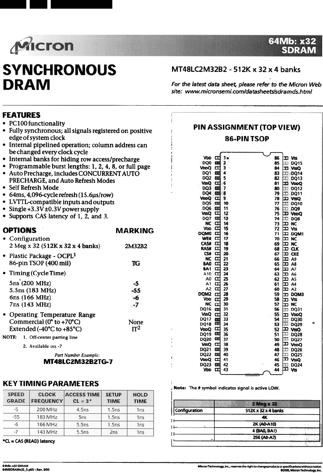
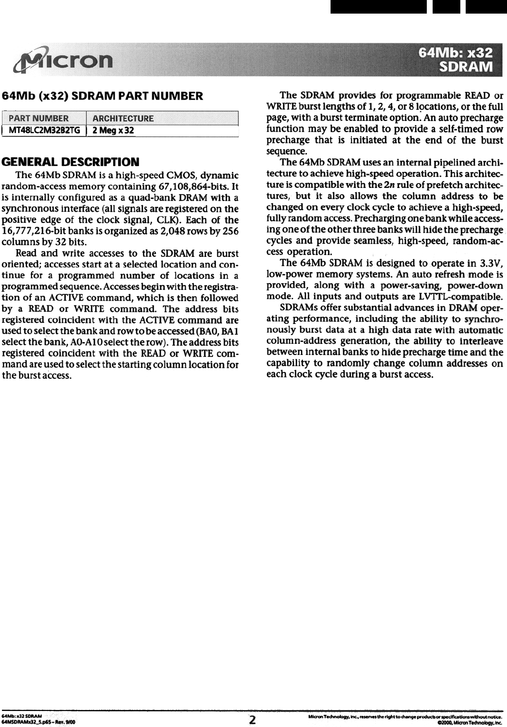
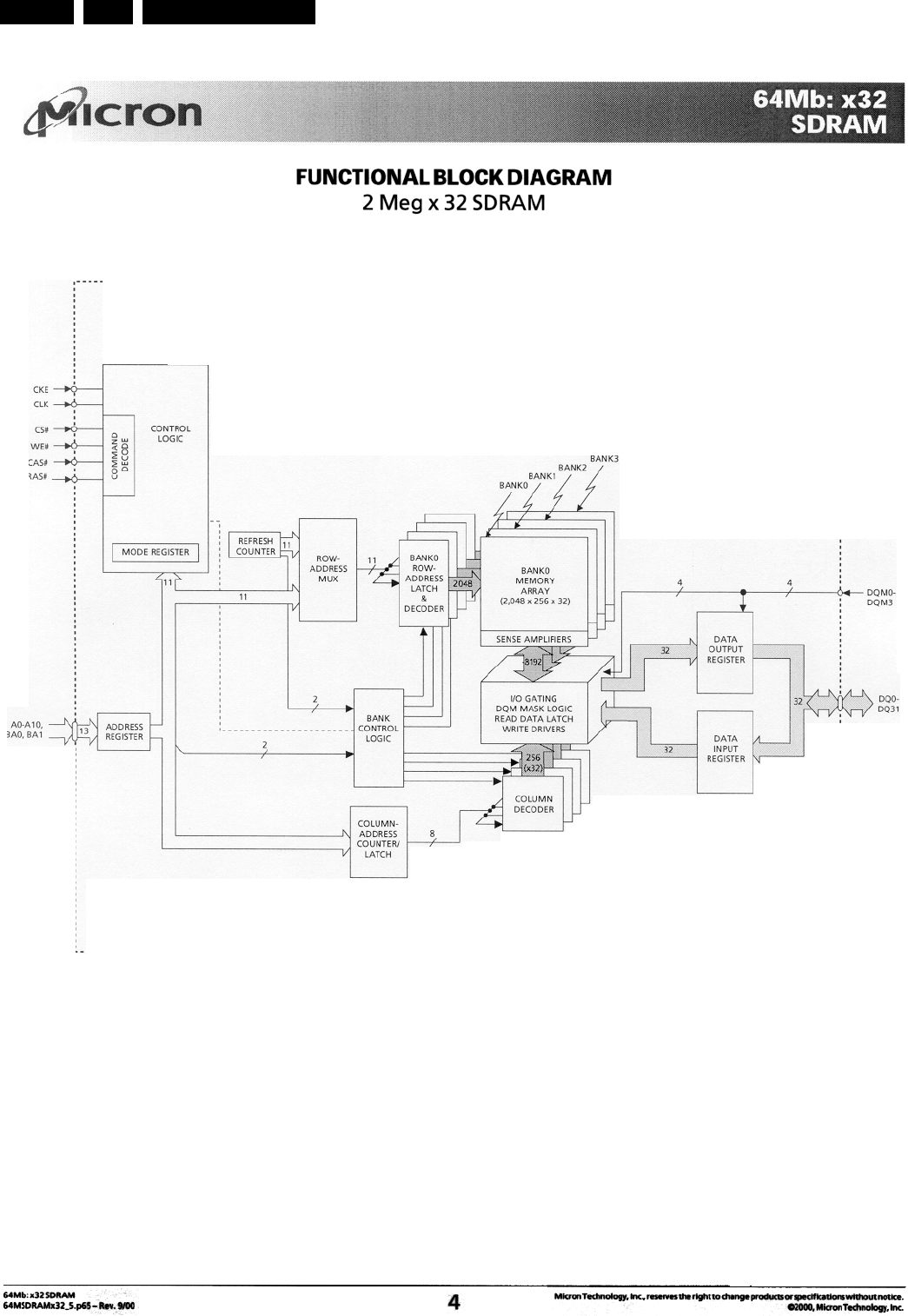
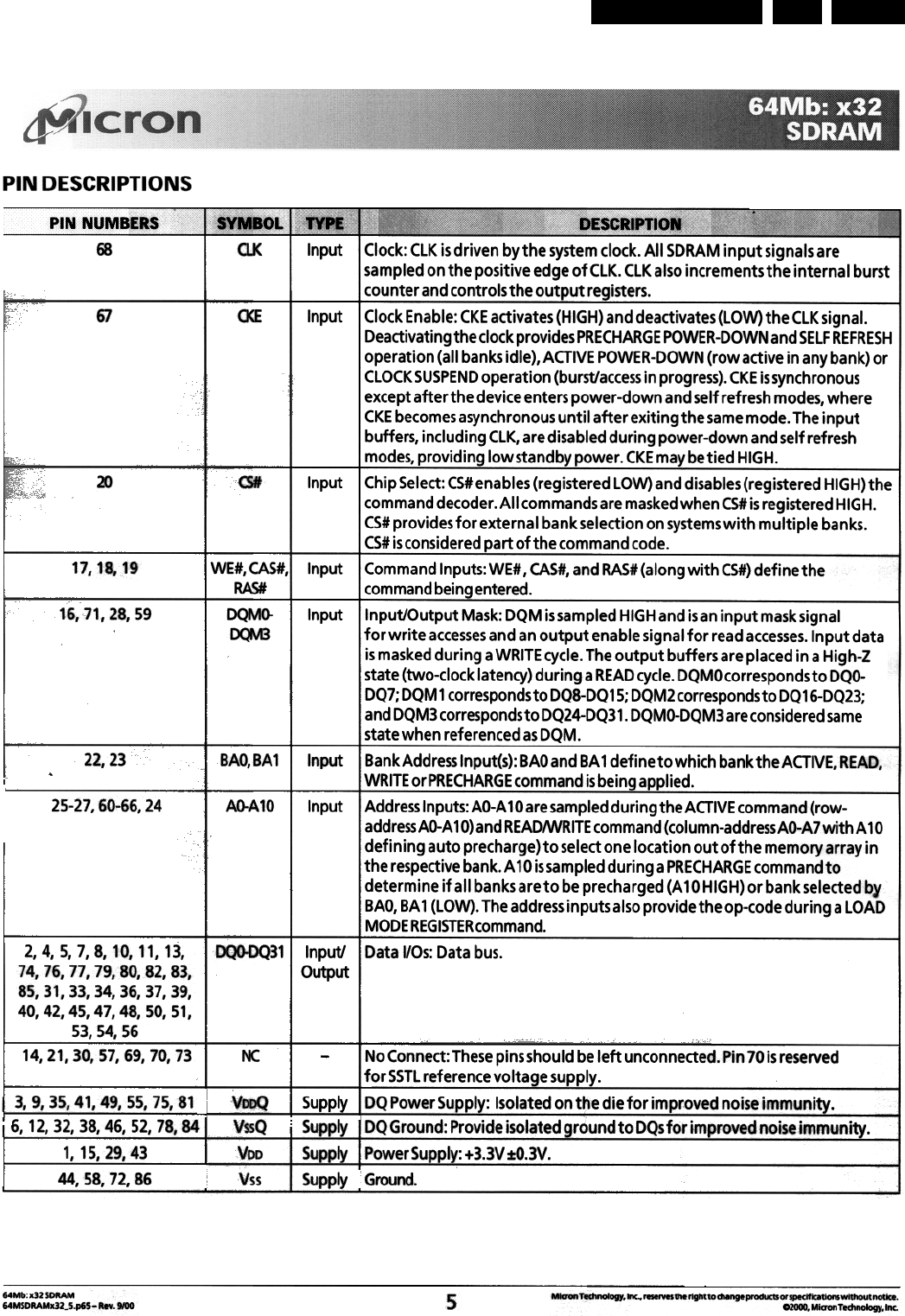
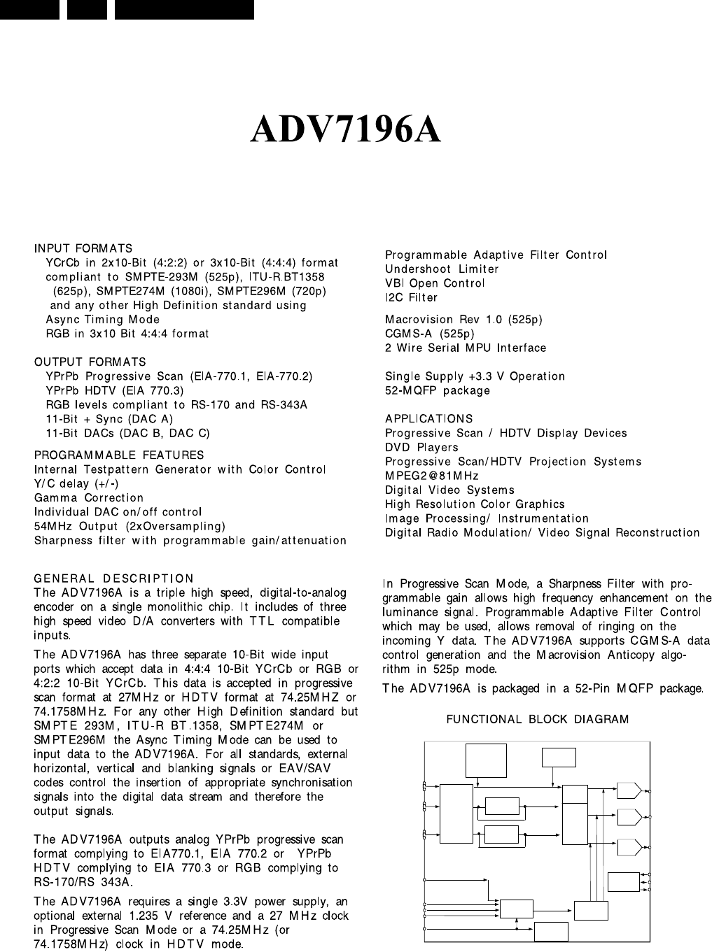
Circuit-, IC Descriptions and List of Abbreviations
EN 280 DVDR980-985 /0X19.
9.8.10 ADV7196
DAC CONTROL
BLOCK
SYNC
GENERATOR
TIMING
GENERATOR
SHARPNESS
FILTER CONTROL
&
ADAPTIVE
FILTER CONTROL
TESTPATTERN
GENERATOR
&
DELAY
&
GAMMA
CORRECTION
2XINTER-
POLATION
CGMS
M AC RO V ISIO N
I2C MPU PORT
11-BIT +
SYNC
DAC
11-BIT
DAC
11-BIT
DAC
HORIZONTALSYNC
VERTICAL SYNC
BLANKING
CLKIN
RESET
DAC A (Y)
DAC B
DAC C
VREF
RSET
COMP
Y0- Y9
Cr0-9
Cb 0-9
CHROMA
4:2:2 to 4:4:4
(SSAF)
LUMA
SSAF
CHROMA
4:2:2 to 4:4:4
(SSAF)
Circuit-, IC Descriptions and List of Abbreviations EN 281DVDR980-985 /0X1 9.
Cr[1]
Cr[2]
Cr[9]
Cr[8]
Cr[3]
Cr[4]
Cr[5]
Cr[7]
Cr[6]
CLKIN
GND
Y[0]
Y[1]
Y[2]
Y[3]
Y[4]
Y[9]
Y[5]
Y[6]
Y[7]
Y[8]
VDD
GND
VREF
RSET
DV
HSYNC/SYNC
VSYNC/TSYNC
DAC B
COMP
DAC A / Y output
DAC C
AGND
VAA
VAA
AGND
ALSB
Cr[0]
SDA
SCL
VDD
Cb/Cr[0]
Cb/Cr[1]
Cb/Cr[2]
Cb/Cr[3]
Cb/Cr[4]
Cb/Cr[5]
Cb/Cr[6]
Cb/Cr[7]
Cb/Cr[8]
Cb/Cr[9]
ADV7196 A
RESET
1
2
3
4
5
6
7
8
9
10
11
12
13
14 15 16 17 18 19 20 21 22 23 24 25 26
27
28
29
30
31
32
33
34
35
36
37
38
39
40414243444546
47
484950
51
52
Pin Id
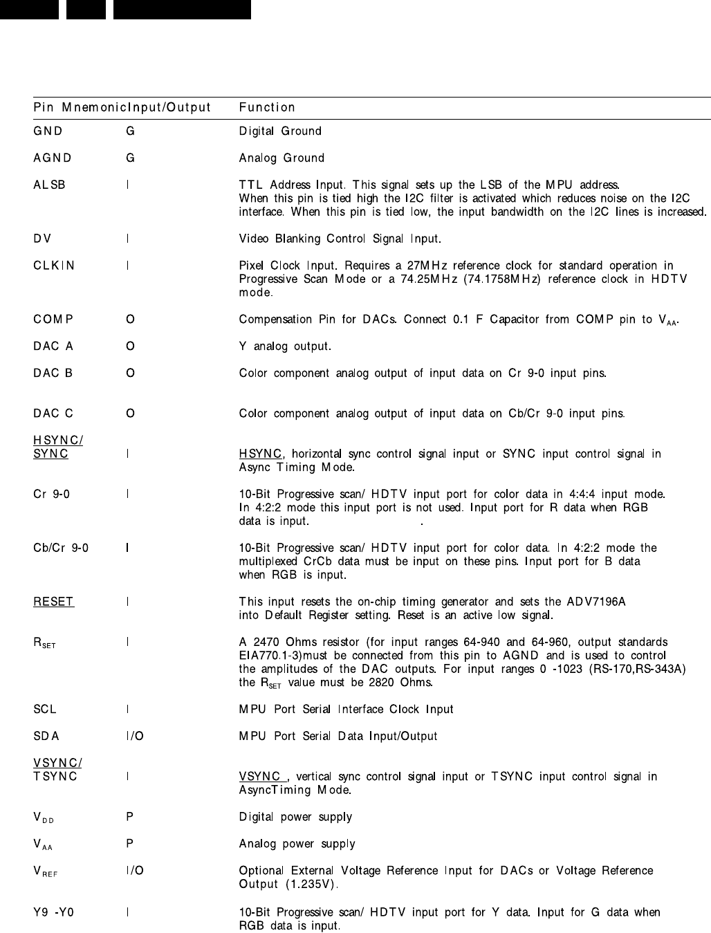

Circuit-, IC Descriptions and List of Abbreviations EN 283DVDR980-985 /0X1 9.
9.9 IC’s Divio
9.9.1 IC7101: 58PDI1394P25PHY
PDI1394P25
1.0 FEATURES
•Fully supports provisions of IEEE 1394±1995 Standard for high
performance serial bus and the P1394a±2000 Standard1
•Fully interoperable with Firewire? and i.LINK? implementations of
the IEEE 1394 Standard.2
•Full P1394a support includes:
±Connection debounce
±Arbitrated short reset
±Multispeed concatenation
±Arbitration acceleration
±Fly-by concatenation
±Port disable/suspend/resume
•Provides one 1394a fully-compliant cable port at
100/200/400 Mbps. Can be used as a one port PHY without the
use of any extra external components
•Fully compliant with Open HCI requirements
•Cable ports monitor line conditions for active connection to remote
node.
•Power down features to conserve energy in battery-powered
applications include:
±Automatic device power down during suspend
±Device power down terminal
±Link interface disable via LPS
±Inactive ports powered-down
•Logic performs system initialization and arbitration functions
•Encode and decode functions included for data-strobe bit level
encoding
•Incoming data resynchronized to local clock
•Single 3.3 volt supply operation
•Minimum VDD of 2.7 V for end-of-wire power-consuming devices
•While unpowered and connected to the bus, will not drive TPBIAS
on a connected port, even if receiving incoming bias voltage on
that port
•Supports extended bias-handshake time for enhanced
interoperability with camcorders
•Interface to link-layer controller supports both low-cost bus-holder
isolation and optional Annex J electrical isolation
•Data interface to link-layer controller through 2/4/8 parallel lines at
49.152 MHz
•Low-cost 24.576 MHz crystal provides transmit, receive data at
100/200/400 Mbps, and link-layer controller clock at 49.152 MHz
•Does not require external filter capacitors for PLL
•Interoperable with link-layer controllers using 3.3 V and 5 V
supplies
•Interoperable with other Physical Layers (PHYs) using 3.3 V and
5 V supplies
•Node power class information signaling for system power
management
•Cable power presence monitoring
•Separate cable bias (TPBIAS) for each port
•Register bits give software control of contender bit, power class
bits, link active bit, and 1394a features
•Function and pin compatible with the Texas Instruments
TSB41LV01? 400 Mbps Phy
2.0 DESCRIPTION
The PDI1394P25 provides the digital and analog transceiver functions
needed to implement a one port node in a cable-based IEEE
1394±1995 and/or 1394a network. Each cable port incorporates two
differential line transceivers. The transceivers include circuitry to
monitor the line conditions as needed for determining connection
status, for initialization and arbitration, and for packet reception and
transmission. The PDI1394P25 is designed to interface with a Link
Layer Controller (LLC), such as the PDI1394L11 or PDI1394L21.
3.0 ORDERING INFORMATION
PACKAGE TEMPERATURE RANGE ORDER CODE PKG. DWG. #
64-pin plastic LQFP 0 to +70°C PDI1394P25BD SOT314-2

Circuit-, IC Descriptions and List of Abbreviations
EN 284 DVDR980-985 /0X19.
4.0 PIN CONFIGURATION
1
2
3
4
5
6
7
19 20 21 22 23 24 25
LREQ
SYSCLK
CNA
CTL0
CTL1
D1
D0
26 2717 18
8
9
10
11
D2
D3
D5
D4
12
13
14
15
D7
PD
LPS
NC
28 29 30 31 32
DGND
48
47
46
45
44
43
42
AGND
NC
NC
NC
NC
AVDD
NC
41
40
39
38
R1
R0
TPBIAS0
AGND
37
36
35
34
TPA0+
TPA0±
TPB0+
TPB0±
62 61 60 59 58 57 56 55 5464 63 53 52 51 50 49
16
D6
33 AGND
DGND
DGND
XO
XI
PLLGND
PLLGND
PLLV
NC
NC
RESET
AV
AGND
AGND
PDI1394P25
DD
AV DD
DVDD
DVDD
DD
DGND
C/LKON
PC0
PC1
PC2
ISO
CPS
DV
DV
TESTM
TEST1
TEST0
AV
AV
AGND
DD
DD
DD
DD
Circuit-, IC Descriptions and List of Abbreviations EN 285DVDR980-985 /0X1 9.
5.0 PIN DESCRIPTION
Name Pin Type Pin Numbers I/O Description
AGND Supply 32, 33, 39, 48, 49,
50 ÐAnalog circuit ground terminals. These terminals should be tied together
to the low impedance circuit board ground plane.
AVDD Supply 30, 31, 42, 51, 52 ÐAnalog circuit power terminals. A combination of high frequency
decoupling capacitors on each side are suggested, such as paralleled
0.1 µF and 0.001 µF. These supply terminals are separated from
PLLVDD and DVDD internal to the device to provide noise isolation. They
should be tied at a low impedance point on the circuit board.
C/LKON CMOS 5 V tol 19 I/O Bus Manager Contender programming input and link-on output. On
hardware reset, this terminal is used to set the default value of the
contender status indicated during self-ID. Programming is done by tying
the terminal through a 10-kΩ resistor to a high (contender) or low (not
contender). The resistor allows the link-on output to override the input.
If this pin is connected to a LLC driver pin for setting Bus Manager/IRM
contender status, then a 10-kΩ series resistor should be placed on this
line between the PHY and the LLC to prevent possible contention. In this
case. the pull-high or pull-low resistors mentioned in the previous
paragraph should not be used. Refer to Figure 9.
Following hardware reset, this terminal is the link-on output, which is
used to notify the LLC to power-up and become active. The link-on
output is a square-wave signal with a period of approximately 163 ns (8
SYSCLK cycles) when active. The link-on output is otherwise driven low,
except during hardware reset when it is high impedance.
The link-on output is activated if the LLC is inactive (LPS inactive or the
LCtrl bit cleared) and when:
a) the PHY receives a link-on PHY packet addressed to this node,
b) the PEI (port-event interrupt) register bit is 1, or
c) any of the CTOI (configuration-timeout interrupt), CPSI
(cable-power-status interrupt), or STOI (state-timeout interrupt)
register bits are 1 and the RPIE (resuming-port interrupt enable)
register bit is also 1.
Once activated, the link-on output will continue active until the LLC
becomes active (both LPS active and the LCtrl bit set). The PHY also
deasserts the link-on output when a bus-reset occurs unless the link-on
output would otherwise be active because one of the interrupt bits is set
(i.e., the link-on output is active due solely to the reception of a link-on
PHY packet).
NOTE: If an interrupt condition exists which would otherwise cause the
link-on output to be activated if the LLC were inactive, the link-on output
will be activated when the LLC subsequently becomes inactive.
CNA CMOS 3 O Cable Not Active output. This terminal is asserted high when there are
no ports receiving incoming bias voltage.
CPS CMOS 24 I Cable Power Status input. This terminal is normally connected to cable
power through a 390 kΩ resistor. This circuit drives an internal
comparator that is used to detect the presence of cable power.
CTL0,
CTL1 CMOS 5 V tol 4, 5 I/O Control I/Os. These bi-directional signals control communication
between the PDI1394P25 and the LLC. Bus holders are built into
these terminals.
D0±D7 CMOS 5 V tol 6, 7, 8, 9, 10, 11,
12, 13 I/O Data I/Os. These are bi-directional data signals between the
PDI1394P25 and the LLC. Bus holders are built into these terminals.
Unused Dn pins should be pulled to ground through 10 kΩ resistors.
DGND Supply 17, 18, 63, 64 ÐDigital circuit ground terminals. These terminals should be tied together
to the low impedance circuit board ground plane.
DVDD Supply 25, 26, 61, 62 ÐDigital circuit power terminals. A combination of high frequency
decoupling capacitors near each side of the IC package are suggested,
such as paralleled 0.1 µF and 0.001 µF. Lower frequency 10 µF filtering
capacitors are also recommended. These supply terminals are
separated from PLLVDD and AVDD internal to the device to provide noise
isolation. They should be tied at a low impedance point on the circuit
board.
Circuit-, IC Descriptions and List of Abbreviations
EN 286 DVDR980-985 /0X19.
Name DescriptionI/OPin NumbersPin Type
ISO CMOS 23 I Link interface isolation control input. This terminal controls the operation
of output differentiation logic on the CTL and D terminals. If an optional
isolation barrier of the type described in Annex J of IEEE Std 1394±1395
is implemented between the PDI1394P25 and LLC, the ISO terminal
should be tied low to enable the differentiation logic. If no isolation
barrier is implemented (direct connection), or bus holder isolation is
implemented, the ISO terminal should be tied high to disable the
differentiation logic.
LPS CMOS 5 V tol 15 I Link Power Status input. This terminal is used to monitor the
active/power status of the link layer controller and to control the state of
the PHY-LLC interface. This terminal should be connected to either the
VDD supplying the LLC through a 10 kΩ resistor, or to a pulsed output
which is active when the LLC is powered. A pulsed signal should be
used when an isolation barrier exists between the LLC and PHY. (See
Figure 8)
The LPS input is considered inactive if it is sampled low by the PHY for
more than 2.6 µs (128 SYSCLK cycles), and is considered active
otherwise (i.e., asserted steady high or an oscillating signal with a low
time less than 2.6 µs). The LPS input must be high for at least 21 ns in
order to be guaranteed to be observed as high by the PHY.
When the PDI1394P25 detects that LPS is inactive, it will place the
PHY-LLC interface into a low-power reset state. In the reset state, the
CTL and D outputs are held in the logic zero state and the LREQ input is
ignored; however, the SYSCLK output remains active. If the LPS input
remains low for more than 26 µs (1280 SYSCLK cycles), the PHY-LLC
interface is put into a low-power disabled state in which the SYSCLK
output is also held inactive. The PHY-LLC interface is placed into the
disabled state upon hardware reset.
The LLC is considered active only if both the LPS input is active and the
LCtrl register bit is set to 1, and is considered inactive if either the LPS
input is inactive or the LCtrl register bit is cleared to 0.
LREQ CMOS 5 V tol 1 I LLC Request input. The LLC uses this input to initiate a service request
to the PDI1394P25. Bus holder is built into this terminal.
NC No connect 54, 55 ÐThese pins are not internally connected and consequently are ªdon't
caresº. Other vendors' pin compatible chips may require
connections and external circuitry on these pins.
NC No connect 16, 43, 44, 45, 46,
47 ÐNo connect.
PC0, PC1,
PC2 CMOS 5 V tol 20, 21, 22 IPower Class programming inputs. On hardware reset, these inputs set
the default value of the power class indicated during self-ID.
Programming is done by tying the terminals high or low. Refer to
Table 21 for encoding.
PD CMOS 5 V tol 14 I Power Down input. A logic high on this terminal turns off all internal
circuitry except the cable-active monitor circuits which control the CNA
output. For more information, refer to Section 17.2
PLLGND Supply 57, 58 ÐPLL circuit ground terminals. These terminals should be tied together to
the low impedance circuit board ground plane.
PLLVDD Supply 56 Ð PLL circuit power terminals. A combination of high frequency decoupling
capacitors near each terminal are suggested, such as paralleled 0.1 µF
and 0.001 µF. These supply terminals are separated from DVDD and
AVDD internal to the device to provide noise isolation. They should be
tied at a low impedance point on the circuit board.
RESET CMOS 5 V tol 53 I Logic reset input. Asserting this terminal low resets the internal logic. An
internal pull-up resistor to VDD is provided so only an external
delay capacitor is required for proper power-up operation. For more
information, refer to Section 17.2. This input is otherwise a standard
Schmitt logic input, and can also be driven by an open-drain type driver.
R0, R1 Bias 40, 41 ÐCurrent setting resistor pins These pins are connected to an external
resistance to set the internal operating currents and cable driver output
currents. A resistance of 6.34 kΩ ±1% is required to meet the IEEE
1394±1995 Std. output voltage limits.
Circuit-, IC Descriptions and List of Abbreviations EN 287DVDR980-985 /0X1 9.
Name DescriptionI/OPin NumbersPin Type
SYSCLK CMOS 2 O System clock output. Provides a 49.152 MHz clock signal, synchronized
with data transfers, to the LLC.
TEST0 CMOS 29 I Test control input. This input is used in manufacturing tests of the
PDI1394P25. For normal use, this terminal should be tied to GND.
TEST1 CMOS 28 I Test control input. This input is used in manufacturing tests of the
PDI1394P25. For normal use, this terminal should be tied to GND.
Other vendors' pin compatible chips may require connections and
external circuitry on this pin.
TESTM CMOS 27 I Test control input. This input is used in manufacturing tests of the
PDI1394P25. For normal use, this terminal should be tied to VDD.
TPA0+ Cable 37 I/O Twisted-pair cable A differential signal terminals. Board traces from each
pair of positive and ne
g
ative differential si
g
nal terminals should be kept
TPA0± Cable 36 I/O
gg
matched and as short as possible to the external load resistors and to
the cable connector.
TPB0+ Cable 35 I/O Twisted-pair cable B differential signal terminals. Board traces from each
pair of positive and ne
g
ative differential si
g
nal terminals should be kept
TPB0± Cable 34 I/O
gg
matched and as short as possible to the external load resistors and to
the cable connector.
TPBIAS0 Cable 38 I/O Twisted-pair bias output. This provides the 1.86 V nominal bias voltage
needed for proper operation of the twisted-pair cable drivers and
receivers, and for signaling to the remote nodes that there is an active
cable connection. These terminals must be decoupled with a
0.3 µF±1 µF capacitor to ground.
XO, XI Crystal 59, 60 ÐCrystal oscillator inputs. These terminals connect to a 24.576 MHz
parallel resonant fundamental mode crystal. The optimum values for the
external shunt capacitors are dependent on the specifications of the
crystal used. Can also be driven by an external clock generator (leave
XO unconnected in this case and start supplying the external clock
before resetting the PDI1394P25). For more information, refer to
Section 17.5
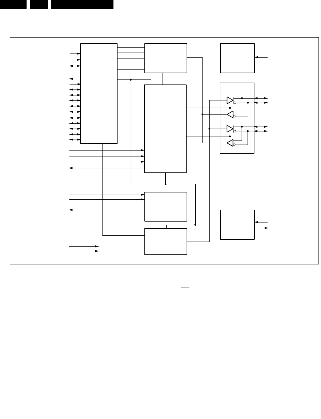
Circuit-, IC Descriptions and List of Abbreviations
EN 288 DVDR980-985 /0X19.
6.0 BLOCK DIAGRAM
CABLE PORT 0
RECEIVED DATA
DECODER/
RETIMER
LINK
INTERFACE
I/O
ARBITRATION
AND CONTROL
STATE MACHINE
LOGIC
CRYSTAL
OSCILLATOR,
PLL SYSTEM,
AND CLOCK
GENERATOR
TRANSMIT
DATA
ENCODER
CNA
PC0
PC1
PC2
D0
D1
D2
D3
CTL0
CTL1
LREQ
SYSCLK
C/LKON
/ISO
LPS
/RESET
PD
TPA0+
TPA0±
TPB0+
TPB0±
XI
XO
SV01829
D4
D5
D6
D7
BIAS VOLTAGE
AND
CURRENT
GENERATOR
R0
R1
TPBIAS0
CABLE POWER
DETECTOR CPS
7.0 FUNCTIONAL SPECIFICATION
The PDI1394P25 requires only an external 24.576 MHz crystal as a
reference. An external clock can be connected to XI instead of a
crystal. An internal oscillator drives an internal phase-locked loop
(PLL), which generates the required 393.216 MHz reference signal.
This reference signal is internally divided to provide the clock signals
used to control transmission of the outbound encoded Strobe and
Data information. A 49.152 MHz clock signal, supplied to the
associated LLC for synchronization of the two chips, is used for
resynchronization of the received data. The Power Down (PD)
function, when enabled by asserting the PD terminal high, stops
operation of the PLL and disables all circuits except the cable bias
detectors at the TPB terminals. The port transmitter circuitry and the
receiver circuitry are also disabled when the port is disabled,
suspended, or disconnected.
The PDI1394P25 supports an optional isolation barrier between
itself and its LLC. When the ISO input terminal is tied high, the
LLC interface outputs behave normally. When the ISO terminal is
tied low, internal differentiating logic is enabled, and the outputs are
driven such that they can be coupled through a capacitive or
transformer galvanic isolation barrier as described in
IEEE 1394a
section 5.9.4
. To operate with single capacitor (bus holder) isolation,
the ISO on the PHY terminal must be tied high. For more details on
using single capacitor isolation, please refer to the Philips Isolation
Application Note AN2452.
Data bits to be transmitted through the cable ports are received from
the LLC on two, four or eight parallel paths (depending on the
requested transmission speed). They are latched internally in the
PDI1394P25 in synchronization with the 49.152 MHz system clock.
These bits are combined serially, encoded, and transmitted at
98.304/196.608/392.216 Mbps (referred to as S100, S200, and
S400 speed, respectively) as the outbound data-strobe information
stream. During transmission, the encoded data information is
transmitted differentially on the TPB cable pair(s), and the encoded
strobe information is transmitted differentially on the TPA cable
pair(s).
During packet reception the TPA and TPB transmitters of the
receiving cable port are disabled, and the receivers for that port are
enabled. The encoded data information is received on the TPA cable
pair, and the encoded strobe information is received on the TPB
cable pair. The received data-strobe information is decoded to
recover the receive clock signal and the serial data bits. The serial

Circuit-, IC Descriptions and List of Abbreviations EN 289DVDR980-985 /0X1 9.
data bits are split into two-, four- or eight-bit parallel streams
(depending upon the indicated receive speed), resynchronized to
the local 49.152 MHz system clock and sent to the associated LLC.
Both the TPA and TPB cable interfaces incorporate differential
comparators to monitor the line states during initialization and
arbitration. The outputs of these comparators are used by the
internal logic to determine the arbitration status. The TPA channel
monitors the incoming cable common-mode voltage. The value of
this common-mode voltage is used during arbitration to set the
speed of the next packet transmission (speed signaling). In addition,
the TPB channel monitors the incoming cable common-mode
voltage on the TPB pair for the presence of the remotely supplied
twisted-pair bias voltage (cable bias detection).
The PDI1394P25 provides a 1.86 V nominal bias voltage at the
TPBIAS terminal for port termination. The PHY contains two
independent TPBIAS circuits. This bias voltage, when seen through
a cable by a remote receiver, indicates the presence of an active
connection. This bias voltage source must be stabilized by an
external filter capacitor of 0.3 µF±1 µF.
The line drivers in the PDI1394P25 operate in a high-impedance
current mode, and are designed to work with external 112 Ω
line-termination resistor networks in order to match the 110 Ω cable
impedance. One network is provided at each end of all twisted-pair
cable connections. Each network is composed of a pair of
series-connected 56 Ω resistors. The midpoint of the pair of resistors
that is directly connected to the twisted-pair A terminals is connected
to its corresponding TPBIAS voltage terminal. The midpoint of the pair
of resistors that is directly connected to the twisted-pair B terminals is
coupled to ground through a parallel R-C network with recommended
values of 5 kΩ and 220 pF. The values of the external line termination
resistors are designed to meet the standard specifications when
connected in parallel with the internal receiver circuits. An external
resistor connected between the R0 and R1 terminals sets the driver
output current, along with other internal operating currents. This
current setting resistor has a value of 6.34 kΩ ±1%.
When the power supply of the PDI1394P25 is removed while the
twisted-pair cables are connected, the PDI1394P25 transmitter and
receiver circuitry presents a high impedance to the cable in order to
not load the TPBIAS voltage on the other end of the cable.
The TEST0 and TEST1 terminals are used to set up various
manufacturing test conditions. For normal operation, they should be
connected to ground. TEST1 can also be tied through a 1 kΩ
resistor to ground to accommodate other vendors' pin compatible
chips.
The TESTM terminal is used to set up various manufacturing test
conditions. For normal operation it should be tied to VDD.
Four package terminals, used as inputs to set the default value for
four configuration status bits in the self-ID packet, should be
hard-wired high or low as a function of the equipment design. The
PC0±PC2 terminals are used to indicate the default power-class
status for the node (the need for power from the cable or the ability
to supply power to the cable). See Table 21 for power class
encoding. The C/LKON terminal is used as an input to indicate that
the node is a contender for bus manager.
The PHY supports suspend/resume as defined in the IEEE 1394a
specification. The suspend mechanism allows pairs of directly
connected ports to be placed into a low power state while
maintaining a port-to-port connection between 1394 bus segments.
While in a low power state, a port is unable to transmit or receive
data transaction packets. However, a port in a low power state is
capable of detecting connection status changes and detecting
incoming TPBIAS. When the PDI1394P25's port is suspended, all
circuits except the bias-detection circuits are powered down,
resulting in significant power savings. The TPBIAS circuit monitors
the value of incoming TPA pair common-mode voltage when local
TPBIAS is inactive. Because this circuit has an internal current
source and the connected node has a current sink, the monitored
value indicates the cable connection status. This monitor is called
connect-detect.
Both the cable bias-detect monitor and TPBIAS connect-detect
monitor are used in suspend/resume signaling and cable connection
detection. For additional details of suspend/resume operation, refer
to the 1394a specification. The use of suspend/resume is
recommended for new designs.
The port transmitter and receiver circuitry is disabled during power
down (when the PD input terminal is asserted high), during reset
(when the RESET input terminal is asserted low), when no active
cable is connected to the port, or when controlled by the internal
arbitration logic. The port twisted-pair bias voltage circuitry is
disabled during power down, during reset, or when the port is
disabled as commanded by the LLC.
The CNA (cable-not-active) terminal provides a high when the
twisted-pair cable port is not receiving incoming bias (i.e., it is either
disconnected or suspended), and can be used along with LPS to
determine when to power-down the PDI1394P25. The CNA output is
not debounced. When the PD terminal is asserted high, the CNA
detection circuitry is enabled (regardless of the previous state of the
ports) and a pull-down is activated on the RESET terminal so as to
force a reset of the PDI1394P25 internal logic.
The LPS (link power status) terminal works with the C/LKON
terminal to manage the power usage in the node. The LPS signal
from the LLC is used in conjunction with the LCtrl bit (see Table 1
and Table 2) to indicate the active/power status of the LLC. The LPS
signal is also used to reset, disable, and initialize the PHY-LLC
interface (the state of the PHY-LCC interface is controlled solely by
the LPS input regardless of the state of the LCtrl bit).
The LPS input is considered inactive if it remains low for more than
2.6 µs and is considered active otherwise. When the PDI1394P25
detects that LPS is inactive, it will place the PHY-LLC interface into a
low-power reset state in which the CTL and D outputs are held in the
logic zero state and the LREQ input is ignored; however, the
SYSCLK output remains active. If the LPS input remains low for
more than 26 µs, the PHY-LLC interface is put into a low-power
disabled state in which the SYSCLK output is also held inactive. The
PHY-LLC interface is also held in the disabled state during hardware
reset. The PDI1394P25 will continue the necessary repeater
functions required for normal network operation regardless of the
state of the PHY-LLC interface. When the interface is in the reset or
disabled state and LPS is again observed active, the PHY will
initialize the interface and return it to normal operation.
The PHY uses the C/LKON terminal to notify the LLC to power up
and become active. When activated, the C/LKON signal is a square
wave of approximately 163 ns period. The PHY activates the
C/LKON output when the LLC is inactive and a wake-up event
occurs. The LLC is considered inactive when either the LPS input is
inactive, as described above, or the LCtrI bit is cleared to 0. A
wake-up event occurs when a link-on PHY packet addressed to this
node is received, or conditionally when a PHY interrupt occurs. The
PHY deasserts the C/LKON output when the LLC becomes active
(both LPS active and the LCtrl bit set to 1). The PHY also deasserts
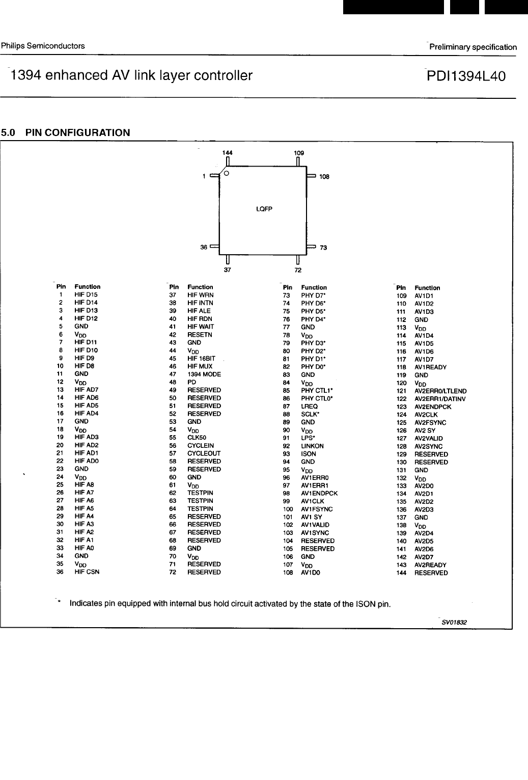

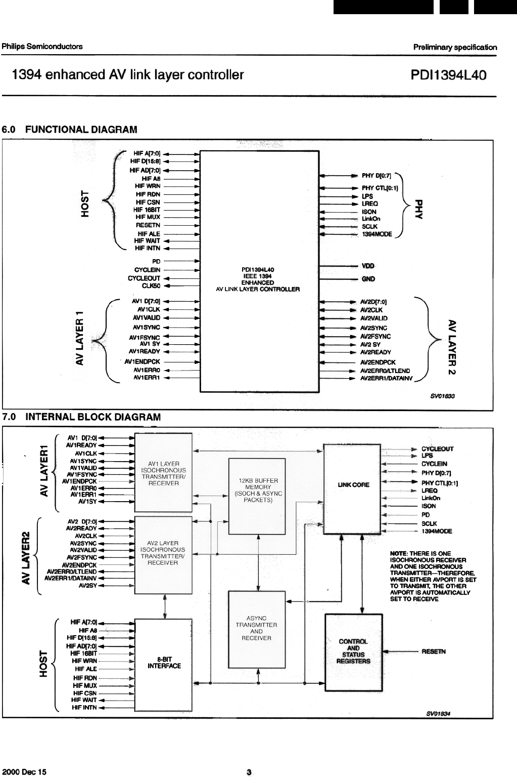
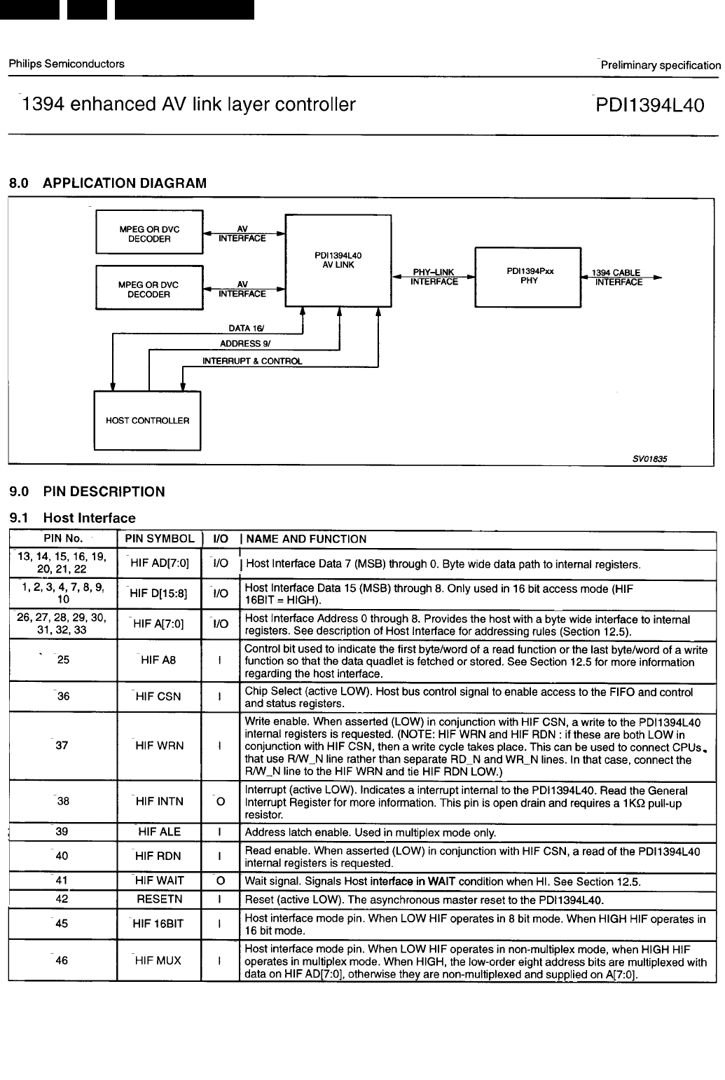
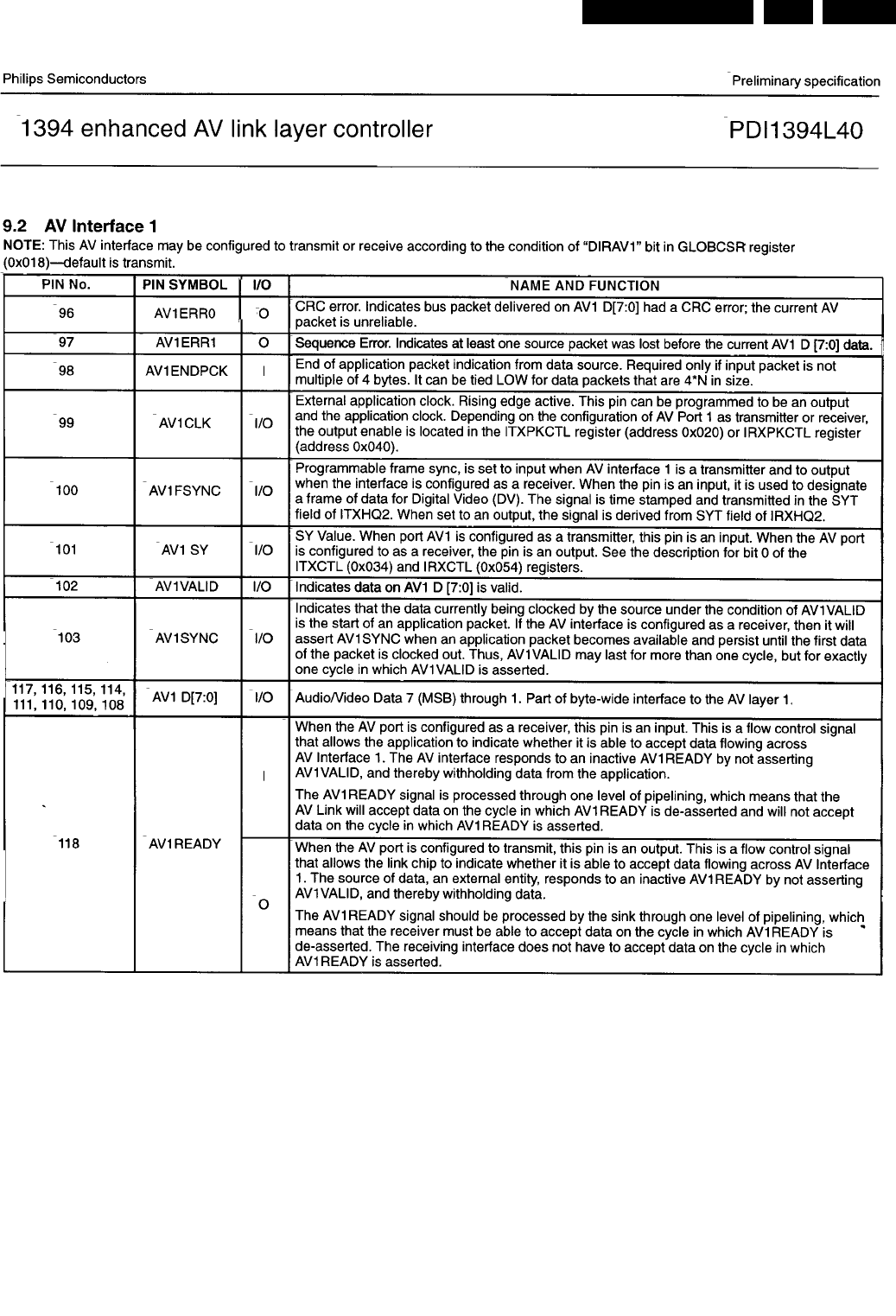
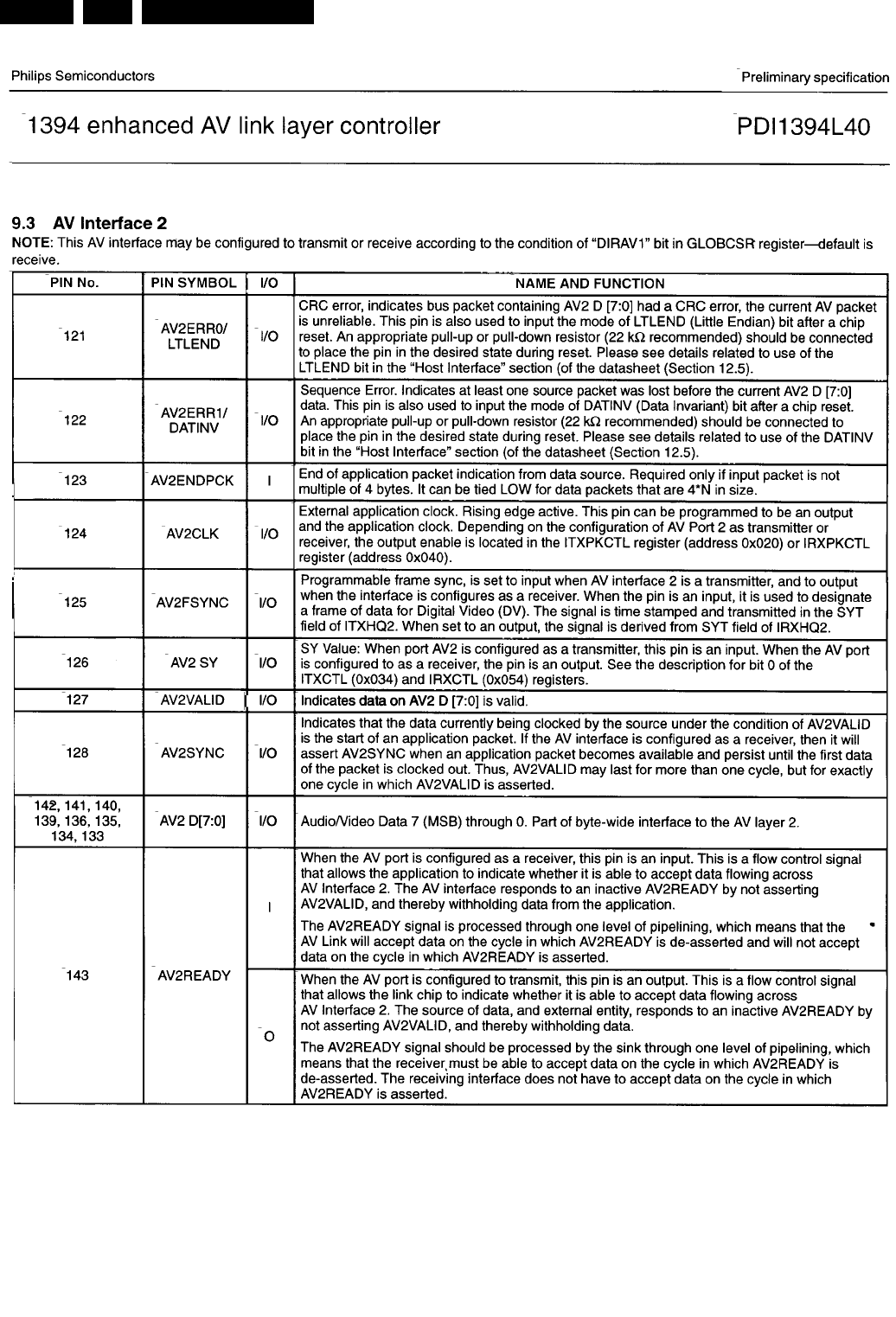
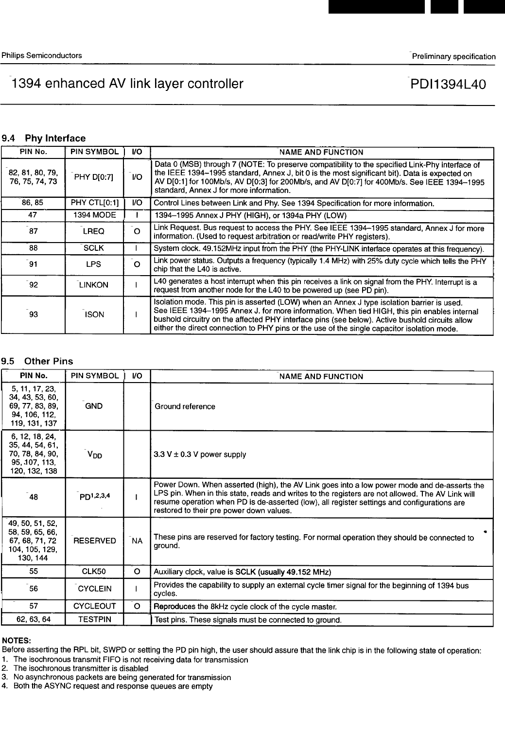

Circuit-, IC Descriptions and List of Abbreviations
EN 298 DVDR980-985 /0X19.
9.9.3 IC7203: P89C51RD
P89C51RB2/P89C51RC2/
P89C51RD2
80C51 8-bit Flash microcontroller family
16KB/32KB/64KB ISP/IAP Flash with 512B/512B/1KB RAM
DESCRIPTION
The P89C51RB2/RC2/RD2 device contains a non-volatile
16kB/32kB/64kB Flash program memory that is both parallel
programmable and serial In-System and In-Application
Programmable. In-System Programming (ISP) allows the user to
download new code while the microcontroller sits in the application.
In-Application Programming (IAP) means that the microcontroller
fetches new program code and reprograms itself while in the
system. This allows for remote programming over a modem link.
A default serial loader (boot loader) program in ROM allows serial
In-System programming of the Flash memory via the UART without
the need for a loader in the Flash code. For In-Application
Programming, the user program erases and reprograms the Flash
memory by use of standard routines contained in ROM.
This device executes one machine cycle in 6 clock cycles, hence
providing twice the speed of a conventional 80C51. An OTP
configuration bit lets the user select conventional 12 clock timing
if desired.
This device is a Single-Chip 8-Bit Microcontroller manufactured in
advanced CMOS process and is a derivative of the 80C51
microcontroller family. The instruction set is 100% compatible with
the 80C51 instruction set.
The device also has four 8-bit I/O ports, three 16-bit timer/event
counters, a multi-source, four-priority-level, nested interrupt structure,
an enhanced UART and on-chip oscillator and timing circuits.
The added features of the P89C51RB2/RC2/RD2 makes it a
powerful microcontroller for applications that require pulse width
modulation, high-speed I/O and up/down counting capabilities such
as motor control.
FEATURES
80C51 Central Processing Unit
On-chip Flash Program Memory with In-System Programming
(ISP) and In-Application Programming (IAP) capability
Boot ROM contains low level Flash programming routines for
downloading via the UART
Can be programmed by the end-user application (IAP)
6 clocks per machine cycle operation (standard)
12 clocks per machine cycle operation (optional)
Speed up to 20 MHz with 6 clock cycles per machine cycle
(40 MHz equivalent performance); up to 33 MHz with 12 clocks
per machine cycle
Fully static operation
RAM expandable externally to 64 kB
4 level priority interrupt
7 interrupt sources
Four 8-bit I/O ports
Full-duplex enhanced UART
±Framing error detection
±Automatic address recognition
Power control modes
±Clock can be stopped and resumed
±Idle mode
±Power down mode
Programmable clock out
Second DPTR register
Asynchronous port reset
Low EMI (inhibit ALE)
Programmable Counter Array (PCA)
±PWM
±Capture/compare
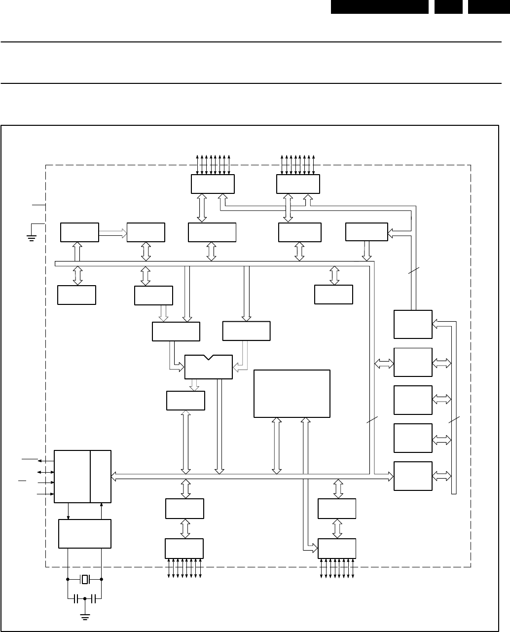
Circuit-, IC Descriptions and List of Abbreviations EN 299DVDR980-985 /0X1 9.
P89C51RB2/P89C51RC2/
P89C51RD2
80C51 8-bit Flash microcontroller family
16KB/32KB/64KB ISP/IAP Flash with 512B/512B/1KB RAM
BLOCK DIAGRAM
SU01065
PSEN
EAVPP
ALE
RST
XTAL1 XTAL2
VCC
VSS
PORT 0
DRIVERS PORT 2
DRIVERS
RAM ADDR
REGISTER RAM PORT 0
LATCH PORT 2
LATCH FLASH
REGISTER
BACC STACK
POINTER
TMP2 TMP1
ALU
TIMING
AND
CONTROL
INSTRUCTION
REGISTER
PD
OSCILLATOR
PSW
PORT 1
LATCH PORT 3
LATCH
PORT 1
DRIVERS PORT 3
DRIVERS
PROGRAM
ADDRESS
REGISTER
BUFFER
PC
INCRE-
MENTER
PROGRAM
COUNTER
DPTR'S
MULTIPLE
P1.0±P1.7 P3.0±P3.7
P0.0±P0.7 P2.0±P2.7
SFRs
TIMERS
P.C.A.
8
8 16
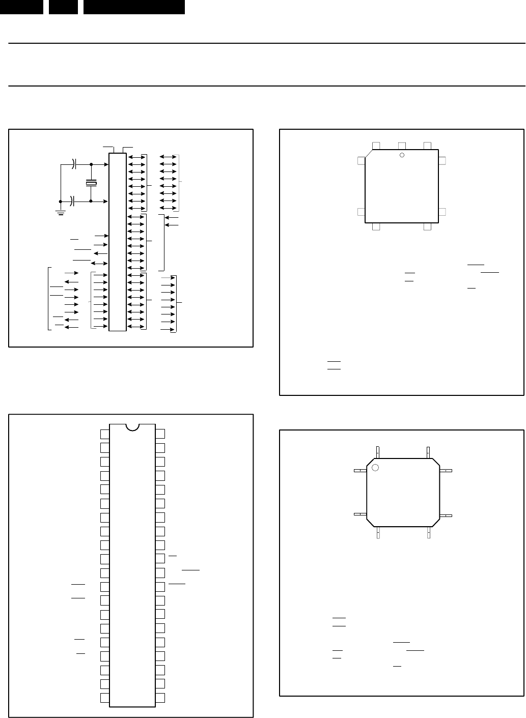
Circuit-, IC Descriptions and List of Abbreviations
EN 300 DVDR980-985 /0X19.
P89C51RB2/P89C51RC2/
P89C51RD2
80C51 8-bit Flash microcontroller family
16KB/32KB/64KB ISP/IAP Flash with 512B/512B/1KB RAM
LOGIC SYMBOL
PORT 0
PORT 1PORT 2
PORT 3
ADDRESS AND
DATA BUS
ADDRESS BUS
T2
T2EX
RxD
TxD
INT0
INT1
T0
T1
WR
RD
SECONDARY FUNCTIONS
RST
EA/VPP
PSEN
ALE/PROG
VSS
VCC
XTAL1
XTAL2
SU01302
PINNING
Plastic Dual In-Line Package
1
2
3
4
5
6
7
8
9
10
11
12
13
14
15
16
17
18
19
20 21
22
23
24
25
26
27
28
29
30
31
32
33
34
35
36
37
38
39
40
T2/P1.0
T2EX/P1.1
ECI/P1.2
CEX0/P1.3
CEX1/P1.4
CEX2/P1.5
CEX3/P1.6
RST
RxD/P3.0
TxD/P3.1
INT0/P3.2
INT1/P3.3
T0/P3.4
T1/P3.5
CEX4/P1.7
WR/P3.6
RD/P3.7
XTAL2
XTAL1
VSS P2.0/A8
P2.1/A9
P2.2/A10
P2.3/A11
P2.4/A12
P2.5/A13
P2.6/A14
P2.7/A15
PSEN
ALE/PROG
EA/VPP
P0.7/AD7
P0.6/AD6
P0.5/AD5
P0.4/AD4
P0.3/AD3
P0.2/AD2
P0.1/AD1
P0.0/AD0
VCC
DUAL
IN-LINE
PACKAGE
SU00021
Plastic Leaded Chip Carrier
LCC
6140
7
17
39
29
18 28
Pin Function
1 NIC*
2 P1.0/T2
3 P1.1/T2EX
4 P1.2/ECI
5 P1.3/CEX0
6 P1.4/CEX1
7 P1.5/CEX2
8 P1.6/CEX3
9 P1.7/CEX4
10 RST
11 P3.0/RxD
12 NIC*
13 P3.1/TxD
14 P3.2/INT0
15 P3.3/INT1
Pin Function
16 P3.4/T0
17 P3.5/T1
18 P3.6/WR
19 P3.7/RD
20 XTAL2
21 XTAL1
22 VSS
23 NIC*
24 P2.0/A8
25 P2.1/A9
26 P2.2/A10
27 P2.3/A11
28 P2.4/A12
29 P2.5/A13
30 P2.6/A14
Pin Function
31 P2.7/A15
32 PSEN
33 ALE/PROG
34 NIC*
35 EA/VPP
36 P0.7/AD7
37 P0.6/AD6
38 P0.5/AD5
39 P0.4/AD4
40 P0.3/AD3
41 P0.2/AD2
42 P0.1/AD1
43 P0.0/AD0
44 VCC
SU00023
* NO INTERNAL CONNECTION
Plastic Quad Flat Pack
LQFP
44 34
1
11
33
23
12 22
Pin Function
1 P1.5/CEX2
2 P1.6/CEX3
3 P1.7/CEX4
4 RST
5 P3.0/RxD
6 NIC*
7 P3.1/TxD
8 P3.2/INT0
9 P3.3/INT1
10 P3.4/T0
11 P3.5/T1
12 P3.6/WR
13 P3.7/RD
14 XTAL2
15 XTAL1
Pin Function
16 VSS
17 NIC*
18 P2.0/A8
19 P2.1/A9
20 P2.2/A10
21 P2.3/A11
22 P2.4/A12
23 P2.5/A13
24 P2.6/A14
25 P2.7/A15
26 PSEN
27 ALE/PROG
28 NIC*
29 EA/VPP
30 P0.7/AD7
Pin Function
31 P0.6/AD6
32 P0.5/AD5
33 P0.4/AD4
34 P0.3/AD3
35 P0.2/AD2
36 P0.1/AD1
37 P0.0/AD0
38 VCC
39 NIC*
40 P1.0/T2
41 P1.1/T2EX
42 P1.2/ECI
43 P1.3/CEX0
44 P1.4/CEX1
SU01400
* NO INTERNAL CONNECTION
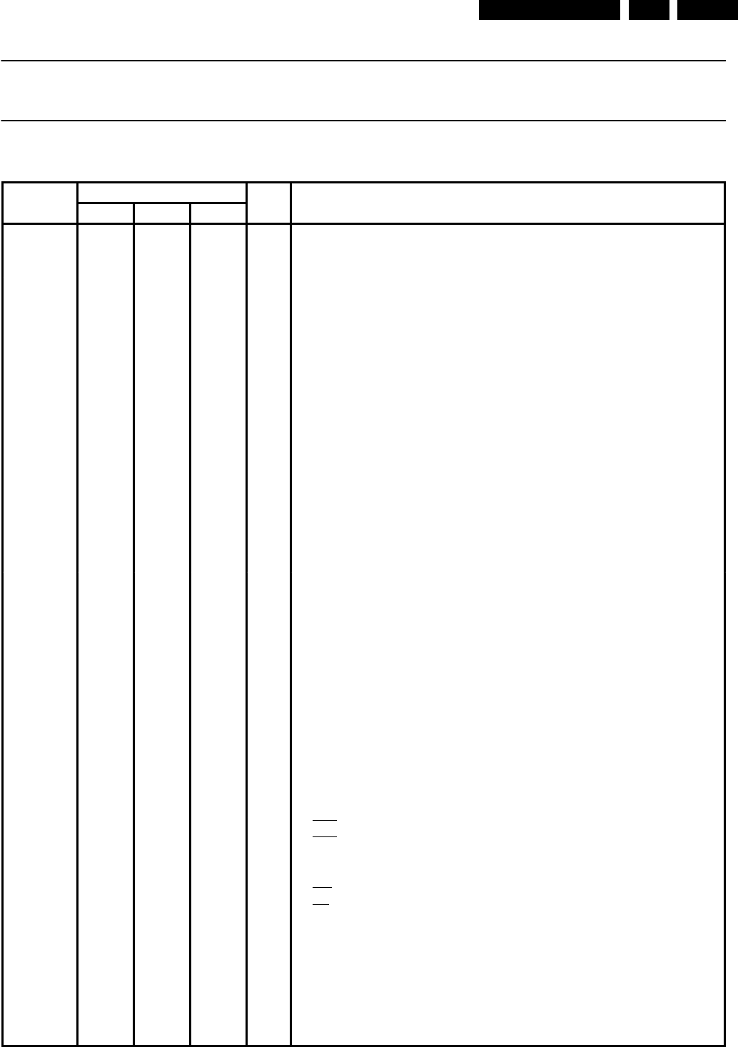
Circuit-, IC Descriptions and List of Abbreviations EN 301DVDR980-985 /0X1 9.
P89C51RB2/P89C51RC2/
P89C51RD2
80C51 8-bit Flash microcontroller family
16KB/32KB/64KB ISP/IAP Flash with 512B/512B/1KB RAM
PIN DESCRIPTIONS
MNEMONIC
PIN NUMBER
TYPE
NAME AND FUNCTION
MNEMONIC
PDIP PLCC LQFP
TYPE
NAME
AND
FUNCTION
V
SS
20 22 16 I Ground: 0 V reference.
V
CC
40 44 38 I Power Supply: This is the power supply voltage for normal, idle, and power-down
operation.
P0.0±0.7 39±32 43±36 37±30 I/O Port 0: Port 0 is an open-drain, bidirectional I/O port. Port 0 pins that have 1s
written to them float and can be used as high-impedance inputs. Port 0 is also the
multiplexed low-order address and data bus during accesses to external program
and data memory. In this application, it uses strong internal pull-ups when emitting 1s.
P1.0±P1.7 1±8 2±9 40±44,
1±3 I/O Port 1: Port 1 is an 8-bit bidirectional I/O port with internal pull-ups on all pins
except P1.6 and P1.7 which are open drain. Port 1 pins that have 1s written to them
are pulled high by the internal pull-ups and can be used as inputs. As inputs, port 1
pins that are externally pulled low will source current because of the internal
pull-ups. (See DC Electrical Characteristics: I
IL
).
Alternate functions for 89C51RB2/RC2/RD2 Port 1 include:
1 2 40 I/O T2 (P1.0): Timer/Counter 2 external count input/Clockout (see Programmable
Clock-Out)
2 3 41 I T2EX (P1.1): Timer/Counter 2 Reload/Capture/Direction Control
3 4 42 I ECI (P1.2): External Clock Input to the PCA
4 5 43 I/O CEX0 (P1.3): Capture/Compare External I/O for PCA module 0
5 6 44 I/O CEX1 (P1.4): Capture/Compare External I/O for PCA module 1
6 7 1 I/O CEX2 (P1.5): Capture/Compare External I/O for PCA module 2
7 8 2 I/O CEX3 (P1.6): Capture/Compare External I/O for PCA module 3
8 9 3 I/O CEX4 (P1.7): Capture/Compare External I/O for PCA module 4
P2.0±P2.7 21±28 24±31 18±25 I/O Port 2: Port 2 is an 8-bit bidirectional I/O port with internal pull-ups. Port 2 pins that
have 1s written to them are pulled high by the internal pull-ups and can be used as
inputs. As inputs, port 2 pins that are externally being pulled low will source current
because of the internal pull-ups. (See DC Electrical Characteristics: I
IL
). Port 2
emits the high-order address byte during fetches from external program memory
and during accesses to external data memory that use 16-bit addresses (MOVX
@DPTR). In this application, it uses strong internal pull-ups when emitting 1s.
During accesses to external data memory that use 8-bit addresses (MOV @Ri),
port 2 emits the contents of the P2 special function register.
P2.7 must be a ªIº to program and erase the device.
P3.0±P3.7 10±17 11,
13±19 5, 7±13 I/O Port 3: Port 3 is an 8-bit bidirectional I/O port with internal pull-ups. Port 3 pins that
have 1s written to them are pulled high by the internal pull-ups and can be used as
inputs. As inputs, port 3 pins that are externally being pulled low will source current
because of the pull-ups. (See DC Electrical Characteristics: I
IL
). Port 3 also serves
the special features of the 89C51RB2/RC2/RD2, as listed below:
10 11 5 I RxD (P3.0): Serial input port
11 13 7 O TxD (P3.1): Serial output port
12 14 8 I INT0 (P3.2): External interrupt
13 15 9 I INT1 (P3.3): External interrupt
14 16 10 I T0 (P3.4): Timer 0 external input
15 17 11 IT1 (P3.5): Timer 1 external input
16 18 12 O WR (P3.6): External data memory write strobe
17 19 13 O RD (P3.7): External data memory read strobe
RST 9 10 4 I Reset: A high on this pin for two machine cycles while the oscillator is running,
resets the device. An internal resistor to V
SS
permits a power-on reset using only
an external capacitor to V
CC
.
ALE 30 33 27 O Address Latch Enable: Output pulse for latching the low byte of the address
during an access to external memory. In normal operation, ALE is emitted twice
every machine cycle, and can be used for external timing or clocking. Note that one
ALE pulse is skipped during each access to external data memory. ALE can be
disabled by setting SFR auxiliary.0. With this bit set, ALE will be active only during a
MOVX instruction.
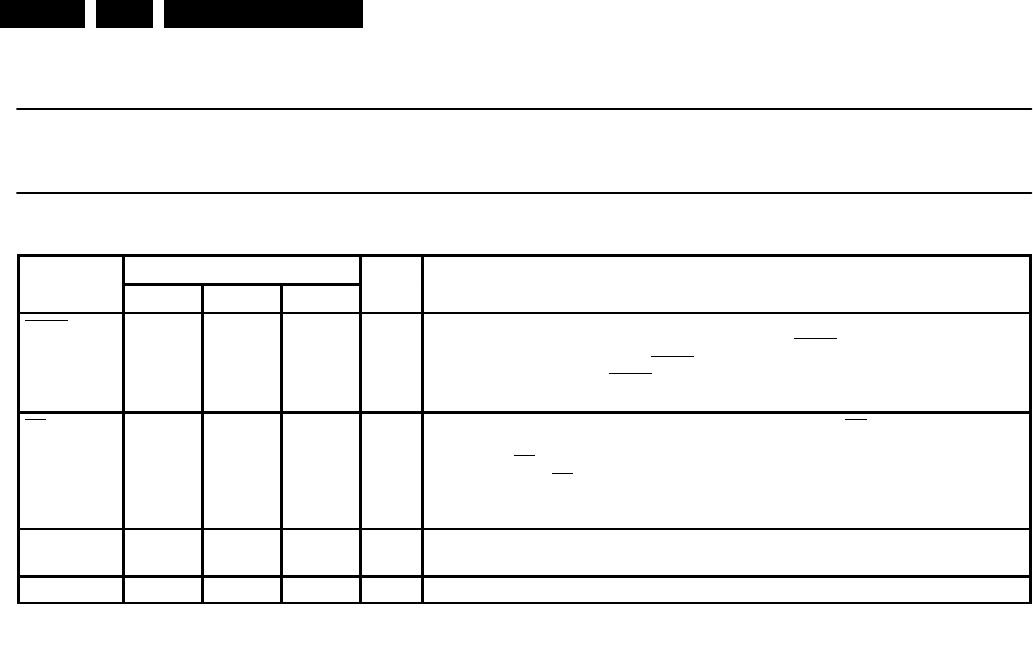
Circuit-, IC Descriptions and List of Abbreviations
EN 302 DVDR980-985 /0X19.
P89C51RB2/P89C51RC2/
P89C51RD2
80C51 8-bit Flash microcontroller family
16KB/32KB/64KB ISP/IAP Flash with 512B/512B/1KB RAM
MNEMONIC NAME AND FUNCTIONTYPE
PIN NUMBER
MNEMONIC NAME AND FUNCTIONTYPE
LQFPPLCCPDIP
PSEN 29 32 26 O Program Store Enable: The read strobe to external program memory. When
executing code from the external program memory, PSEN is activated twice each
machine cycle, except that two PSEN activations are skipped during each access
to external data memory. PSEN is not activated during fetches from internal
program memory.
EA/VPP 31 35 29 I External Access Enable/Programming Supply Voltage: EA must be externally
held low to enable the device to fetch code from external program memory
locations. If EA is held high, the device executes from internal program memory.
The value on the EA pin is latched when RST is released and any subsequent
changes have no effect. This pin also receives the programming supply voltage
(VPP) during Flash programming.
XTAL1 19 21 15 I Crystal 1: Input to the inverting oscillator amplifier and input to the internal clock
generator circuits.
XTAL2 18 20 14 O Crystal 2: Output from the inverting oscillator amplifier.
NOTE:
To avoid ªlatch-upº effect at power-on, the voltage on any pin (other than VPP) must not be higher than VCC + 0.5 V or less than VSS ± 0.5 V.
Circuit-, IC Descriptions and List of Abbreviations EN 303DVDR980-985 /0X1 9.
9.9.4 IC7303: FPGA/EPLD
DS060 (v1.6) September 19, 2001 www.xilinx.com 1
Product Specification 1-800-255-7778
© 2001 Xilinx, Inc. All rights reserved. All Xilinx trademarks, registered trademarks, patents, and disclaimers are as listed at http://www.xilinx.com/legal.htm.
All other trademarks and registered trademarks are the property of their respective owners. All specifications are subject to change without notice.
Introduction
The Spartan
™
and the Spartan-XL families are a high-vol-
ume production FPGA solution that delivers all the key
requirements for ASIC replacement up to 40,000 gates.
These requirements include high performance, on-chip
RAM, core solutions and prices that, in high volume,
approach and in many cases are equivalent to mask pro-
grammed ASIC devices.
The Spartan series is the result of more than 14 years of
FPGA design experience and feedback from thousands of
customers. By streamlining the Spartan series feature set,
leveraging advanced process technologies and focusing on
total cost management, the Spartan series delivers the key
features required by ASIC and other high-volume logic
users while avoiding the initial cost, long development
cycles and inherent risk of conventional ASICs. The Spar-
tan and Spartan-XL families in the Spartan series have ten
members, as shown in Table 1.
Spartan and Spartan-XL Features
Note: The Spartan series devices described in this data
sheet include the 5V Spartan family and the 3.3V
Spartan-XL family. See the separate data sheet for the 2.5V
Spartan-II family.
•First ASIC replacement FPGA for high-volume
production with on-chip RAM
•Density up to 1862 logic cells or 40,000 system gates
•Streamlined feature set based on XC4000 architecture
•System performance beyond 80 MHz
•Broad set of AllianceCORE™ and LogiCORE™
predefined solutions available
•Unlimited reprogrammability
•Low cost
•System level features
- Available in both 5V and 3.3V versions
- On-chip SelectRAM™ memory
- Fully PCI compliant
- Full readback capability for program verification
and internal node observability
- Dedicated high-speed carry logic
- Internal 3-state bus capability
- Eight global low-skew clock or signal networks
- IEEE 1149.1-compatible Boundary Scan logic
- Low cost plastic packages available in all densities
- Footprint compatibility in common packages
•Fully supported by powerful Xilinx development system
- Foundation Series: Integrated, shrink-wrap
software
- Alliance Series: Dozens of PC and workstation
third party development systems supported
- Fully automatic mapping, placement and routing
Additional Spartan-XL Features
•3.3V supply for low power with 5V tolerant I/Os
•Power down input
•Higher performance
•Faster carry logic
•More flexible high-speed clock network
•Latch capability in Configurable Logic Blocks
•Input fast capture latch
•Optional mux or 2-input function generator on outputs
•12 mA or 24 mA output drive
•5V and 3.3V PCI compliant
•Enhanced Boundary Scan
•Express Mode configuration
•Chip scale packaging
0
Spartan and Spartan-XL Families
Field Programmable Gate Arrays
DS060 (v1.6) September 19, 2001 00Product Specification
R
Table 1: Spartan and Spartan-XL Field Programmable Gate Arrays
Device
Logic
Cells
Max
System
Gates
Typical
Gate Range
(Logic and RAM)
(1)
CLB
Matrix
Total
CLBs
No. of
Flip-flops
Max.
Avail.
User I/O
Total
Distributed
RAM Bits
XCS05 and XCS05XL 238 5,000 2,000-5,000 10 x 10 100 360 77 3,200
XCS10 and XCS10XL 466 10,000 3,000-10,000 14 x 14 196 616 112 6,272
XCS20 and XCS20XL 950 20,000 7,000-20,000 20 x 20 400 1,120 160 12,800
XCS30 and XCS30XL 1368 30,000 10,000-30,000 24 x 24 576 1,536 192 18,432
XCS40 and XCS40XL 1862 40,000 13,000-40,000 28 x 28 784 2,016 224 25,088
Notes:
1. Max values of Typical Gate Range include 20-30% of CLBs used as RAM.
Circuit-, IC Descriptions and List of Abbreviations
EN 304 DVDR980-985 /0X19.
Spartan and Spartan-XL Families Field Programmable Gate Arrays
2www.xilinx.com DS060 (v1.6) September 19, 2001
1-800-255-7778 Product Specification
R
General Overview
Spartan series FPGAs are implemented with a regular, flex-
ible, programmable architecture of Configurable Logic
Blocks (CLBs), interconnected by a powerful hierarchy of
versatile routing resources (routing channels), and sur-
rounded by a perimeter of programmable Input/Output
Blocks (IOBs), as seen in Figure 1. They have generous
routing resources to accommodate the most complex inter-
connect patterns.
The devices are customized by loading configuration data
into internal static memory cells. Re-programming is possi-
ble an unlimited number of times. The values stored in these
memory cells determine the logic functions and intercon-
nections implemented in the FPGA. The FPGA can either
actively read its configuration data from an external serial
PROM (Master Serial mode), or the configuration data can
be written into the FPGA from an external device (Slave
Serial mode).
Spartan series FPGAs can be used where hardware must
be adapted to different user applications. FPGAs are ideal
for shortening design and development cycles, and also
offer a cost-effective solution for production rates well
beyond 50,000 systems per month.
Figure 1: Basic FPGA Block Diagram
CLB
B-
SCAN
CLB CLB CLB
CLB CLB
Routing Channels
VersaRing Routing Channels
CLB CLB
CLB CLB CLB CLB
CLB CLB CLB CLB
IOB
IOB
IOB
IOB
IOB
IOB
IOB
IOB
IOB
IOB
IOB
IOB
IOB
IOB
IOB
IOB
IOB
IOB
IOB
IOB
IOB
IOB
IOB
IOB
IOB
IOB
IOB
IOB
IOB
IOB
IOB
IOB
RDBK START
-UP
OSC
DS060_01_081100
Circuit-, IC Descriptions and List of Abbreviations EN 305DVDR980-985 /0X1 9.
Spartan and Spartan-XL Families Field Programmable Gate Arrays
62 www.xilinx.com DS060 (v1.6) September 19, 2001
1-800-255-7778 Product Specification
R
Pin Descriptions
There are three types of pins in the Spartan/XL devices:
•Permanently dedicated pins
•User I/O pins that can have special functions
•Unrestricted user-programmable I/O pins.
Before and during configuration, all outputs not used for the
configuration process are 3-stated with the I/O pull-up resis-
tor network activated. After configuration, if an IOB is
unused it is configured as an input with the I/O pull-up resis-
tor network remaining activated.
Any user I/O can be configured to drive the Global
Set/Reset net GSR or the global three-state net GTS. See
Global Signals: GSR and GTS, page 20 for more informa-
tion.
Device pins for Spartan/XL devices are described in
Table 18.
Table 18: Pin Descriptions
Pin Name
I/O
During
Config.
I/O After
Config. Pin Description
Permanently Dedicated Pins
V
CC
X X Eight or more (depending on package) connections to the nominal +5V supply
voltage (+3.3V for Spartan-XL devices). All must be connected, and each must be
decoupled with a 0.01 –0.1 µF capacitor to Ground.
GND X X Eight or more (depending on package type) connections to Ground. All must be
connected.
CCLK I or O I During configuration, Configuration Clock (CCLK) is an output in Master mode and
is an input in Slave mode. After configuration, CCLK has a weak pull-up resistor
and can be selected as the Readback Clock. There is no CCLK High or Low time
restriction on Spartan/XL devices, except during Readback. See Violating the
Maximum High and Low Time Specification for the Readback Clock, page 39
for an explanation of this exception.
DONE I/O O DONE is a bidirectional signal with an optional internal pull-up resistor. As an
open-drain output, it indicates the completion of the configuration process. As an
input, a Low level on DONE can be configured to delay the global logic initialization
and the enabling of outputs.
The optional pull-up resistor is selected as an option in the program that creates
the configuration bitstream. The resistor is included by default.
PROGRAM I I PROGRAM is an active Low input that forces the FPGA to clear its configuration
memory. It is used to initiate a configuration cycle. When PROGRAM goes High,
the FPGA finishes the current clear cycle and executes another complete clear
cycle, before it goes into a WAIT state and releases INIT.
The PROGRAM pin has a permanent weak pull-up, so it need not be externally
pulled up to VCC.
MODE
(Spartan)
M0, M1
(Spartan-XL)
I X The Mode input(s) are sampled after INIT goes High to determine the
configuration mode to be used.
During configuration, these pins have a weak pull-up resistor. For the most popular
configuration mode, Slave Serial, the mode pins can be left unconnected. For
Master Serial mode, connect the Mode/M0 pin directly to system ground.
Circuit-, IC Descriptions and List of Abbreviations
EN 306 DVDR980-985 /0X19.
Spartan and Spartan-XL Families Field Programmable Gate Arrays
DS060 (v1.6) September 19, 2001 www.xilinx.com 63
Product Specification 1-800-255-7778
R
PWRDWN IIPWRDWN is an active Low input that forces the FPGA into the Power Down state
and reduces power consumption. When PWRDWN is Low, the FPGA disables all
I/O and initializes all flip-flops. All inputs are interpreted as Low independent of
their actual level. VCC must be maintained, and the configuration data is
maintained. PWRDWN halts configuration if asserted before or during
configuration, and re-starts configuration when removed. When PWRDWN returns
High, the FPGA becomes operational by first enabling the inputs and flip-flops and
then enabling the outputs. PWRDWN has a default internal pull-up resistor.
User I/O Pins That Can Have Special Functions
TDO O O If boundary scan is used, this pin is the Test Data Output. If boundary scan is not
used, this pin is a 3-state output without a register, after configuration is
completed.
To use this pin, place the library component TDO instead of the usual pad symbol.
An output buffer must still be used.
TDI, TCK,
TMS
I I/O
or I
(JTAG)
If boundary scan is used, these pins are Test Data In, Test Clock, and Test Mode
Select inputs respectively. They come directly from the pads, bypassing the IOBs.
These pins can also be used as inputs to the CLB logic after configuration is
completed.
If the BSCAN symbol is not placed in the design, all boundary scan functions are
inhibited once configuration is completed, and these pins become
user-programmable I/O. In this case, they must be called out by special library
elements. To use these pins, place the library components TDI, TCK, and TMS
instead of the usual pad symbols. Input or output buffers must still be used.
HDC O I/O High During Configuration (HDC) is driven High until the I/O go active. It is
available as a control output indicating that configuration is not yet completed.
After configuration, HDC is a user-programmable I/O pin.
LDC O I/O Low During Configuration (LDC) is driven Low until the I/O go active. It is available
as a control output indicating that configuration is not yet completed. After
configuration, LDC is a user-programmable I/O pin.
INIT I/O I/O Before and during configuration, INIT is a bidirectional signal. A 1 kΩ to 10 kΩ
external pull-up resistor is recommended.
As an active Low open-drain output, INIT is held Low during the power stabilization
and internal clearing of the configuration memory. As an active Low input, it can
be used to hold the FPGA in the internal WAIT state before the start of
configuration. Master mode devices stay in a WAIT state an additional 30 to
300 µs after INIT has gone High.
During configuration, a Low on this output indicates that a configuration data error
has occurred. After the I/O go active, INIT is a user-programmable I/O pin.
PGCK1 -
PGCK4
(Spartan)
Weak
Pull-up
I or I/O Four Primary Global inputs each drive a dedicated internal global net with short
delay and minimal skew. If not used to drive a global buffer, any of these pins is a
user-programmable I/O.
The PGCK1-PGCK4 pins drive the four Primary Global Buffers. Any input pad
symbol connected directly to the input of a BUFGP symbol is automatically placed
on one of these pins.
Table 18: Pin Descriptions (Continued)
Pin Name
I/O
During
Config.
I/O After
Config. Pin Description
Circuit-, IC Descriptions and List of Abbreviations EN 307DVDR980-985 /0X1 9.
Spartan and Spartan-XL Families Field Programmable Gate Arrays
64 www.xilinx.com DS060 (v1.6) September 19, 2001
1-800-255-7778 Product Specification
R
SGCK1 -
SGCK4
(Spartan)
Weak
Pull-up
(except
SGCK4
is DOUT)
I or I/O Four Secondary Global inputs each drive a dedicated internal global net with short
delay and minimal skew. These internal global nets can also be driven from
internal logic. If not used to drive a global net, any of these pins is a
user-programmable I/O pin.
The SGCK1-SGCK4 pins provide the shortest path to the four Secondary Global
Buffers. Any input pad symbol connected directly to the input of a BUFGS symbol
is automatically placed on one of these pins.
GCK1 -
GCK8
(Spartan-XL)
Weak
Pull-up
(except
GCK6 is
DOUT)
I or I/O Eight Global inputs each drive a dedicated internal global net with short delay and
minimal skew. These internal global nets can also be driven from internal logic. If
not used to drive a global net, any of these pins is a user-programmable I/O pin.
The GCK1-GCK8 pins provide the shortest path to the eight Global Low-Skew
Buffers. Any input pad symbol connected directly to the input of a BUFGLS symbol
is automatically placed on one of these pins.
CS1
(Spartan-XL)
I I/O During Express configuration, CS1 is used as a serial-enable signal for
daisy-chaining.
D0-D7
(Spartan-XL)
I I/O During Express configuration, these eight input pins receive configuration data.
After configuration, they are user-programmable I/O pins.
DIN I I/O During Slave Serial or Master Serial configuration, DIN is the serial configuration
data input receiving data on the rising edge of CCLK. After configuration, DIN is a
user-programmable I/O pin.
DOUT O I/O During Slave Serial or Master Serial configuration, DOUT is the serial
configuration data output that can drive the DIN of daisy-chained slave FPGAs.
DOUT data changes on the falling edge of CCLK, one-and-a-half CCLK periods
after it was received at the DIN input.
In Spartan-XL Express mode, DOUT is the status output that can drive the CS1 of
daisy-chained FPGAs, to enable and disable downstream devices.
After configuration, DOUT is a user-programmable I/O pin.
Unrestricted User-Programmable I/O Pins
I/O Weak
Pull-up
I/O These pins can be configured to be input and/or output after configuration is
completed. Before configuration is completed, these pins have an internal
high-value pull-up resistor network that defines the logic level as High.
Table 18: Pin Descriptions (Continued)
Pin Name
I/O
During
Config.
I/O After
Config. Pin Description
Circuit-, IC Descriptions and List of Abbreviations
EN 308 DVDR980-985 /0X19.
9.9.5 IC7307; IC7308: CY2071AS
CY2071A
EPROM Programmable Clock Generator
i
Features Benefits
Single phase-locked loop architecture Generates a custom frequency from an external source
EPROM programmability Easy customization and fast turnaround
Factory-programmable (CY2071A, CY2071AI) or field-
programmable (CY2071AF, CY2071AFI) device options Programming support available for all opportunities
Up to three configurable outputs Generates three related frequencies from a single device
Low-skew, low-jitter, high-accuracy outputs Meets critical industry standard timing requirements
Internal loop filter Alleviates the need for external components
Power management (OE) Supports low-power applications
Frequency select options 3 outputs with 2 user selectable frequencies
Configurable 5V or 3.3V operation Supports industry standard design platforms
8-pin 150-mil SOIC package Industry-standard packaging saves on board space
Selector Guide
Part Number Outputs Input Frequency Range Output Frequency Range Specifics
CY2071A 3 10 MHz–25 MHz (external crystal)
1 MHz–30 MHz (reference clock) 500 kHz–130 MHz (5V)
500 kHz–100 MHz (3.3V) Factory Programmable
Commercial Temperature
CY2071AI 3 10 MHz–25 MHz (external crystal)
1 MHz–30 MHz (reference clock) 500 kHz–100 MHz (5V)
500 kHz–80 MHz (3.3V) Factory Programmable
Industrial Temperature
CY2071AF 3 10 MHz–25 MHz (external crystal)
1 MHz–30 MHz (reference clock) 500 kHz–100 MHz (5V)
500 kHz–80 MHz (3.3V)
Field Programmable
Commercial Temperature
CY2071AFI 3 10 MHz–25 MHz (external crystal)
1 MHz–30 MHz (reference clock) 500 kHz–90 MHz (5V)
500 kHz–66.6 MHz (3.3V)
Field Programmable
Industrial Temperature
1
2
3
45
8
7
6
CLKA
GND
XTALIN
XTALOUT
VDD
OE/FS
CLKC
CLKB
XTALOUT
XTALIN REFERENCE
OSCILLATOR
PLL
Block
CLKA
CLKB
CLKC
EPROM-
Configurable
Multiplexer
and Divide
Logic
OE / FS
Logic Block Diagram for CY2071A
Top View
8-pin SOIC
Pin Configuration
Circuit-, IC Descriptions and List of Abbreviations EN 309DVDR980-985 /0X1 9.
Functional Description
The CY2071A is a general-purpose clock synthesizer de-
signed for use in applications such as modems, disk drives,
CD-ROM drives, video CD players, games, set-top boxes, and
data/telecommunications. The device offers up to three config-
urable clock outputs in an 8-pin, 150-mil SOIC package and
can operate off either a 3.3V or 5V power supply. The on-chip
reference oscillator is designed for 10-MHz to 25-MHz crys-
tals. Alternatively, an external reference clock of frequency be-
tween 1 MHz and 30 MHz can be used.
The CY2071A has one PLL and outputs three factory-EPROM
configurable clocks: CLKA, CLKB, and CLKC. The output
clocks can originate either from the PLL or the reference, or
selected dividers thereof. Additionally, pin 8 can be configured
to be an Output Enable or a Select input.
The CY2071A can replace multiple Metal Can Oscillators
(MCO) in a synchronous system, providing cost and board
space savings to the manufacturer. Hence, these devices are
ideally suited for applications that require multiple, accurate,
and stable clocks synthesized from low-cost generators in
small packages. A hard-disk drive is an example of such an
application. In this case, CLKA drives the PLL in the Read
Controller, while CLKB and CLKC drive the MCU and associ-
ated sequencers.
CyClocks™ Software
CyClocks is an easy-to-use software application that allows
you to configure any one of the EPROM-Programmable Clocks
offered by Cypress. You may specify the input frequency, PLL
and output frequencies, and different functional options.
Please note the output frequency ranges in this data sheet
when specifying them in CyClocks to ensure that you stay with-
in the limits. You can download a copy of CyClocks free on the
Cypress Semiconductor website at www.cypress.com.
Consider using the CY2081 for applications that require unre-
lated output frequencies. Consider using the CY2291,
CY2292, or CY2907 for applications that require more than
three output clocks.
Cypress FTG Programmer
The Cypress Frequency Timing Generator (FTG) Programmer
is a portable programmer designed to custom program our
family of EPROM Field Programmable Clock Devices. The
FTG programmers connect to a PC serial port and allow users
of CyClocks software to quickly and easily program any of the
CY2291F, CY2292F, CY2071AF, and CY2907F devices. The
ordering code for the Cypress FTG Programmer is CY3670.
Maximum Ratings
(Above which the useful life may be impaired. For user guide-
lines, not tested.)
Supply Voltage................................................–0.5V to +7.0V
DC Input Voltage ..................................... –0.5V to V
DD
+0.5V
Storage Temperature ................................. –65˚C to +150˚C
Max. Soldering Temperature (10 sec) ..........................260˚C
Junction Temperature ...................................................150˚C
Static Discharge Voltage ........................................... >2000V
(per MIL-STD-883, Method 3015)
Pin Summary
Name Number Description
CLKA 1 Configurable Clock Output
GND 2 Ground
XTALIN 3 Reference Crystal Input or External Reference Clock Input
XTALOUT 4 Reference Crystal Feedback
CLKB 5 Configurable Clock Output
CLKC 6 Configurable Clock Output
V
DD
7 Voltage Supply
OE / FS 8 Output Control Pin, either Output Enable or Frequency Select Input
(Active-HIGH, internal pull-up resistor to V
DD
)
Notes:
1. For best accuracy, use a parallel-resonant crystal, CL = 17 pF.
2. Float XTALOUT pin if XTALIN is driven by reference clock (as opposed to an external crystal).
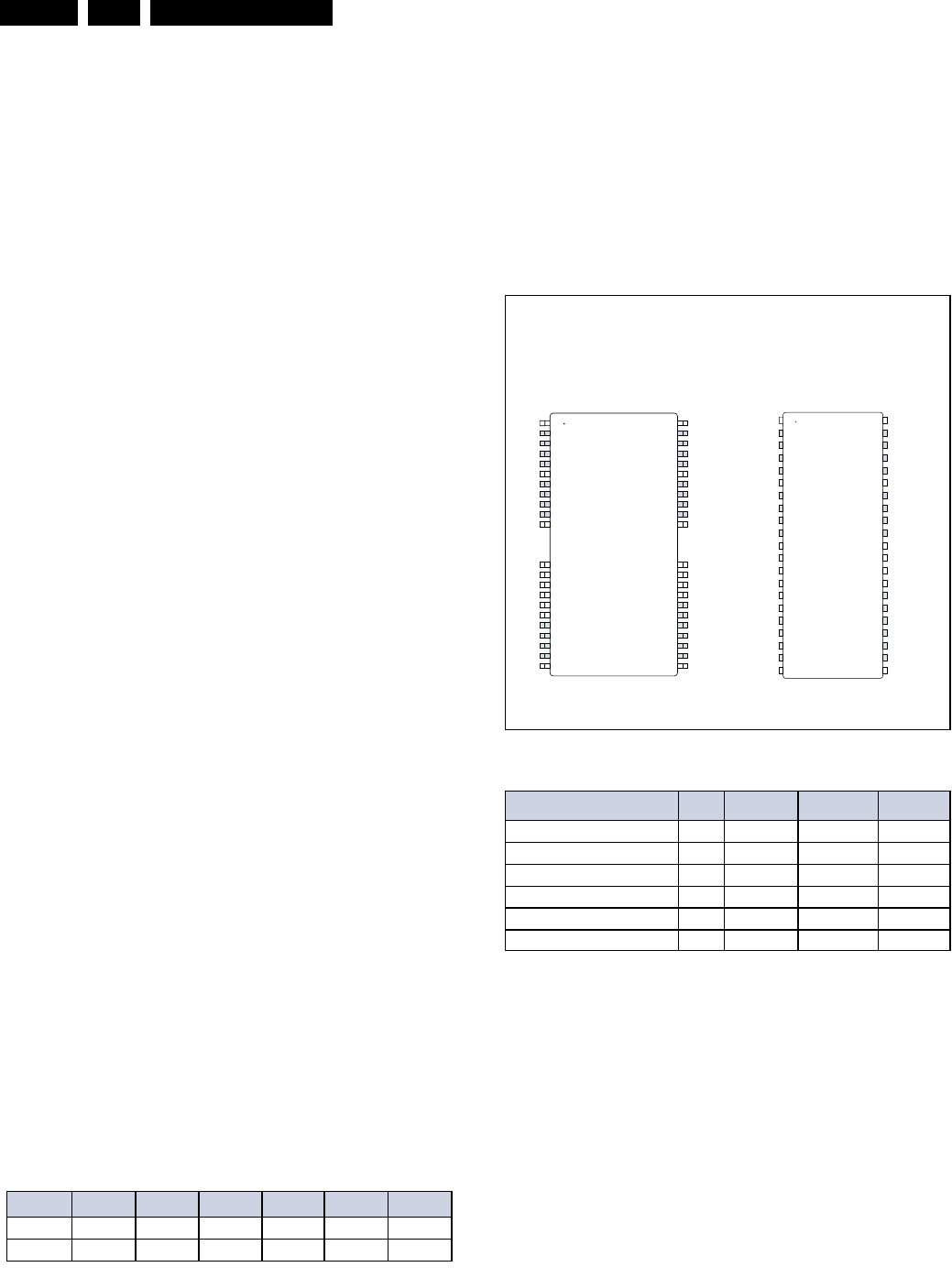
Circuit-, IC Descriptions and List of Abbreviations
EN 310 DVDR980-985 /0X19.
9.9.6 IC7402; IC7403: EDORAM
KEY TIMING PARAMETERS
SPEED tRC tRAC tPC tAA tCAC tCAS
-5 84ns 50ns 20ns 25ns 15ns 8ns
-6 104ns 60ns 25ns 30ns 17ns 10ns
FEATURES
• JEDEC- and industry-standard x16 timing,
functions, pinouts, and packages
• High-performance CMOS silicon-gate process
• Single power supply (+3.3V ±0.3V or 5V ±10%)
• All inputs, outputs and clocks are TTL-compatible
• Refresh modes: RAS#-ONLY, CAS#-BEFORE-RAS#
(CBR), HIDDEN; optional self refresh (S)
• BYTE WRITE access cycles
• 1,024-cycle refresh (10 row, 10 column addresses)
• Extended Data-Out (EDO) PAGE MODE access
• 5V-tolerant inputs and I/Os on 3.3V devices
OPTIONS MARKING
• Voltages1
3.3V LC
5V C
• Refresh Addressing
1,024 (1K) rows E5
• Packages
Plastic SOJ (400 mil) DJ
Plastic TSOP (400 mil) TG
• Timing
50ns access -5
60ns access -6
• Refresh Rates
Standard Refresh (16ms period) None
Self Refresh (128ms period) S2
• Operating Temperature Range
Commercial (0oC to +70oC) None
Extended (-20oC to +80oC) ET
Part Number Example:
MT4LC1M16E5TG-6
NOTE: 1. The third field distinguishes the low voltage offering: LC desig-
nates Vcc = 3.3V and C designates Vcc = 5V.
2. Available only on MT4LC1M16E5 (3.3V)
PIN ASSIGNMENT (Top View)
44/50-Pin TSOP 42-Pin SOJ
1 MEG x 16 EDO DRAM PART NUMBERS
PART NUMBER Vcc REFRESH PACKAGE REFRESH
MT4LC1M16E5DJ-x 3.3V 1K 400-SOJ Standard
MT4LC1M16E5DJ-x S 3.3V 1K 400-SOJ Self
MT4LC1M16E5TG-x 3.3V 1K 400-TSOP Standard
MT4LC1M16E5TG-x S 3.3V 1K 400-TSOP Self
MT4C1M16E5DJ-x 5V 1K 400-SOJ Standard
MT4C1M16E5TG-x 5V 1K 400-TSOP Standard
NOTE: “-x” indicates speed grade marking under timing
options.
EDO DRAM
NOTE: The "#" symbol indicates signal is active LOW.
V
CC
DQ0
DQ1
DQ2
DQ3
V
CC
DQ4
DQ5
DQ6
DQ7
NC
NC
NC
WE#
RAS#
NC
NC
A0
A1
A2
A3
V
CC
1
2
3
4
5
6
7
8
9
10
11
15
16
17
18
19
20
21
22
23
24
25
50
49
48
47
46
45
44
43
42
41
40
36
35
34
33
32
31
30
29
28
27
26
V
SS
DQ15
DQ14
DQ13
DQ12
V
SS
DQ11
DQ10
DQ9
DQ8
NC
NC
CASL#
CASH#
OE#
A9
A8
A7
A6
A5
A4
V
SS
VCC
DQ0
DQ1
DQ2
DQ3
VCC
DQ4
DQ5
DQ6
DQ7
NC
NC
WE#
RAS#
NC
NC
A0
A1
A2
A3
VCC
1
2
3
4
5
6
7
8
9
10
11
12
13
14
15
16
17
18
19
20
21
42
41
40
39
38
37
36
35
34
33
32
31
30
29
28
27
26
25
24
23
22
VSS
DQ15
DQ14
DQ13
DQ12
VSS
DQ11
DQ10
DQ9
DQ8
NC
CASL#
CASH#
OE#
A9
A8
A7
A6
A5
A4
VSS
GENERAL DESCRIPTION
The 1 Meg x 16 is a randomly accessed, solid-state
memory containing 16,777,216 bits organized in a x16
configuration. The 1 Meg x 16 has both BYTE WRITE
and WORD WRITE access cycles via two CAS# pins
(CASL# and CASH#). These function like a single CAS#
found on other DRAMs in that either CASL# or CASH#
will generate an internal CAS#.
The CAS# function and timing are determined by
the first CAS# (CASL# or CASH#) to transition LOW and
the last CAS# to transition back HIGH. Using only one
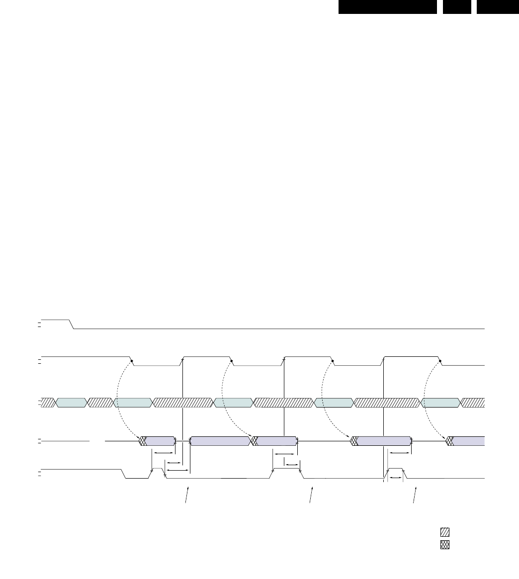
Circuit-, IC Descriptions and List of Abbreviations EN 311DVDR980-985 /0X1 9.
Figure 1
OE# Control of DQs
V
VIH
IL
CASL#/CASH#
V
VIH
IL
RAS#
V
VIH
IL
ADDR ROW COLUMN (A) COLUMN (B)
DON'T CARE
UNDEFINED
V
VIH
IL
OE#
V
VIOH
IOL OPEN
DQ
tOD
VALID DATA (B)
VALID DATA (A)
COLUMN (C)
VALID DATA (A)
tOE
VALID DATA (C)
COLUMN (D)
VALID DATA (D)
tOD
tOEHC
tOD
tOEP
tOES
The DQs go back to
Low-Z if
t
OES is met. The DQs remain High-Z
until the next CAS# cycle
if
t
OEHC is met.
The DQs remain High-Z
until the next CAS# cycle
if
t
OEP is met.
A logic HIGH on WE# dictates read mode, while a
logic LOW on WE# dictates write mode. During a WRITE
cycle, data-in (D) is latched by the falling edge of WE or
CAS# (CASL# or CASH#), whichever occurs last. An
EARLY WRITE occurs when WE is taken LOW prior to
either CAS# falling. A LATE WRITE or READ-MODIFY-
WRITE occurs when WE falls after CAS# (CASL# or
CASH#) was taken LOW. During EARLY WRITE cycles,
the data outputs (Q) will remain High-Z, regardless of
the state of OE#. During LATE WRITE or READ-
MODIFY-WRITE cycles, OE# must be taken HIGH to
disable the data outputs prior to applying input data.
If a LATE WRITE or READ-MODIFY-WRITE is attempted
while keeping OE# LOW, no WRITE will occur, and the
data outputs will drive read data from the accessed
location.
The 16 data inputs and 16 data outputs are routed
through 16 pins using common I/O. Pin direction is
controlled by OE# and WE#.
The 1 Meg x 16 DRAM must be refreshed periodi-
cally in order to retain stored data.
of the two signals results in a BYTE WRITE cycle. CASL#
transitioning LOW selects an access cycle for the lower
byte (DQ0-DQ7), and CASH# transitioning LOW se-
lects an access cycle for the upper byte (DQ8-DQ15).
Each bit is uniquely addressed through the 20 ad-
dress bits during READ or WRITE cycles. These are
entered 10 bits (A0-A9) at a time. RAS# is used to latch
the first 10 bits and CAS#, the latter 10 bits. The CAS#
function also determines whether the cycle will be a
refresh cycle (RAS# ONLY) or an active cycle (READ,
WRITE or READ-WRITE) once RAS# goes LOW.
The CASL# and CASH# inputs internally generate a
CAS# signal that functions like the single CAS# input
on other DRAMs. The key difference is each CAS# input
(CASL# and CASH#) controls its corresponding eight
DQ inputs during WRITE accesses. CASL# controls
DQ0-DQ7, and CASH# controls DQ8-DQ15. The two
CAS# controls give the 1 Meg x 16 both BYTE READ and
BYTE WRITE cycle capabilities.
GENERAL DESCRIPTION (continued)
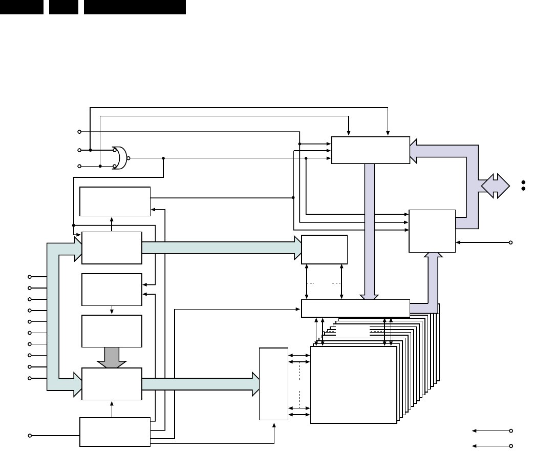
Circuit-, IC Descriptions and List of Abbreviations
EN 312 DVDR980-985 /0X19.
CASL# CAS#
RAS#
10
10
NO. 2 CLOCK
GENERATOR
REFRESH
CONTROLLER
NO. 1 CLOCK
GENERATOR
1,024 x 1,024 x 16
MEMORY
ARRAY
VDD
VSS
10
OE#
DQ0
DQ15
REFRESH
COUNTER
CASH#
A0
A1
A2
A3
A4
A5
A6
A7
A8
A9 1,024
1,024 x 16
16
10
10
SENSE AMPLIFIERS
I/O GATING
1,024
DATA-OUT
BUFFER
WE#
16
ROW-
ADDRESS
BUFFERS (10)
ROW
DECODER
COLUMN-
ADDRESS
BUFFER
DATA-IN BUFFER
COLUMN
DECODER
16
FUNCTIONAL BLOCK DIAGRAM
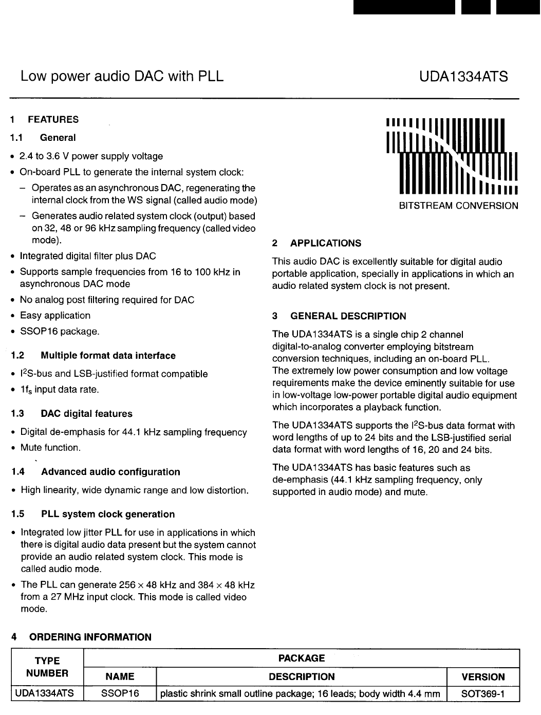
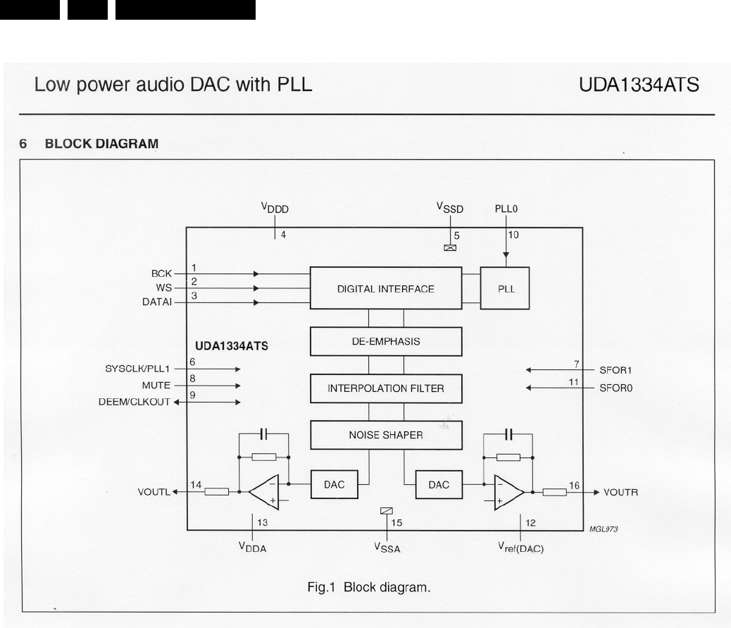
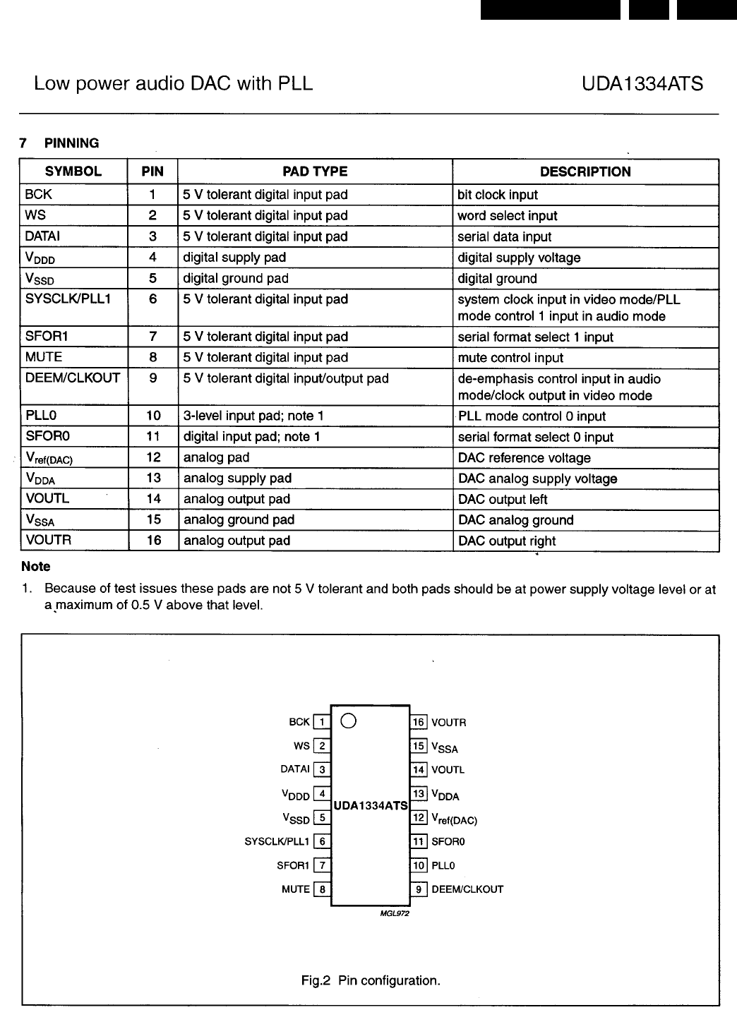
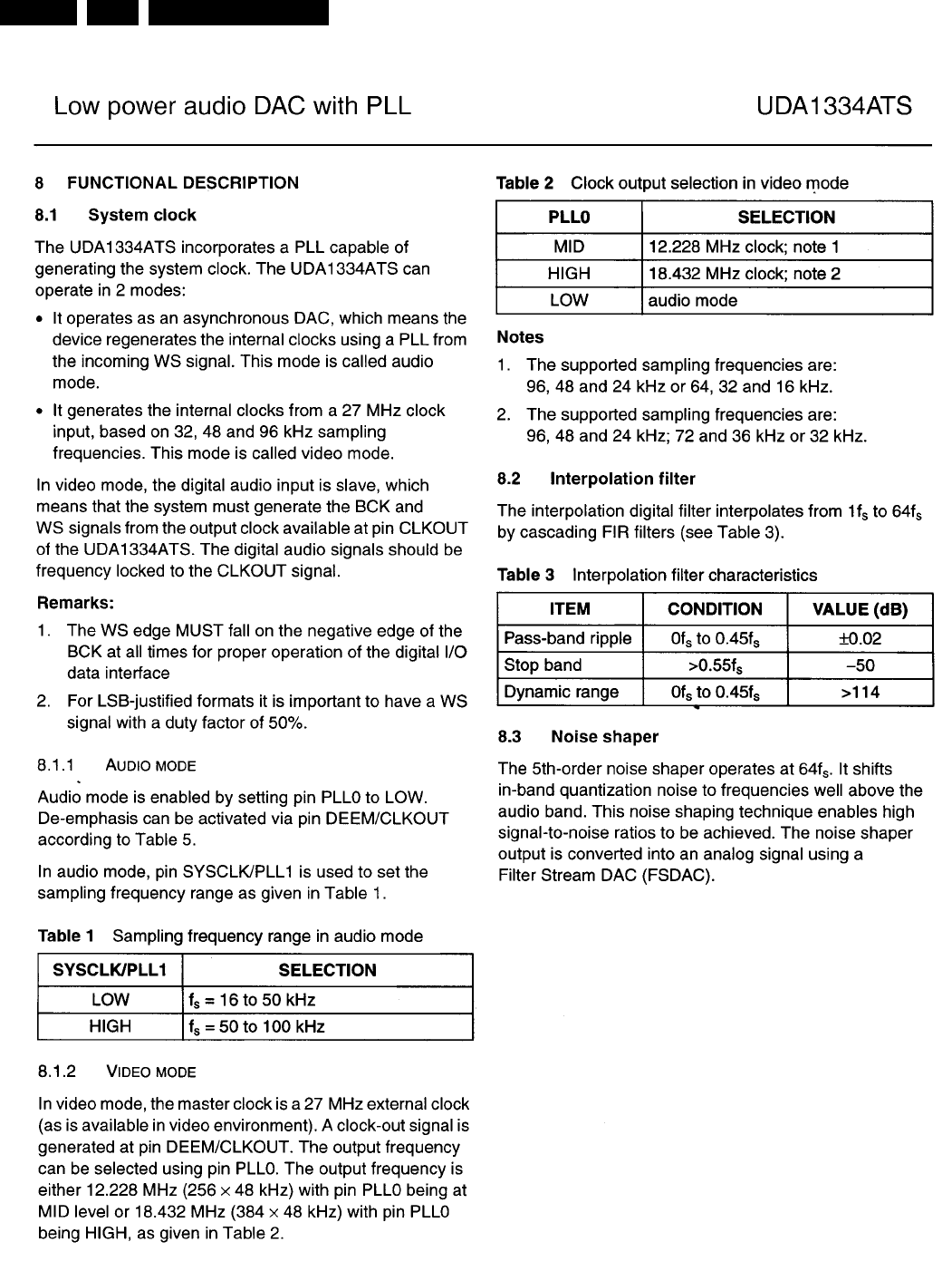
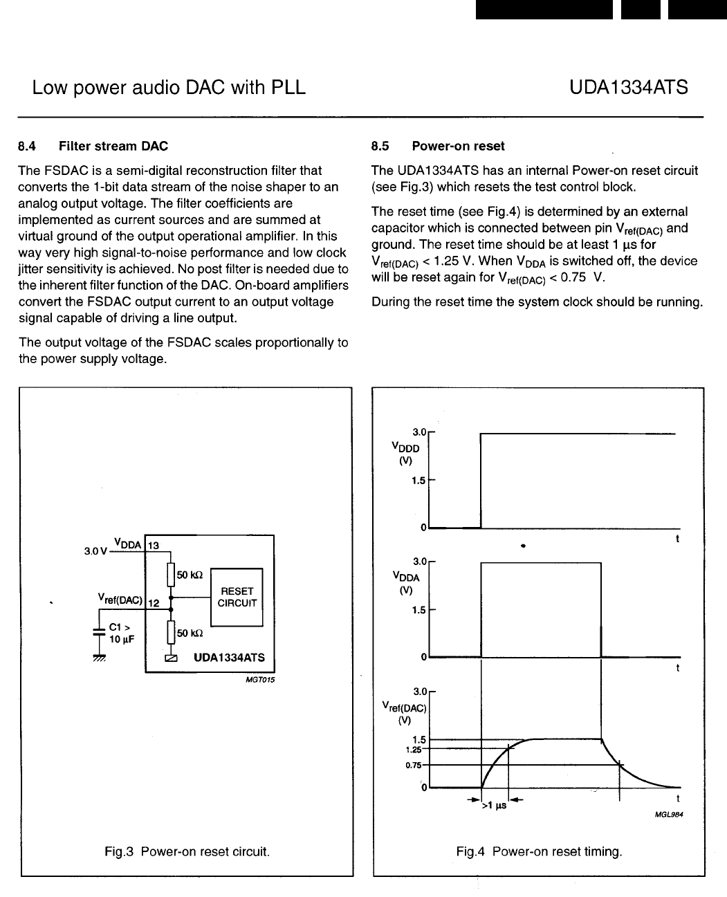
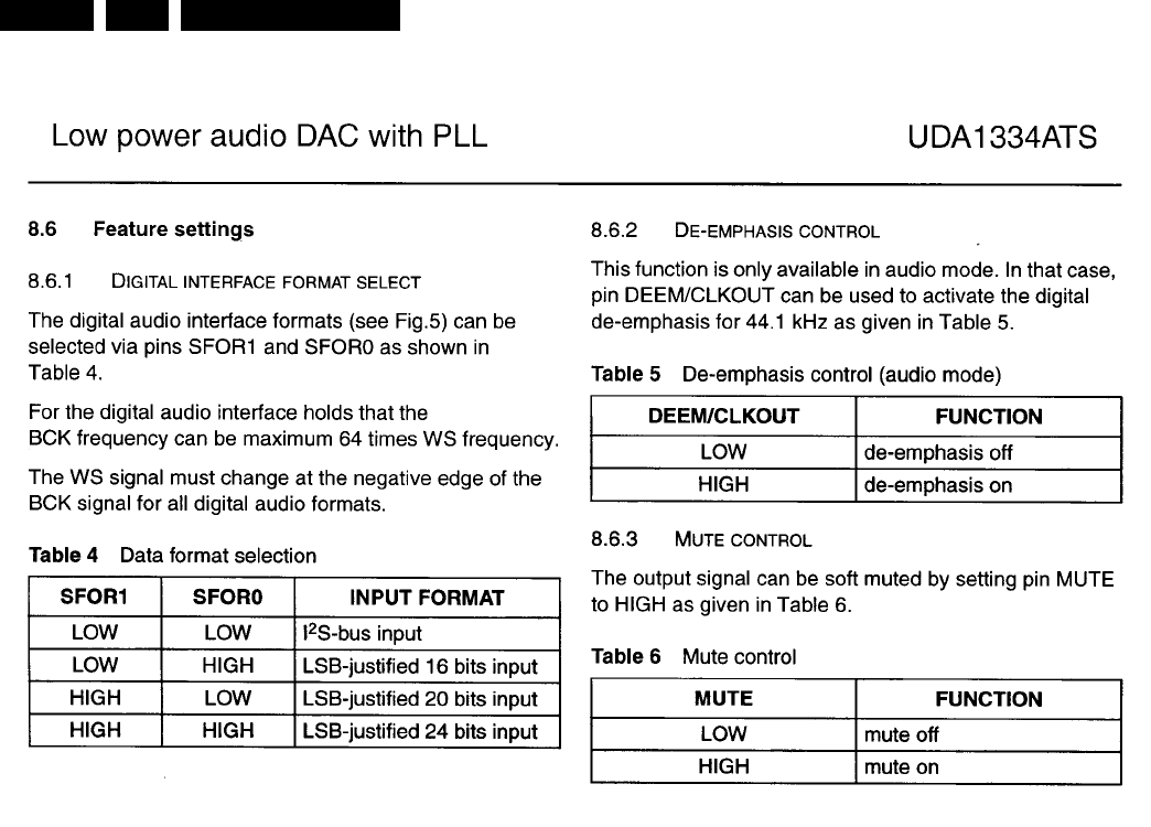
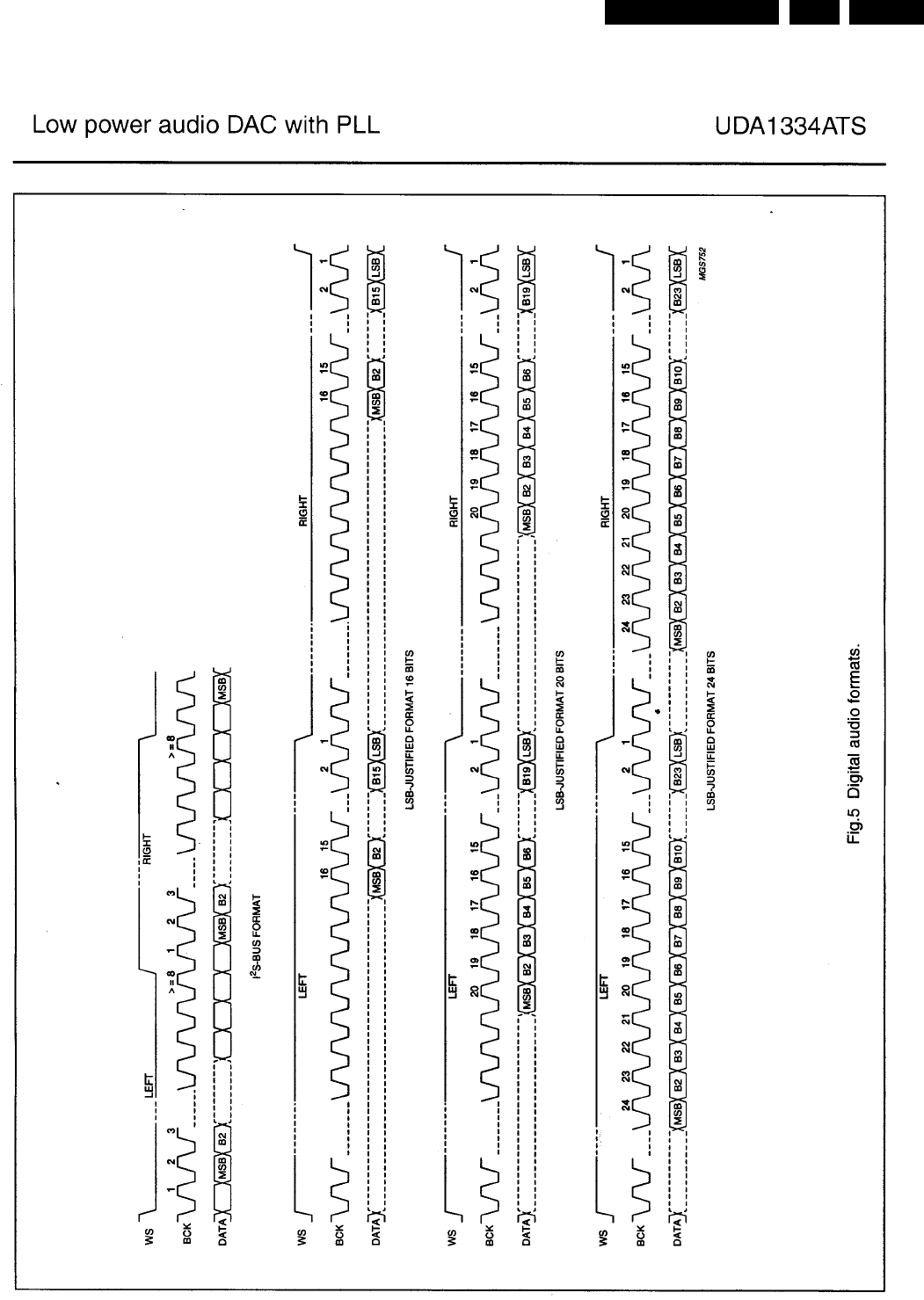

Circuit-, IC Descriptions and List of Abbreviations
EN 322 DVDR980-985 /0X19.
9.10 List of Abbreviations
Digital Board
+12V
+12V Power Supply
+2V5_FLI
+2V5 Power Supply for FLI
+2V5_PLL
+2V5 Power Supply for PLL
+3V3
+3V3 Power Supply
+3V3_ANA
+3V3 Power Supply Analogue
+3V3_DD
+3V3 Power Supply Digital
+3V3_FLI
+3V3 Power Supply for FLI
+5V
+5V Power Supply
+5V_BUFFER
+5V Power Supply for Video Filters
5508_HS
Horizontal Synchronisation from Host Decoder to Progressive
Scan
5508_ODD_EVEN
Odd - Even control from Host Decoder to Progressive Scan
-5V
-5V Power Supply
-5V_BUFFER
-5V Power Supply for Video Filters
A_EMPRESS(13:0)
EMPRESS address output to SDRAM
ACC_ACLK_OSC
Audio Clock PLL output sync with incoming video for record
ACC_ACLK_PLL
Audio Clock PLL output for play back
ACLK_EMP
EMPRESS audio clock output
AD_ACLK
Audio Decoder Clock
AD_BCLK
Audio Decoder I2S bit clock
AD_DATAO
Audio Decoder Output data (PCM)
AD_SPDIF33
Audio digital output to the analog board
AD_WCLK
Audio Decoder I2S word clock
AE_ACLK
Audio Encoder Clock
AE_ACLK_OEN
Audio Encoder Clock Output Enable
AE_BCLK
Audio Encoder I2S bit clock
AE_BCLK_DV
Audio Encoder I2S bit clock to DVIO
AE_BCLK_VSM
Audio Encoder I2S bit clock to VSM
AE_DATAI
Audio Encoder Input data (PCM)
AE_DATAI_DV
Audio Encoder Input data (PCM) from DVIO
AE_DATAO
Audio Encoder Output data (PCM)
AE_WCLK
Audio Encoder I2S word clock
AE_WCLK_DV
Audio Encoder I2S word clock to DVIO
AE_WCLK_VSM
Audio Encoder I2S word clock to VSM
ANA_WE
Analogue write enable
ANA_WE_LV
Analogue write enable Low Voltage
B_IN_VIP
Video blue input to Video Input Processor
B_OUT
Video blue output from Host Decoder
B_OUT_B
Filtered blue video output
BA
Bank Address
BCLK_CTL_SERVICE
Bitclock control Service Interface
BE_BCLK
Basic Engine I2S bit clock
BE_BCLK_VSM
Basic Engine I2S bit clock to VSM
BE_CPR
Basic Engine Control Processor ready to accept data
BE_DATA_RD
Basic Engine Data read
BE_DATA_WR
Basic Engine Data write
BE_FAN
Basic Engine FAN
BE_FLAG
Basic Engine error flag
BE_IRQN
Basic Engine interrupt request
BE_LOADN
Basic Engine LOAD(LOW active)
BE_RXD
Basic Engine S2B received data
BE_SUR
Basic Engine servo unit ready to accept data (S2B)
BE_SYNC
Basic Engine sector/abs time sync
BE_TXD
Basic Engine S2B transmitted data
BE_V4
Basic Engine versatile input pin
BE_WCLK
Basic Engine I2S word clock
C_IN
Video Chrominance input
C_IN_VIP
Chrominance input to Video Input Processor
C_OUT
Chrominance output from Host Decoder
C_OUT_B
Filtered Chrominance output
CAS
Column Address strobe
CB_OUT(9:0)
Chrominance Blue out
CLK4
SDRAM clock
CPUINT0
Control processor unit interrupt
CPUINT1
Control processor unit interrupt
CR_OUT(9:0)
Chrominance Red out
CTS1P
Clear to send (Service Interface)
CVBS_OUT
Composite video output out of the Host Decoder
CVBS_OUT_B
Filtered Composite video output
CVBS_OUT_B_VIP
Composite video output to Video Input Processor(digital board
video loop)
CVBS_Y_IN
Composite video/Luminance input
CVBS_Y_IN_A
Composite video/Luminance input to Video Input Processor
CVBS_Y_IN_B
Composite video/Luminance input to Video Input Processor

Circuit-, IC Descriptions and List of Abbreviations EN 323DVDR980-985 /0X1 9.
CVBS_Y_IN_C
Composite video/Luminance input to Video Input Processor
D_ADDR(10:0)
Address bus
D_DATA(29:0)
Data bus
D_EMPRESS(15:0)
SDRAM data input/output of EMPRESS
D_PAR_D(7:0)
Front-end parallel interface data (record)
D_PAR_DVALID
Front-end parallel interface data valid
D_PAR_REQ
Front-end parallel interface request
D_PAR_STR
Front-end parallel interface strobe
D_PAR_SYNC
Front-end parallel interface sync
DV_IN_CLK
Digital Video in clock from DVIO board
DV_IN_DATA(7:0)
Digital Video in data bus from DVIO board
DV_IN_HS
Digital Video in horizontal synchronisation from DVIO board
DV_IN_VS
Digital Video in vertical synchronisation from DVIO board
EMI_A(21:1)
External Memory Interface Address Bus(Host Decoder)
EMI_BE0N
External Memory Interface Lower byte enable(Host Decoder)
EMI_BE1N
External Memory Interface Upper byte enable(Host Decoder)
EMI_CAS0N
External Memory Interface SDRAM column address
strobe(Host Decoder)
EMI_CE1N
External Memory Interface VSM Lower bank enable
EMI_CE2N
External Memory Interface VSM Higher bank enable
EMI_CE3N
External Memory Interface flash IC's enable
EMI_D(15:0)
External Memory Interface Data Bus(Host Decoder)
EMI_PROCCLK
External Memory Interface Processor Clock(Host Decoder)
EMI_RWN
External Memory Interface Read/Write control signal(Host
Decoder)
EMI_WAIT
External Memory Interface Wait state request(Host Decoder)
EMPRESS_BOOT
EMPRESS BOOT select input
EMPRESS_IRQN
EMPRESS Interrupt request output
FLASH_OEN
FLASH output enable control signal
G_IN_VIP
Video green input to Video Input Processor
G_OUT
Video green output from Host Decoder
G_OUT_B
Filtered green video output from Host Decoder
GNDD
Digital Ground
HD_M_AD(13:0)
Host Decoder SDRAM address bus
HD_M_CASN
Host Decoder SDRAM column address strobe
HD_M_CLK
Host Decoder SDRAM clock
HD_M_CS0N
Host Decoder SDRAM chip select
HD_M_DQ(15:0)
Host Decoder SDRAM data bus
HD_M_DQML
Host Decoder SDRAM data mask enable(Lower)
HD_M_DQMU
Host Decoder SDRAM data mask enable(Upper)
HD_M_RASN
Host Decoder SDRAM row address strobe
HD_M_WEN
Host Decoder SDRAM write enable
HSOUT
Horizontal synchronisation OUT
ION
Inverted ON: Enable the power supply for the digital board
when LOW
IRESET_DIG
Initialisation of the digital board, HIGH when power ON
JTAG3_TCK
JTAG Test Clock
JTAG3_TD_VIP_TO_VE
JTAG Transmitted Data Video Input Processor to Video
Encoder
JTAG3_TD_VSM_TO_VIP
JTAG Transmitted Data Versatile Stream Manager to Video
Input Processor
JTAG3_TMS
JTAG Test Mode Select
JTAG3_TRSTN
JTAG Test part ResetN
LOAD_DVN
LOAD Digital Video(LOW active)
MUTEN
Mute enable
MUTEN_LV
Mute enable Low Voltage
P_SCAN_YUV(7:0)
Progressive Scan digital video bus
R_IN_VIP
Video Red input to Video Input Processor
R_OUT
Video Red output from Host Decoder
R_OUT_B
Filtered Red Video output from Host Decoder
RAS
Row Address Strobe
RESETN
Reset Host Decoder
RESETN_BE
System reset basic engine (buffered)
RESETN_DVIO
System reset Digital Video Input Output (buffered)
RESETN_VE
System reset Video Encoder
ROMH_CEN
Flash 2 chip enable
ROML_CEN
Flash 1 chip enable
RSTN_BE
Reset control of basic engine
RSTN_DVIO
Reset control of DVIO
RTS1P
Ready To Send data to service serial interface
RX1P
Receive data from service serial interface
SCL
I2C bus clock
SD_CASN
SDRAM Column Address strobe output (active LOW)
SD_CLK
SDRAM clock output
SD_CLKE
SDRAM clock enable output
SD_CSN
SDRAM
SD_DQM(1:0)
SDRAM data mask enable output
SD_RASN

Circuit-, IC Descriptions and List of Abbreviations
EN 324 DVDR980-985 /0X19.
SDRAM row address strobe output
SD_WEN
SDRAM write enable output
SDA
I2C bus data
SEL_ACLK1
Select audio clock(playback)
SM_CS3N
SRAM chip select
SM_LBN
SRAM lower bank
SM_OEN
SRAM output enable
SM_UBN
SRAM upper bank
SM_WEN
SRAM write enable
SMA(17:0)
SRAM address output
SMD(15:0)
SRAM data input/output
SYSCLK_EMPRESS
System clock EMPRESS
SYSCLK_PROGSCAN
System clock Progressive Scan
SYSCLK_VSM_5508
System clock VSM and Host decoder
TX1P
Transmit data to service serial interface
U_IN
Video U input
U_IN_VIP
Video U input to Video Input Processor
V_IN
Video V input
V_IN_VIP
Video V input to Video Input Processor
VCC3_CLK_BUF
Power supply 3V3 clock buffer
VCC3_VSM
Power supply 3V3 Versatile Stream Manager
VCC3_VSM_MEM
Power supply 3V3 Versatile Stream Manager Memory
VCC5_4046
Power supply 5V to PLL IC
VDD_125
Power supply 5V to buffer 7202
VDD_CORE
Sti5508 Core supply voltage 2.5V
VDD_EMP
Empress supply voltage 3.3V
VDD_EMP_CORE
Empress Core supply voltage 2.5V
VDD_FLASH_H
Flash 7301 supply voltage
VDD_FLASH_L
Flash 7302 supply voltage
VDD_LVC32
Power supply LVC32
VDD_PCM
Power supply Audio decoder of Sti5508
VDD_PLL
Power supply PLL audio decoder of Sti5508
VDD_RGB
Power supply video encoder of Sti5508
VDD_STI
Power supply of Sti5508
VDD_YCC
Power supply video encoder of Sti5508
VDD5_MK2703
Power supply MK2703
VDD5_OSC
Power supply Oscillator
VDDA1A_7118
Power supply for analog input of VIP
VDDA2A_7118
Power supply for analog input of VIP
VDDA3A_7118
Power supply for analog input of VIP
VDDA4A_7118
Power supply for analog input of VIP
VDDE_7118
Power supply digital for peripheral cells of VIP
VDDI_7118
Power supply digital for core of VIP
VDDX_7118
Power supply for crystal oscillator of VIP
VE_DATA(7:0)
Video Encoder data Bus
VE_DSN
Video Encoder Data Strobe
VE_DTACKN
Video Encoder Data Transfer acknowledge
VIP_ERROR
Video Input Processor error
VIP_FB
Video Input Processor Fast Blanking
VIP_FID_FF
Video Input Processor field indentifier to Flip Flop
VIP_HS
Video Input Processor horizontal synchronisation
VIP_ICLK
Video Input Processor input Clock
VIP_IDQ
Video Input Processor output data qualifier
VIP_IGP1
Video Input Processor input general purpose 1
VIP_INT
Video Input Processor interrupt
VIP_RTS1
Video Input Processor ready to send
VIP_VS
Video Input Processor vertical synchronisation
VIP_YUV(7:0)
Video Input Processor digital video(CCIR 656)
VS_IN
Vertical synchronisation IN
VSM_M_A(13:0)
Versatile Stream Manager SDRAM address bus
VSM_M_CASN
Versatile Stream Manager SDRAM column address strobe
VSM_M_CLKEN
Versatile Stream Manager SDRAM clock enable
VSM_M_CLKOUT
Versatile Stream Manager SDRAM clock out
VSM_M_D(15:0)
Versatile Stream Manager SDRAM data bus
VSM_M_LDQM
Versatile Stream Manager SDRAM lower data mask enable
VSM_M_RASN
Versatile Stream Manager SDRAM row address strobe
VSM_M_UDQM
Versatile Stream Manager SDRAM upper data mask enable
VSM_M_WEN
Versatile Stream Manager SDRAM write enable
VSM_UART1_CTSN
Versatile Stream Manager UART1 clear to send to analog
board (UART1 is gateway to analog board)
VSM_UART1_RTSN
Versatile Stream Manager UART2 clear to send to DVIO board
(UART2 is gateway to DIVIO board)
VSM_UART1_RX
Versatile Stream Manager UART1 ready to send to analog
board
VSM_UART1_TX
Versatile Stream Manager UART2 ready to send to DVIO
board
VSM_UART2_CTSN
Versatile Stream Manager UART1 received data to analog
board

Circuit-, IC Descriptions and List of Abbreviations EN 325DVDR980-985 /0X1 9.
VSM_UART2_RTSN
Versatile Stream Manager UART2 received data to DVIO
board
VSM_UART2_RX
Versatile Stream Manager UART1 transmitted data to analog
board
VSM_UART2_TX
Versatile Stream Manager UART2 transmitted data to DVIO
board
VSOUT
Vertical synchronisation OUT
WE
Write Enable
Y_IN
Luminance input from analog board
Y_OUT
Luminance output from Host Decoder
Y_OUT_B
Filtered luminance output
YY_OUT(9:0)
Luminance output from FLI
Divio Board
+35V_DV_EDO
+3V3 Power supply EDO Bus IC7404
+3V3
+3V3 Power supply
+3V3_DLY
+3V3 Power supply for IC7500
+3V3_DV
+3V3 Power supply for IC7404
+3V3_FPGA
+3V3 Internal Power supply for IC7303
+3V3_FPGA_CONF
+3V3 Power supply for IC 7300
+3V3_IEEE_A
+3V3 Analogue Power supply for PHY IC 7101
+3V3_IEEE_D
+3V3 Digital Power supply for PHY IC 7101
+3V3_IEEE_PLL
+3V3 PLL Power supply for PHY IC 7101
+3V3_LINK
+3V3 Power supply IC7103
+3V3_PLL
+3V3 Power supply IC7307 & IC7308
+3V3_SRAM
+3V3 Power supply IC7301, IC7302, IC7305 & IC7306
+5V
+5V Power supply
+5V_PROC
+5V Power supply IC7200, IC7201, IC7203 & IC7208
+VCC_DV_RAM
+3V3 Power supply for DV_RAM (IC7400--> IC7404)
1394_RSTN
Reset of LINK IC (7103) and PHY IC (7101)
A(0:8)
Address lines
AUD_BCLK
Audio Bit Clock
AUD_MUTE
Audio Mute
AUD_SDI
Audio Serial Data Input
AUD_SDO_CON
Audio Serial Data Output to buffer IC 7505
AUD_SDO_DAC
Audio Serial Data Output to DAC IC 7506
AUD_WS_701
Audio Word Select to DV CODEC IC 7404
AUD_WS_OUT
Audio Word Select to buffer IC 7505
BUFENN_AUD
Buffer Enable Audio
BUFENN_VID
Buffer Enable Video
CCLK
Configuration Clock
CLK27M
27MHz Clock
CLK27M_CON
27MHz Clock to Digital Board
CLK27M_DV
27MHz Clock Digital Video Codec
CLK27M_OSC
27MHz Clock IC7304
CLOCKGENAUD
Clock generator Audio
CLOCKGENVID
Clock generator Video
CTSN
Clear to Send
DATA
Data from config ROM
DONE
Indication of the completion of the configuration process
DOUT
Serial configuration data output
DV_ASN
DVCODEC Address Strobe
DV_DRQN
DVCODEC Data Request Interrupt
DV_DSLN
DVCODEC Data Strobe Lower 8 bits
DV_DSUN
DVCODEC Data Strobe Upper 8 Bits
DV_DTACKN
DVCODEC Data Transfer Acknowledge
DV_ERRN
DVCODEC Error Interrupt
DV_HS_IN
DVCODEC Horizontal synchronisation In
DV_HS_OUT
DVCODEC Horizontal synchronisation Out
DV_LCN
DVCODEC Last Code Interrupt
DV_PDN
DVCODEC Power Down
DV_RSTN
DVCODEC System Reset for NW701
DV_RWN
DVCODEC Read/Write control signal
DV_VS
DVCODEC Vertical synchronisation
FIFOA_A(0:15)
FIFO buffer A Address bus
FIFOA_OEN
FIFO buffer A Output enable
FIFOA_WEN
FIFO buffer A Write enable
HAD(0:7)
Host Address/Data bus for register settings of IC7404
INITN
Initiate Configuration
IO(0:30)
Data bus of IC7404
ISPN
In System Program Line (used for programming IC7203)
LCASN
Lower Column Address strobe for IC7404 DRAMS
LINK_AVCLK
LINK IC Audio/Video Interface Clock
LINK_AVFSYNC
LINK IC Audio/Video frame sync
LINK_AVREADY
LINK IC Audio/Video data ready to send
LINK_AVSYNC
LINK IC Audio/Video packet sync
LINK_AVVALID
LINK IC Audio/Video data valid
LINK_CSN
LINK IC chip select

Circuit-, IC Descriptions and List of Abbreviations
EN 326 DVDR980-985 /0X19.
LINK_INTN
LINK IC interrupt
LINKFIFO_DQ(0:7)
Audio Video data interface
PA(0:15)
SRAM processor address
PAD(0:7)
SRAM processor data
PALE
Processor Address Latch Enable
PHY_CNA
PHY 1394 cable not active
PHY_LPS
LINK IC power status
PINT0N
Processor interrupt 0
PINT1N
Processor interrupt 1
PRDN
Processor read
PROGRAMN
Low active input to initiate a configuration cycle
PRSTN
Processor reset
PWRN
Processor write
RASN
Row address strobe
RESETN
DVIO board reset
RTSN
System Reset
RXD
Receive Data
SRAMCE0N
SRAM processor chip enable 0
SRAMRDN
SRAM processor output enable
TCK
Boundary scan Test Clock
TDI
Boundary scan Test Data Input
TDO
Boundary scan Test Data Output
TDO_CONF
Boundary scan Test Data Output from IC 7309
TMS
Boundary scan Test Mode Select
TXD
Transmitted Data
UCASN
Upper column address strobe
WEN
Write Enable control signal to SRAM
YUV(0:7)
Digital Video

Spare Parts List EN 327DVDR980-985 /0X1 10.
10. Spare Parts List
Mechanical DVDR980 /001 /021
Various
0060 3104 127 13280 CONNECTOR FRONT
ASSY (EU)
0065 3104 127 13450 TRAY FRONT ASSY
COMPLETE
0081 VAE8010/02
0081 VAE8015/01
0151 3104 127 13320 COVER ASSY
0191 3104 124 07455 FILTER AIR INLED
BOTTOM
0197 3104 123 30002 DUST FILTER
0198 3104 124 07733 FILTER AIR INLET COVER
0199 3104 128 93031 DC BRUSHLESS FAN
0251 3104 127 10740 FOOT SILVER ASSY
0252 3104 127 10740 FOOT SILVER ASSY
0253 3104 127 10740 FOOT SILVER ASSY
0254 3104 127 10740 FOOT SILVER ASSY
0309
3104 125 24250 USER MANUAL DVDR980/
EUR
0370 9307 002 60006 DVDRW/006 PHILIPS DISC
EUROPE
1001
3104 128 07750 DVDR DIG. BOARD 1.5
EMPRESS/EU
1002
3122 427 22711 PSU DVDR1000-2 EURO
50PS203
1003
3103 608 50290 DVDR ANALOG BOARD
EUR GEN 1.5
8001 3104 157 11641 CWAS FLEX DVD 22 70 32S
8002 3104 157 11641 CWAS FLEX DVD 22 70 32S
8003 3104 157 11790 CWAS SPLIT FLEX 30 100
32S
8004 3104 157 11531 CWAS FLEX DVD 10 110
32S
Mechanical DVDR980 /051
Various
0060 3104 127 13420 CONNECTOR FRONT
ASSY (UK)
0065 3104 127 13450 TRAY FRONT ASSY
COMPLETE
0081 VAE8010/02
0081 VAE8015/01
0151 3104 127 13320 COVER ASSY
0191 3104 124 07455 FILTER AIR INLED
BOTTOM
0197 3104 123 30002 DUST FILTER
0198 3104 124 07733 FILTER AIR INLET COVER
0199 3104 128 93031 DC BRUSHLESS FAN
0251 3104 127 10740 FOOT SILVER ASSY
0252 3104 127 10740 FOOT SILVER ASSY
0253 3104 127 10740 FOOT SILVER ASSY
0254 3104 127 10740 FOOT SILVER ASSY
0309
3104 125 24270 USER MANUAL DVDR980
UK
0370 9307 002 60006 DVDRW/006 PHILIPS DISC
EUROPE
1001
3104 128 07750 DVDR DIG. BOARD 1.5
EMPRESS/EU
1002
3122 427 22711 PSU DVDR1000-2 EURO
50PS203
1003
3103 608 50290 DVDR ANALOG BOARD
EUR GEN 1.5
8001 3104 157 11641 CWAS FLEX DVD 22 70 32S
8002 3104 157 11641 CWAS FLEX DVD 22 70 32S
8003 3104 157 11790 CWAS SPLIT FLEX 30 100
32S
8004 3104 157 11531 CWAS FLEX DVD 10 110
32S
Mechanical DVD985 /001 /021
Various
0060 3104 127 13600 CONNECTOR FRONT
ASSY 985/EUR
0065 3104 127 13450 TRAY FRONT ASSY
COMPLETE
0081 VAE8015/01
0151 3104 127 13320 COVER ASSY
0191 3104 124 07455 FILTER AIR INLED
BOTTOM
0197 3104 123 30002 DUST FILTER
0198 3104 124 07733 FILTER AIR INLET COVER
0199 3104 128 93031 DC BRUSHLESS FAN
0251 3104 127 10740 FOOT SILVER ASSY
0252 3104 127 10740 FOOT SILVER ASSY
0253 3104 127 10740 FOOT SILVER ASSY
0254 3104 127 10740 FOOT SILVER ASSY
0309
4822 736 16493 EN-FR-ES-BR.PORT-
TRAD.CHIN
0370 9307 002 60006 DVDRW/006 PHILIPS DISC
EUROPE
1001
3104 128 07750 DVDR DIG. BOARD 1.5
EMPRESS/EU
1002
3122 427 22711 PSU DVDR1000-2 EURO
50PS203
1003
3103 608 50290 DVDR ANALOG BOARD
EUR GEN 1.5
1005 3104 128 07900 PB DVDR1000 DVIO
GEN.1.5 ASSY
8001 3104 157 11641 CWAS FLEX DVD 22 70 32S
8002 3104 157 11641 CWAS FLEX DVD 22 70 32S
8003 3104 157 11790 CWAS SPLIT FLEX 30 100
32S
8004 3104 157 11531 CWAS FLEX DVD 10 110
32S
8013 3104 128 92921 CABLE IEEE-1394 4P AMP
8015 3104 157 12191 CWAS FLEX DVDR 7 360
32S
Accessorieskit DVDR980 /001 /021
Various
0318 3128 147 13670 RC2056/01 IRT PROD ASSY
0320 4822 321 22611
0321 3104 128 92490 VIDEO CORD SET GOLD
PLATED
0322
2422 070 98133 MAINSCORD EUR 1M5 BK
B
0323 4822 321 61847 SCART
0324 3111 170 21592 CORDON ANT. L.1,50M
0370 3104 128 93041 S-VHS CABLE 1.5M
0371 9307 002 60006 DVDRW/006 PHILIPS DISC
EUROPE
Accessories DVDR980 /051
Various
0318 3128 147 13670 RC2056/01 IRT PROD ASSY
0320 4822 321 22611
0321 3104 128 92490 VIDEO CORD SET GOLD
PLATED
0322
4622 001 60590 CORDSET UK (WITH COIL)
0323 4822 321 61847 SCART
0324 3111 170 21592 CORDON ANT. L.1,50M
0370 3104 128 93041 S-VHS CABLE 1.5M
0371 9307 002 60006 DVDRW/006 PHILIPS DISC
EUROPE
Accessories DVDR985 /051
Various
0318 3128 147 13670 RC2056/01 IRT PROD ASSY
0320 4822 321 22611
0321 3104 128 92490 VIDEO CORD SET GOLD
PLATED
0322
4622 001 60590 CORDSET UK (WITH COIL)
0323 4822 321 61847 SCART
0324 3111 170 21592 CORDON ANT. L.1,50M
0370 3104 128 93041 S-VHS CABLE 1.5M
0371 9307 002 60006 DVDRW/006 PHILIPS DISC
EUROPE
Front complete
Various
0001 3104 127 13470 FRONT ASSY
0002 3104 127 13220 SIDE PLATE LEFT ASSY
0003 3104 127 13230 SIDE PLATE RIGHT ASSY
0004 3104 124 08470 WINDOW
0005 3139 244 00761 LIGHT GUIDE DVD STEP 2K
0011 3104 127 13240 BUTTON STANDBY ASSY
0012 3104 127 13250 BUTTON PLAY/STOP/
RECORD ASSY
0013 3104 127 13260 BUTTON OPENCLOSE/
RECVOLUM ASSY
0014 3104 127 13270 BUTTON DISPLAY ASSY
0015 3104 127 13530 IR LENS ASSY
1001 3104 128 08270 DISPLAYPANEL 4330 ASSY
DVDR980
Front assy DVD985 /001 /021
Various
0001 3104 127 13580 FRONT ASSY
0002 3104 127 13220 SIDE PLATE LEFT ASSY
0003 3104 127 13230 SIDE PLATE RIGHT ASSY
0004 3104 124 08470 WINDOW
0005 3139 244 00761 LIGHT GUIDE DVD STEP 2K
0011 3104 127 13240 BUTTON STANDBY ASSY
0012 3104 127 13250 BUTTON PLAY/STOP/
RECORD ASSY
0013 3104 127 13260 BUTTON OPENCLOSE/
RECVOLUM ASSY
0014 3104 127 13270 BUTTON DISPLAY ASSY
0015 3104 127 13530 IR LENS ASSY
1001 3104 128 08270 DISPLAYPANEL 4330 ASSY
DVDR980
1006 3104 128 07610 PCB ASSY 4319 DVIO-
FRONT
Display PWB
Various
1140 4822 276 13732 SWITCH TACT PUSH
1150 2422 086 10947 PROT DEV 65V 250MA PSC
A
1153 5322 242 73686 CST12,00MTW-TF01
1156 2422 527 00513 BUZZER PIEZO CB13PA-X5
1159 4822 276 13732 SWITCH TACT PUSH
1160 4822 276 13732 SWITCH TACT PUSH
1162 4822 276 13732 SWITCH TACT PUSH
1163 4822 276 13732 SWITCH TACT PUSH
1167 4822 276 13732 SWITCH TACT PUSH
1168 4822 276 13732 SWITCH TACT PUSH
1169 4822 276 13732 SWITCH TACT PUSH
1170 4822 276 13732 SWITCH TACT PUSH
1171 4822 276 13732 SWITCH TACT PUSH
1174 4822 276 13732 SWITCH TACT PUSH
2140 4822 124 11946 22µF 20% 16V
2150 4822 124 80231 47µF 20% 16V
2151 4822 126 14305 100nF 10% 16V 0603
2152 4822 121 43526 47nF 5% 250V
2154 4822 124 40849 330µF 20% 16V
2155 4822 126 14305 100nF 10% 16V 0603
2156 2238 586 59812 0603 50V 100NP80M
2157 5322 126 11583 10nF 10% 50V 0603
2158 4822 126 14305 100nF 10% 16V 0603
2159 2238 586 59812 0603 50V 100NP80M
2160 4822 126 14305 100nF 10% 16V 0603
2161 4822 126 14305 100nF 10% 16V 0603
2165 5322 126 11583 10nF 10% 50V 0603
2167 4822 126 13881 470pF 5% 50V
2168 4822 122 31765 100pF 2% 63V 1206
2169 5322 126 11583 10nF 10% 50V 0603
2170 5322 126 11583 10nF 10% 50V 0603
2171 4822 126 13879 220nF 20% 16V
2173 5322 126 11583 10nF 10% 50V 0603
2174 4822 126 14305 100nF 10% 16V 0603
2175 3198 017 41050 0603 10V 1µF COL R
2177 5322 126 11583 10nF 10% 50V 0603
2179 5322 126 11583 10nF 10% 50V 0603
2180 4822 126 14305 100nF 10% 16V 0603
3135 4822 117 12063 NTC DC 5W 10k 5%
3136 4822 051 30472 4k7 5% 0.062W
3137 4822 051 30472 4k7 5% 0.062W
3138 4822 051 30103 10k 5% 0.062W

Spare Parts List
EN 328 DVDR980-985 /0X110.
3139 4822 051 30391 390Ω 5% 0.062W
3140 4822 051 30221 220Ω 5% 0.062W
3141 4822 051 30472 4k7 5% 0.062W
3142 4822 117 12925 47k 1% 0.063W 0603
3143 4822 051 30103 10k 5% 0.062W
3144 4822 051 30391 390Ω 5% 0.062W
3145 4822 051 30103 10k 5% 0.062W
3146 4822 051 30103 10k 5% 0.062W
3147 4822 051 30103 10k 5% 0.062W
3148 4822 051 30222 2k2 5% 0.062W
3149 4822 051 30472 4k7 5% 0.062W
3150 4822 051 30562 5k6 5% 0.063W 0603 RC21
RST SM
3151 4822 051 30102 1k 5% 0.062W
3152 4822 116 52257 22k 5% 0.5W
3153 2322 704 65608 RST SM 603 RC22H 5Ω6
PM1
3154 4822 050 21003 10k 1% 0.6W
3155 4822 051 30222 2k2 5% 0.062W
3156 4822 050 21003 10k 1% 0.6W
3157 4822 116 83884 47k 5% 0.5W
3158 4822 051 30223 22k 5% 0.062W
3159 4822 051 30562 5k6 5% 0.063W 0603 RC21
RST SM
3160 2322 704 65608 RST SM 603 RC22H 5Ω6
PM1
3161 4822 051 30683 68k 5% 0.062W
3162 4822 051 30683 68k 5% 0.062W
3163 4822 051 30103 10k 5% 0.062W
3164 4822 050 21003 10k 1% 0.6W
3165 4822 051 30222 2k2 5% 0.062W
3166 4822 116 83876 270Ω 5% 0.5W
3167 4822 116 83876 270Ω 5% 0.5W
3168 4822 116 52175 100Ω 5% 0.5W
3169 4822 051 30103 10k 5% 0.062W
3171 4822 051 30222 2k2 5% 0.062W
3172 4822 051 30472 4k7 5% 0.062W
3173 4822 051 30103 10k 5% 0.062W
3174 4822 051 30475 4M7 5% 0.062W
3177 4822 051 30102 1k 5% 0.062W
3178 4822 051 30222 2k2 5% 0.062W
3180 4822 051 30103 10k 5% 0.062W
3182 4822 051 30152 1k5 5% 0.062W
3183 4822 051 30222 2k2 5% 0.062W
3186 4822 051 30102 1k 5% 0.062W
3187 4822 051 30222 2k2 5% 0.062W
3188 4822 051 30472 4k7 5% 0.062W
3189 4822 051 30103 10k 5% 0.062W
3190 4822 117 12925 47k 1% 0.063W 0603
3192 4822 051 30102 1k 5% 0.062W
3193 4822 051 30103 10k 5% 0.062W
3194 4822 051 30222 2k2 5% 0.062W
3197 4822 051 30472 4k7 5% 0.062W
3999 4822 117 12842
5150 4822 157 51462 10µH 10% 4X9.8MM
LAL04T100K
5151 4822 157 51462 10µH 10% 4X9.8MM
LAL04T100K
5153 2422 531 02423 TRANSFORMER HEATER
6140 9322 140 17676 LED VS LTL-14CHJ(LITO)A
6150 9322 129 38685 DIO REG SM BZM55-C6V8
(TEG0)
6151 4822 130 83757 MCL4148
6152 9340 260 20115 DIO SIG SM
BAW56W(PHSE) R
6154 9322 102 64685 DIO REG SM UDZ2.7B
(RHM0) R
6155 9340 260 20115 DIO SIG SM
BAW56W(PHSE) R
6156 4822 130 83757 MCL4148
6157 4822 130 30621 1N4148
6158 4822 130 30621 1N4148
6159 4822 130 30621 1N4148
6160 9340 260 20115 DIO SIG SM
BAW56W(PHSE) R
6161 9340 260 20115 DIO SIG SM
BAW56W(PHSE) R
6164 4822 130 30621 1N4148
6165 4822 130 30621 1N4148
6166 4822 130 30621 1N4148
6167 4822 130 30621 1N4148
6168 9340 260 20115 DIO SIG SM
BAW56W(PHSE) R
6169 9340 260 20115 DIO SIG SM
BAW56W(PHSE) R
6170 9340 260 20115 DIO SIG SM
BAW56W(PHSE) R
6171 9340 260 20115 DIO SIG SM
BAW56W(PHSE) R
6172 9340 260 20115 DIO SIG SM
BAW56W(PHSE) R
6173 9340 260 20115 DIO SIG SM
BAW56W(PHSE) R
6174 9340 260 20115 DIO SIG SM
BAW56W(PHSE) R
6175 4822 130 30621 1N4148
6176 4822 130 30621 1N4148
6177 4822 130 30621 1N4148
6178 4822 130 30621 1N4148
6179 4822 130 30621 1N4148
6180 4822 130 30621 1N4148
6181 4822 130 30621 1N4148
6182 4822 130 30621 1N4148
6183 4822 130 30621 1N4148
6184 4822 130 30621 1N4148
6185 4822 130 30621 1N4148
6186 4822 130 30621 1N4148
6187 4822 130 30621 1N4148
6188 4822 130 30621 1N4148
6189 4822 130 30621 1N4148
6190 4822 130 30621 1N4148
6191 4822 130 30621 1N4148
6192 4822 130 30621 1N4148
6193 4822 130 30621 1N4148
6194 4822 130 30621 1N4148
6195 4822 130 30621 1N4148
6196 4822 130 30621 1N4148
6197 4822 130 30621 1N4148
6198 4822 130 83757 MCL4148
7140 9322 155 22667 REMOTE RECEIVER
TSOP2236ZC1
7141 4822 130 61553 DTC124EU
7142 9340 217 70115 TRA SIG SM BC847BW
(PHSE) R
7143 9340 218 50115 TRA SIG SM BC857BW
(PHSE) R
7144 9340 218 50115 TRA SIG SM BC857BW
(PHSE) R
7145 9340 217 70115 TRA SIG SM BC847BW
(PHSE) R
7150 2722 171 07721 VFD BJ-801GNK 120X32
7151 9340 217 70115 TRA SIG SM BC847BW
(PHSE) R
7152 9322 148 79668 FET POW SM
STN3NE06(ST00)
7153 9340 217 70115 TRA SIG SM BC847BW
(PHSE) R
7155 9340 217 70115 TRA SIG SM BC847BW
(PHSE) R
7156 3103 178 56451 OTPROM ASSY DDCP1-1U
7157 9340 217 70115 TRA SIG SM BC847BW
(PHSE) R
7160 5322 209 11147 HEF4093BT
7164 9340 217 70115 TRA SIG SM BC847BW
(PHSE) R
7165 4822 130 61553 DTC124EU
7166 9340 217 70115 TRA SIG SM BC847BW
(PHSE) R
Front con PWB
Various
1910 2422 033 00355 YKC22-0489
1911 2422 025 10185 CON BM H 9P M 2.00 PH B
2102 4822 126 14241 0603 50V 330P COL R
2105 4822 126 14241 0603 50V 330P COL R
2106 4822 126 14305 100nF 10% 16V 0603
3101 4822 051 30102 1k 5% 0.062W
3102 4822 051 30105 1M 5% 0.062W
3106 4822 051 30102 1k 5% 0.062W
3107 4822 051 30105 1M 5% 0.062W
3110 4822 051 30151 150Ω 5% 0.062W
3111 4822 051 30759 75Ω 5% 0.062W
3112 4822 051 30759 75Ω 5% 0.062W
3113 4822 051 30759 75Ω 5% 0.062W
6100 9322 146 61685 DIO REG SM DF3A6.8FU
TOSJ
6101 9322 146 61685 DIO REG SM DF3A6.8FU
TOSJ
6102 9322 146 61685 DIO REG SM DF3A6.8FU
TOSJ
6103 9322 146 61685 DIO REG SM DF3A6.8FU
TOSJ
6104 9322 146 61685 DIO REG SM DF3A6.8FU
TOSJ
Analog PWB
Various
1324
2422 086 10954 PROT DEV 65V 1A PSC
1325
2422 086 10951 PROT DEV 65V 500MA PSC
1326
2422 086 10954 PROT DEV 65V 1A PSC
1327
2422 086 10951 PROT DEV 65V 500MA PSC
1600 4822 242 10434 L1101-95263-
0E1(18,432MHz )
1700 4822 242 81436 OFWK3953M
1701 4822 242 10307 OFWG3956M
1702 2422 549 44341 FIL SAW 38MHz 9
OFWK9656M
1703 4822 242 72586 TPS5,5MB-TF20
1705 3139 147 17001 TUNER UV1316MK3(NON
EURO)
1802 4822 242 70938 TA252E00 (32,768KHZ)
1900 4822 265 11154 52030-2210 (22P)
1910 2422 033 00355 YKC22-0489
1911 2422 025 10185 CON BM H 9P M 2.00 PH B
1932 2422 025 11244 CON BM V 07P M 2.50 EH B
1943 9322 155 28667 OPT FIB CON GP1FA550TZ
(SRPJ)L
1945 2422 026 05197 CON BM CINCH H 1P F BK B
1950 2422 033 00334 CON BM EURO H 42P F BK
GRND-L
1953 2422 025 10769 CON BMT 9P VERT PH-B
1954 4822 265 11154 52030-2210 (22P)
1955 2422 026 05046 CON BM MDIN 8P F
TCX0310B
1958 2422 026 05093 CON BM CINCH 4P F
2*WHRD
1959 2422 026 05096 CON BM CINCH H 2P F
YEYE
1960 4822 267 10565 4P
1982 4822 267 11031 10P. FEM. V
1983
2422 086 10919 PROT DEV 65V 125MA
MP13
1984 2412 020 00724 CON BM V 2P M 2.50 EH B
1987 2422 025 10772 CON BM V 12P M 2.00 PH B
1990 4822 242 73552 13,875 000 MHz
1994 4822 242 10956 20MHz 20P AT-49
2000 4822 126 14494 22nF 10% 25V 0603
2002 4822 126 14241 0603 50V 330P COL R
2003 4822 126 14494 22nF 10% 25V 0603
2004 4822 124 40433 47µF 20% 25V
2005 4822 126 14305 100nF 10% 16V 0603
2006 4822 124 40433 47µF 20% 25V
2007 4822 126 13883 220pF 5% 50V
2008 4822 126 14241 0603 50V 330P COL R
2009 4822 126 14305 100nF 10% 16V 0603
2010 4822 126 14305 100nF 10% 16V 0603
2011 4822 124 40433 47µF 20% 25V
2012 4822 126 14305 100nF 10% 16V 0603
2013 4822 124 80151 47µF 16V
2014 4822 126 14305 100nF 10% 16V 0603
2015 4822 124 40433 47µF 20% 25V
2016 4822 126 14305 100nF 10% 16V 0603
2017 4822 124 80151 47µF 16V
2018 4822 126 13883 220pF 5% 50V
2019 4822 126 14305 100nF 10% 16V 0603
2024 4822 122 33777 47pF 5% 63V
2030 4822 124 41584 100µF 20% 10V
2102 4822 126 14241 0603 50V 330P COL R
2105 4822 126 14241 0603 50V 330P COL R
2106 4822 126 14305 100nF 10% 16V 0603
2321 4822 126 14305 100nF 10% 16V 0603
2322 4822 126 14305 100nF 10% 16V 0603
2323 3198 017 34730 0603 16V 47nF COL
2324 2020 552 96327 16V 330nF PM10
2325 4822 126 14305 100nF 10% 16V 0603
2328 4822 124 41584 100µF 20% 10V
2329 3198 017 44740 0603 10V 470nF COL

Spare Parts List EN 329DVDR980-985 /0X1 10.
2331 4822 124 40196 220µF 20% 16V
2332 4822 124 12095 100µF 20% 16V
2400 5322 126 11583 10nF 10% 50V 0603
2401 4822 126 14305 100nF 10% 16V 0603
2402 4822 126 14305 100nF 10% 16V 0603
2403 4822 124 40433 47µF 20% 25V
2404 5322 126 11583 10nF 10% 50V 0603
2405 5322 126 11583 10nF 10% 50V 0603
2406 5322 126 11578 1nF 10% 50V 0603
2407 4822 126 14305 100nF 10% 16V 0603
2408 5322 126 11578 1nF 10% 50V 0603
2410 5322 126 11583 10nF 10% 50V 0603
2411 5322 126 11583 10nF 10% 50V 0603
2430 5322 126 11583 10nF 10% 50V 0603
2431 4822 124 40433 47µF 20% 25V
2432 5322 126 11583 10nF 10% 50V 0603
2433 4822 124 81151 22µF 50V
2434 4822 124 40207 100µF 20% 25V
2436 5322 124 41945 22µF 20% 35V
2437 4822 126 14305 100nF 10% 16V 0603
2438 4822 126 14305 100nF 10% 16V 0603
2439 4822 124 81151 22µF 50V
2440 4822 124 40207 100µF 20% 25V
2441 4822 124 81151 22µF 50V
2442 4822 124 11947 10µF 20% 16V
2443 4822 124 11947 10µF 20% 16V
2446 4822 126 13881 470pF 5% 50V
2447 4822 126 13881 470pF 5% 50V
2460 4822 124 40433 47µF 20% 25V
2461 4822 124 40769 4.7µF 20% 100V
2462 4822 124 40433 47µF 20% 25V
2463 4822 124 40769 4.7µF 20% 100V
2464 4822 126 14305 100nF 10% 16V 0603
2465 4822 126 14305 100nF 10% 16V 0603
2466 5322 126 11583 10nF 10% 50V 0603
2467 4822 126 13881 470pF 5% 50V
2468 4822 126 13881 470pF 5% 50V
2469 3198 017 41050 0603 10V 1µF COL R
2470 4822 126 14305 100nF 10% 16V 0603
2473 4822 122 33753 150pF 5% 50V
2474 4822 126 14305 100nF 10% 16V 0603
2477 4822 126 14305 100nF 10% 16V 0603
2481 2222 867 15339 0603 50V 33P PM5
2483 3198 017 41050 0603 10V 1µF COL R
2484 5322 126 11578 1nF 10% 50V 0603
2500 4822 126 14305 100nF 10% 16V 0603
2501 4822 126 14305 100nF 10% 16V 0603
2502 4822 124 40769 4.7µF 20% 100V
2503 4822 124 40769 4.7µF 20% 100V
2505 4822 126 14305 100nF 10% 16V 0603
2506 4822 126 14305 100nF 10% 16V 0603
2507 4822 126 14305 100nF 10% 16V 0603
2508 4822 124 40433 47µF 20% 25V
2509 4822 124 40769 4.7µF 20% 100V
2510 4822 124 40433 47µF 20% 25V
2511 4822 122 33777 47pF 5% 63V
2512 4822 122 33777 47pF 5% 63V
2513 4822 126 14305 100nF 10% 16V 0603
2514 4822 126 14305 100nF 10% 16V 0603
2515 4822 124 40769 4.7µF 20% 100V
2516 3198 017 41050 0603 10V 1µF COL R
2517 3198 017 41050 0603 10V 1µF COL R
2518 3198 017 41050 0603 10V 1µF COL R
2519 3198 017 41050 0603 10V 1µF COL R
2520 4822 124 41584 100µF 20% 10V
2521 4822 126 14305 100nF 10% 16V 0603
2522 3198 017 41050 0603 10V 1µF COL R
2523 4822 126 14305 100nF 10% 16V 0603
2524 3198 017 41050 0603 10V 1µF COL R
2525 3198 017 41050 0603 10V 1µF COL R
2526 4822 126 14305 100nF 10% 16V 0603
2527 4822 126 14305 100nF 10% 16V 0603
2528 3198 017 41050 0603 10V 1µF COL R
2529 4822 126 14305 100nF 10% 16V 0603
2530 3198 017 41050 0603 10V 1µF COL R
2531 4822 126 14305 100nF 10% 16V 0603
2532 4822 124 11947 10µF 20% 16V
2533 4822 124 11947 10µF 20% 16V
2534 4822 126 14305 100nF 10% 16V 0603
2535 4822 124 11947 10µF 20% 16V
2536 3198 017 41050 0603 10V 1µF COL R
2537 3198 017 41050 0603 10V 1µF COL R
2538 3198 017 41050 0603 10V 1µF COL R
2539 4822 124 11947 10µF 20% 16V
2540 5322 126 11578 1nF 10% 50V 0603
2541 4822 126 14305 100nF 10% 16V 0603
2542 4822 126 13879 220nF 20% 16V
2544 4822 126 14305 100nF 10% 16V 0603
2545 4822 126 13881 470pF 5% 50V
2546 4822 126 13881 470pF 5% 50V
2549 3198 017 41050 0603 10V 1µF COL R
2550 3198 017 41050 0603 10V 1µF COL R
2551 5322 126 11583 10nF 10% 50V 0603
2600 4822 124 40248 10µF 20% 63V
2601 5322 126 11583 10nF 10% 50V 0603
2602 4822 124 40248 10µF 20% 63V
2603 4822 126 14305 100nF 10% 16V 0603
2604 5322 126 11583 10nF 10% 50V 0603
2605 4822 124 23002 10µF 16V
2606 5322 126 11583 10nF 10% 50V 0603
2607 4822 126 14225 56pF 5% 50V 0603
2608 4822 124 40248 10µF 20% 63V
2609 4822 126 14225 56pF 5% 50V 0603
2610 5322 126 11583 10nF 10% 50V 0603
2612 4822 124 40769 4.7µF 20% 100V
2614 3198 030 82280 EL SM 50V 2U2 PM20 COL
R
2615 3198 030 82280 EL SM 50V 2U2 PM20 COL
R
2620 3198 016 33380 0603 50V 3P3 COL
2621 3198 016 33380 0603 50V 3P3 COL
2622 4822 124 40248 10µF 20% 63V
2623 5322 126 11583 10nF 10% 50V 0603
2624 3198 030 82280 EL SM 50V 2U2 PM20 COL
R
2625 3198 030 82280 EL SM 50V 2U2 PM20 COL
R
2700 4822 124 81151 22µF 50V
2701 5322 122 33861 120pF 10% 50V
2702 4822 126 13883 220pF 5% 50V
2703 5322 124 41379 2.2µF 20% 50V
2704 4822 126 13881 470pF 5% 50V
2705 4822 126 14305 100nF 10% 16V 0603
2706 4822 126 14305 100nF 10% 16V 0603
2707 5322 126 11583 10nF 10% 50V 0603
2708 4822 124 40248 10µF 20% 63V
2709 4822 126 13879 220nF 20% 16V
2710 2020 552 94523 0603 50V 8P2 PM0P5
2711 5322 126 11578 1nF 10% 50V 0603
2712 5322 126 11578 1nF 10% 50V 0603
2713 3198 024 44730 47nF 50V 0603
2714 4822 124 22652 2.2µF 20% 50V
2715 5322 126 11578 1nF 10% 50V 0603
2716 4822 124 41584 100µF 20% 10V
2717 4822 124 22652 2.2µF 20% 50V
2718 4822 124 40433 47µF 20% 25V
2800 3198 017 44740 0603 10V 470nF COL
2801 4822 126 14238 0603 50V 2N2 COL R
2802 4822 126 13482 470nF 80/20% 16V
2803 4822 126 13883 220pF 5% 50V
2806 3198 017 44740 0603 10V 470nF COL
2807 4822 126 13482 470nF 80/20% 16V
2810 5322 126 11578 1nF 10% 50V 0603
2811 4822 124 11968 220mF 20% 5.5V
2812 4822 126 14305 100nF 10% 16V 0603
2814 5322 126 11583 10nF 10% 50V 0603
2815 4822 126 14507 18pF 5% 50V 0603
2816 3198 017 41050 0603 10V 1µF COL R
2817 5322 126 11578 1nF 10% 50V 0603
2818 5322 126 11583 10nF 10% 50V 0603
2819 3198 017 44740 0603 10V 470nF COL
2820 3198 017 44740 0603 10V 470nF COL
2821 2020 552 96305 4U7 20% 10V
2822 2020 552 96305 4U7 20% 10V
2823 4822 126 14305 100nF 10% 16V 0603
2831 4822 124 40433 47µF 20% 25V
2832 4822 126 14305 100nF 10% 16V 0603
2900 5322 126 11583 10nF 10% 50V 0603
2901 4822 124 80151 47µF 16V
2902 4822 126 14305 100nF 10% 16V 0603
2903 4822 126 13879 220nF 20% 16V
2904 3198 017 41050 0603 10V 1µF COL R
2905 4822 124 40433 47µF 20% 25V
2906 4822 126 14305 100nF 10% 16V 0603
2907 5322 126 11583 10nF 10% 50V 0603
2909 4822 126 14305 100nF 10% 16V 0603
2910 4822 126 11669 27pF
2911 2222 867 15339 0603 50V 33P PM5
2914 4822 126 14305 100nF 10% 16V 0603
2915 4822 126 14305 100nF 10% 16V 0603
2916 4822 126 14305 100nF 10% 16V 0603
2917 4822 126 14305 100nF 10% 16V 0603
2918 4822 126 14305 100nF 10% 16V 0603
2950 4822 126 14305 100nF 10% 16V 0603
2951 4822 124 40248 10µF 20% 63V
2952 4822 126 14238 0603 50V 2N2 COL R
2953 4822 126 14238 0603 50V 2N2 COL R
2954 4822 126 14508 180pF 5% 50V 0603
2955 4822 126 14508 180pF 5% 50V 0603
2956 3198 017 41050 0603 10V 1µF COL R
2957 3198 017 41050 0603 10V 1µF COL R
2970 4822 124 11947 10µF 20% 16V
2980 4822 124 40207 100µF 20% 25V
2981 4822 126 14305 100nF 10% 16V 0603
2982 4822 124 40207 100µF 20% 25V
2983 5322 126 11583 10nF 10% 50V 0603
2984 3198 016 31020 0603 25V 1nF
2990 4822 126 14305 100nF 10% 16V 0603
2991 4822 124 40433 47µF 20% 25V
2992 4822 126 14305 100nF 10% 16V 0603
2993 4822 126 14305 100nF 10% 16V 0603
2994 4822 126 14305 100nF 10% 16V 0603
2995 4822 122 33761 22pF 5% 50V
2996 4822 122 33761 22pF 5% 50V
3000 4822 051 30472 4k7 5% 0.062W
3001 4822 117 13632 100k 1% 0603 0.62W
3002 4822 051 30103 10k 5% 0.062W
3003 4822 051 30103 10k 5% 0.062W
3004 4822 051 30103 10k 5% 0.062W
3005 5322 117 13026 4k7 1% 0.063W 0603 RC22H
3006 5322 117 13026 4k7 1% 0.063W 0603 RC22H
3007 5322 117 13026 4k7 1% 0.063W 0603 RC22H
3008 2120 108 94006 RST SM 0603 ERJ3G 1Ω5
PM5
3009 2322 704 65102 RST SM 0603 RC22H 5k1
PM1
3010 2120 108 94006 RST SM 0603 ERJ3G 1Ω5
PM5
3011 5322 117 13026 4k7 1% 0.063W 0603 RC22H
3012 5322 117 13026 4k7 1% 0.063W 0603 RC22H
3013 4822 117 12139 22Ω 5% 0.062W
3014 4822 117 12139 22Ω 5% 0.062W
3015 4822 117 12139 22Ω 5% 0.062W
3016 4822 117 12139 22Ω 5% 0.062W
3017 5322 117 13026 4k7 1% 0.063W 0603 RC22H
3018 2120 108 94006 RST SM 0603 ERJ3G 1Ω5
PM5
3019 2120 108 94006 RST SM 0603 ERJ3G 1Ω5
PM5
3020 5322 117 13028 12k 1% 0.063W 0603 RC22H
3021 5322 117 13028 12k 1% 0.063W 0603 RC22H
3022 2322 704 65102 RST SM 0603 RC22H 5k1
PM1
3023 4822 117 12925 47k 1% 0.063W 0603
3024 4822 117 12925 47k 1% 0.063W 0603
3025 4822 117 12139 22Ω 5% 0.062W
3026 4822 117 12139 22Ω 5% 0.062W
3027 4822 117 12139 22Ω 5% 0.062W
3028 4822 117 13608 4.7Ω 5% 0603 0.0016W
3029 4822 051 30008 0Ω jumper
3030 4822 117 12139 22Ω 5% 0.062W
3032 4822 051 30008 0Ω jumper
3101 4822 051 30102 1k 5% 0.062W
3102 4822 051 30105 1M 5% 0.062W
3106 4822 051 30102 1k 5% 0.062W
3107 4822 051 30105 1M 5% 0.062W
3110 4822 051 30151 150Ω 5% 0.062W
3111 4822 051 30759 75Ω 5% 0.062W
3112 4822 051 30759 75Ω 5% 0.062W
3113 4822 051 30759 75Ω 5% 0.062W
3321 4822 117 12891 220k 1% ERJ3Ω
3325 4822 117 12891 220k 1% ERJ3Ω
3326 4822 051 30103 10k 5% 0.062W
3335 4822 051 30472 4k7 5% 0.062W
3336 4822 051 30103 10k 5% 0.062W
3337 4822 117 13632 100k 1% 0603 0.62W
3338 4822 117 12891 220k 1% ERJ3Ω
3339 4822 117 12891 220k 1% ERJ3Ω
3340 4822 117 12891 220k 1% ERJ3Ω
3402 4822 117 13632 100k 1% 0603 0.62W
3403 4822 051 30101 100Ω 5% 0.062W
3404 4822 051 30101 100Ω 5% 0.062W
3405 4822 051 30759 75Ω 5% 0.062W
3406 4822 051 30759 75Ω 5% 0.062W
3407 4822 051 30101 100Ω 5% 0.062W
3408 4822 051 30759 75Ω 5% 0.062W
3409 4822 051 30103 10k 5% 0.062W
3410 2322 574 10402 VDR 0805 1M A/6V4 MAX
21VR
3411 4822 117 13632 100k 1% 0603 0.62W
3412 4822 051 30103 10k 5% 0.062W
3413 4822 051 30103 10k 5% 0.062W
3414 4822 051 30103 10k 5% 0.062W
3415 4822 117 13632 100k 1% 0603 0.62W
3416 2322 574 10402 VDR 0805 1M A/6V4 MAX
21VR
3417 4822 117 13632 100k 1% 0603 0.62W
3418 4822 117 13632 100k 1% 0603 0.62W
3419 4822 117 13632 100k 1% 0603 0.62W
3423 4822 117 12864 82k 5% 0.6W
3424 4822 051 30474 470k 5% 0.062W
3425 4822 051 30474 470k 5% 0.062W
3426 4822 051 30474 470k 5% 0.062W
3428 4822 051 30101 100Ω 5% 0.062W
3429 4822 051 30561 560Ω 5% 0.062W
3431 4822 051 30472 4k7 5% 0.062W
3432 4822 051 30759 75Ω 5% 0.062W

Spare Parts List
EN 330 DVDR980-985 /0X110.
3433 4822 051 30689 68Ω 5% 0.063W 0603 RC21
RST SM
3434 4822 117 12864 82k 5% 0.6W
3435 4822 117 13632 100k 1% 0603 0.62W
3436 4822 051 30759 75Ω 5% 0.062W
3437 4822 117 12864 82k 5% 0.6W
3438 4822 117 13632 100k 1% 0603 0.62W
3439 4822 051 30471 470Ω 5% 0.062W
3440 4822 051 30101 100Ω 5% 0.062W
3441 4822 117 13632 100k 1% 0603 0.62W
3442 4822 051 30472 4k7 5% 0.062W
3443 4822 051 30479 47Ω 5% 0.062W
3445 4822 051 30471 470Ω 5% 0.062W
3446 4822 051 30101 100Ω 5% 0.062W
3450 4822 117 13632 100k 1% 0603 0.62W
3451 4822 051 30472 4k7 5% 0.062W
3455 4822 117 13632 100k 1% 0603 0.62W
3458 4822 051 30152 1k5 5% 0.062W
3459 4822 051 30472 4k7 5% 0.062W
3460 4822 051 30471 470Ω 5% 0.062W
3461 4822 051 30472 4k7 5% 0.062W
3462 2322 574 10402 VDR 0805 1M A/6V4 MAX
21VR
3463 4822 117 13632 100k 1% 0603 0.62W
3464 4822 117 13632 100k 1% 0603 0.62W
3465 2322 574 10402 VDR 0805 1M A/6V4 MAX
21VR
3466 4822 051 30471 470Ω 5% 0.062W
3467 4822 051 30472 4k7 5% 0.062W
3468 2322 574 10402 VDR 0805 1M A/6V4 MAX
21VR
3469 4822 117 13632 100k 1% 0603 0.62W
3470 4822 117 13632 100k 1% 0603 0.62W
3471 2322 574 10402 VDR 0805 1M A/6V4 MAX
21VR
3472 4822 051 30471 470Ω 5% 0.062W
3473 4822 051 30689 68Ω 5% 0.063W 0603 RC21
RST SM
3474 4822 051 30471 470Ω 5% 0.062W
3475 4822 051 30102 1k 5% 0.062W
3476 5322 117 13068 82Ω 1% 0.063W 0603
RC22H
3477 4822 117 12925 47k 1% 0.063W 0603
3478 4822 051 30759 75Ω 5% 0.062W
3479 4822 051 30472 4k7 5% 0.062W
3480 4822 051 30759 75Ω 5% 0.062W
3481 4822 051 30759 75Ω 5% 0.062W
3482 4822 051 30101 100Ω 5% 0.062W
3483 4822 051 30689 68Ω 5% 0.063W 0603 RC21
RST SM
3484 4822 051 30759 75Ω 5% 0.062W
3485 4822 051 30102 1k 5% 0.062W
3486 4822 051 30151 150Ω 5% 0.062W
3487 4822 051 30101 100Ω 5% 0.062W
3488 4822 051 30101 100Ω 5% 0.062W
3489 4822 051 30103 10k 5% 0.062W
3490 4822 051 30471 470Ω 5% 0.062W
3492 4822 117 13632 100k 1% 0603 0.62W
3494 4822 051 30759 75Ω 5% 0.062W
3495 4822 051 30222 2k2 5% 0.062W
3497 4822 051 30101 100Ω 5% 0.062W
3499 4822 051 30331 330Ω 5% 0.062W
3500 4822 051 30272 2k7 5% 0.062W
3501 4822 051 30272 2k7 5% 0.062W
3503 4822 051 30221 220Ω 5% 0.062W
3504 4822 051 30222 2k2 5% 0.062W
3505 4822 051 30222 2k2 5% 0.062W
3506 4822 051 30221 220Ω 5% 0.062W
3515 4822 117 13632 100k 1% 0603 0.62W
3516 4822 051 30471 470Ω 5% 0.062W
3517 2322 574 10402 VDR 0805 1M A/6V4 MAX
21VR
3518 4822 051 30472 4k7 5% 0.062W
3519 4822 117 13632 100k 1% 0603 0.62W
3520 2322 574 10402 VDR 0805 1M A/6V4 MAX
21VR
3521 4822 051 30102 1k 5% 0.062W
3522 4822 051 30471 470Ω 5% 0.062W
3523 2322 574 10402 VDR 0805 1M A/6V4 MAX
21VR
3524 4822 051 30101 100Ω 5% 0.062W
3525 4822 051 30101 100Ω 5% 0.062W
3526 4822 117 13632 100k 1% 0603 0.62W
3527 4822 051 30472 4k7 5% 0.062W
3528 4822 051 30471 470Ω 5% 0.062W
3529 4822 117 13632 100k 1% 0603 0.62W
3530 2322 574 10402 VDR 0805 1M A/6V4 MAX
21VR
3531 4822 051 30471 470Ω 5% 0.062W
3532 4822 051 30471 470Ω 5% 0.062W
3533 4822 117 12925 47k 1% 0.063W 0603
3534 4822 051 30101 100Ω 5% 0.062W
3535 4822 051 30471 470Ω 5% 0.062W
3536 4822 051 30689 68Ω 5% 0.063W 0603 RC21
RST SM
3537 4822 051 30689 68Ω 5% 0.063W 0603 RC21
RST SM
3538 4822 051 30102 1k 5% 0.062W
3539 4822 051 30102 1k 5% 0.062W
3540 5322 117 13068 82Ω 1% 0.063W 0603
RC22H
3541 4822 051 30471 470Ω 5% 0.062W
3542 4822 051 30471 470Ω 5% 0.062W
3543 4822 051 30101 100Ω 5% 0.062W
3544 4822 051 30472 4k7 5% 0.062W
3545 4822 051 30689 68Ω 5% 0.063W 0603 RC21
RST SM
3546 4822 051 30102 1k 5% 0.062W
3547 4822 051 30151 150Ω 5% 0.062W
3548 4822 051 30101 100Ω 5% 0.062W
3549 4822 051 30689 68Ω 5% 0.063W 0603 RC21
RST SM
3550 4822 051 30102 1k 5% 0.062W
3551 4822 051 30101 100Ω 5% 0.062W
3552 4822 051 30689 68Ω 5% 0.063W 0603 RC21
RST SM
3553 4822 051 30102 1k 5% 0.062W
3554 4822 051 30759 75Ω 5% 0.062W
3555 4822 051 30103 10k 5% 0.062W
3556 4822 117 12925 47k 1% 0.063W 0603
3557 4822 117 12925 47k 1% 0.063W 0603
3558 4822 051 30223 22k 5% 0.062W
3559 4822 051 30392 3k9 5% 0.063W 0603
3560 4822 117 12891 220k 1% ERJ3Ω
3561 4822 051 30332 3k3 5% 0.062W
3562 4822 051 30101 100Ω 5% 0.062W
3563 4822 051 30101 100Ω 5% 0.062W
3567 4822 051 30103 10k 5% 0.062W
3568 4822 051 30472 4k7 5% 0.062W
3570 4822 117 13632 100k 1% 0603 0.62W
3600 4822 051 30103 10k 5% 0.062W
3601 4822 051 30101 100Ω 5% 0.062W
3602 4822 051 30472 4k7 5% 0.062W
3603 4822 051 30101 100Ω 5% 0.062W
3604 4822 051 30102 1k 5% 0.062W
3605 4822 051 30102 1k 5% 0.062W
3606 4822 051 30102 1k 5% 0.062W
3607 4822 051 30102 1k 5% 0.062W
3700 4822 051 30333 33k 5% 0.062W
3701 4822 051 30681 680Ω 5% 0.062W
3702 4822 051 30562 5k6 5% 0.063W 0603 RC21
RST SM
3703 4822 051 30154 150k 5% 0.062W
3704 4822 051 30472 4k7 5% 0.062W
3705 4822 051 30183 18k 5% 0.062W
3706 4822 051 30331 330Ω 5% 0.062W
3707 4822 100 12158 22k 30%
3708 4822 051 30101 100Ω 5% 0.062W
3709 4822 051 30183 18k 5% 0.062W
3710 4822 051 30101 100Ω 5% 0.062W
3711 4822 051 30008 0Ω jumper
3712 4822 051 30222 2k2 5% 0.062W
3713 4822 051 30682 6k8 5% 0.062W
3714 4822 051 30472 4k7 5% 0.062W
3715 4822 051 30101 100Ω 5% 0.062W
3716 4822 051 30101 100Ω 5% 0.062W
3717 4822 051 30102 1k 5% 0.062W
3718 4822 051 30472 4k7 5% 0.062W
3719 4822 051 30472 4k7 5% 0.062W
3720 4822 051 30101 100Ω 5% 0.062W
3721 4822 051 30271 270Ω 5% 0.062W
3722 4822 051 30332 3k3 5% 0.062W
3723 4822 117 13632 100k 1% 0603 0.62W
3724 4822 051 30681 680Ω 5% 0.062W
3725 4822 051 30472 4k7 5% 0.062W
3726 4822 051 30562 5k6 5% 0.063W 0603 RC21
RST SM
3727 4822 051 30272 2k7 5% 0.062W
3728 4822 051 30331 330Ω 5% 0.062W
3729 4822 051 30562 5k6 5% 0.063W 0603 RC21
RST SM
3730 4822 051 30562 5k6 5% 0.063W 0603 RC21
RST SM
3800 4822 051 30103 10k 5% 0.062W
3801 4822 051 30273 27k 5% 0.062W
3803 4822 051 30682 6k8 5% 0.062W
3804 4822 051 30222 2k2 5% 0.062W
3805 4822 051 30222 2k2 5% 0.062W
3807 4822 051 30008 0Ω jumper
3808 4822 051 30333 33k 5% 0.062W
3809 4822 051 30103 10k 5% 0.062W
3810 4822 117 13632 100k 1% 0603 0.62W
3811 4822 051 30472 4k7 5% 0.062W
3812 4822 051 30221 220Ω 5% 0.062W
3813 4822 051 30684 680k 5% 0.062W
3814 4822 051 30008 0Ω jumper
3815 5322 117 13018 1k0 1% 0.063W 0603 RC22H
3816 4822 051 30101 100Ω 5% 0.062W
3817 4822 051 30102 1k 5% 0.062W
3818 4822 051 30101 100Ω 5% 0.062W
3819 4822 051 30101 100Ω 5% 0.062W
3820 4822 051 30472 4k7 5% 0.062W
3821 4822 051 30103 10k 5% 0.062W
3822 4822 117 13632 100k 1% 0603 0.62W
3823 4822 051 30103 10k 5% 0.062W
3824 4822 051 30103 10k 5% 0.062W
3825 4822 051 30103 10k 5% 0.062W
3829 4822 051 30008 0Ω jumper
3830 4822 051 30472 4k7 5% 0.062W
3831 4822 051 30103 10k 5% 0.062W
3832 4822 117 13632 100k 1% 0603 0.62W
3833 4822 051 30222 2k2 5% 0.062W
3834 4822 051 30222 2k2 5% 0.062W
3835 4822 051 30103 10k 5% 0.062W
3837 4822 117 13632 100k 1% 0603 0.62W
3838 4822 051 30472 4k7 5% 0.062W
3839 4822 051 30103 10k 5% 0.062W
3840 4822 051 30101 100Ω 5% 0.062W
3841 4822 051 30101 100Ω 5% 0.062W
3842 4822 051 30684 680k 5% 0.062W
3843 4822 051 30103 10k 5% 0.062W
3844 4822 051 30102 1k 5% 0.062W
3845 4822 051 30472 4k7 5% 0.062W
3846 4822 051 30102 1k 5% 0.062W
3847 4822 051 30332 3k3 5% 0.062W
3848 4822 117 12925 47k 1% 0.063W 0603
3849 4822 051 30103 10k 5% 0.062W
3850 4822 051 30472 4k7 5% 0.062W
3851 4822 051 30103 10k 5% 0.062W
3852 4822 051 30223 22k 5% 0.062W
3853 4822 117 13632 100k 1% 0603 0.62W
3854 5322 117 13018 1k0 1% 0.063W 0603 RC22H
3855 4822 051 30472 4k7 5% 0.062W
3856 4822 117 13632 100k 1% 0603 0.62W
3857 4822 051 30222 2k2 5% 0.062W
3858 4822 117 13632 100k 1% 0603 0.62W
3859 4822 051 30223 22k 5% 0.062W
3860 4822 051 30682 6k8 5% 0.062W
3861 4822 051 30103 10k 5% 0.062W
3862 4822 051 30223 22k 5% 0.062W
3863 4822 051 30101 100Ω 5% 0.062W
3864 4822 051 30101 100Ω 5% 0.062W
3865 4822 051 30101 100Ω 5% 0.062W
3866 4822 117 12925 47k 1% 0.063W 0603
3867 4822 051 30101 100Ω 5% 0.062W
3868 4822 051 30103 10k 5% 0.062W
3869 4822 051 30332 3k3 5% 0.062W
3870 4822 051 30101 100Ω 5% 0.062W
3872 4822 051 30103 10k 5% 0.062W
3873 4822 051 30103 10k 5% 0.062W
3874 4822 051 30123 12k 5% 0.062W
3875 4822 051 30102 1k 5% 0.062W
3876 4822 051 30331 330Ω 5% 0.062W
3877 4822 051 30101 100Ω 5% 0.062W
3878 4822 051 30101 100Ω 5% 0.062W
3879 4822 051 30103 10k 5% 0.062W
3880 4822 051 30103 10k 5% 0.062W
3881 4822 051 30103 10k 5% 0.062W
3882 4822 117 13632 100k 1% 0603 0.62W
3883 4822 051 30331 330Ω 5% 0.062W
3885 4822 051 30222 2k2 5% 0.062W
3886 4822 051 30479 47Ω 5% 0.062W
3887 4822 051 30474 470k 5% 0.062W
3888 4822 051 30223 22k 5% 0.062W
3889 4822 051 30102 1k 5% 0.062W
3890 4822 051 30101 100Ω 5% 0.062W
3892 4822 051 30103 10k 5% 0.062W
3893 4822 051 30103 10k 5% 0.062W
3896 4822 051 30103 10k 5% 0.062W
3898 4822 051 30103 10k 5% 0.062W
3899 4822 051 30103 10k 5% 0.062W
3900 4822 051 30103 10k 5% 0.062W
3901 4822 117 12925 47k 1% 0.063W 0603
3902 4822 051 30472 4k7 5% 0.062W
3903 4822 051 30102 1k 5% 0.062W
3904 4822 051 30102 1k 5% 0.062W
3905 4822 051 30102 1k 5% 0.062W
3906 4822 051 30333 33k 5% 0.062W
3907 4822 051 30101 100Ω 5% 0.062W
3908 4822 051 30101 100Ω 5% 0.062W
3909 4822 051 30101 100Ω 5% 0.062W
3910 4822 051 30102 1k 5% 0.062W
3911 4822 051 30472 4k7 5% 0.062W
3912 4822 051 30103 10k 5% 0.062W
3913 4822 117 13632 100k 1% 0603 0.62W
3914 4822 051 30101 100Ω 5% 0.062W
3915 4822 051 30101 100Ω 5% 0.062W
3918 4822 051 30103 10k 5% 0.062W
3919 4822 051 30103 10k 5% 0.062W
3920 4822 117 12891 220k 1% ERJ3Ω
3925 4822 117 12139 22Ω 5% 0.062W

Spare Parts List EN 331DVDR980-985 /0X1 10.
3943 4822 051 30103 10k 5% 0.062W
3944 4822 117 12891 220k 1% ERJ3Ω
3947 4822 051 30103 10k 5% 0.062W
3948 4822 051 30008 0Ω jumper
3950 4822 051 30472 4k7 5% 0.062W
3951 4822 117 13632 100k 1% 0603 0.62W
3952 4822 051 30223 22k 5% 0.062W
3953 4822 051 30153 15k 5% 0.062W
3954 4822 051 30472 4k7 5% 0.062W
3955 4822 051 30472 4k7 5% 0.062W
3956 4822 051 30222 2k2 5% 0.062W
3957 4822 051 30222 2k2 5% 0.062W
3958 4822 051 30472 4k7 5% 0.062W
3959 3198 021 31060 RST SM 0603 10M PM5COL
R
3960 3198 021 31060 RST SM 0603 10M PM5COL
R
3961 4822 051 30333 33k 5% 0.062W
3962 4822 051 30333 33k 5% 0.062W
3963 4822 051 30333 33k 5% 0.062W
3964 4822 051 30333 33k 5% 0.062W
3965 4822 051 30333 33k 5% 0.062W
3966 4822 051 30333 33k 5% 0.062W
3967 4822 051 30109 10Ω 5% 0.062W
3968 4822 051 30109 10Ω 5% 0.062W
3969 4822 051 30109 10Ω 5% 0.062W
3970 4822 117 12891 220k 1% ERJ3Ω
3971 5322 117 13024 33k 1% 0.063W 0603 RC22H
3972 4822 051 30471 470Ω 5% 0.062W
3973 4822 051 30102 1k 5% 0.062W
3975 4822 051 30563 56k 5% 0.062W
3976 4822 051 30393 39k 5% 0.062W
3977 4822 051 30223 22k 5% 0.062W
3978 4822 051 30109 10Ω 5% 0.062W
3979 4822 051 30102 1k 5% 0.062W
3980 4822 051 30333 33k 5% 0.062W
3981 4822 051 30153 15k 5% 0.062W
3982 4822 051 30183 18k 5% 0.062W
3983 4822 051 30563 56k 5% 0.062W
3984 4822 051 30102 1k 5% 0.062W
3985 4822 051 30562 5k6 5% 0.063W 0603 RC21
RST SM
3986 4822 051 30103 10k 5% 0.062W
3987 4822 051 30102 1k 5% 0.062W
3988 4822 051 30273 27k 5% 0.062W
3989 4822 051 30103 10k 5% 0.062W
3990 4822 117 12925 47k 1% 0.063W 0603
3991 4822 117 12925 47k 1% 0.063W 0603
3992 4822 117 12925 47k 1% 0.063W 0603
3993 4822 051 30101 100Ω 5% 0.062W
3994 4822 051 30101 100Ω 5% 0.062W
3995 4822 051 30103 10k 5% 0.062W
3996 4822 051 30109 10Ω 5% 0.062W
3997 4822 051 30109 10Ω 5% 0.062W
5000 4822 157 11074 100µH
5001 4822 157 11074 100µH
5002 4822 157 11299 EL0305RA-100J
5003 4822 157 11499 BLM11P600SPT
5004 4822 157 11499 BLM11P600SPT
5009 4822 157 11775 6.8µH 5% 5X3
5400 4822 157 11299 EL0305RA-100J
5430 4822 157 11299 EL0305RA-100J
5470 2422 536 00019 TRANSFORMER 6RG
(SAGA) B
5600 4822 157 11299 EL0305RA-100J
5601 2422 535 94279 IND FXD EL0305 S 100U
PM5 A
5602 4822 157 11299 EL0305RA-100J
5700 4822 157 11074 100µH
5701 4822 157 11775 6.8µH 5% 5X3
5702 2422 549 44162 IND VAR 7MM Y 77M8 B
5703 2422 549 44162 IND VAR 7MM Y 77M8 B
5705 4822 157 11299 EL0305RA-100J
5706 4822 157 11775 6.8µH 5% 5X3
5707 4822 157 11302 EL0305RA-150J
5901 4822 157 11499 BLM11P600SPT
5903 4822 157 11499 BLM11P600SPT
5904 4822 157 11499 BLM11P600SPT
5990 4822 157 11299 EL0305RA-100J
5991 4822 157 11074 100µH
6000 4822 130 83757 MCL4148
6100 9322 146 61685 DIO REG SM DF3A6.8FU
TOSJ
6101 9322 146 61685 DIO REG SM DF3A6.8FU
TOSJ
6102 9322 146 61685 DIO REG SM DF3A6.8FU
TOSJ
6103 9322 146 61685 DIO REG SM DF3A6.8FU
TOSJ
6104 9322 146 61685 DIO REG SM DF3A6.8FU
TOSJ
6402 9322 146 61685 DIO REG SM DF3A6.8FU
TOSJ
6403 9322 146 61685 DIO REG SM DF3A6.8FU
TOSJ
6405 9322 146 61685 DIO REG SM DF3A6.8FU
TOSJ
6430 9322 146 61685 DIO REG SM DF3A6.8FU
TOSJ
6431 9322 146 61685 DIO REG SM DF3A6.8FU
TOSJ
6432 9322 146 61685 DIO REG SM DF3A6.8FU
TOSJ
6439 9322 146 61685 DIO REG SM DF3A6.8FU
TOSJ
6440 9322 146 61685 DIO REG SM DF3A6.8FU
TOSJ
6460 9322 129 38685 DIO REG SM BZM55-C6V8
(TEG0)
6461 9322 129 42685 DIO REG SM BZM55-C15
(TEG0) R
6462 9322 129 38685 DIO REG SM BZM55-C6V8
(TEG0)
6463 9322 129 38685 DIO REG SM BZM55-C6V8
(TEG0)
6464 9322 129 38685 DIO REG SM BZM55-C6V8
(TEG0)
6465 9322 129 38685 DIO REG SM BZM55-C6V8
(TEG0)
6466 9322 146 61685 DIO REG SM DF3A6.8FU
TOSJ
6468 4822 130 83757 MCL4148
6501 9322 129 42685 DIO REG SM BZM55-C15
(TEG0) R
6502 9322 129 38685 DIO REG SM BZM55-C6V8
(TEG0)
6503 9322 129 38685 DIO REG SM BZM55-C6V8
(TEG0)
6504 9322 129 38685 DIO REG SM BZM55-C6V8
(TEG0)
6505 9322 146 61685 DIO REG SM DF3A6.8FU
TOSJ
6506 9322 129 38685 DIO REG SM BZM55-C6V8
(TEG0)
6507 9322 129 38685 DIO REG SM BZM55-C6V8
(TEG0)
6508 9322 129 38685 DIO REG SM BZM55-C6V8
(TEG0)
6509 9322 150 38685 DIO SIG SM
BAS385(VISH)R
6600 4822 130 83757 MCL4148
6700 4822 130 11525 1SS356
6701 4822 130 11525 1SS356
6702 4822 130 11525 1SS356
6703 4822 130 83757 MCL4148
6801 9322 150 38685 DIO SIG SM
BAS385(VISH)R
6802 4822 130 83757 MCL4148
6803 4822 130 83757 MCL4148
6805 9322 150 38685 DIO SIG SM
BAS385(VISH)R
6807 4822 130 83757 MCL4148
6970 4822 130 83757 MCL4148
6971 4822 130 83757 MCL4148
6972 4822 130 83757 MCL4148
7000 9340 218 50115 TRA SIG SM BC857BW
(PHSE) R
7001 4822 209 17423 UAD1328T
7002 4822 209 62312 MC33078D
7004 9352 615 37118 IC SM UDA1360TS/N1
(PHSE) R
7321 9322 147 95668 FET SIG SM 2SK2839
(TOSJ)
7323 9322 147 95668 FET SIG SM 2SK2839
(TOSJ)
7324 4822 130 61553 DTC124EU
7329 3198 010 42310 BC847BW
7330 3198 010 42310 BC847BW
7331 3198 010 42310 BC847BW
7332 4822 209 33665 L78M08CV
7400 9322 143 92668 IC SM BA7652AF (RHM0) R
7401 9322 143 92668 IC SM BA7652AF (RHM0) R
7430 9965 000 04716 IC BA7660FS-E2
7431 4822 130 42804 BC817-25
7433 4822 130 42804 BC817-25
7460 4822 130 42804 BC817-25
7461 4822 130 42804 BC817-25
7462 3198 010 42310 BC847BW
7463 4822 130 42804 BC817-25
7464 3198 010 42310 BC847BW
7466 4822 130 42804 BC817-25
7470 5322 209 11517 PC74HCU04T
7500 9340 218 50115 TRA SIG SM BC857BW
(PHSE) R
7501 9340 218 50115 TRA SIG SM BC857BW
(PHSE) R
7505 4822 130 42804 BC817-25
7506 4822 130 42804 BC817-25
7507 9322 135 58671 IC SM STV6410AD (ST00) Y
7508 3198 010 42310 BC847BW
7509 3198 010 42310 BC847BW
7510 3198 010 42310 BC847BW
7511 4822 130 42804 BC817-25
7512 3198 010 42310 BC847BW
7513 3198 010 42310 BC847BW
7514 9340 218 50115 TRA SIG SM BC857BW
(PHSE) R
7515 4822 130 42804 BC817-25
7516 3198 010 42310 BC847BW
7517 9340 218 50115 TRA SIG SM BC857BW
(PHSE) R
7600 9322 167 63668 IC SM MSP3415G-QG-B8
(MIAS) R
7700 4822 130 61553 DTC124EU
7701 4822 130 61553 DTC124EU
7702 4822 130 61553 DTC124EU
7703 9352 606 11118 IC SM TDA9818T/V1(PHSE)
R
7704 9340 218 50115 TRA SIG SM BC857BW
(PHSE) R
7705 5322 130 42755 BC847C
7706 9340 218 50115 TRA SIG SM BC857BW
(PHSE) R
7707 3198 010 42310 BC847BW
7708 4822 130 61553 DTC124EU
7709 3198 010 42310 BC847BW
7800 9322 015 84668 IC SM TL074CD (ST00) R
7801 3198 010 42310 BC847BW
7803 4822 209 16884
7804 9340 218 50115 TRA SIG SM BC857BW
(PHSE) R
7805 3198 010 42310 BC847BW
7806 9340 218 50115 TRA SIG SM BC857BW
(PHSE) R
7807 4822 130 60854 DTA124EU-W
7809 3198 010 42310 BC847BW
7810 4822 209 63604 BA7046F
7811 4822 209 15139 PCF8593T
7812 9340 218 50115 TRA SIG SM BC857BW
(PHSE) R
7813 3198 010 42310 BC847BW
7815 4822 209 16954 ST24E16M6
7816 3198 010 42310 BC847BW
7817 3198 010 42310 BC847BW
7900 4822 209 16778 TL7705ACD1013TRA
7901 4822 209 73852 PMBT2369
7902 9340 560 36235 BSH111
7906 9322 152 30668 ICSM M29F800AT-
70N1(ST00)
7907 9322 161 94668 IC SM CY62128-
70SC(CYPR)R
7909 4822 130 61553 DTC124EU
7950 4822 209 60177 LM339D
7951 3198 010 42310 BC847BW
7952 3198 010 42310 BC847BW
7970 4822 209 63709 LM324D
7971 4822 130 41087 BC638
7972 3198 010 42310 BC847BW
7974 3198 010 42310 BC847BW
7975 9340 560 36235 BSH111
7990 4822 209 17505 STV5348D
Tray Front
Various
0002 3104 120 00272 RW BADGE
PSU PWB
Various
0010 4822 492 63066
0021 4822 492 63066
0025 4822 492 63524 FIX. TRANSISTOR

Spare Parts List
EN 332 DVDR980-985 /0X110.
0040 4822 492 63066
0060 4822 492 63066
0090 4822 492 63066
0101
4822 265 31015
0120
4822 265 11253 FUSE HOLDER 2P
1120
4822 253 30383 19181 (2,5A)
1520
4822 252 11144 19398E1(3,150A)
2119
2020 554 90186 CERSAF KX 250V S 1nF
PM20 A
2120
4822 121 10697 220nF 20% 275V
2125 2222 151 90053 EL 151 400V S 68µF PM20
2129 4822 121 70162 10nF 5% 400V
2130 4822 126 14525 47pF 5% 1KV
2131
2020 554 90186 CERSAF KX 250V S 1nF
PM20 A
2136 4822 126 12263 220pF 10%) 1KV
2139 2222 580 15649 100nF 10% 50V
2140 2222 580 15649 100nF 10% 50V
2141 4822 126 13881 470pF 5% 50V
2142 4822 122 33575 220pF 5% 63V CASE
2143 4822 126 14305 100nF 10% 16V 0603
2144 4822 126 14583 470nF 10% 16V XTR
2145 4822 126 14583 470nF 10% 16V XTR
2146 5322 122 34099 470pF 10% 63V
2147 4822 124 40248 10µF 20% 63V
2151 2222 580 15649 100nF 10% 50V
2152 4822 126 14241 0603 50V 330P COL R
2153 4822 126 13694 68pF 1% 63V
2200 4822 124 11566 47µF 20% 50V
2201 2222 580 15649 100nF 10% 50V
2210 2020 021 91657 EL YXG 16V S 680µF PM20
B
2211 4822 124 40255 100µF 20% 63V
2214 4822 124 12285 2200µF 20% 16V YXG EL
2220 4822 124 80144 220µF 20% 25V
2221 4822 124 40255 100µF 20% 63V
2223 2222 580 15649 100nF 10% 50V
2230 4822 124 40255 100µF 20% 63V
2235 2020 012 93762 EL YK 50V S 330µF PM20 B
2240 2020 021 91664 EL YXG 16V S 1000µF PM20
B
2241 4822 124 40255 100µF 20% 63V
2251 4822 126 14494 22nF 10% 25V 0603
2501 4822 126 14494 22nF 10% 25V 0603
2502 4822 124 40255 100µF 20% 63V
2506 4822 124 40255 100µF 20% 63V
2511 4822 126 14305 100nF 10% 16V 0603
2512 4822 124 40255 100µF 20% 63V
2513 2222 580 15649 100nF 10% 50V
2515 4822 124 40255 100µF 20% 63V
2520 4822 126 14494 22nF 10% 25V 0603
2521 4822 124 40255 100µF 20% 63V
3120
2122 550 00147 VDR DC 1M A/423V S MAX
775V B
3122
4822 053 21684 680k 5% 0.5W
3125 4822 116 83866 1M 5% 0.5W
3126 4822 116 83866 1M 5% 0.5W
3127 4822 116 83874 220k 5% 0.5W
3128 4822 116 83874 220k 5% 0.5W
3131 4822 116 52195 47Ω 5% 0.5W
3132 4822 116 52195 47Ω 5% 0.5W
3133 4822 116 80676 1Ω5 5% 0.5W
3134 4822 116 80676 1Ω5 5% 0.5W
3135 4822 116 80676 1Ω5 5% 0.5W
3139 4822 117 13632 100k 1% 0603 0.62W
3140 4822 051 30272 2k7 5% 0.062W
3141 4822 116 52257 22k 5% 0.5W
3142 4822 051 30221 220Ω 5% 0.062W
3143 4822 051 30102 1k 5% 0.062W
3144 4822 051 30102 1k 5% 0.062W
3145 4822 051 20223 22k 5% 0.1W
3146 4822 116 52175 100Ω 5% 0.5W
3147 4822 051 30222 2k2 5% 0.062W
3148 4822 116 52256 2k2 5% 0.5W
3149 4822 116 52256 2k2 5% 0.5W
3150 4822 053 10689 68Ω 5% 1W
3151 4822 117 13632 100k 1% 0603 0.62W
3152 4822 116 52261 24k 5% 0.5W
3200 4822 116 52263 2k7 5% 0.5W
3201 4822 051 20333 33k 5% 0.1W
3220 4822 051 30222 2k2 5% 0.062W
3221 4822 051 30223 22k 5% 0.062W
3222 4822 051 30472 4k7 5% 0.062W
3223 4822 116 52283 4k7 5% 0.5W
3230
4822 052 10479 47Ω 5% 0.33W
3233 4822 117 10833 10k 1% 0.1W
3234 4822 117 10833 10k 1% 0.1W
3250 4822 116 83883 470Ω 5% 0.5W
3253 4822 117 12925 47k 1% 0.063W 0603
3254 4822 116 83883 470Ω 5% 0.5W
3255 5322 117 13026 4k7 1% 0.063W 0603 RC22H
3256 5322 117 13026 4k7 1% 0.063W 0603 RC22H
3501 4822 116 52256 2k2 5% 0.5W
3502 5322 117 13026 4k7 1% 0.063W 0603 RC22H
3503 4822 051 30681 680Ω 5% 0.062W
3504 5322 117 13026 4k7 1% 0.063W 0603 RC22H
3511 4822 051 30103 10k 5% 0.062W
3512 4822 051 20472 4k7 5% 0.1W
3513 4822 117 12925 47k 1% 0.063W 0603
3514 4822 050 21003 10k 1% 0.6W
3515 4822 117 10833 10k 1% 0.1W
3516 4822 051 30103 10k 5% 0.062W
3520 4822 051 20511 510Ω 5% 0.1W
3521 4822 051 30102 1k 5% 0.062W
3522 4822 117 11449 2k2 5% 0.1W 0805
3523 4822 051 30681 680Ω 5% 0.062W
3524 4822 051 20332 3k3 5% 0.1W
3525 5322 117 13036 1k2 1% 0.063W 0603 RC22H
5110 2422 535 94634 IND FXD LHL08 S 2U2 PM20
A
5115 2422 535 94634 IND FXD LHL08 S 2U2 PM20
A
5120
4822 157 11846
5125 4822 157 70826 2.4µH
5131
4822 146 10402 TRAFO CT395FANF/PVF
5210 2422 535 94639 IND FXD LHL08 S 10U PM20
5240 2422 535 94632 IND FXD LHL08 S 1U PM30
A
5501 2422 535 94634 IND FXD LHL08 S 2U2 PM20
A
5505 2422 535 94639 IND FXD LHL08 S 10U PM20
5511 2422 535 94639 IND FXD LHL08 S 10U PM20
5515 2422 535 94639 IND FXD LHL08 S 10U PM20
5520 2422 535 94634 IND FXD LHL08 S 2U2 PM20
A
6125 4822 130 42606 BYD33J
6130 5322 130 34574 1N4004G
6131 5322 130 34574 1N4004G
6132 5322 130 34574 1N4004G
6140 4822 130 30842 BAV21
6141 4822 130 83757 MCL4148
6142 4822 130 30842 BAV21
6143 4822 130 30842 BAV21
6144 9340 387 30115 DIO REG SM BZX284-C16
(PHSE) R
6145 4822 130 83757 MCL4148
6146 4822 130 83757 MCL4148
6151 4822 130 31603 1N4006
6152 4822 130 31603 1N4006
6153 4822 130 31603 1N4006
6154 4822 130 31603 1N4006
6200 4822 130 42606 BYD33J
6201 4822 130 34142 BZX79-B33
6210 4822 130 11596 BYW29EX-200
6211 5322 130 34574 1N4004G
6215 9322 161 46687 DIO REC STPS745FP
(ST00) L
6220 5322 130 31938 BYV27-200
6221 4822 130 30842 BAV21
6230 4822 130 42606 BYD33J
6231 4822 130 34142 BZX79-B33
6240 4822 130 11596 BYW29EX-200
6505 4822 130 32245 BYV10-40
6511 4822 130 11666 BZX284-C8V2
6512 5322 130 34574 1N4004G
6515 4822 130 34278 BZX79-B6V8
6520 4822 130 83757 MCL4148
7125 9322 126 65687 STP5NB60FP
7140 5322 130 60159 BC846B
7141 4822 130 60373 BC856B
7142 5322 130 60159 BC846B
7143 5322 130 60159 BC846B
7200
9322 149 04682 OPT CP TCET1102(G)
(VISH) L
7220 4822 209 72684 L7905CV
7241 4822 130 60373 BC856B
7251 4822 209 81397 TL431CLPST
7501 9322 163 53685 FET POW SM IRLML2502
(INR0) R
7502 4822 209 81397 TL431CLPST
7511 9322 163 53685 FET POW SM IRLML2502
(INR0) R
7512 5322 130 60159 BC846B
7515 9322 163 53685 FET POW SM IRLML2502
(INR0) R
7520 4822 130 11336 STP16NE06FP
7521 4822 209 81397 TL431CLPST
Dig 1.5 PWB
Various
1100 2422 025 17018 CON BM V 15P F 1.00 FFC
0.3 R
1101 2422 025 17018 CON BM V 15P F 1.00 FFC
0.3 R
1200 2422 025 16794 CON BM V 7P F 1.00 FFC
0.3 R
1500 2422 543 01115 RES XTL SM 24M576 12P
CX-11F R
1600 2422 025 16729 CON BM V 10P F 1.00 FFC
0.3 R
1601 2422 025 16389 CON BM V 22P F 1.00 FFC
0.3 R
1602 2422 025 16389 CON BM V 22P F 1.00 FFC
0.3 R
1603 2422 025 16939 CON BM V 60P F 0.80 84616
R
2100 4822 126 14305 100nF 10% 16V 0603
2101 4822 126 14305 100nF 10% 16V 0603
2102 4822 126 14305 100nF 10% 16V 0603
2103 4822 126 14305 100nF 10% 16V 0603
2104 4822 126 14305 100nF 10% 16V 0603
2105 4822 126 14305 100nF 10% 16V 0603
2106 4822 126 14305 100nF 10% 16V 0603
2107 4822 126 14305 100nF 10% 16V 0603
2108 4822 126 14305 100nF 10% 16V 0603
2109 4822 126 14305 100nF 10% 16V 0603
2110 4822 126 14305 100nF 10% 16V 0603
2111 4822 126 14305 100nF 10% 16V 0603
2112 4822 126 14305 100nF 10% 16V 0603
2113 4822 126 14305 100nF 10% 16V 0603
2114 4822 126 14305 100nF 10% 16V 0603
2115 4822 126 14305 100nF 10% 16V 0603
2116 4822 126 14305 100nF 10% 16V 0603
2117 4822 126 14305 100nF 10% 16V 0603
2118 4822 126 14305 100nF 10% 16V 0603
2119 3198 030 74780 EL SM 35V 4U7 PM20 COL
R
2120 4822 126 14305 100nF 10% 16V 0603
2121 4822 126 14305 100nF 10% 16V 0603
2122 4822 126 14305 100nF 10% 16V 0603
2123 4822 126 14305 100nF 10% 16V 0603
2124 4822 126 14305 100nF 10% 16V 0603
2125 4822 126 14305 100nF 10% 16V 0603
2126 4822 126 14305 100nF 10% 16V 0603
2127 3198 030 74780 EL SM 35V 4U7 PM20 COL
R
2128 3198 016 31020 0603 25V 1nF
2129 4822 126 13956 68pF 5% 63V CASE 0603
2130 3198 030 82280 EL SM 50V 2U2 PM20 COL
R
2131 5322 124 41945 22µF 20% 35V
2132 4822 126 14305 100nF 10% 16V 0603
2135 3198 030 74780 EL SM 35V 4U7 PM20 COL
R
2136 4822 122 33777 47pF 5% 63V
2137 4822 126 14305 100nF 10% 16V 0603
2139 4822 126 14305 100nF 10% 16V 0603
2141 4822 122 33777 47pF 5% 63V
2146 4822 126 14305 100nF 10% 16V 0603
2200 3198 016 31020 0603 25V 1nF
2201 4822 126 14494 22nF 10% 25V 0603
2202 4822 126 14305 100nF 10% 16V 0603
2203 3198 030 74780 EL SM 35V 4U7 PM20 COL
R
2204 2222 867 15339 0603 50V 33P PM5
2205 4822 126 14305 100nF 10% 16V 0603
2206 4822 126 14305 100nF 10% 16V 0603
2207 2222 867 15339 0603 50V 33P PM5
2208 4822 126 14305 100nF 10% 16V 0603
2209 4822 126 14305 100nF 10% 16V 0603
2210 4822 126 14305 100nF 10% 16V 0603
2211 4822 126 14305 100nF 10% 16V 0603
2212 4822 126 14305 100nF 10% 16V 0603
2213 4822 126 14305 100nF 10% 16V 0603
2214 4822 126 14305 100nF 10% 16V 0603

Spare Parts List EN 333DVDR980-985 /0X1 10.
2215 4822 126 14305 100nF 10% 16V 0603
2216 4822 126 14305 100nF 10% 16V 0603
2217 4822 126 14305 100nF 10% 16V 0603
2218 3198 030 74780 EL SM 35V 4U7 PM20 COL
R
2220 4822 126 14305 100nF 10% 16V 0603
2221 4822 126 14305 100nF 10% 16V 0603
2222 4822 126 14305 100nF 10% 16V 0603
2223 4822 126 14305 100nF 10% 16V 0603
2224 4822 126 14305 100nF 10% 16V 0603
2225 4822 126 14305 100nF 10% 16V 0603
2226 4822 126 14305 100nF 10% 16V 0603
2227 4822 126 14305 100nF 10% 16V 0603
2228 4822 126 14305 100nF 10% 16V 0603
2229 4822 126 14305 100nF 10% 16V 0603
2230 3198 030 74780 EL SM 35V 4U7 PM20 COL
R
2231 4822 126 14305 100nF 10% 16V 0603
2300 4822 126 14305 100nF 10% 16V 0603
2301 4822 126 14305 100nF 10% 16V 0603
2302 4822 126 14305 100nF 10% 16V 0603
2303 4822 126 14305 100nF 10% 16V 0603
2304 3198 030 74780 EL SM 35V 4U7 PM20 COL
R
2305 3198 030 74780 EL SM 35V 4U7 PM20 COL
R
2306 4822 126 14305 100nF 10% 16V 0603
2307 4822 126 14305 100nF 10% 16V 0603
2308 4822 126 14305 100nF 10% 16V 0603
2309 4822 126 14305 100nF 10% 16V 0603
2310 4822 126 14305 100nF 10% 16V 0603
2311 3198 030 74780 EL SM 35V 4U7 PM20 COL
R
2312 4822 126 14305 100nF 10% 16V 0603
2402 4822 126 14305 100nF 10% 16V 0603
2403 3198 030 74780 EL SM 35V 4U7 PM20 COL
R
2404 4822 126 14305 100nF 10% 16V 0603
2405 4822 126 14305 100nF 10% 16V 0603
2406 4822 126 14305 100nF 10% 16V 0603
2407 4822 126 14305 100nF 10% 16V 0603
2408 4822 126 14305 100nF 10% 16V 0603
2409 4822 126 14305 100nF 10% 16V 0603
2410 4822 126 14305 100nF 10% 16V 0603
2411 3198 030 74780 EL SM 35V 4U7 PM20 COL
R
2412 4822 126 14305 100nF 10% 16V 0603
2413 4822 126 14305 100nF 10% 16V 0603
2414 4822 126 14305 100nF 10% 16V 0603
2415 4822 126 14305 100nF 10% 16V 0603
2416 4822 126 14305 100nF 10% 16V 0603
2417 4822 126 14305 100nF 10% 16V 0603
2418 4822 126 14305 100nF 10% 16V 0603
2419 4822 126 14305 100nF 10% 16V 0603
2420 4822 126 14305 100nF 10% 16V 0603
2421 4822 126 14305 100nF 10% 16V 0603
2422 4822 126 14305 100nF 10% 16V 0603
2423 4822 126 14305 100nF 10% 16V 0603
2424 4822 126 14305 100nF 10% 16V 0603
2425 4822 126 14305 100nF 10% 16V 0603
2426 4822 126 14305 100nF 10% 16V 0603
2427 4822 126 14305 100nF 10% 16V 0603
2428 4822 126 14305 100nF 10% 16V 0603
2429 4822 126 14305 100nF 10% 16V 0603
2430 4822 126 14305 100nF 10% 16V 0603
2431 3198 030 74780 EL SM 35V 4U7 PM20 COL
R
2432 4822 126 14305 100nF 10% 16V 0603
2433 4822 126 14305 100nF 10% 16V 0603
2434 4822 126 14305 100nF 10% 16V 0603
2435 4822 126 14305 100nF 10% 16V 0603
2436 4822 126 14305 100nF 10% 16V 0603
2437 4822 126 14305 100nF 10% 16V 0603
2438 4822 126 14305 100nF 10% 16V 0603
2439 4822 126 14305 100nF 10% 16V 0603
2440 4822 126 14305 100nF 10% 16V 0603
2441 3198 030 74780 EL SM 35V 4U7 PM20 COL
R
2442 4822 126 14305 100nF 10% 16V 0603
2444 4822 126 14305 100nF 10% 16V 0603
2446 3198 016 31020 0603 25V 1nF
2500 3198 016 31020 0603 25V 1nF
2501 4822 126 14305 100nF 10% 16V 0603
2502 4822 126 14305 100nF 10% 16V 0603
2503 4822 126 14305 100nF 10% 16V 0603
2504 4822 126 14305 100nF 10% 16V 0603
2505 4822 126 14305 100nF 10% 16V 0603
2506 4822 126 14305 100nF 10% 16V 0603
2507 4822 126 14305 100nF 10% 16V 0603
2508 4822 126 14305 100nF 10% 16V 0603
2509 4822 126 14305 100nF 10% 16V 0603
2510 4822 126 14507 18pF 5% 50V 0603
2511 4822 126 14507 18pF 5% 50V 0603
2512 4822 126 14305 100nF 10% 16V 0603
2513 4822 126 14305 100nF 10% 16V 0603
2514 4822 126 14305 100nF 10% 16V 0603
2515 4822 126 14305 100nF 10% 16V 0603
2516 4822 126 14305 100nF 10% 16V 0603
2517 3198 030 74780 EL SM 35V 4U7 PM20 COL
R
2518 3198 030 74780 EL SM 35V 4U7 PM20 COL
R
2519 3198 030 74780 EL SM 35V 4U7 PM20 COL
R
2520 3198 030 74780 EL SM 35V 4U7 PM20 COL
R
2521 4822 126 14305 100nF 10% 16V 0603
2522 4822 126 14305 100nF 10% 16V 0603
2523 4822 126 14305 100nF 10% 16V 0603
2524 4822 126 14305 100nF 10% 16V 0603
2525 4822 126 14305 100nF 10% 16V 0603
2526 4822 126 14305 100nF 10% 16V 0603
2527 4822 126 14305 100nF 10% 16V 0603
2528 4822 126 14305 100nF 10% 16V 0603
2529 4822 126 14305 100nF 10% 16V 0603
2530 4822 126 14305 100nF 10% 16V 0603
2531 4822 126 14305 100nF 10% 16V 0603
2532 4822 126 14305 100nF 10% 16V 0603
2533 4822 126 14305 100nF 10% 16V 0603
2534 4822 126 14305 100nF 10% 16V 0603
2535 4822 126 14305 100nF 10% 16V 0603
2536 4822 126 14305 100nF 10% 16V 0603
2537 4822 126 14305 100nF 10% 16V 0603
2538 4822 126 14305 100nF 10% 16V 0603
2539 3198 030 74780 EL SM 35V 4U7 PM20 COL
R
2540 3198 030 74780 EL SM 35V 4U7 PM20 COL
R
2541 3198 030 74780 EL SM 35V 4U7 PM20 COL
R
2542 3198 030 74780 EL SM 35V 4U7 PM20 COL
R
2543 4822 126 14305 100nF 10% 16V 0603
2544 4822 126 14305 100nF 10% 16V 0603
2565 4822 122 33753 150pF 5% 50V
2600 4822 126 14305 100nF 10% 16V 0603
2601 4822 122 33777 47pF 5% 63V
2602 4822 122 33777 47pF 5% 63V
2605 4822 126 14305 100nF 10% 16V 0603
2606 4822 122 33777 47pF 5% 63V
2607 4822 122 33777 47pF 5% 63V
2608 4822 126 14305 100nF 10% 16V 0603
2609 4822 126 14305 100nF 10% 16V 0603
2610 4822 126 14305 100nF 10% 16V 0603
2611 4822 122 33777 47pF 5% 63V
2612 4822 122 33777 47pF 5% 63V
2613 4822 126 14305 100nF 10% 16V 0603
2614 4822 126 14305 100nF 10% 16V 0603
2615 4822 126 14305 100nF 10% 16V 0603
2616 4822 122 33777 47pF 5% 63V
2617 4822 122 33777 47pF 5% 63V
2618 4822 126 14305 100nF 10% 16V 0603
2619 4822 126 14305 100nF 10% 16V 0603
2620 4822 126 14305 100nF 10% 16V 0603
2621 4822 122 33777 47pF 5% 63V
2622 4822 122 33777 47pF 5% 63V
2625 4822 126 14305 100nF 10% 16V 0603
2626 4822 122 33777 47pF 5% 63V
2627 4822 122 33777 47pF 5% 63V
2628 4822 126 14305 100nF 10% 16V 0603
2629 4822 126 14305 100nF 10% 16V 0603
2630 3198 030 74780 EL SM 35V 4U7 PM20 COL
R
2632 4822 126 14305 100nF 10% 16V 0603
2633 4822 126 14305 100nF 10% 16V 0603
2634 4822 126 14494 22nF 10% 25V 0603
2635 4822 126 14305 100nF 10% 16V 0603
2636 3198 030 74780 EL SM 35V 4U7 PM20 COL
R
2722 4822 126 14305 100nF 10% 16V 0603
2900 4822 126 14305 100nF 10% 16V 0603
2901 4822 126 14305 100nF 10% 16V 0603
2902 4822 126 14305 100nF 10% 16V 0603
2903 4822 126 14305 100nF 10% 16V 0603
2904 4822 126 14305 100nF 10% 16V 0603
2906 4822 126 14305 100nF 10% 16V 0603
2907 3198 030 74780 EL SM 35V 4U7 PM20 COL
R
2908 4822 126 14305 100nF 10% 16V 0603
2909 4822 126 14247 0603 50V 1N5 COL R
2911 4822 126 14305 100nF 10% 16V 0603
2912 4822 126 14247 0603 50V 1N5 COL R
2914 3198 030 74780 EL SM 35V 4U7 PM20 COL
R
2915 4822 126 14305 100nF 10% 16V 0603
2916 4822 126 14494 22nF 10% 25V 0603
3100 4822 051 30103 10k 5% 0.062W
3101 4822 051 30222 2k2 5% 0.062W
3102 4822 051 30103 10k 5% 0.062W
3104 4822 051 30479 47Ω 5% 0.062W
3105 4822 051 30479 47Ω 5% 0.062W
3106 4822 051 30479 47Ω 5% 0.062W
3107 4822 051 30109 10Ω 5% 0.062W
3108 4822 051 30479 47Ω 5% 0.062W
3109 4822 051 30479 47Ω 5% 0.062W
3110 4822 051 30479 47Ω 5% 0.062W
3111 4822 051 30472 4k7 5% 0.062W
3112 4822 051 30472 4k7 5% 0.062W
3113 4822 051 30472 4k7 5% 0.062W
3114 4822 051 30472 4k7 5% 0.062W
3115 4822 051 30103 10k 5% 0.062W
3116 4822 051 30103 10k 5% 0.062W
3117 4822 117 12139 22Ω 5% 0.062W
3118 4822 117 12139 22Ω 5% 0.062W
3119 4822 051 30222 2k2 5% 0.062W
3120 4822 051 30153 15k 5% 0.062W
3121 4822 117 12917 1Ω 5% 0.062W CASE0603
3122 4822 051 30123 12k 5% 0.062W
3123 2322 704 62002 RST SM 0603 RC22H 2k
PM1 R
3124 2322 704 63002 RST SM 0603 RC22H 3k
PM1 R
3125 4822 117 12139 22Ω 5% 0.062W
3126 4822 117 12891 220k 1% ERJ3Ω
3127 4822 051 30479 47Ω 5% 0.062W
3128 4822 051 30479 47Ω 5% 0.062W
3129 4822 051 30479 47Ω 5% 0.062W
3130 2120 611 00019 NTC SM 0603 0W1 4k7 PM5
R
3131 4822 117 12917 1Ω 5% 0.062W CASE0603
3132 4822 117 12917 1Ω 5% 0.062W CASE0603
3133 4822 117 12917 1Ω 5% 0.062W CASE0603
3134 4822 117 12917 1Ω 5% 0.062W CASE0603
3135 4822 117 12917 1Ω 5% 0.062W CASE0603
3136 4822 117 12917 1Ω 5% 0.062W CASE0603
3137 4822 051 30472 4k7 5% 0.062W
3138 4822 051 30472 4k7 5% 0.062W
3200 4822 051 30332 3k3 5% 0.062W
3201 4822 051 30152 1k5 5% 0.062W
3202 4822 051 30103 10k 5% 0.062W
3203 4822 117 12139 22Ω 5% 0.062W
3204 4822 051 30101 100Ω 5% 0.062W
3205 4822 051 30101 100Ω 5% 0.062W
3206 4822 051 30101 100Ω 5% 0.062W
3207 4822 051 30103 10k 5% 0.062W
3208 4822 117 12139 22Ω 5% 0.062W
3209 4822 051 30103 10k 5% 0.062W
3211 4822 051 30222 2k2 5% 0.062W
3212 4822 051 30152 1k5 5% 0.062W
3213 4822 051 30103 10k 5% 0.062W
3214 4822 051 30103 10k 5% 0.062W
3215 4822 051 30103 10k 5% 0.062W
3216 4822 051 30103 10k 5% 0.062W
3217 4822 051 30101 100Ω 5% 0.062W
3218 4822 051 30101 100Ω 5% 0.062W
3219 4822 051 30103 10k 5% 0.062W
3220 4822 051 30103 10k 5% 0.062W
3221 4822 051 30103 10k 5% 0.062W
3222 4822 051 30103 10k 5% 0.062W
3223 4822 051 30222 2k2 5% 0.062W
3224 4822 051 30103 10k 5% 0.062W
3225 4822 051 30103 10k 5% 0.062W
3226 4822 051 30103 10k 5% 0.062W
3227 4822 117 12139 22Ω 5% 0.062W
3228 4822 117 12139 22Ω 5% 0.062W
3229 2322 704 61303 RST SM 0603 RC22H 13k
PM1 R
3230 2322 704 61303 RST SM 0603 RC22H 13k
PM1 R
3231 5322 117 13042 3k9 1% 0.063W 0603 RC22H
3232 5322 117 13042 3k9 1% 0.063W 0603 RC22H
3234 3198 031 14720 RST NETW 1206 4X4k7 PM5
COL R
3235 4822 117 12917 1Ω 5% 0.062W CASE0603
3236 4822 117 13576 NETW 4 X 33Ω 5% 1206
3237 4822 117 13576 NETW 4 X 33Ω 5% 1206
3300 4822 051 30479 47Ω 5% 0.062W
3301 4822 051 30479 47Ω 5% 0.062W
3400 4822 051 30101 100Ω 5% 0.062W
3401 4822 051 30101 100Ω 5% 0.062W
3403 4822 051 30103 10k 5% 0.062W
3404 4822 051 30008 0Ω jumper
3404 4822 117 12917 1Ω 5% 0.062W CASE0603
3405 4822 051 30332 3k3 5% 0.062W
3406 4822 051 30479 47Ω 5% 0.062W
3407 4822 051 30181 180Ω 5% 0.062W

Spare Parts List
EN 334 DVDR980-985 /0X110.
3408 4822 117 12139 22Ω 5% 0.062W
3409 4822 117 12139 22Ω 5% 0.062W
3410 4822 117 12139 22Ω 5% 0.062W
3500 4822 051 30101 100Ω 5% 0.062W
3501 4822 051 30101 100Ω 5% 0.062W
3502 4822 051 30222 2k2 5% 0.062W
3503 4822 051 30102 1k 5% 0.062W
3503 4822 051 30759 75Ω 5% 0.062W
3504 4822 051 30681 680Ω 5% 0.062W
3505 4822 117 12139 22Ω 5% 0.062W
3506 4822 051 30222 2k2 5% 0.062W
3507 4822 051 30472 4k7 5% 0.062W
3508 4822 051 30103 10k 5% 0.062W
3513 4822 051 30681 680Ω 5% 0.062W
3515 4822 117 12917 1Ω 5% 0.062W CASE0603
3600 2322 704 65609 RST SM 0603 RC22H 56Ω
PM1 R
3601 5322 117 13059 560Ω 1% 0.063W 0603
RC22H
3602 5322 117 13059 560Ω 1% 0.063W 0603
RC22H
3603 4822 051 30102 1k 5% 0.062W
3604 4822 051 30101 100Ω 5% 0.062W
3604 4822 117 12139 22Ω 5% 0.062W
3605 4822 117 12917 1Ω 5% 0.062W CASE0603
3606 5322 117 13059 560Ω 1% 0.063W 0603
RC22H
3607 5322 117 13059 560Ω 1% 0.063W 0603
RC22H
3608 4822 051 30102 1k 5% 0.062W
3610 4822 117 12917 1Ω 5% 0.062W CASE0603
3611 5322 117 13059 560Ω 1% 0.063W 0603
RC22H
3612 5322 117 13059 560Ω 1% 0.063W 0603
RC22H
3613 4822 051 30102 1k 5% 0.062W
3615 4822 051 30101 100Ω 5% 0.062W
3616 5322 117 13059 560Ω 1% 0.063W 0603
RC22H
3617 5322 117 13059 560Ω 1% 0.063W 0603
RC22H
3618 4822 051 30102 1k 5% 0.062W
3619 4822 051 30561 560Ω 5% 0.062W
3620 4822 051 30222 2k2 5% 0.062W
3621 5322 117 13059 560Ω 1% 0.063W 0603
RC22H
3622 5322 117 13059 560Ω 1% 0.063W 0603
RC22H
3623 4822 051 30101 100Ω 5% 0.062W
3623 4822 117 12139 22Ω 5% 0.062W
3624 4822 051 30102 1k 5% 0.062W
3625 4822 051 30101 100Ω 5% 0.062W
3625 4822 117 12139 22Ω 5% 0.062W
3626 5322 117 13059 560Ω 1% 0.063W 0603
RC22H
3627 5322 117 13059 560Ω 1% 0.063W 0603
RC22H
3628 4822 051 30102 1k 5% 0.062W
3629 4822 051 30181 180Ω 5% 0.062W
3630 4822 051 30181 180Ω 5% 0.062W
3631 4822 117 12917 1Ω 5% 0.062W CASE0603
3632 4822 051 30561 560Ω 5% 0.062W
3633 4822 051 30561 560Ω 5% 0.062W
3635 4822 051 30101 100Ω 5% 0.062W
3635 4822 117 12139 22Ω 5% 0.062W
3636 4822 051 30181 180Ω 5% 0.062W
3637 4822 051 30101 100Ω 5% 0.062W
3637 4822 117 12139 22Ω 5% 0.062W
3638 4822 051 30222 2k2 5% 0.062W
3900 4822 051 30103 10k 5% 0.062W
3901 4822 117 12139 22Ω 5% 0.062W
3902 4822 117 12925 47k 1% 0.063W 0603
3903 4822 117 13632 100k 1% 0603 0.62W
3904 4822 117 12139 22Ω 5% 0.062W
3906 4822 051 30479 47Ω 5% 0.062W
3908 4822 117 12139 22Ω 5% 0.062W
3910 4822 051 30101 100Ω 5% 0.062W
3911 4822 051 30103 10k 5% 0.062W
3913 4822 051 30682 6k8 5% 0.062W
3914 4822 051 30479 47Ω 5% 0.062W
3915 4822 051 30479 47Ω 5% 0.062W
3916 4822 117 13632 100k 1% 0603 0.62W
3917 4822 117 12139 22Ω 5% 0.062W
3918 4822 117 13632 100k 1% 0603 0.62W
3919 4822 051 30101 100Ω 5% 0.062W
3920 4822 117 12139 22Ω 5% 0.062W
3921 4822 051 30103 10k 5% 0.062W
3922 4822 051 30682 6k8 5% 0.062W
3923 4822 117 13632 100k 1% 0603 0.62W
3924 4822 051 30152 1k5 5% 0.062W
3925 4822 051 30472 4k7 5% 0.062W
5100 4822 157 11717 BLM31P500SPT
5101 4822 157 11717 BLM31P500SPT
5102 4822 157 11499 BLM11P600SPT
5103 4822 157 11499 BLM11P600SPT
5200 4822 157 11499 BLM11P600SPT
5201 4822 157 11499 BLM11P600SPT
5202 4822 157 11499 BLM11P600SPT
5203 4822 157 11499 BLM11P600SPT
5204 4822 157 11499 BLM11P600SPT
5205 4822 157 11499 BLM11P600SPT
5207 4822 157 11499 BLM11P600SPT
5208 4822 157 11499 BLM11P600SPT
5209 4822 157 11499 BLM11P600SPT
5300 4822 157 11499 BLM11P600SPT
5302 4822 157 11499 BLM11P600SPT
5400 4822 157 11499 BLM11P600SPT
5402 4822 157 11499 BLM11P600SPT
5403 4822 157 11499 BLM11P600SPT
5404 4822 157 11499 BLM11P600SPT
5500 4822 157 11499 BLM11P600SPT
5501 4822 157 11499 BLM11P600SPT
5502 4822 157 11499 BLM11P600SPT
5503 4822 157 11499 BLM11P600SPT
5504 4822 157 11499 BLM11P600SPT
5505 4822 157 11499 BLM11P600SPT
5506 4822 157 11499 BLM11P600SPT
5507 4822 157 11499 BLM11P600SPT
5508 4822 157 11499 BLM11P600SPT
5600 4822 157 70651 12µH (NL322522T-120J)
5601 4822 157 70651 12µH (NL322522T-120J)
5602 4822 157 70651 12µH (NL322522T-120J)
5603 4822 157 70651 12µH (NL322522T-120J)
5604 4822 157 70651 12µH (NL322522T-120J)
5605 4822 157 70651 12µH (NL322522T-120J)
5606 4822 157 70649 4.7µH (NL322522T-4R7J)
5607 4822 157 70649 4.7µH (NL322522T-4R7J)
5900 4822 157 11717 BLM31P500SPT
5901 4822 157 11717 BLM31P500SPT
5903 4822 157 11499 BLM11P600SPT
5904 4822 157 11717 BLM31P500SPT
5905 4822 157 11499 BLM11P600SPT
5907 4822 157 11499 BLM11P600SPT
6500 4822 130 11528 1PS76SB10
6500 4822 130 80622 BAT54
6900 4822 130 11528 1PS76SB10
6900 4822 130 80622 BAT54
7100 9352 692 48557 IC SM SAA7333HL/M1
(PHSE) Y
7101 9322 166 67668 IC SM MT48LC4M16A2TG-
7E(MRN0)R
7102 5322 209 16384 PC74HCT9046AD
7103 9322 170 16685 IC SM NC7SZ58 (FSC0) R
7104 9352 456 50115 HC1G04
7200 9322 169 81671 IC SM STI5508EVB (ST00) Y
7201 9322 130 41668 IC SM M24C64-WMN6
(ST00) R
7202 4822 209 30212 PC74HCT125T
7203 9322 142 88668 IC SM LF25CDT (ST00) R
7300 9322 166 67668 IC SM MT48LC4M16A2TG-
7E(MRN0)R
7303 9352 499 60118 IC SM 74LVC00AD (PHSE)
R
7402 9322 166 67668 IC SM MT48LC4M16A2TG-
7E(MRN0)R
7403 9352 701 80557 IC SM SAA6752HS/V101
(PHSE) Y
7404 9322 142 88668 IC SM LF25CDT (ST00) R
7500 9352 673 95518 IC SM SAA7118E/V1 (PHSE)
R
7501 9352 500 60118 IC SM 74LVC32AD (PHSE)
R
7502 5322 209 71589 74HC74D
7504 4822 130 60511 BC847B
7600 4822 130 60511 BC847B
7601 4822 130 60511 BC847B
7602 4822 130 60511 BC847B
7603 4822 130 60511 BC847B
7604 4822 130 60511 BC847B
7605 4822 130 60511 BC847B
7606 4822 130 60511 BC847B
7702 9352 501 00118 IC SM 74LVC86ADB (PHSE)
R
7900 9322 151 71668 IC SM MK2703STR (MICL) R
7901 4822 130 60511 BC847B
7902 9322 165 15685 IC SM NCP303LSN30
(ONSE) R
7904 4822 209 16399 74LVC04AD
7905 5322 209 71568 PC74HCT14T
7906 4822 242 10838 27MHZ 120P FX0-31FT
DIVIO front DVD985 /001 /021
Various
1000 2422 033 00363 CON BM H 4P F 0.8 B
1001 2422 025 17106 CON BM H 4P F 0.8 IEEE R
2000 5322 126 10511 1nF 5% 50V
2001 5322 126 10511 1nF 5% 50V
2002 2020 557 90732 250V 4N7 PM10 R
2002 2222 580 19815 50V 330nF P8020 R
2003 2020 557 90732 250V 4N7 PM10 R
2003 2222 580 19815 50V 330nF P8020 R
2004 2020 557 90732 250V 4N7 PM10 R
2005 2020 557 90732 250V 4N7 PM10 R
2204 2222 867 15339 0603 50V 33P PM5
2205 2222 867 15339 0603 50V 33P PM5
3000 4822 051 20105 1M 5% 0.1W
5000 2422 549 44768 IND FXD SM EMI 100mH z
90R R
5001 2422 549 44768 IND FXD SM EMI 100mH z
90R R
6000 4822 130 11395 TLMH3100
6001 9322 172 97668 DIO SUP SM6T39CA (ST00)
R
DIVIO PWB DVD985 /001 /021
Various
1101 2422 025 17106 CON BM H 4P F 0.8 IEEE R
1102 2422 543 01115 RES XTL SM 24M576 12P
CX-11F R
1200 2422 543 01159 RES XTL SM 11M0592 20P
DSX840
1500 2422 025 17084 CON BM V 60P F 0.80
179161 R
2146 4822 126 14305 100nF 10% 16V 0603
2147 4822 126 14305 100nF 10% 16V 0603
2148 4822 126 14305 100nF 10% 16V 0603
2149 4822 126 14305 100nF 10% 16V 0603
2150 4822 126 14305 100nF 10% 16V 0603
2151 4822 126 14305 100nF 10% 16V 0603
2152 4822 126 14305 100nF 10% 16V 0603
2153 4822 126 14305 100nF 10% 16V 0603
2154 4822 126 14305 100nF 10% 16V 0603
2155 4822 126 14305 100nF 10% 16V 0603
2156 4822 126 14305 100nF 10% 16V 0603
2157 4822 126 14305 100nF 10% 16V 0603
2158 3198 017 41050 0603 10V 1µF COL R
2163 4822 126 14506 270pF 5% 50V 0603
2170 4822 126 11663 12pF
2171 4822 126 11663 12pF
2173 4822 124 23002 10µF 16V
2174 4822 126 14305 100nF 10% 16V 0603
2175 4822 124 23002 10µF 16V
2176 4822 126 14305 100nF 10% 16V 0603
2177 4822 126 14305 100nF 10% 16V 0603
2178 4822 126 14305 100nF 10% 16V 0603
2181 4822 124 12095 100µF 20% 16V
2182 4822 124 23002 10µF 16V
2183 4822 126 14305 100nF 10% 16V 0603
2184 4822 126 14305 100nF 10% 16V 0603
2187 4822 126 14305 100nF 10% 16V 0603
2192 4822 126 14305 100nF 10% 16V 0603
2193 4822 126 14305 100nF 10% 16V 0603
2194 4822 126 14305 100nF 10% 16V 0603

Spare Parts List EN 335DVDR980-985 /0X1 10.
2195 4822 126 14305 100nF 10% 16V 0603
2196 4822 126 14305 100nF 10% 16V 0603
2197 4822 126 14305 100nF 10% 16V 0603
2200 4822 126 11663 12pF
2202 4822 126 14305 100nF 10% 16V 0603
2203 4822 126 14305 100nF 10% 16V 0603
2204 4822 126 14305 100nF 10% 16V 0603
2205 4822 126 11663 12pF
2206 4822 122 31765 100pF 2% 63V 1206
2207 4822 126 14305 100nF 10% 16V 0603
2301 4822 126 14305 100nF 10% 16V 0603
2302 4822 124 80151 47µF 16V
2303 4822 126 14305 100nF 10% 16V 0603
2304 4822 126 14305 100nF 10% 16V 0603
2305 4822 126 14305 100nF 10% 16V 0603
2306 4822 126 14305 100nF 10% 16V 0603
2307 4822 126 14305 100nF 10% 16V 0603
2308 4822 126 14305 100nF 10% 16V 0603
2309 4822 126 14305 100nF 10% 16V 0603
2310 4822 126 14305 100nF 10% 16V 0603
2311 4822 126 14305 100nF 10% 16V 0603
2312 4822 126 14305 100nF 10% 16V 0603
2313 4822 126 14305 100nF 10% 16V 0603
2314 4822 124 80151 47µF 16V
2318 4822 126 14305 100nF 10% 16V 0603
2319 4822 126 14305 100nF 10% 16V 0603
2324 4822 126 14305 100nF 10% 16V 0603
2325 4822 126 14305 100nF 10% 16V 0603
2330 4822 126 14305 100nF 10% 16V 0603
2331 4822 126 14305 100nF 10% 16V 0603
2332 4822 126 14305 100nF 10% 16V 0603
2400 4822 126 14305 100nF 10% 16V 0603
2401 4822 126 14305 100nF 10% 16V 0603
2402 4822 126 14305 100nF 10% 16V 0603
2403 4822 126 14305 100nF 10% 16V 0603
2404 4822 126 14305 100nF 10% 16V 0603
2405 4822 126 14305 100nF 10% 16V 0603
2406 4822 126 14305 100nF 10% 16V 0603
2407 4822 126 14305 100nF 10% 16V 0603
2408 4822 126 14305 100nF 10% 16V 0603
2409 4822 126 14305 100nF 10% 16V 0603
2410 4822 126 14305 100nF 10% 16V 0603
2411 4822 126 14305 100nF 10% 16V 0603
2412 4822 126 14305 100nF 10% 16V 0603
2413 4822 126 14305 100nF 10% 16V 0603
2414 4822 126 14305 100nF 10% 16V 0603
2415 4822 126 14305 100nF 10% 16V 0603
2416 4822 126 14305 100nF 10% 16V 0603
2417 4822 126 14305 100nF 10% 16V 0603
2418 4822 126 14305 100nF 10% 16V 0603
2419 4822 126 14305 100nF 10% 16V 0603
2420 4822 126 14305 100nF 10% 16V 0603
2421 4822 126 14305 100nF 10% 16V 0603
2500 4822 126 14305 100nF 10% 16V 0603
2501 4822 126 14305 100nF 10% 16V 0603
2502 4822 126 14305 100nF 10% 16V 0603
2503 4822 126 14305 100nF 10% 16V 0603
2504 4822 126 14305 100nF 10% 16V 0603
2505 4822 124 80151 47µF 16V
2506 4822 126 14305 100nF 10% 16V 0603
2507 4822 124 80151 47µF 16V
2508 4822 126 14305 100nF 10% 16V 0603
2509 4822 126 14305 100nF 10% 16V 0603
2510 4822 126 14305 100nF 10% 16V 0603
2511 4822 124 80151 47µF 16V
2512 4822 124 80151 47µF 16V
2514 4822 124 80151 47µF 16V
2515 4822 124 80151 47µF 16V
2516 5322 126 11583 10nF 10% 50V 0603
2517 5322 126 11583 10nF 10% 50V 0603
2518 4822 124 80151 47µF 16V
2519 4822 126 14305 100nF 10% 16V 0603
3100 4822 117 12925 47k 1% 0.063W 0603
3101 4822 117 12925 47k 1% 0.063W 0603
3102 4822 051 30103 10k 5% 0.062W
3103 4822 051 30103 10k 5% 0.062W
3104 4822 117 12925 47k 1% 0.063W 0603
3105 4822 051 30109 10Ω 5% 0.062W
3106 4822 051 30103 10k 5% 0.062W
3107 4822 051 30109 10Ω 5% 0.062W
3108 4822 051 30109 10Ω 5% 0.062W
3109 4822 117 12925 47k 1% 0.063W 0603
3110 4822 117 12925 47k 1% 0.063W 0603
3113 4822 051 30103 10k 5% 0.062W
3115 4822 051 30102 1k 5% 0.062W
3116 4822 117 12917 1Ω 5% 0.062W CASE0603
3117 4822 051 30109 10Ω 5% 0.062W
3118 4822 117 12925 47k 1% 0.063W 0603
3119 4822 117 12925 47k 1% 0.063W 0603
3120 4822 117 12925 47k 1% 0.063W 0603
3121 4822 117 12925 47k 1% 0.063W 0603
3122 4822 117 12925 47k 1% 0.063W 0603
3123 4822 117 12925 47k 1% 0.063W 0603
3124 4822 117 12925 47k 1% 0.063W 0603
3125 4822 117 12925 47k 1% 0.063W 0603
3126 4822 117 12925 47k 1% 0.063W 0603
3127 4822 117 12925 47k 1% 0.063W 0603
3128 4822 117 12925 47k 1% 0.063W 0603
3130 4822 117 12925 47k 1% 0.063W 0603
3131 4822 117 12925 47k 1% 0.063W 0603
3132 4822 117 12925 47k 1% 0.063W 0603
3133 4822 051 30223 22k 5% 0.062W
3134 4822 051 30223 22k 5% 0.062W
3136 4822 117 12917 1Ω 5% 0.062W CASE0603
3138 4822 051 30103 10k 5% 0.062W
3140 4822 051 30103 10k 5% 0.062W
3148 2322 704 66342 RST SM 0603 RC22H 6k34
PM1 R
3163 4822 051 30008 0Ω jumper
3164 2322 734 65609 RST SM 0805 RC12H 56Ω
PM1 R
3165 2322 734 65609 RST SM 0805 RC12H 56Ω
PM1 R
3171 4822 051 30109 10Ω 5% 0.062W
3172 4822 051 30109 10Ω 5% 0.062W
3173 2322 734 65609 RST SM 0805 RC12H 56Ω
PM1 R
3174 4822 051 30109 10Ω 5% 0.062W
3176 4822 051 30109 10Ω 5% 0.062W
3177 2322 704 65102 RST SM 0603 RC22H 5k1
PM1
3178 2322 734 65609 RST SM 0805 RC12H 56Ω
PM1 R
3179 4822 051 30103 10k 5% 0.062W
3188 4822 051 30479 47Ω 5% 0.062W
3189 4822 051 30109 10Ω 5% 0.062W
3190 4822 051 30479 47Ω 5% 0.062W
3191 4822 051 30109 10Ω 5% 0.062W
3192 4822 117 12925 47k 1% 0.063W 0603
3197 4822 117 12925 47k 1% 0.063W 0603
3198 4822 117 12925 47k 1% 0.063W 0603
3199 4822 117 12925 47k 1% 0.063W 0603
3201 4822 051 30479 47Ω 5% 0.062W
3202 4822 051 30103 10k 5% 0.062W
3203 4822 051 30102 1k 5% 0.062W
3204 4822 051 30103 10k 5% 0.062W
3205 4822 117 12925 47k 1% 0.063W 0603
3206 4822 117 12925 47k 1% 0.063W 0603
3223 4822 051 30472 4k7 5% 0.062W
3224 4822 051 30331 330Ω 5% 0.062W
3225 4822 051 30109 10Ω 5% 0.062W
3300 4822 051 30109 10Ω 5% 0.062W
3301 4822 051 30102 1k 5% 0.062W
3303 4822 051 30102 1k 5% 0.062W
3305 4822 051 30102 1k 5% 0.062W
3306 4822 051 30102 1k 5% 0.062W
3307 4822 051 30102 1k 5% 0.062W
3312 4822 051 30109 10Ω 5% 0.062W
3313 4822 051 30103 10k 5% 0.062W
3314 4822 051 30103 10k 5% 0.062W
3315 4822 051 30339 33Ω 5% 0.062W
3317 4822 051 30339 33Ω 5% 0.062W
3318 4822 051 30339 33Ω 5% 0.062W
3319 4822 051 30339 33Ω 5% 0.062W
3320 4822 051 30479 47Ω 5% 0.062W
3321 4822 051 30479 47Ω 5% 0.062W
3322 4822 051 30479 47Ω 5% 0.062W
3325 4822 051 30479 47Ω 5% 0.062W
3327 4822 051 30479 47Ω 5% 0.062W
3328 4822 051 30103 10k 5% 0.062W
3329 4822 051 30103 10k 5% 0.062W
3330 4822 051 30479 47Ω 5% 0.062W
3331 4822 051 30479 47Ω 5% 0.062W
3400 4822 051 30103 10k 5% 0.062W
3401 4822 117 13573 NETW 4 X 47Ω 5% MNR14
3402 4822 117 13573 NETW 4 X 47Ω 5% MNR14
3403 4822 051 30479 47Ω 5% 0.062W
3404 4822 051 30479 47Ω 5% 0.062W
3405 4822 051 30479 47Ω 5% 0.062W
3502 4822 051 30339 33Ω 5% 0.062W
3504 4822 117 13576 NETW 4 X 33Ω 5% 1206
3505 4822 117 13576 NETW 4 X 33Ω 5% 1206
3506 4822 051 30339 33Ω 5% 0.062W
3510 4822 051 30479 47Ω 5% 0.062W
3511 4822 051 30008 0Ω jumper
3518 4822 051 30101 100Ω 5% 0.062W
3519 4822 051 30101 100Ω 5% 0.062W
3520 4822 117 12891 220k 1% ERJ3Ω
3521 4822 117 12891 220k 1% ERJ3Ω
3524 4822 051 30339 33Ω 5% 0.062W
3525 4822 051 30339 33Ω 5% 0.062W
3526 4822 051 30339 33Ω 5% 0.062W
3527 4822 051 30339 33Ω 5% 0.062W
5103 4822 157 11499 BLM11P600SPT
5106 4822 157 11499 BLM11P600SPT
5109 4822 157 11499 BLM11P600SPT
5110 4822 157 11499 BLM11P600SPT
5200 4822 157 11499 BLM11P600SPT
5300 4822 157 11499 BLM11P600SPT
5301 4822 157 11499 BLM11P600SPT
5302 4822 157 11499 BLM11P600SPT
5303 4822 157 11499 BLM11P600SPT
5304 4822 157 11499 BLM11P600SPT
5402 4822 157 11499 BLM11P600SPT
5403 4822 157 11499 BLM11P600SPT
5404 4822 157 11499 BLM11P600SPT
5500 4822 157 11499 BLM11P600SPT
5501 4822 157 11499 BLM11P600SPT
5502 4822 157 11499 BLM11P600SPT
5503 4822 157 11499 BLM11P600SPT
6300 4822 209 17398 LD1117DT33
7101 9352 683 02157 IC SM PDI1394P25BD
(PHSE) Y
7103 9352 682 52557 IC SM PDI1394L40 (PHSE)
Y
7201 4822 209 91023 UM62256EM-70LL
7202 4822 130 60511 BC847B
7204 9337 331 10215 FET SIG SM BST82 (PHSE)
R
7207 4822 130 60511 BC847B
7208 9352 456 40115 IC SM 74HCT1G04GW
(PHSE) R
7300 3104 123 96640 IC ROM XC17S30XL DVIO
1.5
7301 9322 166 64668 IC SM CY7C1019BV33-
10VC(CYPR)R
7303 9322 169 90671 IC SM XCS30XL-4TQ144C
(XILI) Y
7304 4822 242 10838 27MHZ 120P FX0-31FT
7307 3104 123 96620 IC FLASH PLL CY2071A
DVIO 1.5
7308 3104 123 96620 IC FLASH PLL CY2071A
DVIO 1.5
7309 3104 123 96630 IC FLASH XC18V01 DVIO
1.5
7402 8204 056 07210 IC SM MT4LC1M16E5DJ-6
7402 9322 178 74668 MT4LC1M16E5DJ-6
7403 8204 056 07210 IC SM MT4LC1M16E5DJ-6
7403 9322 178 74668 MT4LC1M16E5DJ-6
7404 8204 056 07160 IC SM NW700LQ TQFP160
7404 9322 179 31671 IC SM NW700
7500 9352 424 20118 IC SM 74LVC04APW
(PHSE) R
7505 9352 351 50118 IC SM 74LVC16244ADGG
(PHSE) R
7506 9352 668 39118 IC SM UDA1334ATS/N2
(PHSE) R
